US11878389B2 - Structures formed using an additive manufacturing process for regenerating surface texture in situ - Google Patents
Structures formed using an additive manufacturing process for regenerating surface texture in situDownload PDFInfo
- Publication number
- US11878389B2 US11878389B2US17/172,152US202117172152AUS11878389B2US 11878389 B2US11878389 B2US 11878389B2US 202117172152 AUS202117172152 AUS 202117172152AUS 11878389 B2US11878389 B2US 11878389B2
- Authority
- US
- United States
- Prior art keywords
- domains
- domain
- polishing
- layers
- top surface
- Prior art date
- Legal status (The legal status is an assumption and is not a legal conclusion. Google has not performed a legal analysis and makes no representation as to the accuracy of the status listed.)
- Active, expires
Links
- 238000004519manufacturing processMethods0.000titleclaimsabstractdescription51
- 239000000654additiveSubstances0.000titleclaimsabstractdescription23
- 230000000996additive effectEffects0.000titleclaimsabstractdescription23
- 230000001172regenerating effectEffects0.000titledescription8
- 238000011065in-situ storageMethods0.000titledescription6
- 239000000463materialSubstances0.000claimsabstractdescription196
- 238000005498polishingMethods0.000claimsabstractdescription121
- 238000000034methodMethods0.000claimsabstractdescription82
- 239000000203mixtureSubstances0.000claimsabstractdescription80
- 230000008569processEffects0.000claimsabstractdescription41
- 239000000126substanceSubstances0.000claimsabstractdescription7
- 108020001568subdomainsProteins0.000claimsdescription19
- 238000009472formulationMethods0.000claimsdescription12
- 238000009826distributionMethods0.000claimsdescription3
- 229910052751metalInorganic materials0.000claimsdescription3
- 239000002184metalSubstances0.000claimsdescription3
- 230000000845anti-microbial effectEffects0.000claimsdescription2
- 239000004599antimicrobialSubstances0.000claimsdescription2
- 238000012377drug deliveryMethods0.000claimsdescription2
- 229920001730Moisture cure polyurethanePolymers0.000description43
- 238000003860storageMethods0.000description28
- 230000003750conditioning effectEffects0.000description26
- 239000000758substrateSubstances0.000description19
- 230000015654memoryEffects0.000description10
- 230000005855radiationEffects0.000description10
- LYCAIKOWRPUZTN-UHFFFAOYSA-NEthylene glycolChemical compoundOCCOLYCAIKOWRPUZTN-UHFFFAOYSA-N0.000description8
- 238000001723curingMethods0.000description8
- 239000012530fluidSubstances0.000description8
- 239000000178monomerSubstances0.000description8
- 239000002002slurrySubstances0.000description8
- XLYOFNOQVPJJNP-UHFFFAOYSA-NwaterSubstancesOXLYOFNOQVPJJNP-UHFFFAOYSA-N0.000description8
- 229920001223polyethylene glycolPolymers0.000description7
- 239000002243precursorSubstances0.000description7
- NIXOWILDQLNWCW-UHFFFAOYSA-MAcrylateChemical compound[O-]C(=O)C=CNIXOWILDQLNWCW-UHFFFAOYSA-M0.000description6
- 150000001252acrylic acid derivativesChemical class0.000description6
- -1benzoin ethersChemical class0.000description6
- 238000004132cross linkingMethods0.000description6
- 125000001931aliphatic groupChemical group0.000description5
- 125000004386diacrylate groupChemical group0.000description5
- 230000005670electromagnetic radiationEffects0.000description5
- 238000007517polishing processMethods0.000description5
- 229920000642polymerPolymers0.000description5
- 238000006116polymerization reactionMethods0.000description5
- 239000003361porogenSubstances0.000description5
- 239000011148porous materialSubstances0.000description5
- 239000004065semiconductorSubstances0.000description5
- 239000002202Polyethylene glycolSubstances0.000description4
- 238000010586diagramMethods0.000description4
- UHESRSKEBRADOO-UHFFFAOYSA-Nethyl carbamate;prop-2-enoic acidChemical compoundOC(=O)C=C.CCOC(N)=OUHESRSKEBRADOO-UHFFFAOYSA-N0.000description4
- 239000011159matrix materialSubstances0.000description4
- 229920000728polyesterPolymers0.000description4
- 230000000717retained effectEffects0.000description4
- PSGCQDPCAWOCSH-UHFFFAOYSA-N(4,7,7-trimethyl-3-bicyclo[2.2.1]heptanyl) prop-2-enoateChemical compoundC1CC2(C)C(OC(=O)C=C)CC1C2(C)CPSGCQDPCAWOCSH-UHFFFAOYSA-N0.000description3
- ZJCCRDAZUWHFQH-UHFFFAOYSA-NTrimethylolpropaneChemical compoundCCC(CO)(CO)COZJCCRDAZUWHFQH-UHFFFAOYSA-N0.000description3
- 230000008901benefitEffects0.000description3
- 239000002131composite materialSubstances0.000description3
- 238000007334copolymerization reactionMethods0.000description3
- 229910003460diamondInorganic materials0.000description3
- 239000010432diamondSubstances0.000description3
- MTHSVFCYNBDYFN-UHFFFAOYSA-Ndiethylene glycolChemical compoundOCCOCCOMTHSVFCYNBDYFN-UHFFFAOYSA-N0.000description3
- 239000003085diluting agentSubstances0.000description3
- 150000002009diolsChemical class0.000description3
- JZMPIUODFXBXSC-UHFFFAOYSA-Nethyl carbamate;prop-2-enoic acidChemical compoundOC(=O)C=C.OC(=O)C=C.CCOC(N)=OJZMPIUODFXBXSC-UHFFFAOYSA-N0.000description3
- 230000006870functionEffects0.000description3
- 230000001788irregularEffects0.000description3
- 125000000956methoxy groupChemical group[H]C([H])([H])O*0.000description3
- 229920000570polyetherPolymers0.000description3
- TVXNKQRAZONMHJ-UHFFFAOYSA-M(4-ethenylphenyl)methyl-trimethylazanium;chlorideChemical compound[Cl-].C[N+](C)(C)CC1=CC=C(C=C)C=C1TVXNKQRAZONMHJ-UHFFFAOYSA-M0.000description2
- LEJBBGNFPAFPKQ-UHFFFAOYSA-N2-(2-prop-2-enoyloxyethoxy)ethyl prop-2-enoateChemical compoundC=CC(=O)OCCOCCOC(=O)C=CLEJBBGNFPAFPKQ-UHFFFAOYSA-N0.000description2
- HZAXFHJVJLSVMW-UHFFFAOYSA-N2-Aminoethan-1-olChemical compoundNCCOHZAXFHJVJLSVMW-UHFFFAOYSA-N0.000description2
- XFCMNSHQOZQILR-UHFFFAOYSA-N2-[2-(2-methylprop-2-enoyloxy)ethoxy]ethyl 2-methylprop-2-enoateChemical compoundCC(=C)C(=O)OCCOCCOC(=O)C(C)=CXFCMNSHQOZQILR-UHFFFAOYSA-N0.000description2
- POAOYUHQDCAZBD-UHFFFAOYSA-N2-butoxyethanolChemical compoundCCCCOCCOPOAOYUHQDCAZBD-UHFFFAOYSA-N0.000description2
- PEDCQBHIVMGVHV-UHFFFAOYSA-NGlycerineChemical compoundOCC(O)COPEDCQBHIVMGVHV-UHFFFAOYSA-N0.000description2
- 239000004721Polyphenylene oxideSubstances0.000description2
- GSEJCLTVZPLZKY-UHFFFAOYSA-NTriethanolamineChemical compoundOCCN(CCO)CCOGSEJCLTVZPLZKY-UHFFFAOYSA-N0.000description2
- 229920003232aliphatic polyesterPolymers0.000description2
- 238000007906compressionMethods0.000description2
- 230000006835compressionEffects0.000description2
- 125000004122cyclic groupChemical group0.000description2
- ZBCBWPMODOFKDW-UHFFFAOYSA-NdiethanolamineChemical compoundOCCNCCOZBCBWPMODOFKDW-UHFFFAOYSA-N0.000description2
- 238000009792diffusion processMethods0.000description2
- GMSCBRSQMRDRCD-UHFFFAOYSA-Ndodecyl 2-methylprop-2-enoateChemical compoundCCCCCCCCCCCCOC(=O)C(C)=CGMSCBRSQMRDRCD-UHFFFAOYSA-N0.000description2
- 230000000694effectsEffects0.000description2
- 238000010304firingMethods0.000description2
- 229920001002functional polymerPolymers0.000description2
- 150000002334glycolsChemical class0.000description2
- 239000007788liquidSubstances0.000description2
- 239000002245particleSubstances0.000description2
- 238000000059patterningMethods0.000description2
- 229920002492poly(sulfone)Polymers0.000description2
- 239000004417polycarbonateSubstances0.000description2
- 229920000515polycarbonatePolymers0.000description2
- 229920002635polyurethanePolymers0.000description2
- 239000004814polyurethaneSubstances0.000description2
- 238000002360preparation methodMethods0.000description2
- QQONPFPTGQHPMA-UHFFFAOYSA-NpropyleneNatural productsCC=CQQONPFPTGQHPMA-UHFFFAOYSA-N0.000description2
- 125000004805propylene groupChemical group[H]C([H])([H])C([H])([*:1])C([H])([H])[*:2]0.000description2
- 230000008929regenerationEffects0.000description2
- 238000011069regeneration methodMethods0.000description2
- 238000000926separation methodMethods0.000description2
- 230000007704transitionEffects0.000description2
- FKMJROWWQOJRJX-UHFFFAOYSA-Mtriphenyl(prop-2-enyl)phosphanium;chlorideChemical compound[Cl-].C=1C=CC=CC=1[P+](C=1C=CC=CC=1)(CC=C)C1=CC=CC=C1FKMJROWWQOJRJX-UHFFFAOYSA-M0.000description2
- ZWVMLYRJXORSEP-UHFFFAOYSA-N1,2,6-HexanetriolChemical compoundOCCCCC(O)COZWVMLYRJXORSEP-UHFFFAOYSA-N0.000description1
- ZDQNWDNMNKSMHI-UHFFFAOYSA-N1-[2-(2-prop-2-enoyloxypropoxy)propoxy]propan-2-yl prop-2-enoateChemical compoundC=CC(=O)OC(C)COC(C)COCC(C)OC(=O)C=CZDQNWDNMNKSMHI-UHFFFAOYSA-N0.000description1
- FYBFGAFWCBMEDG-UHFFFAOYSA-N1-[3,5-di(prop-2-enoyl)-1,3,5-triazinan-1-yl]prop-2-en-1-oneChemical compoundC=CC(=O)N1CN(C(=O)C=C)CN(C(=O)C=C)C1FYBFGAFWCBMEDG-UHFFFAOYSA-N0.000description1
- OSSNTDFYBPYIEC-UHFFFAOYSA-N1-ethenylimidazoleChemical compoundC=CN1C=CN=C1OSSNTDFYBPYIEC-UHFFFAOYSA-N0.000description1
- VOBUAPTXJKMNCT-UHFFFAOYSA-N1-prop-2-enoyloxyhexyl prop-2-enoateChemical classCCCCCC(OC(=O)C=C)OC(=O)C=CVOBUAPTXJKMNCT-UHFFFAOYSA-N0.000description1
- FTALTLPZDVFJSS-UHFFFAOYSA-N2-(2-ethoxyethoxy)ethyl prop-2-enoateChemical compoundCCOCCOCCOC(=O)C=CFTALTLPZDVFJSS-UHFFFAOYSA-N0.000description1
- SMZOUWXMTYCWNB-UHFFFAOYSA-N2-(2-methoxy-5-methylphenyl)ethanamineChemical compoundCOC1=CC=C(C)C=C1CCNSMZOUWXMTYCWNB-UHFFFAOYSA-N0.000description1
- FLKHVLRENDBIDB-UHFFFAOYSA-N2-(butylcarbamoyloxy)ethyl prop-2-enoateChemical compoundCCCCNC(=O)OCCOC(=O)C=CFLKHVLRENDBIDB-UHFFFAOYSA-N0.000description1
- GOXQRTZXKQZDDN-UHFFFAOYSA-N2-Ethylhexyl acrylateChemical compoundCCCCC(CC)COC(=O)C=CGOXQRTZXKQZDDN-UHFFFAOYSA-N0.000description1
- XHZPRMZZQOIPDS-UHFFFAOYSA-N2-Methyl-2-[(1-oxo-2-propenyl)amino]-1-propanesulfonic acidChemical compoundOS(=O)(=O)CC(C)(C)NC(=O)C=CXHZPRMZZQOIPDS-UHFFFAOYSA-N0.000description1
- NIXOWILDQLNWCW-UHFFFAOYSA-N2-Propenoic acidNatural productsOC(=O)C=CNIXOWILDQLNWCW-UHFFFAOYSA-N0.000description1
- HWSSEYVMGDIFMH-UHFFFAOYSA-N2-[2-[2-(2-methylprop-2-enoyloxy)ethoxy]ethoxy]ethyl 2-methylprop-2-enoateChemical compoundCC(=C)C(=O)OCCOCCOCCOC(=O)C(C)=CHWSSEYVMGDIFMH-UHFFFAOYSA-N0.000description1
- OMIGHNLMNHATMP-UHFFFAOYSA-N2-hydroxyethyl prop-2-enoateChemical compoundOCCOC(=O)C=COMIGHNLMNHATMP-UHFFFAOYSA-N0.000description1
- QWGRWMMWNDWRQN-UHFFFAOYSA-N2-methylpropane-1,3-diolChemical compoundOCC(C)COQWGRWMMWNDWRQN-UHFFFAOYSA-N0.000description1
- CEXQWAAGPPNOQF-UHFFFAOYSA-N2-phenoxyethyl 2-methylprop-2-enoateChemical compoundCC(=C)C(=O)OCCOC1=CC=CC=C1CEXQWAAGPPNOQF-UHFFFAOYSA-N0.000description1
- RZVINYQDSSQUKO-UHFFFAOYSA-N2-phenoxyethyl prop-2-enoateChemical compoundC=CC(=O)OCCOC1=CC=CC=C1RZVINYQDSSQUKO-UHFFFAOYSA-N0.000description1
- WHLLTKNSUINYCX-UHFFFAOYSA-N3-(2-methylprop-2-enoyloxy)butyl 2-methylprop-2-enoate 4-prop-2-enoyloxybutyl prop-2-enoateChemical compoundC=CC(=O)OCCCCOC(=O)C=C.CC(CCOC(=O)C(C)=C)OC(=O)C(C)=CWHLLTKNSUINYCX-UHFFFAOYSA-N0.000description1
- BCAIDFOKQCVACE-UHFFFAOYSA-N3-[dimethyl-[2-(2-methylprop-2-enoyloxy)ethyl]azaniumyl]propane-1-sulfonateChemical compoundCC(=C)C(=O)OCC[N+](C)(C)CCCS([O-])(=O)=OBCAIDFOKQCVACE-UHFFFAOYSA-N0.000description1
- MXRGSJAOLKBZLU-UHFFFAOYSA-N3-ethenylazepan-2-oneChemical compoundC=CC1CCCCNC1=OMXRGSJAOLKBZLU-UHFFFAOYSA-N0.000description1
- FQMIAEWUVYWVNB-UHFFFAOYSA-N3-prop-2-enoyloxybutyl prop-2-enoateChemical compoundC=CC(=O)OC(C)CCOC(=O)C=CFQMIAEWUVYWVNB-UHFFFAOYSA-N0.000description1
- XOJWAAUYNWGQAU-UHFFFAOYSA-N4-(2-methylprop-2-enoyloxy)butyl 2-methylprop-2-enoateChemical compoundCC(=C)C(=O)OCCCCOC(=O)C(C)=CXOJWAAUYNWGQAU-UHFFFAOYSA-N0.000description1
- SAPGBCWOQLHKKZ-UHFFFAOYSA-N6-(2-methylprop-2-enoyloxy)hexyl 2-methylprop-2-enoateChemical compoundCC(=C)C(=O)OCCCCCCOC(=O)C(C)=CSAPGBCWOQLHKKZ-UHFFFAOYSA-N0.000description1
- JTHZUSWLNCPZLX-UHFFFAOYSA-N6-fluoro-3-methyl-2h-indazoleChemical compoundFC1=CC=C2C(C)=NNC2=C1JTHZUSWLNCPZLX-UHFFFAOYSA-N0.000description1
- DXPPIEDUBFUSEZ-UHFFFAOYSA-N6-methylheptyl prop-2-enoateChemical compoundCC(C)CCCCCOC(=O)C=CDXPPIEDUBFUSEZ-UHFFFAOYSA-N0.000description1
- FIHBHSQYSYVZQE-UHFFFAOYSA-N6-prop-2-enoyloxyhexyl prop-2-enoateChemical compoundC=CC(=O)OCCCCCCOC(=O)C=CFIHBHSQYSYVZQE-UHFFFAOYSA-N0.000description1
- COCLLEMEIJQBAG-UHFFFAOYSA-N8-methylnonyl 2-methylprop-2-enoateChemical compoundCC(C)CCCCCCCOC(=O)C(C)=CCOCLLEMEIJQBAG-UHFFFAOYSA-N0.000description1
- LVGFPWDANALGOY-UHFFFAOYSA-N8-methylnonyl prop-2-enoateChemical compoundCC(C)CCCCCCCOC(=O)C=CLVGFPWDANALGOY-UHFFFAOYSA-N0.000description1
- 239000012958Amine synergistSubstances0.000description1
- XWUNIDGEMNBBAQ-UHFFFAOYSA-NBisphenol A ethoxylate diacrylateChemical compoundC=1C=C(OCCOC(=O)C=C)C=CC=1C(C)(C)C1=CC=C(OCCOC(=O)C=C)C=C1XWUNIDGEMNBBAQ-UHFFFAOYSA-N0.000description1
- 102100024522Bladder cancer-associated proteinHuman genes0.000description1
- 101150110835Blcap geneProteins0.000description1
- FBPFZTCFMRRESA-FSIIMWSLSA-ND-GlucitolNatural productsOC[C@H](O)[C@H](O)[C@@H](O)[C@H](O)COFBPFZTCFMRRESA-FSIIMWSLSA-N0.000description1
- FBPFZTCFMRRESA-KVTDHHQDSA-ND-MannitolChemical compoundOC[C@@H](O)[C@@H](O)[C@H](O)[C@H](O)COFBPFZTCFMRRESA-KVTDHHQDSA-N0.000description1
- FBPFZTCFMRRESA-JGWLITMVSA-ND-glucitolChemical compoundOC[C@H](O)[C@@H](O)[C@H](O)[C@H](O)COFBPFZTCFMRRESA-JGWLITMVSA-N0.000description1
- 239000004593EpoxySubstances0.000description1
- DGAQECJNVWCQMB-PUAWFVPOSA-MIlexoside XXIXChemical compoundC[C@@H]1CC[C@@]2(CC[C@@]3(C(=CC[C@H]4[C@]3(CC[C@@H]5[C@@]4(CC[C@@H](C5(C)C)OS(=O)(=O)[O-])C)C)[C@@H]2[C@]1(C)O)C)C(=O)O[C@H]6[C@@H]([C@H]([C@@H]([C@H](O6)CO)O)O)O.[Na+]DGAQECJNVWCQMB-PUAWFVPOSA-M0.000description1
- 239000002841Lewis acidSubstances0.000description1
- 229930195725MannitolNatural products0.000description1
- 229920000877Melamine resinPolymers0.000description1
- 241001274658Modulus modulusSpecies0.000description1
- WHNWPMSKXPGLAX-UHFFFAOYSA-NN-Vinyl-2-pyrrolidoneChemical compoundC=CN1CCCC1=OWHNWPMSKXPGLAX-UHFFFAOYSA-N0.000description1
- 101100493740Oryza sativa subsp. japonica BC10 geneProteins0.000description1
- 239000004952PolyamideSubstances0.000description1
- 239000005062PolybutadieneSubstances0.000description1
- 239000004695Polyether sulfoneSubstances0.000description1
- 239000004642PolyimideSubstances0.000description1
- 229920000265PolyparaphenylenePolymers0.000description1
- 239000004734Polyphenylene sulfideSubstances0.000description1
- 239000004793PolystyreneSubstances0.000description1
- 239000004820Pressure-sensitive adhesiveSubstances0.000description1
- XUIMIQQOPSSXEZ-UHFFFAOYSA-NSiliconChemical compound[Si]XUIMIQQOPSSXEZ-UHFFFAOYSA-N0.000description1
- 244000028419Styrax benzoinSpecies0.000description1
- 235000000126Styrax benzoinNutrition0.000description1
- 235000008411Sumatra benzointreeNutrition0.000description1
- UWHCKJMYHZGTIT-UHFFFAOYSA-NTetraethylene glycol,Natural productsOCCOCCOCCOCCOUWHCKJMYHZGTIT-UHFFFAOYSA-N0.000description1
- LCXXNKZQVOXMEH-UHFFFAOYSA-NTetrahydrofurfuryl methacrylateChemical compoundCC(=C)C(=O)OCC1CCCO1LCXXNKZQVOXMEH-UHFFFAOYSA-N0.000description1
- DAKWPKUUDNSNPN-UHFFFAOYSA-NTrimethylolpropane triacrylateChemical compoundC=CC(=O)OCC(CC)(COC(=O)C=C)COC(=O)C=CDAKWPKUUDNSNPN-UHFFFAOYSA-N0.000description1
- 238000003848UV Light-CuringMethods0.000description1
- IAXXETNIOYFMLW-COPLHBTASA-N[(1s,3s,4s)-4,7,7-trimethyl-3-bicyclo[2.2.1]heptanyl] 2-methylprop-2-enoateChemical compoundC1C[C@]2(C)[C@@H](OC(=O)C(=C)C)C[C@H]1C2(C)CIAXXETNIOYFMLW-COPLHBTASA-N0.000description1
- 238000005299abrasionMethods0.000description1
- 239000003082abrasive agentSubstances0.000description1
- 125000002777acetyl groupChemical group[H]C([H])([H])C(*)=O0.000description1
- 239000004676acrylonitrile butadiene styreneSubstances0.000description1
- 239000000853adhesiveSubstances0.000description1
- 230000001070adhesive effectEffects0.000description1
- 125000000217alkyl groupChemical group0.000description1
- 150000001412aminesChemical class0.000description1
- 238000003491arrayMethods0.000description1
- 229960002130benzoinDrugs0.000description1
- 150000008366benzophenonesChemical class0.000description1
- 125000001797benzyl groupChemical group[H]C1=C([H])C([H])=C(C([H])=C1[H])C([H])([H])*0.000description1
- 230000015572biosynthetic processEffects0.000description1
- 229920001400block copolymerPolymers0.000description1
- 239000001273butaneSubstances0.000description1
- CDQSJQSWAWPGKG-UHFFFAOYSA-Nbutane-1,1-diolChemical compoundCCCC(O)OCDQSJQSWAWPGKG-UHFFFAOYSA-N0.000description1
- 239000006227byproductSubstances0.000description1
- 239000000919ceramicSubstances0.000description1
- 229910010293ceramic materialInorganic materials0.000description1
- 230000008859changeEffects0.000description1
- 238000012512characterization methodMethods0.000description1
- 150000001875compoundsChemical class0.000description1
- 238000001816coolingMethods0.000description1
- VKONPUDBRVKQLM-UHFFFAOYSA-Ncyclohexane-1,4-diolChemical compoundOC1CCC(O)CC1VKONPUDBRVKQLM-UHFFFAOYSA-N0.000description1
- SKAVEYIADGPFAI-UHFFFAOYSA-Ncyclohexane;[4-(hydroxymethyl)cyclohexyl]methanol;methanolChemical compoundOC.OC.C1CCCCC1.OCC1CCC(CO)CC1SKAVEYIADGPFAI-UHFFFAOYSA-N0.000description1
- 230000007547defectEffects0.000description1
- 238000000151depositionMethods0.000description1
- ISAOCJYIOMOJEB-UHFFFAOYSA-Ndesyl alcoholNatural productsC=1C=CC=CC=1C(O)C(=O)C1=CC=CC=C1ISAOCJYIOMOJEB-UHFFFAOYSA-N0.000description1
- XXJWXESWEXIICW-UHFFFAOYSA-Ndiethylene glycol monoethyl etherChemical compoundCCOCCOCCOXXJWXESWEXIICW-UHFFFAOYSA-N0.000description1
- 229940075557diethylene glycol monoethyl etherDrugs0.000description1
- 239000000539dimerSubstances0.000description1
- 238000006073displacement reactionMethods0.000description1
- 238000005441electronic device fabricationMethods0.000description1
- 230000002349favourable effectEffects0.000description1
- 235000011187glycerolNutrition0.000description1
- 235000019382gum benzoicNutrition0.000description1
- 238000010438heat treatmentMethods0.000description1
- XXMIOPMDWAUFGU-UHFFFAOYSA-Nhexane-1,6-diolChemical compoundOCCCCCCOXXMIOPMDWAUFGU-UHFFFAOYSA-N0.000description1
- WGCNASOHLSPBMP-UHFFFAOYSA-NhydroxyacetaldehydeNatural productsOCC=OWGCNASOHLSPBMP-UHFFFAOYSA-N0.000description1
- 229940119545isobornyl methacrylateDrugs0.000description1
- PBOSTUDLECTMNL-UHFFFAOYSA-Nlauryl acrylateChemical compoundCCCCCCCCCCCCOC(=O)C=CPBOSTUDLECTMNL-UHFFFAOYSA-N0.000description1
- 150000007517lewis acidsChemical class0.000description1
- 239000000594mannitolSubstances0.000description1
- 235000010355mannitolNutrition0.000description1
- 238000000691measurement methodMethods0.000description1
- 150000007974melaminesChemical class0.000description1
- 238000005555metalworkingMethods0.000description1
- YDKNBNOOCSNPNS-UHFFFAOYSA-Nmethyl 1,3-benzoxazole-2-carboxylateChemical compoundC1=CC=C2OC(C(=O)OC)=NC2=C1YDKNBNOOCSNPNS-UHFFFAOYSA-N0.000description1
- IJDNQMDRQITEOD-UHFFFAOYSA-Nn-butaneChemical compoundCCCCIJDNQMDRQITEOD-UHFFFAOYSA-N0.000description1
- OFBQJSOFQDEBGM-UHFFFAOYSA-Nn-pentaneNatural productsCCCCCOFBQJSOFQDEBGM-UHFFFAOYSA-N0.000description1
- SLCVBVWXLSEKPL-UHFFFAOYSA-Nneopentyl glycolChemical compoundOCC(C)(C)COSLCVBVWXLSEKPL-UHFFFAOYSA-N0.000description1
- HMZGPNHSPWNGEP-UHFFFAOYSA-Noctadecyl 2-methylprop-2-enoateChemical compoundCCCCCCCCCCCCCCCCCCOC(=O)C(C)=CHMZGPNHSPWNGEP-UHFFFAOYSA-N0.000description1
- OEIJHBUUFURJLI-UHFFFAOYSA-Noctane-1,8-diolChemical compoundOCCCCCCCCOOEIJHBUUFURJLI-UHFFFAOYSA-N0.000description1
- RZFODFPMOHAYIR-UHFFFAOYSA-Noxepan-2-one;prop-2-enoic acidChemical compoundOC(=O)C=C.O=C1CCCCCO1RZFODFPMOHAYIR-UHFFFAOYSA-N0.000description1
- 239000007800oxidant agentSubstances0.000description1
- MPQXHAGKBWFSNV-UHFFFAOYSA-NoxidophosphaniumChemical class[PH3]=OMPQXHAGKBWFSNV-UHFFFAOYSA-N0.000description1
- 239000003002pH adjusting agentSubstances0.000description1
- WXZMFSXDPGVJKK-UHFFFAOYSA-NpentaerythritolChemical compoundOCC(CO)(CO)COWXZMFSXDPGVJKK-UHFFFAOYSA-N0.000description1
- FSDNTQSJGHSJBG-UHFFFAOYSA-Npiperidine-4-carbonitrileChemical compoundN#CC1CCNCC1FSDNTQSJGHSJBG-UHFFFAOYSA-N0.000description1
- 229920001643poly(ether ketone)Polymers0.000description1
- 229920003229poly(methyl methacrylate)Polymers0.000description1
- 229920000058polyacrylatePolymers0.000description1
- 229920002239polyacrylonitrilePolymers0.000description1
- 229920002647polyamidePolymers0.000description1
- 229920002857polybutadienePolymers0.000description1
- 229920001748polybutylenePolymers0.000description1
- 229920006393polyether sulfonePolymers0.000description1
- 229920001601polyetherimidePolymers0.000description1
- 229920001721polyimidePolymers0.000description1
- 229920000098polyolefinPolymers0.000description1
- 229920006324polyoxymethylenePolymers0.000description1
- 229920000069polyphenylene sulfidePolymers0.000description1
- 229920001296polysiloxanePolymers0.000description1
- 229920002223polystyrenePolymers0.000description1
- QFXCGXNPCMKTJQ-UHFFFAOYSA-Nprop-2-enoic acid;1,1,3-trimethylcyclohexaneChemical compoundOC(=O)C=C.CC1CCCC(C)(C)C1QFXCGXNPCMKTJQ-UHFFFAOYSA-N0.000description1
- 229920005604random copolymerPolymers0.000description1
- 230000004044responseEffects0.000description1
- 238000006748scratchingMethods0.000description1
- 230000002393scratching effectEffects0.000description1
- 229910052710siliconInorganic materials0.000description1
- 239000010703siliconSubstances0.000description1
- HBMJWWWQQXIZIP-UHFFFAOYSA-Nsilicon carbideChemical compound[Si+]#[C-]HBMJWWWQQXIZIP-UHFFFAOYSA-N0.000description1
- 229910010271silicon carbideInorganic materials0.000description1
- 239000011734sodiumSubstances0.000description1
- 229910052708sodiumInorganic materials0.000description1
- MNCGMVDMOKPCSQ-UHFFFAOYSA-Msodium;2-phenylethenesulfonateChemical compound[Na+].[O-]S(=O)(=O)C=CC1=CC=CC=C1MNCGMVDMOKPCSQ-UHFFFAOYSA-M0.000description1
- XFTALRAZSCGSKN-UHFFFAOYSA-Msodium;4-ethenylbenzenesulfonateChemical compound[Na+].[O-]S(=O)(=O)C1=CC=C(C=C)C=C1XFTALRAZSCGSKN-UHFFFAOYSA-M0.000description1
- 239000002195soluble materialSubstances0.000description1
- 239000000600sorbitolSubstances0.000description1
- 238000010408sweepingMethods0.000description1
- MUTNCGKQJGXKEM-UHFFFAOYSA-NtamibaroteneChemical compoundC=1C=C2C(C)(C)CCC(C)(C)C2=CC=1NC(=O)C1=CC=C(C(O)=O)C=C1MUTNCGKQJGXKEM-UHFFFAOYSA-N0.000description1
- YRHRIQCWCFGUEQ-UHFFFAOYSA-Nthioxanthen-9-oneChemical classC1=CC=C2C(=O)C3=CC=CC=C3SC2=C1YRHRIQCWCFGUEQ-UHFFFAOYSA-N0.000description1
- ZIBGPFATKBEMQZ-UHFFFAOYSA-Ntriethylene glycolChemical compoundOCCOCCOCCOZIBGPFATKBEMQZ-UHFFFAOYSA-N0.000description1
- RRHXZLALVWBDKH-UHFFFAOYSA-Mtrimethyl-[2-(2-methylprop-2-enoyloxy)ethyl]azanium;chlorideChemical compound[Cl-].CC(=C)C(=O)OCC[N+](C)(C)CRRHXZLALVWBDKH-UHFFFAOYSA-M0.000description1
- QXJQHYBHAIHNGG-UHFFFAOYSA-NtrimethylolethaneChemical compoundOCC(C)(CO)COQXJQHYBHAIHNGG-UHFFFAOYSA-N0.000description1
- 229920002554vinyl polymerPolymers0.000description1
- ZTWTYVWXUKTLCP-UHFFFAOYSA-Nvinylphosphonic acidChemical compoundOP(O)(=O)C=CZTWTYVWXUKTLCP-UHFFFAOYSA-N0.000description1
- 229920003169water-soluble polymerPolymers0.000description1
Images


Classifications
- B—PERFORMING OPERATIONS; TRANSPORTING
- B24—GRINDING; POLISHING
- B24B—MACHINES, DEVICES, OR PROCESSES FOR GRINDING OR POLISHING; DRESSING OR CONDITIONING OF ABRADING SURFACES; FEEDING OF GRINDING, POLISHING, OR LAPPING AGENTS
- B24B37/00—Lapping machines or devices; Accessories
- B24B37/11—Lapping tools
- B24B37/20—Lapping pads for working plane surfaces
- B24B37/24—Lapping pads for working plane surfaces characterised by the composition or properties of the pad materials
- B—PERFORMING OPERATIONS; TRANSPORTING
- B23—MACHINE TOOLS; METAL-WORKING NOT OTHERWISE PROVIDED FOR
- B23K—SOLDERING OR UNSOLDERING; WELDING; CLADDING OR PLATING BY SOLDERING OR WELDING; CUTTING BY APPLYING HEAT LOCALLY, e.g. FLAME CUTTING; WORKING BY LASER BEAM
- B23K26/00—Working by laser beam, e.g. welding, cutting or boring
- B23K26/34—Laser welding for purposes other than joining
- B23K26/342—Build-up welding
- B—PERFORMING OPERATIONS; TRANSPORTING
- B29—WORKING OF PLASTICS; WORKING OF SUBSTANCES IN A PLASTIC STATE IN GENERAL
- B29C—SHAPING OR JOINING OF PLASTICS; SHAPING OF MATERIAL IN A PLASTIC STATE, NOT OTHERWISE PROVIDED FOR; AFTER-TREATMENT OF THE SHAPED PRODUCTS, e.g. REPAIRING
- B29C64/00—Additive manufacturing, i.e. manufacturing of three-dimensional [3D] objects by additive deposition, additive agglomeration or additive layering, e.g. by 3D printing, stereolithography or selective laser sintering
- B29C64/30—Auxiliary operations or equipment
- B—PERFORMING OPERATIONS; TRANSPORTING
- B33—ADDITIVE MANUFACTURING TECHNOLOGY
- B33Y—ADDITIVE MANUFACTURING, i.e. MANUFACTURING OF THREE-DIMENSIONAL [3-D] OBJECTS BY ADDITIVE DEPOSITION, ADDITIVE AGGLOMERATION OR ADDITIVE LAYERING, e.g. BY 3-D PRINTING, STEREOLITHOGRAPHY OR SELECTIVE LASER SINTERING
- B33Y40/00—Auxiliary operations or equipment, e.g. for material handling
- B33Y40/20—Post-treatment, e.g. curing, coating or polishing
- B—PERFORMING OPERATIONS; TRANSPORTING
- B33—ADDITIVE MANUFACTURING TECHNOLOGY
- B33Y—ADDITIVE MANUFACTURING, i.e. MANUFACTURING OF THREE-DIMENSIONAL [3-D] OBJECTS BY ADDITIVE DEPOSITION, ADDITIVE AGGLOMERATION OR ADDITIVE LAYERING, e.g. BY 3-D PRINTING, STEREOLITHOGRAPHY OR SELECTIVE LASER SINTERING
- B33Y80/00—Products made by additive manufacturing
- B—PERFORMING OPERATIONS; TRANSPORTING
- B29—WORKING OF PLASTICS; WORKING OF SUBSTANCES IN A PLASTIC STATE IN GENERAL
- B29C—SHAPING OR JOINING OF PLASTICS; SHAPING OF MATERIAL IN A PLASTIC STATE, NOT OTHERWISE PROVIDED FOR; AFTER-TREATMENT OF THE SHAPED PRODUCTS, e.g. REPAIRING
- B29C64/00—Additive manufacturing, i.e. manufacturing of three-dimensional [3D] objects by additive deposition, additive agglomeration or additive layering, e.g. by 3D printing, stereolithography or selective laser sintering
- B29C64/10—Processes of additive manufacturing
- B29C64/106—Processes of additive manufacturing using only liquids or viscous materials, e.g. depositing a continuous bead of viscous material
- B29C64/112—Processes of additive manufacturing using only liquids or viscous materials, e.g. depositing a continuous bead of viscous material using individual droplets, e.g. from jetting heads
- B—PERFORMING OPERATIONS; TRANSPORTING
- B33—ADDITIVE MANUFACTURING TECHNOLOGY
- B33Y—ADDITIVE MANUFACTURING, i.e. MANUFACTURING OF THREE-DIMENSIONAL [3-D] OBJECTS BY ADDITIVE DEPOSITION, ADDITIVE AGGLOMERATION OR ADDITIVE LAYERING, e.g. BY 3-D PRINTING, STEREOLITHOGRAPHY OR SELECTIVE LASER SINTERING
- B33Y10/00—Processes of additive manufacturing
Definitions
- Embodiments of the present disclosuregenerally relate to structures formed using an additive manufacturing process, and more particularly, to polishing pads used for chemical mechanical polishing (CMP) of a substrate in an electronic device fabrication process.
- CMPchemical mechanical polishing
- CMPChemical mechanical polishing
- a substratesuch as a silicon wafer
- the carrier headprovides a controllable load on the substrate to push the device surface against the polishing pad.
- a polishing liquidsuch as slurry with abrasive particles, is supplied to the surface of the moving polishing pad and polishing head.
- the polishing pad and polishing headapply mechanical energy to the substrate, while the pad also helps to control the transport of slurry which interacts with the substrate during the polishing process.
- Polishing padshave surface micro-texture or asperities which allow for abrasive capture and slurry transport and affect surface mechanical properties.
- the surface texture and surface and bulk mechanical properties of a polishing pade.g., elasticity, rebound, hardness, and stiffness
- CMP processing conditionshave a significant impact on the CMP polishing performance on both an integrated circuit (IC) die level (microscopic/nanoscopic) and a wafer or global level (macroscopic).
- ICintegrated circuit
- CMP process forces and conditionssuch as pad compression, pad rebound, friction, changes in temperature during processing, and abrasive aqueous slurry chemistries impact polishing pad properties and thus CMP performance.
- a polishing padis exposed to compression and rebound cycles, heating and cooling cycles, and abrasive slurry chemistries. Eventually the polishing pad becomes worn or “glazed” after polishing a certain number of substrates, and then needs to be replaced or reconditioned.
- a pad conditioning diske.g., diamond impregnated disk
- the surface texture that is regenerated on conventional polishing pads using the pad conditioning diskis fundamentally random, and therefore highly unpredictable and difficult to control.
- polishing pads and methods of manufacturing polishing padsthat provide control of pad surface texture and regeneration of pad surface texture in situ. Such improvements are needed to yield improved polishing uniformity at both a microscopic level and macroscopic level, such as over the entire substrate.
- Embodiments of the present disclosuregenerally relate to structures formed using an additive manufacturing process, and more particularly, to polishing pads, and methods for manufacturing polishing pads, which may be used in a chemical mechanical polishing (CMP) process.
- CMPchemical mechanical polishing
- a structurein one embodiment includes a plurality of printed layers.
- the structurecomprises a first material domain having a first material composition and a plurality of second material domains having a second material composition different from the first material composition.
- the first material domainis configured to have a first rate of removal and the plurality of second material domains are configured to have a different second rate of removal when an equivalent force is applied to a top surface of the first material domain and the plurality of second material domains.
- a method of regenerating a surface textureincludes altering a surface texture of a top surface of a structure comprising using the structure in one or more application-specific processes.
- the structureis formed from a plurality of printed layers, and prior to altering, the surface texture includes a plurality of exemplary features formed in the top surface of the structure.
- the methodincludes applying a process or force to the top surface of the structure to regenerate the surface texture including the plurality of exemplary features.
- a structurein another embodiment, includes a plurality of printed layers.
- the structurecomprises a first material domain comprising a first plurality of sub-domains having a first material formulation and a second material domain comprising a second plurality of sub-domains having a second material formulation different from the first material formulation.
- At least a portion of the second material domainis configured to be selectively removed by a process or force applied to a top surface of the structure at a different rate than the first material domain to regenerate a surface texture on the top surface.
- FIG. 1 Ais a schematic top view of a portion of a 3D printed structure, according to one or more embodiments described herein.
- FIGS. 1 B- 1 Dare schematic cross-sectional views of a portion of a 3D printed structure taken along section line 1 - 1 ′ of FIG. 1 A , according to various embodiments described herein.
- FIG. 2is a diagram of a method for regenerating a surface texture of a 3D printed structure, according to one or more embodiments described herein.
- FIGS. 3 A- 3 Care schematic cross-sectional views of a 3D printed structure at different stages of a method, according to one or more embodiments described herein.
- FIG. 4 Ais a schematic view of a pad conditioning assembly for applying shear force, according to one or more embodiments described herein.
- FIG. 4 Bis a schematic view of a water jet apparatus, according to one or more embodiments described herein.
- FIG. 4 Cis a schematic view of a radiation apparatus, according to one or more embodiments described herein.
- FIG. 5is a schematic side view of a polishing system configured to use a polishing pad formed according to one or a combination of embodiments described herein.
- FIG. 6 Ais a schematic perspective sectional view of a portion of a polishing pad, according to one or more embodiments described herein.
- FIG. 6 Bis a schematic enlarged top view of a portion of a polishing pad surface of the polishing pad shown in FIG. 6 A , according to one embodiment.
- FIG. 7 Ais a schematic perspective sectional view of a portion of a polishing pad, according to one or more embodiments described herein.
- FIG. 7 Bis a schematic enlarged top view of a portion of a polishing pad surface of the polishing pad shown in FIG. 7 A , according to one embodiment.
- FIG. 8 Ais a schematic sectional view of an additive manufacturing system which may be used to manufacture polishing pads according to one or more, or a combination of, the embodiments described herein.
- FIG. 8 Bis an enlarged cross-sectional view schematically illustrating a droplet disposed on a surface of a previously formed print layer, according to one or more, or a combination of, the embodiments described herein.
- FIG. 9is a diagram setting forth a method of forming a print layer of a polishing pad according to one or more embodiments.
- Embodiments described hereingenerally relate to structures formed using an additive manufacturing process, and more particularly, to polishing pads, and methods for manufacturing polishing pads, which may be used in a chemical mechanical polishing (CMP) process.
- CMPchemical mechanical polishing
- the structures and polishing pads described hereinfeature spatially arranged material domains configured to regenerate surface texture in situ.
- the methods set forth hereinuse an additive manufacturing system, e.g., a 2D or a 3D inkjet printer system, to form (print) at least portions of 3D printed structures in a layer-by-layer process.
- each print layeris formed (printed) by sequentially depositing and at least partially curing respective droplets of at least two different pre-polymer or other material compositions on a manufacturing support or a previously formed print layer.
- the additive manufacturing system and the methods set forth hereinenable at least micron scale droplet placement control within each print layer (x-y resolution) as well as micron scale (0.1 ⁇ m to 200 ⁇ m) control over the thickness (z resolution) of each print layer.
- micron scale x-y and z resolutionsprovided by the additive manufacturing systems and the methods set forth herein facilitate the formation of desired and repeatable patterns of at least two different material domains, each having unique properties and attributes.
- the methods of forming 3D printed structureswhich are set forth herein also impart one or more distinctive structural characteristics of the 3D printed structures formed therefrom.
- Embodiments disclosed hereinprovide control of pad surface texture and regeneration of pad surface texture in situ. These advantages are achieved at least in part by apparatus and/or methods disclosed herein which enable precise placement of materials with varied properties in a material matrix through additive manufacturing; tuning of the material matrix in each direction to facilitate the degree of material displacement during a conditioning process; and ability to predict and control post-process surface texture resulting from the conditioning process.
- FIG. 1 Ais a schematic top view of a portion of a 3D printed structure 100 , according to one or more embodiments described herein.
- a top surface 102 of the 3D printed structure 100includes a first material domain 104 and a plurality of second material domains 106 .
- the second material domains 106have a square sectional shape when viewed from above. However, it is contemplated that the second material domains 106 may have any desired sectional shape when viewed from above, including irregular shapes.
- one or both of the first and second material domains 104 , 106have at least one lateral dimension (i.e., measured in the x-y plane) of about 100 ⁇ m or greater, such as about 100 ⁇ m to about 10 mm, such as about 100 ⁇ m to about 5 mm, such as about 100 ⁇ m to about 1 mm, such as about 100 ⁇ m to about 500 ⁇ m.
- one or more lateral dimensions of the first and second material domains 104 , 106are varied across the top surface 102 to tune the hardness, mechanical strength, fluid transport characteristics, or other desirable properties thereof.
- each domain 104 , 106may be formed from a single material or a composite of a plurality of different materials.
- the first and second domains 104 , 106have different material formulations and/or different material properties.
- the first and second domains 104 , 106comprise one or more materials that differ.
- different material formulationsmay exist between the domains 104 , 106 even when both domains 104 , 106 include the same materials, or material composition, only at different relative concentrations and/or distributions within the respective domains.
- different material propertiesmay depend on one or more process parameters such as differences in speed or duration of UV curing, which are described in more detail below with respect to FIG. 8 A .
- the first and second domains 104 , 106are patterned such that the first domain 104 forms an interconnected network which spans substantially the entire length or width of the top surface 102 of the 3D printed structure 100 .
- the plurality of second domains 106are interposed between regions of the first domain 104 and consist of discrete regions which are disconnected from one or more other regions of the same material.
- FIG. 1 Aillustrates an embodiment having one domain interposed between regions of another domain, the first and second domains 104 , 106 are not particularly limited to the illustrated embodiment. For example, it is contemplated that both domains may be interconnected or both domains may consist of discrete regions.
- the pattern shown in FIG. 1 Aextends substantially across an entirety of the 3D printed structure 100 .
- FIGS. 1 B- 1 Dare schematic cross-sectional views of a portion of a 3D printed structure 100 taken along section line 1 - 1 ′ of FIG. 1 A , according to various embodiments described herein.
- the 3D printed structures 100 b - dinclude a plurality of printed layers 108 which are stacked vertically (e.g., in the z-direction). It is contemplated that each printed layer 108 may have a thickness of about 2 ⁇ m to about 10 ⁇ m measured along the z-axis. Referring specifically to FIG.
- the plurality of printed layers 108are identically mapped through uniform material placement in an x-y plane (i.e., laterally) such that each of the first and second domains 104 , 106 is uniformly stacked in a vertical build plane orthogonal to the printed layer 108 .
- the x-y planeis horizontal and the z-axis is vertical.
- FIG. 1 Billustrates that the plurality of printed layers 108 are aligned with each other in relation to the y-axis, and although not shown in FIG. 1 B , the plurality of printed layers 108 are also aligned with each other in relation to the x-axis.
- the plurality of printed layers 108are periodically or intermittently shifted in relation to the x-y plane such that the first and second domains 104 , 106 are non-uniformly stacked in the vertical build plane.
- a conditioning process with stresse.g., a process or force
- intermittent shifting of the plurality of printed layers 108puts a structural limit on the number and depth of layers which are removed. Therefore, the intermittent shifting adds an additional control knob to the conditioning process to regenerate the surface texture of the 3D printed structure 100 c .
- the position of the patternis shifted every 5 layers or about 10 ⁇ m to about 50 ⁇ m.
- the positionmay be shifted after any number of layers are formed.
- FIG. 1 Cshows that the shifting of the plurality of printed layers 108 is alternated back and forth between two positions in relation in to the y-axis, it is contemplated that the shifting of the plurality of printed layers 108 may be random or move serially in one direction.
- the plurality of printed layers 108may be either shifted or aligned with respect to each other without affecting the more general structural and functional differences between the embodiments of FIGS. 1 B- 1 C , which are described in more detail below.
- FIG. 1 Cshows that the second domains 106 in adjacent sections are not overlapping, it is contemplated that some overlap may occur. However, it may be desirable to limit the overlap such that the number and depth of layers which are removed remains limited to only the section of the vertical build plane above the adjacent section of shifted layers.
- a plurality of low adhesion, or separation layers 110are introduced into the 3D printed structure 100 d .
- the low adhesion layers 110are oriented in the x-y plane. Bonding within each low adhesion layer 110 , such as lateral cross-linking in the x-y plane, as well as forces of cohesion, adhesion or both, prevents each low adhesion layer 110 from separating or fracturing internally.
- vertical bonding between each low adhesion layer 110 and the surrounding layers 108is relatively weak compared to the bonding within the low adhesion layer 110 .
- an upper one of the plurality of low adhesion layers 110is configured to separate from the surrounding layers 108 (due to weak bonding therebetween), and the low adhesion layer 110 is configured to be removed as a single sheet (due to relatively strong bonding within the low adhesion layer 110 ).
- the low adhesion layers 110comprise a material which can be solubilized to further weaken the bonding between each low adhesion layer 110 and surrounding layers 108 .
- the effectis similar to the embodiment described above with respect to the 3D printed structure 100 c , namely that the plurality of low adhesion layers 110 put a structural limit on the number and depth of layers which are removed during the conditioning process to regenerate the surface texture of the 3D printed structure 100 d .
- the variable bonding strength which exists within and between layersmay be selected to provide the 3D printed structure 100 d with desired material properties and response to the conditioning process. It is contemplated that the difference in bonding strength between materials may be due to variable amounts of cross-linking. For example, it is contemplated that lateral cross-linking within the low adhesion layer 110 may exceed vertical cross-linking between the low adhesion layer 110 and the surrounding layers 108 . It is contemplated that instead of being oriented in the x-y plane as shown in FIG. 1 D , the low adhesion layers 110 may be oriented along the z-axis to cause vertical separation between different domains of the 3D printed structure.
- FIG. 2is a diagram of a method 200 for regenerating a surface texture of a 3D printed structure 300 , according to one or more embodiments.
- FIGS. 3 A- 3 Care schematic cross-sectional views of the 3D printed structure 300 at different stages of the method 200 , according to one or more embodiments. It is contemplated that apparatus and/or methods disclosed herein may be utilized in a variety of applications which would benefit by providing a 3D structure having a surface texture which may be regenerated in situ. For example, potential applications include CMP pads, precision optics, metal polish, advanced contact surface clean, tissue engineering, textured anti-microbial surfaces, drug delivery systems, and many others.
- a 3D printed structure 300which has a design surface texture 310 , or surface profile, according to a design specification.
- the design surface texture 310includes a plurality of exemplary features, such as recesses 312 , formed in the top surface 302 .
- the top surface 302is substantially flat in relation to x-y plane.
- the recesses 312have a design depth d 1 of 10 layers or about 20 ⁇ m to about 100 ⁇ m.
- the design depth d 1may be from 1 to 25 layers, such as 1 to 5 layers, such as 5 to 10 layers, such as 10 to 15 layers, such as 15 to 20 layers, such as 20 to 25 layers, which corresponds to a domain size of about 2 ⁇ m to about 250 ⁇ m.
- recesses 312are illustrated in FIG. 3 A , it is contemplated that other exemplary features may include wells, channels, or ridges, among others.
- the design surface texture 310 of the top surface 302 of the 3D printed structure 300is altered from using the 3D printed structure 300 in one or more application-specific processes.
- the top surface 302has an altered surface texture 314 in which the top surface 302 is no longer substantially flat in relation to the x-y plane. Instead, the top surface 302 has an undulating topology including a plurality of contact asperities 318 .
- the term “contact asperity” as used hereinrefers to a particular portion of the top surface 302 which is configured to contact a substrate.
- the depth of the recesses 312is reduced from the design depth d 1 to a lower depth d 2 .
- a process or force 316is applied to the top surface 302 of the 3D printed structure 300 to regenerate the design surface texture 310 including the plurality of exemplary features.
- the process or force 316selectively removes layers 308 from the second domain 106 at a different rate than the first domain 104 .
- the first domain 104is planarized by a conventional abrasion process using a conditioning disk which flattens one or more contact asperities 318 and removes material from the top surface 302 without selectively lifting out entire layers from the first domain 104 .
- application of the process or force 316uniformly removes or lifts out one or more entire layers 308 from the second domain 106 .
- the dimensions in the x-y plane of the regions lifted from the second domain 106 to restore the recesses 312are determined by the pattern of the plurality of printed layers 108 .
- the vertical dimensions of the regions lifted from the second domain 106may depend on one or more process parameters (e.g., shear force).
- FIG. 3 Cshows 10 layers being removed from the second domain 106
- the number of layers removedmay be from 1 to 20 layers, such as 1 to 5 layers, such as 5 to 10 layers, such as 10 to 20 layers, or a number of layers which has a total thickness about equal to the design depth d 1 .
- the number of layers removed from the second domain 106is controlled by the magnitude of the process or force 316 which is applied to the top surface 302 .
- the removal rate and/or removal depthdepends on the magnitude of the shear force.
- the number of layers removed from the second domain 106is at least partially controlled by structural limits imposed by intermittent shifting of the plurality of printed layers in relation to the x-y plane.
- applying the same process or force 316 at operation 206 to the 3D printed structure 100 c of FIG. 1 Cmay result in only 5 layers of the second domain 106 being lifted out compared to the 10 layers lifted from the 3D printed structure 300 in FIG. 3 C .
- the change in the pattern of the plurality of printed layers 108 shown in FIG. 1 Ceffectively prevents the layers of the second domain 106 in the adjacent section from being removed during operation 206 .
- the result of applying the method 200 to the 3D printed structure 300 as described aboveis that the flat topology of the top surface 302 and the design depth d 1 of the recesses 312 are restored to the design specification or some other desired specification.
- the surface texture of a 3D printed structurecan be regenerated at any point in time by selectively removing, or displacing, a number of layers in certain regions of the surface via a process or force applied thereto.
- portions of one or more layersmay be selectively removed while other portions of the same layers are retained.
- the second domain 106is selectively removed while the first domain 104 is substantially retained.
- the selective removal of certain portionsis governed by placement of different materials in relation to each other, which may be referred to as the juxtaposition of the different materials.
- the selective removalmay depend on cohesion between molecules of the same material and adhesion between molecules of different materials, as well as the relative strength of the cohesive and adhesive forces. It is contemplated that modulation of material formulations and/or material properties (e.g., modulus, miscibility, solubility and bonding) may contribute to the varying degrees of material cohesion and adhesion. It is also contemplated that material cohesion and adhesion may be affected by relative charge of the materials, and altering charge property and/or charge density may enable additional control over the selective removal of certain materials.
- a low adhesion layermay be introduced into a 3D printed structure to enable selective removal of the low adhesion layer. Consequently, other layers attached to the 3D printed structure via the low adhesion layer are also selectively removed. For example, in the embodiment illustrated in FIG. 1 D , removal of the upper low adhesion layer 110 results in removal of the plurality of printed layers 108 disposed between the upper low adhesion layer 110 and the top surface 102 . This is one example of designing a fatigue point or weakness in the 3D printed structure through material placement.
- the process or force 316includes at least one of a shear force ( FIG. 4 A ), a water jet process ( FIG. 4 B ), or a radiation energy process ( FIG. 4 C ), which are described in more detail below.
- more than one process or force 316may be combined to help regenerate the design surface texture 310 .
- a radiation processmay be applied first to the top surface 302 to modify one or more material properties affecting cohesion or adhesion of at least one of the first and second domains 104 , 106 (e.g., polymer cross-linking) in preparation for applying shear force to actually remove the affected layers 308 .
- a water jet processmay be applied first to the top surface 302 to partially solubilize one of the first or second domains 104 , 106 in preparation for applying shear force to actually remove the affected layers 308 .
- FIG. 4 Ais a schematic view of an exemplary pad conditioning assembly 410 for applying shear force to the top surface 302 .
- the pad conditioning assembly 410includes a conditioning arm 412 and actuators 414 and 416 that are configured to cause a pad conditioning disk 418 (e.g., diamond impregnated disk) to be urged against and sweep across the top surface 302 of the 3D printed structure 300 .
- the pad conditioning disk 418has a hardness similar to diamond or silicon carbide such as having a Mohs scale rating of about 9 or greater.
- FIG. 4 Bis a schematic view of an exemplary water jet apparatus 420 .
- the water jet apparatus 420includes an arm 422 having a plurality of nozzles 424 disposed at a distal end and configured to apply a water jet 426 to the top surface of the 3D printed structure 300 .
- FIG. 4 Cis a schematic view of an exemplary radiation apparatus 430 .
- the apparatus 430includes an arm 432 having a radiation source 434 disposed at a distal end and configured to generate radiation energy 436 which is directed towards the top surface 302 the 3D printed structure 300 .
- the radiation energy 436includes at least one of lasers, ultraviolet light, visible light, or microwaves, among others.
- CMP polishing pads for substrate processingmay benefit from apparatus and/or methods disclosed herein.
- embodiments described hereinare generally related to CMP pads used in semiconductor device manufacturing, the polishing pads and manufacturing methods thereof are also applicable to other polishing processes using both chemically active and chemically inactive polishing fluids and/or polishing fluids free from abrasive particles.
- embodiments described herein, alone or in combinationmay be used in at least the following industries: aerospace, ceramics, hard disk drive (HDD), MEMS and Nano-Tech, metalworking, optics and electro-optics manufacturing, and semiconductor device manufacturing, among others.
- FIG. 5is a schematic side view of an example polishing system 500 configured to use a polishing pad formed according to one or a combination of embodiments described herein.
- the polishing system 500features a platen 504 , having a polishing pad 502 secured thereto using a pressure sensitive adhesive, and a substrate carrier 506 .
- the substrate carrier 506faces the platen 504 and the polishing pad 502 mounted thereon.
- the substrate carrier 506is used to urge a material surface of a substrate 508 , disposed therein, against the polishing surface of the polishing pad 502 while simultaneously rotating about a carrier axis 510 .
- the platen 504rotates about a platen axis 512 while the rotating substrate carrier 506 sweeps back and forth from an inner diameter to an outer diameter of the platen 504 to, in part, reduce uneven wear of the polishing pad 502 .
- the polishing system 500further includes a fluid delivery arm 514 and a pad conditioner assembly 516 .
- the fluid delivery arm 514is positioned over the polishing pad 502 and is used to deliver a polishing fluid, such as a polishing slurry having abrasives suspended therein, to a surface of the polishing pad 502 .
- the polishing fluidcontains a pH adjuster and other chemically active components, such as an oxidizing agent, to enable chemical mechanical polishing of the material surface of the substrate 508 .
- the pad conditioner assembly 516is used to condition the polishing pad 502 by urging a fixed abrasive conditioning disk 518 against the surface of the polishing pad 502 before, after, or during polishing of the substrate 508 .
- Urging the conditioning disk 518 against the polishing pad 502includes rotating the conditioning disk 518 about an axis 520 and sweeping the conditioning disk 518 from an inner diameter the platen 504 to an outer diameter of the platen 504 .
- the conditioning disk 518is used to abrade, rejuvenate, and remove polish byproducts or other debris from, the polishing surface of the polishing pad 502 .
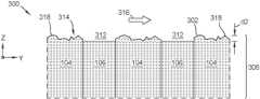
- FIG. 6 Ais a schematic perspective sectional view of a portion of an exemplary polishing pad 600 , according to one or more embodiments described herein.
- FIG. 6 Adepicts a top surface, or polishing surface, 602 of the polishing pad 600 after regenerating the surface texture (e.g., after operation 206 of the method 200 of FIG. 2 ).
- the surface texture of the top surface 602 shown in FIG. 6 Aextends substantially across an entirety of the polishing pad 600 .
- the top surface 602 of the polishing pad 600comprises a plurality of polishing surfaces 604 which define a plurality of channels 606 therebetween. In general, the plurality of channels 606 are used to store and distribute slurry during a polishing process.
- the plurality of channels 606include a plurality of major and minor channels which are aligned substantially orthogonally to each other.
- the major channelsare generally aligned in the direction of the x-axis and formed between adjacent polishing surfaces 604 which are spaced from each other along the y-axis.
- the minor channelsare generally aligned in the direction of the y-axis and formed between adjacent polishing surfaces 604 which are spaced from each other along the x-axis.
- a width 608 of each of the plurality of channels 606is about 100 ⁇ m to about 1000 ⁇ m, such as about 200 ⁇ m to about 800 ⁇ m, such as about 400 ⁇ m to about 600 ⁇ m, such as about 500 ⁇ m.
- a depth 610 of each of the plurality of channels 606 measured from a top of one of the plurality of polishing surfaces 604 to a bottom of an adjacent channel 606is about 10 ⁇ m to about 100 ⁇ m, such as about 20 ⁇ m to about 80 ⁇ m, such as about 40 ⁇ m to about 60 ⁇ m, such as about 50 ⁇ m.
- a width 612 of each of the plurality of polishing surfaces 604is about 200 ⁇ m to about 2000 ⁇ m, such as about 400 ⁇ m to about 1600 ⁇ m, such as about 800 ⁇ m to about 1200 ⁇ m, such as about 1000 ⁇ m.
- FIG. 6 Bis a schematic enlarged top view of a portion of the top surface 602 of the polishing pad 600 shown in FIG. 6 A , according to one embodiment.
- FIG. 6 Bdepicts the top surface 602 of the polishing pad 600 before regenerating the surface texture (e.g., before operation 206 of the method 200 of FIG. 2 ).
- the portion of the polishing pad 600 shown in FIG. 6 Bfeatures a continuous phase of polishing pad material formed of a plurality of first material domains 620 and a second material domain 630 .
- the spatially arranged first material domains 620are interposed between regions of the second material domain 630 .
- Each of the first material domains 620corresponds to one of the plurality of polishing surfaces 604 shown in FIG. 6 A .
- the second material domain 630corresponds to the plurality of channels 606 shown in FIG. 6 A .
- the first material domains 620 and second material domain 630are formed from a plurality of individual sub-domains 622 and sub-domains 632 , respectively. As shown in FIG. 6 B , each sub-domain 622 , 632 has a square sectional shape when viewed from above with a first lateral dimension w 1 and a second lateral dimension w 2 . However, it is contemplated that the sub-domains 622 , 632 may have any desired sectional shape when viewed from above, including irregular shapes.
- the lateral dimensions w 1 and w 2are measured parallel to top the surface 602 , and thus parallel to the supporting surface, of the polishing pad 600 in the x-y plane.
- the lateral dimensions w 1 and w 2are defined by an additive manufacturing process which is described in more detail below. In certain embodiments, the lateral dimensions w 1 and w 2 are about 0.1 ⁇ m or greater, such as about 1 ⁇ m or greater, such as about 1 ⁇ m to about 40 ⁇ m.
- Each sub-domain 622 , 632 depicted in the bitmap image of FIG. 6 Bcorresponds to a single droplet deposited during the additive manufacturing process (described in more detail below). Therefore, each individual sub-domain 622 , 632 has a characteristic material composition associated with a respective droplet, and the material composition may differ from that of one or more adjacent sub-domains 622 , 632 .
- the first and second material domains 620 , 630are formed of different pre-polymer compositions, such as the example pre-polymer compositions set forth in the description of FIG. 8 A , and thus comprise a difference from one another in one or more material properties.
- one or more of the first and second material domainscomprise at least one metal or ceramic material.
- the storage modulus E′ of the first material domains 620 and the second material domain 630are different from one another, and the difference may be measured using a suitable measurement method, such as nanoindentation.
- the plurality of first material domains 620have a relativity low storage modulus E′ and the second material domain 630 has a relatively medium or relativity high storage modulus E′.
- Characterizations of low, medium, and high storage modulus E′ material domains at a temperature of about 30° C. (E′30)are summarized in Table 1.
- compositionsCompositions E′30 ⁇ 100 MPa, (e.g., 100 MPa-500 MPa >500 MPa (e.g., 1 MPa-100 MPa) 500 MPa-3000 MPa)
- a ratio of the storage modulus E′30 between the first material domains 620 and the second material domain 630is more than about 1:2, more than about 1:5, more than about 1:10, more than about 1:50, for example more than about 1:100. In some embodiments, the ratio of the storage modulus E′30 between the first material domains 620 and the second material domain 630 is more than about 1:500, for example more than 1:1000.
- the first material domains 620comprise only low modulus material M 2 such that each of the individual sub-domains 622 within the first material domains 620 has the same material composition. Therefore, the storage modulus E′ of the first material domains 620 is substantially equal to the storage modulus E′ of each individual sub-domain 622 .
- the second material domain 630comprises a mixed modulus composite in which the individual sub-domains 632 have a plurality of different material compositions.
- the second material domain 630comprises blocks of porogen material M 3 interposed between regions having an alternating pattern of high modulus material M 1 and low modulus material M 2 .
- porogenrefers to any pore forming material composition such as a soluble sacrificial material which dissolves upon exposure to a conditioning fluid thus forming a corresponding plurality of pores within the second material domain 630 .
- the porogen material M 3is evacuated with a liquid, such as water.
- the relative density and patterning of each of the individual sub-domains 632determines the overall storage modulus E′ of the second material domain 630 .
- the second material domain 630comprises only high modulus material M 1 .
- FIG. 6 Bonly shows the top layer of the polishing pad 600
- the polishing pad 600may have a structure similar to that of FIG. 1 B , FIG. 1 C or FIG. 1 D .
- the first and second domains 620 , 630may be uniformly stacked between layers in the vertical build plane
- the first and second domains 620 , 630may be intermittently shifted and non-uniformly stacked between layers in the vertical build plane
- one or more low adhesion layersmay be introduced between the first and second domains 620 , 630 at selected depths along the vertical build plane, or combinations thereof.
- the second domain 630is selectively removed while the first domains 620 are substantially retained. Selective removal of the second domain 630 results in the structure shown in FIG. 6 A . It is contemplated that stress may be applied using any apparatus described herein, such as one or more apparatus described with respect to FIGS. 4 A- 4 C .
- FIG. 7 Ais a schematic perspective sectional view of a portion of an exemplary polishing pad 700 , according to one or more embodiments described herein.
- FIG. 7 Adepicts a top surface 702 of the polishing pad 700 after regenerating the surface texture (e.g., after operation 206 of the method 200 of FIG. 2 ).
- the surface texture of the top surface 702 shown in FIG. 7 Aextends substantially across an entirety of the polishing pad 700 .
- the top surface 702 of the polishing pad 700comprises a plurality of polishing surfaces 704 having a plurality of wells 706 defined therein.
- the plurality of wells 706are recessed below the top surface 702 .
- the plurality of wells 706are used to store and distribute slurry during a polishing process.
- the plurality of wells 706have a circular shape when viewed from above.
- the plurality of wells 706may have any desired shape when viewed from above, including irregular shapes.
- the wells 706are rounded at the bottom with gently sloping sides.
- the plurality of wells 706may have any desired sectional profile when viewed from the side, including a flat bottom and/or sides.
- a width 708 of each of the plurality of wells 706is about 100 ⁇ m to about 1000 ⁇ m, such as about 200 ⁇ m to about 800 ⁇ m, such as about 400 ⁇ m to about 600 ⁇ m, such as about 500 ⁇ m.
- a depth 710 of each of the plurality of wells 706 measured from a top of one of the plurality of polishing surfaces 704 to a bottom of an adjacent well 706is about 20 ⁇ m to about 120 ⁇ m, such as about 40 ⁇ m to about 120 ⁇ m, such as about 60 ⁇ m to about 100 ⁇ m, such as about 60 ⁇ m.
- a width 712 of each of the plurality of polishing surfaces 704is about 200 ⁇ m to about 2000 ⁇ m, such as about 400 ⁇ m to about 1600 ⁇ m, such as about 800 ⁇ m to about 1200 ⁇ m, such as about 1000 ⁇ m.
- FIG. 7 Bis a schematic enlarged top view of a portion of the top surface 702 of the polishing pad 700 shown in FIG. 7 A , according to one embodiment.
- FIG. 7 Bdepicts the top surface 702 of the polishing pad 700 before regenerating the surface texture (e.g., before operation 206 of the method 200 of FIG. 2 ).
- the portion of the polishing pad 700 shown in FIG. 7 Bfeatures a continuous polymer phase of polishing pad material formed of a plurality of first material domains 720 and a second material domain 730 .
- the spatially arranged first material domains 720are interposed between regions of the second material domain 730 .
- Each of the first material domains 720corresponds to one of the plurality of wells 706 shown in FIG. 7 A .
- the second material domain 730corresponds to the plurality of polishing surfaces 704 shown in FIG. 7 A .
- the first material domains 720 and second material domain 730are formed from a plurality of individual sub-domains 722 and sub-domains 732 , respectively, which are similar to the sub-domains described with respect to FIG. 6 B . Therefore, corresponding description of the sub-domains 622 , 632 of FIG. 6 B is incorporated herein without limitation.
- the first material domains 720 and the second material domain 730comprise mixed modulus composites in which the individual sub-domains 722 , 732 have a plurality of different material compositions.
- the first material domains 720comprise an alternating pattern of high modulus material M 1 and low modulus material M 2 .
- the second material domain 730comprises blocks of porogen material M 3 interposed between regions of low modulus material M 2 .
- the relative density and patterning of each of the individual sub-domains 722 , 732determines the overall storage modulus E′ of each of the first and second material domains 720 , 730 , respectively.
- the first material domains 720comprise only high modulus material M 1 .
- the high modulus material M 1has a storage modulus of about 1600 MPa measured at room temperature.
- the low modulus material M 2has a storage modulus of about 4 MPa measured at room temperature.
- FIG. 7 Bonly shows the top layer of the polishing pad 700
- the polishing pad 700may have a structure similar to that of FIG. 1 B , FIG. 1 C or FIG. 1 D .
- the first and second domains 720 , 730may be uniformly stacked between layers in the vertical build plane
- the first and second domains 720 , 730may be intermittently shifted and non-uniformly stacked between layers in the vertical build plane
- one or more low adhesion layersmay be introduced between the first and second domains 720 , 730 at selected depths along the vertical build plane, or combinations thereof.
- the first domains 720are selectively removed while the second domain 730 is substantially retained. Selective removal of the first domains 720 results in the structure shown in FIG. 7 A . It is contemplated that stress may be applied using any apparatus described herein, such as one or more apparatus described with respect to FIGS. 4 A- 4 C .
- Each of the polishing pads 600 , 700 described abovehas at least one relativity low storage modulus E′ domain (i.e., domains 620 in FIG. 6 B and domain 730 in FIG. 7 B ) and at least one relativity high storage modulus E′ domain (i.e. domain 630 in FIG. 6 B and domains 720 in FIG. 7 B ).
- the relatively high storage modulus E′ domainis selectively removed during the conditioning process resulting in the structures shown in FIGS. 6 A and 7 A . Consequently, contact asperities formed on the top surfaces 602 , 702 after the conditioning process have a relativity low storage modulus E′ compared to the overall storage modulus E′ of the polishing pad 600 and the polishing pad 700 , respectively.
- a bulk matrix, or scaffolding, of each of the polishing pads 600 , 700can be made relatively more rigid, while a polishing surface thereof can have distinct properties (e.g., relatively low storage modulus E′), compared to the bulk matrix, which are more favorable for contacting and polishing a substrate (e.g., less prone to scratching or causing other polishing pad induced defects).
- FIG. 8 Ais a schematic sectional view of an additive manufacturing system which may be used to form the polishing pads described herein, according to some embodiments.
- the additive manufacturing system 800features a movable manufacturing support 802 , a plurality of dispense heads 804 and 806 disposed above the manufacturing support 802 , a curing source 808 , and a system controller 810 .
- the dispense heads 804 , 806move independently of one another and independently of the manufacturing support 802 during the polishing pad manufacturing process.
- the first and second dispense heads 804 and 806are fluidly coupled to corresponding first and second pre-polymer composition sources 812 and 814 which provide respective first and second pre-polymer compositions.
- the additive manufacturing system 800features a third dispense head (not shown) which is fluidly coupled to a sacrificial material precursor source (e.g., a porogen material) (not shown).
- a sacrificial material precursor sourcee.g., a porogen material
- the additive manufacturing system 800includes as many dispense heads as desired to each dispense a different pre-polymer composition or sacrificial material precursor composition.
- the additive manufacturing system 800further comprises pluralities of dispense heads where two or more dispense heads are configured to dispense the same pre-polymer compositions or sacrificial material precursor compositions.
- each of dispense heads 804 , 806features an array of droplet ejecting nozzles 816 configured to eject droplets 830 , 832 of the respective pre-polymer compositions delivered to the dispense head reservoirs.
- the droplets 830 , 832are ejected towards the manufacturing support and thus onto the manufacturing support 802 or onto a previously formed print layer 818 disposed on the manufacturing support 802 .
- Each of dispense heads 804 , 806is configured to fire (control the ejection of) droplets 830 , 832 from each of the nozzles 816 in a respective geometric array or pattern independently of the firing other nozzles 816 thereof.
- the nozzles 816are independently fired according to a droplet dispense pattern for a print layer to be formed, such as the print layer 824 , as the dispense heads 804 , 806 move relative to the manufacturing support 802 .
- the droplets 830 , 832are at least partially cured by exposure to electromagnetic radiation (e.g., UV radiation 826 ) provided by an electromagnetic radiation source, such as a UV radiation source 808 to form a print layer, such as the partially formed print layer 824 .
- electromagnetic radiatione.g., UV radiation 826
- an electromagnetic radiation sourcesuch as a UV radiation source 808
- the dispensed droplets 830 , 832are exposed to electromagnetic radiation to physically fix the droplet before it spreads to an equilibrium size such as set forth in the description of FIG. 8 B .
- the dispensed droplets 830 , 832are exposed to electromagnetic radiation to at least partially cure the pre-polymer compositions thereof within 1 second or less of the droplet contacting a surface, such as the surface of the manufacturing support 802 or of a previously formed print layer 818 disposed on the manufacturing support 802 .
- fixing a dropletalso desirably fixes the location of dispensed droplet on a surface by preventing the coalescing of the droplet with other droplets disposed adjacent thereto.
- the intermixing of droplets of different pre-polymer compositionsmay be desirably controlled to provide relatively distinct material property transitions between different adjacently disposed material domains.
- one or more transition regions between adjacently disposed different material domains which generally comprise some intermixing of the different precursor compositionshave a width (not shown) of less than about 50 ⁇ m, such as less than about 40 ⁇ m, less than about 30 ⁇ m, less than about 20 ⁇ m, for example less than about 10 ⁇ m. It may be desirable to allow some intermixing to occur between droplets of different adjacently disposed material domains in order to improve adhesion which can inhibit or prevent fracturing from occurring at the interface.
- FIG. 8 Bis a close up cross-sectional view schematically illustrating a droplet 832 disposed on a surface 818 a of a previously formed layer, such as the previously formed layer 818 shown in FIG. 8 A , according to some embodiments.
- a droplet of pre-polymer compositionsuch as the droplet 832 a spreads and reaches an equilibrium contact angle ⁇ with the surface 818 a of a previously formed layer within about one second from the moment in time that the droplet 832 a contacts the surface 818 a .
- the equilibrium contact angle ⁇is a function of at least the material properties of the pre-polymer composition and the energy at the surface 818 a (surface energy) of the previously formed layer (e.g., previously formed layer 818 ). In some embodiments, it is desirable to at least partially cure the dispensed droplet before it reaches an equilibrium size in order to fix the droplets contact angle with the surface 818 a of the previously formed layer. In those embodiments, the fixed droplet's 832 b contact angle ⁇ is greater than the equilibrium contact angle ⁇ of the droplet 832 a of the same pre-polymer composition which was allowed to spread to its equilibrium size.
- At least partially curing the dispensed droplets 830 , 832causes the at least partial polymerization (e.g., the cross-linking) of each of the first and second pre-polymer compositions within the droplets and with adjacently disposed droplets of the same pre-polymer composition to form distinct first and second polymer domains respectively, such as the first and second material domains described herein. Further, at least partially curing the first and second pre-polymer compositions causes the at least partial copolymerization of the first and second pre-polymer compositions at the interfacial regions between adjacently disposed droplets of the first and second pre-polymer compositions.
- the at least partial polymerizatione.g., the cross-linking
- At least partial polymerization of the first and second pre-polymer compositionsretards or substantially prevents the diffusion of pre-polymer components across the interfacial boundary regions of adjoining droplets of different pre-polymer composition allowing for fine control of intermixing therebetween.
- at least partially curing the dispensed droplets 830 , 832causes the at least partial polymerization of the first and second pre-polymer compositions within the droplets, the at least partial co-polymerization of the first and second pre-polymer compositions between adjacently disposed droplets, and the at least partial polymerization or co-polymerization between the droplets 830 , 832 and the at the least partially cured material of the previously formed print layer 818 adjacently disposed there below.
- the first and second pre-polymer compositionseach comprise a mixture of one or more of functional polymers, functional oligomers, functional monomers, reactive diluents, and photoinitiators.
- suitable functional polymerswhich may be used to form one or both of the at least two pre-polymer compositions include multifunctional acrylates including di, tri, tetra, and higher functionality acrylates, such as 1,3,5-triacryloylhexahydro-1,3,5-triazine or trimethylolpropane triacrylate.
- Suitable functional oligomerswhich may be used to form one or both of the at least two pre-polymer compositions include monofunctional and multifunctional oligomers, acrylate oligomers, such as aliphatic urethane acrylate oligomers, aliphatic hexafunctional urethane acrylate oligomers, diacrylate, aliphatic hexafunctional acrylate oligomers, multifunctional urethane acrylate oligomers, aliphatic urethane diacrylate oligomers, aliphatic urethane acrylate oligomers, aliphatic polyester urethane diacrylate blends with aliphatic diacrylate oligomers, or combinations thereof, for example bisphenol-A ethoxylate diacrylate or polybutadiene diacrylate, tetrafunctional acrylated polyester oligomers, and aliphatic polyester based urethane diacrylate oligomers.
- acrylate oligomerssuch as
- Suitable monomerswhich may be used to from one or both of the at least two pre-polymer compositions include both mono-functional monomers and multifunctional monomers.
- Suitable mono-functional monomersinclude tetrahydrofurfuryl acrylate (e.g., SR285 from Sartomer®), tetrahydrofurfuryl methacrylate, vinyl caprolactam, isobornyl acrylate, isobornyl methacrylate, 2-phenoxyethyl acrylate, 2-phenoxyethyl methacrylate, 2-(2-ethoxyethoxy)ethyl acrylate, isooctyl acrylate, isodecyl acrylate, isodecyl methacrylate, lauryl acrylate, lauryl methacrylate, stearyl acrylate, stearyl methacrylate, cyclic trimethylolpropane formal acrylate, 2-[[(Butylamino) carbonyl]oxy]e
- Suitable multifunctional monomersinclude diacrylates or dimethacrylates of diols and polyether diols, such as propoxylated neopentyl glycol diacrylate, 1,6-hexanediol diacrylate, 1,6-hexanediol dimethacrylate, 1,3-butylene glycol diacrylate, 1,3-butylene glycol dimethacrylate 1,4-butanediol diacrylate, 1,4-butanediol dimethacrylate, alkoxylated aliphatic diacrylate (e.g., SR9209A from Sartomer®), diethylene glycol diacrylate, diethylene glycol dimethacrylate, dipropylene glycol diacrylate, tripropylene glycol diacrylate, triethylene glycol dimethacrylate, alkoxylated hexanediol diacrylates, or combinations thereof, for example SR562, SR563, SR564 from Sartomer®.
- the reactive diluents used to form one or more of the at least two different pre-polymer compositionsare least monofunctional, and undergo polymerization when exposed to free radicals, Lewis acids, and/or electromagnetic radiation.
- suitable reactive diluentsinclude monoacrylate, 2-ethylhexyl acrylate, octyldecyl acrylate, cyclic trimethylolpropane formal acrylate, caprolactone acrylate, isobornyl acrylate (IBOA), or alkoxylated lauryl methacrylate.
- suitable photoinitiators used to form one or more of the at least two different pre-polymer compositionsinclude polymeric photoinitiators and/or oligomer photoinitiators, such as benzoin ethers, benzyl ketals, acetyl phenones, alkyl phenones, phosphine oxides, benzophenone compounds and thioxanthone compounds that include an amine synergist, or combinations thereof.
- polymeric photoinitiators and/or oligomer photoinitiatorssuch as benzoin ethers, benzyl ketals, acetyl phenones, alkyl phenones, phosphine oxides, benzophenone compounds and thioxanthone compounds that include an amine synergist, or combinations thereof.
- polishing pad materials formed of the pre-polymer compositions described abovemay include at least one of oligomeric or polymeric segments, compounds, or materials selected from the group consisting of: polyamides, polycarbonates, polyesters, polyether ketones, polyethers, polyoxymethylenes, polyether sulfone, polyetherimides, polyimides, polyolefins, polysiloxanes, polysulfones, polyphenylenes, polyphenylene sulfides, polyurethanes, polystyrene, polyacrylonitriles, polyacrylates, polymethylmethacrylates, polyurethane acrylates, polyester acrylates, polyether acrylates, epoxy acrylates, polycarbonates, polyesters, melamines, polysulfones, polyvinyl materials, acrylonitrile butadiene styrene (ABS), halogenated polymers, block copolymers, and random copolymers thereof, and combinations thereof.
- ABSacrylated poly
- Some embodiments described hereinfurther include pore forming features formed of a sacrificial material (e.g., a water soluble material, such as glycols (e.g., polyethylene glycols), glycol-ethers, and amines).
- a sacrificial materiale.g., a water soluble material, such as glycols (e.g., polyethylene glycols), glycol-ethers, and amines).
- Suitable sacrificial material precursorswhich may be used to form the pore forming features described herein include ethylene glycol, butanediol, dimer diol, propylene glycol-(1,2) and propylene glycol-(1,3), octane-1,8-diol, neopentyl glycol, cyclohexane dimethanol (1,4-bis-hydroxymethylcyclohexane), 2-methyl-1,3-propane diol, glycerine, trimethylolpropane, hexanediol-(1,6), hexanetriol-(1,2,6) butane triol-(1,2,4), trimethylolethane, pentaerythritol, quinitol, mannitol and sorbitol, methylglycoside, also diethylene glycol, triethylene glycol, tetraethylene glycol, polyethylene glycols, dibutylene glycol, polybuty
- the sacrificial material precursorcomprises a water soluble polymer, such as 1-vinyl-2-pyrrolidone, vinylimidazole, polyethylene glycol diacrylate, acrylic acid, sodium styrenesulfonate, Hitenol BC10®, Maxemul 6106®, hydroxyethyl acrylate and [2-(methacryloyloxy)ethyl]trimethylammonium chloride, 3-allyloxy-2-hydroxy-1-propanesulfonic acid sodium, sodium 4-vinylbenzenesulfonate, [2-(methacryloyloxy)ethyl]dimethyl-(3-sulfopropyl)ammonium hydroxide, 2-acrylamido-2-methyl-1-propanesulfonic acid, vinylphosphonic acid, allyltriphenylphosphonium chloride, (vinylbenzyl)trimethylammonium chloride, allyltriphenylphosphonium chloride, (vinylbenzylbenzyl
- the additive manufacturing system 800 shown in FIG. 8 Afurther includes the system controller 810 to direct the operation thereof.
- the system controller 810includes a programmable central processing unit (CPU) 834 which is operable with a memory 835 (e.g., non-volatile memory) and support circuits 836 .
- the support circuits 836are conventionally coupled to the CPU 834 and comprise cache, clock circuits, input/output subsystems, power supplies, and the like, and combinations thereof coupled to the various components of the additive manufacturing system 800 , to facilitate control thereof.
- the CPU 834is one of any form of general purpose computer processor used in an industrial setting, such as a programmable logic controller (PLC), for controlling various components and sub-processors of the additive manufacturing system 800 .
- PLCprogrammable logic controller
- the memory 835coupled to the CPU 834 , is non-transitory and may be one or more of readily available memories such as random access memory (RAM), read only memory (ROM), floppy disk drive, hard disk, or any other form of digital storage, local or remote.
- RAMrandom access memory
- ROMread only memory
- floppy disk drivehard disk
- hard diskany other form of digital storage, local or remote.
- the memory 835is in the form of a computer-readable storage media containing instructions (e.g., non-volatile memory), which when executed by the CPU 834 , facilitates the operation of the manufacturing system 800 .
- the instructions in the memory 835are in the form of a program product such as a program that implements the methods of the present disclosure.
- the program codemay conform to any one of a number of different programming languages.
- the disclosuremay be implemented as a program product stored on computer-readable storage media for use with a computer system.
- the program(s) of the program productdefine functions of the embodiments (including the methods described herein).
- Illustrative computer-readable storage mediainclude, but are not limited to: (i) non-writable storage media (e.g., read-only memory devices within a computer such as CD-ROM disks readable by a CD-ROM drive, flash memory, ROM chips or any type of solid-state non-volatile semiconductor memory) on which information is permanently stored; and (ii) writable storage media (e.g., floppy disks within a diskette drive or hard-disk drive or any type of solid-state random-access semiconductor memory) on which alterable information is stored.
- non-writable storage mediae.g., read-only memory devices within a computer such as CD-ROM disks readable by a CD-ROM drive, flash memory, ROM chips or any type of solid-state non-volatile semiconductor memory
- writable storage mediae.g., floppy disks within a diskette drive or hard-disk drive or any type of solid-state random-access semiconductor memory
- the methods set forth herein, or portions thereof,are performed by one or more application specific integrated circuits (ASICs), field-programmable gate arrays (FPGAs), or other types of hardware implementations.
- ASICsapplication specific integrated circuits
- FPGAsfield-programmable gate arrays
- the polishing pad manufacturing methods set forth hereinare performed by a combination of software routines, ASIC(s), FPGAs and, or, other types of hardware implementations.
- the system controller 810directs the motion of the manufacturing support 802 , the motion of the dispense heads 804 and 806 , the firing of the nozzles 816 to eject droplets of pre-polymer compositions therefrom, and the degree and timing of the curing of the dispensed droplets provided by the UV radiation source 808 .
- the instructions used by the system controller to direct the operation of the manufacturing system 800include droplet dispense patterns for each of the print layers to be formed.
- the droplet dispense patternsare collectively stored in the memory 835 as CAD-compatible digital printing instructions.
- FIG. 9is a flow diagram setting forth a method of forming a print layer of a polishing pad according to one or more embodiments.
- Embodiments of the method 900may be used in combination with one or more of the systems and system operations described herein, such as the additive manufacturing system 800 of FIG. 8 A and the fixed droplets of FIG. 8 B . Further, embodiments of the method 900 may be used to form any one or combination of the 3D printed structures or polishing pads shown and described herein.
- the method 900includes dispensing droplets of a first pre-polymer composition and droplets of a second pre-polymer composition onto a surface of a previously formed print layer according to a predetermined droplet dispense pattern.
- the first pre-polymer compositionis different from the second pre-polymer composition.
- the first pre-polymer compositionincludes one or more monomers or oligomers which are different from the monomers or oligomers used to form the second pre-polymer composition.
- the method 900includes at least partially curing the dispensed droplets of the first pre-polymer composition and the dispensed droplets of the second pre-polymer composition to form a print layer comprising at least portions of one or more first material domains and a plurality of second material domains.
- at least partially curing the dispensed dropletsco-polymerizes the first pre-polymer composition and the second pre-polymer composition at interfacial regions between the one or more first material domains and the plurality of second material domains to form a continuous polymer phase of polishing material.
- the one or more first material domains and the second material domainscomprise a difference in one or more material properties from one another.
- the method 900further includes sequential repetitions of operations 901 and 902 to form a plurality of print layers stacked in the z-direction (i.e., a direction orthogonal to the surface of the manufacturing support or a previously formed print layer disposed thereon).
- the predetermined droplet dispense pattern used to form each print layermay be the same or different as a predetermined droplet dispense pattern used to form a previous print layer disposed there below.
- the method 900further includes dispensing droplets of a sacrificial material or a sacrificial material precursor according to a predetermined droplet dispense pattern to form at least portions of a plurality of spatially arranged pore forming features in one or more sequentially formed print layers.
- the methods described hereinbeneficially provide for the manufacturing of structures (e.g., polishing pads) having controlled and repeatable spatially arranged material domains comprising different material properties therebetween.
- structurese.g., polishing pads
- the ability to spatially arrange material domainsallows for the repeatable and controlled manufacture of structures (e.g., polishing pads) having a surface texture which can be regenerated in situ.
Landscapes
- Engineering & Computer Science (AREA)
- Mechanical Engineering (AREA)
- Chemical & Material Sciences (AREA)
- Materials Engineering (AREA)
- Physics & Mathematics (AREA)
- Optics & Photonics (AREA)
- Manufacturing & Machinery (AREA)
- Plasma & Fusion (AREA)
- Mechanical Treatment Of Semiconductor (AREA)
- Finish Polishing, Edge Sharpening, And Grinding By Specific Grinding Devices (AREA)
Abstract
Description
| TABLE 1 | ||||
| Low Storage | Medium Storage | High Storage | ||
| Modulus | Modulus | Modulus | ||
| Compositions | Compositions | Compositions | ||
| E′30 | <100 MPa, (e.g., | 100 MPa-500 MPa | >500 MPa (e.g., |
| 1 MPa-100 MPa) | 500 MPa-3000 MPa) | ||
Claims (12)
Priority Applications (6)
| Application Number | Priority Date | Filing Date | Title |
|---|---|---|---|
| US17/172,152US11878389B2 (en) | 2021-02-10 | 2021-02-10 | Structures formed using an additive manufacturing process for regenerating surface texture in situ |
| PCT/US2022/013403WO2022173581A1 (en) | 2021-02-10 | 2022-01-21 | Structures formed using an additive manufacturing process for regenerating surface texture in situ |
| KR1020237030540AKR20230142595A (en) | 2021-02-10 | 2022-01-21 | Structures formed using additive manufacturing processes to recreate surface texture in-situ |
| CN202280015948.7ACN116963870A (en) | 2021-02-10 | 2022-01-21 | Structures formed using additive manufacturing processes for in situ re-texturing of surfaces |
| EP22753118.3AEP4291352A4 (en) | 2021-02-10 | 2022-01-21 | Structures formed using an additive manufacturing process for regenerating surface texture in situ |
| TW111103068ATW202245979A (en) | 2021-02-10 | 2022-01-25 | Structures formed using an additive manufacturing process for regenerating surface texture in situ |
Applications Claiming Priority (1)
| Application Number | Priority Date | Filing Date | Title |
|---|---|---|---|
| US17/172,152US11878389B2 (en) | 2021-02-10 | 2021-02-10 | Structures formed using an additive manufacturing process for regenerating surface texture in situ |
Publications (2)
| Publication Number | Publication Date |
|---|---|
| US20220250203A1 US20220250203A1 (en) | 2022-08-11 |
| US11878389B2true US11878389B2 (en) | 2024-01-23 |
Family
ID=82704378
Family Applications (1)
| Application Number | Title | Priority Date | Filing Date |
|---|---|---|---|
| US17/172,152Active2041-10-05US11878389B2 (en) | 2021-02-10 | 2021-02-10 | Structures formed using an additive manufacturing process for regenerating surface texture in situ |
Country Status (6)
| Country | Link |
|---|---|
| US (1) | US11878389B2 (en) |
| EP (1) | EP4291352A4 (en) |
| KR (1) | KR20230142595A (en) |
| CN (1) | CN116963870A (en) |
| TW (1) | TW202245979A (en) |
| WO (1) | WO2022173581A1 (en) |
Families Citing this family (2)
| Publication number | Priority date | Publication date | Assignee | Title |
|---|---|---|---|---|
| US11806829B2 (en)* | 2020-06-19 | 2023-11-07 | Applied Materials, Inc. | Advanced polishing pads and related polishing pad manufacturing methods |
| US20240383092A1 (en)* | 2023-05-16 | 2024-11-21 | Taiwan Semiconductor Manufacturing Company, Ltd. | Polishing tool and method |
Citations (512)
| Publication number | Priority date | Publication date | Assignee | Title |
|---|---|---|---|---|
| US2001911A (en) | 1932-04-21 | 1935-05-21 | Carborundum Co | Abrasive articles |
| US3357598A (en) | 1965-09-21 | 1967-12-12 | Dole Valve Co | Adjustable liquid dispenser |
| US3741116A (en) | 1970-06-25 | 1973-06-26 | American Screen Process Equip | Vacuum belt |
| US4459779A (en) | 1982-09-16 | 1984-07-17 | International Business Machines Corporation | Fixed abrasive grinding media |
| US4575330A (en) | 1984-08-08 | 1986-03-11 | Uvp, Inc. | Apparatus for production of three-dimensional objects by stereolithography |
| US4836832A (en) | 1986-08-11 | 1989-06-06 | Minnesota Mining And Manufacturing Company | Method of preparing coated abrasive having radiation curable binder |
| US4841680A (en) | 1987-08-25 | 1989-06-27 | Rodel, Inc. | Inverted cell pad material for grinding, lapping, shaping and polishing |
| US4844144A (en) | 1988-08-08 | 1989-07-04 | Desoto, Inc. | Investment casting utilizing patterns produced by stereolithography |
| US4942001A (en) | 1988-03-02 | 1990-07-17 | Inc. DeSoto | Method of forming a three-dimensional object by stereolithography and composition therefore |
| US4960673A (en) | 1988-03-17 | 1990-10-02 | Basf Aktiengesellschaft | Photopolymerizable laminate suitable for producing printing plates |
| US5096530A (en) | 1990-06-28 | 1992-03-17 | 3D Systems, Inc. | Resin film recoating method and apparatus |
| US5121329A (en) | 1989-10-30 | 1992-06-09 | Stratasys, Inc. | Apparatus and method for creating three-dimensional objects |
| US5120476A (en) | 1989-12-23 | 1992-06-09 | Basf Aktiengesellschaft | Production of objects |
| US5178646A (en) | 1992-01-22 | 1993-01-12 | Minnesota Mining And Manufacturing Company | Coatable thermally curable binder presursor solutions modified with a reactive diluent, abrasive articles incorporating same, and methods of making said abrasive articles |
| US5193316A (en) | 1991-10-29 | 1993-03-16 | Texas Instruments Incorporated | Semiconductor wafer polishing using a hydrostatic medium |
| US5212910A (en) | 1991-07-09 | 1993-05-25 | Intel Corporation | Composite polishing pad for semiconductor process |
| US5287663A (en) | 1992-01-21 | 1994-02-22 | National Semiconductor Corporation | Polishing pad and method for polishing semiconductor wafers |
| US5300417A (en) | 1991-06-25 | 1994-04-05 | Eastman Kodak Company | Photographic element containing stress absorbing protective layer |
| US5378527A (en) | 1991-02-15 | 1995-01-03 | Toyota Jidosha Kabushiki Kaisha | Carbon film coated glass |
| US5470368A (en) | 1992-12-17 | 1995-11-28 | Minnesota Mining And Manufacturing Company | Reduced viscosity slurries, abrasive articles made therefrom, and methods of making said articles |
| US5533923A (en) | 1995-04-10 | 1996-07-09 | Applied Materials, Inc. | Chemical-mechanical polishing pad providing polishing unformity |
| US5605760A (en) | 1995-08-21 | 1997-02-25 | Rodel, Inc. | Polishing pads |
| US5605499A (en) | 1994-04-27 | 1997-02-25 | Speedfam Company Limited | Flattening method and flattening apparatus of a semiconductor device |
| US5609517A (en) | 1995-11-20 | 1997-03-11 | International Business Machines Corporation | Composite polishing pad |
| US5624303A (en) | 1996-01-22 | 1997-04-29 | Micron Technology, Inc. | Polishing pad and a method for making a polishing pad with covalently bonded particles |
| US5626919A (en) | 1990-03-01 | 1997-05-06 | E. I. Du Pont De Nemours And Company | Solid imaging apparatus and method with coating station |
| US5645471A (en) | 1995-08-11 | 1997-07-08 | Minnesota Mining And Manufacturing Company | Method of texturing a substrate using an abrasive article having multiple abrasive natures |
| US5664986A (en) | 1995-02-15 | 1997-09-09 | Daewoo Electronics Co., Ltd. | Apparatus for polishing a dielectric layer formed on a substrate |
| US5690540A (en) | 1996-02-23 | 1997-11-25 | Micron Technology, Inc. | Spiral grooved polishing pad for chemical-mechanical planarization of semiconductor wafers |
| US5738574A (en) | 1995-10-27 | 1998-04-14 | Applied Materials, Inc. | Continuous processing system for chemical mechanical polishing |
| US5778481A (en) | 1996-02-15 | 1998-07-14 | International Business Machines Corporation | Silicon wafer cleaning and polishing pads |
| US5795218A (en) | 1996-09-30 | 1998-08-18 | Micron Technology, Inc. | Polishing pad with elongated microcolumns |
| US5876268A (en) | 1997-01-03 | 1999-03-02 | Minnesota Mining And Manufacturing Company | Method and article for the production of optical quality surfaces on glass |
| US5876490A (en) | 1996-12-09 | 1999-03-02 | International Business Machines Corporatin | Polish process and slurry for planarization |
| US5888121A (en) | 1997-09-23 | 1999-03-30 | Lsi Logic Corporation | Controlling groove dimensions for enhanced slurry flow |
| US5900164A (en) | 1992-08-19 | 1999-05-04 | Rodel, Inc. | Method for planarizing a semiconductor device surface with polymeric pad containing hollow polymeric microelements |
| US5905099A (en) | 1995-11-06 | 1999-05-18 | Minnesota Mining And Manufacturing Company | Heat-activatable adhesive composition |
| US5906863A (en) | 1994-08-08 | 1999-05-25 | Lombardi; John | Methods for the preparation of reinforced three-dimensional bodies |
| US5910471A (en) | 1997-03-07 | 1999-06-08 | Minnesota Mining And Manufacturing Company | Abrasive article for providing a clear surface finish on glass |
| US5919082A (en) | 1997-08-22 | 1999-07-06 | Micron Technology, Inc. | Fixed abrasive polishing pad |
| US5921855A (en) | 1997-05-15 | 1999-07-13 | Applied Materials, Inc. | Polishing pad having a grooved pattern for use in a chemical mechanical polishing system |
| US5932040A (en) | 1997-10-01 | 1999-08-03 | Bibielle S.P.A. | Method for producing a ring of abrasive elements from which to form a rotary brush |
| US5940674A (en) | 1997-04-09 | 1999-08-17 | Massachusetts Institute Of Technology | Three-dimensional product manufacture using masks |
| US5944583A (en) | 1997-03-17 | 1999-08-31 | International Business Machines Corporation | Composite polish pad for CMP |
| US5951380A (en) | 1996-12-24 | 1999-09-14 | Lg Semicon Co.,Ltd. | Polishing apparatus for a semiconductor wafer |
| US5965460A (en) | 1997-01-29 | 1999-10-12 | Mac Dermid, Incorporated | Polyurethane composition with (meth)acrylate end groups useful in the manufacture of polishing pads |
| US5976000A (en) | 1996-05-28 | 1999-11-02 | Micron Technology, Inc. | Polishing pad with incompressible, highly soluble particles for chemical-mechanical planarization of semiconductor wafers |
| US6017609A (en) | 1996-05-27 | 2000-01-25 | Central Glass Company, Limited | Water-repellent glass plate |
| US6022264A (en) | 1997-02-10 | 2000-02-08 | Rodel Inc. | Polishing pad and methods relating thereto |
| US6029096A (en) | 1997-05-13 | 2000-02-22 | 3D Systems, Inc. | Method and apparatus for identifying surface features associated with selected lamina of a three dimensional object being stereolithographically formed |
| US6036579A (en) | 1997-01-13 | 2000-03-14 | Rodel Inc. | Polymeric polishing pad having photolithographically induced surface patterns(s) and methods relating thereto |
| US6062968A (en) | 1997-04-18 | 2000-05-16 | Cabot Corporation | Polishing pad for a semiconductor substrate |
| US6077581A (en) | 1996-07-31 | 2000-06-20 | Tosoh Corporation | Abrasive shaped article, abrasive disc and polishing method |
| US6090475A (en) | 1996-05-24 | 2000-07-18 | Micron Technology Inc. | Polishing pad, methods of manufacturing and use |
| US6095902A (en) | 1998-09-23 | 2000-08-01 | Rodel Holdings, Inc. | Polyether-polyester polyurethane polishing pads and related methods |
| US6117000A (en) | 1998-07-10 | 2000-09-12 | Cabot Corporation | Polishing pad for a semiconductor substrate |
| US6122564A (en) | 1998-06-30 | 2000-09-19 | Koch; Justin | Apparatus and methods for monitoring and controlling multi-layer laser cladding |
| US6121143A (en) | 1997-09-19 | 2000-09-19 | 3M Innovative Properties Company | Abrasive articles comprising a fluorochemical agent for wafer surface modification |
| US6126532A (en) | 1997-04-18 | 2000-10-03 | Cabot Corporation | Polishing pads for a semiconductor substrate |
| US6176992B1 (en) | 1998-11-03 | 2001-01-23 | Nutool, Inc. | Method and apparatus for electro-chemical mechanical deposition |
| US6206759B1 (en) | 1998-11-30 | 2001-03-27 | Micron Technology, Inc. | Polishing pads and planarizing machines for mechanical or chemical-mechanical planarization of microelectronic-device substrate assemblies, and methods for making and using such pads and machines |
| US6213845B1 (en) | 1999-04-26 | 2001-04-10 | Micron Technology, Inc. | Apparatus for in-situ optical endpointing on web-format planarizing machines in mechanical or chemical-mechanical planarization of microelectronic-device substrate assemblies and methods for making and using same |
| US6228133B1 (en) | 1998-05-01 | 2001-05-08 | 3M Innovative Properties Company | Abrasive articles having abrasive layer bond system derived from solid, dry-coated binder precursor particles having a fusible, radiation curable component |
| US6231942B1 (en) | 1998-01-21 | 2001-05-15 | Trexel, Inc. | Method and apparatus for microcellular polypropylene extrusion, and polypropylene articles produced thereby |
| US6231629B1 (en) | 1997-03-07 | 2001-05-15 | 3M Innovative Properties Company | Abrasive article for providing a clear surface finish on glass |
| US6241596B1 (en) | 2000-01-14 | 2001-06-05 | Applied Materials, Inc. | Method and apparatus for chemical mechanical polishing using a patterned pad |
| US6257973B1 (en) | 1999-11-04 | 2001-07-10 | Norton Company | Coated abrasive discs |
| US20010008830A1 (en) | 1999-04-06 | 2001-07-19 | Applied Materials, Inc. | CMP polishing pad |
| US6267641B1 (en) | 2000-05-19 | 2001-07-31 | Motorola, Inc. | Method of manufacturing a semiconductor component and chemical-mechanical polishing system therefor |
| US6273806B1 (en) | 1997-05-15 | 2001-08-14 | Applied Materials, Inc. | Polishing pad having a grooved pattern for use in a chemical mechanical polishing apparatus |
| US20010020448A1 (en) | 1996-10-02 | 2001-09-13 | Micron Technology, Inc. | Method and apparatus for vaporizing liquid precursors and system for using same |
| US20010029151A1 (en) | 1999-08-31 | 2001-10-11 | Dinesh Chopra | Polishing pads and planarizing machines for mechanical and/or chemical-mechanical planarization of microelectronic substrate assemblies |
| US20010034089A1 (en) | 2000-01-20 | 2001-10-25 | Shunpei Yamazaki | Method of manufacturing a semiconductor device |
| US6309282B1 (en) | 1997-04-04 | 2001-10-30 | Micron Technology, Inc. | Variable abrasive polishing pad for mechanical and chemical-mechanical planarization |
| US6309276B1 (en) | 2000-02-01 | 2001-10-30 | Applied Materials, Inc. | Endpoint monitoring with polishing rate change |
| US20010041511A1 (en) | 2000-01-19 | 2001-11-15 | Lack Craig D. | Printing of polishing pads |
| US6319108B1 (en) | 1999-07-09 | 2001-11-20 | 3M Innovative Properties Company | Metal bond abrasive article comprising porous ceramic abrasive composites and method of using same to abrade a workpiece |
| US6322728B1 (en) | 1998-07-10 | 2001-11-27 | Jeneric/Pentron, Inc. | Mass production of dental restorations by solid free-form fabrication methods |
| US20010046834A1 (en) | 2000-02-28 | 2001-11-29 | Anuradha Ramana | Pad surface texture formed by solid phase droplets |
| US6325706B1 (en) | 1998-10-29 | 2001-12-04 | Lam Research Corporation | Use of zeta potential during chemical mechanical polishing for end point detection |
| US6328634B1 (en) | 1999-05-11 | 2001-12-11 | Rodel Holdings Inc. | Method of polishing |
| US6332832B1 (en) | 1999-04-19 | 2001-12-25 | Rohm Company, Ltd. | CMP polish pad and CMP processing apparatus using the same |
| US6338901B1 (en) | 1999-05-03 | 2002-01-15 | Guardian Industries Corporation | Hydrophobic coating including DLC on substrate |
| US20020016139A1 (en) | 2000-07-25 | 2002-02-07 | Kazuto Hirokawa | Polishing tool and manufacturing method therefor |
| US6361411B1 (en) | 1999-06-21 | 2002-03-26 | Micron Technology, Inc. | Method for conditioning polishing surface |
| US6368184B1 (en) | 2000-01-06 | 2002-04-09 | Advanced Micro Devices, Inc. | Apparatus for determining metal CMP endpoint using integrated polishing pad electrodes |
| US20020058468A1 (en) | 2000-05-03 | 2002-05-16 | Eppert Stanley E. | Semiconductor polishing pad |
| US6390890B1 (en) | 1999-02-06 | 2002-05-21 | Charles J Molnar | Finishing semiconductor wafers with a fixed abrasive finishing element |
| US6399501B2 (en) | 1999-12-13 | 2002-06-04 | Applied Materials, Inc. | Method and apparatus for detecting polishing endpoint with optical monitoring |
| US20020069591A1 (en) | 1999-12-14 | 2002-06-13 | Yancey Paul J. | Method of manufacturing a polymer or polymer/composite polishing pad |
| US20020077036A1 (en) | 1997-04-04 | 2002-06-20 | Roberts John V. H. | Polishing pads and methods relating thereto |
| US20020083577A1 (en) | 2000-12-28 | 2002-07-04 | Hiroo Suzuki | Polishing member and apparatus |
| US6423255B1 (en) | 2000-03-24 | 2002-07-23 | Rainer Hoechsmann | Method for manufacturing a structural part by deposition technique |
| US20020112632A1 (en) | 2001-02-21 | 2002-08-22 | Creo Ltd | Method for supporting sensitive workpieces during processing |
| US6454634B1 (en) | 2000-05-27 | 2002-09-24 | Rodel Holdings Inc. | Polishing pads for chemical mechanical planarization |
| US6477926B1 (en) | 2000-09-15 | 2002-11-12 | Ppg Industries Ohio, Inc. | Polishing pad |
| US20020173248A1 (en) | 1998-10-28 | 2002-11-21 | Doan Trung Tri | Method and apparatus for releasably attaching a polishing pad to a chemical-mechanical planarization machine |
| US6488570B1 (en) | 1997-02-10 | 2002-12-03 | Rodel Holdings Inc. | Method relating to a polishing system having a multi-phase polishing layer |
| US6500053B2 (en) | 1999-01-21 | 2002-12-31 | Rodel Holdings, Inc. | Polishing pads and methods relating thereto |
| US6506097B1 (en) | 2000-01-18 | 2003-01-14 | Applied Materials, Inc. | Optical monitoring in a two-step chemical mechanical polishing process |
| US20030022611A1 (en) | 2000-06-09 | 2003-01-30 | Bartlett Aaron T. | Method for attaching web based polishing materials together on a polishing tool |
| US20030019570A1 (en) | 2001-07-26 | 2003-01-30 | Hsueh-Chung Chen | Polishing pad for a chemical mechanical polishing process |
| US6518162B2 (en) | 2000-09-08 | 2003-02-11 | Sharp Kabushiki Kaisha | Method for manufacturing a semiconductor device |
| US6520834B1 (en) | 2000-08-09 | 2003-02-18 | Micron Technology, Inc. | Methods and apparatuses for analyzing and controlling performance parameters in mechanical and chemical-mechanical planarization of microelectronic substrates |
| US20030056870A1 (en) | 2001-09-21 | 2003-03-27 | Stratasys, Inc. | High-precision modeling filament |
| US6548407B1 (en) | 2000-04-26 | 2003-04-15 | Micron Technology, Inc. | Method and apparatus for controlling chemical interactions during planarization of microelectronic substrates |
| US6569373B2 (en) | 2000-03-13 | 2003-05-27 | Object Geometries Ltd. | Compositions and methods for use in three dimensional model printing |
| US20030113509A1 (en) | 2001-12-13 | 2003-06-19 | 3M Innovative Properties Company | Abrasive article for the deposition and polishing of a conductive material |
| US6585563B1 (en) | 1999-02-04 | 2003-07-01 | Applied Materials, Inc. | In-situ monitoring of linear substrate polishing operations |
| US6586494B2 (en) | 2001-08-08 | 2003-07-01 | Spectra Group Limited, Inc. | Radiation curable inkjet composition |
| US6592443B1 (en) | 2000-08-30 | 2003-07-15 | Micron Technology, Inc. | Method and apparatus for forming and using planarizing pads for mechanical and chemical-mechanical planarization of microelectronic substrates |
| US20030134581A1 (en) | 2002-01-11 | 2003-07-17 | Wang Hsing Maw | Device for chemical mechanical polishing |
| US20030153253A1 (en) | 2001-12-14 | 2003-08-14 | Rodel Nitta Company | Polishing cloth |
| US20030153255A1 (en) | 2000-05-31 | 2003-08-14 | Kou Hasegawa | Abrasive material |
| US20030166381A1 (en) | 2002-02-28 | 2003-09-04 | Samsung Electronics Co., Ltd. | Chemical mechanical polishing slurry and chemical mechanical polishing method using the same |
| US6641463B1 (en) | 1999-02-06 | 2003-11-04 | Beaver Creek Concepts Inc | Finishing components and elements |
| US6641471B1 (en) | 2000-09-19 | 2003-11-04 | Rodel Holdings, Inc | Polishing pad having an advantageous micro-texture and methods relating thereto |
| US20030205325A1 (en) | 2001-12-12 | 2003-11-06 | Lam Research Corporation | Apparatus and method for providing a signal port in a polishing pad for optical endpoint detection |
| US20030220061A1 (en) | 2002-05-23 | 2003-11-27 | Cabot Microelectronics Corporation | Microporous polishing pads |
| US20040003895A1 (en) | 2000-08-14 | 2004-01-08 | Takashi Amano | Abrasive pad for cmp |
| US20040014413A1 (en) | 2002-06-03 | 2004-01-22 | Jsr Corporation | Polishing pad and multi-layer polishing pad |
| US6682402B1 (en) | 1997-04-04 | 2004-01-27 | Rodel Holdings, Inc. | Polishing pads and methods relating thereto |
| US6685548B2 (en) | 2000-06-29 | 2004-02-03 | International Business Machines Corporation | Grooved polishing pads and methods of use |
| US6684704B1 (en) | 2002-09-12 | 2004-02-03 | Psiloquest, Inc. | Measuring the surface properties of polishing pads using ultrasonic reflectance |
| US6692338B1 (en) | 1997-07-23 | 2004-02-17 | Lsi Logic Corporation | Through-pad drainage of slurry during chemical mechanical polishing |
| US20040033758A1 (en) | 2001-12-28 | 2004-02-19 | Wiswesser Andreas Norbert | Polishing pad with window |
| US20040058623A1 (en) | 2002-09-20 | 2004-03-25 | Lam Research Corporation | Polishing media for chemical mechanical planarization (CMP) |
| US20040055223A1 (en) | 2000-12-01 | 2004-03-25 | Koichi Ono | Polishing pad, method of manufacturing the polishing pad, and cushion layer for polishing pad |
| US6719818B1 (en) | 1995-03-28 | 2004-04-13 | Applied Materials, Inc. | Apparatus and method for in-situ endpoint detection for chemical mechanical polishing operations |
| US20040092108A1 (en) | 2002-11-01 | 2004-05-13 | Kouichi Yajima | Method of processing a semiconductor wafer |
| US6736709B1 (en) | 2000-05-27 | 2004-05-18 | Rodel Holdings, Inc. | Grooved polishing pads for chemical mechanical planarization |
| US6736714B2 (en) | 1997-07-30 | 2004-05-18 | Praxair S.T. Technology, Inc. | Polishing silicon wafers |
| US6746225B1 (en) | 1992-11-30 | 2004-06-08 | Bechtel Bwtx Idaho, Llc | Rapid solidification processing system for producing molds, dies and related tooling |
| US6746311B1 (en) | 2000-01-24 | 2004-06-08 | 3M Innovative Properties Company | Polishing pad with release layer |
| US6749714B1 (en) | 1999-03-30 | 2004-06-15 | Nikon Corporation | Polishing body, polisher, polishing method, and method for producing semiconductor device |
| US6749485B1 (en) | 2000-05-27 | 2004-06-15 | Rodel Holdings, Inc. | Hydrolytically stable grooved polishing pads for chemical mechanical planarization |
| US20040126575A1 (en) | 2002-07-26 | 2004-07-01 | Nitto Denko Corporation | Pressure-sensitive adhesive sheet, method for producing the same and method for using the same as well as a multi-layer sheet for use in the pressure-sensitive adhesive sheet and method for producing the same |
| US20040133298A1 (en) | 2002-10-31 | 2004-07-08 | Ehsan Toyserkani | System and method for closed-loop control of laser cladding by powder injection |
| US6773474B2 (en) | 2002-04-19 | 2004-08-10 | 3M Innovative Properties Company | Coated abrasive article |
| US20040154533A1 (en) | 2000-08-28 | 2004-08-12 | Agarwal Vishnu K. | Apparatuses for forming a planarizing pad for planarization of microlectronic substrates |
| US6783436B1 (en) | 2003-04-29 | 2004-08-31 | Rohm And Haas Electronic Materials Cmp Holdings, Inc. | Polishing pad with optimized grooves and method of forming same |
| US20040173946A1 (en) | 2003-03-07 | 2004-09-09 | Rolf Pfeifer | Process for quality control for a powder based layer building up process |
| US20040175451A1 (en) | 2003-03-07 | 2004-09-09 | Tsutomu Maekawa | Three-dimensional laminating molding device |
| US6790883B2 (en) | 2000-05-31 | 2004-09-14 | Jsr Corporation | Composition for polishing pad and polishing pad using the same |
| US20040180611A1 (en) | 2003-02-12 | 2004-09-16 | Hirokazu Tajima | Glass substrate for data recording medium, manufacturing method thereof and polishing pad used in the method |
| US20040187714A1 (en) | 2000-03-13 | 2004-09-30 | Eduardo Napadensky | Compositons and methods for use in three dimensional model printing |
| US6811937B2 (en) | 2001-06-21 | 2004-11-02 | Dsm Desotech, Inc. | Radiation-curable resin composition and rapid prototyping process using the same |
| US6811680B2 (en) | 2001-03-14 | 2004-11-02 | Applied Materials Inc. | Planarization of substrates using electrochemical mechanical polishing |
| US6815570B1 (en) | 2002-05-07 | 2004-11-09 | Uop Llc | Shaped catalysts for transalkylation of aromatics for enhanced xylenes production |
| US20040224616A1 (en) | 2003-04-25 | 2004-11-11 | Jsr Corporation | Polishing pad and chemical mechanical polishing method |
| US6833046B2 (en) | 2000-05-04 | 2004-12-21 | Micron Technology, Inc. | Planarizing machines and methods for mechanical and/or chemical-mechanical planarization of microelectronic-device substrate assemblies |
| US20040266326A1 (en) | 2002-08-08 | 2004-12-30 | Hiroshi Shiho | Method of machining semiconductor wafer-use polishing pad and semiconductor wafer-use polishing pad |
| US20050003189A1 (en) | 2003-05-21 | 2005-01-06 | Bredt James F. | Thermoplastic powder material system for appearance models from 3D prinitng systems |
| US6840843B2 (en) | 2001-03-01 | 2005-01-11 | Cabot Microelectronics Corporation | Method for manufacturing a polishing pad having a compressed translucent region |
| US6843711B1 (en) | 2003-12-11 | 2005-01-18 | Rohm And Haas Electronic Materials Cmp Holdings, Inc | Chemical mechanical polishing pad having a process-dependent groove configuration |
| US6847014B1 (en) | 2001-04-30 | 2005-01-25 | Lam Research Corporation | Method and apparatus for controlling the spatial temperature distribution across the surface of a workpiece support |
| US20050016868A1 (en) | 1998-12-01 | 2005-01-27 | Asm Nutool, Inc. | Electrochemical mechanical planarization process and apparatus |
| US20050020082A1 (en) | 2000-05-27 | 2005-01-27 | Arun Vishwanathan | Polishing pads for chemical mechanical planarization |
| US20050032464A1 (en) | 2003-08-07 | 2005-02-10 | Swisher Robert G. | Polishing pad having edge surface treatment |
| US6855588B1 (en) | 2003-10-07 | 2005-02-15 | United Microelectronics Corp. | Method of fabricating a double gate MOSFET device |
| US6860793B2 (en) | 2000-03-15 | 2005-03-01 | Rohm And Haas Electronic Materials Cmp Holdings, Inc. | Window portion with an adjusted rate of wear |
| US20050062900A1 (en) | 2003-09-19 | 2005-03-24 | Kim Yong Sang | Bracket for liquid crystal display device |
| US6875097B2 (en) | 2003-05-25 | 2005-04-05 | J. G. Systems, Inc. | Fixed abrasive CMP pad with built-in additives |
| US6875096B2 (en) | 2001-08-16 | 2005-04-05 | Skc Co., Ltd. | Chemical mechanical polishing pad having holes and or grooves |
| US20050086869A1 (en) | 2003-08-29 | 2005-04-28 | Moo-Yong Park | Polishing pads including slurry and chemicals thereon and methods of fabricating the same |
| US20050098540A1 (en) | 2003-11-10 | 2005-05-12 | Cabot Microelectronics Corporation | Polishing pad comprising biodegradable polymer |
| US20050101228A1 (en) | 2003-11-10 | 2005-05-12 | Cabot Microelectronics Corporation | Polishing pad comprising biodegradable polymer |
| US20050110853A1 (en) | 2003-10-07 | 2005-05-26 | Fujifilm Electronic Imaging Limited | Providing a surface layer or structure on a substrate |
| US20050112998A1 (en) | 2003-10-30 | 2005-05-26 | Hisanori Matsuo | Polishing apparatus |
| US20050124262A1 (en) | 2003-12-03 | 2005-06-09 | Applied Materials, Inc. | Processing pad assembly with zone control |
| US20050153634A1 (en) | 2004-01-09 | 2005-07-14 | Cabot Microelectronics Corporation | Negative poisson's ratio material-containing CMP polishing pad |
| US20050171224A1 (en) | 2004-02-03 | 2005-08-04 | Kulp Mary J. | Polyurethane polishing pad |
| US20050194681A1 (en) | 2002-05-07 | 2005-09-08 | Yongqi Hu | Conductive pad with high abrasion |
| US20050215177A1 (en) | 2004-03-23 | 2005-09-29 | Cabot Microelectronics Corporation | CMC porous pad with component-filled pores |
| US20050227590A1 (en) | 2004-04-09 | 2005-10-13 | Chien-Min Sung | Fixed abrasive tools and associated methods |
| US6955588B1 (en) | 2004-03-31 | 2005-10-18 | Lam Research Corporation | Method of and platen for controlling removal rate characteristics in chemical mechanical planarization |
| US20050250431A1 (en) | 2004-05-05 | 2005-11-10 | Iv Technologies Co., Ltd. | Single-layer polishing pad and method of producing the same |
| US20050260928A1 (en) | 2002-09-17 | 2005-11-24 | Hyun Huh | Integral polishing pad and manufacturing method thereof |
| US20050260939A1 (en) | 2004-05-18 | 2005-11-24 | Saint-Gobain Abrasives, Inc. | Brazed diamond dressing tool |
| US20050261150A1 (en) | 2004-05-21 | 2005-11-24 | Battelle Memorial Institute, A Part Interest | Reactive fluid systems for removing deposition materials and methods for using same |
| US20050276967A1 (en) | 2002-05-23 | 2005-12-15 | Cabot Microelectronics Corporation | Surface textured microporous polishing pads |
| US20050274627A1 (en) | 2004-06-10 | 2005-12-15 | Cabot Microelectronics Corporation | Electrochemical-mechanical polishing system |
| US20050284536A1 (en) | 2004-06-28 | 2005-12-29 | Sumitomo Rubber Industries, Ltd. | Supplying/removing apparatus of puncture sealant of tire |
| US6984163B2 (en) | 2003-11-25 | 2006-01-10 | Rohm And Haas Electronic Materials Cmp Holdings, Inc. | Polishing pad with high optical transmission window |
| US20060019587A1 (en) | 2004-07-21 | 2006-01-26 | Manish Deopura | Methods for producing in-situ grooves in Chemical Mechanical Planarization (CMP) pads, and novel CMP pad designs |
| US6991528B2 (en) | 2000-02-17 | 2006-01-31 | Applied Materials, Inc. | Conductive polishing article for electrochemical mechanical polishing |
| US20060024434A1 (en) | 2004-07-29 | 2006-02-02 | Hongyu Wang | Manufacturing of polymer-coated particles for chemical mechanical polishing |
| US6998166B2 (en) | 2003-06-17 | 2006-02-14 | Cabot Microelectronics Corporation | Polishing pad with oriented pore structure |
| US20060052040A1 (en) | 2002-10-28 | 2006-03-09 | Cabot Microelectronics Corporation | Method for manufacturing microporous CMP materials having controlled pore size |
| US7018560B2 (en) | 2003-08-05 | 2006-03-28 | Rohm And Haas Electronic Materials Cmp Holdings, Inc. | Composition for polishing semiconductor layers |
| US20060079159A1 (en) | 2004-10-08 | 2006-04-13 | Markus Naujok | Chemical mechanical polish with multi-zone abrasive-containing matrix |
| US20060096179A1 (en) | 2004-11-05 | 2006-05-11 | Cabot Microelectronics Corporation | CMP composition containing surface-modified abrasive particles |
| US7044836B2 (en) | 2003-04-21 | 2006-05-16 | Cabot Microelectronics Corporation | Coated metal oxide particles for CMP |
| US7059950B1 (en) | 2004-12-14 | 2006-06-13 | Rohm And Haas Electronic Materials Cmp Holdings, Inc. | CMP polishing pad having grooves arranged to improve polishing medium utilization |
| US7059949B1 (en) | 2004-12-14 | 2006-06-13 | Rohm And Haas Electronic Materials Cmp Holdings, Inc. | CMP pad having an overlapping stepped groove arrangement |
| US20060125133A1 (en) | 2002-09-17 | 2006-06-15 | Korea Polyol Co., Ltd. | Polishing pad containing embedded liquid microelements and method of manufacturing the same |
| US20060160478A1 (en) | 2005-01-14 | 2006-07-20 | Applied Materials, Inc. | Chemical mechanical polishing pad for controlling polishing slurry distribution |
| US20060189269A1 (en) | 2005-02-18 | 2006-08-24 | Roy Pradip K | Customized polishing pads for CMP and methods of fabrication and use thereof |
| US20060185256A1 (en) | 2005-02-22 | 2006-08-24 | Saint-Gobain Abrasives, Inc. | Rapid tooling system and methods for manufacturing abrasive articles |
| US20060192315A1 (en) | 2005-02-25 | 2006-08-31 | Isaac Farr | Core-shell solid freeform fabrication |
| US7120512B2 (en) | 2003-08-25 | 2006-10-10 | Hewlett-Packard Development Company, L.P. | Method and a system for solid freeform fabricating using non-reactive powder |
| US20060226567A1 (en) | 2005-04-11 | 2006-10-12 | James David B | Method for forming a porous polishing pad |
| US7125318B2 (en) | 2003-11-13 | 2006-10-24 | Rohm And Haas Electronic Materials Cmp Holdings, Inc. | Polishing pad having a groove arrangement for reducing slurry consumption |
| US7132033B2 (en) | 2004-02-27 | 2006-11-07 | Rohm And Haas Electronic Materials Cmp Holdings, Inc. | Method of forming a layered polishing pad |
| US20060252900A1 (en) | 2003-02-24 | 2006-11-09 | Bowman Christopher N | (Meth)arcrylic and (meth)acrylamide monomers, polymerizable compositions, and polymers obtained |
| US20060276109A1 (en) | 2003-03-24 | 2006-12-07 | Roy Pradip K | Customized polishing pads for CMP and methods of fabrication and use thereof |
| US20070009606A1 (en) | 2004-05-12 | 2007-01-11 | Serdy James G | Manufacturing process, such as three dimensional printing, including binding of water-soluble material followed by softening and flowing and forming films of organic-solvent-soluble material |
| US20070007698A1 (en) | 2003-08-27 | 2007-01-11 | Shojiro Sano | Method of producting three-dimensional model |
| US7166017B2 (en) | 2003-09-18 | 2007-01-23 | Kabushiki Kaisha Toshiba | Slurry for CMP, polishing method and method of manufacturing semiconductor device |
| US7169030B1 (en) | 2006-05-25 | 2007-01-30 | Rohm And Haas Electronic Materials Cmp Holdings, Inc. | Chemical mechanical polishing pad |
| US20070032170A1 (en) | 2000-09-29 | 2007-02-08 | Strasbaugh | Polishing pad with built-in optical sensor |
| US20070037486A1 (en) | 2005-08-09 | 2007-02-15 | Kyoung-Moon Kang | Polishing pad, method of manufacturing the polishing pad, and chemical mechanical polishing apparatus comprising the polishing pad |
| US7186322B2 (en) | 2000-03-09 | 2007-03-06 | Sony Corporation | Methods of producing and polishing semiconductor device and polishing apparatus |
| US20070054599A1 (en) | 2002-07-18 | 2007-03-08 | Micron Technology, Inc. | Apparatus and method of controlling the temperature of polishing pads used in planarizing micro-device workpieces |
| US7204742B2 (en) | 2004-03-25 | 2007-04-17 | Cabot Microelectronics Corporation | Polishing pad comprising hydrophobic region and endpoint detection port |
| US20070093185A1 (en) | 2004-08-20 | 2007-04-26 | Micron Technology, Inc. | Polishing liquids for activating and/or conditioning fixed abrasive polishing pads, and associated systems and methods |
| US20070117393A1 (en) | 2005-11-21 | 2007-05-24 | Alexander Tregub | Hardened porous polymer chemical mechanical polishing (CMP) pad |
| US20070128991A1 (en) | 2005-12-07 | 2007-06-07 | Yoon Il-Young | Fixed abrasive polishing pad, method of preparing the same, and chemical mechanical polishing apparatus including the same |
| US20070128874A1 (en) | 2005-11-30 | 2007-06-07 | Jsr Corporation | Chemical mechanical polishing method and method of manufacturing semiconductor device |
| US7234224B1 (en) | 2006-11-03 | 2007-06-26 | Rohm And Haas Electronic Materials Cmp Holdings, Inc. | Curved grooving of polishing pads |
| US20070149096A1 (en) | 2005-12-28 | 2007-06-28 | Jsr Corporation | Chemical mechanical polishing pad and chemical mechanical polishing method |
| US7252871B2 (en) | 2004-06-16 | 2007-08-07 | Rohm And Haas Electronic Materials Cmp Holdings, Inc. | Polishing pad having a pressure relief channel |
| US20070204420A1 (en) | 2006-03-06 | 2007-09-06 | Hornby David M | Polishing pad and method of making |
| US7267607B2 (en) | 2002-10-28 | 2007-09-11 | Cabot Microelectronics Corporation | Transparent microporous materials for CMP |
| US7268173B2 (en) | 2002-06-19 | 2007-09-11 | 3M Innovative Properties Company | Free-radically radiation-curable, solvent-free and printable precursor of a pressure-sensitive adhesive |
| US7267610B1 (en) | 2006-08-30 | 2007-09-11 | Rohm And Haas Electronic Materials Cmp Holdings, Inc. | CMP pad having unevenly spaced grooves |
| US20070212979A1 (en) | 2006-03-09 | 2007-09-13 | Rimpad Tech Ltd. | Composite polishing pad |
| US20070221287A1 (en) | 2004-05-20 | 2007-09-27 | Bridgestone Corporation | Sealing agent injecting apparatus, sealing agent injecting method and sealing pump up apparatus |
| US20070235133A1 (en) | 2006-03-29 | 2007-10-11 | Strasbaugh | Devices and methods for measuring wafer characteristics during semiconductor wafer polishing |
| US20070235904A1 (en) | 2006-04-06 | 2007-10-11 | Saikin Alan H | Method of forming a chemical mechanical polishing pad utilizing laser sintering |
| US20070243795A1 (en) | 2004-06-21 | 2007-10-18 | Ebara Corporation | Polishing Apparatus And Polishing Method |
| US20070269987A1 (en) | 2003-05-09 | 2007-11-22 | Sanyo Chemical Industries, Ltd. | Polishing Liquid for Cmp Process and Polishing Method |
| US7300340B1 (en) | 2006-08-30 | 2007-11-27 | Rohm and Haas Electronics Materials CMP Holdings, Inc. | CMP pad having overlaid constant area spiral grooves |
| US7311590B1 (en) | 2007-01-31 | 2007-12-25 | Rohm And Haas Electronic Materials Cmp Holdings, Inc. | Polishing pad with grooves to retain slurry on the pad texture |
| US20080004743A1 (en) | 2006-06-28 | 2008-01-03 | 3M Innovative Properties Company | Abrasive Articles, CMP Monitoring System and Method |
| US20080009228A1 (en) | 2006-07-10 | 2008-01-10 | Fujitsu Limited | Polishing pad, method for manufacturing the polishing pad, and method for polishing an object |
| US7332104B2 (en) | 2003-06-18 | 2008-02-19 | Kabushiki Kaisha Toshiba | Slurry for CMP, polishing method and method of manufacturing semiconductor device |
| US20080060734A1 (en) | 2004-09-02 | 2008-03-13 | Michael Stehle | Device for Discharging Air and/or Tire Sealant |
| US7357698B2 (en) | 2005-05-24 | 2008-04-15 | Hynix Semiconductor Inc. | Polishing pad and chemical mechanical polishing apparatus using the same |
| US7371160B1 (en) | 2006-12-21 | 2008-05-13 | Rohm And Haas Electronic Materials Cmp Holdings Inc. | Elastomer-modified chemical mechanical polishing pad |
| US7382959B1 (en) | 2006-10-13 | 2008-06-03 | Hrl Laboratories, Llc | Optically oriented three-dimensional polymer microstructures |
| US20080157436A1 (en) | 2001-02-15 | 2008-07-03 | Huntsman Advanced Materials Americas Inc. | Three-dimensional structered printing |
| US20080207100A1 (en) | 2003-03-25 | 2008-08-28 | Roy Pradip K | Customized polishing pads for CMP and methods of fabrication and use thereof |
| US20080220702A1 (en) | 2006-07-03 | 2008-09-11 | Sang Fang Chemical Industry Co., Ltd. | Polishing pad having surface texture |
| US7425172B2 (en) | 2003-03-25 | 2008-09-16 | Nexplanar Corporation | Customized polish pads for chemical mechanical planarization |
| US7427340B2 (en) | 2005-04-08 | 2008-09-23 | Applied Materials, Inc. | Conductive pad |
| US7435165B2 (en) | 2002-10-28 | 2008-10-14 | Cabot Microelectronics Corporation | Transparent microporous materials for CMP |
| US7435161B2 (en) | 2003-06-17 | 2008-10-14 | Cabot Microelectronics Corporation | Multi-layer polishing pad material for CMP |
| US20080255823A1 (en) | 2007-04-10 | 2008-10-16 | Continental Automotive France | System of Automated Creation of a Software Interface |
| US7438636B2 (en) | 2006-12-21 | 2008-10-21 | Rohm And Haas Electronic Materials Cmp Holdings, Inc. | Chemical mechanical polishing pad |
| US20080268760A1 (en) | 2004-11-29 | 2008-10-30 | Rajeev Bajaj | Method and Apparatus for Improved Chemical Mechanical Planarization Pad with Pressure Control and Process Monitor |
| US7445847B2 (en) | 2006-05-25 | 2008-11-04 | Rohm And Haas Electronic Materials Cmp Holdings, Inc. | Chemical mechanical polishing pad |
| US7455571B1 (en) | 2007-06-20 | 2008-11-25 | Rohm And Haas Electronic Materials Cmp Holdings, Inc. | Window polishing pad |
| US20080314878A1 (en) | 2007-06-22 | 2008-12-25 | General Electric Company | Apparatus and method for controlling a machining system |
| US20090011679A1 (en) | 2007-04-06 | 2009-01-08 | Rajeev Bajaj | Method of removal profile modulation in cmp pads |
| US20090053983A1 (en) | 2006-01-25 | 2009-02-26 | Jsr Corporation | Chemical mechanical polishing pad and method for manufacturing same |
| US20090053976A1 (en) | 2005-02-18 | 2009-02-26 | Roy Pradip K | Customized Polishing Pads for CMP and Methods of Fabrication and Use Thereof |
| US7497885B2 (en) | 2006-12-22 | 2009-03-03 | 3M Innovative Properties Company | Abrasive articles with nanoparticulate fillers and method for making and using them |
| US20090081927A1 (en) | 2007-09-21 | 2009-03-26 | Cabot Microelectronics Corporation | Polishing composition and method utilizing abrasive particles treated with an aminosilane |
| US7513818B2 (en) | 2003-10-31 | 2009-04-07 | Applied Materials, Inc. | Polishing endpoint detection system and method using friction sensor |
| US20090093201A1 (en) | 2005-05-17 | 2009-04-09 | Atsushi Kazuno | Polishing pad |
| US7517488B2 (en) | 2006-03-08 | 2009-04-14 | Rohm And Haas Electronic Materials Cmp Holdings, Inc. | Method of forming a chemical mechanical polishing pad utilizing laser sintering |
| US7517277B2 (en) | 2007-08-16 | 2009-04-14 | Rohm And Haas Electronic Materials Cmp Holdings, Inc. | Layered-filament lattice for chemical mechanical polishing |
| US20090094902A1 (en) | 2007-08-28 | 2009-04-16 | Jiaxiang Hou | Grinding Tools that Contain Uniform Distribution of Abrasive Grits and Method of Manufacture Thereof |
| US7520798B2 (en) | 2007-01-31 | 2009-04-21 | Rohm And Haas Electronic Materials Cmp Holdings, Inc. | Polishing pad with grooves to reduce slurry consumption |
| US20090105363A1 (en) | 2000-03-13 | 2009-04-23 | Eduardo Napadensky | Compositions and methods for use in three dimensional model printing |
| US7531117B2 (en) | 2002-06-05 | 2009-05-12 | Ingo Ederer | Method for constructing patterns in a layered manner |
| US20090130956A1 (en) | 2007-11-20 | 2009-05-21 | Ebara Corporation | Polishing apparatus and polishing method |
| US7537446B2 (en) | 2005-04-06 | 2009-05-26 | Rohm And Haas Electronic Materials Cmp Holdings, Inc. | Apparatus for forming a porous reaction injection molded chemical mechanical polishing pad |
| US20090133716A1 (en) | 2007-10-29 | 2009-05-28 | Wai Mun Lee | Methods of post chemical mechanical polishing and wafer cleaning using amidoxime compositions |
| US20090137121A1 (en) | 2007-10-26 | 2009-05-28 | Innopad, Inc. | Three-Dimensional Network in CMP Pad |
| US20090169455A1 (en) | 2004-03-19 | 2009-07-02 | Agfa-Gevaert, N.V. | Ink-jet recording material |
| US20090206065A1 (en) | 2006-06-20 | 2009-08-20 | Jean-Pierre Kruth | Procedure and apparatus for in-situ monitoring and feedback control of selective laser powder processing |
| US7582127B2 (en) | 2004-06-16 | 2009-09-01 | Cabot Microelectronics Corporation | Polishing composition for a tungsten-containing substrate |
| US20090253353A1 (en) | 2004-12-10 | 2009-10-08 | Toyo Tire & Rubber Co., Ltd | Polishing pad |
| US20090270019A1 (en) | 2008-04-29 | 2009-10-29 | Rajeev Bajaj | Polishing pad composition and method of manufacture and use |
| US20090308739A1 (en) | 2008-06-17 | 2009-12-17 | Applied Materials, Inc. | Wafer processing deposition shielding components |
| US20090311955A1 (en) | 2008-03-14 | 2009-12-17 | Nexplanar Corporation | Grooved CMP pad |
| US20090308553A1 (en) | 2006-04-27 | 2009-12-17 | Coatex S.A.S. | Method for Treating Mineral Materials Using Amphoteric Polymers, Mineral Materials Thereby Obtained, and their Usage as an Agent for Reducing the Quantity of Colloids in Manufacturing Paper |
| US7635290B2 (en) | 2007-08-15 | 2009-12-22 | Rohm And Haas Electronic Materials Cmp Holdings, Inc. | Interpenetrating network for chemical mechanical polishing |
| US20090320379A1 (en) | 2006-07-24 | 2009-12-31 | Sung-Min Jun | Chemical Mechanical Polishing Pads Comprising Liquid Organic Material Encapsulated in Polymer Shell and Methods For Producing The Same |
| US20090321979A1 (en) | 2008-06-30 | 2009-12-31 | Seiko Epson Corporation | Method and device for forming three-dimensional model, sheet material processing method, and sheet material processing device |
| US20100009612A1 (en) | 2006-09-06 | 2010-01-14 | Jaehong Park | Polishing pad |
| US20100007692A1 (en) | 2006-12-21 | 2010-01-14 | Agfa Graphics Nv | 3d-inkjet printing methods |
| US7648645B2 (en) | 2006-11-08 | 2010-01-19 | 3M Innovative Properties Company | Pre-polymer formulations for liquid crystal displays |
| US20100011672A1 (en) | 2008-07-16 | 2010-01-21 | Kincaid Don H | Coated abrasive article and method of making and using the same |
| US7652286B2 (en) | 2001-12-28 | 2010-01-26 | Semiconductor Energy Laboratory Co., Ltd. | Semiconductor device and semiconductor device producing system |
| US20100087128A1 (en) | 2007-02-01 | 2010-04-08 | Kuraray Co., Ltd. | Polishing pad, and method for manufacturing polishing pad |
| US20100112919A1 (en) | 2008-11-03 | 2010-05-06 | Applied Materials, Inc. | Monolithic linear polishing sheet |
| US20100120249A1 (en) | 2007-03-27 | 2010-05-13 | Toyo Tire & Rubber Co., Ltd. | Process for producing polyurethane foam |
| US20100120343A1 (en) | 2007-03-20 | 2010-05-13 | Kuraray Co., Ltd. | Cushion for polishing pad and polishing pad using the cushion |
| US20100130112A1 (en) | 2008-11-26 | 2010-05-27 | Rajeev Bajaj | Polishing pad with endpoint window and systems and method using the same |
| US7731568B2 (en) | 2004-03-11 | 2010-06-08 | Toyo Tire & Rubber Co., Ltd. | Polishing pad and semiconductor device manufacturing method |
| US20100140850A1 (en) | 2008-12-04 | 2010-06-10 | Objet Geometries Ltd. | Compositions for 3D printing |
| US20100203815A1 (en) | 2007-09-03 | 2010-08-12 | Rajeev Bajaj | Polishing pad |
| US20100210197A1 (en) | 2007-09-28 | 2010-08-19 | Fujibo Holdings Inc. | Polishing pad |
| US20100221489A1 (en) | 2006-02-23 | 2010-09-02 | Picodeon Ltd Oy | Coating on a glass substrate and a coated glass product |
| US20100255254A1 (en) | 2007-12-31 | 2010-10-07 | Culler Scott R | Plasma treated abrasive article and method of making same |
| US7815778B2 (en) | 2005-11-23 | 2010-10-19 | Semiquest Inc. | Electro-chemical mechanical planarization pad with uniform polish performance |
| US7828634B2 (en) | 2007-08-16 | 2010-11-09 | Rohm And Haas Electronic Materials Cmp Holdings, Inc. | Interconnected-multi-element-lattice polishing pad |
| US7846008B2 (en) | 2004-11-29 | 2010-12-07 | Semiquest Inc. | Method and apparatus for improved chemical mechanical planarization and CMP pad |
| US20100323050A1 (en) | 2007-07-17 | 2010-12-23 | Seiko Epson Corporation | Three-dimensional object forming apparatus and method for forming three dimensional object |
| US20110014858A1 (en) | 2009-07-16 | 2011-01-20 | Cabot Microelectronics Corporation | Grooved cmp polishing pad |
| US20110011217A1 (en) | 2008-03-25 | 2011-01-20 | Yoshihide Kojima | Tire puncture repair apparatus |
| US7875091B2 (en) | 2005-02-22 | 2011-01-25 | Saint-Gobain Abrasives, Inc. | Rapid tooling system and methods for manufacturing abrasive articles |
| US20110045199A1 (en) | 2009-08-20 | 2011-02-24 | Lianhui Cong | Radiation curable ink compositions |
| US20110048772A1 (en) | 2006-03-24 | 2011-03-03 | Clemson University | Conducting polymer ink |
| US20110059247A1 (en) | 2008-05-26 | 2011-03-10 | Sony Corporation | Modeling apparatus and modeling method |
| US7935276B2 (en) | 2006-02-09 | 2011-05-03 | Headwaters Technology Innovation Llc | Polymeric materials incorporating carbon nanostructures |
| US7943681B2 (en) | 2000-11-09 | 2011-05-17 | 3M Innovative Properties Company | Weather resistant, ink jettable, radiation curable, fluid compositions particularly suitable for outdoor applications |
| US20110130077A1 (en) | 2009-05-27 | 2011-06-02 | Brian Litke | Polishing pad, composition for the manufacture thereof, and method of making and using |
| US7976901B2 (en) | 2003-11-25 | 2011-07-12 | Fujibo Holdings, Inc. | Polishing sheet and manufacturing method of elastic plastic foam sheet |
| US20110171890A1 (en) | 2008-08-08 | 2011-07-14 | Kuraray Co., Ltd. | Polishing pad and method for manufacturing the polishing pad |
| US20110183583A1 (en) | 2008-07-18 | 2011-07-28 | Joseph William D | Polishing Pad with Floating Elements and Method of Making and Using the Same |
| US20110204538A1 (en) | 2001-04-20 | 2011-08-25 | Drury Thomas J | Method of manufacturing a foam composition roller brush |
| US8047899B2 (en) | 2007-07-26 | 2011-11-01 | Macronix International Co., Ltd. | Pad and method for chemical mechanical polishing |
| US8053487B2 (en) | 2009-01-30 | 2011-11-08 | The United States Of America As Represented By The Secretary Of The Navy | Multifunctional acrylates used as cross-linkers in dental and biomedical self-etching bonding adhesives |
| US8057282B2 (en) | 2008-12-23 | 2011-11-15 | Rohm And Haas Electronic Materials Cmp Holdings, Inc. | High-rate polishing method |
| US20110277877A1 (en) | 2008-12-11 | 2011-11-17 | Doukas Ag | Device for delivering a gas |
| US20110277789A1 (en) | 2003-08-08 | 2011-11-17 | Entegris, Inc. | Methods and materials for making a monolithic porous pad cast onto a rotatable base |
| US8062103B2 (en) | 2008-12-23 | 2011-11-22 | Rohm And Haas Electronic Materials Cmp Holdings, Inc. | High-rate groove pattern |
| US8067814B2 (en) | 2007-06-01 | 2011-11-29 | Panasonic Corporation | Semiconductor device and method of manufacturing the same |
| US8075372B2 (en) | 2004-09-01 | 2011-12-13 | Cabot Microelectronics Corporation | Polishing pad with microporous regions |
| US8075745B2 (en) | 2004-11-29 | 2011-12-13 | Semiquest Inc. | Electro-method and apparatus for improved chemical mechanical planarization pad with uniform polish performance |
| US8083820B2 (en) | 2006-12-22 | 2011-12-27 | 3M Innovative Properties Company | Structured fixed abrasive articles including surface treated nano-ceria filler, and method for making and using the same |
| US8111603B2 (en) | 2006-09-29 | 2012-02-07 | Hitachi, Ltd. | Optical disk apparatus and its reproducing method |
| US8118641B2 (en) | 2009-03-04 | 2012-02-21 | Rohm And Haas Electronic Materials Cmp Holdings, Inc. | Chemical mechanical polishing pad having window with integral identification feature |
| US8142869B2 (en) | 2007-09-27 | 2012-03-27 | Toyoda Gosei Co., Ltd. | Coated base fabric for airbags |
| US20120094487A1 (en) | 1997-04-30 | 2012-04-19 | 3M Innovative Properties Company | Compositions and methods for modifying a surface suited for semiconductor fabrication |
| US8172648B2 (en) | 2007-12-31 | 2012-05-08 | Innopad, Inc. | Chemical-mechanical planarization pad |
| US20120178845A1 (en) | 2000-03-13 | 2012-07-12 | Eduardo Napadensky | Compositions and methods for use in three dimensional model printing |
| US20120178348A1 (en) | 2006-07-19 | 2012-07-12 | Innopad, Inc. | Polishing pad having micro-grooves on the pad surface |
| US8257545B2 (en) | 2010-09-29 | 2012-09-04 | Rohm And Haas Electronic Materials Cmp Holdings, Inc. | Chemical mechanical polishing pad with light stable polymeric endpoint detection window and method of polishing therewith |
| US8260447B2 (en) | 2008-12-02 | 2012-09-04 | Eos Gmbh Electro Optical Systems | Method of providing an identifiable powder amount and method of manufacturing an object |
| US8292592B2 (en) | 2008-04-02 | 2012-10-23 | United Technologies Corporation | Nosecone bolt access and aerodynamic leakage baffle |
| US20120281334A1 (en) | 2009-12-10 | 2012-11-08 | Sumitomo Osaka Cement Co., Ltd. | Electrostatic chuck apparatus |
| US20120302148A1 (en) | 2011-05-23 | 2012-11-29 | Rajeev Bajaj | Polishing pad with homogeneous body having discrete protrusions thereon |
| US20120315830A1 (en) | 2009-12-30 | 2012-12-13 | 3M Innovative Properties Company | Polishing pads including phase-separated polymer blend and method of making and using the same |
| US8349706B2 (en) | 2003-11-12 | 2013-01-08 | 3M Innovtive Properties Company | Semiconductor surface protecting method |
| US20130012108A1 (en) | 2009-12-22 | 2013-01-10 | Naichao Li | Polishing pad and method of making the same |
| US20130017769A1 (en) | 2010-04-15 | 2013-01-17 | Toyo Tire & Rubber Co., Ltd. | Polishing pad |
| US20130019570A1 (en) | 2010-02-03 | 2013-01-24 | Kaercher Futuretech Gmbh | Apparatus and method for automatically forming and filling containers, in particular water bottles |
| US8377623B2 (en) | 2007-11-27 | 2013-02-19 | 3D Systems, Inc. | Photocurable resin composition for producing three dimensional articles having high clarity |
| US20130052917A1 (en) | 2010-03-19 | 2013-02-28 | Jaehong Park | Polishing apparatus, polishing pad, and polishing information management system |
| US20130048018A1 (en) | 2010-02-22 | 2013-02-28 | Entegris, Inc. | Post-cmp cleaning brush |
| US20130055568A1 (en) | 2010-03-11 | 2013-03-07 | Global Beam Technologies Ag | Method and device for producing a component |
| US20130059506A1 (en) | 2010-05-11 | 2013-03-07 | 3M Innovative Properties Company | Fixed abrasive pad with surfactant for chemical mechanical planarization |
| US8393934B2 (en) | 2006-11-16 | 2013-03-12 | Chien-Min Sung | CMP pad dressers with hybridized abrasive surface and related methods |
| US8398466B2 (en) | 2006-11-16 | 2013-03-19 | Chien-Min Sung | CMP pad conditioners with mosaic abrasive segments and associated methods |
| US8398461B2 (en) | 2009-07-20 | 2013-03-19 | Iv Technologies Co., Ltd. | Polishing method, polishing pad and polishing system |
| US8409976B2 (en) | 2007-02-16 | 2013-04-02 | Nanogram Corporation | Solar cell structures, photovoltaic panels and corresponding processes |
| US20130102231A1 (en) | 2009-12-30 | 2013-04-25 | 3M Innovative Properties Company | Organic particulate loaded polishing pads and method of making and using the same |
| US20130122705A1 (en) | 2008-09-26 | 2013-05-16 | Clarkson University | Abrasive compositions for chemical polishing and methods for using same |
| US20130137350A1 (en) | 2011-11-29 | 2013-05-30 | William C. Allison | Polishing pad with foundation layer and polishing surface layer |
| US20130139851A1 (en) | 2003-10-27 | 2013-06-06 | Applied Materials, Inc. | Post cmp scrubbing of substrates |
| US20130172509A1 (en) | 2010-09-22 | 2013-07-04 | Interfacial Solutions Ip, Llc | Methods of Producing Microfabricated Particles for Composite Materials |
| US20130183824A1 (en) | 2012-01-18 | 2013-07-18 | Samsung Electronics Co., Ltd. | Method of fabricating a semiconductor device |
| US20130212951A1 (en) | 2012-02-20 | 2013-08-22 | Samsung Electronics Co., Ltd. | Polishing pad and method of manufacturing the same |
| US20130231032A1 (en) | 2002-07-24 | 2013-09-05 | Applied Materials, Inc., A Delaware Corporation | Polishing pad with two-section window having recess |
| US20130247477A1 (en) | 2012-03-22 | 2013-09-26 | Rohm And Haas Electronic Materials Cmp Holdings, Inc. | Method Of Manufacturing Chemical Mechanical Polishing Layers Having a Window |
| US8545292B2 (en) | 2009-06-29 | 2013-10-01 | Dic Corporation | Two-component urethane resin composition for polishing pad, polyurethane polishing pad, and method for producing polyurethane polishing pad |
| US8546717B2 (en) | 2009-09-17 | 2013-10-01 | Sciaky, Inc. | Electron beam layer manufacturing |
| US8562389B2 (en) | 2007-06-08 | 2013-10-22 | Applied Materials, Inc. | Thin polishing pad with window and molding process |
| US20130287980A1 (en) | 2011-04-27 | 2013-10-31 | Henkel Corporation | Curable elastomer compositions with low temperature sealing capability |
| US20130283700A1 (en) | 2012-04-25 | 2013-10-31 | Rajeev Bajaj | Printed Chemical Mechanical Polishing Pad |
| US20130307194A1 (en) | 2011-01-26 | 2013-11-21 | Justin Elsey | Device for making an object |
| US20130316081A1 (en) | 2012-05-22 | 2013-11-28 | General Electric Company | System and method for three-dimensional printing |
| US8598523B2 (en) | 2009-11-13 | 2013-12-03 | Sciaky, Inc. | Electron beam layer manufacturing using scanning electron monitored closed loop control |
| US8602851B2 (en) | 2003-06-09 | 2013-12-10 | Rohm And Haas Electronic Materials Cmp Holdings, Inc. | Controlled penetration subpad |
| US20130328228A1 (en) | 2012-06-08 | 2013-12-12 | Makerbot Industries, Llc | Color three dimensional printing |
| US20130327977A1 (en) | 2012-06-11 | 2013-12-12 | Cabot Microelectronics Corporation | Composition and method for polishing molybdenum |
| US20140024216A1 (en) | 2012-07-17 | 2014-01-23 | Matthias Stender | Gst cmp slurries |
| US20140034229A1 (en) | 2005-07-22 | 2014-02-06 | Molecular Imprints, Inc. | Method for Adhering Materials Together |
| US20140048970A1 (en) | 2012-08-16 | 2014-02-20 | Stratasys, Inc. | Draw control for extrusion-based additive manufacturing systems |
| US20140065932A1 (en) | 2011-04-21 | 2014-03-06 | Toyo Tire & Rubber Co., Ltd. | Laminated polishing pad |
| US8684794B2 (en) | 2008-04-11 | 2014-04-01 | Fns Tech Co., Ltd. | Chemical mechanical planarization pad with void network |
| US8690978B2 (en) | 2007-10-01 | 2014-04-08 | Saint-Gobain Abrasives, Inc. | Liquid resin composition for abrasive articles |
| US8702479B2 (en) | 2010-10-15 | 2014-04-22 | Nexplanar Corporation | Polishing pad with multi-modal distribution of pore diameters |
| US20140109784A1 (en) | 2011-06-21 | 2014-04-24 | Agfa Graphics Nv | Curable jettable fluid for making a flexographic printing master |
| US8709114B2 (en) | 2012-03-22 | 2014-04-29 | Rohm And Haas Electronic Materials Cmp Holdings, Inc. | Method of manufacturing chemical mechanical polishing layers |
| US20140117575A1 (en) | 2012-10-29 | 2014-05-01 | Makerbot Industries, Llc | Three-dimensional printer with force detection |
| US20140127973A1 (en) | 2012-09-24 | 2014-05-08 | Ebara Corporation | Polishing method and polishing apparatus |
| US8734206B2 (en) | 2010-03-03 | 2014-05-27 | Samsung Electronics Co., Ltd. | Polishing pad for chemical mechanical polishing process and chemical mechanical polishing apparatus including the same |
| US20140163717A1 (en) | 2012-11-08 | 2014-06-12 | Suman Das | Systems and methods for additive manufacturing and repair of metal components |
| US8784721B2 (en) | 2007-11-27 | 2014-07-22 | Eos Gmbh Electro Optical Systems | Method of manufacturing three-dimensional objects by laser sintering |
| US20140206268A1 (en) | 2013-01-22 | 2014-07-24 | Nexplanar Corporation | Polishing pad having polishing surface with continuous protrusions |
| US8801949B2 (en) | 2011-09-22 | 2014-08-12 | Dow Global Technologies Llc | Method of forming open-network polishing pads |
| US20140230170A1 (en) | 2011-09-26 | 2014-08-21 | Entegris, Inc. | Post-cmp cleaning apparatus and method |
| US20140239527A1 (en) | 2012-12-18 | 2014-08-28 | Dentca, Inc. | Photo-curable resin compositions and method of using the same in three-dimensional printing for manufacturing artificial teeth and denture base |
| US8821214B2 (en) | 2008-06-26 | 2014-09-02 | 3M Innovative Properties Company | Polishing pad with porous elements and method of making and using the same |
| US8845852B2 (en) | 2002-11-27 | 2014-09-30 | Toyo Tire & Rubber Co., Ltd. | Polishing pad and method of producing semiconductor device |
| US8853082B2 (en) | 2009-12-28 | 2014-10-07 | Hitachi Chemical Company, Ltd. | Polishing liquid for CMP and polishing method using the same |
| US20140324206A1 (en) | 2007-04-01 | 2014-10-30 | Stratasys Ltd. | Method and system for three-dimensional fabrication |
| US8888480B2 (en) | 2012-09-05 | 2014-11-18 | Aprecia Pharmaceuticals Company | Three-dimensional printing system and equipment assembly |
| US8894799B2 (en) | 2011-09-22 | 2014-11-25 | Dow Global Technologies Llc | Method of forming layered-open-network polishing pads |
| US20140370788A1 (en) | 2013-06-13 | 2014-12-18 | Cabot Microelectronics Corporation | Low surface roughness polishing pad |
| US20140370214A1 (en) | 2013-06-12 | 2014-12-18 | Fujifilm Corporation | Image formation method, decorative sheet, molding method, decorative sheet molded product, process for producing in-mold molded article, and in-mold molded article |
| US20150024233A1 (en) | 2013-07-19 | 2015-01-22 | The Boeing Company | Quality control of additive manufactured parts |
| US20150031781A1 (en) | 2012-03-08 | 2015-01-29 | Evonik Industries Ag | Additive for adjusting the glass transition temperature of visco-elastic polyurethane soft foams |
| US20150037601A1 (en) | 2013-08-02 | 2015-02-05 | Rolls-Royce Plc | Method of manufacturing a component |
| US20150038066A1 (en) | 2013-07-31 | 2015-02-05 | Nexplanar Corporation | Low density polishing pad |
| US20150045928A1 (en) | 2013-08-07 | 2015-02-12 | Massachusetts Institute Of Technology | Automatic Process Control of Additive Manufacturing Device |
| US20150043122A1 (en) | 2013-08-08 | 2015-02-12 | Kabushiki Kaisha Toshiba | Electrostatic chuck, mount plate support, and manufacturing method of electrostatic chuck |
| US20150044951A1 (en) | 2013-08-10 | 2015-02-12 | Applied Materials, Inc. | Cmp pads having material composition that facilitates controlled conditioning |
| US20150056895A1 (en) | 2013-08-22 | 2015-02-26 | Cabot Microelectronics Corporation | Ultra high void volume polishing pad with closed pore structure |
| US20150056892A1 (en) | 2013-08-22 | 2015-02-26 | Cabot Microelectronics Corporation | Polishing pad with porous interface and solid core, and related apparatus and methods |
| US20150056421A1 (en) | 2012-03-01 | 2015-02-26 | Stratasys Ltd. | Cationic polymerizable compositions and methods of use thereof |
| US8968058B2 (en) | 2011-05-05 | 2015-03-03 | Nexplanar Corporation | Polishing pad with alignment feature |
| US20150061170A1 (en) | 2013-09-02 | 2015-03-05 | Thomas Engel | Method and arrangement for producing a workpiece by using additive manufacturing techniques |
| US20150065020A1 (en) | 2003-03-25 | 2015-03-05 | Pradip K. Roy | Customized polishing pads for cmp and methods of fabrication and use thereof |
| US20150072522A1 (en) | 2013-09-12 | 2015-03-12 | Ubmaterials Inc. | Abrasive particle, polishing slurry, and method of manufacturing semiconductor device using the same |
| US8980749B1 (en) | 2013-10-24 | 2015-03-17 | Rohm And Haas Electronic Materials Cmp Holdings, Inc. | Method for chemical mechanical polishing silicon wafers |
| US20150084238A1 (en) | 2004-08-11 | 2015-03-26 | Cornell Research Foundation, Inc. | Modular fabrication systems and methods |
| US20150089881A1 (en) | 2013-09-30 | 2015-04-02 | Saint-Gobain Ceramics & Plastics, Inc. | Shaped abrasive particles and methods of forming same |
| US9017140B2 (en) | 2010-01-13 | 2015-04-28 | Nexplanar Corporation | CMP pad with local area transparency |
| US20150115490A1 (en) | 2012-04-20 | 2015-04-30 | Eos Gmbh Electro Optical Systems | Method and Divice for Producing Components in a Beam Melting Installation |
| US20150126099A1 (en) | 2013-11-04 | 2015-05-07 | Applied Materials, Inc. | Printed chemical mechanical polishing pad having abrasives therein |
| US9033764B2 (en) | 2010-09-09 | 2015-05-19 | Ngk Insulators, Ltd. | Method of polishing object to be polished |
| US20150159046A1 (en) | 2013-12-09 | 2015-06-11 | Cabot Microelectronics Corporation | Cmp compositions and methods for selective removal of silicon nitride |
| US20150174826A1 (en) | 2013-12-20 | 2015-06-25 | Applied Materials, Inc. | Printed chemical mechanical polishing pad having controlled porosity |
| US9068085B2 (en) | 2009-10-16 | 2015-06-30 | Posco | Radiation curable resin composition, and fingerprint-resistant resin composition containing same |
| US9067298B2 (en) | 2011-11-29 | 2015-06-30 | Nexplanar Corporation | Polishing pad with grooved foundation layer and polishing surface layer |
| US9089943B2 (en) | 2010-01-29 | 2015-07-28 | Ronald Lipson | Composite pads for buffing and polishing painted vehicle body surfaces and other applications |
| US20150216790A1 (en) | 2012-10-11 | 2015-08-06 | Dow Corning Corporation | Aqueous Silicone Polyether Microemulsions |
| US9108291B2 (en) | 2011-09-22 | 2015-08-18 | Dow Global Technologies Llc | Method of forming structured-open-network polishing pads |
| US20150252202A1 (en) | 2012-09-25 | 2015-09-10 | 3M Innovative Properties Company | Radiation curable ink composition |
| US9152340B2 (en) | 2013-05-28 | 2015-10-06 | Netapp, Inc. | System and method for managing and producing a dataset image across multiple storage systems |
| US9152006B2 (en) | 2011-11-30 | 2015-10-06 | Merck Patent Gmbh | Particles for electrophoretic displays |
| US9156124B2 (en) | 2010-07-08 | 2015-10-13 | Nexplanar Corporation | Soft polishing pad for polishing a semiconductor substrate |
| US9162341B2 (en) | 2009-01-27 | 2015-10-20 | Fns Tech Co., Ltd | Chemical-mechanical planarization pad including patterned structural domains |
| US9211628B2 (en) | 2011-01-26 | 2015-12-15 | Nexplanar Corporation | Polishing pad with concentric or approximately concentric polygon groove pattern |
| US9216546B2 (en) | 2013-02-12 | 2015-12-22 | Carbon3D, Inc. | Method and apparatus for three-dimensional fabrication with feed through carrier |
| US20150375361A1 (en) | 2014-06-25 | 2015-12-31 | Rohm And Haas Electronic Materials Cmp Holdings, Inc. | Chemical mechanical polishing method |
| US9259820B2 (en) | 2014-03-28 | 2016-02-16 | Rohm And Haas Electronic Materials Cmp Holdings, Inc. | Chemical mechanical polishing pad with polishing layer and window |
| US9259821B2 (en) | 2014-06-25 | 2016-02-16 | Rohm And Haas Electronic Materials Cmp Holdings, Inc. | Chemical mechanical polishing layer formulation with conditioning tolerance |
| US20160052103A1 (en) | 2014-08-22 | 2016-02-25 | Rohm And Haas Electronic Materials Cmp Holdings, Inc. | Polyurethane polishing pad |
| US20160068996A1 (en) | 2014-09-05 | 2016-03-10 | Applied Materials, Inc. | Susceptor and pre-heat ring for thermal processing of substrates |
| US9308620B2 (en) | 2013-09-18 | 2016-04-12 | Texas Instruments Incorporated | Permeated grooving in CMP polishing pads |
| US20160101500A1 (en) | 2014-10-09 | 2016-04-14 | Applied Materials, Inc. | Chemical mechanical polishing pad with internal channels |
| US9314897B2 (en) | 2014-04-29 | 2016-04-19 | Rohm And Haas Electronic Materials Cmp Holdings, Inc. | Chemical mechanical polishing pad with endpoint detection window |
| US20160107287A1 (en) | 2014-10-17 | 2016-04-21 | Applied Materials, Inc. | Polishing pads produced by an additive manufacturing process |
| US20160107295A1 (en) | 2014-10-17 | 2016-04-21 | Applied Materials, Inc. | Polishing pads produced by an additive manufacturing process |
| US20160107290A1 (en) | 2014-10-17 | 2016-04-21 | Applied Materials, Inc. | Cmp pad construction with composite material properties using additive manufacturing processes |
| US20160107288A1 (en) | 2014-10-17 | 2016-04-21 | Applied Materials, Inc. | Printed chemical mechanical polishing pad |
| US20160107381A1 (en)* | 2014-10-17 | 2016-04-21 | Applied Materials, Inc. | Polishing articles and integrated system and methods for manufacturing chemical mechanical polishing articles |
| US20160114458A1 (en) | 2014-10-17 | 2016-04-28 | Applied Materials, Inc. | Polishing pads produced by an additive manufacturing process |
| US9333620B2 (en) | 2014-04-29 | 2016-05-10 | Rohm And Haas Electronic Materials Cmp Holdings, Inc. | Chemical mechanical polishing pad with clear endpoint detection window |
| US20160136787A1 (en)* | 2014-10-17 | 2016-05-19 | Applied Materials, Inc. | Advanced polishing pad materials and formulations |
| US9352443B2 (en) | 2013-11-13 | 2016-05-31 | Taiwan Semiconductor Manufacturing Co., Ltd. | Platen assembly, chemical-mechanical polisher, and method for polishing substrate |
| US20160176021A1 (en) | 2014-12-18 | 2016-06-23 | Applied Materials, Inc. | Uv curable cmp polishing pad and method of manufacture |
| US9375821B2 (en) | 2011-11-24 | 2016-06-28 | National Taiwan University Of Science And Technology | Electrically assisted chemical-mechanical planarization (EACMP) system and method thereof |
| US9393740B2 (en) | 2014-03-14 | 2016-07-19 | Seiko Epson Corporation | Method of producing three-dimensional structure, apparatus for producing three-dimensional structure, and three-dimensional structure |
| US20160221145A1 (en) | 2015-01-30 | 2016-08-04 | Ping Huang | Low density polishing pad |
| US20160229023A1 (en) | 2013-09-25 | 2016-08-11 | 3M Innovative Properties Company | Multi-layered polishing pads |
| US20160236279A1 (en) | 2013-09-23 | 2016-08-18 | Renishaw Plc | Additive manufacturing apparatus and method |
| US20160252813A1 (en) | 2013-10-30 | 2016-09-01 | Anocoil Corporation | Lithographic Printing Plate Precursors and Coating |
| US20160257856A1 (en) | 2015-03-05 | 2016-09-08 | Cabot Microelectronics Corporation | Polishing composition containing ceria abrasive |
| US20160271869A1 (en) | 2013-10-17 | 2016-09-22 | Luxexcel Holding B.V. | Device for printing a three-dimensional structure |
| US20160279757A1 (en) | 2015-03-26 | 2016-09-29 | Rohm And Haas Electronic Materials Cmp Holdings, Inc. | Polishing pad window |
| US9481069B2 (en) | 2013-11-06 | 2016-11-01 | Taiwan Semiconductor Manufacturing Co., Ltd. | Chemical mechanical polishing apparatus and polishing method using the same |
| US20160346997A1 (en) | 2014-02-10 | 2016-12-01 | President And Fellows Of Harvard College | Three-dimensional (3d) printed composite structure and 3d printable composite ink formulation |
| US20160375546A1 (en) | 2015-06-29 | 2016-12-29 | Iv Technologies Co., Ltd. | Polishing layer of polishing pad and method of forming the same and polishing method |
| US20170036320A1 (en) | 2014-04-17 | 2017-02-09 | Cabot Microelectronics Corporation | Cmp polishing pad with columnar structure and methods related thereto |
| US9587127B2 (en) | 2013-02-06 | 2017-03-07 | Sun Chemical Corporation | Digital printing inks |
| US20170100817A1 (en) | 2014-10-17 | 2017-04-13 | Applied Materials, Inc. | Advanced polishing pads having compositional gradients by use of an additive manufacturing process |
| US9630249B2 (en) | 2013-01-17 | 2017-04-25 | Ehsan Toyserkani | Systems and methods for additive manufacturing of heterogeneous porous structures and structures made therefrom |
| US20170120416A1 (en) | 2015-10-30 | 2017-05-04 | Applied Materials, Inc. | Apparatus and method of forming a polishing article that has a desired zeta potential |
| US20170133252A1 (en)* | 2015-11-06 | 2017-05-11 | Applied Materials, Inc. | Techniques for combining cmp process tracking data with 3d printed cmp consumables |
| US20170148539A1 (en) | 2015-11-20 | 2017-05-25 | Xerox Corporation | Three phase immiscible polymer-metal blends for high conductivty composites |
| US20170151648A1 (en) | 2015-11-30 | 2017-06-01 | Taiwan Semiconductor Manufacturing Co., Ltd. | Polishing pad, method for manufacturing polishing pad, and polishing method |
| US20170173865A1 (en) | 2014-02-10 | 2017-06-22 | Stratasys Ltd. | Composition and method for additive manufacturing of an object |
| US20170182629A1 (en) | 2014-04-03 | 2017-06-29 | 3M Innovative Properties Company | Polishing pads and systems and methods of making and using the same |
| US20170203406A1 (en)* | 2016-01-19 | 2017-07-20 | Applied Materials, Inc. | Porous chemical mechanical polishing pads |
| US20170203408A1 (en)* | 2016-01-19 | 2017-07-20 | Applied Materials, Inc. | Method and apparatus for forming porous advanced polishing pads using an additive manufacturing process |
| US9718129B2 (en) | 2012-12-17 | 2017-08-01 | Arcam Ab | Additive manufacturing method and apparatus |
| US20170239886A1 (en) | 2014-01-23 | 2017-08-24 | Yoshihiro Norikane | Three-dimensional object and method for forming same |
| US20170259499A1 (en) | 2016-03-09 | 2017-09-14 | Applied Materials, Inc. | Pad structure and fabrication methods |
| US20170259396A1 (en)* | 2016-03-09 | 2017-09-14 | Mayu Felicia Yamamura | Correction of fabricated shapes in additive manufacturing |
| US20170274498A1 (en) | 2016-03-24 | 2017-09-28 | Jeonghoon Oh | Textured small pad for chemical mechanical polishing |
| US9868230B2 (en) | 2013-03-14 | 2018-01-16 | Stratasys Ltd. | Polymer based molds and methods of manufacturing there of |
| US20180100075A1 (en) | 2016-10-11 | 2018-04-12 | Xerox Corporation | Curable Ink Composition |
| US20180100074A1 (en) | 2016-10-11 | 2018-04-12 | Xerox Corporation | Ink composition for use in 3d printing |
| US20180100073A1 (en) | 2016-10-11 | 2018-04-12 | Xerox Corporation | Ink composition for use in 3d printing |
| US9951054B2 (en) | 2009-04-23 | 2018-04-24 | Cabot Microelectronics Corporation | CMP porous pad with particles in a polymeric matrix |
| US9950405B2 (en) | 2013-12-30 | 2018-04-24 | Semiconductor Manufacturing International (Beijing) Corporation | Chemical mechanical planarization apparatus and methods |
| US9956314B2 (en) | 2016-01-26 | 2018-05-01 | Modern Ideas LLC | Adhesive for use with bone and bone-like structures |
| US20180158707A1 (en) | 2016-12-02 | 2018-06-07 | Applied Materials, Inc. | Rfid part authentication and tracking of processing components |
| US20180161953A1 (en) | 2016-12-14 | 2018-06-14 | Taiwan Semiconductor Manufacturing Company, Ltd. | Polishing pad and method of using |
| US20180229343A1 (en) | 2017-02-15 | 2018-08-16 | Research & Business Foundation Sungkyunkwan Univer Sity | Chemical mechanical polishing device |
| US20180339397A1 (en) | 2017-05-25 | 2018-11-29 | Applied Materials, Inc. | Fabrication of Polishing Pad by Additive Manufacturing Onto Mold |
| US20180340104A1 (en) | 2015-10-30 | 2018-11-29 | Knauf Insulation Sprl | Improved Binder Compositions and Uses Thereof |
| US20180339447A1 (en) | 2017-05-25 | 2018-11-29 | Applied Materials, Inc. | Correction of fabricated shapes in additive manufacturing using modified edge |
| US20180371276A1 (en) | 2015-10-30 | 2018-12-27 | Konica Minolta, Inc. | Active light ray-curable inkjet ink composition and inkjet recording method |
| US20190030678A1 (en) | 2017-07-26 | 2019-01-31 | Applied Materials, Inc. | Integrated abrasive polishing pads and manufacturing methods |
| US20190039204A1 (en) | 2017-08-07 | 2019-02-07 | Applied Materials, Inc. | Abrasive delivery polishing pads and manufacturing methods thereof |
| US20190047112A1 (en) | 2017-08-04 | 2019-02-14 | Applied Materials, Inc. | Polishing pad with window and manufacturing methods thereof |
| US10245704B2 (en) | 2010-07-02 | 2019-04-02 | 3M Innovative Properties Company | Coated abrasive articles |
| US10406801B2 (en) | 2015-08-21 | 2019-09-10 | Voxel8, Inc. | Calibration and alignment of 3D printing deposition heads |
| US20190299537A1 (en) | 2018-03-30 | 2019-10-03 | Applied Materials, Inc. | Integrating 3d printing into multi-process fabrication schemes |
| US20190337117A1 (en) | 2018-05-07 | 2019-11-07 | Applied Materials, Inc. | Hydrophilic and zeta potential tunable chemical mechanical polishing pads |
| US10483235B2 (en) | 2015-05-08 | 2019-11-19 | Winbond Electronics Corp. | Stacked electronic device and method for fabricating the same |
| US20200070302A1 (en) | 2018-09-04 | 2020-03-05 | Applied Materials, Inc. | Formulations for advanced polishing pads |
| US20200156311A1 (en) | 2017-06-21 | 2020-05-21 | Carbon, Inc. | Method of Additive Manufacturing |
| US20200230781A1 (en) | 2019-01-23 | 2020-07-23 | Applied Materials, Inc. | Polishing pads formed using an additive manufacturing process and methods related thereto |
| US10744714B2 (en) | 2015-04-30 | 2020-08-18 | Hewlett-Packard Development Company, L.P. | Misalignment detection for a 3D printing device |
| US20200299834A1 (en) | 2019-03-19 | 2020-09-24 | Applied Materials, Inc. | Hydrophobic and icephobic coating |
| US20200325353A1 (en) | 2019-04-12 | 2020-10-15 | Applied Materials, Inc. | Anionic polishing pads formed by printing processes |
| US20200353586A1 (en) | 2019-05-07 | 2020-11-12 | Cabot Microelectronics Corporation | Chemical mechanical planarization pads via vat-based production |
| US10876073B2 (en) | 2016-08-09 | 2020-12-29 | Fujimi Incorporated | Composition for surface treatment, and method for surface treatment using the same |
| US20210013014A1 (en) | 2018-05-28 | 2021-01-14 | Applied Materials, Inc. | Process kit with adjustable tuning ring for edge uniformity control |
| US10919123B2 (en) | 2018-02-05 | 2021-02-16 | Applied Materials, Inc. | Piezo-electric end-pointing for 3D printed CMP pads |
| US20210220857A1 (en) | 2012-12-27 | 2021-07-22 | Kateeva, Inc. | Techniques for arrayed printing of a permanent layer with improved speed and accuracy |
- 2021
- 2021-02-10USUS17/172,152patent/US11878389B2/enactiveActive
- 2022
- 2022-01-21EPEP22753118.3Apatent/EP4291352A4/enactivePending
- 2022-01-21WOPCT/US2022/013403patent/WO2022173581A1/ennot_activeCeased
- 2022-01-21CNCN202280015948.7Apatent/CN116963870A/enactivePending
- 2022-01-21KRKR1020237030540Apatent/KR20230142595A/ennot_activeCeased
- 2022-01-25TWTW111103068Apatent/TW202245979A/enunknown
Patent Citations (658)
| Publication number | Priority date | Publication date | Assignee | Title |
|---|---|---|---|---|
| US2001911A (en) | 1932-04-21 | 1935-05-21 | Carborundum Co | Abrasive articles |
| US3357598A (en) | 1965-09-21 | 1967-12-12 | Dole Valve Co | Adjustable liquid dispenser |
| US3741116A (en) | 1970-06-25 | 1973-06-26 | American Screen Process Equip | Vacuum belt |
| US4459779A (en) | 1982-09-16 | 1984-07-17 | International Business Machines Corporation | Fixed abrasive grinding media |
| US4575330A (en) | 1984-08-08 | 1986-03-11 | Uvp, Inc. | Apparatus for production of three-dimensional objects by stereolithography |
| US4575330B1 (en) | 1984-08-08 | 1989-12-19 | ||
| US4836832A (en) | 1986-08-11 | 1989-06-06 | Minnesota Mining And Manufacturing Company | Method of preparing coated abrasive having radiation curable binder |
| US4841680A (en) | 1987-08-25 | 1989-06-27 | Rodel, Inc. | Inverted cell pad material for grinding, lapping, shaping and polishing |
| US4942001A (en) | 1988-03-02 | 1990-07-17 | Inc. DeSoto | Method of forming a three-dimensional object by stereolithography and composition therefore |
| US4960673A (en) | 1988-03-17 | 1990-10-02 | Basf Aktiengesellschaft | Photopolymerizable laminate suitable for producing printing plates |
| US4844144A (en) | 1988-08-08 | 1989-07-04 | Desoto, Inc. | Investment casting utilizing patterns produced by stereolithography |
| US5121329A (en) | 1989-10-30 | 1992-06-09 | Stratasys, Inc. | Apparatus and method for creating three-dimensional objects |
| US5120476A (en) | 1989-12-23 | 1992-06-09 | Basf Aktiengesellschaft | Production of objects |
| US5626919A (en) | 1990-03-01 | 1997-05-06 | E. I. Du Pont De Nemours And Company | Solid imaging apparatus and method with coating station |
| US5096530A (en) | 1990-06-28 | 1992-03-17 | 3D Systems, Inc. | Resin film recoating method and apparatus |
| US5378527A (en) | 1991-02-15 | 1995-01-03 | Toyota Jidosha Kabushiki Kaisha | Carbon film coated glass |
| US5300417A (en) | 1991-06-25 | 1994-04-05 | Eastman Kodak Company | Photographic element containing stress absorbing protective layer |
| US5212910A (en) | 1991-07-09 | 1993-05-25 | Intel Corporation | Composite polishing pad for semiconductor process |
| US5193316A (en) | 1991-10-29 | 1993-03-16 | Texas Instruments Incorporated | Semiconductor wafer polishing using a hydrostatic medium |
| US5287663A (en) | 1992-01-21 | 1994-02-22 | National Semiconductor Corporation | Polishing pad and method for polishing semiconductor wafers |
| US5178646A (en) | 1992-01-22 | 1993-01-12 | Minnesota Mining And Manufacturing Company | Coatable thermally curable binder presursor solutions modified with a reactive diluent, abrasive articles incorporating same, and methods of making said abrasive articles |
| US5900164A (en) | 1992-08-19 | 1999-05-04 | Rodel, Inc. | Method for planarizing a semiconductor device surface with polymeric pad containing hollow polymeric microelements |
| US6746225B1 (en) | 1992-11-30 | 2004-06-08 | Bechtel Bwtx Idaho, Llc | Rapid solidification processing system for producing molds, dies and related tooling |
| US5470368A (en) | 1992-12-17 | 1995-11-28 | Minnesota Mining And Manufacturing Company | Reduced viscosity slurries, abrasive articles made therefrom, and methods of making said articles |
| US5605499A (en) | 1994-04-27 | 1997-02-25 | Speedfam Company Limited | Flattening method and flattening apparatus of a semiconductor device |
| US5906863A (en) | 1994-08-08 | 1999-05-25 | Lombardi; John | Methods for the preparation of reinforced three-dimensional bodies |
| US5932290A (en) | 1994-08-08 | 1999-08-03 | Advanced Ceramics Research | Methods for the preparation of three-dimensional bodies |
| US5664986A (en) | 1995-02-15 | 1997-09-09 | Daewoo Electronics Co., Ltd. | Apparatus for polishing a dielectric layer formed on a substrate |
| US6719818B1 (en) | 1995-03-28 | 2004-04-13 | Applied Materials, Inc. | Apparatus and method for in-situ endpoint detection for chemical mechanical polishing operations |
| US5533923A (en) | 1995-04-10 | 1996-07-09 | Applied Materials, Inc. | Chemical-mechanical polishing pad providing polishing unformity |
| US5645471A (en) | 1995-08-11 | 1997-07-08 | Minnesota Mining And Manufacturing Company | Method of texturing a substrate using an abrasive article having multiple abrasive natures |
| US5605760A (en) | 1995-08-21 | 1997-02-25 | Rodel, Inc. | Polishing pads |
| US5738574A (en) | 1995-10-27 | 1998-04-14 | Applied Materials, Inc. | Continuous processing system for chemical mechanical polishing |
| US5905099A (en) | 1995-11-06 | 1999-05-18 | Minnesota Mining And Manufacturing Company | Heat-activatable adhesive composition |
| US5609517A (en) | 1995-11-20 | 1997-03-11 | International Business Machines Corporation | Composite polishing pad |
| US5624303A (en) | 1996-01-22 | 1997-04-29 | Micron Technology, Inc. | Polishing pad and a method for making a polishing pad with covalently bonded particles |
| US5778481A (en) | 1996-02-15 | 1998-07-14 | International Business Machines Corporation | Silicon wafer cleaning and polishing pads |
| US5690540A (en) | 1996-02-23 | 1997-11-25 | Micron Technology, Inc. | Spiral grooved polishing pad for chemical-mechanical planarization of semiconductor wafers |
| US6090475A (en) | 1996-05-24 | 2000-07-18 | Micron Technology Inc. | Polishing pad, methods of manufacturing and use |
| US6017609A (en) | 1996-05-27 | 2000-01-25 | Central Glass Company, Limited | Water-repellent glass plate |
| US5976000A (en) | 1996-05-28 | 1999-11-02 | Micron Technology, Inc. | Polishing pad with incompressible, highly soluble particles for chemical-mechanical planarization of semiconductor wafers |
| US6077581A (en) | 1996-07-31 | 2000-06-20 | Tosoh Corporation | Abrasive shaped article, abrasive disc and polishing method |
| US5795218A (en) | 1996-09-30 | 1998-08-18 | Micron Technology, Inc. | Polishing pad with elongated microcolumns |
| US5989470A (en) | 1996-09-30 | 1999-11-23 | Micron Technology, Inc. | Method for making polishing pad with elongated microcolumns |
| US20010020448A1 (en) | 1996-10-02 | 2001-09-13 | Micron Technology, Inc. | Method and apparatus for vaporizing liquid precursors and system for using same |
| US5876490A (en) | 1996-12-09 | 1999-03-02 | International Business Machines Corporatin | Polish process and slurry for planarization |
| US5951380A (en) | 1996-12-24 | 1999-09-14 | Lg Semicon Co.,Ltd. | Polishing apparatus for a semiconductor wafer |
| US6155910A (en) | 1997-01-03 | 2000-12-05 | 3M Innovative Properties Company | Method and article for the production of optical quality surfaces on glass |
| US5876268A (en) | 1997-01-03 | 1999-03-02 | Minnesota Mining And Manufacturing Company | Method and article for the production of optical quality surfaces on glass |
| US5989111A (en) | 1997-01-03 | 1999-11-23 | 3M Innovative Properties Company | Method and article for the production of optical quality surfaces on glass |
| US6210254B1 (en) | 1997-01-13 | 2001-04-03 | Rodel Holdings Inc. | Method of manufacturing a polymeric polishing pad having photolithographically induced surface pattern(s) |
| US6036579A (en) | 1997-01-13 | 2000-03-14 | Rodel Inc. | Polymeric polishing pad having photolithographically induced surface patterns(s) and methods relating thereto |
| US5965460A (en) | 1997-01-29 | 1999-10-12 | Mac Dermid, Incorporated | Polyurethane composition with (meth)acrylate end groups useful in the manufacture of polishing pads |
| US6022264A (en) | 1997-02-10 | 2000-02-08 | Rodel Inc. | Polishing pad and methods relating thereto |
| US6488570B1 (en) | 1997-02-10 | 2002-12-03 | Rodel Holdings Inc. | Method relating to a polishing system having a multi-phase polishing layer |
| US6231629B1 (en) | 1997-03-07 | 2001-05-15 | 3M Innovative Properties Company | Abrasive article for providing a clear surface finish on glass |
| US5910471A (en) | 1997-03-07 | 1999-06-08 | Minnesota Mining And Manufacturing Company | Abrasive article for providing a clear surface finish on glass |
| US5944583A (en) | 1997-03-17 | 1999-08-31 | International Business Machines Corporation | Composite polish pad for CMP |
| US6869350B2 (en) | 1997-04-04 | 2005-03-22 | Rohm And Haas Electronic Materials Cmp Holdings, Inc. | Polishing pads and methods relating thereto |
| US6309282B1 (en) | 1997-04-04 | 2001-10-30 | Micron Technology, Inc. | Variable abrasive polishing pad for mechanical and chemical-mechanical planarization |
| US20020077036A1 (en) | 1997-04-04 | 2002-06-20 | Roberts John V. H. | Polishing pads and methods relating thereto |
| US6682402B1 (en) | 1997-04-04 | 2004-01-27 | Rodel Holdings, Inc. | Polishing pads and methods relating thereto |
| US5940674A (en) | 1997-04-09 | 1999-08-17 | Massachusetts Institute Of Technology | Three-dimensional product manufacture using masks |
| US6126532A (en) | 1997-04-18 | 2000-10-03 | Cabot Corporation | Polishing pads for a semiconductor substrate |
| US6062968A (en) | 1997-04-18 | 2000-05-16 | Cabot Corporation | Polishing pad for a semiconductor substrate |
| US20120094487A1 (en) | 1997-04-30 | 2012-04-19 | 3M Innovative Properties Company | Compositions and methods for modifying a surface suited for semiconductor fabrication |
| US6029096A (en) | 1997-05-13 | 2000-02-22 | 3D Systems, Inc. | Method and apparatus for identifying surface features associated with selected lamina of a three dimensional object being stereolithographically formed |
| US6645061B1 (en) | 1997-05-15 | 2003-11-11 | Applied Materials, Inc. | Polishing pad having a grooved pattern for use in chemical mechanical polishing |
| US5921855A (en) | 1997-05-15 | 1999-07-13 | Applied Materials, Inc. | Polishing pad having a grooved pattern for use in a chemical mechanical polishing system |
| US6699115B2 (en) | 1997-05-15 | 2004-03-02 | Applied Materials Inc. | Polishing pad having a grooved pattern for use in a chemical mechanical polishing apparatus |
| US5984769A (en) | 1997-05-15 | 1999-11-16 | Applied Materials, Inc. | Polishing pad having a grooved pattern for use in a chemical mechanical polishing apparatus |
| US20020137450A1 (en) | 1997-05-15 | 2002-09-26 | Applied Materials, Inc., A Delaware Corporation | Polishing pad having a grooved pattern for use in chemical mechanical polishing apparatus |
| US6520847B2 (en) | 1997-05-15 | 2003-02-18 | Applied Materials, Inc. | Polishing pad having a grooved pattern for use in chemical mechanical polishing |
| US6273806B1 (en) | 1997-05-15 | 2001-08-14 | Applied Materials, Inc. | Polishing pad having a grooved pattern for use in a chemical mechanical polishing apparatus |
| US6692338B1 (en) | 1997-07-23 | 2004-02-17 | Lsi Logic Corporation | Through-pad drainage of slurry during chemical mechanical polishing |
| US6736714B2 (en) | 1997-07-30 | 2004-05-18 | Praxair S.T. Technology, Inc. | Polishing silicon wafers |
| US20040106367A1 (en) | 1997-08-22 | 2004-06-03 | Walker Michael A. | Fixed abrasive polishing pad |
| US6254460B1 (en) | 1997-08-22 | 2001-07-03 | Micron Technology, Inc. | Fixed abrasive polishing pad |
| US5919082A (en) | 1997-08-22 | 1999-07-06 | Micron Technology, Inc. | Fixed abrasive polishing pad |
| US6121143A (en) | 1997-09-19 | 2000-09-19 | 3M Innovative Properties Company | Abrasive articles comprising a fluorochemical agent for wafer surface modification |
| US5888121A (en) | 1997-09-23 | 1999-03-30 | Lsi Logic Corporation | Controlling groove dimensions for enhanced slurry flow |
| US5932040A (en) | 1997-10-01 | 1999-08-03 | Bibielle S.P.A. | Method for producing a ring of abrasive elements from which to form a rotary brush |
| US6231942B1 (en) | 1998-01-21 | 2001-05-15 | Trexel, Inc. | Method and apparatus for microcellular polypropylene extrusion, and polypropylene articles produced thereby |
| US6228133B1 (en) | 1998-05-01 | 2001-05-08 | 3M Innovative Properties Company | Abrasive articles having abrasive layer bond system derived from solid, dry-coated binder precursor particles having a fusible, radiation curable component |
| US6122564A (en) | 1998-06-30 | 2000-09-19 | Koch; Justin | Apparatus and methods for monitoring and controlling multi-layer laser cladding |
| US6322728B1 (en) | 1998-07-10 | 2001-11-27 | Jeneric/Pentron, Inc. | Mass production of dental restorations by solid free-form fabrication methods |
| US6117000A (en) | 1998-07-10 | 2000-09-12 | Cabot Corporation | Polishing pad for a semiconductor substrate |
| US6095902A (en) | 1998-09-23 | 2000-08-01 | Rodel Holdings, Inc. | Polyether-polyester polyurethane polishing pads and related methods |
| US20020173248A1 (en) | 1998-10-28 | 2002-11-21 | Doan Trung Tri | Method and apparatus for releasably attaching a polishing pad to a chemical-mechanical planarization machine |
| US6325706B1 (en) | 1998-10-29 | 2001-12-04 | Lam Research Corporation | Use of zeta potential during chemical mechanical polishing for end point detection |
| US6176992B1 (en) | 1998-11-03 | 2001-01-23 | Nutool, Inc. | Method and apparatus for electro-chemical mechanical deposition |
| US6206759B1 (en) | 1998-11-30 | 2001-03-27 | Micron Technology, Inc. | Polishing pads and planarizing machines for mechanical or chemical-mechanical planarization of microelectronic-device substrate assemblies, and methods for making and using such pads and machines |
| US6361832B1 (en) | 1998-11-30 | 2002-03-26 | Micron Technology, Inc. | Polishing pads and planarizing machines for mechanical or chemical-mechanical planarization of microelectronic-device substrate assemblies, and methods for making and using such pads and machines |
| US7425250B2 (en) | 1998-12-01 | 2008-09-16 | Novellus Systems, Inc. | Electrochemical mechanical processing apparatus |
| US20050016868A1 (en) | 1998-12-01 | 2005-01-27 | Asm Nutool, Inc. | Electrochemical mechanical planarization process and apparatus |
| US6500053B2 (en) | 1999-01-21 | 2002-12-31 | Rodel Holdings, Inc. | Polishing pads and methods relating thereto |
| US6585563B1 (en) | 1999-02-04 | 2003-07-01 | Applied Materials, Inc. | In-situ monitoring of linear substrate polishing operations |
| US6796880B2 (en) | 1999-02-04 | 2004-09-28 | Applied Materials, Inc. | Linear polishing sheet with window |
| US20040198185A1 (en) | 1999-02-04 | 2004-10-07 | Redeker Fred C. | Linear polishing sheet with window |
| US20030181137A1 (en) | 1999-02-04 | 2003-09-25 | Applied Materials, Inc., A Delaware Corporation | Linear polishing sheet with window |
| US6991517B2 (en) | 1999-02-04 | 2006-01-31 | Applied Materials Inc. | Linear polishing sheet with window |
| US6641463B1 (en) | 1999-02-06 | 2003-11-04 | Beaver Creek Concepts Inc | Finishing components and elements |
| US6390890B1 (en) | 1999-02-06 | 2002-05-21 | Charles J Molnar | Finishing semiconductor wafers with a fixed abrasive finishing element |
| US6749714B1 (en) | 1999-03-30 | 2004-06-15 | Nikon Corporation | Polishing body, polisher, polishing method, and method for producing semiconductor device |
| US20010008830A1 (en) | 1999-04-06 | 2001-07-19 | Applied Materials, Inc. | CMP polishing pad |
| US6332832B1 (en) | 1999-04-19 | 2001-12-25 | Rohm Company, Ltd. | CMP polish pad and CMP processing apparatus using the same |
| US6213845B1 (en) | 1999-04-26 | 2001-04-10 | Micron Technology, Inc. | Apparatus for in-situ optical endpointing on web-format planarizing machines in mechanical or chemical-mechanical planarization of microelectronic-device substrate assemblies and methods for making and using same |
| US6338901B1 (en) | 1999-05-03 | 2002-01-15 | Guardian Industries Corporation | Hydrophobic coating including DLC on substrate |
| US6328634B1 (en) | 1999-05-11 | 2001-12-11 | Rodel Holdings Inc. | Method of polishing |
| US6361411B1 (en) | 1999-06-21 | 2002-03-26 | Micron Technology, Inc. | Method for conditioning polishing surface |
| US6319108B1 (en) | 1999-07-09 | 2001-11-20 | 3M Innovative Properties Company | Metal bond abrasive article comprising porous ceramic abrasive composites and method of using same to abrade a workpiece |
| US20010029151A1 (en) | 1999-08-31 | 2001-10-11 | Dinesh Chopra | Polishing pads and planarizing machines for mechanical and/or chemical-mechanical planarization of microelectronic substrate assemblies |
| US6257973B1 (en) | 1999-11-04 | 2001-07-10 | Norton Company | Coated abrasive discs |
| US6402604B2 (en) | 1999-11-04 | 2002-06-11 | Saint-Gobain Abrasive Technology Company | Process for the production of coated abrasive discs |
| US6399501B2 (en) | 1999-12-13 | 2002-06-04 | Applied Materials, Inc. | Method and apparatus for detecting polishing endpoint with optical monitoring |
| US6428586B1 (en) | 1999-12-14 | 2002-08-06 | Rodel Holdings Inc. | Method of manufacturing a polymer or polymer/composite polishing pad |
| US20020069591A1 (en) | 1999-12-14 | 2002-06-13 | Yancey Paul J. | Method of manufacturing a polymer or polymer/composite polishing pad |
| US6368184B1 (en) | 2000-01-06 | 2002-04-09 | Advanced Micro Devices, Inc. | Apparatus for determining metal CMP endpoint using integrated polishing pad electrodes |
| US6241596B1 (en) | 2000-01-14 | 2001-06-05 | Applied Materials, Inc. | Method and apparatus for chemical mechanical polishing using a patterned pad |
| US6506097B1 (en) | 2000-01-18 | 2003-01-14 | Applied Materials, Inc. | Optical monitoring in a two-step chemical mechanical polishing process |
| US20010041511A1 (en) | 2000-01-19 | 2001-11-15 | Lack Craig D. | Printing of polishing pads |
| US20010034089A1 (en) | 2000-01-20 | 2001-10-25 | Shunpei Yamazaki | Method of manufacturing a semiconductor device |
| US6746311B1 (en) | 2000-01-24 | 2004-06-08 | 3M Innovative Properties Company | Polishing pad with release layer |
| US6309276B1 (en) | 2000-02-01 | 2001-10-30 | Applied Materials, Inc. | Endpoint monitoring with polishing rate change |
| US6991528B2 (en) | 2000-02-17 | 2006-01-31 | Applied Materials, Inc. | Conductive polishing article for electrochemical mechanical polishing |
| US20010046834A1 (en) | 2000-02-28 | 2001-11-29 | Anuradha Ramana | Pad surface texture formed by solid phase droplets |
| US7186322B2 (en) | 2000-03-09 | 2007-03-06 | Sony Corporation | Methods of producing and polishing semiconductor device and polishing apparatus |
| US7300619B2 (en) | 2000-03-13 | 2007-11-27 | Objet Geometries Ltd. | Compositions and methods for use in three dimensional model printing |
| US20110180952A1 (en) | 2000-03-13 | 2011-07-28 | Eduardo Napadensky | Compositions and methods for use in three dimensional model printing |
| US20110077321A1 (en) | 2000-03-13 | 2011-03-31 | Eduardo Napadensky | Compositions and methods for use in three dimensional model printing |
| US8883392B2 (en) | 2000-03-13 | 2014-11-11 | Stratasys Ltd. | Compositions and methods for use in three dimensional model printing |
| US20090105363A1 (en) | 2000-03-13 | 2009-04-23 | Eduardo Napadensky | Compositions and methods for use in three dimensional model printing |
| US10335994B2 (en) | 2000-03-13 | 2019-07-02 | Stratasys Ltd | Methods for three-dimensional model printing |
| US6569373B2 (en) | 2000-03-13 | 2003-05-27 | Object Geometries Ltd. | Compositions and methods for use in three dimensional model printing |
| US20150123298A1 (en) | 2000-03-13 | 2015-05-07 | Stratasys Ltd. | Compositions and methods for use in three dimensional model printing |
| US20040187714A1 (en) | 2000-03-13 | 2004-09-30 | Eduardo Napadensky | Compositons and methods for use in three dimensional model printing |
| US20120178845A1 (en) | 2000-03-13 | 2012-07-12 | Eduardo Napadensky | Compositions and methods for use in three dimensional model printing |
| US8932511B2 (en) | 2000-03-13 | 2015-01-13 | Stratasys Ltd. | Method of making a composite material by three-dimensional ink-jet printing |
| US20080105818A1 (en) | 2000-03-13 | 2008-05-08 | Avi Cohen | Compositions and methods for use in three dimensional model printing |
| US20150129798A1 (en) | 2000-03-13 | 2015-05-14 | Stratasys Ltd. | Compositions and methods for use in three dimensional model printing |
| US6860793B2 (en) | 2000-03-15 | 2005-03-01 | Rohm And Haas Electronic Materials Cmp Holdings, Inc. | Window portion with an adjusted rate of wear |
| US6423255B1 (en) | 2000-03-24 | 2002-07-23 | Rainer Hoechsmann | Method for manufacturing a structural part by deposition technique |
| US6548407B1 (en) | 2000-04-26 | 2003-04-15 | Micron Technology, Inc. | Method and apparatus for controlling chemical interactions during planarization of microelectronic substrates |
| US20020058468A1 (en) | 2000-05-03 | 2002-05-16 | Eppert Stanley E. | Semiconductor polishing pad |
| US6833046B2 (en) | 2000-05-04 | 2004-12-21 | Micron Technology, Inc. | Planarizing machines and methods for mechanical and/or chemical-mechanical planarization of microelectronic-device substrate assemblies |
| US6267641B1 (en) | 2000-05-19 | 2001-07-31 | Motorola, Inc. | Method of manufacturing a semiconductor component and chemical-mechanical polishing system therefor |
| US6454634B1 (en) | 2000-05-27 | 2002-09-24 | Rodel Holdings Inc. | Polishing pads for chemical mechanical planarization |
| US6582283B2 (en) | 2000-05-27 | 2003-06-24 | Rodel Holdings, Inc. | Polishing pads for chemical mechanical planarization |
| US20050020082A1 (en) | 2000-05-27 | 2005-01-27 | Arun Vishwanathan | Polishing pads for chemical mechanical planarization |
| US6749485B1 (en) | 2000-05-27 | 2004-06-15 | Rodel Holdings, Inc. | Hydrolytically stable grooved polishing pads for chemical mechanical planarization |
| US6736709B1 (en) | 2000-05-27 | 2004-05-18 | Rodel Holdings, Inc. | Grooved polishing pads for chemical mechanical planarization |
| US6860802B1 (en) | 2000-05-27 | 2005-03-01 | Rohm And Haas Electric Materials Cmp Holdings, Inc. | Polishing pads for chemical mechanical planarization |
| US6790883B2 (en) | 2000-05-31 | 2004-09-14 | Jsr Corporation | Composition for polishing pad and polishing pad using the same |
| US20030153255A1 (en) | 2000-05-31 | 2003-08-14 | Kou Hasegawa | Abrasive material |
| US7077879B2 (en) | 2000-05-31 | 2006-07-18 | Jsr Corporation | Composition for polishing pad and polishing pad using the same |
| US20030022611A1 (en) | 2000-06-09 | 2003-01-30 | Bartlett Aaron T. | Method for attaching web based polishing materials together on a polishing tool |
| US6685548B2 (en) | 2000-06-29 | 2004-02-03 | International Business Machines Corporation | Grooved polishing pads and methods of use |
| US20020016139A1 (en) | 2000-07-25 | 2002-02-07 | Kazuto Hirokawa | Polishing tool and manufacturing method therefor |
| US6520834B1 (en) | 2000-08-09 | 2003-02-18 | Micron Technology, Inc. | Methods and apparatuses for analyzing and controlling performance parameters in mechanical and chemical-mechanical planarization of microelectronic substrates |
| US20040003895A1 (en) | 2000-08-14 | 2004-01-08 | Takashi Amano | Abrasive pad for cmp |
| US20040154533A1 (en) | 2000-08-28 | 2004-08-12 | Agarwal Vishnu K. | Apparatuses for forming a planarizing pad for planarization of microlectronic substrates |
| US6592443B1 (en) | 2000-08-30 | 2003-07-15 | Micron Technology, Inc. | Method and apparatus for forming and using planarizing pads for mechanical and chemical-mechanical planarization of microelectronic substrates |
| US7192336B2 (en) | 2000-08-30 | 2007-03-20 | Micron Technology, Inc. | Method and apparatus for forming and using planarizing pads for mechanical and chemical-mechanical planarization of microelectronic substrates |
| US6518162B2 (en) | 2000-09-08 | 2003-02-11 | Sharp Kabushiki Kaisha | Method for manufacturing a semiconductor device |
| US6477926B1 (en) | 2000-09-15 | 2002-11-12 | Ppg Industries Ohio, Inc. | Polishing pad |
| US6641471B1 (en) | 2000-09-19 | 2003-11-04 | Rodel Holdings, Inc | Polishing pad having an advantageous micro-texture and methods relating thereto |
| US20070032170A1 (en) | 2000-09-29 | 2007-02-08 | Strasbaugh | Polishing pad with built-in optical sensor |
| US7943681B2 (en) | 2000-11-09 | 2011-05-17 | 3M Innovative Properties Company | Weather resistant, ink jettable, radiation curable, fluid compositions particularly suitable for outdoor applications |
| US7762870B2 (en) | 2000-12-01 | 2010-07-27 | Toyo Tire & Rubber Co., Ltd | Polishing pad and cushion layer for polishing pad |
| US20040055223A1 (en) | 2000-12-01 | 2004-03-25 | Koichi Ono | Polishing pad, method of manufacturing the polishing pad, and cushion layer for polishing pad |
| US20020083577A1 (en) | 2000-12-28 | 2002-07-04 | Hiroo Suzuki | Polishing member and apparatus |
| US20080157436A1 (en) | 2001-02-15 | 2008-07-03 | Huntsman Advanced Materials Americas Inc. | Three-dimensional structered printing |
| US20020112632A1 (en) | 2001-02-21 | 2002-08-22 | Creo Ltd | Method for supporting sensitive workpieces during processing |
| US6840843B2 (en) | 2001-03-01 | 2005-01-11 | Cabot Microelectronics Corporation | Method for manufacturing a polishing pad having a compressed translucent region |
| US6811680B2 (en) | 2001-03-14 | 2004-11-02 | Applied Materials Inc. | Planarization of substrates using electrochemical mechanical polishing |
| US20110204538A1 (en) | 2001-04-20 | 2011-08-25 | Drury Thomas J | Method of manufacturing a foam composition roller brush |
| US8444890B2 (en) | 2001-04-20 | 2013-05-21 | Hydrofera, Llc | Method of manufacturing a foam composition roller brush |
| US6847014B1 (en) | 2001-04-30 | 2005-01-25 | Lam Research Corporation | Method and apparatus for controlling the spatial temperature distribution across the surface of a workpiece support |
| US6811937B2 (en) | 2001-06-21 | 2004-11-02 | Dsm Desotech, Inc. | Radiation-curable resin composition and rapid prototyping process using the same |
| US20030019570A1 (en) | 2001-07-26 | 2003-01-30 | Hsueh-Chung Chen | Polishing pad for a chemical mechanical polishing process |
| CN1400636A (en) | 2001-07-26 | 2003-03-05 | 联华电子股份有限公司 | Composite polishing pad for polishing semiconductor wafer and manufacturing method thereof |
| US6544373B2 (en) | 2001-07-26 | 2003-04-08 | United Microelectronics Corp. | Polishing pad for a chemical mechanical polishing process |
| US6586494B2 (en) | 2001-08-08 | 2003-07-01 | Spectra Group Limited, Inc. | Radiation curable inkjet composition |
| US6875096B2 (en) | 2001-08-16 | 2005-04-05 | Skc Co., Ltd. | Chemical mechanical polishing pad having holes and or grooves |
| US20030056870A1 (en) | 2001-09-21 | 2003-03-27 | Stratasys, Inc. | High-precision modeling filament |
| US6866807B2 (en) | 2001-09-21 | 2005-03-15 | Stratasys, Inc. | High-precision modeling filament |
| US20030205325A1 (en) | 2001-12-12 | 2003-11-06 | Lam Research Corporation | Apparatus and method for providing a signal port in a polishing pad for optical endpoint detection |
| US6838149B2 (en) | 2001-12-13 | 2005-01-04 | 3M Innovative Properties Company | Abrasive article for the deposition and polishing of a conductive material |
| US20030113509A1 (en) | 2001-12-13 | 2003-06-19 | 3M Innovative Properties Company | Abrasive article for the deposition and polishing of a conductive material |
| US20030153253A1 (en) | 2001-12-14 | 2003-08-14 | Rodel Nitta Company | Polishing cloth |
| US7652286B2 (en) | 2001-12-28 | 2010-01-26 | Semiconductor Energy Laboratory Co., Ltd. | Semiconductor device and semiconductor device producing system |
| US20040033758A1 (en) | 2001-12-28 | 2004-02-19 | Wiswesser Andreas Norbert | Polishing pad with window |
| US20030134581A1 (en) | 2002-01-11 | 2003-07-17 | Wang Hsing Maw | Device for chemical mechanical polishing |
| US20030166381A1 (en) | 2002-02-28 | 2003-09-04 | Samsung Electronics Co., Ltd. | Chemical mechanical polishing slurry and chemical mechanical polishing method using the same |
| US6887137B2 (en) | 2002-02-28 | 2005-05-03 | Samsung Electronics Co., Ltd. | Chemical mechanical polishing slurry and chemical mechanical polishing method using the same |
| US6773474B2 (en) | 2002-04-19 | 2004-08-10 | 3M Innovative Properties Company | Coated abrasive article |
| US6815570B1 (en) | 2002-05-07 | 2004-11-09 | Uop Llc | Shaped catalysts for transalkylation of aromatics for enhanced xylenes production |
| US20050194681A1 (en) | 2002-05-07 | 2005-09-08 | Yongqi Hu | Conductive pad with high abrasion |
| US20030220061A1 (en) | 2002-05-23 | 2003-11-27 | Cabot Microelectronics Corporation | Microporous polishing pads |
| US20040171340A1 (en) | 2002-05-23 | 2004-09-02 | Cabot Microelectronics Corporation | Microporous polishing pads |
| US6935931B2 (en) | 2002-05-23 | 2005-08-30 | Cabot Microelectronics Corporation | Microporous polishing pads |
| US6896593B2 (en) | 2002-05-23 | 2005-05-24 | Cabot Microelectronic Corporation | Microporous polishing pads |
| US20050276967A1 (en) | 2002-05-23 | 2005-12-15 | Cabot Microelectronics Corporation | Surface textured microporous polishing pads |
| US6913517B2 (en) | 2002-05-23 | 2005-07-05 | Cabot Microelectronics Corporation | Microporous polishing pads |
| US20040014413A1 (en) | 2002-06-03 | 2004-01-22 | Jsr Corporation | Polishing pad and multi-layer polishing pad |
| US7531117B2 (en) | 2002-06-05 | 2009-05-12 | Ingo Ederer | Method for constructing patterns in a layered manner |
| US7268173B2 (en) | 2002-06-19 | 2007-09-11 | 3M Innovative Properties Company | Free-radically radiation-curable, solvent-free and printable precursor of a pressure-sensitive adhesive |
| US20070054599A1 (en) | 2002-07-18 | 2007-03-08 | Micron Technology, Inc. | Apparatus and method of controlling the temperature of polishing pads used in planarizing micro-device workpieces |
| US20130231032A1 (en) | 2002-07-24 | 2013-09-05 | Applied Materials, Inc., A Delaware Corporation | Polishing pad with two-section window having recess |
| US20040126575A1 (en) | 2002-07-26 | 2004-07-01 | Nitto Denko Corporation | Pressure-sensitive adhesive sheet, method for producing the same and method for using the same as well as a multi-layer sheet for use in the pressure-sensitive adhesive sheet and method for producing the same |
| US20040266326A1 (en) | 2002-08-08 | 2004-12-30 | Hiroshi Shiho | Method of machining semiconductor wafer-use polishing pad and semiconductor wafer-use polishing pad |
| US6684704B1 (en) | 2002-09-12 | 2004-02-03 | Psiloquest, Inc. | Measuring the surface properties of polishing pads using ultrasonic reflectance |
| US20050260928A1 (en) | 2002-09-17 | 2005-11-24 | Hyun Huh | Integral polishing pad and manufacturing method thereof |
| US7029747B2 (en) | 2002-09-17 | 2006-04-18 | Korea Polyol Co., Ltd. | Integral polishing pad and manufacturing method thereof |
| US7754118B2 (en) | 2002-09-17 | 2010-07-13 | Hyun Huh | Polishing pad containing embedded liquid microelements and method of manufacturing the same |
| US20060125133A1 (en) | 2002-09-17 | 2006-06-15 | Korea Polyol Co., Ltd. | Polishing pad containing embedded liquid microelements and method of manufacturing the same |
| US20040058623A1 (en) | 2002-09-20 | 2004-03-25 | Lam Research Corporation | Polishing media for chemical mechanical planarization (CMP) |
| US7435165B2 (en) | 2002-10-28 | 2008-10-14 | Cabot Microelectronics Corporation | Transparent microporous materials for CMP |
| US7311862B2 (en) | 2002-10-28 | 2007-12-25 | Cabot Microelectronics Corporation | Method for manufacturing microporous CMP materials having controlled pore size |
| US20060052040A1 (en) | 2002-10-28 | 2006-03-09 | Cabot Microelectronics Corporation | Method for manufacturing microporous CMP materials having controlled pore size |
| US7267607B2 (en) | 2002-10-28 | 2007-09-11 | Cabot Microelectronics Corporation | Transparent microporous materials for CMP |
| US20080057845A1 (en) | 2002-10-28 | 2008-03-06 | Cabot Microelectronics Corporation | Method for manufacturing microporous CMP materials having controlled pore size |
| US20040133298A1 (en) | 2002-10-31 | 2004-07-08 | Ehsan Toyserkani | System and method for closed-loop control of laser cladding by powder injection |
| US20040092108A1 (en) | 2002-11-01 | 2004-05-13 | Kouichi Yajima | Method of processing a semiconductor wafer |
| US8845852B2 (en) | 2002-11-27 | 2014-09-30 | Toyo Tire & Rubber Co., Ltd. | Polishing pad and method of producing semiconductor device |
| US20040180611A1 (en) | 2003-02-12 | 2004-09-16 | Hirokazu Tajima | Glass substrate for data recording medium, manufacturing method thereof and polishing pad used in the method |
| US20060252900A1 (en) | 2003-02-24 | 2006-11-09 | Bowman Christopher N | (Meth)arcrylic and (meth)acrylamide monomers, polymerizable compositions, and polymers obtained |
| US20040173946A1 (en) | 2003-03-07 | 2004-09-09 | Rolf Pfeifer | Process for quality control for a powder based layer building up process |
| US20040175451A1 (en) | 2003-03-07 | 2004-09-09 | Tsutomu Maekawa | Three-dimensional laminating molding device |
| US20060276109A1 (en) | 2003-03-24 | 2006-12-07 | Roy Pradip K | Customized polishing pads for CMP and methods of fabrication and use thereof |
| US7704125B2 (en) | 2003-03-24 | 2010-04-27 | Nexplanar Corporation | Customized polishing pads for CMP and methods of fabrication and use thereof |
| US20150065020A1 (en) | 2003-03-25 | 2015-03-05 | Pradip K. Roy | Customized polishing pads for cmp and methods of fabrication and use thereof |
| US7704122B2 (en) | 2003-03-25 | 2010-04-27 | Nexplanar Corporation | Customized polish pads for chemical mechanical planarization |
| US10220487B2 (en) | 2003-03-25 | 2019-03-05 | Cabot Microelectronics Corporation | Customized polishing pads for CMP and methods of fabrication and use thereof |
| US8380339B2 (en) | 2003-03-25 | 2013-02-19 | Nexplanar Corporation | Customized polish pads for chemical mechanical planarization |
| US9278424B2 (en) | 2003-03-25 | 2016-03-08 | Nexplanar Corporation | Customized polishing pads for CMP and methods of fabrication and use thereof |
| US20080207100A1 (en) | 2003-03-25 | 2008-08-28 | Roy Pradip K | Customized polishing pads for CMP and methods of fabrication and use thereof |
| US8864859B2 (en) | 2003-03-25 | 2014-10-21 | Nexplanar Corporation | Customized polishing pads for CMP and methods of fabrication and use thereof |
| US7425172B2 (en) | 2003-03-25 | 2008-09-16 | Nexplanar Corporation | Customized polish pads for chemical mechanical planarization |
| US7044836B2 (en) | 2003-04-21 | 2006-05-16 | Cabot Microelectronics Corporation | Coated metal oxide particles for CMP |
| US20040224616A1 (en) | 2003-04-25 | 2004-11-11 | Jsr Corporation | Polishing pad and chemical mechanical polishing method |
| US6783436B1 (en) | 2003-04-29 | 2004-08-31 | Rohm And Haas Electronic Materials Cmp Holdings, Inc. | Polishing pad with optimized grooves and method of forming same |
| US20070269987A1 (en) | 2003-05-09 | 2007-11-22 | Sanyo Chemical Industries, Ltd. | Polishing Liquid for Cmp Process and Polishing Method |
| US20050003189A1 (en) | 2003-05-21 | 2005-01-06 | Bredt James F. | Thermoplastic powder material system for appearance models from 3D prinitng systems |
| US6875097B2 (en) | 2003-05-25 | 2005-04-05 | J. G. Systems, Inc. | Fixed abrasive CMP pad with built-in additives |
| US8602851B2 (en) | 2003-06-09 | 2013-12-10 | Rohm And Haas Electronic Materials Cmp Holdings, Inc. | Controlled penetration subpad |
| US7435161B2 (en) | 2003-06-17 | 2008-10-14 | Cabot Microelectronics Corporation | Multi-layer polishing pad material for CMP |
| US6998166B2 (en) | 2003-06-17 | 2006-02-14 | Cabot Microelectronics Corporation | Polishing pad with oriented pore structure |
| US7332104B2 (en) | 2003-06-18 | 2008-02-19 | Kabushiki Kaisha Toshiba | Slurry for CMP, polishing method and method of manufacturing semiconductor device |
| US7018560B2 (en) | 2003-08-05 | 2006-03-28 | Rohm And Haas Electronic Materials Cmp Holdings, Inc. | Composition for polishing semiconductor layers |
| US20050032464A1 (en) | 2003-08-07 | 2005-02-10 | Swisher Robert G. | Polishing pad having edge surface treatment |
| US20110277789A1 (en) | 2003-08-08 | 2011-11-17 | Entegris, Inc. | Methods and materials for making a monolithic porous pad cast onto a rotatable base |
| US7120512B2 (en) | 2003-08-25 | 2006-10-10 | Hewlett-Packard Development Company, L.P. | Method and a system for solid freeform fabricating using non-reactive powder |
| US20070007698A1 (en) | 2003-08-27 | 2007-01-11 | Shojiro Sano | Method of producting three-dimensional model |
| US8062102B2 (en) | 2003-08-29 | 2011-11-22 | Samsung Electronics Co., Ltd. | Polishing pads including slurry and chemicals thereon and methods of fabricating the same |
| US20050086869A1 (en) | 2003-08-29 | 2005-04-28 | Moo-Yong Park | Polishing pads including slurry and chemicals thereon and methods of fabricating the same |
| US7166017B2 (en) | 2003-09-18 | 2007-01-23 | Kabushiki Kaisha Toshiba | Slurry for CMP, polishing method and method of manufacturing semiconductor device |
| US20050062900A1 (en) | 2003-09-19 | 2005-03-24 | Kim Yong Sang | Bracket for liquid crystal display device |
| US20050110853A1 (en) | 2003-10-07 | 2005-05-26 | Fujifilm Electronic Imaging Limited | Providing a surface layer or structure on a substrate |
| US6855588B1 (en) | 2003-10-07 | 2005-02-15 | United Microelectronics Corp. | Method of fabricating a double gate MOSFET device |
| US20130139851A1 (en) | 2003-10-27 | 2013-06-06 | Applied Materials, Inc. | Post cmp scrubbing of substrates |
| US20050112998A1 (en) | 2003-10-30 | 2005-05-26 | Hisanori Matsuo | Polishing apparatus |
| US7513818B2 (en) | 2003-10-31 | 2009-04-07 | Applied Materials, Inc. | Polishing endpoint detection system and method using friction sensor |
| US7264641B2 (en) | 2003-11-10 | 2007-09-04 | Cabot Microelectronics Corporation | Polishing pad comprising biodegradable polymer |
| US20050101228A1 (en) | 2003-11-10 | 2005-05-12 | Cabot Microelectronics Corporation | Polishing pad comprising biodegradable polymer |
| US20050098540A1 (en) | 2003-11-10 | 2005-05-12 | Cabot Microelectronics Corporation | Polishing pad comprising biodegradable polymer |
| US8349706B2 (en) | 2003-11-12 | 2013-01-08 | 3M Innovtive Properties Company | Semiconductor surface protecting method |
| US7125318B2 (en) | 2003-11-13 | 2006-10-24 | Rohm And Haas Electronic Materials Cmp Holdings, Inc. | Polishing pad having a groove arrangement for reducing slurry consumption |
| US6984163B2 (en) | 2003-11-25 | 2006-01-10 | Rohm And Haas Electronic Materials Cmp Holdings, Inc. | Polishing pad with high optical transmission window |
| US7976901B2 (en) | 2003-11-25 | 2011-07-12 | Fujibo Holdings, Inc. | Polishing sheet and manufacturing method of elastic plastic foam sheet |
| US7186164B2 (en) | 2003-12-03 | 2007-03-06 | Applied Materials, Inc. | Processing pad assembly with zone control |
| US20050124262A1 (en) | 2003-12-03 | 2005-06-09 | Applied Materials, Inc. | Processing pad assembly with zone control |
| US6843711B1 (en) | 2003-12-11 | 2005-01-18 | Rohm And Haas Electronic Materials Cmp Holdings, Inc | Chemical mechanical polishing pad having a process-dependent groove configuration |
| US20050153634A1 (en) | 2004-01-09 | 2005-07-14 | Cabot Microelectronics Corporation | Negative poisson's ratio material-containing CMP polishing pad |
| US20050171224A1 (en) | 2004-02-03 | 2005-08-04 | Kulp Mary J. | Polyurethane polishing pad |
| US8288448B2 (en) | 2004-02-03 | 2012-10-16 | Rohm And Haas Electronic Materials Cmp Holdings, Inc. | Polyurethane polishing pad |
| US7132033B2 (en) | 2004-02-27 | 2006-11-07 | Rohm And Haas Electronic Materials Cmp Holdings, Inc. | Method of forming a layered polishing pad |
| US7731568B2 (en) | 2004-03-11 | 2010-06-08 | Toyo Tire & Rubber Co., Ltd. | Polishing pad and semiconductor device manufacturing method |
| US20090169455A1 (en) | 2004-03-19 | 2009-07-02 | Agfa-Gevaert, N.V. | Ink-jet recording material |
| US20050215177A1 (en) | 2004-03-23 | 2005-09-29 | Cabot Microelectronics Corporation | CMC porous pad with component-filled pores |
| US7699684B2 (en) | 2004-03-23 | 2010-04-20 | Cabot Microelectronics Corporation | CMP porous pad with component-filled pores |
| US7195544B2 (en) | 2004-03-23 | 2007-03-27 | Cabot Microelectronics Corporation | CMP porous pad with component-filled pores |
| US7204742B2 (en) | 2004-03-25 | 2007-04-17 | Cabot Microelectronics Corporation | Polishing pad comprising hydrophobic region and endpoint detection port |
| US6955588B1 (en) | 2004-03-31 | 2005-10-18 | Lam Research Corporation | Method of and platen for controlling removal rate characteristics in chemical mechanical planarization |
| US20050227590A1 (en) | 2004-04-09 | 2005-10-13 | Chien-Min Sung | Fixed abrasive tools and associated methods |
| US20050250431A1 (en) | 2004-05-05 | 2005-11-10 | Iv Technologies Co., Ltd. | Single-layer polishing pad and method of producing the same |
| US20070009606A1 (en) | 2004-05-12 | 2007-01-11 | Serdy James G | Manufacturing process, such as three dimensional printing, including binding of water-soluble material followed by softening and flowing and forming films of organic-solvent-soluble material |
| US20050260939A1 (en) | 2004-05-18 | 2005-11-24 | Saint-Gobain Abrasives, Inc. | Brazed diamond dressing tool |
| US7926521B2 (en) | 2004-05-20 | 2011-04-19 | Bridgestone Corporation | Sealing agent injecting apparatus, sealing agent injecting method and sealing pump up apparatus |
| US20070221287A1 (en) | 2004-05-20 | 2007-09-27 | Bridgestone Corporation | Sealing agent injecting apparatus, sealing agent injecting method and sealing pump up apparatus |
| US20050261150A1 (en) | 2004-05-21 | 2005-11-24 | Battelle Memorial Institute, A Part Interest | Reactive fluid systems for removing deposition materials and methods for using same |
| US7438795B2 (en) | 2004-06-10 | 2008-10-21 | Cabot Microelectronics Corp. | Electrochemical-mechanical polishing system |
| US20050274627A1 (en) | 2004-06-10 | 2005-12-15 | Cabot Microelectronics Corporation | Electrochemical-mechanical polishing system |
| US7582127B2 (en) | 2004-06-16 | 2009-09-01 | Cabot Microelectronics Corporation | Polishing composition for a tungsten-containing substrate |
| US7252871B2 (en) | 2004-06-16 | 2007-08-07 | Rohm And Haas Electronic Materials Cmp Holdings, Inc. | Polishing pad having a pressure relief channel |
| US20070243795A1 (en) | 2004-06-21 | 2007-10-18 | Ebara Corporation | Polishing Apparatus And Polishing Method |
| US20050284536A1 (en) | 2004-06-28 | 2005-12-29 | Sumitomo Rubber Industries, Ltd. | Supplying/removing apparatus of puncture sealant of tire |
| US7377840B2 (en) | 2004-07-21 | 2008-05-27 | Neopad Technologies Corporation | Methods for producing in-situ grooves in chemical mechanical planarization (CMP) pads, and novel CMP pad designs |
| US8287793B2 (en) | 2004-07-21 | 2012-10-16 | Nexplanar Corporation | Methods for producing in-situ grooves in chemical mechanical planarization (CMP) pads, and novel CMP pad designs |
| US8932116B2 (en) | 2004-07-21 | 2015-01-13 | Nexplanar Corporation | Methods for producing in-situ grooves in chemical mechanical planarization (CMP) pads, and novel CMP pad designs |
| US20060019587A1 (en) | 2004-07-21 | 2006-01-26 | Manish Deopura | Methods for producing in-situ grooves in Chemical Mechanical Planarization (CMP) pads, and novel CMP pad designs |
| US20080211141A1 (en) | 2004-07-21 | 2008-09-04 | Manish Deopura | Methods for producing in-situ grooves in chemical mechanical planarization (CMP) pads, and novel CMP pad designs |
| US20130059509A1 (en) | 2004-07-21 | 2013-03-07 | Manish Deopura | Methods for producing in-situ grooves in chemical mechanical planarization (cmp) pads, and novel cmp pad designs |
| US20150093977A1 (en) | 2004-07-21 | 2015-04-02 | Manish Deopura | Methods for producing in-situ grooves in chemical mechanical planarization (cmp) pads, and novel cmp pad designs |
| US20060024434A1 (en) | 2004-07-29 | 2006-02-02 | Hongyu Wang | Manufacturing of polymer-coated particles for chemical mechanical polishing |
| US20150084238A1 (en) | 2004-08-11 | 2015-03-26 | Cornell Research Foundation, Inc. | Modular fabrication systems and methods |
| US20070093185A1 (en) | 2004-08-20 | 2007-04-26 | Micron Technology, Inc. | Polishing liquids for activating and/or conditioning fixed abrasive polishing pads, and associated systems and methods |
| US8075372B2 (en) | 2004-09-01 | 2011-12-13 | Cabot Microelectronics Corporation | Polishing pad with microporous regions |
| US20080060734A1 (en) | 2004-09-02 | 2008-03-13 | Michael Stehle | Device for Discharging Air and/or Tire Sealant |
| US20060079159A1 (en) | 2004-10-08 | 2006-04-13 | Markus Naujok | Chemical mechanical polish with multi-zone abrasive-containing matrix |
| US20060096179A1 (en) | 2004-11-05 | 2006-05-11 | Cabot Microelectronics Corporation | CMP composition containing surface-modified abrasive particles |
| US8075745B2 (en) | 2004-11-29 | 2011-12-13 | Semiquest Inc. | Electro-method and apparatus for improved chemical mechanical planarization pad with uniform polish performance |
| US20080268760A1 (en) | 2004-11-29 | 2008-10-30 | Rajeev Bajaj | Method and Apparatus for Improved Chemical Mechanical Planarization Pad with Pressure Control and Process Monitor |
| US7530880B2 (en) | 2004-11-29 | 2009-05-12 | Semiquest Inc. | Method and apparatus for improved chemical mechanical planarization pad with pressure control and process monitor |
| US7846008B2 (en) | 2004-11-29 | 2010-12-07 | Semiquest Inc. | Method and apparatus for improved chemical mechanical planarization and CMP pad |
| US20090253353A1 (en) | 2004-12-10 | 2009-10-08 | Toyo Tire & Rubber Co., Ltd | Polishing pad |
| US7871309B2 (en) | 2004-12-10 | 2011-01-18 | Toyo Tire & Rubber Co., Ltd. | Polishing pad |
| US7059949B1 (en) | 2004-12-14 | 2006-06-13 | Rohm And Haas Electronic Materials Cmp Holdings, Inc. | CMP pad having an overlapping stepped groove arrangement |
| US7059950B1 (en) | 2004-12-14 | 2006-06-13 | Rohm And Haas Electronic Materials Cmp Holdings, Inc. | CMP polishing pad having grooves arranged to improve polishing medium utilization |
| US20060160478A1 (en) | 2005-01-14 | 2006-07-20 | Applied Materials, Inc. | Chemical mechanical polishing pad for controlling polishing slurry distribution |
| US8715035B2 (en) | 2005-02-18 | 2014-05-06 | Nexplanar Corporation | Customized polishing pads for CMP and methods of fabrication and use thereof |
| US20090053976A1 (en) | 2005-02-18 | 2009-02-26 | Roy Pradip K | Customized Polishing Pads for CMP and Methods of Fabrication and Use Thereof |
| US20060189269A1 (en) | 2005-02-18 | 2006-08-24 | Roy Pradip K | Customized polishing pads for CMP and methods of fabrication and use thereof |
| US7875091B2 (en) | 2005-02-22 | 2011-01-25 | Saint-Gobain Abrasives, Inc. | Rapid tooling system and methods for manufacturing abrasive articles |
| US7524345B2 (en) | 2005-02-22 | 2009-04-28 | Saint-Gobain Abrasives, Inc. | Rapid tooling system and methods for manufacturing abrasive articles |
| US20060185256A1 (en) | 2005-02-22 | 2006-08-24 | Saint-Gobain Abrasives, Inc. | Rapid tooling system and methods for manufacturing abrasive articles |
| US20060192315A1 (en) | 2005-02-25 | 2006-08-31 | Isaac Farr | Core-shell solid freeform fabrication |
| US7537446B2 (en) | 2005-04-06 | 2009-05-26 | Rohm And Haas Electronic Materials Cmp Holdings, Inc. | Apparatus for forming a porous reaction injection molded chemical mechanical polishing pad |
| US7427340B2 (en) | 2005-04-08 | 2008-09-23 | Applied Materials, Inc. | Conductive pad |
| US20060226567A1 (en) | 2005-04-11 | 2006-10-12 | James David B | Method for forming a porous polishing pad |
| US20090093201A1 (en) | 2005-05-17 | 2009-04-09 | Atsushi Kazuno | Polishing pad |
| US7357698B2 (en) | 2005-05-24 | 2008-04-15 | Hynix Semiconductor Inc. | Polishing pad and chemical mechanical polishing apparatus using the same |
| US20140034229A1 (en) | 2005-07-22 | 2014-02-06 | Molecular Imprints, Inc. | Method for Adhering Materials Together |
| US20070037486A1 (en) | 2005-08-09 | 2007-02-15 | Kyoung-Moon Kang | Polishing pad, method of manufacturing the polishing pad, and chemical mechanical polishing apparatus comprising the polishing pad |
| US20070117393A1 (en) | 2005-11-21 | 2007-05-24 | Alexander Tregub | Hardened porous polymer chemical mechanical polishing (CMP) pad |
| US7815778B2 (en) | 2005-11-23 | 2010-10-19 | Semiquest Inc. | Electro-chemical mechanical planarization pad with uniform polish performance |
| US20070128874A1 (en) | 2005-11-30 | 2007-06-07 | Jsr Corporation | Chemical mechanical polishing method and method of manufacturing semiconductor device |
| US20070128991A1 (en) | 2005-12-07 | 2007-06-07 | Yoon Il-Young | Fixed abrasive polishing pad, method of preparing the same, and chemical mechanical polishing apparatus including the same |
| US20070149096A1 (en) | 2005-12-28 | 2007-06-28 | Jsr Corporation | Chemical mechanical polishing pad and chemical mechanical polishing method |
| US20090053983A1 (en) | 2006-01-25 | 2009-02-26 | Jsr Corporation | Chemical mechanical polishing pad and method for manufacturing same |
| US7935276B2 (en) | 2006-02-09 | 2011-05-03 | Headwaters Technology Innovation Llc | Polymeric materials incorporating carbon nanostructures |
| US20100221489A1 (en) | 2006-02-23 | 2010-09-02 | Picodeon Ltd Oy | Coating on a glass substrate and a coated glass product |
| US20070204420A1 (en) | 2006-03-06 | 2007-09-06 | Hornby David M | Polishing pad and method of making |
| US7517488B2 (en) | 2006-03-08 | 2009-04-14 | Rohm And Haas Electronic Materials Cmp Holdings, Inc. | Method of forming a chemical mechanical polishing pad utilizing laser sintering |
| US20070212979A1 (en) | 2006-03-09 | 2007-09-13 | Rimpad Tech Ltd. | Composite polishing pad |
| US20110048772A1 (en) | 2006-03-24 | 2011-03-03 | Clemson University | Conducting polymer ink |
| US20070235133A1 (en) | 2006-03-29 | 2007-10-11 | Strasbaugh | Devices and methods for measuring wafer characteristics during semiconductor wafer polishing |
| US20070235904A1 (en) | 2006-04-06 | 2007-10-11 | Saikin Alan H | Method of forming a chemical mechanical polishing pad utilizing laser sintering |
| US20090308553A1 (en) | 2006-04-27 | 2009-12-17 | Coatex S.A.S. | Method for Treating Mineral Materials Using Amphoteric Polymers, Mineral Materials Thereby Obtained, and their Usage as an Agent for Reducing the Quantity of Colloids in Manufacturing Paper |
| US7169030B1 (en) | 2006-05-25 | 2007-01-30 | Rohm And Haas Electronic Materials Cmp Holdings, Inc. | Chemical mechanical polishing pad |
| US7445847B2 (en) | 2006-05-25 | 2008-11-04 | Rohm And Haas Electronic Materials Cmp Holdings, Inc. | Chemical mechanical polishing pad |
| US20090206065A1 (en) | 2006-06-20 | 2009-08-20 | Jean-Pierre Kruth | Procedure and apparatus for in-situ monitoring and feedback control of selective laser powder processing |
| US20080004743A1 (en) | 2006-06-28 | 2008-01-03 | 3M Innovative Properties Company | Abrasive Articles, CMP Monitoring System and Method |
| US7840305B2 (en) | 2006-06-28 | 2010-11-23 | 3M Innovative Properties Company | Abrasive articles, CMP monitoring system and method |
| US20080220702A1 (en) | 2006-07-03 | 2008-09-11 | Sang Fang Chemical Industry Co., Ltd. | Polishing pad having surface texture |
| US20080009228A1 (en) | 2006-07-10 | 2008-01-10 | Fujitsu Limited | Polishing pad, method for manufacturing the polishing pad, and method for polishing an object |
| US20120178348A1 (en) | 2006-07-19 | 2012-07-12 | Innopad, Inc. | Polishing pad having micro-grooves on the pad surface |
| US9375822B2 (en) | 2006-07-19 | 2016-06-28 | Fns Tech Co., Ltd. | Polishing pad having micro-grooves on the pad surface |
| US20090320379A1 (en) | 2006-07-24 | 2009-12-31 | Sung-Min Jun | Chemical Mechanical Polishing Pads Comprising Liquid Organic Material Encapsulated in Polymer Shell and Methods For Producing The Same |
| US7267610B1 (en) | 2006-08-30 | 2007-09-11 | Rohm And Haas Electronic Materials Cmp Holdings, Inc. | CMP pad having unevenly spaced grooves |
| US7300340B1 (en) | 2006-08-30 | 2007-11-27 | Rohm and Haas Electronics Materials CMP Holdings, Inc. | CMP pad having overlaid constant area spiral grooves |
| US8337282B2 (en) | 2006-09-06 | 2012-12-25 | Nitta Haas Incorporated | Polishing pad |
| US20100009612A1 (en) | 2006-09-06 | 2010-01-14 | Jaehong Park | Polishing pad |
| US8111603B2 (en) | 2006-09-29 | 2012-02-07 | Hitachi, Ltd. | Optical disk apparatus and its reproducing method |
| US7382959B1 (en) | 2006-10-13 | 2008-06-03 | Hrl Laboratories, Llc | Optically oriented three-dimensional polymer microstructures |
| US7234224B1 (en) | 2006-11-03 | 2007-06-26 | Rohm And Haas Electronic Materials Cmp Holdings, Inc. | Curved grooving of polishing pads |
| US7648645B2 (en) | 2006-11-08 | 2010-01-19 | 3M Innovative Properties Company | Pre-polymer formulations for liquid crystal displays |
| US8393934B2 (en) | 2006-11-16 | 2013-03-12 | Chien-Min Sung | CMP pad dressers with hybridized abrasive surface and related methods |
| US8398466B2 (en) | 2006-11-16 | 2013-03-19 | Chien-Min Sung | CMP pad conditioners with mosaic abrasive segments and associated methods |
| US7371160B1 (en) | 2006-12-21 | 2008-05-13 | Rohm And Haas Electronic Materials Cmp Holdings Inc. | Elastomer-modified chemical mechanical polishing pad |
| US20100007692A1 (en) | 2006-12-21 | 2010-01-14 | Agfa Graphics Nv | 3d-inkjet printing methods |
| US7438636B2 (en) | 2006-12-21 | 2008-10-21 | Rohm And Haas Electronic Materials Cmp Holdings, Inc. | Chemical mechanical polishing pad |
| US8142860B2 (en) | 2006-12-21 | 2012-03-27 | Agfa Graphics Nv | 3D-inkjet printing methods |
| US7497885B2 (en) | 2006-12-22 | 2009-03-03 | 3M Innovative Properties Company | Abrasive articles with nanoparticulate fillers and method for making and using them |
| US8083820B2 (en) | 2006-12-22 | 2011-12-27 | 3M Innovative Properties Company | Structured fixed abrasive articles including surface treated nano-ceria filler, and method for making and using the same |
| US7311590B1 (en) | 2007-01-31 | 2007-12-25 | Rohm And Haas Electronic Materials Cmp Holdings, Inc. | Polishing pad with grooves to retain slurry on the pad texture |
| US7520798B2 (en) | 2007-01-31 | 2009-04-21 | Rohm And Haas Electronic Materials Cmp Holdings, Inc. | Polishing pad with grooves to reduce slurry consumption |
| US8647179B2 (en) | 2007-02-01 | 2014-02-11 | Kuraray Co., Ltd. | Polishing pad, and method for manufacturing polishing pad |
| US20100087128A1 (en) | 2007-02-01 | 2010-04-08 | Kuraray Co., Ltd. | Polishing pad, and method for manufacturing polishing pad |
| US8409976B2 (en) | 2007-02-16 | 2013-04-02 | Nanogram Corporation | Solar cell structures, photovoltaic panels and corresponding processes |
| US8853527B2 (en) | 2007-02-16 | 2014-10-07 | Nanogram Corporation | Solar cell structures, photovoltaic panels and corresponding processes |
| US8211543B2 (en) | 2007-03-20 | 2012-07-03 | Kuraray Co., Ltd. | Cushion for polishing pad and polishing pad using the cushion |
| US20100120343A1 (en) | 2007-03-20 | 2010-05-13 | Kuraray Co., Ltd. | Cushion for polishing pad and polishing pad using the cushion |
| US20100120249A1 (en) | 2007-03-27 | 2010-05-13 | Toyo Tire & Rubber Co., Ltd. | Process for producing polyurethane foam |
| US20140324206A1 (en) | 2007-04-01 | 2014-10-30 | Stratasys Ltd. | Method and system for three-dimensional fabrication |
| US20090011679A1 (en) | 2007-04-06 | 2009-01-08 | Rajeev Bajaj | Method of removal profile modulation in cmp pads |
| US20080255823A1 (en) | 2007-04-10 | 2008-10-16 | Continental Automotive France | System of Automated Creation of a Software Interface |
| US8067814B2 (en) | 2007-06-01 | 2011-11-29 | Panasonic Corporation | Semiconductor device and method of manufacturing the same |
| US8562389B2 (en) | 2007-06-08 | 2013-10-22 | Applied Materials, Inc. | Thin polishing pad with window and molding process |
| US9138858B2 (en) | 2007-06-08 | 2015-09-22 | Applied Materials, Inc. | Thin polishing pad with window and molding process |
| US20130309951A1 (en) | 2007-06-08 | 2013-11-21 | Applied Materials, Inc. | Thin polishing pad with window and molding process |
| US7455571B1 (en) | 2007-06-20 | 2008-11-25 | Rohm And Haas Electronic Materials Cmp Holdings, Inc. | Window polishing pad |
| US20080314878A1 (en) | 2007-06-22 | 2008-12-25 | General Electric Company | Apparatus and method for controlling a machining system |
| US20100323050A1 (en) | 2007-07-17 | 2010-12-23 | Seiko Epson Corporation | Three-dimensional object forming apparatus and method for forming three dimensional object |
| US8047899B2 (en) | 2007-07-26 | 2011-11-01 | Macronix International Co., Ltd. | Pad and method for chemical mechanical polishing |
| US7635290B2 (en) | 2007-08-15 | 2009-12-22 | Rohm And Haas Electronic Materials Cmp Holdings, Inc. | Interpenetrating network for chemical mechanical polishing |
| US7517277B2 (en) | 2007-08-16 | 2009-04-14 | Rohm And Haas Electronic Materials Cmp Holdings, Inc. | Layered-filament lattice for chemical mechanical polishing |
| US7828634B2 (en) | 2007-08-16 | 2010-11-09 | Rohm And Haas Electronic Materials Cmp Holdings, Inc. | Interconnected-multi-element-lattice polishing pad |
| US20090094902A1 (en) | 2007-08-28 | 2009-04-16 | Jiaxiang Hou | Grinding Tools that Contain Uniform Distribution of Abrasive Grits and Method of Manufacture Thereof |
| US8066555B2 (en) | 2007-09-03 | 2011-11-29 | Semiquest Inc. | Polishing pad |
| US20100203815A1 (en) | 2007-09-03 | 2010-08-12 | Rajeev Bajaj | Polishing pad |
| US20090081927A1 (en) | 2007-09-21 | 2009-03-26 | Cabot Microelectronics Corporation | Polishing composition and method utilizing abrasive particles treated with an aminosilane |
| US8142869B2 (en) | 2007-09-27 | 2012-03-27 | Toyoda Gosei Co., Ltd. | Coated base fabric for airbags |
| US20100210197A1 (en) | 2007-09-28 | 2010-08-19 | Fujibo Holdings Inc. | Polishing pad |
| US8690978B2 (en) | 2007-10-01 | 2014-04-08 | Saint-Gobain Abrasives, Inc. | Liquid resin composition for abrasive articles |
| US20090137121A1 (en) | 2007-10-26 | 2009-05-28 | Innopad, Inc. | Three-Dimensional Network in CMP Pad |
| US20090133716A1 (en) | 2007-10-29 | 2009-05-28 | Wai Mun Lee | Methods of post chemical mechanical polishing and wafer cleaning using amidoxime compositions |
| US20090130956A1 (en) | 2007-11-20 | 2009-05-21 | Ebara Corporation | Polishing apparatus and polishing method |
| US8784721B2 (en) | 2007-11-27 | 2014-07-22 | Eos Gmbh Electro Optical Systems | Method of manufacturing three-dimensional objects by laser sintering |
| US8377623B2 (en) | 2007-11-27 | 2013-02-19 | 3D Systems, Inc. | Photocurable resin composition for producing three dimensional articles having high clarity |
| US8172648B2 (en) | 2007-12-31 | 2012-05-08 | Innopad, Inc. | Chemical-mechanical planarization pad |
| US20100255254A1 (en) | 2007-12-31 | 2010-10-07 | Culler Scott R | Plasma treated abrasive article and method of making same |
| US20090311955A1 (en) | 2008-03-14 | 2009-12-17 | Nexplanar Corporation | Grooved CMP pad |
| US20110011217A1 (en) | 2008-03-25 | 2011-01-20 | Yoshihide Kojima | Tire puncture repair apparatus |
| US8292592B2 (en) | 2008-04-02 | 2012-10-23 | United Technologies Corporation | Nosecone bolt access and aerodynamic leakage baffle |
| US8684794B2 (en) | 2008-04-11 | 2014-04-01 | Fns Tech Co., Ltd. | Chemical mechanical planarization pad with void network |
| US20090270019A1 (en) | 2008-04-29 | 2009-10-29 | Rajeev Bajaj | Polishing pad composition and method of manufacture and use |
| US8177603B2 (en) | 2008-04-29 | 2012-05-15 | Semiquest, Inc. | Polishing pad composition |
| US20110059247A1 (en) | 2008-05-26 | 2011-03-10 | Sony Corporation | Modeling apparatus and modeling method |
| US20090308739A1 (en) | 2008-06-17 | 2009-12-17 | Applied Materials, Inc. | Wafer processing deposition shielding components |
| US8821214B2 (en) | 2008-06-26 | 2014-09-02 | 3M Innovative Properties Company | Polishing pad with porous elements and method of making and using the same |
| US8282866B2 (en) | 2008-06-30 | 2012-10-09 | Seiko Epson Corporation | Method and device for forming three-dimensional model, sheet material processing method, and sheet material processing device |
| US20090321979A1 (en) | 2008-06-30 | 2009-12-31 | Seiko Epson Corporation | Method and device for forming three-dimensional model, sheet material processing method, and sheet material processing device |
| US20100011672A1 (en) | 2008-07-16 | 2010-01-21 | Kincaid Don H | Coated abrasive article and method of making and using the same |
| US20110183583A1 (en) | 2008-07-18 | 2011-07-28 | Joseph William D | Polishing Pad with Floating Elements and Method of Making and Using the Same |
| US20110171890A1 (en) | 2008-08-08 | 2011-07-14 | Kuraray Co., Ltd. | Polishing pad and method for manufacturing the polishing pad |
| US20190218697A1 (en) | 2008-08-08 | 2019-07-18 | Kuraray Co., Ltd. | Polishing pad and method for manufacturing the polishing pad |
| US20130122705A1 (en) | 2008-09-26 | 2013-05-16 | Clarkson University | Abrasive compositions for chemical polishing and methods for using same |
| US20100112919A1 (en) | 2008-11-03 | 2010-05-06 | Applied Materials, Inc. | Monolithic linear polishing sheet |
| US20100130112A1 (en) | 2008-11-26 | 2010-05-27 | Rajeev Bajaj | Polishing pad with endpoint window and systems and method using the same |
| US8292692B2 (en) | 2008-11-26 | 2012-10-23 | Semiquest, Inc. | Polishing pad with endpoint window and systems and method using the same |
| US8260447B2 (en) | 2008-12-02 | 2012-09-04 | Eos Gmbh Electro Optical Systems | Method of providing an identifiable powder amount and method of manufacturing an object |
| US20100140850A1 (en) | 2008-12-04 | 2010-06-10 | Objet Geometries Ltd. | Compositions for 3D printing |
| US20110277877A1 (en) | 2008-12-11 | 2011-11-17 | Doukas Ag | Device for delivering a gas |
| US8062103B2 (en) | 2008-12-23 | 2011-11-22 | Rohm And Haas Electronic Materials Cmp Holdings, Inc. | High-rate groove pattern |
| US8057282B2 (en) | 2008-12-23 | 2011-11-15 | Rohm And Haas Electronic Materials Cmp Holdings, Inc. | High-rate polishing method |
| US9162341B2 (en) | 2009-01-27 | 2015-10-20 | Fns Tech Co., Ltd | Chemical-mechanical planarization pad including patterned structural domains |
| US8053487B2 (en) | 2009-01-30 | 2011-11-08 | The United States Of America As Represented By The Secretary Of The Navy | Multifunctional acrylates used as cross-linkers in dental and biomedical self-etching bonding adhesives |
| US8118641B2 (en) | 2009-03-04 | 2012-02-21 | Rohm And Haas Electronic Materials Cmp Holdings, Inc. | Chemical mechanical polishing pad having window with integral identification feature |
| US9951054B2 (en) | 2009-04-23 | 2018-04-24 | Cabot Microelectronics Corporation | CMP porous pad with particles in a polymeric matrix |
| US20110130077A1 (en) | 2009-05-27 | 2011-06-02 | Brian Litke | Polishing pad, composition for the manufacture thereof, and method of making and using |
| US8545292B2 (en) | 2009-06-29 | 2013-10-01 | Dic Corporation | Two-component urethane resin composition for polishing pad, polyurethane polishing pad, and method for producing polyurethane polishing pad |
| US20110014858A1 (en) | 2009-07-16 | 2011-01-20 | Cabot Microelectronics Corporation | Grooved cmp polishing pad |
| US8398461B2 (en) | 2009-07-20 | 2013-03-19 | Iv Technologies Co., Ltd. | Polishing method, polishing pad and polishing system |
| US20110045199A1 (en) | 2009-08-20 | 2011-02-24 | Lianhui Cong | Radiation curable ink compositions |
| US8546717B2 (en) | 2009-09-17 | 2013-10-01 | Sciaky, Inc. | Electron beam layer manufacturing |
| US9068085B2 (en) | 2009-10-16 | 2015-06-30 | Posco | Radiation curable resin composition, and fingerprint-resistant resin composition containing same |
| US8598523B2 (en) | 2009-11-13 | 2013-12-03 | Sciaky, Inc. | Electron beam layer manufacturing using scanning electron monitored closed loop control |
| US20120281334A1 (en) | 2009-12-10 | 2012-11-08 | Sumitomo Osaka Cement Co., Ltd. | Electrostatic chuck apparatus |
| US20130012108A1 (en) | 2009-12-22 | 2013-01-10 | Naichao Li | Polishing pad and method of making the same |
| US8853082B2 (en) | 2009-12-28 | 2014-10-07 | Hitachi Chemical Company, Ltd. | Polishing liquid for CMP and polishing method using the same |
| US9162340B2 (en) | 2009-12-30 | 2015-10-20 | 3M Innovative Properties Company | Polishing pads including phase-separated polymer blend and method of making and using the same |
| US20130102231A1 (en) | 2009-12-30 | 2013-04-25 | 3M Innovative Properties Company | Organic particulate loaded polishing pads and method of making and using the same |
| US20120315830A1 (en) | 2009-12-30 | 2012-12-13 | 3M Innovative Properties Company | Polishing pads including phase-separated polymer blend and method of making and using the same |
| US9017140B2 (en) | 2010-01-13 | 2015-04-28 | Nexplanar Corporation | CMP pad with local area transparency |
| US9089943B2 (en) | 2010-01-29 | 2015-07-28 | Ronald Lipson | Composite pads for buffing and polishing painted vehicle body surfaces and other applications |
| US20130019570A1 (en) | 2010-02-03 | 2013-01-24 | Kaercher Futuretech Gmbh | Apparatus and method for automatically forming and filling containers, in particular water bottles |
| US20130048018A1 (en) | 2010-02-22 | 2013-02-28 | Entegris, Inc. | Post-cmp cleaning brush |
| US8734206B2 (en) | 2010-03-03 | 2014-05-27 | Samsung Electronics Co., Ltd. | Polishing pad for chemical mechanical polishing process and chemical mechanical polishing apparatus including the same |
| US20130055568A1 (en) | 2010-03-11 | 2013-03-07 | Global Beam Technologies Ag | Method and device for producing a component |
| US20130052917A1 (en) | 2010-03-19 | 2013-02-28 | Jaehong Park | Polishing apparatus, polishing pad, and polishing information management system |
| US9254545B2 (en) | 2010-03-19 | 2016-02-09 | Nitta Haas Incorporated | Polishing apparatus, polishing pad, and polishing information management system |
| US9126304B2 (en) | 2010-04-15 | 2015-09-08 | Toyo Tire & Rubber Co., Ltd. | Polishing pad |
| US20130017769A1 (en) | 2010-04-15 | 2013-01-17 | Toyo Tire & Rubber Co., Ltd. | Polishing pad |
| US20130059506A1 (en) | 2010-05-11 | 2013-03-07 | 3M Innovative Properties Company | Fixed abrasive pad with surfactant for chemical mechanical planarization |
| US10245704B2 (en) | 2010-07-02 | 2019-04-02 | 3M Innovative Properties Company | Coated abrasive articles |
| US9156124B2 (en) | 2010-07-08 | 2015-10-13 | Nexplanar Corporation | Soft polishing pad for polishing a semiconductor substrate |
| US9033764B2 (en) | 2010-09-09 | 2015-05-19 | Ngk Insulators, Ltd. | Method of polishing object to be polished |
| US20130172509A1 (en) | 2010-09-22 | 2013-07-04 | Interfacial Solutions Ip, Llc | Methods of Producing Microfabricated Particles for Composite Materials |
| US8257545B2 (en) | 2010-09-29 | 2012-09-04 | Rohm And Haas Electronic Materials Cmp Holdings, Inc. | Chemical mechanical polishing pad with light stable polymeric endpoint detection window and method of polishing therewith |
| US8702479B2 (en) | 2010-10-15 | 2014-04-22 | Nexplanar Corporation | Polishing pad with multi-modal distribution of pore diameters |
| US20130307194A1 (en) | 2011-01-26 | 2013-11-21 | Justin Elsey | Device for making an object |
| US9211628B2 (en) | 2011-01-26 | 2015-12-15 | Nexplanar Corporation | Polishing pad with concentric or approximately concentric polygon groove pattern |
| US20140065932A1 (en) | 2011-04-21 | 2014-03-06 | Toyo Tire & Rubber Co., Ltd. | Laminated polishing pad |
| US20130287980A1 (en) | 2011-04-27 | 2013-10-31 | Henkel Corporation | Curable elastomer compositions with low temperature sealing capability |
| US8968058B2 (en) | 2011-05-05 | 2015-03-03 | Nexplanar Corporation | Polishing pad with alignment feature |
| US20120302148A1 (en) | 2011-05-23 | 2012-11-29 | Rajeev Bajaj | Polishing pad with homogeneous body having discrete protrusions thereon |
| US9296085B2 (en) | 2011-05-23 | 2016-03-29 | Nexplanar Corporation | Polishing pad with homogeneous body having discrete protrusions thereon |
| US20140109784A1 (en) | 2011-06-21 | 2014-04-24 | Agfa Graphics Nv | Curable jettable fluid for making a flexographic printing master |
| US8801949B2 (en) | 2011-09-22 | 2014-08-12 | Dow Global Technologies Llc | Method of forming open-network polishing pads |
| US8894799B2 (en) | 2011-09-22 | 2014-11-25 | Dow Global Technologies Llc | Method of forming layered-open-network polishing pads |
| US9108291B2 (en) | 2011-09-22 | 2015-08-18 | Dow Global Technologies Llc | Method of forming structured-open-network polishing pads |
| US20140230170A1 (en) | 2011-09-26 | 2014-08-21 | Entegris, Inc. | Post-cmp cleaning apparatus and method |
| US9375821B2 (en) | 2011-11-24 | 2016-06-28 | National Taiwan University Of Science And Technology | Electrically assisted chemical-mechanical planarization (EACMP) system and method thereof |
| US9067297B2 (en) | 2011-11-29 | 2015-06-30 | Nexplanar Corporation | Polishing pad with foundation layer and polishing surface layer |
| US20130137350A1 (en) | 2011-11-29 | 2013-05-30 | William C. Allison | Polishing pad with foundation layer and polishing surface layer |
| US9067298B2 (en) | 2011-11-29 | 2015-06-30 | Nexplanar Corporation | Polishing pad with grooved foundation layer and polishing surface layer |
| US9152006B2 (en) | 2011-11-30 | 2015-10-06 | Merck Patent Gmbh | Particles for electrophoretic displays |
| US20130183824A1 (en) | 2012-01-18 | 2013-07-18 | Samsung Electronics Co., Ltd. | Method of fabricating a semiconductor device |
| US20130212951A1 (en) | 2012-02-20 | 2013-08-22 | Samsung Electronics Co., Ltd. | Polishing pad and method of manufacturing the same |
| US20140364044A1 (en) | 2012-02-20 | 2014-12-11 | Kpx Chemical Co., Ltd. | Polishing pad and method of manufacturing the same |
| US20150056421A1 (en) | 2012-03-01 | 2015-02-26 | Stratasys Ltd. | Cationic polymerizable compositions and methods of use thereof |
| US20210187822A1 (en) | 2012-03-01 | 2021-06-24 | Stratasys Ltd. | Cationic polymerizable compositions and methods of use thereof |
| US10005236B2 (en) | 2012-03-01 | 2018-06-26 | Stratasys Ltd. | Cationic polymerizable compositions and methods of use thereof |
| US20150031781A1 (en) | 2012-03-08 | 2015-01-29 | Evonik Industries Ag | Additive for adjusting the glass transition temperature of visco-elastic polyurethane soft foams |
| US20130247477A1 (en) | 2012-03-22 | 2013-09-26 | Rohm And Haas Electronic Materials Cmp Holdings, Inc. | Method Of Manufacturing Chemical Mechanical Polishing Layers Having a Window |
| US8709114B2 (en) | 2012-03-22 | 2014-04-29 | Rohm And Haas Electronic Materials Cmp Holdings, Inc. | Method of manufacturing chemical mechanical polishing layers |
| US8986585B2 (en) | 2012-03-22 | 2015-03-24 | Rohm And Haas Electronic Materials Cmp Holdings, Inc. | Method of manufacturing chemical mechanical polishing layers having a window |
| US20150115490A1 (en) | 2012-04-20 | 2015-04-30 | Eos Gmbh Electro Optical Systems | Method and Divice for Producing Components in a Beam Melting Installation |
| US10029405B2 (en) | 2012-04-25 | 2018-07-24 | Applied Materials, Inc. | Printing a chemical mechanical polishing pad |
| US20160347002A1 (en) | 2012-04-25 | 2016-12-01 | Applied Materials, Inc. | Apparatus for printing a chemical mechanical polishing pad |
| US9067299B2 (en) | 2012-04-25 | 2015-06-30 | Applied Materials, Inc. | Printed chemical mechanical polishing pad |
| US20130283700A1 (en) | 2012-04-25 | 2013-10-31 | Rajeev Bajaj | Printed Chemical Mechanical Polishing Pad |
| US9457520B2 (en) | 2012-04-25 | 2016-10-04 | Applied Materials, Inc. | Apparatus for printing a chemical mechanical polishing pad |
| US9744724B2 (en) | 2012-04-25 | 2017-08-29 | Applied Materials, Inc. | Apparatus for printing a chemical mechanical polishing pad |
| US20130316081A1 (en) | 2012-05-22 | 2013-11-28 | General Electric Company | System and method for three-dimensional printing |
| US20130328228A1 (en) | 2012-06-08 | 2013-12-12 | Makerbot Industries, Llc | Color three dimensional printing |
| US20150221520A1 (en) | 2012-06-11 | 2015-08-06 | Cabot Microelectronics Corporation | Composition and method for polishing molybdenum |
| US20130327977A1 (en) | 2012-06-11 | 2013-12-12 | Cabot Microelectronics Corporation | Composition and method for polishing molybdenum |
| US20140024216A1 (en) | 2012-07-17 | 2014-01-23 | Matthias Stender | Gst cmp slurries |
| US20140048970A1 (en) | 2012-08-16 | 2014-02-20 | Stratasys, Inc. | Draw control for extrusion-based additive manufacturing systems |
| US8888480B2 (en) | 2012-09-05 | 2014-11-18 | Aprecia Pharmaceuticals Company | Three-dimensional printing system and equipment assembly |
| US20140127973A1 (en) | 2012-09-24 | 2014-05-08 | Ebara Corporation | Polishing method and polishing apparatus |
| US20150252202A1 (en) | 2012-09-25 | 2015-09-10 | 3M Innovative Properties Company | Radiation curable ink composition |
| US20150216790A1 (en) | 2012-10-11 | 2015-08-06 | Dow Corning Corporation | Aqueous Silicone Polyether Microemulsions |
| US20140117575A1 (en) | 2012-10-29 | 2014-05-01 | Makerbot Industries, Llc | Three-dimensional printer with force detection |
| US20140163717A1 (en) | 2012-11-08 | 2014-06-12 | Suman Das | Systems and methods for additive manufacturing and repair of metal components |
| US9718129B2 (en) | 2012-12-17 | 2017-08-01 | Arcam Ab | Additive manufacturing method and apparatus |
| US10406599B2 (en) | 2012-12-17 | 2019-09-10 | Arcam Ab | Additive manufacturing method and apparatus |
| US20140239527A1 (en) | 2012-12-18 | 2014-08-28 | Dentca, Inc. | Photo-curable resin compositions and method of using the same in three-dimensional printing for manufacturing artificial teeth and denture base |
| US20210220857A1 (en) | 2012-12-27 | 2021-07-22 | Kateeva, Inc. | Techniques for arrayed printing of a permanent layer with improved speed and accuracy |
| US9630249B2 (en) | 2013-01-17 | 2017-04-25 | Ehsan Toyserkani | Systems and methods for additive manufacturing of heterogeneous porous structures and structures made therefrom |
| US20170203409A1 (en) | 2013-01-22 | 2017-07-20 | Nexplanar Corporation | Polishing pad having polishing surface with continuous protrusions |
| US20140206268A1 (en) | 2013-01-22 | 2014-07-24 | Nexplanar Corporation | Polishing pad having polishing surface with continuous protrusions |
| US9587127B2 (en) | 2013-02-06 | 2017-03-07 | Sun Chemical Corporation | Digital printing inks |
| US9216546B2 (en) | 2013-02-12 | 2015-12-22 | Carbon3D, Inc. | Method and apparatus for three-dimensional fabrication with feed through carrier |
| US9868230B2 (en) | 2013-03-14 | 2018-01-16 | Stratasys Ltd. | Polymer based molds and methods of manufacturing there of |
| US10675789B2 (en) | 2013-03-14 | 2020-06-09 | Stratasys Ltd. | Polymer based molds and methods of manufacturing thereof |
| US9152340B2 (en) | 2013-05-28 | 2015-10-06 | Netapp, Inc. | System and method for managing and producing a dataset image across multiple storage systems |
| US20140370214A1 (en) | 2013-06-12 | 2014-12-18 | Fujifilm Corporation | Image formation method, decorative sheet, molding method, decorative sheet molded product, process for producing in-mold molded article, and in-mold molded article |
| US20140370788A1 (en) | 2013-06-13 | 2014-12-18 | Cabot Microelectronics Corporation | Low surface roughness polishing pad |
| US20150024233A1 (en) | 2013-07-19 | 2015-01-22 | The Boeing Company | Quality control of additive manufactured parts |
| US20150038066A1 (en) | 2013-07-31 | 2015-02-05 | Nexplanar Corporation | Low density polishing pad |
| US20150037601A1 (en) | 2013-08-02 | 2015-02-05 | Rolls-Royce Plc | Method of manufacturing a component |
| US20150045928A1 (en) | 2013-08-07 | 2015-02-12 | Massachusetts Institute Of Technology | Automatic Process Control of Additive Manufacturing Device |
| US20150043122A1 (en) | 2013-08-08 | 2015-02-12 | Kabushiki Kaisha Toshiba | Electrostatic chuck, mount plate support, and manufacturing method of electrostatic chuck |
| US9669512B2 (en) | 2013-08-10 | 2017-06-06 | Applied Materials, Inc. | CMP pads having material composition that facilitates controlled conditioning |
| US20150044951A1 (en) | 2013-08-10 | 2015-02-12 | Applied Materials, Inc. | Cmp pads having material composition that facilitates controlled conditioning |
| US20150056892A1 (en) | 2013-08-22 | 2015-02-26 | Cabot Microelectronics Corporation | Polishing pad with porous interface and solid core, and related apparatus and methods |
| US20150056895A1 (en) | 2013-08-22 | 2015-02-26 | Cabot Microelectronics Corporation | Ultra high void volume polishing pad with closed pore structure |
| US20150061170A1 (en) | 2013-09-02 | 2015-03-05 | Thomas Engel | Method and arrangement for producing a workpiece by using additive manufacturing techniques |
| US9469800B2 (en) | 2013-09-12 | 2016-10-18 | Industrial Bank Of Korea | Abrasive particle, polishing slurry, and method of manufacturing semiconductor device using the same |
| US20150072522A1 (en) | 2013-09-12 | 2015-03-12 | Ubmaterials Inc. | Abrasive particle, polishing slurry, and method of manufacturing semiconductor device using the same |
| US9308620B2 (en) | 2013-09-18 | 2016-04-12 | Texas Instruments Incorporated | Permeated grooving in CMP polishing pads |
| US20160236279A1 (en) | 2013-09-23 | 2016-08-18 | Renishaw Plc | Additive manufacturing apparatus and method |
| US20210039167A1 (en) | 2013-09-23 | 2021-02-11 | Renishaw Plc | Additive manufacturing apparatus and method |
| US20160229023A1 (en) | 2013-09-25 | 2016-08-11 | 3M Innovative Properties Company | Multi-layered polishing pads |
| US20150089881A1 (en) | 2013-09-30 | 2015-04-02 | Saint-Gobain Ceramics & Plastics, Inc. | Shaped abrasive particles and methods of forming same |
| US20160271869A1 (en) | 2013-10-17 | 2016-09-22 | Luxexcel Holding B.V. | Device for printing a three-dimensional structure |
| US8980749B1 (en) | 2013-10-24 | 2015-03-17 | Rohm And Haas Electronic Materials Cmp Holdings, Inc. | Method for chemical mechanical polishing silicon wafers |
| US20160252813A1 (en) | 2013-10-30 | 2016-09-01 | Anocoil Corporation | Lithographic Printing Plate Precursors and Coating |
| US9421666B2 (en) | 2013-11-04 | 2016-08-23 | Applied Materials, Inc. | Printed chemical mechanical polishing pad having abrasives therein |
| US20150126099A1 (en) | 2013-11-04 | 2015-05-07 | Applied Materials, Inc. | Printed chemical mechanical polishing pad having abrasives therein |
| US10016877B2 (en) | 2013-11-04 | 2018-07-10 | Applied Materials, Inc. | Printed chemical mechanical polishing pad having abrasives therein and system for printing |
| US20160354901A1 (en) | 2013-11-04 | 2016-12-08 | Applied Materials, Inc. | Printed chemical mechanical polishing pad having abrasives therein and system for printing |
| US9481069B2 (en) | 2013-11-06 | 2016-11-01 | Taiwan Semiconductor Manufacturing Co., Ltd. | Chemical mechanical polishing apparatus and polishing method using the same |
| US9352443B2 (en) | 2013-11-13 | 2016-05-31 | Taiwan Semiconductor Manufacturing Co., Ltd. | Platen assembly, chemical-mechanical polisher, and method for polishing substrate |
| US20150159046A1 (en) | 2013-12-09 | 2015-06-11 | Cabot Microelectronics Corporation | Cmp compositions and methods for selective removal of silicon nitride |
| US9993907B2 (en) | 2013-12-20 | 2018-06-12 | Applied Materials, Inc. | Printed chemical mechanical polishing pad having printed window |
| US20150174826A1 (en) | 2013-12-20 | 2015-06-25 | Applied Materials, Inc. | Printed chemical mechanical polishing pad having controlled porosity |
| US20180236632A1 (en) | 2013-12-20 | 2018-08-23 | Applied Materials, Inc. | Printing chemical mechanical polishing pad having window or controlled porosity |
| US9950405B2 (en) | 2013-12-30 | 2018-04-24 | Semiconductor Manufacturing International (Beijing) Corporation | Chemical mechanical planarization apparatus and methods |
| US20170239886A1 (en) | 2014-01-23 | 2017-08-24 | Yoshihiro Norikane | Three-dimensional object and method for forming same |
| US20160346997A1 (en) | 2014-02-10 | 2016-12-01 | President And Fellows Of Harvard College | Three-dimensional (3d) printed composite structure and 3d printable composite ink formulation |
| US20170173865A1 (en) | 2014-02-10 | 2017-06-22 | Stratasys Ltd. | Composition and method for additive manufacturing of an object |
| US9393740B2 (en) | 2014-03-14 | 2016-07-19 | Seiko Epson Corporation | Method of producing three-dimensional structure, apparatus for producing three-dimensional structure, and three-dimensional structure |
| US9259820B2 (en) | 2014-03-28 | 2016-02-16 | Rohm And Haas Electronic Materials Cmp Holdings, Inc. | Chemical mechanical polishing pad with polishing layer and window |
| US20170182629A1 (en) | 2014-04-03 | 2017-06-29 | 3M Innovative Properties Company | Polishing pads and systems and methods of making and using the same |
| US20170036320A1 (en) | 2014-04-17 | 2017-02-09 | Cabot Microelectronics Corporation | Cmp polishing pad with columnar structure and methods related thereto |
| US9314897B2 (en) | 2014-04-29 | 2016-04-19 | Rohm And Haas Electronic Materials Cmp Holdings, Inc. | Chemical mechanical polishing pad with endpoint detection window |
| US9333620B2 (en) | 2014-04-29 | 2016-05-10 | Rohm And Haas Electronic Materials Cmp Holdings, Inc. | Chemical mechanical polishing pad with clear endpoint detection window |
| US9259821B2 (en) | 2014-06-25 | 2016-02-16 | Rohm And Haas Electronic Materials Cmp Holdings, Inc. | Chemical mechanical polishing layer formulation with conditioning tolerance |
| US20150375361A1 (en) | 2014-06-25 | 2015-12-31 | Rohm And Haas Electronic Materials Cmp Holdings, Inc. | Chemical mechanical polishing method |
| US20160052103A1 (en) | 2014-08-22 | 2016-02-25 | Rohm And Haas Electronic Materials Cmp Holdings, Inc. | Polyurethane polishing pad |
| US20160068996A1 (en) | 2014-09-05 | 2016-03-10 | Applied Materials, Inc. | Susceptor and pre-heat ring for thermal processing of substrates |
| US20160101500A1 (en) | 2014-10-09 | 2016-04-14 | Applied Materials, Inc. | Chemical mechanical polishing pad with internal channels |
| US9873180B2 (en) | 2014-10-17 | 2018-01-23 | Applied Materials, Inc. | CMP pad construction with composite material properties using additive manufacturing processes |
| US20180161954A1 (en) | 2014-10-17 | 2018-06-14 | Applied Materials, Inc. | Cmp pad construction with composite material properties using additive manufacturing processes |
| US10875145B2 (en) | 2014-10-17 | 2020-12-29 | Applied Materials, Inc. | Polishing pads produced by an additive manufacturing process |
| US20160107287A1 (en) | 2014-10-17 | 2016-04-21 | Applied Materials, Inc. | Polishing pads produced by an additive manufacturing process |
| US10875153B2 (en) | 2014-10-17 | 2020-12-29 | Applied Materials, Inc. | Advanced polishing pad materials and formulations |
| US10821573B2 (en) | 2014-10-17 | 2020-11-03 | Applied Materials, Inc. | Polishing pads produced by an additive manufacturing process |
| US20160107295A1 (en) | 2014-10-17 | 2016-04-21 | Applied Materials, Inc. | Polishing pads produced by an additive manufacturing process |
| US9776361B2 (en) | 2014-10-17 | 2017-10-03 | Applied Materials, Inc. | Polishing articles and integrated system and methods for manufacturing chemical mechanical polishing articles |
| US20170100817A1 (en) | 2014-10-17 | 2017-04-13 | Applied Materials, Inc. | Advanced polishing pads having compositional gradients by use of an additive manufacturing process |
| US10322491B2 (en) | 2014-10-17 | 2019-06-18 | Applied Materials, Inc. | Printed chemical mechanical polishing pad |
| US20180043613A1 (en) | 2014-10-17 | 2018-02-15 | Applied Materials, Inc. | Polishing articles and integrated system and methods for manufacturing chemical mechanical polishing articles |
| US10384330B2 (en) | 2014-10-17 | 2019-08-20 | Applied Materials, Inc. | Polishing pads produced by an additive manufacturing process |
| US20200147750A1 (en) | 2014-10-17 | 2020-05-14 | Applied Materials, Inc. | Cmp pad construction with composite material properties using additive manufacturing processes |
| US10953515B2 (en) | 2014-10-17 | 2021-03-23 | Applied Materials, Inc. | Apparatus and method of forming a polishing pads by use of an additive manufacturing process |
| US10399201B2 (en) | 2014-10-17 | 2019-09-03 | Applied Materials, Inc. | Advanced polishing pads having compositional gradients by use of an additive manufacturing process |
| US20160136787A1 (en)* | 2014-10-17 | 2016-05-19 | Applied Materials, Inc. | Advanced polishing pad materials and formulations |
| US20200101657A1 (en) | 2014-10-17 | 2020-04-02 | Applied Materials, Inc. | Polishing articles and integrated system and methods for manufacturing chemical mechanical polishing articles |
| US10537974B2 (en) | 2014-10-17 | 2020-01-21 | Applied Materials, Inc. | CMP pad construction with composite material properties using additive manufacturing processes |
| US20210107116A1 (en) | 2014-10-17 | 2021-04-15 | Applied Materials, Inc. | Polishing pads produced by an additive manufacturing process |
| US20170136603A1 (en) | 2014-10-17 | 2017-05-18 | Applied Materials, Inc. | Apparatus and method of forming a polishing pads by use of an additive manufacturing process |
| US20200001433A1 (en) | 2014-10-17 | 2020-01-02 | Applied Materials, Inc. | Precursor formulations for polishing pads produced by an additive manufacturing process |
| US20160114458A1 (en) | 2014-10-17 | 2016-04-28 | Applied Materials, Inc. | Polishing pads produced by an additive manufacturing process |
| US20160107381A1 (en)* | 2014-10-17 | 2016-04-21 | Applied Materials, Inc. | Polishing articles and integrated system and methods for manufacturing chemical mechanical polishing articles |
| US20160107288A1 (en) | 2014-10-17 | 2016-04-21 | Applied Materials, Inc. | Printed chemical mechanical polishing pad |
| US10493691B2 (en) | 2014-10-17 | 2019-12-03 | Applied Materials, Inc. | Polishing articles and integrated system and methods for manufacturing chemical mechanical polishing articles |
| US20160107290A1 (en) | 2014-10-17 | 2016-04-21 | Applied Materials, Inc. | Cmp pad construction with composite material properties using additive manufacturing processes |
| US20190299357A1 (en) | 2014-10-17 | 2019-10-03 | Applied Materials, Inc. | Printed chemical mechanical polishing pad |
| US10086500B2 (en) | 2014-12-18 | 2018-10-02 | Applied Materials, Inc. | Method of manufacturing a UV curable CMP polishing pad |
| US20160176021A1 (en) | 2014-12-18 | 2016-06-23 | Applied Materials, Inc. | Uv curable cmp polishing pad and method of manufacture |
| US20160221145A1 (en) | 2015-01-30 | 2016-08-04 | Ping Huang | Low density polishing pad |
| US20160257856A1 (en) | 2015-03-05 | 2016-09-08 | Cabot Microelectronics Corporation | Polishing composition containing ceria abrasive |
| US9505952B2 (en) | 2015-03-05 | 2016-11-29 | Cabot Microelectronics Corporation | Polishing composition containing ceria abrasive |
| US20160279757A1 (en) | 2015-03-26 | 2016-09-29 | Rohm And Haas Electronic Materials Cmp Holdings, Inc. | Polishing pad window |
| US10744714B2 (en) | 2015-04-30 | 2020-08-18 | Hewlett-Packard Development Company, L.P. | Misalignment detection for a 3D printing device |
| US10483235B2 (en) | 2015-05-08 | 2019-11-19 | Winbond Electronics Corp. | Stacked electronic device and method for fabricating the same |
| US20160375546A1 (en) | 2015-06-29 | 2016-12-29 | Iv Technologies Co., Ltd. | Polishing layer of polishing pad and method of forming the same and polishing method |
| US10406801B2 (en) | 2015-08-21 | 2019-09-10 | Voxel8, Inc. | Calibration and alignment of 3D printing deposition heads |
| US10618141B2 (en) | 2015-10-30 | 2020-04-14 | Applied Materials, Inc. | Apparatus for forming a polishing article that has a desired zeta potential |
| US20180340104A1 (en) | 2015-10-30 | 2018-11-29 | Knauf Insulation Sprl | Improved Binder Compositions and Uses Thereof |
| US20170120416A1 (en) | 2015-10-30 | 2017-05-04 | Applied Materials, Inc. | Apparatus and method of forming a polishing article that has a desired zeta potential |
| US20180371276A1 (en) | 2015-10-30 | 2018-12-27 | Konica Minolta, Inc. | Active light ray-curable inkjet ink composition and inkjet recording method |
| US20200055161A1 (en) | 2015-10-30 | 2020-02-20 | Applied Materials, Inc. | Apparatus and method of forming a polishing article that has a desired zeta potential |
| US20170133252A1 (en)* | 2015-11-06 | 2017-05-11 | Applied Materials, Inc. | Techniques for combining cmp process tracking data with 3d printed cmp consumables |
| US20200135517A1 (en) | 2015-11-06 | 2020-04-30 | Applied Materials, Inc. | Techniques for combining cmp process tracking data with 3d printed cmp consumables |
| US10593574B2 (en) | 2015-11-06 | 2020-03-17 | Applied Materials, Inc. | Techniques for combining CMP process tracking data with 3D printed CMP consumables |
| US20170148539A1 (en) | 2015-11-20 | 2017-05-25 | Xerox Corporation | Three phase immiscible polymer-metal blends for high conductivty composites |
| US20170151648A1 (en) | 2015-11-30 | 2017-06-01 | Taiwan Semiconductor Manufacturing Co., Ltd. | Polishing pad, method for manufacturing polishing pad, and polishing method |
| US10456886B2 (en) | 2016-01-19 | 2019-10-29 | Applied Materials, Inc. | Porous chemical mechanical polishing pads |
| US10391605B2 (en) | 2016-01-19 | 2019-08-27 | Applied Materials, Inc. | Method and apparatus for forming porous advanced polishing pads using an additive manufacturing process |
| US20170203408A1 (en)* | 2016-01-19 | 2017-07-20 | Applied Materials, Inc. | Method and apparatus for forming porous advanced polishing pads using an additive manufacturing process |
| US20190202024A1 (en) | 2016-01-19 | 2019-07-04 | Applied Materials, Inc. | Method and apparatus for forming porous advanced polishing pads using an additive manufacturing process |
| US20190224809A1 (en) | 2016-01-19 | 2019-07-25 | Applied Materials, Inc. | Porous chemical mechanical polishing pads |
| US20170203406A1 (en)* | 2016-01-19 | 2017-07-20 | Applied Materials, Inc. | Porous chemical mechanical polishing pads |
| US9956314B2 (en) | 2016-01-26 | 2018-05-01 | Modern Ideas LLC | Adhesive for use with bone and bone-like structures |
| US10773509B2 (en) | 2016-03-09 | 2020-09-15 | Applied Materials, Inc. | Pad structure and fabrication methods |
| US20170259396A1 (en)* | 2016-03-09 | 2017-09-14 | Mayu Felicia Yamamura | Correction of fabricated shapes in additive manufacturing |
| US20170259499A1 (en) | 2016-03-09 | 2017-09-14 | Applied Materials, Inc. | Pad structure and fabrication methods |
| US20170274498A1 (en) | 2016-03-24 | 2017-09-28 | Jeonghoon Oh | Textured small pad for chemical mechanical polishing |
| US10876073B2 (en) | 2016-08-09 | 2020-12-29 | Fujimi Incorporated | Composition for surface treatment, and method for surface treatment using the same |
| US20180100075A1 (en) | 2016-10-11 | 2018-04-12 | Xerox Corporation | Curable Ink Composition |
| US20180100073A1 (en) | 2016-10-11 | 2018-04-12 | Xerox Corporation | Ink composition for use in 3d printing |
| US20180100074A1 (en) | 2016-10-11 | 2018-04-12 | Xerox Corporation | Ink composition for use in 3d printing |
| US20180158707A1 (en) | 2016-12-02 | 2018-06-07 | Applied Materials, Inc. | Rfid part authentication and tracking of processing components |
| US20180161953A1 (en) | 2016-12-14 | 2018-06-14 | Taiwan Semiconductor Manufacturing Company, Ltd. | Polishing pad and method of using |
| US20180229343A1 (en) | 2017-02-15 | 2018-08-16 | Research & Business Foundation Sungkyunkwan Univer Sity | Chemical mechanical polishing device |
| US20180339402A1 (en) | 2017-05-25 | 2018-11-29 | Daniel Redfield | Correction of fabricated shapes in additive manufacturing using sacrificial material |
| US20180339447A1 (en) | 2017-05-25 | 2018-11-29 | Applied Materials, Inc. | Correction of fabricated shapes in additive manufacturing using modified edge |
| US20180339397A1 (en) | 2017-05-25 | 2018-11-29 | Applied Materials, Inc. | Fabrication of Polishing Pad by Additive Manufacturing Onto Mold |
| US20200156311A1 (en) | 2017-06-21 | 2020-05-21 | Carbon, Inc. | Method of Additive Manufacturing |
| US20190030678A1 (en) | 2017-07-26 | 2019-01-31 | Applied Materials, Inc. | Integrated abrasive polishing pads and manufacturing methods |
| US20190047112A1 (en) | 2017-08-04 | 2019-02-14 | Applied Materials, Inc. | Polishing pad with window and manufacturing methods thereof |
| US20190039204A1 (en) | 2017-08-07 | 2019-02-07 | Applied Materials, Inc. | Abrasive delivery polishing pads and manufacturing methods thereof |
| US10919123B2 (en) | 2018-02-05 | 2021-02-16 | Applied Materials, Inc. | Piezo-electric end-pointing for 3D printed CMP pads |
| US20190299537A1 (en) | 2018-03-30 | 2019-10-03 | Applied Materials, Inc. | Integrating 3d printing into multi-process fabrication schemes |
| US20190337117A1 (en) | 2018-05-07 | 2019-11-07 | Applied Materials, Inc. | Hydrophilic and zeta potential tunable chemical mechanical polishing pads |
| US20210013014A1 (en) | 2018-05-28 | 2021-01-14 | Applied Materials, Inc. | Process kit with adjustable tuning ring for edge uniformity control |
| US20200070302A1 (en) | 2018-09-04 | 2020-03-05 | Applied Materials, Inc. | Formulations for advanced polishing pads |
| WO2020153979A1 (en) | 2019-01-23 | 2020-07-30 | Applied Materials, Inc. | Polishing pads formed using an additive manufacturing process and methods related thereto |
| US20200230781A1 (en) | 2019-01-23 | 2020-07-23 | Applied Materials, Inc. | Polishing pads formed using an additive manufacturing process and methods related thereto |
| US20200299834A1 (en) | 2019-03-19 | 2020-09-24 | Applied Materials, Inc. | Hydrophobic and icephobic coating |
| US20200325353A1 (en) | 2019-04-12 | 2020-10-15 | Applied Materials, Inc. | Anionic polishing pads formed by printing processes |
| US20200353586A1 (en) | 2019-05-07 | 2020-11-12 | Cabot Microelectronics Corporation | Chemical mechanical planarization pads via vat-based production |
Non-Patent Citations (3)
| Title |
|---|
| International Search Report dated Apr. 28, 2022 for Application No. PCT/US2022/013403. |
| U.S. Appl. No. 16/906,992, filed Jun. 19, 2020, entitled "Advanced Polishing Pads and Related Polishing Pad Manufacturing Methods". |
| U.S. Appl. No. 17/036,623, filed Sep. 29, 2020, entitled "Polishing Pads Having Selectively Arranged Porosity". |
Also Published As
| Publication number | Publication date |
|---|---|
| US20220250203A1 (en) | 2022-08-11 |
| EP4291352A1 (en) | 2023-12-20 |
| CN116963870A (en) | 2023-10-27 |
| KR20230142595A (en) | 2023-10-11 |
| EP4291352A4 (en) | 2025-01-01 |
| WO2022173581A1 (en) | 2022-08-18 |
| TW202245979A (en) | 2022-12-01 |
Similar Documents
| Publication | Publication Date | Title |
|---|---|---|
| KR102514550B1 (en) | Polishing pads formed using an additive manufacturing process and related methods | |
| US11878389B2 (en) | Structures formed using an additive manufacturing process for regenerating surface texture in situ | |
| US20240025010A1 (en) | Advanced polishing pads and related polishing pad manufacturing methods | |
| US20240025009A1 (en) | Polishing pads having selectively arranged porosity | |
| US11951590B2 (en) | Polishing pads with interconnected pores | |
| US11470956B2 (en) | Brush, method of forming a brush, and structure embodied in a machine readable medium used in a design process | |
| US20220362904A1 (en) | Polishing pads having improved pore structure | |
| US11911870B2 (en) | Polishing pads for high temperature processing |
Legal Events
| Date | Code | Title | Description |
|---|---|---|---|
| FEPP | Fee payment procedure | Free format text:ENTITY STATUS SET TO UNDISCOUNTED (ORIGINAL EVENT CODE: BIG.); ENTITY STATUS OF PATENT OWNER: LARGE ENTITY | |
| AS | Assignment | Owner name:APPLIED MATERIALS, INC., CALIFORNIA Free format text:ASSIGNMENT OF ASSIGNORS INTEREST;ASSIGNORS:JAWALI, PUNEET NARENDRA;KAKIREDDY, VEERA RAGHAVA REDDY;BAJAJ, RAJEEV;AND OTHERS;REEL/FRAME:055414/0996 Effective date:20210212 | |
| STPP | Information on status: patent application and granting procedure in general | Free format text:DOCKETED NEW CASE - READY FOR EXAMINATION | |
| STPP | Information on status: patent application and granting procedure in general | Free format text:NON FINAL ACTION MAILED | |
| STPP | Information on status: patent application and granting procedure in general | Free format text:RESPONSE TO NON-FINAL OFFICE ACTION ENTERED AND FORWARDED TO EXAMINER | |
| STPP | Information on status: patent application and granting procedure in general | Free format text:AWAITING TC RESP., ISSUE FEE NOT PAID | |
| STPP | Information on status: patent application and granting procedure in general | Free format text:AWAITING TC RESP, ISSUE FEE PAYMENT RECEIVED | |
| STPP | Information on status: patent application and granting procedure in general | Free format text:AWAITING TC RESP, ISSUE FEE PAYMENT RECEIVED | |
| STPP | Information on status: patent application and granting procedure in general | Free format text:AWAITING TC RESP, ISSUE FEE PAYMENT VERIFIED | |
| STPP | Information on status: patent application and granting procedure in general | Free format text:PUBLICATIONS -- ISSUE FEE PAYMENT VERIFIED | |
| STCF | Information on status: patent grant | Free format text:PATENTED CASE |