US11874897B2 - Integrated circuit device with deep learning accelerator and random access memory - Google Patents
Integrated circuit device with deep learning accelerator and random access memoryDownload PDFInfo
- Publication number
- US11874897B2 US11874897B2US16/844,988US202016844988AUS11874897B2US 11874897 B2US11874897 B2US 11874897B2US 202016844988 AUS202016844988 AUS 202016844988AUS 11874897 B2US11874897 B2US 11874897B2
- Authority
- US
- United States
- Prior art keywords
- random access
- access memory
- matrix
- memory
- deep learning
- Prior art date
- Legal status (The legal status is an assumption and is not a legal conclusion. Google has not performed a legal analysis and makes no representation as to the accuracy of the status listed.)
- Active, expires
Links
Images


Classifications
- G—PHYSICS
- G11—INFORMATION STORAGE
- G11C—STATIC STORES
- G11C11/00—Digital stores characterised by the use of particular electric or magnetic storage elements; Storage elements therefor
- G11C11/54—Digital stores characterised by the use of particular electric or magnetic storage elements; Storage elements therefor using elements simulating biological cells, e.g. neuron
- G—PHYSICS
- G06—COMPUTING OR CALCULATING; COUNTING
- G06F—ELECTRIC DIGITAL DATA PROCESSING
- G06F17/00—Digital computing or data processing equipment or methods, specially adapted for specific functions
- G06F17/10—Complex mathematical operations
- G06F17/16—Matrix or vector computation, e.g. matrix-matrix or matrix-vector multiplication, matrix factorization
- G—PHYSICS
- G06—COMPUTING OR CALCULATING; COUNTING
- G06N—COMPUTING ARRANGEMENTS BASED ON SPECIFIC COMPUTATIONAL MODELS
- G06N3/00—Computing arrangements based on biological models
- G06N3/02—Neural networks
- G06N3/06—Physical realisation, i.e. hardware implementation of neural networks, neurons or parts of neurons
- G06N3/063—Physical realisation, i.e. hardware implementation of neural networks, neurons or parts of neurons using electronic means
- G06N3/065—Analogue means
- G—PHYSICS
- G06—COMPUTING OR CALCULATING; COUNTING
- G06F—ELECTRIC DIGITAL DATA PROCESSING
- G06F9/00—Arrangements for program control, e.g. control units
- G06F9/06—Arrangements for program control, e.g. control units using stored programs, i.e. using an internal store of processing equipment to receive or retain programs
- G06F9/30—Arrangements for executing machine instructions, e.g. instruction decode
- G06F9/30003—Arrangements for executing specific machine instructions
- G06F9/30007—Arrangements for executing specific machine instructions to perform operations on data operands
- G06F9/3001—Arithmetic instructions
- G—PHYSICS
- G06—COMPUTING OR CALCULATING; COUNTING
- G06F—ELECTRIC DIGITAL DATA PROCESSING
- G06F9/00—Arrangements for program control, e.g. control units
- G06F9/06—Arrangements for program control, e.g. control units using stored programs, i.e. using an internal store of processing equipment to receive or retain programs
- G06F9/30—Arrangements for executing machine instructions, e.g. instruction decode
- G06F9/30003—Arrangements for executing specific machine instructions
- G06F9/30007—Arrangements for executing specific machine instructions to perform operations on data operands
- G06F9/30036—Instructions to perform operations on packed data, e.g. vector, tile or matrix operations
- G—PHYSICS
- G06—COMPUTING OR CALCULATING; COUNTING
- G06F—ELECTRIC DIGITAL DATA PROCESSING
- G06F9/00—Arrangements for program control, e.g. control units
- G06F9/06—Arrangements for program control, e.g. control units using stored programs, i.e. using an internal store of processing equipment to receive or retain programs
- G06F9/46—Multiprogramming arrangements
- G06F9/50—Allocation of resources, e.g. of the central processing unit [CPU]
- G06F9/5005—Allocation of resources, e.g. of the central processing unit [CPU] to service a request
- G06F9/5027—Allocation of resources, e.g. of the central processing unit [CPU] to service a request the resource being a machine, e.g. CPUs, Servers, Terminals
- G—PHYSICS
- G06—COMPUTING OR CALCULATING; COUNTING
- G06N—COMPUTING ARRANGEMENTS BASED ON SPECIFIC COMPUTATIONAL MODELS
- G06N3/00—Computing arrangements based on biological models
- G06N3/02—Neural networks
- G06N3/04—Architecture, e.g. interconnection topology
- G06N3/0464—Convolutional networks [CNN, ConvNet]
- G—PHYSICS
- G06—COMPUTING OR CALCULATING; COUNTING
- G06N—COMPUTING ARRANGEMENTS BASED ON SPECIFIC COMPUTATIONAL MODELS
- G06N3/00—Computing arrangements based on biological models
- G06N3/02—Neural networks
- G06N3/06—Physical realisation, i.e. hardware implementation of neural networks, neurons or parts of neurons
- G06N3/063—Physical realisation, i.e. hardware implementation of neural networks, neurons or parts of neurons using electronic means
- G—PHYSICS
- G06—COMPUTING OR CALCULATING; COUNTING
- G06N—COMPUTING ARRANGEMENTS BASED ON SPECIFIC COMPUTATIONAL MODELS
- G06N3/00—Computing arrangements based on biological models
- G06N3/02—Neural networks
- G06N3/08—Learning methods
- G—PHYSICS
- G06—COMPUTING OR CALCULATING; COUNTING
- G06F—ELECTRIC DIGITAL DATA PROCESSING
- G06F2209/00—Indexing scheme relating to G06F9/00
- G06F2209/50—Indexing scheme relating to G06F9/50
- G06F2209/509—Offload
Definitions
- At least some embodiments disclosed hereinrelate to integrated circuit devices in general and more particularly, but not limited to, integrated circuit devices having accelerators for Artificial Neural Networks (ANNs), such as ANNs configured through machine learning and/or deep learning.
- ANNsArtificial Neural Networks
- An Artificial Neural Networkuses a network of neurons to process inputs to the network and to generate outputs from the network.
- each neuron in the networkreceives a set of inputs.
- Some of the inputs to a neuronmay be the outputs of certain neurons in the network; and some of the inputs to a neuron may be the inputs provided to the neural network.
- the input/output relations among the neurons in the networkrepresent the neuron connectivity in the network.
- each neuroncan have a bias, an activation function, and a set of synaptic weights for its inputs respectively.
- the activation functionmay be in the form of a step function, a linear function, a log-sigmoid function, etc. Different neurons in the network may have different activation functions.
- each neuroncan generate a weighted sum of its inputs and its bias and then produce an output that is the function of the weighted sum, computed using the activation function of the neuron.
- ANN modelthat includes the data representing the connectivity of the neurons in the network, as well as the bias, activation function, and synaptic weights of each neuron.
- a computing devicecan be configured to compute the output(s) of the network from a given set of inputs to the network.
- the inputs to an ANN networkmay be generated based on camera inputs; and the outputs from the ANN network may be the identification of an item, such as an event or an object.
- an ANNmay be trained using a supervised method where the parameters in the ANN are adjusted to minimize or reduce the error between known outputs associated with or resulted from respective inputs and computed outputs generated via applying the inputs to the ANN.
- supervised learning/training methodsinclude reinforcement learning and learning with error correction.
- an ANNmay be trained using an unsupervised method where the exact outputs resulted from a given set of inputs is not known before the completion of the training.
- the ANNcan be trained to classify an item into a plurality of categories, or data points into clusters.
- Deep learninguses multiple layers of machine learning to progressively extract features from input data. For example, lower layers can be configured to identify edges in an image; and higher layers can be configured to identify, based on the edges detected using the lower layers, items captured in the image, such as faces, objects, events, etc. Deep learning can be implemented via Artificial Neural Networks (ANNs), such as deep neural networks, deep belief networks, recurrent neural networks, and/or convolutional neural networks.
- ANNsArtificial Neural Networks
- Deep learninghas been applied to many application fields, such as computer vision, speech/audio recognition, natural language processing, machine translation, bioinformatics, drug design, medical image processing, games, etc.
- FIG. 1shows an integrated circuit device having a Deep Learning Accelerator and random access memory configured according to one embodiment.
- FIG. 2shows a processing unit configured to perform matrix-matrix operations according to one embodiment.
- FIG. 3shows a processing unit configured to perform matrix-vector operations according to one embodiment.
- FIG. 4shows a processing unit configured to perform vector-vector operations according to one embodiment.
- FIG. 5shows a Deep Learning Accelerator and random access memory configured to autonomously apply inputs to a trained Artificial Neural Network according to one embodiment.
- FIG. 6shows a method implemented in an integrated circuit device according to one embodiment.
- At least some embodiments disclosed hereinprovide a general-purpose integrated circuit device configured to perform computations of Artificial Neural Networks (ANNs) with reduced energy consumption and computation time.
- the integrated circuit deviceincludes a Deep Learning Accelerator (DLA) and random access memory.
- DLADeep Learning Accelerator
- the Deep Learning Acceleratorincludes a set of general-purpose, programmable hardware computing logic that is specialized and/or optimized to perform parallel vector and/or matrix calculations, including but not limited to multiplication and accumulation of vectors and/or matrices.
- Deep Learning Acceleratorcan include one or more Arithmetic-Logic Units (ALUs) to perform arithmetic and bitwise operations on integer binary numbers.
- ALUsArithmetic-Logic Units
- the Deep Learning Acceleratoris programmable via a set of instructions to perform the computations of an Artificial Neural Network (ANN).
- ANNArtificial Neural Network
- the granularity of the Deep Learning Accelerator (DLA) operating on vectors and matricescorresponds to the largest unit of vectors/matrices that can be operated upon during the execution of one instruction by the Deep Learning Accelerator (DLA).
- elements of vector/matrix operandscan be operated upon by the Deep Learning Accelerator (DLA) in parallel to reduce execution time and/or energy consumption associated with memory/data access.
- the operations on vector/matrix operands of the granularity of the Deep Learning Accelerator (DLA)can be used as building blocks to implement computations on vectors/matrices of larger sizes.
- ANNArtificial Neural Network
- DLADeep Learning Accelerator
- atomic computation capabilities of the Deep Learning Accelerator (DLA) in manipulating vectors and matrices of the granularity of the Deep Learning Accelerator (DLA) in response to instructionscan be programmed to implement computations in an Artificial Neural Network (ANN).
- ANNArtificial Neural Network
- the Deep Learning Acceleratorlacks some of the logic operation capabilities of a typical Central Processing Unit (CPU).
- the Deep Learning Accelerator (DLA)can be configured with sufficient logic units to process the input data provided to an Artificial Neural Network (ANN) and generate the output of the Artificial Neural Network (ANN) according to a set of instructions generated for the Deep Learning Accelerator (DLA).
- the Deep Learning Accelerator (DLA)can perform the computation of an Artificial Neural Network (ANN) with little or no help from a Central Processing Unit (CPU) or another processor.
- a conventional general purpose processorcan also be configured as part of the Deep Learning Accelerator (DLA) to perform operations that cannot be implemented efficiently using the vector/matrix processing units of the Deep Learning Accelerator (DLA), and/or that cannot be performed by the vector/matrix processing units of the Deep Learning Accelerator (DLA).
- DLADeep Learning Accelerator
- a typical Artificial Neural Networkcan be described/specified in a standard format (e.g., Open Neural Network Exchange (ONNX)).
- a compilercan be used to convert the description of the Artificial Neural Network (ANN) into a set of instructions for the Deep Learning Accelerator (DLA) to perform calculations of the Artificial Neural Network (ANN).
- the compilercan optimize the set of instructions to improve the performance of the Deep Learning Accelerator (DLA) in implementing the Artificial Neural Network (ANN).
- the Deep Learning Acceleratorcan have local memory, such as registers, buffers and/or caches, configured to store vector/matrix operands and the results of vector/matrix operations. Intermediate results in the registers can be pipelined/shifted in the Deep Learning Accelerator (DLA) as operands for subsequent vector/matrix operations to reduce time and energy consumption in accessing memory/data and thus speed up typical patterns of vector/matrix operations in implementing a typical Artificial Neural Network (ANN).
- the capacity of registers, buffers and/or caches in the Deep Learning Accelerator (DLA)is typically insufficient to hold the entire data set for implementing the computation of a typical Artificial Neural Network (ANN).
- a random access memory coupled to the Deep Learning Accelerator (DLA)is configured to provide an improved data storage capability for implementing a typical Artificial Neural Network (ANN).
- ANNArtificial Neural Network
- the Deep Learning Accelerator (DLA)loads data and instructions from the random access memory and stores results back into the random access memory.
- the communication bandwidth between the Deep Learning Accelerator (DLA) and the random access memoryis configured to optimize or maximize the utilization of the computation power of the Deep Learning Accelerator (DLA).
- high communication bandwidthcan be provided between the Deep Learning Accelerator (DLA) and the random access memory such that vector/matrix operands can be loaded from the random access memory into the Deep Learning Accelerator (DLA) and results stored back into the random access memory in a time period that is approximately equal to the time for the Deep Learning Accelerator (DLA) to perform the computations on the vector/matrix operands.
- the granularity of the Deep Learning Accelerator (DLA)can be configured to increase the ratio between the amount of computations performed by the Deep Learning Accelerator (DLA) and the size of the vector/matrix operands such that the data access traffic between the Deep Learning Accelerator (DLA) and the random access memory can be reduced, which can reduce the requirement on the communication bandwidth between the Deep Learning Accelerator (DLA) and the random access memory.
- DLADeep Learning Accelerator
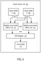
- FIG. 1shows an integrated circuit device ( 101 ) having a Deep Learning Accelerator ( 103 ) and random access memory ( 105 ) configured according to one embodiment.
- the Deep Learning Accelerator ( 103 ) in FIG. 1includes processing units ( 111 ), a control unit ( 113 ), and local memory ( 115 ).
- the control unit ( 113 )can use the processing units ( 111 ) to perform vector and matrix operations in accordance with instructions. Further, the control unit ( 113 ) can load instructions and operands from the random access memory ( 105 ) through a memory interface ( 117 ) and a high speed/bandwidth connection ( 119 ).
- the integrated circuit device ( 101 )is configured to be enclosed within an integrated circuit package with pins or contacts for a memory controller interface ( 107 ).
- the memory controller interface ( 107 )is configured to support a standard memory access protocol such that the integrated circuit device ( 101 ) appears to a typical memory controller (e.g., 108 connected to connectors 106 of the integrated circuit devices ( 101 )) in a way same as a conventional random access memory device having no Deep Learning Accelerator (DLA) ( 103 ).
- a memory controller external to the integrated circuit device ( 101 )can access, using a standard memory access protocol through the memory controller interface ( 107 ), the random access memory ( 105 ) in the integrated circuit device ( 101 ).
- the integrated circuit device ( 101 )is configured with a high bandwidth connection ( 119 ) between the random access memory ( 105 ) and the Deep Learning Accelerator (DLA) ( 103 ) that are enclosed within the integrated circuit device ( 101 ).
- the bandwidth of the connection ( 119 )is higher than the bandwidth of the connection ( 109 ) between the random access memory ( 105 ) and the memory controller interface ( 107 ).
- both the memory controller interface ( 107 ) and the memory interface ( 117 )are configured to access the random access memory ( 105 ) via a same set of buses or wires.
- the bandwidth to access the random access memory ( 105 )is shared between the memory interface ( 117 ) and the memory controller interface ( 107 ).
- the memory controller interface ( 107 ) and the memory interface ( 117 )are configured to access the random access memory ( 105 ) via separate sets of buses or wires.
- the random access memory ( 105 )can include multiple sections that can be accessed concurrently via the connection ( 119 ).
- the memory control interface ( 107 )can concurrently access another section of the random access memory ( 105 ).
- the different sectionscan be configured on different integrated circuit dies and/or different planes/banks of memory cells; and the different sections can be accessed in parallel to increase throughput in accessing the random access memory ( 105 ).
- the memory controller interface ( 107 )is configured to access one data unit of a predetermined size at a time; and the memory interface ( 117 ) is configured to access multiple data units, each of the same predetermined size, at a time.
- the random access memory ( 105 ) and the integrated circuit device ( 101 )are configured on different integrated circuit dies configured within a same integrated circuit package. Further, the random access memory ( 105 ) can be configured on one or more integrated circuit dies that allows parallel access of multiple data elements concurrently.
- the number of data elements of a vector or matrix that can be accessed in parallel over the connection ( 119 )corresponds to the granularity of the Deep Learning Accelerator (DLA) operating on vectors or matrices.
- DLADeep Learning Accelerator
- the connection ( 119 )is configured to load or store the same number, or multiples of the number, of elements via the connection ( 119 ) in parallel.
- the data access speed of the connection ( 119 )can be configured based on the processing speed of the Deep Learning Accelerator (DLA) ( 103 ). For example, after an amount of data and instructions have been loaded into the local memory ( 115 ), the control unit ( 113 ) can execute an instruction to operate on the data using the processing units ( 111 ) to generate output. Within the time period of processing to generate the output, the access bandwidth of the connection ( 119 ) allows the same amount of data and instructions to be loaded into the local memory ( 115 ) for the next operation and the same amount of output to be stored back to the random access memory ( 105 ).
- DLADeep Learning Accelerator
- the memory interface ( 117 )can offload the output of a prior operation into the random access memory ( 105 ) from, and load operand data and instructions into, another portion of the local memory ( 115 ).
- DLADeep Learning Accelerator
- the random access memory ( 105 )can be used to store the model data of an Artificial Neural Network (ANN) and to buffer input data for the Artificial Neural Network (ANN).
- the model datadoes not change frequently.
- the model datacan include the output generated by a compiler for the Deep Learning Accelerator (DLA) to implement the Artificial Neural Network (ANN).
- the model datatypically includes matrices used in the description of the Artificial Neural Network (ANN) and instructions generated for the Deep Learning Accelerator (DLA) ( 103 ) to perform vector/matrix operations of the Artificial Neural Network (ANN) based on vector/matrix operations of the granularity of the Deep Learning Accelerator (DLA) ( 103 ).
- the instructionsoperate not only on the vector/matrix operations of the Artificial Neural Network (ANN), but also on the input data for the Artificial Neural Network (ANN).
- the control unit ( 113 ) of the Deep Learning Accelerator (DLA) ( 103 )can automatically execute the instructions for the Artificial Neural Network (ANN) to generate an output of the Artificial Neural Network (ANN).
- the outputis stored into a predefined region in the random access memory ( 105 ).
- the Deep Learning Accelerator (DLA) ( 103 )can execute the instructions without help from a Central Processing Unit (CPU).
- CPUCentral Processing Unit
- the logic circuit of the Deep Learning Accelerator (DLA) ( 103 )can be implemented via Complementary Metal Oxide Semiconductor (CMOS).
- CMOSComplementary Metal Oxide Semiconductor
- the technique of CMOS Under the Array (CUA) of memory cells of the random access memory ( 105 )can be used to implement the logic circuit of the Deep Learning Accelerator (DLA) ( 103 ), including the processing units ( 111 ) and the control unit ( 113 ).
- the technique of CMOS in the Array of memory cells of the random access memory ( 105 )can be used to implement the logic circuit of the Deep Learning Accelerator (DLA) ( 103 ).
- the Deep Learning Accelerator (DLA) ( 103 ) and the random access memory ( 105 )can be implemented on separate integrated circuit dies and connected using Through-Silicon Vias (TSV) for increased data bandwidth between the Deep Learning Accelerator (DLA) ( 103 ) and the random access memory ( 105 ).
- TSVThrough-Silicon Vias
- the Deep Learning Accelerator (DLA) ( 103 )can be formed on an integrated circuit die of a Field-Programmable Gate Array (FPGA) or Application Specific Integrated circuit (ASIC).
- FPGAField-Programmable Gate Array
- ASICApplication Specific Integrated circuit
- the Deep Learning Accelerator (DLA) ( 103 ) and the random access memory ( 105 )can be configured in separate integrated circuit packages and connected via multiple point-to-point connections on a printed circuit board (PCB) for parallel communications and thus increased data transfer bandwidth.
- DLADeep Learning Accelerator
- PCBprinted circuit board
- the random access memory ( 105 )can be volatile memory or non-volatile memory, or a combination of volatile memory and non-volatile memory.
- non-volatile memoryinclude flash memory, memory cells formed based on negative-and (NAND) logic gates, negative-or (NOR) logic gates, Phase-Change Memory (PCM), magnetic memory (MRAM), resistive random-access memory, cross point storage and memory devices.
- a cross point memory devicecan use transistor-less memory elements, each of which has a memory cell and a selector that are stacked together as a column.
- Memory element columnsare connected via two layers of wires running in perpendicular directions, where wires of one layer run in one direction in the layer that is located above the memory element columns, and wires of the other layer run in another direction and are located below the memory element columns.
- Each memory elementcan be individually selected at a cross point of one wire on each of the two layers.
- Cross point memory devicesare fast and non-volatile and can be used as a unified memory pool for processing and storage.
- Further examples of non-volatile memoryinclude Read-Only Memory (ROM), Programmable Read-Only Memory (PROM), Erasable Programmable Read-Only Memory (EPROM) and Electronically Erasable Programmable Read-Only Memory (EEPROM) memory, etc.
- Examples of volatile memoryinclude Dynamic Random-Access Memory (DRAM) and Static Random-Access Memory (SRAM).
- non-volatile memorycan be configured to implement at least a portion of the random access memory ( 105 ).
- the non-volatile memory in the random access memory ( 105 )can be used to store the model data of an Artificial Neural Network (ANN).
- ANNArtificial Neural Network
- the non-volatile memorycan be programmable/rewritable.
- the model data of the Artificial Neural Network (ANN) in the integrated circuit device ( 101 )can be updated or replaced to implement an update Artificial Neural Network (ANN), or another Artificial Neural Network (ANN).
- the processing units ( 111 ) of the Deep Learning Accelerator (DLA) ( 103 )can include vector-vector units, matrix-vector units, and/or matrix-matrix units. Examples of units configured to perform for vector-vector operations, matrix-vector operations, and matrix-matrix operations are discussed below in connection with FIGS. 2 - 4 .
- FIG. 2shows a processing unit ( 121 ) configured to perform matrix-matrix operations according to one embodiment.
- the matrix-matrix unit ( 121 ) of FIG. 2can be used as one of the processing units ( 111 ) of the Deep Learning Accelerator (DLA) ( 103 ) of FIG. 1 .
- DLADeep Learning Accelerator
- the matrix-matrix unit ( 121 )includes multiple kernel buffers ( 131 to 133 ) and multiple the maps banks ( 151 to 153 ).
- Each of the maps banks ( 151 to 153 )stores one vector of a matrix operand that has multiple vectors stored in the maps banks ( 151 to 153 ) respectively; and each of the kernel buffers ( 131 to 133 ) stores one vector of another matrix operand that has multiple vectors stored in the kernel buffers ( 131 to 133 ) respectively.
- the matrix-matrix unit ( 121 )is configured to perform multiplication and accumulation operations on the elements of the two matrix operands, using multiple matrix-vector units ( 141 to 143 ) that operate in parallel.
- a cross bar ( 123 )connects the maps banks ( 151 to 153 ) to the matrix-vector units ( 141 to 143 ).
- the same matrix operand stored in the maps bank ( 151 to 153 )is provided via the crossbar ( 123 ) to each of the matrix-vector units ( 141 to 143 ); and the matrix-vector units ( 141 to 143 ) receives data elements from the maps banks ( 151 to 153 ) in parallel.
- Each of the kernel buffers ( 131 to 133 )is connected to a respective one in the matrix-vector units ( 141 to 143 ) and provides a vector operand to the respective matrix-vector unit.
- the matrix-vector units ( 141 to 143 )operate concurrently to compute the operation of the same matrix operand, stored in the maps banks ( 151 to 153 ) multiplied by the corresponding vectors stored in the kernel buffers ( 131 to 133 ).
- the matrix-vector unit ( 141 )performs the multiplication operation on the matrix operand stored in the maps banks ( 151 to 153 ) and the vector operand stored in the kernel buffer ( 131 ), while the matrix-vector unit ( 143 ) is concurrently performing the multiplication operation on the matrix operand stored in the maps banks ( 151 to 153 ) and the vector operand stored in the kernel buffer ( 133 ).
- Each of the matrix-vector units ( 141 to 143 ) in FIG. 2can be implemented in a way as illustrated in FIG. 3 .
- FIG. 3shows a processing unit ( 141 ) configured to perform matrix-vector operations according to one embodiment.
- the matrix-vector unit ( 141 ) of FIG. 3can be used as any of the matrix-vector units in the matrix-matrix unit ( 121 ) of FIG. 2 .
- each of the maps banks ( 151 to 153 )stores one vector of a matrix operand that has multiple vectors stored in the maps banks ( 151 to 153 ) respectively, in a way similar to the maps banks ( 151 to 153 ) of FIG. 2 .
- the crossbar ( 123 ) in FIG. 3provides the vectors from the maps banks ( 151 ) to the vector-vector units ( 161 to 163 ) respectively.
- a same vector stored in the kernel buffer ( 131 )is provided to the vector-vector units ( 161 to 163 ).
- the vector-vector units ( 161 to 163 )operate concurrently to compute the operation of the corresponding vector operands, stored in the maps banks ( 151 to 153 ) respectively, multiplied by the same vector operand that is stored in the kernel buffer ( 131 ).
- the vector-vector unit ( 161 )performs the multiplication operation on the vector operand stored in the maps bank ( 151 ) and the vector operand stored in the kernel buffer ( 131 ), while the vector-vector unit ( 163 ) is concurrently performing the multiplication operation on the vector operand stored in the maps bank ( 153 ) and the vector operand stored in the kernel buffer ( 131 ).
- the matrix-vector unit ( 141 ) of FIG. 3can use the maps banks ( 151 to 153 ), the crossbar ( 123 ) and the kernel buffer ( 131 ) of the matrix-matrix unit ( 121 ).
- Each of the vector-vector units ( 161 to 163 ) in FIG. 3can be implemented in a way as illustrated in FIG. 4 .
- FIG. 4shows a processing unit ( 161 ) configured to perform vector-vector operations according to one embodiment.
- the vector-vector unit ( 161 ) of FIG. 4can be used as any of the vector-vector units in the matrix-vector unit ( 141 ) of FIG. 3 .
- the vector-vector unit ( 161 )has multiple multiply-accumulate (MAC) units ( 171 to 173 ).
- Each of the multiply-accumulate (MAC) units ( 171 to 173 )can receive two numbers as operands, perform multiplication of the two numbers, and add the result of the multiplication to a sum maintained in the multiply-accumulate (MAC) unit.
- Each of the vector buffers ( 181 and 183 )stores a list of numbers.
- a pair of numbers, each from one of the vector buffers ( 181 and 183 ),can be provided to each of the multiply-accumulate (MAC) units ( 171 to 173 ) as input.
- the multiply-accumulate (MAC) units ( 171 to 173 )can receive multiple pairs of numbers from the vector buffers ( 181 and 183 ) in parallel and perform the multiply-accumulate (MAC) operations in parallel.
- the outputs from the multiply-accumulate (MAC) units ( 171 to 173 )are stored into the shift register ( 175 ); and an accumulator ( 177 ) computes the sum of the results in the shift register ( 175 ).
- the vector-vector unit ( 161 ) of FIG. 4can use a maps bank (e.g., 151 or 153 ) as one vector buffer ( 181 ), and the kernel buffer ( 131 ) of the matrix-vector unit ( 141 ) as another vector buffer ( 183 ).
- a maps banke.g., 151 or 153
- the kernel buffer ( 131 ) of the matrix-vector unit ( 141 )as another vector buffer ( 183 ).
- the vector buffers ( 181 and 183 )can have a same length to store the same number/count of data elements.
- the lengthcan be equal to, or the multiple of, the count of multiply-accumulate (MAC) units ( 171 to 173 ) in the vector-vector unit ( 161 ).
- the length of the vector buffers ( 181 and 183 )is the multiple of the count of multiply-accumulate (MAC) units ( 171 to 173 )
- MACmultiply-accumulate
- a number of pairs of inputs, equal to the count of the multiply-accumulate (MAC) units ( 171 to 173 )can be provided from the vector buffers ( 181 and 183 ) as inputs to the multiply-accumulate (MAC) units ( 171 to 173 ) in each iteration; and the vector buffers ( 181 and 183 ) feed their elements into the multiply-accumulate (MAC) units ( 171 to 173 ) through multiple iterations.
- the communication bandwidth of the connection ( 119 ) between the Deep Learning Accelerator (DLA) ( 103 ) and the random access memory ( 105 )is sufficient for the matrix-matrix unit ( 121 ) to use portions of the random access memory ( 105 ) as the maps banks ( 151 to 153 ) and the kernel buffers ( 131 to 133 ).
- the maps banks ( 151 to 153 ) and the kernel buffers ( 131 to 133 )are implemented in a portion of the local memory ( 115 ) of the Deep Learning Accelerator (DLA) ( 103 ).
- the communication bandwidth of the connection ( 119 ) between the Deep Learning Accelerator (DLA) ( 103 ) and the random access memory ( 105 )is sufficient to load, into another portion of the local memory ( 115 ), matrix operands of the next operation cycle of the matrix-matrix unit ( 121 ), while the matrix-matrix unit ( 121 ) is performing the computation in the current operation cycle using the maps banks ( 151 to 153 ) and the kernel buffers ( 131 to 133 ) implemented in a different portion of the local memory ( 115 ) of the Deep Learning Accelerator (DLA) ( 103 ).
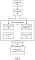
- FIG. 5shows a Deep Learning Accelerator and random access memory configured to autonomously apply inputs to a trained Artificial Neural Network according to one embodiment.
- An Artificial Neural Network (ANN) ( 201 ) that has been trained through machine learning (e.g., deep learning)can be described in a standard format (e.g., Open Neural Network Exchange (ONNX)).
- the description of the trained ANN ( 201 ) in the standard formatidentifies the properties of the artificial neurons and their connectivity.
- a Deep Learning Accelerator (DLA) compilerconverts trained ANN ( 201 ) by generating instructions ( 205 ) for a Deep Learning Accelerator (DLA) ( 103 ) and matrices ( 207 ) corresponding to the properties of the artificial neurons and their connectivity.
- the instructions ( 205 ) and the matrices ( 207 ) generated by the DLA compiler ( 203 ) from the trained ANN ( 201 )can be stored in random access memory ( 105 ) for the Deep Learning Accelerator (DLA) ( 103 ).
- the random access memory ( 105 ) and the Deep Learning Accelerator (DLA) ( 103 )can be connected via a high bandwidth connection ( 119 ) in a way as in the integrated circuit device ( 101 ) of FIG. 1 .
- the autonomous computation of FIG. 5 based on the instructions ( 205 ) and the matrices ( 207 )can be implemented in the integrated circuit device ( 101 ) of FIG. 1 .
- the random access memory ( 105 ) and the Deep Learning Accelerator (DLA) ( 103 )can be configured on a printed circuit board with multiple point to point serial buses running in parallel to implement the connection ( 119 ).
- the application of the trained ANN ( 201 ) to process an input ( 211 ) to the trained ANN ( 201 ) to generate the corresponding output ( 213 ) of the trained ANN ( 201 )can be triggered by the presence of the input ( 211 ) in the random access memory ( 105 ), or another indication provided in the random access memory ( 105 ).
- the Deep Learning Accelerator (DLA) ( 103 )executes the instructions ( 205 ) to combine the input ( 211 ) and the matrices ( 207 ).
- the execution of the instructions ( 205 )can include the generation of maps matrices for the maps banks ( 151 to 153 ) of one or more matrix-matrix units (e.g., 121 ) of the Deep Learning Accelerator (DLA) ( 103 ).
- the inputs to ANN ( 211 )is in the form of an initial maps matrix. Portions of the initial maps matrix can be retrieved from the random access memory ( 105 ) as the matrix operand stored in the maps banks ( 151 to 153 ) of a matrix-matrix unit ( 121 ).
- the DLA instructions ( 205 )also include instructions for the Deep Learning Accelerator (DLA) ( 103 ) to generate the initial maps matrix from the input ( 211 ).
- the Deep Learning Accelerator (DLA) ( 103 )loads matrix operands into the kernel buffers ( 131 to 133 ) and maps banks ( 151 to 153 ) of its matrix-matrix unit ( 121 ).
- the matrix-matrix unit ( 121 )performs the matrix computation on the matrix operands.
- the DLA instructions ( 205 )break down matrix computations of the trained ANN ( 201 ) according to the computation granularity of the Deep Learning Accelerator (DLA) ( 103 ) (e.g., the sizes/dimensions of matrices that loaded as matrix operands in the matrix-matrix unit ( 121 )) and applies the input feature maps to the kernel of a layer of artificial neurons to generate output as the input for the next layer of artificial neurons.
- DLADeep Learning Accelerator
- the Deep Learning Accelerator (DLA) ( 103 )Upon completion of the computation of the trained ANN ( 201 ) performed according to the instructions ( 205 ), the Deep Learning Accelerator (DLA) ( 103 ) stores the output ( 213 ) of the ANN ( 201 ) at a pre-defined location in the random access memory ( 105 ), or at a location specified in an indication provided in the random access memory ( 105 ) to trigger the computation.
- DLADeep Learning Accelerator
- an external device connected to the memory controller interface ( 107 )can write the input ( 211 ) into the random access memory ( 105 ) and trigger the autonomous computation of applying the input ( 211 ) to the trained ANN ( 201 ) by the Deep Learning Accelerator (DLA) ( 103 ).
- the output ( 213 )is available in the random access memory ( 105 ); and the external device can read the output ( 213 ) via the memory controller interface ( 107 ) of the integrated circuit device ( 101 ).
- a predefined location in the random access memory ( 105 )can be configured to store an indication to trigger the autonomous execution of the instructions ( 205 ) by the Deep Learning Accelerator (DLA) ( 103 ).
- the indicationcan optionally include a location of the input ( 211 ) within the random access memory ( 105 ).
- the external devicecan retrieve the output generated during a previous run of the instructions ( 205 ), and/or store another set of input for the next run of the instructions ( 205 ).
- a further predefined location in the random access memory ( 105 )can be configured to store an indication of the progress status of the current run of the instructions ( 205 ).
- the indicationcan include a prediction of the completion time of the current run of the instructions ( 205 ) (e.g., estimated based on a prior run of the instructions ( 205 )).
- the external devicecan check the completion status at a suitable time window to retrieve the output ( 213 ).
- the random access memory ( 105 )is configured with sufficient capacity to store multiple sets of inputs (e.g., 211 ) and outputs (e.g., 213 ). Each set can be configured in a predetermined slot/area in the random access memory ( 105 ).
- the Deep Learning Accelerator (DLA) ( 103 )can execute the instructions ( 205 ) autonomously to generate the output ( 213 ) from the input ( 211 ) according to matrices ( 207 ) stored in the random access memory ( 105 ) without helps from a processor or device that is located outside of the integrated circuit device ( 101 ).
- FIG. 6shows a method implemented in an integrated circuit device according to one embodiment.
- the method of FIG. 6can be implemented in the integrated circuit device ( 101 ) of FIG. 1 , or another device similar to that illustrated in FIG. 5 but configured on a printed circuit board.
- random access memory ( 105 ) of a computing devicecan be accessed using an interface ( 107 ) of the computing device (e.g., 101 ) to a memory controller.
- the computing devicee.g., 101
- the computing devicecan have processing units (e.g., 111 ) configured to perform at least computations on matrix operands, such as a matrix operand stored in maps banks ( 151 to 153 ) and a matrix operand stored in kernel buffers ( 131 to 133 ).
- the computing devicee.g., 101
- the computing devicecan be enclosed within an integrated circuit package; and a set of connections can connect the interface ( 107 ) to the memory controller that is located outside of the integrated circuit package.
- instructions ( 205 ) executable by the processing unitscan be written into the random access memory ( 105 ) through the interface ( 107 ).
- matrices ( 207 ) of an Artificial Neural Network ( 201 )can be written into the random access memory ( 105 ) through the interface ( 107 ).
- the matrices ( 207 )identify the property and/or state of the Artificial Neural Network ( 201 ).
- At least a portion of the random access memory ( 105 )is non-volatile and configured to store the instructions ( 205 ) and the matrices ( 07 ) of the Artificial Neural Network ( 201 ).
- first input ( 211 ) to the Artificial Neural Networkcan be written into the random access memory ( 105 ) through the interface ( 107 ).
- an indicationis provided in the random access memory ( 105 ) to cause the processing units ( 111 ) to start execution of the instructions ( 205 ).
- the processing units ( 111 )execute the instructions to combine the first input ( 211 ) with the matrices ( 207 ) of the Artificial Neural Network ( 201 ) to generate first output ( 213 ) from the Artificial Neural Network ( 201 ) and store the first output ( 213 ) in the random access memory ( 105 ).
- the indicationcan be an address of the first input ( 211 ) in the random access memory ( 105 ); and the indication can be stored a predetermined location in the random access memory ( 105 ) to cause the initiation of the execution of the instructions ( 205 ) for the input ( 211 ) identified by the address.
- the indicationcan also include an address for storing the output ( 213 ).
- the first output ( 213 )can be read, through the interface ( 107 ), from the random access memory ( 105 ).
- the computing devicee.g., 101
- the computing devicecan have a Deep Learning Accelerator ( 103 ) formed on a first integrated circuit die and the random access memory ( 105 ) formed on one or more second integrated circuit dies.
- the connection ( 119 ) between the first integrated circuit die and the one or more second integrated circuit diescan include Through-Silicon Vias (TSVs) to provide high bandwidth for memory access.
- TSVsThrough-Silicon Vias
- a description of the Artificial Neural Network ( 201 )can be converted using a compiler ( 203 ) into the instructions ( 205 ) and the matrices ( 207 ).
- the combination of the instructions ( 205 ) and the matrices ( 207 ) stored in the random access memory ( 105 ) and the Deep Learning Accelerator ( 103 )provides an autonomous implementation of the Artificial Neural Network ( 201 ) that can automatically convert input ( 211 ) to the Artificial Neural Network ( 201 ) to its output ( 213 ).
- the Deep Learning Accelerator ( 103 )executes the instructions ( 205 ) to generate the first output ( 213 ) from the first input ( 211 ) according to the matrices ( 207 ) of the Artificial Neural Network ( 201 )
- the second input to Artificial Neural Network ( 201 )can be written into the random access memory ( 105 ) through the interface ( 107 ) at an alternative location.
- an indicationcan be provided in the random access memory to cause the Deep Learning Accelerator ( 103 ) to again start the execution of the instructions and generate second output from the second input.
- the first output ( 213 )can be read from the random access memory ( 105 ) through the interface ( 107 ); and a further input can be written into the random access memory to replace the first input ( 211 ), or written at a different location.
- the processcan be repeated for a sequence of inputs.
- the Deep Learning Accelerator ( 103 )can include at least one matrix-matrix unit ( 121 ) that can execute an instruction on two matrix operands.
- the two matrix operandscan be a first matrix and a second matrix.
- Each of two matriceshas a plurality of vectors.
- the matrix-matrix unit ( 121 )can include a plurality of matrix-vector units ( 141 to 143 ) configured to operate in parallel.
- Each of the matrix-vector units ( 141 to 143 )are configured to operate, in parallel with other matrix-vector units, on the first matrix and one vector from second matrix.
- each of the matrix-vector units ( 141 to 143 )can have a plurality of vector-vector units ( 161 to 163 ) configured to operate in parallel.
- Each of the vector-vector units ( 161 to 163 )is configured to operate, in parallel with other vector-vector units, on a vector from the first matrix and a common vector operand of the corresponding matrix-vector unit.
- each of the vector-vector units ( 161 to 163 )can have a plurality of multiply-accumulate units ( 171 to 173 ) configured to operate in parallel.
- the Deep Learning Accelerator ( 103 )can have local memory ( 115 ) and a control unit ( 113 ) in addition to the processing units ( 111 ).
- the control unit ( 113 )can load instructions ( 205 ) and matrix operands (e.g., 207 ) from the random access memory ( 105 ) for execution by the processing units ( 111 ).
- the local memorycan cache matrix operands used by the matrix-matrix unit.
- the connection ( 119 )can be configured with a bandwidth sufficient to load a set of matrix operands from the random access memory ( 105 ) to the local memory ( 115 ) during a time period in which the matrix-matrix unit performs operations on two other matrix operands. Further, during the time period, the bandwidth is sufficient to store a result, generated by the matrix-matrix unit ( 121 ) in a prior instruction execution, from the local memory ( 115 ) to the random access memory ( 105 ).
- the present disclosureincludes methods and apparatuses which perform the methods described above, including data processing systems which perform these methods, and computer readable media containing instructions which when executed on data processing systems cause the systems to perform these methods.
- a typical data processing systemmay include an inter-connect (e.g., bus and system core logic), which interconnects a microprocessor(s) and memory.
- the microprocessoris typically coupled to cache memory.
- the inter-connectinterconnects the microprocessor(s) and the memory together and also interconnects them to input/output (I/O) device(s) via I/O controller(s).
- I/O devicesmay include a display device and/or peripheral devices, such as mice, keyboards, modems, network interfaces, printers, scanners, video cameras and other devices known in the art.
- the data processing systemis a server system, some of the I/O devices, such as printers, scanners, mice, and/or keyboards, are optional.
- the inter-connectcan include one or more buses connected to one another through various bridges, controllers and/or adapters.
- the I/O controllersinclude a USB (Universal Serial Bus) adapter for controlling USB peripherals, and/or an IEEE-1394 bus adapter for controlling IEEE-1394 peripherals.
- USBUniversal Serial Bus
- IEEE-1394IEEE-1394
- the memorymay include one or more of: ROM (Read Only Memory), volatile RAM (Random Access Memory), and non-volatile memory, such as hard drive, flash memory, etc.
- ROMRead Only Memory
- RAMRandom Access Memory
- non-volatile memorysuch as hard drive, flash memory, etc.
- Volatile RAMis typically implemented as dynamic RAM (DRAM) which requires power continually in order to refresh or maintain the data in the memory.
- Non-volatile memoryis typically a magnetic hard drive, a magnetic optical drive, an optical drive (e.g., a DVD RAM), or other type of memory system which maintains data even after power is removed from the system.
- the non-volatile memorymay also be a random access memory.
- the non-volatile memorycan be a local device coupled directly to the rest of the components in the data processing system.
- a non-volatile memory that is remote from the systemsuch as a network storage device coupled to the data processing system through a network interface such as a modem or Ethernet interface, can also be used.
- the functions and operations as described herecan be implemented using special purpose circuitry, with or without software instructions, such as using Application-Specific Integrated Circuit (ASIC) or Field-Programmable Gate Array (FPGA).
- ASICApplication-Specific Integrated Circuit
- FPGAField-Programmable Gate Array
- Embodimentscan be implemented using hardwired circuitry without software instructions, or in combination with software instructions. Thus, the techniques are limited neither to any specific combination of hardware circuitry and software, nor to any particular source for the instructions executed by the data processing system.
- While one embodimentcan be implemented in fully functioning computers and computer systems, various embodiments are capable of being distributed as a computing product in a variety of forms and are capable of being applied regardless of the particular type of machine or computer-readable media used to actually effect the distribution.
- At least some aspects disclosedcan be embodied, at least in part, in software. That is, the techniques may be carried out in a computer system or other data processing system in response to its processor, such as a microprocessor, executing sequences of instructions contained in a memory, such as ROM, volatile RAM, non-volatile memory, cache or a remote storage device.
- processorsuch as a microprocessor
- a memorysuch as ROM, volatile RAM, non-volatile memory, cache or a remote storage device.
- Routines executed to implement the embodimentsmay be implemented as part of an operating system or a specific application, component, program, object, module or sequence of instructions referred to as “computer programs.”
- the computer programstypically include one or more instructions set at various times in various memory and storage devices in a computer, and that, when read and executed by one or more processors in a computer, cause the computer to perform operations necessary to execute elements involving the various aspects.
- a machine readable mediumcan be used to store software and data which when executed by a data processing system causes the system to perform various methods.
- the executable software and datamay be stored in various places including for example ROM, volatile RAM, non-volatile memory and/or cache. Portions of this software and/or data may be stored in any one of these storage devices.
- the data and instructionscan be obtained from centralized servers or peer to peer networks. Different portions of the data and instructions can be obtained from different centralized servers and/or peer to peer networks at different times and in different communication sessions or in a same communication session.
- the data and instructionscan be obtained in entirety prior to the execution of the applications. Alternatively, portions of the data and instructions can be obtained dynamically, just in time, when needed for execution. Thus, it is not required that the data and instructions be on a machine readable medium in entirety at a particular instance of time.
- Examples of computer-readable mediainclude but are not limited to non-transitory, recordable and non-recordable type media such as volatile and non-volatile memory devices, Read Only Memory (ROM), Random Access Memory (RAM), flash memory devices, floppy and other removable disks, magnetic disk storage media, optical storage media (e.g., Compact Disk Read-Only Memory (CD ROM), Digital Versatile Disks (DVDs), etc.), among others.
- the computer-readable mediamay store the instructions.
- the instructionsmay also be embodied in digital and analog communication links for electrical, optical, acoustical or other forms of propagated signals, such as carrier waves, infrared signals, digital signals, etc.
- propagated signalssuch as carrier waves, infrared signals, digital signals, etc. are not tangible machine readable medium and are not configured to store instructions.
- a machine readable mediumincludes any mechanism that provides (i.e., stores and/or transmits) information in a form accessible by a machine (e.g., a computer, network device, personal digital assistant, manufacturing tool, any device with a set of one or more processors, etc.).
- a machinee.g., a computer, network device, personal digital assistant, manufacturing tool, any device with a set of one or more processors, etc.
- hardwired circuitrymay be used in combination with software instructions to implement the techniques.
- the techniquesare neither limited to any specific combination of hardware circuitry and software nor to any particular source for the instructions executed by the data processing system.
Landscapes
- Engineering & Computer Science (AREA)
- Physics & Mathematics (AREA)
- Theoretical Computer Science (AREA)
- General Physics & Mathematics (AREA)
- Software Systems (AREA)
- Mathematical Physics (AREA)
- General Engineering & Computer Science (AREA)
- Data Mining & Analysis (AREA)
- Biomedical Technology (AREA)
- Life Sciences & Earth Sciences (AREA)
- Health & Medical Sciences (AREA)
- Biophysics (AREA)
- Computing Systems (AREA)
- Mathematical Optimization (AREA)
- Computational Mathematics (AREA)
- General Health & Medical Sciences (AREA)
- Pure & Applied Mathematics (AREA)
- Molecular Biology (AREA)
- Mathematical Analysis (AREA)
- Computational Linguistics (AREA)
- Artificial Intelligence (AREA)
- Evolutionary Computation (AREA)
- Neurology (AREA)
- Algebra (AREA)
- Databases & Information Systems (AREA)
- Computer Hardware Design (AREA)
- Advance Control (AREA)
- Memory System (AREA)
- Complex Calculations (AREA)
Abstract
Description
Claims (10)
Priority Applications (5)
| Application Number | Priority Date | Filing Date | Title |
|---|---|---|---|
| US16/844,988US11874897B2 (en) | 2020-04-09 | 2020-04-09 | Integrated circuit device with deep learning accelerator and random access memory |
| KR1020227038775AKR20220164571A (en) | 2020-04-09 | 2021-03-30 | Integrated circuit device with deep learning accelerator and random access memory |
| EP21784882.9AEP4133424A4 (en) | 2020-04-09 | 2021-03-30 | Integrated circuit device with deep learning accelerator and random access memory |
| CN202180025067.9ACN115443467A (en) | 2020-04-09 | 2021-03-30 | Integrated circuit device with deep learning accelerator and random access memory |
| PCT/US2021/025017WO2021206973A1 (en) | 2020-04-09 | 2021-03-30 | Integrated circuit device with deep learning accelerator and random access memory |
Applications Claiming Priority (1)
| Application Number | Priority Date | Filing Date | Title |
|---|---|---|---|
| US16/844,988US11874897B2 (en) | 2020-04-09 | 2020-04-09 | Integrated circuit device with deep learning accelerator and random access memory |
Publications (2)
| Publication Number | Publication Date |
|---|---|
| US20210319821A1 US20210319821A1 (en) | 2021-10-14 |
| US11874897B2true US11874897B2 (en) | 2024-01-16 |
Family
ID=78006584
Family Applications (1)
| Application Number | Title | Priority Date | Filing Date |
|---|---|---|---|
| US16/844,988Active2041-01-21US11874897B2 (en) | 2020-04-09 | 2020-04-09 | Integrated circuit device with deep learning accelerator and random access memory |
Country Status (5)
| Country | Link |
|---|---|
| US (1) | US11874897B2 (en) |
| EP (1) | EP4133424A4 (en) |
| KR (1) | KR20220164571A (en) |
| CN (1) | CN115443467A (en) |
| WO (1) | WO2021206973A1 (en) |
Families Citing this family (6)
| Publication number | Priority date | Publication date | Assignee | Title |
|---|---|---|---|---|
| US11887647B2 (en) | 2020-04-09 | 2024-01-30 | Micron Technology, Inc. | Deep learning accelerator and random access memory with separate memory access connections |
| US11461651B2 (en) | 2020-04-09 | 2022-10-04 | Micron Technology, Inc. | System on a chip with deep learning accelerator and random access memory |
| US11726784B2 (en) | 2020-04-09 | 2023-08-15 | Micron Technology, Inc. | Patient monitoring using edge servers having deep learning accelerator and random access memory |
| US11355175B2 (en) | 2020-04-09 | 2022-06-07 | Micron Technology, Inc. | Deep learning accelerator and random access memory with a camera interface |
| US12094531B2 (en)* | 2021-01-11 | 2024-09-17 | Micron Technology, Inc. | Caching techniques for deep learning accelerator |
| CN113766669B (en)* | 2021-11-10 | 2021-12-31 | 香港中文大学(深圳) | Large-scale random access method based on deep learning network |
Citations (65)
| Publication number | Priority date | Publication date | Assignee | Title |
|---|---|---|---|---|
| US5815458A (en) | 1996-09-06 | 1998-09-29 | Micron Technology, Inc. | System and method for writing data to memory cells so as to enable faster reads of the data using dual wordline drivers |
| US20050047670A1 (en) | 2003-08-29 | 2005-03-03 | Shen-En Qian | Data compression engines and real-time wideband compressor for multi-dimensional data |
| WO2005091203A2 (en) | 2004-03-12 | 2005-09-29 | Aureon Laboratories, Inc. | Systems and methods for treating, diagnosing and predicting the occurrence of a medical condition |
| US20060230213A1 (en) | 2005-03-29 | 2006-10-12 | Via Technologies, Inc. | Digital signal system with accelerators and method for operating the same |
| US20100076915A1 (en) | 2008-09-25 | 2010-03-25 | Microsoft Corporation | Field-Programmable Gate Array Based Accelerator System |
| US7873812B1 (en) | 2004-04-05 | 2011-01-18 | Tibet MIMAR | Method and system for efficient matrix multiplication in a SIMD processor architecture |
| US20110219150A1 (en) | 2010-03-05 | 2011-09-08 | Gary Piccirillo | Dma engine capable of concurrent data manipulation |
| US20110307228A1 (en) | 2008-10-15 | 2011-12-15 | Nikola Kirilov Kasabov | Data analysis and predictive systems and related methodologies |
| US20120257742A1 (en) | 2011-04-06 | 2012-10-11 | Certicom Corp. | Efficient Implementation of Hash Algorithm on a Processor |
| US20140279746A1 (en) | 2008-02-20 | 2014-09-18 | Digital Medical Experts Inc. | Expert system for determining patient treatment response |
| US20150038806A1 (en) | 2012-10-09 | 2015-02-05 | Bodies Done Right | Personalized avatar responsive to user physical state and context |
| US20170316312A1 (en)* | 2016-05-02 | 2017-11-02 | Cavium, Inc. | Systems and methods for deep learning processor |
| US20180307974A1 (en) | 2017-04-19 | 2018-10-25 | Beijing Deephi Intelligence Technology Co., Ltd. | Device for implementing artificial neural network with mutiple instruction units |
| US20180307976A1 (en) | 2017-04-19 | 2018-10-25 | Beijing Deephi Intelligence Technology Co., Ltd. | Device for implementing artificial neural network with separate computation units |
| US20190027018A1 (en) | 2017-07-21 | 2019-01-24 | Accenture Global Solutions Limited | Artificial intelligence based service control and home monitoring |
| US20190042411A1 (en)* | 2016-03-31 | 2019-02-07 | Hewlett Packard Enterprise Development Lp | Logical operations |
| US20190046039A1 (en) | 2017-08-14 | 2019-02-14 | Amrita Vishwa Vidyapeetham | Systems, methods, and devices for remote health monitoring and management |
| US20190050733A1 (en) | 2017-04-14 | 2019-02-14 | Rohan Bopardikar | Reducing the size of a neural network through reduction of the weight matrices |
| US20190121837A1 (en) | 2018-12-21 | 2019-04-25 | Omid Azizi | Apparatus and method for a masked multiply instruction to support neural network pruning operations |
| US20190171941A1 (en) | 2017-12-01 | 2019-06-06 | Abee Technology Co., Ltd. | Electronic device, accelerator, and accelerating method applicable to convolutional neural network computation |
| US20190180170A1 (en) | 2017-12-12 | 2019-06-13 | Amazon Technologies, Inc. | Multi-memory on-chip computational network |
| US20190196825A1 (en) | 2016-09-13 | 2019-06-27 | Arm Limited | Vector multiply-add instruction |
| US10387122B1 (en)* | 2018-05-04 | 2019-08-20 | Olsen Ip Reserve, Llc | Residue number matrix multiplier |
| US20190258306A1 (en) | 2018-02-20 | 2019-08-22 | Apical Ltd | Data processing system and method |
| US20190286972A1 (en) | 2018-03-14 | 2019-09-19 | Microsoft Technology Licensing, Llc | Hardware accelerated neural network subgraphs |
| US20190303198A1 (en)* | 2018-04-03 | 2019-10-03 | FuriosaAI Co. | Neural network processor |
| US20190318230A1 (en) | 2018-04-17 | 2019-10-17 | Samsung Electronics Co., Ltd. | Neuromorphic circuit having 3d stacked structure and semiconductor device having the same |
| US20190370631A1 (en)* | 2019-08-14 | 2019-12-05 | Intel Corporation | Methods and apparatus to tile walk a tensor for convolution operations |
| US20190370086A1 (en)* | 2019-08-15 | 2019-12-05 | Intel Corporation | Methods and apparatus to manage power of deep learning accelerator systems |
| US10515135B1 (en)* | 2017-10-17 | 2019-12-24 | Xilinx, Inc. | Data format suitable for fast massively parallel general matrix multiplication in a programmable IC |
| US20190391811A1 (en) | 2019-08-29 | 2019-12-26 | Intel Corporation | Multi-variate strided read operations for accessing matrix operands |
| US20200034145A1 (en)* | 2018-07-24 | 2020-01-30 | Apple Inc. | Computation Engine that Operates in Matrix and Vector Modes |
| WO2020058560A1 (en) | 2018-09-17 | 2020-03-26 | Nokia Solutions And Networks Oy | Object tracking |
| US20200117580A1 (en) | 2018-04-22 | 2020-04-16 | Sas Institute Inc. | Validation Sets for Machine Learning Algorithms |
| US20200117450A1 (en) | 2017-06-28 | 2020-04-16 | Arm Limited | Register-based matrix multiplication |
| US10678479B1 (en) | 2018-11-29 | 2020-06-09 | Amazon Technologies, Inc. | Registers for restricted memory |
| US20200184001A1 (en) | 2018-12-07 | 2020-06-11 | Samsung Electronics Co., Ltd. | Dataflow accelerator architecture for general matrix-matrix multiplication and tensor computation in deep learning |
| US20200202527A1 (en) | 2017-12-20 | 2020-06-25 | Medi Whale Inc. | Method and device for assisting heart disease diagnosis |
| US20200250545A1 (en) | 2019-02-06 | 2020-08-06 | Qualcomm Incorporated | Split network acceleration architecture |
| US20200380361A1 (en) | 2019-02-22 | 2020-12-03 | Neureality Ltd. | Directed and interconnected grid dataflow architecture |
| US10885314B2 (en) | 2018-01-22 | 2021-01-05 | Kneron Inc. | Face identification system and face identification method with high security level and low power consumption |
| US20210011846A1 (en) | 2019-07-11 | 2021-01-14 | Facebook Technologies, Llc | Systems and methods for reading and writing sparse data in a neural network accelerator |
| US20210012178A1 (en) | 2019-07-11 | 2021-01-14 | Facebook Technologies, Llc | Systems, methods, and devices for early-exit from convolution |
| US20210019591A1 (en) | 2019-07-15 | 2021-01-21 | Facebook Technologies, Llc | System and method for performing small channel count convolutions in energy-efficient input operand stationary accelerator |
| US20210049231A1 (en)* | 2019-08-16 | 2021-02-18 | Google Llc | Multiple Output Fusion For Operations Performed In A Multi-Dimensional Array of Processing Units |
| US10978382B2 (en) | 2019-01-30 | 2021-04-13 | Taiwan Semiconductor Manufacturing Company, Ltd. | Integrated circuit package and method |
| US20210150260A1 (en) | 2019-11-14 | 2021-05-20 | Alibaba Group Holding Limited | Using selected components of frequency domain image data in artificial intelligence tasks |
| US20210150317A1 (en) | 2019-11-18 | 2021-05-20 | Industrial Technology Research Institute | Neuron circuit and artificial neural network chip |
| US20210192287A1 (en) | 2019-12-18 | 2021-06-24 | Nvidia Corporation | Master transform architecture for deep learning |
| US20210209451A1 (en) | 2020-01-03 | 2021-07-08 | Shanghai Zhaoxin Semiconductor Co., Ltd. | Artificial intelligence integrated circuit |
| US20210255860A1 (en) | 2018-08-29 | 2021-08-19 | Cerebras Systems Inc. | Isa enhancements for accelerated deep learning |
| US20210279629A1 (en) | 2020-03-05 | 2021-09-09 | oneFiveFIFTY LLC | Machine learning and computer-based generation of standard work matrices for improving execution of a standard work |
| US20210319305A1 (en) | 2020-04-09 | 2021-10-14 | Micron Technology, Inc. | System on a Chip with Deep Learning Accelerator and Random Access Memory |
| US20210318871A1 (en) | 2020-04-09 | 2021-10-14 | Micron Technology, Inc. | Patient Monitoring using Edge Servers having Deep Learning Accelerator and Random Access Memory |
| US20210319822A1 (en) | 2020-04-09 | 2021-10-14 | Micron Technology, Inc. | Deep Learning Accelerator and Random Access Memory with Separate Memory Access Connections |
| US20210319823A1 (en) | 2020-04-09 | 2021-10-14 | Micron Technology, Inc. | Deep Learning Accelerator and Random Access Memory with a Camera Interface |
| US20210320967A1 (en) | 2020-04-09 | 2021-10-14 | Micron Technology, Inc. | Edge Server with Deep Learning Accelerator and Random Access Memory |
| US11188825B2 (en) | 2018-10-15 | 2021-11-30 | International Business Machines Corporation | Mixed-precision deep-learning with multi-memristive devices |
| US20210390076A1 (en)* | 2020-06-12 | 2021-12-16 | Alibaba Group Holding Limited | Apparatuses and methods for map reduce |
| US11204747B1 (en) | 2017-10-17 | 2021-12-21 | Xilinx, Inc. | Re-targetable interface for data exchange between heterogeneous systems and accelerator abstraction into software instructions |
| US20220044043A1 (en) | 2019-07-31 | 2022-02-10 | Huawei Technologies Co.,Ltd. | Integrated circuit and sensor data processing method |
| US20220067527A1 (en) | 2018-12-18 | 2022-03-03 | Movidius Ltd. | Neural network compression |
| US11539763B2 (en) | 2019-02-13 | 2022-12-27 | Apple Inc. | Apparatus and method for session initiated protocol (SIP) registration procedure for access network bitrate recommendation (ANBR) capability signaling |
| US11544548B2 (en) | 2021-05-24 | 2023-01-03 | Rebellions Inc. | Processing element and neural processing device including same |
| US20230068106A1 (en) | 2015-05-29 | 2023-03-02 | Pure Storage, Inc. | Cloud-Based User Authorization Control For Storage System Access |
- 2020
- 2020-04-09USUS16/844,988patent/US11874897B2/enactiveActive
- 2021
- 2021-03-30WOPCT/US2021/025017patent/WO2021206973A1/ennot_activeCeased
- 2021-03-30EPEP21784882.9Apatent/EP4133424A4/enactivePending
- 2021-03-30KRKR1020227038775Apatent/KR20220164571A/enactivePending
- 2021-03-30CNCN202180025067.9Apatent/CN115443467A/enactivePending
Patent Citations (72)
| Publication number | Priority date | Publication date | Assignee | Title |
|---|---|---|---|---|
| US5815458A (en) | 1996-09-06 | 1998-09-29 | Micron Technology, Inc. | System and method for writing data to memory cells so as to enable faster reads of the data using dual wordline drivers |
| US20050047670A1 (en) | 2003-08-29 | 2005-03-03 | Shen-En Qian | Data compression engines and real-time wideband compressor for multi-dimensional data |
| WO2005091203A2 (en) | 2004-03-12 | 2005-09-29 | Aureon Laboratories, Inc. | Systems and methods for treating, diagnosing and predicting the occurrence of a medical condition |
| US7873812B1 (en) | 2004-04-05 | 2011-01-18 | Tibet MIMAR | Method and system for efficient matrix multiplication in a SIMD processor architecture |
| US20060230213A1 (en) | 2005-03-29 | 2006-10-12 | Via Technologies, Inc. | Digital signal system with accelerators and method for operating the same |
| US20140279746A1 (en) | 2008-02-20 | 2014-09-18 | Digital Medical Experts Inc. | Expert system for determining patient treatment response |
| US20100076915A1 (en) | 2008-09-25 | 2010-03-25 | Microsoft Corporation | Field-Programmable Gate Array Based Accelerator System |
| US20110307228A1 (en) | 2008-10-15 | 2011-12-15 | Nikola Kirilov Kasabov | Data analysis and predictive systems and related methodologies |
| US20110219150A1 (en) | 2010-03-05 | 2011-09-08 | Gary Piccirillo | Dma engine capable of concurrent data manipulation |
| US20120257742A1 (en) | 2011-04-06 | 2012-10-11 | Certicom Corp. | Efficient Implementation of Hash Algorithm on a Processor |
| US20150038806A1 (en) | 2012-10-09 | 2015-02-05 | Bodies Done Right | Personalized avatar responsive to user physical state and context |
| US20230068106A1 (en) | 2015-05-29 | 2023-03-02 | Pure Storage, Inc. | Cloud-Based User Authorization Control For Storage System Access |
| US20190042411A1 (en)* | 2016-03-31 | 2019-02-07 | Hewlett Packard Enterprise Development Lp | Logical operations |
| US20170316312A1 (en)* | 2016-05-02 | 2017-11-02 | Cavium, Inc. | Systems and methods for deep learning processor |
| US20190196825A1 (en) | 2016-09-13 | 2019-06-27 | Arm Limited | Vector multiply-add instruction |
| US20190050733A1 (en) | 2017-04-14 | 2019-02-14 | Rohan Bopardikar | Reducing the size of a neural network through reduction of the weight matrices |
| US20180307976A1 (en) | 2017-04-19 | 2018-10-25 | Beijing Deephi Intelligence Technology Co., Ltd. | Device for implementing artificial neural network with separate computation units |
| US20180307974A1 (en) | 2017-04-19 | 2018-10-25 | Beijing Deephi Intelligence Technology Co., Ltd. | Device for implementing artificial neural network with mutiple instruction units |
| US20200117450A1 (en) | 2017-06-28 | 2020-04-16 | Arm Limited | Register-based matrix multiplication |
| US20190027018A1 (en) | 2017-07-21 | 2019-01-24 | Accenture Global Solutions Limited | Artificial intelligence based service control and home monitoring |
| US20190046039A1 (en) | 2017-08-14 | 2019-02-14 | Amrita Vishwa Vidyapeetham | Systems, methods, and devices for remote health monitoring and management |
| US11204747B1 (en) | 2017-10-17 | 2021-12-21 | Xilinx, Inc. | Re-targetable interface for data exchange between heterogeneous systems and accelerator abstraction into software instructions |
| US10515135B1 (en)* | 2017-10-17 | 2019-12-24 | Xilinx, Inc. | Data format suitable for fast massively parallel general matrix multiplication in a programmable IC |
| US20190171941A1 (en) | 2017-12-01 | 2019-06-06 | Abee Technology Co., Ltd. | Electronic device, accelerator, and accelerating method applicable to convolutional neural network computation |
| US20190180170A1 (en) | 2017-12-12 | 2019-06-13 | Amazon Technologies, Inc. | Multi-memory on-chip computational network |
| US20200202527A1 (en) | 2017-12-20 | 2020-06-25 | Medi Whale Inc. | Method and device for assisting heart disease diagnosis |
| US10885314B2 (en) | 2018-01-22 | 2021-01-05 | Kneron Inc. | Face identification system and face identification method with high security level and low power consumption |
| US20190258306A1 (en) | 2018-02-20 | 2019-08-22 | Apical Ltd | Data processing system and method |
| US20190286972A1 (en) | 2018-03-14 | 2019-09-19 | Microsoft Technology Licensing, Llc | Hardware accelerated neural network subgraphs |
| US20190286973A1 (en) | 2018-03-14 | 2019-09-19 | Microsoft Technology Licensing, Llc | Hardware accelerated neural network subgraphs |
| US20190303198A1 (en)* | 2018-04-03 | 2019-10-03 | FuriosaAI Co. | Neural network processor |
| US20190318230A1 (en) | 2018-04-17 | 2019-10-17 | Samsung Electronics Co., Ltd. | Neuromorphic circuit having 3d stacked structure and semiconductor device having the same |
| US20200117580A1 (en) | 2018-04-22 | 2020-04-16 | Sas Institute Inc. | Validation Sets for Machine Learning Algorithms |
| US10754764B2 (en) | 2018-04-22 | 2020-08-25 | Sas Institute Inc. | Validation sets for machine learning algorithms |
| US10387122B1 (en)* | 2018-05-04 | 2019-08-20 | Olsen Ip Reserve, Llc | Residue number matrix multiplier |
| US20200034145A1 (en)* | 2018-07-24 | 2020-01-30 | Apple Inc. | Computation Engine that Operates in Matrix and Vector Modes |
| US20210255860A1 (en) | 2018-08-29 | 2021-08-19 | Cerebras Systems Inc. | Isa enhancements for accelerated deep learning |
| WO2020058560A1 (en) | 2018-09-17 | 2020-03-26 | Nokia Solutions And Networks Oy | Object tracking |
| US11188825B2 (en) | 2018-10-15 | 2021-11-30 | International Business Machines Corporation | Mixed-precision deep-learning with multi-memristive devices |
| US10678479B1 (en) | 2018-11-29 | 2020-06-09 | Amazon Technologies, Inc. | Registers for restricted memory |
| US20200184001A1 (en) | 2018-12-07 | 2020-06-11 | Samsung Electronics Co., Ltd. | Dataflow accelerator architecture for general matrix-matrix multiplication and tensor computation in deep learning |
| US20220067527A1 (en) | 2018-12-18 | 2022-03-03 | Movidius Ltd. | Neural network compression |
| US20190121837A1 (en) | 2018-12-21 | 2019-04-25 | Omid Azizi | Apparatus and method for a masked multiply instruction to support neural network pruning operations |
| US10978382B2 (en) | 2019-01-30 | 2021-04-13 | Taiwan Semiconductor Manufacturing Company, Ltd. | Integrated circuit package and method |
| US20200250545A1 (en) | 2019-02-06 | 2020-08-06 | Qualcomm Incorporated | Split network acceleration architecture |
| US11539763B2 (en) | 2019-02-13 | 2022-12-27 | Apple Inc. | Apparatus and method for session initiated protocol (SIP) registration procedure for access network bitrate recommendation (ANBR) capability signaling |
| US20200380361A1 (en) | 2019-02-22 | 2020-12-03 | Neureality Ltd. | Directed and interconnected grid dataflow architecture |
| US20210011846A1 (en) | 2019-07-11 | 2021-01-14 | Facebook Technologies, Llc | Systems and methods for reading and writing sparse data in a neural network accelerator |
| US20210012178A1 (en) | 2019-07-11 | 2021-01-14 | Facebook Technologies, Llc | Systems, methods, and devices for early-exit from convolution |
| US20210019591A1 (en) | 2019-07-15 | 2021-01-21 | Facebook Technologies, Llc | System and method for performing small channel count convolutions in energy-efficient input operand stationary accelerator |
| US20220044043A1 (en) | 2019-07-31 | 2022-02-10 | Huawei Technologies Co.,Ltd. | Integrated circuit and sensor data processing method |
| US20190370631A1 (en)* | 2019-08-14 | 2019-12-05 | Intel Corporation | Methods and apparatus to tile walk a tensor for convolution operations |
| US20190370086A1 (en)* | 2019-08-15 | 2019-12-05 | Intel Corporation | Methods and apparatus to manage power of deep learning accelerator systems |
| US20210049231A1 (en)* | 2019-08-16 | 2021-02-18 | Google Llc | Multiple Output Fusion For Operations Performed In A Multi-Dimensional Array of Processing Units |
| US20190391811A1 (en) | 2019-08-29 | 2019-12-26 | Intel Corporation | Multi-variate strided read operations for accessing matrix operands |
| US20210150260A1 (en) | 2019-11-14 | 2021-05-20 | Alibaba Group Holding Limited | Using selected components of frequency domain image data in artificial intelligence tasks |
| US20210150317A1 (en) | 2019-11-18 | 2021-05-20 | Industrial Technology Research Institute | Neuron circuit and artificial neural network chip |
| US20210192287A1 (en) | 2019-12-18 | 2021-06-24 | Nvidia Corporation | Master transform architecture for deep learning |
| US20210209451A1 (en) | 2020-01-03 | 2021-07-08 | Shanghai Zhaoxin Semiconductor Co., Ltd. | Artificial intelligence integrated circuit |
| US11625587B2 (en) | 2020-01-03 | 2023-04-11 | Glenfly Technology Co., Ltd. | Artificial intelligence integrated circuit |
| US20210279629A1 (en) | 2020-03-05 | 2021-09-09 | oneFiveFIFTY LLC | Machine learning and computer-based generation of standard work matrices for improving execution of a standard work |
| US20210319822A1 (en) | 2020-04-09 | 2021-10-14 | Micron Technology, Inc. | Deep Learning Accelerator and Random Access Memory with Separate Memory Access Connections |
| US20210320967A1 (en) | 2020-04-09 | 2021-10-14 | Micron Technology, Inc. | Edge Server with Deep Learning Accelerator and Random Access Memory |
| US11355175B2 (en) | 2020-04-09 | 2022-06-07 | Micron Technology, Inc. | Deep learning accelerator and random access memory with a camera interface |
| US20220254400A1 (en) | 2020-04-09 | 2022-08-11 | Micron Technology, Inc. | Deep Learning Accelerator and Random Access Memory with a Camera Interface |
| US11461651B2 (en) | 2020-04-09 | 2022-10-04 | Micron Technology, Inc. | System on a chip with deep learning accelerator and random access memory |
| US20210319823A1 (en) | 2020-04-09 | 2021-10-14 | Micron Technology, Inc. | Deep Learning Accelerator and Random Access Memory with a Camera Interface |
| US20230004804A1 (en) | 2020-04-09 | 2023-01-05 | Micron Technology, Inc. | System on a Chip with Deep Learning Accelerator and Random Access Memory |
| US20210318871A1 (en) | 2020-04-09 | 2021-10-14 | Micron Technology, Inc. | Patient Monitoring using Edge Servers having Deep Learning Accelerator and Random Access Memory |
| US20210319305A1 (en) | 2020-04-09 | 2021-10-14 | Micron Technology, Inc. | System on a Chip with Deep Learning Accelerator and Random Access Memory |
| US20210390076A1 (en)* | 2020-06-12 | 2021-12-16 | Alibaba Group Holding Limited | Apparatuses and methods for map reduce |
| US11544548B2 (en) | 2021-05-24 | 2023-01-03 | Rebellions Inc. | Processing element and neural processing device including same |
Non-Patent Citations (21)
| Title |
|---|
| Chen, et al. "A Design of High-Speed Image Acquisition Card Based on PCI Express." International Conference on Computer Application and System Modeling, ICCASM, IEEE, 2010. |
| Deep Learning Accelerator and Random Access Memory with a Camera Interface, U.S. Appl. No. 16/844,997, filed Apr. 9, 2020, May 18, 2022, Poorna Kale, et al., Patented Case. |
| Deep Learning Accelerator and Random Access Memory with a Camera Interface, U.S. Appl. No. 16/844,997, filed Apr. 9, 2020, Poorna Kale et al., Notice of Allowance—Application Received in Office of Publications, Feb. 2, 2022. |
| Deep Learning Accelerator and Random Access Memory with a Camera Interface, U.S. Appl. No. 17/729,830, filed Apr. 26, 2022, Feb. 14, 2023, Poorna Kale, et al., Non Final Action Mailed. |
| Deep Learning Accelerator and Random Access Memory with a Camera Interface, U.S. Appl. No. 17/729,830, filed Apr. 26, 2022, Poorna Kale et al., Application Undergoing Preexam Processing, Apr. 26, 2022. |
| Deep Learning Accelerator and Random Access Memory with a Separate Memory Access Connections, U.S. Appl. No. 16/844,993, filed Apr. 9, 2020, Poorna Kale et al., Docketed New Case—Ready for Examination, Aug. 20, 2021. |
| Deep Learning Accelerator and Random Access Memory with Separate Memory Access Connections, U.S. Appl. No. 16/844,993, filed Apr. 9, 2020, Mar. 22, 2023, Poorna Kale, et al., Docketed New Case—Ready for Examination. |
| Edge Server with Deep Learning Accelerator and Random Access Memory, U.S. Appl. No. 16/845,007, filed Apr. 9, 2020, Dec. 22, 2022, Poorna Kale, et al., Docketed New Case—Ready for Examination. |
| Edge Server with Deep Learning Accelerator and Random Access Memory, U.S. Appl. No. 16/845,007, filed Apr. 9, 2020, Poorna Kale et al., Docketed New Case—Ready for Examination, May 1, 2020. |
| International Search Report and Written Opinion, PCT/US2021/025017, dated Jul. 13, 2021. |
| International Search Report and Written Opinion, PCT/US2021/025018, dated Jul. 13, 2021. |
| International Search Report and Written Opinion, PCT/US2021/026005, dated Jul. 23, 2021. |
| International Search Report and Written Opinion, PCT/US2021/026007, dated Jul. 22, 2021. |
| International Search Report and Written Opinion, PCT/US2021/026008, dated Jul. 22, 2021. |
| International Search Report and Written Opinion, PCT/US2021/026243, dated Jul. 27, 2021. |
| Marin, et al. "Image Processing System for PC Through the Enhanced Parallel Port." Proceedings of the IEEE International Symposium on Industrial Electronics, IEEE, 2010. |
| Patient Monitoring using Edge Servers having Deep Learning Accelerator and Random Access Memory, U.S. Appl. No. 16/845,010, filed Apr. 9, 2020, Mar. 28, 2023, Poorna Kale, et al., Notice of Allowance Mailed—Application Received in Office of Publications. |
| Patient Monitoring using Edge Servers having Deep Learning Accelerator and Random Access Memory, U.S. Appl. No. 16/845,010, filed Apr. 9, 2020, Poorna Kale et al., Docketed New Case—Ready for Examination, May 15, 2020. |
| System on a Chip with Deep Learning Accelerator and Random Access Memory, U.S. Appl. No. 16/845,002, filed Apr. 9, 2020, Poorna Kale et al., Docketed New Case—Ready for Examination, Aug. 20, 2021. |
| System on a Chip with Deep Learning Accelerator and Random Access Memory, U.S. Appl. No. 16/845,002, filed Apr. 9, 2020, Sep. 14, 2022, Poorna Kale, et al., Patented Case. |
| System on a Chip with Deep Learning Accelerator and Random Access Memory, U.S. Appl. No. 17/940,343, filed Sep. 8, 2022, Mar. 27, 2023, Poorna Kale, et al., Non Final Action Mailed. |
Also Published As
| Publication number | Publication date |
|---|---|
| EP4133424A1 (en) | 2023-02-15 |
| CN115443467A (en) | 2022-12-06 |
| KR20220164571A (en) | 2022-12-13 |
| EP4133424A4 (en) | 2024-06-05 |
| US20210319821A1 (en) | 2021-10-14 |
| WO2021206973A1 (en) | 2021-10-14 |
Similar Documents
| Publication | Publication Date | Title |
|---|---|---|
| US11874897B2 (en) | Integrated circuit device with deep learning accelerator and random access memory | |
| US11887647B2 (en) | Deep learning accelerator and random access memory with separate memory access connections | |
| US11942135B2 (en) | Deep learning accelerator and random access memory with a camera interface | |
| US11733763B2 (en) | Intelligent low power modes for deep learning accelerator and random access memory | |
| US20220044107A1 (en) | Optimized sensor fusion in deep learning accelerator with integrated random access memory | |
| US20250036950A1 (en) | Discovery of hardware characteristics of deep learning accelerators for optimization via compiler | |
| US20220147812A1 (en) | Compiler with an artificial neural network to optimize instructions generated for execution on a deep learning accelerator of artificial neural networks | |
| US12094531B2 (en) | Caching techniques for deep learning accelerator | |
| US20220188606A1 (en) | Memory Configuration to Support Deep Learning Accelerator in an Integrated Circuit Device | |
| WO2022098497A1 (en) | Implement the computation of an artificial neural network using multiple deep learning accelerators | |
| US20250148275A1 (en) | Fault tolerant artificial neural network computation in deep learning accelerator having integrated random access memory | |
| WO2022098495A1 (en) | Compiler configurable to generate instructions executable by different deep learning accelerators from a description of an artificial neural network | |
| WO2022098496A1 (en) | Deep learning accelerators with configurable hardware options optimizable via compiler | |
| US20220358748A1 (en) | Object Detection with a Deep Learning Accelerator of Artificial Neural Networks | |
| US12327175B2 (en) | Collaborative sensor data processing by deep learning accelerators with integrated random access memory |
Legal Events
| Date | Code | Title | Description |
|---|---|---|---|
| FEPP | Fee payment procedure | Free format text:ENTITY STATUS SET TO UNDISCOUNTED (ORIGINAL EVENT CODE: BIG.); ENTITY STATUS OF PATENT OWNER: LARGE ENTITY | |
| AS | Assignment | Owner name:MICRON TECHNOLOGY, INC., IDAHO Free format text:ASSIGNMENT OF ASSIGNORS INTEREST;ASSIGNORS:KALE, POORNA;CUMMINS, JAIME;SIGNING DATES FROM 20200616 TO 20201015;REEL/FRAME:054424/0308 | |
| STPP | Information on status: patent application and granting procedure in general | Free format text:DOCKETED NEW CASE - READY FOR EXAMINATION | |
| STPP | Information on status: patent application and granting procedure in general | Free format text:NON FINAL ACTION MAILED | |
| STPP | Information on status: patent application and granting procedure in general | Free format text:FINAL REJECTION MAILED | |
| STPP | Information on status: patent application and granting procedure in general | Free format text:DOCKETED NEW CASE - READY FOR EXAMINATION | |
| STPP | Information on status: patent application and granting procedure in general | Free format text:RESPONSE TO NON-FINAL OFFICE ACTION ENTERED AND FORWARDED TO EXAMINER | |
| STPP | Information on status: patent application and granting procedure in general | Free format text:ADVISORY ACTION MAILED | |
| STPP | Information on status: patent application and granting procedure in general | Free format text:RESPONSE AFTER FINAL ACTION FORWARDED TO EXAMINER | |
| STPP | Information on status: patent application and granting procedure in general | Free format text:NOTICE OF ALLOWANCE MAILED -- APPLICATION RECEIVED IN OFFICE OF PUBLICATIONS | |
| STPP | Information on status: patent application and granting procedure in general | Free format text:AWAITING TC RESP., ISSUE FEE NOT PAID | |
| STPP | Information on status: patent application and granting procedure in general | Free format text:NOTICE OF ALLOWANCE MAILED -- APPLICATION RECEIVED IN OFFICE OF PUBLICATIONS | |
| STPP | Information on status: patent application and granting procedure in general | Free format text:PUBLICATIONS -- ISSUE FEE PAYMENT RECEIVED | |
| STPP | Information on status: patent application and granting procedure in general | Free format text:PUBLICATIONS -- ISSUE FEE PAYMENT VERIFIED | |
| STCF | Information on status: patent grant | Free format text:PATENTED CASE |