US11869829B2 - Semiconductor device with through-mold via - Google Patents
Semiconductor device with through-mold viaDownload PDFInfo
- Publication number
- US11869829B2 US11869829B2US16/925,599US202016925599AUS11869829B2US 11869829 B2US11869829 B2US 11869829B2US 202016925599 AUS202016925599 AUS 202016925599AUS 11869829 B2US11869829 B2US 11869829B2
- Authority
- US
- United States
- Prior art keywords
- conductive
- semiconductor device
- package body
- substrate
- electrically conductive
- Prior art date
- Legal status (The legal status is an assumption and is not a legal conclusion. Google has not performed a legal analysis and makes no representation as to the accuracy of the status listed.)
- Active, expires
Links
Images


Classifications
- H—ELECTRICITY
- H01—ELECTRIC ELEMENTS
- H01L—SEMICONDUCTOR DEVICES NOT COVERED BY CLASS H10
- H01L23/00—Details of semiconductor or other solid state devices
- H01L23/48—Arrangements for conducting electric current to or from the solid state body in operation, e.g. leads, terminal arrangements ; Selection of materials therefor
- H01L23/482—Arrangements for conducting electric current to or from the solid state body in operation, e.g. leads, terminal arrangements ; Selection of materials therefor consisting of lead-in layers inseparably applied to the semiconductor body (electrodes)
- H—ELECTRICITY
- H01—ELECTRIC ELEMENTS
- H01L—SEMICONDUCTOR DEVICES NOT COVERED BY CLASS H10
- H01L23/00—Details of semiconductor or other solid state devices
- H01L23/28—Encapsulations, e.g. encapsulating layers, coatings, e.g. for protection
- H01L23/31—Encapsulations, e.g. encapsulating layers, coatings, e.g. for protection characterised by the arrangement or shape
- H01L23/3107—Encapsulations, e.g. encapsulating layers, coatings, e.g. for protection characterised by the arrangement or shape the device being completely enclosed
- H01L23/3121—Encapsulations, e.g. encapsulating layers, coatings, e.g. for protection characterised by the arrangement or shape the device being completely enclosed a substrate forming part of the encapsulation
- H01L23/3128—Encapsulations, e.g. encapsulating layers, coatings, e.g. for protection characterised by the arrangement or shape the device being completely enclosed a substrate forming part of the encapsulation the substrate having spherical bumps for external connection
- H—ELECTRICITY
- H01—ELECTRIC ELEMENTS
- H01L—SEMICONDUCTOR DEVICES NOT COVERED BY CLASS H10
- H01L23/00—Details of semiconductor or other solid state devices
- H01L23/48—Arrangements for conducting electric current to or from the solid state body in operation, e.g. leads, terminal arrangements ; Selection of materials therefor
- H01L23/481—Internal lead connections, e.g. via connections, feedthrough structures
- H—ELECTRICITY
- H01—ELECTRIC ELEMENTS
- H01L—SEMICONDUCTOR DEVICES NOT COVERED BY CLASS H10
- H01L23/00—Details of semiconductor or other solid state devices
- H01L23/48—Arrangements for conducting electric current to or from the solid state body in operation, e.g. leads, terminal arrangements ; Selection of materials therefor
- H01L23/488—Arrangements for conducting electric current to or from the solid state body in operation, e.g. leads, terminal arrangements ; Selection of materials therefor consisting of soldered or bonded constructions
- H01L23/498—Leads, i.e. metallisations or lead-frames on insulating substrates, e.g. chip carriers
- H01L23/49811—Additional leads joined to the metallisation on the insulating substrate, e.g. pins, bumps, wires, flat leads
- H01L23/49816—Spherical bumps on the substrate for external connection, e.g. ball grid arrays [BGA]
- H—ELECTRICITY
- H01—ELECTRIC ELEMENTS
- H01L—SEMICONDUCTOR DEVICES NOT COVERED BY CLASS H10
- H01L23/00—Details of semiconductor or other solid state devices
- H01L23/48—Arrangements for conducting electric current to or from the solid state body in operation, e.g. leads, terminal arrangements ; Selection of materials therefor
- H01L23/488—Arrangements for conducting electric current to or from the solid state body in operation, e.g. leads, terminal arrangements ; Selection of materials therefor consisting of soldered or bonded constructions
- H01L23/498—Leads, i.e. metallisations or lead-frames on insulating substrates, e.g. chip carriers
- H01L23/49827—Via connections through the substrates, e.g. pins going through the substrate, coaxial cables
- H—ELECTRICITY
- H01—ELECTRIC ELEMENTS
- H01L—SEMICONDUCTOR DEVICES NOT COVERED BY CLASS H10
- H01L24/00—Arrangements for connecting or disconnecting semiconductor or solid-state bodies; Methods or apparatus related thereto
- H01L24/01—Means for bonding being attached to, or being formed on, the surface to be connected, e.g. chip-to-package, die-attach, "first-level" interconnects; Manufacturing methods related thereto
- H01L24/18—High density interconnect [HDI] connectors; Manufacturing methods related thereto
- H01L24/19—Manufacturing methods of high density interconnect preforms
- H—ELECTRICITY
- H01—ELECTRIC ELEMENTS
- H01L—SEMICONDUCTOR DEVICES NOT COVERED BY CLASS H10
- H01L24/00—Arrangements for connecting or disconnecting semiconductor or solid-state bodies; Methods or apparatus related thereto
- H01L24/01—Means for bonding being attached to, or being formed on, the surface to be connected, e.g. chip-to-package, die-attach, "first-level" interconnects; Manufacturing methods related thereto
- H01L24/18—High density interconnect [HDI] connectors; Manufacturing methods related thereto
- H01L24/20—Structure, shape, material or disposition of high density interconnect preforms
- H—ELECTRICITY
- H01—ELECTRIC ELEMENTS
- H01L—SEMICONDUCTOR DEVICES NOT COVERED BY CLASS H10
- H01L24/00—Arrangements for connecting or disconnecting semiconductor or solid-state bodies; Methods or apparatus related thereto
- H01L24/73—Means for bonding being of different types provided for in two or more of groups H01L24/10, H01L24/18, H01L24/26, H01L24/34, H01L24/42, H01L24/50, H01L24/63, H01L24/71
- H—ELECTRICITY
- H01—ELECTRIC ELEMENTS
- H01L—SEMICONDUCTOR DEVICES NOT COVERED BY CLASS H10
- H01L25/00—Assemblies consisting of a plurality of semiconductor or other solid state devices
- H01L25/03—Assemblies consisting of a plurality of semiconductor or other solid state devices all the devices being of a type provided for in a single subclass of subclasses H10B, H10D, H10F, H10H, H10K or H10N, e.g. assemblies of rectifier diodes
- H01L25/04—Assemblies consisting of a plurality of semiconductor or other solid state devices all the devices being of a type provided for in a single subclass of subclasses H10B, H10D, H10F, H10H, H10K or H10N, e.g. assemblies of rectifier diodes the devices not having separate containers
- H01L25/065—Assemblies consisting of a plurality of semiconductor or other solid state devices all the devices being of a type provided for in a single subclass of subclasses H10B, H10D, H10F, H10H, H10K or H10N, e.g. assemblies of rectifier diodes the devices not having separate containers the devices being of a type provided for in group H10D89/00
- H01L25/0657—Stacked arrangements of devices
- H—ELECTRICITY
- H01—ELECTRIC ELEMENTS
- H01L—SEMICONDUCTOR DEVICES NOT COVERED BY CLASS H10
- H01L25/00—Assemblies consisting of a plurality of semiconductor or other solid state devices
- H01L25/03—Assemblies consisting of a plurality of semiconductor or other solid state devices all the devices being of a type provided for in a single subclass of subclasses H10B, H10D, H10F, H10H, H10K or H10N, e.g. assemblies of rectifier diodes
- H01L25/10—Assemblies consisting of a plurality of semiconductor or other solid state devices all the devices being of a type provided for in a single subclass of subclasses H10B, H10D, H10F, H10H, H10K or H10N, e.g. assemblies of rectifier diodes the devices having separate containers
- H01L25/105—Assemblies consisting of a plurality of semiconductor or other solid state devices all the devices being of a type provided for in a single subclass of subclasses H10B, H10D, H10F, H10H, H10K or H10N, e.g. assemblies of rectifier diodes the devices having separate containers the devices being integrated devices of class H10
- H—ELECTRICITY
- H01—ELECTRIC ELEMENTS
- H01L—SEMICONDUCTOR DEVICES NOT COVERED BY CLASS H10
- H01L2224/00—Indexing scheme for arrangements for connecting or disconnecting semiconductor or solid-state bodies and methods related thereto as covered by H01L24/00
- H01L2224/01—Means for bonding being attached to, or being formed on, the surface to be connected, e.g. chip-to-package, die-attach, "first-level" interconnects; Manufacturing methods related thereto
- H01L2224/02—Bonding areas; Manufacturing methods related thereto
- H01L2224/04—Structure, shape, material or disposition of the bonding areas prior to the connecting process
- H01L2224/0401—Bonding areas specifically adapted for bump connectors, e.g. under bump metallisation [UBM]
- H—ELECTRICITY
- H01—ELECTRIC ELEMENTS
- H01L—SEMICONDUCTOR DEVICES NOT COVERED BY CLASS H10
- H01L2224/00—Indexing scheme for arrangements for connecting or disconnecting semiconductor or solid-state bodies and methods related thereto as covered by H01L24/00
- H01L2224/01—Means for bonding being attached to, or being formed on, the surface to be connected, e.g. chip-to-package, die-attach, "first-level" interconnects; Manufacturing methods related thereto
- H01L2224/02—Bonding areas; Manufacturing methods related thereto
- H01L2224/04—Structure, shape, material or disposition of the bonding areas prior to the connecting process
- H01L2224/04042—Bonding areas specifically adapted for wire connectors, e.g. wirebond pads
- H—ELECTRICITY
- H01—ELECTRIC ELEMENTS
- H01L—SEMICONDUCTOR DEVICES NOT COVERED BY CLASS H10
- H01L2224/00—Indexing scheme for arrangements for connecting or disconnecting semiconductor or solid-state bodies and methods related thereto as covered by H01L24/00
- H01L2224/01—Means for bonding being attached to, or being formed on, the surface to be connected, e.g. chip-to-package, die-attach, "first-level" interconnects; Manufacturing methods related thereto
- H01L2224/02—Bonding areas; Manufacturing methods related thereto
- H01L2224/04—Structure, shape, material or disposition of the bonding areas prior to the connecting process
- H01L2224/04105—Bonding areas formed on an encapsulation of the semiconductor or solid-state body, e.g. bonding areas on chip-scale packages
- H—ELECTRICITY
- H01—ELECTRIC ELEMENTS
- H01L—SEMICONDUCTOR DEVICES NOT COVERED BY CLASS H10
- H01L2224/00—Indexing scheme for arrangements for connecting or disconnecting semiconductor or solid-state bodies and methods related thereto as covered by H01L24/00
- H01L2224/01—Means for bonding being attached to, or being formed on, the surface to be connected, e.g. chip-to-package, die-attach, "first-level" interconnects; Manufacturing methods related thereto
- H01L2224/02—Bonding areas; Manufacturing methods related thereto
- H01L2224/04—Structure, shape, material or disposition of the bonding areas prior to the connecting process
- H01L2224/05—Structure, shape, material or disposition of the bonding areas prior to the connecting process of an individual bonding area
- H01L2224/0554—External layer
- H01L2224/0556—Disposition
- H01L2224/0557—Disposition the external layer being disposed on a via connection of the semiconductor or solid-state body
- H—ELECTRICITY
- H01—ELECTRIC ELEMENTS
- H01L—SEMICONDUCTOR DEVICES NOT COVERED BY CLASS H10
- H01L2224/00—Indexing scheme for arrangements for connecting or disconnecting semiconductor or solid-state bodies and methods related thereto as covered by H01L24/00
- H01L2224/01—Means for bonding being attached to, or being formed on, the surface to be connected, e.g. chip-to-package, die-attach, "first-level" interconnects; Manufacturing methods related thereto
- H01L2224/02—Bonding areas; Manufacturing methods related thereto
- H01L2224/04—Structure, shape, material or disposition of the bonding areas prior to the connecting process
- H01L2224/06—Structure, shape, material or disposition of the bonding areas prior to the connecting process of a plurality of bonding areas
- H01L2224/061—Disposition
- H01L2224/0618—Disposition being disposed on at least two different sides of the body, e.g. dual array
- H01L2224/06181—On opposite sides of the body
- H—ELECTRICITY
- H01—ELECTRIC ELEMENTS
- H01L—SEMICONDUCTOR DEVICES NOT COVERED BY CLASS H10
- H01L2224/00—Indexing scheme for arrangements for connecting or disconnecting semiconductor or solid-state bodies and methods related thereto as covered by H01L24/00
- H01L2224/01—Means for bonding being attached to, or being formed on, the surface to be connected, e.g. chip-to-package, die-attach, "first-level" interconnects; Manufacturing methods related thereto
- H01L2224/10—Bump connectors; Manufacturing methods related thereto
- H01L2224/12—Structure, shape, material or disposition of the bump connectors prior to the connecting process
- H01L2224/13—Structure, shape, material or disposition of the bump connectors prior to the connecting process of an individual bump connector
- H01L2224/13001—Core members of the bump connector
- H01L2224/1302—Disposition
- H01L2224/13025—Disposition the bump connector being disposed on a via connection of the semiconductor or solid-state body
- H—ELECTRICITY
- H01—ELECTRIC ELEMENTS
- H01L—SEMICONDUCTOR DEVICES NOT COVERED BY CLASS H10
- H01L2224/00—Indexing scheme for arrangements for connecting or disconnecting semiconductor or solid-state bodies and methods related thereto as covered by H01L24/00
- H01L2224/01—Means for bonding being attached to, or being formed on, the surface to be connected, e.g. chip-to-package, die-attach, "first-level" interconnects; Manufacturing methods related thereto
- H01L2224/10—Bump connectors; Manufacturing methods related thereto
- H01L2224/12—Structure, shape, material or disposition of the bump connectors prior to the connecting process
- H01L2224/13—Structure, shape, material or disposition of the bump connectors prior to the connecting process of an individual bump connector
- H01L2224/13001—Core members of the bump connector
- H01L2224/13099—Material
- H01L2224/131—Material with a principal constituent of the material being a metal or a metalloid, e.g. boron [B], silicon [Si], germanium [Ge], arsenic [As], antimony [Sb], tellurium [Te] and polonium [Po], and alloys thereof
- H01L2224/13101—Material with a principal constituent of the material being a metal or a metalloid, e.g. boron [B], silicon [Si], germanium [Ge], arsenic [As], antimony [Sb], tellurium [Te] and polonium [Po], and alloys thereof the principal constituent melting at a temperature of less than 400°C
- H—ELECTRICITY
- H01—ELECTRIC ELEMENTS
- H01L—SEMICONDUCTOR DEVICES NOT COVERED BY CLASS H10
- H01L2224/00—Indexing scheme for arrangements for connecting or disconnecting semiconductor or solid-state bodies and methods related thereto as covered by H01L24/00
- H01L2224/01—Means for bonding being attached to, or being formed on, the surface to be connected, e.g. chip-to-package, die-attach, "first-level" interconnects; Manufacturing methods related thereto
- H01L2224/10—Bump connectors; Manufacturing methods related thereto
- H01L2224/12—Structure, shape, material or disposition of the bump connectors prior to the connecting process
- H01L2224/13—Structure, shape, material or disposition of the bump connectors prior to the connecting process of an individual bump connector
- H01L2224/13001—Core members of the bump connector
- H01L2224/13099—Material
- H01L2224/131—Material with a principal constituent of the material being a metal or a metalloid, e.g. boron [B], silicon [Si], germanium [Ge], arsenic [As], antimony [Sb], tellurium [Te] and polonium [Po], and alloys thereof
- H01L2224/13138—Material with a principal constituent of the material being a metal or a metalloid, e.g. boron [B], silicon [Si], germanium [Ge], arsenic [As], antimony [Sb], tellurium [Te] and polonium [Po], and alloys thereof the principal constituent melting at a temperature of greater than or equal to 950°C and less than 1550°C
- H01L2224/13139—Silver [Ag] as principal constituent
- H—ELECTRICITY
- H01—ELECTRIC ELEMENTS
- H01L—SEMICONDUCTOR DEVICES NOT COVERED BY CLASS H10
- H01L2224/00—Indexing scheme for arrangements for connecting or disconnecting semiconductor or solid-state bodies and methods related thereto as covered by H01L24/00
- H01L2224/01—Means for bonding being attached to, or being formed on, the surface to be connected, e.g. chip-to-package, die-attach, "first-level" interconnects; Manufacturing methods related thereto
- H01L2224/10—Bump connectors; Manufacturing methods related thereto
- H01L2224/12—Structure, shape, material or disposition of the bump connectors prior to the connecting process
- H01L2224/13—Structure, shape, material or disposition of the bump connectors prior to the connecting process of an individual bump connector
- H01L2224/13001—Core members of the bump connector
- H01L2224/13099—Material
- H01L2224/131—Material with a principal constituent of the material being a metal or a metalloid, e.g. boron [B], silicon [Si], germanium [Ge], arsenic [As], antimony [Sb], tellurium [Te] and polonium [Po], and alloys thereof
- H01L2224/13138—Material with a principal constituent of the material being a metal or a metalloid, e.g. boron [B], silicon [Si], germanium [Ge], arsenic [As], antimony [Sb], tellurium [Te] and polonium [Po], and alloys thereof the principal constituent melting at a temperature of greater than or equal to 950°C and less than 1550°C
- H01L2224/13144—Gold [Au] as principal constituent
- H—ELECTRICITY
- H01—ELECTRIC ELEMENTS
- H01L—SEMICONDUCTOR DEVICES NOT COVERED BY CLASS H10
- H01L2224/00—Indexing scheme for arrangements for connecting or disconnecting semiconductor or solid-state bodies and methods related thereto as covered by H01L24/00
- H01L2224/01—Means for bonding being attached to, or being formed on, the surface to be connected, e.g. chip-to-package, die-attach, "first-level" interconnects; Manufacturing methods related thereto
- H01L2224/10—Bump connectors; Manufacturing methods related thereto
- H01L2224/12—Structure, shape, material or disposition of the bump connectors prior to the connecting process
- H01L2224/13—Structure, shape, material or disposition of the bump connectors prior to the connecting process of an individual bump connector
- H01L2224/13001—Core members of the bump connector
- H01L2224/13099—Material
- H01L2224/131—Material with a principal constituent of the material being a metal or a metalloid, e.g. boron [B], silicon [Si], germanium [Ge], arsenic [As], antimony [Sb], tellurium [Te] and polonium [Po], and alloys thereof
- H01L2224/13138—Material with a principal constituent of the material being a metal or a metalloid, e.g. boron [B], silicon [Si], germanium [Ge], arsenic [As], antimony [Sb], tellurium [Te] and polonium [Po], and alloys thereof the principal constituent melting at a temperature of greater than or equal to 950°C and less than 1550°C
- H01L2224/13147—Copper [Cu] as principal constituent
- H—ELECTRICITY
- H01—ELECTRIC ELEMENTS
- H01L—SEMICONDUCTOR DEVICES NOT COVERED BY CLASS H10
- H01L2224/00—Indexing scheme for arrangements for connecting or disconnecting semiconductor or solid-state bodies and methods related thereto as covered by H01L24/00
- H01L2224/01—Means for bonding being attached to, or being formed on, the surface to be connected, e.g. chip-to-package, die-attach, "first-level" interconnects; Manufacturing methods related thereto
- H01L2224/10—Bump connectors; Manufacturing methods related thereto
- H01L2224/15—Structure, shape, material or disposition of the bump connectors after the connecting process
- H01L2224/16—Structure, shape, material or disposition of the bump connectors after the connecting process of an individual bump connector
- H01L2224/161—Disposition
- H01L2224/16151—Disposition the bump connector connecting between a semiconductor or solid-state body and an item not being a semiconductor or solid-state body, e.g. chip-to-substrate, chip-to-passive
- H01L2224/16221—Disposition the bump connector connecting between a semiconductor or solid-state body and an item not being a semiconductor or solid-state body, e.g. chip-to-substrate, chip-to-passive the body and the item being stacked
- H01L2224/16225—Disposition the bump connector connecting between a semiconductor or solid-state body and an item not being a semiconductor or solid-state body, e.g. chip-to-substrate, chip-to-passive the body and the item being stacked the item being non-metallic, e.g. insulating substrate with or without metallisation
- H01L2224/16227—Disposition the bump connector connecting between a semiconductor or solid-state body and an item not being a semiconductor or solid-state body, e.g. chip-to-substrate, chip-to-passive the body and the item being stacked the item being non-metallic, e.g. insulating substrate with or without metallisation the bump connector connecting to a bond pad of the item
- H—ELECTRICITY
- H01—ELECTRIC ELEMENTS
- H01L—SEMICONDUCTOR DEVICES NOT COVERED BY CLASS H10
- H01L2224/00—Indexing scheme for arrangements for connecting or disconnecting semiconductor or solid-state bodies and methods related thereto as covered by H01L24/00
- H01L2224/01—Means for bonding being attached to, or being formed on, the surface to be connected, e.g. chip-to-package, die-attach, "first-level" interconnects; Manufacturing methods related thereto
- H01L2224/10—Bump connectors; Manufacturing methods related thereto
- H01L2224/15—Structure, shape, material or disposition of the bump connectors after the connecting process
- H01L2224/16—Structure, shape, material or disposition of the bump connectors after the connecting process of an individual bump connector
- H01L2224/161—Disposition
- H01L2224/16151—Disposition the bump connector connecting between a semiconductor or solid-state body and an item not being a semiconductor or solid-state body, e.g. chip-to-substrate, chip-to-passive
- H01L2224/16221—Disposition the bump connector connecting between a semiconductor or solid-state body and an item not being a semiconductor or solid-state body, e.g. chip-to-substrate, chip-to-passive the body and the item being stacked
- H01L2224/16225—Disposition the bump connector connecting between a semiconductor or solid-state body and an item not being a semiconductor or solid-state body, e.g. chip-to-substrate, chip-to-passive the body and the item being stacked the item being non-metallic, e.g. insulating substrate with or without metallisation
- H01L2224/16237—Disposition the bump connector connecting between a semiconductor or solid-state body and an item not being a semiconductor or solid-state body, e.g. chip-to-substrate, chip-to-passive the body and the item being stacked the item being non-metallic, e.g. insulating substrate with or without metallisation the bump connector connecting to a bonding area disposed in a recess of the surface of the item
- H—ELECTRICITY
- H01—ELECTRIC ELEMENTS
- H01L—SEMICONDUCTOR DEVICES NOT COVERED BY CLASS H10
- H01L2224/00—Indexing scheme for arrangements for connecting or disconnecting semiconductor or solid-state bodies and methods related thereto as covered by H01L24/00
- H01L2224/01—Means for bonding being attached to, or being formed on, the surface to be connected, e.g. chip-to-package, die-attach, "first-level" interconnects; Manufacturing methods related thereto
- H01L2224/10—Bump connectors; Manufacturing methods related thereto
- H01L2224/15—Structure, shape, material or disposition of the bump connectors after the connecting process
- H01L2224/16—Structure, shape, material or disposition of the bump connectors after the connecting process of an individual bump connector
- H01L2224/161—Disposition
- H01L2224/16151—Disposition the bump connector connecting between a semiconductor or solid-state body and an item not being a semiconductor or solid-state body, e.g. chip-to-substrate, chip-to-passive
- H01L2224/16221—Disposition the bump connector connecting between a semiconductor or solid-state body and an item not being a semiconductor or solid-state body, e.g. chip-to-substrate, chip-to-passive the body and the item being stacked
- H01L2224/16225—Disposition the bump connector connecting between a semiconductor or solid-state body and an item not being a semiconductor or solid-state body, e.g. chip-to-substrate, chip-to-passive the body and the item being stacked the item being non-metallic, e.g. insulating substrate with or without metallisation
- H01L2224/16238—Disposition the bump connector connecting between a semiconductor or solid-state body and an item not being a semiconductor or solid-state body, e.g. chip-to-substrate, chip-to-passive the body and the item being stacked the item being non-metallic, e.g. insulating substrate with or without metallisation the bump connector connecting to a bonding area protruding from the surface of the item
- H—ELECTRICITY
- H01—ELECTRIC ELEMENTS
- H01L—SEMICONDUCTOR DEVICES NOT COVERED BY CLASS H10
- H01L2224/00—Indexing scheme for arrangements for connecting or disconnecting semiconductor or solid-state bodies and methods related thereto as covered by H01L24/00
- H01L2224/01—Means for bonding being attached to, or being formed on, the surface to be connected, e.g. chip-to-package, die-attach, "first-level" interconnects; Manufacturing methods related thereto
- H01L2224/10—Bump connectors; Manufacturing methods related thereto
- H01L2224/15—Structure, shape, material or disposition of the bump connectors after the connecting process
- H01L2224/17—Structure, shape, material or disposition of the bump connectors after the connecting process of a plurality of bump connectors
- H01L2224/171—Disposition
- H01L2224/1718—Disposition being disposed on at least two different sides of the body, e.g. dual array
- H01L2224/17181—On opposite sides of the body
- H—ELECTRICITY
- H01—ELECTRIC ELEMENTS
- H01L—SEMICONDUCTOR DEVICES NOT COVERED BY CLASS H10
- H01L2224/00—Indexing scheme for arrangements for connecting or disconnecting semiconductor or solid-state bodies and methods related thereto as covered by H01L24/00
- H01L2224/01—Means for bonding being attached to, or being formed on, the surface to be connected, e.g. chip-to-package, die-attach, "first-level" interconnects; Manufacturing methods related thereto
- H01L2224/18—High density interconnect [HDI] connectors; Manufacturing methods related thereto
- H01L2224/23—Structure, shape, material or disposition of the high density interconnect connectors after the connecting process
- H01L2224/24—Structure, shape, material or disposition of the high density interconnect connectors after the connecting process of an individual high density interconnect connector
- H01L2224/241—Disposition
- H01L2224/24151—Connecting between a semiconductor or solid-state body and an item not being a semiconductor or solid-state body, e.g. chip-to-substrate, chip-to-passive
- H01L2224/24221—Connecting between a semiconductor or solid-state body and an item not being a semiconductor or solid-state body, e.g. chip-to-substrate, chip-to-passive the body and the item being stacked
- H01L2224/24225—Connecting between a semiconductor or solid-state body and an item not being a semiconductor or solid-state body, e.g. chip-to-substrate, chip-to-passive the body and the item being stacked the item being non-metallic, e.g. insulating substrate with or without metallisation
- H01L2224/24227—Connecting between a semiconductor or solid-state body and an item not being a semiconductor or solid-state body, e.g. chip-to-substrate, chip-to-passive the body and the item being stacked the item being non-metallic, e.g. insulating substrate with or without metallisation the HDI interconnect not connecting to the same level of the item at which the semiconductor or solid-state body is mounted, e.g. the semiconductor or solid-state body being mounted in a cavity or on a protrusion of the item
- H—ELECTRICITY
- H01—ELECTRIC ELEMENTS
- H01L—SEMICONDUCTOR DEVICES NOT COVERED BY CLASS H10
- H01L2224/00—Indexing scheme for arrangements for connecting or disconnecting semiconductor or solid-state bodies and methods related thereto as covered by H01L24/00
- H01L2224/01—Means for bonding being attached to, or being formed on, the surface to be connected, e.g. chip-to-package, die-attach, "first-level" interconnects; Manufacturing methods related thereto
- H01L2224/18—High density interconnect [HDI] connectors; Manufacturing methods related thereto
- H01L2224/23—Structure, shape, material or disposition of the high density interconnect connectors after the connecting process
- H01L2224/24—Structure, shape, material or disposition of the high density interconnect connectors after the connecting process of an individual high density interconnect connector
- H01L2224/244—Connecting portions
- H—ELECTRICITY
- H01—ELECTRIC ELEMENTS
- H01L—SEMICONDUCTOR DEVICES NOT COVERED BY CLASS H10
- H01L2224/00—Indexing scheme for arrangements for connecting or disconnecting semiconductor or solid-state bodies and methods related thereto as covered by H01L24/00
- H01L2224/01—Means for bonding being attached to, or being formed on, the surface to be connected, e.g. chip-to-package, die-attach, "first-level" interconnects; Manufacturing methods related thereto
- H01L2224/26—Layer connectors, e.g. plate connectors, solder or adhesive layers; Manufacturing methods related thereto
- H01L2224/31—Structure, shape, material or disposition of the layer connectors after the connecting process
- H01L2224/32—Structure, shape, material or disposition of the layer connectors after the connecting process of an individual layer connector
- H01L2224/321—Disposition
- H01L2224/32135—Disposition the layer connector connecting between different semiconductor or solid-state bodies, i.e. chip-to-chip
- H01L2224/32145—Disposition the layer connector connecting between different semiconductor or solid-state bodies, i.e. chip-to-chip the bodies being stacked
- H—ELECTRICITY
- H01—ELECTRIC ELEMENTS
- H01L—SEMICONDUCTOR DEVICES NOT COVERED BY CLASS H10
- H01L2224/00—Indexing scheme for arrangements for connecting or disconnecting semiconductor or solid-state bodies and methods related thereto as covered by H01L24/00
- H01L2224/01—Means for bonding being attached to, or being formed on, the surface to be connected, e.g. chip-to-package, die-attach, "first-level" interconnects; Manufacturing methods related thereto
- H01L2224/26—Layer connectors, e.g. plate connectors, solder or adhesive layers; Manufacturing methods related thereto
- H01L2224/31—Structure, shape, material or disposition of the layer connectors after the connecting process
- H01L2224/32—Structure, shape, material or disposition of the layer connectors after the connecting process of an individual layer connector
- H01L2224/321—Disposition
- H01L2224/32151—Disposition the layer connector connecting between a semiconductor or solid-state body and an item not being a semiconductor or solid-state body, e.g. chip-to-substrate, chip-to-passive
- H01L2224/32221—Disposition the layer connector connecting between a semiconductor or solid-state body and an item not being a semiconductor or solid-state body, e.g. chip-to-substrate, chip-to-passive the body and the item being stacked
- H01L2224/32225—Disposition the layer connector connecting between a semiconductor or solid-state body and an item not being a semiconductor or solid-state body, e.g. chip-to-substrate, chip-to-passive the body and the item being stacked the item being non-metallic, e.g. insulating substrate with or without metallisation
- H—ELECTRICITY
- H01—ELECTRIC ELEMENTS
- H01L—SEMICONDUCTOR DEVICES NOT COVERED BY CLASS H10
- H01L2224/00—Indexing scheme for arrangements for connecting or disconnecting semiconductor or solid-state bodies and methods related thereto as covered by H01L24/00
- H01L2224/01—Means for bonding being attached to, or being formed on, the surface to be connected, e.g. chip-to-package, die-attach, "first-level" interconnects; Manufacturing methods related thereto
- H01L2224/42—Wire connectors; Manufacturing methods related thereto
- H01L2224/47—Structure, shape, material or disposition of the wire connectors after the connecting process
- H01L2224/48—Structure, shape, material or disposition of the wire connectors after the connecting process of an individual wire connector
- H01L2224/4805—Shape
- H01L2224/4809—Loop shape
- H01L2224/48091—Arched
- H—ELECTRICITY
- H01—ELECTRIC ELEMENTS
- H01L—SEMICONDUCTOR DEVICES NOT COVERED BY CLASS H10
- H01L2224/00—Indexing scheme for arrangements for connecting or disconnecting semiconductor or solid-state bodies and methods related thereto as covered by H01L24/00
- H01L2224/01—Means for bonding being attached to, or being formed on, the surface to be connected, e.g. chip-to-package, die-attach, "first-level" interconnects; Manufacturing methods related thereto
- H01L2224/42—Wire connectors; Manufacturing methods related thereto
- H01L2224/47—Structure, shape, material or disposition of the wire connectors after the connecting process
- H01L2224/48—Structure, shape, material or disposition of the wire connectors after the connecting process of an individual wire connector
- H01L2224/481—Disposition
- H01L2224/48151—Connecting between a semiconductor or solid-state body and an item not being a semiconductor or solid-state body, e.g. chip-to-substrate, chip-to-passive
- H01L2224/48221—Connecting between a semiconductor or solid-state body and an item not being a semiconductor or solid-state body, e.g. chip-to-substrate, chip-to-passive the body and the item being stacked
- H01L2224/48225—Connecting between a semiconductor or solid-state body and an item not being a semiconductor or solid-state body, e.g. chip-to-substrate, chip-to-passive the body and the item being stacked the item being non-metallic, e.g. insulating substrate with or without metallisation
- H01L2224/48227—Connecting between a semiconductor or solid-state body and an item not being a semiconductor or solid-state body, e.g. chip-to-substrate, chip-to-passive the body and the item being stacked the item being non-metallic, e.g. insulating substrate with or without metallisation connecting the wire to a bond pad of the item
- H—ELECTRICITY
- H01—ELECTRIC ELEMENTS
- H01L—SEMICONDUCTOR DEVICES NOT COVERED BY CLASS H10
- H01L2224/00—Indexing scheme for arrangements for connecting or disconnecting semiconductor or solid-state bodies and methods related thereto as covered by H01L24/00
- H01L2224/01—Means for bonding being attached to, or being formed on, the surface to be connected, e.g. chip-to-package, die-attach, "first-level" interconnects; Manufacturing methods related thereto
- H01L2224/42—Wire connectors; Manufacturing methods related thereto
- H01L2224/47—Structure, shape, material or disposition of the wire connectors after the connecting process
- H01L2224/48—Structure, shape, material or disposition of the wire connectors after the connecting process of an individual wire connector
- H01L2224/484—Connecting portions
- H01L2224/48463—Connecting portions the connecting portion on the bonding area of the semiconductor or solid-state body being a ball bond
- H01L2224/48465—Connecting portions the connecting portion on the bonding area of the semiconductor or solid-state body being a ball bond the other connecting portion not on the bonding area being a wedge bond, i.e. ball-to-wedge, regular stitch
- H—ELECTRICITY
- H01—ELECTRIC ELEMENTS
- H01L—SEMICONDUCTOR DEVICES NOT COVERED BY CLASS H10
- H01L2224/00—Indexing scheme for arrangements for connecting or disconnecting semiconductor or solid-state bodies and methods related thereto as covered by H01L24/00
- H01L2224/73—Means for bonding being of different types provided for in two or more of groups H01L2224/10, H01L2224/18, H01L2224/26, H01L2224/34, H01L2224/42, H01L2224/50, H01L2224/63, H01L2224/71
- H01L2224/732—Location after the connecting process
- H01L2224/73251—Location after the connecting process on different surfaces
- H01L2224/73253—Bump and layer connectors
- H—ELECTRICITY
- H01—ELECTRIC ELEMENTS
- H01L—SEMICONDUCTOR DEVICES NOT COVERED BY CLASS H10
- H01L2224/00—Indexing scheme for arrangements for connecting or disconnecting semiconductor or solid-state bodies and methods related thereto as covered by H01L24/00
- H01L2224/73—Means for bonding being of different types provided for in two or more of groups H01L2224/10, H01L2224/18, H01L2224/26, H01L2224/34, H01L2224/42, H01L2224/50, H01L2224/63, H01L2224/71
- H01L2224/732—Location after the connecting process
- H01L2224/73251—Location after the connecting process on different surfaces
- H01L2224/73259—Bump and HDI connectors
- H—ELECTRICITY
- H01—ELECTRIC ELEMENTS
- H01L—SEMICONDUCTOR DEVICES NOT COVERED BY CLASS H10
- H01L2224/00—Indexing scheme for arrangements for connecting or disconnecting semiconductor or solid-state bodies and methods related thereto as covered by H01L24/00
- H01L2224/73—Means for bonding being of different types provided for in two or more of groups H01L2224/10, H01L2224/18, H01L2224/26, H01L2224/34, H01L2224/42, H01L2224/50, H01L2224/63, H01L2224/71
- H01L2224/732—Location after the connecting process
- H01L2224/73251—Location after the connecting process on different surfaces
- H01L2224/73265—Layer and wire connectors
- H—ELECTRICITY
- H01—ELECTRIC ELEMENTS
- H01L—SEMICONDUCTOR DEVICES NOT COVERED BY CLASS H10
- H01L2224/00—Indexing scheme for arrangements for connecting or disconnecting semiconductor or solid-state bodies and methods related thereto as covered by H01L24/00
- H01L2224/73—Means for bonding being of different types provided for in two or more of groups H01L2224/10, H01L2224/18, H01L2224/26, H01L2224/34, H01L2224/42, H01L2224/50, H01L2224/63, H01L2224/71
- H01L2224/732—Location after the connecting process
- H01L2224/73251—Location after the connecting process on different surfaces
- H01L2224/73267—Layer and HDI connectors
- H—ELECTRICITY
- H01—ELECTRIC ELEMENTS
- H01L—SEMICONDUCTOR DEVICES NOT COVERED BY CLASS H10
- H01L2224/00—Indexing scheme for arrangements for connecting or disconnecting semiconductor or solid-state bodies and methods related thereto as covered by H01L24/00
- H01L2224/80—Methods for connecting semiconductor or other solid state bodies using means for bonding being attached to, or being formed on, the surface to be connected
- H01L2224/81—Methods for connecting semiconductor or other solid state bodies using means for bonding being attached to, or being formed on, the surface to be connected using a bump connector
- H01L2224/8119—Arrangement of the bump connectors prior to mounting
- H01L2224/81191—Arrangement of the bump connectors prior to mounting wherein the bump connectors are disposed only on the semiconductor or solid-state body
- H—ELECTRICITY
- H01—ELECTRIC ELEMENTS
- H01L—SEMICONDUCTOR DEVICES NOT COVERED BY CLASS H10
- H01L2224/00—Indexing scheme for arrangements for connecting or disconnecting semiconductor or solid-state bodies and methods related thereto as covered by H01L24/00
- H01L2224/80—Methods for connecting semiconductor or other solid state bodies using means for bonding being attached to, or being formed on, the surface to be connected
- H01L2224/81—Methods for connecting semiconductor or other solid state bodies using means for bonding being attached to, or being formed on, the surface to be connected using a bump connector
- H01L2224/818—Bonding techniques
- H01L2224/81801—Soldering or alloying
- H—ELECTRICITY
- H01—ELECTRIC ELEMENTS
- H01L—SEMICONDUCTOR DEVICES NOT COVERED BY CLASS H10
- H01L2224/00—Indexing scheme for arrangements for connecting or disconnecting semiconductor or solid-state bodies and methods related thereto as covered by H01L24/00
- H01L2224/91—Methods for connecting semiconductor or solid state bodies including different methods provided for in two or more of groups H01L2224/80 - H01L2224/90
- H01L2224/92—Specific sequence of method steps
- H01L2224/922—Connecting different surfaces of the semiconductor or solid-state body with connectors of different types
- H01L2224/9222—Sequential connecting processes
- H01L2224/92222—Sequential connecting processes the first connecting process involving a bump connector
- H01L2224/92224—Sequential connecting processes the first connecting process involving a bump connector the second connecting process involving a build-up interconnect
- H—ELECTRICITY
- H01—ELECTRIC ELEMENTS
- H01L—SEMICONDUCTOR DEVICES NOT COVERED BY CLASS H10
- H01L2225/00—Details relating to assemblies covered by the group H01L25/00 but not provided for in its subgroups
- H01L2225/03—All the devices being of a type provided for in the same main group of the same subclass of class H10, e.g. assemblies of rectifier diodes
- H01L2225/04—All the devices being of a type provided for in the same main group of the same subclass of class H10, e.g. assemblies of rectifier diodes the devices not having separate containers
- H01L2225/065—All the devices being of a type provided for in the same main group of the same subclass of class H10
- H01L2225/06503—Stacked arrangements of devices
- H01L2225/0651—Wire or wire-like electrical connections from device to substrate
- H—ELECTRICITY
- H01—ELECTRIC ELEMENTS
- H01L—SEMICONDUCTOR DEVICES NOT COVERED BY CLASS H10
- H01L2225/00—Details relating to assemblies covered by the group H01L25/00 but not provided for in its subgroups
- H01L2225/03—All the devices being of a type provided for in the same main group of the same subclass of class H10, e.g. assemblies of rectifier diodes
- H01L2225/04—All the devices being of a type provided for in the same main group of the same subclass of class H10, e.g. assemblies of rectifier diodes the devices not having separate containers
- H01L2225/065—All the devices being of a type provided for in the same main group of the same subclass of class H10
- H01L2225/06503—Stacked arrangements of devices
- H01L2225/06513—Bump or bump-like direct electrical connections between devices, e.g. flip-chip connection, solder bumps
- H—ELECTRICITY
- H01—ELECTRIC ELEMENTS
- H01L—SEMICONDUCTOR DEVICES NOT COVERED BY CLASS H10
- H01L2225/00—Details relating to assemblies covered by the group H01L25/00 but not provided for in its subgroups
- H01L2225/03—All the devices being of a type provided for in the same main group of the same subclass of class H10, e.g. assemblies of rectifier diodes
- H01L2225/04—All the devices being of a type provided for in the same main group of the same subclass of class H10, e.g. assemblies of rectifier diodes the devices not having separate containers
- H01L2225/065—All the devices being of a type provided for in the same main group of the same subclass of class H10
- H01L2225/06503—Stacked arrangements of devices
- H01L2225/06517—Bump or bump-like direct electrical connections from device to substrate
- H—ELECTRICITY
- H01—ELECTRIC ELEMENTS
- H01L—SEMICONDUCTOR DEVICES NOT COVERED BY CLASS H10
- H01L2225/00—Details relating to assemblies covered by the group H01L25/00 but not provided for in its subgroups
- H01L2225/03—All the devices being of a type provided for in the same main group of the same subclass of class H10, e.g. assemblies of rectifier diodes
- H01L2225/04—All the devices being of a type provided for in the same main group of the same subclass of class H10, e.g. assemblies of rectifier diodes the devices not having separate containers
- H01L2225/065—All the devices being of a type provided for in the same main group of the same subclass of class H10
- H01L2225/06503—Stacked arrangements of devices
- H01L2225/06548—Conductive via connections through the substrate, container, or encapsulation
- H—ELECTRICITY
- H01—ELECTRIC ELEMENTS
- H01L—SEMICONDUCTOR DEVICES NOT COVERED BY CLASS H10
- H01L2225/00—Details relating to assemblies covered by the group H01L25/00 but not provided for in its subgroups
- H01L2225/03—All the devices being of a type provided for in the same main group of the same subclass of class H10, e.g. assemblies of rectifier diodes
- H01L2225/04—All the devices being of a type provided for in the same main group of the same subclass of class H10, e.g. assemblies of rectifier diodes the devices not having separate containers
- H01L2225/065—All the devices being of a type provided for in the same main group of the same subclass of class H10
- H01L2225/06503—Stacked arrangements of devices
- H01L2225/06572—Auxiliary carrier between devices, the carrier having an electrical connection structure
- H—ELECTRICITY
- H01—ELECTRIC ELEMENTS
- H01L—SEMICONDUCTOR DEVICES NOT COVERED BY CLASS H10
- H01L2225/00—Details relating to assemblies covered by the group H01L25/00 but not provided for in its subgroups
- H01L2225/03—All the devices being of a type provided for in the same main group of the same subclass of class H10, e.g. assemblies of rectifier diodes
- H01L2225/04—All the devices being of a type provided for in the same main group of the same subclass of class H10, e.g. assemblies of rectifier diodes the devices not having separate containers
- H01L2225/065—All the devices being of a type provided for in the same main group of the same subclass of class H10
- H01L2225/06503—Stacked arrangements of devices
- H01L2225/06582—Housing for the assembly, e.g. chip scale package [CSP]
- H—ELECTRICITY
- H01—ELECTRIC ELEMENTS
- H01L—SEMICONDUCTOR DEVICES NOT COVERED BY CLASS H10
- H01L2225/00—Details relating to assemblies covered by the group H01L25/00 but not provided for in its subgroups
- H01L2225/03—All the devices being of a type provided for in the same main group of the same subclass of class H10, e.g. assemblies of rectifier diodes
- H01L2225/10—All the devices being of a type provided for in the same main group of the same subclass of class H10, e.g. assemblies of rectifier diodes the devices having separate containers
- H01L2225/1005—All the devices being of a type provided for in the same main group of the same subclass of class H10, e.g. assemblies of rectifier diodes the devices having separate containers the devices being integrated devices of class H10
- H01L2225/1011—All the devices being of a type provided for in the same main group of the same subclass of class H10, e.g. assemblies of rectifier diodes the devices having separate containers the devices being integrated devices of class H10 the containers being in a stacked arrangement
- H01L2225/1047—Details of electrical connections between containers
- H—ELECTRICITY
- H01—ELECTRIC ELEMENTS
- H01L—SEMICONDUCTOR DEVICES NOT COVERED BY CLASS H10
- H01L23/00—Details of semiconductor or other solid state devices
- H01L23/52—Arrangements for conducting electric current within the device in operation from one component to another, i.e. interconnections, e.g. wires, lead frames
- H01L23/538—Arrangements for conducting electric current within the device in operation from one component to another, i.e. interconnections, e.g. wires, lead frames the interconnection structure between a plurality of semiconductor chips being formed on, or in, insulating substrates
- H01L23/5389—Arrangements for conducting electric current within the device in operation from one component to another, i.e. interconnections, e.g. wires, lead frames the interconnection structure between a plurality of semiconductor chips being formed on, or in, insulating substrates the chips being integrally enclosed by the interconnect and support structures
- H—ELECTRICITY
- H01—ELECTRIC ELEMENTS
- H01L—SEMICONDUCTOR DEVICES NOT COVERED BY CLASS H10
- H01L24/00—Arrangements for connecting or disconnecting semiconductor or solid-state bodies; Methods or apparatus related thereto
- H01L24/01—Means for bonding being attached to, or being formed on, the surface to be connected, e.g. chip-to-package, die-attach, "first-level" interconnects; Manufacturing methods related thereto
- H01L24/10—Bump connectors ; Manufacturing methods related thereto
- H01L24/12—Structure, shape, material or disposition of the bump connectors prior to the connecting process
- H01L24/13—Structure, shape, material or disposition of the bump connectors prior to the connecting process of an individual bump connector
- H—ELECTRICITY
- H01—ELECTRIC ELEMENTS
- H01L—SEMICONDUCTOR DEVICES NOT COVERED BY CLASS H10
- H01L24/00—Arrangements for connecting or disconnecting semiconductor or solid-state bodies; Methods or apparatus related thereto
- H01L24/01—Means for bonding being attached to, or being formed on, the surface to be connected, e.g. chip-to-package, die-attach, "first-level" interconnects; Manufacturing methods related thereto
- H01L24/10—Bump connectors ; Manufacturing methods related thereto
- H01L24/15—Structure, shape, material or disposition of the bump connectors after the connecting process
- H01L24/16—Structure, shape, material or disposition of the bump connectors after the connecting process of an individual bump connector
- H—ELECTRICITY
- H01—ELECTRIC ELEMENTS
- H01L—SEMICONDUCTOR DEVICES NOT COVERED BY CLASS H10
- H01L24/00—Arrangements for connecting or disconnecting semiconductor or solid-state bodies; Methods or apparatus related thereto
- H01L24/01—Means for bonding being attached to, or being formed on, the surface to be connected, e.g. chip-to-package, die-attach, "first-level" interconnects; Manufacturing methods related thereto
- H01L24/18—High density interconnect [HDI] connectors; Manufacturing methods related thereto
- H01L24/23—Structure, shape, material or disposition of the high density interconnect connectors after the connecting process
- H01L24/24—Structure, shape, material or disposition of the high density interconnect connectors after the connecting process of an individual high density interconnect connector
- H—ELECTRICITY
- H01—ELECTRIC ELEMENTS
- H01L—SEMICONDUCTOR DEVICES NOT COVERED BY CLASS H10
- H01L24/00—Arrangements for connecting or disconnecting semiconductor or solid-state bodies; Methods or apparatus related thereto
- H01L24/01—Means for bonding being attached to, or being formed on, the surface to be connected, e.g. chip-to-package, die-attach, "first-level" interconnects; Manufacturing methods related thereto
- H01L24/26—Layer connectors, e.g. plate connectors, solder or adhesive layers; Manufacturing methods related thereto
- H01L24/31—Structure, shape, material or disposition of the layer connectors after the connecting process
- H01L24/32—Structure, shape, material or disposition of the layer connectors after the connecting process of an individual layer connector
- H—ELECTRICITY
- H01—ELECTRIC ELEMENTS
- H01L—SEMICONDUCTOR DEVICES NOT COVERED BY CLASS H10
- H01L24/00—Arrangements for connecting or disconnecting semiconductor or solid-state bodies; Methods or apparatus related thereto
- H01L24/01—Means for bonding being attached to, or being formed on, the surface to be connected, e.g. chip-to-package, die-attach, "first-level" interconnects; Manufacturing methods related thereto
- H01L24/42—Wire connectors; Manufacturing methods related thereto
- H01L24/47—Structure, shape, material or disposition of the wire connectors after the connecting process
- H01L24/48—Structure, shape, material or disposition of the wire connectors after the connecting process of an individual wire connector
- H—ELECTRICITY
- H01—ELECTRIC ELEMENTS
- H01L—SEMICONDUCTOR DEVICES NOT COVERED BY CLASS H10
- H01L2924/00—Indexing scheme for arrangements or methods for connecting or disconnecting semiconductor or solid-state bodies as covered by H01L24/00
- H01L2924/0001—Technical content checked by a classifier
- H01L2924/00012—Relevant to the scope of the group, the symbol of which is combined with the symbol of this group
- H—ELECTRICITY
- H01—ELECTRIC ELEMENTS
- H01L—SEMICONDUCTOR DEVICES NOT COVERED BY CLASS H10
- H01L2924/00—Indexing scheme for arrangements or methods for connecting or disconnecting semiconductor or solid-state bodies as covered by H01L24/00
- H01L2924/0001—Technical content checked by a classifier
- H01L2924/00014—Technical content checked by a classifier the subject-matter covered by the group, the symbol of which is combined with the symbol of this group, being disclosed without further technical details
- H—ELECTRICITY
- H01—ELECTRIC ELEMENTS
- H01L—SEMICONDUCTOR DEVICES NOT COVERED BY CLASS H10
- H01L2924/00—Indexing scheme for arrangements or methods for connecting or disconnecting semiconductor or solid-state bodies as covered by H01L24/00
- H01L2924/15—Details of package parts other than the semiconductor or other solid state devices to be connected
- H01L2924/151—Die mounting substrate
- H01L2924/153—Connection portion
- H01L2924/1531—Connection portion the connection portion being formed only on the surface of the substrate opposite to the die mounting surface
- H01L2924/15311—Connection portion the connection portion being formed only on the surface of the substrate opposite to the die mounting surface being a ball array, e.g. BGA
- H—ELECTRICITY
- H01—ELECTRIC ELEMENTS
- H01L—SEMICONDUCTOR DEVICES NOT COVERED BY CLASS H10
- H01L2924/00—Indexing scheme for arrangements or methods for connecting or disconnecting semiconductor or solid-state bodies as covered by H01L24/00
- H01L2924/15—Details of package parts other than the semiconductor or other solid state devices to be connected
- H01L2924/151—Die mounting substrate
- H01L2924/153—Connection portion
- H01L2924/1532—Connection portion the connection portion being formed on the die mounting surface of the substrate
- H01L2924/1533—Connection portion the connection portion being formed on the die mounting surface of the substrate the connection portion being formed both on the die mounting surface of the substrate and outside the die mounting surface of the substrate
- H01L2924/15331—Connection portion the connection portion being formed on the die mounting surface of the substrate the connection portion being formed both on the die mounting surface of the substrate and outside the die mounting surface of the substrate being a ball array, e.g. BGA
- H—ELECTRICITY
- H01—ELECTRIC ELEMENTS
- H01L—SEMICONDUCTOR DEVICES NOT COVERED BY CLASS H10
- H01L2924/00—Indexing scheme for arrangements or methods for connecting or disconnecting semiconductor or solid-state bodies as covered by H01L24/00
- H01L2924/15—Details of package parts other than the semiconductor or other solid state devices to be connected
- H01L2924/181—Encapsulation
- H01L2924/1815—Shape
- H01L2924/1816—Exposing the passive side of the semiconductor or solid-state body
- H01L2924/18161—Exposing the passive side of the semiconductor or solid-state body of a flip chip
- H—ELECTRICITY
- H01—ELECTRIC ELEMENTS
- H01L—SEMICONDUCTOR DEVICES NOT COVERED BY CLASS H10
- H01L2924/00—Indexing scheme for arrangements or methods for connecting or disconnecting semiconductor or solid-state bodies as covered by H01L24/00
- H01L2924/19—Details of hybrid assemblies other than the semiconductor or other solid state devices to be connected
- H01L2924/191—Disposition
- H01L2924/19101—Disposition of discrete passive components
- H01L2924/19107—Disposition of discrete passive components off-chip wires
Definitions
- the present inventionrelates generally to semiconductor devices, and more particularly to a semiconductor device having a thin profile and optimized electrical signal paths to provide enhanced electrical performance.
- One method to minimize the space needed to accommodate semiconductor devicesis to stack plural semiconductor dies in a single semiconductor device which is itself fabricated to be of a reduced size.
- semiconductor devices including stacked plural semiconductor diesare typically connected to an external circuit board through the use of solder balls or lands disposed solely on a lower external surface thereof.
- the available space for input/output terminalse.g., lands
- POPpackage on package
- PIPpackage in package
- a typical PIP semiconductor devicecomprises various combinations of electronic components including passive devices, semiconductor dies, semiconductor packages, and/or other elements which are arranged in a horizontal direction, or stacked in a vertical direction on an underlying substrate.
- the substrate and the electronic componentsare interconnected to one another through the use of conductive wires alone or in combination with conductive bumps, with such electronic components thereafter being encapsulated by a suitable encapsulant material which hardens into a package body of the PIP device.
- the semiconductor devicecomprises a substrate having a conductive pattern formed thereon.
- each embodiment of the semiconductor deviceincludes at least one semiconductor die which is electrically connected to the substrate, both the semiconductor die and the substrate being at least partially covered by a package body of the semiconductor device.
- through-mold viasare formed in the package body to provide electrical signal paths from an exterior surface thereof to the conductive pattern of the substrate.
- through mold viasare also included in the package body to provide electrical signal paths between the semiconductor die and an exterior surface of the package body.
- the semiconductor devicecomprise one or more interposers which are electrically connected to the through-mold vias, and may be covered by the package body and/or disposed in spaced relation thereto.
- the interposermay not be electrically connected to the through mold vias, but may have one or more semiconductor dies of the semiconductor device electrically connected thereto.
- FIG. 1is a cross-sectional view of a semiconductor device constructed in accordance with a first embodiment of the present invention
- FIG. 2is a cross-sectional view of a semiconductor device constructed in accordance with a second embodiment of the present invention
- FIG. 3is a cross-sectional view of a semiconductor device constructed in accordance with a third embodiment of the present invention.
- FIG. 4is a cross-sectional view of a semiconductor device constructed in accordance with a fourth embodiment of the present invention.
- FIG. 5is a cross-sectional view of a semiconductor device constructed in accordance with a fifth embodiment of the present invention.
- FIG. 6is a cross-sectional view of a semiconductor device constructed in accordance with a sixth embodiment of the present invention.
- FIG. 7is a cross-sectional view of a semiconductor device constructed in accordance with a seventh embodiment of the present invention.
- FIG. 8is a cross-sectional view of a semiconductor device constructed in accordance with an eighth embodiment of the present invention.
- FIG. 9is a cross-sectional view of a semiconductor device constructed in accordance with a ninth embodiment of the present invention.
- FIG. 10is a flow chart illustrating an exemplary fabrication method for the semiconductor device shown in FIG. 1 ;
- FIGS. 11 A, 11 B, 11 C, 11 D, 11 E, 11 F, 11 G, and 11 Hare views illustrating an exemplary fabrication method for the semiconductor package shown in FIG. 1 ;
- FIG. 12is a flow chart illustrating an exemplary fabrication method for the semiconductor device shown in FIG. 6 ;
- FIGS. 13 A, 13 B, 13 C, 13 D, 13 E, 13 F, 13 G, and 13 Hare views illustrating an exemplary fabrication method for the semiconductor package shown in FIG. 6 .
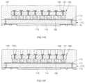
- FIG. 1depicts in cross-section a semiconductor device 100 constructed in accordance with a first embodiment of the present invention.
- the semiconductor device 100comprises a substrate 110 which preferably has a generally quadrangular configuration.
- the substrate 110can be selected from common circuit boards (e.g., rigid circuit boards and flexible circuit boards) and equivalents thereof.
- the present inventionis not intended to be limited to any particular type of substrate 110 .
- the substrate 110may include an insulating layer 114 having opposed, generally planar top and bottom surfaces.
- an electrically conductive pattern 112Disposed on the top surface is an electrically conductive pattern 112 , while disposed on the bottom surface are conductive lands 113 .
- the conductive pattern 112 and lands 113are electrically interconnected to each other in a prescribed pattern or arrangement through the use of conductive vias 111 which extend through the insulation layer 114 in a direction generally perpendicularly between the top and bottom surfaces thereof.
- a solder mask 115is preferably coated on at least portions of the lands 113 and the bottom surface of the insulating layer 114 . The solder mask 115 is used to protect portions of the lands 113 which would otherwise be exposed to the ambient environment.
- the semiconductor device 100further comprises a semiconductor die 120 which is electrically connected to the substrate 110 , and in particular to the conductive pattern 112 thereof.
- the semiconductor die 120defines opposed, generally planar top and bottom surfaces, and includes a plurality of terminals or bond pads 121 disposed on the top surface thereof.
- each of the bond pads 121is depicted as projecting upwardly from the generally planar top surface of the semiconductor die 120 .
- the semiconductor die 120further includes a plurality of through electrodes 122 formed therein and passing between the top and bottom surfaces thereof. As seen in FIG.
- each electrode 122is electrically coupled to a respective one of the bond pads 121 , with the remaining end (the bottom end as viewed from the perspective shown in FIG. 1 ) extending to the bottom surface of the semiconductor die 120 .
- each of the electrodes 122is electrically connected to the conductive pattern 112 of the substrate 110 through the use of respective ones of a plurality of conductive bumps 130 .
- suitable material for the conductive bumps 130include, but are not limited to, gold, silver, copper, soldering materials or equivalents thereto.
- the conductive bumps 130which are formed between the semiconductor die 120 and the substrate 110 , effectively transmit electrical signals between the semiconductor die 120 and the substrate 110 .
- an underfill materialmay be disposed between the bottom surface of the semiconductor die 120 and the top surface of the insulating layer 114 , the underfill material also covering portions of the conductive pattern 112 and the conductive bumps 130 .
- the underfill materialif included, would serve to protect the semiconductor die 120 by absorbing stress according to differences between the thermal expansion coefficients of the substrate 110 and the semiconductor die 120 .
- the semiconductor die 120may comprise a circuit that includes transistors, resistors and capacitors integrated on a silicon substrate.
- the semiconductor device 100further comprises a plurality of solder balls 160 which are electrically connected to the respective ones of the lands 113 of the substrate 110 in a prescribed pattern or arrangement. As seen in FIG. 1 , the solder mask 115 extends into contact with the solder balls 160 .
- suitable materials for the solder balls 160include, but are not limited to, eutectic solders (e.g., Sn37Pb), high-lead solders (e.g., Sn95Pb) having a high melting point, lead-free solders (e.g., SnAg, SnCu, SnZn, SnZnBi, SnAgCu and SnAgBi), or equivalents thereto.
- the solder balls 160are used to electrically couple the substrate 110 , and hence the semiconductor die 120 , to an external circuit.
- the semiconductor die 120at least portions of the semiconductor die 120 , the conductive bumps 130 , the top surface of the insulating layer 114 , and the conductive pattern 112 are each encapsulated or covered by an encapsulant material which ultimately hardens into a package body 140 of the semiconductor device 100 .
- the present inventionis not intended to be limited to any specific material which could be used to facilitate the fabrication of the package body 140 .
- the package body 140can be formed from epoxy molding compounds or equivalents thereto.
- the fully formed package body 140preferably includes a generally planar top surface, and generally planar side surfaces which extend in generally flush or co-planar relation to respective side surfaces of the insulating layer 114 of the substrate 110 .
- the package body 140includes a plurality of through-mold vias 150 formed therein.
- Each through-mold via (TMV) 150extends from the top surface of the package body 140 to a respective one of the bond pads 121 disposed on the top surface of the semiconductor die 120 .
- Each TMV 150is preferably formed by creating a hole in the package body 140 using a laser or an etching solution, and filling such hole with a conductive material selected from copper, aluminum, gold, silver, tin, lead, bismuth, soldering materials or equivalents thereto.
- each TMV 150may be facilitated by the completion of a reflow process subsequent to placing a ball fabricated from one of the aforementioned materials on top of the hole formed in the package body 140 through the use of one of the aforementioned processes.
- each TMV 150has a generally conical configuration. More particularly, each TMV 150 is of a first diameter at a respective one of the bond pads 121 , and a second diameter at the top surface of the package body 140 , the second diameter exceeding the first diameter. As such, each TMV 150 defines a continuous side wall which is inclined at a predetermined angle relative to the top surface of the package body 140 .
- each TMV 150creates an electrically conductive path from the semiconductor die 120 to the top surface of the package body 140 , whereas the conductive bumps 130 , substrate 110 and solder balls 160 collectively define an electrically conductive path which extends from the semiconductor die 120 in an opposite direction, such as toward an underlying substrate to which the semiconductor device 110 may ultimately be electrically connected through the use of the solder balls 160 .
- each TMV 150may have a shape or configuration differing from that shown in FIG. 1 without departing from the spirit and scope of the present invention.
- the semiconductor device 100is particularly suited for having another semiconductor device stacked thereon and electrically connected thereto.
- the lands or solder balls of a second semiconductor devicecan be electrically coupled to respective ones of the TMV's 150 exposed in the top surface of the package body 140 .
- the end of each TMV 150 extending to the top surface of the package body 140have a generally concave configuration to partially accommodate the solder balls of a conventional BGA (Ball Grid Array) semiconductor device which may be stacked upon the semiconductor device 100 , thus reducing the overall height or profile of the stack.
- BGABall Grid Array
- Another semiconductor device suitable for stacking upon the semiconductor device 100is an LGA (Land Grid Array) device, the stack comprising the semiconductor device 100 and the LGA device also being of comparatively reduced thickness due to the use of the TMV's 150 to facilitate the electrical interconnection therebetween.
- LGALand Grid Array
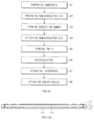
- FIG. 10there is provided a flow chart which sets forth an exemplary method for fabricating the semiconductor device 100 of the present invention shown in FIG. 1 .
- the methodcomprises the steps of preparing the substrate (S 1 ), preparing the semiconductor die (S 2 ), forming conductive bumps on the semiconductor die (S 3 ), attaching and electrically connecting the semiconductor die to the substrate (S 4 ), encapsulation to form a package body (S 5 ), forming TMV's in the package body (S 6 ), and the connection of solder balls to the substrate (S 7 ).
- FIGS. 11 A- 11 Hprovide illustrations corresponding to these particular steps, as will be discussed in more detail below.
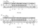
- the substrate 110 having the above-described structural attributesis provided in the initial step S 1 of the fabrication process for the semiconductor device 100 .
- a solder mask 115may be coated on at least portions of the lands 113 and the bottom surface of the insulating layer 114 .
- the semiconductor die 120is prepared. More particularly, as shown in FIG. 11 B , the semiconductor die 120 is formed to include the aforementioned bond pads 121 on the top surface thereof, and the through-electrodes 122 which pass through the semiconductor die 120 between the top and bottom surfaces thereof, the electrodes 122 being electrically coupled to respective ones of the bond pads 121 as indicated above. Thereafter, as illustrated in FIG. 11 C , step S 3 is completed wherein the conductive bumps 130 are electrically connected to those ends of the through electrodes 122 opposite those ends electrically coupled to the bond pads 121 . Thus, the electrodes 122 effectively electrically couple the bond pads 121 to respective ones of the conductive bumps 130 .
- the semiconductor die 120is electrically connected to the substrate 110 . More particularly, the conductive bumps 130 electrically connected to the semiconductor die 120 as described above in relation to step S 3 are each electrically connected to the conductive pattern 112 of the substrate 110 . As also indicated above, an underfill material may be interposed between the semiconductor die 120 and the substrate 110 , such underfill material thus covering or encapsulating at least portions of the conductive bumps 130 .
- the fully formed package body 140preferably includes a generally planar top surface, and generally planar side surfaces which extend in generally flush or co-planar relation to respective side surfaces of the insulating layer 114 of the substrate 110 .
- the encapsulation step S 5can be carried out by transfer molding using a mold or dispensing molding using a dispenser.
- the TMV's 150are formed in the package body 140 . More particularly, the formation of the TMV's 150 comprises the initial step of forming vias or holes 140 a in the package body 140 as shown in FIG. 11 F . Each of the holes 140 a extends from the top surface of the package body 140 to a respective one of the bond pads 121 . As indicated above, the holes 140 a may be formed through the use of a laser drilling or chemical etching process. After being formed in the package body 140 in the aforementioned manner, each of the holes 140 a is filled with a conductive metal material as shown in FIG. 11 G , thus completing the formation of the TMV's 150 .
- each hole 140 a with the metal materialmay be accomplished through the completion of a reflow process subsequent to the placement of a ball fabricated from a suitable conductive metal material upon that end of each hole 140 extending to the top surface of the package body 140 .
- the solder balls 160are electrically connected to respective ones of the lands 113 of the substrate 110 .
- the solder mask 115may extend into contact with the solder balls 160 .
- the solder balls 160may be fabricated from the materials described above in relation thereto.
- FIG. 2there is shown a semiconductor device 200 constructed in accordance with a second embodiment of the present invention.
- the semiconductor device 200is substantially similar to the above-described semiconductor device 100 , with only the differences between the semiconductor devices 200 , 100 being described below.
- each of the TMV's 250extends from the top surface of the package body 140 to a corresponding portion of the conductive pattern 112 of the substrate 110 .
- Each TMV 250is preferably fabricated using the same process described above in relation to each TMV 150 .
- the inclusion of the TMV's 250increases the available number of input/output terminals of the semiconductor device 200 in comparison to the semiconductor device 100 .
- the semiconductor device 300comprises the above-described substrate 110 .
- the semiconductor device 300comprises a first (upper) semiconductor die 320 which is attached to the top surface of the insulating layer 114 of the substrate 110 (as viewed from the perspective shown in FIG. 3 ) through the use of an adhesive layer 323 .
- the first semiconductor die 320defines opposed, generally planar top and bottom surfaces, and includes a plurality of terminals or bond pads 321 disposed on the top surface thereof.
- the bottom surface of the first semiconductor die 320is that surface which is attached to the substrate 110 through the use of the adhesive layer 323 .
- each conductive wire 330may be formed by the completion of a normal wire bonding method, that is, by forming a ball bond at the corresponding bond pad 321 of the first semiconductor die 320 , and then forming a stitch bonding region at a prescribed portion of the conductive pattern 112 of the substrate 110 .
- each conductive wire 330may be formed by a reverse loop wire bonding method, that is, by forming a ball bond at the corresponding bond pad 321 and corresponding portion of the conductive pattern 112 , and then connecting such ball bonds to each other.
- the semiconductor device 300includes a second (lower) semiconductor die 325 which is also electrically connected to the substrate 110 , and in particular the lands 113 thereof.
- the second semiconductor die 325defines opposed, generally planar top and bottom surfaces, and includes a plurality of bond pads 326 on that surface which defines the top surface as viewed from the perspective shown in FIG. 3 .
- each of the bond pads 326 of the second semiconductor die 325is electrically connected to a respective one of the lands 113 through the use of respective ones of a plurality of conductive bumps 331 .
- the conductive bumps 331are each preferably fabricated from the same material described above in relation to the conductive bumps 130 of the semiconductor device 100 .
- the semiconductor device 300at least portions of the first and second semiconductor dies 320 , 325 , the conductive wires 330 , the conductive bumps 331 , the top and bottom surfaces of the insulating layer 114 , the conductive pattern 112 , and the lands 113 are each encapsulated or covered by an encapsulant material which ultimately hardens into a package body 340 of the semiconductor device 300 .
- the package body 340may be fabricated from the same material described above in relation to the package body 140 of the semiconductor device 100 .
- the fully formed package body 340preferably includes a generally planar top surface when viewed from the perspective shown in FIG.
- the package body 340includes a plurality of through-mold vias (TMV's) 350 disposed therein. As seen in FIG. 3 , certain ones of the TMV's 350 extend from the top surface of the package body 340 to a corresponding portion of the conductive pattern 112 of the substrate 110 . The remaining TMV's 350 extend from the bottom surface of the package body 340 to respective ones of the lands 113 of the substrate 110 .
- Each TMV 350is identically configured to the above-described TMV's 250 of the semiconductor device 200 , and is preferably fabricated using the same process described above in relation to each TMV 150 of the semiconductor device 100 .
- each TMV 350 extending to the top surface and/or the bottom surface of the package body 340may have a generally concave configuration to partially accommodate solder balls of a conventional BGA semiconductor device which may be stacked on the top surface and/or the bottom surface of the semiconductor device 300 .
- the inclusion of the TMV's 350 in the semiconductor device 300makes the semiconductor device 300 particularly suited for having one or more additional semiconductor devices stacked on the top and/or bottom surfaces thereof.
- the semiconductor device 400comprises the above-described substrate 110 . Additionally, in the semiconductor device 400 , the above-described solder balls 160 are formed on and electrically connected to respective ones of the lands 113 of the substrate 110 . Further, the above-described solder mask 115 is preferably applied to the bottom surface of the insulating layer 114 of the substrate 110 , the solder mask 115 being coated on at least portions of the lands 113 and extending into contact with portions of each of the solder balls 160 .
- the semiconductor device 400comprises a first (lower) semiconductor die 320 which is electrically connected to the conductive pattern 112 of the substrate 110 .
- the first semiconductor die 420defines opposed, generally planar top and bottom surfaces, and includes a plurality of terminals or bond pads 421 disposed on the bottom surface thereof.
- Each of the bond pads 421is electrically connected to the conductive pattern 112 through the use of a respective one of a plurality of conductive bumps 430 .
- the conductive bumps 430are each preferably fabricated from the same material described above in relation to the conductive bumps 130 of the semiconductor device 100 .
- the semiconductor device 400further comprises an interposer 423 which is attached to the top surface of the first semiconductor die 420 through the use of an adhesive layer 415 .
- the interposer 423includes an interposer body 424 having a first conductive pattern 423 a formed within the top surface thereof, a second conductive pattern 423 b formed therein, and a third conductive pattern 423 c which is also formed therein and electrically connects the first and second conductive patterns 423 a , 423 b to each other. That surface of the body 424 disposed furthest from the first conductive pattern 423 a is secured to the top surface of the first semiconductor die 420 through the use of the aforementioned adhesive layer 413 . As seen in FIG.
- the first and second conductive patterns 423 a , 423 bare formed within the body 424 of the interposer 423 so as to extend along respective ones of a spaced, generally parallel pair of planes.
- the third conductive pattern 423 cis formed in a direction which extends generally perpendicularly between the planes along which respective ones of the first and second patterns 423 a , 423 b extend.
- the semiconductor device 400further comprises a second (upper) semiconductor die 425 which is electrically connected to the interposer 423 , and in particular to the first conductive pattern 423 a formed on the body 424 thereof.
- the second semiconductor die 425defines opposed, generally planar top and bottom surfaces.
- Disposed on the bottom surface of the first semiconductor die 425is a plurality of conductive terminals or bond pads 426 .
- the bond pads 426are each electrically connected to the first conductive pattern 423 a through the use of respective ones of a plurality of conductive bumps 431 which are each preferably fabricated from the same material used in relation to the conductive bumps 430 . As seen in FIG.
- the second and third conductive patterns 423 b , 423 c of the interposer 423are configured to effectively route signals between a portion of the first conductive pattern 423 a to which the second semiconductor die 425 is electrically connected to another portion of the first conductive pattern 423 a which is located outwardly beyond the lateral side surfaces of the second semiconductor die 425 .
- a peripheral portion of the interposer 423protrudes beyond the lateral side surfaces of each of the first and second semiconductor dies 420 , 425 .
- a portion of the first conductive pattern 423 ais exposed in the body 424 of such peripheral portion of the interposer 423 .
- the interposer 423(and hence the second semiconductor die 425 ) is electrically connected to the conductive pattern 112 of the substrate 110 through the use of one or more electrically conductive wires 432 . More particularly, one end of each conductive wire 432 extends and is electrically connected to a portion of the first conductive pattern 423 a which is exposed in the peripheral portion of the substrate 423 , and in particular the body 424 thereof. The remaining, opposite end of the conductive wire 432 is electrically connected to a prescribed portion of the conductive pattern 112 of the substrate 110 .
- the second semiconductor die 425is capable of receiving electrical signals from and outputting electrical signals to an external circuit via the interposer 423 , conductive wire(s) 432 , and substrate 110 .
- the semiconductor device 400at least portions of the first and second semiconductor dies 420 , 425 , the conductive bumps 430 , 431 , the interposer 423 , the conductive wires 432 , the insulating layer 114 of the substrate 110 , and the conductive pattern 112 are each encapsulated or covered by an encapsulant material which ultimately hardens into a package body 440 of the semiconductor device 100 .
- the package body 440may be fabricated from the same materials described above in relation to the package body 140 of the semiconductor device 100 .
- the fully formed package body 440preferably includes a generally planar top surface, and generally planar side surfaces which extend in generally flush or co-planar relation to respective side surfaces of the insulating layer 114 of the substrate 110 .
- the package body 440preferably includes a plurality of through-mold vias (TMV's) 450 formed therein. As seen in FIG. 4 , each of the TMV's 450 extends from the top surface of the package body 440 to a corresponding portion of the conductive pattern 112 of the substrate 110 .
- Each TMV 450is identically configured to the above-described TMV's 250 , 350 , and is preferably fabricated using the same process described above in relation to each TMV 150 .
- the semiconductor device 500comprises the above-described substrate 110 . Additionally, in the semiconductor device 500 , the above-described solder balls 160 are formed on and electrically connected to respective ones of the lands 113 of the substrate 110 . Further, the above-described solder mask 115 is preferably applied to the bottom surface of the insulating layer 114 of the substrate 110 , the solder mask 115 being coated on at least portions of the lands 113 and extending into contact with portions of each of the solder balls 160 .
- the semiconductor device 500also includes a first semiconductor die 120 which is identical to the above-described semiconductor 120 of the semiconductor device 100 , and is electrically connected to the conductive pattern 112 of the substrate 110 through the use of the conductive bumps 130 in the same manner described above in relation to the semiconductor device 100 .
- a plurality of conductive balls 551is also electrically connected to the conductive pattern 112 of the substrate 110 .
- the conductive balls 551are electrically connected to a peripheral portion of the conductive pattern 112 .
- Each of the conductive balls 551is preferably fabricated from a conductive material selected from copper, aluminum, gold, silver, tin, lead, bismuth, soldering materials or equivalents thereto.
- the semiconductor device 500further comprises an interposer 523 which is disposed on the top surface of the first semiconductor die 420 and electrically connected to the first semiconductor die 120 .
- the interposer 523includes an interposer body 524 having a first conductive pattern 523 a formed within the top surface thereof, a second conductive pattern 523 b formed therein, and a third conductive pattern 523 c which is also formed therein and electrically connects the first and second conductive patterns 523 a , 523 b to each other.
- the first and second conductive patterns 523 a , 523 bare formed within the body 524 of the interposer 523 so as to extend along respective ones of a spaced, generally parallel pair of planes.
- the third conductive pattern 523 cis formed in a direction which extends generally perpendicularly between the planes along which respective ones of the first and second conductive patterns 523 a , 523 b extend.
- the second conductive pattern 523 b of the interposer 523is electrically connected to the bond pads 121 of the first semiconductor die 121 .
- the interposer 523is sized relative to the first semiconductor die 120 such that the side surfaces of the body 524 extend in substantially co-planar relation to respective side surfaces of the first semiconductor die 120 .
- the semiconductor device 500further comprises the second (upper) semiconductor die 425 described above in relation to the semiconductor device 400 .
- the second semiconductor die 425is electrically connected to the interposer 523 , and in particular to the first conductive pattern 523 a formed on the body 524 thereof.
- the bond pads 426 of the second semiconductor die 425are each electrically connected to the first conductive pattern 523 a through the use of respective ones of the aforementioned conductive bumps 431 .
- the side surfaces of the body 524 of the interposer 523also extend in substantially co-planar to respective side surfaces of the second semiconductor die 425 .
- the side surfaces of the body 524 of the interposer 523extend in generally co-planar relation to respective ones of the lateral side surfaces of each of the first and second semiconductor dies 120 , 425 .
- the semiconductor device 500at least portions of the first and second semiconductor dies 120 , 425 , the conductive bumps 130 , 431 , the interposer 523 , the conductive balls 551 , the insulating layer 114 of the substrate 110 , and the conductive pattern 112 are each encapsulated or covered by an encapsulant material which ultimately hardens into a package body 540 of the semiconductor device 500 .
- the package body 540may be fabricated from the same materials described above in relation to the package body 140 of the semiconductor device 100 .
- the fully formed package body 540preferably includes a generally planar top surface, and generally planar side surfaces which extend in generally flush or co-planar relation to respective side surfaces of the insulating layer 114 of the substrate 110 .
- the package body 140preferably includes a plurality of through-mold vias (TMV's) 550 formed therein.
- TMV'sthrough-mold vias
- Each TMV 550includes a first region which is defined by a respective one of the conductive balls 551 electrically connected to the conductive pattern 112 of the substrate 110 .
- each TMV 550includes a second region 552 which extends from the top surface of the package body 140 to a respective one of the conductive balls 551 .
- the second region 552 of each TMV 550is identically configured to the above-described TMV's 250 , 350 , 450 , and is preferably fabricated using the same process described above in relation to each TMV 150 .
- each TMV 550is defined by a metal-filled hole which is formed in the package body 540 to extend from the top surface thereof to a corresponding conductive ball 551 (i.e., the first region of the same TMV 550 ).
- each TMV 550(comprising the second region 552 and the first region or conductive ball 551 ) extends from the top surface of the package body 540 to (and in electrical communication with) the conductive pattern 112 .
- each second region 552 of the TMV's 550extends to respective ones of the conductive balls 551 rather than to the conductive pattern 112 , each second region 552 is of a shorter height in comparison to the TMV's 450 included in the semiconductor device 400 , though being fabricated in the same manner as indicated above. Due to the shortened height of height of the second regions 552 of the TMV's 550 , including the holes used to form the same, potential adverse effects on the first and second semiconductor dies 120 , 425 attributable to the formation of the holes is reduced, thus improving the reliability of the semiconductor device 500 .
- the semiconductor device 600comprises the above-described substrate 110 . Additionally, in the semiconductor device 600 , the above-described solder balls 160 are formed on and electrically connected to respective ones of the lands 113 of the substrate 110 . Further, the above-described solder mask 115 is preferably applied to the bottom surface of the insulating layer 114 of the substrate 110 , the solder mask 115 being coated on at least portions of the lands 113 and extending into contact with portions of each of the solder balls 160 .
- the semiconductor device 600also includes a semiconductor die 420 which is identical to the above-described semiconductor 420 of the semiconductor device 400 , and is electrically connected to the conductive pattern 112 of the substrate 110 through the use of the conductive bumps 430 in the same manner described above in relation to the semiconductor device 400 .
- the semiconductor die 420In the semiconductor device 600 , at least portions of the semiconductor die 420 , the conductive bumps 430 , the insulating layer 114 of the substrate 110 , and the conductive pattern 112 are each encapsulated or covered by an encapsulant material which ultimately hardens into a package body 640 of the semiconductor device 600 .
- the package body 640may be fabricated from the same materials described above in relation to the package body 140 of the semiconductor device 100 .
- the fully formed package body 640preferably includes a generally planar top surface, and generally planar side surfaces which extend in generally flush or co-planar relation to respective side surfaces of the insulating layer 114 of the substrate 110 .
- the generally planar top surface of the semiconductor die 420is preferably exposed in and substantially flush with the top surface of the package body 640 .
- the package body 640preferably includes a plurality of through-mold vias (TMV's) 650 formed therein.
- TMV 650preferably comprises a conductive ball which is electrically connected to a peripheral portion of the conductive pattern 112 .
- the conductive balls used to define the TMV's 650are preferably fabricated from a conductive material selected from copper, aluminum, gold, silver, tin, lead, bismuth, soldering materials or equivalents thereto.
- the package body 640is formed in a manner wherein portions of the conductive balls used to form the TMV's 650 protrude from the top surface of the package body 640 in the manner shown in FIG. 6 .
- each TMV 650slightly exceeds the height or thickness of the package body 640 . It is also contemplated that the package body 640 may be fabricated by attaching a mold film to the substrate 110 , such mold film partially covering the semiconductor die 420 and TMV's 650 in the aforementioned manner.
- the semiconductor device 600further comprises an interposer 623 which is disposed on and electrically connected to the TMV's 650 .
- the interposer 623includes an interposer body 624 having a first conductive pattern 623 a formed within the top surface thereof, a second conductive pattern 623 b formed therein, and a third conductive pattern 623 c which is also formed therein and electrically connects the first and second conductive patterns 623 a , 623 b to each other.
- the first and second conductive patterns 623 a , 623 bare formed within the body 624 of the interposer 623 so as to extend along respective ones of a spaced, generally parallel pair of planes.
- the third conductive pattern 623 cis formed in a direction which extends generally perpendicularly between the planes along which respective ones of the first and second conductive patterns 623 a , 623 b extend.
- the second conductive pattern 623 b of the interposer 623is electrically connected to the exposed portions of the TMV's 650 in the manner shown in FIG. 6 .
- a narrow space or gap 615is defined between the top surface of the package body 640 (as well as the top surface of the semiconductor die 420 ) and the interposer 623 (i.e., the bottom surface of the body 624 ).
- the formation of the gap 615 between the package body 640 and the interposer 623enhances the ability of the semiconductor die 420 to dissipate heat outside of the semiconductor device 600 .
- the inclusion of the interposer 623 in the semiconductor device 600allows a wiring pattern of the TMV's 650 to be selectively redistributed using the interposer 623 .
- the interposer 623is sized relative to the package body 640 such that the side surfaces of the body 624 extend in substantially co-planar relation to respective side surfaces of the package body 640 .
- FIG. 12there is provided a flow chart which sets forth an exemplary method for fabricating the semiconductor device 600 of the present invention shown in FIG. 6 .
- the methodcomprises the steps of preparing the substrate (S 1 ), preparing the semiconductor die (S 2 ), forming conductive bumps on the semiconductor die (S 3 ), attaching and electrically connecting the semiconductor die to the substrate (S 4 ), forming TMV's on the substrate (S 5 ), encapsulation to form a package body (S 6 ), attaching an interposer to the TMV's (S 7 ), and the connection of solder balls to the substrate (S 8 ).
- FIGS. 13 A- 13 Hprovide illustrations corresponding to these particular steps, as will be discussed in more detail below.
- the substrate 110 having the above-described structural attributesis provided in the initial step S 1 of the fabrication process for the semiconductor device 600 .
- a solder mask 115may be coated on at least portions of the lands 113 and the bottom surface of the insulating layer 114 .
- the semiconductor die 420is prepared. More particularly, as shown in FIG. 13 B , the semiconductor die 420 is formed to include the aforementioned bond pads 421 on the bottom surface thereof. As shown in FIG. 13 B , the bond pads 421 are formed on the bottom surface of the semiconductor die 420 so as to protrude therefrom. In this regard, those of ordinary skill in the art will recognize that the bond pads 421 may alternatively be formed so as to be at least partially embedded in the semiconductor die 420 and to extend in substantially flush relation to the bottom surface thereof. Thereafter, as illustrated in FIG. 13 C , step S 3 is completed wherein the conductive bumps 430 are electrically connected to respective ones of the bond pads 121 .
- the semiconductor die 420is electrically connected to the substrate 110 . More particularly, the conductive bumps 430 electrically connected to the semiconductor die 420 as described above in relation to step S 3 are each electrically connected to the conductive pattern 112 of the substrate 110 , and hence to the lands 113 .
- the TMV's 650are formed on the substrate 110 . More particularly, as explained above, the formation of the TMV's 650 is facilitated by forming the aforementioned conductive balls on respective peripheral portions of the conductive pattern 112 of the substrate 110 . Thus, the TMV's 650 extend at least partially about the periphery of the semiconductor die 420 in the manner shown in FIG. 13 E .
- the fully formed package body 640preferably includes a generally planar top surface, and generally planar side surfaces which extend in generally flush or co-planar relation to respective side surfaces of the insulating layer 114 of the substrate 110 .
- the package body 640is formed such that the top surface of the semiconductor die 420 extends in substantially flush relation to the top surface of the package body, with the TMV's 650 protruding slightly beyond the top surface of the package body 640 .
- the encapsulation step S 6can be carried out by transfer molding using a mold, dispensing molding using a dispenser, or through the use of the aforementioned mold film.
- the interposer 623is electrically connected to the TMV's 650 . More particularly, the second conductive pattern 623 b of the interposer 623 is electrically connected to the exposed portions of the TMV's 650 such that the aforementioned gap 615 is defined between the bottom surface of the body 624 of the interposer 623 and the top surface of the package body 640 .
- the solder balls 160are electrically connected to respective ones of the lands 113 of the substrate 110 .
- the solder mask 115may extend into contact with the solder balls 160 .
- the solder balls 160may be fabricated from the materials described above in relation thereto.
- the semiconductor device 700comprises the above-described substrate 110 . Additionally, in the semiconductor device 700 , the above-described solder balls 160 are formed on and electrically connected to respective ones of the lands 113 of the substrate 110 . Further, the above-described solder mask 115 is preferably applied to the bottom surface of the insulating layer 114 of the substrate 110 , the solder mask 115 being coated on at least portions of the lands 113 and extending into contact with portions of each of the solder balls 160 .
- the semiconductor device 700also includes a first (lower) semiconductor die 420 which is identical to the above-described semiconductor 420 of the semiconductor device 400 , and is electrically connected to the conductive pattern 112 of the substrate 110 through the use of the conductive bumps 430 in the same manner described above in relation to the semiconductor device 400 .
- a plurality of conductive balls(which ultimately define lower through-mold vias or TMV's 650 as described below) are electrically connected to a peripheral portion of the first conductive pattern 112 .
- the conductive balls used to define the TMV's 650are preferably fabricated from a conductive material selected from copper, aluminum, gold, silver, tin, lead, bismuth, soldering materials or equivalents thereto.
- the semiconductor device 700further comprises a first (lower) interposer 723 which is disposed on and electrically connected to the conductive balls ultimately defining the TMV's 650 .
- the first interposer 723includes an interposer body 724 having a first conductive pattern 723 a formed within the top surface thereof, a second conductive pattern 723 b formed therein, and a third conductive pattern 723 c which is also formed therein and electrically connects the first and second conductive patterns 723 a , 723 b to each other. As seen in FIG.
- the first and second conductive patterns 723 a , 723 bare formed within the body 724 of the first interposer 723 so as to extend along respective ones of a spaced, generally parallel pair of planes.
- the third conductive pattern 723 cis formed in a direction which extends generally perpendicularly between the planes along which respective ones of the first and second conductive patterns 723 a , 723 b extend.
- the second conductive pattern 723 b of the first interposer 723is electrically connected to the conductive balls ultimately defining the TMV's 650 in the manner shown in FIG. 7 .
- the first interposer 723and in particular a central portion of the bottom surface of the body 724 thereof, is attached to the top surface of the first semiconductor die through the use of an adhesive layer 415 .
- the semiconductor device 700also includes a second (upper) semiconductor die 425 which is identical to the above-described semiconductor 425 of the semiconductor device 400 , and is electrically connected to a central portion of the first conductive pattern 723 a of the first interposer 723 through the use of the conductive bumps 431 in the same manner described above in relation to electrical connection of the second semiconductor die 425 of the semiconductor device 400 to the first conductive pattern 423 a of the interposer 423 thereof.
- a plurality of conductive balls(which ultimately define upper through-mold vias or TMV's 750 as described below) are electrically connected to a peripheral portion of the first conductive pattern 723 a of the first interposer 723 .
- the conductive balls used to define the TMV's 750are also preferably fabricated from a conductive material selected from copper, aluminum, gold, silver, tin, lead, bismuth, soldering materials or equivalents thereto.
- the semiconductor device 700at least portions of the first and second semiconductor dies 420 , 425 , the first interposer 723 , the conductive bumps 430 , the conductive balls ultimately defining the TMV's 650 , 750 , the insulating layer 114 of the substrate 110 , and the conductive pattern 112 are each encapsulated or covered by an encapsulant material which ultimately hardens into a package body 740 of the semiconductor device 700 .
- the package body 740may be fabricated from the same materials described above in relation to the package body 140 of the semiconductor device 100 .
- the fully formed package body 740preferably includes a generally planar top surface, and generally planar side surfaces which extend in generally flush or co-planar relation to respective side surfaces of the insulating layer 114 of the substrate 110 .
- the generally planar top surface of the second semiconductor die 425is preferably exposed in and substantially flush with the top surface of the package body 740 .
- the TMVs 650are defined by the encapsulation of the conductive balls electrically connected to and extending between the conductive pattern 112 of the substrate 110 and the second conductive pattern 723 b of the interposer 723 .
- the upper TMVs 750are defined by the partial encapsulation of the conductive balls electrically connected to the first conductive pattern 723 a of the interposer 723 with the package body 740 .
- the package body 740is formed in a manner wherein portions of the conductive balls used to form the TMV's 750 protrude from the top surface of the package body 740 in the manner shown in FIG. 7 .
- each TMV 750slightly exceeds the height or thickness of the package body 740 .
- each TMV 650 , 750preferably comprises a respective one of the aforementioned conductive balls which are each electrically connected to a peripheral portion of the first interposer 723 .
- the semiconductor device 700further comprises a second (upper) interposer 770 which is disposed on and electrically connected to the TMV's 750 .
- the second interposer 770includes an interposer body 774 having a first conductive pattern 771 formed within the top surface thereof, a second conductive pattern 772 formed therein, and a third conductive pattern 773 which is also formed therein and electrically connects the first and second conductive patterns 771 , 772 to each other.
- the first and second conductive patterns 771 , 772are formed within the body 774 of the second interposer 770 so as to extend along respective ones of a spaced, generally parallel pair of planes.
- the third conductive pattern 773is formed in a direction which extends generally perpendicularly between the planes along which respective ones of the first and second conductive patterns 771 , 772 extend.
- the second conductive pattern 772 of the second interposer 770is electrically connected to the exposed portions of the TMV's 750 in the manner shown in FIG. 7 .
- a narrow space or gap 715is defined between the top surface of the package body 740 (as well as the top surface of the second semiconductor die 425 ) and the second interposer 770 (i.e., the bottom surface of the body 774 ).
- the formation of the gap 715 between the package body 740 and the second interposer 770enhances the ability of the second semiconductor die 425 to dissipate heat outside of the semiconductor device 700 .
- the inclusion of the second interposer 770 in the semiconductor device 700allows a wiring pattern of the TMV's 750 to be selectively redistributed using the interposer 770 .
- FIG. 8there is shown a semiconductor device 800 constructed in accordance with an eighth embodiment of the present invention.
- the semiconductor device 800is substantially similar to the above-described semiconductor device 700 , with only the differences between the semiconductor devices 800 , 700 being described below.
- the semiconductor devices 800 , 700lies in the omission of the above-described second interposer 770 in the semiconductor device 800 . Additionally, in the semiconductor device 800 , the package body 740 described above in relation to the semiconductor device 700 is substituted with the package body 840 which is formed to completely cover the top surface of the second semiconductor die 425 . This is in contrast to the semiconductor device 700 wherein the top surface of the second semiconductor die 425 is exposed in the top surface of the package body 740 .
- each of the TMV's 850bears substantial structural similarity to the TMV's 550 described above in relation to the semiconductor device 500 . More particularly, as seen in FIG. 8 , each TMV 850 includes a first region which is defined by a respective one of a plurality of conductive balls 851 which are each electrically connected to a peripheral portion of the first conductive pattern 723 a of the interposer 723 .
- each TMV 850includes a second region 852 which extends from the top surface of the package body 840 to a respective one of the conductive balls 851 .
- the second region 852 of each TMV 850is identically configured to the above-described TMV's 250 , 350 , 450 , 550 , and is preferably fabricated using the same process described above in relation to each TMV 150 .
- the second region 852 of each TMV 850is defined by a metal-filled hole which is formed in the package body 840 to extend from the top surface thereof to a corresponding conductive ball 851 (i.e., the first region of the same TMV 850 ).
- each TMV 850(comprising the second region 852 and the first region or conductive ball 851 ) extends from the top surface of the package body 840 to (and in electrical communication with) the first conductive pattern 723 a of the interposer 723 .
- the semiconductor device 900comprises the above-described substrate 110 . Additionally, in the semiconductor device 900 , the above-described solder balls 160 are formed on and electrically connected to respective ones of the lands 113 of the substrate 110 . Further, the above-described solder mask 115 is preferably applied to the bottom surface of the insulating layer 114 of the substrate 110 , the solder mask 115 being coated on at least portions of the lands 113 and extending into contact with portions of each of the solder balls 160 .
- the semiconductor device 900also includes a first (lower) semiconductor die 420 which is identical to the above-described semiconductor 420 of the semiconductor device 400 , and is electrically connected to the conductive pattern 112 of the substrate 110 through the use of the conductive bumps 430 in the same manner described above in relation to the semiconductor device 400 .
- the semiconductor device 900further comprises a second (upper) semiconductor die 925 .
- the second semiconductor die 925defines opposed, generally planar top and bottom surfaces, and includes a plurality of conductive terminals or bond pads 926 disposed on the top surface thereof when viewed from the perspective shown in FIG. 9 .
- the bottom surface of the second semiconductor die 925is attached to the top surface of the first semiconductor die 420 through the use of an intervening adhesive layer 415 .
- the first and second semiconductor dies 420 , 925are preferably sized relative to each other such that the side surfaces thereof extend in substantially flush relation to each other when the first and second semiconductor dies 420 , 925 are attached to each other through the use of the adhesive layer 415 .
- each of the bond pads 926is a respective one of a plurality of conductive bumps 931 , each of which is preferably fabricated from the same material used to facilitate the fabrication of conductive bumps 430 used to electrically connect the first semiconductor die 420 to the conductive pattern 112 of the substrate 110 .
- the semiconductor device 900at least portions of the first and second semiconductor dies 420 , 925 , the conductive bumps 430 , 931 , the insulating layer 114 of the substrate 110 and the conductive pattern 112 are each encapsulated or covered by an encapsulant material which ultimately hardens into a package body 940 of the semiconductor device 900 .
- the package body 940may be fabricated from the same materials described above in relation to the package body 140 of the semiconductor device 100 .
- the fully formed package body 940preferably includes a generally planar top surface, and generally planar side surfaces which extend in substantially flush or co-planar relation to respective side surfaces of the insulating layer 114 of the substrate 110 .
- portions of each of the conductive bumps 931preferably protrude from the top surface of the package body 940 .
- the package body 940preferably includes a plurality of through-mold vias (TMV's) 950 formed therein.
- TMV 950preferably comprises a conductive ball which is electrically connected to a peripheral portion of the conductive pattern 112 .
- the conductive balls used to define the TMV's 950are preferably fabricated from a conductive material selected from copper, aluminum, gold, silver, tin, lead, bismuth, soldering materials or equivalents thereto.
- the package body 940is formed in a manner wherein portions of the conductive balls used to form the TMV's 950 protrude from the top surface of the package body 940 in the manner shown in FIG. 9 .
- the height of each TMV 950slightly exceeds the height or thickness of the package body 940 .
- the semiconductor device 900further comprises an interposer 970 which is disposed on and electrically connected to the conductive bumps 931 and the TMV's 950 .
- the interposer 970includes an interposer body 974 having a first conductive pattern 971 formed within the top surface thereof, a second conductive pattern 972 formed therein, and a third conductive pattern 973 which is also formed therein and electrically connects the first and second conductive patterns 971 , 972 to each other.
- the first and second conductive patterns 971 , 972are formed within the body 974 of the interposer 623 so as to extend along respective ones of a spaced, generally parallel pair of planes.
- the third conductive pattern 973is formed in a direction which extends generally perpendicularly between the planes along which respective ones of the first and second conductive patterns 971 , 972 extend.
- the second conductive pattern 972 of the interposer 970is electrically connected to the exposed portions of the conductive bumps 931 and the TMV's 950 in the manner shown in FIG. 9 .
- no space or gapsuch as the aforementioned gaps 615 , 715 is defined between the interposer 970 and the top surface of the package body 940 .
- the interposer 970and in particular the bottom surface of the body 974 thereof, is in direct contact with the top surface of the package body 940 .
- the inclusion of the interposer 970 in the semiconductor device 900allows a wiring pattern of the conductive bumps 931 and the TMV's 950 to be selectively redistributed using the interposer 970 .
- the interposer 970is sized relative to the package body 940 such that the side surfaces of the body 974 extend in substantially co-planar relation to respective side surfaces of the package body 940 .
Landscapes
- Engineering & Computer Science (AREA)
- Microelectronics & Electronic Packaging (AREA)
- Power Engineering (AREA)
- Computer Hardware Design (AREA)
- Physics & Mathematics (AREA)
- Condensed Matter Physics & Semiconductors (AREA)
- General Physics & Mathematics (AREA)
- Manufacturing & Machinery (AREA)
- Wire Bonding (AREA)
Abstract
Description
Claims (12)
Priority Applications (2)
| Application Number | Priority Date | Filing Date | Title |
|---|---|---|---|
| US16/925,599US11869829B2 (en) | 2009-01-05 | 2020-07-10 | Semiconductor device with through-mold via |
| US18/406,784US20240145346A1 (en) | 2009-01-05 | 2024-01-08 | Semiconductor device with through-mold via |
Applications Claiming Priority (4)
| Application Number | Priority Date | Filing Date | Title |
|---|---|---|---|
| US34881309A | 2009-01-05 | 2009-01-05 | |
| US15/390,568US20170117214A1 (en) | 2009-01-05 | 2016-12-26 | Semiconductor device with through-mold via |
| US16/025,465US10811341B2 (en) | 2009-01-05 | 2018-07-02 | Semiconductor device with through-mold via |
| US16/925,599US11869829B2 (en) | 2009-01-05 | 2020-07-10 | Semiconductor device with through-mold via |
Related Parent Applications (1)
| Application Number | Title | Priority Date | Filing Date |
|---|---|---|---|
| US16/025,465DivisionUS10811341B2 (en) | 2009-01-05 | 2018-07-02 | Semiconductor device with through-mold via |
Related Child Applications (1)
| Application Number | Title | Priority Date | Filing Date |
|---|---|---|---|
| US16/025,465DivisionUS10811341B2 (en) | 2009-01-05 | 2018-07-02 | Semiconductor device with through-mold via |
Publications (2)
| Publication Number | Publication Date |
|---|---|
| US20200343163A1 US20200343163A1 (en) | 2020-10-29 |
| US11869829B2true US11869829B2 (en) | 2024-01-09 |
Family
ID=58559016
Family Applications (4)
| Application Number | Title | Priority Date | Filing Date |
|---|---|---|---|
| US15/390,568AbandonedUS20170117214A1 (en) | 2009-01-05 | 2016-12-26 | Semiconductor device with through-mold via |
| US16/025,465Active2029-03-29US10811341B2 (en) | 2009-01-05 | 2018-07-02 | Semiconductor device with through-mold via |
| US16/925,599Active2029-07-12US11869829B2 (en) | 2009-01-05 | 2020-07-10 | Semiconductor device with through-mold via |
| US18/406,784PendingUS20240145346A1 (en) | 2009-01-05 | 2024-01-08 | Semiconductor device with through-mold via |
Family Applications Before (2)
| Application Number | Title | Priority Date | Filing Date |
|---|---|---|---|
| US15/390,568AbandonedUS20170117214A1 (en) | 2009-01-05 | 2016-12-26 | Semiconductor device with through-mold via |
| US16/025,465Active2029-03-29US10811341B2 (en) | 2009-01-05 | 2018-07-02 | Semiconductor device with through-mold via |
Family Applications After (1)
| Application Number | Title | Priority Date | Filing Date |
|---|---|---|---|
| US18/406,784PendingUS20240145346A1 (en) | 2009-01-05 | 2024-01-08 | Semiconductor device with through-mold via |
Country Status (1)
| Country | Link |
|---|---|
| US (4) | US20170117214A1 (en) |
Families Citing this family (8)
| Publication number | Priority date | Publication date | Assignee | Title |
|---|---|---|---|---|
| TWI667743B (en)* | 2017-10-20 | 2019-08-01 | 矽品精密工業股份有限公司 | Electronic package and method for fabricating the same |
| US11239173B2 (en)* | 2019-03-28 | 2022-02-01 | Taiwan Semiconductor Manufacturing Co., Ltd. | Structure and formation method of chip package with fan-out feature |
| CN112151514B (en) | 2019-06-28 | 2025-07-29 | 桑迪士克科技股份有限公司 | Semiconductor device including vertically stacked semiconductor die |
| US12347785B2 (en)* | 2019-09-29 | 2025-07-01 | Taiwan Semiconductor Manufacturing Co., Ltd. | Semiconductor structure and method manufacturing the same |
| CN113539978B (en)* | 2020-04-17 | 2023-11-10 | 江苏长电科技股份有限公司 | Fan-out packaging structure |
| CN118366875A (en) | 2021-01-26 | 2024-07-19 | 长江存储科技有限责任公司 | Substrate structure and its manufacturing and packaging method |
| WO2023157747A1 (en)* | 2022-02-16 | 2023-08-24 | 株式会社村田製作所 | Circuit module |
| US20240264370A1 (en)* | 2023-02-07 | 2024-08-08 | Cisco Technology, Inc. | Optical packaging features for mechanical stability and optical fiber coupling |
Citations (449)
| Publication number | Priority date | Publication date | Assignee | Title |
|---|---|---|---|---|
| US2596993A (en) | 1949-01-13 | 1952-05-20 | United Shoe Machinery Corp | Method and mold for covering of eyelets by plastic injection |
| US3435815A (en) | 1966-07-15 | 1969-04-01 | Micro Tech Mfg Inc | Wafer dicer |
| US3734660A (en) | 1970-01-09 | 1973-05-22 | Tuthill Pump Co | Apparatus for fabricating a bearing device |
| US3838984A (en) | 1973-04-16 | 1974-10-01 | Sperry Rand Corp | Flexible carrier and interconnect for uncased ic chips |
| US4054238A (en) | 1976-03-23 | 1977-10-18 | Western Electric Company, Inc. | Method, apparatus and lead frame for assembling leads with terminals on a substrate |
| US4189342A (en) | 1971-10-07 | 1980-02-19 | U.S. Philips Corporation | Semiconductor device comprising projecting contact layers |
| US4221925A (en) | 1978-09-18 | 1980-09-09 | Western Electric Company, Incorporated | Printed circuit board |
| JPS55163868A (en) | 1979-06-08 | 1980-12-20 | Fujitsu Ltd | Lead frame and semiconductor device using the same |
| US4258381A (en) | 1977-12-07 | 1981-03-24 | Steag, Kernergie Gmbh | Lead frame for a semiconductor device suitable for mass production |
| US4289922A (en) | 1979-09-04 | 1981-09-15 | Plessey Incorporated | Integrated circuit package and lead frame |
| US4301464A (en) | 1978-08-02 | 1981-11-17 | Hitachi, Ltd. | Lead frame and semiconductor device employing the same with improved arrangement of supporting leads for securing the semiconductor supporting member |
| US4332537A (en) | 1978-07-17 | 1982-06-01 | Dusan Slepcevic | Encapsulation mold with removable cavity plates |
| US4394712A (en) | 1981-03-18 | 1983-07-19 | General Electric Company | Alignment-enhancing feed-through conductors for stackable silicon-on-sapphire wafers |
| JPS58160096A (en) | 1982-03-16 | 1983-09-22 | 株式会社 日立工機原町工場 | Brake gear in meat slicer |
| US4417266A (en) | 1981-08-14 | 1983-11-22 | Amp Incorporated | Power and ground plane structure for chip carrier |
| US4451224A (en) | 1982-03-25 | 1984-05-29 | General Electric Company | Mold device for making plastic articles from resin |
| JPS59208756A (en) | 1983-05-12 | 1984-11-27 | Sony Corp | Manufacture of semiconductor device package |
| JPS59227143A (en) | 1983-06-07 | 1984-12-20 | Dainippon Printing Co Ltd | Package of integrated circuit |
| JPS6010756A (en) | 1983-06-30 | 1985-01-19 | Nec Corp | Manufacture of beam-lead type semiconductor device |
| US4499655A (en) | 1981-03-18 | 1985-02-19 | General Electric Company | Method for making alignment-enhancing feed-through conductors for stackable silicon-on-sapphire |
| JPS60116239A (en) | 1983-11-28 | 1985-06-22 | Nec Corp | Radio communication equipment |
| US4530152A (en) | 1982-04-01 | 1985-07-23 | Compagnie Industrielle Des Telecommunications Cit-Alcatel | Method for encapsulating semiconductor components using temporary substrates |
| US4541003A (en) | 1978-12-27 | 1985-09-10 | Hitachi, Ltd. | Semiconductor device including an alpha-particle shield |
| JPS60195957A (en) | 1984-03-19 | 1985-10-04 | Hitachi Ltd | lead frame |
| JPS60231349A (en) | 1984-05-01 | 1985-11-16 | Toshiba Corp | lead frame |
| JPS61248541A (en) | 1985-04-26 | 1986-11-05 | Matsushita Electronics Corp | Semiconductor device |
| US4646710A (en) | 1982-09-22 | 1987-03-03 | Crystal Systems, Inc. | Multi-wafer slicing with a fixed abrasive |
| US4707724A (en) | 1984-06-04 | 1987-11-17 | Hitachi, Ltd. | Semiconductor device and method of manufacturing thereof |
| US4727633A (en) | 1985-08-08 | 1988-03-01 | Tektronix, Inc. | Method of securing metallic members together |
| JPS6367762A (en) | 1986-09-09 | 1988-03-26 | Fujitsu Ltd | Lead frame for resin sealed semiconductor device |
| US4737839A (en) | 1984-03-19 | 1988-04-12 | Trilogy Computer Development Partners, Ltd. | Semiconductor chip mounting system |
| US4756080A (en) | 1986-01-27 | 1988-07-12 | American Microsystems, Inc. | Metal foil semiconductor interconnection method |
| JPS63188964A (en) | 1987-01-31 | 1988-08-04 | Dainippon Printing Co Ltd | integrated circuit package |
| JPS63205935A (en) | 1987-02-23 | 1988-08-25 | Toshiba Corp | Resin-encapsulated semiconductor device with heat sink |
| JPS63233555A (en) | 1987-03-23 | 1988-09-29 | Toshiba Corp | Resin-encapsulated semiconductor device |
| JPS63249345A (en) | 1987-04-06 | 1988-10-17 | Olympus Optical Co Ltd | Flexible mounting substrate |
| JPS63289951A (en) | 1987-05-22 | 1988-11-28 | Dainippon Printing Co Ltd | Lead frame |
| JPS63316470A (en) | 1987-06-19 | 1988-12-23 | Alps Electric Co Ltd | Manufacture of thin film transistor |
| JPS6454749A (en) | 1987-08-26 | 1989-03-02 | Matsushita Electric Industrial Co Ltd | Semiconductor device and manufacture thereof |
| US4812696A (en) | 1987-02-17 | 1989-03-14 | Louis Stanley | Motor core with winding slots having reduced air gaps |
| JPH01106456A (en) | 1987-10-19 | 1989-04-24 | Matsushita Electric Ind Co Ltd | Semiconductor integrated circuit device |
| JPH01205544A (en) | 1988-02-12 | 1989-08-17 | Seiko Epson Corp | Integrated circuit device assembly tape |
| US4862246A (en) | 1984-09-26 | 1989-08-29 | Hitachi, Ltd. | Semiconductor device lead frame with etched through holes |
| US4862245A (en) | 1985-04-18 | 1989-08-29 | International Business Machines Corporation | Package semiconductor chip |
| JPH01251747A (en) | 1988-03-31 | 1989-10-06 | Toshiba Corp | Semiconductor device and its manufacturing method |
| US4907067A (en) | 1988-05-11 | 1990-03-06 | Texas Instruments Incorporated | Thermally efficient power device package |
| US4920074A (en) | 1987-02-25 | 1990-04-24 | Hitachi, Ltd. | Surface mount plastic package semiconductor integrated circuit, manufacturing method thereof, as well as mounting method and mounted structure thereof |
| JPH02129948A (en) | 1988-11-09 | 1990-05-18 | Dainippon Printing Co Ltd | Pre-molded semiconductor device |
| US4935803A (en) | 1988-09-09 | 1990-06-19 | Motorola, Inc. | Self-centering electrode for power devices |
| US4942454A (en) | 1987-08-05 | 1990-07-17 | Mitsubishi Denki Kabushiki Kaisha | Resin sealed semiconductor device |
| EP0393997A2 (en) | 1989-04-20 | 1990-10-24 | Honeywell Inc. | Method of providing a variable-pitch leadframe assembly |
| US4987475A (en) | 1988-02-29 | 1991-01-22 | Digital Equipment Corporation | Alignment of leads for ceramic integrated circuit packages |
| JPH0369248A (en) | 1989-08-08 | 1991-03-25 | Nec Off Syst Ltd | Telephone set |
| US5018003A (en) | 1988-10-20 | 1991-05-21 | Mitsubishi Denki Kabushiki Kaisha | Lead frame and semiconductor device |
| US5029386A (en) | 1990-09-17 | 1991-07-09 | Hewlett-Packard Company | Hierarchical tape automated bonding method |
| US5041902A (en) | 1989-12-14 | 1991-08-20 | Motorola, Inc. | Molded electronic package with compression structures |
| US5057900A (en) | 1988-10-17 | 1991-10-15 | Semiconductor Energy Laboratory Co., Ltd. | Electronic device and a manufacturing method for the same |
| US5059379A (en) | 1987-07-20 | 1991-10-22 | Mitsubishi Denki Kabushiki Kaisha | Method of resin sealing semiconductor devices |
| US5065223A (en) | 1989-05-31 | 1991-11-12 | Fujitsu Vlsi Limited | Packaged semiconductor device |
| US5070039A (en) | 1989-04-13 | 1991-12-03 | Texas Instruments Incorporated | Method of making an integrated circuit using a pre-served dam bar to reduce mold flash and to facilitate flash removal |
| EP0459493A2 (en) | 1990-06-01 | 1991-12-04 | Kabushiki Kaisha Toshiba | A semiconductor device using a lead frame and its manufacturing method |
| US5087961A (en) | 1987-01-28 | 1992-02-11 | Lsi Logic Corporation | Semiconductor device package |
| US5091341A (en) | 1989-05-22 | 1992-02-25 | Kabushiki Kaisha Toshiba | Method of sealing semiconductor device with resin by pressing a lead frame to a heat sink using an upper mold pressure member |
| US5096852A (en) | 1988-06-02 | 1992-03-17 | Burr-Brown Corporation | Method of making plastic encapsulated multichip hybrid integrated circuits |
| US5118298A (en) | 1991-04-04 | 1992-06-02 | Advanced Interconnections Corporation | Through hole mounting of integrated circuit adapter leads |
| US5122860A (en) | 1987-08-26 | 1992-06-16 | Matsushita Electric Industrial Co., Ltd. | Integrated circuit device and manufacturing method thereof |
| US5134773A (en) | 1989-05-26 | 1992-08-04 | Gerard Lemaire | Method for making a credit card containing a microprocessor chip |
| US5151039A (en) | 1990-04-06 | 1992-09-29 | Advanced Interconnections Corporation | Integrated circuit adapter having gullwing-shaped leads |
| US5157475A (en) | 1988-07-08 | 1992-10-20 | Oki Electric Industry Co., Ltd. | Semiconductor device having a particular conductive lead structure |
| US5157480A (en) | 1991-02-06 | 1992-10-20 | Motorola, Inc. | Semiconductor device having dual electrical contact sites |
| US5168368A (en) | 1991-05-09 | 1992-12-01 | International Business Machines Corporation | Lead frame-chip package with improved configuration |
| US5172213A (en) | 1991-05-23 | 1992-12-15 | At&T Bell Laboratories | Molded circuit package having heat dissipating post |
| US5172214A (en) | 1991-02-06 | 1992-12-15 | Motorola, Inc. | Leadless semiconductor device and method for making the same |
| US5175060A (en) | 1989-07-01 | 1992-12-29 | Ibiden Co., Ltd. | Leadframe semiconductor-mounting substrate having a roughened adhesive conductor circuit substrate and method of producing the same |
| US5200362A (en) | 1989-09-06 | 1993-04-06 | Motorola, Inc. | Method of attaching conductive traces to an encapsulated semiconductor die using a removable transfer film |
| US5200809A (en) | 1991-09-27 | 1993-04-06 | Vlsi Technology, Inc. | Exposed die-attach heatsink package |
| US5216278A (en) | 1990-12-04 | 1993-06-01 | Motorola, Inc. | Semiconductor device having a pad array carrier package |
| US5214845A (en) | 1992-05-11 | 1993-06-01 | Micron Technology, Inc. | Method for producing high speed integrated circuits |
| US5218231A (en) | 1989-08-30 | 1993-06-08 | Kabushiki Kaisha Toshiba | Mold-type semiconductor device |
| US5221642A (en) | 1991-08-15 | 1993-06-22 | Staktek Corporation | Lead-on-chip integrated circuit fabrication method |
| US5250841A (en) | 1992-04-06 | 1993-10-05 | Motorola, Inc. | Semiconductor device with test-only leads |
| US5250843A (en) | 1991-03-27 | 1993-10-05 | Integrated System Assemblies Corp. | Multichip integrated circuit modules |
| US5252853A (en) | 1991-09-19 | 1993-10-12 | Mitsubishi Denki Kabushiki Kaisha | Packaged semiconductor device having tab tape and particular power distribution lead structure |
| US5258094A (en) | 1991-09-18 | 1993-11-02 | Nec Corporation | Method for producing multilayer printed wiring boards |
| US5266834A (en) | 1989-03-13 | 1993-11-30 | Hitachi Ltd. | Semiconductor device and an electronic device with the semiconductor devices mounted thereon |
| US5277972A (en) | 1988-09-29 | 1994-01-11 | Tomoegawa Paper Co., Ltd. | Adhesive tapes |
| US5278446A (en) | 1992-07-06 | 1994-01-11 | Motorola, Inc. | Reduced stress plastic package |
| US5279029A (en) | 1990-08-01 | 1994-01-18 | Staktek Corporation | Ultra high density integrated circuit packages method |
| US5281849A (en) | 1991-05-07 | 1994-01-25 | Singh Deo Narendra N | Semiconductor package with segmented lead frame |
| JPH0629639A (en) | 1992-07-08 | 1994-02-04 | Tokyo Electric Co Ltd | Circuit board |
| US5285352A (en) | 1992-07-15 | 1994-02-08 | Motorola, Inc. | Pad array semiconductor device with thermal conductor and process for making the same |
| JPH0652333A (en) | 1992-07-29 | 1994-02-25 | Nec Corp | Single chip microcomputer |
| US5294897A (en) | 1992-07-20 | 1994-03-15 | Mitsubishi Denki Kabushiki Kaisha | Microwave IC package |
| US5299647A (en) | 1992-10-16 | 1994-04-05 | Schiller-Pfeiffer, Inc. | Tined rotary blade for cultivators |
| JPH0692076A (en) | 1992-09-16 | 1994-04-05 | Oki Electric Ind Co Ltd | Lead frame form for ic card module |
| KR940010938A (en) | 1992-11-25 | 1994-06-20 | 오정학 | Processing method of seaweed |
| US5327008A (en) | 1993-03-22 | 1994-07-05 | Motorola Inc. | Semiconductor device having universal low-stress die support and method for making the same |
| US5332864A (en) | 1991-12-27 | 1994-07-26 | Vlsi Technology, Inc. | Integrated circuit package having an interposer |
| US5336931A (en) | 1993-09-03 | 1994-08-09 | Motorola, Inc. | Anchoring method for flow formed integrated circuit covers |
| US5335771A (en) | 1990-09-25 | 1994-08-09 | R. H. Murphy Company, Inc. | Spacer trays for stacking storage trays with integrated circuits |
| US5343076A (en) | 1990-07-21 | 1994-08-30 | Mitsui Petrochemical Industries, Ltd. | Semiconductor device with an airtight space formed internally within a hollow package |
| US5356661A (en)* | 1990-11-21 | 1994-10-18 | Sumitomo Electric Industries, Ltd. | Heat transfer insulated parts and manufacturing method thereof |
| US5358905A (en) | 1993-04-02 | 1994-10-25 | Texas Instruments Incorporated | Semiconductor device having die pad locking to substantially reduce package cracking |
| US5365106A (en) | 1992-10-27 | 1994-11-15 | Kabushiki Kaisha Toshiba | Resin mold semiconductor device |
| US5381042A (en) | 1992-03-31 | 1995-01-10 | Amkor Electronics, Inc. | Packaged integrated circuit including heat slug having an exposed surface |
| US5391439A (en) | 1990-09-27 | 1995-02-21 | Dai Nippon Printing Co., Ltd. | Leadframe adapted to support semiconductor elements |
| US5406124A (en) | 1992-12-04 | 1995-04-11 | Mitsui Toatsu Chemicals, Inc. | Insulating adhesive tape, and lead frame and semiconductor device employing the tape |
| US5410180A (en) | 1992-07-28 | 1995-04-25 | Shinko Electric Industries Co., Ltd. | Metal plane support for multi-layer lead frames and a process for manufacturing such frames |
| US5414299A (en) | 1993-09-24 | 1995-05-09 | Vlsi Technology, Inc. | Semi-conductor device interconnect package assembly for improved package performance |
| US5417905A (en) | 1989-05-26 | 1995-05-23 | Esec (Far East) Limited | Method of making a card having decorations on both faces |
| US5428248A (en) | 1992-08-21 | 1995-06-27 | Goldstar Electron Co., Ltd. | Resin molded semiconductor package |
| US5434057A (en) | 1994-02-02 | 1995-07-18 | Quidel Corporation | Sperm motility assay and devices |
| KR950018924A (en) | 1993-12-09 | 1995-07-22 | 박홍기 | Manufacturing method of suede artificial leather |
| US5444301A (en) | 1993-06-23 | 1995-08-22 | Goldstar Electron Co. Ltd. | Semiconductor package and method for manufacturing the same |
| US5452511A (en) | 1993-11-04 | 1995-09-26 | Chang; Alexander H. C. | Composite lead frame manufacturing method |
| US5454905A (en) | 1994-08-09 | 1995-10-03 | National Semiconductor Corporation | Method for manufacturing fine pitch lead frame |
| US5467032A (en) | 1993-11-09 | 1995-11-14 | Samsung Electronics Co., Ltd. | Word line driver circuit for a semiconductor memory device |
| US5474958A (en) | 1993-05-04 | 1995-12-12 | Motorola, Inc. | Method for making semiconductor device having no die supporting surface |
| US5484274A (en) | 1992-11-24 | 1996-01-16 | Neu Dynamics Corp. | Encapsulation molding equipment |
| US5493151A (en) | 1993-07-15 | 1996-02-20 | Kabushiki Kaisha Toshiba | Semiconductor device, lead frame and method for manufacturing semiconductor devices |
| US5508556A (en) | 1994-09-02 | 1996-04-16 | Motorola, Inc. | Leaded semiconductor device having accessible power supply pad terminals |
| US5517056A (en) | 1993-09-30 | 1996-05-14 | Motorola, Inc. | Molded carrier ring leadframe having a particular resin injecting area design for gate removal and semiconductor device employing the same |
| US5521429A (en) | 1993-11-25 | 1996-05-28 | Sanyo Electric Co., Ltd. | Surface-mount flat package semiconductor device |
| US5528076A (en) | 1995-02-01 | 1996-06-18 | Motorola, Inc. | Leadframe having metal impregnated silicon carbide mounting area |
| EP0720234A2 (en) | 1994-12-30 | 1996-07-03 | SILICONIX Incorporated | Vertical power MOSFET having thick metal layer to reduce distributed resistance and method of fabricating the same |
| EP0720225A2 (en) | 1994-12-30 | 1996-07-03 | SILICONIX Incorporated | Lateral power MOSFET having metal strap layer to reduce distributed resistance and method of fabricating the same |
| US5534467A (en) | 1993-03-18 | 1996-07-09 | Lsi Logic Corporation | Semiconductor packages for high I/O semiconductor dies |
| US5539251A (en) | 1992-05-11 | 1996-07-23 | Micron Technology, Inc. | Tie bar over chip lead frame design |
| US5543657A (en) | 1994-10-07 | 1996-08-06 | International Business Machines Corporation | Single layer leadframe design with groundplane capability |
| US5544412A (en) | 1994-05-24 | 1996-08-13 | Motorola, Inc. | Method for coupling a power lead to a bond pad in an electronic module |
| US5545923A (en) | 1993-10-22 | 1996-08-13 | Lsi Logic Corporation | Semiconductor device assembly with minimized bond finger connections |
| US5581122A (en) | 1994-10-25 | 1996-12-03 | Industrial Technology Research Institute | Packaging assembly with consolidated common voltage connections for integrated circuits |
| US5592019A (en) | 1994-04-19 | 1997-01-07 | Mitsubishi Denki Kabushiki Kaisha | Semiconductor device and module |
| US5592025A (en) | 1992-08-06 | 1997-01-07 | Motorola, Inc. | Pad array semiconductor device |
| JPH098206A (en) | 1995-06-19 | 1997-01-10 | Dainippon Printing Co Ltd | Lead frame and bga resin sealed semiconductor device |
| JPH098207A (en) | 1995-06-21 | 1997-01-10 | Dainippon Printing Co Ltd | Resin-sealed semiconductor device |
| US5594274A (en) | 1993-07-01 | 1997-01-14 | Nec Corporation | Lead frame for use in a semiconductor device and method of manufacturing the semiconductor device using the same |
| US5595934A (en) | 1995-05-17 | 1997-01-21 | Samsung Electronics Co., Ltd. | Method for forming oxide protective film on bonding pads of semiconductor chips by UV/O3 treatment |
| US5604376A (en) | 1994-06-30 | 1997-02-18 | Digital Equipment Corporation | Paddleless molded plastic semiconductor chip package |
| US5608267A (en) | 1992-09-17 | 1997-03-04 | Olin Corporation | Molded plastic semiconductor package including heat spreader |
| US5608265A (en) | 1993-03-17 | 1997-03-04 | Hitachi, Ltd. | Encapsulated semiconductor device package having holes for electrically conductive material |
| JPH0964284A (en) | 1995-06-15 | 1997-03-07 | Oki Electric Ind Co Ltd | Semiconductor integrated circuit |
| US5625222A (en) | 1993-11-18 | 1997-04-29 | Fujitsu Limited | Semiconductor device in a resin package housed in a frame having high thermal conductivity |
| US5633528A (en) | 1994-05-25 | 1997-05-27 | Texas Instruments Incorporated | Lead frame structure for IC devices with strengthened encapsulation adhesion |
| US5637922A (en) | 1994-02-07 | 1997-06-10 | General Electric Company | Wireless radio frequency power semiconductor devices using high density interconnect |
| US5639990A (en) | 1992-06-05 | 1997-06-17 | Mitsui Toatsu Chemicals, Inc. | Solid printed substrate and electronic circuit package using the same |
| US5640047A (en) | 1995-09-25 | 1997-06-17 | Mitsui High-Tec, Inc. | Ball grid assembly type semiconductor device having a heat diffusion function and an electric and magnetic shielding function |
| US5641997A (en) | 1993-09-14 | 1997-06-24 | Kabushiki Kaisha Toshiba | Plastic-encapsulated semiconductor device |
| US5643433A (en) | 1992-12-23 | 1997-07-01 | Shinko Electric Industries Co., Ltd. | Lead frame and method for manufacturing same |
| US5644169A (en) | 1993-03-04 | 1997-07-01 | Goldstar Electron Co., Ltd. | Mold and method for manufacturing a package for a semiconductor chip and the package manufactured thereby |
| US5646831A (en) | 1995-12-28 | 1997-07-08 | Vlsi Technology, Inc. | Electrically enhanced power quad flat pack arrangement |
| US5650663A (en) | 1995-07-03 | 1997-07-22 | Olin Corporation | Electronic package with improved thermal properties |
| US5661088A (en) | 1996-01-11 | 1997-08-26 | Motorola, Inc. | Electronic component and method of packaging |
| EP0794572A2 (en) | 1996-03-07 | 1997-09-10 | Matsushita Electronics Corporation | Electronic component, method for making the same, and lead frame and mold assembly for use therein |
| US5673479A (en) | 1993-12-20 | 1997-10-07 | Lsi Logic Corporation | Method for mounting a microelectronic circuit peripherally-leaded package including integral support member with spacer |
| US5682062A (en) | 1995-06-05 | 1997-10-28 | Harris Corporation | System for interconnecting stacked integrated circuits |
| US5683943A (en) | 1994-06-14 | 1997-11-04 | Dai Nippon Printing Co., Ltd. | Process for etching a semiconductor lead frame |
| US5683806A (en) | 1988-09-29 | 1997-11-04 | Tomoegawa Paper Co., Ltd. | Adhesive tapes |
| US5689135A (en) | 1995-12-19 | 1997-11-18 | Micron Technology, Inc. | Multi-chip device and method of fabrication employing leads over and under processes |
| US5696666A (en) | 1995-10-11 | 1997-12-09 | Motorola, Inc. | Low profile exposed die chip carrier package |
| US5701034A (en) | 1994-05-03 | 1997-12-23 | Amkor Electronics, Inc. | Packaged semiconductor die including heat sink with locking feature |
| US5703407A (en) | 1995-02-14 | 1997-12-30 | Kabushiki Kaisha Toshiba | Resin-sealed type semiconductor device |
| US5710064A (en) | 1994-08-16 | 1998-01-20 | Samsung Electronics Co., Ltd. | Method for manufacturing a semiconductor package |
| JPH1022447A (en) | 1996-06-28 | 1998-01-23 | Goto Seisakusho:Kk | Resin-sealed semiconductor device and method of manufacturing the same |
| US5724233A (en) | 1993-07-09 | 1998-03-03 | Fujitsu Limited | Semiconductor device having first and second semiconductor chips with a gap therebetween, a die stage in the gap and associated lead frames disposed in a package, the lead frames providing electrical connections from the chips to an exterior of the packag |
| US5723899A (en) | 1994-08-30 | 1998-03-03 | Amkor Electronics, Inc. | Semiconductor lead frame having connection bar and guide rings |
| US5726493A (en) | 1994-06-13 | 1998-03-10 | Fujitsu Limited | Semiconductor device and semiconductor device unit having ball-grid-array type package structure |
| US5736432A (en) | 1996-09-20 | 1998-04-07 | National Semiconductor Corporation | Lead frame with lead finger locking feature and method for making same |
| US5745984A (en) | 1995-07-10 | 1998-05-05 | Martin Marietta Corporation | Method for making an electronic module |
| US5753532A (en) | 1995-08-30 | 1998-05-19 | Samsung Electronics Co., Ltd. | Method of manufacturing semiconductor chip package |
| US5753977A (en) | 1996-03-22 | 1998-05-19 | Mitsubishi Denki Kabushiki Kaisha | Semiconductor device and lead frame therefor |
| EP0844665A2 (en) | 1996-11-21 | 1998-05-27 | Texas Instruments Incorporated | Wafer level packaging |
| US5767566A (en) | 1995-10-18 | 1998-06-16 | Kabushiki Kaisha Toshiba | Plastic mold type semiconductor device |
| US5766972A (en) | 1994-06-02 | 1998-06-16 | Mitsubishi Denki Kabushiki Kaisha | Method of making resin encapsulated semiconductor device with bump electrodes |
| US5770888A (en) | 1995-12-29 | 1998-06-23 | Lg Semicon Co., Ltd. | Integrated chip package with reduced dimensions and leads exposed from the top and bottom of the package |
| US5776798A (en) | 1996-09-04 | 1998-07-07 | Motorola, Inc. | Semiconductor package and method thereof |
| DE19734794A1 (en) | 1997-01-09 | 1998-07-16 | Mitsubishi Electric Corp | Wiring part and lead frame with the wiring part |
| US5783661A (en) | 1991-09-20 | 1998-07-21 | Fred Hutchinson Cancer Research Center | Human cyclin E polypeptides |
| JPH10199934A (en) | 1997-01-13 | 1998-07-31 | Hitachi Ltd | Semiconductor element mounting structure and semiconductor element mounting method |
| US5801440A (en) | 1995-10-10 | 1998-09-01 | Acc Microelectronics Corporation | Chip package board having utility rings |
| JPH10256240A (en) | 1997-01-10 | 1998-09-25 | Sony Corp | Manufacture of semiconductor device |
| US5814881A (en) | 1996-12-20 | 1998-09-29 | Lsi Logic Corporation | Stacked integrated chip package and method of making same |
| US5814884A (en) | 1996-10-24 | 1998-09-29 | International Rectifier Corporation | Commonly housed diverse semiconductor die |
| US5814883A (en) | 1995-10-04 | 1998-09-29 | Mitsubishi Denki Kabushiki Kaisha | Packaged semiconductor chip |
| US5818105A (en) | 1994-07-22 | 1998-10-06 | Nec Corporation | Semiconductor device with plastic material covering a semiconductor chip mounted on a substrate of the device |
| US5817540A (en) | 1996-09-20 | 1998-10-06 | Micron Technology, Inc. | Method of fabricating flip-chip on leads devices and resulting assemblies |
| US5821457A (en) | 1994-03-11 | 1998-10-13 | The Panda Project | Semiconductor die carrier having a dielectric epoxy between adjacent leads |
| US5821615A (en) | 1995-12-06 | 1998-10-13 | Lg Semicon Co., Ltd. | Semiconductor chip package having clip-type outlead and fabrication method of same |
| US5835988A (en) | 1996-03-27 | 1998-11-10 | Mitsubishi Denki Kabushiki Kaisha | Packed semiconductor device with wrap around external leads |
| US5834830A (en) | 1995-12-18 | 1998-11-10 | Lg Semicon Co., Ltd. | LOC (lead on chip) package and fabricating method thereof |
| US5844306A (en) | 1995-09-28 | 1998-12-01 | Mitsubishi Denki Kabushiki Kaisha | Die pad structure for solder bonding |
| US5854511A (en) | 1995-11-17 | 1998-12-29 | Anam Semiconductor, Inc. | Semiconductor package including heat sink with layered conductive plate and non-conductive tape bonding to leads |
| US5854512A (en) | 1996-09-20 | 1998-12-29 | Vlsi Technology, Inc. | High density leaded ball-grid array package |
| US5856911A (en) | 1996-11-12 | 1999-01-05 | National Semiconductor Corporation | Attachment assembly for integrated circuits |
| US5859471A (en) | 1992-11-17 | 1999-01-12 | Shinko Electric Industries Co., Ltd. | Semiconductor device having tab tape lead frame with reinforced outer leads |
| US5866939A (en) | 1996-01-21 | 1999-02-02 | Anam Semiconductor Inc. | Lead end grid array semiconductor package |
| US5866942A (en) | 1995-04-28 | 1999-02-02 | Nec Corporation | Metal base package for a semiconductor device |
| US5870289A (en) | 1994-12-15 | 1999-02-09 | Hitachi, Ltd. | Chip connection structure having diret through-hole connections through adhesive film and wiring substrate |
| US5871782A (en) | 1995-12-30 | 1999-02-16 | Lg Semicon Co. Ltd. | Transfer molding apparatus having laminated chase block |
| US5874784A (en) | 1995-10-25 | 1999-02-23 | Sharp Kabushiki Kaisha | Semiconductor device having external connection terminals provided on an interconnection plate and fabrication process therefor |
| US5877043A (en) | 1996-02-01 | 1999-03-02 | International Business Machines Corporation | Electronic package with strain relief means and method of making |
| JPH1175250A (en) | 1997-08-29 | 1999-03-16 | Fujikura Ltd | Cell formation method in mobile communication |
| US5886397A (en) | 1996-09-05 | 1999-03-23 | International Rectifier Corporation | Crushable bead on lead finger side surface to improve moldability |
| EP0936671A1 (en) | 1998-02-12 | 1999-08-18 | Hitachi, Ltd. | Resin-moulded semiconductor hybrid module and manufacturing method thereof |
| KR100220154B1 (en) | 1996-04-01 | 1999-09-01 | 김규현 | Method manufacture of semiconductor package |
| US5973935A (en) | 1997-04-07 | 1999-10-26 | Micron Technology, Inc. | Interdigitated leads-over-chip lead frame for supporting an integrated circuit die |
| US5977630A (en) | 1997-08-15 | 1999-11-02 | International Rectifier Corp. | Plural semiconductor die housed in common package with split heat sink |
| WO1999056316A1 (en) | 1998-04-28 | 1999-11-04 | Tessera, Inc. | Encapsulation of microelectronic assemblies |
| JPH11307675A (en) | 1998-04-20 | 1999-11-05 | Matsushita Electron Corp | Resin-encapsulate semiconductor device and its manufacture |
| WO1999067821A1 (en) | 1998-06-24 | 1999-12-29 | Amkor Technology, Inc. | Plastic integrated circuit package and method and leadframe for making the package |
| EP0989608A2 (en) | 1998-09-21 | 2000-03-29 | Amkor Technology Inc. | Plastic integrated circuit device package and method of making the same |
| USRE36773E (en) | 1993-10-18 | 2000-07-11 | Motorola, Inc. | Method for plating using nested plating buses and semiconductor device having the same |
| US6107679A (en) | 1997-12-22 | 2000-08-22 | Oki Electric Industry Co., Ltd. | Semiconductor device |
| EP1032037A2 (en) | 1999-02-24 | 2000-08-30 | Matsushita Electronics Corporation | Resin-moulded semiconductor device, method for manufacturing the same, and leadframe |
| US6130823A (en)* | 1999-02-01 | 2000-10-10 | Raytheon E-Systems, Inc. | Stackable ball grid array module and method |
| KR20000072714A (en) | 2000-09-21 | 2000-12-05 | 이희영 | Mandibular angle retractor |
| US6166430A (en) | 1998-05-27 | 2000-12-26 | Matsushita Electronics Corporation | Lead frame, method for manufacturing the frame, resin-molded semiconductor device and method for manufacturing the device |
| US6168969B1 (en) | 1996-02-16 | 2001-01-02 | Micron Technology, Inc. | Surface mount IC using silicon vias in an area array format or same size as die array |
| US6169329B1 (en) | 1996-04-02 | 2001-01-02 | Micron Technology, Inc. | Semiconductor devices having interconnections using standardized bonding locations and methods of designing |
| US6177718B1 (en) | 1998-04-28 | 2001-01-23 | Kabushiki Kaisha Toshiba | Resin-sealed semiconductor device |
| US6181002B1 (en) | 1998-12-22 | 2001-01-30 | Sharp Kabushiki Kaisha | Semiconductor device having a plurality of semiconductor chips |
| US6184573B1 (en) | 1999-05-13 | 2001-02-06 | Siliconware Precision Industries Co., Ltd. | Chip packaging |
| US6184465B1 (en) | 1998-11-12 | 2001-02-06 | Micron Technology, Inc. | Semiconductor package |
| US6194777B1 (en) | 1998-06-27 | 2001-02-27 | Texas Instruments Incorporated | Leadframes with selective palladium plating |
| US6197615B1 (en) | 1997-04-04 | 2001-03-06 | Samsung Electronics Co., Ltd. | Method of producing lead frame having uneven surfaces |
| US6198171B1 (en) | 1999-12-30 | 2001-03-06 | Siliconware Precision Industries Co., Ltd. | Thermally enhanced quad flat non-lead package of semiconductor |
| US6201186B1 (en) | 1998-06-29 | 2001-03-13 | Motorola, Inc. | Electronic component assembly and method of making the same |
| US6201292B1 (en) | 1997-04-02 | 2001-03-13 | Dai Nippon Insatsu Kabushiki Kaisha | Resin-sealed semiconductor device, circuit member used therefor |
| US6204554B1 (en) | 1996-09-05 | 2001-03-20 | International Rectifier Corporation | Surface mount semiconductor package |
| US6208021B1 (en) | 1996-03-27 | 2001-03-27 | Oki Electric Industry Co., Ltd. | Semiconductor device, manufacturing method thereof and aggregate type semiconductor device |
| US6208023B1 (en) | 1997-07-31 | 2001-03-27 | Matsushita Electronics Corporation | Lead frame for use with an RF powered semiconductor |
| US6211462B1 (en) | 1998-11-05 | 2001-04-03 | Texas Instruments Incorporated | Low inductance power package for integrated circuits |
| US6218731B1 (en) | 1999-05-21 | 2001-04-17 | Siliconware Precision Industries Co., Ltd. | Tiny ball grid array package |
| US6222259B1 (en) | 1998-09-15 | 2001-04-24 | Hyundai Electronics Industries Co., Ltd. | Stack package and method of fabricating the same |
| US6222258B1 (en) | 1996-11-11 | 2001-04-24 | Fujitsu Limited | Semiconductor device and method for producing a semiconductor device |
| US6225146B1 (en) | 1996-12-24 | 2001-05-01 | Matsushita Electronics Corporation | Lead frame, method of manufacturing lead frame, semiconductor device and method of manufacturing semiconductor device |
| US6229205B1 (en) | 1997-06-30 | 2001-05-08 | Samsung Electronics Co., Ltd. | Semiconductor device package having twice-bent tie bar and small die pad |
| US6229200B1 (en) | 1998-06-10 | 2001-05-08 | Asat Limited | Saw-singulated leadless plastic chip carrier |
| US6238952B1 (en) | 2000-02-29 | 2001-05-29 | Advanced Semiconductor Engineering, Inc. | Low-pin-count chip package and manufacturing method thereof |
| US6239367B1 (en) | 1999-01-29 | 2001-05-29 | United Microelectronics Corp. | Multi-chip chip scale package |
| US6239384B1 (en) | 1995-09-18 | 2001-05-29 | Tessera, Inc. | Microelectric lead structures with plural conductors |
| JP3177060B2 (en) | 1992-04-13 | 2001-06-18 | 株式会社リコー | Reversible thermosensitive recording label and card |
| US6256200B1 (en) | 1999-05-27 | 2001-07-03 | Allen K. Lam | Symmetrical package for semiconductor die |
| US6258629B1 (en) | 1999-08-09 | 2001-07-10 | Amkor Technology, Inc. | Electronic device package and leadframe and method for making the package |
| US6261864B1 (en) | 2000-01-28 | 2001-07-17 | Advanced Semiconductor Engineering, Inc. | Low-pin-count chip package and manufacturing method thereof |
| US20010008305A1 (en) | 1998-06-10 | 2001-07-19 | Asat Ltd. | Leadless plastic chip carrier with etch back pad singulation |
| US20010011654A1 (en) | 1998-07-16 | 2001-08-09 | The University Of Texas System | Method for rapid drying of coated materials with close capture of vapors |
| US6282095B1 (en) | 1999-02-02 | 2001-08-28 | Compaq Computer Corporation | Method and system for controlling radio frequency radiation in microelectronic packages using heat dissipation structures |
| US6281566B1 (en) | 1996-09-30 | 2001-08-28 | Sgs-Thomson Microelectronics S.R.L. | Plastic package for electronic devices |
| US6282094B1 (en) | 1999-04-12 | 2001-08-28 | Siliconware Precision Industries, Co., Ltd. | Ball-grid array integrated circuit package with an embedded type of heat-dissipation structure and method of manufacturing the same |
| US6285075B1 (en) | 1998-11-02 | 2001-09-04 | Asat, Limited | Integrated circuit package with bonding planes on a ceramic ring using an adhesive assembly |
| US6291271B1 (en) | 1999-09-14 | 2001-09-18 | Advanced Semiconductor Engineering, Inc. | Method of making semiconductor chip package |
| US6291273B1 (en) | 1996-12-26 | 2001-09-18 | Hitachi, Ltd. | Plastic molded type semiconductor device and fabrication process thereof |
| US6294100B1 (en) | 1998-06-10 | 2001-09-25 | Asat Ltd | Exposed die leadless plastic chip carrier |
| US6294830B1 (en) | 1996-04-18 | 2001-09-25 | Tessera, Inc. | Microelectronic assembly with conductive terminals having an exposed surface through a dielectric layer |
| US6297548B1 (en) | 1998-06-30 | 2001-10-02 | Micron Technology, Inc. | Stackable ceramic FBGA for high thermal applications |
| US6295977B1 (en) | 1998-11-05 | 2001-10-02 | Wacker Chemie Gmbh | Method and device for simultaneously cutting off a multiplicity of wafers from a workpiece |
| US6303997B1 (en) | 1998-04-08 | 2001-10-16 | Anam Semiconductor, Inc. | Thin, stackable semiconductor packages |
| US6303984B1 (en) | 1997-08-12 | 2001-10-16 | Micron Technology, Inc. | Lead frame including angle iron tie bar |
| US6306685B1 (en) | 2000-02-01 | 2001-10-23 | Advanced Semiconductor Engineering, Inc. | Method of molding a bump chip carrier and structure made thereby |
| US6307272B1 (en) | 1998-05-27 | 2001-10-23 | Hitachi, Ltd. | Semiconductor device and method for manufacturing the same |
| US6309909B1 (en) | 1998-07-02 | 2001-10-30 | Mitsubishi Denki Kabushiki Kaisha | Semiconductor device and method of manufacturing the same |
| US6316822B1 (en) | 1998-09-16 | 2001-11-13 | Texas Instruments Incorporated | Multichip assembly semiconductor |
| US6316838B1 (en) | 1999-10-29 | 2001-11-13 | Fujitsu Limited | Semiconductor device |
| US20010044538A1 (en) | 1997-10-20 | 2001-11-22 | Soan Cheng | p38 MAP kinase inhibitors |
| US6323550B1 (en) | 1995-06-06 | 2001-11-27 | Analog Devices, Inc. | Package for sealing an integrated circuit die |
| US6326244B1 (en) | 1998-09-03 | 2001-12-04 | Micron Technology, Inc. | Method of making a cavity ball grid array apparatus |
| US6326243B1 (en) | 1995-08-15 | 2001-12-04 | Kabushiki Kaisha Toshiba | Resin sealed semiconductor device including a die pad uniformly having heat conducting paths and circulating holes for fluid resin |
| US6326678B1 (en) | 1993-09-03 | 2001-12-04 | Asat, Limited | Molded plastic package with heat sink and enhanced electrical performance |
| US6335564B1 (en) | 1998-05-06 | 2002-01-01 | Conexant Systems, Inc. | Single Paddle having a semiconductor device and a passive electronic component |
| US6337510B1 (en) | 2000-11-17 | 2002-01-08 | Walsin Advanced Electronics Ltd | Stackable QFN semiconductor package |
| JP2002003497A (en) | 2000-04-06 | 2002-01-09 | Exploit Des Prod Pour Les Ind Chim Sepc:Soc | Novel polyxyloside derivatives, methods for their production and use as surfactants |
| US6339255B1 (en) | 1998-10-24 | 2002-01-15 | Hyundai Electronics Industries Co., Ltd. | Stacked semiconductor chips in a single semiconductor package |
| US6342730B1 (en) | 2000-01-28 | 2002-01-29 | Advanced Semiconductor Engineering, Inc. | Low-pin-count chip package and manufacturing method thereof |
| US20020017710A1 (en) | 2000-08-04 | 2002-02-14 | Seiko Epson Corporation | Semiconductor device and method of manufacturing the same, circuit board, and electronic equipment |
| US6348726B1 (en) | 2001-01-18 | 2002-02-19 | National Semiconductor Corporation | Multi row leadless leadframe package |
| US20020024122A1 (en) | 2000-08-25 | 2002-02-28 | Samsung Electronics Co., Ltd. | Lead frame having a side ring pad and semiconductor chip package including the same |
| US20020027297A1 (en) | 2000-09-04 | 2002-03-07 | Chikao Ikenaga | Semiconductor package |
| US6355502B1 (en) | 2000-04-25 | 2002-03-12 | National Science Council | Semiconductor package and method for making the same |
| US6359221B1 (en) | 1997-08-04 | 2002-03-19 | Dai Nippon Insatsu Kabushiki Kaisha | Resin sealed semiconductor device, circuit member for use therein |
| US6362525B1 (en) | 1999-11-09 | 2002-03-26 | Cypress Semiconductor Corp. | Circuit structure including a passive element formed within a grid array substrate and method for making the same |
| US20020038873A1 (en) | 2000-09-29 | 2002-04-04 | Michiaki Hiyoshi | Semiconductor device including intermediate wiring element |
| US6369454B1 (en) | 1998-12-31 | 2002-04-09 | Amkor Technology, Inc. | Semiconductor package and method for fabricating the same |
| US6369447B2 (en) | 1998-04-20 | 2002-04-09 | Mitsubishi Denki Kabushiki Kaisha | Plastic-packaged semiconductor device including a plurality of chips |
| US6373127B1 (en) | 1998-09-29 | 2002-04-16 | Texas Instruments Incorporated | Integrated capacitor on the back of a chip |
| US6377464B1 (en) | 1999-01-29 | 2002-04-23 | Conexant Systems, Inc. | Multiple chip module with integrated RF capabilities |
| US6379982B1 (en) | 2000-08-17 | 2002-04-30 | Micron Technology, Inc. | Wafer on wafer packaging and method of fabrication for full-wafer burn-in and testing |
| US6380048B1 (en) | 2001-08-02 | 2002-04-30 | St Assembly Test Services Pte Ltd | Die paddle enhancement for exposed pad in semiconductor packaging |
| US6384472B1 (en) | 2000-03-24 | 2002-05-07 | Siliconware Precision Industries Co., Ltd | Leadless image sensor package structure and method for making the same |
| US6388336B1 (en) | 1999-09-15 | 2002-05-14 | Texas Instruments Incorporated | Multichip semiconductor assembly |
| US20020061642A1 (en) | 1999-09-02 | 2002-05-23 | Matsushita Electric Industrial Co., Ltd. | Semiconductor device and method of manufacturing the same |
| US6395578B1 (en) | 1999-05-20 | 2002-05-28 | Amkor Technology, Inc. | Semiconductor package and method for fabricating the same |
| JP3289162B2 (en) | 1993-11-12 | 2002-06-04 | 本田技研工業株式会社 | Casting method for casting parts |
| US6400004B1 (en) | 2000-08-17 | 2002-06-04 | Advanced Semiconductor Engineering, Inc. | Leadless semiconductor package |
| US6399415B1 (en) | 2000-03-20 | 2002-06-04 | National Semiconductor Corporation | Electrical isolation in panels of leadless IC packages |
| US20020072147A1 (en) | 2000-10-24 | 2002-06-13 | Murata Manufacturing Co., Ltd. | High-frequency circuit board unit, high frequency module using the same unit, electronic apparatus using the same module, and manufacturing method for the high-frequency circuit board unit |
| US6410979B2 (en) | 1998-12-21 | 2002-06-25 | Nec Corporation | Ball-grid-array semiconductor device with protruding terminals |
| KR20020049944A (en) | 2000-12-20 | 2002-06-26 | 박종섭 | semiconductor package and method for fabricating the same |
| US6414385B1 (en) | 1999-11-08 | 2002-07-02 | Siliconware Precisionindustries Co., Ltd. | Quad flat non-lead package of semiconductor |
| US6421013B1 (en) | 1999-10-04 | 2002-07-16 | Amerasia International Technology, Inc. | Tamper-resistant wireless article including an antenna |
| US6420779B1 (en) | 1999-09-14 | 2002-07-16 | St Assembly Test Services Ltd. | Leadframe based chip scale package and method of producing the same |
| US6423643B1 (en) | 1999-10-01 | 2002-07-23 | Shinko Electric Industries Co., Ltd | Process of making carrier substrate and semiconductor device |
| US6429508B1 (en) | 2000-08-09 | 2002-08-06 | Kostat Semiconductor Co., Ltd. | Semiconductor package having implantable conductive lands and method for manufacturing the same |
| US6429509B1 (en) | 1999-05-03 | 2002-08-06 | United Microelectronics Corporation | Integrated circuit with improved interconnect structure and process for making same |
| US20020111009A1 (en) | 2001-02-15 | 2002-08-15 | Megic Corporation | Reliable metal bumps on top of I/O pads after removal of test probe marks |
| US6437429B1 (en) | 2001-05-11 | 2002-08-20 | Walsin Advanced Electronics Ltd | Semiconductor package with metal pads |
| US6444499B1 (en) | 2000-03-30 | 2002-09-03 | Amkor Technology, Inc. | Method for fabricating a snapable multi-package array substrate, snapable multi-package array and snapable packaged electronic components |
| US6448633B1 (en) | 1998-11-20 | 2002-09-10 | Amkor Technology, Inc. | Semiconductor package and method of making using leadframe having lead locks to secure leads to encapsulant |
| US6448661B1 (en) | 2001-02-09 | 2002-09-10 | Samsung Electornics Co., Ltd. | Three-dimensional multi-chip package having chip selection pads and manufacturing method thereof |
| US6452279B2 (en) | 2000-07-14 | 2002-09-17 | Mitsubishi Denki Kabushiki Kaisha | Semiconductor device |
| US6459148B1 (en) | 2000-11-13 | 2002-10-01 | Walsin Advanced Electronics Ltd | QFN semiconductor package |
| US20020140068A1 (en) | 2001-03-28 | 2002-10-03 | Ming-Hsun Lee | Leadframe-based semiconductor package for multi-media card |
| US20020140061A1 (en) | 2001-03-27 | 2002-10-03 | Lee Hyung Ju | Lead frame for semiconductor package |
| US20020140081A1 (en) | 2000-12-07 | 2002-10-03 | Young-Huang Chou | Highly integrated multi-layer circuit module having ceramic substrates with embedded passive devices |
| US6465883B2 (en) | 1998-07-08 | 2002-10-15 | Telefonaktiebolaget Lm Ericsson (Publ) | Capsule for at least one high power transistor chip for high frequencies |
| US6464121B2 (en) | 2000-12-21 | 2002-10-15 | Xerox Corporation | Specialized tool adapted for a process for manufacture and interconnection between adjoining printed wiring boards |
| US6472735B2 (en) | 2000-06-21 | 2002-10-29 | Harlan R. Isaak | Three-dimensional memory stacking using anisotropic epoxy interconnections |
| US20020158318A1 (en) | 2001-04-25 | 2002-10-31 | Chen Hung Nan | Multi-chip module |
| US6476469B2 (en) | 2000-11-23 | 2002-11-05 | Siliconware Precision Industries Co., Ltd. | Quad flat non-leaded package structure for housing CMOS sensor |
| US6475646B2 (en) | 2000-08-17 | 2002-11-05 | Samsung Techwin Co., Ltd. | Lead frame and method of manufacturing the lead frame |
| US6476474B1 (en) | 2000-10-10 | 2002-11-05 | Siliconware Precision Industries Co., Ltd. | Dual-die package structure and method for fabricating the same |
| US20020163015A1 (en) | 2001-02-27 | 2002-11-07 | Chippac, Inc. | Plastic semiconductor package |
| US20020167060A1 (en) | 2001-03-02 | 2002-11-14 | Buijsman Adrianus Alphonsus Jozef | Module and electronic device |
| US6482680B1 (en) | 2001-07-20 | 2002-11-19 | Carsem Semiconductor Sdn, Bhd. | Flip-chip on lead frame |
| US6483178B1 (en) | 2000-07-14 | 2002-11-19 | Siliconware Precision Industries Co., Ltd. | Semiconductor device package structure |
| US6489676B2 (en) | 2000-12-04 | 2002-12-03 | Fujitsu Limited | Semiconductor device having an interconnecting post formed on an interposer within a sealing resin |
| US6492718B2 (en) | 1999-12-20 | 2002-12-10 | Kabushiki Kaisha Toshiba | Stacked semiconductor device and semiconductor system |
| US6495909B2 (en) | 2000-01-05 | 2002-12-17 | Advanced Semiconductor Engineering, Inc. | Low-pin-count chip package and manufacturing method thereof |
| US6498099B1 (en) | 1998-06-10 | 2002-12-24 | Asat Ltd. | Leadless plastic chip carrier with etch back pad singulation |
| US6498392B2 (en) | 2000-01-24 | 2002-12-24 | Nec Corporation | Semiconductor devices having different package sizes made by using common parts |
| US20030006055A1 (en) | 2001-07-05 | 2003-01-09 | Walsin Advanced Electronics Ltd | Semiconductor package for fixed surface mounting |
| US6507096B2 (en) | 2000-08-09 | 2003-01-14 | Kostat Semiconductor Co., Ltd. | Tape having implantable conductive lands for semiconductor packaging process and method for manufacturing the same |
| US6507120B2 (en) | 2000-12-22 | 2003-01-14 | Siliconware Precision Industries Co., Ltd. | Flip chip type quad flat non-leaded package |
| US6518089B2 (en) | 2001-02-02 | 2003-02-11 | Texas Instruments Incorporated | Flip chip semiconductor device in a molded chip scale package (CSP) and method of assembly |
| US20030030131A1 (en) | 2000-09-15 | 2003-02-13 | Samsung Techwin Co., Ltd., | Semiconductor package apparatus and method |
| US6525942B2 (en) | 2000-09-19 | 2003-02-25 | Siliconware Precision Industries Co., Ltd. | Heat dissipation ball grid array package |
| US20030059644A1 (en) | 2001-09-21 | 2003-03-27 | Intel Corporation | Thermo-mechanically robust C4 ball-limiting metallurgy to prevent failure due to die-package interaction and method of making same |
| US6545345B1 (en) | 2001-03-20 | 2003-04-08 | Amkor Technology, Inc. | Mounting for a package containing a chip |
| US6545332B2 (en) | 2001-01-17 | 2003-04-08 | Siliconware Precision Industries Co., Ltd. | Image sensor of a quad flat package |
| US6545348B1 (en) | 1999-03-12 | 2003-04-08 | Kabushiki Kaisha Toshiba | Package for a semiconductor device comprising a plurality of interconnection patterns around a semiconductor chip |
| US20030073265A1 (en) | 2001-10-12 | 2003-04-17 | Tom Hu | Semiconductor package with singulation crease |
| US6552421B2 (en) | 2000-06-09 | 2003-04-22 | Hitachi, Ltd. | Semiconductor device and a method of manufacturing the same |
| US6559525B2 (en) | 2000-01-13 | 2003-05-06 | Siliconware Precision Industries Co., Ltd. | Semiconductor package having heat sink at the outer surface |
| US6573461B2 (en) | 2001-09-20 | 2003-06-03 | Dpac Technologies Corp | Retaining ring interconnect used for 3-D stacking |
| US6577013B1 (en) | 2000-09-05 | 2003-06-10 | Amkor Technology, Inc. | Chip size semiconductor packages with stacked dies |
| US6580161B2 (en) | 2001-01-25 | 2003-06-17 | Rohm Co., Ltd. | Semiconductor device and method of making the same |
| US6583503B2 (en) | 1997-03-10 | 2003-06-24 | Micron Technology, Inc. | Semiconductor package with stacked substrates and multiple semiconductor dice |
| US6585905B1 (en) | 1998-06-10 | 2003-07-01 | Asat Ltd. | Leadless plastic chip carrier with partial etch die attach pad |
| JP2003243595A (en) | 2002-02-19 | 2003-08-29 | New Japan Radio Co Ltd | Semiconductor device with incorporated passive component |
| US20030164554A1 (en) | 2001-08-06 | 2003-09-04 | Fee Setho Sing | Quad flat no lead (QFN) grid array package, method of making and memory module and computer system including same |
| US20030168719A1 (en) | 2002-03-06 | 2003-09-11 | Cheng Man Hon | Multi-row leadframe |
| US6624005B1 (en) | 2000-09-06 | 2003-09-23 | Amkor Technology, Inc. | Semiconductor memory cards and method of making same |
| US6627977B1 (en) | 2002-05-09 | 2003-09-30 | Amkor Technology, Inc. | Semiconductor package including isolated ring structure |
| US20030198032A1 (en) | 2002-04-23 | 2003-10-23 | Paul Collander | Integrated circuit assembly and method for making same |
| US6646339B1 (en) | 1999-10-15 | 2003-11-11 | Amkor Technology, Inc. | Thin and heat radiant semiconductor package and method for manufacturing |
| US6667546B2 (en) | 2001-11-15 | 2003-12-23 | Siliconware Precision Industries Co., Ltd. | Ball grid array semiconductor package and substrate without power ring or ground ring |
| US6677663B1 (en) | 1999-12-30 | 2004-01-13 | Amkor Technology, Inc. | End grid array semiconductor package |
| US6686649B1 (en) | 2001-05-14 | 2004-02-03 | Amkor Technology, Inc. | Multi-chip semiconductor package with integral shield and antenna |
| US20040027788A1 (en) | 2002-08-08 | 2004-02-12 | Tz-Cheng Chiu | Polymer-embedded solder bumps for reliable plastic package attachment |
| US6696752B2 (en) | 2000-05-22 | 2004-02-24 | Siliconware Precision Industries Co., Ltd. | Encapsulated semiconductor device with flash-proof structure |
| US6700189B2 (en) | 2000-10-10 | 2004-03-02 | Rohm Co., Ltd. | Resin sealed semiconductor device |
| US20040056277A1 (en) | 2002-09-17 | 2004-03-25 | Chippac, Inc. | Semiconductor multi-package module including stacked-die package and having wire bond interconnect between stacked packages |
| US6713375B2 (en) | 1998-12-17 | 2004-03-30 | Koninklijke Philips Electronics N.V. | Method of making an electronic product including package-based inductor coupled to integrated circuit |
| US20040061213A1 (en) | 2002-09-17 | 2004-04-01 | Chippac, Inc. | Semiconductor multi-package module having package stacked over die-up flip chip ball grid array package and having wire bond interconnect between stacked packages |
| US20040063246A1 (en) | 2002-09-17 | 2004-04-01 | Chippac, Inc. | Semiconductor multi-package module having package stacked over die-down flip chip ball grid array package and having wire bond interconnect between stacked packages |
| US20040063242A1 (en) | 2002-09-17 | 2004-04-01 | Chippac, Inc. | Semiconductor multi-package module having package stacked over ball grid array package and having wire bond interconnect between stacked packages |
| US20040061212A1 (en) | 2002-09-17 | 2004-04-01 | Chippac, Inc. | Semiconductor multi-package module having wire bond interconnect between stacked packages |
| US20040065963A1 (en) | 2002-09-17 | 2004-04-08 | Chippac, Inc. | Semiconductor multi-package module having wire bond interconnect between stacked packages and having electrical shield |
| US20040080025A1 (en) | 2002-09-17 | 2004-04-29 | Shinko Electric Industries Co., Ltd. | Lead frame, method of manufacturing the same, and semiconductor device manufactured with the same |
| US20040089926A1 (en) | 2002-11-12 | 2004-05-13 | Taiwan Ic Packaging Corporation | Ultra thin semiconductor device |
| US6740964B2 (en) | 2000-11-17 | 2004-05-25 | Oki Electric Industry Co., Ltd. | Semiconductor package for three-dimensional mounting, fabrication method thereof, and semiconductor device |
| JP2004158753A (en) | 2002-11-08 | 2004-06-03 | Sony Corp | Lead frame material, manufacturing method, and semiconductor device and manufacturing method |
| US6757178B2 (en) | 2001-02-23 | 2004-06-29 | Renesas Technology Corp. | Electronic circuit equipment using multilayer circuit board |
| US6780770B2 (en) | 2000-12-13 | 2004-08-24 | Medtronic, Inc. | Method for stacking semiconductor die within an implanted medical device |
| US20040164387A1 (en) | 2003-02-21 | 2004-08-26 | Dai Nippon Printing Co., Ltd. | Semiconductor device fabricating apparatus and semiconductor device fabricating method |
| US6800936B2 (en) | 2001-05-07 | 2004-10-05 | Sony Corporation | High-frequency module device |
| US6812552B2 (en) | 2002-04-29 | 2004-11-02 | Advanced Interconnect Technologies Limited | Partially patterned lead frames and methods of making and using the same in semiconductor packaging |
| US20040222508A1 (en) | 2003-03-18 | 2004-11-11 | Akiyoshi Aoyagi | Semiconductor device, electronic device, electronic apparatus, method of manufacturing semiconductor device, and method of manufacturing electronic device |
| US6818973B1 (en) | 2002-09-09 | 2004-11-16 | Amkor Technology, Inc. | Exposed lead QFP package fabricated through the use of a partial saw process |
| US6828665B2 (en) | 2002-10-18 | 2004-12-07 | Siliconware Precision Industries Co., Ltd. | Module device of stacked semiconductor packages and method for fabricating the same |
| US20040253803A1 (en) | 2003-06-16 | 2004-12-16 | Akira Tomono | Packaging assembly and method of assembling the same |
| US6847109B2 (en) | 2002-09-25 | 2005-01-25 | Samsung Electronics Co., Ltd. | Area array semiconductor package and 3-dimensional stack thereof |
| US6853572B1 (en) | 2003-02-28 | 2005-02-08 | Virage Logic Corporation | Methods and apparatuses for a ROM memory array having twisted source or bit lines |
| US6858919B2 (en) | 2000-03-25 | 2005-02-22 | Amkor Technology, Inc. | Semiconductor package |
| US6861288B2 (en) | 2003-01-23 | 2005-03-01 | St Assembly Test Services, Ltd. | Stacked semiconductor packages and method for the fabrication thereof |
| US20050046002A1 (en) | 2003-08-26 | 2005-03-03 | Kang-Wook Lee | Chip stack package and manufacturing method thereof |
| US6867492B2 (en) | 2002-01-17 | 2005-03-15 | Infineon Technologies Ag | Radio-frequency power component, radio-frequency power module, method for producing a radio-frequency power component, and method for producing a radio-frequency power module |
| US6873054B2 (en) | 2002-04-24 | 2005-03-29 | Seiko Epson Corporation | Semiconductor device and a method of manufacturing the same, a circuit board and an electronic apparatus |
| US6897552B2 (en) | 2001-12-12 | 2005-05-24 | Kabushiki Kaisha Toshiba | Semiconductor device wherein chips are stacked to have a fine pitch structure |
| US6906416B2 (en) | 2002-10-08 | 2005-06-14 | Chippac, Inc. | Semiconductor multi-package module having inverted second package stacked over die-up flip-chip ball grid array (BGA) package |
| US6927478B2 (en) | 2001-01-15 | 2005-08-09 | Amkor Technology, Inc. | Reduced size semiconductor package with stacked dies |
| US6946323B1 (en) | 2001-11-02 | 2005-09-20 | Amkor Technology, Inc. | Semiconductor package having one or more die stacked on a prepackaged device and method therefor |
| US7002805B2 (en) | 2002-12-30 | 2006-02-21 | Advanced Semiconductor Engineering Inc. | Thermal enhance MCM package and manufacturing method thereof |
| US7005327B2 (en) | 2002-09-11 | 2006-02-28 | Advanced Semiconductor Engineering, Inc. | Process and structure for semiconductor package |
| US7015571B2 (en) | 2003-11-12 | 2006-03-21 | Advanced Semiconductor Engineering, Inc. | Multi-chips module assembly package |
| US7034387B2 (en) | 2003-04-04 | 2006-04-25 | Chippac, Inc. | Semiconductor multipackage module including processor and memory package assemblies |
| US20060087020A1 (en) | 2004-10-22 | 2006-04-27 | Matsushita Electric Industrial Co., Ltd. | Semiconductor device and method for producing the same |
| US7045396B2 (en) | 1999-12-16 | 2006-05-16 | Amkor Technology, Inc. | Stackable semiconductor package and method for manufacturing same |
| US7053469B2 (en) | 2004-03-30 | 2006-05-30 | Advanced Semiconductor Engineering, Inc. | Leadless semiconductor package and manufacturing method thereof |
| US20060157843A1 (en) | 2005-01-17 | 2006-07-20 | Sung-Wook Hwang | Stacked semiconductor package having interposing print circuit board |
| US7081661B2 (en) | 2001-03-16 | 2006-07-25 | Matsushita Electric Industrial Co., Ltd. | High-frequency module and method for manufacturing the same |
| US7102209B1 (en) | 2003-08-27 | 2006-09-05 | National Semiconductor Corporation | Substrate for use in semiconductor manufacturing and method of making same |
| US20060231939A1 (en) | 2005-04-19 | 2006-10-19 | Takeshi Kawabata | Multilevel semiconductor module and method for fabricating the same |
| US20070007639A1 (en) | 2005-06-24 | 2007-01-11 | Motohiko Fukazawa | Semiconductor device, manufacturing method for semiconductor device, and electronic equipment |
| US20070023202A1 (en) | 2005-07-29 | 2007-02-01 | Sanyo Electric Co., Ltd. | Circuit board and circuit apparatus using the same |
| US7185426B1 (en) | 2002-05-01 | 2007-03-06 | Amkor Technology, Inc. | Method of manufacturing a semiconductor package |
| US7193298B2 (en) | 2002-02-01 | 2007-03-20 | Infineon Technologies Ag | Lead frame |
| US7202554B1 (en) | 2004-08-19 | 2007-04-10 | Amkor Technology, Inc. | Semiconductor package and its manufacturing method |
| US7242081B1 (en) | 2006-04-24 | 2007-07-10 | Advanced Semiconductor Engineering Inc. | Stacked package structure |
| US7245007B1 (en) | 2003-09-18 | 2007-07-17 | Amkor Technology, Inc. | Exposed lead interposer leadframe package |
| US7253511B2 (en) | 2004-07-13 | 2007-08-07 | Chippac, Inc. | Semiconductor multipackage module including die and inverted land grid array package stacked over ball grid array package |
| US7253503B1 (en) | 1999-11-05 | 2007-08-07 | Amkor Technology, Inc. | Integrated circuit device packages and substrates for making the packages |
| US20070210433A1 (en) | 2006-03-08 | 2007-09-13 | Rajesh Subraya | Integrated device having a plurality of chip arrangements and method for producing the same |
| US7271496B2 (en) | 2005-02-04 | 2007-09-18 | Stats Chippac Ltd. | Integrated circuit package-in-package system |
| US7288835B2 (en) | 2006-03-17 | 2007-10-30 | Stats Chippac Ltd. | Integrated circuit package-in-package system |
| US7298038B2 (en) | 2006-02-25 | 2007-11-20 | Stats Chippac Ltd. | Integrated circuit package system including die stacking |
| US7298037B2 (en) | 2006-02-17 | 2007-11-20 | Stats Chippac Ltd. | Stacked integrated circuit package-in-package system with recessed spacer |
| US7312519B2 (en) | 2006-01-12 | 2007-12-25 | Stats Chippac Ltd. | Stacked integrated circuit package-in-package system |
| US20080017968A1 (en) | 2006-07-18 | 2008-01-24 | Samsung Electronics Co., Ltd. | Stack type semiconductor package and method of fabricating the same |
| US7345361B2 (en) | 2003-12-04 | 2008-03-18 | Intel Corporation | Stackable integrated circuit packaging |
| US7372151B1 (en) | 2003-09-12 | 2008-05-13 | Asat Ltd. | Ball grid array package and process for manufacturing same |
| JP4098864B2 (en) | 1997-12-26 | 2008-06-11 | 東北リコー株式会社 | Paper discharge device |
| US20080136003A1 (en) | 2006-12-07 | 2008-06-12 | Stats Chippac, Inc. | Multi-layer semiconductor package |
| US20080230887A1 (en) | 2007-03-23 | 2008-09-25 | Advanced Semiconductor Engineering, Inc. | Semiconductor package and the method of making the same |
| US20080258289A1 (en) | 2007-04-23 | 2008-10-23 | Pendse Rajendra D | Integrated circuit package system for package stacking |
| US7602047B2 (en) | 2006-11-06 | 2009-10-13 | Samsung Electronics Co., Ltd. | Semiconductor device having through vias |
| US20090302437A1 (en) | 2008-06-10 | 2009-12-10 | Stats Chippac, Ltd. | Semiconductor Device and Method of Connecting a Shielding Layer to Ground Through Conductive Vias |
| US7642133B2 (en) | 2006-09-27 | 2010-01-05 | Advanced Semiconductor Engineering, Inc. | Method of making a semiconductor package and method of making a semiconductor device |
| US20100019360A1 (en) | 2007-10-22 | 2010-01-28 | Broadcom Corporation | Integrated circuit package with etched leadframe for package-on-package interconnects |
| KR100941979B1 (en) | 2009-02-17 | 2010-02-11 | 대민산업개발(주) | Auto measuring system of the watermark pondage |
| US7737539B2 (en) | 2006-01-12 | 2010-06-15 | Stats Chippac Ltd. | Integrated circuit package system including honeycomb molding |
| US7777351B1 (en) | 2007-10-01 | 2010-08-17 | Amkor Technology, Inc. | Thin stacked interposer package |
| US7939947B2 (en) | 2006-10-03 | 2011-05-10 | Samsung Electronics Co., Ltd. | Semiconductor package structure |
| US7960210B2 (en) | 2007-04-23 | 2011-06-14 | Cufer Asset Ltd. L.L.C. | Ultra-thin chip packaging |
| US20110304349A1 (en) | 2010-06-11 | 2011-12-15 | Texas Instruments Incorporated | Lateral coupling enabled topside only dual-side testing of tsv die attached to package substrate |
| US8082537B1 (en) | 2009-01-28 | 2011-12-20 | Xilinx, Inc. | Method and apparatus for implementing spatially programmable through die vias in an integrated circuit |
| US20120306078A1 (en) | 2008-08-08 | 2012-12-06 | Reza Argenty Pagaila | Exposed interconnect for a package on package system |
| JP5129473B2 (en) | 2005-11-15 | 2013-01-30 | 富士フイルム株式会社 | Radiation detector |
| JP5166992B2 (en) | 2008-06-25 | 2013-03-21 | 積水化学工業株式会社 | Fireproof coating structure |
| JP5283460B2 (en) | 2008-09-11 | 2013-09-04 | 喜義 工藤 | pillow |
| JP5745959B2 (en) | 2011-07-08 | 2015-07-08 | 日本放送協会 | OFDM transmitter and receiver for wireless microphone |
| JP6061401B2 (en) | 2014-03-20 | 2017-01-18 | フリュー株式会社 | Data generation apparatus and image generation method |
| JP6139555B2 (en) | 2011-12-06 | 2017-05-31 | テラパワー, エルエルシー | Passive reactivity control device, reactivity control device, nuclear fission reactor device, method for manufacturing passive reactivity control device, and method for manufacturing reactivity control device |
| JP6140563B2 (en) | 2013-07-25 | 2017-05-31 | 京セラ株式会社 | Solar cell, solar cell module and installation method thereof |
| JP6252333B2 (en) | 2014-04-18 | 2017-12-27 | 富士通株式会社 | apparatus |
| JP6260532B2 (en) | 2012-06-01 | 2018-01-17 | Jnc株式会社 | (Meth) acrylic acid ester compound having β-propiolactone skeleton and method for producing the same |
| JP6323854B2 (en) | 2014-06-24 | 2018-05-16 | フジイコーポレーション株式会社 | Mower |
| JP7297344B1 (en) | 2022-11-21 | 2023-06-26 | 島工業Hd株式会社 | CONCRETE FORM EQUIPMENT COMPONENT UNIT, CONCRETE FORM EQUIPMENT CONVEYING METHOD, CONCRETE FORM EQUIPMENT CONSTRUCTION METHOD, AND CONCRETE FORM EQUIPMENT DISASSEMBLY METHOD |
| JP7312405B2 (en) | 2020-04-01 | 2023-07-21 | 株式会社大一商会 | game machine |
Family Cites Families (31)
| Publication number | Priority date | Publication date | Assignee | Title |
|---|---|---|---|---|
| JPS5129473B2 (en) | 1972-04-06 | 1976-08-25 | ||
| CH642006A5 (en) | 1978-04-10 | 1984-03-30 | Goeran Toernebaeck | SLIDING PROTECTION DEVICE FOR VEHICLE WHEELS ON A MOTOR VEHICLE. |
| JPS567734A (en) | 1979-06-28 | 1981-01-27 | Takeda Chem Ind Ltd | Preparation of quinone derivative |
| JPS56105199A (en) | 1980-01-21 | 1981-08-21 | Kawasaki Heavy Ind Ltd | Antifreezing structure for low temperature underground tank bottom |
| JPS5819384A (en) | 1981-07-27 | 1983-02-04 | Osaka Gas Co Ltd | Heating of coke oven |
| JPS5820813A (en) | 1981-07-28 | 1983-02-07 | Mitsui Eng & Shipbuild Co Ltd | Fabrication of landing and elevating type offshore working platform |
| JPS5868570A (en) | 1981-10-19 | 1983-04-23 | Matsushita Electric Ind Co Ltd | Proportional control valve |
| JPS5953946A (en) | 1982-09-22 | 1984-03-28 | Fujitsu Ltd | Error processing system in pushing-off control of store operation |
| JPS60168820U (en) | 1984-04-16 | 1985-11-09 | 東陽精工株式会社 | Victim movement equipment |
| US4812896A (en) | 1986-11-13 | 1989-03-14 | Olin Corporation | Metal electronic package sealed with thermoplastic having a grafted metal deactivator and antioxidant |
| JPH062076Y2 (en) | 1987-09-17 | 1994-01-19 | ジャトコ株式会社 | Automatic transaxle |
| JPH01175250A (en) | 1987-12-28 | 1989-07-11 | Sony Corp | Lead frame and semiconductor device using it |
| JP2738772B2 (en) | 1990-04-05 | 1998-04-08 | ローム株式会社 | Surface mount type electronic components |
| JPH0498864A (en) | 1990-08-16 | 1992-03-31 | Nec Kyushu Ltd | Resin sealed type semiconductor device |
| JPH05166992A (en) | 1991-12-13 | 1993-07-02 | Fujitsu Ltd | Semiconductor device |
| JP3480950B2 (en) | 1992-04-02 | 2003-12-22 | 新光電気工業株式会社 | Semiconductor device and film carrier for semiconductor device |
| JPH0661401A (en) | 1992-08-11 | 1994-03-04 | Mitsui High Tec Inc | Lead frame and its manufacture |
| KR970010676B1 (en) | 1994-03-29 | 1997-06-30 | 엘지반도체 주식회사 | Semiconductor package and lead frame used therein |
| JPH07297344A (en) | 1994-04-25 | 1995-11-10 | Toshiba Corp | Lead frame |
| JP3243116B2 (en) | 1994-05-17 | 2002-01-07 | 株式会社日立製作所 | Semiconductor device |
| JPH0883877A (en) | 1994-07-12 | 1996-03-26 | Sony Corp | Lead frame |
| JPH0864364A (en) | 1994-08-17 | 1996-03-08 | Seikosha Co Ltd | Lighting flashing device |
| JP3475306B2 (en) | 1994-10-26 | 2003-12-08 | 大日本印刷株式会社 | Method for manufacturing resin-encapsulated semiconductor device |
| JPH08222682A (en) | 1995-02-14 | 1996-08-30 | Dainippon Printing Co Ltd | Lead frame and manufacturing method thereof |
| JPH08306853A (en) | 1995-05-09 | 1996-11-22 | Fujitsu Ltd | Semiconductor device, method of manufacturing the same, and method of manufacturing lead frame |
| JPH098205A (en) | 1995-06-14 | 1997-01-10 | Dainippon Printing Co Ltd | Resin-sealed semiconductor device |
| JP3163961B2 (en) | 1995-09-22 | 2001-05-08 | 日立電線株式会社 | Semiconductor device |
| JPH09293822A (en) | 1996-04-25 | 1997-11-11 | Seiko Epson Corp | Semiconductor device with lead frame for power supply |
| JP4400802B2 (en) | 1999-08-23 | 2010-01-20 | 大日本印刷株式会社 | Lead frame, manufacturing method thereof, and semiconductor device |
| JP3289192B2 (en) | 2000-02-25 | 2002-06-04 | 敏治 大坂 | Containers for storing sealing materials, containers for kneading and transporting sealing materials, and combinations of these containers |
| JP3177060U (en) | 2012-05-07 | 2012-07-19 | 泰子 西 | Women's underwear |
- 2016
- 2016-12-26USUS15/390,568patent/US20170117214A1/ennot_activeAbandoned
- 2018
- 2018-07-02USUS16/025,465patent/US10811341B2/enactiveActive
- 2020
- 2020-07-10USUS16/925,599patent/US11869829B2/enactiveActive
- 2024
- 2024-01-08USUS18/406,784patent/US20240145346A1/enactivePending
Patent Citations (496)
| Publication number | Priority date | Publication date | Assignee | Title |
|---|---|---|---|---|
| US2596993A (en) | 1949-01-13 | 1952-05-20 | United Shoe Machinery Corp | Method and mold for covering of eyelets by plastic injection |
| US3435815A (en) | 1966-07-15 | 1969-04-01 | Micro Tech Mfg Inc | Wafer dicer |
| US3734660A (en) | 1970-01-09 | 1973-05-22 | Tuthill Pump Co | Apparatus for fabricating a bearing device |
| US4189342A (en) | 1971-10-07 | 1980-02-19 | U.S. Philips Corporation | Semiconductor device comprising projecting contact layers |
| US3838984A (en) | 1973-04-16 | 1974-10-01 | Sperry Rand Corp | Flexible carrier and interconnect for uncased ic chips |
| US4054238A (en) | 1976-03-23 | 1977-10-18 | Western Electric Company, Inc. | Method, apparatus and lead frame for assembling leads with terminals on a substrate |
| US4258381A (en) | 1977-12-07 | 1981-03-24 | Steag, Kernergie Gmbh | Lead frame for a semiconductor device suitable for mass production |
| US4332537A (en) | 1978-07-17 | 1982-06-01 | Dusan Slepcevic | Encapsulation mold with removable cavity plates |
| US4301464A (en) | 1978-08-02 | 1981-11-17 | Hitachi, Ltd. | Lead frame and semiconductor device employing the same with improved arrangement of supporting leads for securing the semiconductor supporting member |
| US4221925A (en) | 1978-09-18 | 1980-09-09 | Western Electric Company, Incorporated | Printed circuit board |
| US4541003A (en) | 1978-12-27 | 1985-09-10 | Hitachi, Ltd. | Semiconductor device including an alpha-particle shield |
| JPS55163868A (en) | 1979-06-08 | 1980-12-20 | Fujitsu Ltd | Lead frame and semiconductor device using the same |
| US4289922A (en) | 1979-09-04 | 1981-09-15 | Plessey Incorporated | Integrated circuit package and lead frame |
| US4394712A (en) | 1981-03-18 | 1983-07-19 | General Electric Company | Alignment-enhancing feed-through conductors for stackable silicon-on-sapphire wafers |
| US4499655A (en) | 1981-03-18 | 1985-02-19 | General Electric Company | Method for making alignment-enhancing feed-through conductors for stackable silicon-on-sapphire |
| US4417266A (en) | 1981-08-14 | 1983-11-22 | Amp Incorporated | Power and ground plane structure for chip carrier |
| JPS58160096A (en) | 1982-03-16 | 1983-09-22 | 株式会社 日立工機原町工場 | Brake gear in meat slicer |
| US4451224A (en) | 1982-03-25 | 1984-05-29 | General Electric Company | Mold device for making plastic articles from resin |
| US4530152A (en) | 1982-04-01 | 1985-07-23 | Compagnie Industrielle Des Telecommunications Cit-Alcatel | Method for encapsulating semiconductor components using temporary substrates |
| US4646710A (en) | 1982-09-22 | 1987-03-03 | Crystal Systems, Inc. | Multi-wafer slicing with a fixed abrasive |
| JPS59208756A (en) | 1983-05-12 | 1984-11-27 | Sony Corp | Manufacture of semiconductor device package |
| JPS59227143A (en) | 1983-06-07 | 1984-12-20 | Dainippon Printing Co Ltd | Package of integrated circuit |
| JPS6010756A (en) | 1983-06-30 | 1985-01-19 | Nec Corp | Manufacture of beam-lead type semiconductor device |
| JPS60116239A (en) | 1983-11-28 | 1985-06-22 | Nec Corp | Radio communication equipment |
| JPS60195957A (en) | 1984-03-19 | 1985-10-04 | Hitachi Ltd | lead frame |
| US4737839A (en) | 1984-03-19 | 1988-04-12 | Trilogy Computer Development Partners, Ltd. | Semiconductor chip mounting system |
| JPS60231349A (en) | 1984-05-01 | 1985-11-16 | Toshiba Corp | lead frame |
| US4707724A (en) | 1984-06-04 | 1987-11-17 | Hitachi, Ltd. | Semiconductor device and method of manufacturing thereof |
| US4862246A (en) | 1984-09-26 | 1989-08-29 | Hitachi, Ltd. | Semiconductor device lead frame with etched through holes |
| US4862245A (en) | 1985-04-18 | 1989-08-29 | International Business Machines Corporation | Package semiconductor chip |
| JPS61248541A (en) | 1985-04-26 | 1986-11-05 | Matsushita Electronics Corp | Semiconductor device |
| US4727633A (en) | 1985-08-08 | 1988-03-01 | Tektronix, Inc. | Method of securing metallic members together |
| US4756080A (en) | 1986-01-27 | 1988-07-12 | American Microsystems, Inc. | Metal foil semiconductor interconnection method |
| JPS6367762A (en) | 1986-09-09 | 1988-03-26 | Fujitsu Ltd | Lead frame for resin sealed semiconductor device |
| US5087961A (en) | 1987-01-28 | 1992-02-11 | Lsi Logic Corporation | Semiconductor device package |
| JPS63188964A (en) | 1987-01-31 | 1988-08-04 | Dainippon Printing Co Ltd | integrated circuit package |
| US4812696A (en) | 1987-02-17 | 1989-03-14 | Louis Stanley | Motor core with winding slots having reduced air gaps |
| JPS63205935A (en) | 1987-02-23 | 1988-08-25 | Toshiba Corp | Resin-encapsulated semiconductor device with heat sink |
| US4920074A (en) | 1987-02-25 | 1990-04-24 | Hitachi, Ltd. | Surface mount plastic package semiconductor integrated circuit, manufacturing method thereof, as well as mounting method and mounted structure thereof |
| JPS63233555A (en) | 1987-03-23 | 1988-09-29 | Toshiba Corp | Resin-encapsulated semiconductor device |
| JPS63249345A (en) | 1987-04-06 | 1988-10-17 | Olympus Optical Co Ltd | Flexible mounting substrate |
| JPS63289951A (en) | 1987-05-22 | 1988-11-28 | Dainippon Printing Co Ltd | Lead frame |
| JPS63316470A (en) | 1987-06-19 | 1988-12-23 | Alps Electric Co Ltd | Manufacture of thin film transistor |
| US5059379A (en) | 1987-07-20 | 1991-10-22 | Mitsubishi Denki Kabushiki Kaisha | Method of resin sealing semiconductor devices |
| US4942454A (en) | 1987-08-05 | 1990-07-17 | Mitsubishi Denki Kabushiki Kaisha | Resin sealed semiconductor device |
| JPS6454749A (en) | 1987-08-26 | 1989-03-02 | Matsushita Electric Industrial Co Ltd | Semiconductor device and manufacture thereof |
| US5122860A (en) | 1987-08-26 | 1992-06-16 | Matsushita Electric Industrial Co., Ltd. | Integrated circuit device and manufacturing method thereof |
| JPH01106456A (en) | 1987-10-19 | 1989-04-24 | Matsushita Electric Ind Co Ltd | Semiconductor integrated circuit device |
| JPH01205544A (en) | 1988-02-12 | 1989-08-17 | Seiko Epson Corp | Integrated circuit device assembly tape |
| US4987475A (en) | 1988-02-29 | 1991-01-22 | Digital Equipment Corporation | Alignment of leads for ceramic integrated circuit packages |
| JPH01251747A (en) | 1988-03-31 | 1989-10-06 | Toshiba Corp | Semiconductor device and its manufacturing method |
| US4907067A (en) | 1988-05-11 | 1990-03-06 | Texas Instruments Incorporated | Thermally efficient power device package |
| US5096852A (en) | 1988-06-02 | 1992-03-17 | Burr-Brown Corporation | Method of making plastic encapsulated multichip hybrid integrated circuits |
| US5157475A (en) | 1988-07-08 | 1992-10-20 | Oki Electric Industry Co., Ltd. | Semiconductor device having a particular conductive lead structure |
| US4935803A (en) | 1988-09-09 | 1990-06-19 | Motorola, Inc. | Self-centering electrode for power devices |
| US5277972B1 (en) | 1988-09-29 | 1996-11-05 | Tomoegawa Paper Co Ltd | Adhesive tapes |
| US5683806A (en) | 1988-09-29 | 1997-11-04 | Tomoegawa Paper Co., Ltd. | Adhesive tapes |
| US5277972A (en) | 1988-09-29 | 1994-01-11 | Tomoegawa Paper Co., Ltd. | Adhesive tapes |
| US5057900A (en) | 1988-10-17 | 1991-10-15 | Semiconductor Energy Laboratory Co., Ltd. | Electronic device and a manufacturing method for the same |
| US5018003A (en) | 1988-10-20 | 1991-05-21 | Mitsubishi Denki Kabushiki Kaisha | Lead frame and semiconductor device |
| JPH02129948A (en) | 1988-11-09 | 1990-05-18 | Dainippon Printing Co Ltd | Pre-molded semiconductor device |
| US5266834A (en) | 1989-03-13 | 1993-11-30 | Hitachi Ltd. | Semiconductor device and an electronic device with the semiconductor devices mounted thereon |
| US5070039A (en) | 1989-04-13 | 1991-12-03 | Texas Instruments Incorporated | Method of making an integrated circuit using a pre-served dam bar to reduce mold flash and to facilitate flash removal |
| EP0393997A2 (en) | 1989-04-20 | 1990-10-24 | Honeywell Inc. | Method of providing a variable-pitch leadframe assembly |
| US5091341A (en) | 1989-05-22 | 1992-02-25 | Kabushiki Kaisha Toshiba | Method of sealing semiconductor device with resin by pressing a lead frame to a heat sink using an upper mold pressure member |
| US5134773A (en) | 1989-05-26 | 1992-08-04 | Gerard Lemaire | Method for making a credit card containing a microprocessor chip |
| US5417905A (en) | 1989-05-26 | 1995-05-23 | Esec (Far East) Limited | Method of making a card having decorations on both faces |
| US5065223A (en) | 1989-05-31 | 1991-11-12 | Fujitsu Vlsi Limited | Packaged semiconductor device |
| US5175060A (en) | 1989-07-01 | 1992-12-29 | Ibiden Co., Ltd. | Leadframe semiconductor-mounting substrate having a roughened adhesive conductor circuit substrate and method of producing the same |
| JPH0369248A (en) | 1989-08-08 | 1991-03-25 | Nec Off Syst Ltd | Telephone set |
| US5218231A (en) | 1989-08-30 | 1993-06-08 | Kabushiki Kaisha Toshiba | Mold-type semiconductor device |
| US5200362A (en) | 1989-09-06 | 1993-04-06 | Motorola, Inc. | Method of attaching conductive traces to an encapsulated semiconductor die using a removable transfer film |
| US5273938A (en) | 1989-09-06 | 1993-12-28 | Motorola, Inc. | Method for attaching conductive traces to plural, stacked, encapsulated semiconductor die using a removable transfer film |
| US5041902A (en) | 1989-12-14 | 1991-08-20 | Motorola, Inc. | Molded electronic package with compression structures |
| US5151039A (en) | 1990-04-06 | 1992-09-29 | Advanced Interconnections Corporation | Integrated circuit adapter having gullwing-shaped leads |
| EP0459493A2 (en) | 1990-06-01 | 1991-12-04 | Kabushiki Kaisha Toshiba | A semiconductor device using a lead frame and its manufacturing method |
| US5343076A (en) | 1990-07-21 | 1994-08-30 | Mitsui Petrochemical Industries, Ltd. | Semiconductor device with an airtight space formed internally within a hollow package |
| US5279029A (en) | 1990-08-01 | 1994-01-18 | Staktek Corporation | Ultra high density integrated circuit packages method |
| US5029386A (en) | 1990-09-17 | 1991-07-09 | Hewlett-Packard Company | Hierarchical tape automated bonding method |
| US5335771A (en) | 1990-09-25 | 1994-08-09 | R. H. Murphy Company, Inc. | Spacer trays for stacking storage trays with integrated circuits |
| US5391439A (en) | 1990-09-27 | 1995-02-21 | Dai Nippon Printing Co., Ltd. | Leadframe adapted to support semiconductor elements |
| US5356661A (en)* | 1990-11-21 | 1994-10-18 | Sumitomo Electric Industries, Ltd. | Heat transfer insulated parts and manufacturing method thereof |
| US5216278A (en) | 1990-12-04 | 1993-06-01 | Motorola, Inc. | Semiconductor device having a pad array carrier package |
| US5172214A (en) | 1991-02-06 | 1992-12-15 | Motorola, Inc. | Leadless semiconductor device and method for making the same |
| US5157480A (en) | 1991-02-06 | 1992-10-20 | Motorola, Inc. | Semiconductor device having dual electrical contact sites |
| US5250843A (en) | 1991-03-27 | 1993-10-05 | Integrated System Assemblies Corp. | Multichip integrated circuit modules |
| US5118298A (en) | 1991-04-04 | 1992-06-02 | Advanced Interconnections Corporation | Through hole mounting of integrated circuit adapter leads |
| US5281849A (en) | 1991-05-07 | 1994-01-25 | Singh Deo Narendra N | Semiconductor package with segmented lead frame |
| US5168368A (en) | 1991-05-09 | 1992-12-01 | International Business Machines Corporation | Lead frame-chip package with improved configuration |
| US5172213A (en) | 1991-05-23 | 1992-12-15 | At&T Bell Laboratories | Molded circuit package having heat dissipating post |
| US5221642A (en) | 1991-08-15 | 1993-06-22 | Staktek Corporation | Lead-on-chip integrated circuit fabrication method |
| US5258094A (en) | 1991-09-18 | 1993-11-02 | Nec Corporation | Method for producing multilayer printed wiring boards |
| US5252853A (en) | 1991-09-19 | 1993-10-12 | Mitsubishi Denki Kabushiki Kaisha | Packaged semiconductor device having tab tape and particular power distribution lead structure |
| US5783661A (en) | 1991-09-20 | 1998-07-21 | Fred Hutchinson Cancer Research Center | Human cyclin E polypeptides |
| US5200809A (en) | 1991-09-27 | 1993-04-06 | Vlsi Technology, Inc. | Exposed die-attach heatsink package |
| US5332864A (en) | 1991-12-27 | 1994-07-26 | Vlsi Technology, Inc. | Integrated circuit package having an interposer |
| US5381042A (en) | 1992-03-31 | 1995-01-10 | Amkor Electronics, Inc. | Packaged integrated circuit including heat slug having an exposed surface |
| US5250841A (en) | 1992-04-06 | 1993-10-05 | Motorola, Inc. | Semiconductor device with test-only leads |
| JP3177060B2 (en) | 1992-04-13 | 2001-06-18 | 株式会社リコー | Reversible thermosensitive recording label and card |
| US5214845A (en) | 1992-05-11 | 1993-06-01 | Micron Technology, Inc. | Method for producing high speed integrated circuits |
| US5539251A (en) | 1992-05-11 | 1996-07-23 | Micron Technology, Inc. | Tie bar over chip lead frame design |
| US5639990A (en) | 1992-06-05 | 1997-06-17 | Mitsui Toatsu Chemicals, Inc. | Solid printed substrate and electronic circuit package using the same |
| US5278446A (en) | 1992-07-06 | 1994-01-11 | Motorola, Inc. | Reduced stress plastic package |
| JPH0629639A (en) | 1992-07-08 | 1994-02-04 | Tokyo Electric Co Ltd | Circuit board |
| US5285352A (en) | 1992-07-15 | 1994-02-08 | Motorola, Inc. | Pad array semiconductor device with thermal conductor and process for making the same |
| US5294897A (en) | 1992-07-20 | 1994-03-15 | Mitsubishi Denki Kabushiki Kaisha | Microwave IC package |
| US5410180A (en) | 1992-07-28 | 1995-04-25 | Shinko Electric Industries Co., Ltd. | Metal plane support for multi-layer lead frames and a process for manufacturing such frames |
| JPH0652333A (en) | 1992-07-29 | 1994-02-25 | Nec Corp | Single chip microcomputer |
| US5592025A (en) | 1992-08-06 | 1997-01-07 | Motorola, Inc. | Pad array semiconductor device |
| US5428248A (en) | 1992-08-21 | 1995-06-27 | Goldstar Electron Co., Ltd. | Resin molded semiconductor package |
| JPH0692076A (en) | 1992-09-16 | 1994-04-05 | Oki Electric Ind Co Ltd | Lead frame form for ic card module |
| US5608267A (en) | 1992-09-17 | 1997-03-04 | Olin Corporation | Molded plastic semiconductor package including heat spreader |
| US5299647A (en) | 1992-10-16 | 1994-04-05 | Schiller-Pfeiffer, Inc. | Tined rotary blade for cultivators |
| US5365106A (en) | 1992-10-27 | 1994-11-15 | Kabushiki Kaisha Toshiba | Resin mold semiconductor device |
| US5859471A (en) | 1992-11-17 | 1999-01-12 | Shinko Electric Industries Co., Ltd. | Semiconductor device having tab tape lead frame with reinforced outer leads |
| US5484274A (en) | 1992-11-24 | 1996-01-16 | Neu Dynamics Corp. | Encapsulation molding equipment |
| KR940010938A (en) | 1992-11-25 | 1994-06-20 | 오정학 | Processing method of seaweed |
| US5406124A (en) | 1992-12-04 | 1995-04-11 | Mitsui Toatsu Chemicals, Inc. | Insulating adhesive tape, and lead frame and semiconductor device employing the tape |
| US5643433A (en) | 1992-12-23 | 1997-07-01 | Shinko Electric Industries Co., Ltd. | Lead frame and method for manufacturing same |
| US5644169A (en) | 1993-03-04 | 1997-07-01 | Goldstar Electron Co., Ltd. | Mold and method for manufacturing a package for a semiconductor chip and the package manufactured thereby |
| US5608265A (en) | 1993-03-17 | 1997-03-04 | Hitachi, Ltd. | Encapsulated semiconductor device package having holes for electrically conductive material |
| US5534467A (en) | 1993-03-18 | 1996-07-09 | Lsi Logic Corporation | Semiconductor packages for high I/O semiconductor dies |
| US5327008A (en) | 1993-03-22 | 1994-07-05 | Motorola Inc. | Semiconductor device having universal low-stress die support and method for making the same |
| US5424576A (en) | 1993-03-22 | 1995-06-13 | Motorola, Inc. | Semiconductor device having x-shaped die support member and method for making the same |
| US5358905A (en) | 1993-04-02 | 1994-10-25 | Texas Instruments Incorporated | Semiconductor device having die pad locking to substantially reduce package cracking |
| US5474958A (en) | 1993-05-04 | 1995-12-12 | Motorola, Inc. | Method for making semiconductor device having no die supporting surface |
| US5444301A (en) | 1993-06-23 | 1995-08-22 | Goldstar Electron Co. Ltd. | Semiconductor package and method for manufacturing the same |
| US5594274A (en) | 1993-07-01 | 1997-01-14 | Nec Corporation | Lead frame for use in a semiconductor device and method of manufacturing the semiconductor device using the same |
| US5724233A (en) | 1993-07-09 | 1998-03-03 | Fujitsu Limited | Semiconductor device having first and second semiconductor chips with a gap therebetween, a die stage in the gap and associated lead frames disposed in a package, the lead frames providing electrical connections from the chips to an exterior of the packag |
| US5493151A (en) | 1993-07-15 | 1996-02-20 | Kabushiki Kaisha Toshiba | Semiconductor device, lead frame and method for manufacturing semiconductor devices |
| US5336931A (en) | 1993-09-03 | 1994-08-09 | Motorola, Inc. | Anchoring method for flow formed integrated circuit covers |
| US6326678B1 (en) | 1993-09-03 | 2001-12-04 | Asat, Limited | Molded plastic package with heat sink and enhanced electrical performance |
| US5641997A (en) | 1993-09-14 | 1997-06-24 | Kabushiki Kaisha Toshiba | Plastic-encapsulated semiconductor device |
| US5414299A (en) | 1993-09-24 | 1995-05-09 | Vlsi Technology, Inc. | Semi-conductor device interconnect package assembly for improved package performance |
| US5517056A (en) | 1993-09-30 | 1996-05-14 | Motorola, Inc. | Molded carrier ring leadframe having a particular resin injecting area design for gate removal and semiconductor device employing the same |
| USRE36773E (en) | 1993-10-18 | 2000-07-11 | Motorola, Inc. | Method for plating using nested plating buses and semiconductor device having the same |
| US5545923A (en) | 1993-10-22 | 1996-08-13 | Lsi Logic Corporation | Semiconductor device assembly with minimized bond finger connections |
| US5452511A (en) | 1993-11-04 | 1995-09-26 | Chang; Alexander H. C. | Composite lead frame manufacturing method |
| US5467032A (en) | 1993-11-09 | 1995-11-14 | Samsung Electronics Co., Ltd. | Word line driver circuit for a semiconductor memory device |
| JP3289162B2 (en) | 1993-11-12 | 2002-06-04 | 本田技研工業株式会社 | Casting method for casting parts |
| US5625222A (en) | 1993-11-18 | 1997-04-29 | Fujitsu Limited | Semiconductor device in a resin package housed in a frame having high thermal conductivity |
| US5521429A (en) | 1993-11-25 | 1996-05-28 | Sanyo Electric Co., Ltd. | Surface-mount flat package semiconductor device |
| KR950018924A (en) | 1993-12-09 | 1995-07-22 | 박홍기 | Manufacturing method of suede artificial leather |
| US5673479A (en) | 1993-12-20 | 1997-10-07 | Lsi Logic Corporation | Method for mounting a microelectronic circuit peripherally-leaded package including integral support member with spacer |
| US5434057A (en) | 1994-02-02 | 1995-07-18 | Quidel Corporation | Sperm motility assay and devices |
| US5637922A (en) | 1994-02-07 | 1997-06-10 | General Electric Company | Wireless radio frequency power semiconductor devices using high density interconnect |
| US5821457A (en) | 1994-03-11 | 1998-10-13 | The Panda Project | Semiconductor die carrier having a dielectric epoxy between adjacent leads |
| US5592019A (en) | 1994-04-19 | 1997-01-07 | Mitsubishi Denki Kabushiki Kaisha | Semiconductor device and module |
| US5701034A (en) | 1994-05-03 | 1997-12-23 | Amkor Electronics, Inc. | Packaged semiconductor die including heat sink with locking feature |
| US5544412A (en) | 1994-05-24 | 1996-08-13 | Motorola, Inc. | Method for coupling a power lead to a bond pad in an electronic module |
| US5633528A (en) | 1994-05-25 | 1997-05-27 | Texas Instruments Incorporated | Lead frame structure for IC devices with strengthened encapsulation adhesion |
| US5766972A (en) | 1994-06-02 | 1998-06-16 | Mitsubishi Denki Kabushiki Kaisha | Method of making resin encapsulated semiconductor device with bump electrodes |
| US5726493A (en) | 1994-06-13 | 1998-03-10 | Fujitsu Limited | Semiconductor device and semiconductor device unit having ball-grid-array type package structure |
| US5683943A (en) | 1994-06-14 | 1997-11-04 | Dai Nippon Printing Co., Ltd. | Process for etching a semiconductor lead frame |
| US5604376A (en) | 1994-06-30 | 1997-02-18 | Digital Equipment Corporation | Paddleless molded plastic semiconductor chip package |
| US5818105A (en) | 1994-07-22 | 1998-10-06 | Nec Corporation | Semiconductor device with plastic material covering a semiconductor chip mounted on a substrate of the device |
| US5454905A (en) | 1994-08-09 | 1995-10-03 | National Semiconductor Corporation | Method for manufacturing fine pitch lead frame |
| US5710064A (en) | 1994-08-16 | 1998-01-20 | Samsung Electronics Co., Ltd. | Method for manufacturing a semiconductor package |
| US5723899A (en) | 1994-08-30 | 1998-03-03 | Amkor Electronics, Inc. | Semiconductor lead frame having connection bar and guide rings |
| US5508556A (en) | 1994-09-02 | 1996-04-16 | Motorola, Inc. | Leaded semiconductor device having accessible power supply pad terminals |
| US5543657A (en) | 1994-10-07 | 1996-08-06 | International Business Machines Corporation | Single layer leadframe design with groundplane capability |
| US5814877A (en) | 1994-10-07 | 1998-09-29 | International Business Machines Corporation | Single layer leadframe design with groundplane capability |
| US5581122A (en) | 1994-10-25 | 1996-12-03 | Industrial Technology Research Institute | Packaging assembly with consolidated common voltage connections for integrated circuits |
| US5870289A (en) | 1994-12-15 | 1999-02-09 | Hitachi, Ltd. | Chip connection structure having diret through-hole connections through adhesive film and wiring substrate |
| EP0720225A2 (en) | 1994-12-30 | 1996-07-03 | SILICONIX Incorporated | Lateral power MOSFET having metal strap layer to reduce distributed resistance and method of fabricating the same |
| EP0720234A2 (en) | 1994-12-30 | 1996-07-03 | SILICONIX Incorporated | Vertical power MOSFET having thick metal layer to reduce distributed resistance and method of fabricating the same |
| US5665996A (en) | 1994-12-30 | 1997-09-09 | Siliconix Incorporated | Vertical power mosfet having thick metal layer to reduce distributed resistance |
| US5528076A (en) | 1995-02-01 | 1996-06-18 | Motorola, Inc. | Leadframe having metal impregnated silicon carbide mounting area |
| US5703407A (en) | 1995-02-14 | 1997-12-30 | Kabushiki Kaisha Toshiba | Resin-sealed type semiconductor device |
| US5866942A (en) | 1995-04-28 | 1999-02-02 | Nec Corporation | Metal base package for a semiconductor device |
| US5595934A (en) | 1995-05-17 | 1997-01-21 | Samsung Electronics Co., Ltd. | Method for forming oxide protective film on bonding pads of semiconductor chips by UV/O3 treatment |
| US5682062A (en) | 1995-06-05 | 1997-10-28 | Harris Corporation | System for interconnecting stacked integrated circuits |
| US6323550B1 (en) | 1995-06-06 | 2001-11-27 | Analog Devices, Inc. | Package for sealing an integrated circuit die |
| JPH0964284A (en) | 1995-06-15 | 1997-03-07 | Oki Electric Ind Co Ltd | Semiconductor integrated circuit |
| JPH098206A (en) | 1995-06-19 | 1997-01-10 | Dainippon Printing Co Ltd | Lead frame and bga resin sealed semiconductor device |
| JPH098207A (en) | 1995-06-21 | 1997-01-10 | Dainippon Printing Co Ltd | Resin-sealed semiconductor device |
| US5650663A (en) | 1995-07-03 | 1997-07-22 | Olin Corporation | Electronic package with improved thermal properties |
| US5745984A (en) | 1995-07-10 | 1998-05-05 | Martin Marietta Corporation | Method for making an electronic module |
| US6326243B1 (en) | 1995-08-15 | 2001-12-04 | Kabushiki Kaisha Toshiba | Resin sealed semiconductor device including a die pad uniformly having heat conducting paths and circulating holes for fluid resin |
| US5753532A (en) | 1995-08-30 | 1998-05-19 | Samsung Electronics Co., Ltd. | Method of manufacturing semiconductor chip package |
| US6239384B1 (en) | 1995-09-18 | 2001-05-29 | Tessera, Inc. | Microelectric lead structures with plural conductors |
| US5640047A (en) | 1995-09-25 | 1997-06-17 | Mitsui High-Tec, Inc. | Ball grid assembly type semiconductor device having a heat diffusion function and an electric and magnetic shielding function |
| US5844306A (en) | 1995-09-28 | 1998-12-01 | Mitsubishi Denki Kabushiki Kaisha | Die pad structure for solder bonding |
| US5814883A (en) | 1995-10-04 | 1998-09-29 | Mitsubishi Denki Kabushiki Kaisha | Packaged semiconductor chip |
| US5801440A (en) | 1995-10-10 | 1998-09-01 | Acc Microelectronics Corporation | Chip package board having utility rings |
| US5696666A (en) | 1995-10-11 | 1997-12-09 | Motorola, Inc. | Low profile exposed die chip carrier package |
| US5767566A (en) | 1995-10-18 | 1998-06-16 | Kabushiki Kaisha Toshiba | Plastic mold type semiconductor device |
| US5874784A (en) | 1995-10-25 | 1999-02-23 | Sharp Kabushiki Kaisha | Semiconductor device having external connection terminals provided on an interconnection plate and fabrication process therefor |
| US5854511A (en) | 1995-11-17 | 1998-12-29 | Anam Semiconductor, Inc. | Semiconductor package including heat sink with layered conductive plate and non-conductive tape bonding to leads |
| US5821615A (en) | 1995-12-06 | 1998-10-13 | Lg Semicon Co., Ltd. | Semiconductor chip package having clip-type outlead and fabrication method of same |
| US5834830A (en) | 1995-12-18 | 1998-11-10 | Lg Semicon Co., Ltd. | LOC (lead on chip) package and fabricating method thereof |
| US5689135A (en) | 1995-12-19 | 1997-11-18 | Micron Technology, Inc. | Multi-chip device and method of fabrication employing leads over and under processes |
| US5646831A (en) | 1995-12-28 | 1997-07-08 | Vlsi Technology, Inc. | Electrically enhanced power quad flat pack arrangement |
| US5770888A (en) | 1995-12-29 | 1998-06-23 | Lg Semicon Co., Ltd. | Integrated chip package with reduced dimensions and leads exposed from the top and bottom of the package |
| US5871782A (en) | 1995-12-30 | 1999-02-16 | Lg Semicon Co. Ltd. | Transfer molding apparatus having laminated chase block |
| US5661088A (en) | 1996-01-11 | 1997-08-26 | Motorola, Inc. | Electronic component and method of packaging |
| US5866939A (en) | 1996-01-21 | 1999-02-02 | Anam Semiconductor Inc. | Lead end grid array semiconductor package |
| US5877043A (en) | 1996-02-01 | 1999-03-02 | International Business Machines Corporation | Electronic package with strain relief means and method of making |
| US6168969B1 (en) | 1996-02-16 | 2001-01-02 | Micron Technology, Inc. | Surface mount IC using silicon vias in an area array format or same size as die array |
| EP0794572A2 (en) | 1996-03-07 | 1997-09-10 | Matsushita Electronics Corporation | Electronic component, method for making the same, and lead frame and mold assembly for use therein |
| US5753977A (en) | 1996-03-22 | 1998-05-19 | Mitsubishi Denki Kabushiki Kaisha | Semiconductor device and lead frame therefor |
| US5835988A (en) | 1996-03-27 | 1998-11-10 | Mitsubishi Denki Kabushiki Kaisha | Packed semiconductor device with wrap around external leads |
| US6208021B1 (en) | 1996-03-27 | 2001-03-27 | Oki Electric Industry Co., Ltd. | Semiconductor device, manufacturing method thereof and aggregate type semiconductor device |
| KR100220154B1 (en) | 1996-04-01 | 1999-09-01 | 김규현 | Method manufacture of semiconductor package |
| US6169329B1 (en) | 1996-04-02 | 2001-01-02 | Micron Technology, Inc. | Semiconductor devices having interconnections using standardized bonding locations and methods of designing |
| US6294830B1 (en) | 1996-04-18 | 2001-09-25 | Tessera, Inc. | Microelectronic assembly with conductive terminals having an exposed surface through a dielectric layer |
| US6150709A (en) | 1996-06-21 | 2000-11-21 | Anam Semiconductor Inc. | Grid array type lead frame having lead ends in different planes |
| JPH1022447A (en) | 1996-06-28 | 1998-01-23 | Goto Seisakusho:Kk | Resin-sealed semiconductor device and method of manufacturing the same |
| US5776798A (en) | 1996-09-04 | 1998-07-07 | Motorola, Inc. | Semiconductor package and method thereof |
| US5886397A (en) | 1996-09-05 | 1999-03-23 | International Rectifier Corporation | Crushable bead on lead finger side surface to improve moldability |
| US6204554B1 (en) | 1996-09-05 | 2001-03-20 | International Rectifier Corporation | Surface mount semiconductor package |
| US5854512A (en) | 1996-09-20 | 1998-12-29 | Vlsi Technology, Inc. | High density leaded ball-grid array package |
| US5817540A (en) | 1996-09-20 | 1998-10-06 | Micron Technology, Inc. | Method of fabricating flip-chip on leads devices and resulting assemblies |
| US5736432A (en) | 1996-09-20 | 1998-04-07 | National Semiconductor Corporation | Lead frame with lead finger locking feature and method for making same |
| US6281566B1 (en) | 1996-09-30 | 2001-08-28 | Sgs-Thomson Microelectronics S.R.L. | Plastic package for electronic devices |
| US5814884A (en) | 1996-10-24 | 1998-09-29 | International Rectifier Corporation | Commonly housed diverse semiconductor die |
| US5814884C1 (en) | 1996-10-24 | 2002-01-29 | Int Rectifier Corp | Commonly housed diverse semiconductor die |
| US6222258B1 (en) | 1996-11-11 | 2001-04-24 | Fujitsu Limited | Semiconductor device and method for producing a semiconductor device |
| US5856911A (en) | 1996-11-12 | 1999-01-05 | National Semiconductor Corporation | Attachment assembly for integrated circuits |
| EP0844665A2 (en) | 1996-11-21 | 1998-05-27 | Texas Instruments Incorporated | Wafer level packaging |
| US5814881A (en) | 1996-12-20 | 1998-09-29 | Lsi Logic Corporation | Stacked integrated chip package and method of making same |
| US6225146B1 (en) | 1996-12-24 | 2001-05-01 | Matsushita Electronics Corporation | Lead frame, method of manufacturing lead frame, semiconductor device and method of manufacturing semiconductor device |
| US6291273B1 (en) | 1996-12-26 | 2001-09-18 | Hitachi, Ltd. | Plastic molded type semiconductor device and fabrication process thereof |
| DE19734794A1 (en) | 1997-01-09 | 1998-07-16 | Mitsubishi Electric Corp | Wiring part and lead frame with the wiring part |
| JPH10256240A (en) | 1997-01-10 | 1998-09-25 | Sony Corp | Manufacture of semiconductor device |
| JPH10199934A (en) | 1997-01-13 | 1998-07-31 | Hitachi Ltd | Semiconductor element mounting structure and semiconductor element mounting method |
| US6583503B2 (en) | 1997-03-10 | 2003-06-24 | Micron Technology, Inc. | Semiconductor package with stacked substrates and multiple semiconductor dice |
| US6201292B1 (en) | 1997-04-02 | 2001-03-13 | Dai Nippon Insatsu Kabushiki Kaisha | Resin-sealed semiconductor device, circuit member used therefor |
| US6197615B1 (en) | 1997-04-04 | 2001-03-06 | Samsung Electronics Co., Ltd. | Method of producing lead frame having uneven surfaces |
| US5973935A (en) | 1997-04-07 | 1999-10-26 | Micron Technology, Inc. | Interdigitated leads-over-chip lead frame for supporting an integrated circuit die |
| US6229205B1 (en) | 1997-06-30 | 2001-05-08 | Samsung Electronics Co., Ltd. | Semiconductor device package having twice-bent tie bar and small die pad |
| US6208023B1 (en) | 1997-07-31 | 2001-03-27 | Matsushita Electronics Corporation | Lead frame for use with an RF powered semiconductor |
| US6359221B1 (en) | 1997-08-04 | 2002-03-19 | Dai Nippon Insatsu Kabushiki Kaisha | Resin sealed semiconductor device, circuit member for use therein |
| US6303984B1 (en) | 1997-08-12 | 2001-10-16 | Micron Technology, Inc. | Lead frame including angle iron tie bar |
| US5977630A (en) | 1997-08-15 | 1999-11-02 | International Rectifier Corp. | Plural semiconductor die housed in common package with split heat sink |
| JPH1175250A (en) | 1997-08-29 | 1999-03-16 | Fujikura Ltd | Cell formation method in mobile communication |
| US20010044538A1 (en) | 1997-10-20 | 2001-11-22 | Soan Cheng | p38 MAP kinase inhibitors |
| US6107679A (en) | 1997-12-22 | 2000-08-22 | Oki Electric Industry Co., Ltd. | Semiconductor device |
| JP4098864B2 (en) | 1997-12-26 | 2008-06-11 | 東北リコー株式会社 | Paper discharge device |
| EP0936671A1 (en) | 1998-02-12 | 1999-08-18 | Hitachi, Ltd. | Resin-moulded semiconductor hybrid module and manufacturing method thereof |
| US6303997B1 (en) | 1998-04-08 | 2001-10-16 | Anam Semiconductor, Inc. | Thin, stackable semiconductor packages |
| US6369447B2 (en) | 1998-04-20 | 2002-04-09 | Mitsubishi Denki Kabushiki Kaisha | Plastic-packaged semiconductor device including a plurality of chips |
| JPH11307675A (en) | 1998-04-20 | 1999-11-05 | Matsushita Electron Corp | Resin-encapsulate semiconductor device and its manufacture |
| US6177718B1 (en) | 1998-04-28 | 2001-01-23 | Kabushiki Kaisha Toshiba | Resin-sealed semiconductor device |
| WO1999056316A1 (en) | 1998-04-28 | 1999-11-04 | Tessera, Inc. | Encapsulation of microelectronic assemblies |
| US6335564B1 (en) | 1998-05-06 | 2002-01-01 | Conexant Systems, Inc. | Single Paddle having a semiconductor device and a passive electronic component |
| US6307272B1 (en) | 1998-05-27 | 2001-10-23 | Hitachi, Ltd. | Semiconductor device and method for manufacturing the same |
| US6166430A (en) | 1998-05-27 | 2000-12-26 | Matsushita Electronics Corporation | Lead frame, method for manufacturing the frame, resin-molded semiconductor device and method for manufacturing the device |
| US20030102537A1 (en) | 1998-06-10 | 2003-06-05 | Mclellan Neil | Saw singulated leadless plastic chip carrier |
| US20010008305A1 (en) | 1998-06-10 | 2001-07-19 | Asat Ltd. | Leadless plastic chip carrier with etch back pad singulation |
| US6242281B1 (en) | 1998-06-10 | 2001-06-05 | Asat, Limited | Saw-singulated leadless plastic chip carrier |
| US6229200B1 (en) | 1998-06-10 | 2001-05-08 | Asat Limited | Saw-singulated leadless plastic chip carrier |
| US6294100B1 (en) | 1998-06-10 | 2001-09-25 | Asat Ltd | Exposed die leadless plastic chip carrier |
| US6498099B1 (en) | 1998-06-10 | 2002-12-24 | Asat Ltd. | Leadless plastic chip carrier with etch back pad singulation |
| US6585905B1 (en) | 1998-06-10 | 2003-07-01 | Asat Ltd. | Leadless plastic chip carrier with partial etch die attach pad |
| JP2002519848A (en) | 1998-06-24 | 2002-07-02 | アムコール・テクノロジー・インコーポレイテッド | Integrated circuit plastic package, method of forming the same, and lead frame for forming the package |
| WO1999067821A1 (en) | 1998-06-24 | 1999-12-29 | Amkor Technology, Inc. | Plastic integrated circuit package and method and leadframe for making the package |
| US6143981A (en) | 1998-06-24 | 2000-11-07 | Amkor Technology, Inc. | Plastic integrated circuit package and method and leadframe for making the package |
| US6194777B1 (en) | 1998-06-27 | 2001-02-27 | Texas Instruments Incorporated | Leadframes with selective palladium plating |
| US6201186B1 (en) | 1998-06-29 | 2001-03-13 | Motorola, Inc. | Electronic component assembly and method of making the same |
| US6297548B1 (en) | 1998-06-30 | 2001-10-02 | Micron Technology, Inc. | Stackable ceramic FBGA for high thermal applications |
| US6309909B1 (en) | 1998-07-02 | 2001-10-30 | Mitsubishi Denki Kabushiki Kaisha | Semiconductor device and method of manufacturing the same |
| US6465883B2 (en) | 1998-07-08 | 2002-10-15 | Telefonaktiebolaget Lm Ericsson (Publ) | Capsule for at least one high power transistor chip for high frequencies |
| US20010011654A1 (en) | 1998-07-16 | 2001-08-09 | The University Of Texas System | Method for rapid drying of coated materials with close capture of vapors |
| US6326244B1 (en) | 1998-09-03 | 2001-12-04 | Micron Technology, Inc. | Method of making a cavity ball grid array apparatus |
| US6222259B1 (en) | 1998-09-15 | 2001-04-24 | Hyundai Electronics Industries Co., Ltd. | Stack package and method of fabricating the same |
| US6316822B1 (en) | 1998-09-16 | 2001-11-13 | Texas Instruments Incorporated | Multichip assembly semiconductor |
| EP0989608A2 (en) | 1998-09-21 | 2000-03-29 | Amkor Technology Inc. | Plastic integrated circuit device package and method of making the same |
| US6373127B1 (en) | 1998-09-29 | 2002-04-16 | Texas Instruments Incorporated | Integrated capacitor on the back of a chip |
| JP2000150765A (en) | 1998-10-21 | 2000-05-30 | Amkor Technology Inc | Semiconductor integrated circuit plastic package, ultra- compact lead frame for manufacture thereof, and its manufacture |
| US6339255B1 (en) | 1998-10-24 | 2002-01-15 | Hyundai Electronics Industries Co., Ltd. | Stacked semiconductor chips in a single semiconductor package |
| US6285075B1 (en) | 1998-11-02 | 2001-09-04 | Asat, Limited | Integrated circuit package with bonding planes on a ceramic ring using an adhesive assembly |
| US6211462B1 (en) | 1998-11-05 | 2001-04-03 | Texas Instruments Incorporated | Low inductance power package for integrated circuits |
| US6295977B1 (en) | 1998-11-05 | 2001-10-02 | Wacker Chemie Gmbh | Method and device for simultaneously cutting off a multiplicity of wafers from a workpiece |
| US6184465B1 (en) | 1998-11-12 | 2001-02-06 | Micron Technology, Inc. | Semiconductor package |
| US6448633B1 (en) | 1998-11-20 | 2002-09-10 | Amkor Technology, Inc. | Semiconductor package and method of making using leadframe having lead locks to secure leads to encapsulant |
| US6713375B2 (en) | 1998-12-17 | 2004-03-30 | Koninklijke Philips Electronics N.V. | Method of making an electronic product including package-based inductor coupled to integrated circuit |
| US6410979B2 (en) | 1998-12-21 | 2002-06-25 | Nec Corporation | Ball-grid-array semiconductor device with protruding terminals |
| US6181002B1 (en) | 1998-12-22 | 2001-01-30 | Sharp Kabushiki Kaisha | Semiconductor device having a plurality of semiconductor chips |
| US6369454B1 (en) | 1998-12-31 | 2002-04-09 | Amkor Technology, Inc. | Semiconductor package and method for fabricating the same |
| US6239367B1 (en) | 1999-01-29 | 2001-05-29 | United Microelectronics Corp. | Multi-chip chip scale package |
| US6377464B1 (en) | 1999-01-29 | 2002-04-23 | Conexant Systems, Inc. | Multiple chip module with integrated RF capabilities |
| US6130823A (en)* | 1999-02-01 | 2000-10-10 | Raytheon E-Systems, Inc. | Stackable ball grid array module and method |
| US6282095B1 (en) | 1999-02-02 | 2001-08-28 | Compaq Computer Corporation | Method and system for controlling radio frequency radiation in microelectronic packages using heat dissipation structures |
| US6208020B1 (en) | 1999-02-24 | 2001-03-27 | Matsushita Electronics Corporation | Leadframe for use in manufacturing a resin-molded semiconductor device |
| EP1032037A2 (en) | 1999-02-24 | 2000-08-30 | Matsushita Electronics Corporation | Resin-moulded semiconductor device, method for manufacturing the same, and leadframe |
| US6545348B1 (en) | 1999-03-12 | 2003-04-08 | Kabushiki Kaisha Toshiba | Package for a semiconductor device comprising a plurality of interconnection patterns around a semiconductor chip |
| US6282094B1 (en) | 1999-04-12 | 2001-08-28 | Siliconware Precision Industries, Co., Ltd. | Ball-grid array integrated circuit package with an embedded type of heat-dissipation structure and method of manufacturing the same |
| US6429509B1 (en) | 1999-05-03 | 2002-08-06 | United Microelectronics Corporation | Integrated circuit with improved interconnect structure and process for making same |
| US6184573B1 (en) | 1999-05-13 | 2001-02-06 | Siliconware Precision Industries Co., Ltd. | Chip packaging |
| US6395578B1 (en) | 1999-05-20 | 2002-05-28 | Amkor Technology, Inc. | Semiconductor package and method for fabricating the same |
| US6218731B1 (en) | 1999-05-21 | 2001-04-17 | Siliconware Precision Industries Co., Ltd. | Tiny ball grid array package |
| US6256200B1 (en) | 1999-05-27 | 2001-07-03 | Allen K. Lam | Symmetrical package for semiconductor die |
| US6258629B1 (en) | 1999-08-09 | 2001-07-10 | Amkor Technology, Inc. | Electronic device package and leadframe and method for making the package |
| US6339252B1 (en) | 1999-08-09 | 2002-01-15 | Amkor Technology, Inc. | Electronic device package and leadframe |
| US20020061642A1 (en) | 1999-09-02 | 2002-05-23 | Matsushita Electric Industrial Co., Ltd. | Semiconductor device and method of manufacturing the same |
| US6291271B1 (en) | 1999-09-14 | 2001-09-18 | Advanced Semiconductor Engineering, Inc. | Method of making semiconductor chip package |
| US6420779B1 (en) | 1999-09-14 | 2002-07-16 | St Assembly Test Services Ltd. | Leadframe based chip scale package and method of producing the same |
| US6388336B1 (en) | 1999-09-15 | 2002-05-14 | Texas Instruments Incorporated | Multichip semiconductor assembly |
| US6423643B1 (en) | 1999-10-01 | 2002-07-23 | Shinko Electric Industries Co., Ltd | Process of making carrier substrate and semiconductor device |
| US6421013B1 (en) | 1999-10-04 | 2002-07-16 | Amerasia International Technology, Inc. | Tamper-resistant wireless article including an antenna |
| US6646339B1 (en) | 1999-10-15 | 2003-11-11 | Amkor Technology, Inc. | Thin and heat radiant semiconductor package and method for manufacturing |
| US6316838B1 (en) | 1999-10-29 | 2001-11-13 | Fujitsu Limited | Semiconductor device |
| US7253503B1 (en) | 1999-11-05 | 2007-08-07 | Amkor Technology, Inc. | Integrated circuit device packages and substrates for making the packages |
| US6414385B1 (en) | 1999-11-08 | 2002-07-02 | Siliconware Precisionindustries Co., Ltd. | Quad flat non-lead package of semiconductor |
| US6362525B1 (en) | 1999-11-09 | 2002-03-26 | Cypress Semiconductor Corp. | Circuit structure including a passive element formed within a grid array substrate and method for making the same |
| US7045396B2 (en) | 1999-12-16 | 2006-05-16 | Amkor Technology, Inc. | Stackable semiconductor package and method for manufacturing same |
| US6492718B2 (en) | 1999-12-20 | 2002-12-10 | Kabushiki Kaisha Toshiba | Stacked semiconductor device and semiconductor system |
| US6198171B1 (en) | 1999-12-30 | 2001-03-06 | Siliconware Precision Industries Co., Ltd. | Thermally enhanced quad flat non-lead package of semiconductor |
| US6677663B1 (en) | 1999-12-30 | 2004-01-13 | Amkor Technology, Inc. | End grid array semiconductor package |
| US6495909B2 (en) | 2000-01-05 | 2002-12-17 | Advanced Semiconductor Engineering, Inc. | Low-pin-count chip package and manufacturing method thereof |
| US6559525B2 (en) | 2000-01-13 | 2003-05-06 | Siliconware Precision Industries Co., Ltd. | Semiconductor package having heat sink at the outer surface |
| US6498392B2 (en) | 2000-01-24 | 2002-12-24 | Nec Corporation | Semiconductor devices having different package sizes made by using common parts |
| US6528893B2 (en) | 2000-01-28 | 2003-03-04 | Advanced Semiconductor Engineering, Inc. | Low-pin-count chip package and manufacturing method thereof |
| US6261864B1 (en) | 2000-01-28 | 2001-07-17 | Advanced Semiconductor Engineering, Inc. | Low-pin-count chip package and manufacturing method thereof |
| US6342730B1 (en) | 2000-01-28 | 2002-01-29 | Advanced Semiconductor Engineering, Inc. | Low-pin-count chip package and manufacturing method thereof |
| US6306685B1 (en) | 2000-02-01 | 2001-10-23 | Advanced Semiconductor Engineering, Inc. | Method of molding a bump chip carrier and structure made thereby |
| US6238952B1 (en) | 2000-02-29 | 2001-05-29 | Advanced Semiconductor Engineering, Inc. | Low-pin-count chip package and manufacturing method thereof |
| US6399415B1 (en) | 2000-03-20 | 2002-06-04 | National Semiconductor Corporation | Electrical isolation in panels of leadless IC packages |
| US6384472B1 (en) | 2000-03-24 | 2002-05-07 | Siliconware Precision Industries Co., Ltd | Leadless image sensor package structure and method for making the same |
| US6858919B2 (en) | 2000-03-25 | 2005-02-22 | Amkor Technology, Inc. | Semiconductor package |
| US6444499B1 (en) | 2000-03-30 | 2002-09-03 | Amkor Technology, Inc. | Method for fabricating a snapable multi-package array substrate, snapable multi-package array and snapable packaged electronic components |
| JP2002003497A (en) | 2000-04-06 | 2002-01-09 | Exploit Des Prod Pour Les Ind Chim Sepc:Soc | Novel polyxyloside derivatives, methods for their production and use as surfactants |
| US6355502B1 (en) | 2000-04-25 | 2002-03-12 | National Science Council | Semiconductor package and method for making the same |
| US6696752B2 (en) | 2000-05-22 | 2004-02-24 | Siliconware Precision Industries Co., Ltd. | Encapsulated semiconductor device with flash-proof structure |
| US6552421B2 (en) | 2000-06-09 | 2003-04-22 | Hitachi, Ltd. | Semiconductor device and a method of manufacturing the same |
| US6878571B2 (en) | 2000-06-21 | 2005-04-12 | Staktek Group L.P. | Panel stacking of BGA devices to form three-dimensional modules |
| US6472735B2 (en) | 2000-06-21 | 2002-10-29 | Harlan R. Isaak | Three-dimensional memory stacking using anisotropic epoxy interconnections |
| US20030064548A1 (en) | 2000-06-21 | 2003-04-03 | Isaak Harlan R. | Panel stacking of BGA devices to form three-dimensional modules |
| US6452279B2 (en) | 2000-07-14 | 2002-09-17 | Mitsubishi Denki Kabushiki Kaisha | Semiconductor device |
| US6483178B1 (en) | 2000-07-14 | 2002-11-19 | Siliconware Precision Industries Co., Ltd. | Semiconductor device package structure |
| US20020017710A1 (en) | 2000-08-04 | 2002-02-14 | Seiko Epson Corporation | Semiconductor device and method of manufacturing the same, circuit board, and electronic equipment |
| US6507096B2 (en) | 2000-08-09 | 2003-01-14 | Kostat Semiconductor Co., Ltd. | Tape having implantable conductive lands for semiconductor packaging process and method for manufacturing the same |
| US6429508B1 (en) | 2000-08-09 | 2002-08-06 | Kostat Semiconductor Co., Ltd. | Semiconductor package having implantable conductive lands and method for manufacturing the same |
| US6534849B1 (en) | 2000-08-09 | 2003-03-18 | Kostat Semiconductor Co., Ltd. | Tape having implantable conductive lands for semiconductor packaging process and method for manufacturing the same |
| US6566168B2 (en) | 2000-08-09 | 2003-05-20 | Kostat Semiconductor Co., Inc. | Semiconductor package having implantable conductive lands and method for manufacturing the same |
| US6475646B2 (en) | 2000-08-17 | 2002-11-05 | Samsung Techwin Co., Ltd. | Lead frame and method of manufacturing the lead frame |
| US6400004B1 (en) | 2000-08-17 | 2002-06-04 | Advanced Semiconductor Engineering, Inc. | Leadless semiconductor package |
| US6379982B1 (en) | 2000-08-17 | 2002-04-30 | Micron Technology, Inc. | Wafer on wafer packaging and method of fabrication for full-wafer burn-in and testing |
| US20020024122A1 (en) | 2000-08-25 | 2002-02-28 | Samsung Electronics Co., Ltd. | Lead frame having a side ring pad and semiconductor chip package including the same |
| US20020027297A1 (en) | 2000-09-04 | 2002-03-07 | Chikao Ikenaga | Semiconductor package |
| US6577013B1 (en) | 2000-09-05 | 2003-06-10 | Amkor Technology, Inc. | Chip size semiconductor packages with stacked dies |
| US6624005B1 (en) | 2000-09-06 | 2003-09-23 | Amkor Technology, Inc. | Semiconductor memory cards and method of making same |
| US20030030131A1 (en) | 2000-09-15 | 2003-02-13 | Samsung Techwin Co., Ltd., | Semiconductor package apparatus and method |
| US6525942B2 (en) | 2000-09-19 | 2003-02-25 | Siliconware Precision Industries Co., Ltd. | Heat dissipation ball grid array package |
| KR20000072714A (en) | 2000-09-21 | 2000-12-05 | 이희영 | Mandibular angle retractor |
| US20020038873A1 (en) | 2000-09-29 | 2002-04-04 | Michiaki Hiyoshi | Semiconductor device including intermediate wiring element |
| US6700189B2 (en) | 2000-10-10 | 2004-03-02 | Rohm Co., Ltd. | Resin sealed semiconductor device |
| US6476474B1 (en) | 2000-10-10 | 2002-11-05 | Siliconware Precision Industries Co., Ltd. | Dual-die package structure and method for fabricating the same |
| US20020072147A1 (en) | 2000-10-24 | 2002-06-13 | Murata Manufacturing Co., Ltd. | High-frequency circuit board unit, high frequency module using the same unit, electronic apparatus using the same module, and manufacturing method for the high-frequency circuit board unit |
| US6459148B1 (en) | 2000-11-13 | 2002-10-01 | Walsin Advanced Electronics Ltd | QFN semiconductor package |
| US6740964B2 (en) | 2000-11-17 | 2004-05-25 | Oki Electric Industry Co., Ltd. | Semiconductor package for three-dimensional mounting, fabrication method thereof, and semiconductor device |
| US6337510B1 (en) | 2000-11-17 | 2002-01-08 | Walsin Advanced Electronics Ltd | Stackable QFN semiconductor package |
| US6476469B2 (en) | 2000-11-23 | 2002-11-05 | Siliconware Precision Industries Co., Ltd. | Quad flat non-leaded package structure for housing CMOS sensor |
| US6489676B2 (en) | 2000-12-04 | 2002-12-03 | Fujitsu Limited | Semiconductor device having an interconnecting post formed on an interposer within a sealing resin |
| US20020140081A1 (en) | 2000-12-07 | 2002-10-03 | Young-Huang Chou | Highly integrated multi-layer circuit module having ceramic substrates with embedded passive devices |
| US6780770B2 (en) | 2000-12-13 | 2004-08-24 | Medtronic, Inc. | Method for stacking semiconductor die within an implanted medical device |
| KR20020049944A (en) | 2000-12-20 | 2002-06-26 | 박종섭 | semiconductor package and method for fabricating the same |
| US6464121B2 (en) | 2000-12-21 | 2002-10-15 | Xerox Corporation | Specialized tool adapted for a process for manufacture and interconnection between adjoining printed wiring boards |
| US6507120B2 (en) | 2000-12-22 | 2003-01-14 | Siliconware Precision Industries Co., Ltd. | Flip chip type quad flat non-leaded package |
| US6927478B2 (en) | 2001-01-15 | 2005-08-09 | Amkor Technology, Inc. | Reduced size semiconductor package with stacked dies |
| US6545332B2 (en) | 2001-01-17 | 2003-04-08 | Siliconware Precision Industries Co., Ltd. | Image sensor of a quad flat package |
| US6348726B1 (en) | 2001-01-18 | 2002-02-19 | National Semiconductor Corporation | Multi row leadless leadframe package |
| US6580161B2 (en) | 2001-01-25 | 2003-06-17 | Rohm Co., Ltd. | Semiconductor device and method of making the same |
| US6518089B2 (en) | 2001-02-02 | 2003-02-11 | Texas Instruments Incorporated | Flip chip semiconductor device in a molded chip scale package (CSP) and method of assembly |
| US6448661B1 (en) | 2001-02-09 | 2002-09-10 | Samsung Electornics Co., Ltd. | Three-dimensional multi-chip package having chip selection pads and manufacturing method thereof |
| US20020111009A1 (en) | 2001-02-15 | 2002-08-15 | Megic Corporation | Reliable metal bumps on top of I/O pads after removal of test probe marks |
| US6757178B2 (en) | 2001-02-23 | 2004-06-29 | Renesas Technology Corp. | Electronic circuit equipment using multilayer circuit board |
| US20020163015A1 (en) | 2001-02-27 | 2002-11-07 | Chippac, Inc. | Plastic semiconductor package |
| US20020167060A1 (en) | 2001-03-02 | 2002-11-14 | Buijsman Adrianus Alphonsus Jozef | Module and electronic device |
| US7125744B2 (en) | 2001-03-16 | 2006-10-24 | Matsushita Electric Industrial Co., Ltd. | High-frequency module and method for manufacturing the same |
| US7081661B2 (en) | 2001-03-16 | 2006-07-25 | Matsushita Electric Industrial Co., Ltd. | High-frequency module and method for manufacturing the same |
| US6545345B1 (en) | 2001-03-20 | 2003-04-08 | Amkor Technology, Inc. | Mounting for a package containing a chip |
| US20020140061A1 (en) | 2001-03-27 | 2002-10-03 | Lee Hyung Ju | Lead frame for semiconductor package |
| US6603196B2 (en) | 2001-03-28 | 2003-08-05 | Siliconware Precision Industries Co., Ltd. | Leadframe-based semiconductor package for multi-media card |
| US20020140068A1 (en) | 2001-03-28 | 2002-10-03 | Ming-Hsun Lee | Leadframe-based semiconductor package for multi-media card |
| US20020158318A1 (en) | 2001-04-25 | 2002-10-31 | Chen Hung Nan | Multi-chip module |
| US6800936B2 (en) | 2001-05-07 | 2004-10-05 | Sony Corporation | High-frequency module device |
| US6437429B1 (en) | 2001-05-11 | 2002-08-20 | Walsin Advanced Electronics Ltd | Semiconductor package with metal pads |
| US6686649B1 (en) | 2001-05-14 | 2004-02-03 | Amkor Technology, Inc. | Multi-chip semiconductor package with integral shield and antenna |
| US20030006055A1 (en) | 2001-07-05 | 2003-01-09 | Walsin Advanced Electronics Ltd | Semiconductor package for fixed surface mounting |
| US6482680B1 (en) | 2001-07-20 | 2002-11-19 | Carsem Semiconductor Sdn, Bhd. | Flip-chip on lead frame |
| US6380048B1 (en) | 2001-08-02 | 2002-04-30 | St Assembly Test Services Pte Ltd | Die paddle enhancement for exposed pad in semiconductor packaging |
| US7075816B2 (en) | 2001-08-06 | 2006-07-11 | Micron Technology, Inc. | Quad flat no-lead (QFN) grid array package, method of making and memory module and computer system including same |
| US6967125B2 (en) | 2001-08-06 | 2005-11-22 | Micron Technology, Inc. | Quad flat no lead (QFN) grid array package, method of making and memory module and computer system including same |
| US7109572B2 (en) | 2001-08-06 | 2006-09-19 | Micron Technology, Inc. | Quad flat no lead (QFN) grid array package |
| US20030164554A1 (en) | 2001-08-06 | 2003-09-04 | Fee Setho Sing | Quad flat no lead (QFN) grid array package, method of making and memory module and computer system including same |
| US6573461B2 (en) | 2001-09-20 | 2003-06-03 | Dpac Technologies Corp | Retaining ring interconnect used for 3-D stacking |
| US20030059644A1 (en) | 2001-09-21 | 2003-03-27 | Intel Corporation | Thermo-mechanically robust C4 ball-limiting metallurgy to prevent failure due to die-package interaction and method of making same |
| US20030073265A1 (en) | 2001-10-12 | 2003-04-17 | Tom Hu | Semiconductor package with singulation crease |
| US6946323B1 (en) | 2001-11-02 | 2005-09-20 | Amkor Technology, Inc. | Semiconductor package having one or more die stacked on a prepackaged device and method therefor |
| US6667546B2 (en) | 2001-11-15 | 2003-12-23 | Siliconware Precision Industries Co., Ltd. | Ball grid array semiconductor package and substrate without power ring or ground ring |
| US6897552B2 (en) | 2001-12-12 | 2005-05-24 | Kabushiki Kaisha Toshiba | Semiconductor device wherein chips are stacked to have a fine pitch structure |
| US6867492B2 (en) | 2002-01-17 | 2005-03-15 | Infineon Technologies Ag | Radio-frequency power component, radio-frequency power module, method for producing a radio-frequency power component, and method for producing a radio-frequency power module |
| US7193298B2 (en) | 2002-02-01 | 2007-03-20 | Infineon Technologies Ag | Lead frame |
| JP2003243595A (en) | 2002-02-19 | 2003-08-29 | New Japan Radio Co Ltd | Semiconductor device with incorporated passive component |
| US20030168719A1 (en) | 2002-03-06 | 2003-09-11 | Cheng Man Hon | Multi-row leadframe |
| US20030198032A1 (en) | 2002-04-23 | 2003-10-23 | Paul Collander | Integrated circuit assembly and method for making same |
| US6873054B2 (en) | 2002-04-24 | 2005-03-29 | Seiko Epson Corporation | Semiconductor device and a method of manufacturing the same, a circuit board and an electronic apparatus |
| US6812552B2 (en) | 2002-04-29 | 2004-11-02 | Advanced Interconnect Technologies Limited | Partially patterned lead frames and methods of making and using the same in semiconductor packaging |
| US7185426B1 (en) | 2002-05-01 | 2007-03-06 | Amkor Technology, Inc. | Method of manufacturing a semiconductor package |
| US7671457B1 (en) | 2002-05-01 | 2010-03-02 | Amkor Technology, Inc. | Semiconductor package including top-surface terminals for mounting another semiconductor package |
| US6627977B1 (en) | 2002-05-09 | 2003-09-30 | Amkor Technology, Inc. | Semiconductor package including isolated ring structure |
| US20040027788A1 (en) | 2002-08-08 | 2004-02-12 | Tz-Cheng Chiu | Polymer-embedded solder bumps for reliable plastic package attachment |
| US6818973B1 (en) | 2002-09-09 | 2004-11-16 | Amkor Technology, Inc. | Exposed lead QFP package fabricated through the use of a partial saw process |
| US6995459B2 (en) | 2002-09-09 | 2006-02-07 | Amkor Technology, Inc. | Semiconductor package with increased number of input and output pins |
| US7211471B1 (en) | 2002-09-09 | 2007-05-01 | Amkor Technology, Inc. | Exposed lead QFP package fabricated through the use of a partial saw process |
| US6876068B1 (en) | 2002-09-09 | 2005-04-05 | Amkor Technology, Inc | Semiconductor package with increased number of input and output pins |
| US7005327B2 (en) | 2002-09-11 | 2006-02-28 | Advanced Semiconductor Engineering, Inc. | Process and structure for semiconductor package |
| US20040080025A1 (en) | 2002-09-17 | 2004-04-29 | Shinko Electric Industries Co., Ltd. | Lead frame, method of manufacturing the same, and semiconductor device manufactured with the same |
| US6972481B2 (en) | 2002-09-17 | 2005-12-06 | Chippac, Inc. | Semiconductor multi-package module including stacked-die package and having wire bond interconnect between stacked packages |
| US20040056277A1 (en) | 2002-09-17 | 2004-03-25 | Chippac, Inc. | Semiconductor multi-package module including stacked-die package and having wire bond interconnect between stacked packages |
| US20040061213A1 (en) | 2002-09-17 | 2004-04-01 | Chippac, Inc. | Semiconductor multi-package module having package stacked over die-up flip chip ball grid array package and having wire bond interconnect between stacked packages |
| US7279361B2 (en) | 2002-09-17 | 2007-10-09 | Chippac, Inc. | Method for making a semiconductor multi-package module having wire bond interconnect between stacked packages |
| US20040063246A1 (en) | 2002-09-17 | 2004-04-01 | Chippac, Inc. | Semiconductor multi-package module having package stacked over die-down flip chip ball grid array package and having wire bond interconnect between stacked packages |
| US7064426B2 (en) | 2002-09-17 | 2006-06-20 | Chippac, Inc. | Semiconductor multi-package module having wire bond interconnect between stacked packages |
| US7053476B2 (en) | 2002-09-17 | 2006-05-30 | Chippac, Inc. | Semiconductor multi-package module having package stacked over die-down flip chip ball grid array package and having wire bond interconnect between stacked packages |
| US6838761B2 (en) | 2002-09-17 | 2005-01-04 | Chippac, Inc. | Semiconductor multi-package module having wire bond interconnect between stacked packages and having electrical shield |
| US20040063242A1 (en) | 2002-09-17 | 2004-04-01 | Chippac, Inc. | Semiconductor multi-package module having package stacked over ball grid array package and having wire bond interconnect between stacked packages |
| US7205647B2 (en) | 2002-09-17 | 2007-04-17 | Chippac, Inc. | Semiconductor multi-package module having package stacked over ball grid array package and having wire bond interconnect between stacked packages |
| US20040061212A1 (en) | 2002-09-17 | 2004-04-01 | Chippac, Inc. | Semiconductor multi-package module having wire bond interconnect between stacked packages |
| US20040065963A1 (en) | 2002-09-17 | 2004-04-08 | Chippac, Inc. | Semiconductor multi-package module having wire bond interconnect between stacked packages and having electrical shield |
| US6847109B2 (en) | 2002-09-25 | 2005-01-25 | Samsung Electronics Co., Ltd. | Area array semiconductor package and 3-dimensional stack thereof |
| US7247519B2 (en) | 2002-10-08 | 2007-07-24 | Chippac, Inc. | Method for making a semiconductor multi-package module having inverted bump chip carrier second package |
| US7101731B2 (en) | 2002-10-08 | 2006-09-05 | Chippac, Inc. | Semiconductor multi-package module having inverted second package stacked over die-up flip-chip ball grid array (BGA) package |
| US7049691B2 (en) | 2002-10-08 | 2006-05-23 | Chippac, Inc. | Semiconductor multi-package module having inverted second package and including additional die or stacked package on second package |
| US7169642B2 (en) | 2002-10-08 | 2007-01-30 | Chippac, Inc | Method of fabricating a semiconductor multi-package module having inverted land grid array (LGA) package stacked over ball grid array (BGA) package |
| US7166494B2 (en) | 2002-10-08 | 2007-01-23 | Chippac, Inc. | Method of fabricating a semiconductor stacked multi-package module having inverted second package |
| US7053477B2 (en) | 2002-10-08 | 2006-05-30 | Chippac, Inc. | Semiconductor multi-package module having inverted bump chip carrier second package |
| US7057269B2 (en) | 2002-10-08 | 2006-06-06 | Chippac, Inc. | Semiconductor multi-package module having inverted land grid array (LGA) package stacked over ball grid array (BGA) package |
| US7061088B2 (en) | 2002-10-08 | 2006-06-13 | Chippac, Inc. | Semiconductor stacked multi-package module having inverted second package |
| US7045887B2 (en) | 2002-10-08 | 2006-05-16 | Chippac, Inc. | Semiconductor multi-package module having inverted second package stacked over die-up flip-chip ball grid array (BGA) package |
| US6933598B2 (en) | 2002-10-08 | 2005-08-23 | Chippac, Inc. | Semiconductor stacked multi-package module having inverted second package and electrically shielded first package |
| US6906416B2 (en) | 2002-10-08 | 2005-06-14 | Chippac, Inc. | Semiconductor multi-package module having inverted second package stacked over die-up flip-chip ball grid array (BGA) package |
| US7288434B2 (en) | 2002-10-08 | 2007-10-30 | Chippac, Inc. | Method for making semiconductor multi-package module having inverted second package and including additional die or package stacked on second package |
| US6828665B2 (en) | 2002-10-18 | 2004-12-07 | Siliconware Precision Industries Co., Ltd. | Module device of stacked semiconductor packages and method for fabricating the same |
| JP2004158753A (en) | 2002-11-08 | 2004-06-03 | Sony Corp | Lead frame material, manufacturing method, and semiconductor device and manufacturing method |
| US20040089926A1 (en) | 2002-11-12 | 2004-05-13 | Taiwan Ic Packaging Corporation | Ultra thin semiconductor device |
| US7002805B2 (en) | 2002-12-30 | 2006-02-21 | Advanced Semiconductor Engineering Inc. | Thermal enhance MCM package and manufacturing method thereof |
| US6861288B2 (en) | 2003-01-23 | 2005-03-01 | St Assembly Test Services, Ltd. | Stacked semiconductor packages and method for the fabrication thereof |
| US20040164387A1 (en) | 2003-02-21 | 2004-08-26 | Dai Nippon Printing Co., Ltd. | Semiconductor device fabricating apparatus and semiconductor device fabricating method |
| US6853572B1 (en) | 2003-02-28 | 2005-02-08 | Virage Logic Corporation | Methods and apparatuses for a ROM memory array having twisted source or bit lines |
| US20040222508A1 (en) | 2003-03-18 | 2004-11-11 | Akiyoshi Aoyagi | Semiconductor device, electronic device, electronic apparatus, method of manufacturing semiconductor device, and method of manufacturing electronic device |
| US7034387B2 (en) | 2003-04-04 | 2006-04-25 | Chippac, Inc. | Semiconductor multipackage module including processor and memory package assemblies |
| US7306973B2 (en) | 2003-04-04 | 2007-12-11 | Chippac, Inc. | Method for making a semiconductor multipackage module including a processor and memory package assemblies |
| US20040253803A1 (en) | 2003-06-16 | 2004-12-16 | Akira Tomono | Packaging assembly and method of assembling the same |
| US20050046002A1 (en) | 2003-08-26 | 2005-03-03 | Kang-Wook Lee | Chip stack package and manufacturing method thereof |
| US7276799B2 (en) | 2003-08-26 | 2007-10-02 | Samsung Electronics Co., Ltd. | Chip stack package and manufacturing method thereof |
| US7102209B1 (en) | 2003-08-27 | 2006-09-05 | National Semiconductor Corporation | Substrate for use in semiconductor manufacturing and method of making same |
| US7372151B1 (en) | 2003-09-12 | 2008-05-13 | Asat Ltd. | Ball grid array package and process for manufacturing same |
| US7245007B1 (en) | 2003-09-18 | 2007-07-17 | Amkor Technology, Inc. | Exposed lead interposer leadframe package |
| US7015571B2 (en) | 2003-11-12 | 2006-03-21 | Advanced Semiconductor Engineering, Inc. | Multi-chips module assembly package |
| US7345361B2 (en) | 2003-12-04 | 2008-03-18 | Intel Corporation | Stackable integrated circuit packaging |
| US7053469B2 (en) | 2004-03-30 | 2006-05-30 | Advanced Semiconductor Engineering, Inc. | Leadless semiconductor package and manufacturing method thereof |
| US7253511B2 (en) | 2004-07-13 | 2007-08-07 | Chippac, Inc. | Semiconductor multipackage module including die and inverted land grid array package stacked over ball grid array package |
| US7202554B1 (en) | 2004-08-19 | 2007-04-10 | Amkor Technology, Inc. | Semiconductor package and its manufacturing method |
| US20060087020A1 (en) | 2004-10-22 | 2006-04-27 | Matsushita Electric Industrial Co., Ltd. | Semiconductor device and method for producing the same |
| US20060157843A1 (en) | 2005-01-17 | 2006-07-20 | Sung-Wook Hwang | Stacked semiconductor package having interposing print circuit board |
| US7271496B2 (en) | 2005-02-04 | 2007-09-18 | Stats Chippac Ltd. | Integrated circuit package-in-package system |
| US20060231939A1 (en) | 2005-04-19 | 2006-10-19 | Takeshi Kawabata | Multilevel semiconductor module and method for fabricating the same |
| US20070007639A1 (en) | 2005-06-24 | 2007-01-11 | Motohiko Fukazawa | Semiconductor device, manufacturing method for semiconductor device, and electronic equipment |
| US20070023202A1 (en) | 2005-07-29 | 2007-02-01 | Sanyo Electric Co., Ltd. | Circuit board and circuit apparatus using the same |
| JP5129473B2 (en) | 2005-11-15 | 2013-01-30 | 富士フイルム株式会社 | Radiation detector |
| US7312519B2 (en) | 2006-01-12 | 2007-12-25 | Stats Chippac Ltd. | Stacked integrated circuit package-in-package system |
| US7737539B2 (en) | 2006-01-12 | 2010-06-15 | Stats Chippac Ltd. | Integrated circuit package system including honeycomb molding |
| US7298037B2 (en) | 2006-02-17 | 2007-11-20 | Stats Chippac Ltd. | Stacked integrated circuit package-in-package system with recessed spacer |
| US7298038B2 (en) | 2006-02-25 | 2007-11-20 | Stats Chippac Ltd. | Integrated circuit package system including die stacking |
| US20070210433A1 (en) | 2006-03-08 | 2007-09-13 | Rajesh Subraya | Integrated device having a plurality of chip arrangements and method for producing the same |
| US7288835B2 (en) | 2006-03-17 | 2007-10-30 | Stats Chippac Ltd. | Integrated circuit package-in-package system |
| US7242081B1 (en) | 2006-04-24 | 2007-07-10 | Advanced Semiconductor Engineering Inc. | Stacked package structure |
| US20080017968A1 (en) | 2006-07-18 | 2008-01-24 | Samsung Electronics Co., Ltd. | Stack type semiconductor package and method of fabricating the same |
| US7642133B2 (en) | 2006-09-27 | 2010-01-05 | Advanced Semiconductor Engineering, Inc. | Method of making a semiconductor package and method of making a semiconductor device |
| US7939947B2 (en) | 2006-10-03 | 2011-05-10 | Samsung Electronics Co., Ltd. | Semiconductor package structure |
| US7602047B2 (en) | 2006-11-06 | 2009-10-13 | Samsung Electronics Co., Ltd. | Semiconductor device having through vias |
| US20080136003A1 (en) | 2006-12-07 | 2008-06-12 | Stats Chippac, Inc. | Multi-layer semiconductor package |
| US20080230887A1 (en) | 2007-03-23 | 2008-09-25 | Advanced Semiconductor Engineering, Inc. | Semiconductor package and the method of making the same |
| US20080258289A1 (en) | 2007-04-23 | 2008-10-23 | Pendse Rajendra D | Integrated circuit package system for package stacking |
| US7960210B2 (en) | 2007-04-23 | 2011-06-14 | Cufer Asset Ltd. L.L.C. | Ultra-thin chip packaging |
| US7777351B1 (en) | 2007-10-01 | 2010-08-17 | Amkor Technology, Inc. | Thin stacked interposer package |
| US20100019360A1 (en) | 2007-10-22 | 2010-01-28 | Broadcom Corporation | Integrated circuit package with etched leadframe for package-on-package interconnects |
| US20090302437A1 (en) | 2008-06-10 | 2009-12-10 | Stats Chippac, Ltd. | Semiconductor Device and Method of Connecting a Shielding Layer to Ground Through Conductive Vias |
| JP5166992B2 (en) | 2008-06-25 | 2013-03-21 | 積水化学工業株式会社 | Fireproof coating structure |
| US20120306078A1 (en) | 2008-08-08 | 2012-12-06 | Reza Argenty Pagaila | Exposed interconnect for a package on package system |
| JP5283460B2 (en) | 2008-09-11 | 2013-09-04 | 喜義 工藤 | pillow |
| US8082537B1 (en) | 2009-01-28 | 2011-12-20 | Xilinx, Inc. | Method and apparatus for implementing spatially programmable through die vias in an integrated circuit |
| KR100941979B1 (en) | 2009-02-17 | 2010-02-11 | 대민산업개발(주) | Auto measuring system of the watermark pondage |
| US20110304349A1 (en) | 2010-06-11 | 2011-12-15 | Texas Instruments Incorporated | Lateral coupling enabled topside only dual-side testing of tsv die attached to package substrate |
| JP5745959B2 (en) | 2011-07-08 | 2015-07-08 | 日本放送協会 | OFDM transmitter and receiver for wireless microphone |
| JP6139555B2 (en) | 2011-12-06 | 2017-05-31 | テラパワー, エルエルシー | Passive reactivity control device, reactivity control device, nuclear fission reactor device, method for manufacturing passive reactivity control device, and method for manufacturing reactivity control device |
| JP6260532B2 (en) | 2012-06-01 | 2018-01-17 | Jnc株式会社 | (Meth) acrylic acid ester compound having β-propiolactone skeleton and method for producing the same |
| JP6140563B2 (en) | 2013-07-25 | 2017-05-31 | 京セラ株式会社 | Solar cell, solar cell module and installation method thereof |
| JP6061401B2 (en) | 2014-03-20 | 2017-01-18 | フリュー株式会社 | Data generation apparatus and image generation method |
| JP6252333B2 (en) | 2014-04-18 | 2017-12-27 | 富士通株式会社 | apparatus |
| JP6323854B2 (en) | 2014-06-24 | 2018-05-16 | フジイコーポレーション株式会社 | Mower |
| JP7312405B2 (en) | 2020-04-01 | 2023-07-21 | 株式会社大一商会 | game machine |
| JP7297344B1 (en) | 2022-11-21 | 2023-06-26 | 島工業Hd株式会社 | CONCRETE FORM EQUIPMENT COMPONENT UNIT, CONCRETE FORM EQUIPMENT CONVEYING METHOD, CONCRETE FORM EQUIPMENT CONSTRUCTION METHOD, AND CONCRETE FORM EQUIPMENT DISASSEMBLY METHOD |
Non-Patent Citations (3)
| Title |
|---|
| National Semiconductor Corporation, "Leadless Leadframe Package," Informational Pamphlet from webpage, 21 pages, Oct. 2002, www.national.com. |
| Patrick Mannion, "MOSFETs Break out of the Shackles of Wire Bonding," Informational Packet, 5 pages, Electronic Design, Mar. 22, 1999 vol. 47, No. 6, www.elecdesign.com/1999/mar2299/ti/0322ti1.shtml. |
| Vishay, "4 Milliohms in the So-8: Vishay Siliconix Sets New Record for Power MOSFET On-Resistance," Press Release from webpage, 3 pages, www.vishay.com/news/releases, Nov. 7, 2002. |
Also Published As
| Publication number | Publication date |
|---|---|
| US20170117214A1 (en) | 2017-04-27 |
| US20180308788A1 (en) | 2018-10-25 |
| US20240145346A1 (en) | 2024-05-02 |
| US20200343163A1 (en) | 2020-10-29 |
| US10811341B2 (en) | 2020-10-20 |
Similar Documents
| Publication | Publication Date | Title |
|---|---|---|
| US11869829B2 (en) | Semiconductor device with through-mold via | |
| TWI581400B (en) | Package-on-packages and method of forming the same | |
| US7242081B1 (en) | Stacked package structure | |
| US7579690B2 (en) | Semiconductor package structure | |
| US9502335B2 (en) | Package structure and method for fabricating the same | |
| US9129870B2 (en) | Package structure having embedded electronic component | |
| US8703599B2 (en) | Microelectronic devices having intermediate contacts for connection to interposer substrates, and associated methods of packaging microelectronic devices with intermediate contacts | |
| US8008765B2 (en) | Semiconductor package having adhesive layer and method of manufacturing the same | |
| KR20020061812A (en) | Ball grid array type multi chip package and stack package | |
| US7420814B2 (en) | Package stack and manufacturing method thereof | |
| CN107342237A (en) | Manufacture the method for semiconductor package part and the method for manufacture PoP semiconductor devices | |
| KR101474189B1 (en) | Integrated circuit package | |
| KR101394647B1 (en) | Semiconductor package and method for fabricating the same | |
| CN102412241B (en) | Semiconductor chip encapsulating piece and manufacturing method thereof | |
| US7154171B1 (en) | Stacking structure for semiconductor devices using a folded over flexible substrate and method therefor | |
| CN117637657A (en) | Semiconductor package | |
| CN104392979A (en) | Chip stacking encapsulation structure | |
| KR102029804B1 (en) | Package on package type semiconductor package and manufacturing method thereof | |
| US9190370B2 (en) | Semiconductor device utilizing redistribution layers to couple stacked die | |
| KR20140045248A (en) | Integrated circuit package and method for manufacturing the same | |
| KR102026227B1 (en) | Package on package type semiconductor package and manufacturing method thereof | |
| US20060145313A1 (en) | Semiconductor package device having reduced mounting height and method for manufacturing the same | |
| KR100813621B1 (en) | Stacked Semiconductor Device Package | |
| WO2013084384A1 (en) | Semiconductor device and method for manufacturing same |
Legal Events
| Date | Code | Title | Description |
|---|---|---|---|
| AS | Assignment | Owner name:AMKOR TECHNOLOGY SINGAPORE HOLDING PTE. LTD., SINGAPORE Free format text:ASSIGNMENT OF ASSIGNORS INTEREST;ASSIGNOR:AMKOR TECHNOLOGY, INC.;REEL/FRAME:053181/0158 Effective date:20190101 Owner name:AMKOR TECHNOLOGY, INC., ARIZONA Free format text:ASSIGNMENT OF ASSIGNORS INTEREST;ASSIGNORS:PARK, DONG JOO;KIM, JIN SEONG;LEE, KI WOOK;AND OTHERS;SIGNING DATES FROM 20081220 TO 20090102;REEL/FRAME:053184/0763 | |
| FEPP | Fee payment procedure | Free format text:ENTITY STATUS SET TO UNDISCOUNTED (ORIGINAL EVENT CODE: BIG.); ENTITY STATUS OF PATENT OWNER: LARGE ENTITY | |
| STPP | Information on status: patent application and granting procedure in general | Free format text:DOCKETED NEW CASE - READY FOR EXAMINATION | |
| STPP | Information on status: patent application and granting procedure in general | Free format text:NON FINAL ACTION MAILED | |
| STPP | Information on status: patent application and granting procedure in general | Free format text:RESPONSE TO NON-FINAL OFFICE ACTION ENTERED AND FORWARDED TO EXAMINER | |
| STPP | Information on status: patent application and granting procedure in general | Free format text:FINAL REJECTION MAILED | |
| STPP | Information on status: patent application and granting procedure in general | Free format text:ADVISORY ACTION MAILED | |
| STPP | Information on status: patent application and granting procedure in general | Free format text:DOCKETED NEW CASE - READY FOR EXAMINATION | |
| STPP | Information on status: patent application and granting procedure in general | Free format text:NOTICE OF ALLOWANCE MAILED -- APPLICATION RECEIVED IN OFFICE OF PUBLICATIONS | |
| STPP | Information on status: patent application and granting procedure in general | Free format text:AWAITING TC RESP., ISSUE FEE NOT PAID | |
| STPP | Information on status: patent application and granting procedure in general | Free format text:NOTICE OF ALLOWANCE MAILED -- APPLICATION RECEIVED IN OFFICE OF PUBLICATIONS | |
| STPP | Information on status: patent application and granting procedure in general | Free format text:PUBLICATIONS -- ISSUE FEE PAYMENT RECEIVED | |
| STPP | Information on status: patent application and granting procedure in general | Free format text:PUBLICATIONS -- ISSUE FEE PAYMENT VERIFIED | |
| STCF | Information on status: patent grant | Free format text:PATENTED CASE |