US11855210B2 - Method for fabricating a strained structure and structure formed - Google Patents
Method for fabricating a strained structure and structure formedDownload PDFInfo
- Publication number
- US11855210B2 US11855210B2US17/671,042US202217671042AUS11855210B2US 11855210 B2US11855210 B2US 11855210B2US 202217671042 AUS202217671042 AUS 202217671042AUS 11855210 B2US11855210 B2US 11855210B2
- Authority
- US
- United States
- Prior art keywords
- layer
- strained layer
- substrate
- strained
- dielectric
- Prior art date
- Legal status (The legal status is an assumption and is not a legal conclusion. Google has not performed a legal analysis and makes no representation as to the accuracy of the status listed.)
- Active
Links
- 238000000034methodMethods0.000titledescription99
- 239000000758substrateSubstances0.000claimsabstractdescription63
- 238000002955isolationMethods0.000claimsabstractdescription42
- 239000004065semiconductorSubstances0.000claimsdescription39
- 230000007547defectEffects0.000claimsdescription27
- 229910052710siliconInorganic materials0.000claimsdescription23
- 239000010703siliconSubstances0.000claimsdescription23
- XUIMIQQOPSSXEZ-UHFFFAOYSA-NSiliconChemical compound[Si]XUIMIQQOPSSXEZ-UHFFFAOYSA-N0.000claimsdescription22
- VYPSYNLAJGMNEJ-UHFFFAOYSA-NSilicium dioxideChemical compoundO=[Si]=OVYPSYNLAJGMNEJ-UHFFFAOYSA-N0.000claimsdescription9
- 229910052814silicon oxideInorganic materials0.000claimsdescription9
- 125000006850spacer groupChemical group0.000claimsdescription9
- 239000000463materialSubstances0.000claimsdescription6
- 229910052732germaniumInorganic materials0.000claimsdescription4
- 229910052799carbonInorganic materials0.000claims3
- OKTJSMMVPCPJKN-UHFFFAOYSA-NCarbonChemical compound[C]OKTJSMMVPCPJKN-UHFFFAOYSA-N0.000claims1
- 230000005669field effectEffects0.000abstractdescription17
- 239000010410layerSubstances0.000description134
- 238000004518low pressure chemical vapour depositionMethods0.000description21
- 229910000577Silicon-germaniumInorganic materials0.000description14
- 238000004519manufacturing processMethods0.000description12
- 238000005530etchingMethods0.000description11
- 239000007789gasSubstances0.000description11
- 239000013078crystalSubstances0.000description10
- 238000005229chemical vapour depositionMethods0.000description9
- 238000006243chemical reactionMethods0.000description8
- 229920002120photoresistant polymerPolymers0.000description8
- 230000015572biosynthetic processEffects0.000description7
- KRHYYFGTRYWZRS-UHFFFAOYSA-NFluoraneChemical compoundFKRHYYFGTRYWZRS-UHFFFAOYSA-N0.000description6
- LEVVHYCKPQWKOP-UHFFFAOYSA-N[Si].[Ge]Chemical compound[Si].[Ge]LEVVHYCKPQWKOP-UHFFFAOYSA-N0.000description6
- 239000003989dielectric materialSubstances0.000description6
- 238000001312dry etchingMethods0.000description6
- 229910052581Si3N4Inorganic materials0.000description5
- 230000003647oxidationEffects0.000description5
- 238000007254oxidation reactionMethods0.000description5
- 238000005240physical vapour depositionMethods0.000description5
- HQVNEWCFYHHQES-UHFFFAOYSA-Nsilicon nitrideChemical compoundN12[Si]34N5[Si]62N3[Si]51N64HQVNEWCFYHHQES-UHFFFAOYSA-N0.000description5
- 238000001039wet etchingMethods0.000description5
- 238000000231atomic layer depositionMethods0.000description4
- 238000000059patterningMethods0.000description4
- HBMJWWWQQXIZIP-UHFFFAOYSA-Nsilicon carbideChemical compound[Si+]#[C-]HBMJWWWQQXIZIP-UHFFFAOYSA-N0.000description4
- 238000000151depositionMethods0.000description3
- 230000008021depositionEffects0.000description3
- 238000013461designMethods0.000description3
- 239000002019doping agentSubstances0.000description3
- 238000005516engineering processMethods0.000description3
- 238000000206photolithographyMethods0.000description3
- 238000001020plasma etchingMethods0.000description3
- JBRZTFJDHDCESZ-UHFFFAOYSA-NAsGaChemical compound[As]#[Ga]JBRZTFJDHDCESZ-UHFFFAOYSA-N0.000description2
- GPXJNWSHGFTCBW-UHFFFAOYSA-NIndium phosphideChemical compound[In]#PGPXJNWSHGFTCBW-UHFFFAOYSA-N0.000description2
- 229910052782aluminiumInorganic materials0.000description2
- 230000000295complement effectEffects0.000description2
- 238000007598dipping methodMethods0.000description2
- GNPVGFCGXDBREM-UHFFFAOYSA-Ngermanium atomChemical compound[Ge]GNPVGFCGXDBREM-UHFFFAOYSA-N0.000description2
- 239000012212insulatorSubstances0.000description2
- 230000000873masking effectEffects0.000description2
- 229910044991metal oxideInorganic materials0.000description2
- 150000004706metal oxidesChemical class0.000description2
- 238000012986modificationMethods0.000description2
- 230000004048modificationEffects0.000description2
- QPJSUIGXIBEQAC-UHFFFAOYSA-Nn-(2,4-dichloro-5-propan-2-yloxyphenyl)acetamideChemical compoundCC(C)OC1=CC(NC(C)=O)=C(Cl)C=C1ClQPJSUIGXIBEQAC-UHFFFAOYSA-N0.000description2
- 229910021420polycrystalline siliconInorganic materials0.000description2
- 238000012545processingMethods0.000description2
- 239000012495reaction gasSubstances0.000description2
- 239000002356single layerSubstances0.000description2
- ZOXJGFHDIHLPTG-UHFFFAOYSA-NBoronChemical compound[B]ZOXJGFHDIHLPTG-UHFFFAOYSA-N0.000description1
- 229910052684CeriumInorganic materials0.000description1
- 229910019001CoSiInorganic materials0.000description1
- 229910052692DysprosiumInorganic materials0.000description1
- 229910052691ErbiumInorganic materials0.000description1
- 229910052693EuropiumInorganic materials0.000description1
- 229910052688GadoliniumInorganic materials0.000description1
- GYHNNYVSQQEPJS-UHFFFAOYSA-NGalliumChemical compound[Ga]GYHNNYVSQQEPJS-UHFFFAOYSA-N0.000description1
- 229910001218Gallium arsenideInorganic materials0.000description1
- 229910052689HolmiumInorganic materials0.000description1
- 229910000673Indium arsenideInorganic materials0.000description1
- 229910052765LutetiumInorganic materials0.000description1
- 229910052779NeodymiumInorganic materials0.000description1
- 229910005883NiSiInorganic materials0.000description1
- OAICVXFJPJFONN-UHFFFAOYSA-NPhosphorusChemical compound[P]OAICVXFJPJFONN-UHFFFAOYSA-N0.000description1
- 229910052777PraseodymiumInorganic materials0.000description1
- 229910052772SamariumInorganic materials0.000description1
- 229910004166TaNInorganic materials0.000description1
- 229910052771TerbiumInorganic materials0.000description1
- 229910052775ThuliumInorganic materials0.000description1
- 229910010038TiAlInorganic materials0.000description1
- 229910010037TiAlNInorganic materials0.000description1
- ATJFFYVFTNAWJD-UHFFFAOYSA-NTinChemical compound[Sn]ATJFFYVFTNAWJD-UHFFFAOYSA-N0.000description1
- 229910052769YtterbiumInorganic materials0.000description1
- HMDDXIMCDZRSNE-UHFFFAOYSA-N[C].[Si]Chemical compound[C].[Si]HMDDXIMCDZRSNE-UHFFFAOYSA-N0.000description1
- 238000009825accumulationMethods0.000description1
- 229910045601alloyInorganic materials0.000description1
- 239000000956alloySubstances0.000description1
- 238000000137annealingMethods0.000description1
- 229910052785arsenicInorganic materials0.000description1
- RQNWIZPPADIBDY-UHFFFAOYSA-Narsenic atomChemical compound[As]RQNWIZPPADIBDY-UHFFFAOYSA-N0.000description1
- QVGXLLKOCUKJST-UHFFFAOYSA-Natomic oxygenChemical compound[O]QVGXLLKOCUKJST-UHFFFAOYSA-N0.000description1
- 229910052790berylliumInorganic materials0.000description1
- 229910052796boronInorganic materials0.000description1
- 229910052791calciumInorganic materials0.000description1
- 239000003990capacitorSubstances0.000description1
- 239000011248coating agentSubstances0.000description1
- 238000000576coating methodMethods0.000description1
- 150000001875compoundsChemical class0.000description1
- 239000004020conductorSubstances0.000description1
- 229910052802copperInorganic materials0.000description1
- 229910021419crystalline siliconInorganic materials0.000description1
- 238000011161developmentMethods0.000description1
- 229910003460diamondInorganic materials0.000description1
- 239000010432diamondSubstances0.000description1
- 230000000694effectsEffects0.000description1
- 238000011049fillingMethods0.000description1
- 230000006870functionEffects0.000description1
- 229910052733galliumInorganic materials0.000description1
- 229910052735hafniumInorganic materials0.000description1
- RPQDHPTXJYYUPQ-UHFFFAOYSA-Nindium arsenideChemical compound[In]#[As]RPQDHPTXJYYUPQ-UHFFFAOYSA-N0.000description1
- 229910052746lanthanumInorganic materials0.000description1
- 229910052744lithiumInorganic materials0.000description1
- 238000001459lithographyMethods0.000description1
- 229910052749magnesiumInorganic materials0.000description1
- 229910052751metalInorganic materials0.000description1
- 239000002184metalSubstances0.000description1
- 239000000203mixtureSubstances0.000description1
- 229910052760oxygenInorganic materials0.000description1
- 239000001301oxygenSubstances0.000description1
- 229910052698phosphorusInorganic materials0.000description1
- 239000011574phosphorusSubstances0.000description1
- 238000007747platingMethods0.000description1
- 239000002243precursorSubstances0.000description1
- 229910052706scandiumInorganic materials0.000description1
- 239000005368silicate glassSubstances0.000description1
- 229910010271silicon carbideInorganic materials0.000description1
- 229910052712strontiumInorganic materials0.000description1
- 229910052715tantalumInorganic materials0.000description1
- 229910052718tinInorganic materials0.000description1
- 229910052719titaniumInorganic materials0.000description1
- 229910052721tungstenInorganic materials0.000description1
- 229910052720vanadiumInorganic materials0.000description1
- 239000011800void materialSubstances0.000description1
- 229910052727yttriumInorganic materials0.000description1
- 229910052726zirconiumInorganic materials0.000description1
Images


Classifications
- H—ELECTRICITY
- H10—SEMICONDUCTOR DEVICES; ELECTRIC SOLID-STATE DEVICES NOT OTHERWISE PROVIDED FOR
- H10D—INORGANIC ELECTRIC SEMICONDUCTOR DEVICES
- H10D30/00—Field-effect transistors [FET]
- H10D30/01—Manufacture or treatment
- H10D30/021—Manufacture or treatment of FETs having insulated gates [IGFET]
- H10D30/024—Manufacture or treatment of FETs having insulated gates [IGFET] of fin field-effect transistors [FinFET]
- H01L29/7848—
- H—ELECTRICITY
- H01—ELECTRIC ELEMENTS
- H01L—SEMICONDUCTOR DEVICES NOT COVERED BY CLASS H10
- H01L21/00—Processes or apparatus adapted for the manufacture or treatment of semiconductor or solid state devices or of parts thereof
- H01L21/02—Manufacture or treatment of semiconductor devices or of parts thereof
- H01L21/02104—Forming layers
- H01L21/02365—Forming inorganic semiconducting materials on a substrate
- H01L21/02518—Deposited layers
- H01L21/02521—Materials
- H01L21/02524—Group 14 semiconducting materials
- H01L21/02529—Silicon carbide
- H—ELECTRICITY
- H01—ELECTRIC ELEMENTS
- H01L—SEMICONDUCTOR DEVICES NOT COVERED BY CLASS H10
- H01L21/00—Processes or apparatus adapted for the manufacture or treatment of semiconductor or solid state devices or of parts thereof
- H01L21/02—Manufacture or treatment of semiconductor devices or of parts thereof
- H01L21/02104—Forming layers
- H01L21/02365—Forming inorganic semiconducting materials on a substrate
- H01L21/02518—Deposited layers
- H01L21/02521—Materials
- H01L21/02524—Group 14 semiconducting materials
- H01L21/02532—Silicon, silicon germanium, germanium
- H—ELECTRICITY
- H01—ELECTRIC ELEMENTS
- H01L—SEMICONDUCTOR DEVICES NOT COVERED BY CLASS H10
- H01L21/00—Processes or apparatus adapted for the manufacture or treatment of semiconductor or solid state devices or of parts thereof
- H01L21/02—Manufacture or treatment of semiconductor devices or of parts thereof
- H01L21/02104—Forming layers
- H01L21/02365—Forming inorganic semiconducting materials on a substrate
- H01L21/02612—Formation types
- H01L21/02617—Deposition types
- H01L21/0262—Reduction or decomposition of gaseous compounds, e.g. CVD
- H—ELECTRICITY
- H01—ELECTRIC ELEMENTS
- H01L—SEMICONDUCTOR DEVICES NOT COVERED BY CLASS H10
- H01L21/00—Processes or apparatus adapted for the manufacture or treatment of semiconductor or solid state devices or of parts thereof
- H01L21/02—Manufacture or treatment of semiconductor devices or of parts thereof
- H01L21/02104—Forming layers
- H01L21/02365—Forming inorganic semiconducting materials on a substrate
- H01L21/02612—Formation types
- H01L21/02617—Deposition types
- H01L21/02636—Selective deposition, e.g. simultaneous growth of mono- and non-monocrystalline semiconductor materials
- H—ELECTRICITY
- H01—ELECTRIC ELEMENTS
- H01L—SEMICONDUCTOR DEVICES NOT COVERED BY CLASS H10
- H01L21/00—Processes or apparatus adapted for the manufacture or treatment of semiconductor or solid state devices or of parts thereof
- H01L21/02—Manufacture or treatment of semiconductor devices or of parts thereof
- H01L21/04—Manufacture or treatment of semiconductor devices or of parts thereof the devices having potential barriers, e.g. a PN junction, depletion layer or carrier concentration layer
- H01L21/18—Manufacture or treatment of semiconductor devices or of parts thereof the devices having potential barriers, e.g. a PN junction, depletion layer or carrier concentration layer the devices having semiconductor bodies comprising elements of Group IV of the Periodic Table or AIIIBV compounds with or without impurities, e.g. doping materials
- H01L21/30—Treatment of semiconductor bodies using processes or apparatus not provided for in groups H01L21/20 - H01L21/26
- H01L21/302—Treatment of semiconductor bodies using processes or apparatus not provided for in groups H01L21/20 - H01L21/26 to change their surface-physical characteristics or shape, e.g. etching, polishing, cutting
- H01L21/306—Chemical or electrical treatment, e.g. electrolytic etching
- H01L21/30604—Chemical etching
- H—ELECTRICITY
- H01—ELECTRIC ELEMENTS
- H01L—SEMICONDUCTOR DEVICES NOT COVERED BY CLASS H10
- H01L21/00—Processes or apparatus adapted for the manufacture or treatment of semiconductor or solid state devices or of parts thereof
- H01L21/02—Manufacture or treatment of semiconductor devices or of parts thereof
- H01L21/04—Manufacture or treatment of semiconductor devices or of parts thereof the devices having potential barriers, e.g. a PN junction, depletion layer or carrier concentration layer
- H01L21/18—Manufacture or treatment of semiconductor devices or of parts thereof the devices having potential barriers, e.g. a PN junction, depletion layer or carrier concentration layer the devices having semiconductor bodies comprising elements of Group IV of the Periodic Table or AIIIBV compounds with or without impurities, e.g. doping materials
- H01L21/30—Treatment of semiconductor bodies using processes or apparatus not provided for in groups H01L21/20 - H01L21/26
- H01L21/31—Treatment of semiconductor bodies using processes or apparatus not provided for in groups H01L21/20 - H01L21/26 to form insulating layers thereon, e.g. for masking or by using photolithographic techniques; After treatment of these layers; Selection of materials for these layers
- H01L21/3105—After-treatment
- H01L21/311—Etching the insulating layers by chemical or physical means
- H01L21/31105—Etching inorganic layers
- H01L21/31111—Etching inorganic layers by chemical means
- H01L21/31116—Etching inorganic layers by chemical means by dry-etching
- H—ELECTRICITY
- H01—ELECTRIC ELEMENTS
- H01L—SEMICONDUCTOR DEVICES NOT COVERED BY CLASS H10
- H01L21/00—Processes or apparatus adapted for the manufacture or treatment of semiconductor or solid state devices or of parts thereof
- H01L21/70—Manufacture or treatment of devices consisting of a plurality of solid state components formed in or on a common substrate or of parts thereof; Manufacture of integrated circuit devices or of parts thereof
- H01L21/71—Manufacture of specific parts of devices defined in group H01L21/70
- H01L21/76—Making of isolation regions between components
- H01L29/0653—
- H01L29/0847—
- H01L29/0856—
- H01L29/0873—
- H01L29/165—
- H01L29/6653—
- H01L29/66553—
- H01L29/66795—
- H01L29/785—
- H01L29/7851—
- H—ELECTRICITY
- H10—SEMICONDUCTOR DEVICES; ELECTRIC SOLID-STATE DEVICES NOT OTHERWISE PROVIDED FOR
- H10D—INORGANIC ELECTRIC SEMICONDUCTOR DEVICES
- H10D30/00—Field-effect transistors [FET]
- H10D30/60—Insulated-gate field-effect transistors [IGFET]
- H10D30/62—Fin field-effect transistors [FinFET]
- H10D30/6211—Fin field-effect transistors [FinFET] having fin-shaped semiconductor bodies integral with the bulk semiconductor substrates
- H—ELECTRICITY
- H10—SEMICONDUCTOR DEVICES; ELECTRIC SOLID-STATE DEVICES NOT OTHERWISE PROVIDED FOR
- H10D—INORGANIC ELECTRIC SEMICONDUCTOR DEVICES
- H10D30/00—Field-effect transistors [FET]
- H10D30/60—Insulated-gate field-effect transistors [IGFET]
- H10D30/62—Fin field-effect transistors [FinFET]
- H10D30/6219—Fin field-effect transistors [FinFET] characterised by the source or drain electrodes
- H—ELECTRICITY
- H10—SEMICONDUCTOR DEVICES; ELECTRIC SOLID-STATE DEVICES NOT OTHERWISE PROVIDED FOR
- H10D—INORGANIC ELECTRIC SEMICONDUCTOR DEVICES
- H10D30/00—Field-effect transistors [FET]
- H10D30/60—Insulated-gate field-effect transistors [IGFET]
- H10D30/791—Arrangements for exerting mechanical stress on the crystal lattice of the channel regions
- H10D30/797—Arrangements for exerting mechanical stress on the crystal lattice of the channel regions being in source or drain regions, e.g. SiGe source or drain
- H—ELECTRICITY
- H10—SEMICONDUCTOR DEVICES; ELECTRIC SOLID-STATE DEVICES NOT OTHERWISE PROVIDED FOR
- H10D—INORGANIC ELECTRIC SEMICONDUCTOR DEVICES
- H10D62/00—Semiconductor bodies, or regions thereof, of devices having potential barriers
- H10D62/10—Shapes, relative sizes or dispositions of the regions of the semiconductor bodies; Shapes of the semiconductor bodies
- H10D62/113—Isolations within a component, i.e. internal isolations
- H10D62/115—Dielectric isolations, e.g. air gaps
- H10D62/116—Dielectric isolations, e.g. air gaps adjoining the input or output regions of field-effect devices, e.g. adjoining source or drain regions
- H—ELECTRICITY
- H10—SEMICONDUCTOR DEVICES; ELECTRIC SOLID-STATE DEVICES NOT OTHERWISE PROVIDED FOR
- H10D—INORGANIC ELECTRIC SEMICONDUCTOR DEVICES
- H10D62/00—Semiconductor bodies, or regions thereof, of devices having potential barriers
- H10D62/10—Shapes, relative sizes or dispositions of the regions of the semiconductor bodies; Shapes of the semiconductor bodies
- H10D62/13—Semiconductor regions connected to electrodes carrying current to be rectified, amplified or switched, e.g. source or drain regions
- H10D62/149—Source or drain regions of field-effect devices
- H10D62/151—Source or drain regions of field-effect devices of IGFETs
- H10D62/152—Source regions of DMOS transistors
- H—ELECTRICITY
- H10—SEMICONDUCTOR DEVICES; ELECTRIC SOLID-STATE DEVICES NOT OTHERWISE PROVIDED FOR
- H10D—INORGANIC ELECTRIC SEMICONDUCTOR DEVICES
- H10D62/00—Semiconductor bodies, or regions thereof, of devices having potential barriers
- H10D62/10—Shapes, relative sizes or dispositions of the regions of the semiconductor bodies; Shapes of the semiconductor bodies
- H10D62/13—Semiconductor regions connected to electrodes carrying current to be rectified, amplified or switched, e.g. source or drain regions
- H10D62/149—Source or drain regions of field-effect devices
- H10D62/151—Source or drain regions of field-effect devices of IGFETs
- H10D62/156—Drain regions of DMOS transistors
- H—ELECTRICITY
- H10—SEMICONDUCTOR DEVICES; ELECTRIC SOLID-STATE DEVICES NOT OTHERWISE PROVIDED FOR
- H10D—INORGANIC ELECTRIC SEMICONDUCTOR DEVICES
- H10D62/00—Semiconductor bodies, or regions thereof, of devices having potential barriers
- H10D62/80—Semiconductor bodies, or regions thereof, of devices having potential barriers characterised by the materials
- H10D62/82—Heterojunctions
- H10D62/822—Heterojunctions comprising only Group IV materials heterojunctions, e.g. Si/Ge heterojunctions
- H—ELECTRICITY
- H10—SEMICONDUCTOR DEVICES; ELECTRIC SOLID-STATE DEVICES NOT OTHERWISE PROVIDED FOR
- H10D—INORGANIC ELECTRIC SEMICONDUCTOR DEVICES
- H10D64/00—Electrodes of devices having potential barriers
- H10D64/01—Manufacture or treatment
- H10D64/015—Manufacture or treatment removing at least parts of gate spacers, e.g. disposable spacers
- H—ELECTRICITY
- H10—SEMICONDUCTOR DEVICES; ELECTRIC SOLID-STATE DEVICES NOT OTHERWISE PROVIDED FOR
- H10D—INORGANIC ELECTRIC SEMICONDUCTOR DEVICES
- H10D64/00—Electrodes of devices having potential barriers
- H10D64/01—Manufacture or treatment
- H10D64/018—Spacers formed inside holes at the prospective gate locations, e.g. holes left by removing dummy gates
- H01L29/1608—
- H—ELECTRICITY
- H10—SEMICONDUCTOR DEVICES; ELECTRIC SOLID-STATE DEVICES NOT OTHERWISE PROVIDED FOR
- H10D—INORGANIC ELECTRIC SEMICONDUCTOR DEVICES
- H10D62/00—Semiconductor bodies, or regions thereof, of devices having potential barriers
- H10D62/80—Semiconductor bodies, or regions thereof, of devices having potential barriers characterised by the materials
- H10D62/83—Semiconductor bodies, or regions thereof, of devices having potential barriers characterised by the materials being Group IV materials, e.g. B-doped Si or undoped Ge
- H10D62/832—Semiconductor bodies, or regions thereof, of devices having potential barriers characterised by the materials being Group IV materials, e.g. B-doped Si or undoped Ge being Group IV materials comprising two or more elements, e.g. SiGe
- H10D62/8325—Silicon carbide
Definitions
- This disclosurerelates to integrated circuit fabrication, and more particularly to a field effect transistor with a strained structure.
- a typical FinFETis fabricated with a thin vertical “fin” (or fin structure) extending from a substrate, for example, etched into a silicon layer of the substrate.
- the channel of the FinFETis formed in this vertical fin.
- a gateis provided over (e.g., wrapping) the fin. Having a gate on both sides of the channel allows gate control of the channel from both sides. Further advantages of FinFET comprise reducing the short channel effect and enabling higher current flow.
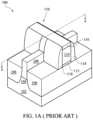
- FIG. 1 Ashows an isometric view of a conventional FinFET 100
- FIG. 1 Billustrates a cross-sectional view of the FinFET 100 taken along the line a-a of FIG. 1 A
- the fin 104 / 108comprises a raised active region 104 above a semiconductor substrate 102
- Fin 104 / 108is surrounded by a shallow trench isolation (STI) structure 106
- a gate structure 110comprising a gate dielectric 112 , a gate electrode 114 , and an optional hardmask layer 116 is formed above the fin 104 / 108
- Sidewall spacers 118are formed on both sides of the gate structure 110 .
- a portion of the fin 104 / 108contains strained structures 108 in source and drain (S/D) recess cavities of the FinFET 100 .
- the strained structures 108are formed after a fin recessing process and an epitaxial growth step.
- the strained structures 108 utilizing epitaxial silicon germanium (SiGe)may be used to enhance carrier mobility.
- CMOScomplementary metal-oxide-semiconductor
- FIG. 1 Ashows an isometric view of a conventional FinFET
- FIG. 1 Billustrates a cross-sectional view of the FinFET taken along the line a-a of FIG. 1 A ;
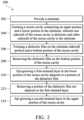
- FIG. 2is a flowchart illustrating a method for fabricating strained structures according to various aspects of the present disclosure
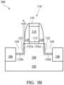
- FIGS. 3 A-Fshow schematic cross-sectional views of a FinFET comprising a strained structure at various stages of fabrication according to various aspects of the present disclosure.
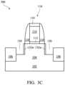
- FIGS. 4 A-Eshow schematic cross-sectional views of a FinFET comprising a strained structure at various stages of fabrication according to various aspects of the present disclosure.
- first and second featuresare formed in direct contact
- additional featuresmay be formed between the first and second features, such that the first and second features may not be in direct contact
- present disclosuremay repeat reference numerals and/or letters in the various examples. This repetition is for the purpose of simplicity and clarity and does not in itself dictate a relationship between the various embodiments and/or configurations discussed.
- the method 200begins with block 202 in which a substrate is provided.
- the method 200continues with block 204 in which a recess cavity comprising an upper portion and a lower portion may be formed in the substrate, wherein one sidewall of the recess cavity is dielectric and other sidewall of the recess cavity is the substrate.
- the method 200continues with block 206 in which a dielectric film may be formed on the substrate sidewall portion and a bottom portion of the recess cavity.
- the method 200continues with block 208 in which removing the dielectric film may include removing the dielectric film on the bottom portion of the recess cavity.
- the method 200continues with block 210 in which epi-growing a first strained layer may be epi-grown in the lower portion of the recess cavity adjacent to a portion of the dielectric film.
- the method 200continues with block 212 in which a portion of the dielectric film not adjacent to the first strained layer may be removed.
- the method 200continues with block 214 in which a second strained layer may be epi-grown in the upper portion of the recess cavity.
- FIGS. 3 A- 3 F and 4 A- 4 Eillustrated are schematic cross-sectional views of strained structures 308 , 408 (in FIGS. 3 F and 4 E ) of semiconductor devices 300 , 400 at various stages of fabrication according to various aspects of the present disclosure.
- the term semiconductor devices 300 , 400refer to a FinFET.
- the FinFETrefers to any fin-based, multi-gate transistor.
- the semiconductor devices 300 , 400may be included in a microprocessor, memory cell, and/or other integrated circuit (IC). It is noted that the method of FIG. 2 does not produce completed semiconductor devices 300 , 400 .
- Completed semiconductor devices 300 , 400may be fabricated using complementary metal-oxide-semiconductor (CMOS) technology processing. Accordingly, it is understood that additional processes may be provided before, during, and after the method 200 of FIG. 2 , and that some other processes may only be briefly described herein. Also, FIGS. 2 through 4 E are simplified for a better understanding of the present disclosure. For example, although the figures illustrate the semiconductor devices 300 , 400 , it is understood the IC may comprise a number of other devices comprising resistors, capacitors, inductors, fuses, etc.
- CMOScomplementary metal-oxide-semiconductor
- a substrate 102is provided having a fin structure 104 .
- the substrate 102comprises a crystalline silicon substrate (e.g., wafer).
- the substrate 102may comprise various doped regions depending on design requirements (e.g., p-type substrate or n-type substrate).
- the doped regionsmay be doped with p-type or n-type dopants.
- the doped regionsmay be doped with p-type dopants, such as boron or BF.sub.2; n-type dopants, such as phosphorus or arsenic; and/or combinations thereof.
- the doped regionsmay be configured for an n-type FinFET, or alternatively configured for a p-type FinFET.
- the substrate 102may alternatively be made of some other suitable elementary semiconductor, such as diamond or germanium; a suitable compound semiconductor, such as gallium arsenide, silicon carbide, indium arsenide, or indium phosphide; or a suitable alloy semiconductor, such as silicon germanium carbide, gallium arsenic phosphide, or gallium indium phosphide.
- the substrate 102may include an epitaxial layer (epi-layer), may be strained for performance enhancement, and/or may include a silicon-on-insulator (SOI) structure.
- epi-layerepitaxial layer
- SOIsilicon-on-insulator
- the fin structure 104formed over the substrate 102 , comprises one or more fins.
- the fin structure 104comprises a single fin.
- the fincomprises any suitable material, for example, the fin structure 104 comprises silicon.
- the fin structure 104may further comprise a capping layer disposed on the fin, which may be a silicon-capping layer.
- the fin structure 104is formed using any suitable process comprising various deposition, photolithography, and/or etching processes.
- An exemplary photolithography processmay include forming a photoresist layer (resist) overlying the substrate 102 (e.g., on a silicon layer), exposing the resist to a pattern, performing a post-exposure bake process, and developing the resist to form a masking element including the resist. The masking element may then be used to etch the fin structure 104 into the silicon layer.
- the fin structure 104may be etched using reactive ion etching (RIE) processes and/or other suitable processes.
- RIEreactive ion etching
- the silicon fin 104is formed by using patterning and etching of a portion of the silicon substrate 102 .
- silicon fins of the fin structure 104may be formed by using patterning and etching of a silicon layer deposited overlying an insulator layer (for example, an upper silicon layer of a silicon-insulator-silicon stack of an SOI substrate).
- Isolation structure 106may be formed on the substrate 102 to isolate the various doped regions.
- the isolation structure 106may utilize isolation technology, such as local oxidation of silicon (LOCOS) or shallow trench isolation (STI), to define and electrically isolate the various doped regions.
- LOClocal oxidation of silicon
- STIshallow trench isolation
- the isolation structure 106includes a STI.
- the isolation structure 106may comprise silicon oxide, silicon nitride, silicon oxynitride, fluoride-doped silicate glass (FSG), a low-K dielectric material, and/or combinations thereof.
- the isolation structure 106and in the present embodiment, the STI, may be formed by any suitable process.
- the formation of the STImay include patterning the semiconductor substrate 102 by a conventional photolithography process, etching a trench in the substrate 102 (for example, by using a dry etching, wet etching, and/or plasma etching process), and filling the trench (for example, by using a chemical vapor deposition process) with a dielectric material.
- the filled trenchmay have a multi-layer structure such as a thermal oxide liner layer filled with silicon nitride or silicon oxide.
- a gate stack 110is formed over the substrate 102 and over a portion of the fin structure 104 .
- the gate stack 110typically comprises a gate dielectric layer 112 and a gate electrode layer 114 .
- the gate stack 110may be formed using any suitable process, including the processes described herein.
- the gate dielectric layer 112 and gate electrode layer 114are sequentially deposited on the substrate 102 and over a portion of the fin structure 104 .
- the gate dielectric layer 112may include silicon oxide, silicon nitride, silicon oxy-nitride, or high-k dielectric.
- High-k dielectricscomprise metal oxides. Examples of metal oxides used for high-k dielectrics include oxides of Li, Be, Mg, Ca, Sr, Sc, Y, Zr, Hf, Al, La, Ce, Pr, Nd, Sm, Eu, Gd, Tb, Dy, Ho, Er, Tm, Yb, Lu and mixtures thereof.
- the gate dielectric layer 112is a high-k dielectric layer with a thickness in the range of about 10 to 30 angstroms.
- the gate dielectric layer 112may be formed using a suitable process such as atomic layer deposition (ALD), chemical vapor deposition (CVD), physical vapor deposition (PVD), thermal oxidation, UV-ozone oxidation, or combinations thereof.
- the gate dielectric layer 112may further comprise an interfacial layer (not shown) to reduce damage between the gate dielectric layer 112 and the fin structure 104 .
- the interfacial layermay comprise silicon oxide.
- the gate electrode layer 114may comprise a single layer or multilayer structure.
- the gate electrode layer 114may comprise poly-silicon.
- the gate electrode layer 114may be doped poly-silicon with uniform or non-uniform doping.
- the gate electrode layer 114may include a metal such as Al, Cu, W, Ti, Ta, TiN, TiAl, TiAlN, TaN, NiSi, CoSi, other conductive materials with a work function compatible with the substrate material, or combinations thereof.
- the gate electrode layer 114comprises a thickness in the range of about 30 nm to about 60 nm.
- the gate electrode layer 114may be formed using a suitable process such as ALD, CVD, PVD, plating, or combinations thereof.
- a layer of photoresistis formed over the gate stack 110 by a suitable process, such as spin-on coating, and patterned to form a patterned photoresist feature by a proper lithography patterning method.
- a width of the patterned photoresist featureis in the range of about 15 to 45 nm.
- the patterned photoresist featurecan then be transferred using a dry etching process to the underlying layers (i.e., the gate electrode layer 114 and the gate dielectric layer 112 ) to form the gate stack 110 .
- the photoresist layermay be stripped thereafter.
- a hard mask layer 116is formed over the gate stack 110 ; a patterned photoresist layer is formed on the hard mask layer 116 ; the pattern of the photoresist layer is transferred to the hard mask layer 116 and then transferred to the gate electrode layer 114 and the gate dielectric layer 112 to form the gate stack 110 .
- the hard mask layer 116comprises silicon oxide.
- the hard mask layer 116may optionally comprise silicon nitride, silicon oxynitride, and/or other suitable dielectric materials, and may be formed using a method such as CVD or PVD.
- the hard mask layer 116has a thickness in the range from about 100 to 800 angstroms.
- the semiconductor device 300further comprises a dielectric layer 118 formed over the substrate 102 and the gate stack 110 .
- the dielectric layer 118may include silicon oxide, silicon nitride, silicon oxy-nitride, or other suitable material.
- the dielectric layer 118may comprise a single layer or multilayer structure.
- the dielectric layer 118may be formed by CVD, PVD, ALD, or other suitable technique.
- the dielectric layer 118comprises a thickness ranging from about 5 to 15 nm. Then, an anisotropic etching is performed on the dielectric layer 118 to form a pair of spacers 118 on two sides of the gate stack 110 .
- other portions of the fin structure 104are recessed to form source and drain (S/D) recess cavities 130 below a top surface of the substrate 102 disposed between the gate stack 110 and the isolation structure 106 .
- S/Dsource and drain
- a biased etching processis performed to recess a top surface of the fin structure 104 that are unprotected or exposed to form the S/D recess cavities 130 .
- the etching processmay be performed under a pressure of about 1 mTorr to 1000 mTorr, a power of about 50 W to 1000 W, a bias voltage of about 20 V to 500 V, at a temperature of about 40° C. to 60° C., using a HBr and/or Cl2 as etch gases.
- the bias voltage used in the etching processmay be tuned to allow better control of an etching direction to achieve desired profiles for the S/D recess cavities 130 .
- the recess cavity 130may comprise an upper portion 130 u and a lower portion 130 l separated by the dotted line in FIG. 3 A .
- One sidewall 130 i of the recess cavity 130is dielectric and other sidewall 130 f of the recess cavity 130 is the substrate 102 .
- a ratio of a height of the upper portion 130 u to a height of the lower portion 1301may be from 0.8 to 1.2.
- a height 130 a between the top surface of the substrate 102 and a bottom of the S/D recess cavity 130is in the range of about 300 to 2000 nm.
- a dielectric film 132may be formed along the substrate surface of the recess cavity 130 .
- the dielectric film 132comprises a sidewall portion 132 w and a bottom portion 132 b .
- the dielectric film 132may be formed of silicon oxide or silicon oxynitride grown using a thermal oxidation process.
- the dielectric film 132can be grown by a rapid thermal oxidation (RTO) process or in a conventional annealing process, which includes oxygen or NO.sub.2.
- a thickness t.sub.1 of the dielectric film 132may be in the range of about 20 to 100 angstroms.
- a dry etching processis performed to remove the bottom portion 132 b of the dielectric film 132 , whereby the sidewall portion 132 w of the dielectric film 132 is not removed.
- the dry etching processmay be a plasma etch process performed under a source power of about 120 to 160 W, and a pressure of about 450 to 550 mTorr, using BF3, H2, and Ar as etching gases.
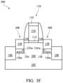
- a first strained layer 136is epi-grown in the lower portion 1301 of the recess cavities 130 adjacent to a portion of the dielectric film 132 .
- a first strained layer 136comprising silicon germanium (SiGe) is epi-grown by a low-pressure chemical vapor deposition (LPCVD) process.
- the first strained layer 136may serve as a relaxation layer and trap defects 136 a to eliminate crystal defects in a second strained layer 138 (shown in FIG. 3 F ) in the source and drain regions of the n-type FinFET.
- the LPCVD processis performed at a temperature of about 400 to 800° C.
- a first strained layer 136 comprising silicon carbon (SiC)is epi-grown by a LPCVD process.
- the first strained layer 136may serve as a relaxation layer and trap defects 136 a to eliminate crystal defects in a second strained layer 138 (shown in FIG. 3 F ) in the source and drain regions of the p-type FinFET.
- the LPCVD processis performed at a temperature of about 400 to 800° C. and under a pressure of about 1 to 200 Torr, using SiH.sub.4 and CH.sub.4 as reaction gases.
- a thickness t.sub.2 of the first strained layer 136may be in the range of about 15 to 45 nm.
- the thickness t.sub.1 of the dielectric film 132is less than the thickness t.sub.2 of the first strained layer 136 .
- a top portion of the sidewall portion 132 w of the dielectric film 132 not adjacent to the first strained layer 136has been removed using a wet etching process, for example, by dipping the substrate 102 in hydrofluoric acid (HF), exposing a top surface 132 a of the remaining sidewall portion 132 w of the dielectric film 132 .
- HFhydrofluoric acid
- the wet etching processhas higher etch selectivity for oxide than to silicon, SiGe, and SiC, the etch process removes the dielectric film 132 faster than the fin structure 104 and the first strained layer 136 .
- the first strained layer 136is disposed between the isolation structure 106 and the remaining sidewall portion 132 w of the dielectric film 132 .
- a top surface 136 b of the first strained layer 136 and the top surface 132 a of the remaining sidewall portion 132 w of the dielectric film 132are substantially aligned.
- the top surface 136 b of the first strained layer 136 and the top surface 132 a of the remaining sidewall portion 132 w of the dielectric film 132are below a top surface 106 a of the isolation structure 106 .
- a second strained layer 138 overlying the first strained layer 136 and remaining sidewall portion 132 w of the dielectric film 132is epi-grown in the upper portion 130 u of the recess cavities 130 in the fin structure 104 .
- the first strained layer 136 , remaining sidewall portion 132 w of the dielectric film 132 , and second strained layer 138are collectively hereinafter referred to as a strained structure 308 .
- the first strained layer 136serves as a relaxation layer and may trap defects 136 a to eliminate crystal defects in the second strained layer 138 .
- Crystal defects in the second strained layer 138may provide carrier transportation paths during device operation, thereby increasing the likelihood of device instability and/or device failure. Accordingly, the above method of fabricating a semiconductor device 300 may form a reduced-defect strained structure 308 to enhance carrier mobility and upgrade the device performance.
- the second strained layer 138such as silicon carbide (SiC) is epi-grown by a LPCVD process to form the source and drain regions of the n-type FinFET.
- a LPCVD process for the growth of SiCis performed at a temperature of about 400 to 800° C. and under a pressure of about 1 to 200 Torr, using SiH.sub.4 and CH.sub.4 as reaction gases.
- the second strained layer 138such as silicon germanium (SiGe) is epi-grown by a LPCVD process to form the source and drain regions of the p-type FinFET.
- the LPCVD processis performed at a temperature of about 400 to 800° C.
- the second strained layer 138such as silicon, is epi-grown by a LPCVD process to form the source and drain regions of both the p-type FinFET and n-type FinFET.
- the LPCVD processis performed at a temperature of about 400 to 800° C. and under a pressure of about 1 to 200 Torr, using SiH.sub.4 as a reaction gas.
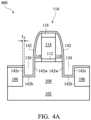
- FIG. 4 Ashows the substrate 102 of FIG. 3 A after deposition of a dielectric film 142 by a CVD process.
- the dielectric film 142 formed by CVDwill deposit over all exposed surfaces, and thus may be formed on the isolation structure 106 , hard mask layer 116 , spacers 118 , and recess cavities 130 .
- the dielectric film 142may comprise a first sidewall portion 142 w , a second sidewall portion 142 s , and a bottom portion 142 b .
- the dielectric film 142may be formed of silicon oxide or silicon oxynitride deposited using a CVD process.
- the dielectric film 142can be deposited under a pressure less than 10 mTorr and a temperature of about 350° C. to 500° C., using SiH.sub.4 and N.sub.20 as reacting precursors.
- a thickness t.sub.3 of the dielectric film 142may be in the range of about 20 to 100 angstroms.
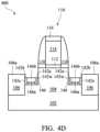
- a dry etching processis performed to remove the bottom portion 142 b of the dielectric film 142 , whereby the first sidewall portion 142 w and second sidewall portion 142 s of the dielectric film 142 are not removed.
- the dry etching processmay be performed under a source power of about 120 to 160 W, and a pressure of about 450 to 550 mTorr, using BF3, H2, and Ar as etching gases.
- a first strained layer 146is epi-grown in the lower portion 1301 of the recess cavities 130 adjacent to a portion of the dielectric film 142 .
- a first strained layer 146comprising silicon germanium (SiGe) is epi-grown by a LPCVD process.
- the first strained layer 146may serve as a relaxation layer and trap defects 146 a to eliminate crystal defects in a second strained layer 148 (shown in FIG. 4 E ) in the source and drain regions of the n-type FinFET.
- the LPCVD processis performed at a temperature of about 400 to 800° C.
- a first strained layer 146comprising silicon carbide (SiC) is epi-grown by a LPCVD process.
- the first strained layer 146may serve as a relaxation layer and trap defects 146 a to eliminate crystal defects in the second strained layer 148 (shown in FIG. 4 E ) in the source and drain regions of the p-type FinFET.
- LPCVD process for SiC depositionis performed at a temperature of about 400 to 800 C. and under a pressure of about 1 to 200 Torr, using SiH.sub.4 and CH.sub.4 as reaction gases.
- a thickness t.sub.4 of the first strained layer 146may be in the range of about 12 to 40 nm.
- the thickness t.sub.3 of the dielectric film 142is less than the thickness t.sub.4 of the first strained layer 146 .
- top portions of the first and second sidewall portions 142 w , 142 s of the dielectric film 142 not adjacent to the first strained layer 146are removed using a wet etching process, for example, by dipping the substrate 102 in hydrofluoric acid (HF), exposing top surfaces 142 a , 142 b of the remaining first and second sidewall portions 142 w , 142 s of the dielectric film 142 . Because the wet etching process preferentially etches oxide over silicon, SiGe, and SiC, the etch process removes the dielectric film 142 faster than the fin structure 104 and the first strained layer 146 .
- a wet etching processfor example, by dipping the substrate 102 in hydrofluoric acid (HF), exposing top surfaces 142 a , 142 b of the remaining first and second sidewall portions 142 w , 142 s of the dielectric film 142 . Because the wet etching process preferentially etches oxide over silicon,
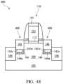
- the first strained layer 146is disposed between the isolation structure 106 and the remaining first sidewall portion 142 w of the dielectric film 142 . Further, the remaining second sidewall portion 142 s of dielectric film 142 is between the first strained layer 146 and the isolation structure 106 . In an embodiment, a top surface 146 b of the first strained layer 146 and the top surfaces 142 a , 142 b of the remaining first and second sidewall portions 142 w , 142 s of the dielectric film 142 are substantially aligned.
- the top surface 146 b of the first strained layer 136 and the top surfaces 142 a , 142 b of the remaining first and second sidewall portions 142 w , 142 s of the dielectric film 142are below the top surface 106 a of the isolation structure 106 .
- a second strained layer 148 overlying the first strained layer 146 and remaining first and second sidewall portions 142 w , 142 s of the dielectric film 142is epi-grown in the upper portion 130 u of the recess cavities 130 .
- the first strained layer 146 , remaining first sidewall portion 142 w and second sidewall portion 142 w of the dielectric film 142 , and second strained layer 148are collectively hereinafter referred to as a strained structure 408 .
- the first strained layer 146serves as a relaxation layer and may trap defects 146 a to eliminate crystal defects in the second strained layer 148 .
- Crystal defects in the second strained layer 148may provide carrier transportation paths during device operation, thereby increasing the likelihood of device instability and/or device failure. Accordingly, the above method of fabricating a semiconductor device 400 may form a reduced-defect strained structure 408 to enhance carrier mobility and upgrade the device performance.
- a second strained layer 148 comprising silicon carbide (SiC)is epi-grown by a LPCVD process to form the source and drain regions of the n-type FinFET.
- the LPCVD processis performed at a temperature of about 400 to 800° C. and under a pressure of about 1 to 200 Torr, using SiH.sub.4 and CH.sub.4 as reaction gases.
- a second strained layer 148 comprising silicon germanium (SiGe)is epi-grown by a LPCVD process to form the source and drain regions of the p-type FinFET.
- the LPCVD processis performed at a temperature of about 400 to 800° C.
- a second strained layer 148 comprising siliconis epi-grown by a LPCVD process to form the source and drain regions of both the p-type FinFET and n-type FinFET.
- the LPCVD processis performed at a temperature of about 400 to 800° C. and under a pressure of about 1 to 200 Torr, using SiH.sub.4 as a reaction gas.
- the field effect transistorincludes a substrate comprising a fin structure.
- the field effect transistorfurther includes an isolation structure in the substrate.
- the field effect transistorfurther includes a source/drain (S/D) recess cavity below a top surface of the substrate.
- the S/D recess cavityis between the fin structure and the isolation structure.
- the field effect transistorfurther includes a strained structure in the S/D recess cavity.
- the strain structureincludes a lower portion.
- the lower portionincludes a first strained layer, wherein the first strained layer is in direct contact with the isolation structure, and a dielectric layer, wherein the dielectric layer is in direct contact with the substrate, and the first strained layer is in direct contact with the dielectric layer.
- the strained structurefurther includes an upper portion comprising a second strained layer overlying the first strained layer.
- the methodincludes forming a recess cavity comprising an upper portion and a lower portion in a substrate, wherein the recess cavity includes a sidewall defined by an isolation structure.
- the methodfurther includes forming a dielectric film on a bottom portion and a sidewall of the recess cavity opposite the isolation structure.
- the methodfurther includes removing the dielectric film on the bottom portion of the recess cavity.
- the methodfurther includes forming a first strained layer in the lower portion of the recess cavity in direct contact with the dielectric film, wherein the first strained layer is between the dielectric film and the isolation structure.
- the methodfurther includes forming a second strained layer over the first strained layer in the upper portion of the recess cavity.
- the field effect transistorincludes an isolation structure in a substrate.
- the field effect transistorfurther includes a source/drain (S/D) recess cavity below a top surface of the substrate, wherein a sidewall of the S/D recess cavity is defined by the isolation structure.
- the field effect transistorfurther includes a strained structure in the S/D recess cavity.
- the strain structureincludes a lower portion.
- the lower portionincludes a defect trapping layer, wherein the first defect trapping layer is in direct contact with the isolation structure, and a dielectric layer, wherein the dielectric layer is in direct contact with the substrate, and the defect trapping layer is in direct contact with the dielectric layer.
- the strained structurefurther includes an upper portion comprising a strained layer overlying the defect trapping layer.
- the disclosurecan be used to form or fabricate a strained structure for a semiconductor device. In this way, a strained structure having no defect in a semiconductor device is fabricated.
Landscapes
- Engineering & Computer Science (AREA)
- Microelectronics & Electronic Packaging (AREA)
- Condensed Matter Physics & Semiconductors (AREA)
- General Physics & Mathematics (AREA)
- Manufacturing & Machinery (AREA)
- Computer Hardware Design (AREA)
- Physics & Mathematics (AREA)
- Power Engineering (AREA)
- Chemical & Material Sciences (AREA)
- Chemical Kinetics & Catalysis (AREA)
- General Chemical & Material Sciences (AREA)
- Inorganic Chemistry (AREA)
- Insulated Gate Type Field-Effect Transistor (AREA)
- Thin Film Transistor (AREA)
- Metal-Oxide And Bipolar Metal-Oxide Semiconductor Integrated Circuits (AREA)
Abstract
Description
Claims (20)
Priority Applications (2)
| Application Number | Priority Date | Filing Date | Title |
|---|---|---|---|
| US17/671,042US11855210B2 (en) | 2010-05-06 | 2022-02-14 | Method for fabricating a strained structure and structure formed |
| US18/522,461US12356674B2 (en) | 2010-05-06 | 2023-11-29 | Method for fabricating a strained structure and structure formed |
Applications Claiming Priority (7)
| Application Number | Priority Date | Filing Date | Title |
|---|---|---|---|
| US12/775,006US8497528B2 (en) | 2010-05-06 | 2010-05-06 | Method for fabricating a strained structure |
| US13/910,633US9147594B2 (en) | 2010-05-06 | 2013-06-05 | Method for fabricating a strained structure |
| US14/844,247US9564529B2 (en) | 2010-05-06 | 2015-09-03 | Method for fabricating a strained structure and structure formed |
| US15/425,552US10510887B2 (en) | 2010-05-06 | 2017-02-06 | Method for fabricating a strained structure and structure formed |
| US16/711,497US10998442B2 (en) | 2010-05-06 | 2019-12-12 | Method for fabricating a strained structure and structure formed |
| US16/986,043US11251303B2 (en) | 2010-05-06 | 2020-08-05 | Method for fabricating a strained structure and structure formed |
| US17/671,042US11855210B2 (en) | 2010-05-06 | 2022-02-14 | Method for fabricating a strained structure and structure formed |
Related Parent Applications (1)
| Application Number | Title | Priority Date | Filing Date |
|---|---|---|---|
| US16/986,043ContinuationUS11251303B2 (en) | 2010-05-06 | 2020-08-05 | Method for fabricating a strained structure and structure formed |
Related Child Applications (1)
| Application Number | Title | Priority Date | Filing Date |
|---|---|---|---|
| US18/522,461ContinuationUS12356674B2 (en) | 2010-05-06 | 2023-11-29 | Method for fabricating a strained structure and structure formed |
Publications (2)
| Publication Number | Publication Date |
|---|---|
| US20220173245A1 US20220173245A1 (en) | 2022-06-02 |
| US11855210B2true US11855210B2 (en) | 2023-12-26 |
Family
ID=44887875
Family Applications (8)
| Application Number | Title | Priority Date | Filing Date |
|---|---|---|---|
| US12/775,006Expired - Fee RelatedUS8497528B2 (en) | 2009-07-28 | 2010-05-06 | Method for fabricating a strained structure |
| US13/910,633Active2030-06-02US9147594B2 (en) | 2010-05-06 | 2013-06-05 | Method for fabricating a strained structure |
| US14/844,247Expired - Fee RelatedUS9564529B2 (en) | 2010-05-06 | 2015-09-03 | Method for fabricating a strained structure and structure formed |
| US15/425,552Active2030-05-12US10510887B2 (en) | 2010-05-06 | 2017-02-06 | Method for fabricating a strained structure and structure formed |
| US16/711,497ActiveUS10998442B2 (en) | 2010-05-06 | 2019-12-12 | Method for fabricating a strained structure and structure formed |
| US16/986,043Active2030-05-07US11251303B2 (en) | 2010-05-06 | 2020-08-05 | Method for fabricating a strained structure and structure formed |
| US17/671,042ActiveUS11855210B2 (en) | 2010-05-06 | 2022-02-14 | Method for fabricating a strained structure and structure formed |
| US18/522,461ActiveUS12356674B2 (en) | 2010-05-06 | 2023-11-29 | Method for fabricating a strained structure and structure formed |
Family Applications Before (6)
| Application Number | Title | Priority Date | Filing Date |
|---|---|---|---|
| US12/775,006Expired - Fee RelatedUS8497528B2 (en) | 2009-07-28 | 2010-05-06 | Method for fabricating a strained structure |
| US13/910,633Active2030-06-02US9147594B2 (en) | 2010-05-06 | 2013-06-05 | Method for fabricating a strained structure |
| US14/844,247Expired - Fee RelatedUS9564529B2 (en) | 2010-05-06 | 2015-09-03 | Method for fabricating a strained structure and structure formed |
| US15/425,552Active2030-05-12US10510887B2 (en) | 2010-05-06 | 2017-02-06 | Method for fabricating a strained structure and structure formed |
| US16/711,497ActiveUS10998442B2 (en) | 2010-05-06 | 2019-12-12 | Method for fabricating a strained structure and structure formed |
| US16/986,043Active2030-05-07US11251303B2 (en) | 2010-05-06 | 2020-08-05 | Method for fabricating a strained structure and structure formed |
Family Applications After (1)
| Application Number | Title | Priority Date | Filing Date |
|---|---|---|---|
| US18/522,461ActiveUS12356674B2 (en) | 2010-05-06 | 2023-11-29 | Method for fabricating a strained structure and structure formed |
Country Status (3)
| Country | Link |
|---|---|
| US (8) | US8497528B2 (en) |
| KR (1) | KR101219064B1 (en) |
| CN (1) | CN102237408B (en) |
Families Citing this family (149)
| Publication number | Priority date | Publication date | Assignee | Title |
|---|---|---|---|---|
| US7608693B2 (en) | 2006-10-02 | 2009-10-27 | Regeneron Pharmaceuticals, Inc. | High affinity human antibodies to human IL-4 receptor |
| US8497528B2 (en) | 2010-05-06 | 2013-07-30 | Taiwan Semiconductor Manufacturing Company, Ltd. | Method for fabricating a strained structure |
| KR101097469B1 (en)* | 2009-07-31 | 2011-12-23 | 주식회사 하이닉스반도체 | Semiconductor device and method for fabricating the same |
| US8796759B2 (en) | 2010-07-15 | 2014-08-05 | Taiwan Semiconductor Manufacturing Company, Ltd. | Fin-like field effect transistor (FinFET) device and method of manufacturing same |
| CN102810481B (en)* | 2011-06-02 | 2016-03-30 | 中芯国际集成电路制造(北京)有限公司 | The manufacture method of semiconductor device |
| US8685825B2 (en)* | 2011-07-27 | 2014-04-01 | Advanced Ion Beam Technology, Inc. | Replacement source/drain finFET fabrication |
| US8647941B2 (en)* | 2011-08-17 | 2014-02-11 | United Microelectronics Corp. | Method of forming semiconductor device |
| US9064892B2 (en) | 2011-08-30 | 2015-06-23 | Taiwan Semiconductor Manufacturing Company, Ltd. | Semiconductor devices utilizing partially doped stressor film portions and methods for forming the same |
| EP2761662B1 (en) | 2011-09-30 | 2022-02-02 | Sony Group Corporation | Tungsten gates for non-planar transistors |
| US9202699B2 (en) | 2011-09-30 | 2015-12-01 | Intel Corporation | Capping dielectric structure for transistor gates |
| US9637810B2 (en) | 2011-09-30 | 2017-05-02 | Intel Corporation | Tungsten gates for non-planar transistors |
| CN103918083A (en) | 2011-10-01 | 2014-07-09 | 英特尔公司 | Source/drain contacts for non-planar transistors |
| US8723236B2 (en)* | 2011-10-13 | 2014-05-13 | Taiwan Semiconductor Manufacturing Company, Ltd. | FinFET device and method of manufacturing same |
| US9246004B2 (en) | 2011-11-15 | 2016-01-26 | Taiwan Semiconductor Manufacturing Company, Ltd. | Strained structures of semiconductor devices |
| US9087915B2 (en)* | 2011-12-06 | 2015-07-21 | Intel Corporation | Interlayer dielectric for non-planar transistors |
| US9263342B2 (en)* | 2012-03-02 | 2016-02-16 | Taiwan Semiconductor Manufacturing Company, Ltd. | Semiconductor device having a strained region |
| US8872284B2 (en) | 2012-03-20 | 2014-10-28 | Taiwan Semiconductor Manufacturing Company, Ltd. | FinFET with metal gate stressor |
| US8901615B2 (en) | 2012-06-13 | 2014-12-02 | Synopsys, Inc. | N-channel and P-channel end-to-end finfet cell architecture |
| US9136383B2 (en) | 2012-08-09 | 2015-09-15 | Taiwan Semiconductor Manufacturing Company, Ltd. | Contact structure of semiconductor device |
| JP6306588B2 (en) | 2012-08-21 | 2018-04-04 | サノフィ・バイオテクノロジー | Method for treating or preventing asthma by administering an IL-4R antagonist |
| CN103824775B (en)* | 2012-11-16 | 2018-04-24 | 中国科学院微电子研究所 | FinFET and manufacturing method thereof |
| US8823102B2 (en)* | 2012-11-16 | 2014-09-02 | Taiwan Semiconductor Manufacturing Company, Ltd. | Device with a strained Fin |
| US9123633B2 (en) | 2013-02-01 | 2015-09-01 | Taiwan Semiconductor Manufacturing Company, Ltd. | Methods for forming semiconductor regions in trenches |
| US9466668B2 (en) | 2013-02-08 | 2016-10-11 | Taiwan Semiconductor Manufacturing Company, Ltd. | Inducing localized strain in vertical nanowire transistors |
| US9368619B2 (en) | 2013-02-08 | 2016-06-14 | Taiwan Semiconductor Manufacturing Company, Ltd. | Method for inducing strain in vertical semiconductor columns |
| US8963258B2 (en)* | 2013-03-13 | 2015-02-24 | Taiwan Semiconductor Manufacturing Company | FinFET with bottom SiGe layer in source/drain |
| CN105027291A (en)* | 2013-03-29 | 2015-11-04 | 英特尔公司 | Transistor architecture with extended recessed spacers and source/drain regions and method of fabrication thereof |
| US9209247B2 (en) | 2013-05-10 | 2015-12-08 | Taiwan Semiconductor Manufacturing Company, Ltd. | Self-aligned wrapped-around structure |
| CN103346086B (en)* | 2013-05-31 | 2016-08-10 | 上海华力微电子有限公司 | The manufacture method of embedded germanium silicon structure |
| TWI697334B (en) | 2013-06-04 | 2020-07-01 | 美商再生元醫藥公司 | Methods for treating allergy and enhancing allergen-specific immunotherapy by administering an il-4r inhibitor |
| TWI634900B (en) | 2013-07-11 | 2018-09-11 | 再生元醫藥公司 | Method for treating eosinophilic esophagitis by administering an IL-4R inhibitor |
| US9142673B2 (en)* | 2013-07-31 | 2015-09-22 | Globalfoundries Inc. | Devices and methods of forming bulk FinFETS with lateral seg for source and drain on dielectrics |
| KR20160120735A (en) | 2014-02-28 | 2016-10-18 | 리제너론 파아마슈티컬스, 인크. | Methods for treating skin infection by administering an il-4r antagonist |
| US9548303B2 (en) | 2014-03-13 | 2017-01-17 | Taiwan Semiconductor Manufacturing Company, Ltd. | FinFET devices with unique fin shape and the fabrication thereof |
| US9590037B2 (en) | 2014-03-19 | 2017-03-07 | International Business Machines Corporation | p-FET with strained silicon-germanium channel |
| US9263580B2 (en)* | 2014-03-24 | 2016-02-16 | Globalfoundries Inc. | Methods of forming isolated channel regions for a FinFET semiconductor device and the resulting device |
| US9461170B2 (en) | 2014-04-23 | 2016-10-04 | Taiwan Semiconductor Manufacturing Company Ltd. | FinFET with ESD protection |
| US9318552B2 (en)* | 2014-05-21 | 2016-04-19 | Globalfoundries Inc. | Methods of forming conductive contact structures for a semiconductor device with a larger metal silicide contact area and the resulting devices |
| TWI615976B (en) | 2014-07-07 | 2018-02-21 | 聯華電子股份有限公司 | Fin field effect transistor and manufacturing method thereof |
| US9299803B2 (en) | 2014-07-16 | 2016-03-29 | Taiwan Semiconductor Manufacturing Company, Ltd. | Method for semiconductor device fabrication |
| DE102015100860A1 (en) | 2014-08-22 | 2016-02-25 | Taiwan Semiconductor Manufacturing Company, Ltd. | Metal-insensitive epitaxy formation |
| US10263108B2 (en) | 2014-08-22 | 2019-04-16 | Taiwan Semiconductor Manufacturing Company, Ltd. | Metal-insensitive epitaxy formation |
| US9450093B2 (en) | 2014-10-15 | 2016-09-20 | Taiwan Semiconductor Manufacturing Company Ltd. | Semiconductor device structure and manufacturing method thereof |
| CN105633152B (en)* | 2014-11-05 | 2019-12-10 | 联华电子股份有限公司 | Semiconductor structure and manufacturing method thereof |
| RU2734490C2 (en) | 2014-11-14 | 2020-10-19 | Санофи Байотекнолоджи | Methods of treating chronic sinusitis with nasal polyps by administering il-4r antagonist |
| US9287403B1 (en) | 2014-12-05 | 2016-03-15 | Taiwan Semiconductor Manufacturing Co., Ltd. | FinFET and method for manufacturing the same |
| US9780214B2 (en) | 2014-12-22 | 2017-10-03 | Taiwan Semiconductor Manufacturing Co., Ltd. | Semiconductor device including Fin- FET and manufacturing method thereof |
| US9515071B2 (en) | 2014-12-24 | 2016-12-06 | Taiwan Semiconductor Manufacturing Company, Ltd. | Asymmetric source/drain depths |
| US9876114B2 (en) | 2014-12-30 | 2018-01-23 | Taiwan Semiconductor Manufacturing Company, Ltd. | Structure and method for 3D FinFET metal gate |
| US9991384B2 (en) | 2015-01-15 | 2018-06-05 | Taiwan Semiconductor Manufacturing Co., Ltd. | Semiconductor device including fin structures and manufacturing method thereof |
| US9391078B1 (en) | 2015-01-16 | 2016-07-12 | Taiwan Semiconductor Manufacturing Company, Ltd. | Method and structure for finFET devices |
| US9349859B1 (en) | 2015-01-29 | 2016-05-24 | Taiwan Semiconductor Manufacturing Company, Ltd. | Top metal pads as local interconnectors of vertical transistors |
| US9406680B1 (en) | 2015-02-13 | 2016-08-02 | Taiwan Semiconductor Manufacturing Co., Ltd. | Semiconductor device including fin structures and manufacturing method thereof |
| US9564493B2 (en) | 2015-03-13 | 2017-02-07 | Taiwan Semiconductor Manufacturing Company, Ltd. | Devices having a semiconductor material that is semimetal in bulk and methods of forming the same |
| US9406675B1 (en) | 2015-03-16 | 2016-08-02 | Taiwan Semiconductor Manufacturing Company Ltd. | FinFET structure and method of manufacturing the same |
| US9570557B2 (en) | 2015-04-29 | 2017-02-14 | Taiwan Semiconductor Manufacturing Co., Ltd. | Tilt implantation for STI formation in FinFET structures |
| US10483262B2 (en) | 2015-05-15 | 2019-11-19 | Taiwan Semiconductor Manufacturing Co., Ltd. | Dual nitride stressor for semiconductor device and method of manufacturing |
| US9530889B2 (en) | 2015-05-21 | 2016-12-27 | Taiwan Semiconductor Manufacturing Co., Ltd. | Semiconductor device and manufacturing method thereof |
| US9647071B2 (en) | 2015-06-15 | 2017-05-09 | Taiwan Semiconductor Manufacturing Company, Ltd. | FINFET structures and methods of forming the same |
| US9449975B1 (en) | 2015-06-15 | 2016-09-20 | Taiwan Semiconductor Manufacturing Company, Ltd. | FinFET devices and methods of forming |
| US9685368B2 (en) | 2015-06-26 | 2017-06-20 | Taiwan Semiconductor Manufacturing Company, Ltd. | Interconnect structure having an etch stop layer over conductive lines |
| US9818872B2 (en) | 2015-06-30 | 2017-11-14 | Taiwan Semiconductor Manufacturing Company, Ltd. | Multi-gate device and method of fabrication thereof |
| US9583623B2 (en) | 2015-07-31 | 2017-02-28 | Taiwan Semiconductor Manufacturing Co., Ltd. | Semiconductor device including fin structures disposed over buffer structures and manufacturing method thereof |
| US9954083B2 (en) | 2015-08-20 | 2018-04-24 | International Business Machines Corporation | Semiconductor structures having increased channel strain using fin release in gate regions |
| US9666581B2 (en) | 2015-08-21 | 2017-05-30 | Taiwan Semiconductor Manufacturing Company, Ltd. | FinFET with source/drain structure and method of fabrication thereof |
| US10164096B2 (en) | 2015-08-21 | 2018-12-25 | Taiwan Semiconductor Manufacturing Co., Ltd. | Semiconductor device and manufacturing method thereof |
| US9515165B1 (en)* | 2015-09-11 | 2016-12-06 | International Business Machines Corporation | III-V field effect transistor (FET) with reduced short channel leakage, integrated circuit (IC) chip and method of manufacture |
| US9647122B2 (en) | 2015-09-15 | 2017-05-09 | Taiwan Semiconductor Manufacturing Company, Ltd. | Semiconductor device and method of forming the same |
| DE102016113434B4 (en) | 2015-09-15 | 2020-11-19 | Taiwan Semiconductor Manufacturing Company, Ltd. | Semiconductor device and method of forming the same |
| US10032873B2 (en) | 2015-09-15 | 2018-07-24 | Taiwan Semiconductor Manufacturing Company, Ltd. | Semiconductor device and method of forming the same |
| US9680017B2 (en) | 2015-09-16 | 2017-06-13 | Taiwan Semiconductor Manufacturing Co., Ltd. | Semiconductor device including Fin FET and manufacturing method thereof |
| US9607838B1 (en)* | 2015-09-18 | 2017-03-28 | Taiwan Semiconductor Manufacturing Co., Ltd. | Enhanced channel strain to reduce contact resistance in NMOS FET devices |
| US10121858B2 (en) | 2015-10-30 | 2018-11-06 | Taiwan Semiconductor Manufacturing Company, Ltd. | Elongated semiconductor structure planarization |
| US9960273B2 (en) | 2015-11-16 | 2018-05-01 | Taiwan Semiconductor Manufacturing Company, Ltd. | Integrated circuit structure with substrate isolation and un-doped channel |
| US10490552B2 (en) | 2015-12-29 | 2019-11-26 | Taiwan Semiconductor Manufacturing Co., Ltd. | FinFET device having flat-top epitaxial features and method of making the same |
| US11264452B2 (en) | 2015-12-29 | 2022-03-01 | Taiwan Semiconductor Manufacturing Company, Ltd. | Hetero-tunnel field-effect transistor (TFET) having a tunnel barrier formed directly above channel region, directly below first source/drain region and adjacent gate electrode |
| DE102016119024B4 (en) | 2015-12-29 | 2023-12-21 | Taiwan Semiconductor Manufacturing Co. Ltd. | Method of fabricating a FinFET device with flat top epitaxial elements |
| US9887130B2 (en)* | 2016-01-29 | 2018-02-06 | Taiwan Semiconductor Manufacturing Co., Ltd. | FinFET device and method of forming the same |
| US9502507B1 (en)* | 2016-02-01 | 2016-11-22 | Globalfoundries Inc. | Methods of forming strained channel regions on FinFET devices |
| US9825036B2 (en) | 2016-02-23 | 2017-11-21 | Taiwan Semiconductor Manufacturing Co., Ltd. | Structure and method for semiconductor device |
| US9748389B1 (en) | 2016-03-25 | 2017-08-29 | Taiwan Semiconductor Manufacturing Co., Ltd. | Method for semiconductor device fabrication with improved source drain epitaxy |
| US10340383B2 (en) | 2016-03-25 | 2019-07-02 | Taiwan Semiconductor Manufacturing Co., Ltd. | Semiconductor device having stressor layer |
| TWI686351B (en) | 2016-04-01 | 2020-03-01 | 聯華電子股份有限公司 | Nanowire transistor and method for fabricating the same |
| US10163898B2 (en) | 2016-04-25 | 2018-12-25 | Taiwan Semiconductor Manufacturing Company, Ltd. | FinFETs and methods of forming FinFETs |
| US9899382B2 (en) | 2016-06-01 | 2018-02-20 | Taiwan Semiconductor Manufacturing Co., Ltd. | Fin field effect transistor (FinFET) device structure with different gate profile and method for forming the same |
| CN107516635B (en)* | 2016-06-15 | 2021-05-04 | 中芯国际集成电路制造(上海)有限公司 | Fin field effect transistor and method of forming the same |
| US10008414B2 (en) | 2016-06-28 | 2018-06-26 | Taiwan Semiconductor Manufacturing Co., Ltd. | System and method for widening Fin widths for small pitch FinFET devices |
| US10164098B2 (en) | 2016-06-30 | 2018-12-25 | Taiwan Semiconductor Manufacturing Company, Ltd. | Method of manufacturing semiconductor device |
| US10115624B2 (en) | 2016-06-30 | 2018-10-30 | Taiwan Semiconductor Manufacturing Co., Ltd. | Method of semiconductor integrated circuit fabrication |
| US9640540B1 (en) | 2016-07-19 | 2017-05-02 | Taiwan Semiconductor Manufacturing Co., Ltd. | Structure and method for an SRAM circuit |
| US9870926B1 (en) | 2016-07-28 | 2018-01-16 | Taiwan Semiconductor Manufacturing Co., Ltd. | Semiconductor device and manufacturing method thereof |
| EP4442323A3 (en) | 2016-09-01 | 2025-01-01 | Regeneron Pharmaceuticals, Inc. | Methods for preventing or treating allergy by administering an il-4r antagonist |
| US10008418B2 (en) | 2016-09-30 | 2018-06-26 | Taiwan Semiconductor Manufacturing Co., Ltd. | Method of semiconductor integrated circuit fabrication |
| US9847392B1 (en)* | 2016-10-11 | 2017-12-19 | United Microelectronics Corp. | Semiconductor device and method for fabricating the same |
| US10026840B2 (en) | 2016-10-13 | 2018-07-17 | Taiwan Semiconductor Manufacturing Co., Ltd. | Structure of semiconductor device with source/drain structures |
| US10510618B2 (en) | 2016-10-24 | 2019-12-17 | Taiwan Semiconductor Manufacturing Company, Ltd. | FinFET EPI channels having different heights on a stepped substrate |
| US9865589B1 (en) | 2016-10-31 | 2018-01-09 | Taiwan Semiconductor Manufacturing Co., Ltd. | System and method of fabricating ESD FinFET with improved metal landing in the drain |
| US10872889B2 (en) | 2016-11-17 | 2020-12-22 | Taiwan Semiconductor Manufacturing Co., Ltd. | Semiconductor component and fabricating method thereof |
| US10529861B2 (en) | 2016-11-18 | 2020-01-07 | Taiwan Semiconductor Manufacturing Company, Ltd. | FinFET structures and methods of forming the same |
| US11437516B2 (en) | 2016-11-28 | 2022-09-06 | Taiwan Semiconductor Manufacturing Co., Ltd. | Mechanisms for growing epitaxy structure of finFET device |
| US10490661B2 (en) | 2016-11-29 | 2019-11-26 | Taiwan Semiconductor Manufacturing Company, Ltd. | Dopant concentration boost in epitaxially formed material |
| US9935173B1 (en) | 2016-11-29 | 2018-04-03 | Taiwan Semiconductor Manufacturing Co., Ltd. | Structure and formation method of semiconductor device structure |
| US10290546B2 (en) | 2016-11-29 | 2019-05-14 | Taiwan Semiconductor Manufacturing Co., Ltd. | Threshold voltage adjustment for a gate-all-around semiconductor structure |
| US9812363B1 (en) | 2016-11-29 | 2017-11-07 | Taiwan Semiconductor Manufacturing Company, Ltd. | FinFET device and method of forming same |
| TWI857389B (en) | 2016-12-01 | 2024-10-01 | 美商再生元醫藥公司 | Methods of treating inflammatory conditions |
| US9865595B1 (en) | 2016-12-14 | 2018-01-09 | Taiwan Semiconductor Manufacturing Co., Ltd. | FinFET device with epitaxial structures that wrap around the fins and the method of fabricating the same |
| US10431670B2 (en) | 2016-12-15 | 2019-10-01 | Taiwan Semiconductor Manufacturing Co., Ltd | Source and drain formation technique for fin-like field effect transistor |
| DE102017117970B4 (en) | 2016-12-15 | 2022-08-25 | Taiwan Semiconductor Manufacturing Co., Ltd. | Semiconductor device having fused epitaxial features with an arch-like underside and method of making same |
| US10049936B2 (en) | 2016-12-15 | 2018-08-14 | Taiwan Semiconductor Manufacturing Co., Ltd. | Semiconductor device having merged epitaxial features with Arc-like bottom surface and method of making the same |
| US10090385B1 (en) | 2017-03-31 | 2018-10-02 | Globalfoundries Inc. | Methods of forming a vertical transistor device with a channel structure comprised of alternative semiconductor materials |
| US10522643B2 (en) | 2017-04-26 | 2019-12-31 | Taiwan Semiconductor Manufacturing Co., Ltd. | Device and method for tuning threshold voltage by implementing different work function metals in different segments of a gate |
| US10522417B2 (en) | 2017-04-27 | 2019-12-31 | Taiwan Semiconductor Manufacturing Co., Ltd. | FinFET device with different liners for PFET and NFET and method of fabricating thereof |
| US10134901B1 (en)* | 2017-06-26 | 2018-11-20 | Globalfoundries Inc. | Methods of forming a bulk field effect transistor (FET) with sub-source/drain isolation layers and the resulting structures |
| WO2019028367A1 (en) | 2017-08-04 | 2019-02-07 | Regeneron Pharmaceuticals, Inc. | Methods for treating active eosinophilic esophagitis |
| MA46269B1 (en) | 2017-08-18 | 2024-05-31 | Regeneron Pharma | METHODS OF TREATING SEVERE ATOPIC DERMATITIS BY ADMINISTRATION OF AN IL-4R INHIBITOR |
| US10453753B2 (en) | 2017-08-31 | 2019-10-22 | Taiwan Semiconductor Manufacturing Co., Ltd. | Using a metal-containing layer as an etching stop layer and to pattern source/drain regions of a FinFET |
| US10276697B1 (en) | 2017-10-27 | 2019-04-30 | Taiwan Semiconductor Manufacturing Co., Ltd. | Negative capacitance FET with improved reliability performance |
| US10522557B2 (en) | 2017-10-30 | 2019-12-31 | Taiwan Semiconductor Manufacturing Co., Ltd. | Surface topography by forming spacer-like components |
| JP7315545B2 (en) | 2017-10-30 | 2023-07-26 | サノフィ・バイオテクノロジー | Methods for treating or preventing asthma by administering an IL-4R antagonist |
| US10468530B2 (en)* | 2017-11-15 | 2019-11-05 | Taiwan Semiconductor Manufacturing Co., Ltd. | Semiconductor structure with source/drain multi-layer structure and method for forming the same |
| US10366915B2 (en) | 2017-11-15 | 2019-07-30 | Taiwan Semiconductor Manufacturing Co., Ltd. | FinFET devices with embedded air gaps and the fabrication thereof |
| US10510894B2 (en) | 2017-11-30 | 2019-12-17 | Taiwan Semiconductor Manufacturing Co., Ltd. | Isolation structure having different distances to adjacent FinFET devices |
| US10854615B2 (en) | 2018-03-30 | 2020-12-01 | Taiwan Semiconductor Manufacturing Co., Ltd. | FinFET having non-merging epitaxially grown source/drains |
| CA3099066A1 (en) | 2018-05-13 | 2019-11-21 | Regeneron Pharmaceuticals, Inc. | Methods for treating atopic dermatitis by administering an il-4r inhibitor |
| CN110517990B (en)* | 2018-05-21 | 2021-10-15 | 中芯国际集成电路制造(北京)有限公司 | Semiconductor structure and method of forming the same |
| CN110634820B (en)* | 2018-06-22 | 2021-10-19 | 中芯国际集成电路制造(上海)有限公司 | Semiconductor structure and method of forming the same |
| US10861973B2 (en) | 2018-06-27 | 2020-12-08 | Taiwan Semiconductor Manufacturing Co., Ltd. | Negative capacitance transistor with a diffusion blocking layer |
| US11302535B2 (en) | 2018-06-27 | 2022-04-12 | Taiwan Semiconductor Manufacturing Co., Ltd. | Performing annealing process to improve fin quality of a FinFET semiconductor |
| US10388771B1 (en) | 2018-06-28 | 2019-08-20 | Taiwan Semiconductor Manufacturing Co., Ltd. | Method and device for forming cut-metal-gate feature |
| US10790352B2 (en) | 2018-06-28 | 2020-09-29 | Taiwan Semiconductor Manufacturing Co., Ltd. | High density capacitor implemented using FinFET |
| US10886226B2 (en) | 2018-07-31 | 2021-01-05 | Taiwan Semiconductor Manufacturing Co, Ltd. | Conductive contact having staircase barrier layers |
| US10998241B2 (en) | 2018-09-19 | 2021-05-04 | Taiwan Semiconductor Manufacturing Co., Ltd. | Selective dual silicide formation using a maskless fabrication process flow |
| DE102019118061A1 (en) | 2018-09-19 | 2020-03-19 | Taiwan Semiconductor Manufacturing Co., Ltd. | SELECTIVE DOUBLE SILICIDE MANUFACTURING USING A MASKLESS MANUFACTURING PROCESS |
| CN110957220B (en)* | 2018-09-27 | 2023-04-25 | 中芯国际集成电路制造(上海)有限公司 | Semiconductor structure and forming method thereof |
| US11222958B2 (en) | 2018-09-28 | 2022-01-11 | Taiwan Semiconductor Manufacturing Co., Ltd. | Negative capacitance transistor with external ferroelectric structure |
| US10971605B2 (en) | 2018-10-22 | 2021-04-06 | Taiwan Semiconductor Manufacturing Co., Ltd. | Dummy dielectric fin design for parasitic capacitance reduction |
| US11101347B2 (en) | 2018-11-29 | 2021-08-24 | Taiwan Semiconductor Manufacturing Company, Ltd. | Confined source/drain epitaxy regions and method forming same |
| DE102019118613B4 (en) | 2018-11-29 | 2024-12-05 | Taiwan Semiconductor Manufacturing Company, Ltd. | CONFINED SOURCE/DRAIN EPITAXY AREAS AND METHODS FOR THEIR PRODUCTION |
| CN111435645B (en)* | 2019-01-11 | 2023-09-12 | 中芯国际集成电路制造(上海)有限公司 | Semiconductor structures and methods of forming them |
| WO2020191346A1 (en) | 2019-03-21 | 2020-09-24 | Regeneron Pharmaceuticals, Inc. | Combination of il-4/il-13 pathway inhibitors and plasma cell ablation for treating allergy |
| US11069578B2 (en) | 2019-05-31 | 2021-07-20 | Taiwan Semiconductor Manufacturing Company, Ltd. | Method of manufacturing a semiconductor device |
| KR20220034878A (en) | 2019-07-16 | 2022-03-18 | 사노피 바이오테크놀로지 | Methods of treating or preventing asthma by administering an IL-4R antagonist |
| US11282934B2 (en) | 2019-07-26 | 2022-03-22 | Taiwan Semiconductor Manufacturing Co., Ltd. | Structure for metal gate electrode and method of fabrication |
| BR112022000581A2 (en) | 2019-08-05 | 2022-03-03 | Regeneron Pharma | Methods for treating allergy and enhancing allergen-specific immunotherapy by administering an il-4r antagonist |
| KR20220044563A (en) | 2019-08-05 | 2022-04-08 | 리제너론 파아마슈티컬스, 인크. | A method for treating atopic dermatitis by administering an IL-4R antagonist |
| US11557590B2 (en) | 2020-02-19 | 2023-01-17 | Taiwan Semiconductor Manufacturing Co., Ltd. | Transistor gate profile optimization |
| DE102020116347B4 (en) | 2020-02-19 | 2025-03-13 | Taiwan Semiconductor Manufacturing Co., Ltd. | Device and optimization of a transistor gate profile |
| US12046479B2 (en) | 2020-08-13 | 2024-07-23 | Taiwan Semiconductor Manufacturing Company, Ltd. | Nitride-containing STI liner for SiGe channel |
| CN116121721B (en)* | 2023-04-14 | 2023-06-23 | 松诺盟科技有限公司 | Nano strain film, spoke force sensor and preparation method of spoke force sensor |
Citations (175)
| Publication number | Priority date | Publication date | Assignee | Title |
|---|---|---|---|---|
| US5581202A (en) | 1993-11-08 | 1996-12-03 | Hitachi, Ltd. | Semiconductor integrated circuit device and production method thereof |
| US5658417A (en) | 1992-12-08 | 1997-08-19 | Nec Corporation | HF vapor selective etching method and apparatus |
| US5767732A (en) | 1995-06-26 | 1998-06-16 | Samsung Electronics Co., Ltd. | Circuit for permanently adjusting a circuit element value in a semiconductor integrated circuit using fuse elements |
| US5963789A (en) | 1996-07-08 | 1999-10-05 | Kabushiki Kaisha Toshiba | Method for silicon island formation |
| US6065481A (en) | 1997-03-26 | 2000-05-23 | Fsi International, Inc. | Direct vapor delivery of enabling chemical for enhanced HF etch process performance |
| US6121786A (en) | 1997-06-30 | 2000-09-19 | Matsushita Electric Industrial Co., Ltd. | Semiconductor integrated circuit |
| US20020098667A1 (en) | 2000-12-29 | 2002-07-25 | Brian Roberds | Technique to produce isolated junctions by forming an insulation layer |
| TW497253B (en) | 2000-08-15 | 2002-08-01 | Hitachi Ltd | Semiconductor integrated circuit device and its manufacturing method |
| US6503794B1 (en) | 1997-04-10 | 2003-01-07 | Hitachi, Ltd. | Semiconductor integrated circuit device and method for manufacturing the same |
| US20030080361A1 (en) | 2001-11-01 | 2003-05-01 | Anand Murthy | Semiconductor transistor having a stressed channel |
| US20030109086A1 (en) | 2001-10-31 | 2003-06-12 | Semiconductor Energy Laboratory Co., Ltd. | Manufacturing method for field-effect transistor |
| US6622738B2 (en) | 2000-10-16 | 2003-09-23 | Micron Technology, Inc. | Apparatus and system for removing photoresist through the use of hot deionized water bath, water vapor and ozone gas |
| US6642090B1 (en) | 2002-06-03 | 2003-11-04 | International Business Machines Corporation | Fin FET devices from bulk semiconductor and method for forming |
| US20030234422A1 (en) | 2002-06-20 | 2003-12-25 | Micron Technology, Inc. | Methods of fabricating a dielectric plug in mosfets to suppress short-channel effects |
| US20040007121A1 (en) | 2002-05-23 | 2004-01-15 | Graves Kenneth P. | System and method for reuse of command and control software components |
| US6706571B1 (en) | 2002-10-22 | 2004-03-16 | Advanced Micro Devices, Inc. | Method for forming multiple structures in a semiconductor device |
| US6713365B2 (en) | 2002-09-04 | 2004-03-30 | Macronix International Co., Ltd. | Methods for filling shallow trench isolations having high aspect ratios |
| US6727557B2 (en) | 2001-12-07 | 2004-04-27 | Fujitsu Limited | Semiconductor device having well tap provided in memory cell |
| US6740247B1 (en) | 1999-02-05 | 2004-05-25 | Massachusetts Institute Of Technology | HF vapor phase wafer cleaning and oxide etching |
| US20040129998A1 (en) | 2002-09-19 | 2004-07-08 | Kazumi Inoh | Semiconductor device with a cavity therein and a method of manufacturing the same |
| US6762448B1 (en) | 2003-04-03 | 2004-07-13 | Advanced Micro Devices, Inc. | FinFET device with multiple fin structures |
| US6791155B1 (en) | 2002-09-20 | 2004-09-14 | Integrated Device Technology, Inc. | Stress-relieved shallow trench isolation (STI) structure and method for forming the same |
| US20040192067A1 (en) | 2003-02-28 | 2004-09-30 | Bruno Ghyselen | Method for forming a relaxed or pseudo-relaxed useful layer on a substrate |
| US20040219722A1 (en) | 2003-05-01 | 2004-11-04 | Pham Daniel T. | Method for forming a double-gated semiconductor device |
| US6828646B2 (en) | 2001-10-17 | 2004-12-07 | Stmicroelectronics Sa | Isolating trench and manufacturing process |
| US6830994B2 (en) | 2001-03-09 | 2004-12-14 | Semiconductor Energy Laboratory Co., Ltd. | Method of manufacturing a semiconductor device having a crystallized semiconductor film |
| US20040259315A1 (en) | 2003-06-09 | 2004-12-23 | Canon Kabushiki Kaisha | Semiconductor substrate, semiconductor device, and method of manufacturing the same |
| US20050020020A1 (en) | 2002-07-16 | 2005-01-27 | Nadine Collaert | Integrated semiconductor fin device and a method for manufacturing such device |
| US6858478B2 (en) | 2002-08-23 | 2005-02-22 | Intel Corporation | Tri-gate devices and methods of fabrication |
| US20050051865A1 (en) | 2003-09-05 | 2005-03-10 | Tai-Peng Lee | Control of air gap position in a dielectric layer |
| US6872647B1 (en) | 2003-05-06 | 2005-03-29 | Advanced Micro Devices, Inc. | Method for forming multiple fins in a semiconductor device |
| US20050082616A1 (en) | 2003-10-20 | 2005-04-21 | Huajie Chen | High performance stress-enhanced MOSFETs using Si:C and SiGe epitaxial source/drain and method of manufacture |
| US20050153490A1 (en) | 2003-12-16 | 2005-07-14 | Jae-Man Yoon | Method of forming fin field effect transistor |
| US20050170593A1 (en) | 2004-02-02 | 2005-08-04 | Hee-Soo Kang | Method for forming a FinFET by a damascene process |
| US6940747B1 (en) | 2004-05-26 | 2005-09-06 | Hewlett-Packard Development Company, L.P. | Magnetic memory device |
| US6949768B1 (en) | 2004-10-18 | 2005-09-27 | International Business Machines Corporation | Planar substrate devices integrated with finfets and method of manufacture |
| US20050212080A1 (en) | 2004-03-23 | 2005-09-29 | Shien-Yang Wu | Diode junction poly fuse |
| US20050221591A1 (en) | 2004-04-06 | 2005-10-06 | International Business Machines Corporation | Method of forming high-quality relaxed SiGe alloy layers on bulk Si substrates |
| US20050224800A1 (en) | 2004-03-31 | 2005-10-13 | Nick Lindert | Bulk non-planar transistor having strained enhanced mobility and methods of fabrication |
| US20050233598A1 (en) | 2004-04-19 | 2005-10-20 | Samsung Electronics Co., Ltd. | Method of fabricating high-k dielectric layer having reduced impurity |
| US6964832B2 (en) | 2002-06-06 | 2005-11-15 | Hitachi, Ltd. | Semiconductor device and manufacturing method thereof |
| US20050266698A1 (en) | 2004-05-26 | 2005-12-01 | International Business Machines Corporation | Exposed pore sealing post patterning |
| KR20050119424A (en) | 2004-06-16 | 2005-12-21 | 삼성전자주식회사 | Field effect transistor improvable junction abruptness and method for manufacturing the same |
| US20060038230A1 (en) | 2004-08-20 | 2006-02-23 | Samsung Electronics Co., Ltd. | Transistor and method of manufacturing the same |
| US7018901B1 (en) | 2004-09-29 | 2006-03-28 | Freescale Semiconductor, Inc. | Method for forming a semiconductor device having a strained channel and a heterojunction source/drain |
| US7026232B1 (en) | 2004-12-23 | 2006-04-11 | Texas Instruments Incorporated | Systems and methods for low leakage strained-channel transistor |
| US20060091481A1 (en) | 2004-10-28 | 2006-05-04 | Ming Li | Multi bridge channel field effect transistors with nano-wire channels and methods of manufacturing the same |
| US20060091482A1 (en) | 2004-11-02 | 2006-05-04 | Samsung Electronics Co., Ltd. | Metal oxide semiconductor (MOS) transistors having a recessed gate electrode and methods of fabricating the same |
| US20060091937A1 (en) | 2004-11-04 | 2006-05-04 | Hynix Semiconductor Inc. | Internal voltage generator |
| US20060105557A1 (en) | 2004-11-12 | 2006-05-18 | Veit Klee | Method of making fully silicided gate electrode |
| US20060128071A1 (en) | 2002-12-20 | 2006-06-15 | Rankin Jed H | Integrated antifuse structure for finfet and cmos devices |
| US7067400B2 (en) | 2004-09-17 | 2006-06-27 | International Business Machines Corporation | Method for preventing sidewall consumption during oxidation of SGOI islands |
| US20060138572A1 (en) | 2003-08-29 | 2006-06-29 | Kabushiki Kaisha Toshiba | Semiconductor device and method for manufacturing the same |
| US20060151808A1 (en) | 2005-01-12 | 2006-07-13 | Chien-Hao Chen | MOSFET device with localized stressor |
| US20060153995A1 (en) | 2004-05-21 | 2006-07-13 | Applied Materials, Inc. | Method for fabricating a dielectric stack |
| US7078312B1 (en) | 2003-09-02 | 2006-07-18 | Novellus Systems, Inc. | Method for controlling etch process repeatability |
| US20060166475A1 (en) | 2003-03-10 | 2006-07-27 | Siegfried Mantl | Method for the production of stree-relaxed layer structure on a non-lattice adapted substrate and utilization of said layer system in electronic and/or optoelectronic components |
| US7084506B2 (en) | 2004-05-13 | 2006-08-01 | Fujitsu Limited | Semiconductor device |
| US7084079B2 (en) | 2001-08-10 | 2006-08-01 | International Business Machines Corporation | Method for low temperature chemical vapor deposition of low-k films using selected cyclosiloxane and ozone gases for semiconductor applications |
| US7112495B2 (en) | 2003-08-15 | 2006-09-26 | Taiwan Semiconductor Manufacturing Company, Ltd. | Structure and method of a strained channel transistor and a second semiconductor component in an integrated circuit |
| US20060214212A1 (en) | 2005-03-23 | 2006-09-28 | Renesas Technology Corp. | Semiconductor device and method of manufacturing semiconductor device |
| US20060258156A1 (en) | 2005-05-16 | 2006-11-16 | Interuniversitair Microelektronica Centrum (Imec) | Method for forming fully silicided gates and devices obtained thereof |
| US7153744B2 (en) | 2003-12-03 | 2006-12-26 | Taiwan Semiconductor Manufacturing Company, Ltd. | Method of forming self-aligned poly for embedded flash |
| US7157351B2 (en) | 2004-05-20 | 2007-01-02 | Taiwan Semiconductor Manufacturing Co., Ltd. | Ozone vapor clean method |
| US20070001173A1 (en) | 2005-06-21 | 2007-01-04 | Brask Justin K | Semiconductor device structures and methods of forming semiconductor structures |
| US20070004218A1 (en) | 2005-06-30 | 2007-01-04 | Samsung Electronics Co., Ltd | Method of cleaning a semiconductor device and method of manufacturing a semiconductor device using the same |
| US20070015334A1 (en) | 2005-07-11 | 2007-01-18 | Interuniversitair Microelektronica Centrum (Imec) | Method for forming a fully silicided gate and devices obtained thereof |
| US20070020827A1 (en) | 2005-07-22 | 2007-01-25 | Samsung Electronics Co., Ltd. | Methods of forming semiconductor device |
| US20070018236A1 (en) | 2005-07-12 | 2007-01-25 | Kabushiki Kaisha Toshiba | Semiconductor device and manufacturing method thereof |
| US20070024349A1 (en) | 2005-07-27 | 2007-02-01 | Renesas Technology Corp. | Semiconductor device having internal power supply voltage generation circuit |
| US20070029576A1 (en) | 2005-08-03 | 2007-02-08 | International Business Machines Corporation | Programmable semiconductor device containing a vertically notched fusible link region and methods of making and using same |
| US20070048907A1 (en) | 2005-08-24 | 2007-03-01 | Ho Lee | Methods of forming NMOS/PMOS transistors with source/drains including strained materials and devices so formed |
| US7190050B2 (en) | 2005-07-01 | 2007-03-13 | Synopsys, Inc. | Integrated circuit on corrugated substrate |
| US7193399B2 (en) | 2005-07-21 | 2007-03-20 | Oki Electric Industry Co., Ltd. | Voltage regulator |
| US20070076477A1 (en) | 2005-10-05 | 2007-04-05 | Taiwan Semiconductor Manufacturing Company, Ltd. | SONOS type two-bit FinFET flash memory cell |
| CN1945829A (en) | 2005-10-07 | 2007-04-11 | 台湾积体电路制造股份有限公司 | Manufacturing method and structure of single-transistor type and macro-collector type semiconductor device |
| US20070093010A1 (en) | 2005-10-25 | 2007-04-26 | Leo Mathew | Method of making an inverted-T channel transistor |
| US20070093036A1 (en) | 2005-10-26 | 2007-04-26 | International Business Machines Corporation | Methods for forming germanium-on-insulator semiconductor structures using a porous layer and semiconductor structures formed by these methods |
| US20070096148A1 (en) | 2005-10-31 | 2007-05-03 | Jan Hoentschel | Embedded strain layer in thin soi transistors and a method of forming the same |
| US20070122954A1 (en) | 2005-07-01 | 2007-05-31 | Synopsys, Inc. | Sequential Selective Epitaxial Growth |
| US20070120156A1 (en) | 2005-07-01 | 2007-05-31 | Synopsys, Inc. | Enhanced Segmented Channel MOS Transistor with Multi Layer Regions |
| US20070122953A1 (en) | 2005-07-01 | 2007-05-31 | Synopsys, Inc. | Enhanced Segmented Channel MOS Transistor with High-Permittivity Dielectric Isolation Material |
| US20070128782A1 (en) | 2005-07-01 | 2007-06-07 | Synopsys, Inc. | Enhanced Segmented Channel MOS Transistor with Narrowed Base Regions |
| KR20070064231A (en) | 2005-12-16 | 2007-06-20 | 삼성전자주식회사 | PSI is embedded silicon, NF is raised source / drain structure |
| US20070145487A1 (en) | 2005-12-27 | 2007-06-28 | Intel Corporation | Multigate device with recessed strain regions |
| US20070152276A1 (en) | 2005-12-30 | 2007-07-05 | International Business Machines Corporation | High performance CMOS circuits, and methods for fabricating the same |
| US20070166929A1 (en) | 2006-01-18 | 2007-07-19 | Sumco Corporation | Method of producing semiconductor wafer |
| US7247887B2 (en) | 2005-07-01 | 2007-07-24 | Synopsys, Inc. | Segmented channel MOS transistor |
| US20070178637A1 (en) | 2006-01-31 | 2007-08-02 | Samsung Electronics Co., Ltd. | Method of fabricating gate of semiconductor device using oxygen-free ashing process |
| US7265008B2 (en) | 2005-07-01 | 2007-09-04 | Synopsys, Inc. | Method of IC production using corrugated substrate |
| US7265418B2 (en) | 2004-01-06 | 2007-09-04 | Samsung Electronics Co., Ltd. | Semiconductor devices having field effect transistors |
| US20070221956A1 (en) | 2006-03-23 | 2007-09-27 | Kabushiki Kaisha Toshiba | Semiconductor device and method of fabricating the same |
| US20070236278A1 (en) | 2006-04-06 | 2007-10-11 | Hynix Semiconductor Inc. | Internal voltage generator for semiconductor integrated circuit capable of compensating for change in voltage level |
| US20070241414A1 (en) | 2004-06-10 | 2007-10-18 | Mitsuru Narihiro | Semiconductor Device and Manufacturing Process Therefor |
| WO2007115585A1 (en) | 2006-04-11 | 2007-10-18 | Freescale Semiconductor, Inc. | Method of forming a semiconductor device and semiconductor device |
| US20070247906A1 (en) | 2006-03-28 | 2007-10-25 | Hiroshi Watanabe | Fin type memory cell |
| US20070254440A1 (en) | 2005-02-24 | 2007-11-01 | Nicolas Daval | Thermal oxidation of a sige layer and applications thereof |
| US7297600B2 (en) | 2004-06-04 | 2007-11-20 | Samsung Electronics Co., Ltd. | Methods of forming fin field effect transistors using oxidation barrier layers |
| US7300837B2 (en) | 2004-04-30 | 2007-11-27 | Taiwan Semiconductor Manufacturing Co., Ltd | FinFET transistor device on SOI and method of fabrication |
| US7315994B2 (en) | 2003-12-22 | 2008-01-01 | International Business Machines Corporation | Method and device for automated layer generation for double-gate FinFET designs |
| US20080001171A1 (en) | 2006-06-30 | 2008-01-03 | Tsutomu Tezuka | Field effect transistor, integrated circuit element, and method for manufacturing the same |
| US7323375B2 (en) | 2004-05-04 | 2008-01-29 | Samsung Electronics Co., Ltd. | Fin field effect transistor device and method of fabricating the same |
| US20080042209A1 (en) | 2006-08-16 | 2008-02-21 | Chartered Semiconductor Manufacturing Ltd. | Semiconductor system using germanium condensation |
| US20080050882A1 (en) | 2003-05-13 | 2008-02-28 | Texas Instruments Incorporated | System and Method for Mitigating Oxide Growth in a Gate Dielectric |
| US7338614B2 (en) | 2005-04-05 | 2008-03-04 | Analog Devices, Inc. | Vapor HF etch process mask and method |
| US20080085590A1 (en) | 2006-10-05 | 2008-04-10 | Liang-Gi Yao | Method of making FUSI gate and resulting structure |
| US20080085580A1 (en) | 2006-09-29 | 2008-04-10 | Brian Doyle | Methods for uniform doping of non-planar transistor structures |
| US7358166B2 (en) | 2002-11-20 | 2008-04-15 | International Business Machines Corporation | Relaxed, low-defect SGOI for strained Si CMOS applications |
| US7361563B2 (en) | 2004-06-17 | 2008-04-22 | Samsung Electronics Co., Ltd. | Methods of fabricating a semiconductor device using a selective epitaxial growth technique |
| US20080095954A1 (en) | 2004-09-27 | 2008-04-24 | Gabelnick Aaron M | Multilayer Coatings By Plasma Enhanced Chemical Vapor Deposition |
| US20080102586A1 (en) | 2004-05-25 | 2008-05-01 | Samsung Electronics Co., Ltd. | Phosphorous doping methods of manufacturing field effect transistors having multiple stacked channels |
| CN101179046A (en) | 2006-11-06 | 2008-05-14 | 北京北方微电子基地设备工艺研究中心有限责任公司 | Silicon chip shallow plow groove isolation etching method |
| US7374986B2 (en) | 2004-09-07 | 2008-05-20 | Samsung Electronics Co., Ltd. | Method of fabricating field effect transistor (FET) having wire channels |
| US20080124878A1 (en) | 2006-11-28 | 2008-05-29 | Cook Ted E | Multi-component strain-inducing semiconductor regions |
| US7394116B2 (en) | 2004-06-28 | 2008-07-01 | Samsung Electronics Co., Ltd. | Semiconductor device including a multi-channel fin field effect transistor including protruding active portions and method of fabricating the same |
| US20080157119A1 (en) | 2006-12-29 | 2008-07-03 | Pang-Yen Tsai | Stack SiGe for short channel improvement |
| US7396710B2 (en) | 2005-01-17 | 2008-07-08 | Fujitsu Limited | Fin-type semiconductor device with low contact resistance and its manufacture method |
| US20080169490A1 (en) | 2005-09-22 | 2008-07-17 | Fujitsu Limited | Semiconductor device and manufacturing method thereof |
| US7407847B2 (en) | 2006-03-31 | 2008-08-05 | Intel Corporation | Stacked multi-gate transistor design and method of fabrication |
| US20080185612A1 (en) | 2007-02-07 | 2008-08-07 | Fujitsu Limited | Semiconductor device and manufacturing method |
| US7410844B2 (en) | 2006-01-17 | 2008-08-12 | International Business Machines Corporation | Device fabrication by anisotropic wet etch |
| US20080227241A1 (en) | 2007-03-12 | 2008-09-18 | Yukio Nakabayashi | Method of fabricating semiconductor device |
| US20080246057A1 (en) | 2007-04-05 | 2008-10-09 | Hsien-Hsin Lin | Silicon layer for stopping dislocation propagation |
| US7442967B2 (en) | 2003-08-12 | 2008-10-28 | Taiwan Semiconductor Manufacturing Company, Ltd. | Strained channel complementary field-effect transistors |
| US20080265344A1 (en) | 2007-04-27 | 2008-10-30 | Texas Instruments Incorporated | Method of simultaneously siliciding a polysilicon gate and source/drain of a semiconductor device, and related device |
| US7456087B2 (en) | 2007-02-09 | 2008-11-25 | United Microelectronics Corp. | Semiconductor device and method of fabricating the same |
| US20080296632A1 (en) | 2007-05-30 | 2008-12-04 | Synopsys, Inc. | Stress-Enhanced Performance Of A FinFet Using Surface/Channel Orientations And Strained Capping Layers |
| US20080318392A1 (en) | 2007-06-23 | 2008-12-25 | Promos Technologies Inc. | Shallow trench isolation structure and method for forming the same |
| US20090026540A1 (en) | 2007-07-27 | 2009-01-29 | Matsushita Electric Industrial, Ltd. | Semiconductor device and method for producing the same |
| US20090039388A1 (en) | 2007-08-07 | 2009-02-12 | Chartered Semiconductor Manufacturing Ltd. | Integrated circuit system employing a condensation process |
| US20090045411A1 (en) | 2007-08-15 | 2009-02-19 | Hong-Nien Lin | Forming Embedded Dielectric Layers Adjacent to Sidewalls of Shallow Trench Isolation Regions |
| US20090066763A1 (en) | 2007-09-12 | 2009-03-12 | Takamichi Fujii | Piezoelectric device, ink-jet head using the same, and process for producing the same |
| US20090075029A1 (en) | 2007-09-19 | 2009-03-19 | Asm America, Inc. | Stressor for engineered strain on channel |
| US20090108308A1 (en) | 2007-10-31 | 2009-04-30 | Jusung Engineering Co., Ltd | Transistor and method of fabricating the same |
| US7534689B2 (en) | 2006-11-21 | 2009-05-19 | Advanced Micro Devices, Inc. | Stress enhanced MOS transistor and methods for its fabrication |
| US20090155969A1 (en) | 2007-12-12 | 2009-06-18 | International Business Machines Corporation | Protection of sige during etch and clean operations |
| US7550332B2 (en) | 2003-11-24 | 2009-06-23 | Samsung Electronics Co., Ltd. | Non-planar transistor having germanium channel region and method of manufacturing the same |
| US20090166625A1 (en) | 2007-12-28 | 2009-07-02 | United Microelectronics Corp. | Mos device structure |
| US20090200612A1 (en) | 2008-02-08 | 2009-08-13 | Viktor Koldiaev | Integrated Circuit Having Memory Cells Including Gate Material Having High Work Function, and Method of Manufacturing Same |
| US20090242995A1 (en) | 2007-11-16 | 2009-10-01 | Panasonic Corporation | Semiconductor device and method for fabricating the same |
| US7598145B2 (en) | 2006-06-12 | 2009-10-06 | Commissariat A L 'energie Atomique | Method for producing Si1-yGey based zones with different contents in Ge on a same substrate by condensation of germanium |
| US20090273034A1 (en) | 2008-04-30 | 2009-11-05 | Wei-Yen Woon | Source/Drain Carbon Implant and RTA Anneal, Pre-SiGe Deposition |
| US20090321836A1 (en) | 2008-06-30 | 2009-12-31 | Andy Wei | Double gate and tri-gate transistor formed on a bulk substrate and method for forming the transistor |
| US7682911B2 (en) | 2007-03-16 | 2010-03-23 | Hynix Semiconductor Inc. | Semiconductor device having a fin transistor and method for fabricating the same |
| CN101459116B (en) | 2007-12-13 | 2010-06-09 | 中芯国际集成电路制造(上海)有限公司 | Shallow groove isolation construction manufacturing method |
| US20100155790A1 (en) | 2008-12-22 | 2010-06-24 | Jing-Cheng Lin | N-FET with a Highly Doped Source/Drain and Strain Booster |
| US20100163926A1 (en) | 2008-12-29 | 2010-07-01 | Hudait Mantu K | Modulation-doped multi-gate devices |
| US7759228B2 (en) | 2005-06-13 | 2010-07-20 | Kabushiki Kaisha Toshiba | Semiconductor device and method of manufacturing the same |
| US20100187613A1 (en) | 2007-08-24 | 2010-07-29 | Texas Instruments Incorporated | Method of Setting a Work Function of a Fully Silicided Semiconductor Device, and Related Device |
| US20100207211A1 (en) | 2008-05-29 | 2010-08-19 | Panasonic Corporation | Semiconductor device |
| US7795097B2 (en) | 2007-11-20 | 2010-09-14 | Texas Instruments Incorporated | Semiconductor device manufactured by removing sidewalls during replacement gate integration scheme |
| US7798332B1 (en) | 2009-03-24 | 2010-09-21 | Sarah Mary Brunet | Nasal prong protector |
| US20100252862A1 (en) | 2009-04-01 | 2010-10-07 | Chih-Hsin Ko | Source/Drain Engineering of Devices with High-Mobility Channels |
| US7820513B2 (en) | 2003-06-27 | 2010-10-26 | Intel Corporation | Nonplanar semiconductor device with partially or fully wrapped around gate electrode and methods of fabrication |
| US20100308379A1 (en) | 2009-06-03 | 2010-12-09 | Taiwan Semiconductor Manufacturing Company, Ltd. | Methods for forming a transistor with a strained channel |
| US7851865B2 (en) | 2007-10-17 | 2010-12-14 | International Business Machines Corporation | Fin-type field effect transistor structure with merged source/drain silicide and method of forming the structure |
| US7868317B2 (en) | 2006-09-15 | 2011-01-11 | Taiwan Semiconductor Manufacturing Company, Ltd. | MOS devices with partial stressor channel |
| US20110018065A1 (en) | 2008-02-26 | 2011-01-27 | Nxp B.V. | Method for manufacturing semiconductor device and semiconductor device |
| US7898041B2 (en) | 2005-06-30 | 2011-03-01 | Intel Corporation | Block contact architectures for nanoscale channel transistors |
| US7923339B2 (en) | 2004-12-06 | 2011-04-12 | Nxp B.V. | Method of producing an epitaxial layer on semiconductor substrate and device produced with such a method |
| US7923321B2 (en) | 2008-11-03 | 2011-04-12 | Taiwan Semiconductor Manufacturing Company, Ltd. | Method for gap filling in a gate last process |
| US20110108920A1 (en) | 2009-11-09 | 2011-05-12 | International Business Machines Corporation | High-k/metal gate cmos finfet with improved pfet threshold voltage |
| US20110129990A1 (en) | 2009-11-30 | 2011-06-02 | Applied Materials, Inc. | Method for doping non-planar transistors |
| US7960791B2 (en) | 2005-06-24 | 2011-06-14 | International Business Machines Corporation | Dense pitch bulk FinFET process by selective EPI and etch |
| US7985633B2 (en) | 2007-10-30 | 2011-07-26 | International Business Machines Corporation | Embedded DRAM integrated circuits with extremely thin silicon-on-insulator pass transistors |
| US7989846B2 (en) | 2007-07-02 | 2011-08-02 | Renesas Electronics Corporation | Semiconductor device with three-dimensional field effect transistor structure |
| US20110195570A1 (en) | 2010-02-09 | 2011-08-11 | Taiwan Semiconductor Manufacturing Company, Ltd. | Integration of bottom-up metal film deposition |
| US20110195555A1 (en) | 2010-02-09 | 2011-08-11 | Taiwan Semiconductor Manufacturing Company, Ltd. | Techniques for FinFET Doping |
| US8003466B2 (en) | 2008-04-08 | 2011-08-23 | Advanced Micro Devices, Inc. | Method of forming multiple fins for a semiconductor device |
| US20110256682A1 (en) | 2010-04-15 | 2011-10-20 | Taiwan Semiconductor Manufacturing Company, Ltd. | Multiple Deposition, Multiple Treatment Dielectric Layer For A Semiconductor Device |
| US8043920B2 (en) | 2009-09-17 | 2011-10-25 | International Business Machines Corporation | finFETS and methods of making same |
| US20120086053A1 (en) | 2010-10-08 | 2012-04-12 | Taiwan Semiconductor Manufacturing Company, Ltd. | Transistor having notched fin structure and method of making the same |
| US8338259B2 (en) | 2010-03-30 | 2012-12-25 | Taiwan Semiconductor Manufacturing Company, Ltd. | Semiconductor device with a buried stressor |
| US8497528B2 (en) | 2010-05-06 | 2013-07-30 | Taiwan Semiconductor Manufacturing Company, Ltd. | Method for fabricating a strained structure |
| US8975697B2 (en) | 2013-05-22 | 2015-03-10 | International Business Machines Corporation | Integrated circuit having MOSFET with embedded stressor and method to fabricate same |
Family Cites Families (5)
| Publication number | Priority date | Publication date | Assignee | Title |
|---|---|---|---|---|
| KR100376876B1 (en)* | 2000-06-30 | 2003-03-19 | 주식회사 하이닉스반도체 | Method for forming a self aligned contact in a damascene metal gate |
| US6833588B2 (en) | 2002-10-22 | 2004-12-21 | Advanced Micro Devices, Inc. | Semiconductor device having a U-shaped gate structure |
| KR20070035492A (en)* | 2004-04-27 | 2007-03-30 | 인피니언 테크놀로지스 아게 | Fin field effect transistor device and pin field effect transistor production method |
| US8197989B2 (en)* | 2006-01-17 | 2012-06-12 | Henkel Corporation | UV-curable fuel cell sealants and fuel cells formed therefrom |
| EP2141585A1 (en)* | 2008-06-27 | 2010-01-06 | Panasonic Corporation | Combined adder circuit array and and/or plane |
- 2010
- 2010-05-06USUS12/775,006patent/US8497528B2/ennot_activeExpired - Fee Related
- 2010-09-14KRKR1020100090019Apatent/KR101219064B1/enactiveActive
- 2010-11-02CNCN2010105341752Apatent/CN102237408B/enactiveActive
- 2013
- 2013-06-05USUS13/910,633patent/US9147594B2/enactiveActive
- 2015
- 2015-09-03USUS14/844,247patent/US9564529B2/ennot_activeExpired - Fee Related
- 2017
- 2017-02-06USUS15/425,552patent/US10510887B2/enactiveActive
- 2019
- 2019-12-12USUS16/711,497patent/US10998442B2/enactiveActive
- 2020
- 2020-08-05USUS16/986,043patent/US11251303B2/enactiveActive
- 2022
- 2022-02-14USUS17/671,042patent/US11855210B2/enactiveActive
- 2023
- 2023-11-29USUS18/522,461patent/US12356674B2/enactiveActive
Patent Citations (203)
| Publication number | Priority date | Publication date | Assignee | Title |
|---|---|---|---|---|
| US5658417A (en) | 1992-12-08 | 1997-08-19 | Nec Corporation | HF vapor selective etching method and apparatus |
| US5581202A (en) | 1993-11-08 | 1996-12-03 | Hitachi, Ltd. | Semiconductor integrated circuit device and production method thereof |
| US5767732A (en) | 1995-06-26 | 1998-06-16 | Samsung Electronics Co., Ltd. | Circuit for permanently adjusting a circuit element value in a semiconductor integrated circuit using fuse elements |
| US5963789A (en) | 1996-07-08 | 1999-10-05 | Kabushiki Kaisha Toshiba | Method for silicon island formation |
| US6065481A (en) | 1997-03-26 | 2000-05-23 | Fsi International, Inc. | Direct vapor delivery of enabling chemical for enhanced HF etch process performance |
| US6299724B1 (en) | 1997-03-26 | 2001-10-09 | Fsi International, Inc. | Direct vapor delivery of enabling chemical for enhanced HF etch process performance |
| US6503794B1 (en) | 1997-04-10 | 2003-01-07 | Hitachi, Ltd. | Semiconductor integrated circuit device and method for manufacturing the same |
| US6743673B2 (en) | 1997-04-10 | 2004-06-01 | Hitachi, Ltd. | Semiconductor integrated circuitry and method for manufacturing the circuitry |
| US6121786A (en) | 1997-06-30 | 2000-09-19 | Matsushita Electric Industrial Co., Ltd. | Semiconductor integrated circuit |
| US6740247B1 (en) | 1999-02-05 | 2004-05-25 | Massachusetts Institute Of Technology | HF vapor phase wafer cleaning and oxide etching |
| TW497253B (en) | 2000-08-15 | 2002-08-01 | Hitachi Ltd | Semiconductor integrated circuit device and its manufacturing method |
| US6613634B2 (en) | 2000-08-15 | 2003-09-02 | Hitachi, Ltd. | Method of manufacturing a semiconductor device using oblique ion injection |
| US6622738B2 (en) | 2000-10-16 | 2003-09-23 | Micron Technology, Inc. | Apparatus and system for removing photoresist through the use of hot deionized water bath, water vapor and ozone gas |
| US6518109B2 (en) | 2000-12-29 | 2003-02-11 | Intel Corporation | Technique to produce isolated junctions by forming an insulation layer |
| US20020098667A1 (en) | 2000-12-29 | 2002-07-25 | Brian Roberds | Technique to produce isolated junctions by forming an insulation layer |
| US6830994B2 (en) | 2001-03-09 | 2004-12-14 | Semiconductor Energy Laboratory Co., Ltd. | Method of manufacturing a semiconductor device having a crystallized semiconductor film |
| US7084079B2 (en) | 2001-08-10 | 2006-08-01 | International Business Machines Corporation | Method for low temperature chemical vapor deposition of low-k films using selected cyclosiloxane and ozone gases for semiconductor applications |
| US6828646B2 (en) | 2001-10-17 | 2004-12-07 | Stmicroelectronics Sa | Isolating trench and manufacturing process |
| US20030109086A1 (en) | 2001-10-31 | 2003-06-12 | Semiconductor Energy Laboratory Co., Ltd. | Manufacturing method for field-effect transistor |
| US20030080361A1 (en) | 2001-11-01 | 2003-05-01 | Anand Murthy | Semiconductor transistor having a stressed channel |
| US6727557B2 (en) | 2001-12-07 | 2004-04-27 | Fujitsu Limited | Semiconductor device having well tap provided in memory cell |
| US20040007121A1 (en) | 2002-05-23 | 2004-01-15 | Graves Kenneth P. | System and method for reuse of command and control software components |
| US6642090B1 (en) | 2002-06-03 | 2003-11-04 | International Business Machines Corporation | Fin FET devices from bulk semiconductor and method for forming |
| US6964832B2 (en) | 2002-06-06 | 2005-11-15 | Hitachi, Ltd. | Semiconductor device and manufacturing method thereof |
| US20030234422A1 (en) | 2002-06-20 | 2003-12-25 | Micron Technology, Inc. | Methods of fabricating a dielectric plug in mosfets to suppress short-channel effects |
| US20050020020A1 (en) | 2002-07-16 | 2005-01-27 | Nadine Collaert | Integrated semiconductor fin device and a method for manufacturing such device |
| US6858478B2 (en) | 2002-08-23 | 2005-02-22 | Intel Corporation | Tri-gate devices and methods of fabrication |
| US6713365B2 (en) | 2002-09-04 | 2004-03-30 | Macronix International Co., Ltd. | Methods for filling shallow trench isolations having high aspect ratios |
| US7009273B2 (en) | 2002-09-19 | 2006-03-07 | Kabushiki Kaisha Toshiba | Semiconductor device with a cavity therein and a method of manufacturing the same |
| US20040129998A1 (en) | 2002-09-19 | 2004-07-08 | Kazumi Inoh | Semiconductor device with a cavity therein and a method of manufacturing the same |
| US6791155B1 (en) | 2002-09-20 | 2004-09-14 | Integrated Device Technology, Inc. | Stress-relieved shallow trench isolation (STI) structure and method for forming the same |
| US6706571B1 (en) | 2002-10-22 | 2004-03-16 | Advanced Micro Devices, Inc. | Method for forming multiple structures in a semiconductor device |
| US7358166B2 (en) | 2002-11-20 | 2008-04-15 | International Business Machines Corporation | Relaxed, low-defect SGOI for strained Si CMOS applications |
| US20060128071A1 (en) | 2002-12-20 | 2006-06-15 | Rankin Jed H | Integrated antifuse structure for finfet and cmos devices |
| US20040192067A1 (en) | 2003-02-28 | 2004-09-30 | Bruno Ghyselen | Method for forming a relaxed or pseudo-relaxed useful layer on a substrate |
| US20060166475A1 (en) | 2003-03-10 | 2006-07-27 | Siegfried Mantl | Method for the production of stree-relaxed layer structure on a non-lattice adapted substrate and utilization of said layer system in electronic and/or optoelectronic components |
| US6762448B1 (en) | 2003-04-03 | 2004-07-13 | Advanced Micro Devices, Inc. | FinFET device with multiple fin structures |
| US20040219722A1 (en) | 2003-05-01 | 2004-11-04 | Pham Daniel T. | Method for forming a double-gated semiconductor device |
| US6872647B1 (en) | 2003-05-06 | 2005-03-29 | Advanced Micro Devices, Inc. | Method for forming multiple fins in a semiconductor device |
| US20080050882A1 (en) | 2003-05-13 | 2008-02-28 | Texas Instruments Incorporated | System and Method for Mitigating Oxide Growth in a Gate Dielectric |
| US20040259315A1 (en) | 2003-06-09 | 2004-12-23 | Canon Kabushiki Kaisha | Semiconductor substrate, semiconductor device, and method of manufacturing the same |
| US7820513B2 (en) | 2003-06-27 | 2010-10-26 | Intel Corporation | Nonplanar semiconductor device with partially or fully wrapped around gate electrode and methods of fabrication |
| US7442967B2 (en) | 2003-08-12 | 2008-10-28 | Taiwan Semiconductor Manufacturing Company, Ltd. | Strained channel complementary field-effect transistors |
| US7112495B2 (en) | 2003-08-15 | 2006-09-26 | Taiwan Semiconductor Manufacturing Company, Ltd. | Structure and method of a strained channel transistor and a second semiconductor component in an integrated circuit |
| US20060138572A1 (en) | 2003-08-29 | 2006-06-29 | Kabushiki Kaisha Toshiba | Semiconductor device and method for manufacturing the same |
| US7078312B1 (en) | 2003-09-02 | 2006-07-18 | Novellus Systems, Inc. | Method for controlling etch process repeatability |
| US20050051865A1 (en) | 2003-09-05 | 2005-03-10 | Tai-Peng Lee | Control of air gap position in a dielectric layer |
| US20050082616A1 (en) | 2003-10-20 | 2005-04-21 | Huajie Chen | High performance stress-enhanced MOSFETs using Si:C and SiGe epitaxial source/drain and method of manufacture |
| US7550332B2 (en) | 2003-11-24 | 2009-06-23 | Samsung Electronics Co., Ltd. | Non-planar transistor having germanium channel region and method of manufacturing the same |
| US7153744B2 (en) | 2003-12-03 | 2006-12-26 | Taiwan Semiconductor Manufacturing Company, Ltd. | Method of forming self-aligned poly for embedded flash |
| US20050153490A1 (en) | 2003-12-16 | 2005-07-14 | Jae-Man Yoon | Method of forming fin field effect transistor |
| US7315994B2 (en) | 2003-12-22 | 2008-01-01 | International Business Machines Corporation | Method and device for automated layer generation for double-gate FinFET designs |
| US20080036001A1 (en) | 2004-01-06 | 2008-02-14 | Samsung Electronics Co., Ltd. | Semiconductor devices having field effect transistors |
| US7265418B2 (en) | 2004-01-06 | 2007-09-04 | Samsung Electronics Co., Ltd. | Semiconductor devices having field effect transistors |
| US20050170593A1 (en) | 2004-02-02 | 2005-08-04 | Hee-Soo Kang | Method for forming a FinFET by a damascene process |
| US20050212080A1 (en) | 2004-03-23 | 2005-09-29 | Shien-Yang Wu | Diode junction poly fuse |
| US20050224800A1 (en) | 2004-03-31 | 2005-10-13 | Nick Lindert | Bulk non-planar transistor having strained enhanced mobility and methods of fabrication |
| US20050221591A1 (en) | 2004-04-06 | 2005-10-06 | International Business Machines Corporation | Method of forming high-quality relaxed SiGe alloy layers on bulk Si substrates |
| US20050233598A1 (en) | 2004-04-19 | 2005-10-20 | Samsung Electronics Co., Ltd. | Method of fabricating high-k dielectric layer having reduced impurity |
| US7300837B2 (en) | 2004-04-30 | 2007-11-27 | Taiwan Semiconductor Manufacturing Co., Ltd | FinFET transistor device on SOI and method of fabrication |
| US7323375B2 (en) | 2004-05-04 | 2008-01-29 | Samsung Electronics Co., Ltd. | Fin field effect transistor device and method of fabricating the same |
| US7084506B2 (en) | 2004-05-13 | 2006-08-01 | Fujitsu Limited | Semiconductor device |
| US7157351B2 (en) | 2004-05-20 | 2007-01-02 | Taiwan Semiconductor Manufacturing Co., Ltd. | Ozone vapor clean method |
| US20060153995A1 (en) | 2004-05-21 | 2006-07-13 | Applied Materials, Inc. | Method for fabricating a dielectric stack |
| US20080102586A1 (en) | 2004-05-25 | 2008-05-01 | Samsung Electronics Co., Ltd. | Phosphorous doping methods of manufacturing field effect transistors having multiple stacked channels |
| US20050266698A1 (en) | 2004-05-26 | 2005-12-01 | International Business Machines Corporation | Exposed pore sealing post patterning |
| US6940747B1 (en) | 2004-05-26 | 2005-09-06 | Hewlett-Packard Development Company, L.P. | Magnetic memory device |
| US7297600B2 (en) | 2004-06-04 | 2007-11-20 | Samsung Electronics Co., Ltd. | Methods of forming fin field effect transistors using oxidation barrier layers |
| US20070241414A1 (en) | 2004-06-10 | 2007-10-18 | Mitsuru Narihiro | Semiconductor Device and Manufacturing Process Therefor |
| US7989855B2 (en) | 2004-06-10 | 2011-08-02 | Nec Corporation | Semiconductor device including a deflected part |
| US20050280102A1 (en) | 2004-06-16 | 2005-12-22 | Chang-Woo Oh | Field effect transistor and method for manufacturing the same |
| KR20050119424A (en) | 2004-06-16 | 2005-12-21 | 삼성전자주식회사 | Field effect transistor improvable junction abruptness and method for manufacturing the same |
| US8101475B2 (en) | 2004-06-16 | 2012-01-24 | Samsung Electronics Co., Ltd. | Field effect transistor and method for manufacturing the same |
| US7361563B2 (en) | 2004-06-17 | 2008-04-22 | Samsung Electronics Co., Ltd. | Methods of fabricating a semiconductor device using a selective epitaxial growth technique |
| US7394116B2 (en) | 2004-06-28 | 2008-07-01 | Samsung Electronics Co., Ltd. | Semiconductor device including a multi-channel fin field effect transistor including protruding active portions and method of fabricating the same |
| US20060038230A1 (en) | 2004-08-20 | 2006-02-23 | Samsung Electronics Co., Ltd. | Transistor and method of manufacturing the same |
| US7374986B2 (en) | 2004-09-07 | 2008-05-20 | Samsung Electronics Co., Ltd. | Method of fabricating field effect transistor (FET) having wire channels |
| US7067400B2 (en) | 2004-09-17 | 2006-06-27 | International Business Machines Corporation | Method for preventing sidewall consumption during oxidation of SGOI islands |
| US20080095954A1 (en) | 2004-09-27 | 2008-04-24 | Gabelnick Aaron M | Multilayer Coatings By Plasma Enhanced Chemical Vapor Deposition |
| US20060068553A1 (en) | 2004-09-29 | 2006-03-30 | Voon-Yew Thean | Method for forming a semiconductor device having a strained channel and a heterojunction source/drain |
| US7018901B1 (en) | 2004-09-29 | 2006-03-28 | Freescale Semiconductor, Inc. | Method for forming a semiconductor device having a strained channel and a heterojunction source/drain |
| US6949768B1 (en) | 2004-10-18 | 2005-09-27 | International Business Machines Corporation | Planar substrate devices integrated with finfets and method of manufacture |
| US20060091481A1 (en) | 2004-10-28 | 2006-05-04 | Ming Li | Multi bridge channel field effect transistors with nano-wire channels and methods of manufacturing the same |
| US20060091482A1 (en) | 2004-11-02 | 2006-05-04 | Samsung Electronics Co., Ltd. | Metal oxide semiconductor (MOS) transistors having a recessed gate electrode and methods of fabricating the same |
| US20060091937A1 (en) | 2004-11-04 | 2006-05-04 | Hynix Semiconductor Inc. | Internal voltage generator |
| US20060105557A1 (en) | 2004-11-12 | 2006-05-18 | Veit Klee | Method of making fully silicided gate electrode |
| US7923339B2 (en) | 2004-12-06 | 2011-04-12 | Nxp B.V. | Method of producing an epitaxial layer on semiconductor substrate and device produced with such a method |
| US7026232B1 (en) | 2004-12-23 | 2006-04-11 | Texas Instruments Incorporated | Systems and methods for low leakage strained-channel transistor |
| US20060151808A1 (en) | 2005-01-12 | 2006-07-13 | Chien-Hao Chen | MOSFET device with localized stressor |
| US7396710B2 (en) | 2005-01-17 | 2008-07-08 | Fujitsu Limited | Fin-type semiconductor device with low contact resistance and its manufacture method |
| US20070254440A1 (en) | 2005-02-24 | 2007-11-01 | Nicolas Daval | Thermal oxidation of a sige layer and applications thereof |
| US20060214212A1 (en) | 2005-03-23 | 2006-09-28 | Renesas Technology Corp. | Semiconductor device and method of manufacturing semiconductor device |
| US7338614B2 (en) | 2005-04-05 | 2008-03-04 | Analog Devices, Inc. | Vapor HF etch process mask and method |
| US20060258156A1 (en) | 2005-05-16 | 2006-11-16 | Interuniversitair Microelektronica Centrum (Imec) | Method for forming fully silicided gates and devices obtained thereof |
| US7759228B2 (en) | 2005-06-13 | 2010-07-20 | Kabushiki Kaisha Toshiba | Semiconductor device and method of manufacturing the same |
| US20070001173A1 (en) | 2005-06-21 | 2007-01-04 | Brask Justin K | Semiconductor device structures and methods of forming semiconductor structures |
| US7960791B2 (en) | 2005-06-24 | 2011-06-14 | International Business Machines Corporation | Dense pitch bulk FinFET process by selective EPI and etch |
| US7898041B2 (en) | 2005-06-30 | 2011-03-01 | Intel Corporation | Block contact architectures for nanoscale channel transistors |
| US20070004218A1 (en) | 2005-06-30 | 2007-01-04 | Samsung Electronics Co., Ltd | Method of cleaning a semiconductor device and method of manufacturing a semiconductor device using the same |
| US7605449B2 (en) | 2005-07-01 | 2009-10-20 | Synopsys, Inc. | Enhanced segmented channel MOS transistor with high-permittivity dielectric isolation material |
| US20070132053A1 (en) | 2005-07-01 | 2007-06-14 | Synopsys Inc. | Integrated Circuit On Corrugated Substrate |
| US7190050B2 (en) | 2005-07-01 | 2007-03-13 | Synopsys, Inc. | Integrated circuit on corrugated substrate |
| US7528465B2 (en) | 2005-07-01 | 2009-05-05 | Synopsys, Inc. | Integrated circuit on corrugated substrate |
| US20070120156A1 (en) | 2005-07-01 | 2007-05-31 | Synopsys, Inc. | Enhanced Segmented Channel MOS Transistor with Multi Layer Regions |
| US7265008B2 (en) | 2005-07-01 | 2007-09-04 | Synopsys, Inc. | Method of IC production using corrugated substrate |
| US7508031B2 (en) | 2005-07-01 | 2009-03-24 | Synopsys, Inc. | Enhanced segmented channel MOS transistor with narrowed base regions |
| US20070122954A1 (en) | 2005-07-01 | 2007-05-31 | Synopsys, Inc. | Sequential Selective Epitaxial Growth |
| US20070122953A1 (en) | 2005-07-01 | 2007-05-31 | Synopsys, Inc. | Enhanced Segmented Channel MOS Transistor with High-Permittivity Dielectric Isolation Material |
| US7247887B2 (en) | 2005-07-01 | 2007-07-24 | Synopsys, Inc. | Segmented channel MOS transistor |
| US20080290470A1 (en) | 2005-07-01 | 2008-11-27 | Synopsys, Inc. | Integrated Circuit On Corrugated Substrate |
| US20070128782A1 (en) | 2005-07-01 | 2007-06-07 | Synopsys, Inc. | Enhanced Segmented Channel MOS Transistor with Narrowed Base Regions |
| US20090181477A1 (en) | 2005-07-01 | 2009-07-16 | Synopsys, Inc. | Integrated Circuit On Corrugated Substrate |
| US20070015334A1 (en) | 2005-07-11 | 2007-01-18 | Interuniversitair Microelektronica Centrum (Imec) | Method for forming a fully silicided gate and devices obtained thereof |
| US20070018236A1 (en) | 2005-07-12 | 2007-01-25 | Kabushiki Kaisha Toshiba | Semiconductor device and manufacturing method thereof |
| US7193399B2 (en) | 2005-07-21 | 2007-03-20 | Oki Electric Industry Co., Ltd. | Voltage regulator |
| US7351622B2 (en) | 2005-07-22 | 2008-04-01 | Samsung Electronics Co., Ltd. | Methods of forming semiconductor device |
| US20070020827A1 (en) | 2005-07-22 | 2007-01-25 | Samsung Electronics Co., Ltd. | Methods of forming semiconductor device |
| US20070024349A1 (en) | 2005-07-27 | 2007-02-01 | Renesas Technology Corp. | Semiconductor device having internal power supply voltage generation circuit |
| US20070029576A1 (en) | 2005-08-03 | 2007-02-08 | International Business Machines Corporation | Programmable semiconductor device containing a vertically notched fusible link region and methods of making and using same |
| US20070048907A1 (en) | 2005-08-24 | 2007-03-01 | Ho Lee | Methods of forming NMOS/PMOS transistors with source/drains including strained materials and devices so formed |
| US20080169490A1 (en) | 2005-09-22 | 2008-07-17 | Fujitsu Limited | Semiconductor device and manufacturing method thereof |
| US20070076477A1 (en) | 2005-10-05 | 2007-04-05 | Taiwan Semiconductor Manufacturing Company, Ltd. | SONOS type two-bit FinFET flash memory cell |
| CN1945829A (en) | 2005-10-07 | 2007-04-11 | 台湾积体电路制造股份有限公司 | Manufacturing method and structure of single-transistor type and macro-collector type semiconductor device |
| US7425740B2 (en) | 2005-10-07 | 2008-09-16 | Taiwan Semiconductor Manufacturing Company, Ltd. | Method and structure for a 1T-RAM bit cell and macro |
| US20070093010A1 (en) | 2005-10-25 | 2007-04-26 | Leo Mathew | Method of making an inverted-T channel transistor |
| US20070093036A1 (en) | 2005-10-26 | 2007-04-26 | International Business Machines Corporation | Methods for forming germanium-on-insulator semiconductor structures using a porous layer and semiconductor structures formed by these methods |
| US20070096148A1 (en) | 2005-10-31 | 2007-05-03 | Jan Hoentschel | Embedded strain layer in thin soi transistors and a method of forming the same |
| KR20070064231A (en) | 2005-12-16 | 2007-06-20 | 삼성전자주식회사 | PSI is embedded silicon, NF is raised source / drain structure |
| US20070145487A1 (en) | 2005-12-27 | 2007-06-28 | Intel Corporation | Multigate device with recessed strain regions |
| US20070152276A1 (en) | 2005-12-30 | 2007-07-05 | International Business Machines Corporation | High performance CMOS circuits, and methods for fabricating the same |
| US7410844B2 (en) | 2006-01-17 | 2008-08-12 | International Business Machines Corporation | Device fabrication by anisotropic wet etch |
| US20070166929A1 (en) | 2006-01-18 | 2007-07-19 | Sumco Corporation | Method of producing semiconductor wafer |
| JP2007194336A (en) | 2006-01-18 | 2007-08-02 | Sumco Corp | Method for manufacturing semiconductor wafer |
| US20070178637A1 (en) | 2006-01-31 | 2007-08-02 | Samsung Electronics Co., Ltd. | Method of fabricating gate of semiconductor device using oxygen-free ashing process |
| US20070221956A1 (en) | 2006-03-23 | 2007-09-27 | Kabushiki Kaisha Toshiba | Semiconductor device and method of fabricating the same |
| US20070247906A1 (en) | 2006-03-28 | 2007-10-25 | Hiroshi Watanabe | Fin type memory cell |
| US7407847B2 (en) | 2006-03-31 | 2008-08-05 | Intel Corporation | Stacked multi-gate transistor design and method of fabrication |
| US20070236278A1 (en) | 2006-04-06 | 2007-10-11 | Hynix Semiconductor Inc. | Internal voltage generator for semiconductor integrated circuit capable of compensating for change in voltage level |
| WO2007115585A1 (en) | 2006-04-11 | 2007-10-18 | Freescale Semiconductor, Inc. | Method of forming a semiconductor device and semiconductor device |
| US8076189B2 (en) | 2006-04-11 | 2011-12-13 | Freescale Semiconductor, Inc. | Method of forming a semiconductor device and semiconductor device |
| US7598145B2 (en) | 2006-06-12 | 2009-10-06 | Commissariat A L 'energie Atomique | Method for producing Si1-yGey based zones with different contents in Ge on a same substrate by condensation of germanium |
| US20080001171A1 (en) | 2006-06-30 | 2008-01-03 | Tsutomu Tezuka | Field effect transistor, integrated circuit element, and method for manufacturing the same |
| US20080042209A1 (en) | 2006-08-16 | 2008-02-21 | Chartered Semiconductor Manufacturing Ltd. | Semiconductor system using germanium condensation |
| US7868317B2 (en) | 2006-09-15 | 2011-01-11 | Taiwan Semiconductor Manufacturing Company, Ltd. | MOS devices with partial stressor channel |
| US7494862B2 (en) | 2006-09-29 | 2009-02-24 | Intel Corporation | Methods for uniform doping of non-planar transistor structures |
| US20080085580A1 (en) | 2006-09-29 | 2008-04-10 | Brian Doyle | Methods for uniform doping of non-planar transistor structures |
| US20080085590A1 (en) | 2006-10-05 | 2008-04-10 | Liang-Gi Yao | Method of making FUSI gate and resulting structure |
| CN101179046A (en) | 2006-11-06 | 2008-05-14 | 北京北方微电子基地设备工艺研究中心有限责任公司 | Silicon chip shallow plow groove isolation etching method |
| US7534689B2 (en) | 2006-11-21 | 2009-05-19 | Advanced Micro Devices, Inc. | Stress enhanced MOS transistor and methods for its fabrication |
| US20080124878A1 (en) | 2006-11-28 | 2008-05-29 | Cook Ted E | Multi-component strain-inducing semiconductor regions |
| US20080157119A1 (en) | 2006-12-29 | 2008-07-03 | Pang-Yen Tsai | Stack SiGe for short channel improvement |
| US7538387B2 (en) | 2006-12-29 | 2009-05-26 | Taiwan Semiconductor Manufacturing Company, Ltd. | Stack SiGe for short channel improvement |
| US20080185612A1 (en) | 2007-02-07 | 2008-08-07 | Fujitsu Limited | Semiconductor device and manufacturing method |
| US7456087B2 (en) | 2007-02-09 | 2008-11-25 | United Microelectronics Corp. | Semiconductor device and method of fabricating the same |
| US20080227241A1 (en) | 2007-03-12 | 2008-09-18 | Yukio Nakabayashi | Method of fabricating semiconductor device |
| US7682911B2 (en) | 2007-03-16 | 2010-03-23 | Hynix Semiconductor Inc. | Semiconductor device having a fin transistor and method for fabricating the same |
| US20080246057A1 (en) | 2007-04-05 | 2008-10-09 | Hsien-Hsin Lin | Silicon layer for stopping dislocation propagation |
| US20080265344A1 (en) | 2007-04-27 | 2008-10-30 | Texas Instruments Incorporated | Method of simultaneously siliciding a polysilicon gate and source/drain of a semiconductor device, and related device |
| US20080296632A1 (en) | 2007-05-30 | 2008-12-04 | Synopsys, Inc. | Stress-Enhanced Performance Of A FinFet Using Surface/Channel Orientations And Strained Capping Layers |
| US20080318392A1 (en) | 2007-06-23 | 2008-12-25 | Promos Technologies Inc. | Shallow trench isolation structure and method for forming the same |
| US7989846B2 (en) | 2007-07-02 | 2011-08-02 | Renesas Electronics Corporation | Semiconductor device with three-dimensional field effect transistor structure |
| US20090026540A1 (en) | 2007-07-27 | 2009-01-29 | Matsushita Electric Industrial, Ltd. | Semiconductor device and method for producing the same |
| US20090039388A1 (en) | 2007-08-07 | 2009-02-12 | Chartered Semiconductor Manufacturing Ltd. | Integrated circuit system employing a condensation process |
| US20090045411A1 (en) | 2007-08-15 | 2009-02-19 | Hong-Nien Lin | Forming Embedded Dielectric Layers Adjacent to Sidewalls of Shallow Trench Isolation Regions |
| US20100187613A1 (en) | 2007-08-24 | 2010-07-29 | Texas Instruments Incorporated | Method of Setting a Work Function of a Fully Silicided Semiconductor Device, and Related Device |
| US20090066763A1 (en) | 2007-09-12 | 2009-03-12 | Takamichi Fujii | Piezoelectric device, ink-jet head using the same, and process for producing the same |
| US20090075029A1 (en) | 2007-09-19 | 2009-03-19 | Asm America, Inc. | Stressor for engineered strain on channel |
| US7851865B2 (en) | 2007-10-17 | 2010-12-14 | International Business Machines Corporation | Fin-type field effect transistor structure with merged source/drain silicide and method of forming the structure |
| US7985633B2 (en) | 2007-10-30 | 2011-07-26 | International Business Machines Corporation | Embedded DRAM integrated circuits with extremely thin silicon-on-insulator pass transistors |
| US20090108308A1 (en) | 2007-10-31 | 2009-04-30 | Jusung Engineering Co., Ltd | Transistor and method of fabricating the same |
| US20090242995A1 (en) | 2007-11-16 | 2009-10-01 | Panasonic Corporation | Semiconductor device and method for fabricating the same |
| US7795097B2 (en) | 2007-11-20 | 2010-09-14 | Texas Instruments Incorporated | Semiconductor device manufactured by removing sidewalls during replacement gate integration scheme |
| US20090155969A1 (en) | 2007-12-12 | 2009-06-18 | International Business Machines Corporation | Protection of sige during etch and clean operations |
| CN101459116B (en) | 2007-12-13 | 2010-06-09 | 中芯国际集成电路制造(上海)有限公司 | Shallow groove isolation construction manufacturing method |
| US20090239347A1 (en) | 2007-12-28 | 2009-09-24 | United Microelectronics Corp. | Method of forming mos device |
| US20090166625A1 (en) | 2007-12-28 | 2009-07-02 | United Microelectronics Corp. | Mos device structure |
| US20090200612A1 (en) | 2008-02-08 | 2009-08-13 | Viktor Koldiaev | Integrated Circuit Having Memory Cells Including Gate Material Having High Work Function, and Method of Manufacturing Same |
| US20110018065A1 (en) | 2008-02-26 | 2011-01-27 | Nxp B.V. | Method for manufacturing semiconductor device and semiconductor device |
| US8003466B2 (en) | 2008-04-08 | 2011-08-23 | Advanced Micro Devices, Inc. | Method of forming multiple fins for a semiconductor device |
| US20090273034A1 (en) | 2008-04-30 | 2009-11-05 | Wei-Yen Woon | Source/Drain Carbon Implant and RTA Anneal, Pre-SiGe Deposition |
| US20100207211A1 (en) | 2008-05-29 | 2010-08-19 | Panasonic Corporation | Semiconductor device |
| US20090321836A1 (en) | 2008-06-30 | 2009-12-31 | Andy Wei | Double gate and tri-gate transistor formed on a bulk substrate and method for forming the transistor |
| US7923321B2 (en) | 2008-11-03 | 2011-04-12 | Taiwan Semiconductor Manufacturing Company, Ltd. | Method for gap filling in a gate last process |
| US20100155790A1 (en) | 2008-12-22 | 2010-06-24 | Jing-Cheng Lin | N-FET with a Highly Doped Source/Drain and Strain Booster |
| US20100163926A1 (en) | 2008-12-29 | 2010-07-01 | Hudait Mantu K | Modulation-doped multi-gate devices |
| US7798332B1 (en) | 2009-03-24 | 2010-09-21 | Sarah Mary Brunet | Nasal prong protector |
| US20100252862A1 (en) | 2009-04-01 | 2010-10-07 | Chih-Hsin Ko | Source/Drain Engineering of Devices with High-Mobility Channels |
| US20100308379A1 (en) | 2009-06-03 | 2010-12-09 | Taiwan Semiconductor Manufacturing Company, Ltd. | Methods for forming a transistor with a strained channel |
| US8043920B2 (en) | 2009-09-17 | 2011-10-25 | International Business Machines Corporation | finFETS and methods of making same |
| US20110108920A1 (en) | 2009-11-09 | 2011-05-12 | International Business Machines Corporation | High-k/metal gate cmos finfet with improved pfet threshold voltage |
| US20110129990A1 (en) | 2009-11-30 | 2011-06-02 | Applied Materials, Inc. | Method for doping non-planar transistors |
| US20110195555A1 (en) | 2010-02-09 | 2011-08-11 | Taiwan Semiconductor Manufacturing Company, Ltd. | Techniques for FinFET Doping |
| US20110195570A1 (en) | 2010-02-09 | 2011-08-11 | Taiwan Semiconductor Manufacturing Company, Ltd. | Integration of bottom-up metal film deposition |
| US8338259B2 (en) | 2010-03-30 | 2012-12-25 | Taiwan Semiconductor Manufacturing Company, Ltd. | Semiconductor device with a buried stressor |
| US20110256682A1 (en) | 2010-04-15 | 2011-10-20 | Taiwan Semiconductor Manufacturing Company, Ltd. | Multiple Deposition, Multiple Treatment Dielectric Layer For A Semiconductor Device |
| US8497528B2 (en) | 2010-05-06 | 2013-07-30 | Taiwan Semiconductor Manufacturing Company, Ltd. | Method for fabricating a strained structure |
| US9147594B2 (en) | 2010-05-06 | 2015-09-29 | Taiwan Semiconductor Manufacturing Company, Ltd. | Method for fabricating a strained structure |
| US9564529B2 (en) | 2010-05-06 | 2017-02-07 | Taiwan Semiconductor Manufacturing Company, Ltd. | Method for fabricating a strained structure and structure formed |
| US20170148917A1 (en) | 2010-05-06 | 2017-05-25 | Taiwan Semiconductor Manufacturing Company, Ltd. | Method for Fabricating a Strained Structure and Structure Formed |
| US20200365736A1 (en) | 2010-05-06 | 2020-11-19 | Taiwan Semiconductor Manufacturing Company, Ltd. | Method for Fabricating a Strained Structure and Structure Formed |
| US20120086053A1 (en) | 2010-10-08 | 2012-04-12 | Taiwan Semiconductor Manufacturing Company, Ltd. | Transistor having notched fin structure and method of making the same |
| US8975697B2 (en) | 2013-05-22 | 2015-03-10 | International Business Machines Corporation | Integrated circuit having MOSFET with embedded stressor and method to fabricate same |
| US9299837B2 (en) | 2013-05-22 | 2016-03-29 | Globalfoundries Inc. | Integrated circuit having MOSFET with embedded stressor and method to fabricate same |
Non-Patent Citations (13)
| Title |
|---|
| 90 nm Technology. Retrieved from the internet http://tsmc.com/english/dedicated/Foundry/technology/90nm.htm. |
| Anathan, Hari, et al., "FinFet SRAM—Device and Circuit Design Considerations", Quality Electronics Design, 2004 Proceedings 5th International Symposium (2004); pp. 511-516. |
| Chui, King-Jien et al., "Source/Drain Germanium Condensation for P-Channel Strained Ultra-Thin Body Transistors" Silicon Nano Device Lab, Dept. of Electrical and Computer Engineering, National University of Singapore, IEEE 2005. |
| Jha, Niraj, Low-Power FinFet Circuit Design, Dept. of Electrical Engineering, Princeton University n.d. |
| Kedzierski, J., et al., "Extension and Source/Drain Design for High-Performance FinFet Devices", IEEE Transactions on Electronic Devices. vol. 50, No. 4, Apr. 2003, pp. 952-958. |
| Lenoble, Damien, STMicroelectronics, Crolles Cedex, France, "Plasma Doping as an Alternative Route for Ultra-Shallow Junction Intergrationto Standard CMOS Technologies", Semicondutor Fabtech—16th Edition, pp. 1-5. |
| Liow, Tsung-Yang et al., "Strained N-Channel FinFETs Featuring in Situ Doped Silicon-Carbon Si1—YCy Source Drain Stressors with High Carbon Content", IEEE Transactions on Electronic Devisces 55.9 (2008): 2475-483. |
| Liow, Tsung-Yang et al., "Strained N-Channel FinFETS with 25 nm Gate Length and Silicon-Carbon Source/Drain Regions for Performance Enhancement", VLSI Technology, 2006 Digets of Technical papers, 2006 Symposium on VLSI Technology 2006, pp. 56-57. |
| McVittie, James P., et al., "SPEEDIE: A Profile Simulator for Etching and Deposition", Proc. SPIE 1392, 126 (1991). |
| Merriam Webster definition of substantiall retrieved from the internet https://www.merriam-webster.com/dictionary/substantial. |
| Quirk et al., Semiconductor Manufacturing Technology, Oct. 2001, Prentice Hall, Chapter 16. |
| Shikida, Mitsuhiro, et al., "Comparisonof Anisotropic Etching Properties Between KOH and TMAH Solutions". IEEE Xplore, Jun. 30, 2010, pp. 315-320 Jun. 30, 2010. |
| Smith Casey Eben, Advanced Technology four Source Drain Resistance, Diss. University of North Texas, 2008. |
Also Published As
| Publication number | Publication date |
|---|---|
| US20200365736A1 (en) | 2020-11-19 |
| US10998442B2 (en) | 2021-05-04 |
| CN102237408B (en) | 2013-06-05 |
| KR101219064B1 (en) | 2013-01-18 |
| US10510887B2 (en) | 2019-12-17 |
| US11251303B2 (en) | 2022-02-15 |
| US9564529B2 (en) | 2017-02-07 |
| US12356674B2 (en) | 2025-07-08 |
| US20170148917A1 (en) | 2017-05-25 |
| US9147594B2 (en) | 2015-09-29 |
| US20200119196A1 (en) | 2020-04-16 |
| US20150380554A1 (en) | 2015-12-31 |
| KR20110123194A (en) | 2011-11-14 |
| US8497528B2 (en) | 2013-07-30 |
| US20130264643A1 (en) | 2013-10-10 |
| CN102237408A (en) | 2011-11-09 |
| US20220173245A1 (en) | 2022-06-02 |
| US20110272739A1 (en) | 2011-11-10 |
| US20240097034A1 (en) | 2024-03-21 |
Similar Documents
| Publication | Publication Date | Title |
|---|---|---|
| US11855210B2 (en) | Method for fabricating a strained structure and structure formed | |
| US10096710B2 (en) | Method of forming strained structures of semiconductor devices | |
| US9337304B2 (en) | Method of making semiconductor device | |
| US9171929B2 (en) | Strained structure of semiconductor device and method of making the strained structure | |
| US9379215B2 (en) | Fin field effect transistor | |
| US10026641B2 (en) | Isolation structure of semiconductor device |
Legal Events
| Date | Code | Title | Description |
|---|---|---|---|
| AS | Assignment | Owner name:TAIWAN SEMICONDUCTOR MANUFACTURING COMPANY, LTD., TAIWAN Free format text:ASSIGNMENT OF ASSIGNORS INTEREST;ASSIGNORS:LEE, TSUNG-LIN;CHANG, CHIH-HAO;KO, CHIH-HSIN;AND OTHERS;REEL/FRAME:059004/0522 Effective date:20100505 | |
| FEPP | Fee payment procedure | Free format text:ENTITY STATUS SET TO UNDISCOUNTED (ORIGINAL EVENT CODE: BIG.); ENTITY STATUS OF PATENT OWNER: LARGE ENTITY | |
| STPP | Information on status: patent application and granting procedure in general | Free format text:DOCKETED NEW CASE - READY FOR EXAMINATION | |
| STPP | Information on status: patent application and granting procedure in general | Free format text:NON FINAL ACTION MAILED | |
| STPP | Information on status: patent application and granting procedure in general | Free format text:RESPONSE TO NON-FINAL OFFICE ACTION ENTERED AND FORWARDED TO EXAMINER | |
| STPP | Information on status: patent application and granting procedure in general | Free format text:NOTICE OF ALLOWANCE MAILED -- APPLICATION RECEIVED IN OFFICE OF PUBLICATIONS | |
| STPP | Information on status: patent application and granting procedure in general | Free format text:PUBLICATIONS -- ISSUE FEE PAYMENT RECEIVED | |
| STPP | Information on status: patent application and granting procedure in general | Free format text:PUBLICATIONS -- ISSUE FEE PAYMENT VERIFIED | |
| STCF | Information on status: patent grant | Free format text:PATENTED CASE |