US11831289B2 - Transversely-excited film bulk acoustic resonator with reduced spurious modes - Google Patents
Transversely-excited film bulk acoustic resonator with reduced spurious modesDownload PDFInfo
- Publication number
- US11831289B2 US11831289B2US17/322,605US202117322605AUS11831289B2US 11831289 B2US11831289 B2US 11831289B2US 202117322605 AUS202117322605 AUS 202117322605AUS 11831289 B2US11831289 B2US 11831289B2
- Authority
- US
- United States
- Prior art keywords
- idt
- piezoelectric plate
- equal
- interleaved fingers
- diaphragm
- Prior art date
- Legal status (The legal status is an assumption and is not a legal conclusion. Google has not performed a legal analysis and makes no representation as to the accuracy of the status listed.)
- Active, expires
Links
- 239000004020conductorSubstances0.000claimsabstractdescription35
- 238000000034methodMethods0.000claimsabstractdescription32
- 229910052782aluminiumInorganic materials0.000claimsdescription12
- XAGFODPZIPBFFR-UHFFFAOYSA-NaluminiumChemical compound[Al]XAGFODPZIPBFFR-UHFFFAOYSA-N0.000claimsdescription12
- GQYHUHYESMUTHG-UHFFFAOYSA-Nlithium niobateChemical group[Li+].[O-][Nb](=O)=OGQYHUHYESMUTHG-UHFFFAOYSA-N0.000claimsdescription11
- 238000004519manufacturing processMethods0.000claimsdescription3
- 239000000758substrateSubstances0.000description40
- 239000000463materialSubstances0.000description18
- 230000008878couplingEffects0.000description16
- 238000010168coupling processMethods0.000description16
- 238000005859coupling reactionMethods0.000description16
- 230000008569processEffects0.000description15
- 238000004891communicationMethods0.000description10
- 239000010408filmSubstances0.000description10
- 238000005530etchingMethods0.000description8
- 230000005684electric fieldEffects0.000description7
- 229910052751metalInorganic materials0.000description7
- 239000002184metalSubstances0.000description6
- 238000010897surface acoustic wave methodMethods0.000description6
- VYPSYNLAJGMNEJ-UHFFFAOYSA-Nsilicon dioxideInorganic materialsO=[Si]=OVYPSYNLAJGMNEJ-UHFFFAOYSA-N0.000description5
- 239000007787solidSubstances0.000description5
- 230000033001locomotionEffects0.000description4
- 230000013011matingEffects0.000description4
- 230000009467reductionEffects0.000description4
- XUIMIQQOPSSXEZ-UHFFFAOYSA-NSiliconChemical compound[Si]XUIMIQQOPSSXEZ-UHFFFAOYSA-N0.000description3
- 238000000151depositionMethods0.000description3
- 238000013461designMethods0.000description3
- 229920002120photoresistant polymerPolymers0.000description3
- 229910052710siliconInorganic materials0.000description3
- 239000010703siliconSubstances0.000description3
- WSMQKESQZFQMFW-UHFFFAOYSA-N5-methyl-pyrazole-3-carboxylic acidChemical compoundCC1=CC(C(O)=O)=NN1WSMQKESQZFQMFW-UHFFFAOYSA-N0.000description2
- 229910000838Al alloyInorganic materials0.000description2
- VYZAMTAEIAYCRO-UHFFFAOYSA-NChromiumChemical compound[Cr]VYZAMTAEIAYCRO-UHFFFAOYSA-N0.000description2
- RYGMFSIKBFXOCR-UHFFFAOYSA-NCopperChemical compound[Cu]RYGMFSIKBFXOCR-UHFFFAOYSA-N0.000description2
- RTAQQCXQSZGOHL-UHFFFAOYSA-NTitaniumChemical compound[Ti]RTAQQCXQSZGOHL-UHFFFAOYSA-N0.000description2
- 230000009471actionEffects0.000description2
- 229910052802copperInorganic materials0.000description2
- 239000010949copperSubstances0.000description2
- 239000013078crystalSubstances0.000description2
- 230000007423decreaseEffects0.000description2
- 230000001419dependent effectEffects0.000description2
- 238000010586diagramMethods0.000description2
- 239000003989dielectric materialSubstances0.000description2
- PCHJSUWPFVWCPO-UHFFFAOYSA-NgoldChemical compound[Au]PCHJSUWPFVWCPO-UHFFFAOYSA-N0.000description2
- 229910052737goldInorganic materials0.000description2
- 239000010931goldSubstances0.000description2
- 238000003780insertionMethods0.000description2
- 230000037431insertionEffects0.000description2
- 238000001020plasma etchingMethods0.000description2
- 235000012239silicon dioxideNutrition0.000description2
- 239000000377silicon dioxideSubstances0.000description2
- 238000012360testing methodMethods0.000description2
- 239000010409thin filmSubstances0.000description2
- 229910052719titaniumInorganic materials0.000description2
- 239000010936titaniumSubstances0.000description2
- 229910000881Cu alloyInorganic materials0.000description1
- 229910002601GaNInorganic materials0.000description1
- GYHNNYVSQQEPJS-UHFFFAOYSA-NGalliumChemical compound[Ga]GYHNNYVSQQEPJS-UHFFFAOYSA-N0.000description1
- JMASRVWKEDWRBT-UHFFFAOYSA-NGallium nitrideChemical compound[Ga]#NJMASRVWKEDWRBT-UHFFFAOYSA-N0.000description1
- ZOKXTWBITQBERF-UHFFFAOYSA-NMolybdenumChemical compound[Mo]ZOKXTWBITQBERF-UHFFFAOYSA-N0.000description1
- BPQQTUXANYXVAA-UHFFFAOYSA-NOrthosilicateChemical compound[O-][Si]([O-])([O-])[O-]BPQQTUXANYXVAA-UHFFFAOYSA-N0.000description1
- 229910052581Si3N4Inorganic materials0.000description1
- 229910005171Si3O4Inorganic materials0.000description1
- 238000004458analytical methodMethods0.000description1
- 238000000137annealingMethods0.000description1
- 230000003466anti-cipated effectEffects0.000description1
- 230000008901benefitEffects0.000description1
- 229910052790berylliumInorganic materials0.000description1
- ATBAMAFKBVZNFJ-UHFFFAOYSA-Nberyllium atomChemical compound[Be]ATBAMAFKBVZNFJ-UHFFFAOYSA-N0.000description1
- 230000002457bidirectional effectEffects0.000description1
- 230000015572biosynthetic processEffects0.000description1
- 230000001413cellular effectEffects0.000description1
- 229910052804chromiumInorganic materials0.000description1
- 239000011651chromiumSubstances0.000description1
- -1chromium or titaniumChemical class0.000description1
- 238000004140cleaningMethods0.000description1
- 229910052681coesiteInorganic materials0.000description1
- PMHQVHHXPFUNSP-UHFFFAOYSA-Mcopper(1+);methylsulfanylmethane;bromideChemical compoundBr[Cu].CSCPMHQVHHXPFUNSP-UHFFFAOYSA-M0.000description1
- 229910052906cristobaliteInorganic materials0.000description1
- 230000003247decreasing effectEffects0.000description1
- 238000003870depth resolved spectroscopyMethods0.000description1
- 208000009743drug hypersensitivity syndromeDiseases0.000description1
- 238000005516engineering processMethods0.000description1
- 229910052733galliumInorganic materials0.000description1
- 238000007689inspectionMethods0.000description1
- 230000001788irregularEffects0.000description1
- 238000002955isolationMethods0.000description1
- 229910052746lanthanumInorganic materials0.000description1
- FZLIPJUXYLNCLC-UHFFFAOYSA-Nlanthanum atomChemical compound[La]FZLIPJUXYLNCLC-UHFFFAOYSA-N0.000description1
- 230000007774longtermEffects0.000description1
- 239000007769metal materialSubstances0.000description1
- 150000002739metalsChemical class0.000description1
- 229910052750molybdenumInorganic materials0.000description1
- 239000011733molybdenumSubstances0.000description1
- 238000012544monitoring processMethods0.000description1
- 238000004806packaging method and processMethods0.000description1
- 238000002161passivationMethods0.000description1
- 238000000059patterningMethods0.000description1
- 238000000206photolithographyMethods0.000description1
- 238000002360preparation methodMethods0.000description1
- 238000012545processingMethods0.000description1
- 239000010453quartzSubstances0.000description1
- 229910052594sapphireInorganic materials0.000description1
- 239000010980sapphireSubstances0.000description1
- HQVNEWCFYHHQES-UHFFFAOYSA-Nsilicon nitrideChemical compoundN12[Si]34N5[Si]62N3[Si]51N64HQVNEWCFYHHQES-UHFFFAOYSA-N0.000description1
- 238000004088simulationMethods0.000description1
- 229910000679solderInorganic materials0.000description1
- 229910052682stishoviteInorganic materials0.000description1
- 230000002123temporal effectEffects0.000description1
- 238000012546transferMethods0.000description1
- 229910052905tridymiteInorganic materials0.000description1
- 238000012800visualizationMethods0.000description1
- 238000003631wet chemical etchingMethods0.000description1
Images


Classifications
- H—ELECTRICITY
- H03—ELECTRONIC CIRCUITRY
- H03H—IMPEDANCE NETWORKS, e.g. RESONANT CIRCUITS; RESONATORS
- H03H3/00—Apparatus or processes specially adapted for the manufacture of impedance networks, resonating circuits, resonators
- H03H3/007—Apparatus or processes specially adapted for the manufacture of impedance networks, resonating circuits, resonators for the manufacture of electromechanical resonators or networks
- H03H3/02—Apparatus or processes specially adapted for the manufacture of impedance networks, resonating circuits, resonators for the manufacture of electromechanical resonators or networks for the manufacture of piezoelectric or electrostrictive resonators or networks
- H—ELECTRICITY
- H03—ELECTRONIC CIRCUITRY
- H03H—IMPEDANCE NETWORKS, e.g. RESONANT CIRCUITS; RESONATORS
- H03H9/00—Networks comprising electromechanical or electro-acoustic elements; Electromechanical resonators
- H03H9/02—Details
- H03H9/02228—Guided bulk acoustic wave devices or Lamb wave devices having interdigital transducers situated in parallel planes on either side of a piezoelectric layer
- H—ELECTRICITY
- H03—ELECTRONIC CIRCUITRY
- H03H—IMPEDANCE NETWORKS, e.g. RESONANT CIRCUITS; RESONATORS
- H03H3/00—Apparatus or processes specially adapted for the manufacture of impedance networks, resonating circuits, resonators
- H03H3/007—Apparatus or processes specially adapted for the manufacture of impedance networks, resonating circuits, resonators for the manufacture of electromechanical resonators or networks
- H03H3/02—Apparatus or processes specially adapted for the manufacture of impedance networks, resonating circuits, resonators for the manufacture of electromechanical resonators or networks for the manufacture of piezoelectric or electrostrictive resonators or networks
- H03H3/04—Apparatus or processes specially adapted for the manufacture of impedance networks, resonating circuits, resonators for the manufacture of electromechanical resonators or networks for the manufacture of piezoelectric or electrostrictive resonators or networks for obtaining desired frequency or temperature coefficient
- H—ELECTRICITY
- H03—ELECTRONIC CIRCUITRY
- H03H—IMPEDANCE NETWORKS, e.g. RESONANT CIRCUITS; RESONATORS
- H03H9/00—Networks comprising electromechanical or electro-acoustic elements; Electromechanical resonators
- H03H9/02—Details
- H03H9/02007—Details of bulk acoustic wave devices
- H03H9/02015—Characteristics of piezoelectric layers, e.g. cutting angles
- H03H9/02031—Characteristics of piezoelectric layers, e.g. cutting angles consisting of ceramic
- H—ELECTRICITY
- H03—ELECTRONIC CIRCUITRY
- H03H—IMPEDANCE NETWORKS, e.g. RESONANT CIRCUITS; RESONATORS
- H03H9/00—Networks comprising electromechanical or electro-acoustic elements; Electromechanical resonators
- H03H9/02—Details
- H03H9/125—Driving means, e.g. electrodes, coils
- H03H9/13—Driving means, e.g. electrodes, coils for networks consisting of piezoelectric or electrostrictive materials
- H03H9/132—Driving means, e.g. electrodes, coils for networks consisting of piezoelectric or electrostrictive materials characterized by a particular shape
- H—ELECTRICITY
- H03—ELECTRONIC CIRCUITRY
- H03H—IMPEDANCE NETWORKS, e.g. RESONANT CIRCUITS; RESONATORS
- H03H9/00—Networks comprising electromechanical or electro-acoustic elements; Electromechanical resonators
- H03H9/15—Constructional features of resonators consisting of piezoelectric or electrostrictive material
- H03H9/17—Constructional features of resonators consisting of piezoelectric or electrostrictive material having a single resonator
- H03H9/171—Constructional features of resonators consisting of piezoelectric or electrostrictive material having a single resonator implemented with thin-film techniques, i.e. of the film bulk acoustic resonator [FBAR] type
- H03H9/172—Means for mounting on a substrate, i.e. means constituting the material interface confining the waves to a volume
- H03H9/174—Membranes
- H—ELECTRICITY
- H03—ELECTRONIC CIRCUITRY
- H03H—IMPEDANCE NETWORKS, e.g. RESONANT CIRCUITS; RESONATORS
- H03H9/00—Networks comprising electromechanical or electro-acoustic elements; Electromechanical resonators
- H03H9/15—Constructional features of resonators consisting of piezoelectric or electrostrictive material
- H03H9/17—Constructional features of resonators consisting of piezoelectric or electrostrictive material having a single resonator
- H03H9/176—Constructional features of resonators consisting of piezoelectric or electrostrictive material having a single resonator consisting of ceramic material
- H—ELECTRICITY
- H03—ELECTRONIC CIRCUITRY
- H03H—IMPEDANCE NETWORKS, e.g. RESONANT CIRCUITS; RESONATORS
- H03H9/00—Networks comprising electromechanical or electro-acoustic elements; Electromechanical resonators
- H03H9/46—Filters
- H03H9/54—Filters comprising resonators of piezoelectric or electrostrictive material
- H03H9/56—Monolithic crystal filters
- H03H9/562—Monolithic crystal filters comprising a ceramic piezoelectric layer
- H—ELECTRICITY
- H03—ELECTRONIC CIRCUITRY
- H03H—IMPEDANCE NETWORKS, e.g. RESONANT CIRCUITS; RESONATORS
- H03H9/00—Networks comprising electromechanical or electro-acoustic elements; Electromechanical resonators
- H03H9/46—Filters
- H03H9/54—Filters comprising resonators of piezoelectric or electrostrictive material
- H03H9/56—Monolithic crystal filters
- H03H9/564—Monolithic crystal filters implemented with thin-film techniques
- H—ELECTRICITY
- H03—ELECTRONIC CIRCUITRY
- H03H—IMPEDANCE NETWORKS, e.g. RESONANT CIRCUITS; RESONATORS
- H03H9/00—Networks comprising electromechanical or electro-acoustic elements; Electromechanical resonators
- H03H9/46—Filters
- H03H9/54—Filters comprising resonators of piezoelectric or electrostrictive material
- H03H9/56—Monolithic crystal filters
- H03H9/566—Electric coupling means therefor
- H03H9/568—Electric coupling means therefor consisting of a ladder configuration
- H—ELECTRICITY
- H03—ELECTRONIC CIRCUITRY
- H03H—IMPEDANCE NETWORKS, e.g. RESONANT CIRCUITS; RESONATORS
- H03H3/00—Apparatus or processes specially adapted for the manufacture of impedance networks, resonating circuits, resonators
- H03H3/007—Apparatus or processes specially adapted for the manufacture of impedance networks, resonating circuits, resonators for the manufacture of electromechanical resonators or networks
- H03H3/02—Apparatus or processes specially adapted for the manufacture of impedance networks, resonating circuits, resonators for the manufacture of electromechanical resonators or networks for the manufacture of piezoelectric or electrostrictive resonators or networks
- H03H2003/023—Apparatus or processes specially adapted for the manufacture of impedance networks, resonating circuits, resonators for the manufacture of electromechanical resonators or networks for the manufacture of piezoelectric or electrostrictive resonators or networks the resonators or networks being of the membrane type
- H—ELECTRICITY
- H03—ELECTRONIC CIRCUITRY
- H03H—IMPEDANCE NETWORKS, e.g. RESONANT CIRCUITS; RESONATORS
- H03H3/00—Apparatus or processes specially adapted for the manufacture of impedance networks, resonating circuits, resonators
- H03H3/007—Apparatus or processes specially adapted for the manufacture of impedance networks, resonating circuits, resonators for the manufacture of electromechanical resonators or networks
- H03H3/02—Apparatus or processes specially adapted for the manufacture of impedance networks, resonating circuits, resonators for the manufacture of electromechanical resonators or networks for the manufacture of piezoelectric or electrostrictive resonators or networks
- H03H3/04—Apparatus or processes specially adapted for the manufacture of impedance networks, resonating circuits, resonators for the manufacture of electromechanical resonators or networks for the manufacture of piezoelectric or electrostrictive resonators or networks for obtaining desired frequency or temperature coefficient
- H03H2003/0414—Resonance frequency
- H03H2003/0421—Modification of the thickness of an element
- H03H2003/0442—Modification of the thickness of an element of a non-piezoelectric layer
Definitions
- This disclosurerelates to radio frequency filters using acoustic wave resonators, and specifically to filters for use in communications equipment.
- a radio frequency (RF) filteris a two-port device configured to pass some frequencies and to stop other frequencies, where “pass” means transmit with relatively low signal loss and “stop” means block or substantially attenuate.
- the range of frequencies passed by a filteris referred to as the “pass-band” of the filter.
- the range of frequencies stopped by such a filteris referred to as the “stop-band” of the filter.
- a typical RF filterhas at least one pass-band and at least one stop-band. Specific requirements on a passband or stop-band depend on the specific application.
- a “pass-band”may be defined as a frequency range where the insertion loss of a filter is better than a defined value such as 1 dB, 2 dB, or 3 dB.
- a “stop-band”may be defined as a frequency range where the rejection of a filter is greater than a defined value such as 20 dB, 30 dB, 40 dB, or greater depending on application.
- RF filtersare used in communications systems where information is transmitted over wireless links.
- RF filtersmay be found in the RF front-ends of cellular base stations, mobile telephone and computing devices, satellite transceivers and ground stations, IoT (Internet of Things) devices, laptop computers and tablets, fixed point radio links, and other communications systems.
- IoTInternet of Things
- RF filtersare also used in radar and electronic and information warfare systems.
- RF filterstypically require many design trade-offs to achieve, for each specific application, the best compromise between performance parameters such as insertion loss, rejection, isolation, power handling, linearity, size and cost. Specific design and manufacturing methods and enhancements can benefit simultaneously one or several of these requirements.
- Performance enhancements to the RF filters in a wireless systemcan have broad impact to system performance. Improvements in RF filters can be leveraged to provide system performance improvements such as larger cell size, longer battery life, higher data rates, greater network capacity, lower cost, enhanced security, higher reliability, etc. These improvements can be realized at many levels of the wireless system both separately and in combination, for example at the RF module, RF transceiver, mobile or fixed sub-system, or network levels.
- High performance RF filters for present communication systemscommonly incorporate acoustic wave resonators including surface acoustic wave (SAW) resonators, bulk acoustic wave (BAW) resonators, film bulk acoustic wave resonators (FBAR), and other types of acoustic resonators.
- SAWsurface acoustic wave
- BAWbulk acoustic wave
- FBARfilm bulk acoustic wave resonators
- these existing technologiesare not well-suited for use at the higher frequencies proposed for future communications networks.
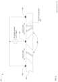
- FIG. 1has a schematic plan view and two schematic cross-sectional views of a transversely-excited film bulk acoustic resonator (XBAR).
- XBARtransversely-excited film bulk acoustic resonator
- FIG. 2is an expanded schematic cross-sectional view of a portion of the XBAR of FIG. 1 .
- FIG. 3is an alternative schematic cross-sectional view of the XBAR of FIG. 1 .
- FIG. 4is a graphic illustrating a shear primary acoustic mode in an XBAR.
- FIG. 5is a schematic block diagram of a filter using XBARs.
- FIG. 6is a graph of the magnitude of admittance versus frequency for an XBAR.
- FIG. 7is a graph of the frequency and coupling of a primary shear mode and the frequency of an A1-3 spurious mode as functions of interdigital transducer (IDT) pitch.
- IDTinterdigital transducer
- FIG. 8is a graph of the frequency and coupling of the A1-3 spurious mode as functions of IDT mark-to-pitch ratio.
- FIG. 9is a graph of absolute admittance and frequency of the A1-3 spurious mode as functions of IDT mark-to-pitch ratio.
- FIG. 10is a graph of the magnitude of admittance versus frequency for three XBARs with different mark-to-pitch ratios.
- FIG. 11is a flow chart of a process for fabricating an XBAR or filter incorporating XBARs.
- FIG. 1shows a simplified schematic top view and orthogonal cross-sectional views of a transversely-excited film bulk acoustic resonator (XBAR) 100 .
- XBAR resonatorssuch as the resonator 100 may be used in a variety of RF filters including band-reject filters, band-pass filters, duplexers, and multiplexers.
- XBARsare well suited for use in filters for communications bands with frequencies above 3 GHz.
- the XBAR 100is made up of a thin film conductor pattern formed on a surface of a piezoelectric plate 110 having a front surface 112 and a back surface 114 .
- the front and back surfacesare essentially parallel. “Essentially parallel” means parallel to the extent possible within normal manufacturing tolerances.
- the piezoelectric plateis a thin single-crystal layer of a piezoelectric material such as lithium niobate, lithium tantalate, lanthanum gallium silicate, gallium nitride, or aluminum nitride. The piezoelectric plate is cut such that the orientation of the X, Y, and Z crystalline axes with respect to the front and back surfaces is known and consistent.
- the piezoelectric platesare Z-cut, which is to say the Z axis is normal to the front surface 112 and back surface 114 .
- XBARsmay be fabricated on piezoelectric plates with other crystallographic orientations including rotated Z-cut and rotated YX-cut.
- the back surface 114 of the piezoelectric plate 110is attached to a surface 122 of the substrate 120 except for a portion of the piezoelectric plate 110 that forms a diaphragm 115 spanning a cavity 140 formed in the substrate 120 .
- the cavity 140has a perimeter defined by the intersection of the cavity and the surface 122 of the substrate 120 .
- the portion of the piezoelectric plate that spans the cavityis referred to herein as the “diaphragm” due to its physical resemblance to the diaphragm of a microphone.
- the diaphragm 115is contiguous with the rest of the piezoelectric plate 110 around all of the perimeter 145 of the cavity 140 .
- “contiguous”means “continuously connected without any intervening item”.
- the substrate 120provides mechanical support to the piezoelectric plate 110 .
- the substrate 120may be, for example, silicon, sapphire, quartz, or some other material or combination of materials.
- the back surface 114 of the piezoelectric plate 110may be attached to the substrate 120 using a wafer bonding process. Alternatively, the piezoelectric plate 110 may be grown on the substrate 120 or otherwise attached to the substrate.
- the piezoelectric plate 110may be attached directly to the substrate or may be attached to the substrate 120 via one or more intermediate material layers.
- the cavity 140is an empty space within a solid body of the resonator 100 .
- the cavity 140may be a hole completely through the substrate 120 (as shown in Section A-A and Section B-B) or a recess in the substrate 120 (as shown subsequently in FIG. 3 ).
- the cavity 140may be formed, for example, by selective etching of the substrate 120 before or after the piezoelectric plate 110 and the substrate 120 are attached.
- the conductor pattern of the XBAR 100includes an interdigital transducer (IDT) 130 .
- An IDTis an electrode structure for converting between electrical and acoustic energy in piezoelectric devices.
- the IDT 130includes a first plurality of parallel elongated conductors, commonly called “fingers”, such as finger 136 , extending from a first busbar 132 .
- the IDT 130includes a second plurality of fingers extending from a second busbar 134 .
- the first and second pluralities of parallel fingersare interleaved.
- the interleaved fingersoverlap for a distance AP, commonly referred to as the “aperture” of the IDT.
- the center-to-center distance L between the outermost fingers of the IDT 130is the “length” of the IDT.
- busbarrefers to the conductors that interconnect the first and second sets of fingers in an IDT.
- each busbar 132 , 134is an elongated rectangular conductor with a long axis orthogonal to the interleaved fingers and having a length approximately equal to the length L of the IDT.
- the busbars of an IDTneed not be rectangular or orthogonal to the interleaved fingers and may have lengths longer than the length of the IDT.
- the first and second busbars 132 , 134serve as the terminals of the XBAR 100 .
- a radio frequency or microwave signal applied between the two busbars 132 , 134 of the IDT 130excites a primary acoustic mode within the piezoelectric plate 110 .
- the primary acoustic modeis a bulk shear mode where acoustic energy propagates along a direction substantially orthogonal to the surface of the piezoelectric plate 110 , which is also normal, or transverse, to the direction of the electric field created by the IDT fingers.
- the XBARis considered a transversely-excited film bulk wave resonator.
- the IDT 130is positioned on the piezoelectric plate 110 such that at least the fingers of the IDT 130 are disposed on the diaphragm 115 of the piezoelectric plate that spans, or is suspended over, the cavity 140 .
- the cavity 140has a rectangular shape with an extent greater than the aperture AP and length L of the IDT 130 .
- a cavity of an XBARmay have a different shape, such as a regular or irregular polygon.
- the cavity of an XBARmay more or fewer than four sides, which may be straight or curved.
- the geometric pitch and width of the IDT fingersis greatly exaggerated with respect to the length (dimension L) and aperture (dimension AP) of the XBAR.
- An XBAR for a 5G devicewill have more than ten parallel fingers in the IDT 110 .
- An XBARmay have hundreds, possibly thousands, of parallel fingers in the IDT 110 .
- the thickness of the fingers in the cross-sectional viewsis greatly exaggerated in the drawings.
- FIG. 2shows a detailed schematic cross-sectional view of the XBAR 100 .
- the piezoelectric plate 110is a single-crystal layer of piezoelectrical material having a thickness ts.
- tsmay be, for example, 100 nm to 1500 nm.
- the thickness tsmay be, for example, 200 nm to 1000 nm.
- a front-side dielectric layer 214may be formed on the front side of the piezoelectric plate 110 .
- the “front side” of the XBARis the surface facing away from the substrate.
- the front-side dielectric layer 214has a thickness tfd.
- the front-side dielectric layer 214is formed between the IDT fingers 238 .
- the front side dielectric layer 214may also be deposited over the IDT fingers 238 .
- a back-side dielectric layer 216may be formed on the back side of the piezoelectric plate 110 .
- the back-side dielectric layer 216has a thickness tbd.
- the front-side and back-side dielectric layers 214 , 216may be a non-piezoelectric dielectric material, such as silicon dioxide or silicon nitride.
- tfd and tbdmay be, for example, 0 to 500 nm.
- tfd and tbdare typically less than the thickness ts of the piezoelectric plate.
- tfd and tbdare not necessarily equal, and the front-side and back-side dielectric layers 214 , 216 are not necessarily the same material.
- Either or both of the front-side and back-side dielectric layers 214 , 216may be formed of multiple layers of two or more materials.
- the IDT fingers 238may be one or more layers of aluminum, a substantially aluminum alloys, copper, a substantially copper alloys, beryllium, gold, molybdenum, or some other conductive material. Thin (relative to the total thickness of the conductors) layers of other metals, such as chromium or titanium, may be formed under and/or over the fingers to improve adhesion between the fingers and the piezoelectric plate 110 and/or to passivate or encapsulate the fingers.
- the busbars ( 132 , 134 in FIG. 1 ) of the IDTmay be made of the same or different materials as the fingers. As shown in FIG. 2 , the IDT fingers 238 have rectangular cross-sections. The IDT fingers may have some other cross-sectional shape, such as trapezoidal.
- Dimension pis the center-to-center spacing or “pitch” of the IDT fingers, which may be referred to as the pitch of the IDT and/or the pitch of the XBAR.
- Dimension wis the width or “mark” of the IDT fingers.
- the IDT of an XBARdiffers substantially from the IDTs used in surface acoustic wave (SAW) resonators.
- SAWsurface acoustic wave
- the pitch of the IDTis one-half of the acoustic wavelength at the resonance frequency.
- the mark-to-pitch ratio of a SAW resonator IDTis typically close to 0.5 (i.e., the mark or finger width is about one-fourth of the acoustic wavelength at resonance).
- the pitch p of the IDTis typically 2 to 20 times the width w of the fingers.
- the pitch p of the IDTis typically 2 to 20 times the thickness ts of the piezoelectric slab 212 .
- the width of the IDT fingers in an XBARis not constrained to one-fourth of the acoustic wavelength at resonance.
- the width of XBAR IDT fingersmay be 500 nm or greater, such that the IDT can be fabricated using optical lithography.
- the thickness tm of the IDT fingersmay be from 100 nm to about equal to the width w.
- the thickness of the busbars ( 132 , 134 in FIG. 1 ) of the IDTmay be the same as, or greater than, the thickness tm of the IDT fingers.
- FIG. 3is a plan view and a cross-sectional view of another XBAR 300 which is similar to the XBAR 100 of FIG. 1 .
- a piezoelectric plate 310is attached to a substrate 320 .
- a portion of the piezoelectric plate 310forms a diaphragm 315 spanning a cavity 340 in the substrate 320 .
- An IDT 330is formed on the surface 312 of the piezoelectric plate as previously described.
- the cavity 340does not fully penetrate the substrate 320 .
- the cavity 340may be formed, for example, by etching the substrate 320 before attaching the piezoelectric plate 310 .
- the cavity 340may be formed by etching the substrate 320 with a selective etchant that reaches the substrate through one or more openings, such as opening 350 , provided in the piezoelectric plate 310 .
- the diaphragm 315may be contiguous with the rest of the piezoelectric plate 310 around a large portion of a perimeter 345 of the cavity 340 .
- the diaphragm 315may be contiguous with the rest of the piezoelectric plate 310 around at least 50% of the perimeter 345 of the cavity 340 .
- FIG. 4is a graphical illustration of the primary acoustic mode of interest in an XBAR.
- FIG. 4shows a small portion of an XBAR 400 including a piezoelectric plate 410 and three interleaved IDT fingers 430 .
- a radio frequency (RF) voltageis applied to the interleaved fingers 430 .
- This voltagecreates a time-varying electric field between the fingers.
- the direction of the electric fieldis primarily lateral, or parallel to the surface of the piezoelectric plate 410 , as indicated by the arrows labeled “electric field”. Since the dielectric constant of the piezoelectric plate is significantly higher than the surrounding air, the electric field is highly concentrated in the plate relative to the air.
- Shear deformationis deformation in which parallel planes in a material remain parallel and maintain a constant distance while translating relative to each other.
- a “shear acoustic mode”is an acoustic vibration mode in a medium that results in shear deformation of the medium.
- the shear deformations in the XBAR 400are represented by the curves 460 , with the adjacent small arrows providing a schematic indication of the direction and magnitude of atomic motion.
- the degree of atomic motion, as well as the thickness of the piezoelectric plate 410have been greatly exaggerated for ease of visualization.
- the direction of acoustic energy flow of the excited primary shear acoustic modeis substantially orthogonal to the surface of the piezoelectric plate, as indicated by the arrow 465 .
- An acoustic resonator based on shear acoustic wave resonancescan achieve better performance than current state-of-the art film-bulk-acoustic-resonators (FBAR) and solidly-mounted-resonator bulk-acoustic-wave (SMR BAW) devices where the electric field is applied in the thickness direction.
- FBARfilm-bulk-acoustic-resonators
- SMR BAWsolidly-mounted-resonator bulk-acoustic-wave
- the piezoelectric coupling for shear wave XBAR resonancescan be high (>20%) compared to other acoustic resonators. High piezoelectric coupling enables the design and implementation of microwave and millimeter-wave filters with appreciable bandwidth.
- FIG. 5is a schematic circuit diagram and layout for a high frequency band-pass filter 500 using XBARs.
- the filter 500has a conventional ladder filter architecture including three series resonators 510 A, 510 B, 510 C and two shunt resonators 520 A, 520 B.
- the three series resonators 510 A, 510 B, and 510 Care connected in series between a first port and a second port (hence the term “series resonator”).
- the first and second portsare labeled “In” and “Out”, respectively.
- the filter 500is bidirectional and either port may serve as the input or output of the filter.
- the two shunt resonators 520 A, 520 Bare connected from nodes between the series resonators to ground.
- a filtermay contain additional reactive components, such as inductors, not shown in FIG. 5 .
- All the shunt resonators and series resonatorsare XBARs. The inclusion of three series and two shunt resonators is exemplary.
- a filtermay have more or fewer than five total resonators, more or fewer than three series resonators, and more or fewer than two shunt resonators.
- all of the series resonatorsare connected in series between an input and an output of the filter. All of the shunt resonators are typically connected between ground and the input, the output, or a node between two series resonators.
- the three series resonators 510 A, B, C and the two shunt resonators 520 A, B of the filter 500are formed on a single plate 530 of piezoelectric material bonded to a silicon substrate (not visible).
- Each resonatorincludes a respective IDT (not shown), with at least the fingers of the IDT disposed over a cavity in the substrate.
- the term “respective”means “relating things each to each”, which is to say with a one-to-one correspondence.
- the cavitiesare illustrated schematically as the dashed rectangles (such as the rectangle 535 ).
- each IDTis disposed over a respective cavity.
- the IDTs of two or more resonatorsmay be disposed over a single cavity.
- Each of the resonators 510 A, 510 B, 510 C, 520 A, 520 B in the filter 500has resonance where the admittance of the resonator is very high and an anti-resonance where the admittance of the resonator is very low.
- the resonance and anti-resonanceoccur at a resonance frequency and an anti-resonance frequency, respectively, which may be the same or different for the various resonators in the filter 500 .
- each resonatorcan be considered a short-circuit at its resonance frequency and an open circuit at its anti-resonance frequency.
- the input-output transfer functionwill be near zero at the resonance frequencies of the shunt resonators and at the anti-resonance frequencies of the series resonators.
- the resonance frequencies of the shunt resonatorsare positioned below the lower edge of the filter's passband and the anti-resonance frequencies of the series resonators are positioned above the upper edge of the passband.
- FIG. 6is a graph 600 of the performance of a typical XBAR.
- the curve 610is a plot of the magnitude of the admittance of an XBAR device having a lithium niobate diaphragm.
- the diaphragm thicknessis 400 nm.
- the IDT conductorsare aluminum, 100 nm thick.
- the IDT pitchis 3 ⁇ m and the IDT mark or finger width is 500 nm.
- the primary shear acoustic modehas a resonance 620 at a frequency of 4.8 GHz and an anti-resonance 625 at a frequency about 5.4 GHz.
- the coupling of the primary modeis greater than 25% and the Q at the resonance and anti-resonance frequencies is 400 to 500.
- the solid curve 610also exhibits multiple spurious modes.
- the largest spurious modeis an A1-3 mode (the third harmonic of the primary shear acoustic mode) with a resonance 630 and anti-resonance 635 at about 6.25 GHz.
- Small spurious modes 640are high order harmonics of plate wave modes that travel along the length of the XBAR in a direction normal to the IDT fingers. Data presented in FIG. 6 and subsequent figures is derived from two-dimensional simulation of XBARs using a finite-element technique.
- FIG. 7is a graph 700 of relationships between XBAR performance and IDT pitch.
- the solid curve 710is a plot of the resonance frequency of the XBAR shear primary mode as a function of IDT pitch for an XBAR with a z-cut lithium niobate diaphragm 400 nm thick and aluminum conductors 100 nm thick.
- the diaphragm thicknessis the dominant parameter that determines resonance frequency of an XBAR.
- the resonance frequencyhas a smaller dependence on IDT pitch. As shown in FIG. 7 , varying the IDT pitch from 1 ⁇ m to 6 ⁇ m results in reduction in resonance frequency by about 25%.
- the dashed curve 720is a plot of the resonance frequency of the A1-3 spurious mode of the same XBAR as a function of IDT pitch. Diaphragm thickness is also the dominant parameter that determines resonance frequency of A1-3 mode. However, the resonance frequency of the A1-3 mode has a much larger dependence on IDT pitch compared to the shear primary mode. Varying the IDT pitch from 1 ⁇ m to 6 ⁇ m results in reduction in resonance frequency of the A1-4 mode by about 85%. The frequencies of other spurious modes (i.e. spurious modes 640 in FIG. 6 ) are also very dependent on IDT pitch.
- the dot-dash curve 730is a plot of electromechanical coupling of the shear primary mode as a function of IDT pitch.
- the relationship between coupling and pitchis nonlinear. Larger IDT pitch results in higher coupling and coupling decreases rapidly for pitch values less than 3 ⁇ m. However, 17% coupling is available at pitch value of 1 ⁇ m, which is still sufficient for many filter applications.
- FIG. 8is a graph 800 of relationships between XBAR performance and IDT mark-to-pitch ratio (mark/pitch).
- the solid curve 810is a plot of the resonance frequency of the XBAR shear primary mode as a function of IDT mark/pitch for an XBAR with a z-cut lithium niobate diaphragm 400 nm thick.
- the IDT conductorsare aluminum 100 nm thick and the IDT pitch is 3 ⁇ m.
- the diaphragm thicknessis the dominant parameter that determines resonance frequency of an XBAR.
- the resonance frequencyhas a smaller dependence on IDT mark/pitch. As shown in FIG. 8 , varying the IDT mark/pitch from 0.15 to 0.45 ⁇ m results in reduction in resonance frequency by about 6%.
- the dashed curve 820is a plot of electromechanical coupling of the shear primary mode as a function of IDT mark/pitch.
- the relationship between coupling and mark/pitchis nonlinear. Maximum coupling occurs for IDT mark/pitch between 0.40 and 0.45. Coupling decreases with decreasing mark/pitch. However, 27% coupling is available at mark/pitch value of about 0.12, which is sufficient for most filter applications.
- FIG. 7 and FIG. 8illustrate the complexity of selecting the pitch and mark of XBAR IDTs within a filter to provide a desired resonance frequency and electromechanical coupling of each XBAR while trying to place spurious modes at frequencies that do not degrade the filter performance.
- the pitch and marksince the resonance frequency of the shear primary acoustic mode varies with both IDT pitch and IDT mark, the pitch and mark must be selected in combination to set the resonance frequency of an XBAR to a predetermined target frequency. Since the same resonance frequency may be achieved with different IDT pitch and mark combinations, a filter designer has some freedom to select the pitch and mark to control the frequencies of spurious modes.
- FIG. 9is a graph 900 of relationships between the A1-3 spurious mode and IDT mark-to-pitch ratio (mark/pitch).
- the solid curve 910is a plot of the resonance frequency of the A1-3 mode as a function of IDT mark/pitch for an XBAR with a z-cut lithium niobate diaphragm 400 nm thick.
- the IDT conductorsare aluminum 100 nm thick and the IDT pitch is 3 ⁇ m.
- the A1-3 mode resonance frequencydepends on IDT mark/pitch. As shown in FIG. 9 , varying the IDT mark/pitch from 0.15 to 0.45 ⁇ m results in reduction in resonance frequency by about 10%.
- the dashed curve 920is a plot of the absolute admittance of the A1-3 mode as a function of IDT mark/pitch.
- the relationship between admittance and mark/pitchis nonlinear.
- Minimum admittanceoccurs for IDT mark/pitch from 0.235 to 0.265.
- Admittanceincrease for mark/pitch values outside of this range but is still small for a mark/pitch range from 0.2 to 0.3.
- FIG. 10is a graph 1000 of the performance of three XBARs having different mark/pitch ratios.
- the IDT conductorsare aluminum 100 nm thick and the IDT pitch is 3 ⁇ m.
- FIG. 9 and FIG. 10demonstrate that selecting IDT mark/pitch in a range from 0.2 to 0.3, or in a preferred range of 0.235 to 0.265, reduces or eliminates the A1-3 spurious mode. It is anticipated that this range will be valid for values of IDT pitch greater than or less than 3 ⁇ m and for thin aluminum IDT conductors with a thickness between 50 nm and 150 nm.
- FIG. 11is a simplified flow chart showing a process 1100 for making an XBAR or a filter incorporating XBARs.
- the process 1100starts at 1105 with a substrate and a plate of piezoelectric material and ends at 1195 with a completed XBAR or filter.
- the flow chart of FIG. 11includes only major process steps.
- Various conventional process stepse.g. surface preparation, cleaning, inspection, baking, annealing, monitoring, testing, etc. may be performed before, between, after, and during the steps shown in FIG. 11 .
- the flow chart of FIG. 11captures three variations of the process 1100 for making an XBAR which differ in when and how cavities are formed in the substrate.
- the cavitiesmay be formed at steps 1110 A, 1110 B, or 1110 C. Only one of these steps is performed in each of the three variations of the process 1100 .
- the piezoelectric platemay be, for example, Z-cut lithium niobate as used in the previously presented examples.
- the piezoelectric platemay be rotated ZY-lithium niobate or rotated YX-cut lithium niobate.
- the piezoelectric platemay be some other material and/or some other cut.
- the substratemay preferably be silicon.
- the substratemay be some other material that allows formation of deep cavities by etching or other processing.
- one or more cavitiesare formed in the substrate at 1110 A before the piezoelectric plate is bonded to the substrate at 1120 .
- a separate cavitymay be formed for each resonator in a filter device.
- the one or more cavitiesmay be formed using conventional photolithographic and etching techniques. Typically, the cavities formed at 1110 A will not penetrate through the substrate, and the resulting resonator devices will have a cross-section as shown in FIG. 3 .
- the piezoelectric plateis bonded to the substrate.
- the piezoelectric plate and the substratemay be bonded by a wafer bonding process.
- the mating surfaces of the substrate and the piezoelectric plateare highly polished.
- One or more layers of intermediate materials, such as an oxide or metal,may be formed or deposited on the mating surface of one or both of the piezoelectric plate and the substrate.
- One or both mating surfacesmay be activated using, for example, a plasma process. The mating surfaces may then be pressed together with considerable force to establish molecular bonds between the piezoelectric plate and the substrate or intermediate material layers.
- a conductor pattern, including IDTs of each XBAR,is formed at 1130 by depositing and patterning one or more conductor layers on the front side of the piezoelectric plate.
- the conductor layermay be, for example, aluminum or an aluminum alloy with a thickness of 50 nm to 150 nm.
- one or more layers of other materialsmay be disposed below (i.e. between the conductor layer and the piezoelectric plate) and/or on top of the conductor layer.
- a thin film of titanium, chrome, or other metalmay be used to improve the adhesion between the conductor layer and the piezoelectric plate.
- a conduction enhancement layer of gold, aluminum, copper or other higher conductivity metalmay be formed over portions of the conductor pattern (for example the IDT bus bars and interconnections between the IDTs).
- the conductor patternmay be formed at 1130 by depositing the conductor layer and, optionally, one or more other metal layers in sequence over the surface of the piezoelectric plate. The excess metal may then be removed by etching through patterned photoresist.
- the conductor layercan be etched, for example, by plasma etching, reactive ion etching, wet chemical etching, and other etching techniques.
- the conductor patternmay be formed at 1130 using a lift-off process.
- Photoresistmay be deposited over the piezoelectric plate. and patterned to define the conductor pattern.
- the conductor layer and, optionally, one or more other layersmay be deposited in sequence over the surface of the piezoelectric plate. The photoresist may then be removed, which removes the excess material, leaving the conductor pattern.
- one or more cavitiesare formed in the back side of the substrate at 1110 B.
- a separate cavitymay be formed for each resonator in a filter device.
- the one or more cavitiesmay be formed using an anisotropic or orientation-dependent dry or wet etch to open holes through the back side of the substrate to the piezoelectric plate.
- the resulting resonator deviceswill have a cross-section as shown in FIG. 1 .
- one or more cavities in the form of recesses in the substratemay be formed at 1110 C by etching the substrate using an etchant introduced through openings in the piezoelectric plate.
- a separate cavitymay be formed for each resonator in a filter device.
- the one or more cavities formed at 1110 Cwill not penetrate through the substrate, and the resulting resonator devices will have a cross-section as shown in FIG. 3 .
- the filter deviceis completed at 1160 .
- Actions that may occur at 1160include depositing a passivation and tuning layer such as SiO 2 or Si 3 O 4 over all or a portion of the device; forming bonding pads or solder bumps or other means for making connection between the device and external circuitry; excising individual devices from a wafer containing multiple devices; other packaging steps; and testing. Any dielectric layer deposited at 1160 or elsewhere in the process 1100 is deposited over all resonators.
- Another action that may occur at 1160is to tune the resonant frequencies of the resonators within the device by adding or removing metal or dielectric material from the front side of the device. After the filter device is completed, the process ends at 1195 .
- “plurality”means two or more. As used herein, a “set” of items may include one or more of such items.
- the terms “comprising”, “including”, “carrying”, “having”, “containing”, “involving”, and the likeare to be understood to be open-ended, i.e., to mean including but not limited to. Only the transitional phrases “consisting of” and “consisting essentially of”, respectively, are closed or semi-closed transitional phrases with respect to claims.
Landscapes
- Physics & Mathematics (AREA)
- Acoustics & Sound (AREA)
- Chemical & Material Sciences (AREA)
- Engineering & Computer Science (AREA)
- Crystallography & Structural Chemistry (AREA)
- Ceramic Engineering (AREA)
- Manufacturing & Machinery (AREA)
- Piezo-Electric Or Mechanical Vibrators, Or Delay Or Filter Circuits (AREA)
Abstract
Description
Claims (21)
Priority Applications (1)
| Application Number | Priority Date | Filing Date | Title |
|---|---|---|---|
| US17/322,605US11831289B2 (en) | 2018-06-15 | 2021-05-17 | Transversely-excited film bulk acoustic resonator with reduced spurious modes |
Applications Claiming Priority (11)
| Application Number | Priority Date | Filing Date | Title |
|---|---|---|---|
| US201862685825P | 2018-06-15 | 2018-06-15 | |
| US201862701363P | 2018-07-20 | 2018-07-20 | |
| US201862741702P | 2018-10-05 | 2018-10-05 | |
| US201862748883P | 2018-10-22 | 2018-10-22 | |
| US201862753815P | 2018-10-31 | 2018-10-31 | |
| US16/230,443US10491192B1 (en) | 2018-06-15 | 2018-12-21 | Transversely-excited film bulk acoustic resonator |
| US16/438,121US10756697B2 (en) | 2018-06-15 | 2019-06-11 | Transversely-excited film bulk acoustic resonator |
| US201962904386P | 2019-09-23 | 2019-09-23 | |
| US16/920,173US11139794B2 (en) | 2018-06-15 | 2020-07-02 | Transversely-excited film bulk acoustic resonator |
| US17/030,066US11146232B2 (en) | 2018-06-15 | 2020-09-23 | Transversely-excited film bulk acoustic resonator with reduced spurious modes |
| US17/322,605US11831289B2 (en) | 2018-06-15 | 2021-05-17 | Transversely-excited film bulk acoustic resonator with reduced spurious modes |
Related Parent Applications (1)
| Application Number | Title | Priority Date | Filing Date |
|---|---|---|---|
| US17/030,066ContinuationUS11146232B2 (en) | 2018-02-18 | 2020-09-23 | Transversely-excited film bulk acoustic resonator with reduced spurious modes |
Publications (2)
| Publication Number | Publication Date |
|---|---|
| US20210273626A1 US20210273626A1 (en) | 2021-09-02 |
| US11831289B2true US11831289B2 (en) | 2023-11-28 |
Family
ID=74189865
Family Applications (5)
| Application Number | Title | Priority Date | Filing Date |
|---|---|---|---|
| US17/030,066Active2039-03-10US11146232B2 (en) | 2018-02-18 | 2020-09-23 | Transversely-excited film bulk acoustic resonator with reduced spurious modes |
| US17/200,703ActiveUS11881834B2 (en) | 2018-06-15 | 2021-03-12 | Transversely-excited film bulk acoustic resonator with reduced spurious modes |
| US17/322,605Active2039-06-30US11831289B2 (en) | 2018-06-15 | 2021-05-17 | Transversely-excited film bulk acoustic resonator with reduced spurious modes |
| US17/351,204Active2039-02-04US11929727B2 (en) | 2018-02-18 | 2021-06-17 | Transversely-excited film bulk acoustic resonator with reduced spurious modes |
| US17/351,203Active2039-04-24US11923821B2 (en) | 2018-06-15 | 2021-06-17 | Transversely-excited film bulk acoustic resonator with reduced spurious modes |
Family Applications Before (2)
| Application Number | Title | Priority Date | Filing Date |
|---|---|---|---|
| US17/030,066Active2039-03-10US11146232B2 (en) | 2018-02-18 | 2020-09-23 | Transversely-excited film bulk acoustic resonator with reduced spurious modes |
| US17/200,703ActiveUS11881834B2 (en) | 2018-06-15 | 2021-03-12 | Transversely-excited film bulk acoustic resonator with reduced spurious modes |
Family Applications After (2)
| Application Number | Title | Priority Date | Filing Date |
|---|---|---|---|
| US17/351,204Active2039-02-04US11929727B2 (en) | 2018-02-18 | 2021-06-17 | Transversely-excited film bulk acoustic resonator with reduced spurious modes |
| US17/351,203Active2039-04-24US11923821B2 (en) | 2018-06-15 | 2021-06-17 | Transversely-excited film bulk acoustic resonator with reduced spurious modes |
Country Status (1)
| Country | Link |
|---|---|
| US (5) | US11146232B2 (en) |
Families Citing this family (82)
| Publication number | Priority date | Publication date | Assignee | Title |
|---|---|---|---|---|
| US11509279B2 (en) | 2020-07-18 | 2022-11-22 | Resonant Inc. | Acoustic resonators and filters with reduced temperature coefficient of frequency |
| US11323096B2 (en) | 2018-06-15 | 2022-05-03 | Resonant Inc. | Transversely-excited film bulk acoustic resonator with periodic etched holes |
| US12237826B2 (en) | 2018-06-15 | 2025-02-25 | Murata Manufacturing Co., Ltd. | Transversely-excited film bulk acoustic resonator with optimized electrode thickness, mark, and pitch |
| US11206009B2 (en) | 2019-08-28 | 2021-12-21 | Resonant Inc. | Transversely-excited film bulk acoustic resonator with interdigital transducer with varied mark and pitch |
| US11323090B2 (en) | 2018-06-15 | 2022-05-03 | Resonant Inc. | Transversely-excited film bulk acoustic resonator using Y-X-cut lithium niobate for high power applications |
| US10601392B2 (en) | 2018-06-15 | 2020-03-24 | Resonant Inc. | Solidly-mounted transversely-excited film bulk acoustic resonator |
| US11146232B2 (en) | 2018-06-15 | 2021-10-12 | Resonant Inc. | Transversely-excited film bulk acoustic resonator with reduced spurious modes |
| US11323089B2 (en) | 2018-06-15 | 2022-05-03 | Resonant Inc. | Filter using piezoelectric film bonded to high resistivity silicon substrate with trap-rich layer |
| US11929731B2 (en) | 2018-02-18 | 2024-03-12 | Murata Manufacturing Co., Ltd. | Transversely-excited film bulk acoustic resonator with optimized electrode mark, and pitch |
| US11996827B2 (en) | 2018-06-15 | 2024-05-28 | Murata Manufacturing Co., Ltd. | Transversely-excited film bulk acoustic resonator with periodic etched holes |
| US11936358B2 (en) | 2020-11-11 | 2024-03-19 | Murata Manufacturing Co., Ltd. | Transversely-excited film bulk acoustic resonator with low thermal impedance |
| US10911023B2 (en) | 2018-06-15 | 2021-02-02 | Resonant Inc. | Transversely-excited film bulk acoustic resonator with etch-stop layer |
| US10637438B2 (en) | 2018-06-15 | 2020-04-28 | Resonant Inc. | Transversely-excited film bulk acoustic resonators for high power applications |
| US12119805B2 (en) | 2018-06-15 | 2024-10-15 | Murata Manufacturing Co., Ltd. | Substrate processing and membrane release of transversely-excited film bulk acoustic resonator using a sacrificial tub |
| US12149227B2 (en) | 2018-06-15 | 2024-11-19 | Murata Manufacturing Co., Ltd. | Transversely-excited film bulk acoustic resonator package |
| US11329628B2 (en) | 2020-06-17 | 2022-05-10 | Resonant Inc. | Filter using lithium niobate and lithium tantalate transversely-excited film bulk acoustic resonators |
| US12155371B2 (en) | 2021-03-29 | 2024-11-26 | Murata Manufacturing Co., Ltd. | Layout of xbars with multiple sub-resonators in series |
| US11876498B2 (en) | 2018-06-15 | 2024-01-16 | Murata Manufacturing Co., Ltd. | Transversely-excited film bulk acoustic resonator with multiple diaphragm thicknesses and fabrication method |
| US12009798B2 (en) | 2018-06-15 | 2024-06-11 | Murata Manufacturing Co., Ltd. | Transversely-excited film bulk acoustic resonators with electrodes having irregular hexagon cross-sectional shapes |
| US11901878B2 (en) | 2018-06-15 | 2024-02-13 | Murata Manufacturing Co., Ltd. | Transversely-excited film bulk acoustic resonators with two-layer electrodes with a wider top layer |
| US11323091B2 (en) | 2018-06-15 | 2022-05-03 | Resonant Inc. | Transversely-excited film bulk acoustic resonator with diaphragm support pedestals |
| US12113512B2 (en) | 2021-03-29 | 2024-10-08 | Murata Manufacturing Co., Ltd. | Layout of XBARs with multiple sub-resonators in parallel |
| US11374549B2 (en) | 2018-06-15 | 2022-06-28 | Resonant Inc. | Filter using transversely-excited film bulk acoustic resonators with divided frequency-setting dielectric layers |
| US11349450B2 (en) | 2018-06-15 | 2022-05-31 | Resonant Inc. | Symmetric transversely-excited film bulk acoustic resonators with reduced spurious modes |
| US11264966B2 (en) | 2018-06-15 | 2022-03-01 | Resonant Inc. | Solidly-mounted transversely-excited film bulk acoustic resonator with diamond layers in Bragg reflector stack |
| US12237827B2 (en) | 2018-06-15 | 2025-02-25 | Murata Manufacturing Co., Ltd. | Solidly-mounted transversely-excited film bulk acoustic filters with multiple piezoelectric plate thicknesses |
| US12224732B2 (en) | 2018-06-15 | 2025-02-11 | Murata Manufacturing Co., Ltd. | Solidly-mounted transversely-excited film bulk acoustic resonators and filters for 27 GHz communications bands |
| US12095441B2 (en) | 2018-06-15 | 2024-09-17 | Murata Manufacturing Co., Ltd. | Transversely excited film bulk acoustic resonator with recessed interdigital transducer fingers |
| US11888463B2 (en) | 2018-06-15 | 2024-01-30 | Murata Manufacturing Co., Ltd. | Multi-port filter using transversely-excited film bulk acoustic resonators |
| US11323095B2 (en) | 2018-06-15 | 2022-05-03 | Resonant Inc. | Rotation in XY plane to suppress spurious modes in XBAR devices |
| US11916539B2 (en) | 2020-02-28 | 2024-02-27 | Murata Manufacturing Co., Ltd. | Split-ladder band N77 filter using transversely-excited film bulk acoustic resonators |
| US12119808B2 (en) | 2018-06-15 | 2024-10-15 | Murata Manufacturing Co., Ltd. | Transversely-excited film bulk acoustic resonator package |
| US11909381B2 (en) | 2018-06-15 | 2024-02-20 | Murata Manufacturing Co., Ltd. | Transversely-excited film bulk acoustic resonators with two-layer electrodes having a narrower top layer |
| US11949402B2 (en) | 2020-08-31 | 2024-04-02 | Murata Manufacturing Co., Ltd. | Resonators with different membrane thicknesses on the same die |
| US12021496B2 (en) | 2020-08-31 | 2024-06-25 | Murata Manufacturing Co., Ltd. | Resonators with different membrane thicknesses on the same die |
| US12132464B2 (en) | 2018-06-15 | 2024-10-29 | Murata Manufacturing Co., Ltd. | Filter using transversely-excited film bulk acoustic resonators with divided frequency-setting dielectric layers |
| US12191837B2 (en) | 2018-06-15 | 2025-01-07 | Murata Manufacturing Co., Ltd. | Solidly-mounted transversely-excited film bulk acoustic device |
| US10826462B2 (en) | 2018-06-15 | 2020-11-03 | Resonant Inc. | Transversely-excited film bulk acoustic resonators with molybdenum conductors |
| US11967945B2 (en) | 2018-06-15 | 2024-04-23 | Murata Manufacturing Co., Ltd. | Transversly-excited film bulk acoustic resonators and filters |
| US12155374B2 (en) | 2021-04-02 | 2024-11-26 | Murata Manufacturing Co., Ltd. | Tiled transversely-excited film bulk acoustic resonator high power filters |
| US12191838B2 (en) | 2018-06-15 | 2025-01-07 | Murata Manufacturing Co., Ltd. | Solidly-mounted transversely-excited film bulk acoustic device and method |
| US10917072B2 (en) | 2019-06-24 | 2021-02-09 | Resonant Inc. | Split ladder acoustic wave filters |
| US10992284B2 (en) | 2018-06-15 | 2021-04-27 | Resonant Inc. | Filter using transversely-excited film bulk acoustic resonators with multiple frequency setting layers |
| US11996822B2 (en) | 2018-06-15 | 2024-05-28 | Murata Manufacturing Co., Ltd. | Wide bandwidth time division duplex transceiver |
| US12081187B2 (en) | 2018-06-15 | 2024-09-03 | Murata Manufacturing Co., Ltd. | Transversely-excited film bulk acoustic resonator |
| US10985728B2 (en) | 2018-06-15 | 2021-04-20 | Resonant Inc. | Transversely-excited film bulk acoustic resonator and filter with a uniform-thickness dielectric overlayer |
| US11349452B2 (en) | 2018-06-15 | 2022-05-31 | Resonant Inc. | Transversely-excited film bulk acoustic filters with symmetric layout |
| US12040781B2 (en) | 2018-06-15 | 2024-07-16 | Murata Manufacturing Co., Ltd. | Transversely-excited film bulk acoustic resonator package |
| DE112020001227T5 (en) | 2019-03-14 | 2022-02-10 | Resonant Inc. | Transversally excited acoustic film resonator with half-wave dielectric layer |
| JP2022525465A (en) | 2019-04-05 | 2022-05-16 | レゾナント インコーポレイテッド | Laterally Excited Film Bulk Acoustic Resonator Package and Method |
| US12255625B2 (en) | 2020-02-28 | 2025-03-18 | Murata Manufacturing Co., Ltd. | Filter using transversely-excited film bulk acoustic resonators with inductively coupled sub-resonators |
| US12341493B2 (en) | 2020-04-20 | 2025-06-24 | Murata Manufacturing Co., Ltd. | Low loss transversely-excited film bulk acoustic resonators and filters |
| US12341490B2 (en) | 2020-04-20 | 2025-06-24 | Murata Manufacturing Co., Ltd. | Low loss transversely-excited film bulk acoustic resonators and filters |
| US12278617B2 (en) | 2020-04-20 | 2025-04-15 | Murata Manufacturing Co., Ltd. | High Q solidly-mounted transversely-excited film bulk acoustic resonators |
| US11811391B2 (en) | 2020-05-04 | 2023-11-07 | Murata Manufacturing Co., Ltd. | Transversely-excited film bulk acoustic resonator with etched conductor patterns |
| KR20230003544A (en)* | 2020-05-18 | 2023-01-06 | 어쿠스티스, 인크. | Bulk Acoustic Wave Resonator Filters Containing High Impedance Shunt Branches and Methods of Forming The Same |
| US11742828B2 (en) | 2020-06-30 | 2023-08-29 | Murata Manufacturing Co., Ltd. | Transversely-excited film bulk acoustic resonator with symmetric diaphragm |
| US11271539B1 (en) | 2020-08-19 | 2022-03-08 | Resonant Inc. | Transversely-excited film bulk acoustic resonator with tether-supported diaphragm |
| US11658639B2 (en) | 2020-10-05 | 2023-05-23 | Murata Manufacturing Co., Ltd. | Transversely-excited film bulk acoustic resonator matrix filters with noncontiguous passband |
| US11476834B2 (en) | 2020-10-05 | 2022-10-18 | Resonant Inc. | Transversely-excited film bulk acoustic resonator matrix filters with switches in parallel with sub-filter shunt capacitors |
| US11728784B2 (en) | 2020-10-05 | 2023-08-15 | Murata Manufacturing Co., Ltd. | Transversely-excited film bulk acoustic resonator matrix filters with split die sub-filters |
| US11405017B2 (en) | 2020-10-05 | 2022-08-02 | Resonant Inc. | Acoustic matrix filters and radios using acoustic matrix filters |
| US12119806B2 (en) | 2020-10-30 | 2024-10-15 | Murata Manufacturing Co., Ltd. | Transversely-excited film bulk acoustic resonator with spiral interdigitated transducer fingers |
| US12255617B2 (en) | 2020-11-11 | 2025-03-18 | Murata Manufacturing Co., Ltd. | Solidly-mounted transversely-excited film bulk acoustic resonators with low thermal impedance |
| US11496113B2 (en) | 2020-11-13 | 2022-11-08 | Resonant Inc. | XBAR devices with excess piezoelectric material removed |
| US12255626B2 (en) | 2020-11-13 | 2025-03-18 | Murata Manufacturing Co., Ltd. | Solidly-mounted transversely-excited film bulk acoustic filters with excess piezoelectric material removed |
| US11239816B1 (en) | 2021-01-15 | 2022-02-01 | Resonant Inc. | Decoupled transversely-excited film bulk acoustic resonators |
| US12355426B2 (en) | 2021-03-24 | 2025-07-08 | Murata Manufacturing Co., Ltd. | Acoustic filters with shared acoustic tracks |
| US12289099B2 (en) | 2021-03-24 | 2025-04-29 | Murata Manufacturing Co., Ltd. | Acoustic filters with shared acoustic tracks for series and shunt resonators |
| US12348216B2 (en) | 2021-03-24 | 2025-07-01 | Murata Manufacturing Co., Ltd. | Acoustic filters with shared acoustic tracks and cascaded series resonators |
| CN117321912A (en) | 2021-03-30 | 2023-12-29 | 株式会社村田制作所 | Filters for 6GHz WI-FI using transversely excited thin film bulk acoustic resonators |
| US12249971B2 (en) | 2021-04-02 | 2025-03-11 | Murata Manufacturing Co., Ltd. | Transversely-excited film bulk acoustic resonators with solidly mounted resonator (SMR) pedestals |
| US12126316B2 (en) | 2021-04-16 | 2024-10-22 | Murata Manufacturing Co., Ltd | Transversely-excited film bulk acoustic resonator |
| US12255633B2 (en) | 2021-04-16 | 2025-03-18 | Murata Manufacturing Co., Ltd. | Filter using transversely-excited film bulk acoustic resonators |
| US12255607B2 (en) | 2021-04-30 | 2025-03-18 | Murata Manufacturing Co., Ltd. | Transversely-excited film bulk acoustic resonator with buried oxide strip acoustic confinement structures |
| US12160220B2 (en) | 2021-04-30 | 2024-12-03 | Murata Manufacturing Co., Ltd. | Transversely-excited film bulk acoustic resonator with oxide strip acoustic confinement structures |
| US12057823B2 (en) | 2021-05-07 | 2024-08-06 | Murata Manufacturing Co., Ltd. | Transversely-excited film bulk acoustic resonator with concentric interdigitated transducer fingers |
| US12267063B2 (en) | 2021-09-24 | 2025-04-01 | Rf360 Singapore Pte. Ltd. | Harmonic reduction with filtering |
| US12225387B2 (en) | 2021-09-29 | 2025-02-11 | Murata Manufacturing Co., Ltd. | Communications device with concurrent operation in 5GHZ and 6GHZ U-NII frequency ranges |
| US12407326B2 (en) | 2021-11-04 | 2025-09-02 | Murata Manufacturing Co., Ltd. | Stacked die transversely-excited film bulk acoustic resonator (XBAR) filters |
| US12113511B2 (en) | 2022-03-16 | 2024-10-08 | Rf360 Singapore Pte. Ltd. | Bridge-type filters |
| US12231112B2 (en)* | 2022-03-16 | 2025-02-18 | Rf360 Singapore Pte. Ltd. | Bridge-type filters |
Citations (162)
| Publication number | Priority date | Publication date | Assignee | Title |
|---|---|---|---|---|
| US5446330A (en) | 1993-03-15 | 1995-08-29 | Matsushita Electric Industrial Co., Ltd. | Surface acoustic wave device having a lamination structure |
| US5552655A (en) | 1994-05-04 | 1996-09-03 | Trw Inc. | Low frequency mechanical resonator |
| US5726610A (en) | 1995-06-19 | 1998-03-10 | Motorola Inc. | Saw filter device for radio tranceiver utilizing different coupling coefficient ratios |
| JPH10209804A (en) | 1997-01-27 | 1998-08-07 | Oki Electric Ind Co Ltd | Surface acoustic wave resonator and surface acoustic wave filter |
| US5853601A (en) | 1997-04-03 | 1998-12-29 | Northrop Grumman Corporation | Top-via etch technique for forming dielectric membranes |
| JP2001244785A (en) | 2000-02-29 | 2001-09-07 | Kyocera Corp | Surface acoustic wave device |
| US6377140B1 (en) | 1999-07-09 | 2002-04-23 | Oki Electric Industry Co., Ltd. | Saw resonator filter with bridged-T configuration |
| US20020079986A1 (en) | 2000-12-21 | 2002-06-27 | Ruby Richard C. | Bulk acoustic resonator perimeter reflection system |
| JP2002300003A (en) | 2001-03-29 | 2002-10-11 | Kyocera Corp | Elastic wave filter |
| US20020158714A1 (en) | 2001-04-27 | 2002-10-31 | Nokia Corporation | Method and system for wafer-level tuning of bulk acoustic wave resonators and filters by reducing thickness non-uniformity |
| US20020189062A1 (en) | 2001-06-15 | 2002-12-19 | Asia Pacific Microsystems, Inc. | Manufacturing method for a high quality film bulk acoustic wave device |
| US6516503B1 (en) | 1999-05-26 | 2003-02-11 | Murata Manufacturing Co., Ltd. | Method of making surface acoustic wave device |
| JP2003078389A (en) | 2001-08-31 | 2003-03-14 | Matsushita Electric Ind Co Ltd | Surface acoustic wave device and method of manufacturing the same |
| US6540827B1 (en) | 1998-02-17 | 2003-04-01 | Trustees Of Columbia University In The City Of New York | Slicing of single-crystal films using ion implantation |
| US20030080831A1 (en) | 2001-10-25 | 2003-05-01 | Naumenko Natalya F. | Surface acoustic wave devices using optimized cuts of lithium niobate (LiNbO3) |
| US20030199105A1 (en) | 2002-04-22 | 2003-10-23 | Kub Francis J. | Method for making piezoelectric resonator and surface acoustic wave device using hydrogen implant layer splitting |
| US20040041496A1 (en) | 2002-09-04 | 2004-03-04 | Fujitsu Media Devices Limited | Surface acoustic wave device, filter device and method of producing the surface acoustic wave device |
| US6707229B1 (en) | 1999-06-03 | 2004-03-16 | Tele Filter Zweigniederlassung Der Dover Germany Gmbh | Surface acoustic wave filter |
| JP2004129222A (en) | 2002-07-31 | 2004-04-22 | Murata Mfg Co Ltd | Piezoelectric component and method of manufacturing the same |
| US20040100164A1 (en) | 2002-11-26 | 2004-05-27 | Murata Manufacturing Co., Ltd. | Manufacturing method of electronic device |
| JP2004304622A (en) | 2003-03-31 | 2004-10-28 | Fujitsu Media Device Kk | Surface acoustic wave device and method of manufacturing the same |
| US20040261250A1 (en) | 2000-09-06 | 2004-12-30 | Murata Manufacturing Co., Ltd. | Method for adjusting a frequency characteristic of an edge reflection type surface acoustic wave device and method for producing an- edge reflection type surface acoustic wave device |
| US20050099091A1 (en) | 2003-11-12 | 2005-05-12 | Fujitsu Media Devices Limited | Elastic boundary wave device and method of manufacturing the same |
| US20050185026A1 (en) | 2004-01-26 | 2005-08-25 | Motohisa Noguchi | Piezoelectric element, piezoelectric actuator, ink jet recording head, ink jet printer, surface acoustic wave element, frequency filter, oscillator, electronic circuit, thin film piezoelectric resonator, and electronic apparatus |
| US20050218488A1 (en) | 2004-03-31 | 2005-10-06 | Mie Matsuo | Electronic component having micro-electrical mechanical system |
| US20050264136A1 (en) | 2004-05-31 | 2005-12-01 | Jun Tsutsumi | Surface acoustic wave device |
| US7042132B2 (en) | 2001-03-13 | 2006-05-09 | Epcos Ag | Transducer structure that operates with acoustic waves |
| JP2006173557A (en) | 2004-11-22 | 2006-06-29 | Toshiba Corp | Hollow semiconductor device and manufacturing method thereof |
| US20060179642A1 (en) | 2005-02-03 | 2006-08-17 | Kabushiki Kaisha Toshiba | Method for manufacturing a film bulk acoustic resonator |
| US20070182510A1 (en) | 2006-02-06 | 2007-08-09 | Samsung Electronics Co., Ltd. | Multi-band filter module and method of fabricating the same |
| US20070188047A1 (en) | 2006-02-16 | 2007-08-16 | Seiko Epson Corporation | Lamb wave type frequency device and method thereof |
| US20070194863A1 (en) | 2006-02-17 | 2007-08-23 | Kabushiki Kaisha Toshiba | Film bulk acoustic resonator and method of manufacturing same |
| US20070267942A1 (en) | 2006-05-19 | 2007-11-22 | Hisanori Matsumoto | Piezoelectric film resonator, radio-frequency filter using them, and radio-frequency module using them |
| US20070296304A1 (en) | 2006-06-22 | 2007-12-27 | Seiko Epson Corporation | Acoustic wave device and method of manufacturing acoustic wave device |
| US7345400B2 (en) | 2003-01-27 | 2008-03-18 | Murata Manufacturing Co., Ltd. | Surface acoustic wave device |
| US20080246559A1 (en) | 2007-01-19 | 2008-10-09 | Farrokh Ayazi | Lithographically-defined multi-standard multi-frequency high-Q tunable micromechanical resonators |
| US7463118B2 (en) | 2006-06-09 | 2008-12-09 | Texas Instruments Incorporated | Piezoelectric resonator with an efficient all-dielectric Bragg reflector |
| US7535152B2 (en) | 2005-10-19 | 2009-05-19 | Murata Manufacturing Co., Ltd. | Lamb wave device |
| JP2010062816A (en) | 2008-09-03 | 2010-03-18 | Murata Mfg Co Ltd | Acoustic wave filter |
| US7684109B2 (en) | 2007-02-28 | 2010-03-23 | Maxim Integrated Products, Inc. | Bragg mirror optimized for shear waves |
| WO2010047114A1 (en) | 2008-10-24 | 2010-04-29 | エプソントヨコム株式会社 | Surface acoustic wave resonator, surface acoustic wave oscillator, and surface acoustic wave modular device |
| JP2010103803A (en) | 2008-10-24 | 2010-05-06 | Epson Toyocom Corp | Surface acoustic wave resonator, surface acoustic wave oscillator, and surface acoustic wave module device |
| US20100123367A1 (en) | 2008-11-19 | 2010-05-20 | Ngk Insulators, Ltd. | Lamb wave device |
| US20100212127A1 (en) | 2009-02-24 | 2010-08-26 | Habbo Heinze | Process for Adapting Resonance Frequency of a BAW Resonator |
| JP2010233210A (en) | 2009-03-03 | 2010-10-14 | Nippon Dempa Kogyo Co Ltd | Elastic wave device and electronic component |
| US7868519B2 (en) | 2007-09-06 | 2011-01-11 | Murata Manufacturing Co., Ltd. | Piezoelectric resonator including an acoustic reflector portion |
| US20110018654A1 (en) | 2009-07-27 | 2011-01-27 | Avago Technologies Wireless Ip (Singapore) Pte. Ltd. | Resonator filter with multiple cross-couplings |
| US20110018389A1 (en) | 2008-01-30 | 2011-01-27 | Kyocera Corporation | Acoustic Wave Device and Method for Production of Same |
| US20110102107A1 (en) | 2008-02-05 | 2011-05-05 | Nihon Dempa Kogyo Co., Ltd. | Filter, portable terminal and electronic component |
| US7939987B1 (en) | 2008-10-23 | 2011-05-10 | Triquint Semiconductor, Inc. | Acoustic wave device employing reflective elements for confining elastic energy |
| US7941103B2 (en) | 2005-11-15 | 2011-05-10 | Taiyo Yuden Co., Ltd. | Duplexer |
| US20110109196A1 (en) | 2008-07-11 | 2011-05-12 | Goto Rei | Plate wave element and electronic equipment using same |
| US20110278993A1 (en) | 2010-05-17 | 2011-11-17 | Murata Manufacturing Co., Ltd. | Method for manufacturing composite piezoelectric substrate and piezoelectric device |
| US8278802B1 (en) | 2008-04-24 | 2012-10-02 | Rf Micro Devices, Inc. | Planarized sacrificial layer for MEMS fabrication |
| US8294330B1 (en) | 2009-03-31 | 2012-10-23 | Triquint Semiconductor, Inc. | High coupling, low loss saw filter and associated method |
| US20120286900A1 (en) | 2010-01-28 | 2012-11-15 | Murata Manufacturing Co., Ltd. | Tunable filter |
| WO2013021948A1 (en) | 2011-08-08 | 2013-02-14 | 株式会社村田製作所 | Elastic wave device |
| US20130057360A1 (en) | 2010-04-23 | 2013-03-07 | Teknologian Tutkimuskeskus Vtt | Wide-band acoustically coupled thin-film baw filter |
| US20130207747A1 (en) | 2010-12-28 | 2013-08-15 | Kyocera Corporation | Acoustic wave element and acoustic wave device using same |
| US20130234805A1 (en) | 2012-03-07 | 2013-09-12 | Taiyo Yuden Co., Ltd. | Resonator, frequency filter, duplexer, electronic device, and method of manufacturing resonator |
| US20130271238A1 (en) | 2012-04-13 | 2013-10-17 | Taiyo Yuden Co., Ltd. | Filter device, manufacturing method for filter device, and duplexer |
| US20130278609A1 (en) | 2012-04-19 | 2013-10-24 | Qualcomm Mems Technologies, Inc. | Isotropically-etched cavities for evanescent-mode electromagnetic-wave cavity resonators |
| US20130321100A1 (en) | 2012-06-05 | 2013-12-05 | Avago Technologies Wireless Ip (Singapore) Pte. Ltd. | Laterally-coupled acoustic resonators |
| US20140009032A1 (en) | 2012-07-04 | 2014-01-09 | Taiyo Yuden Co., Ltd. | Lamb wave device and manufacturing method thereof |
| US20140113571A1 (en) | 2012-10-18 | 2014-04-24 | Panasonic Corporation | Electronic device including filter |
| US20140130319A1 (en) | 2010-09-28 | 2014-05-15 | Murata Manufacturing Co., Ltd. | Method for manufacturing piezoelectric device |
| US20140151151A1 (en) | 2010-10-15 | 2014-06-05 | Commissariat A L'energie Atomique Et Aux Energies Alternatives | Heterogenous acoustic structure formed from a homogeneous material |
| US20140152145A1 (en) | 2010-11-30 | 2014-06-05 | Murata Manufacturing Co., Ltd. | Elastic wave device and manufacturing method for same |
| US20140173862A1 (en) | 2007-12-25 | 2014-06-26 | Murata Manufacturing Co., Ltd. | Method for manufacturing composite piezoelectric substrate |
| US20140225684A1 (en) | 2011-10-24 | 2014-08-14 | Murata Manufacturing Co., Ltd. | Surface acoustic wave device |
| US8816567B2 (en) | 2011-07-19 | 2014-08-26 | Qualcomm Mems Technologies, Inc. | Piezoelectric laterally vibrating resonator structure geometries for spurious frequency suppression |
| US8829766B2 (en) | 2008-08-01 | 2014-09-09 | Epcos Ag | Piezoelectric resonator operating in thickness shear mode |
| US8932686B2 (en) | 2008-10-31 | 2015-01-13 | Murata Manufacturing Co., Ltd. | Method for producing piezoelectric composite substrate |
| US20150042417A1 (en) | 2013-08-06 | 2015-02-12 | Murata Manufacturing Co., Ltd. | High-frequency module |
| JP2015054986A (en) | 2013-09-11 | 2015-03-23 | 太陽誘電株式会社 | Aluminum nitride film forming method, acoustic wave device manufacturing method, and aluminum nitride film manufacturing apparatus |
| US20150244149A1 (en) | 2012-05-30 | 2015-08-27 | Euphoenix B.V. | Tunable Semiconductor Device And Method For Making Tunable Semiconductor Device |
| US9130145B2 (en) | 2012-03-29 | 2015-09-08 | Vectron International Gmbh | Surface acoustic wave component |
| US20150319537A1 (en) | 2012-12-12 | 2015-11-05 | Epcos Ag | Electroacoustic Components and Methods Thereof |
| US9219466B2 (en) | 2011-11-11 | 2015-12-22 | Teknologian Tutkimuskeskus Vtt Oy | Laterally coupled bulk acoustic wave filter with improved passband characteristics |
| JP2016001923A (en) | 2013-02-27 | 2016-01-07 | 京セラ株式会社 | Elastic wave device, duplexer and communication module |
| US9240768B2 (en) | 2011-11-22 | 2016-01-19 | Taiyo Yuden Co., Ltd. | Duplexer with transmission and reception filters each including resonators formed on different chips |
| US20160028367A1 (en) | 2014-07-25 | 2016-01-28 | Akoustis, Inc. | Single crystal acoustic resonator and bulk acoustic wave filter |
| US20160036415A1 (en) | 2014-07-31 | 2016-02-04 | Skyworks Panasonic Filter Solutions Japan Co., Ltd. | Elastic wave filters and duplexers using same |
| WO2016017104A1 (en) | 2014-07-31 | 2016-02-04 | Skyworks Panasonic Filter Solutions Japan Co., Ltd. | Acoustic wave filters and duplexers using same |
| US9276557B1 (en) | 2013-07-01 | 2016-03-01 | Sandia Corporation | Programmable electroacoustic filter apparatus and method for its manufacture |
| US20160079958A1 (en) | 2014-05-30 | 2016-03-17 | Avago Technologies General Ip (Singapore) Pte. Ltd. | Acoustic resonator comprising vertically extended acoustic cavity |
| WO2016052129A1 (en) | 2014-09-30 | 2016-04-07 | 株式会社村田製作所 | Acoustic wave device and method for manufacturing same |
| US9369105B1 (en) | 2007-08-31 | 2016-06-14 | Rf Micro Devices, Inc. | Method for manufacturing a vibrating MEMS circuit |
| US20160182009A1 (en) | 2014-12-17 | 2016-06-23 | Rf Micro Devices, Inc. | Plate wave devices with wave confinement structures and fabrication methods |
| US9425765B2 (en) | 2013-04-22 | 2016-08-23 | Northeastern University | Nano- and micro-electromechanical resonators |
| WO2016147687A1 (en) | 2015-03-13 | 2016-09-22 | 株式会社村田製作所 | Elastic wave device and production method for same |
| US9525398B1 (en) | 2014-05-27 | 2016-12-20 | Sandia Corporation | Single crystal micromechanical resonator and fabrication methods thereof |
| US20170063332A1 (en) | 2015-08-25 | 2017-03-02 | Avago Technologies General Ip (Singapore) Pte. Ltd. | Surface acoustic wave (saw) resonator having trap-rich region |
| US9640750B2 (en) | 2011-03-25 | 2017-05-02 | Skyworks Filter Solutions Japan Co., Ltd. | Acoustic wave device with suppressed higher order transverse modes |
| US20170179928A1 (en) | 2015-11-13 | 2017-06-22 | Resonant Inc. | Acoustic wave filter with enhanced rejection |
| US20170201232A1 (en) | 2016-01-07 | 2017-07-13 | Taiyo Yuden Co., Ltd. | Acoustic wave device and method of fabricating the same |
| US20170214381A1 (en) | 2016-01-22 | 2017-07-27 | Rf Micro Devices, Inc. | Guided wave devices with selectively thinned piezoelectric layers |
| US20170214387A1 (en) | 2016-01-26 | 2017-07-27 | Avago Technologies General Ip (Singapore) Pte. Ltd. | Bulk acoustic wave resonator with piezoelectric layer comprising lithium niobate or lithium tantalate |
| US20170222622A1 (en) | 2016-01-28 | 2017-08-03 | Triquint Semiconductor, Inc. | Surface acoustic wave device having a piezoelectric layer on a quartz substrate and methods of manufacturing thereof |
| US20170222617A1 (en) | 2014-10-16 | 2017-08-03 | Murata Manufacturing Co., Ltd. | High-frequency module |
| US9762202B2 (en) | 2008-12-17 | 2017-09-12 | Analog Devices, Inc. | Method of manufacturing a mechanical resonating structure |
| US20170264266A1 (en) | 2014-12-25 | 2017-09-14 | Murata Manufacturing Co., Ltd. | Acoustic wave device and manufacturing method for same |
| US9780759B2 (en) | 2010-12-24 | 2017-10-03 | Murata Manufacturing Co., Ltd. | Elastic wave device and method for manufacturing the same |
| US20170290160A1 (en) | 2016-04-01 | 2017-10-05 | Skyworks Filter Solutions Japan Co., Ltd. | Electronic package including cavity defined by resin and method of forming same |
| WO2017188342A1 (en) | 2016-04-27 | 2017-11-02 | 京セラ株式会社 | Elastic wave element and communication device |
| US9837984B2 (en) | 2014-12-24 | 2017-12-05 | Qorvo Us, Inc. | RF ladder filter with simplified acoustic RF resonator parallel capacitance compensation |
| US20170359050A1 (en) | 2016-06-10 | 2017-12-14 | Taiyo Yuden Co., Ltd. | Acoustic wave device |
| US20170370791A1 (en) | 2016-06-28 | 2017-12-28 | Taiyo Yuden Co., Ltd. | Method of fabricating acoustic wave device and acoustic wave device |
| US20180005950A1 (en) | 2016-06-29 | 2018-01-04 | Murata Manufacturing Co., Ltd. | Electronic component device, method of mounting electronic component device on circuit board, and mounting structure of electronic component device on circuit board |
| WO2018003273A1 (en) | 2016-06-28 | 2018-01-04 | 株式会社村田製作所 | Multiplexer, high-frequency front end circuit, and communication device |
| US20180013405A1 (en) | 2015-04-30 | 2018-01-11 | Murata Manufacturing Co., Ltd. | Ladder filter and duplexer |
| US20180013400A1 (en) | 2016-07-05 | 2018-01-11 | Taiyo Yuden Co., Ltd. | Acoustic wave device |
| US20180026603A1 (en) | 2015-05-22 | 2018-01-25 | Murata Manufacturing Co., Ltd. | Electronic component |
| US20180033952A1 (en) | 2016-07-28 | 2018-02-01 | Taiyo Yuden Co., Ltd. | Electronic device and method of fabricating the same |
| US20180062615A1 (en) | 2015-05-08 | 2018-03-01 | Murata Manufacturing Co., Ltd. | High frequency module |
| US20180062617A1 (en) | 2016-08-25 | 2018-03-01 | Qualcomm Incorporated | Single-chip multi-frequency film bulk acoustic-wave resonators |
| US20180123016A1 (en) | 2012-06-15 | 2018-05-03 | Carnegie Mellon University | Microelectronic structures with suspended lithium-based thin films |
| US20180152169A1 (en) | 2016-11-30 | 2018-05-31 | Skyworks Solutions, Inc. | Saw filters with stepped-profile piezoelectric substrate |
| US20180191322A1 (en) | 2017-01-03 | 2018-07-05 | Win Semiconductors Corp. | Method for fabricating bulk acoustic wave resonator with mass adjustment structure |
| US20180212589A1 (en) | 2010-10-14 | 2018-07-26 | Teknologian Tutkimuskeskus Vtt Oy | Wide-band acoustically coupled thin-film baw filter |
| US10079414B2 (en) | 2015-03-17 | 2018-09-18 | The United States Of America, As Represented By The Secretary Of The Navy | Switched multiplexer with flat group delay and channelized limiting |
| US20190007022A1 (en) | 2017-03-31 | 2019-01-03 | Ngk Insulators, Ltd. | Bonded bodies and acoustic wave devices |
| US10187039B2 (en) | 2016-06-07 | 2019-01-22 | Skyworks Filter Solutions Japan Co., Ltd. | Filter devices having reduced spurious emissions from lamb waves |
| US10200013B2 (en) | 2016-02-18 | 2019-02-05 | X-Celeprint Limited | Micro-transfer-printed acoustic wave filter device |
| US20190068164A1 (en) | 2016-03-11 | 2019-02-28 | Akoustis, Inc. | 5G BAND n79 ACOUSTIC WAVE RESONATOR RF FILTER CIRCUIT |
| US20190068155A1 (en) | 2016-06-07 | 2019-02-28 | Murata Manufacturing Co., Ltd. | Elastic wave device and method for producing the same |
| US20190131953A1 (en) | 2017-10-31 | 2019-05-02 | The Board Of Trustees Of The University Of Illinois | Interdigital transducers on a piezoelectric thin-film for signal compression |
| US10284176B1 (en) | 2015-06-03 | 2019-05-07 | Qorvo Us, Inc. | Temperature compensated surface acoustic wave device and methods of manufacturing the same |
| US20190181833A1 (en) | 2016-08-26 | 2019-06-13 | Murata Manufacturing Co., Ltd. | Acoustic wave filter device, multiplexer, radio frequency front-end circuit, and communication device |
| US20190207583A1 (en) | 2017-12-28 | 2019-07-04 | Taiyo Yuden Co., Ltd. | Acoustic wave device, filter, and multiplexer |
| WO2019138810A1 (en) | 2018-01-12 | 2019-07-18 | 株式会社村田製作所 | Elastic wave device, multiplexer, high-frequency front end circuit, and communication device |
| US20190245518A1 (en) | 2016-10-28 | 2019-08-08 | Kyocera Corporation | Acoustic wave filter, acoustic wave device, multiplexer, and communication apparatus |
| US20190273480A1 (en) | 2018-03-02 | 2019-09-05 | Skyworks Solutions, Inc. | Lamb wave loop circuit for acoustic wave filter |
| JP2019186655A (en) | 2018-04-04 | 2019-10-24 | 太陽誘電株式会社 | Elastic wave device, multiplexer, and composite substrate |
| US20190348966A1 (en) | 2018-05-10 | 2019-11-14 | Globalfoundries Singapore Pte. Ltd. | Acoustic wave filter formed on a v-groove topography and method for producing the same |
| US10491192B1 (en) | 2018-06-15 | 2019-11-26 | Resonant Inc. | Transversely-excited film bulk acoustic resonator |
| US20200021272A1 (en) | 2018-07-10 | 2020-01-16 | Texas Instruments Incorporated | Laterally Vibrating Bulk Acoustic Wave Resonator |
| US20200036357A1 (en) | 2017-04-26 | 2020-01-30 | Murata Manufacturing Co., Ltd. | Acoustic wave device |
| US10601392B2 (en) | 2018-06-15 | 2020-03-24 | Resonant Inc. | Solidly-mounted transversely-excited film bulk acoustic resonator |
| US10637438B2 (en) | 2018-06-15 | 2020-04-28 | Resonant Inc. | Transversely-excited film bulk acoustic resonators for high power applications |
| WO2020092414A2 (en) | 2018-10-31 | 2020-05-07 | Resonant Inc. | Solidly-mounted transversely-excited film bulk acoustic resonator |
| WO2020100744A1 (en) | 2018-11-16 | 2020-05-22 | 株式会社村田製作所 | Elastic wave device |
| US20200235719A1 (en) | 2018-06-15 | 2020-07-23 | Resonant Inc. | Xbar resonators with non-rectangular diaphragms |
| US10756697B2 (en) | 2018-06-15 | 2020-08-25 | Resonant Inc. | Transversely-excited film bulk acoustic resonator |
| US20200295729A1 (en) | 2019-03-14 | 2020-09-17 | Resonant Inc. | Transversely-excited film bulk acoustic resonator with partial bragg reflectors |
| US20200304091A1 (en) | 2018-06-15 | 2020-09-24 | Resonant Inc. | Solidly-mounted transversely-excited film bulk acoustic resonator with diamond layers in bragg reflector stack |
| US10790802B2 (en) | 2018-06-15 | 2020-09-29 | Resonant Inc. | Transversely excited film bulk acoustic resonator using rotated Y-X cut lithium niobate |
| US10797675B2 (en) | 2018-06-15 | 2020-10-06 | Resonant Inc. | Transversely excited film bulk acoustic resonator using rotated z-cut lithium niobate |
| US20200321939A1 (en) | 2019-04-05 | 2020-10-08 | Resonant Inc. | Transversely-excited film bulk acoustic resonator package and method |
| US10826462B2 (en) | 2018-06-15 | 2020-11-03 | Resonant Inc. | Transversely-excited film bulk acoustic resonators with molybdenum conductors |
| US10868510B2 (en) | 2018-06-15 | 2020-12-15 | Resonant Inc. | Transversely-excited film bulk acoustic resonator with half-lambda dielectric layer |
| US10985728B2 (en) | 2018-06-15 | 2021-04-20 | Resonant Inc. | Transversely-excited film bulk acoustic resonator and filter with a uniform-thickness dielectric overlayer |
| US20210273631A1 (en) | 2020-02-28 | 2021-09-02 | Resonant Inc. | Split-ladder band n77 filter using transversely-excited film bulk acoustic resonators |
| US20210313951A1 (en) | 2018-06-15 | 2021-10-07 | Resonant Inc. | Transversely-excited film bulk acoustic resonator with reduced spurious modes |
| US20210328575A1 (en) | 2018-06-15 | 2021-10-21 | Resonant Inc. | Film bulk acoustic resonator fabrication method |
| CN113765495A (en) | 2020-05-19 | 2021-12-07 | 谐振公司 | Transverse-excited film bulk acoustic resonator using YX-cut lithium niobate for high power applications |
| US11201601B2 (en) | 2018-06-15 | 2021-12-14 | Resonant Inc. | Transversely-excited film bulk acoustic resonator with multiple diaphragm thicknesses and fabrication method |
| US20220103160A1 (en) | 2020-02-28 | 2022-03-31 | Resonant Inc. | Filter using transversely-excited film bulk acoustic resonators with inductively coupled sub-resonators |
| US20220116015A1 (en) | 2018-06-15 | 2022-04-14 | Resonant Inc. | Transversely-excited film bulk acoustic resonator with optimized electrode thickness, mark, and pitch |
| US20220123720A1 (en) | 2018-02-18 | 2022-04-21 | Resonant Inc. | Transversely-excited film bulk acoustic resonator with optimized electrode mark, and pitch |
| US20220149808A1 (en) | 2020-11-11 | 2022-05-12 | Resonant Inc. | Transversely-excited film bulk acoustic resonator with low thermal impedance |
| US11418167B2 (en) | 2020-02-28 | 2022-08-16 | Resonant, Inc. | Transversely-excited film bulk acoustic resonator with multi-pitch interdigital transducer |
Family Cites Families (31)
| Publication number | Priority date | Publication date | Assignee | Title |
|---|---|---|---|---|
| US7825749B2 (en) | 2007-05-31 | 2010-11-02 | Avago Technologies Wireless Ip (Singapore) Pte. Ltd. | Integrated coupled resonator filter and bulk acoustic wave devices |
| US8766512B2 (en) | 2009-03-31 | 2014-07-01 | Sand 9, Inc. | Integration of piezoelectric materials with substrates |
| JP4586897B2 (en) | 2008-06-24 | 2010-11-24 | 株式会社村田製作所 | Duplexer |
| KR101904991B1 (en) | 2011-05-25 | 2018-10-08 | 페어차일드코리아반도체 주식회사 | Semiconductor device with super junction and method of manufacturing the same |
| JP5848675B2 (en) | 2012-07-03 | 2016-01-27 | 太陽誘電株式会社 | Duplexer |
| US20150014795A1 (en) | 2013-07-10 | 2015-01-15 | Avago Technologies General Ip (Singapore) Pte. Ltd. | Surface passivation of substrate by mechanically damaging surface layer |
| WO2015033892A1 (en) | 2013-09-06 | 2015-03-12 | 株式会社村田製作所 | Surface acoustic wave resonator, surface acoustic wave filter device and duplexer |
| CN205725680U (en) | 2013-12-26 | 2016-11-23 | 株式会社村田制作所 | elastic wave device |
| US20170104470A1 (en) | 2015-10-09 | 2017-04-13 | Avago Technologies General Ip (Singapore) Pte. Ltd. | Interdigitated transducers and reflectors for surface acoustic wave devices with non-uniformly spaced elements |
| JP6445152B2 (en) | 2016-01-29 | 2018-12-26 | 京セラ株式会社 | Elastic wave resonator, elastic wave filter, duplexer, and communication device |
| CN106788318B (en) | 2016-11-22 | 2020-03-06 | 山东科技大学 | A method for fabricating thin-film bulk acoustic resonators on flexible substrates |
| WO2018163860A1 (en) | 2017-03-06 | 2018-09-13 | 株式会社村田製作所 | Elastic wave device, high-frequency front end circuit, communication device and method for manufacturing elastic wave device |
| JP2018166259A (en) | 2017-03-28 | 2018-10-25 | 京セラ株式会社 | Elastic wave element |
| JP6882929B2 (en) | 2017-05-01 | 2021-06-02 | 太陽誘電株式会社 | Elastic wave resonators, filters and multiplexers |
| JP6934324B2 (en) | 2017-05-30 | 2021-09-15 | 太陽誘電株式会社 | Elastic wave device |
| WO2019094388A1 (en) | 2017-11-07 | 2019-05-16 | Resonant Inc. | Ultra-wide-band saw sensor with hyperbolically frequency-modulated etched reflector |
| CN110034770A (en) | 2017-12-07 | 2019-07-19 | 英飞凌科技股份有限公司 | System and method for radio-frequency filter |
| US11323090B2 (en) | 2018-06-15 | 2022-05-03 | Resonant Inc. | Transversely-excited film bulk acoustic resonator using Y-X-cut lithium niobate for high power applications |
| US10911023B2 (en) | 2018-06-15 | 2021-02-02 | Resonant Inc. | Transversely-excited film bulk acoustic resonator with etch-stop layer |
| US10917072B2 (en) | 2019-06-24 | 2021-02-09 | Resonant Inc. | Split ladder acoustic wave filters |
| US10868513B2 (en) | 2018-06-15 | 2020-12-15 | Resonant Inc. | Transversely-excited film bulk acoustic filters with symmetric layout |
| US10992284B2 (en) | 2018-06-15 | 2021-04-27 | Resonant Inc. | Filter using transversely-excited film bulk acoustic resonators with multiple frequency setting layers |
| US10992283B2 (en) | 2018-06-15 | 2021-04-27 | Resonant Inc. | High power transversely-excited film bulk acoustic resonators on rotated Z-cut lithium niobate |
| US10998877B2 (en) | 2018-06-15 | 2021-05-04 | Resonant Inc. | Film bulk acoustic resonator fabrication method with frequency trimming based on electric measurements prior to cavity etch |
| US10819319B1 (en) | 2018-11-20 | 2020-10-27 | Impinj, Inc. | Level shifter circuit with self-gated transition amplifier |
| JP2020113939A (en) | 2019-01-16 | 2020-07-27 | 株式会社村田製作所 | Elastic wave device |
| JP2020123819A (en) | 2019-01-30 | 2020-08-13 | 株式会社村田製作所 | Elastic wave filter |
| US10911021B2 (en) | 2019-06-27 | 2021-02-02 | Resonant Inc. | Transversely-excited film bulk acoustic resonator with lateral etch stop |
| CN210431367U (en) | 2019-07-25 | 2020-04-28 | 华南理工大学 | A Frequency Tunable Transverse Field Excited Thin Film Bulk Acoustic Resonator |
| CN110417373A (en) | 2019-07-25 | 2019-11-05 | 华南理工大学 | A frequency-tunable transverse field-excited film bulk acoustic resonator and its preparation method |
| US10992282B1 (en) | 2020-06-18 | 2021-04-27 | Resonant Inc. | Transversely-excited film bulk acoustic resonators with electrodes having a second layer of variable width |
- 2020
- 2020-09-23USUS17/030,066patent/US11146232B2/enactiveActive
- 2021
- 2021-03-12USUS17/200,703patent/US11881834B2/enactiveActive
- 2021-05-17USUS17/322,605patent/US11831289B2/enactiveActive
- 2021-06-17USUS17/351,204patent/US11929727B2/enactiveActive
- 2021-06-17USUS17/351,203patent/US11923821B2/enactiveActive
Patent Citations (190)
| Publication number | Priority date | Publication date | Assignee | Title |
|---|---|---|---|---|
| US5446330A (en) | 1993-03-15 | 1995-08-29 | Matsushita Electric Industrial Co., Ltd. | Surface acoustic wave device having a lamination structure |
| US5552655A (en) | 1994-05-04 | 1996-09-03 | Trw Inc. | Low frequency mechanical resonator |
| US5726610A (en) | 1995-06-19 | 1998-03-10 | Motorola Inc. | Saw filter device for radio tranceiver utilizing different coupling coefficient ratios |
| JPH10209804A (en) | 1997-01-27 | 1998-08-07 | Oki Electric Ind Co Ltd | Surface acoustic wave resonator and surface acoustic wave filter |
| US5853601A (en) | 1997-04-03 | 1998-12-29 | Northrop Grumman Corporation | Top-via etch technique for forming dielectric membranes |
| US6540827B1 (en) | 1998-02-17 | 2003-04-01 | Trustees Of Columbia University In The City Of New York | Slicing of single-crystal films using ion implantation |
| US6516503B1 (en) | 1999-05-26 | 2003-02-11 | Murata Manufacturing Co., Ltd. | Method of making surface acoustic wave device |
| US6710514B2 (en) | 1999-05-26 | 2004-03-23 | Murata Manufacturing Co., Ltd. | Surface acoustic wave device |
| US6707229B1 (en) | 1999-06-03 | 2004-03-16 | Tele Filter Zweigniederlassung Der Dover Germany Gmbh | Surface acoustic wave filter |
| US6377140B1 (en) | 1999-07-09 | 2002-04-23 | Oki Electric Industry Co., Ltd. | Saw resonator filter with bridged-T configuration |
| JP2001244785A (en) | 2000-02-29 | 2001-09-07 | Kyocera Corp | Surface acoustic wave device |
| US20040261250A1 (en) | 2000-09-06 | 2004-12-30 | Murata Manufacturing Co., Ltd. | Method for adjusting a frequency characteristic of an edge reflection type surface acoustic wave device and method for producing an- edge reflection type surface acoustic wave device |
| US20020079986A1 (en) | 2000-12-21 | 2002-06-27 | Ruby Richard C. | Bulk acoustic resonator perimeter reflection system |
| US7042132B2 (en) | 2001-03-13 | 2006-05-09 | Epcos Ag | Transducer structure that operates with acoustic waves |
| JP2002300003A (en) | 2001-03-29 | 2002-10-11 | Kyocera Corp | Elastic wave filter |
| US20020158714A1 (en) | 2001-04-27 | 2002-10-31 | Nokia Corporation | Method and system for wafer-level tuning of bulk acoustic wave resonators and filters by reducing thickness non-uniformity |
| US20020189062A1 (en) | 2001-06-15 | 2002-12-19 | Asia Pacific Microsystems, Inc. | Manufacturing method for a high quality film bulk acoustic wave device |
| JP2003078389A (en) | 2001-08-31 | 2003-03-14 | Matsushita Electric Ind Co Ltd | Surface acoustic wave device and method of manufacturing the same |
| US20030080831A1 (en) | 2001-10-25 | 2003-05-01 | Naumenko Natalya F. | Surface acoustic wave devices using optimized cuts of lithium niobate (LiNbO3) |
| US20030199105A1 (en) | 2002-04-22 | 2003-10-23 | Kub Francis J. | Method for making piezoelectric resonator and surface acoustic wave device using hydrogen implant layer splitting |
| JP2004129222A (en) | 2002-07-31 | 2004-04-22 | Murata Mfg Co Ltd | Piezoelectric component and method of manufacturing the same |
| JP2004096677A (en) | 2002-09-04 | 2004-03-25 | Fujitsu Media Device Kk | Surface acoustic wave device, filter device and method of manufacturing the same |
| US20040041496A1 (en) | 2002-09-04 | 2004-03-04 | Fujitsu Media Devices Limited | Surface acoustic wave device, filter device and method of producing the surface acoustic wave device |
| US20040100164A1 (en) | 2002-11-26 | 2004-05-27 | Murata Manufacturing Co., Ltd. | Manufacturing method of electronic device |
| US7345400B2 (en) | 2003-01-27 | 2008-03-18 | Murata Manufacturing Co., Ltd. | Surface acoustic wave device |
| JP2004304622A (en) | 2003-03-31 | 2004-10-28 | Fujitsu Media Device Kk | Surface acoustic wave device and method of manufacturing the same |
| US20050099091A1 (en) | 2003-11-12 | 2005-05-12 | Fujitsu Media Devices Limited | Elastic boundary wave device and method of manufacturing the same |
| US20050185026A1 (en) | 2004-01-26 | 2005-08-25 | Motohisa Noguchi | Piezoelectric element, piezoelectric actuator, ink jet recording head, ink jet printer, surface acoustic wave element, frequency filter, oscillator, electronic circuit, thin film piezoelectric resonator, and electronic apparatus |
| US20050218488A1 (en) | 2004-03-31 | 2005-10-06 | Mie Matsuo | Electronic component having micro-electrical mechanical system |
| US20050264136A1 (en) | 2004-05-31 | 2005-12-01 | Jun Tsutsumi | Surface acoustic wave device |
| JP2006173557A (en) | 2004-11-22 | 2006-06-29 | Toshiba Corp | Hollow semiconductor device and manufacturing method thereof |
| US20060179642A1 (en) | 2005-02-03 | 2006-08-17 | Kabushiki Kaisha Toshiba | Method for manufacturing a film bulk acoustic resonator |
| US7535152B2 (en) | 2005-10-19 | 2009-05-19 | Murata Manufacturing Co., Ltd. | Lamb wave device |
| US7941103B2 (en) | 2005-11-15 | 2011-05-10 | Taiyo Yuden Co., Ltd. | Duplexer |
| US20070182510A1 (en) | 2006-02-06 | 2007-08-09 | Samsung Electronics Co., Ltd. | Multi-band filter module and method of fabricating the same |
| US20070188047A1 (en) | 2006-02-16 | 2007-08-16 | Seiko Epson Corporation | Lamb wave type frequency device and method thereof |
| US20100064492A1 (en) | 2006-02-16 | 2010-03-18 | Seiko Epson Corporation | Lamb wave type frequency device and method thereof |
| US7728483B2 (en) | 2006-02-16 | 2010-06-01 | Seiko Epson Corporation | Lamb wave type frequency device and method thereof |
| JP2007251910A (en) | 2006-02-16 | 2007-09-27 | Seiko Epson Corp | Lamb wave type high frequency device, manufacturing method of lamb wave type high frequency device |
| US20070194863A1 (en) | 2006-02-17 | 2007-08-23 | Kabushiki Kaisha Toshiba | Film bulk acoustic resonator and method of manufacturing same |
| US20070267942A1 (en) | 2006-05-19 | 2007-11-22 | Hisanori Matsumoto | Piezoelectric film resonator, radio-frequency filter using them, and radio-frequency module using them |
| US7463118B2 (en) | 2006-06-09 | 2008-12-09 | Texas Instruments Incorporated | Piezoelectric resonator with an efficient all-dielectric Bragg reflector |
| US20070296304A1 (en) | 2006-06-22 | 2007-12-27 | Seiko Epson Corporation | Acoustic wave device and method of manufacturing acoustic wave device |
| US20080246559A1 (en) | 2007-01-19 | 2008-10-09 | Farrokh Ayazi | Lithographically-defined multi-standard multi-frequency high-Q tunable micromechanical resonators |
| US7684109B2 (en) | 2007-02-28 | 2010-03-23 | Maxim Integrated Products, Inc. | Bragg mirror optimized for shear waves |
| US9369105B1 (en) | 2007-08-31 | 2016-06-14 | Rf Micro Devices, Inc. | Method for manufacturing a vibrating MEMS circuit |
| US7868519B2 (en) | 2007-09-06 | 2011-01-11 | Murata Manufacturing Co., Ltd. | Piezoelectric resonator including an acoustic reflector portion |
| US20140173862A1 (en) | 2007-12-25 | 2014-06-26 | Murata Manufacturing Co., Ltd. | Method for manufacturing composite piezoelectric substrate |
| US20110018389A1 (en) | 2008-01-30 | 2011-01-27 | Kyocera Corporation | Acoustic Wave Device and Method for Production of Same |
| US20110102107A1 (en) | 2008-02-05 | 2011-05-05 | Nihon Dempa Kogyo Co., Ltd. | Filter, portable terminal and electronic component |
| US8278802B1 (en) | 2008-04-24 | 2012-10-02 | Rf Micro Devices, Inc. | Planarized sacrificial layer for MEMS fabrication |
| US20110109196A1 (en) | 2008-07-11 | 2011-05-12 | Goto Rei | Plate wave element and electronic equipment using same |
| US8829766B2 (en) | 2008-08-01 | 2014-09-09 | Epcos Ag | Piezoelectric resonator operating in thickness shear mode |
| JP2010062816A (en) | 2008-09-03 | 2010-03-18 | Murata Mfg Co Ltd | Acoustic wave filter |
| US7939987B1 (en) | 2008-10-23 | 2011-05-10 | Triquint Semiconductor, Inc. | Acoustic wave device employing reflective elements for confining elastic energy |
| US8344815B2 (en) | 2008-10-24 | 2013-01-01 | Seiko Epson Corporation | Surface acoustic wave resonator, surface acoustic wave oscillator, and surface acoustic wave module unit |
| WO2010047114A1 (en) | 2008-10-24 | 2010-04-29 | エプソントヨコム株式会社 | Surface acoustic wave resonator, surface acoustic wave oscillator, and surface acoustic wave modular device |
| JP2010103803A (en) | 2008-10-24 | 2010-05-06 | Epson Toyocom Corp | Surface acoustic wave resonator, surface acoustic wave oscillator, and surface acoustic wave module device |
| US8932686B2 (en) | 2008-10-31 | 2015-01-13 | Murata Manufacturing Co., Ltd. | Method for producing piezoelectric composite substrate |
| US7965015B2 (en) | 2008-11-19 | 2011-06-21 | Ngk Insulators, Ltd. | Lamb wave device |
| US20100123367A1 (en) | 2008-11-19 | 2010-05-20 | Ngk Insulators, Ltd. | Lamb wave device |
| US9762202B2 (en) | 2008-12-17 | 2017-09-12 | Analog Devices, Inc. | Method of manufacturing a mechanical resonating structure |
| US20100212127A1 (en) | 2009-02-24 | 2010-08-26 | Habbo Heinze | Process for Adapting Resonance Frequency of a BAW Resonator |
| JP2010233210A (en) | 2009-03-03 | 2010-10-14 | Nippon Dempa Kogyo Co Ltd | Elastic wave device and electronic component |
| US8294330B1 (en) | 2009-03-31 | 2012-10-23 | Triquint Semiconductor, Inc. | High coupling, low loss saw filter and associated method |
| US20110018654A1 (en) | 2009-07-27 | 2011-01-27 | Avago Technologies Wireless Ip (Singapore) Pte. Ltd. | Resonator filter with multiple cross-couplings |
| US20120286900A1 (en) | 2010-01-28 | 2012-11-15 | Murata Manufacturing Co., Ltd. | Tunable filter |
| US20130057360A1 (en) | 2010-04-23 | 2013-03-07 | Teknologian Tutkimuskeskus Vtt | Wide-band acoustically coupled thin-film baw filter |
| US20150333730A1 (en) | 2010-04-23 | 2015-11-19 | Teknologian Tutkimuskeskus Vtt Oy | Wide-band acoustically coupled thin-film BAW filter |
| JP2013528996A (en) | 2010-04-23 | 2013-07-11 | テクノロジアン テュトキムスケスクス ヴェーテーテー | Broadband acoustic coupling thin film BAW filter |
| US20110278993A1 (en) | 2010-05-17 | 2011-11-17 | Murata Manufacturing Co., Ltd. | Method for manufacturing composite piezoelectric substrate and piezoelectric device |
| US20140130319A1 (en) | 2010-09-28 | 2014-05-15 | Murata Manufacturing Co., Ltd. | Method for manufacturing piezoelectric device |
| US20180212589A1 (en) | 2010-10-14 | 2018-07-26 | Teknologian Tutkimuskeskus Vtt Oy | Wide-band acoustically coupled thin-film baw filter |
| US20140151151A1 (en) | 2010-10-15 | 2014-06-05 | Commissariat A L'energie Atomique Et Aux Energies Alternatives | Heterogenous acoustic structure formed from a homogeneous material |
| US20140152145A1 (en) | 2010-11-30 | 2014-06-05 | Murata Manufacturing Co., Ltd. | Elastic wave device and manufacturing method for same |
| US9748923B2 (en) | 2010-11-30 | 2017-08-29 | Murata Manufacturing Co., Ltd. | Elastic wave device and manufacturing method for same |
| US9780759B2 (en) | 2010-12-24 | 2017-10-03 | Murata Manufacturing Co., Ltd. | Elastic wave device and method for manufacturing the same |
| US20130207747A1 (en) | 2010-12-28 | 2013-08-15 | Kyocera Corporation | Acoustic wave element and acoustic wave device using same |
| US9640750B2 (en) | 2011-03-25 | 2017-05-02 | Skyworks Filter Solutions Japan Co., Ltd. | Acoustic wave device with suppressed higher order transverse modes |
| US8816567B2 (en) | 2011-07-19 | 2014-08-26 | Qualcomm Mems Technologies, Inc. | Piezoelectric laterally vibrating resonator structure geometries for spurious frequency suppression |
| WO2013021948A1 (en) | 2011-08-08 | 2013-02-14 | 株式会社村田製作所 | Elastic wave device |
| US20140145556A1 (en) | 2011-08-08 | 2014-05-29 | Murata Manufacturing Co., Ltd. | Elastic wave device |
| US20140225684A1 (en) | 2011-10-24 | 2014-08-14 | Murata Manufacturing Co., Ltd. | Surface acoustic wave device |
| US9219466B2 (en) | 2011-11-11 | 2015-12-22 | Teknologian Tutkimuskeskus Vtt Oy | Laterally coupled bulk acoustic wave filter with improved passband characteristics |
| US9240768B2 (en) | 2011-11-22 | 2016-01-19 | Taiyo Yuden Co., Ltd. | Duplexer with transmission and reception filters each including resonators formed on different chips |
| US9112134B2 (en) | 2012-03-07 | 2015-08-18 | Taiyo Yuden Co., Ltd. | Resonator, frequency filter, duplexer, electronic device, and method of manufacturing resonator |
| US20130234805A1 (en) | 2012-03-07 | 2013-09-12 | Taiyo Yuden Co., Ltd. | Resonator, frequency filter, duplexer, electronic device, and method of manufacturing resonator |
| JP2013214954A (en) | 2012-03-07 | 2013-10-17 | Taiyo Yuden Co Ltd | Resonator, frequency filter, duplexer, electronic device, and method for manufacturing resonator |
| US9130145B2 (en) | 2012-03-29 | 2015-09-08 | Vectron International Gmbh | Surface acoustic wave component |
| US20130271238A1 (en) | 2012-04-13 | 2013-10-17 | Taiyo Yuden Co., Ltd. | Filter device, manufacturing method for filter device, and duplexer |
| US20130278609A1 (en) | 2012-04-19 | 2013-10-24 | Qualcomm Mems Technologies, Inc. | Isotropically-etched cavities for evanescent-mode electromagnetic-wave cavity resonators |
| US20150244149A1 (en) | 2012-05-30 | 2015-08-27 | Euphoenix B.V. | Tunable Semiconductor Device And Method For Making Tunable Semiconductor Device |
| US9093979B2 (en) | 2012-06-05 | 2015-07-28 | Avago Technologies General Ip (Singapore) Pte. Ltd. | Laterally-coupled acoustic resonators |
| US20130321100A1 (en) | 2012-06-05 | 2013-12-05 | Avago Technologies Wireless Ip (Singapore) Pte. Ltd. | Laterally-coupled acoustic resonators |
| US20180123016A1 (en) | 2012-06-15 | 2018-05-03 | Carnegie Mellon University | Microelectronic structures with suspended lithium-based thin films |
| US20140009032A1 (en) | 2012-07-04 | 2014-01-09 | Taiyo Yuden Co., Ltd. | Lamb wave device and manufacturing method thereof |
| US20140113571A1 (en) | 2012-10-18 | 2014-04-24 | Panasonic Corporation | Electronic device including filter |
| US20150319537A1 (en) | 2012-12-12 | 2015-11-05 | Epcos Ag | Electroacoustic Components and Methods Thereof |
| JP2016001923A (en) | 2013-02-27 | 2016-01-07 | 京セラ株式会社 | Elastic wave device, duplexer and communication module |
| US9425765B2 (en) | 2013-04-22 | 2016-08-23 | Northeastern University | Nano- and micro-electromechanical resonators |
| US9276557B1 (en) | 2013-07-01 | 2016-03-01 | Sandia Corporation | Programmable electroacoustic filter apparatus and method for its manufacture |
| US20150042417A1 (en) | 2013-08-06 | 2015-02-12 | Murata Manufacturing Co., Ltd. | High-frequency module |
| JP2015054986A (en) | 2013-09-11 | 2015-03-23 | 太陽誘電株式会社 | Aluminum nitride film forming method, acoustic wave device manufacturing method, and aluminum nitride film manufacturing apparatus |
| US9525398B1 (en) | 2014-05-27 | 2016-12-20 | Sandia Corporation | Single crystal micromechanical resonator and fabrication methods thereof |
| US20160079958A1 (en) | 2014-05-30 | 2016-03-17 | Avago Technologies General Ip (Singapore) Pte. Ltd. | Acoustic resonator comprising vertically extended acoustic cavity |
| US20160028367A1 (en) | 2014-07-25 | 2016-01-28 | Akoustis, Inc. | Single crystal acoustic resonator and bulk acoustic wave filter |
| WO2016017104A1 (en) | 2014-07-31 | 2016-02-04 | Skyworks Panasonic Filter Solutions Japan Co., Ltd. | Acoustic wave filters and duplexers using same |
| US20160036415A1 (en) | 2014-07-31 | 2016-02-04 | Skyworks Panasonic Filter Solutions Japan Co., Ltd. | Elastic wave filters and duplexers using same |
| JP2017526254A (en) | 2014-07-31 | 2017-09-07 | スカイワークスフィルターソリューションズジャパン株式会社 | Elastic wave filter and duplexer using the same |
| US20170187352A1 (en) | 2014-09-30 | 2017-06-29 | Murata Manufacturing Co., Ltd. | Elastic wave device and manufacturing method therefor |
| WO2016052129A1 (en) | 2014-09-30 | 2016-04-07 | 株式会社村田製作所 | Acoustic wave device and method for manufacturing same |
| US20170222617A1 (en) | 2014-10-16 | 2017-08-03 | Murata Manufacturing Co., Ltd. | High-frequency module |
| US20160182009A1 (en) | 2014-12-17 | 2016-06-23 | Rf Micro Devices, Inc. | Plate wave devices with wave confinement structures and fabrication methods |
| US9837984B2 (en) | 2014-12-24 | 2017-12-05 | Qorvo Us, Inc. | RF ladder filter with simplified acoustic RF resonator parallel capacitance compensation |
| US20170264266A1 (en) | 2014-12-25 | 2017-09-14 | Murata Manufacturing Co., Ltd. | Acoustic wave device and manufacturing method for same |
| WO2016147687A1 (en) | 2015-03-13 | 2016-09-22 | 株式会社村田製作所 | Elastic wave device and production method for same |
| US10079414B2 (en) | 2015-03-17 | 2018-09-18 | The United States Of America, As Represented By The Secretary Of The Navy | Switched multiplexer with flat group delay and channelized limiting |
| US20180013405A1 (en) | 2015-04-30 | 2018-01-11 | Murata Manufacturing Co., Ltd. | Ladder filter and duplexer |
| US20180062615A1 (en) | 2015-05-08 | 2018-03-01 | Murata Manufacturing Co., Ltd. | High frequency module |
| US20180026603A1 (en) | 2015-05-22 | 2018-01-25 | Murata Manufacturing Co., Ltd. | Electronic component |
| US10284176B1 (en) | 2015-06-03 | 2019-05-07 | Qorvo Us, Inc. | Temperature compensated surface acoustic wave device and methods of manufacturing the same |
| US20170063332A1 (en) | 2015-08-25 | 2017-03-02 | Avago Technologies General Ip (Singapore) Pte. Ltd. | Surface acoustic wave (saw) resonator having trap-rich region |
| US20170179928A1 (en) | 2015-11-13 | 2017-06-22 | Resonant Inc. | Acoustic wave filter with enhanced rejection |
| US20170201232A1 (en) | 2016-01-07 | 2017-07-13 | Taiyo Yuden Co., Ltd. | Acoustic wave device and method of fabricating the same |
| US20170214381A1 (en) | 2016-01-22 | 2017-07-27 | Rf Micro Devices, Inc. | Guided wave devices with selectively thinned piezoelectric layers |
| US10211806B2 (en) | 2016-01-22 | 2019-02-19 | Qorvo Us, Inc. | Guided wave devices with embedded electrodes and non-embedded electrodes |
| US20170214387A1 (en) | 2016-01-26 | 2017-07-27 | Avago Technologies General Ip (Singapore) Pte. Ltd. | Bulk acoustic wave resonator with piezoelectric layer comprising lithium niobate or lithium tantalate |
| US20170222622A1 (en) | 2016-01-28 | 2017-08-03 | Triquint Semiconductor, Inc. | Surface acoustic wave device having a piezoelectric layer on a quartz substrate and methods of manufacturing thereof |
| US10200013B2 (en) | 2016-02-18 | 2019-02-05 | X-Celeprint Limited | Micro-transfer-printed acoustic wave filter device |
| US20190068164A1 (en) | 2016-03-11 | 2019-02-28 | Akoustis, Inc. | 5G BAND n79 ACOUSTIC WAVE RESONATOR RF FILTER CIRCUIT |
| US20170290160A1 (en) | 2016-04-01 | 2017-10-05 | Skyworks Filter Solutions Japan Co., Ltd. | Electronic package including cavity defined by resin and method of forming same |
| WO2017188342A1 (en) | 2016-04-27 | 2017-11-02 | 京セラ株式会社 | Elastic wave element and communication device |
| US10187039B2 (en) | 2016-06-07 | 2019-01-22 | Skyworks Filter Solutions Japan Co., Ltd. | Filter devices having reduced spurious emissions from lamb waves |
| US20190068155A1 (en) | 2016-06-07 | 2019-02-28 | Murata Manufacturing Co., Ltd. | Elastic wave device and method for producing the same |
| JP2017220910A (en) | 2016-06-10 | 2017-12-14 | 太陽誘電株式会社 | Elastic wave device |
| US20170359050A1 (en) | 2016-06-10 | 2017-12-14 | Taiyo Yuden Co., Ltd. | Acoustic wave device |
| US10644674B2 (en) | 2016-06-28 | 2020-05-05 | Murata Manufacturing Co., Ltd. | Multiplexer, radio-frequency front-end circuit, and communication device |
| US20170370791A1 (en) | 2016-06-28 | 2017-12-28 | Taiyo Yuden Co., Ltd. | Method of fabricating acoustic wave device and acoustic wave device |
| US20190123721A1 (en) | 2016-06-28 | 2019-04-25 | Murata Manufacturing Co., Ltd. | Multiplexer, radio-frequency front-end circuit, and communication device |
| WO2018003273A1 (en) | 2016-06-28 | 2018-01-04 | 株式会社村田製作所 | Multiplexer, high-frequency front end circuit, and communication device |
| US20180005950A1 (en) | 2016-06-29 | 2018-01-04 | Murata Manufacturing Co., Ltd. | Electronic component device, method of mounting electronic component device on circuit board, and mounting structure of electronic component device on circuit board |
| US20180013400A1 (en) | 2016-07-05 | 2018-01-11 | Taiyo Yuden Co., Ltd. | Acoustic wave device |
| US20180033952A1 (en) | 2016-07-28 | 2018-02-01 | Taiyo Yuden Co., Ltd. | Electronic device and method of fabricating the same |
| US20180062617A1 (en) | 2016-08-25 | 2018-03-01 | Qualcomm Incorporated | Single-chip multi-frequency film bulk acoustic-wave resonators |
| US20190181833A1 (en) | 2016-08-26 | 2019-06-13 | Murata Manufacturing Co., Ltd. | Acoustic wave filter device, multiplexer, radio frequency front-end circuit, and communication device |
| US20190245518A1 (en) | 2016-10-28 | 2019-08-08 | Kyocera Corporation | Acoustic wave filter, acoustic wave device, multiplexer, and communication apparatus |
| JP2018093487A (en) | 2016-11-30 | 2018-06-14 | スカイワークス ソリューションズ, インコーポレイテッドSkyworks Solutions, Inc. | Saw filter that comprises piezoelectric substrate having stepwise cross section |
| US20180152169A1 (en) | 2016-11-30 | 2018-05-31 | Skyworks Solutions, Inc. | Saw filters with stepped-profile piezoelectric substrate |
| US20180191322A1 (en) | 2017-01-03 | 2018-07-05 | Win Semiconductors Corp. | Method for fabricating bulk acoustic wave resonator with mass adjustment structure |
| US20190007022A1 (en) | 2017-03-31 | 2019-01-03 | Ngk Insulators, Ltd. | Bonded bodies and acoustic wave devices |
| US20200036357A1 (en) | 2017-04-26 | 2020-01-30 | Murata Manufacturing Co., Ltd. | Acoustic wave device |
| US20190131953A1 (en) | 2017-10-31 | 2019-05-02 | The Board Of Trustees Of The University Of Illinois | Interdigital transducers on a piezoelectric thin-film for signal compression |
| US20190207583A1 (en) | 2017-12-28 | 2019-07-04 | Taiyo Yuden Co., Ltd. | Acoustic wave device, filter, and multiplexer |
| WO2019138810A1 (en) | 2018-01-12 | 2019-07-18 | 株式会社村田製作所 | Elastic wave device, multiplexer, high-frequency front end circuit, and communication device |
| US20200328728A1 (en) | 2018-01-12 | 2020-10-15 | Murata Manufacturing Co., Ltd. | Acoustic wave device, multiplexer, radio-frequency front-end circuit, and communication device |
| US20220123720A1 (en) | 2018-02-18 | 2022-04-21 | Resonant Inc. | Transversely-excited film bulk acoustic resonator with optimized electrode mark, and pitch |
| US20190273480A1 (en) | 2018-03-02 | 2019-09-05 | Skyworks Solutions, Inc. | Lamb wave loop circuit for acoustic wave filter |
| JP2019186655A (en) | 2018-04-04 | 2019-10-24 | 太陽誘電株式会社 | Elastic wave device, multiplexer, and composite substrate |
| US20190348966A1 (en) | 2018-05-10 | 2019-11-14 | Globalfoundries Singapore Pte. Ltd. | Acoustic wave filter formed on a v-groove topography and method for producing the same |
| US20210313951A1 (en) | 2018-06-15 | 2021-10-07 | Resonant Inc. | Transversely-excited film bulk acoustic resonator with reduced spurious modes |
| US10868512B2 (en) | 2018-06-15 | 2020-12-15 | Resonant Inc. | High power transversely-excited film bulk acoustic resonators on Z-cut lithium niobate |
| US20220149814A1 (en) | 2018-06-15 | 2022-05-12 | Resonant Inc. | Transversely-excited film bulk acoustic resonator with a front-side dielectric layer and optimized pitch and mark |
| US10491192B1 (en) | 2018-06-15 | 2019-11-26 | Resonant Inc. | Transversely-excited film bulk acoustic resonator |
| US20200235719A1 (en) | 2018-06-15 | 2020-07-23 | Resonant Inc. | Xbar resonators with non-rectangular diaphragms |
| US10756697B2 (en) | 2018-06-15 | 2020-08-25 | Resonant Inc. | Transversely-excited film bulk acoustic resonator |
| US20220123723A1 (en) | 2018-06-15 | 2022-04-21 | Resonant Inc. | Transversely-excited film bulk acoustic resonator with optimized piezoelectric plate thickness and electrode mark and pitch |
| US20200304091A1 (en) | 2018-06-15 | 2020-09-24 | Resonant Inc. | Solidly-mounted transversely-excited film bulk acoustic resonator with diamond layers in bragg reflector stack |
| US10790802B2 (en) | 2018-06-15 | 2020-09-29 | Resonant Inc. | Transversely excited film bulk acoustic resonator using rotated Y-X cut lithium niobate |
| US10797675B2 (en) | 2018-06-15 | 2020-10-06 | Resonant Inc. | Transversely excited film bulk acoustic resonator using rotated z-cut lithium niobate |
| US20220116015A1 (en) | 2018-06-15 | 2022-04-14 | Resonant Inc. | Transversely-excited film bulk acoustic resonator with optimized electrode thickness, mark, and pitch |
| US10601392B2 (en) | 2018-06-15 | 2020-03-24 | Resonant Inc. | Solidly-mounted transversely-excited film bulk acoustic resonator |
| US11201601B2 (en) | 2018-06-15 | 2021-12-14 | Resonant Inc. | Transversely-excited film bulk acoustic resonator with multiple diaphragm thicknesses and fabrication method |
| US10826462B2 (en) | 2018-06-15 | 2020-11-03 | Resonant Inc. | Transversely-excited film bulk acoustic resonators with molybdenum conductors |
| US10868510B2 (en) | 2018-06-15 | 2020-12-15 | Resonant Inc. | Transversely-excited film bulk acoustic resonator with half-lambda dielectric layer |
| US10637438B2 (en) | 2018-06-15 | 2020-04-28 | Resonant Inc. | Transversely-excited film bulk acoustic resonators for high power applications |
| US10917070B2 (en) | 2018-06-15 | 2021-02-09 | Resonant Inc. | Bandpass filter with frequency separation between shunt and series resonators set by dielectric layer thickness |
| US10985728B2 (en) | 2018-06-15 | 2021-04-20 | Resonant Inc. | Transversely-excited film bulk acoustic resonator and filter with a uniform-thickness dielectric overlayer |
| US20210328575A1 (en) | 2018-06-15 | 2021-10-21 | Resonant Inc. | Film bulk acoustic resonator fabrication method |
| US11146232B2 (en)* | 2018-06-15 | 2021-10-12 | Resonant Inc. | Transversely-excited film bulk acoustic resonator with reduced spurious modes |
| US20200021272A1 (en) | 2018-07-10 | 2020-01-16 | Texas Instruments Incorporated | Laterally Vibrating Bulk Acoustic Wave Resonator |
| WO2020092414A2 (en) | 2018-10-31 | 2020-05-07 | Resonant Inc. | Solidly-mounted transversely-excited film bulk acoustic resonator |
| WO2020100744A1 (en) | 2018-11-16 | 2020-05-22 | 株式会社村田製作所 | Elastic wave device |
| US20200295729A1 (en) | 2019-03-14 | 2020-09-17 | Resonant Inc. | Transversely-excited film bulk acoustic resonator with partial bragg reflectors |
| US10819309B1 (en) | 2019-04-05 | 2020-10-27 | Resonant Inc. | Transversely-excited film bulk acoustic resonator package and method |
| US20200321939A1 (en) | 2019-04-05 | 2020-10-08 | Resonant Inc. | Transversely-excited film bulk acoustic resonator package and method |
| US20210273631A1 (en) | 2020-02-28 | 2021-09-02 | Resonant Inc. | Split-ladder band n77 filter using transversely-excited film bulk acoustic resonators |
| US20220103160A1 (en) | 2020-02-28 | 2022-03-31 | Resonant Inc. | Filter using transversely-excited film bulk acoustic resonators with inductively coupled sub-resonators |
| US11418167B2 (en) | 2020-02-28 | 2022-08-16 | Resonant, Inc. | Transversely-excited film bulk acoustic resonator with multi-pitch interdigital transducer |
| CN113765495A (en) | 2020-05-19 | 2021-12-07 | 谐振公司 | Transverse-excited film bulk acoustic resonator using YX-cut lithium niobate for high power applications |
| US20220149808A1 (en) | 2020-11-11 | 2022-05-12 | Resonant Inc. | Transversely-excited film bulk acoustic resonator with low thermal impedance |
Non-Patent Citations (36)
| Title |
|---|
| A. C. Guyette, "Theory and Design of Intrinsically Switched Multiplexers With Optimum Phase Linearity," in IEEE Transactions on Microwave Theory and Techniques, vol. 61, No. 9, pp. 3254-3264, Sep. 2013, doi: 10.1109/TMTT.2013.2274963. Sep. 2013. |
| Acoustic Properties of Solids ONDA Corporation 592 Weddell Drive, Sunnyvale, CA 94089, Apr. 11, 2003, pp. 5 (Year 2003). 2003. |
| Bahreyni, B. Fabrication and Design of Resonant Microdevices Andrew William, Inc. 2018, NY (Year 2008). 2008. |
| Buchanan "Ceramit Materials for Electronics" 3rd Edition, first published in 2004 by Marcel Dekker, Inc. pp. 496 (Year 2004). Jan. 00, 2004. |
| Chen et al., "Development and Application of SAW Filter," Micromachines, Apr. 20, 2022, vol. 13, No. 656, pp. 1-15. |
| Ekeom, D. & Dubus, Bertrand & Volatier, A., Solidly mounted resonator (SMR) FEM-BEM simulation, 2006, 1474-1477, 10.1109/ULTSYM.2006.371. 2006. |
| G. Manohar, "Investigation of Various Surface Acoustic Wave Design Configurations for Improved Sensitivity." Doctoral dissertation, University of South Florida, USA, Jan. 2012, 7 pages. 2012. |
| Hermann et al., "Properties of shear-horizontal surface acoustic waves in different layered quartz-SiO2 structures," Ultrasonics, 1999, vol. 37, pp. 335-341. |
| International Search Report and Written Opinion in PCT/US2022/081068, dated Apr. 18, 2023, 17 pages. |
| Kadota et al. "5.4 Ghz Lamb Wave Resonator on LiNbO3 Thin Crystal Plate and Its Application," published in Japanese Journal of Applied Physics 50 (2011) 07HD11. (Year: 2011) 2011. |
| M. Kadota, S. Tanaka, "Wideband acoustic wave resonators composed of hetero acoustic layer structure" Japanese Journal of Applied Physics, vol. 57, No. 7S1. Published Jun. 5, 2018. 5 pages. 2018. |
| Material Properties of Tibtech Innovations, © 2018 TIBTECH Innovations (Year 2018). 2018. |
| Merriam Webster, dictionary meaning of the word "diaphragm", since 1828, Merriam Webster (Year: 1828) 1828. |
| Mizutaui, K. and Toda, K., "Analysis of lamb wave propagation characteristics in rotated Y-cut X-propagation LiNbO3 plates." Electron. Comm. Jpn. Pt. I, 69, No. 4 (1986): 47-55. doi:10.1002/ecja.4410690406 1986. |
| Moussa et al. Review on Triggered Liposomal Drug Delivery with a Focus on Ultrasound 2015, Bentham Science Publishers, pp. 16 (Year 2005) 2005. |
| Namdeo et al. "Simulation on Effects of Electrical Loading due to Interdigital Transducers in Surface Acoustic Wave Resonator", published in Procedia Engineering 64 ( 2013) of Science Direct pp. 322-330 (Year: 2013) 2013. |
| Naumenko et al., "Optimal orientations of Lithium Niobate for resonator SAW filters", 2003 IEEE Ultrasonics SYMPOSIUM-pp. 2110-2113. (Year: 2003) 2003. |
| Office Action in CN202080066592.0, dated Nov. 17, 2022, 7 pages. |
| Office Action in DE112020004113.1, daated Jan. 30, 2023, 8 pages. |
| Office Action in JP2020567546, dated Mar. 14, 2023, 5 pages. |
| Office Action in JP2022513503, dated Mar. 14, 2023, 4 pages. |
| R. Olsson III, K. Hattar et al. "A high electromechanical coupling coefficient SHO Lamb wave lithiumniobate micromechanical resonator and a method for fabrication" Sensors and Actuators A: Physical, vol. 209, Mar. 1, 2014, pp. 183-190. 2014. |
| Rodriguez-Madrid et al., "Super-High-Frequency SAW Resonators on AIN/Diamond", IEEE Electron Device Letters, vol. 33, No. 4, Apr. 2012, pp. 495-497. Year: 2012) 2012. |
| Safari et al. "Piezoelectric for Transducer Applications" published by Elsevier Science Ltd., pp. 4 (Year: 2000). 2020. |
| Santosh, G. , Surface acoustic wave devices on silicon using patterned and thin film ZnO, Ph.D. thesis, Feb. 2016, Indian Institute of technology Guwahati, Assam, India Feb. 2016. |
| Sorokin et al. Study of Microwave Acoustic Attenuation in a Multi-frequency Bulk Acoustic Resonator Based on a Synthetic Diamond Single Crystal Published in Acoustical Physics, vol. 61, No. 6, 2015 pp. 675 (Year 2015) Jan. 00, 2015. |
| T. Takai, H. Iwamoto, et al., "I.H.P.Saw Technology and its Application to Microacoustic Components (Invited)." 2017 IEEE International Ultrasonics Symposium, Sep. 6-9, 2017. pp. 1-8 2017. |
| T. Takai, H. Iwamoto, et al., "I.H.P.Saw Technology and its Application to Microacoustic Components (Invited)." 2017 IEEE International Ultrasonics Symposium, Sep. 6-9, 2017. pp. 1-8 Sep. 6, 2017. |
| USPTO/ISA, International Search Report and Written Opinion for PCT Application No. PCT/US2019/036433 dated Aug. 29, 2019. Aug. 29, 2019. |
| USPTO/ISA, International Search Report and Written Opinion for PCT Application No. PCT/US2019/058632 dated Jan. 17, 2020. 2020. |
| USPTO/ISA, International Search Report and Written Opinion for PCT Application No. PCT/US2020/45654 dated Oct. 29, 2020. 2020. |
| Y. Yang, A. Gao et al. "5 Ghz Lithium Niobate MEMS Resonators With High FOM of 153", 2017 IEEE 30th International Conference in Micro Electro Mechanical Systems (MEMS). Jan. 22-26, 2017. pp. 942-945 Jan. 22, 2017. |
| Y. Yang, R. Lu et al. "Towards Ka Band Acoustics: Lithium Niobat Asymmetrical Mode Piezoelectric MEMS Resonators", Department of Electrical and Computer Engineering University of Illinois at Urbana-Champaign, May 2018. pp. 1-2. 2018. |
| Yanson Yang, Ruochen Lu, Songbin Gong, High Q Antisymmetric Mode Lithium Niobate MEMS Resonators With Spurious Mitigation, Journal of Microelectromechanical Systems, vol. 29, No. 2, Apr. 2020. Apr. 2, 2020. |
| Yu-Po Wong, Luyan Qiu, Naoto Matsuoka, Ken-ya Hashimoto, Broadband Piston Mode Operation for First-order Antisymmetric Mode Resonators, 2020 IEEE International Ultrasonics Symposium, Sep. 2020. Sep. 2020. |
| Zou, Jie "High-Performance Aluminum Nitride Lamb Wave Resonators for RF Front-End Technology" University of California, Berkeley, Summer 2015, pp. 63 (Year 2015) Jan. 00, 2015. |
Also Published As
| Publication number | Publication date |
|---|---|
| US11881834B2 (en) | 2024-01-23 |
| US20210313953A1 (en) | 2021-10-07 |
| US11923821B2 (en) | 2024-03-05 |
| US11929727B2 (en) | 2024-03-12 |
| US20210313951A1 (en) | 2021-10-07 |
| US11146232B2 (en) | 2021-10-12 |
| US20210313952A1 (en) | 2021-10-07 |
| US20210028757A1 (en) | 2021-01-28 |
| US20210273626A1 (en) | 2021-09-02 |
Similar Documents
| Publication | Publication Date | Title |
|---|---|---|
| US11831289B2 (en) | Transversely-excited film bulk acoustic resonator with reduced spurious modes | |
| US12034428B2 (en) | Transversely-excited film bulk acoustic filter using pitch to establish frequency separation between resonators | |
| US11990888B2 (en) | Resonator using YX-cut lithium niobate for high power applications | |
| US11909374B2 (en) | Transversely-excited film bulk acoustic resonators with interdigital transducer configured to reduce diaphragm stress | |
| US12267064B2 (en) | Filter using transversely-excited film bulk acoustic resonators with multiple frequency setting layers | |
| US11374549B2 (en) | Filter using transversely-excited film bulk acoustic resonators with divided frequency-setting dielectric layers | |
| US11228296B2 (en) | Transversely-excited film bulk acoustic resonator with a cavity having a curved perimeter | |
| US11916532B2 (en) | Transversely-excited film bulk acoustic resonators with piezoelectric diaphragm supported by piezoelectric substrate | |
| US11482981B2 (en) | Transversely-excited film bulk acoustic resonators with piezoelectric diaphragm supported by piezoelectric substrate | |
| US20250023539A1 (en) | Filter using transversely-excited film bulk acoustic resonators with divided frequency-setting dielectric layers | |
| US20210281238A1 (en) | Transversely-excited film bulk acoustic resonator with a cavity having round end zones | |
| US20230318564A1 (en) | Transversely-excited film bulk acoustic resonator with reduced spurious modes |
Legal Events
| Date | Code | Title | Description |
|---|---|---|---|
| AS | Assignment | Owner name:RESONANT INC., TEXAS Free format text:ASSIGNMENT OF ASSIGNORS INTEREST;ASSIGNORS:YANDRAPALLI, SOUMYA;PLESSKI, VIKTOR;KOSKELA, JULIUS;AND OTHERS;SIGNING DATES FROM 20201005 TO 20201022;REEL/FRAME:056264/0716 | |
| FEPP | Fee payment procedure | Free format text:ENTITY STATUS SET TO UNDISCOUNTED (ORIGINAL EVENT CODE: BIG.); ENTITY STATUS OF PATENT OWNER: LARGE ENTITY | |
| STPP | Information on status: patent application and granting procedure in general | Free format text:DOCKETED NEW CASE - READY FOR EXAMINATION | |
| AS | Assignment | Owner name:MURATA MANUFACTURING CO., LTD, JAPAN Free format text:ASSIGNMENT OF ASSIGNORS INTEREST;ASSIGNOR:RESONANT INC.;REEL/FRAME:061966/0748 Effective date:20221117 | |
| STPP | Information on status: patent application and granting procedure in general | Free format text:NON FINAL ACTION MAILED | |
| STPP | Information on status: patent application and granting procedure in general | Free format text:NOTICE OF ALLOWANCE MAILED -- APPLICATION RECEIVED IN OFFICE OF PUBLICATIONS | |
| STPP | Information on status: patent application and granting procedure in general | Free format text:NOTICE OF ALLOWANCE MAILED -- APPLICATION RECEIVED IN OFFICE OF PUBLICATIONS | |
| STPP | Information on status: patent application and granting procedure in general | Free format text:PUBLICATIONS -- ISSUE FEE PAYMENT VERIFIED | |
| STCF | Information on status: patent grant | Free format text:PATENTED CASE |