US11830731B2 - Semiconductor deposition reactor manifolds - Google Patents
Semiconductor deposition reactor manifoldsDownload PDFInfo
- Publication number
- US11830731B2 US11830731B2US17/074,887US202017074887AUS11830731B2US 11830731 B2US11830731 B2US 11830731B2US 202017074887 AUS202017074887 AUS 202017074887AUS 11830731 B2US11830731 B2US 11830731B2
- Authority
- US
- United States
- Prior art keywords
- bore
- supply channel
- gas
- manifold
- processing device
- Prior art date
- Legal status (The legal status is an assumption and is not a legal conclusion. Google has not performed a legal analysis and makes no representation as to the accuracy of the status listed.)
- Active, expires
Links
- 239000004065semiconductorSubstances0.000titleclaimsabstractdescription52
- 230000008021depositionEffects0.000titleabstractdescription20
- 239000000376reactantSubstances0.000claimsdescription145
- 239000007789gasSubstances0.000claimsdescription115
- 238000006243chemical reactionMethods0.000claimsdescription48
- 239000012808vapor phaseSubstances0.000claimsdescription46
- 238000012545processingMethods0.000claimsdescription45
- 238000010926purgeMethods0.000claimsdescription39
- 239000000758substrateSubstances0.000claimsdescription31
- XKRFYHLGVUSROY-UHFFFAOYSA-NArgonChemical compound[Ar]XKRFYHLGVUSROY-UHFFFAOYSA-N0.000claimsdescription14
- 238000004891communicationMethods0.000claimsdescription11
- 239000012530fluidSubstances0.000claimsdescription11
- IJGRMHOSHXDMSA-UHFFFAOYSA-NAtomic nitrogenChemical compoundN#NIJGRMHOSHXDMSA-UHFFFAOYSA-N0.000claimsdescription9
- 229910052786argonInorganic materials0.000claimsdescription7
- 229910001873dinitrogenInorganic materials0.000claimsdescription4
- 230000001154acute effectEffects0.000claims1
- 238000000231atomic layer depositionMethods0.000abstractdescription34
- 238000000034methodMethods0.000abstractdescription32
- 238000000151depositionMethods0.000abstractdescription23
- 230000008569processEffects0.000abstractdescription22
- 238000012864cross contaminationMethods0.000abstractdescription7
- QGZKDVFQNNGYKY-UHFFFAOYSA-NAmmoniaChemical compoundNQGZKDVFQNNGYKY-UHFFFAOYSA-N0.000description24
- 239000002243precursorSubstances0.000description23
- 238000013461designMethods0.000description17
- 229910000069nitrogen hydrideInorganic materials0.000description16
- 239000011261inert gasSubstances0.000description14
- 238000005229chemical vapour depositionMethods0.000description13
- JLTRXTDYQLMHGR-UHFFFAOYSA-NtrimethylaluminiumChemical compoundC[Al](C)CJLTRXTDYQLMHGR-UHFFFAOYSA-N0.000description12
- 239000000463materialSubstances0.000description9
- 230000037361pathwayEffects0.000description8
- 239000007788liquidSubstances0.000description7
- 238000002156mixingMethods0.000description7
- 230000035515penetrationEffects0.000description7
- 239000011248coating agentSubstances0.000description6
- 239000010408filmSubstances0.000description6
- 238000005979thermal decomposition reactionMethods0.000description6
- 235000012431wafersNutrition0.000description6
- 239000006227byproductSubstances0.000description5
- 238000000576coating methodMethods0.000description5
- 238000009833condensationMethods0.000description5
- 230000005494condensationEffects0.000description5
- 239000006185dispersionSubstances0.000description5
- 239000002356single layerSubstances0.000description5
- 238000007740vapor depositionMethods0.000description5
- 229910021529ammoniaInorganic materials0.000description4
- MROCJMGDEKINLD-UHFFFAOYSA-NdichlorosilaneChemical compoundCl[SiH2]ClMROCJMGDEKINLD-UHFFFAOYSA-N0.000description4
- 238000009826distributionMethods0.000description4
- 230000007246mechanismEffects0.000description4
- 239000000203mixtureSubstances0.000description4
- 230000003071parasitic effectEffects0.000description4
- 239000012071phaseSubstances0.000description4
- 239000007787solidSubstances0.000description4
- XJDNKRIXUMDJCW-UHFFFAOYSA-Jtitanium tetrachlorideChemical compoundCl[Ti](Cl)(Cl)ClXJDNKRIXUMDJCW-UHFFFAOYSA-J0.000description4
- ZDHXKXAHOVTTAH-UHFFFAOYSA-NtrichlorosilaneChemical compoundCl[SiH](Cl)ClZDHXKXAHOVTTAH-UHFFFAOYSA-N0.000description4
- 239000005052trichlorosilaneSubstances0.000description4
- 230000008901benefitEffects0.000description3
- 238000002347injectionMethods0.000description3
- 239000007924injectionSubstances0.000description3
- 239000010410layerSubstances0.000description3
- 239000003446ligandSubstances0.000description3
- 239000000126substanceSubstances0.000description3
- 238000006557surface reactionMethods0.000description3
- 239000010409thin filmSubstances0.000description3
- 238000011144upstream manufacturingMethods0.000description3
- 239000006200vaporizerSubstances0.000description3
- 229910003865HfCl4Inorganic materials0.000description2
- 229910007932ZrCl4Inorganic materials0.000description2
- 238000010276constructionMethods0.000description2
- 230000007423decreaseEffects0.000description2
- 230000000694effectsEffects0.000description2
- PDPJQWYGJJBYLF-UHFFFAOYSA-Jhafnium tetrachlorideChemical compoundCl[Hf](Cl)(Cl)ClPDPJQWYGJJBYLF-UHFFFAOYSA-J0.000description2
- 230000004048modificationEffects0.000description2
- 238000012986modificationMethods0.000description2
- 239000002052molecular layerSubstances0.000description2
- 229910052757nitrogenInorganic materials0.000description2
- 125000002524organometallic groupChemical group0.000description2
- TWNQGVIAIRXVLR-UHFFFAOYSA-Noxo(oxoalumanyloxy)alumaneChemical compoundO=[Al]O[Al]=OTWNQGVIAIRXVLR-UHFFFAOYSA-N0.000description2
- 239000011253protective coatingSubstances0.000description2
- 150000004756silanesChemical class0.000description2
- VEDJZFSRVVQBIL-UHFFFAOYSA-NtrisilaneChemical compound[SiH3][SiH2][SiH3]VEDJZFSRVVQBIL-UHFFFAOYSA-N0.000description2
- 238000005019vapor deposition processMethods0.000description2
- 230000008016vaporizationEffects0.000description2
- XLYOFNOQVPJJNP-UHFFFAOYSA-NwaterSubstancesOXLYOFNOQVPJJNP-UHFFFAOYSA-N0.000description2
- DUNKXUFBGCUVQW-UHFFFAOYSA-Jzirconium tetrachlorideChemical compoundCl[Zr](Cl)(Cl)ClDUNKXUFBGCUVQW-UHFFFAOYSA-J0.000description2
- CBENFWSGALASAD-UHFFFAOYSA-NOzoneChemical compound[O-][O+]=OCBENFWSGALASAD-UHFFFAOYSA-N0.000description1
- 230000004913activationEffects0.000description1
- QVGXLLKOCUKJST-UHFFFAOYSA-Natomic oxygenChemical compound[O]QVGXLLKOCUKJST-UHFFFAOYSA-N0.000description1
- 230000004888barrier functionEffects0.000description1
- 230000015572biosynthetic processEffects0.000description1
- 239000012159carrier gasSubstances0.000description1
- 230000008859changeEffects0.000description1
- 238000004140cleaningMethods0.000description1
- 150000001875compoundsChemical class0.000description1
- 238000011109contaminationMethods0.000description1
- 238000005137deposition processMethods0.000description1
- 230000004907fluxEffects0.000description1
- 238000010574gas phase reactionMethods0.000description1
- 125000002887hydroxy groupChemical group[H]O*0.000description1
- 230000003993interactionEffects0.000description1
- 238000004519manufacturing processMethods0.000description1
- 229910052751metalInorganic materials0.000description1
- 239000002184metalSubstances0.000description1
- 238000001451molecular beam epitaxyMethods0.000description1
- 150000002926oxygenChemical class0.000description1
- 239000001301oxygenSubstances0.000description1
- 229910052760oxygenInorganic materials0.000description1
- 238000000623plasma-assisted chemical vapour depositionMethods0.000description1
- 239000000047productSubstances0.000description1
- 230000001681protective effectEffects0.000description1
- 230000009257reactivityEffects0.000description1
- 238000001179sorption measurementMethods0.000description1
- 238000000859sublimationMethods0.000description1
- 230000008022sublimationEffects0.000description1
- 238000004381surface treatmentMethods0.000description1
- 230000002123temporal effectEffects0.000description1
- 238000012876topographyMethods0.000description1
- 238000007738vacuum evaporationMethods0.000description1
Images


Classifications
- C—CHEMISTRY; METALLURGY
- C23—COATING METALLIC MATERIAL; COATING MATERIAL WITH METALLIC MATERIAL; CHEMICAL SURFACE TREATMENT; DIFFUSION TREATMENT OF METALLIC MATERIAL; COATING BY VACUUM EVAPORATION, BY SPUTTERING, BY ION IMPLANTATION OR BY CHEMICAL VAPOUR DEPOSITION, IN GENERAL; INHIBITING CORROSION OF METALLIC MATERIAL OR INCRUSTATION IN GENERAL
- C23C—COATING METALLIC MATERIAL; COATING MATERIAL WITH METALLIC MATERIAL; SURFACE TREATMENT OF METALLIC MATERIAL BY DIFFUSION INTO THE SURFACE, BY CHEMICAL CONVERSION OR SUBSTITUTION; COATING BY VACUUM EVAPORATION, BY SPUTTERING, BY ION IMPLANTATION OR BY CHEMICAL VAPOUR DEPOSITION, IN GENERAL
- C23C16/00—Chemical coating by decomposition of gaseous compounds, without leaving reaction products of surface material in the coating, i.e. chemical vapour deposition [CVD] processes
- C23C16/44—Chemical coating by decomposition of gaseous compounds, without leaving reaction products of surface material in the coating, i.e. chemical vapour deposition [CVD] processes characterised by the method of coating
- C23C16/455—Chemical coating by decomposition of gaseous compounds, without leaving reaction products of surface material in the coating, i.e. chemical vapour deposition [CVD] processes characterised by the method of coating characterised by the method used for introducing gases into reaction chamber or for modifying gas flows in reaction chamber
- C23C16/45523—Pulsed gas flow or change of composition over time
- C23C16/45525—Atomic layer deposition [ALD]
- C23C16/45544—Atomic layer deposition [ALD] characterized by the apparatus
- C23C16/45548—Atomic layer deposition [ALD] characterized by the apparatus having arrangements for gas injection at different locations of the reactor for each ALD half-reaction
- H—ELECTRICITY
- H01—ELECTRIC ELEMENTS
- H01L—SEMICONDUCTOR DEVICES NOT COVERED BY CLASS H10
- H01L21/00—Processes or apparatus adapted for the manufacture or treatment of semiconductor or solid state devices or of parts thereof
- H01L21/02—Manufacture or treatment of semiconductor devices or of parts thereof
- H01L21/02104—Forming layers
- H01L21/02107—Forming insulating materials on a substrate
- H01L21/02225—Forming insulating materials on a substrate characterised by the process for the formation of the insulating layer
- H01L21/0226—Forming insulating materials on a substrate characterised by the process for the formation of the insulating layer formation by a deposition process
- H01L21/02263—Forming insulating materials on a substrate characterised by the process for the formation of the insulating layer formation by a deposition process deposition from the gas or vapour phase
- H01L21/02271—Forming insulating materials on a substrate characterised by the process for the formation of the insulating layer formation by a deposition process deposition from the gas or vapour phase deposition by decomposition or reaction of gaseous or vapour phase compounds, i.e. chemical vapour deposition
- H01L21/0228—Forming insulating materials on a substrate characterised by the process for the formation of the insulating layer formation by a deposition process deposition from the gas or vapour phase deposition by decomposition or reaction of gaseous or vapour phase compounds, i.e. chemical vapour deposition deposition by cyclic CVD, e.g. ALD, ALE, pulsed CVD
- C—CHEMISTRY; METALLURGY
- C23—COATING METALLIC MATERIAL; COATING MATERIAL WITH METALLIC MATERIAL; CHEMICAL SURFACE TREATMENT; DIFFUSION TREATMENT OF METALLIC MATERIAL; COATING BY VACUUM EVAPORATION, BY SPUTTERING, BY ION IMPLANTATION OR BY CHEMICAL VAPOUR DEPOSITION, IN GENERAL; INHIBITING CORROSION OF METALLIC MATERIAL OR INCRUSTATION IN GENERAL
- C23C—COATING METALLIC MATERIAL; COATING MATERIAL WITH METALLIC MATERIAL; SURFACE TREATMENT OF METALLIC MATERIAL BY DIFFUSION INTO THE SURFACE, BY CHEMICAL CONVERSION OR SUBSTITUTION; COATING BY VACUUM EVAPORATION, BY SPUTTERING, BY ION IMPLANTATION OR BY CHEMICAL VAPOUR DEPOSITION, IN GENERAL
- C23C16/00—Chemical coating by decomposition of gaseous compounds, without leaving reaction products of surface material in the coating, i.e. chemical vapour deposition [CVD] processes
- C23C16/44—Chemical coating by decomposition of gaseous compounds, without leaving reaction products of surface material in the coating, i.e. chemical vapour deposition [CVD] processes characterised by the method of coating
- C23C16/455—Chemical coating by decomposition of gaseous compounds, without leaving reaction products of surface material in the coating, i.e. chemical vapour deposition [CVD] processes characterised by the method of coating characterised by the method used for introducing gases into reaction chamber or for modifying gas flows in reaction chamber
- C23C16/45561—Gas plumbing upstream of the reaction chamber
- C—CHEMISTRY; METALLURGY
- C23—COATING METALLIC MATERIAL; COATING MATERIAL WITH METALLIC MATERIAL; CHEMICAL SURFACE TREATMENT; DIFFUSION TREATMENT OF METALLIC MATERIAL; COATING BY VACUUM EVAPORATION, BY SPUTTERING, BY ION IMPLANTATION OR BY CHEMICAL VAPOUR DEPOSITION, IN GENERAL; INHIBITING CORROSION OF METALLIC MATERIAL OR INCRUSTATION IN GENERAL
- C23C—COATING METALLIC MATERIAL; COATING MATERIAL WITH METALLIC MATERIAL; SURFACE TREATMENT OF METALLIC MATERIAL BY DIFFUSION INTO THE SURFACE, BY CHEMICAL CONVERSION OR SUBSTITUTION; COATING BY VACUUM EVAPORATION, BY SPUTTERING, BY ION IMPLANTATION OR BY CHEMICAL VAPOUR DEPOSITION, IN GENERAL
- C23C16/00—Chemical coating by decomposition of gaseous compounds, without leaving reaction products of surface material in the coating, i.e. chemical vapour deposition [CVD] processes
- C23C16/22—Chemical coating by decomposition of gaseous compounds, without leaving reaction products of surface material in the coating, i.e. chemical vapour deposition [CVD] processes characterised by the deposition of inorganic material, other than metallic material
- C23C16/30—Deposition of compounds, mixtures or solid solutions, e.g. borides, carbides, nitrides
- C23C16/34—Nitrides
- C—CHEMISTRY; METALLURGY
- C23—COATING METALLIC MATERIAL; COATING MATERIAL WITH METALLIC MATERIAL; CHEMICAL SURFACE TREATMENT; DIFFUSION TREATMENT OF METALLIC MATERIAL; COATING BY VACUUM EVAPORATION, BY SPUTTERING, BY ION IMPLANTATION OR BY CHEMICAL VAPOUR DEPOSITION, IN GENERAL; INHIBITING CORROSION OF METALLIC MATERIAL OR INCRUSTATION IN GENERAL
- C23C—COATING METALLIC MATERIAL; COATING MATERIAL WITH METALLIC MATERIAL; SURFACE TREATMENT OF METALLIC MATERIAL BY DIFFUSION INTO THE SURFACE, BY CHEMICAL CONVERSION OR SUBSTITUTION; COATING BY VACUUM EVAPORATION, BY SPUTTERING, BY ION IMPLANTATION OR BY CHEMICAL VAPOUR DEPOSITION, IN GENERAL
- C23C16/00—Chemical coating by decomposition of gaseous compounds, without leaving reaction products of surface material in the coating, i.e. chemical vapour deposition [CVD] processes
- C23C16/44—Chemical coating by decomposition of gaseous compounds, without leaving reaction products of surface material in the coating, i.e. chemical vapour deposition [CVD] processes characterised by the method of coating
- C23C16/4401—Means for minimising impurities, e.g. dust, moisture or residual gas, in the reaction chamber
- C23C16/4408—Means for minimising impurities, e.g. dust, moisture or residual gas, in the reaction chamber by purging residual gases from the reaction chamber or gas lines
- C—CHEMISTRY; METALLURGY
- C23—COATING METALLIC MATERIAL; COATING MATERIAL WITH METALLIC MATERIAL; CHEMICAL SURFACE TREATMENT; DIFFUSION TREATMENT OF METALLIC MATERIAL; COATING BY VACUUM EVAPORATION, BY SPUTTERING, BY ION IMPLANTATION OR BY CHEMICAL VAPOUR DEPOSITION, IN GENERAL; INHIBITING CORROSION OF METALLIC MATERIAL OR INCRUSTATION IN GENERAL
- C23C—COATING METALLIC MATERIAL; COATING MATERIAL WITH METALLIC MATERIAL; SURFACE TREATMENT OF METALLIC MATERIAL BY DIFFUSION INTO THE SURFACE, BY CHEMICAL CONVERSION OR SUBSTITUTION; COATING BY VACUUM EVAPORATION, BY SPUTTERING, BY ION IMPLANTATION OR BY CHEMICAL VAPOUR DEPOSITION, IN GENERAL
- C23C16/00—Chemical coating by decomposition of gaseous compounds, without leaving reaction products of surface material in the coating, i.e. chemical vapour deposition [CVD] processes
- C23C16/44—Chemical coating by decomposition of gaseous compounds, without leaving reaction products of surface material in the coating, i.e. chemical vapour deposition [CVD] processes characterised by the method of coating
- C23C16/455—Chemical coating by decomposition of gaseous compounds, without leaving reaction products of surface material in the coating, i.e. chemical vapour deposition [CVD] processes characterised by the method of coating characterised by the method used for introducing gases into reaction chamber or for modifying gas flows in reaction chamber
- C23C16/45523—Pulsed gas flow or change of composition over time
- C23C16/45525—Atomic layer deposition [ALD]
- C23C16/45544—Atomic layer deposition [ALD] characterized by the apparatus
- C—CHEMISTRY; METALLURGY
- C23—COATING METALLIC MATERIAL; COATING MATERIAL WITH METALLIC MATERIAL; CHEMICAL SURFACE TREATMENT; DIFFUSION TREATMENT OF METALLIC MATERIAL; COATING BY VACUUM EVAPORATION, BY SPUTTERING, BY ION IMPLANTATION OR BY CHEMICAL VAPOUR DEPOSITION, IN GENERAL; INHIBITING CORROSION OF METALLIC MATERIAL OR INCRUSTATION IN GENERAL
- C23C—COATING METALLIC MATERIAL; COATING MATERIAL WITH METALLIC MATERIAL; SURFACE TREATMENT OF METALLIC MATERIAL BY DIFFUSION INTO THE SURFACE, BY CHEMICAL CONVERSION OR SUBSTITUTION; COATING BY VACUUM EVAPORATION, BY SPUTTERING, BY ION IMPLANTATION OR BY CHEMICAL VAPOUR DEPOSITION, IN GENERAL
- C23C16/00—Chemical coating by decomposition of gaseous compounds, without leaving reaction products of surface material in the coating, i.e. chemical vapour deposition [CVD] processes
- C23C16/44—Chemical coating by decomposition of gaseous compounds, without leaving reaction products of surface material in the coating, i.e. chemical vapour deposition [CVD] processes characterised by the method of coating
- C23C16/455—Chemical coating by decomposition of gaseous compounds, without leaving reaction products of surface material in the coating, i.e. chemical vapour deposition [CVD] processes characterised by the method of coating characterised by the method used for introducing gases into reaction chamber or for modifying gas flows in reaction chamber
- C23C16/45523—Pulsed gas flow or change of composition over time
- C23C16/45525—Atomic layer deposition [ALD]
- C23C16/45553—Atomic layer deposition [ALD] characterized by the use of precursors specially adapted for ALD
- C—CHEMISTRY; METALLURGY
- C23—COATING METALLIC MATERIAL; COATING MATERIAL WITH METALLIC MATERIAL; CHEMICAL SURFACE TREATMENT; DIFFUSION TREATMENT OF METALLIC MATERIAL; COATING BY VACUUM EVAPORATION, BY SPUTTERING, BY ION IMPLANTATION OR BY CHEMICAL VAPOUR DEPOSITION, IN GENERAL; INHIBITING CORROSION OF METALLIC MATERIAL OR INCRUSTATION IN GENERAL
- C23C—COATING METALLIC MATERIAL; COATING MATERIAL WITH METALLIC MATERIAL; SURFACE TREATMENT OF METALLIC MATERIAL BY DIFFUSION INTO THE SURFACE, BY CHEMICAL CONVERSION OR SUBSTITUTION; COATING BY VACUUM EVAPORATION, BY SPUTTERING, BY ION IMPLANTATION OR BY CHEMICAL VAPOUR DEPOSITION, IN GENERAL
- C23C16/00—Chemical coating by decomposition of gaseous compounds, without leaving reaction products of surface material in the coating, i.e. chemical vapour deposition [CVD] processes
- C23C16/44—Chemical coating by decomposition of gaseous compounds, without leaving reaction products of surface material in the coating, i.e. chemical vapour deposition [CVD] processes characterised by the method of coating
- C23C16/455—Chemical coating by decomposition of gaseous compounds, without leaving reaction products of surface material in the coating, i.e. chemical vapour deposition [CVD] processes characterised by the method of coating characterised by the method used for introducing gases into reaction chamber or for modifying gas flows in reaction chamber
- C23C16/45563—Gas nozzles
- C23C16/45565—Shower nozzles
- H—ELECTRICITY
- H01—ELECTRIC ELEMENTS
- H01L—SEMICONDUCTOR DEVICES NOT COVERED BY CLASS H10
- H01L21/00—Processes or apparatus adapted for the manufacture or treatment of semiconductor or solid state devices or of parts thereof
- H01L21/02—Manufacture or treatment of semiconductor devices or of parts thereof
- H01L21/02104—Forming layers
- H01L21/02107—Forming insulating materials on a substrate
- H01L21/02109—Forming insulating materials on a substrate characterised by the type of layer, e.g. type of material, porous/non-porous, pre-cursors, mixtures or laminates
- H01L21/02112—Forming insulating materials on a substrate characterised by the type of layer, e.g. type of material, porous/non-porous, pre-cursors, mixtures or laminates characterised by the material of the layer
- H01L21/02123—Forming insulating materials on a substrate characterised by the type of layer, e.g. type of material, porous/non-porous, pre-cursors, mixtures or laminates characterised by the material of the layer the material containing silicon
- H01L21/02164—Forming insulating materials on a substrate characterised by the type of layer, e.g. type of material, porous/non-porous, pre-cursors, mixtures or laminates characterised by the material of the layer the material containing silicon the material being a silicon oxide, e.g. SiO2
- H—ELECTRICITY
- H01—ELECTRIC ELEMENTS
- H01L—SEMICONDUCTOR DEVICES NOT COVERED BY CLASS H10
- H01L21/00—Processes or apparatus adapted for the manufacture or treatment of semiconductor or solid state devices or of parts thereof
- H01L21/02—Manufacture or treatment of semiconductor devices or of parts thereof
- H01L21/02104—Forming layers
- H01L21/02107—Forming insulating materials on a substrate
- H01L21/02109—Forming insulating materials on a substrate characterised by the type of layer, e.g. type of material, porous/non-porous, pre-cursors, mixtures or laminates
- H01L21/02112—Forming insulating materials on a substrate characterised by the type of layer, e.g. type of material, porous/non-porous, pre-cursors, mixtures or laminates characterised by the material of the layer
- H01L21/02123—Forming insulating materials on a substrate characterised by the type of layer, e.g. type of material, porous/non-porous, pre-cursors, mixtures or laminates characterised by the material of the layer the material containing silicon
- H01L21/0217—Forming insulating materials on a substrate characterised by the type of layer, e.g. type of material, porous/non-porous, pre-cursors, mixtures or laminates characterised by the material of the layer the material containing silicon the material being a silicon nitride not containing oxygen, e.g. SixNy or SixByNz
- H—ELECTRICITY
- H01—ELECTRIC ELEMENTS
- H01L—SEMICONDUCTOR DEVICES NOT COVERED BY CLASS H10
- H01L21/00—Processes or apparatus adapted for the manufacture or treatment of semiconductor or solid state devices or of parts thereof
- H01L21/02—Manufacture or treatment of semiconductor devices or of parts thereof
- H01L21/02104—Forming layers
- H01L21/02107—Forming insulating materials on a substrate
- H01L21/02109—Forming insulating materials on a substrate characterised by the type of layer, e.g. type of material, porous/non-porous, pre-cursors, mixtures or laminates
- H01L21/02112—Forming insulating materials on a substrate characterised by the type of layer, e.g. type of material, porous/non-porous, pre-cursors, mixtures or laminates characterised by the material of the layer
- H01L21/02172—Forming insulating materials on a substrate characterised by the type of layer, e.g. type of material, porous/non-porous, pre-cursors, mixtures or laminates characterised by the material of the layer the material containing at least one metal element, e.g. metal oxides, metal nitrides, metal oxynitrides or metal carbides
- H01L21/02175—Forming insulating materials on a substrate characterised by the type of layer, e.g. type of material, porous/non-porous, pre-cursors, mixtures or laminates characterised by the material of the layer the material containing at least one metal element, e.g. metal oxides, metal nitrides, metal oxynitrides or metal carbides characterised by the metal
- H01L21/02181—Forming insulating materials on a substrate characterised by the type of layer, e.g. type of material, porous/non-porous, pre-cursors, mixtures or laminates characterised by the material of the layer the material containing at least one metal element, e.g. metal oxides, metal nitrides, metal oxynitrides or metal carbides characterised by the metal the material containing hafnium, e.g. HfO2
- H—ELECTRICITY
- H01—ELECTRIC ELEMENTS
- H01L—SEMICONDUCTOR DEVICES NOT COVERED BY CLASS H10
- H01L21/00—Processes or apparatus adapted for the manufacture or treatment of semiconductor or solid state devices or of parts thereof
- H01L21/02—Manufacture or treatment of semiconductor devices or of parts thereof
- H01L21/02104—Forming layers
- H01L21/02107—Forming insulating materials on a substrate
- H01L21/02109—Forming insulating materials on a substrate characterised by the type of layer, e.g. type of material, porous/non-porous, pre-cursors, mixtures or laminates
- H01L21/02112—Forming insulating materials on a substrate characterised by the type of layer, e.g. type of material, porous/non-porous, pre-cursors, mixtures or laminates characterised by the material of the layer
- H01L21/02172—Forming insulating materials on a substrate characterised by the type of layer, e.g. type of material, porous/non-porous, pre-cursors, mixtures or laminates characterised by the material of the layer the material containing at least one metal element, e.g. metal oxides, metal nitrides, metal oxynitrides or metal carbides
- H01L21/02175—Forming insulating materials on a substrate characterised by the type of layer, e.g. type of material, porous/non-porous, pre-cursors, mixtures or laminates characterised by the material of the layer the material containing at least one metal element, e.g. metal oxides, metal nitrides, metal oxynitrides or metal carbides characterised by the metal
- H01L21/02186—Forming insulating materials on a substrate characterised by the type of layer, e.g. type of material, porous/non-porous, pre-cursors, mixtures or laminates characterised by the material of the layer the material containing at least one metal element, e.g. metal oxides, metal nitrides, metal oxynitrides or metal carbides characterised by the metal the material containing titanium, e.g. TiO2
- H—ELECTRICITY
- H01—ELECTRIC ELEMENTS
- H01L—SEMICONDUCTOR DEVICES NOT COVERED BY CLASS H10
- H01L21/00—Processes or apparatus adapted for the manufacture or treatment of semiconductor or solid state devices or of parts thereof
- H01L21/02—Manufacture or treatment of semiconductor devices or of parts thereof
- H01L21/02104—Forming layers
- H01L21/02107—Forming insulating materials on a substrate
- H01L21/02109—Forming insulating materials on a substrate characterised by the type of layer, e.g. type of material, porous/non-porous, pre-cursors, mixtures or laminates
- H01L21/02112—Forming insulating materials on a substrate characterised by the type of layer, e.g. type of material, porous/non-porous, pre-cursors, mixtures or laminates characterised by the material of the layer
- H01L21/02172—Forming insulating materials on a substrate characterised by the type of layer, e.g. type of material, porous/non-porous, pre-cursors, mixtures or laminates characterised by the material of the layer the material containing at least one metal element, e.g. metal oxides, metal nitrides, metal oxynitrides or metal carbides
- H01L21/02175—Forming insulating materials on a substrate characterised by the type of layer, e.g. type of material, porous/non-porous, pre-cursors, mixtures or laminates characterised by the material of the layer the material containing at least one metal element, e.g. metal oxides, metal nitrides, metal oxynitrides or metal carbides characterised by the metal
- H01L21/02189—Forming insulating materials on a substrate characterised by the type of layer, e.g. type of material, porous/non-porous, pre-cursors, mixtures or laminates characterised by the material of the layer the material containing at least one metal element, e.g. metal oxides, metal nitrides, metal oxynitrides or metal carbides characterised by the metal the material containing zirconium, e.g. ZrO2
Definitions
- the fieldrelates generally to manifolds for vapor deposition, and, in particular, to manifolds for improving the quality of deposition in an atomic layer deposition (ALD) reactor.
- ALDatomic layer deposition
- vapor deposition methodsfor depositing thin films on surfaces of substrates. These methods include vacuum evaporation deposition, Molecular Beam Epitaxy (MBE), different variants of Chemical Vapor Deposition (CVD) (including low-pressure and organometallic CVD and plasma-enhanced CVD), and Atomic Layer Deposition (ALD).
- MBEMolecular Beam Epitaxy
- CVDChemical Vapor Deposition
- ALDAtomic Layer Deposition
- one or more substrates with at least one surface to be coatedare introduced into a deposition chamber.
- the substrateis heated to a desired temperature, typically above the condensation temperatures of the selected vapor phase reactants and below their thermal decomposition temperatures.
- One reactantis capable of reacting with the adsorbed species of a prior reactant to form a desired product on the substrate surface.
- Two, three or more reactantsare provided to the substrate, typically in spatially and temporally separated pulses.
- a first reactant representing a precursor materialis adsorbed largely intact in a self-limiting process on a wafer.
- the processis self-limiting because the vapor phase precursor cannot react with or adsorb upon the adsorbed portion of the precursor.
- the adsorbed precursor material on the substratereacted with a subsequent reactant pulse to form no more than a single molecular layer of the desired material.
- the subsequent reactantmay, e.g., strip ligands from the adsorbed precursor material to make the surface reactive again, replace ligands and leave additional material for a compound, etc.
- Reactants and temperaturesare typically selected to avoid both condensation and thermal decomposition of the reactants during the process, such that chemical reaction is responsible for growth through multiple cycles.
- conditionscan be selected to vary growth rates per cycle, possibly beyond one molecular monolayer per cycle, by utilizing hybrid CVD and ALD reaction mechanisms.
- Other variationsmay be allow some amount of spatial and/or temporal overlap between the reactants.
- ALD and other sequential vapor deposition variations thereoftwo, three, four or more reactants can be supplied in sequence in a single cycle, and the content of different cycles can be varied to tailor composition.
- the reactant pulsesare pulsed sequentially into a reaction space (e.g., reaction chamber) with removal steps between reactant pulses to avoid direct interaction between reactants in the vapor phase.
- a reaction spacee.g., reaction chamber
- inert gas pulses or “purge” pulsescan be provided between the pulses of reactants.
- the inert gaspurges the chamber of one reactant pulse before the next reactant pulse to avoid gas phase mixing.
- a sufficient amount of each precursoris provided to saturate the substrate.
- the rate of growthis proportional to the repetition rate of the reaction sequences rather than to the flux of reactant.
- a semiconductor processing devicewhich includes: a manifold including: a bore configured to deliver vaporized reactant to a reaction chamber, the bore extending along a longitudinal axis; an upper wall disposed at an upper portion of the manifold, the upper wall defining a capping surface at a first end of the bore along the longitudinal axis; an outlet at a lower portion of the manifold along the longitudinal axis, the outlet configured to deliver gas to a reactor; a first supply channel configured to supply gas to the bore; and a second supply channel configured to supply gas to the bore, wherein the first supply channel and the second supply channel merge with the bore at offset positions along the longitudinal axis.
- the capping surfaceis shaped to redirect upwardly directed gas downwardly back through the bore to the outlet.
- the semiconductor processing devicefurther includes a first block mounted to the manifold, the first block and the manifold cooperating to at least partially define the first supply channel. In some embodiments, the semiconductor processing device further includes a second block mounted to the manifold, the second block and the manifold cooperating to at least partially define the second supply channel.
- the first supply channelis in fluid communication with a first reactant source and is configured to deliver a first vaporized reactant to the bore
- the second supply channelis in fluid communication with a second reactant source and is configured to deliver a second vaporized reactant to the bore.
- the first supply channelis in fluid communication with an inactive gas to purge the bore.
- the semiconductor processing devicefurther includes a showerhead device below the outlet, the showerhead device configured to disperse a flow of the gas from the outlet.
- the semiconductor processing devicecan further include a reaction chamber below the showerhead device and a substrate support configured to support a substrate in the reaction chamber.
- the first blockincludes a first vapor phase inlet configured to input a first reactant into the first supply channel.
- the first blockfurther includes a second vapor phase inlet and a third vapor phase inlet. In some embodiments, the first block further includes a fourth vapor phase inlet, wherein the fourth vapor phase inlet is located on a lateral side of the first block opposite to the manifold.
- the fourth vapor phase inletis configured to input a purge gas into the manifold.
- the first supply channelis angled towards the capping surface and the second supply channel is angled towards the outlet, the second supply channel downstream of the first supply channel.
- the manifoldincludes a single monolithic block.
- the boreextends continuously along the longitudinal axis.
- a semiconductor processing devicewhich includes: a manifold including a bore configured to deliver gas to a reaction chamber, the bore disposed along a longitudinal axis; an upper wall disposed at an upper portion of the manifold, the upper wall defining a capping surface at a first end of the bore along the longitudinal axis; a first supply line configured to supply an inactive purge gas to the bore at a first location along the longitudinal axis downstream of the capping surface; a second supply line configured to supply a gas to the bore at a second location along the longitudinal axis, the second location different from the first location.
- the supply lineis connected to an inactive gas source to purge the bore.
- the inactive gascomprises at least one of argon gas and nitrogen gas.
- a method of depositionincludes: supplying a first gas through a first supply channel to a bore of a manifold at a first location along a longitudinal axis of the bore, a capping surface disposed at an upper end of the bore; supplying a second gas through a second supply channel to the bore of the manifold at a second location along the longitudinal axis of the bore that is longitudinally offset from the first supply channel; directing at least one of the first gas and the second gas downstream along the longitudinal axis towards an outlet of the bore.
- supplying the first and second gasescomprises supplying a first vaporized reactant and supplying a second vaporized reactant.
- the methodfurther includes purging the reaction chamber with an inactive gas after supplying the first vaporized reactant and before supplying the second vaporized reactant.
- the inactive gascan include at least one of nitrogen gas and argon gas.
- the first vaporized reactantcan include at least one of H 2 , NH 3 , N 2 , O 2 , or O.
- the second vaporized reactantcan include at least one of dichlorosilane (DCS), trichlorosilane (TCS), trisilane, organic silanes, titanium chloride (TiCl 4 ), ZrCl 4 , and HfCl 4 .
- the first vaporized reactantcan include NH 3 and the second vaporized reactant can include TiCl 4 .
- the methodincludes vaporizing liquid TiCl 4 to create the second vaporized reactant.
- FIG. 1is a schematic perspective view of an illustrative embodiment of a semiconductor processing device.
- FIG. 2is a schematic side sectional view of a semiconductor processing device having an inactive gas inlet at an upper portion of a manifold body.
- FIGS. 3 A-Care images of various components of the semiconductor processing device of FIG. 2 .
- FIG. 4 Ais an additional cross-sectional view of the semiconductor processing device of FIG. 2 .
- FIG. 4 Bis a cross-sectional view of a portion of the semiconductor processing device of FIG. 1 .
- FIG. 5 Ais a top down view of the semiconductor processing device of FIG. 2 .
- FIG. 5 Bis a top down view of the semiconductor processing device of FIGS. 1 and 4 B .
- FIG. 6 Ais a top cross-sectional view of the semiconductor processing device of FIG. 4 A .
- FIG. 6 Bis a top cross-sectional view of the semiconductor processing device of FIG. 4 B .
- FIG. 7 Ais a perspective view of a bore and supply channels of a semiconductor processing device, according to various embodiments.
- FIG. 7 Bis a perspective view of a bore and supply channels of the semiconductor processing device of FIGS. 4 B, 5 B, and 6 B .
- FIGS. 8 A and 8 Bare velocity plots vapors passing through the respective bores for the two different supply channel designs of FIGS. 7 A and 7 B .
- FIGS. 9 A and 9 Bare mole fraction plots of ammonia (NH 3 ) reactant for the respective bores of the two different supply channel designs of FIGS. 7 A and 7 B .
- FIGS. 10 A and 10 Bare plots of mole fraction of NH 3 reactant at positions within the supply channels and the bore respectively for the two different supply channel designs of FIGS. 7 A and 7 B .
- the embodiments disclosed hereincan be utilized with semiconductor processing devices configured for any suitable gas or vapor deposition process, including processes that alternate reactant exposures (e.g., pulses) to the substrate.
- the illustrated embodimentsshow various systems for depositing material on a substrate using atomic layer deposition (ALD) techniques.
- ALDatomic layer deposition
- vapor deposition techniquesALD has many advantages, including high conformity at low temperatures and fine control of composition during the process.
- ALD type processesare based on controlled, self-limiting surface reactions of precursor chemicals. Gas phase reactions are avoided by feeding the precursors alternately and sequentially into the reaction chamber. Vapor phase reactants are separated from each other in the reaction chamber, for example, by removing excess reactants and/or reactant by-products from the reaction chamber between reactant pulses.
- Removalcan be accomplished by a variety of techniques, including purging and/or lowering pressure between pulses. Pulses can be sequential in a continuous flow, or the reactor can be isolated and can backfilled for each pulse. Of course, the equipment disclosed herein can be useful for other vapor deposition processes, particularly those in which alternation of reactants is desired, such that processes employed by the equipment may include some degree of thermal decomposition and/or overlap of precursor spatially or temporally.
- a substrateis loaded into a reaction chamber and is heated to a suitable deposition temperature, generally at lowered pressure.
- Deposition temperaturesare typically maintained below the precursor thermal decomposition temperature but at a high enough level to avoid condensation of reactants and to provide the activation energy for the desired surface reactions.
- the appropriate temperature window for any given ALD reactionwill depend upon the surface termination and reactant species involved, and processes that allow for either condensation or thermal decomposition can be conducted with equipment described herein.
- a first reactantcan be conducted into the chamber in the form of a vapor phase pulse and contacted with the surface of a substrate.
- Any suitable reactant vaporcan be pulsed into the chamber.
- the first vaporized reactantcan comprise ammonia (NH 3 ).
- Conditionscan be selected such that no more than about one monolayer of the precursor is adsorbed on the substrate surface in a self-limiting manner. Excess first reactant and reaction byproducts, if any, are purged from the reaction chamber, often with a pulse of inert gas such as nitrogen or argon.
- Purging the reaction chambermeans that vapor phase precursors and/or vapor phase byproducts are removed from the reaction chamber such as by evacuating the chamber with a vacuum pump and/or by replacing the gas inside the reactor with an inert gas such as argon or nitrogen.
- Typical purging times for a single wafer reactorare from about 0.05 to 20 seconds, particularly between about 1 and 10 seconds, and still more particularly between about 1 and 2 seconds.
- other purge timescan be utilized if desired, such as when depositing layers over extremely high aspect ratio structures or other structures with complex surface morphology is needed, or when a high volume batch reactor is employed.
- the appropriate pulsing timescan be readily determined by the skilled artisan based on the particular circumstances.
- a second gaseous reactantcan be pulsed into the chamber where it reacts with the first reactant bound to the surface.
- Any suitable reactant vaporcan be pulsed into the chamber.
- the second vaporized reactantcan comprise titanium chloride, or TiCl 4 .
- Excess second reactant and gaseous by-products of the surface reactionare purged out of the reaction chamber, preferably with the aid of an inert gas.
- the steps of pulsing and purgingare repeated until a thin film of the desired thickness has been formed on the substrate, with each cycle leaving no more than a molecular monolayer.
- Some ALD processescan have more complex sequences with three or more precursor pulses alternated, where each precursor contributes elements to the growing film.
- Reactantscan also be supplied in their own pulses or with precursor pulses to strip or getter adhered ligands and/or free by-product, rather than contribute elements to the film. Additionally, not all cycles need to be identical.
- a binary filmcan be doped with a third element by infrequent addition of a third reactant pulse, e.g., every fifth cycle, in order to control stoichiometry of the film, and the frequency can change during the deposition in order to grade film composition.
- some recipesmay start with the other reactant or with a separate surface treatment, for example to ensure maximal reaction sites to initiate the ALD reactions (e.g., for certain recipes, a water pulse can provide hydroxyl groups on the substrate to enhance reactivity for certain ALD precursors).
- each pulse or phase of each cycleis preferably self-limiting for ALD reactions.
- An excess of reactant precursorsis supplied in each phase to saturate the susceptible structure surfaces.
- Surface saturationensures reactant occupation of all available reactive sites (subject, for example, to physical size or steric hindrance restraints) and thus ensures excellent step coverage over any topography on the substrate.
- the degree of self-limiting behaviorcan be adjusted by, e.g., allowing some overlap of reactant pulses to trade off deposition speed (by allowing some CVD-type reactions) against conformity.
- Ideal ALD conditions with reactants well separated in time and spaceprovide near perfect self-limiting behavior and thus maximum conformity, but steric hindrance results in less than one molecular layer per cycle.
- the manifoldcan also be employed for pulsed or continuous CVD processing.
- Many kinds of reactors capable of ALD growth of thin filmsincluding CVD reactors equipped with appropriate equipment and means for pulsing the precursors, can be employed.
- a flow type ALD reactoris used, as compared to a backfilled reactor.
- the manifoldis upstream of an injector designed to distribute gas into the reaction space, particularly a dispersion mechanism such as a showerhead assembly above a single-wafer reaction space.
- the ALD processescan optionally be carried out in a reaction chamber or space connected to a cluster tool.
- a cluster toolbecause each reaction space is dedicated to one type of process, the temperature of the reaction space in each module can be kept constant, which improves the throughput compared to a reactor in which the substrate is heated to the process temperature before each run.
- a stand-alone reactorcan be equipped with a load-lock. In that case, it is not necessary to cool down the reaction chamber or space between each run.
- These processescan also be carried out in a reactor designed to process multiple substrates simultaneously, e.g., a mini-batch type showerhead reactor.
- a semiconductor devicesuch as a vapor deposition device (e.g., an ALD device, a CVD device, etc.), that includes a manifold for delivering reactant vapor(s) to a reaction chamber.
- the reactant vaporsmay be referred to as “gases” herein.
- the embodiments disclosed hereincan beneficially provide the first reactant and the second reactant through a first supply channel and a second supply channel, respectively, that are offset from each other along a bore of the manifold.
- the first and second supply channelscan supply first and second reactant vapors, respectively, to the manifold.
- first and second supply channelscan also supply purge gas(es) (for example, inert carrier gases) to the manifold to purge the manifold and supply channels of reactant.
- purge gas(es)for example, inert carrier gases
- the offset nature of the first supply channel and second supply channelallows for reduced penetration of the first reactant into the second supply channel and the second reactant into the first supply channel. Penetration of the first reactant into the second supply channel and the second reactant into the second supply channel may cause cross contamination of reactants in the supply channels which can lead to poor deposition quality. Increased offset between the supply channels can reduce penetration of reactants into opposing supply channels.
- the manifoldincludes an intermediate block surrounded by two valve blocks.
- Purge gas inletsare provided on surfaces of the valve blocks that are opposite to the surface where the intermediate block and the two valve blocks meet.
- FIG. 1is a perspective view of a semiconductor process device 10 that can include a manifold 100 to deliver gases to a reaction chamber (not shown).
- the semiconductor processing device 10can include a manifold 100 comprising a manifold body 120 .
- First and second valve blocks 110 a , 110 bcan be mounted to the manifold body 120 and can include one or a plurality of vapor phase inlets to deliver reactant vapor and/or inactive gas (e.g., purge gas) to the manifold body 120 .
- reactant vapor and/or inactive gase.g., purge gas
- the semiconductor processing device 10can include a plurality of valves to control the delivery of reactant vapor and inactive gas to the manifold body 120 .
- the device 10can comprise inert gas valves 132 a , 132 b to control the supply of inactive gas to the manifold 100 , reactant gas valves 134 a , 134 b to control the supply of reactant vapor to the manifold 100 , and first and second valves 136 a , 136 b to control the supply of etchant and coating vapors to the manifold 100 .
- one of the first and second valves 136 a , 136 bcan control the flow of etchant(s) from a remote plasma unit (RPU) to periodically clean surfaces of the reaction chamber of deposits (e.g., after every wafer, or after every set number of wafers being processed).
- the etchantcan be activated in the RPU and supplied to the manifold 100 and reaction chamber.
- the other of the first and second valves 136 a , 136 bcan control the flow of a coating precursor (such as trimethylaluminum, or TMA) which, along with an oxygen source (such as water, remote activated oxygen, ozone, etc.), can be used to periodically coat the chamber with a protective coating (such as aluminum oxide) to deactivate chamber walls, to reduce deposition on the chamber walls, and/or to protect the chamber walls from other chemicals such as etchants.
- a coating precursorsuch as trimethylaluminum, or TMA
- an oxygen sourcesuch as water, remote activated oxygen, ozone, etc.
- a protective coatingsuch as aluminum oxide
- FIG. 2is a schematic side sectional view of a semiconductor processing device 20 that can include a manifold 200 to deliver a gas to a reaction chamber (not shown).
- the semiconductor processing device 20 and manifold 200 shown in FIG. 2may be generally similar to the semiconductor processing devices and manifolds shown and described in U.S. Pat. No. 9,574,268 and U.S. Patent Publication No. US 2017-0350011, the disclosures of which are incorporated by reference herein in their entirety and for all purposes.
- There may be various differences between the manifolds described in U.S. Patent Publication No. US 2017-0350011 and the manifold 200 of FIG. 2but the overall functionality and design may be similar to, e.g., FIGS.
- FIGS. 8A-8F of U.S. Patent Publication No. US 2017-0350011Furthermore, the manifold of the present disclosure can be combined with the valves of FIG. 2 of U.S. Patent Publication No. US 2017-0350011; and/or combined with the reactant/inert gas sources, gas dispersion mechanism, controller, reaction chamber and vacuum source of FIG. 3A of the U.S. Patent Publication No. US 2017-0350011.
- the manifold 200can include the manifold body 202 connected with valve blocks 212 a , 212 b , shown on opposite sides of the manifold body 202 .
- Reactant valves and inert gas valves(not shown) are disposed on the blocks 212 a , 212 b , or on other upstream blocks (not shown).
- An inert gas inlet 220can supply inert gas to the manifold 200 , for example, from an upper portion of the manifold 200 .
- the manifold body 202comprises multiple blocks stacked on one another to at least partially define a bore 230 along which gas(es) flow, including, for example, an upper block 204 , an intermediate block 206 , and a lower block 208 .
- the intermediate block 206comprises a sub-block 206 a and a sub-block 206 b mechanically connected to the sub-block 206 a .
- the lower block 208comprises a first sub-block 208 a , a second sub-block 208 b mechanically connected to the first sub-block 208 a , and a third sub-block 208 c mechanically connected to the second sub-block 208 b .
- the use of multiple blocks and sub-blockscan enable a modular construction of the manifold 200 which can enable the use of internal channels with curved or angled shapes and other internal lumens.
- FIG. 2is a modified version of the manifold described with respect to FIGS. 6A-6J of U.S. Patent Publication No. US 2017-0350011.
- the sub-blocks 208 a - 208 ccan define an extended mixing length pathway 280 having a first lateral portion 280 a , an offset axial portion 280 b , and a second lateral portion 280 b .
- the pathway 280can provide an extended mixing length downstream of where the supply gases are introduced to the bore 230 .
- the manifold 200can include a plurality of gas distribution channels, including gas distribution channel 236 shown in FIG. 2 A .
- Supply channels 238 a - cconvey gases from the distribution channel 236 to the bore 230 .
- the supply channels 238 a - ccomprise angled supply channels that are angled downwardly to join the bore 230 , where the flow is also downward toward an outlet 232 .
- gasflows through the bore 230 , including along the extended mixing length pathway 280 , and exits the manifold 200 through the outlet 232 .
- the outlet 232can be disposed over a dispersion mechanism, such as a showerhead, which can disperse the gas over the substrate in a reaction chamber (not shown).
- the extended mixing length pathway 280 and other pathways in the manifold 200includes curvature and turns which may introduce dead volumes, for example, during purging of reactant gases.
- the formation of dead volumescan reduce the efficiency and effectiveness of the deposition process.
- the curved and angled flow pathways of the arrangement shown in FIG. 2may also create a “throw” onto the substrate.
- the use of the curved pathway 280can impart angular momentum to the gas, which can introduce non-uniformities on the substrate.
- the manifold 200utilizes a funnel shaped structure as the inactive gas inlet 220 at the top of the bore 230 to introduce purge gas in order to purge the system.
- the purge gas injected through the inactive gas inlet 220may not be sufficient, and a dead volume may be present at the top of the bore 230 such that supplied reactant vapor can back-flow into the funnel-shaped inlet 220 .
- the use of o-rings 237 between blocks 204 , 206can further increase the dead volume within the inlet 220 . These dead volumes may not be effectively purged from purge gas introduced from the inactive gas inlet 220 .
- Parasitic chemical vapor deposition (CVD) of the reactants along portions of the inlet 220 during injection of the first reactant and/or the second reactantcan degrade the performance of the device 20 .
- CVDParasitic chemical vapor deposition
- FIG. 3 Adepicts the parasitic deposition of reactant along portions of the inactive gas inlet 220 in the form of a yellow adduct formed within the funnel 220 .
- FIG. 3 Bshows a block 222 that connects to the top of the funnel 220 which supplies the purge gas into the funnel 220 .
- Yellow adduct indicative of deposited reactantcan be seen formed in a first inlet which supplies an inactive gas (e.g., a nitrogen gas, an argon gas, or other inactive gas) to the funnel 220 .
- FIG. 3 Cshows another side of the block 222 where a second inlet (e.g., an inlet for trimethylaluminium, or TMA) is located.
- a second inlete.g., an inlet for trimethylaluminium, or TMA
- TMAcan be supplied to the reactor to form a protective coating on chamber walls, for example, a protective aluminum oxide coating.
- the TMAcan be applied to the chamber after a set number of cleanings. Yellow adduct can be seen formed in the second inlet which supplies TMA to the system. It can be difficult to remove the illustrated adduct along the inlet 220 , which can contaminate the substrate and degrade device quality. Accordingly, there is a need for improved delivery of gases to the reactor.
- FIG. 4 Ashows another schematic side sectional view of the semiconductor processing device 20 which shares all the components of FIG. 2 and therefore will not be discussed again.
- FIG. 4 Bis a schematic side sectional view of the semiconductor processing device 10 presented in FIG. 1 .
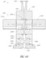
- the device 10 of FIG. 4 Bcan include a manifold 100 that defines a bore 126 through a manifold body 120 .
- the manifold 100can be constructed by mounting multiple blocks to one another.
- the manifold 100can be constructed of a single monolithic block which makes up the manifold body 120 .
- a unitary blockcan improve the manifold body 120 by providing a leak-proof bore 126 , for example, by obviating the use of o-rings and/or other interfaces. In various embodiments, deadlegs which can result in contamination may also be avoided.
- the manifold body 120can instead be made of an upper block, an intermediate block, and a lower block as shown in the embodiment of FIGS. 4 A and 2 .
- a skilled artisanwill recognize multiple blocks and a unitary block are interchangeable based on cost and manufacturing tradeoffs. The use of multiple blocks can enable a modular construction of the module, including curved, angled, or other complex geometries.
- the bottom of the manifold body 120can include an outlet 130 .
- First and second valve blocks 110 a , 110 bcan also be mounted to the manifold body 120 .
- the bore 126 of the manifold body 120can deliver reactant and/or inactive gases to a reaction chamber 30 of a reactor 21 by way of the outlet 130 at the bottom of the manifold body 120 .
- a dispersion device 35such as a showerhead as shown, or a horizontal injection device in other embodiments, can include a plenum 32 in fluid communication with a plurality of openings 19 .
- the reactant vaporcan pass through the openings 19 and be supplied into the reaction chamber 30 .
- a substrate support 22can be configured, or sized and shaped, to support a substrate 36 , such as a wafer, within the reaction chamber 30 .
- the dispersed reactant vaporcan contact the substrate and react to form a layer (e.g., a monolayer) on the substrate.
- the dispersion device 35can disperse the reactant vapor in a manner so as to form a uniform layer on the substrate.
- An exhaust line 23can be in fluid communication with the reaction chamber 30 .
- a vacuum pump 24can apply suction to the exhaust line 23 to evacuate vapors and excess materials from the reaction chamber 30 .
- the reactor 21can comprise any suitable type of semiconductor reactor, such as an atomic layer deposition (ALD) device, a chemical vapor deposition (CVD) device, etc.
- the device 10can comprise a control system 34 in electronic and data communication with the reactor 21 .
- the control system 34can comprise one or a plurality of processors configured to control the operation of the device 10 . Additional components may be provided to manage the operation of the device 10 .
- Supply channels 124 a and 124 bcan be provided to supply gas from corresponding gas distribution channels to the bore 126 .
- the first supply channel 124 a and the second supply channel 124 bcan be in fluid connection with supply channels 122 a and 122 b located in the first valve block 110 a and the second valve block 110 b .
- the first and second supply channels 124 a , 124 bcan merge with the bore 126 at approximately the same region along a longitudinal axis L of the manifold body 120 , but inlet openings 127 a , 127 b into the bore 126 can be slightly offset along the longitudinal axis L. As shown in FIG.
- the bore 126can extend continuously along the longitudinal axis L, such that the bore 126 does not include any turns or curved pathways, unlike the arrangement in FIGS. 2 and 4 A .
- An upper end of the bore 126can be capped by an upper wall 123 that defines a capping surface 128 at the upper end of the bore 126 .
- the first supply channel 124 acan be angled upward towards the capping surface 128 and the second supply channel 124 b can be angled downward towards the outlet 130 .
- the first supply channel 124 a and second supply channel 124 bcan be fabricated to be at different levels and arrive at staggered positions at the bore 126 .
- the first supply channel 124 a and second supply channelcan be angled upwards, downwards, or straight across, and can merge with the bore 126 at offset positions along the longitudinal axis L.
- the first and second valve blocks 110 a , 110 bcan mechanically connect to the manifold body 120 without the use of o-rings.
- metal sealscan be used between the manifold body 120 and the first and second valve blocks 110 a , 110 b.
- the inlet opening 127 a of the first supply channel 124 acan direct gases upwardly into the capping surface 128 , which may redirect the supplied gas(es) downwardly through the bore 130 .
- the first supply channel 124 acan terminate well below the capping surface 128 .
- the capping surface 128can comprise a curved surface shaped so as to efficiently direct the gases impinging on the surface 128 at an angle back down through the bore 126 .
- the capping surface 128 and the outlet 130can be disposed along the linear longitudinal axis L of the bore 126 .
- the uppermost portion of the manifold body 120is capped, such that the supplied gases, including reactant and inert gases, are provided from the side of the manifold 100 .
- FIG. 7 BAn illustration of where the first supply channel 124 a and second supply channel 124 b meet the bore 126 at a staggered offset position is seen in FIG. 7 B .
- FIG. 7 Aillustrates an arrangement where the first supply channel 124 a and the second supply channel 124 b meet the bore 126 at the same position.
- FIGS. 7 A and 7 Bare described in more detail below.
- a first reactant vaporsuch as ammonia
- a first reactant vaporcan be supplied to the bore 126 along the first supply channel 124 a .
- a second reactant vapor(such as titanium chloride) can be supplied to the bore 126 along the second supply channel 124 b .
- the first and second supply channels 124 a , 124 bcan be disposed opposite the bore 126 from one another.
- first and second supply channels 124 a , 124 bare disposed directly across from one another at the same location along the longitudinal axis L, then the first reactant vapor (e.g., ammonia) may be driven into the opposing second supply line 124 b .
- the first reactant vapore.g., ammonia
- the second reactant vapore.g., titanium chloride
- a low flow of inactive gasmay be provided through the first and second supply lines 124 a , 124 b , which can serve as a barrier to reactant vapors from the opposing supply line.
- the reactant vaporsmay be directed at sufficiently high pressures so as to overcome the low pressure of the inactive gas.
- the inlet openings 127 a , 127 b of the first and second supply channels 124 a , 124 bcan be offset from one another along the longitudinal axis L.
- the inlet openings 127 a , 127 bcan be angled opposite to one another along the longitudinal axis L.
- the upstream first inlet opening 127 acan be angled to have a directional component facing towards the capping surface 128 of the upper wall 123 .
- the downstream second inlet opening 127 bcan be angled to have a directional component facing towards the outlet 130 . Accordingly, the orientation and/or positioning of the first and second supply channels 124 a , 124 b can reduce or eliminate the penetration of the first reactant into the second supply channel 124 b and the second reactant into the first supply channel 124 a , which can reduce the effects of cross contamination and improve overall deposition quality.
- An example of this reduced cross contaminationis illustrated in FIG. 10 B and is described in more detail below.
- the bore 126 of FIG. 4 Bcan provide improved flow conductance, e.g., higher flow rates, due to the use of a larger diameter bore 126 .
- the larger diameter or major dimensioncan increase the flow rates of the gas flowing to the reactor 21 .
- purge or inactive gas inlets 108 and 118can be located at the lateral sides opposite to the side where the valve blocks 110 a / 110 b meet the manifold body 120 .
- the inactive purge gascan be directed laterally through supply channels to the bore 126 .
- the inactive purge gas(es)can be directed through the first and second supply channels 124 a , 124 b through which the first and second reactant vapors are supplied to the bore 126 .
- the inactive purge gas(es)can be directed through additional supply channels that merge into the bore 126 from a side portion of the bore 126 , rather than an upper portion of the bore 126 .
- the embodiment of FIG. 4 Bcan reduce or eliminate dead volumes above the merger point for reactant vapors and the resulting parasitic deposition that can occur in the device 20 of FIG. 4 A .
- the purge or inactive gas inlets 108 and 118can be located at the last leg of the supply channel so that the whole channel can be directly accessed by the purge gases. Therefore, during the purge cycle, the entire supply channel can be purged which can reduce or eliminate dead volumes.
- FIG. 5 Ashows a top down view of the embodiment of FIGS. 2 and 4 A .
- Each valve block 212 b and 212 aincludes gas inlets.
- the first valve block 212 bincludes vapor phase inlet 220 used to input a first gas or vapor phase reactant.
- the first valve block 212 balso includes vapor phase inlet 222 used to input a low flow rate inactive gas in order to carry vaporized reactant to the reactor 21 and/or to provide a buffer against cross-contamination from other reactants.
- the second valve block 212 aincludes vapor phase inlet 224 used to input a second gas or vapor phase reactant.
- the second valve block 212 aalso includes vapor phase inlet 222 used to supply inactive gas in order to carry vaporized reactant to the reactor 21 and/or to provide a buffer against cross-contamination from other reactants.
- the manifold body 202includes the funnel-shaped inlet 220 in which high flow rate inactive gas enters the system in order to purge the device 20 . As explained above in connection with FIGS. 2 and 4 A , the funnel-shaped inlet 220 can direct the inactive purge gas downwardly into the bore 230 . Also, additional etchants (for example, from an RPU) and coating agents (such as TMA) may enter the bore 230 from the funnel-shaped inlet 220 .
- FIG. 5 Aalso illustrates reactant valves 214 a , 214 b mounted to the respective valve blocks 212 a , 212 b .
- the reactant valves 214 a , 214 bcan be used to regulate the flow of the first reactant vapor and the second reactant vapor, respectively.
- inactive gasexamples include argon (Ar) gas or nitrogen (N 2 ) gas, although any suitable inactive gas may be used.
- a mix of two different inactive gasescan be used.
- a first gas phase reactantis a naturally gaseous ALD reactant such as H 2 , NH 3 , N 2 , O 2 , or O.
- the second gas or vapor phase reactantcan be produced by a vaporizer (not shown) for vaporizing a reactant which is solid or liquid at room temperature and atmospheric pressure.
- the vaporizer(s)can comprise, e.g., liquid bubblers or solid sublimation vessels.
- the first reactant vaporcomprises NH 3 and the second reactant vapor comprises TiCl 4 .
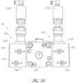
- FIG. 5 Bshows a top down view of the embodiment of FIGS. 1 and 4 B .
- the first valve block 110 bincludes a vapor phase inlet 116 used to supply a first gas or vapor phase reactant and a vapor phase inlet 114 used to supply inactive gas to serve as a carrier or buffer.
- the first valve block 110 bincludes additional vapor phase inlet 112 used to supply an etchant (such as RPU). It is noted that the inlet 112 is disposed on a lateral side of the manifold body 120 , e.g., in the valve block 110 b , instead of communicating with the funnel-shaped inlet 220 shown in FIG. 5 A .
- the first valve block 110 balso includes additional inactive vapor phase inlet 118 in which high flow rate inactive gas enters the bore 126 in order to purge the manifold 120 .
- the vapor phase inlet 118can also be disposed on a lateral side of the manifold body 120 , e.g., in the valve block 110 b , instead of communicating with the funnel-shaped inlet 220 shown in FIG. 5 A .
- the inactive vapor phase inlet 118can be placed on the side opposite to the side in which the first valve block 110 b meets the manifold body 120 .
- the second valve block 110 aincludes a vapor phase inlet 106 used to input a second gas or vapor phase reactant and a vapor phase inlet 104 used to supply low flow rate inactive gas to serve as a carrier or buffer.
- the second valve block 110 aincludes additional vapor phase inlet 102 used to input a coating material (e.g., TMA). It is noted that the inlet 102 can be disposed on a lateral side of the manifold body 120 , e.g., in the valve block 110 a , instead of communicating with the funnel-shaped inlet 220 shown in FIG. 5 A .
- the second valve block 110 aalso includes additional vapor phase inlet 108 in which high flow rate inactive gas enters the bore 126 in order to purge the manifold 120 .
- the inactive vapor inlet 108can also be disposed on a lateral side of the manifold body 120 , e.g., in the valve block 110 a , instead of communicating with the funnel-shaped inlet 220 shown in FIG. 5 A .
- the inactive vapor phase inlet 108can be placed on the side opposite to the side where the second valve block 110 a meets the manifold body 120 . Similar to FIG. 5 A , FIG.
- FIG. 5 Billustrates also reactant valves 134 a , 134 b mounted to the respective valve blocks 110 a , 110 b .
- FIG. 5 Bfurther illustrates inactive gas valves 132 a , 132 b and additional first and second valves 136 a , 136 b mounted to the respective valve blocks 110 a / 110 b .
- the inactive gas valves 132 a , 132 bcontrol the inert gas entering from the additional vapor phase inlets 108 , 118 .
- first and second valves 136 a , 136 bcan control a coating material (e.g., TMA) entering from the vapor phase inlet 102 and an etchant (e.g., an etchant from an RPU) entering from the vapor phase inlet 112 , respectively.
- a coating materiale.g., TMA
- an etchante.g., an etchant from an RPU
- FIGS. 6 A and 6 Bare top cross sectional views of the arrangements of FIGS. 5 A and 5 B , respectively, showing internal channels within the manifolds.
- internal channels 220 A, 222 A, 224 A, 226 Acorrespond to internal supply lines that convey the respective vapors from the vapor phase inlets 220 , 222 , 224 , 226 , with the reference numerals for the inlets appended by the letter “A” to refer to the corresponding internal supply channel.
- FIG. 6 Ainternal channels 220 A, 222 A, 224 A, 226 A correspond to internal supply lines that convey the respective vapors from the vapor phase inlets 220 , 222 , 224 , 226 , with the reference numerals for the inlets appended by the letter “A” to refer to the corresponding internal supply channel.
- FIG. 6 Ainternal channels 220 A, 222 A, 224 A, 226 A correspond to internal supply lines that convey the respective vapors from the vapor phase inlets 220 ,
- internal channels 102 A, 104 A, 106 A, 108 A, 112 A, 114 A, 116 A, 118 Acorrespond to internal supply lines that convey the respective vapors from the corresponding vapor phase inlets 102 , 104 , 106 , 108 , 112 , 114 , 116 , 118 , with the reference numerals for the inlets appended by the letter “A” to refer to the corresponding internal supply channel.
- the internal channelsare in fluid communication with the reactant valves 214 a , 214 b which regulate the flow of first reactant and second reactant into the reaction chamber.
- the internal channelsare also in fluid communication with the reactant valves 134 a , 134 b which regulate the flow of first reactant and second reactant.
- FIG. 6 Billustrates inactive gas valves 132 a , 132 b and the first and second valves 136 a , 136 b as described above.
- the inactive gases from the inactive gas valves 132 a , 132 bcan flow through the entire channel which allows the entire channel to be purged of reactants and yields reduced dead volume.
- FIGS. 7 A and 7 Bare perspective views of the interior bores and supply channels for two different arrangements of the first and second supply lines to the bore.
- FIG. 7 Bis the offset design shown in FIG. 4 B in which a capping surface 128 is disposed at an upper portion of the bore 126 and directs the vapors down the bore 126 through the outlet 130 .
- FIG. 7 Aalso shows a similar design in which a capping surface 506 directs vapors down a bore 502 through an outlet 508 .
- the supply channels 124 a , 124 bmerge with the bore 126 at locations that are offset relative to the longitudinal axis L.
- FIG. 128is disposed at an upper portion of the bore 126 and directs the vapors down the bore 126 through the outlet 130 .
- FIG. 7 Aalso shows a similar design in which a capping surface 506 directs vapors down a bore 502 through an outlet 508 .
- the supply channels 124 a , 124 bmerge
- the supply channels 504 a , 504 bmeet at the same position with the bore 126 along the longitudinal axis L.
- the arrangement of FIG. 7 Bcan beneficially reduce cross-contamination of reactants in the supply channels 124 a , 124 b.
- FIGS. 8 A and 8 Bshows the velocity plots of the respective bores for the two different supply channel designs of FIGS. 7 A and 7 B .
- FIG. 8 Blittle or no “throw” is observed, meaning that non-uniformities due to angular momentum of the vapors is reduced.
- FIGS. 9 A and 9 Billustrates a NH 3 reactant mole fraction plot of the respective bores for the two different supply channel designs of FIGS. 7 A and 7 B , respectively.
- the non-uniformity displayed in FIG. 9 Ais lower than the non-uniformity displayed in FIG. 9 B .
- FIGS. 9 A and 9 Bare significantly lower than the non-uniformity displayed in FIGS. 9 A and 9 B . While non-uniformity during mixed deposition of two reactants may be higher in the design of FIGS. 7 A and 7 B (and 4 B) as compared with that of FIG. 4 A , in some embodiments it may be more important to provide high flow rate or conductance pulses, for example, to achieve high aspect ratio structures. In such processes, mixing non-uniformity may be less important than high flow conductance, and the design of FIG. 4 B may be preferred.
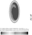
- FIGS. 10 A and 10 Billustrates the mole fraction of NH 3 reactant the position within the supply channels and the bore, respectively, for the two different supply channel designs of FIGS. 7 A and 7 B .
- Region C to the left of the vertical extending yellow highlighted regiondepicts a position within the first supply channel which inputs NH 3 reactant.
- the NH 3 levelis high in both the different supply channel designs within Region C.
- Region A within the vertical extending yellow highlighted regiondepicts the bore region. Comparing the right edge portion of Region A for FIGS. 10 A and 10 B , the NH 3 level tapers off much faster in the offset design depicted in FIG. 7 B than the straight T design of FIG. 7 A .
- Region B to the right of the vertical extending yellow highlighted regiondepicts a region within the second supply line.
- the left edge portion of Region B displaying where the bore meets the second supply lineshows high concentrations of NH 3 in FIG. 10 A and comparatively low concentrations of NH 3 in the same region in FIG. 10 B depicting remarkably less penetration of NH 3 into the second supply line for the offset design of FIG. 7 B . Therefore, there is less unwanted penetration of NH 3 into the second supply line in the offset design of FIG. 7 B .
Landscapes
- Chemical & Material Sciences (AREA)
- Engineering & Computer Science (AREA)
- Chemical Kinetics & Catalysis (AREA)
- Mechanical Engineering (AREA)
- General Chemical & Material Sciences (AREA)
- Organic Chemistry (AREA)
- Metallurgy (AREA)
- Materials Engineering (AREA)
- Power Engineering (AREA)
- General Physics & Mathematics (AREA)
- Condensed Matter Physics & Semiconductors (AREA)
- Manufacturing & Machinery (AREA)
- Physics & Mathematics (AREA)
- Microelectronics & Electronic Packaging (AREA)
- Computer Hardware Design (AREA)
- Inorganic Chemistry (AREA)
- Chemical Vapour Deposition (AREA)
Abstract
Description
Claims (18)
Priority Applications (1)
| Application Number | Priority Date | Filing Date | Title |
|---|---|---|---|
| US17/074,887US11830731B2 (en) | 2019-10-22 | 2020-10-20 | Semiconductor deposition reactor manifolds |
Applications Claiming Priority (3)
| Application Number | Priority Date | Filing Date | Title |
|---|---|---|---|
| US201962924608P | 2019-10-22 | 2019-10-22 | |
| US201962925035P | 2019-10-23 | 2019-10-23 | |
| US17/074,887US11830731B2 (en) | 2019-10-22 | 2020-10-20 | Semiconductor deposition reactor manifolds |
Publications (2)
| Publication Number | Publication Date |
|---|---|
| US20210118668A1 US20210118668A1 (en) | 2021-04-22 |
| US11830731B2true US11830731B2 (en) | 2023-11-28 |
Family
ID=75491331
Family Applications (1)
| Application Number | Title | Priority Date | Filing Date |
|---|---|---|---|
| US17/074,887Active2041-05-08US11830731B2 (en) | 2019-10-22 | 2020-10-20 | Semiconductor deposition reactor manifolds |
Country Status (4)
| Country | Link |
|---|---|
| US (1) | US11830731B2 (en) |
| KR (1) | KR20210048408A (en) |
| CN (1) | CN112695294B (en) |
| TW (1) | TWI854051B (en) |
Families Citing this family (9)
| Publication number | Priority date | Publication date | Assignee | Title |
|---|---|---|---|---|
| US10662527B2 (en)* | 2016-06-01 | 2020-05-26 | Asm Ip Holding B.V. | Manifolds for uniform vapor deposition |
| US10927459B2 (en)* | 2017-10-16 | 2021-02-23 | Asm Ip Holding B.V. | Systems and methods for atomic layer deposition |
| US11492701B2 (en)* | 2019-03-19 | 2022-11-08 | Asm Ip Holding B.V. | Reactor manifolds |
| TWI861207B (en) | 2019-09-19 | 2024-11-11 | 美商應用材料股份有限公司 | Apparatus and method using dead volume-free valve |
| KR20210048408A (en) | 2019-10-22 | 2021-05-03 | 에이에스엠 아이피 홀딩 비.브이. | Semiconductor deposition reactor manifolds |
| JP1700780S (en)* | 2021-03-22 | 2021-11-29 | Nozzle holder for substrate processing equipment | |
| CN115161619B (en)* | 2022-09-08 | 2023-04-14 | 拓荆科技(上海)有限公司 | Valve and vapor deposition equipment |
| CN116641041B (en)* | 2023-05-06 | 2024-11-15 | 拓荆科技(上海)有限公司 | Gas distribution device |
| USD1089130S1 (en)* | 2024-01-19 | 2025-08-19 | Applied Materials, Inc. | Process chamber manifold |
Citations (243)
| Publication number | Priority date | Publication date | Assignee | Title |
|---|---|---|---|---|
| US1523156A (en) | 1923-07-05 | 1925-01-13 | Leslie M Adams | Electrically-energized faucet heater |
| US1853045A (en) | 1931-01-09 | 1932-04-12 | Air Conditioning & Eng | Fluid mixing means |
| US3429903A (en) | 1968-03-12 | 1969-02-25 | American Metal Climax Inc | Method of preparing molybdenum (iii) acetylacetonate |
| US3784631A (en) | 1972-03-09 | 1974-01-08 | Goodyear Tire & Rubber | Dimerization or codimerization of alpha-olefins |
| US3882934A (en) | 1972-06-02 | 1975-05-13 | Aga Ab | Heat exchanger |
| US3913617A (en) | 1972-11-20 | 1975-10-21 | Hoogovens Ijmuiden Bv | Apparatus for mixing two gas flows |
| US4222671A (en) | 1978-09-05 | 1980-09-16 | Gilmore Oscar Patrick | Static mixer |
| US4401052A (en) | 1979-05-29 | 1983-08-30 | The University Of Delaware | Apparatus for continuous deposition by vacuum evaporation |
| US4410281A (en) | 1981-03-02 | 1983-10-18 | Ralph B. Carter Company | Mixing method and apparatus utilizing pipe elbows |
| US4422773A (en) | 1980-08-04 | 1983-12-27 | Technicon Instruments Corporation | Apparatus and method for the non-invasive mixing of a flowing fluid stream |
| US4649859A (en) | 1985-02-19 | 1987-03-17 | The United States Of America As Represented By The United States Department Of Energy | Reactor design for uniform chemical vapor deposition-grown films without substrate rotation |
| US4747367A (en) | 1986-06-12 | 1988-05-31 | Crystal Specialties, Inc. | Method and apparatus for producing a constant flow, constant pressure chemical vapor deposition |
| DE3715644A1 (en) | 1987-05-11 | 1988-12-01 | Fraunhofer Ges Forschung | MOLECULAR BEAM EPITAXY SYSTEM |
| US4828224A (en) | 1987-10-15 | 1989-05-09 | Epsilon Technology, Inc. | Chemical vapor deposition system |
| US4869284A (en) | 1985-10-29 | 1989-09-26 | Plessey Overseas Limited | Manifold assembly |
| US4889609A (en) | 1988-09-06 | 1989-12-26 | Ovonic Imaging Systems, Inc. | Continuous dry etching system |
| US4895107A (en) | 1987-07-06 | 1990-01-23 | Kabushiki Kaisha Toshiba | Photo chemical reaction apparatus |
| US4907534A (en) | 1988-12-09 | 1990-03-13 | Siemens Aktiengesellschaft | Gas distributor for OMVPE Growth |
| US4949783A (en) | 1988-05-18 | 1990-08-21 | Veeco Instruments, Inc. | Substrate transport and cooling apparatus and method for same |
| US4951601A (en) | 1986-12-19 | 1990-08-28 | Applied Materials, Inc. | Multi-chamber integrated process system |
| WO1990010092A1 (en) | 1989-02-24 | 1990-09-07 | Massachusetts Institute Of Technology | A modified stagnation flow apparatus for chemical vapor deposition providing excellent control of the deposition |
| US4990047A (en) | 1988-05-24 | 1991-02-05 | Balzers Aktiengesellschaft | Vacuum apparatus |
| US5004374A (en) | 1990-02-28 | 1991-04-02 | Bettie Grey | Method of laying out a pathway for piping |
| US5028724A (en) | 1990-03-30 | 1991-07-02 | Air Products And Chemicals, Inc. | Synthesis of volatile fluorinated and non-fluorinated metal-beta-ketonate and metal-beta-ketoiminato complexes |
| US5071460A (en) | 1988-03-04 | 1991-12-10 | Nippon Telegraph And Telephone Corporation | Process for the preparation of fluoride glass and process for the preparation of optical fiber preform using the fluoride glass |
| US5080549A (en) | 1987-05-11 | 1992-01-14 | Epsilon Technology, Inc. | Wafer handling system with Bernoulli pick-up |
| US5106453A (en) | 1990-01-29 | 1992-04-21 | At&T Bell Laboratories | MOCVD method and apparatus |
| US5121705A (en) | 1991-04-05 | 1992-06-16 | Mbk Microtek Inc. | Loading lock for chemical vapor deposition apparatus |
| US5131627A (en) | 1990-10-17 | 1992-07-21 | Nupro Company | Diaphragm valve |
| US5166092A (en) | 1988-01-28 | 1992-11-24 | Fujitsu Limited | Method of growing compound semiconductor epitaxial layer by atomic layer epitaxy |
| US5186718A (en) | 1989-05-19 | 1993-02-16 | Applied Materials, Inc. | Staged-vacuum wafer processing system and method |
| US5192371A (en) | 1991-05-21 | 1993-03-09 | Asm Japan K.K. | Substrate supporting apparatus for a CVD apparatus |
| US5199483A (en) | 1991-05-15 | 1993-04-06 | Applied Materials, Inc. | Method and apparatus for cooling wafers |
| US5217501A (en) | 1989-07-25 | 1993-06-08 | Tokyo Electron Limited | Vertical wafer heat treatment apparatus having dual load lock chambers |
| US5223001A (en) | 1991-11-21 | 1993-06-29 | Tokyo Electron Kabushiki Kaisha | Vacuum processing apparatus |
| US5229615A (en) | 1992-03-05 | 1993-07-20 | Eaton Corporation | End station for a parallel beam ion implanter |
| US5248253A (en) | 1992-01-28 | 1993-09-28 | Digital Equipment Corporation | Thermal processing furnace with improved plug flow |
| US5252131A (en) | 1992-02-27 | 1993-10-12 | Daidousanso Co., Ltd. | Apparatus for gas source molecular beam epitaxy |
| US5284519A (en) | 1990-05-16 | 1994-02-08 | Simon Fraser University | Inverted diffuser stagnation point flow reactor for vapor deposition of thin films |
| US5286296A (en) | 1991-01-10 | 1994-02-15 | Sony Corporation | Multi-chamber wafer process equipment having plural, physically communicating transfer means |
| US5288327A (en) | 1992-03-12 | 1994-02-22 | Bell Communications Research, Inc. | Deflected flow in chemical vapor deposition cell |
| US5350453A (en) | 1990-03-02 | 1994-09-27 | Hoechst Aktiengesellschaft | Device for producing thin films of mixed metal oxides from organic metal compounds on a substrate |
| US5388944A (en) | 1992-02-07 | 1995-02-14 | Tokyo Electron Tohoku Kabushiki Kaisha | Vertical heat-treating apparatus and heat-treating process by using the vertical heat-treating apparatus |
| US5391035A (en) | 1992-11-06 | 1995-02-21 | Applied Materials, Inc. | Micro-enviroment load lock |
| US5405446A (en) | 1993-07-16 | 1995-04-11 | Dainippon Screen Mfg. Co., Ltd. | Apparatus for heat processing a substrate |
| US5433785A (en) | 1992-10-14 | 1995-07-18 | Sony Corporation | Thermal treatment apparatus, semiconductor device fabrication apparatus, load-lock chamber |
| US5462397A (en) | 1993-03-16 | 1995-10-31 | Tokyo Electron Limited | Processing apparatus |
| US5488925A (en) | 1993-10-28 | 1996-02-06 | Fujitsu Limited | Gas handling device assembly used for a CVD apparatus |
| US5516732A (en) | 1992-12-04 | 1996-05-14 | Sony Corporation | Wafer processing machine vacuum front end method and apparatus |
| US5520743A (en) | 1992-09-03 | 1996-05-28 | Tokyo Electron Kabushiki Kaisha | Processing apparatus with means for rotating an object mounting means and a disk body located in the mounting means differently relative to each other |
| US5520742A (en) | 1993-03-03 | 1996-05-28 | Tokyo Electron Kabushiki Kaisha | Thermal processing apparatus with heat shielding member |
| US5525157A (en) | 1987-06-24 | 1996-06-11 | Advanced Semiconductor Materials America, Inc. | Gas injectors for reaction chambers in CVD systems |
| US5538390A (en) | 1993-10-29 | 1996-07-23 | Applied Materials, Inc. | Enclosure for load lock interface |
| US5571330A (en) | 1992-11-13 | 1996-11-05 | Asm Japan K.K. | Load lock chamber for vertical type heat treatment apparatus |
| WO1996040690A1 (en) | 1995-06-07 | 1996-12-19 | Advanced Technology Materials, Inc. | Metal complex source reagents for chemical vapor deposition |
| US5586585A (en) | 1995-02-27 | 1996-12-24 | Asyst Technologies, Inc. | Direct loadlock interface |
| US5601651A (en) | 1992-09-17 | 1997-02-11 | Fujitsu Limited | Flow control valve for use in fabrication of semiconductor devices |
| US5609459A (en) | 1995-07-06 | 1997-03-11 | Brooks Automation, Inc. | Door drive mechanisms for substrate carrier and load lock |
| JPH09186111A (en) | 1995-12-27 | 1997-07-15 | Tokyo Electron Ltd | Film forming processor |
| US5728223A (en) | 1995-06-09 | 1998-03-17 | Ebara Corporation | Reactant gas ejector head and thin-film vapor deposition apparatus |
| US5755878A (en) | 1994-10-25 | 1998-05-26 | Shin-Etsu Handotai Co., Ltd. | Method for vapor phase growth |
| US5789027A (en) | 1996-11-12 | 1998-08-04 | University Of Massachusetts | Method of chemically depositing material onto a substrate |
| US5846330A (en) | 1997-06-26 | 1998-12-08 | Celestech, Inc. | Gas injection disc assembly for CVD applications |
| US5851294A (en) | 1995-10-23 | 1998-12-22 | Watkins-Johnson Company | Gas injection system for semiconductor processing |
| US5885358A (en) | 1996-07-09 | 1999-03-23 | Applied Materials, Inc. | Gas injection slit nozzle for a plasma process reactor |
| US5893641A (en) | 1998-05-26 | 1999-04-13 | Garcia; Paul | Differential injector |
| US5951771A (en) | 1996-09-30 | 1999-09-14 | Celestech, Inc. | Plasma jet system |
| US6036783A (en) | 1996-04-05 | 2000-03-14 | Ebara Corporation | Liquid material vaporizer apparatus and gas ejection device |
| US6070550A (en) | 1996-09-12 | 2000-06-06 | Applied Materials, Inc. | Apparatus for the stabilization of halogen-doped films through the use of multiple sealing layers |
| US6079353A (en) | 1998-03-28 | 2000-06-27 | Quester Technology, Inc. | Chamber for reducing contamination during chemical vapor deposition |
| US6110529A (en) | 1990-07-06 | 2000-08-29 | Advanced Tech Materials | Method of forming metal films on a substrate by chemical vapor deposition |
| US6217658B1 (en) | 1997-06-03 | 2001-04-17 | Applied Materials, Inc. | Sequencing of the recipe steps for the optimal low-dielectric constant HDP-CVD Processing |
| WO2001029282A2 (en) | 1999-10-20 | 2001-04-26 | Cvd Systems, Inc. | Fluid processing system |
| US6224676B1 (en) | 1998-12-02 | 2001-05-01 | Hitachi, Ltd. | Gas supply apparatus and film forming apparatus |
| US20010003015A1 (en) | 1997-12-02 | 2001-06-07 | Mei Chang | Method for in-situ, post deposition surface passivation of a chemical vapor deposited film |
| US20010006093A1 (en) | 1999-12-07 | 2001-07-05 | Toshihiro Tabuchi | Surface treatment apparatus |
| US6258157B1 (en) | 1997-04-17 | 2001-07-10 | President And Fellows Of Harvard College | Liquid precursors for formation of metal oxides |
| US6299692B1 (en) | 2000-07-21 | 2001-10-09 | Applied Materials, Inc. | Head for vaporizing and flowing various precursor materials onto semiconductor wafers during chemical vapor deposition |
| US6303501B1 (en) | 2000-04-17 | 2001-10-16 | Applied Materials, Inc. | Gas mixing apparatus and method |
| US6302965B1 (en) | 2000-08-15 | 2001-10-16 | Applied Materials, Inc. | Dispersion plate for flowing vaporizes compounds used in chemical vapor deposition of films onto semiconductor surfaces |
| US6331072B1 (en) | 1997-07-24 | 2001-12-18 | Axiva Gmbh | Continuous, chaotic convection mixer, heat exchanger and reactor |
| US20010054377A1 (en) | 2000-04-14 | 2001-12-27 | Sven Lindfors | Method of growing a thin film onto a substrate |
| US20020007790A1 (en) | 2000-07-22 | 2002-01-24 | Park Young-Hoon | Atomic layer deposition (ALD) thin film deposition equipment having cleaning apparatus and cleaning method |
| WO2002018394A1 (en) | 2000-08-28 | 2002-03-07 | Advanced Technology Materials, Inc. | Source reagent compositions and method for forming metal films on a substrate by chemical vapor deposition |
| US6375750B1 (en) | 1995-07-10 | 2002-04-23 | Applied Materials, Inc. | Plasma enhanced chemical processing reactor and method |
| US20020072164A1 (en) | 2000-09-13 | 2002-06-13 | Applied Materials, Inc. | Processing chamber with multi-layer brazed lid |
| US20020081381A1 (en) | 2000-10-10 | 2002-06-27 | Rensselaer Polytechnic Institute | Atomic layer deposition of cobalt from cobalt metallorganic compounds |
| US6416213B1 (en) | 1998-01-26 | 2002-07-09 | Kazuji Fukunaga | Device and method with spiral mixing pipe for coagulating/condensing waste water |
| US20020113327A1 (en) | 2001-02-21 | 2002-08-22 | Shibuya Kogyo Co., Ltd | Jetting apparatus for mixed flow of gas and liquid |
| US6482740B2 (en) | 2000-05-15 | 2002-11-19 | Asm Microchemistry Oy | Method of growing electrical conductors by reducing metal oxide film with organic compound containing -OH, -CHO, or -COOH |
| US20020170674A1 (en) | 2001-05-17 | 2002-11-21 | Shapiro Nathan P. | Continuous processing chamber |
| US20020195055A1 (en) | 2000-10-16 | 2002-12-26 | Grant Robert W. | Vortex based CVD reactor |
| US20030008072A1 (en) | 2001-06-14 | 2003-01-09 | Lee Jung-Hyun | Atomic layer deposition using organometallic complex with beta-diketone ligand |
| US20030010451A1 (en) | 2001-07-16 | 2003-01-16 | Applied Materials, Inc. | Lid assembly for a processing system to facilitate sequential deposition techniques |
| US20030019428A1 (en) | 2001-04-28 | 2003-01-30 | Applied Materials, Inc. | Chemical vapor deposition chamber |
| US6534133B1 (en) | 1996-06-14 | 2003-03-18 | Research Foundation Of State University Of New York | Methodology for in-situ doping of aluminum coatings |
| US20030056720A1 (en) | 2000-02-04 | 2003-03-27 | Martin Dauelsberg | Device and method for depositing one or more layers on a substrate |
| US6539891B1 (en) | 1999-06-19 | 2003-04-01 | Genitech, Inc. | Chemical deposition reactor and method of forming a thin film using the same |
| US20030070620A1 (en) | 2001-10-15 | 2003-04-17 | Cooperberg David J. | Tunable multi-zone gas injection system |
| US20030079686A1 (en) | 2001-10-26 | 2003-05-01 | Ling Chen | Gas delivery apparatus and method for atomic layer deposition |
| US20030101938A1 (en) | 1998-10-27 | 2003-06-05 | Applied Materials, Inc. | Apparatus for the deposition of high dielectric constant films |
| US20030172872A1 (en) | 2002-01-25 | 2003-09-18 | Applied Materials, Inc. | Apparatus for cyclical deposition of thin films |
| US20030180460A1 (en) | 2000-09-22 | 2003-09-25 | Gerd Strauch | Method for depositing in particular crystalline layers, gas-admission element and device for carrying out the method |
| US20030194360A1 (en) | 2001-04-10 | 2003-10-16 | Huziwara Wilson Kenzo | Multifunctional entry method and device for downward flow tube reactor |
| US20030205096A1 (en) | 2002-05-03 | 2003-11-06 | Gehner Gerrick S. | Method and apparatus for mixing gases |
| US6660177B2 (en) | 2001-11-07 | 2003-12-09 | Rapt Industries Inc. | Apparatus and method for reactive atom plasma processing for material deposition |
| US20040016404A1 (en) | 2002-07-23 | 2004-01-29 | John Gregg | Vaporizer delivery ampoule |
| US20040028810A1 (en) | 2000-10-16 | 2004-02-12 | Primaxx, Inc. | Chemical vapor deposition reactor and method for utilizing vapor vortex |
| US20040035358A1 (en) | 2002-08-23 | 2004-02-26 | Cem Basceri | Reactors having gas distributors and methods for depositing materials onto micro-device workpieces |
| US20040043557A1 (en) | 2000-10-10 | 2004-03-04 | Haukka Suvi P. | Methods for making a dielectric stack in an integrated circuit |
| US20040113289A1 (en) | 2001-01-18 | 2004-06-17 | Masayuki Toda | Carburetor, various types of devices using the carburetor, and method of vaporization |
| US20040118342A1 (en) | 2002-12-18 | 2004-06-24 | Taiwan Semiconductor Manufacturing Co., Ltd. | Bypass gas feed system and method to improve reactant gas flow and film deposition |
| US20040144311A1 (en) | 2002-11-14 | 2004-07-29 | Ling Chen | Apparatus and method for hybrid chemical processing |
| US20040197090A1 (en) | 2002-11-22 | 2004-10-07 | Honda Motor Co., Ltd. | Heat storage apparatus |
| US20040217217A1 (en) | 2003-04-09 | 2004-11-04 | Samsung Electronics Co., Ltd. | Gas supplying apparatus |
| US20040224504A1 (en) | 2000-06-23 | 2004-11-11 | Gadgil Prasad N. | Apparatus and method for plasma enhanced monolayer processing |
| US20040221807A1 (en) | 2003-05-09 | 2004-11-11 | Mohith Verghese | Reactor surface passivation through chemical deactivation |
| US20050000656A1 (en) | 2001-01-30 | 2005-01-06 | Rapt Industries, Inc. | Apparatus for atmospheric pressure reactive atom plasma processing for surface modification |
| US20050000428A1 (en) | 2003-05-16 | 2005-01-06 | Shero Eric J. | Method and apparatus for vaporizing and delivering reactant |
| US20050009325A1 (en) | 2003-06-18 | 2005-01-13 | Hua Chung | Atomic layer deposition of barrier materials |
| US6846516B2 (en) | 2002-04-08 | 2005-01-25 | Applied Materials, Inc. | Multiple precursor cyclical deposition system |
| US6878628B2 (en) | 2000-05-15 | 2005-04-12 | Asm International Nv | In situ reduction of copper oxide prior to silicon carbide deposition |
| US6881263B2 (en) | 2000-07-20 | 2005-04-19 | Asm Microchemistry Oy | Method of growing a thin film onto a substrate |
| US20050092247A1 (en) | 2003-08-29 | 2005-05-05 | Schmidt Ryan M. | Gas mixer and manifold assembly for ALD reactor |
| US6899507B2 (en) | 2002-02-08 | 2005-05-31 | Asm Japan K.K. | Semiconductor processing apparatus comprising chamber partitioned into reaction and transfer sections |
| US6905547B1 (en) | 2000-12-21 | 2005-06-14 | Genus, Inc. | Method and apparatus for flexible atomic layer deposition |
| US20050208217A1 (en) | 2003-10-09 | 2005-09-22 | Asm Japan K.K. | Apparatus and method for forming thin film using upstream and downstream exhaust mechanisms |
| US20050241176A1 (en) | 2003-10-29 | 2005-11-03 | Shero Eric J | Reaction system for growing a thin film |
| US20050252449A1 (en) | 2004-05-12 | 2005-11-17 | Nguyen Son T | Control of gas flow and delivery to suppress the formation of particles in an MOCVD/ALD system |
| US20050263197A1 (en) | 1998-03-05 | 2005-12-01 | Eidsmore Paul E | Modular surface mount manifold |
| US20060053833A1 (en) | 2002-10-31 | 2006-03-16 | Carlos Martins | Condenser, in particular for a motor vehicle air conditioning circuit, and circuit comprising same |
| US20060096540A1 (en) | 2004-11-11 | 2006-05-11 | Choi Jin H | Apparatus to manufacture semiconductor |
| US7045060B1 (en) | 2002-12-05 | 2006-05-16 | Inflowsion, L.L.C. | Apparatus and method for treating a liquid |
| US20060266289A1 (en) | 2005-01-18 | 2006-11-30 | Mohith Verghese | Reaction system for growing a thin film |
| US20070001326A1 (en) | 2003-09-26 | 2007-01-04 | Masayuki Toda | Vaporizer |
| US7163587B2 (en) | 2002-02-08 | 2007-01-16 | Axcelis Technologies, Inc. | Reactor assembly and processing method |
| US20070081923A1 (en) | 2005-09-26 | 2007-04-12 | Choe Jae H | Stack type reactor |
| US20070098894A1 (en) | 2003-05-09 | 2007-05-03 | Mohith Verghese | Reactor surface passivation through chemical deactivation |
| US7220669B2 (en) | 2000-11-30 | 2007-05-22 | Asm International N.V. | Thin films for magnetic device |
| US20070128864A1 (en) | 2005-11-04 | 2007-06-07 | Paul Ma | Apparatus and process for plasma-enhanced atomic layer deposition |
| US20070187634A1 (en) | 2003-10-17 | 2007-08-16 | Sundew Technologies, Llc | Fail-safe pneumatically actuated valve with fast time response and adjustable conductance |
| US20070194470A1 (en) | 2006-02-17 | 2007-08-23 | Aviza Technology, Inc. | Direct liquid injector device |
| US7297892B2 (en) | 2003-08-14 | 2007-11-20 | Rapt Industries, Inc. | Systems and methods for laser-assisted plasma processing |
| US7304263B2 (en) | 2003-08-14 | 2007-12-04 | Rapt Industries, Inc. | Systems and methods utilizing an aperture with a reactive atom plasma torch |
| WO2008002546A1 (en) | 2006-06-28 | 2008-01-03 | President And Fellows Of Harvard College | Metal(iv) tetra-amidinate compounds and their use in vapor deposition |
| US7323581B1 (en) | 1990-07-06 | 2008-01-29 | Advanced Technology Materials, Inc. | Source reagent compositions and method for forming metal films on a substrate by chemical vapor deposition |
| CN101117308A (en) | 2006-08-04 | 2008-02-06 | 浙江医药股份有限公司新昌制药厂 | Method for preparing acetylacetone acid molybdenum |
| US20080037968A1 (en) | 2004-02-25 | 2008-02-14 | Ferro Techniek Holding B.V. | Device A Method For Heating Liquids, And Base Structure |
| US20080085226A1 (en) | 2006-10-10 | 2008-04-10 | Asm America, Inc. | Precursor delivery system |
| US20080102208A1 (en) | 2001-10-26 | 2008-05-01 | Dien-Yeh Wu | Vortex chamber lids for atomic layer deposition |
| US20080102203A1 (en)* | 2001-10-26 | 2008-05-01 | Dien-Yeh Wu | Vortex chamber lids for atomic layer deposition |
| US20080115740A1 (en) | 2006-11-20 | 2008-05-22 | Tuming You | Method and device for forming steam for household appliance |
| US7416994B2 (en) | 2005-06-28 | 2008-08-26 | Micron Technology, Inc. | Atomic layer deposition systems and methods including metal beta-diketiminate compounds |
| US20080202416A1 (en) | 2006-01-19 | 2008-08-28 | Provencher Timothy J | High temperature ALD inlet manifold |
| US20080241387A1 (en) | 2007-03-29 | 2008-10-02 | Asm International N.V. | Atomic layer deposition reactor |
| US20080254218A1 (en) | 2007-04-16 | 2008-10-16 | Air Products And Chemicals, Inc. | Metal Precursor Solutions For Chemical Vapor Deposition |
| JP2008264640A (en) | 2007-04-18 | 2008-11-06 | Shimadzu Corp | Mixer |
| US20080271610A1 (en) | 2004-03-08 | 2008-11-06 | Laitram, L.L.C. | Method and a Product for Heating or Cooling of Foodstuffs |
| US7494927B2 (en) | 2000-05-15 | 2009-02-24 | Asm International N.V. | Method of growing electrical conductors |
| US20090095222A1 (en) | 2007-10-16 | 2009-04-16 | Alexander Tam | Multi-gas spiral channel showerhead |
| US20090215912A1 (en) | 2004-11-09 | 2009-08-27 | Sumitomo Bakelite Company Limited | Decomposition Reaction Apparatus, System For Producing Raw Material For Recycled Resin Composition, Method For Producing Raw Material For Recycled Resin Composition, Raw Material For Recycled Resin Composition, And Formed Article |
| US7638645B2 (en) | 2006-06-28 | 2009-12-29 | President And Fellows Of Harvard University | Metal (IV) tetra-amidinate compounds and their use in vapor deposition |
| US20090320754A1 (en) | 2006-08-23 | 2009-12-31 | Horiba Stec, Co., Ltd. | Integrated gas panel apparatus |
| US20100003406A1 (en) | 2008-07-03 | 2010-01-07 | Applied Materials, Inc. | Apparatuses and methods for atomic layer deposition |
| US20100024727A1 (en) | 2008-08-04 | 2010-02-04 | Samsung Electro-Mechanics Co., Ltd | Showerhead and chemical vapor deposition apparatus including the same |
| US20100048032A1 (en) | 2008-08-22 | 2010-02-25 | Applied Materials, Inc. | Process gas delivery for semiconductor process chamber |
| US7670399B2 (en) | 2006-08-16 | 2010-03-02 | Samsung Electronics Co., Ltd. | Exhaust pipe having turbulence wings and an exhaust system |
| US20100092163A1 (en) | 2008-06-24 | 2010-04-15 | Advanced Materials Enterprises Company Limited | Water Heating Apparatus |
| WO2010047168A1 (en) | 2008-10-20 | 2010-04-29 | 旭有機材工業株式会社 | Spiral fluid mixer and device using spiral fluid mixer |
| US20100150756A1 (en) | 2008-12-16 | 2010-06-17 | Lap Kei Eric Chow | Nozzle device employing high frequency wave energy |
| US7780789B2 (en) | 2001-10-26 | 2010-08-24 | Applied Materials, Inc. | Vortex chamber lids for atomic layer deposition |
| US7780785B2 (en) | 2001-10-26 | 2010-08-24 | Applied Materials, Inc. | Gas delivery apparatus for atomic layer deposition |
| WO2010114386A1 (en) | 2009-03-30 | 2010-10-07 | Universitetet I Oslo | Thin films containing molybdenum oxide |
| US20100255198A1 (en) | 2006-08-31 | 2010-10-07 | Advanced Technology Materials, Inc. | Solid precursor-based delivery of fluid utilizing controlled solids morphology |
| US20100266765A1 (en) | 2009-04-21 | 2010-10-21 | White Carl L | Method and apparatus for growing a thin film onto a substrate |
| US20100296800A1 (en) | 2008-01-23 | 2010-11-25 | Cmtech Co., Ltd. | Fluid heating device |
| US7846499B2 (en) | 2004-12-30 | 2010-12-07 | Asm International N.V. | Method of pulsing vapor precursors in an ALD reactor |
| US20100310772A1 (en) | 2008-02-20 | 2010-12-09 | Tokyo Electron Limited | Gas supply device |
| US7927942B2 (en) | 2008-12-19 | 2011-04-19 | Asm International N.V. | Selective silicide process |
| US20110098841A1 (en) | 2008-03-27 | 2011-04-28 | Tokyo Electron Limited | Gas supply device, processing apparatus, processing method, and storage medium |
| US20110111136A1 (en) | 2009-09-29 | 2011-05-12 | Novellus Systems Inc. | Precursor vapor generation and delivery system with filters and filter monitoring system |
| US20110116776A1 (en) | 2008-08-06 | 2011-05-19 | Nexthermal Corporation | Fluid preheater |
| JP2011104482A (en) | 2009-11-13 | 2011-06-02 | Asahi Organic Chemicals Industry Co Ltd | Static-type fluid mixer and device employing the same |
| JP2011104483A (en) | 2009-11-13 | 2011-06-02 | Asahi Organic Chemicals Industry Co Ltd | Static-type fluid mixer and device employing the same |
| US20110128814A1 (en) | 2008-08-07 | 2011-06-02 | Toshihiro Hanada | Fluid mixer and apparatus using fluid mixer |
| US20110199855A1 (en) | 2008-10-20 | 2011-08-18 | Asahi Organic Chemicals Industry Co., Ltd. | Spiral type fluid mixer and apparatus using spiral type fluid mixer |
| US20110223334A1 (en) | 2010-03-12 | 2011-09-15 | Applied Materials, Inc. | Atomic layer deposition chamber with multi inject |
| JP2011246466A (en) | 2010-04-28 | 2011-12-08 | Showa Denko Kk | Organometal complex compound, production method of organometal complex compound, and photocuring composition containing organometal complex compound |
| US8137463B2 (en) | 2007-12-19 | 2012-03-20 | Applied Materials, Inc. | Dual zone gas injection nozzle |
| US8142847B2 (en) | 2007-07-13 | 2012-03-27 | Rohm And Haas Electronic Materials Llc | Precursor compositions and methods |
| JP2012099594A (en) | 2010-11-01 | 2012-05-24 | Hitachi Kokusai Electric Inc | Substrate processing apparatus |
| US8298336B2 (en) | 2005-04-01 | 2012-10-30 | Lam Research Corporation | High strip rate downstream chamber |
| US20120289057A1 (en) | 2011-05-11 | 2012-11-15 | Intermolecular, Inc. | Apparatus and method for multiple symmetrical divisional gas distribution |
| US20120307589A1 (en) | 2010-02-05 | 2012-12-06 | Asahi Organic Chemical Industry Co., Ltd. | Fluid mixer and apparatus using fluid mixer |
| US20130058835A1 (en) | 2011-09-07 | 2013-03-07 | Marathon Oil Canada Company | Nozzle reactor and method of use |
| US20130061759A1 (en) | 2011-09-08 | 2013-03-14 | Laor Consulting Llc | Gas delivery system |
| US8399056B2 (en) | 2006-06-02 | 2013-03-19 | L'Air Liquide, Société Anonyme pour l'Etude et l'Exploitation des Procédés Georges Claude | Method of forming high-k dielectric films based on novel titanium, zirconium, and hafnium precursors and their use for semiconductor manufacturing |
| US20130091933A1 (en) | 2010-06-16 | 2013-04-18 | Nobuhiro Tsukada | Liquid mixing device and liquid chromatograph |
| JP2013075281A (en) | 2011-09-30 | 2013-04-25 | Asahi Organic Chemicals Industry Co Ltd | Fluid mixer and apparatus using fluid mixer |
| US20130160709A1 (en) | 2011-12-27 | 2013-06-27 | Asm America, Inc. | Vapor flow control apparatus for atomic layer deposition |
| WO2013111789A1 (en) | 2012-01-23 | 2013-08-01 | 旭有機材工業株式会社 | Static mixer and device using static mixer |
| US20130206338A1 (en) | 2012-01-20 | 2013-08-15 | Tokyo Electron Limited | Plasma processing apparatus |
| US20130333768A1 (en) | 2012-06-15 | 2013-12-19 | Ramesh Chandrasekharan | Point of use valve manifold for semiconductor fabrication equipment |
| US20130333620A1 (en) | 2012-06-14 | 2013-12-19 | Zilan Li | Feed-through apparatus for a chemical vapour deposition device |
| US20140120031A1 (en) | 2012-10-31 | 2014-05-01 | Nanjing Jiuzhang Chemical Technology Co., Ltd | Passive spiral micromixer and its applications |
| US20140141165A1 (en) | 2011-05-27 | 2014-05-22 | Hiroki Sato | Method for manufacturing molybdenum oxide-containing thin film, starting material for forming molybdenum oxide-containing thin film, and molybdenum amide compound |
| US8809170B2 (en) | 2011-05-19 | 2014-08-19 | Asm America Inc. | High throughput cyclical epitaxial deposition and etch process |
| US20140261178A1 (en) | 2013-03-13 | 2014-09-18 | Applied Materials, Inc. | Peald apparatus to enable rapid cycling |
| US20140284404A1 (en) | 2013-03-20 | 2014-09-25 | Asm Technology Singapore Pte Ltd. | Chemical vapour deposition injector |
| WO2014163742A1 (en) | 2013-03-12 | 2014-10-09 | Applied Materials, Inc. | Multi-zone gas injection assembly with azimuthal and radial distribution control |
| KR101464173B1 (en) | 2013-07-23 | 2014-11-21 | 영남대학교 산학협력단 | Method for forming transition metal chalcogenides thin film |
| US20150104161A1 (en) | 2012-05-24 | 2015-04-16 | Luigi Lavazza S.P.A. | Electric heating device for the production of hot water and/or steam |
| CN104561937A (en) | 2015-01-05 | 2015-04-29 | 上海纳米技术及应用国家工程研究中心有限公司 | Method for preparing WS2 film having solid lubrication function by means of atomic layer deposition |
| US9029189B2 (en) | 2003-11-14 | 2015-05-12 | President And Fellows Of Harvard College | Bicyclic guanidines, metal complexes thereof and their use in vapor deposition |
| US20150176126A1 (en) | 2013-12-20 | 2015-06-25 | Applied Materials, Inc. | Dual-Direction Chemical Delivery System for ALD/CVD Chambers |
| US20150211112A1 (en) | 2014-01-24 | 2015-07-30 | Commissariat A L'energie Atomique Et Aux Energies Alternatives | Method of forming by ALD a thin film of formula MYx |
| US20150232355A1 (en) | 2014-02-20 | 2015-08-20 | King Abdullah University Of Science And Technology | Spiral-shaped disinfection reactors |
| US20150240359A1 (en) | 2014-02-25 | 2015-08-27 | Asm Ip Holding B.V. | Gas Supply Manifold And Method Of Supplying Gases To Chamber Using Same |
| KR20150126789A (en) | 2014-05-05 | 2015-11-13 | 램 리써치 코포레이션 | Low volume showerhead with porous baffle |
| US20150377481A1 (en) | 2014-06-30 | 2015-12-31 | Lam Research Corporation | Configurable liquid precursor vaporizer |
| KR20160016622A (en) | 2014-07-31 | 2016-02-15 | 램 리써치 코포레이션 | Azimuthal mixer |
| US9312154B2 (en) | 2009-04-21 | 2016-04-12 | Applied Materials, Inc. | CVD apparatus for improved film thickness non-uniformity and particle performance |
| US20160108523A1 (en) | 2014-10-17 | 2016-04-21 | Lam Research Corporation | Monolithic gas distribution manifold and various construction techniques and use cases therefor |
| US20160122868A1 (en) | 2014-11-04 | 2016-05-05 | Industry-Academic Cooperation Foundation, Yonsei University | Method for synthesis of transition metal chalcogenide |
| US9394608B2 (en) | 2009-04-06 | 2016-07-19 | Asm America, Inc. | Semiconductor processing reactor and components thereof |
| US20160222508A1 (en) | 2015-01-30 | 2016-08-04 | Lam Research Corporation | Modular vaporizer |
| US20160256889A1 (en) | 2015-03-06 | 2016-09-08 | Nordson Corporation | Variable output dispensing applicator and associated methods of dispensing |
| US9567672B2 (en) | 2014-08-26 | 2017-02-14 | Asm Ip Holding B.V. | Deposition apparatus and cleansing method using the same |
| US9574268B1 (en) | 2011-10-28 | 2017-02-21 | Asm America, Inc. | Pulsed valve manifold for atomic layer deposition |
| US20170216796A1 (en) | 2014-10-14 | 2017-08-03 | Alps Electric Co., Ltd. | Fluid mixing device |
| US9802220B2 (en) | 2010-08-27 | 2017-10-31 | Merck Patent Gmbh | Molybdenum (IV) amide precursors and use thereof in atomic layer deposition |
| US20170350011A1 (en) | 2016-06-01 | 2017-12-07 | Asm Ip Holding B.V. | Manifolds for uniform vapor deposition |
| US9863039B2 (en) | 2013-07-31 | 2018-01-09 | Konkuk University Industrial Cooperation Corp. | MoS2 thin film and method for manufacturing same |
| US10131984B2 (en) | 2009-02-27 | 2018-11-20 | Kokusai Electric Corporation | Substrate processing apparatus |
| US10147597B1 (en) | 2017-09-14 | 2018-12-04 | Lam Research Corporation | Turbulent flow spiral multi-zone precursor vaporizer |
| US20190032206A1 (en) | 2017-07-28 | 2019-01-31 | Entegris, Inc. | Modular Tray Ampoule |
| US20190195378A1 (en) | 2016-06-21 | 2019-06-27 | Fujikin Incorporated | Fluid control system |
| US10358407B2 (en) | 2016-10-12 | 2019-07-23 | Asm Ip Holding B.V. | Synthesis and use of precursors for vapor deposition of tungsten containing thin films |
| US20190264326A1 (en) | 2016-10-24 | 2019-08-29 | Fujikin Incorporated | Fluid control system and product manufacturing method using fluid control system |
| US20200299836A1 (en) | 2019-03-19 | 2020-09-24 | Asm Ip Holding B.V. | Reactor manifolds |
| US20200354835A1 (en) | 2017-11-30 | 2020-11-12 | Fujikin Incorporated | Valve device, fluid control device and semiconductor manufacturing apparatus using the valve device |
| US20210118668A1 (en) | 2019-10-22 | 2021-04-22 | Asm Ip Holding B.V. | Semiconductor deposition reactor manifolds |
| US11047042B2 (en) | 2015-05-27 | 2021-06-29 | Asm Ip Holding B.V. | Synthesis and use of precursors for ALD of molybdenum or tungsten containing thin films |
Family Cites Families (1)
| Publication number | Priority date | Publication date | Assignee | Title |
|---|---|---|---|---|
| US8960235B2 (en)* | 2011-10-28 | 2015-02-24 | Applied Materials, Inc. | Gas dispersion apparatus |
- 2020
- 2020-10-13KRKR1020200131655Apatent/KR20210048408A/enactivePending
- 2020-10-20USUS17/074,887patent/US11830731B2/enactiveActive
- 2020-10-20CNCN202011124004.2Apatent/CN112695294B/enactiveActive
- 2020-10-20TWTW109136243Apatent/TWI854051B/enactive
Patent Citations (297)
| Publication number | Priority date | Publication date | Assignee | Title |
|---|---|---|---|---|
| US1523156A (en) | 1923-07-05 | 1925-01-13 | Leslie M Adams | Electrically-energized faucet heater |
| US1853045A (en) | 1931-01-09 | 1932-04-12 | Air Conditioning & Eng | Fluid mixing means |
| US3429903A (en) | 1968-03-12 | 1969-02-25 | American Metal Climax Inc | Method of preparing molybdenum (iii) acetylacetonate |
| US3784631A (en) | 1972-03-09 | 1974-01-08 | Goodyear Tire & Rubber | Dimerization or codimerization of alpha-olefins |
| US3882934A (en) | 1972-06-02 | 1975-05-13 | Aga Ab | Heat exchanger |
| US3913617A (en) | 1972-11-20 | 1975-10-21 | Hoogovens Ijmuiden Bv | Apparatus for mixing two gas flows |
| US4222671A (en) | 1978-09-05 | 1980-09-16 | Gilmore Oscar Patrick | Static mixer |
| US4401052A (en) | 1979-05-29 | 1983-08-30 | The University Of Delaware | Apparatus for continuous deposition by vacuum evaporation |
| US4422773A (en) | 1980-08-04 | 1983-12-27 | Technicon Instruments Corporation | Apparatus and method for the non-invasive mixing of a flowing fluid stream |
| US4410281A (en) | 1981-03-02 | 1983-10-18 | Ralph B. Carter Company | Mixing method and apparatus utilizing pipe elbows |
| US4649859A (en) | 1985-02-19 | 1987-03-17 | The United States Of America As Represented By The United States Department Of Energy | Reactor design for uniform chemical vapor deposition-grown films without substrate rotation |
| US4869284A (en) | 1985-10-29 | 1989-09-26 | Plessey Overseas Limited | Manifold assembly |
| US4747367A (en) | 1986-06-12 | 1988-05-31 | Crystal Specialties, Inc. | Method and apparatus for producing a constant flow, constant pressure chemical vapor deposition |
| US4951601A (en) | 1986-12-19 | 1990-08-28 | Applied Materials, Inc. | Multi-chamber integrated process system |
| DE3715644A1 (en) | 1987-05-11 | 1988-12-01 | Fraunhofer Ges Forschung | MOLECULAR BEAM EPITAXY SYSTEM |
| US5080549A (en) | 1987-05-11 | 1992-01-14 | Epsilon Technology, Inc. | Wafer handling system with Bernoulli pick-up |
| US5525157A (en) | 1987-06-24 | 1996-06-11 | Advanced Semiconductor Materials America, Inc. | Gas injectors for reaction chambers in CVD systems |
| US4895107A (en) | 1987-07-06 | 1990-01-23 | Kabushiki Kaisha Toshiba | Photo chemical reaction apparatus |
| US4828224A (en) | 1987-10-15 | 1989-05-09 | Epsilon Technology, Inc. | Chemical vapor deposition system |
| US5166092A (en) | 1988-01-28 | 1992-11-24 | Fujitsu Limited | Method of growing compound semiconductor epitaxial layer by atomic layer epitaxy |
| US5071460A (en) | 1988-03-04 | 1991-12-10 | Nippon Telegraph And Telephone Corporation | Process for the preparation of fluoride glass and process for the preparation of optical fiber preform using the fluoride glass |
| US4949783A (en) | 1988-05-18 | 1990-08-21 | Veeco Instruments, Inc. | Substrate transport and cooling apparatus and method for same |
| US4990047A (en) | 1988-05-24 | 1991-02-05 | Balzers Aktiengesellschaft | Vacuum apparatus |
| US4889609A (en) | 1988-09-06 | 1989-12-26 | Ovonic Imaging Systems, Inc. | Continuous dry etching system |
| US4907534A (en) | 1988-12-09 | 1990-03-13 | Siemens Aktiengesellschaft | Gas distributor for OMVPE Growth |
| WO1990010092A1 (en) | 1989-02-24 | 1990-09-07 | Massachusetts Institute Of Technology | A modified stagnation flow apparatus for chemical vapor deposition providing excellent control of the deposition |
| US5186718A (en) | 1989-05-19 | 1993-02-16 | Applied Materials, Inc. | Staged-vacuum wafer processing system and method |
| US5217501A (en) | 1989-07-25 | 1993-06-08 | Tokyo Electron Limited | Vertical wafer heat treatment apparatus having dual load lock chambers |
| US5106453A (en) | 1990-01-29 | 1992-04-21 | At&T Bell Laboratories | MOCVD method and apparatus |
| US5004374A (en) | 1990-02-28 | 1991-04-02 | Bettie Grey | Method of laying out a pathway for piping |
| US5350453A (en) | 1990-03-02 | 1994-09-27 | Hoechst Aktiengesellschaft | Device for producing thin films of mixed metal oxides from organic metal compounds on a substrate |
| US5028724A (en) | 1990-03-30 | 1991-07-02 | Air Products And Chemicals, Inc. | Synthesis of volatile fluorinated and non-fluorinated metal-beta-ketonate and metal-beta-ketoiminato complexes |
| US5284519A (en) | 1990-05-16 | 1994-02-08 | Simon Fraser University | Inverted diffuser stagnation point flow reactor for vapor deposition of thin films |
| US6126996A (en) | 1990-07-06 | 2000-10-03 | Advanced Technology Materials, Inc. | Metal complex source reagents for chemical vapor deposition |
| US6110529A (en) | 1990-07-06 | 2000-08-29 | Advanced Tech Materials | Method of forming metal films on a substrate by chemical vapor deposition |
| US7323581B1 (en) | 1990-07-06 | 2008-01-29 | Advanced Technology Materials, Inc. | Source reagent compositions and method for forming metal films on a substrate by chemical vapor deposition |
| US5131627A (en) | 1990-10-17 | 1992-07-21 | Nupro Company | Diaphragm valve |
| US5286296A (en) | 1991-01-10 | 1994-02-15 | Sony Corporation | Multi-chamber wafer process equipment having plural, physically communicating transfer means |
| US5121705A (en) | 1991-04-05 | 1992-06-16 | Mbk Microtek Inc. | Loading lock for chemical vapor deposition apparatus |
| US5199483A (en) | 1991-05-15 | 1993-04-06 | Applied Materials, Inc. | Method and apparatus for cooling wafers |
| US5192371A (en) | 1991-05-21 | 1993-03-09 | Asm Japan K.K. | Substrate supporting apparatus for a CVD apparatus |
| US5223001A (en) | 1991-11-21 | 1993-06-29 | Tokyo Electron Kabushiki Kaisha | Vacuum processing apparatus |
| US5248253A (en) | 1992-01-28 | 1993-09-28 | Digital Equipment Corporation | Thermal processing furnace with improved plug flow |
| US5388944A (en) | 1992-02-07 | 1995-02-14 | Tokyo Electron Tohoku Kabushiki Kaisha | Vertical heat-treating apparatus and heat-treating process by using the vertical heat-treating apparatus |
| US5252131A (en) | 1992-02-27 | 1993-10-12 | Daidousanso Co., Ltd. | Apparatus for gas source molecular beam epitaxy |
| US5229615A (en) | 1992-03-05 | 1993-07-20 | Eaton Corporation | End station for a parallel beam ion implanter |
| US5288327A (en) | 1992-03-12 | 1994-02-22 | Bell Communications Research, Inc. | Deflected flow in chemical vapor deposition cell |
| US5520743A (en) | 1992-09-03 | 1996-05-28 | Tokyo Electron Kabushiki Kaisha | Processing apparatus with means for rotating an object mounting means and a disk body located in the mounting means differently relative to each other |
| US5601651A (en) | 1992-09-17 | 1997-02-11 | Fujitsu Limited | Flow control valve for use in fabrication of semiconductor devices |
| US5433785A (en) | 1992-10-14 | 1995-07-18 | Sony Corporation | Thermal treatment apparatus, semiconductor device fabrication apparatus, load-lock chamber |
| US5391035A (en) | 1992-11-06 | 1995-02-21 | Applied Materials, Inc. | Micro-enviroment load lock |
| US5571330A (en) | 1992-11-13 | 1996-11-05 | Asm Japan K.K. | Load lock chamber for vertical type heat treatment apparatus |
| US5516732A (en) | 1992-12-04 | 1996-05-14 | Sony Corporation | Wafer processing machine vacuum front end method and apparatus |
| US5520742A (en) | 1993-03-03 | 1996-05-28 | Tokyo Electron Kabushiki Kaisha | Thermal processing apparatus with heat shielding member |
| US5462397A (en) | 1993-03-16 | 1995-10-31 | Tokyo Electron Limited | Processing apparatus |
| US5405446A (en) | 1993-07-16 | 1995-04-11 | Dainippon Screen Mfg. Co., Ltd. | Apparatus for heat processing a substrate |
| US5488925A (en) | 1993-10-28 | 1996-02-06 | Fujitsu Limited | Gas handling device assembly used for a CVD apparatus |
| US5538390A (en) | 1993-10-29 | 1996-07-23 | Applied Materials, Inc. | Enclosure for load lock interface |
| US5938840A (en) | 1994-10-24 | 1999-08-17 | Shin-Etsu Handotai, Co., Ltd | Method for vapor phase growth |
| US5755878A (en) | 1994-10-25 | 1998-05-26 | Shin-Etsu Handotai Co., Ltd. | Method for vapor phase growth |
| US5586585A (en) | 1995-02-27 | 1996-12-24 | Asyst Technologies, Inc. | Direct loadlock interface |
| WO1996040690A1 (en) | 1995-06-07 | 1996-12-19 | Advanced Technology Materials, Inc. | Metal complex source reagents for chemical vapor deposition |
| US5728223A (en) | 1995-06-09 | 1998-03-17 | Ebara Corporation | Reactant gas ejector head and thin-film vapor deposition apparatus |
| US5609459A (en) | 1995-07-06 | 1997-03-11 | Brooks Automation, Inc. | Door drive mechanisms for substrate carrier and load lock |
| US6375750B1 (en) | 1995-07-10 | 2002-04-23 | Applied Materials, Inc. | Plasma enhanced chemical processing reactor and method |
| US5851294A (en) | 1995-10-23 | 1998-12-22 | Watkins-Johnson Company | Gas injection system for semiconductor processing |
| JPH09186111A (en) | 1995-12-27 | 1997-07-15 | Tokyo Electron Ltd | Film forming processor |
| US6036783A (en) | 1996-04-05 | 2000-03-14 | Ebara Corporation | Liquid material vaporizer apparatus and gas ejection device |
| US6534133B1 (en) | 1996-06-14 | 2003-03-18 | Research Foundation Of State University Of New York | Methodology for in-situ doping of aluminum coatings |
| US5885358A (en) | 1996-07-09 | 1999-03-23 | Applied Materials, Inc. | Gas injection slit nozzle for a plasma process reactor |
| US6070550A (en) | 1996-09-12 | 2000-06-06 | Applied Materials, Inc. | Apparatus for the stabilization of halogen-doped films through the use of multiple sealing layers |
| US5951771A (en) | 1996-09-30 | 1999-09-14 | Celestech, Inc. | Plasma jet system |
| US5789027A (en) | 1996-11-12 | 1998-08-04 | University Of Massachusetts | Method of chemically depositing material onto a substrate |
| US6258157B1 (en) | 1997-04-17 | 2001-07-10 | President And Fellows Of Harvard College | Liquid precursors for formation of metal oxides |
| US6217658B1 (en) | 1997-06-03 | 2001-04-17 | Applied Materials, Inc. | Sequencing of the recipe steps for the optimal low-dielectric constant HDP-CVD Processing |
| US5846330A (en) | 1997-06-26 | 1998-12-08 | Celestech, Inc. | Gas injection disc assembly for CVD applications |
| US6331072B1 (en) | 1997-07-24 | 2001-12-18 | Axiva Gmbh | Continuous, chaotic convection mixer, heat exchanger and reactor |
| US20010003015A1 (en) | 1997-12-02 | 2001-06-07 | Mei Chang | Method for in-situ, post deposition surface passivation of a chemical vapor deposited film |
| US6416213B1 (en) | 1998-01-26 | 2002-07-09 | Kazuji Fukunaga | Device and method with spiral mixing pipe for coagulating/condensing waste water |
| US20050263197A1 (en) | 1998-03-05 | 2005-12-01 | Eidsmore Paul E | Modular surface mount manifold |
| US7195037B2 (en) | 1998-03-05 | 2007-03-27 | Swagelok Company | Modular surface mount manifold |
| US6079353A (en) | 1998-03-28 | 2000-06-27 | Quester Technology, Inc. | Chamber for reducing contamination during chemical vapor deposition |
| US6114227A (en) | 1998-03-28 | 2000-09-05 | Quester Technology, Inc. | Chamber for reducing contamination during chemical vapor deposition |
| US5893641A (en) | 1998-05-26 | 1999-04-13 | Garcia; Paul | Differential injector |
| US20030101938A1 (en) | 1998-10-27 | 2003-06-05 | Applied Materials, Inc. | Apparatus for the deposition of high dielectric constant films |
| US6224676B1 (en) | 1998-12-02 | 2001-05-01 | Hitachi, Ltd. | Gas supply apparatus and film forming apparatus |
| US6539891B1 (en) | 1999-06-19 | 2003-04-01 | Genitech, Inc. | Chemical deposition reactor and method of forming a thin film using the same |
| WO2001029282A2 (en) | 1999-10-20 | 2001-04-26 | Cvd Systems, Inc. | Fluid processing system |
| US20010006093A1 (en) | 1999-12-07 | 2001-07-05 | Toshihiro Tabuchi | Surface treatment apparatus |
| US20030106643A1 (en) | 1999-12-07 | 2003-06-12 | Toshihiro Tabuchi | Surface treatment apparatus |
| US20030056720A1 (en) | 2000-02-04 | 2003-03-27 | Martin Dauelsberg | Device and method for depositing one or more layers on a substrate |
| US7018478B2 (en) | 2000-04-14 | 2006-03-28 | Asm International N.V. | Method of growing a thin film onto a substrate |
| US20010054377A1 (en) | 2000-04-14 | 2001-12-27 | Sven Lindfors | Method of growing a thin film onto a substrate |
| US6783590B2 (en) | 2000-04-14 | 2004-08-31 | Asm International N.V. | Method of growing a thin film onto a substrate |
| US6303501B1 (en) | 2000-04-17 | 2001-10-16 | Applied Materials, Inc. | Gas mixing apparatus and method |
| US6921712B2 (en) | 2000-05-15 | 2005-07-26 | Asm International Nv | Process for producing integrated circuits including reduction using gaseous organic compounds |
| US6878628B2 (en) | 2000-05-15 | 2005-04-12 | Asm International Nv | In situ reduction of copper oxide prior to silicon carbide deposition |
| US6482740B2 (en) | 2000-05-15 | 2002-11-19 | Asm Microchemistry Oy | Method of growing electrical conductors by reducing metal oxide film with organic compound containing -OH, -CHO, or -COOH |
| US7494927B2 (en) | 2000-05-15 | 2009-02-24 | Asm International N.V. | Method of growing electrical conductors |
| US20040224504A1 (en) | 2000-06-23 | 2004-11-11 | Gadgil Prasad N. | Apparatus and method for plasma enhanced monolayer processing |
| US6881263B2 (en) | 2000-07-20 | 2005-04-19 | Asm Microchemistry Oy | Method of growing a thin film onto a substrate |
| US6299692B1 (en) | 2000-07-21 | 2001-10-09 | Applied Materials, Inc. | Head for vaporizing and flowing various precursor materials onto semiconductor wafers during chemical vapor deposition |
| US20020007790A1 (en) | 2000-07-22 | 2002-01-24 | Park Young-Hoon | Atomic layer deposition (ALD) thin film deposition equipment having cleaning apparatus and cleaning method |
| US6302965B1 (en) | 2000-08-15 | 2001-10-16 | Applied Materials, Inc. | Dispersion plate for flowing vaporizes compounds used in chemical vapor deposition of films onto semiconductor surfaces |
| WO2002018394A1 (en) | 2000-08-28 | 2002-03-07 | Advanced Technology Materials, Inc. | Source reagent compositions and method for forming metal films on a substrate by chemical vapor deposition |
| US20020072164A1 (en) | 2000-09-13 | 2002-06-13 | Applied Materials, Inc. | Processing chamber with multi-layer brazed lid |
| US20030180460A1 (en) | 2000-09-22 | 2003-09-25 | Gerd Strauch | Method for depositing in particular crystalline layers, gas-admission element and device for carrying out the method |
| US20040043557A1 (en) | 2000-10-10 | 2004-03-04 | Haukka Suvi P. | Methods for making a dielectric stack in an integrated circuit |
| US20020081381A1 (en) | 2000-10-10 | 2002-06-27 | Rensselaer Polytechnic Institute | Atomic layer deposition of cobalt from cobalt metallorganic compounds |
| US20020195055A1 (en) | 2000-10-16 | 2002-12-26 | Grant Robert W. | Vortex based CVD reactor |
| US20040028810A1 (en) | 2000-10-16 | 2004-02-12 | Primaxx, Inc. | Chemical vapor deposition reactor and method for utilizing vapor vortex |
| US7220669B2 (en) | 2000-11-30 | 2007-05-22 | Asm International N.V. | Thin films for magnetic device |
| US6905547B1 (en) | 2000-12-21 | 2005-06-14 | Genus, Inc. | Method and apparatus for flexible atomic layer deposition |
| US20040113289A1 (en) | 2001-01-18 | 2004-06-17 | Masayuki Toda | Carburetor, various types of devices using the carburetor, and method of vaporization |
| US7591957B2 (en) | 2001-01-30 | 2009-09-22 | Rapt Industries, Inc. | Method for atmospheric pressure reactive atom plasma processing for surface modification |
| US20050000656A1 (en) | 2001-01-30 | 2005-01-06 | Rapt Industries, Inc. | Apparatus for atmospheric pressure reactive atom plasma processing for surface modification |
| US20020113327A1 (en) | 2001-02-21 | 2002-08-22 | Shibuya Kogyo Co., Ltd | Jetting apparatus for mixed flow of gas and liquid |
| US20030194360A1 (en) | 2001-04-10 | 2003-10-16 | Huziwara Wilson Kenzo | Multifunctional entry method and device for downward flow tube reactor |
| US20030019428A1 (en) | 2001-04-28 | 2003-01-30 | Applied Materials, Inc. | Chemical vapor deposition chamber |
| US20020170674A1 (en) | 2001-05-17 | 2002-11-21 | Shapiro Nathan P. | Continuous processing chamber |
| US20030008072A1 (en) | 2001-06-14 | 2003-01-09 | Lee Jung-Hyun | Atomic layer deposition using organometallic complex with beta-diketone ligand |
| US10280509B2 (en) | 2001-07-16 | 2019-05-07 | Applied Materials, Inc. | Lid assembly for a processing system to facilitate sequential deposition techniques |
| US20030010451A1 (en) | 2001-07-16 | 2003-01-16 | Applied Materials, Inc. | Lid assembly for a processing system to facilitate sequential deposition techniques |
| US20030070620A1 (en) | 2001-10-15 | 2003-04-17 | Cooperberg David J. | Tunable multi-zone gas injection system |
| US7780789B2 (en) | 2001-10-26 | 2010-08-24 | Applied Materials, Inc. | Vortex chamber lids for atomic layer deposition |
| US20080102208A1 (en) | 2001-10-26 | 2008-05-01 | Dien-Yeh Wu | Vortex chamber lids for atomic layer deposition |
| US20080102203A1 (en)* | 2001-10-26 | 2008-05-01 | Dien-Yeh Wu | Vortex chamber lids for atomic layer deposition |
| US20030079686A1 (en) | 2001-10-26 | 2003-05-01 | Ling Chen | Gas delivery apparatus and method for atomic layer deposition |
| US20070026147A1 (en) | 2001-10-26 | 2007-02-01 | Ling Chen | Enhanced copper growth with ultrathin barrier layer for high performance interconnects |
| US7780785B2 (en) | 2001-10-26 | 2010-08-24 | Applied Materials, Inc. | Gas delivery apparatus for atomic layer deposition |
| US6916398B2 (en) | 2001-10-26 | 2005-07-12 | Applied Materials, Inc. | Gas delivery apparatus and method for atomic layer deposition |
| US8668776B2 (en) | 2001-10-26 | 2014-03-11 | Applied Materials, Inc. | Gas delivery apparatus and method for atomic layer deposition |
| US20050173068A1 (en) | 2001-10-26 | 2005-08-11 | Ling Chen | Gas delivery apparatus and method for atomic layer deposition |
| US7311851B2 (en) | 2001-11-07 | 2007-12-25 | Rapt Industries, Inc. | Apparatus and method for reactive atom plasma processing for material deposition |
| US6660177B2 (en) | 2001-11-07 | 2003-12-09 | Rapt Industries Inc. | Apparatus and method for reactive atom plasma processing for material deposition |
| US7175713B2 (en) | 2002-01-25 | 2007-02-13 | Applied Materials, Inc. | Apparatus for cyclical deposition of thin films |
| US20070095285A1 (en) | 2002-01-25 | 2007-05-03 | Thakur Randhir P | Apparatus for cyclical depositing of thin films |
| US20030172872A1 (en) | 2002-01-25 | 2003-09-18 | Applied Materials, Inc. | Apparatus for cyclical deposition of thin films |
| US7163587B2 (en) | 2002-02-08 | 2007-01-16 | Axcelis Technologies, Inc. | Reactor assembly and processing method |
| US6899507B2 (en) | 2002-02-08 | 2005-05-31 | Asm Japan K.K. | Semiconductor processing apparatus comprising chamber partitioned into reaction and transfer sections |
| US7021881B2 (en) | 2002-02-08 | 2006-04-04 | Asm Japan K.K. | Semiconductor processing apparatus comprising chamber partitioned into reaction and transfer sections |
| US6846516B2 (en) | 2002-04-08 | 2005-01-25 | Applied Materials, Inc. | Multiple precursor cyclical deposition system |
| US20030205096A1 (en) | 2002-05-03 | 2003-11-06 | Gehner Gerrick S. | Method and apparatus for mixing gases |
| US20040016404A1 (en) | 2002-07-23 | 2004-01-29 | John Gregg | Vaporizer delivery ampoule |
| US20040035358A1 (en) | 2002-08-23 | 2004-02-26 | Cem Basceri | Reactors having gas distributors and methods for depositing materials onto micro-device workpieces |
| US6884296B2 (en) | 2002-08-23 | 2005-04-26 | Micron Technology, Inc. | Reactors having gas distributors and methods for depositing materials onto micro-device workpieces |
| US20060053833A1 (en) | 2002-10-31 | 2006-03-16 | Carlos Martins | Condenser, in particular for a motor vehicle air conditioning circuit, and circuit comprising same |
| US7591907B2 (en) | 2002-11-14 | 2009-09-22 | Applied Materials, Inc. | Apparatus for hybrid chemical processing |
| US20040144311A1 (en) | 2002-11-14 | 2004-07-29 | Ling Chen | Apparatus and method for hybrid chemical processing |
| US7204886B2 (en) | 2002-11-14 | 2007-04-17 | Applied Materials, Inc. | Apparatus and method for hybrid chemical processing |
| US7402210B2 (en) | 2002-11-14 | 2008-07-22 | Applied Materials, Inc. | Apparatus and method for hybrid chemical processing |
| US8070879B2 (en) | 2002-11-14 | 2011-12-06 | Applied Materials, Inc. | Apparatus and method for hybrid chemical processing |
| US20040197090A1 (en) | 2002-11-22 | 2004-10-07 | Honda Motor Co., Ltd. | Heat storage apparatus |
| US7045060B1 (en) | 2002-12-05 | 2006-05-16 | Inflowsion, L.L.C. | Apparatus and method for treating a liquid |
| US20040118342A1 (en) | 2002-12-18 | 2004-06-24 | Taiwan Semiconductor Manufacturing Co., Ltd. | Bypass gas feed system and method to improve reactant gas flow and film deposition |
| US20040217217A1 (en) | 2003-04-09 | 2004-11-04 | Samsung Electronics Co., Ltd. | Gas supplying apparatus |
| US20040221807A1 (en) | 2003-05-09 | 2004-11-11 | Mohith Verghese | Reactor surface passivation through chemical deactivation |
| US20070098894A1 (en) | 2003-05-09 | 2007-05-03 | Mohith Verghese | Reactor surface passivation through chemical deactivation |
| US20050000428A1 (en) | 2003-05-16 | 2005-01-06 | Shero Eric J. | Method and apparatus for vaporizing and delivering reactant |
| US20050009325A1 (en) | 2003-06-18 | 2005-01-13 | Hua Chung | Atomic layer deposition of barrier materials |
| US7297892B2 (en) | 2003-08-14 | 2007-11-20 | Rapt Industries, Inc. | Systems and methods for laser-assisted plasma processing |
| US7304263B2 (en) | 2003-08-14 | 2007-12-04 | Rapt Industries, Inc. | Systems and methods utilizing an aperture with a reactive atom plasma torch |
| US20050092247A1 (en) | 2003-08-29 | 2005-05-05 | Schmidt Ryan M. | Gas mixer and manifold assembly for ALD reactor |
| US8465801B2 (en) | 2003-08-29 | 2013-06-18 | Asm America, Inc. | Gas mixer and manifold assembly for ALD reactor |
| US8784563B2 (en) | 2003-08-29 | 2014-07-22 | Asm America, Inc. | Gas mixer and manifold assembly for ALD reactor |
| US8152922B2 (en) | 2003-08-29 | 2012-04-10 | Asm America, Inc. | Gas mixer and manifold assembly for ALD reactor |
| US20120079984A1 (en) | 2003-08-29 | 2012-04-05 | Asm America, Inc. | Gas mixer and manifold assembly for ald reactor |
| US20090196992A1 (en) | 2003-08-29 | 2009-08-06 | Asm America, Inc. | Gas mixer and manifold assembly for ald reactor |
| US20070001326A1 (en) | 2003-09-26 | 2007-01-04 | Masayuki Toda | Vaporizer |
| US20050208217A1 (en) | 2003-10-09 | 2005-09-22 | Asm Japan K.K. | Apparatus and method for forming thin film using upstream and downstream exhaust mechanisms |
| US7408225B2 (en) | 2003-10-09 | 2008-08-05 | Asm Japan K.K. | Apparatus and method for forming thin film using upstream and downstream exhaust mechanisms |
| US20070187634A1 (en) | 2003-10-17 | 2007-08-16 | Sundew Technologies, Llc | Fail-safe pneumatically actuated valve with fast time response and adjustable conductance |
| US20050241176A1 (en) | 2003-10-29 | 2005-11-03 | Shero Eric J | Reaction system for growing a thin film |
| US9029189B2 (en) | 2003-11-14 | 2015-05-12 | President And Fellows Of Harvard College | Bicyclic guanidines, metal complexes thereof and their use in vapor deposition |
| US20080037968A1 (en) | 2004-02-25 | 2008-02-14 | Ferro Techniek Holding B.V. | Device A Method For Heating Liquids, And Base Structure |
| US20080271610A1 (en) | 2004-03-08 | 2008-11-06 | Laitram, L.L.C. | Method and a Product for Heating or Cooling of Foodstuffs |
| US20050252449A1 (en) | 2004-05-12 | 2005-11-17 | Nguyen Son T | Control of gas flow and delivery to suppress the formation of particles in an MOCVD/ALD system |
| US20050271812A1 (en) | 2004-05-12 | 2005-12-08 | Myo Nyi O | Apparatuses and methods for atomic layer deposition of hafnium-containing high-k dielectric materials |
| US20090215912A1 (en) | 2004-11-09 | 2009-08-27 | Sumitomo Bakelite Company Limited | Decomposition Reaction Apparatus, System For Producing Raw Material For Recycled Resin Composition, Method For Producing Raw Material For Recycled Resin Composition, Raw Material For Recycled Resin Composition, And Formed Article |
| US20060096540A1 (en) | 2004-11-11 | 2006-05-11 | Choi Jin H | Apparatus to manufacture semiconductor |
| US7846499B2 (en) | 2004-12-30 | 2010-12-07 | Asm International N.V. | Method of pulsing vapor precursors in an ALD reactor |
| US9359672B2 (en) | 2005-01-18 | 2016-06-07 | Asm America, Inc. | Reaction system for growing a thin film |
| US20060266289A1 (en) | 2005-01-18 | 2006-11-30 | Mohith Verghese | Reaction system for growing a thin film |
| US8211230B2 (en) | 2005-01-18 | 2012-07-03 | Asm America, Inc. | Reaction system for growing a thin film |
| US10468291B2 (en) | 2005-01-18 | 2019-11-05 | Asm America, Inc. | Reaction system for growing a thin film |
| US8298336B2 (en) | 2005-04-01 | 2012-10-30 | Lam Research Corporation | High strip rate downstream chamber |
| US8425682B2 (en) | 2005-04-01 | 2013-04-23 | Lam Research Corporation | High strip rate downstream chamber |
| US8188464B2 (en) | 2005-06-28 | 2012-05-29 | Micron Technology, Inc. | Atomic layer deposition systems and methods including metal beta-diketiminate compounds |
| US7416994B2 (en) | 2005-06-28 | 2008-08-26 | Micron Technology, Inc. | Atomic layer deposition systems and methods including metal beta-diketiminate compounds |
| US20070081923A1 (en) | 2005-09-26 | 2007-04-12 | Choe Jae H | Stack type reactor |
| US20070128864A1 (en) | 2005-11-04 | 2007-06-07 | Paul Ma | Apparatus and process for plasma-enhanced atomic layer deposition |
| US7918938B2 (en) | 2006-01-19 | 2011-04-05 | Asm America, Inc. | High temperature ALD inlet manifold |
| US20110162580A1 (en) | 2006-01-19 | 2011-07-07 | Asm America, Inc. | High temperature ald inlet manifold |
| US8372201B2 (en) | 2006-01-19 | 2013-02-12 | Asm America, Inc. | High temperature ALD inlet manifold |
| US20080202416A1 (en) | 2006-01-19 | 2008-08-28 | Provencher Timothy J | High temperature ALD inlet manifold |
| US20070194470A1 (en) | 2006-02-17 | 2007-08-23 | Aviza Technology, Inc. | Direct liquid injector device |
| US8399056B2 (en) | 2006-06-02 | 2013-03-19 | L'Air Liquide, Société Anonyme pour l'Etude et l'Exploitation des Procédés Georges Claude | Method of forming high-k dielectric films based on novel titanium, zirconium, and hafnium precursors and their use for semiconductor manufacturing |
| US9911590B2 (en) | 2006-06-02 | 2018-03-06 | L'Air Liquide Société Anonyme pour l'Etude et l'Exploitation des Procédés Georges Claude | Methods of forming dielectric films, new precursors and their use in semiconductor manufacturing |
| WO2008002546A1 (en) | 2006-06-28 | 2008-01-03 | President And Fellows Of Harvard College | Metal(iv) tetra-amidinate compounds and their use in vapor deposition |
| US7638645B2 (en) | 2006-06-28 | 2009-12-29 | President And Fellows Of Harvard University | Metal (IV) tetra-amidinate compounds and their use in vapor deposition |
| CN101117308A (en) | 2006-08-04 | 2008-02-06 | 浙江医药股份有限公司新昌制药厂 | Method for preparing acetylacetone acid molybdenum |
| US7670399B2 (en) | 2006-08-16 | 2010-03-02 | Samsung Electronics Co., Ltd. | Exhaust pipe having turbulence wings and an exhaust system |
| US20090320754A1 (en) | 2006-08-23 | 2009-12-31 | Horiba Stec, Co., Ltd. | Integrated gas panel apparatus |
| US20100255198A1 (en) | 2006-08-31 | 2010-10-07 | Advanced Technology Materials, Inc. | Solid precursor-based delivery of fluid utilizing controlled solids morphology |
| US20080085226A1 (en) | 2006-10-10 | 2008-04-10 | Asm America, Inc. | Precursor delivery system |
| US20080115740A1 (en) | 2006-11-20 | 2008-05-22 | Tuming You | Method and device for forming steam for household appliance |
| US20080241387A1 (en) | 2007-03-29 | 2008-10-02 | Asm International N.V. | Atomic layer deposition reactor |
| US20080254218A1 (en) | 2007-04-16 | 2008-10-16 | Air Products And Chemicals, Inc. | Metal Precursor Solutions For Chemical Vapor Deposition |
| JP2008264640A (en) | 2007-04-18 | 2008-11-06 | Shimadzu Corp | Mixer |
| US8142847B2 (en) | 2007-07-13 | 2012-03-27 | Rohm And Haas Electronic Materials Llc | Precursor compositions and methods |
| US20090095222A1 (en) | 2007-10-16 | 2009-04-16 | Alexander Tam | Multi-gas spiral channel showerhead |
| US8137463B2 (en) | 2007-12-19 | 2012-03-20 | Applied Materials, Inc. | Dual zone gas injection nozzle |
| US20100296800A1 (en) | 2008-01-23 | 2010-11-25 | Cmtech Co., Ltd. | Fluid heating device |
| US20100310772A1 (en) | 2008-02-20 | 2010-12-09 | Tokyo Electron Limited | Gas supply device |
| US20110098841A1 (en) | 2008-03-27 | 2011-04-28 | Tokyo Electron Limited | Gas supply device, processing apparatus, processing method, and storage medium |
| US20100092163A1 (en) | 2008-06-24 | 2010-04-15 | Advanced Materials Enterprises Company Limited | Water Heating Apparatus |
| US20100003406A1 (en) | 2008-07-03 | 2010-01-07 | Applied Materials, Inc. | Apparatuses and methods for atomic layer deposition |
| US20100024727A1 (en) | 2008-08-04 | 2010-02-04 | Samsung Electro-Mechanics Co., Ltd | Showerhead and chemical vapor deposition apparatus including the same |
| US20110116776A1 (en) | 2008-08-06 | 2011-05-19 | Nexthermal Corporation | Fluid preheater |
| US20110128814A1 (en) | 2008-08-07 | 2011-06-02 | Toshihiro Hanada | Fluid mixer and apparatus using fluid mixer |
| US20100048032A1 (en) | 2008-08-22 | 2010-02-25 | Applied Materials, Inc. | Process gas delivery for semiconductor process chamber |
| JP4667541B2 (en) | 2008-10-20 | 2011-04-13 | 旭有機材工業株式会社 | Swirl fluid mixer and device using a spiral fluid mixer |
| US20110199855A1 (en) | 2008-10-20 | 2011-08-18 | Asahi Organic Chemicals Industry Co., Ltd. | Spiral type fluid mixer and apparatus using spiral type fluid mixer |
| WO2010047168A1 (en) | 2008-10-20 | 2010-04-29 | 旭有機材工業株式会社 | Spiral fluid mixer and device using spiral fluid mixer |
| US20100150756A1 (en) | 2008-12-16 | 2010-06-17 | Lap Kei Eric Chow | Nozzle device employing high frequency wave energy |
| US7927942B2 (en) | 2008-12-19 | 2011-04-19 | Asm International N.V. | Selective silicide process |
| US10131984B2 (en) | 2009-02-27 | 2018-11-20 | Kokusai Electric Corporation | Substrate processing apparatus |
| WO2010114386A1 (en) | 2009-03-30 | 2010-10-07 | Universitetet I Oslo | Thin films containing molybdenum oxide |
| US10844486B2 (en) | 2009-04-06 | 2020-11-24 | Asm Ip Holding B.V. | Semiconductor processing reactor and components thereof |
| US9394608B2 (en) | 2009-04-06 | 2016-07-19 | Asm America, Inc. | Semiconductor processing reactor and components thereof |
| US10480072B2 (en) | 2009-04-06 | 2019-11-19 | Asm Ip Holding B.V. | Semiconductor processing reactor and components thereof |
| US20200056286A1 (en) | 2009-04-06 | 2020-02-20 | ASM IP Holding, B.V. | Semiconductor processing reactor and components thereof |
| US9312154B2 (en) | 2009-04-21 | 2016-04-12 | Applied Materials, Inc. | CVD apparatus for improved film thickness non-uniformity and particle performance |
| US20100266765A1 (en) | 2009-04-21 | 2010-10-21 | White Carl L | Method and apparatus for growing a thin film onto a substrate |
| US20110111136A1 (en) | 2009-09-29 | 2011-05-12 | Novellus Systems Inc. | Precursor vapor generation and delivery system with filters and filter monitoring system |
| JP2011104483A (en) | 2009-11-13 | 2011-06-02 | Asahi Organic Chemicals Industry Co Ltd | Static-type fluid mixer and device employing the same |
| JP2011104482A (en) | 2009-11-13 | 2011-06-02 | Asahi Organic Chemicals Industry Co Ltd | Static-type fluid mixer and device employing the same |
| US20120307589A1 (en) | 2010-02-05 | 2012-12-06 | Asahi Organic Chemical Industry Co., Ltd. | Fluid mixer and apparatus using fluid mixer |
| US20110223334A1 (en) | 2010-03-12 | 2011-09-15 | Applied Materials, Inc. | Atomic layer deposition chamber with multi inject |
| JP2011246466A (en) | 2010-04-28 | 2011-12-08 | Showa Denko Kk | Organometal complex compound, production method of organometal complex compound, and photocuring composition containing organometal complex compound |
| US20130091933A1 (en) | 2010-06-16 | 2013-04-18 | Nobuhiro Tsukada | Liquid mixing device and liquid chromatograph |
| US9802220B2 (en) | 2010-08-27 | 2017-10-31 | Merck Patent Gmbh | Molybdenum (IV) amide precursors and use thereof in atomic layer deposition |
| JP2012099594A (en) | 2010-11-01 | 2012-05-24 | Hitachi Kokusai Electric Inc | Substrate processing apparatus |
| US20120289057A1 (en) | 2011-05-11 | 2012-11-15 | Intermolecular, Inc. | Apparatus and method for multiple symmetrical divisional gas distribution |
| US8809170B2 (en) | 2011-05-19 | 2014-08-19 | Asm America Inc. | High throughput cyclical epitaxial deposition and etch process |
| US20140141165A1 (en) | 2011-05-27 | 2014-05-22 | Hiroki Sato | Method for manufacturing molybdenum oxide-containing thin film, starting material for forming molybdenum oxide-containing thin film, and molybdenum amide compound |
| US20130058835A1 (en) | 2011-09-07 | 2013-03-07 | Marathon Oil Canada Company | Nozzle reactor and method of use |
| US20130061759A1 (en) | 2011-09-08 | 2013-03-14 | Laor Consulting Llc | Gas delivery system |
| JP2013075281A (en) | 2011-09-30 | 2013-04-25 | Asahi Organic Chemicals Industry Co Ltd | Fluid mixer and apparatus using fluid mixer |
| US10370761B2 (en) | 2011-10-28 | 2019-08-06 | Asm America, Inc. | Pulsed valve manifold for atomic layer deposition |
| US9574268B1 (en) | 2011-10-28 | 2017-02-21 | Asm America, Inc. | Pulsed valve manifold for atomic layer deposition |
| US20170121818A1 (en) | 2011-10-28 | 2017-05-04 | Asm America, Inc. | Pulsed valve manifold for atomic layer deposition |
| US20160281232A1 (en) | 2011-12-27 | 2016-09-29 | Asm America, Inc. | Vapor flow control apparatus for atomic layer deposition |
| US20130160709A1 (en) | 2011-12-27 | 2013-06-27 | Asm America, Inc. | Vapor flow control apparatus for atomic layer deposition |
| US9388492B2 (en) | 2011-12-27 | 2016-07-12 | Asm America, Inc. | Vapor flow control apparatus for atomic layer deposition |
| US20130206338A1 (en) | 2012-01-20 | 2013-08-15 | Tokyo Electron Limited | Plasma processing apparatus |
| WO2013111789A1 (en) | 2012-01-23 | 2013-08-01 | 旭有機材工業株式会社 | Static mixer and device using static mixer |
| US20150104161A1 (en) | 2012-05-24 | 2015-04-16 | Luigi Lavazza S.P.A. | Electric heating device for the production of hot water and/or steam |
| US20130333620A1 (en) | 2012-06-14 | 2013-12-19 | Zilan Li | Feed-through apparatus for a chemical vapour deposition device |
| US20130333768A1 (en) | 2012-06-15 | 2013-12-19 | Ramesh Chandrasekharan | Point of use valve manifold for semiconductor fabrication equipment |
| US20140120031A1 (en) | 2012-10-31 | 2014-05-01 | Nanjing Jiuzhang Chemical Technology Co., Ltd | Passive spiral micromixer and its applications |
| WO2014163742A1 (en) | 2013-03-12 | 2014-10-09 | Applied Materials, Inc. | Multi-zone gas injection assembly with azimuthal and radial distribution control |
| US20150371831A1 (en) | 2013-03-12 | 2015-12-24 | Applied Materials, Inc. | Multi-zone gas injection assembly with azimuthal and radial distribution control |
| US20140261178A1 (en) | 2013-03-13 | 2014-09-18 | Applied Materials, Inc. | Peald apparatus to enable rapid cycling |
| US20140284404A1 (en) | 2013-03-20 | 2014-09-25 | Asm Technology Singapore Pte Ltd. | Chemical vapour deposition injector |
| KR101464173B1 (en) | 2013-07-23 | 2014-11-21 | 영남대학교 산학협력단 | Method for forming transition metal chalcogenides thin film |
| US9863039B2 (en) | 2013-07-31 | 2018-01-09 | Konkuk University Industrial Cooperation Corp. | MoS2 thin film and method for manufacturing same |
| US20150176126A1 (en) | 2013-12-20 | 2015-06-25 | Applied Materials, Inc. | Dual-Direction Chemical Delivery System for ALD/CVD Chambers |
| US20150211112A1 (en) | 2014-01-24 | 2015-07-30 | Commissariat A L'energie Atomique Et Aux Energies Alternatives | Method of forming by ALD a thin film of formula MYx |
| US20150232355A1 (en) | 2014-02-20 | 2015-08-20 | King Abdullah University Of Science And Technology | Spiral-shaped disinfection reactors |
| US10683571B2 (en) | 2014-02-25 | 2020-06-16 | Asm Ip Holding B.V. | Gas supply manifold and method of supplying gases to chamber using same |
| US20150240359A1 (en) | 2014-02-25 | 2015-08-27 | Asm Ip Holding B.V. | Gas Supply Manifold And Method Of Supplying Gases To Chamber Using Same |
| US10741365B2 (en) | 2014-05-05 | 2020-08-11 | Lam Research Corporation | Low volume showerhead with porous baffle |
| KR20150126789A (en) | 2014-05-05 | 2015-11-13 | 램 리써치 코포레이션 | Low volume showerhead with porous baffle |
| US20150377481A1 (en) | 2014-06-30 | 2015-12-31 | Lam Research Corporation | Configurable liquid precursor vaporizer |
| KR20160016622A (en) | 2014-07-31 | 2016-02-15 | 램 리써치 코포레이션 | Azimuthal mixer |
| US10113232B2 (en) | 2014-07-31 | 2018-10-30 | Lam Research Corporation | Azimuthal mixer |
| US9567672B2 (en) | 2014-08-26 | 2017-02-14 | Asm Ip Holding B.V. | Deposition apparatus and cleansing method using the same |
| US20170216796A1 (en) | 2014-10-14 | 2017-08-03 | Alps Electric Co., Ltd. | Fluid mixing device |
| US20160108523A1 (en) | 2014-10-17 | 2016-04-21 | Lam Research Corporation | Monolithic gas distribution manifold and various construction techniques and use cases therefor |
| US20160122868A1 (en) | 2014-11-04 | 2016-05-05 | Industry-Academic Cooperation Foundation, Yonsei University | Method for synthesis of transition metal chalcogenide |
| CN104561937A (en) | 2015-01-05 | 2015-04-29 | 上海纳米技术及应用国家工程研究中心有限公司 | Method for preparing WS2 film having solid lubrication function by means of atomic layer deposition |
| US20160222508A1 (en) | 2015-01-30 | 2016-08-04 | Lam Research Corporation | Modular vaporizer |
| US20160256889A1 (en) | 2015-03-06 | 2016-09-08 | Nordson Corporation | Variable output dispensing applicator and associated methods of dispensing |
| US11047042B2 (en) | 2015-05-27 | 2021-06-29 | Asm Ip Holding B.V. | Synthesis and use of precursors for ALD of molybdenum or tungsten containing thin films |
| US20200248308A1 (en) | 2016-06-01 | 2020-08-06 | Asm Ip Holding B.V. | Manifolds for uniform vapor deposition |
| US20170350011A1 (en) | 2016-06-01 | 2017-12-07 | Asm Ip Holding B.V. | Manifolds for uniform vapor deposition |
| US10662527B2 (en) | 2016-06-01 | 2020-05-26 | Asm Ip Holding B.V. | Manifolds for uniform vapor deposition |
| US20190195378A1 (en) | 2016-06-21 | 2019-06-27 | Fujikin Incorporated | Fluid control system |
| US10358407B2 (en) | 2016-10-12 | 2019-07-23 | Asm Ip Holding B.V. | Synthesis and use of precursors for vapor deposition of tungsten containing thin films |
| US11014866B2 (en) | 2016-10-12 | 2021-05-25 | Asm Ip Holding B.V. | Synthesis and use of precursors for vapor deposition of tungsten containing thin films |
| US20190264326A1 (en) | 2016-10-24 | 2019-08-29 | Fujikin Incorporated | Fluid control system and product manufacturing method using fluid control system |
| US20190032206A1 (en) | 2017-07-28 | 2019-01-31 | Entegris, Inc. | Modular Tray Ampoule |
| US10147597B1 (en) | 2017-09-14 | 2018-12-04 | Lam Research Corporation | Turbulent flow spiral multi-zone precursor vaporizer |
| US20200354835A1 (en) | 2017-11-30 | 2020-11-12 | Fujikin Incorporated | Valve device, fluid control device and semiconductor manufacturing apparatus using the valve device |
| US20200299836A1 (en) | 2019-03-19 | 2020-09-24 | Asm Ip Holding B.V. | Reactor manifolds |
| US20210118668A1 (en) | 2019-10-22 | 2021-04-22 | Asm Ip Holding B.V. | Semiconductor deposition reactor manifolds |
Non-Patent Citations (11)
Also Published As
| Publication number | Publication date |
|---|---|
| KR20210048408A (en) | 2021-05-03 |
| CN112695294B (en) | 2025-02-18 |
| US20210118668A1 (en) | 2021-04-22 |
| TW202129064A (en) | 2021-08-01 |
| CN112695294A (en) | 2021-04-23 |
| TWI854051B (en) | 2024-09-01 |
Similar Documents
| Publication | Publication Date | Title |
|---|---|---|
| US11830731B2 (en) | Semiconductor deposition reactor manifolds | |
| US12416081B2 (en) | Manifolds for uniform vapor deposition | |
| US10370761B2 (en) | Pulsed valve manifold for atomic layer deposition | |
| US11208722B2 (en) | Vapor flow control apparatus for atomic layer deposition | |
| US11814727B2 (en) | Systems and methods for atomic layer deposition | |
| Crowell | Chemical methods of thin film deposition: Chemical vapor deposition, atomic layer deposition, and related technologies | |
| US7927662B2 (en) | CVD method in vertical CVD apparatus using different reactive gases | |
| US8197599B2 (en) | Gas head and thin-film manufacturing apparatus | |
| EP1216106B1 (en) | Improved apparatus and method for growth of a thin film | |
| US7771535B2 (en) | Semiconductor manufacturing apparatus | |
| KR20120028305A (en) | Method and apparatus for growing a thin film onto a substrate | |
| KR20050100610A (en) | Method and apparatus for layer by layer deposition of thin films | |
| US20210214846A1 (en) | Showerhead assembly and components | |
| US11492701B2 (en) | Reactor manifolds | |
| US20230069359A1 (en) | Reactor manifolds | |
| CN221720921U (en) | Semiconductor processing equipment |
Legal Events
| Date | Code | Title | Description |
|---|---|---|---|
| FEPP | Fee payment procedure | Free format text:ENTITY STATUS SET TO UNDISCOUNTED (ORIGINAL EVENT CODE: BIG.); ENTITY STATUS OF PATENT OWNER: LARGE ENTITY | |
| AS | Assignment | Owner name:ASM IP HOLDING B.V., NETHERLANDS Free format text:ASSIGNMENT OF ASSIGNORS INTEREST;ASSIGNORS:NANDWANA, DINKAR;SHERO, ERIC JAMES;WHITE, CARL LOUIS;AND OTHERS;SIGNING DATES FROM 20200730 TO 20200908;REEL/FRAME:054120/0434 | |
| STPP | Information on status: patent application and granting procedure in general | Free format text:APPLICATION DISPATCHED FROM PREEXAM, NOT YET DOCKETED | |
| STPP | Information on status: patent application and granting procedure in general | Free format text:DOCKETED NEW CASE - READY FOR EXAMINATION | |
| STPP | Information on status: patent application and granting procedure in general | Free format text:NON FINAL ACTION MAILED | |
| STPP | Information on status: patent application and granting procedure in general | Free format text:RESPONSE TO NON-FINAL OFFICE ACTION ENTERED AND FORWARDED TO EXAMINER | |
| STPP | Information on status: patent application and granting procedure in general | Free format text:NON FINAL ACTION MAILED | |
| STPP | Information on status: patent application and granting procedure in general | Free format text:DOCKETED NEW CASE - READY FOR EXAMINATION | |
| STPP | Information on status: patent application and granting procedure in general | Free format text:NOTICE OF ALLOWANCE MAILED -- APPLICATION RECEIVED IN OFFICE OF PUBLICATIONS | |
| STPP | Information on status: patent application and granting procedure in general | Free format text:PUBLICATIONS -- ISSUE FEE PAYMENT VERIFIED | |
| STCF | Information on status: patent grant | Free format text:PATENTED CASE |