US11804377B2 - Method for preparing a surface for direct-bonding - Google Patents
Method for preparing a surface for direct-bondingDownload PDFInfo
- Publication number
- US11804377B2 US11804377B2US17/335,833US202117335833AUS11804377B2US 11804377 B2US11804377 B2US 11804377B2US 202117335833 AUS202117335833 AUS 202117335833AUS 11804377 B2US11804377 B2US 11804377B2
- Authority
- US
- United States
- Prior art keywords
- dielectric surface
- temporary filler
- bonding
- direct
- top layer
- Prior art date
- Legal status (The legal status is an assumption and is not a legal conclusion. Google has not performed a legal analysis and makes no representation as to the accuracy of the status listed.)
- Active
Links
Images


Classifications
- H—ELECTRICITY
- H01—ELECTRIC ELEMENTS
- H01L—SEMICONDUCTOR DEVICES NOT COVERED BY CLASS H10
- H01L21/00—Processes or apparatus adapted for the manufacture or treatment of semiconductor or solid state devices or of parts thereof
- H01L21/02—Manufacture or treatment of semiconductor devices or of parts thereof
- H01L21/04—Manufacture or treatment of semiconductor devices or of parts thereof the devices having potential barriers, e.g. a PN junction, depletion layer or carrier concentration layer
- H01L21/18—Manufacture or treatment of semiconductor devices or of parts thereof the devices having potential barriers, e.g. a PN junction, depletion layer or carrier concentration layer the devices having semiconductor bodies comprising elements of Group IV of the Periodic Table or AIIIBV compounds with or without impurities, e.g. doping materials
- H01L21/30—Treatment of semiconductor bodies using processes or apparatus not provided for in groups H01L21/20 - H01L21/26
- H01L21/31—Treatment of semiconductor bodies using processes or apparatus not provided for in groups H01L21/20 - H01L21/26 to form insulating layers thereon, e.g. for masking or by using photolithographic techniques; After treatment of these layers; Selection of materials for these layers
- H01L21/3105—After-treatment
- H01L21/31051—Planarisation of the insulating layers
- H01L21/31053—Planarisation of the insulating layers involving a dielectric removal step
- H—ELECTRICITY
- H01—ELECTRIC ELEMENTS
- H01L—SEMICONDUCTOR DEVICES NOT COVERED BY CLASS H10
- H01L21/00—Processes or apparatus adapted for the manufacture or treatment of semiconductor or solid state devices or of parts thereof
- H01L21/02—Manufacture or treatment of semiconductor devices or of parts thereof
- H01L21/02104—Forming layers
- H01L21/02107—Forming insulating materials on a substrate
- H01L21/02109—Forming insulating materials on a substrate characterised by the type of layer, e.g. type of material, porous/non-porous, pre-cursors, mixtures or laminates
- H01L21/02112—Forming insulating materials on a substrate characterised by the type of layer, e.g. type of material, porous/non-porous, pre-cursors, mixtures or laminates characterised by the material of the layer
- H01L21/02123—Forming insulating materials on a substrate characterised by the type of layer, e.g. type of material, porous/non-porous, pre-cursors, mixtures or laminates characterised by the material of the layer the material containing silicon
- H01L21/0217—Forming insulating materials on a substrate characterised by the type of layer, e.g. type of material, porous/non-porous, pre-cursors, mixtures or laminates characterised by the material of the layer the material containing silicon the material being a silicon nitride not containing oxygen, e.g. SixNy or SixByNz
- H—ELECTRICITY
- H01—ELECTRIC ELEMENTS
- H01L—SEMICONDUCTOR DEVICES NOT COVERED BY CLASS H10
- H01L21/00—Processes or apparatus adapted for the manufacture or treatment of semiconductor or solid state devices or of parts thereof
- H01L21/02—Manufacture or treatment of semiconductor devices or of parts thereof
- H01L21/04—Manufacture or treatment of semiconductor devices or of parts thereof the devices having potential barriers, e.g. a PN junction, depletion layer or carrier concentration layer
- H01L21/18—Manufacture or treatment of semiconductor devices or of parts thereof the devices having potential barriers, e.g. a PN junction, depletion layer or carrier concentration layer the devices having semiconductor bodies comprising elements of Group IV of the Periodic Table or AIIIBV compounds with or without impurities, e.g. doping materials
- H01L21/30—Treatment of semiconductor bodies using processes or apparatus not provided for in groups H01L21/20 - H01L21/26
- H01L21/31—Treatment of semiconductor bodies using processes or apparatus not provided for in groups H01L21/20 - H01L21/26 to form insulating layers thereon, e.g. for masking or by using photolithographic techniques; After treatment of these layers; Selection of materials for these layers
- H01L21/3105—After-treatment
- H01L21/311—Etching the insulating layers by chemical or physical means
- H01L21/31105—Etching inorganic layers
- H01L21/31111—Etching inorganic layers by chemical means
- H—ELECTRICITY
- H01—ELECTRIC ELEMENTS
- H01L—SEMICONDUCTOR DEVICES NOT COVERED BY CLASS H10
- H01L24/00—Arrangements for connecting or disconnecting semiconductor or solid-state bodies; Methods or apparatus related thereto
- H01L24/80—Methods for connecting semiconductor or other solid state bodies using means for bonding being attached to, or being formed on, the surface to be connected
- H01L24/83—Methods for connecting semiconductor or other solid state bodies using means for bonding being attached to, or being formed on, the surface to be connected using a layer connector
- H—ELECTRICITY
- H01—ELECTRIC ELEMENTS
- H01L—SEMICONDUCTOR DEVICES NOT COVERED BY CLASS H10
- H01L2224/00—Indexing scheme for arrangements for connecting or disconnecting semiconductor or solid-state bodies and methods related thereto as covered by H01L24/00
- H01L2224/01—Means for bonding being attached to, or being formed on, the surface to be connected, e.g. chip-to-package, die-attach, "first-level" interconnects; Manufacturing methods related thereto
- H01L2224/02—Bonding areas; Manufacturing methods related thereto
- H01L2224/03—Manufacturing methods
- H01L2224/03001—Involving a temporary auxiliary member not forming part of the manufacturing apparatus, e.g. removable or sacrificial coating, film or substrate
- H01L2224/03005—Involving a temporary auxiliary member not forming part of the manufacturing apparatus, e.g. removable or sacrificial coating, film or substrate for aligning the bonding area, e.g. marks, spacers
- H—ELECTRICITY
- H01—ELECTRIC ELEMENTS
- H01L—SEMICONDUCTOR DEVICES NOT COVERED BY CLASS H10
- H01L2224/00—Indexing scheme for arrangements for connecting or disconnecting semiconductor or solid-state bodies and methods related thereto as covered by H01L24/00
- H01L2224/01—Means for bonding being attached to, or being formed on, the surface to be connected, e.g. chip-to-package, die-attach, "first-level" interconnects; Manufacturing methods related thereto
- H01L2224/02—Bonding areas; Manufacturing methods related thereto
- H01L2224/03—Manufacturing methods
- H01L2224/038—Post-treatment of the bonding area
- H01L2224/0383—Reworking, e.g. shaping
- H01L2224/03845—Chemical mechanical polishing [CMP]
- H—ELECTRICITY
- H01—ELECTRIC ELEMENTS
- H01L—SEMICONDUCTOR DEVICES NOT COVERED BY CLASS H10
- H01L2224/00—Indexing scheme for arrangements for connecting or disconnecting semiconductor or solid-state bodies and methods related thereto as covered by H01L24/00
- H01L2224/01—Means for bonding being attached to, or being formed on, the surface to be connected, e.g. chip-to-package, die-attach, "first-level" interconnects; Manufacturing methods related thereto
- H01L2224/02—Bonding areas; Manufacturing methods related thereto
- H01L2224/07—Structure, shape, material or disposition of the bonding areas after the connecting process
- H01L2224/08—Structure, shape, material or disposition of the bonding areas after the connecting process of an individual bonding area
- H01L2224/081—Disposition
- H01L2224/0812—Disposition the bonding area connecting directly to another bonding area, i.e. connectorless bonding, e.g. bumpless bonding
- H01L2224/08135—Disposition the bonding area connecting directly to another bonding area, i.e. connectorless bonding, e.g. bumpless bonding the bonding area connecting between different semiconductor or solid-state bodies, i.e. chip-to-chip
- H01L2224/08145—Disposition the bonding area connecting directly to another bonding area, i.e. connectorless bonding, e.g. bumpless bonding the bonding area connecting between different semiconductor or solid-state bodies, i.e. chip-to-chip the bodies being stacked
- H—ELECTRICITY
- H01—ELECTRIC ELEMENTS
- H01L—SEMICONDUCTOR DEVICES NOT COVERED BY CLASS H10
- H01L2224/00—Indexing scheme for arrangements for connecting or disconnecting semiconductor or solid-state bodies and methods related thereto as covered by H01L24/00
- H01L2224/80—Methods for connecting semiconductor or other solid state bodies using means for bonding being attached to, or being formed on, the surface to be connected
- H01L2224/80001—Methods for connecting semiconductor or other solid state bodies using means for bonding being attached to, or being formed on, the surface to be connected by connecting a bonding area directly to another bonding area, i.e. connectorless bonding, e.g. bumpless bonding
- H01L2224/80009—Pre-treatment of the bonding area
- H01L2224/8001—Cleaning the bonding area, e.g. oxide removal step, desmearing
- H—ELECTRICITY
- H01—ELECTRIC ELEMENTS
- H01L—SEMICONDUCTOR DEVICES NOT COVERED BY CLASS H10
- H01L2224/00—Indexing scheme for arrangements for connecting or disconnecting semiconductor or solid-state bodies and methods related thereto as covered by H01L24/00
- H01L2224/80—Methods for connecting semiconductor or other solid state bodies using means for bonding being attached to, or being formed on, the surface to be connected
- H01L2224/80001—Methods for connecting semiconductor or other solid state bodies using means for bonding being attached to, or being formed on, the surface to be connected by connecting a bonding area directly to another bonding area, i.e. connectorless bonding, e.g. bumpless bonding
- H01L2224/80009—Pre-treatment of the bonding area
- H01L2224/8003—Reshaping the bonding area in the bonding apparatus, e.g. flattening the bonding area
- H01L2224/80031—Reshaping the bonding area in the bonding apparatus, e.g. flattening the bonding area by chemical means, e.g. etching, anodisation
- H—ELECTRICITY
- H01—ELECTRIC ELEMENTS
- H01L—SEMICONDUCTOR DEVICES NOT COVERED BY CLASS H10
- H01L2224/00—Indexing scheme for arrangements for connecting or disconnecting semiconductor or solid-state bodies and methods related thereto as covered by H01L24/00
- H01L2224/80—Methods for connecting semiconductor or other solid state bodies using means for bonding being attached to, or being formed on, the surface to be connected
- H01L2224/80001—Methods for connecting semiconductor or other solid state bodies using means for bonding being attached to, or being formed on, the surface to be connected by connecting a bonding area directly to another bonding area, i.e. connectorless bonding, e.g. bumpless bonding
- H01L2224/80009—Pre-treatment of the bonding area
- H01L2224/8003—Reshaping the bonding area in the bonding apparatus, e.g. flattening the bonding area
- H01L2224/80047—Reshaping the bonding area in the bonding apparatus, e.g. flattening the bonding area by mechanical means, e.g. severing, pressing, stamping
- H—ELECTRICITY
- H01—ELECTRIC ELEMENTS
- H01L—SEMICONDUCTOR DEVICES NOT COVERED BY CLASS H10
- H01L2224/00—Indexing scheme for arrangements for connecting or disconnecting semiconductor or solid-state bodies and methods related thereto as covered by H01L24/00
- H01L2224/80—Methods for connecting semiconductor or other solid state bodies using means for bonding being attached to, or being formed on, the surface to be connected
- H01L2224/80001—Methods for connecting semiconductor or other solid state bodies using means for bonding being attached to, or being formed on, the surface to be connected by connecting a bonding area directly to another bonding area, i.e. connectorless bonding, e.g. bumpless bonding
- H01L2224/8034—Bonding interfaces of the bonding area
- H01L2224/80345—Shape, e.g. interlocking features
- H—ELECTRICITY
- H01—ELECTRIC ELEMENTS
- H01L—SEMICONDUCTOR DEVICES NOT COVERED BY CLASS H10
- H01L2224/00—Indexing scheme for arrangements for connecting or disconnecting semiconductor or solid-state bodies and methods related thereto as covered by H01L24/00
- H01L2224/80—Methods for connecting semiconductor or other solid state bodies using means for bonding being attached to, or being formed on, the surface to be connected
- H01L2224/80001—Methods for connecting semiconductor or other solid state bodies using means for bonding being attached to, or being formed on, the surface to be connected by connecting a bonding area directly to another bonding area, i.e. connectorless bonding, e.g. bumpless bonding
- H01L2224/8034—Bonding interfaces of the bonding area
- H01L2224/80359—Material
- H—ELECTRICITY
- H01—ELECTRIC ELEMENTS
- H01L—SEMICONDUCTOR DEVICES NOT COVERED BY CLASS H10
- H01L2224/00—Indexing scheme for arrangements for connecting or disconnecting semiconductor or solid-state bodies and methods related thereto as covered by H01L24/00
- H01L2224/80—Methods for connecting semiconductor or other solid state bodies using means for bonding being attached to, or being formed on, the surface to be connected
- H01L2224/80001—Methods for connecting semiconductor or other solid state bodies using means for bonding being attached to, or being formed on, the surface to be connected by connecting a bonding area directly to another bonding area, i.e. connectorless bonding, e.g. bumpless bonding
- H01L2224/808—Bonding techniques
- H01L2224/80894—Direct bonding, i.e. joining surfaces by means of intermolecular attracting interactions at their interfaces, e.g. covalent bonds, van der Waals forces
- H01L2224/80896—Direct bonding, i.e. joining surfaces by means of intermolecular attracting interactions at their interfaces, e.g. covalent bonds, van der Waals forces between electrically insulating surfaces, e.g. oxide or nitride layers
- H—ELECTRICITY
- H01—ELECTRIC ELEMENTS
- H01L—SEMICONDUCTOR DEVICES NOT COVERED BY CLASS H10
- H01L2224/00—Indexing scheme for arrangements for connecting or disconnecting semiconductor or solid-state bodies and methods related thereto as covered by H01L24/00
- H01L2224/80—Methods for connecting semiconductor or other solid state bodies using means for bonding being attached to, or being formed on, the surface to be connected
- H01L2224/83—Methods for connecting semiconductor or other solid state bodies using means for bonding being attached to, or being formed on, the surface to be connected using a layer connector
- H01L2224/83009—Pre-treatment of the layer connector or the bonding area
- H01L2224/8303—Reshaping the layer connector in the bonding apparatus, e.g. flattening the layer connector
- H01L2224/83031—Reshaping the layer connector in the bonding apparatus, e.g. flattening the layer connector by chemical means, e.g. etching, anodisation
- H—ELECTRICITY
- H01—ELECTRIC ELEMENTS
- H01L—SEMICONDUCTOR DEVICES NOT COVERED BY CLASS H10
- H01L2224/00—Indexing scheme for arrangements for connecting or disconnecting semiconductor or solid-state bodies and methods related thereto as covered by H01L24/00
- H01L2224/80—Methods for connecting semiconductor or other solid state bodies using means for bonding being attached to, or being formed on, the surface to be connected
- H01L2224/83—Methods for connecting semiconductor or other solid state bodies using means for bonding being attached to, or being formed on, the surface to be connected using a layer connector
- H01L2224/838—Bonding techniques
- H01L2224/83894—Direct bonding, i.e. joining surfaces by means of intermolecular attracting interactions at their interfaces, e.g. covalent bonds, van der Waals forces
- H01L2224/83896—Direct bonding, i.e. joining surfaces by means of intermolecular attracting interactions at their interfaces, e.g. covalent bonds, van der Waals forces between electrically insulating surfaces, e.g. oxide or nitride layers
- H—ELECTRICITY
- H01—ELECTRIC ELEMENTS
- H01L—SEMICONDUCTOR DEVICES NOT COVERED BY CLASS H10
- H01L2224/00—Indexing scheme for arrangements for connecting or disconnecting semiconductor or solid-state bodies and methods related thereto as covered by H01L24/00
- H01L2224/93—Batch processes
- H01L2224/94—Batch processes at wafer-level, i.e. with connecting carried out on a wafer comprising a plurality of undiced individual devices
- H—ELECTRICITY
- H01—ELECTRIC ELEMENTS
- H01L—SEMICONDUCTOR DEVICES NOT COVERED BY CLASS H10
- H01L24/00—Arrangements for connecting or disconnecting semiconductor or solid-state bodies; Methods or apparatus related thereto
- H01L24/01—Means for bonding being attached to, or being formed on, the surface to be connected, e.g. chip-to-package, die-attach, "first-level" interconnects; Manufacturing methods related thereto
- H01L24/02—Bonding areas ; Manufacturing methods related thereto
- H01L24/07—Structure, shape, material or disposition of the bonding areas after the connecting process
- H01L24/08—Structure, shape, material or disposition of the bonding areas after the connecting process of an individual bonding area
- H—ELECTRICITY
- H01—ELECTRIC ELEMENTS
- H01L—SEMICONDUCTOR DEVICES NOT COVERED BY CLASS H10
- H01L24/00—Arrangements for connecting or disconnecting semiconductor or solid-state bodies; Methods or apparatus related thereto
- H01L24/80—Methods for connecting semiconductor or other solid state bodies using means for bonding being attached to, or being formed on, the surface to be connected
Definitions
- Wafer-level microfabrication in the semiconductor artsoften relies on etching to create trenches and cavities in wafer surfaces.
- a substrate of insulator materialsuch as silicon oxide, can be patterned with open trenches and cavities where a metal conductor will be deposited. Part of the wafer surface is protected from the etchant by a masking material.
- the masking materialmay be a photoresist that has been applied in a pattern, through photolithography.
- copper metalmay be deposited on the insulator material, overfilling the trenches. Damascene processes may be used to inlay the open trenches with the copper metal. Then, chemical-mechanical planarization (CMP) may be used to remove the copper overburden above the top plane of the trench or cavity. The copper in the trenches remains as patterned conductive lines. The process may be repeated many times to build up many-layered interconnect structures. Cavities and trenches in a silicon oxide substrate may serve many other purposes besides hosting patterned conductors.
- CMPchemical-mechanical planarization
- trenchesare “cavities” are referred to herein as “cavities” to streamline the description, although trenches and cavities may have different origins and different purposes.
- Roundingis the deviation in the dielectric surface extending from the interface with the meta that is no longer parallel to the silicon surface.
- Dielectric loss and surface planarityare important parameters for CMP in which Cu is to be involved in later stages of the fabrication.
- a barrierusually has a relatively slow removal rate, acting as a stop layer for dielectric removal on the larger field. Some wafer sections are cleared faster than others, resulting in surface nonplanarity. Appearance of step-like discontinuities may even appear near relatively harder areas due to redistribution of the contact forces.
- Each cavity edgeis an interface between the dielectric layer and air. Polishing forces are orthogonal to these interfaces, resulting in an extreme redistribution of contact forces, thereby leading to a local increase in the dielectric removal rate.
- Corner erosionallows the future Cu conductor to more easily protrude into the dip, setting the stage for eventual metal thinning in a next CMP stage and an increase in functional line resistance from the metal thinning.
- a common process flowmeticulously prepares the bonding surface 102 of the wafer for the contact bonding, then patterns and etches the wafer to form the cavities 100 as the last step before the contact bonding, as shown in FIG. 1 .
- An example of such a direct oxide-bonding processis the ZiBond® brand direct bonding process (Ziptronix Inc. and Invensas Corporation, subsidiaries of Xperi Corporation, San Jose, Calif.).
- Silicon oxide 104is a common material for the bonding surface 102 involved and thus for the interior surfaces 106 of the cavities 100 .
- the silicon oxide 104may be disposed over a layer of silicon 108 , for example.
- the oxide surface topography 110is often critical for achieving a high-quality bond, so the bonding surface 102 must have low surface roughness and little or no rounding 118 at the edges 112 of cavities 100 to ensure a good molecular bond, and must have a globally flat surface to bring the opposing surfaces close enough to enable bond formation at a molecule-to-molecule level for direct-bonding.
- each cavity 100should therefore come to a sharp corner 112 that has low rounding 118 in order to ensure minimal bond seams adjacent to each cavity 100 . Minimizing this bond seam at the edge 112 of each cavity 100 permits minimization of the associated oxide wall width in turn, thereby reducing overall cavity bonding seam dimensions.
- An obstacle in the process depicted in FIG. 1arises because the oxide surface 102 may be covered with photoresist 114 , an organic material applied onto the inorganic silicon oxide 104 , which then has to be completely removed without affecting the critical oxide bonding surface 102 .
- the strip and clean processcan be difficult, because plasma ashing can lead to surface roughening, which degrades the quality of the bond to be formed.
- Chemical-mechanical planarization (CMP) 116provides an alternative method of cleaning after stripping the resist, but leads to increased rounding 118 on the edges 112 of the cavities 100 because the lack of material in the cavities 100 allows a slight deformation of mechanical polisher 116 at the very edge 112 resulting in marginally higher oxide polishing rates near the cavity edges 112 . This slight perturbation of the polisher 116 at the edges 112 results in undesirable rounding 118 of the cavity edges.
- An example method of protecting an oxide surface for direct bonding during a microelectronics fabrication processincludes overfilling cavities and trenches in the oxide surface with a temporary filler that has an approximately equal chemical and mechanical resistance to a chemical-mechanical planarization (CMP) process as the oxide bonding surface.
- CMPchemical-mechanical planarization
- the CMP processis applied to the temporary filler to flatten the temporary filler down to the oxide bonding surface.
- the temporary filleris then removed with an etchant that is selective to the temporary filler, but nonreactive toward the oxide surface and toward inner surfaces of the cavities and trenches in the oxide bonding surface. Edges of the cavities remain sharp, which minimizes oxide artifacts, strengthens the direct bond, and reduces the bonding seam.
- FIG. 1is a diagram of an example conventional process for making cavities in a bonding surface for microelectronics.
- FIG. 2is a diagram of an example method of protecting a bonding surface that has cavities, during preparation for direct-bonding.
- FIG. 3is a diagram of an example bonded wafer with cavities that have sharp corners with a few angstroms for direct bonding with a second surface.
- FIG. 4is a flow diagram of an example method for protecting an oxide surface for bonding during a microelectronics fabrication process.
- FIG. 5is a flow diagram of an example method of an example method for improving bonding surfaces for microelectronics.
- FIG. 6is a flow diagram of an example method for protecting edges of trenches and cavities of a bonding surface for direct-bonding.
- This disclosuredescribes systems and processes for improving bonding surfaces for microelectronics.
- the example processes described hereinlead to stronger direct bonds with higher bond integrity, in microelectronics packages.
- the example techniquesare especially useful for fabricating bonded wafers that have cavities and trenches in the surfaces to be joined at the bonding interface, especially during direct-oxide bonding (oxide-to-oxide direct-bonding) of the surfaces to be joined.
- FIG. 2shows an example process for improving a bonding surface 102 that has cavities.
- the example processstarts with patterning using a photoresist 114 and subsequent etching to create a cavity 100 in an oxide layer 104 of a die or wafer.
- the bonding surface 102 of the oxide layer 104is then cleared of the photoresist 114 .
- Removing the photoresist 114 and residuesuses stripping and cleaning processes to some degree.
- the stripping and cleaning processescan impart an undesirable surface roughening that is detrimental to the goal of direct-bonding the bonding surface 102 to an opposing surface.
- a sacrificial material or temporary filler 200is deposited in the cavity 100 and overfilled onto the bonding surface 102 .
- the temporary filler 200is selected to have CMP removal properties that are very similar to the CMP removal properties of the oxide layer 104 itself.
- the oxide layer 104 and the temporary filler 200are intended to be as close as possible to being indistinguishable to the CMP process 116 , so that the CMP process 116 has a similar or the same 1:1 selectivity to the temporary filler 200 as to the oxide layer 104 with respect to both the chemical component of the CMP polishing and the mechanical component of the CMP polishing.
- the die or waferAfter placement of the sacrificial material or temporary filler 200 , the die or wafer then undergoes the CMP process, which planarizes the temporary filler 200 down to the bonding surface 102 .
- the temporary filler 200ensures that the edges (corners) 112 of the cavity 100 remain sharp 202 , and that any rounding tendency ( 118 in FIG. 1 ) near the cavity edge 112 or corners is minimized or eliminated altogether.
- a second etchant 204is applied, such as a wet-chemical etchant 204 , that is selective or highly selective to the temporary filler 200 , but not to the oxide layer 104 .
- the second etchant 204removes the temporary filler 200 , while remaining nonreactive to the oxide layer 104 , including the inner surfaces 106 of the cavity 100 .
- the oxide layer 104is a silicon oxide
- the sacrificial material or temporary filler 200is silicon nitride.
- Phosphoric acidmay be used as the second etchant 204 that is selective to the silicon nitride 200 but nonreactive with respect to the silicon oxide 104 .
- An advantage of the example process shown in FIG. 2is that the CMP process 116 may be applied after formation of the cavity 100 so that the bonding surface 102 can be prepared with improved flatness and with roughness eliminated without risking an increase in conventional rounding ( 118 in FIG. 1 ) of the cavity edges 112 due to exposure of open cavity edges 112 during the polish 116 , as shown back in FIG. 1 .
- the cavity 100 as shown in FIG. 2only extends into the oxide layer 104 , but the cavity 100 can extend into layers below the oxide layer 104 too. Since lower layers beneath the oxide layer 104 are not involved with the CMP process 116 , the selectivity of the CMP process 116 to these lower layers, such as silicon, is not important to the example process described here. However, the etchant 204 for removing the temporary filler 200 should be nonreactive with respect to these lower layers, just as the selective etchant 204 is nonreactive with the oxide layer 104 .
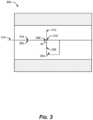
- FIG. 3shows a cross-sectional close-up of an example bonded wafer 300 .
- a first horizontal bonding surface 302 of the bonded waferis made of a dielectric material, such as silicon dioxide.
- the first horizontal bonding surface 302has been flattened by a chemical-mechanical planarization (CMP) process.
- a cavity 304has been created in the first horizontal bonding surface 302 , by etching for example.
- a vertical wall 306 of the cavity 304is disposed at a 90° angle to the first horizontal bonding surface 302 .
- the dielectric material of the vertical wall 306 of the cavity 304 and the dielectric material of the first horizontal bonding surface 302make a 90° corner 308 at a line or a point 310 .
- the 90° corner 308 made of the dielectric materialdefines an intersection of a vertical plane 312 of the vertical wall 306 of the cavity 304 and a horizontal plane 314 of the first horizontal bonding surface 302 .
- the first horizontal bonding surface 302 of the bonded wafer 300can be flattened by the chemical-mechanical planarization (CMP) process to a depth of field of a standard photolithography system.
- CMPchemical-mechanical planarization
- the flatness of the first horizontal bonding surface 302may be smooth (flat or planar) by the CMP process to within less than 5 angstroms ( ⁇ ).
- ⁇angstroms
- an obtainable flatnesshas a slope equivalent to 5 nm in vertical rise variation over each 100 ⁇ m span of horizontal run.
- a desirable roughness specificationis preferably less than 0.5 nm RMS.
- the 90° corner 308 made of dielectric material where the vertical wall 306 of the cavity 304 meets the first horizontal bonding surface 302may form a more perfect geometric 90° corner 308 with little or no rounding in the dielectric material, to within a few angstroms. Most conventional etches try to achieve as good a 90° corner as possible, but conventional industrial processes may deviate the corner by +/ ⁇ 3° from a 90° corner.
- a second horizontal bonding surface 316is direct-bonded to the first horizontal bonding surface 302 .
- the first horizontal bonding surface 302 and the second horizontal bonding surface 316may be direct-bonded together with an oxide-to-oxide direct bond.
- the oxide-to-oxide direct-bond between the first horizontal bonding surface 302 and the second horizontal bonding surface 316is present at a geometric point 310 where the vertical wall 306 of the cavity 304 and the horizontal bonding surface 302 meet at the 90° corner 308 .
- the bonded wafer 300may be two wafers direct-bonded together by a wafer-to-wafer process or may be a die and a wafer direct-bonded together by a die-to-wafer process.
- FIG. 4shows an example of method 400 of protecting an oxide surface for bonding during a microelectronics fabrication process. Operations of the example method 400 are shown in individual blocks.
- cavities and trenches in the oxide surfaceare overfilled with a temporary filler having approximately equal chemical and mechanical responses to a chemical-mechanical planarization (CMP) process as the oxide surface itself.
- CMPchemical-mechanical planarization
- the CMP processis applied to the temporary filler to planarize the temporary filler down to the oxide surface.
- the temporary filleris removed with an etchant that is selective to the temporary filler and nonreactive toward the oxide surface and nonreactive toward inner surfaces of the cavities and trenches.
- the oxide surfacemay be a silicon oxide surface and the temporary filler may be silicon nitride, for example.
- the etchantcan be a phosphoric acid etchant to selectively remove the silicon nitride while being nonreactive towards the silicon oxide surfaces.
- FIG. 5shows an example method 500 of improving bonding surfaces for microelectronics. Operations of the example method 500 are shown in individual blocks.
- an oxide surface of a wafer or dieis prepared for direct-bonding during a microelectronics fabrication process.
- the preparationincludes planarization and cleaning of the surface, and sometimes activation of the surface molecules through plasma activation.
- the planarizingmay bring the oxide surface to a flatness comparable to a depth of field of a photolithography system.
- the oxide surfaceis masked with a resist material for etching a cavity in the oxide surface.
- the cavityis etched in the oxide surface with a first etchant.
- the resist materialis stripped from the oxide surface.
- the cavityis overflowed with a temporary filler to preserve edges of the cavity during a chemical-mechanical planarization (CMP) process, wherein the temporary filler possesses chemical and physical properties similar to the oxide surface with respect to the chemical-mechanical planarization (CMP) process, and wherein the CMP process has approximately equal selectivity for the oxide surface and the temporary filler.
- CMPchemical-mechanical planarization
- a CMP processis applied to planarize the temporary filler down to an interface between the temporary filler and the silicon oxide.
- the temporary filleris removed with a second etchant selective to the temporary filler and nonreactive to the oxide surface and nonreactive to the inner surfaces of the cavity.
- the oxide surfacemay be a silicon oxide and the temporary filler may be silicon nitride.
- the second etchantcan be phosphoric acid to selectively etch the silicon nitride while remaining nonreactive to the silicon oxide surface.
- the cavitymay have a depth penetrating through a layer of the silicon oxide surface into an underlying layer below the layer of silicon oxide, such as a layer of silicon.
- FIG. 6shows an example method 600 of protecting edges of trenches and cavities of a bonding surface. Operations of the example method 600 are shown in individual blocks.
- edges of trenches and cavities in a bonding surface for microelectronicsare protected by depositing a sacrificial material into and over the trenches and cavities.
- the sacrificial materialis polished down to the bonding surface.
- the sacrificial materialis removed with an agent selective for reacting with the sacrificial material while remaining inert towards the bonding surface and towards surfaces of the trenches and cavities.
- connectionIn the specification and appended claims: the terms “connect,” “connection,” “connected,” “in connection with,” and “connecting,” are used to mean “in direct connection with” or “in connection with via one or more elements.”
- coupledthe terms “couple,” “coupling,” “coupled,” “coupled together,” and “coupled with,” are used to mean “directly coupled together” or “coupled together via one or more elements.”
Landscapes
- Engineering & Computer Science (AREA)
- Computer Hardware Design (AREA)
- Microelectronics & Electronic Packaging (AREA)
- Power Engineering (AREA)
- General Physics & Mathematics (AREA)
- Condensed Matter Physics & Semiconductors (AREA)
- Physics & Mathematics (AREA)
- Manufacturing & Machinery (AREA)
- Chemical & Material Sciences (AREA)
- Chemical Kinetics & Catalysis (AREA)
- General Chemical & Material Sciences (AREA)
- Inorganic Chemistry (AREA)
- Weting (AREA)
- Internal Circuitry In Semiconductor Integrated Circuit Devices (AREA)
- Mechanical Treatment Of Semiconductor (AREA)
Abstract
Description
Claims (20)
Priority Applications (2)
| Application Number | Priority Date | Filing Date | Title |
|---|---|---|---|
| US17/335,833US11804377B2 (en) | 2018-04-05 | 2021-06-01 | Method for preparing a surface for direct-bonding |
| US18/475,977US12341018B2 (en) | 2018-04-05 | 2023-09-27 | Method for preparing a surface for direct-bonding |
Applications Claiming Priority (3)
| Application Number | Priority Date | Filing Date | Title |
|---|---|---|---|
| US201862653315P | 2018-04-05 | 2018-04-05 | |
| US16/371,402US11056348B2 (en) | 2018-04-05 | 2019-04-01 | Bonding surfaces for microelectronics |
| US17/335,833US11804377B2 (en) | 2018-04-05 | 2021-06-01 | Method for preparing a surface for direct-bonding |
Related Parent Applications (1)
| Application Number | Title | Priority Date | Filing Date |
|---|---|---|---|
| US16/371,402ContinuationUS11056348B2 (en) | 2018-04-05 | 2019-04-01 | Bonding surfaces for microelectronics |
Related Child Applications (1)
| Application Number | Title | Priority Date | Filing Date |
|---|---|---|---|
| US18/475,977ContinuationUS12341018B2 (en) | 2018-04-05 | 2023-09-27 | Method for preparing a surface for direct-bonding |
Publications (2)
| Publication Number | Publication Date |
|---|---|
| US20210287910A1 US20210287910A1 (en) | 2021-09-16 |
| US11804377B2true US11804377B2 (en) | 2023-10-31 |
Family
ID=68097376
Family Applications (3)
| Application Number | Title | Priority Date | Filing Date |
|---|---|---|---|
| US16/371,402ActiveUS11056348B2 (en) | 2018-04-05 | 2019-04-01 | Bonding surfaces for microelectronics |
| US17/335,833ActiveUS11804377B2 (en) | 2018-04-05 | 2021-06-01 | Method for preparing a surface for direct-bonding |
| US18/475,977ActiveUS12341018B2 (en) | 2018-04-05 | 2023-09-27 | Method for preparing a surface for direct-bonding |
Family Applications Before (1)
| Application Number | Title | Priority Date | Filing Date |
|---|---|---|---|
| US16/371,402ActiveUS11056348B2 (en) | 2018-04-05 | 2019-04-01 | Bonding surfaces for microelectronics |
Family Applications After (1)
| Application Number | Title | Priority Date | Filing Date |
|---|---|---|---|
| US18/475,977ActiveUS12341018B2 (en) | 2018-04-05 | 2023-09-27 | Method for preparing a surface for direct-bonding |
Country Status (1)
| Country | Link |
|---|---|
| US (3) | US11056348B2 (en) |
Cited By (3)
| Publication number | Priority date | Publication date | Assignee | Title |
|---|---|---|---|---|
| US20230230901A1 (en)* | 2022-01-10 | 2023-07-20 | International Business Machines Corporation | TSV and Backside Power Distribution Structure |
| US20240021574A1 (en)* | 2020-12-16 | 2024-01-18 | The University Of Hong Kong | Cu-cu direct welding for packaging application in semiconductor industry |
| US12341018B2 (en) | 2018-04-05 | 2025-06-24 | Adeia Semiconductor Bonding Technologies Inc. | Method for preparing a surface for direct-bonding |
Families Citing this family (78)
| Publication number | Priority date | Publication date | Assignee | Title |
|---|---|---|---|---|
| US7109092B2 (en) | 2003-05-19 | 2006-09-19 | Ziptronix, Inc. | Method of room temperature covalent bonding |
| US7485968B2 (en) | 2005-08-11 | 2009-02-03 | Ziptronix, Inc. | 3D IC method and device |
| US8735219B2 (en) | 2012-08-30 | 2014-05-27 | Ziptronix, Inc. | Heterogeneous annealing method and device |
| US10886250B2 (en) | 2015-07-10 | 2021-01-05 | Invensas Corporation | Structures and methods for low temperature bonding using nanoparticles |
| US9953941B2 (en) | 2015-08-25 | 2018-04-24 | Invensas Bonding Technologies, Inc. | Conductive barrier direct hybrid bonding |
| US10204893B2 (en) | 2016-05-19 | 2019-02-12 | Invensas Bonding Technologies, Inc. | Stacked dies and methods for forming bonded structures |
| US10580735B2 (en) | 2016-10-07 | 2020-03-03 | Xcelsis Corporation | Stacked IC structure with system level wiring on multiple sides of the IC die |
| US11176450B2 (en) | 2017-08-03 | 2021-11-16 | Xcelsis Corporation | Three dimensional circuit implementing machine trained network |
| US10672663B2 (en) | 2016-10-07 | 2020-06-02 | Xcelsis Corporation | 3D chip sharing power circuit |
| TWI822659B (en) | 2016-10-27 | 2023-11-21 | 美商艾德亞半導體科技有限責任公司 | Structures and methods for low temperature bonding |
| US10002844B1 (en) | 2016-12-21 | 2018-06-19 | Invensas Bonding Technologies, Inc. | Bonded structures |
| US20180182665A1 (en) | 2016-12-28 | 2018-06-28 | Invensas Bonding Technologies, Inc. | Processed Substrate |
| CN117878055A (en) | 2016-12-28 | 2024-04-12 | 艾德亚半导体接合科技有限公司 | Stacking substrate processing |
| TWI837879B (en) | 2016-12-29 | 2024-04-01 | 美商艾德亞半導體接合科技有限公司 | Bonded structures with integrated passive component |
| WO2018169968A1 (en) | 2017-03-16 | 2018-09-20 | Invensas Corporation | Direct-bonded led arrays and applications |
| US10515913B2 (en) | 2017-03-17 | 2019-12-24 | Invensas Bonding Technologies, Inc. | Multi-metal contact structure |
| US10508030B2 (en) | 2017-03-21 | 2019-12-17 | Invensas Bonding Technologies, Inc. | Seal for microelectronic assembly |
| US10269756B2 (en) | 2017-04-21 | 2019-04-23 | Invensas Bonding Technologies, Inc. | Die processing |
| US10879212B2 (en) | 2017-05-11 | 2020-12-29 | Invensas Bonding Technologies, Inc. | Processed stacked dies |
| US10446441B2 (en) | 2017-06-05 | 2019-10-15 | Invensas Corporation | Flat metal features for microelectronics applications |
| US10217720B2 (en) | 2017-06-15 | 2019-02-26 | Invensas Corporation | Multi-chip modules formed using wafer-level processing of a reconstitute wafer |
| US10840205B2 (en) | 2017-09-24 | 2020-11-17 | Invensas Bonding Technologies, Inc. | Chemical mechanical polishing for hybrid bonding |
| US11031285B2 (en) | 2017-10-06 | 2021-06-08 | Invensas Bonding Technologies, Inc. | Diffusion barrier collar for interconnects |
| US11380597B2 (en) | 2017-12-22 | 2022-07-05 | Invensas Bonding Technologies, Inc. | Bonded structures |
| US10923408B2 (en) | 2017-12-22 | 2021-02-16 | Invensas Bonding Technologies, Inc. | Cavity packages |
| US10727219B2 (en) | 2018-02-15 | 2020-07-28 | Invensas Bonding Technologies, Inc. | Techniques for processing devices |
| US11169326B2 (en) | 2018-02-26 | 2021-11-09 | Invensas Bonding Technologies, Inc. | Integrated optical waveguides, direct-bonded waveguide interface joints, optical routing and interconnects |
| US11256004B2 (en) | 2018-03-20 | 2022-02-22 | Invensas Bonding Technologies, Inc. | Direct-bonded lamination for improved image clarity in optical devices |
| US10991804B2 (en) | 2018-03-29 | 2021-04-27 | Xcelsis Corporation | Transistor level interconnection methodologies utilizing 3D interconnects |
| US10790262B2 (en) | 2018-04-11 | 2020-09-29 | Invensas Bonding Technologies, Inc. | Low temperature bonded structures |
| US11244916B2 (en) | 2018-04-11 | 2022-02-08 | Invensas Bonding Technologies, Inc. | Low temperature bonded structures |
| US10964664B2 (en) | 2018-04-20 | 2021-03-30 | Invensas Bonding Technologies, Inc. | DBI to Si bonding for simplified handle wafer |
| US11004757B2 (en) | 2018-05-14 | 2021-05-11 | Invensas Bonding Technologies, Inc. | Bonded structures |
| US11276676B2 (en) | 2018-05-15 | 2022-03-15 | Invensas Bonding Technologies, Inc. | Stacked devices and methods of fabrication |
| US10923413B2 (en) | 2018-05-30 | 2021-02-16 | Xcelsis Corporation | Hard IP blocks with physically bidirectional passageways |
| KR20210009426A (en) | 2018-06-13 | 2021-01-26 | 인벤사스 본딩 테크놀로지스 인코포레이티드 | TV as a pad |
| US11393779B2 (en) | 2018-06-13 | 2022-07-19 | Invensas Bonding Technologies, Inc. | Large metal pads over TSV |
| US10910344B2 (en) | 2018-06-22 | 2021-02-02 | Xcelsis Corporation | Systems and methods for releveled bump planes for chiplets |
| WO2020010056A1 (en) | 2018-07-03 | 2020-01-09 | Invensas Bonding Technologies, Inc. | Techniques for joining dissimilar materials in microelectronics |
| US11158606B2 (en) | 2018-07-06 | 2021-10-26 | Invensas Bonding Technologies, Inc. | Molded direct bonded and interconnected stack |
| US11462419B2 (en) | 2018-07-06 | 2022-10-04 | Invensas Bonding Technologies, Inc. | Microelectronic assemblies |
| US12406959B2 (en) | 2018-07-26 | 2025-09-02 | Adeia Semiconductor Bonding Technologies Inc. | Post CMP processing for hybrid bonding |
| US11515291B2 (en) | 2018-08-28 | 2022-11-29 | Adeia Semiconductor Inc. | Integrated voltage regulator and passive components |
| US20200075533A1 (en) | 2018-08-29 | 2020-03-05 | Invensas Bonding Technologies, Inc. | Bond enhancement in microelectronics by trapping contaminants and arresting cracks during direct-bonding processes |
| US11011494B2 (en) | 2018-08-31 | 2021-05-18 | Invensas Bonding Technologies, Inc. | Layer structures for making direct metal-to-metal bonds at low temperatures in microelectronics |
| US11158573B2 (en) | 2018-10-22 | 2021-10-26 | Invensas Bonding Technologies, Inc. | Interconnect structures |
| US11244920B2 (en) | 2018-12-18 | 2022-02-08 | Invensas Bonding Technologies, Inc. | Method and structures for low temperature device bonding |
| CN113330557A (en) | 2019-01-14 | 2021-08-31 | 伊文萨思粘合技术公司 | Bonding structure |
| US11387202B2 (en) | 2019-03-01 | 2022-07-12 | Invensas Llc | Nanowire bonding interconnect for fine-pitch microelectronics |
| US11901281B2 (en) | 2019-03-11 | 2024-02-13 | Adeia Semiconductor Bonding Technologies Inc. | Bonded structures with integrated passive component |
| US10854578B2 (en) | 2019-03-29 | 2020-12-01 | Invensas Corporation | Diffused bitline replacement in stacked wafer memory |
| US11205625B2 (en) | 2019-04-12 | 2021-12-21 | Invensas Bonding Technologies, Inc. | Wafer-level bonding of obstructive elements |
| US11610846B2 (en) | 2019-04-12 | 2023-03-21 | Adeia Semiconductor Bonding Technologies Inc. | Protective elements for bonded structures including an obstructive element |
| US11373963B2 (en) | 2019-04-12 | 2022-06-28 | Invensas Bonding Technologies, Inc. | Protective elements for bonded structures |
| US11355404B2 (en) | 2019-04-22 | 2022-06-07 | Invensas Bonding Technologies, Inc. | Mitigating surface damage of probe pads in preparation for direct bonding of a substrate |
| US11385278B2 (en) | 2019-05-23 | 2022-07-12 | Invensas Bonding Technologies, Inc. | Security circuitry for bonded structures |
| US12374641B2 (en) | 2019-06-12 | 2025-07-29 | Adeia Semiconductor Bonding Technologies Inc. | Sealed bonded structures and methods for forming the same |
| US11296053B2 (en) | 2019-06-26 | 2022-04-05 | Invensas Bonding Technologies, Inc. | Direct bonded stack structures for increased reliability and improved yield in microelectronics |
| US12080672B2 (en) | 2019-09-26 | 2024-09-03 | Adeia Semiconductor Bonding Technologies Inc. | Direct gang bonding methods including directly bonding first element to second element to form bonded structure without adhesive |
| US12113054B2 (en) | 2019-10-21 | 2024-10-08 | Adeia Semiconductor Technologies Llc | Non-volatile dynamic random access memory |
| US11862602B2 (en) | 2019-11-07 | 2024-01-02 | Adeia Semiconductor Technologies Llc | Scalable architecture for reduced cycles across SOC |
| US11762200B2 (en) | 2019-12-17 | 2023-09-19 | Adeia Semiconductor Bonding Technologies Inc. | Bonded optical devices |
| US11876076B2 (en) | 2019-12-20 | 2024-01-16 | Adeia Semiconductor Technologies Llc | Apparatus for non-volatile random access memory stacks |
| US11721653B2 (en) | 2019-12-23 | 2023-08-08 | Adeia Semiconductor Bonding Technologies Inc. | Circuitry for electrical redundancy in bonded structures |
| CN115088068A (en) | 2019-12-23 | 2022-09-20 | 伊文萨思粘合技术公司 | Electrical redundancy for bonded structures |
| WO2021188846A1 (en) | 2020-03-19 | 2021-09-23 | Invensas Bonding Technologies, Inc. | Dimension compensation control for directly bonded structures |
| US11742314B2 (en) | 2020-03-31 | 2023-08-29 | Adeia Semiconductor Bonding Technologies Inc. | Reliable hybrid bonded apparatus |
| WO2021236361A1 (en) | 2020-05-19 | 2021-11-25 | Invensas Bonding Technologies, Inc. | Laterally unconfined structure |
| US11631647B2 (en) | 2020-06-30 | 2023-04-18 | Adeia Semiconductor Bonding Technologies Inc. | Integrated device packages with integrated device die and dummy element |
| US11728273B2 (en) | 2020-09-04 | 2023-08-15 | Adeia Semiconductor Bonding Technologies Inc. | Bonded structure with interconnect structure |
| US11764177B2 (en) | 2020-09-04 | 2023-09-19 | Adeia Semiconductor Bonding Technologies Inc. | Bonded structure with interconnect structure |
| US11264357B1 (en) | 2020-10-20 | 2022-03-01 | Invensas Corporation | Mixed exposure for large die |
| KR20230097121A (en) | 2020-10-29 | 2023-06-30 | 아데이아 세미컨덕터 본딩 테크놀로지스 인코포레이티드 | Direct bonding method and structure |
| JP2024501017A (en) | 2020-12-28 | 2024-01-10 | アデイア セミコンダクター ボンディング テクノロジーズ インコーポレイテッド | Structure with through-substrate via and method for forming the same |
| JP2024501559A (en) | 2020-12-30 | 2024-01-12 | アデイア セミコンダクター ボンディング テクノロジーズ インコーポレイテッド | Structures with conductive features and methods of forming the same |
| KR20240036698A (en) | 2021-08-02 | 2024-03-20 | 아데이아 세미컨덕터 본딩 테크놀로지스 인코포레이티드 | Protective semiconductor elements for combined structures |
| US20240105674A1 (en)* | 2022-09-07 | 2024-03-28 | Adeia Semiconductor Bonding Technologies Inc. | Bonded structure and method of forming same |
| US12341083B2 (en) | 2023-02-08 | 2025-06-24 | Adeia Semiconductor Bonding Technologies Inc. | Electronic device cooling structures bonded to semiconductor elements |
Citations (391)
| Publication number | Priority date | Publication date | Assignee | Title |
|---|---|---|---|---|
| JPS6130059A (en) | 1984-07-20 | 1986-02-12 | Nec Corp | Manufacturing method of semiconductor device |
| US4818728A (en) | 1986-12-03 | 1989-04-04 | Sharp Kabushiki Kaisha | Method of making a hybrid semiconductor device |
| JPH01168040A (en) | 1987-11-18 | 1989-07-03 | Grumman Aerospace Corp | Method of forming integrated circuit for touching electrical connection to external electronic circuit |
| US4904328A (en) | 1987-09-08 | 1990-02-27 | Gencorp Inc. | Bonding of FRP parts |
| US4939568A (en) | 1986-03-20 | 1990-07-03 | Fujitsu Limited | Three-dimensional integrated circuit and manufacturing method thereof |
| US4998665A (en) | 1988-09-07 | 1991-03-12 | Nec Corporation | Bonding structure of substrates and method for bonding substrates |
| EP0465227A2 (en) | 1990-07-02 | 1992-01-08 | Kabushiki Kaisha Toshiba | Composite integrated circuit device |
| US5087585A (en) | 1989-07-11 | 1992-02-11 | Nec Corporation | Method of stacking semiconductor substrates for fabrication of three-dimensional integrated circuit |
| JPH04259249A (en) | 1991-02-14 | 1992-09-14 | Mitsubishi Electric Corp | Semiconductor device |
| JPH0529183A (en) | 1991-07-22 | 1993-02-05 | Fuji Electric Co Ltd | Joining method |
| JPH05198739A (en) | 1991-09-10 | 1993-08-06 | Mitsubishi Electric Corp | Stacked semiconductor device and manufacturing method thereof |
| US5236118A (en) | 1992-05-12 | 1993-08-17 | The Regents Of The University Of California | Aligned wafer bonding |
| JPH0613456A (en) | 1992-09-28 | 1994-01-21 | Toshiba Corp | Method for manufacturing semiconductor device |
| US5322593A (en) | 1991-11-21 | 1994-06-21 | Nec Corporation | Method for manufacturing polyimide multilayer wiring substrate |
| JPH06260594A (en) | 1993-02-11 | 1994-09-16 | Siemens Ag | Preparation of three-dimensional circuit device |
| JPH0766093A (en) | 1993-08-23 | 1995-03-10 | Sumitomo Sitix Corp | Method and device for bonding semiconductor wafers |
| US5413952A (en) | 1994-02-02 | 1995-05-09 | Motorola, Inc. | Direct wafer bonded structure method of making |
| US5442235A (en) | 1993-12-23 | 1995-08-15 | Motorola Inc. | Semiconductor device having an improved metal interconnect structure |
| JPH07249749A (en) | 1994-03-11 | 1995-09-26 | Canon Inc | Method for manufacturing SOI substrate |
| JPH07283382A (en) | 1994-04-12 | 1995-10-27 | Sony Corp | Method of pasting silicon substrates |
| US5489804A (en) | 1989-08-28 | 1996-02-06 | Lsi Logic Corporation | Flexible preformed planar structures for interposing between a chip and a substrate |
| JPH0878645A (en) | 1994-09-05 | 1996-03-22 | Mitsubishi Materials Corp | Silicon semiconductor wafer and its manufacture |
| US5501003A (en) | 1993-12-15 | 1996-03-26 | Bel Fuse Inc. | Method of assembling electronic packages for surface mount applications |
| US5503704A (en) | 1993-01-06 | 1996-04-02 | The Regents Of The University Of California | Nitrogen based low temperature direct bonding |
| US5516727A (en) | 1993-04-19 | 1996-05-14 | International Business Machines Corporation | Method for encapsulating light emitting diodes |
| JPH08125121A (en) | 1994-08-29 | 1996-05-17 | Matsushita Electric Ind Co Ltd | Semiconductor device and manufacturing method thereof |
| JPH08186235A (en) | 1994-12-16 | 1996-07-16 | Texas Instr Inc <Ti> | Manufacture of semiconductor device |
| US5563084A (en) | 1994-09-22 | 1996-10-08 | Fraunhofer-Gesellschaft zur F orderung der angewandten Forschung e.V. | Method of making a three-dimensional integrated circuit |
| US5610431A (en) | 1995-05-12 | 1997-03-11 | The Charles Stark Draper Laboratory, Inc. | Covers for micromechanical sensors and other semiconductor devices |
| JPH09120979A (en) | 1995-10-25 | 1997-05-06 | Matsushita Electric Ind Co Ltd | Semiconductor device and manufacturing method thereof |
| US5696406A (en) | 1993-10-29 | 1997-12-09 | Nec Corportion | Semiconductor device and method for fabricating the same |
| US5734199A (en) | 1995-12-18 | 1998-03-31 | Matsushita Electric Industrial Co., Ltd. | Semiconductor device having improved test electrodes |
| US5753536A (en) | 1994-08-29 | 1998-05-19 | Matsushita Electric Industrial Co., Ltd. | Semiconductor device and associated fabrication method |
| JPH10135404A (en) | 1996-10-28 | 1998-05-22 | Matsushita Electric Ind Co Ltd | Semiconductor chip module and method of manufacturing the same |
| US5771555A (en) | 1993-11-01 | 1998-06-30 | Matsushita Electric Industrial Co., Ltd. | Method for producing an electronic component using direct bonding |
| JPH10223636A (en) | 1997-02-12 | 1998-08-21 | Nec Yamagata Ltd | Manufacture of semiconductor integrated circuit device |
| JPH10242383A (en) | 1997-02-24 | 1998-09-11 | Sanyo Electric Co Ltd | Semiconductor device |
| US5821692A (en) | 1996-11-26 | 1998-10-13 | Motorola, Inc. | Organic electroluminescent device hermetic encapsulation package |
| US5866942A (en) | 1995-04-28 | 1999-02-02 | Nec Corporation | Metal base package for a semiconductor device |
| JPH11186120A (en) | 1997-12-24 | 1999-07-09 | Canon Inc | Adhesion bonding between substrates of the same or different materials |
| US5985739A (en) | 1994-09-19 | 1999-11-16 | Fraunhofer-Gesellschaft Zur Forderung Der Angewandten Forschung E.V. | Semiconductor structures having advantageous high-frequency characteristics and processes for producing such semiconductor structures |
| US5998808A (en) | 1997-06-27 | 1999-12-07 | Sony Corporation | Three-dimensional integrated circuit device and its manufacturing method |
| US6008126A (en) | 1992-04-08 | 1999-12-28 | Elm Technology Corporation | Membrane dielectric isolation IC fabrication |
| US6034393A (en) | 1997-06-16 | 2000-03-07 | Mitsubishi Denki Kabushiki Kaisha | Nonvolatile semiconductor memory device using trench isolation and manufacturing method thereof |
| JP2000100679A (en) | 1998-09-22 | 2000-04-07 | Canon Inc | Micro-region solid-state bonding method between substrates by thinning and device structure |
| US6054363A (en) | 1996-11-15 | 2000-04-25 | Canon Kabushiki Kaisha | Method of manufacturing semiconductor article |
| US6063968A (en) | 1996-05-14 | 2000-05-16 | Degussa Aktiengesellschaft | Method for the production of trimethylhydroquinone |
| US6071761A (en) | 1997-03-18 | 2000-06-06 | Jacobs; Richard L. | Method for encapsulated integrated circuits |
| US6080640A (en) | 1997-07-11 | 2000-06-27 | Advanced Micro Devices, Inc. | Metal attachment method and structure for attaching substrates at low temperatures |
| JP2000260934A (en) | 1999-03-05 | 2000-09-22 | Seiko Epson Corp | Method for manufacturing semiconductor device |
| US6123825A (en) | 1998-12-02 | 2000-09-26 | International Business Machines Corporation | Electromigration-resistant copper microstructure and process of making |
| JP2000299379A (en) | 1999-04-13 | 2000-10-24 | Tadatomo Suga | Semiconductor device and manufacturing method thereof |
| JP2000311982A (en) | 1999-04-26 | 2000-11-07 | Toshiba Corp | Semiconductor device, semiconductor module, and manufacturing method thereof |
| US6147000A (en) | 1998-08-11 | 2000-11-14 | Advanced Micro Devices, Inc. | Method for forming low dielectric passivation of copper interconnects |
| US6183592B1 (en) | 1996-11-08 | 2001-02-06 | Mark F. Sylvester | Method for minimizing warp in the production of electronic assemblies |
| JP2001102479A (en) | 1999-09-27 | 2001-04-13 | Toshiba Corp | Semiconductor integrated circuit device and method of manufacturing the same |
| US6218203B1 (en) | 1999-06-28 | 2001-04-17 | Advantest Corp. | Method of producing a contact structure |
| US6232150B1 (en) | 1998-12-03 | 2001-05-15 | The Regents Of The University Of Michigan | Process for making microstructures and microstructures made thereby |
| US6258625B1 (en) | 1999-05-18 | 2001-07-10 | International Business Machines Corporation | Method of interconnecting electronic components using a plurality of conductive studs |
| US6259160B1 (en) | 1999-04-21 | 2001-07-10 | Advanced Micro Devices, Inc. | Apparatus and method of encapsulated copper (Cu) Interconnect formation |
| US6265775B1 (en) | 1997-01-24 | 2001-07-24 | Micron Technology, Inc. | Flip chip technique for chip assembly |
| WO2001061743A1 (en) | 2000-02-16 | 2001-08-23 | Ziptronix, Inc. | Method for low temperature bonding and bonded structure |
| US6297072B1 (en) | 1998-04-17 | 2001-10-02 | Interuniversitair Micro-Elktronica Centrum (Imec Vzw) | Method of fabrication of a microstructure having an internal cavity |
| US6316786B1 (en) | 1998-08-29 | 2001-11-13 | International Business Machines Corporation | Organic opto-electronic devices |
| JP2001326326A (en) | 2000-05-16 | 2001-11-22 | Seiko Epson Corp | Semiconductor device and manufacturing method thereof |
| US6322600B1 (en) | 1997-04-23 | 2001-11-27 | Advanced Technology Materials, Inc. | Planarization compositions and methods for removing interlayer dielectric films |
| US6333120B1 (en) | 1999-10-27 | 2001-12-25 | International Business Machines Corporation | Method for controlling the texture and microstructure of plated copper and plated structure |
| US6333206B1 (en) | 1996-12-24 | 2001-12-25 | Nitto Denko Corporation | Process for the production of semiconductor device |
| US20020000328A1 (en) | 2000-06-22 | 2002-01-03 | Kabushiki Kaisha Toshiba | Printed wiring board and manufacturing method thereof |
| US20020003307A1 (en) | 2000-07-05 | 2002-01-10 | Tadatomo Suga | Semiconductor device and method for fabricating the device |
| TW476145B (en) | 1999-06-28 | 2002-02-11 | Hyundai Electronics Ind | Chip scale stack package and method of fabricating the same |
| US6348709B1 (en) | 1999-03-15 | 2002-02-19 | Micron Technology, Inc. | Electrical contact for high dielectric constant capacitors and method for fabricating the same |
| US20020025665A1 (en) | 2000-08-29 | 2002-02-28 | Werner Juengling | Method of forming a metal to polysilicon contact in oxygen environment |
| US6355153B1 (en) | 1999-09-17 | 2002-03-12 | Nutool, Inc. | Chip interconnect and packaging deposition methods and structures |
| US6359235B1 (en) | 1999-07-30 | 2002-03-19 | Kyocera Corporation | Electrical device mounting wiring board and method of producing the same |
| US6374770B1 (en) | 1995-10-26 | 2002-04-23 | Applied Materials, Inc. | Apparatus for improving film stability of halogen-doped silicon oxide films |
| JP2002516033A (en) | 1997-04-04 | 2002-05-28 | グレン ジェイ リーディ | 3D structure memory |
| US6409904B1 (en) | 1998-12-01 | 2002-06-25 | Nutool, Inc. | Method and apparatus for depositing and controlling the texture of a thin film |
| US20020094661A1 (en) | 1999-10-01 | 2002-07-18 | Ziptronix | Three dimensional device intergration method and intergrated device |
| US6423640B1 (en) | 2000-08-09 | 2002-07-23 | Taiwan Semiconductor Manufacturing Co., Ltd. | Headless CMP process for oxide planarization |
| US20020113241A1 (en) | 2000-07-24 | 2002-08-22 | Tdk Corporation | Light emitting device |
| JP2002353416A (en) | 2001-05-25 | 2002-12-06 | Sony Corp | Semiconductor storage device and method of manufacturing the same |
| JP2002368159A (en) | 2001-06-11 | 2002-12-20 | Denso Corp | Semiconductor device and manufacturing method therefor |
| JP2003023071A (en) | 2001-07-05 | 2003-01-24 | Sony Corp | Semiconductor device manufacturing method and semiconductor device |
| US6515343B1 (en) | 1998-11-19 | 2003-02-04 | Quicklogic Corporation | Metal-to-metal antifuse with non-conductive diffusion barrier |
| US6528894B1 (en) | 1996-09-20 | 2003-03-04 | Micron Technology, Inc. | Use of nitrides for flip-chip encapsulation |
| US6541382B1 (en) | 2000-04-17 | 2003-04-01 | Taiwan Semiconductor Manufacturing Company | Lining and corner rounding method for shallow trench isolation |
| US6552436B2 (en) | 2000-12-08 | 2003-04-22 | Motorola, Inc. | Semiconductor device having a ball grid array and method therefor |
| US6555917B1 (en) | 2001-10-09 | 2003-04-29 | Amkor Technology, Inc. | Semiconductor package having stacked semiconductor chips and method of making the same |
| US20030092220A1 (en) | 2000-06-08 | 2003-05-15 | Salman Akram | Stereolithographic methods of fabricating semiconductor devices having protective layers thereon through which contact pads are exposed |
| US20030109083A1 (en) | 2000-08-23 | 2003-06-12 | Ahmad Syed Sajid | Interconnecting substrates for electrical coupling of microelectronic components |
| US6579744B1 (en) | 1998-02-27 | 2003-06-17 | Micron Technology, Inc. | Electrical interconnections, methods of conducting electricity, and methods of reducing horizontal conductivity within an anisotropic conductive adhesive |
| US6583515B1 (en) | 1999-09-03 | 2003-06-24 | Texas Instruments Incorporated | Ball grid array package for enhanced stress tolerance |
| WO2003054954A2 (en) | 2001-12-19 | 2003-07-03 | Intel Corporation | Electrical/optical integration scheme using direct copper bonding |
| US20030129796A1 (en) | 2001-06-29 | 2003-07-10 | Rainer Bruchhaus | Method for fabricating a semiconductor memory device |
| US6593645B2 (en) | 1999-09-24 | 2003-07-15 | United Microelectronics Corp. | Three-dimensional system-on-chip structure |
| US6600224B1 (en) | 2000-10-31 | 2003-07-29 | International Business Machines Corporation | Thin film attachment to laminate using a dendritic interconnection |
| US20030157748A1 (en) | 2002-02-20 | 2003-08-21 | Kim Sarah E. | Process of vertically stacking multiple wafers supporting different active integrated circuit (IC) devices |
| US6624003B1 (en) | 2002-02-06 | 2003-09-23 | Teravicta Technologies, Inc. | Integrated MEMS device and package |
| US6627814B1 (en) | 2002-03-22 | 2003-09-30 | David H. Stark | Hermetically sealed micro-device package with window |
| US6632377B1 (en) | 1998-10-23 | 2003-10-14 | International Business Machines Corporation | Chemical-mechanical planarization of metallurgy |
| US6642081B1 (en) | 2002-04-11 | 2003-11-04 | Robert Patti | Interlocking conductor method for bonding wafers to produce stacked integrated circuits |
| US6656826B2 (en) | 2000-09-27 | 2003-12-02 | Kabushiki Kaisha Toshiba | Semiconductor device with fuse to be blown with energy beam and method of manufacturing the semiconductor device |
| US6660564B2 (en) | 2002-01-25 | 2003-12-09 | Sony Corporation | Wafer-level through-wafer packaging process for MEMS and MEMS package produced thereby |
| US6667225B2 (en) | 2001-12-17 | 2003-12-23 | Intel Corporation | Wafer-bonding using solder and method of making the same |
| US6720212B2 (en) | 2002-03-14 | 2004-04-13 | Infineon Technologies Ag | Method of eliminating back-end rerouting in ball grid array packaging |
| US20040084414A1 (en) | 2002-08-19 | 2004-05-06 | Kenji Sakai | Polishing method and polishing composition used for polishing |
| US20040126990A1 (en) | 2002-12-26 | 2004-07-01 | Fujitsu Limited | Semiconductor device having STI without divot its manufacture |
| US6759738B1 (en) | 1995-08-02 | 2004-07-06 | International Business Machines Corporation | Systems interconnected by bumps of joining material |
| JP2004200547A (en) | 2002-12-20 | 2004-07-15 | Seiko Epson Corp | Semiconductor chip, semiconductor wafer, semiconductor device and manufacturing method thereof, circuit board, and electronic equipment |
| US20040157407A1 (en) | 2003-02-07 | 2004-08-12 | Ziptronix | Room temperature metal direct bonding |
| US20040217483A1 (en) | 2003-04-30 | 2004-11-04 | Infineon Technologies Ag | Semiconductor device and method for fabricating the semiconductor device |
| US20040262772A1 (en) | 2003-06-30 | 2004-12-30 | Shriram Ramanathan | Methods for bonding wafers using a metal interlayer |
| US6847527B2 (en) | 2001-08-24 | 2005-01-25 | 3M Innovative Properties Company | Interconnect module with reduced power distribution impedance |
| US6864585B2 (en) | 2000-03-22 | 2005-03-08 | Ziptronix, Inc. | Three dimensional device integration method and integrated device |
| US6867073B1 (en) | 2003-10-21 | 2005-03-15 | Ziptronix, Inc. | Single mask via method and device |
| JP2005086089A (en) | 2003-09-10 | 2005-03-31 | Seiko Epson Corp | Manufacturing method of three-dimensional device |
| JP2005093486A (en) | 2003-09-12 | 2005-04-07 | Seiko Epson Corp | Semiconductor device manufacturing method and semiconductor device |
| US6887769B2 (en) | 2002-02-06 | 2005-05-03 | Intel Corporation | Dielectric recess for wafer-to-wafer and die-to-die metal bonding and method of fabricating the same |
| US20050104224A1 (en) | 2003-11-19 | 2005-05-19 | Tai-Chun Huang | Bond pad for flip chip package |
| JP2005135988A (en) | 2003-10-28 | 2005-05-26 | Toshiba Corp | Manufacturing method of semiconductor device |
| US6908027B2 (en) | 2003-03-31 | 2005-06-21 | Intel Corporation | Complete device layer transfer without edge exclusion via direct wafer bonding and constrained bond-strengthening process |
| US6909194B2 (en) | 1999-08-27 | 2005-06-21 | Micron Technology, Inc. | Electronic assembly having semiconductor component with polymer support member and method of fabrication |
| US6960492B1 (en) | 2003-01-30 | 2005-11-01 | Kabushiki Kaisha Toshiba | Semiconductor device having multilayer wiring and manufacturing method therefor |
| US6974769B2 (en) | 2000-04-27 | 2005-12-13 | Asm Nutool, Inc. | Conductive structure fabrication process using novel layered structure and conductive structure fabricated thereby for use in multi-level metallization |
| US20060024950A1 (en) | 2004-08-02 | 2006-02-02 | Suk-Hun Choi | Methods of forming metal contact structures and methods of fabricating phase-change memory devices using the same |
| US20060057945A1 (en) | 2004-09-16 | 2006-03-16 | Chia-Lin Hsu | Chemical mechanical polishing process |
| US7045453B2 (en) | 2002-10-24 | 2006-05-16 | International Business Machines Corporation | Very low effective dielectric constant interconnect structures and methods for fabricating the same |
| US20060138368A1 (en) | 2004-12-29 | 2006-06-29 | Lee Jin K | Apparatus and method for inspecting semiconductor wafers for metal residue |
| US7105980B2 (en) | 2002-07-03 | 2006-09-12 | Sawtek, Inc. | Saw filter device and method employing normal temperature bonding for producing desirable filter production and performance characteristics |
| US7109063B2 (en) | 2003-02-12 | 2006-09-19 | Micron Technology, Inc. | Semiconductor substrate for build-up packages |
| US7109092B2 (en) | 2003-05-19 | 2006-09-19 | Ziptronix, Inc. | Method of room temperature covalent bonding |
| WO2006100444A1 (en) | 2005-03-22 | 2006-09-28 | Cambridge Display Technology Limited | Apparatus and method for increased device lifetime in an organic electro-luminescent device. |
| US7193423B1 (en) | 2005-12-12 | 2007-03-20 | International Business Machines Corporation | Wafer-to-wafer alignments |
| US20070096294A1 (en) | 2003-06-06 | 2007-05-03 | Sanyo Electric Co., Ltd. | Semiconductor device and manufacturing method of the same |
| US20070212870A1 (en) | 2006-03-13 | 2007-09-13 | International Business Machines Corporation | Interconnect structure with a barrier-redundancy feature |
| US20070222048A1 (en) | 2006-03-24 | 2007-09-27 | Advanced Semiconductor Engineering, Inc. | Package structure |
| US20070257366A1 (en) | 2006-05-03 | 2007-11-08 | Taiwan Semiconductor Manufacturing Company, Ltd. | Barrier layer for semiconductor interconnect structure |
| US20070295456A1 (en) | 2006-03-28 | 2007-12-27 | Innovative Micro Technology | Wafer bonding material with embedded conductive particles |
| US7354798B2 (en) | 2002-12-20 | 2008-04-08 | International Business Machines Corporation | Three-dimensional device fabrication method |
| US20080122092A1 (en) | 2006-11-29 | 2008-05-29 | Ji Ho Hong | Semiconductor Device and Method of Manufacturing the Same |
| US7485968B2 (en) | 2005-08-11 | 2009-02-03 | Ziptronix, Inc. | 3D IC method and device |
| US20090108469A1 (en) | 2007-10-30 | 2009-04-30 | Samsung Electronics Co., Ltd. | Chip stack package |
| US20090197408A1 (en) | 2008-01-31 | 2009-08-06 | Matthias Lehr | Increasing electromigration resistance in an interconnect structure of a semiconductor device by forming an alloy |
| US20090200668A1 (en) | 2008-02-07 | 2009-08-13 | International Business Machines Corporation | Interconnect structure with high leakage resistance |
| US20100164066A1 (en) | 2008-12-30 | 2010-07-01 | Stmicroelectronics S.R.L. | Integrated capacitor having a non-uniform thickness |
| US7750488B2 (en) | 2006-07-10 | 2010-07-06 | Tezzaron Semiconductor, Inc. | Method for bonding wafers to produce stacked integrated circuits |
| US7803693B2 (en) | 2007-02-15 | 2010-09-28 | John Trezza | Bowed wafer hybridization compensation |
| US20110074040A1 (en) | 2009-09-29 | 2011-03-31 | Manfred Frank | Semiconductor Device And Method For Making Same |
| US7998335B2 (en) | 2005-06-13 | 2011-08-16 | Cabot Microelectronics Corporation | Controlled electrochemical polishing method |
| US20110290552A1 (en) | 2004-09-27 | 2011-12-01 | Qualcomm Mems Technologies, Inc. | Method and system for packaging mems devices with incorporated getter |
| WO2012013162A1 (en) | 2010-07-30 | 2012-02-02 | 昆山智拓达电子科技有限公司 | Tsv interconnect structure and manufacturing method thereof |
| US8241961B2 (en) | 2008-12-09 | 2012-08-14 | Young Hae KIM | Method for manufacturing hetero-bonded wafer |
| US20120211894A1 (en) | 2011-02-23 | 2012-08-23 | Sony Corporation | Joining electrode, method of manufacturing the same, semiconductor device, and method of manufacturing the same |
| US20120212384A1 (en) | 2011-02-17 | 2012-08-23 | International Business Machines Corporation | Integrated antenna for rfic package applications |
| KR20120106366A (en) | 2011-03-18 | 2012-09-26 | 삼성전자주식회사 | Semiconductor device and method of forming the same |
| US8314007B2 (en) | 2009-12-23 | 2012-11-20 | Soitec | Process for fabricating a heterostructure with minimized stress |
| US20120319280A1 (en) | 2010-03-01 | 2012-12-20 | Osaka University | Semiconductor device and bonding material for semiconductor device |
| US8349635B1 (en) | 2008-05-20 | 2013-01-08 | Silicon Laboratories Inc. | Encapsulated MEMS device and method to form the same |
| US8357931B2 (en) | 2004-02-27 | 2013-01-22 | Nvidia Corporation | Flip chip semiconductor die internal signal access system and method |
| US20130020704A1 (en) | 2011-07-18 | 2013-01-24 | S.O.I.Tec Silicon On Insulator Technologies | Bonding surfaces for direct bonding of semiconductor structures |
| US20130034948A1 (en) | 2011-08-05 | 2013-02-07 | Taiwan Semiconductor Manufacturing Company, Ltd. | Method of Manufacturing a Semiconductor Device |
| JP2013033786A (en) | 2011-08-01 | 2013-02-14 | Sony Corp | Semiconductor device and semiconductor device manufacturing method |
| US8377798B2 (en) | 2010-11-10 | 2013-02-19 | Taiwan Semiconductor Manufacturing Co., Ltd | Method and structure for wafer to wafer bonding in semiconductor packaging |
| US20130078783A1 (en)* | 2011-09-24 | 2013-03-28 | Taiwan Semiconductor Manufacturing Company, Ltd. | Forming a protective film on a back side of a silicon wafer in a iii-v family fabrication process |
| US20130075900A1 (en) | 2008-03-19 | 2013-03-28 | Stats Chippac, Ltd. | Semiconductor Device and Method of Forming Insulating Layer on Conductive Traces for Electrical Isolation in Fine Pitch Bonding |
| US8435421B2 (en) | 2007-11-27 | 2013-05-07 | Cabot Microelectronics Corporation | Metal-passivating CMP compositions and methods |
| US8441131B2 (en) | 2011-09-12 | 2013-05-14 | Globalfoundries Inc. | Strain-compensating fill patterns for controlling semiconductor chip package interactions |
| US8476146B2 (en) | 2010-12-03 | 2013-07-02 | Taiwan Semiconductor Manufacturing Company, Ltd. | Reducing wafer distortion through a low CTE layer |
| US8476165B2 (en) | 2009-04-01 | 2013-07-02 | Tokyo Electron Limited | Method for thinning a bonding wafer |
| US8482132B2 (en) | 2009-10-08 | 2013-07-09 | International Business Machines Corporation | Pad bonding employing a self-aligned plated liner for adhesion enhancement |
| US20130187287A1 (en) | 2010-06-28 | 2013-07-25 | Byung-lyul Park | Semiconductor Device and Method of Fabricating the Same |
| US8501537B2 (en) | 2011-03-31 | 2013-08-06 | Soitec | Methods for bonding semiconductor structures involving annealing processes, and bonded semiconductor structures formed using such methods |
| US8507979B1 (en) | 2012-07-31 | 2013-08-13 | Taiwan Semiconductor Manufacturing Company, Ltd. | Semiconductor integrated circuit with metal gate |
| US20130221527A1 (en) | 2012-02-24 | 2013-08-29 | International Business Machines Corporation | Metallic capped interconnect structure with high electromigration resistance and low resistivity |
| US20130256913A1 (en) | 2012-03-30 | 2013-10-03 | Bryan Black | Die stacking with coupled electrical interconnects to align proximity interconnects |
| US20130284885A1 (en) | 2012-04-27 | 2013-10-31 | Taiwan Semiconductor Manufacturing Company, Ltd. | Method and Apparatus for Image Sensor Packaging |
| US20130320556A1 (en) | 2012-06-05 | 2013-12-05 | Taiwan Semiconductor Manufacturing Company, Ltd. | Three Dimensional Integrated Circuit Structures and Hybrid Bonding Methods for Semiconductor Wafers |
| JP2013243333A (en) | 2012-04-24 | 2013-12-05 | Tadatomo Suga | Chip-on wafer bonding method and bonding device and structure including chip and wafer |
| US20130328186A1 (en) | 2012-06-08 | 2013-12-12 | Invensas Corporation | Reduced stress tsv and interposer structures |
| US8620164B2 (en) | 2011-01-20 | 2013-12-31 | Intel Corporation | Hybrid III-V silicon laser formed by direct bonding |
| US8647987B2 (en) | 2012-04-16 | 2014-02-11 | The Institute of Microelectronics, Chinese Academy of Science | Method for improving uniformity of chemical-mechanical planarization process |
| US8716105B2 (en) | 2011-03-31 | 2014-05-06 | Soitec | Methods for bonding semiconductor structures involving annealing processes, and bonded semiconductor structures and intermediate structures formed using such methods |
| US20140131869A1 (en) | 2003-11-10 | 2014-05-15 | Stats Chippac, Ltd. | Semiconductor Device and Method of Self-Confinement of Conductive Bump Material During Reflow Without Solder Mask |
| US20140145338A1 (en) | 2011-05-24 | 2014-05-29 | Sony Corporation | Semiconductor device |
| US20140175655A1 (en) | 2012-12-22 | 2014-06-26 | Industrial Technology Research Institute | Chip bonding structure and manufacturing method thereof |
| US20140206109A1 (en) | 2013-01-18 | 2014-07-24 | Infineon Technologies Ag | Method of Manufacturing and Testing a Chip Package |
| US8802538B1 (en) | 2013-03-15 | 2014-08-12 | Taiwan Semiconductor Manufacturing Company, Ltd. | Methods for hybrid wafer bonding |
| US20140225795A1 (en) | 2013-02-08 | 2014-08-14 | Sj Antenna Design | Shielding module integrating antenna and integrated circuit component |
| US20140252635A1 (en) | 2013-03-08 | 2014-09-11 | Taiwan Semiconductor Manufacturing Company, Ltd. | Bonding Structures and Methods of Forming the Same |
| US20140264948A1 (en) | 2013-03-15 | 2014-09-18 | Taiwan Semiconductor Manufacturing Company, Ltd. | Air Trench in Packages Incorporating Hybrid Bonding |
| US20140332980A1 (en) | 2008-11-25 | 2014-11-13 | Invensas Corporation | Methods of forming 3-d circuits with integrated passive devices |
| US8916448B2 (en) | 2013-01-09 | 2014-12-23 | International Business Machines Corporation | Metal to metal bonding for stacked (3D) integrated circuits |
| US20150097022A1 (en) | 2013-10-03 | 2015-04-09 | Commissariat A L'energie Atomique Et Aux Ene Alt | Process for direct bonding of two elements comprising metallic portions and dielectric materials |
| US20150108644A1 (en) | 2013-10-17 | 2015-04-23 | Taiwan Semiconductor Manufacturing Company, Ltd. | 3D Integrated Circuit and Methods of Forming the Same |
| US9040385B2 (en) | 2013-07-24 | 2015-05-26 | Taiwan Semiconductor Manufacturing Co., Ltd. | Mechanisms for cleaning substrate surface for hybrid bonding |
| US20150155263A1 (en) | 2013-12-04 | 2015-06-04 | International Business Machines Corporation | Facilitating chip dicing for metal-metal bonding and hybrid wafer bonding |
| US9064937B2 (en) | 2013-05-30 | 2015-06-23 | International Business Machines Corporation | Substrate bonding with diffusion barrier structures |
| US20150200073A1 (en) | 2014-01-15 | 2015-07-16 | Axcelis Technologies, Inc. | Ion Implantation System and Method with Variable Energy Control |
| US20150206823A1 (en) | 2014-01-17 | 2015-07-23 | Taiwan Semiconductor Manufacturing Company, Ltd. | Robust Through-Silicon-Via Structure |
| US9093350B2 (en) | 2010-07-09 | 2015-07-28 | Canon Kabushiki Kaisha | Member for solid-state image pickup device and method for manufacturing solid-state image pickup device having first and second wiring structures with a concave portion between first and second substrates |
| US20150214191A1 (en) | 2014-01-28 | 2015-07-30 | Taiwan Semiconductor Manufacturing Company, Ltd. | Packages with Stacked Dies and Methods of Forming the Same |
| US20150228621A1 (en) | 2013-02-26 | 2015-08-13 | Sandisk Information Technology (Shanghai) Co., Ltd. | Semiconductor device including alternating stepped semiconductor die stacks |
| KR20150097798A (en) | 2012-12-21 | 2015-08-26 | 테사 소시에타스 유로파에아 | Adhesive tape containing getter material |
| US9142517B2 (en) | 2012-06-05 | 2015-09-22 | Taiwan Semiconductor Manufacturing Company, Ltd. | Hybrid bonding mechanisms for semiconductor wafers |
| US20150307819A1 (en)* | 2012-12-13 | 2015-10-29 | Kurita Water Industries Ltd. | Substrate cleaning liquid and substrate cleaning method |
| US9184125B2 (en) | 2012-08-30 | 2015-11-10 | Ziptronix, Inc. | Heterogeneous annealing method and device |
| US20150340371A1 (en)* | 2014-05-21 | 2015-11-26 | Macronix International Co., Ltd. | 3d independent double gate flash memory on bounded conductor layer |
| US20150340269A1 (en) | 2014-05-21 | 2015-11-26 | Stmicroelectronics (Crolles 2) Sas | Method of planarizing recesses filled with copper |
| CN105140144A (en) | 2015-09-02 | 2015-12-09 | 武汉新芯集成电路制造有限公司 | Medium pressurized thermal annealing mixed bonding method |
| US9224704B2 (en) | 2010-10-14 | 2015-12-29 | Soitec | Process for realizing a connecting structure |
| US9230941B2 (en) | 2014-03-28 | 2016-01-05 | Taiwan Semiconductor Manufacturing Company, Ltd. | Bonding structure for stacked semiconductor devices |
| US20160086923A1 (en) | 2009-05-26 | 2016-03-24 | Rambus Inc. | Stacked Semiconductor Device Assembly |
| US9299736B2 (en) | 2014-03-28 | 2016-03-29 | Taiwan Semiconductor Manufacturing Company, Ltd. | Hybrid bonding with uniform pattern density |
| US9331032B2 (en) | 2013-03-06 | 2016-05-03 | Taiwan Semiconductor Manufacturing Company, Ltd. | Hybrid bonding and apparatus for performing the same |
| US9337235B2 (en) | 2013-02-18 | 2016-05-10 | Taiwan Semiconductor Manufacturing Company, Ltd. | Method and apparatus for image sensor packaging |
| US9343330B2 (en) | 2006-12-06 | 2016-05-17 | Cabot Microelectronics Corporation | Compositions for polishing aluminum/copper and titanium in damascene structures |
| US9343369B2 (en) | 2014-05-19 | 2016-05-17 | Qualcomm Incorporated | Three dimensional (3D) integrated circuits (ICs) (3DICs) and related systems |
| US20160148816A1 (en)* | 2014-11-20 | 2016-05-26 | United Microelectronics Corp. | Method for fabricating semiconductor device |
| US20160181228A1 (en) | 2013-09-17 | 2016-06-23 | Panasonic Intellectual Property Management Co., Ltd. | Semiconductor device and method for manufacturing same |
| US20160190103A1 (en) | 2013-09-20 | 2016-06-30 | Panasonic Intellectual Property Management Co., Ltd. | Semiconductor device and manufacturing method therefor |
| US9394161B2 (en) | 2014-11-14 | 2016-07-19 | Taiwan Semiconductor Manufacturing Co., Ltd. | MEMS and CMOS integration with low-temperature bonding |
| US9425155B2 (en) | 2014-02-25 | 2016-08-23 | Taiwan Semiconductor Manufacturing Company, Ltd. | Wafer bonding process and structure |
| US9437572B2 (en) | 2013-12-18 | 2016-09-06 | Taiwan Semiconductor Manufacturing Company, Ltd. | Conductive pad structure for hybrid bonding and methods of forming same |
| US9461007B2 (en) | 2014-07-11 | 2016-10-04 | Samsung Electronics Co., Ltd. | Wafer-to-wafer bonding structure |
| US20160322414A1 (en) | 2014-03-28 | 2016-11-03 | Taiwan Semiconductor Manufacturing Company, Ltd. | Uniform-Size Bonding Patterns |
| US9496239B1 (en) | 2015-12-11 | 2016-11-15 | International Business Machines Corporation | Nitride-enriched oxide-to-oxide 3D wafer bonding |
| WO2016185883A1 (en) | 2015-05-18 | 2016-11-24 | ソニー株式会社 | Semiconductor device and imaging device |
| US20160343682A1 (en) | 2013-12-11 | 2016-11-24 | Kabushiki Kaisha Toshiba | Semiconductor device |
| US9536848B2 (en) | 2014-10-16 | 2017-01-03 | Globalfoundries Inc. | Bond pad structure for low temperature flip chip bonding |
| US9559081B1 (en) | 2015-08-21 | 2017-01-31 | Apple Inc. | Independent 3D stacking |
| US20170062366A1 (en) | 2015-08-25 | 2017-03-02 | Ziptronix, Inc. | Conductive barrier direct hybrid bonding |
| CN106653720A (en) | 2016-12-30 | 2017-05-10 | 武汉新芯集成电路制造有限公司 | Mixed bonding structure and mixed bonding method |
| US9656852B2 (en) | 2015-07-06 | 2017-05-23 | Taiwan Semiconductor Manufacturing Company Ltd. | CMOS-MEMS device structure, bonding mesa structure and associated method |
| US20170179029A1 (en) | 2015-12-18 | 2017-06-22 | Ziptronix, Inc. | Increased contact alignment tolerance for direct bonding |
| CN106920795A (en) | 2017-03-08 | 2017-07-04 | 长江存储科技有限责任公司 | Memory construction and preparation method thereof, the method for testing of memory |
| US20170194271A1 (en) | 2016-01-06 | 2017-07-06 | Mediatek Inc. | Semiconductor package with three-dimensional antenna |
| US9723716B2 (en) | 2013-09-27 | 2017-08-01 | Infineon Technologies Ag | Contact pad structure, an electronic component, and a method for manufacturing a contact pad structure |
| US9728521B2 (en) | 2015-07-23 | 2017-08-08 | Taiwan Semiconductor Manufacturing Co., Ltd. | Hybrid bond using a copper alloy for yield improvement |
| CN107039380A (en) | 2015-12-28 | 2017-08-11 | 台湾积体电路制造股份有限公司 | Connected structure and forming method thereof |
| US9741620B2 (en) | 2015-06-24 | 2017-08-22 | Invensas Corporation | Structures and methods for reliable packages |
| US20170250160A1 (en) | 2016-02-26 | 2017-08-31 | Taiwan Semiconductor Manufacturing Company, Ltd. | 3DIC Structure and Methods of Forming |
| WO2017151442A1 (en) | 2016-02-29 | 2017-09-08 | Invensas Corporation | Correction die for wafer/die stack |
| WO2017155002A1 (en) | 2016-03-11 | 2017-09-14 | ボンドテック株式会社 | Substrate bonding method |
| US20170278698A1 (en) | 2016-03-22 | 2017-09-28 | Tokyo Electron Limited | Semiconductor Device Manufacturing Method and Semiconductor Device Manufacturing System |
| US20170358551A1 (en) | 2012-07-05 | 2017-12-14 | Taiwan Semiconductor Manufacturing Company, Ltd. | Hybrid Bonding Systems and Methods for Semiconductor Wafers |
| US20170365487A1 (en)* | 2017-08-31 | 2017-12-21 | L'air Liquide, Societe Anonyme Pour L'etude Et I'exploitation Des Procedes Georges Claude | Chemistries for etching multi-stacked layers |
| US9859254B1 (en) | 2016-06-30 | 2018-01-02 | Taiwan Semiconductor Manufacturing Company Ltd. | Semiconductor structure and a manufacturing method thereof |
| US9865581B2 (en) | 2014-11-13 | 2018-01-09 | Samsung Electronics Co., Ltd. | Method of fabricating multi-substrate semiconductor devices |
| US9893004B2 (en) | 2011-07-27 | 2018-02-13 | Broadpak Corporation | Semiconductor interposer integration |
| US9899442B2 (en) | 2014-12-11 | 2018-02-20 | Invensas Corporation | Image sensor device |
| CN107731668A (en) | 2017-08-31 | 2018-02-23 | 长江存储科技有限责任公司 | The method that wafer stress is compensated in the hybrid bonded techniques of 3D NAND |
| US9929050B2 (en) | 2013-07-16 | 2018-03-27 | Taiwan Semiconductor Manufacturing Company, Ltd. | Mechanisms for forming three-dimensional integrated circuit (3DIC) stacking structure |
| US9941241B2 (en) | 2016-06-30 | 2018-04-10 | International Business Machines Corporation | Method for wafer-wafer bonding |
| US9941243B2 (en) | 2016-06-09 | 2018-04-10 | Samsung Electronics Co., Ltd. | Wafer-to-wafer bonding structure |
| CN107993927A (en) | 2017-11-20 | 2018-05-04 | 长江存储科技有限责任公司 | The method for improving the hybrid bonded intensity of wafer |
| CN107993928A (en) | 2017-11-20 | 2018-05-04 | 长江存储科技有限责任公司 | A kind of method for suppressing the hybrid bonded middle copper electromigration of wafer |
| US10002844B1 (en) | 2016-12-21 | 2018-06-19 | Invensas Bonding Technologies, Inc. | Bonded structures |
| US20180175012A1 (en) | 2016-12-15 | 2018-06-21 | Taiwan Semiconductor Manufacturing Co., Ltd. | Seal ring structures and methods of forming same |
| US20180182639A1 (en) | 2016-12-28 | 2018-06-28 | Invensas Bonding Technologies, Inc. | Processing Stacked Substrates |
| US20180182666A1 (en) | 2016-12-28 | 2018-06-28 | Invensas Bonding Technologies, Inc. | Microelectronic assembly from processed substrate |
| US20180190580A1 (en) | 2016-12-29 | 2018-07-05 | Invensas Bonding Technologies, Inc. | Bonded structures with integrated passive component |
| US20180190583A1 (en) | 2016-12-29 | 2018-07-05 | Invensas Bonding Technologies, Inc. | Bonded structures with integrated passive component |
| US10026605B2 (en) | 2014-06-04 | 2018-07-17 | Semiconductor Components Industries, Llc | Method of reducing residual contamination in singulated semiconductor die |
| US20180219038A1 (en) | 2017-02-01 | 2018-08-02 | Semiconductor Components Industries, Llc | Edge seals for semiconductor packages |
| US20180226375A1 (en) | 2017-02-09 | 2018-08-09 | Invensas Bonding Technologies, Inc. | Bonded structures |
| US10075657B2 (en) | 2015-07-21 | 2018-09-11 | Fermi Research Alliance, Llc | Edgeless large area camera system |
| US20180269325A1 (en)* | 2017-03-17 | 2018-09-20 | International Business Machines Corporation | Wrapped source/drain contacts with enhanced area |
| US20180273377A1 (en) | 2017-03-21 | 2018-09-27 | Invensas Bonding Technologies, Inc. | Seal for microelectronic assembly |
| US20180286805A1 (en) | 2017-03-31 | 2018-10-04 | Invensas Bonding Technologies, Inc. | Interface structures and methods for forming same |
| JP2018160519A (en) | 2017-03-22 | 2018-10-11 | 東芝メモリ株式会社 | Semiconductor device manufacturing method and semiconductor device |
| US20180323227A1 (en) | 2017-05-03 | 2018-11-08 | United Microelectronics Corp. | Wafer level packaging method |
| US20180323177A1 (en) | 2016-04-15 | 2018-11-08 | Taiwan Semiconductor Manufacturing Company, Ltd. | 3DIC Formation with Dies Bonded to Formed RDLs |
| US20180331066A1 (en) | 2017-05-11 | 2018-11-15 | Invensas Bonding Technologies, Inc. | Processed stacked dies |
| US20180350674A1 (en) | 2017-06-05 | 2018-12-06 | Invensas Corporation | Flat Metal Features for Microelectronics Applications |
| CN109155301A (en) | 2018-08-13 | 2019-01-04 | 长江存储科技有限责任公司 | Bonding contacts and forming method thereof with cap layer |
| US10204893B2 (en) | 2016-05-19 | 2019-02-12 | Invensas Bonding Technologies, Inc. | Stacked dies and methods for forming bonded structures |
| US10211166B2 (en) | 2017-03-24 | 2019-02-19 | Toshiba Memory Corporation | Semiconductor device and method of manufacturing the same |
| US20190057756A1 (en) | 2017-03-08 | 2019-02-21 | Yangtze Memory Technologies Co., Ltd. | Structure and method for testing three-dimensional memory device |
| CN109417075A (en) | 2018-09-20 | 2019-03-01 | 长江存储科技有限责任公司 | Multi-layer stacked three-dimensional memory device |
| CN109417073A (en) | 2018-09-10 | 2019-03-01 | 长江存储科技有限责任公司 | Memory Devices Using Comb Routing to Reduce Wire Loading |
| CN109417077A (en) | 2018-09-10 | 2019-03-01 | 长江存储科技有限责任公司 | The memory device of metal wire loading is reduced using pectination routing infrastructure |
| US20190088535A1 (en) | 2017-08-24 | 2019-03-21 | Yangtze Memory Technologies Co., Ltd. | Method for forming lead wires in hybrid-bonded semiconductor devices |
| US20190096741A1 (en) | 2017-09-27 | 2019-03-28 | Invensas Corporation | Interconnect structures and methods for forming same |
| US20190096842A1 (en) | 2017-09-24 | 2019-03-28 | Invensas Bonding Technologies, Inc. | Chemical mechanical polishing for hybrid bonding |
| US20190109042A1 (en) | 2017-10-06 | 2019-04-11 | Invensas Bonding Technologies, Inc. | Diffusion barrier collar for interconnects |
| CN109643643A (en) | 2018-11-30 | 2019-04-16 | 长江存储科技有限责任公司 | Bond memory part and its manufacturing method |
| US20190115277A1 (en) | 2016-12-05 | 2019-04-18 | Taiwan Semiconductor Manufacturing Company, Ltd. | Package Structure for Heat Dissipation |
| US10269756B2 (en) | 2017-04-21 | 2019-04-23 | Invensas Bonding Technologies, Inc. | Die processing |
| US10269778B2 (en) | 2012-12-28 | 2019-04-23 | Taiwan Semiconductor Manufacturing Company, Ltd. | Package on package (PoP) bonding structures |
| US10276909B2 (en) | 2016-12-30 | 2019-04-30 | Invensas Bonding Technologies, Inc. | Structure comprising at least a first element bonded to a carrier having a closed metallic channel waveguide formed therein |
| US10276619B2 (en) | 2016-01-12 | 2019-04-30 | Taiwan Semiconductor Manufacturing Co., Ltd. | Semiconductor device structure with a conductive feature passing through a passivation layer |
| US20190131277A1 (en) | 2017-11-01 | 2019-05-02 | Taiwan Semiconductor Manufacturing Co., Ltd. | Die stack structure and method of fabricating the same and package |
| US20190157334A1 (en) | 2017-11-21 | 2019-05-23 | Taiwan Semiconductor Manufacturing Co., Ltd. | Anchor structures and methods for uniform wafer planarization and bonding |
| US10312275B2 (en) | 2017-04-25 | 2019-06-04 | Semiconductor Components Industries, Llc | Single-photon avalanche diode image sensor with photon counting and time-of-flight detection capabilities |
| CN109844915A (en) | 2019-01-02 | 2019-06-04 | 长江存储科技有限责任公司 | Plasma-activated processing for wafer bonding |
| US20190189603A1 (en) | 2017-12-15 | 2019-06-20 | Invensas Bonding Technologies, Inc. | Direct-bonded optoelectronic interconnect for high-density integrated photonics |
| US20190198407A1 (en) | 2017-12-22 | 2019-06-27 | Invensas Bonding Technologies, Inc. | Cavity packages |
| US20190198409A1 (en) | 2017-12-22 | 2019-06-27 | Invensas Bonding Technologies, Inc. | Bonded structures |
| WO2019146427A1 (en) | 2018-01-23 | 2019-08-01 | 東京エレクトロン株式会社 | Bonding system and bonding method |
| JP2019129199A (en) | 2018-01-23 | 2019-08-01 | 東京エレクトロン株式会社 | Joining method and joining device |
| US20190265411A1 (en) | 2018-02-26 | 2019-08-29 | Invensas Bonding Technologies, Inc. | Integrated optical waveguides, direct-bonded waveguide interface joints, optical routing and interconnects |
| US10418277B2 (en) | 2016-08-09 | 2019-09-17 | International Business Machines Corporation | Air gap spacer formation for nano-scale semiconductor devices |
| US10446487B2 (en) | 2016-09-30 | 2019-10-15 | Invensas Bonding Technologies, Inc. | Interface structures and methods for forming same |
| US10446532B2 (en) | 2016-01-13 | 2019-10-15 | Invensas Bonding Technologies, Inc. | Systems and methods for efficient transfer of semiconductor elements |
| US10446456B2 (en) | 2014-03-12 | 2019-10-15 | Invensas Corporation | Integrated circuits protected by substrates with cavities, and methods of manufacture |
| US20190333550A1 (en) | 2018-04-30 | 2019-10-31 | Invensas Corporation | Multi-die module with low power operation |
| US20190348336A1 (en) | 2018-05-14 | 2019-11-14 | Invensas Bonding Technologies, Inc. | Structures for bonding elements |
| US20190385935A1 (en) | 2018-06-13 | 2019-12-19 | Invensas Bonding Technologies, Inc. | Tsv as pad |
| US20190385966A1 (en) | 2018-06-13 | 2019-12-19 | Invensas Bonding Technologies, Inc. | Large metal pads over tsv |
| US20200013765A1 (en) | 2018-07-03 | 2020-01-09 | Invensas Bonding Technologies, Inc. | Techniques for joining dissimilar materials in microelectronics |
| US20200013637A1 (en) | 2018-07-06 | 2020-01-09 | Invensas Bonding Technologies, Inc. | Microelectronic assemblies |
| US20200035641A1 (en) | 2018-07-26 | 2020-01-30 | Invensas Bonding Technologies, Inc. | Post cmp processing for hybrid bonding |
| US20200035630A1 (en) | 2016-10-19 | 2020-01-30 | Sony Semiconductor Solutions Corporation | Semiconductor device, manufacturing method, and electronic device |
| US20200075553A1 (en) | 2018-08-28 | 2020-03-05 | Xcelsis Corporation | Integrated voltage regulator and passive components |
| US20200075520A1 (en) | 2018-08-29 | 2020-03-05 | Invensas Bonding Technologies, Inc. | Bond enhancement in microelectronics by trapping contaminants and arresting cracks during direct-bonding processes |
| US20200075534A1 (en) | 2018-08-31 | 2020-03-05 | Invensas Bonding Technologies, Inc. | Layer structures for making direct metal-to-metal bonds at low temperatures in microelectronics |
| US20200126906A1 (en) | 2018-10-22 | 2020-04-23 | Invensas Bonding Technologies, Inc. | Interconnect structures |
| US20200194396A1 (en) | 2018-12-18 | 2020-06-18 | Invensas Bonding Technologies, Inc. | Method and structures for low temperature device bonding |
| US20200227367A1 (en) | 2019-01-14 | 2020-07-16 | Invensas Bonding Technologies, Inc. | Bonded structures |
| US20200279821A1 (en) | 2019-03-01 | 2020-09-03 | Invensas Corporation | Nanowire bonding interconnect for fine-pitch microelectronics |
| US20200294908A1 (en) | 2019-03-11 | 2020-09-17 | Invensas Bonding Technologies, Inc. | Bonded structures with integrated passive component |
| US10790262B2 (en) | 2018-04-11 | 2020-09-29 | Invensas Bonding Technologies, Inc. | Low temperature bonded structures |
| US10796913B2 (en) | 2016-10-26 | 2020-10-06 | Shanghai Ic R&D Center Co., Ltd | Method for hybrid wafer-to-wafer bonding |
| US20200328165A1 (en) | 2019-04-12 | 2020-10-15 | Invensas Bonding Technologies, Inc. | Wafer-level bonding of obstructive elements |
| US20200328162A1 (en) | 2019-04-12 | 2020-10-15 | Invensas Bonding Technologies, Inc. | Protective elements for bonded structures |
| US20200328164A1 (en) | 2019-04-12 | 2020-10-15 | Invensas Bonding Technologies, Inc. | Protective elements for bonded structures |
| US20200335408A1 (en) | 2019-04-22 | 2020-10-22 | lnvensas Bonding Technologies, Inc., | Mitigating surface damage of probe pads in preparation for direct bonding of a substrate |
| US20200365575A1 (en) | 2018-02-15 | 2020-11-19 | Invensas Bonding Technologies, Inc. | Techniques for processing devices |
| US20200371154A1 (en) | 2019-05-23 | 2020-11-26 | Invensas Bonding Technologies, Inc. | Security circuitry for bonded structures |
| US10854578B2 (en) | 2019-03-29 | 2020-12-01 | Invensas Corporation | Diffused bitline replacement in stacked wafer memory |
| US20200395321A1 (en) | 2019-06-12 | 2020-12-17 | Invensas Bonding Technologies, Inc. | Sealed bonded structures and methods for forming the same |
| US20200411483A1 (en) | 2019-06-26 | 2020-12-31 | Invensas Bonding Technologies, Inc. | Direct bonded stack structures for increased reliability and improved yield in microelectronics |
| US10886177B2 (en) | 2016-10-07 | 2021-01-05 | Xcelsis Corporation | 3D chip with shared clock distribution network |
| US10892246B2 (en) | 2015-07-10 | 2021-01-12 | Invensas Corporation | Structures and methods for low temperature bonding using nanoparticles |
| US10923413B2 (en) | 2018-05-30 | 2021-02-16 | Xcelsis Corporation | Hard IP blocks with physically bidirectional passageways |
| US10937755B2 (en) | 2018-06-29 | 2021-03-02 | Advanced Micro Devices, Inc. | Bond pads for low temperature hybrid bonding |
| US10950547B2 (en) | 2016-10-07 | 2021-03-16 | Xcelsis Corporation | Stacked IC structure with system level wiring on multiple sides of the IC die |
| US10964664B2 (en) | 2018-04-20 | 2021-03-30 | Invensas Bonding Technologies, Inc. | DBI to Si bonding for simplified handle wafer |
| US20210098412A1 (en) | 2019-09-26 | 2021-04-01 | Invensas Bonding Technologies, Inc. | Direct gang bonding methods and structures |
| US20210118864A1 (en) | 2019-10-21 | 2021-04-22 | Invensas Corporation | Non-Volatile Dynamic Random Access Memory |
| US10991804B2 (en) | 2018-03-29 | 2021-04-27 | Xcelsis Corporation | Transistor level interconnection methodologies utilizing 3D interconnects |
| US20210143125A1 (en) | 2019-11-07 | 2021-05-13 | Invensas Corporation | Scalable Architecture for Reduced Cycles Across SoC |
| US20210181510A1 (en) | 2019-12-17 | 2021-06-17 | Invensas Bonding Technologies, Inc. | Bonded optical devices |
| US20210193624A1 (en) | 2019-12-20 | 2021-06-24 | Invensas Corporation | Apparatus For Non-Volatile Random Access Memory Stacks |
| US20210193603A1 (en) | 2019-12-23 | 2021-06-24 | Invensas Bonding Technologies, Inc. | Circuitry for electrical redundancy in bonded structures |
| US20210193625A1 (en) | 2019-12-23 | 2021-06-24 | Invensas Bonding Technologies, Inc. | Electrical redundancy for bonded structures |
| US11056348B2 (en) | 2018-04-05 | 2021-07-06 | Invensas Bonding Technologies, Inc. | Bonding surfaces for microelectronics |
| US11069734B2 (en) | 2014-12-11 | 2021-07-20 | Invensas Corporation | Image sensor device |
| US20210242152A1 (en) | 2020-02-05 | 2021-08-05 | Invensas Bonding Technologies, Inc. | Selective alteration of interconnect pads for direct bonding |
| US11088099B2 (en) | 2017-03-17 | 2021-08-10 | Invensas Bonding Technologies, Inc. | Multi-metal contact structure in microelectronic component |
| US11127738B2 (en) | 2018-02-09 | 2021-09-21 | Xcelsis Corporation | Back biasing of FD-SOI circuit blocks |
| US20210296282A1 (en) | 2020-03-19 | 2021-09-23 | Invensas Bonding Technologies, Inc. | Dimension compensation control for directly bonded structures |
| US20210305202A1 (en) | 2020-03-31 | 2021-09-30 | Invensas Bonding Technologies, Inc. | Reliable hybrid bonded apparatus |
| US11158606B2 (en) | 2018-07-06 | 2021-10-26 | Invensas Bonding Technologies, Inc. | Molded direct bonded and interconnected stack |
| US11171117B2 (en) | 2018-06-12 | 2021-11-09 | Invensas Bonding Technologies, Inc. | Interlayer connection of stacked microelectronic components |
| US11176450B2 (en) | 2017-08-03 | 2021-11-16 | Xcelsis Corporation | Three dimensional circuit implementing machine trained network |
| US20210366820A1 (en) | 2020-05-19 | 2021-11-25 | Invensas Bonding Technologies, Inc. | Laterally unconfined structure |
| US20210407941A1 (en) | 2020-06-30 | 2021-12-30 | Invensas Bonding Technologies, Inc. | Integrated device packages |
| US11256004B2 (en) | 2018-03-20 | 2022-02-22 | Invensas Bonding Technologies, Inc. | Direct-bonded lamination for improved image clarity in optical devices |
| US11264357B1 (en) | 2020-10-20 | 2022-03-01 | Invensas Corporation | Mixed exposure for large die |
| US20220077063A1 (en) | 2020-09-04 | 2022-03-10 | Invensas Bonding Technologies, Inc. | Bonded structure with interconnect structure |
| US20220077087A1 (en) | 2020-09-04 | 2022-03-10 | Invensas Bonding Technologies, Inc. | Bonded structure with interconnect structure |
| US11276676B2 (en) | 2018-05-15 | 2022-03-15 | Invensas Bonding Technologies, Inc. | Stacked devices and methods of fabrication |
| US20220139867A1 (en) | 2020-10-29 | 2022-05-05 | Invensas Bonding Technologies, Inc. | Direct bonding methods and structures |
| US20220139869A1 (en) | 2020-10-29 | 2022-05-05 | Invensas Bonding Technologies, Inc. | Direct bonding methods and structures |
| US11329034B2 (en) | 2017-03-16 | 2022-05-10 | Invensas Corporation | Direct-bonded LED structure contacts and substrate contacts |
| US11348898B2 (en) | 2018-06-22 | 2022-05-31 | Xcelsis Corporation | Systems and methods for releveled bump planes for chiplets |
| US11355443B2 (en) | 2018-05-03 | 2022-06-07 | Invensas Corporation | Dielets on flexible and stretchable packaging for microelectronics |
| US20220208723A1 (en) | 2020-12-30 | 2022-06-30 | Invensas Bonding Technologies, Inc. | Directly bonded structures |
| US20220208650A1 (en) | 2020-12-28 | 2022-06-30 | Invensas Bonding Technologies, Inc. | Structures with through-substrate vias and methods for forming the same |
| US20220208702A1 (en) | 2020-12-30 | 2022-06-30 | Invensas Bonding Technologies, Inc. | Structure with conductive feature and method of forming same |
| US20220246497A1 (en) | 2020-12-28 | 2022-08-04 | Invensas Bonding Technologies, Inc. | Structures with through-substrate vias and methods for forming the same |
| US20220285303A1 (en) | 2021-03-03 | 2022-09-08 | Invensas Bonding Technologies, Inc. | Contact structures for direct bonding |
| US20220319901A1 (en) | 2021-03-31 | 2022-10-06 | Invensas Bonding Technologies, Inc. | Direct bonding and debonding of carrier |
| US20220320035A1 (en) | 2021-03-31 | 2022-10-06 | Invensas Bonding Technologies, Inc. | Direct bonding methods and structures |
| US20220320036A1 (en) | 2021-03-31 | 2022-10-06 | Invensas Bonding Technologies, Inc. | Direct bonding and debonding of carrier |
| US20230005850A1 (en) | 2021-06-30 | 2023-01-05 | Invensas Bonding Technologies, Inc. | Element with routing structure in bonding layer |
| US20230019869A1 (en) | 2021-07-16 | 2023-01-19 | Invensas Bonding Technologies, Inc. | Optically occlusive protective element for bonded structures |
| US20230036441A1 (en) | 2021-08-02 | 2023-02-02 | Invensas Bonding Technologies, Inc. | Protective semiconductor elements for bonded structures |
| US20230069183A1 (en) | 2021-09-01 | 2023-03-02 | Invensas Llc | Stacked structure with interposer |
| US20230067677A1 (en) | 2021-09-01 | 2023-03-02 | Invensas Bonding Technologies, Inc. | Sequences and equipment for direct bonding |
| US20230100032A1 (en) | 2021-09-24 | 2023-03-30 | Adeia Semiconductor Bonding Technologies Inc. | Bonded structure with active interposer |
| US20230115122A1 (en) | 2021-09-14 | 2023-04-13 | Adeia Semiconductor Bonding Technologies Inc. | Method of bonding thin substrates |
| US20230122531A1 (en) | 2021-10-18 | 2023-04-20 | Invensas Llc | Reduced parasitic capacitance in bonded structures |
| US20230123423A1 (en) | 2021-10-19 | 2023-04-20 | Adeia Semiconductor Bonding Technologies Inc | Stacked inductors in multi-die stacking |
| US20230130259A1 (en) | 2021-10-22 | 2023-04-27 | Invensas Llc | Radio frequency device packages |
| US20230125395A1 (en) | 2021-10-27 | 2023-04-27 | Adeia Semiconductor Bonding Technologies Inc. | Stacked structures with capacitive coupling connections |
| US20230140107A1 (en) | 2021-10-28 | 2023-05-04 | Adeia Semiconductor Bonding Technologies Inc. | Direct bonding methods and structures |
| US20230132632A1 (en) | 2021-10-28 | 2023-05-04 | Adeia Semiconductor Bonding Technologies Inc. | Diffusion barriers and method of forming same |
| US20230142680A1 (en) | 2021-10-28 | 2023-05-11 | Adeia Semiconductor Bonding Technologies Inc. | Stacked electronic devices |
Family Cites Families (50)
| Publication number | Priority date | Publication date | Assignee | Title |
|---|---|---|---|---|
| JPS63274248A (en) | 1987-04-30 | 1988-11-11 | Mitsubishi Electric Corp | Diagnosis method for transmission error detection unit |
| KR100263905B1 (en)* | 1998-05-18 | 2000-09-01 | 윤종용 | Fabrication method for contact hole using etching blocking layer pattern |
| JP3659101B2 (en) | 1999-12-13 | 2005-06-15 | 富士ゼロックス株式会社 | Nitride semiconductor device and manufacturing method thereof |
| AU2002248343A1 (en) | 2001-01-12 | 2002-08-19 | University Of Rochester | Methods and systems for electro-or electroless-plating of metal in high-aspect ratio features |
| US7617279B2 (en) | 2003-02-27 | 2009-11-10 | Fujifilm Corporation | Image-printing system using peer-to-peer network |
| JP2005029183A (en) | 2003-07-09 | 2005-02-03 | Sumitomo Bakelite Co Ltd | Embossed carrier tape for storing electronic component |
| JP2007283382A (en) | 2006-04-19 | 2007-11-01 | Mitsubishi Heavy Ind Ltd | Core for casting, core for precision casting, and precision cast product manufactured using the same core for precision casting |
| JP4453678B2 (en) | 2006-05-01 | 2010-04-21 | ソニー株式会社 | Data processing method and data processing system |
| JP5204408B2 (en) | 2007-01-30 | 2013-06-05 | 株式会社ソニー・コンピュータエンタテインメント | CHARACTER INPUT DEVICE, ITS CONTROL METHOD, PROGRAM, AND INFORMATION STORAGE MEDIUM |
| JP2009120979A (en) | 2007-11-13 | 2009-06-04 | Satoshi Tsuchiya | Return-sewing assistant tool for bead loom |
| JP2008125121A (en) | 2008-01-15 | 2008-05-29 | Sumitomo Bakelite Co Ltd | Method for manufacturing printing base material for decorative plate |
| JP2010135404A (en) | 2008-12-02 | 2010-06-17 | Mitsui Chemicals Inc | Organic transistor |
| JP2010223636A (en) | 2009-03-19 | 2010-10-07 | Olympus Corp | Optical encoder |
| JP2010242383A (en) | 2009-04-07 | 2010-10-28 | Bunka Shutter Co Ltd | Opening and closing body device |
| JP2011186120A (en) | 2010-03-08 | 2011-09-22 | Konica Minolta Business Technologies Inc | Organic photoreceptor, image forming apparatus and process cartridge |
| JP5183708B2 (en)* | 2010-09-21 | 2013-04-17 | 株式会社日立製作所 | Semiconductor device and manufacturing method thereof |
| EP2848330B1 (en) | 2011-06-13 | 2016-07-27 | Mitsubishi Electric Corporation | Insertion frame structure |
| JP6031765B2 (en) | 2011-07-05 | 2016-11-24 | ソニー株式会社 | SEMICONDUCTOR DEVICE, ELECTRONIC DEVICE, AND METHOD FOR MANUFACTURING SEMICONDUCTOR DEVICE |
| TWI490962B (en) | 2013-02-07 | 2015-07-01 | Univ Nat Chiao Tung | Electrical connecting element and method for manufacturing the same |
| US9484325B2 (en) | 2013-10-09 | 2016-11-01 | Invensas Corporation | Interconnections for a substrate associated with a backside reveal |
| JP2016018879A (en)* | 2014-07-08 | 2016-02-01 | 株式会社東芝 | Semiconductor device and manufacturing method of semiconductor device |
| JP6335099B2 (en) | 2014-11-04 | 2018-05-30 | 東芝メモリ株式会社 | Semiconductor device and manufacturing method of semiconductor device |
| US10319701B2 (en)* | 2015-01-07 | 2019-06-11 | Taiwan Semiconductor Manufacturing Company, Ltd. | Bonded 3D integrated circuit (3DIC) structure |
| CN118355491A (en) | 2021-10-25 | 2024-07-16 | 美商艾德亚半导体接合科技有限公司 | Power Distribution in Stacked Electronics |
| KR20240094026A (en) | 2021-11-05 | 2024-06-24 | 아데이아 세미컨덕터 본딩 테크놀로지스 인코포레이티드 | Multi-channel device stacking |
| CN118476024A (en) | 2021-11-17 | 2024-08-09 | 美商艾德亚半导体接合科技有限公司 | Thermal bypass for stacked die |
| WO2023091485A1 (en) | 2021-11-18 | 2023-05-25 | Adeia Semiconductor Bonding Technologies Inc. | Fluid cooling for die stacks |
| KR20240122826A (en) | 2021-12-13 | 2024-08-13 | 아데이아 세미컨덕터 본딩 테크놀로지스 인코포레이티드 | Interconnected structure |
| US20230187264A1 (en) | 2021-12-13 | 2023-06-15 | Adeia Semiconductor Technologies Llc | Methods for bonding semiconductor elements |
| KR20240118874A (en) | 2021-12-17 | 2024-08-05 | 아데이아 세미컨덕터 본딩 테크놀로지스 인코포레이티드 | Structures with conductive features for direct bonding and methods of forming the same |
| US20230197559A1 (en) | 2021-12-20 | 2023-06-22 | Adeia Semiconductor Bonding Technologies Inc. | Thermoelectric cooling for die packages |
| KR20240127407A (en) | 2021-12-20 | 2024-08-22 | 아데이아 세미컨덕터 본딩 테크놀로지스 인코포레이티드 | Direct bonding and debonding of elements |
| CN118614163A (en) | 2021-12-20 | 2024-09-06 | 美商艾德亚半导体接合科技有限公司 | Thermoelectric Cooling in Microelectronics |
| EP4454006A1 (en) | 2021-12-22 | 2024-10-30 | Adeia Semiconductor Bonding Technologies Inc. | Low stress direct hybrid bonding |
| KR20240128928A (en) | 2021-12-23 | 2024-08-27 | 아데이아 세미컨덕터 본딩 테크놀로지스 인코포레이티드 | Device and method for die bonding control |
| JP2024545467A (en) | 2021-12-23 | 2024-12-06 | アデイア セミコンダクター ボンディング テクノロジーズ インコーポレイテッド | Joint structure with interconnect assembly |
| EP4454008A1 (en) | 2021-12-23 | 2024-10-30 | Adeia Semiconductor Bonding Technologies Inc. | Direct bonding on package substrates |
| EP4457860A1 (en) | 2021-12-27 | 2024-11-06 | Adeia Semiconductor Bonding Technologies Inc. | Directly bonded frame wafers |
| KR20240144961A (en) | 2022-01-31 | 2024-10-04 | 아데이아 세미컨덕터 본딩 테크놀로지스 인코포레이티드 | Heat dissipation systems for electronic devices |
| WO2023164564A1 (en) | 2022-02-24 | 2023-08-31 | Adeia Semiconductor Bonding Technologies Inc. | Bonded structures |
| EP4494184A1 (en) | 2022-03-16 | 2025-01-22 | Adeia Semiconductor Bonding Technologies Inc. | Expansion control for bonding |
| CN119096348A (en) | 2022-04-25 | 2024-12-06 | 美商艾德亚半导体接合科技有限公司 | Expansion control structure for direct bonding and method of forming the same |
| US20230360950A1 (en) | 2022-05-05 | 2023-11-09 | Adeia Semiconductor Bonding Technologies Inc. | Gang-flipping of dies prior to bonding |
| CN119110988A (en) | 2022-05-05 | 2024-12-10 | 美商艾德亚半导体接合科技有限公司 | Low temperature direct bonding |
| US20230369136A1 (en) | 2022-05-13 | 2023-11-16 | Adeia Semiconductor Bonding Technologies Inc. | Bonding surface validation on dicing tape |
| US20230375613A1 (en) | 2022-05-23 | 2023-11-23 | Adeia Semiconductor Bonding Technologies Inc. | Testing elements for bonded structures |
| US20240038702A1 (en) | 2022-07-27 | 2024-02-01 | Adeia Semiconductor Bonding Technologies Inc. | High-performance hybrid bonded interconnect systems |
| US20240055407A1 (en) | 2022-08-11 | 2024-02-15 | Adeia Semiconductor Bonding Technologies Inc. | Bonded debugging elements for integrated circuits and methods for debugging integrated circuits using same |
| WO2024054799A1 (en) | 2022-09-07 | 2024-03-14 | Adeia Semiconductor Bonding Technologies Inc. | Rapid thermal processing for direct bonding |
| US20240222315A1 (en) | 2022-12-29 | 2024-07-04 | Adeia Semiconductor Bonding Technologies Inc. | Directly bonded metal structures having aluminum features and methods of preparing same |
- 2019
- 2019-04-01USUS16/371,402patent/US11056348B2/enactiveActive
- 2021
- 2021-06-01USUS17/335,833patent/US11804377B2/enactiveActive
- 2023
- 2023-09-27USUS18/475,977patent/US12341018B2/enactiveActive
Patent Citations (465)
| Publication number | Priority date | Publication date | Assignee | Title |
|---|---|---|---|---|
| JPS6130059A (en) | 1984-07-20 | 1986-02-12 | Nec Corp | Manufacturing method of semiconductor device |
| US4612083A (en) | 1984-07-20 | 1986-09-16 | Nec Corporation | Process of fabricating three-dimensional semiconductor device |
| US4939568A (en) | 1986-03-20 | 1990-07-03 | Fujitsu Limited | Three-dimensional integrated circuit and manufacturing method thereof |
| US4818728A (en) | 1986-12-03 | 1989-04-04 | Sharp Kabushiki Kaisha | Method of making a hybrid semiconductor device |
| US4904328A (en) | 1987-09-08 | 1990-02-27 | Gencorp Inc. | Bonding of FRP parts |
| JPH01168040A (en) | 1987-11-18 | 1989-07-03 | Grumman Aerospace Corp | Method of forming integrated circuit for touching electrical connection to external electronic circuit |
| US4998665A (en) | 1988-09-07 | 1991-03-12 | Nec Corporation | Bonding structure of substrates and method for bonding substrates |
| US5087585A (en) | 1989-07-11 | 1992-02-11 | Nec Corporation | Method of stacking semiconductor substrates for fabrication of three-dimensional integrated circuit |
| US5489804A (en) | 1989-08-28 | 1996-02-06 | Lsi Logic Corporation | Flexible preformed planar structures for interposing between a chip and a substrate |
| EP0465227A2 (en) | 1990-07-02 | 1992-01-08 | Kabushiki Kaisha Toshiba | Composite integrated circuit device |
| JPH04259249A (en) | 1991-02-14 | 1992-09-14 | Mitsubishi Electric Corp | Semiconductor device |
| JPH0529183A (en) | 1991-07-22 | 1993-02-05 | Fuji Electric Co Ltd | Joining method |
| JPH05198739A (en) | 1991-09-10 | 1993-08-06 | Mitsubishi Electric Corp | Stacked semiconductor device and manufacturing method thereof |
| US5504376A (en) | 1991-09-10 | 1996-04-02 | Mitsubishi Denki Kabushiki Kaisha | Stacked-type semiconductor device |
| US5322593A (en) | 1991-11-21 | 1994-06-21 | Nec Corporation | Method for manufacturing polyimide multilayer wiring substrate |
| US6008126A (en) | 1992-04-08 | 1999-12-28 | Elm Technology Corporation | Membrane dielectric isolation IC fabrication |
| US5236118A (en) | 1992-05-12 | 1993-08-17 | The Regents Of The University Of California | Aligned wafer bonding |
| JPH0613456A (en) | 1992-09-28 | 1994-01-21 | Toshiba Corp | Method for manufacturing semiconductor device |
| US5503704A (en) | 1993-01-06 | 1996-04-02 | The Regents Of The University Of California | Nitrogen based low temperature direct bonding |
| US5419806A (en) | 1993-02-11 | 1995-05-30 | Siemens Aktiengesellschaft | Method for manufacturing a three-dimensional circuit apparatus |
| JPH06260594A (en) | 1993-02-11 | 1994-09-16 | Siemens Ag | Preparation of three-dimensional circuit device |
| US5516727A (en) | 1993-04-19 | 1996-05-14 | International Business Machines Corporation | Method for encapsulating light emitting diodes |
| JPH0766093A (en) | 1993-08-23 | 1995-03-10 | Sumitomo Sitix Corp | Method and device for bonding semiconductor wafers |
| US5696406A (en) | 1993-10-29 | 1997-12-09 | Nec Corportion | Semiconductor device and method for fabricating the same |
| US5771555A (en) | 1993-11-01 | 1998-06-30 | Matsushita Electric Industrial Co., Ltd. | Method for producing an electronic component using direct bonding |
| US5501003A (en) | 1993-12-15 | 1996-03-26 | Bel Fuse Inc. | Method of assembling electronic packages for surface mount applications |
| US5442235A (en) | 1993-12-23 | 1995-08-15 | Motorola Inc. | Semiconductor device having an improved metal interconnect structure |
| US5413952A (en) | 1994-02-02 | 1995-05-09 | Motorola, Inc. | Direct wafer bonded structure method of making |
| JPH07249749A (en) | 1994-03-11 | 1995-09-26 | Canon Inc | Method for manufacturing SOI substrate |
| JPH07283382A (en) | 1994-04-12 | 1995-10-27 | Sony Corp | Method of pasting silicon substrates |
| US5753536A (en) | 1994-08-29 | 1998-05-19 | Matsushita Electric Industrial Co., Ltd. | Semiconductor device and associated fabrication method |
| JPH08125121A (en) | 1994-08-29 | 1996-05-17 | Matsushita Electric Ind Co Ltd | Semiconductor device and manufacturing method thereof |
| JPH0878645A (en) | 1994-09-05 | 1996-03-22 | Mitsubishi Materials Corp | Silicon semiconductor wafer and its manufacture |
| US5985739A (en) | 1994-09-19 | 1999-11-16 | Fraunhofer-Gesellschaft Zur Forderung Der Angewandten Forschung E.V. | Semiconductor structures having advantageous high-frequency characteristics and processes for producing such semiconductor structures |
| US5563084A (en) | 1994-09-22 | 1996-10-08 | Fraunhofer-Gesellschaft zur F orderung der angewandten Forschung e.V. | Method of making a three-dimensional integrated circuit |
| JPH08186235A (en) | 1994-12-16 | 1996-07-16 | Texas Instr Inc <Ti> | Manufacture of semiconductor device |
| US5866942A (en) | 1995-04-28 | 1999-02-02 | Nec Corporation | Metal base package for a semiconductor device |
| US5610431A (en) | 1995-05-12 | 1997-03-11 | The Charles Stark Draper Laboratory, Inc. | Covers for micromechanical sensors and other semiconductor devices |
| US6759738B1 (en) | 1995-08-02 | 2004-07-06 | International Business Machines Corporation | Systems interconnected by bumps of joining material |
| JPH09120979A (en) | 1995-10-25 | 1997-05-06 | Matsushita Electric Ind Co Ltd | Semiconductor device and manufacturing method thereof |
| US6374770B1 (en) | 1995-10-26 | 2002-04-23 | Applied Materials, Inc. | Apparatus for improving film stability of halogen-doped silicon oxide films |
| US5734199A (en) | 1995-12-18 | 1998-03-31 | Matsushita Electric Industrial Co., Ltd. | Semiconductor device having improved test electrodes |
| US6063968A (en) | 1996-05-14 | 2000-05-16 | Degussa Aktiengesellschaft | Method for the production of trimethylhydroquinone |
| US6528894B1 (en) | 1996-09-20 | 2003-03-04 | Micron Technology, Inc. | Use of nitrides for flip-chip encapsulation |
| JPH10135404A (en) | 1996-10-28 | 1998-05-22 | Matsushita Electric Ind Co Ltd | Semiconductor chip module and method of manufacturing the same |
| US6183592B1 (en) | 1996-11-08 | 2001-02-06 | Mark F. Sylvester | Method for minimizing warp in the production of electronic assemblies |
| US6054363A (en) | 1996-11-15 | 2000-04-25 | Canon Kabushiki Kaisha | Method of manufacturing semiconductor article |
| US5821692A (en) | 1996-11-26 | 1998-10-13 | Motorola, Inc. | Organic electroluminescent device hermetic encapsulation package |
| US6333206B1 (en) | 1996-12-24 | 2001-12-25 | Nitto Denko Corporation | Process for the production of semiconductor device |
| US6265775B1 (en) | 1997-01-24 | 2001-07-24 | Micron Technology, Inc. | Flip chip technique for chip assembly |
| JPH10223636A (en) | 1997-02-12 | 1998-08-21 | Nec Yamagata Ltd | Manufacture of semiconductor integrated circuit device |
| JPH10242383A (en) | 1997-02-24 | 1998-09-11 | Sanyo Electric Co Ltd | Semiconductor device |
| US6071761A (en) | 1997-03-18 | 2000-06-06 | Jacobs; Richard L. | Method for encapsulated integrated circuits |
| JP2002516033A (en) | 1997-04-04 | 2002-05-28 | グレン ジェイ リーディ | 3D structure memory |
| US7193239B2 (en) | 1997-04-04 | 2007-03-20 | Elm Technology Corporation | Three dimensional structure integrated circuit |
| US6322600B1 (en) | 1997-04-23 | 2001-11-27 | Advanced Technology Materials, Inc. | Planarization compositions and methods for removing interlayer dielectric films |
| US6034393A (en) | 1997-06-16 | 2000-03-07 | Mitsubishi Denki Kabushiki Kaisha | Nonvolatile semiconductor memory device using trench isolation and manufacturing method thereof |
| US5998808A (en) | 1997-06-27 | 1999-12-07 | Sony Corporation | Three-dimensional integrated circuit device and its manufacturing method |
| US6080640A (en) | 1997-07-11 | 2000-06-27 | Advanced Micro Devices, Inc. | Metal attachment method and structure for attaching substrates at low temperatures |
| US6097096A (en) | 1997-07-11 | 2000-08-01 | Advanced Micro Devices | Metal attachment method and structure for attaching substrates at low temperatures |
| JPH11186120A (en) | 1997-12-24 | 1999-07-09 | Canon Inc | Adhesion bonding between substrates of the same or different materials |
| US6579744B1 (en) | 1998-02-27 | 2003-06-17 | Micron Technology, Inc. | Electrical interconnections, methods of conducting electricity, and methods of reducing horizontal conductivity within an anisotropic conductive adhesive |
| US6297072B1 (en) | 1998-04-17 | 2001-10-02 | Interuniversitair Micro-Elktronica Centrum (Imec Vzw) | Method of fabrication of a microstructure having an internal cavity |
| US6147000A (en) | 1998-08-11 | 2000-11-14 | Advanced Micro Devices, Inc. | Method for forming low dielectric passivation of copper interconnects |
| US6316786B1 (en) | 1998-08-29 | 2001-11-13 | International Business Machines Corporation | Organic opto-electronic devices |
| JP2000100679A (en) | 1998-09-22 | 2000-04-07 | Canon Inc | Micro-region solid-state bonding method between substrates by thinning and device structure |
| US6632377B1 (en) | 1998-10-23 | 2003-10-14 | International Business Machines Corporation | Chemical-mechanical planarization of metallurgy |
| US6515343B1 (en) | 1998-11-19 | 2003-02-04 | Quicklogic Corporation | Metal-to-metal antifuse with non-conductive diffusion barrier |
| US6837979B2 (en) | 1998-12-01 | 2005-01-04 | Asm-Nutool Inc. | Method and apparatus for depositing and controlling the texture of a thin film |
| US6409904B1 (en) | 1998-12-01 | 2002-06-25 | Nutool, Inc. | Method and apparatus for depositing and controlling the texture of a thin film |
| US6123825A (en) | 1998-12-02 | 2000-09-26 | International Business Machines Corporation | Electromigration-resistant copper microstructure and process of making |
| US6232150B1 (en) | 1998-12-03 | 2001-05-15 | The Regents Of The University Of Michigan | Process for making microstructures and microstructures made thereby |
| JP2000260934A (en) | 1999-03-05 | 2000-09-22 | Seiko Epson Corp | Method for manufacturing semiconductor device |
| US6348709B1 (en) | 1999-03-15 | 2002-02-19 | Micron Technology, Inc. | Electrical contact for high dielectric constant capacitors and method for fabricating the same |
| US6465892B1 (en) | 1999-04-13 | 2002-10-15 | Oki Electric Industry Co., Ltd. | Interconnect structure for stacked semiconductor device |
| JP2000299379A (en) | 1999-04-13 | 2000-10-24 | Tadatomo Suga | Semiconductor device and manufacturing method thereof |
| US20020074670A1 (en) | 1999-04-13 | 2002-06-20 | Tadatomo Suga | Method for manufacturing an interconnect structure for stacked semiconductor device |
| US6259160B1 (en) | 1999-04-21 | 2001-07-10 | Advanced Micro Devices, Inc. | Apparatus and method of encapsulated copper (Cu) Interconnect formation |
| JP2000311982A (en) | 1999-04-26 | 2000-11-07 | Toshiba Corp | Semiconductor device, semiconductor module, and manufacturing method thereof |
| US6258625B1 (en) | 1999-05-18 | 2001-07-10 | International Business Machines Corporation | Method of interconnecting electronic components using a plurality of conductive studs |
| US6828686B2 (en) | 1999-06-28 | 2004-12-07 | Hyundai Electronics Industries Co., Ltd. | Chip size stack package and method of fabricating the same |
| US6589813B1 (en) | 1999-06-28 | 2003-07-08 | Hyundai Electronics Industries Co., Ltd. | Chip size stack package and method of fabricating the same |
| US6218203B1 (en) | 1999-06-28 | 2001-04-17 | Advantest Corp. | Method of producing a contact structure |
| TW476145B (en) | 1999-06-28 | 2002-02-11 | Hyundai Electronics Ind | Chip scale stack package and method of fabricating the same |
| US6359235B1 (en) | 1999-07-30 | 2002-03-19 | Kyocera Corporation | Electrical device mounting wiring board and method of producing the same |
| US6909194B2 (en) | 1999-08-27 | 2005-06-21 | Micron Technology, Inc. | Electronic assembly having semiconductor component with polymer support member and method of fabrication |
| US6583515B1 (en) | 1999-09-03 | 2003-06-24 | Texas Instruments Incorporated | Ball grid array package for enhanced stress tolerance |
| US6355153B1 (en) | 1999-09-17 | 2002-03-12 | Nutool, Inc. | Chip interconnect and packaging deposition methods and structures |
| US6593645B2 (en) | 1999-09-24 | 2003-07-15 | United Microelectronics Corp. | Three-dimensional system-on-chip structure |
| JP2001102479A (en) | 1999-09-27 | 2001-04-13 | Toshiba Corp | Semiconductor integrated circuit device and method of manufacturing the same |
| US7126212B2 (en) | 1999-10-01 | 2006-10-24 | Ziptronix, Inc. | Three dimensional device integration method and integrated device |
| US20020094661A1 (en) | 1999-10-01 | 2002-07-18 | Ziptronix | Three dimensional device intergration method and intergrated device |
| US9431368B2 (en) | 1999-10-01 | 2016-08-30 | Ziptronix, Inc. | Three dimensional device integration method and integrated device |
| US6333120B1 (en) | 1999-10-27 | 2001-12-25 | International Business Machines Corporation | Method for controlling the texture and microstructure of plated copper and plated structure |
| US7553744B2 (en) | 2000-02-16 | 2009-06-30 | Ziptronix, Inc. | Method for low temperature bonding and bonded structure |
| US9082627B2 (en) | 2000-02-16 | 2015-07-14 | Ziptronix, Inc. | Method for low temperature bonding and bonded structure |
| US7335572B2 (en) | 2000-02-16 | 2008-02-26 | Ziptronix, Inc. | Method for low temperature bonding and bonded structure |
| US7807549B2 (en) | 2000-02-16 | 2010-10-05 | Ziptronix, Inc. | Method for low temperature bonding and bonded structure |
| WO2001061743A1 (en) | 2000-02-16 | 2001-08-23 | Ziptronix, Inc. | Method for low temperature bonding and bonded structure |
| US6902987B1 (en) | 2000-02-16 | 2005-06-07 | Ziptronix, Inc. | Method for low temperature bonding and bonded structure |
| US9331149B2 (en) | 2000-02-16 | 2016-05-03 | Ziptronix, Inc. | Method for low temperature bonding and bonded structure |
| US7387944B2 (en) | 2000-02-16 | 2008-06-17 | Ziptronix, Inc. | Method for low temperature bonding and bonded structure |
| US6864585B2 (en) | 2000-03-22 | 2005-03-08 | Ziptronix, Inc. | Three dimensional device integration method and integrated device |
| US7037755B2 (en) | 2000-03-22 | 2006-05-02 | Ziptronix, Inc. | Three dimensional device integration method and integrated device |
| US6541382B1 (en) | 2000-04-17 | 2003-04-01 | Taiwan Semiconductor Manufacturing Company | Lining and corner rounding method for shallow trench isolation |
| US6974769B2 (en) | 2000-04-27 | 2005-12-13 | Asm Nutool, Inc. | Conductive structure fabrication process using novel layered structure and conductive structure fabricated thereby for use in multi-level metallization |
| JP2001326326A (en) | 2000-05-16 | 2001-11-22 | Seiko Epson Corp | Semiconductor device and manufacturing method thereof |
| US20030092220A1 (en) | 2000-06-08 | 2003-05-15 | Salman Akram | Stereolithographic methods of fabricating semiconductor devices having protective layers thereon through which contact pads are exposed |
| US20020000328A1 (en) | 2000-06-22 | 2002-01-03 | Kabushiki Kaisha Toshiba | Printed wiring board and manufacturing method thereof |
| JP2002026123A (en) | 2000-07-05 | 2002-01-25 | Tadatomo Suga | Semiconductor device and method of manufacturing the same |
| US7078811B2 (en) | 2000-07-05 | 2006-07-18 | Tadatomo Suga | Semiconductor device and method for fabricating the device |
| US20020003307A1 (en) | 2000-07-05 | 2002-01-10 | Tadatomo Suga | Semiconductor device and method for fabricating the device |
| US20020113241A1 (en) | 2000-07-24 | 2002-08-22 | Tdk Corporation | Light emitting device |
| US6423640B1 (en) | 2000-08-09 | 2002-07-23 | Taiwan Semiconductor Manufacturing Co., Ltd. | Headless CMP process for oxide planarization |
| US20030109083A1 (en) | 2000-08-23 | 2003-06-12 | Ahmad Syed Sajid | Interconnecting substrates for electrical coupling of microelectronic components |
| US20020025665A1 (en) | 2000-08-29 | 2002-02-28 | Werner Juengling | Method of forming a metal to polysilicon contact in oxygen environment |
| US6656826B2 (en) | 2000-09-27 | 2003-12-02 | Kabushiki Kaisha Toshiba | Semiconductor device with fuse to be blown with energy beam and method of manufacturing the semiconductor device |
| US6600224B1 (en) | 2000-10-31 | 2003-07-29 | International Business Machines Corporation | Thin film attachment to laminate using a dendritic interconnection |
| US6552436B2 (en) | 2000-12-08 | 2003-04-22 | Motorola, Inc. | Semiconductor device having a ball grid array and method therefor |
| JP2002353416A (en) | 2001-05-25 | 2002-12-06 | Sony Corp | Semiconductor storage device and method of manufacturing the same |
| JP2002368159A (en) | 2001-06-11 | 2002-12-20 | Denso Corp | Semiconductor device and manufacturing method therefor |
| US20030129796A1 (en) | 2001-06-29 | 2003-07-10 | Rainer Bruchhaus | Method for fabricating a semiconductor memory device |
| JP2003023071A (en) | 2001-07-05 | 2003-01-24 | Sony Corp | Semiconductor device manufacturing method and semiconductor device |
| US6847527B2 (en) | 2001-08-24 | 2005-01-25 | 3M Innovative Properties Company | Interconnect module with reduced power distribution impedance |
| US6555917B1 (en) | 2001-10-09 | 2003-04-29 | Amkor Technology, Inc. | Semiconductor package having stacked semiconductor chips and method of making the same |
| US6667225B2 (en) | 2001-12-17 | 2003-12-23 | Intel Corporation | Wafer-bonding using solder and method of making the same |
| WO2003054954A2 (en) | 2001-12-19 | 2003-07-03 | Intel Corporation | Electrical/optical integration scheme using direct copper bonding |
| US6660564B2 (en) | 2002-01-25 | 2003-12-09 | Sony Corporation | Wafer-level through-wafer packaging process for MEMS and MEMS package produced thereby |
| US6887769B2 (en) | 2002-02-06 | 2005-05-03 | Intel Corporation | Dielectric recess for wafer-to-wafer and die-to-die metal bonding and method of fabricating the same |
| US6624003B1 (en) | 2002-02-06 | 2003-09-23 | Teravicta Technologies, Inc. | Integrated MEMS device and package |
| US20030157748A1 (en) | 2002-02-20 | 2003-08-21 | Kim Sarah E. | Process of vertically stacking multiple wafers supporting different active integrated circuit (IC) devices |
| US20070111386A1 (en) | 2002-02-20 | 2007-05-17 | Kim Sarah E | Process of vertically stacking multiple wafers supporting different active integrated circuit (IC) devices |
| US6720212B2 (en) | 2002-03-14 | 2004-04-13 | Infineon Technologies Ag | Method of eliminating back-end rerouting in ball grid array packaging |
| US6627814B1 (en) | 2002-03-22 | 2003-09-30 | David H. Stark | Hermetically sealed micro-device package with window |
| US6642081B1 (en) | 2002-04-11 | 2003-11-04 | Robert Patti | Interlocking conductor method for bonding wafers to produce stacked integrated circuits |
| US7105980B2 (en) | 2002-07-03 | 2006-09-12 | Sawtek, Inc. | Saw filter device and method employing normal temperature bonding for producing desirable filter production and performance characteristics |
| US20040084414A1 (en) | 2002-08-19 | 2004-05-06 | Kenji Sakai | Polishing method and polishing composition used for polishing |
| US7045453B2 (en) | 2002-10-24 | 2006-05-16 | International Business Machines Corporation | Very low effective dielectric constant interconnect structures and methods for fabricating the same |
| US7354798B2 (en) | 2002-12-20 | 2008-04-08 | International Business Machines Corporation | Three-dimensional device fabrication method |
| JP2004200547A (en) | 2002-12-20 | 2004-07-15 | Seiko Epson Corp | Semiconductor chip, semiconductor wafer, semiconductor device and manufacturing method thereof, circuit board, and electronic equipment |
| US20040126990A1 (en) | 2002-12-26 | 2004-07-01 | Fujitsu Limited | Semiconductor device having STI without divot its manufacture |
| US6960492B1 (en) | 2003-01-30 | 2005-11-01 | Kabushiki Kaisha Toshiba | Semiconductor device having multilayer wiring and manufacturing method therefor |
| US6962835B2 (en) | 2003-02-07 | 2005-11-08 | Ziptronix, Inc. | Method for room temperature metal direct bonding |
| US8524533B2 (en) | 2003-02-07 | 2013-09-03 | Ziptronix, Inc. | Room temperature metal direct bonding |
| US9385024B2 (en) | 2003-02-07 | 2016-07-05 | Ziptronix, Inc. | Room temperature metal direct bonding |
| US20040157407A1 (en) | 2003-02-07 | 2004-08-12 | Ziptronix | Room temperature metal direct bonding |
| US7109063B2 (en) | 2003-02-12 | 2006-09-19 | Micron Technology, Inc. | Semiconductor substrate for build-up packages |
| US6908027B2 (en) | 2003-03-31 | 2005-06-21 | Intel Corporation | Complete device layer transfer without edge exclusion via direct wafer bonding and constrained bond-strengthening process |
| US20040217483A1 (en) | 2003-04-30 | 2004-11-04 | Infineon Technologies Ag | Semiconductor device and method for fabricating the semiconductor device |
| US7247948B2 (en) | 2003-04-30 | 2007-07-24 | Infineon Technologies Ag | Semiconductor device and method for fabricating the semiconductor device |
| US20150064498A1 (en) | 2003-05-19 | 2015-03-05 | Ziptronix, Inc. | Method of room temperature covalent bonding |
| US7109092B2 (en) | 2003-05-19 | 2006-09-19 | Ziptronix, Inc. | Method of room temperature covalent bonding |
| US8841002B2 (en) | 2003-05-19 | 2014-09-23 | Ziptronix, Inc. | Method of room temperature covalent bonding |
| US20070096294A1 (en) | 2003-06-06 | 2007-05-03 | Sanyo Electric Co., Ltd. | Semiconductor device and manufacturing method of the same |
| US20040262772A1 (en) | 2003-06-30 | 2004-12-30 | Shriram Ramanathan | Methods for bonding wafers using a metal interlayer |
| JP2005086089A (en) | 2003-09-10 | 2005-03-31 | Seiko Epson Corp | Manufacturing method of three-dimensional device |
| JP2005093486A (en) | 2003-09-12 | 2005-04-07 | Seiko Epson Corp | Semiconductor device manufacturing method and semiconductor device |
| US20050181542A1 (en) | 2003-10-21 | 2005-08-18 | Ziptronix, Inc. | Single mask via method and device |
| US6867073B1 (en) | 2003-10-21 | 2005-03-15 | Ziptronix, Inc. | Single mask via method and device |
| WO2005043584A2 (en) | 2003-10-21 | 2005-05-12 | Ziptronix, Inc. | Single mask via method and device |
| JP2005135988A (en) | 2003-10-28 | 2005-05-26 | Toshiba Corp | Manufacturing method of semiconductor device |
| US20140131869A1 (en) | 2003-11-10 | 2014-05-15 | Stats Chippac, Ltd. | Semiconductor Device and Method of Self-Confinement of Conductive Bump Material During Reflow Without Solder Mask |
| US20050104224A1 (en) | 2003-11-19 | 2005-05-19 | Tai-Chun Huang | Bond pad for flip chip package |
| US8357931B2 (en) | 2004-02-27 | 2013-01-22 | Nvidia Corporation | Flip chip semiconductor die internal signal access system and method |
| US20060024950A1 (en) | 2004-08-02 | 2006-02-02 | Suk-Hun Choi | Methods of forming metal contact structures and methods of fabricating phase-change memory devices using the same |
| US20060057945A1 (en) | 2004-09-16 | 2006-03-16 | Chia-Lin Hsu | Chemical mechanical polishing process |
| US20110290552A1 (en) | 2004-09-27 | 2011-12-01 | Qualcomm Mems Technologies, Inc. | Method and system for packaging mems devices with incorporated getter |
| US20060138368A1 (en) | 2004-12-29 | 2006-06-29 | Lee Jin K | Apparatus and method for inspecting semiconductor wafers for metal residue |
| WO2006100444A1 (en) | 2005-03-22 | 2006-09-28 | Cambridge Display Technology Limited | Apparatus and method for increased device lifetime in an organic electro-luminescent device. |
| US7998335B2 (en) | 2005-06-13 | 2011-08-16 | Cabot Microelectronics Corporation | Controlled electrochemical polishing method |
| US9171756B2 (en) | 2005-08-11 | 2015-10-27 | Ziptronix, Inc. | 3D IC method and device |
| US10147641B2 (en) | 2005-08-11 | 2018-12-04 | Invensas Bonding Technologies, Inc. | 3D IC method and device |
| US7485968B2 (en) | 2005-08-11 | 2009-02-03 | Ziptronix, Inc. | 3D IC method and device |
| US7193423B1 (en) | 2005-12-12 | 2007-03-20 | International Business Machines Corporation | Wafer-to-wafer alignments |
| US20070212870A1 (en) | 2006-03-13 | 2007-09-13 | International Business Machines Corporation | Interconnect structure with a barrier-redundancy feature |
| US20070222048A1 (en) | 2006-03-24 | 2007-09-27 | Advanced Semiconductor Engineering, Inc. | Package structure |
| US20070295456A1 (en) | 2006-03-28 | 2007-12-27 | Innovative Micro Technology | Wafer bonding material with embedded conductive particles |
| US20070257366A1 (en) | 2006-05-03 | 2007-11-08 | Taiwan Semiconductor Manufacturing Company, Ltd. | Barrier layer for semiconductor interconnect structure |
| US8183127B2 (en) | 2006-07-10 | 2012-05-22 | Tezzaron Semiconductor, Inc. | Method for bonding wafers to produce stacked integrated circuits |
| US7750488B2 (en) | 2006-07-10 | 2010-07-06 | Tezzaron Semiconductor, Inc. | Method for bonding wafers to produce stacked integrated circuits |
| US20080122092A1 (en) | 2006-11-29 | 2008-05-29 | Ji Ho Hong | Semiconductor Device and Method of Manufacturing the Same |
| US9343330B2 (en) | 2006-12-06 | 2016-05-17 | Cabot Microelectronics Corporation | Compositions for polishing aluminum/copper and titanium in damascene structures |
| US7803693B2 (en) | 2007-02-15 | 2010-09-28 | John Trezza | Bowed wafer hybridization compensation |
| US20090108469A1 (en) | 2007-10-30 | 2009-04-30 | Samsung Electronics Co., Ltd. | Chip stack package |
| US8435421B2 (en) | 2007-11-27 | 2013-05-07 | Cabot Microelectronics Corporation | Metal-passivating CMP compositions and methods |
| US20090197408A1 (en) | 2008-01-31 | 2009-08-06 | Matthias Lehr | Increasing electromigration resistance in an interconnect structure of a semiconductor device by forming an alloy |
| US20090200668A1 (en) | 2008-02-07 | 2009-08-13 | International Business Machines Corporation | Interconnect structure with high leakage resistance |
| US20130075900A1 (en) | 2008-03-19 | 2013-03-28 | Stats Chippac, Ltd. | Semiconductor Device and Method of Forming Insulating Layer on Conductive Traces for Electrical Isolation in Fine Pitch Bonding |
| US8349635B1 (en) | 2008-05-20 | 2013-01-08 | Silicon Laboratories Inc. | Encapsulated MEMS device and method to form the same |
| US20140332980A1 (en) | 2008-11-25 | 2014-11-13 | Invensas Corporation | Methods of forming 3-d circuits with integrated passive devices |
| US8241961B2 (en) | 2008-12-09 | 2012-08-14 | Young Hae KIM | Method for manufacturing hetero-bonded wafer |
| US20100164066A1 (en) | 2008-12-30 | 2010-07-01 | Stmicroelectronics S.R.L. | Integrated capacitor having a non-uniform thickness |
| US8476165B2 (en) | 2009-04-01 | 2013-07-02 | Tokyo Electron Limited | Method for thinning a bonding wafer |
| US20160086923A1 (en) | 2009-05-26 | 2016-03-24 | Rambus Inc. | Stacked Semiconductor Device Assembly |
| US20110074040A1 (en) | 2009-09-29 | 2011-03-31 | Manfred Frank | Semiconductor Device And Method For Making Same |
| US8482132B2 (en) | 2009-10-08 | 2013-07-09 | International Business Machines Corporation | Pad bonding employing a self-aligned plated liner for adhesion enhancement |
| US8314007B2 (en) | 2009-12-23 | 2012-11-20 | Soitec | Process for fabricating a heterostructure with minimized stress |
| US20120319280A1 (en) | 2010-03-01 | 2012-12-20 | Osaka University | Semiconductor device and bonding material for semiconductor device |
| US20130187287A1 (en) | 2010-06-28 | 2013-07-25 | Byung-lyul Park | Semiconductor Device and Method of Fabricating the Same |
| US9093350B2 (en) | 2010-07-09 | 2015-07-28 | Canon Kabushiki Kaisha | Member for solid-state image pickup device and method for manufacturing solid-state image pickup device having first and second wiring structures with a concave portion between first and second substrates |
| WO2012013162A1 (en) | 2010-07-30 | 2012-02-02 | 昆山智拓达电子科技有限公司 | Tsv interconnect structure and manufacturing method thereof |
| US9224704B2 (en) | 2010-10-14 | 2015-12-29 | Soitec | Process for realizing a connecting structure |
| US8377798B2 (en) | 2010-11-10 | 2013-02-19 | Taiwan Semiconductor Manufacturing Co., Ltd | Method and structure for wafer to wafer bonding in semiconductor packaging |
| US8476146B2 (en) | 2010-12-03 | 2013-07-02 | Taiwan Semiconductor Manufacturing Company, Ltd. | Reducing wafer distortion through a low CTE layer |
| US8620164B2 (en) | 2011-01-20 | 2013-12-31 | Intel Corporation | Hybrid III-V silicon laser formed by direct bonding |
| US20120212384A1 (en) | 2011-02-17 | 2012-08-23 | International Business Machines Corporation | Integrated antenna for rfic package applications |
| US8988299B2 (en) | 2011-02-17 | 2015-03-24 | International Business Machines Corporation | Integrated antenna for RFIC package applications |
| US20120211894A1 (en) | 2011-02-23 | 2012-08-23 | Sony Corporation | Joining electrode, method of manufacturing the same, semiconductor device, and method of manufacturing the same |
| KR20120106366A (en) | 2011-03-18 | 2012-09-26 | 삼성전자주식회사 | Semiconductor device and method of forming the same |
| US8716105B2 (en) | 2011-03-31 | 2014-05-06 | Soitec | Methods for bonding semiconductor structures involving annealing processes, and bonded semiconductor structures and intermediate structures formed using such methods |
| US8501537B2 (en) | 2011-03-31 | 2013-08-06 | Soitec | Methods for bonding semiconductor structures involving annealing processes, and bonded semiconductor structures formed using such methods |
| US20140145338A1 (en) | 2011-05-24 | 2014-05-29 | Sony Corporation | Semiconductor device |
| US9799587B2 (en) | 2011-05-24 | 2017-10-24 | Sony Corporation | Semiconductor device |
| US8697493B2 (en) | 2011-07-18 | 2014-04-15 | Soitec | Bonding surfaces for direct bonding of semiconductor structures |
| US20130020704A1 (en) | 2011-07-18 | 2013-01-24 | S.O.I.Tec Silicon On Insulator Technologies | Bonding surfaces for direct bonding of semiconductor structures |
| US9893004B2 (en) | 2011-07-27 | 2018-02-13 | Broadpak Corporation | Semiconductor interposer integration |
| JP2013033786A (en) | 2011-08-01 | 2013-02-14 | Sony Corp | Semiconductor device and semiconductor device manufacturing method |
| US20130034948A1 (en) | 2011-08-05 | 2013-02-07 | Taiwan Semiconductor Manufacturing Company, Ltd. | Method of Manufacturing a Semiconductor Device |
| US8441131B2 (en) | 2011-09-12 | 2013-05-14 | Globalfoundries Inc. | Strain-compensating fill patterns for controlling semiconductor chip package interactions |
| US20130078783A1 (en)* | 2011-09-24 | 2013-03-28 | Taiwan Semiconductor Manufacturing Company, Ltd. | Forming a protective film on a back side of a silicon wafer in a iii-v family fabrication process |
| US20130221527A1 (en) | 2012-02-24 | 2013-08-29 | International Business Machines Corporation | Metallic capped interconnect structure with high electromigration resistance and low resistivity |
| US20130256913A1 (en) | 2012-03-30 | 2013-10-03 | Bryan Black | Die stacking with coupled electrical interconnects to align proximity interconnects |
| US8647987B2 (en) | 2012-04-16 | 2014-02-11 | The Institute of Microelectronics, Chinese Academy of Science | Method for improving uniformity of chemical-mechanical planarization process |
| JP2013243333A (en) | 2012-04-24 | 2013-12-05 | Tadatomo Suga | Chip-on wafer bonding method and bonding device and structure including chip and wafer |
| US20130284885A1 (en) | 2012-04-27 | 2013-10-31 | Taiwan Semiconductor Manufacturing Company, Ltd. | Method and Apparatus for Image Sensor Packaging |
| US8809123B2 (en) | 2012-06-05 | 2014-08-19 | Taiwan Semiconductor Manufacturing Company, Ltd. | Three dimensional integrated circuit structures and hybrid bonding methods for semiconductor wafers |
| US9142517B2 (en) | 2012-06-05 | 2015-09-22 | Taiwan Semiconductor Manufacturing Company, Ltd. | Hybrid bonding mechanisms for semiconductor wafers |
| US20130320556A1 (en) | 2012-06-05 | 2013-12-05 | Taiwan Semiconductor Manufacturing Company, Ltd. | Three Dimensional Integrated Circuit Structures and Hybrid Bonding Methods for Semiconductor Wafers |
| US20130328186A1 (en) | 2012-06-08 | 2013-12-12 | Invensas Corporation | Reduced stress tsv and interposer structures |
| US10103122B2 (en) | 2012-07-05 | 2018-10-16 | Taiwan Semiconductor Manufacturing Company | Hybrid bonding systems and methods for semiconductor wafers |
| US20170358551A1 (en) | 2012-07-05 | 2017-12-14 | Taiwan Semiconductor Manufacturing Company, Ltd. | Hybrid Bonding Systems and Methods for Semiconductor Wafers |
| US8507979B1 (en) | 2012-07-31 | 2013-08-13 | Taiwan Semiconductor Manufacturing Company, Ltd. | Semiconductor integrated circuit with metal gate |
| US9184125B2 (en) | 2012-08-30 | 2015-11-10 | Ziptronix, Inc. | Heterogeneous annealing method and device |
| US9960129B2 (en) | 2012-10-31 | 2018-05-01 | Taiwan Semiconductor Manufacturing Company, Ltd. | Hybrid bonding mechanisms for semiconductor wafers |
| US20150307819A1 (en)* | 2012-12-13 | 2015-10-29 | Kurita Water Industries Ltd. | Substrate cleaning liquid and substrate cleaning method |
| KR20150097798A (en) | 2012-12-21 | 2015-08-26 | 테사 소시에타스 유로파에아 | Adhesive tape containing getter material |
| US20140175655A1 (en) | 2012-12-22 | 2014-06-26 | Industrial Technology Research Institute | Chip bonding structure and manufacturing method thereof |
| US10269778B2 (en) | 2012-12-28 | 2019-04-23 | Taiwan Semiconductor Manufacturing Company, Ltd. | Package on package (PoP) bonding structures |
| US8916448B2 (en) | 2013-01-09 | 2014-12-23 | International Business Machines Corporation | Metal to metal bonding for stacked (3D) integrated circuits |
| US9082644B2 (en) | 2013-01-18 | 2015-07-14 | Infineon Technologies Ag | Method of manufacturing and testing a chip package |
| US20140206109A1 (en) | 2013-01-18 | 2014-07-24 | Infineon Technologies Ag | Method of Manufacturing and Testing a Chip Package |
| US20140225795A1 (en) | 2013-02-08 | 2014-08-14 | Sj Antenna Design | Shielding module integrating antenna and integrated circuit component |
| US9368866B2 (en) | 2013-02-08 | 2016-06-14 | Sj Antenna Design | Shielding module integrating antenna and integrated circuit component |
| US9337235B2 (en) | 2013-02-18 | 2016-05-10 | Taiwan Semiconductor Manufacturing Company, Ltd. | Method and apparatus for image sensor packaging |
| US20150228621A1 (en) | 2013-02-26 | 2015-08-13 | Sandisk Information Technology (Shanghai) Co., Ltd. | Semiconductor device including alternating stepped semiconductor die stacks |
| US9331032B2 (en) | 2013-03-06 | 2016-05-03 | Taiwan Semiconductor Manufacturing Company, Ltd. | Hybrid bonding and apparatus for performing the same |
| US20140252635A1 (en) | 2013-03-08 | 2014-09-11 | Taiwan Semiconductor Manufacturing Company, Ltd. | Bonding Structures and Methods of Forming the Same |
| US9443796B2 (en) | 2013-03-15 | 2016-09-13 | Taiwan Semiconductor Manufacturing Company, Ltd. | Air trench in packages incorporating hybrid bonding |
| US8802538B1 (en) | 2013-03-15 | 2014-08-12 | Taiwan Semiconductor Manufacturing Company, Ltd. | Methods for hybrid wafer bonding |
| US9312229B2 (en) | 2013-03-15 | 2016-04-12 | Taiwan Semiconductor Manufacturing Company, Ltd. | Hybrid bonding with air-gap structure |
| US20150364434A1 (en) | 2013-03-15 | 2015-12-17 | Taiwan Semiconductor Manufacturing Company, Ltd. | Hybrid bonding with air-gap structure |
| US9960142B2 (en) | 2013-03-15 | 2018-05-01 | Taiwan Semiconductor Manufacturing Company, Ltd. | Hybrid bonding with air-gap structure |
| US20140264948A1 (en) | 2013-03-15 | 2014-09-18 | Taiwan Semiconductor Manufacturing Company, Ltd. | Air Trench in Packages Incorporating Hybrid Bonding |
| US9620481B2 (en) | 2013-05-30 | 2017-04-11 | Globalfoundries Inc. | Substrate bonding with diffusion barrier structures |
| US9064937B2 (en) | 2013-05-30 | 2015-06-23 | International Business Machines Corporation | Substrate bonding with diffusion barrier structures |
| US9929050B2 (en) | 2013-07-16 | 2018-03-27 | Taiwan Semiconductor Manufacturing Company, Ltd. | Mechanisms for forming three-dimensional integrated circuit (3DIC) stacking structure |
| US9040385B2 (en) | 2013-07-24 | 2015-05-26 | Taiwan Semiconductor Manufacturing Co., Ltd. | Mechanisms for cleaning substrate surface for hybrid bonding |
| US20160181228A1 (en) | 2013-09-17 | 2016-06-23 | Panasonic Intellectual Property Management Co., Ltd. | Semiconductor device and method for manufacturing same |
| US20160190103A1 (en) | 2013-09-20 | 2016-06-30 | Panasonic Intellectual Property Management Co., Ltd. | Semiconductor device and manufacturing method therefor |
| US9723716B2 (en) | 2013-09-27 | 2017-08-01 | Infineon Technologies Ag | Contact pad structure, an electronic component, and a method for manufacturing a contact pad structure |
| US20150097022A1 (en) | 2013-10-03 | 2015-04-09 | Commissariat A L'energie Atomique Et Aux Ene Alt | Process for direct bonding of two elements comprising metallic portions and dielectric materials |
| EP2863420A1 (en) | 2013-10-03 | 2015-04-22 | Commissariat à l'Énergie Atomique et aux Énergies Alternatives | Improved method for assembly by direct bonding between two elements, each element comprising portions of metal and dielectric materials |
| US20150108644A1 (en) | 2013-10-17 | 2015-04-23 | Taiwan Semiconductor Manufacturing Company, Ltd. | 3D Integrated Circuit and Methods of Forming the Same |
| US9257399B2 (en) | 2013-10-17 | 2016-02-09 | Taiwan Semiconductor Manufacturing Company, Ltd. | 3D integrated circuit and methods of forming the same |
| US20150155263A1 (en) | 2013-12-04 | 2015-06-04 | International Business Machines Corporation | Facilitating chip dicing for metal-metal bonding and hybrid wafer bonding |
| US20160343682A1 (en) | 2013-12-11 | 2016-11-24 | Kabushiki Kaisha Toshiba | Semiconductor device |
| US9437572B2 (en) | 2013-12-18 | 2016-09-06 | Taiwan Semiconductor Manufacturing Company, Ltd. | Conductive pad structure for hybrid bonding and methods of forming same |
| US20150200073A1 (en) | 2014-01-15 | 2015-07-16 | Axcelis Technologies, Inc. | Ion Implantation System and Method with Variable Energy Control |
| US20150206823A1 (en) | 2014-01-17 | 2015-07-23 | Taiwan Semiconductor Manufacturing Company, Ltd. | Robust Through-Silicon-Via Structure |
| US20150214191A1 (en) | 2014-01-28 | 2015-07-30 | Taiwan Semiconductor Manufacturing Company, Ltd. | Packages with Stacked Dies and Methods of Forming the Same |
| US9425155B2 (en) | 2014-02-25 | 2016-08-23 | Taiwan Semiconductor Manufacturing Company, Ltd. | Wafer bonding process and structure |
| US10446456B2 (en) | 2014-03-12 | 2019-10-15 | Invensas Corporation | Integrated circuits protected by substrates with cavities, and methods of manufacture |
| US9299736B2 (en) | 2014-03-28 | 2016-03-29 | Taiwan Semiconductor Manufacturing Company, Ltd. | Hybrid bonding with uniform pattern density |
| US20160322414A1 (en) | 2014-03-28 | 2016-11-03 | Taiwan Semiconductor Manufacturing Company, Ltd. | Uniform-Size Bonding Patterns |
| US9230941B2 (en) | 2014-03-28 | 2016-01-05 | Taiwan Semiconductor Manufacturing Company, Ltd. | Bonding structure for stacked semiconductor devices |
| US9343369B2 (en) | 2014-05-19 | 2016-05-17 | Qualcomm Incorporated | Three dimensional (3D) integrated circuits (ICs) (3DICs) and related systems |
| US20150340269A1 (en) | 2014-05-21 | 2015-11-26 | Stmicroelectronics (Crolles 2) Sas | Method of planarizing recesses filled with copper |
| US20150340371A1 (en)* | 2014-05-21 | 2015-11-26 | Macronix International Co., Ltd. | 3d independent double gate flash memory on bounded conductor layer |
| US10026605B2 (en) | 2014-06-04 | 2018-07-17 | Semiconductor Components Industries, Llc | Method of reducing residual contamination in singulated semiconductor die |
| US9461007B2 (en) | 2014-07-11 | 2016-10-04 | Samsung Electronics Co., Ltd. | Wafer-to-wafer bonding structure |
| US9536848B2 (en) | 2014-10-16 | 2017-01-03 | Globalfoundries Inc. | Bond pad structure for low temperature flip chip bonding |
| US9865581B2 (en) | 2014-11-13 | 2018-01-09 | Samsung Electronics Co., Ltd. | Method of fabricating multi-substrate semiconductor devices |
| US9394161B2 (en) | 2014-11-14 | 2016-07-19 | Taiwan Semiconductor Manufacturing Co., Ltd. | MEMS and CMOS integration with low-temperature bonding |
| US20160148816A1 (en)* | 2014-11-20 | 2016-05-26 | United Microelectronics Corp. | Method for fabricating semiconductor device |
| US11069734B2 (en) | 2014-12-11 | 2021-07-20 | Invensas Corporation | Image sensor device |
| US9899442B2 (en) | 2014-12-11 | 2018-02-20 | Invensas Corporation | Image sensor device |
| WO2016185883A1 (en) | 2015-05-18 | 2016-11-24 | ソニー株式会社 | Semiconductor device and imaging device |
| US9741620B2 (en) | 2015-06-24 | 2017-08-22 | Invensas Corporation | Structures and methods for reliable packages |
| US9656852B2 (en) | 2015-07-06 | 2017-05-23 | Taiwan Semiconductor Manufacturing Company Ltd. | CMOS-MEMS device structure, bonding mesa structure and associated method |
| US10892246B2 (en) | 2015-07-10 | 2021-01-12 | Invensas Corporation | Structures and methods for low temperature bonding using nanoparticles |
| US10075657B2 (en) | 2015-07-21 | 2018-09-11 | Fermi Research Alliance, Llc | Edgeless large area camera system |
| US9728521B2 (en) | 2015-07-23 | 2017-08-08 | Taiwan Semiconductor Manufacturing Co., Ltd. | Hybrid bond using a copper alloy for yield improvement |
| US20170053897A1 (en) | 2015-08-21 | 2017-02-23 | Apple Inc. | Independent 3d stacking |
| US9559081B1 (en) | 2015-08-21 | 2017-01-31 | Apple Inc. | Independent 3D stacking |
| US9953941B2 (en) | 2015-08-25 | 2018-04-24 | Invensas Bonding Technologies, Inc. | Conductive barrier direct hybrid bonding |
| US20170062366A1 (en) | 2015-08-25 | 2017-03-02 | Ziptronix, Inc. | Conductive barrier direct hybrid bonding |
| US20180226371A1 (en) | 2015-08-25 | 2018-08-09 | Invensas Bonding Technologies, Inc. | Conductive barrier direct hybrid bonding |
| CN105140144A (en) | 2015-09-02 | 2015-12-09 | 武汉新芯集成电路制造有限公司 | Medium pressurized thermal annealing mixed bonding method |
| US9496239B1 (en) | 2015-12-11 | 2016-11-15 | International Business Machines Corporation | Nitride-enriched oxide-to-oxide 3D wafer bonding |
| US20180204798A1 (en) | 2015-12-18 | 2018-07-19 | Invensas Bonding Technologies, Inc. | Increased contact alignment tolerance for direct bonding |
| US20170179029A1 (en) | 2015-12-18 | 2017-06-22 | Ziptronix, Inc. | Increased contact alignment tolerance for direct bonding |
| US9852988B2 (en) | 2015-12-18 | 2017-12-26 | Invensas Bonding Technologies, Inc. | Increased contact alignment tolerance for direct bonding |
| US10269708B2 (en) | 2015-12-18 | 2019-04-23 | Invensas Bonding Technologies, Inc. | Increased contact alignment tolerance for direct bonding |
| CN107039380A (en) | 2015-12-28 | 2017-08-11 | 台湾积体电路制造股份有限公司 | Connected structure and forming method thereof |
| US20170194271A1 (en) | 2016-01-06 | 2017-07-06 | Mediatek Inc. | Semiconductor package with three-dimensional antenna |
| US9881882B2 (en) | 2016-01-06 | 2018-01-30 | Mediatek Inc. | Semiconductor package with three-dimensional antenna |
| US10276619B2 (en) | 2016-01-12 | 2019-04-30 | Taiwan Semiconductor Manufacturing Co., Ltd. | Semiconductor device structure with a conductive feature passing through a passivation layer |
| US10446532B2 (en) | 2016-01-13 | 2019-10-15 | Invensas Bonding Technologies, Inc. | Systems and methods for efficient transfer of semiconductor elements |
| US20170250160A1 (en) | 2016-02-26 | 2017-08-31 | Taiwan Semiconductor Manufacturing Company, Ltd. | 3DIC Structure and Methods of Forming |
| WO2017151442A1 (en) | 2016-02-29 | 2017-09-08 | Invensas Corporation | Correction die for wafer/die stack |
| WO2017155002A1 (en) | 2016-03-11 | 2017-09-14 | ボンドテック株式会社 | Substrate bonding method |
| US20170278698A1 (en) | 2016-03-22 | 2017-09-28 | Tokyo Electron Limited | Semiconductor Device Manufacturing Method and Semiconductor Device Manufacturing System |
| US20180323177A1 (en) | 2016-04-15 | 2018-11-08 | Taiwan Semiconductor Manufacturing Company, Ltd. | 3DIC Formation with Dies Bonded to Formed RDLs |
| US10204893B2 (en) | 2016-05-19 | 2019-02-12 | Invensas Bonding Technologies, Inc. | Stacked dies and methods for forming bonded structures |
| US9941243B2 (en) | 2016-06-09 | 2018-04-10 | Samsung Electronics Co., Ltd. | Wafer-to-wafer bonding structure |
| US9859254B1 (en) | 2016-06-30 | 2018-01-02 | Taiwan Semiconductor Manufacturing Company Ltd. | Semiconductor structure and a manufacturing method thereof |
| US9941241B2 (en) | 2016-06-30 | 2018-04-10 | International Business Machines Corporation | Method for wafer-wafer bonding |
| US10418277B2 (en) | 2016-08-09 | 2019-09-17 | International Business Machines Corporation | Air gap spacer formation for nano-scale semiconductor devices |
| US10446487B2 (en) | 2016-09-30 | 2019-10-15 | Invensas Bonding Technologies, Inc. | Interface structures and methods for forming same |
| US10950547B2 (en) | 2016-10-07 | 2021-03-16 | Xcelsis Corporation | Stacked IC structure with system level wiring on multiple sides of the IC die |
| US10886177B2 (en) | 2016-10-07 | 2021-01-05 | Xcelsis Corporation | 3D chip with shared clock distribution network |
| US20200035630A1 (en) | 2016-10-19 | 2020-01-30 | Sony Semiconductor Solutions Corporation | Semiconductor device, manufacturing method, and electronic device |
| US10796913B2 (en) | 2016-10-26 | 2020-10-06 | Shanghai Ic R&D Center Co., Ltd | Method for hybrid wafer-to-wafer bonding |
| US20190115277A1 (en) | 2016-12-05 | 2019-04-18 | Taiwan Semiconductor Manufacturing Company, Ltd. | Package Structure for Heat Dissipation |
| US20180175012A1 (en) | 2016-12-15 | 2018-06-21 | Taiwan Semiconductor Manufacturing Co., Ltd. | Seal ring structures and methods of forming same |
| US10002844B1 (en) | 2016-12-21 | 2018-06-19 | Invensas Bonding Technologies, Inc. | Bonded structures |
| US20180182666A1 (en) | 2016-12-28 | 2018-06-28 | Invensas Bonding Technologies, Inc. | Microelectronic assembly from processed substrate |
| US20180182639A1 (en) | 2016-12-28 | 2018-06-28 | Invensas Bonding Technologies, Inc. | Processing Stacked Substrates |
| US20200243380A1 (en) | 2016-12-28 | 2020-07-30 | Invensas Bonding Technologies, Inc. | Microelectronic assembly from processed substrate |
| US20180182665A1 (en) | 2016-12-28 | 2018-06-28 | Invensas Bonding Technologies, Inc. | Processed Substrate |
| US10672654B2 (en) | 2016-12-28 | 2020-06-02 | Invensas Bonding Technologies, Inc. | Microelectronic assembly from processed substrate |
| US10707087B2 (en) | 2016-12-28 | 2020-07-07 | Invensas Bonding Technologies, Inc. | Processing stacked substrates |
| US20180190583A1 (en) | 2016-12-29 | 2018-07-05 | Invensas Bonding Technologies, Inc. | Bonded structures with integrated passive component |
| US20180190580A1 (en) | 2016-12-29 | 2018-07-05 | Invensas Bonding Technologies, Inc. | Bonded structures with integrated passive component |
| US10276909B2 (en) | 2016-12-30 | 2019-04-30 | Invensas Bonding Technologies, Inc. | Structure comprising at least a first element bonded to a carrier having a closed metallic channel waveguide formed therein |
| CN106653720A (en) | 2016-12-30 | 2017-05-10 | 武汉新芯集成电路制造有限公司 | Mixed bonding structure and mixed bonding method |
| US20180219038A1 (en) | 2017-02-01 | 2018-08-02 | Semiconductor Components Industries, Llc | Edge seals for semiconductor packages |
| US10431614B2 (en) | 2017-02-01 | 2019-10-01 | Semiconductor Components Industries, Llc | Edge seals for semiconductor packages |
| US20180226375A1 (en) | 2017-02-09 | 2018-08-09 | Invensas Bonding Technologies, Inc. | Bonded structures |
| US20190057756A1 (en) | 2017-03-08 | 2019-02-21 | Yangtze Memory Technologies Co., Ltd. | Structure and method for testing three-dimensional memory device |
| CN106920795A (en) | 2017-03-08 | 2017-07-04 | 长江存储科技有限责任公司 | Memory construction and preparation method thereof, the method for testing of memory |
| US11329034B2 (en) | 2017-03-16 | 2022-05-10 | Invensas Corporation | Direct-bonded LED structure contacts and substrate contacts |
| US20180269325A1 (en)* | 2017-03-17 | 2018-09-20 | International Business Machines Corporation | Wrapped source/drain contacts with enhanced area |
| US11088099B2 (en) | 2017-03-17 | 2021-08-10 | Invensas Bonding Technologies, Inc. | Multi-metal contact structure in microelectronic component |
| US20180273377A1 (en) | 2017-03-21 | 2018-09-27 | Invensas Bonding Technologies, Inc. | Seal for microelectronic assembly |
| JP2018160519A (en) | 2017-03-22 | 2018-10-11 | 東芝メモリ株式会社 | Semiconductor device manufacturing method and semiconductor device |
| US10211166B2 (en) | 2017-03-24 | 2019-02-19 | Toshiba Memory Corporation | Semiconductor device and method of manufacturing the same |
| US20180286805A1 (en) | 2017-03-31 | 2018-10-04 | Invensas Bonding Technologies, Inc. | Interface structures and methods for forming same |
| US10985133B2 (en) | 2017-04-21 | 2021-04-20 | Invensas Bonding Technologies, Inc. | Die processing |
| US10269756B2 (en) | 2017-04-21 | 2019-04-23 | Invensas Bonding Technologies, Inc. | Die processing |
| US20200321307A1 (en) | 2017-04-21 | 2020-10-08 | Invensas Bonding Technologies, Inc. | Die processing |
| US10312275B2 (en) | 2017-04-25 | 2019-06-04 | Semiconductor Components Industries, Llc | Single-photon avalanche diode image sensor with photon counting and time-of-flight detection capabilities |
| US20180323227A1 (en) | 2017-05-03 | 2018-11-08 | United Microelectronics Corp. | Wafer level packaging method |
| US20180331066A1 (en) | 2017-05-11 | 2018-11-15 | Invensas Bonding Technologies, Inc. | Processed stacked dies |
| US10879212B2 (en) | 2017-05-11 | 2020-12-29 | Invensas Bonding Technologies, Inc. | Processed stacked dies |
| US10840135B2 (en) | 2017-06-05 | 2020-11-17 | Invensas Corporation | Flat metal features for microelectronics applications |
| US20180350674A1 (en) | 2017-06-05 | 2018-12-06 | Invensas Corporation | Flat Metal Features for Microelectronics Applications |
| US11176450B2 (en) | 2017-08-03 | 2021-11-16 | Xcelsis Corporation | Three dimensional circuit implementing machine trained network |
| US20190088535A1 (en) | 2017-08-24 | 2019-03-21 | Yangtze Memory Technologies Co., Ltd. | Method for forming lead wires in hybrid-bonded semiconductor devices |
| CN107731668A (en) | 2017-08-31 | 2018-02-23 | 长江存储科技有限责任公司 | The method that wafer stress is compensated in the hybrid bonded techniques of 3D NAND |
| US20170365487A1 (en)* | 2017-08-31 | 2017-12-21 | L'air Liquide, Societe Anonyme Pour L'etude Et I'exploitation Des Procedes Georges Claude | Chemistries for etching multi-stacked layers |
| US10840205B2 (en) | 2017-09-24 | 2020-11-17 | Invensas Bonding Technologies, Inc. | Chemical mechanical polishing for hybrid bonding |
| US20190096842A1 (en) | 2017-09-24 | 2019-03-28 | Invensas Bonding Technologies, Inc. | Chemical mechanical polishing for hybrid bonding |
| US11552041B2 (en) | 2017-09-24 | 2023-01-10 | Adeia Semiconductor Bonding Technologies Inc. | Chemical mechanical polishing for hybrid bonding |
| US20190096741A1 (en) | 2017-09-27 | 2019-03-28 | Invensas Corporation | Interconnect structures and methods for forming same |
| US20190109042A1 (en) | 2017-10-06 | 2019-04-11 | Invensas Bonding Technologies, Inc. | Diffusion barrier collar for interconnects |
| US11031285B2 (en) | 2017-10-06 | 2021-06-08 | Invensas Bonding Technologies, Inc. | Diffusion barrier collar for interconnects |
| US20190131277A1 (en) | 2017-11-01 | 2019-05-02 | Taiwan Semiconductor Manufacturing Co., Ltd. | Die stack structure and method of fabricating the same and package |
| CN107993928A (en) | 2017-11-20 | 2018-05-04 | 长江存储科技有限责任公司 | A kind of method for suppressing the hybrid bonded middle copper electromigration of wafer |
| CN107993927A (en) | 2017-11-20 | 2018-05-04 | 长江存储科技有限责任公司 | The method for improving the hybrid bonded intensity of wafer |
| US20190157334A1 (en) | 2017-11-21 | 2019-05-23 | Taiwan Semiconductor Manufacturing Co., Ltd. | Anchor structures and methods for uniform wafer planarization and bonding |
| US20190189603A1 (en) | 2017-12-15 | 2019-06-20 | Invensas Bonding Technologies, Inc. | Direct-bonded optoelectronic interconnect for high-density integrated photonics |
| US11011503B2 (en) | 2017-12-15 | 2021-05-18 | Invensas Bonding Technologies, Inc. | Direct-bonded optoelectronic interconnect for high-density integrated photonics |
| US20190198409A1 (en) | 2017-12-22 | 2019-06-27 | Invensas Bonding Technologies, Inc. | Bonded structures |
| US20190198407A1 (en) | 2017-12-22 | 2019-06-27 | Invensas Bonding Technologies, Inc. | Cavity packages |
| JP2019129199A (en) | 2018-01-23 | 2019-08-01 | 東京エレクトロン株式会社 | Joining method and joining device |
| WO2019146427A1 (en) | 2018-01-23 | 2019-08-01 | 東京エレクトロン株式会社 | Bonding system and bonding method |
| US11127738B2 (en) | 2018-02-09 | 2021-09-21 | Xcelsis Corporation | Back biasing of FD-SOI circuit blocks |
| US11037919B2 (en) | 2018-02-15 | 2021-06-15 | Invensas Bonding Technologies, Inc. | Techniques for processing devices |
| US20200365575A1 (en) | 2018-02-15 | 2020-11-19 | Invensas Bonding Technologies, Inc. | Techniques for processing devices |
| US20190265411A1 (en) | 2018-02-26 | 2019-08-29 | Invensas Bonding Technologies, Inc. | Integrated optical waveguides, direct-bonded waveguide interface joints, optical routing and interconnects |
| US11256004B2 (en) | 2018-03-20 | 2022-02-22 | Invensas Bonding Technologies, Inc. | Direct-bonded lamination for improved image clarity in optical devices |
| US10991804B2 (en) | 2018-03-29 | 2021-04-27 | Xcelsis Corporation | Transistor level interconnection methodologies utilizing 3D interconnects |
| US11056348B2 (en) | 2018-04-05 | 2021-07-06 | Invensas Bonding Technologies, Inc. | Bonding surfaces for microelectronics |
| US10790262B2 (en) | 2018-04-11 | 2020-09-29 | Invensas Bonding Technologies, Inc. | Low temperature bonded structures |
| US10964664B2 (en) | 2018-04-20 | 2021-03-30 | Invensas Bonding Technologies, Inc. | DBI to Si bonding for simplified handle wafer |
| US20190333550A1 (en) | 2018-04-30 | 2019-10-31 | Invensas Corporation | Multi-die module with low power operation |
| US11355443B2 (en) | 2018-05-03 | 2022-06-07 | Invensas Corporation | Dielets on flexible and stretchable packaging for microelectronics |
| US20190348336A1 (en) | 2018-05-14 | 2019-11-14 | Invensas Bonding Technologies, Inc. | Structures for bonding elements |
| US11276676B2 (en) | 2018-05-15 | 2022-03-15 | Invensas Bonding Technologies, Inc. | Stacked devices and methods of fabrication |
| US10923413B2 (en) | 2018-05-30 | 2021-02-16 | Xcelsis Corporation | Hard IP blocks with physically bidirectional passageways |
| US11171117B2 (en) | 2018-06-12 | 2021-11-09 | Invensas Bonding Technologies, Inc. | Interlayer connection of stacked microelectronic components |
| US20190385935A1 (en) | 2018-06-13 | 2019-12-19 | Invensas Bonding Technologies, Inc. | Tsv as pad |
| US20190385966A1 (en) | 2018-06-13 | 2019-12-19 | Invensas Bonding Technologies, Inc. | Large metal pads over tsv |
| US10998292B2 (en) | 2018-06-13 | 2021-05-04 | Invensas Bonding Technologies, Inc. | Offset pads over TSV |
| US11348898B2 (en) | 2018-06-22 | 2022-05-31 | Xcelsis Corporation | Systems and methods for releveled bump planes for chiplets |
| US10937755B2 (en) | 2018-06-29 | 2021-03-02 | Advanced Micro Devices, Inc. | Bond pads for low temperature hybrid bonding |
| US20200013765A1 (en) | 2018-07-03 | 2020-01-09 | Invensas Bonding Technologies, Inc. | Techniques for joining dissimilar materials in microelectronics |
| US20200013637A1 (en) | 2018-07-06 | 2020-01-09 | Invensas Bonding Technologies, Inc. | Microelectronic assemblies |
| US11158606B2 (en) | 2018-07-06 | 2021-10-26 | Invensas Bonding Technologies, Inc. | Molded direct bonded and interconnected stack |
| US20200035641A1 (en) | 2018-07-26 | 2020-01-30 | Invensas Bonding Technologies, Inc. | Post cmp processing for hybrid bonding |
| CN109155301A (en) | 2018-08-13 | 2019-01-04 | 长江存储科技有限责任公司 | Bonding contacts and forming method thereof with cap layer |
| US20200075553A1 (en) | 2018-08-28 | 2020-03-05 | Xcelsis Corporation | Integrated voltage regulator and passive components |
| US20200075520A1 (en) | 2018-08-29 | 2020-03-05 | Invensas Bonding Technologies, Inc. | Bond enhancement in microelectronics by trapping contaminants and arresting cracks during direct-bonding processes |
| US20220005784A1 (en) | 2018-08-31 | 2022-01-06 | Invensas Bonding Technologies, Inc. | Layer structures for making direct metal-to-metal bonds at low temperatures in microelectronics |
| US11011494B2 (en) | 2018-08-31 | 2021-05-18 | Invensas Bonding Technologies, Inc. | Layer structures for making direct metal-to-metal bonds at low temperatures in microelectronics |
| US20200075534A1 (en) | 2018-08-31 | 2020-03-05 | Invensas Bonding Technologies, Inc. | Layer structures for making direct metal-to-metal bonds at low temperatures in microelectronics |
| US20230118156A1 (en) | 2018-08-31 | 2023-04-20 | Adeia Semiconductor Bonding Technologies Inc. | Layer structures for making direct metal-to-metal bonds at low temperatures in microelectronics |
| CN109417073A (en) | 2018-09-10 | 2019-03-01 | 长江存储科技有限责任公司 | Memory Devices Using Comb Routing to Reduce Wire Loading |
| CN109417077A (en) | 2018-09-10 | 2019-03-01 | 长江存储科技有限责任公司 | The memory device of metal wire loading is reduced using pectination routing infrastructure |
| CN109417075A (en) | 2018-09-20 | 2019-03-01 | 长江存储科技有限责任公司 | Multi-layer stacked three-dimensional memory device |
| US20200126906A1 (en) | 2018-10-22 | 2020-04-23 | Invensas Bonding Technologies, Inc. | Interconnect structures |
| CN109643643A (en) | 2018-11-30 | 2019-04-16 | 长江存储科技有限责任公司 | Bond memory part and its manufacturing method |
| US20200194396A1 (en) | 2018-12-18 | 2020-06-18 | Invensas Bonding Technologies, Inc. | Method and structures for low temperature device bonding |
| CN109844915A (en) | 2019-01-02 | 2019-06-04 | 长江存储科技有限责任公司 | Plasma-activated processing for wafer bonding |
| US20200227367A1 (en) | 2019-01-14 | 2020-07-16 | Invensas Bonding Technologies, Inc. | Bonded structures |
| US20200279821A1 (en) | 2019-03-01 | 2020-09-03 | Invensas Corporation | Nanowire bonding interconnect for fine-pitch microelectronics |
| US20200294908A1 (en) | 2019-03-11 | 2020-09-17 | Invensas Bonding Technologies, Inc. | Bonded structures with integrated passive component |
| US10854578B2 (en) | 2019-03-29 | 2020-12-01 | Invensas Corporation | Diffused bitline replacement in stacked wafer memory |
| US20200328164A1 (en) | 2019-04-12 | 2020-10-15 | Invensas Bonding Technologies, Inc. | Protective elements for bonded structures |
| US20200328162A1 (en) | 2019-04-12 | 2020-10-15 | Invensas Bonding Technologies, Inc. | Protective elements for bonded structures |
| US20200328165A1 (en) | 2019-04-12 | 2020-10-15 | Invensas Bonding Technologies, Inc. | Wafer-level bonding of obstructive elements |
| US20200335408A1 (en) | 2019-04-22 | 2020-10-22 | lnvensas Bonding Technologies, Inc., | Mitigating surface damage of probe pads in preparation for direct bonding of a substrate |
| US20200371154A1 (en) | 2019-05-23 | 2020-11-26 | Invensas Bonding Technologies, Inc. | Security circuitry for bonded structures |
| US20200395321A1 (en) | 2019-06-12 | 2020-12-17 | Invensas Bonding Technologies, Inc. | Sealed bonded structures and methods for forming the same |
| US20200411483A1 (en) | 2019-06-26 | 2020-12-31 | Invensas Bonding Technologies, Inc. | Direct bonded stack structures for increased reliability and improved yield in microelectronics |
| US20210098412A1 (en) | 2019-09-26 | 2021-04-01 | Invensas Bonding Technologies, Inc. | Direct gang bonding methods and structures |
| US20210118864A1 (en) | 2019-10-21 | 2021-04-22 | Invensas Corporation | Non-Volatile Dynamic Random Access Memory |
| US20210143125A1 (en) | 2019-11-07 | 2021-05-13 | Invensas Corporation | Scalable Architecture for Reduced Cycles Across SoC |
| US20210181510A1 (en) | 2019-12-17 | 2021-06-17 | Invensas Bonding Technologies, Inc. | Bonded optical devices |
| US20210193624A1 (en) | 2019-12-20 | 2021-06-24 | Invensas Corporation | Apparatus For Non-Volatile Random Access Memory Stacks |
| US20210193625A1 (en) | 2019-12-23 | 2021-06-24 | Invensas Bonding Technologies, Inc. | Electrical redundancy for bonded structures |
| US20210193603A1 (en) | 2019-12-23 | 2021-06-24 | Invensas Bonding Technologies, Inc. | Circuitry for electrical redundancy in bonded structures |
| US20210242152A1 (en) | 2020-02-05 | 2021-08-05 | Invensas Bonding Technologies, Inc. | Selective alteration of interconnect pads for direct bonding |
| US20210296282A1 (en) | 2020-03-19 | 2021-09-23 | Invensas Bonding Technologies, Inc. | Dimension compensation control for directly bonded structures |
| US20210305202A1 (en) | 2020-03-31 | 2021-09-30 | Invensas Bonding Technologies, Inc. | Reliable hybrid bonded apparatus |
| US20210366820A1 (en) | 2020-05-19 | 2021-11-25 | Invensas Bonding Technologies, Inc. | Laterally unconfined structure |
| US20210407941A1 (en) | 2020-06-30 | 2021-12-30 | Invensas Bonding Technologies, Inc. | Integrated device packages |
| US20220077087A1 (en) | 2020-09-04 | 2022-03-10 | Invensas Bonding Technologies, Inc. | Bonded structure with interconnect structure |
| US20220077063A1 (en) | 2020-09-04 | 2022-03-10 | Invensas Bonding Technologies, Inc. | Bonded structure with interconnect structure |
| US11264357B1 (en) | 2020-10-20 | 2022-03-01 | Invensas Corporation | Mixed exposure for large die |
| US20220139869A1 (en) | 2020-10-29 | 2022-05-05 | Invensas Bonding Technologies, Inc. | Direct bonding methods and structures |
| US20220139867A1 (en) | 2020-10-29 | 2022-05-05 | Invensas Bonding Technologies, Inc. | Direct bonding methods and structures |
| US20220246497A1 (en) | 2020-12-28 | 2022-08-04 | Invensas Bonding Technologies, Inc. | Structures with through-substrate vias and methods for forming the same |
| US20220208650A1 (en) | 2020-12-28 | 2022-06-30 | Invensas Bonding Technologies, Inc. | Structures with through-substrate vias and methods for forming the same |
| US20220208702A1 (en) | 2020-12-30 | 2022-06-30 | Invensas Bonding Technologies, Inc. | Structure with conductive feature and method of forming same |
| US20220208723A1 (en) | 2020-12-30 | 2022-06-30 | Invensas Bonding Technologies, Inc. | Directly bonded structures |
| US20220285303A1 (en) | 2021-03-03 | 2022-09-08 | Invensas Bonding Technologies, Inc. | Contact structures for direct bonding |
| US20220319901A1 (en) | 2021-03-31 | 2022-10-06 | Invensas Bonding Technologies, Inc. | Direct bonding and debonding of carrier |
| US20220320035A1 (en) | 2021-03-31 | 2022-10-06 | Invensas Bonding Technologies, Inc. | Direct bonding methods and structures |
| US20220320036A1 (en) | 2021-03-31 | 2022-10-06 | Invensas Bonding Technologies, Inc. | Direct bonding and debonding of carrier |
| US20230005850A1 (en) | 2021-06-30 | 2023-01-05 | Invensas Bonding Technologies, Inc. | Element with routing structure in bonding layer |
| US20230019869A1 (en) | 2021-07-16 | 2023-01-19 | Invensas Bonding Technologies, Inc. | Optically occlusive protective element for bonded structures |
| US20230036441A1 (en) | 2021-08-02 | 2023-02-02 | Invensas Bonding Technologies, Inc. | Protective semiconductor elements for bonded structures |
| US20230067677A1 (en) | 2021-09-01 | 2023-03-02 | Invensas Bonding Technologies, Inc. | Sequences and equipment for direct bonding |
| US20230069183A1 (en) | 2021-09-01 | 2023-03-02 | Invensas Llc | Stacked structure with interposer |
| US20230115122A1 (en) | 2021-09-14 | 2023-04-13 | Adeia Semiconductor Bonding Technologies Inc. | Method of bonding thin substrates |
| US20230100032A1 (en) | 2021-09-24 | 2023-03-30 | Adeia Semiconductor Bonding Technologies Inc. | Bonded structure with active interposer |
| US20230122531A1 (en) | 2021-10-18 | 2023-04-20 | Invensas Llc | Reduced parasitic capacitance in bonded structures |
| US20230123423A1 (en) | 2021-10-19 | 2023-04-20 | Adeia Semiconductor Bonding Technologies Inc | Stacked inductors in multi-die stacking |
| US20230130259A1 (en) | 2021-10-22 | 2023-04-27 | Invensas Llc | Radio frequency device packages |
| US20230125395A1 (en) | 2021-10-27 | 2023-04-27 | Adeia Semiconductor Bonding Technologies Inc. | Stacked structures with capacitive coupling connections |
| US20230140107A1 (en) | 2021-10-28 | 2023-05-04 | Adeia Semiconductor Bonding Technologies Inc. | Direct bonding methods and structures |
| US20230132632A1 (en) | 2021-10-28 | 2023-05-04 | Adeia Semiconductor Bonding Technologies Inc. | Diffusion barriers and method of forming same |
| US20230142680A1 (en) | 2021-10-28 | 2023-05-11 | Adeia Semiconductor Bonding Technologies Inc. | Stacked electronic devices |
Non-Patent Citations (127)
| Title |
|---|
| "Chemical Mechanical Polishing (CMP) Metrology with Advanced Surface Polisher," Park Systems, 4 pages. |
| "Hybrid Bonding—Patent Landscape Analysis," from Technologies to IP Business Intelligence, KnowMade Patent & Technology Intelligence, www.kmowmade.com, Nov. 2019, 81 pages. |
| Amirfeiz et al., "Formation of silicon structures by plasma-activated wafer bonding," Journal of The Electrochemical Society, 2000, vol. 147, No. 7, pp. 2693-2698. |
| Appeal Decision of Rejection dated Apr. 12, 2016 in Japanese Patent Application No. 2008- 526104, in 14 pages. |
| Aspar, B. et al., "The smart-cut process: Status and developments," Proc. Electrochem Soc., 1999, vol. 99-53, pp. 48-59. |
| Bower, R. et al., "Low temperature Si3N4 direct bonding," Appl. Phys. Lett., Jun. 28, 1993, vol. 62, No. 26, pp. 3485-3487. |
| Canadian Office Action dated Aug. 1, 2013 in Canadian Patent Application No. 2,618,191, 4 pages. |
| Canadian Office Action, dated May 16, 2012 for Canadian Patent Application No. 2,515,375, with international preliminary report, 2 pages. |
| Ceramic Microstructures: Control at the Atomic Level, Recent Progress in Surface Activated Bonding, 1998, pp. 385-389. |
| Chung et al., "Room temperature GaAseu + Si and InPeu + Si wafer direct bonding by the surface activate bonding method," Nuclear Instruments and Methods in Physics Research Section B: Beam Interactions with Materials and Atoms, Jan. 2, 1997, vol. 121, Issues 1-4, pp. 203-206. |
| Chung et al., "Wafer direct bonding of compound semiconductors and silicon at room temperature by the surface activated bonding method," Applied Surface Science, Jun. 2, 1997, vols. 117-118, pp. 808-812. |
| D'Agostino, R., "Plasma etching of Si and SiO2 in SF6—O2 mixtures," J. Appl. Phys., Jan. 1981, vol. 52, No. 1, pp. 162-167. |
| Decision—Request for Trail Granted, Inter Partes Review, U.S. Pat. No. 7,485,968, Case IPR2013-00381, dated Dec. 18, 2013, in 27 pages. |
| Declaration of Richard A. Blanchard in Support of Petition for inter partes review of U.S. Pat. No. 7,485,968, dated Jun. 13, 2013, pp. 1-18. |
| Derbyshire, Katherine, "The darker side of hybrid bonding," Semiconductor Engineering, Dec. 17, 2020, https://semiengineering.com/author/katherine/, 6 pages. |
| Dysard, Jeffrey M et al., "CMP solutions for the integration of high-k metal gate technologies," ECS Transactions, 2010, vol. 33, Issue 10, pp. 77-89. |
| Fan et al., "Copper water bonding," Electrochem. Solid-State Lett., U.S.A., The Electrochemical Society, Aug. 6, 1999, vol. 2, No. 10, pp. 534-536. |
| Fang, S.J. et al., "Advanced process control in dielectric chemical mechanical polishing (CMP)," Texas Instruments, Silicon Technology Development, 8 pages. |
| Farrens et al., "Chemical free room temperature wafer to wafer direct bonding," J. Electrochem. Soc., The Electrochemical Society, Inc., Nov. 1995, vol. 142, No. 11. pp. 3949-3955. |
| Farrens et al., "Chemical free wafer bonding of silicon to glass and sapphire," Electrochemical Society Proceedings vol. 95-7, 1995, pp. 72-77. |
| Final Written Decision, Inter PartesReview, U.S. Pat. No. 7,485,968, Case IPR2013-00381, dated Feb. 27, 2014, in 3 pages. |
| Gao, Guilian et al., "Scaling package interconnects below 20 m pitch with hybrid bonding," 2018 IEEE 68th Electronic Components and Technology Conference (ECTC), IEEE, May 29, 2018, pp. 314-322, XP033380016. |
| Gösele et al., "Semiconductor Wafer Bonding: A flexible approach to materials combinations in microelectronics; micromechanics and optoelectronics," IEEE, 1997, pp. 23-32. |
| Gösele et al., "Silicon layer transfer by wafer bonding," Proceedings of the Second International Symposium on Semiconductor Wafer Bonding: Science, Technology and Applications, The Electrochemical Society Proceedings, vol. 93-29 (1993), pp. 395-409. |
| Handbook of Thin Film Technology, Maissel and Glang, 1983 Reissue, pp. 12-24. |
| Harendt, C. et al., "Vertical polysilicon interconnects by aligned wafer bonding," Electrochemical Society Proceedings, 1998, vol. 97-36, pp. 501-508. |
| Hayashi, Y. et al., "Fabrication of three-dimensional IC using cumulatively bonded IC (CUBIC) technology," VSLI Tech. Dog., 1990, pp. 95-96. |
| Hizukuri, M. et al., "Dynamic strain and chip damage during ultrasonic flip chip bonding," Jpn. J. Appl. Phys. 40, 2001, pp. 3044-3048. |
| Hosoda et al., "Effect of the surface treatment on the room-temperature bonding of Al to Si and SiO2," Journal of Materials Science, Jan. 1, 1998, vol. 33, Issue 1, pp. 253-258. |
| Hosoda et al., "Room temperature GaAs—Si and InP—Si wafer direct bonding by the surface activated bonding method," Nuclear Inst. And Methods in Physics Research B, 1997, vol. 121, Nos. 1-4, pp. 203-206. |
| Howlader et al., "A novel method for bonding of ionic wafers," Electronics Components and Technology Conference, 2006, IEEE, pp. 7. |
| Howlader et al., "Bonding of p-Si/n-InP wafers through surface activated bonding method at room temperature," Indium Phosphide and Related Materials, 2001, IEEE International Conference On, pp. 272-275. |
| Howlader et al., "Characterization of the bonding strength and interface current of p-Si/ n-InP wafers bonded by surface activated bonding method at room temperature," Journal of Applied Physics, Mar. 1, 2002, vol. 91, No. 5, pp. 3062-3066. |
| Howlader et al., "Investigation of the bonding strength and interface current of p-SionGaAs wafers bonded by surface activated bonding at room temperature," J. Vac. Sci. Technol. B 19, Nov./Dec. 2001, pp. 2114-2118. |
| Hymes, S. et al., "Determination of the planarization distance for copper CMP process," 6 pages. |
| Iida, A. et al., "The study of initial mechanism for Al—Au solid phase diffusion flip-chip bonding," Jpn. J. Appl. Phys. 40, 1997, pp. 3044-3661. |
| Image showing a partial cross-section of Omnivision OV16B10 16MP BSI image sensor from Huawei P20 Lite Phone; product believed to be released May 2018. |
| Image showing a partial cross-section of Sony IMX260 Bsi image sensor from Samsung Galaxy S7; product believed to be released Mar. 2016. |
| International Search Report and Written Opinion dated Apr. 22, 2019 in International Application No. PCT/US2018/064982, 13 pages. |
| International Search Report and Written Opinion dated Dec. 6, 2019, in International Application No. PCT/US2019/047513, 12 pages. |
| International Search Report and Written Opinion dated Mar. 7, 2019, in International Application No. PCT/US2018/060044, 14 pages. |
| International Search Report and Written Opinion dated Oct. 8, 2019, in International Application No. PCT/US2019/037072, 13 pages. |
| International Search Report and Written Opinion, dated Jan. 10, 2019, for PCT Application No. PCT/US2018/051537, 3 pages. |
| Itoh et al., "Characteristics of fritting contacts utilized for micromachined wafer probe cards," 2000 American Institute of Physics, AIP Review of Scientific Instruments, vol. 71, 2000, pp. 2224. |
| Itoh et al., "Characteristics of low force contact process for MEMS probe cards," Sensors and Actuators A: Physical, Apr. 1, 2002, vols. 97-98, pp. 462-467. |
| Itoh et al., "Development of MEMS IC probe card utilizing fritting contact," Initiatives of Precision Engineering at the Beginning of a Millennium: 10th International Conference on Precision Engineering (ICPE) Jul. 18-20, 2001, Yokohama, Japan, 2002, Book Part 1, pp. 314-318. |
| Itoh et al., "Room temperature vacuum sealing using surface activated bonding method," The 12th International Conference on Solid State Sensors, Actuators and Microsystems, Boston, Jun. 8-12, 2003, 2003 IEEE, pp. 1828-1831. |
| Juang, Jing-Ye et al., "Copper-to-copper direct bonding on highly (111)-oriented nanotwinned copper in no-vacuum ambient," Scientific Reports, Sep. 17, 2018, vol. 8, 11 pages. |
| Ker, Ming-Dou, et al., "Fully Process-Compatible Layout Design on Bond Pad to Improve Wire Bond Reliability in CMOS ICs" IEEE Transactions on Components and Packaging Technologies, Jun. 2002, vol. 25, No. 2, pp. 309-316. |
| Kim et al., "Low temperature direct Cu—Cu bonding with low energy ion activation method," Electronic Materials and Packaging, 2001, IEEE, pp. 193-195. |
| Kim et al., "Room temperature Cu—Cu direct bonding using surface activated bonding method," J. Vac. Sci. Technol., 2003 American Vacuum Society, Mar./Apr. 2003, vol. 21, No. 2, pp. 449-453. |
| Kim et al., "Wafer-scale activated bonding of Cu—CU, Cu—Si, and Cu—SiO2 at low temperature," Proceedings - Electrochemical Society, 2003, vol. 19, pp. 239-247. |
| Kissinger, G. et al., "Void-free silicon-wafer-bond stregthening in the 200-400 C range," Sensors and Actuators A, 1993, vol. 36, pp. 149-156. |
| Krauter, G. et al., "Low temperature silicon direct bonding for application in micromechanics: bonding energies for different combinations of oxides," Sensors and Actuators A, 1998, vol. 70, pp. 271-275. |
| Kunio, Takemitsu, "Three dimensional IC technology, using cubic method," Journal of the JWS, Japan Welding Society, Apr. 5, 1994, vol. 63, No. 3, pp. 185-189. |
| Lee, D. et al., "Slurry components in metal chemical mechanical planarization (CMP) process: A review," International Journal of Precision Engineering and Manufacturing, Dec. 2016, vol. 17, No. 12, pp. 1751-1762. |
| Li, Y.A. et al., "Low temperature copper to copper direct bonding," Jpn. Appl. Phys. 37, 1998, pp. L1068-L1069. |
| Li, Y.A. et al., "Systematic low temperature silicon bonding using pressure and temperature," Jpn. J. Appl. Phys., vol. 37, 1998, pp. 737-741. |
| Li, Yuzhuo, "Key factors that influence step height reduction efficiency and defectivity during metal CMP," Clarkson University, Levitronix CMP Users' Conference 2006, 2006, 32 pages. |
| Liu, C. et al., "Low-temperature direct copper-to-copper bonding enabled by creep on (111) surfaces of nanotwinned Cu," Scientific Reports, May 12, 2015, 5:09734, pp. 1-11. |
| Liu, Zi-Yu et al. "Detection and formation mechanism of micro-defects in ultrafine pitch Cu—Cu direct bonding," Chin. Phys. B, 2016, vol. 25, No. 1, pp. 018103-1-018103-7. |
| Lu, L. et al., "Grain growth and strain release in nanocrystalline copper," Journal of Applied Physics, vol. 89, Issue 11, pp. 6408. |
| Luo, Ying, "Slurry Chemistry Effects On Copper Chemical Mechanical Planarization," University of Central Florida Stars, Electronic Theses and Disserations, 2004, Paper 36, 111 pages. |
| Matsuzawa et al., "Room-temperature interconnection of electroplated Au microbump by means of surface activated bonding method," Electornic Components and Technology Confererence, 2001, 51st Proceedings, IEEE, pp. 384-387. |
| Monsma et al., "Development of the spin-valve transistor," IEEE Tran. Magnet., vol. 33, No. 5, Sep. 1997, pp. 3495-3499. |
| Moriceau, H., et al., "Overview of Recent Direct Wafer Bonding Advances and Applications," Advances in Natural Sciences—Nanoscience and Nanotechnology, 2010, 12 pages. |
| Mott, D. et al., "Synthesis of size-controlled and shaped copper nanoparticles," Langmuir, 2007, vol. 23, No. 10, pp. 5740-5745. |
| Nakanishi, H., et al., "Studies on SiO2—SiO2 Bonding with Hydrofluoric Acid, Room Temperature and Low Stress Bonding Technique for MEMS," Tech. Research Lab, 200, Elsevier Science S.A., 8 pages. |
| Oberhammer, et al., "Sealing of Adhesive Bonded Devices on Wafer Level," in Sensors and Actuators A. vol. 110, No. 1-3, pp. 407-412, Feb. 29, 2004, see pp. 407-412, and figures 1(a)-1(I), 6 pages. |
| Office Action for U.S. Appl. No. 16/371,402, dated Dec. 10, 2020, Theil, "Improved Bonding Surfaces for Microelectronics", 14 pages. |
| Office Action for U.S. Appl. No. 16/371,402, dated May 29, 2020, Theil, "Improved Bonding Surfaces for Microelectronics", 10 pages. |
| Onodera et al., "The effect of prebonding heat treatment on the separability of Au wire from Ag-plated Cu alloy substrate," Electronics Packaging Manufacturing, IEEE Transactions, Jan. 2002, vol. 25, Issue 1, pp. 5-12. |
| Ortleb, Thomas et al., "Controlling macro and micro surface topography for a 45nm copper CMP process using a high resolution profiler," Proc. Of SPIE, 2008, vol. 6922, 11 pages. |
| Paul, E. et al., "A model of copper Cmp," J. Electrochem. Soc., 2005, vol. 152, Issue 4, pp. G322-G328. |
| Petition for Inter Partes Review of U.S. Pat. No. 7,485,968, IPR 2013-00381, filed Jun. 21, 2013, pp. 1-49. |
| Plobi, et al., "Wafer Direct Bonding: Tailoring Adhesion Between Brittle Materials," Materials Science and Engineering Review Journal, 1999, 88 pages. |
| Reiche et al., "The effect of a plasma pretreatment on the Si/Si bonding behaviouir," Electrochemical Society Proceedings, 1998, vol. 97-36, pp. 437-444. |
| Rhoades, Robert L., "The Dark Art of CMP," Future Fab International, Issue 24, 10 pages. |
| Roberds et al., "Low temperature , in situ, plasma activated wafer bonding," Electrochecmical Society Proceedings, 1997, vol. 97-36, pp. 598-606. |
| Rosales-Yeomans, D. et al., "Evaluation of pad groove designs under reduced slurry flow rate conditions during copper CMP," Journal of The Electrochemical Society, 2008, vol. 155, No. 10, pp. H812-H818. |
| Samsung Galaxy S7 Edge Teardown, posted Apr. 24, 2016, contributing authors: Jim Morrison, Ray Fontaine, Dick James and Daniel Yang, https://www.techinsights.com/blog/samsung-galaxy-s7-edge-teardown, last accessed on May 16, 2022, 6 pages. |
| Sart C., et al., "Cu/SiO2 hybrid bonding; Finite element modeling and experimental characterization," 2016 6th Electronic System-Integration Technology Conference (ESTC), IEEE, Sep. 13, 2016, pp. 1-7, XP033015798. |
| Schmidt, Martin A., Wafer-To-Wafer Bonding for Microstructure Formation, Proceedings of the IEEE, vol. 86, No. 8, 1998, pp. 1575-1586. |
| Shigetou et al., "Cu—Cu direct bonding for bump-less interconnect," Research Center for Advanced Science and Technolog., University of Tokyo, Optoelectronic Packaging and Solder Bumps, (2002), pp. 628-639. |
| Shigetou et al., "Room temperature bonding of ultra-fine pitch and low-profiled Cu electrodes for bump-less interconnect," 2003 Electronic Components and Technology Conference, pp. 848-852. |
| Shigetou et al., "Room-temperature direct bonding of CMP-Cu film for bumpless interconnection," Electronic Components and Technology Confererence, 51st Proceedings, 2001, IEEE, pp. 755-760. |
| Shimatsu, T. et al., "Metal bonding during sputter film deposition," J. Vac. Sci. Technol. A 16(4), 1998, pp. 2125-2131. |
| Shingo et al., "Design and fabrication of an electrostatically actuated MEMS probe card," Transducers Solid-State Sensors, Actuators and Microsystems, 12th International Conference, Jun. 8-12, 2003, vol. 2, pp. 1522-1525. |
| Steinkirchner, J. et al., "Silicon wafer bonding via designed monolayers," Advanced Materials, 1995, vol. 7, No. 7, 7 pages. |
| Suga et al., "A new approach to Cu—Cu direct bump bonding," IEMT/IMC Symposium, 1997, Joint International Electronic Manufacturing Symposium and the International Microelectronics Conference, Apr. 16-18, 1997, IEEE, pp. 146-151. |
| Suga et al., "A new bumping process using lead-free solder paste," Electronics Packaging Manufacturing, IEEE Transactions on (vol. 25, Issue 4), IEEE, Oct. 2002, pp. 253-256. |
| Suga et al., "A new wafer-bonder of ultra-high precision using surface activated bonding (SAB) concept," Electronic Components and Technology Conference, 2001, IEEE, pp. 1013-1018. |
| Suga et al., "Bump-less Interconnect for Next Generation System Packaging," IEEE (2001) and ECTC 2001, 6 pages. |
| Suga et al., "Surface activated bonding for new flip chip and bumpless interconnect systems," Electronic Components and Technology Conference, 2002, IEEE, pp. 105-111. |
| Suga et al., "Surface activated bonding—an approach to joining at room temperature," Ceramic Transactions: Structural Ceramics Joining II, The American Ceramic Society, 1993, pp. 323-331. |
| Suga, "UHV room temperature joining by the surface activated bonding method," Advances in science and technology, Techna, Faenza, Italie, 1999, pp. C1079-C1089. |
| Suga, T., "Feasibility of surface activated bonding for ultra-fine pitch interconnection—A new concept of bump-less direct bonding for system level packaging," The University of Tokyo, Research Center for Science and Technology, 2000 Electronic Components and Technology Conference, 2000 IEEE, pp. 702-705. |
| Suga, T., "Room-temperature bonding on metals and ceramics," Proceedings of the Second International Symposium on Semiconductor Wafer Bonding: Science, Technology and Applications, The Electrochemical Society Proceedings, vol. 93-29 (1993), pp. 71-80. |
| Takagi et al., "Effect of surface roughness on room-temperature wafer bonding by Ar beam surface activation," Japanese Journal of Applied Physics, 1998, vol. 37, Part 1, No. 1, pp. 4197. |
| Takagi et al., "Low temperature direct bonding of silicon and silicon dioxide by the surface activation method," Solid State Sensors and Actuators, 1997, Transducers '97 Chicago, 1997 International Conference, vol. 1, pp. 657-660. |
| Takagi et al., "Room temperature silicon wafer direct bonding in vacuum by Ar beam irradiation," Micro Electro Mehcanical Systems, MEMS '97 Proceedings, 1997, IEEE, pp. 191-196. |
| Takagi et al., "Room-temperature bonding of lithium niobate and silicon wafers by argon-beam surface activation," Appl. Phys. Lett., 1999. Vol. 74, pp. 2387. |
| Takagi et al., "Room-temperature wafer bonding of Si to LiNbO3, LiTaO3 and Gd3Ga5012 by Ar-beam surface activation," Journal of Micromechanics and Microengineering, 2001, vol. 11, No. 4, pp. 348. |
| Takagi et al., "Room-temperature wafer bonding of silicon and lithium niobate by means of arbon-beam surface activation," Integrated Ferroelectrics: An International Journal, 2002, vol. 50, Issue 1, pp. 53-59. |
| Takagi et al., "Surface activated bonding silicon wafers at room temperature," Appl. Phys. Lett. 68, 2222 (1996). |
| Takagi et al., "Wafer-scale room-temperature bonding between silicon and ceramic wafers by means of argon-beam surface activation," Micro Electro Mechanical Systems, 2001, MEMS 2001, The 14th IEEE International Conference, Jan. 25, 2001, IEEE, pp. 60-63. |
| Takagi et al., "Wafer-scale spontaneous bonding of silicon wafers by argon-beam surface activation at room temperature," Sensors and Actuators A: Physical, Jun. 15, 2003, vol. 105, Issue 1, pp. 98-102. |
| Tong et al., "Low temperature wafer direct bonding," Journal of Microelectromechanical Systems, IEEE Service Center, Piscataway, NJ, vol. 3, No. 1, Mar. 1, 1994, pp. 29-35, XP-000885425, ISSN 1057-7157. |
| Tong, Q.Y. et al., "Semiconductor wafer bonding," Materials Chemistry and Physics, R25, 1999, 239 pages (exerpts). |
| Tong, Q.Y. et al., "Semiconductor wafer bonding: recent developments," Materials Chemistry and Physics, vol. 37, 1994, pp. 101-127. |
| Tong, Q.Y. et al., "Semiconductor wafer bonding: science and technology," 1999, 120 pages. |
| Tong, Q.Y. et al., "Semiconductor wafer bonding: science and technology," 1999, 159 pages. |
| Tong, Q.Y. et al., "Wafer bonding and layer splitting for microsystems," Advanced Materials, 1999, vol. 11, No. 17, pp. 1409-1425. |
| Topol et al., "Enabling technologies for wafer-level bonding of 3D MEMS and integrated circuit structures," 2004 Electronics Components and Technology Conference, 2004 IEEE, pp. 931-938. |
| Tsau et al., "Fabrication process and plasticity of gold-gold thermocompression bonds," Mater. Soc. Symp. Proc. 605, 171 (1999). |
| Tsau, C.H. et al., "Characterization of low temperature wafer-level gold—gold thermocompression bonds," Mater. Soc. Symp. Proc. 605, 1999, pp. 171-176. |
| Vossen, J. et al., "Thin Film Processes II," Academic Press, 1991, 62 pages. |
| Vossen, J. et al., "Thin Film Processes," Academic Press, 1978, 62 pages. |
| Wang et al., "Reliability and microstructure of Au—Al and Au—Cu direct bonding fabricated by the Surface Activated Bonding," Electronic Components and Technology Conference, 2002, IEEE, pp. 915-919. |
| Wang et al., "Reliability of Au bump—Cu direct interconnections fabricated by means of surface activated bonding method," Microelectronics Reliability, May 2003, vol. 43, Issue 5, pp. 751-756. |
| Warner, K. et al., "Low-temperature oxide-bonded three-dimensional integrated circuits," IEEE International SOI Conference, Oct. 2012, pp. 123-125. |
| Weldon et al., "Physics and chemistry of silicon wafer bonding investigated by infrared absorption spectroscopy," Journal of Vacuum Science & Technology B, Jul./Aug. 1996, vol. 14, No. 4, pp. 3095-3106. |
| Wikipedia, "Chemical bond," URL http://en.wikipedia.org/wiki/chemical_bond, accessed on Mar. 31, 2010, 10 pages. |
| Wikipedia, "Van der Waals force," URL https://en.wikipedia.org/wiki/Van_der Waals_force, originally accessed on Mar. 31, 2010, 7 pages. |
| WO2020028080 Search Report and Written Opinion, dated Jul. 2019, 9 pages. |
| Xu et al., "New Au—Al interconnect technology and its reliability by surface activated bonding," Electronic Packaging Technology Proceedings, Oct. 28-30, 2003, Shanghai, China, pp. 479-483. |
| Yablonovitch, E. et al., "Van der Waals bonding of GaAs on Pd leads to a permanent, solid-phase-topotaxial metallurgical bond," Appl. Phys. Lett. 59, 1991, pp. 3159-3161. |
Cited By (4)
| Publication number | Priority date | Publication date | Assignee | Title |
|---|---|---|---|---|
| US12341018B2 (en) | 2018-04-05 | 2025-06-24 | Adeia Semiconductor Bonding Technologies Inc. | Method for preparing a surface for direct-bonding |
| US20240021574A1 (en)* | 2020-12-16 | 2024-01-18 | The University Of Hong Kong | Cu-cu direct welding for packaging application in semiconductor industry |
| US20230230901A1 (en)* | 2022-01-10 | 2023-07-20 | International Business Machines Corporation | TSV and Backside Power Distribution Structure |
| US12431408B2 (en)* | 2022-01-10 | 2025-09-30 | International Business Machines Corporation | TSV and backside power distribution structure |
Also Published As
| Publication number | Publication date |
|---|---|
| US12341018B2 (en) | 2025-06-24 |
| US20240234159A9 (en) | 2024-07-11 |
| US20190311911A1 (en) | 2019-10-10 |
| US20210287910A1 (en) | 2021-09-16 |
| US11056348B2 (en) | 2021-07-06 |
| US20240136196A1 (en) | 2024-04-25 |
Similar Documents
| Publication | Publication Date | Title |
|---|---|---|
| US11804377B2 (en) | Method for preparing a surface for direct-bonding | |
| KR100530306B1 (en) | Electronic structure | |
| US11996322B2 (en) | Method for forming lead wires in hybrid-bonded semiconductor devices | |
| US9330964B2 (en) | Semiconductor structures and fabrication methods for improving undercut between porous film and hardmask film | |
| US11557507B2 (en) | Via cleaning to reduce resistance | |
| US20020065023A1 (en) | Multilayered CMP stop for flat planarization | |
| JPH09167800A (en) | Global planarization method in integrated circuit device fabrication | |
| US6261923B1 (en) | Method to solve the dishing issue in CMP planarization by using a nitride hard mask for local inverse etchback and CMP | |
| JP2003179135A (en) | Method of fabricating copper interconnect with very low dielectric constant interlayer insulator | |
| CN114695224A (en) | Chip bonding alignment structure, bonded chip structure and manufacturing method thereof | |
| JP4750948B2 (en) | Two-step CMP for damascene structures on semiconductor wafers | |
| US20130161798A1 (en) | Graded density layer for formation of interconnect structures | |
| CN107527863B (en) | Manufacturing method of semiconductor device | |
| EP0597603A2 (en) | Trench isolation planarization using a hard mask | |
| CN118248628B (en) | Method for forming semiconductor structure | |
| US7727894B2 (en) | Formation of an integrated circuit structure with reduced dishing in metallization levels | |
| CN117059565A (en) | Packaging method | |
| KR100403197B1 (en) | Method of forming a metal wiring in a semiconductor device | |
| KR20050010160A (en) | Method of forming a metal line for a semiconductor device | |
| TWI550713B (en) | Method for manufacturing damascene structure | |
| KR100575621B1 (en) | method for forming metal line | |
| US6462409B1 (en) | Semiconductor wafer polishing apparatus | |
| US20040077174A1 (en) | Method for forming a high aspect ratio via | |
| KR100587058B1 (en) | How to prevent metal shorts in the metal damascene process | |
| JP2009283812A (en) | Method of manufacturing semiconductor device |
Legal Events
| Date | Code | Title | Description |
|---|---|---|---|
| AS | Assignment | Owner name:INVENSAS BONDING TECHNOLOGIES, INC., CALIFORNIA Free format text:ASSIGNMENT OF ASSIGNORS INTEREST;ASSIGNOR:THEIL, JEREMY ALFRED;REEL/FRAME:056404/0701 Effective date:20190415 | |
| FEPP | Fee payment procedure | Free format text:ENTITY STATUS SET TO UNDISCOUNTED (ORIGINAL EVENT CODE: BIG.); ENTITY STATUS OF PATENT OWNER: LARGE ENTITY | |
| STPP | Information on status: patent application and granting procedure in general | Free format text:DOCKETED NEW CASE - READY FOR EXAMINATION | |
| STPP | Information on status: patent application and granting procedure in general | Free format text:NON FINAL ACTION MAILED | |
| AS | Assignment | Owner name:ADEIA SEMICONDUCTOR BONDING TECHNOLOGIES INC., CALIFORNIA Free format text:CHANGE OF NAME;ASSIGNOR:INVENSAS BONDING TECHNOLOGIES, INC.;REEL/FRAME:062903/0425 Effective date:20220815 | |
| AS | Assignment | Owner name:BANK OF AMERICA, N.A., AS COLLATERAL AGENT, NORTH CAROLINA Free format text:SECURITY INTEREST;ASSIGNORS:ADEIA GUIDES INC.;ADEIA MEDIA HOLDINGS LLC;ADEIA MEDIA SOLUTIONS INC.;AND OTHERS;REEL/FRAME:063707/0884 Effective date:20230519 | |
| STPP | Information on status: patent application and granting procedure in general | Free format text:NOTICE OF ALLOWANCE MAILED -- APPLICATION RECEIVED IN OFFICE OF PUBLICATIONS | |
| STPP | Information on status: patent application and granting procedure in general | Free format text:PUBLICATIONS -- ISSUE FEE PAYMENT VERIFIED | |
| STCF | Information on status: patent grant | Free format text:PATENTED CASE |