US11800813B2 - High isolation current sensor - Google Patents
High isolation current sensorDownload PDFInfo
- Publication number
- US11800813B2 US11800813B2US16/887,045US202016887045AUS11800813B2US 11800813 B2US11800813 B2US 11800813B2US 202016887045 AUS202016887045 AUS 202016887045AUS 11800813 B2US11800813 B2US 11800813B2
- Authority
- US
- United States
- Prior art keywords
- leadframe
- die
- current sensor
- sensor according
- active layer
- Prior art date
- Legal status (The legal status is an assumption and is not a legal conclusion. Google has not performed a legal analysis and makes no representation as to the accuracy of the status listed.)
- Active, expires
Links
- 238000002955isolationMethods0.000titleclaimsabstractdescription96
- 230000005291magnetic effectEffects0.000claimsabstractdescription91
- 239000004020conductorSubstances0.000claimsabstractdescription30
- 239000010410layerSubstances0.000claimsdescription106
- XUIMIQQOPSSXEZ-UHFFFAOYSA-NSiliconChemical compound[Si]XUIMIQQOPSSXEZ-UHFFFAOYSA-N0.000claimsdescription19
- 239000000463materialSubstances0.000claimsdescription19
- 229910052710siliconInorganic materials0.000claimsdescription19
- 239000010703siliconSubstances0.000claimsdescription19
- 150000001875compoundsChemical class0.000claimsdescription14
- 229910000679solderInorganic materials0.000claimsdescription9
- 239000012790adhesive layerSubstances0.000claimsdescription5
- 239000004642PolyimideSubstances0.000claimsdescription4
- 239000012212insulatorSubstances0.000claimsdescription4
- 229920001721polyimidePolymers0.000claimsdescription4
- 239000012811non-conductive materialSubstances0.000claimsdescription2
- 238000000034methodMethods0.000abstractdescription8
- 230000035945sensitivityEffects0.000description21
- VYPSYNLAJGMNEJ-UHFFFAOYSA-NSilicium dioxideChemical compoundO=[Si]=OVYPSYNLAJGMNEJ-UHFFFAOYSA-N0.000description14
- 230000005294ferromagnetic effectEffects0.000description10
- 239000000758substrateSubstances0.000description8
- 229910052681coesiteInorganic materials0.000description7
- 229910052906cristobaliteInorganic materials0.000description7
- 239000000377silicon dioxideSubstances0.000description7
- 235000012239silicon dioxideNutrition0.000description7
- 229910052682stishoviteInorganic materials0.000description7
- 229910052905tridymiteInorganic materials0.000description7
- UMIVXZPTRXBADB-UHFFFAOYSA-NbenzocyclobuteneChemical compoundC1=CC=C2CCC2=C1UMIVXZPTRXBADB-UHFFFAOYSA-N0.000description6
- 238000005530etchingMethods0.000description5
- 238000010586diagramMethods0.000description4
- 230000005355Hall effectEffects0.000description3
- WPYVAWXEWQSOGY-UHFFFAOYSA-Nindium antimonideChemical compound[Sb]#[In]WPYVAWXEWQSOGY-UHFFFAOYSA-N0.000description3
- 238000009413insulationMethods0.000description3
- 239000004065semiconductorSubstances0.000description3
- RYGMFSIKBFXOCR-UHFFFAOYSA-NCopperChemical compound[Cu]RYGMFSIKBFXOCR-UHFFFAOYSA-N0.000description2
- 238000010276constructionMethods0.000description2
- 229910052802copperInorganic materials0.000description2
- 239000010949copperSubstances0.000description2
- 238000001514detection methodMethods0.000description2
- 238000009434installationMethods0.000description2
- 238000004519manufacturing processMethods0.000description2
- 229910052751metalInorganic materials0.000description2
- 239000002184metalSubstances0.000description2
- 238000000926separation methodMethods0.000description2
- 230000005641tunnelingEffects0.000description2
- JBRZTFJDHDCESZ-UHFFFAOYSA-NAsGaChemical compound[As]#[Ga]JBRZTFJDHDCESZ-UHFFFAOYSA-N0.000description1
- 239000004593EpoxySubstances0.000description1
- 238000013459approachMethods0.000description1
- 230000002457bidirectional effectEffects0.000description1
- -1e.g.Chemical compound0.000description1
- 239000008393encapsulating agentSubstances0.000description1
- 238000001914filtrationMethods0.000description1
- 229910052732germaniumInorganic materials0.000description1
- GNPVGFCGXDBREM-UHFFFAOYSA-Ngermanium atomChemical compound[Ge]GNPVGFCGXDBREM-UHFFFAOYSA-N0.000description1
- 150000002472indium compoundsChemical class0.000description1
- 230000005381magnetic domainEffects0.000description1
- 230000005415magnetizationEffects0.000description1
- 238000005259measurementMethods0.000description1
- 238000004806packaging method and processMethods0.000description1
- 230000004044responseEffects0.000description1
- 238000007665saggingMethods0.000description1
Images


Classifications
- H—ELECTRICITY
- H10—SEMICONDUCTOR DEVICES; ELECTRIC SOLID-STATE DEVICES NOT OTHERWISE PROVIDED FOR
- H10N—ELECTRIC SOLID-STATE DEVICES NOT OTHERWISE PROVIDED FOR
- H10N50/00—Galvanomagnetic devices
- H10N50/80—Constructional details
- G—PHYSICS
- G01—MEASURING; TESTING
- G01R—MEASURING ELECTRIC VARIABLES; MEASURING MAGNETIC VARIABLES
- G01R15/00—Details of measuring arrangements of the types provided for in groups G01R17/00 - G01R29/00, G01R33/00 - G01R33/26 or G01R35/00
- G01R15/14—Adaptations providing voltage or current isolation, e.g. for high-voltage or high-current networks
- G01R15/20—Adaptations providing voltage or current isolation, e.g. for high-voltage or high-current networks using galvano-magnetic devices, e.g. Hall-effect devices, i.e. measuring a magnetic field via the interaction between a current and a magnetic field, e.g. magneto resistive or Hall effect devices
- G01R15/207—Constructional details independent of the type of device used
- G—PHYSICS
- G01—MEASURING; TESTING
- G01R—MEASURING ELECTRIC VARIABLES; MEASURING MAGNETIC VARIABLES
- G01R19/00—Arrangements for measuring currents or voltages or for indicating presence or sign thereof
- G01R19/0092—Arrangements for measuring currents or voltages or for indicating presence or sign thereof measuring current only
- G—PHYSICS
- G01—MEASURING; TESTING
- G01R—MEASURING ELECTRIC VARIABLES; MEASURING MAGNETIC VARIABLES
- G01R33/00—Arrangements or instruments for measuring magnetic variables
- G01R33/02—Measuring direction or magnitude of magnetic fields or magnetic flux
- G01R33/06—Measuring direction or magnitude of magnetic fields or magnetic flux using galvano-magnetic devices
- H—ELECTRICITY
- H01—ELECTRIC ELEMENTS
- H01L—SEMICONDUCTOR DEVICES NOT COVERED BY CLASS H10
- H01L25/00—Assemblies consisting of a plurality of semiconductor or other solid state devices
- H01L25/16—Assemblies consisting of a plurality of semiconductor or other solid state devices the devices being of types provided for in two or more different subclasses of H10B, H10D, H10F, H10H, H10K or H10N, e.g. forming hybrid circuits
Definitions
- some current sensorsuse a magnetic field sensing element in proximity to a current conductor.
- the sensing elementcan generate an output signal having a magnitude proportional to the magnetic field induced by a current that flows through the current conductor.
- Sensitivityis related to the magnitude of a change in output voltage from the sensing element in response to a change in the sensed current.
- the sensitivity of a current sensorcan be influenced by a variety of factors, including a physical distance between the sensing element and the conductor.
- current sensorstypically have a limited operational range with respect to an amount of current they can sense and thus measure. However, some applications may require sensing currents at amounts greater than the operational range of the respective current sensor. Voltage levels of signals to be sensed may be limited due to isolation characteristics of the sensor.
- Example embodiments of the inventionprovide methods an apparatus for a high isolation current sensor.
- an isolation regioncan be created, such as by etching, in a leadframe to increase a distance from a die to the current carrying portion of the leadframe so as to increase electrical isolation of the die and current carrying portion of the leadframe.
- SOI processes and configurationsare used to enhance isolation of the current sensor.
- a current sensorcomprises: a leadframe having a first portion and a second portion, wherein the first portion of the leadframe includes a current conductor; a magnetic field sensing element positioned in relation to the current conductor for detecting a magnetic field generated by current flow through the current conductor; and a die supported by at least a portion of the first and/or second portions of the leadframe, wherein the first portion of the lead frame includes an isolation region aligned with a first edge of the die.
- a current sensorcan further include one or more of the following features: an insulative layer applied to a surface of the die that faces the leadframe, the first edge of the die extends into the isolation region, the isolation region is at least partially filled with insulative mold compound, a shortest distance from the die edges to a location on the first portion of the leadframe is greater with the isolation region than without the isolation region, the current conductor has a U-shaped portion aligned with the magnetic field sensing element, a length of the isolation region is greater than a length of the first edge of the die, the die is configured in a flip chip configuration, the die is configured in a die-up configuration, the die is configured in a chip-on-lead configuration, the die comprises a silicon-on-insulator (SOI) configuration, the die comprises a bulk silicon layer, an oxide layer, and an active layer, a nonconductive layer abutting the active layer, a trench formed in the active layer and at an edge of the die, wherein the trench is filled with an insulative material, the
- a current sensorcomprises: a leadframe having a first portion and a second portion, wherein the first portion of the leadframe includes a current conductor, and wherein the first and second portions of the leadframe are separate from each other; a magnetic field sensing element positioned in relation to the current conductor for detecting a magnetic field generated by current flow through the current conductor; and an SOI die supported by at least a portion of the first and/or second portions of the leadframe, wherein the die comprises a silicon layer, an oxide layer, and an active layer.
- a current sensorcan further include one or more of the following features: the die further includes and an insulative adhesive layer on the active layer, the active layer includes an oxide portion located at an edge of the active layer, the second portion of the leadframe is configured for a lower voltage than the first portion of the leadframe, wherein the active layer is coupled to the second portion of the leadframe, an oxide portion located at an edge of the active layer is aligned over the first portion of the leadframe, the adhesive layer comprises BCB or polyimide, the die is supported by the first and second portions of the leadframe, wherein the active layer is separated into separate first and second portions by an oxide island, wherein the first portion of the active layer is connected to the first portion of the leadframe and the second portion of the active layer is connected to the second portion of the active layer, the first portion of the active layer is connected to the first portion of the leadframe by a first via and a first solder bump and the second portion of the active layer is connected to the second portion of the active layer by a second via and a second solder bump, the current sensor
- FIG. 1is a partially transparent perspective view of a current sensor having enhanced isolation
- FIG. 2is an example pinout diagram for the sensor of FIG. 1 ;
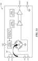
- FIG. 3is an example functional block diagram of the sensor of FIG. 1 ;
- FIG. 3 Ais an example functional block diagram of the sensor of FIG. 1 having differential sensing
- FIG. 4 Ais a partially transparent perspective view of a portion of the sensor of FIG. 1 ;
- FIG. 4 Bis a partially transparent top view of a portion of the sensor of FIG. 1 ;
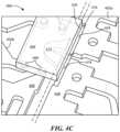
- FIG. 4 Cis a partially transparent perspective view of a portion of the sensor of FIG. 1 ;
- FIG. 5 Ais a partially transparent perspective view of a portion of sensor having enhanced isolation in a chip-on-lead configuration
- FIG. 5 Bis a partially transparent top view of a portion of the sensor of FIG. 5 A ;
- FIG. 6 Ais a partially transparent perspective view of a portion of sensor having enhanced isolation in a die up on current loop configuration
- FIG. 6 Bis a partially transparent top view of a portion of the sensor of FIG. 6 A ;
- FIG. 7 Ais a schematic representation of a current sensing having enhanced isolation with a SOI substrate in a flip chip configuration
- FIG. 7 Bis a schematic representation of a current sensing having enhanced isolation with a SOI substrate in a flip chip configuration with a connection to a high voltage portion of a leadframe;
- FIG. 8 Ais a schematic representation of a current sensing having enhanced isolation with a SOI substrate in a die up configuration
- FIG. 8 Bis a schematic representation of another current sensing having enhanced isolation with a SOI substrate in a die up configuration.
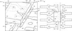
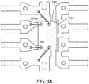
- FIG. 1shows an example current sensor 100 having a leadframe 102 that is etched to enhance voltage isolation levels.
- the leadframe 102is etched to increase electrical isolation between a die 104 and the leadframe 102 b by increasing a separation distance, which can also be referred to as the creepage distance.
- a separation distancewhich can also be referred to as the creepage distance.
- increasing distance between different materials, particularly conductive materialsincreases the electrical isolation.
- materialshave dielectric properties, in addition to separation distance, that can determine the isolation voltage level and creepage distance.
- mold compoundsmay be selected to have a high dielectric constant for achieving desired higher electrical isolation.
- the current sensor 100is shown partially transparent and without encapsulant to facilitate an understanding of the disclosure. It is understood that the current sensor 100 can be provided as an integrated circuit (IC) package having leads.
- the current sensor 100 of FIG. 1has a flip chip configuration with a bumped die and solder bumps, for example, providing electrical connections between the die and the lead fingers.
- the current sensor 100has the die 104 supported by the leadframe 102 , which has a first portion 102 a and a second portion 102 b .
- the first and second portions 102 a,bare formed from separate portions of conductive material, such as copper.
- the first portion 102 ais connected to first, second, third, and fourth lead fingers 106 e - h and the second portion 102 b is connected to fifth, sixth, seventh, and eighth lead fingers 106 a - d .
- the lead fingerscan provide external IO for the sensor IC package.
- the die 104can include an analog and/or digital signal processing circuit 110 to process signals from a magnetic field sensing element 108 for sensing magnetic fields generated by current through leadfingers. It is understood that in the illustrated embodiment that circuitry for the digital signal processing circuit 110 and magnetic field sensing element 108 is located on leadframe-side of the die.
- the first and second lead fingers 106 a,bare a single node providing a current input (or output) and the third and fourth lead fingers 106 c,d are a single node providing a current output (or input). This path can be considered a current conductor to which the current to be measured by the current sensor can be connected using external IO of the sensor IC package.
- the current conductorincludes an arcuate portion 111 for focusing current flow to enhance magnetic field detection by the magnetic field sensing element 108 .
- Any practical number and type of magnetic field sensing elementscan be used to meet the needs of a particular application. Etching of the leadframe 102 proximate the die 104 is discussed in detail below.
- the processing circuit 110may include a calibration circuit for calibrating a sensitivity of the sensor.
- the magnetic field sensing element 108may experience a change in sensitivity, for example and without limitations, due to temperature changes in an environment around and/or within current sensor 100 .
- the change in sensitivitycan impact the performance of magnetic field sensing element 108 and thus impact the accuracy of output signal of the current sensor 100 .
- the calibration circuitcan be configured to detect a change in sensitivity of magnetic field sensing element 108 by comparing an expected output of current sensor 100 to a measured output of current sensor.
- the calibration circuitcan generate a compensation signal to modify and/or tune the output signal to account for the change in sensitivity.
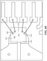
- FIG. 2shows an example IC package 200 implementation and pinout diagram.
- Current input (output) pins 1 , 2can be provided by lead fingers 106 a,b of FIG. 1 and output (input) pins 3 , 4 can be provided by leadfingers 106 c,d .
- An output signal VIOUT on pin 7outputs an analog signal that changes proportionally with the bidirectional AC or DC primary sensed current IP within a specified measurement range.
- the FILTER pincan be used to decrease the bandwidth in order to optimize noise performance.
- FIG. 3shows an example current sensor implementation 300 for AC or DC current sensing for applications such as, motor control, load detection and management, switched-mode power supplies, overcurrent fault protection, and the like.
- Applied current flowing through the current conductorgenerates a magnetic field which is sensed by the magnetic field sensing element and converted into a proportional voltage.
- the currentis sensed differentially in order to reject common-mode fields so as to improve accuracy in magnetically noisy environments.
- the inherent device accuracyis optimized through the close proximity of the magnetic field to the Hall transducer.
- a precise, proportional voltageis provided by the low-offset, chopper-stabilized BiCMOS Hall IC, which is programmed for accuracy after packaging.
- the output of the devicehas a positive slope when an increasing current flows through the primary copper conduction path (from pins 1 and 2 , to pins 3 and 4 FIG. 2 )), which is the path used for current sensing.
- the internal resistance of this conductive pathis in the order of 1.2 m ⁇ , for example, providing low power loss.
- the terminals of the conductive pathare electrically, isolated from the sensor leads (pins 5 through 8 ) which allows the current sensor IC to be used in high-side current sense applications without the use of high-side differential amplifiers.
- a current sensor 300includes a magnetic field sensing circuit 350 .
- Magnetic field sensing element 352such as one or more Hall elements, is configured to sense the current.
- magnetic field sensing element 352may be positioned such that is can sense the current as it generates a magnetic field signal 352 a .
- Currentcan flow into the sensor 300 via current input/output pins 340 a,b and 340 c,d , which may be similar to pins 1 , 2 , 3 , 4 on sensor IC 200 of FIG. 2 .
- Magnetic sensing element 352may include a Hall effect element and/or a magnetoresistance element.
- the magnetoresistance elementmay include at least one of at least one of Indium Antimonide (InSb), a giant magnetoresistance (GMR) element, an anisotropic magnetoresistance (AMR) element, a tunneling magnetoresistance (TMR) element or a magnetic tunnel junction (MTJ) element.
- InSbIndium Antimonide
- GMRgiant magnetoresistance
- AMRanisotropic magnetoresistance
- TMRtunneling magnetoresistance
- MTJmagnetic tunnel junction
- a magnetic field signal 352 a provided by the magnetic sensing element 352is coupled to a first input of a first amplifier 356 .
- a second input of first amplifier 356may be coupled to an output of a sensitivity control circuit 354 configured to generate a compensation for a change in sensitivity experienced by magnetic field sensing element 352 .
- sensitivity signal 354 amay include a compensation for the change in sensitivity of magnetic field sensing element 352 .
- First amplifier 356can change a gain of the magnetic field signal 352 a depending upon a value of the sensitivity signal 356 a.
- An output of first amplifier 356is coupled to an input of a filter 358 .
- Filter 358reduces the bandwidth of the current to be sensed and may include low-pass filtering. If the current being sensed is AC, filter 358 may include a band-pass filter. Filter 358 can be configured to receive the signal 356 a and generate a filtered signal 358 a .
- An output of filter 358is coupled to second amplifier 360 .
- An output of an offset control circuit 362can be coupled to the second amplifier 360 to provide an offset control signal 362 a .
- the offset control signal 362 amay include an offset value to reduce an offset (e.g., DC offset) of the filtered signal 358 a.
- Second amplifier 360can be configured to receive the filtered signal 358 a and apply offset control signal 362 a to the filtered signal 358 a to generate a second control signal 360 a .
- an output of second amplifier 360can be coupled to a VI out node of magnetic field sensing circuit 350 .
- second control signal 360 amay be the output of magnetic field sensing circuit 350 .
- Magnetic field sensing circuit 350may include digital control circuits 370 .
- Digital control circuits 370include a memory circuit 372 and a processor circuit 374 .
- Memory circuit 372may include volatile and non-volatile memory.
- the non-volatile memorymay store computer instructions, an operating system and/or data.
- Non-volatile memorymay include one or more look-up tables for storing and organizing captured data, as well as any tables or matrices generated using the captured data.
- the computer instructionscan be executed by the processor circuit 374 out of volatile memory.
- sensitivity control circuit 354 and offset control circuit 362can be components of digital control circuits 370 .
- magnetic field sensing circuit 350includes a temperature sensor 376 .
- Temperature sensor 376can be configured to detect a temperature in an environment around and/or within current sensor 300 and/or magnetic field sensing circuit 350 .
- temperature sensor 376can detect a change in a temperature in the environment around and/or within current sensor 300 and/or magnetic field sensing circuit 350 .
- a change in a sensitivity of magnetic field sensing element 352may be caused by from temperature changes.
- temperature sensor 376can provide temperature information to digital control circuits 370 .
- An output of temperature sensor 350is coupled to an input of digital control circuits 370 to provide a temperature signal 376 a to digital control circuits 370 .
- the temperature information from temperature signal 376 amay be used to generate the sensitivity signal 354 a .
- digital control circuits 370may use temperature signal 376 a to instruct sensitivity control circuit 354 on an amount to compensate the magnetic field signal 352 a generated by magnetic field sensing element 352 .
- Magnetic field sensing circuit 350may include a first and second reference voltage node 380 , 366 and an output node 364 .
- the first reference voltage node 380(e.g., VCC) may be coupled to a voltage source.
- the voltage sourcemay provide a voltage to magnetic field sensing circuit 350 and thus each of the components of magnetic field sensing circuit 350 .
- the second reference voltage 366may be coupled to ground.
- the output node 364may correspond to an output of magnetic field sensing circuit 350 .
- FIG. 3 Ashows an example sensor 390 having similarity with the sensor 300 of FIG. 3 with a magnetic field sensing element 392 comprising a series of magnetoresistive sensing elements configured in a bridge positioned in relation to a current conductor 394 .
- the bridge configuration of the magnetic field sensing elementprovides differential sensing.
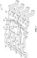
- FIGS. 4 A-Cshow further detail of sensor 400 having a leadframe 402 with etching to enhance electrical isolation and creepage characteristics.
- a bottom die edgeextends into an isolation region so as to increase a distance from die-edge to the leadframe, as compared to not having an isolation region. By increasing this distance, the isolation voltage is increased, as described more fully below.
- the voltage potential of the current carrying section of the lead-frame 402 amay be volts to kvolts or higher relative to the signal side of the lead-frame 402 b .
- Increasing the isolation of the leadframe and dieis desirable to increase the voltage level of the signal to be sensed.
- Suitable epoxy mold compoundsare available from rom SUMITOMO and include part numbers E670 and G700. These compounds have dielectric strengths of ⁇ 15 to 20 kV/mm.
- a die 404is supported by the leadframe 402 with various connections 406 , e.g., solder, to various leadfingers 407 that can provide 10 connections, such an IC package output signal with a voltage proportional to the sensed current level, as described above.
- various connections 406e.g., solder
- leadfingers 407can provide 10 connections, such an IC package output signal with a voltage proportional to the sensed current level, as described above.
- the leadframe 402has a top surface 408 that may form a plane on which a portion of the die 404 is supported. As described above, the leadframe 402 may comprise electrically isolated first and second leadframe portions 402 a,b .
- the first leadframe portion 402 aincludes a U-shaped, for example, current conductor portion 412 above which a magnetic field sensing element in the die 404 can be located to sense a magnetic field generated by current flow.
- the first leadframe portion 402 aincludes an isolation region 414 having a bottom surface 416 below the top surface 408 .
- the isolation region 414can include a first side 418 under the die 404 and a second side 420 on the leadfinger side of the first leadframe portion 402 a .
- a length of the isolation region 414is longer than a length of the die 404 .
- a width of the isolation region 414 formed in the leadframeis twice a depth of the isolation region. It is understood that isolation is provided by distance from the lead-frame to the edge of the die.
- the isolation region 414 depthcreates a distance X from the bottom of the etch to the die edge. If the width is 2 ⁇ this depth, then the distance from the edge of the etch to the die edge is X.
- the diehas an isolation layer on top of the die that protects everything but die edges from the primary loop.
- the isolation regionincreases the distance from the primary to the die edge.
- the isolation region 414can comprise any practical geometry that serves to increase the creepage distance and isolation voltage of the die edge and leadframe.
- the isolation region 414can comprise a rounded channel, V-shape, U-shape, bulbous channel, and the like to meet the needs of a particular application.
- an edge 430 of a bottom of the die 404extends into the isolation region 416 .
- the isolation region 416increase a distance from die-edge 430 to the leadframe 402 as compared to not having an isolation region. By increasing this distance, the isolation voltage is increased. For example, the isolation voltage may increase from about 3.5 kV with no isolation region 416 to about 4.3 kV with the isolation region.
- a certain level, e.g., kVs, through mold compoundis needed, which results in needing a certain distance (um) of distance through the mold compound.
- Bumps on the diemay be around 20 to 50 um high, so that another 80 to 150 um of distance is needed for a desired level of isolation. If we were to draw an arc from the edge of the die with a 180 um long string, that would provide the needed etch.
- etchingis used to create square edges/shapes. If a 20 um bump height is assumed, then a 160 um deep etch is needed, and it should be 360 um wide everywhere it intersects the die edge. In embodiments, ⁇ 200 um deep etching is performed because most etches are done as “half” etches, and this is a 400 um thick lead-frame in an example embodiment.
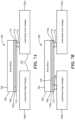
- FIGS. 5 A and 5 Bshow a top and perspective view respectively of a high isolation current sensor 500 having a chip-on-lead configuration where a leadframe 502 supports a die 504 that is ‘up’ so that die IO (and circuitry) are opposite the leadframe. Wirebonds 505 can be used to make connections from the die 504 to the leadfingers.
- the leadframe 502can be manipulated, e.g., etched, to create an isolation region 516 that increases a distance from an edge 530 of the die 504 and the leadframe 502 as compared to not having isolation region 516 .
- the die 504is coated with an insulative material 540 on at least the leadframe-side of the die.
- the insulative materialhas a relatively high dielectric characteristic to enhance isolation of the die 504 and leadframe 502 .
- FIGS. 6 A and 6 Bshow a current sensor 600 having a die up on current loop configuration.
- a leadframe 602 a,bhas an etched current loop 603 that supports a die 604 .
- the leadframe 602can include leadfingers 602 a and the current loop 602 b portion.
- An insulative layer 640insulates the die 604 from the current loop 603 .
- the die 604overlaps with the second portion 602 b of the leadframe, which includes the current loop 603 , but not the first portion 602 a of the leadframe.
- the current loop 603is etched to create an isolation region 616 that surrounds an inner region 660 of the current loop that abuts the die 604 and insulative layer 640 .
- edges 630 a,b,c,d of the dieare increased in distance from the conductive current loop 603 material as compared to not having an isolation region.
- an etchcan increase the distance from the metal to the die edge.
- current sensorscan include a silicon on insulator (SOI) configuration to enhance isolation between the die and the leadframe.
- SOIsilicon on insulator
- One or more oxide layers and/or other materialscan seal active circuitry and increase the isolation voltage level.
- FIG. 7shows an example current sensor 700 having a flip chip configuration with a leadframe 702 bumped to a die 704 .
- the current sensor 700may have some similarity with the current sensor 400 of FIGS. 4 A-C with or without an isolation region.
- the die 704is connected to a first portion 702 a of the leadframe, which is at a lower voltage than a second portion 702 b of the leadframe.
- the die 704comprises a bulk silicon layer 706 , an oxide layer 708 , which can comprise SiO2, an active layer 710 , and an adhesive layer 712 , which can comprise benzocyclobutene (BCB) or polyimide, for example.
- the insulative SiO2 layer 708 and the BCB/PI layer 712which may be used in a solder bumping process, seals around the active circuitry 710 where the die 704 overlaps the high voltage second portion 702 b of the lead-frame, which provides the current conductor loop.
- One or more solder ball 714 and via 716provide an electrical connection from the active layer 710 to the second portion 702 b of the leadframe.
- a first trench 720 ais be formed at an edge of the active layer 710 and filled with SiO2 or other insulative material.
- the SiO2-filled trench 720 awhich may be in the order of 0.4 mm, and BCB layer 712 may combine to reinforce electrical isolation of the die and leadframe 702 . In example embodiments, over 5 kV of isolation can be achieved.
- FIG. 7 Bshows an example current sensor 700 ′ having a flip chip configuration with commonality to the current sensor 700 of FIG. 7 A with the addition of an electrical connection to the high voltage second leadframe portion 702 b .
- the SOI processingallows for relatively deep trenches to isolate sections of the active layer 710 of the die from each other.
- the SiO2 filled trench 720provides one or more isolation islands.
- one or more solder bumps 724provide a connection(s) to the high voltage second portion 702 b of the leadframe.
- FIG. 7 Ashows an example cantilevered configuration. An isolated bump can keep spacing consistent by preventing the die from sagging.
- FIG. 8 Ashows an example current sensor 800 having a die up configuration having wirebond(s) 801 from a lower voltage first portion 802 a of the leadframe 802 to a die 804 .
- the die 804comprises a bulk silicon layer 806 , an oxide layer 808 , which can comprise SiO2, and an active layer 810 to which the wirebonds 801 are connected.
- the bulk silicon layer 806 of the dieis supported by the high voltage second portion 802 b of the leadframe.
- Insulationis provided by the SOI process and structure, which may be the only insulation in a die up construction.
- SOI current sensor embodimentsmay have higher isolation capability per micron than non-conductive die attach implementations.
- trenches 820 a,bcan provide an insulating moat around edges of the die 804 . This create a longer path through mold compound to the active circuitry 810 .
- isolation levels of at least 5 kVcan be achieved.
- the wire-bonds 801should go up (vertically) from the die 804 before going down to the low voltage leadframe 802 a so that the distance through mold compound from the high voltage lead-frame to the wire-bond is sufficient to meet a desired isolation voltage level, e.g., 5 kV.
- FIG. 8 Bshows an example current sensor 800 ′ having a die up configuration similar to that shown in FIG. 8 A with the addition of a non-conductive layer 825 comprising tape and/or non-conductive die-attach between the die 804 and leadframe 802 to add insulation.
- the non-conductive layer 825 in the form of die-attach materialonly covers the leadframe 802 in the area in which the die is located.
- the non-conductive layer 825 in the form of tapeis larger than the die 804 . If the non-conductive layer 825 is sufficient to achieve isolation greater than a given threshold, such as 5 kV, then one effectively has two layers of isolation and can obtain reinforced isolation as long as the distance through mold compound and/or cemented joints is greater than about 0.4 mm, for example.
- a given thresholdsuch as 5 kV
- FIGS. 7 A to 8 Bmay or may not have an isolation area, such as the isolation areas shown in FIGS. 1 and 4 A- 6 B .
- magnetic field sensing elementis used to describe a variety of electronic elements that can sense a magnetic field.
- the magnetic field sensing elementcan be, but is not limited to, a Hall effect element, a magnetoresistance element, or a magnetotransistor.
- Hall effect elementsfor example, a planar Hall element, a vertical Hall element, and a Circular Vertical Hall (CVH) element.
- magnetoresistance elementsfor example, a semiconductor magnetoresistance element such as Indium Antimonide (InSb), a giant magnetoresistance (GMR) element, for example, a spin valve, an anisotropic magnetoresistance element (AMR), a tunneling magnetoresistance (TMR) element, and a magnetic tunnel junction (MTJ).
- the magnetic field sensing elementmay be a single element or, alternatively, may include two or more magnetic field sensing elements arranged in various configurations, e.g., a half bridge or full (Wheatstone) bridge.
- the magnetic field sensing elementmay be a device made of a type IV semiconductor material such as Silicon (Si) or Germanium (Ge), or a type III-V semiconductor material like Gallium-Arsenide (GaAs) or an Indium compound, e.g., Indium-Antimonide (InSb).
- a type IV semiconductor materialsuch as Silicon (Si) or Germanium (Ge)
- a type III-V semiconductor materiallike Gallium-Arsenide (GaAs) or an Indium compound, e.g., Indium-Antimonide (InSb).
- Some of the above-described magnetic field sensing elementstend to have an axis of maximum sensitivity parallel to a substrate that supports the magnetic field sensing element, and others of the above-described magnetic field sensing elements tend to have an axis of maximum sensitivity perpendicular to a substrate that supports the magnetic field sensing element.
- planar Hall elementstend to have axes of sensitivity perpendicular to a substrate
- metal based or metallic magnetoresistance elementse.g., GMR, TMR, AMR
- vertical Hall elementstend to have axes of sensitivity parallel to a substrate.
- magnetic field sensoris used to describe a circuit that uses a magnetic field sensing element, generally in combination with other circuits.
- Magnetic field sensorsare used in a variety of applications, including, but not limited to, an angle sensor that senses an angle of a direction of a magnetic field, a current sensor that senses a magnetic field generated by a current carried by a current-carrying conductor, a magnetic switch that senses the proximity of a ferromagnetic object, a rotation detector that senses passing ferromagnetic articles, for example, magnetic domains of a ring magnet or a ferromagnetic target (e.g., gear teeth) where the magnetic field sensor is used in combination with a back-biased or other magnet, and a magnetic field sensor that senses a magnetic field density of a magnetic field.
- an angle sensorthat senses an angle of a direction of a magnetic field
- a current sensorthat senses a magnetic field generated by a current carried by a current-carrying conductor
- a magnetic switchthat
- the term “accuracy,” when referring to a magnetic field sensor,is used to refer to a variety of aspects of the magnetic field sensor. These aspects include, but are not limited to, an ability of the magnetic field sensor to differentiate: a gear tooth from a gear valley (or, more generally, the presence of a ferromagnetic object from the absence of a ferromagnetic object) when the gear is not rotating and/or when the gear is rotating (or, more generally, when a ferromagnetic object is moving or not moving), an ability to differentiate an edge of a tooth of the gear from the tooth or the valley of the gear (or, more generally, the edge of a ferromagnetic object or a change in magnetization direction of a hard ferromagnetic object), and a rotational accuracy with which the edge of the gear tooth is identified (or, more generally, the positional accuracy with which an edge of a ferromagnetic object or hard ferromagnetic object can be identified).
- accuracyrefers to output signal edge placement accuracy and consistency
- parallel and perpendicularare used in various contexts herein. It should be understood that the terms parallel and perpendicular do not require exact perpendicularity or exact parallelism, but instead it is intended that normal manufacturing tolerances apply, which tolerances depend upon the context in which the terms are used. In some instances, the term “substantially” is used to modify the terms “parallel” or “perpendicular.” In general, use of the term “substantially” reflects angles that are beyond manufacturing tolerances, for example, within +/ ⁇ ten degrees.
- magnetic field sensorsit is desirable for magnetic field sensors to achieve a certain level or amount of accuracy even in the presence of variations in an air gap between the magnetic field sensor and the gear that may change from installation to installation or from time to time. It is also desirable for magnetic field sensors to achieve accuracy even in the presence of variations in relative positions of the magnet and the magnetic field sensing element within the magnetic field sensor. It is also desirable for magnetic field sensors to achieve accuracy even in the presence of unit-to-unit variations in the magnetic field generated by a magnet within the magnetic field sensors. It is also desirable for magnetic field sensors to achieve accuracy even in the presence of variations of an axial rotation of the magnetic field sensors relative to the gear. It is also desirable for magnetic field sensors to achieve accuracy even in the presence of temperature variations of the magnetic field sensors.
Landscapes
- Physics & Mathematics (AREA)
- General Physics & Mathematics (AREA)
- Engineering & Computer Science (AREA)
- Condensed Matter Physics & Semiconductors (AREA)
- Microelectronics & Electronic Packaging (AREA)
- Computer Hardware Design (AREA)
- Power Engineering (AREA)
- Hall/Mr Elements (AREA)
Abstract
Description
Claims (35)
Priority Applications (4)
| Application Number | Priority Date | Filing Date | Title |
|---|---|---|---|
| US16/887,045US11800813B2 (en) | 2020-05-29 | 2020-05-29 | High isolation current sensor |
| CN202180014841.6ACN115136012A (en) | 2020-05-29 | 2021-02-18 | High-isolation current sensor |
| PCT/US2021/018442WO2021242336A1 (en) | 2020-05-29 | 2021-02-18 | High isolation current sensor |
| EP21711129.3AEP4078199A1 (en) | 2020-05-29 | 2021-02-18 | High isolation current sensor |
Applications Claiming Priority (1)
| Application Number | Priority Date | Filing Date | Title |
|---|---|---|---|
| US16/887,045US11800813B2 (en) | 2020-05-29 | 2020-05-29 | High isolation current sensor |
Publications (2)
| Publication Number | Publication Date |
|---|---|
| US20210376227A1 US20210376227A1 (en) | 2021-12-02 |
| US11800813B2true US11800813B2 (en) | 2023-10-24 |
Family
ID=74867669
Family Applications (1)
| Application Number | Title | Priority Date | Filing Date |
|---|---|---|---|
| US16/887,045Active2041-06-17US11800813B2 (en) | 2020-05-29 | 2020-05-29 | High isolation current sensor |
Country Status (4)
| Country | Link |
|---|---|
| US (1) | US11800813B2 (en) |
| EP (1) | EP4078199A1 (en) |
| CN (1) | CN115136012A (en) |
| WO (1) | WO2021242336A1 (en) |
Families Citing this family (6)
| Publication number | Priority date | Publication date | Assignee | Title |
|---|---|---|---|---|
| US11289406B2 (en) | 2019-09-18 | 2022-03-29 | Allegro Microsystems, Llc | Signal isolator having enhanced creepage characteristics |
| US11366141B1 (en)* | 2021-01-28 | 2022-06-21 | Allegro Microsystems, Llc | Multipath wide bandwidth current sensor |
| US11644485B2 (en) | 2021-10-07 | 2023-05-09 | Allegro Microsystems, Llc | Current sensor integrated circuits |
| WO2024184224A1 (en)* | 2023-03-09 | 2024-09-12 | Lem International Sa | Magnetic field gradient transducer and current transducer therewith |
| CN116314059B (en)* | 2023-04-27 | 2023-08-15 | 宁波中车时代传感技术有限公司 | Packaged chip and current sensor |
| CN118688488B (en)* | 2024-08-23 | 2024-11-08 | 宁波中车时代传感技术有限公司 | Method for manufacturing a current sensor chip |
Citations (89)
| Publication number | Priority date | Publication date | Assignee | Title |
|---|---|---|---|---|
| US4425596A (en) | 1980-09-26 | 1984-01-10 | Tokyo Shibaura Denki Kabushiki Kaisha | Electric circuit breaker |
| JPS6171649A (en) | 1984-09-17 | 1986-04-12 | Seiko Instr & Electronics Ltd | Ic package |
| JPS63191069A (en) | 1986-12-12 | 1988-08-08 | Mitsubishi Electric Corp | current detector |
| US4893073A (en) | 1989-01-30 | 1990-01-09 | General Motors Corporation | Electric circuit board current sensor |
| US5041780A (en) | 1988-09-13 | 1991-08-20 | California Institute Of Technology | Integrable current sensors |
| US5124642A (en) | 1989-12-21 | 1992-06-23 | Sigma Instruments, Inc. | Power line post insulator with dual inductor current sensor |
| JPH04364472A (en) | 1991-06-12 | 1992-12-16 | Fuji Electric Co Ltd | Magnetoelectric conversion device |
| DE4141386A1 (en) | 1991-12-16 | 1993-06-17 | Itt Ind Gmbh Deutsche | Hall sensor integrated on semiconductor chip mfd. using semiconductor processing - has current conductor for producing magnetic field and magnetic field regional cover of ferromagnetic material and substrate with two different conducting types |
| US5247202A (en) | 1991-10-09 | 1993-09-21 | Landis & Gyr Betriebs Ag | Plurality of arrangements each including an ic magnetic field sensor and two ferromagnetic field concentrators, and a procedure for incorporating each arrangement into a package |
| US5442228A (en) | 1992-04-06 | 1995-08-15 | Motorola, Inc. | Monolithic shielded integrated circuit |
| US5561366A (en) | 1991-10-22 | 1996-10-01 | Hitachi, Ltd. | Current sensor system and detection method comprising magetoresistance element, biasing conductor and current measurement conductor on insulating substrate |
| US5615075A (en) | 1995-05-30 | 1997-03-25 | General Electric Company | AC/DC current sensor for a circuit breaker |
| EP0867725A1 (en) | 1997-03-24 | 1998-09-30 | Nana Electronics Co., Ltd. | Current sensor |
| WO1999014605A1 (en) | 1997-09-15 | 1999-03-25 | Institute Of Quantum Electronics | A current monitor system and a method for manufacturing it |
| US6005383A (en) | 1995-03-24 | 1999-12-21 | Liasons Electroniques-Mecaniques Lem S.A. | Electrical current sensor with magnetic field detector |
| JP2000174357A (en) | 1998-10-02 | 2000-06-23 | Sanken Electric Co Ltd | Semiconductor device having a ball effect element |
| US6150714A (en) | 1997-09-19 | 2000-11-21 | Texas Instruments Incorporated | Current sense element incorporated into integrated circuit package lead frame |
| EP1107328A2 (en) | 1999-12-09 | 2001-06-13 | Sanken Electric Co., Ltd. | Current detector having a hall-effect device |
| EP1107327A2 (en) | 1999-12-09 | 2001-06-13 | Sanken Electric Co., Ltd. | Semiconductor current detector of improved noise immunity |
| US6252389B1 (en) | 1998-03-18 | 2001-06-26 | Mitsubishi Denki Kabushiki Kaisha | Current detector having magnetic core for concentrating a magnetic flux near a hall-effect sensor, and power switch apparatus incorporating same |
| EP1111693A2 (en) | 1999-12-20 | 2001-06-27 | Sanken Electric Co., Ltd. | Large current detector having a Hall-effect device |
| JP2001221815A (en) | 2000-02-04 | 2001-08-17 | Sanken Electric Co Ltd | Current detector provided with hall element |
| US20010028115A1 (en) | 2000-03-31 | 2001-10-11 | Eiji Yanagawa | semiconductor device and method of manufacturing the same |
| US6316931B1 (en) | 1998-12-15 | 2001-11-13 | Tdk Corporation | Magnetic sensor apparatus and current sensor apparatus |
| US6323634B1 (en) | 1998-10-14 | 2001-11-27 | Tdk Corporation | Magnetic sensor apparatus, current sensor apparatus and magnetic sensor element |
| JP2001339109A (en) | 2000-05-26 | 2001-12-07 | Sanken Electric Co Ltd | Current sensing device equipped with hall element |
| JP2002026419A (en) | 2000-07-07 | 2002-01-25 | Sanken Electric Co Ltd | Magnetism-electricity conversion device |
| JP2002040058A (en) | 2000-05-17 | 2002-02-06 | Sanken Electric Co Ltd | Current detection device equipped with hall element |
| US6411078B1 (en) | 1999-01-21 | 2002-06-25 | Tdk Corporation | Current sensor apparatus |
| JP2002202326A (en) | 2000-10-23 | 2002-07-19 | Sanken Electric Co Ltd | Current detector equipped with hall element |
| JP2002202327A (en) | 2000-10-23 | 2002-07-19 | Sanken Electric Co Ltd | Current detector equipped with hall element |
| US6424018B1 (en) | 1998-10-02 | 2002-07-23 | Sanken Electric Co., Ltd. | Semiconductor device having a hall-effect element |
| US6445171B2 (en) | 1999-10-29 | 2002-09-03 | Honeywell Inc. | Closed-loop magnetoresistive current sensor system having active offset nulling |
| US20020179987A1 (en) | 2000-02-21 | 2002-12-05 | Marcus Meyer | Electronic control circuit |
| EP1281974A2 (en) | 2001-07-06 | 2003-02-05 | Sanken Electric Co., Ltd. | Hall-effect current detector |
| US6545456B1 (en) | 1998-08-12 | 2003-04-08 | Rockwell Automation Technologies, Inc. | Hall effect current sensor package for sensing electrical current in an electrical conductor |
| US6642705B2 (en) | 2000-10-19 | 2003-11-04 | Canon Denshi Kabushiki Kaisha | Electric current sensor |
| US6667682B2 (en) | 2001-12-26 | 2003-12-23 | Honeywell International Inc. | System and method for using magneto-resistive sensors as dual purpose sensors |
| US6759841B2 (en) | 2001-06-15 | 2004-07-06 | Sanken Electric Co., Ltd. | Hall-effect current detector |
| US20040155644A1 (en) | 2003-02-11 | 2004-08-12 | Jason Stauth | Integrated sensor |
| US6781359B2 (en) | 2002-09-20 | 2004-08-24 | Allegro Microsystems, Inc. | Integrated current sensor |
| US6841989B2 (en) | 2001-06-15 | 2005-01-11 | Sanken Electric Co, Ltd. | Hall-effect current detector |
| US20050024908A1 (en) | 2003-07-31 | 2005-02-03 | Gizara Andrew Roman | System and method for integrating a digital core with a switch mode power supply |
| US6853178B2 (en) | 2000-06-19 | 2005-02-08 | Texas Instruments Incorporated | Integrated circuit leadframes patterned for measuring the accurate amplitude of changing currents |
| US20050045359A1 (en) | 2003-08-26 | 2005-03-03 | Michael Doogue | Current sensor |
| US6867573B1 (en) | 2003-11-07 | 2005-03-15 | National Semiconductor Corporation | Temperature calibrated over-current protection circuit for linear voltage regulators |
| US6921955B2 (en) | 2002-12-25 | 2005-07-26 | Sanken Electric Co., Ltd. | Noise-proof semiconductor device having a Hall effect element |
| US20050224248A1 (en) | 2003-08-26 | 2005-10-13 | Allegro Microsystems, Inc. | Current sensor |
| US20050230843A1 (en) | 2000-02-24 | 2005-10-20 | Williams Vernon M | Flip-chip type semiconductor devices and conductive elements thereof |
| US20060002147A1 (en) | 2004-06-23 | 2006-01-05 | Lg.Philips Lcd Co. Ltd. | Backlight unit and liquid crystal display device using the same |
| US6989665B2 (en) | 2002-10-28 | 2006-01-24 | Sanken Electric Co., Ltd. | Electric current detector with hall effect sensor |
| US6995315B2 (en) | 2003-08-26 | 2006-02-07 | Allegro Microsystems, Inc. | Current sensor |
| US7006749B2 (en) | 2002-08-07 | 2006-02-28 | Dornier Medtech Laser Gmbh | Laser system with fiber-bound communication |
| US20060071655A1 (en) | 2004-10-01 | 2006-04-06 | Tdk Corporation | Current sensor |
| US20060091993A1 (en) | 2004-10-28 | 2006-05-04 | Tdk Corporation | Current sensor |
| US20060114098A1 (en) | 2004-11-30 | 2006-06-01 | Tdk Corporation | Current sensor |
| US20060145690A1 (en) | 2004-12-06 | 2006-07-06 | Tdk Corporation | Current sensor |
| US7075287B1 (en) | 2003-08-26 | 2006-07-11 | Allegro Microsystems, Inc. | Current sensor |
| US20060170529A1 (en) | 2005-01-31 | 2006-08-03 | Tdk Corporation | Current sensor |
| US20060181263A1 (en) | 2003-08-26 | 2006-08-17 | Allegro Microsystems, Inc. | Current sensor |
| US20060219436A1 (en) | 2003-08-26 | 2006-10-05 | Taylor William P | Current sensor |
| US20060255797A1 (en) | 2005-05-16 | 2006-11-16 | Allegro Microsystems, Inc. | Integrated magnetic flux concentrator |
| US20060291106A1 (en) | 2005-06-27 | 2006-12-28 | Tdk Corporation | Magnetic sensor and current sensor |
| US20070044370A1 (en) | 2005-08-31 | 2007-03-01 | Tdk Corporation | Coil, coil module and method of manufacturing the same, current sensor and method of manufacturing the same |
| US20070076322A1 (en) | 2005-10-04 | 2007-04-05 | Samsung Electronics Co., Ltd | Slider, head gimbal assembly and hard disc drive |
| US20070090825A1 (en) | 2005-09-30 | 2007-04-26 | Tdk Corporation | Current sensor |
| US20070096716A1 (en) | 2005-10-14 | 2007-05-03 | Tdk Corporation | Current sensor |
| US7248045B2 (en) | 2004-02-20 | 2007-07-24 | Tdk Corporation | Magnetic sensing device, method of forming the same, magnetic sensor, and ammeter |
| US20070188946A1 (en) | 2006-02-15 | 2007-08-16 | Tdk Corporation | Magnetic sensor and current sensor |
| US20070279053A1 (en) | 2006-05-12 | 2007-12-06 | Taylor William P | Integrated current sensor |
| US7348724B2 (en) | 2003-12-02 | 2008-03-25 | Lg Electronics, Llp | Organic electroluminescence device with short-prevention layer |
| US20090096072A1 (en) | 2007-10-15 | 2009-04-16 | Power Integrations, Inc. | Package for a power semiconductor device |
| US20110204887A1 (en) | 2010-02-24 | 2011-08-25 | Infineon Technologies Ag | Current sensors and methods |
| US8629539B2 (en) | 2012-01-16 | 2014-01-14 | Allegro Microsystems, Llc | Methods and apparatus for magnetic sensor having non-conductive die paddle |
| US20140151697A1 (en) | 2012-11-30 | 2014-06-05 | Infineon Technologies Ag | Semiconductor Packages, Systems, and Methods of Formation Thereof |
| US20140175528A1 (en) | 2012-12-20 | 2014-06-26 | Nxp B.V. | Semiconductor magnetic field sensors |
| US20140253115A1 (en) | 2010-04-08 | 2014-09-11 | Infineon Technologies Ag | Magnetic field current sensors |
| US8907437B2 (en) | 2011-07-22 | 2014-12-09 | Allegro Microsystems, Llc | Reinforced isolation for current sensor with magnetic field transducer |
| US9190606B2 (en) | 2013-03-15 | 2015-11-17 | Allegro Micosystems, LLC | Packaging for an electronic device |
| US9362209B1 (en) | 2012-01-23 | 2016-06-07 | Amkor Technology, Inc. | Shielding technique for semiconductor package including metal lid |
| US20160282388A1 (en) | 2013-03-15 | 2016-09-29 | Allegro Microsystems, Llc | Current sensor isolation |
| US9735773B2 (en) | 2014-04-29 | 2017-08-15 | Allegro Microsystems, Llc | Systems and methods for sensing current through a low-side field effect transistor |
| US9958482B1 (en) | 2016-12-20 | 2018-05-01 | Allegro Microsystems, Llc | Systems and methods for a high isolation current sensor |
| US10114044B2 (en) | 2016-08-08 | 2018-10-30 | Allegro Microsystems, Llc | Current sensor |
| US10247758B2 (en) | 2016-08-08 | 2019-04-02 | Allegro Microsystems, Llc | Current sensor |
| EP3644069A1 (en) | 2018-10-24 | 2020-04-29 | Melexis Technologies SA | Insulated current sensor |
| US20200185234A1 (en) | 2018-12-05 | 2020-06-11 | Texas Instruments Incorporated | Mcm package isolation through leadframe design and package saw process |
| US20200289013A1 (en)* | 2019-03-15 | 2020-09-17 | The Charles Stark Draper Laboratory, Inc. | Miniature electric field detector |
| US20200313078A1 (en)* | 2019-03-30 | 2020-10-01 | Texas Instruments Incorporated | Hall sensor with performance control |
Family Cites Families (1)
| Publication number | Priority date | Publication date | Assignee | Title |
|---|---|---|---|---|
| EP3331007A1 (en)* | 2016-12-05 | 2018-06-06 | Melexis Technologies SA | Integrated circuit package comprising lead frame |
- 2020
- 2020-05-29USUS16/887,045patent/US11800813B2/enactiveActive
- 2021
- 2021-02-18CNCN202180014841.6Apatent/CN115136012A/enactivePending
- 2021-02-18EPEP21711129.3Apatent/EP4078199A1/enactivePending
- 2021-02-18WOPCT/US2021/018442patent/WO2021242336A1/ennot_activeCeased
Patent Citations (115)
| Publication number | Priority date | Publication date | Assignee | Title |
|---|---|---|---|---|
| US4425596A (en) | 1980-09-26 | 1984-01-10 | Tokyo Shibaura Denki Kabushiki Kaisha | Electric circuit breaker |
| JPS6171649A (en) | 1984-09-17 | 1986-04-12 | Seiko Instr & Electronics Ltd | Ic package |
| JPS63191069A (en) | 1986-12-12 | 1988-08-08 | Mitsubishi Electric Corp | current detector |
| US5041780A (en) | 1988-09-13 | 1991-08-20 | California Institute Of Technology | Integrable current sensors |
| US4893073A (en) | 1989-01-30 | 1990-01-09 | General Motors Corporation | Electric circuit board current sensor |
| US5124642A (en) | 1989-12-21 | 1992-06-23 | Sigma Instruments, Inc. | Power line post insulator with dual inductor current sensor |
| JPH04364472A (en) | 1991-06-12 | 1992-12-16 | Fuji Electric Co Ltd | Magnetoelectric conversion device |
| US5247202A (en) | 1991-10-09 | 1993-09-21 | Landis & Gyr Betriebs Ag | Plurality of arrangements each including an ic magnetic field sensor and two ferromagnetic field concentrators, and a procedure for incorporating each arrangement into a package |
| US5561366A (en) | 1991-10-22 | 1996-10-01 | Hitachi, Ltd. | Current sensor system and detection method comprising magetoresistance element, biasing conductor and current measurement conductor on insulating substrate |
| DE4141386A1 (en) | 1991-12-16 | 1993-06-17 | Itt Ind Gmbh Deutsche | Hall sensor integrated on semiconductor chip mfd. using semiconductor processing - has current conductor for producing magnetic field and magnetic field regional cover of ferromagnetic material and substrate with two different conducting types |
| US5442228A (en) | 1992-04-06 | 1995-08-15 | Motorola, Inc. | Monolithic shielded integrated circuit |
| US6005383A (en) | 1995-03-24 | 1999-12-21 | Liasons Electroniques-Mecaniques Lem S.A. | Electrical current sensor with magnetic field detector |
| US5615075A (en) | 1995-05-30 | 1997-03-25 | General Electric Company | AC/DC current sensor for a circuit breaker |
| EP0867725A1 (en) | 1997-03-24 | 1998-09-30 | Nana Electronics Co., Ltd. | Current sensor |
| WO1999014605A1 (en) | 1997-09-15 | 1999-03-25 | Institute Of Quantum Electronics | A current monitor system and a method for manufacturing it |
| US6356068B1 (en) | 1997-09-15 | 2002-03-12 | Ams International Ag | Current monitor system and a method for manufacturing it |
| US6150714A (en) | 1997-09-19 | 2000-11-21 | Texas Instruments Incorporated | Current sense element incorporated into integrated circuit package lead frame |
| US6252389B1 (en) | 1998-03-18 | 2001-06-26 | Mitsubishi Denki Kabushiki Kaisha | Current detector having magnetic core for concentrating a magnetic flux near a hall-effect sensor, and power switch apparatus incorporating same |
| US6545456B1 (en) | 1998-08-12 | 2003-04-08 | Rockwell Automation Technologies, Inc. | Hall effect current sensor package for sensing electrical current in an electrical conductor |
| US6424018B1 (en) | 1998-10-02 | 2002-07-23 | Sanken Electric Co., Ltd. | Semiconductor device having a hall-effect element |
| JP2000174357A (en) | 1998-10-02 | 2000-06-23 | Sanken Electric Co Ltd | Semiconductor device having a ball effect element |
| US6323634B1 (en) | 1998-10-14 | 2001-11-27 | Tdk Corporation | Magnetic sensor apparatus, current sensor apparatus and magnetic sensor element |
| US6316931B1 (en) | 1998-12-15 | 2001-11-13 | Tdk Corporation | Magnetic sensor apparatus and current sensor apparatus |
| US6411078B1 (en) | 1999-01-21 | 2002-06-25 | Tdk Corporation | Current sensor apparatus |
| US6566856B2 (en) | 1999-10-29 | 2003-05-20 | Honeywell International Inc. | Closed-loop magnetoresistive current sensor system having active offset nulling |
| US6445171B2 (en) | 1999-10-29 | 2002-09-03 | Honeywell Inc. | Closed-loop magnetoresistive current sensor system having active offset nulling |
| JP2001230467A (en) | 1999-12-09 | 2001-08-24 | Sanken Electric Co Ltd | Current detector provided with hall element |
| US6812687B1 (en) | 1999-12-09 | 2004-11-02 | Sanken Electric Co., Ltd. | Semiconductor current detector of improved noise immunity |
| JP2001165963A (en) | 1999-12-09 | 2001-06-22 | Sanken Electric Co Ltd | Current detecting device |
| US6462531B1 (en) | 1999-12-09 | 2002-10-08 | Sanken Electric Co., Ltd. | Current detector having a hall-effect device |
| EP1107327A2 (en) | 1999-12-09 | 2001-06-13 | Sanken Electric Co., Ltd. | Semiconductor current detector of improved noise immunity |
| EP1107328A2 (en) | 1999-12-09 | 2001-06-13 | Sanken Electric Co., Ltd. | Current detector having a hall-effect device |
| JP2001174486A (en) | 1999-12-20 | 2001-06-29 | Sanken Electric Co Ltd | Current detection device equipped with a ball element |
| EP1111693A2 (en) | 1999-12-20 | 2001-06-27 | Sanken Electric Co., Ltd. | Large current detector having a Hall-effect device |
| US6791313B2 (en) | 1999-12-20 | 2004-09-14 | Sanken Electric Co., Ltd. | Electrical current detector having a U-shaped current path and hall-effect device |
| US6683448B1 (en) | 1999-12-20 | 2004-01-27 | Sanken Electric Co., Ltd. | Large current detector having a hall-effect device |
| JP2001221815A (en) | 2000-02-04 | 2001-08-17 | Sanken Electric Co Ltd | Current detector provided with hall element |
| US20020179987A1 (en) | 2000-02-21 | 2002-12-05 | Marcus Meyer | Electronic control circuit |
| US20050230843A1 (en) | 2000-02-24 | 2005-10-20 | Williams Vernon M | Flip-chip type semiconductor devices and conductive elements thereof |
| US20010028115A1 (en) | 2000-03-31 | 2001-10-11 | Eiji Yanagawa | semiconductor device and method of manufacturing the same |
| JP2002040058A (en) | 2000-05-17 | 2002-02-06 | Sanken Electric Co Ltd | Current detection device equipped with hall element |
| JP2001339109A (en) | 2000-05-26 | 2001-12-07 | Sanken Electric Co Ltd | Current sensing device equipped with hall element |
| US6853178B2 (en) | 2000-06-19 | 2005-02-08 | Texas Instruments Incorporated | Integrated circuit leadframes patterned for measuring the accurate amplitude of changing currents |
| JP2002026419A (en) | 2000-07-07 | 2002-01-25 | Sanken Electric Co Ltd | Magnetism-electricity conversion device |
| EP1180804A2 (en) | 2000-07-07 | 2002-02-20 | Sanken Electric Co., Ltd. | Hall-effect magnetoelectric converter |
| US6642705B2 (en) | 2000-10-19 | 2003-11-04 | Canon Denshi Kabushiki Kaisha | Electric current sensor |
| JP2002202326A (en) | 2000-10-23 | 2002-07-19 | Sanken Electric Co Ltd | Current detector equipped with hall element |
| JP2002202327A (en) | 2000-10-23 | 2002-07-19 | Sanken Electric Co Ltd | Current detector equipped with hall element |
| US6759841B2 (en) | 2001-06-15 | 2004-07-06 | Sanken Electric Co., Ltd. | Hall-effect current detector |
| US6841989B2 (en) | 2001-06-15 | 2005-01-11 | Sanken Electric Co, Ltd. | Hall-effect current detector |
| US6727683B2 (en) | 2001-07-06 | 2004-04-27 | Sanken Electric Co., Ltd. | Hall-effect current detector |
| EP1281974A2 (en) | 2001-07-06 | 2003-02-05 | Sanken Electric Co., Ltd. | Hall-effect current detector |
| US6667682B2 (en) | 2001-12-26 | 2003-12-23 | Honeywell International Inc. | System and method for using magneto-resistive sensors as dual purpose sensors |
| US7006749B2 (en) | 2002-08-07 | 2006-02-28 | Dornier Medtech Laser Gmbh | Laser system with fiber-bound communication |
| US6781359B2 (en) | 2002-09-20 | 2004-08-24 | Allegro Microsystems, Inc. | Integrated current sensor |
| US6989665B2 (en) | 2002-10-28 | 2006-01-24 | Sanken Electric Co., Ltd. | Electric current detector with hall effect sensor |
| US6921955B2 (en) | 2002-12-25 | 2005-07-26 | Sanken Electric Co., Ltd. | Noise-proof semiconductor device having a Hall effect element |
| US7259545B2 (en) | 2003-02-11 | 2007-08-21 | Allegro Microsystems, Inc. | Integrated sensor |
| US20040155644A1 (en) | 2003-02-11 | 2004-08-12 | Jason Stauth | Integrated sensor |
| US20050024908A1 (en) | 2003-07-31 | 2005-02-03 | Gizara Andrew Roman | System and method for integrating a digital core with a switch mode power supply |
| WO2005026749A1 (en) | 2003-08-26 | 2005-03-24 | Allegro Microsystems, Inc. | Current sensor |
| US7166807B2 (en) | 2003-08-26 | 2007-01-23 | Allegro Microsystems, Inc. | Current sensor |
| US20050224248A1 (en) | 2003-08-26 | 2005-10-13 | Allegro Microsystems, Inc. | Current sensor |
| US6995315B2 (en) | 2003-08-26 | 2006-02-07 | Allegro Microsystems, Inc. | Current sensor |
| US20080297138A1 (en) | 2003-08-26 | 2008-12-04 | Taylor William P | Current sensor |
| US7476816B2 (en) | 2003-08-26 | 2009-01-13 | Allegro Microsystems, Inc. | Current sensor |
| US7598601B2 (en) | 2003-08-26 | 2009-10-06 | Allegro Microsystems, Inc. | Current sensor |
| US20050045359A1 (en) | 2003-08-26 | 2005-03-03 | Michael Doogue | Current sensor |
| US7709754B2 (en) | 2003-08-26 | 2010-05-04 | Allegro Microsystems, Inc. | Current sensor |
| US7075287B1 (en) | 2003-08-26 | 2006-07-11 | Allegro Microsystems, Inc. | Current sensor |
| US20060219436A1 (en) | 2003-08-26 | 2006-10-05 | Taylor William P | Current sensor |
| US20060181263A1 (en) | 2003-08-26 | 2006-08-17 | Allegro Microsystems, Inc. | Current sensor |
| US6867573B1 (en) | 2003-11-07 | 2005-03-15 | National Semiconductor Corporation | Temperature calibrated over-current protection circuit for linear voltage regulators |
| US7348724B2 (en) | 2003-12-02 | 2008-03-25 | Lg Electronics, Llp | Organic electroluminescence device with short-prevention layer |
| US7248045B2 (en) | 2004-02-20 | 2007-07-24 | Tdk Corporation | Magnetic sensing device, method of forming the same, magnetic sensor, and ammeter |
| US20060002147A1 (en) | 2004-06-23 | 2006-01-05 | Lg.Philips Lcd Co. Ltd. | Backlight unit and liquid crystal display device using the same |
| US20060071655A1 (en) | 2004-10-01 | 2006-04-06 | Tdk Corporation | Current sensor |
| US20060091993A1 (en) | 2004-10-28 | 2006-05-04 | Tdk Corporation | Current sensor |
| US20060114098A1 (en) | 2004-11-30 | 2006-06-01 | Tdk Corporation | Current sensor |
| US20060145690A1 (en) | 2004-12-06 | 2006-07-06 | Tdk Corporation | Current sensor |
| US20060170529A1 (en) | 2005-01-31 | 2006-08-03 | Tdk Corporation | Current sensor |
| US20060255797A1 (en) | 2005-05-16 | 2006-11-16 | Allegro Microsystems, Inc. | Integrated magnetic flux concentrator |
| WO2006130393A1 (en) | 2005-05-27 | 2006-12-07 | Allegro Microsystems, Inc. | Current sensor |
| US20060291106A1 (en) | 2005-06-27 | 2006-12-28 | Tdk Corporation | Magnetic sensor and current sensor |
| US20070044370A1 (en) | 2005-08-31 | 2007-03-01 | Tdk Corporation | Coil, coil module and method of manufacturing the same, current sensor and method of manufacturing the same |
| US20070090825A1 (en) | 2005-09-30 | 2007-04-26 | Tdk Corporation | Current sensor |
| US20070076322A1 (en) | 2005-10-04 | 2007-04-05 | Samsung Electronics Co., Ltd | Slider, head gimbal assembly and hard disc drive |
| US20070096716A1 (en) | 2005-10-14 | 2007-05-03 | Tdk Corporation | Current sensor |
| US20070188946A1 (en) | 2006-02-15 | 2007-08-16 | Tdk Corporation | Magnetic sensor and current sensor |
| US8080994B2 (en) | 2006-05-12 | 2011-12-20 | Allegro Microsystems, Inc. | Integrated current sensor |
| US20090058412A1 (en) | 2006-05-12 | 2009-03-05 | Taylor William P | Integrated Current Sensor |
| US20070279053A1 (en) | 2006-05-12 | 2007-12-06 | Taylor William P | Integrated current sensor |
| US20090096072A1 (en) | 2007-10-15 | 2009-04-16 | Power Integrations, Inc. | Package for a power semiconductor device |
| US20110204887A1 (en) | 2010-02-24 | 2011-08-25 | Infineon Technologies Ag | Current sensors and methods |
| US20140253115A1 (en) | 2010-04-08 | 2014-09-11 | Infineon Technologies Ag | Magnetic field current sensors |
| US8907437B2 (en) | 2011-07-22 | 2014-12-09 | Allegro Microsystems, Llc | Reinforced isolation for current sensor with magnetic field transducer |
| US9620705B2 (en) | 2012-01-16 | 2017-04-11 | Allegro Microsystems, Llc | Methods and apparatus for magnetic sensor having non-conductive die paddle |
| US8629539B2 (en) | 2012-01-16 | 2014-01-14 | Allegro Microsystems, Llc | Methods and apparatus for magnetic sensor having non-conductive die paddle |
| US9299915B2 (en) | 2012-01-16 | 2016-03-29 | Allegro Microsystems, Llc | Methods and apparatus for magnetic sensor having non-conductive die paddle |
| US10333055B2 (en) | 2012-01-16 | 2019-06-25 | Allegro Microsystems, Llc | Methods for magnetic sensor having non-conductive die paddle |
| US9362209B1 (en) | 2012-01-23 | 2016-06-07 | Amkor Technology, Inc. | Shielding technique for semiconductor package including metal lid |
| US20140151697A1 (en) | 2012-11-30 | 2014-06-05 | Infineon Technologies Ag | Semiconductor Packages, Systems, and Methods of Formation Thereof |
| US20140175528A1 (en) | 2012-12-20 | 2014-06-26 | Nxp B.V. | Semiconductor magnetic field sensors |
| US9190606B2 (en) | 2013-03-15 | 2015-11-17 | Allegro Micosystems, LLC | Packaging for an electronic device |
| US9865807B2 (en) | 2013-03-15 | 2018-01-09 | Allegro Microsystems, Llc | Packaging for an electronic device |
| US20160282388A1 (en) | 2013-03-15 | 2016-09-29 | Allegro Microsystems, Llc | Current sensor isolation |
| US10345343B2 (en) | 2013-03-15 | 2019-07-09 | Allegro Microsystems, Llc | Current sensor isolation |
| US9735773B2 (en) | 2014-04-29 | 2017-08-15 | Allegro Microsystems, Llc | Systems and methods for sensing current through a low-side field effect transistor |
| US10114044B2 (en) | 2016-08-08 | 2018-10-30 | Allegro Microsystems, Llc | Current sensor |
| US10247758B2 (en) | 2016-08-08 | 2019-04-02 | Allegro Microsystems, Llc | Current sensor |
| US9958482B1 (en) | 2016-12-20 | 2018-05-01 | Allegro Microsystems, Llc | Systems and methods for a high isolation current sensor |
| EP3644069A1 (en) | 2018-10-24 | 2020-04-29 | Melexis Technologies SA | Insulated current sensor |
| US20200185234A1 (en) | 2018-12-05 | 2020-06-11 | Texas Instruments Incorporated | Mcm package isolation through leadframe design and package saw process |
| US20200289013A1 (en)* | 2019-03-15 | 2020-09-17 | The Charles Stark Draper Laboratory, Inc. | Miniature electric field detector |
| US20200313078A1 (en)* | 2019-03-30 | 2020-10-01 | Texas Instruments Incorporated | Hall sensor with performance control |
Non-Patent Citations (68)
| Title |
|---|
| Allegro MicroSystems, LLC, "Automotive-Grade, Galvanically Isolated Current Sensor IC with Common-Mode Field Rejection in a Small-Footprint SOIC8 Package;" ACS724 Datasheet, Rev. 15; Jun. 3, 2019; 33 Pages. |
| Chinese Office Action for Chinese National Stage Application No. CN 2004 80024296.5 dated Apr. 29, 2009; 14 Pages. |
| Chinese Office Action for Chinese National Stage Application No. CN 2004 80024296.5 dated May 6, 2008; 11 Pages. |
| Chinese Office Action for Chinese National Stage Application No. CN 2004 80024296.5 dated Nov. 23, 2007; 18 Pages. |
| Chinese Office Action for Chinese National Stage Application No. CN 2004 80024296.5 dated Sep. 26, 2008; 7 Pages. |
| Clemson University Vehicular Electronics Laboratory (CVEL); "Electromagnetic Compatibility;" inet: http://www.cvel.clemson.edu/emc/tutorials/Shielding02/Practical_Shielding.html; 9 Pages. |
| Daughton, "Spin-Dependent Sensors;" Invited Paper; Proceedings of the IEEE, vol. 91, No. 5; May 2003; 6 Pages. |
| European Communication Pursuant to Rules 161/162 dated Aug. 9, 2022 for European Application No. 21711129.3; 3 Pages. |
| European Intention to Grant dated Apr. 27, 2009 for European Pat. App. No. 06770974.1-2216; 6 Pages. |
| European Office Action dated Feb. 23, 2011 for European Application No. 09000121.5; 4 Pages. |
| European Office Action for European Application No. 04816162.4 dated Jan. 2, 2008; 26 Pages. |
| European Office Action for European Application No. 04816162.4 dated Jun. 17, 2009; 5 Pages. |
| European Office Action for European Application No. 04816162.4 dated Jun. 27, 2007; 8 Pages. |
| European Official Communication dated May 16, 2008 for European Pat. App. No. 06770974.1-2216; 4 Pages. |
| Extended European Search Report dated Feb. 10, 2010 for European Application No. 09000121.5; 5 Pages. |
| Extended European Search Report dated Feb. 4, 2011 for European Application No. 10183958.7; 6 Pages. |
| Extended European Search Report dated Jan. 22, 2010 for European Application No. 09000123.1; 5 Pages. |
| Invitation to Pay Additional Fee dated May 25, 2021 for PCT Application No. PCT/US2021/018442; 17 pages. |
| Japanese 1st Office Action (English Translation Only) dated Sep. 21, 2010 for Japanese Application No. 2008-513632; 2 Pages. |
| Japanese 2nd Office Action (English Translation Only) dated May 19, 2011 for JP Pat. App. No. 2008513632; 2 Pages. |
| Japanese Amendment filed on Aug. 18, 2011; for JP Pat. App. No. 2010-281774; 5 Pages. |
| Japanese Amendment filed on Aug. 18, 2011; for JP Pat. App. No. 2010-281828; 6 Pages. |
| Japanese Amendment filed on Aug. 18, 2011; for JP Pat. App. No. 2010-281841; 7 Pages. |
| Japanese Amendment filed on Sep. 21, 2011; for JP Pat. App. No. 2010-281804; 8 Pages. |
| Japanese Amendment with( full English Translation) filed Sep. 28, 2011; for JP Pat. App. No. 2009-151851; 9 Pages. |
| Japanese Final Office Action for Japanese Application No. 2006-524610 dated Apr. 23, 2009; 5 Pages. |
| Japanese Office Action (English Translation Only) dated May 16, 2011 for JP Pat. App. No. 2009-151851; 1 Page. |
| Japanese Office Action (English Translation Only) dated May 19, 2011 for JP Pat. App. No. 2010-281774; 2 Pages. |
| Japanese Office Action (English Translation Only) dated May 19, 2011 for JP Pat. App. No. 2010-281804; 2 Pages. |
| Japanese Office Action (English Translation Only) dated May 19, 2011 for JP Pat. App. No. 2010-281828; 2 Pages. |
| Japanese Office Action (English Translation Only) dated May 19, 2011 for JP Pat. App. No. 2010-281841; 2 Pages. |
| Japanese Office Action for Japanese Application No. 2006-524610 dated Jul. 10, 2008; 33 Pages. |
| Japanese Office Action for Japanese Application No. 2006-524610 dated Sep. 10, 2008; 11 Pages. |
| Korean Office Action (with English Translation) dated Jul. 22, 2010 for Korean Application No. 10-2006-7002842; 9 Pages. |
| Lee et al.; "Fine Pitch Au—SnAgCu Joint-in-via Flip-Chip Packaging;" IEEE 9th Electronics Packaging. Technology Conference, Dec. 10-12, 2007; 7 Pages. |
| Letter from Yuasa and Hara dated Sep. 20, 2011 and a Response filed on Aug. 18, 2011 for JP Pat. App. No. 2008-513632; 9 pages. |
| Letter to Yuasa and Hara including a First Set of Draft Claim Amendments for Consideration and a Second Set of Draft Claim Amendments for Consideration; dated Jul. 18, 2011; for JP Pat. App. No. 2008-513632; 14 pages. |
| Mosbarger et al., "The Effects of Materials and Post-Mold Profiles on Plastic Encapsulated Integrated Circuits;" IEEE/IRPS; Apr. 1994; pp. 93-100; 8 Pages. |
| PCT International Preliminary Amendment on Patentability dated Dec. 8, 2022 for International Application No. PCT/US2021/018442; 16 Pages. |
| PCT International Preliminary Report on Patentability and Written Opinion of the ISA dated Dec. 13, 2007 for PCT Pat. App. PCT/US2006/019953; 7 Pages. |
| PCT International Search Report and Written Opinion dated Aug. 16, 2004 for International Application No. PCT/US2004/009908; 15 Pages. |
| PCT International Search Report and Written Opinion dated Sep. 25, 2006 for International Application No. PCT/US2006/019953; 10 Pages. |
| Response (and Preliminary Amendment) to U.S. Restriction Requirement dated Mar. 7, 2023 for U.S. Appl. No. 17/650,874; Response filed May 4, 2023; 4 Pages. |
| Response (with English Translation) to Korean Office Action dated Jul. 22, 2010 for Korean Application No. 10-2006-7002842; Response Filed Sep. 16, 2010; 18 Pages. |
| Response to European Communication Pursuant to Rules 161/162 dated Aug. 9, 2022 for European Application No. 21711129.3; Response filed Feb. 7, 2023; 21 Pages. |
| Response to European Official Communication dated May 16, 2008 for European Pat. App. No. 06770974.1-2216; Response filed Nov. 26, 2008; 44 Pages. |
| Response to Office Action filed on Aug. 18, 2021 for U.S. Appl. No. 16/574,621; 13 pages. |
| Response to U.S. Final Office Action dated Dec. 24, 2021 for U.S. Appl. No. 16/574,621; Response Filed Jan. 7, 2022; 6 Pages. |
| Response to U.S. Non-Final Office Action dated May 22, 2023 for U.S. Appl. No. 17/650,874; Response filed Aug. 8, 2023; 7 Pages. |
| Response to U.S. Restriction Requirement dated Mar. 26, 2021 for U.S. Appl. No. 16/574,621; Response filed Mar. 30, 2021; 1 page. |
| Response to US. Final Office Action dated Dec. 24, 2021 for U.S. Appl. No. 16/574,621; Response filed on Jan. 7, 2022; 6 Pages. |
| Search Report and Written Opinion dated Aug. 19, 2021 for PCT Application No. PCT/US2021/018442; 24 pages. |
| Steiner, et al.; "Fully Packaged CMOS Current Monitor Using Lead-on-Chip Technology;" Physical Electronics Laboratory, ETH Zurich, CH8093 Zurich, Switzerland; No. 0-7803-4412-X/98; IEEE 1998; pp. 603-608; 6 Pages. |
| U.S. Appl. No. 16/574,621, filed Sep. 18, 2019, Briano et al. |
| U.S. Appl. No. 16/884,311, filed May 27, 2020, Liu et al. |
| U.S. Final Office Action dated Dec. 24, 2021 for U.S. Appl. No. 16/574,621; 10 Pages. |
| U.S. Non-Final Office Action dated Apr. 19, 2021 for U.S. Appl. No. 16/574,621; 15 Pages. |
| U.S. Non-Final Office Action dated May 22, 2023 for U.S. Appl. No. 17/650,874; 7 Pages. |
| U.S. Notice of Allowance dated Feb. 1, 2022 for U.S. Appl. No. 16/574,621; 7 Pages. |
| U.S. Notice of Allowance dated Jun. 10, 2009 for U.S. Appl. No. 12/171,651; 16 Pages. |
| U.S. Notice of Allowance dated Jun. 4, 2008 for U.S. Appl. No. 11/383,021; 9 Pages. |
| U.S. Office Action dated Nov. 26, 2007 for U.S. Appl. No. 11/383,021; 19 Pages. |
| U.S. Response to Office Action dated Nov. 26, 2007 and filed on Feb. 26, 2008 for U.S. Appl. No. 11/383,021; 14 Pages. |
| U.S. Restriction Requirement dated Mar. 26, 2021 for U.S. Appl. No. 16/574,621; 6 pages. |
| U.S. Restriction Requirement dated Mar. 7, 2023 for U.S. Appl. No. 17/650,874; 5 Pages. |
| Wikipedia; "Electromagnetic Field;" inet: http://en.wikipedia.org/wiki/Electromagnetic_field; 7 Pages. |
| Wikipedia; "Electromagnetic Shielding;" inet: http://en.wikipedia.org/wiki/Electromagnetic_shielding; 3 Pages. |
| Wikipedia; "Magnetic Field;" inet: http://en.wikipedia.org/wiki/Magnetic_field; 25 Pages. |
Also Published As
| Publication number | Publication date |
|---|---|
| EP4078199A1 (en) | 2022-10-26 |
| WO2021242336A1 (en) | 2021-12-02 |
| CN115136012A (en) | 2022-09-30 |
| US20210376227A1 (en) | 2021-12-02 |
Similar Documents
| Publication | Publication Date | Title |
|---|---|---|
| US11800813B2 (en) | High isolation current sensor | |
| US9958482B1 (en) | Systems and methods for a high isolation current sensor | |
| US10333055B2 (en) | Methods for magnetic sensor having non-conductive die paddle | |
| JP6150855B2 (en) | Integrated sensor array | |
| US20230049864A1 (en) | Insulated current sensor | |
| US11287490B2 (en) | Magnetoresistive sensor with sensing elements and permanent magnet bars oriented at non-orthogonal and non-parallel angles with respect to the sensing direction of the sensing elements | |
| US9739850B2 (en) | Push-pull flipped-die half-bridge magnetoresistive switch | |
| US11561112B2 (en) | Current sensor having stray field immunity | |
| US11513141B2 (en) | Current sensor having a flux concentrator for redirecting a magnetic field through two magnetic field sensing elements | |
| US11320466B1 (en) | Differential current sensor | |
| US11366141B1 (en) | Multipath wide bandwidth current sensor | |
| US11474168B2 (en) | Magnetic sensor device | |
| US10156614B2 (en) | Systems and methods for sensing a voltage transient in a magnetic field sensor integrated circuit | |
| US10914765B1 (en) | Multi-die integrated current sensor | |
| US20130127454A1 (en) | Magnetic field sensor including an anisotropic magnetoresistive magnetic sensor and a hall magnetic sensor | |
| US9121899B2 (en) | Semiconductor device | |
| US12163983B2 (en) | Packaged current sensor integrated circuit | |
| US20250164529A1 (en) | Current sensor integrated circuit | |
| US20250164531A1 (en) | Current sensor integrated circuit having different current path widths for detecting stray fields | |
| US20240047314A1 (en) | Packaged current sensor integrated circuit | |
| US20230221355A1 (en) | Packaged current sensor integrated circuit | |
| JP2025506633A (en) | Packaged Current Sensor Integrated Circuit | |
| CN120405200A (en) | Current transducer with TMR magnetic field sensor |
Legal Events
| Date | Code | Title | Description |
|---|---|---|---|
| FEPP | Fee payment procedure | Free format text:ENTITY STATUS SET TO UNDISCOUNTED (ORIGINAL EVENT CODE: BIG.); ENTITY STATUS OF PATENT OWNER: LARGE ENTITY | |
| AS | Assignment | Owner name:ALLEGRO MICROSYSTEMS, LLC, NEW HAMPSHIRE Free format text:ASSIGNMENT OF ASSIGNORS INTEREST;ASSIGNORS:LATHAM, ALEXANDER;HEALEY, NATASHA;SIGNING DATES FROM 20200520 TO 20200525;REEL/FRAME:052806/0153 | |
| AS | Assignment | Owner name:CREDIT SUISSE AG, CAYMAN ISLANDS BRANCH, AS COLLATERAL AGENT, NEW YORK Free format text:PATENT SECURITY AGREEMENT;ASSIGNOR:ALLEGRO MICROSYSTEMS, LLC;REEL/FRAME:053957/0874 Effective date:20200930 Owner name:MIZUHO BANK LTD., AS COLLATERAL AGENT, NEW YORK Free format text:PATENT SECURITY AGREEMENT;ASSIGNOR:ALLEGRO MICROSYSTEMS, LLC;REEL/FRAME:053957/0620 Effective date:20200930 | |
| STPP | Information on status: patent application and granting procedure in general | Free format text:DOCKETED NEW CASE - READY FOR EXAMINATION | |
| STPP | Information on status: patent application and granting procedure in general | Free format text:NON FINAL ACTION MAILED | |
| STPP | Information on status: patent application and granting procedure in general | Free format text:RESPONSE TO NON-FINAL OFFICE ACTION ENTERED AND FORWARDED TO EXAMINER | |
| STPP | Information on status: patent application and granting procedure in general | Free format text:RESPONSE TO NON-FINAL OFFICE ACTION ENTERED AND FORWARDED TO EXAMINER | |
| AS | Assignment | Owner name:ALLEGRO MICROSYSTEMS, LLC, NEW HAMPSHIRE Free format text:RELEASE OF SECURITY INTEREST IN PATENTS (R/F 053957/0620);ASSIGNOR:MIZUHO BANK, LTD., AS COLLATERAL AGENT;REEL/FRAME:064068/0360 Effective date:20230621 Owner name:MORGAN STANLEY SENIOR FUNDING, INC., AS THE COLLATERAL AGENT, MARYLAND Free format text:PATENT SECURITY AGREEMENT;ASSIGNOR:ALLEGRO MICROSYSTEMS, LLC;REEL/FRAME:064068/0459 Effective date:20230621 | |
| STPP | Information on status: patent application and granting procedure in general | Free format text:NOTICE OF ALLOWANCE MAILED -- APPLICATION RECEIVED IN OFFICE OF PUBLICATIONS | |
| STPP | Information on status: patent application and granting procedure in general | Free format text:PUBLICATIONS -- ISSUE FEE PAYMENT RECEIVED | |
| STPP | Information on status: patent application and granting procedure in general | Free format text:PUBLICATIONS -- ISSUE FEE PAYMENT VERIFIED | |
| STCF | Information on status: patent grant | Free format text:PATENTED CASE | |
| AS | Assignment | Owner name:ALLEGRO MICROSYSTEMS, LLC, NEW HAMPSHIRE Free format text:RELEASE OF SECURITY INTEREST IN PATENTS AT REEL 053957/FRAME 0874;ASSIGNOR:CREDIT SUISSE AG, CAYMAN ISLANDS BRANCH, AS COLLATERAL AGENT;REEL/FRAME:065420/0572 Effective date:20231031 |