US11789132B2 - Compensation circuitry for lidar receiver systems and method of use thereof - Google Patents
Compensation circuitry for lidar receiver systems and method of use thereofDownload PDFInfo
- Publication number
- US11789132B2 US11789132B2US16/379,207US201916379207AUS11789132B2US 11789132 B2US11789132 B2US 11789132B2US 201916379207 AUS201916379207 AUS 201916379207AUS 11789132 B2US11789132 B2US 11789132B2
- Authority
- US
- United States
- Prior art keywords
- voltage
- avalanche
- bias voltage
- apd
- controller
- Prior art date
- Legal status (The legal status is an assumption and is not a legal conclusion. Google has not performed a legal analysis and makes no representation as to the accuracy of the status listed.)
- Active, expires
Links
Images


Classifications
- G—PHYSICS
- G01—MEASURING; TESTING
- G01S—RADIO DIRECTION-FINDING; RADIO NAVIGATION; DETERMINING DISTANCE OR VELOCITY BY USE OF RADIO WAVES; LOCATING OR PRESENCE-DETECTING BY USE OF THE REFLECTION OR RERADIATION OF RADIO WAVES; ANALOGOUS ARRANGEMENTS USING OTHER WAVES
- G01S7/00—Details of systems according to groups G01S13/00, G01S15/00, G01S17/00
- G01S7/48—Details of systems according to groups G01S13/00, G01S15/00, G01S17/00 of systems according to group G01S17/00
- G01S7/481—Constructional features, e.g. arrangements of optical elements
- G01S7/4818—Constructional features, e.g. arrangements of optical elements using optical fibres
- G—PHYSICS
- G01—MEASURING; TESTING
- G01S—RADIO DIRECTION-FINDING; RADIO NAVIGATION; DETERMINING DISTANCE OR VELOCITY BY USE OF RADIO WAVES; LOCATING OR PRESENCE-DETECTING BY USE OF THE REFLECTION OR RERADIATION OF RADIO WAVES; ANALOGOUS ARRANGEMENTS USING OTHER WAVES
- G01S7/00—Details of systems according to groups G01S13/00, G01S15/00, G01S17/00
- G01S7/48—Details of systems according to groups G01S13/00, G01S15/00, G01S17/00 of systems according to group G01S17/00
- G01S7/497—Means for monitoring or calibrating
- G—PHYSICS
- G01—MEASURING; TESTING
- G01S—RADIO DIRECTION-FINDING; RADIO NAVIGATION; DETERMINING DISTANCE OR VELOCITY BY USE OF RADIO WAVES; LOCATING OR PRESENCE-DETECTING BY USE OF THE REFLECTION OR RERADIATION OF RADIO WAVES; ANALOGOUS ARRANGEMENTS USING OTHER WAVES
- G01S17/00—Systems using the reflection or reradiation of electromagnetic waves other than radio waves, e.g. lidar systems
- G01S17/02—Systems using the reflection of electromagnetic waves other than radio waves
- G01S17/06—Systems determining position data of a target
- G01S17/42—Simultaneous measurement of distance and other co-ordinates
- G—PHYSICS
- G01—MEASURING; TESTING
- G01S—RADIO DIRECTION-FINDING; RADIO NAVIGATION; DETERMINING DISTANCE OR VELOCITY BY USE OF RADIO WAVES; LOCATING OR PRESENCE-DETECTING BY USE OF THE REFLECTION OR RERADIATION OF RADIO WAVES; ANALOGOUS ARRANGEMENTS USING OTHER WAVES
- G01S7/00—Details of systems according to groups G01S13/00, G01S15/00, G01S17/00
- G01S7/48—Details of systems according to groups G01S13/00, G01S15/00, G01S17/00 of systems according to group G01S17/00
- G01S7/481—Constructional features, e.g. arrangements of optical elements
- G01S7/4816—Constructional features, e.g. arrangements of optical elements of receivers alone
- G—PHYSICS
- G01—MEASURING; TESTING
- G01S—RADIO DIRECTION-FINDING; RADIO NAVIGATION; DETERMINING DISTANCE OR VELOCITY BY USE OF RADIO WAVES; LOCATING OR PRESENCE-DETECTING BY USE OF THE REFLECTION OR RERADIATION OF RADIO WAVES; ANALOGOUS ARRANGEMENTS USING OTHER WAVES
- G01S7/00—Details of systems according to groups G01S13/00, G01S15/00, G01S17/00
- G01S7/48—Details of systems according to groups G01S13/00, G01S15/00, G01S17/00 of systems according to group G01S17/00
- G01S7/483—Details of pulse systems
- G01S7/484—Transmitters
- G—PHYSICS
- G01—MEASURING; TESTING
- G01S—RADIO DIRECTION-FINDING; RADIO NAVIGATION; DETERMINING DISTANCE OR VELOCITY BY USE OF RADIO WAVES; LOCATING OR PRESENCE-DETECTING BY USE OF THE REFLECTION OR RERADIATION OF RADIO WAVES; ANALOGOUS ARRANGEMENTS USING OTHER WAVES
- G01S7/00—Details of systems according to groups G01S13/00, G01S15/00, G01S17/00
- G01S7/48—Details of systems according to groups G01S13/00, G01S15/00, G01S17/00 of systems according to group G01S17/00
- G01S7/483—Details of pulse systems
- G01S7/486—Receivers
- G01S7/4861—Circuits for detection, sampling, integration or read-out
- G—PHYSICS
- G01—MEASURING; TESTING
- G01S—RADIO DIRECTION-FINDING; RADIO NAVIGATION; DETERMINING DISTANCE OR VELOCITY BY USE OF RADIO WAVES; LOCATING OR PRESENCE-DETECTING BY USE OF THE REFLECTION OR RERADIATION OF RADIO WAVES; ANALOGOUS ARRANGEMENTS USING OTHER WAVES
- G01S7/00—Details of systems according to groups G01S13/00, G01S15/00, G01S17/00
- G01S7/48—Details of systems according to groups G01S13/00, G01S15/00, G01S17/00 of systems according to group G01S17/00
- G01S7/483—Details of pulse systems
- G01S7/486—Receivers
- G01S7/4868—Controlling received signal intensity or exposure of sensor
- G—PHYSICS
- G01—MEASURING; TESTING
- G01S—RADIO DIRECTION-FINDING; RADIO NAVIGATION; DETERMINING DISTANCE OR VELOCITY BY USE OF RADIO WAVES; LOCATING OR PRESENCE-DETECTING BY USE OF THE REFLECTION OR RERADIATION OF RADIO WAVES; ANALOGOUS ARRANGEMENTS USING OTHER WAVES
- G01S7/00—Details of systems according to groups G01S13/00, G01S15/00, G01S17/00
- G01S7/48—Details of systems according to groups G01S13/00, G01S15/00, G01S17/00 of systems according to group G01S17/00
- G01S7/481—Constructional features, e.g. arrangements of optical elements
- G01S7/4817—Constructional features, e.g. arrangements of optical elements relating to scanning
Definitions
- the present disclosurerelates to light detection and ranging (LiDAR), and in particular to LiDAR systems and methods for use in a vehicle.
- LiDARlight detection and ranging
- Systemsexist that enable vehicles to be driven semi-autonomously or fully autonomously. Such systems may use one or more range finding, mapping, or object detection systems to provide sensory input to assist in semi-autonomous or fully autonomous vehicle control.
- Conventional LiDAR systemscan use fiber optic lasers or diode lasers as the light source. Both light sources have their advantages and disadvantages.
- Embodiments discussed hereinrefer to LiDAR systems that use avalanche photo diodes for detecting returns of laser pulses.
- the bias voltage applied to the avalanche photo diodeis adjusted to ensure that it operates at a desired operating capacity.
- a LiDAR systemcan include a scanning system that includes an avalanche photo diode (APD) having first and second terminals, the APD having an avalanche voltage threshold, wherein the avalanche voltage threshold is temperature dependent; a variable voltage source coupled to the first terminal, the variable voltage source operative to apply a bias voltage to the first terminal; an amplifier coupled to the second terminal; and a controller coupled to the variable voltage source and operative to adjust a magnitude of the bias voltage applied to the first terminal to ensure that the applied bias voltage does not exceed the avalanche voltage threshold.
- APDavalanche photo diode
- a method for using a LiDAR systemthat includes an avalanche photo diode (APD), a variable voltage source, and a temperature sensor.
- the methodcan include receiving a temperature value from the temperature sensor, determining a bias voltage to be applied to the APD based on the received temperature such that the applied bias voltage does not exceed an avalanche voltage threshold of the APD, and controlling the variable voltage source to apply the determined bias voltage to the APD.
- APDavalanche photo diode
- a method for using a LiDAR systemthat includes an avalanche photo diode (APD), a variable voltage source, and an amplifier, is provided.
- the methodcan include conducting a bias voltage calibration that instructs the variable voltage source to sweep through a plurality of applied bias voltages; monitor an output of the amplifier during the bias voltage calibration sweep; determining an avalanche threshold voltage of the APD based on the monitored output; and setting the applied bias voltage, via the variable voltage source, to an optimal applied bias voltage based on the determined avalanche voltage, wherein the optimal applied bias voltage is less than the determined avalanche voltage.
- a method for using a LiDAR systemincluding an avalanche photo diode (APD), a temperature sensor, and a variable voltage source.
- the methodcan include determining a physical breakdown voltage of the APD, generating an anticipated avalanche voltage threshold based, at least in part, on the determined physical breakdown voltage, determining an initial bias voltage based on the anticipated avalanche voltage threshold and a voltage offset, and determining an active scanning event bias voltage based on the initial bias voltage and a temperature received by the temperature sensor, wherein the active scanning event bias voltage is applied to the avalanche photodiode by the variable voltage source to prevent the avalanche photodiode from operating at or above the anticipated avalanche voltage threshold.
- a LiDAR systemin one embodiment, includes an avalanche photo diode (APD), a temperature sensor, a variable voltage source, and a controller operative to determine a physical breakdown voltage of the APD; generate an anticipated avalanche voltage threshold based, at least in part, on the physical breakdown voltage; determine an initial bias voltage based on the anticipated avalanche voltage threshold and a voltage offset; and determine an active scanning event bias voltage based on the initial bias voltage and a temperature received by the temperature sensor, wherein the active scanning event bias voltage is applied to the avalanche photodiode by the variable voltage source to prevent the avalanche photodiode from operating at or above the anticipated avalanche voltage threshold.
- APDavalanche photo diode
- a method for using a LiDAR that includes an avalanche photo diodeis provided.
- the methodcan include transmitting a light pulse each light pulse period; and dynamically sweeping through a pre-defined range of bias voltages that are applied to the APD during each light pulse period.
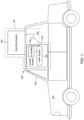
- FIG. 1shows an illustrative vehicle having a LiDAR system that is attached to and/or incorporated therein, according to an embodiment
- FIG. 2shows an illustrative scanning system according to an embodiment
- FIG. 3shows an illustrative compensation circuit diagram, according to an embodiment
- FIG. 4shows an illustrative plot of avalanche photo diode voltage output vs. bias voltage, according to an embodiment
- FIG. 5shows an illustrative plot of avalanche photo diode avalanche threshold vs. temperature, according to an embodiment
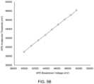
- FIG. 5 Ashows an illustrative plot of signal intensity as a function of bias voltage according to an embodiment
- FIG. 5 Bshows an illustrative plot of the avalanche voltage threshold as a function of APD breakdown voltage according to an embodiment
- FIG. 6shows an illustrative compensation circuit diagram, according to an embodiment
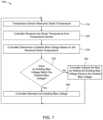
- FIG. 7shows an illustrative process, according to an embodiment
- FIG. 8shows an illustrative compensation circuit diagram, according to an embodiment
- FIG. 9shows an illustrative process, according to an embodiment
- FIG. 10 Ashows an illustrative plot of signal gain vs. distance, according to an embodiment
- FIG. 10 Bshows an illustrative plot of signal gain vs. distance, according to an embodiment
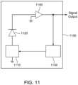
- FIG. 11shows an illustrative compensation circuit diagram, according to an embodiment
- FIG. 12shows an illustrative process, according to an embodiment
- FIG. 13shows an illustrative plot of controlled bias voltage sweeps, according to an embodiment
- FIG. 14shows an illustrative block diagram of temperature based bias offset system for controlling the bias voltage applied to an avalanche photo diode according to an embodiment
- FIG. 15shows an illustrative process for using the equations of FIG. 14 according to an embodiment.
- FIG. 1shows an illustrative vehicle 100 having a LiDAR system 120 that is attached to and/or incorporated therein according to an embodiment.
- Vehicle 100can be generically classified as having interior portion 101 and exterior portion 102 .
- Interior portion 101may be portions of vehicle 100 that are not directly exposed to external environmental factors such as the environment conditions (e.g., water, humidity, sun, ice, wind, etc.) and road conditions (e.g., road debris). Interior portion 101 may be influenced by external environment conditions but to a lesser degree than exterior portion 102 .
- LiDAR system 120may include, among other features, control system 130 , cable system 140 , and scanning system 150 .
- Control system 130may be contained within interior portion 101 , scanning system 150 may be mounted to exterior portion 102 , and cable system 140 may exist solely within interior portion 101 or can exist as part of interior portion 101 and exterior portion 102 . This arrangement is illustrative and in some embodiments, control system 130 or portions thereof (e.g., laser system 134 ) can be mounted to exterior portion 102 .
- Control system 130can include controller 132 and laser system 134 .
- Controller 132 and laser system 134may be coupled to scanning system 150 via cable system 140 .
- Laser system 134may transmit light pulses through cable system 140 to scanning system 150 .
- Laser system 134may use diode lasers to generate light pulses or fiber lasers.
- Controller 132may control a current source at which laser system 134 transmits its light pulses.
- Controller 132may receive detector signals from scanning system 150 via cable system 140 .
- the detector signalsmay be the return or consequence signals that are detected by one or more detectors when the transmitted light pulses bounce of an object being observed by scanning system 150 .
- Scanning system 150may include the appropriate lenses, mirrors, steering optics, and detectors needed to capture an image of a scene existing within a vicinity of vehicle 100 .
- LiDAR system 120can separate laser system 134 and scanning system 150 from each other such that laser system 134 is contained within interior portion 101 . Keeping laser system 134 (and other components associated with control system 130 ) within interior portion 101 provides an environment that is less harsh than that of exterior portion 102 . This provides cooling advantages over containing laser system 134 as part of scanning system 150 , which is located on exterior portion 102 .
- Laser system 134can use diode lasers or fiber lasers, and the light pulses are transmitted through cable system 140 to scanning system 150 .
- Cable system 140can include one or more fiber optic cables for transmitting light pulses from laser system 134 to scanning system 150 .
- Cable system 140can include one or more electrical conduits for transferring electrical signals between control system 130 and scanning system 150 .
- control system 130may provide instructions to scanning system 150 to control steering optics.
- scanning system 150may provide detection signals to controller 132 via cable system 140 .
- FIG. 2shows illustrative scanning system 200 according to an embodiment.
- Scanning system 200can include housing 201 , laser source 210 , receiver system 220 , polygon structure 230 , and mirror 240 .
- Housing 201is constructed to house laser source 210 , receiver system 220 , polygon structure 230 , and mirror 240 .
- Laser source 210may be operative to direct light energy towards mirror 240 and receiver system 220 is operative to receive reflected light energy from mirror 240 .
- Mirror 240is operative to redirect light energy transmitted from laser source 210 to polygon structure 230 .
- Mirror 240is also operative to redirect light energy received from polygon structure 230 to receiver system 220 .
- Mirror 240may be moved in the directions shown by arrow 241 . As mirror 240 oscillates back and forth, it causes light being transmitted by laser system 210 to interface with different portions of polygon structure 230 .
- light energyis emitted by laser source 210 towards mirror 240 , which redirects the light to polygon structure 230 , which redirects the light energy out of housing 201 .
- the light energy being directed by polygon structure 230is cast in accordance with the field of view parameters of scanning system 200 . That is, if system 200 has a field of view with range of x, a lateral angle of y, and vertical angle of z, the range x can be controlled by the power of transmitter system 210 , the vertical angle z can be controlled by the movement of mirror 240 , and the lateral angle y can be controlled by polygon structure 230 . Light energy that is reflected back from objects in the field of view and returns to polygon structure 230 where it is directed back to mirror 240 , which redirects it back to receiver system 220 .
- Polygon structure 230may be constructed from a metal such as aluminum, plastic, or other material that can have a polished or mirrored surface. Polygon structure 230 may be selectively masked to control the lateral dispersion of light energy being projected in accordance with the field of view of scanning system 200 . Polygon structure 230 can include a number of facets to accommodate a desired horizontal field of view (FOV). The facets can be parallel or non-parallel to its symmetric axis. Polygon structure 230 is operative to spin about axis 231 in a first direction at a substantially constant speed.
- a metalsuch as aluminum, plastic, or other material that can have a polished or mirrored surface. Polygon structure 230 may be selectively masked to control the lateral dispersion of light energy being projected in accordance with the field of view of scanning system 200 . Polygon structure 230 can include a number of facets to accommodate a desired horizontal field of view (FOV). The facets can be parallel or non-parallel to its symmetric axis
- Axis 231can be coincident to the symmetrical axis of structure 230 or it can be tilted at an angle with respect to the symmetrical axis of structure 230 , which can effectively increase resolution in vertical angle of z.
- the shape of polygon structure 230can be trimmed (e.g., chop off the sharp corner or tip to reduce overall weight, chamfer the sharp edge to reduce air resistance) for better operation performance.
- Polygon structure 230may sometime be referred to herein as a mirror.
- Mirror 240may be a single plane or multi-plane mirror that oscillates back and forth to redirect light energy emitted by laser source 210 to polygon 230 .
- the single plane mirrormay provide higher resolutions at the top and bottom portions of the vertical field of view than the middle portion, whereas the multi-plane mirror may provide higher resolution at a middle portion of the vertical field of view than the top and bottom portions.
- Receiver system 220can include optics 221 , detector 222 , control circuitry 223 , and compensation circuitry 224 .
- Optics 221may contain light-transmitting optics that gather laser light returned from mirror 240 .
- Detection sub-assembly 225may include detector array 222 and compensation circuitry 224 .
- Detector array 222may contain one or more detectors 222 a that generate voltage signals when exposed to light energy through optics 221 .
- Detectors 222 amay be, for example, avalanche photo diodes.
- Compensation circuitry 224may include electrical circuitry operative to modify operational characteristics of detectors 222 a to ensure optimal performance. For example, compensation circuitry 224 may monitor and control avalanche photo diode bias voltage.
- compensation circuitry 224can be connected to detector array 222 (e.g., to the anode and cathode of each detector 222 a ) and to control circuitry 223 .
- the outputs of detectors 222 acan be processed by control circuitry 223 and delivered to a control system (e.g., control system 130 ) to enable processing of return pulses (not shown).
- FIG. 3shows an illustrative circuit 300 having an avalanche photo diode for use in a LiDAR signal control system according to an embodiment.
- Circuit 300may represent circuitry that may be found in detectors 222 .
- Circuit 300may contain avalanche photo diode 310 and amplifier 320 .
- Bias voltage 330may be applied to a first terminal of diode 310 and amplifier may be coupled to a second terminal of diode 310 .
- Bias voltage 330may be used to bias an avalanche threshold of diode 310 .
- Amplifier 320may amplify the output of diode 310 .
- Avalanche photo diodeshave a breakdown voltage and an avalanche voltage.
- the breakdown voltageis not noise based and represents the voltage level where the diode avalanches.
- the avalanche voltagerepresents the voltage or range of voltages where the noise being generated within the gain medium of the diode starts to grow and eventually grows to the point out where it amplifies itself, thereby causing the avalanche.
- the avalanche photo diodecan experience avalanche effects at voltage levels below the breakdown voltage. These avalanche effects can be represented by the amount of noise that is being produced by the diode. Because the amount of noise can grow exponentially as a function of voltage, it is desirable to operate the avalanche photodiode at a voltage level before the noise becomes too great for the LiDAR system to handle.
- FIG. 4shows an illustrative plot of voltage gain produced by an avalanche photo diode with respect to diode bias voltage according to an embodiment.
- High avalanche photo diode voltage gainmay be desirable for data analysis.
- avalanche photo diode voltage gainmay increase non-linearly.
- Voltage V A,THrepresents the avalanche threshold of the avalanche photo diode.
- V A,IDEALmay represent an optimal bias voltage for operating the avalanche photo diode.
- V A,IDEALis slightly lower than V A,TH and is selected to maximize avalanche photo diode voltage gain while minimizing noise amplification. Not shown in FIG. 4 is the breakdown voltage.
- FIG. 5shows a plot of avalanche voltage threshold as a function of temperature for an avalanche photo diode according to an embodiment. Since a LiDAR system such as LiDAR system 120 operates in various and dynamic environmental conditions that may include temperature fluctuations, the avalanche voltage of the system might change over time due to temperature fluctuations. Embodiments discussed herein are able to dynamically adjust the bias voltage by taking temperature into account.
- FIG. 5 Ashows an illustrative plot of signal intensity as a function of bias voltage according to an embodiment.
- Signal intensityrefers to the output of the avalanche photo diode.
- V BRbreakdown voltage of the APD device
- FIG. 5 Bshows an illustrative plot of the relationship between the physical breakdown voltage and the avalanche voltage threshold at different temperatures for certain APD devices. It is clear that for some APD devices, a simple linear formula can be used to predict the avalanche voltage threshold based on the measured breakdown voltage.
- the relationship between the physical breakdown voltage and the avalanche voltage thresholdmay not be as simple, but in general the avalanche voltage threshold can still be characterized as a function of breakdown voltage and temperature. Combining FIG. 5 A and FIG. 5 B , it is therefore possible to obtain the APD breakdown voltage at any temperature through a bias voltage scan, and then use a pre-defined formula to predict the corresponding avalanche voltage threshold at that temperature.
- FIG. 6shows an illustrative bias voltage control circuit diagram according to an embodiment.
- Circuit 600may contain voltage generator 610 , avalanche photo diode 620 , temperature sensor 630 , controller 640 , and amplifier 650 .
- Circuit 600can control the bias voltage applied to diode 620 based, at least in part, on the temperature obtained by temperature sensor 630 .
- Temperature sensor 630may sense the temperature of diode 620 using, for example, a thermistor that is placed adjacent to diode 620 or on a circuit board (not shown). The sensed temperature may be provided to controller 640 , which may determine the ideal avalanche photo diode bias voltages for that sensed temperature and may adjust the bias voltage accordingly.
- controller 640can access a look up table to determine the ideal bias voltage. In another embodiment controller 640 can perform calculations based on the sensed temperature to set the bias voltage. See, for example, the description below in connection FIG. 14 for examples of calculations that may be made to determine the bias voltage. This way, regardless of the temperature associated with diode 620 , controller 640 can adjust the bias voltage such that it exists at V A,IDEAL , as indicated in FIG. 4 .
- FIG. 7shows an illustrative process 700 according to an embodiment.
- Process 700may represent the control circuit logic that may be used, for example, by circuit 600 .
- a temperature sensorsuch as temperature sensor 630 records avalanche photo diode temperature.
- a controllere.g., controller 640 ) receives the avalanche photo diode temperature as indicated by step 720 .
- the controllerdetermines a desired bias voltage based, at least in part, on the temperature it receives, as indicated by step 730 .
- a determinationis made as to whether the existing bias voltage matches a desired voltage for the measured temperature. If the determination is NO, process 700 can adjust bias voltage by setting the existing bias voltage equal to the desired voltage as indicated by step 750 . If the determination is YES, process 700 can maintain the existing bias voltage as indicated by step 760 .
- steps shown in FIG. 7are illustrative and that the steps can be rearranged, that steps may be added, steps may be combined, or steps can be omitted.
- FIG. 8shows an illustrative bias voltage control circuit diagram, according to an embodiment.
- Circuit 800may contain voltage generator 810 , avalanche photo diode 820 , controller 830 , and amplifier 840 .
- avalanche photo diode 820As the LiDAR system laser return pulses interact with an avalanche photo diode such as avalanche photo diode 820 , voltage is generated and amplified.
- a circuit such as circuit 800may be used to control bias voltage.
- a controllersuch as controller 830 may be used to directly detect the avalanche voltage threshold of diode 820 .
- controller 830can sweep through a predefined range of bias voltages while monitoring the output of amplifier 840 . As the controller sweeps through the predefined range, it can determine the avalanche voltage threshold existing for the current set of conditions. Once the avalanche threshold is determined, an ideal bias voltage may be selected to ensure that diode 820 operates at the best bias voltage for the current set of conditions.
- the calibration sweepmay be initiated on a time interval, at system startup, when unusual data is detected by the LiDAR control software, when a temperature sensor outside of the circuit detects temperature changes, during dead time of normal operation, or by other methods.
- circuit 800may be used to determine the breakdown voltage of diode 820 .
- the breakdown voltagemay be determined as part of a LiDAR system initiation, at the start of LiDAR scanning event, or any other suitable trigger event.
- the determination of the breakdown voltagemay be used as an input in a calculation equation for determining the initial Vbias (as discussed down below in connection with FIG. 14 ).
- FIG. 9shows an illustrative process 900 according to an embodiment.
- Process 900may represent the control circuit logic that may be used, for example, by circuit 800 .
- a controllersuch as controller 830 initiates a bias voltage calibration sweep.
- the controllercommands a voltage generator such as voltage generator 810 to sweep bias voltages across a predefined range of bias voltages as indicated by process 920 .
- the controllerthen records amplifier output data produced by the bias voltage sweep according to step 930 .
- the controllerdetects photo diode avalanche voltage threshold or the breakdown voltage threshold based on recorded amplifier output data across the bias voltage sweep voltage range.
- the controllersets the bias voltage to an ideal bias voltage based on the detected avalanche voltage.
- the controllermay determine the ideal bias voltage by applying the detected avalanche voltage or breakdown voltage to a formula. For example, the formula can subtract a fixed value from the detected avalanche voltage or the breakdown voltage threshold to yield the ideal bias voltage.
- steps shown in FIG. 9are illustrative and that the steps can be rearranged, that steps may be added, steps may be combined, or steps can be omitted.
- FIGS. 10 A and 10 Bshow illustrative plots of control system gain, according to an embodiment.
- an amplified signal generated by a photo diode circuitmay be used by a LiDAR system to generate data on objects in the environment.
- many factorsmay influence the intensity of laser energy returning to the system's photo diode.
- One of these factorsmay be the distance between the object and the LiDAR system.
- FIG. 10 Ashows two representative voltage gains for a single object that reflected laser light back to the LiDAR system from different distances.
- Pulse 1010represents relative high signal gain response if the object is physically near the LiDAR system and pulse 1020 represents relatively low signal gain response if the object is physically far away from the LiDAR system.
- a potential issue with the disparity in the gain responses of pulses 1010 and 1020is that a system may have difficulty in recognizing pulse 1020 as legitimate object return, as the gain may be too low to exceed a threshold or it may be obscured by background radiation and noise.
- FIG. 10 Bshows two representative signal gains, pulses 1030 and 1040 , that correspond to the same objects corresponding to pulses 1010 and 1020 described in FIG. 10 A .
- pulse 1030is derived from the same relatively close object as that for which pulse 1010 was derived and pulse 1040 is derived from the same relatively far object as that for which pulse 1020 was derived.
- the bias voltagemay have been modulated such that the disparity in signal gains is less extreme.
- a relatively close objectis represented by a relatively moderate signal gain response (as shown by pulse 1030 ) as opposed to the relatively high signal gain response of pulse 1010
- a relatively far objectis also represented by a relatively moderate signal gain response (as shown by pulse 1040 ) as opposed to the relatively low signal gain response of pulse 1020 .
- Pulse 1030is greater than pulse 1040 , but the disparity is not nearly as great as that shown in FIG. 10 A .
- the bias voltage modulation featuremay be important for LiDAR design considerations since extreme high or low signal gain may produce non-linear data analysis results and thus can be undesirable for data processing. If signal gain is too low, this can result in an object not being detected by the LiDAR system. If a signal gain is too high, this may result in signal saturation. Signal gains that are too low or too high may result in data being acquired in a non-linear range, thereby undesirably forcing data processing software to handle non-linear inputs.
- FIG. 11shows an illustrative bias voltage modulation control circuit diagram, according to an embodiment.
- Circuit 1100may contain voltage generator 1110 , photo diode 1120 , controller 1130 , and amplifier 1140 . Return pulses interact with photo diode 1120 , which produces an output in response thereto and that output is amplified by amplifier 1140 .
- control circuitry 1130ensures the bias voltage remains below the avalanche voltage threshold (as discussed above) and may also modulate the bias voltage as part of a modulation feedback loop that is designed to compress relatively high gain signals and boost relatively low gain signals.
- Control circuitry 1130may modulate the bias voltage to ensure that the signal gain provided by diode 1120 is within an amplitude range suitable for data processing. Control circuitry 1130 may modulate the bias voltage based on a previously received output (e.g., signal gain) of diode 1120 (which output is received via amplifier 1140 ). For example, if the signal gain is too high, controller 1130 may reduce the bias voltage. If the signal gain is too low, controller 1130 may increase the bias voltage. Controller 1130 may ensure that diode 1120 operates below its avalanche voltage threshold such that bias voltages can be modulated up or down to produce desired signal gains without exceeding the avalanche voltage threshold.
- a previously received outpute.g., signal gain
- FIG. 12shows an illustrative process 1200 according to an embodiment.
- Process 1200represents control circuit logic that may be used, for example, by circuit 1100 .
- a controllersuch as controller 1130 observes a signal amplitude generated by a LiDAR laser return pulse. The controller then compares the signal amplitude with a desired range of signal amplitudes as indicated by step 1220 .
- a determinationis made as to whether the signal amplitude is appropriate for linear data processing according to a pre-determined range of desired signal amplitudes. If the determination is YES, process 1200 maintains existing bias voltage as shown in step 1240 .
- process 1200determines whether the signal amplitude is too low or too high, as shown in step 1250 . If the determination is made that the signal amplitude is too HIGH, process 1200 then decreases bias voltage as shown in step 1260 . If the determination is made that the signal amplitude is too LOW, process 1200 then increases bias voltage as shown in step 1270 . Process 1200 then commands the system to run its next LiDAR system laser scan in step 1280 .
- steps shown in FIG. 12are illustrative and that the steps can be rearranged, that steps may be added, steps may be combined, or steps can be omitted.
- FIG. 13shows an illustrative plot of controlled bias voltage sweeps, according to an embodiment.
- bias voltageis modulated from low to high over the duration of each laser pulse.
- bias voltage over timeis shown for three identical laser pulses. These three pulses go from time t 0 to time t 1 , from time t 1 to time t 2 , and from time t 2 to time t 3 , respectively.
- Each pulsemay begin at a low bias voltage at the start of the pulse and end at a high bias voltage at the end of each pulse.
- avalanche photo diode bias voltageis lowest at the start of each pulse and highest at the end of each pulse, a time dependence of bias voltage and therefore signal gain is established. If two identical objects are located at different distances from the LiDAR system, light energy reflected from the closer object would interact with the avalanche photo diode sooner than it would from the farther object. Light energy from the closer object may also reflect more light energy back to the LiDAR system than the object farther away and could therefore generate a stronger signal by the avalanche photo diode. Thus a controlled bias voltage sweep may result in a moderation of circuit signal gain since stronger signal generating objects are subject to lower bias voltage and lower gain while weaker signal generating objects are subject to higher bias voltage and higher gain. Though FIG. 13 represents the controlled bias voltage sweeps as being linear with time, non-linear bias voltage modulations may be used.
- FIG. 14shows an illustrative block diagram of temperature based bias offset system 1400 for controlling the bias voltage applied to an avalanche photo diode according to an embodiment.
- System 1400can include inputs 1410 , calculation module 1430 , and V_Bias output 1450 .
- Inputs 1410are provided to calculation module 1430 , which generates V_Bias output 1450 to be applied to the avalanche photodiode.
- Inputs 1410can include V_BR0 1412 , V_Offset 1414 , T_INT 1415 , T_0 1416 , and T_Active 1417 .
- V_BR0 1412represents an avalanche photodiode breakdown voltage based on an initial system calibration (e.g., when the LiDAR system is turned ON). V_BR0 1412 may be set using, for example, the voltage sweeping process of FIGS. 8 and 9 that can be used to determine the breakdown voltage of the photodiode.
- V_Offset 1414represents an operating voltage offset from avalanche condition of the avalanche photodiode. The value chosen for V_Offset 1414 can be selected based on how aggressive or conservative system 1400 desires to run the avalanche photodiode. A larger V_offset corresponds to a conservative approach whereas a smaller V_Offset corresponds to an aggressive approach.
- T_INT 1415represents a temperature measurement at initial system calibration
- T_0 1416represents a temperature measurement at the beginning of a LiDAR system scanning event
- T_Active 1417represents a temperature measurement taken during the LiDAR system scanning event.
- T_INT 1415 , T_0 1416 , and T_Active 1417may all be obtained by the same temperature sensor (e.g., sensor 630 of FIG. 6 ).
- Calculation module 1430can include bias voltage calculation module 1432 and temperature offset calculation module 1434 .
- Bias voltage calculation module 1432can calculate an initial bias voltage V_Bias0 that is fed as an input to temperature offset calculation module 1434 .
- V_Bias0can represent the bias voltage at the start of LiDAR scanning event.
- the product of V_BR0 and Sproduces the anticipated avalanche threshold, which can represent an inflection point within the photodiode where system 1400 expects the noise to be too problematic for data processing even though the photodiode has not reached full avalanche breakdown.
- the operating voltage offset V_Offsetallows the LiDAR system to be operated at a fixed level below the anticipated avalanche threshold, where the system noise is more manageable.
- Temperature offset calculation module 1434can calculate the temperature offset bias voltage, V_Bias, that is applied to avalanche photo diode as output 1450 .
- V_Biascan represent bias voltage applied to the avalanche photo diode during the LiDAR scanning event.
- FIG. 15shows an illustrative process for using the equations of FIG. 14 according to an embodiment.
- the process in FIG. 15can be implemented in a LiDAR system including an avalanche photo diode (APD), a temperature sensor, and a variable voltage source.
- APDavalanche photo diode
- a temperature sensore.g., a thermocouple
- a variable voltage sourcee.g., a breakdown voltage of the APD can be determined.
- the breakdown voltagecan be determined by performing a voltage sweep of the APD to determine a voltage level where the APD experiences a breakdown event, and selecting the voltage level as the breakdown voltage.
- an anticipated avalanche voltage thresholdcan be generated based on the breakdown voltage.
- the anticipated avalanche voltage thresholdcan represent an inflection point within the APD where the LiDAR system expects noise generated by the APD to be too problematic for data processing even though the APD has not reached full avalanche breakdown.
- an initial bias voltagecan be determined based on the anticipated avalanche voltage threshold and a voltage offset.
- the voltage offsetcan set the initial bias voltage to a voltage level that is lower than the anticipated avalanche voltage threshold.
- the initial bias voltagecan be determined using equation 1 above.
- an active scanning event bias voltagecan be determined based on the initial bias voltage and a temperature received by the temperature sensor, wherein the active scanning event bias voltage is applied to the avalanche photodiode by the variable voltage source to prevent the avalanche photodiode from operating at or above the anticipated avalanche voltage.
- the active scanning event bias voltagecan be determined using equation 2 above.
- any processes described with respect to FIGS. 1 - 15may each be implemented by software, but may also be implemented in hardware, firmware, or any combination of software, hardware, and firmware. They each may also be embodied as machine- or computer-readable code recorded on a machine- or computer-readable medium.
- the computer-readable mediummay be any data storage device that can store data or instructions which can thereafter be read by a computer system. Examples of the computer-readable medium may include, but are not limited to, read-only memory, random-access memory, flash memory, CD-ROMs, DVDs, magnetic tape, and optical data storage devices.
- the computer-readable mediumcan also be distributed over network-coupled computer systems so that the computer readable code is stored and executed in a distributed fashion.
- the computer-readable mediummay be communicated from one electronic subsystem or device to another electronic subsystem or device using any suitable communications protocol.
- the computer-readable mediummay embody computer-readable code, instructions, data structures, program modules, or other data in a modulated data signal, such as a carrier wave or other transport mechanism, and may include any information delivery media.
- a modulated data signalmay be a signal that has one or more of its characteristics set or changed in such a manner as to encode information in the signal.
- any or each module or state machine discussed hereinmay be provided as a software construct, firmware construct, one or more hardware components, or a combination thereof.
- any one or more of the state machines or modulesmay be described in the general context of computer-executable instructions, such as program modules, that may be executed by one or more computers or other devices.
- a program modulemay include one or more routines, programs, objects, components, and/or data structures that may perform one or more particular tasks or that may implement one or more particular abstract data types.
- modules or state machinesare merely illustrative, and that the number, configuration, functionality, and interconnection of existing modules may be modified or omitted, additional modules may be added, and the interconnection of certain modules may be altered.
Landscapes
- Engineering & Computer Science (AREA)
- Physics & Mathematics (AREA)
- Computer Networks & Wireless Communication (AREA)
- General Physics & Mathematics (AREA)
- Radar, Positioning & Navigation (AREA)
- Remote Sensing (AREA)
- Electromagnetism (AREA)
- Optical Radar Systems And Details Thereof (AREA)
Abstract
Description
V_Bias0=V_BR0*S+E−V_Offset (1),
where V_BR0 is the avalanche photodiode breakdown voltage based on an initial system calibration, S and E are fit constants representing a linear relationship between the breakdown voltage and the avalanche voltage threshold, and V_Offset is the operating voltage offset from the avalanche voltage threshold. The product of V_BR0 and S produces the anticipated avalanche threshold, which can represent an inflection point within the photodiode where system1400 expects the noise to be too problematic for data processing even though the photodiode has not reached full avalanche breakdown. The operating voltage offset V_Offset allows the LiDAR system to be operated at a fixed level below the anticipated avalanche threshold, where the system noise is more manageable.
V_Bias=V_Bias0+V_Adj(T_Active,T0) (2),
where V_Bias0 is the initial bias voltage, T_Active is the temperature during the LiDAR scanning event, T0 is the temperature at the beginning of the LiDAR scanning event, and V_Adj (T_Active, T0) is the temperature compensation function for APD bias voltage.
Claims (25)
Priority Applications (2)
| Application Number | Priority Date | Filing Date | Title |
|---|---|---|---|
| US16/379,207US11789132B2 (en) | 2018-04-09 | 2019-04-09 | Compensation circuitry for lidar receiver systems and method of use thereof |
| US18/376,426US20240027593A1 (en) | 2018-04-09 | 2023-10-03 | Compensation circuitry for lidar receiver systems and method of use thereof |
Applications Claiming Priority (2)
| Application Number | Priority Date | Filing Date | Title |
|---|---|---|---|
| US201862654913P | 2018-04-09 | 2018-04-09 | |
| US16/379,207US11789132B2 (en) | 2018-04-09 | 2019-04-09 | Compensation circuitry for lidar receiver systems and method of use thereof |
Related Child Applications (1)
| Application Number | Title | Priority Date | Filing Date |
|---|---|---|---|
| US18/376,426ContinuationUS20240027593A1 (en) | 2018-04-09 | 2023-10-03 | Compensation circuitry for lidar receiver systems and method of use thereof |
Publications (2)
| Publication Number | Publication Date |
|---|---|
| US20190310354A1 US20190310354A1 (en) | 2019-10-10 |
| US11789132B2true US11789132B2 (en) | 2023-10-17 |
Family
ID=68098071
Family Applications (2)
| Application Number | Title | Priority Date | Filing Date |
|---|---|---|---|
| US16/379,207Active2042-05-18US11789132B2 (en) | 2018-04-09 | 2019-04-09 | Compensation circuitry for lidar receiver systems and method of use thereof |
| US18/376,426PendingUS20240027593A1 (en) | 2018-04-09 | 2023-10-03 | Compensation circuitry for lidar receiver systems and method of use thereof |
Family Applications After (1)
| Application Number | Title | Priority Date | Filing Date |
|---|---|---|---|
| US18/376,426PendingUS20240027593A1 (en) | 2018-04-09 | 2023-10-03 | Compensation circuitry for lidar receiver systems and method of use thereof |
Country Status (2)
| Country | Link |
|---|---|
| US (2) | US11789132B2 (en) |
| WO (1) | WO2019199796A1 (en) |
Families Citing this family (20)
| Publication number | Priority date | Publication date | Assignee | Title |
|---|---|---|---|---|
| US11789132B2 (en) | 2018-04-09 | 2023-10-17 | Innovusion, Inc. | Compensation circuitry for lidar receiver systems and method of use thereof |
| WO2020121857A1 (en)* | 2018-12-12 | 2020-06-18 | 浜松ホトニクス株式会社 | Photodetector and method for manufacturing photodetector |
| CN110889242B (en)* | 2019-12-10 | 2023-10-20 | 深圳市联洲国际技术有限公司 | APD voltage adjusting method and device, storage medium and ONU equipment |
| US11681023B2 (en)* | 2020-06-17 | 2023-06-20 | Continental Autonomous Mobility US, LLC | Lidar system with varied detection sensitivity based on lapsed time since light emission |
| US20210396846A1 (en)* | 2020-06-18 | 2021-12-23 | Continental Automotive Systems, Inc. | Lidar system with detection sensitivity of photodetectors |
| US11552200B2 (en) | 2020-08-03 | 2023-01-10 | Texas Instruments Incorporated | Avalanche photodiode gain control comprising a bias circuit having a second avalanche photodiode |
| DE102020120688A1 (en) | 2020-08-05 | 2022-02-10 | Valeo Schalter Und Sensoren Gmbh | Determining a blocking voltage limit of a sensor system |
| CN116076072A (en)* | 2020-09-15 | 2023-05-05 | 索尼半导体解决方案公司 | Distance measuring system and light detecting device |
| US12339403B2 (en) | 2020-10-20 | 2025-06-24 | Luminar Technologies, Inc. | Adaptive avalanche photodiode bias set point calibration system and method |
| CN115728746A (en)* | 2021-08-26 | 2023-03-03 | 上海禾赛科技有限公司 | Laser radar and method for three-dimensional detection using laser radar |
| EP4402507A4 (en)* | 2021-09-17 | 2025-09-17 | Banner Eng Corporation | FIELD-SELECTIBLE DYNAMIC GAIN CONTROL MODES OF SENSORS |
| CN114281137B (en)* | 2021-12-02 | 2022-09-02 | 探维科技(北京)有限公司 | Method, device and system for controlling bias voltage of photoelectric detector and laser radar |
| CN113900072A (en)* | 2021-12-06 | 2022-01-07 | 探维科技(北京)有限公司 | Method, device and system for adjusting bias voltage by using non-probe light and laser radar |
| CN114442109B (en)* | 2021-12-17 | 2024-06-07 | 北京理工大学 | Large dynamic range hybrid solid-state lidar system based on transceiver array module |
| CN114614891B (en)* | 2022-03-22 | 2023-09-08 | Nano科技(北京)有限公司 | Avalanche photodetector light responsivity measurement system and measurement method |
| WO2023205477A1 (en)* | 2022-04-22 | 2023-10-26 | Innovusion, Inc. | Dynamic calibration method of avalanche photodiodes on lidar |
| JP2023170280A (en)* | 2022-05-18 | 2023-12-01 | ソニーセミコンダクタソリューションズ株式会社 | Ranging device and ranging system |
| CN115656974B (en)* | 2022-12-09 | 2023-04-07 | 武汉灵途传感科技有限公司 | Detection method for laser radar integrated double APDs |
| CN117148368B (en)* | 2023-08-31 | 2024-04-12 | 探维科技(苏州)有限公司 | APD and optimal gain determining method, control method, device and laser radar thereof |
| CN117452169A (en)* | 2023-09-28 | 2024-01-26 | 深圳市意普兴科技有限公司 | Avalanche voltage detection method, device, equipment and medium |
Citations (164)
| Publication number | Priority date | Publication date | Assignee | Title |
|---|---|---|---|---|
| US3897150A (en) | 1972-04-03 | 1975-07-29 | Hughes Aircraft Co | Scanned laser imaging and ranging system |
| GB1427164A (en) | 1972-02-19 | 1976-03-10 | Nippon Electric Co | Interference eliminating system for radars |
| GB2000411A (en) | 1977-06-15 | 1979-01-04 | Impulsphysik Gmbh | Ceilometric method and apparatus |
| US4464048A (en) | 1981-03-25 | 1984-08-07 | Barr & Stroud Limited | Laser rangefinders |
| US5006721A (en) | 1990-03-23 | 1991-04-09 | Perceptron, Inc. | Lidar scanning system |
| US5157451A (en) | 1991-04-01 | 1992-10-20 | John Taboada | Laser imaging and ranging system using two cameras |
| US5319434A (en) | 1992-12-30 | 1994-06-07 | Litton Systems, Inc. | Laser rangefinder apparatus with fiber optic interface |
| US5369661A (en) | 1991-02-07 | 1994-11-29 | Nippon Steel Corporation | Semiconductor laser-pumped solid state laser system and optical coupling system coupling semiconductor laser with optical fiber |
| US5442358A (en) | 1991-08-16 | 1995-08-15 | Kaman Aerospace Corporation | Imaging lidar transmitter downlink for command guidance of underwater vehicle |
| US5546188A (en) | 1992-11-23 | 1996-08-13 | Schwartz Electro-Optics, Inc. | Intelligent vehicle highway system sensor and method |
| US5579153A (en) | 1992-04-27 | 1996-11-26 | Pirelli Cavi S.P.A. | Optical power limiting amplifier |
| EP0757257A2 (en) | 1995-07-31 | 1997-02-05 | HE HOLDINGS, INC. dba HUGHES ELECTRONICS | Laser range finder receiver |
| US5638163A (en) | 1995-06-07 | 1997-06-10 | Hughes Electronics | Low cost laser range finder system architecture |
| US5657077A (en) | 1993-02-18 | 1997-08-12 | Deangelis; Douglas J. | Event recording system with digital line camera |
| US5793491A (en) | 1992-12-30 | 1998-08-11 | Schwartz Electro-Optics, Inc. | Intelligent vehicle highway system multi-lane sensor and method |
| US5838239A (en) | 1992-10-20 | 1998-11-17 | Robotic Vision Systems, Inc. | System for detecting ice or snow on surface which specularly reflects light |
| US5864391A (en) | 1996-04-04 | 1999-01-26 | Denso Corporation | Radar apparatus and a vehicle safe distance control system using this radar apparatus |
| US5926259A (en) | 1995-05-04 | 1999-07-20 | Bushnell Corporation | Laser range finder with target quality display |
| US5929982A (en)* | 1997-02-04 | 1999-07-27 | Tektronix, Inc. | Active APD gain control for an optical receiver |
| US5936756A (en) | 1996-01-10 | 1999-08-10 | Ricoh Company Ltd. | Compact scanning optical system |
| US6163378A (en) | 1999-06-14 | 2000-12-19 | Khoury; Jehad | Spectroscopic time integrative correlation for rapid medical diagnostic and universal image analysis |
| US6317202B1 (en) | 1998-11-12 | 2001-11-13 | Denso Corporation | Automotive radar detecting lane mark and frontal obstacle |
| EP1237305A2 (en) | 2001-02-28 | 2002-09-04 | KiloLambda IP Limited | Multi-wavelength light source |
| US20020136251A1 (en) | 2001-01-25 | 2002-09-26 | Science And Technology Corporation | Automatic gain control system for use with multiple wavelength signal detector |
| US6650404B1 (en) | 2002-05-28 | 2003-11-18 | Analog Modules, Inc. | Laser rangefinder receiver |
| US20040135992A1 (en) | 2002-11-26 | 2004-07-15 | Munro James F. | Apparatus for high accuracy distance and velocity measurement and methods thereof |
| US20050033497A1 (en) | 2003-08-06 | 2005-02-10 | Stopczynski Lawrence Gerard | Method of controlling an external object sensor for an automotive vehicle |
| US20050190424A1 (en) | 2004-02-27 | 2005-09-01 | Sick Ag | Method and device for optical scanning of objects |
| US20050195383A1 (en) | 1994-05-23 | 2005-09-08 | Breed David S. | Method for obtaining information about objects in a vehicular blind spot |
| CN1677050A (en) | 2004-03-31 | 2005-10-05 | 株式会社电装 | Object detector of vehicle |
| US20060071846A1 (en) | 2003-05-30 | 2006-04-06 | Yakayuki Yanagisawa | Coherent laser radar |
| US20060132752A1 (en) | 2004-12-16 | 2006-06-22 | Kane David M | Micromechanical and related lidar apparatus and method, and fast light-routing components |
| US7128267B2 (en) | 2003-07-11 | 2006-10-31 | Sick Ag | Device for optical scanning of objects, especially markings |
| US20070091948A1 (en) | 2005-07-29 | 2007-04-26 | Aculight Corporation | Multi-stage optical amplifier having photonic-crystal waveguides for generation of high-power pulsed radiation and associated method |
| JP2007144667A (en) | 2005-11-24 | 2007-06-14 | Fuji Xerox Co Ltd | Image forming apparatus and formed image correcting method |
| US20070216995A1 (en) | 2006-03-16 | 2007-09-20 | Bollond Paul G | Optical fiber laser having improved efficiency |
| US7345271B2 (en) | 2002-09-25 | 2008-03-18 | Ibeo Automobile Sensor Gmbh | Optoelectric sensing device with common deflection device |
| EP1923721A1 (en) | 2005-08-15 | 2008-05-21 | Topcon Corporation | Measuring device |
| US20080174762A1 (en) | 2006-08-29 | 2008-07-24 | Jony Jiang Liu | Micro-mirror optical tracking and ranging system |
| US20080193135A1 (en) | 2007-02-14 | 2008-08-14 | Finisar Corporation | Collimated ball lenses for optical triplexers |
| US20090010644A1 (en) | 2002-02-01 | 2009-01-08 | Cubic Corporation | Integrated optical communication and range finding system and applications thereof |
| US20090051926A1 (en) | 2007-04-13 | 2009-02-26 | United States Of America As Represented By The Administrator Of The National Aeronautics And Spac | Multiple frequency optical mixer and demultiplexer and apparatus for remote sensing |
| US20090059201A1 (en) | 2007-08-28 | 2009-03-05 | Science Applications International Corporation | Full-Field Light Detection and Ranging Imaging System |
| US20090067453A1 (en) | 2005-04-07 | 2009-03-12 | Matsushita Electric Industrial Co., Ltd. | Laser Light Source and Optical Device |
| US20090147239A1 (en) | 2005-09-02 | 2009-06-11 | Neptec | Apparatus and method for tracking an object |
| US20090262760A1 (en) | 2005-01-20 | 2009-10-22 | Vladimir Krupkin | Laser Obstacle Ranging and Display |
| US20090316134A1 (en) | 2004-07-08 | 2009-12-24 | Michael Christopher E | Fiber laser ladar |
| US20100006760A1 (en) | 2004-04-13 | 2010-01-14 | Science & Engineering Services, Inc. | Ultraviolet lidar for detection of biological warfare agents |
| US20100020306A1 (en) | 2006-07-13 | 2010-01-28 | Velodyne Acoustics, Inc. | High definition lidar system |
| US20100027602A1 (en) | 2008-07-31 | 2010-02-04 | United States Of America As Represented By The Administrator Of The National Aeronautics And Spac | Time delay and distance measurement |
| JP2010035385A (en) | 2008-07-31 | 2010-02-12 | Kyocera Mita Corp | Motor drive controller |
| EP2157445A2 (en) | 2008-08-19 | 2010-02-24 | Rosemount Aerospace Inc. | Lidar system using a pseudo-random pulse sequence |
| US20100053715A1 (en) | 2006-10-30 | 2010-03-04 | O'neill James | Scanning system for lidar |
| US20100128109A1 (en) | 2008-11-25 | 2010-05-27 | Banks Paul S | Systems And Methods Of High Resolution Three-Dimensional Imaging |
| US20100271614A1 (en) | 2006-01-27 | 2010-10-28 | Vijay Albuquerque | LIDAR system utilizing SOI-based opto-electronic components |
| US20100301194A1 (en)* | 2009-05-26 | 2010-12-02 | Princeton Lightwave, Inc. | Optical Receiver Comprising Breakdown-Voltage Compensation |
| US20110181864A1 (en) | 2008-07-04 | 2011-07-28 | Eads Deutschland Gmbh | Lidar method for measuring speeds and lidar device with time-controlled detection |
| EP2395368A1 (en) | 2010-06-11 | 2011-12-14 | Sick AG | Distance-measuring laser scanner for detecting objects in a surveillance range |
| KR20120013515A (en) | 2010-08-05 | 2012-02-15 | (주)이오시스템 | Avalanche Photodiode Gain Compensation Device of Optical Measuring Equipment |
| US20120038903A1 (en) | 2010-08-16 | 2012-02-16 | Ball Aerospace & Technologies Corp. | Electronically steered flash lidar |
| US20120124113A1 (en) | 2010-11-05 | 2012-05-17 | University of Maribor | LIGHT DETECTION AND RANGING (LiDAR)DATA COMPRESSION AND DECOMPRESSION METHODS AND APPARATUS |
| US20120221142A1 (en) | 2011-02-24 | 2012-08-30 | Mss, Inc. | Sequential Scanning Of Multiple Wavelengths |
| US20130107016A1 (en) | 2010-05-17 | 2013-05-02 | Iee International Electronics & Engineering S.A. | Scanning 3d imager |
| US20130116971A1 (en) | 2010-06-28 | 2013-05-09 | Fraunhofer-Gesellschaft Zur Foerderung Der Angewandten Forschung E.V. | Method for generating a signal for a distance measurement and method and system for distance measurement between a transmitter and a receiver |
| KR20130068224A (en) | 2011-12-15 | 2013-06-26 | 여우순엽 | The apparatus and method of monitoring with terrestrial lidar and reflectless totalstation |
| US20130241761A1 (en) | 2012-03-16 | 2013-09-19 | Nikon Corporation | Beam steering for laser radar and other uses |
| US20130293946A1 (en) | 2012-05-01 | 2013-11-07 | Imra America, Inc. | Optical frequency ruler |
| US20130293867A1 (en) | 2009-09-23 | 2013-11-07 | Pixart Imaging Inc. | Distance-measuring device of measuring distance according to variation of imaging location and calibrating method thereof |
| US20130329279A1 (en) | 2004-03-31 | 2013-12-12 | Imra America, Inc. | Method and apparatus for controlling and protecting pulsed high power fiber amplifier systems |
| US20130342822A1 (en) | 2011-03-02 | 2013-12-26 | Toyota Jidosha Kabushiki Kaisha | Laser radar device |
| US20140078514A1 (en) | 2010-10-22 | 2014-03-20 | Neptec Design Group Ltd. | Wide angle bistatic scanning optical ranging sensor |
| US20140104594A1 (en) | 2009-07-28 | 2014-04-17 | Applied Concepts, Inc. | Lidar Measurement Device with Target Tracking and Method for Use of Same |
| US20140231630A1 (en)* | 2013-02-18 | 2014-08-21 | Stmicroelectronics (Research & Development) Limited | Method and apparatus for image sensor calibration |
| US20140347650A1 (en) | 2011-12-23 | 2014-11-27 | Leica Geosystems Ag | Distance-measuring device alignment |
| US20140350836A1 (en) | 2013-05-24 | 2014-11-27 | Advance Scientific Concepts, Inc. | Automotive auxiliary ladar sensor |
| US20150078123A1 (en) | 2013-09-16 | 2015-03-19 | Appareo Systems, Llc | Synthetic underwater visualization system |
| US20150084805A1 (en) | 2012-03-19 | 2015-03-26 | Qinetiq Limited | Detection Techniques |
| US20150109603A1 (en) | 2013-10-21 | 2015-04-23 | Electronics And Telecommunications Research Institute | Multi-wavelength image lidar sensor apparatus and signal processing method thereof |
| US20150116692A1 (en) | 2012-04-30 | 2015-04-30 | Michigan Aerospace Corporation | System and method for scan range gating |
| US20150139259A1 (en) | 2013-11-21 | 2015-05-21 | Christie Digital Systems Canada Inc. | Method, system and apparatus for automatically determining operating conditions of a periodically poled lithium niobate crystal in a laser system |
| US20150158489A1 (en) | 2013-12-09 | 2015-06-11 | Hyundai Motor Company | Method for object processing and vehicle supporting the same |
| EP2889642A1 (en) | 2013-12-16 | 2015-07-01 | Riegl Laser Measurement Systems GmbH | Method for distance measurement |
| US9086273B1 (en) | 2013-03-08 | 2015-07-21 | Google Inc. | Microrod compression of laser beam in combination with transmit lens |
| CN204758260U (en) | 2015-07-21 | 2015-11-11 | 北京杏林睿光科技有限公司 | Semiconductor laser structure of multitube core characteristic monitoring |
| US20150338270A1 (en) | 2012-05-10 | 2015-11-26 | Voxtel, Inc. | Discriminating photo counts and dark counts in an avalanche photodiode |
| US20150355327A1 (en) | 2012-11-21 | 2015-12-10 | Nikon Metrology Nv | Scan mirrors for laser radar |
| CN204885804U (en) | 2015-07-21 | 2015-12-16 | 北京杏林睿光科技有限公司 | A narrow linewidth beam combining module and a multi-wavelength Raman laser with the module |
| US20160003946A1 (en) | 2014-07-03 | 2016-01-07 | Advanced Scientific Concepts, Inc. | Ladar sensor for a dense environment |
| US20160047900A1 (en) | 2014-08-15 | 2016-02-18 | US LADAR, Inc. | Method and System for Scanning Ladar Transmission with Pulse Modulation |
| US20160061655A1 (en) | 2014-09-03 | 2016-03-03 | Panasonic Intellectual Property Management Co., Ltd. | Measurement system |
| US20160061935A1 (en) | 2014-08-28 | 2016-03-03 | Google Inc. | Methods and Systems for Vehicle Radar Coordination and Interference Reduction |
| US9304316B2 (en) | 2004-11-15 | 2016-04-05 | Apple Inc. | Method and device for scanning light |
| US9304203B1 (en)* | 2013-03-13 | 2016-04-05 | Google Inc. | Methods, devices, and systems for improving dynamic range of signal receiver |
| US20160100521A1 (en) | 2014-10-10 | 2016-04-14 | Irobot Corporation | Autonomous Robot Localization |
| US9316724B2 (en) | 2012-12-18 | 2016-04-19 | Sick Ag | Optoelectronic sensor for the detection of objects |
| US20160117048A1 (en) | 2014-09-26 | 2016-04-28 | Cypress Semiconductor Corporation | Background Light Detection for Optical Navigation Systems |
| US20160172819A1 (en) | 2014-12-12 | 2016-06-16 | Omron Corporation | Light amplifying device and laser processing apparatus |
| US20160178736A1 (en) | 2014-12-19 | 2016-06-23 | Hanwha Techwin Co., Ltd. | Lidar system |
| US20160226210A1 (en) | 2015-01-29 | 2016-08-04 | John J. Zayhowski | Systems and methods for light amplification |
| US20160245902A1 (en) | 2015-02-25 | 2016-08-25 | Abbie T. Watnik | Real-time processing and adaptable illumination lidar camera using a spatial light modulator |
| US20160282451A1 (en)* | 2016-06-03 | 2016-09-29 | Caterpillar Inc. | Lidar system |
| US20160291134A1 (en) | 2015-04-06 | 2016-10-06 | Google Inc. | Long Range Steerable LIDAR System |
| US20160313445A1 (en) | 2012-03-16 | 2016-10-27 | Advanced Scientific Concepts, Inc. | Personal ladar sensor |
| US20160327646A1 (en) | 2015-05-07 | 2016-11-10 | GM Global Technology Operations LLC | Pseudo random sequences in array lidar systems |
| JP2017003347A (en) | 2015-06-08 | 2017-01-05 | 日本信号株式会社 | Object detection device and object detection method |
| US20170003116A1 (en) | 2015-06-30 | 2017-01-05 | Korea Research Institute Of Standards And Science | Apparatus for real-time non-contact non-destructive thickness measurement using terahertz wave |
| US20170122804A1 (en)* | 2015-10-28 | 2017-05-04 | Ranovus Inc. | Avalanche photodiode in a photonic integrated circuit with a waveguide optical sampling device |
| US20170153319A1 (en) | 2015-11-30 | 2017-06-01 | Luminar Technologies, Inc. | Lidar system with distributed laser and multiple sensor heads |
| WO2017110417A1 (en) | 2015-12-21 | 2017-06-29 | 株式会社小糸製作所 | Image acquisition device for vehicles, control device, vehicle provided with image acquisition device for vehicles and control device, and image acquisition method for vehicles |
| JP2017138301A (en) | 2016-01-28 | 2017-08-10 | 株式会社デンソー | Laser radar equipment |
| US20170242104A1 (en) | 2016-02-18 | 2017-08-24 | Aeye, Inc. | Ladar Transmitter with Induced Phase Drift for Improved Gaze on Scan Area Portions |
| US20170307738A1 (en)* | 2013-11-22 | 2017-10-26 | Uber Technologies, Inc. | Lidar scanner calibration |
| US20170365105A1 (en) | 2016-06-17 | 2017-12-21 | Ford Global Technologies, Llc | Method and apparatus for inter-vehicular safety awareness and alert |
| US9869754B1 (en) | 2017-03-22 | 2018-01-16 | Luminar Technologies, Inc. | Scan patterns for lidar systems |
| US9880278B2 (en) | 2013-08-01 | 2018-01-30 | Robert Bosch Gmbh | Object determination using a radar sensor |
| US20180040171A1 (en) | 2016-08-02 | 2018-02-08 | International Business Machines Corporation | Self-driving vehicle sensor fault remediation |
| US20180050704A1 (en) | 2016-08-16 | 2018-02-22 | Uber Technologies, Inc. | Autonomous vehicle diagnostic system |
| US20180152691A1 (en) | 2015-09-24 | 2018-05-31 | Ouster, Inc. | Optical system for collecting distance information within a field |
| US20180156896A1 (en) | 2016-05-18 | 2018-06-07 | James Thomas O'Keeffe | Dynamically steered lidar adapted to vehicle shape |
| US20180158471A1 (en) | 2016-12-02 | 2018-06-07 | Breakaway Records, L.L.C. | Record Stabilizer for Multiple Vinyl Sizes |
| US20180164439A1 (en) | 2016-12-13 | 2018-06-14 | Waymo Llc | Power Modulation for a Rotary Light Detection and Ranging (LIDAR) Device |
| WO2018125725A1 (en) | 2016-12-31 | 2018-07-05 | Innovusion Ireland Limited | 2D SCANNING HIGH PRECISION LiDAR USING COMBINATION OR ROTATING CONCAVE MIRROR AND BEAM STEERING DEVICES |
| US20180188357A1 (en) | 2017-01-05 | 2018-07-05 | Innovusion Ireland Limited | HIGH RESOLUTION LiDAR USING HIGH FREQUENCY PULSE FIRING |
| US20180188371A1 (en) | 2016-12-30 | 2018-07-05 | Innovusion Ireland Limited | Multiwavelength lidar design |
| US20180188358A1 (en) | 2017-01-05 | 2018-07-05 | Innovusion Ireland Limited | METHOD AND SYSTEM FOR ENCODING AND DECODING LiDAR |
| WO2018129410A1 (en) | 2017-01-05 | 2018-07-12 | Innovusion Ireland Limited | Mems beam steering and fisheye receiving lens for lidar system |
| US20180210084A1 (en) | 2017-01-26 | 2018-07-26 | Sick Ag | Optoelectronic sensor and method of determining the distance of an object in a monitored zone |
| US10042159B2 (en) | 2016-02-18 | 2018-08-07 | Aeye, Inc. | Ladar transmitter with optical field splitter/inverter |
| US10061019B1 (en) | 2017-03-28 | 2018-08-28 | Luminar Technologies, Inc. | Diffractive optical element in a lidar system to correct for backscan |
| WO2018175990A1 (en) | 2017-03-23 | 2018-09-27 | Innovusion Ireland Limited | High resolution lidar using multi-stage multi-phase signal modulation, integration, sampling, and analysis |
| KR20180107673A (en) | 2017-03-22 | 2018-10-02 | (주) 위키옵틱스 | LIDAR light-emitting system improved pattern rotation |
| US20180284286A1 (en) | 2017-03-31 | 2018-10-04 | Luminar Technologies, Inc. | Multi-eye lidar system |
| US20180284242A1 (en) | 2017-03-30 | 2018-10-04 | Luminar Technologies, Inc. | Protecting Detector in a Lidar System Using Off-Axis Illumination |
| US20180284241A1 (en) | 2017-03-29 | 2018-10-04 | Luminar Technologies, Inc. | Sizing the Field of View of a Detector to Improve Operation of a Lidar System |
| US10094925B1 (en) | 2017-03-31 | 2018-10-09 | Luminar Technologies, Inc. | Multispectral lidar system |
| US20180329060A1 (en) | 2017-05-15 | 2018-11-15 | Ouster, Inc. | Lidar unit with an optical link between controller and photosensor layer |
| US10191155B2 (en) | 2017-03-29 | 2019-01-29 | Luminar Technologies, Inc. | Optical resolution in front of a vehicle |
| US20190107623A1 (en) | 2017-10-09 | 2019-04-11 | Luminar Technologies, Inc. | Adjustable scan patterns for lidar system |
| WO2019079642A1 (en) | 2017-10-19 | 2019-04-25 | Innovusion Ireland Limited | Lidar with large dynamic range |
| US20190120962A1 (en) | 2017-10-20 | 2019-04-25 | Sick Ag | Transmission/reception module for an optoelectronic sensor and method of detecting objects |
| US20190146027A1 (en)* | 2017-11-13 | 2019-05-16 | Saint-Gobain Ceramics & Plastics, Inc. | Apparatus comprising a semiconductor-based photomultiplier and method regarding gain stabilization |
| US10295656B1 (en) | 2018-06-13 | 2019-05-21 | Hesai Photonics Technology Co., Ltd. | Lidar systems and methods |
| US20190154807A1 (en) | 2017-11-21 | 2019-05-23 | Sick Ag | Polygon scanner and method of detecting objects in a monitored zone |
| US20190154804A1 (en) | 2017-11-22 | 2019-05-23 | Luminar Technologies, Inc. | Efficient orientation of a lidar system in a vehicle |
| US10324170B1 (en) | 2018-04-05 | 2019-06-18 | Luminar Technologies, Inc. | Multi-beam lidar system with polygon mirror |
| US20190212416A1 (en) | 2018-01-09 | 2019-07-11 | Innovusion Ireland Limited | Lidar detection systems and methods |
| US20190257924A1 (en) | 2018-02-22 | 2019-08-22 | Innovusion Ireland Limited | Receive path for lidar system |
| US10393877B2 (en) | 2016-06-01 | 2019-08-27 | Velodyne Lidar, Inc. | Multiple pixel scanning LIDAR |
| US20190265339A1 (en) | 2018-02-23 | 2019-08-29 | Innovusion Ireland Limited | Distributed lidar systems |
| US20190265337A1 (en) | 2018-02-23 | 2019-08-29 | Innovusion Ireland Limited | Multi-wavelength pulse steering in lidar systems |
| US20190265336A1 (en) | 2018-02-23 | 2019-08-29 | Innovusion Ireland Limited | 2-dimensional steering system for lidar systems |
| US20190277952A1 (en) | 2018-03-08 | 2019-09-12 | Zf Friedrichshafen Ag | Receiver arrangement for the reception of light impulses, lidar module and method for receiving light impulses |
| US10429495B1 (en) | 2018-04-03 | 2019-10-01 | Hesai Photonics Technology Co., Ltd. | Lidar system and method |
| US20190310368A1 (en) | 2018-04-06 | 2019-10-10 | Luminar Technologies, Inc. | Lidar System with AlInAsSb Avalanche Photodiode |
| US20190310354A1 (en) | 2018-04-09 | 2019-10-10 | Innovusion Ireland Limited | Compensation circuitry for lidar receiver systems and method of use thereof |
| US10451716B2 (en) | 2017-11-22 | 2019-10-22 | Luminar Technologies, Inc. | Monitoring rotation of a mirror in a lidar system |
| US10627491B2 (en) | 2017-03-31 | 2020-04-21 | Velodyne Lidar, Inc. | Integrated LIDAR illumination power control |
| US10641872B2 (en) | 2016-02-18 | 2020-05-05 | Aeye, Inc. | Ladar receiver with advanced optics |
| US10663564B2 (en) | 2017-03-30 | 2020-05-26 | Luminar Technologies, Inc. | Cross-talk mitigation using wavelength switching |
| US10663596B2 (en) | 2017-09-15 | 2020-05-26 | Aeye, Inc. | Ladar receiver with co-bore sited camera |
| US20200319310A1 (en) | 2016-01-31 | 2020-10-08 | Velodyne Lidar, Inc. | Multiple pulse, lidar based 3-d imaging |
| US20200400798A1 (en) | 2019-06-21 | 2020-12-24 | Aeva, Inc. | Lidar system with solid state spectral scanning |
| US20210088630A9 (en) | 2017-04-19 | 2021-03-25 | Surestar Laser Technology (Suzhou) Co., Ltd. | Laser scanning device, radar device and scanning method thereof |
| US11002835B2 (en) | 2018-04-03 | 2021-05-11 | Hesai Photonics Technology Co., Ltd. | Distributed laser radar |
- 2019
- 2019-04-09USUS16/379,207patent/US11789132B2/enactiveActive
- 2019-04-09WOPCT/US2019/026547patent/WO2019199796A1/ennot_activeCeased
- 2023
- 2023-10-03USUS18/376,426patent/US20240027593A1/enactivePending
Patent Citations (244)
| Publication number | Priority date | Publication date | Assignee | Title |
|---|---|---|---|---|
| GB1427164A (en) | 1972-02-19 | 1976-03-10 | Nippon Electric Co | Interference eliminating system for radars |
| US3897150A (en) | 1972-04-03 | 1975-07-29 | Hughes Aircraft Co | Scanned laser imaging and ranging system |
| GB2000411A (en) | 1977-06-15 | 1979-01-04 | Impulsphysik Gmbh | Ceilometric method and apparatus |
| US4464048A (en) | 1981-03-25 | 1984-08-07 | Barr & Stroud Limited | Laser rangefinders |
| US5006721A (en) | 1990-03-23 | 1991-04-09 | Perceptron, Inc. | Lidar scanning system |
| US5369661A (en) | 1991-02-07 | 1994-11-29 | Nippon Steel Corporation | Semiconductor laser-pumped solid state laser system and optical coupling system coupling semiconductor laser with optical fiber |
| US5157451A (en) | 1991-04-01 | 1992-10-20 | John Taboada | Laser imaging and ranging system using two cameras |
| US5442358A (en) | 1991-08-16 | 1995-08-15 | Kaman Aerospace Corporation | Imaging lidar transmitter downlink for command guidance of underwater vehicle |
| US5579153A (en) | 1992-04-27 | 1996-11-26 | Pirelli Cavi S.P.A. | Optical power limiting amplifier |
| US5838239A (en) | 1992-10-20 | 1998-11-17 | Robotic Vision Systems, Inc. | System for detecting ice or snow on surface which specularly reflects light |
| US5546188A (en) | 1992-11-23 | 1996-08-13 | Schwartz Electro-Optics, Inc. | Intelligent vehicle highway system sensor and method |
| US5319434A (en) | 1992-12-30 | 1994-06-07 | Litton Systems, Inc. | Laser rangefinder apparatus with fiber optic interface |
| US5793491A (en) | 1992-12-30 | 1998-08-11 | Schwartz Electro-Optics, Inc. | Intelligent vehicle highway system multi-lane sensor and method |
| US5657077A (en) | 1993-02-18 | 1997-08-12 | Deangelis; Douglas J. | Event recording system with digital line camera |
| US20050195383A1 (en) | 1994-05-23 | 2005-09-08 | Breed David S. | Method for obtaining information about objects in a vehicular blind spot |
| US5926259A (en) | 1995-05-04 | 1999-07-20 | Bushnell Corporation | Laser range finder with target quality display |
| US5638163A (en) | 1995-06-07 | 1997-06-10 | Hughes Electronics | Low cost laser range finder system architecture |
| EP0757257B1 (en) | 1995-07-31 | 2002-05-29 | Raytheon Company | Laser range finder receiver |
| EP0757257A2 (en) | 1995-07-31 | 1997-02-05 | HE HOLDINGS, INC. dba HUGHES ELECTRONICS | Laser range finder receiver |
| US5936756A (en) | 1996-01-10 | 1999-08-10 | Ricoh Company Ltd. | Compact scanning optical system |
| US5864391A (en) | 1996-04-04 | 1999-01-26 | Denso Corporation | Radar apparatus and a vehicle safe distance control system using this radar apparatus |
| US5929982A (en)* | 1997-02-04 | 1999-07-27 | Tektronix, Inc. | Active APD gain control for an optical receiver |
| US6317202B1 (en) | 1998-11-12 | 2001-11-13 | Denso Corporation | Automotive radar detecting lane mark and frontal obstacle |
| US6163378A (en) | 1999-06-14 | 2000-12-19 | Khoury; Jehad | Spectroscopic time integrative correlation for rapid medical diagnostic and universal image analysis |
| US20020136251A1 (en) | 2001-01-25 | 2002-09-26 | Science And Technology Corporation | Automatic gain control system for use with multiple wavelength signal detector |
| US6594000B2 (en) | 2001-01-25 | 2003-07-15 | Science And Technology Corporation | Automatic gain control system for use with multiple wavelength signal detector |
| EP1237305A2 (en) | 2001-02-28 | 2002-09-04 | KiloLambda IP Limited | Multi-wavelength light source |
| US7489865B2 (en) | 2002-02-01 | 2009-02-10 | Cubic Corporation | Integrated optical communication and range finding system and applications thereof |
| US20090010644A1 (en) | 2002-02-01 | 2009-01-08 | Cubic Corporation | Integrated optical communication and range finding system and applications thereof |
| US6650404B1 (en) | 2002-05-28 | 2003-11-18 | Analog Modules, Inc. | Laser rangefinder receiver |
| US7345271B2 (en) | 2002-09-25 | 2008-03-18 | Ibeo Automobile Sensor Gmbh | Optoelectric sensing device with common deflection device |
| US20040135992A1 (en) | 2002-11-26 | 2004-07-15 | Munro James F. | Apparatus for high accuracy distance and velocity measurement and methods thereof |
| US7202941B2 (en) | 2002-11-26 | 2007-04-10 | Munro James F | Apparatus for high accuracy distance and velocity measurement and methods thereof |
| US20060071846A1 (en) | 2003-05-30 | 2006-04-06 | Yakayuki Yanagisawa | Coherent laser radar |
| US7128267B2 (en) | 2003-07-11 | 2006-10-31 | Sick Ag | Device for optical scanning of objects, especially markings |
| US6950733B2 (en) | 2003-08-06 | 2005-09-27 | Ford Global Technologies, Llc | Method of controlling an external object sensor for an automotive vehicle |
| US20050033497A1 (en) | 2003-08-06 | 2005-02-10 | Stopczynski Lawrence Gerard | Method of controlling an external object sensor for an automotive vehicle |
| US20050190424A1 (en) | 2004-02-27 | 2005-09-01 | Sick Ag | Method and device for optical scanning of objects |
| CN1677050A (en) | 2004-03-31 | 2005-10-05 | 株式会社电装 | Object detector of vehicle |
| US20130329279A1 (en) | 2004-03-31 | 2013-12-12 | Imra America, Inc. | Method and apparatus for controlling and protecting pulsed high power fiber amplifier systems |
| US20100006760A1 (en) | 2004-04-13 | 2010-01-14 | Science & Engineering Services, Inc. | Ultraviolet lidar for detection of biological warfare agents |
| US20090316134A1 (en) | 2004-07-08 | 2009-12-24 | Michael Christopher E | Fiber laser ladar |
| US9304316B2 (en) | 2004-11-15 | 2016-04-05 | Apple Inc. | Method and device for scanning light |
| US7440084B2 (en) | 2004-12-16 | 2008-10-21 | Arete' Associates | Micromechanical and related lidar apparatus and method, and fast light-routing components |
| US20060132752A1 (en) | 2004-12-16 | 2006-06-22 | Kane David M | Micromechanical and related lidar apparatus and method, and fast light-routing components |
| US20090262760A1 (en) | 2005-01-20 | 2009-10-22 | Vladimir Krupkin | Laser Obstacle Ranging and Display |
| US7847235B2 (en) | 2005-01-20 | 2010-12-07 | Elbit Systems Electro-Optics Elop Ltd. | Laser obstacle ranging and display |
| US20090067453A1 (en) | 2005-04-07 | 2009-03-12 | Matsushita Electric Industrial Co., Ltd. | Laser Light Source and Optical Device |
| US7835068B1 (en) | 2005-07-29 | 2010-11-16 | Lockheed Martin Corporation | Photonic-crystal-rod optical amplifier with sealed-hole endcap and associated method |
| US7440175B2 (en) | 2005-07-29 | 2008-10-21 | Aculight Corporation | Multi-stage optical amplifier having photonic-crystal waveguides for generation of high-power pulsed radiation and associated method |
| US20070091948A1 (en) | 2005-07-29 | 2007-04-26 | Aculight Corporation | Multi-stage optical amplifier having photonic-crystal waveguides for generation of high-power pulsed radiation and associated method |
| EP1923721A1 (en) | 2005-08-15 | 2008-05-21 | Topcon Corporation | Measuring device |
| US20090147239A1 (en) | 2005-09-02 | 2009-06-11 | Neptec | Apparatus and method for tracking an object |
| JP2007144667A (en) | 2005-11-24 | 2007-06-14 | Fuji Xerox Co Ltd | Image forming apparatus and formed image correcting method |
| US20100271614A1 (en) | 2006-01-27 | 2010-10-28 | Vijay Albuquerque | LIDAR system utilizing SOI-based opto-electronic components |
| US7936448B2 (en) | 2006-01-27 | 2011-05-03 | Lightwire Inc. | LIDAR system utilizing SOI-based opto-electronic components |
| US20070216995A1 (en) | 2006-03-16 | 2007-09-20 | Bollond Paul G | Optical fiber laser having improved efficiency |
| US20100020306A1 (en) | 2006-07-13 | 2010-01-28 | Velodyne Acoustics, Inc. | High definition lidar system |
| US7969558B2 (en) | 2006-07-13 | 2011-06-28 | Velodyne Acoustics Inc. | High definition lidar system |
| US7576837B2 (en) | 2006-08-29 | 2009-08-18 | The United States Of America As Represented By The Secretary Of The Army | Micro-mirror optical tracking and ranging system |
| US20080174762A1 (en) | 2006-08-29 | 2008-07-24 | Jony Jiang Liu | Micro-mirror optical tracking and ranging system |
| US20100053715A1 (en) | 2006-10-30 | 2010-03-04 | O'neill James | Scanning system for lidar |
| US20080193135A1 (en) | 2007-02-14 | 2008-08-14 | Finisar Corporation | Collimated ball lenses for optical triplexers |
| US7830527B2 (en) | 2007-04-13 | 2010-11-09 | The United States Of America As Represented By The Administrator Of The National Aeronautics And Space Administration | Multiple frequency optical mixer and demultiplexer and apparatus for remote sensing |
| US20090051926A1 (en) | 2007-04-13 | 2009-02-26 | United States Of America As Represented By The Administrator Of The National Aeronautics And Spac | Multiple frequency optical mixer and demultiplexer and apparatus for remote sensing |
| US20090059201A1 (en) | 2007-08-28 | 2009-03-05 | Science Applications International Corporation | Full-Field Light Detection and Ranging Imaging System |
| US20110181864A1 (en) | 2008-07-04 | 2011-07-28 | Eads Deutschland Gmbh | Lidar method for measuring speeds and lidar device with time-controlled detection |
| JP2010035385A (en) | 2008-07-31 | 2010-02-12 | Kyocera Mita Corp | Motor drive controller |
| US20100027602A1 (en) | 2008-07-31 | 2010-02-04 | United States Of America As Represented By The Administrator Of The National Aeronautics And Spac | Time delay and distance measurement |
| US7982861B2 (en) | 2008-07-31 | 2011-07-19 | The United States Of America As Represented By The Administrator Of The National Aeronautics And Space Administration | Time delay and distance measurement |
| US20100045965A1 (en) | 2008-08-19 | 2010-02-25 | Rosemount Aerospace Inc. | Lidar system using a pseudo-random pulse sequence |
| EP2157445A2 (en) | 2008-08-19 | 2010-02-24 | Rosemount Aerospace Inc. | Lidar system using a pseudo-random pulse sequence |
| US8072582B2 (en) | 2008-08-19 | 2011-12-06 | Rosemount Aerospace Inc. | Lidar system using a pseudo-random pulse sequence |
| US20100128109A1 (en) | 2008-11-25 | 2010-05-27 | Banks Paul S | Systems And Methods Of High Resolution Three-Dimensional Imaging |
| US8471895B2 (en) | 2008-11-25 | 2013-06-25 | Paul S. Banks | Systems and methods of high resolution three-dimensional imaging |
| US20100301194A1 (en)* | 2009-05-26 | 2010-12-02 | Princeton Lightwave, Inc. | Optical Receiver Comprising Breakdown-Voltage Compensation |
| US20140104594A1 (en) | 2009-07-28 | 2014-04-17 | Applied Concepts, Inc. | Lidar Measurement Device with Target Tracking and Method for Use of Same |
| US8749764B2 (en) | 2009-09-23 | 2014-06-10 | Pixart Imaging Inc. | Distance-measuring device of measuring distance according to variation of imaging location and calibrating method thereof |
| US20130293867A1 (en) | 2009-09-23 | 2013-11-07 | Pixart Imaging Inc. | Distance-measuring device of measuring distance according to variation of imaging location and calibrating method thereof |
| US9621876B2 (en) | 2010-05-17 | 2017-04-11 | Iee International Electronics & Engineering S.A. | Scanning 3D imager |
| US20130107016A1 (en) | 2010-05-17 | 2013-05-02 | Iee International Electronics & Engineering S.A. | Scanning 3d imager |
| EP2395368A1 (en) | 2010-06-11 | 2011-12-14 | Sick AG | Distance-measuring laser scanner for detecting objects in a surveillance range |
| US20130116971A1 (en) | 2010-06-28 | 2013-05-09 | Fraunhofer-Gesellschaft Zur Foerderung Der Angewandten Forschung E.V. | Method for generating a signal for a distance measurement and method and system for distance measurement between a transmitter and a receiver |
| KR20120013515A (en) | 2010-08-05 | 2012-02-15 | (주)이오시스템 | Avalanche Photodiode Gain Compensation Device of Optical Measuring Equipment |
| US20120038903A1 (en) | 2010-08-16 | 2012-02-16 | Ball Aerospace & Technologies Corp. | Electronically steered flash lidar |
| US8736818B2 (en) | 2010-08-16 | 2014-05-27 | Ball Aerospace & Technologies Corp. | Electronically steered flash LIDAR |
| US9255790B2 (en) | 2010-10-22 | 2016-02-09 | Neptec Design Group Ltd. | Wide angle bistatic scanning optical ranging sensor |
| US20140078514A1 (en) | 2010-10-22 | 2014-03-20 | Neptec Design Group Ltd. | Wide angle bistatic scanning optical ranging sensor |
| US9300321B2 (en) | 2010-11-05 | 2016-03-29 | University of Maribor | Light detection and ranging (LiDAR)data compression and decompression methods and apparatus |
| US20120124113A1 (en) | 2010-11-05 | 2012-05-17 | University of Maribor | LIGHT DETECTION AND RANGING (LiDAR)DATA COMPRESSION AND DECOMPRESSION METHODS AND APPARATUS |
| US8812149B2 (en) | 2011-02-24 | 2014-08-19 | Mss, Inc. | Sequential scanning of multiple wavelengths |
| US20120221142A1 (en) | 2011-02-24 | 2012-08-30 | Mss, Inc. | Sequential Scanning Of Multiple Wavelengths |
| US8994928B2 (en) | 2011-03-02 | 2015-03-31 | Toyota Jidosha Kabushiki Kaisha | Laser radar device |
| US20130342822A1 (en) | 2011-03-02 | 2013-12-26 | Toyota Jidosha Kabushiki Kaisha | Laser radar device |
| KR20130068224A (en) | 2011-12-15 | 2013-06-26 | 여우순엽 | The apparatus and method of monitoring with terrestrial lidar and reflectless totalstation |
| US20140347650A1 (en) | 2011-12-23 | 2014-11-27 | Leica Geosystems Ag | Distance-measuring device alignment |
| US9194701B2 (en) | 2011-12-23 | 2015-11-24 | Leica Geosystems Ag | Distance-measuring device alignment |
| US9915726B2 (en) | 2012-03-16 | 2018-03-13 | Continental Advanced Lidar Solutions Us, Llc | Personal LADAR sensor |
| US20130241761A1 (en) | 2012-03-16 | 2013-09-19 | Nikon Corporation | Beam steering for laser radar and other uses |
| US20160313445A1 (en) | 2012-03-16 | 2016-10-27 | Advanced Scientific Concepts, Inc. | Personal ladar sensor |
| US20150084805A1 (en) | 2012-03-19 | 2015-03-26 | Qinetiq Limited | Detection Techniques |
| US9696426B2 (en) | 2012-04-30 | 2017-07-04 | Michigan Aerospace Corporation | System and method for scan range gating |
| US20150116692A1 (en) | 2012-04-30 | 2015-04-30 | Michigan Aerospace Corporation | System and method for scan range gating |
| US20130293946A1 (en) | 2012-05-01 | 2013-11-07 | Imra America, Inc. | Optical frequency ruler |
| US9354485B2 (en) | 2012-05-01 | 2016-05-31 | Imra America, Inc. | Optical frequency ruler |
| US20150338270A1 (en) | 2012-05-10 | 2015-11-26 | Voxtel, Inc. | Discriminating photo counts and dark counts in an avalanche photodiode |
| US20150355327A1 (en) | 2012-11-21 | 2015-12-10 | Nikon Metrology Nv | Scan mirrors for laser radar |
| US9638799B2 (en) | 2012-11-21 | 2017-05-02 | Nikon Corporation | Scan mirrors for laser radar |
| US9316724B2 (en) | 2012-12-18 | 2016-04-19 | Sick Ag | Optoelectronic sensor for the detection of objects |
| US20140231630A1 (en)* | 2013-02-18 | 2014-08-21 | Stmicroelectronics (Research & Development) Limited | Method and apparatus for image sensor calibration |
| US9086273B1 (en) | 2013-03-08 | 2015-07-21 | Google Inc. | Microrod compression of laser beam in combination with transmit lens |
| US9304203B1 (en)* | 2013-03-13 | 2016-04-05 | Google Inc. | Methods, devices, and systems for improving dynamic range of signal receiver |
| US20140350836A1 (en) | 2013-05-24 | 2014-11-27 | Advance Scientific Concepts, Inc. | Automotive auxiliary ladar sensor |
| US9880278B2 (en) | 2013-08-01 | 2018-01-30 | Robert Bosch Gmbh | Object determination using a radar sensor |
| US9702966B2 (en) | 2013-09-16 | 2017-07-11 | Appareo Systems, Llc | Synthetic underwater visualization system |
| US20150078123A1 (en) | 2013-09-16 | 2015-03-19 | Appareo Systems, Llc | Synthetic underwater visualization system |
| US20150109603A1 (en) | 2013-10-21 | 2015-04-23 | Electronics And Telecommunications Research Institute | Multi-wavelength image lidar sensor apparatus and signal processing method thereof |
| US9048616B1 (en) | 2013-11-21 | 2015-06-02 | Christie Digital Systems Usa, Inc. | Method, system and apparatus for automatically determining operating conditions of a periodically poled lithium niobate crystal in a laser system |
| US20150139259A1 (en) | 2013-11-21 | 2015-05-21 | Christie Digital Systems Canada Inc. | Method, system and apparatus for automatically determining operating conditions of a periodically poled lithium niobate crystal in a laser system |
| US20170307738A1 (en)* | 2013-11-22 | 2017-10-26 | Uber Technologies, Inc. | Lidar scanner calibration |
| US20150158489A1 (en) | 2013-12-09 | 2015-06-11 | Hyundai Motor Company | Method for object processing and vehicle supporting the same |
| EP2889642A1 (en) | 2013-12-16 | 2015-07-01 | Riegl Laser Measurement Systems GmbH | Method for distance measurement |
| US9575184B2 (en) | 2014-07-03 | 2017-02-21 | Continental Advanced Lidar Solutions Us, Inc. | LADAR sensor for a dense environment |
| US20160003946A1 (en) | 2014-07-03 | 2016-01-07 | Advanced Scientific Concepts, Inc. | Ladar sensor for a dense environment |
| US20160047900A1 (en) | 2014-08-15 | 2016-02-18 | US LADAR, Inc. | Method and System for Scanning Ladar Transmission with Pulse Modulation |
| US9885778B2 (en) | 2014-08-15 | 2018-02-06 | Aeye, Inc. | Method and system for scanning ladar transmission with pulse modulation |
| US10073166B2 (en) | 2014-08-15 | 2018-09-11 | Aeye, Inc. | Method and system for ladar transmission with spinning polygon mirror for dynamic scan patterns |
| US20160047896A1 (en) | 2014-08-15 | 2016-02-18 | US LADAR, Inc. | Method and System for Ladar Transmission with Spinning Polygon Mirror for Dynamic Scan Patterns |
| US9897689B2 (en) | 2014-08-15 | 2018-02-20 | Aeye, Inc. | Method and system for ladar transmission with interline skipping for dynamic scan patterns |
| US20160061935A1 (en) | 2014-08-28 | 2016-03-03 | Google Inc. | Methods and Systems for Vehicle Radar Coordination and Interference Reduction |
| US20160061655A1 (en) | 2014-09-03 | 2016-03-03 | Panasonic Intellectual Property Management Co., Ltd. | Measurement system |
| US9605998B2 (en) | 2014-09-03 | 2017-03-28 | Panasonic Intellectual Property Management Co., Ltd. | Measurement system |
| US20160117048A1 (en) | 2014-09-26 | 2016-04-28 | Cypress Semiconductor Corporation | Background Light Detection for Optical Navigation Systems |
| US9927915B2 (en) | 2014-09-26 | 2018-03-27 | Cypress Semiconductor Corporation | Optical navigation systems and methods for background light detection and avoiding false detection and auto-movement |
| US9510505B2 (en) | 2014-10-10 | 2016-12-06 | Irobot Corporation | Autonomous robot localization |
| US20160100521A1 (en) | 2014-10-10 | 2016-04-14 | Irobot Corporation | Autonomous Robot Localization |
| US20160172819A1 (en) | 2014-12-12 | 2016-06-16 | Omron Corporation | Light amplifying device and laser processing apparatus |
| US20160178736A1 (en) | 2014-12-19 | 2016-06-23 | Hanwha Techwin Co., Ltd. | Lidar system |
| US20160226210A1 (en) | 2015-01-29 | 2016-08-04 | John J. Zayhowski | Systems and methods for light amplification |
| US10557923B2 (en) | 2015-02-25 | 2020-02-11 | The Government Of The United States Of America, As Represented By The Secretary Of The Navy | Real-time processing and adaptable illumination lidar camera using a spatial light modulator |
| US20160245902A1 (en) | 2015-02-25 | 2016-08-25 | Abbie T. Watnik | Real-time processing and adaptable illumination lidar camera using a spatial light modulator |
| US20160291134A1 (en) | 2015-04-06 | 2016-10-06 | Google Inc. | Long Range Steerable LIDAR System |
| US9880263B2 (en) | 2015-04-06 | 2018-01-30 | Waymo Llc | Long range steerable LIDAR system |
| US10215847B2 (en) | 2015-05-07 | 2019-02-26 | GM Global Technology Operations LLC | Pseudo random sequences in array lidar systems |
| US20160327646A1 (en) | 2015-05-07 | 2016-11-10 | GM Global Technology Operations LLC | Pseudo random sequences in array lidar systems |
| JP2017003347A (en) | 2015-06-08 | 2017-01-05 | 日本信号株式会社 | Object detection device and object detection method |
| US20170003116A1 (en) | 2015-06-30 | 2017-01-05 | Korea Research Institute Of Standards And Science | Apparatus for real-time non-contact non-destructive thickness measurement using terahertz wave |
| CN204758260U (en) | 2015-07-21 | 2015-11-11 | 北京杏林睿光科技有限公司 | Semiconductor laser structure of multitube core characteristic monitoring |
| CN204885804U (en) | 2015-07-21 | 2015-12-16 | 北京杏林睿光科技有限公司 | A narrow linewidth beam combining module and a multi-wavelength Raman laser with the module |
| US20180359460A1 (en) | 2015-09-24 | 2018-12-13 | Ouster, Inc. | Optical imaging system with a plurality of sense channels |
| US20180152691A1 (en) | 2015-09-24 | 2018-05-31 | Ouster, Inc. | Optical system for collecting distance information within a field |
| US20170122804A1 (en)* | 2015-10-28 | 2017-05-04 | Ranovus Inc. | Avalanche photodiode in a photonic integrated circuit with a waveguide optical sampling device |
| US20180069367A1 (en) | 2015-11-30 | 2018-03-08 | Luminar Technologies, Inc. | Pulsed laser for lidar system |
| US9823353B2 (en) | 2015-11-30 | 2017-11-21 | Luminar Technologies, Inc. | Lidar system |
| US20170153319A1 (en) | 2015-11-30 | 2017-06-01 | Luminar Technologies, Inc. | Lidar system with distributed laser and multiple sensor heads |
| US20170299721A1 (en) | 2015-11-30 | 2017-10-19 | Luminar Technologies, Inc. | Lidar system |
| US10591600B2 (en) | 2015-11-30 | 2020-03-17 | Luminar Technologies, Inc. | Lidar system with distributed laser and multiple sensor heads |
| US9804264B2 (en) | 2015-11-30 | 2017-10-31 | Luminar Technologies, Inc. | Lidar system with distributed laser and multiple sensor heads |
| WO2017110417A1 (en) | 2015-12-21 | 2017-06-29 | 株式会社小糸製作所 | Image acquisition device for vehicles, control device, vehicle provided with image acquisition device for vehicles and control device, and image acquisition method for vehicles |
| JP2017138301A (en) | 2016-01-28 | 2017-08-10 | 株式会社デンソー | Laser radar equipment |
| US20200319310A1 (en) | 2016-01-31 | 2020-10-08 | Velodyne Lidar, Inc. | Multiple pulse, lidar based 3-d imaging |
| US20170242104A1 (en) | 2016-02-18 | 2017-08-24 | Aeye, Inc. | Ladar Transmitter with Induced Phase Drift for Improved Gaze on Scan Area Portions |
| US10042159B2 (en) | 2016-02-18 | 2018-08-07 | Aeye, Inc. | Ladar transmitter with optical field splitter/inverter |
| US10641872B2 (en) | 2016-02-18 | 2020-05-05 | Aeye, Inc. | Ladar receiver with advanced optics |
| US10908262B2 (en) | 2016-02-18 | 2021-02-02 | Aeye, Inc. | Ladar transmitter with optical field splitter/inverter for improved gaze on scan area portions |
| US20180156896A1 (en) | 2016-05-18 | 2018-06-07 | James Thomas O'Keeffe | Dynamically steered lidar adapted to vehicle shape |
| US20190369258A1 (en) | 2016-06-01 | 2019-12-05 | Velodyne Lidar, Inc. | Multiple Pixel Scanning LIDAR |
| US10983218B2 (en) | 2016-06-01 | 2021-04-20 | Velodyne Lidar Usa, Inc. | Multiple pixel scanning LIDAR |
| US10393877B2 (en) | 2016-06-01 | 2019-08-27 | Velodyne Lidar, Inc. | Multiple pixel scanning LIDAR |
| US20200142070A1 (en) | 2016-06-01 | 2020-05-07 | Velodyne Lidar, Inc. | Multiple Pixel Scanning LIDAR |
| US20160282451A1 (en)* | 2016-06-03 | 2016-09-29 | Caterpillar Inc. | Lidar system |
| US20170365105A1 (en) | 2016-06-17 | 2017-12-21 | Ford Global Technologies, Llc | Method and apparatus for inter-vehicular safety awareness and alert |
| US20180040171A1 (en) | 2016-08-02 | 2018-02-08 | International Business Machines Corporation | Self-driving vehicle sensor fault remediation |
| US20180050704A1 (en) | 2016-08-16 | 2018-02-22 | Uber Technologies, Inc. | Autonomous vehicle diagnostic system |
| US20180158471A1 (en) | 2016-12-02 | 2018-06-07 | Breakaway Records, L.L.C. | Record Stabilizer for Multiple Vinyl Sizes |
| US10157630B2 (en) | 2016-12-02 | 2018-12-18 | Breakaway Records, L.L.C. | Record stabilizer for multiple vinyl sizes |
| US20180164439A1 (en) | 2016-12-13 | 2018-06-14 | Waymo Llc | Power Modulation for a Rotary Light Detection and Ranging (LIDAR) Device |
| WO2018182812A2 (en) | 2016-12-30 | 2018-10-04 | Innovusion Ireland Limited | Multiwavelength lidar design |
| US20180188371A1 (en) | 2016-12-30 | 2018-07-05 | Innovusion Ireland Limited | Multiwavelength lidar design |
| US20180188355A1 (en) | 2016-12-31 | 2018-07-05 | Innovusion Ireland Limited | 2D SCANNING HIGH PRECISION LiDAR USING COMBINATION OF ROTATING CONCAVE MIRROR AND BEAM STEERING DEVICES |
| WO2018125725A1 (en) | 2016-12-31 | 2018-07-05 | Innovusion Ireland Limited | 2D SCANNING HIGH PRECISION LiDAR USING COMBINATION OR ROTATING CONCAVE MIRROR AND BEAM STEERING DEVICES |
| US20190025428A1 (en) | 2017-01-05 | 2019-01-24 | Innovusion Ireland Limited | MEMS BEAM STEERING AND FISHEYE RECEIVING LENS FOR LiDAR SYSTEM |
| US20180188358A1 (en) | 2017-01-05 | 2018-07-05 | Innovusion Ireland Limited | METHOD AND SYSTEM FOR ENCODING AND DECODING LiDAR |
| US10969475B2 (en) | 2017-01-05 | 2021-04-06 | Innovusion Ireland Limited | Method and system for encoding and decoding LiDAR |
| WO2018129409A1 (en) | 2017-01-05 | 2018-07-12 | Innovusion Ireland Limited | High resolution lidar using high frequency pulse firing |
| WO2018129408A1 (en) | 2017-01-05 | 2018-07-12 | Innovusion Ireland Limited | Method and system for encoding and decoding lidar |
| WO2018129410A1 (en) | 2017-01-05 | 2018-07-12 | Innovusion Ireland Limited | Mems beam steering and fisheye receiving lens for lidar system |
| US20180188357A1 (en) | 2017-01-05 | 2018-07-05 | Innovusion Ireland Limited | HIGH RESOLUTION LiDAR USING HIGH FREQUENCY PULSE FIRING |
| US11009605B2 (en) | 2017-01-05 | 2021-05-18 | Innovusion Ireland Limited | MEMS beam steering and fisheye receiving lens for LiDAR system |
| US20180210084A1 (en) | 2017-01-26 | 2018-07-26 | Sick Ag | Optoelectronic sensor and method of determining the distance of an object in a monitored zone |
| US20190250254A1 (en) | 2017-03-22 | 2019-08-15 | Luminar Technologies, Inc. | Scan patterns for lidar systems |
| KR20180107673A (en) | 2017-03-22 | 2018-10-02 | (주) 위키옵틱스 | LIDAR light-emitting system improved pattern rotation |
| US9869754B1 (en) | 2017-03-22 | 2018-01-16 | Luminar Technologies, Inc. | Scan patterns for lidar systems |
| US20180275274A1 (en) | 2017-03-23 | 2018-09-27 | Innovusion Ireland Limited | High resolution lidar using multi-stage multi-phase signal modulation, integration, sampling, and analysis |
| WO2018175990A1 (en) | 2017-03-23 | 2018-09-27 | Innovusion Ireland Limited | High resolution lidar using multi-stage multi-phase signal modulation, integration, sampling, and analysis |
| US10061019B1 (en) | 2017-03-28 | 2018-08-28 | Luminar Technologies, Inc. | Diffractive optical element in a lidar system to correct for backscan |
| US20200256964A1 (en) | 2017-03-29 | 2020-08-13 | Luminar Technologies, Inc. | Sizing the field of view of a detector to improve operation of a lidar system |
| US10191155B2 (en) | 2017-03-29 | 2019-01-29 | Luminar Technologies, Inc. | Optical resolution in front of a vehicle |
| US20180284241A1 (en) | 2017-03-29 | 2018-10-04 | Luminar Technologies, Inc. | Sizing the Field of View of a Detector to Improve Operation of a Lidar System |
| US20180284242A1 (en) | 2017-03-30 | 2018-10-04 | Luminar Technologies, Inc. | Protecting Detector in a Lidar System Using Off-Axis Illumination |
| US10663564B2 (en) | 2017-03-30 | 2020-05-26 | Luminar Technologies, Inc. | Cross-talk mitigation using wavelength switching |
| US10684360B2 (en) | 2017-03-30 | 2020-06-16 | Luminar Technologies, Inc. | Protecting detector in a lidar system using off-axis illumination |
| US10094925B1 (en) | 2017-03-31 | 2018-10-09 | Luminar Technologies, Inc. | Multispectral lidar system |
| US10627491B2 (en) | 2017-03-31 | 2020-04-21 | Velodyne Lidar, Inc. | Integrated LIDAR illumination power control |
| US20180284286A1 (en) | 2017-03-31 | 2018-10-04 | Luminar Technologies, Inc. | Multi-eye lidar system |
| US20210088630A9 (en) | 2017-04-19 | 2021-03-25 | Surestar Laser Technology (Suzhou) Co., Ltd. | Laser scanning device, radar device and scanning method thereof |
| US20180329060A1 (en) | 2017-05-15 | 2018-11-15 | Ouster, Inc. | Lidar unit with an optical link between controller and photosensor layer |
| US10663596B2 (en) | 2017-09-15 | 2020-05-26 | Aeye, Inc. | Ladar receiver with co-bore sited camera |
| US20190107623A1 (en) | 2017-10-09 | 2019-04-11 | Luminar Technologies, Inc. | Adjustable scan patterns for lidar system |
| US20190107607A1 (en) | 2017-10-09 | 2019-04-11 | Luminar Technologies, Inc. | Interlaced scan patterns for lidar system |
| WO2019079642A1 (en) | 2017-10-19 | 2019-04-25 | Innovusion Ireland Limited | Lidar with large dynamic range |
| US20190120942A1 (en) | 2017-10-19 | 2019-04-25 | Innovusion Ireland Limited | Lidar with large dynamic range |
| US20190120962A1 (en) | 2017-10-20 | 2019-04-25 | Sick Ag | Transmission/reception module for an optoelectronic sensor and method of detecting objects |
| US20190146027A1 (en)* | 2017-11-13 | 2019-05-16 | Saint-Gobain Ceramics & Plastics, Inc. | Apparatus comprising a semiconductor-based photomultiplier and method regarding gain stabilization |
| US20190154807A1 (en) | 2017-11-21 | 2019-05-23 | Sick Ag | Polygon scanner and method of detecting objects in a monitored zone |
| US20190154804A1 (en) | 2017-11-22 | 2019-05-23 | Luminar Technologies, Inc. | Efficient orientation of a lidar system in a vehicle |
| US10571567B2 (en) | 2017-11-22 | 2020-02-25 | Luminar Technologies, Inc. | Low profile lidar scanner with polygon mirror |
| US10451716B2 (en) | 2017-11-22 | 2019-10-22 | Luminar Technologies, Inc. | Monitoring rotation of a mirror in a lidar system |
| US10310058B1 (en) | 2017-11-22 | 2019-06-04 | Luminar Technologies, Inc. | Concurrent scan of multiple pixels in a lidar system equipped with a polygon mirror |
| US10324185B2 (en) | 2017-11-22 | 2019-06-18 | Luminar Technologies, Inc. | Reducing audio noise in a lidar scanner with a polygon mirror |
| US10502831B2 (en) | 2017-11-22 | 2019-12-10 | Luminar Technologies, Inc. | Scan sensors on the exterior surfaces of a vehicle |
| US10663585B2 (en) | 2017-11-22 | 2020-05-26 | Luminar Technologies, Inc. | Manufacturing a balanced polygon mirror |
| US20200284906A1 (en) | 2017-11-22 | 2020-09-10 | Luminar Technologies, Inc. | Lidar system with polygon mirror |
| US20190212416A1 (en) | 2018-01-09 | 2019-07-11 | Innovusion Ireland Limited | Lidar detection systems and methods |
| US20190257924A1 (en) | 2018-02-22 | 2019-08-22 | Innovusion Ireland Limited | Receive path for lidar system |
| WO2019165289A1 (en) | 2018-02-22 | 2019-08-29 | Innovusion Ireland Limited | Receive path for lidar system |
| US20190265339A1 (en) | 2018-02-23 | 2019-08-29 | Innovusion Ireland Limited | Distributed lidar systems |
| WO2020013890A2 (en) | 2018-02-23 | 2020-01-16 | Innovusion Ireland Limited | Multi-wavelength pulse steering in lidar systems |
| WO2019165095A1 (en) | 2018-02-23 | 2019-08-29 | Innovusion Ireland Limited | Distributed lidar systems |
| WO2019165294A1 (en) | 2018-02-23 | 2019-08-29 | Innovusion Ireland Limited | 2-dimensional steering system for lidar systems |
| US20190265334A1 (en) | 2018-02-23 | 2019-08-29 | Innovusion Ireland Limited | Distributed lidar systems |
| US20190265336A1 (en) | 2018-02-23 | 2019-08-29 | Innovusion Ireland Limited | 2-dimensional steering system for lidar systems |
| US20190265337A1 (en) | 2018-02-23 | 2019-08-29 | Innovusion Ireland Limited | Multi-wavelength pulse steering in lidar systems |
| US20190277952A1 (en) | 2018-03-08 | 2019-09-12 | Zf Friedrichshafen Ag | Receiver arrangement for the reception of light impulses, lidar module and method for receiving light impulses |
| US10429495B1 (en) | 2018-04-03 | 2019-10-01 | Hesai Photonics Technology Co., Ltd. | Lidar system and method |
| US20190369215A1 (en) | 2018-04-03 | 2019-12-05 | Hesai Photonics Technology Co., Ltd. | Lidar system and method |
| US11002835B2 (en) | 2018-04-03 | 2021-05-11 | Hesai Photonics Technology Co., Ltd. | Distributed laser radar |
| US10578720B2 (en) | 2018-04-05 | 2020-03-03 | Luminar Technologies, Inc. | Lidar system with a polygon mirror and a noise-reducing feature |
| US10324170B1 (en) | 2018-04-05 | 2019-06-18 | Luminar Technologies, Inc. | Multi-beam lidar system with polygon mirror |
| US20190310368A1 (en) | 2018-04-06 | 2019-10-10 | Luminar Technologies, Inc. | Lidar System with AlInAsSb Avalanche Photodiode |
| US20190310354A1 (en) | 2018-04-09 | 2019-10-10 | Innovusion Ireland Limited | Compensation circuitry for lidar receiver systems and method of use thereof |
| US20190383915A1 (en) | 2018-06-13 | 2019-12-19 | Hesai Photonics Technology Co., Ltd. | Lidar systems and methods |
| US10295656B1 (en) | 2018-06-13 | 2019-05-21 | Hesai Photonics Technology Co., Ltd. | Lidar systems and methods |
| US20200400798A1 (en) | 2019-06-21 | 2020-12-24 | Aeva, Inc. | Lidar system with solid state spectral scanning |
Non-Patent Citations (28)
| Title |
|---|
| "Fiber laser," Wikipedia, https://en.wikipedia.org/wiki/Fiber_laser, 6 pages. |
| "Mirrors", Physics LibreTexts, https://phys.libretexts.org/Bookshelves/Optics/Supplemental_Modules_(Components)/Mirrors, (2021), 2 pages. |
| "Why Wavelengths Matter in Fiber Optics", FirstLight, https://www.firstlight.net/why-wavelengths-matter-in-fiber-optics/, (2021), 5 pages. |
| Chen, X, et al. (Feb. 2010). "Polarization Coupling of Light and Optoelectronics Devices Based on Periodically Poled Lithium Niobate," Shanghai Jiao Tong University, China, Frontiers in Guided Wave Optics and Optoelectronics, 24 pages. |
| European Search Report, dated Jun. 17, 2021, for EP Application No. 18868896.4, 7 pages. |
| Extended European Search Report, dated Jul. 10, 2020, for EP Application No. 18736738.8, 9 pages. |
| Extended European Search Report, dated Jul. 17, 2020, for EP Application No. 18776977.3, 12 pages. |
| Extended European Search Report, dated Jul. 22, 2020, for EP Application No. 18736685.1, 10 pages. |
| Gluckman, J. (May 13, 2016). "Design of the processing chain for a high-altitude, airborne, single-photon lidar mapping instrument," Proceedings of SPIE; [Proceedings of SPIE ISSN 0277-786X vol. 10524], SPIE, US, vol. 9832, 9 pages. |
| Goldstein, R. (Apr. 1986) "Electro-Optic Devices in Review, The Linear Electro-Optic (Pockels) Effect Forms the Basis for a Family of Active Devices," Laser & Applications, FastPuLse Technology, Inc., 6 pages. |
| Gunzung, Kim, et al., (Mar. 2, 2016). "A hybrid 3D Lidar imager based on pixei-by-pixel scanning and DS-OCDMA," pages Proceedings of SPIE [Proceedings of SPIE ISSN 0277-786X vol. 10524], SPIE, US, vol. 9751, pp. 975119-1-975119-8. |
| International Preliminary Report on Patentability, dated Apr. 30, 2020, for International Application No. PCT/US2018/056577, 8 pages. |
| International Preliminary Report on Patentability, dated Jul. 9, 2019, for International Application No. PCT/US2018/012703, 10 pages. |
| International Preliminary Report on Patentability, dated Jul. 9, 2019, for International Application No. PCT/US2018/012704, 7 pages. |
| International Preliminary Report on Patentability, dated Jul. 9, 2019, for International Application No. PCT/US2018/012705, 7 pages. |
| International Search Report and Written Opinion, dated Jan. 17, 2020, for International Application No. PCT/US2019/019276, 14 pages. |
| International Search Report and Written Opinion, dated Jan. 3, 2019, for international Application No. PCT/US2018/056577, 15 pages. |
| International Search Report and Written Opinion, dated Jul. 9, 2019, for international Application No. PCT/US2019/018987, 17 pages. |
| International Search Report and Written Opinion, dated Jun. 7, 2018, for international Application No. PCT/US2018/024185, 9 pages. |
| International Search Report and Written Opinion, dated Mar. 19, 2018, for international Application No. PCT/US2018/012705, 12 pages. |
| International Search Report and Written Opinion, dated Mar. 20, 2018, for international Application No. PCT/US2018/012703, 13 pages. |
| International Search Report and Written Opinion, dated Mar. 23, 2018, for international Application No. PCT/US2018/012704, 12 pages. |
| International Search Report and Written Opinion, dated May 3, 2019, for International Application No. PCT/US2019/019272, 16 pages. |
| International Search Report and Written Opinion, dated May 6, 2019, for International Application No. PCT/US2019/019264, 15 pages. |
| International Search Report and Written Opinion, dated Sep. 18, 2018, for International Application No. PCT/US2018/012116, 12 pages. |
| Jingjing Xie et al., "An InGaAs/A1AsSb Avalanche Photodiode with a Small Temperature Coefficient of Breakdown" IEEE Photonics Journal, IEEE, USA, vol. 5, No. 4, Aug. 1, 2013 (Aug. 1, 2013), p. 6800706. |
| Office Action Issued in Japanese Patent Application No. 2019-536019 dated Nov. 30, 2021, 6 pages. |
| Xinxin Zhou, et al., "Thin Al1-xGaxAs0.56Sb0.44 diodes with extremely weak temperature dependence of avalanche breakdown" Royal Society Open Science, vol. 4, No. 5, May 1, 2017 (May 1, 2017), p. 170071. |
Also Published As
| Publication number | Publication date |
|---|---|
| US20190310354A1 (en) | 2019-10-10 |
| US20240027593A1 (en) | 2024-01-25 |
| WO2019199796A1 (en) | 2019-10-17 |
Similar Documents
| Publication | Publication Date | Title |
|---|---|---|
| US20240027593A1 (en) | Compensation circuitry for lidar receiver systems and method of use thereof | |
| CN109870678B (en) | Laser radar transmitting power and echo gain automatic adjusting method and adjusting device | |
| US11397249B2 (en) | Light detection device and electronic apparatus comprising a reverse bias voltage adjustment in accordance with a pulse number output by a first SPAD array | |
| CN112799086B (en) | Method, device and equipment for laser ranging | |
| US9267796B2 (en) | Distance measuring device | |
| US9791570B2 (en) | Laser radar apparatus and method of acquiring image thereof | |
| WO2019104679A1 (en) | Power adjustment method and laser measurement device | |
| US11581697B2 (en) | Detector system comparing pixel response with photonic energy decay | |
| KR102664396B1 (en) | LiDAR device and operating method of the same | |
| CN111983586B (en) | Control method and control system of photoelectric detector and laser radar | |
| US11885646B2 (en) | Programmable active pixel test injection | |
| US5917593A (en) | Apparatus for use in construction machines for detecting laser beam and displaying information based on the same | |
| US11061138B2 (en) | Distance measuring device and method of measuring distance by using the same | |
| CN101978286A (en) | Geodetic scanner with increased efficiency | |
| US20220291358A1 (en) | Photonic roic having safety features | |
| US11585910B1 (en) | Non-uniformity correction of photodetector arrays | |
| US20210096226A1 (en) | Lidar system and its control method | |
| WO2022150129A1 (en) | Systems and methods for controlling laser power in light detection and ranging (lidar) systems | |
| KR20210083602A (en) | Device for stabilizing optical power output | |
| JPH05129857A (en) | Gain control method for avalanche photodiode | |
| CN115980708A (en) | Strong light protection system and method of laser radar | |
| CN113900072A (en) | Method, device and system for adjusting bias voltage by using non-probe light and laser radar | |
| KR20230102817A (en) | LiDAR device and operating method thereof | |
| CN116324508A (en) | Dynamic Receiver Gain Control for LiDAR Systems | |
| KR20220112097A (en) | Lidar device and operating mothod for the same |
Legal Events
| Date | Code | Title | Description |
|---|---|---|---|
| FEPP | Fee payment procedure | Free format text:ENTITY STATUS SET TO UNDISCOUNTED (ORIGINAL EVENT CODE: BIG.); ENTITY STATUS OF PATENT OWNER: LARGE ENTITY | |
| FEPP | Fee payment procedure | Free format text:ENTITY STATUS SET TO SMALL (ORIGINAL EVENT CODE: SMAL); ENTITY STATUS OF PATENT OWNER: LARGE ENTITY | |
| AS | Assignment | Owner name:INNOVUSION IRELAND LIMITED, CALIFORNIA Free format text:ASSIGNMENT OF ASSIGNORS INTEREST;ASSIGNORS:LI, YUFENG;LI, YIMIN;ZHANG, RUI;AND OTHERS;SIGNING DATES FROM 20190507 TO 20190709;REEL/FRAME:049715/0419 | |
| STPP | Information on status: patent application and granting procedure in general | Free format text:DOCKETED NEW CASE - READY FOR EXAMINATION | |
| AS | Assignment | Owner name:INNOVUSION, INC., CALIFORNIA Free format text:ASSIGNMENT OF ASSIGNORS INTEREST;ASSIGNOR:INNOVUSION IRELAND LIMITED;REEL/FRAME:060202/0550 Effective date:20220331 | |
| FEPP | Fee payment procedure | Free format text:ENTITY STATUS SET TO UNDISCOUNTED (ORIGINAL EVENT CODE: BIG.); ENTITY STATUS OF PATENT OWNER: LARGE ENTITY | |
| STPP | Information on status: patent application and granting procedure in general | Free format text:NOTICE OF ALLOWANCE MAILED -- APPLICATION RECEIVED IN OFFICE OF PUBLICATIONS | |
| STPP | Information on status: patent application and granting procedure in general | Free format text:NOTICE OF ALLOWANCE MAILED -- APPLICATION RECEIVED IN OFFICE OF PUBLICATIONS | |
| STPP | Information on status: patent application and granting procedure in general | Free format text:AWAITING TC RESP, ISSUE FEE PAYMENT VERIFIED | |
| STPP | Information on status: patent application and granting procedure in general | Free format text:PUBLICATIONS -- ISSUE FEE PAYMENT VERIFIED | |
| STCF | Information on status: patent grant | Free format text:PATENTED CASE | |
| AS | Assignment | Owner name:SEYOND, INC., CALIFORNIA Free format text:CHANGE OF NAME;ASSIGNOR:INNOVUSION, INC.;REEL/FRAME:066660/0957 Effective date:20231031 |