US11785729B2 - Glass enclosure - Google Patents
Glass enclosureDownload PDFInfo
- Publication number
- US11785729B2 US11785729B2US16/992,853US202016992853AUS11785729B2US 11785729 B2US11785729 B2US 11785729B2US 202016992853 AUS202016992853 AUS 202016992853AUS 11785729 B2US11785729 B2US 11785729B2
- Authority
- US
- United States
- Prior art keywords
- enclosure
- glass
- transparent
- defining
- electronic device
- Prior art date
- Legal status (The legal status is an assumption and is not a legal conclusion. Google has not performed a legal analysis and makes no representation as to the accuracy of the status listed.)
- Active
Links
Images


Classifications
- G—PHYSICS
- G06—COMPUTING OR CALCULATING; COUNTING
- G06F—ELECTRIC DIGITAL DATA PROCESSING
- G06F1/00—Details not covered by groups G06F3/00 - G06F13/00 and G06F21/00
- G06F1/16—Constructional details or arrangements
- G06F1/1613—Constructional details or arrangements for portable computers
- G06F1/1633—Constructional details or arrangements of portable computers not specific to the type of enclosures covered by groups G06F1/1615 - G06F1/1626
- G06F1/1656—Details related to functional adaptations of the enclosure, e.g. to provide protection against EMI, shock, water, or to host detachable peripherals like a mouse or removable expansions units like PCMCIA cards, or to provide access to internal components for maintenance or to removable storage supports like CDs or DVDs, or to mechanically mount accessories
- G—PHYSICS
- G02—OPTICS
- G02F—OPTICAL DEVICES OR ARRANGEMENTS FOR THE CONTROL OF LIGHT BY MODIFICATION OF THE OPTICAL PROPERTIES OF THE MEDIA OF THE ELEMENTS INVOLVED THEREIN; NON-LINEAR OPTICS; FREQUENCY-CHANGING OF LIGHT; OPTICAL LOGIC ELEMENTS; OPTICAL ANALOGUE/DIGITAL CONVERTERS
- G02F1/00—Devices or arrangements for the control of the intensity, colour, phase, polarisation or direction of light arriving from an independent light source, e.g. switching, gating or modulating; Non-linear optics
- G02F1/01—Devices or arrangements for the control of the intensity, colour, phase, polarisation or direction of light arriving from an independent light source, e.g. switching, gating or modulating; Non-linear optics for the control of the intensity, phase, polarisation or colour
- G02F1/13—Devices or arrangements for the control of the intensity, colour, phase, polarisation or direction of light arriving from an independent light source, e.g. switching, gating or modulating; Non-linear optics for the control of the intensity, phase, polarisation or colour based on liquid crystals, e.g. single liquid crystal display cells
- G02F1/133—Constructional arrangements; Operation of liquid crystal cells; Circuit arrangements
- G02F1/1333—Constructional arrangements; Manufacturing methods
- G02F1/13338—Input devices, e.g. touch panels
- G—PHYSICS
- G02—OPTICS
- G02F—OPTICAL DEVICES OR ARRANGEMENTS FOR THE CONTROL OF LIGHT BY MODIFICATION OF THE OPTICAL PROPERTIES OF THE MEDIA OF THE ELEMENTS INVOLVED THEREIN; NON-LINEAR OPTICS; FREQUENCY-CHANGING OF LIGHT; OPTICAL LOGIC ELEMENTS; OPTICAL ANALOGUE/DIGITAL CONVERTERS
- G02F1/00—Devices or arrangements for the control of the intensity, colour, phase, polarisation or direction of light arriving from an independent light source, e.g. switching, gating or modulating; Non-linear optics
- G02F1/01—Devices or arrangements for the control of the intensity, colour, phase, polarisation or direction of light arriving from an independent light source, e.g. switching, gating or modulating; Non-linear optics for the control of the intensity, phase, polarisation or colour
- G02F1/13—Devices or arrangements for the control of the intensity, colour, phase, polarisation or direction of light arriving from an independent light source, e.g. switching, gating or modulating; Non-linear optics for the control of the intensity, phase, polarisation or colour based on liquid crystals, e.g. single liquid crystal display cells
- G02F1/133—Constructional arrangements; Operation of liquid crystal cells; Circuit arrangements
- G02F1/1333—Constructional arrangements; Manufacturing methods
- G02F1/1343—Electrodes
- G02F1/13439—Electrodes characterised by their electrical, optical, physical properties; materials therefor; method of making
- G—PHYSICS
- G06—COMPUTING OR CALCULATING; COUNTING
- G06F—ELECTRIC DIGITAL DATA PROCESSING
- G06F1/00—Details not covered by groups G06F3/00 - G06F13/00 and G06F21/00
- G06F1/16—Constructional details or arrangements
- G06F1/1613—Constructional details or arrangements for portable computers
- G06F1/1626—Constructional details or arrangements for portable computers with a single-body enclosure integrating a flat display, e.g. Personal Digital Assistants [PDAs]
- G—PHYSICS
- G06—COMPUTING OR CALCULATING; COUNTING
- G06F—ELECTRIC DIGITAL DATA PROCESSING
- G06F1/00—Details not covered by groups G06F3/00 - G06F13/00 and G06F21/00
- G06F1/16—Constructional details or arrangements
- G06F1/1613—Constructional details or arrangements for portable computers
- G06F1/1633—Constructional details or arrangements of portable computers not specific to the type of enclosures covered by groups G06F1/1615 - G06F1/1626
- G06F1/1637—Details related to the display arrangement, including those related to the mounting of the display in the housing
- G06F1/1643—Details related to the display arrangement, including those related to the mounting of the display in the housing the display being associated to a digitizer, e.g. laptops that can be used as penpads
- H—ELECTRICITY
- H04—ELECTRIC COMMUNICATION TECHNIQUE
- H04B—TRANSMISSION
- H04B1/00—Details of transmission systems, not covered by a single one of groups H04B3/00 - H04B13/00; Details of transmission systems not characterised by the medium used for transmission
- H04B1/38—Transceivers, i.e. devices in which transmitter and receiver form a structural unit and in which at least one part is used for functions of transmitting and receiving
- H04B1/3827—Portable transceivers
- H04B1/3888—Arrangements for carrying or protecting transceivers
- H—ELECTRICITY
- H04—ELECTRIC COMMUNICATION TECHNIQUE
- H04M—TELEPHONIC COMMUNICATION
- H04M1/00—Substation equipment, e.g. for use by subscribers
- H04M1/02—Constructional features of telephone sets
- H04M1/0202—Portable telephone sets, e.g. cordless phones, mobile phones or bar type handsets
- H04M1/0249—Details of the mechanical connection between the housing parts or relating to the method of assembly
- H—ELECTRICITY
- H05—ELECTRIC TECHNIQUES NOT OTHERWISE PROVIDED FOR
- H05K—PRINTED CIRCUITS; CASINGS OR CONSTRUCTIONAL DETAILS OF ELECTRIC APPARATUS; MANUFACTURE OF ASSEMBLAGES OF ELECTRICAL COMPONENTS
- H05K5/00—Casings, cabinets or drawers for electric apparatus
- H05K5/0017—Casings, cabinets or drawers for electric apparatus with operator interface units
- H—ELECTRICITY
- H05—ELECTRIC TECHNIQUES NOT OTHERWISE PROVIDED FOR
- H05K—PRINTED CIRCUITS; CASINGS OR CONSTRUCTIONAL DETAILS OF ELECTRIC APPARATUS; MANUFACTURE OF ASSEMBLAGES OF ELECTRICAL COMPONENTS
- H05K5/00—Casings, cabinets or drawers for electric apparatus
- H05K5/0086—Casings, cabinets or drawers for electric apparatus portable, e.g. battery operated apparatus
- H—ELECTRICITY
- H05—ELECTRIC TECHNIQUES NOT OTHERWISE PROVIDED FOR
- H05K—PRINTED CIRCUITS; CASINGS OR CONSTRUCTIONAL DETAILS OF ELECTRIC APPARATUS; MANUFACTURE OF ASSEMBLAGES OF ELECTRICAL COMPONENTS
- H05K5/00—Casings, cabinets or drawers for electric apparatus
- H05K5/0091—Housing specially adapted for small components
- H—ELECTRICITY
- H05—ELECTRIC TECHNIQUES NOT OTHERWISE PROVIDED FOR
- H05K—PRINTED CIRCUITS; CASINGS OR CONSTRUCTIONAL DETAILS OF ELECTRIC APPARATUS; MANUFACTURE OF ASSEMBLAGES OF ELECTRICAL COMPONENTS
- H05K5/00—Casings, cabinets or drawers for electric apparatus
- H05K5/02—Details
- H—ELECTRICITY
- H05—ELECTRIC TECHNIQUES NOT OTHERWISE PROVIDED FOR
- H05K—PRINTED CIRCUITS; CASINGS OR CONSTRUCTIONAL DETAILS OF ELECTRIC APPARATUS; MANUFACTURE OF ASSEMBLAGES OF ELECTRICAL COMPONENTS
- H05K5/00—Casings, cabinets or drawers for electric apparatus
- H05K5/02—Details
- H05K5/0217—Mechanical details of casings
- H—ELECTRICITY
- H04—ELECTRIC COMMUNICATION TECHNIQUE
- H04M—TELEPHONIC COMMUNICATION
- H04M2201/00—Electronic components, circuits, software, systems or apparatus used in telephone systems
- H04M2201/38—Displays
- Y—GENERAL TAGGING OF NEW TECHNOLOGICAL DEVELOPMENTS; GENERAL TAGGING OF CROSS-SECTIONAL TECHNOLOGIES SPANNING OVER SEVERAL SECTIONS OF THE IPC; TECHNICAL SUBJECTS COVERED BY FORMER USPC CROSS-REFERENCE ART COLLECTIONS [XRACs] AND DIGESTS
- Y10—TECHNICAL SUBJECTS COVERED BY FORMER USPC
- Y10T—TECHNICAL SUBJECTS COVERED BY FORMER US CLASSIFICATION
- Y10T29/00—Metal working
- Y10T29/49—Method of mechanical manufacture
- Y10T29/49002—Electrical device making
Definitions
- the described embodimentsrelate generally to portable computing devices. More particularly, the present embodiments relate to enclosures of portable computing devices and methods of assembling portable computing devices.
- One design challenge associated with the portable electronic devicesis in techniques for mounting structures within the portable computing devices.
- the structureshave been laid over one of the casings (upper or lower) and attached to one of the casings with fasteners, such as screws, bolts, and rivets. That is, the structures are positioned in a sandwich like manner in layers over the casing and thereafter fastened to the casing.
- fastenerssuch as screws, bolts, and rivets.
- Another design challengeis to provide an aesthetically pleasing enclosure that is functional for the intended purpose of the device.
- a radio transparent enclosurewould be beneficial, as it would allow components, such as antennas, to be positioned inside the enclosure. Users also desire an enclosure that can withstand mishaps. Thus, a water-resistant and scratch-resistant enclosure would also be desirable.
- the enclosurecan be transparent or at least translucent and as such can be formed of materials such as glass. It will be understood that the enclosure can be formed of glass but does not need to have any transparent portion. In other words, the entire glass enclosure can be opaque. In other embodiments, the glass enclosure can be fully transparent or partially transparent or translucent.
- a portable computing devicecapable of wireless communications.
- the portable computing deviceincludes an integral and substantially seamless enclosure that surrounds and protects the internal operational components of the portable computing device.
- the enclosureincludes a tube like main body that is extruded in its entirety with glass material that permits wireless communications therethrough.
- a portable electronic deviceincludes a substantially seamless enclosure that surrounds and protects the internal operational components of the portable electronic device.
- the enclosurealso includes at least one structural wall formed from a glass material.
- a method for manufacturing a portable electronic device capable of wireless communicationsis disclosed.
- the portable electronic devicesurrounds and protects internal operation components.
- the methodcan be carried out by the following operations: providing an integral and substantially seamless enclosure extending along a longitudinal axis, sliding at least one operational component into an internal lumen defined by the enclosure, and securing the operational component to the lumen when the operational component is in its desired position within the lumen.
- the enclosureincludes a structural wall defining a shape or form of the portable electronic device and is formed from a glass material that permits wireless communications therethrough.
- FIG. 1is an exploded perspective diagram of an electronic device, in accordance with one embodiment.
- FIG. 2is an exploded side view of a touch screen display assembly in a glass enclosure.
- FIG. 3is a side view of a LCD display integrated with a glass enclosure.
- FIG. 4shows an embodiment of end caps for a glass enclosure.
- FIGS. 5 A and 5 Bshow embodiments of end caps for a glass enclosure.
- FIGS. 6 A and 6 Bshow embodiments of end caps for a glass enclosure.
- FIG. 7is a side cross-sectional view of a glass enclosure having a wall with a continuous uniform thickness all around.
- FIG. 8is a side cross-sectional view of a glass enclosure having a wall with a thicker wall portion at the edge or corner portions.
- FIG. 9is a perspective diagram of a handheld computing device, in accordance with one embodiment.
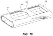
- FIG. 10is a front perspective view of a glass seamless enclosure, in accordance with one embodiment.
- FIG. 11is a top plan view of a glass enclosure co-extruded with both an opaque material and a transparent material, in accordance with one embodiment.
- FIG. 12is a perspective view of a two-layer clad glass enclosure.
- FIG. 13is a front perspective view of an embodiment of an electronic device having an enclosure formed from two glass members bonded together.
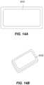
- FIGS. 14 A and 14 Bare a top plan view and perspective view of a glass band, respectively.
- FIG. 15is a side cross-sectional view of a glass enclosure with two flat pieces of glass bonded to the glass band shown in FIG. 14 .
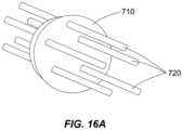
- FIG. 16 Ais a perspective view of a ceramic disk formed around several metal rods for forming a water-resistant audio jack in accordance with an embodiment.
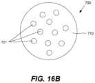
- FIG. 16 Bis a top plan view of the water-resistant audio jack shown in FIG. 16 A .
- FIG. 17is a method of manufacturing an electronic device with a glass enclosure, in accordance with one embodiment.
- FIG. 18is a perspective view of a solid block of glass prior to being formed into a glass enclosure.
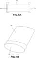
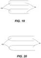
- FIGS. 19 and 20are side view showing chamfered edges and radius edges of an embodiment of a glass enclosure.
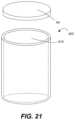
- FIG. 21is a perspective view of an embodiment of a glass enclosure made by a deep drawn blow molding process.
- FIG. 22is a side cross-sectional view of a glass main body with ink printing or back printing to achieve opacity around a display.
- FIG. 23is a perspective view of an embodiment of a glass main body having textured portions for use as light indicators.
- FIG. 24is a perspective view of a method of sealing of the interior of a glass enclosure to achieve a thicker surface layer in compression in a chemical strengthening process in accordance with an embodiment.
- FIG. 25shows an embodiment of a main body with rails that are adhered to and a screw boss molded into the main body.
- FIG. 1is an exploded perspective diagram of an electronic device 50 , in accordance with one embodiment.
- the device 50may be sized for one-handed operation and placement into small areas, such as a pocket.
- the device 50can be a handheld pocket-sized electronic device.
- the electronic device 50may correspond to a computer, media device, telecommunication device, and the like.
- the device 50includes a housing 52 that encloses and supports internally various electrical components (including, for example, integrated circuit chips and other circuitry) to provide computing operations for the device 50 .
- the housing 52can also define the shape or form of the device 50 . That is, the contour of the housing 52 may embody the outward physical appearance of the device 50 . It should be noted that, although the device 50 is illustrated in FIG. 1 with 90 degree edges, it will be understood that the device 50 can have rounded or chamfered edges.
- the housing 52generally includes a main body 54 in the form of an integral tube.
- integralit is meant that the main body is a single complete unit.
- the main bodyis structurally stiffer than conventional housings, which typically include two parts that are fastened together.
- the main bodyhas a substantially seamless appearance.
- the seamless housingprevents contamination and is more water resistant than conventional housings.
- the main body 54can define a cavity 56 therethrough between two open ends. In some embodiments, the main body 54 has only one open end.
- the main body 54can also include one or more windows 62 , which provide access to the electrical components, particularly the user interface elements, when they are assembled inside the cavity 56 of the main body 54 .
- the main body 54may be formed from a variety of materials or material combinations including, but not limited to, glass, metals, metal alloys, plastics, ceramics and the like. In a particular embodiment, the main body is formed of glass.
- the material selectedgenerally depends on many factors including, but not limited to, strength (tensile), density (lightweight), strength to weight ratio, Young's modulus, corrosion resistance, formability, finishing, recyclability, tooling costs, design flexibility, manufacturing costs, manufacturing throughput, reproducibility, and the like.
- the material selectedmay also depend on electrical conductivity, thermal conductivity, radio wave transparency, combustibility, toxicity, and the like.
- the material selectedmay also depend on aesthetics, including color, surface finish, and weight.
- the main body or glass enclosure 54is formed from a glass tube.
- the glass tubemay be formed from an extrusion or extrusion-like process.
- a glass enclosurecan also provide the portable electronic device with a unique, aesthetically pleasing appearance.
- the glasscan also be coated with an oleophobic coating to reduce finger prints and smudging on the glass.
- the glasscan also be coated with an anti-reflective coating to reduce glare.
- chemically strengthened glasscan also be scratch resistant.
- the glasscan also be color tinted in a wide variety of colors and can also have a variety of surface finishes including smooth and rough. For example, the glass can be polished to create a smooth (gloss) finish, or a blasting operation can performed to create a rough or textured (matte) finish.
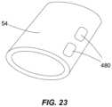
- Portions 480 of the glasscan also be textured so that the textured surface will disperse light and can be used as light indicator, as shown in FIG. 23 .
- the glass materialcan be formed so that the enclosure can have a seamless or substantially seamless appearance.
- the seamless enclosurein addition to being aesthetically pleasing, can provide the added benefit of less contamination and moisture intrusion into the interior of the device.
- glasshas been used in a wide variety of products, including electronic devices, such as watches, and phones. In these cases, however, the glass materials have not been used as structural components. In most of these cases, the glass materials have been used as cosmetic accoutrements or solely as a screen for a display. It is believed that, up until now, glass materials have never been used as a structural element providing substantially all of the structural frames, walls and main body of a consumer electronic device, and more particularly an enclosure of a portable electronic device, such as a media player or mobile phone.
- the glass enclosurealso allows a display screen to be positioned underneath and protected by the glass enclosure.
- the glass material of the enclosureis capable of capacitive sensing so that a touch screen can be used through the glass enclosure.
- FIG. 2An embodiment of a touch screen display in a glass enclosure 54 is illustrated in FIG. 2 , which is an exploded side view of the glass enclosure 54 with a liquid crystal display (LCD) touch screen assembly 120 .
- the glass enclosure 54can have an opening 55 on its rear face opposite the face with the display.
- the entire touch screen display assembly 120can be inserted through the opening 55 and into the enclosure. As shown in FIG.
- the touch screen display assembly 120includes a double indium tin oxide (DITO) 124 layer sandwiched between two optically clear adhesive (OCA) layers 122 , and a LCD 126 over one of the OCA layers 122 .
- the top OCA layer 122can adhere the DITO layer 124 to the LCD 126 .
- the bottom OCA layer 122can adhere the touch screen display assembly 120 to the glass enclosure 54 .
- the cover glass of a conventional touch screen display assemblycan be eliminated and the device can therefore be thinner as well as more aesthetically pleasing with a seamless enclosure.
- the housingcan be sealed with a door or a cap formed of glass or any other suitable material, including metal, plastic, and ceramic.
- the glass enclosure around the displaycan be made opaque so the operational components of the device are not visible.
- One method of making the glass opaqueis to use ink printing 128 in the areas where opacity is desired, as shown in FIG. 2 .
- a maskcan be used to mask off the display area.
- the opacitycan be painted or screen printed.
- Other techniques for achieving opacity in certain areassuch as using a two-layer clad glass, can be used, as will be described in more detail below.
- a LCD 130can be integrated with the glass enclosure 54 .
- a color filter panel 132may be positioned between a thin film transistor (TFT) glass 134 and the glass enclosure 54 to form the LCD 130 .
- TFTthin film transistor
- a conventional LCDhas a color filter panel sandwiched between two TFT glass layers.
- the glass enclosure 54is used in place of one of the TFT glass layers. This embodiment therefore allows the device to be thinner, as one less piece of TFT glass is used. It will be understood, that although the embodiment illustrated in FIG. 3 shows an opening in the enclosure 54 , this embodiment of the LCD can be employed in any of the embodiments of glass enclosures described herein.
- the housing 52can additionally include a pair of end caps or plugs 64 A and 64 B.
- Each of the end caps or plugs 64is configured to cover one of the open ends of the main body 54 , thereby forming a fully enclosed housing system.
- the end caps 64can be formed of materials, such as plastic, metal, and ceramic. The end caps 64 also serve as protection for the edges of the glass main body 54 , as will be explained in more detail below.
- an enclosureit is desirable for an enclosure to be durable.
- a piece of glasstypically breaks due to an exposed edge.
- crisp, 90 degree edges and cornersare prone to failure.
- Crisp edgescan easily be chipped off and become an origin for crack propagation.
- the edgescan be machined or buffed to make an edge chamfer 160 (as shown in FIG. 19 ) or an edge radius 162 to round out the edges (as shown in FIG. 20 ).
- the edgescan be coated with a protective material.
- the exposed ends of the glass enclosurecan be covered by applying protective coatings, such as plated metal using metallization or PVD plate metal.
- polymer coatingscan be applied over the exposed glass edges.
- the end caps 64can also provide further protection for the glass edges.
- the end caps 64may be attached to the main body 54 using a variety of techniques, including but not limited to, fasteners, glues, snaps, and the like. In some cases, the end caps 64 may be positioned on the surface of the open ends. If so, they typically have the same shape as the outer periphery of the main body 54 . In order to eliminate gaps, cracks or breaks on the front and side surfaces, the end caps 64 may alternatively be placed inside the cavity 56 at each of the ends. In this arrangement, the outer periphery of the end cap 64 generally matches the inner periphery of the main body 54 . This implementation is typically preferred in order to form a housing 52 with a uniform and seamless appearance, i.e., no breaks when looking directly at the front, back or side of the housing.
- FIGS. 4 - 6illustrate additional embodiments of end caps 64 for the glass main body 54 .
- the end caps 64can cover the open ends of the main body 54 in order to provide a fully contained housing 52 .
- the end caps 64can be applied in a variety or ways, in the particular embodiment shown in FIG. 4 , the end caps 64 have a shape that coincides with the internal shape of the main body 54 such that a portion of the end caps 64 may be inserted into the open ends.
- the end caps 64do not fully cover the open ends, but do provide protection to the edge of the main body 54 .
- a feature, such as a doorcan be used to fully cover an open end of the main body 54 .
- FIG. 6 Bis a perspective view of an end cap 64 shown in the side view of FIG. 6 A .
- the cross-sectional shape, including both the outer and inner shapes, of the main body 54may be widely varied. They may be formed from simple or intricate shapes, whether rectilinear and/or curvilinear. For hand held devices, it is typically preferred to use a shape that better fits the hand (e.g., form fits). By way of example, a rectangle with curved edges or an oval or pill shaped cross section having curvature that more easily receives the hand may be used. It should be noted that the inner cross-sectional shape may be the same or different from the external cross sectional shape of the main body. For example, it may be desirable to have a pill shaped external and a rectangular shaped interior, etc. In addition, although not a requirement, the front surface of the main body 54 may be substantially planar for placement of the user interface of the device 50 .
- the main body 54can have a wall having a continuous uniform thickness all around, as shown in FIG. 7 .
- the wall of the main body 54can be thicker at the edge or corner portions to provide strength in the areas where strength is more needed.
- the seamless main body 54can extend along a longitudinal axis, and can include an internal lumen that is sized and dimension for receipt of the internal components of the device 50 through an open end of the main body 54 .
- the device 50can also include one or more electronic subassemblies.
- the subassembliescan each include a carrier 68 and one or more operational components 70 of the electronic device 50 .
- the carrier 68can provide a structure for carrying the operational components 70 and supporting them when assembled inside the housing 52 .
- the carrier 68may be formed from plastics, metals, or a printed circuit board (PCB).
- the operational components 70perform operations associated with the computing device 50 .
- the operational components 70may, for example, include components such as user interface elements 70 A and circuit elements 70 B.
- the user interface elements 70 Aallow a user to interact with the computing device 50 .
- the user interface elements 70 Amay correspond to a display or an input device, such as a keypad, touch pad, touch screen, joystick, trackball, buttons, switches and the like.
- the circuit components 70 Bperform operations, such as computing operations for the computing device 50 .
- the computing components 70 Bmay include a microprocessor, memory, hard drive, battery, I/O connectors, switches, power connectors, and the like.
- the subassembliesare positioned inside the cavity 56 of the main body 54 .
- the subassembliescan be inserted into an open end of the main body 54 mainly along a longitudinal axis 74 of the main body 54 to their desired position within the housing 52 .
- the end caps 64 of the housing 52may be attached to the main body 54 in order to fully enclose the housing 52 around the subassemblies.
- the user interface elements 70 Aare positioned relative to the window opening 62 so that a user may utilize the user interface elements 70 A.
- the window 62may allow viewing access to a display or finger access to a touch pad or button.
- the glass main body 54is capable of capacitive sensing, so a touch screen or a touch pad could be positioned underneath the glass enclosure without a window opening 62 .
- the device 50may include an internal rail system 78 disposed inside the cavity 56 of the main body 54 .
- the internal rail system 78is integrally formed with the main body 54 , i.e., formed as a single part.
- the rail system 78can be adhered to the main body 54 .
- Features, such the internal rails 80 and screw bosses 79 , for mounting subassembliescan be adhered or molded into the main body 54 .
- the internal rail system 78is configured to receive the various subassemblies and guide them to their desired position within the main body 54 when the subassemblies are inserted through one of the open ends.
- the internal rail system 78enables the subassemblies to be easily and quickly assembled within the device 50 .
- the rail system 78provides for insertion (or removal) with minimal effort and without tools.
- the internal rail system 78also helps support and store the subassemblies in an organized manner within the device 50 .
- the rail system 78may store the subassemblies in a stacked parallel arrangement thereby using available space more efficiently.
- the rail system 78includes at least one set of opposed rails 80 , each of which extends longitudinally through the cavity 56 and each of which protrudes from the inner sides of the main body 54 .
- the rails 80are configured to receive the subassemblies and cooperate to guide subassemblies to their desired position within the housing 52 .
- the internal rails 80generally allow the subassemblies to be slid into the cavity 56 through an open end following the longitudinal axis 74 of the main body 54 . That is, the subassemblies are capable of sliding in and out of the housing 52 along one or more surfaces of the rails 80 .
- the portion of the subassemblies that engages the rails 80may be a surface of the subassemblies or alternatively one or more posts or mounts that extend outwardly from the subassemblies.
- the reference surfaces for the opposed rails 80may be positioned in the same plane or they may be positioned in different planes.
- the configurationgenerally depends on the configuration of the subassemblies.
- the subassembliesmay have a cross section that is stepped rather than completely planar.
- the opposed rails 80have references surfaces in different planes in order to coincide with the stepped cross section.
- each of the rails 80may be segmented or include removed portions as for example at the ends for placement of the flush mounted end caps.
- the width of the rails 80may be widely varied. For example, they may be one integral piece that extends entirely from one side to the other, or they may be separate pieces with a gap located therebetween (as shown).
- the position and cross sectional dimensions and shapes of each of the railsmay also be widely varied.
- the size and shape as well as the position of the rails 80generally depend on the configuration of the subassemblies.
- the rails 80may have the same shape and size or they may have different shape and size. In most cases, the size and shape is a balance between keeping them as small as possible (for weight and space requirements) while providing the required reference surface and ample support to the subassemblies.
- the rails 80define one or more channels 82 that receive the one or more subassemblies.
- the rails 80 along with the main body 54define a pair of channels, particularly an upper channel 82 A and a lower channel 82 B.
- the upper channel 82 Areceives a first subassembly 66 A and the lower channel 82 B receives a second subassembly 66 B. It should be noted, however, that this is not a limitation and that additional sets of rails 80 may be used to produce additional channels 82 .
- the subassembliesare not limited to being fully contained with a single channel and that portions of a subassembly may be positioned in multiple channels.
- the second subassembly 66 Bwhich is positioned in the lower channel 82 B, may include a protruding portion that is positioned through the rails 80 and into the upper channel 82 A.
- the channels 82generally include an entry point and a final point.
- the entry pointrepresents the area of the channel 82 that initially receives the subassemblies 66 , i.e., the area proximate the ends of the main body 54 .
- the final pointrepresents the area of the channel 82 that prevents further sliding movement.
- the final pointmay, for example, set the final mount position of the subassemblies 66 within the housing 52 .
- the final pointmay, for example, correspond to an abutment stop.
- the abutment stopmay be integral with the main body 54 or a separate component. By way of example, the abutment stop may correspond to one more posts that are mounted inside the cavity 56 on the inside surface of the main body 54 at a predetermined distance along the longitudinal axis 74 .
- the interface between the subassemblies 66 and housing 52may include a locking or securing mechanism.
- the locking mechanismgenerally consists of two parts, including a housing side locking feature and a subassembly side locking feature that are cooperatively positioned so that when the subassembly 66 is inserted into the housing 52 , the locking features engage with one another thus holding the subassembly 66 in its desired position within the housing 52 .
- the locking featuresare configured to provide quick and easy assembly of the subassembly into the housing without the use of tools.
- the locking featuresmay correspond to snaps, friction couplings, detents, flexures and/or the like.
- the subassemblies 66may be attached to the main body 54 with fasteners or adhesives.
- the operational components 70can be directly secured to the main body 54 .
- the locking features of the subassemblies 66each include a flexure tab 88 that engages a recess 90 located on an inner surface of the main body 54 .
- the tab 88snaps into the recess 90 thereby securing the subassembly 66 at a predetermined position along the longitudinal axis 74 . That is, because the tabs 88 flex, they allow the subassemblies 66 to pass when pushed into the cavity 76 .
- the tabs 88resume their natural position thereby trapping the subassemblies 66 in the channel 82 between the locking tab/recess 88 / 90 and the abutment stop at the end of the channel 82 .
- the subassemblies 66are prevented from sliding out of the channels 82 on their own.
- a usersimply lifts the tab 88 away from the recess 90 while pulling on the subassembly 66 .
- the recess 90 and abutment stopmay cooperate to set the final position of the subassembly 66 in the cavity 56 of the main body 54 .
- the recess and abutment stopmay be configured to position the user interface elements 70 A directly behind the window opening 62 so that a user has full access to the user interface elements 70 A.
- the main body 54which may include the internal rails 80 (or other internal features), is formed via an extrusion or extrusion-like process.
- the processis capable of producing an integral tube without seams, crack, breaks, and the like.
- extrusion of conventional materialssuch as metals and plastics
- extrusion processis a shaping process where a continuous work piece (i.e., a solid block of glass 10 as shown in FIG. 18 ) is produced by forcing molten or hot material through a shaped orifice.
- the extrusion processproduces a length of a particular cross sectional shape.
- the cross-sectional shape of the continuous or length of the extruded work pieceis controlled at least in part on the shaped orifice. As the shaped work piece exits the orifice, it is cooled and thereafter cut to a desired length.
- FIG. 9is a perspective view of a handheld computing device 100 , in accordance with one embodiment.
- the computing device 100may generally correspond to the device 50 shown and described in FIG. 1 .
- the computing device 100is capable of processing data and more particularly media, such as audio, video, images, and the like.
- the computing device 100may generally correspond to a music player, game player, video player, camera, cell phone, personal digital assistant (PDA), and the like.
- PDApersonal digital assistant
- the computing device 100can be operated solely by the user's hand(s), i.e., no reference surface, such as a desktop, is needed. In some cases, the handheld device is sized for placement into a pocket of the user.
- the computing device 100is a pocket-sized hand held music player that allows a user to store a large collection of music.
- the music playermay correspond to the iPod series MP3 players, including for example the iPod MiniTM and iPod NanoTM manufactured by Apple Inc. of Cupertino, Calif.
- the computing device 100includes a housing 102 , which can be formed of glass, which encloses and supports internally various electrical components (including integrated circuit chips and other circuitry) to provide computing operations for the device.
- the integrated circuit chips and other circuitrymay include a microprocessor, hard drive, Read-Only Memory (ROM), Random-Access Memory (RAM), a battery, a circuit board, and various input/output (I/O) support circuitry.
- the housing 102may also define the shape or form of the device 100 . In this particular illustrated embodiment, the housing 102 extends longitudinally and has a pill like cross section. The size and shape of the housing 102 is preferably dimensioned to fit comfortably within a user's hand.
- the housingis formed from a glass material and has a seamless or substantially seamless look along the length of the device 100 . That is, unlike conventional housings, the housing 102 , particularly the main body, does not include any breaks between the top and bottom ends, thereby making it stiffer and more aesthetically pleasing.
- the computing device 100can also include a display screen 104 .
- the display screen 104which is assembled within the housing 102 and which can be visible through the glass housing 102 or can be positioned in a window 106 , can be used to display a graphical user interface (GUI) as well as other information to the user (e.g., text, objects, graphics).
- GUIgraphical user interface
- the display screen 104can also employ touch screen technology.
- the glass material of the housing 102allows the display screen 104 to be positioned underneath and protected by the glass housing 102 .
- the glass material of the housing 102is also capable of capacitive sensing so that a touch screen or touch pad can be used through the glass housing 102 .
- the computing device 100can also include one or more input devices 108 configured to transfer data from the outside world into the computing device 100 .
- the input devices 108may, for example, be used to perform tracking or scrolling to make selections or to issue commands in the computing device 100 .
- the input devices 108may correspond to keypads, joysticks, touch screens, touch pads, track balls, wheels, buttons, switches, and the like.
- the computing device 100includes a touch pad 108 A and one or more buttons 108 B, which are assembled within the housing 102 and which are accessible through an opening 110 in the housing 102 .
- the touch pad 108 Agenerally consists of a touchable outer surface 111 for receiving a finger for manipulation on the touch pad 100 A.
- a sensor arrangementbeneath the touchable outer surface 111 is a sensor arrangement.
- the sensor arrangementmay be positioned directly underneath the glass enclosure without the touchable outer surface 111 , as the glass is capable of capacitive sensing and can act as the touchable outer surface.
- the sensor arrangementincludes a plurality of sensors that are configured to activate as the finger passes over them. In the simplest case, an electrical signal is produced each time the finger passes a sensor.
- the number of signals in a given time framemay indicate location, direction, speed and acceleration of the finger on the touch pad, i.e., the more signals, the more the user moved his or her finger.
- the signalsare monitored by an electronic interface that converts the number, combination and frequency of the signals into location, direction, and speed and acceleration information. This information may then be used by the device 100 to perform the desired control function on the display screen 104 .
- the buttons 108 Bare configured to provide one or more dedicated control functions for making selections or issuing commands associated with operating the device 100 .
- the button functionsare implemented via a mechanical clicking action although they may also be associated with touch sensing similar to the touch pad 108 A.
- the position of the buttons 108 B relative to the touch pad 108 Amay be widely varied.
- touch pad/button arrangementswhich may be used in the device 100 , are described in greater detail in U.S. patent application Ser. Nos. 10/643,256, 10/188,182, 10/722,948, which are all hereby incorporated by reference herein in their entireties.
- the computing device 100can also include one or more switches 112 , including power switches, hold switches, and the like. Like the touch pad 108 A and buttons 108 B, the switches 112 can be accessible through a second opening 114 in the housing 102 .
- the device 100may also include one or more connectors 116 for transferring data and/or power to and from the device 100 .
- the device 100includes an audio jack 116 A, a data port 116 B and a power port 116 C.
- the data port 116 Bmay serve as both a data and power port thus replacing a dedicated power port 116 C.
- a data portsuch as this is described in greater detail in U.S. patent application Ser. No. 10/423,490, which is hereby incorporated by reference herein in its entirety.
- the glass main body 54can include an access opening or window 62 having a shape that coincides with the shape of the input assembly.
- the access openings 62 for the display and touch padcan be located in the front planar surface 280 .
- the access openings 62may be formed from processes (individually or in combination), such as machining, drilling, cutting, punching, and the like. In embodiments having the access openings 62 , some of the operational components may be loaded into the enclosure through the access openings 62 .
- the access openings 62may provide user access to components, such as displays, touch pads, and buttons.
- Another way to provide access to a displayis through the transparent glass enclosure.
- opacityor translucency
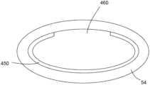
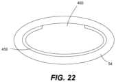
- FIG. 22is a side cross-sectional view of a glass main body 54 with ink printing or back printing 450 to achieve opacity around a display. As shown in FIG. 22 , the printing 450 does not go all the way around the main body 54 so as to leave an area or transparency 460 for the display.
- Another way to achieve opacity around a display or other componentis to form the main body 54 by co-extruding an opaque glass material 146 together with a transparent glass material 148 , as shown in FIG. 11 .
- the dotted lines in FIG. 11illustrate the separation between the opaque material 146 and the transparent material 148 .
- the access opening or window 62 for the displayis in the transparent material 148 portion.
- FIG. 12Yet another way to achieve opacity around a component, such as a display, is to use a two-layer clad glass 140 for the main body 54 , as shown in FIG. 12 .
- the clad glass 140is formed by fusing together a layer of opaque glass material 142 and a layer of transparent glass material 144 at a high temperature. The two layers 142 , 144 will cool as a single fused layer. If the opaque glass material 142 is positioned as the external layer and the transparent glass material 144 is positioned as the internal layer, then a portion of the opaque glass 142 can be etched, or otherwise removed, to expose a portion of the transparent glass 144 underneath to form a window for the display.
- Another benefit of using a two-layer clad glass 140is that the enclosure can be made stronger if the glass includes two layers having different coefficients of thermal expansion (CTE). If the external layer has a high CTE and the internal layer has a low CTE, then the two layers 142 , 144 will fuse into one layer, with the external surface glass layer 142 being in a compressive state.
- CTEcoefficients of thermal expansion
- a sheet of glasscan be made stronger by chemically strengthening it.
- the glasscan be placed in a potassium bath to cause the entire surface of the glass to be in a compressed state and therefore stronger.
- a glass enclosure, as described herein, having a single layer of glass materialcould be chemically treated to improve the strength of the glass.
- potassium bathsare expensive, so using a two-layer clad glass with layers that have different CTEs can provide cost savings.
- opacity in desired portionscan be achieved and the glass enclosure can be made stronger without employing an expensive potassium bath.
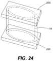
- FIG. 24is a perspective view illustrating a method of sealing of the interior of a glass enclosure to achieve a thicker surface layer in compression in a chemical strengthening process, in accordance with an embodiment.
- a thicker layer of compression on the external surface of the glass main body 54is achieved. This thicker layer of compression on the external surface is relative to the internal surface of the main body 54 .
- the external surface of the glass main body 54can be made even stronger by sealing the open ends of the main body 54 to close off the interior of the main body 54 with seals 650 and placing the sealed off glass main body 54 in a potassium bath to compress only the exterior of the tube and not the interior.
- the internal componentsmay also include components for processing, transmitting and receiving wireless signals (e.g., transmitter, receiver, antenna, etc.) through the glass enclosure 54 .
- the devicemay include components for supporting FM, RF, Bluetooth, 802.11, and the like.
- the devicecan include functionality for supporting cellular or mobile phone usage.
- the deviceincludes processors, transmitters, receivers, and antennas for supporting RF, and more particularly GSM, DCS and/or PCS wireless communications in the range of about 850 to about 1900 MHz.
- the devicemay, for example, include one or more antennas tuned to operate over the GSM, PCS and/or DCS frequency bands.
- monopole, dipole and tri band and quad band antennasmay be used.
- a PCS+DCS dipole antennais used.
- the antennamay protrude out of the enclosure or it may be fully enclosed by the enclosure. If the latter, the glass enclosure is radio transparent and therefore capable of transmitting and receiving RF signals therethrough.
- the main body of the enclosurecan be formed from a glass material that is radio-transparent.
- an internal antennamay be used, which is typically more robust and durable than an external antenna.
- many advantages regarding the use of an internal antennamay be achieved. For example, a smaller and cheaper antenna may be used.
- the antennacan be integrated with other components and placed at almost any location within the enclosure, which helps make a smaller and more compact device in addition to reducing the cost of manufacture.
- An example of wireless communication devices and mechanismscan be found in U.S. patent application Ser. No. 10/423,490, which is hereby incorporated by reference herein in its entirety.
- the glass enclosure 400can be formed using a deep drawing and a blow molding process.
- the deep drawing and blow molding processesresult in a bucket or cup-like glass enclosure 400 with only one open end 410 , as shown in FIG. 21 . Therefore, only one end cap 64 is necessary to close off or seal such housing.
- FIG. 13shows one embodiment of an enclosure 550 that includes a top member 552 with a bottom member 554 attached thereto.
- the top and bottom members 552 and 554can be formed from the same or different materials.
- the top and bottom members 552 , 554are both formed of glass.
- any combinationcan be used.
- this designcan be made with or without using end caps.
- the top and bottom membersmay include a closed end.
- the two members 552 , 554allow components to be assembled onto the members 552 , 554 before the two members 552 , 554 are bonded together using, for example, an adhesive or laser frit bonding.
- the laser frit bondingmay be employed to hermetically seal the two members 552 , 554 together to form the enclosure 550 .
- Ink printing or back painting to achieve opacity in certain areascan also he performed prior to assembling the components and bonding the members 552 , 554 together.
- the enclosure 550can be polished so that the enclosure 550 has a more continuous and substantially seamless appearance. If no openings are provided in the enclosure 550 , then a laser frit bonded enclosure 550 can be fully hermetically sealed and therefore water resistant, as will be described in more detail below.
- FIGS. 14 A and 14 Bare a top plan view and perspective view of a glass band 610 according to an embodiment.
- the glass band 610is formed by an extrusion process and then cut to the desired height.
- the glass band 610is laser frit bonded to two flat pieces of glass: a cover glass 620 and a back glass 630 to form a hermetic seal.
- the glass band 610can be bonded to a cover glass 620 and a back plate (not shown).
- the embodiment of the housing 600 shown in FIG. 15can be made fully hermetically sealed if the housing 600 is not provided with any access openings.
- the glass housingis capable of capacitive sensing, so components such as touch screens and touch pads can be positioned underneath the glass enclosure.
- Other controlssuch as buttons for volume control or power, can also be positioned underneath the glass enclosure by placing capacitive sensors underneath the glass housing so that openings for buttons are unnecessary.
- Speakers and microphonesmay be provided with a GORETEX® membrane, which is waterproof.
- the devicecan send and receive signals using wireless signals, which can be transmitted through the radio transparent glass housing 600 .
- a component such as the one shown in FIG. 16can be provided to maintain the water resistant characteristic of the device.
- the electrical signal transferring component 700is made by forming a ceramic disk 710 around several metal rods 720 , as shown in FIG. 16 A . These metal rods are then shaved down or machined away to leave metal contacts 721 in the ceramic disk, thereby forming the water resistant audio jack, as shown in FIG. 16 B . It will be understood that the metal contacts 721 serve as electrical contacts.
- the component 700can be used to receive signals from an audio jack and pass them into a water-resistant device, such as the one shown in FIG. 15 , such that no water can get through this geometry, but the electric signals can.
- a display screencan be built into the glass enclosure.
- LCDsare typically formed with a carrier.
- the glass enclosurecan be used as the carrier for the display, thereby decreasing the bulk of the device. It will be understood that such a display screen can only be built into an enclosures formed by bonding together two members, such as the one illustrated in FIG. 13 .
- the inventionis not limited to this particular form factor.
- the cross-sectional shape, width, thickness, and height of the enclosurecan all be adjusted according to the needs of the device.
- the width and thicknessmay be reduced while increasing the height.
- the openings in the enclosurecan also be modified and may take on other shapes.
- the touch pad circlemay be decreased in diameter.
- the enclosuremay have dimensions similar to the iPod Nano manufactured by Apple Inc. of Cupertino, Calif.
- the devicemay correspond to smaller more compact devices, such as the Shuffle and remote controls manufactured by Apple Inc. of Cupertino, Calif.
- FIG. 17is a method of manufacturing an electronic device with a glass enclosure, in accordance with one embodiment.
- the glass enclosuremay be embodied in various forms including those previously mentioned.
- the methodbegins at block 1700 , where a hollow glass tube is provided. It will be understood that the glass may be tinted a desired color or made opaque or translucent in certain areas.
- the tubecan have any cross-sectional shape to create the desired shaped enclosure formed from glass.
- the glass enclosurecan be machined to create holes and features into the enclosure, such as, for example, the openings in the front face of the enclosure.
- a CNC machinemay be used to perform some or all of the machining operations.
- the openings and featuresmay be made with laser cutting, jet cutting, ultrasonic cutting, chemical etching, or any other suitable material removal operation.
- a surface finishing operationmay be performed.
- a polishing operationcan be performed to create a smooth (gloss) finish.
- a blasting operationcan be performed to create a rough (matte) finish.
- the methodmay include an additional step 1740 of applying a protective coating or protective features to the outside of the glass enclosure.
- a protective coating or protective featuresmay, for example, be formed from deformable materials, such as silicon, foam and rubber materials.
- the coatings or protective featuresare typically positioned on the exterior surface to prevent cracking and protect the glass enclosure from undesirable forces as, for example, when the glass enclosure is dropped.
- the coatings and protective featurescan be placed almost anywhere on the glass enclosure, but in most cases are placed at least at the edges where the glass enclosure may be susceptible to cracking. In some cases, the end plates may even serve this function.
- the methodthen proceeds to block 1750 where the enclosure is cleaned and inspected.
- the inspectionmay include micro photography as well as chemical composition analysis.
- the enclosurecan be used to assemble the final product (e.g., internal components inserted inside) in block 1760 .
- the end capsare placed on the open ends to seal the housing.
- the enclosuremay be formed from multiple parts rather than a single integrally formed piece.
- Each of these partsmay be extruded or otherwise formed.
- theymay be formed from the same materials (glass/glass), same class of materials (first glass material/second glass material) or from different classes of materials (glass/metal, glass/plastic, plastic/metal or glass/plastic/metal).
- glass/glasssame class of materials
- first glass material/second glass materialglass/metal, glass/plastic, plastic/metal or glass/plastic/metal
- the multiple partsmay include frame components with plates attached thereto, or a top member and a bottom member that are attached together.
- the attachment meansmay be widely varied and may include such things as fasteners, glues, epoxies, double sided tape, snaps, mechanical interlocks that are molded together, and the like.
- fastenersglues, epoxies, double sided tape, snaps, mechanical interlocks that are molded together, and the like.
- One example of connecting parts togethercan be found in U.S. Pat. No. 7,012,189 and U.S. application Ser. No. 10/928,780, both of which are hereby incorporated by reference herein in their entireties.
- the various components of the enclosuremay consist of multiple layers that are glued, press fit, molded or otherwise secured together.
- the enclosureconsists of multiple layers that form a single laminate structure formed for example by gluing.
- the entire or portions of the enclosure wallsmay be formed from layers of metals, ceramics and/or plastics.
- the layersmay include glass and ceramics as, for example, forming a wall with a glass outer layer and a ceramic inner layer (or vice versa).
- the enclosurewhen using an internal antenna, it is desirable to increase the radio transparency of the enclosure in order to effectively perform wireless transmissions therethrough.
- a substantial portion of the enclosureis formed form materials capable of providing radio-transparency (e.g., glass, ceramics, plastics, etc.).
- the radio transparent portions of the enclosureconstitute a significant area of the entire enclosure, for example, greater than 50%, more particularly greater than 75%, and even more particularly greater than 85%.
- the radio transparent portionsmay even be greater than 90%, and more particularly greater than 95%, and in some cases 100% of the enclosure.
- the radio transparent portionsmay be embodied in a variety of ways.
- the radio transparent portionsconstitute the entire enclosure.
- all the walls of the enclosureare radio transparent (e.g., both the main body and the end caps).
- the radio transparent portionsconstitute one or more walls of the housing, such as, for example, the top and/or bottom member of the enclosure shown in FIG. 13 .
- the radio transparent portionsmay constitute a part of one or more walls of the enclosure. That is, only a portion of a wall may be radio transparent.
- the wallmay be separated into two parts, or in the case of a laminated wall, some portion of the wall may include a non radio transparent layer.
- the internal antennamay be positioned closer or proximate to the radio transparent portions of the enclosure.
- non radio transparent portionssuch as metals typically degrade radio transmissions, in some cases, non radio transparent portions may be designed in such a manner as to enhance or help radio transmissions.
Landscapes
- Engineering & Computer Science (AREA)
- Physics & Mathematics (AREA)
- Computer Hardware Design (AREA)
- Theoretical Computer Science (AREA)
- Microelectronics & Electronic Packaging (AREA)
- General Physics & Mathematics (AREA)
- General Engineering & Computer Science (AREA)
- Nonlinear Science (AREA)
- Human Computer Interaction (AREA)
- Mathematical Physics (AREA)
- Crystallography & Structural Chemistry (AREA)
- Chemical & Material Sciences (AREA)
- Optics & Photonics (AREA)
- Signal Processing (AREA)
- Computer Networks & Wireless Communication (AREA)
- Casings For Electric Apparatus (AREA)
- Telephone Set Structure (AREA)
Abstract
Description
Claims (20)
Priority Applications (3)
| Application Number | Priority Date | Filing Date | Title |
|---|---|---|---|
| US16/992,853US11785729B2 (en) | 2010-09-17 | 2020-08-13 | Glass enclosure |
| US18/244,287US12219720B2 (en) | 2010-09-17 | 2023-09-10 | Glass enclosure |
| US19/002,667US20250126727A1 (en) | 2010-09-17 | 2024-12-26 | Glass enclosure |
Applications Claiming Priority (7)
| Application Number | Priority Date | Filing Date | Title |
|---|---|---|---|
| US38421110P | 2010-09-17 | 2010-09-17 | |
| US13/233,940US8824140B2 (en) | 2010-09-17 | 2011-09-15 | Glass enclosure |
| US14/447,507US9439305B2 (en) | 2010-09-17 | 2014-07-30 | Glass enclosure |
| US15/226,737US10021798B2 (en) | 2010-09-17 | 2016-08-02 | Glass enclosure |
| US16/022,588US10398043B2 (en) | 2010-09-17 | 2018-06-28 | Glass enclosure |
| US16/538,686US10765020B2 (en) | 2010-09-17 | 2019-08-12 | Glass enclosure |
| US16/992,853US11785729B2 (en) | 2010-09-17 | 2020-08-13 | Glass enclosure |
Related Parent Applications (1)
| Application Number | Title | Priority Date | Filing Date |
|---|---|---|---|
| US16/538,686ContinuationUS10765020B2 (en) | 2010-09-17 | 2019-08-12 | Glass enclosure |
Related Child Applications (1)
| Application Number | Title | Priority Date | Filing Date |
|---|---|---|---|
| US18/244,287ContinuationUS12219720B2 (en) | 2010-09-17 | 2023-09-10 | Glass enclosure |
Publications (2)
| Publication Number | Publication Date |
|---|---|
| US20200375045A1 US20200375045A1 (en) | 2020-11-26 |
| US11785729B2true US11785729B2 (en) | 2023-10-10 |
Family
ID=45817589
Family Applications (8)
| Application Number | Title | Priority Date | Filing Date |
|---|---|---|---|
| US13/233,940Active2031-12-18US8824140B2 (en) | 2010-09-17 | 2011-09-15 | Glass enclosure |
| US14/447,507Active2031-12-02US9439305B2 (en) | 2010-09-17 | 2014-07-30 | Glass enclosure |
| US15/226,737ActiveUS10021798B2 (en) | 2010-09-17 | 2016-08-02 | Glass enclosure |
| US16/022,588ActiveUS10398043B2 (en) | 2010-09-17 | 2018-06-28 | Glass enclosure |
| US16/538,686ActiveUS10765020B2 (en) | 2010-09-17 | 2019-08-12 | Glass enclosure |
| US16/992,853ActiveUS11785729B2 (en) | 2010-09-17 | 2020-08-13 | Glass enclosure |
| US18/244,287ActiveUS12219720B2 (en) | 2010-09-17 | 2023-09-10 | Glass enclosure |
| US19/002,667PendingUS20250126727A1 (en) | 2010-09-17 | 2024-12-26 | Glass enclosure |
Family Applications Before (5)
| Application Number | Title | Priority Date | Filing Date |
|---|---|---|---|
| US13/233,940Active2031-12-18US8824140B2 (en) | 2010-09-17 | 2011-09-15 | Glass enclosure |
| US14/447,507Active2031-12-02US9439305B2 (en) | 2010-09-17 | 2014-07-30 | Glass enclosure |
| US15/226,737ActiveUS10021798B2 (en) | 2010-09-17 | 2016-08-02 | Glass enclosure |
| US16/022,588ActiveUS10398043B2 (en) | 2010-09-17 | 2018-06-28 | Glass enclosure |
| US16/538,686ActiveUS10765020B2 (en) | 2010-09-17 | 2019-08-12 | Glass enclosure |
Family Applications After (2)
| Application Number | Title | Priority Date | Filing Date |
|---|---|---|---|
| US18/244,287ActiveUS12219720B2 (en) | 2010-09-17 | 2023-09-10 | Glass enclosure |
| US19/002,667PendingUS20250126727A1 (en) | 2010-09-17 | 2024-12-26 | Glass enclosure |
Country Status (1)
| Country | Link |
|---|---|
| US (8) | US8824140B2 (en) |
Cited By (1)
| Publication number | Priority date | Publication date | Assignee | Title |
|---|---|---|---|---|
| US12219720B2 (en)* | 2010-09-17 | 2025-02-04 | Apple Inc. | Glass enclosure |
Families Citing this family (80)
| Publication number | Priority date | Publication date | Assignee | Title |
|---|---|---|---|---|
| CN102388003B (en) | 2009-03-02 | 2014-11-19 | 苹果公司 | Technology for Strengthening Glass Covers for Portable Electronic Devices |
| US20120024200A1 (en)* | 2009-06-08 | 2012-02-02 | Lap Solutions Llc. | Multifunction Computer Table and Carrier |
| US9778685B2 (en) | 2011-05-04 | 2017-10-03 | Apple Inc. | Housing for portable electronic device with reduced border region |
| US8797721B2 (en) | 2010-02-02 | 2014-08-05 | Apple Inc. | Portable electronic device housing with outer glass surfaces |
| US10189743B2 (en) | 2010-08-18 | 2019-01-29 | Apple Inc. | Enhanced strengthening of glass |
| TW201223906A (en)* | 2010-10-08 | 2012-06-16 | Corning Inc | Strengthened glass enclosures and method |
| FI124625B (en)* | 2010-10-15 | 2014-11-14 | Perlos Oyj | Electronic device, shells and procedure |
| US9725359B2 (en) | 2011-03-16 | 2017-08-08 | Apple Inc. | Electronic device having selectively strengthened glass |
| US10781135B2 (en) | 2011-03-16 | 2020-09-22 | Apple Inc. | Strengthening variable thickness glass |
| US9128666B2 (en) | 2011-05-04 | 2015-09-08 | Apple Inc. | Housing for portable electronic device with reduced border region |
| CN202261417U (en)* | 2011-08-22 | 2012-05-30 | 深圳富泰宏精密工业有限公司 | Shell and portable electronic device using same |
| DE102011111506B4 (en)* | 2011-08-31 | 2017-05-18 | Leonhard Kurz Stiftung & Co. Kg | Plastic film and touch sensor |
| US9944554B2 (en) | 2011-09-15 | 2018-04-17 | Apple Inc. | Perforated mother sheet for partial edge chemical strengthening and method therefor |
| US9516149B2 (en) | 2011-09-29 | 2016-12-06 | Apple Inc. | Multi-layer transparent structures for electronic device housings |
| US10144669B2 (en) | 2011-11-21 | 2018-12-04 | Apple Inc. | Self-optimizing chemical strengthening bath for glass |
| US9237660B2 (en) | 2011-11-22 | 2016-01-12 | Corning Incorporated | 3-D glass enclosures for electronic devices |
| FR2985631B1 (en)* | 2012-01-09 | 2014-03-14 | Hikob | HOUSING FOR ELECTRONIC DEVICE |
| US10133156B2 (en) | 2012-01-10 | 2018-11-20 | Apple Inc. | Fused opaque and clear glass for camera or display window |
| US8773848B2 (en) | 2012-01-25 | 2014-07-08 | Apple Inc. | Fused glass device housings |
| KR101709387B1 (en)* | 2012-02-27 | 2017-02-22 | 코닝 인코포레이티드 | Low Tg glass gasket for hermetic sealing applications |
| JP2013201742A (en)* | 2012-03-23 | 2013-10-03 | Hzo Inc | Portless electronic devices |
| US20130319866A1 (en) | 2012-05-29 | 2013-12-05 | Lucy Elizabeth Browning | Anodized films |
| US9611165B2 (en)* | 2012-06-08 | 2017-04-04 | Corning Incorporated | Method and apparatus for bending a glass sheet and an electronic device casing |
| CN104335114B (en)* | 2012-06-08 | 2018-02-23 | 苹果公司 | The jealous glass and transparent glass of the fusion of camera window or indicator gate |
| CN103491738B (en)* | 2012-06-11 | 2016-07-13 | 鸿富锦精密工业(深圳)有限公司 | Housing structure and electronic device adopting the housing structure |
| US9429997B2 (en) | 2012-06-12 | 2016-08-30 | Apple Inc. | Electronic device with wrapped display |
| CN104411657B (en)* | 2012-06-27 | 2017-02-22 | 东曹株式会社 | Composite plate and production method therefor |
| US9364861B2 (en) | 2012-06-28 | 2016-06-14 | Nokia Technologies Oy | Tube-shaped part and an associated method of manufacture |
| KR101994889B1 (en)* | 2012-09-14 | 2019-07-01 | 삼성전자 주식회사 | A protective device for portable terminal |
| US9946302B2 (en) | 2012-09-19 | 2018-04-17 | Apple Inc. | Exposed glass article with inner recessed area for portable electronic device housing |
| US20140098472A1 (en)* | 2012-10-04 | 2014-04-10 | Corning Incorporated | Glass enclosure body having mechanical resistance to impact damage |
| US9413861B2 (en)* | 2012-10-05 | 2016-08-09 | Nokia Technologies Oy | Metallization and anodization of plastic and conductive parts of the body of an apparatus |
| USD733125S1 (en)* | 2013-01-03 | 2015-06-30 | Samsung Electronics Co., Ltd. | Tablet computer |
| WO2014144322A1 (en) | 2013-03-15 | 2014-09-18 | Kinestral Technologies, Inc. | Laser cutting strengthened glass |
| TW201503793A (en)* | 2013-03-29 | 2015-01-16 | Toshiba Machine Co Ltd | Cover member |
| USD732499S1 (en)* | 2013-06-14 | 2015-06-23 | Lg Electronics Inc. | Mobile phone |
| USD744990S1 (en)* | 2013-06-14 | 2015-12-08 | Lg Electronics Inc. | Mobile phone |
| US9459661B2 (en) | 2013-06-19 | 2016-10-04 | Apple Inc. | Camouflaged openings in electronic device housings |
| CN104252201A (en)* | 2013-06-28 | 2014-12-31 | 鸿富锦精密工业(深圳)有限公司 | Electronic device with displaying module |
| TW201501587A (en)* | 2013-06-28 | 2015-01-01 | Hon Hai Prec Ind Co Ltd | Electronic device with displaying module |
| US20150116157A1 (en)* | 2013-10-25 | 2015-04-30 | Jinyoung Park | Antenna case of air-hole structure |
| US9886062B2 (en) | 2014-02-28 | 2018-02-06 | Apple Inc. | Exposed glass article with enhanced stiffness for portable electronic device housing |
| US11097514B2 (en) | 2014-05-12 | 2021-08-24 | Corning Incorporated | Method of improving optical quality of curved glass structures |
| WO2015200550A1 (en)* | 2014-06-24 | 2015-12-30 | Dinesh Pinakin | Protective enclosures for mobile computing devices |
| KR200488235Y1 (en)* | 2014-08-27 | 2018-12-31 | 애플 인크. | Sapphire cover for electronic devices |
| WO2016053258A1 (en)* | 2014-09-29 | 2016-04-07 | Apple Inc. | Tube hydroforming of jointless usb stainless steel shell |
| US9890070B2 (en) | 2015-01-30 | 2018-02-13 | Corning Incorporated | Manufacturing process to reform glass tubes |
| CN106163168A (en)* | 2015-04-22 | 2016-11-23 | 富泰华精密电子(郑州)有限公司 | Housing and use the electronic installation of this housing |
| KR102672500B1 (en)* | 2015-08-31 | 2024-06-07 | 코닝 인코포레이티드 | Apparatus and method for protecting glass displays of electronic devices |
| DE102015117226A1 (en)* | 2015-09-15 | 2017-03-16 | Preh Gmbh | Arrangement of electrical indicator and turntable with foreign body intrusion protection |
| WO2017131854A1 (en)* | 2016-01-26 | 2017-08-03 | Google Inc. | Glass enclosures for electronic devices |
| US20180150256A1 (en)* | 2016-11-29 | 2018-05-31 | Intel Corporation | Technologies for data deduplication in disaggregated architectures |
| US10334092B2 (en)* | 2017-01-04 | 2019-06-25 | Toughbuilt Industries, Inc. | Mobile Phone |
| US11678445B2 (en) | 2017-01-25 | 2023-06-13 | Apple Inc. | Spatial composites |
| EP4589618A3 (en) | 2017-03-29 | 2025-10-15 | Apple Inc. | Device having integrated interface system |
| US10292286B2 (en)* | 2017-07-31 | 2019-05-14 | Apple Inc. | Patterned glass layers in electronic devices |
| WO2019067772A1 (en) | 2017-09-29 | 2019-04-04 | Mikael Silvanto | Multi-part device enclosure |
| KR102547540B1 (en)* | 2018-02-14 | 2023-06-26 | 삼성전자주식회사 | Window cover glass and having the same |
| US10969255B2 (en)* | 2018-04-20 | 2021-04-06 | Darrel Eugene Self | TIC environmental event sensor |
| CN111356979B (en) | 2018-05-25 | 2023-12-29 | 苹果公司 | Portable computer with dynamic display interface |
| US10708403B2 (en)* | 2018-07-23 | 2020-07-07 | Case-Mate, Inc. | Electronic device case with a transparent or translucent back panel |
| US11175769B2 (en) | 2018-08-16 | 2021-11-16 | Apple Inc. | Electronic device with glass enclosure |
| US11258163B2 (en) | 2018-08-30 | 2022-02-22 | Apple Inc. | Housing and antenna architecture for mobile device |
| US11189909B2 (en) | 2018-08-30 | 2021-11-30 | Apple Inc. | Housing and antenna architecture for mobile device |
| US11133572B2 (en) | 2018-08-30 | 2021-09-28 | Apple Inc. | Electronic device with segmented housing having molded splits |
| US10705570B2 (en) | 2018-08-30 | 2020-07-07 | Apple Inc. | Electronic device housing with integrated antenna |
| US10426050B1 (en)* | 2018-10-15 | 2019-09-24 | Roo Inc. | Home security device assembly for direct mail packages |
| CA3131892A1 (en)* | 2019-01-07 | 2020-07-16 | Johnathan COLEMAN | Power screen protector |
| USD997920S1 (en)* | 2019-01-09 | 2023-09-05 | Intel Corporation | Electronic device |
| CN114399012B (en) | 2019-04-17 | 2024-08-06 | 苹果公司 | Wireless locatable tag |
| CN112235005B (en)* | 2019-06-30 | 2022-01-04 | Oppo广东移动通信有限公司 | Display components, antenna components and electronic equipment |
| WO2021000145A1 (en)* | 2019-06-30 | 2021-01-07 | 瑞声声学科技(深圳)有限公司 | Mobile terminal and glass shell thereof, and performance optimization method for antenna module |
| US11448801B2 (en) | 2019-07-30 | 2022-09-20 | Apple Inc. | Textured glass layers in electronic devices |
| US11269374B2 (en)* | 2019-09-11 | 2022-03-08 | Apple Inc. | Electronic device with a cover assembly having an adhesion layer |
| JP7327031B2 (en)* | 2019-09-19 | 2023-08-16 | セイコーエプソン株式会社 | electro-optical devices and electronics |
| US12009576B2 (en) | 2019-12-03 | 2024-06-11 | Apple Inc. | Handheld electronic device |
| WO2021231221A1 (en) | 2020-05-13 | 2021-11-18 | Apple Inc. | Wearable electronic device with glass shell |
| US12234173B2 (en)* | 2021-06-14 | 2025-02-25 | Samsung Electronics Co., Ltd. | Electronic device including back surface plate and manufacturing method of back surface plate |
| US20240268040A1 (en)* | 2023-02-03 | 2024-08-08 | I-Lumenate, Llc | Protective cover for a portable electronic device |
| WO2025186774A1 (en)* | 2024-03-08 | 2025-09-12 | Nice S.P.A. | Portable remote control unit for home automation components |
Citations (356)
| Publication number | Priority date | Publication date | Assignee | Title |
|---|---|---|---|---|
| US2643020A (en) | 1946-03-04 | 1953-06-23 | Corning Glass Works | Soft glass and composite article |
| US3414465A (en)* | 1965-06-21 | 1968-12-03 | Owens Illinois Inc | Sealed glass article of manufacture |
| US3415637A (en) | 1967-06-14 | 1968-12-10 | Saint Gobain Corp | Strengthening glass sheets by ion exchange |
| US3441398A (en) | 1964-08-10 | 1969-04-29 | Ppg Industries Inc | Method of removing ion from salt bath by ion exchange regeneration |
| DE1496586A1 (en) | 1962-12-19 | 1969-06-04 | Philips Nv | Process for the production of glass objects with high mechanical strength |
| US3467508A (en) | 1965-07-09 | 1969-09-16 | Pilkington Brothers Ltd | Float glass surface modification process |
| US3498773A (en) | 1966-02-23 | 1970-03-03 | Owens Illinois Inc | Method of strengthening glass by ion exchange |
| AT283630B (en) | 1967-04-28 | 1970-08-10 | Glaverbel | Method and device for the production of bent and toughened glass sheets |
| US3558415A (en) | 1969-01-13 | 1971-01-26 | Ppg Industries Inc | Glass window having a compressively stressed outer glass sheet |
| US3607172A (en) | 1968-11-01 | 1971-09-21 | Brockway Glass Co Inc | Tripotassium phosphate treatment for strengthening glass |
| US3619240A (en) | 1967-04-25 | 1971-11-09 | Glaverbel | Mechanically strengthening articles made of vitreous or ceramic materials |
| US3626723A (en) | 1967-04-28 | 1971-12-14 | Glaverbel | Production of chemically strengthened curved glass bodies |
| DE1771268A1 (en) | 1967-04-28 | 1971-12-23 | Glaverbel | Method and device for bending glass |
| US3652244A (en) | 1967-04-27 | 1972-03-28 | Glaverbel | Chemical treatments for modifying physical properties of various materials |
| JPS486925B1 (en) | 1966-08-31 | 1973-03-01 | ||
| US3753840A (en) | 1970-01-19 | 1973-08-21 | Glaverbel | Fabrication of curved glass sheets |
| GB1346747A (en) | 1971-07-28 | 1974-02-13 | Saint Gobain | Method for strengthening glass by ion exchange |
| US3798013A (en) | 1971-04-26 | 1974-03-19 | Nippon Sheet Glass Co Ltd | Double ion exchange method for strengthening glass articles |
| US3843472A (en) | 1971-05-21 | 1974-10-22 | Glaverbel | Method of strengthening an edge of a glass article and article with strengthened edge |
| US3857689A (en) | 1971-12-28 | 1974-12-31 | Nippon Selfoc Co Ltd | Ion exchange process for manufacturing integrated optical circuits |
| US3925583A (en)* | 1972-02-11 | 1975-12-09 | Heraeus Schott Quarzschmelze | Composite quartz glass body |
| US3926605A (en) | 1974-06-27 | 1975-12-16 | Ppg Industries Inc | Method and apparatus for forming a ribbon of glass on a molten metal bath |
| US3951707A (en) | 1973-04-02 | 1976-04-20 | Kulite Semiconductor Products, Inc. | Method for fabricating glass-backed transducers and glass-backed structures |
| JPS5231757A (en) | 1975-09-05 | 1977-03-10 | Hitachi Ltd | Manufacturing method of liquid crystal display element |
| US4015045A (en) | 1974-01-09 | 1977-03-29 | Ppg Industries, Inc. | Chemical strengthening of glass |
| JPS5249422A (en) | 1975-10-16 | 1977-04-20 | Matsushita Electric Industrial Co Ltd | Battery |
| US4052184A (en) | 1976-03-23 | 1977-10-04 | Corning Glass Works | Contouring glass seal edge |
| US4119760A (en) | 1975-08-15 | 1978-10-10 | Ppg Industries, Inc. | Chemical strengthening of glass |
| US4156755A (en) | 1978-04-19 | 1979-05-29 | Ppg Industries, Inc. | Lithium containing ion exchange strengthened glass |
| US4165228A (en) | 1977-05-26 | 1979-08-21 | Agency Of Industrial Science And Technology | Process and apparatus for heat treating edge of plate glass |
| US4178082A (en) | 1976-12-18 | 1979-12-11 | Carl Zeiss-Stiftung | Hardened circular spectacle-lens element and method of making the same |
| JPS5531944A (en) | 1978-08-29 | 1980-03-06 | Toshiba Corp | Surface stress measuring unit for wind cooled tempered glass |
| JPS5567529A (en) | 1978-11-10 | 1980-05-21 | Asahi Glass Co Ltd | Glass article strengthening method |
| US4212919A (en) | 1979-06-28 | 1980-07-15 | Corning Glass Works | Strengthened polychromatic glasses |
| JPS5595645A (en) | 1979-01-17 | 1980-07-21 | Seiko Instr & Electronics Ltd | Tempering treatment method for inorganic glass |
| US4218230A (en) | 1978-08-04 | 1980-08-19 | Brockway Glass Company, Inc. | Method of glass strengthening by ion exchange |
| JPS55136979A (en) | 1979-04-13 | 1980-10-25 | Seiko Instr & Electronics Ltd | Digital watch with curved surface |
| JPS55144450A (en) | 1979-04-23 | 1980-11-11 | Seiko Instr & Electronics Ltd | Reinforcing treatment of inorganic glass for watch |
| US4346601A (en) | 1980-08-18 | 1982-08-31 | The Post Office | Testing glass fibres |
| US4353649A (en) | 1979-07-06 | 1982-10-12 | Tokyo Shibaura Denki Kabushiki Kaisha | Apparatus for surface stress measurement of glass coating and transparent plastic product |
| DE3212612A1 (en) | 1982-04-05 | 1983-10-13 | Schott Glaswerke, 6500 Mainz | Chemically curable watch glass of high Knoop hardness |
| US4425810A (en) | 1981-11-05 | 1984-01-17 | Chevron Research Company | Apparatus for physical properties measurements at high temperatures and pressures |
| JPS5913638A (en) | 1982-07-08 | 1984-01-24 | Matsushita Electronics Corp | Method and apparatus for manufacturing box-shaped cover glass |
| JPS5937451A (en) | 1982-05-27 | 1984-02-29 | イ−ドウエス | Method and device for automatically inspecting vessel |
| JPS6066696A (en) | 1983-09-20 | 1985-04-16 | Toshiba Corp | Stepping motor control method |
| US4537820A (en) | 1983-11-01 | 1985-08-27 | Union Carbide Corporation | Insulation board and process of making |
| JPS6242260A (en) | 1986-08-01 | 1987-02-24 | Hitachi Ltd | Decentralized processing method |
| US4646722A (en) | 1984-12-10 | 1987-03-03 | Opielab, Inc. | Protective endoscope sheath and method of installing same |
| JPS6360129A (en) | 1986-08-28 | 1988-03-16 | Central Glass Co Ltd | Method for chemically tempering glass |
| US4733973A (en) | 1986-05-12 | 1988-03-29 | American Glass Research, Inc. | Method and apparatus for testing glassware |
| JPS63222234A (en) | 1987-03-11 | 1988-09-16 | Mitsubishi Heavy Ind Ltd | Strain/stress measuring film |
| US4842629A (en) | 1986-12-01 | 1989-06-27 | Siemens Aktiengesellschaft | Method for producing buried regions of raised refractive index in a glass member by ion exchange |
| US4844724A (en) | 1984-11-29 | 1989-07-04 | Hoya Corporation | Method of adjusting refractive index distribution lenses |
| US4846868A (en) | 1986-09-05 | 1989-07-11 | Central Glass Company, Limited | Chemically strengthened glass article and method of producing same |
| US4849002A (en) | 1987-10-27 | 1989-07-18 | Kigre, Inc. | Ion-exchangeable germanate method for strengthened germanate glass articles |
| US4872896A (en) | 1988-05-27 | 1989-10-10 | Alfred University | Process for strengthening glass |
| US4911743A (en) | 1986-05-29 | 1990-03-27 | Hughes Aircraft Company | Glass structure strengthening by etching |
| US4937129A (en) | 1988-01-06 | 1990-06-26 | Semiconductor Energy Laboratory Co., Ltd. | Thin film pattern structure formed on a glass substrate |
| US4957364A (en) | 1989-04-18 | 1990-09-18 | Hughes Aircraft Company | Helical bend proof testing of optical fibers |
| US4959548A (en) | 1989-05-02 | 1990-09-25 | The United States Of America As Represented By The United States Department Of Energy | Neutron apparatus for measuring strain in composites |
| US4983197A (en) | 1988-08-09 | 1991-01-08 | Froning Edilbert A K | Method for producing waveguides in a glass substrate by ion exchange |
| US4986130A (en) | 1989-10-19 | 1991-01-22 | Engelhaupt Darell E | Apparatus and method for monitoring stress as a coating is applied |
| US5041173A (en) | 1985-03-25 | 1991-08-20 | Kabushiki Kaisha Toshiba | Lapping tools |
| US5104435A (en) | 1985-03-05 | 1992-04-14 | Nippon Sheet Glass Co., Ltd. | Method of making a plate microlens |
| US5129934A (en) | 1990-12-24 | 1992-07-14 | Ford Motor Company | Method and apparatus for bending glass sheets |
| JPH04201599A (en) | 1990-11-30 | 1992-07-22 | Kyodo Printing Co Ltd | Magnetic recording medium |
| US5157746A (en) | 1990-06-08 | 1992-10-20 | Brother Kogyo Kabushiki Kaisha | Optical waveguide array including two-dimensional lens and its manufacturing method |
| US5160523A (en) | 1990-07-10 | 1992-11-03 | Oy Nokia Ab | Method of producing optical waveguides by an ion exchange technique on a glass substrate |
| JPH0532431A (en) | 1991-05-20 | 1993-02-09 | Hoya Corp | Glass for chemical reinforcement |
| US5254149A (en) | 1992-04-06 | 1993-10-19 | Ford Motor Company | Process for determining the quality of temper of a glass sheet using a laser beam |
| US5269888A (en) | 1990-04-19 | 1993-12-14 | Cselt - Centro Studi E Laboratori Telecomunicazioni S.P.A. | Method of fabricating integrated optical devices by means of field-assisted ion exchange |
| US5281303A (en) | 1991-09-27 | 1994-01-25 | Corning Incorporated | Process for manufacturing integrated optical components using silicon mask |
| JPH0697147A (en) | 1992-09-11 | 1994-04-08 | Hitachi Ltd | Dryer |
| US5369267A (en) | 1993-05-18 | 1994-11-29 | Intevac, Inc. | Microchannel image intensifier tube with novel sealing feature |
| JPH0750144A (en) | 1993-08-04 | 1995-02-21 | Nec Kagoshima Ltd | Fluorescent character display tube |
| US5411563A (en) | 1993-06-25 | 1995-05-02 | Industrial Technology Research Institute | Strengthening of multilayer ceramic/glass articles |
| US5437193A (en) | 1994-03-22 | 1995-08-01 | The United States Of America As Represented By The United States Department Of Energy | Method and apparatus for testing microfilaments |
| US5445871A (en) | 1990-10-30 | 1995-08-29 | Kansai Paint Co., Ltd. | Surface-modified plastic plate |
| US5483261A (en) | 1992-02-14 | 1996-01-09 | Itu Research, Inc. | Graphical input controller and method with rear screen image detection |
| US5488204A (en) | 1992-06-08 | 1996-01-30 | Synaptics, Incorporated | Paintbrush stylus for capacitive touch sensor pad |
| US5525138A (en) | 1994-05-26 | 1996-06-11 | Ford Motor Company | Determination of tensile membrane stress and compressive layer thickness in tempered glass using a CO2 laser beam |
| JPH0973072A (en) | 1995-03-01 | 1997-03-18 | Canon Inc | Display device |
| US5625154A (en) | 1993-12-24 | 1997-04-29 | Ngk Ceramics Europe S.A. | Method and apparatus for testing ceramic specimens by simultaneous application of mechanical and thermal stresses |
| US5641558A (en)* | 1992-05-27 | 1997-06-24 | Asahi Glass Company Ltd. | Window glass for an automobile |
| JPH09507206A (en) | 1994-10-13 | 1997-07-22 | サン−ゴバン ビトラージュ ソシエテ アノニム | Tempered glass base material |
| US5654057A (en) | 1994-12-28 | 1997-08-05 | Hoya Corporation | Sheet glass flattening method, method of manufacturing glass substrate for an information recording disk using flattened glass, method of manufacturing a magnetic recording disk using glass substrate, and magnetic recording medium |
| JPH09312245A (en) | 1996-05-21 | 1997-12-02 | Hoya Corp | Thin-film-deposited substrate and manufacture thereof |
| US5733622A (en) | 1995-06-07 | 1998-03-31 | International Business Machines Corporation | Edge strengthened substrate of a data storage disk and method for fabricating same |
| US5768217A (en)* | 1996-05-14 | 1998-06-16 | Casio Computer Co., Ltd. | Antennas and their making methods and electronic devices or timepieces with the antennas |
| US5766493A (en) | 1995-07-06 | 1998-06-16 | Lg Electronics Inc. | Method of fabricating a liquid crystal display substrate |
| US5816225A (en) | 1996-05-14 | 1998-10-06 | I.A.T. Technologies Limited | Device for the treatment of engine and heating fuels obtained from mineral oil or from plants |
| US5825352A (en) | 1996-01-04 | 1998-10-20 | Logitech, Inc. | Multiple fingers contact sensing method for emulating mouse buttons and mouse operations on a touch sensor pad |
| US5826601A (en) | 1995-03-30 | 1998-10-27 | Dainippon Screen Mfg., Co. | Treating liquid replacing method, substrate treating method and substrate treating apparatus |
| US5835079A (en) | 1996-06-13 | 1998-11-10 | International Business Machines Corporation | Virtual pointing device for touchscreens |
| US5880411A (en) | 1992-06-08 | 1999-03-09 | Synaptics, Incorporated | Object position detector with edge motion feature and gesture recognition |
| US5930047A (en) | 1995-04-21 | 1999-07-27 | Xelux Holding Ag | Anti-glare device |
| US5953094A (en) | 1997-04-04 | 1999-09-14 | Sanyo Electric Co., Ltd. | Liquid crystal display device |
| US5985014A (en) | 1996-10-01 | 1999-11-16 | Minolta Co., Ltd. | Ink for ink-jet recording containing specified glycol derivatives |
| JP2000086261A (en) | 1998-09-14 | 2000-03-28 | Nippon Electric Glass Co Ltd | Glass substrate, flat-panel display device using the same glass substrate and heat treatment of the same glass substrate |
| US6050870A (en) | 1994-12-09 | 2000-04-18 | Seiko Instruments, Inc. | Display device and method of manufacturing the same |
| US6058356A (en)* | 1998-04-30 | 2000-05-02 | Cooper Instrument Corporation | Hand-held electronic instrument |
| JP2000163031A (en) | 1998-11-25 | 2000-06-16 | Seiko Epson Corp | Portable information devices and information storage media |
| WO2000047529A1 (en) | 1999-02-12 | 2000-08-17 | The Pennsylvania State University | Strengthening, crack arrest and multiple cracking in brittle materials using residual stresses |
| US6114039A (en) | 1996-02-07 | 2000-09-05 | Saint Gobain Vitrage | Process for treating glass substrates |
| US6120908A (en) | 1997-09-08 | 2000-09-19 | Elf Atochem North America, Inc. | Strengthening flat glass by edge coating |
| EP1038663A2 (en) | 1999-03-26 | 2000-09-27 | Agfa-Gevaert N.V. | Method of making an electronic module comprising a glass laminate |
| CN1277090A (en) | 1999-06-14 | 2000-12-20 | 康宁股份有限公司 | Method for finishing glass plate edge |
| US6166915A (en) | 1996-01-11 | 2000-12-26 | Micron Technology, Inc. | Electronic circuits and circuit boards |
| US6188391B1 (en) | 1998-07-09 | 2001-02-13 | Synaptics, Inc. | Two-layer capacitive touchpad and method of making same |
| FR2797627A1 (en) | 1999-08-19 | 2001-02-23 | Stein Heurtey | Improved annealing unit for flat glass has single cooling air manifold at junction of pre-annealing and annealing zones and at junction of annealing and post annealing zones |
| JP2001083887A (en) | 1999-09-10 | 2001-03-30 | Nec Eng Ltd | Mounting structure of liquid crystal display device |
| FR2801302A1 (en) | 1999-11-22 | 2001-05-25 | Saint Gobain Vitrage | Treatment of glass substrates used for production of display screens involves ion-exchange and thermal processing |
| US6245313B1 (en) | 1998-05-19 | 2001-06-12 | Toshiba Machine Co., Ltd. | Process for manufacturing a product of glassy carbon |
| US6287674B1 (en) | 1997-10-24 | 2001-09-11 | Agfa-Gevaert | Laminate comprising a thin borosilicate glass substrate as a constituting layer |
| US6307590B1 (en) | 1997-01-30 | 2001-10-23 | Fuji Photo Film Co., Ltd. | Cooled CCD camera |
| US6310610B1 (en) | 1997-12-04 | 2001-10-30 | Nortel Networks Limited | Intelligent touch display |
| CN1322339A (en) | 1999-09-27 | 2001-11-14 | 时至准钟表股份有限公司 | Method for driving color liquid crystal display panel and method for control of display of time piece |
| US6323846B1 (en) | 1998-01-26 | 2001-11-27 | University Of Delaware | Method and apparatus for integrating manual input |
| US6327011B2 (en) | 1997-10-20 | 2001-12-04 | Lg Electronics, Inc. | Liquid crystal display device having thin glass substrate on which protective layer formed and method of making the same |
| JP2002003895A (en) | 2000-06-26 | 2002-01-09 | Lion Hygiene Kk | Solid detergent and its manufacturing method |
| US6350664B1 (en) | 1999-09-02 | 2002-02-26 | Matsushita Electric Industrial Co., Ltd. | Semiconductor device and method of manufacturing the same |
| US6393180B1 (en) | 1997-10-07 | 2002-05-21 | Jds Fitel Inc. | Providing a refractive index change in an ion diffused material |
| WO2002042838A1 (en) | 2000-11-27 | 2002-05-30 | Seamless Display Limited | Visual display screen arrangement |
| JP2002160932A (en) | 2000-11-17 | 2002-06-04 | Sony Corp | Method of producing glass substrate, glass substrate, and electronic device having the glass plate |
| US20020105793A1 (en) | 2000-12-12 | 2002-08-08 | Masaharu Oda | Surface lighting device |
| US6437867B2 (en) | 1996-12-04 | 2002-08-20 | The Research Foundation Of The City University Of New York | Performing selected optical measurements with optical coherence domain reflectometry |
| CN1369449A (en) | 2002-03-26 | 2002-09-18 | 中国建筑材料科学研究院 | Process for over-all strengthening of glass |
| US20020155302A1 (en) | 2001-04-19 | 2002-10-24 | Smith Novis W. | Method for preparing laminated safety glass |
| US20020157199A1 (en) | 2000-05-19 | 2002-10-31 | International Business Machines Corporation | Lanthanide oxide dissolution from glass surface |
| JP2002342033A (en) | 2001-05-21 | 2002-11-29 | Sony Corp | Non-contact type user input device |
| US20030003950A1 (en) | 1997-07-16 | 2003-01-02 | Kroll Chase R. | Self defense cellular telephone |
| JP2003502257A (en) | 1999-06-15 | 2003-01-21 | ホヤ・コリア・カンパニー・リミテッド | Cover glass for flat panel display device and manufacturing method thereof |
| US20030024274A1 (en) | 2001-08-06 | 2003-02-06 | Cho Doo Hee | Method of manufacturing a planar waveguide using ion exchange method |
| US6521862B1 (en) | 2001-10-09 | 2003-02-18 | International Business Machines Corporation | Apparatus and method for improving chamfer quality of disk edge surfaces with laser treatment |
| US20030057183A1 (en) | 2001-09-21 | 2003-03-27 | Cho Gyu Sn | Method of fabricating thin liquid crystal display device |
| US20030077453A1 (en) | 2001-10-18 | 2003-04-24 | Hitoshi Oaku | Display device substrate and display device formed therewith |
| JP2003146705A (en) | 2001-11-09 | 2003-05-21 | Nippon Sheet Glass Co Ltd | Method for chemically strengthened glass substrate for information recording medium |
| US6586087B2 (en)* | 1999-12-30 | 2003-07-01 | Corning Incorporated | Articles sealed with glass |
| US6621542B1 (en) | 1999-10-29 | 2003-09-16 | Seiko Epson Corporation | Electro-optic panel, device, and apparatus having a mark on a planarized layer on an irregular surface |
| US20030206256A1 (en)* | 2002-05-06 | 2003-11-06 | Drain Kieran F. | Display device with backlight |
| US20030234771A1 (en) | 2002-06-21 | 2003-12-25 | Mulligan Roger C. | Capacitive touch sensor architecture with unique sensor bar addressing |
| US6690387B2 (en) | 2001-12-28 | 2004-02-10 | Koninklijke Philips Electronics N.V. | Touch-screen image scrolling system and method |
| WO2004014109A1 (en) | 2002-07-31 | 2004-02-12 | Nippon Sheet Glass Co., Ltd. | Sealing plate for electroluminecense element and mother glass substrate for taking a large number of sealing plates |
| US20040041504A1 (en)* | 2002-09-03 | 2004-03-04 | Ozolins Helmars E. | Bezel-less electronic display |
| JP2004094256A (en) | 2002-09-03 | 2004-03-25 | Samsung Electronics Co Ltd | Flat panel display |
| US6718612B2 (en) | 1999-08-04 | 2004-04-13 | Asahi Glass Company, Ltd. | Method for manufacturing a magnetic disk comprising a glass substrate using a protective layer over a glass workpiece |
| US20040119701A1 (en) | 2002-12-19 | 2004-06-24 | Mulligan Roger C. | Lattice touch-sensing system |
| US20040137828A1 (en) | 2002-07-17 | 2004-07-15 | Hoya Corporation | Glass substrate for a mask blank, method of producing a glass substrate for a mask blank, mask blank, method of producing the mask blank, transfer mask, and method of producing a transfer mask |
| WO2004061806A1 (en) | 2002-12-27 | 2004-07-22 | Semiconductor Energy Laboratory Co., Ltd. | Display and electronic device |
| US20040142118A1 (en) | 2003-01-10 | 2004-07-22 | Nec Corporation | Flexible electronic device and production method of the same |
| US20040163414A1 (en) | 2003-02-20 | 2004-08-26 | Hoya Corporation | Method of processing a glass substrate for a magnetic disk and method of manufacturing the glass substrate |
| JP2004259402A (en) | 2003-02-27 | 2004-09-16 | Hoya Corp | Manufacturing method of glass substrate for magnetic disk and manufacturing method of magnetic disk |
| US20040207314A1 (en)* | 2003-04-16 | 2004-10-21 | Aitken Bruce G. | Glass package that is hermetically sealed with a frit and method of fabrication |
| JP2004339019A (en) | 2003-05-16 | 2004-12-02 | Asahi Glass Co Ltd | Tempered glass member and vacuum envelope for display using the same |
| DE10322350A1 (en) | 2003-05-17 | 2004-12-09 | Schott Ag | Production of optical device comprises coating first region of substrate with coating having first layer with exchange atoms, removing substrate material from second region, and exchanging substrate ions with exchange ions |
| WO2004106253A1 (en) | 2003-05-28 | 2004-12-09 | Central Glass Company, Limited | Chemically reinforced glass and method for production thereof |
| US20050105071A1 (en) | 2003-06-03 | 2005-05-19 | Fusao Ishii | Methods for patterning substrates having arbitrary and unexpected dimensional changes |
| JP2005140901A (en) | 2003-11-05 | 2005-06-02 | Nippon Sheet Glass Co Ltd | Filter glass substrate and its manufacturing method |
| JP2005156766A (en) | 2003-11-25 | 2005-06-16 | Nec Corp | Display system and electronic apparatus using same |
| US20050130721A1 (en) | 2003-12-12 | 2005-06-16 | Gartrell Andrew J. | Interlocking cover for mobile terminals |
| US20050135724A1 (en)* | 2003-12-19 | 2005-06-23 | Henry Helvajian | Integrated glass ceramic systems |
| JP2005162549A (en) | 2003-12-03 | 2005-06-23 | Toshiba Ceramics Co Ltd | Silica glass crucible |
| US20050174525A1 (en) | 2004-01-06 | 2005-08-11 | International Business Machines Corporation | Liquid crystal display device, liquid crystal cell, transparent substrate, and method of manufacturing liquid crystal cell |
| US6936741B2 (en) | 2003-06-30 | 2005-08-30 | Bayer Materialscience Ag | Process for working up the waste water obtained in the preparation of dinitrotoluene |
| US20050193772A1 (en) | 2004-03-05 | 2005-09-08 | Davidson Ronald A. | Closed cassette and method for heat treating glass sheets |
| US6955971B2 (en) | 2002-11-12 | 2005-10-18 | S.O.I.Tec Silicon On Insulator Technologies S.A. | Semiconductor structure and methods for fabricating same |
| EP1592073A1 (en) | 2004-04-30 | 2005-11-02 | Kabushiki Kaisha Toyota Jidoshokki | Method for thinning substrates of EL devices |
| EP1593658A1 (en) | 2004-05-07 | 2005-11-09 | Schott AG | Chemically and thermally pre-stressable lithium aluminosilicate float glass of high temperature resistance |
| US20050259438A1 (en) | 2003-02-21 | 2005-11-24 | Minebea Co., Ltd. | Spread illuminating apparatus with light conductive plate having polygonal configuration |
| US20050285991A1 (en) | 2004-06-28 | 2005-12-29 | Kabushiki Kaisha Toshiba | Liquid crystal display device protection structure for electronic equipment |
| KR20060005920A (en) | 2004-07-14 | 2006-01-18 | 삼성코닝 주식회사 | Manufacturing Method of Glass Panel |
| US20060026521A1 (en) | 2004-07-30 | 2006-02-02 | Apple Computer, Inc. | Gestures for touch sensitive input devices |
| US6996324B2 (en) | 2001-09-19 | 2006-02-07 | Matsushita Electric Industrial Co., Ltd. | Optical waveguide and method for fabricating the same |
| US7012700B2 (en) | 2002-06-17 | 2006-03-14 | Zygo Corporation | Interferometric optical systems having simultaneously scanned optical path length and focus |
| US20060055936A1 (en) | 2004-09-10 | 2006-03-16 | The General Hospital Corporation | System and method for optical coherence imaging |
| US7013709B2 (en) | 2002-01-31 | 2006-03-21 | Symyx Technologies, Inc. | High throughput preparation and analysis of plastically shaped material samples |
| US7015894B2 (en) | 2001-09-28 | 2006-03-21 | Ricoh Company, Ltd. | Information input and output system, method, storage medium, and carrier wave |
| US20060063351A1 (en) | 2004-09-10 | 2006-03-23 | Versatilis Llc | Method of making a microelectronic and/or optoelectronic circuitry sheet |
| US20060070694A1 (en) | 2000-05-03 | 2006-04-06 | Saint-Gobain Glass France | Laminated glazing material |
| US20060097991A1 (en) | 2004-05-06 | 2006-05-11 | Apple Computer, Inc. | Multipoint touchscreen |
| US7070837B2 (en) | 2001-08-08 | 2006-07-04 | Mark Ross | Screen protector |
| US20060176524A1 (en) | 2005-02-08 | 2006-08-10 | Willrich Scott Consulting Group, Inc. | Compact portable document digitizer and organizer with integral display |
| US20060197753A1 (en) | 2005-03-04 | 2006-09-07 | Hotelling Steven P | Multi-functional hand-held device |
| US20060227331A1 (en) | 2005-04-06 | 2006-10-12 | Frank Vollmer | Method and apparatus for measuring and monitoring optical properties based on a ring-resonator |
| US7123243B2 (en) | 2002-04-01 | 2006-10-17 | Pioneer Corporation | Touch panel integrated type display apparatus |
| US20060238695A1 (en) | 2005-04-26 | 2006-10-26 | Sharp Kabushiki Kaisha | Display device and method for manufacturing the same |
| US20060250559A1 (en) | 2003-07-03 | 2006-11-09 | Bocko Peter L | Glass product for use in ultra-thin glass display applications |
| US20060268528A1 (en)* | 2004-07-02 | 2006-11-30 | Apple Computer, Inc. | Handheld computing device |
| US20060273304A1 (en) | 2005-06-07 | 2006-12-07 | Eastman Kodak Company | OLED device having curved viewing surface |
| US20060292822A1 (en) | 2005-06-27 | 2006-12-28 | Ya-Hong Xie | Method for producing dislocation-free strained crystalline films |
| US20060294420A1 (en) | 2005-06-28 | 2006-12-28 | Schneider Janet L | Isolating and storing configuration data for disaster recovery |
| US20070003796A1 (en) | 2005-06-03 | 2007-01-04 | Hoya Corporation | Method for manufacturing magnetic disk glass substrate and method for manufacturing magnetic disk |
| US20070013822A1 (en) | 2005-07-15 | 2007-01-18 | Toshiba Matsushita Display Technology Co., Ltd | Display device and method of manufacturing the same |
| US7166531B1 (en) | 2005-01-31 | 2007-01-23 | Novellus Systems, Inc. | VLSI fabrication processes for introducing pores into dielectric materials |
| US20070029519A1 (en) | 2001-08-24 | 2007-02-08 | Hirohisa Kikuyama | Surface treating solution for fine processing of glass base plate having a plurality of components |
| US20070030436A1 (en) | 2005-08-05 | 2007-02-08 | Seiko Epson Corporation | Liquid crystal device, electro-optical device, projector, and micro-device |
| US20070039353A1 (en) | 2003-09-29 | 2007-02-22 | Naohiro Kamiya | Chemical strengthening treatment method of magnetic disk glass substrate |
| US20070046200A1 (en) | 2005-08-31 | 2007-03-01 | Chung-Lin Fu | Plasma display panel and manufacturing method of barrier ribs thereof |
| US20070063876A1 (en) | 2005-08-24 | 2007-03-22 | Wong Alex K | Multiple sensing element touch sensor |
| JP2007099557A (en) | 2005-10-04 | 2007-04-19 | Nippon Electric Glass Co Ltd | Tempered glass article and method for producing the same |
| US20070089827A1 (en) | 2004-06-01 | 2007-04-26 | Asahi Glass Co., Ltd. | Method for producing an optical element |
| US20070122542A1 (en) | 2003-07-03 | 2007-05-31 | Donnelly Corporation | Method of manufacturing a touch screen |
| US20070132737A1 (en) | 2005-12-09 | 2007-06-14 | Mulligan Roger C | Systems and methods for determining touch location |
| US20070158220A1 (en) | 2004-01-07 | 2007-07-12 | Cleereman Robert J | Impact-resistant case with sealable opening |
| WO2007089054A1 (en) | 2006-01-31 | 2007-08-09 | Optron-Tec Co., Ltd. | Protective glass complex and method of manufacturing the same |
| US20070196578A1 (en) | 2006-10-10 | 2007-08-23 | Michael Karp | Method and system for coating |
| US20070236618A1 (en) | 2006-03-31 | 2007-10-11 | 3M Innovative Properties Company | Touch Screen Having Reduced Visibility Transparent Conductor Pattern |
| JP2008001590A (en) | 2006-05-25 | 2008-01-10 | Nippon Electric Glass Co Ltd | Tempered glass and method for producing the same |
| JP2008007360A (en) | 2006-06-28 | 2008-01-17 | Optrex Corp | Mother glass substrate, glass substrate and method for manufacturing the glass substrate |
| US20080020919A1 (en) | 2006-05-25 | 2008-01-24 | Nippon Electric Glass Co., Ltd. | Tempered glass and process for producing the same |
| US20080024470A1 (en) | 2006-07-11 | 2008-01-31 | Apple Computer, Inc. | Invisible, light-transmissive display system |
| US20080026260A1 (en) | 2006-07-03 | 2008-01-31 | Hideki Kawai | Method for fabricating a glass substrate, magnetic disk, and method for fabricating the same |
| JP2008066126A (en) | 2006-09-07 | 2008-03-21 | Pentax Corp | Sealing member and organic electroluminescence element |
| JP2008063166A (en) | 2006-09-05 | 2008-03-21 | Casio Comput Co Ltd | Method for reducing deformation of workpiece, method for machining workpiece, and method for manufacturing reactor |
| US20080074028A1 (en) | 2002-09-03 | 2008-03-27 | Helmars Ozolins | Bezel-less electronic display |
| WO2008044694A1 (en) | 2006-10-10 | 2008-04-17 | Nippon Electric Glass Co., Ltd. | Reinforced glass substrate |
| US20080094716A1 (en) | 2004-09-10 | 2008-04-24 | Toshihiko Ushiro | Transmission-Type Display Panel and Method of Manufacturing the Same |
| US20080135175A1 (en) | 2005-08-09 | 2008-06-12 | Asahi Glass Company, Limited | Thin plate glass laminate and process for producing display device using thin plate glass laminate |
| CN101206314A (en) | 2006-12-19 | 2008-06-25 | 蔡孟廷 | Touch panel display device, touch panel unit manufacturing method, and glass grinder for manufacturing touch panel unit |
| US20080158181A1 (en) | 2007-01-03 | 2008-07-03 | Apple Computer, Inc. | Double-sided touch sensitive panel and flex circuit bonding |
| JP2008192194A (en) | 2007-01-31 | 2008-08-21 | Hoya Corp | Manufacturing method of glass substrate for magnetic disk, manufacturing method of magnetic disk, magnetic disk and manufacturing system of glass substrate for magnetic disk |
| JP2008195602A (en) | 2007-01-16 | 2008-08-28 | Nippon Electric Glass Co Ltd | Method for manufacturing tempered glass substrate and tempered glass substrate |
| US20080202167A1 (en) | 2007-02-23 | 2008-08-28 | Nicholas Dominic Cavallaro | Thermal edge finishing |
| CN101267509A (en) | 2008-04-28 | 2008-09-17 | 刘圣平 | A bluetooth TV receiving device and its method |
| US20080227507A1 (en)* | 2007-03-16 | 2008-09-18 | Won Seok Joo | Cover for a mobile device and mobile device having same |
| JP2008216938A (en) | 2007-03-08 | 2008-09-18 | Epson Imaging Devices Corp | Electrooptical device, electronic equipment, and manufacturing method of electrooptical device |
| US20080230177A1 (en) | 2007-03-19 | 2008-09-25 | White Electronic Designs Corp. | Enhanced liquid crystal display system and methods |
| US20080243321A1 (en) | 2005-02-11 | 2008-10-02 | Econtrols, Inc. | Event sensor |
| US20080261057A1 (en) | 2007-04-20 | 2008-10-23 | White Electronic Designs Corp. | Bezelless display system |
| US20080264176A1 (en) | 2007-04-30 | 2008-10-30 | Snecma | Method of making an alumina deposit on a substrate covered in sic |
| US20080286548A1 (en) | 2007-05-18 | 2008-11-20 | Adam James Ellison | Down-drawable, chemically strengthened glass for cover plate |
| US20080297999A1 (en)* | 2007-06-04 | 2008-12-04 | Choi Man Yong | Display apparatus |
| US7461564B2 (en) | 2006-10-04 | 2008-12-09 | Corning Incorporated | Method and apparatus for proof testing a sheet of brittle material |
| JP2008306149A (en) | 2007-07-24 | 2008-12-18 | Hoya Candeo Optronics株式会社 | Wafer support glass |
| WO2009003029A2 (en) | 2007-06-25 | 2008-12-31 | Brewer Science Inc. | High-temperature spin-on temporary bonding compositions |
| EP2025556A2 (en) | 2007-08-07 | 2009-02-18 | Murakami Corporation | Image pickup device-equipped rear view mirror |
| US20090046240A1 (en) | 2007-08-16 | 2009-02-19 | Brian Bolton | Methods and Systems for Strengthening LCD Modules |
| US20090049773A1 (en) | 2007-08-22 | 2009-02-26 | Apple Inc. | Laminated display window and device incorporating same |
| US20090069164A1 (en) | 2005-12-06 | 2009-03-12 | Corning Incorporated | Glass Package That Is Hermetically Sealed With a Frit and Method of Fabrication |
| US20090067141A1 (en)* | 2007-09-04 | 2009-03-12 | Apple Inc. | Assembly of a handheld electronic device |
| EP2036867A1 (en) | 2006-06-08 | 2009-03-18 | Hoya Corporation | Glass for use as substrate for information recording medium, substrate for information recording medium, information recording medium, and their production methods |
| US20090091551A1 (en) | 2007-10-04 | 2009-04-09 | Apple Inc. | Single-layer touch-sensitive display |
| US20090096937A1 (en) | 2007-08-16 | 2009-04-16 | Bauer Frederick T | Vehicle Rearview Assembly Including a Display for Displaying Video Captured by a Camera and User Instructions |
| US20090111538A1 (en) | 2007-10-30 | 2009-04-30 | Fujitsu Limited | Mobile device |
| US20090153729A1 (en) | 2007-12-17 | 2009-06-18 | Jari Hiltunen | Reflowable Camera Module With Integrated Flash |
| CN101465892A (en) | 2007-12-19 | 2009-06-24 | 深圳富泰宏精密工业有限公司 | Pick-up head protective cover structure |
| WO2009078406A1 (en) | 2007-12-18 | 2009-06-25 | Hoya Corporation | Cover glass for portable terminal, method for manufacturing cover glass for portable terminal, and portable terminal apparatus |
| US20090162703A1 (en) | 2006-10-16 | 2009-06-25 | Konica Minolta | Glass Substrate for Information Recording Medium, and Method of Manufacturing Glass Substrate for Magnetic Recording Medium and Information Recording Medium |
| US7558054B1 (en) | 2008-01-03 | 2009-07-07 | Apple Inc. | Display window securing system |
| US20090197048A1 (en) | 2008-02-05 | 2009-08-06 | Jaymin Amin | Damage resistant glass article for use as a cover plate in electronic devices |
| US20090202808A1 (en) | 2008-02-08 | 2009-08-13 | Gregory Scott Glaesemann | Damage resistant chemically-toughened protective cover glass |
| WO2009102326A1 (en) | 2008-02-13 | 2009-08-20 | Hewlett-Packard Development Company, L.P. | Reinforced display devices |
| CN101523275A (en) | 2006-10-17 | 2009-09-02 | 精工电子有限公司 | Display device |
| US20090220761A1 (en) | 2008-02-29 | 2009-09-03 | Matthew John Dejneka | Ion exchanged, fast cooled glasses |
| JP2009230341A (en) | 2008-03-21 | 2009-10-08 | Epson Imaging Devices Corp | Input device, electro-optical device, and electronic appliance |
| WO2009125133A2 (en) | 2008-03-27 | 2009-10-15 | Saint-Gobain Glass France | Method of manufacturing flat optical elements, and elements obtained |
| US20090257189A1 (en) | 2008-04-11 | 2009-10-15 | Wang Erik L | Portable electronic device housing structures |
| JP2009234856A (en) | 2008-03-27 | 2009-10-15 | Hoya Corp | Glass base material and method for manufacturing the same |
| US7626807B2 (en) | 2007-01-17 | 2009-12-01 | Askey Computer Corp. | Display device capable of protecting a display panel |
| US20090296325A1 (en)* | 2008-06-03 | 2009-12-03 | Kabushiki Kaisha Toshiba | Chassis, electronic equipment and manufacturing method for chassis |
| US20090324939A1 (en) | 2008-06-27 | 2009-12-31 | Feinstein Casey J | Method for Fabricating Thin Sheets of Glass |
| US20090324899A1 (en) | 2008-06-30 | 2009-12-31 | Feinstein Casey J | Full perimeter chemical strengthening of substrates |
| US20100009154A1 (en) | 2008-07-11 | 2010-01-14 | Douglas Clippinger Allan | Glass with compressive surface for consumer applications |
| US20100014232A1 (en) | 2006-09-22 | 2010-01-21 | Nissha Printing Co., Ltd. | Housing Case, Method for Manufacturing Housing Case, and Glass Insert Molding Die Used in Same |
| US20100028607A1 (en) | 2008-07-29 | 2010-02-04 | Christopher Morton Lee | Dual stage ion exchange for chemical strengthening of glass |
| US20100035038A1 (en) | 2008-08-08 | 2010-02-11 | Barefoot Kristen L | Strengthened glass articles and methods of making |
| TW201007521A (en) | 2008-08-12 | 2010-02-16 | Cando Corp | Cover lens with touch-sensing function and method for fabricating the same |
| WO2010019829A1 (en) | 2008-08-13 | 2010-02-18 | Robert Stancel | Impact resistant thin-glass solar modules |
| US20100053632A1 (en) | 2004-11-12 | 2010-03-04 | Medeikon Corporation | Single Trace Multi-Channel Low Coherence Interferometric Sensor |
| US20100062284A1 (en) | 2006-12-04 | 2010-03-11 | Toru Watanabe | Method of manufacturing glass substrate for recording medium, glass substrate for recording medium, recording medium and holding jig |
| US20100061040A1 (en) | 2008-09-05 | 2010-03-11 | Apple Inc. | Handheld computing device |
| JP2010060908A (en) | 2008-09-04 | 2010-03-18 | Panasonic Corp | Video display device |
| JP2010064943A (en) | 2008-09-12 | 2010-03-25 | Olympus Corp | Method for producing glass substrate and apparatus for reinforcing glass substrate |
| US20100091442A1 (en)* | 2008-10-13 | 2010-04-15 | Matthew Theobald | Portable computer unified top case |
| US20100113108A1 (en) | 2008-10-31 | 2010-05-06 | Fujitsu Limited | Electronic device |
| US20100119846A1 (en) | 2007-03-02 | 2010-05-13 | Masahiro Sawada | Reinforced plate glass and method for manufacturing the same |
| JP2010116276A (en) | 2008-11-11 | 2010-05-27 | Nippon Electric Glass Co Ltd | Tempered glass substrate and producing method of the same |
| US20100137031A1 (en) | 2008-12-01 | 2010-06-03 | Research In Motion Limited | Portable electronic device and method of controlling same |
| EP2196870A1 (en) | 2007-09-26 | 2010-06-16 | Citizen Holdings Co., Ltd. | Cover glass for watch |
| US20100154992A1 (en) | 2008-12-22 | 2010-06-24 | Feinstein Casey J | Layer-Specific Energy Distribution Delamination |
| US20100167059A1 (en) | 2008-12-26 | 2010-07-01 | Kazuaki Hashimoto | Glass substrate and method for manufacturing the same |
| US20100171920A1 (en) | 2007-06-22 | 2010-07-08 | Tomohiro Nishiyama | Display device and method for producing the same |
| WO2010080988A2 (en) | 2009-01-09 | 2010-07-15 | Apple Inc. | A method for fabricating thin touch sensor panels |
| US20100179044A1 (en) | 2007-09-03 | 2010-07-15 | Saint- Gobain Glass France | Glass substrate with refractive index gradient and manufacturing process of same |
| US20100206008A1 (en) | 2009-02-19 | 2010-08-19 | Harvey Daniel R | Method of separating strengthened glass |
| US20100216514A1 (en) | 2009-02-25 | 2010-08-26 | Embarq Holdings Company, Llc | Multi-directional display communication devices, systems, and methods |
| US20100215862A1 (en) | 2009-02-26 | 2010-08-26 | Sinue Gomez | Method for forming an opal glass |
| US20100224767A1 (en) | 2009-03-04 | 2010-09-09 | Tdk Corporation | Photodetector, method for manufacturing the same, and photodetection system |
| JP2010195600A (en) | 2009-02-23 | 2010-09-09 | Nishiyama Stainless Chemical Kk | Methods for manufacturing glass substrate for electronic device and electronic device |
| WO2010101961A2 (en) | 2009-03-02 | 2010-09-10 | Apple Inc. | Techniques for strengthening glass covers for portable electronic devices |
| JP2010237493A (en) | 2009-03-31 | 2010-10-21 | Toshiba Mobile Display Co Ltd | Liquid crystal display |
| US20100265188A1 (en) | 2009-04-20 | 2010-10-21 | Shih Chang Chang | Touch actuated sensor configuration integrated with an oled structure |
| US20100277439A1 (en) | 2009-04-30 | 2010-11-04 | Motorola, Inc. | Dual Sided Transparent Display Module and Portable Electronic Device Incorporating the Same |
| US20100279067A1 (en) | 2009-04-30 | 2010-11-04 | Robert Sabia | Glass sheet having enhanced edge strength |
| US20100285275A1 (en) | 2009-05-06 | 2010-11-11 | Adra Smith Baca | Fingerprint-resistant glass substrates |
| US20100315570A1 (en)* | 2009-06-11 | 2010-12-16 | Mathew Dinesh C | Portable computer display structures |
| US20100321305A1 (en) | 2009-06-18 | 2010-12-23 | Shih Chang Chang | Driving an oled display structure integrated with a touch sensor configuration |
| US7872644B2 (en) | 2005-12-01 | 2011-01-18 | Lg Display Co., Ltd. | Aging pad and flat panel display device having the same |
| US20110012873A1 (en) | 2009-07-15 | 2011-01-20 | Prest Christopher D | Display modules |
| US20110019354A1 (en) | 2009-03-02 | 2011-01-27 | Christopher Prest | Techniques for Strengthening Glass Covers for Portable Electronic Devices |
| JP2011032124A (en) | 2009-07-31 | 2011-02-17 | Bridgestone Plant Engineering Co Ltd | Processing apparatus for thin sheet glass |
| JP2011032140A (en) | 2009-08-05 | 2011-02-17 | Hoya Corp | Method for producing ion exchange treatment glass, method for producing chemically strengthened glass and ion exchange treatment apparatus |
| US20110063550A1 (en)* | 2009-09-11 | 2011-03-17 | Gettemy Shawn R | Electronic device display structures with alignment features |
| US20110067447A1 (en) | 2010-08-18 | 2011-03-24 | Stephen Paul Zadesky | Enhanced Strengthening of Glass |
| KR20110030919A (en) | 2009-09-18 | 2011-03-24 | 엘지전자 주식회사 | Handheld terminal |
| US20110072856A1 (en) | 2009-09-30 | 2011-03-31 | Andrew Davidson | Pre-Processing Techniques to Produce Complex Edges Using a Glass Slumping Process |
| WO2011041484A1 (en) | 2009-09-30 | 2011-04-07 | Apple Inc. | Techniques for strengthening glass covers for portable electronic devices |
| US20110102346A1 (en) | 2009-10-30 | 2011-05-05 | Orsley Timothy J | Methods and apparatus for providing touch sensitive displays |
| US20110159321A1 (en) | 2009-12-29 | 2011-06-30 | Hoya Corporation | Glass substrate for magnetic disk and manufacturing method thereof |
| US20110164372A1 (en)* | 2010-01-06 | 2011-07-07 | Apple Inc. | Display module |
| CN102131357A (en) | 2010-02-02 | 2011-07-20 | 苹果公司 | Hand-held device shell |
| US20110182084A1 (en) | 2008-09-29 | 2011-07-28 | Andrew Michael Tomlinson | Light guide device |
| US20110186345A1 (en) | 2010-02-02 | 2011-08-04 | David Pakula | Offset Control for Assemblying an Electronic Device Housing |
| US20110188846A1 (en) | 2008-04-25 | 2011-08-04 | Osram Opto Semiconductors Gmbh | Illumination Unit |
| JP2011158799A (en) | 2010-02-03 | 2011-08-18 | Sony Corp | Electro-optical device and electronic device |
| US8013834B2 (en) | 2005-08-04 | 2011-09-06 | Lg Electronics Inc. | Display apparatus and mobile communication terminal having the same |
| US20110248152A1 (en) | 2010-04-13 | 2011-10-13 | Silicon Laboratories, Inc. | Apparatus and Circuit with a Multi-Directional Arrangement of Optical Elements |
| US20110255218A1 (en) | 2010-04-19 | 2011-10-20 | Apple Inc. | Systems and methods for cover assembly retention of a portable electronic device |
| US20110255000A1 (en)* | 2010-04-19 | 2011-10-20 | Trent Weber | Camera alignment and mounting structures |
| US20110255250A1 (en) | 2010-04-19 | 2011-10-20 | Richard Hung Minh Dinh | Printed circuit board components for electronic devices |
| US20110267833A1 (en) | 2008-10-27 | 2011-11-03 | Saint-Gobain Glass France | Light-emitting diode module for a vehicle, and productions |
| US20110279383A1 (en) | 2010-05-14 | 2011-11-17 | Wilson Stephen S | Touch Screen Shield |
| JP2011231009A (en) | 2011-08-12 | 2011-11-17 | Hoya Corp | Glass substrate of cover glass for portable equipment |
| US20110300908A1 (en) | 2010-06-04 | 2011-12-08 | Silvio Grespan | Thin Glass for Touch Panel Sensors and Methods Therefor |
| US20110305875A1 (en) | 2008-09-05 | 2011-12-15 | Apple Inc. | Electronic device assembly |
| US20120018323A1 (en) | 2010-07-20 | 2012-01-26 | Otter Products, Llc | Flash Isolation for Device Covers |
| US20120027399A1 (en) | 2010-07-30 | 2012-02-02 | Yeates Kyle H | Electronic Device Having Selectively Strengthening Glass Cover Glass |
| US8111248B2 (en) | 2008-09-12 | 2012-02-07 | Lg Display Co., Ltd. | Liquid crystal display device and method of manufacturing thereof |
| US8110268B2 (en) | 2006-11-03 | 2012-02-07 | Skinit, Inc. | Adhesive cover for consumer devices |
| US20120099113A1 (en) | 2008-11-05 | 2012-04-26 | The General Hospital Corporation | System and method for providing full jones matrix-based analysis to determine non-depolarizing polarization parameters using optical frequency domain imaging |
| US20120105400A1 (en) | 2010-10-29 | 2012-05-03 | Mathew Dinesh C | Camera lens structures and display structures for electronic devices |
| US20120118628A1 (en) | 2010-11-11 | 2012-05-17 | David Pakula | Insert Molding Around Glass Members for Portable Electronic Devices |
| US20120136259A1 (en) | 2006-06-05 | 2012-05-31 | Volcano Corporation | Polarization-sensitive spectral interferometry |
| US20120135195A1 (en) | 2010-11-30 | 2012-05-31 | Gregory Scott Glaesemann | Methods for separating glass articles from strengthened glass substrate sheets |
| US8198203B2 (en)* | 2008-10-20 | 2012-06-12 | Corning Incorporated | Antimony-free glass, antimony-free frit and a glass package that is hermetically sealed with the frit |
| US20120151760A1 (en) | 2010-12-15 | 2012-06-21 | Sony Ericsson Mobile Communications Ab | Non-planar display glass for mobile device |
| US20120188743A1 (en) | 2010-05-14 | 2012-07-26 | Wilson Stephen S | Touch screen shield |
| US20120196071A1 (en) | 2011-02-01 | 2012-08-02 | Cornejo Ivan A | Strengthened glass substrate sheets and methods for fabricating glass panels from glass substrate sheets |
| TW201235744A (en) | 2010-11-22 | 2012-09-01 | 3M Innovative Properties Co | Electronic display including an obscuring layer and method of making same |
| US20120236477A1 (en) | 2011-03-16 | 2012-09-20 | Weber Douglas J | Electronic device having selectively strengthened glass |
| US20120236526A1 (en) | 2011-03-16 | 2012-09-20 | Weber Douglas J | Strengthening variable thickness glass |
| US20120281381A1 (en) | 2011-05-04 | 2012-11-08 | Sanford Emery A | Housing for Portable Electronic Device with Reduced Border Region |
| US8312743B2 (en) | 2005-05-18 | 2012-11-20 | City University Of Hong Kong | Method for fabricating buried ion-exchanged waveguides using field-assisted annealing |
| US20120328843A1 (en) | 2011-06-24 | 2012-12-27 | Cleary Thomas M | Light-weight hybrid glass laminates |
| US8393175B2 (en) | 2010-08-26 | 2013-03-12 | Corning Incorporated | Methods for extracting strengthened glass substrates from glass sheets |
| CN202799425U (en) | 2011-05-04 | 2013-03-13 | 苹果公司 | Portable electronic device |
| US20130071601A1 (en) | 2011-09-16 | 2013-03-21 | Amazon Technologies, Inc. | Cover glass for electronic devices |
| US20130083506A1 (en) | 2011-09-29 | 2013-04-04 | Derek W. Wright | Multi-layer transparent structures for electronic device housings |
| US8448468B2 (en)* | 2008-06-11 | 2013-05-28 | Corning Incorporated | Mask and method for sealing a glass envelope |
| US20130182259A1 (en) | 2009-12-01 | 2013-07-18 | Mark Brezinski | System and method for calibrated spectral domain optical coherence tomography and low coherence interferometry |
| WO2013106242A2 (en) | 2012-01-10 | 2013-07-18 | Apple Inc. | Integrated camera window |
| US20130213565A1 (en) | 2009-04-28 | 2013-08-22 | Cheil Industries Inc. | Flexible substrate for display panel and manufacturing method thereof |
| EP2635540A1 (en) | 2010-11-04 | 2013-09-11 | Apple Inc. | Enhanced strengthening of glass |
| JP2013537723A (en) | 2010-08-26 | 2013-10-03 | コーニング インコーポレイテッド | Glass interposer panel and method of manufacturing the same |
| US8773848B2 (en)* | 2012-01-25 | 2014-07-08 | Apple Inc. | Fused glass device housings |
| US8824140B2 (en)* | 2010-09-17 | 2014-09-02 | Apple Inc. | Glass enclosure |
Family Cites Families (123)
| Publication number | Priority date | Publication date | Assignee | Title |
|---|---|---|---|---|
| GB1066432A (en) | 1962-10-08 | 1967-04-26 | Produktionsaktieselskabet Toro | Electronic plug-in assembly |
| US3479568A (en) | 1968-05-13 | 1969-11-18 | Aerospace Res | Instrument housing |
| US3912482A (en)* | 1968-05-18 | 1975-10-14 | Philips Corp | Method of providing a sealed joint for joining parts of a vacuum vessel |
| US3837829A (en)* | 1969-05-20 | 1974-09-24 | Couleur F | Method of manufacture for cathode-ray tubes for color television receivers |
| JPS5231757B2 (en) | 1972-12-30 | 1977-08-17 | ||
| JPS5531944Y2 (en) | 1975-07-23 | 1980-07-30 | ||
| US3978316A (en)* | 1975-09-19 | 1976-08-31 | Corning Glass Works | Electrical heating unit |
| JPS6032258B2 (en) | 1976-09-13 | 1985-07-26 | ソニー株式会社 | Automatic tracking control device |
| GB1592571A (en)* | 1977-05-18 | 1981-07-08 | Nat Res Dev | Cathode ray tubes |
| DE2735493C2 (en)* | 1977-08-05 | 1981-10-15 | Siemens AG, 1000 Berlin und 8000 München | A method for manufacturing a liquid crystal cell and a liquid crystal cell manufactured thereafter |
| CH622358A5 (en)* | 1977-09-06 | 1981-03-31 | Bbc Brown Boveri & Cie | |
| JPS5937451Y2 (en) | 1978-10-13 | 1984-10-17 | 株式会社クボタ | label pasting equipment |
| JPS5567529U (en) | 1978-11-02 | 1980-05-09 | ||
| USD264969S (en) | 1978-11-08 | 1982-06-15 | Pye (Electronic Products) Limited | Cabinet for electronic equipment |
| JPS5822688Y2 (en) | 1978-12-22 | 1983-05-14 | 東芝テック株式会社 | vacuum cleaner |
| JPS6333394Y2 (en) | 1979-04-03 | 1988-09-06 | ||
| JPS5653208A (en) | 1979-10-01 | 1981-05-12 | Kanebo Ltd | Composite acrylic fiber and its production |
| JPS6197147A (en) | 1984-10-16 | 1986-05-15 | Seiko Epson Corp | high strength glass |
| JPH0532431Y2 (en) | 1987-08-25 | 1993-08-19 | ||
| US4843624A (en) | 1988-01-13 | 1989-06-27 | Rashak Enclosures | Portable enclosure system for audio equipment |
| US4976435A (en) | 1988-10-17 | 1990-12-11 | Will Shatford | Video game control adapter |
| CA2002912A1 (en) | 1988-11-14 | 1990-05-14 | William A. Clough | Portable computer with touch screen and computer system employing same |
| US5066368A (en) | 1990-08-17 | 1991-11-19 | Olin Corporation | Process for producing black integrally colored anodized aluminum components |
| US5192082A (en) | 1990-08-24 | 1993-03-09 | Nintendo Company Limited | TV game machine |
| JP2678325B2 (en) | 1992-03-06 | 1997-11-17 | カシオ計算機株式会社 | Manufacturing method of liquid crystal display element |
| JP2777041B2 (en) | 1993-02-12 | 1998-07-16 | 京セラ株式会社 | Watch cover glass |
| US5418021A (en)* | 1993-11-22 | 1995-05-23 | Kim; Chang S. | Tinted-glass window assembly |
| US5661632A (en) | 1994-01-04 | 1997-08-26 | Dell Usa, L.P. | Hand held computer with dual display screen orientation capability controlled by toggle switches having first and second non-momentary positions |
| US5528453A (en) | 1994-08-05 | 1996-06-18 | Video Express Systems, Inc. | Video recording traveling cart |
| US6122526A (en) | 1997-04-24 | 2000-09-19 | Eastman Kodak Company | Cellular telephone and electronic camera system with programmable transmission capability |
| USD432523S (en) | 1995-05-18 | 2000-10-24 | Bose Corporation | Music source central controller |
| US5917545A (en) | 1995-08-31 | 1999-06-29 | Nikon Corporation | Electronic still camera that can be directly inserted in an external device |
| US5964661A (en) | 1995-11-24 | 1999-10-12 | Dodge; Samuel D. | Apparatus and method for timing video games |
| US5867772A (en) | 1996-03-08 | 1999-02-02 | Ericsson, Inc. | Cellular telephone assembly and method for assembling a cellular telephone |
| US5757617A (en)* | 1996-08-19 | 1998-05-26 | Sherry; Raymond C. | Module with snap-fit cover |
| US6227966B1 (en) | 1997-02-19 | 2001-05-08 | Kabushiki Kaisha Bandai | Simulation device for fostering a virtual creature |
| US6249427B1 (en) | 1997-03-26 | 2001-06-19 | Via, Inc. | Wearable computer packaging configurations |
| US6837435B2 (en) | 1997-06-26 | 2005-01-04 | Symbol Technologies, Inc. | Adapter unit having a handle grip for a personal digital assistant |
| KR200225264Y1 (en) | 1997-10-01 | 2001-06-01 | 김순택 | Portable display |
| US6292556B1 (en) | 1997-11-06 | 2001-09-18 | Anacapa Technology, Inc. | Local loop telecommunication repeater housings employing thermal collection, transfer and distribution via solid thermal conduction |
| US5880441A (en) | 1997-11-12 | 1999-03-09 | National Presto Industries, Inc. | Microwave beverage maker apparatus and method |
| US6127986A (en) | 1998-01-02 | 2000-10-03 | Transystem, Inc. | Integrated down-converter with dipole-antenna implemented with novel mechanical filter structure |
| US6134121A (en) | 1998-02-02 | 2000-10-17 | Motorola, Inc. | Housing assembly utilizing a heat shrinkable composite laminate |
| TW469379B (en) | 1998-02-16 | 2001-12-21 | Sony Computer Entertainment Inc | Portable electronic device |
| USD412940S (en) | 1998-05-14 | 1999-08-17 | Sega Enterprises, Ltd. | Video game machine |
| TW541193B (en) | 1998-06-01 | 2003-07-11 | Sony Computer Entertainment Inc | Portable electronic machine and entertaining system |
| USD437860S1 (en) | 1998-06-01 | 2001-02-20 | Sony Corporation | Selector for audio visual apparatus |
| JP2980591B1 (en) | 1998-07-27 | 1999-11-22 | 三菱電機株式会社 | Board mounting device |
| JP2000203895A (en) | 1998-12-28 | 2000-07-25 | Nippon Sheet Glass Co Ltd | Windowpane unit |
| JP3397163B2 (en) | 1999-03-25 | 2003-04-14 | ソニー株式会社 | mobile phone |
| US6319631B1 (en) | 1999-09-08 | 2001-11-20 | Motorola, Inc. | Contact system for interconnection of substrate and battery cell |
| US6790556B1 (en) | 1999-12-06 | 2004-09-14 | E.C.R. - Electro Chemical Research, Ltd. | Electrochemical energy storage device having improved enclosure arrangement |
| USD430169S (en) | 1999-12-15 | 2000-08-29 | Advanced Communication Design, Inc. | Interactive multimedia control panel with speakers |
| US7878852B2 (en) | 2000-01-06 | 2011-02-01 | Supertalent Electronics, Inc. | Single chip universal serial bus (USB) package with metal housing |
| US20010053464A1 (en) | 2000-01-28 | 2001-12-20 | Ra Chang Ho | Telecommunication apparatus having electromagnetic wave absorbing device |
| US6486473B2 (en) | 2000-03-02 | 2002-11-26 | Mine Safety Applicances Company | Thermal imaging camera |
| CA2342095A1 (en) | 2000-03-27 | 2001-09-27 | Symagery Microsystems Inc. | Image capture and processing accessory |
| DE20006440U1 (en) | 2000-04-07 | 2000-08-24 | Enlight Corp., Takang Kwei-Shan, Taoyuan | Computer case |
| US6643918B2 (en) | 2000-04-17 | 2003-11-11 | Shielding For Electronics, Inc. | Methods for shielding of cables and connectors |
| AU144018S (en) | 2000-05-09 | 2001-05-24 | Sony Computer Entertainment Inc | Control unit |
| USD455793S1 (en) | 2000-12-04 | 2002-04-16 | Legend Technology Co., Ltd. | Liquid crystal display monitor for multi-media games |
| USD452250S1 (en)* | 2000-12-06 | 2001-12-18 | Perfect Union Co., Ltd. | MP3 player |
| US7203309B2 (en) | 2000-12-29 | 2007-04-10 | Vertu Limited | Mobile telephone |
| GB2374235B (en) | 2000-12-29 | 2004-09-22 | Nokia Mobile Phones Ltd | A casing |
| USD450713S1 (en) | 2001-03-16 | 2001-11-20 | Sony Corporation | Audio player |
| JP2002338283A (en) | 2001-05-21 | 2002-11-27 | Nippon Sheet Glass Co Ltd | Glass substrate manufacturing method and glass substrate manufactured by the manufacturing method |
| US6693601B2 (en)* | 2001-09-24 | 2004-02-17 | Romain Louis Billiet | Ceramic-embedded micro-electromagnetic device and method of fabrication thereof |
| US7070881B2 (en) | 2001-10-18 | 2006-07-04 | Quallion Llc | Electrical battery assembly and method of manufacture |
| US7046230B2 (en) | 2001-10-22 | 2006-05-16 | Apple Computer, Inc. | Touch pad handheld device |
| USD469109S1 (en) | 2001-10-22 | 2003-01-21 | Apple Computer, Inc. | Media player |
| TW488610U (en) | 2001-10-31 | 2002-05-21 | Yang Chang Ke | Portable electronic device |
| US7180735B2 (en)* | 2001-11-19 | 2007-02-20 | Otter Products, Llc | Protective enclosure and watertight adapter for an interactive flat-panel controlled device |
| US6659274B2 (en)* | 2001-12-14 | 2003-12-09 | Hewlett-Packard Development Company, L.P. | Waterproof casing for Hewlett-Packard Jornada portable personal computer |
| US6449164B1 (en) | 2002-01-22 | 2002-09-10 | Jack Gershfeld | Enclosure for housing a printed circuit board |
| USD468365S1 (en) | 2002-03-12 | 2003-01-07 | Digisette, Llc | Dataplay player |
| US6817442B2 (en) | 2002-03-29 | 2004-11-16 | Intel Corporation | Acoustically insulated bezel |
| USD483809S1 (en) | 2002-05-13 | 2003-12-16 | Storm Electronics Company Limited | System selector for electronic game console |
| JP2004047574A (en) | 2002-07-09 | 2004-02-12 | Sumitomo Electric Ind Ltd | Multilayer wiring board, optical transceiver, and transponder |
| US6926141B2 (en)* | 2003-02-06 | 2005-08-09 | Mike F. Montler | Flexible hygienic remote control enclosure |
| US6840311B2 (en) | 2003-02-25 | 2005-01-11 | Delphi Technologies, Inc. | Compact thermosiphon for dissipating heat generated by electronic components |
| DE10310122A1 (en) | 2003-03-07 | 2004-09-16 | Siemens Ag | Electrical protection device and method of manufacture |
| USD497618S1 (en) | 2003-04-25 | 2004-10-26 | Apple Computer, Inc. | Media device |
| US7627343B2 (en) | 2003-04-25 | 2009-12-01 | Apple Inc. | Media player system |
| US7188484B2 (en) | 2003-06-09 | 2007-03-13 | Lg Electronics Inc. | Heat dissipating structure for mobile device |
| US6995715B2 (en) | 2003-07-30 | 2006-02-07 | Sony Ericsson Mobile Communications Ab | Antennas integrated with acoustic guide channels and wireless terminals incorporating the same |
| USD489731S1 (en) | 2003-08-05 | 2004-05-11 | Tatung Co., Ltd. | Portable media player |
| US7499040B2 (en) | 2003-08-18 | 2009-03-03 | Apple Inc. | Movable touch pad with added functionality |
| USD490068S1 (en) | 2003-09-12 | 2004-05-18 | A-Tec Subsystem Inc. | MP3 player |
| JP2005165249A (en) | 2003-11-10 | 2005-06-23 | Olympus Corp | Antireflection film, optical lens equipped therewith and optical lens unit |
| US7495659B2 (en) | 2003-11-25 | 2009-02-24 | Apple Inc. | Touch pad for handheld device |
| CA106580S (en) | 2004-01-05 | 2005-10-31 | Apple Computer | Media device |
| US7013164B2 (en) | 2004-03-24 | 2006-03-14 | Jow Tong Technology Co., Ltd. | FM transmitter and charger assembly for MP3 players with different sizes |
| CA2582946A1 (en) | 2004-04-30 | 2005-11-10 | Nova-Duct Technologies Pty Ltd | Manufacture of reinforced tubular products of predetermined length |
| USD515545S1 (en) | 2004-05-10 | 2006-02-21 | Griffin Technology, Inc. | Radio transmitter which is connectable to a computer or an MP3 player device |
| US7092746B2 (en)* | 2004-06-02 | 2006-08-15 | Research In Motion Limited | Slim line battery pack |
| US7515431B1 (en)* | 2004-07-02 | 2009-04-07 | Apple Inc. | Handheld computing device |
| US7292881B2 (en)* | 2004-09-08 | 2007-11-06 | Belkin International, Inc. | Holder, electrical supply, and RF transmitter unit for electronic devices |
| USD516579S1 (en) | 2005-01-26 | 2006-03-07 | Sony Corporation | Combined audio player and hard disc drive |
| US20060255493A1 (en)* | 2005-05-11 | 2006-11-16 | Sik, Inc. | Apparatus and method for making form-fitted molded protective cases for products |
| USD521023S1 (en) | 2005-06-02 | 2006-05-16 | Samsung Electronics Co., Ltd. | MP3 player |
| CN1322339C (en) | 2005-06-08 | 2007-06-20 | 中国科学院上海光学精密机械研究所 | High diffraction efficiency quartz transmission grating with 532 nm wavelength |
| CA2622848A1 (en)* | 2005-09-30 | 2007-04-05 | Nokia Corporation | A method, device, computer program and graphical user interface used for the selection, movement and de-selection of an item |
| US7660127B2 (en)* | 2006-09-11 | 2010-02-09 | Apple Inc. | Electrical components coupled to circuit boards |
| JP4710850B2 (en)* | 2007-02-28 | 2011-06-29 | ソニー株式会社 | Electronics |
| US20090003141A1 (en)* | 2007-06-27 | 2009-01-01 | Seiko Epson Corporation | Timepiece |
| US20090011803A1 (en)* | 2007-07-03 | 2009-01-08 | Douglas Weber | Method and Systems for Qualifying Glass Windows Using a Thermal Shock |
| US8112130B2 (en)* | 2008-04-01 | 2012-02-07 | Apple Inc. | Receiver acoustic system |
| US8258427B2 (en) | 2008-05-30 | 2012-09-04 | Corning Incorporated | Laser cutting of glass along a predetermined line |
| CN101610598A (en)* | 2008-06-18 | 2009-12-23 | 鸿富锦精密工业(深圳)有限公司 | mobile phone with measurement function |
| US7894185B2 (en)* | 2008-07-11 | 2011-02-22 | Apple Inc. | Cold-drawn housing for electronic device |
| US8346183B2 (en)* | 2008-08-19 | 2013-01-01 | Apple Inc. | Seamless insert molding techniques |
| US7869206B2 (en)* | 2008-09-05 | 2011-01-11 | Apple Inc. | Handheld computing device |
| CN101790712A (en)* | 2008-09-26 | 2010-07-28 | 讬福思株式会社 | Touch panel using tempered glass |
| US20100093412A1 (en)* | 2008-10-09 | 2010-04-15 | Inside Contactless | Protective envelope for a handheld electronic device |
| US20110151191A1 (en)* | 2009-04-24 | 2011-06-23 | Cincotti K Dominic | Camouflage systems, kits and related methods with frictional contact surfaces |
| KR100969192B1 (en)* | 2009-12-08 | 2010-07-09 | 주식회사 우전앤한단 | Portable electronic products |
| US8432678B2 (en)* | 2010-01-06 | 2013-04-30 | Apple Inc. | Component assembly |
| US8913395B2 (en)* | 2010-02-02 | 2014-12-16 | Apple Inc. | High tolerance connection between elements |
| KR101717523B1 (en)* | 2010-05-19 | 2017-03-17 | 엘지전자 주식회사 | Mobile terminal |
| US8391010B2 (en)* | 2010-08-19 | 2013-03-05 | Apple Inc. | Internal frame optimized for stiffness and heat transfer |
| US8693204B2 (en)* | 2011-01-10 | 2014-04-08 | Apple Inc. | Electronic devices having multi-purpose cowling structures and a compass mounted on a flex circuit |
| US20120227399A1 (en) | 2011-03-11 | 2012-09-13 | International Engine Intellectual Property Company, Llc | In-flow air injection housing |
| JP6066696B2 (en) | 2012-12-03 | 2017-01-25 | 三菱電機株式会社 | Scroll fluid machinery |
- 2011
- 2011-09-15USUS13/233,940patent/US8824140B2/enactiveActive
- 2014
- 2014-07-30USUS14/447,507patent/US9439305B2/enactiveActive
- 2016
- 2016-08-02USUS15/226,737patent/US10021798B2/enactiveActive
- 2018
- 2018-06-28USUS16/022,588patent/US10398043B2/enactiveActive
- 2019
- 2019-08-12USUS16/538,686patent/US10765020B2/enactiveActive
- 2020
- 2020-08-13USUS16/992,853patent/US11785729B2/enactiveActive
- 2023
- 2023-09-10USUS18/244,287patent/US12219720B2/enactiveActive
- 2024
- 2024-12-26USUS19/002,667patent/US20250126727A1/enactivePending
Patent Citations (409)
| Publication number | Priority date | Publication date | Assignee | Title |
|---|---|---|---|---|
| US2643020A (en) | 1946-03-04 | 1953-06-23 | Corning Glass Works | Soft glass and composite article |
| DE1496586A1 (en) | 1962-12-19 | 1969-06-04 | Philips Nv | Process for the production of glass objects with high mechanical strength |
| US3441398A (en) | 1964-08-10 | 1969-04-29 | Ppg Industries Inc | Method of removing ion from salt bath by ion exchange regeneration |
| US3414465A (en)* | 1965-06-21 | 1968-12-03 | Owens Illinois Inc | Sealed glass article of manufacture |
| US3467508A (en) | 1965-07-09 | 1969-09-16 | Pilkington Brothers Ltd | Float glass surface modification process |
| US3498773A (en) | 1966-02-23 | 1970-03-03 | Owens Illinois Inc | Method of strengthening glass by ion exchange |
| JPS486925B1 (en) | 1966-08-31 | 1973-03-01 | ||
| US3619240A (en) | 1967-04-25 | 1971-11-09 | Glaverbel | Mechanically strengthening articles made of vitreous or ceramic materials |
| US3652244A (en) | 1967-04-27 | 1972-03-28 | Glaverbel | Chemical treatments for modifying physical properties of various materials |
| US3626723A (en) | 1967-04-28 | 1971-12-14 | Glaverbel | Production of chemically strengthened curved glass bodies |
| DE1771268A1 (en) | 1967-04-28 | 1971-12-23 | Glaverbel | Method and device for bending glass |
| AT283630B (en) | 1967-04-28 | 1970-08-10 | Glaverbel | Method and device for the production of bent and toughened glass sheets |
| US3415637A (en) | 1967-06-14 | 1968-12-10 | Saint Gobain Corp | Strengthening glass sheets by ion exchange |
| US3607172A (en) | 1968-11-01 | 1971-09-21 | Brockway Glass Co Inc | Tripotassium phosphate treatment for strengthening glass |
| US3558415A (en) | 1969-01-13 | 1971-01-26 | Ppg Industries Inc | Glass window having a compressively stressed outer glass sheet |
| US3753840A (en) | 1970-01-19 | 1973-08-21 | Glaverbel | Fabrication of curved glass sheets |
| US3798013A (en) | 1971-04-26 | 1974-03-19 | Nippon Sheet Glass Co Ltd | Double ion exchange method for strengthening glass articles |
| US3843472A (en) | 1971-05-21 | 1974-10-22 | Glaverbel | Method of strengthening an edge of a glass article and article with strengthened edge |
| GB1346747A (en) | 1971-07-28 | 1974-02-13 | Saint Gobain | Method for strengthening glass by ion exchange |
| US3857689A (en) | 1971-12-28 | 1974-12-31 | Nippon Selfoc Co Ltd | Ion exchange process for manufacturing integrated optical circuits |
| US3925583A (en)* | 1972-02-11 | 1975-12-09 | Heraeus Schott Quarzschmelze | Composite quartz glass body |
| US3951707A (en) | 1973-04-02 | 1976-04-20 | Kulite Semiconductor Products, Inc. | Method for fabricating glass-backed transducers and glass-backed structures |
| US4015045A (en) | 1974-01-09 | 1977-03-29 | Ppg Industries, Inc. | Chemical strengthening of glass |
| US3926605A (en) | 1974-06-27 | 1975-12-16 | Ppg Industries Inc | Method and apparatus for forming a ribbon of glass on a molten metal bath |
| US4119760A (en) | 1975-08-15 | 1978-10-10 | Ppg Industries, Inc. | Chemical strengthening of glass |
| JPS5231757A (en) | 1975-09-05 | 1977-03-10 | Hitachi Ltd | Manufacturing method of liquid crystal display element |
| JPS5249422A (en) | 1975-10-16 | 1977-04-20 | Matsushita Electric Industrial Co Ltd | Battery |
| US4052184A (en) | 1976-03-23 | 1977-10-04 | Corning Glass Works | Contouring glass seal edge |
| US4178082A (en) | 1976-12-18 | 1979-12-11 | Carl Zeiss-Stiftung | Hardened circular spectacle-lens element and method of making the same |
| US4165228A (en) | 1977-05-26 | 1979-08-21 | Agency Of Industrial Science And Technology | Process and apparatus for heat treating edge of plate glass |
| US4156755A (en) | 1978-04-19 | 1979-05-29 | Ppg Industries, Inc. | Lithium containing ion exchange strengthened glass |
| US4218230A (en) | 1978-08-04 | 1980-08-19 | Brockway Glass Company, Inc. | Method of glass strengthening by ion exchange |
| JPS5531944A (en) | 1978-08-29 | 1980-03-06 | Toshiba Corp | Surface stress measuring unit for wind cooled tempered glass |
| JPS5567529A (en) | 1978-11-10 | 1980-05-21 | Asahi Glass Co Ltd | Glass article strengthening method |
| JPS5595645A (en) | 1979-01-17 | 1980-07-21 | Seiko Instr & Electronics Ltd | Tempering treatment method for inorganic glass |
| JPS55136979A (en) | 1979-04-13 | 1980-10-25 | Seiko Instr & Electronics Ltd | Digital watch with curved surface |
| JPS55144450A (en) | 1979-04-23 | 1980-11-11 | Seiko Instr & Electronics Ltd | Reinforcing treatment of inorganic glass for watch |
| US4212919A (en) | 1979-06-28 | 1980-07-15 | Corning Glass Works | Strengthened polychromatic glasses |
| US4353649A (en) | 1979-07-06 | 1982-10-12 | Tokyo Shibaura Denki Kabushiki Kaisha | Apparatus for surface stress measurement of glass coating and transparent plastic product |
| US4346601A (en) | 1980-08-18 | 1982-08-31 | The Post Office | Testing glass fibres |
| US4425810A (en) | 1981-11-05 | 1984-01-17 | Chevron Research Company | Apparatus for physical properties measurements at high temperatures and pressures |
| DE3212612A1 (en) | 1982-04-05 | 1983-10-13 | Schott Glaswerke, 6500 Mainz | Chemically curable watch glass of high Knoop hardness |
| JPS5937451A (en) | 1982-05-27 | 1984-02-29 | イ−ドウエス | Method and device for automatically inspecting vessel |
| JPS5913638A (en) | 1982-07-08 | 1984-01-24 | Matsushita Electronics Corp | Method and apparatus for manufacturing box-shaped cover glass |
| JPS6066696A (en) | 1983-09-20 | 1985-04-16 | Toshiba Corp | Stepping motor control method |
| US4537820A (en) | 1983-11-01 | 1985-08-27 | Union Carbide Corporation | Insulation board and process of making |
| US4844724A (en) | 1984-11-29 | 1989-07-04 | Hoya Corporation | Method of adjusting refractive index distribution lenses |
| US4646722A (en) | 1984-12-10 | 1987-03-03 | Opielab, Inc. | Protective endoscope sheath and method of installing same |
| US5104435A (en) | 1985-03-05 | 1992-04-14 | Nippon Sheet Glass Co., Ltd. | Method of making a plate microlens |
| US5041173A (en) | 1985-03-25 | 1991-08-20 | Kabushiki Kaisha Toshiba | Lapping tools |
| US4733973A (en) | 1986-05-12 | 1988-03-29 | American Glass Research, Inc. | Method and apparatus for testing glassware |
| US4911743A (en) | 1986-05-29 | 1990-03-27 | Hughes Aircraft Company | Glass structure strengthening by etching |
| JPS6242260A (en) | 1986-08-01 | 1987-02-24 | Hitachi Ltd | Decentralized processing method |
| JPS6360129A (en) | 1986-08-28 | 1988-03-16 | Central Glass Co Ltd | Method for chemically tempering glass |
| US4846868A (en) | 1986-09-05 | 1989-07-11 | Central Glass Company, Limited | Chemically strengthened glass article and method of producing same |
| US4842629A (en) | 1986-12-01 | 1989-06-27 | Siemens Aktiengesellschaft | Method for producing buried regions of raised refractive index in a glass member by ion exchange |
| JPS63222234A (en) | 1987-03-11 | 1988-09-16 | Mitsubishi Heavy Ind Ltd | Strain/stress measuring film |
| US4849002A (en) | 1987-10-27 | 1989-07-18 | Kigre, Inc. | Ion-exchangeable germanate method for strengthened germanate glass articles |
| US4937129A (en) | 1988-01-06 | 1990-06-26 | Semiconductor Energy Laboratory Co., Ltd. | Thin film pattern structure formed on a glass substrate |
| US4872896A (en) | 1988-05-27 | 1989-10-10 | Alfred University | Process for strengthening glass |
| US4983197A (en) | 1988-08-09 | 1991-01-08 | Froning Edilbert A K | Method for producing waveguides in a glass substrate by ion exchange |
| US4957364A (en) | 1989-04-18 | 1990-09-18 | Hughes Aircraft Company | Helical bend proof testing of optical fibers |
| US4959548A (en) | 1989-05-02 | 1990-09-25 | The United States Of America As Represented By The United States Department Of Energy | Neutron apparatus for measuring strain in composites |
| US4986130A (en) | 1989-10-19 | 1991-01-22 | Engelhaupt Darell E | Apparatus and method for monitoring stress as a coating is applied |
| US5269888A (en) | 1990-04-19 | 1993-12-14 | Cselt - Centro Studi E Laboratori Telecomunicazioni S.P.A. | Method of fabricating integrated optical devices by means of field-assisted ion exchange |
| US5157746A (en) | 1990-06-08 | 1992-10-20 | Brother Kogyo Kabushiki Kaisha | Optical waveguide array including two-dimensional lens and its manufacturing method |
| US5160523A (en) | 1990-07-10 | 1992-11-03 | Oy Nokia Ab | Method of producing optical waveguides by an ion exchange technique on a glass substrate |
| US5445871A (en) | 1990-10-30 | 1995-08-29 | Kansai Paint Co., Ltd. | Surface-modified plastic plate |
| JPH04201599A (en) | 1990-11-30 | 1992-07-22 | Kyodo Printing Co Ltd | Magnetic recording medium |
| US5129934A (en) | 1990-12-24 | 1992-07-14 | Ford Motor Company | Method and apparatus for bending glass sheets |
| JPH0532431A (en) | 1991-05-20 | 1993-02-09 | Hoya Corp | Glass for chemical reinforcement |
| US5281303A (en) | 1991-09-27 | 1994-01-25 | Corning Incorporated | Process for manufacturing integrated optical components using silicon mask |
| US5483261A (en) | 1992-02-14 | 1996-01-09 | Itu Research, Inc. | Graphical input controller and method with rear screen image detection |
| US5254149A (en) | 1992-04-06 | 1993-10-19 | Ford Motor Company | Process for determining the quality of temper of a glass sheet using a laser beam |
| US5641558A (en)* | 1992-05-27 | 1997-06-24 | Asahi Glass Company Ltd. | Window glass for an automobile |
| US5488204A (en) | 1992-06-08 | 1996-01-30 | Synaptics, Incorporated | Paintbrush stylus for capacitive touch sensor pad |
| US5880411A (en) | 1992-06-08 | 1999-03-09 | Synaptics, Incorporated | Object position detector with edge motion feature and gesture recognition |
| JPH0697147A (en) | 1992-09-11 | 1994-04-08 | Hitachi Ltd | Dryer |
| US5369267A (en) | 1993-05-18 | 1994-11-29 | Intevac, Inc. | Microchannel image intensifier tube with novel sealing feature |
| US5411563A (en) | 1993-06-25 | 1995-05-02 | Industrial Technology Research Institute | Strengthening of multilayer ceramic/glass articles |
| JPH0750144A (en) | 1993-08-04 | 1995-02-21 | Nec Kagoshima Ltd | Fluorescent character display tube |
| US5625154A (en) | 1993-12-24 | 1997-04-29 | Ngk Ceramics Europe S.A. | Method and apparatus for testing ceramic specimens by simultaneous application of mechanical and thermal stresses |
| US5437193A (en) | 1994-03-22 | 1995-08-01 | The United States Of America As Represented By The United States Department Of Energy | Method and apparatus for testing microfilaments |
| US5525138A (en) | 1994-05-26 | 1996-06-11 | Ford Motor Company | Determination of tensile membrane stress and compressive layer thickness in tempered glass using a CO2 laser beam |
| JPH09507206A (en) | 1994-10-13 | 1997-07-22 | サン−ゴバン ビトラージュ ソシエテ アノニム | Tempered glass base material |
| US5780371A (en) | 1994-10-13 | 1998-07-14 | Saint-Gobain Vitrage S.A. | Reinforced glass substrate |
| US6050870A (en) | 1994-12-09 | 2000-04-18 | Seiko Instruments, Inc. | Display device and method of manufacturing the same |
| US5654057A (en) | 1994-12-28 | 1997-08-05 | Hoya Corporation | Sheet glass flattening method, method of manufacturing glass substrate for an information recording disk using flattened glass, method of manufacturing a magnetic recording disk using glass substrate, and magnetic recording medium |
| US5725625A (en) | 1994-12-28 | 1998-03-10 | Hoya Corporation | Method of manufacturing a magnetic recording disk using glass substrate |
| JPH0973072A (en) | 1995-03-01 | 1997-03-18 | Canon Inc | Display device |
| US5826601A (en) | 1995-03-30 | 1998-10-27 | Dainippon Screen Mfg., Co. | Treating liquid replacing method, substrate treating method and substrate treating apparatus |
| US5930047A (en) | 1995-04-21 | 1999-07-27 | Xelux Holding Ag | Anti-glare device |
| US5733622A (en) | 1995-06-07 | 1998-03-31 | International Business Machines Corporation | Edge strengthened substrate of a data storage disk and method for fabricating same |
| US5766493A (en) | 1995-07-06 | 1998-06-16 | Lg Electronics Inc. | Method of fabricating a liquid crystal display substrate |
| US5825352A (en) | 1996-01-04 | 1998-10-20 | Logitech, Inc. | Multiple fingers contact sensing method for emulating mouse buttons and mouse operations on a touch sensor pad |
| US6166915A (en) | 1996-01-11 | 2000-12-26 | Micron Technology, Inc. | Electronic circuits and circuit boards |
| US6114039A (en) | 1996-02-07 | 2000-09-05 | Saint Gobain Vitrage | Process for treating glass substrates |
| US5816225A (en) | 1996-05-14 | 1998-10-06 | I.A.T. Technologies Limited | Device for the treatment of engine and heating fuels obtained from mineral oil or from plants |
| US5768217A (en)* | 1996-05-14 | 1998-06-16 | Casio Computer Co., Ltd. | Antennas and their making methods and electronic devices or timepieces with the antennas |
| JPH09312245A (en) | 1996-05-21 | 1997-12-02 | Hoya Corp | Thin-film-deposited substrate and manufacture thereof |
| US5835079A (en) | 1996-06-13 | 1998-11-10 | International Business Machines Corporation | Virtual pointing device for touchscreens |
| US5985014A (en) | 1996-10-01 | 1999-11-16 | Minolta Co., Ltd. | Ink for ink-jet recording containing specified glycol derivatives |
| US6437867B2 (en) | 1996-12-04 | 2002-08-20 | The Research Foundation Of The City University Of New York | Performing selected optical measurements with optical coherence domain reflectometry |
| US6307590B1 (en) | 1997-01-30 | 2001-10-23 | Fuji Photo Film Co., Ltd. | Cooled CCD camera |
| US5953094A (en) | 1997-04-04 | 1999-09-14 | Sanyo Electric Co., Ltd. | Liquid crystal display device |
| US20030003950A1 (en) | 1997-07-16 | 2003-01-02 | Kroll Chase R. | Self defense cellular telephone |
| US6120908A (en) | 1997-09-08 | 2000-09-19 | Elf Atochem North America, Inc. | Strengthening flat glass by edge coating |
| US6393180B1 (en) | 1997-10-07 | 2002-05-21 | Jds Fitel Inc. | Providing a refractive index change in an ion diffused material |
| US6327011B2 (en) | 1997-10-20 | 2001-12-04 | Lg Electronics, Inc. | Liquid crystal display device having thin glass substrate on which protective layer formed and method of making the same |
| US6287674B1 (en) | 1997-10-24 | 2001-09-11 | Agfa-Gevaert | Laminate comprising a thin borosilicate glass substrate as a constituting layer |
| US6310610B1 (en) | 1997-12-04 | 2001-10-30 | Nortel Networks Limited | Intelligent touch display |
| US6323846B1 (en) | 1998-01-26 | 2001-11-27 | University Of Delaware | Method and apparatus for integrating manual input |
| US6058356A (en)* | 1998-04-30 | 2000-05-02 | Cooper Instrument Corporation | Hand-held electronic instrument |
| US6245313B1 (en) | 1998-05-19 | 2001-06-12 | Toshiba Machine Co., Ltd. | Process for manufacturing a product of glassy carbon |
| US6188391B1 (en) | 1998-07-09 | 2001-02-13 | Synaptics, Inc. | Two-layer capacitive touchpad and method of making same |
| JP2000086261A (en) | 1998-09-14 | 2000-03-28 | Nippon Electric Glass Co Ltd | Glass substrate, flat-panel display device using the same glass substrate and heat treatment of the same glass substrate |
| JP2000163031A (en) | 1998-11-25 | 2000-06-16 | Seiko Epson Corp | Portable information devices and information storage media |
| WO2000047529A1 (en) | 1999-02-12 | 2000-08-17 | The Pennsylvania State University | Strengthening, crack arrest and multiple cracking in brittle materials using residual stresses |
| US6516634B1 (en) | 1999-02-12 | 2003-02-11 | The Penn State Research Foundation | Strengthening, crack arrest and multiple cracking in brittle materials using residual stresses |
| EP1038663A2 (en) | 1999-03-26 | 2000-09-27 | Agfa-Gevaert N.V. | Method of making an electronic module comprising a glass laminate |
| US20020035853A1 (en) | 1999-06-14 | 2002-03-28 | Corning Incorporated | Method for finishing edges of glass sheets |
| US6325704B1 (en) | 1999-06-14 | 2001-12-04 | Corning Incorporated | Method for finishing edges of glass sheets |
| CN1277090A (en) | 1999-06-14 | 2000-12-20 | 康宁股份有限公司 | Method for finishing glass plate edge |
| JP2003502257A (en) | 1999-06-15 | 2003-01-21 | ホヤ・コリア・カンパニー・リミテッド | Cover glass for flat panel display device and manufacturing method thereof |
| US6718612B2 (en) | 1999-08-04 | 2004-04-13 | Asahi Glass Company, Ltd. | Method for manufacturing a magnetic disk comprising a glass substrate using a protective layer over a glass workpiece |
| EP1206422A1 (en) | 1999-08-19 | 2002-05-22 | Stein Heurtey | Improved flat glass annealing lehrs |
| FR2797627A1 (en) | 1999-08-19 | 2001-02-23 | Stein Heurtey | Improved annealing unit for flat glass has single cooling air manifold at junction of pre-annealing and annealing zones and at junction of annealing and post annealing zones |
| US6772610B1 (en) | 1999-08-19 | 2004-08-10 | Stein Heurtey | Flat glass annealing lehrs |
| US6350664B1 (en) | 1999-09-02 | 2002-02-26 | Matsushita Electric Industrial Co., Ltd. | Semiconductor device and method of manufacturing the same |
| JP2001083887A (en) | 1999-09-10 | 2001-03-30 | Nec Eng Ltd | Mounting structure of liquid crystal display device |
| CN1322339A (en) | 1999-09-27 | 2001-11-14 | 时至准钟表股份有限公司 | Method for driving color liquid crystal display panel and method for control of display of time piece |
| US6429840B1 (en) | 1999-09-27 | 2002-08-06 | Citizen Watch Co., Ltd. | Method of driving color liquid crystal display panel and method of controlling display of timepiece |
| US6621542B1 (en) | 1999-10-29 | 2003-09-16 | Seiko Epson Corporation | Electro-optic panel, device, and apparatus having a mark on a planarized layer on an irregular surface |
| FR2801302A1 (en) | 1999-11-22 | 2001-05-25 | Saint Gobain Vitrage | Treatment of glass substrates used for production of display screens involves ion-exchange and thermal processing |
| US6810688B1 (en) | 1999-11-22 | 2004-11-02 | Saint-Gobain Glass France | Method for treating glass substrates and glass substrates for the producing of display screens |
| US6586087B2 (en)* | 1999-12-30 | 2003-07-01 | Corning Incorporated | Articles sealed with glass |
| US20060070694A1 (en) | 2000-05-03 | 2006-04-06 | Saint-Gobain Glass France | Laminated glazing material |
| US20020157199A1 (en) | 2000-05-19 | 2002-10-31 | International Business Machines Corporation | Lanthanide oxide dissolution from glass surface |
| JP2002003895A (en) | 2000-06-26 | 2002-01-09 | Lion Hygiene Kk | Solid detergent and its manufacturing method |
| JP2002160932A (en) | 2000-11-17 | 2002-06-04 | Sony Corp | Method of producing glass substrate, glass substrate, and electronic device having the glass plate |
| WO2002042838A1 (en) | 2000-11-27 | 2002-05-30 | Seamless Display Limited | Visual display screen arrangement |
| US20040051944A1 (en) | 2000-11-27 | 2004-03-18 | Stark Bernard Harry | Visual display screen arrangement |
| US20020105793A1 (en) | 2000-12-12 | 2002-08-08 | Masaharu Oda | Surface lighting device |
| US20020155302A1 (en) | 2001-04-19 | 2002-10-24 | Smith Novis W. | Method for preparing laminated safety glass |
| JP2002342033A (en) | 2001-05-21 | 2002-11-29 | Sony Corp | Non-contact type user input device |
| US6769274B2 (en) | 2001-08-06 | 2004-08-03 | Electronics And Telecommunications Research Institute | Method of manufacturing a planar waveguide using ion exchange method |
| US20030024274A1 (en) | 2001-08-06 | 2003-02-06 | Cho Doo Hee | Method of manufacturing a planar waveguide using ion exchange method |
| US7070837B2 (en) | 2001-08-08 | 2006-07-04 | Mark Ross | Screen protector |
| US20070029519A1 (en) | 2001-08-24 | 2007-02-08 | Hirohisa Kikuyama | Surface treating solution for fine processing of glass base plate having a plurality of components |
| US6996324B2 (en) | 2001-09-19 | 2006-02-07 | Matsushita Electric Industrial Co., Ltd. | Optical waveguide and method for fabricating the same |
| US20030057183A1 (en) | 2001-09-21 | 2003-03-27 | Cho Gyu Sn | Method of fabricating thin liquid crystal display device |
| US7015894B2 (en) | 2001-09-28 | 2006-03-21 | Ricoh Company, Ltd. | Information input and output system, method, storage medium, and carrier wave |
| US6521862B1 (en) | 2001-10-09 | 2003-02-18 | International Business Machines Corporation | Apparatus and method for improving chamfer quality of disk edge surfaces with laser treatment |
| US20030077453A1 (en) | 2001-10-18 | 2003-04-24 | Hitoshi Oaku | Display device substrate and display device formed therewith |
| JP2003146705A (en) | 2001-11-09 | 2003-05-21 | Nippon Sheet Glass Co Ltd | Method for chemically strengthened glass substrate for information recording medium |
| US6690387B2 (en) | 2001-12-28 | 2004-02-10 | Koninklijke Philips Electronics N.V. | Touch-screen image scrolling system and method |
| US7184064B2 (en) | 2001-12-28 | 2007-02-27 | Koninklijke Philips Electronics N.V. | Touch-screen image scrolling system and method |
| US7013709B2 (en) | 2002-01-31 | 2006-03-21 | Symyx Technologies, Inc. | High throughput preparation and analysis of plastically shaped material samples |
| CN1369449A (en) | 2002-03-26 | 2002-09-18 | 中国建筑材料科学研究院 | Process for over-all strengthening of glass |
| US7123243B2 (en) | 2002-04-01 | 2006-10-17 | Pioneer Corporation | Touch panel integrated type display apparatus |
| US20030206256A1 (en)* | 2002-05-06 | 2003-11-06 | Drain Kieran F. | Display device with backlight |
| US7012700B2 (en) | 2002-06-17 | 2006-03-14 | Zygo Corporation | Interferometric optical systems having simultaneously scanned optical path length and focus |
| US20030234771A1 (en) | 2002-06-21 | 2003-12-25 | Mulligan Roger C. | Capacitive touch sensor architecture with unique sensor bar addressing |
| US20040137828A1 (en) | 2002-07-17 | 2004-07-15 | Hoya Corporation | Glass substrate for a mask blank, method of producing a glass substrate for a mask blank, mask blank, method of producing the mask blank, transfer mask, and method of producing a transfer mask |
| WO2004014109A1 (en) | 2002-07-31 | 2004-02-12 | Nippon Sheet Glass Co., Ltd. | Sealing plate for electroluminecense element and mother glass substrate for taking a large number of sealing plates |
| US20080074028A1 (en) | 2002-09-03 | 2008-03-27 | Helmars Ozolins | Bezel-less electronic display |
| US20040041504A1 (en)* | 2002-09-03 | 2004-03-04 | Ozolins Helmars E. | Bezel-less electronic display |
| JP2004094256A (en) | 2002-09-03 | 2004-03-25 | Samsung Electronics Co Ltd | Flat panel display |
| US6955971B2 (en) | 2002-11-12 | 2005-10-18 | S.O.I.Tec Silicon On Insulator Technologies S.A. | Semiconductor structure and methods for fabricating same |
| US20040119701A1 (en) | 2002-12-19 | 2004-06-24 | Mulligan Roger C. | Lattice touch-sensing system |
| WO2004061806A1 (en) | 2002-12-27 | 2004-07-22 | Semiconductor Energy Laboratory Co., Ltd. | Display and electronic device |
| CN101025502A (en) | 2003-01-10 | 2007-08-29 | 日本电气株式会社 | Production method of flexible electronic device |
| US20040142118A1 (en) | 2003-01-10 | 2004-07-22 | Nec Corporation | Flexible electronic device and production method of the same |
| US20040163414A1 (en) | 2003-02-20 | 2004-08-26 | Hoya Corporation | Method of processing a glass substrate for a magnetic disk and method of manufacturing the glass substrate |
| US20050259438A1 (en) | 2003-02-21 | 2005-11-24 | Minebea Co., Ltd. | Spread illuminating apparatus with light conductive plate having polygonal configuration |
| JP2004259402A (en) | 2003-02-27 | 2004-09-16 | Hoya Corp | Manufacturing method of glass substrate for magnetic disk and manufacturing method of magnetic disk |
| US7407423B2 (en)* | 2003-04-16 | 2008-08-05 | Corning Incorporated | Glass package that is hermetically sealed with a frit and method of fabrication |
| US8063560B2 (en)* | 2003-04-16 | 2011-11-22 | Corning Incorporated | Glass package that is hermetically sealed with a frit and method of fabrication |
| US20040207314A1 (en)* | 2003-04-16 | 2004-10-21 | Aitken Bruce G. | Glass package that is hermetically sealed with a frit and method of fabrication |
| US7602121B2 (en)* | 2003-04-16 | 2009-10-13 | Corning Incorporated | Glass package that is hermetically sealed with a frit and method of fabrication |
| US6998776B2 (en)* | 2003-04-16 | 2006-02-14 | Corning Incorporated | Glass package that is hermetically sealed with a frit and method of fabrication |
| JP2004339019A (en) | 2003-05-16 | 2004-12-02 | Asahi Glass Co Ltd | Tempered glass member and vacuum envelope for display using the same |
| DE10322350A1 (en) | 2003-05-17 | 2004-12-09 | Schott Ag | Production of optical device comprises coating first region of substrate with coating having first layer with exchange atoms, removing substrate material from second region, and exchanging substrate ions with exchange ions |
| US20050058423A1 (en) | 2003-05-17 | 2005-03-17 | Schott Glas | Optical device, and process for producing it |
| WO2004106253A1 (en) | 2003-05-28 | 2004-12-09 | Central Glass Company, Limited | Chemically reinforced glass and method for production thereof |
| US20050105071A1 (en) | 2003-06-03 | 2005-05-19 | Fusao Ishii | Methods for patterning substrates having arbitrary and unexpected dimensional changes |
| US6936741B2 (en) | 2003-06-30 | 2005-08-30 | Bayer Materialscience Ag | Process for working up the waste water obtained in the preparation of dinitrotoluene |
| US20070122542A1 (en) | 2003-07-03 | 2007-05-31 | Donnelly Corporation | Method of manufacturing a touch screen |
| US20060250559A1 (en) | 2003-07-03 | 2006-11-09 | Bocko Peter L | Glass product for use in ultra-thin glass display applications |
| US20070039353A1 (en) | 2003-09-29 | 2007-02-22 | Naohiro Kamiya | Chemical strengthening treatment method of magnetic disk glass substrate |
| JP2005140901A (en) | 2003-11-05 | 2005-06-02 | Nippon Sheet Glass Co Ltd | Filter glass substrate and its manufacturing method |
| JP2005156766A (en) | 2003-11-25 | 2005-06-16 | Nec Corp | Display system and electronic apparatus using same |
| JP2005162549A (en) | 2003-12-03 | 2005-06-23 | Toshiba Ceramics Co Ltd | Silica glass crucible |
| US20050130721A1 (en) | 2003-12-12 | 2005-06-16 | Gartrell Andrew J. | Interlocking cover for mobile terminals |
| US20050135724A1 (en)* | 2003-12-19 | 2005-06-23 | Henry Helvajian | Integrated glass ceramic systems |
| US20050174525A1 (en) | 2004-01-06 | 2005-08-11 | International Business Machines Corporation | Liquid crystal display device, liquid crystal cell, transparent substrate, and method of manufacturing liquid crystal cell |
| US20070158220A1 (en) | 2004-01-07 | 2007-07-12 | Cleereman Robert J | Impact-resistant case with sealable opening |
| US20050193772A1 (en) | 2004-03-05 | 2005-09-08 | Davidson Ronald A. | Closed cassette and method for heat treating glass sheets |
| EP1592073A1 (en) | 2004-04-30 | 2005-11-02 | Kabushiki Kaisha Toyota Jidoshokki | Method for thinning substrates of EL devices |
| US20050245165A1 (en) | 2004-04-30 | 2005-11-03 | Masayuki Harada | Method for thinning substrate of EL device |
| CN1694589A (en) | 2004-04-30 | 2005-11-09 | 株式会社丰田自动织机 | Method for thinning substrate of EL device |
| US20060097991A1 (en) | 2004-05-06 | 2006-05-11 | Apple Computer, Inc. | Multipoint touchscreen |
| US7663607B2 (en) | 2004-05-06 | 2010-02-16 | Apple Inc. | Multipoint touchscreen |
| EP1593658A1 (en) | 2004-05-07 | 2005-11-09 | Schott AG | Chemically and thermally pre-stressable lithium aluminosilicate float glass of high temperature resistance |
| US20070089827A1 (en) | 2004-06-01 | 2007-04-26 | Asahi Glass Co., Ltd. | Method for producing an optical element |
| US20050285991A1 (en) | 2004-06-28 | 2005-12-29 | Kabushiki Kaisha Toshiba | Liquid crystal display device protection structure for electronic equipment |
| US20060268528A1 (en)* | 2004-07-02 | 2006-11-30 | Apple Computer, Inc. | Handheld computing device |
| KR20060005920A (en) | 2004-07-14 | 2006-01-18 | 삼성코닝 주식회사 | Manufacturing Method of Glass Panel |
| US20060026521A1 (en) | 2004-07-30 | 2006-02-02 | Apple Computer, Inc. | Gestures for touch sensitive input devices |
| US20060055936A1 (en) | 2004-09-10 | 2006-03-16 | The General Hospital Corporation | System and method for optical coherence imaging |
| US20060063351A1 (en) | 2004-09-10 | 2006-03-23 | Versatilis Llc | Method of making a microelectronic and/or optoelectronic circuitry sheet |
| US20080094716A1 (en) | 2004-09-10 | 2008-04-24 | Toshihiko Ushiro | Transmission-Type Display Panel and Method of Manufacturing the Same |
| US20100053632A1 (en) | 2004-11-12 | 2010-03-04 | Medeikon Corporation | Single Trace Multi-Channel Low Coherence Interferometric Sensor |
| US7166531B1 (en) | 2005-01-31 | 2007-01-23 | Novellus Systems, Inc. | VLSI fabrication processes for introducing pores into dielectric materials |
| US20060176524A1 (en) | 2005-02-08 | 2006-08-10 | Willrich Scott Consulting Group, Inc. | Compact portable document digitizer and organizer with integral display |
| US20080243321A1 (en) | 2005-02-11 | 2008-10-02 | Econtrols, Inc. | Event sensor |
| US20060197753A1 (en) | 2005-03-04 | 2006-09-07 | Hotelling Steven P | Multi-functional hand-held device |
| US20060227331A1 (en) | 2005-04-06 | 2006-10-12 | Frank Vollmer | Method and apparatus for measuring and monitoring optical properties based on a ring-resonator |
| US20060238695A1 (en) | 2005-04-26 | 2006-10-26 | Sharp Kabushiki Kaisha | Display device and method for manufacturing the same |
| US8312743B2 (en) | 2005-05-18 | 2012-11-20 | City University Of Hong Kong | Method for fabricating buried ion-exchanged waveguides using field-assisted annealing |
| US20070003796A1 (en) | 2005-06-03 | 2007-01-04 | Hoya Corporation | Method for manufacturing magnetic disk glass substrate and method for manufacturing magnetic disk |
| US20060273304A1 (en) | 2005-06-07 | 2006-12-07 | Eastman Kodak Company | OLED device having curved viewing surface |
| US20060292822A1 (en) | 2005-06-27 | 2006-12-28 | Ya-Hong Xie | Method for producing dislocation-free strained crystalline films |
| US20060294420A1 (en) | 2005-06-28 | 2006-12-28 | Schneider Janet L | Isolating and storing configuration data for disaster recovery |
| US20070013822A1 (en) | 2005-07-15 | 2007-01-18 | Toshiba Matsushita Display Technology Co., Ltd | Display device and method of manufacturing the same |
| US8013834B2 (en) | 2005-08-04 | 2011-09-06 | Lg Electronics Inc. | Display apparatus and mobile communication terminal having the same |
| US20070030436A1 (en) | 2005-08-05 | 2007-02-08 | Seiko Epson Corporation | Liquid crystal device, electro-optical device, projector, and micro-device |
| US20080135175A1 (en) | 2005-08-09 | 2008-06-12 | Asahi Glass Company, Limited | Thin plate glass laminate and process for producing display device using thin plate glass laminate |
| US20070063876A1 (en) | 2005-08-24 | 2007-03-22 | Wong Alex K | Multiple sensing element touch sensor |
| US20070046200A1 (en) | 2005-08-31 | 2007-03-01 | Chung-Lin Fu | Plasma display panel and manufacturing method of barrier ribs thereof |
| JP2007099557A (en) | 2005-10-04 | 2007-04-19 | Nippon Electric Glass Co Ltd | Tempered glass article and method for producing the same |
| US7872644B2 (en) | 2005-12-01 | 2011-01-18 | Lg Display Co., Ltd. | Aging pad and flat panel display device having the same |
| US20090069164A1 (en) | 2005-12-06 | 2009-03-12 | Corning Incorporated | Glass Package That Is Hermetically Sealed With a Frit and Method of Fabrication |
| US20070132737A1 (en) | 2005-12-09 | 2007-06-14 | Mulligan Roger C | Systems and methods for determining touch location |
| WO2007089054A1 (en) | 2006-01-31 | 2007-08-09 | Optron-Tec Co., Ltd. | Protective glass complex and method of manufacturing the same |
| US20070236618A1 (en) | 2006-03-31 | 2007-10-11 | 3M Innovative Properties Company | Touch Screen Having Reduced Visibility Transparent Conductor Pattern |
| US20080020919A1 (en) | 2006-05-25 | 2008-01-24 | Nippon Electric Glass Co., Ltd. | Tempered glass and process for producing the same |
| JP2008001590A (en) | 2006-05-25 | 2008-01-10 | Nippon Electric Glass Co Ltd | Tempered glass and method for producing the same |
| US20120136259A1 (en) | 2006-06-05 | 2012-05-31 | Volcano Corporation | Polarization-sensitive spectral interferometry |
| EP2036867A1 (en) | 2006-06-08 | 2009-03-18 | Hoya Corporation | Glass for use as substrate for information recording medium, substrate for information recording medium, information recording medium, and their production methods |
| JP2008007360A (en) | 2006-06-28 | 2008-01-17 | Optrex Corp | Mother glass substrate, glass substrate and method for manufacturing the glass substrate |
| US20080026260A1 (en) | 2006-07-03 | 2008-01-31 | Hideki Kawai | Method for fabricating a glass substrate, magnetic disk, and method for fabricating the same |
| US20080024470A1 (en) | 2006-07-11 | 2008-01-31 | Apple Computer, Inc. | Invisible, light-transmissive display system |
| JP2008063166A (en) | 2006-09-05 | 2008-03-21 | Casio Comput Co Ltd | Method for reducing deformation of workpiece, method for machining workpiece, and method for manufacturing reactor |
| JP2008066126A (en) | 2006-09-07 | 2008-03-21 | Pentax Corp | Sealing member and organic electroluminescence element |
| US20100014232A1 (en) | 2006-09-22 | 2010-01-21 | Nissha Printing Co., Ltd. | Housing Case, Method for Manufacturing Housing Case, and Glass Insert Molding Die Used in Same |
| US7461564B2 (en) | 2006-10-04 | 2008-12-09 | Corning Incorporated | Method and apparatus for proof testing a sheet of brittle material |
| US20070196578A1 (en) | 2006-10-10 | 2007-08-23 | Michael Karp | Method and system for coating |
| EP2075237A1 (en) | 2006-10-10 | 2009-07-01 | Nippon Electric Glass Co., Ltd. | Reinforced glass substrate |
| WO2008044694A1 (en) | 2006-10-10 | 2008-04-17 | Nippon Electric Glass Co., Ltd. | Reinforced glass substrate |
| US20090162703A1 (en) | 2006-10-16 | 2009-06-25 | Konica Minolta | Glass Substrate for Information Recording Medium, and Method of Manufacturing Glass Substrate for Magnetic Recording Medium and Information Recording Medium |
| CN101523275A (en) | 2006-10-17 | 2009-09-02 | 精工电子有限公司 | Display device |
| US20100296027A1 (en) | 2006-10-17 | 2010-11-25 | Tsutomu Matsuhira | Display device |
| US8110268B2 (en) | 2006-11-03 | 2012-02-07 | Skinit, Inc. | Adhesive cover for consumer devices |
| US20100062284A1 (en) | 2006-12-04 | 2010-03-11 | Toru Watanabe | Method of manufacturing glass substrate for recording medium, glass substrate for recording medium, recording medium and holding jig |
| CN101206314A (en) | 2006-12-19 | 2008-06-25 | 蔡孟廷 | Touch panel display device, touch panel unit manufacturing method, and glass grinder for manufacturing touch panel unit |
| US20080158181A1 (en) | 2007-01-03 | 2008-07-03 | Apple Computer, Inc. | Double-sided touch sensitive panel and flex circuit bonding |
| JP2008195602A (en) | 2007-01-16 | 2008-08-28 | Nippon Electric Glass Co Ltd | Method for manufacturing tempered glass substrate and tempered glass substrate |
| US7626807B2 (en) | 2007-01-17 | 2009-12-01 | Askey Computer Corp. | Display device capable of protecting a display panel |
| JP2008192194A (en) | 2007-01-31 | 2008-08-21 | Hoya Corp | Manufacturing method of glass substrate for magnetic disk, manufacturing method of magnetic disk, magnetic disk and manufacturing system of glass substrate for magnetic disk |
| US20080202167A1 (en) | 2007-02-23 | 2008-08-28 | Nicholas Dominic Cavallaro | Thermal edge finishing |
| US20100119846A1 (en) | 2007-03-02 | 2010-05-13 | Masahiro Sawada | Reinforced plate glass and method for manufacturing the same |
| JP2008216938A (en) | 2007-03-08 | 2008-09-18 | Epson Imaging Devices Corp | Electrooptical device, electronic equipment, and manufacturing method of electrooptical device |
| US20080227507A1 (en)* | 2007-03-16 | 2008-09-18 | Won Seok Joo | Cover for a mobile device and mobile device having same |
| US20080230177A1 (en) | 2007-03-19 | 2008-09-25 | White Electronic Designs Corp. | Enhanced liquid crystal display system and methods |
| US20080261057A1 (en) | 2007-04-20 | 2008-10-23 | White Electronic Designs Corp. | Bezelless display system |
| US20080264176A1 (en) | 2007-04-30 | 2008-10-30 | Snecma | Method of making an alumina deposit on a substrate covered in sic |
| WO2008143999A1 (en) | 2007-05-18 | 2008-11-27 | Corning Incorporated | Down-drawable, chemically strengthened glass for cover plate |
| KR20100019526A (en) | 2007-05-18 | 2010-02-18 | 코닝 인코포레이티드 | Down-drawable, chemically strengthened glass for cover plate |
| US20080286548A1 (en) | 2007-05-18 | 2008-11-20 | Adam James Ellison | Down-drawable, chemically strengthened glass for cover plate |
| US20080297999A1 (en)* | 2007-06-04 | 2008-12-04 | Choi Man Yong | Display apparatus |
| US20100171920A1 (en) | 2007-06-22 | 2010-07-08 | Tomohiro Nishiyama | Display device and method for producing the same |
| WO2009003029A2 (en) | 2007-06-25 | 2008-12-31 | Brewer Science Inc. | High-temperature spin-on temporary bonding compositions |
| JP2008306149A (en) | 2007-07-24 | 2008-12-18 | Hoya Candeo Optronics株式会社 | Wafer support glass |
| EP2025556A2 (en) | 2007-08-07 | 2009-02-18 | Murakami Corporation | Image pickup device-equipped rear view mirror |
| US20090046240A1 (en) | 2007-08-16 | 2009-02-19 | Brian Bolton | Methods and Systems for Strengthening LCD Modules |
| US20090096937A1 (en) | 2007-08-16 | 2009-04-16 | Bauer Frederick T | Vehicle Rearview Assembly Including a Display for Displaying Video Captured by a Camera and User Instructions |
| US20090049773A1 (en) | 2007-08-22 | 2009-02-26 | Apple Inc. | Laminated display window and device incorporating same |
| US20100179044A1 (en) | 2007-09-03 | 2010-07-15 | Saint- Gobain Glass France | Glass substrate with refractive index gradient and manufacturing process of same |
| US20090067141A1 (en)* | 2007-09-04 | 2009-03-12 | Apple Inc. | Assembly of a handheld electronic device |
| EP2196870A1 (en) | 2007-09-26 | 2010-06-16 | Citizen Holdings Co., Ltd. | Cover glass for watch |
| US20090091551A1 (en) | 2007-10-04 | 2009-04-09 | Apple Inc. | Single-layer touch-sensitive display |
| US20090111538A1 (en) | 2007-10-30 | 2009-04-30 | Fujitsu Limited | Mobile device |
| US20090153729A1 (en) | 2007-12-17 | 2009-06-18 | Jari Hiltunen | Reflowable Camera Module With Integrated Flash |
| WO2009078406A1 (en) | 2007-12-18 | 2009-06-25 | Hoya Corporation | Cover glass for portable terminal, method for manufacturing cover glass for portable terminal, and portable terminal apparatus |
| US20110003619A1 (en) | 2007-12-18 | 2011-01-06 | Hoya Corporation | Cover glass for mobile terminals, manufacturing method of the same and mobile terminal device |
| EP2233447A1 (en) | 2007-12-18 | 2010-09-29 | Hoya Corporation | Cover glass for portable terminal, method for manufacturing cover glass for portable terminal, and portable terminal apparatus |
| JP2009167086A (en) | 2007-12-18 | 2009-07-30 | Hoya Corp | Cover glass for portable terminal, its manufacturing method, and portable terminal apparatus |
| CN101465892A (en) | 2007-12-19 | 2009-06-24 | 深圳富泰宏精密工业有限公司 | Pick-up head protective cover structure |
| US7558054B1 (en) | 2008-01-03 | 2009-07-07 | Apple Inc. | Display window securing system |
| WO2009099615A1 (en) | 2008-02-05 | 2009-08-13 | Corning Incorporated | Damage resistant glass article for use as a cover plate in electronic devices |
| US20090197048A1 (en) | 2008-02-05 | 2009-08-06 | Jaymin Amin | Damage resistant glass article for use as a cover plate in electronic devices |
| US20090202808A1 (en) | 2008-02-08 | 2009-08-13 | Gregory Scott Glaesemann | Damage resistant chemically-toughened protective cover glass |
| WO2009102326A1 (en) | 2008-02-13 | 2009-08-20 | Hewlett-Packard Development Company, L.P. | Reinforced display devices |
| US20090220761A1 (en) | 2008-02-29 | 2009-09-03 | Matthew John Dejneka | Ion exchanged, fast cooled glasses |
| JP2009230341A (en) | 2008-03-21 | 2009-10-08 | Epson Imaging Devices Corp | Input device, electro-optical device, and electronic appliance |
| JP2009234856A (en) | 2008-03-27 | 2009-10-15 | Hoya Corp | Glass base material and method for manufacturing the same |
| WO2009125133A2 (en) | 2008-03-27 | 2009-10-15 | Saint-Gobain Glass France | Method of manufacturing flat optical elements, and elements obtained |
| US20110199687A1 (en) | 2008-03-27 | 2011-08-18 | Saint-Gobain Glass France | Process for the manufacture of flat optical elements and elements thus obtained |
| US20090257189A1 (en) | 2008-04-11 | 2009-10-15 | Wang Erik L | Portable electronic device housing structures |
| US20110188846A1 (en) | 2008-04-25 | 2011-08-04 | Osram Opto Semiconductors Gmbh | Illumination Unit |
| CN101267509A (en) | 2008-04-28 | 2008-09-17 | 刘圣平 | A bluetooth TV receiving device and its method |
| US20090296325A1 (en)* | 2008-06-03 | 2009-12-03 | Kabushiki Kaisha Toshiba | Chassis, electronic equipment and manufacturing method for chassis |
| US8448468B2 (en)* | 2008-06-11 | 2013-05-28 | Corning Incorporated | Mask and method for sealing a glass envelope |
| US9399594B2 (en)* | 2008-06-11 | 2016-07-26 | Corning Incorporated | Mask and method for sealing a glass envelope |
| US8673163B2 (en) | 2008-06-27 | 2014-03-18 | Apple Inc. | Method for fabricating thin sheets of glass |
| US20090324939A1 (en) | 2008-06-27 | 2009-12-31 | Feinstein Casey J | Method for Fabricating Thin Sheets of Glass |
| US20090324899A1 (en) | 2008-06-30 | 2009-12-31 | Feinstein Casey J | Full perimeter chemical strengthening of substrates |
| US7810355B2 (en) | 2008-06-30 | 2010-10-12 | Apple Inc. | Full perimeter chemical strengthening of substrates |
| WO2010005578A1 (en) | 2008-07-11 | 2010-01-14 | Corning Incorporated | Glass with compressive surface for consumer applications |
| US20100009154A1 (en) | 2008-07-11 | 2010-01-14 | Douglas Clippinger Allan | Glass with compressive surface for consumer applications |
| JP2011527661A (en) | 2008-07-11 | 2011-11-04 | コーニング インコーポレイテッド | Glass with compression surface for consumer use |
| US20100028607A1 (en) | 2008-07-29 | 2010-02-04 | Christopher Morton Lee | Dual stage ion exchange for chemical strengthening of glass |
| WO2010014163A1 (en) | 2008-07-29 | 2010-02-04 | Corning Incorporated | Dual stage ion exchange for chemical strengthening of glass |
| US20100035038A1 (en) | 2008-08-08 | 2010-02-11 | Barefoot Kristen L | Strengthened glass articles and methods of making |
| US20120202040A1 (en) | 2008-08-08 | 2012-08-09 | Barefoot Kristen L | Strengthened glass articles and methods of making |
| TW201007521A (en) | 2008-08-12 | 2010-02-16 | Cando Corp | Cover lens with touch-sensing function and method for fabricating the same |
| WO2010019829A1 (en) | 2008-08-13 | 2010-02-18 | Robert Stancel | Impact resistant thin-glass solar modules |
| JP2010060908A (en) | 2008-09-04 | 2010-03-18 | Panasonic Corp | Video display device |
| US20110305875A1 (en) | 2008-09-05 | 2011-12-15 | Apple Inc. | Electronic device assembly |
| US20100061040A1 (en) | 2008-09-05 | 2010-03-11 | Apple Inc. | Handheld computing device |
| JP2010064943A (en) | 2008-09-12 | 2010-03-25 | Olympus Corp | Method for producing glass substrate and apparatus for reinforcing glass substrate |
| US8111248B2 (en) | 2008-09-12 | 2012-02-07 | Lg Display Co., Ltd. | Liquid crystal display device and method of manufacturing thereof |
| US20110182084A1 (en) | 2008-09-29 | 2011-07-28 | Andrew Michael Tomlinson | Light guide device |
| US20100091442A1 (en)* | 2008-10-13 | 2010-04-15 | Matthew Theobald | Portable computer unified top case |
| US8198203B2 (en)* | 2008-10-20 | 2012-06-12 | Corning Incorporated | Antimony-free glass, antimony-free frit and a glass package that is hermetically sealed with the frit |
| US8434328B2 (en)* | 2008-10-20 | 2013-05-07 | Corning Incorporated | Antimony-free glass, antimony-free frit and a glass package that is hermetically sealed with the frit |
| US20110267833A1 (en) | 2008-10-27 | 2011-11-03 | Saint-Gobain Glass France | Light-emitting diode module for a vehicle, and productions |
| US20100113108A1 (en) | 2008-10-31 | 2010-05-06 | Fujitsu Limited | Electronic device |
| US20120099113A1 (en) | 2008-11-05 | 2012-04-26 | The General Hospital Corporation | System and method for providing full jones matrix-based analysis to determine non-depolarizing polarization parameters using optical frequency domain imaging |
| JP2010116276A (en) | 2008-11-11 | 2010-05-27 | Nippon Electric Glass Co Ltd | Tempered glass substrate and producing method of the same |
| US20100137031A1 (en) | 2008-12-01 | 2010-06-03 | Research In Motion Limited | Portable electronic device and method of controlling same |
| US20100154992A1 (en) | 2008-12-22 | 2010-06-24 | Feinstein Casey J | Layer-Specific Energy Distribution Delamination |
| US20100167059A1 (en) | 2008-12-26 | 2010-07-01 | Kazuaki Hashimoto | Glass substrate and method for manufacturing the same |
| US20110030209A1 (en) | 2009-01-09 | 2011-02-10 | Shih Chang Chang | Method for fabricating thin touch sensor panels |
| WO2010080988A2 (en) | 2009-01-09 | 2010-07-15 | Apple Inc. | A method for fabricating thin touch sensor panels |
| US7918019B2 (en) | 2009-01-09 | 2011-04-05 | Apple Inc. | Method for fabricating thin touch sensor panels |
| US20100206008A1 (en) | 2009-02-19 | 2010-08-19 | Harvey Daniel R | Method of separating strengthened glass |
| JP2010195600A (en) | 2009-02-23 | 2010-09-09 | Nishiyama Stainless Chemical Kk | Methods for manufacturing glass substrate for electronic device and electronic device |
| US20100216514A1 (en) | 2009-02-25 | 2010-08-26 | Embarq Holdings Company, Llc | Multi-directional display communication devices, systems, and methods |
| US20100215862A1 (en) | 2009-02-26 | 2010-08-26 | Sinue Gomez | Method for forming an opal glass |
| US20110019123A1 (en) | 2009-03-02 | 2011-01-27 | Christopher Prest | Techniques for Strengthening Glass Covers for Portable Electronic Devices |
| US20110019354A1 (en) | 2009-03-02 | 2011-01-27 | Christopher Prest | Techniques for Strengthening Glass Covers for Portable Electronic Devices |
| WO2010101961A2 (en) | 2009-03-02 | 2010-09-10 | Apple Inc. | Techniques for strengthening glass covers for portable electronic devices |
| US20100224767A1 (en) | 2009-03-04 | 2010-09-09 | Tdk Corporation | Photodetector, method for manufacturing the same, and photodetection system |
| JP2010237493A (en) | 2009-03-31 | 2010-10-21 | Toshiba Mobile Display Co Ltd | Liquid crystal display |
| US20100265188A1 (en) | 2009-04-20 | 2010-10-21 | Shih Chang Chang | Touch actuated sensor configuration integrated with an oled structure |
| US20130213565A1 (en) | 2009-04-28 | 2013-08-22 | Cheil Industries Inc. | Flexible substrate for display panel and manufacturing method thereof |
| US20100279067A1 (en) | 2009-04-30 | 2010-11-04 | Robert Sabia | Glass sheet having enhanced edge strength |
| US20100277439A1 (en) | 2009-04-30 | 2010-11-04 | Motorola, Inc. | Dual Sided Transparent Display Module and Portable Electronic Device Incorporating the Same |
| US20100285275A1 (en) | 2009-05-06 | 2010-11-11 | Adra Smith Baca | Fingerprint-resistant glass substrates |
| US20100315570A1 (en)* | 2009-06-11 | 2010-12-16 | Mathew Dinesh C | Portable computer display structures |
| US20100321305A1 (en) | 2009-06-18 | 2010-12-23 | Shih Chang Chang | Driving an oled display structure integrated with a touch sensor configuration |
| US20110012873A1 (en) | 2009-07-15 | 2011-01-20 | Prest Christopher D | Display modules |
| WO2011008433A1 (en) | 2009-07-15 | 2011-01-20 | Apple Inc. | Display modules |
| JP2011032124A (en) | 2009-07-31 | 2011-02-17 | Bridgestone Plant Engineering Co Ltd | Processing apparatus for thin sheet glass |
| JP2011032140A (en) | 2009-08-05 | 2011-02-17 | Hoya Corp | Method for producing ion exchange treatment glass, method for producing chemically strengthened glass and ion exchange treatment apparatus |
| US20110063550A1 (en)* | 2009-09-11 | 2011-03-17 | Gettemy Shawn R | Electronic device display structures with alignment features |
| KR20110030919A (en) | 2009-09-18 | 2011-03-24 | 엘지전자 주식회사 | Handheld terminal |
| EP2483216A1 (en) | 2009-09-30 | 2012-08-08 | Apple Inc. | Techniques for strengthening glass covers for portable electronic devices |
| US20110072856A1 (en) | 2009-09-30 | 2011-03-31 | Andrew Davidson | Pre-Processing Techniques to Produce Complex Edges Using a Glass Slumping Process |
| WO2011041484A1 (en) | 2009-09-30 | 2011-04-07 | Apple Inc. | Techniques for strengthening glass covers for portable electronic devices |
| US20110102346A1 (en) | 2009-10-30 | 2011-05-05 | Orsley Timothy J | Methods and apparatus for providing touch sensitive displays |
| US20130182259A1 (en) | 2009-12-01 | 2013-07-18 | Mark Brezinski | System and method for calibrated spectral domain optical coherence tomography and low coherence interferometry |
| US20110159321A1 (en) | 2009-12-29 | 2011-06-30 | Hoya Corporation | Glass substrate for magnetic disk and manufacturing method thereof |
| US20110164372A1 (en)* | 2010-01-06 | 2011-07-07 | Apple Inc. | Display module |
| CN102131357A (en) | 2010-02-02 | 2011-07-20 | 苹果公司 | Hand-held device shell |
| US8551283B2 (en) | 2010-02-02 | 2013-10-08 | Apple Inc. | Offset control for assembling an electronic device housing |
| US20110186345A1 (en) | 2010-02-02 | 2011-08-04 | David Pakula | Offset Control for Assemblying an Electronic Device Housing |
| JP2011158799A (en) | 2010-02-03 | 2011-08-18 | Sony Corp | Electro-optical device and electronic device |
| US20110248152A1 (en) | 2010-04-13 | 2011-10-13 | Silicon Laboratories, Inc. | Apparatus and Circuit with a Multi-Directional Arrangement of Optical Elements |
| US20110255250A1 (en) | 2010-04-19 | 2011-10-20 | Richard Hung Minh Dinh | Printed circuit board components for electronic devices |
| US20110255218A1 (en) | 2010-04-19 | 2011-10-20 | Apple Inc. | Systems and methods for cover assembly retention of a portable electronic device |
| US20110255000A1 (en)* | 2010-04-19 | 2011-10-20 | Trent Weber | Camera alignment and mounting structures |
| US20120188743A1 (en) | 2010-05-14 | 2012-07-26 | Wilson Stephen S | Touch screen shield |
| US20110279383A1 (en) | 2010-05-14 | 2011-11-17 | Wilson Stephen S | Touch Screen Shield |
| US20110300908A1 (en) | 2010-06-04 | 2011-12-08 | Silvio Grespan | Thin Glass for Touch Panel Sensors and Methods Therefor |
| US20120018323A1 (en) | 2010-07-20 | 2012-01-26 | Otter Products, Llc | Flash Isolation for Device Covers |
| US20120027399A1 (en) | 2010-07-30 | 2012-02-02 | Yeates Kyle H | Electronic Device Having Selectively Strengthening Glass Cover Glass |
| WO2012015960A2 (en) | 2010-07-30 | 2012-02-02 | Apple Inc. | Electronic device having selectively strengthened cover glass |
| US20110067447A1 (en) | 2010-08-18 | 2011-03-24 | Stephen Paul Zadesky | Enhanced Strengthening of Glass |
| US8393175B2 (en) | 2010-08-26 | 2013-03-12 | Corning Incorporated | Methods for extracting strengthened glass substrates from glass sheets |
| JP2013537723A (en) | 2010-08-26 | 2013-10-03 | コーニング インコーポレイテッド | Glass interposer panel and method of manufacturing the same |
| US20150016058A1 (en) | 2010-09-17 | 2015-01-15 | Apple Inc. | Glass enclosure |
| US10021798B2 (en)* | 2010-09-17 | 2018-07-10 | Apple Inc. | Glass enclosure |
| US10398043B2 (en)* | 2010-09-17 | 2019-08-27 | Apple Inc. | Glass enclosure |
| US8824140B2 (en)* | 2010-09-17 | 2014-09-02 | Apple Inc. | Glass enclosure |
| US10765020B2 (en)* | 2010-09-17 | 2020-09-01 | Apple Inc. | Glass enclosure |
| US9439305B2 (en)* | 2010-09-17 | 2016-09-06 | Apple Inc. | Glass enclosure |
| US20120105400A1 (en) | 2010-10-29 | 2012-05-03 | Mathew Dinesh C | Camera lens structures and display structures for electronic devices |
| EP2635540A1 (en) | 2010-11-04 | 2013-09-11 | Apple Inc. | Enhanced strengthening of glass |
| US20120118628A1 (en) | 2010-11-11 | 2012-05-17 | David Pakula | Insert Molding Around Glass Members for Portable Electronic Devices |
| TW201235744A (en) | 2010-11-22 | 2012-09-01 | 3M Innovative Properties Co | Electronic display including an obscuring layer and method of making same |
| US20120135195A1 (en) | 2010-11-30 | 2012-05-31 | Gregory Scott Glaesemann | Methods for separating glass articles from strengthened glass substrate sheets |
| US20120151760A1 (en) | 2010-12-15 | 2012-06-21 | Sony Ericsson Mobile Communications Ab | Non-planar display glass for mobile device |
| WO2012106280A1 (en) | 2011-02-01 | 2012-08-09 | Corning Incorporated | Strengthened glass substrate sheets and methods for fabricating glass panels from glass substrate sheets |
| US20120196071A1 (en) | 2011-02-01 | 2012-08-02 | Cornejo Ivan A | Strengthened glass substrate sheets and methods for fabricating glass panels from glass substrate sheets |
| US20120236526A1 (en) | 2011-03-16 | 2012-09-20 | Weber Douglas J | Strengthening variable thickness glass |
| US20120236477A1 (en) | 2011-03-16 | 2012-09-20 | Weber Douglas J | Electronic device having selectively strengthened glass |
| CN202799425U (en) | 2011-05-04 | 2013-03-13 | 苹果公司 | Portable electronic device |
| US20120281381A1 (en) | 2011-05-04 | 2012-11-08 | Sanford Emery A | Housing for Portable Electronic Device with Reduced Border Region |
| US20120328843A1 (en) | 2011-06-24 | 2012-12-27 | Cleary Thomas M | Light-weight hybrid glass laminates |
| JP2011231009A (en) | 2011-08-12 | 2011-11-17 | Hoya Corp | Glass substrate of cover glass for portable equipment |
| US20130071601A1 (en) | 2011-09-16 | 2013-03-21 | Amazon Technologies, Inc. | Cover glass for electronic devices |
| US20130083506A1 (en) | 2011-09-29 | 2013-04-04 | Derek W. Wright | Multi-layer transparent structures for electronic device housings |
| WO2013106242A2 (en) | 2012-01-10 | 2013-07-18 | Apple Inc. | Integrated camera window |
| US20140176779A1 (en) | 2012-01-10 | 2014-06-26 | Apple Inc. | Integrated camera window |
| US8684613B2 (en) | 2012-01-10 | 2014-04-01 | Apple Inc. | Integrated camera window |
| US8773848B2 (en)* | 2012-01-25 | 2014-07-08 | Apple Inc. | Fused glass device housings |
Non-Patent Citations (16)
| Title |
|---|
| Aben, "Laboratory of Photoelasticity," Institute of Cybernetics at TTU, www.ioc.ee/res/photo.html, Oct. 5, 2000. |
| Author Unknown, "Toward Making Smart Phone Touch-Screens More Glare and Smudge Resistant", e! Science News, http://eciencenews.com/articles/2009/08/19toward.making.smart.phone.touch-.screens.more.glare.and.smudge.resistant, 1 page, at least as early as Oct. 31, 2011. |
| Author Unknown, Chemically Strengthened Glass, Wikipedia, http://en/wikipedia.org/w/index.php?title=Chemically.sub.-strengthened.s-ub.-glass&oldid=284794988, Apr. 19, 2009. |
| Author Unknown, Wikipedia: "Iphone 4", www.wikipedia.org, 15 pages, at least as early as Oct. 31, 2011. |
| Author Unknown, Wikipedia: "Iphone 4", www.wikipedia.org, 17 pages, at least as early as Jan. 4, 2012. |
| Forooghian et al., "Investigative Ophthalmology & Visual Science," vol. 49, No. 10, Oct. 2008. |
| Karlsson et al., "The Technology of Chemical Glass Strengthening—a review," Glass Technology, European Journal of Glass Science and Technology A., vol. 51, No. 2, pp. 41-54, Apr. 2010. |
| Kingery et al., "Introduction to Ceramics," 2nd Edition, John Wiley & Sons, pp. 792 and 833-844, 1976. |
| Lee et al., "A Multi-Touch Three Dimensional Touch-Sensitive Tablet," Proceedings of CHI: ACM Conference on Human Factors in Computing Systems, pp. 21-25, Apr. 1985. |
| Mehrl et al., "Designer's Noticebook: Proximity Detection IR LED and Optical Crosstalk," http://ams.com/eng/content/view/download/145137, 5 pages, Aug. 1, 2011. |
| Ohkuma, "Development of a Manufacturing Process of a Thin, Lightweight LCD Cell," Department of Cell Process Development, IBM, Japan, Section 13.4., at least as early as Oct. 31, 2011. |
| Rubin, "Combining Gestures and Direct Manipulation," CHI'92, pp. 659-660, May 1992. |
| Rubin, "The Automatic Recognition of Gestures," CMU-CS-91-202, Submitted in Partial Fulfillment of the Requirements of the Degree of Doctor of Philosophy in Computer Science at Carnegie Mellon University, 285 pages, Dec. 1991. |
| Saxer et al., "High-Speed Fiber-Based Polarization—sensitive optical coherence tomography of in vivo human skin," Optics Letters, vol. 25, No. 18, pp. 1355-1357, Sep. 15, 2000. |
| Varshneya, "Chemical Strengthening of Glass: Lessons Learned and Yet to be Learned," International Journal of Applied Glass Science, vol. 1, No. 2, pp. 131-142, 2010. |
| Westerman, "Hand Tracking, Finger Identification and Chronic Manipulation of a Multi-Touch Surface," A Dissertation Submitted to the Faculty of the University of Delaware in Partial Fulfillment of the Requirements for the degree of Doctor of Philosophy in Electrical Engineering, 364 pages, Spring 1999. |
Cited By (1)
| Publication number | Priority date | Publication date | Assignee | Title |
|---|---|---|---|---|
| US12219720B2 (en)* | 2010-09-17 | 2025-02-04 | Apple Inc. | Glass enclosure |
Also Published As
| Publication number | Publication date |
|---|---|
| US9439305B2 (en) | 2016-09-06 |
| US20190014672A1 (en) | 2019-01-10 |
| US20120069517A1 (en) | 2012-03-22 |
| US20230422416A1 (en) | 2023-12-28 |
| US12219720B2 (en) | 2025-02-04 |
| US20250126727A1 (en) | 2025-04-17 |
| US20160345449A1 (en) | 2016-11-24 |
| US8824140B2 (en) | 2014-09-02 |
| US20150016058A1 (en) | 2015-01-15 |
| US20200375045A1 (en) | 2020-11-26 |
| US10398043B2 (en) | 2019-08-27 |
| US10765020B2 (en) | 2020-09-01 |
| US20190364680A1 (en) | 2019-11-28 |
| US10021798B2 (en) | 2018-07-10 |
Similar Documents
| Publication | Publication Date | Title |
|---|---|---|
| US12219720B2 (en) | Glass enclosure | |
| US11737230B2 (en) | Offset control for assembling an electronic device housing | |
| US8635763B2 (en) | Method for manufacturing a portable computing device | |
| US9011997B2 (en) | Multi-layered ceramic enclosure | |
| EP2663907B1 (en) | Handheld portable device | |
| US9823708B2 (en) | Handheld computing device | |
| KR101396615B1 (en) | Component assembly | |
| CN102131356A (en) | Portable electronic device housing with exterior glass surface | |
| CN213461830U (en) | Mobile terminal |
Legal Events
| Date | Code | Title | Description |
|---|---|---|---|
| FEPP | Fee payment procedure | Free format text:ENTITY STATUS SET TO UNDISCOUNTED (ORIGINAL EVENT CODE: BIG.); ENTITY STATUS OF PATENT OWNER: LARGE ENTITY | |
| STPP | Information on status: patent application and granting procedure in general | Free format text:DOCKETED NEW CASE - READY FOR EXAMINATION | |
| STPP | Information on status: patent application and granting procedure in general | Free format text:PRE-INTERVIEW COMMUNICATION MAILED | |
| STPP | Information on status: patent application and granting procedure in general | Free format text:RESPONSE TO NON-FINAL OFFICE ACTION ENTERED AND FORWARDED TO EXAMINER | |
| STPP | Information on status: patent application and granting procedure in general | Free format text:NON FINAL ACTION MAILED | |
| STPP | Information on status: patent application and granting procedure in general | Free format text:FINAL REJECTION MAILED | |
| STPP | Information on status: patent application and granting procedure in general | Free format text:RESPONSE AFTER FINAL ACTION FORWARDED TO EXAMINER | |
| STPP | Information on status: patent application and granting procedure in general | Free format text:ADVISORY ACTION MAILED | |
| STPP | Information on status: patent application and granting procedure in general | Free format text:DOCKETED NEW CASE - READY FOR EXAMINATION | |
| STPP | Information on status: patent application and granting procedure in general | Free format text:NON FINAL ACTION MAILED | |
| STPP | Information on status: patent application and granting procedure in general | Free format text:RESPONSE TO NON-FINAL OFFICE ACTION ENTERED AND FORWARDED TO EXAMINER | |
| STPP | Information on status: patent application and granting procedure in general | Free format text:FINAL REJECTION MAILED | |
| STPP | Information on status: patent application and granting procedure in general | Free format text:NOTICE OF ALLOWANCE MAILED -- APPLICATION RECEIVED IN OFFICE OF PUBLICATIONS | |
| STPP | Information on status: patent application and granting procedure in general | Free format text:AWAITING TC RESP, ISSUE FEE PAYMENT VERIFIED | |
| STPP | Information on status: patent application and granting procedure in general | Free format text:PUBLICATIONS -- ISSUE FEE PAYMENT VERIFIED | |
| STCF | Information on status: patent grant | Free format text:PATENTED CASE |