US11777059B2 - Pixelated light-emitting diode for self-aligned photoresist patterning - Google Patents
Pixelated light-emitting diode for self-aligned photoresist patterningDownload PDFInfo
- Publication number
- US11777059B2 US11777059B2US17/084,999US202017084999AUS11777059B2US 11777059 B2US11777059 B2US 11777059B2US 202017084999 AUS202017084999 AUS 202017084999AUS 11777059 B2US11777059 B2US 11777059B2
- Authority
- US
- United States
- Prior art keywords
- light
- light emitters
- array
- light source
- microns
- Prior art date
- Legal status (The legal status is an assumption and is not a legal conclusion. Google has not performed a legal analysis and makes no representation as to the accuracy of the status listed.)
- Active, expires
Links
Images


Classifications
- H01L33/32—
- H—ELECTRICITY
- H10—SEMICONDUCTOR DEVICES; ELECTRIC SOLID-STATE DEVICES NOT OTHERWISE PROVIDED FOR
- H10H—INORGANIC LIGHT-EMITTING SEMICONDUCTOR DEVICES HAVING POTENTIAL BARRIERS
- H10H20/00—Individual inorganic light-emitting semiconductor devices having potential barriers, e.g. light-emitting diodes [LED]
- H10H20/80—Constructional details
- H10H20/81—Bodies
- H10H20/822—Materials of the light-emitting regions
- H10H20/824—Materials of the light-emitting regions comprising only Group III-V materials, e.g. GaP
- H10H20/825—Materials of the light-emitting regions comprising only Group III-V materials, e.g. GaP containing nitrogen, e.g. GaN
- H—ELECTRICITY
- H01—ELECTRIC ELEMENTS
- H01L—SEMICONDUCTOR DEVICES NOT COVERED BY CLASS H10
- H01L25/00—Assemblies consisting of a plurality of semiconductor or other solid state devices
- H01L25/03—Assemblies consisting of a plurality of semiconductor or other solid state devices all the devices being of a type provided for in a single subclass of subclasses H10B, H10D, H10F, H10H, H10K or H10N, e.g. assemblies of rectifier diodes
- H01L25/04—Assemblies consisting of a plurality of semiconductor or other solid state devices all the devices being of a type provided for in a single subclass of subclasses H10B, H10D, H10F, H10H, H10K or H10N, e.g. assemblies of rectifier diodes the devices not having separate containers
- H01L25/075—Assemblies consisting of a plurality of semiconductor or other solid state devices all the devices being of a type provided for in a single subclass of subclasses H10B, H10D, H10F, H10H, H10K or H10N, e.g. assemblies of rectifier diodes the devices not having separate containers the devices being of a type provided for in group H10H20/00
- H01L25/0753—Assemblies consisting of a plurality of semiconductor or other solid state devices all the devices being of a type provided for in a single subclass of subclasses H10B, H10D, H10F, H10H, H10K or H10N, e.g. assemblies of rectifier diodes the devices not having separate containers the devices being of a type provided for in group H10H20/00 the devices being arranged next to each other
- H01L27/156—
- H01L33/007—
- H01L33/502—
- H—ELECTRICITY
- H10—SEMICONDUCTOR DEVICES; ELECTRIC SOLID-STATE DEVICES NOT OTHERWISE PROVIDED FOR
- H10H—INORGANIC LIGHT-EMITTING SEMICONDUCTOR DEVICES HAVING POTENTIAL BARRIERS
- H10H20/00—Individual inorganic light-emitting semiconductor devices having potential barriers, e.g. light-emitting diodes [LED]
- H10H20/01—Manufacture or treatment
- H10H20/011—Manufacture or treatment of bodies, e.g. forming semiconductor layers
- H10H20/013—Manufacture or treatment of bodies, e.g. forming semiconductor layers having light-emitting regions comprising only Group III-V materials
- H10H20/0133—Manufacture or treatment of bodies, e.g. forming semiconductor layers having light-emitting regions comprising only Group III-V materials with a substrate not being Group III-V materials
- H10H20/01335—Manufacture or treatment of bodies, e.g. forming semiconductor layers having light-emitting regions comprising only Group III-V materials with a substrate not being Group III-V materials the light-emitting regions comprising nitride materials
- H—ELECTRICITY
- H10—SEMICONDUCTOR DEVICES; ELECTRIC SOLID-STATE DEVICES NOT OTHERWISE PROVIDED FOR
- H10H—INORGANIC LIGHT-EMITTING SEMICONDUCTOR DEVICES HAVING POTENTIAL BARRIERS
- H10H20/00—Individual inorganic light-emitting semiconductor devices having potential barriers, e.g. light-emitting diodes [LED]
- H10H20/80—Constructional details
- H10H20/85—Packages
- H10H20/851—Wavelength conversion means
- H10H20/8511—Wavelength conversion means characterised by their material, e.g. binder
- H10H20/8512—Wavelength conversion materials
- H—ELECTRICITY
- H10—SEMICONDUCTOR DEVICES; ELECTRIC SOLID-STATE DEVICES NOT OTHERWISE PROVIDED FOR
- H10H—INORGANIC LIGHT-EMITTING SEMICONDUCTOR DEVICES HAVING POTENTIAL BARRIERS
- H10H29/00—Integrated devices, or assemblies of multiple devices, comprising at least one light-emitting semiconductor element covered by group H10H20/00
- H10H29/10—Integrated devices comprising at least one light-emitting semiconductor component covered by group H10H20/00
- H10H29/14—Integrated devices comprising at least one light-emitting semiconductor component covered by group H10H20/00 comprising multiple light-emitting semiconductor components
- H10H29/142—Two-dimensional arrangements, e.g. asymmetric LED layout
- H—ELECTRICITY
- H10—SEMICONDUCTOR DEVICES; ELECTRIC SOLID-STATE DEVICES NOT OTHERWISE PROVIDED FOR
- H10H—INORGANIC LIGHT-EMITTING SEMICONDUCTOR DEVICES HAVING POTENTIAL BARRIERS
- H10H20/00—Individual inorganic light-emitting semiconductor devices having potential barriers, e.g. light-emitting diodes [LED]
- H10H20/01—Manufacture or treatment
- H10H20/036—Manufacture or treatment of packages
- H10H20/0361—Manufacture or treatment of packages of wavelength conversion means
- H—ELECTRICITY
- H10—SEMICONDUCTOR DEVICES; ELECTRIC SOLID-STATE DEVICES NOT OTHERWISE PROVIDED FOR
- H10H—INORGANIC LIGHT-EMITTING SEMICONDUCTOR DEVICES HAVING POTENTIAL BARRIERS
- H10H20/00—Individual inorganic light-emitting semiconductor devices having potential barriers, e.g. light-emitting diodes [LED]
- H10H20/80—Constructional details
- H10H20/85—Packages
- H10H20/851—Wavelength conversion means
- H10H20/8511—Wavelength conversion means characterised by their material, e.g. binder
- H—ELECTRICITY
- H10—SEMICONDUCTOR DEVICES; ELECTRIC SOLID-STATE DEVICES NOT OTHERWISE PROVIDED FOR
- H10H—INORGANIC LIGHT-EMITTING SEMICONDUCTOR DEVICES HAVING POTENTIAL BARRIERS
- H10H20/00—Individual inorganic light-emitting semiconductor devices having potential barriers, e.g. light-emitting diodes [LED]
- H10H20/80—Constructional details
- H10H20/85—Packages
- H10H20/851—Wavelength conversion means
- H10H20/8514—Wavelength conversion means characterised by their shape, e.g. plate or foil
- H—ELECTRICITY
- H10—SEMICONDUCTOR DEVICES; ELECTRIC SOLID-STATE DEVICES NOT OTHERWISE PROVIDED FOR
- H10H—INORGANIC LIGHT-EMITTING SEMICONDUCTOR DEVICES HAVING POTENTIAL BARRIERS
- H10H20/00—Individual inorganic light-emitting semiconductor devices having potential barriers, e.g. light-emitting diodes [LED]
- H10H20/80—Constructional details
- H10H20/85—Packages
- H10H20/851—Wavelength conversion means
- H10H20/8516—Wavelength conversion means having a non-uniform spatial arrangement or non-uniform concentration, e.g. patterned wavelength conversion layer or wavelength conversion layer with a concentration gradient
- H—ELECTRICITY
- H10—SEMICONDUCTOR DEVICES; ELECTRIC SOLID-STATE DEVICES NOT OTHERWISE PROVIDED FOR
- H10H—INORGANIC LIGHT-EMITTING SEMICONDUCTOR DEVICES HAVING POTENTIAL BARRIERS
- H10H20/00—Individual inorganic light-emitting semiconductor devices having potential barriers, e.g. light-emitting diodes [LED]
- H10H20/80—Constructional details
- H10H20/85—Packages
- H10H20/855—Optical field-shaping means, e.g. lenses
- H—ELECTRICITY
- H10—SEMICONDUCTOR DEVICES; ELECTRIC SOLID-STATE DEVICES NOT OTHERWISE PROVIDED FOR
- H10H—INORGANIC LIGHT-EMITTING SEMICONDUCTOR DEVICES HAVING POTENTIAL BARRIERS
- H10H20/00—Individual inorganic light-emitting semiconductor devices having potential barriers, e.g. light-emitting diodes [LED]
- H10H20/80—Constructional details
- H10H20/882—Scattering means
Definitions
- the present disclosurerelates generally to micro-light emitting diode (LED) lighting systems.
- LEDmicro-light emitting diode
- self-aligned photoresist patterningis used to create features that reduce optical crosstalk between LED pixels.
- LEDsLight emitting diodes
- LEDshave been widely for vehicular headlamps, roadway illumination, light fixtures, and various applications requiring high luminous efficacy, long lifetime, and good controllability of light direction and intensity.
- lightingcan be improved or new lighting applications enabled by providing an LED light source that includes multiple pixels that can be adaptively programmed to emit light of defined intensity.
- LED pixel arrayscan often benefit from smaller pixel sizes, larger numbers of pixels, and greater pixel density.
- High-intensity/brightness light emitting devicescapable of operation across the visible spectrum include Group III-V semiconductors, particularly binary, ternary, and quaternary alloys of gallium, aluminum, indium, and nitrogen, also referred to as III-nitride materials.
- III-nitride light emitting devicesare fabricated by epitaxially growing a stack of semiconductor layers of different compositions and dopant concentrations on a growth substrate such as a sapphire, silicon carbide, III-nitride, or other suitable substrate by metal-organic chemical vapor deposition (MOCVD), molecular beam epitaxy (MBE), or other epitaxial techniques.
- MOCVDmetal-organic chemical vapor deposition
- MBEmolecular beam epitaxy
- Sapphireis often used as the growth substrate due to its wide commercial availability and relative ease of use.
- the stack grown on the growth substratetypically includes one or more n-type layers doped with, for example, Si, formed over the substrate, a light emitting or active region formed over the n-type layer or layers, and one or more p-type layers doped with, for example, Mg, formed over the active region.
- Light emitterse.g., pixels
- Light emitterscomprise central patterned surfaces and an unpatterned borders to facilitate self-aligned maskless methods of making light sources.
- a light sourcecomprises an array comprising: a plurality of light emitters.
- Each light emittercomprises a semiconductor layer having first and second surfaces.
- the semiconductor layermay comprise a III-nitride material.
- the semiconductor layercomprises GaN.
- the semiconductor layercomprises a stack of layers including an n-type layer, a light emitting region, and a p-type layer.
- the first surfaces of at least a portion of the light emitterscomprising: a central patterned surface and an unpatterned border.
- the unpatterned borderhas a width in a range of 1 to 50 microns.
- Each light emitterfurther comprises a down-converter material, for example a phosphor material, on the semiconductor layer.
- the arrayfurther comprises light blocking metal positioned between each of the light emitters and down-converter material positioned on each of the array of light emitters.
- the down-converter materiale.g., phosphor layers, can be positioned within self-aligned cavities defined in part by emission of light from at least some of the array of light emitters into a positive photoresist and removal of exposed photoresist.
- each of the light emitterscomprises a minimum width in a range of 5 microns and 500 microns.
- the light emitterscan be formed from at least partially roughened or patterned GaN formed by direct etching or growth on a previously patterned and removal sapphire or other substrate.
- light emitting materialcomprises GaN.
- each of the light emitterscan support a light blocking metal layer having a height of less than 5 microns.
- the light blocking layercan be electroplated aluminum or other reflective metal.
- Metal depositioncan occur both before or after deposition of down-converter material, e.g., phosphor material, on discrete pixels of the light emitter array.
- the arrayincludes common electrical contacts active at wafer or die level. Selected or all of the array of light emitters can be provided with electrical current to generate and emit light that develops portions of a positive photoresist layer.
- the arrayprovides multicolor lighting and can be color tunable by selective activation and/or current levels provided to pixels in the array.
- phosphorsare formed from particles bound together by a condensation cure silicone system.
- optical elementsare aligned with at least some of the array of light emitters.
- various protective layerscan also be applied.
- active optical or electrical layersincluding ITO, graphene, or other conductive layers can be applied.
- the light sourcecan be used for at least one of architectural, camera flash, and automotive lighting.
- a method of manufacturing a light source by a self-aligned maskless methodcomprises: coating an array of light emitters with a positive photoresist.
- the array of light emittersmay be provided by a die or wafer level substrate. At least some of the light emitters can be activated to expose portions of the positive photoresist and create developed positive photoresist. After washing away the developed positive photoresist, cavities are within positive (undeveloped) photoresist sidewalls.
- a down-converter materiale.g., a phosphor material, or other suitable material can be used to at least partially fill the cavities.
- further processingcan include depositing and washing away a second positive photoresist layer.
- depositing and washing away a second positive photoresist layercan be depositing and washing away.
- processingcan include electroplating metal on a bonding metal layer deposited in GaN trenches. This allows increasing height of reflective sidewalls, reducing potential optical crosstalk between adjacent light emitters.
- electrical contacts on a reverse side of a waferare supplied with current to activate the array of light emitters.
- Activationcan define a desired pattern, which can include, but is not limited to checkerboard or RGBY consistent patterns.
- FIG. 1is a schematic view illustrating in cross-section a portion of a pixel array formed at least in part from a GaN-based die or wafer;
- FIGS. 2 A- 2 E . 2illustrate a self-aligned process suitable for applying and patterning photoresist to a structure such as illustrated with respect to FIG. 1 ;
- FIG. 3 Aillustrates an embodiment of a pixel array topped with a first phosphor material 352 after processing in which all pixels in the pixel array are illuminated;
- FIG. 3 Billustrates another embodiment of a pixel array 310 topped with both a first phosphor material 352 and a second phosphor material 354 ;
- FIGS. 4 A, 4 B, and 4 Crespectively show microscopic images of an LED pixel array processed according to one embodiment
- FIG. 5illustrates an exemplary contact layout for making electrical contact to subsets of pixels at the wafer level for photoresist exposure
- FIGS. 6 A- 6 Killustrate a self-aligned process suitable for surface treatment of pixels.
- substraterefers to a structure, intermediate or final, having a surface, or portion of a surface, upon which a process acts.
- reference to a substrate in some embodimentsalso refers to only a portion of the substrate, unless the context clearly indicates otherwise.
- reference to depositing on a substrate according to some embodimentsincludes depositing on a bare substrate, or on a substrate with one or more films or features or materials deposited or formed thereon.
- the “substrate”means any substrate or material surface formed on a substrate upon which film processing is performed during a fabrication process.
- a substrate surface on which processing is performedincludes materials such as silicon, silicon oxide, silicon on insulator (SOI), strained silicon, amorphous silicon, doped silicon, carbon doped silicon oxides, germanium, gallium arsenide, glass, sapphire, and any other suitable materials such as metals, metal nitrides, III-nitrides (e.g., GaN, AN, InN and alloys), metal alloys, and other conductive materials, depending on the application.
- Substratesinclude, without limitation, light emitting diode (LED) devices, including uLED devices.
- Substrates in some embodimentsare exposed to a pretreatment process to polish, etch, reduce, oxidize, hydroxylate, anneal, UV cure, e-beam cure and/or bake the substrate surface.
- any of the film processing steps disclosedare also performed on an underlayer formed on the substrate, and the term “substrate surface” is intended to include such underlayer as the context indicates.
- the exposed surface of the newly deposited film/layerbecomes the substrate surface.
- Reference to a micro-LEDmeans a light emitting diode having one or more characteristic dimensions (e.g., height, width, depth, thickness, etc. dimensions) of less than 100 micrometers. In one or embodiments, one or more dimensions of height, width, depth, thickness have values in a range of 2 to 25 micrometers.
- a down-converter materialabsorbs energy, converting an entering wavelength to a lower-energy higher wavelength.
- the down-converter materialmay be a phosphor material, or semiconductor nanoparticles (quantum dots), or a combination of phosphor and quantum dots.
- references to an absence of a material, e.g., down-converter material, on at least portions of the unpatterned borderrecognizes that during a deposition process, some material could bleed onto the unpatterned border.
- Methods of depositing thin filmsinclude but are not limited to: sputter deposition, atomic layer deposition (ALD), chemical vapor deposition (CVD), physical vapor deposition (PVD), plasma enhanced atomic layer deposition (PEALD), plasma enhanced chemical vapor deposition (PECVD), and combinations thereof.
- ALDatomic layer deposition
- CVDchemical vapor deposition
- PVDphysical vapor deposition
- PEALDplasma enhanced atomic layer deposition
- PECVDplasma enhanced chemical vapor deposition
- FIG. 1is a schematic view illustrating in cross-section a portion of a pixel array 100 comprising a plurality of light emitters, e.g. pixels. Two pixels ( 120 and 122 ) are partially shown in cross section. In FIG. 1 , details are provided for pixel 120 , and it is understood that pixel 122 has corresponding features.
- Each light emittercomprises a semiconductor layer 110 having a first surface 132 and a second surface 134 .
- the semiconductor layercomprises GaN.
- the semiconductor layercomprises a stack of layers including an n-type layer, a light emitting region, and a p-type layer.
- the arraymay be formed at least in part by patterning an underlying die or wafer, which may include: a plurality of individual pixels including at least: a semiconductor layer and contacts that can be electrically addressed to emit light.
- Each pixelcomprises a central patterned surface 124 and an unpatterned border 126 .
- the plurality of pixels 120 and 122is separated by a trench or a groove filled with a light blocking metal 130 or other suitable structure able to absorb or reflect overlapping light emissions from adjacent LED pixels.
- the unpatterned borderis designed to minimize lateral emission from each pixel.
- electroplating of the die or waferstarts with a seed layer followed by photoresist pattern to outline metal pad growth areas.
- existing metal structurescan be electroplated after laser lift-off of the sapphire layer.
- the metal electroplatingcan be limited to less than 5 microns in height to reduce the spreading of the electroplated material into the active GaN pixel area.
- Metallization and contact pattern of die or wafercan be designed such that specific subsets of pixels can be electrically contacted at the wafer or tile level. Common contacts can later be severed to allow for individual addressability of all pixels.
- FIGS. 2 A- 2 Eillustrate a self-aligned process 200 suitable for applying and patterning photoresist to a structure such as illustrated with respect to FIG. 1 .
- FIG. 2 Ashows a die or wafer 202 including a plurality of individual pixels 210 each having a central patterned surface 224 and an unpatterned border 226 and being separated by a light blocking metal 230 .
- the pixelseach comprise a semiconductor layer.
- Shown in FIG. 2 Bis a close-up excerpt of three pixels (LED 1 , LED 2 , and LED 3 ) from FIG. 2 A , where a layer of positive photoresist 220 is deposited onto top surfaces of the die or wafer 202 , above the patterned surfaces of the “LED”s 224 and their unpatterned borders 226 and the light blocking metal 230 .
- a first option at FIG. 2 C . 1all pixels, e.g., LED 1 , LED 2 , and LED 3 , are illuminated, which develops positive photoresist into developed positive photoresist 222 above only the patterned surfaces of each pixel (LED 1 , LED 2 , and LED 3 ).
- Positive (undeveloped) photoresist 220resides on the unpatterned borders and the light blocking metal.
- a second option at FIG. 2 C . 2only some pixels are illuminated, e.g., LED 1 and LED 3 forming a defined pattern of developed photoresist 222 .
- the pixelsare illuminated for a duration. In one or more embodiments, the duration is greater than one second and less than ten seconds.
- Positive photoresistis developed by suitable methods including flooding with developer and drying. Illumination, addition of developer, and drying is repeated as needed.
- the developed positive photoresist portionsi.e. those exposed to light from patterned surfaces of the lit pixels
- the cavity 240can be further processed by infill or addition of a down-converter material, for example, a phosphor material.
- a down-converter materialfor example, a phosphor material.
- the cavity 240is filled with a down-converter material 252 , according to desired configurations. Thereafter, remaining photoresist 220 is removed.
- FIG. 2 E . 2further processing is possible to develop the positive resist of thick edge wall 244 by illuminating pixel LED 2 , removing the developed photoresist, and depositing a desired down-converter material on LED 2 .
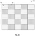
- FIG. 3 Aillustrates a pixel array 300 topped with a first phosphor material 352 after processing in which all pixels in the pixel array are illuminated.
- FIG. 3 Billustrates a pixel array 310 topped with both a first phosphor material 352 and a second phosphor material 354 after processing in which half of the pixels in the pixel array are illuminated in a checkerboard pattern.
- any cavitiesare filled with the first phosphor material. Any previously unilluminated pixels are lit, the photoresist developed and washed, and any cavities filled with the second phosphor material are used to define the checkerboard or other desired pattern.
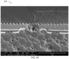
- FIGS. 4 A, 4 B, and 4 Crespectively show images of an LED pixel array processed according to one embodiment.
- a 6 ⁇ 3 array of blue-emitting LEDs on a ceramic tilewas coated with the adhesion promoter hexamethyldisilazane (HMDS).
- HMDSadhesion promoter hexamethyldisilazane
- a 15 micron layer of the positive photoresist AZ4562was spin-coated onto the tile, and subsequently dried at 100° C. for 2 minutes. Electrical contact was made to a single pixel of the array, which was then run at 800 mA/cm2 for 5 seconds.
- the photoresistwas then flooded with the TMAH-based developer RD6 for 50 s, and then spun dry. This process was repeated, and the sample was then rinsed in DI water.
- FIG. 4 Ashows an optical image 400 , having a scale of 100 ⁇ m, of the resulting photoresist pattern with photoresist removed from one of the center pixels.
- FIG. 4 Bshows a scanning electron microscope image 410 of a corner of the pattern, while
- FIG. 4 Cshows a scanning electron microscope image 420 of a cross-section of the same sample along an edge of a photoresist pattern between two neighboring LED pixels. Thickness of remaining photoresist was measured at two spots: 14.18 micrometers and 15.44 micrometers. The angle of undercut was 42.4°.
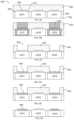
- FIG. 5illustrates an exemplary contact layout 500 for making electrical contact to subsets of pixels at the wafer level for photoresist exposure.
- a subset of pixels 502 of a first colorfor example red, is electrically connected between a first contact “C 1 ” of each 502 to a first-color common contact 512 .
- a second contact “C 2 ” of each 502is in electrical contact with connection 510 to a layout common contact 508 .
- a subset of pixels 504 of a second color, for example greenis electrically connected between a first contact “C 1 ” of each 504 to a second-color common contact 514 .
- a second contact “E 2 ” of each 504is in electrical contact with connection 510 to the layout common contact 508 .
- a subset of pixels 506 of a third color, for example blue,is electrically connected between a first contact “C 1 ” of each 506 to a third-color common contact 516 .
- a second contact “C 2 ” of each 506is in electrical contact with connection 510 to the layout common contact 508 .
- Common contactscan be later severed to allow for individual addressability of all pixels.
- LED pixels containing a central patterned surface and an unpatterned borderwill minimize lateral emission from each pixel so that a photoresist film on the die or wafer surface can be patterned with high resolution.
- a width of the unpatterned borderis in a range of 1 to 50 micrometers, including all values and subranges therebetween, including 5 to 20 microns.
- the GaN surface in the semiconductor devicehave a roughened surface either by patterned sapphire from resist patterned etching or by a photo-electrochemical etch.
- patterned sapphirecan be formed to leave the sapphire smooth near the edge of the die layout. This requires alignment of the sapphire to the LED. The lack of surface roughness at the outer 5 to 20 micron edge of each pixel in the LED reduces the light intensity at the edge of the pixel and improved quality of the blue light extinction to reduce cross-talk between LED pixels.
- forming the self-aligned photoresist arraycan rely on deposition or coating of a uniform layer of positive photoresist sensitive to the LED's emission wavelength. When some or all of the LED pixels are then turned on, only the photoresist directly above the LED will be exposed. After developing, photoresist remains only on the dark areas of the array (“off” pixels, spaces between pixels), as well as around the border of the array. If the resulting pattern is filled with phosphor, the photoresist can then be stripped to yield a pixelated phosphor array aligned with the LED array. The photoresist thickness and LED light dosage can be tuned to minimize the over exposure in the areas of interest.
- a multi-step approachcan be applied where a thin photoresist film is followed by the LED exposure and then a thin light blocking layer (such as aluminum metal) on the photoresist sidewall can be applied to further reduce the cross-talk from the LED light source. Any excess aluminum on the LED emitting surface can be removed by a directional dry etch process. A second photoresist layer can then be patterned with the aid of this blocking layer between pixels. This procedure can be repeated to create the desired photopatterned aspect ratio and sidewall profile.
- a thin light blocking layersuch as aluminum metal
- Positive photoresist compounds useful for this described processcan include photosensitive materials that are degraded by light so that a developer will dissolve away deposited regions that are exposed to light. In effect, this leaves behind a coating where a mask was placed (i.e. the film remains on the formerly dark portions of an illuminated resist). Positive resists typically need to be used at low temperatures, since they are susceptible to permanent crosslinking (also called “hard bake”) at high temperatures, rendering the resist unable to be removed afterwards by the stripping bath (typically a mild solvent system).
- the light emitting pixel arrayscan include but are not limited to LEDs formed of sapphire or silicon carbide.
- the LEDscan be formed from an epitaxially grown or deposited semiconductor n-layer.
- a semiconductor p-layercan then be sequentially grown or deposited on the n-layer, forming an active region at the junction between layers.
- Semiconductor materials capable of forming high-brightness light emitting devicescan include, but are not limited to, Group III-V semiconductors, particularly binary, ternary, and quaternary alloys of gallium, aluminum, indium, and nitrogen, also referred to as III-nitride materials.
- laser light emitting elementscan be used.
- Color of emitted light from the LEDscan be modified using a phosphor particles that include one or more wavelength converting materials able to create white light or monochromatic light of other colors.
- phosphor particles held together by adhesives or binderscan be used. Phosphors bound together with silicone, for example, can be molded, dispensed, screen printed, sprayed, or laminated.
- a condensation cure silicone systemcan be used to bind phosphor particles.
- Silicone material or siloxanescan be selected for mechanical stability, low temperature cure properties (e.g. below 150-120 degrees Celsius), and ability to be catalyzed using vapor phase catalysts.
- organosiloxane block copolymerscan be used.
- Organopolysiloxanes containing D and T units, where the D unit are primarily bonded together to form linear blocks having 10 to 400 D units and the T units are primarily bonded to each other to form branched polymeric chains, which are referred to as “non-linear blocks”can be used.
- the condensation cure silicone systemcan include optional organic, inorganic, or organic/inorganic binder and filler material.
- light active phosphors, dyes, or nanoparticlescan be bound together by the silicone.
- the siliconecan additionally form optical structures, including lenses, light guides, or refractive elements.
- Catalysts for the condensation cure silicone system catalystscan be selected to minimize generation of species requiring removal, and/or should not require high-temperature activation to enable curing at relatively low temperatures and/or the use of heat-sensitive substrates.
- Compositionscan employ catalysts that are relatively non-toxic, and that are relatively stable in solution but relatively fast-curing upon drying. Catalysts can be effective in relatively low concentrations, and/or effective under relatively low (or no) moisture conditions. Catalysts that can be employed as a vapor phase can be used.
- vapor phase cure of the condensation cure silicone systemcan be conducted using basic or alkaline catalyzing agents.
- superbase catalyzing agentssuch as described in U.S. Pat. No. 9,688,035 by Swier et. al. can be used.
- silicone solid compositions manufactured using a superbase catalystexhibit enhanced cure rates, improved mechanical strength, and improved thermal stability over similar compositions without the superbase catalyst.
- the term “superbase” used hereinrefers to compounds having a very high basicity, such as lithium diisopropylamide.
- the term “superbase”also encompasses bases resulting from a mixing of two (or more) bases leading to new basic species possessing inherent new properties.
- the term “superbase”does not necessarily mean a base that is thermodynamically and/or kinetically stronger than another. Instead, in some embodiments, it means that a basic reagent is created by combining the characteristics of several different bases.
- Non-limiting examples of superbasesinclude organic superbases, organometallic superbases, and inorganic superbases.
- Organic superbasesinclude but are not limited to nitrogen-containing compounds.
- the nitrogen-containing compoundsalso have low nucleophilicity and relatively mild conditions of use.
- Non-limiting examples of nitrogen-containing compoundsinclude phosphazenes, amidines, guanidines, and multicyclic polyamines.
- Organic superbasesalso include compounds where a reactive metal has been exchanged for a hydrogen on a heteroatom, such as oxygen (unstabilized alkoxides) or nitrogen (metal amides such as lithium diisopropylamide).
- the superbase catalystis an amidine compound.
- the term “superbase”refers to organic superbases having at least two nitrogen atoms and a pKb of from about 0.5 to about 11, as measured in water.
- the superbase catalystis an organic superbase, such as any of the organic superbases as described above or known in the art.
- RGB LEDsAll or only a portion of the light emitted by the LEDs may be converted by the wavelength converting material of the phosphor. Unconverted light may be part of the final spectrum of light, though it need not be.
- Examples of common devicesinclude a blue-emitting LED segment combined with a yellow-emitting phosphor, a blue-emitting LED segment combined with green- and red-emitting phosphors, a UV-emitting LED segment combined with blue- and yellow-emitting phosphors, and a UV-emitting LED segment combined with blue-, green-, and red-emitting phosphors.
- individually controllable RGB (three LEDs) or RGBY (four LEDs)can be positioned under a single micro-optic. This allows for precise color control of emitted light. Typically, such RGB LEDs are spaced sufficiently far apart that color mixing will occur in the far field.
- Micro-opticscan be a single optical element or a multiple optic elements.
- Optical elementscan include converging or diverging lenses, aspherical lens, Fresnel lens, or graded index lens, for example.
- Other optical elementssuch as mirrors, beam diffusers, filters, masks, apertures, collimators, or light waveguides are also included.
- Micro-opticscan be positioned at a distance from the LEDs that allows receipt and redirection of light from multiple LEDs. Alternatively, micro-optics can be set atop each LED to individually guide, focus, or defocus emitted LED light.
- Micro-opticscan be directly attached to the LEDs, attached to LEDs via a transparent interposer or plate, or held at a fixed distance from LEDs by surrounding substrate attachments (not shown).
- each LED pixel in the light emitter arraycan be separately controlled, while in other embodiments groups of pixels can be controlled as a block. In still other embodiments, both single pixels and groups of pixels can be controlled. To reduce overall data management requirements, control can be limited to on/off functionality or switching between relatively few light intensity levels. In other embodiments, continuous changes in lighting intensity are supported. Both individual and group level control of light intensity is contemplated. In one embodiment, overlapping or dynamically selected zones of control are also possible, with for example, overlapping groups of light emitters in the pixel array being separately controllable despite having common pixels depending on lighting requirements. In one embodiment, intensity can be separately controlled and adjusted by setting appropriate ramp times and pulse width for each pixel using a pulse width modulation. This allows staging of pixel activation to reduce power fluctuations, and to provide superior luminous intensity control.
- Programmable light emitting arrayssuch as disclosed herein may also support a wide range of applications that benefit from fine-grained intensity, spatial, and temporal control of light distribution. This may include, but is not limited to, precise spatial patterning of emitted light from blocks or individual LEDs. Depending on the application, emitted light may be spectrally distinct, adaptive over time, and/or environmentally responsive. In some embodiments, the light emitting arrays may provide pre-programmed light distribution in various intensity, spatial, or temporal patterns. The emitted light may be based at least in part on received sensor data and may be used for optical wireless communications. Associated optics may be distinct at single or multiple LED level.
- An example light emitting arraymay include a device having a commonly controlled central block of high intensity LEDS with an associated common optic, whereas edge positioned LEDs may have individual optics.
- Common applications supported by light emitting LED arraysinclude camera or video lighting, architectural and area illumination, and street lighting.
- Programmable light emitting arraysmay be used to selectively and adaptively illuminate buildings or areas for improved visual display or to reduce lighting costs.
- light emitting arraysmay be used to project media facades for decorative motion or video effects.
- selective illumination of areas around pedestriansmay be possible.
- Spectrally distinct LEDsmay be used to adjust the color temperature of lighting, as well as support wavelength specific horticultural illumination.
- Street lightingis an important application that may greatly benefit from use of programmable light emitting arrays.
- a single type of light emitting arraymay be used to mimic various street light types, allowing, for example, switching between a Type I linear street light and a Type IV semicircular street light by appropriate activation or deactivation of selected LEDs.
- street lighting costsmay be lowered by adjusting light beam intensity or distribution according to environmental conditions or time of use. For example, light intensity and area of distribution may be reduced when pedestrians are not present. If LEDs are spectrally distinct, the color temperature of the light may be adjusted according to respective daylight, twilight, or night conditions.
- Programmable light emitting LEDsare also well suited for supporting applications requiring direct or projected displays. For example, automotive headlights requiring calibration, or warning, emergency, or informational signs may all be displayed or projected using light emitting arrays. This allows, for example, modifying directionality of light output from a automotive headlight. If a light emitting array is composed of a large number of LEDs or includes a suitable dynamic light mask, textual or numerical information may be presented with user guided placement. Directional arrows or similar indicators may also be provided.
- FIG. 6 Ashows a die or wafer 602 including semiconductor layer 610 that is divided into a plurality of individual pixels each having a central patterned surface 624 and an unpatterned border 626 and being separated by light blocking metal 630 .
- a layer of positive photoresist 620is deposited onto top surfaces of the die or wafer 602 , above the patterned surfaces 624 , the unpatterned borders 626 , and the light blocking metal 630 . All or some pixels (LED 1 , LED 2 , and LED 3 ) are illuminated. For illustration purposes here, FIG.
- FIG. 6 Bshows that LED 1 and LED 3 are illuminated, which develops positive photoresist into developed positive photoresist 622 above only the patterned surfaces of each illuminated pixel.
- Positive (undeveloped) photoresist 620resides on the unpatterned borders, LED 2 which was not illuminated, and the light blocking metal.
- FIG. 6 Cthe developed positive photoresist 622 portions (i.e. those exposed to light from patterned surfaces of the lit pixels) are washed away. This leaves a cavity 640 separated by a thin edge wall 642 or thick edge wall 644 .
- FIG. 6 Dillustrates that surface treatment of the exposed LEDs occurs, e.g., chemical etch of exposed GaN surfaces to form porosity 646 .
- FIG. 1 and LED 3are illuminated, which develops positive photoresist into developed positive photoresist 622 above only the patterned surfaces of each illuminated pixel.
- Positive (undeveloped) photoresist 620resides on the unpatterned borders, LED 2 which was not illuminate
- FIG. 6 Eillustrates that small down-converter particles, such as quantum dots (QD), are infused into the treated surfaces.
- QDquantum dots
- a “phosphor pixel” 648 embedded in the surface of the GaNis created (for a specific set of colors/pixels/designs).
- the walls 642 and 644 of remaining positive photoresistare removed.
- the surface treatment and down-converter particlesare present material on the central pattered surface, and there is an absence of the same on at least portions of the unpatterned border.
- the processcan optionally can be repeated for a different set of pixels/colors/designs.
- Another layer of positive photoresist 620is deposited onto the substrate. With respect to FIG. 6 G , a different set of pixels relative to FIG. 6 B is illuminated. For illustration purposes here, LED 2 is illuminated, which develops positive photoresist into developed positive photoresist 622 above only the patterned surfaces 624 of LED 2 , e.g., each illuminated pixel. Positive (undeveloped) photoresist 620 resides on the unpatterned borders 626 , the light blocking metal 630 , and the unilluminated LEDs: LED 1 and LED 3 . Thereafter at FIG. 6 H , the developed positive photoresist portion (i.e.
- Embodiment (a)A light source, comprising: an array comprising: a plurality of light emitters, each light emitter comprising: a semiconductor layer having a first surface and a second surface, the first surfaces of at least a portion of the light emitters comprising: a central patterned surface and an unpatterned border, and a down-converter material on the semiconductor layer; and a light blocking metal layer positioned between each of the light emitters.
- Embodiment (b)The light source of embodiment (a), wherein the unpatterned border has a width in a range of 1 to 50 microns.
- Embodiment (c)The light source of any one of embodiments (a) to (b), wherein there is a presence of the down-converter material on the central pattered surface, and an absence of the down-converter material on at least portions of the unpatterned border.
- Embodiment (d)The light source of any one of embodiments (a) to (c), wherein each of the light emitters comprises a minimum width in a range of 5 microns to 500 microns.
- Embodiment (e)The light source of any one of embodiments (a) to (d), wherein the semiconductor layer comprises GaN.
- Embodiment (f)The light source of any one of embodiments (a) to (e), wherein the down-converter material comprises a phosphor material.
- Embodiment (g)The light source of any one of embodiments (a) to (f), wherein the light blocking metal layer has a height of less than 5 microns.
- Embodiment (h)The light source of any one of embodiments (a) to (g), wherein the array provides multicolor lighting with phosphors formed from particles bound together by a condensation cure silicone system.
- Embodiment (i)The light source of any one of embodiments (a) to (h), wherein the plurality of light emitters is color tunable.
- Embodiment (j)The light source of any one of embodiments (a) to (i), further comprising optical elements that are aligned with at least some of the light emitters.
- Embodiment (k)The light source of any one of embodiments (a) to (j), wherein the light source is used for at least one of architectural, camera flash, and automotive lighting.
- Embodiment (l)The light source of any one of embodiments (a) to (k), wherein the array includes common electrical contacts active at wafer or die level.
- Embodiment (m)A method of manufacturing a light source by a self-aligned maskless method comprising: coating an array of light emitters with a positive photoresist; activating at least some of the light emitters to expose portions of the positive photoresist and create developed positive photoresist, each light emitter comprising: a semiconductor layer having a first surface and a second surface, the first surfaces of at least a portion of the light emitters comprising: a central patterned surface and an unpatterned border; washing away the developed positive photoresist to leave cavities having positive photoresist sidewalls; and at least partially filling the cavities with a down-converter material.
- Embodiment (n)The method of embodiment (m), wherein the unpatterned border has a width in a range of 1 to 50 microns.
- Embodiment (o)The method of any one of embodiments (m) to (n), wherein each of the light emitters comprises a minimum width in a range of 5 microns to 500 microns.
- Embodiment (p)The method of any one of embodiments (m) to (o), wherein the semiconductor layer of each of the light emitters comprises GaN.
- Embodiment (q)The method of any one of embodiments (m) to (p), wherein the down-converter material comprises a phosphor material.
- Embodiment (r)The method of any one of embodiments (m) to (q), further comprising depositing a light blocking metal layer having a height of less than 5 microns between each of the light emitters.
- Embodiment (s)The method of any one of embodiments (m) to (r), further comprising depositing and washing away a second positive photoresist layer.
- Embodiment (t)The method of any one of embodiments (m) to (s), further comprising an electroplating metal on a bonding metal layer deposited in GaN trenches.
- Embodiment (u)The method of any one of embodiments (m) to (t), further comprising providing electrical contacts on a reverse side of a wafer supporting the array of light emitters.
- Embodiment (v)The method of any one of embodiments (m) to (u), further comprising activating each of the array of light emitters.
- Embodiment (w)The method of any one of embodiments (m) to (v), further comprising activating selected light emitters to define a desired pattern.
- Embodiment (x)The method of any one of embodiments (m) to (w), further comprising aligning optical elements with at least some of the array of light emitters.
Landscapes
- Engineering & Computer Science (AREA)
- Power Engineering (AREA)
- Microelectronics & Electronic Packaging (AREA)
- Physics & Mathematics (AREA)
- Condensed Matter Physics & Semiconductors (AREA)
- General Physics & Mathematics (AREA)
- Computer Hardware Design (AREA)
- Led Devices (AREA)
- Led Device Packages (AREA)
Abstract
Description
Claims (18)
Priority Applications (5)
| Application Number | Priority Date | Filing Date | Title |
|---|---|---|---|
| US17/084,999US11777059B2 (en) | 2019-11-20 | 2020-10-30 | Pixelated light-emitting diode for self-aligned photoresist patterning |
| CN202080080415.8ACN114667601A (en) | 2019-11-20 | 2020-11-11 | Pixelated light emitting diodes for self-aligned photoresist patterning |
| EP20819993.5AEP4062448A1 (en) | 2019-11-20 | 2020-11-11 | Pixelated light-emitting diode for self-aligned photoresist patterning |
| PCT/US2020/059938WO2021101765A1 (en) | 2019-11-20 | 2020-11-11 | Pixelated light-emitting diode for self-aligned photoresist patterning |
| TW109140704ATWI764385B (en) | 2019-11-20 | 2020-11-20 | Pixelated light-emitting diode for self-aligned photoresist patterning |
Applications Claiming Priority (2)
| Application Number | Priority Date | Filing Date | Title |
|---|---|---|---|
| US201962938001P | 2019-11-20 | 2019-11-20 | |
| US17/084,999US11777059B2 (en) | 2019-11-20 | 2020-10-30 | Pixelated light-emitting diode for self-aligned photoresist patterning |
Publications (2)
| Publication Number | Publication Date |
|---|---|
| US20210151626A1 US20210151626A1 (en) | 2021-05-20 |
| US11777059B2true US11777059B2 (en) | 2023-10-03 |
Family
ID=75910062
Family Applications (1)
| Application Number | Title | Priority Date | Filing Date |
|---|---|---|---|
| US17/084,999Active2041-11-27US11777059B2 (en) | 2019-11-20 | 2020-10-30 | Pixelated light-emitting diode for self-aligned photoresist patterning |
Country Status (5)
| Country | Link |
|---|---|
| US (1) | US11777059B2 (en) |
| EP (1) | EP4062448A1 (en) |
| CN (1) | CN114667601A (en) |
| TW (1) | TWI764385B (en) |
| WO (1) | WO2021101765A1 (en) |
Families Citing this family (4)
| Publication number | Priority date | Publication date | Assignee | Title |
|---|---|---|---|---|
| FR3106396B1 (en)* | 2020-01-17 | 2022-03-18 | Valeo Vision | Motor vehicle luminous device incorporating a screen |
| WO2022192588A1 (en)* | 2021-03-12 | 2022-09-15 | Applied Materials, Inc. | Print process for color conversion layer |
| KR102727056B1 (en)* | 2021-12-01 | 2024-11-06 | 삼성전자주식회사 | Micro emitting semiconductor device, display apparatus having the same, manufacturing the same |
| KR20240140140A (en)* | 2022-01-28 | 2024-09-24 | 루미레즈 엘엘씨 | Phosphor conversion light emitting diode (LED) color tuning |
Citations (86)
| Publication number | Priority date | Publication date | Assignee | Title |
|---|---|---|---|---|
| US3698396A (en) | 1970-12-04 | 1972-10-17 | Abbott Lab | Catheter assembly for peritoneal cavity insertion |
| WO1997048138A2 (en) | 1996-06-11 | 1997-12-18 | Philips Electronics N.V. | Visible light emitting devices including uv-light emitting diode and uv-excitable, visible light emitting phosphor, and method of producing such devices |
| US20020106847A1 (en) | 2000-07-14 | 2002-08-08 | Kazlas Peter T. | Fabrication of electronic circuit elements using unpatterned semiconductor layers |
| US6504180B1 (en)* | 1998-07-28 | 2003-01-07 | Imec Vzw And Vrije Universiteit | Method of manufacturing surface textured high-efficiency radiating devices and devices obtained therefrom |
| US20030181122A1 (en) | 2002-03-22 | 2003-09-25 | Collins William D. | Producing self-aligned and self-exposed photoresist patterns on light emitting devices |
| US20060281203A1 (en) | 2005-06-09 | 2006-12-14 | Lumileds Lighting U.S, Llc | Method of removing the growth substrate of a semiconductor light emitting device |
| EP2027608A1 (en) | 2006-06-09 | 2009-02-25 | Commissariat à l'Energie Atomique | Process of making a microelectronic light-emitting device on semi-conducting nanowire formed on a metallic substrate |
| EP2203939A1 (en) | 2007-10-22 | 2010-07-07 | Commissariat à l'énergie atomique et aux énergies alternatives | Optoelectronic device including nanowires, and corresponding methods |
| EP2211387A2 (en) | 2009-01-22 | 2010-07-28 | Commissariat à l'Énergie Atomique et aux Énergies Alternatives | Method of making a p-n homojunction in a nanostructure |
| WO2011045289A1 (en) | 2009-10-16 | 2011-04-21 | Commissariat A L'energie Atomique Et Aux Energies Alternatives | Semiconductor nanocrystal-based infrared source built into silicon |
| WO2011048318A1 (en) | 2009-10-23 | 2011-04-28 | Commissariat A L'energie Atomique Et Aux Energies Alternatives | Method for manufacturing a very-high-resolution screen using a nanowire-based emitting anisotropic conductive film |
| FR2952366A1 (en) | 2010-04-07 | 2011-05-13 | Commissariat Energie Atomique | Developing carbon nanotubes for e.g. LCD and organic LEDs, comprises depositing a network of carbon nanotubes on a substrate, and irradiating the carbon nanotubes network by laser impulsion having specified power |
| US20110151607A1 (en) | 2009-12-23 | 2011-06-23 | Commissariat A L'energie Atomique Et Aux Energies Alternatives | Method for manufacturing a metal and dielectric nanostructures electrode for colored filtering in an oled and method for manufacturing an oled |
| US20110287606A1 (en) | 2010-05-18 | 2011-11-24 | Commissariat A L'energie Atomique Et Aux Energies Alternatives | Method for fabricating chip elements provided with wire insertion grooves |
| FR2964796A1 (en) | 2010-09-14 | 2012-03-16 | Commissariat Energie Atomique | Optoelectronic light emitting device i.e. gallium nitride based LED, has p-doped planarized layer allowing radial injection of holes in nanowire, and n-type silicon substrate allowing axial injection of electrons in nanowire |
| WO2012035243A1 (en) | 2010-09-14 | 2012-03-22 | Commissariat A L'energie Atomique Et Aux Energies Alternatives | Nanowire-based optoelectronic device for light emission |
| FR2969995A1 (en) | 2011-01-03 | 2012-07-06 | Commissariat Energie Atomique | Producing nitride nanostructures e.g. nanowires on side of substrate, by forming base of nanostructures made of wurtzite nitride phase on substrate, and forming upper part of nanostructures made of nitrides having zinc-blende phase on base |
| US8222811B2 (en) | 2008-07-07 | 2012-07-17 | Commissariat A L'energie Atomique Et Aux Energies Alternatives | Electroluminescent display, illumination or indicating device, and its fabrication process |
| EP2499958A1 (en) | 2011-03-15 | 2012-09-19 | Commissariat à l'Énergie Atomique et aux Énergies Alternatives | Disposable bi-spectral optical head for video endoscope and associated video endoscope |
| EP2521161A1 (en) | 2011-05-06 | 2012-11-07 | Commissariat à l'Énergie Atomique et aux Énergies Alternatives | Method for producing semiconductor nanocrystals |
| EP2521162A1 (en) | 2011-05-06 | 2012-11-07 | Commissariat à l'Énergie Atomique et aux Énergies Alternatives | Method for producing semiconductor nanocrystals oriented in a pre-defined direction |
| WO2012156620A2 (en) | 2011-05-18 | 2012-11-22 | Commissariat A L'energie Atomique Et Aux Energies Alternatives | In-series electrical connection of light-emitting nanowires |
| US20130020115A1 (en) | 2010-03-26 | 2013-01-24 | Commissariat A L'energie Atomique Et Aux Energies Alternatives | Method for etching conductive metal oxide layer using microelectrode |
| TWI408839B (en) | 2004-12-28 | 2013-09-11 | Samsung Display Co Ltd | Electroluminescent device and method of fabricating an electroluminescent device comprising an optical spacer |
| FR2991342A1 (en) | 2012-06-05 | 2013-12-06 | Commissariat Energie Atomique | METHOD FOR IMPROVING THE ELECTRICAL AND OPTICAL PERFORMANCE OF ELECTRICALLY CONDUCTIVE AND TRANSPARENT MATERIAL BASED ON SILVER NANOWIRES |
| EP2674516A1 (en) | 2012-06-15 | 2013-12-18 | Commissariat A L'energie Atomique Et Aux Energies Alternatives | Method of electrochemically manufacturing nanowires from CuSCN |
| US8638032B2 (en) | 2008-09-30 | 2014-01-28 | Commissariat A L'energie Atomique Et Aux Energies Alternatives | Organic optoelectronic device coated with a multilayer encapsulation structure and a method for encapsulating said device |
| FR2998090A1 (en) | 2013-06-26 | 2014-05-16 | Commissariat Energie Atomique | Method for structuring material surface of substrate for producing e.g. nanometric patterns on surface for LEDs, involves forming patterns due to difference between etch selectivity of material and changed etch selectivity of regions |
| US20140138719A1 (en) | 2011-07-08 | 2014-05-22 | Commissariat A L'energie Atomique Et Aux Energies Alternatives | Organic Optoelectronic Device And Method For The Encapsulation Thereof |
| WO2014150263A1 (en) | 2013-03-15 | 2014-09-25 | Ledengin, Inc. | Printing phosphor on led wafer using dry film lithography |
| WO2015044620A1 (en) | 2013-09-30 | 2015-04-02 | Commissariat A L'energie Atomique Et Aux Energies Alternatives | Method for producing optoelectronic devices comprising light-emitting diodes |
| US20150118544A1 (en) | 2013-10-29 | 2015-04-30 | Commissariat A L'energie Atomique Et Aux Energies Alternatives | Device for encapsulating a sensitive device and process for producing said device |
| TWI485877B (en) | 2007-01-22 | 2015-05-21 | Cree Inc | Wafer level phosphor coating method and device manufactured using the same |
| US20150380461A1 (en) | 2014-06-27 | 2015-12-31 | Commissariat A L'energie Atomique Et Aux Energies Alternatives | P-n junction optoelectronic device for ionizing dopants by field effect |
| TW201622187A (en) | 2014-10-27 | 2016-06-16 | 皇家飛利浦有限公司 | Directional illuminating configuration and manufacturing method thereof |
| TWI556684B (en) | 2011-05-04 | 2016-11-01 | 環球展覽公司 | Illumination source using light-emitting diodes and organic light-emitting diodes |
| EP3144272A1 (en) | 2015-09-17 | 2017-03-22 | Commissariat A L'energie Atomique Et Aux Energies Alternatives | Verfahren zur ausrichtung auf einer substratoberlfäche angeordneter länglicher objekte |
| US20170137645A1 (en) | 2013-11-26 | 2017-05-18 | Commissariat A L'energie Atomique Et Aux Energies Alternatives | Ink for forming p layers in organic electronic devices |
| US20170149019A1 (en) | 2013-03-14 | 2017-05-25 | Q1 Nanosystems Corporation | Three-dimensional optical devices including cavity-containing cores and methods of manufacture |
| WO2017089676A1 (en) | 2015-11-26 | 2017-06-01 | Commissariat A L'energie Atomique Et Aux Energies Alternatives | Illuminated faceplate and method for producing such an illuminated faceplate |
| US20170186612A1 (en) | 2015-12-28 | 2017-06-29 | Commissariat A L'energie Atomique Et Aux Energies Alternatives | Method for producing nanocrystals with controlled dimensions and density |
| US20170186907A1 (en) | 2015-12-24 | 2017-06-29 | Vuereal Inc. | Vertical solid state devices |
| US20170215280A1 (en) | 2016-01-21 | 2017-07-27 | Vuereal Inc. | Selective transfer of micro devices |
| WO2017149521A1 (en) | 2016-03-04 | 2017-09-08 | Vuereal Inc. | Micro device integration into system substrate |
| US20170270231A1 (en) | 2016-03-18 | 2017-09-21 | Vuereal Inc. | Maskless patterning |
| WO2017216445A1 (en) | 2016-06-17 | 2017-12-21 | Commissariat A L'energie Atomique Et Aux Energies Alternatives | Method for making a gallium nitride light-emitting diode |
| US20180017939A1 (en) | 2016-07-13 | 2018-01-18 | Commissariat A L'energie Atomique Et Aux Energies Alternatives | Device for observing a sample |
| US20180095124A1 (en) | 2016-10-04 | 2018-04-05 | Vuereal Inc. | Micro device arrangement in donor substrate |
| US20180097037A1 (en) | 2016-10-04 | 2018-04-05 | Vuereal Inc. | Color conversion layer integration into display substrate with high intensity light sources |
| US20180102449A1 (en) | 2016-10-12 | 2018-04-12 | Kateeva, Inc. | Display Devices Utilizing Quantum Dots and Inkjet Printing Techniques Thereof |
| US20180151804A1 (en) | 2016-11-25 | 2018-05-31 | Vuereal Inc. | Integration of micro-devices into system substrate |
| US20180166424A1 (en) | 2016-12-14 | 2018-06-14 | Samsung Electronics Co., Ltd. | Light-emitting diode (led) device for realizing multi-colors |
| TWI636584B (en) | 2013-04-25 | 2018-09-21 | 皇家飛利浦有限公司 | Light-emitting diode assembly, light-emitting diode including the same, and micro-optical multilayer structure |
| US20180287027A1 (en) | 2017-03-30 | 2018-10-04 | Vuereal Inc. | Vertical solid-state devices |
| US20180358404A1 (en) | 2015-01-23 | 2018-12-13 | Vuereal Inc. | Micro device integration into system substrate |
| US20180358405A1 (en) | 2015-01-23 | 2018-12-13 | Vuereal Inc. | Micro device integration into system substrate |
| US20190080970A1 (en) | 2017-09-11 | 2019-03-14 | Vuereal Inc. | Repair techniques for micro-led devices and arrays |
| US20190097179A1 (en) | 2017-09-28 | 2019-03-28 | Boe Technology Group Co., Ltd. | Array substrate, method of preparing the same and display panel |
| US20190096774A1 (en) | 2016-11-25 | 2019-03-28 | Vuereal Inc. | Microdevice transfer setup and integration of micro-devices into system substrate |
| US20190123033A1 (en) | 2017-10-19 | 2019-04-25 | Spy Eye, Llc | Ultra-Dense LED Projector |
| CA2984214A1 (en) | 2017-10-30 | 2019-04-30 | Vuereal Inc | Integration of micro-devices into system substrate |
| CA2986412A1 (en) | 2017-11-14 | 2019-05-14 | Vuereal Inc | Vertical microdevice structure |
| US20190146626A1 (en) | 2017-11-14 | 2019-05-16 | Vuereal Inc. | Integration of touch and sensing |
| US20190148321A1 (en) | 2017-11-14 | 2019-05-16 | Vuereal Inc. | Integration and bonding of micro-devices into system substrate |
| DE102019101489A1 (en) | 2017-11-23 | 2019-05-23 | Vuereal Inc. | MICROPOWER TRANSMISSION CONSTRUCTION AND INTEGRATION OF MICRO DEVICES INTO A SYSTEM SUBSTRATE |
| US10304364B2 (en) | 2015-01-23 | 2019-05-28 | Vuereal Inc. | Identifying and repairing defects for micro-device integrated systems |
| US10312224B2 (en) | 2016-04-12 | 2019-06-04 | Cree, Inc. | High density pixelated LED and devices and methods thereof |
| US20190181181A1 (en)* | 2017-12-12 | 2019-06-13 | Samsung Electronics Co., Ltd. | Method of fabricating light emitting device package |
| US20190242550A1 (en)* | 2018-02-06 | 2019-08-08 | HELLA GmbH & Co. KGaA | Lighting Device with Homogenous Light Distribution |
| US20190288156A1 (en) | 2017-03-30 | 2019-09-19 | Vuereal Inc. | High efficient microdevices |
| TW201946313A (en) | 2014-10-17 | 2019-12-01 | 日商半導體能源研究所股份有限公司 | Light-emitting device, module, electronic device, and method for manufacturing light-emitting device |
| US20190371868A1 (en) | 2016-11-25 | 2019-12-05 | Vuereal Inc. | Integration of microdevices into system substrate |
| US20200013761A1 (en) | 2017-02-09 | 2020-01-09 | Vuereal Inc. | Circuit and system integration onto a microdevice substrate |
| US20200013662A1 (en) | 2016-11-25 | 2020-01-09 | Vuereal Inc. | Integration of microdevices into system substrate |
| US10535546B2 (en) | 2016-09-06 | 2020-01-14 | Vuereal Inc. | Micro device arrangement in donor substrate |
| US20200091388A1 (en) | 2018-09-19 | 2020-03-19 | Vuereal Inc. | Highly efficient microdevices |
| US20200161290A1 (en) | 2018-11-15 | 2020-05-21 | Vuereal Inc. | Self-aligned vertical solid state devices fabrication and integration methods |
| WO2020100127A1 (en) | 2018-11-16 | 2020-05-22 | Vuereal Inc. | Microdevice cartridge structure |
| US20200203579A1 (en) | 2018-12-21 | 2020-06-25 | Lumileds Holding B.V. | Photoresist patterning process supporting two step phosphor-deposition to form an led matrix array |
| US10700120B2 (en) | 2015-01-23 | 2020-06-30 | Vuereal Inc. | Micro device integration into system substrate |
| US20200212270A1 (en) | 2018-12-26 | 2020-07-02 | Lumileds Holding B.V. | Two step phosphor deposition to make a matrix array |
| US10707277B2 (en) | 2016-10-04 | 2020-07-07 | Vuereal Inc. | Method of integrating functional tuning materials with micro devices and structures thereof |
| WO2020170201A1 (en) | 2019-02-21 | 2020-08-27 | Vuereal Inc. | Probe structure for micro device inspection |
| WO2020170219A1 (en) | 2019-02-22 | 2020-08-27 | Vuereal Inc. | Microdevice cartridge structure |
| US20200273945A1 (en) | 2019-02-22 | 2020-08-27 | Vuereal Inc. | Staggered and tile stacked microdevice integration and driving |
| WO2020170214A1 (en) | 2019-02-21 | 2020-08-27 | Vuereal Inc. | Optoelectronic solid state array |
Family Cites Families (2)
| Publication number | Priority date | Publication date | Assignee | Title |
|---|---|---|---|---|
| CN104159726B (en) | 2012-01-16 | 2017-01-18 | 道康宁公司 | Optical article and method of forming |
| CN109638138B (en)* | 2018-12-03 | 2021-01-15 | 惠州市华星光电技术有限公司 | A kind of preparation method of LED display screen and LED display screen |
- 2020
- 2020-10-30USUS17/084,999patent/US11777059B2/enactiveActive
- 2020-11-11EPEP20819993.5Apatent/EP4062448A1/enactivePending
- 2020-11-11WOPCT/US2020/059938patent/WO2021101765A1/ennot_activeCeased
- 2020-11-11CNCN202080080415.8Apatent/CN114667601A/enactivePending
- 2020-11-20TWTW109140704Apatent/TWI764385B/enactive
Patent Citations (126)
| Publication number | Priority date | Publication date | Assignee | Title |
|---|---|---|---|---|
| US3698396A (en) | 1970-12-04 | 1972-10-17 | Abbott Lab | Catheter assembly for peritoneal cavity insertion |
| WO1997048138A2 (en) | 1996-06-11 | 1997-12-18 | Philips Electronics N.V. | Visible light emitting devices including uv-light emitting diode and uv-excitable, visible light emitting phosphor, and method of producing such devices |
| US6504180B1 (en)* | 1998-07-28 | 2003-01-07 | Imec Vzw And Vrije Universiteit | Method of manufacturing surface textured high-efficiency radiating devices and devices obtained therefrom |
| US20020106847A1 (en) | 2000-07-14 | 2002-08-08 | Kazlas Peter T. | Fabrication of electronic circuit elements using unpatterned semiconductor layers |
| US20030181122A1 (en) | 2002-03-22 | 2003-09-25 | Collins William D. | Producing self-aligned and self-exposed photoresist patterns on light emitting devices |
| US6756186B2 (en) | 2002-03-22 | 2004-06-29 | Lumileds Lighting U.S., Llc | Producing self-aligned and self-exposed photoresist patterns on light emitting devices |
| TWI408839B (en) | 2004-12-28 | 2013-09-11 | Samsung Display Co Ltd | Electroluminescent device and method of fabricating an electroluminescent device comprising an optical spacer |
| TWI575790B (en) | 2004-12-28 | 2017-03-21 | 三星顯示器有限公司 | Electroluminescent device and method of fabricating an electroluminescent device comprising an optical spacer |
| US20060281203A1 (en) | 2005-06-09 | 2006-12-14 | Lumileds Lighting U.S, Llc | Method of removing the growth substrate of a semiconductor light emitting device |
| EP2027608A1 (en) | 2006-06-09 | 2009-02-25 | Commissariat à l'Energie Atomique | Process of making a microelectronic light-emitting device on semi-conducting nanowire formed on a metallic substrate |
| TWI485877B (en) | 2007-01-22 | 2015-05-21 | Cree Inc | Wafer level phosphor coating method and device manufactured using the same |
| EP2203939A1 (en) | 2007-10-22 | 2010-07-07 | Commissariat à l'énergie atomique et aux énergies alternatives | Optoelectronic device including nanowires, and corresponding methods |
| US8487340B2 (en) | 2007-10-22 | 2013-07-16 | Commissariat A L'energie Atomique Et Aux Energies Alternatives | Optoelectronic device based on nanowires and corresponding processes |
| US8222811B2 (en) | 2008-07-07 | 2012-07-17 | Commissariat A L'energie Atomique Et Aux Energies Alternatives | Electroluminescent display, illumination or indicating device, and its fabrication process |
| US8638032B2 (en) | 2008-09-30 | 2014-01-28 | Commissariat A L'energie Atomique Et Aux Energies Alternatives | Organic optoelectronic device coated with a multilayer encapsulation structure and a method for encapsulating said device |
| EP2211387A2 (en) | 2009-01-22 | 2010-07-28 | Commissariat à l'Énergie Atomique et aux Énergies Alternatives | Method of making a p-n homojunction in a nanostructure |
| WO2011045289A1 (en) | 2009-10-16 | 2011-04-21 | Commissariat A L'energie Atomique Et Aux Energies Alternatives | Semiconductor nanocrystal-based infrared source built into silicon |
| WO2011048318A1 (en) | 2009-10-23 | 2011-04-28 | Commissariat A L'energie Atomique Et Aux Energies Alternatives | Method for manufacturing a very-high-resolution screen using a nanowire-based emitting anisotropic conductive film |
| EP2491591A1 (en) | 2009-10-23 | 2012-08-29 | Commissariat à l'Énergie Atomique et aux Énergies Alternatives | Method for manufacturing a very-high-resolution screen using a nanowire-based emitting anisotropic conductive film |
| US8890111B2 (en) | 2009-10-23 | 2014-11-18 | Commissariat à l'énergie atomique et aux énergies alternatives | Method for manufacturing a very-high-resolution screen using a nanowire-based emitting anisotropic conductive film |
| US20120205614A1 (en) | 2009-10-23 | 2012-08-16 | Commissariat A L'energie Atomique Et Aux Energies Alternatives | Method for manufacturing a very-high-resolution screen using a nanowire-based emitting anisotropic conductive film |
| US20110151607A1 (en) | 2009-12-23 | 2011-06-23 | Commissariat A L'energie Atomique Et Aux Energies Alternatives | Method for manufacturing a metal and dielectric nanostructures electrode for colored filtering in an oled and method for manufacturing an oled |
| EP2339658A2 (en) | 2009-12-23 | 2011-06-29 | Commissariat à l'Énergie Atomique et aux Énergies Alternatives | Method of fabricating an electrode having a metallic and dielectric nanostructure for color filtering in an oled and method of fabricating an oled. |
| EP2553149A1 (en) | 2010-03-26 | 2013-02-06 | Commissariat à l'Énergie Atomique et aux Énergies Alternatives | Method for etching conductive metal oxide layer using microelectrode |
| US20130020115A1 (en) | 2010-03-26 | 2013-01-24 | Commissariat A L'energie Atomique Et Aux Energies Alternatives | Method for etching conductive metal oxide layer using microelectrode |
| US9109296B2 (en) | 2010-03-26 | 2015-08-18 | Commissariat A L'energie Atomique Et Aux Energies Alternatives | Method for etching conductive metal oxide layer using microelectrode |
| FR2952366A1 (en) | 2010-04-07 | 2011-05-13 | Commissariat Energie Atomique | Developing carbon nanotubes for e.g. LCD and organic LEDs, comprises depositing a network of carbon nanotubes on a substrate, and irradiating the carbon nanotubes network by laser impulsion having specified power |
| US8258044B2 (en) | 2010-05-18 | 2012-09-04 | Commissariat A L'energie Atomique Et Aux Energies Alternatives | Method for fabricating chip elements provided with wire insertion grooves |
| US20110287606A1 (en) | 2010-05-18 | 2011-11-24 | Commissariat A L'energie Atomique Et Aux Energies Alternatives | Method for fabricating chip elements provided with wire insertion grooves |
| US9093607B2 (en) | 2010-09-14 | 2015-07-28 | Commissariat A L'energie Atomique Et Aux Energies Alternatives | Nanowire-based optoelectronic device for light emission |
| US9263633B2 (en) | 2010-09-14 | 2016-02-16 | Commissariat A L'energie Atomique Et Aux Energies Alternatives | Nanowire-based optoelectronic device for light-emission |
| US20150280060A1 (en) | 2010-09-14 | 2015-10-01 | Commissariat A L'energie Atomique Et Aux Energies Alternatives | Nanowire-based optoelectronic device for light-emission |
| US20130112945A1 (en) | 2010-09-14 | 2013-05-09 | Commissariat A L'energie Atomique Et Aux Energies Alternatives | Nanowire-based optoelectronic device for light emission |
| EP2617069A1 (en) | 2010-09-14 | 2013-07-24 | Commissariat à l'Énergie Atomique et aux Énergies Alternatives | Nanowire-based optoelectronic device for light emission |
| WO2012035243A1 (en) | 2010-09-14 | 2012-03-22 | Commissariat A L'energie Atomique Et Aux Energies Alternatives | Nanowire-based optoelectronic device for light emission |
| FR2964796A1 (en) | 2010-09-14 | 2012-03-16 | Commissariat Energie Atomique | Optoelectronic light emitting device i.e. gallium nitride based LED, has p-doped planarized layer allowing radial injection of holes in nanowire, and n-type silicon substrate allowing axial injection of electrons in nanowire |
| FR2969995A1 (en) | 2011-01-03 | 2012-07-06 | Commissariat Energie Atomique | Producing nitride nanostructures e.g. nanowires on side of substrate, by forming base of nanostructures made of wurtzite nitride phase on substrate, and forming upper part of nanostructures made of nitrides having zinc-blende phase on base |
| FR2972815A1 (en) | 2011-03-15 | 2012-09-21 | Commissariat Energie Atomique | BISPECTRAL OPTICAL HEAD FOR SINGLE USE FOR VIDEOENDOSCOPE AND VIDEOENDOSCOPE |
| EP2499958A1 (en) | 2011-03-15 | 2012-09-19 | Commissariat à l'Énergie Atomique et aux Énergies Alternatives | Disposable bi-spectral optical head for video endoscope and associated video endoscope |
| TWI556684B (en) | 2011-05-04 | 2016-11-01 | 環球展覽公司 | Illumination source using light-emitting diodes and organic light-emitting diodes |
| FR2974941A1 (en) | 2011-05-06 | 2012-11-09 | Commissariat Energie Atomique | PROCESS FOR PRODUCING SEMICONDUCTOR NANOCRYSTALS |
| FR2974940A1 (en) | 2011-05-06 | 2012-11-09 | Commissariat Energie Atomique | PROCESS FOR PRODUCING SEMICONDUCTOR NANOCRYSTALS ORIENTED ACCORDING TO A PRE-DEFINED DIRECTION |
| US8647957B2 (en) | 2011-05-06 | 2014-02-11 | Commissariat à l'énergie atomique et aux énergies alternatives | Method for making semi-conductor nanocrystals |
| EP2521162A1 (en) | 2011-05-06 | 2012-11-07 | Commissariat à l'Énergie Atomique et aux Énergies Alternatives | Method for producing semiconductor nanocrystals oriented in a pre-defined direction |
| US8697548B2 (en) | 2011-05-06 | 2014-04-15 | Commissariat A L'energie Atomique Et Aux Energies Alternatives | Method for making semi-conductor nanocrystals oriented along a predefined direction |
| EP2521161A1 (en) | 2011-05-06 | 2012-11-07 | Commissariat à l'Énergie Atomique et aux Énergies Alternatives | Method for producing semiconductor nanocrystals |
| FR2975532A1 (en) | 2011-05-18 | 2012-11-23 | Commissariat Energie Atomique | ELECTRICAL CONNECTION IN SERIES OF LIGHT EMITTING NANOWIRES |
| US9768350B2 (en) | 2011-05-18 | 2017-09-19 | Commissariat A L'energie Atomique Et Aux Energies Alternatives | In-series electrical connection of light-emitting nanowires |
| EP2710634B1 (en) | 2011-05-18 | 2020-10-07 | Commissariat à l'Énergie Atomique et aux Énergies Alternatives | In-series electrical connection of light-emitting nanowires |
| WO2012156620A2 (en) | 2011-05-18 | 2012-11-22 | Commissariat A L'energie Atomique Et Aux Energies Alternatives | In-series electrical connection of light-emitting nanowires |
| US20140077156A1 (en) | 2011-05-18 | 2014-03-20 | Commissariat A L'energie Atomique Et Aux Energies Alternatives | In-series electrical connection of light-emitting nanowires |
| US20160079565A1 (en) | 2011-07-08 | 2016-03-17 | Commissariat A L'energie Atomique Et Aux Energies Alternatives | Organic optoelectronic device and method for the encapsulation thereof |
| US9209366B2 (en) | 2011-07-08 | 2015-12-08 | Commissariat A L'energie Atomique Et Aux Energies Alternatives | Organic optoelectronic device and method for the encapsulation thereof |
| US20140138719A1 (en) | 2011-07-08 | 2014-05-22 | Commissariat A L'energie Atomique Et Aux Energies Alternatives | Organic Optoelectronic Device And Method For The Encapsulation Thereof |
| US9422628B2 (en) | 2012-06-05 | 2016-08-23 | Commissariat A L'energie Atomique Et Aux Energies Alternatives | Process for improving the electrical and optical performance of a transparent electrically conductive material based on silver nanowires |
| US20150144590A1 (en) | 2012-06-05 | 2015-05-28 | Commissariat A L'energie Atomique Et Aux Energies Alternatives | Process For Improving The Electrical And Optical Performance Of A Transparent Electrically Conductive Material Based On Silver Nanowires |
| EP2855744B1 (en) | 2012-06-05 | 2016-05-25 | Commissariat à l'Énergie Atomique et aux Énergies Alternatives | Process for improving the electrical and optical performance of a transparent electrically conductive material based on silver nanowires |
| FR2991342A1 (en) | 2012-06-05 | 2013-12-06 | Commissariat Energie Atomique | METHOD FOR IMPROVING THE ELECTRICAL AND OPTICAL PERFORMANCE OF ELECTRICALLY CONDUCTIVE AND TRANSPARENT MATERIAL BASED ON SILVER NANOWIRES |
| WO2013182969A1 (en) | 2012-06-05 | 2013-12-12 | Commissariat A L'energie Atomique Et Aux Energies Alternatives | Process for improving the electrical and optical performance of a transparent electrically conductive material based on silver nanowires |
| US9396970B2 (en) | 2012-06-15 | 2016-07-19 | Commissariat A L'energie Atomique Et Aux Energies Alternatives | Method for electrochemically manufacturing CuSCN nanowires |
| FR2991999A1 (en) | 2012-06-15 | 2013-12-20 | Commissariat Energie Atomique | PROCESS FOR THE PRODUCTION OF CUSCN NANOWILS BY ELECTROCHEMICAL MEANS |
| EP2674516A1 (en) | 2012-06-15 | 2013-12-18 | Commissariat A L'energie Atomique Et Aux Energies Alternatives | Method of electrochemically manufacturing nanowires from CuSCN |
| US20170149019A1 (en) | 2013-03-14 | 2017-05-25 | Q1 Nanosystems Corporation | Three-dimensional optical devices including cavity-containing cores and methods of manufacture |
| WO2014150263A1 (en) | 2013-03-15 | 2014-09-25 | Ledengin, Inc. | Printing phosphor on led wafer using dry film lithography |
| TWI636584B (en) | 2013-04-25 | 2018-09-21 | 皇家飛利浦有限公司 | Light-emitting diode assembly, light-emitting diode including the same, and micro-optical multilayer structure |
| FR2998090A1 (en) | 2013-06-26 | 2014-05-16 | Commissariat Energie Atomique | Method for structuring material surface of substrate for producing e.g. nanometric patterns on surface for LEDs, involves forming patterns due to difference between etch selectivity of material and changed etch selectivity of regions |
| US20160218240A1 (en) | 2013-09-30 | 2016-07-28 | Commissariat à l'énergie atomique et aux énergies alternatives | Method for producing optoelectronic devices comprising light-emitting diodes |
| WO2015044620A1 (en) | 2013-09-30 | 2015-04-02 | Commissariat A L'energie Atomique Et Aux Energies Alternatives | Method for producing optoelectronic devices comprising light-emitting diodes |
| EP3053199A1 (en) | 2013-09-30 | 2016-08-10 | Commissariat à l'Énergie Atomique et aux Énergies Alternatives | Method for producing optoelectronic devices comprising light-emitting diodes |
| FR3011383A1 (en) | 2013-09-30 | 2015-04-03 | Commissariat Energie Atomique | METHOD FOR MANUFACTURING OPTOELECTRONIC DEVICES WITH ELECTROLUMINESCENT DIODES |
| US20150118544A1 (en) | 2013-10-29 | 2015-04-30 | Commissariat A L'energie Atomique Et Aux Energies Alternatives | Device for encapsulating a sensitive device and process for producing said device |
| US20170137645A1 (en) | 2013-11-26 | 2017-05-18 | Commissariat A L'energie Atomique Et Aux Energies Alternatives | Ink for forming p layers in organic electronic devices |
| US9601542B2 (en) | 2014-06-27 | 2017-03-21 | Commissariat à l'énergie atomique et aux énergies alternatives | P-N junction optoelectronic device for ionizing dopants by field effect |
| US20150380461A1 (en) | 2014-06-27 | 2015-12-31 | Commissariat A L'energie Atomique Et Aux Energies Alternatives | P-n junction optoelectronic device for ionizing dopants by field effect |
| TW201946313A (en) | 2014-10-17 | 2019-12-01 | 日商半導體能源研究所股份有限公司 | Light-emitting device, module, electronic device, and method for manufacturing light-emitting device |
| TW201622187A (en) | 2014-10-27 | 2016-06-16 | 皇家飛利浦有限公司 | Directional illuminating configuration and manufacturing method thereof |
| US10700120B2 (en) | 2015-01-23 | 2020-06-30 | Vuereal Inc. | Micro device integration into system substrate |
| US10304364B2 (en) | 2015-01-23 | 2019-05-28 | Vuereal Inc. | Identifying and repairing defects for micro-device integrated systems |
| US20180358405A1 (en) | 2015-01-23 | 2018-12-13 | Vuereal Inc. | Micro device integration into system substrate |
| US20180358404A1 (en) | 2015-01-23 | 2018-12-13 | Vuereal Inc. | Micro device integration into system substrate |
| FR3041274A1 (en) | 2015-09-17 | 2017-03-24 | Commissariat Energie Atomique | METHOD FOR ORIENTATION OF ELONGATE OBJECTS DISPOSED IN SURFACE OF A SUBSTRATE |
| US20170080457A1 (en) | 2015-09-17 | 2017-03-23 | Commissariat A L'energie Atomique Et Aux Energies Alternatives | Method for orienting elongated objects arranged on a surface of a substrate |
| EP3144272A1 (en) | 2015-09-17 | 2017-03-22 | Commissariat A L'energie Atomique Et Aux Energies Alternatives | Verfahren zur ausrichtung auf einer substratoberlfäche angeordneter länglicher objekte |
| WO2017089676A1 (en) | 2015-11-26 | 2017-06-01 | Commissariat A L'energie Atomique Et Aux Energies Alternatives | Illuminated faceplate and method for producing such an illuminated faceplate |
| US20170186907A1 (en) | 2015-12-24 | 2017-06-29 | Vuereal Inc. | Vertical solid state devices |
| FR3046155A1 (en) | 2015-12-28 | 2017-06-30 | Commissariat Energie Atomique | METHOD FOR MAKING NANOCRYSTALS WITH CONTROLLED DIMENSIONS AND DENSITY |
| US20170186612A1 (en) | 2015-12-28 | 2017-06-29 | Commissariat A L'energie Atomique Et Aux Energies Alternatives | Method for producing nanocrystals with controlled dimensions and density |
| US20170215280A1 (en) | 2016-01-21 | 2017-07-27 | Vuereal Inc. | Selective transfer of micro devices |
| WO2017149521A1 (en) | 2016-03-04 | 2017-09-08 | Vuereal Inc. | Micro device integration into system substrate |
| US20170270231A1 (en) | 2016-03-18 | 2017-09-21 | Vuereal Inc. | Maskless patterning |
| US10312224B2 (en) | 2016-04-12 | 2019-06-04 | Cree, Inc. | High density pixelated LED and devices and methods thereof |
| FR3052915A1 (en) | 2016-06-17 | 2017-12-22 | Commissariat Energie Atomique | METHOD FOR MANUFACTURING GALLIUM NITRIDE ELECTROLUMINESCENT DIODE |
| WO2017216445A1 (en) | 2016-06-17 | 2017-12-21 | Commissariat A L'energie Atomique Et Aux Energies Alternatives | Method for making a gallium nitride light-emitting diode |
| US20180017939A1 (en) | 2016-07-13 | 2018-01-18 | Commissariat A L'energie Atomique Et Aux Energies Alternatives | Device for observing a sample |
| US10535546B2 (en) | 2016-09-06 | 2020-01-14 | Vuereal Inc. | Micro device arrangement in donor substrate |
| US10707277B2 (en) | 2016-10-04 | 2020-07-07 | Vuereal Inc. | Method of integrating functional tuning materials with micro devices and structures thereof |
| US20180097037A1 (en) | 2016-10-04 | 2018-04-05 | Vuereal Inc. | Color conversion layer integration into display substrate with high intensity light sources |
| US20180095124A1 (en) | 2016-10-04 | 2018-04-05 | Vuereal Inc. | Micro device arrangement in donor substrate |
| US20180102449A1 (en) | 2016-10-12 | 2018-04-12 | Kateeva, Inc. | Display Devices Utilizing Quantum Dots and Inkjet Printing Techniques Thereof |
| US20190096774A1 (en) | 2016-11-25 | 2019-03-28 | Vuereal Inc. | Microdevice transfer setup and integration of micro-devices into system substrate |
| US20180151804A1 (en) | 2016-11-25 | 2018-05-31 | Vuereal Inc. | Integration of micro-devices into system substrate |
| US20200013662A1 (en) | 2016-11-25 | 2020-01-09 | Vuereal Inc. | Integration of microdevices into system substrate |
| US20190371868A1 (en) | 2016-11-25 | 2019-12-05 | Vuereal Inc. | Integration of microdevices into system substrate |
| US20180166424A1 (en) | 2016-12-14 | 2018-06-14 | Samsung Electronics Co., Ltd. | Light-emitting diode (led) device for realizing multi-colors |
| US20200013761A1 (en) | 2017-02-09 | 2020-01-09 | Vuereal Inc. | Circuit and system integration onto a microdevice substrate |
| US20180287027A1 (en) | 2017-03-30 | 2018-10-04 | Vuereal Inc. | Vertical solid-state devices |
| US20190288156A1 (en) | 2017-03-30 | 2019-09-19 | Vuereal Inc. | High efficient microdevices |
| US20190080970A1 (en) | 2017-09-11 | 2019-03-14 | Vuereal Inc. | Repair techniques for micro-led devices and arrays |
| US20190097179A1 (en) | 2017-09-28 | 2019-03-28 | Boe Technology Group Co., Ltd. | Array substrate, method of preparing the same and display panel |
| US20190123033A1 (en) | 2017-10-19 | 2019-04-25 | Spy Eye, Llc | Ultra-Dense LED Projector |
| CA2984214A1 (en) | 2017-10-30 | 2019-04-30 | Vuereal Inc | Integration of micro-devices into system substrate |
| US20190146626A1 (en) | 2017-11-14 | 2019-05-16 | Vuereal Inc. | Integration of touch and sensing |
| US20190148321A1 (en) | 2017-11-14 | 2019-05-16 | Vuereal Inc. | Integration and bonding of micro-devices into system substrate |
| CA2986412A1 (en) | 2017-11-14 | 2019-05-14 | Vuereal Inc | Vertical microdevice structure |
| DE102019101489A1 (en) | 2017-11-23 | 2019-05-23 | Vuereal Inc. | MICROPOWER TRANSMISSION CONSTRUCTION AND INTEGRATION OF MICRO DEVICES INTO A SYSTEM SUBSTRATE |
| US20190181181A1 (en)* | 2017-12-12 | 2019-06-13 | Samsung Electronics Co., Ltd. | Method of fabricating light emitting device package |
| US20190242550A1 (en)* | 2018-02-06 | 2019-08-08 | HELLA GmbH & Co. KGaA | Lighting Device with Homogenous Light Distribution |
| US20200091388A1 (en) | 2018-09-19 | 2020-03-19 | Vuereal Inc. | Highly efficient microdevices |
| US20200161290A1 (en) | 2018-11-15 | 2020-05-21 | Vuereal Inc. | Self-aligned vertical solid state devices fabrication and integration methods |
| WO2020100127A1 (en) | 2018-11-16 | 2020-05-22 | Vuereal Inc. | Microdevice cartridge structure |
| US20200203579A1 (en) | 2018-12-21 | 2020-06-25 | Lumileds Holding B.V. | Photoresist patterning process supporting two step phosphor-deposition to form an led matrix array |
| US20200212270A1 (en) | 2018-12-26 | 2020-07-02 | Lumileds Holding B.V. | Two step phosphor deposition to make a matrix array |
| WO2020170201A1 (en) | 2019-02-21 | 2020-08-27 | Vuereal Inc. | Probe structure for micro device inspection |
| WO2020170214A1 (en) | 2019-02-21 | 2020-08-27 | Vuereal Inc. | Optoelectronic solid state array |
| WO2020170219A1 (en) | 2019-02-22 | 2020-08-27 | Vuereal Inc. | Microdevice cartridge structure |
| US20200273945A1 (en) | 2019-02-22 | 2020-08-27 | Vuereal Inc. | Staggered and tile stacked microdevice integration and driving |
Non-Patent Citations (2)
| Title |
|---|
| European Search Report dated Jul. 29, 2020 from European Application No. 20154542.3, 8 pages. |
| PCT International Search Report and Written Opinion in PCT/US2020/059938 dated Feb. 19, 2021, 13 pages. |
Also Published As
| Publication number | Publication date |
|---|---|
| TW202135309A (en) | 2021-09-16 |
| WO2021101765A1 (en) | 2021-05-27 |
| US20210151626A1 (en) | 2021-05-20 |
| EP4062448A1 (en) | 2022-09-28 |
| TWI764385B (en) | 2022-05-11 |
| CN114667601A (en) | 2022-06-24 |
Similar Documents
| Publication | Publication Date | Title |
|---|---|---|
| US11777059B2 (en) | Pixelated light-emitting diode for self-aligned photoresist patterning | |
| TWI780195B (en) | High density pixelated-led chips and chip array devices, and fabrication methods | |
| US9246067B2 (en) | Semiconductor light emitting device and vehicle lamp | |
| US20120199852A1 (en) | Light-emitting diode component | |
| US11973167B2 (en) | Photoresist patterning process supporting two step phosphor-deposition to form an LED matrix array | |
| EP3900056B1 (en) | Led package with increased contrast ratio and method of manufacturing the same | |
| US20250143056A1 (en) | Patterning Of Light Emitting Diode (LED) Functional Material | |
| JP2022510037A (en) | Two-step fluorophore deposition for making matrix arrays | |
| EP4470044A1 (en) | Phosphor-converted light emitting diodes (leds) color tuning | |
| JP2023551566A (en) | Downconverter layer transfer device and method of using the downconverter layer transfer device | |
| WO2025049224A1 (en) | Inorganic light conversion module | |
| WO2025049221A1 (en) | Electrophoretic deposition of converter materials onto thin non-conductive substrates | |
| KR20120009297A (en) | Manufacturing method of light emitting device |
Legal Events
| Date | Code | Title | Description |
|---|---|---|---|
| FEPP | Fee payment procedure | Free format text:ENTITY STATUS SET TO UNDISCOUNTED (ORIGINAL EVENT CODE: BIG.); ENTITY STATUS OF PATENT OWNER: LARGE ENTITY | |
| STPP | Information on status: patent application and granting procedure in general | Free format text:APPLICATION DISPATCHED FROM PREEXAM, NOT YET DOCKETED | |
| AS | Assignment | Owner name:LUMILEDS LLC, CALIFORNIA Free format text:ASSIGNMENT OF ASSIGNORS INTEREST;ASSIGNORS:DOHNER, EMMA;SHIMIZU, KENTARO;SIGNING DATES FROM 20201118 TO 20201123;REEL/FRAME:054465/0254 | |
| STPP | Information on status: patent application and granting procedure in general | Free format text:DOCKETED NEW CASE - READY FOR EXAMINATION | |
| AS | Assignment | Owner name:DEUTSCHE BANK AG NEW YORK BRANCH, NEW YORK Free format text:PATENT SECURITY AGREEMENT;ASSIGNOR:LUMILEDS, LLC;REEL/FRAME:062114/0001 Effective date:20221208 | |
| AS | Assignment | Owner name:SOUND POINT AGENCY LLC, NEW YORK Free format text:SECURITY INTEREST;ASSIGNORS:LUMILEDS LLC;LUMILEDS HOLDING B.V.;REEL/FRAME:062299/0338 Effective date:20221230 | |
| STPP | Information on status: patent application and granting procedure in general | Free format text:RESPONSE TO NON-FINAL OFFICE ACTION ENTERED AND FORWARDED TO EXAMINER | |
| STPP | Information on status: patent application and granting procedure in general | Free format text:NOTICE OF ALLOWANCE MAILED -- APPLICATION RECEIVED IN OFFICE OF PUBLICATIONS | |
| STPP | Information on status: patent application and granting procedure in general | Free format text:PUBLICATIONS -- ISSUE FEE PAYMENT RECEIVED | |
| STPP | Information on status: patent application and granting procedure in general | Free format text:PUBLICATIONS -- ISSUE FEE PAYMENT VERIFIED | |
| STCF | Information on status: patent grant | Free format text:PATENTED CASE | |
| AS | Assignment | Owner name:LUMILEDS HOLDING B.V., NETHERLANDS Free format text:RELEASE BY SECURED PARTY;ASSIGNOR:SOUND POINT AGENCY LLC;REEL/FRAME:070046/0001 Effective date:20240731 Owner name:LUMILEDS LLC, CALIFORNIA Free format text:RELEASE BY SECURED PARTY;ASSIGNOR:SOUND POINT AGENCY LLC;REEL/FRAME:070046/0001 Effective date:20240731 | |
| AS | Assignment | Owner name:LUMILEDS, LLC, CALIFORNIA Free format text:RELEASE BY SECURED PARTY;ASSIGNOR:DEUTSCHE BANK AG NEW YORK BRANCH;REEL/FRAME:070074/0554 Effective date:20250131 | |
| AS | Assignment | Owner name:LUMILEDS SINGAPORE PTE. LTD., SINGAPORE Free format text:ASSIGNMENT OF ASSIGNORS INTEREST;ASSIGNOR:LUMILEDS LLC;REEL/FRAME:071888/0086 Effective date:20250708 |