US11776788B2 - Pulsed voltage boost for substrate processing - Google Patents
Pulsed voltage boost for substrate processingDownload PDFInfo
- Publication number
- US11776788B2 US11776788B2US17/361,178US202117361178AUS11776788B2US 11776788 B2US11776788 B2US 11776788B2US 202117361178 AUS202117361178 AUS 202117361178AUS 11776788 B2US11776788 B2US 11776788B2
- Authority
- US
- United States
- Prior art keywords
- electrode
- phase
- capacitive element
- switch
- during
- Prior art date
- Legal status (The legal status is an assumption and is not a legal conclusion. Google has not performed a legal analysis and makes no representation as to the accuracy of the status listed.)
- Active, expires
Links
Images


Classifications
- H—ELECTRICITY
- H01—ELECTRIC ELEMENTS
- H01J—ELECTRIC DISCHARGE TUBES OR DISCHARGE LAMPS
- H01J37/00—Discharge tubes with provision for introducing objects or material to be exposed to the discharge, e.g. for the purpose of examination or processing thereof
- H01J37/32—Gas-filled discharge tubes
- H01J37/32009—Arrangements for generation of plasma specially adapted for examination or treatment of objects, e.g. plasma sources
- H01J37/32082—Radio frequency generated discharge
- H01J37/32091—Radio frequency generated discharge the radio frequency energy being capacitively coupled to the plasma
- H—ELECTRICITY
- H01—ELECTRIC ELEMENTS
- H01J—ELECTRIC DISCHARGE TUBES OR DISCHARGE LAMPS
- H01J37/00—Discharge tubes with provision for introducing objects or material to be exposed to the discharge, e.g. for the purpose of examination or processing thereof
- H01J37/32—Gas-filled discharge tubes
- H01J37/32009—Arrangements for generation of plasma specially adapted for examination or treatment of objects, e.g. plasma sources
- H01J37/32082—Radio frequency generated discharge
- H01J37/32128—Radio frequency generated discharge using particular waveforms, e.g. polarised waves
- H—ELECTRICITY
- H01—ELECTRIC ELEMENTS
- H01J—ELECTRIC DISCHARGE TUBES OR DISCHARGE LAMPS
- H01J37/00—Discharge tubes with provision for introducing objects or material to be exposed to the discharge, e.g. for the purpose of examination or processing thereof
- H01J37/32—Gas-filled discharge tubes
- H01J37/32009—Arrangements for generation of plasma specially adapted for examination or treatment of objects, e.g. plasma sources
- H01J37/32082—Radio frequency generated discharge
- H01J37/32174—Circuits specially adapted for controlling the RF discharge
- H—ELECTRICITY
- H01—ELECTRIC ELEMENTS
- H01J—ELECTRIC DISCHARGE TUBES OR DISCHARGE LAMPS
- H01J37/00—Discharge tubes with provision for introducing objects or material to be exposed to the discharge, e.g. for the purpose of examination or processing thereof
- H01J37/32—Gas-filled discharge tubes
- H01J37/32431—Constructional details of the reactor
- H01J37/32532—Electrodes
- H01J37/32568—Relative arrangement or disposition of electrodes; moving means
- H—ELECTRICITY
- H01—ELECTRIC ELEMENTS
- H01J—ELECTRIC DISCHARGE TUBES OR DISCHARGE LAMPS
- H01J37/00—Discharge tubes with provision for introducing objects or material to be exposed to the discharge, e.g. for the purpose of examination or processing thereof
- H01J37/32—Gas-filled discharge tubes
- H01J37/32431—Constructional details of the reactor
- H01J37/32532—Electrodes
- H01J37/32577—Electrical connecting means
- H—ELECTRICITY
- H01—ELECTRIC ELEMENTS
- H01J—ELECTRIC DISCHARGE TUBES OR DISCHARGE LAMPS
- H01J2237/00—Discharge tubes exposing object to beam, e.g. for analysis treatment, etching, imaging
- H01J2237/32—Processing objects by plasma generation
- H01J2237/33—Processing objects by plasma generation characterised by the type of processing
- H01J2237/334—Etching
Definitions
- Embodiments of the present disclosuregenerally relate to a system used in semiconductor device manufacturing. More specifically, embodiments of the present disclosure relate to a plasma processing system used to process a substrate.
- One method of forming high aspect ratio featuresuses a plasma-assisted etching process in which a plasma is formed in a processing chamber and ions from the plasma are accelerated towards a surface of a substrate to form openings in a material layer disposed beneath a mask layer formed on the surface of the substrate.
- the substrateis positioned on a substrate support disposed in a processing chamber, a plasma is formed over the substrate, and ions are accelerated from the plasma towards the substrate across a plasma sheath, i.e., region depleted of electrons, formed between the plasma and the surface of the substrate.
- a plasma sheathi.e., region depleted of electrons
- a sheath capacitance of 200 pF and sheath voltage of 8000Vtypically for high aspect ratio etch applications.
- the number of electrons used to charge the wafer surfaceis about 1e13. So in about tens of nanoseconds, about 15 percent of the bulk electrons is drawn from the plasma to establish the DC bias. This consumption repeats at the pulsing frequency, which may be around 400 kHz.
- the bulk electron consumptionis a significant perturbation to plasma sustainability and stability. This scenario may only worsen with the evolving processes using higher ion energies.
- WIWwith-in-wafer
- WTWwafer-to-wafer
- Embodiments provided hereingenerally include apparatus, plasma processing systems and methods for generation of a waveform for plasma processing of a substrate in a processing chamber.
- the plasma processing systemgenerally includes a processing chamber, a plurality of switches, an electrode disposed in the processing chamber, a voltage source, and a capacitive element.
- the voltage sourceis selectively coupled to the electrode via one of the plurality of switches.
- the capacitive elementis selectively coupled to the electrode via one of the plurality of switches.
- the capacitive element and the voltage sourceare coupled to the electrode in parallel.
- the plurality of switchesare configured to couple the capacitive element and the voltage source to the electrode during a first phase, couple the capacitive element and the electrode to a ground node during a second phase, and couple the capacitive element to the electrode during a third phase.
- One embodiment of the present disclosureis directed to a method of processing a substrate.
- the methodgenerally includes coupling a capacitive element and a voltage source to an electrode disposed within a processing chamber during a first phase, where the capacitive element and the voltage source are coupled to the electrode in parallel.
- the methodalso includes coupling the capacitive element and the electrode to a ground node during a second phase.
- the methodfurther includes coupling the capacitive element to the electrode during a third phase.
- FIG. 1is a schematic cross-sectional view of a processing system, according to one or more embodiments, configured to practice the methods set forth herein.
- FIG. 2 Ashows a voltage waveform that may be applied to an electrode of a processing chamber, according to one or more embodiments.
- FIG. 2 Bshows a voltage waveform that is established on a substrate due to a voltage waveform applied to an electrode of a processing chamber.
- FIG. 3illustrates an example ion energy distribution (IED).
- FIG. 4illustrates a functionally equivalent, simplified electrical circuit of a plasma processing system that may establish a voltage boost at an electrode, in accordance with certain embodiments of the present disclosure
- FIG. 5is a timing diagram illustrating state of switches of the plasma processing system, in accordance with certain embodiments of the present disclosure.
- FIGS. 6 A- 6 Care circuit diagrams illustrating the states of the switches during corresponding phases depicted in FIG. 5 , in accordance with certain embodiments of the present disclosure
- FIG. 7is a process flow diagram illustrating a method for establishing a boost voltage at an electrode.
- FIG. 8 Ashows an additional voltage waveform that may be established at an electrode of a processing chamber, in accordance with certain embodiments of the present disclosure.
- FIG. 8 Bshows an additional voltage waveform that is established on a substrate due to a voltage waveform applied to an electrode of a processing chamber.
- FIG. 9is an additional functionally equivalent, simplified electrical circuit of a plasma processing system, in accordance with certain embodiments of the present disclosure.
- FIG. 10is an additional functionally equivalent, simplified electrical circuit of a plasma processing system with a separate voltage source for a boost capacitor, in accordance with certain embodiments of the present disclosure.
- Some embodiments of the present disclosureare generally directed to techniques and apparatus that use the concept of a charge pump to increase wafer surface voltage without or reduced consumption of plasma electrons.
- the electrons from an external circuit(such as a capacitive element coupled in parallel with the electrode of the processing chamber) may be used to boost the DC bias at the electrode.
- the techniques and apparatus for boosting the DC bias at the electrode described hereinmay reduce the load to plasma electrons and/or facilitate higher energy substrate processing operations.
- FIG. 1is a schematic cross-sectional view of a plasma processing system 10 configured to perform one or more of the plasma processing methods set forth herein.
- the processing system 10is configured for plasma-assisted etching processes, such as a reactive ion etch (RIE) plasma processing.
- RIEreactive ion etch
- plasma-enhanced deposition processesfor example, plasma-enhanced chemical vapor deposition (PECVD) processes, plasma-enhanced physical vapor deposition (PEPVD) processes, plasma-enhanced atomic layer deposition (PEALD) processes, plasma treatment processing or plasma-based ion implant processing, for example, plasma doping (PLAD) processing.
- PECVDplasma-enhanced chemical vapor deposition
- PVDplasma-enhanced physical vapor deposition
- PEALDplasma-enhanced atomic layer deposition
- PADplasma doping
- the processing system 10is configured to form a capacitively coupled plasma (CCP), where the processing chamber 100 include an upper electrode (e.g., chamber lid 123 ) disposed in a processing volume 129 facing a lower electrode (e.g., the substrate support assembly 136 ) also disposed in the processing volume 129 .
- a radio frequency (RF) sourceis electrically coupled to one of the upper or lower electrode delivers an RF signal configured to ignite and maintain a plasma (e.g., the plasma 101 ), which is capacitively coupled to each of the upper and lower electrodes and is disposed in a processing region therebetween.
- RFradio frequency
- the opposing one of the upper or lower electrodesis coupled to ground or to a second RF power source for additional plasma excitation.
- the processing system 10includes a processing chamber 100 , a support assembly 136 , and a system controller 126 .
- the processing chamber 100typically includes a chamber body 113 that includes the chamber lid 123 , one or more sidewalls 122 , and a chamber base 124 , which collectively define the processing volume 129 .
- the one or more sidewalls 122 and chamber base 124generally include materials that are sized and shaped to form the structural support for the elements of the processing chamber 100 and are configured to withstand the pressures and added energy applied to them while a plasma 101 is generated within a vacuum environment maintained in the processing volume 129 of the processing chamber 100 during processing.
- the one or more sidewalls 122 and chamber base 124are formed from a metal, such as aluminum, an aluminum alloy, or a stainless steel alloy.
- a gas inlet 128 disposed through the chamber lid 123is used to deliver one or more processing gases to the processing volume 129 from a processing gas source 119 that is in fluid communication therewith.
- a substrate 103is loaded into, and removed from, the processing volume 129 through an opening (not shown) in one of the one or more sidewalls 122 , which is sealed with a slit valve (not shown) during plasma processing of the substrate 103 .
- a plurality of lift pins(not shown) movably disposed through openings formed in the substrate support assembly 136 are used to facilitate substrate transfer to and from a substrate supporting surface 105 A.
- the plurality of lift pins 132are disposed above and are coupled to and/or are engageable with a lift pin hoop (not shown) disposed in the processing volume 129 .
- the lift pin hoopmay be coupled to a shaft (not shown) that sealingly extends through the chamber base 124 .
- the shaftmay be coupled to an actuator (not shown) that is used to raise and lower the lift pin hoop.
- the lift pin hoopWhen the lift pin hoop is in a raised position, it engages with the plurality of lift pins 132 to raise the upper surfaces of the lift pins above the substrate supporting surface 105 A, lifting the substrate 103 therefrom and enabling access to a non-active (backside) surface the substrate 103 by a robot handler (not shown).
- the lift pin hoopWhen the lift pin hoop is in a lowered position, the plurality of lift pins 132 are flush with or recessed below the substrate supporting surface 105 A, and the substrate 103 rests thereon.
- the system controller 126also referred to herein as a processing chamber controller, includes a central processing unit (CPU) 133 , a memory 134 , and support circuits 135 .
- the system controller 126is used to control the process sequence used to process the substrate 103 , including the substrate biasing and/or voltage boosting method(s) described herein.
- the CPU 133is a general-purpose computer processor configured for use in an industrial setting for controlling the processing chamber and sub-processors related thereto.
- the memory 134 described herein, which is generally non-volatile memory,may include random access memory, read-only memory, floppy or hard disk drive, or other suitable forms of digital storage, local or remote.
- the support circuits 135are conventionally coupled to the CPU 133 and comprise cache, clock circuits, input/output subsystems, power supplies, and the like, and combinations thereof.
- Software instructions (program) and datacan be coded and stored within the memory 134 for instructing a processor within the CPU 133 .
- a software program (or computer instructions) readable by CPU 133 in the system controller 126determines which tasks are performable by the components in the processing system 10 .
- the programwhich is readable by CPU 133 in the system controller 126 , includes code, which, when executed by the processor (CPU 133 ), performs tasks relating to the plasma processing schemes described herein.
- the programmay include instructions that are used to control the various hardware and electrical components within the processing system 10 to perform the various process tasks and various process sequences used to implement the methods described herein.
- the programincludes instructions that are used to perform one or more of the operations described below in relation to FIG. 7 .
- the plasma control systemgenerally includes a first source assembly 196 for establishing at least a first pulsed voltage (PV) waveform at a bias electrode 104 (on a complex load as depicted in FIG. 4 ), and a second source assembly 197 for establishing at least a second PV waveform at an edge control electrode 115 .
- the first PV waveform or the second PV waveformmay be generated using one or more components (e.g., PV sources) within a waveform generator assembly 150 , which may correspond to a voltage source and/or current source as described in more detail herein with respect to FIG. 4 .
- the waveform generatordelivers an RF signal to the support base 107 (e.g., power electrode or cathode) and/or bias electrode 104 which may be used to generate (maintain and/or ignite) a plasma 101 in a processing region disposed between the substrate support assembly 136 and the chamber lid 123 .
- a separate waveform generator assembly 150 within a third source assembly 198includes at least an RF source that is configured to deliver an RF signal to the support base 107 (e.g., power electrode or cathode).
- the applied RF signal provided from the first source assembly 196 , the second source assembly 197 or the third source assembly 198may be configured to generate (maintain and/or ignite) a plasma 101 in a processing region disposed between the substrate support assembly 136 and the chamber lid 123 .
- the RF signalis used to ignite and maintain a processing plasma 101 using the processing gases disposed in the processing volume 129 and fields generated by the RF power (RF signal) delivered to the support base 107 and/or bias electrode 104 .
- the RF signalmay be generated by an RF source (not shown) disposed within the waveform generator assembly 150 .
- the processing volume 129is fluidly coupled to one or more dedicated vacuum pumps through a vacuum outlet 120 , which maintain the processing volume 129 at sub-atmospheric pressure conditions and evacuate processing and/or other gases, therefrom.
- the substrate support assembly 136disposed in the processing volume 129 , is disposed on a support shaft 138 that is grounded and extends through the chamber base 124 .
- the RF signal generatormay be configured to deliver an RF signal having a frequency that is greater than 40 MHz, such as between about 40 MHz and about 200 MHz.
- a capacitive element 152may be selectively coupled to the bias electrode 104 and/or the support base 107 , as further described herein with respect to FIG. 4 .
- the capacitive element 152may be electrically coupled to the bias electrode 104 and/or the support base 107 via the power delivery line 157 .
- the capacitive element 152may provide a voltage boost during ESC recharge stage to reduce the bulk electrons consumed from the plasma. The voltage boost may reduce or prevent the perturbation to plasma sustainability and stability caused by the consumption of bulk electrons from the plasma.
- the substrate support assembly 136generally includes the substrate support 105 (e.g., an electrostatic chuck (ESC) substrate support) and support base 107 .
- the substrate support assembly 136can additionally include an insulator plate 111 and a ground plate 112 , as is discussed further below.
- the support base 107is electrically isolated from the chamber base 124 by the insulator plate 111 , and the ground plate 112 is interposed between the insulator plate 111 and the chamber base 124 .
- the substrate support 105is thermally coupled to and disposed on the support base 107 .
- the support base 107is configured to regulate the temperature of the substrate support 105 , and the substrate 103 disposed on the substrate support 105 , during substrate processing.
- the support base 107includes one or more cooling channels (not shown) disposed therein that are fluidly coupled to, and in fluid communication with, a coolant source (not shown), such as a refrigerant source or water source having a relatively high electrical resistance.
- the substrate support 105includes a heater (not shown), such as a resistive heating element embedded in the dielectric material thereof.
- the support base 107is formed of a corrosion-resistant thermally conductive material, such as a corrosion-resistant metal, for example aluminum, an aluminum alloy, or a stainless steel and is coupled to the substrate support with an adhesive or by mechanical means.
- the substrate support 105is formed of a dielectric material, such as a bulk sintered ceramic material, such as a corrosion-resistant metal oxide or metal nitride material, for example, aluminum oxide (Al 2 O 3 ), aluminum nitride (AlN), titanium oxide (TiO), titanium nitride (TiN), yttrium oxide (Y 2 O 3 ), mixtures thereof, or combinations thereof.
- a corrosion-resistant metal oxide or metal nitride materialfor example, aluminum oxide (Al 2 O 3 ), aluminum nitride (AlN), titanium oxide (TiO), titanium nitride (TiN), yttrium oxide (Y 2 O 3 ), mixtures thereof, or combinations thereof.
- the substrate support 105further includes the bias electrode 104 embedded in the dielectric material thereof.
- the bias electrode 104is a chucking pole used to secure (i.e., chuck) the substrate 103 to the substrate supporting surface 105 A of the substrate support 105 and to bias the substrate 103 with respect to the processing plasma 101 using one or more of the pulsed-voltage biasing schemes described herein.
- the bias electrode 104is formed of one or more electrically conductive parts, such as one or more metal meshes, foils, plates, or combinations thereof.
- the bias electrode 104is electrically coupled to a clamping network, which provides a chucking voltage thereto, such as static DC voltage between about ⁇ 5000 V and about 5000 V, using an electrical conductor, such as the coaxial power delivery line 106 (e.g., a coaxial cable).
- the clamping networkincludes a DC power supply 155 (e.g., a high voltage DC (HVDC) supply) and a filter 151 (e.g., a low-pass filter).
- HVDChigh voltage DC
- the substrate support assembly 136may further include the edge control electrode 115 that is positioned below the edge ring 114 and surrounds the bias electrode 104 and/or is disposed a distance from a center of the bias electrode 104 .
- the edge control electrode 115is annular in shape, is made from a conductive material, and is configured to surround at least a portion of the bias electrode 104 .
- the edge control electrode 115is positioned within a region of the substrate support 105 .
- the edge control electrode 115includes a conductive mesh, foil, and/or plate that is disposed a similar distance (i.e., Z-direction) from the substrate supporting surface 105 A of the substrate support 105 as the bias electrode 104 .
- the edge control electrode 115can be biased by use of a waveform generator assembly that is different from the waveform generator assembly 150 , which is used to bias the bias electrode 104 .
- the edge control electrode 115can be biased by use of a waveform generator assembly 150 that is also used to bias the bias electrode 104 by splitting part of the power to the edge control electrode 115 .
- a first waveform generator assembly 150 of the first source assembly 196is configured to bias the bias electrode 104
- a second waveform generator assembly 150 of a second source assembly 197is configured to bias the edge control electrode 115 .
- a power delivery line 157electrically connects the output of the waveform generator assembly 150 of the first source assembly 196 to the bias electrode 104 . While the discussion below primarily discusses the power delivery line 157 of the first source assembly 196 , which is used to couple a waveform generator assembly 150 to the bias electrode 104 , the power delivery line 158 of the second source assembly 197 , which couples a waveform generator assembly 150 to the edge control electrode 115 , will include the same or similar components.
- the electrical conductor(s) within the various parts of the power delivery line 157may include: (a) one or a combination of coaxial cables, such as a flexible coaxial cable that is connected in series with a rigid coaxial cable, (b) an insulated high-voltage corona-resistant hookup wire, (c) a bare wire, (d) a metal rod, (e) an electrical connector, or (f) any combination of electrical elements in (a)-(e).
- the processing chamber 100further includes the quartz pipe 110 , or collar, that at least partially circumscribes portions of the substrate support assembly 136 to prevent the substrate support 105 and/or the support base 107 from contact with corrosive processing gases or plasma, cleaning gases or plasma, or byproducts thereof.
- the quartz pipe 110 , the insulator plate 111 , and the ground plate 112are circumscribed by a liner 108 .
- a plasma screen 109is positioned between the cathode liner 108 and the sidewalls 122 to prevent plasma from forming in a volume underneath the plasma screen 109 between the liner 108 and the one or more sidewalls 122 .
- FIG. 2 Ashows an example voltage waveform that may be established at an electrode (e.g., the bias electrode 104 and/or support base 107 ) of a processing chamber.
- FIG. 2 Billustrates an example of different types of voltage waveforms 225 and 230 established at a substrate due to different voltage waveforms, similar to the voltage waveform shown in FIG. 2 A , that are separately established at an electrode within the processing chamber.
- the waveformsinclude two stages: an ion current stage and a sheath collapse stage, as shown. At the beginning of the ion current stage, a drop in substrate voltage creates a high voltage sheath above the substrate, accelerating positive ions to the substrate.
- the drop of the substrate voltagemay be boosted using a capacitive element (e.g., the capacitive element 152 ) as a source for bulk electrons.
- the voltage boostmay reduce the bulk electrons consumed from the plasma and improve the sustainability and stability of the plasma during the etching process.
- the positive ions that bombard the surface of the substrate during the ion current stagedeposit a positive charge on the substrate surface, which if uncompensated causes a gradually increasing substrate voltage during the ion current stage, as illustrated by voltage waveform 225 in FIG. 2 B .
- the uncontrolled accumulation of positive charge on the substrate surfaceundesirably gradually discharges the sheath and chuck capacitors, slowly decreasing the sheath voltage drop and bringing the substrate potential closer to zero, as illustrated by voltage waveform 225 .
- the accumulation of positive chargeresults in the voltage droop in the voltage waveform established at the substrate ( FIG. 2 B ).
- a voltage waveform that is established at the electrode that has a negative slope during the ion current stageas shown in FIG.
- ion current compensationcan be generated so as to establish a square shaped region (e.g., near zero slope) for an established substrate voltage waveform, as shown by curve 230 in FIG. 2 B .
- IEDFion energy distribution function
- the voltage difference between the beginning and end of the ion current phasedetermines an ion energy distribution function (IEDF) width.
- IEDFion energy distribution function
- operationsare performed to flatten the substrate voltage waveform in the ion current phase using the ion current compensation.
- an RF signalis overlaid on the voltage waveform shown in FIG. 2 A .
- FIG. 3is a graph illustrating an IED function (IEDF), in accordance with certain embodiments of the present disclosure.
- the IEDFincludes a mono-energy peak 302 that may be produced using a specific waveform at the electrode during the ion current compensation stage.
- the energy associated with the energy peakmay be less than a few hundred eVs (e.g., less 1K eV).
- the energy associated with the energy peakmay be a few hundred eVs to tens of thousands eVs, depending on aspect ratio of the feature to be formed in substrate.
- the energy associated with the energy peakmay be between 4 k eV to 10 k eV.
- Some embodimentsare directed to techniques for implementing the ion energy distribution shown in FIG. 3 or other suitable ion energy distributions, for example, as depicted in FIG. 8 B .
- Certain embodiments of the present disclosureare generally directed to techniques and apparatus for boosting the voltage at an electrode, such as a bias electrode (e.g., the bias electrode 104 depicted in FIG. 1 ) and/or a support base (e.g., the support base 107 depicted in FIG. 1 ), of a processing chamber.
- a bias electrodee.g., the bias electrode 104 depicted in FIG. 1
- a support basee.g., the support base 107 depicted in FIG. 1
- the voltage boost described hereinmay reduce the consumption of bulk electrons from the plasma and facilitate desirable plasma-assisted etching process results.
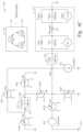
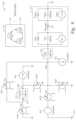
- FIG. 4is a functionally equivalent, simplified electrical circuit 400 of a plasma processing system (e.g., the processing system 10 ) that may establish a voltage boost at an electrode, in accordance with certain embodiments of the present disclosure.
- the electrical circuit 400may include switches 402 a - 402 f (collectively referred to as switches 402 and labeled as S 1 -S 6 ), a voltage source 404 , a current source 406 , a capacitive element 152 , an equivalent capacitance of the substrate support 105 (labeled as C ESC ), an input node 408 (representative of the bias electrode 104 and/or support base 107 in the processing chamber), and a complex load 410 , which may be representative of a standard electrical plasma model as further described herein.
- the processingmay include a substrate support (e.g., the substrate support 105 ) that comprises a dielectric layer (e.g., the dielectric material of the substrate support 105 ) disposed over the electrode (e.g., the bias electrode 104 and/or support base 107 ).
- a substrate supporte.g., the substrate support 105
- a dielectric layere.g., the dielectric material of the substrate support 105
- the electrodee.g., the bias electrode 104 and/or support base 107 .
- a voltage boost on the pulsed voltage from the voltage source 404 and/or current source 406may be established at an electrode (which may be represented by the input node 408 ) using the capacitive element 152 during a portion of the process of establishing the waveform at the electrode, such as the waveform depicted in FIG. 2 A .
- the electrical circuit 400illustrates a simplified model of the interaction among the waveform generator assembly (which may be represented by the voltage source 404 and/or current source 406 ), capacitive element 152 , and certain elements (e.g., the substrate support and plasma) within the processing chamber 100 , and generally illustrate the basic elements used during operation of the processing chamber 100 .
- the following definitionsare used throughout the present disclosure: (1) unless a reference is specified, all potentials are referenced to ground; (2) the voltage at any physical point (like a substrate or a biasing electrode) is likewise defined as the potential of this point with respect to ground (zero potential point); (3) the cathode sheath is implied to be an electron-repelling, ion-accelerating sheath that corresponds to a negative substrate potential with respect to plasma; (4) the sheath voltage (also referred to sometimes as “sheath voltage drop”), V sh , is defined as the absolute value of the potential difference between the plasma and the adjacent surface (e.g. of the substrate or the chamber wall); and (5) the substrate potential is the potential at the substrate surface facing the plasma.
- the complex load 410is depicted as a standard electrical plasma model that represents the processing plasma 101 as three series elements.
- the first elementbeing an electron-repelling cathode sheath (which sometimes may also be referred to as the “plasma sheath” or merely the “sheath”) adjacent to the substrate 103 .
- the cathode sheathis represented by a conventional three-part circuit element comprising: (a) the diode D SH , which when open represents the sheath collapse, (b) the current source I i , representing the ion current flowing to the substrate in the presence of the sheath, and (c) the capacitor C SH (e.g., ⁇ 100-300 pF), which represents the sheath for the main portion of the biasing cycle (e.g., the ion current stage of the waveform depicted in FIG. 2 A ), during which the ion acceleration and the etching occur.
- the third elementbeing an electron-repelling wall sheath forming at the chamber walls.
- the wall sheathis likewise represented by a three-part circuit element comprising: (a) the diode D wall , (b) the current source I iwall representing the ion current to the wall, and (c) the capacitor C wall (e.g., ⁇ 5 ⁇ 10 nF), which represents the wall sheath primarily during the ESC recharging phase of the waveform at the electrode.
- the interior surface of the grounded metal wallscan also be coated with a thin layer of a dielectric material, which may provide a capacitance (not shown), such as ⁇ 300 ⁇ 1000 nF, coupled in series between the complex load 410 and the ground node 414 .
- the parasitic and stray capacitances of the ESC assemblymay not be critical to the voltage boost scheme described herein and are not depicted in FIG. 4 . In certain cases, these factors (among others) may be considered in determining the values of certain electrical components (such as the capacitance of the capacitive element 152 , capacitance of C ESC , etc.) and/or the characteristics (e.g., voltage levels, duration, and/or the RF signal) of the waveform established at the electrode.
- the capacitive element 152may be implemented as one or more capacitors, such as a ceramic capacitor and/or a multi-layered dielectric capacitor.
- the capacitive element 152may include multiple capacitors coupled together in a network, such as a parallel network and/or series network.
- the capacitive element 152may be rated to operate at high voltages, such as voltage levels above 10 kV.
- the capacitive element 152may have a capacitance within a range of 500 picofarads (pF) to 1 nanofarad (nF).
- the capacitance value of the capacitive element 152may be close to or higher than C ESC and/or C SH .
- the capacitive elementmay have a capacitance equal to or greater than at least one of a substrate support capacitance (e.g., C ESC ) or a sheath capacitance (e.g., C SH ) of the processing chamber.
- a substrate support capacitancee.g., C ESC
- a sheath capacitancee.g., C SH
- the capacitive element 152may be selectively coupled to the electrode (e.g., the input node 408 ) of the processing chamber via at least one of the switches 402 (e.g., the switch 402 c ).
- the capacitive element 152may be selectively coupled to the voltage source 404 and the ground node 414 , for example, via at least one of the switches 402 (e.g., the switches 402 d , 402 e , and 402 f ).
- the capacitive element 152 and the voltage source 404may be selectively coupled in parallel with the electrode (e.g., the input node 408 ). That is, the capacitive element 152 and the voltage source 404 may be selectively coupled to the electrode in parallel with each other.
- the capacitive element 152is a separate electrical component from the substrate support capacitance (C ESC ) and/or sheath capacitance (C SH ). In certain cases, the capacitive element 152 may be integrated with and/or co-located with the waveform generator assembly 150 , such as the voltage source 404 and/or current source 406 . In certain cases, the capacitive element 152 may be integrated with and/or co-located with the substrate support capacitance (C ESC ) and/or sheath capacitance (C SH ) to provide a suitable boost voltage as described herein.
- the capacitive element 152may provide a source for bulk electrons that is separate from the plasma. In certain cases, the capacitive element 152 may improve the sustainability and stability of the plasma by reducing the bulk electrons consumed from the plasma to establish the DC bias at the electrode.
- the switches 402may be implemented as high voltage solid-state relays. In certain cases, the switches 402 may be implemented as a high voltage multiplexer and/or demultiplexer. In this example, the switches 402 may include a first switch 402 a , second switch 402 b , third switch 402 c , fourth switch 402 d , fifth switch 402 e , and sixth switch 402 f .
- the first switch 402 amay be coupled between the voltage source 404 and the input node 408 , which may be electrically coupled to the electrode or representative of the electrode.
- the second switch 402 bmay be coupled between the input node 408 and the ground node 414 .
- the third switch 402 cmay be coupled between a first terminal 416 of the capacitive element 152 and the input node 408 .
- the fourth switch 402 dmay be coupled between a second terminal 418 of the capacitive element 152 and the input node 408 .
- the fifth switch 402 emay be coupled between the first terminal 416 of the capacitive element 152 and the ground node 414 .
- the sixth switch 402 fmay be coupled between the second terminal 418 of the capacitive element 152 and the ground node 414 .
- the state of the switches 402may be controlled by the system controller 126 .
- the system controller 126may be in communication with control inputs (not shown) of the switches 402 , such that control signals from the system controller 126 toggle the states of the switches 402 .
- the system controller 126may control the individual state of each switch 402 with a separate control signal applied to the respective switch. As further described herein with respect to FIGS.
- the switches 402may be configured to couple the capacitive element 152 and the voltage source 404 to the electrode (e.g., the input node 408 ) during a first phase (which may be referred to as the ESC recharging phase), couple the capacitive element 152 and the electrode to the ground node 414 during a second phase (which may be referred to as the voltage negation phase), and couple the capacitive element 152 to the electrode during a third phase (which may be referred to as the voltage boost phase).
- the second phasemay occur after the first phase
- the third phasemay occur after the second phase.
- the switches 402may decouple the electrode from the capacitive element 152 and the voltage source 404 during the second phase and decouple the electrode from the ground node during the third phase.
- the voltage source 404may be a component of a waveform generator assembly (e.g., the waveform generator assembly 150 ). That is, the waveform generator assembly may include the voltage source 404 , which may include a pulsed-voltage DC waveform generator and/or RF generator (also referred to as an RF signal generator).
- the voltage source 404may be selectively coupled to the electrode (e.g., the input node 408 ) via one of the switches 402 (e.g., the switch 402 a ).
- the switch 402 amay be coupled in series between the voltage source 404 and the input node 408 .
- the current source 406may be a component of the waveform generator assembly.
- the current source 406may be used to implement the ramp voltage during the ion current stage, for example, as described herein with respect to FIG. 2 A .
- the current sourcemay be configured to apply an ion compensation current to the processing chamber (e.g., the electrode) during a fourth phase (e.g., the ion current stage as depicted in FIG. 2 A ).
- the switches 402may be configured to couple the capacitive element 152 to the processing chamber (e.g., the electrode) during the fourth phase, which may occur after the third phase.
- the current source 406may be coupled to the electrode.
- the voltage source 404 , current source 406 , and capacitive element 152may be coupled in parallel to the electrode (e.g., the input node 408 ).
- the electrical circuit 400is merely an example, and other electrical circuits (such as the circuits depicted in FIGS. 9 and 10 ) may be used in addition to or instead of the circuit illustrated to provide the voltage boost at the electrode and reduce the bulk electron consumption from the plasma. While the examples depicted in the present disclosure are described herein with respect to using a positive voltage pulse for the substrate processing to facilitate understanding, aspects of the present disclosure may also be applied to using a negative voltage pulse to establish the waveform at the electrode.
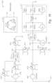
- FIG. 5is a timing diagram 500 illustrating states of the switches 402 (labeled as S 1 -S 6 , respectively) of the electrical circuit 400
- FIGS. 6 A- 6 Care circuit diagrams illustrating the states of the switches 402 during corresponding phases depicted in FIG. 5 , in accordance with certain embodiments of the present disclosure.
- the waveform at the electrodemay be established in a first phase 502 , a second phase 504 , a third phase 506 , and a fourth phase 508 .
- the first phase 502can take from 20 nanoseconds (ns) to 2000 ns to allow enough electrons to be collected at the wafer surface.
- the second phase 504 and/or the third phase 506can take from tens of nanoseconds to hundreds of nanoseconds, such as 20 ns to 500 ns.
- the fourth phase 508can take greater than 50% of the waveform cycle, such as 85 ⁇ 90% of the waveform cycle.
- the frequency of the voltage functioncould range from 50 kHz to 5000 kHz.
- switches 402 a , 402 d , and 402 e(S 1 , S 4 , and S 5 ) are closed to charge the substrate support 105 (C ESC ) and plasma sheath capacitance(s) (C SH and C WALL ), as well as the capacitive element 152 (C BOOST ), as shown in FIG. 6 A .
- the charging time for these capacitorsmay be shorter or longer than the duration depicted in FIG. 5 .
- the first switch 402 ais configured to close; the second switch 402 b is configured to open; the third switch 402 c is configured to open; the fourth switch 402 d is configured to close; the fifth switch 402 e is configured to close; and the sixth switch 402 f is configured to open.
- the capacitive element 152 , C ESC , and C SHmay be charged to a voltage VBOOST during the first phase 502 .
- Plasma bulk electronsare attracted to the wafer surface due to the rising edge of the waveform shown in FIG. 5 .
- the electronsmay not establish a negative DC sheath potential yet, for example, due to there being equal amounts of positive charge on the other electrode.
- An equivalent capacitance depicted as C ESCmay form between the wafer surface and the electrode, and there may be an equal amount of positive charge on the electrode to cancel the field generated by those electrons.
- the second switch 402 b and sixth switch 402 fare closed as shown in FIG. 6 B .
- the first switch 402 a , the fourth switch 402 d , and the fifth switch 402 eare configured to open during the second phase 504
- the second switch 402 b and sixth switch 402 fare configured to close during the second phase to couple the second terminal 418 of the capacitive element 152 and the input node 408 to the ground node 414 .
- the substrate support capacitance C ESCis coupled to the ground node 414 .
- the potential at the electrodemay be forced to the voltage level at the ground node 414 (such as 0 Volts).
- the voltage on the wafer surfacebecomes negative thereby establishing a negative V dc on the wafer surface.
- the voltage at the electrodemay be reduced to first voltage level.
- the sixth switch 402 fcloses and pulls the potential of the connected capacitive element 152 to ground.
- the potential of at the capacitive element 152becomes a negative voltage.
- the capacitive element 152may not be coupled to the input node 408 and the substrate support.
- the negative DC voltage (V dc ) on the wafer surface after the second switch 402 b closescan be approximated by using the magnitude of the falling edge ⁇ V and the ratio between the C ESC and sheath capacitance C sheath :
- C sheathis the capacitance of the wafer sheath capacitance (C SH ) in series with the ground sheath capacitance (C WALL ).
- C sheathmay be approximated by the wafer sheath capacitance (C SH ) due to the ground sheath capacitance (C WALL ) being much larger.
- the third switch 402 c and sixth switch 402 fare closed as shown in FIG. 6 C .
- the second switch 402 bis configured to open, and the third switch 402 c is configured to close during the third phase, such that the first terminal 416 of the capacitive element 152 is coupled to the input node 408 .
- the capacitive element 152may further reduce the voltage at the electrode to a second voltage level less than the first voltage level.
- the third switch 402 cconnects the capacitive element 152 to the input node 408 , which may further enhance V dc on the wafer surface and pull V dc more negative.
- the voltage at the electrodemay be given by:
- V d ⁇ c
- may be higher than
- may be 1750 Volts, and
- the capacitive element 152may reduce the number of electrons required to accumulate on the wafer surface by 2.75 times for the same amount of V dc .
- the fourth phase 508is the ion current compensation phase, which may be implemented as described herein with respect to FIGS. 2 A and 2 B .
- the electrode voltagemay have a negative slope to compensate ion current.
- the states of switches 402may remain the same as the states established at the end of the third phase 506 . That is, the third switch 402 c and sixth switch 402 f may remain closed during the fourth phase 508 .
- the oncoming ion currentneutralizes the negative discharges on the wafer surface and discharges the sheath capacitor (e.g., C SH ).
- the wafer voltagemay be kept at a constant voltage to provide single peak IED as described herein with respect to FIGS. 2 B and 3 .
- the current source 406can be used to pump electrons to the circuit to compensate for the ion current. In doing so, the current source establishes a voltage waveform having a negative slope at the electrode.
- the plasma ionsbombard the wafer surface and induce etching reactions.
- the fourth phase 508may be considered the etching period and may be made as long as possible to facilitate the desired etching (e.g., 1000 ns to 10,000 ns). The length may be limited by the charging speed of the wafer surface or the maximum voltage of the current source (if current compensation is performed).
- the ion compensation current (I ion )can be calibrated using ion energy/flux diagnostics or calculated by sampling the electrode voltage (V 0 ) (e.g., to calculate time derivative of V 0 ) and the value of the sheath capacitance:
- I i ⁇ o ⁇ n( C s ⁇ h ⁇ e ⁇ a ⁇ t ⁇ h + C b ⁇ o ⁇ o ⁇ s ⁇ t ) ⁇ d ⁇ V ⁇ 0 d ⁇ t ( 3 )
- C boostis the capacitance of the capacitive element 152 .
- the first tens to hundreds of the cyclescan be used to sample the electrode voltage and calculate lion for ion current compensation. The current compensation may then be implemented for the subsequent cycles.
- the current source 406may be configured to adjust the ion compensation current in response to a change in voltage over time measured at the electrode based at least in part on a capacitance of the capacitive element, for example, as given by Equation (3).
- An increased capacitance of the capacitive element 152may slow down the decay of V dc .
- C boostmay be made as large as possible in the voltage rating allowed range.
- FIG. 7is a process flow diagram illustrating a method 700 for boosting the voltage at the electrode.
- the method 700may be performed by a plasma processing system, such as the processing system 10 .
- a capacitive elemente.g., the capacitive element 152
- a voltage sourcee.g., the voltage source 404
- an electrodee.g., represented by the input node 408
- the capacitive element 152 and the voltage source 404may be coupled to the electrode in parallel, for example, as depicted in FIG. 4 .
- the first switch 402 a , the fourth switch 402 d , and the fifth switch 402 emay be closed during the first phase.
- the second switch 402 b , the third switch 402 c , and the sixth switch 402 fare opened during the first phase.
- the capacitive element 152 and the electrodemay be coupled to a ground node (e.g., the ground node 414 ) during a second phase (e.g., the second phase 504 ).
- the electrodemay be decoupled from the voltage source and the capacitive element.
- the first switch 402 a , fourth switch 402 d , and fifth switch 402 eare opened during the second phase.
- the second switch 402 b and sixth switch 402 fare closed during the second phase to couple the capacitive element to the input node (e.g., the input node 408 ). With the second switch 402 b closed, a voltage at the electrode may be reduced to a first voltage level.
- the capacitive element 152may be coupled to the electrode during a third phase (e.g., the third phase 506 ).
- the electrodemay decoupled from the ground node.
- the second switch 402 bmay be opened during the third phase, and the third switch may be closed to couple the first terminal 416 of the capacitive element 152 to the input node 408 .
- the third switch 402 cWith the third switch 402 c closed, the voltage at the electrode may be reduced to a second voltage level less than the first voltage level.
- a current source(e.g., the current source 406 ) may apply an ion compensation current to the electrode during a fourth phase (e.g., the fourth phase 508 ).
- the capacitive element 152may be coupled to the electrode during the fourth phase.
- the current sourcemay adjust the ion compensation current in response to a change in voltage over time measured at the electrode based at least in part on a capacitance of the capacitive element, for example, as given by the Equation (3).
- the method 700may also include generating a plasma over a substrate supporting surface (e.g., the substrate support surface 105 A) of a substrate support (e.g., the substrate support 105 ) disposed in the processing chamber.
- the plasma and ion current compensationmay facilitate the etching of the substrate as described herein.
- the timing of when the charged capacitive element is coupled to the electrodemay be adjusted, for example, to produce multiple ion energies and/or adjust the width of an ion energy in an etching cycle.
- FIG. 8 Ashows an example voltage waveform that may be established at an electrode (e.g., the bias electrode 104 and/or support base 107 ) of a processing chamber, in accordance with certain embodiments of the present disclosure.
- closing the third switch 402 c in the third phasemay be delayed compared to the waveform depicted in FIGS. 2 A and 5 .
- the second phasemay be have a longer duration than the duration depicted in FIGS. 2 A and 5 .
- An IEDF with two ion energies as depicted in FIG. 8 Bmay be produced with the delayed coupling of the capacitive element.
- the IEDFincludes a low energy peak 802 and a high energy peak 804 .
- FIG. 9is an additional functionally equivalent, simplified electrical circuit 900 of a plasma processing system (e.g., the processing system 10 ) that may establish a voltage boost at an electrode, in accordance with certain embodiments of the present disclosure.
- the current source 406may be selectively coupled to the processing chamber (e.g., the electrode) via the switches 402 (e.g., the third switch 402 c ), which may be configured to couple the current source to the processing chamber during the fourth phase.
- the capacitive element 152may be selectively coupled in series between the current source 406 and the electrode (e.g., the input node 408 ).
- the sixth switch 402 fmay be excluded.
- the ion currentmay be adjusted according to the following expression:
- the electrical circuit 900may enable a lower ion current compared to the electrical circuit 400 .
- FIG. 10is an additional functionally equivalent, simplified electrical circuit 1000 of a plasma processing system (e.g., the processing system 10 ) that may establish a voltage boost at an electrode, in accordance with certain embodiments of the present disclosure.
- the voltage sourcemay include a first voltage source 404 a selectively coupled to the electrode (e.g., the input node 408 ) and a second voltage source 404 b selective coupled to the capacitive element 152 .
- the sixth switch 402 fmay be coupled in parallel with the second voltage source 404 b and the fourth switch 402 d .
- the fifth switch 402 emay be coupled in series between the capacitive element 152 and the ground node 414 .
- the first switch 402 a , fourth switch 402 d , and the fifth switch 402 emay be closed, while the second switch 402 b , third switch 402 c , and sixth switch 402 f may be open.
- the sixth switch 402 f and second switch 402 bmay be closed, while the first switch 402 a , third switch 402 c , and fourth switch 402 d may be open.
- the third switch 402 c and sixth switch 402 fmay be closed, while the first switch 402 a , second switch 402 b , and fifth switch 402 e may be open.
- the capacitive element 152 and the second voltage source 404 bmay be used to compensate ion current.
- the third switch 402 cmay be closed at the middle of the fourth phase to produce a step down in voltage during the ion current compensation stage.
- multiple stages of the boost capacitancecan be used to further increase the wafer DC voltage.
- Such embodimentsmay use more switches and/or relays.
- the techniques and apparatus described hereinmay reduce the number of plasma electrons consumed to establish the DC bias. As such, the techniques and apparatus described herein may improve plasma stability and extend the achievable maximum ion energy for substrate processing.
- Coupledis used herein to refer to the direct or indirect coupling between two objects. For example, if object A physically touches object B and object B touches object C, then objects A and C may still be considered coupled to one another—even if objects A and C do not directly physically touch each other. For instance, a first object may be coupled to a second object even though the first object is never directly physically in contact with the second object.
Landscapes
- Physics & Mathematics (AREA)
- Engineering & Computer Science (AREA)
- Plasma & Fusion (AREA)
- Chemical & Material Sciences (AREA)
- Analytical Chemistry (AREA)
- Plasma Technology (AREA)
- Drying Of Semiconductors (AREA)
- Chemical Vapour Deposition (AREA)
Abstract
Description
Embodiments of the present disclosure generally relate to a system used in semiconductor device manufacturing. More specifically, embodiments of the present disclosure relate to a plasma processing system used to process a substrate.
Reliably producing high aspect ratio features is one of the key technology challenges for the next generation of semiconductor devices. One method of forming high aspect ratio features uses a plasma-assisted etching process in which a plasma is formed in a processing chamber and ions from the plasma are accelerated towards a surface of a substrate to form openings in a material layer disposed beneath a mask layer formed on the surface of the substrate.
In a typical plasma-assisted etching process, the substrate is positioned on a substrate support disposed in a processing chamber, a plasma is formed over the substrate, and ions are accelerated from the plasma towards the substrate across a plasma sheath, i.e., region depleted of electrons, formed between the plasma and the surface of the substrate.
It has been found that pulsing techniques have to periodically and suddenly consume a large amount of plasma generated bulk electrons to establish the DC bias, and the amount of bulk electrons consumed is often on the order of the number of free electrons found in the generated plasma. Therefore, the consumption of bulk electrons cause severe perturbation to plasma stability and sometimes cause the plasma to extinguish. As an example, assume a plasma processing system has a plasma density of 5e10 cm−3, gap of 2 cm (1 inch gap minus sheath thickness, about 0.5 cm) and wafer diameter of 30 cm. In such a system, the total available electrons in the volume above the wafer is 7e13. Further assume a sheath capacitance of 200 pF and sheath voltage of 8000V (typical for high aspect ratio etch applications). The number of electrons used to charge the wafer surface is about 1e13. So in about tens of nanoseconds, about 15 percent of the bulk electrons is drawn from the plasma to establish the DC bias. This consumption repeats at the pulsing frequency, which may be around 400 kHz. The bulk electron consumption is a significant perturbation to plasma sustainability and stability. This scenario may only worsen with the evolving processes using higher ion energies. During processing, variations in the plasma created by plasma instability will affect the with-in-wafer (WIW) and wafer-to-wafer (WTW) process performance, and thus device yield and other related process results.
Accordingly, there is a need in the art for plasma processing and biasing methods that are able to provide desirable plasma-assisted etching process results.
Embodiments provided herein generally include apparatus, plasma processing systems and methods for generation of a waveform for plasma processing of a substrate in a processing chamber.
One embodiment of the present disclosure is directed to a plasma processing system. The plasma processing system generally includes a processing chamber, a plurality of switches, an electrode disposed in the processing chamber, a voltage source, and a capacitive element. The voltage source is selectively coupled to the electrode via one of the plurality of switches. The capacitive element is selectively coupled to the electrode via one of the plurality of switches. The capacitive element and the voltage source are coupled to the electrode in parallel. The plurality of switches are configured to couple the capacitive element and the voltage source to the electrode during a first phase, couple the capacitive element and the electrode to a ground node during a second phase, and couple the capacitive element to the electrode during a third phase.
One embodiment of the present disclosure is directed to a method of processing a substrate. The method generally includes coupling a capacitive element and a voltage source to an electrode disposed within a processing chamber during a first phase, where the capacitive element and the voltage source are coupled to the electrode in parallel. The method also includes coupling the capacitive element and the electrode to a ground node during a second phase. The method further includes coupling the capacitive element to the electrode during a third phase.
So that the manner in which the above-recited features of the present disclosure can be understood in detail, a more particular description of the disclosure, briefly summarized above, may be had by reference to embodiments, some of which are illustrated in the appended drawings. It is to be noted, however, that the appended drawings illustrate only exemplary embodiments and are therefore not to be considered limiting of its scope and may admit to other equally effective embodiments.
To facilitate understanding, identical reference numerals have been used, where possible, to designate identical elements that are common to the figures. It is contemplated that elements disclosed in one aspect may be beneficially utilized on other aspects without specific recitation.
With technology node advancing towards 2 nm, fabrication of smaller features with larger aspect ratios involve atomic precision for plasma processing. For etching processes where the plasma ions play an important role, ion energy control is challenging the semiconductor equipment industry. Traditionally, RF biased techniques use a sinusoidal wave to excite plasma and accelerate ions.
Some embodiments of the present disclosure are generally directed to techniques and apparatus that use the concept of a charge pump to increase wafer surface voltage without or reduced consumption of plasma electrons. In certain aspects, the electrons from an external circuit (such as a capacitive element coupled in parallel with the electrode of the processing chamber) may be used to boost the DC bias at the electrode. The techniques and apparatus for boosting the DC bias at the electrode described herein may reduce the load to plasma electrons and/or facilitate higher energy substrate processing operations.
As shown, theprocessing system 10 is configured to form a capacitively coupled plasma (CCP), where theprocessing chamber 100 include an upper electrode (e.g., chamber lid123) disposed in aprocessing volume 129 facing a lower electrode (e.g., the substrate support assembly136) also disposed in theprocessing volume 129. In a typical capacitively coupled plasma (CCP) processing system, a radio frequency (RF) source is electrically coupled to one of the upper or lower electrode delivers an RF signal configured to ignite and maintain a plasma (e.g., the plasma101), which is capacitively coupled to each of the upper and lower electrodes and is disposed in a processing region therebetween. Typically, the opposing one of the upper or lower electrodes is coupled to ground or to a second RF power source for additional plasma excitation. As shown, theprocessing system 10 includes aprocessing chamber 100, asupport assembly 136, and asystem controller 126.
Theprocessing chamber 100 typically includes achamber body 113 that includes thechamber lid 123, one or more sidewalls122, and achamber base 124, which collectively define theprocessing volume 129. The one or more sidewalls122 andchamber base 124 generally include materials that are sized and shaped to form the structural support for the elements of theprocessing chamber 100 and are configured to withstand the pressures and added energy applied to them while aplasma 101 is generated within a vacuum environment maintained in theprocessing volume 129 of theprocessing chamber 100 during processing. In one example, the one or more sidewalls122 andchamber base 124 are formed from a metal, such as aluminum, an aluminum alloy, or a stainless steel alloy.
Agas inlet 128 disposed through thechamber lid 123 is used to deliver one or more processing gases to theprocessing volume 129 from aprocessing gas source 119 that is in fluid communication therewith. Asubstrate 103 is loaded into, and removed from, theprocessing volume 129 through an opening (not shown) in one of the one or more sidewalls122, which is sealed with a slit valve (not shown) during plasma processing of thesubstrate 103.
In some embodiments, a plurality of lift pins (not shown) movably disposed through openings formed in thesubstrate support assembly 136 are used to facilitate substrate transfer to and from asubstrate supporting surface 105A. In some embodiments, the plurality of lift pins132 are disposed above and are coupled to and/or are engageable with a lift pin hoop (not shown) disposed in theprocessing volume 129. The lift pin hoop may be coupled to a shaft (not shown) that sealingly extends through thechamber base 124. The shaft may be coupled to an actuator (not shown) that is used to raise and lower the lift pin hoop. When the lift pin hoop is in a raised position, it engages with the plurality of lift pins132 to raise the upper surfaces of the lift pins above thesubstrate supporting surface 105A, lifting thesubstrate 103 therefrom and enabling access to a non-active (backside) surface thesubstrate 103 by a robot handler (not shown). When the lift pin hoop is in a lowered position, the plurality of lift pins132 are flush with or recessed below thesubstrate supporting surface 105A, and thesubstrate 103 rests thereon.
Thesystem controller 126, also referred to herein as a processing chamber controller, includes a central processing unit (CPU)133, amemory 134, and supportcircuits 135. Thesystem controller 126 is used to control the process sequence used to process thesubstrate 103, including the substrate biasing and/or voltage boosting method(s) described herein. TheCPU 133 is a general-purpose computer processor configured for use in an industrial setting for controlling the processing chamber and sub-processors related thereto. Thememory 134 described herein, which is generally non-volatile memory, may include random access memory, read-only memory, floppy or hard disk drive, or other suitable forms of digital storage, local or remote. Thesupport circuits 135 are conventionally coupled to theCPU 133 and comprise cache, clock circuits, input/output subsystems, power supplies, and the like, and combinations thereof. Software instructions (program) and data can be coded and stored within thememory 134 for instructing a processor within theCPU 133. A software program (or computer instructions) readable byCPU 133 in thesystem controller 126 determines which tasks are performable by the components in theprocessing system 10.
Typically, the program, which is readable byCPU 133 in thesystem controller 126, includes code, which, when executed by the processor (CPU133), performs tasks relating to the plasma processing schemes described herein. The program may include instructions that are used to control the various hardware and electrical components within theprocessing system 10 to perform the various process tasks and various process sequences used to implement the methods described herein. In one embodiment, the program includes instructions that are used to perform one or more of the operations described below in relation toFIG.7 .
The plasma control system generally includes afirst source assembly 196 for establishing at least a first pulsed voltage (PV) waveform at a bias electrode104 (on a complex load as depicted inFIG.4 ), and asecond source assembly 197 for establishing at least a second PV waveform at anedge control electrode 115. The first PV waveform or the second PV waveform may be generated using one or more components (e.g., PV sources) within awaveform generator assembly 150, which may correspond to a voltage source and/or current source as described in more detail herein with respect toFIG.4 . In some embodiments, the waveform generator delivers an RF signal to the support base107 (e.g., power electrode or cathode) and/orbias electrode 104 which may be used to generate (maintain and/or ignite) aplasma 101 in a processing region disposed between thesubstrate support assembly 136 and thechamber lid 123. In some embodiments, as shown inFIG.1 , a separatewaveform generator assembly 150 within athird source assembly 198 includes at least an RF source that is configured to deliver an RF signal to the support base107 (e.g., power electrode or cathode).
The applied RF signal provided from thefirst source assembly 196, thesecond source assembly 197 or thethird source assembly 198 may be configured to generate (maintain and/or ignite) aplasma 101 in a processing region disposed between thesubstrate support assembly 136 and thechamber lid 123. In some embodiments, the RF signal is used to ignite and maintain aprocessing plasma 101 using the processing gases disposed in theprocessing volume 129 and fields generated by the RF power (RF signal) delivered to thesupport base 107 and/orbias electrode 104. In some aspects, the RF signal may be generated by an RF source (not shown) disposed within thewaveform generator assembly 150. Theprocessing volume 129 is fluidly coupled to one or more dedicated vacuum pumps through avacuum outlet 120, which maintain theprocessing volume 129 at sub-atmospheric pressure conditions and evacuate processing and/or other gases, therefrom. In some embodiments, thesubstrate support assembly 136, disposed in theprocessing volume 129, is disposed on asupport shaft 138 that is grounded and extends through thechamber base 124. In some embodiments, the RF signal generator may be configured to deliver an RF signal having a frequency that is greater than 40 MHz, such as between about 40 MHz and about 200 MHz.
In some embodiments, acapacitive element 152 may be selectively coupled to thebias electrode 104 and/or thesupport base 107, as further described herein with respect toFIG.4 . In certain cases, thecapacitive element 152 may be electrically coupled to thebias electrode 104 and/or thesupport base 107 via thepower delivery line 157. Thecapacitive element 152 may provide a voltage boost during ESC recharge stage to reduce the bulk electrons consumed from the plasma. The voltage boost may reduce or prevent the perturbation to plasma sustainability and stability caused by the consumption of bulk electrons from the plasma.
Thesubstrate support assembly 136, as briefly discussed above, generally includes the substrate support105 (e.g., an electrostatic chuck (ESC) substrate support) andsupport base 107. In some embodiments, thesubstrate support assembly 136 can additionally include an insulator plate111 and aground plate 112, as is discussed further below. Thesupport base 107 is electrically isolated from thechamber base 124 by the insulator plate111, and theground plate 112 is interposed between the insulator plate111 and thechamber base 124. Thesubstrate support 105 is thermally coupled to and disposed on thesupport base 107. In some embodiments, thesupport base 107 is configured to regulate the temperature of thesubstrate support 105, and thesubstrate 103 disposed on thesubstrate support 105, during substrate processing. In some embodiments, thesupport base 107 includes one or more cooling channels (not shown) disposed therein that are fluidly coupled to, and in fluid communication with, a coolant source (not shown), such as a refrigerant source or water source having a relatively high electrical resistance. In some embodiments, thesubstrate support 105 includes a heater (not shown), such as a resistive heating element embedded in the dielectric material thereof. Herein, thesupport base 107 is formed of a corrosion-resistant thermally conductive material, such as a corrosion-resistant metal, for example aluminum, an aluminum alloy, or a stainless steel and is coupled to the substrate support with an adhesive or by mechanical means.
Typically, thesubstrate support 105 is formed of a dielectric material, such as a bulk sintered ceramic material, such as a corrosion-resistant metal oxide or metal nitride material, for example, aluminum oxide (Al2O3), aluminum nitride (AlN), titanium oxide (TiO), titanium nitride (TiN), yttrium oxide (Y2O3), mixtures thereof, or combinations thereof. In embodiments herein, thesubstrate support 105 further includes thebias electrode 104 embedded in the dielectric material thereof.
In one configuration, thebias electrode 104 is a chucking pole used to secure (i.e., chuck) thesubstrate 103 to thesubstrate supporting surface 105A of thesubstrate support 105 and to bias thesubstrate 103 with respect to theprocessing plasma 101 using one or more of the pulsed-voltage biasing schemes described herein. Typically, thebias electrode 104 is formed of one or more electrically conductive parts, such as one or more metal meshes, foils, plates, or combinations thereof.
In some embodiments, thebias electrode 104 is electrically coupled to a clamping network, which provides a chucking voltage thereto, such as static DC voltage between about −5000 V and about 5000 V, using an electrical conductor, such as the coaxial power delivery line106 (e.g., a coaxial cable). As will be discussed further below, the clamping network includes a DC power supply155 (e.g., a high voltage DC (HVDC) supply) and a filter151 (e.g., a low-pass filter).
Thesubstrate support assembly 136 may further include theedge control electrode 115 that is positioned below theedge ring 114 and surrounds thebias electrode 104 and/or is disposed a distance from a center of thebias electrode 104. In general, for aprocessing chamber 100 that is configured to process circular substrates, theedge control electrode 115 is annular in shape, is made from a conductive material, and is configured to surround at least a portion of thebias electrode 104. In some embodiments, such as shown inFIG.1 , theedge control electrode 115 is positioned within a region of thesubstrate support 105. In some embodiments, as illustrated inFIG.1 , theedge control electrode 115 includes a conductive mesh, foil, and/or plate that is disposed a similar distance (i.e., Z-direction) from thesubstrate supporting surface 105A of thesubstrate support 105 as thebias electrode 104.
Theedge control electrode 115 can be biased by use of a waveform generator assembly that is different from thewaveform generator assembly 150, which is used to bias thebias electrode 104. In some embodiments, theedge control electrode 115 can be biased by use of awaveform generator assembly 150 that is also used to bias thebias electrode 104 by splitting part of the power to theedge control electrode 115. In one configuration, a firstwaveform generator assembly 150 of thefirst source assembly 196 is configured to bias thebias electrode 104, and a secondwaveform generator assembly 150 of asecond source assembly 197 is configured to bias theedge control electrode 115.
In one embodiment, apower delivery line 157 electrically connects the output of thewaveform generator assembly 150 of thefirst source assembly 196 to thebias electrode 104. While the discussion below primarily discusses thepower delivery line 157 of thefirst source assembly 196, which is used to couple awaveform generator assembly 150 to thebias electrode 104, thepower delivery line 158 of thesecond source assembly 197, which couples awaveform generator assembly 150 to theedge control electrode 115, will include the same or similar components. The electrical conductor(s) within the various parts of thepower delivery line 157 may include: (a) one or a combination of coaxial cables, such as a flexible coaxial cable that is connected in series with a rigid coaxial cable, (b) an insulated high-voltage corona-resistant hookup wire, (c) a bare wire, (d) a metal rod, (e) an electrical connector, or (f) any combination of electrical elements in (a)-(e).
In some embodiments, theprocessing chamber 100 further includes thequartz pipe 110, or collar, that at least partially circumscribes portions of thesubstrate support assembly 136 to prevent thesubstrate support 105 and/or thesupport base 107 from contact with corrosive processing gases or plasma, cleaning gases or plasma, or byproducts thereof. Typically, thequartz pipe 110, the insulator plate111, and theground plate 112 are circumscribed by aliner 108. In some embodiments, aplasma screen 109 is positioned between thecathode liner 108 and thesidewalls 122 to prevent plasma from forming in a volume underneath theplasma screen 109 between theliner 108 and the one or more sidewalls122.
The positive ions that bombard the surface of the substrate during the ion current stage deposit a positive charge on the substrate surface, which if uncompensated causes a gradually increasing substrate voltage during the ion current stage, as illustrated byvoltage waveform 225 inFIG.2B . However, the uncontrolled accumulation of positive charge on the substrate surface undesirably gradually discharges the sheath and chuck capacitors, slowly decreasing the sheath voltage drop and bringing the substrate potential closer to zero, as illustrated byvoltage waveform 225. The accumulation of positive charge results in the voltage droop in the voltage waveform established at the substrate (FIG.2B ). However, a voltage waveform that is established at the electrode that has a negative slope during the ion current stage, as shown inFIG.2A , can be generated so as to establish a square shaped region (e.g., near zero slope) for an established substrate voltage waveform, as shown bycurve 230 inFIG.2B . Implementing the slope in the waveform established at the electrode during the ion current stage may be referred to as ion current compensation. The voltage difference between the beginning and end of the ion current phase determines an ion energy distribution function (IEDF) width. The greater the voltage difference, the wider the IEDF width. To achieve monoenergetic ions and a narrower IEDF width, operations are performed to flatten the substrate voltage waveform in the ion current phase using the ion current compensation. In some embodiments of the present disclosure, an RF signal is overlaid on the voltage waveform shown inFIG.2A .
Certain embodiments of the present disclosure are generally directed to techniques and apparatus for boosting the voltage at an electrode, such as a bias electrode (e.g., thebias electrode 104 depicted inFIG.1 ) and/or a support base (e.g., thesupport base 107 depicted inFIG.1 ), of a processing chamber. The voltage boost described herein may reduce the consumption of bulk electrons from the plasma and facilitate desirable plasma-assisted etching process results.
In theelectrical circuit 400, a voltage boost on the pulsed voltage from thevoltage source 404 and/orcurrent source 406 may be established at an electrode (which may be represented by the input node408) using thecapacitive element 152 during a portion of the process of establishing the waveform at the electrode, such as the waveform depicted inFIG.2A . Theelectrical circuit 400 illustrates a simplified model of the interaction among the waveform generator assembly (which may be represented by thevoltage source 404 and/or current source406),capacitive element 152, and certain elements (e.g., the substrate support and plasma) within theprocessing chamber 100, and generally illustrate the basic elements used during operation of theprocessing chamber 100. For clarity purposes, the following definitions are used throughout the present disclosure: (1) unless a reference is specified, all potentials are referenced to ground; (2) the voltage at any physical point (like a substrate or a biasing electrode) is likewise defined as the potential of this point with respect to ground (zero potential point); (3) the cathode sheath is implied to be an electron-repelling, ion-accelerating sheath that corresponds to a negative substrate potential with respect to plasma; (4) the sheath voltage (also referred to sometimes as “sheath voltage drop”), Vsh, is defined as the absolute value of the potential difference between the plasma and the adjacent surface (e.g. of the substrate or the chamber wall); and (5) the substrate potential is the potential at the substrate surface facing the plasma.
Thecomplex load 410 is depicted as a standard electrical plasma model that represents theprocessing plasma 101 as three series elements. The first element being an electron-repelling cathode sheath (which sometimes may also be referred to as the “plasma sheath” or merely the “sheath”) adjacent to thesubstrate 103. The cathode sheath is represented by a conventional three-part circuit element comprising: (a) the diode DSH, which when open represents the sheath collapse, (b) the current source Ii, representing the ion current flowing to the substrate in the presence of the sheath, and (c) the capacitor CSH(e.g., ˜100-300 pF), which represents the sheath for the main portion of the biasing cycle (e.g., the ion current stage of the waveform depicted inFIG.2A ), during which the ion acceleration and the etching occur. The second element being a bulk plasma, which is represented by a single resistor Rplasma(e.g.,resistor 412=˜5−10 Ohms). The third element being an electron-repelling wall sheath forming at the chamber walls. The wall sheath is likewise represented by a three-part circuit element comprising: (a) the diode Dwall, (b) the current source Iiwallrepresenting the ion current to the wall, and (c) the capacitor Cwall(e.g., ˜5−10 nF), which represents the wall sheath primarily during the ESC recharging phase of the waveform at the electrode. The interior surface of the grounded metal walls can also be coated with a thin layer of a dielectric material, which may provide a capacitance (not shown), such as ˜300−1000 nF, coupled in series between thecomplex load 410 and theground node 414. The parasitic and stray capacitances of the ESC assembly (e.g., the substrate support105) and the inductance of the ESC assembly may not be critical to the voltage boost scheme described herein and are not depicted inFIG.4 . In certain cases, these factors (among others) may be considered in determining the values of certain electrical components (such as the capacitance of thecapacitive element 152, capacitance of CESC, etc.) and/or the characteristics (e.g., voltage levels, duration, and/or the RF signal) of the waveform established at the electrode.
Thecapacitive element 152 may be implemented as one or more capacitors, such as a ceramic capacitor and/or a multi-layered dielectric capacitor. For example, thecapacitive element 152 may include multiple capacitors coupled together in a network, such as a parallel network and/or series network. In certain cases, thecapacitive element 152 may be rated to operate at high voltages, such as voltage levels above 10 kV. Thecapacitive element 152 may have a capacitance within a range of 500 picofarads (pF) to 1 nanofarad (nF). The capacitance value of thecapacitive element 152 may be close to or higher than CESCand/or CSH. That is, the capacitive element may have a capacitance equal to or greater than at least one of a substrate support capacitance (e.g., CESC) or a sheath capacitance (e.g., CSH) of the processing chamber.
Thecapacitive element 152 may be selectively coupled to the electrode (e.g., the input node408) of the processing chamber via at least one of the switches402 (e.g., theswitch 402c). Thecapacitive element 152 may be selectively coupled to thevoltage source 404 and theground node 414, for example, via at least one of the switches402 (e.g., theswitches capacitive element 152 and thevoltage source 404 may be selectively coupled in parallel with the electrode (e.g., the input node408). That is, thecapacitive element 152 and thevoltage source 404 may be selectively coupled to the electrode in parallel with each other. In certain aspects, thecapacitive element 152 is a separate electrical component from the substrate support capacitance (CESC) and/or sheath capacitance (CSH). In certain cases, thecapacitive element 152 may be integrated with and/or co-located with thewaveform generator assembly 150, such as thevoltage source 404 and/orcurrent source 406. In certain cases, thecapacitive element 152 may be integrated with and/or co-located with the substrate support capacitance (CESC) and/or sheath capacitance (CSH) to provide a suitable boost voltage as described herein.
Thecapacitive element 152 may provide a source for bulk electrons that is separate from the plasma. In certain cases, thecapacitive element 152 may improve the sustainability and stability of the plasma by reducing the bulk electrons consumed from the plasma to establish the DC bias at the electrode.
The switches402 may be implemented as high voltage solid-state relays. In certain cases, the switches402 may be implemented as a high voltage multiplexer and/or demultiplexer. In this example, the switches402 may include afirst switch 402a,second switch 402b,third switch 402c,fourth switch 402d,fifth switch 402e, andsixth switch 402f. Thefirst switch 402amay be coupled between thevoltage source 404 and theinput node 408, which may be electrically coupled to the electrode or representative of the electrode. Thesecond switch 402bmay be coupled between theinput node 408 and theground node 414. Thethird switch 402cmay be coupled between afirst terminal 416 of thecapacitive element 152 and theinput node 408. Thefourth switch 402dmay be coupled between asecond terminal 418 of thecapacitive element 152 and theinput node 408. Thefifth switch 402emay be coupled between thefirst terminal 416 of thecapacitive element 152 and theground node 414. Thesixth switch 402fmay be coupled between thesecond terminal 418 of thecapacitive element 152 and theground node 414.
In certain cases, the state of the switches402 (e.g., opened or closed) may be controlled by thesystem controller 126. For example, thesystem controller 126 may be in communication with control inputs (not shown) of the switches402, such that control signals from thesystem controller 126 toggle the states of the switches402. Thesystem controller 126 may control the individual state of each switch402 with a separate control signal applied to the respective switch. As further described herein with respect toFIGS.5 and6A-6C , the switches402 may be configured to couple thecapacitive element 152 and thevoltage source 404 to the electrode (e.g., the input node408) during a first phase (which may be referred to as the ESC recharging phase), couple thecapacitive element 152 and the electrode to theground node 414 during a second phase (which may be referred to as the voltage negation phase), and couple thecapacitive element 152 to the electrode during a third phase (which may be referred to as the voltage boost phase). In aspects, the second phase may occur after the first phase, and the third phase may occur after the second phase. For certain aspects, the switches402 may decouple the electrode from thecapacitive element 152 and thevoltage source 404 during the second phase and decouple the electrode from the ground node during the third phase.
Thevoltage source 404 may be a component of a waveform generator assembly (e.g., the waveform generator assembly150). That is, the waveform generator assembly may include thevoltage source 404, which may include a pulsed-voltage DC waveform generator and/or RF generator (also referred to as an RF signal generator). Thevoltage source 404 may be selectively coupled to the electrode (e.g., the input node408) via one of the switches402 (e.g., theswitch 402a). For example, theswitch 402amay be coupled in series between thevoltage source 404 and theinput node 408.
Similarly, thecurrent source 406 may be a component of the waveform generator assembly. Thecurrent source 406 may be used to implement the ramp voltage during the ion current stage, for example, as described herein with respect toFIG.2A . The current source may be configured to apply an ion compensation current to the processing chamber (e.g., the electrode) during a fourth phase (e.g., the ion current stage as depicted inFIG.2A ). In aspects, the switches402 may be configured to couple thecapacitive element 152 to the processing chamber (e.g., the electrode) during the fourth phase, which may occur after the third phase. Thecurrent source 406 may be coupled to the electrode. In certain cases, thevoltage source 404,current source 406, andcapacitive element 152 may be coupled in parallel to the electrode (e.g., the input node408).
Those of skill in the art will understand that theelectrical circuit 400 is merely an example, and other electrical circuits (such as the circuits depicted inFIGS.9 and10 ) may be used in addition to or instead of the circuit illustrated to provide the voltage boost at the electrode and reduce the bulk electron consumption from the plasma. While the examples depicted in the present disclosure are described herein with respect to using a positive voltage pulse for the substrate processing to facilitate understanding, aspects of the present disclosure may also be applied to using a negative voltage pulse to establish the waveform at the electrode.
Referring toFIG.5 , the waveform at the electrode may be established in afirst phase 502, asecond phase 504, athird phase 506, and afourth phase 508. Thefirst phase 502 can take from 20 nanoseconds (ns) to 2000 ns to allow enough electrons to be collected at the wafer surface. Thesecond phase 504 and/or thethird phase 506 can take from tens of nanoseconds to hundreds of nanoseconds, such as 20 ns to 500 ns. Thefourth phase 508 can take greater than 50% of the waveform cycle, such as 85˜90% of the waveform cycle. The frequency of the voltage function could range from 50 kHz to 5000 kHz.
During thefirst phase 502, switches402a,402d, and402e(S1, S4, and S5) are closed to charge the substrate support105 (CESC) and plasma sheath capacitance(s) (CSHand CWALL), as well as the capacitive element152 (CBOOST), as shown inFIG.6A . The charging time for these capacitors may be shorter or longer than the duration depicted inFIG.5 . During thefirst phase 502, thefirst switch 402ais configured to close; thesecond switch 402bis configured to open; thethird switch 402cis configured to open; thefourth switch 402dis configured to close; thefifth switch 402eis configured to close; and thesixth switch 402fis configured to open.
Thecapacitive element 152, CESC, and CSHmay be charged to a voltage VBOOST during thefirst phase 502. Plasma bulk electrons are attracted to the wafer surface due to the rising edge of the waveform shown inFIG.5 . The electrons may not establish a negative DC sheath potential yet, for example, due to there being equal amounts of positive charge on the other electrode. An equivalent capacitance depicted as CESCmay form between the wafer surface and the electrode, and there may be an equal amount of positive charge on the electrode to cancel the field generated by those electrons.
During thesecond phase 504, thesecond switch 402bandsixth switch 402fare closed as shown inFIG.6B . Thefirst switch 402a, thefourth switch 402d, and thefifth switch 402eare configured to open during thesecond phase 504, and thesecond switch 402bandsixth switch 402fare configured to close during the second phase to couple thesecond terminal 418 of thecapacitive element 152 and theinput node 408 to theground node 414. Effectively, the substrate support capacitance CESCis coupled to theground node 414.
As thesecond switch 402bcloses, the potential at the electrode may be forced to the voltage level at the ground node414 (such as 0 Volts). As a capacitor's voltage drop cannot change instantaneously, the voltage on the wafer surface becomes negative thereby establishing a negative Vdcon the wafer surface. For example, with thesecond switch 402bin a closed state, the voltage at the electrode may be reduced to first voltage level.
Thesixth switch 402fcloses and pulls the potential of the connectedcapacitive element 152 to ground. The potential of at thecapacitive element 152 becomes a negative voltage. During thesecond phase 504, thecapacitive element 152 may not be coupled to theinput node 408 and the substrate support. The negative DC voltage (Vdc) on the wafer surface after thesecond switch 402bcloses can be approximated by using the magnitude of the falling edge ΔV and the ratio between the CESCand sheath capacitance Csheath:
where Csheathis the capacitance of the wafer sheath capacitance (CSH) in series with the ground sheath capacitance (CWALL). In certain cases, Csheathmay be approximated by the wafer sheath capacitance (CSH) due to the ground sheath capacitance (CWALL) being much larger.
During thethird phase 506, thethird switch 402candsixth switch 402fare closed as shown inFIG.6C . Thesecond switch 402bis configured to open, and thethird switch 402cis configured to close during the third phase, such that thefirst terminal 416 of thecapacitive element 152 is coupled to theinput node 408. With thethird switch 402cclosed, thecapacitive element 152 may further reduce the voltage at the electrode to a second voltage level less than the first voltage level. Thethird switch 402cconnects thecapacitive element 152 to theinput node 408, which may further enhance Vdcon the wafer surface and pull Vdcmore negative.
The voltage at the electrode may be given by:
In certain cases, |Vboost| may be higher than |ΔV|. For example, |Vboost| may be 1750 Volts, and |ΔV| may be 1000 Volts. In this example, thecapacitive element 152 may reduce the number of electrons required to accumulate on the wafer surface by 2.75 times for the same amount of Vdc.
Thefourth phase 508 is the ion current compensation phase, which may be implemented as described herein with respect toFIGS.2A and2B . During thefourth phase 508, the electrode voltage may have a negative slope to compensate ion current. The states of switches402 may remain the same as the states established at the end of thethird phase 506. That is, thethird switch 402candsixth switch 402fmay remain closed during thefourth phase 508.
The oncoming ion current neutralizes the negative discharges on the wafer surface and discharges the sheath capacitor (e.g., CSH). The wafer voltage may be kept at a constant voltage to provide single peak IED as described herein with respect toFIGS.2B and3 . Thecurrent source 406 can be used to pump electrons to the circuit to compensate for the ion current. In doing so, the current source establishes a voltage waveform having a negative slope at the electrode. Infourth phase 508, the plasma ions bombard the wafer surface and induce etching reactions. Thefourth phase 508 may be considered the etching period and may be made as long as possible to facilitate the desired etching (e.g., 1000 ns to 10,000 ns). The length may be limited by the charging speed of the wafer surface or the maximum voltage of the current source (if current compensation is performed).
The ion compensation current (Iion) can be calibrated using ion energy/flux diagnostics or calculated by sampling the electrode voltage (V0) (e.g., to calculate time derivative of V0) and the value of the sheath capacitance:
where Cboostis the capacitance of the
Atactivity 702, a capacitive element (e.g., the capacitive element152) and a voltage source (e.g., the voltage source404) may be coupled to an electrode (e.g., represented by the input node408) disposed within a processing chamber (e.g., the processing chamber100) during a first phase (e.g., the first phase502). Thecapacitive element 152 and thevoltage source 404 may be coupled to the electrode in parallel, for example, as depicted inFIG.4 . As an example, with respect to theelectrical circuit 400, thefirst switch 402a, thefourth switch 402d, and thefifth switch 402emay be closed during the first phase. Thesecond switch 402b, thethird switch 402c, and thesixth switch 402fare opened during the first phase.
Atactivity 704, thecapacitive element 152 and the electrode may be coupled to a ground node (e.g., the ground node414) during a second phase (e.g., the second phase504). During the second phase, the electrode may be decoupled from the voltage source and the capacitive element. As an example, with respect to theelectrical circuit 400, thefirst switch 402a,fourth switch 402d, andfifth switch 402eare opened during the second phase. Thesecond switch 402bandsixth switch 402fare closed during the second phase to couple the capacitive element to the input node (e.g., the input node408). With thesecond switch 402bclosed, a voltage at the electrode may be reduced to a first voltage level.
Atactivity 706, thecapacitive element 152 may be coupled to the electrode during a third phase (e.g., the third phase506). During the third phase, the electrode may decoupled from the ground node. As an example, with respect to theelectrical circuit 400, thesecond switch 402bmay be opened during the third phase, and the third switch may be closed to couple thefirst terminal 416 of thecapacitive element 152 to theinput node 408. With thethird switch 402cclosed, the voltage at the electrode may be reduced to a second voltage level less than the first voltage level.
Atactivity 708, a current source (e.g., the current source406) may apply an ion compensation current to the electrode during a fourth phase (e.g., the fourth phase508). In aspects, thecapacitive element 152 may be coupled to the electrode during the fourth phase. For certain aspects, the current source may adjust the ion compensation current in response to a change in voltage over time measured at the electrode based at least in part on a capacitance of the capacitive element, for example, as given by the Equation (3).
In certain aspects, themethod 700 may also include generating a plasma over a substrate supporting surface (e.g., thesubstrate support surface 105A) of a substrate support (e.g., the substrate support105) disposed in the processing chamber. The plasma and ion current compensation may facilitate the etching of the substrate as described herein.
In certain aspects, the timing of when the charged capacitive element is coupled to the electrode may be adjusted, for example, to produce multiple ion energies and/or adjust the width of an ion energy in an etching cycle.
For certain aspects, the current source may be coupled in series with the capacitive element. For example,FIG.9 is an additional functionally equivalent, simplified electrical circuit900 of a plasma processing system (e.g., the processing system10) that may establish a voltage boost at an electrode, in accordance with certain embodiments of the present disclosure. Thecurrent source 406 may be selectively coupled to the processing chamber (e.g., the electrode) via the switches402 (e.g., thethird switch 402c), which may be configured to couple the current source to the processing chamber during the fourth phase. In this example, thecapacitive element 152 may be selectively coupled in series between thecurrent source 406 and the electrode (e.g., the input node408). In the electrical circuit900, thesixth switch 402fmay be excluded.
The ion current may be adjusted according to the following expression:
As a result, the electrical circuit900 may enable a lower ion current compared to theelectrical circuit 400.
In certain aspects, a separate voltage source may be used to charge the capacitive element. For example,FIG.10 is an additional functionally equivalent, simplifiedelectrical circuit 1000 of a plasma processing system (e.g., the processing system10) that may establish a voltage boost at an electrode, in accordance with certain embodiments of the present disclosure. In theelectrical circuit 1000, the voltage source may include afirst voltage source 404aselectively coupled to the electrode (e.g., the input node408) and asecond voltage source 404bselective coupled to thecapacitive element 152. In this example, thesixth switch 402fmay be coupled in parallel with thesecond voltage source 404band thefourth switch 402d. Thefifth switch 402emay be coupled in series between thecapacitive element 152 and theground node 414.
During the first phase, thefirst switch 402a,fourth switch 402d, and thefifth switch 402emay be closed, while thesecond switch 402b,third switch 402c, andsixth switch 402fmay be open. During the second phase, thesixth switch 402fandsecond switch 402bmay be closed, while thefirst switch 402a,third switch 402c, andfourth switch 402dmay be open. During the third phase, thethird switch 402candsixth switch 402fmay be closed, while thefirst switch 402a,second switch 402b, andfifth switch 402emay be open.
In certain cases, thecapacitive element 152 and thesecond voltage source 404bmay be used to compensate ion current. For example, thethird switch 402cmay be closed at the middle of the fourth phase to produce a step down in voltage during the ion current compensation stage.
Similar to the concept of Voltage Triplers and Quadruplers, multiple stages of the boost capacitance can be used to further increase the wafer DC voltage. Such embodiments may use more switches and/or relays.
It will be appreciated that the techniques and apparatus described herein may reduce the number of plasma electrons consumed to establish the DC bias. As such, the techniques and apparatus described herein may improve plasma stability and extend the achievable maximum ion energy for substrate processing.
The term “coupled” is used herein to refer to the direct or indirect coupling between two objects. For example, if object A physically touches object B and object B touches object C, then objects A and C may still be considered coupled to one another—even if objects A and C do not directly physically touch each other. For instance, a first object may be coupled to a second object even though the first object is never directly physically in contact with the second object.
While the foregoing is directed to embodiments of the present disclosure, other and further embodiments of the disclosure may be devised without departing from the basic scope thereof, and the scope thereof is determined by the claims that follow.
Claims (29)
1. A method of processing a substrate, comprising:
coupling a capacitive element and a voltage source to an electrode disposed within a processing chamber during a first phase, wherein the capacitive element and the voltage source are coupled to the electrode in parallel;
coupling the capacitive element and the electrode to a ground node during a second phase; and
coupling the capacitive element to the electrode during a third phase.
2. The method ofclaim 1 , further comprising:
generating a plasma over a substrate supporting surface of a substrate support disposed in the processing chamber, the substrate support comprising the electrode and a dielectric layer disposed between the electrode and the substrate supporting surface;
wherein coupling during the second phase further comprises decoupling the electrode from the voltage source and the capacitive element; and
wherein coupling during the third phase further comprises decoupling the electrode from the ground node.
3. The method ofclaim 1 , wherein coupling during the first phase comprises:
closing a first switch coupled between the voltage source and an input node that is electrically coupled to the electrode;
closing a second switch coupled between a first terminal of the capacitive element and the input node; and
closing a third switch coupled between a second terminal of the capacitive element and the ground node.
4. The method ofclaim 3 , wherein coupling during the first phase further comprises:
opening a fourth switch coupled between the input node and the ground node;
opening a fifth switch coupled between the first terminal of the capacitive element and the ground node; and
opening a sixth switch coupled between the second terminal of the capacitive element and the input node.
5. The method ofclaim 4 , wherein coupling during the second phase comprises:
opening the first switch, the second switch, and the third switch; and
closing the fourth switch and the fifth switch to couple the first terminal of the capacitive element and the input node to the ground node.
6. The method ofclaim 5 , wherein coupling during the third phase comprises:
opening the fourth switch; and
closing the sixth switch to couple the second terminal of the capacitive element to the input node.
7. The method ofclaim 1 , further comprising applying, by use of a current source, an ion compensation current to the electrode during a fourth phase.
8. The method ofclaim 7 , wherein the capacitive element is coupled to the electrode during the fourth phase.
9. The method ofclaim 7 , further comprising:
generating a plasma over a substrate supporting surface of a substrate support disposed in the processing chamber, the substrate support comprising the electrode and a dielectric layer disposed between the electrode and the substrate supporting surface; and
wherein applying the ion compensation current comprises adjusting the ion compensation current in response to a change in voltage over time measured at the electrode based at least in part on a capacitance of the capacitive element.
10. The method ofclaim 1 , wherein:
coupling during the second phase comprises reducing a voltage at the electrode to a first voltage level; and
coupling during the third phase comprises reducing the voltage at the electrode to a second voltage level less than the first voltage level.
11. The method ofclaim 1 , further comprising applying, by use of a current source, an ion compensation current to the electrode during a fourth phase, wherein the capacitive element is selectively coupled in series between the current source and the electrode.
12. The method ofclaim 1 , wherein the voltage source comprises a first voltage source selectively coupled to the electrode and a second voltage source selectively coupled to the capacitive element.
13. The method ofclaim 1 , wherein the second phase occurs after the first phase, and the third phase occurs after the second phase.
14. The method ofclaim 1 , wherein the capacitive element has a capacitance within a range of 500 picofarads (pF) to 1 nanofarad (nF).
15. The method ofclaim 1 , wherein the capacitive element has a capacitance equal to or greater than at least one of a substrate support capacitance or a sheath capacitance of the processing chamber.
16. A plasma processing system, comprising:
a plurality of switches;
an electrode disposed within a processing chamber;
a voltage source selectively coupled to the electrode via one of the plurality of switches; and
a capacitive element selectively coupled to the electrode via the one of the plurality of switches, wherein the capacitive element and the voltage source are coupled to the electrode in parallel, and wherein the plurality of switches are configured to:
couple the capacitive element and the voltage source to the electrode during a first phase,
couple the capacitive element and the electrode to a ground node during a second phase, and
couple the capacitive element to the electrode during a third phase.
17. The plasma processing system ofclaim 16 , wherein:
the processing chamber comprises a substrate support that comprises a dielectric layer disposed over the electrode;
wherein the plurality of switches are configured to:
decouple the electrode from the capacitive element and the voltage source during the second phase, and
decouple the electrode from the ground node during the third phase.
18. The plasma processing system ofclaim 17 , wherein the plurality of switches comprise:
a first switch coupled between the voltage source and an input node that is electrically coupled to the electrode, wherein the first switch is configured to close during the first phase;
a second switch coupled between a first terminal of the capacitive element and the input node, wherein the second switch is configured to close during the first phase; and
a third switch coupled between a second terminal of the capacitive element and the ground node, wherein the third switch is configured to close during the first phase.
19. The plasma processing system ofclaim 18 , wherein the plurality of switches comprise:
a fourth switch coupled between the input node and the ground node, wherein the fourth switch is configured to open during the first phase;
a fifth switch coupled between the first terminal of the capacitive element and the ground node, wherein the fifth switch is configured to open during the first phase; and
a sixth switch coupled between the second terminal of the capacitive element and the input node, wherein the sixth switch is configured to open during the first phase.
20. The plasma processing system ofclaim 19 , wherein:
the first switch, the second switch, and the fifth switch are configured to open during the second phase; and
the fourth switch and the fifth switch are configured to close during the second phase to couple the first terminal of the capacitive element and the input node to the ground node.
21. The plasma processing system ofclaim 20 , wherein:
the fourth switch is configured to open during the third phase; and
the sixth switch is configured to close during the third phase to couple the second terminal of the capacitive element to the input node.
22. The plasma processing system ofclaim 16 , further comprising:
a current source coupled to the electrode; and
wherein the current source is configured to apply an ion compensation current to the processing chamber during a fourth phase.
23. The plasma processing systemclaim 22 , wherein the plurality of switches are configured to couple the capacitive element to the processing chamber during the fourth phase.
24. The plasma processing system ofclaim 22 , wherein:
the processing chamber comprises a substrate support that comprises a dielectric layer that is disposed over the electrode; and
the current source is configured to adjust the ion compensation current in response to a change in voltage over time measured at the electrode based at least in part on a capacitance of the capacitive element.
25. The plasma processing system ofclaim 16 , the plurality of switches are configured to:
couple the electrode to the ground node during the second phase to reduce a voltage at the electrode to a first voltage level; and
couple the capacitive element to the electrode during the third phase to reduce the voltage at the first electrode to a second voltage level less than the first voltage level.
26. The plasma processing system ofclaim 16 , further comprising:
a current source selectively coupled to the processing chamber via the plurality of switches;
wherein the current source is configured to apply an ion compensation current to the electrode during a fourth phase;
wherein the plurality of switches are configured to couple the current source to the processing chamber during the fourth phase; and
wherein the capacitive element is selectively coupled in series between the current source and the electrode.
27. The plasma processing system ofclaim 16 , wherein the second phase occurs after the first phase, and the third phase occurs after the second phase.
28. The plasma processing system ofclaim 16 , wherein the capacitive element has a capacitance within a range of 500 picofarads (pF) to 1 nanofarad (nF).
29. The plasma processing system ofclaim 16 , wherein the capacitive element has a capacitance equal to or greater than at least one of a substrate support capacitance or a sheath capacitance of the processing chamber.
Priority Applications (6)
| Application Number | Priority Date | Filing Date | Title |
|---|---|---|---|
| US17/361,178US11776788B2 (en) | 2021-06-28 | 2021-06-28 | Pulsed voltage boost for substrate processing |
| JP2023504707AJP7534528B2 (en) | 2021-06-28 | 2022-05-25 | Pulsed voltage boost for substrate processing |
| KR1020237002924AKR20230026506A (en) | 2021-06-28 | 2022-05-25 | Pulsed Voltage Boost for Substrate Processing |
| PCT/US2022/030844WO2023278075A1 (en) | 2021-06-28 | 2022-05-25 | Pulsed voltage boost for substrate processing |
| CN202280005624.5ACN115868003B (en) | 2021-06-28 | 2022-05-25 | Pulse voltage boosting for substrate processing |
| TW111121797ATWI835163B (en) | 2021-06-28 | 2022-06-13 | Pulsed voltage boost for substrate processing |
Applications Claiming Priority (1)
| Application Number | Priority Date | Filing Date | Title |
|---|---|---|---|
| US17/361,178US11776788B2 (en) | 2021-06-28 | 2021-06-28 | Pulsed voltage boost for substrate processing |
Publications (2)
| Publication Number | Publication Date |
|---|---|
| US20220415614A1 US20220415614A1 (en) | 2022-12-29 |
| US11776788B2true US11776788B2 (en) | 2023-10-03 |
Family
ID=84541248
Family Applications (1)
| Application Number | Title | Priority Date | Filing Date |
|---|---|---|---|
| US17/361,178Active2041-12-23US11776788B2 (en) | 2021-06-28 | 2021-06-28 | Pulsed voltage boost for substrate processing |
Country Status (6)
| Country | Link |
|---|---|
| US (1) | US11776788B2 (en) |
| JP (1) | JP7534528B2 (en) |
| KR (1) | KR20230026506A (en) |
| CN (1) | CN115868003B (en) |
| TW (1) | TWI835163B (en) |
| WO (1) | WO2023278075A1 (en) |
Families Citing this family (9)
| Publication number | Priority date | Publication date | Assignee | Title |
|---|---|---|---|---|
| EP3945541A1 (en)* | 2020-07-29 | 2022-02-02 | TRUMPF Huettinger Sp. Z o. o. | Pulsing assembly, power supply arrangement and method using the assembly |
| US11848176B2 (en) | 2020-07-31 | 2023-12-19 | Applied Materials, Inc. | Plasma processing using pulsed-voltage and radio-frequency power |
| US11776788B2 (en) | 2021-06-28 | 2023-10-03 | Applied Materials, Inc. | Pulsed voltage boost for substrate processing |
| US12272524B2 (en) | 2022-09-19 | 2025-04-08 | Applied Materials, Inc. | Wideband variable impedance load for high volume manufacturing qualification and on-site diagnostics |
| US12111341B2 (en) | 2022-10-05 | 2024-10-08 | Applied Materials, Inc. | In-situ electric field detection method and apparatus |
| US20250087461A1 (en)* | 2023-09-11 | 2025-03-13 | Applied Materials, Inc. | Pulsed voltage-assisted plasma strike |
| WO2025197564A1 (en)* | 2024-03-22 | 2025-09-25 | 東京エレクトロン株式会社 | Plasma processing device, bias power supply system, and plasma processing method |
| JP7514462B1 (en)* | 2024-04-02 | 2024-07-11 | 京都電機器株式会社 | Pulse power supply device for plasma etching equipment and bias control method |
| JP7587093B1 (en)* | 2024-06-18 | 2024-11-20 | 京都電機器株式会社 | Pulse power supply device for plasma etching equipment and bias control method |
Citations (369)
| Publication number | Priority date | Publication date | Assignee | Title |
|---|---|---|---|---|
| US3055203A (en) | 1959-10-01 | 1962-09-25 | Gen Electric | Automatic washer-dryer including a pre-spin impulse speed and unbalance switch means |
| US4464223A (en) | 1983-10-03 | 1984-08-07 | Tegal Corp. | Plasma reactor apparatus and method |
| US4585516A (en) | 1985-03-04 | 1986-04-29 | Tegal Corporation | Variable duty cycle, multiple frequency, plasma reactor |
| US5099697A (en) | 1990-04-02 | 1992-03-31 | Agar Corporation Ltd. | Two and three-phase flow measurement |
| US5242561A (en) | 1989-12-15 | 1993-09-07 | Canon Kabushiki Kaisha | Plasma processing method and plasma processing apparatus |
| US5449410A (en) | 1993-07-28 | 1995-09-12 | Applied Materials, Inc. | Plasma processing apparatus |
| US5464499A (en) | 1992-06-24 | 1995-11-07 | Texas Instruments Incorporated | Multi-electrode plasma processing apparatus |
| US5565036A (en) | 1994-01-19 | 1996-10-15 | Tel America, Inc. | Apparatus and method for igniting plasma in a process module |
| US5595627A (en) | 1995-02-07 | 1997-01-21 | Tokyo Electron Limited | Plasma etching method |
| US5597438A (en) | 1995-09-14 | 1997-01-28 | Siemens Aktiengesellschaft | Etch chamber having three independently controlled electrodes |
| US5698062A (en) | 1993-11-05 | 1997-12-16 | Tokyo Electron Limited | Plasma treatment apparatus and method |
| US5716534A (en) | 1994-12-05 | 1998-02-10 | Tokyo Electron Limited | Plasma processing method and plasma etching method |
| US5810982A (en) | 1994-06-17 | 1998-09-22 | Eni Technologies, Inc. | Preferential sputtering of insulators from conductive targets |
| US5830330A (en) | 1997-05-22 | 1998-11-03 | Tokyo Electron Limited | Method and apparatus for low pressure sputtering |
| US5882424A (en) | 1997-01-21 | 1999-03-16 | Applied Materials, Inc. | Plasma cleaning of a CVD or etch reactor using a low or mixed frequency excitation field |
| US5928963A (en) | 1995-10-26 | 1999-07-27 | Tokyo Electron Limited | Plasma etching method |
| US5933314A (en) | 1997-06-27 | 1999-08-03 | Lam Research Corp. | Method and an apparatus for offsetting plasma bias voltage in bi-polar electro-static chucks |
| US5935373A (en) | 1996-09-27 | 1999-08-10 | Tokyo Electron Limited | Plasma processing apparatus |
| US5948704A (en) | 1996-06-05 | 1999-09-07 | Lam Research Corporation | High flow vacuum chamber including equipment modules such as a plasma generating source, vacuum pumping arrangement and/or cantilevered substrate support |
| US5997687A (en) | 1996-08-23 | 1999-12-07 | Tokyo Electron Limited | Plasma processing apparatus |
| US6043607A (en) | 1997-12-16 | 2000-03-28 | Applied Materials, Inc. | Apparatus for exciting a plasma in a semiconductor wafer processing system using a complex RF waveform |
| US6055150A (en) | 1996-05-02 | 2000-04-25 | Applied Materials, Inc. | Multi-electrode electrostatic chuck having fuses in hollow cavities |
| US6074518A (en) | 1994-04-20 | 2000-06-13 | Tokyo Electron Limited | Plasma processing apparatus |
| US6089181A (en) | 1996-07-23 | 2000-07-18 | Tokyo Electron Limited | Plasma processing apparatus |
| US6110287A (en) | 1993-03-31 | 2000-08-29 | Tokyo Electron Limited | Plasma processing method and plasma processing apparatus |
| US6117279A (en) | 1998-11-12 | 2000-09-12 | Tokyo Electron Limited | Method and apparatus for increasing the metal ion fraction in ionized physical vapor deposition |
| US6125025A (en) | 1998-09-30 | 2000-09-26 | Lam Research Corporation | Electrostatic dechucking method and apparatus for dielectric workpieces in vacuum processors |
| US6133557A (en) | 1995-01-31 | 2000-10-17 | Kyocera Corporation | Wafer holding member |
| US6136387A (en) | 1997-06-04 | 2000-10-24 | Tokyo Electron Limited | Ion flow forming method and apparatus |
| US6198616B1 (en) | 1998-04-03 | 2001-03-06 | Applied Materials, Inc. | Method and apparatus for supplying a chucking voltage to an electrostatic chuck within a semiconductor wafer processing system |
| US6197151B1 (en) | 1996-03-01 | 2001-03-06 | Hitachi, Ltd. | Plasma processing apparatus and plasma processing method |
| US6202590B1 (en) | 1998-09-25 | 2001-03-20 | Samsung Electronics Co., Ltd. | Plasma apparatus for fabricating semiconductor devices |
| US6214162B1 (en) | 1996-09-27 | 2001-04-10 | Tokyo Electron Limited | Plasma processing apparatus |
| US6232236B1 (en) | 1999-08-03 | 2001-05-15 | Applied Materials, Inc. | Apparatus and method for controlling plasma uniformity in a semiconductor wafer processing system |
| US6252354B1 (en) | 1996-11-04 | 2001-06-26 | Applied Materials, Inc. | RF tuning method for an RF plasma reactor using frequency servoing and power, voltage, current or DI/DT control |
| US6277506B1 (en) | 1999-03-11 | 2001-08-21 | Sumitomo Special Metals Co., Ltd. | Thin film magnetic head thin film magnetic head substrate and method for fabricating such substrate |
| US20010033755A1 (en) | 2000-04-21 | 2001-10-25 | Toshiaki Ino | Image forming apparatus |
| US6309978B1 (en) | 1998-07-22 | 2001-10-30 | Micron Technology, Inc. | Beat frequency modulation for plasma generation |
| US6313583B1 (en) | 1998-12-01 | 2001-11-06 | Matsushita Electric Industrial Co., Ltd. | Plasma processing apparatus and method |
| US6358573B1 (en) | 1997-12-01 | 2002-03-19 | Applied Materials, Inc. | Mixed frequency CVD process |
| US6367413B1 (en) | 1999-06-15 | 2002-04-09 | Tokyo Electron Limited | Apparatus for monitoring substrate biasing during plasma processing of a substrate |
| US6395641B2 (en) | 1995-10-13 | 2002-05-28 | Mattson Techonolgy, Inc. | Apparatus and method for pulsed plasma processing of a semiconductor substrate |
| US6413358B2 (en) | 1993-04-16 | 2002-07-02 | Micron Technology, Inc. | Method and apparatus for improving etch uniformity in remote source plasma reactors with powered wafer chucks |
| US6423192B1 (en) | 1999-10-29 | 2002-07-23 | Kabushiki Kaisha Toshiba | Sputtering apparatus and film forming method |
| US6433297B1 (en) | 1999-03-19 | 2002-08-13 | Kabushiki Kaisha Toshiba | Plasma processing method and plasma processing apparatus |
| US6451389B1 (en) | 1999-04-17 | 2002-09-17 | Advanced Energy Industries, Inc. | Method for deposition of diamond like carbon |
| US6456010B2 (en) | 2000-03-13 | 2002-09-24 | Mitsubishi Heavy Industries, Ltd. | Discharge plasma generating method, discharge plasma generating apparatus, semiconductor device fabrication method, and semiconductor device fabrication apparatus |
| US20030049558A1 (en) | 2000-12-12 | 2003-03-13 | Makoto Aoki | Vacuum processing method, vacuum processing apparatus, semiconductor device manufacturing method and semiconductor device |
| US6535785B2 (en) | 1997-09-17 | 2003-03-18 | Tokyo Electron Limited | System and method for monitoring and controlling gas plasma processes |
| US20030052085A1 (en) | 2000-03-28 | 2003-03-20 | Richard Parsons | Control of power delivered to a multiple segment inject electrode |
| US20030079983A1 (en) | 2000-02-25 | 2003-05-01 | Maolin Long | Multi-zone RF electrode for field/plasma uniformity control in capacitive plasma sources |
| US20030091355A1 (en) | 2001-10-19 | 2003-05-15 | Markus Jeschonek | Apparatus and method for acquiring the nature of a toner particle layer and the moisture content of a carrier material in a printer or copier |
| US20030151372A1 (en) | 2002-02-08 | 2003-08-14 | Nobuaki Tsuchiya | RF plasma processing method and RF plasma processing system |
| US20030165044A1 (en) | 2002-03-04 | 2003-09-04 | Kouichi Yamamoto | Electrostatic chuck and method of treating substrate using electrostatic chuck |
| US6621674B1 (en) | 1999-08-13 | 2003-09-16 | Hüttinger Elektronik GmbH & Co. KG | Electric supply unit for plasma installations |
| US20030201069A1 (en) | 2000-09-18 | 2003-10-30 | Johnson Wayne L. | Tunable focus ring for plasma processing |
| US6664739B1 (en) | 1999-08-02 | 2003-12-16 | Advanced Energy Industries, Inc. | Enhanced electron emissive surfaces for a thin film deposition system using ion sources |
| US20040040931A1 (en) | 2000-12-26 | 2004-03-04 | Akira Koshiishi | Plasma processing method and plasma processor |
| US20040040665A1 (en) | 2002-06-18 | 2004-03-04 | Anelva Corporation | Electrostatic chuck device |
| US6733624B2 (en) | 2000-07-17 | 2004-05-11 | Tokyo Electron Limited | Apparatus for holding an object to be processed |
| US6740842B2 (en) | 1999-07-13 | 2004-05-25 | Tokyo Electron Limited | Radio frequency power source for generating an inductively coupled plasma |
| US6741446B2 (en) | 2001-03-30 | 2004-05-25 | Lam Research Corporation | Vacuum plasma processor and method of operating same |
| US20040112536A1 (en) | 2001-05-29 | 2004-06-17 | Tokyo Electron Limited | Plasma processing apparatus and method |
| US20040223284A1 (en) | 2002-12-04 | 2004-11-11 | Shibaura Mechatronics Corporation | Electrostatic attracting method, electrostatic attracting apparatus, and bonding apparatus |
| US6818103B1 (en) | 1999-10-15 | 2004-11-16 | Advanced Energy Industries, Inc. | Method and apparatus for substrate biasing in multiple electrode sputtering systems |
| US6830595B2 (en) | 2002-12-20 | 2004-12-14 | Advanced Energy Technology Inc. | Method of making composite electrode and current collectors |
| US6849154B2 (en) | 1998-11-27 | 2005-02-01 | Tokyo Electron Limited | Plasma etching apparatus |
| US20050022933A1 (en) | 2003-08-01 | 2005-02-03 | Howard Bradley J. | Multi-frequency plasma reactor and method of etching |
| US20050024809A1 (en) | 2003-05-26 | 2005-02-03 | Kyocera Corporation | Electrostatic chuck |
| US20050039852A1 (en) | 2002-07-12 | 2005-02-24 | Advanced Energy Industries, Inc. | Wafer probe for measuring plasma and surface characteristics in plasma processing enviroments |
| US6896775B2 (en) | 2002-10-29 | 2005-05-24 | Zond, Inc. | High-power pulsed magnetically enhanced plasma processing |
| US6917204B2 (en) | 2001-01-08 | 2005-07-12 | Tokyo Electron Limited | Addition of power at selected harmonics of plasma processor drive frequency |
| US20050151544A1 (en) | 2003-08-14 | 2005-07-14 | Advanced Energy Industries, Inc. | Sensor array for measuring plasma characteristics in plasma processing environments |
| US6962664B2 (en) | 2000-01-10 | 2005-11-08 | Tokyo Electron Limited | Controlled method for segmented electrode apparatus and method for plasma processing |
| US6970042B2 (en) | 2002-10-29 | 2005-11-29 | Huettinger Elektronik Gmbh & Co. Kg | Power control for high frequency amplifiers |
| US6972524B1 (en) | 2004-03-24 | 2005-12-06 | Lam Research Corporation | Plasma processing system control |
| US20050286916A1 (en) | 2004-06-28 | 2005-12-29 | Yasushi Nakazato | Recording medium conveyance failure occurrence predicting apparatus, fixing device, image forming apparatus, and recording medium conveyance failure occurrence predicting method |
| US7016620B2 (en) | 2001-07-25 | 2006-03-21 | Oce Printing Systems Gmbh | Method and device for controlling a print process with high color density |
| US7046088B2 (en) | 2002-03-12 | 2006-05-16 | Huettinger Elektronik Gmbh & Co. | Power amplifier |
| US7059267B2 (en) | 2000-08-28 | 2006-06-13 | Micron Technology, Inc. | Use of pulsed grounding source in a plasma reactor |
| US20060171848A1 (en) | 2005-01-31 | 2006-08-03 | Advanced Energy Industries, Inc. | Diagnostic plasma sensors for endpoint and end-of-life detection |
| US7104217B2 (en) | 2000-04-18 | 2006-09-12 | Tokyo Electron Limited | Plasma processing apparatus |
| US7147759B2 (en) | 2002-09-30 | 2006-12-12 | Zond, Inc. | High-power pulsed magnetron sputtering |
| US7151242B2 (en) | 2004-09-16 | 2006-12-19 | Huettinger Elektronik Gmbh + Co. Kg | Induction heating system and method |
| US7166233B2 (en) | 1999-08-17 | 2007-01-23 | Tokyo Electron Limited | Pulsed plasma processing method and apparatus |
| US7183177B2 (en) | 2000-08-11 | 2007-02-27 | Applied Materials, Inc. | Silicon-on-insulator wafer transfer method using surface activation plasma immersion ion implantation for wafer-to-wafer adhesion enhancement |
| US7206189B2 (en) | 2002-12-20 | 2007-04-17 | Advanced Energy Technology Inc. | Composite electrode and current collectors and processes for making the same |
| US7218872B2 (en) | 2004-05-20 | 2007-05-15 | Oki Data Corporation | Image forming apparatus |
| US7218503B2 (en) | 1998-09-30 | 2007-05-15 | Lam Research Corporation | Method of determining the correct average bias compensation voltage during a plasma process |
| US20070113787A1 (en) | 2001-12-13 | 2007-05-24 | Tokyo Electron Limited | Plasma process apparatus |
| US7226868B2 (en) | 2001-10-31 | 2007-06-05 | Tokyo Electron Limited | Method of etching high aspect ratio features |
| US7265963B2 (en) | 2000-07-26 | 2007-09-04 | Tokyo Electron Limited | Holding mechanism of object to be processed |
| KR100757347B1 (en) | 2006-08-30 | 2007-09-10 | 삼성전자주식회사 | Ion implantation device |
| US7274266B2 (en) | 2005-02-12 | 2007-09-25 | Huettinger Elektronik Gmbh + Co. Kg | Radio frequency excitation arrangement |
| US7305311B2 (en) | 2005-04-22 | 2007-12-04 | Advanced Energy Industries, Inc. | Arc detection and handling in radio frequency power applications |
| US20070284344A1 (en) | 2006-06-13 | 2007-12-13 | Todorov Valentin N | High ac current high rf power ac-rf decoupling filter for plasma reactor heated electrostatic chuck |
| US20080012548A1 (en) | 2006-03-25 | 2008-01-17 | Huettinger Elektronik Gmbh + Co. Kg | Measuring device of an hf plasma system |
| US20080048498A1 (en) | 2003-02-15 | 2008-02-28 | Huettinger Elektronik Gmbh + Co. Kg | Power Delivery Control and Balancing Between Multiple Loads |
| US20080160212A1 (en) | 2006-12-27 | 2008-07-03 | Bon-Woong Koo | Method and apparatuses for providing electrical contact for plasma processing applications |
| US7408329B2 (en) | 2003-03-21 | 2008-08-05 | Huettinger Elektronik Gmbh + Co. Kg | Power supply unit for gas discharge processes |
| US20080185537A1 (en) | 2004-08-20 | 2008-08-07 | Varian Semiconductor Equipment Associates, Inc. | In situ surface contamination removal for ion implanting |
| US7415940B2 (en) | 2001-05-15 | 2008-08-26 | Tokyo Electron Limited | Plasma processor |
| US20080236493A1 (en) | 2007-03-27 | 2008-10-02 | Tokyo Electron Limited | Plasma processing apparatus |
| US20080236750A1 (en)* | 2007-03-27 | 2008-10-02 | Tokyo Electron Limited | Plasma processing apparatus |
| US7440301B2 (en) | 2001-12-15 | 2008-10-21 | Huettinger Elektronik Gmbh & Co. Kg | High frequency excitation system |
| US7452443B2 (en) | 2005-03-05 | 2008-11-18 | Huettinger Elektronik Gmbh + Co. Kg | Vacuum plasma generator |
| US7479712B2 (en) | 2003-09-10 | 2009-01-20 | Applied Materials Gmbh & Co. Kg. | Configuration for N consumers of electric energy, of which M consumers are simultaneously supplied with energy |
| US7509105B2 (en) | 2003-08-11 | 2009-03-24 | Huettinger Elektronik Gmbh + Co. Kg | Radio frequency excitation arrangement including a limiting circuit |
| US20090078678A1 (en) | 2007-09-14 | 2009-03-26 | Akihiro Kojima | Plasma processing apparatus and plasma processing method |
| US7512387B2 (en) | 2004-05-17 | 2009-03-31 | Huettinger Elektronik Gmbh + Co. Kg | Method and control system for controlling the output power of an RF amplifier system |
| US7535688B2 (en) | 2005-03-25 | 2009-05-19 | Tokyo Electron Limited | Method for electrically discharging substrate, substrate processing apparatus and program |
| US20090133839A1 (en) | 2007-11-14 | 2009-05-28 | Tokyo Electron Limited | Plasma processing apparatus |
| US7586099B2 (en) | 2005-03-30 | 2009-09-08 | Huettinger Elektronik Gmbh + Co. Kg | Vacuum plasma generator |
| US7588667B2 (en) | 2006-04-07 | 2009-09-15 | Tokyo Electron Limited | Depositing rhuthenium films using ionized physical vapor deposition (IPVD) |
| US20090236214A1 (en) | 2008-03-20 | 2009-09-24 | Karthik Janakiraman | Tunable ground planes in plasma chambers |
| US7601246B2 (en) | 2004-09-29 | 2009-10-13 | Lam Research Corporation | Methods of sputtering a protective coating on a semiconductor substrate |
| US7609740B2 (en) | 2006-11-04 | 2009-10-27 | Huettinger Elektronik Gmbh + Co. Kg | Method and arrangement for the excitation of a gas laser arrangement |
| US7618686B2 (en) | 2001-04-27 | 2009-11-17 | European Community (Ec) | Method and apparatus for sequential plasma treatment |
| US7645341B2 (en) | 2003-12-23 | 2010-01-12 | Lam Research Corporation | Showerhead electrode assembly for plasma processing apparatuses |
| US7651586B2 (en) | 2003-08-22 | 2010-01-26 | Tokyo Electron Limited | Particle removal apparatus and method and plasma processing apparatus |
| US20100018648A1 (en) | 2008-07-23 | 2010-01-28 | Applied Marterials, Inc. | Workpiece support for a plasma reactor with controlled apportionment of rf power to a process kit ring |
| US20100029038A1 (en) | 2006-11-22 | 2010-02-04 | Tokyo Electron Limited | Manufacturing method of solar cell and manufacturing apparatus of solar cell |
| US20100025230A1 (en) | 2006-04-11 | 2010-02-04 | Hauzer Techno Coating Bv | Vacuum Treatment Apparatus, A Bias Power Supply And A Method Of Operating A Vacuum Treatment Apparatus |
| US7692936B2 (en) | 2006-05-05 | 2010-04-06 | Huettinger Elektronik Gmbh + Co. Kg | Medium frequency power generator |
| US7700474B2 (en) | 2006-04-07 | 2010-04-20 | Tokyo Electron Limited | Barrier deposition using ionized physical vapor deposition (iPVD) |
| US7706907B2 (en) | 2006-06-02 | 2010-04-27 | Tokyo Electron Limited | Substrate processing apparatus, substrate processing method, computer program, and storage medium |
| US7705676B2 (en) | 2007-03-09 | 2010-04-27 | Huettinger Elektronik Gmbh + Co. Kg | Class D amplifier arrangement |
| US20100118464A1 (en) | 2008-11-13 | 2010-05-13 | Tokyo Electron Limited | Electrostatic chuck and substrate processing apparatus having same |
| US7740704B2 (en) | 2004-06-25 | 2010-06-22 | Tokyo Electron Limited | High rate atomic layer deposition apparatus and method of using |
| US20100154994A1 (en) | 2008-12-19 | 2010-06-24 | Andreas Fischer | Controlling ion energy distribution in plasma processing systems |
| US7758764B2 (en) | 2007-06-28 | 2010-07-20 | Lam Research Corporation | Methods and apparatus for substrate processing |
| US7782100B2 (en) | 2008-02-29 | 2010-08-24 | Huettinger Elektronik Gmbh + Co. Kg | Driving a full bridge circuit |
| US7795817B2 (en) | 2006-11-24 | 2010-09-14 | Huettinger Elektronik Gmbh + Co. Kg | Controlled plasma power supply |
| US7821767B2 (en) | 2004-11-04 | 2010-10-26 | Ulvac, Inc. | Electrostatic chuck device |
| US20100321047A1 (en) | 2007-02-23 | 2010-12-23 | Alfred Zollner | Method and device for detecting electric potential and electric charges in a printer or copier |
| US7858533B2 (en) | 2008-03-06 | 2010-12-28 | Tokyo Electron Limited | Method for curing a porous low dielectric constant dielectric film |
| US20100326957A1 (en) | 2009-06-24 | 2010-12-30 | Kenji Maeda | Plasma processing apparatus and plasma processing method |
| CN101990353A (en) | 2009-08-04 | 2011-03-23 | 东京毅力科创株式会社 | Plasma processing apparatus and plasma processing method |
| US7929261B2 (en) | 2007-03-08 | 2011-04-19 | Huettinger Elektronik Gmbh + Co. Kg | Suppressing arc discharges |
| CN102084024A (en) | 2008-06-30 | 2011-06-01 | 株式会社爱发科 | power supply unit |
| US20110143537A1 (en) | 2009-12-14 | 2011-06-16 | Samsung Electronics Co., Ltd. | Method of fabricating semiconductor device and synchronous pulse plasma etching equipment for the same |
| US7977256B2 (en) | 2008-03-06 | 2011-07-12 | Tokyo Electron Limited | Method for removing a pore-generating material from an uncured low-k dielectric film |
| US20110177669A1 (en) | 2010-01-15 | 2011-07-21 | Applied Materials, Inc. | Method of controlling trench microloading using plasma pulsing |
| US20110177694A1 (en) | 2010-01-15 | 2011-07-21 | Tokyo Electron Limited | Switchable Neutral Beam Source |
| US7988816B2 (en) | 2004-06-21 | 2011-08-02 | Tokyo Electron Limited | Plasma processing apparatus and method |
| US7995313B2 (en) | 2006-11-23 | 2011-08-09 | Huettinger Elektronik Gmbh + Co. Kg | Method for operating a plasma process and arc discharge detection device |
| US20110298376A1 (en) | 2009-01-13 | 2011-12-08 | River Bell Co. | Apparatus And Method For Producing Plasma |
| US8083961B2 (en) | 2006-07-31 | 2011-12-27 | Tokyo Electron Limited | Method and system for controlling the uniformity of a ballistic electron beam by RF modulation |
| US8128831B2 (en) | 2005-12-28 | 2012-03-06 | Tokyo Electron Limited | Plasma etching method and computer-readable storage medium |
| US8140292B2 (en) | 2007-09-18 | 2012-03-20 | Wisconsin Alumni Research Foundation | Method and system for controlling a voltage waveform |
| US20120171390A1 (en) | 2007-11-16 | 2012-07-05 | Advanced Energy Industries, Inc. | Methods and apparatus for sputtering using direct current |
| US8221582B2 (en) | 2008-07-07 | 2012-07-17 | Lam Research Corporation | Clamped monolithic showerhead electrode |
| US8236109B2 (en) | 2008-12-18 | 2012-08-07 | Tokyo Electron Limited | Component cleaning method and storage medium |
| US8313664B2 (en) | 2008-11-21 | 2012-11-20 | Applied Materials, Inc. | Efficient and accurate method for real-time prediction of the self-bias voltage of a wafer and feedback control of ESC voltage in plasma processing chamber |
| US8313612B2 (en) | 2009-03-24 | 2012-11-20 | Lam Research Corporation | Method and apparatus for reduction of voltage potential spike during dechucking |
| US8333114B2 (en) | 2007-11-26 | 2012-12-18 | Tokyo Electron Limited | Microstructure inspecting device, and microstructure inspecting method |
| US20130059448A1 (en) | 2011-09-07 | 2013-03-07 | Lam Research Corporation | Pulsed Plasma Chamber in Dual Chamber Configuration |
| US8399366B1 (en) | 2011-08-25 | 2013-03-19 | Tokyo Electron Limited | Method of depositing highly conformal amorphous carbon films over raised features |
| US20130087447A1 (en) | 2011-10-11 | 2013-04-11 | Applied Materials, Inc. | Methods of preventing plasma induced damage during substrate processing |
| US8419959B2 (en) | 2009-09-18 | 2013-04-16 | Lam Research Corporation | Clamped monolithic showerhead electrode |
| US8441772B2 (en) | 2009-10-26 | 2013-05-14 | Shinko Electric Industries Co., Ltd. | Substrate for electrostatic chuck and electrostatic chuck |
| US8456220B2 (en) | 2009-12-18 | 2013-06-04 | Huettinger Elektronik Gmbh + Co. Kg | Managing a temperature of a semiconductor switching element |
| US8460567B2 (en) | 2008-07-01 | 2013-06-11 | Tokyo Electron Limited | Method and system for etching a MEM device |
| US8466622B2 (en) | 2007-07-23 | 2013-06-18 | Huettinger Elektronik Gmbh + Co. Kg | High frequency power supply |
| US20130214828A1 (en) | 2012-02-22 | 2013-08-22 | Valcore John C, JR. | Methods and apparatus for synchronizing rf pulses in a plasma processing system |
| US8542076B2 (en) | 2009-03-05 | 2013-09-24 | Huettinger Elektronik Gmbh + Co. Kg | Impedance matching |
| US8551289B2 (en) | 2009-04-28 | 2013-10-08 | Tokyo Electron Limited | Plasma processing apparatus |
| US8568606B2 (en) | 2009-03-31 | 2013-10-29 | Tokyo Electron Limited | Substrate processing apparatus and substrate processing method using same |
| US20130340938A1 (en) | 2008-02-08 | 2013-12-26 | Lam Research Corporation | Adjustable gap capacitively coupled rf plasma reactor including lateral bellows and non-contact particle seal |
| US20130344702A1 (en) | 2011-03-04 | 2013-12-26 | Tokyo Electron Limited | Method of etching silicon nitride films |
| US8641916B2 (en) | 2009-01-26 | 2014-02-04 | Tokyo Electron Limited | Plasma etching apparatus, plasma etching method and storage medium |
| US20140057447A1 (en) | 2012-08-02 | 2014-02-27 | Applied Materials, Inc. | Semiconductor processing with dc assisted rf power for improved control |
| US20140061156A1 (en) | 2012-08-28 | 2014-03-06 | Advanced Energy Industries, Inc. | Wide dynamic range ion energy bias control; fast ion energy switching; ion energy control and a pulsed bias supply; and a virtual front panel |
| US8685267B2 (en) | 2010-06-23 | 2014-04-01 | Tokyo Electron Limited | Substrate processing method |
| US20140117861A1 (en) | 2012-11-01 | 2014-05-01 | Advanced Energy Industries, Inc. | Differing boost voltages applied to two or more anodeless electrodes for plasma processing |
| US8716114B2 (en) | 2006-12-25 | 2014-05-06 | National University Corporation Tohoku University | Semiconductor device manufacturing method and semiconductor device |
| US8735291B2 (en) | 2011-08-25 | 2014-05-27 | Tokyo Electron Limited | Method for etching high-k dielectric using pulsed bias power |
| JP2014112644A (en) | 2012-11-06 | 2014-06-19 | Tokyo Electron Ltd | Plasma processing apparatus and plasma processing method |
| US8796933B2 (en) | 2010-12-08 | 2014-08-05 | Applied Materials, Inc. | Generating plasmas in pulsed power systems |
| US8809199B2 (en) | 2011-02-12 | 2014-08-19 | Tokyo Electron Limited | Method of etching features in silicon nitride films |
| US8821684B2 (en) | 2008-02-01 | 2014-09-02 | Kabushiki Kaisha Toshiba | Substrate plasma processing apparatus and plasma processing method |
| US8852347B2 (en) | 2010-06-11 | 2014-10-07 | Tokyo Electron Limited | Apparatus for chemical vapor deposition control |
| US8884525B2 (en) | 2011-03-22 | 2014-11-11 | Advanced Energy Industries, Inc. | Remote plasma source generating a disc-shaped plasma |
| US8884523B2 (en) | 2006-11-04 | 2014-11-11 | Trumpf Huettinger Gmbh + Co. Kg | Driving at least two high frequency-power generators |
| US8889534B1 (en) | 2013-05-29 | 2014-11-18 | Tokyo Electron Limited | Solid state source introduction of dopants and additives for a plasma doping process |
| US8895942B2 (en) | 2008-09-16 | 2014-11-25 | Tokyo Electron Limited | Dielectric treatment module using scanning IR radiation source |
| US8907259B2 (en) | 2010-09-14 | 2014-12-09 | Tokyo Electron Limited | Microwave irradiation device and microwave irradiation method |
| US20150002018A1 (en) | 2013-06-28 | 2015-01-01 | Lam Research Corporation | Controlling Ion Energy Within A Plasma Chamber |
| US8993943B2 (en) | 2010-10-20 | 2015-03-31 | Trumpf Huettinger Gmbh + Co. Kg | Systems for operating multiple plasma and/or induction heating systems and related methods |
| US9011636B2 (en) | 2010-03-04 | 2015-04-21 | Tokyo Electron Limited | Automatic matching method, computer-readable storage medium, automatic matching unit, and plasma processing apparatus |
| US20150111394A1 (en) | 2013-10-23 | 2015-04-23 | Taiwan Semiconductor Manufacturing Co., Ltd. | Mechanisms for forming uniform film on semiconductor substrate |
| US20150130354A1 (en) | 2013-11-11 | 2015-05-14 | Applied Materials, Inc. | Frequency tuning for dual level radio frequency (rf) pulsing |
| US9053908B2 (en) | 2013-09-19 | 2015-06-09 | Lam Research Corporation | Method and apparatus for controlling substrate DC-bias and ion energy and angular distribution during substrate etching |
| US9059178B2 (en) | 2010-04-30 | 2015-06-16 | Tokyo Electron Limited | Method for forming carbon nanotubes and carbon nanotube film forming apparatus |
| US9087798B2 (en) | 2013-08-12 | 2015-07-21 | Tokyo Electron Limited | Etching method |
| US20150235809A1 (en) | 2012-09-12 | 2015-08-20 | Tokyo Electron Limited | Plasma processing apparatus and filter unit |
| US9123762B2 (en) | 2010-10-22 | 2015-09-01 | Applied Materials, Inc. | Substrate support with symmetrical feed structure |
| US9139910B2 (en) | 2010-06-11 | 2015-09-22 | Tokyo Electron Limited | Method for chemical vapor deposition control |
| US9147555B2 (en) | 2010-07-20 | 2015-09-29 | Trumpf Huettinger Gmbh + Co. Kg | Arc extinction arrangement and method for extinguishing arcs |
| US9209032B2 (en) | 2013-03-15 | 2015-12-08 | Tokyo Electron Limited | Electric pressure systems for control of plasma properties and uniformity |
| US9209034B2 (en) | 2012-02-01 | 2015-12-08 | Tokyo Electron Limited | Plasma etching method and plasma etching apparatus |
| US20150366004A1 (en) | 2013-03-12 | 2015-12-17 | Applied Materials, Inc. | Multi zone heating and cooling esc for plasma process chamber |
| US20160004475A1 (en) | 2013-02-28 | 2016-01-07 | Hitachi, Ltd | Management system and method of dynamic storage service level monitoring |
| US20160027678A1 (en) | 2014-07-23 | 2016-01-28 | Applied Materials, Inc. | Tunable temperature controlled substrate support assembly |
| US9287086B2 (en) | 2010-04-26 | 2016-03-15 | Advanced Energy Industries, Inc. | System, method and apparatus for controlling ion energy distribution |
| CN105408993A (en) | 2013-08-06 | 2016-03-16 | 应用材料公司 | Locally heated multi-zone substrate support |
| US9313872B2 (en) | 2009-10-27 | 2016-04-12 | Tokyo Electron Limited | Plasma processing apparatus and plasma processing method |
| US9355822B2 (en) | 2011-12-27 | 2016-05-31 | Tokyo Electron Limited | Plasma processing apparatus |
| US9373521B2 (en) | 2010-02-24 | 2016-06-21 | Tokyo Electron Limited | Etching processing method |
| US9384992B2 (en) | 2012-02-09 | 2016-07-05 | Tokyo Electron Limited | Plasma processing method |
| US9396960B2 (en) | 2012-11-01 | 2016-07-19 | Tokyo Electron Limited | Plasma processing method and plasma processing apparatus |
| US9404176B2 (en) | 2012-06-05 | 2016-08-02 | Applied Materials, Inc. | Substrate support with radio frequency (RF) return path |
| US9435029B2 (en) | 2010-08-29 | 2016-09-06 | Advanced Energy Industries, Inc. | Wafer chucking system for advanced plasma ion energy processing systems |
| US20160284514A1 (en) | 2015-03-23 | 2016-09-29 | Tokyo Electron Limited | Power supply system, plasma processing apparatus and power supply control method |
| US9503006B2 (en) | 2010-10-20 | 2016-11-22 | Trumpf Huettinger Gmbh + Co. Kg | Plasma and induction heating power supply systems and related methods |
| US20160351375A1 (en) | 2009-11-19 | 2016-12-01 | Lam Research Corporation | Arrangement For Plasma Processing System Control Based On RF Voltage |
| US20160358755A1 (en) | 2014-07-21 | 2016-12-08 | Lam Research Corporation | Large dynamic range rf voltage sensor and method for voltage mode rf bias application of plasma processing systems |
| US9530667B2 (en) | 2015-02-13 | 2016-12-27 | Tokyo Electron Limited | Method for roughness improvement and selectivity enhancement during arc layer etch using carbon |
| US9576810B2 (en) | 2013-10-03 | 2017-02-21 | Applied Materials, Inc. | Process for etching metal using a combination of plasma and solid state sources |
| US9576816B2 (en) | 2015-02-13 | 2017-02-21 | Tokyo Electron Limited | Method for roughness improvement and selectivity enhancement during arc layer etch using hydrogen |
| US9593421B2 (en) | 2013-11-06 | 2017-03-14 | Applied Materials, Inc. | Particle generation suppressor by DC bias modulation |
| US9607843B2 (en) | 2015-02-13 | 2017-03-28 | Tokyo Electron Limited | Method for roughness improvement and selectivity enhancement during arc layer etch via adjustment of carbon-fluorine content |
| US20170098527A1 (en) | 2015-10-05 | 2017-04-06 | Applied Materials, Inc. | Rf power delivery regulation for processing substrates |
| US9637814B2 (en) | 2013-02-20 | 2017-05-02 | University Of West Bohemia In Pilsen | High-rate reactive sputtering of dielectric stoichiometric films |
| US9644221B2 (en) | 2012-03-30 | 2017-05-09 | Toray Industries, Inc. | Method of producing chemical by continuous fermentation and continuous fermentation apparatus |
| TW201717247A (en) | 2015-06-02 | 2017-05-16 | 蘭姆研究公司 | Large dynamic range RF voltage sensor of plasma processing system and voltage mode RF bias application method |
| US9666446B2 (en) | 2015-04-22 | 2017-05-30 | Tokyo Electron Limited | Etching method |
| US9666447B2 (en) | 2014-10-28 | 2017-05-30 | Tokyo Electron Limited | Method for selectivity enhancement during dry plasma etching |
| US9663858B2 (en) | 2013-10-09 | 2017-05-30 | Tokyo Electron Limited | Plasma processing apparatus |
| US9673059B2 (en) | 2015-02-02 | 2017-06-06 | Tokyo Electron Limited | Method for increasing pattern density in self-aligned patterning integration schemes |
| US9673027B2 (en) | 2013-01-24 | 2017-06-06 | Tokyo Electron Limited | Test apparatus and plasma processing apparatus |
| US20170162417A1 (en) | 2015-12-07 | 2017-06-08 | Applied Materials, Inc. | Method and apparatus for clamping and declamping substrates using electrostatic chucks |
| US9685297B2 (en) | 2012-08-28 | 2017-06-20 | Advanced Energy Industries, Inc. | Systems and methods for monitoring faults, anomalies, and other characteristics of a switched mode ion energy distribution system |
| US20170221682A1 (en) | 2014-10-15 | 2017-08-03 | Tokyo Electron Limited | Plasma processing apparatus |
| US9734992B2 (en) | 2011-12-15 | 2017-08-15 | Tokyo Electron Limited | Plasma processing apparatus |
| US9754768B2 (en) | 2011-12-09 | 2017-09-05 | Tokyo Electron Limited | Plasma processing method and plasma processing apparatus |
| US9761419B2 (en) | 2015-02-16 | 2017-09-12 | Tokyo Electron Limited | Method for controlling potential of susceptor of plasma processing apparatus |
| US9788405B2 (en) | 2015-10-03 | 2017-10-10 | Applied Materials, Inc. | RF power delivery with approximated saw tooth wave pulsing |
| US9786503B2 (en) | 2015-04-08 | 2017-10-10 | Tokyo Electron Limited | Method for increasing pattern density in self-aligned patterning schemes without using hard masks |
| US9799494B2 (en) | 2015-04-03 | 2017-10-24 | Tokyo Electron Limited | Energetic negative ion impact ionization plasma |
| US9805916B2 (en) | 2013-11-05 | 2017-10-31 | Tokyo Electron Limited | Plasma processing apparatus |
| US9805965B2 (en) | 2014-03-05 | 2017-10-31 | Applied Materials, Inc. | Pixelated capacitance controlled ESC |
| US20170330734A1 (en) | 2016-05-12 | 2017-11-16 | Samsung Electronics Co., Ltd. | Plasma processing apparatus |
| US9831064B2 (en) | 2013-11-05 | 2017-11-28 | Tokyo Electron Limited | Plasma processing apparatus |
| US9837285B2 (en) | 2014-08-28 | 2017-12-05 | Tokyo Electron Limited | Etching method |
| US9840770B2 (en) | 2011-06-27 | 2017-12-12 | Trumpf Huettinger Sp. Z O. O. | Generating a highly ionized plasma in a plasma chamber |
| US9865471B2 (en) | 2015-04-30 | 2018-01-09 | Tokyo Electron Limited | Etching method and etching apparatus |
| US9865893B2 (en) | 2012-07-27 | 2018-01-09 | Lockheed Martin Advanced Energy Storage, Llc | Electrochemical energy storage systems and methods featuring optimal membrane systems |
| US9870898B2 (en) | 2015-02-23 | 2018-01-16 | Tokyo Electron Limited | Plasma processing method and plasma processing apparatus |
| US20180076032A1 (en) | 2016-09-13 | 2018-03-15 | Applied Materials, Inc. | Thick tungsten hardmask films deposition on high compressive/tensile bow wafers |
| US9922806B2 (en) | 2015-06-23 | 2018-03-20 | Tokyo Electron Limited | Etching method and plasma processing apparatus |
| US9922802B2 (en) | 2012-02-20 | 2018-03-20 | Tokyo Electron Limited | Power supply system, plasma etching apparatus, and plasma etching method |
| US9941097B2 (en) | 2009-10-27 | 2018-04-10 | Tokyo Electron Limited | Plasma processing apparatus |
| US9941098B2 (en) | 2016-03-22 | 2018-04-10 | Tokyo Electron Limited | Plasma processing method |
| US20180139834A1 (en) | 2016-11-11 | 2018-05-17 | Tokyo Electron Limited | Filter device and plasma processing apparatus |
| US9997374B2 (en) | 2015-12-18 | 2018-06-12 | Tokyo Electron Limited | Etching method |
| WO2018111751A1 (en) | 2016-12-12 | 2018-06-21 | Applied Materials, Inc. | Creating ion energy distribution functions (iedf) |
| US20180190501A1 (en) | 2017-01-05 | 2018-07-05 | Tokyo Electron Limited | Plasma processing apparatus |
| US20180204708A1 (en)* | 2017-01-17 | 2018-07-19 | Lam Research Corporation | Near-Substrate Supplemental Plasma Density Generation with Low Bias Voltage within Inductively Coupled Plasma Processing Chamber |
| US20180309423A1 (en) | 2017-04-25 | 2018-10-25 | Tokyo Electron Limited | Filter device and plasma processing apparatus |
| US20180366305A1 (en) | 2017-06-14 | 2018-12-20 | Tokyo Electron Limited | Plasma processing apparatus and plasma processing method |
| US20180374672A1 (en) | 2017-06-21 | 2018-12-27 | Tokyo Electron Limited | Plasma processing apparatus |
| US10176970B2 (en) | 2015-02-10 | 2019-01-08 | Trumpf Huettinger Gmbh + Co. Kg | Redundant Power Supply System for a plasma process |
| US20190027344A1 (en) | 2017-07-19 | 2019-01-24 | Tokyo Electron Limited | Plasma processing apparatus |
| US10199246B2 (en) | 2013-10-25 | 2019-02-05 | Tokyo Electron Limited | Temperature control mechanism, temperature control method and substrate processing apparatus |
| US10217933B2 (en) | 2014-10-15 | 2019-02-26 | Tokyo Electron Limited | Method for etching multilayer film |
| US10229819B2 (en) | 2012-06-11 | 2019-03-12 | Tokyo Electron Limited | Plasma processing apparatus and probe apparatus |
| US20190090338A1 (en) | 2017-09-20 | 2019-03-21 | Applied Materials, Inc. | Substrate support with electrically floating power supply |
| US10268846B2 (en) | 2016-12-30 | 2019-04-23 | Eagle Harbor Technologies, Inc. | High voltage inductive adder |
| US10283321B2 (en) | 2011-01-18 | 2019-05-07 | Applied Materials, Inc. | Semiconductor processing system and methods using capacitively coupled plasma |
| US20190157044A1 (en) | 2014-02-28 | 2019-05-23 | Eagle Harbor Technologies, Inc. | High voltage resistive output stage circuit |
| US10304661B2 (en) | 2017-08-25 | 2019-05-28 | Eagle Harbor Technologies, Inc. | Arbitarary waveform generation using nanosecond pulses |
| US10312056B2 (en) | 2017-08-10 | 2019-06-04 | Applied Materials, Inc. | Distributed electrode array for plasma processing |
| US20190172688A1 (en) | 2017-12-01 | 2019-06-06 | Tokyo Electron Limited | Support assembly and support assembly assembling method |
| US10320373B2 (en) | 2016-10-11 | 2019-06-11 | Eagle Harbor Technologies, Inc. | RF production using nonlinear semiconductor junction capacitance |
| US20190198333A1 (en) | 2017-12-21 | 2019-06-27 | Micron Technology, Inc. | Methods of processing semiconductor device structures and related systems |
| US10348186B2 (en) | 2014-10-17 | 2019-07-09 | Trumpf Huettinger Gmbh + Co. Kg | Overvoltage limiting of AC voltage generation |
| US10373755B2 (en) | 2015-11-30 | 2019-08-06 | Eagle Harbor Technologies, Inc. | High voltage transformer |
| US10382022B2 (en) | 2013-11-14 | 2019-08-13 | Eagle Harbor Technologies, Inc. | High voltage nanosecond pulser with variable pulse width and pulse repetition frequency |
| US10389345B2 (en) | 2012-01-09 | 2019-08-20 | Eagle Harbor Technologies, Inc. | Efficient IGBT switching |
| US10387166B2 (en) | 2001-04-24 | 2019-08-20 | Northwater Intellectual Property Fund L.P. 2 | Dynamic configuration of a multiprocessor system |
| US20190267218A1 (en) | 2018-02-23 | 2019-08-29 | Lam Research Corporation | Multi-plate electrostatic chucks with ceramic baseplates |
| US20190277804A1 (en) | 2018-03-08 | 2019-09-12 | Eagle Harbor Technologies, Inc | Precision eddy current sensor for nondestructive evaluation of structures |
| US20190295819A1 (en) | 2018-03-26 | 2019-09-26 | Tokyo Electron Limited | Plasma processing apparatus |
| US20190318918A1 (en) | 2018-04-11 | 2019-10-17 | Tokyo Electron Limited | Plasma processing apparatus, plasma control method, and computer storage medium |
| US10460911B2 (en) | 2017-03-31 | 2019-10-29 | Eagle Harbor Technologies, Inc. | High voltage resistive output stage circuit |
| US20190333741A1 (en)* | 2018-04-27 | 2019-10-31 | Tokyo Electron Limited | Plasma processing method and plasma processing apparatus |
| US20190341232A1 (en) | 2018-05-03 | 2019-11-07 | Applied Materials, Inc. | Rf grounding configuration for pedestals |
| US20190348263A1 (en) | 2018-05-10 | 2019-11-14 | Tokyo Electron Limited | Filter device and plasma processing apparatus |
| US10483100B2 (en) | 2015-09-25 | 2019-11-19 | Tokyo Electron Limited | Method for forming TiON film |
| US20190363388A1 (en) | 2012-08-15 | 2019-11-28 | Lockheed Martin Advanced Energy Storage, Llc | High solubility iron hexacyanides |
| US10510575B2 (en) | 2017-09-20 | 2019-12-17 | Applied Materials, Inc. | Substrate support with multiple embedded electrodes |
| US20190385822A1 (en) | 2018-06-18 | 2019-12-19 | Lam Research Corporation | Active control of radial etch uniformity |
| US20190393791A1 (en) | 2014-02-28 | 2019-12-26 | Eagle Harbor Technologies, Inc. | Nanosecond pulser bias compensation |
| US10522343B2 (en) | 2014-03-02 | 2019-12-31 | Tokyo Electron Limited | Method of enhancing high-k film nucleation rate and electrical mobility in a semiconductor device by microwave plasma treatment |
| US20200016109A1 (en) | 2005-11-09 | 2020-01-16 | Novartis Ag | Compounds containing s-n-valeryl-n-{[2'-(1h-tetrazole-5-yl)-biphenyl-4-yl]-methyl}-valine and (2r,4s)-5-biphenyl-4-yl-4-(3-carboxy-propionylamino)-2-methyl-pentanoic acid ethyl ester moieties and cations |
| US20200024330A1 (en) | 2010-08-31 | 2020-01-23 | Theraclone Sciences, Inc. | Broadly neutralizing human immunodeficiency virus type 1 (hiv-1) gp120-specific monoclonal antibody |
| US20200035459A1 (en) | 2018-07-27 | 2020-01-30 | Eagle Harbor Technologies, Inc. | Spatially variable wafer bias power system |
| US20200051786A1 (en) | 2018-08-10 | 2020-02-13 | Eagle Harbor Technologies, Inc. | High voltage switch with isolated power |
| US20200051785A1 (en) | 2018-08-10 | 2020-02-13 | Eagle Harbor Technologies, Inc. | Plasma sheath control for rf plasma reactors |
| US20200058475A1 (en) | 2017-04-27 | 2020-02-20 | Trumpf Huettinger Sp. Z O. O. | Controlling multiple plasma processes |
| US20200066497A1 (en) | 2017-04-27 | 2020-02-27 | Trumpf Huettinger Sp. Z O. O. | Controlling multiple plasma processes |
| US20200066498A1 (en) | 2017-04-27 | 2020-02-27 | Trumpf Huettinger Sp. Z O. O. | Controlling multiple plasma processes |
| US20200075293A1 (en) | 2018-08-30 | 2020-03-05 | Tokyo Electron Limited | Method and apparatus for plasma processing |
| US20200106137A1 (en) | 2017-05-30 | 2020-04-02 | Titan Advanced Energy Solutions, Inc. | Battery life assessment and capacity restoration |
| US20200126837A1 (en) | 2017-10-30 | 2020-04-23 | Ngk Insulators, Ltd. | Electrostatic chuck and method for manufacturing the same |
| US20200144030A1 (en) | 2018-07-27 | 2020-05-07 | Eagle Harbor Technologies, Inc. | Efficient energy recovery in a nanosecond pulser circuit |
| US20200154556A1 (en) | 2018-05-10 | 2020-05-14 | Applied Materials, Inc. | Method of controlling ion energy distribution using a pulse generator with a current-return output stage |
| US10658189B2 (en) | 2016-05-30 | 2020-05-19 | Tokyo Electron Limited | Etching method |
| US10665434B2 (en) | 2015-04-20 | 2020-05-26 | Tokyo Electron Limited | Slip ring, support mechanism, and plasma processing apparatus |
| US10666198B2 (en) | 2017-05-09 | 2020-05-26 | Eagle Harbor Technologies, Inc | Efficient high power microwave generation using recirculating pulses |
| US20200168437A1 (en) | 2018-07-27 | 2020-05-28 | Eagle Harbor Technologies, Inc. | Precise plasma control system |
| US10672616B2 (en) | 2014-12-25 | 2020-06-02 | Tokyo Electon Limited | Plasma processing apparatus and plasma processing method |
| US10672596B2 (en) | 2016-03-28 | 2020-06-02 | Tokyo Electron Limited | Ionized physical vapor deposition (IPVD) apparatus and method for an inductively coupled plasma sweeping source |
| US20200176221A1 (en) | 2018-11-30 | 2020-06-04 | Eagle Harbor Technologies, Inc. | Variable output impedance rf generator |
| US10707054B1 (en) | 2019-02-05 | 2020-07-07 | Tokyo Electron Limited | Plasma processing apparatus |
| US10707055B2 (en) | 2017-11-17 | 2020-07-07 | Advanced Energy Industries, Inc. | Spatial and temporal control of ion bias voltage for plasma processing |
| US10707090B2 (en) | 2015-12-03 | 2020-07-07 | Tokyo Electron Limited | Plasma etching method |
| US10707864B2 (en) | 2013-11-14 | 2020-07-07 | Eagle Harbor Technologies, Inc. | High voltage nanosecond pulser |
| US10707086B2 (en) | 2018-01-18 | 2020-07-07 | Applied Materials, Inc. | Etching methods |
| US10714372B2 (en) | 2017-09-20 | 2020-07-14 | Applied Materials, Inc. | System for coupling a voltage to portions of a substrate |
| US20200227230A1 (en) | 2018-07-27 | 2020-07-16 | Eagle Harbor Technologies, Inc. | Nanosecond pulser bias compensation |
| US20200227289A1 (en) | 2019-01-10 | 2020-07-16 | Samsung Electronics Co., Ltd. | Plasma processing method, plasma processing apparatus and method of manufacturing semiconductor device using the apparatus |
| US10720305B2 (en) | 2018-12-21 | 2020-07-21 | Advanced Energy Industries, Inc. | Plasma delivery system for modulated plasma systems |
| US20200234923A1 (en) | 2019-01-22 | 2020-07-23 | Applied Materials, Inc. | Apparatus and method of forming plasma using a pulsed waveform |
| US10734906B2 (en) | 2014-02-28 | 2020-08-04 | Eagle Harbor Technologies, Inc. | Nanosecond pulser |
| US20200251371A1 (en) | 2017-11-06 | 2020-08-06 | Ngk Insulators, Ltd. | Electrostatic chuck assembly, electrostatic chuck, and focus ring |
| US10748746B2 (en) | 2018-05-01 | 2020-08-18 | Tokyo Electron Limited | Microwave output device and plasma processing apparatus |
| US20200266035A1 (en) | 2018-06-12 | 2020-08-20 | Tokyo Electron Limited | Plasma processing apparatus and method for controlling radio-frequency power supply of plasma processing apparatus |
| US10763150B2 (en) | 2017-09-20 | 2020-09-01 | Applied Materials, Inc. | System for coupling a voltage to spatially segmented portions of the wafer with variable voltage |
| US10773282B2 (en) | 2016-03-31 | 2020-09-15 | Tokyo Electron Limited | Controlling dry etch process characteristics using waferless dry clean optical emission spectroscopy |
| US10790816B2 (en) | 2014-01-27 | 2020-09-29 | Eagle Harbor Technologies, Inc. | Solid-state replacement for tube-based modulators |
| US10796887B2 (en) | 2019-01-08 | 2020-10-06 | Eagle Harbor Technologies, Inc. | Efficient nanosecond pulser with source and sink capability for plasma control applications |
| US10804886B2 (en) | 2016-06-21 | 2020-10-13 | Eagle Harbor Technologies, Inc. | High voltage pre-pulsing |
| US10811228B2 (en) | 2017-11-17 | 2020-10-20 | Advanced Energy Industries, Inc. | Control of plasma processing systems that include plasma modulating supplies |
| US10811296B2 (en) | 2017-09-20 | 2020-10-20 | Applied Materials, Inc. | Substrate support with dual embedded electrodes |
| WO2020216741A1 (en) | 2019-04-24 | 2020-10-29 | Prodrive Technologies B.V. | Voltage waveform generator for plasma processing apparatuses |
| US20200357607A1 (en) | 2018-07-27 | 2020-11-12 | Eagle Harbor Technologies, Inc. | Precise plasma control system |
| US20200373114A1 (en) | 2019-05-24 | 2020-11-26 | Eagle Harbor Technologies, Inc. | Klystron Driver |
| WO2020263673A1 (en) | 2019-06-25 | 2020-12-30 | Applied Materials, Inc. | Method and apparatus for actively tuning a plasma power source |
| US20200411286A1 (en) | 2018-06-22 | 2020-12-31 | Tokyo Electron Limited | Control method and plasma processing apparatus |
| US20200407840A1 (en) | 2018-07-19 | 2020-12-31 | Tokyo Electron Limited | Stage and electrode member |
| US20210013006A1 (en) | 2019-07-12 | 2021-01-14 | Advanced Energy Industries, Inc. | Bias supply with a single controlled switch |
| US10896807B2 (en) | 2017-11-17 | 2021-01-19 | Advanced Energy Industries, Inc. | Synchronization between an excitation source and a substrate bias supply |
| US20210029815A1 (en) | 2019-07-02 | 2021-01-28 | Eagle Harbor Technologies, Inc. | Nanosecond pulser rf isolation |
| US20210043472A1 (en) | 2018-07-30 | 2021-02-11 | Tokyo Electron Limited | Control method and plasma processing apparatus |
| US10923367B2 (en) | 2011-10-27 | 2021-02-16 | Applied Materials, Inc. | Process chamber for etching low K and other dielectric films |
| US10923320B2 (en) | 2017-02-03 | 2021-02-16 | Applied Materials, Inc. | System for tunable workpiece biasing in a plasma reactor |
| US10923379B2 (en) | 2017-02-15 | 2021-02-16 | Lam Research Corporation | Methods for controlling clamping of insulator-type substrate on electrostatic-type substrate support structure |
| US20210051792A1 (en) | 2018-06-22 | 2021-02-18 | Tokyo Electron Limited | Plasma processing method and plasma processing apparatus |
| US20210091759A1 (en) | 2019-09-25 | 2021-03-25 | Eagle Harbor Technologies, Inc. | Nonlinear transmission line high voltage pulse sharpening with energy recovery |
| US10978274B2 (en) | 2018-06-22 | 2021-04-13 | Tokyo Electron Limited | Plasma processing apparatus and method for generating plasma |
| US10991554B2 (en)* | 2017-11-16 | 2021-04-27 | Tokyo Electron Limited | Plasma processing system with synchronized signal modulation |
| US10998169B2 (en) | 2018-08-14 | 2021-05-04 | Tokyo Electron Limited | Systems and methods of control for plasma processing |
| US20210130955A1 (en) | 2018-07-27 | 2021-05-06 | Tokyo Electron Limited | Film forming apparatus and film forming method |
| US20210140044A1 (en)* | 2018-07-27 | 2021-05-13 | Tokyo Electron Limited | Film forming method and film forming apparatus |
| US11011349B2 (en) | 2009-05-01 | 2021-05-18 | Aes Global Holdings, Pte. Ltd. | System, method, and apparatus for controlling ion energy distribution in plasma processing systems |
| US20210152163A1 (en) | 2013-11-14 | 2021-05-20 | Eagle Harbor Technologies, Inc. | Transformer resonant converter |
| US20210151295A1 (en) | 2019-11-15 | 2021-05-20 | Eagle Harbor Technologies, Inc. | Nanosecond pulser bias compensation with correction |
| US20210210313A1 (en) | 2019-12-24 | 2021-07-08 | Eagle Harbor Technologies, Inc. | Nanosecond pulser rf isolation for plasma systems |
| US20210249227A1 (en) | 2018-07-27 | 2021-08-12 | Eagle Harbor Technologies, Inc. | Precise plasma control system |
| US20210272775A1 (en) | 2020-02-28 | 2021-09-02 | Tokyo Electron Limited | Plasma processing apparatus and plasma processing method |
| US11476090B1 (en) | 2021-08-24 | 2022-10-18 | Applied Materials, Inc. | Voltage pulse time-domain multiplexing |
| US20220392750A1 (en) | 2021-06-02 | 2022-12-08 | Applied Materials, Inc. | Plasma excitation with ion energy control |
| US20220399183A1 (en) | 2021-06-09 | 2022-12-15 | Applied Materials, Inc. | Method and apparatus to reduce feature charging in plasma processing chamber |
| US20220399189A1 (en) | 2021-06-11 | 2022-12-15 | Applied Materials, Inc. | Hardware switch on main feed line in a radio frequency plasma processing chamber |
| US20220406567A1 (en) | 2021-06-16 | 2022-12-22 | Applied Materials, Inc. | Apparatus and method of ion current compensation |
| US20220415614A1 (en) | 2021-06-28 | 2022-12-29 | Applied Materials, Inc. | Pulsed Voltage Boost For Substrate Processing |
| US20230087307A1 (en) | 2021-09-14 | 2023-03-23 | Applied Materials, Inc. | Distortion current mitigation in a radio frequency plasma processing chamber |
Family Cites Families (24)
| Publication number | Priority date | Publication date | Assignee | Title |
|---|---|---|---|---|
| US5710486A (en)* | 1995-05-08 | 1998-01-20 | Applied Materials, Inc. | Inductively and multi-capacitively coupled plasma reactor |
| JPH1197516A (en)* | 1997-09-24 | 1999-04-09 | Hitachi Ltd | Vacuum processing equipment |
| JP2000091247A (en) | 1998-09-14 | 2000-03-31 | Tokyo Electron Ltd | Plasma processing device |
| US6577113B2 (en)* | 2001-06-06 | 2003-06-10 | Tokyo Electron Limited | Apparatus and method for measuring substrate biasing during plasma processing of a substrate |
| JP2005063760A (en) | 2003-08-08 | 2005-03-10 | Sekisui Chem Co Ltd | Plasma treatment method and treatment device |
| JP4365227B2 (en) | 2004-01-14 | 2009-11-18 | 株式会社日立ハイテクノロジーズ | Plasma processing apparatus and plasma processing method |
| JP4672456B2 (en) | 2004-06-21 | 2011-04-20 | 東京エレクトロン株式会社 | Plasma processing equipment |
| JP5036143B2 (en) | 2004-06-21 | 2012-09-26 | 東京エレクトロン株式会社 | Plasma processing apparatus, plasma processing method, and computer-readable storage medium |
| JP4640939B2 (en) | 2005-01-13 | 2011-03-02 | 株式会社日立ハイテクノロジーズ | Plasma processing apparatus and plasma processing method |
| US20170213734A9 (en)* | 2007-03-30 | 2017-07-27 | Alexei Marakhtanov | Multifrequency capacitively coupled plasma etch chamber |
| US8299391B2 (en)* | 2008-07-30 | 2012-10-30 | Applied Materials, Inc. | Field enhanced inductively coupled plasma (Fe-ICP) reactor |
| US10125422B2 (en)* | 2013-03-27 | 2018-11-13 | Applied Materials, Inc. | High impedance RF filter for heater with impedance tuning device |
| JP6353223B2 (en) | 2013-12-20 | 2018-07-04 | 東京エレクトロン株式会社 | Plasma processing method and plasma processing apparatus |
| US9617638B2 (en)* | 2014-07-30 | 2017-04-11 | Lam Research Corporation | Methods and apparatuses for showerhead backside parasitic plasma suppression in a secondary purge enabled ALD system |
| US9978606B2 (en)* | 2015-10-02 | 2018-05-22 | Applied Materials, Inc. | Methods for atomic level resolution and plasma processing control |
| JP2017120721A (en) | 2015-12-28 | 2017-07-06 | 芝浦メカトロニクス株式会社 | Plasma processing device |
| DE102016109343A1 (en) | 2016-05-20 | 2017-11-23 | Christof-Herbert Diener | Circuit arrangement for the provision of high-frequency energy and system for generating an electrical discharge |
| US20170358431A1 (en)* | 2016-06-13 | 2017-12-14 | Applied Materials, Inc. | Systems and methods for controlling a voltage waveform at a substrate during plasma processing |
| JP6762002B2 (en) | 2016-12-26 | 2020-09-30 | 高知県公立大学法人 | Power regenerative pulse power supply |
| US10763081B2 (en)* | 2017-07-10 | 2020-09-01 | Applied Materials, Inc. | Apparatus and methods for manipulating radio frequency power at an edge ring in plasma process device |
| US11476145B2 (en) | 2018-11-20 | 2022-10-18 | Applied Materials, Inc. | Automatic ESC bias compensation when using pulsed DC bias |
| US11289310B2 (en)* | 2018-11-21 | 2022-03-29 | Applied Materials, Inc. | Circuits for edge ring control in shaped DC pulsed plasma process device |
| JP6603927B1 (en) | 2018-12-05 | 2019-11-13 | 京都電機器株式会社 | DC pulse power supply for plasma equipment |
| JP6613411B1 (en) | 2019-07-08 | 2019-12-04 | 京都電機器株式会社 | DC pulse power supply for plasma processing equipment |
- 2021
- 2021-06-28USUS17/361,178patent/US11776788B2/enactiveActive
- 2022
- 2022-05-25WOPCT/US2022/030844patent/WO2023278075A1/ennot_activeCeased
- 2022-05-25CNCN202280005624.5Apatent/CN115868003B/enactiveActive
- 2022-05-25JPJP2023504707Apatent/JP7534528B2/enactiveActive
- 2022-05-25KRKR1020237002924Apatent/KR20230026506A/enactivePending
- 2022-06-13TWTW111121797Apatent/TWI835163B/enactive
Patent Citations (453)
| Publication number | Priority date | Publication date | Assignee | Title |
|---|---|---|---|---|
| US3055203A (en) | 1959-10-01 | 1962-09-25 | Gen Electric | Automatic washer-dryer including a pre-spin impulse speed and unbalance switch means |
| US4464223A (en) | 1983-10-03 | 1984-08-07 | Tegal Corp. | Plasma reactor apparatus and method |
| US4464223B1 (en) | 1983-10-03 | 1991-04-09 | Tegal Corp | |
| US4585516A (en) | 1985-03-04 | 1986-04-29 | Tegal Corporation | Variable duty cycle, multiple frequency, plasma reactor |
| US5242561A (en) | 1989-12-15 | 1993-09-07 | Canon Kabushiki Kaisha | Plasma processing method and plasma processing apparatus |
| US5099697A (en) | 1990-04-02 | 1992-03-31 | Agar Corporation Ltd. | Two and three-phase flow measurement |
| US5464499A (en) | 1992-06-24 | 1995-11-07 | Texas Instruments Incorporated | Multi-electrode plasma processing apparatus |
| US6110287A (en) | 1993-03-31 | 2000-08-29 | Tokyo Electron Limited | Plasma processing method and plasma processing apparatus |
| US6413358B2 (en) | 1993-04-16 | 2002-07-02 | Micron Technology, Inc. | Method and apparatus for improving etch uniformity in remote source plasma reactors with powered wafer chucks |
| US5449410A (en) | 1993-07-28 | 1995-09-12 | Applied Materials, Inc. | Plasma processing apparatus |
| US5698062A (en) | 1993-11-05 | 1997-12-16 | Tokyo Electron Limited | Plasma treatment apparatus and method |
| US5565036A (en) | 1994-01-19 | 1996-10-15 | Tel America, Inc. | Apparatus and method for igniting plasma in a process module |
| US6074518A (en) | 1994-04-20 | 2000-06-13 | Tokyo Electron Limited | Plasma processing apparatus |
| US5810982A (en) | 1994-06-17 | 1998-09-22 | Eni Technologies, Inc. | Preferential sputtering of insulators from conductive targets |
| US5716534A (en) | 1994-12-05 | 1998-02-10 | Tokyo Electron Limited | Plasma processing method and plasma etching method |
| US6133557A (en) | 1995-01-31 | 2000-10-17 | Kyocera Corporation | Wafer holding member |
| US5595627A (en) | 1995-02-07 | 1997-01-21 | Tokyo Electron Limited | Plasma etching method |
| US5597438A (en) | 1995-09-14 | 1997-01-28 | Siemens Aktiengesellschaft | Etch chamber having three independently controlled electrodes |
| US6395641B2 (en) | 1995-10-13 | 2002-05-28 | Mattson Techonolgy, Inc. | Apparatus and method for pulsed plasma processing of a semiconductor substrate |
| US5928963A (en) | 1995-10-26 | 1999-07-27 | Tokyo Electron Limited | Plasma etching method |
| US6197151B1 (en) | 1996-03-01 | 2001-03-06 | Hitachi, Ltd. | Plasma processing apparatus and plasma processing method |
| US6055150A (en) | 1996-05-02 | 2000-04-25 | Applied Materials, Inc. | Multi-electrode electrostatic chuck having fuses in hollow cavities |
| US5948704A (en) | 1996-06-05 | 1999-09-07 | Lam Research Corporation | High flow vacuum chamber including equipment modules such as a plasma generating source, vacuum pumping arrangement and/or cantilevered substrate support |
| US6089181A (en) | 1996-07-23 | 2000-07-18 | Tokyo Electron Limited | Plasma processing apparatus |
| US5997687A (en) | 1996-08-23 | 1999-12-07 | Tokyo Electron Limited | Plasma processing apparatus |
| US5935373A (en) | 1996-09-27 | 1999-08-10 | Tokyo Electron Limited | Plasma processing apparatus |
| US6214162B1 (en) | 1996-09-27 | 2001-04-10 | Tokyo Electron Limited | Plasma processing apparatus |
| US6252354B1 (en) | 1996-11-04 | 2001-06-26 | Applied Materials, Inc. | RF tuning method for an RF plasma reactor using frequency servoing and power, voltage, current or DI/DT control |
| US5882424A (en) | 1997-01-21 | 1999-03-16 | Applied Materials, Inc. | Plasma cleaning of a CVD or etch reactor using a low or mixed frequency excitation field |
| US5830330A (en) | 1997-05-22 | 1998-11-03 | Tokyo Electron Limited | Method and apparatus for low pressure sputtering |
| US6136387A (en) | 1997-06-04 | 2000-10-24 | Tokyo Electron Limited | Ion flow forming method and apparatus |
| US5933314A (en) | 1997-06-27 | 1999-08-03 | Lam Research Corp. | Method and an apparatus for offsetting plasma bias voltage in bi-polar electro-static chucks |
| US6535785B2 (en) | 1997-09-17 | 2003-03-18 | Tokyo Electron Limited | System and method for monitoring and controlling gas plasma processes |
| US6358573B1 (en) | 1997-12-01 | 2002-03-19 | Applied Materials, Inc. | Mixed frequency CVD process |
| US6043607A (en) | 1997-12-16 | 2000-03-28 | Applied Materials, Inc. | Apparatus for exciting a plasma in a semiconductor wafer processing system using a complex RF waveform |
| US6198616B1 (en) | 1998-04-03 | 2001-03-06 | Applied Materials, Inc. | Method and apparatus for supplying a chucking voltage to an electrostatic chuck within a semiconductor wafer processing system |
| US6435131B1 (en) | 1998-06-25 | 2002-08-20 | Tokyo Electron Limited | Ion flow forming method and apparatus |
| US6309978B1 (en) | 1998-07-22 | 2001-10-30 | Micron Technology, Inc. | Beat frequency modulation for plasma generation |
| US6202590B1 (en) | 1998-09-25 | 2001-03-20 | Samsung Electronics Co., Ltd. | Plasma apparatus for fabricating semiconductor devices |
| US6125025A (en) | 1998-09-30 | 2000-09-26 | Lam Research Corporation | Electrostatic dechucking method and apparatus for dielectric workpieces in vacuum processors |
| US7218503B2 (en) | 1998-09-30 | 2007-05-15 | Lam Research Corporation | Method of determining the correct average bias compensation voltage during a plasma process |
| US6117279A (en) | 1998-11-12 | 2000-09-12 | Tokyo Electron Limited | Method and apparatus for increasing the metal ion fraction in ionized physical vapor deposition |
| US6849154B2 (en) | 1998-11-27 | 2005-02-01 | Tokyo Electron Limited | Plasma etching apparatus |
| US6313583B1 (en) | 1998-12-01 | 2001-11-06 | Matsushita Electric Industrial Co., Ltd. | Plasma processing apparatus and method |
| US6277506B1 (en) | 1999-03-11 | 2001-08-21 | Sumitomo Special Metals Co., Ltd. | Thin film magnetic head thin film magnetic head substrate and method for fabricating such substrate |
| US6433297B1 (en) | 1999-03-19 | 2002-08-13 | Kabushiki Kaisha Toshiba | Plasma processing method and plasma processing apparatus |
| US6451389B1 (en) | 1999-04-17 | 2002-09-17 | Advanced Energy Industries, Inc. | Method for deposition of diamond like carbon |
| US20050098118A1 (en) | 1999-04-17 | 2005-05-12 | Advanced Energy Industries, Inc. | Apparatus for deposition of diamond like carbon |
| US6818257B2 (en) | 1999-04-17 | 2004-11-16 | Advanced Energy Industries, Inc. | Method of providing a material processing ion beam |
| US6367413B1 (en) | 1999-06-15 | 2002-04-09 | Tokyo Electron Limited | Apparatus for monitoring substrate biasing during plasma processing of a substrate |
| US6740842B2 (en) | 1999-07-13 | 2004-05-25 | Tokyo Electron Limited | Radio frequency power source for generating an inductively coupled plasma |
| US6664739B1 (en) | 1999-08-02 | 2003-12-16 | Advanced Energy Industries, Inc. | Enhanced electron emissive surfaces for a thin film deposition system using ion sources |
| US6232236B1 (en) | 1999-08-03 | 2001-05-15 | Applied Materials, Inc. | Apparatus and method for controlling plasma uniformity in a semiconductor wafer processing system |
| US20010009139A1 (en) | 1999-08-03 | 2001-07-26 | Hongqing Shan | Apparatus and method for controlling plasma uniformity in a semiconductor wafer processing system |
| US6621674B1 (en) | 1999-08-13 | 2003-09-16 | Hüttinger Elektronik GmbH & Co. KG | Electric supply unit for plasma installations |
| US7166233B2 (en) | 1999-08-17 | 2007-01-23 | Tokyo Electron Limited | Pulsed plasma processing method and apparatus |
| US6818103B1 (en) | 1999-10-15 | 2004-11-16 | Advanced Energy Industries, Inc. | Method and apparatus for substrate biasing in multiple electrode sputtering systems |
| US6423192B1 (en) | 1999-10-29 | 2002-07-23 | Kabushiki Kaisha Toshiba | Sputtering apparatus and film forming method |
| US6962664B2 (en) | 2000-01-10 | 2005-11-08 | Tokyo Electron Limited | Controlled method for segmented electrode apparatus and method for plasma processing |
| US20030079983A1 (en) | 2000-02-25 | 2003-05-01 | Maolin Long | Multi-zone RF electrode for field/plasma uniformity control in capacitive plasma sources |
| US6456010B2 (en) | 2000-03-13 | 2002-09-24 | Mitsubishi Heavy Industries, Ltd. | Discharge plasma generating method, discharge plasma generating apparatus, semiconductor device fabrication method, and semiconductor device fabrication apparatus |
| US20030052085A1 (en) | 2000-03-28 | 2003-03-20 | Richard Parsons | Control of power delivered to a multiple segment inject electrode |
| US7104217B2 (en) | 2000-04-18 | 2006-09-12 | Tokyo Electron Limited | Plasma processing apparatus |
| US20010033755A1 (en) | 2000-04-21 | 2001-10-25 | Toshiaki Ino | Image forming apparatus |
| US6733624B2 (en) | 2000-07-17 | 2004-05-11 | Tokyo Electron Limited | Apparatus for holding an object to be processed |
| US7265963B2 (en) | 2000-07-26 | 2007-09-04 | Tokyo Electron Limited | Holding mechanism of object to be processed |
| US7183177B2 (en) | 2000-08-11 | 2007-02-27 | Applied Materials, Inc. | Silicon-on-insulator wafer transfer method using surface activation plasma immersion ion implantation for wafer-to-wafer adhesion enhancement |
| US7059267B2 (en) | 2000-08-28 | 2006-06-13 | Micron Technology, Inc. | Use of pulsed grounding source in a plasma reactor |
| US20030201069A1 (en) | 2000-09-18 | 2003-10-30 | Johnson Wayne L. | Tunable focus ring for plasma processing |
| US6861373B2 (en) | 2000-12-12 | 2005-03-01 | Canon Kabushiki Kaisha | Vacuum processing method and semiconductor device manufacturing method in which high-frequency powers having mutually different frequencies are applied to at least one electrode |
| US20030049558A1 (en) | 2000-12-12 | 2003-03-13 | Makoto Aoki | Vacuum processing method, vacuum processing apparatus, semiconductor device manufacturing method and semiconductor device |
| US20040040931A1 (en) | 2000-12-26 | 2004-03-04 | Akira Koshiishi | Plasma processing method and plasma processor |
| US6917204B2 (en) | 2001-01-08 | 2005-07-12 | Tokyo Electron Limited | Addition of power at selected harmonics of plasma processor drive frequency |
| US6741446B2 (en) | 2001-03-30 | 2004-05-25 | Lam Research Corporation | Vacuum plasma processor and method of operating same |
| US10387166B2 (en) | 2001-04-24 | 2019-08-20 | Northwater Intellectual Property Fund L.P. 2 | Dynamic configuration of a multiprocessor system |
| US7618686B2 (en) | 2001-04-27 | 2009-11-17 | European Community (Ec) | Method and apparatus for sequential plasma treatment |
| US7415940B2 (en) | 2001-05-15 | 2008-08-26 | Tokyo Electron Limited | Plasma processor |
| US20040112536A1 (en) | 2001-05-29 | 2004-06-17 | Tokyo Electron Limited | Plasma processing apparatus and method |
| US7016620B2 (en) | 2001-07-25 | 2006-03-21 | Oce Printing Systems Gmbh | Method and device for controlling a print process with high color density |
| US20030091355A1 (en) | 2001-10-19 | 2003-05-15 | Markus Jeschonek | Apparatus and method for acquiring the nature of a toner particle layer and the moisture content of a carrier material in a printer or copier |
| US7226868B2 (en) | 2001-10-31 | 2007-06-05 | Tokyo Electron Limited | Method of etching high aspect ratio features |
| US20070113787A1 (en) | 2001-12-13 | 2007-05-24 | Tokyo Electron Limited | Plasma process apparatus |
| US7652901B2 (en) | 2001-12-15 | 2010-01-26 | Huettinger Elektronik Gmbh + Co. Kg | High frequency excitation system |
| US7440301B2 (en) | 2001-12-15 | 2008-10-21 | Huettinger Elektronik Gmbh & Co. Kg | High frequency excitation system |
| US20030151372A1 (en) | 2002-02-08 | 2003-08-14 | Nobuaki Tsuchiya | RF plasma processing method and RF plasma processing system |
| US20030165044A1 (en) | 2002-03-04 | 2003-09-04 | Kouichi Yamamoto | Electrostatic chuck and method of treating substrate using electrostatic chuck |
| US7046088B2 (en) | 2002-03-12 | 2006-05-16 | Huettinger Elektronik Gmbh & Co. | Power amplifier |
| US20040040665A1 (en) | 2002-06-18 | 2004-03-04 | Anelva Corporation | Electrostatic chuck device |
| US20090059462A1 (en) | 2002-06-18 | 2009-03-05 | Anelva Corporation | Electrostatic chuck device |
| US20050039852A1 (en) | 2002-07-12 | 2005-02-24 | Advanced Energy Industries, Inc. | Wafer probe for measuring plasma and surface characteristics in plasma processing enviroments |
| US7147759B2 (en) | 2002-09-30 | 2006-12-12 | Zond, Inc. | High-power pulsed magnetron sputtering |
| US6970042B2 (en) | 2002-10-29 | 2005-11-29 | Huettinger Elektronik Gmbh & Co. Kg | Power control for high frequency amplifiers |
| US6896775B2 (en) | 2002-10-29 | 2005-05-24 | Zond, Inc. | High-power pulsed magnetically enhanced plasma processing |
| US20040223284A1 (en) | 2002-12-04 | 2004-11-11 | Shibaura Mechatronics Corporation | Electrostatic attracting method, electrostatic attracting apparatus, and bonding apparatus |
| US7206189B2 (en) | 2002-12-20 | 2007-04-17 | Advanced Energy Technology Inc. | Composite electrode and current collectors and processes for making the same |
| US6830595B2 (en) | 2002-12-20 | 2004-12-14 | Advanced Energy Technology Inc. | Method of making composite electrode and current collectors |
| US7586210B2 (en) | 2003-02-15 | 2009-09-08 | Huettinger Elektronik Gmbh + Co. Kg | Power delivery control and balancing between multiple loads |
| US20080048498A1 (en) | 2003-02-15 | 2008-02-28 | Huettinger Elektronik Gmbh + Co. Kg | Power Delivery Control and Balancing Between Multiple Loads |
| US7408329B2 (en) | 2003-03-21 | 2008-08-05 | Huettinger Elektronik Gmbh + Co. Kg | Power supply unit for gas discharge processes |
| US7898238B2 (en) | 2003-03-21 | 2011-03-01 | Huettinger Elektronik Gmbh + Co. Kg | Generating an output DC voltage with a boost converter having a controlled pulse-duty factor |
| US7312974B2 (en) | 2003-05-26 | 2007-12-25 | Kyocera Corporation | Electrostatic chuck |
| US20050024809A1 (en) | 2003-05-26 | 2005-02-03 | Kyocera Corporation | Electrostatic chuck |
| US20050022933A1 (en) | 2003-08-01 | 2005-02-03 | Howard Bradley J. | Multi-frequency plasma reactor and method of etching |
| US7509105B2 (en) | 2003-08-11 | 2009-03-24 | Huettinger Elektronik Gmbh + Co. Kg | Radio frequency excitation arrangement including a limiting circuit |
| US20050151544A1 (en) | 2003-08-14 | 2005-07-14 | Advanced Energy Industries, Inc. | Sensor array for measuring plasma characteristics in plasma processing environments |
| US7651586B2 (en) | 2003-08-22 | 2010-01-26 | Tokyo Electron Limited | Particle removal apparatus and method and plasma processing apparatus |
| US8052798B2 (en) | 2003-08-22 | 2011-11-08 | Tokyo Electron Limited | Particle removal apparatus and method and plasma processing apparatus |
| US7479712B2 (en) | 2003-09-10 | 2009-01-20 | Applied Materials Gmbh & Co. Kg. | Configuration for N consumers of electric energy, of which M consumers are simultaneously supplied with energy |
| US7645341B2 (en) | 2003-12-23 | 2010-01-12 | Lam Research Corporation | Showerhead electrode assembly for plasma processing apparatuses |
| US6972524B1 (en) | 2004-03-24 | 2005-12-06 | Lam Research Corporation | Plasma processing system control |
| US7512387B2 (en) | 2004-05-17 | 2009-03-31 | Huettinger Elektronik Gmbh + Co. Kg | Method and control system for controlling the output power of an RF amplifier system |
| US7218872B2 (en) | 2004-05-20 | 2007-05-15 | Oki Data Corporation | Image forming apparatus |
| US20210082669A1 (en) | 2004-06-21 | 2021-03-18 | Tokyo Electron Limited | Plasma processing apparatus and method |
| US7988816B2 (en) | 2004-06-21 | 2011-08-02 | Tokyo Electron Limited | Plasma processing apparatus and method |
| US8603293B2 (en)* | 2004-06-21 | 2013-12-10 | Tokyo Electron Limited | Plasma processing apparatus and method |
| US7740704B2 (en) | 2004-06-25 | 2010-06-22 | Tokyo Electron Limited | High rate atomic layer deposition apparatus and method of using |
| US20050286916A1 (en) | 2004-06-28 | 2005-12-29 | Yasushi Nakazato | Recording medium conveyance failure occurrence predicting apparatus, fixing device, image forming apparatus, and recording medium conveyance failure occurrence predicting method |
| US20080185537A1 (en) | 2004-08-20 | 2008-08-07 | Varian Semiconductor Equipment Associates, Inc. | In situ surface contamination removal for ion implanting |
| US7151242B2 (en) | 2004-09-16 | 2006-12-19 | Huettinger Elektronik Gmbh + Co. Kg | Induction heating system and method |
| USRE42362E1 (en) | 2004-09-16 | 2011-05-17 | Huettinger Elektronik Gmbh + Co. Kg | Induction heating system and method |
| US7601246B2 (en) | 2004-09-29 | 2009-10-13 | Lam Research Corporation | Methods of sputtering a protective coating on a semiconductor substrate |
| US7821767B2 (en) | 2004-11-04 | 2010-10-26 | Ulvac, Inc. | Electrostatic chuck device |
| US20060171848A1 (en) | 2005-01-31 | 2006-08-03 | Advanced Energy Industries, Inc. | Diagnostic plasma sensors for endpoint and end-of-life detection |
| US7274266B2 (en) | 2005-02-12 | 2007-09-25 | Huettinger Elektronik Gmbh + Co. Kg | Radio frequency excitation arrangement |
| US7452443B2 (en) | 2005-03-05 | 2008-11-18 | Huettinger Elektronik Gmbh + Co. Kg | Vacuum plasma generator |
| US8133347B2 (en) | 2005-03-05 | 2012-03-13 | Huettinger Elektronik Gmbh + Co. Kg | Vacuum plasma generator |
| US7535688B2 (en) | 2005-03-25 | 2009-05-19 | Tokyo Electron Limited | Method for electrically discharging substrate, substrate processing apparatus and program |
| US7586099B2 (en) | 2005-03-30 | 2009-09-08 | Huettinger Elektronik Gmbh + Co. Kg | Vacuum plasma generator |
| US7305311B2 (en) | 2005-04-22 | 2007-12-04 | Advanced Energy Industries, Inc. | Arc detection and handling in radio frequency power applications |
| US7761247B2 (en) | 2005-04-22 | 2010-07-20 | Advanced Energy Industries, Inc. | Arc detection and handling in radio frequency power applications |
| US20200016109A1 (en) | 2005-11-09 | 2020-01-16 | Novartis Ag | Compounds containing s-n-valeryl-n-{[2'-(1h-tetrazole-5-yl)-biphenyl-4-yl]-methyl}-valine and (2r,4s)-5-biphenyl-4-yl-4-(3-carboxy-propionylamino)-2-methyl-pentanoic acid ethyl ester moieties and cations |
| US8128831B2 (en) | 2005-12-28 | 2012-03-06 | Tokyo Electron Limited | Plasma etching method and computer-readable storage medium |
| US20080012548A1 (en) | 2006-03-25 | 2008-01-17 | Huettinger Elektronik Gmbh + Co. Kg | Measuring device of an hf plasma system |
| US7588667B2 (en) | 2006-04-07 | 2009-09-15 | Tokyo Electron Limited | Depositing rhuthenium films using ionized physical vapor deposition (IPVD) |
| US7700474B2 (en) | 2006-04-07 | 2010-04-20 | Tokyo Electron Limited | Barrier deposition using ionized physical vapor deposition (iPVD) |
| US20100025230A1 (en) | 2006-04-11 | 2010-02-04 | Hauzer Techno Coating Bv | Vacuum Treatment Apparatus, A Bias Power Supply And A Method Of Operating A Vacuum Treatment Apparatus |
| US7692936B2 (en) | 2006-05-05 | 2010-04-06 | Huettinger Elektronik Gmbh + Co. Kg | Medium frequency power generator |
| US7706907B2 (en) | 2006-06-02 | 2010-04-27 | Tokyo Electron Limited | Substrate processing apparatus, substrate processing method, computer program, and storage medium |
| US20070284344A1 (en) | 2006-06-13 | 2007-12-13 | Todorov Valentin N | High ac current high rf power ac-rf decoupling filter for plasma reactor heated electrostatic chuck |
| US8083961B2 (en) | 2006-07-31 | 2011-12-27 | Tokyo Electron Limited | Method and system for controlling the uniformity of a ballistic electron beam by RF modulation |
| KR100757347B1 (en) | 2006-08-30 | 2007-09-10 | 삼성전자주식회사 | Ion implantation device |
| US8884523B2 (en) | 2006-11-04 | 2014-11-11 | Trumpf Huettinger Gmbh + Co. Kg | Driving at least two high frequency-power generators |
| US7609740B2 (en) | 2006-11-04 | 2009-10-27 | Huettinger Elektronik Gmbh + Co. Kg | Method and arrangement for the excitation of a gas laser arrangement |
| US20100029038A1 (en) | 2006-11-22 | 2010-02-04 | Tokyo Electron Limited | Manufacturing method of solar cell and manufacturing apparatus of solar cell |
| US7995313B2 (en) | 2006-11-23 | 2011-08-09 | Huettinger Elektronik Gmbh + Co. Kg | Method for operating a plasma process and arc discharge detection device |
| US8044595B2 (en) | 2006-11-23 | 2011-10-25 | Huettinger Elektronik Gmbh + Co. Kg | Operating a plasma process |
| US7795817B2 (en) | 2006-11-24 | 2010-09-14 | Huettinger Elektronik Gmbh + Co. Kg | Controlled plasma power supply |
| US8110992B2 (en) | 2006-11-24 | 2012-02-07 | Huettinger Elektronik Gmbh + Co. Kg | Controlled plasma power supply |
| US8716114B2 (en) | 2006-12-25 | 2014-05-06 | National University Corporation Tohoku University | Semiconductor device manufacturing method and semiconductor device |
| US20080160212A1 (en) | 2006-12-27 | 2008-07-03 | Bon-Woong Koo | Method and apparatuses for providing electrical contact for plasma processing applications |
| US20100321047A1 (en) | 2007-02-23 | 2010-12-23 | Alfred Zollner | Method and device for detecting electric potential and electric charges in a printer or copier |
| US8384403B2 (en) | 2007-02-23 | 2013-02-26 | OCé PRINTING SYSTEMS GMBH | Method and device for detecting electric potential and electric charges in a printer or copier |
| US7929261B2 (en) | 2007-03-08 | 2011-04-19 | Huettinger Elektronik Gmbh + Co. Kg | Suppressing arc discharges |
| US7705676B2 (en) | 2007-03-09 | 2010-04-27 | Huettinger Elektronik Gmbh + Co. Kg | Class D amplifier arrangement |
| US20120145186A1 (en)* | 2007-03-27 | 2012-06-14 | Tokyo Electron Limited | Plasma processing apparatus |
| US20080236750A1 (en)* | 2007-03-27 | 2008-10-02 | Tokyo Electron Limited | Plasma processing apparatus |
| US20080236493A1 (en) | 2007-03-27 | 2008-10-02 | Tokyo Electron Limited | Plasma processing apparatus |
| US7758764B2 (en) | 2007-06-28 | 2010-07-20 | Lam Research Corporation | Methods and apparatus for substrate processing |
| US20140125315A1 (en) | 2007-07-23 | 2014-05-08 | Huettinger Elektronik Gmbh + Co. Kg | Determining high frequency operating parameters in a plasma system |
| US8466622B2 (en) | 2007-07-23 | 2013-06-18 | Huettinger Elektronik Gmbh + Co. Kg | High frequency power supply |
| US20090078678A1 (en) | 2007-09-14 | 2009-03-26 | Akihiro Kojima | Plasma processing apparatus and plasma processing method |
| US8140292B2 (en) | 2007-09-18 | 2012-03-20 | Wisconsin Alumni Research Foundation | Method and system for controlling a voltage waveform |
| US20090133839A1 (en) | 2007-11-14 | 2009-05-28 | Tokyo Electron Limited | Plasma processing apparatus |
| US20120171390A1 (en) | 2007-11-16 | 2012-07-05 | Advanced Energy Industries, Inc. | Methods and apparatus for sputtering using direct current |
| US8333114B2 (en) | 2007-11-26 | 2012-12-18 | Tokyo Electron Limited | Microstructure inspecting device, and microstructure inspecting method |
| US8821684B2 (en) | 2008-02-01 | 2014-09-02 | Kabushiki Kaisha Toshiba | Substrate plasma processing apparatus and plasma processing method |
| US20130340938A1 (en) | 2008-02-08 | 2013-12-26 | Lam Research Corporation | Adjustable gap capacitively coupled rf plasma reactor including lateral bellows and non-contact particle seal |
| US7782100B2 (en) | 2008-02-29 | 2010-08-24 | Huettinger Elektronik Gmbh + Co. Kg | Driving a full bridge circuit |
| US7977256B2 (en) | 2008-03-06 | 2011-07-12 | Tokyo Electron Limited | Method for removing a pore-generating material from an uncured low-k dielectric film |
| US7858533B2 (en) | 2008-03-06 | 2010-12-28 | Tokyo Electron Limited | Method for curing a porous low dielectric constant dielectric film |
| US20090236214A1 (en) | 2008-03-20 | 2009-09-24 | Karthik Janakiraman | Tunable ground planes in plasma chambers |
| US10774423B2 (en) | 2008-03-20 | 2020-09-15 | Applied Materials, Inc. | Tunable ground planes in plasma chambers |
| CN102084024A (en) | 2008-06-30 | 2011-06-01 | 株式会社爱发科 | power supply unit |
| US8460567B2 (en) | 2008-07-01 | 2013-06-11 | Tokyo Electron Limited | Method and system for etching a MEM device |
| US8221582B2 (en) | 2008-07-07 | 2012-07-17 | Lam Research Corporation | Clamped monolithic showerhead electrode |
| US20100018648A1 (en) | 2008-07-23 | 2010-01-28 | Applied Marterials, Inc. | Workpiece support for a plasma reactor with controlled apportionment of rf power to a process kit ring |
| US8895942B2 (en) | 2008-09-16 | 2014-11-25 | Tokyo Electron Limited | Dielectric treatment module using scanning IR radiation source |
| US20100118464A1 (en) | 2008-11-13 | 2010-05-13 | Tokyo Electron Limited | Electrostatic chuck and substrate processing apparatus having same |
| US8313664B2 (en) | 2008-11-21 | 2012-11-20 | Applied Materials, Inc. | Efficient and accurate method for real-time prediction of the self-bias voltage of a wafer and feedback control of ESC voltage in plasma processing chamber |
| US8236109B2 (en) | 2008-12-18 | 2012-08-07 | Tokyo Electron Limited | Component cleaning method and storage medium |
| US20100154994A1 (en) | 2008-12-19 | 2010-06-24 | Andreas Fischer | Controlling ion energy distribution in plasma processing systems |
| US20110298376A1 (en) | 2009-01-13 | 2011-12-08 | River Bell Co. | Apparatus And Method For Producing Plasma |
| US8641916B2 (en) | 2009-01-26 | 2014-02-04 | Tokyo Electron Limited | Plasma etching apparatus, plasma etching method and storage medium |
| US8542076B2 (en) | 2009-03-05 | 2013-09-24 | Huettinger Elektronik Gmbh + Co. Kg | Impedance matching |
| US8313612B2 (en) | 2009-03-24 | 2012-11-20 | Lam Research Corporation | Method and apparatus for reduction of voltage potential spike during dechucking |
| US8568606B2 (en) | 2009-03-31 | 2013-10-29 | Tokyo Electron Limited | Substrate processing apparatus and substrate processing method using same |
| US9564287B2 (en) | 2009-03-31 | 2017-02-07 | Tokyo Electron Limited | Substrate processing apparatus and substrate processing method using same |
| US8551289B2 (en) | 2009-04-28 | 2013-10-08 | Tokyo Electron Limited | Plasma processing apparatus |
| US11011349B2 (en) | 2009-05-01 | 2021-05-18 | Aes Global Holdings, Pte. Ltd. | System, method, and apparatus for controlling ion energy distribution in plasma processing systems |
| US20100326957A1 (en) | 2009-06-24 | 2010-12-30 | Kenji Maeda | Plasma processing apparatus and plasma processing method |
| CN101990353A (en) | 2009-08-04 | 2011-03-23 | 东京毅力科创株式会社 | Plasma processing apparatus and plasma processing method |
| US8419959B2 (en) | 2009-09-18 | 2013-04-16 | Lam Research Corporation | Clamped monolithic showerhead electrode |
| US8441772B2 (en) | 2009-10-26 | 2013-05-14 | Shinko Electric Industries Co., Ltd. | Substrate for electrostatic chuck and electrostatic chuck |
| US9941097B2 (en) | 2009-10-27 | 2018-04-10 | Tokyo Electron Limited | Plasma processing apparatus |
| US9313872B2 (en) | 2009-10-27 | 2016-04-12 | Tokyo Electron Limited | Plasma processing apparatus and plasma processing method |
| US20160351375A1 (en) | 2009-11-19 | 2016-12-01 | Lam Research Corporation | Arrangement For Plasma Processing System Control Based On RF Voltage |
| US20110143537A1 (en) | 2009-12-14 | 2011-06-16 | Samsung Electronics Co., Ltd. | Method of fabricating semiconductor device and synchronous pulse plasma etching equipment for the same |
| US8456220B2 (en) | 2009-12-18 | 2013-06-04 | Huettinger Elektronik Gmbh + Co. Kg | Managing a temperature of a semiconductor switching element |
| US20110177694A1 (en) | 2010-01-15 | 2011-07-21 | Tokyo Electron Limited | Switchable Neutral Beam Source |
| US20110177669A1 (en) | 2010-01-15 | 2011-07-21 | Applied Materials, Inc. | Method of controlling trench microloading using plasma pulsing |
| US9496150B2 (en) | 2010-02-24 | 2016-11-15 | Tokyo Electron Limited | Etching processing method |
| US9373521B2 (en) | 2010-02-24 | 2016-06-21 | Tokyo Electron Limited | Etching processing method |
| US9011636B2 (en) | 2010-03-04 | 2015-04-21 | Tokyo Electron Limited | Automatic matching method, computer-readable storage medium, automatic matching unit, and plasma processing apparatus |
| US9287086B2 (en) | 2010-04-26 | 2016-03-15 | Advanced Energy Industries, Inc. | System, method and apparatus for controlling ion energy distribution |
| US9059178B2 (en) | 2010-04-30 | 2015-06-16 | Tokyo Electron Limited | Method for forming carbon nanotubes and carbon nanotube film forming apparatus |
| US9139910B2 (en) | 2010-06-11 | 2015-09-22 | Tokyo Electron Limited | Method for chemical vapor deposition control |
| US8852347B2 (en) | 2010-06-11 | 2014-10-07 | Tokyo Electron Limited | Apparatus for chemical vapor deposition control |
| US8685267B2 (en) | 2010-06-23 | 2014-04-01 | Tokyo Electron Limited | Substrate processing method |
| US9147555B2 (en) | 2010-07-20 | 2015-09-29 | Trumpf Huettinger Gmbh + Co. Kg | Arc extinction arrangement and method for extinguishing arcs |
| US9435029B2 (en) | 2010-08-29 | 2016-09-06 | Advanced Energy Industries, Inc. | Wafer chucking system for advanced plasma ion energy processing systems |
| US20200024330A1 (en) | 2010-08-31 | 2020-01-23 | Theraclone Sciences, Inc. | Broadly neutralizing human immunodeficiency virus type 1 (hiv-1) gp120-specific monoclonal antibody |
| US8907259B2 (en) | 2010-09-14 | 2014-12-09 | Tokyo Electron Limited | Microwave irradiation device and microwave irradiation method |
| US8993943B2 (en) | 2010-10-20 | 2015-03-31 | Trumpf Huettinger Gmbh + Co. Kg | Systems for operating multiple plasma and/or induction heating systems and related methods |
| US9503006B2 (en) | 2010-10-20 | 2016-11-22 | Trumpf Huettinger Gmbh + Co. Kg | Plasma and induction heating power supply systems and related methods |
| US9123762B2 (en) | 2010-10-22 | 2015-09-01 | Applied Materials, Inc. | Substrate support with symmetrical feed structure |
| US8796933B2 (en) | 2010-12-08 | 2014-08-05 | Applied Materials, Inc. | Generating plasmas in pulsed power systems |
| US10283321B2 (en) | 2011-01-18 | 2019-05-07 | Applied Materials, Inc. | Semiconductor processing system and methods using capacitively coupled plasma |
| US8809199B2 (en) | 2011-02-12 | 2014-08-19 | Tokyo Electron Limited | Method of etching features in silicon nitride films |
| US20130344702A1 (en) | 2011-03-04 | 2013-12-26 | Tokyo Electron Limited | Method of etching silicon nitride films |
| US8884525B2 (en) | 2011-03-22 | 2014-11-11 | Advanced Energy Industries, Inc. | Remote plasma source generating a disc-shaped plasma |
| US9840770B2 (en) | 2011-06-27 | 2017-12-12 | Trumpf Huettinger Sp. Z O. O. | Generating a highly ionized plasma in a plasma chamber |
| US8399366B1 (en) | 2011-08-25 | 2013-03-19 | Tokyo Electron Limited | Method of depositing highly conformal amorphous carbon films over raised features |
| US9570313B2 (en) | 2011-08-25 | 2017-02-14 | Tokyo Electron Limited | Method for etching high-K dielectric using pulsed bias power |
| US9159575B2 (en) | 2011-08-25 | 2015-10-13 | Tokyo Electron Limited | Method for etching high-K dielectric using pulsed bias power |
| US8735291B2 (en) | 2011-08-25 | 2014-05-27 | Tokyo Electron Limited | Method for etching high-k dielectric using pulsed bias power |
| US20130059448A1 (en) | 2011-09-07 | 2013-03-07 | Lam Research Corporation | Pulsed Plasma Chamber in Dual Chamber Configuration |
| US20130087447A1 (en) | 2011-10-11 | 2013-04-11 | Applied Materials, Inc. | Methods of preventing plasma induced damage during substrate processing |
| US10923367B2 (en) | 2011-10-27 | 2021-02-16 | Applied Materials, Inc. | Process chamber for etching low K and other dielectric films |
| US10593519B2 (en) | 2011-12-09 | 2020-03-17 | Tokyo Electron Limited | Plasma processing apparatus |
| US9754768B2 (en) | 2011-12-09 | 2017-09-05 | Tokyo Electron Limited | Plasma processing method and plasma processing apparatus |
| US10109461B2 (en) | 2011-12-15 | 2018-10-23 | Tokyo Electron Limited | Plasma processing method |
| US9734992B2 (en) | 2011-12-15 | 2017-08-15 | Tokyo Electron Limited | Plasma processing apparatus |
| US9355822B2 (en) | 2011-12-27 | 2016-05-31 | Tokyo Electron Limited | Plasma processing apparatus |
| US11095280B2 (en) | 2012-01-09 | 2021-08-17 | Eagle Harbor Technologies, Inc. | Efficient IGBT switching |
| US10389345B2 (en) | 2012-01-09 | 2019-08-20 | Eagle Harbor Technologies, Inc. | Efficient IGBT switching |
| US9209034B2 (en) | 2012-02-01 | 2015-12-08 | Tokyo Electron Limited | Plasma etching method and plasma etching apparatus |
| US9384992B2 (en) | 2012-02-09 | 2016-07-05 | Tokyo Electron Limited | Plasma processing method |
| US10755894B2 (en) | 2012-02-20 | 2020-08-25 | Tokyo Electron Limited | Power supply system |
| US9922802B2 (en) | 2012-02-20 | 2018-03-20 | Tokyo Electron Limited | Power supply system, plasma etching apparatus, and plasma etching method |
| US20130214828A1 (en) | 2012-02-22 | 2013-08-22 | Valcore John C, JR. | Methods and apparatus for synchronizing rf pulses in a plasma processing system |
| US9644221B2 (en) | 2012-03-30 | 2017-05-09 | Toray Industries, Inc. | Method of producing chemical by continuous fermentation and continuous fermentation apparatus |
| US9404176B2 (en) | 2012-06-05 | 2016-08-02 | Applied Materials, Inc. | Substrate support with radio frequency (RF) return path |
| US10229819B2 (en) | 2012-06-11 | 2019-03-12 | Tokyo Electron Limited | Plasma processing apparatus and probe apparatus |
| US9865893B2 (en) | 2012-07-27 | 2018-01-09 | Lockheed Martin Advanced Energy Storage, Llc | Electrochemical energy storage systems and methods featuring optimal membrane systems |
| US20140057447A1 (en) | 2012-08-02 | 2014-02-27 | Applied Materials, Inc. | Semiconductor processing with dc assisted rf power for improved control |
| US20190363388A1 (en) | 2012-08-15 | 2019-11-28 | Lockheed Martin Advanced Energy Storage, Llc | High solubility iron hexacyanides |
| US20140061156A1 (en) | 2012-08-28 | 2014-03-06 | Advanced Energy Industries, Inc. | Wide dynamic range ion energy bias control; fast ion energy switching; ion energy control and a pulsed bias supply; and a virtual front panel |
| US20200090905A1 (en) | 2012-08-28 | 2020-03-19 | Advanced Energy Industries, Inc. | Ion energy bias control with plasma-source pulsing |
| US9685297B2 (en) | 2012-08-28 | 2017-06-20 | Advanced Energy Industries, Inc. | Systems and methods for monitoring faults, anomalies, and other characteristics of a switched mode ion energy distribution system |
| US20150235809A1 (en) | 2012-09-12 | 2015-08-20 | Tokyo Electron Limited | Plasma processing apparatus and filter unit |
| US20140117861A1 (en) | 2012-11-01 | 2014-05-01 | Advanced Energy Industries, Inc. | Differing boost voltages applied to two or more anodeless electrodes for plasma processing |
| US9396960B2 (en) | 2012-11-01 | 2016-07-19 | Tokyo Electron Limited | Plasma processing method and plasma processing apparatus |
| JP2014112644A (en) | 2012-11-06 | 2014-06-19 | Tokyo Electron Ltd | Plasma processing apparatus and plasma processing method |
| US9673027B2 (en) | 2013-01-24 | 2017-06-06 | Tokyo Electron Limited | Test apparatus and plasma processing apparatus |
| US9637814B2 (en) | 2013-02-20 | 2017-05-02 | University Of West Bohemia In Pilsen | High-rate reactive sputtering of dielectric stoichiometric films |
| US20160004475A1 (en) | 2013-02-28 | 2016-01-07 | Hitachi, Ltd | Management system and method of dynamic storage service level monitoring |
| US20150366004A1 (en) | 2013-03-12 | 2015-12-17 | Applied Materials, Inc. | Multi zone heating and cooling esc for plasma process chamber |
| US9209032B2 (en) | 2013-03-15 | 2015-12-08 | Tokyo Electron Limited | Electric pressure systems for control of plasma properties and uniformity |
| US20140356984A1 (en) | 2013-05-29 | 2014-12-04 | Tokyo Electron Limited | Solid state source introduction of dopants and additives for a plasma doping process |
| US8889534B1 (en) | 2013-05-29 | 2014-11-18 | Tokyo Electron Limited | Solid state source introduction of dopants and additives for a plasma doping process |
| US20150002018A1 (en) | 2013-06-28 | 2015-01-01 | Lam Research Corporation | Controlling Ion Energy Within A Plasma Chamber |
| CN105408993A (en) | 2013-08-06 | 2016-03-16 | 应用材料公司 | Locally heated multi-zone substrate support |
| US9087798B2 (en) | 2013-08-12 | 2015-07-21 | Tokyo Electron Limited | Etching method |
| US9053908B2 (en) | 2013-09-19 | 2015-06-09 | Lam Research Corporation | Method and apparatus for controlling substrate DC-bias and ion energy and angular distribution during substrate etching |
| US9576810B2 (en) | 2013-10-03 | 2017-02-21 | Applied Materials, Inc. | Process for etching metal using a combination of plasma and solid state sources |
| US9663858B2 (en) | 2013-10-09 | 2017-05-30 | Tokyo Electron Limited | Plasma processing apparatus |
| US20150111394A1 (en) | 2013-10-23 | 2015-04-23 | Taiwan Semiconductor Manufacturing Co., Ltd. | Mechanisms for forming uniform film on semiconductor substrate |
| US10199246B2 (en) | 2013-10-25 | 2019-02-05 | Tokyo Electron Limited | Temperature control mechanism, temperature control method and substrate processing apparatus |
| US9805916B2 (en) | 2013-11-05 | 2017-10-31 | Tokyo Electron Limited | Plasma processing apparatus |
| US9831064B2 (en) | 2013-11-05 | 2017-11-28 | Tokyo Electron Limited | Plasma processing apparatus |
| US9593421B2 (en) | 2013-11-06 | 2017-03-14 | Applied Materials, Inc. | Particle generation suppressor by DC bias modulation |
| US20160196958A1 (en) | 2013-11-11 | 2016-07-07 | Applied Materials, Inc. | Frequency tuning for dual level radio frequency (rf) pulsing |
| US20150130354A1 (en) | 2013-11-11 | 2015-05-14 | Applied Materials, Inc. | Frequency tuning for dual level radio frequency (rf) pulsing |
| US10707864B2 (en) | 2013-11-14 | 2020-07-07 | Eagle Harbor Technologies, Inc. | High voltage nanosecond pulser |
| US20200328739A1 (en) | 2013-11-14 | 2020-10-15 | Eagle Harbor Technologies, Inc. | High voltage nanosecond pulser |
| US10985740B2 (en) | 2013-11-14 | 2021-04-20 | Eagle Harbor Technologies, Inc. | High voltage nanosecond pulser with variable pulse width and pulse repetition frequency |
| US10382022B2 (en) | 2013-11-14 | 2019-08-13 | Eagle Harbor Technologies, Inc. | High voltage nanosecond pulser with variable pulse width and pulse repetition frequency |
| US20200162061A1 (en) | 2013-11-14 | 2020-05-21 | Eagle Harbor Technologies, Inc. | High voltage nanosecond pulser with variable pulse width and pulse repetition frequency |
| US20210152163A1 (en) | 2013-11-14 | 2021-05-20 | Eagle Harbor Technologies, Inc. | Transformer resonant converter |
| US10790816B2 (en) | 2014-01-27 | 2020-09-29 | Eagle Harbor Technologies, Inc. | Solid-state replacement for tube-based modulators |
| US20210066042A1 (en) | 2014-02-28 | 2021-03-04 | Eagle Harbor Technologies, Inc. | High voltage resistive output stage circuit |
| US10847346B2 (en) | 2014-02-28 | 2020-11-24 | Eagle Harbor Technologies, Inc. | High voltage resistive output stage circuit |
| US20210288582A1 (en) | 2014-02-28 | 2021-09-16 | Eagle Harbor Technologies, Inc. | Nanosecond pulser bias compensation |
| US10483089B2 (en) | 2014-02-28 | 2019-11-19 | Eagle Harbor Technologies, Inc. | High voltage resistive output stage circuit |
| US10978955B2 (en) | 2014-02-28 | 2021-04-13 | Eagle Harbor Technologies, Inc. | Nanosecond pulser bias compensation |
| US20190157044A1 (en) | 2014-02-28 | 2019-05-23 | Eagle Harbor Technologies, Inc. | High voltage resistive output stage circuit |
| US20190393791A1 (en) | 2014-02-28 | 2019-12-26 | Eagle Harbor Technologies, Inc. | Nanosecond pulser bias compensation |
| US10734906B2 (en) | 2014-02-28 | 2020-08-04 | Eagle Harbor Technologies, Inc. | Nanosecond pulser |
| US10522343B2 (en) | 2014-03-02 | 2019-12-31 | Tokyo Electron Limited | Method of enhancing high-k film nucleation rate and electrical mobility in a semiconductor device by microwave plasma treatment |
| US9805965B2 (en) | 2014-03-05 | 2017-10-31 | Applied Materials, Inc. | Pixelated capacitance controlled ESC |
| US20160358755A1 (en) | 2014-07-21 | 2016-12-08 | Lam Research Corporation | Large dynamic range rf voltage sensor and method for voltage mode rf bias application of plasma processing systems |
| US20160027678A1 (en) | 2014-07-23 | 2016-01-28 | Applied Materials, Inc. | Tunable temperature controlled substrate support assembly |
| US9837285B2 (en) | 2014-08-28 | 2017-12-05 | Tokyo Electron Limited | Etching method |
| US9972503B2 (en) | 2014-08-28 | 2018-05-15 | Tokyo Electron Limited | Etching method |
| US20170221682A1 (en) | 2014-10-15 | 2017-08-03 | Tokyo Electron Limited | Plasma processing apparatus |
| US10217933B2 (en) | 2014-10-15 | 2019-02-26 | Tokyo Electron Limited | Method for etching multilayer film |
| US10348186B2 (en) | 2014-10-17 | 2019-07-09 | Trumpf Huettinger Gmbh + Co. Kg | Overvoltage limiting of AC voltage generation |
| US9666447B2 (en) | 2014-10-28 | 2017-05-30 | Tokyo Electron Limited | Method for selectivity enhancement during dry plasma etching |
| US10672616B2 (en) | 2014-12-25 | 2020-06-02 | Tokyo Electon Limited | Plasma processing apparatus and plasma processing method |
| US9673059B2 (en) | 2015-02-02 | 2017-06-06 | Tokyo Electron Limited | Method for increasing pattern density in self-aligned patterning integration schemes |
| US10176970B2 (en) | 2015-02-10 | 2019-01-08 | Trumpf Huettinger Gmbh + Co. Kg | Redundant Power Supply System for a plasma process |
| US9530667B2 (en) | 2015-02-13 | 2016-12-27 | Tokyo Electron Limited | Method for roughness improvement and selectivity enhancement during arc layer etch using carbon |
| US9607843B2 (en) | 2015-02-13 | 2017-03-28 | Tokyo Electron Limited | Method for roughness improvement and selectivity enhancement during arc layer etch via adjustment of carbon-fluorine content |
| US9576816B2 (en) | 2015-02-13 | 2017-02-21 | Tokyo Electron Limited | Method for roughness improvement and selectivity enhancement during arc layer etch using hydrogen |
| US9761419B2 (en) | 2015-02-16 | 2017-09-12 | Tokyo Electron Limited | Method for controlling potential of susceptor of plasma processing apparatus |
| US9870898B2 (en) | 2015-02-23 | 2018-01-16 | Tokyo Electron Limited | Plasma processing method and plasma processing apparatus |
| US10707053B2 (en) | 2015-02-23 | 2020-07-07 | Tokyo Electron Limited | Plasma processing method and plasma processing apparatus |
| US20160284514A1 (en) | 2015-03-23 | 2016-09-29 | Tokyo Electron Limited | Power supply system, plasma processing apparatus and power supply control method |
| US9799494B2 (en) | 2015-04-03 | 2017-10-24 | Tokyo Electron Limited | Energetic negative ion impact ionization plasma |
| US9786503B2 (en) | 2015-04-08 | 2017-10-10 | Tokyo Electron Limited | Method for increasing pattern density in self-aligned patterning schemes without using hard masks |
| US10665434B2 (en) | 2015-04-20 | 2020-05-26 | Tokyo Electron Limited | Slip ring, support mechanism, and plasma processing apparatus |
| US9666446B2 (en) | 2015-04-22 | 2017-05-30 | Tokyo Electron Limited | Etching method |
| US9865471B2 (en) | 2015-04-30 | 2018-01-09 | Tokyo Electron Limited | Etching method and etching apparatus |
| TW201717247A (en) | 2015-06-02 | 2017-05-16 | 蘭姆研究公司 | Large dynamic range RF voltage sensor of plasma processing system and voltage mode RF bias application method |
| US9922806B2 (en) | 2015-06-23 | 2018-03-20 | Tokyo Electron Limited | Etching method and plasma processing apparatus |
| US10483100B2 (en) | 2015-09-25 | 2019-11-19 | Tokyo Electron Limited | Method for forming TiON film |
| US9788405B2 (en) | 2015-10-03 | 2017-10-10 | Applied Materials, Inc. | RF power delivery with approximated saw tooth wave pulsing |
| US20170098527A1 (en) | 2015-10-05 | 2017-04-06 | Applied Materials, Inc. | Rf power delivery regulation for processing substrates |
| US20190295769A1 (en) | 2015-11-30 | 2019-09-26 | Eagle Harbor Technologies, Inc. | High Voltage Transformer |
| US10373755B2 (en) | 2015-11-30 | 2019-08-06 | Eagle Harbor Technologies, Inc. | High voltage transformer |
| US10707090B2 (en) | 2015-12-03 | 2020-07-07 | Tokyo Electron Limited | Plasma etching method |
| US20170162417A1 (en) | 2015-12-07 | 2017-06-08 | Applied Materials, Inc. | Method and apparatus for clamping and declamping substrates using electrostatic chucks |
| US9997374B2 (en) | 2015-12-18 | 2018-06-12 | Tokyo Electron Limited | Etching method |
| US9941098B2 (en) | 2016-03-22 | 2018-04-10 | Tokyo Electron Limited | Plasma processing method |
| US10672596B2 (en) | 2016-03-28 | 2020-06-02 | Tokyo Electron Limited | Ionized physical vapor deposition (IPVD) apparatus and method for an inductively coupled plasma sweeping source |
| US10773282B2 (en) | 2016-03-31 | 2020-09-15 | Tokyo Electron Limited | Controlling dry etch process characteristics using waferless dry clean optical emission spectroscopy |
| US20170330734A1 (en) | 2016-05-12 | 2017-11-16 | Samsung Electronics Co., Ltd. | Plasma processing apparatus |
| US10658189B2 (en) | 2016-05-30 | 2020-05-19 | Tokyo Electron Limited | Etching method |
| US20210013874A1 (en) | 2016-06-21 | 2021-01-14 | Eagle Harbor Technologies, Inc. | High voltage pre-pulsing |
| US10804886B2 (en) | 2016-06-21 | 2020-10-13 | Eagle Harbor Technologies, Inc. | High voltage pre-pulsing |
| US20180076032A1 (en) | 2016-09-13 | 2018-03-15 | Applied Materials, Inc. | Thick tungsten hardmask films deposition on high compressive/tensile bow wafers |
| US10320373B2 (en) | 2016-10-11 | 2019-06-11 | Eagle Harbor Technologies, Inc. | RF production using nonlinear semiconductor junction capacitance |
| US20180139834A1 (en) | 2016-11-11 | 2018-05-17 | Tokyo Electron Limited | Filter device and plasma processing apparatus |
| WO2018111751A1 (en) | 2016-12-12 | 2018-06-21 | Applied Materials, Inc. | Creating ion energy distribution functions (iedf) |
| US20190259562A1 (en) | 2016-12-12 | 2019-08-22 | Applied Materials, Inc. | Creating ion energy distribution functions (iedf) |
| US10282567B2 (en) | 2016-12-30 | 2019-05-07 | Eagle Harbor Technologies, Inc. | High voltage inductive adder |
| US10268846B2 (en) | 2016-12-30 | 2019-04-23 | Eagle Harbor Technologies, Inc. | High voltage inductive adder |
| US20180190501A1 (en) | 2017-01-05 | 2018-07-05 | Tokyo Electron Limited | Plasma processing apparatus |
| US20180204708A1 (en)* | 2017-01-17 | 2018-07-19 | Lam Research Corporation | Near-Substrate Supplemental Plasma Density Generation with Low Bias Voltage within Inductively Coupled Plasma Processing Chamber |
| US10923320B2 (en) | 2017-02-03 | 2021-02-16 | Applied Materials, Inc. | System for tunable workpiece biasing in a plasma reactor |
| US10923379B2 (en) | 2017-02-15 | 2021-02-16 | Lam Research Corporation | Methods for controlling clamping of insulator-type substrate on electrostatic-type substrate support structure |
| US10460911B2 (en) | 2017-03-31 | 2019-10-29 | Eagle Harbor Technologies, Inc. | High voltage resistive output stage circuit |
| US10460910B2 (en) | 2017-03-31 | 2019-10-29 | Eagle Harbor Technologies, Inc. | High voltage resistive output stage circuit |
| US20180309423A1 (en) | 2017-04-25 | 2018-10-25 | Tokyo Electron Limited | Filter device and plasma processing apparatus |
| US20200058475A1 (en) | 2017-04-27 | 2020-02-20 | Trumpf Huettinger Sp. Z O. O. | Controlling multiple plasma processes |
| US10971342B2 (en) | 2017-04-27 | 2021-04-06 | Trumpf Huettinger Sp. Z O. O. | Controlling multiple plasma processes |
| US20200066497A1 (en) | 2017-04-27 | 2020-02-27 | Trumpf Huettinger Sp. Z O. O. | Controlling multiple plasma processes |
| US20200066498A1 (en) | 2017-04-27 | 2020-02-27 | Trumpf Huettinger Sp. Z O. O. | Controlling multiple plasma processes |
| US10666198B2 (en) | 2017-05-09 | 2020-05-26 | Eagle Harbor Technologies, Inc | Efficient high power microwave generation using recirculating pulses |
| US20200389126A1 (en) | 2017-05-09 | 2020-12-10 | Eagle Harbor Technologies, Inc. | Efficient high power microwave generation using recirculating pulses |
| US20200106137A1 (en) | 2017-05-30 | 2020-04-02 | Titan Advanced Energy Solutions, Inc. | Battery life assessment and capacity restoration |
| US20180366305A1 (en) | 2017-06-14 | 2018-12-20 | Tokyo Electron Limited | Plasma processing apparatus and plasma processing method |
| US20180374672A1 (en) | 2017-06-21 | 2018-12-27 | Tokyo Electron Limited | Plasma processing apparatus |
| US20190027344A1 (en) | 2017-07-19 | 2019-01-24 | Tokyo Electron Limited | Plasma processing apparatus |
| US10312056B2 (en) | 2017-08-10 | 2019-06-04 | Applied Materials, Inc. | Distributed electrode array for plasma processing |
| US10304661B2 (en) | 2017-08-25 | 2019-05-28 | Eagle Harbor Technologies, Inc. | Arbitarary waveform generation using nanosecond pulses |
| US20200168436A1 (en) | 2017-08-25 | 2020-05-28 | Eagle Harbor Technologies, Inc. | Arbitarary waveform generation using nanosecond pulses |
| US20210027990A1 (en) | 2017-08-25 | 2021-01-28 | Eagle Harbor Technologies, Inc. | Apparatus and Method of Generating a Waveform |
| US10777388B2 (en) | 2017-08-25 | 2020-09-15 | Eagle Harbor Technologies, Inc. | Arbitrary waveform generation using digital pulses |
| US10904996B2 (en) | 2017-09-20 | 2021-01-26 | Applied Materials, Inc. | Substrate support with electrically floating power supply |
| US20190090338A1 (en) | 2017-09-20 | 2019-03-21 | Applied Materials, Inc. | Substrate support with electrically floating power supply |
| US10811296B2 (en) | 2017-09-20 | 2020-10-20 | Applied Materials, Inc. | Substrate support with dual embedded electrodes |
| US10510575B2 (en) | 2017-09-20 | 2019-12-17 | Applied Materials, Inc. | Substrate support with multiple embedded electrodes |
| US10763150B2 (en) | 2017-09-20 | 2020-09-01 | Applied Materials, Inc. | System for coupling a voltage to spatially segmented portions of the wafer with variable voltage |
| US10714372B2 (en) | 2017-09-20 | 2020-07-14 | Applied Materials, Inc. | System for coupling a voltage to portions of a substrate |
| US20200126837A1 (en) | 2017-10-30 | 2020-04-23 | Ngk Insulators, Ltd. | Electrostatic chuck and method for manufacturing the same |
| US20200251371A1 (en) | 2017-11-06 | 2020-08-06 | Ngk Insulators, Ltd. | Electrostatic chuck assembly, electrostatic chuck, and focus ring |
| US10991554B2 (en)* | 2017-11-16 | 2021-04-27 | Tokyo Electron Limited | Plasma processing system with synchronized signal modulation |
| US10707055B2 (en) | 2017-11-17 | 2020-07-07 | Advanced Energy Industries, Inc. | Spatial and temporal control of ion bias voltage for plasma processing |
| US10811228B2 (en) | 2017-11-17 | 2020-10-20 | Advanced Energy Industries, Inc. | Control of plasma processing systems that include plasma modulating supplies |
| US10811227B2 (en) | 2017-11-17 | 2020-10-20 | Advanced Energy Industries, Inc. | Application of modulating supplies in a plasma processing system |
| US20210005428A1 (en) | 2017-11-17 | 2021-01-07 | Advanced Energy Industries, Inc. | Spatial monitoring and control of plasma processing environments |
| US10896807B2 (en) | 2017-11-17 | 2021-01-19 | Advanced Energy Industries, Inc. | Synchronization between an excitation source and a substrate bias supply |
| US10811229B2 (en) | 2017-11-17 | 2020-10-20 | Advanced Energy Industries, Inc. | Synchronization with a bias supply in a plasma processing system |
| US20190172688A1 (en) | 2017-12-01 | 2019-06-06 | Tokyo Electron Limited | Support assembly and support assembly assembling method |
| US20190198333A1 (en) | 2017-12-21 | 2019-06-27 | Micron Technology, Inc. | Methods of processing semiconductor device structures and related systems |
| US10707086B2 (en) | 2018-01-18 | 2020-07-07 | Applied Materials, Inc. | Etching methods |
| US20190267218A1 (en) | 2018-02-23 | 2019-08-29 | Lam Research Corporation | Multi-plate electrostatic chucks with ceramic baseplates |
| US20190277804A1 (en) | 2018-03-08 | 2019-09-12 | Eagle Harbor Technologies, Inc | Precision eddy current sensor for nondestructive evaluation of structures |
| US20190295819A1 (en) | 2018-03-26 | 2019-09-26 | Tokyo Electron Limited | Plasma processing apparatus |
| US20190318918A1 (en) | 2018-04-11 | 2019-10-17 | Tokyo Electron Limited | Plasma processing apparatus, plasma control method, and computer storage medium |
| US20190333741A1 (en)* | 2018-04-27 | 2019-10-31 | Tokyo Electron Limited | Plasma processing method and plasma processing apparatus |
| US10748746B2 (en) | 2018-05-01 | 2020-08-18 | Tokyo Electron Limited | Microwave output device and plasma processing apparatus |
| US20190341232A1 (en) | 2018-05-03 | 2019-11-07 | Applied Materials, Inc. | Rf grounding configuration for pedestals |
| US20190348263A1 (en) | 2018-05-10 | 2019-11-14 | Tokyo Electron Limited | Filter device and plasma processing apparatus |
| US20200154556A1 (en) | 2018-05-10 | 2020-05-14 | Applied Materials, Inc. | Method of controlling ion energy distribution using a pulse generator with a current-return output stage |
| US20200266035A1 (en) | 2018-06-12 | 2020-08-20 | Tokyo Electron Limited | Plasma processing apparatus and method for controlling radio-frequency power supply of plasma processing apparatus |
| US20190385822A1 (en) | 2018-06-18 | 2019-12-19 | Lam Research Corporation | Active control of radial etch uniformity |
| US10978274B2 (en) | 2018-06-22 | 2021-04-13 | Tokyo Electron Limited | Plasma processing apparatus and method for generating plasma |
| US20200411286A1 (en) | 2018-06-22 | 2020-12-31 | Tokyo Electron Limited | Control method and plasma processing apparatus |
| US20210051792A1 (en) | 2018-06-22 | 2021-02-18 | Tokyo Electron Limited | Plasma processing method and plasma processing apparatus |
| US20200407840A1 (en) | 2018-07-19 | 2020-12-31 | Tokyo Electron Limited | Stage and electrode member |
| US20210140044A1 (en)* | 2018-07-27 | 2021-05-13 | Tokyo Electron Limited | Film forming method and film forming apparatus |
| US11075058B2 (en) | 2018-07-27 | 2021-07-27 | Eagle Harbor Technologies, Inc. | Spatially variable wafer bias power system |
| US20210130955A1 (en) | 2018-07-27 | 2021-05-06 | Tokyo Electron Limited | Film forming apparatus and film forming method |
| US20210125812A1 (en) | 2018-07-27 | 2021-04-29 | Eagle Harbor Technologies, Inc. | Nanosecond pulser pulse generation |
| US20200168437A1 (en) | 2018-07-27 | 2020-05-28 | Eagle Harbor Technologies, Inc. | Precise plasma control system |
| US10991553B2 (en) | 2018-07-27 | 2021-04-27 | Eagle Harbor Technologies, Inc. | Nanosecond pulser thermal management |
| US10811230B2 (en) | 2018-07-27 | 2020-10-20 | Eagle Harbor Technologies, Inc. | Spatially variable wafer bias power system |
| US20200036367A1 (en) | 2018-07-27 | 2020-01-30 | Eagle Harbor Technologies, Inc. | Nanosecond pulser adc system |
| US20200035458A1 (en) | 2018-07-27 | 2020-01-30 | Eagle Harbor Technologies, Inc. | Nanosecond pulser pulse generation |
| US10892140B2 (en) | 2018-07-27 | 2021-01-12 | Eagle Harbor Technologies, Inc. | Nanosecond pulser bias compensation |
| US10892141B2 (en) | 2018-07-27 | 2021-01-12 | Eagle Harbor Technologies, Inc. | Nanosecond pulser pulse generation |
| US20200357607A1 (en) | 2018-07-27 | 2020-11-12 | Eagle Harbor Technologies, Inc. | Precise plasma control system |
| US20200035459A1 (en) | 2018-07-27 | 2020-01-30 | Eagle Harbor Technologies, Inc. | Spatially variable wafer bias power system |
| US20210249227A1 (en) | 2018-07-27 | 2021-08-12 | Eagle Harbor Technologies, Inc. | Precise plasma control system |
| US20200227230A1 (en) | 2018-07-27 | 2020-07-16 | Eagle Harbor Technologies, Inc. | Nanosecond pulser bias compensation |
| US20200035457A1 (en) | 2018-07-27 | 2020-01-30 | Eagle Harbor Technologies, Inc. | Nanosecond pulser bias compensation |
| US10903047B2 (en) | 2018-07-27 | 2021-01-26 | Eagle Harbor Technologies, Inc. | Precise plasma control system |
| US11101108B2 (en) | 2018-07-27 | 2021-08-24 | Eagle Harbor Technologies Inc. | Nanosecond pulser ADC system |
| US20200126760A1 (en) | 2018-07-27 | 2020-04-23 | Eagle Harbor Technologies, Inc. | Spatially variable wafer bias power system |
| US20200037468A1 (en) | 2018-07-27 | 2020-01-30 | Eagle Harbor Technologies, Inc. | Nanosecond pulser thermal management |
| US20200144030A1 (en) | 2018-07-27 | 2020-05-07 | Eagle Harbor Technologies, Inc. | Efficient energy recovery in a nanosecond pulser circuit |
| US10659019B2 (en) | 2018-07-27 | 2020-05-19 | Eagle Harbor Technologies, Inc. | Nanosecond pulser ADC system |
| US20210043472A1 (en) | 2018-07-30 | 2021-02-11 | Tokyo Electron Limited | Control method and plasma processing apparatus |
| US20200051786A1 (en) | 2018-08-10 | 2020-02-13 | Eagle Harbor Technologies, Inc. | High voltage switch with isolated power |
| US20210210315A1 (en) | 2018-08-10 | 2021-07-08 | Eagle Harbor Technologies, Inc. | High voltage switch with isolated power |
| US20200051785A1 (en) | 2018-08-10 | 2020-02-13 | Eagle Harbor Technologies, Inc. | Plasma sheath control for rf plasma reactors |
| US10896809B2 (en) | 2018-08-10 | 2021-01-19 | Eagle Harbor Technologies, Inc. | High voltage switch with isolated power |
| US20200161091A1 (en) | 2018-08-10 | 2020-05-21 | Eagle Harbor Technologies, Inc. | High voltage switch with isolated power |
| US10607814B2 (en) | 2018-08-10 | 2020-03-31 | Eagle Harbor Technologies, Inc. | High voltage switch with isolated power |
| US10998169B2 (en) | 2018-08-14 | 2021-05-04 | Tokyo Electron Limited | Systems and methods of control for plasma processing |
| US20200075293A1 (en) | 2018-08-30 | 2020-03-05 | Tokyo Electron Limited | Method and apparatus for plasma processing |
| US11004660B2 (en) | 2018-11-30 | 2021-05-11 | Eagle Harbor Technologies, Inc. | Variable output impedance RF generator |
| US20200176221A1 (en) | 2018-11-30 | 2020-06-04 | Eagle Harbor Technologies, Inc. | Variable output impedance rf generator |
| US10720305B2 (en) | 2018-12-21 | 2020-07-21 | Advanced Energy Industries, Inc. | Plasma delivery system for modulated plasma systems |
| US20210013011A1 (en) | 2019-01-08 | 2021-01-14 | Eagle Harbor Technologies, Inc. | Efficient nanosecond pulser with source and sink capability for plasma control applications |
| US10796887B2 (en) | 2019-01-08 | 2020-10-06 | Eagle Harbor Technologies, Inc. | Efficient nanosecond pulser with source and sink capability for plasma control applications |
| US20200227289A1 (en) | 2019-01-10 | 2020-07-16 | Samsung Electronics Co., Ltd. | Plasma processing method, plasma processing apparatus and method of manufacturing semiconductor device using the apparatus |
| US20200234923A1 (en) | 2019-01-22 | 2020-07-23 | Applied Materials, Inc. | Apparatus and method of forming plasma using a pulsed waveform |
| US20200234922A1 (en) | 2019-01-22 | 2020-07-23 | Applied Materials, Inc. | Apparatus and method of generating a pulsed waveform |
| US10916408B2 (en) | 2019-01-22 | 2021-02-09 | Applied Materials, Inc. | Apparatus and method of forming plasma using a pulsed waveform |
| US10923321B2 (en) | 2019-01-22 | 2021-02-16 | Applied Materials, Inc. | Apparatus and method of generating a pulsed waveform |
| US10707054B1 (en) | 2019-02-05 | 2020-07-07 | Tokyo Electron Limited | Plasma processing apparatus |
| US20200294770A1 (en) | 2019-02-05 | 2020-09-17 | Tokyo Electron Limited | Plasma processing apparatus |
| WO2020216741A1 (en) | 2019-04-24 | 2020-10-29 | Prodrive Technologies B.V. | Voltage waveform generator for plasma processing apparatuses |
| US20200373114A1 (en) | 2019-05-24 | 2020-11-26 | Eagle Harbor Technologies, Inc. | Klystron Driver |
| WO2020263673A1 (en) | 2019-06-25 | 2020-12-30 | Applied Materials, Inc. | Method and apparatus for actively tuning a plasma power source |
| US20210029815A1 (en) | 2019-07-02 | 2021-01-28 | Eagle Harbor Technologies, Inc. | Nanosecond pulser rf isolation |
| US20210013006A1 (en) | 2019-07-12 | 2021-01-14 | Advanced Energy Industries, Inc. | Bias supply with a single controlled switch |
| US11108384B2 (en) | 2019-09-25 | 2021-08-31 | Eagle Harbor Technologies, Inc. | Nonlinear transmission line high voltage pulse sharpening with energy recovery |
| US20210091759A1 (en) | 2019-09-25 | 2021-03-25 | Eagle Harbor Technologies, Inc. | Nonlinear transmission line high voltage pulse sharpening with energy recovery |
| US20210151295A1 (en) | 2019-11-15 | 2021-05-20 | Eagle Harbor Technologies, Inc. | Nanosecond pulser bias compensation with correction |
| US20210210313A1 (en) | 2019-12-24 | 2021-07-08 | Eagle Harbor Technologies, Inc. | Nanosecond pulser rf isolation for plasma systems |
| US20210272775A1 (en) | 2020-02-28 | 2021-09-02 | Tokyo Electron Limited | Plasma processing apparatus and plasma processing method |
| US20220392750A1 (en) | 2021-06-02 | 2022-12-08 | Applied Materials, Inc. | Plasma excitation with ion energy control |
| US20220399183A1 (en) | 2021-06-09 | 2022-12-15 | Applied Materials, Inc. | Method and apparatus to reduce feature charging in plasma processing chamber |
| US20220399186A1 (en) | 2021-06-09 | 2022-12-15 | Applied Materials, Inc. | Method and apparatus to reduce feature charging in plasma processing chamber |
| US20220399189A1 (en) | 2021-06-11 | 2022-12-15 | Applied Materials, Inc. | Hardware switch on main feed line in a radio frequency plasma processing chamber |
| US20220406567A1 (en) | 2021-06-16 | 2022-12-22 | Applied Materials, Inc. | Apparatus and method of ion current compensation |
| US20220415614A1 (en) | 2021-06-28 | 2022-12-29 | Applied Materials, Inc. | Pulsed Voltage Boost For Substrate Processing |
| US11476090B1 (en) | 2021-08-24 | 2022-10-18 | Applied Materials, Inc. | Voltage pulse time-domain multiplexing |
| US20230087307A1 (en) | 2021-09-14 | 2023-03-23 | Applied Materials, Inc. | Distortion current mitigation in a radio frequency plasma processing chamber |
Non-Patent Citations (10)
| Title |
|---|
| Chinese Office Action for 201880053380.1 dated Dec. 2, 2021. |
| International Search Report and Written Opinion dated Feb. 4, 2022 for Application No. PCT/US2021/054806. |
| International Search Report and Written Opinion dated Feb. 4, 2022 for Application No. PCT/US2021/054814. |
| International Search Report/Written Opinion issued to PCT/US2022/030844 dated Sep. 27, 2022. |
| Taiwan Office Action for 108132682 (APPM/44016030TW01 dated Mar. 24, 2022. |
| The International Search Report and the Written Opinion for International Application No. PCT/US2021/040380; dated Oct. 27, 2021; 10 pages. |
| U.S. Appl. No. 17/537, 107, filed Nov. 29, 2021. |
| U.S. Appl. No. 17/537,314, filed Nov. 29, 2021. |
| U.S. Appl. No. 63/210,956, filed Jun. 15, 2021. |
| U.S. Appl. No. 63/242,410, filed Sep. 9, 2021. |
Also Published As
| Publication number | Publication date |
|---|---|
| CN115868003B (en) | 2025-08-15 |
| KR20230026506A (en) | 2023-02-24 |
| CN115868003A (en) | 2023-03-28 |
| WO2023278075A1 (en) | 2023-01-05 |
| JP2023542779A (en) | 2023-10-12 |
| JP7534528B2 (en) | 2024-08-14 |
| TWI835163B (en) | 2024-03-11 |
| TW202303753A (en) | 2023-01-16 |
| US20220415614A1 (en) | 2022-12-29 |
Similar Documents
| Publication | Publication Date | Title |
|---|---|---|
| US11776788B2 (en) | Pulsed voltage boost for substrate processing | |
| US11476090B1 (en) | Voltage pulse time-domain multiplexing | |
| US11569066B2 (en) | Pulsed voltage source for plasma processing applications | |
| US20230071168A1 (en) | Method and apparatus for digital control of ion energy distribution in a plasma | |
| US11810760B2 (en) | Apparatus and method of ion current compensation | |
| US11967483B2 (en) | Plasma excitation with ion energy control | |
| TWI895631B (en) | Method and apparatus for digital control of ion energy distribution in a plasma | |
| JP2025157283A (en) | Plasma excitation with ion energy control |
Legal Events
| Date | Code | Title | Description |
|---|---|---|---|
| FEPP | Fee payment procedure | Free format text:ENTITY STATUS SET TO UNDISCOUNTED (ORIGINAL EVENT CODE: BIG.); ENTITY STATUS OF PATENT OWNER: LARGE ENTITY | |
| AS | Assignment | Owner name:APPLIED MATERIALS, INC., CALIFORNIA Free format text:ASSIGNMENT OF ASSIGNORS INTEREST;ASSIGNORS:YANG, YANG;GUO, YUE;RAMASWAMY, KARTIK;REEL/FRAME:056849/0718 Effective date:20210713 | |
| STPP | Information on status: patent application and granting procedure in general | Free format text:DOCKETED NEW CASE - READY FOR EXAMINATION | |
| STPP | Information on status: patent application and granting procedure in general | Free format text:NOTICE OF ALLOWANCE MAILED -- APPLICATION RECEIVED IN OFFICE OF PUBLICATIONS | |
| STPP | Information on status: patent application and granting procedure in general | Free format text:PUBLICATIONS -- ISSUE FEE PAYMENT VERIFIED | |
| STCF | Information on status: patent grant | Free format text:PATENTED CASE |