US11774233B2 - Method and system for measuring geometric parameters of through holes - Google Patents
Method and system for measuring geometric parameters of through holesDownload PDFInfo
- Publication number
- US11774233B2 US11774233B2US17/004,092US202017004092AUS11774233B2US 11774233 B2US11774233 B2US 11774233B2US 202017004092 AUS202017004092 AUS 202017004092AUS 11774233 B2US11774233 B2US 11774233B2
- Authority
- US
- United States
- Prior art keywords
- volume
- substrate
- sub
- hole
- camera
- Prior art date
- Legal status (The legal status is an assumption and is not a legal conclusion. Google has not performed a legal analysis and makes no representation as to the accuracy of the status listed.)
- Active, expires
Links
Images


Classifications
- G—PHYSICS
- G01—MEASURING; TESTING
- G01B—MEASURING LENGTH, THICKNESS OR SIMILAR LINEAR DIMENSIONS; MEASURING ANGLES; MEASURING AREAS; MEASURING IRREGULARITIES OF SURFACES OR CONTOURS
- G01B7/00—Measuring arrangements characterised by the use of electric or magnetic techniques
- G01B7/12—Measuring arrangements characterised by the use of electric or magnetic techniques for measuring diameters
- G—PHYSICS
- G01—MEASURING; TESTING
- G01B—MEASURING LENGTH, THICKNESS OR SIMILAR LINEAR DIMENSIONS; MEASURING ANGLES; MEASURING AREAS; MEASURING IRREGULARITIES OF SURFACES OR CONTOURS
- G01B11/00—Measuring arrangements characterised by the use of optical techniques
- G01B11/08—Measuring arrangements characterised by the use of optical techniques for measuring diameters
- G01B11/12—Measuring arrangements characterised by the use of optical techniques for measuring diameters internal diameters
- G—PHYSICS
- G01—MEASURING; TESTING
- G01B—MEASURING LENGTH, THICKNESS OR SIMILAR LINEAR DIMENSIONS; MEASURING ANGLES; MEASURING AREAS; MEASURING IRREGULARITIES OF SURFACES OR CONTOURS
- G01B7/00—Measuring arrangements characterised by the use of electric or magnetic techniques
- G01B7/12—Measuring arrangements characterised by the use of electric or magnetic techniques for measuring diameters
- G01B7/13—Internal diameters
- B—PERFORMING OPERATIONS; TRANSPORTING
- B60—VEHICLES IN GENERAL
- B60R—VEHICLES, VEHICLE FITTINGS, OR VEHICLE PARTS, NOT OTHERWISE PROVIDED FOR
- B60R1/00—Optical viewing arrangements; Real-time viewing arrangements for drivers or passengers using optical image capturing systems, e.g. cameras or video systems specially adapted for use in or on vehicles
- B60R1/12—Mirror assemblies combined with other articles, e.g. clocks
- B60R2001/1253—Mirror assemblies combined with other articles, e.g. clocks with cameras, video cameras or video screens
- G—PHYSICS
- G01—MEASURING; TESTING
- G01B—MEASURING LENGTH, THICKNESS OR SIMILAR LINEAR DIMENSIONS; MEASURING ANGLES; MEASURING AREAS; MEASURING IRREGULARITIES OF SURFACES OR CONTOURS
- G01B11/00—Measuring arrangements characterised by the use of optical techniques
- G01B11/08—Measuring arrangements characterised by the use of optical techniques for measuring diameters
- G—PHYSICS
- G06—COMPUTING OR CALCULATING; COUNTING
- G06T—IMAGE DATA PROCESSING OR GENERATION, IN GENERAL
- G06T2207/00—Indexing scheme for image analysis or image enhancement
- G06T2207/10—Image acquisition modality
- G06T2207/10028—Range image; Depth image; 3D point clouds
Definitions
- the present disclosurerelates to measurement of geometric parameters of through holes in substrates.
- Optical Coordinate Measuring MachineOCMM
- OCMMOptical Coordinate Measuring Machine
- These systemstypically use high optical magnification objective lenses to resolve small features, and because of the small depth of field of the lens, measurements are limited to features on or near the surface of the object.
- Microscope objective lensare designed to work at specific conjugate points, and their aberration corrections will suffer significantly if they are used at other distances, resulting in a distorted image.
- object depth or shape informationcan be acquired using scanning electron microscopy or 3D confocal microscopy, but these methods are destructive and slow and cannot be used to inspect thousands of features quickly.
- a method and system for measuring geometric parameters of through holes in thin substratesare disclosed herein.
- the methodis non-destructive, and the method and system can be automated to provide inspection of hundreds to thousands of holes in a matter of minutes.
- the method and systemcan be used to measure geometric parameters, such as clear aperture size and the like, of all types of hole profiles, such as straight, tapered, hour glass, and the like.
- geometric parameterssuch as clear aperture size and the like, of all types of hole profiles, such as straight, tapered, hour glass, and the like.
- the term “clear aperture”refers to the clear unobstructed opening of a hole when looking through the hole under normal incidence. For a straight hole, where the diameter of the hole is uniform, the clear aperture size is the same as the diameter of the hole. For other types of holes, such as a hour glass hole or tapered hole, the clear aperture size is defined by the minimum transverse dimension of the hole.
- the minimum transverse dimensionwould be located at the narrowest point, or waist, of the hole.
- the method and systemcan measure the clear aperture size of every hole, independent of the depth at which the clear aperture occurs. Even if the clear aperture size and depth show large variations across a substrate, the method and system will not require any adjustments or refocusing during the measurement.
- a method of measuring geometric parameters of through holes in a substrateincludes positioning a camera comprising an image sensor and a lens having a depth of field greater than the thickness of the substrate at a measuring station.
- the methodincludes positioning a select sub-volume of the substrate within a field of view of the camera and within the depth of range.
- the methodincludes illuminating the select sub-volume.
- the methodincludes capturing an image of the select sub-volume on the image sensor and processing the image to determine at least one geometric parameter of at least one through hole in the select sub-volume.
- a second aspect of this disclosureincludes the method as described in the first aspect, where the at least one geometric parameter is a clear aperture size of the at least one through hole.
- a third aspect of this disclosureincludes the method as described in the first or second aspect, where the substrate has a thickness of 1 mm or less.
- a fourth aspect of this disclosureincludes the method as described in any of the first to the third aspects, wherein the lens is a telecentric lens.
- a fifth aspect of this disclosureincludes the method as described in the fourth aspect, wherein the illuminating the select sub-volume comprises using collimated light.
- a sixth aspect of this disclosureincludes the method as described in any one of the first to the fifth aspects, where the select sub-volume has a front side and a back side, the front side is positioned in opposing relation to the lens, and the select sub-volume is illuminated by directing light at the front side of the select sub-volume.
- a seventh aspect of this disclosureincludes the method as described in the fifth aspect, where the light is directed at the front side of the select sub-volume by passing the light through the telecentric lens to the front side of the select sub-volume.
- An eighth aspect of this disclosureincludes the method as described in the fourth or fifth aspect, where illuminating the select sub-volume further includes reflecting the light into the select sub-volume using a mirror mounted at the back side of the select sub-volume.
- a ninth aspect of this disclosureincludes the method as described in any one of the first to the fifth aspects, where the select sub-volume has a front side and a back side, the front side is positioned in opposing relation to the lens, and the select sub-volume is illuminated by directing light at the back side of the select sub-volume.
- a tenth aspect of this disclosureincludes the method as described in any one of the first to the ninth aspects.
- the tenth aspectfurther includes effecting a relative motion between the camera and the substrate to position a new sub-volume of the substrate within the field of view of the camera and within the depth of field.
- An eleventh aspect of this disclosureincludes the method as described in the tenth aspect.
- the eleventh aspectfurther includes illuminating the new sub-volume with the light, capturing an image of the new sub-volume on the image sensor, and processing the image of the new sub-volume to determine at least one geometric parameter of at least one through hole in the new sub-volume.
- a twelfth aspect of this disclosureincludes the method as described in the eleventh aspect, where illuminating the new sub-volume includes effecting a relative motion between a source of the light and the substrate such that the new sub-volume is within an illumination volume of the light.
- a thirteenth aspect of this disclosureincludes the method as described in any one of the first to the twelfth aspects, where processing the image includes detecting changes in contrast in the image.
- a system of measuring geometric parameters of through holes in a substrateincludes a camera comprising an image sensor and a lens having a depth of field greater than a thickness of the substrate.
- the camerais positioned relative to the substrate such that a select sub-volume of the substrate is within a field of view of the camera and within the depth of field.
- the systemincludes a lighting arrangement for illuminating the select sub-volume.
- the systemfurther includes a processor configured to receive image data from the camera and determine from the image data at least one geometric parameter of at least one through hole in the select sub-volume.
- a fifteenth aspect of this disclosureincludes the system as described in the fourteenth aspect, wherein the lens is a telecentric lens.
- a sixteenth aspect of this disclosureincludes the system as described in the fourteenth or fifteenth aspect, wherein the lighting arrangement is a collimated lighting arrangement.
- a seventeenth aspect of this disclosureincludes the system as described in any one of the fourteenth to sixteenth aspects, where the select sub-volume has a front side and a back side, where the front side is in opposing relation relative to the lens, and where the lighting arrangement includes a light source positioned to direct a light beam at the back side of the select sub-volume.
- An eighteenth aspect of this disclosureincludes the system as described in any one of the twelfth to sixteenth aspects, where the select sub-volume has a front side and a back side, where the front side is in opposing relation to the lens, and where the lighting arrangement includes a coaxial light source optically coupled to the lens.
- a nineteenth aspect of this disclosureincludes the system as described in the eighteenth aspect, where the lighting arrangement further includes a mirror mounted in contact with a backside of the select sub-volume.
- a twentieth aspect of this disclosureincludes the system as described in the nineteenth aspect, where the mirror extends across a back side of the substrate including the back side of the select sub-volume.
- a twenty-first aspect of this disclosureincludes the system as described in any one of the fourteenth to the twentieth aspects.
- the twenty-first aspectfurther includes a translation mechanism coupled to the substrate and operable to translate the substrate relative to the camera.
- a twenty-second aspect of this disclosureincludes the system as described in any one of the fourteenth to the twenty-first aspects, where the processor is configured to determine a clear aperture size of the at least one through hole from the image data.
- FIG. 1 Ais a cross-section of an example substrate having through holes.
- FIG. 1 Bis a top view of the substrate shown in FIG. 1 A .
- FIG. 2 Ais a diagram of a system for measuring geometric parameters of through holes in a substrate.
- FIG. 2 Bis a top view of the system shown in FIG. 2 A .
- FIG. 3is an image of a hole acquired by the method of FIG. 1 .
- FIG. 4is a diagram of another system for measuring geometric parameters of through holes in a substrate.
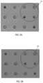
- FIG. 5 Ais an image of a select sub-volume of a substrate acquired without using telecentric optics.
- FIG. 5 Bis an image of a select sub-volume of a substrate acquired with use of telecentric optics.
- FIG. 6 Ais a close-up view of section 6 A of FIG. 5 A .
- FIG. 6 Bis a close-up view of section 6 B of FIG. 5 B .
- FIGS. 1 A and 1 Billustrate geometric parameters of example through holes 10 formed in an example substrate 12 .
- the through holes 10are holes that run along the thickness (T) of the substrate 12 or from the front side 12 A of the substrate 12 to the back side 12 B of the substrate 12 .
- the through holes 10may have any desired shape, such as straight, tapered, or hourglass.
- the through holes 10may have any desired cross-sectional shape, such as circular, square, or elliptical.
- One of the hole geometric parameters that may be measuredis clear aperture size.
- the clear aperture of a through holeis the aperture of the path through the through hole where light can travel unobstructed.
- the clear aperture size of a through hole 10may be defined as the minimum distance diameter, or minimum transverse dimension, (C) of the through hole 10 .
- Examples of other hole geometric parameters that may be measuredare maximum diameter (d 1 ) of the through hole 10 , average diameter of the through hole 10 , aspect ratio of the through hole 10 , and direction of a major axis of the through hole 10 .
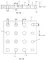
- FIG. 2 Ashows a measurement system 101 including an imaging apparatus 104 for acquiring images of through holes in a substrate according to one embodiment.
- the images acquired by the imaging apparatus 104can be processed to determine any of the hole geometric parameters discussed above.
- FIG. 2 Ashows a sample substrate 100 having through holes 102 and a thickness T 1 , which is also the depth of the through holes 102 .
- T 1thickness
- a sample substratewill have numerous through holes, e.g., ranging from tens to thousands of holes.
- the measurement system 101is not limited to any number of through holes in the substrate 100 .
- the through holes 102are shown as straight holes having a circular cross-section (see FIG.
- the measurement system of 101is also not limited to any particular shape of through holes or orientation of through holes in the substrate.
- the through holes in the substrate 100may have any of the shapes discussed above and other shapes not specifically mentioned above.
- the substrate 100is a thin substrate having a thickness of 1 mm or less, although the thickness of the substrate will generally only be limited by the depth of field of the imaging apparatus 104 .
- the through holes 102are exaggerated in size (diameter) relative to the field of view of the imaging apparatus 104 .
- the through holes 102 in the sample substrate 100will typically be micron-sized, although the size of the through holes 102 will generally only be limited by the field of view and the resolution of the imaging apparatus 104 .
- the imaging apparatus 104includes a camera 106 and a backlight illuminator 108 arranged on opposite sides of the substrate 100 , and particularly on opposite sides of a target sub-volume 109 of the substrate 100 .
- the target sub-volume 109includes one or more through holes 102 whose geometric parameters are to be measured.
- the camera 106includes an image sensor 110 and an objective lens 112 optically coupled to the image sensor 110 .
- the image sensor 110has a pixel count of at least 10 megapixels (MP), allowing the camera 106 to capture high resolution images. However, the size of the image sensor 110 will generally be dictated by the desired accuracy of the measurement.
- the image pixel sizeshould be close to 1 micron.
- Image pixel sizeis a function of the physical size of the image sensor pixel and the magnification of the objective lens.
- the objective lens 112is a telecentric lens. Reasons for selecting a telecentric lens as the objective lens 112 are discussed below.
- Telecentric lenseseliminate this parallax error by having a constant, non-angular field of view. With telecentric lenses, magnification remains constant with object displacement, provided the object stays within the telecentric range.
- the telecentric range (or telecentric depth or DOF) of a telecentric lenscan be obtained from the lens manufacturer or may be included in the specification of the telecentric lens.
- the telecentric objective lens 112has a telecentric range (TR in FIG. 2 A ), that is greater than the thickness T 1 of the substrate 100 .
- a procedure for selecting the telecentric objective lens 112may include finding telecentric lenses from commercial sources (for example Opto Engineering) that meet the telecentric range requirement stated above. From this set of telecentric lenses, the telecentric lens with the highest magnification can be selected for use as the telecentric objective lens 112 .
- the working distance WDwhich is the distance between the front surface of the telecentric lens 112 and the front surface 100 A of the substrate 100 , is adjusted such that the target sub-volume 109 of the substrate 100 lies entirely within the telecentric range.
- the manufacturer's specification for the telecentric lenswill typically include the working distance for the selected magnification and telecentric range (or DOF or telecentric depth).
- the backlight illuminator 108is used to produce a sharp silhouetted image of the holes to be measured.
- the backlight illuminator 108can be a telecentric illuminator, which is a collimated illuminator that is designed to work specifically with telecentric lenses. Telecentric illuminators are available commercially (for example, from Opto Engineering).
- the telecentric illuminator 108will uniformly illuminate the target sub-volume 109 of the substrate 100 with a collimated light beam.
- the illumination volumemust be the size of the target sub-volume 109 or bigger to assure illumination of the entire field of view. For the arrangement shown in FIG.
- the optical axes of the backlight illuminator 108 and telecentric lens 112are aligned.
- the distance BD of the backlight illuminator 108 from the back surface 100 B of the substrate 100may be selected to achieve a desired illumination of the target sub-volume 109 of the substrate 100 .
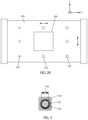
- FIG. 3shows an example of a silhouetted image, where the through hole in the target sub-volume appears as a light spot 120 surrounded by a dark ring 122 in a transparent substrate 124 .
- the dark ring 122is the superimposed area of sidewalls as seen when looking into the hole. The more the sidewalls are tapered and distinctly different from a cylinder, the thicker the dark ring will appear in the image.
- the diameter 126 of the light spot 120will indicate the clear aperture size of the hole.
- the clear aperture sizecan be measured by counting the pixels corresponding to the diameter 126 .
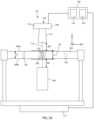
- FIG. 4shows a modified system 101 A including a different lighting arrangement that may be used with the telecentric lens 112 .
- the different lighting arrangementincludes a coaxial light source 130 arranged on the same side of the substrate 100 as the camera 106 ′.
- the coaxial light source 130may include a light source 130 A and optics module 130 B for aligning the light from the light source 130 A in a direction generally parallel to the optical axis 115 of the telecentric lens 112 .
- the optics module 130 Bmay include a beam splitter.
- the optics module 130 Bmay be arranged in line with the telecentric lens 112 and image sensor 110 , as shown in FIG. 4 .
- the different lighting arrangementmay further include a mirror 134 arranged in contact with the back surface 100 B of the substrate 100 .
- the mirror 134will reflect the light from the optics module 130 B into the target sub-volume 109 of the substrate 100 to be measured.
- the mirror 134may extend across the back surface 100 B of the substrate 100 and may be movable with the substrate 100 as a unit.
- Both the lighting arrangements shown in FIGS. 2 A and 4can be used when measuring through hole parameters in transparent substrates such as glass. Both the lighting arrangements shown in FIGS. 2 A and 4 are also suitable for use with opaque substrates. However, the lighting arrangement shown in FIG. 2 A may work better for opaque substrates due to its higher contrast.
- the lighting arrangement shown in FIG. 4has an advantage when there is no access to the back side of the substrate, such as when the substrate sits in a solid chuck, or when there is insufficient room behind the back side of the substrate to put the backlight illuminator.
- the field of view of the camera 106is limited to the diameter of the front surface of the telecentric lens 112 (i.e., the surface of the lens in opposed relation to the substrate 100 ).
- the field of view of the camera 106 ( 106 ′ in FIG. 4 ) and the telecentric range of the telecentric lens 112define the target sub-volume of the substrate whose image is acquired at any moment.
- scanning of the substratewill allow all the holes in the substrate or all the holes within a desired volume of the substrate to be measured. Scanning involves providing relative motion between the substrate 100 and the imaging apparatus 104 .
- the camera 106 and backlight illuminator 108may be held in fixed positions while the substrate 100 is translated in a plane perpendicular to the optical axis 115 of the camera 106 (i.e., the XY plane as shown in FIG. 2 B ). This will allow different sub-volumes of the substrate 100 to be moved into the field of view of the camera 106 over the scanning period.
- a translation stage 117may be coupled to the substrate 100 and operated to translate the substrate 100 in the desired directions or plane. It is also possible to hold the substrate 100 fixed while translating the camera 106 and backlight illuminator 108 (or camera 106 ′ and coaxial light source 130 in the embodiment of FIG. 4 ) relative to the substrate 100 .
- a controller 140may be coupled to the camera 106 ( 106 ′ in FIG. 4 ) to receive image data from the camera 106 .
- the controller 140may include a memory device 142 for storing the received image data and a processor 144 for processing the image data.
- the processor 144may be configured to process the image data to determine one or more geometric parameters, such as clear aperture size, of through holes represented in the image data.
- the processor 144may run a commercially available image processing software capable of analyzing the image data and extracting the desired geometric parameters from the image data. Examples of suitable commercial image processing software packages include, but are not limited to, HALCON by MVTec Software GmbH, MATLAB by MathWorks, Matrox Inspector with Matrox Imaging Library by Matrox, and NI Vision by National Instrument.
- the measured geometric parametersmay be stored in the memory device 142 or other suitable storage device for later use.
- the controller 140may also control translation of the substrate 100 during scanning of the substrate 100 . For example, after processing the image data acquired by the camera 106 ( 106 ′ in FIG. 4 ) for a current target sub-volume, the processor 144 may issue a command to the translation stage 117 to move the next target sub-volume into the field of view of the camera 106 (camera 106 ′ for the embodiment in FIG. 4 ).
- Table 1 belowshows examples of telecentric lens options for acquiring images of through holes in thin substrates.
- FIG. 5 Ashows an image of 3 ⁇ 4 holes acquired with VIEW Summit 650 Optical Coordinate Measuring Machine (OCMM).
- FIG. 5 Bshows an image of 3 ⁇ 4 holes acquired with a 10 megapixels camera using telecentric optics as listed in Option 1 in Table 1. Both images in FIGS. 5 A and 5 B were taken at 1 X optical magnification with green backlighting. For the image in FIG. 5 B , the backlight was a telecentric (i.e., collimated) light source.
- FIG. 6 Ashows a zoomed-in view of four of the holes in FIG. 5 A .
- FIG. 6 Bshows a zoomed-in view of four of the holes in FIG. 5 B .
- FIG. 6 Bwhich was acquired with telecentric optics, shows a much more defined outline of the holes than the image in FIG. 6 A , which was acquired with the OCMM.
- the much smaller depth of field in the OCMM measurement system used to acquire the image of FIG. 6 Aprevented waists at different depths from being in focus simultaneously.
- a procedure for measuring one or more geometric parameters of through holes in a substratemay include selecting the lens objective for a particular substrate thickness. Examples of lens objectives are given in Table 1. After the lens objective has been selected, the desired geometric parameters, such as clear aperture size, of holes in the substrate can be measured quickly in a few simple steps, as outlined below.
- the substrateis moved in between the backlight illuminator 108 and the camera 106 for the system shown in FIG. 2 A (or beneath the coaxial light source 130 and camera 106 ′ for the system shown in FIG. 4 ) to position a target sub-volume of the substrate in the field of view of the camera.
- the target sub-volumeis illuminated, and an image of the illuminated target sub-volume is acquired.
- the acquired imageis processed to determine at least one geometric parameter of each through hole in the target sub-volume. Processing involves detecting changes in light levels, or contrast, in the acquired image. Changes in contrast can define boundaries, or lines, within the image. These lines can be extended to create objects like segments, circles, ellipses, and the like, and then parameters such as diameter or distance can be extracted.
- the acquired imageis typically processed on a computer using commercially available image analysis software. Examples of suitable commercial imaging processing software packages include, but are not limited to, HALCON by MVTec Software GmbH, MATLAB by MathWorks, Matrox Inspector with Matrox Imaging Library by Matrox, and NI Vision by National Instrument.
- the geometric parameter values for each holeare recorded.
- the acquired imagemay be discarded after recording the geometric parameter values to save storage space since the high-resolution images can be quite large.
- the substrateis then translated relative to the camera and lighting arrangement to place another target sub-volume of the substrate in the field of view of the camera and within the illumination volume provided by the lighting arrangement.
- the acquiring of the image of the target sub-volume, processing of the image, and recording of geometric parameter values for each hole in the target sub-volumeare repeated for the new target sub-volume.
- the procedure described abovecan be automated to scan an entire substrate or a small area within the substrate.
- the duration of a measurement runis determined predominantly by how fast the substrate can be translated and how fast the images can be acquired and processed and not by the number of holes in the field of view.
- a substrate with holes ranging from hundreds to thousandscan be quickly measured using an automated procedure and any of the setups described in FIGS. 2 A and 4 .
- multiple cameras 106 , 106 ′may be utilized to increase the speed of scanning the substrate.
- multiple illuminator 108may be used in conjunction with the multiple cameras.
- illuminator 108 or light source 130may turn on and off (e.g., strobe) at regular intervals for cameras 106 , 106 ′ to take images.
Landscapes
- Physics & Mathematics (AREA)
- General Physics & Mathematics (AREA)
- Length Measuring Devices By Optical Means (AREA)
Abstract
Description
This application is a continuation of and claims the benefit of priority under 35 U.S.C. § 120 of U.S. patent application Ser. No. 15/632,919, filed on Jun. 26, 2017, which claims the benefit of priority under 35 U.S.C. § 119 of U.S. Provisional Application Ser. No. 62/356,091 filed on Jun. 29, 2016, the content of which is relied upon and incorporated herein by reference in its entirety.
The present disclosure relates to measurement of geometric parameters of through holes in substrates.
Typically, small geometric features with diameters below 100 microns are measured using a microscope or an Optical Coordinate Measuring Machine (OCMM). These systems typically use high optical magnification objective lenses to resolve small features, and because of the small depth of field of the lens, measurements are limited to features on or near the surface of the object. Microscope objective lens are designed to work at specific conjugate points, and their aberration corrections will suffer significantly if they are used at other distances, resulting in a distorted image. Commonly, object depth or shape information can be acquired using scanning electron microscopy or 3D confocal microscopy, but these methods are destructive and slow and cannot be used to inspect thousands of features quickly.
A method and system for measuring geometric parameters of through holes in thin substrates are disclosed herein. The method is non-destructive, and the method and system can be automated to provide inspection of hundreds to thousands of holes in a matter of minutes. The method and system can be used to measure geometric parameters, such as clear aperture size and the like, of all types of hole profiles, such as straight, tapered, hour glass, and the like. The term “clear aperture” refers to the clear unobstructed opening of a hole when looking through the hole under normal incidence. For a straight hole, where the diameter of the hole is uniform, the clear aperture size is the same as the diameter of the hole. For other types of holes, such as a hour glass hole or tapered hole, the clear aperture size is defined by the minimum transverse dimension of the hole. The minimum transverse dimension would be located at the narrowest point, or waist, of the hole. The method and system can measure the clear aperture size of every hole, independent of the depth at which the clear aperture occurs. Even if the clear aperture size and depth show large variations across a substrate, the method and system will not require any adjustments or refocusing during the measurement.
In a first aspect, a method of measuring geometric parameters of through holes in a substrate includes positioning a camera comprising an image sensor and a lens having a depth of field greater than the thickness of the substrate at a measuring station. The method includes positioning a select sub-volume of the substrate within a field of view of the camera and within the depth of range. The method includes illuminating the select sub-volume. The method includes capturing an image of the select sub-volume on the image sensor and processing the image to determine at least one geometric parameter of at least one through hole in the select sub-volume.
A second aspect of this disclosure includes the method as described in the first aspect, where the at least one geometric parameter is a clear aperture size of the at least one through hole.
A third aspect of this disclosure includes the method as described in the first or second aspect, where the substrate has a thickness of 1 mm or less.
A fourth aspect of this disclosure includes the method as described in any of the first to the third aspects, wherein the lens is a telecentric lens.
A fifth aspect of this disclosure includes the method as described in the fourth aspect, wherein the illuminating the select sub-volume comprises using collimated light.
A sixth aspect of this disclosure includes the method as described in any one of the first to the fifth aspects, where the select sub-volume has a front side and a back side, the front side is positioned in opposing relation to the lens, and the select sub-volume is illuminated by directing light at the front side of the select sub-volume.
A seventh aspect of this disclosure includes the method as described in the fifth aspect, where the light is directed at the front side of the select sub-volume by passing the light through the telecentric lens to the front side of the select sub-volume.
An eighth aspect of this disclosure includes the method as described in the fourth or fifth aspect, where illuminating the select sub-volume further includes reflecting the light into the select sub-volume using a mirror mounted at the back side of the select sub-volume.
A ninth aspect of this disclosure includes the method as described in any one of the first to the fifth aspects, where the select sub-volume has a front side and a back side, the front side is positioned in opposing relation to the lens, and the select sub-volume is illuminated by directing light at the back side of the select sub-volume.
A tenth aspect of this disclosure includes the method as described in any one of the first to the ninth aspects. The tenth aspect further includes effecting a relative motion between the camera and the substrate to position a new sub-volume of the substrate within the field of view of the camera and within the depth of field.
An eleventh aspect of this disclosure includes the method as described in the tenth aspect. The eleventh aspect further includes illuminating the new sub-volume with the light, capturing an image of the new sub-volume on the image sensor, and processing the image of the new sub-volume to determine at least one geometric parameter of at least one through hole in the new sub-volume.
A twelfth aspect of this disclosure includes the method as described in the eleventh aspect, where illuminating the new sub-volume includes effecting a relative motion between a source of the light and the substrate such that the new sub-volume is within an illumination volume of the light.
A thirteenth aspect of this disclosure includes the method as described in any one of the first to the twelfth aspects, where processing the image includes detecting changes in contrast in the image.
In a fourteenth aspect, a system of measuring geometric parameters of through holes in a substrate includes a camera comprising an image sensor and a lens having a depth of field greater than a thickness of the substrate. The camera is positioned relative to the substrate such that a select sub-volume of the substrate is within a field of view of the camera and within the depth of field. The system includes a lighting arrangement for illuminating the select sub-volume. The system further includes a processor configured to receive image data from the camera and determine from the image data at least one geometric parameter of at least one through hole in the select sub-volume.
A fifteenth aspect of this disclosure includes the system as described in the fourteenth aspect, wherein the lens is a telecentric lens.
A sixteenth aspect of this disclosure includes the system as described in the fourteenth or fifteenth aspect, wherein the lighting arrangement is a collimated lighting arrangement.
A seventeenth aspect of this disclosure includes the system as described in any one of the fourteenth to sixteenth aspects, where the select sub-volume has a front side and a back side, where the front side is in opposing relation relative to the lens, and where the lighting arrangement includes a light source positioned to direct a light beam at the back side of the select sub-volume.
An eighteenth aspect of this disclosure includes the system as described in any one of the twelfth to sixteenth aspects, where the select sub-volume has a front side and a back side, where the front side is in opposing relation to the lens, and where the lighting arrangement includes a coaxial light source optically coupled to the lens.
A nineteenth aspect of this disclosure includes the system as described in the eighteenth aspect, where the lighting arrangement further includes a mirror mounted in contact with a backside of the select sub-volume.
A twentieth aspect of this disclosure includes the system as described in the nineteenth aspect, where the mirror extends across a back side of the substrate including the back side of the select sub-volume.
A twenty-first aspect of this disclosure includes the system as described in any one of the fourteenth to the twentieth aspects. The twenty-first aspect further includes a translation mechanism coupled to the substrate and operable to translate the substrate relative to the camera.
A twenty-second aspect of this disclosure includes the system as described in any one of the fourteenth to the twenty-first aspects, where the processor is configured to determine a clear aperture size of the at least one through hole from the image data.
The following is a description of the figures in the accompanying drawings. The figures are not necessarily to scale, and certain figures and certain views of the figures may be shown exaggerated in scale or in schematic in the interest of clarity and conciseness.
To provide a context for the method and system disclosed herein,FIGS.1A and1B illustrate geometric parameters of example throughholes 10 formed in anexample substrate 12. The through holes10 are holes that run along the thickness (T) of thesubstrate 12 or from thefront side 12A of thesubstrate 12 to theback side 12B of thesubstrate 12. Along the thickness (T) of thesubstrate 12, i.e., along the Z axis, the throughholes 10 may have any desired shape, such as straight, tapered, or hourglass. In the plane of thesubstrate 12, i.e., in the XY plane, the throughholes 10 may have any desired cross-sectional shape, such as circular, square, or elliptical. One of the hole geometric parameters that may be measured is clear aperture size. The clear aperture of a through hole is the aperture of the path through the through hole where light can travel unobstructed. The clear aperture size of a throughhole 10 may be defined as the minimum distance diameter, or minimum transverse dimension, (C) of the throughhole 10. Examples of other hole geometric parameters that may be measured are maximum diameter (d1) of the throughhole 10, average diameter of the throughhole 10, aspect ratio of the throughhole 10, and direction of a major axis of the throughhole 10.
In one embodiment, theimaging apparatus 104 includes acamera 106 and abacklight illuminator 108 arranged on opposite sides of thesubstrate 100, and particularly on opposite sides of atarget sub-volume 109 of thesubstrate 100. Thetarget sub-volume 109 includes one or more throughholes 102 whose geometric parameters are to be measured. In one embodiment, thecamera 106 includes animage sensor 110 and anobjective lens 112 optically coupled to theimage sensor 110. In one embodiment, theimage sensor 110 has a pixel count of at least 10 megapixels (MP), allowing thecamera 106 to capture high resolution images. However, the size of theimage sensor 110 will generally be dictated by the desired accuracy of the measurement. For example, if a 100 micron geometric feature is to be measured with 1 micron accuracy, the image pixel size should be close to 1 micron. Image pixel size is a function of the physical size of the image sensor pixel and the magnification of the objective lens. In some embodiments, theobjective lens 112 is a telecentric lens. Reasons for selecting a telecentric lens as theobjective lens 112 are discussed below.
Conventional lenses have angular fields of view, which means that as the distance between the lens and object increases, the magnification decreases. This angular field of view results in parallax error, also known as perspective error. Telecentric lenses eliminate this parallax error by having a constant, non-angular field of view. With telecentric lenses, magnification remains constant with object displacement, provided the object stays within the telecentric range. The term “telecentric range” or “telecentric depth” or “depth of field (DOF)”, as used with telecentric lenses, refers to the total distance above and below an object that remains in focus and at constant magnification. Telecentric range may be defined as a range of axial displacements causing a variation in image size of less than 1 micron. The telecentric range (or telecentric depth or DOF) of a telecentric lens can be obtained from the lens manufacturer or may be included in the specification of the telecentric lens.
By using a telecentric lens as theobjective lens 112, according to one embodiment, virtually distortion free images can be acquired and used to accurately determine the desired geometric parameters of the through holes in thesubstrate 100. In one embodiment, the telecentricobjective lens 112 has a telecentric range (TR inFIG.2A ), that is greater than the thickness T1 of thesubstrate 100. A procedure for selecting the telecentricobjective lens 112 may include finding telecentric lenses from commercial sources (for example Opto Engineering) that meet the telecentric range requirement stated above. From this set of telecentric lenses, the telecentric lens with the highest magnification can be selected for use as the telecentricobjective lens 112. For measurement of hole geometric parameters using the selected telecentric lens, the working distance WD, which is the distance between the front surface of thetelecentric lens 112 and thefront surface 100A of thesubstrate 100, is adjusted such that thetarget sub-volume 109 of thesubstrate 100 lies entirely within the telecentric range. The manufacturer's specification for the telecentric lens will typically include the working distance for the selected magnification and telecentric range (or DOF or telecentric depth).
In one embodiment, thebacklight illuminator 108 is used to produce a sharp silhouetted image of the holes to be measured. For thetelecentric lens 112, thebacklight illuminator 108 can be a telecentric illuminator, which is a collimated illuminator that is designed to work specifically with telecentric lenses. Telecentric illuminators are available commercially (for example, from Opto Engineering). Thetelecentric illuminator 108 will uniformly illuminate thetarget sub-volume 109 of thesubstrate 100 with a collimated light beam. The illumination volume must be the size of thetarget sub-volume 109 or bigger to assure illumination of the entire field of view. For the arrangement shown inFIG.2A , the optical axes of thebacklight illuminator 108 andtelecentric lens 112 are aligned. The distance BD of thebacklight illuminator 108 from theback surface 100B of thesubstrate 100 may be selected to achieve a desired illumination of thetarget sub-volume 109 of thesubstrate 100.
Both the lighting arrangements shown inFIGS.2A and4 can be used when measuring through hole parameters in transparent substrates such as glass. Both the lighting arrangements shown inFIGS.2A and4 are also suitable for use with opaque substrates. However, the lighting arrangement shown inFIG.2A may work better for opaque substrates due to its higher contrast. The lighting arrangement shown inFIG.4 has an advantage when there is no access to the back side of the substrate, such as when the substrate sits in a solid chuck, or when there is insufficient room behind the back side of the substrate to put the backlight illuminator.
Returning toFIG.2A , the field of view of the camera106 (106′ inFIG.4 ) is limited to the diameter of the front surface of the telecentric lens112 (i.e., the surface of the lens in opposed relation to the substrate100). The field of view of the camera106 (106′ inFIG.4 ) and the telecentric range of thetelecentric lens 112 define the target sub-volume of the substrate whose image is acquired at any moment. However, scanning of the substrate will allow all the holes in the substrate or all the holes within a desired volume of the substrate to be measured. Scanning involves providing relative motion between thesubstrate 100 and theimaging apparatus 104. In one embodiment, thecamera 106 and backlight illuminator108 (orcamera 106′ and coaxiallight source 130 in the embodiment ofFIG.4 ) may be held in fixed positions while thesubstrate 100 is translated in a plane perpendicular to theoptical axis 115 of the camera106 (i.e., the XY plane as shown inFIG.2B ). This will allow different sub-volumes of thesubstrate 100 to be moved into the field of view of thecamera 106 over the scanning period. Atranslation stage 117 may be coupled to thesubstrate 100 and operated to translate thesubstrate 100 in the desired directions or plane. It is also possible to hold thesubstrate 100 fixed while translating thecamera 106 and backlight illuminator108 (orcamera 106′ and coaxiallight source 130 in the embodiment ofFIG.4 ) relative to thesubstrate 100.
Acontroller 140 may be coupled to the camera106 (106′ inFIG.4 ) to receive image data from thecamera 106. Thecontroller 140 may include amemory device 142 for storing the received image data and aprocessor 144 for processing the image data. Theprocessor 144 may be configured to process the image data to determine one or more geometric parameters, such as clear aperture size, of through holes represented in the image data. Theprocessor 144 may run a commercially available image processing software capable of analyzing the image data and extracting the desired geometric parameters from the image data. Examples of suitable commercial image processing software packages include, but are not limited to, HALCON by MVTec Software GmbH, MATLAB by MathWorks, Matrox Inspector with Matrox Imaging Library by Matrox, and NI Vision by National Instrument. The measured geometric parameters may be stored in thememory device 142 or other suitable storage device for later use. Thecontroller 140 may also control translation of thesubstrate 100 during scanning of thesubstrate 100. For example, after processing the image data acquired by the camera106 (106′ inFIG.4 ) for a current target sub-volume, theprocessor 144 may issue a command to thetranslation stage 117 to move the next target sub-volume into the field of view of the camera106 (camera 106′ for the embodiment inFIG.4 ).
Table 1 below shows examples of telecentric lens options for acquiring images of through holes in thin substrates.
| TABLE 1 | |||||
| Tele- | |||||
| centric | |||||
| Lens | range or | Field | Pixel | ||
| Magnifica- | DOF | Camera | of View | Size | |
| Option | tion | (mm) | Array | (mm) | (microns) |
| 1 | 1X | 0.9 | 3840 × 2748 | 6.4 × 4.8 | 1.7 |
| 2 | 1.33X | 0.5 | 3840 × 2748 | 4.8 × 3.6 | 1.3 |
| 3 | 2X | 0.2 | 3840 × 2748 | 3.2 × 2.4 | 0.85 |
A procedure for measuring one or more geometric parameters of through holes in a substrate may include selecting the lens objective for a particular substrate thickness. Examples of lens objectives are given in Table 1. After the lens objective has been selected, the desired geometric parameters, such as clear aperture size, of holes in the substrate can be measured quickly in a few simple steps, as outlined below.
The substrate is moved in between thebacklight illuminator 108 and thecamera 106 for the system shown inFIG.2A (or beneath the coaxiallight source 130 andcamera 106′ for the system shown inFIG.4 ) to position a target sub-volume of the substrate in the field of view of the camera.
The target sub-volume is illuminated, and an image of the illuminated target sub-volume is acquired.
The acquired image is processed to determine at least one geometric parameter of each through hole in the target sub-volume. Processing involves detecting changes in light levels, or contrast, in the acquired image. Changes in contrast can define boundaries, or lines, within the image. These lines can be extended to create objects like segments, circles, ellipses, and the like, and then parameters such as diameter or distance can be extracted. The acquired image is typically processed on a computer using commercially available image analysis software. Examples of suitable commercial imaging processing software packages include, but are not limited to, HALCON by MVTec Software GmbH, MATLAB by MathWorks, Matrox Inspector with Matrox Imaging Library by Matrox, and NI Vision by National Instrument.
The geometric parameter values for each hole are recorded. The acquired image may be discarded after recording the geometric parameter values to save storage space since the high-resolution images can be quite large.
The substrate is then translated relative to the camera and lighting arrangement to place another target sub-volume of the substrate in the field of view of the camera and within the illumination volume provided by the lighting arrangement. The acquiring of the image of the target sub-volume, processing of the image, and recording of geometric parameter values for each hole in the target sub-volume are repeated for the new target sub-volume.
The procedure described above can be automated to scan an entire substrate or a small area within the substrate. The duration of a measurement run is determined predominantly by how fast the substrate can be translated and how fast the images can be acquired and processed and not by the number of holes in the field of view. A substrate with holes ranging from hundreds to thousands can be quickly measured using an automated procedure and any of the setups described inFIGS.2A and4 . In some embodiments,multiple cameras multiple illuminator 108 may be used in conjunction with the multiple cameras. In some embodiments, there may be constant relative movement between the substrate andcameras illuminator 108 orlight source 130 may turn on and off (e.g., strobe) at regular intervals forcameras
While the invention has been described with respect to a limited number of embodiments, those skilled in the art of, having benefit of this disclosure, will appreciate that other embodiments can be devised which do not depart from the scope of the invention as disclosed herein. Accordingly, the scope of the invention should be limited only by the accompanying claims.
Claims (16)
1. A method of measuring geometric parameters of through holes in a substrate, comprising:
positioning a camera comprising an image sensor and a lens having a depth of field greater than a thickness of the substrate at a measuring station, the image sensor having a pixel count of at least 10 megapixels and a pixel size of 1.7 microns or less;
positioning a select sub-volume of the substrate within a field of view of the camera and within the depth of field,
the select sub-volume having a front side, a back side, and at least one through hole, and
the at least one through hole having a first side at the front side of the select sub-volume and a second at the back side of the select sub-volume;
illuminating the select sub-volume with a light source;
capturing an image of the select sub-volume on the image sensor; and
processing the image to determine at least a minimum transverse dimension of the at least one through hole along a length of the through hole, the minimum transverse dimension of the through hole being between the first side and the second side of the through hole,
wherein the light source and the camera are arranged on a same side of the substrate.
2. The method ofclaim 1 , wherein illuminating the select sub-volume with the light source further comprises reflecting light from the light source into the select sub-volume using a mirror.
3. The method ofclaim 2 , further comprising moving the mirror with the substrate.
4. The method ofclaim 2 , wherein the light source and the camera are disposed on the front side of the select sub-volume and the mirror is disposed on the on a back side of the select sub-volume.
5. The method ofclaim 1 , wherein the light source is a coaxial light source.
6. The method ofclaim 1 , wherein the substrate has a thickness of 1 mm or less.
7. The method ofclaim 1 , wherein the lens is a telecentric lens.
8. The method ofclaim 1 , further comprising effecting a lateral relative motion between the camera and the substrate to position another sub-volume of the substrate within the field of view of the camera and within the depth of field.
9. The method ofclaim 8 , further comprising illuminating the another sub-volume with light, capturing an image of the another sub-volume on the image sensor, and processing the image of the another sub-volume to determine at least one geometric parameter of at least one hole in the another sub-volume.
10. The method ofclaim 9 , wherein illuminating the another sub-volume comprises effecting a lateral relative motion between the light source and the substrate such that the another sub-volume is within an illumination volume of the light.
11. The method ofclaim 1 , wherein processing the image comprises detecting changes in contrast in the image.
12. A system for measuring geometric parameters of through holes in a substrate, comprising:
a camera comprising an image sensor and a lens having a depth of field greater than a thickness of the substrate, the image sensor having a pixel count of at least 10 megapixels and a pixel size of 1.7 microns or less, and the camera positioned at a select working distance relative to the substrate such that a select sub-volume of the substrate is within a field of view of the camera and within the depth of field,
the select-sub volume having a front side, a back side, and at least one through hole, and
the at least one through hole having a first side at the front side of the select sub-volume and a second at the back side of the select sub-volume;
a light source for illuminating the select sub-volume; and
a processor configured to receive image data from the camera and determine from the image data at least a minimum transverse dimension of the least one through hole along a length of the through hole, the minimum transverse dimension of the through hole being between the first side and the second side of the through hole,
wherein the light source and the camera are arranged on a same side of the substrate.
13. The system ofclaim 12 , further comprising a mirror configured to reflect light from the light source into the select sub-volume.
14. The system ofclaim 13 , wherein the mirror is moveable with the substrate.
15. The system ofclaim 13 , wherein the light source and the camera are disposed on the front side of the select sub-volume and the mirror is disposed on the back side of the select sub-volume.
16. The system ofclaim 12 , wherein the light source is a coaxial light source.
Priority Applications (1)
| Application Number | Priority Date | Filing Date | Title |
|---|---|---|---|
| US17/004,092US11774233B2 (en) | 2016-06-29 | 2020-08-27 | Method and system for measuring geometric parameters of through holes |
Applications Claiming Priority (3)
| Application Number | Priority Date | Filing Date | Title |
|---|---|---|---|
| US201662356091P | 2016-06-29 | 2016-06-29 | |
| US15/632,919US10794679B2 (en) | 2016-06-29 | 2017-06-26 | Method and system for measuring geometric parameters of through holes |
| US17/004,092US11774233B2 (en) | 2016-06-29 | 2020-08-27 | Method and system for measuring geometric parameters of through holes |
Related Parent Applications (1)
| Application Number | Title | Priority Date | Filing Date |
|---|---|---|---|
| US15/632,919ContinuationUS10794679B2 (en) | 2016-06-29 | 2017-06-26 | Method and system for measuring geometric parameters of through holes |
Publications (2)
| Publication Number | Publication Date |
|---|---|
| US20200393233A1 US20200393233A1 (en) | 2020-12-17 |
| US11774233B2true US11774233B2 (en) | 2023-10-03 |
Family
ID=59276921
Family Applications (2)
| Application Number | Title | Priority Date | Filing Date |
|---|---|---|---|
| US15/632,919ActiveUS10794679B2 (en) | 2016-06-29 | 2017-06-26 | Method and system for measuring geometric parameters of through holes |
| US17/004,092Active2038-04-19US11774233B2 (en) | 2016-06-29 | 2020-08-27 | Method and system for measuring geometric parameters of through holes |
Family Applications Before (1)
| Application Number | Title | Priority Date | Filing Date |
|---|---|---|---|
| US15/632,919ActiveUS10794679B2 (en) | 2016-06-29 | 2017-06-26 | Method and system for measuring geometric parameters of through holes |
Country Status (5)
| Country | Link |
|---|---|
| US (2) | US10794679B2 (en) |
| JP (1) | JP2019522797A (en) |
| KR (1) | KR102501212B1 (en) |
| TW (2) | TWI738808B (en) |
| WO (1) | WO2018005404A1 (en) |
Families Citing this family (5)
| Publication number | Priority date | Publication date | Assignee | Title |
|---|---|---|---|---|
| US11148935B2 (en) | 2019-02-22 | 2021-10-19 | Menlo Microsystems, Inc. | Full symmetric multi-throw switch using conformal pinched through via |
| KR102557965B1 (en)* | 2021-01-21 | 2023-07-20 | 주식회사 야스 | Inspection System of Glass Hole |
| CN116007499A (en)* | 2023-01-04 | 2023-04-25 | 海克斯康制造智能技术(青岛)有限公司 | Three-coordinate image measuring machine |
| TWI865375B (en)* | 2024-02-06 | 2024-12-01 | 翔緯光電股份有限公司 | Via waist depth detection device and method for through glass via (tgv) substrate |
| CN120445032A (en)* | 2024-02-06 | 2025-08-08 | 翔纬光电股份有限公司 | Device and method for detecting perforation of TGV glass substrate |
Citations (799)
| Publication number | Priority date | Publication date | Assignee | Title |
|---|---|---|---|---|
| US108387A (en) | 1870-10-18 | Improvement in machines for making rope | ||
| US208387A (en) | 1878-09-24 | Improvement in stocking-supporters | ||
| US237571A (en) | 1881-02-08 | messier | ||
| US1790397A (en) | 1931-01-27 | Glass workins machine | ||
| US2682134A (en) | 1951-08-17 | 1954-06-29 | Corning Glass Works | Glass sheet containing translucent linear strips |
| US2749794A (en) | 1953-04-24 | 1956-06-12 | Corning Glass Works | Illuminating glassware and method of making it |
| GB1242172A (en) | 1968-02-23 | 1971-08-11 | Ford Motor Co | A process for chemically cutting glass |
| US3647410A (en) | 1969-09-09 | 1972-03-07 | Owens Illinois Inc | Glass ribbon machine blow head mechanism |
| US3695498A (en) | 1970-08-26 | 1972-10-03 | Ppg Industries Inc | Non-contact thermal cutting |
| US3695497A (en) | 1970-08-26 | 1972-10-03 | Ppg Industries Inc | Method of severing glass |
| US3713921A (en) | 1971-04-01 | 1973-01-30 | Gen Electric | Geometry control of etched nuclear particle tracks |
| US3729302A (en) | 1970-01-02 | 1973-04-24 | Owens Illinois Inc | Removal of glass article from ribbon forming machine by vibrating force |
| US3775084A (en) | 1970-01-02 | 1973-11-27 | Owens Illinois Inc | Pressurizer apparatus for glass ribbon machine |
| DE2231330A1 (en) | 1972-06-27 | 1974-01-10 | Agfa Gevaert Ag | METHOD AND DEVICE FOR GENERATING A SHARP FOCUS |
| US3798013A (en) | 1971-04-26 | 1974-03-19 | Nippon Sheet Glass Co Ltd | Double ion exchange method for strengthening glass articles |
| US4226607A (en) | 1977-12-24 | 1980-10-07 | Firma Karl Lutz | Method for the manufacture of ampules from glass tubes |
| JPS55130839A (en) | 1979-03-29 | 1980-10-11 | Asahi Glass Co Ltd | Uniform etching method of article |
| JPS56129261A (en) | 1980-03-17 | 1981-10-09 | Hitachi Ltd | Thin film-forming coating liquid composition |
| JPS56160893A (en) | 1980-05-16 | 1981-12-10 | Matsushita Electric Ind Co Ltd | Absorbing film for laser work |
| US4395271A (en) | 1979-04-13 | 1983-07-26 | Corning Glass Works | Method for making porous magnetic glass and crystal-containing structures |
| US4441008A (en) | 1981-09-14 | 1984-04-03 | Ford Motor Company | Method of drilling ultrafine channels through glass |
| US4546231A (en) | 1983-11-14 | 1985-10-08 | Group Ii Manufacturing Ltd. | Creation of a parting zone in a crystal structure |
| US4547836A (en) | 1984-02-01 | 1985-10-15 | General Electric Company | Insulating glass body with electrical feedthroughs and method of preparation |
| JPS60220340A (en) | 1984-04-17 | 1985-11-05 | Nippon Telegr & Teleph Corp <Ntt> | Photosensitive resin composition and formation of pattern |
| US4564579A (en) | 1983-04-18 | 1986-01-14 | Nippon Telegraph & Telephone Public Corporation | Pattern forming material of a siloxane polymer |
| US4646308A (en) | 1985-09-30 | 1987-02-24 | Spectra-Physics, Inc. | Synchronously pumped dye laser using ultrashort pump pulses |
| EP0247993A1 (en) | 1986-05-28 | 1987-12-02 | Avl Ag | Method of preparing carrier materials for optical sensors |
| EP0270897A1 (en) | 1986-12-12 | 1988-06-15 | Ppg Industries, Inc. | Method and apparatus for shearing glass along a selected line of cut |
| US4764930A (en) | 1988-01-27 | 1988-08-16 | Intelligent Surgical Lasers | Multiwavelength laser source |
| EP0280918A2 (en) | 1987-02-19 | 1988-09-07 | International Business Machines Corporation | Process for metal plating of substrates |
| JPS6477001A (en) | 1986-12-18 | 1989-03-23 | Sumitomo Chemical Co | Light control plate and its production |
| WO1989002877A1 (en) | 1987-10-01 | 1989-04-06 | Asahi Glass Company Ltd. | Alkali free glass |
| JPH01179770A (en) | 1988-01-12 | 1989-07-17 | Hiroshima Denki Gakuen | How to join metal and ceramics |
| US4891054A (en) | 1988-12-30 | 1990-01-02 | Ppg Industries, Inc. | Method for cutting hot glass |
| US4907586A (en) | 1988-03-31 | 1990-03-13 | Intelligent Surgical Lasers | Method for reshaping the eye |
| US4918751A (en) | 1987-10-05 | 1990-04-17 | The University Of Rochester | Method for optical pulse transmission through optical fibers which increases the pulse power handling capacity of the fibers |
| US4929065A (en) | 1988-11-03 | 1990-05-29 | Isotec Partners, Ltd. | Glass plate fusion for macro-gradient refractive index materials |
| US4948941A (en) | 1989-02-27 | 1990-08-14 | Motorola, Inc. | Method of laser drilling a substrate |
| EP0393381A2 (en) | 1989-04-17 | 1990-10-24 | International Business Machines Corporation | Lamination method for coating the sidewall or filling a cavity in a substrate |
| US5022959A (en) | 1988-08-23 | 1991-06-11 | Semiconductor Energy Laboratory Co., Ltd. | Method of wet etching by use of plasma etched carbonaceous masks |
| US5035918A (en) | 1989-04-26 | 1991-07-30 | Amp Incorporated | Non-flammable and strippable plating resist and method of using same |
| US5040182A (en) | 1990-04-24 | 1991-08-13 | Coherent, Inc. | Mode-locked laser |
| JPH03252384A (en) | 1990-02-28 | 1991-11-11 | Taiyo Yuden Co Ltd | Laser scribing of ceramic substrate |
| US5089062A (en) | 1988-10-14 | 1992-02-18 | Abb Power T&D Company, Inc. | Drilling of steel sheet |
| US5104210A (en) | 1989-04-24 | 1992-04-14 | Monsanto Company | Light control films and method of making |
| US5108857A (en) | 1986-12-18 | 1992-04-28 | Sumitomo Chemical Company, Limited | Light control sheets |
| US5112722A (en) | 1989-04-12 | 1992-05-12 | Nippon Sheet Glass Co., Ltd. | Method of producing light control plate which induces scattering of light at different angles |
| US5114834A (en) | 1987-10-23 | 1992-05-19 | Yehuda Nachshon | Photoresist removal |
| US5166493A (en) | 1989-01-10 | 1992-11-24 | Canon Kabushiki Kaisha | Apparatus and method of boring using laser |
| JPH04349132A (en) | 1990-12-28 | 1992-12-03 | Seikosha Co Ltd | Method for working photosensitive glass |
| US5208068A (en) | 1989-04-17 | 1993-05-04 | International Business Machines Corporation | Lamination method for coating the sidewall or filling a cavity in a substrate |
| US5265107A (en) | 1992-02-05 | 1993-11-23 | Bell Communications Research, Inc. | Broadband absorber having multiple quantum wells of different thicknesses |
| JPH0679486A (en) | 1992-08-25 | 1994-03-22 | Rohm Co Ltd | Working method for ink jet head |
| US5314522A (en) | 1991-11-19 | 1994-05-24 | Seikosha Co., Ltd. | Method of processing photosensitive glass with a pulsed laser to form grooves |
| JPH06318756A (en) | 1993-05-06 | 1994-11-15 | Toshiba Corp | Laser device |
| US5374291A (en) | 1991-12-10 | 1994-12-20 | Director-General Of Agency Of Industrial Science And Technology | Method of processing photosensitive glass |
| CN1096936A (en) | 1993-07-01 | 1995-01-04 | 山东矿业学院济南分院 | A kind of labour protection beverage and manufacture method thereof |
| US5400350A (en) | 1994-03-31 | 1995-03-21 | Imra America, Inc. | Method and apparatus for generating high energy ultrashort pulses |
| US5434875A (en) | 1994-08-24 | 1995-07-18 | Tamar Technology Co. | Low cost, high average power, high brightness solid state laser |
| US5436925A (en) | 1994-03-01 | 1995-07-25 | Hewlett-Packard Company | Colliding pulse mode-locked fiber ring laser using a semiconductor saturable absorber |
| US5457836A (en) | 1993-02-25 | 1995-10-17 | Krupp Fordertechnik Gmbh | Deployable bridge and apparatus for laying the same |
| US5493096A (en) | 1994-05-10 | 1996-02-20 | Grumman Aerospace Corporation | Thin substrate micro-via interconnect |
| US5553093A (en) | 1994-05-09 | 1996-09-03 | Massachusetts Institute Of Technology | Dispersion-compensated laser using prismatic end elements |
| US5574597A (en) | 1992-05-22 | 1996-11-12 | Hitachi Koki Co., Ltd. | Light scanner and multi-beam generator using the same |
| US5575291A (en) | 1993-11-17 | 1996-11-19 | Fujitsu Ltd. | Ultrasonic coupler |
| US5575936A (en) | 1992-12-18 | 1996-11-19 | Firebird Traders Ltd. | Process and apparatus for etching an image within a solid article |
| US5586138A (en) | 1994-04-26 | 1996-12-17 | Nec Corporation | Multiple-cavity semiconductor laser capable of generating ultrashort light pulse train with ultrahigh repetition rate |
| JPH09106243A (en) | 1995-10-12 | 1997-04-22 | Dainippon Printing Co Ltd | Hologram duplication method |
| US5696782A (en) | 1995-05-19 | 1997-12-09 | Imra America, Inc. | High power fiber chirped pulse amplification systems based on cladding pumped rare-earth doped fibers |
| US5736709A (en) | 1996-08-12 | 1998-04-07 | Armco Inc. | Descaling metal with a laser having a very short pulse width and high average power |
| US5745236A (en) | 1994-05-31 | 1998-04-28 | New Creation Co., Ltd. | Optical inspecting apparatus having a focusing system with a telecentric optical system and an aperture stop |
| US5746884A (en) | 1996-08-13 | 1998-05-05 | Advanced Micro Devices, Inc. | Fluted via formation for superior metal step coverage |
| WO1998021154A1 (en) | 1996-11-13 | 1998-05-22 | Corning Incorporated | Method for forming an internally channeled glass article |
| US5776220A (en) | 1994-09-19 | 1998-07-07 | Corning Incorporated | Method and apparatus for breaking brittle materials |
| JPH10263873A (en) | 1997-03-27 | 1998-10-06 | Sumitomo Heavy Ind Ltd | Laser beam machine and machining method |
| CN1196562A (en) | 1997-04-17 | 1998-10-21 | 三菱电机株式会社 | Energy storage device of circuit breaker |
| US5844200A (en) | 1996-05-16 | 1998-12-01 | Sendex Medical, Inc. | Method for drilling subminiature through holes in a sensor substrate with a laser |
| US5879424A (en) | 1996-05-24 | 1999-03-09 | Agency Of Industrial Science & Technology | Optical micro-machining method of glass |
| US5909284A (en) | 1997-04-23 | 1999-06-01 | Mitutoyo Corporation | Method and system for measuring an inner diameter of a hole formed in an object |
| WO1999029243A1 (en) | 1997-12-05 | 1999-06-17 | Thermolase Corporation | Skin enhancement using laser light |
| US5919607A (en) | 1995-10-26 | 1999-07-06 | Brown University Research Foundation | Photo-encoded selective etching for glass based microtechnology applications |
| JPH11197498A (en) | 1998-01-13 | 1999-07-27 | Japan Science & Technology Corp | Method for selectively modifying the inside of inorganic material and inorganic material in which the inside is selectively modified |
| US5933230A (en) | 1997-04-28 | 1999-08-03 | International Business Machines Corporation | Surface inspection tool |
| EP0938946A1 (en) | 1998-02-27 | 1999-09-01 | Nec Corporation | Method of cleaving a brittle material using a point heat source for providing a thermal stress |
| JPH11269683A (en) | 1998-03-18 | 1999-10-05 | Armco Inc | Method and apparatus for removing oxide from metal surface |
| US5965043A (en) | 1996-11-08 | 1999-10-12 | W. L. Gore & Associates, Inc. | Method for using ultrasonic treatment in combination with UV-lasers to enable plating of high aspect ratio micro-vias |
| JPH11297703A (en) | 1998-04-15 | 1999-10-29 | Fuji Electric Co Ltd | Method for manufacturing semiconductor device |
| JPH11330597A (en) | 1998-04-09 | 1999-11-30 | Jmar Technol Co | Short-pulse laser system |
| WO1999063900A1 (en) | 1998-06-12 | 1999-12-16 | Photogen, Inc. | Improved methods and apparatus for multi-photon photo-activation of therapeutic agents |
| JPH11347758A (en) | 1998-06-10 | 1999-12-21 | Mitsubishi Heavy Ind Ltd | Super precision machining device |
| JP2000010289A (en) | 1998-06-22 | 2000-01-14 | Toshiba Corp | Pattern forming method and photosensitive composition |
| US6016223A (en) | 1992-08-31 | 2000-01-18 | Canon Kabushiki Kaisha | Double bessel beam producing method and apparatus |
| US6055829A (en) | 1997-07-07 | 2000-05-02 | Schott Glas | Process for producing a desired breaking point on a glass body |
| US6072624A (en) | 1992-01-09 | 2000-06-06 | Biomedical Photometrics Inc. | Apparatus and method for scanning laser imaging of macroscopic samples |
| US6078599A (en) | 1997-07-22 | 2000-06-20 | Cymer, Inc. | Wavelength shift correction technique for a laser |
| CN2388062Y (en) | 1999-06-21 | 2000-07-19 | 郭广宗 | Double-glazing window for vehicle and ship |
| WO2000051778A1 (en) | 1999-02-27 | 2000-09-08 | Robert Bosch Gmbh | Shielding against laser beams |
| US6120131A (en) | 1995-08-28 | 2000-09-19 | Lexmark International, Inc. | Method of forming an inkjet printhead nozzle structure |
| EP1043110A2 (en) | 1999-04-02 | 2000-10-11 | Murata Manufacturing Co., Ltd. | Method for machining ceramic green sheet and apparatus for machining the same |
| US6140243A (en) | 1996-12-12 | 2000-10-31 | Texas Instruments Incorporated | Low temperature process for post-etch defluoridation of metals |
| JP2000301372A (en) | 1999-04-23 | 2000-10-31 | Seiko Epson Corp | Laser processing method of transparent material |
| JP2000302488A (en) | 1999-04-23 | 2000-10-31 | Seiko Epson Corp | Micro hole processing method for glass |
| US6143382A (en) | 1997-06-04 | 2000-11-07 | Nippon Sheet Glass Co., Ltd. | Glass substrate having fine holes |
| US6156030A (en) | 1997-06-04 | 2000-12-05 | Y-Beam Technologies, Inc. | Method and apparatus for high precision variable rate material removal and modification |
| US6160835A (en) | 1998-03-20 | 2000-12-12 | Rocky Mountain Instrument Co. | Hand-held marker with dual output laser |
| US6210401B1 (en) | 1991-08-02 | 2001-04-03 | Shui T. Lai | Method of, and apparatus for, surgery of the cornea |
| JP2001106545A (en) | 1999-07-30 | 2001-04-17 | Hoya Corp | Glass substrate, method for manufacturing semiconductor sensor and semiconductor sensor |
| JP2001105398A (en) | 1999-03-04 | 2001-04-17 | Seiko Epson Corp | Processing method |
| US6224713B1 (en) | 1998-08-27 | 2001-05-01 | Micron Technology, Inc. | Method and apparatus for ultrasonic wet etching of silicon |
| WO2001033621A2 (en) | 1999-11-02 | 2001-05-10 | Alien Technology Corporation | Methods for forming openings in a substrate and methods for creating assemblies |
| JP2001138083A (en) | 1999-11-18 | 2001-05-22 | Seiko Epson Corp | Laser processing apparatus and laser irradiation method |
| US6234755B1 (en) | 1999-10-04 | 2001-05-22 | General Electric Company | Method for improving the cooling effectiveness of a gaseous coolant stream, and related articles of manufacture |
| US6256328B1 (en) | 1998-05-15 | 2001-07-03 | University Of Central Florida | Multiwavelength modelocked semiconductor diode laser |
| US6259151B1 (en) | 1999-07-21 | 2001-07-10 | Intersil Corporation | Use of barrier refractive or anti-reflective layer to improve laser trim characteristics of thin film resistors |
| US6259512B1 (en) | 1997-08-04 | 2001-07-10 | Canon Kabushiki Kaisha | Illumination system and exposure apparatus having the same |
| US20010009250A1 (en) | 2000-01-25 | 2001-07-26 | Herman Peter R. | Burst-ultrafast laser machining method |
| US6272156B1 (en) | 1998-01-28 | 2001-08-07 | Coherent, Inc. | Apparatus for ultrashort pulse transportation and delivery |
| US6308055B1 (en) | 1998-05-29 | 2001-10-23 | Silicon Laboratories, Inc. | Method and apparatus for operating a PLL for synthesizing high-frequency signals for wireless communications |
| US6319867B1 (en) | 1998-11-30 | 2001-11-20 | Corning Incorporated | Glasses for flat panel displays |
| US6322958B1 (en) | 1998-11-26 | 2001-11-27 | Sumitomo Heavy Industries Ltd. | Laser marking method and apparatus, and marked member |
| EP1164113A1 (en) | 2000-06-12 | 2001-12-19 | Matsushita Electric Industrial Co., Ltd. | Method of laser machining glass substrate and method of fabricating high-frequency circuit |
| US6339208B1 (en) | 2000-01-19 | 2002-01-15 | General Electric Company | Method of forming cooling holes |
| US6338901B1 (en) | 1999-05-03 | 2002-01-15 | Guardian Industries Corporation | Hydrophobic coating including DLC on substrate |
| JP2002028799A (en) | 2000-07-10 | 2002-01-29 | Seiko Epson Corp | Laser micro-machining method |
| US6344242B1 (en) | 1999-09-10 | 2002-02-05 | Mcdonnell Douglas Corporation | Sol-gel catalyst for electroless plating |
| US20020041946A1 (en) | 2000-08-18 | 2002-04-11 | Nippon Sheet Glass Co., Ltd. | Process for cutting a glass sheet and a glass disk for a recording medium |
| US6373565B1 (en) | 1999-05-27 | 2002-04-16 | Spectra Physics Lasers, Inc. | Method and apparatus to detect a flaw in a surface of an article |
| US20020046997A1 (en) | 2000-10-21 | 2002-04-25 | Hyung-Woo Nam | Method and apparatus for cutting a non-metal substrate by using a laser beam |
| US6381391B1 (en) | 1999-02-19 | 2002-04-30 | The Regents Of The University Of Michigan | Method and system for generating a broadband spectral continuum and continuous wave-generating system utilizing same |
| US20020051563A1 (en) | 2000-04-27 | 2002-05-02 | Noboru Goto | Method and apparatus for examining foreign matters in through holes |
| US20020052125A1 (en) | 2000-08-21 | 2002-05-02 | Shaffer Edward O. | Organosilicate resins as hardmasks for organic polymer dielectrics in fabrication of microelectronic devices |
| US6391213B1 (en) | 1999-09-07 | 2002-05-21 | Komag, Inc. | Texturing of a landing zone on glass-based substrates by a chemical etching process |
| KR20020038707A (en) | 1999-07-29 | 2002-05-23 | 알프레드 엘. 미첼슨 | Direct writing of optical devices in silica-based glass using femtosecond pulse lasers |
| US6396856B1 (en) | 1994-04-01 | 2002-05-28 | Irma America, Inc. | Scanning temporal ultrafast delay methods and apparatuses therefor |
| JP2002154846A (en) | 2000-11-17 | 2002-05-28 | National Institute Of Advanced Industrial & Technology | Glass substrate processing method |
| US20020062563A1 (en) | 1998-06-29 | 2002-05-30 | Jun Koide | Method for processing discharge port of ink jet head, and method for manufacturing ink jet head |
| US6399914B1 (en) | 2000-07-10 | 2002-06-04 | Igor Troitski | Method and laser system for production of high quality laser-induced damage images by using material processing made before and during image creation |
| US6407360B1 (en) | 1998-08-26 | 2002-06-18 | Samsung Electronics, Co., Ltd. | Laser cutting apparatus and method |
| US20020082466A1 (en) | 2000-12-22 | 2002-06-27 | Jeongho Han | Laser surgical system with light source and video scope |
| US6420088B1 (en) | 2000-06-23 | 2002-07-16 | International Business Machines Corporation | Antireflective silicon-containing compositions as hardmask layer |
| US20020097486A1 (en) | 2000-07-25 | 2002-07-25 | Olympus Optical Co., Ltd. | Optical element change-over control apparatus and microscope using the same |
| JP2002210730A (en) | 2001-01-19 | 2002-07-30 | Tokyo Instruments Inc | Laser assisted processing method |
| KR20020066005A (en) | 2001-02-08 | 2002-08-14 | 황선우 | Coating method of printed circuit board |
| JP2002228818A (en) | 2001-02-05 | 2002-08-14 | Taiyo Yuden Co Ltd | Diffraction optical device for laser beam machining and device and method for laser beam machining |
| US20020110639A1 (en) | 2000-11-27 | 2002-08-15 | Donald Bruns | Epoxy coating for optical surfaces |
| US6438996B1 (en) | 1997-06-11 | 2002-08-27 | Georges Cuvelier | Method for cracking off glassware |
| US6445491B2 (en) | 1999-01-29 | 2002-09-03 | Irma America, Inc. | Method and apparatus for optical sectioning and imaging using time-gated parametric image amplification |
| US6449301B1 (en) | 1999-06-22 | 2002-09-10 | The Regents Of The University Of California | Method and apparatus for mode locking of external cavity semiconductor lasers with saturable Bragg reflectors |
| US20020137344A1 (en) | 2000-07-26 | 2002-09-26 | Jordan Stephen G. | Etched substrate |
| WO2002081142A1 (en) | 2001-04-02 | 2002-10-17 | Taiyo Yuden Co., Ltd. | Method for machining translucent material by laser beam and machined translucent material |
| US6484052B1 (en) | 1999-03-30 | 2002-11-19 | The Regents Of The University Of California | Optically generated ultrasound for enhanced drug delivery |
| US6489589B1 (en) | 1994-02-07 | 2002-12-03 | Board Of Regents, University Of Nebraska-Lincoln | Femtosecond laser utilization methods and apparatus and method for producing nanoparticles |
| US20020182871A1 (en) | 2001-05-31 | 2002-12-05 | Zhijian Lu | Method for removing polysilane from a semiconductor without stripping |
| US20020180015A1 (en) | 2001-05-31 | 2002-12-05 | Yoshihide Yamaguchi | Semiconductor module |
| US6501578B1 (en) | 1997-12-19 | 2002-12-31 | Electric Power Research Institute, Inc. | Apparatus and method for line of sight laser communications |
| US20030006221A1 (en) | 2001-07-06 | 2003-01-09 | Minghui Hong | Method and apparatus for cutting a multi-layer substrate by dual laser irradiation |
| US20030007772A1 (en) | 2001-07-06 | 2003-01-09 | Borrelli Nicholas F. | Method of making optical fiber devices and devices thereof |
| JP2003017503A (en) | 2001-06-29 | 2003-01-17 | Denso Corp | Semiconductor device manufacturing method and semiconductor device |
| WO2003007370A1 (en) | 2001-07-12 | 2003-01-23 | Hitachi, Ltd. | Wiring glass substrate and method of manufacturing the wiring glass substrate, conductive paste and semiconductor module used for wiring glass substrate, and method of forming wiring substrate and conductor |
| WO2003011522A1 (en) | 2001-08-02 | 2003-02-13 | Skc Co., Ltd. | Method for fabricating polishing pad using laser beam and mask |
| JP2003062756A (en) | 2001-08-24 | 2003-03-05 | Noritake Co Ltd | Resinoid grinding wheel using hydrogenerated bisphenol a type epoxy resin |
| US20030045420A1 (en) | 2001-03-05 | 2003-03-06 | Nippon Sheet Glass Co., Ltd. | Mother glass for laser processing and glass for laser processing |
| WO2003021004A1 (en) | 2001-08-30 | 2003-03-13 | The University Of Dundee | Process for making thin film porous ceramic-metal composites and composites obtained by this process |
| US6537937B1 (en) | 1999-08-03 | 2003-03-25 | Asahi Glass Company, Limited | Alkali-free glass |
| JP2003114400A (en) | 2001-10-04 | 2003-04-18 | Sumitomo Electric Ind Ltd | Laser optical system and laser processing method |
| US6563079B1 (en) | 1999-02-25 | 2003-05-13 | Seiko Epson Corporation | Method for machining work by laser beam |
| JP2003148931A (en) | 2001-11-16 | 2003-05-21 | Sefa Technology Kk | Method and apparatus for measuring inner diameter of hollow transparent body |
| JP2003154517A (en) | 2001-11-21 | 2003-05-27 | Seiko Epson Corp | Method and apparatus for cleaving brittle material, and method for manufacturing electronic component |
| US6573026B1 (en) | 1999-07-29 | 2003-06-03 | Corning Incorporated | Femtosecond laser writing of glass, including borosilicate, sulfide, and lead glasses |
| JP2003181668A (en) | 2001-11-30 | 2003-07-02 | Matsushita Electric Ind Co Ltd | Picosecond laser fine processing device, beam light intensity control device, laser milling method, beam light intensity distribution control method, microfilter design method, reflection angle correction method, hysteresis effect correction method, and scanning mirror operation method |
| JP2003197811A (en) | 2001-12-27 | 2003-07-11 | Hitachi Ltd | Glass substrate and its manufacturing method, wiring substrate, and semiconductor module |
| US6592703B1 (en) | 1998-11-06 | 2003-07-15 | Schott Glas | Method and apparatus for cutting a laminate made of a brittle material and a plastic |
| US20030137056A1 (en) | 2002-01-18 | 2003-07-24 | Fujitsu Limited | Circuit substrate and method for fabricating the same |
| US20030150839A1 (en) | 2002-02-05 | 2003-08-14 | Fumitoshi Kobayashi | Glass substrate with fine hole and method for producing the same |
| JP2003238178A (en) | 2002-02-21 | 2003-08-27 | Toshiba Ceramics Co Ltd | Gas introducing shower plate and method of manufacturing the same |
| US6635850B2 (en) | 1993-06-04 | 2003-10-21 | Seiko Epson Corporation | Laser machining method for precision machining |
| US6635849B1 (en) | 1999-03-05 | 2003-10-21 | Mitsubishi Denki Kabushiki Kaisha | Laser beam machine for micro-hole machining |
| US20030206651A1 (en) | 2000-04-27 | 2003-11-06 | Noboru Goto | Method for examining foreign matters in through holes |
| US20030217568A1 (en) | 2002-02-22 | 2003-11-27 | Hirotaka Koyo | Glass structure and method for producing the same |
| US20030235385A1 (en) | 2002-05-08 | 2003-12-25 | Rod Taylor | Method of fabricating sub-micron structures in transparent dielectric materials |
| US20040000534A1 (en) | 2002-06-28 | 2004-01-01 | Infineon Technologies North America Corp. | Hardmask of amorphous carbon-hydrogen (a-C:H) layers with tunable etch resistivity |
| CN1473087A (en) | 2000-09-13 | 2004-02-04 | ��ɹ���ѧ��ʽ���� | Laser processing method and laser processing apparatus |
| US20040022487A1 (en) | 2002-07-01 | 2004-02-05 | Seiko Epson Corporation | Optical transceiver and method for producing the same |
| US20040058476A1 (en) | 2002-09-25 | 2004-03-25 | Ziptronix | Wafer bonding hermetic encapsulation |
| CN1485812A (en) | 2002-09-27 | 2004-03-31 | Lg电子株式会社 | Automatic photographing device |
| US20040092105A1 (en) | 2002-11-12 | 2004-05-13 | Lee Moon-Chul | Method of forming a via hole through a glass wafer |
| US6737345B1 (en) | 2002-09-10 | 2004-05-18 | Taiwan Semiconductor Manufacturing Company | Scheme to define laser fuse in dual damascene CU process |
| US20040094524A1 (en) | 2002-11-15 | 2004-05-20 | Rolls-Royce Plc | Laser drilling shaped holes |
| US6744009B1 (en) | 2002-04-02 | 2004-06-01 | Seagate Technology Llc | Combined laser-scribing and laser-breaking for shaping of brittle substrates |
| JP2004190043A (en) | 2002-12-06 | 2004-07-08 | Sony Corp | Device and method for producing substrate |
| JP2004209675A (en) | 2002-12-26 | 2004-07-29 | Kashifuji:Kk | Press cutting device and press cutting method |
| US20040152229A1 (en) | 2002-10-18 | 2004-08-05 | Khalil Najafi | Manufacturing methods and vacuum or hermetically packaged micromachined or MEMS devices formed thereby having substantially vertical feedthroughs |
| EP1449810A2 (en) | 2003-02-24 | 2004-08-25 | Samsung Electronics Co., Ltd. | Method for manufacturing micro-electro-mechanical system using solder balls |
| US6787732B1 (en) | 2002-04-02 | 2004-09-07 | Seagate Technology Llc | Method for laser-scribing brittle substrates and apparatus therefor |
| US20040188393A1 (en) | 2002-12-24 | 2004-09-30 | Ming Li | Method and apparatus of drilling high density submicron cavities using parallel laser beams |
| US6800831B1 (en) | 1999-10-29 | 2004-10-05 | Schott Glas | Method and device for rapid cutting of a workpiece from a brittle material |
| US20040214423A1 (en) | 2003-04-28 | 2004-10-28 | Gerd Marxsen | Method of electroplating copper over a patterned dielectric layer to enhance process uniformity of a subsequent CMP process |
| US20040223704A1 (en) | 2003-03-10 | 2004-11-11 | Eiichi Fujii | Manufacturing method of optical communication module, optical communication module, and electronic apparatus |
| US20040221615A1 (en) | 2003-04-22 | 2004-11-11 | Dennis Postupack | Method and apparatus for strengthening glass |
| JP2004330236A (en) | 2003-05-07 | 2004-11-25 | Mitsubishi Gas Chem Co Inc | Auxiliary sheet for laser drilling |
| DE10322376A1 (en) | 2003-05-13 | 2004-12-02 | Carl Zeiss Smt Ag | Axicon system and lighting system with it |
| JP2004351494A (en) | 2003-05-30 | 2004-12-16 | Seiko Epson Corp | Drilling method of material transparent to laser |
| WO2004110693A1 (en) | 2003-06-12 | 2004-12-23 | Nippon Sheet Glass Co., Ltd. | Laser beam machining method and laser beam machining device |
| US20040256619A1 (en) | 2003-06-18 | 2004-12-23 | Hideshi Nomura | Display device and manufacturing method of the same |
| JP2004363212A (en) | 2003-06-03 | 2004-12-24 | Hitachi Metals Ltd | Wiring board with through-hole conductor |
| JP2005019576A (en) | 2003-06-25 | 2005-01-20 | Hitachi Metals Ltd | Wiring board having through hole conductor |
| US20050023246A1 (en) | 2003-08-01 | 2005-02-03 | Mcentee John F. | Methods and devices for modifying a substrate surface |
| US20050024743A1 (en) | 2003-05-22 | 2005-02-03 | Frederic Camy-Peyret | Focusing optic for laser cutting |
| US20050029238A1 (en) | 2003-08-08 | 2005-02-10 | Ga-Lane Chen | Method for laser machining |
| US20050033184A1 (en) | 2002-03-14 | 2005-02-10 | Ralf Christoph | Arrangement and method for measuring shape of basically two dimensional objects |
| JP2005074663A (en) | 2003-08-28 | 2005-03-24 | Seiko Epson Corp | Single crystal substrate processing method |
| AU2004276725A1 (en) | 2003-06-27 | 2005-04-07 | Purdue Research Foundation | Device for detecting biological and chemical particles |
| WO2005034594A1 (en) | 2003-10-06 | 2005-04-14 | Hoya Corporation | Method of forming through hole in photosensitive glass substrate |
| WO2005033033A1 (en) | 2003-10-06 | 2005-04-14 | Hoya Corporation | Glass component having through hole and production method therefor |
| US20050079650A1 (en) | 2003-10-09 | 2005-04-14 | Mancini David P. | Device including an amorphous carbon layer for improved adhesion of organic layers and method of fabrication |
| JP2005104819A (en) | 2003-09-10 | 2005-04-21 | Nippon Sheet Glass Co Ltd | Method and apparatus for cutting laminated glass |
| US20050098458A1 (en) | 2003-11-10 | 2005-05-12 | Gruetzmacher Richard J. | Level case |
| JP2005121417A (en) | 2003-10-15 | 2005-05-12 | Seiren Denshi Kk | Inspection device for printed circuit board |
| US20050098548A1 (en) | 2003-11-06 | 2005-05-12 | Satoshi Kobayashi | Processing apparatus using laser beam |
| US20050106874A1 (en) | 2003-09-12 | 2005-05-19 | Yukiteru Matsui | Method of manufacturing a semiconductor device |
| US20050112506A1 (en) | 2001-10-29 | 2005-05-26 | Gunter Czech | Photolithographic patterning process using a carbon hard mask layer of diamond-like hardness produced by a plasma-enhanced deposition process |
| US20050115938A1 (en) | 2003-11-13 | 2005-06-02 | Kazushige Sawaki | Laser processing apparatus and laser processing method |
| JP2005144622A (en) | 2003-11-18 | 2005-06-09 | Seiko Epson Corp | Structure manufacturing method, droplet discharge head, and droplet discharge apparatus |
| US20050142364A1 (en) | 2003-12-30 | 2005-06-30 | Aitken Bruce G. | High strain point glasses |
| US20050158538A1 (en) | 2004-01-16 | 2005-07-21 | Brewer Science Inc. | Spin-on protective coatings for wet-etch processing of microelectronic substrates |
| JP2005205440A (en) | 2004-01-22 | 2005-08-04 | Tdk Corp | Device and method for laser beam machining |
| CN1657220A (en) | 2004-02-19 | 2005-08-24 | 佳能株式会社 | Laser based splitting method, object to be split, and semiconductor element chip |
| US20050202683A1 (en) | 2004-03-12 | 2005-09-15 | Applied Materials, Inc. | Method of depositing an amorphous carbon film for etch hardmask application |
| JP2005257339A (en) | 2004-03-09 | 2005-09-22 | Heureka Co Ltd | Semiconductor wafer inspection device |
| JP2005279755A (en) | 2004-03-30 | 2005-10-13 | Nitto Denko Corp | Manufacturing method of laser processed product and protective sheet for laser processing |
| JP2005288503A (en) | 2004-03-31 | 2005-10-20 | Laser System:Kk | Laser beam machining method |
| US6958094B2 (en) | 2000-07-11 | 2005-10-25 | Shin-Etsu Handotai Co., Ltd. | Single crystal cutting method |
| JP2005306702A (en) | 2004-04-26 | 2005-11-04 | Namiki Precision Jewel Co Ltd | Method for forming a microhole having a tapered shape |
| US20050266320A1 (en) | 2004-05-28 | 2005-12-01 | Hoya Corporation | Mask blank and mask for electron beam exposure |
| US20050274690A1 (en) | 2004-05-25 | 2005-12-15 | Hyun-Mog Park | Via etch process |
| US20050274702A1 (en) | 2004-06-15 | 2005-12-15 | Laserfacturing Inc. | Method and apparatus for dicing of thin and ultra thin semiconductor wafer using ultrafast pulse laser |
| EP1609559A1 (en) | 2003-03-12 | 2005-12-28 | Hamamatsu Photonics K. K. | Laser beam machining method |
| EP1614665A1 (en) | 2003-03-03 | 2006-01-11 | Nippon Sheet Glass Company, Limited | Method of manufacturing article with recess and protrusion |
| US20060012766A1 (en) | 2004-07-13 | 2006-01-19 | Klosner Marc A | Versatile maskless lithography system with multiple resolutions |
| US20060011593A1 (en) | 2002-03-12 | 2006-01-19 | Fumitsugu Fukuyo | Method of cutting processed object |
| US6990285B2 (en) | 2003-07-31 | 2006-01-24 | Corning Incorporated | Method of making at least one hole in a transparent body and devices made by this method |
| US20060019814A1 (en) | 2004-06-29 | 2006-01-26 | Nam-Seok Baik | Pb-free glass composition for barrier ribs of plasma display panel, and plasma display panel comprising the Pb-free glass barrier ribs prepared therefrom |
| US6992030B2 (en) | 2002-08-29 | 2006-01-31 | Corning Incorporated | Low-density glass for flat panel display substrates |
| CN1735568A (en) | 2003-01-06 | 2006-02-15 | 罗润泽系统公司 | Glass-plate cutting machine |
| US20060039160A1 (en) | 2004-08-23 | 2006-02-23 | Cassarly William J | Lighting systems for producing different beam patterns |
| US7009138B2 (en) | 2003-02-03 | 2006-03-07 | Seiko Epson Corporation | Laser processing method, laser welding method, and laser processing apparatus |
| CN1761378A (en) | 2005-09-20 | 2006-04-19 | 沪士电子股份有限公司 | Method of drilling a hole through Co2 laser directly |
| JP3775250B2 (en) | 2001-07-12 | 2006-05-17 | セイコーエプソン株式会社 | Laser processing method and laser processing apparatus |
| US20060109874A1 (en) | 2004-11-22 | 2006-05-25 | Sumitomo Electric Industries, Ltd. | Laser processing method and laser processing apparatus |
| JP2006130691A (en) | 2004-11-02 | 2006-05-25 | Shibuya Kogyo Co Ltd | Method and apparatus for dividing and cutting fragile material |
| US7057135B2 (en) | 2004-03-04 | 2006-06-06 | Matsushita Electric Industrial, Co. Ltd. | Method of precise laser nanomachining with UV ultrafast laser pulses |
| US20060127679A1 (en) | 2004-12-13 | 2006-06-15 | Gulati Suresh T | Glass laminate substrate having enhanced impact and static loading resistance |
| JP2006161124A (en) | 2004-12-09 | 2006-06-22 | Canon Inc | Formation method of through electrode |
| WO2006073098A1 (en) | 2005-01-05 | 2006-07-13 | Thk Co., Ltd. | Method and device for breaking work, method for scribing and breaking work, and scribing device with breaking function |
| US20060194916A1 (en) | 2003-05-23 | 2006-08-31 | Bianxiao Zhong | Siloxane resin-based anti-reflective coating composition having high wet etch rate |
| US20060192978A1 (en) | 2003-10-10 | 2006-08-31 | Ferran Laguarta Bertran | Optical metrology method which is used to determine the three-dimensional topography of a hole |
| JP3823108B2 (en) | 2001-08-10 | 2006-09-20 | 三星ダイヤモンド工業株式会社 | Chamfering method for brittle material substrate |
| JP2006248885A (en) | 2005-02-08 | 2006-09-21 | Takeji Arai | Cutting method of quartz by ultrashort pulse laser |
| US20060207976A1 (en) | 2005-01-21 | 2006-09-21 | Bovatsek James M | Laser material micromachining with green femtosecond pulses |
| US20060219676A1 (en) | 2005-03-25 | 2006-10-05 | National Research Council Of Canada | Fabrication of long range periodic nanostructures in transparent or semitransparent dielectrics |
| US20060227440A1 (en) | 2003-06-26 | 2006-10-12 | Jesper Gluckstad | Generation of a desired wavefront with a plurality of phase contrast filters |
| EP1714730A1 (en) | 2003-12-25 | 2006-10-25 | Nitto Denko Corporation | Laser processing protection sheet and production methodfor laser processed article |
| WO2006112822A1 (en) | 2005-04-14 | 2006-10-26 | Thomson Licensing | Automatic replacement of objectionable audio content from audio signals |
| JP2006290630A (en) | 2005-02-23 | 2006-10-26 | Nippon Sheet Glass Co Ltd | Processing method of glass using laser |
| US20060270232A1 (en) | 2005-05-31 | 2006-11-30 | Toshinori Kawamura | Manufacturing method of printed wiring board as well as copper-clad laminate and treatment solutions used therefor |
| US20060290232A1 (en) | 2005-06-24 | 2006-12-28 | Mitsubishi Denki Kabushiki Kaisha | Alternating-current dynamoelectric machine |
| US20060289410A1 (en) | 2004-03-05 | 2006-12-28 | Terumasa Morita | Laser machining apparatus |
| US20060292877A1 (en) | 2005-06-28 | 2006-12-28 | Lake Rickie C | Semiconductor substrates including vias of nonuniform cross section, methods of forming and associated structures |
| JP2007021548A (en) | 2005-07-19 | 2007-02-01 | Laser System:Kk | Laser processing apparatus and laser processing method |
| JP2007042741A (en) | 2005-08-01 | 2007-02-15 | Shinko Electric Ind Co Ltd | Electronic component mounting structure and manufacturing method thereof |
| US20070045779A1 (en) | 2005-09-01 | 2007-03-01 | Hiatt W M | Methods for forming through-wafer interconnects, intermediate structures so formed, and devices and systems having at least one solder dam structure |
| US20070051706A1 (en) | 2005-09-08 | 2007-03-08 | Imra America, Inc. | Transparent material processing with an ultrashort pulse laser |
| JP2007067031A (en) | 2005-08-30 | 2007-03-15 | Tdk Corp | Method of manufacturing wiring board |
| US20070111390A1 (en) | 2005-11-16 | 2007-05-17 | Denso Corporation | Semiconductor device and method for processing wafer |
| US20070111480A1 (en) | 2005-11-16 | 2007-05-17 | Denso Corporation | Wafer product and processing method therefor |
| CN1967815A (en) | 2005-11-16 | 2007-05-23 | 株式会社电装 | Wafer product and processing method therefor |
| US20070117044A1 (en) | 2005-11-21 | 2007-05-24 | Shin-Etsu Chemical Co., Ltd. | Silicon-containing film forming composition, silicon-containing film serving as etching mask, substrate processing intermediate, and substrate processing method |
| US20070119831A1 (en) | 2005-11-28 | 2007-05-31 | Electro Scientific Industries, Inc. | X & Y orthogonal cut direction processing with set beam separation using 45 degree beam split orientation apparatus and method |
| US20070132977A1 (en) | 2005-02-03 | 2007-06-14 | Nikon Corporation | Optical integrator, illumination optical device, exposure device, and exposure method |
| US20070138151A1 (en) | 2005-12-16 | 2007-06-21 | Semiconductor Energy Laboratory Co., Ltd. | Laser irradiation apparatus, laser irradiation method, and manufacturing method of semiconductor device |
| US20070177116A1 (en) | 2006-01-27 | 2007-08-02 | Seiko Epson Corporation | Method and apparatus for manufacturing microstructure and device manufactured thereby |
| US20070190340A1 (en) | 2006-02-10 | 2007-08-16 | Coppola Frank T | Laminated glass articles and methods of making thereof |
| WO2007094160A1 (en) | 2006-02-15 | 2007-08-23 | Asahi Glass Company, Limited | Method and apparatus for chamfering glass substrate |
| WO2007094233A1 (en) | 2006-02-15 | 2007-08-23 | Shin-Etsu Chemical Co., Ltd. | Soi substrate and method for manufacturing soi substrate |
| WO2007096958A1 (en) | 2006-02-22 | 2007-08-30 | Nippon Sheet Glass Company, Limited | Glass processing method using laser and processing device |
| US20070202619A1 (en) | 2005-11-16 | 2007-08-30 | Denso Corporation | Laser processing apparatus and laser processing method |
| CN101048255A (en) | 2004-10-25 | 2007-10-03 | 三星钻石工业股份有限公司 | Method and apparatus for forming cracks |
| US20070232028A1 (en) | 2006-03-29 | 2007-10-04 | Lee Eun K | Method of manufacturing silicon nanowires using porous glass template and device comprising silicon nanowires formed by the same |
| JP2007253203A (en) | 2006-03-24 | 2007-10-04 | Sumitomo Electric Ind Ltd | Optical device for laser processing |
| US20070298529A1 (en) | 2006-05-31 | 2007-12-27 | Toyoda Gosei, Co., Ltd. | Semiconductor light-emitting device and method for separating semiconductor light-emitting devices |
| US20080000884A1 (en) | 2006-07-03 | 2008-01-03 | Hamamatsu Photonics K.K. | Laser processing method and chip |
| WO2008012186A1 (en) | 2006-07-27 | 2008-01-31 | Eliog-Kelvitherm Industrieofenbau Gmbh | Arrangement and method for deforming glass panels |
| JP2008094641A (en) | 2006-10-06 | 2008-04-24 | Ohara Inc | Method for producing substrate |
| US20080099444A1 (en) | 2004-01-16 | 2008-05-01 | Hiroaki Misawa | Micro-Fabrication Method |
| JP2008156200A (en) | 2006-02-22 | 2008-07-10 | Nippon Sheet Glass Co Ltd | Glass processing method and processing apparatus using laser |
| WO2008080182A1 (en) | 2007-01-05 | 2008-07-10 | Lisec Maschinenbau Gmbh | Method and device for the production of a dividing gap in a glass pane |
| US7407889B2 (en) | 2003-03-03 | 2008-08-05 | Nippon Sheet Glass Company, Limited | Method of manufacturing article having uneven surface |
| CN101238572A (en) | 2005-08-05 | 2008-08-06 | 美光科技公司 | Methods of forming through-wafer interconnects and structures resulting therefrom |
| US20080194109A1 (en) | 2007-02-14 | 2008-08-14 | Renesas Technology Corp. | Method of fabricating a semiconductor device |
| US20080206690A1 (en) | 2007-02-26 | 2008-08-28 | Joseph Kennedy | Compositions, coatings and films for tri-layer patterning applications and methods of preparation thereof |
| WO2008102848A1 (en) | 2007-02-22 | 2008-08-28 | Nippon Sheet Glass Company, Limited | Glass for anodic bonding |
| US20080212185A1 (en) | 2005-09-22 | 2008-09-04 | Keiji Fuse | Laser Optical Device |
| WO2008110061A1 (en) | 2007-03-12 | 2008-09-18 | 3I Systems Corp | Plane substrate auto-test system and the method thereof |
| US20080245109A1 (en) | 2007-03-28 | 2008-10-09 | Life Bioscience, Inc. | Methods to fabricate a photoactive substrate suitable for shaped glass structures |
| JP2008247639A (en) | 2007-03-29 | 2008-10-16 | Tosoh Quartz Corp | Quartz glass material and its manufacture method |
| WO2008128612A1 (en) | 2007-04-18 | 2008-10-30 | Lzh Laserzentrum Hannover E.V. | Method for forming through-holes in glass components |
| TW200842345A (en) | 2007-04-24 | 2008-11-01 | Univ Minghsin Sci & Tech | Measurement system and method by using white light interferometer |
| TW200842313A (en) | 2006-11-21 | 2008-11-01 | Corning Inc | Gauge to measure distortion in glass sheet |
| JP2008273783A (en) | 2007-04-27 | 2008-11-13 | Central Glass Co Ltd | Coating composition for glass |
| JP2008288577A (en) | 2007-04-18 | 2008-11-27 | Fujikura Ltd | Substrate processing method, through wiring substrate and method for manufacturing the same, and electronic component |
| US20080314883A1 (en) | 2004-05-26 | 2008-12-25 | Saulius Juodkazis | Laser Processing Method and Equipment |
| US20090029189A1 (en) | 2007-07-25 | 2009-01-29 | Fujifilm Corporation | Imprint mold structure, and imprinting method using the same, as well as magnetic recording medium, and method for manufacturing magnetic recording medium |
| EP2020273A1 (en) | 2006-05-20 | 2009-02-04 | Sumitomo Electric Industries, Ltd. | Object having through-hole formed therein and laser processing method |
| US20090032510A1 (en) | 2005-06-01 | 2009-02-05 | Phoeton Corp. | Laser Processing Apparatus and Laser Processing Method |
| CN101386466A (en) | 2007-09-12 | 2009-03-18 | 三星钻石工业股份有限公司 | Chamfering method for brittle substrate |
| US20090075087A1 (en) | 2007-09-13 | 2009-03-19 | Gu Xu | Spin-on protective coatings for wet-etch processing of microelectronic substrates |
| US7511886B2 (en) | 2003-05-13 | 2009-03-31 | Carl Zeiss Smt Ag | Optical beam transformation system and illumination system comprising an optical beam transformation system |
| US20090098351A1 (en) | 2006-05-18 | 2009-04-16 | Asahi Glass Company, Limited | Glass substrate provided with transparent electrodes and process for its production |
| US7528967B2 (en) | 2007-05-16 | 2009-05-05 | Otsuka Electronics Co., Ltd. | Optical characteristic measuring apparatus and measuring method using light reflected from object to be measured |
| CN101427427A (en) | 2004-05-28 | 2009-05-06 | 电子科学工业公司 | Method of providing consistent quality of target material removal by lasers having different output performance characteristics |
| US7534734B2 (en) | 2006-11-13 | 2009-05-19 | Corning Incorporated | Alkali-free glasses containing iron and tin as fining agents |
| US7535634B1 (en) | 2006-02-16 | 2009-05-19 | The United States Of America As Represented By The National Aeronautics And Space Administration | Optical device, system, and method of generating high angular momentum beams |
| CN101438397A (en) | 2006-05-09 | 2009-05-20 | 东京毅力科创株式会社 | Imaging position correction method, imaging method, and substrate imaging apparatus |
| CN100494879C (en) | 2007-10-08 | 2009-06-03 | 天津大学 | Measuring method of spatial circular hole geometric parameters based on line structured light vision sensor |
| KR20090057161A (en) | 2007-12-01 | 2009-06-04 | 주식회사 이엔팩 | Super Water Repellent Toilet Seat |
| WO2009072810A2 (en) | 2007-12-04 | 2009-06-11 | Chemtronics Co., Ltd. | Etchant composition for glass substrate |
| US20090176034A1 (en) | 2006-02-23 | 2009-07-09 | Picodeon Ltd. Oy | Surface Treatment Technique and Surface Treatment Apparatus Associated With Ablation Technology |
| US20090183764A1 (en) | 2008-01-18 | 2009-07-23 | Tenksolar, Inc | Detachable Louver System |
| CN101502914A (en) | 2009-03-06 | 2009-08-12 | 苏州德龙激光有限公司 | Picosecond laser machining apparatus for processing nozzle micropore |
| JP2009200356A (en) | 2008-02-22 | 2009-09-03 | Tdk Corp | Printed wiring board and manufacturing method therefor |
| US20090219491A1 (en) | 2007-10-18 | 2009-09-03 | Evans & Sutherland Computer Corporation | Method of combining multiple Gaussian beams for efficient uniform illumination of one-dimensional light modulators |
| WO2009114375A2 (en) | 2008-03-07 | 2009-09-17 | Imra America, Inc. | Transparent material processing with an ultrashort pulse laser |
| CN100546004C (en) | 2005-01-05 | 2009-09-30 | Thk株式会社 | Cutting method and device for workpiece, marking and cutting method, and marking device with cutting function |
| US20090242528A1 (en) | 2008-03-27 | 2009-10-01 | Electro Scientific Industries, Inc. | Method and apparatus for laser drilling holes with gaussian pulses |
| US20090250446A1 (en) | 2006-09-19 | 2009-10-08 | Hamamatsu Photonics K.K. | Laser processing method and laser processing apparatus |
| JP4349132B2 (en) | 2004-01-09 | 2009-10-21 | アイシン精機株式会社 | Concave processing equipment |
| CN100555601C (en) | 2006-05-18 | 2009-10-28 | 旺宏电子股份有限公司 | Silicon-on-insulator structure and method of making same |
| US20090286091A1 (en) | 2008-05-13 | 2009-11-19 | Paul Stephen Danielson | Rare-earth-containing glass material and substrate and device comprising such substrate |
| US7626665B2 (en) | 2004-08-31 | 2009-12-01 | Tohoku University | Copper alloys and liquid-crystal display device |
| US20090294422A1 (en) | 2005-08-22 | 2009-12-03 | Holger Lubatschowski | Method and device for the removal of material by means of laser pulses |
| US20090294419A1 (en) | 2008-05-27 | 2009-12-03 | Corning Incorporated | Scoring of non-flat materials |
| CN201357287Y (en) | 2009-03-06 | 2009-12-09 | 苏州德龙激光有限公司 | Novel picosecond laser processing device |
| US7633033B2 (en) | 2004-01-09 | 2009-12-15 | General Lasertronics Corporation | Color sensing for laser decoating |
| EP2133170A1 (en) | 2008-06-11 | 2009-12-16 | Nitto Denko Corporation | Pressure-sensitive adhesive sheet for UV laser processing and UV laser processing method |
| CN101610870A (en) | 2007-10-16 | 2009-12-23 | 三星钻石工业股份有限公司 | Method for processing U-shaped groove of brittle material substrate, and removing method, punching method, and chamfering method using the same |
| US20090324899A1 (en) | 2008-06-30 | 2009-12-31 | Feinstein Casey J | Full perimeter chemical strengthening of substrates |
| US20100000259A1 (en) | 2008-07-02 | 2010-01-07 | Ljerka Ukrainczyk | Method of making shaped glass articles |
| US7649153B2 (en) | 1998-12-11 | 2010-01-19 | International Business Machines Corporation | Method for minimizing sample damage during the ablation of material using a focused ultrashort pulsed laser beam |
| CN101631739A (en) | 2006-03-20 | 2010-01-20 | 沃福森微电子股份有限公司 | Method for manufacturing a MEMS microphone |
| US20100015454A1 (en) | 2006-12-20 | 2010-01-21 | Nicole Anderson | Glass Substrates Coated or Laminated With Multiple Layers of Cured Silicone Resin Compositions |
| US20100015439A1 (en) | 2006-12-20 | 2010-01-21 | John Fredrick Buether | Glass Substrates Coated or Laminated With Cured Silicone Resin Compositions |
| CN101637849A (en) | 2009-08-07 | 2010-02-03 | 苏州德龙激光有限公司 | High-precision Z-axis carrier platform of picosecond laser process equipment |
| US20100050692A1 (en) | 2008-08-29 | 2010-03-04 | Stephan Lvovich Logunov | Laser Patterning of Glass Bodies |
| JP2010046761A (en) | 2008-08-21 | 2010-03-04 | Noritake Co Ltd | Resinoid super abrasive grain grinding wheel for working plateau surface |
| US20100068453A1 (en) | 2008-09-18 | 2010-03-18 | Hirofumi Imai | Method for producing processed glass substrate |
| US7683370B2 (en) | 2005-08-17 | 2010-03-23 | Kobe Steel, Ltd. | Source/drain electrodes, transistor substrates and manufacture methods, thereof, and display devices |
| WO2010035736A1 (en) | 2008-09-29 | 2010-04-01 | 富士フイルム株式会社 | Laser machining device |
| US20100080961A1 (en) | 2007-06-05 | 2010-04-01 | Asahi Glass Company, Limited | Method of processing glass substrate surface |
| JP2010074017A (en) | 2008-09-22 | 2010-04-02 | Mitsubishi Materials Corp | Wiring film for thin-film transistor having excellent adhesion and sputtering target for forming the same |
| US20100086870A1 (en) | 2008-10-02 | 2010-04-08 | Shin-Etsu Chemical Co., Ltd. | Composition for forming silicon-containing film, silicon-containing film-formed substrate and patterning process |
| US20100089882A1 (en) | 2008-04-08 | 2010-04-15 | Lemi Co., Ltd. | High speed laser scribing method of fragile material |
| US20100089631A1 (en) | 2008-10-09 | 2010-04-15 | Shinko Electric Industries Co., Ltd. | Wiring board and manufacturing method of the same |
| US20100102042A1 (en) | 2008-10-23 | 2010-04-29 | Sean Matthew Garner | Non-contact glass shearing device and method for scribing or cutting a moving glass sheet |
| US20100119846A1 (en) | 2007-03-02 | 2010-05-13 | Masahiro Sawada | Reinforced plate glass and method for manufacturing the same |
| US20100119808A1 (en) | 2008-11-10 | 2010-05-13 | Xinghua Li | Method of making subsurface marks in glass |
| CN201471092U (en) | 2009-08-07 | 2010-05-19 | 苏州德龙激光有限公司 | High-precision Z-axis objective table of picosecond laser machining equipment |
| US20100129603A1 (en) | 2008-11-25 | 2010-05-27 | Blick Robert H | Retro-percussive technique for creating nanoscale holes |
| US20100133697A1 (en) | 2007-07-05 | 2010-06-03 | Aac Microtec Ab | Low resistance through-wafer via |
| CN101722367A (en) | 2008-10-17 | 2010-06-09 | 华通电脑股份有限公司 | Laser drilling method for printed circuit board |
| US20100147813A1 (en) | 2008-12-17 | 2010-06-17 | Electro Scientific Industries, Inc. | Method for laser processing glass with a chamfered edge |
| EP2202545A1 (en) | 2008-12-23 | 2010-06-30 | Karlsruher Institut für Technologie | Beam transformation module with an axicon in a double-pass mode |
| US7749809B2 (en) | 2007-12-17 | 2010-07-06 | National Semiconductor Corporation | Methods and systems for packaging integrated circuits |
| US20100178732A1 (en) | 2009-01-14 | 2010-07-15 | Ting-Hau Wu | Laser Bonding for Stacking Semiconductor Substrates |
| US7763559B2 (en) | 2007-02-27 | 2010-07-27 | Avanstrate Inc. | Glass substrate for display and display |
| WO2010087483A1 (en) | 2009-02-02 | 2010-08-05 | 旭硝子株式会社 | Glass substrate for semiconductor device member, and process for producing glass substrate for semiconductor device member |
| US20100206008A1 (en) | 2009-02-19 | 2010-08-19 | Harvey Daniel R | Method of separating strengthened glass |
| WO2010111609A2 (en) | 2009-03-27 | 2010-09-30 | Electro Scientific Industries, Inc. | Method for improved brittle materials processing |
| CN101862907A (en) | 2003-07-18 | 2010-10-20 | 浜松光子学株式会社 | Laser processing, laser processing device and converted products |
| US20100279509A1 (en) | 2008-01-11 | 2010-11-04 | Sang Kyun Kim | Silicon-based hardmask composition and process of producing semiconductor integrated circuit device using the same |
| US20100279067A1 (en) | 2009-04-30 | 2010-11-04 | Robert Sabia | Glass sheet having enhanced edge strength |
| US20100276505A1 (en) | 2007-09-26 | 2010-11-04 | Roger Earl Smith | Drilling in stretched substrates |
| US20100284027A1 (en) | 2007-12-10 | 2010-11-11 | David Scheiner | Optical system and method for measurement of one or more parameters of via-holes |
| WO2010129459A2 (en) | 2009-05-06 | 2010-11-11 | Corning Incorporated | Carrier for glass substrates |
| TW201041027A (en) | 2009-02-25 | 2010-11-16 | Nichia Corp | Method of manufacturing a semiconductor element |
| TW201041118A (en) | 2009-03-25 | 2010-11-16 | Fujitsu Ltd | Semiconductor device |
| US20100287991A1 (en) | 2009-05-15 | 2010-11-18 | James William Brown | Preventing gas from occupying a spray nozzle used in a process of scoring a hot glass sheet |
| US20100292068A1 (en) | 2004-03-22 | 2010-11-18 | Tatsuya Takaya | Method for producing glass for display substrate |
| US20100289186A1 (en) | 2007-01-18 | 2010-11-18 | International Business Machines Corporation | Enhanced quality of laser ablation by controlling laser repetition rate |
| US20100291353A1 (en) | 2009-02-19 | 2010-11-18 | Matthew John Dejneka | Method of separating strengthened glass |
| US7836727B2 (en) | 2003-03-24 | 2010-11-23 | Nishiyama Stainless Chemical Co., Ltd. | Glass cutting method |
| EP2253414A1 (en) | 2008-02-28 | 2010-11-24 | Wise Micro Technology Co., Ltd. | Through hole forming method, and product having through hole |
| US20100294748A1 (en) | 2009-05-21 | 2010-11-25 | Sean Matthew Garner | Method for separating a sheet of brittle material |
| JP4592855B2 (en) | 1999-12-24 | 2010-12-08 | 株式会社半導体エネルギー研究所 | Method for manufacturing semiconductor device |
| US20100307809A1 (en) | 2009-06-09 | 2010-12-09 | Ibiden, Co., Ltd. | Printed wiring board and method for manufacturing the same |
| US20100326138A1 (en) | 2009-06-30 | 2010-12-30 | Mitsuboshi Diamond Industrial Co., Ltd. | Glass substrate processing device using laser beam |
| US20110003619A1 (en) | 2007-12-18 | 2011-01-06 | Hoya Corporation | Cover glass for mobile terminals, manufacturing method of the same and mobile terminal device |
| JP2011011212A (en) | 2009-06-30 | 2011-01-20 | Mitsuboshi Diamond Industrial Co Ltd | Glass substrate working device using laser beam |
| US20110032467A1 (en) | 2004-08-31 | 2011-02-10 | Tohoku University | Copper alloy and liquid-crystal display device |
| US20110045239A1 (en) | 2009-07-03 | 2011-02-24 | Tatsuya Takaya | Glass film laminate |
| WO2011025908A1 (en) | 2009-08-28 | 2011-03-03 | Corning Incorporated | Methods for laser cutting articles from chemically strengthened glass substrates |
| US20110049764A1 (en) | 2009-09-02 | 2011-03-03 | Lee Hyun-Chul | Substrate cutting apparatus and method for cutting substrate using the same |
| US20110049765A1 (en) | 2009-08-28 | 2011-03-03 | Xinghua Li | Methods for Laser Cutting Glass Substrates |
| KR101020621B1 (en) | 2009-01-15 | 2011-03-09 | 연세대학교 산학협력단 | Optical device manufacturing method using optical fiber, optical device using optical fiber and optical tweezer using same |
| JP2011049398A (en) | 2009-08-27 | 2011-03-10 | Semiconductor Energy Lab Co Ltd | Laser irradiation device and manufacturing method of semiconductor substrate |
| US20110088324A1 (en) | 2009-10-20 | 2011-04-21 | Wessel Robert B | Apparatus and method for solar heat gain reduction in a window assembly |
| US20110100401A1 (en) | 2008-05-14 | 2011-05-05 | Gerresheimer Pisa S.P.A | Method and device for removing contaminating particles from containers |
| KR20110046953A (en) | 2009-10-29 | 2011-05-06 | 한국기계연구원 | TS processing technology using hybrid process |
| WO2011056781A1 (en) | 2009-11-03 | 2011-05-12 | Corning Incorporated | Laser scoring of a moving glass ribbon having a non-constant speed |
| CN102060437A (en) | 2009-10-06 | 2011-05-18 | 株式会社莱奥 | Brittle material thermal stress cutting method based on large-area uneven temperature distribution and thermal stress cutting device |
| US20110123787A1 (en) | 2009-09-18 | 2011-05-26 | Masahiro Tomamoto | Method for producing glass film, method for treating glass film and glass film laminate |
| US20110132881A1 (en) | 2009-12-07 | 2011-06-09 | Xinbing Liu | Apparatus and methods for drilling holes with no taper or reverse taper |
| US20110132883A1 (en) | 2009-12-07 | 2011-06-09 | Panasonic Corporation | Methods for precise laser micromachining |
| US7981810B1 (en) | 2006-06-08 | 2011-07-19 | Novellus Systems, Inc. | Methods of depositing highly selective transparent ashable hardmask films |
| US20110183116A1 (en) | 2010-01-27 | 2011-07-28 | Jeng-Jye Hung | Method for cutting tempered glass and preparatory tempered glass structure |
| JP2011143434A (en) | 2010-01-14 | 2011-07-28 | Hitachi Via Mechanics Ltd | Laser beam drilling method |
| US20110189847A1 (en) | 2010-01-29 | 2011-08-04 | Taiwan Semiconductor Manufacturing Company, Ltd. | Method for metal gate n/p patterning |
| US20110187025A1 (en) | 2010-02-04 | 2011-08-04 | Costin Sr Darryl J | Laser etching system and method |
| US7994503B2 (en) | 2006-12-04 | 2011-08-09 | Kobe Steel, Ltd. | Cu alloy wiring film, TFT element for flat-panel display using the Cu alloy wiring film, and Cu alloy sputtering target for depositing the Cu alloy wiring film |
| US20110195360A1 (en) | 2010-02-10 | 2011-08-11 | Life Bioscience, Inc. | Methods to fabricate a photoactive substrate suitable for microfabrication |
| US20110201197A1 (en) | 2008-10-15 | 2011-08-18 | Aac Microtec Ab | Method for making via interconnection |
| US20110204528A1 (en) | 2008-09-04 | 2011-08-25 | Hiroshi Matsutani | Postive-type photosensitive resin composition, method for producing resist pattern, and electronic component |
| WO2011109648A1 (en) | 2010-03-03 | 2011-09-09 | Georgia Tech Research Corporation | Through-package-via (tpv) structures on inorganic interposer and methods for fabricating same |
| JP2011178642A (en) | 2010-03-03 | 2011-09-15 | Nippon Sheet Glass Co Ltd | Method for producing glass sheet with through-electrode, and electronic component |
| US8021950B1 (en) | 2010-10-26 | 2011-09-20 | International Business Machines Corporation | Semiconductor wafer processing method that allows device regions to be selectively annealed following back end of the line (BEOL) metal wiring layer formation |
| US20110229687A1 (en) | 2010-03-19 | 2011-09-22 | Qualcomm Incorporated | Through Glass Via Manufacturing Process |
| US20110240611A1 (en) | 2010-03-05 | 2011-10-06 | Micronic MyData Systems AB | Methods and Device for Laser Processing |
| DE102010003817A1 (en) | 2010-04-09 | 2011-10-13 | Trumpf Werkzeugmaschinen Gmbh + Co. Kg | Coating for applying on a workpiece for laser material processing with laser wavelengths, comprises absorption layer whose absorption is high at laser wavelength so that coating is vaporized locally before actual machining of workpiece |
| US20110248405A1 (en) | 2010-04-09 | 2011-10-13 | Qualcomm Incorporated | Selective Patterning for Low Cost through Vias |
| US20110259860A1 (en) | 2010-04-22 | 2011-10-27 | Lawrence Livermore National Security, Llc | Method and system for laser-based formation of micro-shapes in surfaces of optical elements |
| US20110259373A1 (en) | 2010-04-21 | 2011-10-27 | C. Uyemura Co., Ltd | Method and agent for surface processing of printed circuit board substrate |
| AU2011101310A4 (en) | 2011-08-26 | 2011-11-10 | Sterlite Technologies Limited | Glass composition for strengthened cover glass |
| CN102246292A (en) | 2008-10-10 | 2011-11-16 | 台湾积体电路制造股份有限公司 | Method for electroplating through wafer vias in a wafer for 3D packaging |
| US20110277507A1 (en) | 2010-05-13 | 2011-11-17 | Hung Cheng Lu | Methods of producing glass sheets |
| US20110300908A1 (en) | 2010-06-04 | 2011-12-08 | Silvio Grespan | Thin Glass for Touch Panel Sensors and Methods Therefor |
| JP2011251872A (en) | 2010-06-01 | 2011-12-15 | Canon Inc | Production method of porous glass |
| GB2481190A (en) | 2010-06-04 | 2011-12-21 | Plastic Logic Ltd | Laser ablation |
| US20110308942A1 (en) | 2010-06-16 | 2011-12-22 | Nanyang Technological University | Microelectrode array sensor for detection of heavy metals in aqueous solutions |
| US20110318555A1 (en) | 2010-06-29 | 2011-12-29 | Dana Craig Bookbinder | Glass Sheets With Improved Mechanical Strength |
| US20110318561A1 (en) | 2009-03-19 | 2011-12-29 | Takashi Murata | Alkali-free glass |
| US20110316561A1 (en) | 2010-06-25 | 2011-12-29 | Keith Raynard Tinsley | Systems, methods, apparatus and computer readable mediums for use association with systems having interference |
| CN102304323A (en) | 2011-07-22 | 2012-01-04 | 绵阳惠利电子材料有限公司 | Room-temperature cured phenyl silicon resin conformal coating |
| CN102319960A (en) | 2011-07-27 | 2012-01-18 | 苏州德龙激光有限公司 | Device and method for making metal film group holes by using ultra-short pulse laser |
| WO2012006736A2 (en) | 2010-07-12 | 2012-01-19 | Filaser Inc. | Method of material processing by laser filamentation |
| US20120013196A1 (en) | 2010-07-16 | 2012-01-19 | Young-Jae Kim | Fuel cell system and power managing method of the same |
| US20120017642A1 (en) | 2010-07-22 | 2012-01-26 | Yasuo Teranishi | Cleaving method for a glass film, manufacturing method for a glass roll, and cleaving apparatus for a glass film |
| WO2012011230A1 (en) | 2010-07-22 | 2012-01-26 | Canon Kabushiki Kaisha | Method for filling through hole of substrate with metal and substrate |
| US8104385B2 (en) | 2004-10-08 | 2012-01-31 | Shibaura Mechatronics Corporation | Brittle workpiece splitting system and brittle workpiece splitting method |
| CN102343631A (en) | 2010-07-21 | 2012-02-08 | 澁谷工业株式会社 | Brittle material chamfering method and device thereof |
| JP2012024782A (en) | 2010-07-20 | 2012-02-09 | Amada Co Ltd | Solid-state laser machining device |
| CN102356050A (en) | 2009-02-19 | 2012-02-15 | 康宁股份有限公司 | Method of separating strengthened glass |
| JP2012031018A (en) | 2010-07-30 | 2012-02-16 | Asahi Glass Co Ltd | Tempered glass substrate, method for grooving tempered glass substrate, and method for cutting tempered glass substrate |
| US8118971B2 (en) | 2005-09-12 | 2012-02-21 | Nippon Sheet Glass Company, Limited | Interlayer film separation method |
| US8119462B2 (en) | 2006-08-10 | 2012-02-21 | Ulvac, Inc. | Method for forming conductive film, thin-film transistor, panel with thin-film transistor, and method for manufacturing thin-film transistor |
| KR20120015366A (en) | 2010-07-19 | 2012-02-21 | 엘지디스플레이 주식회사 | Tempered glass cutting method and cutting device |
| US20120047956A1 (en) | 2010-08-31 | 2012-03-01 | Xinghua Li | Methods of separating strengthened glass substrates |
| US20120047951A1 (en) | 2009-05-13 | 2012-03-01 | Thierry Luc Alain Dannoux | Methods and systems for forming continuous glass sheets |
| WO2012027220A2 (en) | 2010-08-26 | 2012-03-01 | Corning Incorporated | Glass interposer panels and methods for making the same |
| US20120052302A1 (en) | 2010-08-24 | 2012-03-01 | Matusick Joseph M | Method of strengthening edge of glass article |
| US20120050692A1 (en) | 2010-08-31 | 2012-03-01 | Jacques Gollier | Energy Transfer In Scanning Laser Projectors |
| KR101120471B1 (en) | 2011-08-05 | 2012-03-05 | (주)지엘코어 | Apparatus for cleaving brittle materials by using the pulse laser of multi-focusing method |
| US20120064306A1 (en) | 2010-09-15 | 2012-03-15 | Hen-Ta Kang | Method for cutting tempered glass, preparatory structure used in cutting tempered glass, and glass block cut from tempered glass substrate |
| US20120061440A1 (en) | 2009-06-02 | 2012-03-15 | Grenzebach Maschinenbau Gmbh | Method and aparatus for producing an elastically deformable glass plate |
| US20120092681A1 (en) | 2010-10-15 | 2012-04-19 | Rolls-Royce Plc | Hole inspection |
| US8163649B2 (en) | 2008-03-25 | 2012-04-24 | Advanced Interconnect Materials, Llc | Copper interconnection structure, semiconductor device, and method for forming copper interconnection structure |
| US8168514B2 (en) | 2006-08-24 | 2012-05-01 | Corning Incorporated | Laser separation of thin laminated glass substrates for flexible display applications |
| US20120105095A1 (en) | 2010-11-03 | 2012-05-03 | International Business Machines Corporation | Silicon-on-insulator (soi) body-contact pass gate structure |
| US20120103018A1 (en) | 2010-10-29 | 2012-05-03 | Lu Hung Cheng Henry | Method and apparatus for cutting glass ribbon |
| US20120111057A1 (en) | 2008-08-08 | 2012-05-10 | Kristen L Barefoot | Strengthened glass articles and methods of making |
| WO2012060277A1 (en) | 2010-11-02 | 2012-05-10 | 日本電気硝子株式会社 | Non-alkali glass |
| US20120129359A1 (en) | 2010-07-26 | 2012-05-24 | Hamamatsu Photonics K.K. | Laser processing method |
| US20120125892A1 (en) | 2010-07-26 | 2012-05-24 | Hamamatsu Photonics K.K. | Laser processing method |
| US20120125893A1 (en) | 2010-07-26 | 2012-05-24 | Hamamatsu Photonics K.K. | Laser processing method |
| US20120131962A1 (en) | 2010-11-22 | 2012-05-31 | Kaoru Mitsugi | Cleaving apparatus for a band-like glass film and cleaving method for a band-like glass film |
| US20120135177A1 (en) | 2010-11-30 | 2012-05-31 | Cornejo Ivan A | Methods for forming grooves and separating strengthened glass substrate sheets |
| US20120135852A1 (en) | 2010-11-30 | 2012-05-31 | Adam James Ellison | Alkaline earth alumino-borosilicate crack resistant glass |
| US20120131958A1 (en) | 2010-07-26 | 2012-05-31 | Hamamatsu Photonics K.K. | Laser processing method |
| US20120135853A1 (en) | 2010-11-30 | 2012-05-31 | Jaymin Amin | Glass articles/materials for use as touchscreen substrates |
| US20120135607A1 (en) | 2010-07-26 | 2012-05-31 | Hamamatsu Photonics K.K. | Substrate processing method |
| US20120135608A1 (en) | 2010-07-26 | 2012-05-31 | Hamamatsu Photonics K.K. | Substrate processing method |
| US20120135195A1 (en) | 2010-11-30 | 2012-05-31 | Gregory Scott Glaesemann | Methods for separating glass articles from strengthened glass substrate sheets |
| CN102485405A (en) | 2010-12-02 | 2012-06-06 | 詹诺普蒂克自动化技术有限公司 | Method used for producing single layer covering object of air bag |
| WO2012075072A2 (en) | 2010-11-30 | 2012-06-07 | Corning Incorporated | Methods of forming high-density arrays of holes in glass |
| US20120142136A1 (en) | 2010-12-01 | 2012-06-07 | Honeywell International Inc. | Wafer level packaging process for mems devices |
| US20120141668A1 (en) | 2010-04-27 | 2012-06-07 | Asahi Glass Company, Limited | Method for producing magnetic disk, and glass substrate for information recording medium |
| KR101159697B1 (en) | 2010-12-30 | 2012-06-26 | 광주과학기술원 | Fabrication method of invasive microelectode based on glass wafer |
| TW201226345A (en) | 2010-12-27 | 2012-07-01 | Liefco Optical Inc | Method of cutting tempered glass |
| CN102540474A (en) | 2012-01-11 | 2012-07-04 | 哈尔滨工业大学 | Flat-top light beam shaping control method for achieving abrupt edge and low light-intensity variation and shaping device thereof |
| US20120168412A1 (en) | 2011-01-05 | 2012-07-05 | Electro Scientific Industries, Inc | Apparatus and method for forming an aperture in a substrate |
| KR20120074508A (en) | 2010-12-28 | 2012-07-06 | (주)큐엠씨 | Laser processing equipment |
| CN102585696A (en) | 2012-02-13 | 2012-07-18 | 江苏大学 | Methyl phenyl silicone resin base high-temperature-resistant coating and preparation method thereof |
| US20120196071A1 (en) | 2011-02-01 | 2012-08-02 | Cornejo Ivan A | Strengthened glass substrate sheets and methods for fabricating glass panels from glass substrate sheets |
| DE102011000768A1 (en) | 2011-02-16 | 2012-08-16 | Ewag Ag | Laser processing apparatus with switchable laser arrangement and laser processing method |
| WO2012108052A1 (en) | 2011-02-10 | 2012-08-16 | 信越ポリマー株式会社 | Monocrystalline substrate production method and monocrystalline member with modified layer formed therein |
| US8245540B2 (en) | 2009-02-24 | 2012-08-21 | Corning Incorporated | Method for scoring a sheet of brittle material |
| US20120214006A1 (en) | 2009-10-28 | 2012-08-23 | Wei Chen | Polysilane - Polysilazane Copolymers And Methods For Their Preparation And Use |
| JP2012159749A (en) | 2011-02-01 | 2012-08-23 | Nichia Chem Ind Ltd | Bessel beam generator |
| US20120211923A1 (en) | 2011-02-18 | 2012-08-23 | Sean Matthew Garner | Laser cutting method |
| CN102649199A (en) | 2011-02-25 | 2012-08-29 | 三星钻石工业股份有限公司 | Substrate processing device and substrate processing method |
| CN102672355A (en) | 2012-05-18 | 2012-09-19 | 杭州士兰明芯科技有限公司 | Scribing method of LED (light-emitting diode) substrate |
| US20120234049A1 (en) | 2007-08-16 | 2012-09-20 | Brian Bolton | Methods and Systems for Strengthening LCD Modules |
| US20120235969A1 (en) | 2011-03-15 | 2012-09-20 | Qualcomm Mems Technologies, Inc. | Thin film through-glass via and methods for forming same |
| US20120234807A1 (en) | 2009-12-07 | 2012-09-20 | J.P. Sercel Associates Inc. | Laser scribing with extended depth affectation into a workplace |
| US20120241919A1 (en) | 2009-12-11 | 2012-09-27 | Sharp Kabushiki Kaisha | Method for manufacturing semiconductor device, and semiconductor device |
| JP2012187618A (en) | 2011-03-11 | 2012-10-04 | V Technology Co Ltd | Laser machining apparatus for glass substrate |
| US20120255935A1 (en) | 2011-02-09 | 2012-10-11 | National University Corporation Okayama University | Laser processing method |
| US20120261697A1 (en) | 2009-09-20 | 2012-10-18 | Viagan Ltd. | Wafer Level Packaging of Electronic Devices |
| US8292141B2 (en) | 2005-05-17 | 2012-10-23 | Corning Incorporated | Method for separating a pane of brittle material from a moving ribbon of material |
| US8296066B2 (en) | 2001-12-06 | 2012-10-23 | At&T Intellectual Property I, L.P. | Automated location-intelligent traffic notification service systems and methods |
| US20120276483A1 (en) | 2011-04-28 | 2012-11-01 | Shin-Etsu Chemical Co., Ltd. | Patterning process |
| US20120276743A1 (en) | 2011-04-26 | 2012-11-01 | Jai-Hyung Won | Methods of forming a carbon type hard mask layer using induced coupled plasma and methods of forming patterns using the same |
| US8303754B2 (en) | 2006-07-12 | 2012-11-06 | Asahi Glass Company, Limited | Glass substrate with protective glass, process for producing display device using glass substrate with protective glass, and silicone for release paper |
| US8307672B2 (en) | 2005-11-22 | 2012-11-13 | Olympus Corporation | Glass substrate processing method and glass component |
| CN102795596A (en) | 2011-05-27 | 2012-11-28 | 中国科学院物理研究所 | Ultrafast laser pulse method for forming nanopores with diameters of 2 nanometers |
| US20120299219A1 (en) | 2011-05-27 | 2012-11-29 | Hamamatsu Photonics K.K. | Laser processing method |
| WO2012161317A1 (en) | 2011-05-25 | 2012-11-29 | 株式会社フジクラ | Method of manufacturing base substance disposed with fine hole, and base substance disposed with fine hole |
| US20120299203A1 (en) | 2011-05-23 | 2012-11-29 | Shin-Etsu Chemical Co., Ltd. | Polymer having silphenylene and siloxane structures, a method of preparing the same, an adhesive composition, an adhesive sheet, a protective material for a semiconductor device, and a semiconductor device |
| US20120302139A1 (en) | 2011-05-26 | 2012-11-29 | Darcangelo Charles M | Methods of finishing an edge of a glass sheet |
| WO2012166753A1 (en) | 2011-05-31 | 2012-12-06 | Corning Incorporated | High-speed micro-hole fabrication in glass |
| US20120308803A1 (en) | 2007-11-29 | 2012-12-06 | Matthew John Dejneka | Glasses having improved toughness and scratch resistance |
| JP2013007842A (en) | 2011-06-23 | 2013-01-10 | Toyo Seikan Kaisha Ltd | Structure forming device, structure forming method, and structure |
| TW201303259A (en) | 2011-03-21 | 2013-01-16 | Asml Netherlands Bv | Method and apparatus for determining structure parameters of microstructures |
| WO2013008344A1 (en) | 2011-07-14 | 2013-01-17 | 株式会社島津製作所 | Plasma processing apparatus |
| US8358888B2 (en) | 2008-04-10 | 2013-01-22 | Ofs Fitel, Llc | Systems and techniques for generating Bessel beams |
| US20130019637A1 (en) | 2007-06-06 | 2013-01-24 | Guardian Industries Corp. | Method of making coated glass article, and intermediate product used in same |
| CN102898014A (en) | 2012-09-29 | 2013-01-30 | 江苏太平洋石英股份有限公司 | Method for non-contact laser cutting of quartz glass product and device thereof |
| WO2013016157A1 (en) | 2011-07-25 | 2013-01-31 | Corning Incorporated | Laminated and ion- exchanged strengthened glass laminates and their manufacturing method |
| US20130029092A1 (en) | 2010-04-08 | 2013-01-31 | Fujikura Ltd. | Method of forming microstructures, laser irradiation device, and substrate |
| CN102916081A (en) | 2012-10-19 | 2013-02-06 | 张立国 | Edge deletion method for thin-film solar cells |
| US20130034688A1 (en) | 2010-04-20 | 2013-02-07 | Asahi Glass Company, Limited | Glass substrate for forming through-substrate via of semiconductor device |
| CN102923939A (en) | 2012-09-17 | 2013-02-13 | 江西沃格光电科技有限公司 | Method for cutting tempered glass |
| JP2013031879A (en) | 2012-09-04 | 2013-02-14 | Imra America Inc | Processing of transparent material by ultra-short pulse laser |
| US20130044371A1 (en) | 2010-04-22 | 2013-02-21 | Trumpf Werkzeugmaschinen Gmbh + Co. Kg | Beam Shaping Unit For Focusing a Laser Beam |
| US8384083B2 (en) | 2008-10-24 | 2013-02-26 | Mitsubishi Materials Corporation | Thin-film transistor having high adhesive strength between barrier film and drain electrode and source electrode films |
| US20130050226A1 (en) | 2011-08-30 | 2013-02-28 | Qualcomm Mems Technologies, Inc. | Die-cut through-glass via and methods for forming same |
| JP2013043808A (en) | 2011-08-25 | 2013-03-04 | Asahi Glass Co Ltd | Holder for tempered glass plate cutting, and method for cutting tempered glass plate |
| CN102958642A (en) | 2010-07-02 | 2013-03-06 | 肖特公开股份有限公司 | Method and devices for creating a multiplicity of holes in workpieces |
| US20130061636A1 (en) | 2011-09-09 | 2013-03-14 | Hoya Corporation | Method of manufacturing an ion-exchanged glass article |
| US20130068736A1 (en) | 2011-09-21 | 2013-03-21 | Michael Mielke | Systems and processes that singulate materials |
| WO2013043173A1 (en) | 2011-09-21 | 2013-03-28 | Raydiance, Inc. | Systems and processes that singulate materials |
| US20130078891A1 (en) | 2010-04-21 | 2013-03-28 | Lg Chem., Ltd | Device for cutting of glass sheet |
| US20130075480A1 (en) | 2010-05-19 | 2013-03-28 | Masashi Yokogi | Sheet for card, and card |
| KR20130031380A (en) | 2010-07-08 | 2013-03-28 | 텔 쏠라 아게 | Laser processing with multiple beams and respective suitable laser optics head |
| US8411459B2 (en) | 2010-06-10 | 2013-04-02 | Taiwan Semiconductor Manufacturing Company, Ltd | Interposer-on-glass package structures |
| EP2574983A1 (en) | 2011-09-30 | 2013-04-03 | Commissariat A L'energie Atomique Et Aux Energies Alternatives | Lithography device and method |
| CN103013374A (en) | 2012-12-28 | 2013-04-03 | 吉林大学 | Bionic anti-sticking lyophobic and oleophobic pasting film |
| US20130089701A1 (en) | 2011-10-06 | 2013-04-11 | Electro Scientific Industries, Inc. | Substrate containing aperture and methods of forming the same |
| US20130091897A1 (en) | 2011-09-15 | 2013-04-18 | Takahide Fujii | Glass sheet cutting method |
| JP2013075802A (en) | 2011-09-30 | 2013-04-25 | Hamamatsu Photonics Kk | Method for cutting tempered glass plate |
| US20130105213A1 (en) | 2011-10-31 | 2013-05-02 | Unimicron Technology Corporation | Packaging substrate having embedded through-via interposer and method of fabricating the same |
| JP2013091578A (en) | 2011-10-25 | 2013-05-16 | Mitsuboshi Diamond Industrial Co Ltd | Scribing method for glass substrate |
| US20130122264A1 (en) | 2011-09-15 | 2013-05-16 | Takahide Fujii | Cutting method for glass sheet and glass sheet cutting apparatus |
| US8444906B2 (en) | 2009-03-25 | 2013-05-21 | Samsung Display Co., Ltd. | Method of cutting substrate |
| US20130129947A1 (en) | 2011-11-18 | 2013-05-23 | Daniel Ralph Harvey | Glass article having high damage resistance |
| KR101269474B1 (en) | 2011-11-09 | 2013-05-30 | 주식회사 모린스 | Method for cutting tempered glass |
| US20130133367A1 (en) | 2011-11-28 | 2013-05-30 | Anatoli A. Abramov | Method for low energy separation of a glass ribbon |
| US20130135745A1 (en) | 2010-07-26 | 2013-05-30 | Asahi Glass Company, Limited | Alkali-free cover glass composition, and light extracting member using same |
| US8455378B2 (en) | 2007-06-08 | 2013-06-04 | Nippon Electric Glass Co., Ltd. | Alkali-free glass and alkali-free glass substrate |
| EP2600397A1 (en) | 2010-07-26 | 2013-06-05 | Hamamatsu Photonics K.K. | Method for manufacturing interposer |
| CN103143841A (en) | 2013-03-08 | 2013-06-12 | 西北工业大学 | Method for hole machining with picosecond laser |
| WO2013084877A1 (en) | 2011-12-07 | 2013-06-13 | 旭硝子株式会社 | Method for cutting toughened glass plates and device for cutting toughened glass plates |
| US20130149494A1 (en) | 2010-07-12 | 2013-06-13 | Asahi Glass Company, Limited | TiO2-CONTAINING QUARTZ-GLASS SUBSTRATE FOR AN IMPRINT MOLD AND MANUFACTURING METHOD THEREFOR |
| US20130149434A1 (en) | 2011-12-09 | 2013-06-13 | Samsung Corning Precision Materials Co., Ltd. | Method of cutting tempered glass and method of fabricating touchscreen using the same |
| WO2013084879A1 (en) | 2011-12-07 | 2013-06-13 | 旭硝子株式会社 | Method for cutting toughened glass plates and device for cutting toughened glass plates |
| CN203021443U (en) | 2012-12-24 | 2013-06-26 | 深圳大宇精雕科技有限公司 | Water jet cutter for glass plate |
| US20130163801A1 (en) | 2011-12-26 | 2013-06-27 | Chung Soo Ha | Transparent panel for mobile device, method for manufacturing the same, and mobile device using the same |
| US20130167590A1 (en) | 2011-12-12 | 2013-07-04 | Nippon Electric Glass Co., Ltd. | Method of cleaving and separating a glass sheet and apparatus for cleaving and separating a glass sheet |
| US8482189B2 (en) | 2009-01-16 | 2013-07-09 | Kobe Steel, Ltd. | Display device |
| US20130174607A1 (en) | 2011-07-29 | 2013-07-11 | Ats Automation Tooling Systems Inc. | Systems and methods for producing silicon slim rods |
| US20130174610A1 (en) | 2011-12-12 | 2013-07-11 | Nippon Electric Glass Co., Ltd. | Method of cleaving and separating a glass sheet |
| US20130180285A1 (en) | 2011-03-31 | 2013-07-18 | Hiroyuki Kariya | Glass-plate manufacturing method |
| US20130189806A1 (en) | 2012-01-24 | 2013-07-25 | Disco Corporation | Processing method for wafer |
| US20130192305A1 (en) | 2011-08-10 | 2013-08-01 | Matthew L. Black | Methods for separating glass substrate sheets by laser-formed grooves |
| US20130193585A1 (en) | 2012-02-01 | 2013-08-01 | Chin-Fu Lin | Fabrication method and structure of through silicon via |
| US20130205835A1 (en) | 2012-02-14 | 2013-08-15 | Vytran, Llc | Optical element cleaver and splicer apparatus and methods |
| US20130210245A1 (en) | 2010-07-02 | 2013-08-15 | Schott Ag | Interposer and method for producing holes in an interposer |
| US20130213467A1 (en) | 2010-07-02 | 2013-08-22 | Schott Ag | Production of microholes |
| US8518280B2 (en) | 2007-12-21 | 2013-08-27 | Hon Hai Precision Industry Co., Ltd. | Brittle non-metallic workpiece with through hole and method for making same |
| JP5274085B2 (en) | 2008-04-09 | 2013-08-28 | 株式会社アルバック | Laser processing apparatus, laser beam pitch variable method, and laser processing method |
| US20130224492A1 (en) | 2012-02-29 | 2013-08-29 | Corning Incorporated | Ion exchanged glasses via non-error function compressive stress profiles |
| US20130224439A1 (en) | 2012-02-28 | 2013-08-29 | Electro Scientific Industries, Inc. | Method and apparatus for separation of strengthened glass and articles produced thereby |
| US20130220982A1 (en) | 2012-02-28 | 2013-08-29 | James W. Thomas | Laser ablation for the environmentally beneficial removal of surface coatings |
| US20130221053A1 (en) | 2012-02-28 | 2013-08-29 | Electro Scientific Industries, Inc. | Method and apparatus for separation of strengthened glass and articles produced thereby |
| CN103273195A (en) | 2013-05-28 | 2013-09-04 | 江苏大学 | Micro-blanking automation device and method of sheet metal under indirect impact of laser |
| US20130228918A1 (en) | 2012-03-05 | 2013-09-05 | Yi-An Chen | Three-dimensional integrated circuit which incorporates a glass interposer and method for fabricating the same |
| WO2013130718A1 (en) | 2012-02-29 | 2013-09-06 | Corning Incorporated | Low cte alkali-free boroaluminosilicate glass compositions and glass articles comprising the same |
| JP2013178371A (en) | 2012-02-28 | 2013-09-09 | Hoya Corp | Method for removing thin film of substrate with thin film, method for manufacturing transfer mask, method for regenerating substrate and method for manufacturing mask blank |
| US8535997B2 (en) | 2008-07-03 | 2013-09-17 | Kobe Steel, Ltd. | Wiring structure, thin film transistor substrate, method for manufacturing thin film transistor substrate, and display device |
| US8533942B2 (en) | 2007-11-22 | 2013-09-17 | Ajinomoto Co., Inc. | Production method of multilayer printed wiring board and multilayer printed wiring board |
| JP2013187247A (en) | 2012-03-06 | 2013-09-19 | Nippon Hoso Kyokai <Nhk> | Interposer and method for manufacturing the same |
| WO2013138802A1 (en) | 2012-03-16 | 2013-09-19 | Ipg Microsystems Llc | Laser scribing with extended depth affectation into a workpiece |
| JP5300544B2 (en) | 2009-03-17 | 2013-09-25 | 株式会社ディスコ | Optical system and laser processing apparatus |
| CN103316990A (en) | 2013-05-28 | 2013-09-25 | 江苏大学 | Micro-blanking automation device of pulsed laser driven flying sheet loading plate and method thereof |
| TW201340272A (en) | 2012-01-06 | 2013-10-01 | Toppan Printing Co Ltd | Semiconductor device and method of manufacturing same |
| TW201339111A (en) | 2012-03-29 | 2013-10-01 | Global Display Co Ltd | Method for cutting tempered glass |
| WO2013147694A1 (en) | 2012-03-30 | 2013-10-03 | Silex Microsystems Ab | Method of providing a via hole and routing structure |
| US20130255779A1 (en) | 2008-10-06 | 2013-10-03 | Corsam Technologies Llc | Intermediate thermal expansion coefficient glass |
| JP2013203631A (en) | 2012-03-29 | 2013-10-07 | Asahi Glass Co Ltd | Method for cutting tempered glass plate and apparatus for cutting tempered glass plate |
| JP2013203630A (en) | 2012-03-29 | 2013-10-07 | Asahi Glass Co Ltd | Method for cutting tempered glass plate |
| WO2013150990A1 (en) | 2012-04-06 | 2013-10-10 | 旭硝子株式会社 | Reinforced glass sheet-cutting method and reinforced glass sheet-cutting system |
| US20130266757A1 (en) | 2012-04-05 | 2013-10-10 | Sage Electrochromics, Inc. | Thermal laser scribe cutting for electrochromic device production |
| WO2013153195A1 (en) | 2012-04-13 | 2013-10-17 | Centre National De La Recherche Scientifique - Cnrs | Laser nanomachining device and method |
| US20130270240A1 (en) | 2011-01-05 | 2013-10-17 | Kiyoyuki Kondo | Beam processor |
| CN103359948A (en) | 2013-07-12 | 2013-10-23 | 深圳南玻伟光导电膜有限公司 | Method for cutting tempered glass |
| US20130280495A1 (en) | 2012-04-05 | 2013-10-24 | Nippon Electric Glass Co., Ltd. | Glass film cutting method and glass film laminate |
| JP2013220958A (en) | 2012-04-13 | 2013-10-28 | Namiki Precision Jewel Co Ltd | Microvoid forming method |
| US20130288010A1 (en) | 2012-04-27 | 2013-10-31 | Ravindra Kumar Akarapu | Strengthened glass article having shaped edge and method of making |
| JP2013223886A (en) | 2007-04-05 | 2013-10-31 | Charm Engineering Co Ltd | Laser machining method, laser cutting method, and method for dividing structure having multilayer substrate |
| US20130291598A1 (en) | 2011-01-11 | 2013-11-07 | Asahi Glass Company, Limited | Method of cutting strengthened glass plate |
| KR20130124646A (en) | 2012-05-07 | 2013-11-15 | 주식회사 엠엠테크 | Method for cutting tempered glass |
| DE102012010635A1 (en) | 2012-05-18 | 2013-11-21 | Leibniz-Institut für Oberflächenmodifizierung e.V. | Three dimensional structuring or shaping of hard, brittle, and optical materials, comprises patterning surface of a hard, brittle and optical material with an ultra-short pulse laser, where surface of structure is smoothed by plasma jet |
| US8592716B2 (en) | 2009-07-22 | 2013-11-26 | Corning Incorporated | Methods and apparatus for initiating scoring |
| US20130312460A1 (en) | 2011-02-10 | 2013-11-28 | National University Corporation Saitama University | Manufacturing method of single crystal substrate and manufacturing method of internal modified layer-forming single crystal member |
| US20130323469A1 (en) | 2012-06-05 | 2013-12-05 | Corning Incorporated | Methods of cutting glass using a laser |
| JP2013245153A (en) | 2012-05-29 | 2013-12-09 | Hamamatsu Photonics Kk | Method for cutting tempered glass plate |
| US8604380B2 (en) | 2010-08-19 | 2013-12-10 | Electro Scientific Industries, Inc. | Method and apparatus for optimally laser marking articles |
| US20130330515A1 (en) | 2012-06-12 | 2013-12-12 | Samsung Display Co., Ltd. | Method of processing cover glass |
| CN103460368A (en) | 2011-04-13 | 2013-12-18 | Snu精度株式会社 | Interferometer for TSV measurement and measurement method using same |
| US20130337599A1 (en) | 2007-03-20 | 2013-12-19 | Luminus Devices, Inc. | Laser liftoff structure and related methods |
| US20130334185A1 (en) | 2012-06-14 | 2013-12-19 | Disco Corporation | Laser processing apparatus |
| KR101344368B1 (en) | 2013-07-08 | 2013-12-24 | 정우라이팅 주식회사 | Cutting device for glass tube using laser |
| US20130340480A1 (en) | 2010-07-02 | 2013-12-26 | Schott Ag | Method for producing perforated workpieces in a stress-relieving manner |
| US20140015121A1 (en) | 2012-07-13 | 2014-01-16 | Shinko Electric Industries, Co. Ltd. | Wiring substrate and manufacturing method thereof |
| WO2014010490A1 (en) | 2012-07-09 | 2014-01-16 | 旭硝子株式会社 | Method for cutting tempered glass plate |
| CN103531414A (en) | 2013-10-14 | 2014-01-22 | 南京三乐电子信息产业集团有限公司 | Picosecond pulse laser cutting preparation method for grid-control traveling wave tube grid mesh |
| WO2014012125A1 (en) | 2012-07-17 | 2014-01-23 | Lisec Austria Gmbh | Method and arrangement for creating bevels on the edges of flat glass |
| US20140027951A1 (en) | 2012-07-30 | 2014-01-30 | Raydiance, Inc. | Cutting of brittle materials with tailored edge shape and roughness |
| US20140034730A1 (en) | 2011-04-07 | 2014-02-06 | Nethom | Wireless identification tag, electronic product pcb having same, and system for managing electronic products |
| US20140044143A1 (en) | 2011-04-28 | 2014-02-13 | William Andrew Clarkson | Laser with a tailored axially symmetric pump beam profile by mode conversion a waveguide |
| US20140042202A1 (en) | 2012-08-08 | 2014-02-13 | Samsung Corning Precision Materials Co., Ltd. | Cutting Method And Cutting Stage Of Toughened Glass |
| WO2014028022A1 (en) | 2012-08-16 | 2014-02-20 | Hewlett-Packard Development Company, L.P. | Diagonal openings in photodefinable glass |
| US20140047957A1 (en) | 2012-08-17 | 2014-02-20 | Jih Chun Wu | Robust Torque-Indicating Wrench |
| KR20140022981A (en) | 2012-08-14 | 2014-02-26 | (주)하드램 | Laser cutting apparatus for tempered glass comprising substrate edge protection unit and method for cutting tempered glass |
| KR20140022980A (en) | 2012-08-14 | 2014-02-26 | (주)하드램 | Laser cutting apparatus for tempered glass and method for cutting tempered glass |
| US20140054618A1 (en) | 2012-08-22 | 2014-02-27 | Syue- Min Li | Light-emitting diode devices |
| WO2014038326A1 (en) | 2012-09-07 | 2014-03-13 | 旭硝子株式会社 | Process for producing intermediate for interposer, and intermediate for interposer |
| CN203509350U (en) | 2013-09-27 | 2014-04-02 | 东莞市盛雄激光设备有限公司 | Picosecond laser processing device |
| US20140102146A1 (en) | 2011-06-15 | 2014-04-17 | Asahi Glass Company, Limited | Method for cutting glass plate |
| CN103746027A (en) | 2013-12-11 | 2014-04-23 | 西安交通大学 | A method for etching extremely-thin electrical isolation grooves on the surface of an ITO conductive thin film |
| US20140113797A1 (en) | 2011-06-28 | 2014-04-24 | Ihi Corporation | Device and method for cutting brittle member and cut-out brittle member |
| US20140110040A1 (en) | 2012-10-23 | 2014-04-24 | Ronald Steven Cok | Imprinted micro-louver structure method |
| WO2014064492A1 (en) | 2012-10-22 | 2014-05-01 | Lidaris, Uab | Change-over device for adjustable optical mounts and a system comprising such devices |
| DE102012110971A1 (en) | 2012-11-14 | 2014-05-15 | Schott Ag | Separating transparent workpieces |
| US20140133119A1 (en) | 2010-03-30 | 2014-05-15 | Ibiden Co., Ltd. | Wiring board and method for manufacturing the same |
| KR20140064220A (en) | 2012-11-20 | 2014-05-28 | 에스케이씨 주식회사 | Process for the preparation of film for security |
| US20140147624A1 (en) | 2012-11-29 | 2014-05-29 | Corning Incorporated | Methods of Fabricating Glass Articles by Laser Damage and Etching |
| US20140147623A1 (en) | 2012-11-29 | 2014-05-29 | Corning Incorporated | Sacrificial Cover Layers for Laser Drilling Substrates and Methods Thereof |
| WO2014079570A1 (en) | 2012-11-20 | 2014-05-30 | Light In Light Srl | High speed laser processing of transparent materials |
| US20140154439A1 (en) | 2012-11-30 | 2014-06-05 | Corning Incorporated | Methods for glass strengthening |
| US20140170378A1 (en) | 2012-12-13 | 2014-06-19 | Corning Incorporated | Glass articles and methods for controlled bonding of glass sheets with carriers |
| US20140166199A1 (en) | 2012-12-13 | 2014-06-19 | Corning Incorporated | Methods for processing oled devices |
| US20140165652A1 (en) | 2011-08-29 | 2014-06-19 | Asahi Glass Company, Limited | Cutting method for reinforced glass plate and reinforced glass plate cutting device |
| US20140174131A1 (en) | 2011-08-31 | 2014-06-26 | Asahi Glass Company, Limited | Cutting method for reinforced glass plate and reinforced glass plate cutting device |
| JP2014127701A (en) | 2012-12-27 | 2014-07-07 | Ibiden Co Ltd | Wiring board and method of manufacturing the same |
| EP2754524A1 (en) | 2013-01-15 | 2014-07-16 | Corning Laser Technologies GmbH | Method and apparatus for laser based processing of flat substrates using a laser beam line |
| US20140216108A1 (en) | 2011-10-07 | 2014-08-07 | Schott Ag | Method for cutting thin glass with special edge formation |
| WO2014121261A1 (en) | 2013-02-04 | 2014-08-07 | Newport Corporation | Method and apparatus for laser cutting transparent and semitransparent substrates |
| US20140231390A1 (en) | 2011-11-04 | 2014-08-21 | Fujikura Ltd. | Method of manufacturing substrate including micro hole |
| US20140235796A1 (en) | 2013-02-15 | 2014-08-21 | Shin-Etsu Chemical Co., Ltd. | Composition for forming resist underlayer film and patterning process |
| US20140242375A1 (en) | 2013-02-28 | 2014-08-28 | Corning Incorporated | Laminated glass articles with phase-separated claddings and methods for forming the same |
| US20140254004A1 (en) | 2013-03-08 | 2014-09-11 | Church & Dwight Co., Inc. | Sperm motility test device and method |
| KR20140112652A (en) | 2013-03-13 | 2014-09-24 | 삼성디스플레이 주식회사 | Picosecond laser processing device |
| EP2781296A1 (en) | 2013-03-21 | 2014-09-24 | Corning Laser Technologies GmbH | Device and method for cutting out contours from flat substrates using a laser |
| WO2014148020A1 (en) | 2013-03-22 | 2014-09-25 | 日本板硝子株式会社 | Glass composition, glass composition for chemical strengthening, reinforced glass article, and cover glass for display |
| US20140290310A1 (en) | 2012-05-14 | 2014-10-02 | Richard Green | Systems and methods for altering stress profiles of glass |
| WO2014161535A2 (en) | 2013-04-04 | 2014-10-09 | Lpkf Laser & Electronics Ag | Method and device for separating a substrate |
| US20140300728A1 (en) | 2010-05-03 | 2014-10-09 | United Technologies Corporation | On-The-Fly Dimensional Imaging Inspection |
| DE102013103370A1 (en) | 2013-04-04 | 2014-10-09 | Lpkf Laser & Electronics Ag | Method for introducing perforations into a glass substrate and a glass substrate produced in this way |
| WO2014161534A2 (en) | 2013-04-04 | 2014-10-09 | Lpkf Laser & Electronics Ag | Method and device for providing through-openings in a substrate and a substrate produced in said manner |
| US20140320947A1 (en) | 2008-06-25 | 2014-10-30 | View, Inc. | Multi-pane dynamic window and method for making same |
| US20140333929A1 (en) | 2013-02-05 | 2014-11-13 | Yongjin Sung | 3-d holographic imaging flow cytometry |
| JP2014214036A (en) | 2013-04-24 | 2014-11-17 | 旭硝子株式会社 | Method for forming through-hole through glass substrate by using laser |
| US20140339207A1 (en) | 2011-09-16 | 2014-11-20 | Amada Company, Limited | Laser cutting method and apparatus |
| US20140340730A1 (en) | 2013-03-15 | 2014-11-20 | Howard S. Bergh | Laser cutting strengthened glass |
| US20140361463A1 (en) | 2013-02-12 | 2014-12-11 | Eipi Systems, Inc. | Method and apparatus for three-dimensional fabrication |
| WO2014205301A2 (en) | 2013-06-21 | 2014-12-24 | Corning Incorporated | Etch rate enhancement at low temperatures |
| US20150021513A1 (en) | 2013-07-17 | 2015-01-22 | Yun-jeong Kim | Cmp slurry composition for polishing an organic layer and method of forming a semiconductor device using the same |
| US20150027757A1 (en) | 2013-07-29 | 2015-01-29 | Samsung Electro-Mechanics Co., Ltd. | Pcb having glass core |
| US20150036065A1 (en) | 2013-08-05 | 2015-02-05 | Apple Inc. | Fingerprint Sensor in an Electronic Device |
| US20150038313A1 (en) | 2013-08-02 | 2015-02-05 | Rofin-Sinar Technologies Inc. | Method and apparatus for performing laser filamentation within transparent materials |
| CN104344202A (en) | 2014-09-26 | 2015-02-11 | 张玉芬 | Porous glass |
| US20150051060A1 (en) | 2013-08-15 | 2015-02-19 | Corning Incorporated | Alkali-doped and alkali-free boroaluminosilicate glass |
| US20150060402A1 (en) | 2013-08-29 | 2015-03-05 | Corning Incorporated | Methods for forming vias in glass substrates |
| WO2015029286A1 (en) | 2013-08-27 | 2015-03-05 | パナソニック株式会社 | Thin film transistor substrate manufacturing method and thin film transistor substrate |
| US8980727B1 (en) | 2014-05-07 | 2015-03-17 | Applied Materials, Inc. | Substrate patterning using hybrid laser scribing and plasma etching processing schemes |
| US8993465B2 (en) | 2011-01-25 | 2015-03-31 | Corning Incorporated | Glass composition having high thermal and chemical stability |
| US20150093908A1 (en) | 2013-09-30 | 2015-04-02 | Lam Research Corporation | High selectivity and low stress carbon hardmask by pulsed low frequency rf power |
| US8999179B2 (en) | 2010-07-13 | 2015-04-07 | Taiwan Semiconductor Manufacturing Company, Ltd. | Conductive vias in a substrate |
| US20150102498A1 (en) | 2013-10-14 | 2015-04-16 | Corning Incorporated | Carrier-bonding methods and articles for semiconductor and interposer processing |
| US20150110442A1 (en) | 2006-02-13 | 2015-04-23 | Adc Telecommunications, Inc. | Fiber optic splitter module |
| US20150118522A1 (en) | 2013-10-25 | 2015-04-30 | Rofin-Sinar Technologies Inc. | Method of fabricating a glass magnetic hard drive disk platter using filamentation by burst ultrafast laser pulses |
| US9024443B2 (en) | 2012-09-05 | 2015-05-05 | Kabushiki Kaisha Toshiba | Semiconductor device and manufacturing method thereof |
| US20150136743A1 (en) | 2013-11-19 | 2015-05-21 | Rofin-Sinar Technologies Inc. | Method of closed form release for brittle materials using burst ultrafast laser pulses |
| US20150140299A1 (en) | 2013-11-20 | 2015-05-21 | Corning Incorporated | Scratch-resistant boroaluminosilicate glass |
| DE102013223637A1 (en) | 2013-11-20 | 2015-05-21 | Trumpf Laser- Und Systemtechnik Gmbh | A method of treating a laser transparent substrate for subsequently separating the substrate |
| US20150140241A1 (en) | 2013-11-19 | 2015-05-21 | Rofin-Sinar Technologies Inc. | Method and apparatus for spiral cutting a glass tube using filamentation by burst ultrafast laser pulses |
| WO2015077113A1 (en) | 2013-11-25 | 2015-05-28 | Corning Incorporated | Methods for determining a shape of a substantially cylindrical specular reflective surface |
| US20150151380A1 (en) | 2013-12-03 | 2015-06-04 | Rofin-Sinar Technologies Inc. | Method and apparatus for laser processing of silicon by filamentation of burst ultrafast laser pulses |
| US20150166397A1 (en) | 2013-12-17 | 2015-06-18 | Corning Incorporated | Transparent material cutting with ultrafast laser & beam optics |
| US20150165562A1 (en) | 2013-12-17 | 2015-06-18 | Corning Incorporated | Laser processing of sapphire substrate and related applications |
| US20150165548A1 (en) | 2013-12-17 | 2015-06-18 | Corning Incorporated | Edge chamfering methods |
| US20150165563A1 (en) | 2013-12-17 | 2015-06-18 | Corning Incorporated | Stacked transparent material cutting with ultrafast laser beam optics, disruptive layers and other layers |
| US20150166396A1 (en) | 2013-12-17 | 2015-06-18 | Corning Incorporated | Method for rapid laser drilling of holes in glass and products made therefrom |
| US20150166394A1 (en) | 2013-12-17 | 2015-06-18 | Corning Incorporated | Processing 3d shaped transparent brittle substrate |
| US20150166393A1 (en) | 2013-12-17 | 2015-06-18 | Corning Incorporated | Laser cutting of ion-exchangeable glass substrates |
| US20150166391A1 (en) | 2013-12-17 | 2015-06-18 | Corning Incorporated | Laser cut composite glass article and method of cutting |
| US20150165560A1 (en) | 2013-12-17 | 2015-06-18 | Corning Incorporated | Laser processing of slots and holes |
| WO2015095088A1 (en) | 2013-12-17 | 2015-06-25 | Corning Incorporated | Laser cutting of display glass compositions |
| US9093381B2 (en) | 2008-03-28 | 2015-07-28 | Stmicroelectronics (Tours) Sas | Method for forming a seed layer for the deposition of a metal on a substrate |
| WO2015113023A1 (en) | 2014-01-27 | 2015-07-30 | Corning Incorporated | Treatment of a surface modification layer for controlled bonding of thin sheets with carriers |
| JP2015146410A (en) | 2014-02-04 | 2015-08-13 | 大日本印刷株式会社 | Glass interposer substrate, glass interposer substrate manufacturing method |
| US20150239775A1 (en) | 2014-02-24 | 2015-08-27 | Corning Incorporated | Strengthened glass with deep depth of compression |
| WO2015127583A1 (en) | 2014-02-25 | 2015-09-03 | Schott Ag | Chemically toughened glass article with low coefficient of thermal expansion |
| CN104897062A (en) | 2015-06-26 | 2015-09-09 | 北方工业大学 | Visual measurement method and device for shape and position deviation of part non-coplanar parallel holes |
| US20150274583A1 (en) | 2014-03-31 | 2015-10-01 | Samsung Display Co., Ltd. | Glass-reinforcing composition and method of manufacturing touchscreen glass using the same |
| WO2015157202A1 (en) | 2014-04-09 | 2015-10-15 | Corning Incorporated | Device modified substrate article and methods for making |
| US20150306847A1 (en) | 2012-12-13 | 2015-10-29 | Robert Alan Bellman | Facilitated Processing for Controlling Bonding Between Sheet and Carrier |
| US20150329415A1 (en) | 2012-12-13 | 2015-11-19 | Robert Alan Bellman | Glass and methods of making glass articles |
| US20150368145A1 (en) | 2013-02-07 | 2015-12-24 | Nippon Sheet Glass Company, Limited | Glass composition, glass composition for chemical strengthening, strengthened glass article, and cover glass for display |
| US20150376050A1 (en) | 2013-02-07 | 2015-12-31 | Nippon Sheet Glass Company, Limited | Glass composition, glass composition for chemical strengthening, strengthened glass article, and cover glass for display |
| US9227868B2 (en) | 2012-02-29 | 2016-01-05 | Electro Scientific Industries, Inc. | Method and apparatus for machining strengthened glass and articles produced thereby |
| US9232652B2 (en) | 2011-09-22 | 2016-01-05 | Hoya Corporation | Manufacturing method of substrate, manufacturing method of wiring substrate, glass substrate and wiring substrate |
| WO2016005455A1 (en) | 2014-07-09 | 2016-01-14 | High Q Laser Gmbh | Processing of material using non-circular laser beams |
| US20160009066A1 (en) | 2014-07-14 | 2016-01-14 | Corning Incorporated | System and method for cutting laminated structures |
| US20160008927A1 (en) | 2014-07-08 | 2016-01-14 | Corning Incorporated | Methods and apparatuses for laser processing materials |
| WO2016010954A2 (en) | 2014-07-14 | 2016-01-21 | Corning Incorporated | Systems and methods for processing transparent materials using adjustable laser beam focal lines |
| US20160016257A1 (en) | 2014-07-21 | 2016-01-21 | Rofin-Sinar Technologies Inc. | Method and apparatus for performing laser curved filamentation within transparent materials |
| WO2016010991A1 (en) | 2014-07-14 | 2016-01-21 | Corning Incorporated | Interface block; system for and method of cutting a substrate being transparent within a range of wavelengths using such interface block |
| US20160026842A1 (en) | 2014-07-25 | 2016-01-28 | Qualcomm Technologies, Inc. | High-resolution electric field sensor in cover glass |
| US20160023922A1 (en) | 2013-06-26 | 2016-01-28 | Corning Incorporated | Filter and methods for heavy metal remediation of water |
| US20160035587A1 (en) | 2014-07-30 | 2016-02-04 | Corning Incorporated | Ultrasonic tank and methods for uniform glass substrate etching |
| US9263300B2 (en) | 2014-04-30 | 2016-02-16 | Corning Incorporated | Etch back processes of bonding material for the manufacture of through-glass vias |
| US9285593B1 (en) | 2013-12-20 | 2016-03-15 | AdlOptica Optical Systems GmbH | Method and apparatus for shaping focused laser beams |
| TW201610602A (en) | 2014-07-28 | 2016-03-16 | Asml荷蘭公司 | Illumination system, inspection apparatus including such an illumination system, inspection method and manufacturing method |
| DE102014113339A1 (en) | 2014-09-16 | 2016-03-17 | Lpkf Laser & Electronics Ag | Method for producing recesses in a material |
| US9305470B2 (en) | 2010-07-21 | 2016-04-05 | Kobe Steel, Ltd. | Cu alloy film for display device and display device |
| WO2016069821A1 (en) | 2014-10-31 | 2016-05-06 | Corning Incorporated | Dimensionally stable fast etching glasses |
| WO2016089844A1 (en) | 2014-12-04 | 2016-06-09 | Invensas Corporation | Encapsulated integrated circuit assembly with interposer and manufacturing method thereof |
| US20160166395A9 (en) | 2010-02-24 | 2016-06-16 | Globus Medical, Inc. | Expandable Intervertebral Spacer and Method of Posterior Insertion Thereof |
| TW201621267A (en) | 2014-12-12 | 2016-06-16 | 財團法人工業技術研究院 | Thin-film curvature measurment apparatus and method thereof |
| CN105693102A (en) | 2016-01-12 | 2016-06-22 | 中国建筑材料科学研究总院 | Mask for quartz glass acid etching and acid etching method for quart glass pendulous reed |
| US20160199944A1 (en) | 2015-01-13 | 2016-07-14 | Rofin-Sinar Technologies Inc. | Method and system for scribing brittle material followed by chemical etching |
| US20160200621A1 (en) | 2015-01-12 | 2016-07-14 | Corning Incorporated | Laser cutting of thermally tempered substrates |
| US20160201474A1 (en) | 2014-10-17 | 2016-07-14 | United Technologies Corporation | Gas turbine engine component with film cooling hole feature |
| US20160208387A1 (en) | 2013-09-26 | 2016-07-21 | Atotech Deutschland Gmbh | Novel adhesion promoting process for metallisation of substrate surfaces |
| US20160219704A1 (en) | 2015-01-28 | 2016-07-28 | Rf Micro Devices, Inc. | Hermetically sealed through vias (tvs) |
| WO2016118683A1 (en) | 2015-01-23 | 2016-07-28 | Corning Incorporated | Coated substrate for use in sensors |
| US20160237571A1 (en) | 2013-09-26 | 2016-08-18 | Atotech Deutschland Gmbh | Novel adhesion promoting agents for metallisation of substrate surfaces |
| US9425125B2 (en) | 2014-02-20 | 2016-08-23 | Altera Corporation | Silicon-glass hybrid interposer circuitry |
| US9442377B1 (en) | 2015-06-15 | 2016-09-13 | Rohm And Haas Electronic Materials Llc | Wet-strippable silicon-containing antireflectant |
| WO2016154284A1 (en) | 2015-03-24 | 2016-09-29 | Corning Incorporated | Laser cutting and processing of display glass compositions |
| US20160282584A1 (en) | 2015-03-25 | 2016-09-29 | Microsoft Technology Licensing, Llc | Lens assembly |
| US20160289669A1 (en) | 2015-01-22 | 2016-10-06 | Becton, Dickinson And Company | Devices and systems for molecular barcoding of nucleic acid targets in single cells |
| US20160305764A1 (en) | 2014-03-20 | 2016-10-20 | Harbin Institute Of Technology | Method And Equipment Based On Detecting The Polarization Property Of A Polarization Maintaining Fiber Probe For Measuring Structures Of A Micro Part |
| US20160311717A1 (en) | 2013-12-17 | 2016-10-27 | Corning Incorporated | 3-d forming of glass |
| US20160312365A1 (en) | 2015-04-24 | 2016-10-27 | Kanto Gakuin School Corporation | Electroless plating method and electroless plating film |
| US20160322291A1 (en) | 2015-04-28 | 2016-11-03 | Corning Incorporated | Work pieces and methods of laser drilling through holes in substrates using an exit sacrificial cover layer |
| WO2016178966A1 (en) | 2015-05-01 | 2016-11-10 | Corning Incorporated | Method and apparatus for controlling thickness of glass sheet |
| US20160334203A1 (en) | 2014-01-17 | 2016-11-17 | Harbin Institute Of Technology | Method and Equipment Based on Multi-Core Fiber Bragg Grating Probe for Measuring Structures of a Micro Part |
| US20160351410A1 (en) | 2015-05-28 | 2016-12-01 | United Microelectronics Corp. | Method for forming patterns for semiconductor device |
| US20160352023A1 (en) | 2014-05-20 | 2016-12-01 | International Business Machines Corporation | Integration of area efficient antennas for phased array or wafer scale array antenna applications |
| US20160365275A1 (en) | 2015-06-15 | 2016-12-15 | Taiwan Semiconductor Manufacturing Co., Ltd | Fin field effect transistor (finfet) device structure with interconnect structure |
| JP2016213253A (en) | 2015-04-30 | 2016-12-15 | 大日本印刷株式会社 | Through electrode substrate and interposer using through electrode substrate and semiconductor device |
| WO2016201027A2 (en) | 2015-06-10 | 2016-12-15 | Corning Incorporated | Methods of etching glass substrates and glass substrates |
| US20160370680A1 (en) | 2015-06-19 | 2016-12-22 | Gentex Corporation | Second surface laser ablation |
| US20160376186A1 (en) | 2015-06-26 | 2016-12-29 | Corning Incorporated | Glass with high surface strength |
| US20170008122A1 (en) | 2015-07-10 | 2017-01-12 | Corning Incorporated | Methods of continuous fabrication of holes in flexible substrate sheets and products relating to the same |
| US20170011914A1 (en) | 2015-07-10 | 2017-01-12 | Uchicago Argonne, Llc | Transparent nanocrystalline diamond coatings and devices |
| US20170029957A1 (en) | 2015-07-31 | 2017-02-02 | Samsung Display Co., Ltd. | Method of manufacturing a mask |
| US20170036419A1 (en) | 2014-01-27 | 2017-02-09 | Corning Incorporated | Articles and methods for controlled bonding of thin sheets with carriers |
| WO2017038075A1 (en) | 2015-08-31 | 2017-03-09 | 日本板硝子株式会社 | Method for producing glass with fine structure |
| JP2017059669A (en) | 2015-09-16 | 2017-03-23 | 大日本印刷株式会社 | A through-hole forming substrate, a through-electrode substrate, and a substrate. |
| US20170103249A1 (en) | 2015-10-09 | 2017-04-13 | Corning Incorporated | Glass-based substrate with vias and process of forming the same |
| US20170119891A1 (en) | 2014-06-13 | 2017-05-04 | The Regents Of The University Of California | Nanostructured carriers for guided and targeted on-demand substance delivery |
| EP3166372A1 (en) | 2014-07-15 | 2017-05-10 | Material Concept, Inc. | Electronic component and method for manufacturing same |
| US20170160077A1 (en) | 2014-02-24 | 2017-06-08 | Renishaw Plc | Method of inspecting an object with a vision probe |
| US9676046B2 (en) | 2012-07-31 | 2017-06-13 | Makino Milling Machine Co., Ltd. | Electrical discharge machining method |
| US20170169847A1 (en) | 2012-12-29 | 2017-06-15 | Hoya Corporation | Glass substrate for magnetic disk and magnetic disk |
| WO2017127489A1 (en) | 2016-01-21 | 2017-07-27 | Corning Incorporated | Methods for processing a substrate |
| US20170228884A1 (en) | 2016-02-05 | 2017-08-10 | Mitutoyo Corporation | Image measuring device and program |
| US20170252859A1 (en) | 2014-11-19 | 2017-09-07 | Trumpf Laser- Und Systemtechnik Gmbh | System for asymmetric optical beam shaping |
| US9760986B2 (en) | 2015-11-11 | 2017-09-12 | General Electric Company | Method and system for automated shaped cooling hole measurement |
| US20170276951A1 (en) | 2014-11-19 | 2017-09-28 | Trumpf Laser- Und Systemtechnik Gmbh | Diffractive optical beam shaping element |
| US9832868B1 (en) | 2015-08-26 | 2017-11-28 | Apple Inc. | Electronic device display vias |
| WO2017210376A1 (en) | 2016-06-01 | 2017-12-07 | Corning Incorporated | Articles and methods of forming vias in substrates |
| US20170358447A1 (en) | 2014-10-03 | 2017-12-14 | Nippon Sheet Glass Company, Limited | Method for producing glass substrate with through glass vias and glass substrate |
| US20170363417A1 (en) | 2015-03-05 | 2017-12-21 | Harbin Institute Of Technology | Method and equipment for dimensional measurement of a micro part based on fiber laser with multi-core fbg probe |
| US20170372899A1 (en) | 2016-06-28 | 2017-12-28 | Applied Materials, Inc. | Diamond like carbon layer formed by an electron beam plasma process |
| US20180005922A1 (en) | 2016-06-29 | 2018-01-04 | Corning Incorporated | Inorganic wafer having through-holes attached to semiconductor wafer |
| US20180033128A1 (en) | 2015-02-27 | 2018-02-01 | Brigham And Women's Hospital, Inc. | Imaging systems and methods of using the same |
| US20180062342A1 (en) | 2016-08-30 | 2018-03-01 | Corning Incorporated | Laser cutting of materials with intensity mapping optical system |
| US20180068868A1 (en) | 2016-09-08 | 2018-03-08 | Corning Incorporated | Articles having holes with morphology attributes and methods for fabricating the same |
| US20180093914A1 (en) | 2016-09-30 | 2018-04-05 | Corning Incorporated | Apparatuses and methods for laser processing transparent workpieces using non-axisymmetric beam spots |
| CN108191258A (en) | 2018-01-30 | 2018-06-22 | 武汉理工大学 | A kind of DLC film hardening glass and preparation method thereof |
| US20180215647A1 (en) | 2017-01-27 | 2018-08-02 | Schott Ag | Structured plate-like glass element and process for the production thereof |
| WO2018162385A1 (en) | 2017-03-06 | 2018-09-13 | Lpkf Laser & Electronics Ag | Method for producing at least one recess in a material by means of electromagnetic radiation and subsequent etching process |
| US20180342451A1 (en) | 2017-05-25 | 2018-11-29 | Corning Incorporated | Silica-containing substrates with vias having an axially variable sidewall taper and methods for forming the same |
| US20180342450A1 (en) | 2017-05-25 | 2018-11-29 | Corning Incorporated | Articles having vias with geometry attributes and methods for fabricating the same |
| US20190185373A1 (en) | 2017-12-19 | 2019-06-20 | Corning Incorporated | Methods for etching vias in glass-based articles employing positive charge organic molecules |
| US20200156990A1 (en) | 2017-08-31 | 2020-05-21 | Nippon Electric Glass Co., Ltd. | Method for etching glass, etching treatment device and glass sheet |
- 2017
- 2017-06-26USUS15/632,919patent/US10794679B2/enactiveActive
- 2017-06-27JPJP2018567871Apatent/JP2019522797A/enactivePending
- 2017-06-27WOPCT/US2017/039360patent/WO2018005404A1/ennot_activeCeased
- 2017-06-27KRKR1020197002128Apatent/KR102501212B1/enactiveActive
- 2017-06-28TWTW106121561Apatent/TWI738808B/enactive
- 2017-06-28TWTW110129226Apatent/TWI764801B/enactive
- 2020
- 2020-08-27USUS17/004,092patent/US11774233B2/enactiveActive
Patent Citations (1043)
| Publication number | Priority date | Publication date | Assignee | Title |
|---|---|---|---|---|
| US108387A (en) | 1870-10-18 | Improvement in machines for making rope | ||
| US208387A (en) | 1878-09-24 | Improvement in stocking-supporters | ||
| US237571A (en) | 1881-02-08 | messier | ||
| US1790397A (en) | 1931-01-27 | Glass workins machine | ||
| US2682134A (en) | 1951-08-17 | 1954-06-29 | Corning Glass Works | Glass sheet containing translucent linear strips |
| US2749794A (en) | 1953-04-24 | 1956-06-12 | Corning Glass Works | Illuminating glassware and method of making it |
| GB1242172A (en) | 1968-02-23 | 1971-08-11 | Ford Motor Co | A process for chemically cutting glass |
| US3647410A (en) | 1969-09-09 | 1972-03-07 | Owens Illinois Inc | Glass ribbon machine blow head mechanism |
| US3729302A (en) | 1970-01-02 | 1973-04-24 | Owens Illinois Inc | Removal of glass article from ribbon forming machine by vibrating force |
| US3775084A (en) | 1970-01-02 | 1973-11-27 | Owens Illinois Inc | Pressurizer apparatus for glass ribbon machine |
| US3695498A (en) | 1970-08-26 | 1972-10-03 | Ppg Industries Inc | Non-contact thermal cutting |
| US3695497A (en) | 1970-08-26 | 1972-10-03 | Ppg Industries Inc | Method of severing glass |
| US3713921A (en) | 1971-04-01 | 1973-01-30 | Gen Electric | Geometry control of etched nuclear particle tracks |
| US3798013A (en) | 1971-04-26 | 1974-03-19 | Nippon Sheet Glass Co Ltd | Double ion exchange method for strengthening glass articles |
| DE2231330A1 (en) | 1972-06-27 | 1974-01-10 | Agfa Gevaert Ag | METHOD AND DEVICE FOR GENERATING A SHARP FOCUS |
| US4226607A (en) | 1977-12-24 | 1980-10-07 | Firma Karl Lutz | Method for the manufacture of ampules from glass tubes |
| JPS55130839A (en) | 1979-03-29 | 1980-10-11 | Asahi Glass Co Ltd | Uniform etching method of article |
| US4395271A (en) | 1979-04-13 | 1983-07-26 | Corning Glass Works | Method for making porous magnetic glass and crystal-containing structures |
| JPS56129261A (en) | 1980-03-17 | 1981-10-09 | Hitachi Ltd | Thin film-forming coating liquid composition |
| JPS56160893A (en) | 1980-05-16 | 1981-12-10 | Matsushita Electric Ind Co Ltd | Absorbing film for laser work |
| US4441008A (en) | 1981-09-14 | 1984-04-03 | Ford Motor Company | Method of drilling ultrafine channels through glass |
| US4564579A (en) | 1983-04-18 | 1986-01-14 | Nippon Telegraph & Telephone Public Corporation | Pattern forming material of a siloxane polymer |
| US4546231A (en) | 1983-11-14 | 1985-10-08 | Group Ii Manufacturing Ltd. | Creation of a parting zone in a crystal structure |
| US4547836A (en) | 1984-02-01 | 1985-10-15 | General Electric Company | Insulating glass body with electrical feedthroughs and method of preparation |
| JPS60220340A (en) | 1984-04-17 | 1985-11-05 | Nippon Telegr & Teleph Corp <Ntt> | Photosensitive resin composition and formation of pattern |
| US4646308A (en) | 1985-09-30 | 1987-02-24 | Spectra-Physics, Inc. | Synchronously pumped dye laser using ultrashort pump pulses |
| EP0247993A1 (en) | 1986-05-28 | 1987-12-02 | Avl Ag | Method of preparing carrier materials for optical sensors |
| EP0270897A1 (en) | 1986-12-12 | 1988-06-15 | Ppg Industries, Inc. | Method and apparatus for shearing glass along a selected line of cut |
| JPS6477001A (en) | 1986-12-18 | 1989-03-23 | Sumitomo Chemical Co | Light control plate and its production |
| US5108857A (en) | 1986-12-18 | 1992-04-28 | Sumitomo Chemical Company, Limited | Light control sheets |
| EP0280918A2 (en) | 1987-02-19 | 1988-09-07 | International Business Machines Corporation | Process for metal plating of substrates |
| WO1989002877A1 (en) | 1987-10-01 | 1989-04-06 | Asahi Glass Company Ltd. | Alkali free glass |
| US4918751A (en) | 1987-10-05 | 1990-04-17 | The University Of Rochester | Method for optical pulse transmission through optical fibers which increases the pulse power handling capacity of the fibers |
| US5114834A (en) | 1987-10-23 | 1992-05-19 | Yehuda Nachshon | Photoresist removal |
| JPH01179770A (en) | 1988-01-12 | 1989-07-17 | Hiroshima Denki Gakuen | How to join metal and ceramics |
| US4764930A (en) | 1988-01-27 | 1988-08-16 | Intelligent Surgical Lasers | Multiwavelength laser source |
| US4907586A (en) | 1988-03-31 | 1990-03-13 | Intelligent Surgical Lasers | Method for reshaping the eye |
| US5022959A (en) | 1988-08-23 | 1991-06-11 | Semiconductor Energy Laboratory Co., Ltd. | Method of wet etching by use of plasma etched carbonaceous masks |
| US5102498A (en) | 1988-08-23 | 1992-04-07 | Semiconductor Energy Laboratory Co., Ltd. | Method of wet etching by use of carbonaceous masks |
| US5089062A (en) | 1988-10-14 | 1992-02-18 | Abb Power T&D Company, Inc. | Drilling of steel sheet |
| US4929065A (en) | 1988-11-03 | 1990-05-29 | Isotec Partners, Ltd. | Glass plate fusion for macro-gradient refractive index materials |
| US4891054A (en) | 1988-12-30 | 1990-01-02 | Ppg Industries, Inc. | Method for cutting hot glass |
| US5166493A (en) | 1989-01-10 | 1992-11-24 | Canon Kabushiki Kaisha | Apparatus and method of boring using laser |
| US4948941A (en) | 1989-02-27 | 1990-08-14 | Motorola, Inc. | Method of laser drilling a substrate |
| US5112722A (en) | 1989-04-12 | 1992-05-12 | Nippon Sheet Glass Co., Ltd. | Method of producing light control plate which induces scattering of light at different angles |
| EP0393381A2 (en) | 1989-04-17 | 1990-10-24 | International Business Machines Corporation | Lamination method for coating the sidewall or filling a cavity in a substrate |
| US5208068A (en) | 1989-04-17 | 1993-05-04 | International Business Machines Corporation | Lamination method for coating the sidewall or filling a cavity in a substrate |
| US5104210A (en) | 1989-04-24 | 1992-04-14 | Monsanto Company | Light control films and method of making |
| US5035918A (en) | 1989-04-26 | 1991-07-30 | Amp Incorporated | Non-flammable and strippable plating resist and method of using same |
| JPH03252384A (en) | 1990-02-28 | 1991-11-11 | Taiyo Yuden Co Ltd | Laser scribing of ceramic substrate |
| US5040182A (en) | 1990-04-24 | 1991-08-13 | Coherent, Inc. | Mode-locked laser |
| JPH04349132A (en) | 1990-12-28 | 1992-12-03 | Seikosha Co Ltd | Method for working photosensitive glass |
| US6210401B1 (en) | 1991-08-02 | 2001-04-03 | Shui T. Lai | Method of, and apparatus for, surgery of the cornea |
| US5314522A (en) | 1991-11-19 | 1994-05-24 | Seikosha Co., Ltd. | Method of processing photosensitive glass with a pulsed laser to form grooves |
| US5374291A (en) | 1991-12-10 | 1994-12-20 | Director-General Of Agency Of Industrial Science And Technology | Method of processing photosensitive glass |
| US6072624A (en) | 1992-01-09 | 2000-06-06 | Biomedical Photometrics Inc. | Apparatus and method for scanning laser imaging of macroscopic samples |
| US5265107A (en) | 1992-02-05 | 1993-11-23 | Bell Communications Research, Inc. | Broadband absorber having multiple quantum wells of different thicknesses |
| US5574597A (en) | 1992-05-22 | 1996-11-12 | Hitachi Koki Co., Ltd. | Light scanner and multi-beam generator using the same |
| JPH0679486A (en) | 1992-08-25 | 1994-03-22 | Rohm Co Ltd | Working method for ink jet head |
| US6016223A (en) | 1992-08-31 | 2000-01-18 | Canon Kabushiki Kaisha | Double bessel beam producing method and apparatus |
| US5575936A (en) | 1992-12-18 | 1996-11-19 | Firebird Traders Ltd. | Process and apparatus for etching an image within a solid article |
| US5457836A (en) | 1993-02-25 | 1995-10-17 | Krupp Fordertechnik Gmbh | Deployable bridge and apparatus for laying the same |
| JPH06318756A (en) | 1993-05-06 | 1994-11-15 | Toshiba Corp | Laser device |
| US6635850B2 (en) | 1993-06-04 | 2003-10-21 | Seiko Epson Corporation | Laser machining method for precision machining |
| CN1096936A (en) | 1993-07-01 | 1995-01-04 | 山东矿业学院济南分院 | A kind of labour protection beverage and manufacture method thereof |
| US5575291A (en) | 1993-11-17 | 1996-11-19 | Fujitsu Ltd. | Ultrasonic coupler |
| US6489589B1 (en) | 1994-02-07 | 2002-12-03 | Board Of Regents, University Of Nebraska-Lincoln | Femtosecond laser utilization methods and apparatus and method for producing nanoparticles |
| US5436925A (en) | 1994-03-01 | 1995-07-25 | Hewlett-Packard Company | Colliding pulse mode-locked fiber ring laser using a semiconductor saturable absorber |
| US5400350A (en) | 1994-03-31 | 1995-03-21 | Imra America, Inc. | Method and apparatus for generating high energy ultrashort pulses |
| US6396856B1 (en) | 1994-04-01 | 2002-05-28 | Irma America, Inc. | Scanning temporal ultrafast delay methods and apparatuses therefor |
| US5586138A (en) | 1994-04-26 | 1996-12-17 | Nec Corporation | Multiple-cavity semiconductor laser capable of generating ultrashort light pulse train with ultrahigh repetition rate |
| US5553093A (en) | 1994-05-09 | 1996-09-03 | Massachusetts Institute Of Technology | Dispersion-compensated laser using prismatic end elements |
| US5493096A (en) | 1994-05-10 | 1996-02-20 | Grumman Aerospace Corporation | Thin substrate micro-via interconnect |
| US5745236A (en) | 1994-05-31 | 1998-04-28 | New Creation Co., Ltd. | Optical inspecting apparatus having a focusing system with a telecentric optical system and an aperture stop |
| US5434875A (en) | 1994-08-24 | 1995-07-18 | Tamar Technology Co. | Low cost, high average power, high brightness solid state laser |
| US6016324A (en) | 1994-08-24 | 2000-01-18 | Jmar Research, Inc. | Short pulse laser system |
| US5776220A (en) | 1994-09-19 | 1998-07-07 | Corning Incorporated | Method and apparatus for breaking brittle materials |
| US5696782A (en) | 1995-05-19 | 1997-12-09 | Imra America, Inc. | High power fiber chirped pulse amplification systems based on cladding pumped rare-earth doped fibers |
| US6120131A (en) | 1995-08-28 | 2000-09-19 | Lexmark International, Inc. | Method of forming an inkjet printhead nozzle structure |
| JPH09106243A (en) | 1995-10-12 | 1997-04-22 | Dainippon Printing Co Ltd | Hologram duplication method |
| US5919607A (en) | 1995-10-26 | 1999-07-06 | Brown University Research Foundation | Photo-encoded selective etching for glass based microtechnology applications |
| US5844200A (en) | 1996-05-16 | 1998-12-01 | Sendex Medical, Inc. | Method for drilling subminiature through holes in a sensor substrate with a laser |
| US5879424A (en) | 1996-05-24 | 1999-03-09 | Agency Of Industrial Science & Technology | Optical micro-machining method of glass |
| US5736709A (en) | 1996-08-12 | 1998-04-07 | Armco Inc. | Descaling metal with a laser having a very short pulse width and high average power |
| US5746884A (en) | 1996-08-13 | 1998-05-05 | Advanced Micro Devices, Inc. | Fluted via formation for superior metal step coverage |
| US7353829B1 (en) | 1996-10-30 | 2008-04-08 | Provectus Devicetech, Inc. | Methods and apparatus for multi-photon photo-activation of therapeutic agents |
| US5965043A (en) | 1996-11-08 | 1999-10-12 | W. L. Gore & Associates, Inc. | Method for using ultrasonic treatment in combination with UV-lasers to enable plating of high aspect ratio micro-vias |
| US6301932B1 (en) | 1996-11-13 | 2001-10-16 | Corning Incorporated | Method for forming an internally channeled glass article |
| WO1998021154A1 (en) | 1996-11-13 | 1998-05-22 | Corning Incorporated | Method for forming an internally channeled glass article |
| US6140243A (en) | 1996-12-12 | 2000-10-31 | Texas Instruments Incorporated | Low temperature process for post-etch defluoridation of metals |
| JPH10263873A (en) | 1997-03-27 | 1998-10-06 | Sumitomo Heavy Ind Ltd | Laser beam machine and machining method |
| CN1196562A (en) | 1997-04-17 | 1998-10-21 | 三菱电机株式会社 | Energy storage device of circuit breaker |
| US5909284A (en) | 1997-04-23 | 1999-06-01 | Mitutoyo Corporation | Method and system for measuring an inner diameter of a hole formed in an object |
| US5933230A (en) | 1997-04-28 | 1999-08-03 | International Business Machines Corporation | Surface inspection tool |
| US6156030A (en) | 1997-06-04 | 2000-12-05 | Y-Beam Technologies, Inc. | Method and apparatus for high precision variable rate material removal and modification |
| US6143382A (en) | 1997-06-04 | 2000-11-07 | Nippon Sheet Glass Co., Ltd. | Glass substrate having fine holes |
| US6438996B1 (en) | 1997-06-11 | 2002-08-27 | Georges Cuvelier | Method for cracking off glassware |
| US6055829A (en) | 1997-07-07 | 2000-05-02 | Schott Glas | Process for producing a desired breaking point on a glass body |
| US6078599A (en) | 1997-07-22 | 2000-06-20 | Cymer, Inc. | Wavelength shift correction technique for a laser |
| US6259512B1 (en) | 1997-08-04 | 2001-07-10 | Canon Kabushiki Kaisha | Illumination system and exposure apparatus having the same |
| WO1999029243A1 (en) | 1997-12-05 | 1999-06-17 | Thermolase Corporation | Skin enhancement using laser light |
| US6501578B1 (en) | 1997-12-19 | 2002-12-31 | Electric Power Research Institute, Inc. | Apparatus and method for line of sight laser communications |
| JPH11197498A (en) | 1998-01-13 | 1999-07-27 | Japan Science & Technology Corp | Method for selectively modifying the inside of inorganic material and inorganic material in which the inside is selectively modified |
| US6729161B1 (en) | 1998-01-13 | 2004-05-04 | Japan Science And Technology, Corporation | Method of selectively reforming an inner part of an inorganic body |
| US6272156B1 (en) | 1998-01-28 | 2001-08-07 | Coherent, Inc. | Apparatus for ultrashort pulse transportation and delivery |
| EP0938946A1 (en) | 1998-02-27 | 1999-09-01 | Nec Corporation | Method of cleaving a brittle material using a point heat source for providing a thermal stress |
| US6186384B1 (en) | 1998-02-27 | 2001-02-13 | Nec Corporation | Method of cleaving a brittle material using a point heat source for providing a thermal stress |
| JPH11269683A (en) | 1998-03-18 | 1999-10-05 | Armco Inc | Method and apparatus for removing oxide from metal surface |
| US6160835A (en) | 1998-03-20 | 2000-12-12 | Rocky Mountain Instrument Co. | Hand-held marker with dual output laser |
| JPH11330597A (en) | 1998-04-09 | 1999-11-30 | Jmar Technol Co | Short-pulse laser system |
| JPH11297703A (en) | 1998-04-15 | 1999-10-29 | Fuji Electric Co Ltd | Method for manufacturing semiconductor device |
| US6256328B1 (en) | 1998-05-15 | 2001-07-03 | University Of Central Florida | Multiwavelength modelocked semiconductor diode laser |
| US6308055B1 (en) | 1998-05-29 | 2001-10-23 | Silicon Laboratories, Inc. | Method and apparatus for operating a PLL for synthesizing high-frequency signals for wireless communications |
| JPH11347758A (en) | 1998-06-10 | 1999-12-21 | Mitsubishi Heavy Ind Ltd | Super precision machining device |
| WO1999063900A1 (en) | 1998-06-12 | 1999-12-16 | Photogen, Inc. | Improved methods and apparatus for multi-photon photo-activation of therapeutic agents |
| JP2000010289A (en) | 1998-06-22 | 2000-01-14 | Toshiba Corp | Pattern forming method and photosensitive composition |
| US20020062563A1 (en) | 1998-06-29 | 2002-05-30 | Jun Koide | Method for processing discharge port of ink jet head, and method for manufacturing ink jet head |
| US6407360B1 (en) | 1998-08-26 | 2002-06-18 | Samsung Electronics, Co., Ltd. | Laser cutting apparatus and method |
| US6224713B1 (en) | 1998-08-27 | 2001-05-01 | Micron Technology, Inc. | Method and apparatus for ultrasonic wet etching of silicon |
| US6592703B1 (en) | 1998-11-06 | 2003-07-15 | Schott Glas | Method and apparatus for cutting a laminate made of a brittle material and a plastic |
| US6322958B1 (en) | 1998-11-26 | 2001-11-27 | Sumitomo Heavy Industries Ltd. | Laser marking method and apparatus, and marked member |
| US6319867B1 (en) | 1998-11-30 | 2001-11-20 | Corning Incorporated | Glasses for flat panel displays |
| US7649153B2 (en) | 1998-12-11 | 2010-01-19 | International Business Machines Corporation | Method for minimizing sample damage during the ablation of material using a focused ultrashort pulsed laser beam |
| US6445491B2 (en) | 1999-01-29 | 2002-09-03 | Irma America, Inc. | Method and apparatus for optical sectioning and imaging using time-gated parametric image amplification |
| US6381391B1 (en) | 1999-02-19 | 2002-04-30 | The Regents Of The University Of Michigan | Method and system for generating a broadband spectral continuum and continuous wave-generating system utilizing same |
| CN1200793C (en) | 1999-02-25 | 2005-05-11 | 精工爱普生株式会社 | A method of processing a workpiece with a laser |
| US6563079B1 (en) | 1999-02-25 | 2003-05-13 | Seiko Epson Corporation | Method for machining work by laser beam |
| EP1159104A1 (en) | 1999-02-27 | 2001-12-05 | Robert Bosch Gmbh | Shielding against laser beams |
| WO2000051778A1 (en) | 1999-02-27 | 2000-09-08 | Robert Bosch Gmbh | Shielding against laser beams |
| JP2001105398A (en) | 1999-03-04 | 2001-04-17 | Seiko Epson Corp | Processing method |
| US6635849B1 (en) | 1999-03-05 | 2003-10-21 | Mitsubishi Denki Kabushiki Kaisha | Laser beam machine for micro-hole machining |
| US6484052B1 (en) | 1999-03-30 | 2002-11-19 | The Regents Of The University Of California | Optically generated ultrasound for enhanced drug delivery |
| US6800237B1 (en) | 1999-04-02 | 2004-10-05 | Murata Manufacturing Co., Ltd. | Method for machining ceramic green sheet |
| EP1043110A2 (en) | 1999-04-02 | 2000-10-11 | Murata Manufacturing Co., Ltd. | Method for machining ceramic green sheet and apparatus for machining the same |
| JP2000302488A (en) | 1999-04-23 | 2000-10-31 | Seiko Epson Corp | Micro hole processing method for glass |
| JP2000301372A (en) | 1999-04-23 | 2000-10-31 | Seiko Epson Corp | Laser processing method of transparent material |
| US6338901B1 (en) | 1999-05-03 | 2002-01-15 | Guardian Industries Corporation | Hydrophobic coating including DLC on substrate |
| US6373565B1 (en) | 1999-05-27 | 2002-04-16 | Spectra Physics Lasers, Inc. | Method and apparatus to detect a flaw in a surface of an article |
| CN2388062Y (en) | 1999-06-21 | 2000-07-19 | 郭广宗 | Double-glazing window for vehicle and ship |
| US6449301B1 (en) | 1999-06-22 | 2002-09-10 | The Regents Of The University Of California | Method and apparatus for mode locking of external cavity semiconductor lasers with saturable Bragg reflectors |
| US6259151B1 (en) | 1999-07-21 | 2001-07-10 | Intersil Corporation | Use of barrier refractive or anti-reflective layer to improve laser trim characteristics of thin film resistors |
| KR20020038707A (en) | 1999-07-29 | 2002-05-23 | 알프레드 엘. 미첼슨 | Direct writing of optical devices in silica-based glass using femtosecond pulse lasers |
| US6573026B1 (en) | 1999-07-29 | 2003-06-03 | Corning Incorporated | Femtosecond laser writing of glass, including borosilicate, sulfide, and lead glasses |
| JP2001106545A (en) | 1999-07-30 | 2001-04-17 | Hoya Corp | Glass substrate, method for manufacturing semiconductor sensor and semiconductor sensor |
| US6537937B1 (en) | 1999-08-03 | 2003-03-25 | Asahi Glass Company, Limited | Alkali-free glass |
| US6391213B1 (en) | 1999-09-07 | 2002-05-21 | Komag, Inc. | Texturing of a landing zone on glass-based substrates by a chemical etching process |
| US6344242B1 (en) | 1999-09-10 | 2002-02-05 | Mcdonnell Douglas Corporation | Sol-gel catalyst for electroless plating |
| US6234755B1 (en) | 1999-10-04 | 2001-05-22 | General Electric Company | Method for improving the cooling effectiveness of a gaseous coolant stream, and related articles of manufacture |
| US6800831B1 (en) | 1999-10-29 | 2004-10-05 | Schott Glas | Method and device for rapid cutting of a workpiece from a brittle material |
| WO2001033621A2 (en) | 1999-11-02 | 2001-05-10 | Alien Technology Corporation | Methods for forming openings in a substrate and methods for creating assemblies |
| JP2001138083A (en) | 1999-11-18 | 2001-05-22 | Seiko Epson Corp | Laser processing apparatus and laser irradiation method |
| JP4592855B2 (en) | 1999-12-24 | 2010-12-08 | 株式会社半導体エネルギー研究所 | Method for manufacturing semiconductor device |
| US6339208B1 (en) | 2000-01-19 | 2002-01-15 | General Electric Company | Method of forming cooling holes |
| US6552301B2 (en) | 2000-01-25 | 2003-04-22 | Peter R. Herman | Burst-ultrafast laser machining method |
| US20010009250A1 (en) | 2000-01-25 | 2001-07-26 | Herman Peter R. | Burst-ultrafast laser machining method |
| US6906795B2 (en) | 2000-04-27 | 2005-06-14 | Seiko Epson Corporation | Method and apparatus for examining foreign matters in through holes |
| US20020051563A1 (en) | 2000-04-27 | 2002-05-02 | Noboru Goto | Method and apparatus for examining foreign matters in through holes |
| US20030206651A1 (en) | 2000-04-27 | 2003-11-06 | Noboru Goto | Method for examining foreign matters in through holes |
| US7043072B2 (en) | 2000-04-27 | 2006-05-09 | Seiko Epson Corporation | Method for examining foreign matters in through holes |
| US20020005805A1 (en) | 2000-06-12 | 2002-01-17 | Hiroshi Ogura | Method of machining glass substrate and method of fabricating high-frequency circuit |
| EP1164113A1 (en) | 2000-06-12 | 2001-12-19 | Matsushita Electric Industrial Co., Ltd. | Method of laser machining glass substrate and method of fabricating high-frequency circuit |
| US6420088B1 (en) | 2000-06-23 | 2002-07-16 | International Business Machines Corporation | Antireflective silicon-containing compositions as hardmask layer |
| JP2002028799A (en) | 2000-07-10 | 2002-01-29 | Seiko Epson Corp | Laser micro-machining method |
| US6399914B1 (en) | 2000-07-10 | 2002-06-04 | Igor Troitski | Method and laser system for production of high quality laser-induced damage images by using material processing made before and during image creation |
| US6958094B2 (en) | 2000-07-11 | 2005-10-25 | Shin-Etsu Handotai Co., Ltd. | Single crystal cutting method |
| US20020097486A1 (en) | 2000-07-25 | 2002-07-25 | Olympus Optical Co., Ltd. | Optical element change-over control apparatus and microscope using the same |
| US20020137344A1 (en) | 2000-07-26 | 2002-09-26 | Jordan Stephen G. | Etched substrate |
| US20020041946A1 (en) | 2000-08-18 | 2002-04-11 | Nippon Sheet Glass Co., Ltd. | Process for cutting a glass sheet and a glass disk for a recording medium |
| US20020052125A1 (en) | 2000-08-21 | 2002-05-02 | Shaffer Edward O. | Organosilicate resins as hardmasks for organic polymer dielectrics in fabrication of microelectronic devices |
| US8283595B2 (en) | 2000-09-13 | 2012-10-09 | Hamamatsu Photonics K.K. | Laser processing method and laser processing apparatus |
| US6992026B2 (en) | 2000-09-13 | 2006-01-31 | Hamamatsu Photonics K.K. | Laser processing method and laser processing apparatus |
| CN1473087A (en) | 2000-09-13 | 2004-02-04 | ��ɹ���ѧ��ʽ���� | Laser processing method and laser processing apparatus |
| US20020046997A1 (en) | 2000-10-21 | 2002-04-25 | Hyung-Woo Nam | Method and apparatus for cutting a non-metal substrate by using a laser beam |
| JP2002154846A (en) | 2000-11-17 | 2002-05-28 | National Institute Of Advanced Industrial & Technology | Glass substrate processing method |
| US20020110639A1 (en) | 2000-11-27 | 2002-08-15 | Donald Bruns | Epoxy coating for optical surfaces |
| US20020082466A1 (en) | 2000-12-22 | 2002-06-27 | Jeongho Han | Laser surgical system with light source and video scope |
| JP4880820B2 (en) | 2001-01-19 | 2012-02-22 | 株式会社レーザーシステム | Laser assisted machining method |
| JP2002210730A (en) | 2001-01-19 | 2002-07-30 | Tokyo Instruments Inc | Laser assisted processing method |
| JP2002228818A (en) | 2001-02-05 | 2002-08-14 | Taiyo Yuden Co Ltd | Diffraction optical device for laser beam machining and device and method for laser beam machining |
| KR20020066005A (en) | 2001-02-08 | 2002-08-14 | 황선우 | Coating method of printed circuit board |
| US20030045420A1 (en) | 2001-03-05 | 2003-03-06 | Nippon Sheet Glass Co., Ltd. | Mother glass for laser processing and glass for laser processing |
| WO2002081142A1 (en) | 2001-04-02 | 2002-10-17 | Taiyo Yuden Co., Ltd. | Method for machining translucent material by laser beam and machined translucent material |
| US20040013951A1 (en) | 2001-04-02 | 2004-01-22 | Jun Wang | Method for machining translucent material by laser beam and machined translucent material |
| US20020180015A1 (en) | 2001-05-31 | 2002-12-05 | Yoshihide Yamaguchi | Semiconductor module |
| US20020182871A1 (en) | 2001-05-31 | 2002-12-05 | Zhijian Lu | Method for removing polysilane from a semiconductor without stripping |
| JP2003017503A (en) | 2001-06-29 | 2003-01-17 | Denso Corp | Semiconductor device manufacturing method and semiconductor device |
| US20030007772A1 (en) | 2001-07-06 | 2003-01-09 | Borrelli Nicholas F. | Method of making optical fiber devices and devices thereof |
| US6754429B2 (en) | 2001-07-06 | 2004-06-22 | Corning Incorporated | Method of making optical fiber devices and devices thereof |
| US20030006221A1 (en) | 2001-07-06 | 2003-01-09 | Minghui Hong | Method and apparatus for cutting a multi-layer substrate by dual laser irradiation |
| JP3775250B2 (en) | 2001-07-12 | 2006-05-17 | セイコーエプソン株式会社 | Laser processing method and laser processing apparatus |
| US20040217455A1 (en) | 2001-07-12 | 2004-11-04 | Osamu Shiono | Wiring glass substrate and method of manufacturing the wiring glass substrate, conductive paste and semiconductor module used for wiring glass substrate, and method of forming wiring substrate and conductor |
| WO2003007370A1 (en) | 2001-07-12 | 2003-01-23 | Hitachi, Ltd. | Wiring glass substrate and method of manufacturing the wiring glass substrate, conductive paste and semiconductor module used for wiring glass substrate, and method of forming wiring substrate and conductor |
| US6794605B2 (en) | 2001-08-02 | 2004-09-21 | Skc Co., Ltd | Method for fabricating chemical mechanical polshing pad using laser |
| EP1412131A1 (en) | 2001-08-02 | 2004-04-28 | SKC Co., Ltd. | Method for fabricating polishing pad using laser beam and mask |
| WO2003011522A1 (en) | 2001-08-02 | 2003-02-13 | Skc Co., Ltd. | Method for fabricating polishing pad using laser beam and mask |
| JP3823108B2 (en) | 2001-08-10 | 2006-09-20 | 三星ダイヤモンド工業株式会社 | Chamfering method for brittle material substrate |
| CN1283409C (en) | 2001-08-10 | 2006-11-08 | 三星钻石工业股份有限公司 | Brittle material substrate chamfering method and chamfering device |
| JP2003062756A (en) | 2001-08-24 | 2003-03-05 | Noritake Co Ltd | Resinoid grinding wheel using hydrogenerated bisphenol a type epoxy resin |
| WO2003021004A1 (en) | 2001-08-30 | 2003-03-13 | The University Of Dundee | Process for making thin film porous ceramic-metal composites and composites obtained by this process |
| JP2003114400A (en) | 2001-10-04 | 2003-04-18 | Sumitomo Electric Ind Ltd | Laser optical system and laser processing method |
| US20050112506A1 (en) | 2001-10-29 | 2005-05-26 | Gunter Czech | Photolithographic patterning process using a carbon hard mask layer of diamond-like hardness produced by a plasma-enhanced deposition process |
| JP2003148931A (en) | 2001-11-16 | 2003-05-21 | Sefa Technology Kk | Method and apparatus for measuring inner diameter of hollow transparent body |
| JP2003154517A (en) | 2001-11-21 | 2003-05-27 | Seiko Epson Corp | Method and apparatus for cleaving brittle material, and method for manufacturing electronic component |
| JP2003181668A (en) | 2001-11-30 | 2003-07-02 | Matsushita Electric Ind Co Ltd | Picosecond laser fine processing device, beam light intensity control device, laser milling method, beam light intensity distribution control method, microfilter design method, reflection angle correction method, hysteresis effect correction method, and scanning mirror operation method |
| US6720519B2 (en) | 2001-11-30 | 2004-04-13 | Matsushita Electric Industrial Co., Ltd. | System and method of laser drilling |
| US8296066B2 (en) | 2001-12-06 | 2012-10-23 | At&T Intellectual Property I, L.P. | Automated location-intelligent traffic notification service systems and methods |
| JP2003197811A (en) | 2001-12-27 | 2003-07-11 | Hitachi Ltd | Glass substrate and its manufacturing method, wiring substrate, and semiconductor module |
| US20030137056A1 (en) | 2002-01-18 | 2003-07-24 | Fujitsu Limited | Circuit substrate and method for fabricating the same |
| US7211899B2 (en) | 2002-01-18 | 2007-05-01 | Fujitsu Limited | Circuit substrate and method for fabricating the same |
| US20030150839A1 (en) | 2002-02-05 | 2003-08-14 | Fumitoshi Kobayashi | Glass substrate with fine hole and method for producing the same |
| JP2003238178A (en) | 2002-02-21 | 2003-08-27 | Toshiba Ceramics Co Ltd | Gas introducing shower plate and method of manufacturing the same |
| US20030217568A1 (en) | 2002-02-22 | 2003-11-27 | Hirotaka Koyo | Glass structure and method for producing the same |
| US20060011593A1 (en) | 2002-03-12 | 2006-01-19 | Fumitsugu Fukuyo | Method of cutting processed object |
| US20050033184A1 (en) | 2002-03-14 | 2005-02-10 | Ralf Christoph | Arrangement and method for measuring shape of basically two dimensional objects |
| US6787732B1 (en) | 2002-04-02 | 2004-09-07 | Seagate Technology Llc | Method for laser-scribing brittle substrates and apparatus therefor |
| US6744009B1 (en) | 2002-04-02 | 2004-06-01 | Seagate Technology Llc | Combined laser-scribing and laser-breaking for shaping of brittle substrates |
| US7033519B2 (en) | 2002-05-08 | 2006-04-25 | National Research Council Of Canada | Method of fabricating sub-micron structures in transparent dielectric materials |
| US20030235385A1 (en) | 2002-05-08 | 2003-12-25 | Rod Taylor | Method of fabricating sub-micron structures in transparent dielectric materials |
| US20040000534A1 (en) | 2002-06-28 | 2004-01-01 | Infineon Technologies North America Corp. | Hardmask of amorphous carbon-hydrogen (a-C:H) layers with tunable etch resistivity |
| US20040022487A1 (en) | 2002-07-01 | 2004-02-05 | Seiko Epson Corporation | Optical transceiver and method for producing the same |
| US6992030B2 (en) | 2002-08-29 | 2006-01-31 | Corning Incorporated | Low-density glass for flat panel display substrates |
| US6737345B1 (en) | 2002-09-10 | 2004-05-18 | Taiwan Semiconductor Manufacturing Company | Scheme to define laser fuse in dual damascene CU process |
| US20040058476A1 (en) | 2002-09-25 | 2004-03-25 | Ziptronix | Wafer bonding hermetic encapsulation |
| US20040061705A1 (en) | 2002-09-27 | 2004-04-01 | Yoon Jong Kun | Method of controlling brightness of user-selected area for image desplay device |
| CN1485812A (en) | 2002-09-27 | 2004-03-31 | Lg电子株式会社 | Automatic photographing device |
| US20040152229A1 (en) | 2002-10-18 | 2004-08-05 | Khalil Najafi | Manufacturing methods and vacuum or hermetically packaged micromachined or MEMS devices formed thereby having substantially vertical feedthroughs |
| US7084073B2 (en) | 2002-11-12 | 2006-08-01 | Samsung Electronics Co., Ltd. | Method of forming a via hole through a glass wafer |
| US20040092105A1 (en) | 2002-11-12 | 2004-05-13 | Lee Moon-Chul | Method of forming a via hole through a glass wafer |
| US7019257B2 (en) | 2002-11-15 | 2006-03-28 | Rolls-Royce Plc | Laser drilling shaped holes |
| US20040094524A1 (en) | 2002-11-15 | 2004-05-20 | Rolls-Royce Plc | Laser drilling shaped holes |
| JP2004190043A (en) | 2002-12-06 | 2004-07-08 | Sony Corp | Device and method for producing substrate |
| US20040188393A1 (en) | 2002-12-24 | 2004-09-30 | Ming Li | Method and apparatus of drilling high density submicron cavities using parallel laser beams |
| US7880117B2 (en) | 2002-12-24 | 2011-02-01 | Panasonic Corporation | Method and apparatus of drilling high density submicron cavities using parallel laser beams |
| JP2004209675A (en) | 2002-12-26 | 2004-07-29 | Kashifuji:Kk | Press cutting device and press cutting method |
| CN1735568A (en) | 2003-01-06 | 2006-02-15 | 罗润泽系统公司 | Glass-plate cutting machine |
| US7642483B2 (en) | 2003-01-06 | 2010-01-05 | Rorze Systems Corporation | Glass-plate cutting machine |
| US20060151450A1 (en) | 2003-01-06 | 2006-07-13 | Ki-Yong You | Glass-plate cutting machine |
| JP3775410B2 (en) | 2003-02-03 | 2006-05-17 | セイコーエプソン株式会社 | Laser processing method, laser welding method and laser processing apparatus |
| US7009138B2 (en) | 2003-02-03 | 2006-03-07 | Seiko Epson Corporation | Laser processing method, laser welding method, and laser processing apparatus |
| EP1449810A2 (en) | 2003-02-24 | 2004-08-25 | Samsung Electronics Co., Ltd. | Method for manufacturing micro-electro-mechanical system using solder balls |
| US7008817B2 (en) | 2003-02-24 | 2006-03-07 | Samsung Electronics Co., Ltd. | Method for manufacturing micro electro-mechanical systems using solder balls |
| JP2004255562A (en) | 2003-02-24 | 2004-09-16 | Samsung Electronics Co Ltd | Method of manufacturing micro electro mechanical system using solder balls |
| US20050009315A1 (en) | 2003-02-24 | 2005-01-13 | Samsung Electronics Co., Ltd. | Method for manufacturing micro electro-mechanical systems using solder balls |
| EP1614665A1 (en) | 2003-03-03 | 2006-01-11 | Nippon Sheet Glass Company, Limited | Method of manufacturing article with recess and protrusion |
| US7407889B2 (en) | 2003-03-03 | 2008-08-05 | Nippon Sheet Glass Company, Limited | Method of manufacturing article having uneven surface |
| US20040223704A1 (en) | 2003-03-10 | 2004-11-11 | Eiichi Fujii | Manufacturing method of optical communication module, optical communication module, and electronic apparatus |
| US8685838B2 (en) | 2003-03-12 | 2014-04-01 | Hamamatsu Photonics K.K. | Laser beam machining method |
| EP1609559A1 (en) | 2003-03-12 | 2005-12-28 | Hamamatsu Photonics K. K. | Laser beam machining method |
| US7836727B2 (en) | 2003-03-24 | 2010-11-23 | Nishiyama Stainless Chemical Co., Ltd. | Glass cutting method |
| US20040221615A1 (en) | 2003-04-22 | 2004-11-11 | Dennis Postupack | Method and apparatus for strengthening glass |
| US20040214423A1 (en) | 2003-04-28 | 2004-10-28 | Gerd Marxsen | Method of electroplating copper over a patterned dielectric layer to enhance process uniformity of a subsequent CMP process |
| TW200423242A (en) | 2003-04-28 | 2004-11-01 | Advanced Micro Devices Inc | Method of electroplating copper over a patterned dielectric layer to enhance process uniformity of a subsequent CMP process |
| JP2004330236A (en) | 2003-05-07 | 2004-11-25 | Mitsubishi Gas Chem Co Inc | Auxiliary sheet for laser drilling |
| DE10322376A1 (en) | 2003-05-13 | 2004-12-02 | Carl Zeiss Smt Ag | Axicon system and lighting system with it |
| US7511886B2 (en) | 2003-05-13 | 2009-03-31 | Carl Zeiss Smt Ag | Optical beam transformation system and illumination system comprising an optical beam transformation system |
| US20050024743A1 (en) | 2003-05-22 | 2005-02-03 | Frederic Camy-Peyret | Focusing optic for laser cutting |
| US20060194916A1 (en) | 2003-05-23 | 2006-08-31 | Bianxiao Zhong | Siloxane resin-based anti-reflective coating composition having high wet etch rate |
| JP2004351494A (en) | 2003-05-30 | 2004-12-16 | Seiko Epson Corp | Drilling method of material transparent to laser |
| JP2004363212A (en) | 2003-06-03 | 2004-12-24 | Hitachi Metals Ltd | Wiring board with through-hole conductor |
| WO2004110693A1 (en) | 2003-06-12 | 2004-12-23 | Nippon Sheet Glass Co., Ltd. | Laser beam machining method and laser beam machining device |
| JP2005000952A (en) | 2003-06-12 | 2005-01-06 | Nippon Sheet Glass Co Ltd | Laser beam machining method and device |
| US20040256619A1 (en) | 2003-06-18 | 2004-12-23 | Hideshi Nomura | Display device and manufacturing method of the same |
| JP2005019576A (en) | 2003-06-25 | 2005-01-20 | Hitachi Metals Ltd | Wiring board having through hole conductor |
| US20060227440A1 (en) | 2003-06-26 | 2006-10-12 | Jesper Gluckstad | Generation of a desired wavefront with a plurality of phase contrast filters |
| EP1651943A2 (en) | 2003-06-27 | 2006-05-03 | Purdue Research Foundation | Device for detecting biological and chemical particles |
| AU2004276725A1 (en) | 2003-06-27 | 2005-04-07 | Purdue Research Foundation | Device for detecting biological and chemical particles |
| CA2530607A1 (en) | 2003-06-27 | 2005-04-07 | Purdue Research Foundation | Device for detecting biological and chemical particles |
| WO2005031300A2 (en) | 2003-06-27 | 2005-04-07 | Purdue Research Foundation | Device for detecting biological and chemical particles |
| US8852698B2 (en) | 2003-07-18 | 2014-10-07 | Hamamatsu Photonics K.K. | Laser beam machining method, laser beam machining apparatus, and laser beam machining product |
| CN101862907A (en) | 2003-07-18 | 2010-10-20 | 浜松光子学株式会社 | Laser processing, laser processing device and converted products |
| CN1845812A (en) | 2003-07-31 | 2006-10-11 | 康宁股份有限公司 | A method of making at least one hole in a transparent body and devices made by this method |
| US6990285B2 (en) | 2003-07-31 | 2006-01-24 | Corning Incorporated | Method of making at least one hole in a transparent body and devices made by this method |
| US20050023246A1 (en) | 2003-08-01 | 2005-02-03 | Mcentee John F. | Methods and devices for modifying a substrate surface |
| US20050029238A1 (en) | 2003-08-08 | 2005-02-10 | Ga-Lane Chen | Method for laser machining |
| JP2005074663A (en) | 2003-08-28 | 2005-03-24 | Seiko Epson Corp | Single crystal substrate processing method |
| JP2005104819A (en) | 2003-09-10 | 2005-04-21 | Nippon Sheet Glass Co Ltd | Method and apparatus for cutting laminated glass |
| US20050106874A1 (en) | 2003-09-12 | 2005-05-19 | Yukiteru Matsui | Method of manufacturing a semiconductor device |
| WO2005033033A1 (en) | 2003-10-06 | 2005-04-14 | Hoya Corporation | Glass component having through hole and production method therefor |
| WO2005034594A1 (en) | 2003-10-06 | 2005-04-14 | Hoya Corporation | Method of forming through hole in photosensitive glass substrate |
| US20050079650A1 (en) | 2003-10-09 | 2005-04-14 | Mancini David P. | Device including an amorphous carbon layer for improved adhesion of organic layers and method of fabrication |
| US20060192978A1 (en) | 2003-10-10 | 2006-08-31 | Ferran Laguarta Bertran | Optical metrology method which is used to determine the three-dimensional topography of a hole |
| JP2005121417A (en) | 2003-10-15 | 2005-05-12 | Seiren Denshi Kk | Inspection device for printed circuit board |
| CN1619778A (en) | 2003-11-06 | 2005-05-25 | 株式会社迪斯科 | Processing devices using laser beams |
| US20050098548A1 (en) | 2003-11-06 | 2005-05-12 | Satoshi Kobayashi | Processing apparatus using laser beam |
| US20050098458A1 (en) | 2003-11-10 | 2005-05-12 | Gruetzmacher Richard J. | Level case |
| US20050115938A1 (en) | 2003-11-13 | 2005-06-02 | Kazushige Sawaki | Laser processing apparatus and laser processing method |
| CN1636912A (en) | 2003-11-18 | 2005-07-13 | 精工爱普生株式会社 | Manufacturing method of structural body, droplet discharging head and droplet discharging device |
| JP2005144622A (en) | 2003-11-18 | 2005-06-09 | Seiko Epson Corp | Structure manufacturing method, droplet discharge head, and droplet discharge apparatus |
| US7337540B2 (en) | 2003-11-18 | 2008-03-04 | Seiko Epson Corporation | Method of manufacturing a structure body bonding with a glass substrate and semiconductor substrate |
| US20050142812A1 (en) | 2003-11-18 | 2005-06-30 | Ryuichi Kurosawa | Manufacturing method of structural body, droplet discharging head and droplet discharging device |
| US20070181543A1 (en) | 2003-12-25 | 2007-08-09 | Masakatsu Urairi | Protective sheet for laser processing and manufacturing method of laser processed parts |
| EP1714730A1 (en) | 2003-12-25 | 2006-10-25 | Nitto Denko Corporation | Laser processing protection sheet and production methodfor laser processed article |
| US20050142364A1 (en) | 2003-12-30 | 2005-06-30 | Aitken Bruce G. | High strain point glasses |
| JP4349132B2 (en) | 2004-01-09 | 2009-10-21 | アイシン精機株式会社 | Concave processing equipment |
| US7633033B2 (en) | 2004-01-09 | 2009-12-15 | General Lasertronics Corporation | Color sensing for laser decoating |
| US20050158538A1 (en) | 2004-01-16 | 2005-07-21 | Brewer Science Inc. | Spin-on protective coatings for wet-etch processing of microelectronic substrates |
| US20080099444A1 (en) | 2004-01-16 | 2008-05-01 | Hiroaki Misawa | Micro-Fabrication Method |
| JP2005205440A (en) | 2004-01-22 | 2005-08-04 | Tdk Corp | Device and method for laser beam machining |
| CN1657220A (en) | 2004-02-19 | 2005-08-24 | 佳能株式会社 | Laser based splitting method, object to be split, and semiconductor element chip |
| US20050199592A1 (en) | 2004-02-19 | 2005-09-15 | Canon Kabushiki Kaisha | Laser based splitting method, object to be split, and semiconductor element chip |
| US7057135B2 (en) | 2004-03-04 | 2006-06-06 | Matsushita Electric Industrial, Co. Ltd. | Method of precise laser nanomachining with UV ultrafast laser pulses |
| US20060289410A1 (en) | 2004-03-05 | 2006-12-28 | Terumasa Morita | Laser machining apparatus |
| JP2005257339A (en) | 2004-03-09 | 2005-09-22 | Heureka Co Ltd | Semiconductor wafer inspection device |
| US20050202683A1 (en) | 2004-03-12 | 2005-09-15 | Applied Materials, Inc. | Method of depositing an amorphous carbon film for etch hardmask application |
| US20100292068A1 (en) | 2004-03-22 | 2010-11-18 | Tatsuya Takaya | Method for producing glass for display substrate |
| JP2005279755A (en) | 2004-03-30 | 2005-10-13 | Nitto Denko Corp | Manufacturing method of laser processed product and protective sheet for laser processing |
| JP2005288503A (en) | 2004-03-31 | 2005-10-20 | Laser System:Kk | Laser beam machining method |
| JP4418282B2 (en) | 2004-03-31 | 2010-02-17 | 株式会社レーザーシステム | Laser processing method |
| JP2005306702A (en) | 2004-04-26 | 2005-11-04 | Namiki Precision Jewel Co Ltd | Method for forming a microhole having a tapered shape |
| US20050274690A1 (en) | 2004-05-25 | 2005-12-15 | Hyun-Mog Park | Via etch process |
| US20080314883A1 (en) | 2004-05-26 | 2008-12-25 | Saulius Juodkazis | Laser Processing Method and Equipment |
| CN101427427A (en) | 2004-05-28 | 2009-05-06 | 电子科学工业公司 | Method of providing consistent quality of target material removal by lasers having different output performance characteristics |
| US20050266320A1 (en) | 2004-05-28 | 2005-12-01 | Hoya Corporation | Mask blank and mask for electron beam exposure |
| US20050274702A1 (en) | 2004-06-15 | 2005-12-15 | Laserfacturing Inc. | Method and apparatus for dicing of thin and ultra thin semiconductor wafer using ultrafast pulse laser |
| US20060019814A1 (en) | 2004-06-29 | 2006-01-26 | Nam-Seok Baik | Pb-free glass composition for barrier ribs of plasma display panel, and plasma display panel comprising the Pb-free glass barrier ribs prepared therefrom |
| US20060012766A1 (en) | 2004-07-13 | 2006-01-19 | Klosner Marc A | Versatile maskless lithography system with multiple resolutions |
| US20060039160A1 (en) | 2004-08-23 | 2006-02-23 | Cassarly William J | Lighting systems for producing different beam patterns |
| US20110032467A1 (en) | 2004-08-31 | 2011-02-10 | Tohoku University | Copper alloy and liquid-crystal display device |
| US7626665B2 (en) | 2004-08-31 | 2009-12-01 | Tohoku University | Copper alloys and liquid-crystal display device |
| US8104385B2 (en) | 2004-10-08 | 2012-01-31 | Shibaura Mechatronics Corporation | Brittle workpiece splitting system and brittle workpiece splitting method |
| CN101048255A (en) | 2004-10-25 | 2007-10-03 | 三星钻石工业股份有限公司 | Method and apparatus for forming cracks |
| US7726532B2 (en) | 2004-10-25 | 2010-06-01 | Mitsuboshi Diamond Industrial Co., Ltd. | Method and apparatus for forming cracks |
| JP2006130691A (en) | 2004-11-02 | 2006-05-25 | Shibuya Kogyo Co Ltd | Method and apparatus for dividing and cutting fragile material |
| US20060109874A1 (en) | 2004-11-22 | 2006-05-25 | Sumitomo Electric Industries, Ltd. | Laser processing method and laser processing apparatus |
| JP2006161124A (en) | 2004-12-09 | 2006-06-22 | Canon Inc | Formation method of through electrode |
| JP2008522950A (en) | 2004-12-13 | 2008-07-03 | コーニング インコーポレイテッド | Glass laminated substrate with increased impact / static load strength |
| US20060127679A1 (en) | 2004-12-13 | 2006-06-15 | Gulati Suresh T | Glass laminate substrate having enhanced impact and static loading resistance |
| WO2006073098A1 (en) | 2005-01-05 | 2006-07-13 | Thk Co., Ltd. | Method and device for breaking work, method for scribing and breaking work, and scribing device with breaking function |
| CN100546004C (en) | 2005-01-05 | 2009-09-30 | Thk株式会社 | Cutting method and device for workpiece, marking and cutting method, and marking device with cutting function |
| US20060207976A1 (en) | 2005-01-21 | 2006-09-21 | Bovatsek James M | Laser material micromachining with green femtosecond pulses |
| US20070132977A1 (en) | 2005-02-03 | 2007-06-14 | Nikon Corporation | Optical integrator, illumination optical device, exposure device, and exposure method |
| JP2006248885A (en) | 2005-02-08 | 2006-09-21 | Takeji Arai | Cutting method of quartz by ultrashort pulse laser |
| JP2006290630A (en) | 2005-02-23 | 2006-10-26 | Nippon Sheet Glass Co Ltd | Processing method of glass using laser |
| US20060219676A1 (en) | 2005-03-25 | 2006-10-05 | National Research Council Of Canada | Fabrication of long range periodic nanostructures in transparent or semitransparent dielectrics |
| WO2006112822A1 (en) | 2005-04-14 | 2006-10-26 | Thomson Licensing | Automatic replacement of objectionable audio content from audio signals |
| US8292141B2 (en) | 2005-05-17 | 2012-10-23 | Corning Incorporated | Method for separating a pane of brittle material from a moving ribbon of material |
| US20060270232A1 (en) | 2005-05-31 | 2006-11-30 | Toshinori Kawamura | Manufacturing method of printed wiring board as well as copper-clad laminate and treatment solutions used therefor |
| US20090032510A1 (en) | 2005-06-01 | 2009-02-05 | Phoeton Corp. | Laser Processing Apparatus and Laser Processing Method |
| US20060290232A1 (en) | 2005-06-24 | 2006-12-28 | Mitsubishi Denki Kabushiki Kaisha | Alternating-current dynamoelectric machine |
| US20060292877A1 (en) | 2005-06-28 | 2006-12-28 | Lake Rickie C | Semiconductor substrates including vias of nonuniform cross section, methods of forming and associated structures |
| JP2007021548A (en) | 2005-07-19 | 2007-02-01 | Laser System:Kk | Laser processing apparatus and laser processing method |
| JP2007042741A (en) | 2005-08-01 | 2007-02-15 | Shinko Electric Ind Co Ltd | Electronic component mounting structure and manufacturing method thereof |
| CN101238572A (en) | 2005-08-05 | 2008-08-06 | 美光科技公司 | Methods of forming through-wafer interconnects and structures resulting therefrom |
| US7683370B2 (en) | 2005-08-17 | 2010-03-23 | Kobe Steel, Ltd. | Source/drain electrodes, transistor substrates and manufacture methods, thereof, and display devices |
| US20090294422A1 (en) | 2005-08-22 | 2009-12-03 | Holger Lubatschowski | Method and device for the removal of material by means of laser pulses |
| JP2007067031A (en) | 2005-08-30 | 2007-03-15 | Tdk Corp | Method of manufacturing wiring board |
| US20070045779A1 (en) | 2005-09-01 | 2007-03-01 | Hiatt W M | Methods for forming through-wafer interconnects, intermediate structures so formed, and devices and systems having at least one solder dam structure |
| US7772115B2 (en) | 2005-09-01 | 2010-08-10 | Micron Technology, Inc. | Methods for forming through-wafer interconnects, intermediate structures so formed, and devices and systems having at least one solder dam structure |
| US9138913B2 (en) | 2005-09-08 | 2015-09-22 | Imra America, Inc. | Transparent material processing with an ultrashort pulse laser |
| US20100025387A1 (en) | 2005-09-08 | 2010-02-04 | Imra America, Inc. | Transparent material processing with an ultrashort pulse laser |
| US20070051706A1 (en) | 2005-09-08 | 2007-03-08 | Imra America, Inc. | Transparent material processing with an ultrashort pulse laser |
| US20100086741A1 (en) | 2005-09-08 | 2010-04-08 | Imra America, Inc. | Transparent material processing with an ultrashort pulse laser |
| US8118971B2 (en) | 2005-09-12 | 2012-02-21 | Nippon Sheet Glass Company, Limited | Interlayer film separation method |
| CN1761378A (en) | 2005-09-20 | 2006-04-19 | 沪士电子股份有限公司 | Method of drilling a hole through Co2 laser directly |
| US20080212185A1 (en) | 2005-09-22 | 2008-09-04 | Keiji Fuse | Laser Optical Device |
| US20070111480A1 (en) | 2005-11-16 | 2007-05-17 | Denso Corporation | Wafer product and processing method therefor |
| US20070202619A1 (en) | 2005-11-16 | 2007-08-30 | Denso Corporation | Laser processing apparatus and laser processing method |
| CN1967815A (en) | 2005-11-16 | 2007-05-23 | 株式会社电装 | Wafer product and processing method therefor |
| US20070111390A1 (en) | 2005-11-16 | 2007-05-17 | Denso Corporation | Semiconductor device and method for processing wafer |
| US20070117044A1 (en) | 2005-11-21 | 2007-05-24 | Shin-Etsu Chemical Co., Ltd. | Silicon-containing film forming composition, silicon-containing film serving as etching mask, substrate processing intermediate, and substrate processing method |
| US8307672B2 (en) | 2005-11-22 | 2012-11-13 | Olympus Corporation | Glass substrate processing method and glass component |
| US20070119831A1 (en) | 2005-11-28 | 2007-05-31 | Electro Scientific Industries, Inc. | X & Y orthogonal cut direction processing with set beam separation using 45 degree beam split orientation apparatus and method |
| US20070138151A1 (en) | 2005-12-16 | 2007-06-21 | Semiconductor Energy Laboratory Co., Ltd. | Laser irradiation apparatus, laser irradiation method, and manufacturing method of semiconductor device |
| JP2007196277A (en) | 2006-01-27 | 2007-08-09 | Seiko Epson Corp | Microstructure manufacturing method, manufacturing apparatus, and device |
| US20070177116A1 (en) | 2006-01-27 | 2007-08-02 | Seiko Epson Corporation | Method and apparatus for manufacturing microstructure and device manufactured thereby |
| US8007913B2 (en) | 2006-02-10 | 2011-08-30 | Corning Incorporated | Laminated glass articles and methods of making thereof |
| US20070190340A1 (en) | 2006-02-10 | 2007-08-16 | Coppola Frank T | Laminated glass articles and methods of making thereof |
| US20150110442A1 (en) | 2006-02-13 | 2015-04-23 | Adc Telecommunications, Inc. | Fiber optic splitter module |
| WO2007094160A1 (en) | 2006-02-15 | 2007-08-23 | Asahi Glass Company, Limited | Method and apparatus for chamfering glass substrate |
| WO2007094233A1 (en) | 2006-02-15 | 2007-08-23 | Shin-Etsu Chemical Co., Ltd. | Soi substrate and method for manufacturing soi substrate |
| US20100289115A1 (en) | 2006-02-15 | 2010-11-18 | Shin-Etsu Chemical Co.,Ltd. | Soi substrate and method for manufacturing soi substrate |
| US7535634B1 (en) | 2006-02-16 | 2009-05-19 | The United States Of America As Represented By The National Aeronautics And Space Administration | Optical device, system, and method of generating high angular momentum beams |
| US20090013724A1 (en) | 2006-02-22 | 2009-01-15 | Nippon Sheet Glass Company, Limited | Glass Processing Method Using Laser and Processing Device |
| EP1990125A1 (en) | 2006-02-22 | 2008-11-12 | Nippon Sheet Glass Company Limited | Glass processing method using laser and processing device |
| JP2011037707A (en) | 2006-02-22 | 2011-02-24 | Nippon Sheet Glass Co Ltd | Method and apparatus for processing glass by using laser |
| WO2007096958A1 (en) | 2006-02-22 | 2007-08-30 | Nippon Sheet Glass Company, Limited | Glass processing method using laser and processing device |
| JP4672689B2 (en) | 2006-02-22 | 2011-04-20 | 日本板硝子株式会社 | Glass processing method and processing apparatus using laser |
| JP2008156200A (en) | 2006-02-22 | 2008-07-10 | Nippon Sheet Glass Co Ltd | Glass processing method and processing apparatus using laser |
| US20090176034A1 (en) | 2006-02-23 | 2009-07-09 | Picodeon Ltd. Oy | Surface Treatment Technique and Surface Treatment Apparatus Associated With Ablation Technology |
| CN101631739A (en) | 2006-03-20 | 2010-01-20 | 沃福森微电子股份有限公司 | Method for manufacturing a MEMS microphone |
| US8643129B2 (en) | 2006-03-20 | 2014-02-04 | Wolfson Microelectronics Plc | MEMS device |
| JP2007253203A (en) | 2006-03-24 | 2007-10-04 | Sumitomo Electric Ind Ltd | Optical device for laser processing |
| US20070232028A1 (en) | 2006-03-29 | 2007-10-04 | Lee Eun K | Method of manufacturing silicon nanowires using porous glass template and device comprising silicon nanowires formed by the same |
| JP2007260896A (en) | 2006-03-29 | 2007-10-11 | Samsung Electronics Co Ltd | Silicon nanowire manufacturing method using porous glass template, and element including silicon nanowire formed thereby |
| CN101438397A (en) | 2006-05-09 | 2009-05-20 | 东京毅力科创株式会社 | Imaging position correction method, imaging method, and substrate imaging apparatus |
| US7777275B2 (en) | 2006-05-18 | 2010-08-17 | Macronix International Co., Ltd. | Silicon-on-insulator structures |
| US20090098351A1 (en) | 2006-05-18 | 2009-04-16 | Asahi Glass Company, Limited | Glass substrate provided with transparent electrodes and process for its production |
| CN100555601C (en) | 2006-05-18 | 2009-10-28 | 旺宏电子股份有限公司 | Silicon-on-insulator structure and method of making same |
| EP2020273A1 (en) | 2006-05-20 | 2009-02-04 | Sumitomo Electric Industries, Ltd. | Object having through-hole formed therein and laser processing method |
| US20090151996A1 (en) | 2006-05-20 | 2009-06-18 | Hidehiko Mishima | Product having through-hole and laser processing method |
| US20070298529A1 (en) | 2006-05-31 | 2007-12-27 | Toyoda Gosei, Co., Ltd. | Semiconductor light-emitting device and method for separating semiconductor light-emitting devices |
| US7981810B1 (en) | 2006-06-08 | 2011-07-19 | Novellus Systems, Inc. | Methods of depositing highly selective transparent ashable hardmask films |
| US20080000884A1 (en) | 2006-07-03 | 2008-01-03 | Hamamatsu Photonics K.K. | Laser processing method and chip |
| US8303754B2 (en) | 2006-07-12 | 2012-11-06 | Asahi Glass Company, Limited | Glass substrate with protective glass, process for producing display device using glass substrate with protective glass, and silicone for release paper |
| DE102006035555A1 (en) | 2006-07-27 | 2008-01-31 | Eliog-Kelvitherm Industrieofenbau Gmbh | Arrangement and method for the deformation of glass panes |
| WO2008012186A1 (en) | 2006-07-27 | 2008-01-31 | Eliog-Kelvitherm Industrieofenbau Gmbh | Arrangement and method for deforming glass panels |
| US8119462B2 (en) | 2006-08-10 | 2012-02-21 | Ulvac, Inc. | Method for forming conductive film, thin-film transistor, panel with thin-film transistor, and method for manufacturing thin-film transistor |
| US8168514B2 (en) | 2006-08-24 | 2012-05-01 | Corning Incorporated | Laser separation of thin laminated glass substrates for flexible display applications |
| US20090250446A1 (en) | 2006-09-19 | 2009-10-08 | Hamamatsu Photonics K.K. | Laser processing method and laser processing apparatus |
| JP2008094641A (en) | 2006-10-06 | 2008-04-24 | Ohara Inc | Method for producing substrate |
| US7534734B2 (en) | 2006-11-13 | 2009-05-19 | Corning Incorporated | Alkali-free glasses containing iron and tin as fining agents |
| TW200842313A (en) | 2006-11-21 | 2008-11-01 | Corning Inc | Gauge to measure distortion in glass sheet |
| US7994503B2 (en) | 2006-12-04 | 2011-08-09 | Kobe Steel, Ltd. | Cu alloy wiring film, TFT element for flat-panel display using the Cu alloy wiring film, and Cu alloy sputtering target for depositing the Cu alloy wiring film |
| US20100015454A1 (en) | 2006-12-20 | 2010-01-21 | Nicole Anderson | Glass Substrates Coated or Laminated With Multiple Layers of Cured Silicone Resin Compositions |
| US20100015439A1 (en) | 2006-12-20 | 2010-01-21 | John Fredrick Buether | Glass Substrates Coated or Laminated With Cured Silicone Resin Compositions |
| WO2008080182A1 (en) | 2007-01-05 | 2008-07-10 | Lisec Maschinenbau Gmbh | Method and device for the production of a dividing gap in a glass pane |
| US20100289186A1 (en) | 2007-01-18 | 2010-11-18 | International Business Machines Corporation | Enhanced quality of laser ablation by controlling laser repetition rate |
| US20080194109A1 (en) | 2007-02-14 | 2008-08-14 | Renesas Technology Corp. | Method of fabricating a semiconductor device |
| WO2008102848A1 (en) | 2007-02-22 | 2008-08-28 | Nippon Sheet Glass Company, Limited | Glass for anodic bonding |
| JP5318748B2 (en) | 2007-02-22 | 2013-10-16 | 日本板硝子株式会社 | Anodic bonding glass |
| US20100029460A1 (en) | 2007-02-22 | 2010-02-04 | Nippon Sheet Glass Company, Limited | Glass for anodic bonding |
| US20080206690A1 (en) | 2007-02-26 | 2008-08-28 | Joseph Kennedy | Compositions, coatings and films for tri-layer patterning applications and methods of preparation thereof |
| US7763559B2 (en) | 2007-02-27 | 2010-07-27 | Avanstrate Inc. | Glass substrate for display and display |
| US20100119846A1 (en) | 2007-03-02 | 2010-05-13 | Masahiro Sawada | Reinforced plate glass and method for manufacturing the same |
| WO2008110061A1 (en) | 2007-03-12 | 2008-09-18 | 3I Systems Corp | Plane substrate auto-test system and the method thereof |
| US20130337599A1 (en) | 2007-03-20 | 2013-12-19 | Luminus Devices, Inc. | Laser liftoff structure and related methods |
| US20080245109A1 (en) | 2007-03-28 | 2008-10-09 | Life Bioscience, Inc. | Methods to fabricate a photoactive substrate suitable for shaped glass structures |
| JP2008247639A (en) | 2007-03-29 | 2008-10-16 | Tosoh Quartz Corp | Quartz glass material and its manufacture method |
| JP2013223886A (en) | 2007-04-05 | 2013-10-31 | Charm Engineering Co Ltd | Laser machining method, laser cutting method, and method for dividing structure having multilayer substrate |
| JP2008288577A (en) | 2007-04-18 | 2008-11-27 | Fujikura Ltd | Substrate processing method, through wiring substrate and method for manufacturing the same, and electronic component |
| WO2008128612A1 (en) | 2007-04-18 | 2008-10-30 | Lzh Laserzentrum Hannover E.V. | Method for forming through-holes in glass components |
| TW200842345A (en) | 2007-04-24 | 2008-11-01 | Univ Minghsin Sci & Tech | Measurement system and method by using white light interferometer |
| JP2008273783A (en) | 2007-04-27 | 2008-11-13 | Central Glass Co Ltd | Coating composition for glass |
| KR101423338B1 (en) | 2007-05-16 | 2014-07-24 | 오츠카 일렉트로닉스 가부시키가이샤 | Apparatus and method for measuring optical characteristics using reflected light from a measured object |
| US7528967B2 (en) | 2007-05-16 | 2009-05-05 | Otsuka Electronics Co., Ltd. | Optical characteristic measuring apparatus and measuring method using light reflected from object to be measured |
| US20100080961A1 (en) | 2007-06-05 | 2010-04-01 | Asahi Glass Company, Limited | Method of processing glass substrate surface |
| US20130019637A1 (en) | 2007-06-06 | 2013-01-24 | Guardian Industries Corp. | Method of making coated glass article, and intermediate product used in same |
| US8455378B2 (en) | 2007-06-08 | 2013-06-04 | Nippon Electric Glass Co., Ltd. | Alkali-free glass and alkali-free glass substrate |
| US20100133697A1 (en) | 2007-07-05 | 2010-06-03 | Aac Microtec Ab | Low resistance through-wafer via |
| US8338957B2 (en) | 2007-07-05 | 2012-12-25 | ÅAC Microtec AB | Low resistance through-wafer via |
| US8871641B2 (en) | 2007-07-05 | 2014-10-28 | ÅAC Microtec AB | Low resistance through-wafer via |
| US20090029189A1 (en) | 2007-07-25 | 2009-01-29 | Fujifilm Corporation | Imprint mold structure, and imprinting method using the same, as well as magnetic recording medium, and method for manufacturing magnetic recording medium |
| US20120234049A1 (en) | 2007-08-16 | 2012-09-20 | Brian Bolton | Methods and Systems for Strengthening LCD Modules |
| CN101386466A (en) | 2007-09-12 | 2009-03-18 | 三星钻石工业股份有限公司 | Chamfering method for brittle substrate |
| JP2010539288A (en) | 2007-09-13 | 2010-12-16 | ブルーワー サイエンス アイ エヌ シー. | Spin-on protective coating for wet etching of microelectronic substrates |
| US20120130004A1 (en) | 2007-09-13 | 2012-05-24 | Brewer Science Inc. | Spin-on protective coatings for wet-etch processing of microelectronic substrates |
| US20090075087A1 (en) | 2007-09-13 | 2009-03-19 | Gu Xu | Spin-on protective coatings for wet-etch processing of microelectronic substrates |
| US20100276505A1 (en) | 2007-09-26 | 2010-11-04 | Roger Earl Smith | Drilling in stretched substrates |
| CN100494879C (en) | 2007-10-08 | 2009-06-03 | 天津大学 | Measuring method of spatial circular hole geometric parameters based on line structured light vision sensor |
| CN101610870A (en) | 2007-10-16 | 2009-12-23 | 三星钻石工业股份有限公司 | Method for processing U-shaped groove of brittle material substrate, and removing method, punching method, and chamfering method using the same |
| US20100320179A1 (en) | 2007-10-16 | 2010-12-23 | Hideki Morita | Method for Creating Trench in U Shape in Brittle Material Substrate, Method for Removing Process, Method for Hollowing Process and Chamfering Method Using Same |
| US20090219491A1 (en) | 2007-10-18 | 2009-09-03 | Evans & Sutherland Computer Corporation | Method of combining multiple Gaussian beams for efficient uniform illumination of one-dimensional light modulators |
| US8533942B2 (en) | 2007-11-22 | 2013-09-17 | Ajinomoto Co., Inc. | Production method of multilayer printed wiring board and multilayer printed wiring board |
| US20120308803A1 (en) | 2007-11-29 | 2012-12-06 | Matthew John Dejneka | Glasses having improved toughness and scratch resistance |
| KR20090057161A (en) | 2007-12-01 | 2009-06-04 | 주식회사 이엔팩 | Super Water Repellent Toilet Seat |
| WO2009072810A2 (en) | 2007-12-04 | 2009-06-11 | Chemtronics Co., Ltd. | Etchant composition for glass substrate |
| US20100284027A1 (en) | 2007-12-10 | 2010-11-11 | David Scheiner | Optical system and method for measurement of one or more parameters of via-holes |
| US20140376006A1 (en) | 2007-12-10 | 2014-12-25 | Nova Measuring Instruments Ltd. | Optical system and method for measurement of one or more parameters of via-holes |
| US9140539B2 (en) | 2007-12-10 | 2015-09-22 | Nova Measuring Instruments Ltd. | Optical system and method for measurement of one or more parameters of via-holes |
| US8531679B2 (en) | 2007-12-10 | 2013-09-10 | Nova Measuring Instruments Ltd. | Optical system and method for measurement of one or more parameters of via-holes |
| US7749809B2 (en) | 2007-12-17 | 2010-07-06 | National Semiconductor Corporation | Methods and systems for packaging integrated circuits |
| US20110003619A1 (en) | 2007-12-18 | 2011-01-06 | Hoya Corporation | Cover glass for mobile terminals, manufacturing method of the same and mobile terminal device |
| US8518280B2 (en) | 2007-12-21 | 2013-08-27 | Hon Hai Precision Industry Co., Ltd. | Brittle non-metallic workpiece with through hole and method for making same |
| US20100279509A1 (en) | 2008-01-11 | 2010-11-04 | Sang Kyun Kim | Silicon-based hardmask composition and process of producing semiconductor integrated circuit device using the same |
| US20090183764A1 (en) | 2008-01-18 | 2009-07-23 | Tenksolar, Inc | Detachable Louver System |
| JP2009200356A (en) | 2008-02-22 | 2009-09-03 | Tdk Corp | Printed wiring board and manufacturing method therefor |
| EP2253414A1 (en) | 2008-02-28 | 2010-11-24 | Wise Micro Technology Co., Ltd. | Through hole forming method, and product having through hole |
| JP2011517299A (en) | 2008-03-07 | 2011-06-02 | イムラ アメリカ インコーポレイテッド | Transparent material processing with ultrashort pulse laser |
| CN101965242A (en) | 2008-03-07 | 2011-02-02 | Imra美国公司 | Transparent material processing using ultrashort pulse laser |
| KR20100120297A (en) | 2008-03-07 | 2010-11-15 | 아이엠알에이 아메리카, 인코포레이티드. | Transparent material processing with an ultrashort pulse laser |
| WO2009114375A2 (en) | 2008-03-07 | 2009-09-17 | Imra America, Inc. | Transparent material processing with an ultrashort pulse laser |
| US8163649B2 (en) | 2008-03-25 | 2012-04-24 | Advanced Interconnect Materials, Llc | Copper interconnection structure, semiconductor device, and method for forming copper interconnection structure |
| US20090242528A1 (en) | 2008-03-27 | 2009-10-01 | Electro Scientific Industries, Inc. | Method and apparatus for laser drilling holes with gaussian pulses |
| US9093381B2 (en) | 2008-03-28 | 2015-07-28 | Stmicroelectronics (Tours) Sas | Method for forming a seed layer for the deposition of a metal on a substrate |
| US20100089882A1 (en) | 2008-04-08 | 2010-04-15 | Lemi Co., Ltd. | High speed laser scribing method of fragile material |
| JP5274085B2 (en) | 2008-04-09 | 2013-08-28 | 株式会社アルバック | Laser processing apparatus, laser beam pitch variable method, and laser processing method |
| US8358888B2 (en) | 2008-04-10 | 2013-01-22 | Ofs Fitel, Llc | Systems and techniques for generating Bessel beams |
| US20090286091A1 (en) | 2008-05-13 | 2009-11-19 | Paul Stephen Danielson | Rare-earth-containing glass material and substrate and device comprising such substrate |
| US20110100401A1 (en) | 2008-05-14 | 2011-05-05 | Gerresheimer Pisa S.P.A | Method and device for removing contaminating particles from containers |
| US20090294419A1 (en) | 2008-05-27 | 2009-12-03 | Corning Incorporated | Scoring of non-flat materials |
| CN102046545A (en) | 2008-05-27 | 2011-05-04 | 康宁股份有限公司 | Scoring of non-flat materials |
| EP2133170A1 (en) | 2008-06-11 | 2009-12-16 | Nitto Denko Corporation | Pressure-sensitive adhesive sheet for UV laser processing and UV laser processing method |
| US20100032087A1 (en) | 2008-06-11 | 2010-02-11 | Nitto Denko Corporation | Pressure-sensitive adhesive sheet for laser processing and laser processing method |
| CN101602148A (en) | 2008-06-11 | 2009-12-16 | 日东电工株式会社 | Adhesive sheet for laser processing and laser processing method |
| US20140320947A1 (en) | 2008-06-25 | 2014-10-30 | View, Inc. | Multi-pane dynamic window and method for making same |
| US20090324899A1 (en) | 2008-06-30 | 2009-12-31 | Feinstein Casey J | Full perimeter chemical strengthening of substrates |
| US20100000259A1 (en) | 2008-07-02 | 2010-01-07 | Ljerka Ukrainczyk | Method of making shaped glass articles |
| US8535997B2 (en) | 2008-07-03 | 2013-09-17 | Kobe Steel, Ltd. | Wiring structure, thin film transistor substrate, method for manufacturing thin film transistor substrate, and display device |
| US20120111057A1 (en) | 2008-08-08 | 2012-05-10 | Kristen L Barefoot | Strengthened glass articles and methods of making |
| JP2010046761A (en) | 2008-08-21 | 2010-03-04 | Noritake Co Ltd | Resinoid super abrasive grain grinding wheel for working plateau surface |
| US8257603B2 (en) | 2008-08-29 | 2012-09-04 | Corning Incorporated | Laser patterning of glass bodies |
| US20100050692A1 (en) | 2008-08-29 | 2010-03-04 | Stephan Lvovich Logunov | Laser Patterning of Glass Bodies |
| US20110204528A1 (en) | 2008-09-04 | 2011-08-25 | Hiroshi Matsutani | Postive-type photosensitive resin composition, method for producing resist pattern, and electronic component |
| US20100068453A1 (en) | 2008-09-18 | 2010-03-18 | Hirofumi Imai | Method for producing processed glass substrate |
| JP2010074017A (en) | 2008-09-22 | 2010-04-02 | Mitsubishi Materials Corp | Wiring film for thin-film transistor having excellent adhesion and sputtering target for forming the same |
| WO2010035736A1 (en) | 2008-09-29 | 2010-04-01 | 富士フイルム株式会社 | Laser machining device |
| US20100086870A1 (en) | 2008-10-02 | 2010-04-08 | Shin-Etsu Chemical Co., Ltd. | Composition for forming silicon-containing film, silicon-containing film-formed substrate and patterning process |
| US20130255779A1 (en) | 2008-10-06 | 2013-10-03 | Corsam Technologies Llc | Intermediate thermal expansion coefficient glass |
| US20100089631A1 (en) | 2008-10-09 | 2010-04-15 | Shinko Electric Industries Co., Ltd. | Wiring board and manufacturing method of the same |
| CN102246292A (en) | 2008-10-10 | 2011-11-16 | 台湾积体电路制造股份有限公司 | Method for electroplating through wafer vias in a wafer for 3D packaging |
| US20110201197A1 (en) | 2008-10-15 | 2011-08-18 | Aac Microtec Ab | Method for making via interconnection |
| US8742588B2 (en) | 2008-10-15 | 2014-06-03 | ÅAC Microtec AB | Method for making via interconnection |
| CN101722367A (en) | 2008-10-17 | 2010-06-09 | 华通电脑股份有限公司 | Laser drilling method for printed circuit board |
| JP2012506837A (en) | 2008-10-23 | 2012-03-22 | コーニング インコーポレイテッド | Non-contact glass shearing apparatus and method for scoring or cutting moving glass sheets |
| US20100102042A1 (en) | 2008-10-23 | 2010-04-29 | Sean Matthew Garner | Non-contact glass shearing device and method for scribing or cutting a moving glass sheet |
| US8384083B2 (en) | 2008-10-24 | 2013-02-26 | Mitsubishi Materials Corporation | Thin-film transistor having high adhesive strength between barrier film and drain electrode and source electrode films |
| US20100119808A1 (en) | 2008-11-10 | 2010-05-13 | Xinghua Li | Method of making subsurface marks in glass |
| US20100129603A1 (en) | 2008-11-25 | 2010-05-27 | Blick Robert H | Retro-percussive technique for creating nanoscale holes |
| US20100147813A1 (en) | 2008-12-17 | 2010-06-17 | Electro Scientific Industries, Inc. | Method for laser processing glass with a chamfered edge |
| EP2202545A1 (en) | 2008-12-23 | 2010-06-30 | Karlsruher Institut für Technologie | Beam transformation module with an axicon in a double-pass mode |
| US20100178732A1 (en) | 2009-01-14 | 2010-07-15 | Ting-Hau Wu | Laser Bonding for Stacking Semiconductor Substrates |
| TW201027601A (en) | 2009-01-14 | 2010-07-16 | Taiwan Semiconductor Mfg | Laser bonding for stacking semiconductor substrates |
| KR101020621B1 (en) | 2009-01-15 | 2011-03-09 | 연세대학교 산학협력단 | Optical device manufacturing method using optical fiber, optical device using optical fiber and optical tweezer using same |
| US8482189B2 (en) | 2009-01-16 | 2013-07-09 | Kobe Steel, Ltd. | Display device |
| CN102300820A (en) | 2009-02-02 | 2011-12-28 | 旭硝子株式会社 | Glass substrate for semiconductor device member, and process for producing glass substrate for semiconductor device member |
| US20110256344A1 (en) | 2009-02-02 | 2011-10-20 | Asahi Glass Company, Limited | Glass substrate for semiconductor device component and process for producing glass substrate for semiconductor device component |
| WO2010087483A1 (en) | 2009-02-02 | 2010-08-05 | 旭硝子株式会社 | Glass substrate for semiconductor device member, and process for producing glass substrate for semiconductor device member |
| US20100206008A1 (en) | 2009-02-19 | 2010-08-19 | Harvey Daniel R | Method of separating strengthened glass |
| US8327666B2 (en) | 2009-02-19 | 2012-12-11 | Corning Incorporated | Method of separating strengthened glass |
| CN102356049A (en) | 2009-02-19 | 2012-02-15 | 康宁股份有限公司 | Method of separating strengthened glass |
| WO2010096359A1 (en) | 2009-02-19 | 2010-08-26 | Corning Incorporated | Method of separating strengthened glass |
| US20100291353A1 (en) | 2009-02-19 | 2010-11-18 | Matthew John Dejneka | Method of separating strengthened glass |
| US8347651B2 (en) | 2009-02-19 | 2013-01-08 | Corning Incorporated | Method of separating strengthened glass |
| US8341976B2 (en) | 2009-02-19 | 2013-01-01 | Corning Incorporated | Method of separating strengthened glass |
| EP2398746A1 (en) | 2009-02-19 | 2011-12-28 | Corning Inc. | Method of separating strengthened glass |
| JP2012517957A (en) | 2009-02-19 | 2012-08-09 | コーニング インコーポレイテッド | Tempered glass splitting method |
| KR20110121637A (en) | 2009-02-19 | 2011-11-07 | 코닝 인코포레이티드 | How to separate tempered glass |
| CN102356050A (en) | 2009-02-19 | 2012-02-15 | 康宁股份有限公司 | Method of separating strengthened glass |
| US8245540B2 (en) | 2009-02-24 | 2012-08-21 | Corning Incorporated | Method for scoring a sheet of brittle material |
| TW201041027A (en) | 2009-02-25 | 2010-11-16 | Nichia Corp | Method of manufacturing a semiconductor element |
| CN102326232A (en) | 2009-02-25 | 2012-01-18 | 日亚化学工业株式会社 | Manufacturing method of semiconductor element |
| US9324791B2 (en) | 2009-02-25 | 2016-04-26 | Nichia Corporation | Semiconductor element |
| CN201357287Y (en) | 2009-03-06 | 2009-12-09 | 苏州德龙激光有限公司 | Novel picosecond laser processing device |
| CN101502914A (en) | 2009-03-06 | 2009-08-12 | 苏州德龙激光有限公司 | Picosecond laser machining apparatus for processing nozzle micropore |
| JP5300544B2 (en) | 2009-03-17 | 2013-09-25 | 株式会社ディスコ | Optical system and laser processing apparatus |
| US20110318561A1 (en) | 2009-03-19 | 2011-12-29 | Takashi Murata | Alkali-free glass |
| US8835335B2 (en) | 2009-03-19 | 2014-09-16 | Nippon Electric Glass Co., Ltd. | Alkali-free glass |
| US8444906B2 (en) | 2009-03-25 | 2013-05-21 | Samsung Display Co., Ltd. | Method of cutting substrate |
| TW201041118A (en) | 2009-03-25 | 2010-11-16 | Fujitsu Ltd | Semiconductor device |
| WO2010111609A2 (en) | 2009-03-27 | 2010-09-30 | Electro Scientific Industries, Inc. | Method for improved brittle materials processing |
| US20100252959A1 (en) | 2009-03-27 | 2010-10-07 | Electro Scientific Industries, Inc. | Method for improved brittle materials processing |
| US20100252540A1 (en) | 2009-03-27 | 2010-10-07 | Electro Scientific Industries, Inc. | Method and apparatus for brittle materials processing |
| US20100279067A1 (en) | 2009-04-30 | 2010-11-04 | Robert Sabia | Glass sheet having enhanced edge strength |
| US8697228B2 (en) | 2009-05-06 | 2014-04-15 | Corning Incorporated | Carrier for glass substrates |
| WO2010129459A2 (en) | 2009-05-06 | 2010-11-11 | Corning Incorporated | Carrier for glass substrates |
| US20120047951A1 (en) | 2009-05-13 | 2012-03-01 | Thierry Luc Alain Dannoux | Methods and systems for forming continuous glass sheets |
| US8549881B2 (en) | 2009-05-15 | 2013-10-08 | Corning Incorporated | Preventing gas from occupying a spray nozzle used in a process of scoring a hot glass sheet |
| US20100287991A1 (en) | 2009-05-15 | 2010-11-18 | James William Brown | Preventing gas from occupying a spray nozzle used in a process of scoring a hot glass sheet |
| US8826696B2 (en) | 2009-05-15 | 2014-09-09 | Corning Incorporated | Preventing gas from occupying a spray nozzle used in a process of scoring a hot glass sheet |
| US8132427B2 (en) | 2009-05-15 | 2012-03-13 | Corning Incorporated | Preventing gas from occupying a spray nozzle used in a process of scoring a hot glass sheet |
| CN102458754A (en) | 2009-05-21 | 2012-05-16 | 康宁股份有限公司 | Method for separating a sheet of brittle material |
| US20100294748A1 (en) | 2009-05-21 | 2010-11-25 | Sean Matthew Garner | Method for separating a sheet of brittle material |
| US8269138B2 (en) | 2009-05-21 | 2012-09-18 | Corning Incorporated | Method for separating a sheet of brittle material |
| CN102428047A (en) | 2009-06-02 | 2012-04-25 | 格林策巴赫机械制造有限公司 | Method and apparatus for manufacturing elastically deformable glass plate |
| US20120061440A1 (en) | 2009-06-02 | 2012-03-15 | Grenzebach Maschinenbau Gmbh | Method and aparatus for producing an elastically deformable glass plate |
| US20100307809A1 (en) | 2009-06-09 | 2010-12-09 | Ibiden, Co., Ltd. | Printed wiring board and method for manufacturing the same |
| US8448471B2 (en) | 2009-06-30 | 2013-05-28 | Mitsuboshi Diamond Industrial Co., Ltd. | Glass substrate processing device using laser beam |
| US20100326138A1 (en) | 2009-06-30 | 2010-12-30 | Mitsuboshi Diamond Industrial Co., Ltd. | Glass substrate processing device using laser beam |
| JP2011011212A (en) | 2009-06-30 | 2011-01-20 | Mitsuboshi Diamond Industrial Co Ltd | Glass substrate working device using laser beam |
| US20110045239A1 (en) | 2009-07-03 | 2011-02-24 | Tatsuya Takaya | Glass film laminate |
| US8592716B2 (en) | 2009-07-22 | 2013-11-26 | Corning Incorporated | Methods and apparatus for initiating scoring |
| CN201471092U (en) | 2009-08-07 | 2010-05-19 | 苏州德龙激光有限公司 | High-precision Z-axis objective table of picosecond laser machining equipment |
| CN101637849A (en) | 2009-08-07 | 2010-02-03 | 苏州德龙激光有限公司 | High-precision Z-axis carrier platform of picosecond laser process equipment |
| US9290407B2 (en) | 2009-08-21 | 2016-03-22 | Corning Incorporated | Crack and scratch resistant glass and enclosures made therefrom |
| JP2011049398A (en) | 2009-08-27 | 2011-03-10 | Semiconductor Energy Lab Co Ltd | Laser irradiation device and manufacturing method of semiconductor substrate |
| WO2011025908A1 (en) | 2009-08-28 | 2011-03-03 | Corning Incorporated | Methods for laser cutting articles from chemically strengthened glass substrates |
| CN102574246A (en) | 2009-08-28 | 2012-07-11 | 康宁股份有限公司 | Methods for laser cutting glass substrates |
| CN102596830A (en) | 2009-08-28 | 2012-07-18 | 康宁股份有限公司 | Methods for laser cutting articles from chemically strengthened glass substrates |
| US20120145331A1 (en) | 2009-08-28 | 2012-06-14 | Kior, Inc, | Methods for laser cutting articles from ion exchanged glass substrates |
| US20110049765A1 (en) | 2009-08-28 | 2011-03-03 | Xinghua Li | Methods for Laser Cutting Glass Substrates |
| US8943855B2 (en) | 2009-08-28 | 2015-02-03 | Corning Incorporated | Methods for laser cutting articles from ion exchanged glass substrates |
| US20130180665A2 (en) | 2009-08-28 | 2013-07-18 | Sinue Gomez | Methods for laser cutting articles from ion exchanged glass substrates |
| US20110049764A1 (en) | 2009-09-02 | 2011-03-03 | Lee Hyun-Chul | Substrate cutting apparatus and method for cutting substrate using the same |
| US20110123787A1 (en) | 2009-09-18 | 2011-05-26 | Masahiro Tomamoto | Method for producing glass film, method for treating glass film and glass film laminate |
| US20120261697A1 (en) | 2009-09-20 | 2012-10-18 | Viagan Ltd. | Wafer Level Packaging of Electronic Devices |
| CN102060437A (en) | 2009-10-06 | 2011-05-18 | 株式会社莱奥 | Brittle material thermal stress cutting method based on large-area uneven temperature distribution and thermal stress cutting device |
| US20110088324A1 (en) | 2009-10-20 | 2011-04-21 | Wessel Robert B | Apparatus and method for solar heat gain reduction in a window assembly |
| US20120214006A1 (en) | 2009-10-28 | 2012-08-23 | Wei Chen | Polysilane - Polysilazane Copolymers And Methods For Their Preparation And Use |
| KR20110046953A (en) | 2009-10-29 | 2011-05-06 | 한국기계연구원 | TS processing technology using hybrid process |
| WO2011056781A1 (en) | 2009-11-03 | 2011-05-12 | Corning Incorporated | Laser scoring of a moving glass ribbon having a non-constant speed |
| KR20120102675A (en) | 2009-11-03 | 2012-09-18 | 코닝 인코포레이티드 | Laser scoring of a moving glass ribbon having a non-constant speed |
| US20110132881A1 (en) | 2009-12-07 | 2011-06-09 | Xinbing Liu | Apparatus and methods for drilling holes with no taper or reverse taper |
| US20120234807A1 (en) | 2009-12-07 | 2012-09-20 | J.P. Sercel Associates Inc. | Laser scribing with extended depth affectation into a workplace |
| US20110132883A1 (en) | 2009-12-07 | 2011-06-09 | Panasonic Corporation | Methods for precise laser micromachining |
| US20120241919A1 (en) | 2009-12-11 | 2012-09-27 | Sharp Kabushiki Kaisha | Method for manufacturing semiconductor device, and semiconductor device |
| JP2011143434A (en) | 2010-01-14 | 2011-07-28 | Hitachi Via Mechanics Ltd | Laser beam drilling method |
| US20110183116A1 (en) | 2010-01-27 | 2011-07-28 | Jeng-Jye Hung | Method for cutting tempered glass and preparatory tempered glass structure |
| US20110189847A1 (en) | 2010-01-29 | 2011-08-04 | Taiwan Semiconductor Manufacturing Company, Ltd. | Method for metal gate n/p patterning |
| US20110187025A1 (en) | 2010-02-04 | 2011-08-04 | Costin Sr Darryl J | Laser etching system and method |
| US20110195360A1 (en) | 2010-02-10 | 2011-08-11 | Life Bioscience, Inc. | Methods to fabricate a photoactive substrate suitable for microfabrication |
| US20160166395A9 (en) | 2010-02-24 | 2016-06-16 | Globus Medical, Inc. | Expandable Intervertebral Spacer and Method of Posterior Insertion Thereof |
| WO2011109648A1 (en) | 2010-03-03 | 2011-09-09 | Georgia Tech Research Corporation | Through-package-via (tpv) structures on inorganic interposer and methods for fabricating same |
| EP2543065A1 (en) | 2010-03-03 | 2013-01-09 | Georgia Tech Research Corporation | Through-package-via (tpv) structures on inorganic interposer and methods for fabricating same |
| JP2011178642A (en) | 2010-03-03 | 2011-09-15 | Nippon Sheet Glass Co Ltd | Method for producing glass sheet with through-electrode, and electronic component |
| US20110240611A1 (en) | 2010-03-05 | 2011-10-06 | Micronic MyData Systems AB | Methods and Device for Laser Processing |
| US20110229687A1 (en) | 2010-03-19 | 2011-09-22 | Qualcomm Incorporated | Through Glass Via Manufacturing Process |
| US8971053B2 (en) | 2010-03-30 | 2015-03-03 | Ibiden Co., Ltd. | Wiring board and method for manufacturing the same |
| US20140133119A1 (en) | 2010-03-30 | 2014-05-15 | Ibiden Co., Ltd. | Wiring board and method for manufacturing the same |
| US20130029092A1 (en) | 2010-04-08 | 2013-01-31 | Fujikura Ltd. | Method of forming microstructures, laser irradiation device, and substrate |
| US20110248405A1 (en) | 2010-04-09 | 2011-10-13 | Qualcomm Incorporated | Selective Patterning for Low Cost through Vias |
| DE102010003817A1 (en) | 2010-04-09 | 2011-10-13 | Trumpf Werkzeugmaschinen Gmbh + Co. Kg | Coating for applying on a workpiece for laser material processing with laser wavelengths, comprises absorption layer whose absorption is high at laser wavelength so that coating is vaporized locally before actual machining of workpiece |
| US20130034688A1 (en) | 2010-04-20 | 2013-02-07 | Asahi Glass Company, Limited | Glass substrate for forming through-substrate via of semiconductor device |
| JP2011228517A (en) | 2010-04-21 | 2011-11-10 | C Uyemura & Co Ltd | Surface treatment method of printed wiring board and surface treating agent |
| KR101259349B1 (en) | 2010-04-21 | 2013-04-30 | 주식회사 엘지화학 | Device for Cutting of Glass Sheet |
| US20110259373A1 (en) | 2010-04-21 | 2011-10-27 | C. Uyemura Co., Ltd | Method and agent for surface processing of printed circuit board substrate |
| US9327381B2 (en) | 2010-04-21 | 2016-05-03 | Lg Chem, Ltd. | Device for cutting of glass sheet |
| TW201212755A (en) | 2010-04-21 | 2012-03-16 | Uyemura & Amp Co Ltd C | Method and agent for surface processing of printed circuit board substrate |
| US20130078891A1 (en) | 2010-04-21 | 2013-03-28 | Lg Chem., Ltd | Device for cutting of glass sheet |
| US20110259860A1 (en) | 2010-04-22 | 2011-10-27 | Lawrence Livermore National Security, Llc | Method and system for laser-based formation of micro-shapes in surfaces of optical elements |
| US20130044371A1 (en) | 2010-04-22 | 2013-02-21 | Trumpf Werkzeugmaschinen Gmbh + Co. Kg | Beam Shaping Unit For Focusing a Laser Beam |
| US20120141668A1 (en) | 2010-04-27 | 2012-06-07 | Asahi Glass Company, Limited | Method for producing magnetic disk, and glass substrate for information recording medium |
| US9023421B2 (en) | 2010-04-27 | 2015-05-05 | Asahi Glass Company, Limited | Method for producing magnetic disk, and glass substrate for information recording medium |
| US20140300728A1 (en) | 2010-05-03 | 2014-10-09 | United Technologies Corporation | On-The-Fly Dimensional Imaging Inspection |
| US8245539B2 (en) | 2010-05-13 | 2012-08-21 | Corning Incorporated | Methods of producing glass sheets |
| US20110277507A1 (en) | 2010-05-13 | 2011-11-17 | Hung Cheng Lu | Methods of producing glass sheets |
| KR20130079395A (en) | 2010-05-19 | 2013-07-10 | 미쓰비시 가가꾸 가부시키가이샤 | Sheet for cards and card |
| US20130075480A1 (en) | 2010-05-19 | 2013-03-28 | Masashi Yokogi | Sheet for card, and card |
| JP2011251872A (en) | 2010-06-01 | 2011-12-15 | Canon Inc | Production method of porous glass |
| GB2481190A (en) | 2010-06-04 | 2011-12-21 | Plastic Logic Ltd | Laser ablation |
| US20110300908A1 (en) | 2010-06-04 | 2011-12-08 | Silvio Grespan | Thin Glass for Touch Panel Sensors and Methods Therefor |
| US20130143416A1 (en) | 2010-06-04 | 2013-06-06 | Plastic Logic Limited | Laser ablation with extraction of the ablated material |
| US8411459B2 (en) | 2010-06-10 | 2013-04-02 | Taiwan Semiconductor Manufacturing Company, Ltd | Interposer-on-glass package structures |
| US20110308942A1 (en) | 2010-06-16 | 2011-12-22 | Nanyang Technological University | Microelectrode array sensor for detection of heavy metals in aqueous solutions |
| US20110316561A1 (en) | 2010-06-25 | 2011-12-29 | Keith Raynard Tinsley | Systems, methods, apparatus and computer readable mediums for use association with systems having interference |
| US20110318555A1 (en) | 2010-06-29 | 2011-12-29 | Dana Craig Bookbinder | Glass Sheets With Improved Mechanical Strength |
| US20130213467A1 (en) | 2010-07-02 | 2013-08-22 | Schott Ag | Production of microholes |
| US20130340480A1 (en) | 2010-07-02 | 2013-12-26 | Schott Ag | Method for producing perforated workpieces in a stress-relieving manner |
| CN102958642A (en) | 2010-07-02 | 2013-03-06 | 肖特公开股份有限公司 | Method and devices for creating a multiplicity of holes in workpieces |
| US20130209731A1 (en) | 2010-07-02 | 2013-08-15 | Schott Ag | Method and devices for creating a multiplicity of holes in workpieces |
| US20130210245A1 (en) | 2010-07-02 | 2013-08-15 | Schott Ag | Interposer and method for producing holes in an interposer |
| KR20130031380A (en) | 2010-07-08 | 2013-03-28 | 텔 쏠라 아게 | Laser processing with multiple beams and respective suitable laser optics head |
| US20130149494A1 (en) | 2010-07-12 | 2013-06-13 | Asahi Glass Company, Limited | TiO2-CONTAINING QUARTZ-GLASS SUBSTRATE FOR AN IMPRINT MOLD AND MANUFACTURING METHOD THEREFOR |
| JP2013536081A (en) | 2010-07-12 | 2013-09-19 | フィレイザー ユーエスエー エルエルシー | Material processing by laser filament formation |
| US9296066B2 (en) | 2010-07-12 | 2016-03-29 | Rofin-Sinar Technologies Inc. | Method of material processing by laser filamentation |
| CN103079747A (en) | 2010-07-12 | 2013-05-01 | 费拉瑟美国有限公司 | Method of material processing by laser filamentation |
| US20130126573A1 (en) | 2010-07-12 | 2013-05-23 | Filaser Inc. | Method of material processing by laser filamentation |
| WO2012006736A2 (en) | 2010-07-12 | 2012-01-19 | Filaser Inc. | Method of material processing by laser filamentation |
| US8999179B2 (en) | 2010-07-13 | 2015-04-07 | Taiwan Semiconductor Manufacturing Company, Ltd. | Conductive vias in a substrate |
| US20120013196A1 (en) | 2010-07-16 | 2012-01-19 | Young-Jae Kim | Fuel cell system and power managing method of the same |
| KR20120015366A (en) | 2010-07-19 | 2012-02-21 | 엘지디스플레이 주식회사 | Tempered glass cutting method and cutting device |
| JP2012024782A (en) | 2010-07-20 | 2012-02-09 | Amada Co Ltd | Solid-state laser machining device |
| CN102343631A (en) | 2010-07-21 | 2012-02-08 | 澁谷工业株式会社 | Brittle material chamfering method and device thereof |
| US9305470B2 (en) | 2010-07-21 | 2016-04-05 | Kobe Steel, Ltd. | Cu alloy film for display device and display device |
| US20130118793A1 (en) | 2010-07-22 | 2013-05-16 | Canon Kabushiki Kaisha | Method for filling through hole of substrate with metal and substrate |
| JP2012028533A (en) | 2010-07-22 | 2012-02-09 | Canon Inc | Method of filling metal into substrate penetration hole, and substrate |
| WO2012011230A1 (en) | 2010-07-22 | 2012-01-26 | Canon Kabushiki Kaisha | Method for filling through hole of substrate with metal and substrate |
| US20120017642A1 (en) | 2010-07-22 | 2012-01-26 | Yasuo Teranishi | Cleaving method for a glass film, manufacturing method for a glass roll, and cleaving apparatus for a glass film |
| US20120125893A1 (en) | 2010-07-26 | 2012-05-24 | Hamamatsu Photonics K.K. | Laser processing method |
| US20120129359A1 (en) | 2010-07-26 | 2012-05-24 | Hamamatsu Photonics K.K. | Laser processing method |
| US20120131958A1 (en) | 2010-07-26 | 2012-05-31 | Hamamatsu Photonics K.K. | Laser processing method |
| US20120125892A1 (en) | 2010-07-26 | 2012-05-24 | Hamamatsu Photonics K.K. | Laser processing method |
| EP2600397A1 (en) | 2010-07-26 | 2013-06-05 | Hamamatsu Photonics K.K. | Method for manufacturing interposer |
| US20120135607A1 (en) | 2010-07-26 | 2012-05-31 | Hamamatsu Photonics K.K. | Substrate processing method |
| US20130135745A1 (en) | 2010-07-26 | 2013-05-30 | Asahi Glass Company, Limited | Alkali-free cover glass composition, and light extracting member using same |
| US20120135608A1 (en) | 2010-07-26 | 2012-05-31 | Hamamatsu Photonics K.K. | Substrate processing method |
| US8670182B2 (en) | 2010-07-26 | 2014-03-11 | Asahi Glass Company, Limited | Alkali-free cover glass composition, and light extracting member using same |
| JP2012031018A (en) | 2010-07-30 | 2012-02-16 | Asahi Glass Co Ltd | Tempered glass substrate, method for grooving tempered glass substrate, and method for cutting tempered glass substrate |
| US8604380B2 (en) | 2010-08-19 | 2013-12-10 | Electro Scientific Industries, Inc. | Method and apparatus for optimally laser marking articles |
| US20120052302A1 (en) | 2010-08-24 | 2012-03-01 | Matusick Joseph M | Method of strengthening edge of glass article |
| US20120048604A1 (en) | 2010-08-26 | 2012-03-01 | Cornejo Ivan A | Glass Interposer Panels And Methods For Making The Same |
| US20140034374A1 (en) | 2010-08-26 | 2014-02-06 | Corning Incorporated | Glass interposer panels and methods for making the same |
| WO2012027220A2 (en) | 2010-08-26 | 2012-03-01 | Corning Incorporated | Glass interposer panels and methods for making the same |
| US8584354B2 (en) | 2010-08-26 | 2013-11-19 | Corning Incorporated | Method for making glass interposer panels |
| US8720228B2 (en) | 2010-08-31 | 2014-05-13 | Corning Incorporated | Methods of separating strengthened glass substrates |
| US20120047956A1 (en) | 2010-08-31 | 2012-03-01 | Xinghua Li | Methods of separating strengthened glass substrates |
| US20120050692A1 (en) | 2010-08-31 | 2012-03-01 | Jacques Gollier | Energy Transfer In Scanning Laser Projectors |
| US20120064306A1 (en) | 2010-09-15 | 2012-03-15 | Hen-Ta Kang | Method for cutting tempered glass, preparatory structure used in cutting tempered glass, and glass block cut from tempered glass substrate |
| US8699037B2 (en) | 2010-10-15 | 2014-04-15 | Rolls-Royce Plc | Hole inspection |
| US20120092681A1 (en) | 2010-10-15 | 2012-04-19 | Rolls-Royce Plc | Hole inspection |
| US8021950B1 (en) | 2010-10-26 | 2011-09-20 | International Business Machines Corporation | Semiconductor wafer processing method that allows device regions to be selectively annealed following back end of the line (BEOL) metal wiring layer formation |
| US8887529B2 (en) | 2010-10-29 | 2014-11-18 | Corning Incorporated | Method and apparatus for cutting glass ribbon |
| US20120103018A1 (en) | 2010-10-29 | 2012-05-03 | Lu Hung Cheng Henry | Method and apparatus for cutting glass ribbon |
| WO2012060277A1 (en) | 2010-11-02 | 2012-05-10 | 日本電気硝子株式会社 | Non-alkali glass |
| US20120105095A1 (en) | 2010-11-03 | 2012-05-03 | International Business Machines Corporation | Silicon-on-insulator (soi) body-contact pass gate structure |
| US20140347083A1 (en) | 2010-11-03 | 2014-11-27 | International Business Machines Corporation | Silicon-on-insulator (soi) body-contact pass gate structure |
| US20120131962A1 (en) | 2010-11-22 | 2012-05-31 | Kaoru Mitsugi | Cleaving apparatus for a band-like glass film and cleaving method for a band-like glass film |
| US20140342897A1 (en) | 2010-11-30 | 2014-11-20 | Corning Incorporated | Glass Articles/Materials For Use As Touchscreen Substrates |
| US20120135853A1 (en) | 2010-11-30 | 2012-05-31 | Jaymin Amin | Glass articles/materials for use as touchscreen substrates |
| US20120135195A1 (en) | 2010-11-30 | 2012-05-31 | Gregory Scott Glaesemann | Methods for separating glass articles from strengthened glass substrate sheets |
| US8607590B2 (en) | 2010-11-30 | 2013-12-17 | Corning Incorporated | Methods for separating glass articles from strengthened glass substrate sheets |
| US20160102009A1 (en) | 2010-11-30 | 2016-04-14 | Corning Incorporated | Methods of forming high-density arrays of holes in glass |
| CN103237771A (en) | 2010-11-30 | 2013-08-07 | 康宁股份有限公司 | Method for forming high-density hole arrays in glass |
| US20120135852A1 (en) | 2010-11-30 | 2012-05-31 | Adam James Ellison | Alkaline earth alumino-borosilicate crack resistant glass |
| WO2012075072A2 (en) | 2010-11-30 | 2012-06-07 | Corning Incorporated | Methods of forming high-density arrays of holes in glass |
| US20130247615A1 (en) | 2010-11-30 | 2013-09-26 | Corning Incorporated | Methods of forming high-density arrays of holes in glass |
| US9278886B2 (en) | 2010-11-30 | 2016-03-08 | Corning Incorporated | Methods of forming high-density arrays of holes in glass |
| US8796165B2 (en) | 2010-11-30 | 2014-08-05 | Corning Incorporated | Alkaline earth alumino-borosilicate crack resistant glass |
| US8616024B2 (en) | 2010-11-30 | 2013-12-31 | Corning Incorporated | Methods for forming grooves and separating strengthened glass substrate sheets |
| US20120135177A1 (en) | 2010-11-30 | 2012-05-31 | Cornejo Ivan A | Methods for forming grooves and separating strengthened glass substrate sheets |
| US20120142136A1 (en) | 2010-12-01 | 2012-06-07 | Honeywell International Inc. | Wafer level packaging process for mems devices |
| CN102485405A (en) | 2010-12-02 | 2012-06-06 | 詹诺普蒂克自动化技术有限公司 | Method used for producing single layer covering object of air bag |
| TW201226345A (en) | 2010-12-27 | 2012-07-01 | Liefco Optical Inc | Method of cutting tempered glass |
| KR20120074508A (en) | 2010-12-28 | 2012-07-06 | (주)큐엠씨 | Laser processing equipment |
| KR101159697B1 (en) | 2010-12-30 | 2012-06-26 | 광주과학기술원 | Fabrication method of invasive microelectode based on glass wafer |
| US20120168412A1 (en) | 2011-01-05 | 2012-07-05 | Electro Scientific Industries, Inc | Apparatus and method for forming an aperture in a substrate |
| US20130270240A1 (en) | 2011-01-05 | 2013-10-17 | Kiyoyuki Kondo | Beam processor |
| US20130291598A1 (en) | 2011-01-11 | 2013-11-07 | Asahi Glass Company, Limited | Method of cutting strengthened glass plate |
| US8993465B2 (en) | 2011-01-25 | 2015-03-31 | Corning Incorporated | Glass composition having high thermal and chemical stability |
| JP2012159749A (en) | 2011-02-01 | 2012-08-23 | Nichia Chem Ind Ltd | Bessel beam generator |
| US20120196071A1 (en) | 2011-02-01 | 2012-08-02 | Cornejo Ivan A | Strengthened glass substrate sheets and methods for fabricating glass panels from glass substrate sheets |
| US20120255935A1 (en) | 2011-02-09 | 2012-10-11 | National University Corporation Okayama University | Laser processing method |
| US20130312460A1 (en) | 2011-02-10 | 2013-11-28 | National University Corporation Saitama University | Manufacturing method of single crystal substrate and manufacturing method of internal modified layer-forming single crystal member |
| WO2012108052A1 (en) | 2011-02-10 | 2012-08-16 | 信越ポリマー株式会社 | Monocrystalline substrate production method and monocrystalline member with modified layer formed therein |
| US20120205356A1 (en) | 2011-02-16 | 2012-08-16 | Pluess Christoph | Laser machining apparatus with switchable laser system and laser machining method |
| DE102011000768A1 (en) | 2011-02-16 | 2012-08-16 | Ewag Ag | Laser processing apparatus with switchable laser arrangement and laser processing method |
| US8916798B2 (en) | 2011-02-16 | 2014-12-23 | Ewag Ag | Laser machining apparatus with switchable laser system and laser machining method |
| US20120211923A1 (en) | 2011-02-18 | 2012-08-23 | Sean Matthew Garner | Laser cutting method |
| US8584490B2 (en) | 2011-02-18 | 2013-11-19 | Corning Incorporated | Laser cutting method |
| CN102649199A (en) | 2011-02-25 | 2012-08-29 | 三星钻石工业股份有限公司 | Substrate processing device and substrate processing method |
| JP2012187618A (en) | 2011-03-11 | 2012-10-04 | V Technology Co Ltd | Laser machining apparatus for glass substrate |
| US20120235969A1 (en) | 2011-03-15 | 2012-09-20 | Qualcomm Mems Technologies, Inc. | Thin film through-glass via and methods for forming same |
| TW201303259A (en) | 2011-03-21 | 2013-01-16 | Asml Netherlands Bv | Method and apparatus for determining structure parameters of microstructures |
| US20130180285A1 (en) | 2011-03-31 | 2013-07-18 | Hiroyuki Kariya | Glass-plate manufacturing method |
| US20140034730A1 (en) | 2011-04-07 | 2014-02-06 | Nethom | Wireless identification tag, electronic product pcb having same, and system for managing electronic products |
| US8873067B2 (en) | 2011-04-13 | 2014-10-28 | Snu Precision Co., Ltd. | Interferometer for TSV measurement and measurement method using same |
| CN103460368A (en) | 2011-04-13 | 2013-12-18 | Snu精度株式会社 | Interferometer for TSV measurement and measurement method using same |
| US20120276743A1 (en) | 2011-04-26 | 2012-11-01 | Jai-Hyung Won | Methods of forming a carbon type hard mask layer using induced coupled plasma and methods of forming patterns using the same |
| US20120276483A1 (en) | 2011-04-28 | 2012-11-01 | Shin-Etsu Chemical Co., Ltd. | Patterning process |
| US20140044143A1 (en) | 2011-04-28 | 2014-02-13 | William Andrew Clarkson | Laser with a tailored axially symmetric pump beam profile by mode conversion a waveguide |
| US20120299203A1 (en) | 2011-05-23 | 2012-11-29 | Shin-Etsu Chemical Co., Ltd. | Polymer having silphenylene and siloxane structures, a method of preparing the same, an adhesive composition, an adhesive sheet, a protective material for a semiconductor device, and a semiconductor device |
| WO2012161317A1 (en) | 2011-05-25 | 2012-11-29 | 株式会社フジクラ | Method of manufacturing base substance disposed with fine hole, and base substance disposed with fine hole |
| US20120302139A1 (en) | 2011-05-26 | 2012-11-29 | Darcangelo Charles M | Methods of finishing an edge of a glass sheet |
| CN102795596A (en) | 2011-05-27 | 2012-11-28 | 中国科学院物理研究所 | Ultrafast laser pulse method for forming nanopores with diameters of 2 nanometers |
| US20120299219A1 (en) | 2011-05-27 | 2012-11-29 | Hamamatsu Photonics K.K. | Laser processing method |
| WO2012166753A1 (en) | 2011-05-31 | 2012-12-06 | Corning Incorporated | High-speed micro-hole fabrication in glass |
| US20140116091A1 (en) | 2011-05-31 | 2014-05-01 | Corning Incorporated | High-speed micro-hole fabrication in glass |
| TW201311592A (en) | 2011-05-31 | 2013-03-16 | Corning Inc | High-speed micro-hole fabrication in glass |
| US9321680B2 (en) | 2011-05-31 | 2016-04-26 | Corning Incorporated | High-speed micro-hole fabrication in glass |
| US20140102146A1 (en) | 2011-06-15 | 2014-04-17 | Asahi Glass Company, Limited | Method for cutting glass plate |
| JP2013007842A (en) | 2011-06-23 | 2013-01-10 | Toyo Seikan Kaisha Ltd | Structure forming device, structure forming method, and structure |
| US20140113797A1 (en) | 2011-06-28 | 2014-04-24 | Ihi Corporation | Device and method for cutting brittle member and cut-out brittle member |
| WO2013008344A1 (en) | 2011-07-14 | 2013-01-17 | 株式会社島津製作所 | Plasma processing apparatus |
| CN102304323A (en) | 2011-07-22 | 2012-01-04 | 绵阳惠利电子材料有限公司 | Room-temperature cured phenyl silicon resin conformal coating |
| US20140141217A1 (en) | 2011-07-25 | 2014-05-22 | Corning Incorporated | Laminated and ion-exchanged strengthened glass laminates |
| WO2013016157A1 (en) | 2011-07-25 | 2013-01-31 | Corning Incorporated | Laminated and ion- exchanged strengthened glass laminates and their manufacturing method |
| CN102319960A (en) | 2011-07-27 | 2012-01-18 | 苏州德龙激光有限公司 | Device and method for making metal film group holes by using ultra-short pulse laser |
| US20130174607A1 (en) | 2011-07-29 | 2013-07-11 | Ats Automation Tooling Systems Inc. | Systems and methods for producing silicon slim rods |
| WO2013022148A1 (en) | 2011-08-05 | 2013-02-14 | (주)엘투케이플러스 | Apparatus for cutting brittle materials using a multifocusing-type pulse laser |
| KR101120471B1 (en) | 2011-08-05 | 2012-03-05 | (주)지엘코어 | Apparatus for cleaving brittle materials by using the pulse laser of multi-focusing method |
| US20130192305A1 (en) | 2011-08-10 | 2013-08-01 | Matthew L. Black | Methods for separating glass substrate sheets by laser-formed grooves |
| US8635887B2 (en) | 2011-08-10 | 2014-01-28 | Corning Incorporated | Methods for separating glass substrate sheets by laser-formed grooves |
| JP2013043808A (en) | 2011-08-25 | 2013-03-04 | Asahi Glass Co Ltd | Holder for tempered glass plate cutting, and method for cutting tempered glass plate |
| CN103534216A (en) | 2011-08-26 | 2014-01-22 | 斯德莱特技术有限公司 | Glass composition for strengthened cover glass |
| AU2011101310A4 (en) | 2011-08-26 | 2011-11-10 | Sterlite Technologies Limited | Glass composition for strengthened cover glass |
| WO2013030848A1 (en) | 2011-08-26 | 2013-03-07 | Sterlite Technologies Ltd | Glass composition for strengthened cover glass |
| US20140165652A1 (en) | 2011-08-29 | 2014-06-19 | Asahi Glass Company, Limited | Cutting method for reinforced glass plate and reinforced glass plate cutting device |
| TW201317622A (en) | 2011-08-30 | 2013-05-01 | Qualcomm Mems Technologies Inc | Die-cut through-glass via and methods for forming same |
| US20130050226A1 (en) | 2011-08-30 | 2013-02-28 | Qualcomm Mems Technologies, Inc. | Die-cut through-glass via and methods for forming same |
| US20140174131A1 (en) | 2011-08-31 | 2014-06-26 | Asahi Glass Company, Limited | Cutting method for reinforced glass plate and reinforced glass plate cutting device |
| US20130061636A1 (en) | 2011-09-09 | 2013-03-14 | Hoya Corporation | Method of manufacturing an ion-exchanged glass article |
| US20130122264A1 (en) | 2011-09-15 | 2013-05-16 | Takahide Fujii | Cutting method for glass sheet and glass sheet cutting apparatus |
| US20130091897A1 (en) | 2011-09-15 | 2013-04-18 | Takahide Fujii | Glass sheet cutting method |
| US20140339207A1 (en) | 2011-09-16 | 2014-11-20 | Amada Company, Limited | Laser cutting method and apparatus |
| WO2013043173A1 (en) | 2011-09-21 | 2013-03-28 | Raydiance, Inc. | Systems and processes that singulate materials |
| US20130068736A1 (en) | 2011-09-21 | 2013-03-21 | Michael Mielke | Systems and processes that singulate materials |
| US9232652B2 (en) | 2011-09-22 | 2016-01-05 | Hoya Corporation | Manufacturing method of substrate, manufacturing method of wiring substrate, glass substrate and wiring substrate |
| EP2574983A1 (en) | 2011-09-30 | 2013-04-03 | Commissariat A L'energie Atomique Et Aux Energies Alternatives | Lithography device and method |
| US8680489B2 (en) | 2011-09-30 | 2014-03-25 | Commissariat à l'énergie atomique et aux énergies alternatives | Lithography method and device |
| JP2013075802A (en) | 2011-09-30 | 2013-04-25 | Hamamatsu Photonics Kk | Method for cutting tempered glass plate |
| JP2015501531A (en) | 2011-10-06 | 2015-01-15 | エレクトロ サイエンティフィック インダストリーズ インコーポレーテッド | Substrate including opening and method of forming the same |
| US20130089701A1 (en) | 2011-10-06 | 2013-04-11 | Electro Scientific Industries, Inc. | Substrate containing aperture and methods of forming the same |
| US20140216108A1 (en) | 2011-10-07 | 2014-08-07 | Schott Ag | Method for cutting thin glass with special edge formation |
| JP2013091578A (en) | 2011-10-25 | 2013-05-16 | Mitsuboshi Diamond Industrial Co Ltd | Scribing method for glass substrate |
| US20130105213A1 (en) | 2011-10-31 | 2013-05-02 | Unimicron Technology Corporation | Packaging substrate having embedded through-via interposer and method of fabricating the same |
| US20140231390A1 (en) | 2011-11-04 | 2014-08-21 | Fujikura Ltd. | Method of manufacturing substrate including micro hole |
| KR101269474B1 (en) | 2011-11-09 | 2013-05-30 | 주식회사 모린스 | Method for cutting tempered glass |
| US20130129947A1 (en) | 2011-11-18 | 2013-05-23 | Daniel Ralph Harvey | Glass article having high damage resistance |
| US20130133367A1 (en) | 2011-11-28 | 2013-05-30 | Anatoli A. Abramov | Method for low energy separation of a glass ribbon |
| WO2013084877A1 (en) | 2011-12-07 | 2013-06-13 | 旭硝子株式会社 | Method for cutting toughened glass plates and device for cutting toughened glass plates |
| WO2013084879A1 (en) | 2011-12-07 | 2013-06-13 | 旭硝子株式会社 | Method for cutting toughened glass plates and device for cutting toughened glass plates |
| TW201331136A (en) | 2011-12-09 | 2013-08-01 | Samsung Corning Prec Mat Co | Method of cutting tempered glass and method of fabricating touchscreen using the same |
| US20130149434A1 (en) | 2011-12-09 | 2013-06-13 | Samsung Corning Precision Materials Co., Ltd. | Method of cutting tempered glass and method of fabricating touchscreen using the same |
| JP2013121908A (en) | 2011-12-09 | 2013-06-20 | Samsung Corning Precision Materials Co Ltd | Method of cutting tempered glass and method of fabricating touchscreen using the same |
| CN103159401A (en) | 2011-12-09 | 2013-06-19 | 三星康宁精密素材株式会社 | Method of cutting tempered glass and method of fabricating touchscreen using the same |
| US20130174610A1 (en) | 2011-12-12 | 2013-07-11 | Nippon Electric Glass Co., Ltd. | Method of cleaving and separating a glass sheet |
| US20130167590A1 (en) | 2011-12-12 | 2013-07-04 | Nippon Electric Glass Co., Ltd. | Method of cleaving and separating a glass sheet and apparatus for cleaving and separating a glass sheet |
| US20130163801A1 (en) | 2011-12-26 | 2013-06-27 | Chung Soo Ha | Transparent panel for mobile device, method for manufacturing the same, and mobile device using the same |
| US20140312506A1 (en) | 2012-01-06 | 2014-10-23 | Toppan Printing Co., Ltd. | Semiconductor device and method for manufacturing same |
| TW201340272A (en) | 2012-01-06 | 2013-10-01 | Toppan Printing Co Ltd | Semiconductor device and method of manufacturing same |
| CN102540474A (en) | 2012-01-11 | 2012-07-04 | 哈尔滨工业大学 | Flat-top light beam shaping control method for achieving abrupt edge and low light-intensity variation and shaping device thereof |
| US20130189806A1 (en) | 2012-01-24 | 2013-07-25 | Disco Corporation | Processing method for wafer |
| US20130193585A1 (en) | 2012-02-01 | 2013-08-01 | Chin-Fu Lin | Fabrication method and structure of through silicon via |
| CN102585696A (en) | 2012-02-13 | 2012-07-18 | 江苏大学 | Methyl phenyl silicone resin base high-temperature-resistant coating and preparation method thereof |
| US20130205835A1 (en) | 2012-02-14 | 2013-08-15 | Vytran, Llc | Optical element cleaver and splicer apparatus and methods |
| US20160327744A1 (en) | 2012-02-14 | 2016-11-10 | Thorlabs, Inc. | Optical element cleaver and splicer apparatus and methods |
| US9377583B2 (en) | 2012-02-14 | 2016-06-28 | Thorlabs, Inc. | Optical element cleaver and splicer apparatus and methods |
| US20130221053A1 (en) | 2012-02-28 | 2013-08-29 | Electro Scientific Industries, Inc. | Method and apparatus for separation of strengthened glass and articles produced thereby |
| US20130220982A1 (en) | 2012-02-28 | 2013-08-29 | James W. Thomas | Laser ablation for the environmentally beneficial removal of surface coatings |
| JP2013178371A (en) | 2012-02-28 | 2013-09-09 | Hoya Corp | Method for removing thin film of substrate with thin film, method for manufacturing transfer mask, method for regenerating substrate and method for manufacturing mask blank |
| US20130224439A1 (en) | 2012-02-28 | 2013-08-29 | Electro Scientific Industries, Inc. | Method and apparatus for separation of strengthened glass and articles produced thereby |
| US9227868B2 (en) | 2012-02-29 | 2016-01-05 | Electro Scientific Industries, Inc. | Method and apparatus for machining strengthened glass and articles produced thereby |
| WO2013130718A1 (en) | 2012-02-29 | 2013-09-06 | Corning Incorporated | Low cte alkali-free boroaluminosilicate glass compositions and glass articles comprising the same |
| US20130224492A1 (en) | 2012-02-29 | 2013-08-29 | Corning Incorporated | Ion exchanged glasses via non-error function compressive stress profiles |
| US20150037553A1 (en) | 2012-02-29 | 2015-02-05 | Corning Incorporated | Low cte alkali-free boroaluminosilicate glass compositions and glass articles comprising the same |
| US20130228918A1 (en) | 2012-03-05 | 2013-09-05 | Yi-An Chen | Three-dimensional integrated circuit which incorporates a glass interposer and method for fabricating the same |
| WO2013134237A1 (en) | 2012-03-05 | 2013-09-12 | Corning Incorporated | Three-dimensional integrated circuit which incorporates a glass interposer and method for fabricating the same |
| JP2013187247A (en) | 2012-03-06 | 2013-09-19 | Nippon Hoso Kyokai <Nhk> | Interposer and method for manufacturing the same |
| JP2015519722A (en) | 2012-03-16 | 2015-07-09 | アイピージー・マイクロシステムズ・エルエルシー | Laser scribing with high depth action in the workpiece |
| WO2013138802A1 (en) | 2012-03-16 | 2013-09-19 | Ipg Microsystems Llc | Laser scribing with extended depth affectation into a workpiece |
| TW201339111A (en) | 2012-03-29 | 2013-10-01 | Global Display Co Ltd | Method for cutting tempered glass |
| JP2013203631A (en) | 2012-03-29 | 2013-10-07 | Asahi Glass Co Ltd | Method for cutting tempered glass plate and apparatus for cutting tempered glass plate |
| JP2013203630A (en) | 2012-03-29 | 2013-10-07 | Asahi Glass Co Ltd | Method for cutting tempered glass plate |
| KR20130111269A (en) | 2012-03-29 | 2013-10-10 | 글로벌 디스플레이 컴퍼니 리미티드 | Method for cutting tempered glass |
| CN103359947A (en) | 2012-03-29 | 2013-10-23 | 技迪科技股份有限公司 | Cutting method of tempered glass |
| WO2013147694A1 (en) | 2012-03-30 | 2013-10-03 | Silex Microsystems Ab | Method of providing a via hole and routing structure |
| EP2831913A1 (en) | 2012-03-30 | 2015-02-04 | Silex Microsystems AB | Method of providing a via hole and routing structure |
| US20150054136A1 (en) | 2012-03-30 | 2015-02-26 | Silex Microsystems Ab | Method of providing a via hole and routing structure |
| US20130280495A1 (en) | 2012-04-05 | 2013-10-24 | Nippon Electric Glass Co., Ltd. | Glass film cutting method and glass film laminate |
| US20130266757A1 (en) | 2012-04-05 | 2013-10-10 | Sage Electrochromics, Inc. | Thermal laser scribe cutting for electrochromic device production |
| WO2013150990A1 (en) | 2012-04-06 | 2013-10-10 | 旭硝子株式会社 | Reinforced glass sheet-cutting method and reinforced glass sheet-cutting system |
| FR2989294A1 (en) | 2012-04-13 | 2013-10-18 | Centre Nat Rech Scient | DEVICE AND METHOD FOR LASER NANO-MACHINING |
| WO2013153195A1 (en) | 2012-04-13 | 2013-10-17 | Centre National De La Recherche Scientifique - Cnrs | Laser nanomachining device and method |
| JP2013220958A (en) | 2012-04-13 | 2013-10-28 | Namiki Precision Jewel Co Ltd | Microvoid forming method |
| US20150158120A1 (en) | 2012-04-13 | 2015-06-11 | Université de Franche-Comté | Laser nanomachining device and method |
| US20130288010A1 (en) | 2012-04-27 | 2013-10-31 | Ravindra Kumar Akarapu | Strengthened glass article having shaped edge and method of making |
| KR20130124646A (en) | 2012-05-07 | 2013-11-15 | 주식회사 엠엠테크 | Method for cutting tempered glass |
| US20140290310A1 (en) | 2012-05-14 | 2014-10-02 | Richard Green | Systems and methods for altering stress profiles of glass |
| DE102012010635A1 (en) | 2012-05-18 | 2013-11-21 | Leibniz-Institut für Oberflächenmodifizierung e.V. | Three dimensional structuring or shaping of hard, brittle, and optical materials, comprises patterning surface of a hard, brittle and optical material with an ultra-short pulse laser, where surface of structure is smoothed by plasma jet |
| CN102672355A (en) | 2012-05-18 | 2012-09-19 | 杭州士兰明芯科技有限公司 | Scribing method of LED (light-emitting diode) substrate |
| JP2013245153A (en) | 2012-05-29 | 2013-12-09 | Hamamatsu Photonics Kk | Method for cutting tempered glass plate |
| US20150075221A1 (en) | 2012-05-29 | 2015-03-19 | Hamamatsu Photonics K.K. | Method for cutting toughened glass plate |
| US20130323469A1 (en) | 2012-06-05 | 2013-12-05 | Corning Incorporated | Methods of cutting glass using a laser |
| US20130330515A1 (en) | 2012-06-12 | 2013-12-12 | Samsung Display Co., Ltd. | Method of processing cover glass |
| US20130334185A1 (en) | 2012-06-14 | 2013-12-19 | Disco Corporation | Laser processing apparatus |
| US20150183679A1 (en) | 2012-07-09 | 2015-07-02 | Asahi Glass Company, Limited | Method for cutting tempered glass plate |
| WO2014010490A1 (en) | 2012-07-09 | 2014-01-16 | 旭硝子株式会社 | Method for cutting tempered glass plate |
| US20140015121A1 (en) | 2012-07-13 | 2014-01-16 | Shinko Electric Industries, Co. Ltd. | Wiring substrate and manufacturing method thereof |
| WO2014012125A1 (en) | 2012-07-17 | 2014-01-23 | Lisec Austria Gmbh | Method and arrangement for creating bevels on the edges of flat glass |
| US20150075222A1 (en) | 2012-07-17 | 2015-03-19 | Lisec Austria Gmbh | Method and arrangement for creating bevels on the edges of flat glass |
| US20140027951A1 (en) | 2012-07-30 | 2014-01-30 | Raydiance, Inc. | Cutting of brittle materials with tailored edge shape and roughness |
| US9676046B2 (en) | 2012-07-31 | 2017-06-13 | Makino Milling Machine Co., Ltd. | Electrical discharge machining method |
| US20140042202A1 (en) | 2012-08-08 | 2014-02-13 | Samsung Corning Precision Materials Co., Ltd. | Cutting Method And Cutting Stage Of Toughened Glass |
| KR20140022980A (en) | 2012-08-14 | 2014-02-26 | (주)하드램 | Laser cutting apparatus for tempered glass and method for cutting tempered glass |
| KR20140022981A (en) | 2012-08-14 | 2014-02-26 | (주)하드램 | Laser cutting apparatus for tempered glass comprising substrate edge protection unit and method for cutting tempered glass |
| US9446590B2 (en) | 2012-08-16 | 2016-09-20 | Hewlett-Packard Development Company, L.P. | Diagonal openings in photodefinable glass |
| WO2014028022A1 (en) | 2012-08-16 | 2014-02-20 | Hewlett-Packard Development Company, L.P. | Diagonal openings in photodefinable glass |
| US20140047957A1 (en) | 2012-08-17 | 2014-02-20 | Jih Chun Wu | Robust Torque-Indicating Wrench |
| US20140054618A1 (en) | 2012-08-22 | 2014-02-27 | Syue- Min Li | Light-emitting diode devices |
| JP2013031879A (en) | 2012-09-04 | 2013-02-14 | Imra America Inc | Processing of transparent material by ultra-short pulse laser |
| US9024443B2 (en) | 2012-09-05 | 2015-05-05 | Kabushiki Kaisha Toshiba | Semiconductor device and manufacturing method thereof |
| US20150173191A1 (en) | 2012-09-07 | 2015-06-18 | Asahi Glass Company, Limited | Method of manufacturing an intermediate product for an interposer and intermediate product for an interposer |
| WO2014038326A1 (en) | 2012-09-07 | 2014-03-13 | 旭硝子株式会社 | Process for producing intermediate for interposer, and intermediate for interposer |
| CN102923939A (en) | 2012-09-17 | 2013-02-13 | 江西沃格光电科技有限公司 | Method for cutting tempered glass |
| CN102898014A (en) | 2012-09-29 | 2013-01-30 | 江苏太平洋石英股份有限公司 | Method for non-contact laser cutting of quartz glass product and device thereof |
| CN102916081A (en) | 2012-10-19 | 2013-02-06 | 张立国 | Edge deletion method for thin-film solar cells |
| WO2014064492A1 (en) | 2012-10-22 | 2014-05-01 | Lidaris, Uab | Change-over device for adjustable optical mounts and a system comprising such devices |
| US20140110040A1 (en) | 2012-10-23 | 2014-04-24 | Ronald Steven Cok | Imprinted micro-louver structure method |
| DE102012110971A1 (en) | 2012-11-14 | 2014-05-15 | Schott Ag | Separating transparent workpieces |
| US20160031745A1 (en) | 2012-11-14 | 2016-02-04 | Schott Ag | Separation of transparent workpieces |
| KR20140064220A (en) | 2012-11-20 | 2014-05-28 | 에스케이씨 주식회사 | Process for the preparation of film for security |
| WO2014079570A1 (en) | 2012-11-20 | 2014-05-30 | Light In Light Srl | High speed laser processing of transparent materials |
| WO2014079478A1 (en) | 2012-11-20 | 2014-05-30 | Light In Light Srl | High speed laser processing of transparent materials |
| EP2922793A1 (en) | 2012-11-20 | 2015-09-30 | UAB Altechna R&D | High speed laser processing of transparent materials |
| US20150299018A1 (en) | 2012-11-20 | 2015-10-22 | Uab Altechna R&D | High Speed Laser Processing of Transparent Materials |
| US9346706B2 (en) | 2012-11-29 | 2016-05-24 | Corning Incorporated | Methods of fabricating glass articles by laser damage and etching |
| US9758876B2 (en) | 2012-11-29 | 2017-09-12 | Corning Incorporated | Sacrificial cover layers for laser drilling substrates and methods thereof |
| CN105246850A (en) | 2012-11-29 | 2016-01-13 | 康宁股份有限公司 | Methods of fabricating glass articles by laser damage and etching |
| WO2014085660A1 (en) | 2012-11-29 | 2014-06-05 | Corning Incorporated | Sacrificial cover layers for laser drilling substrates and methods thereof |
| WO2014085663A1 (en) | 2012-11-29 | 2014-06-05 | Corning Incorporated | Methods of fabricating glass articles by laser damage and etching |
| US20140147624A1 (en) | 2012-11-29 | 2014-05-29 | Corning Incorporated | Methods of Fabricating Glass Articles by Laser Damage and Etching |
| US20140147623A1 (en) | 2012-11-29 | 2014-05-29 | Corning Incorporated | Sacrificial Cover Layers for Laser Drilling Substrates and Methods Thereof |
| US20160152516A1 (en) | 2012-11-29 | 2016-06-02 | Corning Incorporated | Methods of fabricating glass articles by laser damage and etching |
| JP2016508069A (en) | 2012-11-29 | 2016-03-17 | コーニング インコーポレイテッド | Sacrificial cover layer and method for laser drilling a substrate |
| US20140154439A1 (en) | 2012-11-30 | 2014-06-05 | Corning Incorporated | Methods for glass strengthening |
| US20150306847A1 (en) | 2012-12-13 | 2015-10-29 | Robert Alan Bellman | Facilitated Processing for Controlling Bonding Between Sheet and Carrier |
| TW201429897A (en) | 2012-12-13 | 2014-08-01 | Corning Inc | Glass articles and methods for controlled bonding of glass sheets with carriers |
| US20150329415A1 (en) | 2012-12-13 | 2015-11-19 | Robert Alan Bellman | Glass and methods of making glass articles |
| US20140170378A1 (en) | 2012-12-13 | 2014-06-19 | Corning Incorporated | Glass articles and methods for controlled bonding of glass sheets with carriers |
| US20140166199A1 (en) | 2012-12-13 | 2014-06-19 | Corning Incorporated | Methods for processing oled devices |
| CN203021443U (en) | 2012-12-24 | 2013-06-26 | 深圳大宇精雕科技有限公司 | Water jet cutter for glass plate |
| JP2014127701A (en) | 2012-12-27 | 2014-07-07 | Ibiden Co Ltd | Wiring board and method of manufacturing the same |
| CN103013374A (en) | 2012-12-28 | 2013-04-03 | 吉林大学 | Bionic anti-sticking lyophobic and oleophobic pasting film |
| US20170169847A1 (en) | 2012-12-29 | 2017-06-15 | Hoya Corporation | Glass substrate for magnetic disk and magnetic disk |
| US20140199519A1 (en) | 2013-01-15 | 2014-07-17 | Corning Laser Technologies GmbH | Method and device for the laser-based machining of sheet-like substrates |
| WO2014111794A1 (en) | 2013-01-15 | 2014-07-24 | Corning Laser Technologies GmbH | Method of and device for the laser-based machining of sheet-like substrates using a laser beam focal line |
| US20150360991A1 (en) | 2013-01-15 | 2015-12-17 | Corning Laser Technologies GmbH | Method and device for laser-based machining of flat substrates |
| WO2014111385A1 (en) | 2013-01-15 | 2014-07-24 | Corning Laser Technologies GmbH | Method and device for laser-based machining of flat substrates |
| EP2754524A1 (en) | 2013-01-15 | 2014-07-16 | Corning Laser Technologies GmbH | Method and apparatus for laser based processing of flat substrates using a laser beam line |
| US20150367442A1 (en) | 2013-02-04 | 2015-12-24 | Newport Corporation | Method and Apparatus for Laser Cutting Transparent and Semitransparent Substrates |
| WO2014121261A1 (en) | 2013-02-04 | 2014-08-07 | Newport Corporation | Method and apparatus for laser cutting transparent and semitransparent substrates |
| US20140333929A1 (en) | 2013-02-05 | 2014-11-13 | Yongjin Sung | 3-d holographic imaging flow cytometry |
| US20150376050A1 (en) | 2013-02-07 | 2015-12-31 | Nippon Sheet Glass Company, Limited | Glass composition, glass composition for chemical strengthening, strengthened glass article, and cover glass for display |
| US20150368145A1 (en) | 2013-02-07 | 2015-12-24 | Nippon Sheet Glass Company, Limited | Glass composition, glass composition for chemical strengthening, strengthened glass article, and cover glass for display |
| US20140361463A1 (en) | 2013-02-12 | 2014-12-11 | Eipi Systems, Inc. | Method and apparatus for three-dimensional fabrication |
| US20140235796A1 (en) | 2013-02-15 | 2014-08-21 | Shin-Etsu Chemical Co., Ltd. | Composition for forming resist underlayer film and patterning process |
| US20140242375A1 (en) | 2013-02-28 | 2014-08-28 | Corning Incorporated | Laminated glass articles with phase-separated claddings and methods for forming the same |
| US20140254004A1 (en) | 2013-03-08 | 2014-09-11 | Church & Dwight Co., Inc. | Sperm motility test device and method |
| CN103143841A (en) | 2013-03-08 | 2013-06-12 | 西北工业大学 | Method for hole machining with picosecond laser |
| KR20140112652A (en) | 2013-03-13 | 2014-09-24 | 삼성디스플레이 주식회사 | Picosecond laser processing device |
| EP2783784A2 (en) | 2013-03-13 | 2014-10-01 | Samsung Display Co., Ltd. | Picosecond laser processing device |
| US20170002601A1 (en) | 2013-03-15 | 2017-01-05 | Kinestral Technologies, Inc. | Laser Cutting Strengthened Glass |
| US20140340730A1 (en) | 2013-03-15 | 2014-11-20 | Howard S. Bergh | Laser cutting strengthened glass |
| US9481598B2 (en) | 2013-03-15 | 2016-11-01 | Kinestral Technologies, Inc. | Laser cutting strengthened glass |
| CN105392593A (en) | 2013-03-21 | 2016-03-09 | 康宁激光技术有限公司 | Apparatus and method for cutting contours from flat substrates by means of laser |
| EP2781296A1 (en) | 2013-03-21 | 2014-09-24 | Corning Laser Technologies GmbH | Device and method for cutting out contours from flat substrates using a laser |
| US20160280580A1 (en) | 2013-03-21 | 2016-09-29 | Corning Laser Technologies GmbH | Device and method for cutting out contours from planar substrates by means of laser |
| WO2014148020A1 (en) | 2013-03-22 | 2014-09-25 | 日本板硝子株式会社 | Glass composition, glass composition for chemical strengthening, reinforced glass article, and cover glass for display |
| WO2014161535A2 (en) | 2013-04-04 | 2014-10-09 | Lpkf Laser & Electronics Ag | Method and device for separating a substrate |
| DE102013103370A1 (en) | 2013-04-04 | 2014-10-09 | Lpkf Laser & Electronics Ag | Method for introducing perforations into a glass substrate and a glass substrate produced in this way |
| WO2014161534A2 (en) | 2013-04-04 | 2014-10-09 | Lpkf Laser & Electronics Ag | Method and device for providing through-openings in a substrate and a substrate produced in said manner |
| US20160059359A1 (en) | 2013-04-04 | 2016-03-03 | Lpkf Laser & Electronics Ag | Method and device for providing through-openings in a substrate and a substrate produced in said manner |
| US20160060156A1 (en) | 2013-04-04 | 2016-03-03 | Lpkf Laser & Electronics Ag | Method and device for separating a substrate |
| JP2014214036A (en) | 2013-04-24 | 2014-11-17 | 旭硝子株式会社 | Method for forming through-hole through glass substrate by using laser |
| CN103273195A (en) | 2013-05-28 | 2013-09-04 | 江苏大学 | Micro-blanking automation device and method of sheet metal under indirect impact of laser |
| CN103316990A (en) | 2013-05-28 | 2013-09-25 | 江苏大学 | Micro-blanking automation device of pulsed laser driven flying sheet loading plate and method thereof |
| WO2014205301A2 (en) | 2013-06-21 | 2014-12-24 | Corning Incorporated | Etch rate enhancement at low temperatures |
| US20160145149A1 (en) | 2013-06-21 | 2016-05-26 | Corning Incorporated | Etch rate enhancement at low temperatures |
| US9745220B2 (en) | 2013-06-21 | 2017-08-29 | Corning Incorporated | Etch rate enhancement at low temperatures |
| US20160023922A1 (en) | 2013-06-26 | 2016-01-28 | Corning Incorporated | Filter and methods for heavy metal remediation of water |
| KR101344368B1 (en) | 2013-07-08 | 2013-12-24 | 정우라이팅 주식회사 | Cutting device for glass tube using laser |
| CN103359948A (en) | 2013-07-12 | 2013-10-23 | 深圳南玻伟光导电膜有限公司 | Method for cutting tempered glass |
| US20150021513A1 (en) | 2013-07-17 | 2015-01-22 | Yun-jeong Kim | Cmp slurry composition for polishing an organic layer and method of forming a semiconductor device using the same |
| US20150027757A1 (en) | 2013-07-29 | 2015-01-29 | Samsung Electro-Mechanics Co., Ltd. | Pcb having glass core |
| EP2859984A2 (en) | 2013-08-02 | 2015-04-15 | Rofin-Sinar Technologies, Inc. | A method of laser processing a transparent material |
| JP2015030040A (en) | 2013-08-02 | 2015-02-16 | ロフィン−ジナール テクノロジーズ インコーポレイテッド | System for performing laser filamentation within transparent material |
| KR20150016176A (en) | 2013-08-02 | 2015-02-11 | 로핀-시나르 테크놀로지스 인코포레이티드 | Method and apparatus for performing laser filamentation within transparent materials |
| US20150038313A1 (en) | 2013-08-02 | 2015-02-05 | Rofin-Sinar Technologies Inc. | Method and apparatus for performing laser filamentation within transparent materials |
| US20150036065A1 (en) | 2013-08-05 | 2015-02-05 | Apple Inc. | Fingerprint Sensor in an Electronic Device |
| US20150051060A1 (en) | 2013-08-15 | 2015-02-19 | Corning Incorporated | Alkali-doped and alkali-free boroaluminosilicate glass |
| US20160204126A1 (en) | 2013-08-27 | 2016-07-14 | Joled Inc. | Thin-film transistor substrate and method for fabricating the same |
| WO2015029286A1 (en) | 2013-08-27 | 2015-03-05 | パナソニック株式会社 | Thin film transistor substrate manufacturing method and thin film transistor substrate |
| US20160107925A1 (en) | 2013-08-29 | 2016-04-21 | Corning Incorporated | Methods for forming vias in glass substrates |
| US9296646B2 (en) | 2013-08-29 | 2016-03-29 | Corning Incorporated | Methods for forming vias in glass substrates |
| US20150060402A1 (en) | 2013-08-29 | 2015-03-05 | Corning Incorporated | Methods for forming vias in glass substrates |
| US20160208387A1 (en) | 2013-09-26 | 2016-07-21 | Atotech Deutschland Gmbh | Novel adhesion promoting process for metallisation of substrate surfaces |
| US20160237571A1 (en) | 2013-09-26 | 2016-08-18 | Atotech Deutschland Gmbh | Novel adhesion promoting agents for metallisation of substrate surfaces |
| CN203509350U (en) | 2013-09-27 | 2014-04-02 | 东莞市盛雄激光设备有限公司 | Picosecond laser processing device |
| US20150093908A1 (en) | 2013-09-30 | 2015-04-02 | Lam Research Corporation | High selectivity and low stress carbon hardmask by pulsed low frequency rf power |
| CN103531414A (en) | 2013-10-14 | 2014-01-22 | 南京三乐电子信息产业集团有限公司 | Picosecond pulse laser cutting preparation method for grid-control traveling wave tube grid mesh |
| US20150102498A1 (en) | 2013-10-14 | 2015-04-16 | Corning Incorporated | Carrier-bonding methods and articles for semiconductor and interposer processing |
| US20150118522A1 (en) | 2013-10-25 | 2015-04-30 | Rofin-Sinar Technologies Inc. | Method of fabricating a glass magnetic hard drive disk platter using filamentation by burst ultrafast laser pulses |
| US20150136743A1 (en) | 2013-11-19 | 2015-05-21 | Rofin-Sinar Technologies Inc. | Method of closed form release for brittle materials using burst ultrafast laser pulses |
| US20150140241A1 (en) | 2013-11-19 | 2015-05-21 | Rofin-Sinar Technologies Inc. | Method and apparatus for spiral cutting a glass tube using filamentation by burst ultrafast laser pulses |
| JP2015129076A (en) | 2013-11-19 | 2015-07-16 | ロフィン−ジナール テクノロジーズ インコーポレイテッド | A method of removing closed shape from brittle material substrate using burst of ultra high-speed laser pulse |
| US20150140299A1 (en) | 2013-11-20 | 2015-05-21 | Corning Incorporated | Scratch-resistant boroaluminosilicate glass |
| DE102013223637A1 (en) | 2013-11-20 | 2015-05-21 | Trumpf Laser- Und Systemtechnik Gmbh | A method of treating a laser transparent substrate for subsequently separating the substrate |
| WO2015077113A1 (en) | 2013-11-25 | 2015-05-28 | Corning Incorporated | Methods for determining a shape of a substantially cylindrical specular reflective surface |
| US20160290791A1 (en) | 2013-11-25 | 2016-10-06 | Corning Incorporated | Methods for determining a shape of a substantially cylindrical specular reflective surface |
| US20150151380A1 (en) | 2013-12-03 | 2015-06-04 | Rofin-Sinar Technologies Inc. | Method and apparatus for laser processing of silicon by filamentation of burst ultrafast laser pulses |
| CN103746027A (en) | 2013-12-11 | 2014-04-23 | 西安交通大学 | A method for etching extremely-thin electrical isolation grooves on the surface of an ITO conductive thin film |
| WO2015094898A2 (en) | 2013-12-17 | 2015-06-25 | Corning Incorporated | Stacked transparent material cutting with ultrafast laser beam optics, disruptive layers and other layers |
| US20150165560A1 (en) | 2013-12-17 | 2015-06-18 | Corning Incorporated | Laser processing of slots and holes |
| US20150165548A1 (en) | 2013-12-17 | 2015-06-18 | Corning Incorporated | Edge chamfering methods |
| WO2015100056A1 (en) | 2013-12-17 | 2015-07-02 | Corning Incorporated | Method for rapid laser drilling of holes in glass and products made therefrom |
| WO2015095151A2 (en) | 2013-12-17 | 2015-06-25 | Corning Incorporated | Laser processing of slots and holes |
| WO2015095090A1 (en) | 2013-12-17 | 2015-06-25 | Corning Incorporated | Method of laser cutting a sapphire substrate by lasers and an article comprising sapphire with edge having series of defects |
| US20150165562A1 (en) | 2013-12-17 | 2015-06-18 | Corning Incorporated | Laser processing of sapphire substrate and related applications |
| US20150166393A1 (en) | 2013-12-17 | 2015-06-18 | Corning Incorporated | Laser cutting of ion-exchangeable glass substrates |
| WO2015095088A1 (en) | 2013-12-17 | 2015-06-25 | Corning Incorporated | Laser cutting of display glass compositions |
| JP2017510531A (en) | 2013-12-17 | 2017-04-13 | コーニング インコーポレイテッド | High speed laser drilling method for glass and glass products |
| US9815730B2 (en) | 2013-12-17 | 2017-11-14 | Corning Incorporated | Processing 3D shaped transparent brittle substrate |
| US20150166397A1 (en) | 2013-12-17 | 2015-06-18 | Corning Incorporated | Transparent material cutting with ultrafast laser & beam optics |
| US9850160B2 (en) | 2013-12-17 | 2017-12-26 | Corning Incorporated | Laser cutting of display glass compositions |
| US20150166396A1 (en) | 2013-12-17 | 2015-06-18 | Corning Incorporated | Method for rapid laser drilling of holes in glass and products made therefrom |
| US20160311717A1 (en) | 2013-12-17 | 2016-10-27 | Corning Incorporated | 3-d forming of glass |
| US20150232369A1 (en) | 2013-12-17 | 2015-08-20 | Corning Incorporated | Laser cutting of display glass compositions |
| US20150166394A1 (en) | 2013-12-17 | 2015-06-18 | Corning Incorporated | Processing 3d shaped transparent brittle substrate |
| WO2015095146A1 (en) | 2013-12-17 | 2015-06-25 | Corning Incorporated | Laser cutting of ion-exchangeable glass substrates |
| US20150166395A1 (en) | 2013-12-17 | 2015-06-18 | Corning Incorporated | Method for Rapid Laser Drilling of Holes in Glass and Products Made Therefrom |
| US20160368100A1 (en) | 2013-12-17 | 2016-12-22 | Corning Incorporated | Method for rapid laser drilling of holes in glass and products made therefrom |
| US9517963B2 (en) | 2013-12-17 | 2016-12-13 | Corning Incorporated | Method for rapid laser drilling of holes in glass and products made therefrom |
| US20150165563A1 (en) | 2013-12-17 | 2015-06-18 | Corning Incorporated | Stacked transparent material cutting with ultrafast laser beam optics, disruptive layers and other layers |
| US10144093B2 (en) | 2013-12-17 | 2018-12-04 | Corning Incorporated | Method for rapid laser drilling of holes in glass and products made therefrom |
| US20150166391A1 (en) | 2013-12-17 | 2015-06-18 | Corning Incorporated | Laser cut composite glass article and method of cutting |
| US9285593B1 (en) | 2013-12-20 | 2016-03-15 | AdlOptica Optical Systems GmbH | Method and apparatus for shaping focused laser beams |
| US20160334203A1 (en) | 2014-01-17 | 2016-11-17 | Harbin Institute Of Technology | Method and Equipment Based on Multi-Core Fiber Bragg Grating Probe for Measuring Structures of a Micro Part |
| WO2015113023A1 (en) | 2014-01-27 | 2015-07-30 | Corning Incorporated | Treatment of a surface modification layer for controlled bonding of thin sheets with carriers |
| US20170036419A1 (en) | 2014-01-27 | 2017-02-09 | Corning Incorporated | Articles and methods for controlled bonding of thin sheets with carriers |
| JP2015146410A (en) | 2014-02-04 | 2015-08-13 | 大日本印刷株式会社 | Glass interposer substrate, glass interposer substrate manufacturing method |
| US9425125B2 (en) | 2014-02-20 | 2016-08-23 | Altera Corporation | Silicon-glass hybrid interposer circuitry |
| US20150239775A1 (en) | 2014-02-24 | 2015-08-27 | Corning Incorporated | Strengthened glass with deep depth of compression |
| US20170160077A1 (en) | 2014-02-24 | 2017-06-08 | Renishaw Plc | Method of inspecting an object with a vision probe |
| WO2015127583A1 (en) | 2014-02-25 | 2015-09-03 | Schott Ag | Chemically toughened glass article with low coefficient of thermal expansion |
| US20160305764A1 (en) | 2014-03-20 | 2016-10-20 | Harbin Institute Of Technology | Method And Equipment Based On Detecting The Polarization Property Of A Polarization Maintaining Fiber Probe For Measuring Structures Of A Micro Part |
| US20150274583A1 (en) | 2014-03-31 | 2015-10-01 | Samsung Display Co., Ltd. | Glass-reinforcing composition and method of manufacturing touchscreen glass using the same |
| WO2015157202A1 (en) | 2014-04-09 | 2015-10-15 | Corning Incorporated | Device modified substrate article and methods for making |
| US9263300B2 (en) | 2014-04-30 | 2016-02-16 | Corning Incorporated | Etch back processes of bonding material for the manufacture of through-glass vias |
| US8980727B1 (en) | 2014-05-07 | 2015-03-17 | Applied Materials, Inc. | Substrate patterning using hybrid laser scribing and plasma etching processing schemes |
| US20160352023A1 (en) | 2014-05-20 | 2016-12-01 | International Business Machines Corporation | Integration of area efficient antennas for phased array or wafer scale array antenna applications |
| US20170119891A1 (en) | 2014-06-13 | 2017-05-04 | The Regents Of The University Of California | Nanostructured carriers for guided and targeted on-demand substance delivery |
| US20160008927A1 (en) | 2014-07-08 | 2016-01-14 | Corning Incorporated | Methods and apparatuses for laser processing materials |
| WO2016005455A1 (en) | 2014-07-09 | 2016-01-14 | High Q Laser Gmbh | Processing of material using non-circular laser beams |
| WO2016010954A2 (en) | 2014-07-14 | 2016-01-21 | Corning Incorporated | Systems and methods for processing transparent materials using adjustable laser beam focal lines |
| US20160009066A1 (en) | 2014-07-14 | 2016-01-14 | Corning Incorporated | System and method for cutting laminated structures |
| WO2016010991A1 (en) | 2014-07-14 | 2016-01-21 | Corning Incorporated | Interface block; system for and method of cutting a substrate being transparent within a range of wavelengths using such interface block |
| EP3166372A1 (en) | 2014-07-15 | 2017-05-10 | Material Concept, Inc. | Electronic component and method for manufacturing same |
| US20160016257A1 (en) | 2014-07-21 | 2016-01-21 | Rofin-Sinar Technologies Inc. | Method and apparatus for performing laser curved filamentation within transparent materials |
| US20160026842A1 (en) | 2014-07-25 | 2016-01-28 | Qualcomm Technologies, Inc. | High-resolution electric field sensor in cover glass |
| TW201610602A (en) | 2014-07-28 | 2016-03-16 | Asml荷蘭公司 | Illumination system, inspection apparatus including such an illumination system, inspection method and manufacturing method |
| US20160035587A1 (en) | 2014-07-30 | 2016-02-04 | Corning Incorporated | Ultrasonic tank and methods for uniform glass substrate etching |
| DE102014113339A1 (en) | 2014-09-16 | 2016-03-17 | Lpkf Laser & Electronics Ag | Method for producing recesses in a material |
| CN104344202A (en) | 2014-09-26 | 2015-02-11 | 张玉芬 | Porous glass |
| US20170358447A1 (en) | 2014-10-03 | 2017-12-14 | Nippon Sheet Glass Company, Limited | Method for producing glass substrate with through glass vias and glass substrate |
| US20160201474A1 (en) | 2014-10-17 | 2016-07-14 | United Technologies Corporation | Gas turbine engine component with film cooling hole feature |
| WO2016069821A1 (en) | 2014-10-31 | 2016-05-06 | Corning Incorporated | Dimensionally stable fast etching glasses |
| US20170276951A1 (en) | 2014-11-19 | 2017-09-28 | Trumpf Laser- Und Systemtechnik Gmbh | Diffractive optical beam shaping element |
| US20170252859A1 (en) | 2014-11-19 | 2017-09-07 | Trumpf Laser- Und Systemtechnik Gmbh | System for asymmetric optical beam shaping |
| WO2016089844A1 (en) | 2014-12-04 | 2016-06-09 | Invensas Corporation | Encapsulated integrated circuit assembly with interposer and manufacturing method thereof |
| TW201621267A (en) | 2014-12-12 | 2016-06-16 | 財團法人工業技術研究院 | Thin-film curvature measurment apparatus and method thereof |
| US20160200621A1 (en) | 2015-01-12 | 2016-07-14 | Corning Incorporated | Laser cutting of thermally tempered substrates |
| US20160199944A1 (en) | 2015-01-13 | 2016-07-14 | Rofin-Sinar Technologies Inc. | Method and system for scribing brittle material followed by chemical etching |
| CN106132627A (en) | 2015-01-13 | 2016-11-16 | 罗芬-新纳技术公司 | For fragile material being carried out scribing and carrying out the method and system of chemical etching subsequently |
| US20160289669A1 (en) | 2015-01-22 | 2016-10-06 | Becton, Dickinson And Company | Devices and systems for molecular barcoding of nucleic acid targets in single cells |
| WO2016118683A1 (en) | 2015-01-23 | 2016-07-28 | Corning Incorporated | Coated substrate for use in sensors |
| US20160219704A1 (en) | 2015-01-28 | 2016-07-28 | Rf Micro Devices, Inc. | Hermetically sealed through vias (tvs) |
| US20180033128A1 (en) | 2015-02-27 | 2018-02-01 | Brigham And Women's Hospital, Inc. | Imaging systems and methods of using the same |
| US20170363417A1 (en) | 2015-03-05 | 2017-12-21 | Harbin Institute Of Technology | Method and equipment for dimensional measurement of a micro part based on fiber laser with multi-core fbg probe |
| US20180057390A1 (en) | 2015-03-24 | 2018-03-01 | Corning Incorporated | Laser cutting and processing of display glass compositions |
| WO2016154284A1 (en) | 2015-03-24 | 2016-09-29 | Corning Incorporated | Laser cutting and processing of display glass compositions |
| US20160282584A1 (en) | 2015-03-25 | 2016-09-29 | Microsoft Technology Licensing, Llc | Lens assembly |
| US10203476B2 (en) | 2015-03-25 | 2019-02-12 | Microsoft Technology Licensing, Llc | Lens assembly |
| US20160312365A1 (en) | 2015-04-24 | 2016-10-27 | Kanto Gakuin School Corporation | Electroless plating method and electroless plating film |
| US9953912B2 (en) | 2015-04-28 | 2018-04-24 | Corning Incorporated | Work pieces and methods of laser drilling through holes in substrates using an exit sacrificial cover layer |
| WO2016176171A1 (en) | 2015-04-28 | 2016-11-03 | Corning Incorporated | Method of laser drilling through holes in substrates using an exit sacrificial cover layer; corresponding workpiece |
| US20160322291A1 (en) | 2015-04-28 | 2016-11-03 | Corning Incorporated | Work pieces and methods of laser drilling through holes in substrates using an exit sacrificial cover layer |
| JP2016213253A (en) | 2015-04-30 | 2016-12-15 | 大日本印刷株式会社 | Through electrode substrate and interposer using through electrode substrate and semiconductor device |
| EP3288906A1 (en) | 2015-05-01 | 2018-03-07 | Corning Incorporated | Method and apparatus for controlling thickness of glass sheet |
| WO2016178966A1 (en) | 2015-05-01 | 2016-11-10 | Corning Incorporated | Method and apparatus for controlling thickness of glass sheet |
| US20160351410A1 (en) | 2015-05-28 | 2016-12-01 | United Microelectronics Corp. | Method for forming patterns for semiconductor device |
| WO2016201027A2 (en) | 2015-06-10 | 2016-12-15 | Corning Incorporated | Methods of etching glass substrates and glass substrates |
| US20160362331A1 (en) | 2015-06-10 | 2016-12-15 | Corning Incorporated | Methods of etching glass substrates and glass substrates |
| US9442377B1 (en) | 2015-06-15 | 2016-09-13 | Rohm And Haas Electronic Materials Llc | Wet-strippable silicon-containing antireflectant |
| US20160365275A1 (en) | 2015-06-15 | 2016-12-15 | Taiwan Semiconductor Manufacturing Co., Ltd | Fin field effect transistor (finfet) device structure with interconnect structure |
| US20160370680A1 (en) | 2015-06-19 | 2016-12-22 | Gentex Corporation | Second surface laser ablation |
| CN104897062A (en) | 2015-06-26 | 2015-09-09 | 北方工业大学 | Visual measurement method and device for shape and position deviation of part non-coplanar parallel holes |
| US20160376186A1 (en) | 2015-06-26 | 2016-12-29 | Corning Incorporated | Glass with high surface strength |
| US20170011914A1 (en) | 2015-07-10 | 2017-01-12 | Uchicago Argonne, Llc | Transparent nanocrystalline diamond coatings and devices |
| US20170008122A1 (en) | 2015-07-10 | 2017-01-12 | Corning Incorporated | Methods of continuous fabrication of holes in flexible substrate sheets and products relating to the same |
| US20170029957A1 (en) | 2015-07-31 | 2017-02-02 | Samsung Display Co., Ltd. | Method of manufacturing a mask |
| US9832868B1 (en) | 2015-08-26 | 2017-11-28 | Apple Inc. | Electronic device display vias |
| WO2017038075A1 (en) | 2015-08-31 | 2017-03-09 | 日本板硝子株式会社 | Method for producing glass with fine structure |
| US20180340262A1 (en) | 2015-08-31 | 2018-11-29 | Nippon Sheet Glass Company, Limited | Method for producing glass with fine structure |
| JP2017059669A (en) | 2015-09-16 | 2017-03-23 | 大日本印刷株式会社 | A through-hole forming substrate, a through-electrode substrate, and a substrate. |
| WO2017062798A1 (en) | 2015-10-09 | 2017-04-13 | Corning Incorporated | Glass sensor substrate with through holes and process of forming the same |
| US20190012514A1 (en) | 2015-10-09 | 2019-01-10 | Corning Incorporated | Glass-based substrate with vias and process of forming the same |
| US20170103249A1 (en) | 2015-10-09 | 2017-04-13 | Corning Incorporated | Glass-based substrate with vias and process of forming the same |
| US9760986B2 (en) | 2015-11-11 | 2017-09-12 | General Electric Company | Method and system for automated shaped cooling hole measurement |
| CN105693102A (en) | 2016-01-12 | 2016-06-22 | 中国建筑材料科学研究总院 | Mask for quartz glass acid etching and acid etching method for quart glass pendulous reed |
| WO2017127489A1 (en) | 2016-01-21 | 2017-07-27 | Corning Incorporated | Methods for processing a substrate |
| US20170228884A1 (en) | 2016-02-05 | 2017-08-10 | Mitutoyo Corporation | Image measuring device and program |
| WO2017210376A1 (en) | 2016-06-01 | 2017-12-07 | Corning Incorporated | Articles and methods of forming vias in substrates |
| US20170372899A1 (en) | 2016-06-28 | 2017-12-28 | Applied Materials, Inc. | Diamond like carbon layer formed by an electron beam plasma process |
| US20180005922A1 (en) | 2016-06-29 | 2018-01-04 | Corning Incorporated | Inorganic wafer having through-holes attached to semiconductor wafer |
| US20180062342A1 (en) | 2016-08-30 | 2018-03-01 | Corning Incorporated | Laser cutting of materials with intensity mapping optical system |
| US20180068868A1 (en) | 2016-09-08 | 2018-03-08 | Corning Incorporated | Articles having holes with morphology attributes and methods for fabricating the same |
| US20180093914A1 (en) | 2016-09-30 | 2018-04-05 | Corning Incorporated | Apparatuses and methods for laser processing transparent workpieces using non-axisymmetric beam spots |
| US20180215647A1 (en) | 2017-01-27 | 2018-08-02 | Schott Ag | Structured plate-like glass element and process for the production thereof |
| WO2018162385A1 (en) | 2017-03-06 | 2018-09-13 | Lpkf Laser & Electronics Ag | Method for producing at least one recess in a material by means of electromagnetic radiation and subsequent etching process |
| US20180342451A1 (en) | 2017-05-25 | 2018-11-29 | Corning Incorporated | Silica-containing substrates with vias having an axially variable sidewall taper and methods for forming the same |
| US20180342450A1 (en) | 2017-05-25 | 2018-11-29 | Corning Incorporated | Articles having vias with geometry attributes and methods for fabricating the same |
| US20200156990A1 (en) | 2017-08-31 | 2020-05-21 | Nippon Electric Glass Co., Ltd. | Method for etching glass, etching treatment device and glass sheet |
| US20190185373A1 (en) | 2017-12-19 | 2019-06-20 | Corning Incorporated | Methods for etching vias in glass-based articles employing positive charge organic molecules |
| CN108191258A (en) | 2018-01-30 | 2018-06-22 | 武汉理工大学 | A kind of DLC film hardening glass and preparation method thereof |
Non-Patent Citations (128)
| Title |
|---|
| "EagleEtch" Product Brochure, EuropeTec USA Inc., pp. 1-8, Aug. 1, 2014. |
| "PHAROS High-power femtosecond laser system" product brochure; Light Conversion, Vilnius, LT; Apr. 18, 2011, pp. 1-2. |
| "TruMicro 5000" Product Manual, Trumpf Laser GmbH + Co. KG, pp. 1-4, Aug. 2011. |
| "What is the difference between Ra and RMS?"; Harrison Electropolishing LP (http://www.harrisonep.com/electropolishingra.html), Accessed Aug. 8, 2016. |
| Abakians et al."Evaporative Cutting of a Semitransparent Body With a Moving CW Laser", J. Heat Transfer 110(4a), 924-930 (Nov. 1, 1988) (7 pages) doi:10.1115/1.3250594. |
| Abramov et al., "Laser separation of chemically strengthened glass"; Physics Procedia 5 (2010) 285-290, Elsevier.; doi: 10.1016/j.phpro.2010.08.054. |
| Ahmed et al. "Display glass cutting by femtosecond laser induced single shot periodic void array" Applied Physics A Materials Science and Proccessing vol. 93 No. 1 (2008) pp. 189-192. |
| Arimoto et al., "Imaging properties of axicon in a scanning optical system"; Applied Optics, Nov. 1, 1992, vol. 31, No. 31, pp. 6653-6657. |
| ASTM standard C770-16, entitled "Standard Test Method for Measurement of Glass Stress-Optical Coefficient,". |
| Bagchi et al. "Fast ion beams from intense, femtosecond laser irradiated nanostructured surfaces" Applied Physics B 88 (2007) p. 167-173. |
| Benjamin et al.; "The Adhesion of Evaporated Metal Films on Glass"; Proc. Roy. Soc. A., vol. 261, (1962); pp. 516-531. |
| Bhuyan et al. "Laser micro- and nanostructuring using femtosecond Bessel beams", Eur. Phys. J. Special Topics 199 (2011) p. 101-110. |
| Bhuyan et al. "Single shot high aspect ratio bulk nanostructuring of fused silica using chirp-controlled ultrafast laser Bessel beams" Applied Physics Letters 104 (2014) 021107. |
| Bhuyan et al. "Ultrafast Bessel beams for high aspect ratio taper free micromachining of glass" Proc. of SPIE vol. 7728 77281V-1, Apr. 30, 2010, pp. 1-8. |
| Bhuyan et al. "Ultrafast Bessel beams for high aspect ratio taper free micromachining of glass" Proc. of SPIE vol. 7728 77281V-1. |
| Bhuyan et al., "Femtosecond non-diffracting Bessel beams and controlled nanoscale ablation" by IEEE (2011). |
| Bhuyan et al., "High aspect ratio nanochannel machining using single shot femtosecond Bessel beams"; Applied Physics Letters 97, 081102 (2010); doi: 10.1063/1.3479419. |
| Bhuyan et al., "High aspect ratio taper-free microchannel fabrication using femtosecond Bessel beams"; Optics Express (2010) vol. 18, No. 2, pp. 566-574. |
| Borghi et al; "M2 Factor of Bessel-Gauss Beams"; Optics Letters; vol. 22, No. 5; (1997) pp. 262-264. |
| Case Design Guidelines for Apple Devices Release R5 (https://web.archive.org/web/20131006050442/https://developer.apple.com/resources/cases/Case-Design-Guidelines.pdf; archived on Oct. 6, 2013). |
| Chen et al. "Development of an AOI system for chips with a hole on backside based on a frame imager" Proc. of SPIE vol. 9903, 2016. 6 pgs. |
| Chen et al. "Projection ablation of glass-based single and arrayed microstructures using excimer laser", (2005) Optics and Laser Technology 37, 271-280. |
| Chiao et al. 9. "Self-trapping of optical beams," Phys. Rev. Lett, vol. 13, No. 15, p. 479 (1964). |
| Chinese Patent Application No. 201880034479.7, Office Action, dated Feb. 24, 2023, 5 pages Chinese Patent Office. |
| Corning Inc., "Corning(Registered) 1737 AM LCD Glass Substrates Material Information", issued Aug. 2002. |
| Corning Inc., "Corning(Registered) Eagle2000 TM AMLCD Glass Substrates Material Information", issued Apr. 2005. |
| Corning, Properties of VYCOR Code 7913 96% Silica High Temperature Glass, Apr. 2014 (Year: 2014). |
| Couairon et al. "Femtosecond filamentation in transparent media" Physics Reports 441 (2007) pp. 47-189. |
| Courvoisier et al. "Applications of femtosecond Bessel beams to laser ablation" Applied Physics A (2013) 112, p. 29-34. |
| Courvoisier et al. "Surface nanoprocessing with non-diffracting femtosecond Bessel beams" Optics Letters vol. 34 No. 20, (2009) p. 3163-3165. |
| Cubeddu et al., "A compact time-resolved reflectance system for dual-wavelength multichannel assessment of tissue absorption and scattering"; Part of the SPIE Conference on Optical Tomography and Spectroscopy of Tissue III, San Jose, CA (Jan. 1999), SPIE vol. 3597, 0277-786X/99, pp. 450-455. |
| Cubeddu et al., "Compact tissue oximeter based on dual-wavelength multichannel time-resolved reflectance" Applied Optics, vol. 38, No. 16, Jun. 1, 1999, pp. 3670-3680. |
| Ding et al., "High-resolution optical coherence tomography over a large depth range with an axicon lens"; Optic Letters, vol. 27, No. 4, pp. 243-245, Feb. 15, 2002, Optical Society of America. |
| Dong et al. "On-axis irradiance distribution of axicons illuminated by spherical wave", Optics & Laser Technology 39 (2007) 1258-1261. |
| Dumin. "Exact solutions for nondiffracting beams I. The scaler theory" J. Opt. Soc. Am. A. 4(4) pp. 651-654. |
| Duocastella et al. "Bessel and annular beams for material processing", Laser Photonics Rev. 6, 607-621, 2012. |
| Durnin. "Exact solutions for nondiffracting beams I. The scaler theory" J. Opt. Soc. Am. A. 4(4), Apr. 1, 1987, pp. 651-654. |
| Eaton et al. "Heat accumulation effects in femtosecond laser written waveguides with variable repetition rates", Opt. Exp. 5280, vol. 14, No. 23, Jun. 2006. |
| Gattass et al. "Micromachining of bulk glass with bursts of femtosecond laser pulses at variable repetition rates" Opt. Exp. 5280, vol. 14, No. 23, Jun. 2006. |
| Girkin et al., "Macroscopic multiphoton biomedical imaging using semiconductor saturable Bragg reflector modelocked Lasers"; Part of the SPIE Conference on Commercial and Biomedical Applications of Ultrafast Lasers, San Jose, CA (Jan. 1999), SPIE vol. 3616, 0277-786X/99, pp. 92-98. |
| Glezer et al., "Ultrafast-laser driven micro-explosions in transparent materials"; Applied Physics Letters, vol. 71 (1997), pp. 882-884. |
| Golub, I., "Fresnel axicon"; Optic Letters, vol. 31, No. 12, Jun. 15, 2006, Optical Society of America, pp. 1890-1892. |
| Gori et al. "Analytical derivation of the optimum triplicator" Optics Communications 157 (1998) pp. 13-16. |
| Handbook of Adhesives (3rd edition, Edited by Irving Skeist). |
| Herman et al., "Laser micromachining of ‘transparent’ fused silica with 1-ps pulses and pulse trains"; Part of the SPIE Conference on Commercial and Biomedical Applications of Ultrafast Lasers, San Jose, CA (Jan. 1999), SPIE vol. 3616, 0277-786X/99, pp. 148-155. |
| Honda et al. "A Novel Polymer Film that Controls Light Transmission", Progress in Pacific Polymer Science 3, 159-169 (1994). |
| Hu et al. "5-axis laser cutting interference detection and correction based on STL model" (2009) Zhongguo Jiguang/Chinese Journal of Lasers, 36 (12), pp. 3313-3317. |
| Huang et al., "Laser etching of glass substrates by 1064 nm laser irradiation", Applied Physics, Oct. 2008, vol. 93, Issue 1, pp. 159-162. |
| Iijima et al.; "Resistivity Reduction by External Oxidation of Cu-Mn Alloy Films for Semiconductor Interconnect Application"; Journal of Vacuum Science & Technology B Microelectronics and Nanometer Structures Processing, Measurement, and Phenomena, 27, 1963-1968 (2009. |
| Intergrace, "Borosilicate glass: technical glass by Pulles & Hanique: Duan & Pyrex," Pulles & Hanique B.V., 2 pgs. Published Mar. 15, 2012, retrieved from: https://web.archive.org/web/20120315092729/http://www.pulleshanique.com/02_borosilicate-glass.htm. |
| International Search Report of the International Searching Authority; PCT/US2017/039360 dated Aug. 11, 2017; 12 Pages; European Patent Office. |
| Japanese Patent Application No. 2018-567871, Office Action dated Jun. 14, 2021, 7 pages (3 pages of English Translation and 4 pages of Original Document), Japanese Patent Office. |
| Jaramillo et al., Wet etching of hydrogenated amorphous carbon films, Mar. 7, 2001, Diamond and Related Materials, vol. 10, Issues 3-7, pp. 976-979 (Year: 2001). |
| Juodkazis S. et al. Laser induced microexplosion confined in the bulk of a sapphire crystal: evidence of multimegabar pressures., Phys. Rev. Lett. 96, 166101, 2006. |
| Karlsson et al. "The technology of chemical glass strengthening—a review" Glass Technol: Eur. J. Glass Sci. Technol. A (2010) 51 (2) pp. 41-54. |
| Kiyama et al.; "Examination of Etching Agent and Etching Mechanism on Femtosecond Laser Microfabrication of Channels Inside Vitreous Silica Substrates"; J. Phys. Chem. C, 2009, 113, pp. 11560-11566. |
| Koike et al.; "P-33: Cu—Mn Electrodes For a-Si TFT and Its Electrical Characteristics"; SID Symposium Digest of Technical Papers, 41:1, 1343-1346 (2010. |
| Koike et al.; "Self-Forming Diffusion Barrier Layer in Cu—Mn Alloy Metallization"; Appl. Phys. Lett. 87, 041911-1-041911-3 (2005. |
| Kondo et al., Three-Dimensional Microdrilling of Glass by Multiphoton Process and Chemical Etching, 1999, Japanese Journal of Applied Physics, vol. 38, Part 2, No. 10A (Year: 1999). |
| Korean Patent Application No. 10-2019-7038257, Korean Office Action, dated Nov. 1, 2022, 6 pages (3 pages of English Translation and 3 pages of Original copy); Korean Patent Office. |
| Kosareva et al., "Formation of extended plasma channels in a condensed medium upon axicon focusing of a femtosecond laser pulse"; Quantum Electronics 35 (11) 1013-1014 (2005), Kvantovaya Elektronika and Turpion Ltd.; doi: 10.1070/QE2005v035n11ABEH013031. |
| Koyama et al. "Laser-micromachining for Ag Ion Exchanged Glasses," Second International Symposium on Laser Precision Microfabrication, Proc. SPE vol. 4426 (2002) 162-165. |
| Kruger et al. "UV laser drilling of SiC for semiconductor device fabrication," J. Physics:Conference Series 59 (2007) 740-744. |
| Kruger et al., "Femtosecond-pulse visible laser processing of transparent materials"; Applied Surface Science 96-98 (1996) 430-438. |
| Kruger et al., "Laser micromachining of barium aluminium borosilicate glass with pluse durations between 20 fs and 3 ps"; Applied Surface Science 127-129 (1998) 892-898. |
| Kruger et al., "Structuring of dielectric and metallic materials with ultrashort laser pulses between 20 fs and 3 ps" SPIE vol. 2991, 0277-786X/97, pp. 40-47. |
| Kruger et al., "Structuring of dielectric and metallic materials with ultrashort laser pulses between 20 fs and 3 ps"; SPIE vol. 2991, 0277-786X/97, May 9, 1997, pp. 40-47. |
| Lapczyna et al., "Ultra high repetition rate (133 MHz) laser ablation of aluminum with 1.2-ps pulses"; Applied Physics A 69 [Suppl.], S883-S886, Springer-Verlag (1999); doi: 10.1007/s003399900300. |
| Levy et al. "Design, fabrication, and characterization of circular Dammann gratings based on grayscale Tithography," Opt. Lett vol. 35, No. 6, p. 880-882 (2010). |
| Li et al. "Thick Polymer cover layers for laser micromachining of fine holes," Applied Physics A, Sep. 2005, vol. 81, Issues 4, pp. 753-758. |
| Liu X et al. "laser ablation and micromachining with ultrashort laser pulses", IEEE J. Quantum Electronics, 22, 1706-1716, 1997. |
| Madehow.com, Liquid Crystal Display (LCD), Jan. 29, 2006, https:/fweb.archive.org/web/20060129092154/http://www.madehow.com/Volume-1/Liquid-Crystal-Display-LCD.html; pp. 1-6. |
| Maeda et al. "Optical performance of angle-dependent light-control glass", Proc. SPIE 1536, Optical Materials Technology for Energy Efficiency and Solar Energy Conversion X, 138 (Dec. 1, 1991). |
| Matsusaka et al. "Micro-machinability of silversodium ion-exchanged glass by UV nanosecond laser," J. Materials Processing Technology 202 (2008) 514-520. |
| Mbise et al. "Angular selective window coatings: theory and experiments" J. Phys. D: Appl. Phys. 30 2103 (1997). |
| McGloin et al."Bessel beams: diffraction in a new light" Contemporary Physics, vol. 46 No. 1 (2005) pp. 15-28. |
| Merola et al. "Characterization of Bessel beams generated by polymeric microaxicons" Meas. Sci. Technol. 23 (2012) 10 pgs. |
| Microchemicals, "Silicon Wafers, Quartz Wafers, Glass Wafers," Product Specifications: Brochure. 2014, 28 pgs. |
| MicroChemicals, Silicon Wafers Quartz Wafers Glass Wafers, 2014 (no month) (Year: 2014). |
| Miranda et al. (Ultraviolet-induced crosslinking of poly(vinyl alcohol) evaluated by principal component analysis of FTIR spectra; Polym Int 50:1068-1072(2001). |
| Mirkhalaf, M. et al., Overcoming the brittleness of glass through bio-inspiration and micro-achitecture, Nature Communications, 5:3166/ncomm4166(2014). |
| Mukhina L.; "Laser Pulse Damage on the Surface of Ion Exchange Treated Glass"; Soviet Journal of Glass Physics and Chemistry; vol. 19; No. 3; pp. 269-272; (1993. |
| Ogutu et al.; "Superconformal Filling of High Aspect Ratio Through Glass Vias (TGV) for Interposer Applications Using TNBT and NTBC Additives"; Journal of the Electrochemical Society, 162 (9), D457-D464 (2015. |
| P-23:The Contact Properties and TFT Structures of A-IGZO TFTS Combined With Cu—Mn Alloy Electrodes "; SID Symposium Digest of Technical Papers 42:1, 1177-1180". |
| Perry et al., "Ultrashort-pulse laser machining of dielectric materials"; Journal of Applied Physics, vol. 85, No. 9, May 1, 1999, American Institute of Physics, pp. 6803-6810. |
| Perry et al., "Ultrashort-pulse laser machining"; UCRL-1D-132159, Sep. 1998, pp. 1-38. |
| Perry et al., "Ultrashort-pulse laser machining"; UCRL-JC-132159 Rev 1., Jan. 22, 1999, pp. 1-24. |
| Pie Scientific, Photoresist stripping and descum organic contamination removal for silicon wafer, Feb. 2016 (Year: 2016). |
| Polavka et al. "Crosslinking of polymers by the effect of ultraviolet radiation crosslinking of poly(vinyl alcohol) in the presence oflerephthalic aldehyde"; 1980. |
| Polynkin et al., "Extended filamentation with temporally chirped femtosecond Bessel-Gauss beams in air"; Optics Express, vol. 17, No. 2, Jan. 19, 2009, OSA, pp. 575-584. |
| Ramil et al. "Micromachining of glass by the third harmonic of nanosecond Nd:YVO4 laser", Applied Surface Science 255 (2009) p. 5557-5560. |
| Romero et al. "Theory of optimal beam splitting by phase gratings. II. Square and hexagonal gratings" J. Opt. Soc. Am. A/vol. 24 No. 8 (2007) pp. 2296-2312. |
| Salleo A et al., Machining of transparent materials using IR and UV nanosecond laser pulses, Appl. Physics A 71, 601-608, 2000. |
| Serafetinides et al., "Polymer ablation by ultra-short pulsed lasers" Proceedings of SPIE vol. 3885 (2000) http://proceedings. spiedigitallibrary.org/. |
| Serafetinides et al., "Ultra-short pulsed laser ablation of polymers"; Applied Surface Science 180 (2001) 42-56. |
| Shah et al. "Micromachining with a high repetition rate femtosecond fiber laser", Journal of Laser Micro/Nanoengineering vol. 3 No. 3 (2008) pp. 157-162. |
| Shealy et al. "Geometric optics-based design of laser beam shapers",Opt. Eng. 42(11), 3123-3138 (2003). doi:10.1117/1.1617311. |
| Shorey et al.; "Progress and Application of Through Glass Via (TGV) Technology"; 2016 Pan Pacific Microelectronis Symposium, SMTA, Jan. 25, 2016; pp. 1-6. |
| Shorey; "Leveraging Glass for Advanced Packaging and IoT"; Apr. 21, 2016, Retrieved Form the Internet: URL:http://www.corning.com/media/woridwide/cdt/documents/iMAPs%20-%20Corning%200verview%20-%204-21-16%20FINALpptx.pdf. |
| Siegman; "New Development in Laser Resonators"; SPIE, vol. 1227, Optical Resonators (1990) pp. 2-14. |
| Smedskjaer et al.; "Impact Of ZnO on the Structure and Properties of Sodium Aluminosilicate Glasses: Comparison With Alkaline Earth Oxides," Journal of Noncrystalline Solids 381, 58-64 (2013). |
| Stoian et al. "Spatial and temporal laser pulse design for material processing on ultrafast scales" Applied Physics A (2014) 114, p. 119-127. |
| Sundaram et al., "Inducing and probing non-thermal transitions in semiconductors using femtosecond laser pulses" Nature Miracles, vol. 1, Dec. 2002, Nature Publishing Group (2002), pp. 217-224. |
| Swift Glass, Quartz/Fused Silica, Mar. 2016 (Year: 2016). |
| Taiwanese Patent Application No. 107117314, Office Action, dated Aug. 16, 2022, 1 page; Taiwanese Patent Office. |
| Taiwanese Patent Application No. 110129226, Office Action dated Oct. 1, 2021, 2 pages (English Translation Only); Taiwanese Patent Office. |
| Thiele; "Relation Between Catalytic Activity and Size of Particle"; Industrial and Engineering Chemistry, vol. 31, No. 7; (1939) pp. 916-920. |
| Tom Christiansen, Tami Erickson; Standard Operating Procedure: Spin-On-Glass, Surface Level Characterization (2000). |
| Topper et al.; "3-D Thin Film Interposer Based on TGV (Through Glass Vias): an Alternative to Si-Interposer" ; IEEE, Electronic Components and Technology Conference; 2010; pp. 66-73. |
| Toytman et al. "Optical breakdown in transparent media with adjustable axial length and location", Optics Express vol. 18 No. 24, 24688-24698 (2010). |
| Tsai et al. "Investigation of underwater laser drilling for brittle substrates," J. Materials Processing technology 209 (2009) 2838-2846. |
| U.S. Appl. No. 62/846,059; Cai et al. "Silicate Glass Compositions Useful for the Efficient Production of Through Glass Vias", filed May 10, 2019, 43 pgs. Listed in ID as 28483. |
| U.S. Appl. No. 62/846,102; Guo et al. "High Silicate Glass Articles Possessing Through Glass Vias and Methods of Making and Using Thereof", filed May 10, 2019,36 pgs. Listed in ID as 28303. |
| Uzgiris et al. "Etched Laser Filament Tracks in Glasses and Polymers", (1973) Phys. Rev. A 7, 734-740. |
| Vanagas et al., "Glass cutting by femtosecond pulsed irradiation"; J. Micro/Nanolith. MEMS MOEMS. 3(2), 358-363 (April 1, 2004); doi: 10.1117/1.1668274. |
| Varel et al., "Micromachining of quartz with ultrashort laser pulses"; Applied Physics A 65, 367-373, Springer-Verlag (1997). |
| Velpula et al. "Ultrafast imaging of free carriers: controlled excitation with chirped ultrafast laser Bessel beams", Proc. of SPIE vol. 8967 896711-1 (2014). |
| Wakayama et al. "Small size probe for inner profile measurement of pipes using optical fiber ring beam device" Proc. of SPIE vol. 8563, 2012. 7 pgs. |
| Wang et al, "Investigation on CO2 laser irradiation inducing glass strip peeling for microchannel formation", Biomicrofluidics 6, 012820 (2012). |
| West et al., Optimisation of photoresist removal from silicon wafers using atmosphericpressure plasma jet effluent, Jul. 2015, 22nd International Symposium on Plasma Chemistry (Year: 2015). |
| Wlodarczyk et al. "The Impact of Graphite Coating and Wavelength on Picosecond Laser Machining of Optical Glasses,", 31st ICALEO Program Notes (2012). Paper M#309. |
| Wu et al. "Optimal orientation of the cutting head for enhancing smoothness movement in three-dimensional laser cutting" (2013) Zhongguo Jiguang/Chinese Journal of Lasers, 40 (1), art. No. 0103005. |
| Wu et al., "A Study on Annealing Mechanisms With Different Manganese Contents in CuMn ALLOY" ; Journal of Alloys and Compounds, vol. 542, 2012, pp. 118-123. |
| Xu et al. "Optimization of 3D laser cutting head orientation based on the minimum energy consumption" (2014) International Journal of Advanced Manufacturing Technology, 74 (9-12), pp. 1283-1291. |
| Yan et al. "Fiber structure to convert a Gaussian beam to higher-order optical orbital angular momentum modes" Optics Letters vol. 37 No. 16 (2012) pp. 3294-3296. |
| Zavyalov, "3D Hole Inspection Using Lens with High Field Curvature" Measurement Science Review, vol. 15, No. 1, 2015. pp. 52-57. |
| Zeng et al. "Characteristic analysis of a refractive axicon system for optical trepanning"; Optical Engineering 45(9), 094302 (Sep. 2006), pp. 094302-1-094302-10. |
| Zhang et al., "Design of diffractive-phase axicon illuminated by a Gaussian-profile beam"; Acta Physica Sinica (overseas edition), vol. 5, No. 5 (May 1996) Chin. Phys. Soc., 1004-423X/96/05050354-11, pp. 354-364. |
Also Published As
| Publication number | Publication date |
|---|---|
| KR20190020794A (en) | 2019-03-04 |
| TW201809594A (en) | 2018-03-16 |
| US10794679B2 (en) | 2020-10-06 |
| TWI738808B (en) | 2021-09-11 |
| JP2019522797A (en) | 2019-08-15 |
| TW202146842A (en) | 2021-12-16 |
| US20200393233A1 (en) | 2020-12-17 |
| US20180003477A1 (en) | 2018-01-04 |
| WO2018005404A1 (en) | 2018-01-04 |
| TWI764801B (en) | 2022-05-11 |
| KR102501212B1 (en) | 2023-02-17 |
Similar Documents
| Publication | Publication Date | Title |
|---|---|---|
| US11774233B2 (en) | Method and system for measuring geometric parameters of through holes | |
| CN108332708B (en) | Automatic detection system and detection method for laser level meter | |
| TWI797296B (en) | System and method for inspecting optical power and thickness of ophthalmic lenses immersed in a solution | |
| CN114429444B (en) | Contact lens defect analysis tracking system and method | |
| US11372222B2 (en) | Confocal microscope and method for taking image using the same | |
| US20140160267A1 (en) | Image Pickup Apparatus | |
| KR20160068675A (en) | Probe apparatus and probe method | |
| CN106772923A (en) | Atomatic focusing method and system based on angled slots | |
| CN209992407U (en) | Large-caliber ultra-clean smooth surface defect detection device combined with linear array camera | |
| KR101987223B1 (en) | Burr inspection system and method | |
| CN210108678U (en) | A lidar optical assembly inspection tool | |
| JP2011145160A (en) | Device and method for multi-focus inspection | |
| CN117872576B (en) | Line scanning confocal microscopic system | |
| JP2016148569A (en) | Image measuring method and image measuring apparatus | |
| JP2008058133A (en) | Measuring device for radius of curvature of long tool edge and measuring method of radius of curvature of long tool edge | |
| CN112113744B (en) | A laser radar optical assembly detection tool | |
| CN116989693B (en) | Evaluation method of focusing curve | |
| JP2005083981A (en) | Aspheric surface eccentricity measuring apparatus and method | |
| TWI889326B (en) | Metrology system configured to illuminate and measure apertures of workpieces | |
| JP7074742B2 (en) | Wire electrode vertical alignment device and method | |
| CN119846853A (en) | Adjustment method of detection equipment | |
| CN119200191A (en) | An AOI autofocus system and method suitable for low magnification | |
| CN119247611A (en) | A semiconductor dual-channel shared microscopic imaging device and imaging method thereof | |
| CN114485533A (en) | Axial measurement device and method for quadric surface optical element | |
| CN117871536A (en) | Large-range variable-distance measuring device for surface defect detection |
Legal Events
| Date | Code | Title | Description |
|---|---|---|---|
| FEPP | Fee payment procedure | Free format text:ENTITY STATUS SET TO UNDISCOUNTED (ORIGINAL EVENT CODE: BIG.); ENTITY STATUS OF PATENT OWNER: LARGE ENTITY | |
| STPP | Information on status: patent application and granting procedure in general | Free format text:DOCKETED NEW CASE - READY FOR EXAMINATION | |
| STPP | Information on status: patent application and granting procedure in general | Free format text:NON FINAL ACTION MAILED | |
| STPP | Information on status: patent application and granting procedure in general | Free format text:NOTICE OF ALLOWANCE MAILED -- APPLICATION RECEIVED IN OFFICE OF PUBLICATIONS | |
| STPP | Information on status: patent application and granting procedure in general | Free format text:PUBLICATIONS -- ISSUE FEE PAYMENT VERIFIED | |
| STCF | Information on status: patent grant | Free format text:PATENTED CASE | |
| CC | Certificate of correction |