US11764613B2 - Wireless power transfer pad with multiple windings and magnetic pathway between windings - Google Patents
Wireless power transfer pad with multiple windings and magnetic pathway between windingsDownload PDFInfo
- Publication number
- US11764613B2 US11764613B2US17/880,650US202217880650AUS11764613B2US 11764613 B2US11764613 B2US 11764613B2US 202217880650 AUS202217880650 AUS 202217880650AUS 11764613 B2US11764613 B2US 11764613B2
- Authority
- US
- United States
- Prior art keywords
- windings
- winding
- ferrite structure
- ferrite
- horizontal
- Prior art date
- Legal status (The legal status is an assumption and is not a legal conclusion. Google has not performed a legal analysis and makes no representation as to the accuracy of the status listed.)
- Active
Links
Images


Classifications
- H—ELECTRICITY
- H02—GENERATION; CONVERSION OR DISTRIBUTION OF ELECTRIC POWER
- H02J—CIRCUIT ARRANGEMENTS OR SYSTEMS FOR SUPPLYING OR DISTRIBUTING ELECTRIC POWER; SYSTEMS FOR STORING ELECTRIC ENERGY
- H02J50/00—Circuit arrangements or systems for wireless supply or distribution of electric power
- H02J50/10—Circuit arrangements or systems for wireless supply or distribution of electric power using inductive coupling
- H02J50/12—Circuit arrangements or systems for wireless supply or distribution of electric power using inductive coupling of the resonant type
- H—ELECTRICITY
- H01—ELECTRIC ELEMENTS
- H01F—MAGNETS; INDUCTANCES; TRANSFORMERS; SELECTION OF MATERIALS FOR THEIR MAGNETIC PROPERTIES
- H01F27/00—Details of transformers or inductances, in general
- H01F27/24—Magnetic cores
- H01F27/255—Magnetic cores made from particles
- H—ELECTRICITY
- H01—ELECTRIC ELEMENTS
- H01F—MAGNETS; INDUCTANCES; TRANSFORMERS; SELECTION OF MATERIALS FOR THEIR MAGNETIC PROPERTIES
- H01F27/00—Details of transformers or inductances, in general
- H01F27/28—Coils; Windings; Conductive connections
- H01F27/30—Fastening or clamping coils, windings, or parts thereof together; Fastening or mounting coils or windings on core, casing, or other support
- H01F27/306—Fastening or mounting coils or windings on core, casing or other support
- H—ELECTRICITY
- H01—ELECTRIC ELEMENTS
- H01F—MAGNETS; INDUCTANCES; TRANSFORMERS; SELECTION OF MATERIALS FOR THEIR MAGNETIC PROPERTIES
- H01F27/00—Details of transformers or inductances, in general
- H01F27/34—Special means for preventing or reducing unwanted electric or magnetic effects, e.g. no-load losses, reactive currents, harmonics, oscillations, leakage fields
- H01F27/36—Electric or magnetic shields or screens
- H01F27/363—Electric or magnetic shields or screens made of electrically conductive material
- H—ELECTRICITY
- H01—ELECTRIC ELEMENTS
- H01F—MAGNETS; INDUCTANCES; TRANSFORMERS; SELECTION OF MATERIALS FOR THEIR MAGNETIC PROPERTIES
- H01F38/00—Adaptations of transformers or inductances for specific applications or functions
- H01F38/14—Inductive couplings
- H—ELECTRICITY
- H02—GENERATION; CONVERSION OR DISTRIBUTION OF ELECTRIC POWER
- H02J—CIRCUIT ARRANGEMENTS OR SYSTEMS FOR SUPPLYING OR DISTRIBUTING ELECTRIC POWER; SYSTEMS FOR STORING ELECTRIC ENERGY
- H02J50/00—Circuit arrangements or systems for wireless supply or distribution of electric power
- H02J50/40—Circuit arrangements or systems for wireless supply or distribution of electric power using two or more transmitting or receiving devices
- H02J50/402—Circuit arrangements or systems for wireless supply or distribution of electric power using two or more transmitting or receiving devices the two or more transmitting or the two or more receiving devices being integrated in the same unit, e.g. power mats with several coils or antennas with several sub-antennas
- H04B5/0037—
- H—ELECTRICITY
- H04—ELECTRIC COMMUNICATION TECHNIQUE
- H04B—TRANSMISSION
- H04B5/00—Near-field transmission systems, e.g. inductive or capacitive transmission systems
- H04B5/20—Near-field transmission systems, e.g. inductive or capacitive transmission systems characterised by the transmission technique; characterised by the transmission medium
- H04B5/24—Inductive coupling
- H04B5/26—Inductive coupling using coils
- H—ELECTRICITY
- H04—ELECTRIC COMMUNICATION TECHNIQUE
- H04B—TRANSMISSION
- H04B5/00—Near-field transmission systems, e.g. inductive or capacitive transmission systems
- H04B5/40—Near-field transmission systems, e.g. inductive or capacitive transmission systems characterised by components specially adapted for near-field transmission
- H04B5/43—Antennas
- H—ELECTRICITY
- H04—ELECTRIC COMMUNICATION TECHNIQUE
- H04B—TRANSMISSION
- H04B5/00—Near-field transmission systems, e.g. inductive or capacitive transmission systems
- H04B5/70—Near-field transmission systems, e.g. inductive or capacitive transmission systems specially adapted for specific purposes
- H04B5/79—Near-field transmission systems, e.g. inductive or capacitive transmission systems specially adapted for specific purposes for data transfer in combination with power transfer
- H—ELECTRICITY
- H02—GENERATION; CONVERSION OR DISTRIBUTION OF ELECTRIC POWER
- H02J—CIRCUIT ARRANGEMENTS OR SYSTEMS FOR SUPPLYING OR DISTRIBUTING ELECTRIC POWER; SYSTEMS FOR STORING ELECTRIC ENERGY
- H02J2310/00—The network for supplying or distributing electric power characterised by its spatial reach or by the load
- H02J2310/40—The network being an on-board power network, i.e. within a vehicle
- H02J2310/48—The network being an on-board power network, i.e. within a vehicle for electric vehicles [EV] or hybrid vehicles [HEV]
- Y—GENERAL TAGGING OF NEW TECHNOLOGICAL DEVELOPMENTS; GENERAL TAGGING OF CROSS-SECTIONAL TECHNOLOGIES SPANNING OVER SEVERAL SECTIONS OF THE IPC; TECHNICAL SUBJECTS COVERED BY FORMER USPC CROSS-REFERENCE ART COLLECTIONS [XRACs] AND DIGESTS
- Y02—TECHNOLOGIES OR APPLICATIONS FOR MITIGATION OR ADAPTATION AGAINST CLIMATE CHANGE
- Y02T—CLIMATE CHANGE MITIGATION TECHNOLOGIES RELATED TO TRANSPORTATION
- Y02T10/00—Road transport of goods or passengers
- Y02T10/60—Other road transportation technologies with climate change mitigation effect
- Y02T10/70—Energy storage systems for electromobility, e.g. batteries
- Y—GENERAL TAGGING OF NEW TECHNOLOGICAL DEVELOPMENTS; GENERAL TAGGING OF CROSS-SECTIONAL TECHNOLOGIES SPANNING OVER SEVERAL SECTIONS OF THE IPC; TECHNICAL SUBJECTS COVERED BY FORMER USPC CROSS-REFERENCE ART COLLECTIONS [XRACs] AND DIGESTS
- Y02—TECHNOLOGIES OR APPLICATIONS FOR MITIGATION OR ADAPTATION AGAINST CLIMATE CHANGE
- Y02T—CLIMATE CHANGE MITIGATION TECHNOLOGIES RELATED TO TRANSPORTATION
- Y02T10/00—Road transport of goods or passengers
- Y02T10/60—Other road transportation technologies with climate change mitigation effect
- Y02T10/7072—Electromobility specific charging systems or methods for batteries, ultracapacitors, supercapacitors or double-layer capacitors
- Y—GENERAL TAGGING OF NEW TECHNOLOGICAL DEVELOPMENTS; GENERAL TAGGING OF CROSS-SECTIONAL TECHNOLOGIES SPANNING OVER SEVERAL SECTIONS OF THE IPC; TECHNICAL SUBJECTS COVERED BY FORMER USPC CROSS-REFERENCE ART COLLECTIONS [XRACs] AND DIGESTS
- Y02—TECHNOLOGIES OR APPLICATIONS FOR MITIGATION OR ADAPTATION AGAINST CLIMATE CHANGE
- Y02T—CLIMATE CHANGE MITIGATION TECHNOLOGIES RELATED TO TRANSPORTATION
- Y02T90/00—Enabling technologies or technologies with a potential or indirect contribution to GHG emissions mitigation
- Y02T90/10—Technologies relating to charging of electric vehicles
- Y02T90/14—Plug-in electric vehicles
Definitions
- This inventionrelates to wireless power transfer and more particularly relates to a wireless power transfer pad with multiple windings and a magnetic pathway between windings.
- WPTwireless power transfer
- a wireless power transfer (“WPT”) pad apparatusincludes a ferrite structure and four windings adjacent to the ferrite structure.
- a horizontal surface of the ferrite structureis adjacent to each of the four windings and each of the four windings are wound in a horizontal pattern that is planar to the horizontal surface.
- the four windingsare arranged in a two-by-two square pattern in a north-south-north-south polarity arrangement.
- Another WPT pad apparatusincludes a first winding adjacent to the ferrite structure, where the first winding is arranged in a spiral-type pattern, and a second winding adjacent to the ferrite structure.
- the second windingis arranged in a spiral-type pattern and the second winding wound interleaved to the first winding.
- the first and second windingsare arranged to compensate for a difference in length between the first winding and the second winding for portions of the first and second windings wound adjacent to each other.
- Another WPT pad apparatusincludes a ferrite structure that includes a planar surface, and a winding that includes a conductor wound in a planar arrangement in a spiral-type pattern about a center point.
- the conductoris arranged to be adjacent to the planar surface of the ferrite structure and the winding has a starting point.
- Each turn of the windingis adjacent to the planar surface of the ferrite structure and the winding has a fractional number of turns where the starting point is at a different angle from a radial line extending radially from the center point than angle of an ending point of the winding measured from the radial line.
- Another WPT pad apparatusincludes a horizontal shield, a ferrite structure mounted to the horizontal shield where the ferrite structure includes a planar surface distal to a surface of the ferrite structure mounted to the horizontal shield, and a winding with a conductor in a planar arrangement in a spiral-type pattern about a center point.
- the windinghas a center section with the center point within the center section.
- the WPT pad apparatusincludes a capacitor assembly located within the center section of the winding, a winding insulator located between conductors of the winding and the ferrite structure where the winding insulator electrically insulates the conductors from the ferrites structure, and a capacitor insulator located adjacent to the capacitor on a side of the capacitor facing the horizontal shield.
- the capacitor insulatorincludes a material that electrically insulates the capacitor from the ferrite structure and/or the horizontal shield. The capacitor insulator transmits heat from the capacitor to the horizontal shield and/or the ferrite structure.
- Another WPT padincludes a ferrite structure, a first winding adjacent to the ferrite structure, where the first winding arranged in a spiral-type pattern, and a second winding adjacent to the ferrite structure.
- the second windingis arranged in a spiral-type pattern and the second winding wound interleaved to the first winding.
- the first and second windingsare arranged to compensate for a difference in length between the first winding and the second winding for portions of the first and second windings wound adjacent to each other.
- FIG. 1is a schematic block diagram illustrating one embodiment of a system with a low voltage wireless power transfer (“WPT”) pad;
- WPTwireless power transfer
- FIG. 2 Ais a schematic block diagram illustrating one embodiment of a power converter apparatus
- FIG. 2 Bis a schematic block diagram illustrating one embodiment of a power converter apparatus with multiple resonant converters feeding windings of one or more WPT pads and/or windings;
- FIG. 3 Ais a schematic block diagram illustrating one embodiment of a secondary circuit feeding a load
- FIG. 3 Bis a schematic block diagram illustrating one embodiment of several windings of a secondary pad feeding several secondary circuits, which feed a load;
- FIG. 4is a schematic block diagram illustrating one embodiment of a low voltage WPT pad
- FIG. 5is a schematic block diagram illustrating one embodiment of a low voltage WPT pad with two parallel windings
- FIG. 6is a schematic block diagram illustrating one embodiment of a WPT pad with four windings with a ferrite structure removed;
- FIG. 7is a schematic block diagram illustrating one embodiment of a WPT pad with four windings with a ferrite structure included
- FIG. 8is a schematic block diagram illustrating one embodiment of a cross section of a primary pad and a secondary pad, each with a ferrite chimney and a vertical shield;
- FIG. 9is a schematic block diagram illustrating one embodiment of a simplified ferrite structure of a four winding WPT pad and vertical shields depicting shunting of a stray electromagnetic field;
- FIG. 10is a schematic block diagram illustrating one embodiment of a center section of a winding with capacitors.
- FIG. 11is a schematic block diagram illustrating one embodiment of a winding structure that guides conductors within a winding
- FIG. 12is a schematic block diagram illustrating one embodiment of a fractional winding
- FIG. 13 Ais a schematic block diagram illustrating one embodiment of a winding with four conductors in parallel connected to compensate for a variation in winding length where the windings include a capacitor between windings;
- FIG. 13 Bis a simplified schematic block diagram illustrating the winding of FIG. 13 A ;
- FIG. 13 Cis a schematic block diagram illustrating one embodiment of a winding with four conductors in parallel connected to compensate for a variation in winding length;
- FIG. 13 Dis a simplified schematic block diagram illustrating the winding of FIG. 13 C ;
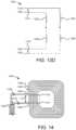
- FIG. 14is a schematic block diagram illustrating one embodiment of a winding with two windings in parallel connected to compensate for a variation in winding length where winding starting and ending points are adjusted to compensate for length variations.
- a list with a conjunction of “and/or”includes any single item in the list or a combination of items in the list.
- a list of A, B and/or Cincludes only A, only B, only C, a combination of A and B, a combination of B and C, a combination of A and Cora combination of A, Band C.
- a list using the terminology “one or more of”includes any single item in the list or a combination of items in the list.
- one or more of A, B and Cincludes only A, only B, only C, a combination of A and B, a combination of B and C, a combination of A and C or a combination of A, B and C.
- a list using the terminology “one of”includes one and only one of any single item in the list.
- “one of A, Band C”includes only A, only B or only C and excludes combinations of A, B and C.
- a member selected from the group consisting of A, B, and Cincludes one and only one of A, B, or C, and excludes combinations of A, B, and C.”
- “a member selected from the group consisting of A, B, and C and combinations thereof”includes only A, only B, only C, a combination of A and B, a combination of B and C, a combination of A and Cora combination of A, Band C.
- a wireless power transfer (“WPT”) pad apparatusincludes a ferrite structure and four windings adjacent to the ferrite structure.
- a horizontal surface of the ferrite structureis adjacent to each of the four windings and each of the four windings are wound in a horizontal pattern that is planar to the horizontal surface.
- the four windingsare arranged in a two-by-two square pattern in a north-south-north-south polarity arrangement.
- adjacent windings of the four windings the ferrite structurecomprises a magnetic pathway.
- a ferrite pathway between adjacent windings of the four windingshas a thickness and a width to provide a low impedance, unsaturated magnetic pathway for an electromagnetic field generated by the adjacent windings.
- the ferrite structureincludes an opening in a center section where the center section is located at a center of the two-by-two square pattern and the center section is external to each of the four windings.
- the WPT pad apparatusincludes a vertical shield external to the ferrite structure positioned to shunt an electromagnetic field radiating in a direction horizontal with the horizontal surface of the ferrite structure.
- the vertical shieldincludes a metallic structure oriented transverse to the horizontal surface of the ferrite structure.
- the vertical shieldhas a width where the width is measured in a direction transverse to the horizontal surface of the ferrite structure. The width includes at least a thickness of an edge of the ferrite structure and a thickness of the winding.
- the vertical shieldincludes an opening at each corner of the ferrite structure.
- the horizontal surfaceincludes a first horizontal surface and the WPT pad apparatus also includes a horizontal shield positioned on a second horizontal surface of the ferrite structure.
- the second horizontal surfaceis distal to the first horizontal surface and planar with the first horizontal surface.
- the horizontal shieldincludes metallic plate and the horizontal shield reduces a strength of an electromagnetic field generated by the four windings and radiating through the horizontal shield to below a specified limit.
- the ferrite structureis thermally coupled to the horizontal shield where heat generated in each of the four windings and in the ferrite structure is transmitted to the horizontal shield.
- the WPT pad apparatusincludes a vertical shield external to the ferrite structure. The vertical shield is coupled to the horizontal shield and extending in a direction transverse to the horizontal shield in a direction of the ferrite structure and the four windings.
- each of the four windingsincludes a spiral pattern starting at an edge of a winding center section and expanding away from the center section.
- the center sectionhas an area without conductors at a center of a winding.
- each winding of the four windingsincludes two or more winding sections wound in parallel and each winding section is connected to a capacitor assembly located at the center section of the winding.
- the center section of each windingincludes a ferrite chimney coupled to the horizontal surface of the ferrite structure and extending in a direction transverse to the horizontal surface at least a thickness of the winding associated with the center section.
- each of the four windingsincludes a conductor where each conductor has multiple strands.
- the strandsare electrically isolated from each other and the conductor has a wide side and a narrow side.
- the wide side of the conductoris oriented transverse to the horizontal surface.
- the conductoris a Litz wire.
- Another WPT pad apparatusincludes a ferrite structure and four windings adjacent to the ferrite structure.
- a horizontal surface of the ferrite structureis adjacent to each of the four windings.
- Each of the four windingsis wound in a horizontal pattern that is planar to the horizontal surface.
- the four windingsare arranged in a two-by-two square pattern in a north-south-north-south polarity arrangement, and for adjacent windings of the four windings, the ferrite structure has a magnetic pathway.
- a ferrite pathway between adjacent windings of the four windingshas a thickness and a width to provide a low impedance, unsaturated magnetic pathway for an electromagnetic field generated by the adjacent windings.
- the ferrite structureincludes an opening in a center section where the center section is located at a center of the two-by-two square pattern and the center section is external to each of the four windings.
- the WPT pad apparatusincludes a vertical shield external to the ferrite structure positioned to shunt an electromagnetic field radiating in a direction horizontal with the horizontal surface of the ferrite structure.
- the WPT pad apparatusincludes a ferrite chimney coupled to the horizontal surface of the ferrite structure in the center section of each winding and extending in a direction transverse to the horizontal surface at least a thickness of the winding associated with the center section.
- a WPT systemincludes a first stage with a resonant converter or an alternating current (“AC”) to direct current (“DC”) converter.
- the first stageis configured to wirelessly transmit power to a second stage on a vehicle.
- the WPT systemincludes a WPT pad apparatus that receives power from the first stage and transmits power wirelessly to a secondary pad of the second stage.
- the WPT pad apparatusincludes a ferrite structure and four windings adjacent to the ferrite structure.
- a horizontal surface of the ferrite structureis adjacent to each of the four windings, and each of the four windings is wound in a horizontal pattern that is planar to the horizontal surface.
- the four windingsare arranged in a two-by-two square pattern in a north-south-north-south polarity arrangement.
- Another WPT pad apparatusincludes a ferrite structure with a horizontal surface and a winding with a conductor.
- the conductorhas a long side and a narrow side. The long side is oriented transverse to the horizontal surface of the ferrite structure and the narrow side is planar with the horizontal surface.
- the conductor of the windingis wound in a spiral-type configuration.
- the conductorhas a rectangular shape and has two parallel long side and two parallel narrow sides. In other embodiments, the conductor has multiple strands where the strands are electrically isolated from each other.
- the WPT pad apparatusincludes a winding with one or more winding guides. The winding guides maintain the conductor in a winding pattern. In other embodiments, the winding guides maintain spacing between each turn of the winding. In other embodiments, the winding structure includes posts and/or channels that maintain the conductor in a winding pattern.
- Another WPT pad with a fractional winding for wireless power transferincludes a ferrite structure with a planar surface and a winding that includes a conductor wound in a planar arrangement in a spiral-type pattern about a center point.
- the conductorsare arranged to be adjacent to the planar surface of the ferrite structure.
- the windinghas a starting point and each turn of the winding is adjacent to the planar surface of the ferrite structure.
- the windingincludes a fractional number of turns where the starting point is at a different angle from a radial line extending radially from the center point than angle of an ending point of the winding measured from the radial line.
- a length of the conductorrelates to an amount of inductance of the winding and the method includes determining a target amount of winding inductance and selecting the fractional number of turns based on the target amount of inductance for the winding.
- the inductance of the windingis further related to a diameter of the spiral-type pattern of the winding and the method includes determining a diameter of the spiral-type pattern along with selecting the fractional number of turns based on the target amount of inductance of the winding.
- the windingis a first winding and the conductor is a first conductor and the WPT pad includes a second winding that includes a second conductor adjacent to the ferrite structure.
- the second windingarranged in a spiral-type pattern and the second winding is wound interleaved to the first winding.
- the first and second windingsare arranged to compensate for a difference in length between the first winding and the second winding for portions of the first and second windings wound adjacent to each other.
- the conductorsare wound within a winding structure with channels and/or posts that maintain the winding in a particular shape and spacing.
- the channelsare distributed around the center point at various distances from the center point to provide for various diameters of the spiral-type pattern and the winding structure has a plurality of gaps between the channels and/or posts arranged to provide pathways to a center section of the winding for a fractional number of turns.
- the WPT pad the conductorsare covered within the winding structure with a position maintaining material that maintains the winding in a selected spiral-type pattern with a fractional number of turns.
- the winding structure with the conductorsis adjacent to the ferrite structure and the conductors are adjacent to the planar surface of the ferrite structure.
- a WPT padincludes a horizontal shield, a ferrite structure mounted to the horizontal shield, where the ferrite structure has a planar surface distal to a surface of the ferrite structure mounted to the horizontal shield, and a winding with a conductor in a planar arrangement in a spiral-type pattern about a center point, where the winding has a center section with the center point within the center section.
- the WPT padincludes a capacitor assembly located within the center section of the winding, a winding insulator located between conductors of the winding and the ferrite structure, where the winding insulator is electrically insulating the conductors from the ferrites structure, and a capacitor insulator located adjacent to the capacitor on a side of the capacitor facing the horizontal shield.
- the capacitor insulatorincludes a material that electrically insulates the capacitor from the ferrite structure and/or the horizontal shield. The capacitor insulator transmits heat from the capacitor to one or more of the horizontal shield and the ferrite structure.
- the windingis a first winding and the conductor is a first conductor and the WPT pad includes a second winding that includes a second conductor adjacent to the ferrite structure.
- the second windingis arranged in a spiral-type pattern and the second winding is wound interleaved to the first winding and the first and second windings are arranged to compensate for a difference in length between the first winding and the second winding for portions of the first and second windings wound adjacent to each other.
- the capacitor insulatorincludes a ceramic printed circuit board (“PCB”) material.
- the capacitor insulatorincludes aluminum nitride.
- the winding insulatorincludes a glass-reinforced epoxy laminate.
- the winding insulatorhas a National Electrical Manufacturers Association (“NEMA”) flame retardant (“FR”) rating of 4 (“FR 4”).
- NEMANational Electrical Manufacturers Association
- FR 4flame retardant
- the capacitoris secured to the horizontal shield with a fastener and the fastener is electrically insulated from the capacitor with a connector insulator.
- the ferrite structurehas a horizontal shield with the planar surface and a ferrite chimney.
- the ferrite chimneyis located in the center section and is adjacent to the winding.
- the ferrite chimneyextends in a direction away from the planar surface of the ferrite structure to at least a distance of a thickness of the conductors or twice a thickness of the horizontal shield. The thickness is measured in a direction transverse to the planar surface.
- the ferrite chimneyis thermally and electrically coupled to the horizontal shield of the ferrite structure.
- the WPT padincludes a winding structure that separates turns of the winding a specified distance. The winding structure is electrically insulating turns of the winding from each other and maintaining the conductors of the winding in the spiral-type pattern.
- a winding structure for a WPT padincludes a base with an insulating material and channels within the base and/or one or more posts extending from the base to a height of a top of the channels.
- the channels and postsare configured to maintain one or more conductors of a winding in a particular shape and spacing.
- the channelsare distributed around a center point of the winding at various distances from the center point to provide for various diameters of a spiral-type pattern, and the winding structure includes a plurality of gaps between the one or more channels and/or the one or more posts. The plurality of gaps is arranged to provide pathways to a center section of the winding.
- the winding structureincludes a capacitor opening.
- the capacitor openingis sized for one or more capacitors.
- the capacitor openingis located in the center section.
- the winding structureincludes one or more ferrite openings. Each ferrite opening is sized for a ferrite chimney. At least one ferrite opening is located in the center section at an outer perimeter of the center section and adjacent to the one or more conductors of the winding.
- the winding structureincludes one or more terminal slots and a terminal within each terminal slot. One or more conductors of the winding each terminate on a terminal within a terminal slot.
- the terminal slotshave a length longer than a terminal and the terminal of a terminal slot is movable within the terminal slot of the terminal along the length of the terminal slot.
- the winding structureincludes a position maintaining material placed around components within the winding structure where the position maintaining material is placed around the components once a configuration of the components is set.
- the position maintaining materialis an epoxy resin.
- the winding structureincludes nylon.
- Another WPT padincludes a ferrite structure, a first winding adjacent to the ferrite structure, where the first winding is arranged in a spiral-type pattern, and a second winding adjacent to the ferrite structure.
- the second windingis arranged in a spiral-type pattern and the second winding is wound interleaved to the first winding.
- the first and second windingsare arranged to compensate for a difference in length between the first winding and the second winding for portions of the first and second windings wound adjacent to each other.
- starting points of the first and second windingsare at an exterior of the first and second windings and the starting point of the second winding is before the starting point of the first winding and an ending point of the second winding is after an ending point of the first winding.
- a length of the second windingis equal to a length of the first winding.
- the starting point of the first windingis positioned so a conductor connected to the ending point of the second winding and traversing the first and second windings to the starting point of the first winding traverses perpendicular to the first and second windings to reach the starting point of the first winding
- the starting point of the second windingis positioned so a conductor connected to the ending point of the second winding and traversing the first and second windings to the starting point of the second winding traverses perpendicular to the first and second windings to reach the starting point of the second winding.
- the first windingincludes a first conductor and a fourth conductor and the second winding includes a second conductor and a third conductor.
- the first conductoris an outermost conductor and is adjacent to the second conductor, the second conductor is adjacent to the third conductor, and the third conductor is adjacent to the fourth conductor is an innermost conductor.
- ending points of the first, second, third and fourth conductorsare at a center section of the first and second windings and a starting point of the first, second, third and fourth conductors are at an exterior of the first and second windings. The ending point of the first conductor is connected to the starting point of the fourth conductor and the ending point of the second conductor is connected to the starting point of the third conductor.
- ending points of the first, second, third and fourth conductorsare at a center section of the first and second windings and a starting point of the first, second, third and fourth conductors are at an exterior of the first and second windings.
- the ending point of the first conductoris connected to a first terminal of a first capacitor and a second terminal of the first capacitor is connected to the starting point of the fourth conductor.
- the ending point of the second conductoris connected to a first terminal of a second capacitor and a second terminal of the second capacitor is connected to the starting point of the third conductor.
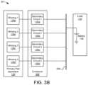
- FIG. 1is a schematic block diagram illustrating one embodiment of a WPT system 100 with a low voltage WPT pad.
- the WPT system 100includes a power converter apparatus 104 and a secondary receiver apparatus 106 separated by a gap 108 , and a load 110 , which are described below.
- the WPT system 100includes a power converter apparatus 104 that receives power from a power source 112 and transmits power over a gap 108 to a secondary receiver apparatus 106 , which transfers power to a load 110 .
- the power converter apparatus 104in one embodiment, may be called a switching power converter and includes a resonant converter 118 that receives a direct current (“DC”) voltage from a DC bus 116 .
- DCdirect current
- the power source 112provides DC power to the DC bus 116 .
- the power source 112is an alternating current (“AC”) power source, for example from a building power system, from a utility, from a generator, etc. and the power converter apparatus 104 includes a form of rectification to provide DC power to the DC bus 116 .
- the rectificationmay be in the form of a power factor correction and rectification circuit 114 .
- the power factor correction and rectification circuit 114may include an active power factor correction circuit, such as a switching power converter.
- the power factor correction and rectification circuit 114may also include a full-bridge rectifier, a half-bridge rectifier, or other rectification circuit that may include diodes, capacitors, surge suppression, etc.
- the resonant converter 118may be controlled by a primary controller 120 , which may vary parameters within the resonant converter 118 , such as conduction time, conduction angle, duty cycle, switching, etc.
- the primary controller 120may receive information from sensors and position detection 122 within or associated with the power converter apparatus 104 .
- the primary controller 120may also receive information wirelessly from the secondary receiver apparatus 106 .
- the power converter apparatus 104includes a primary pad 126 (i.e. a primary WPT pad) that receives power from the resonant converter 118 .
- the primary pad 126includes four windings, which may also be termed “pads.”
- the power converter apparatus 104may include multiple resonant converters 118 .
- portions of the resonant converter 118 and primary pad 126form a resonant circuit that enables efficient wireless power transfer across the gap 108 .
- the power converter apparatus 104includes a switching power converter that is not a resonant converter.
- the gap 108in some embodiments includes an air gap, but may also may partially or totally include other substances.
- the gap 108may include a resin, asphalt, concrete or other material just over the windings of the primary pad 126 in addition to air, snow, water, etc. between the primary pad 126 and a secondary pad 128 located in the secondary receiver apparatus 106 .
- the secondary receiver apparatus 106includes a secondary pad 128 (i.e. a secondary WPT pad) connected to a secondary circuit 130 that delivers power to the load 110 .
- the secondary pad 128may include multiple windings, which may also be termed “pads.” Each winding may feed a separate secondary circuit 130 .
- the secondary receiver apparatus 106may also include a secondary decoupling controller 132 that controls the secondary circuit 130 and may also be in communication with sensors and/or position detection 136 and wireless communications 134 coupled to the power converter apparatus 104 .
- the secondary receiver apparatus 106 and load 110are part of a vehicle 140 that receives power from the power converter apparatus 104 .
- the load 110may include a battery 138 , a motor, a resistive load, a circuit or other electrical load.
- the WPT system 100may transfer power to a portable computer, a consumer electronic device, to an industrial load, or other portable load that would benefit from receiving power wirelessly.
- the secondary circuit 130includes a portion of resonant circuit that interacts with the secondary pad 128 and that is designed to receive power at a resonant frequency.
- the secondary circuit 130includes a power conditioning circuit that is not a resonant circuit.
- the secondary circuit 130may also include a rectification circuit, such as a full-bridge rectifier, a half-bridge rectifier, and the like.
- the secondary circuit 130includes a power converter of some type that receives power from the resonant circuit/rectifier and actively controls power to the load 110 .
- the secondary circuit 130may include a switching power converter.
- the secondary circuit 130includes passive components and power to the load 110 is controlled by adjusting power in the power converter apparatus 104 .
- the secondary circuit 130includes an active rectifier circuit that may receive and transmit power.
- One of skill in the artwill recognize other forms of a secondary circuit 130 appropriate for receiving power from the secondary pad 128 and delivering power to the load 110 .
- the resonant converter 118in one embodiment, includes an active switching section coupled to a resonant circuit formed with components of the resonant converter 118 and the primary pad 126 .
- the resonant converter 118is described in more detail with regard to FIGS. 2 A and 2 B .
- FIG. 2 Ais a schematic block diagram illustrating one embodiment 200 of a power converter apparatus 104 .
- the power converter apparatus 104is connected to a power source 112 and includes a power factor correction and rectification circuit 114 connected to a DC bus 116 feeding a resonant converter 118 connected to a primary pad 126 as described with regard to the WPT system 100 of FIG. 1 .
- the resonant converter 118includes a switching module 202 and a tuning section 204 .
- the switching module 202includes four switches configured to connect the DC bus 116 and to ground. Typically, switches SI and S 3 close while switches S 2 and S 4 are open and vice-versa. When switches SI and S 3 are closed, the DC bus 116 is connected to a positive connection of the tuning section 204 through inductor L 1 a and the ground is connected to the negative connection of the tuning section 204 through inductor L 1 b while switches S 2 and S 4 are open. When switches S 2 and S 4 are closed, the ground is connected to the positive terminal of the tuning section 204 and the DC bus 116 is connected to the positive connection of the tuning section 204 .
- the switching modulealternates connection of the DC bus 116 and ground to the tuning section 204 simulating an AC waveform.
- the AC waveformis typically imperfect due to harmonics.
- switches S 1 -S 4are semiconductor switches, such as a metal-oxide-semiconductor field-effect transistor (“MOSFET”), a junction gate field-effect transistor (“JFET”), a bipolar junction transistor (“BJT”), an insulated-gate bipolar transistor (“IGBT”) or the like.
- MOSFETmetal-oxide-semiconductor field-effect transistor
- JFETjunction gate field-effect transistor
- BJTbipolar junction transistor
- IGBTinsulated-gate bipolar transistor
- the timing of opening and closing switches S 1 -S 4are varied to achieve various modes of operations, such as zero-voltage switching.
- the tuning section 204 of the resonant converter 118 and the primary pad 126are designed based on a chosen topology.
- the resonant converter 118 and primary pad 126may form an inductor-capacitor-inductor (“LCL”) load resonant converter, a series resonant converter, a parallel resonant converter, and the like.
- the embodiment depicted in FIG. 2 Aincludes an LCL load resonant converter.
- Resonant convertersinclude an inductance and capacitance that form a resonant frequency.
- voltage with the tuning section 204 and primary pad 126often increases to voltages levels higher than the voltage of the DC bus 116 .
- voltage of the DC bus 116is 1 kilovolt (“kV”)
- voltage in the tuning section 204 and resonant converter 118may be 3 kV or higher.
- the high voltagesrequire component ratings, insulation ratings, etc. to be high enough for expected voltages.
- the primary pad 126includes capacitor C 3 and inductor Lp while the tuning section 204 includes series capacitor C 2 .
- Capacitors C 2 and C 3add to provide a particular capacitance that forms a resonant frequency with inductor Lp.
- the power converter apparatus 104includes a single series capacitor in the tuning section 204 or in the primary pad 126 . While FIG.
- the secondary receiver apparatus 106includes a secondary pad 128 and a secondary circuit 130 that typically includes a tuning section 204 where the inductance of the secondary pad 128 and capacitance of the tuning section 204 of the secondary circuit 130 form a resonant frequency and the secondary pad 128 and secondary circuit 130 have voltage issues similar to the primary pad 126 and resonant converter 118 .
- the tuning section 204 and primary pad 126are not designed to produce a resonance, but instead condition voltage from the switching module 202 .
- the tuning section 204may filter out harmonic content without filtering a switching frequency.
- FIG. 2 Bis a schematic block diagram illustrating one embodiment 201 of a power converter apparatus 104 with multiple resonant converters 118 a - d feeding windings 126 a - d of one or more primary pads 126 .
- FIG. 2 Bis presented in a one-line diagram format.
- Each line between elementsrepresents two or more conductors.
- the power source 112 , power factor correction and rectification circuit 114 and DC bus 116are substantially similar to those described in the embodiment 200 of FIG. 2 A .
- the power converter apparatus 104includes four resonant converters 118 a - d (generically or individually “ 118 ”) where each resonant converter 118 includes a switching module 202 and may include a tuning section 204 .
- Each resonant converter 118feed a winding (e.g. 126 a ) of a primary pad 126 , which may include multiple windings 126 a - d .
- a resonant converter(e.g. 118 a ) may feed an individual primary pad 126 .
- FIG. 3 Ais a schematic block diagram illustrating one embodiment 300 of a secondary circuit 130 feeding a load 110 .
- a secondary pad 128feeds a tuning section 302 within the secondary circuit 130 and the tuning section 302 feeds a rectification section 304 in the secondary circuit 130 , which feeds a load 110 .
- the secondary pad 128includes one or more windings arranged to receive power from a primary pad 126 .
- the secondary pad 128may include a ferrite structure and windings arranged in a pattern that efficiently receives power from the primary pad 126 .
- the secondary pad 128mirrors the primary pad 126 transmitting power.
- the secondary pad 128differs from the primary pad 126 .
- the secondary pad 128includes an inductance Ls formed as a result of the windings and the ferrite structure of the secondary pad 128 .
- the secondary pad 128includes a capacitor C 4 .
- the tuning section 302includes one or more capacitors CS, C 6 and inductors L 2 a , L 2 b that are arranged to form a resonant circuit with the secondary pad 128 with a resonant frequency.
- capacitor C 6is not present.
- the resonant frequencymatches a resonant frequency of the primary pad 126 transmitting power.
- a resonant frequencyis formed between the inductor Ls of the secondary pad 128 and series capacitors C 4 and CS of the secondary pad 128 and/or tuning section 302 .
- the secondary pad 128 or the tuning section 302include a single series capacitor C 4 or CS.
- Other capacitorse.g.
- a low pass filtermay form a low pass filter to reduce voltage ripple at the resonant frequency.
- a low-pass filteris included after rectification elements in the rectification section 304 .
- a capacitor C 7may be included.
- One of skill in the artwill recognize other configurations of the tuning section 302 that form a resonant tank with the secondary pad 128 and pass energy to the rectification section 304 or another suitable circuit.
- a rectification section 304includes diodes, switches, or other rectification elements to convert alternating current (“AC”) power to direct current (“DC”) power.
- the rectification section 304 depicted in FIG. 3includes a full bridge rectifier with four diodes D 1 -D 4 .
- the diodes D 1 -D 4are replaced with active elements, such as switches, which may be used to reduce harmonics, reduce power consumption, and the like.
- the rectification section 304may include a switching power converter that controls an output voltage to the load 110 .
- the load 110in one embodiment is a battery 138 .
- the load 110may include other components, such as a motor, a resistive load, electronics, and the like.
- the secondary pad 128 , secondary circuit 130 and load 110are part of a vehicle 140 .
- the secondary pad 128 , secondary circuit 130 and load 110are part of a computing device, a smartphone, and the like.
- FIG. 3 Bis a schematic block diagram illustrating one embodiment 301 of several windings 128 a - d of a secondary pad 128 feeding several secondary circuits 130 a - d , which feed a load 110 .
- the secondary circuits 130 a - din one embodiment, are in an enclosure 306 and feed a secondary DC bus 308 , which feeds the load 110 .
- a secondary pad 128 with multiple windings 128 a - dis advantageous to increase a power level and multiple windings 128 a - d may also be used in determining alignment. Multi-winding pads 126 , 126 are discussed in more detail below.
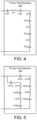
- FIG. 4is a schematic block diagram illustrating one embodiment of a low voltage WPT pad.
- the capacitance Cshas been distributed in five capacitors, Cs 1 , Cs 2 , Cs 3 , Cs 4 and Cs 5 .
- the winding of the primary pad 126which forms an inductance, is divided into four sections, Lp 1 , Lp 2 , Lp 3 , Lp 4 .
- the capacitors Cs 2 , Cs 3 , Cs 4 and Cs 5are distributed between winding sections as depicted. While five capacitors and four winding sections are depicted, one of skill in the art will recognize that other numbers of capacitors and winding sections may be used.
- the low voltage WPT padmay be for a primary or a secondary pad.
- FIG. 5is a schematic block diagram illustrating one embodiment of a low voltage WPT pad with two parallel windings.
- the capacitance Cshas been distributed in two parallel windings.
- a first windingincludes three capacitors, Cs 1 a , Cs 2 a , and Cs 3 a .
- the first winding of the primary pad 126which forms an inductance, is divided into two sections, Lp 1 a and Lp 2 a .
- capacitors Cs 1 a , Cs 2 a and Cs 3 aare distributed between winding sections as depicted.
- a second parallel windingincludes three capacitors, Cs 1 b , Cs 2 b , and Cs 3 b .
- the second winding of the primary pad 126which forms an inductance, is divided into two sections, Lp 1 b and Lp 2 b .
- capacitors Cs 1 b , Cs 2 b and Cs 3 bare distributed between winding sections as depicted. While six capacitors and four winding sections are depicted, one of skill in the art will recognize that other numbers of capacitors and winding sections may be used.
- the windingsare depicted connected in parallel, in other embodiments each winding may be fed by a separate resonant converter 118 . In another embodiment, the windings are connected in series.
- the low voltage WPT padmay be for a primary or a secondary pad.
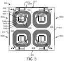
- FIG. 6is a schematic block diagram illustrating one embodiment 600 of a WPT pad 126 , 128 with four windings 602 a , 602 b , 602 c , 602 d (generically or collectively “ 602 ”) with a ferrite structure removed.
- Each winding 602is configured similar to the windings depicted in FIG. 5 with capacitors Cs 1 a , Cs 2 a and Cs 3 a on one winding and Cs 1 b , Cs 2 b and Cs 3 b on the other winding, but other configurations are also contemplated, such as the embodiment 400 of FIG. 4 , windings 602 without intervening capacitors, etc.
- Each winding 602includes a ferrite chimney 606 , which is a ferrite section adjacent to the conductors 604 of the windings 602 .
- the ferrite chimney 606is described in more detail with regard to FIG. 8 .
- Connection points 608are depicted as square boxes.
- Each winding 602 a , 602 b , 602 c , 602 dis configured the same so for clarity only the first winding 602 a is labeled.
- the four windings 602are surrounded by vertical shields 610 .
- Each vertical shield 610is located external to the ferrite structure and is positioned to shunt an electromagnetic field radiating in a direction horizontal with a horizontal surface of the ferrite structure.
- the vertical shields 610are described more in relation to FIGS. 7 and 8 .
- each of the four windings 602 a - dis wound in a spiral pattern starting at an edge of a winding center section and expanding away from the center section.
- the center sectionis an area without conductors at a center of a winding (e.g., 602 a ).
- the spiralis an Archimedean spiral.
- the spiralis a modified Archimedean spiral that is not purely circular, but includes straight sections or other modifications to accommodate the ferrite chimneys 606 , convenience, etc.
- FIG. 7is a schematic block diagram illustrating the embodiment 600 of the WPT pad 126 , 128 with four windings 602 with a ferrite structure 702 a , 702 b , 702 c , 702 d (generically or collectively “ 702 ”) included for each winding 602 a , 602 b , 602 c , 602 d .
- the four windings 602 a - dare adjacent to the ferrite structure 702 , where a horizontal surface of the ferrite structure 702 is adjacent to each of the four windings 602 a - d .
- Each of the four windings 602 a - dare wound in a horizontal pattern that is planar to the horizontal surface.
- the four windings 602 a - dare arranged in a two-by-two square pattern in a north-south-north-south polarity arrangement.
- the ferrite structure 702 a of the first winding 602 ais configured to magnetically connect to the ferrite structure 702 b , 702 d of each adjacent winding 602 b , 602 d to create a low impedance magnetic pathway between each winding 602 .
- the ferrite pathway between adjacent windings (e.g., 602 a , 602 b ) of the four windings 602has a thickness and a width to provide a low impedance, unsaturated magnetic pathway for an electromagnetic field generated by the adjacent windings 602 a , 602 b .
- the ferrite structure 702may be sized for an amount of power wirelessly transferred through the WPT pad 126 , 128 to not saturate for an expected electromagnetic field generated by the windings 602 .
- the resultant ferrite structure 702includes four separate ferrite structures 702 a - d that are positioned to be adjacent to allow for a low impedance magnetic pathway from one winding (e.g., 602 a ) to another winding (e.g. 602 b ).
- the ferrite structures 702 a - dmay be touching or are positioned very close to each other.
- the ferrite structure 702is constructed to be a unitary structure.
- the ferrite structure 702may be a single piece of ferrite or may be constructed of ferrite blocks or similar ferrite pieces.
- the resultant ferrite structure 702includes an opening in a center section 704 , where the center section 704 is located at a center of the two-by-two square pattern of windings 602 and the center section is external to each of the four windings 602 a - d .
- the center section 704includes ferrite.
- the embodiment 600includes vertical shields 610 external to the ferrite structure 702 positioned to shunt an electromagnetic field radiating in a direction horizontal with a horizontal surface of the ferrite structure 702 .
- the vertical shield 610includes a metallic plate oriented transverse to the horizontal surface of the ferrite structure 702 .
- the vertical shield 610has an opening 706 at each corner of the windings 602 a - d and/or ferrite structure 702 , as depicted. As depicted, the vertical shields 610 may run along only a part of an edge of the windings 602 .
- a winding structure 612that may be used to support the windings, ferrite chimneys 606 , connection points 608 , etc.
- the winding structure 612is non-magnetic.
- the winding structure 612is rigid and includes channels, ridges, indentations, etc. to support various components of the windings 602 .
- the winding structure 612provides insulation between components and has a dielectric breakdown sufficient for voltages anticipated on the primary pad 126 or secondary pad 128 .
- the winding structure 612is a rigid material, such as nylon.
- an insulating layer(not shown) is placed between the windings 602 and the ferrite structure 702 .
- the insulating layermay meet the FR-4 standard of the National Electrical Manufacturers Association (“NEMA”) LI 1-1998 specification, and may be a glass-reinforced epoxy laminate or other similar material.
- the windings 602each include conductors 604 which include multiple strands.
- each strand of a conductor 604is electrically isolated from other strands within the conductor 604 , for example, to minimize skin effect.
- the conductors 604are a litz wire.
- the conductors 604are not litz wire, but are in other configurations.
- the conductor 604may include one or more strands of copper or other conductive metal configured to reduce skin effect and may be configured to be pliable.
- the litz wirein one embodiment, includes fine strands of conductors and some of the strands may be wound and/or woven together.
- the litz wireis rectangular shaped with a wide side and a narrow side.
- the litz wiremay bend more readily in a direction transverse to the wide side.
- the wide side of the litz wireis oriented transverse to a horizontal surface of the ferrite structure 702 , which may facilitate tighter bends than if the litz wire was oriented with the wide side toward the horizontal surface of the ferrite structure 702 .
- the litz wirein one embodiment, is placed in channels in the winding structure 612 to maintain a particular pattern, spacing, etc.
- the winding structure 612includes extensions, posts, guides, or the like to facilitate a particular pattern, spacing, etc. of the litz wire.
- the vertical shields 610are adjacent to and/or connected to a horizontal shield (not shown), which is located adjacent to the ferrite structure 702 where the ferrite structure 702 is between the horizontal shield and the windings 602 .
- the vertical shield 610is coupled to the horizontal shield.
- the vertical shield 610is adjacent to the horizontal shield but is not coupled to the horizontal shield.
- the horizontal shieldextends beyond the ferrite structure 702 and the windings 602 and may be placed between the ferrite structure 702 and a vehicle 140 for a secondary pad 128 or between the ferrite structure 702 and a ground below a primary pad 126 .
- the horizontal shieldis thermally and/or electrically coupled to the ferrite structure 702 .
- the horizontal shieldmay be a single structure or may be split into multiple horizontal shields, for example a horizontal shield 708 for each winding 602 a - d .
- a horizontal shield that is a single platemay be advantageous to prevent water or another substance from passing beyond the horizontal shield to the ferrite structure 702 and/or windings 602 .
- the horizontal shieldis described in more detail with regard to the embodiment 800 of FIG. 8 .
- FIG. 8is a schematic block diagram illustrating one embodiment 800 of a cross section of a primary pad 126 and a secondary pad 128 , each with a ferrite chimney 606 and a vertical shield 610 .
- the embodiment 800is substantially similar to the embodiment 600 depicted in FIGS. 6 and 7 .
- Each of the primary pad 126 and secondary pad 128include a horizontal shield 802 with a vertical shield 610 on an end of the horizontal shield 802 .
- the ferrite structure 702 and conductors 604 of the windings 602are separated from the vertical shields 610 .
- the vertical shields 610are adjacent to the ferrite structure 702 and/or conductors 604 .
- the vertical shields 610may be placed within sides of a vehicle 140 to minimize stray electromagnetic field beyond the vehicle 140 where people may be standing.
- a width (measured from the horizontal shield 802 in a direction transverse to the horizontal shield 802 ), a thickness, and a material of the vertical shield 610may be chosen along with a position of the vertical shields to maintain an electromagnetic field strength below a specified limit where people are located, such as a governmental standard.
- the thickness, size, and material of the horizontal shield 802may be chosen to reduce an electromagnetic field strength below a specified limit where people are located.
- the vertical shield 610 and/or the horizontal shield 802include a metallic material, such as aluminum.
- the primary pad 126 and secondary pad 128each include a ferrite chimney 606 .
- the ferrite chimneys 606may reduce a distance between the pads 126 , 128 and may provide a convenient magnetic pathway 804 between the pads 126 , 128 .
- the ferrite chimneys 606in one embodiment, extend at least to a distance away from the ferrite structure 702 that is at least level with the conductors 604 of the windings 602 and may extend beyond the conductors 604 , as depicted in FIG. 8 .
- the ferrite chimneys 606extend at least to a distance away from the ferrite structure 702 that is at least twice a thickness of the horizontal shield 802 .
- the ferrite chimneys 606surround a center section, which may include capacitors (e.g., Cs 2 a , Cs 3 a , Cs 2 b , Cs 3 b ). Note that the capacitors Cs 2 a , Cs 3 a , Cs 2 b , Cs 3 b are not shown for clarity, but are intended to be included in the embodiment 800 . In another embodiment, the center section is empty.
- the ferrite chimneys 606are discussed in more detail in U.S. Patent Application No. 62/554,950 filed Sep. 9, 2017, for Patrice Lethellier, which is incorporated herein by reference for all purposes.
- the primary pad 126includes a pyramid-shaped ferrite chimney (not shown) that is located at a center of each winding, which allows for a degree of misalignment between the pads 126 , 128 while maintaining an adequate degree of magnetic coupling.
- Pyramid-shaped ferrite chimneysare discussed in more detail in U.S. Patent Application No. 62/554,960 filed Sep. 9, 2017, for Patrice Lethellier, which is incorporated herein by reference for all purposes.
- North (“N”) and south (“S”) polesare depicted as well as a magnetic pathway 804 where electromagnetic flux may travel from north to south poles and then through the ferrite structure 702 .
- the ferrite structure 702 extending between windingsprovides a low impedance magnetic pathway from one winding (e.g., 602 a ) to another winding (e.g., 602 b , 602 d ), which facilitates efficient transfer of energy wirelessly between the pads 126 , 128 .
- each winding 602 a - dmay be connected to a different resonant converter 118 to parallel the resonant converters 118 to increase the wireless power transfer capability of the pads 126 , 128 .
- the magnetic pathway formed in the ferrite structure 702 and the ferrite chimneys 606help to direct the electromagnetic field generated in the windings 602 into the ferrite structure 702 and to minimize stray electromagnetic field external to the ferrite structure 702 , ferrite chimneys 606 and area directly between the ferrite chimneys 606 , i.e., in locations where the electromagnetic field is not wanted.
- the horizontal shields 802 and the vertical shields 610help to shunt stray electromagnetic fields to minimize electromagnetic field strength beyond the horizontal shields 802 and the vertical shields 610 .
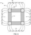
- FIG. 9is a schematic block diagram illustrating one embodiment 900 of a simplified ferrite structure 902 of a four winding WPT pad (e.g., 126 , 128 ) and vertical shields 610 depicting shunting of a stray electromagnetic field.
- the simplified ferrite structure 902may represent the ferrite structure of the embodiments 600 , 800 of FIGS. 7 and 8 , but is simply depicted to indicate functionality of the vertical shields 610 .
- the simplified ferrite structure 902include center sections 904 with north (“N”) and south (“S”) poles as indicated.
- Stray electromagnetic field lines 906extend beyond the simplified ferrite structure 902 , but are shunted by the vertical shields 610 , as depicted by the field lines 908 in the vertical shields 610 .
- the shunting of the stray electromagnetic field 906reduces electromagnetic field strength beyond the vertical shields 610 .
- Figure IOis a schematic block diagram illustrating one embodiment I 000 of a center section of a winding 602 with capacitors (e.g., Cs 2 a ).
- the embodiment 1000in one example, is an enlargement of the center section of the embodiment 800 of FIG. 8 .
- a primary pad 126 and secondary pad 128are depicted and the horizontal shield 802 , the ferrite structure 702 with a horizontal surface 1012 , the conductors 604 of the windings 602 , the ferrite chimneys 606 and the capacitors Cs 2 a , Cs 2 b , Cs 3 a , Cs 3 b (collectively “Cs”) are substantially similar to those described above in relation to the embodiments 600 , 800 of FIGS. 6 - 8 .
- capacitors Csare depicted in the center section of the secondary pad 128 and not in the center section of the primary pad 126 .
- capacitors Cs of the primary pad 126may be located separate from the primary pad 126 , for example, to avoid replacement of the primary pad 126 when a capacitor Cs is replaced.
- the primary pad 126may include capacitors (e.g., C 1 , C 2 in the tuning section 204 without capacitors Cs included with the primary pad 126 .
- the primary pad 126includes one or more capacitors Cs in the center section.
- an insulator I 002 that is thermally conductiveis positioned between the ferrite structure 702 and the conductors 604 .
- the insulator 1002provides electrical insulation between the conductors 604 and the ferrite structure 702 .
- the insulator I 002is thermally conductive to transmit heat from the conductors 604 to the ferrite structure 702 , which transmits heat to the horizontal shield 802 .
- the insulator I 002in one embodiment, is FR-4 compliant.
- the capacitors Csare separated from the horizontal shield 802 with a spacer 1004 .
- the spacer 1004is thermally conductive.
- the spacer I 004provides electrical insulation between the capacitors Cs and the horizontal shield 802 .
- the spacer I 004includes aluminum nitride, which has a high thermal conductance while including a high resistivity, which provides an insulating property.
- the spacer 1004is made of beryllium oxide or boron nitride.
- the spacer 1004has a higher thermal conductivity than the insulator 1002 .
- aluminum nitride or other ceramicsprovide a higher thermal conductance than FR-4.
- the insulator 1002is typically spread over a larger area and FR-4 is more forgiving than ceramics, such as aluminum nitride. Where thermal requirements increase for the conductors 604 , aluminum nitride or another high thermal conductivity insulator may be used.
- the capacitors Csin one embodiment are secured to the horizontal shield 802 with a fastener 1006 , such as a bolt, screw, rivet, etc.
- the fastener 1006is separated from the capacitor Cs with an insulating material 1008 , which electrically isolates the capacitor Cs from the fastener 1006 .
- a bus or other conductormay connect to the capacitors Cs to a winding 602 or other component in the secondary pad 128 .
- the conductors 604 and ferrite chimneys 606are separated by winding guides 1010 .
- the winding guides 1010are part of the winding structure 612 .
- the winding structure 612may have channels and/or posts that maintain spacing between conductors 604 , turns of a conductor 604 , the ferrite chimneys 606 , etc.
- the winding guides 1010are an insulating material that provides electrical insulation for conductors 604 , ferrite chimneys 606 , etc. sufficient for an expected voltage.
- the winding guides 1010may be rated for a voltage much higher than an expected voltage by a certain amount or ratio (i.e. 2 times).
- the winding guides 1010 and/or winding structure 612are nylon or an equivalent material. Nylon may be useful in that nylon may be formed in a particular shape and typically provide an adequate amount of electrical insulation for a desired thickness.
- a WPT pad 600includes a ferrite structure 702 with a horizontal surface 1012 with a winding 602 with a conductor 604 where the conductor 604 includes a long side 1014 and a narrow side 1016 .
- the long side 1014is oriented transverse to the horizontal surface 1012 of the ferrite structure 702 and the narrow side 1016 is planar with the horizontal surface 1012 .
- the conductor 604 of the winding 602is wound in a spiral-type configuration.
- the conductor 604may be in a rectangular shape with two parallel long sides 1014 and two parallel narrow sides 1016 , as depicted in FIG. 10 .
- Having a rectangular shape with the conductor 604 oriented as depictedmay facilitate bending of the conductor 604 in a direction around the center section 704 of the winding 602 with a smaller radius than conductors 604 of other shapes, such as a round conductor, a square conductor, etc.
- the conductor 604is made of litz wire or the like.
- the litz wire conductor 604may include strands and/or sub-strands of small diameter conductors so that the conductor 604 is made up of a lot of conductors with radii much, much smaller than dimensions of the conductor 604 .
- One of skill in the artwill recognize properties of a litz wire.
- the litz wire conductor 604may also provide additional pliability to reduce a bending radius around the center section 704 of the winding 602 .
- having the narrow sides 1016 facing the ferrite structure 702also contributes to a more compact winding 602 because the conductors 604 may be packed together closer than round conductors, square conductors, etc.
- the WPT pad 126 , 128includes a winding structure 612 with one or more winding guides 1010 where the winding guides 1010 maintain the conductor 604 in a winding pattern.
- the winding guides 1010may maintain spacing between each turn of the winding 602 .
- the winding structure 612includes posts and/or channels that maintain the conductor 604 in a winding pattern. The winding structure 612 is described in more detail with regard to FIG. 11 .
- FIG. 11is a schematic block diagram illustrating one embodiment of a winding structure 612 that guides conductors 604 within a winding 602 .
- the winding structure 612provides a framework for creating a winding 602 where the winding 602 may have various radii, various number of turns, etc.
- the winding structure 612may be used to test various spiral-type winding patterns of one or more conductors 604 to adjust inductance, number of turns, connection to components, such as capacitors (e.g., Cs), connectors, etc.
- the winding structure 612includes a base 1102 that includes an insulating material.
- the base 1102may have a planar shape and may have channels 1104 and posts 1106 configured to maintain one or more conductors 604 of a winding 602 in a particular shape and spacing.
- the winding structure 612 depicted in FIG. 11includes channels 1104 and posts 1106 that may be used to produce a winding 602 in a spiral-type pattern with curved sections and straight sections.
- the channels 1104are depicted as solid lines where conductors 604 (dashed lines) are between the solid lines in the channels 1104 .
- the solid linesmay represent tops of winding guides 1010 depicted in FIG.
- channels 1104are between the winding guides 1010 , depicted as the solid lines.
- the channels 1104are distributed around a center point 1108 of the winding 602 at various distances from the center point 1108 to provide for various diameters of a spiral-type pattern.
- the channels 1104are cut into the base 1102 .
- Material around the posts 1106expose the posts 1106 , which are depicted as short, solid lines.
- Conductors 604can follow a channel 1104 and traverse in a straight line through the posts 1106 , for example as depicted on the bottom, left and top of the winding 602 , and can transition through gaps around the posts 1106 to a different channel 1104 or to the center section 1110 , for example to capacitors or connectors.
- the gaps around the posts 1106 and channels 1104are arranged to provide pathways to a center section 1110 .
- the base 1102includes, in one embodiment, recesses for various components.
- the base 1102includes capacitor openings, such as a capacitor opening for capacitors Cs in the center section 1110 or a capacitor opening 1114 around the perimeter of the winding 602 .
- the basemay also include ferrite openings 1112 for the ferrite chimneys 606 .
- the ferrite openings 1112 for the ferrite chimneys 606may be positioned around the center section 1110 and may be sized for the ferrite chimneys 606 .
- the winding structure 612includes one or more terminal slots 1118 and a terminal 1116 within a terminal slot 1118 .
- One or more conductors 604 of the winding 602each terminate on a terminal 1116 within a terminal slot 1118 .
- the terminal slots 1118have a length longer than a terminal 1116 and the terminal 1116 of a terminal slot 1118 is movable within the terminal slot 1118 of the terminal 1116 along the length of the terminal slot 1118 .
- the terminal 1116may allow for a transition between a channel 1104 and a portion of a conductor 604 traversing the channels 1104 to a capacitor Cs or other component in the center section 1110 .
- the terminal slot 1118allows for the terminal 1116 to be easily moved to another position.
- the winding structure 612may also include one or more fasteners 1120 where the conductor(s) 604 terminate on the fasteners 1120 .
- the fasteners 1120allow for external connection of the winding 602 .
- the winding structure 612includes a position maintaining material (not shown) placed around components within the winding structure 612 .
- the position maintaining materialis placed around the components once a configuration of the components is set to maintain the conductors 604 , capacitors Cs, etc.
- the position maintaining materialis an epoxy resin.
- the winding structure 612is advantageous to provide numerous winding configurations and component configurations. For example, a single winding structure 612 may be used for several winding designs. Once a winding design is set and the conductors 604 and components are in place, the position maintaining material can fill in gaps of the winding structure 612 .
- FIG. 12is a schematic block diagram illustrating one embodiment of a fractional winding 1200 .
- the fractional winding 1200includes a conductor 1202 that is capable of terminating at various location in a center section 1110 .
- the conductor 1202may terminate at the top of the center section 1110 with an end 1204 extending to the center section 1110 , providing 51 ⁇ 4 turns.
- the conductor 1202may extend (see dashed conductor 1206 and end 1208 ) to the right side of the center section 1110 providing 51 ⁇ 2 turns.
- the conductor 1202may extend (see dashed conductor with one dot 1210 and end 1212 ) to the bottom of the center section 1110 providing 53 ⁇ 4 turns.
- the conductor 1202may extend (see dashed conductor and two dots 1214 and end 1216 ) to the left side of the center section 1110 providing 6 turns. While FIG. 12 depicts a single conductor 1202 , the fractional winding 1200 may include additional conductors 1202 wound in parallel, as depicted in FIGS. 5 and 6 . Each conductor 1202 , in one embodiment, has a different starting point 1218 .
- the fractional winding 1200may be used in a WPT pad with a ferrite structure 702 with a horizontal surface 1012 .
- a method for constructing a fractional winding 1200 for wireless power transferincludes providing the ferrite structure 702 with a horizontal surface 1012 and winding a conductor 1202 in a planar arrangement in a spiral-type pattern about a center point 1108 .
- the conductor 1202is arranged to be adjacent to the horizontal surface 1012 of the ferrite structure 702 .
- the conductor 1202includes a starting point 1218 .
- each turn of the conductor 1202is adjacent to the horizontal surface 1012 of the ferrite structure 702 , and the fractional winding 1200 includes a fractional number of turns where the starting point 1218 is at a different angle from a radial line 1220 extending radially from the center point 1108 than angle of an ending point (e.g., 1204 , 1208 , 1212 ) of the fractional winding 1200 measured from the radial line 1220 .
- a length of the conductor 1202relates to an amount of inductance of the winding and the method, in one embodiment, includes determining a target amount of winding inductance and selecting the fractional number of turns based on the target amount of inductance for the fractional winding 1200 .
- the target inductancemay be selected to achieve a desired amount of gain, a resonant frequency, to optimize power transfer, etc.
- the target inductancein some embodiments, includes selecting an inductance value that helps to minimize other components while achieving resonance.
- One of skill in the artwill recognize other ways to choose a target inductance.
- the inductance of the fractional winding 1200is related to a diameter of the spiral-type pattern of the fractional winding 1200 and the method includes determining a diameter of the spiral-type pattern along with selecting the fractional number of turns based on the target amount of inductance of the fractional winding 1200 .
- the winding structure 612 of FIG. 11may be used to adjust the diameter of the spiral-type pattern and/or to determine a termination point, resulting in a fractional number of turns.
- the conductor 1202is wound within a winding structure 612 with one or more of channels 1104 and posts 1106 that maintain the fractional winding 1200 in a particular shape and spacing.
- the channels 1104are distributed around the center point 1108 at various distances from the center point 1108 to provide for various diameters of the spiral-type pattern.
- the winding structure 612may include a plurality of gaps between the channels 1104 and/or posts 1106 arranged to provide pathways to the center section 1110 of the fractional winding 1200 for a fractional number of turns.
- the methodin one embodiment, also includes covering the conductors within the winding structure with a position maintaining material that maintains the fractional winding 1200 in a selected spiral-type pattern with a fractional number of turns, and placing the winding structure 612 with the conductors 1202 adjacent to the ferrite structure 702 , where the conductors 1202 are adjacent to the horizontal surface 1012 of the ferrite structure 702 .
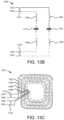
- FIG. 13 Ais a schematic block diagram illustrating one embodiment of a winding 1300 with four conductors 1302 , 1304 , 1306 , 1308 in parallel connected to compensate for a variation in winding length. Windings in parallel may differ in inductance 5 percent or more, which can dramatically affect power sharing between the windings. Where the conductors 1302 , 1304 , 1306 , 1308 start and terminate at a same angle or (i.e., have a same number of turns, where the “same angle” can be exact or approximate), the first conductor 1302 may be longer than the second conductor 1304 , which may be longer than the third conductor 1306 , which may be longer than the fourth conductor 1308 . The same is true for two windings in parallel where the first winding may be longer than the second winding.
- the first and second windingsmay be arranged to compensate for a difference in length between the first winding and the second winding for portions of the first and second windings wound adjacent to each other.
- Various methodsmay be used to compensate for differences in length between conductors, which are discussed with regard to FIGS. 13 A-D and 14 .
- a starting point of a conductor or a windingis located on an exterior of the winding and an ending point of a conductor or a winding is located in a center section of the winding.
- a capacitori.e., 1310 , 1312
- a capacitoris connected at a midpoint of a winding to reduce voltage so the ending point of the first conductor 1302 connects to a terminal of a first capacitor 1310 and a second terminal of the first capacitor 1310 connects to the starting point of the fourth conductor 1308 .
- a conductorjumps out across the conductors 1302 - 1308 to the starting point of the fourth conductor 1308 .
- a conductorjumps across the conductors 1302 - 1308 for an external connection.
- a current sharing transformer 1314connects conductors 1318 , 1320 to the starting points of the first conductor 1302 and the second conductor 1304 .
- another current sharing transformer 1316connects conductors 1322 , 1324 to the ending points of the third conductor 1306 and the fourth conductor 1308 .
- the second transformer 1316is not included.
- one or more current sharing transformers 1314 , 1316are located adjacent to the winding 1300 .
- one or more current sharing transformers 1314 , 1316are located adjacent to the tuning section 204 where a cable is between the tuning section 204 and the winding 1300 .
- Current sharing conductorsare discussed in more detail in U.S. Provisional Patent No. 62/567,106, filed Oct. 2, 2017, for Patrice Lethellier, which is incorporated herein by reference for all purposes.
- FIG. 13 Bis a simplified schematic block diagram illustrating the winding 1300 of FIG. 13 A .
- the simplified diagramincludes the conductors 1302 , 1304 , 1306 , 1308 depicted as inductors, which represent inductance of the conductors 1302 , 1304 , 1306 , 1308 .
- the inductors 1302 , 1304 , 1306 , 1308typically differ based on conductor length, geometric variations, etc.
- FIG. 13 Cis a schematic block diagram illustrating one embodiment of a winding 1301 with four conductors 1302 - 1308 in parallel connected to compensate for a variation in winding length.
- FIG. 13 Dis a simplified schematic block diagram illustrating the winding 1301 of FIG. 13 C .
- the winding 1301 in FIGS. 13 C and 13 Dis the same as the winding 1300 in FIGS. 13 A and 13 B , except without capacitors 1310 , 1312 .
- a conductor connected to the ending point of the first conductor 1302is connected to the starting point of the fourth conductor 1308 and the ending point of the second conductor 1304 is connected to the starting point of the third conductor 1306 .
- FIG. 14is a schematic block diagram illustrating one embodiment of a winding 1400 of a WPT pad with two windings 1402 in parallel which are connected to compensate for a variation in winding length where winding starting points 1406 , 1408 and ending points 1410 , 1412 are adjusted to compensate for length variations.
- the starting point 1408 of the second winding 1404is before the starting point 1406 of the first winding 1402 .
- the starting point 1408 of the second winding 1404starts first and then moving clockwise radially an additional amount, then the starting point 1406 of the first winding 1402 is located past the starting point 1408 of the second winding 1404 .
- an ending point 1412 of the second winding 1404is after an ending point 1410 of the first winding 1402 .
- the first winding 1402ends at the ending point 1410
- the second winding 1404ends at its ending point 1412 after the ending point 1410 of the first winding 1402 .
- a spacing 1414 between the starting and ending points 1406 - 1412 of the windings 1402 , 1404is adjusted to compensate for the length discrepancies between the first and second windings 1402 , 1404 caused by the positioning of the first winding 1402 outside the second winding 1404 .
- the spacing 1414is adjusted so that a length of the second winding 1404 is equal to a length of the first winding 1402 .
- the length of the second winding 1404 being equal to a length of the first winding 1402includes exactly equal as well as approximately equal.
- a difference in length between the first winding 1402 and the second winding 1404may differ one percent or less. In other embodiments, a difference in length between the first winding 1402 and the second winding 1404 may differ 0.5 percent or less.
- winding 1400is depicted in a square pattern, other patterns may be used and the starting points 1406 , 1408 and ending points 1410 , 1412 may be adjusted accordingly so the first and second windings 1402 , 1404 are equal or approximately equal in length. Where the winding 1400 is in a circular pattern, the spacing 1414 may be measured radially.
- the starting point 1406 of the first winding 1402is positioned so a conductor connected to the ending point 1412 of the second winding 1404 and traversing the first and second windings 1402 , 1404 to the starting point 1406 of the first winding 1404 traverses perpendicular to the first and second windings 1402 , 1404 to reach the starting point 1406 of the first winding 1402 .
- a conductor traversing perpendicularincludes a conductor traversing exactly perpendicular and a conductor traversing approximately perpendicular. For example, approximately perpendicular includes traversing at an angle in a range of 80 degrees to 90 degrees and may include a range of between 88 degrees and 90 degrees.
- the starting point 1408 of the second winding 1404is positioned so a conductor connected to the ending point 1410 of the first winding 1402 and traversing the first and second windings 1402 , 1404 to the starting point 1408 of the second winding 1404 traverses perpendicular to the first and second windings 1402 , 1404 to reach the starting point 1408 of the second winding 1404 .
- the conductors 1416 from the starting point 1406 the first winding 1402 and the ending point 1412 of the second winding 1404are run in close proximity to a cable 1420 to minimize electromagnetic radiation.
- the conductors 1416in one embodiment, are twisted together.
- the conductors 1418 from the starting point 1408 the second winding 1404 and the ending point 1410 of the first winding 1402are run in close proximity to the cable 1420 to minimize electromagnetic radiation.
- the conductors 1416 , 1418may be arranged in the cable 1420 to minimize electromagnetic radiation as well.
Landscapes
- Engineering & Computer Science (AREA)
- Power Engineering (AREA)
- Computer Networks & Wireless Communication (AREA)
- Signal Processing (AREA)
- Coils Of Transformers For General Uses (AREA)
- Current-Collector Devices For Electrically Propelled Vehicles (AREA)
Abstract
Description
Claims (17)
Priority Applications (1)
| Application Number | Priority Date | Filing Date | Title |
|---|---|---|---|
| US17/880,650US11764613B2 (en) | 2017-12-22 | 2022-08-04 | Wireless power transfer pad with multiple windings and magnetic pathway between windings |
Applications Claiming Priority (4)
| Application Number | Priority Date | Filing Date | Title |
|---|---|---|---|
| US201762609947P | 2017-12-22 | 2017-12-22 | |
| US16/231,742US10826329B2 (en) | 2017-12-22 | 2018-12-24 | Wireless power transfer pad with multiple windings and magnetic pathway between windings |
| US17/034,813US11437855B2 (en) | 2017-12-22 | 2020-09-28 | Wireless power transfer pad with multiple windings and magnetic pathway between windings |
| US17/880,650US11764613B2 (en) | 2017-12-22 | 2022-08-04 | Wireless power transfer pad with multiple windings and magnetic pathway between windings |
Related Parent Applications (1)
| Application Number | Title | Priority Date | Filing Date |
|---|---|---|---|
| US17/034,813ContinuationUS11437855B2 (en) | 2017-12-22 | 2020-09-28 | Wireless power transfer pad with multiple windings and magnetic pathway between windings |
Publications (2)
| Publication Number | Publication Date |
|---|---|
| US20220376554A1 US20220376554A1 (en) | 2022-11-24 |
| US11764613B2true US11764613B2 (en) | 2023-09-19 |
Family
ID=66949667
Family Applications (3)
| Application Number | Title | Priority Date | Filing Date |
|---|---|---|---|
| US16/231,742Active2039-03-28US10826329B2 (en) | 2017-12-22 | 2018-12-24 | Wireless power transfer pad with multiple windings and magnetic pathway between windings |
| US17/034,813ActiveUS11437855B2 (en) | 2017-12-22 | 2020-09-28 | Wireless power transfer pad with multiple windings and magnetic pathway between windings |
| US17/880,650ActiveUS11764613B2 (en) | 2017-12-22 | 2022-08-04 | Wireless power transfer pad with multiple windings and magnetic pathway between windings |
Family Applications Before (2)
| Application Number | Title | Priority Date | Filing Date |
|---|---|---|---|
| US16/231,742Active2039-03-28US10826329B2 (en) | 2017-12-22 | 2018-12-24 | Wireless power transfer pad with multiple windings and magnetic pathway between windings |
| US17/034,813ActiveUS11437855B2 (en) | 2017-12-22 | 2020-09-28 | Wireless power transfer pad with multiple windings and magnetic pathway between windings |
Country Status (5)
| Country | Link |
|---|---|
| US (3) | US10826329B2 (en) |
| EP (2) | EP4266545A2 (en) |
| CN (1) | CN111742464A (en) |
| CA (1) | CA3124345A1 (en) |
| WO (1) | WO2019126828A1 (en) |
Families Citing this family (4)
| Publication number | Priority date | Publication date | Assignee | Title |
|---|---|---|---|---|
| CN111742464A (en)* | 2017-12-22 | 2020-10-02 | 无线先进车辆电气化有限公司 | Wireless Power Transfer Pad with Multiple Windings |
| CN110932418B (en)* | 2019-12-17 | 2024-07-23 | 华南理工大学 | Fractional order series-parallel electromagnetic field double-coupling wireless power transmission system |
| KR102825251B1 (en)* | 2020-06-26 | 2025-06-25 | 삼성전자주식회사 | Electronic device for wirelessly transmitting power and method of operating the same |
| EP4391299A4 (en)* | 2021-08-17 | 2025-07-30 | Hyundai Motor Co Ltd | WIRELESS POWER TRANSMISSION DEVICE WITH POWER TRANSMISSION CIRCUIT AND COIL STRUCTURE FOR WIRELESS POWER TRANSMISSION AND WIRELESS POWER TRANSMISSION SYSTEM |
Citations (162)
| Publication number | Priority date | Publication date | Assignee | Title |
|---|---|---|---|---|
| US4647910A (en) | 1985-09-17 | 1987-03-03 | Allied Corporation | Selector for AC magnetic inductive field receiver coils |
| WO2003105308A1 (en) | 2002-01-11 | 2003-12-18 | City University Of Hong Kong | Planar inductive battery charger |
| US20040203986A1 (en) | 2002-06-28 | 2004-10-14 | Marc Gagnon | Automatic transmit power control disabling |
| JP2006042519A (en) | 2004-07-28 | 2006-02-09 | Seiko Epson Corp | Contactless power transmission device |
| US20080129246A1 (en) | 2006-11-10 | 2008-06-05 | Mitsubishi Heavy Industries, Ltd. | Non-contact type power feeder system for mobile object and protecting apparatus thereof |
| JP4127935B2 (en) | 1999-07-29 | 2008-07-30 | 大日本印刷株式会社 | Signal and power transmission device and rotary joint |
| WO2008140333A2 (en) | 2007-05-10 | 2008-11-20 | Auckland Uniservices Limited | Multi power sourced electric vehicle |
| JP2008288889A (en) | 2007-05-17 | 2008-11-27 | Showa Aircraft Ind Co Ltd | Signal transmission coil communication device |
| US20090067207A1 (en) | 2005-04-22 | 2009-03-12 | Shuzo Nishino | Secondary-side power receiving circuit of noncontact power supplying equipment |
| US20090160262A1 (en) | 2006-05-30 | 2009-06-25 | Josef Schmidt | Installation |
| WO2009081126A1 (en) | 2007-12-21 | 2009-07-02 | Amway (Europe) Limited | Circuitry for inductive power transfer |
| US20100017249A1 (en) | 2008-07-11 | 2010-01-21 | Fincham Carson C K | Systems and methods for electric vehicle charging and power management |
| US20100109604A1 (en) | 2007-05-10 | 2010-05-06 | John Talbot Boys | Multi power sourced electric vehicle |
| US20100117596A1 (en) | 2008-07-08 | 2010-05-13 | Qualcomm Incorporated | Wireless high power transfer under regulatory constraints |
| US7741734B2 (en) | 2005-07-12 | 2010-06-22 | Massachusetts Institute Of Technology | Wireless non-radiative energy transfer |
| US20100176659A1 (en) | 2009-01-14 | 2010-07-15 | Seiko Epson Corporation | Power transmission control device, power transmission device, electronic apparatus, and load state detection circuit |
| US20100181842A1 (en) | 2007-06-20 | 2010-07-22 | Masayuki Suzuki | Contactless power transmission apparatus and a method of manufacturing a secondary side thereof |
| CN101789636A (en) | 2009-01-27 | 2010-07-28 | 松下电工株式会社 | Contactless Power Transfer System |
| US20100225271A1 (en) | 2007-10-25 | 2010-09-09 | Toyota Jidosha Kabushiki Kaisha | Electrical powered vehicle and power feeding device for vehicle |
| US20100253153A1 (en) | 2009-04-07 | 2010-10-07 | Seiko Epson Corporation | Coil unit and electronic instrument |
| US20100277121A1 (en) | 2008-09-27 | 2010-11-04 | Hall Katherine L | Wireless energy transfer between a source and a vehicle |
| RU2408476C2 (en) | 2009-01-20 | 2011-01-10 | Государственное научное учреждение Всероссийский научно-исследовательский институт электрификации сельского хозяйства Российской академии сельскохозяйственных наук (ГНУ ВИЭСХ Россельхозакадемии) | Method of wireless electric power transmission and device to this end (versions) |
| US7909483B2 (en) | 2006-07-21 | 2011-03-22 | Koninklijke Philips Electronics N.V. | Lighting system |
| JP4681742B2 (en) | 2001-02-14 | 2011-05-11 | Fdk株式会社 | Non-contact coupler |
| US20110127951A1 (en) | 2009-11-30 | 2011-06-02 | Broadcom Corporation | Device with integrated wireless power receiver |
| US20110127845A1 (en) | 2009-11-30 | 2011-06-02 | Broadcom Corporation | Wireless power circuit board and assembly |
| US20110181120A1 (en) | 2010-01-27 | 2011-07-28 | Honeywell International Inc. | Wireless energy transfer |
| US20110221387A1 (en) | 2010-03-09 | 2011-09-15 | Robert Louis Steigerwald | System and method for charging an energy storage system for an electric or hybrid-electric vehicle |
| US20110254503A1 (en) | 2010-04-08 | 2011-10-20 | Qualcomm Incorporated | Wireless power antenna alignment adjustment system for vehicles |
| US20110285349A1 (en) | 2010-05-19 | 2011-11-24 | Qualcomm Incorporated | Adaptive wireless energy transfer system |
| EP2390984A2 (en) | 2005-03-21 | 2011-11-30 | Hanrim Postech Co., Ltd. | Non-contact charging system |
| WO2011156768A2 (en) | 2010-06-11 | 2011-12-15 | Mojo Mobility, Inc. | System for wireless power transfer that supports interoperability, and multi-pole magnets for use therewith |
| US8093758B2 (en) | 2003-05-23 | 2012-01-10 | Auckland Uniservices Limited | Method and apparatus for control of inductively coupled power transfer systems |
| WO2012018268A1 (en) | 2010-08-05 | 2012-02-09 | Auckland Uniservices Limited | Inductive power transfer apparatus |
| US20120043172A1 (en) | 2009-05-14 | 2012-02-23 | Toyota Jidosha Kabushiki Kaisha | Non-contact power receiving apparatus and vehicle having the same |
| WO2012039245A1 (en) | 2010-09-24 | 2012-03-29 | パナソニック株式会社 | Coil module for contactless electric power transfer, and battery pack and charging device provided with same |
| US8169185B2 (en) | 2006-01-31 | 2012-05-01 | Mojo Mobility, Inc. | System and method for inductive charging of portable devices |
| US20120139358A1 (en) | 2010-12-01 | 2012-06-07 | Triune Ip Llc | Multiple Coil Data Transmission System |
| US20120146580A1 (en)* | 2009-09-24 | 2012-06-14 | Panasonic Corporation | Noncontact charger system |
| US20120161696A1 (en) | 2010-10-29 | 2012-06-28 | Qualcomm Incorporated | Wireless energy transfer via coupled parasitic resonators |
| WO2012099965A2 (en) | 2011-01-18 | 2012-07-26 | Afshin Partovi | Systems and methods for providing positioning freedom, and support of different voltages, protocols, and power levels in a wireless power system |
| US20120217818A1 (en) | 2011-02-28 | 2012-08-30 | Yerazunis William S | System and Method for Automatically Optimizing Wireless Power |
| US20120235566A1 (en) | 2008-09-27 | 2012-09-20 | Aristeidis Karalis | Tunable wireless energy transfer for lighting applications |
| US20120235504A1 (en) | 2008-09-27 | 2012-09-20 | Kesler Morris P | Tunable wireless energy transfer for sensors |
| US8304935B2 (en) | 2008-09-27 | 2012-11-06 | Witricity Corporation | Wireless energy transfer using field shaping to reduce loss |
| US20130002034A1 (en) | 2009-09-18 | 2013-01-03 | Kabushiki Kaisha Toshiba | Wireless power transmitter |
| CN102870338A (en) | 2010-03-10 | 2013-01-09 | 无线电力公司 | Wireless energy transfer converter |
| WO2013011726A1 (en) | 2011-07-20 | 2013-01-24 | パナソニック 株式会社 | Non-contact power supply system |
| US20130039099A1 (en) | 2011-03-11 | 2013-02-14 | Utah State University Research Foundation | Method and Apparatus for Controlling LCL Converters Using Asymmetric Voltage Cancellation Techniques |
| US20130038272A1 (en) | 2010-12-24 | 2013-02-14 | Toyota Jidosha Kabushiki Kaisha | Non-contact charging system, non-contact charging method, non-contact charging type vehicle, and non-contact charging management apparatus |
| US20130062959A1 (en) | 2011-09-09 | 2013-03-14 | Qualcomm Incorporated | Systems and methods for detecting and identifying a wireless power device |
| US20130088090A1 (en) | 2011-10-07 | 2013-04-11 | Utah State University Research Foundation | Wireless power transfer magnetic couplers |
| WO2013056234A2 (en) | 2011-10-13 | 2013-04-18 | Integrated Device Technology, Inc. | Apparatus, system, and method for detecting a foreign object in a inductive wireless power transfer system |
| US20130119773A1 (en) | 2011-11-15 | 2013-05-16 | Qualcomm Incorporated | Systems and methods for induction charging with a closed magnetic loop |
| CN103119669A (en) | 2010-09-21 | 2013-05-22 | 松下电器产业株式会社 | Contactless power feeding apparatus |
| US20130127253A1 (en) | 2011-11-21 | 2013-05-23 | Joseph Stark | Transcutaneous power transmission utilizing non-planar resonators |
| WO2013091875A2 (en) | 2011-12-21 | 2013-06-27 | Ampium Limited | Inductive power coupling systems for roadways |
| US20130181668A1 (en) | 2010-12-01 | 2013-07-18 | Panasonic Corporation | Non-contact charging module and non-contact charging instrument |
| WO2013112614A1 (en) | 2012-01-23 | 2013-08-01 | Utah State University | Wireless power transfer system |
| US20130214735A1 (en) | 2012-02-21 | 2013-08-22 | Samsung Electronics Co., Ltd. | Wireless charging apparatus and method |
| US20130236337A1 (en) | 2012-03-09 | 2013-09-12 | Mark A. Gummin | Solenoid actuators using embedded printed circuit coils |
| US20130249299A1 (en) | 2012-03-26 | 2013-09-26 | Kabushiki Kaisha Toshiba | Power transmitting apparatus, power receiving apparatus, control apparatus, and wireless power transfer system |
| US20130272044A1 (en) | 2010-08-13 | 2013-10-17 | Auckland Uniservices Limited | Inductive power transfer control |
| US20130293192A1 (en) | 2011-01-19 | 2013-11-07 | National University Corporation Saitama University | Contactless power transfer system |
| US20130307468A1 (en) | 2012-05-21 | 2013-11-21 | Lg Electronics Inc. | Structure of transmission and reception unit in wireless charging system |
| US20130320759A1 (en) | 2011-02-21 | 2013-12-05 | National University Corporation Saitama University | Contactless power transfer device for moving object |
| US20140008995A1 (en) | 2012-07-05 | 2014-01-09 | Panasonic Corporation | Wireless power transmission system, power transmitting device, and power receiving device |
| US20140015522A1 (en) | 2012-07-13 | 2014-01-16 | Qualcomm Incorporated | Systems, methods, and apparatus for detection of metal objects in a predetermined space |
| US20140015328A1 (en) | 2012-07-16 | 2014-01-16 | Qualcomm, Incorporated | Device alignment and identification in inductive power transfer systems |
| RU2505919C1 (en) | 2012-12-05 | 2014-01-27 | Корпорация "САМСУНГ ЭЛЕКТРОНИКС Ко., Лтд." | Method, system and device for wireless transmission of energy (versions) |
| WO2014038107A1 (en) | 2012-09-06 | 2014-03-13 | パナソニック 株式会社 | Contactless power-supply system, contactless adapter, and power-supply device |
| US20140077614A1 (en) | 2012-09-12 | 2014-03-20 | Samsung Electronics Co., Ltd. | Apparatus and method for wireless power reception, apparatus and method for wireless power transmission, and wireless power transmission system |
| US8710701B2 (en) | 2008-02-27 | 2014-04-29 | Qualcomm Incorporated | Antennas and their coupling characteristics for wireless power transfer via magnetic coupling |
| US20140125140A1 (en) | 2012-11-02 | 2014-05-08 | Qualcomm Incorporated | Coil arrangements in wireless power transfer systems for low electromagnetic emissions |
| US20140183967A1 (en) | 2012-12-27 | 2014-07-03 | Samsung Electronics Co., Ltd. | Apparatus and method for resonance in wireless power transmission system |
| EP2752957A1 (en) | 2013-01-04 | 2014-07-09 | Primax Electronics Ltd | Wireless transmitting device for wireless charging |
| US20140203662A1 (en) | 2011-09-09 | 2014-07-24 | Lg Innotek Co., Ltd. | Wireless power repeater and method thereof |
| US8796990B2 (en) | 2010-02-25 | 2014-08-05 | Evatran Group, Inc. | System and method for inductively transferring AC power and self alignment between a vehicle and a recharging station |
| US20140225439A1 (en) | 2013-02-14 | 2014-08-14 | Hengchun Mao | High Efficiency High Frequency Resonant Power Conversion |
| US8810071B2 (en)* | 2008-04-03 | 2014-08-19 | Koninklijke Philips N.V. | Wireless power transmission system |
| WO2014130065A1 (en) | 2013-02-25 | 2014-08-28 | Access Business Group International Llc | Variable pitch spiral coil |
| CA2908352A1 (en) | 2013-03-29 | 2014-10-02 | Nissan Motor Co., Ltd. | Non-contact power supply system |
| US8854011B2 (en) | 2009-05-14 | 2014-10-07 | Toyota Jidosha Kabushiki Kaisha | Vehicle charging apparatus for charging a power storage device mounted on a vehicle |
| US20140327391A1 (en) | 2013-05-01 | 2014-11-06 | Qualcomm Incorporated | Vehicle charging pad having reduced thickness |
| US8912687B2 (en) | 2008-09-27 | 2014-12-16 | Witricity Corporation | Secure wireless energy transfer for vehicle applications |
| EP2824793A1 (en) | 2012-02-27 | 2015-01-14 | Hitachi Power Solutions Co., Ltd. | Wireless power supply apparatus |
| US20150028478A1 (en) | 2012-01-10 | 2015-01-29 | Intel Mobile Communications GmbH | Semiconductor devices |
| EP2833509A1 (en) | 2012-03-30 | 2015-02-04 | Equos Research Co., Ltd. | Power transmission system |
| US20150042168A1 (en) | 2013-08-09 | 2015-02-12 | Qualcomm Incorporated | Systems, methods, and apparatus related to detecting and identifying electric vehicle and charging station |
| US20150077053A1 (en) | 2013-09-13 | 2015-03-19 | Qualcomm Incorporated | Pickup coil design for tight spaces and asymmetrical coupling |
| US20150094887A1 (en) | 2013-09-27 | 2015-04-02 | Qualcomm Incorporated | Device alignment in inductive power transfer systems |
| US20150091517A1 (en) | 2013-09-27 | 2015-04-02 | Siemens Aktiengesellschaft | Charging station, method, and electrically powered vehicle for the wireless energy-transfer coupling of an electrically powered vehicle |
| US20150091519A1 (en) | 2013-09-27 | 2015-04-02 | Siemens Aktiengesellschaft | Charging configuration for the inductive wireless emission of energy |
| KR20150054641A (en) | 2013-11-11 | 2015-05-20 | 삼성전기주식회사 | Non contact tpye power transmitting coil and non contact tpye power supplying apparatus |
| US20150145340A1 (en) | 2013-11-28 | 2015-05-28 | Tdk Corporation | Coil unit |
| US20150145634A1 (en) | 2013-11-25 | 2015-05-28 | A.K. Stamping Company, Inc. | Wireless Charging Coil |
| KR20150059069A (en) | 2013-11-21 | 2015-05-29 | 엘지전자 주식회사 | Wireless power transmitter and method for controlling the same |
| US20150155095A1 (en) | 2013-12-03 | 2015-06-04 | Utah State University | Determining physical alignment between magnetic couplers for wireless power transfer |
| US20150170833A1 (en) | 2013-12-17 | 2015-06-18 | Qualcomm Incorporated | Coil topologies for inductive power transfer |
| WO2015097995A1 (en) | 2013-12-27 | 2015-07-02 | Toyota Jidosha Kabushiki Kaisha | Power reception device and vehicle including the same |
| GB2522852A (en) | 2014-02-05 | 2015-08-12 | Bombardier Transp Gmbh | A method of communication between a vehicle and a wayside control unit for controlling an inductive energy transfer to the vehicle, a vehicle, a wayside contr |
| TWM508836U (en) | 2014-10-31 | 2015-09-11 | Tdk Taiwan Corp | A wireless charging coil PCB structure |
| US20150263640A1 (en) | 2014-03-14 | 2015-09-17 | Avogy, Inc. | Adaptive synchronous switching in a resonant converter |
| US20150263532A1 (en) | 2012-10-16 | 2015-09-17 | Koninklijke Philips N.V. | Wireless inductive power transfer |
| EP2928039A1 (en) | 2014-04-03 | 2015-10-07 | LG Innotek Co., Ltd. | Wireless power transmitting apparatus |
| US20150302985A1 (en) | 2014-04-17 | 2015-10-22 | Witricity Corporation | Wireless power transfer systems with shaped magnetic components |
| US20150310722A1 (en) | 2014-04-28 | 2015-10-29 | Active-Semi, Inc. | Quality of Charge Detector for Use in Inductive Charging Systems |
| EP2985870A1 (en) | 2013-03-29 | 2016-02-17 | Nissan Motor Co., Ltd. | Contactless electricity supply system and electricity supply device |
| DE102014218067A1 (en) | 2014-09-10 | 2016-03-10 | Robert Bosch Gmbh | Transmission coil for inductive energy transmission |
| US9306636B2 (en) | 2012-09-05 | 2016-04-05 | Samsung Electronics Co., Ltd | Wireless power transmitter for excluding cross-connected wireless power receiver and method for controlling the same |
| US9306635B2 (en) | 2012-01-26 | 2016-04-05 | Witricity Corporation | Wireless energy transfer with reduced fields |
| WO2016077139A1 (en) | 2014-11-14 | 2016-05-19 | Motorola Solutions, Inc. | Multi-plane receiving coil for wirelessly charging a battery |
| WO2016113949A1 (en) | 2015-01-15 | 2016-07-21 | 株式会社村田製作所 | Electric power supply device |
| US20160233728A1 (en) | 2013-12-01 | 2016-08-11 | Lg Electronics Inc. | Wireless power transfer method, apparatus and system |
| US20160241086A1 (en) | 2013-10-31 | 2016-08-18 | Lg Electronics Inc. | Wireless power transmission device and control method therefor |
| US9442172B2 (en) | 2011-09-09 | 2016-09-13 | Witricity Corporation | Foreign object detection in wireless energy transfer systems |
| US20160285317A1 (en) | 2015-03-29 | 2016-09-29 | Sanjaya Maniktala | Wireless Power Transfer Using Multiple Coil Arrays |
| US20160308391A1 (en) | 2015-04-15 | 2016-10-20 | Wireless Advanced Vehicle Electrification, Inc. | Removable inductive power transfer pad |
| US20160336816A1 (en) | 2015-05-12 | 2016-11-17 | Powermat Technologies Ltd. | System and method for responding to activation of over voltage protection mechanisms during wireless power transfer |
| JP2016220312A (en) | 2015-05-15 | 2016-12-22 | トヨタ自動車株式会社 | Power receiving device and power transmitting device |
| US9530556B2 (en) | 2012-05-04 | 2016-12-27 | Det International Holding Limited | Multiple resonant cells for wireless power mats |
| US20160380469A1 (en) | 2015-06-29 | 2016-12-29 | Wireless Advanced Vehicle Electrification, Inc. | Low inductance pad winding using a matched winding of multiple spirals |
| EP3112889A1 (en) | 2015-06-30 | 2017-01-04 | Voxalytic GmbH | Rf resonator with a lenz lens |
| US20170018970A1 (en) | 2015-07-17 | 2017-01-19 | Silergy Semiconductor Technology (Hangzhou) Ltd. | Driving circuit and wireless power transmitter including the same |
| US20170040845A1 (en) | 2015-08-05 | 2017-02-09 | Toyota Jidosha Kabushiki Kaisha | Power transmission apparatus and power reception apparatus |
| US20170063170A1 (en) | 2015-08-28 | 2017-03-02 | Wireless Advanced Vehicle Electrification, Inc. | Identification using signals from a secondary device before wireless power transfer |
| US20170092409A1 (en) | 2015-09-30 | 2017-03-30 | Apple Inc. | Preferentially Magnetically Oriented Ferrites for Improved Power Transfer |
| US20170149294A1 (en) | 2014-10-31 | 2017-05-25 | Teslonix Inc. | Wireless Energy Transfer Using Alignment Of Electromagnetic Waves |
| WO2017093255A1 (en) | 2015-11-30 | 2017-06-08 | Bayerische Motoren Werke Aktiengesellschaft | Secondary coil unit comprising a service opening |
| US9682632B2 (en) | 2012-08-23 | 2017-06-20 | Siemens Aktiengesellschaft | Charging device for inductive charging |
| US9739641B2 (en) | 2011-08-05 | 2017-08-22 | Evatran Group, Inc. | Method and apparatus for controlling stray electromagnetic fields and providing operator feedback when aligning a vehicle with an inductive charging system |
| WO2017156499A1 (en) | 2016-03-10 | 2017-09-14 | Wireless Advanced Vehicle Electrification, Inc. | Bi-plane wireless power transmission pad |
| US9767955B2 (en) | 2008-05-09 | 2017-09-19 | Auckland Uniservices Limited | Multi power sourced electric vehicle |
| US20170271861A1 (en) | 2016-03-18 | 2017-09-21 | Wireless Advanced Vehicle Electrification, Inc. | Litz wire solder termination |
| US20170279307A1 (en) | 2016-03-22 | 2017-09-28 | Samsung Electro-Mechanics Co., Ltd. | Wireless power controller and wireless power transmitter using the same |
| US20170287626A1 (en)* | 2016-03-31 | 2017-10-05 | Tyco Electronics Corporation | Coil assembly for wireless power transfer having a shaped flux-control body |
| US9796280B2 (en) | 2012-03-23 | 2017-10-24 | Hevo Inc. | Systems and mobile application for electric wireless charging stations |
| US20170324281A1 (en) | 2016-05-06 | 2017-11-09 | Ningbo Weie Electronics Technology Ltd. | Wireless power trnsfer device |
| EP2819272B1 (en) | 2012-02-22 | 2017-12-20 | Toyota Jidosha Kabushiki Kaisha | Non-contact electric power transfer device, non-contact electric power reception device, and non-contact electric power reception system |
| US20180048184A1 (en) | 2016-08-11 | 2018-02-15 | Evatran Group, Inc. | Inductive coupling gap compensation |
| US20180062421A1 (en) | 2016-08-24 | 2018-03-01 | Witricity Corporation | Wireless Power Systems Having Interleaved Rectifiers |
| US9954387B2 (en) | 2015-09-01 | 2018-04-24 | Dell Products, Lp | Wireless charging pad with interdependent temperature control and method therefor |
| US20180131239A1 (en)* | 2016-11-04 | 2018-05-10 | Wireless Advanced Vehicle Electrification, Inc. | Passive magnetic field attenuation |
| US9973038B2 (en) | 2013-06-10 | 2018-05-15 | Celico Partnership | Self optimizing antenna for NFC and wireless charging |
| US20180269716A1 (en) | 2014-11-07 | 2018-09-20 | Amosense Co., Ltd. | Transmitter For Wireless Charger |
| US20180287411A1 (en) | 2017-04-04 | 2018-10-04 | Intel Corporation | Field shaper for a wireless power transmitter |
| US20180351415A1 (en) | 2017-05-30 | 2018-12-06 | Wireless Advanced Vehicle Electrification, Inc. | Single feed multi-pad wireless charging |
| US20180361863A1 (en) | 2017-06-16 | 2018-12-20 | Qualcomm Incorporated | System and method for reducing interference in a wireless power transfer system |
| WO2019022438A1 (en) | 2017-07-25 | 2019-01-31 | 엘지이노텍 주식회사 | Coil device and wireless charging device comprising same |
| US20190051452A1 (en) | 2017-08-14 | 2019-02-14 | Wireless Advanced Vehicle Electrification, Inc. | Low voltage wireless power transfer pad |
| US20190074135A1 (en) | 2017-09-06 | 2019-03-07 | Wireless Advanced Vehicle Electrification, Inc. | Wireless power transfer pad with ferrite pyramid-shaped chimney |
| US20190103767A1 (en) | 2017-10-02 | 2019-04-04 | Wireless Advanced Vehicle Electrification, Inc. | Current sharing apparatus for wireless power transfer |
| US20190131823A1 (en) | 2017-10-31 | 2019-05-02 | Electronics And Telecommunications Research Institute | Wireless power receiving apparatus controlling output voltage |
| US10284028B2 (en) | 2016-05-27 | 2019-05-07 | Wireless Advanced Vehicle Electrification, Inc. | Checking alignment of inductive charge pads in motion |
| US20190198239A1 (en) | 2017-12-25 | 2019-06-27 | Ningbo Weie Electronics Technology Ltd. | Coil module, wireless power transmitting circuit and wireless power receiving circuit |
| US20190199134A1 (en)* | 2017-12-22 | 2019-06-27 | Wireless Advanced Vehicle Electrification, Inc. | Wireless power transfer pad with multiple windings and magnetic pathway between windings |
| US20190238001A1 (en) | 2018-01-30 | 2019-08-01 | Wireless Advanced Vehicle Electrification, Inc. | Dc link charging of capacitor in a wireless power transfer pad |
| US10369894B2 (en) | 2016-10-21 | 2019-08-06 | Hevo, Inc. | Parking alignment sequence for wirelessly charging an electric vehicle |
| US20190252921A1 (en) | 2018-02-12 | 2019-08-15 | Wireless Advanced Vehicle Electrification, Inc. | Variable wireless power transfer system |
| US10493855B2 (en) | 2017-04-19 | 2019-12-03 | Arnold Chase | Intelligent autonomous vehicle charging system |
| US20210012959A1 (en) | 2018-03-28 | 2021-01-14 | Huawei Technologies Co., Ltd. | Coil module, wireless charging transmitting apparatus, receiving apparatus, system, and terminal |
| US10988042B1 (en) | 2018-10-12 | 2021-04-27 | Arnold Chase | Vehicle charging system |
- 2018
- 2018-12-24CNCN201880089614.8Apatent/CN111742464A/enactivePending
- 2018-12-24EPEP23196663.1Apatent/EP4266545A2/ennot_activeWithdrawn
- 2018-12-24CACA3124345Apatent/CA3124345A1/ennot_activeAbandoned
- 2018-12-24USUS16/231,742patent/US10826329B2/enactiveActive
- 2018-12-24WOPCT/US2018/067456patent/WO2019126828A1/ennot_activeCeased
- 2018-12-24EPEP18891846.0Apatent/EP3729603B1/enactiveActive
- 2020
- 2020-09-28USUS17/034,813patent/US11437855B2/enactiveActive
- 2022
- 2022-08-04USUS17/880,650patent/US11764613B2/enactiveActive
Patent Citations (204)
| Publication number | Priority date | Publication date | Assignee | Title |
|---|---|---|---|---|
| US4647910A (en) | 1985-09-17 | 1987-03-03 | Allied Corporation | Selector for AC magnetic inductive field receiver coils |
| JP4127935B2 (en) | 1999-07-29 | 2008-07-30 | 大日本印刷株式会社 | Signal and power transmission device and rotary joint |
| JP4681742B2 (en) | 2001-02-14 | 2011-05-11 | Fdk株式会社 | Non-contact coupler |
| WO2003105308A1 (en) | 2002-01-11 | 2003-12-18 | City University Of Hong Kong | Planar inductive battery charger |
| US20040203986A1 (en) | 2002-06-28 | 2004-10-14 | Marc Gagnon | Automatic transmit power control disabling |
| US8093758B2 (en) | 2003-05-23 | 2012-01-10 | Auckland Uniservices Limited | Method and apparatus for control of inductively coupled power transfer systems |
| JP2006042519A (en) | 2004-07-28 | 2006-02-09 | Seiko Epson Corp | Contactless power transmission device |
| EP2390984A2 (en) | 2005-03-21 | 2011-11-30 | Hanrim Postech Co., Ltd. | Non-contact charging system |
| US20090067207A1 (en) | 2005-04-22 | 2009-03-12 | Shuzo Nishino | Secondary-side power receiving circuit of noncontact power supplying equipment |
| US7741734B2 (en) | 2005-07-12 | 2010-06-22 | Massachusetts Institute Of Technology | Wireless non-radiative energy transfer |
| US8169185B2 (en) | 2006-01-31 | 2012-05-01 | Mojo Mobility, Inc. | System and method for inductive charging of portable devices |
| US20090160262A1 (en) | 2006-05-30 | 2009-06-25 | Josef Schmidt | Installation |
| US7909483B2 (en) | 2006-07-21 | 2011-03-22 | Koninklijke Philips Electronics N.V. | Lighting system |
| US20080129246A1 (en) | 2006-11-10 | 2008-06-05 | Mitsubishi Heavy Industries, Ltd. | Non-contact type power feeder system for mobile object and protecting apparatus thereof |
| WO2008140333A2 (en) | 2007-05-10 | 2008-11-20 | Auckland Uniservices Limited | Multi power sourced electric vehicle |
| US20100109604A1 (en) | 2007-05-10 | 2010-05-06 | John Talbot Boys | Multi power sourced electric vehicle |
| JP2008288889A (en) | 2007-05-17 | 2008-11-27 | Showa Aircraft Ind Co Ltd | Signal transmission coil communication device |
| US20100181842A1 (en) | 2007-06-20 | 2010-07-22 | Masayuki Suzuki | Contactless power transmission apparatus and a method of manufacturing a secondary side thereof |
| US20100225271A1 (en) | 2007-10-25 | 2010-09-09 | Toyota Jidosha Kabushiki Kaisha | Electrical powered vehicle and power feeding device for vehicle |
| CN101835653A (en) | 2007-10-25 | 2010-09-15 | 丰田自动车株式会社 | Electric vehicle and power supply device for vehicle |
| US8884468B2 (en) | 2007-12-21 | 2014-11-11 | Access Business Group International Llc | Circuitry for inductive power transfer |
| WO2009081126A1 (en) | 2007-12-21 | 2009-07-02 | Amway (Europe) Limited | Circuitry for inductive power transfer |
| US8710701B2 (en) | 2008-02-27 | 2014-04-29 | Qualcomm Incorporated | Antennas and their coupling characteristics for wireless power transfer via magnetic coupling |
| US8810071B2 (en)* | 2008-04-03 | 2014-08-19 | Koninklijke Philips N.V. | Wireless power transmission system |
| EP2263296B1 (en) | 2008-04-03 | 2015-11-11 | Philips Intellectual Property & Standards GmbH | Wireless power transmission system |
| US9767955B2 (en) | 2008-05-09 | 2017-09-19 | Auckland Uniservices Limited | Multi power sourced electric vehicle |
| US20100117596A1 (en) | 2008-07-08 | 2010-05-13 | Qualcomm Incorporated | Wireless high power transfer under regulatory constraints |
| US20100017249A1 (en) | 2008-07-11 | 2010-01-21 | Fincham Carson C K | Systems and methods for electric vehicle charging and power management |
| US20120235504A1 (en) | 2008-09-27 | 2012-09-20 | Kesler Morris P | Tunable wireless energy transfer for sensors |
| US8304935B2 (en) | 2008-09-27 | 2012-11-06 | Witricity Corporation | Wireless energy transfer using field shaping to reduce loss |
| US8912687B2 (en) | 2008-09-27 | 2014-12-16 | Witricity Corporation | Secure wireless energy transfer for vehicle applications |
| US20120235566A1 (en) | 2008-09-27 | 2012-09-20 | Aristeidis Karalis | Tunable wireless energy transfer for lighting applications |
| US20100277121A1 (en) | 2008-09-27 | 2010-11-04 | Hall Katherine L | Wireless energy transfer between a source and a vehicle |
| US20100176659A1 (en) | 2009-01-14 | 2010-07-15 | Seiko Epson Corporation | Power transmission control device, power transmission device, electronic apparatus, and load state detection circuit |
| RU2408476C2 (en) | 2009-01-20 | 2011-01-10 | Государственное научное учреждение Всероссийский научно-исследовательский институт электрификации сельского хозяйства Российской академии сельскохозяйственных наук (ГНУ ВИЭСХ Россельхозакадемии) | Method of wireless electric power transmission and device to this end (versions) |
| US20100187912A1 (en) | 2009-01-27 | 2010-07-29 | Panasonic Electric Works Co., Ltd. | Contactless power transmission system |
| CN101789636A (en) | 2009-01-27 | 2010-07-28 | 松下电工株式会社 | Contactless Power Transfer System |
| US20100253153A1 (en) | 2009-04-07 | 2010-10-07 | Seiko Epson Corporation | Coil unit and electronic instrument |
| CN102421629A (en) | 2009-05-14 | 2012-04-18 | 丰田自动车株式会社 | Non-contact power reception device and vehicle equipped with same |
| US20120043172A1 (en) | 2009-05-14 | 2012-02-23 | Toyota Jidosha Kabushiki Kaisha | Non-contact power receiving apparatus and vehicle having the same |
| US8854011B2 (en) | 2009-05-14 | 2014-10-07 | Toyota Jidosha Kabushiki Kaisha | Vehicle charging apparatus for charging a power storage device mounted on a vehicle |
| US20130002034A1 (en) | 2009-09-18 | 2013-01-03 | Kabushiki Kaisha Toshiba | Wireless power transmitter |
| US20120146580A1 (en)* | 2009-09-24 | 2012-06-14 | Panasonic Corporation | Noncontact charger system |
| US20110127951A1 (en) | 2009-11-30 | 2011-06-02 | Broadcom Corporation | Device with integrated wireless power receiver |
| US20110127845A1 (en) | 2009-11-30 | 2011-06-02 | Broadcom Corporation | Wireless power circuit board and assembly |
| US20110181120A1 (en) | 2010-01-27 | 2011-07-28 | Honeywell International Inc. | Wireless energy transfer |
| US8796990B2 (en) | 2010-02-25 | 2014-08-05 | Evatran Group, Inc. | System and method for inductively transferring AC power and self alignment between a vehicle and a recharging station |
| US20110221387A1 (en) | 2010-03-09 | 2011-09-15 | Robert Louis Steigerwald | System and method for charging an energy storage system for an electric or hybrid-electric vehicle |
| CN102870338A (en) | 2010-03-10 | 2013-01-09 | 无线电力公司 | Wireless energy transfer converter |
| US20110254503A1 (en) | 2010-04-08 | 2011-10-20 | Qualcomm Incorporated | Wireless power antenna alignment adjustment system for vehicles |
| CN102947124A (en) | 2010-05-19 | 2013-02-27 | 高通股份有限公司 | Adaptive wireless energy transfer system |
| US20110285349A1 (en) | 2010-05-19 | 2011-11-24 | Qualcomm Incorporated | Adaptive wireless energy transfer system |
| US8884581B2 (en) | 2010-05-19 | 2014-11-11 | Qualcomm Incorporated | Adaptive wireless energy transfer system |
| WO2011156768A2 (en) | 2010-06-11 | 2011-12-15 | Mojo Mobility, Inc. | System for wireless power transfer that supports interoperability, and multi-pole magnets for use therewith |
| WO2012018268A1 (en) | 2010-08-05 | 2012-02-09 | Auckland Uniservices Limited | Inductive power transfer apparatus |
| US20130270921A1 (en) | 2010-08-05 | 2013-10-17 | Auckland Uniservices Limited | Inductive power transfer apparatus |
| US20130272044A1 (en) | 2010-08-13 | 2013-10-17 | Auckland Uniservices Limited | Inductive power transfer control |
| US20130181667A1 (en) | 2010-09-21 | 2013-07-18 | Panasonic Corporation | Contactless power supply device |
| CN103119669A (en) | 2010-09-21 | 2013-05-22 | 松下电器产业株式会社 | Contactless power feeding apparatus |
| WO2012039245A1 (en) | 2010-09-24 | 2012-03-29 | パナソニック株式会社 | Coil module for contactless electric power transfer, and battery pack and charging device provided with same |
| US20120161696A1 (en) | 2010-10-29 | 2012-06-28 | Qualcomm Incorporated | Wireless energy transfer via coupled parasitic resonators |
| US20130181668A1 (en) | 2010-12-01 | 2013-07-18 | Panasonic Corporation | Non-contact charging module and non-contact charging instrument |
| US20120139358A1 (en) | 2010-12-01 | 2012-06-07 | Triune Ip Llc | Multiple Coil Data Transmission System |
| CN103262387A (en) | 2010-12-24 | 2013-08-21 | 丰田自动车株式会社 | Non-contact charging system, non-ontact charging method, non-<wbr/>contact charging type vehicle, and non-<wbr/>contact charging management device |
| US20130038272A1 (en) | 2010-12-24 | 2013-02-14 | Toyota Jidosha Kabushiki Kaisha | Non-contact charging system, non-contact charging method, non-contact charging type vehicle, and non-contact charging management apparatus |
| WO2012099965A2 (en) | 2011-01-18 | 2012-07-26 | Afshin Partovi | Systems and methods for providing positioning freedom, and support of different voltages, protocols, and power levels in a wireless power system |
| US20120235636A1 (en) | 2011-01-18 | 2012-09-20 | Afshin Partovi | Systems and methods for providing positioning freedom, and support of different voltages, protocols, and power levels in a wireless power system |
| US20130293192A1 (en) | 2011-01-19 | 2013-11-07 | National University Corporation Saitama University | Contactless power transfer system |
| US20130320759A1 (en) | 2011-02-21 | 2013-12-05 | National University Corporation Saitama University | Contactless power transfer device for moving object |
| US20120217818A1 (en) | 2011-02-28 | 2012-08-30 | Yerazunis William S | System and Method for Automatically Optimizing Wireless Power |
| US20130039099A1 (en) | 2011-03-11 | 2013-02-14 | Utah State University Research Foundation | Method and Apparatus for Controlling LCL Converters Using Asymmetric Voltage Cancellation Techniques |
| WO2013011726A1 (en) | 2011-07-20 | 2013-01-24 | パナソニック 株式会社 | Non-contact power supply system |
| US9739641B2 (en) | 2011-08-05 | 2017-08-22 | Evatran Group, Inc. | Method and apparatus for controlling stray electromagnetic fields and providing operator feedback when aligning a vehicle with an inductive charging system |
| US20140203662A1 (en) | 2011-09-09 | 2014-07-24 | Lg Innotek Co., Ltd. | Wireless power repeater and method thereof |
| US9442172B2 (en) | 2011-09-09 | 2016-09-13 | Witricity Corporation | Foreign object detection in wireless energy transfer systems |
| US20130062959A1 (en) | 2011-09-09 | 2013-03-14 | Qualcomm Incorporated | Systems and methods for detecting and identifying a wireless power device |
| US20130088090A1 (en) | 2011-10-07 | 2013-04-11 | Utah State University Research Foundation | Wireless power transfer magnetic couplers |
| WO2013056234A2 (en) | 2011-10-13 | 2013-04-18 | Integrated Device Technology, Inc. | Apparatus, system, and method for detecting a foreign object in a inductive wireless power transfer system |
| US20130119773A1 (en) | 2011-11-15 | 2013-05-16 | Qualcomm Incorporated | Systems and methods for induction charging with a closed magnetic loop |
| US20150364929A1 (en)* | 2011-11-15 | 2015-12-17 | Qualcomm Incorporated | Systems and methods for induction charging with a closed magnetic loop |
| US20130127253A1 (en) | 2011-11-21 | 2013-05-23 | Joseph Stark | Transcutaneous power transmission utilizing non-planar resonators |
| US20150246614A1 (en) | 2011-12-21 | 2015-09-03 | Andrew Nicholas Dames | Inductive power coupling systems for roadways |
| WO2013091875A2 (en) | 2011-12-21 | 2013-06-27 | Ampium Limited | Inductive power coupling systems for roadways |
| US20150028478A1 (en) | 2012-01-10 | 2015-01-29 | Intel Mobile Communications GmbH | Semiconductor devices |
| WO2013112614A1 (en) | 2012-01-23 | 2013-08-01 | Utah State University | Wireless power transfer system |
| US20130207601A1 (en) | 2012-01-23 | 2013-08-15 | Utah State University | Wireless power transfer system |
| WO2013112613A1 (en) | 2012-01-23 | 2013-08-01 | Utah State University | Dual side control for inductive power transfer |
| US9306635B2 (en) | 2012-01-26 | 2016-04-05 | Witricity Corporation | Wireless energy transfer with reduced fields |
| US20130214735A1 (en) | 2012-02-21 | 2013-08-22 | Samsung Electronics Co., Ltd. | Wireless charging apparatus and method |
| EP2819272B1 (en) | 2012-02-22 | 2017-12-20 | Toyota Jidosha Kabushiki Kaisha | Non-contact electric power transfer device, non-contact electric power reception device, and non-contact electric power reception system |
| EP2824793A1 (en) | 2012-02-27 | 2015-01-14 | Hitachi Power Solutions Co., Ltd. | Wireless power supply apparatus |
| US20130236337A1 (en) | 2012-03-09 | 2013-09-12 | Mark A. Gummin | Solenoid actuators using embedded printed circuit coils |
| US9796280B2 (en) | 2012-03-23 | 2017-10-24 | Hevo Inc. | Systems and mobile application for electric wireless charging stations |
| US11052778B2 (en) | 2012-03-23 | 2021-07-06 | Hevo Inc. | Systems and mobile application for electric wireless charging stations |
| US20130249299A1 (en) | 2012-03-26 | 2013-09-26 | Kabushiki Kaisha Toshiba | Power transmitting apparatus, power receiving apparatus, control apparatus, and wireless power transfer system |
| EP2833509A1 (en) | 2012-03-30 | 2015-02-04 | Equos Research Co., Ltd. | Power transmission system |
| US9530556B2 (en) | 2012-05-04 | 2016-12-27 | Det International Holding Limited | Multiple resonant cells for wireless power mats |
| US20130307468A1 (en) | 2012-05-21 | 2013-11-21 | Lg Electronics Inc. | Structure of transmission and reception unit in wireless charging system |
| US20140008995A1 (en) | 2012-07-05 | 2014-01-09 | Panasonic Corporation | Wireless power transmission system, power transmitting device, and power receiving device |
| US20140015522A1 (en) | 2012-07-13 | 2014-01-16 | Qualcomm Incorporated | Systems, methods, and apparatus for detection of metal objects in a predetermined space |
| US20140015328A1 (en) | 2012-07-16 | 2014-01-16 | Qualcomm, Incorporated | Device alignment and identification in inductive power transfer systems |
| US9682632B2 (en) | 2012-08-23 | 2017-06-20 | Siemens Aktiengesellschaft | Charging device for inductive charging |
| US9306636B2 (en) | 2012-09-05 | 2016-04-05 | Samsung Electronics Co., Ltd | Wireless power transmitter for excluding cross-connected wireless power receiver and method for controlling the same |
| WO2014038107A1 (en) | 2012-09-06 | 2014-03-13 | パナソニック 株式会社 | Contactless power-supply system, contactless adapter, and power-supply device |
| US20140077614A1 (en) | 2012-09-12 | 2014-03-20 | Samsung Electronics Co., Ltd. | Apparatus and method for wireless power reception, apparatus and method for wireless power transmission, and wireless power transmission system |
| US20150263532A1 (en) | 2012-10-16 | 2015-09-17 | Koninklijke Philips N.V. | Wireless inductive power transfer |
| US20140125140A1 (en) | 2012-11-02 | 2014-05-08 | Qualcomm Incorporated | Coil arrangements in wireless power transfer systems for low electromagnetic emissions |
| RU2505919C1 (en) | 2012-12-05 | 2014-01-27 | Корпорация "САМСУНГ ЭЛЕКТРОНИКС Ко., Лтд." | Method, system and device for wireless transmission of energy (versions) |
| US20140183967A1 (en) | 2012-12-27 | 2014-07-03 | Samsung Electronics Co., Ltd. | Apparatus and method for resonance in wireless power transmission system |
| EP2752957A1 (en) | 2013-01-04 | 2014-07-09 | Primax Electronics Ltd | Wireless transmitting device for wireless charging |
| US20140225439A1 (en) | 2013-02-14 | 2014-08-14 | Hengchun Mao | High Efficiency High Frequency Resonant Power Conversion |
| WO2014130065A1 (en) | 2013-02-25 | 2014-08-28 | Access Business Group International Llc | Variable pitch spiral coil |
| CA2908352A1 (en) | 2013-03-29 | 2014-10-02 | Nissan Motor Co., Ltd. | Non-contact power supply system |
| EP2985870A1 (en) | 2013-03-29 | 2016-02-17 | Nissan Motor Co., Ltd. | Contactless electricity supply system and electricity supply device |
| US20140327391A1 (en) | 2013-05-01 | 2014-11-06 | Qualcomm Incorporated | Vehicle charging pad having reduced thickness |
| US9973038B2 (en) | 2013-06-10 | 2018-05-15 | Celico Partnership | Self optimizing antenna for NFC and wireless charging |
| US20150042168A1 (en) | 2013-08-09 | 2015-02-12 | Qualcomm Incorporated | Systems, methods, and apparatus related to detecting and identifying electric vehicle and charging station |
| US20150077053A1 (en) | 2013-09-13 | 2015-03-19 | Qualcomm Incorporated | Pickup coil design for tight spaces and asymmetrical coupling |
| US20150094887A1 (en) | 2013-09-27 | 2015-04-02 | Qualcomm Incorporated | Device alignment in inductive power transfer systems |
| US20150091519A1 (en) | 2013-09-27 | 2015-04-02 | Siemens Aktiengesellschaft | Charging configuration for the inductive wireless emission of energy |
| US20150091517A1 (en) | 2013-09-27 | 2015-04-02 | Siemens Aktiengesellschaft | Charging station, method, and electrically powered vehicle for the wireless energy-transfer coupling of an electrically powered vehicle |
| US20160241086A1 (en) | 2013-10-31 | 2016-08-18 | Lg Electronics Inc. | Wireless power transmission device and control method therefor |
| KR20150054641A (en) | 2013-11-11 | 2015-05-20 | 삼성전기주식회사 | Non contact tpye power transmitting coil and non contact tpye power supplying apparatus |
| KR20150059069A (en) | 2013-11-21 | 2015-05-29 | 엘지전자 주식회사 | Wireless power transmitter and method for controlling the same |
| US20150145634A1 (en) | 2013-11-25 | 2015-05-28 | A.K. Stamping Company, Inc. | Wireless Charging Coil |
| US20150145340A1 (en) | 2013-11-28 | 2015-05-28 | Tdk Corporation | Coil unit |
| US20160233728A1 (en) | 2013-12-01 | 2016-08-11 | Lg Electronics Inc. | Wireless power transfer method, apparatus and system |
| US20150155095A1 (en) | 2013-12-03 | 2015-06-04 | Utah State University | Determining physical alignment between magnetic couplers for wireless power transfer |
| US10075028B2 (en) | 2013-12-03 | 2018-09-11 | Utah State University | Determining physical alignment between magnetic couplers for wireless power transfer |
| EP3080894A1 (en) | 2013-12-03 | 2016-10-19 | Utah State University | Determining physical alignment between magnetic couplers |
| WO2015085013A1 (en) | 2013-12-03 | 2015-06-11 | Utah State University | Determining physical alignment between magnetic couplers |
| US20150170833A1 (en) | 2013-12-17 | 2015-06-18 | Qualcomm Incorporated | Coil topologies for inductive power transfer |
| US9837204B2 (en) | 2013-12-17 | 2017-12-05 | Qualcomm Incorporated | Coil topologies for inductive power transfer |
| WO2015097995A1 (en) | 2013-12-27 | 2015-07-02 | Toyota Jidosha Kabushiki Kaisha | Power reception device and vehicle including the same |
| GB2522852A (en) | 2014-02-05 | 2015-08-12 | Bombardier Transp Gmbh | A method of communication between a vehicle and a wayside control unit for controlling an inductive energy transfer to the vehicle, a vehicle, a wayside contr |
| US20150263640A1 (en) | 2014-03-14 | 2015-09-17 | Avogy, Inc. | Adaptive synchronous switching in a resonant converter |
| EP2928039A1 (en) | 2014-04-03 | 2015-10-07 | LG Innotek Co., Ltd. | Wireless power transmitting apparatus |
| US20150302985A1 (en) | 2014-04-17 | 2015-10-22 | Witricity Corporation | Wireless power transfer systems with shaped magnetic components |
| US20150310722A1 (en) | 2014-04-28 | 2015-10-29 | Active-Semi, Inc. | Quality of Charge Detector for Use in Inductive Charging Systems |
| DE102014218067A1 (en) | 2014-09-10 | 2016-03-10 | Robert Bosch Gmbh | Transmission coil for inductive energy transmission |
| US20170149294A1 (en) | 2014-10-31 | 2017-05-25 | Teslonix Inc. | Wireless Energy Transfer Using Alignment Of Electromagnetic Waves |
| TWM508836U (en) | 2014-10-31 | 2015-09-11 | Tdk Taiwan Corp | A wireless charging coil PCB structure |
| US20180269716A1 (en) | 2014-11-07 | 2018-09-20 | Amosense Co., Ltd. | Transmitter For Wireless Charger |
| WO2016077139A1 (en) | 2014-11-14 | 2016-05-19 | Motorola Solutions, Inc. | Multi-plane receiving coil for wirelessly charging a battery |
| WO2016113949A1 (en) | 2015-01-15 | 2016-07-21 | 株式会社村田製作所 | Electric power supply device |
| US20160285317A1 (en) | 2015-03-29 | 2016-09-29 | Sanjaya Maniktala | Wireless Power Transfer Using Multiple Coil Arrays |
| US10224745B2 (en) | 2015-04-15 | 2019-03-05 | Wireless Advanced Vehicle Electrification, Inc. | Removable inductive power transfer pad |
| US20160308391A1 (en) | 2015-04-15 | 2016-10-20 | Wireless Advanced Vehicle Electrification, Inc. | Removable inductive power transfer pad |
| US20160336816A1 (en) | 2015-05-12 | 2016-11-17 | Powermat Technologies Ltd. | System and method for responding to activation of over voltage protection mechanisms during wireless power transfer |
| JP2016220312A (en) | 2015-05-15 | 2016-12-22 | トヨタ自動車株式会社 | Power receiving device and power transmitting device |
| US10148117B2 (en) | 2015-06-29 | 2018-12-04 | Wireless Advanced Vehicle Electrification, Inc. | Low inductance pad winding using a matched winding of multiple spirals |
| US20160380469A1 (en) | 2015-06-29 | 2016-12-29 | Wireless Advanced Vehicle Electrification, Inc. | Low inductance pad winding using a matched winding of multiple spirals |
| EP3112889A1 (en) | 2015-06-30 | 2017-01-04 | Voxalytic GmbH | Rf resonator with a lenz lens |
| US20170003360A1 (en) | 2015-06-30 | 2017-01-05 | Voxalytic GmbH | RF Resonator with a Lenz Lens |
| US20170018970A1 (en) | 2015-07-17 | 2017-01-19 | Silergy Semiconductor Technology (Hangzhou) Ltd. | Driving circuit and wireless power transmitter including the same |
| US20170040845A1 (en) | 2015-08-05 | 2017-02-09 | Toyota Jidosha Kabushiki Kaisha | Power transmission apparatus and power reception apparatus |
| US20170063170A1 (en) | 2015-08-28 | 2017-03-02 | Wireless Advanced Vehicle Electrification, Inc. | Identification using signals from a secondary device before wireless power transfer |
| US20170057370A1 (en) | 2015-08-28 | 2017-03-02 | Wireless Advanced Vehicle Electrification, Inc. | Alignment using signals from a secondary device before wireless power transfer |
| US9954387B2 (en) | 2015-09-01 | 2018-04-24 | Dell Products, Lp | Wireless charging pad with interdependent temperature control and method therefor |
| US20170092409A1 (en) | 2015-09-30 | 2017-03-30 | Apple Inc. | Preferentially Magnetically Oriented Ferrites for Improved Power Transfer |
| WO2017093255A1 (en) | 2015-11-30 | 2017-06-08 | Bayerische Motoren Werke Aktiengesellschaft | Secondary coil unit comprising a service opening |
| US10530178B2 (en) | 2016-03-10 | 2020-01-07 | Wireless Advanced Vehicle Electrification, Inc. | Bi-plane wireless power transmission pad |
| US20170264130A1 (en)* | 2016-03-10 | 2017-09-14 | Wireless Advanced Vehicle Electrification, Inc. | Bi-plane wireless power transmission pad |
| WO2017156499A1 (en) | 2016-03-10 | 2017-09-14 | Wireless Advanced Vehicle Electrification, Inc. | Bi-plane wireless power transmission pad |
| US20170271861A1 (en) | 2016-03-18 | 2017-09-21 | Wireless Advanced Vehicle Electrification, Inc. | Litz wire solder termination |
| US10374329B2 (en) | 2016-03-18 | 2019-08-06 | Wireless Advanced Vehicle Electrification, Inc. | Method of making a litz wire solder termination |
| US20170279307A1 (en) | 2016-03-22 | 2017-09-28 | Samsung Electro-Mechanics Co., Ltd. | Wireless power controller and wireless power transmitter using the same |
| US20170287626A1 (en)* | 2016-03-31 | 2017-10-05 | Tyco Electronics Corporation | Coil assembly for wireless power transfer having a shaped flux-control body |
| US20170324281A1 (en) | 2016-05-06 | 2017-11-09 | Ningbo Weie Electronics Technology Ltd. | Wireless power trnsfer device |
| US10284028B2 (en) | 2016-05-27 | 2019-05-07 | Wireless Advanced Vehicle Electrification, Inc. | Checking alignment of inductive charge pads in motion |
| US20180048184A1 (en) | 2016-08-11 | 2018-02-15 | Evatran Group, Inc. | Inductive coupling gap compensation |
| US20210046832A1 (en) | 2016-08-11 | 2021-02-18 | Evatran Group, Inc. | Inductive coupling gap compensation |
| US20180062421A1 (en) | 2016-08-24 | 2018-03-01 | Witricity Corporation | Wireless Power Systems Having Interleaved Rectifiers |
| US10369894B2 (en) | 2016-10-21 | 2019-08-06 | Hevo, Inc. | Parking alignment sequence for wirelessly charging an electric vehicle |
| US20180131239A1 (en)* | 2016-11-04 | 2018-05-10 | Wireless Advanced Vehicle Electrification, Inc. | Passive magnetic field attenuation |
| US10530193B2 (en)* | 2016-11-04 | 2020-01-07 | Wireless Advanced Vehicle Electrification, Inc. | Passive magnetic field attenuation |
| US20180287411A1 (en) | 2017-04-04 | 2018-10-04 | Intel Corporation | Field shaper for a wireless power transmitter |
| US10493855B2 (en) | 2017-04-19 | 2019-12-03 | Arnold Chase | Intelligent autonomous vehicle charging system |
| WO2018222758A1 (en) | 2017-05-30 | 2018-12-06 | Wireless Advanced Vehicle Electrification, Inc. | Single feed multi-pad wireless charging |
| US10686336B2 (en) | 2017-05-30 | 2020-06-16 | Wireless Advanced Vehicle Electrification, Inc. | Single feed multi-pad wireless charging |
| US20200313463A1 (en) | 2017-05-30 | 2020-10-01 | Wireless Advanced Vehicle Electrification, Inc. | Single feed multi-pad wireless charging |
| US20180351415A1 (en) | 2017-05-30 | 2018-12-06 | Wireless Advanced Vehicle Electrification, Inc. | Single feed multi-pad wireless charging |
| US20180361863A1 (en) | 2017-06-16 | 2018-12-20 | Qualcomm Incorporated | System and method for reducing interference in a wireless power transfer system |
| WO2019022438A1 (en) | 2017-07-25 | 2019-01-31 | 엘지이노텍 주식회사 | Coil device and wireless charging device comprising same |
| US10978245B2 (en) | 2017-08-14 | 2021-04-13 | Wireless Advanced Vehicle Electrification, Inc. | Low voltage wireless power transfer pad |
| WO2019036501A1 (en) | 2017-08-14 | 2019-02-21 | Wireless Advanced Vehicle Electrification, Inc. | Low voltage wireless power transfer pad |
| US20190051452A1 (en) | 2017-08-14 | 2019-02-14 | Wireless Advanced Vehicle Electrification, Inc. | Low voltage wireless power transfer pad |
| US10868442B2 (en) | 2017-09-06 | 2020-12-15 | Wireless Advanced Vehicle Electrification, Inc. | Wireless power transfer pad with ferrite chimney |
| US10873213B2 (en) | 2017-09-06 | 2020-12-22 | Wireless Advanced Vehicle Electrification, Inc. | Wireless power transfer pad with ferrite pyramid-shaped chimney |
| WO2019051109A1 (en) | 2017-09-06 | 2019-03-14 | Wireless Advanced Vehicle Electrification, Inc. | Wireless power transfer pad with ferrite chimney |
| US20190074134A1 (en) | 2017-09-06 | 2019-03-07 | Wireless Advanced Vehicle Electrification, Inc. | Wireless power transfer pad with ferrite chimney |
| US20190074135A1 (en) | 2017-09-06 | 2019-03-07 | Wireless Advanced Vehicle Electrification, Inc. | Wireless power transfer pad with ferrite pyramid-shaped chimney |
| US20190103767A1 (en) | 2017-10-02 | 2019-04-04 | Wireless Advanced Vehicle Electrification, Inc. | Current sharing apparatus for wireless power transfer |
| US10903690B2 (en) | 2017-10-02 | 2021-01-26 | Wireless Advanced Vehicle Electrification, Inc. | Current sharing apparatus for wireless power transfer |
| WO2019070771A1 (en) | 2017-10-02 | 2019-04-11 | Wireless Advanced Vehicle Electrification, Inc. | Current sharing apparatus for wireless power transfer |
| US20190131823A1 (en) | 2017-10-31 | 2019-05-02 | Electronics And Telecommunications Research Institute | Wireless power receiving apparatus controlling output voltage |
| US10826329B2 (en) | 2017-12-22 | 2020-11-03 | Wireless Advanced Vehicle Electrification, Inc. | Wireless power transfer pad with multiple windings and magnetic pathway between windings |
| WO2019126828A1 (en) | 2017-12-22 | 2019-06-27 | Wireless Advanced Vehicle Electrification, Inc. | Wireless power transfer pad with multiple windings |
| US20190199134A1 (en)* | 2017-12-22 | 2019-06-27 | Wireless Advanced Vehicle Electrification, Inc. | Wireless power transfer pad with multiple windings and magnetic pathway between windings |
| US20190198239A1 (en) | 2017-12-25 | 2019-06-27 | Ningbo Weie Electronics Technology Ltd. | Coil module, wireless power transmitting circuit and wireless power receiving circuit |
| US20190238001A1 (en) | 2018-01-30 | 2019-08-01 | Wireless Advanced Vehicle Electrification, Inc. | Dc link charging of capacitor in a wireless power transfer pad |
| US20190252921A1 (en) | 2018-02-12 | 2019-08-15 | Wireless Advanced Vehicle Electrification, Inc. | Variable wireless power transfer system |
| US20210012959A1 (en) | 2018-03-28 | 2021-01-14 | Huawei Technologies Co., Ltd. | Coil module, wireless charging transmitting apparatus, receiving apparatus, system, and terminal |
| US10988042B1 (en) | 2018-10-12 | 2021-04-27 | Arnold Chase | Vehicle charging system |
Non-Patent Citations (25)
| Title |
|---|
| "System Description Wireless Power Transfer", Wireless Power Consortium, Jun. 2013, pp. 1-186, vol. I, Part 1. |
| Alekseev O.V. et al. EJST—Tech Devices. Moscow, Energoizdat, 1981, p. 22, fig.2.5 (a). |
| Basar et al., Application of Wireless Power Transmission Systems in Wireless Capsule Endoscopy: An Overview. Sensor, 2014, 14, pp. 10932-10934. |
| Boys et al. IPT Fact Sheet Series: No. 1—Basic Concepts, The University of Auckland, 2013. |
| Choi, "Generalized Models on Self-Decoupled Dual Pick-up Coils for Large Lateral Tolerance" IEEE Transactions on Power Electronics, vol. 30, No. 11, Nov. 2015, pp. 6434-6445 (Year 2015). |
| Drive2.com, Japanese puzzled wireless charging of electric vehicles, Pavel Greshnykh, 2016, https:/lwww.drive2.com/c/958023. Last visited Sep. 22, 2016. |
| European Patent Application No. 18853480.4, Search Report dated May 4, 2021, 46 pages. |
| European Patent Application No. 18891846 Search Report dated Aug. 17, 2021, 8 pages. |
| International Application No. PCT/US 2018/067456, "Notification of Transmittal of International Search Report and the written opinion of the international searching authority, or the declaration", dated Apr. 4, 2019, pp. 1-9. |
| International Application No. PCT/US 2018/067456, "Notification of Transmittal of International Search Report", dated Apr. 4, 2019, pp. 1-9. |
| International Application No. PCT/US2018/049783, International Search Report and Written Opinion dated Dec. 20, 2018, 6 pages. |
| International Patent Application No. PCT/US2021/063516, Search Report dated Apr. 19, 2022, 4 pages. |
| International Patent Application No. PCT/US2021/063516, Written Opinion dated Apr. 19, 2022, 4 pages. |
| Kaczmarczyk et al., A multi-coil wireless power transfer (MC-WPT) system—analysis method and properties, Measurement Automation Monitoring, Oct. 2015, vol. 61, No. 10, pp. 480-483. |
| Kissin et al., "Interphase Mutual Inductance in Poly-Phase Inductive Power Transfer Systems", IEEE, Feb. 2009. URL: https://ieeexplore.ieee.org/document/4815502. |
| Li, "A Novel WPT System Based on Dual Transmitters and Dual Receivers for High Power Applications: Analysis, Design and Implementation". Energies 2017, 10, 174, pp. 1-16 (Year 2017). |
| Morozov A.G. Ejschtrotechnika, Ejstkronika and Pulse Technology. Moscow, "High School", 1987, p. 200 paragraph 4, machine translation of paragraph of included. |
| Mude et al., Design and experimentation of two-coil coupling for electric city-car WPT charging, Journal of Electromagnetic Waves and Applications, Nov. 29, 2015, p. 3. |
| Shi et al., "Resistive Coupling Efficiency Criterion for Evaluating Substrate Shielding Structures of Transformers", IEEE Electron Device Letters, vol. 29, No. 1, Jan. 2008. URL: https://www.researchgate.net/profile/A-lssaoun/publication/3257251_Resistive_Coupling_Efficiency_Criterion_for_Evaluating_Substrate_Shielding_Structures_of_Transformers/links/0a85e53bfc7a7c51e8000000/Resistive-Coupling-Efficiency-Criterion-for-Evaluating-Substrate-Shielding-Structures-of-Transformers.pdf. |
| U.S. Appl. No. 16/124,025, Non Final Office Action dated Apr. 29, 2020, 24 pages. |
| U.S. Appl. No. 16/124,035, Non Final Office Action dated Apr. 29, 2020, 27 pages. |
| U.S. Appl. No. 16/273,992, Notice of Allowance dated Apr. 29, 2022, 50 pages. |
| Waffenschmidt et al., "Wireless power pad with local power activation for portable devices", Koninklijke Philips Electronics N.V., Nov. 2007. URL: https://citeseerx.ist.psu.edu/viewdoc/download?doi= 10.1.1.159.7296&rep=rep1&type=pdf. |
| Wang et al., ""Power Transfer Capability and Bifurcation Phenomena of Loosely Coupled Inductive Power Transfer Systems"", IEEE Transactions of Industrial Electronics, vol. 51, No. 1, Feb. 2004. URL: https://ieeexplore.ieee.org/abstract/document/1265794. |
| Yim et al., "The Effects of a Ground Shield on the Characteristics and Performation of Spiral Inductors", IEEE Journal of Solid-State Circuits, vol. 37, No. 2, Feb. 2002. URL: https://picture.iczhiku.com/resource/eetop/WyKtokGRWDgHZVMC.pdf. |
Also Published As
| Publication number | Publication date |
|---|---|
| US20220376554A1 (en) | 2022-11-24 |
| US10826329B2 (en) | 2020-11-03 |
| CA3124345A1 (en) | 2019-06-27 |
| US20190199134A1 (en) | 2019-06-27 |
| EP4266545A2 (en) | 2023-10-25 |
| CN111742464A (en) | 2020-10-02 |
| EP3729603A1 (en) | 2020-10-28 |
| US20210013746A1 (en) | 2021-01-14 |
| WO2019126828A1 (en) | 2019-06-27 |
| US11437855B2 (en) | 2022-09-06 |
| EP3729603A4 (en) | 2021-09-15 |
| EP3729603B1 (en) | 2023-09-13 |
Similar Documents
| Publication | Publication Date | Title |
|---|---|---|
| US11764613B2 (en) | Wireless power transfer pad with multiple windings and magnetic pathway between windings | |
| US7969045B2 (en) | Installation | |
| US8471666B2 (en) | Coil bobbin, coil component and switching power source apparatus | |
| US10530193B2 (en) | Passive magnetic field attenuation | |
| US6486765B1 (en) | Transformer | |
| EP0131808B1 (en) | Very high frequency power transformer and method of manufacturing | |
| US10903690B2 (en) | Current sharing apparatus for wireless power transfer | |
| US12100966B2 (en) | Biplane wireless power transfer pad | |
| US10868442B2 (en) | Wireless power transfer pad with ferrite chimney | |
| US20120257420A1 (en) | Coil bobbin, coil component and switching power source apparatus | |
| US12194873B2 (en) | Power conversion apparatus, vehicle including the same, and method of controlling | |
| US10978245B2 (en) | Low voltage wireless power transfer pad | |
| US10559405B2 (en) | Cable configured to reduce a radiated electromagnetic field | |
| JP2011167020A (en) | Non-contact power supplying device | |
| US9991749B2 (en) | Coil unit, wireless power feeding device, wireless power receiving device, and wireless power transmission device | |
| EP3706149A1 (en) | Reinforced insulation transformer and design method thereof | |
| US20220294267A1 (en) | Triangular arrangements for wireless power transfer pads | |
| US9935500B2 (en) | Coil unit, wireless power feeding device, wireless power receiving device, and wireless power transmission device | |
| JP2003188032A (en) | Step-down transformer for single-phase full-wave rectifier | |
| JP2014042427A (en) | Power reception device, and non-contact power transmission apparatus |
Legal Events
| Date | Code | Title | Description |
|---|---|---|---|
| FEPP | Fee payment procedure | Free format text:ENTITY STATUS SET TO UNDISCOUNTED (ORIGINAL EVENT CODE: BIG.); ENTITY STATUS OF PATENT OWNER: SMALL ENTITY | |
| FEPP | Fee payment procedure | Free format text:ENTITY STATUS SET TO SMALL (ORIGINAL EVENT CODE: SMAL); ENTITY STATUS OF PATENT OWNER: SMALL ENTITY | |
| STPP | Information on status: patent application and granting procedure in general | Free format text:DOCKETED NEW CASE - READY FOR EXAMINATION | |
| AS | Assignment | Owner name:WIRELESS ADVANCED VEHICLE ELECTRIFICATION, INC., UTAH Free format text:ASSIGNMENT OF ASSIGNORS INTEREST;ASSIGNORS:LETHELLIER, PATRICE;HARPER, MARCELLUS;REEL/FRAME:061616/0605 Effective date:20181226 Owner name:WIRELESS ADVANCED VEHICLE ELECTRIFICATION, LLC, UTAH Free format text:MERGER AND CHANGE OF NAME;ASSIGNORS:WIRELESS ADVANCED VEHICLE ELECTRIFICATION, INC.;WIRELESS ADVANCED VEHICLE ELECTRIFICATION, LLC;REEL/FRAME:061616/0791 Effective date:20210113 | |
| STPP | Information on status: patent application and granting procedure in general | Free format text:NOTICE OF ALLOWANCE MAILED -- APPLICATION RECEIVED IN OFFICE OF PUBLICATIONS | |
| STPP | Information on status: patent application and granting procedure in general | Free format text:PUBLICATIONS -- ISSUE FEE PAYMENT VERIFIED | |
| STCF | Information on status: patent grant | Free format text:PATENTED CASE | |
| AS | Assignment | Owner name:WIRELESS ADVANCED VEHICLE ELECTRIFICATION, LLC, UTAH Free format text:LIEN;ASSIGNOR:KUNZLER BEAN & ADAMSON, P.C.;REEL/FRAME:065608/0708 Effective date:20231115 | |
| AS | Assignment | Owner name:WIRELESS ADVANCED VEHICLE ELECTRIFICATION, LLC, UTAH Free format text:RELEASE BY SECURED PARTY;ASSIGNOR:KUNZLER BEAN & ADAMSON, P.C.;REEL/FRAME:069860/0853 Effective date:20250113 |