US11762200B2 - Bonded optical devices - Google Patents
Bonded optical devicesDownload PDFInfo
- Publication number
- US11762200B2 US11762200B2US17/124,408US202017124408AUS11762200B2US 11762200 B2US11762200 B2US 11762200B2US 202017124408 AUS202017124408 AUS 202017124408AUS 11762200 B2US11762200 B2US 11762200B2
- Authority
- US
- United States
- Prior art keywords
- optical
- bonded
- processor element
- emitters
- processor
- Prior art date
- Legal status (The legal status is an assumption and is not a legal conclusion. Google has not performed a legal analysis and makes no representation as to the accuracy of the status listed.)
- Active, expires
Links
Images


Classifications
- G—PHYSICS
- G02—OPTICS
- G02B—OPTICAL ELEMENTS, SYSTEMS OR APPARATUS
- G02B27/00—Optical systems or apparatus not provided for by any of the groups G02B1/00 - G02B26/00, G02B30/00
- G02B27/01—Head-up displays
- G02B27/017—Head mounted
- G02B27/0172—Head mounted characterised by optical features
- H—ELECTRICITY
- H01—ELECTRIC ELEMENTS
- H01L—SEMICONDUCTOR DEVICES NOT COVERED BY CLASS H10
- H01L25/00—Assemblies consisting of a plurality of semiconductor or other solid state devices
- H01L25/03—Assemblies consisting of a plurality of semiconductor or other solid state devices all the devices being of a type provided for in a single subclass of subclasses H10B, H10D, H10F, H10H, H10K or H10N, e.g. assemblies of rectifier diodes
- H01L25/04—Assemblies consisting of a plurality of semiconductor or other solid state devices all the devices being of a type provided for in a single subclass of subclasses H10B, H10D, H10F, H10H, H10K or H10N, e.g. assemblies of rectifier diodes the devices not having separate containers
- H01L25/075—Assemblies consisting of a plurality of semiconductor or other solid state devices all the devices being of a type provided for in a single subclass of subclasses H10B, H10D, H10F, H10H, H10K or H10N, e.g. assemblies of rectifier diodes the devices not having separate containers the devices being of a type provided for in group H10H20/00
- H01L25/0753—Assemblies consisting of a plurality of semiconductor or other solid state devices all the devices being of a type provided for in a single subclass of subclasses H10B, H10D, H10F, H10H, H10K or H10N, e.g. assemblies of rectifier diodes the devices not having separate containers the devices being of a type provided for in group H10H20/00 the devices being arranged next to each other
- G—PHYSICS
- G02—OPTICS
- G02B—OPTICAL ELEMENTS, SYSTEMS OR APPARATUS
- G02B27/00—Optical systems or apparatus not provided for by any of the groups G02B1/00 - G02B26/00, G02B30/00
- G02B27/10—Beam splitting or combining systems
- G02B27/1006—Beam splitting or combining systems for splitting or combining different wavelengths
- G02B27/102—Beam splitting or combining systems for splitting or combining different wavelengths for generating a colour image from monochromatic image signal sources
- G—PHYSICS
- G02—OPTICS
- G02B—OPTICAL ELEMENTS, SYSTEMS OR APPARATUS
- G02B27/00—Optical systems or apparatus not provided for by any of the groups G02B1/00 - G02B26/00, G02B30/00
- G02B27/10—Beam splitting or combining systems
- G02B27/14—Beam splitting or combining systems operating by reflection only
- G02B27/141—Beam splitting or combining systems operating by reflection only using dichroic mirrors
- H—ELECTRICITY
- H10—SEMICONDUCTOR DEVICES; ELECTRIC SOLID-STATE DEVICES NOT OTHERWISE PROVIDED FOR
- H10H—INORGANIC LIGHT-EMITTING SEMICONDUCTOR DEVICES HAVING POTENTIAL BARRIERS
- H10H20/00—Individual inorganic light-emitting semiconductor devices having potential barriers, e.g. light-emitting diodes [LED]
- H10H20/80—Constructional details
- H10H20/85—Packages
- H10H20/855—Optical field-shaping means, e.g. lenses
- H—ELECTRICITY
- H10—SEMICONDUCTOR DEVICES; ELECTRIC SOLID-STATE DEVICES NOT OTHERWISE PROVIDED FOR
- H10H—INORGANIC LIGHT-EMITTING SEMICONDUCTOR DEVICES HAVING POTENTIAL BARRIERS
- H10H29/00—Integrated devices, or assemblies of multiple devices, comprising at least one light-emitting semiconductor element covered by group H10H20/00
- H10H29/10—Integrated devices comprising at least one light-emitting semiconductor component covered by group H10H20/00
- H10H29/14—Integrated devices comprising at least one light-emitting semiconductor component covered by group H10H20/00 comprising multiple light-emitting semiconductor components
- H10H29/142—Two-dimensional arrangements, e.g. asymmetric LED layout
- G—PHYSICS
- G02—OPTICS
- G02B—OPTICAL ELEMENTS, SYSTEMS OR APPARATUS
- G02B27/00—Optical systems or apparatus not provided for by any of the groups G02B1/00 - G02B26/00, G02B30/00
- G02B27/01—Head-up displays
- G02B27/017—Head mounted
- G02B2027/0178—Eyeglass type
- H—ELECTRICITY
- H10—SEMICONDUCTOR DEVICES; ELECTRIC SOLID-STATE DEVICES NOT OTHERWISE PROVIDED FOR
- H10H—INORGANIC LIGHT-EMITTING SEMICONDUCTOR DEVICES HAVING POTENTIAL BARRIERS
- H10H20/00—Individual inorganic light-emitting semiconductor devices having potential barriers, e.g. light-emitting diodes [LED]
- H10H20/80—Constructional details
- H10H20/85—Packages
- H10H20/855—Optical field-shaping means, e.g. lenses
- H10H20/856—Reflecting means
Definitions
- FIG. 1is a diagram showing an illustration of relative distances between a display device and a user's eye.
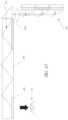
- the mirroring apparatus 406 a - bcan redirect the light from the optical elements 402 a - c along a common channel so as to superimpose the colored light from each optical element 402 a - c .
- the light from each optical element 402 a - ccan be varied, based on for example control via the circuitry of the carrier elements 404 a - c , so as to generate a superimposed light of various colors.
- the image data of the light from each optical element 402 a - ccan pass through an optical combiner apparatus 408 (e.g., a lens) to collect the light and transfer it to the user.
- an optical combiner apparatus 408e.g., a lens
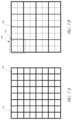
- FIGS. 7 A and 7 Bare diagrams showing different embodiments with different physical separations.
- FIG. 7 Ais a diagram showing an illustration of physical separation 702 between every pixel 704
- FIG. 7 Bis a diagram showing an illustration of physical separation 706 only in A ⁇ A matrix (for example, 2 ⁇ 2, 3 ⁇ 3, etc.) 708 of pixels 710 .
- the embodiment of FIG. 7 Bcan produce a high yield because one (1) malfunctioning pixel may not be a concern for, e.g., the light emitted, since the physical separation is between the A ⁇ A matrices 708 rather than individual pixels 710 .
- Such embodimentcan also enable improved control of, e.g., brightness of the light emitted.
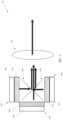
- an optical apparatus 1010(such as for example a prism) can be used to redirect the light transmitted from the optical assembly 1002 , so as to enable the light to travel through the waveguide 1006 .
- the optical assembly 1002can be mounted to another structure that is angled relative to the waveguide 1006 , and light can be redirected to the optical apparatus 1010 by way of mirrors and combiner optics as shown.
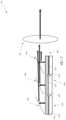
- the plurality of optical elements 1102 a - ccan emit, via a plurality of emitters (not shown) monochromatic light, which can travel through the corresponding optical combining element 1108 and connecting waveguide 1110 , to be reflected by the corresponding mirroring apparatus 1112 a - c .
- the plurality of optical elements 1102 a - ccan be disposed between the carrier element 1104 and the waveguide 1116 .
- the optical elements 1102 a - ccan be directly bonded to the carrier element 1104 without an intervening adhesive.
- the mirroring apparatus 1112 a - ccan be arranged at an angle relative to connecting waveguides 1110 , so as to direct the incoming lights through the optical combiner apparatus 1114 and the waveguide 1116 to the user's eye (not shown).
- the bonded optical devicecan include a third optical element optically coupled with the optical pathway and bonded to the at least one processor element.
- the third optical elementcan be configured to emit light of a third color that is different from the first and second colors.
- the first, second, and third colorscan comprise red, green, and blue, respectively.
- the optical emitters of the first arrayare independently controllable.
- the first and second arrays of optical emitterscan comprise respective arrays of light emitting diodes (LEDs).
- a pitch of the optical emitters of the first arraycan be less than 50 microns.
- a pitch of the optical emitters of the first arraycan be less than 10 microns.
- the at least one carriercomprises a first carrier and a second carrier separate from the first carrier.
- the at least one carriercomprises at least one processor element comprising active circuitry configured to control operation of at least one of the first and second optical elements.
- the first optical elementcan be directly bonded to the at least one carrier without an intervening adhesive
- the second optical elementcan be directly bonded to the at least one carrier without an intervening adhesive.
- respective dielectric bonding surfaces of the first optical element and the at least one carrierare directly bonded to one another without an intervening adhesive.
- respective conductive contact pads of the first optical element and the at least one carrierare directly bonded to one another without an intervening adhesive.
- the at least one carriercomprises at least one of silicon or glass.
- the at least one carriercan have a coefficient of thermal expansion (CTE) less than 7 ppm.
- a method of bonding at least one optical element with at least one processor elementcan include bonding a first optical element with to at least one processor element, wherein the first optical element comprises a first array of optical emitters configured to emit light of a first color, and the at least one processor element comprises active circuitry configured to control operation of the first optical element; bonding a second optical element with to the at least one processor element, wherein the second optical element comprises a second array of optical emitters configured to emit light of a second color different from the first color, and the at least one processor element comprises active circuitry further configured to control operation of the second optical element; and coupling the first and second optical elements with an optical pathway, the optical pathway configured to transmit a superposition of light from the first and second optical emitters to an optical output to be viewed by a user.
- the at least one carriercomprises a processor die.
Landscapes
- Physics & Mathematics (AREA)
- General Physics & Mathematics (AREA)
- Engineering & Computer Science (AREA)
- Optics & Photonics (AREA)
- Power Engineering (AREA)
- Microelectronics & Electronic Packaging (AREA)
- Condensed Matter Physics & Semiconductors (AREA)
- Computer Hardware Design (AREA)
- Led Device Packages (AREA)
- Devices For Indicating Variable Information By Combining Individual Elements (AREA)
Abstract
Description
Claims (32)
Priority Applications (9)
| Application Number | Priority Date | Filing Date | Title |
|---|---|---|---|
| US17/124,408US11762200B2 (en) | 2019-12-17 | 2020-12-16 | Bonded optical devices |
| JP2022537223AJP7676404B2 (en) | 2019-12-17 | 2020-12-17 | Bonded Optical Devices |
| EP20902963.6AEP4078675A4 (en) | 2019-12-17 | 2020-12-17 | RELATED OPTICAL DEVICES |
| PCT/US2020/065544WO2021127138A1 (en) | 2019-12-17 | 2020-12-17 | Bonded optical devices |
| KR1020227024563AKR20220116019A (en) | 2019-12-17 | 2020-12-17 | coupled optical device |
| CN202080095120.8ACN115039223A (en) | 2019-12-17 | 2020-12-17 | Bonding Optical Equipment |
| US18/360,193US12153222B2 (en) | 2019-12-17 | 2023-07-27 | Bonded optical devices |
| US18/819,354US20250044598A1 (en) | 2019-12-17 | 2024-08-29 | Bonded optical devices |
| JP2025075258AJP2025131568A (en) | 2019-12-17 | 2025-04-30 | Bonded Optical Devices |
Applications Claiming Priority (2)
| Application Number | Priority Date | Filing Date | Title |
|---|---|---|---|
| US201962949312P | 2019-12-17 | 2019-12-17 | |
| US17/124,408US11762200B2 (en) | 2019-12-17 | 2020-12-16 | Bonded optical devices |
Related Child Applications (1)
| Application Number | Title | Priority Date | Filing Date |
|---|---|---|---|
| US18/360,193ContinuationUS12153222B2 (en) | 2019-12-17 | 2023-07-27 | Bonded optical devices |
Publications (2)
| Publication Number | Publication Date |
|---|---|
| US20210181510A1 US20210181510A1 (en) | 2021-06-17 |
| US11762200B2true US11762200B2 (en) | 2023-09-19 |
Family
ID=76316975
Family Applications (3)
| Application Number | Title | Priority Date | Filing Date |
|---|---|---|---|
| US17/124,408Active2041-01-15US11762200B2 (en) | 2019-12-17 | 2020-12-16 | Bonded optical devices |
| US18/360,193ActiveUS12153222B2 (en) | 2019-12-17 | 2023-07-27 | Bonded optical devices |
| US18/819,354PendingUS20250044598A1 (en) | 2019-12-17 | 2024-08-29 | Bonded optical devices |
Family Applications After (2)
| Application Number | Title | Priority Date | Filing Date |
|---|---|---|---|
| US18/360,193ActiveUS12153222B2 (en) | 2019-12-17 | 2023-07-27 | Bonded optical devices |
| US18/819,354PendingUS20250044598A1 (en) | 2019-12-17 | 2024-08-29 | Bonded optical devices |
Country Status (6)
| Country | Link |
|---|---|
| US (3) | US11762200B2 (en) |
| EP (1) | EP4078675A4 (en) |
| JP (2) | JP7676404B2 (en) |
| KR (1) | KR20220116019A (en) |
| CN (1) | CN115039223A (en) |
| WO (1) | WO2021127138A1 (en) |
Cited By (9)
| Publication number | Priority date | Publication date | Assignee | Title |
|---|---|---|---|---|
| US11967575B2 (en) | 2018-08-29 | 2024-04-23 | Adeia Semiconductor Bonding Technologies Inc. | Bond enhancement structure in microelectronics for trapping contaminants during direct-bonding processes |
| US12051621B2 (en) | 2016-12-28 | 2024-07-30 | Adeia Semiconductor Bonding Technologies Inc. | Microelectronic assembly from processed substrate |
| US12068278B2 (en) | 2017-05-11 | 2024-08-20 | Adeia Semiconductor Bonding Technologies Inc. | Processed stacked dies |
| US12153222B2 (en) | 2019-12-17 | 2024-11-26 | Adeia Semiconductor Bonding Technologies Inc. | Bonded optical devices |
| US12166024B2 (en) | 2017-03-16 | 2024-12-10 | Adeia Semiconductor Technologies Llc | Direct-bonded LED arrays drivers |
| US12248869B2 (en) | 2017-08-03 | 2025-03-11 | Adeia Semiconductor Inc. | Three dimensional circuit implementing machine trained network |
| US12271032B2 (en) | 2018-02-26 | 2025-04-08 | Adeia Semiconductor Bonding Technologies Inc. | Integrated optical waveguides, direct-bonded waveguide interface joints, optical routing and interconnects |
| US12270970B2 (en) | 2018-03-20 | 2025-04-08 | Adeia Semiconductor Bonding Technologies Inc. | Direct-bonded lamination for improved image clarity in optical devices |
| US12406959B2 (en) | 2018-07-26 | 2025-09-02 | Adeia Semiconductor Bonding Technologies Inc. | Post CMP processing for hybrid bonding |
Families Citing this family (73)
| Publication number | Priority date | Publication date | Assignee | Title |
|---|---|---|---|---|
| US7109092B2 (en) | 2003-05-19 | 2006-09-19 | Ziptronix, Inc. | Method of room temperature covalent bonding |
| US7485968B2 (en) | 2005-08-11 | 2009-02-03 | Ziptronix, Inc. | 3D IC method and device |
| US8735219B2 (en) | 2012-08-30 | 2014-05-27 | Ziptronix, Inc. | Heterogeneous annealing method and device |
| US20150262902A1 (en) | 2014-03-12 | 2015-09-17 | Invensas Corporation | Integrated circuits protected by substrates with cavities, and methods of manufacture |
| US11069734B2 (en) | 2014-12-11 | 2021-07-20 | Invensas Corporation | Image sensor device |
| US10886250B2 (en) | 2015-07-10 | 2021-01-05 | Invensas Corporation | Structures and methods for low temperature bonding using nanoparticles |
| US9953941B2 (en) | 2015-08-25 | 2018-04-24 | Invensas Bonding Technologies, Inc. | Conductive barrier direct hybrid bonding |
| US10204893B2 (en) | 2016-05-19 | 2019-02-12 | Invensas Bonding Technologies, Inc. | Stacked dies and methods for forming bonded structures |
| US10672663B2 (en) | 2016-10-07 | 2020-06-02 | Xcelsis Corporation | 3D chip sharing power circuit |
| US10580735B2 (en) | 2016-10-07 | 2020-03-03 | Xcelsis Corporation | Stacked IC structure with system level wiring on multiple sides of the IC die |
| TWI822659B (en) | 2016-10-27 | 2023-11-21 | 美商艾德亞半導體科技有限責任公司 | Structures and methods for low temperature bonding |
| US10002844B1 (en) | 2016-12-21 | 2018-06-19 | Invensas Bonding Technologies, Inc. | Bonded structures |
| CN117878055A (en) | 2016-12-28 | 2024-04-12 | 艾德亚半导体接合科技有限公司 | Stacking substrate processing |
| TWI837879B (en) | 2016-12-29 | 2024-04-01 | 美商艾德亞半導體接合科技有限公司 | Bonded structures with integrated passive component |
| US10515913B2 (en) | 2017-03-17 | 2019-12-24 | Invensas Bonding Technologies, Inc. | Multi-metal contact structure |
| US10508030B2 (en) | 2017-03-21 | 2019-12-17 | Invensas Bonding Technologies, Inc. | Seal for microelectronic assembly |
| US10269756B2 (en) | 2017-04-21 | 2019-04-23 | Invensas Bonding Technologies, Inc. | Die processing |
| US10446441B2 (en) | 2017-06-05 | 2019-10-15 | Invensas Corporation | Flat metal features for microelectronics applications |
| US10217720B2 (en) | 2017-06-15 | 2019-02-26 | Invensas Corporation | Multi-chip modules formed using wafer-level processing of a reconstitute wafer |
| US10840205B2 (en) | 2017-09-24 | 2020-11-17 | Invensas Bonding Technologies, Inc. | Chemical mechanical polishing for hybrid bonding |
| US11031285B2 (en) | 2017-10-06 | 2021-06-08 | Invensas Bonding Technologies, Inc. | Diffusion barrier collar for interconnects |
| US10923408B2 (en) | 2017-12-22 | 2021-02-16 | Invensas Bonding Technologies, Inc. | Cavity packages |
| US11380597B2 (en) | 2017-12-22 | 2022-07-05 | Invensas Bonding Technologies, Inc. | Bonded structures |
| US10727219B2 (en) | 2018-02-15 | 2020-07-28 | Invensas Bonding Technologies, Inc. | Techniques for processing devices |
| US10991804B2 (en) | 2018-03-29 | 2021-04-27 | Xcelsis Corporation | Transistor level interconnection methodologies utilizing 3D interconnects |
| US11056348B2 (en) | 2018-04-05 | 2021-07-06 | Invensas Bonding Technologies, Inc. | Bonding surfaces for microelectronics |
| US11244916B2 (en) | 2018-04-11 | 2022-02-08 | Invensas Bonding Technologies, Inc. | Low temperature bonded structures |
| US10790262B2 (en) | 2018-04-11 | 2020-09-29 | Invensas Bonding Technologies, Inc. | Low temperature bonded structures |
| US10964664B2 (en) | 2018-04-20 | 2021-03-30 | Invensas Bonding Technologies, Inc. | DBI to Si bonding for simplified handle wafer |
| US11004757B2 (en) | 2018-05-14 | 2021-05-11 | Invensas Bonding Technologies, Inc. | Bonded structures |
| US11276676B2 (en) | 2018-05-15 | 2022-03-15 | Invensas Bonding Technologies, Inc. | Stacked devices and methods of fabrication |
| US10923413B2 (en) | 2018-05-30 | 2021-02-16 | Xcelsis Corporation | Hard IP blocks with physically bidirectional passageways |
| KR20210009426A (en) | 2018-06-13 | 2021-01-26 | 인벤사스 본딩 테크놀로지스 인코포레이티드 | TV as a pad |
| US11393779B2 (en) | 2018-06-13 | 2022-07-19 | Invensas Bonding Technologies, Inc. | Large metal pads over TSV |
| US10910344B2 (en) | 2018-06-22 | 2021-02-02 | Xcelsis Corporation | Systems and methods for releveled bump planes for chiplets |
| WO2020010056A1 (en) | 2018-07-03 | 2020-01-09 | Invensas Bonding Technologies, Inc. | Techniques for joining dissimilar materials in microelectronics |
| US11158606B2 (en) | 2018-07-06 | 2021-10-26 | Invensas Bonding Technologies, Inc. | Molded direct bonded and interconnected stack |
| US11462419B2 (en) | 2018-07-06 | 2022-10-04 | Invensas Bonding Technologies, Inc. | Microelectronic assemblies |
| US11515291B2 (en) | 2018-08-28 | 2022-11-29 | Adeia Semiconductor Inc. | Integrated voltage regulator and passive components |
| US11011494B2 (en) | 2018-08-31 | 2021-05-18 | Invensas Bonding Technologies, Inc. | Layer structures for making direct metal-to-metal bonds at low temperatures in microelectronics |
| US11158573B2 (en) | 2018-10-22 | 2021-10-26 | Invensas Bonding Technologies, Inc. | Interconnect structures |
| US11244920B2 (en) | 2018-12-18 | 2022-02-08 | Invensas Bonding Technologies, Inc. | Method and structures for low temperature device bonding |
| CN113330557A (en) | 2019-01-14 | 2021-08-31 | 伊文萨思粘合技术公司 | Bonding structure |
| US11387202B2 (en) | 2019-03-01 | 2022-07-12 | Invensas Llc | Nanowire bonding interconnect for fine-pitch microelectronics |
| US11901281B2 (en) | 2019-03-11 | 2024-02-13 | Adeia Semiconductor Bonding Technologies Inc. | Bonded structures with integrated passive component |
| US10854578B2 (en) | 2019-03-29 | 2020-12-01 | Invensas Corporation | Diffused bitline replacement in stacked wafer memory |
| US11373963B2 (en) | 2019-04-12 | 2022-06-28 | Invensas Bonding Technologies, Inc. | Protective elements for bonded structures |
| US11610846B2 (en) | 2019-04-12 | 2023-03-21 | Adeia Semiconductor Bonding Technologies Inc. | Protective elements for bonded structures including an obstructive element |
| US11205625B2 (en) | 2019-04-12 | 2021-12-21 | Invensas Bonding Technologies, Inc. | Wafer-level bonding of obstructive elements |
| US11355404B2 (en) | 2019-04-22 | 2022-06-07 | Invensas Bonding Technologies, Inc. | Mitigating surface damage of probe pads in preparation for direct bonding of a substrate |
| US11385278B2 (en) | 2019-05-23 | 2022-07-12 | Invensas Bonding Technologies, Inc. | Security circuitry for bonded structures |
| US12374641B2 (en) | 2019-06-12 | 2025-07-29 | Adeia Semiconductor Bonding Technologies Inc. | Sealed bonded structures and methods for forming the same |
| US11296053B2 (en) | 2019-06-26 | 2022-04-05 | Invensas Bonding Technologies, Inc. | Direct bonded stack structures for increased reliability and improved yield in microelectronics |
| US12080672B2 (en) | 2019-09-26 | 2024-09-03 | Adeia Semiconductor Bonding Technologies Inc. | Direct gang bonding methods including directly bonding first element to second element to form bonded structure without adhesive |
| US12113054B2 (en) | 2019-10-21 | 2024-10-08 | Adeia Semiconductor Technologies Llc | Non-volatile dynamic random access memory |
| US11862602B2 (en) | 2019-11-07 | 2024-01-02 | Adeia Semiconductor Technologies Llc | Scalable architecture for reduced cycles across SOC |
| US11876076B2 (en) | 2019-12-20 | 2024-01-16 | Adeia Semiconductor Technologies Llc | Apparatus for non-volatile random access memory stacks |
| CN115088068A (en) | 2019-12-23 | 2022-09-20 | 伊文萨思粘合技术公司 | Electrical redundancy for bonded structures |
| US11721653B2 (en) | 2019-12-23 | 2023-08-08 | Adeia Semiconductor Bonding Technologies Inc. | Circuitry for electrical redundancy in bonded structures |
| WO2021188846A1 (en) | 2020-03-19 | 2021-09-23 | Invensas Bonding Technologies, Inc. | Dimension compensation control for directly bonded structures |
| US11742314B2 (en) | 2020-03-31 | 2023-08-29 | Adeia Semiconductor Bonding Technologies Inc. | Reliable hybrid bonded apparatus |
| WO2021236361A1 (en) | 2020-05-19 | 2021-11-25 | Invensas Bonding Technologies, Inc. | Laterally unconfined structure |
| US11631647B2 (en) | 2020-06-30 | 2023-04-18 | Adeia Semiconductor Bonding Technologies Inc. | Integrated device packages with integrated device die and dummy element |
| US11728273B2 (en) | 2020-09-04 | 2023-08-15 | Adeia Semiconductor Bonding Technologies Inc. | Bonded structure with interconnect structure |
| US11764177B2 (en) | 2020-09-04 | 2023-09-19 | Adeia Semiconductor Bonding Technologies Inc. | Bonded structure with interconnect structure |
| US11264357B1 (en) | 2020-10-20 | 2022-03-01 | Invensas Corporation | Mixed exposure for large die |
| KR20230097121A (en) | 2020-10-29 | 2023-06-30 | 아데이아 세미컨덕터 본딩 테크놀로지스 인코포레이티드 | Direct bonding method and structure |
| JP2024501017A (en) | 2020-12-28 | 2024-01-10 | アデイア セミコンダクター ボンディング テクノロジーズ インコーポレイテッド | Structure with through-substrate via and method for forming the same |
| JP2024501559A (en) | 2020-12-30 | 2024-01-12 | アデイア セミコンダクター ボンディング テクノロジーズ インコーポレイテッド | Structures with conductive features and methods of forming the same |
| CN113325588A (en)* | 2021-06-21 | 2021-08-31 | 凤凰光学股份有限公司 | High-brightness high-resolution high-contrast augmented reality display equipment |
| KR20240036698A (en) | 2021-08-02 | 2024-03-20 | 아데이아 세미컨덕터 본딩 테크놀로지스 인코포레이티드 | Protective semiconductor elements for combined structures |
| US20240063152A1 (en)* | 2022-08-22 | 2024-02-22 | Micron Technology, Inc. | Hybrid bonding for semiconductor device assemblies |
| US12341083B2 (en) | 2023-02-08 | 2025-06-24 | Adeia Semiconductor Bonding Technologies Inc. | Electronic device cooling structures bonded to semiconductor elements |
Citations (362)
| Publication number | Priority date | Publication date | Assignee | Title |
|---|---|---|---|---|
| JPS60257413A (en) | 1984-06-04 | 1985-12-19 | Matsushita Electric Ind Co Ltd | Photoelectric composite device |
| US4998665A (en) | 1988-09-07 | 1991-03-12 | Nec Corporation | Bonding structure of substrates and method for bonding substrates |
| US5015052A (en) | 1989-07-20 | 1991-05-14 | Battelle Memorial Institute | Optical modulation at millimeter-wave frequencies |
| US5087585A (en) | 1989-07-11 | 1992-02-11 | Nec Corporation | Method of stacking semiconductor substrates for fabrication of three-dimensional integrated circuit |
| US5225797A (en) | 1992-04-27 | 1993-07-06 | Cornell Research Foundation, Inc. | Dielectric waveguide-to-coplanar transmission line transitions |
| US5322593A (en) | 1991-11-21 | 1994-06-21 | Nec Corporation | Method for manufacturing polyimide multilayer wiring substrate |
| US5363464A (en) | 1993-06-28 | 1994-11-08 | Tangible Domain Inc. | Dielectric/conductive waveguide |
| US5408053A (en) | 1993-11-30 | 1995-04-18 | Hughes Aircraft Company | Layered planar transmission lines |
| US5471090A (en) | 1993-03-08 | 1995-11-28 | International Business Machines Corporation | Electronic structures having a joining geometry providing reduced capacitive loading |
| US5753536A (en) | 1994-08-29 | 1998-05-19 | Matsushita Electric Industrial Co., Ltd. | Semiconductor device and associated fabrication method |
| US5771555A (en) | 1993-11-01 | 1998-06-30 | Matsushita Electric Industrial Co., Ltd. | Method for producing an electronic component using direct bonding |
| JPH10189671A (en) | 1996-12-24 | 1998-07-21 | Sony Corp | Probing pad structure of semiconductor wafer |
| US5785874A (en) | 1992-11-16 | 1998-07-28 | Matsushita Electric Industrial Co., Ltd. | Optical waveguide device bonded through direct bonding and a method for fabricating the same |
| US5818631A (en) | 1994-11-16 | 1998-10-06 | Raytheon Company | Electrically conducting, directly bonded infrared windows |
| US5985739A (en) | 1994-09-19 | 1999-11-16 | Fraunhofer-Gesellschaft Zur Forderung Der Angewandten Forschung E.V. | Semiconductor structures having advantageous high-frequency characteristics and processes for producing such semiconductor structures |
| US5998808A (en) | 1997-06-27 | 1999-12-07 | Sony Corporation | Three-dimensional integrated circuit device and its manufacturing method |
| US6008126A (en) | 1992-04-08 | 1999-12-28 | Elm Technology Corporation | Membrane dielectric isolation IC fabrication |
| JP2000100679A (en) | 1998-09-22 | 2000-04-07 | Canon Inc | Micro-region solid-state bonding method between substrates by thinning and device structure |
| US6080640A (en) | 1997-07-11 | 2000-06-27 | Advanced Micro Devices, Inc. | Metal attachment method and structure for attaching substrates at low temperatures |
| US6084714A (en) | 1998-02-16 | 2000-07-04 | Seiko Epson Corporation | Polarizing illumination device and projection display device |
| US6108472A (en) | 1997-02-07 | 2000-08-22 | Bookham Technology Plc. | Device for re-directing light from optical waveguide |
| US6115264A (en) | 1997-12-19 | 2000-09-05 | Murata Manufacturing Co., Ltd. | Multilayer high frequency electronic parts |
| JP2001102479A (en) | 1999-09-27 | 2001-04-13 | Toshiba Corp | Semiconductor integrated circuit device and method of manufacturing the same |
| US6265775B1 (en) | 1997-01-24 | 2001-07-24 | Micron Technology, Inc. | Flip chip technique for chip assembly |
| US6300161B1 (en) | 2000-02-15 | 2001-10-09 | Alpine Microsystems, Inc. | Module and method for interconnecting integrated circuits that facilitates high speed signal propagation with reduced noise |
| US20020000328A1 (en) | 2000-06-22 | 2002-01-03 | Kabushiki Kaisha Toshiba | Printed wiring board and manufacturing method thereof |
| US20020003307A1 (en) | 2000-07-05 | 2002-01-10 | Tadatomo Suga | Semiconductor device and method for fabricating the device |
| US20020025101A1 (en) | 2000-06-30 | 2002-02-28 | Motorola, Inc. | Integrated circuits with optical interconnect |
| US6374770B1 (en) | 1995-10-26 | 2002-04-23 | Applied Materials, Inc. | Apparatus for improving film stability of halogen-doped silicon oxide films |
| US6404550B1 (en) | 1996-07-25 | 2002-06-11 | Seiko Epson Corporation | Optical element suitable for projection display apparatus |
| US6418029B1 (en) | 2000-02-28 | 2002-07-09 | Mckee James S. | Interconnect system having vertically mounted passive components on an underside of a substrate |
| US6423640B1 (en) | 2000-08-09 | 2002-07-23 | Taiwan Semiconductor Manufacturing Co., Ltd. | Headless CMP process for oxide planarization |
| US6429532B1 (en) | 2000-05-09 | 2002-08-06 | United Microelectronics Corp. | Pad design |
| US6442321B1 (en) | 1999-12-23 | 2002-08-27 | Spectalis Corp. | Optical waveguide structures |
| US20020131715A1 (en) | 2001-03-16 | 2002-09-19 | Bookham Technology Plc | Optical coupling |
| WO2002075387A2 (en) | 2001-03-16 | 2002-09-26 | Bookham Technology Plc | A tapered optical waveguide |
| US6465892B1 (en) | 1999-04-13 | 2002-10-15 | Oki Electric Industry Co., Ltd. | Interconnect structure for stacked semiconductor device |
| JP2002353416A (en) | 2001-05-25 | 2002-12-06 | Sony Corp | Semiconductor storage device and method of manufacturing the same |
| JP2003043281A (en) | 2001-07-26 | 2003-02-13 | Kyocera Chemical Corp | Optical wave guide circuit and method for manufacturing the same |
| US20030081906A1 (en) | 2001-10-26 | 2003-05-01 | Filhaber John F. | Direct bonding of optical components |
| US6614960B2 (en) | 1999-12-23 | 2003-09-02 | Speotalis Corp. | Optical waveguide structures |
| US20030168716A1 (en) | 2002-03-05 | 2003-09-11 | Lee Moon-Chul | Device having inductors and capacitors and a fabrication method thereof |
| US6638808B1 (en) | 2002-02-04 | 2003-10-28 | Ixys Corporation | Method of manufacturing gate driver with level shift circuit |
| US20040022691A1 (en) | 2001-08-15 | 2004-02-05 | Allen Susan D. | Method of manufacturing and design of microreactors, including microanalytical and separation devices |
| US6713871B2 (en) | 2002-05-21 | 2004-03-30 | Intel Corporation | Surface mount solder method and apparatus for decoupling capacitance and process of making |
| US20040071424A1 (en) | 2001-09-19 | 2004-04-15 | Masahiro Hiraka | Optical waveguide and method for fabricating the same |
| US20040084414A1 (en) | 2002-08-19 | 2004-05-06 | Kenji Sakai | Polishing method and polishing composition used for polishing |
| US6759692B1 (en) | 2002-02-04 | 2004-07-06 | Ixys Corporation | Gate driver with level shift circuit |
| US20040149991A1 (en) | 2003-02-05 | 2004-08-05 | Won Seok-Jun | Flat-type capacitor for integrated circuit and method of manufacturing the same |
| US20040157407A1 (en) | 2003-02-07 | 2004-08-12 | Ziptronix | Room temperature metal direct bonding |
| US20040155692A1 (en) | 2002-02-04 | 2004-08-12 | Ixys Corporation | Power device with bi-directional level shift circuit |
| US6782179B2 (en) | 2000-07-21 | 2004-08-24 | Micro Managed Photons A/S | Surface plasmon polariton band gap structures |
| US6801691B2 (en) | 1999-12-23 | 2004-10-05 | Spectalis Corp. | Optical waveguide structures |
| US20040207043A1 (en) | 2002-07-26 | 2004-10-21 | Takeshi Matsunaga | Semiconductor device having capacitor formed in multilayer wiring structure |
| US6868258B2 (en) | 2000-04-26 | 2005-03-15 | Kyocera Corporation | Structure for connecting non-radiative dielectric waveguide and metal waveguide, millimeter wave transmitting/receiving module and millimeter wave transmitter/receiver |
| US20050063134A1 (en) | 2003-09-23 | 2005-03-24 | Daehwan Kim | On-chip bypass capacitor and method of manufacturing the same |
| US6887769B2 (en) | 2002-02-06 | 2005-05-03 | Intel Corporation | Dielectric recess for wafer-to-wafer and die-to-die metal bonding and method of fabricating the same |
| WO2005043584A2 (en) | 2003-10-21 | 2005-05-12 | Ziptronix, Inc. | Single mask via method and device |
| US6908832B2 (en) | 1997-08-29 | 2005-06-21 | Silicon Genesis Corporation | In situ plasma wafer bonding method |
| US6908027B2 (en) | 2003-03-31 | 2005-06-21 | Intel Corporation | Complete device layer transfer without edge exclusion via direct wafer bonding and constrained bond-strengthening process |
| US20050135041A1 (en) | 2003-12-22 | 2005-06-23 | Jung Kang | Integrating passive components on spacer in stacked dies |
| WO2005064646A2 (en) | 2003-12-23 | 2005-07-14 | Intel Corporation | An integrated circuit package substrate having a thin film capacitor structure |
| US6936854B2 (en) | 2001-05-10 | 2005-08-30 | Canon Kabushiki Kaisha | Optoelectronic substrate |
| US20050190808A1 (en) | 2004-02-26 | 2005-09-01 | Shinko Electric Industries Co., Ltd. | Optoelectric composite substrate and method of manufacturing the same |
| US20050226299A1 (en) | 2003-09-22 | 2005-10-13 | National Chung-Hsing University | Vertical-cavity surface emitting laser diode |
| US20050231303A1 (en) | 2004-04-16 | 2005-10-20 | Chao-Liang Chang | Tunable passive device |
| US20060012966A1 (en) | 2000-07-31 | 2006-01-19 | Intel Corporation | Electronic assemblies and systems comprising interposer with embedded capacitors |
| US20060017144A1 (en) | 2004-07-21 | 2006-01-26 | Yutaka Uematsu | Semiconductor device |
| US7010183B2 (en) | 2002-03-20 | 2006-03-07 | The Regents Of The University Of Colorado | Surface plasmon devices |
| US20060057945A1 (en) | 2004-09-16 | 2006-03-16 | Chia-Lin Hsu | Chemical mechanical polishing process |
| EP1441410B1 (en) | 1997-01-14 | 2006-04-05 | Sharp Kabushiki Kaisha | Waveguide input apparatus of two orthogonally polarized waves including two probes attached to a common board |
| US7045453B2 (en) | 2002-10-24 | 2006-05-16 | International Business Machines Corporation | Very low effective dielectric constant interconnect structures and methods for fabricating the same |
| US20060145778A1 (en) | 2004-12-30 | 2006-07-06 | Pleva Joseph S | Waveguide - printed wiring board (PWB) interconnection |
| US7105980B2 (en) | 2002-07-03 | 2006-09-12 | Sawtek, Inc. | Saw filter device and method employing normal temperature bonding for producing desirable filter production and performance characteristics |
| WO2006100444A1 (en) | 2005-03-22 | 2006-09-28 | Cambridge Display Technology Limited | Apparatus and method for increased device lifetime in an organic electro-luminescent device. |
| JP2006276313A (en) | 2005-03-29 | 2006-10-12 | Kyocera Kinseki Corp | Manufacturing method of optical filter |
| US7126212B2 (en) | 1999-10-01 | 2006-10-24 | Ziptronix, Inc. | Three dimensional device integration method and integrated device |
| JP2007041117A (en) | 2005-08-01 | 2007-02-15 | Nippon Dempa Kogyo Co Ltd | Laminated optical element and manufacturing method thereof |
| US20070045814A1 (en) | 2005-09-01 | 2007-03-01 | Hiroshi Yamamoto | Wiring board and ceramic chip to be embedded |
| US7193423B1 (en) | 2005-12-12 | 2007-03-20 | International Business Machines Corporation | Wafer-to-wafer alignments |
| US20070085165A1 (en) | 2005-10-19 | 2007-04-19 | Samsung Electronics Co., Ltd. | Capacitor, semiconductor device including the capacitor and methods of fabricating the same |
| US20070096294A1 (en) | 2003-06-06 | 2007-05-03 | Sanyo Electric Co., Ltd. | Semiconductor device and manufacturing method of the same |
| US20070096130A1 (en) | 2005-06-09 | 2007-05-03 | Philips Lumileds Lighting Company, Llc | LED Assembly Having Maximum Metal Support for Laser Lift-Off of Growth Substrate |
| US20070111386A1 (en) | 2002-02-20 | 2007-05-17 | Kim Sarah E | Process of vertically stacking multiple wafers supporting different active integrated circuit (IC) devices |
| US20070147014A1 (en) | 2005-12-22 | 2007-06-28 | Phoenix Precision Technology Corporation | Circuit Board Structure Having Capacitor Array and Embedded Electronic Component and Method for Fabricating the Same |
| US20070222048A1 (en) | 2006-03-24 | 2007-09-27 | Advanced Semiconductor Engineering, Inc. | Package structure |
| US20070295456A1 (en) | 2006-03-28 | 2007-12-27 | Innovative Micro Technology | Wafer bonding material with embedded conductive particles |
| US7354798B2 (en) | 2002-12-20 | 2008-04-08 | International Business Machines Corporation | Three-dimensional device fabrication method |
| US7355836B2 (en) | 2005-06-07 | 2008-04-08 | Intel Corporation | Array capacitor for decoupling multiple voltage rails |
| US20080124835A1 (en) | 2006-11-03 | 2008-05-29 | International Business Machines Corporation | Hermetic seal and reliable bonding structures for 3d applications |
| US20080150821A1 (en) | 2006-12-22 | 2008-06-26 | Sony Deutschland Gmbh | Flexible substrate integrated waveguides |
| JP2008258258A (en) | 2007-04-02 | 2008-10-23 | Sanyo Electric Co Ltd | Semiconductor device |
| US20090009103A1 (en) | 2007-07-05 | 2009-01-08 | Tyco Electronics Corporation | Wireless controlled light emitting assembly |
| US20090052827A1 (en) | 2006-10-09 | 2009-02-26 | Colorado School Of Mines | Silicon-Compatible Surface Plasmon Optical Elements |
| US20090206962A1 (en) | 2008-02-15 | 2009-08-20 | Realtek Semiconductor Corp. | Integrated front-end passive equalizer and method thereof |
| US20090242252A1 (en) | 2008-03-27 | 2009-10-01 | Ibiden Co., Ltd. | Method for Manufacturing A Multilayer Printed Wiring Board for Providing an Electronic Component Therein |
| US7626216B2 (en) | 2005-10-21 | 2009-12-01 | Mckinzie Iii William E | Systems and methods for electromagnetic noise suppression using hybrid electromagnetic bandgap structures |
| US7705691B2 (en) | 2005-10-18 | 2010-04-27 | Agency For Science, Technology & Research | Capacitor interconnection |
| US7746663B2 (en) | 2005-07-06 | 2010-06-29 | Seiko Epson Corporation | Electronic substrate and electronic device |
| US7750488B2 (en) | 2006-07-10 | 2010-07-06 | Tezzaron Semiconductor, Inc. | Method for bonding wafers to produce stacked integrated circuits |
| US7791429B2 (en) | 2008-05-09 | 2010-09-07 | Hon Hai Precision Industry Co., Ltd. | Equalizer and connector including the same |
| US7803693B2 (en) | 2007-02-15 | 2010-09-28 | John Trezza | Bowed wafer hybridization compensation |
| JP2010276940A (en) | 2009-05-29 | 2010-12-09 | Fujifilm Corp | Glass substrate bonding method and glass bonded body |
| US20100317132A1 (en) | 2009-05-12 | 2010-12-16 | Rogers John A | Printed Assemblies of Ultrathin, Microscale Inorganic Light Emitting Diodes for Deformable and Semitransparent Displays |
| US20110018657A1 (en) | 2008-03-18 | 2011-01-27 | Shi Cheng | Substrate Integrated Waveguide |
| US20110024918A1 (en) | 2007-09-21 | 2011-02-03 | Infineon Technologies Ag | Stacked semiconductor chips |
| US20110059275A1 (en) | 2002-03-22 | 2011-03-10 | Electronics Packaging Solutions, Inc. | Insulated glazing units |
| US20110115579A1 (en) | 2007-05-01 | 2011-05-19 | Broadcom Corporation | High frequency signal combining |
| US20110113828A1 (en) | 2008-04-25 | 2011-05-19 | Hamamatsu Photonics K.K. | Process for fusing glass |
| US8009763B2 (en) | 2008-04-02 | 2011-08-30 | Oracle America, Inc. | Method and apparatus for equalizing a high speed serial data link |
| US20110294242A1 (en) | 2009-07-20 | 2011-12-01 | Enerlighting Corp. | Flip-chip gan led fabrication method |
| US20110290552A1 (en) | 2004-09-27 | 2011-12-01 | Qualcomm Mems Technologies, Inc. | Method and system for packaging mems devices with incorporated getter |
| US20120013499A1 (en) | 2009-03-31 | 2012-01-19 | Kyocera Corporation | Circuit Board, High Frequency Module, and Radar Apparatus |
| US8130821B2 (en) | 2006-05-18 | 2012-03-06 | Oracle America, Inc. | Equalization in capacitively coupled communication links |
| US8153505B2 (en) | 2000-02-16 | 2012-04-10 | Ziptronix, Inc. | Method for low temperature bonding and bonded structure |
| US20120100318A1 (en) | 2010-10-26 | 2012-04-26 | Medtronic, Inc. | Laser assisted direct bonding |
| US20120147516A1 (en) | 2010-12-08 | 2012-06-14 | Samsung Electro-Mechanics Co., Ltd. | Multilayer ceramic condenser and method for manufacturing the same |
| US20120168217A1 (en) | 2010-12-29 | 2012-07-05 | Industrial Technology Research Institute | Embedded capacitor substrate module |
| US20120189317A1 (en) | 2011-01-20 | 2012-07-26 | John Heck | Hybrid iii-v silicon laser formed by direct bonding |
| US8241961B2 (en) | 2008-12-09 | 2012-08-14 | Young Hae KIM | Method for manufacturing hetero-bonded wafer |
| US20120212384A1 (en) | 2011-02-17 | 2012-08-23 | International Business Machines Corporation | Integrated antenna for rfic package applications |
| WO2012125237A2 (en) | 2011-03-15 | 2012-09-20 | Rambus Inc. | Area and power efficient clock generation |
| US8300312B2 (en) | 2008-12-01 | 2012-10-30 | Seiko Epson Corporation | Optical element |
| US8314007B2 (en) | 2009-12-23 | 2012-11-20 | Soitec | Process for fabricating a heterostructure with minimized stress |
| US8349635B1 (en) | 2008-05-20 | 2013-01-08 | Silicon Laboratories Inc. | Encapsulated MEMS device and method to form the same |
| US20130009325A1 (en) | 2010-03-18 | 2013-01-10 | Nec Corporation | Semiconductor element-embedded substrate, and method of manufacturing the substrate |
| US20130009183A1 (en) | 2011-07-08 | 2013-01-10 | Han Chang | Reflective circuit board for led backlight |
| US8357931B2 (en) | 2004-02-27 | 2013-01-22 | Nvidia Corporation | Flip chip semiconductor die internal signal access system and method |
| JP2013033786A (en) | 2011-08-01 | 2013-02-14 | Sony Corp | Semiconductor device and semiconductor device manufacturing method |
| US8377798B2 (en) | 2010-11-10 | 2013-02-19 | Taiwan Semiconductor Manufacturing Co., Ltd | Method and structure for wafer to wafer bonding in semiconductor packaging |
| US20130063863A1 (en) | 2011-07-08 | 2013-03-14 | John P. Timler | Insulator Based Upon One or More Dielectric Structures |
| US20130072011A1 (en) | 2009-12-31 | 2013-03-21 | IBM Semiconductor Research and Development Center (SRDC) | Method of repairing probe pads |
| US20130105943A1 (en) | 2011-11-01 | 2013-05-02 | Unimicron Technology Corporation | Packaging substrate having embedded capacitors and fabrication method thereof |
| US8436457B2 (en) | 2011-10-03 | 2013-05-07 | Invensas Corporation | Stub minimization for multi-die wirebond assemblies with parallel windows |
| US8441111B2 (en) | 2011-10-03 | 2013-05-14 | Invensas Corporation | Stub minimization for multi-die wirebond assemblies with parallel windows |
| US8441131B2 (en) | 2011-09-12 | 2013-05-14 | Globalfoundries Inc. | Strain-compensating fill patterns for controlling semiconductor chip package interactions |
| US20130122617A1 (en) | 2008-05-22 | 2013-05-16 | Connector Optics Llc | Method of fabricating optoelectronic devices directly attached to silicon-based integrated circuits |
| US8476146B2 (en) | 2010-12-03 | 2013-07-02 | Taiwan Semiconductor Manufacturing Company, Ltd. | Reducing wafer distortion through a low CTE layer |
| US8476165B2 (en) | 2009-04-01 | 2013-07-02 | Tokyo Electron Limited | Method for thinning a bonding wafer |
| US20130170145A1 (en) | 2012-01-02 | 2013-07-04 | Tem Products Inc. | Thermal connector |
| US8483253B2 (en) | 2009-08-20 | 2013-07-09 | International Business Machines Corporation | 3D optoelectronic packaging |
| US8482132B2 (en) | 2009-10-08 | 2013-07-09 | International Business Machines Corporation | Pad bonding employing a self-aligned plated liner for adhesion enhancement |
| US8501537B2 (en) | 2011-03-31 | 2013-08-06 | Soitec | Methods for bonding semiconductor structures involving annealing processes, and bonded semiconductor structures formed using such methods |
| US20130207234A1 (en) | 2011-12-19 | 2013-08-15 | Hitachi, Ltd. | Semiconductor apparatus, signal transmission system and signal transmission method |
| US20130250430A1 (en) | 2012-03-21 | 2013-09-26 | Steve Robbins | Increasing field of view of reflective waveguide |
| US20130265733A1 (en) | 2012-04-04 | 2013-10-10 | Texas Instruments Incorporated | Interchip communication using an embedded dielectric waveguide |
| US8558636B2 (en) | 2007-03-30 | 2013-10-15 | Intel Corporation | Package embedded equalizer |
| US20130286544A1 (en) | 2011-01-13 | 2013-10-31 | Philippe Azais | Assembly intended for storing electrical energy and having a stacked element |
| US20140001568A1 (en) | 2012-06-29 | 2014-01-02 | Qualcomm Incorporated | Integrated circuit device featuring an antifuse and method of making same |
| US8647987B2 (en) | 2012-04-16 | 2014-02-11 | The Institute of Microelectronics, Chinese Academy of Science | Method for improving uniformity of chemical-mechanical planarization process |
| US20140048908A1 (en) | 2012-08-15 | 2014-02-20 | Industrial Technology Research Institute | Semiconductor substrate assembly |
| US20140071519A1 (en) | 2011-05-03 | 2014-03-13 | Chuangtian Chen | Optical coupling device having kbbf group crystal coupled with prisms and method for manufacturing same |
| US8698323B2 (en) | 2012-06-18 | 2014-04-15 | Invensas Corporation | Microelectronic assembly tolerant to misplacement of microelectronic elements therein |
| US8697493B2 (en) | 2011-07-18 | 2014-04-15 | Soitec | Bonding surfaces for direct bonding of semiconductor structures |
| US20140116761A1 (en) | 2012-10-31 | 2014-05-01 | Samsung Electronics Co., Ltd. | Multilayer ceramic capacitor and printed circuit board including the same |
| US8716105B2 (en) | 2011-03-31 | 2014-05-06 | Soitec | Methods for bonding semiconductor structures involving annealing processes, and bonded semiconductor structures and intermediate structures formed using such methods |
| US20140145338A1 (en) | 2011-05-24 | 2014-05-29 | Sony Corporation | Semiconductor device |
| US20140177189A1 (en) | 2012-12-25 | 2014-06-26 | Industrial Technology Research Institute | Chip stacking structure |
| US20140175655A1 (en) | 2012-12-22 | 2014-06-26 | Industrial Technology Research Institute | Chip bonding structure and manufacturing method thereof |
| US20140175629A1 (en) | 2011-03-03 | 2014-06-26 | Skyworks Solutions, Inc. | Apparatus and methods for reducing impact of high rf loss plating |
| US20140184351A1 (en) | 2012-12-27 | 2014-07-03 | Korea Advanced Institute Of Science And Technology | Low Power, High Speed Multi-Channel Chip-to-Chip Interface using Dielectric Waveguide |
| US8802538B1 (en) | 2013-03-15 | 2014-08-12 | Taiwan Semiconductor Manufacturing Company, Ltd. | Methods for hybrid wafer bonding |
| US20140225795A1 (en) | 2013-02-08 | 2014-08-14 | Sj Antenna Design | Shielding module integrating antenna and integrated circuit component |
| US8809123B2 (en) | 2012-06-05 | 2014-08-19 | Taiwan Semiconductor Manufacturing Company, Ltd. | Three dimensional integrated circuit structures and hybrid bonding methods for semiconductor wafers |
| US20140252635A1 (en) | 2013-03-08 | 2014-09-11 | Taiwan Semiconductor Manufacturing Company, Ltd. | Bonding Structures and Methods of Forming the Same |
| US20140264948A1 (en) | 2013-03-15 | 2014-09-18 | Taiwan Semiconductor Manufacturing Company, Ltd. | Air Trench in Packages Incorporating Hybrid Bonding |
| US20140264751A1 (en) | 2013-03-12 | 2014-09-18 | Qualcomm Incorporated | Metal-insulator-metal (mim) capacitor |
| US8841002B2 (en) | 2003-05-19 | 2014-09-23 | Ziptronix, Inc. | Method of room temperature covalent bonding |
| US20140294342A1 (en) | 2013-03-28 | 2014-10-02 | International Business Machines Corporation | Optoelectronic packaging assembly |
| US8916448B2 (en) | 2013-01-09 | 2014-12-23 | International Business Machines Corporation | Metal to metal bonding for stacked (3D) integrated circuits |
| US20140377946A1 (en) | 2012-08-17 | 2014-12-25 | Taiwan Semiconductor Manufacturing Company, Ltd. | Bonded Structures for Package and Substrate |
| US20150021626A1 (en) | 2012-04-27 | 2015-01-22 | Panasonic Corporation | Light-emitting device |
| US20150097298A1 (en) | 2012-08-15 | 2015-04-09 | Industrial Technology Research Institute | Semiconductor substrate assembly |
| US20150194379A1 (en) | 2014-01-06 | 2015-07-09 | Taiwan Semiconductor Manufacturing Company, Ltd. | Protrusion Bump Pads for Bond-on-Trace Processing |
| US20150206902A1 (en) | 2014-01-17 | 2015-07-23 | Taiwan Semiconductor Manufacturing Co., Ltd. | Semiconductor device and method for forming the same |
| US9093350B2 (en) | 2010-07-09 | 2015-07-28 | Canon Kabushiki Kaisha | Member for solid-state image pickup device and method for manufacturing solid-state image pickup device having first and second wiring structures with a concave portion between first and second substrates |
| US20150221571A1 (en) | 2014-01-31 | 2015-08-06 | Corning Incorporated | Methods and apparatus for providing an interposer for interconnecting semiconductor chips |
| US20150235952A1 (en) | 2010-06-29 | 2015-08-20 | Qualcomm Incorporated | Integrated voltage regulator with embedded passive device(s) for a stacked ic |
| KR20150097798A (en) | 2012-12-21 | 2015-08-26 | 테사 소시에타스 유로파에아 | Adhesive tape containing getter material |
| US9142517B2 (en) | 2012-06-05 | 2015-09-22 | Taiwan Semiconductor Manufacturing Company, Ltd. | Hybrid bonding mechanisms for semiconductor wafers |
| US20150270209A1 (en) | 2014-03-20 | 2015-09-24 | Invensas Corporation | Stacked die integrated circuit |
| US9171756B2 (en) | 2005-08-11 | 2015-10-27 | Ziptronix, Inc. | 3D IC method and device |
| US9179584B2 (en) | 2012-07-25 | 2015-11-03 | International Business Machines Corporation | Method of assembling an electro-optical device |
| US20150318618A1 (en) | 2014-05-02 | 2015-11-05 | Searete Llc | Surface scattering antennas with lumped elements |
| US9184125B2 (en) | 2012-08-30 | 2015-11-10 | Ziptronix, Inc. | Heterogeneous annealing method and device |
| US20150328875A1 (en) | 2013-02-19 | 2015-11-19 | Ngk Insulators, Ltd. | Composite Substrate, Elastic Wave Device, and Method for Producing Elastic Wave Device |
| US9224704B2 (en) | 2010-10-14 | 2015-12-29 | Soitec | Process for realizing a connecting structure |
| US9230941B2 (en) | 2014-03-28 | 2016-01-05 | Taiwan Semiconductor Manufacturing Company, Ltd. | Bonding structure for stacked semiconductor devices |
| US20160027765A1 (en) | 2013-03-15 | 2016-01-28 | Osram Opto Semiconductors Gmbh | Display Device |
| US9257399B2 (en) | 2013-10-17 | 2016-02-09 | Taiwan Semiconductor Manufacturing Company, Ltd. | 3D integrated circuit and methods of forming the same |
| US9263186B2 (en) | 2013-03-05 | 2016-02-16 | Qualcomm Incorporated | DC/ AC dual function Power Delivery Network (PDN) decoupling capacitor |
| US20160077294A1 (en) | 2014-09-11 | 2016-03-17 | Taiwan Semiconductor Manufacturing Co., Ltd. | Silicon interface for dielectric slab waveguide |
| US9299736B2 (en) | 2014-03-28 | 2016-03-29 | Taiwan Semiconductor Manufacturing Company, Ltd. | Hybrid bonding with uniform pattern density |
| WO2016057259A1 (en) | 2014-10-06 | 2016-04-14 | Microsoft Technology Licensing, Llc | Microdisplay optical system having two microlens arrays |
| US20160111404A1 (en) | 2008-11-25 | 2016-04-21 | Invensas Corporation | Methods of forming 3-d circuits with integrated passive devices |
| US9337235B2 (en) | 2013-02-18 | 2016-05-10 | Taiwan Semiconductor Manufacturing Company, Ltd. | Method and apparatus for image sensor packaging |
| US20160141469A1 (en) | 2014-11-18 | 2016-05-19 | Commissariat â l'Energie Atomique et aux Energies Alternatives | Optoelectronic device with light-emitting diodes |
| US20160155677A1 (en) | 2014-12-02 | 2016-06-02 | Infineon Technologies Ag | Semiconductor device and method of manufacturing a semiconductor device |
| US20160181477A1 (en) | 2014-08-27 | 2016-06-23 | Seoul Viosys Co., Ltd. | Light emitting diode and method of fabricating the same |
| US20160197630A1 (en) | 2008-09-25 | 2016-07-07 | Sony Corporation | Millimeter wave transmission device, millimeter wave transmission method, and millimeter wave transmission system |
| US9394161B2 (en) | 2014-11-14 | 2016-07-19 | Taiwan Semiconductor Manufacturing Co., Ltd. | MEMS and CMOS integration with low-temperature bonding |
| US20160233195A1 (en) | 2015-02-05 | 2016-08-11 | Fujitsu Limited | Stacked semiconductor device |
| US20160254345A1 (en) | 2015-02-27 | 2016-09-01 | Globalfoundries Inc. | Metal-insulator-metal capacitor architecture |
| US9437572B2 (en) | 2013-12-18 | 2016-09-06 | Taiwan Semiconductor Manufacturing Company, Ltd. | Conductive pad structure for hybrid bonding and methods of forming same |
| US9434145B2 (en) | 2012-12-07 | 2016-09-06 | Semrock, Inc. | Dichroic filter conformed to optical surface |
| US9461007B2 (en) | 2014-07-11 | 2016-10-04 | Samsung Electronics Co., Ltd. | Wafer-to-wafer bonding structure |
| US20160291265A1 (en) | 2015-04-01 | 2016-10-06 | Coriant Advanced Technology, LLC | Optically Aligned Hybrid Semiconductor Device and Method |
| US20160309578A1 (en) | 2015-04-20 | 2016-10-20 | Samsung Electro-Mechanics Co., Ltd. | Coil electronic component and method of manufacturing the same |
| US9496239B1 (en) | 2015-12-11 | 2016-11-15 | International Business Machines Corporation | Nitride-enriched oxide-to-oxide 3D wafer bonding |
| US20160343682A1 (en) | 2013-12-11 | 2016-11-24 | Kabushiki Kaisha Toshiba | Semiconductor device |
| CN106206872A (en) | 2016-08-04 | 2016-12-07 | 南京大学 | GaN base visible ray micron post array LED device that Si CMOS array drive circuit controls and preparation method thereof |
| US20160372449A1 (en) | 2014-12-24 | 2016-12-22 | Intel Corporation | Integrated passive components in a stacked integrated circuit package |
| US9536848B2 (en) | 2014-10-16 | 2017-01-03 | Globalfoundries Inc. | Bond pad structure for low temperature flip chip bonding |
| US9537199B2 (en) | 2015-03-19 | 2017-01-03 | International Business Machines Corporation | Package structure having an integrated waveguide configured to communicate between first and second integrated circuit chips |
| US20170019086A1 (en) | 2015-07-15 | 2017-01-19 | Michael J. Dueweke | Tunable reactance devices, and methods of making and using the same |
| US9559081B1 (en) | 2015-08-21 | 2017-01-31 | Apple Inc. | Independent 3D stacking |
| US20170062409A1 (en) | 2015-08-25 | 2017-03-02 | International Business Machines Corporation | Cmos compatible fuse or resistor using self-aligned contacts |
| US9620481B2 (en) | 2013-05-30 | 2017-04-11 | Globalfoundries Inc. | Substrate bonding with diffusion barrier structures |
| US9625713B2 (en) | 2011-01-10 | 2017-04-18 | UNIVERSITé LAVAL | Laser reinforced direct bonding of optical components |
| US9656852B2 (en) | 2015-07-06 | 2017-05-23 | Taiwan Semiconductor Manufacturing Company Ltd. | CMOS-MEMS device structure, bonding mesa structure and associated method |
| US20170148777A1 (en) | 2015-11-20 | 2017-05-25 | Commissariat A L'energie Atomique Et Aux Energies Alternatives | Optoelectronic device with light-emitting diodes comprising at least one zener diode |
| WO2017089676A1 (en)* | 2015-11-26 | 2017-06-01 | Commissariat A L'energie Atomique Et Aux Energies Alternatives | Illuminated faceplate and method for producing such an illuminated faceplate |
| US9671572B2 (en) | 2014-09-22 | 2017-06-06 | Oracle International Corporation | Integrated chip package with optical interface |
| US20170179029A1 (en) | 2015-12-18 | 2017-06-22 | Ziptronix, Inc. | Increased contact alignment tolerance for direct bonding |
| US20170186670A1 (en) | 2015-08-13 | 2017-06-29 | International Business Machines Corporation | Packaging optoelectronic components and cmos circuitry using silicon-on-insulator substrates for photonics applications |
| US20170194271A1 (en) | 2016-01-06 | 2017-07-06 | Mediatek Inc. | Semiconductor package with three-dimensional antenna |
| US20170207600A1 (en) | 2014-07-14 | 2017-07-20 | Biond Photonics Inc. | 3d photonic integration with light coupling elements |
| US9723716B2 (en) | 2013-09-27 | 2017-08-01 | Infineon Technologies Ag | Contact pad structure, an electronic component, and a method for manufacturing a contact pad structure |
| US9728521B2 (en) | 2015-07-23 | 2017-08-08 | Taiwan Semiconductor Manufacturing Co., Ltd. | Hybrid bond using a copper alloy for yield improvement |
| US9741620B2 (en) | 2015-06-24 | 2017-08-22 | Invensas Corporation | Structures and methods for reliable packages |
| US9744754B2 (en) | 2013-11-18 | 2017-08-29 | Nichia Corporation | Method for manufacturing light distribution member, and method for manufacturing light emitting device |
| WO2017151442A1 (en) | 2016-02-29 | 2017-09-08 | Invensas Corporation | Correction die for wafer/die stack |
| JP2017177519A (en) | 2016-03-30 | 2017-10-05 | 株式会社トプコン | Method for joining member and optical element produced by the method |
| US20170315299A1 (en) | 2014-10-28 | 2017-11-02 | Hewlett Packard Enterprise Development Lp | Photonic interposer with wafer bonded microlenses |
| US20170338214A1 (en) | 2016-05-19 | 2017-11-23 | Ziptronix, Inc. | Stacked dies and methods for forming bonded structures |
| US20170343498A1 (en) | 2016-05-27 | 2017-11-30 | Taiwan Semiconductor Manufacturing Co., Ltd. | Embedded temperature control system for a biosensor |
| US9893004B2 (en) | 2011-07-27 | 2018-02-13 | Broadpak Corporation | Semiconductor interposer integration |
| US9899442B2 (en) | 2014-12-11 | 2018-02-20 | Invensas Corporation | Image sensor device |
| US9929050B2 (en) | 2013-07-16 | 2018-03-27 | Taiwan Semiconductor Manufacturing Company, Ltd. | Mechanisms for forming three-dimensional integrated circuit (3DIC) stacking structure |
| US9941241B2 (en) | 2016-06-30 | 2018-04-10 | International Business Machines Corporation | Method for wafer-wafer bonding |
| US9941243B2 (en) | 2016-06-09 | 2018-04-10 | Samsung Electronics Co., Ltd. | Wafer-to-wafer bonding structure |
| US9953941B2 (en) | 2015-08-25 | 2018-04-24 | Invensas Bonding Technologies, Inc. | Conductive barrier direct hybrid bonding |
| US20180120568A1 (en)* | 2016-10-31 | 2018-05-03 | Spy Eye, Llc | Femtoprojector optical systems, used in eye-mounted display |
| US20180156965A1 (en) | 2016-12-01 | 2018-06-07 | Ostendo Technologies, Inc. | Polarized Light Emission From Micro-Pixel Displays and Methods of Fabrication Thereof |
| US10002844B1 (en) | 2016-12-21 | 2018-06-19 | Invensas Bonding Technologies, Inc. | Bonded structures |
| US20180175012A1 (en) | 2016-12-15 | 2018-06-21 | Taiwan Semiconductor Manufacturing Co., Ltd. | Seal ring structures and methods of forming same |
| US20180182639A1 (en) | 2016-12-28 | 2018-06-28 | Invensas Bonding Technologies, Inc. | Processing Stacked Substrates |
| US20180182666A1 (en) | 2016-12-28 | 2018-06-28 | Invensas Bonding Technologies, Inc. | Microelectronic assembly from processed substrate |
| US20180190583A1 (en) | 2016-12-29 | 2018-07-05 | Invensas Bonding Technologies, Inc. | Bonded structures with integrated passive component |
| US20180190580A1 (en) | 2016-12-29 | 2018-07-05 | Invensas Bonding Technologies, Inc. | Bonded structures with integrated passive component |
| US20180191047A1 (en) | 2016-12-30 | 2018-07-05 | Invensas Bonding Technologies, Inc. | Structure with integrated metallic waveguide |
| US10026605B2 (en) | 2014-06-04 | 2018-07-17 | Semiconductor Components Industries, Llc | Method of reducing residual contamination in singulated semiconductor die |
| US20180219038A1 (en) | 2017-02-01 | 2018-08-02 | Semiconductor Components Industries, Llc | Edge seals for semiconductor packages |
| US10075657B2 (en) | 2015-07-21 | 2018-09-11 | Fermi Research Alliance, Llc | Edgeless large area camera system |
| US20180261645A1 (en) | 2015-07-23 | 2018-09-13 | Artilux Corporation | High efficiency wide spectrum sensor |
| US20180273377A1 (en) | 2017-03-21 | 2018-09-27 | Invensas Bonding Technologies, Inc. | Seal for microelectronic assembly |
| US20180277523A1 (en) | 2017-03-23 | 2018-09-27 | Intel Corporation | Augmented reality display systems with super-lambertian led source |
| JP2018160519A (en) | 2017-03-22 | 2018-10-11 | 東芝メモリ株式会社 | Semiconductor device manufacturing method and semiconductor device |
| US20180323177A1 (en) | 2016-04-15 | 2018-11-08 | Taiwan Semiconductor Manufacturing Company, Ltd. | 3DIC Formation with Dies Bonded to Formed RDLs |
| US20180323227A1 (en) | 2017-05-03 | 2018-11-08 | United Microelectronics Corp. | Wafer level packaging method |
| US20180331000A1 (en) | 2017-05-11 | 2018-11-15 | Invensas Bonding Technologies, Inc. | Probe methodology for ultrafine pitch Interconnects |
| US20180331066A1 (en) | 2017-05-11 | 2018-11-15 | Invensas Bonding Technologies, Inc. | Processed stacked dies |
| WO2018223150A1 (en) | 2017-06-01 | 2018-12-06 | Pogotec Inc. | Releasably attachable augmented reality system for eyewear |
| US20180358332A1 (en) | 2012-08-20 | 2018-12-13 | SK Hynix Inc. | Multi-chip semiconductor apparatus |
| US20190018245A1 (en)* | 2017-03-21 | 2019-01-17 | Magic Leap, Inc. | Methods, devices, and systems for illuminating spatial light modulators |
| US20190088633A1 (en) | 2017-03-16 | 2019-03-21 | Invensas Corporation | Direct-Bonded LED Arrays and Applications |
| US20190096741A1 (en) | 2017-09-27 | 2019-03-28 | Invensas Corporation | Interconnect structures and methods for forming same |
| US20190115277A1 (en) | 2016-12-05 | 2019-04-18 | Taiwan Semiconductor Manufacturing Company, Ltd. | Package Structure for Heat Dissipation |
| US10269756B2 (en) | 2017-04-21 | 2019-04-23 | Invensas Bonding Technologies, Inc. | Die processing |
| US10276619B2 (en) | 2016-01-12 | 2019-04-30 | Taiwan Semiconductor Manufacturing Co., Ltd. | Semiconductor device structure with a conductive feature passing through a passivation layer |
| US20190131277A1 (en) | 2017-11-01 | 2019-05-02 | Taiwan Semiconductor Manufacturing Co., Ltd. | Die stack structure and method of fabricating the same and package |
| US20190198409A1 (en) | 2017-12-22 | 2019-06-27 | Invensas Bonding Technologies, Inc. | Bonded structures |
| US20190227320A1 (en) | 2018-01-22 | 2019-07-25 | Facebook Technologies, Llc | Application specific integrated circuit for waveguide display |
| US20190265411A1 (en) | 2018-02-26 | 2019-08-29 | Invensas Bonding Technologies, Inc. | Integrated optical waveguides, direct-bonded waveguide interface joints, optical routing and interconnects |
| US10418277B2 (en) | 2016-08-09 | 2019-09-17 | International Business Machines Corporation | Air gap spacer formation for nano-scale semiconductor devices |
| US20190309936A1 (en) | 2016-12-13 | 2019-10-10 | Ngk Insulators, Ltd. | Optical component |
| US10446487B2 (en) | 2016-09-30 | 2019-10-15 | Invensas Bonding Technologies, Inc. | Interface structures and methods for forming same |
| US10446532B2 (en) | 2016-01-13 | 2019-10-15 | Invensas Bonding Technologies, Inc. | Systems and methods for efficient transfer of semiconductor elements |
| US20190333550A1 (en) | 2018-04-30 | 2019-10-31 | Invensas Corporation | Multi-die module with low power operation |
| US10475778B2 (en) | 2015-05-29 | 2019-11-12 | Osram Opto Semiconductors Gmbh | Optoelectronic component and method for producing an optoelectronic component |
| US20190385966A1 (en) | 2018-06-13 | 2019-12-19 | Invensas Bonding Technologies, Inc. | Large metal pads over tsv |
| US20190385935A1 (en) | 2018-06-13 | 2019-12-19 | Invensas Bonding Technologies, Inc. | Tsv as pad |
| US10522499B2 (en) | 2017-02-09 | 2019-12-31 | Invensas Bonding Technologies, Inc. | Bonded structures |
| US20200013637A1 (en) | 2018-07-06 | 2020-01-09 | Invensas Bonding Technologies, Inc. | Microelectronic assemblies |
| US20200013765A1 (en) | 2018-07-03 | 2020-01-09 | Invensas Bonding Technologies, Inc. | Techniques for joining dissimilar materials in microelectronics |
| US20200035641A1 (en) | 2018-07-26 | 2020-01-30 | Invensas Bonding Technologies, Inc. | Post cmp processing for hybrid bonding |
| US20200043817A1 (en) | 2014-03-12 | 2020-02-06 | Invensas Corporation | Integrated circuits protected by substrates with cavities, and methods of manufacture |
| US10571699B1 (en) | 2017-06-14 | 2020-02-25 | Facebook Technologies, Llc | Multi-layered substrates for waveguide displays |
| US20200075553A1 (en) | 2018-08-28 | 2020-03-05 | Xcelsis Corporation | Integrated voltage regulator and passive components |
| US20200118973A1 (en) | 2017-06-15 | 2020-04-16 | Invensas Corporation | Multi-chip modules formed using wafer-level processing of a reconstituted wafer |
| US20200126906A1 (en) | 2018-10-22 | 2020-04-23 | Invensas Bonding Technologies, Inc. | Interconnect structures |
| US20200194396A1 (en) | 2018-12-18 | 2020-06-18 | Invensas Bonding Technologies, Inc. | Method and structures for low temperature device bonding |
| US20200194635A1 (en) | 2017-05-31 | 2020-06-18 | Nichia Corporation | Method of manufacturing light-emitting device |
| US20200194614A1 (en) | 2018-12-13 | 2020-06-18 | Commissariat A L'energie Atomique Et Aux Energies Alternatives | Method for producing a device with light emitting and/or light receiving diodes and with self-aligned collimation grid |
| US20200227367A1 (en) | 2019-01-14 | 2020-07-16 | Invensas Bonding Technologies, Inc. | Bonded structures |
| US20200279821A1 (en) | 2019-03-01 | 2020-09-03 | Invensas Corporation | Nanowire bonding interconnect for fine-pitch microelectronics |
| US20200294908A1 (en) | 2019-03-11 | 2020-09-17 | Invensas Bonding Technologies, Inc. | Bonded structures with integrated passive component |
| US10784191B2 (en) | 2017-03-31 | 2020-09-22 | Invensas Bonding Technologies, Inc. | Interface structures and methods for forming same |
| US10790262B2 (en) | 2018-04-11 | 2020-09-29 | Invensas Bonding Technologies, Inc. | Low temperature bonded structures |
| US20200328164A1 (en) | 2019-04-12 | 2020-10-15 | Invensas Bonding Technologies, Inc. | Protective elements for bonded structures |
| US20200328165A1 (en) | 2019-04-12 | 2020-10-15 | Invensas Bonding Technologies, Inc. | Wafer-level bonding of obstructive elements |
| US20200328162A1 (en) | 2019-04-12 | 2020-10-15 | Invensas Bonding Technologies, Inc. | Protective elements for bonded structures |
| US20200335408A1 (en) | 2019-04-22 | 2020-10-22 | lnvensas Bonding Technologies, Inc., | Mitigating surface damage of probe pads in preparation for direct bonding of a substrate |
| US10840205B2 (en) | 2017-09-24 | 2020-11-17 | Invensas Bonding Technologies, Inc. | Chemical mechanical polishing for hybrid bonding |
| US10840135B2 (en) | 2017-06-05 | 2020-11-17 | Invensas Corporation | Flat metal features for microelectronics applications |
| US20200365575A1 (en) | 2018-02-15 | 2020-11-19 | Invensas Bonding Technologies, Inc. | Techniques for processing devices |
| US20200371154A1 (en) | 2019-05-23 | 2020-11-26 | Invensas Bonding Technologies, Inc. | Security circuitry for bonded structures |
| US10854578B2 (en) | 2019-03-29 | 2020-12-01 | Invensas Corporation | Diffused bitline replacement in stacked wafer memory |
| US20200395321A1 (en) | 2019-06-12 | 2020-12-17 | Invensas Bonding Technologies, Inc. | Sealed bonded structures and methods for forming the same |
| US20200411587A1 (en)* | 2019-06-27 | 2020-12-31 | Bardia Pezeshki | Chip-scale optical interconnect using microleds |
| US20200411483A1 (en) | 2019-06-26 | 2020-12-31 | Invensas Bonding Technologies, Inc. | Direct bonded stack structures for increased reliability and improved yield in microelectronics |
| US10886177B2 (en) | 2016-10-07 | 2021-01-05 | Xcelsis Corporation | 3D chip with shared clock distribution network |
| US10892246B2 (en) | 2015-07-10 | 2021-01-12 | Invensas Corporation | Structures and methods for low temperature bonding using nanoparticles |
| US10923413B2 (en) | 2018-05-30 | 2021-02-16 | Xcelsis Corporation | Hard IP blocks with physically bidirectional passageways |
| US10923408B2 (en) | 2017-12-22 | 2021-02-16 | Invensas Bonding Technologies, Inc. | Cavity packages |
| US10950547B2 (en) | 2016-10-07 | 2021-03-16 | Xcelsis Corporation | Stacked IC structure with system level wiring on multiple sides of the IC die |
| US10964664B2 (en) | 2018-04-20 | 2021-03-30 | Invensas Bonding Technologies, Inc. | DBI to Si bonding for simplified handle wafer |
| US20210098412A1 (en) | 2019-09-26 | 2021-04-01 | Invensas Bonding Technologies, Inc. | Direct gang bonding methods and structures |
| US20210118864A1 (en) | 2019-10-21 | 2021-04-22 | Invensas Corporation | Non-Volatile Dynamic Random Access Memory |
| US10991804B2 (en) | 2018-03-29 | 2021-04-27 | Xcelsis Corporation | Transistor level interconnection methodologies utilizing 3D interconnects |
| US11004757B2 (en) | 2018-05-14 | 2021-05-11 | Invensas Bonding Technologies, Inc. | Bonded structures |
| US20210143125A1 (en) | 2019-11-07 | 2021-05-13 | Invensas Corporation | Scalable Architecture for Reduced Cycles Across SoC |
| US11011494B2 (en) | 2018-08-31 | 2021-05-18 | Invensas Bonding Technologies, Inc. | Layer structures for making direct metal-to-metal bonds at low temperatures in microelectronics |
| US11011503B2 (en) | 2017-12-15 | 2021-05-18 | Invensas Bonding Technologies, Inc. | Direct-bonded optoelectronic interconnect for high-density integrated photonics |
| US11031285B2 (en) | 2017-10-06 | 2021-06-08 | Invensas Bonding Technologies, Inc. | Diffusion barrier collar for interconnects |
| US20210193624A1 (en) | 2019-12-20 | 2021-06-24 | Invensas Corporation | Apparatus For Non-Volatile Random Access Memory Stacks |
| US20210193625A1 (en) | 2019-12-23 | 2021-06-24 | Invensas Bonding Technologies, Inc. | Electrical redundancy for bonded structures |
| US20210193603A1 (en) | 2019-12-23 | 2021-06-24 | Invensas Bonding Technologies, Inc. | Circuitry for electrical redundancy in bonded structures |
| US11056348B2 (en) | 2018-04-05 | 2021-07-06 | Invensas Bonding Technologies, Inc. | Bonding surfaces for microelectronics |
| US20210242152A1 (en) | 2020-02-05 | 2021-08-05 | Invensas Bonding Technologies, Inc. | Selective alteration of interconnect pads for direct bonding |
| US11088099B2 (en) | 2017-03-17 | 2021-08-10 | Invensas Bonding Technologies, Inc. | Multi-metal contact structure in microelectronic component |
| US11127738B2 (en) | 2018-02-09 | 2021-09-21 | Xcelsis Corporation | Back biasing of FD-SOI circuit blocks |
| US20210296282A1 (en) | 2020-03-19 | 2021-09-23 | Invensas Bonding Technologies, Inc. | Dimension compensation control for directly bonded structures |
| US20210305202A1 (en) | 2020-03-31 | 2021-09-30 | Invensas Bonding Technologies, Inc. | Reliable hybrid bonded apparatus |
| US11158606B2 (en) | 2018-07-06 | 2021-10-26 | Invensas Bonding Technologies, Inc. | Molded direct bonded and interconnected stack |
| US11171117B2 (en) | 2018-06-12 | 2021-11-09 | Invensas Bonding Technologies, Inc. | Interlayer connection of stacked microelectronic components |
| US11176450B2 (en) | 2017-08-03 | 2021-11-16 | Xcelsis Corporation | Three dimensional circuit implementing machine trained network |
| US20210366820A1 (en) | 2020-05-19 | 2021-11-25 | Invensas Bonding Technologies, Inc. | Laterally unconfined structure |
| US20210407941A1 (en) | 2020-06-30 | 2021-12-30 | Invensas Bonding Technologies, Inc. | Integrated device packages |
| US11256004B2 (en) | 2018-03-20 | 2022-02-22 | Invensas Bonding Technologies, Inc. | Direct-bonded lamination for improved image clarity in optical devices |
| US11264357B1 (en) | 2020-10-20 | 2022-03-01 | Invensas Corporation | Mixed exposure for large die |
| US20220077063A1 (en) | 2020-09-04 | 2022-03-10 | Invensas Bonding Technologies, Inc. | Bonded structure with interconnect structure |
| US20220077087A1 (en) | 2020-09-04 | 2022-03-10 | Invensas Bonding Technologies, Inc. | Bonded structure with interconnect structure |
| US11276676B2 (en) | 2018-05-15 | 2022-03-15 | Invensas Bonding Technologies, Inc. | Stacked devices and methods of fabrication |
| US11296044B2 (en) | 2018-08-29 | 2022-04-05 | Invensas Bonding Technologies, Inc. | Bond enhancement structure in microelectronics for trapping contaminants during direct-bonding processes |
| US20220139867A1 (en) | 2020-10-29 | 2022-05-05 | Invensas Bonding Technologies, Inc. | Direct bonding methods and structures |
| US20220139869A1 (en) | 2020-10-29 | 2022-05-05 | Invensas Bonding Technologies, Inc. | Direct bonding methods and structures |
| US11348898B2 (en) | 2018-06-22 | 2022-05-31 | Xcelsis Corporation | Systems and methods for releveled bump planes for chiplets |
| US11355443B2 (en) | 2018-05-03 | 2022-06-07 | Invensas Corporation | Dielets on flexible and stretchable packaging for microelectronics |
| US20220208723A1 (en) | 2020-12-30 | 2022-06-30 | Invensas Bonding Technologies, Inc. | Directly bonded structures |
| US20220208650A1 (en) | 2020-12-28 | 2022-06-30 | Invensas Bonding Technologies, Inc. | Structures with through-substrate vias and methods for forming the same |
| US20220208702A1 (en) | 2020-12-30 | 2022-06-30 | Invensas Bonding Technologies, Inc. | Structure with conductive feature and method of forming same |
| US20220246497A1 (en) | 2020-12-28 | 2022-08-04 | Invensas Bonding Technologies, Inc. | Structures with through-substrate vias and methods for forming the same |
| US20220285303A1 (en) | 2021-03-03 | 2022-09-08 | Invensas Bonding Technologies, Inc. | Contact structures for direct bonding |
| US20220319901A1 (en) | 2021-03-31 | 2022-10-06 | Invensas Bonding Technologies, Inc. | Direct bonding and debonding of carrier |
| US20220320036A1 (en) | 2021-03-31 | 2022-10-06 | Invensas Bonding Technologies, Inc. | Direct bonding and debonding of carrier |
| US20220320035A1 (en) | 2021-03-31 | 2022-10-06 | Invensas Bonding Technologies, Inc. | Direct bonding methods and structures |
| US20230005850A1 (en) | 2021-06-30 | 2023-01-05 | Invensas Bonding Technologies, Inc. | Element with routing structure in bonding layer |
| US20230019869A1 (en) | 2021-07-16 | 2023-01-19 | Invensas Bonding Technologies, Inc. | Optically occlusive protective element for bonded structures |
| US20230036441A1 (en) | 2021-08-02 | 2023-02-02 | Invensas Bonding Technologies, Inc. | Protective semiconductor elements for bonded structures |
| US20230067677A1 (en) | 2021-09-01 | 2023-03-02 | Invensas Bonding Technologies, Inc. | Sequences and equipment for direct bonding |
| US20230069183A1 (en) | 2021-09-01 | 2023-03-02 | Invensas Llc | Stacked structure with interposer |
Family Cites Families (77)
| Publication number | Priority date | Publication date | Assignee | Title |
|---|---|---|---|---|
| US6090636A (en) | 1998-02-26 | 2000-07-18 | Micron Technology, Inc. | Integrated circuits using optical waveguide interconnects formed through a semiconductor wafer and methods for forming same |
| US6762796B1 (en) | 1998-08-10 | 2004-07-13 | Olympus Optical Co., Ltd. | Image pickup module having integrated lens and semiconductor chip |
| US6242324B1 (en) | 1999-08-10 | 2001-06-05 | The United States Of America As Represented By The Secretary Of The Navy | Method for fabricating singe crystal materials over CMOS devices |
| JP4495464B2 (en) | 2002-01-17 | 2010-07-07 | シレクス オサケユキチュア | Integrated circuit manufacturing method |
| US7144827B2 (en) | 2002-01-17 | 2006-12-05 | Silecs Oy | Poly(organosiloxane) materials and methods for hybrid organic-inorganic dielectrics for integrated circuit applications |
| WO2004062140A2 (en) | 2002-12-30 | 2004-07-22 | Corning Incorporated | Fast-switching scalable optical interconnection design with fast contention resolution |
| JP4235530B2 (en)* | 2003-10-20 | 2009-03-11 | キヤノン株式会社 | Surface-emitting diode, surface-emitting diode array, and manufacturing method thereof |
| JP2005086044A (en)* | 2003-09-09 | 2005-03-31 | Citizen Electronics Co Ltd | High reliability package |
| IL171820A (en) | 2005-11-08 | 2014-04-30 | Lumus Ltd | Polarizing optical device for light coupling |
| EP2075850A3 (en) | 2007-12-28 | 2011-08-24 | Semiconductor Energy Laboratory Co, Ltd. | Photoelectric conversion device and manufacturing method thereof |
| US8461017B2 (en) | 2010-07-19 | 2013-06-11 | Soitec | Methods of forming bonded semiconductor structures using a temporary carrier having a weakened ion implant region for subsequent separation along the weakened region |
| JP2012226000A (en) | 2011-04-15 | 2012-11-15 | Seiko Epson Corp | Optical element, projection type video apparatus and method for manufacturing optical element |
| JP2012226121A (en) | 2011-04-20 | 2012-11-15 | Seiko Epson Corp | Polarization conversion element, polarization conversion unit, and projection device |
| JP2012247705A (en) | 2011-05-30 | 2012-12-13 | Seiko Epson Corp | Polarization conversion element, polarization conversion unit, and projection type video device |
| US8441087B2 (en) | 2011-07-22 | 2013-05-14 | Raytheon Company | Direct readout focal plane array |
| JP6287037B2 (en) | 2013-10-16 | 2018-03-07 | セイコーエプソン株式会社 | Polarization conversion element, projector, and method of manufacturing polarization conversion element |
| JP2015119072A (en) | 2013-12-19 | 2015-06-25 | 富士電機株式会社 | Laser welding method, laser welding jig, semiconductor device |
| GB201413578D0 (en)* | 2014-07-31 | 2014-09-17 | Infiniled Ltd | A colour iled display on silicon |
| US9772463B2 (en) | 2014-09-04 | 2017-09-26 | International Business Machines Corporation | Intra chip optical interconnect structure |
| US9423563B2 (en) | 2014-10-20 | 2016-08-23 | International Business Machines Corporation | Variable buried oxide thickness for a waveguide |
| WO2016162554A1 (en) | 2015-04-10 | 2016-10-13 | Essilor International (Compagnie Generale D'optique) | Head mounted display device |
| US10177127B2 (en) | 2015-09-04 | 2019-01-08 | Hong Kong Beida Jade Bird Display Limited | Semiconductor apparatus and method of manufacturing the same |
| US20170186730A1 (en) | 2015-12-26 | 2017-06-29 | Invensas Corporation | System and method for providing 3d wafer assembly with known-good-dies |
| KR102601055B1 (en) | 2016-05-10 | 2023-11-09 | 삼성전자주식회사 | Compound and organic photoelectric device, image sensor and electronic device including the same |
| US9806059B1 (en) | 2016-05-12 | 2017-10-31 | Taiwan Semiconductor Manufacturing Company, Ltd. | Multi-stack package-on-package structures |
| KR102304400B1 (en)* | 2017-03-20 | 2021-09-24 | 제이드 버드 디스플레이(상하이) 리미티드 | Fabrication of semiconductor devices by stacking micro LED layers |
| US10942355B2 (en)* | 2018-01-22 | 2021-03-09 | Facebook Technologies, Llc | Systems, devices, and methods for tiled multi-monochromatic displays |
| JP7206628B2 (en)* | 2018-04-27 | 2023-01-18 | セイコーエプソン株式会社 | Light-emitting device and projector |
| CN114503001B (en) | 2019-09-13 | 2024-10-25 | 艾维森纳科技有限公司 | Optical interconnect using micro light emitting diodes (MICROLED) |
| US11762200B2 (en) | 2019-12-17 | 2023-09-19 | Adeia Semiconductor Bonding Technologies Inc. | Bonded optical devices |
| EP4402717A1 (en) | 2021-09-14 | 2024-07-24 | Adeia Semiconductor Bonding Technologies Inc. | Method of bonding thin substrates |
| KR20240059637A (en) | 2021-09-24 | 2024-05-07 | 아데이아 세미컨덕터 본딩 테크놀로지스 인코포레이티드 | Combination structure with active interposer |
| JP2024538179A (en) | 2021-10-18 | 2024-10-18 | アデイア セミコンダクター テクノロジーズ リミテッド ライアビリティ カンパニー | Reducing parasitic capacitance in coupling structures |
| EP4420165A4 (en) | 2021-10-19 | 2025-08-13 | Adeia Semiconductor Bonding Technologies Inc | Stacked inductors in multi-chip stacking |
| WO2023070033A1 (en) | 2021-10-22 | 2023-04-27 | Adeia Semiconductor Technologies Llc | Radio frequency device packages |
| CN118355491A (en) | 2021-10-25 | 2024-07-16 | 美商艾德亚半导体接合科技有限公司 | Power Distribution in Stacked Electronics |
| US20230125395A1 (en) | 2021-10-27 | 2023-04-27 | Adeia Semiconductor Bonding Technologies Inc. | Stacked structures with capacitive coupling connections |
| US20230140107A1 (en) | 2021-10-28 | 2023-05-04 | Adeia Semiconductor Bonding Technologies Inc. | Direct bonding methods and structures |
| JP2024539325A (en) | 2021-10-28 | 2024-10-28 | アデイア セミコンダクター ボンディング テクノロジーズ インコーポレイテッド | Diffusion barrier and method for forming the same - Patents.com |
| US20230142680A1 (en) | 2021-10-28 | 2023-05-11 | Adeia Semiconductor Bonding Technologies Inc. | Stacked electronic devices |
| KR20240094026A (en) | 2021-11-05 | 2024-06-24 | 아데이아 세미컨덕터 본딩 테크놀로지스 인코포레이티드 | Multi-channel device stacking |
| CN118476024A (en) | 2021-11-17 | 2024-08-09 | 美商艾德亚半导体接合科技有限公司 | Thermal bypass for stacked die |
| WO2023091485A1 (en) | 2021-11-18 | 2023-05-25 | Adeia Semiconductor Bonding Technologies Inc. | Fluid cooling for die stacks |
| US20230187264A1 (en) | 2021-12-13 | 2023-06-15 | Adeia Semiconductor Technologies Llc | Methods for bonding semiconductor elements |
| KR20240122826A (en) | 2021-12-13 | 2024-08-13 | 아데이아 세미컨덕터 본딩 테크놀로지스 인코포레이티드 | Interconnected structure |
| KR20240118874A (en) | 2021-12-17 | 2024-08-05 | 아데이아 세미컨덕터 본딩 테크놀로지스 인코포레이티드 | Structures with conductive features for direct bonding and methods of forming the same |
| KR20240127407A (en) | 2021-12-20 | 2024-08-22 | 아데이아 세미컨덕터 본딩 테크놀로지스 인코포레이티드 | Direct bonding and debonding of elements |
| US20230197559A1 (en) | 2021-12-20 | 2023-06-22 | Adeia Semiconductor Bonding Technologies Inc. | Thermoelectric cooling for die packages |
| CN118614163A (en) | 2021-12-20 | 2024-09-06 | 美商艾德亚半导体接合科技有限公司 | Thermoelectric Cooling in Microelectronics |
| EP4454006A1 (en) | 2021-12-22 | 2024-10-30 | Adeia Semiconductor Bonding Technologies Inc. | Low stress direct hybrid bonding |
| KR20240128928A (en) | 2021-12-23 | 2024-08-27 | 아데이아 세미컨덕터 본딩 테크놀로지스 인코포레이티드 | Device and method for die bonding control |
| US20240213191A1 (en) | 2021-12-23 | 2024-06-27 | Adeia Semiconductor Bonding Technologies Inc. | Controlled grain growth for bonding and bonded structure with controlled grain growth |
| JP2024545467A (en) | 2021-12-23 | 2024-12-06 | アデイア セミコンダクター ボンディング テクノロジーズ インコーポレイテッド | Joint structure with interconnect assembly |
| EP4454008A1 (en) | 2021-12-23 | 2024-10-30 | Adeia Semiconductor Bonding Technologies Inc. | Direct bonding on package substrates |
| EP4457860A1 (en) | 2021-12-27 | 2024-11-06 | Adeia Semiconductor Bonding Technologies Inc. | Directly bonded frame wafers |
| KR20240144961A (en) | 2022-01-31 | 2024-10-04 | 아데이아 세미컨덕터 본딩 테크놀로지스 인코포레이티드 | Heat dissipation systems for electronic devices |
| WO2023164564A1 (en) | 2022-02-24 | 2023-08-31 | Adeia Semiconductor Bonding Technologies Inc. | Bonded structures |
| EP4494184A1 (en) | 2022-03-16 | 2025-01-22 | Adeia Semiconductor Bonding Technologies Inc. | Expansion control for bonding |
| CN119096348A (en) | 2022-04-25 | 2024-12-06 | 美商艾德亚半导体接合科技有限公司 | Expansion control structure for direct bonding and method of forming the same |
| US20230360950A1 (en) | 2022-05-05 | 2023-11-09 | Adeia Semiconductor Bonding Technologies Inc. | Gang-flipping of dies prior to bonding |
| CN119110988A (en) | 2022-05-05 | 2024-12-10 | 美商艾德亚半导体接合科技有限公司 | Low temperature direct bonding |
| US20230369136A1 (en) | 2022-05-13 | 2023-11-16 | Adeia Semiconductor Bonding Technologies Inc. | Bonding surface validation on dicing tape |
| US20230375613A1 (en) | 2022-05-23 | 2023-11-23 | Adeia Semiconductor Bonding Technologies Inc. | Testing elements for bonded structures |
| US20240038702A1 (en) | 2022-07-27 | 2024-02-01 | Adeia Semiconductor Bonding Technologies Inc. | High-performance hybrid bonded interconnect systems |
| US20240055407A1 (en) | 2022-08-11 | 2024-02-15 | Adeia Semiconductor Bonding Technologies Inc. | Bonded debugging elements for integrated circuits and methods for debugging integrated circuits using same |
| WO2024054799A1 (en) | 2022-09-07 | 2024-03-14 | Adeia Semiconductor Bonding Technologies Inc. | Rapid thermal processing for direct bonding |
| US20240105674A1 (en) | 2022-09-07 | 2024-03-28 | Adeia Semiconductor Bonding Technologies Inc. | Bonded structure and method of forming same |
| US20240170411A1 (en) | 2022-11-18 | 2024-05-23 | Adeia Semiconductor Bonding Technologies Inc. | Scribe lane reinforcement |
| US20240186248A1 (en) | 2022-12-01 | 2024-06-06 | Adeia Semiconductor Bonding Technologies Inc. | Backside power delivery network |
| KR20250114543A (en) | 2022-12-01 | 2025-07-29 | 아데이아 세미컨덕터 본딩 테크놀로지스 인코포레이티드 | Direct-bonded structure with frame structure |
| US20240186269A1 (en) | 2022-12-02 | 2024-06-06 | Adeia Semiconductor Bonding Technologies Inc. | Bonded structure with security die |
| US20240213210A1 (en) | 2022-12-23 | 2024-06-27 | Adeia Semiconductor Bonding Technologies Inc. | System and method for using acoustic waves to counteract deformations during bonding |
| CN120604335A (en) | 2022-12-28 | 2025-09-05 | 美商艾德亚半导体接合科技有限公司 | Semiconductor component having a bonding layer with functional and non-functional conductive pads |
| US20240222319A1 (en) | 2022-12-28 | 2024-07-04 | Adeia Semiconductor Bonding Technologies Inc. | Debonding repair devices |
| US20240222315A1 (en) | 2022-12-29 | 2024-07-04 | Adeia Semiconductor Bonding Technologies Inc. | Directly bonded metal structures having aluminum features and methods of preparing same |
| US20240217210A1 (en) | 2022-12-29 | 2024-07-04 | Adeia Semiconductor Bonding Technologies Inc. | Directly bonded metal structures having aluminum features and methods of preparing same |
| US12341083B2 (en) | 2023-02-08 | 2025-06-24 | Adeia Semiconductor Bonding Technologies Inc. | Electronic device cooling structures bonded to semiconductor elements |
- 2020
- 2020-12-16USUS17/124,408patent/US11762200B2/enactiveActive
- 2020-12-17CNCN202080095120.8Apatent/CN115039223A/enactivePending
- 2020-12-17WOPCT/US2020/065544patent/WO2021127138A1/ennot_activeCeased
- 2020-12-17KRKR1020227024563Apatent/KR20220116019A/enactivePending
- 2020-12-17EPEP20902963.6Apatent/EP4078675A4/enactivePending
- 2020-12-17JPJP2022537223Apatent/JP7676404B2/enactiveActive
- 2023
- 2023-07-27USUS18/360,193patent/US12153222B2/enactiveActive
- 2024
- 2024-08-29USUS18/819,354patent/US20250044598A1/enactivePending
- 2025
- 2025-04-30JPJP2025075258Apatent/JP2025131568A/enactivePending
Patent Citations (409)
| Publication number | Priority date | Publication date | Assignee | Title |
|---|---|---|---|---|
| JPS60257413A (en) | 1984-06-04 | 1985-12-19 | Matsushita Electric Ind Co Ltd | Photoelectric composite device |
| US4998665A (en) | 1988-09-07 | 1991-03-12 | Nec Corporation | Bonding structure of substrates and method for bonding substrates |
| US5087585A (en) | 1989-07-11 | 1992-02-11 | Nec Corporation | Method of stacking semiconductor substrates for fabrication of three-dimensional integrated circuit |
| US5015052A (en) | 1989-07-20 | 1991-05-14 | Battelle Memorial Institute | Optical modulation at millimeter-wave frequencies |
| US5322593A (en) | 1991-11-21 | 1994-06-21 | Nec Corporation | Method for manufacturing polyimide multilayer wiring substrate |
| US6008126A (en) | 1992-04-08 | 1999-12-28 | Elm Technology Corporation | Membrane dielectric isolation IC fabrication |
| US5225797A (en) | 1992-04-27 | 1993-07-06 | Cornell Research Foundation, Inc. | Dielectric waveguide-to-coplanar transmission line transitions |
| US5785874A (en) | 1992-11-16 | 1998-07-28 | Matsushita Electric Industrial Co., Ltd. | Optical waveguide device bonded through direct bonding and a method for fabricating the same |
| US5471090A (en) | 1993-03-08 | 1995-11-28 | International Business Machines Corporation | Electronic structures having a joining geometry providing reduced capacitive loading |
| US5363464A (en) | 1993-06-28 | 1994-11-08 | Tangible Domain Inc. | Dielectric/conductive waveguide |
| US5771555A (en) | 1993-11-01 | 1998-06-30 | Matsushita Electric Industrial Co., Ltd. | Method for producing an electronic component using direct bonding |
| US5408053A (en) | 1993-11-30 | 1995-04-18 | Hughes Aircraft Company | Layered planar transmission lines |
| US5753536A (en) | 1994-08-29 | 1998-05-19 | Matsushita Electric Industrial Co., Ltd. | Semiconductor device and associated fabrication method |
| US5985739A (en) | 1994-09-19 | 1999-11-16 | Fraunhofer-Gesellschaft Zur Forderung Der Angewandten Forschung E.V. | Semiconductor structures having advantageous high-frequency characteristics and processes for producing such semiconductor structures |
| US5818631A (en) | 1994-11-16 | 1998-10-06 | Raytheon Company | Electrically conducting, directly bonded infrared windows |
| US6374770B1 (en) | 1995-10-26 | 2002-04-23 | Applied Materials, Inc. | Apparatus for improving film stability of halogen-doped silicon oxide films |
| US6404550B1 (en) | 1996-07-25 | 2002-06-11 | Seiko Epson Corporation | Optical element suitable for projection display apparatus |
| JPH10189671A (en) | 1996-12-24 | 1998-07-21 | Sony Corp | Probing pad structure of semiconductor wafer |
| EP1441410B1 (en) | 1997-01-14 | 2006-04-05 | Sharp Kabushiki Kaisha | Waveguide input apparatus of two orthogonally polarized waves including two probes attached to a common board |
| US6265775B1 (en) | 1997-01-24 | 2001-07-24 | Micron Technology, Inc. | Flip chip technique for chip assembly |
| US6108472A (en) | 1997-02-07 | 2000-08-22 | Bookham Technology Plc. | Device for re-directing light from optical waveguide |
| US5998808A (en) | 1997-06-27 | 1999-12-07 | Sony Corporation | Three-dimensional integrated circuit device and its manufacturing method |
| US6080640A (en) | 1997-07-11 | 2000-06-27 | Advanced Micro Devices, Inc. | Metal attachment method and structure for attaching substrates at low temperatures |
| US6908832B2 (en) | 1997-08-29 | 2005-06-21 | Silicon Genesis Corporation | In situ plasma wafer bonding method |
| US6115264A (en) | 1997-12-19 | 2000-09-05 | Murata Manufacturing Co., Ltd. | Multilayer high frequency electronic parts |
| US6084714A (en) | 1998-02-16 | 2000-07-04 | Seiko Epson Corporation | Polarizing illumination device and projection display device |
| JP2000100679A (en) | 1998-09-22 | 2000-04-07 | Canon Inc | Micro-region solid-state bonding method between substrates by thinning and device structure |
| US6465892B1 (en) | 1999-04-13 | 2002-10-15 | Oki Electric Industry Co., Ltd. | Interconnect structure for stacked semiconductor device |
| JP2001102479A (en) | 1999-09-27 | 2001-04-13 | Toshiba Corp | Semiconductor integrated circuit device and method of manufacturing the same |
| US7126212B2 (en) | 1999-10-01 | 2006-10-24 | Ziptronix, Inc. | Three dimensional device integration method and integrated device |
| US9431368B2 (en) | 1999-10-01 | 2016-08-30 | Ziptronix, Inc. | Three dimensional device integration method and integrated device |
| US6801691B2 (en) | 1999-12-23 | 2004-10-05 | Spectalis Corp. | Optical waveguide structures |
| US6442321B1 (en) | 1999-12-23 | 2002-08-27 | Spectalis Corp. | Optical waveguide structures |
| US6614960B2 (en) | 1999-12-23 | 2003-09-02 | Speotalis Corp. | Optical waveguide structures |
| US6300161B1 (en) | 2000-02-15 | 2001-10-09 | Alpine Microsystems, Inc. | Module and method for interconnecting integrated circuits that facilitates high speed signal propagation with reduced noise |
| US9331149B2 (en) | 2000-02-16 | 2016-05-03 | Ziptronix, Inc. | Method for low temperature bonding and bonded structure |
| US8153505B2 (en) | 2000-02-16 | 2012-04-10 | Ziptronix, Inc. | Method for low temperature bonding and bonded structure |
| US9391143B2 (en) | 2000-02-16 | 2016-07-12 | Ziptronix, Inc. | Method for low temperature bonding and bonded structure |
| US6418029B1 (en) | 2000-02-28 | 2002-07-09 | Mckee James S. | Interconnect system having vertically mounted passive components on an underside of a substrate |
| US6868258B2 (en) | 2000-04-26 | 2005-03-15 | Kyocera Corporation | Structure for connecting non-radiative dielectric waveguide and metal waveguide, millimeter wave transmitting/receiving module and millimeter wave transmitter/receiver |
| US6429532B1 (en) | 2000-05-09 | 2002-08-06 | United Microelectronics Corp. | Pad design |
| US20020000328A1 (en) | 2000-06-22 | 2002-01-03 | Kabushiki Kaisha Toshiba | Printed wiring board and manufacturing method thereof |
| US20020025101A1 (en) | 2000-06-30 | 2002-02-28 | Motorola, Inc. | Integrated circuits with optical interconnect |
| US7078811B2 (en) | 2000-07-05 | 2006-07-18 | Tadatomo Suga | Semiconductor device and method for fabricating the device |
| US20020003307A1 (en) | 2000-07-05 | 2002-01-10 | Tadatomo Suga | Semiconductor device and method for fabricating the device |
| US6782179B2 (en) | 2000-07-21 | 2004-08-24 | Micro Managed Photons A/S | Surface plasmon polariton band gap structures |
| US7339798B2 (en) | 2000-07-31 | 2008-03-04 | Intel Corporation | Electronic assemblies and systems comprising interposer with embedded capacitors |
| US20060012966A1 (en) | 2000-07-31 | 2006-01-19 | Intel Corporation | Electronic assemblies and systems comprising interposer with embedded capacitors |
| US6423640B1 (en) | 2000-08-09 | 2002-07-23 | Taiwan Semiconductor Manufacturing Co., Ltd. | Headless CMP process for oxide planarization |
| US20020131715A1 (en) | 2001-03-16 | 2002-09-19 | Bookham Technology Plc | Optical coupling |
| WO2002075387A2 (en) | 2001-03-16 | 2002-09-26 | Bookham Technology Plc | A tapered optical waveguide |
| US6936854B2 (en) | 2001-05-10 | 2005-08-30 | Canon Kabushiki Kaisha | Optoelectronic substrate |
| JP2002353416A (en) | 2001-05-25 | 2002-12-06 | Sony Corp | Semiconductor storage device and method of manufacturing the same |
| JP2003043281A (en) | 2001-07-26 | 2003-02-13 | Kyocera Chemical Corp | Optical wave guide circuit and method for manufacturing the same |
| US20040022691A1 (en) | 2001-08-15 | 2004-02-05 | Allen Susan D. | Method of manufacturing and design of microreactors, including microanalytical and separation devices |
| US20040071424A1 (en) | 2001-09-19 | 2004-04-15 | Masahiro Hiraka | Optical waveguide and method for fabricating the same |
| US20030081906A1 (en) | 2001-10-26 | 2003-05-01 | Filhaber John F. | Direct bonding of optical components |
| US6638808B1 (en) | 2002-02-04 | 2003-10-28 | Ixys Corporation | Method of manufacturing gate driver with level shift circuit |
| US6759692B1 (en) | 2002-02-04 | 2004-07-06 | Ixys Corporation | Gate driver with level shift circuit |
| US20040155692A1 (en) | 2002-02-04 | 2004-08-12 | Ixys Corporation | Power device with bi-directional level shift circuit |
| US6887769B2 (en) | 2002-02-06 | 2005-05-03 | Intel Corporation | Dielectric recess for wafer-to-wafer and die-to-die metal bonding and method of fabricating the same |
| US20070111386A1 (en) | 2002-02-20 | 2007-05-17 | Kim Sarah E | Process of vertically stacking multiple wafers supporting different active integrated circuit (IC) devices |
| US20030168716A1 (en) | 2002-03-05 | 2003-09-11 | Lee Moon-Chul | Device having inductors and capacitors and a fabrication method thereof |
| US7010183B2 (en) | 2002-03-20 | 2006-03-07 | The Regents Of The University Of Colorado | Surface plasmon devices |
| US20110059275A1 (en) | 2002-03-22 | 2011-03-10 | Electronics Packaging Solutions, Inc. | Insulated glazing units |
| US6713871B2 (en) | 2002-05-21 | 2004-03-30 | Intel Corporation | Surface mount solder method and apparatus for decoupling capacitance and process of making |
| US7105980B2 (en) | 2002-07-03 | 2006-09-12 | Sawtek, Inc. | Saw filter device and method employing normal temperature bonding for producing desirable filter production and performance characteristics |
| US20040207043A1 (en) | 2002-07-26 | 2004-10-21 | Takeshi Matsunaga | Semiconductor device having capacitor formed in multilayer wiring structure |
| US20040084414A1 (en) | 2002-08-19 | 2004-05-06 | Kenji Sakai | Polishing method and polishing composition used for polishing |
| US7045453B2 (en) | 2002-10-24 | 2006-05-16 | International Business Machines Corporation | Very low effective dielectric constant interconnect structures and methods for fabricating the same |
| US7354798B2 (en) | 2002-12-20 | 2008-04-08 | International Business Machines Corporation | Three-dimensional device fabrication method |
| US20040149991A1 (en) | 2003-02-05 | 2004-08-05 | Won Seok-Jun | Flat-type capacitor for integrated circuit and method of manufacturing the same |
| US20040157407A1 (en) | 2003-02-07 | 2004-08-12 | Ziptronix | Room temperature metal direct bonding |
| US8524533B2 (en) | 2003-02-07 | 2013-09-03 | Ziptronix, Inc. | Room temperature metal direct bonding |
| US9385024B2 (en) | 2003-02-07 | 2016-07-05 | Ziptronix, Inc. | Room temperature metal direct bonding |
| US6962835B2 (en) | 2003-02-07 | 2005-11-08 | Ziptronix, Inc. | Method for room temperature metal direct bonding |
| US20140370658A1 (en) | 2003-02-07 | 2014-12-18 | Ziptronix, Inc. | Room temperature metal direct bonding |
| US6908027B2 (en) | 2003-03-31 | 2005-06-21 | Intel Corporation | Complete device layer transfer without edge exclusion via direct wafer bonding and constrained bond-strengthening process |
| US8841002B2 (en) | 2003-05-19 | 2014-09-23 | Ziptronix, Inc. | Method of room temperature covalent bonding |
| US20150064498A1 (en) | 2003-05-19 | 2015-03-05 | Ziptronix, Inc. | Method of room temperature covalent bonding |
| US20070096294A1 (en) | 2003-06-06 | 2007-05-03 | Sanyo Electric Co., Ltd. | Semiconductor device and manufacturing method of the same |
| US20050226299A1 (en) | 2003-09-22 | 2005-10-13 | National Chung-Hsing University | Vertical-cavity surface emitting laser diode |
| US20050063134A1 (en) | 2003-09-23 | 2005-03-24 | Daehwan Kim | On-chip bypass capacitor and method of manufacturing the same |
| WO2005043584A2 (en) | 2003-10-21 | 2005-05-12 | Ziptronix, Inc. | Single mask via method and device |
| US20050135041A1 (en) | 2003-12-22 | 2005-06-23 | Jung Kang | Integrating passive components on spacer in stacked dies |
| KR20060105797A (en) | 2003-12-23 | 2006-10-11 | 인텔 코오퍼레이션 | Integrated circuit package substrate having a thin film capacitor structure |
| WO2005064646A2 (en) | 2003-12-23 | 2005-07-14 | Intel Corporation | An integrated circuit package substrate having a thin film capacitor structure |
| US20050190808A1 (en) | 2004-02-26 | 2005-09-01 | Shinko Electric Industries Co., Ltd. | Optoelectric composite substrate and method of manufacturing the same |
| US8357931B2 (en) | 2004-02-27 | 2013-01-22 | Nvidia Corporation | Flip chip semiconductor die internal signal access system and method |
| US20050231303A1 (en) | 2004-04-16 | 2005-10-20 | Chao-Liang Chang | Tunable passive device |
| US20060017144A1 (en) | 2004-07-21 | 2006-01-26 | Yutaka Uematsu | Semiconductor device |
| US20060057945A1 (en) | 2004-09-16 | 2006-03-16 | Chia-Lin Hsu | Chemical mechanical polishing process |
| US20110290552A1 (en) | 2004-09-27 | 2011-12-01 | Qualcomm Mems Technologies, Inc. | Method and system for packaging mems devices with incorporated getter |
| US20060145778A1 (en) | 2004-12-30 | 2006-07-06 | Pleva Joseph S | Waveguide - printed wiring board (PWB) interconnection |
| WO2006100444A1 (en) | 2005-03-22 | 2006-09-28 | Cambridge Display Technology Limited | Apparatus and method for increased device lifetime in an organic electro-luminescent device. |
| JP2006276313A (en) | 2005-03-29 | 2006-10-12 | Kyocera Kinseki Corp | Manufacturing method of optical filter |
| US7355836B2 (en) | 2005-06-07 | 2008-04-08 | Intel Corporation | Array capacitor for decoupling multiple voltage rails |
| US7736945B2 (en) | 2005-06-09 | 2010-06-15 | Philips Lumileds Lighting Company, Llc | LED assembly having maximum metal support for laser lift-off of growth substrate |
| US20070096130A1 (en) | 2005-06-09 | 2007-05-03 | Philips Lumileds Lighting Company, Llc | LED Assembly Having Maximum Metal Support for Laser Lift-Off of Growth Substrate |
| US9496202B2 (en) | 2005-07-06 | 2016-11-15 | Seiko Epson Corporation | Electronic substrate |
| US7746663B2 (en) | 2005-07-06 | 2010-06-29 | Seiko Epson Corporation | Electronic substrate and electronic device |
| JP2007041117A (en) | 2005-08-01 | 2007-02-15 | Nippon Dempa Kogyo Co Ltd | Laminated optical element and manufacturing method thereof |
| US9171756B2 (en) | 2005-08-11 | 2015-10-27 | Ziptronix, Inc. | 3D IC method and device |
| US20070045814A1 (en) | 2005-09-01 | 2007-03-01 | Hiroshi Yamamoto | Wiring board and ceramic chip to be embedded |
| US7705691B2 (en) | 2005-10-18 | 2010-04-27 | Agency For Science, Technology & Research | Capacitor interconnection |
| US20070085165A1 (en) | 2005-10-19 | 2007-04-19 | Samsung Electronics Co., Ltd. | Capacitor, semiconductor device including the capacitor and methods of fabricating the same |
| US7626216B2 (en) | 2005-10-21 | 2009-12-01 | Mckinzie Iii William E | Systems and methods for electromagnetic noise suppression using hybrid electromagnetic bandgap structures |
| US7193423B1 (en) | 2005-12-12 | 2007-03-20 | International Business Machines Corporation | Wafer-to-wafer alignments |
| US20070147014A1 (en) | 2005-12-22 | 2007-06-28 | Phoenix Precision Technology Corporation | Circuit Board Structure Having Capacitor Array and Embedded Electronic Component and Method for Fabricating the Same |
| US20070222048A1 (en) | 2006-03-24 | 2007-09-27 | Advanced Semiconductor Engineering, Inc. | Package structure |
| US20070295456A1 (en) | 2006-03-28 | 2007-12-27 | Innovative Micro Technology | Wafer bonding material with embedded conductive particles |
| US8130821B2 (en) | 2006-05-18 | 2012-03-06 | Oracle America, Inc. | Equalization in capacitively coupled communication links |
| US8183127B2 (en) | 2006-07-10 | 2012-05-22 | Tezzaron Semiconductor, Inc. | Method for bonding wafers to produce stacked integrated circuits |
| US7750488B2 (en) | 2006-07-10 | 2010-07-06 | Tezzaron Semiconductor, Inc. | Method for bonding wafers to produce stacked integrated circuits |
| US20090052827A1 (en) | 2006-10-09 | 2009-02-26 | Colorado School Of Mines | Silicon-Compatible Surface Plasmon Optical Elements |
| US20080124835A1 (en) | 2006-11-03 | 2008-05-29 | International Business Machines Corporation | Hermetic seal and reliable bonding structures for 3d applications |
| US20080150821A1 (en) | 2006-12-22 | 2008-06-26 | Sony Deutschland Gmbh | Flexible substrate integrated waveguides |
| US7803693B2 (en) | 2007-02-15 | 2010-09-28 | John Trezza | Bowed wafer hybridization compensation |
| US8558636B2 (en) | 2007-03-30 | 2013-10-15 | Intel Corporation | Package embedded equalizer |
| JP2008258258A (en) | 2007-04-02 | 2008-10-23 | Sanyo Electric Co Ltd | Semiconductor device |
| US7741724B2 (en) | 2007-04-02 | 2010-06-22 | Sanyo Electric Co., Ltd. | Semiconductor device |
| US20110115579A1 (en) | 2007-05-01 | 2011-05-19 | Broadcom Corporation | High frequency signal combining |
| US7614771B2 (en) | 2007-07-05 | 2009-11-10 | Tyco Electronics Corporation | Wireless controlled light emitting assembly |
| US20090009103A1 (en) | 2007-07-05 | 2009-01-08 | Tyco Electronics Corporation | Wireless controlled light emitting assembly |
| US20110024918A1 (en) | 2007-09-21 | 2011-02-03 | Infineon Technologies Ag | Stacked semiconductor chips |
| US20090206962A1 (en) | 2008-02-15 | 2009-08-20 | Realtek Semiconductor Corp. | Integrated front-end passive equalizer and method thereof |
| US20110018657A1 (en) | 2008-03-18 | 2011-01-27 | Shi Cheng | Substrate Integrated Waveguide |
| US20090242252A1 (en) | 2008-03-27 | 2009-10-01 | Ibiden Co., Ltd. | Method for Manufacturing A Multilayer Printed Wiring Board for Providing an Electronic Component Therein |
| US8009763B2 (en) | 2008-04-02 | 2011-08-30 | Oracle America, Inc. | Method and apparatus for equalizing a high speed serial data link |
| US20110113828A1 (en) | 2008-04-25 | 2011-05-19 | Hamamatsu Photonics K.K. | Process for fusing glass |
| US7791429B2 (en) | 2008-05-09 | 2010-09-07 | Hon Hai Precision Industry Co., Ltd. | Equalizer and connector including the same |
| US8349635B1 (en) | 2008-05-20 | 2013-01-08 | Silicon Laboratories Inc. | Encapsulated MEMS device and method to form the same |
| US20130122617A1 (en) | 2008-05-22 | 2013-05-16 | Connector Optics Llc | Method of fabricating optoelectronic devices directly attached to silicon-based integrated circuits |
| US20160197630A1 (en) | 2008-09-25 | 2016-07-07 | Sony Corporation | Millimeter wave transmission device, millimeter wave transmission method, and millimeter wave transmission system |
| US20160111404A1 (en) | 2008-11-25 | 2016-04-21 | Invensas Corporation | Methods of forming 3-d circuits with integrated passive devices |
| US8300312B2 (en) | 2008-12-01 | 2012-10-30 | Seiko Epson Corporation | Optical element |
| US8241961B2 (en) | 2008-12-09 | 2012-08-14 | Young Hae KIM | Method for manufacturing hetero-bonded wafer |
| US20120013499A1 (en) | 2009-03-31 | 2012-01-19 | Kyocera Corporation | Circuit Board, High Frequency Module, and Radar Apparatus |
| US8476165B2 (en) | 2009-04-01 | 2013-07-02 | Tokyo Electron Limited | Method for thinning a bonding wafer |
| US20100317132A1 (en) | 2009-05-12 | 2010-12-16 | Rogers John A | Printed Assemblies of Ultrathin, Microscale Inorganic Light Emitting Diodes for Deformable and Semitransparent Displays |
| US8865489B2 (en) | 2009-05-12 | 2014-10-21 | The Board Of Trustees Of The University Of Illinois | Printed assemblies of ultrathin, microscale inorganic light emitting diodes for deformable and semitransparent displays |
| JP2010276940A (en) | 2009-05-29 | 2010-12-09 | Fujifilm Corp | Glass substrate bonding method and glass bonded body |
| US8211722B2 (en) | 2009-07-20 | 2012-07-03 | Lu Lien-Shine | Flip-chip GaN LED fabrication method |
| US20110294242A1 (en) | 2009-07-20 | 2011-12-01 | Enerlighting Corp. | Flip-chip gan led fabrication method |
| US8483253B2 (en) | 2009-08-20 | 2013-07-09 | International Business Machines Corporation | 3D optoelectronic packaging |
| US8482132B2 (en) | 2009-10-08 | 2013-07-09 | International Business Machines Corporation | Pad bonding employing a self-aligned plated liner for adhesion enhancement |
| US8314007B2 (en) | 2009-12-23 | 2012-11-20 | Soitec | Process for fabricating a heterostructure with minimized stress |
| US20130072011A1 (en) | 2009-12-31 | 2013-03-21 | IBM Semiconductor Research and Development Center (SRDC) | Method of repairing probe pads |
| US20130009325A1 (en) | 2010-03-18 | 2013-01-10 | Nec Corporation | Semiconductor element-embedded substrate, and method of manufacturing the substrate |
| US20150235952A1 (en) | 2010-06-29 | 2015-08-20 | Qualcomm Incorporated | Integrated voltage regulator with embedded passive device(s) for a stacked ic |
| US9093350B2 (en) | 2010-07-09 | 2015-07-28 | Canon Kabushiki Kaisha | Member for solid-state image pickup device and method for manufacturing solid-state image pickup device having first and second wiring structures with a concave portion between first and second substrates |
| US9224704B2 (en) | 2010-10-14 | 2015-12-29 | Soitec | Process for realizing a connecting structure |
| US20120100318A1 (en) | 2010-10-26 | 2012-04-26 | Medtronic, Inc. | Laser assisted direct bonding |
| US8377798B2 (en) | 2010-11-10 | 2013-02-19 | Taiwan Semiconductor Manufacturing Co., Ltd | Method and structure for wafer to wafer bonding in semiconductor packaging |
| US8476146B2 (en) | 2010-12-03 | 2013-07-02 | Taiwan Semiconductor Manufacturing Company, Ltd. | Reducing wafer distortion through a low CTE layer |
| US20120147516A1 (en) | 2010-12-08 | 2012-06-14 | Samsung Electro-Mechanics Co., Ltd. | Multilayer ceramic condenser and method for manufacturing the same |
| US20120168217A1 (en) | 2010-12-29 | 2012-07-05 | Industrial Technology Research Institute | Embedded capacitor substrate module |
| US9625713B2 (en) | 2011-01-10 | 2017-04-18 | UNIVERSITé LAVAL | Laser reinforced direct bonding of optical components |
| US20130286544A1 (en) | 2011-01-13 | 2013-10-31 | Philippe Azais | Assembly intended for storing electrical energy and having a stacked element |
| US8620164B2 (en) | 2011-01-20 | 2013-12-31 | Intel Corporation | Hybrid III-V silicon laser formed by direct bonding |
| US20120189317A1 (en) | 2011-01-20 | 2012-07-26 | John Heck | Hybrid iii-v silicon laser formed by direct bonding |
| US8988299B2 (en) | 2011-02-17 | 2015-03-24 | International Business Machines Corporation | Integrated antenna for RFIC package applications |
| US20120212384A1 (en) | 2011-02-17 | 2012-08-23 | International Business Machines Corporation | Integrated antenna for rfic package applications |
| US20140175629A1 (en) | 2011-03-03 | 2014-06-26 | Skyworks Solutions, Inc. | Apparatus and methods for reducing impact of high rf loss plating |
| WO2012125237A2 (en) | 2011-03-15 | 2012-09-20 | Rambus Inc. | Area and power efficient clock generation |
| US8716105B2 (en) | 2011-03-31 | 2014-05-06 | Soitec | Methods for bonding semiconductor structures involving annealing processes, and bonded semiconductor structures and intermediate structures formed using such methods |
| US8501537B2 (en) | 2011-03-31 | 2013-08-06 | Soitec | Methods for bonding semiconductor structures involving annealing processes, and bonded semiconductor structures formed using such methods |
| US20140071519A1 (en) | 2011-05-03 | 2014-03-13 | Chuangtian Chen | Optical coupling device having kbbf group crystal coupled with prisms and method for manufacturing same |
| US9799587B2 (en) | 2011-05-24 | 2017-10-24 | Sony Corporation | Semiconductor device |
| US20140145338A1 (en) | 2011-05-24 | 2014-05-29 | Sony Corporation | Semiconductor device |
| US20130009183A1 (en) | 2011-07-08 | 2013-01-10 | Han Chang | Reflective circuit board for led backlight |
| US20130063863A1 (en) | 2011-07-08 | 2013-03-14 | John P. Timler | Insulator Based Upon One or More Dielectric Structures |
| US8697493B2 (en) | 2011-07-18 | 2014-04-15 | Soitec | Bonding surfaces for direct bonding of semiconductor structures |
| US9893004B2 (en) | 2011-07-27 | 2018-02-13 | Broadpak Corporation | Semiconductor interposer integration |
| JP2013033786A (en) | 2011-08-01 | 2013-02-14 | Sony Corp | Semiconductor device and semiconductor device manufacturing method |
| US8441131B2 (en) | 2011-09-12 | 2013-05-14 | Globalfoundries Inc. | Strain-compensating fill patterns for controlling semiconductor chip package interactions |
| US8436457B2 (en) | 2011-10-03 | 2013-05-07 | Invensas Corporation | Stub minimization for multi-die wirebond assemblies with parallel windows |
| US8441111B2 (en) | 2011-10-03 | 2013-05-14 | Invensas Corporation | Stub minimization for multi-die wirebond assemblies with parallel windows |
| US20130105943A1 (en) | 2011-11-01 | 2013-05-02 | Unimicron Technology Corporation | Packaging substrate having embedded capacitors and fabrication method thereof |
| US20130207234A1 (en) | 2011-12-19 | 2013-08-15 | Hitachi, Ltd. | Semiconductor apparatus, signal transmission system and signal transmission method |
| US8929077B2 (en) | 2012-01-02 | 2015-01-06 | Tem Products Inc. | Thermal connector |
| US20130170145A1 (en) | 2012-01-02 | 2013-07-04 | Tem Products Inc. | Thermal connector |
| US20130250430A1 (en) | 2012-03-21 | 2013-09-26 | Steve Robbins | Increasing field of view of reflective waveguide |
| US20130265733A1 (en) | 2012-04-04 | 2013-10-10 | Texas Instruments Incorporated | Interchip communication using an embedded dielectric waveguide |
| US8647987B2 (en) | 2012-04-16 | 2014-02-11 | The Institute of Microelectronics, Chinese Academy of Science | Method for improving uniformity of chemical-mechanical planarization process |
| US20150021626A1 (en) | 2012-04-27 | 2015-01-22 | Panasonic Corporation | Light-emitting device |
| US9142517B2 (en) | 2012-06-05 | 2015-09-22 | Taiwan Semiconductor Manufacturing Company, Ltd. | Hybrid bonding mechanisms for semiconductor wafers |
| US8809123B2 (en) | 2012-06-05 | 2014-08-19 | Taiwan Semiconductor Manufacturing Company, Ltd. | Three dimensional integrated circuit structures and hybrid bonding methods for semiconductor wafers |
| US8698323B2 (en) | 2012-06-18 | 2014-04-15 | Invensas Corporation | Microelectronic assembly tolerant to misplacement of microelectronic elements therein |
| US20140001568A1 (en) | 2012-06-29 | 2014-01-02 | Qualcomm Incorporated | Integrated circuit device featuring an antifuse and method of making same |
| US9179584B2 (en) | 2012-07-25 | 2015-11-03 | International Business Machines Corporation | Method of assembling an electro-optical device |
| US20140048908A1 (en) | 2012-08-15 | 2014-02-20 | Industrial Technology Research Institute | Semiconductor substrate assembly |
| US20150097298A1 (en) | 2012-08-15 | 2015-04-09 | Industrial Technology Research Institute | Semiconductor substrate assembly |
| US20140377946A1 (en) | 2012-08-17 | 2014-12-25 | Taiwan Semiconductor Manufacturing Company, Ltd. | Bonded Structures for Package and Substrate |
| US20180358332A1 (en) | 2012-08-20 | 2018-12-13 | SK Hynix Inc. | Multi-chip semiconductor apparatus |
| US9184125B2 (en) | 2012-08-30 | 2015-11-10 | Ziptronix, Inc. | Heterogeneous annealing method and device |
| US20140116761A1 (en) | 2012-10-31 | 2014-05-01 | Samsung Electronics Co., Ltd. | Multilayer ceramic capacitor and printed circuit board including the same |
| US9434145B2 (en) | 2012-12-07 | 2016-09-06 | Semrock, Inc. | Dichroic filter conformed to optical surface |
| KR20150097798A (en) | 2012-12-21 | 2015-08-26 | 테사 소시에타스 유로파에아 | Adhesive tape containing getter material |
| US20140175655A1 (en) | 2012-12-22 | 2014-06-26 | Industrial Technology Research Institute | Chip bonding structure and manufacturing method thereof |
| US20140177189A1 (en) | 2012-12-25 | 2014-06-26 | Industrial Technology Research Institute | Chip stacking structure |
| US20140184351A1 (en) | 2012-12-27 | 2014-07-03 | Korea Advanced Institute Of Science And Technology | Low Power, High Speed Multi-Channel Chip-to-Chip Interface using Dielectric Waveguide |
| US8916448B2 (en) | 2013-01-09 | 2014-12-23 | International Business Machines Corporation | Metal to metal bonding for stacked (3D) integrated circuits |
| US9368866B2 (en) | 2013-02-08 | 2016-06-14 | Sj Antenna Design | Shielding module integrating antenna and integrated circuit component |
| US20140225795A1 (en) | 2013-02-08 | 2014-08-14 | Sj Antenna Design | Shielding module integrating antenna and integrated circuit component |
| US9337235B2 (en) | 2013-02-18 | 2016-05-10 | Taiwan Semiconductor Manufacturing Company, Ltd. | Method and apparatus for image sensor packaging |
| US20150328875A1 (en) | 2013-02-19 | 2015-11-19 | Ngk Insulators, Ltd. | Composite Substrate, Elastic Wave Device, and Method for Producing Elastic Wave Device |
| US9263186B2 (en) | 2013-03-05 | 2016-02-16 | Qualcomm Incorporated | DC/ AC dual function Power Delivery Network (PDN) decoupling capacitor |
| US20140252635A1 (en) | 2013-03-08 | 2014-09-11 | Taiwan Semiconductor Manufacturing Company, Ltd. | Bonding Structures and Methods of Forming the Same |
| US20140264751A1 (en) | 2013-03-12 | 2014-09-18 | Qualcomm Incorporated | Metal-insulator-metal (mim) capacitor |
| US20160027765A1 (en) | 2013-03-15 | 2016-01-28 | Osram Opto Semiconductors Gmbh | Display Device |
| US8802538B1 (en) | 2013-03-15 | 2014-08-12 | Taiwan Semiconductor Manufacturing Company, Ltd. | Methods for hybrid wafer bonding |
| US9312229B2 (en) | 2013-03-15 | 2016-04-12 | Taiwan Semiconductor Manufacturing Company, Ltd. | Hybrid bonding with air-gap structure |
| US9443796B2 (en) | 2013-03-15 | 2016-09-13 | Taiwan Semiconductor Manufacturing Company, Ltd. | Air trench in packages incorporating hybrid bonding |
| US9960142B2 (en) | 2013-03-15 | 2018-05-01 | Taiwan Semiconductor Manufacturing Company, Ltd. | Hybrid bonding with air-gap structure |
| US20140264948A1 (en) | 2013-03-15 | 2014-09-18 | Taiwan Semiconductor Manufacturing Company, Ltd. | Air Trench in Packages Incorporating Hybrid Bonding |
| US20140294342A1 (en) | 2013-03-28 | 2014-10-02 | International Business Machines Corporation | Optoelectronic packaging assembly |
| US9620481B2 (en) | 2013-05-30 | 2017-04-11 | Globalfoundries Inc. | Substrate bonding with diffusion barrier structures |
| US9929050B2 (en) | 2013-07-16 | 2018-03-27 | Taiwan Semiconductor Manufacturing Company, Ltd. | Mechanisms for forming three-dimensional integrated circuit (3DIC) stacking structure |
| US9723716B2 (en) | 2013-09-27 | 2017-08-01 | Infineon Technologies Ag | Contact pad structure, an electronic component, and a method for manufacturing a contact pad structure |
| US9257399B2 (en) | 2013-10-17 | 2016-02-09 | Taiwan Semiconductor Manufacturing Company, Ltd. | 3D integrated circuit and methods of forming the same |
| US9744754B2 (en) | 2013-11-18 | 2017-08-29 | Nichia Corporation | Method for manufacturing light distribution member, and method for manufacturing light emitting device |
| US20160343682A1 (en) | 2013-12-11 | 2016-11-24 | Kabushiki Kaisha Toshiba | Semiconductor device |
| US9437572B2 (en) | 2013-12-18 | 2016-09-06 | Taiwan Semiconductor Manufacturing Company, Ltd. | Conductive pad structure for hybrid bonding and methods of forming same |
| US20150194379A1 (en) | 2014-01-06 | 2015-07-09 | Taiwan Semiconductor Manufacturing Company, Ltd. | Protrusion Bump Pads for Bond-on-Trace Processing |
| US20150206902A1 (en) | 2014-01-17 | 2015-07-23 | Taiwan Semiconductor Manufacturing Co., Ltd. | Semiconductor device and method for forming the same |
| US20150221571A1 (en) | 2014-01-31 | 2015-08-06 | Corning Incorporated | Methods and apparatus for providing an interposer for interconnecting semiconductor chips |
| US20200043817A1 (en) | 2014-03-12 | 2020-02-06 | Invensas Corporation | Integrated circuits protected by substrates with cavities, and methods of manufacture |
| US20150270209A1 (en) | 2014-03-20 | 2015-09-24 | Invensas Corporation | Stacked die integrated circuit |
| US9230941B2 (en) | 2014-03-28 | 2016-01-05 | Taiwan Semiconductor Manufacturing Company, Ltd. | Bonding structure for stacked semiconductor devices |
| US9299736B2 (en) | 2014-03-28 | 2016-03-29 | Taiwan Semiconductor Manufacturing Company, Ltd. | Hybrid bonding with uniform pattern density |
| US20150318618A1 (en) | 2014-05-02 | 2015-11-05 | Searete Llc | Surface scattering antennas with lumped elements |
| US10026605B2 (en) | 2014-06-04 | 2018-07-17 | Semiconductor Components Industries, Llc | Method of reducing residual contamination in singulated semiconductor die |
| US9461007B2 (en) | 2014-07-11 | 2016-10-04 | Samsung Electronics Co., Ltd. | Wafer-to-wafer bonding structure |
| US20170207600A1 (en) | 2014-07-14 | 2017-07-20 | Biond Photonics Inc. | 3d photonic integration with light coupling elements |
| US9847458B2 (en) | 2014-08-27 | 2017-12-19 | Seoul Viosys Co., Ltd. | Light emitting diode and method of fabricating the same |
| US20160181477A1 (en) | 2014-08-27 | 2016-06-23 | Seoul Viosys Co., Ltd. | Light emitting diode and method of fabricating the same |
| US20160077294A1 (en) | 2014-09-11 | 2016-03-17 | Taiwan Semiconductor Manufacturing Co., Ltd. | Silicon interface for dielectric slab waveguide |
| US9671572B2 (en) | 2014-09-22 | 2017-06-06 | Oracle International Corporation | Integrated chip package with optical interface |
| WO2016057259A1 (en) | 2014-10-06 | 2016-04-14 | Microsoft Technology Licensing, Llc | Microdisplay optical system having two microlens arrays |
| US9536848B2 (en) | 2014-10-16 | 2017-01-03 | Globalfoundries Inc. | Bond pad structure for low temperature flip chip bonding |
| US20170315299A1 (en) | 2014-10-28 | 2017-11-02 | Hewlett Packard Enterprise Development Lp | Photonic interposer with wafer bonded microlenses |
| US9394161B2 (en) | 2014-11-14 | 2016-07-19 | Taiwan Semiconductor Manufacturing Co., Ltd. | MEMS and CMOS integration with low-temperature bonding |
| US9711694B2 (en) | 2014-11-18 | 2017-07-18 | Commissariat à l'Energie Atomique et aux Energies Alternatives | Optoelectronic device with light-emitting diodes |
| US20160141469A1 (en) | 2014-11-18 | 2016-05-19 | Commissariat â l'Energie Atomique et aux Energies Alternatives | Optoelectronic device with light-emitting diodes |
| US20160155677A1 (en) | 2014-12-02 | 2016-06-02 | Infineon Technologies Ag | Semiconductor device and method of manufacturing a semiconductor device |
| US9899442B2 (en) | 2014-12-11 | 2018-02-20 | Invensas Corporation | Image sensor device |
| US20160372449A1 (en) | 2014-12-24 | 2016-12-22 | Intel Corporation | Integrated passive components in a stacked integrated circuit package |
| US20160233195A1 (en) | 2015-02-05 | 2016-08-11 | Fujitsu Limited | Stacked semiconductor device |
| US20160254345A1 (en) | 2015-02-27 | 2016-09-01 | Globalfoundries Inc. | Metal-insulator-metal capacitor architecture |
| US9537199B2 (en) | 2015-03-19 | 2017-01-03 | International Business Machines Corporation | Package structure having an integrated waveguide configured to communicate between first and second integrated circuit chips |
| US20160291265A1 (en) | 2015-04-01 | 2016-10-06 | Coriant Advanced Technology, LLC | Optically Aligned Hybrid Semiconductor Device and Method |
| US20160309578A1 (en) | 2015-04-20 | 2016-10-20 | Samsung Electro-Mechanics Co., Ltd. | Coil electronic component and method of manufacturing the same |
| US10475778B2 (en) | 2015-05-29 | 2019-11-12 | Osram Opto Semiconductors Gmbh | Optoelectronic component and method for producing an optoelectronic component |
| US9741620B2 (en) | 2015-06-24 | 2017-08-22 | Invensas Corporation | Structures and methods for reliable packages |
| US9656852B2 (en) | 2015-07-06 | 2017-05-23 | Taiwan Semiconductor Manufacturing Company Ltd. | CMOS-MEMS device structure, bonding mesa structure and associated method |
| US10892246B2 (en) | 2015-07-10 | 2021-01-12 | Invensas Corporation | Structures and methods for low temperature bonding using nanoparticles |
| US20170019086A1 (en) | 2015-07-15 | 2017-01-19 | Michael J. Dueweke | Tunable reactance devices, and methods of making and using the same |
| US10075657B2 (en) | 2015-07-21 | 2018-09-11 | Fermi Research Alliance, Llc | Edgeless large area camera system |
| US9728521B2 (en) | 2015-07-23 | 2017-08-08 | Taiwan Semiconductor Manufacturing Co., Ltd. | Hybrid bond using a copper alloy for yield improvement |
| US20180261645A1 (en) | 2015-07-23 | 2018-09-13 | Artilux Corporation | High efficiency wide spectrum sensor |
| US9935088B2 (en) | 2015-08-13 | 2018-04-03 | International Business Machines Corporation | Packaging optoelectronic components and CMOS circuitry using silicon-on-insulator substrates for photonics applications |
| US20170186670A1 (en) | 2015-08-13 | 2017-06-29 | International Business Machines Corporation | Packaging optoelectronic components and cmos circuitry using silicon-on-insulator substrates for photonics applications |
| US9559081B1 (en) | 2015-08-21 | 2017-01-31 | Apple Inc. | Independent 3D stacking |
| US9953941B2 (en) | 2015-08-25 | 2018-04-24 | Invensas Bonding Technologies, Inc. | Conductive barrier direct hybrid bonding |
| US20170062409A1 (en) | 2015-08-25 | 2017-03-02 | International Business Machines Corporation | Cmos compatible fuse or resistor using self-aligned contacts |
| US9960152B2 (en) | 2015-11-20 | 2018-05-01 | Commissariat A L'energie Atomique Et Aux Energies Alternatives | Optoelectronic device with light-emitting diodes comprising at least one zener diode |
| US20170148777A1 (en) | 2015-11-20 | 2017-05-25 | Commissariat A L'energie Atomique Et Aux Energies Alternatives | Optoelectronic device with light-emitting diodes comprising at least one zener diode |
| WO2017089676A1 (en)* | 2015-11-26 | 2017-06-01 | Commissariat A L'energie Atomique Et Aux Energies Alternatives | Illuminated faceplate and method for producing such an illuminated faceplate |
| US9496239B1 (en) | 2015-12-11 | 2016-11-15 | International Business Machines Corporation | Nitride-enriched oxide-to-oxide 3D wafer bonding |
| US20170179029A1 (en) | 2015-12-18 | 2017-06-22 | Ziptronix, Inc. | Increased contact alignment tolerance for direct bonding |
| US9852988B2 (en) | 2015-12-18 | 2017-12-26 | Invensas Bonding Technologies, Inc. | Increased contact alignment tolerance for direct bonding |
| US20170194271A1 (en) | 2016-01-06 | 2017-07-06 | Mediatek Inc. | Semiconductor package with three-dimensional antenna |
| US9881882B2 (en) | 2016-01-06 | 2018-01-30 | Mediatek Inc. | Semiconductor package with three-dimensional antenna |
| US10276619B2 (en) | 2016-01-12 | 2019-04-30 | Taiwan Semiconductor Manufacturing Co., Ltd. | Semiconductor device structure with a conductive feature passing through a passivation layer |
| US10446532B2 (en) | 2016-01-13 | 2019-10-15 | Invensas Bonding Technologies, Inc. | Systems and methods for efficient transfer of semiconductor elements |
| WO2017151442A1 (en) | 2016-02-29 | 2017-09-08 | Invensas Corporation | Correction die for wafer/die stack |
| JP2017177519A (en) | 2016-03-30 | 2017-10-05 | 株式会社トプコン | Method for joining member and optical element produced by the method |
| US20180323177A1 (en) | 2016-04-15 | 2018-11-08 | Taiwan Semiconductor Manufacturing Company, Ltd. | 3DIC Formation with Dies Bonded to Formed RDLs |
| US10204893B2 (en) | 2016-05-19 | 2019-02-12 | Invensas Bonding Technologies, Inc. | Stacked dies and methods for forming bonded structures |
| US20170338214A1 (en) | 2016-05-19 | 2017-11-23 | Ziptronix, Inc. | Stacked dies and methods for forming bonded structures |
| US20170343498A1 (en) | 2016-05-27 | 2017-11-30 | Taiwan Semiconductor Manufacturing Co., Ltd. | Embedded temperature control system for a biosensor |
| US9941243B2 (en) | 2016-06-09 | 2018-04-10 | Samsung Electronics Co., Ltd. | Wafer-to-wafer bonding structure |
| US9941241B2 (en) | 2016-06-30 | 2018-04-10 | International Business Machines Corporation | Method for wafer-wafer bonding |
| CN106206872A (en) | 2016-08-04 | 2016-12-07 | 南京大学 | GaN base visible ray micron post array LED device that Si CMOS array drive circuit controls and preparation method thereof |
| US10418277B2 (en) | 2016-08-09 | 2019-09-17 | International Business Machines Corporation | Air gap spacer formation for nano-scale semiconductor devices |
| US10446487B2 (en) | 2016-09-30 | 2019-10-15 | Invensas Bonding Technologies, Inc. | Interface structures and methods for forming same |
| US10886177B2 (en) | 2016-10-07 | 2021-01-05 | Xcelsis Corporation | 3D chip with shared clock distribution network |
| US10950547B2 (en) | 2016-10-07 | 2021-03-16 | Xcelsis Corporation | Stacked IC structure with system level wiring on multiple sides of the IC die |
| US20180120568A1 (en)* | 2016-10-31 | 2018-05-03 | Spy Eye, Llc | Femtoprojector optical systems, used in eye-mounted display |
| US20180156965A1 (en) | 2016-12-01 | 2018-06-07 | Ostendo Technologies, Inc. | Polarized Light Emission From Micro-Pixel Displays and Methods of Fabrication Thereof |
| US20190115277A1 (en) | 2016-12-05 | 2019-04-18 | Taiwan Semiconductor Manufacturing Company, Ltd. | Package Structure for Heat Dissipation |
| US20190309936A1 (en) | 2016-12-13 | 2019-10-10 | Ngk Insulators, Ltd. | Optical component |
| US20180175012A1 (en) | 2016-12-15 | 2018-06-21 | Taiwan Semiconductor Manufacturing Co., Ltd. | Seal ring structures and methods of forming same |
| US10002844B1 (en) | 2016-12-21 | 2018-06-19 | Invensas Bonding Technologies, Inc. | Bonded structures |
| US10707087B2 (en) | 2016-12-28 | 2020-07-07 | Invensas Bonding Technologies, Inc. | Processing stacked substrates |
| US20200243380A1 (en) | 2016-12-28 | 2020-07-30 | Invensas Bonding Technologies, Inc. | Microelectronic assembly from processed substrate |
| US20180182666A1 (en) | 2016-12-28 | 2018-06-28 | Invensas Bonding Technologies, Inc. | Microelectronic assembly from processed substrate |
| US20180182639A1 (en) | 2016-12-28 | 2018-06-28 | Invensas Bonding Technologies, Inc. | Processing Stacked Substrates |
| US20180190580A1 (en) | 2016-12-29 | 2018-07-05 | Invensas Bonding Technologies, Inc. | Bonded structures with integrated passive component |
| US20180190583A1 (en) | 2016-12-29 | 2018-07-05 | Invensas Bonding Technologies, Inc. | Bonded structures with integrated passive component |
| US20180191047A1 (en) | 2016-12-30 | 2018-07-05 | Invensas Bonding Technologies, Inc. | Structure with integrated metallic waveguide |
| US10276909B2 (en) | 2016-12-30 | 2019-04-30 | Invensas Bonding Technologies, Inc. | Structure comprising at least a first element bonded to a carrier having a closed metallic channel waveguide formed therein |
| US20180219038A1 (en) | 2017-02-01 | 2018-08-02 | Semiconductor Components Industries, Llc | Edge seals for semiconductor packages |
| US10522499B2 (en) | 2017-02-09 | 2019-12-31 | Invensas Bonding Technologies, Inc. | Bonded structures |
| US11329034B2 (en) | 2017-03-16 | 2022-05-10 | Invensas Corporation | Direct-bonded LED structure contacts and substrate contacts |
| US20190088633A1 (en) | 2017-03-16 | 2019-03-21 | Invensas Corporation | Direct-Bonded LED Arrays and Applications |
| US20200235085A1 (en) | 2017-03-16 | 2020-07-23 | Invensas Corporation | Direct-bonded led arrays and applications |
| US20210288037A1 (en) | 2017-03-16 | 2021-09-16 | Invensas Corporation | Direct-bonded led arrays and applications |
| US11088099B2 (en) | 2017-03-17 | 2021-08-10 | Invensas Bonding Technologies, Inc. | Multi-metal contact structure in microelectronic component |
| US20180273377A1 (en) | 2017-03-21 | 2018-09-27 | Invensas Bonding Technologies, Inc. | Seal for microelectronic assembly |
| US20190018245A1 (en)* | 2017-03-21 | 2019-01-17 | Magic Leap, Inc. | Methods, devices, and systems for illuminating spatial light modulators |
| US10508030B2 (en) | 2017-03-21 | 2019-12-17 | Invensas Bonding Technologies, Inc. | Seal for microelectronic assembly |
| JP2018160519A (en) | 2017-03-22 | 2018-10-11 | 東芝メモリ株式会社 | Semiconductor device manufacturing method and semiconductor device |
| US20180277523A1 (en) | 2017-03-23 | 2018-09-27 | Intel Corporation | Augmented reality display systems with super-lambertian led source |
| US10784191B2 (en) | 2017-03-31 | 2020-09-22 | Invensas Bonding Technologies, Inc. | Interface structures and methods for forming same |
| US10269756B2 (en) | 2017-04-21 | 2019-04-23 | Invensas Bonding Technologies, Inc. | Die processing |
| US10985133B2 (en) | 2017-04-21 | 2021-04-20 | Invensas Bonding Technologies, Inc. | Die processing |
| US20200321307A1 (en) | 2017-04-21 | 2020-10-08 | Invensas Bonding Technologies, Inc. | Die processing |
| US20180323227A1 (en) | 2017-05-03 | 2018-11-08 | United Microelectronics Corp. | Wafer level packaging method |
| US10879212B2 (en) | 2017-05-11 | 2020-12-29 | Invensas Bonding Technologies, Inc. | Processed stacked dies |
| US20180331066A1 (en) | 2017-05-11 | 2018-11-15 | Invensas Bonding Technologies, Inc. | Processed stacked dies |
| US20180331000A1 (en) | 2017-05-11 | 2018-11-15 | Invensas Bonding Technologies, Inc. | Probe methodology for ultrafine pitch Interconnects |
| US20200194635A1 (en) | 2017-05-31 | 2020-06-18 | Nichia Corporation | Method of manufacturing light-emitting device |
| WO2018223150A1 (en) | 2017-06-01 | 2018-12-06 | Pogotec Inc. | Releasably attachable augmented reality system for eyewear |
| US10840135B2 (en) | 2017-06-05 | 2020-11-17 | Invensas Corporation | Flat metal features for microelectronics applications |
| US10571699B1 (en) | 2017-06-14 | 2020-02-25 | Facebook Technologies, Llc | Multi-layered substrates for waveguide displays |
| US20200118973A1 (en) | 2017-06-15 | 2020-04-16 | Invensas Corporation | Multi-chip modules formed using wafer-level processing of a reconstituted wafer |
| US11176450B2 (en) | 2017-08-03 | 2021-11-16 | Xcelsis Corporation | Three dimensional circuit implementing machine trained network |
| US10840205B2 (en) | 2017-09-24 | 2020-11-17 | Invensas Bonding Technologies, Inc. | Chemical mechanical polishing for hybrid bonding |
| US20190096741A1 (en) | 2017-09-27 | 2019-03-28 | Invensas Corporation | Interconnect structures and methods for forming same |
| US11031285B2 (en) | 2017-10-06 | 2021-06-08 | Invensas Bonding Technologies, Inc. | Diffusion barrier collar for interconnects |
| US20190131277A1 (en) | 2017-11-01 | 2019-05-02 | Taiwan Semiconductor Manufacturing Co., Ltd. | Die stack structure and method of fabricating the same and package |
| US11011503B2 (en) | 2017-12-15 | 2021-05-18 | Invensas Bonding Technologies, Inc. | Direct-bonded optoelectronic interconnect for high-density integrated photonics |
| US20210265331A1 (en) | 2017-12-15 | 2021-08-26 | Invensas Bonding Technologies, Inc. | Direct-bonded optoelectronic interconnect for high-density integrated photonics |
| US10923408B2 (en) | 2017-12-22 | 2021-02-16 | Invensas Bonding Technologies, Inc. | Cavity packages |
| US20190198409A1 (en) | 2017-12-22 | 2019-06-27 | Invensas Bonding Technologies, Inc. | Bonded structures |
| US20190227320A1 (en) | 2018-01-22 | 2019-07-25 | Facebook Technologies, Llc | Application specific integrated circuit for waveguide display |
| US11127738B2 (en) | 2018-02-09 | 2021-09-21 | Xcelsis Corporation | Back biasing of FD-SOI circuit blocks |
| US20200365575A1 (en) | 2018-02-15 | 2020-11-19 | Invensas Bonding Technologies, Inc. | Techniques for processing devices |
| US20220043209A1 (en) | 2018-02-26 | 2022-02-10 | Invensas Bonding Technologies, Inc. | Integrated optical waveguides, direct-bonded waveguide interface joints, optical routing and interconnects |
| US20190265411A1 (en) | 2018-02-26 | 2019-08-29 | Invensas Bonding Technologies, Inc. | Integrated optical waveguides, direct-bonded waveguide interface joints, optical routing and interconnects |
| US20220155490A1 (en) | 2018-03-20 | 2022-05-19 | Invensas Bonding Technologies, Inc. | Direct-bonded lamination for improved image clarity in optical devices |
| US11256004B2 (en) | 2018-03-20 | 2022-02-22 | Invensas Bonding Technologies, Inc. | Direct-bonded lamination for improved image clarity in optical devices |
| US10991804B2 (en) | 2018-03-29 | 2021-04-27 | Xcelsis Corporation | Transistor level interconnection methodologies utilizing 3D interconnects |
| US11056348B2 (en) | 2018-04-05 | 2021-07-06 | Invensas Bonding Technologies, Inc. | Bonding surfaces for microelectronics |
| US10790262B2 (en) | 2018-04-11 | 2020-09-29 | Invensas Bonding Technologies, Inc. | Low temperature bonded structures |
| US10964664B2 (en) | 2018-04-20 | 2021-03-30 | Invensas Bonding Technologies, Inc. | DBI to Si bonding for simplified handle wafer |
| US20190333550A1 (en) | 2018-04-30 | 2019-10-31 | Invensas Corporation | Multi-die module with low power operation |
| US11355443B2 (en) | 2018-05-03 | 2022-06-07 | Invensas Corporation | Dielets on flexible and stretchable packaging for microelectronics |
| US11004757B2 (en) | 2018-05-14 | 2021-05-11 | Invensas Bonding Technologies, Inc. | Bonded structures |
| US11276676B2 (en) | 2018-05-15 | 2022-03-15 | Invensas Bonding Technologies, Inc. | Stacked devices and methods of fabrication |
| US10923413B2 (en) | 2018-05-30 | 2021-02-16 | Xcelsis Corporation | Hard IP blocks with physically bidirectional passageways |
| US11171117B2 (en) | 2018-06-12 | 2021-11-09 | Invensas Bonding Technologies, Inc. | Interlayer connection of stacked microelectronic components |
| US20190385966A1 (en) | 2018-06-13 | 2019-12-19 | Invensas Bonding Technologies, Inc. | Large metal pads over tsv |
| US10998292B2 (en) | 2018-06-13 | 2021-05-04 | Invensas Bonding Technologies, Inc. | Offset pads over TSV |
| US20190385935A1 (en) | 2018-06-13 | 2019-12-19 | Invensas Bonding Technologies, Inc. | Tsv as pad |
| US11348898B2 (en) | 2018-06-22 | 2022-05-31 | Xcelsis Corporation | Systems and methods for releveled bump planes for chiplets |
| US20200013765A1 (en) | 2018-07-03 | 2020-01-09 | Invensas Bonding Technologies, Inc. | Techniques for joining dissimilar materials in microelectronics |
| US20200013637A1 (en) | 2018-07-06 | 2020-01-09 | Invensas Bonding Technologies, Inc. | Microelectronic assemblies |
| US11158606B2 (en) | 2018-07-06 | 2021-10-26 | Invensas Bonding Technologies, Inc. | Molded direct bonded and interconnected stack |
| US20200035641A1 (en) | 2018-07-26 | 2020-01-30 | Invensas Bonding Technologies, Inc. | Post cmp processing for hybrid bonding |
| US20200075553A1 (en) | 2018-08-28 | 2020-03-05 | Xcelsis Corporation | Integrated voltage regulator and passive components |
| US11296044B2 (en) | 2018-08-29 | 2022-04-05 | Invensas Bonding Technologies, Inc. | Bond enhancement structure in microelectronics for trapping contaminants during direct-bonding processes |
| US11011494B2 (en) | 2018-08-31 | 2021-05-18 | Invensas Bonding Technologies, Inc. | Layer structures for making direct metal-to-metal bonds at low temperatures in microelectronics |
| US20200126906A1 (en) | 2018-10-22 | 2020-04-23 | Invensas Bonding Technologies, Inc. | Interconnect structures |
| US20200194614A1 (en) | 2018-12-13 | 2020-06-18 | Commissariat A L'energie Atomique Et Aux Energies Alternatives | Method for producing a device with light emitting and/or light receiving diodes and with self-aligned collimation grid |
| US20200194396A1 (en) | 2018-12-18 | 2020-06-18 | Invensas Bonding Technologies, Inc. | Method and structures for low temperature device bonding |
| US20200227367A1 (en) | 2019-01-14 | 2020-07-16 | Invensas Bonding Technologies, Inc. | Bonded structures |
| US20200279821A1 (en) | 2019-03-01 | 2020-09-03 | Invensas Corporation | Nanowire bonding interconnect for fine-pitch microelectronics |
| US20200294908A1 (en) | 2019-03-11 | 2020-09-17 | Invensas Bonding Technologies, Inc. | Bonded structures with integrated passive component |
| US10854578B2 (en) | 2019-03-29 | 2020-12-01 | Invensas Corporation | Diffused bitline replacement in stacked wafer memory |
| US20200328162A1 (en) | 2019-04-12 | 2020-10-15 | Invensas Bonding Technologies, Inc. | Protective elements for bonded structures |
| US20200328164A1 (en) | 2019-04-12 | 2020-10-15 | Invensas Bonding Technologies, Inc. | Protective elements for bonded structures |
| US20200328165A1 (en) | 2019-04-12 | 2020-10-15 | Invensas Bonding Technologies, Inc. | Wafer-level bonding of obstructive elements |
| US20200335408A1 (en) | 2019-04-22 | 2020-10-22 | lnvensas Bonding Technologies, Inc., | Mitigating surface damage of probe pads in preparation for direct bonding of a substrate |
| US20200371154A1 (en) | 2019-05-23 | 2020-11-26 | Invensas Bonding Technologies, Inc. | Security circuitry for bonded structures |
| US20200395321A1 (en) | 2019-06-12 | 2020-12-17 | Invensas Bonding Technologies, Inc. | Sealed bonded structures and methods for forming the same |
| US20200411483A1 (en) | 2019-06-26 | 2020-12-31 | Invensas Bonding Technologies, Inc. | Direct bonded stack structures for increased reliability and improved yield in microelectronics |
| US20200411587A1 (en)* | 2019-06-27 | 2020-12-31 | Bardia Pezeshki | Chip-scale optical interconnect using microleds |
| US20210098412A1 (en) | 2019-09-26 | 2021-04-01 | Invensas Bonding Technologies, Inc. | Direct gang bonding methods and structures |
| US20210118864A1 (en) | 2019-10-21 | 2021-04-22 | Invensas Corporation | Non-Volatile Dynamic Random Access Memory |
| US20210143125A1 (en) | 2019-11-07 | 2021-05-13 | Invensas Corporation | Scalable Architecture for Reduced Cycles Across SoC |
| US20210193624A1 (en) | 2019-12-20 | 2021-06-24 | Invensas Corporation | Apparatus For Non-Volatile Random Access Memory Stacks |
| US20210193625A1 (en) | 2019-12-23 | 2021-06-24 | Invensas Bonding Technologies, Inc. | Electrical redundancy for bonded structures |
| US20210193603A1 (en) | 2019-12-23 | 2021-06-24 | Invensas Bonding Technologies, Inc. | Circuitry for electrical redundancy in bonded structures |
| US20210242152A1 (en) | 2020-02-05 | 2021-08-05 | Invensas Bonding Technologies, Inc. | Selective alteration of interconnect pads for direct bonding |
| US20210296282A1 (en) | 2020-03-19 | 2021-09-23 | Invensas Bonding Technologies, Inc. | Dimension compensation control for directly bonded structures |
| US20210305202A1 (en) | 2020-03-31 | 2021-09-30 | Invensas Bonding Technologies, Inc. | Reliable hybrid bonded apparatus |
| US20210366820A1 (en) | 2020-05-19 | 2021-11-25 | Invensas Bonding Technologies, Inc. | Laterally unconfined structure |
| US20210407941A1 (en) | 2020-06-30 | 2021-12-30 | Invensas Bonding Technologies, Inc. | Integrated device packages |
| US20220077063A1 (en) | 2020-09-04 | 2022-03-10 | Invensas Bonding Technologies, Inc. | Bonded structure with interconnect structure |
| US20220077087A1 (en) | 2020-09-04 | 2022-03-10 | Invensas Bonding Technologies, Inc. | Bonded structure with interconnect structure |
| US11264357B1 (en) | 2020-10-20 | 2022-03-01 | Invensas Corporation | Mixed exposure for large die |
| US20220139867A1 (en) | 2020-10-29 | 2022-05-05 | Invensas Bonding Technologies, Inc. | Direct bonding methods and structures |
| US20220139869A1 (en) | 2020-10-29 | 2022-05-05 | Invensas Bonding Technologies, Inc. | Direct bonding methods and structures |
| US20220208650A1 (en) | 2020-12-28 | 2022-06-30 | Invensas Bonding Technologies, Inc. | Structures with through-substrate vias and methods for forming the same |
| US20220246497A1 (en) | 2020-12-28 | 2022-08-04 | Invensas Bonding Technologies, Inc. | Structures with through-substrate vias and methods for forming the same |
| US20220208723A1 (en) | 2020-12-30 | 2022-06-30 | Invensas Bonding Technologies, Inc. | Directly bonded structures |
| US20220208702A1 (en) | 2020-12-30 | 2022-06-30 | Invensas Bonding Technologies, Inc. | Structure with conductive feature and method of forming same |
| US20220285303A1 (en) | 2021-03-03 | 2022-09-08 | Invensas Bonding Technologies, Inc. | Contact structures for direct bonding |
| US20220319901A1 (en) | 2021-03-31 | 2022-10-06 | Invensas Bonding Technologies, Inc. | Direct bonding and debonding of carrier |
| US20220320036A1 (en) | 2021-03-31 | 2022-10-06 | Invensas Bonding Technologies, Inc. | Direct bonding and debonding of carrier |
| US20220320035A1 (en) | 2021-03-31 | 2022-10-06 | Invensas Bonding Technologies, Inc. | Direct bonding methods and structures |
| US20230005850A1 (en) | 2021-06-30 | 2023-01-05 | Invensas Bonding Technologies, Inc. | Element with routing structure in bonding layer |
| US20230019869A1 (en) | 2021-07-16 | 2023-01-19 | Invensas Bonding Technologies, Inc. | Optically occlusive protective element for bonded structures |
| US20230036441A1 (en) | 2021-08-02 | 2023-02-02 | Invensas Bonding Technologies, Inc. | Protective semiconductor elements for bonded structures |
| US20230067677A1 (en) | 2021-09-01 | 2023-03-02 | Invensas Bonding Technologies, Inc. | Sequences and equipment for direct bonding |
| US20230069183A1 (en) | 2021-09-01 | 2023-03-02 | Invensas Llc | Stacked structure with interposer |
Non-Patent Citations (61)
| Title |
|---|
| Amirfeiz et al., "Formation of silicon structures by plasma-activated wafer bonding," Journal of The Electrochemical Society, 2000, vol. 147, No. 7, pp. 2693-2698. |
| Ceramic Microstructures: Control at the Atomic Level, Recent Progress in Surface Activated Bonding, 1998, pp. 385-389. |
| Chung et al., "Room temperature GaAseu + Si and InPeu + Si wafer direct bonding by the surface activate bonding method," Nuclear Instruments and Methods in Physics Research Section B: Beam Interactions with Materials and Atoms, Jan. 2, 1997, vol. 121, Issues 1-4, pp. 203-206. |
| Chung et al., "Wafer direct bonding of compound semiconductors and silicon at room temperature by the surface activated bonding method," Applied Surface Science, Jun. 2, 1997, vols. 117-118, pp. 808-812. |
| Farrens et al., "Chemical free room temperature wafer to wafer direct bonding," J. Electrochem. Soc., The Electrochemical Society, Inc., Nov. 1995, vol. 142, No. 11. pp. 3949-3955. |
| Farrens et al., "Chemical free wafer bonding of silicon to glass and sapphire," Electrochemical Society Proceedings vol. 95-7, 1995, pp. 72-77. |
| Gösele et al., "Semiconductor Wafer Bonding: a flexible approach to materials combinations in microelectronics; micromechanics and optoelectronics," IEEE, 1997, pp. 23-32. |
| Hosoda et al., "Effect of the surface treatment on the room-temperature bonding of Al to Si and SiO2," Journal of Materials Science, Jan. 1, 1998, vol. 33, Issue 1, pp. 253-258. |
| Hosoda et al., "Room temperature GaAs—Si and InP—Si wafer direct bonding by the surface activated bonding method," Nuclear Inst. and Methods in Physics Research B, 1997, vol. 121, Nos. 1-4, pp. 203-206. |
| Howlader et al., "A novel method for bonding of ionic wafers," Electronics Components and Technology Conference, 2006, IEEE, pp. 7-pp. |
| Howlader et al., "Bonding of p-Si/n-InP wafers through surface activated bonding method at room temperature," Indium Phosphide and Related Materials, 2001, IEEE International Conference on, pp. 272-275. |
| Howlader et al., "Characterization of the bonding strength and interface current of p-Si/ n-InP wafers bonded by surface activated bonding method at room temperature," Journal of Applied Physics, Mar. 1, 2002, vol. 91, No. 5, pp. 3062-3066. |
| Howlader et al., "Investigation of the bonding strength and interface current of p-SionGaAs wafers bonded by surface activated bonding at room temperature," J. Vac. Sci. Technol. B 19, Nov./Dec. 2001, pp. 2114-2118. |
| International Search Report and Written Opinion dated Apr. 26, 2021, issued in International Application No. PCT/US2020/065544, 11 pages. |
| Itoh et al., "Characteristics of fritting contacts utilized for micromachined wafer probe cards," 2000 American Institute of Physics, AIP Review of Scientific Instruments, vol. 71, 2000, pp. 2224. |
| Itoh et al., "Characteristics of low force contact process for MEMS probe cards," Sensors and Actuators A: Physical, Apr. 1, 2002, vols. 97-98, pp. 462-467. |
| Itoh et al., "Development of MEMS IC probe card utilizing fritting contact," Initiatives of Precision Engineering at the Beginning of a Millennium: 10th International Conference on Precision Engineering (ICPE) Jul. 18-20, 2001, Yokohama, Japan, 2002, Book Part 1, pp. 314-318. |
| Itoh et al., "Room temperature vacuum sealing using surface activated bonding method," the 12th International Conference on Solid State Sensors, Actuators and Microsystems, Boston, Jun. 8-12, 2003, 2003 IEEE, pp. 1828-1831. |
| Jeon, Y. et al., "Design of an on-interposer passive equalizer for high bandwidth memory (HBM) with 30Gbps data transmission," Electronic Components and Technology Conference (ECTC), 2016 IEEE 66th, Aug. 18, 2016. |
| Ker, Ming-Dou et al., "Fully process-compatible layout design on bond pad to improve wire bond reliability in CMOS lcs," IEEE Transactions on Components and Packaging Technologies, Jun. 2002, vol. 25, No. 2, pp. 309-316. |
| Kim et al., "Low temperature direct Cu—Cu bonding with low energy ion activation method," Electronic Materials and Packaging, 2001, IEEE, pp. 193-195. |
| Kim et al., "Room temperature Cu—Cu direct bonding using surface activated bonding method," J. Vac. Sci. Technol., 2003 American Vacuum Society, Mar./Apr. 2003, vol. 21, No. 2, pp. 449-453. |
| Kim et al., "Wafer-scale activated bonding of Cu—CU, Cu—Si, and Cu—SiO2 at low temperature," Proceedings—Electrochemical Society, 2003, vol. 19, pp. 239-247. |
| Kim, H. et al., "A wideband on-interposer passive equalizer design for chip-to-chip 30-GB/s serial data transmission," IEEE Transactions on Components, Packaging and Manufacturing Technology, Jan. 2015, vol. 5, Issue 1, pp. 28-39. |
| Lee, H. et al., "Signal integrity of bump-less high-speed through silicon via channel for terabyte/s bandwidth 2.5D IC," 2016 IEEE 66th Electronic Components and Technology Conference, Aug. 18, 2016. |
| Matsuzawa et al., "Room-temperature interconnection of electroplated Au microbump by means of surface activated bonding method," Electornic Components and Technology Confererence, 2001, 51st Proceedings, IEEE, pp. 384-387. |
| Moriceau, H. et al., "Overview of recent direct wafer bonding advances and applications," Advances in Natural Sciences—Nanoscience and Nanotechnology, 2010, 11 pages. |
| Nakanishi, H. et al., "Studies on SiO2—SiO2 bonding with hydrofluoric acid. Room temperature and low stress bonding technique for MEMS," Sensors and Actuators, 2000, vol. 79, pp. 237-244. |
| Oberhammer, J. et al., "Sealing of adhesive bonded devices on wafer level," Sensors and Actuators A, 2004, vol. 110, No. 1 -3, pp. 407-412, see pp. 407-412, and Figures 1(a)-1(I), 6 pages. |
| Onodera et al., "The effect of prebonding heat treatment on the separability of Au wire from Ag-plated Cu alloy substrate," Electronics Packaging Manufacturing, IEEE Transactions, Jan. 2002, vol. 25, Issue 1, pp. 5-12. |
| Plobi, A. et al., "Wafer direct bonding: tailoring adhesion between brittle materials," Materials Science and Engineering Review Journal, 1999, R25, 88 pages. |
| Reiche et al., "The effect of a plasma pretreatment on the Si/Si bonding behaviouir," Electrochemical Society Proceedings, 1998, vol. 97-36, pp. 437-444. |
| Roberds et al., "Low temperature , in situ, plasma activated wafer bonding," Electrochecmical Society Proceedings, 1997, vol. 97-36, pp. 598-606. |
| Shigetou et al., "Room temperature bonding of ultra-fine pitch and low-profiled Cu electrodes for bump-less interconnect," 2003 Electronic Components and Technology Conference, pp. 848-852. |
| Shigetou et al., "Room-temperature direct bonding of CMP-Cu film for bumpless interconnection," Electronic Components and Technology Confererence, 51st Proceedings, 2001, IEEE, pp. 755-760. |
| Shingo et al., "Design and fabrication of an electrostatically actuated MEMS probe card," Tranducers, Solid-State Sensors, Actuators and Microsystems, 12th International Conference, Jun. 8-12, 2003, vol. 2, pp. 1522-1525. |
| Suga et al., "A new approach to Cu—Cu direct bump bonding," IEMT/IMC Symposium, 1997, Joint International Electronic Manufacturing Symposium and the International Microelectronics Conference, Apr. 16-18, 1997, IEEE, pp. 146-151. |
| Suga et al., "A new bumping process using lead-free solder paste," Electronics Packaging Manufacturing, IEEE Transactions on (vol. 25, Issue 4), IEEE, Oct. 2002, pp. 253-256. |
| Suga et al., "A new wafer-bonder of ultra-high precision using surface activated bonding (SAB) concept," Electronic Components and Technology Conference, 2001, IEEE, pp. 1013-1018. |
| Suga et al., "Bump-less interconnect for next generation system packaging," Electronic Components and Technology Conference, 2001, IEEE, pp. 1003-1008. |
| Suga et al., "Surface activated bonding for new flip chip and bumpless interconnect systems," Electronic Components and Technology Conference, 2002, IEEE, pp. 105-111. |
| Suga et al., "Surface activated bonding—an approach to joining at room temperature," Ceramic Transactions: Structural Ceramics Joining II, the American Ceramic Society, 1993, pp. 323-331. |
| Suga, "UHV room temperature joining by the surface activated bonding method," Advances in science and technology, Techna, Faenza, Italie, 1999, pp. C1079-C1089. |
| Suga, T., "Feasibility of surface activated bonding for ultra-fine pitch interconnection—a new concept of bump-less direct bonding for system level packaging," The University of Tokyo, Research Center for Science and Technology, 2000 Electronic Components and Technology Conference, 2000 IEEE, pp. 702-705. |
| Suga, T., "Room-temperature bonding on metals and ceramics," Proceedings of the Second International Symposium on Semiconductor Wafer Bonding: Science, Technology and Applications, the Electrochemical Society Proceedings, vol. 93-29 (1993), pp. 71-80. |
| Takagi et al., "Effect of surface roughness on room-temperature wafer bonding by Ar beam surface activation," Japanese Journal of Applied Physics, 1998, vol. 37, Part 1, No. 1, pp. 4197. |
| Takagi et al., "Low temperature direct bonding of silicon and silicon dioxide by the surface activation method," Solid State Sensors and Actuators, 1997, Transducers '97 Chicago, 1997 International Conference, vol. 1, pp. 657-660. |
| Takagi et al., "Room temperature silicon wafer direct bonding in vacuum by Ar beam irradiation," Micro Electro Mehcanical Systems, MEMS '97 Proceedings, 1997, IEEE, pp. 191-196. |
| Takagi et al., "Room-temperature bonding of lithium niobate and silicon wafers by argon-beam surface activation," Appl. Phys. Lett., 1999. vol. 74, pp. 2387. |
| Takagi et al., "Room-temperature wafer bonding of Si to LiNbO3, LiTaO3 and Gd3Ga5O12 by Ar-beam surface activation," Journal of Micromechanics and Microengineering, 2001, vol. 11, No. 4, pp. 348. |
| Takagi et al., "Room-temperature wafer bonding of silicon and lithium niobate by means of arbon-beam surface activation," Integrated Ferroelectrics: an International Journal, 2002, vol. 50, Issue 1, pp. 53-59. |
| Takagi et al., "Surface activated bonding silicon wafers at room temperature," Appl. Phys. Lett. 68, 2222 (1996). |
| Takagi et al., "Wafer-scale room-temperature bonding between silicon and ceramic wafers by means of argon-beam surface activation," Micro Electro Mechanical Systems, 2001, MEMS 2001, The 14th IEEE International Conference, Jan. 25, 2001, IEEE, pp. 60-63. |
| Takagi et al., "Wafer-scale spontaneous bonding of silicon wafers by argon-beam surface activation at room temperature," Sensors and Actuators A: Physical, Jun. 15, 2003, vol. 105, Issue 1, pp. 98-102. |
| Tong et al., "Low temperature wafer direct bonding," Journal of Microelectomechanical systems, Mar. 1994, vol. 3, No. 1, pp. 29-35. |
| Topol et al., "Enabling technologies for wafer-level bonding of 3D MEMS and integrated circuit structures," 2004 Electronics Components and Technology Conference, 2004 IEEE, pp. 931-938. |
| Wang et al., "Reliability and microstructure of Au—Al and Au—Cu direct bonding fabricated by the Surface Activated Bonding," Electronic Components and Technology Conference, 2002, IEEE, pp. 915-919. |
| Wang et al., "Reliability of Au bump—Cu direct interconnections fabricated by means of surface activated bonding method," Microelectronics Reliability, May 2003, vol. 43, Issue 5, pp. 751-756. |
| Weldon et al., "Physics and chemistry of silicon wafer bonding investigated by infrared absorption spectroscopy," Journal of Vacuum Science & Technology B, Jul./Aug. 1996, vol. 14, No. 4, pp. 3095-3106. |
| Westphal, W.B. et al., "Dielectric constant and loss data," Air Force Materials Laboratory, Apr. 1972. |
| Xu et al., "New Au—Al interconnect technology and its reliability by surface activated bonding," Electronic Packaging Technology Proceedings, Oct. 28-30, 2003, Shanghai, China, pp. 479-483. |
Cited By (10)
| Publication number | Priority date | Publication date | Assignee | Title |
|---|---|---|---|---|
| US12051621B2 (en) | 2016-12-28 | 2024-07-30 | Adeia Semiconductor Bonding Technologies Inc. | Microelectronic assembly from processed substrate |
| US12166024B2 (en) | 2017-03-16 | 2024-12-10 | Adeia Semiconductor Technologies Llc | Direct-bonded LED arrays drivers |
| US12199082B2 (en) | 2017-03-16 | 2025-01-14 | Adeia Semiconductor Technologies Llc | Method of direct-bonded optoelectronic devices |
| US12068278B2 (en) | 2017-05-11 | 2024-08-20 | Adeia Semiconductor Bonding Technologies Inc. | Processed stacked dies |
| US12248869B2 (en) | 2017-08-03 | 2025-03-11 | Adeia Semiconductor Inc. | Three dimensional circuit implementing machine trained network |
| US12271032B2 (en) | 2018-02-26 | 2025-04-08 | Adeia Semiconductor Bonding Technologies Inc. | Integrated optical waveguides, direct-bonded waveguide interface joints, optical routing and interconnects |
| US12270970B2 (en) | 2018-03-20 | 2025-04-08 | Adeia Semiconductor Bonding Technologies Inc. | Direct-bonded lamination for improved image clarity in optical devices |
| US12406959B2 (en) | 2018-07-26 | 2025-09-02 | Adeia Semiconductor Bonding Technologies Inc. | Post CMP processing for hybrid bonding |
| US11967575B2 (en) | 2018-08-29 | 2024-04-23 | Adeia Semiconductor Bonding Technologies Inc. | Bond enhancement structure in microelectronics for trapping contaminants during direct-bonding processes |
| US12153222B2 (en) | 2019-12-17 | 2024-11-26 | Adeia Semiconductor Bonding Technologies Inc. | Bonded optical devices |
Also Published As
| Publication number | Publication date |
|---|---|
| WO2021127138A1 (en) | 2021-06-24 |
| US20250044598A1 (en) | 2025-02-06 |
| EP4078675A1 (en) | 2022-10-26 |
| KR20220116019A (en) | 2022-08-19 |
| US20240103274A1 (en) | 2024-03-28 |
| JP2023507977A (en) | 2023-02-28 |
| JP7676404B2 (en) | 2025-05-14 |
| US20210181510A1 (en) | 2021-06-17 |
| CN115039223A (en) | 2022-09-09 |
| EP4078675A4 (en) | 2024-01-17 |
| JP2025131568A (en) | 2025-09-09 |
| US12153222B2 (en) | 2024-11-26 |
Similar Documents
| Publication | Publication Date | Title |
|---|---|---|
| US12153222B2 (en) | Bonded optical devices | |
| JP7248828B2 (en) | Color ILED display on silicon | |
| CN111615749A (en) | Display panel based on miniature LED | |
| KR20220101119A (en) | Bonding of light-emitting diode arrays | |
| TW202349647A (en) | Microdisplay architecture with light extraction efficiency enhancement | |
| JP2022538982A (en) | Manufacturing method of integrated structure for optoelectronic device and integrated structure for optoelectronic device | |
| KR102858055B1 (en) | Hybrid CMOS Micro LED Display Layout | |
| KR20220147565A (en) | System and Method for Making Micro LED Display | |
| KR20180009130A (en) | display apparatus | |
| US20240413131A1 (en) | A polychrome wafer structure, a polychrome display device, and a method for production | |
| US20250151502A1 (en) | See-through led displays and methods related thereto | |
| TW202531974A (en) | See-through led displays and methods related thereto | |
| US20220415861A1 (en) | Color optoelectronic solid state device | |
| CN114450809A (en) | Color photoelectric solid-state device | |
| CN117594733A (en) | Micro LED design for high light extraction efficiency |
Legal Events
| Date | Code | Title | Description |
|---|---|---|---|
| FEPP | Fee payment procedure | Free format text:ENTITY STATUS SET TO UNDISCOUNTED (ORIGINAL EVENT CODE: BIG.); ENTITY STATUS OF PATENT OWNER: LARGE ENTITY | |
| STPP | Information on status: patent application and granting procedure in general | Free format text:APPLICATION DISPATCHED FROM PREEXAM, NOT YET DOCKETED | |
| AS | Assignment | Owner name:INVENSAS BONDING TECHNOLOGIES, INC., CALIFORNIA Free format text:ASSIGNMENT OF ASSIGNORS INTEREST;ASSIGNORS:KATKAR, RAJESH;HABA, BELGACEM;REEL/FRAME:055075/0811 Effective date:20210128 | |
| STPP | Information on status: patent application and granting procedure in general | Free format text:DOCKETED NEW CASE - READY FOR EXAMINATION | |
| STPP | Information on status: patent application and granting procedure in general | Free format text:NON FINAL ACTION MAILED | |
| STPP | Information on status: patent application and granting procedure in general | Free format text:NOTICE OF ALLOWANCE MAILED -- APPLICATION RECEIVED IN OFFICE OF PUBLICATIONS | |
| AS | Assignment | Owner name:BANK OF AMERICA, N.A., AS COLLATERAL AGENT, NORTH CAROLINA Free format text:SECURITY INTEREST;ASSIGNORS:ADEIA GUIDES INC.;ADEIA IMAGING LLC;ADEIA MEDIA HOLDINGS LLC;AND OTHERS;REEL/FRAME:063529/0272 Effective date:20230501 | |
| AS | Assignment | Owner name:ADEIA SEMICONDUCTOR BONDING TECHNOLOGIES INC., CALIFORNIA Free format text:CHANGE OF NAME;ASSIGNOR:INVENSAS BONDING TECHNOLOGIES, INC.;REEL/FRAME:064151/0790 Effective date:20220815 | |
| STPP | Information on status: patent application and granting procedure in general | Free format text:PUBLICATIONS -- ISSUE FEE PAYMENT VERIFIED | |
| STCF | Information on status: patent grant | Free format text:PATENTED CASE | |
| CC | Certificate of correction |