US11757166B2 - Surface-mount waveguide for vertical transitions of a printed circuit board - Google Patents
Surface-mount waveguide for vertical transitions of a printed circuit boardDownload PDFInfo
- Publication number
- US11757166B2 US11757166B2US17/155,949US202117155949AUS11757166B2US 11757166 B2US11757166 B2US 11757166B2US 202117155949 AUS202117155949 AUS 202117155949AUS 11757166 B2US11757166 B2US 11757166B2
- Authority
- US
- United States
- Prior art keywords
- waveguide
- pcb
- cavity
- energy
- waveguide cavity
- Prior art date
- Legal status (The legal status is an assumption and is not a legal conclusion. Google has not performed a legal analysis and makes no representation as to the accuracy of the status listed.)
- Active, expires
Links
Images


Classifications
- H—ELECTRICITY
- H01—ELECTRIC ELEMENTS
- H01P—WAVEGUIDES; RESONATORS, LINES, OR OTHER DEVICES OF THE WAVEGUIDE TYPE
- H01P5/00—Coupling devices of the waveguide type
- H01P5/08—Coupling devices of the waveguide type for linking dissimilar lines or devices
- H01P5/10—Coupling devices of the waveguide type for linking dissimilar lines or devices for coupling balanced lines or devices with unbalanced lines or devices
- H01P5/107—Hollow-waveguide/strip-line transitions
- H—ELECTRICITY
- H01—ELECTRIC ELEMENTS
- H01P—WAVEGUIDES; RESONATORS, LINES, OR OTHER DEVICES OF THE WAVEGUIDE TYPE
- H01P5/00—Coupling devices of the waveguide type
- H01P5/08—Coupling devices of the waveguide type for linking dissimilar lines or devices
- H01P5/087—Transitions to a dielectric waveguide
- H—ELECTRICITY
- H05—ELECTRIC TECHNIQUES NOT OTHERWISE PROVIDED FOR
- H05K—PRINTED CIRCUITS; CASINGS OR CONSTRUCTIONAL DETAILS OF ELECTRIC APPARATUS; MANUFACTURE OF ASSEMBLAGES OF ELECTRICAL COMPONENTS
- H05K1/00—Printed circuits
- H05K1/18—Printed circuits structurally associated with non-printed electric components
- H05K1/181—Printed circuits structurally associated with non-printed electric components associated with surface mounted components
- H—ELECTRICITY
- H01—ELECTRIC ELEMENTS
- H01Q—ANTENNAS, i.e. RADIO AERIALS
- H01Q1/00—Details of, or arrangements associated with, antennas
- H01Q1/12—Supports; Mounting means
- H01Q1/22—Supports; Mounting means by structural association with other equipment or articles
- H01Q1/2283—Supports; Mounting means by structural association with other equipment or articles mounted in or on the surface of a semiconductor substrate as a chip-type antenna or integrated with other components into an IC package
- H—ELECTRICITY
- H01—ELECTRIC ELEMENTS
- H01Q—ANTENNAS, i.e. RADIO AERIALS
- H01Q1/00—Details of, or arrangements associated with, antennas
- H01Q1/27—Adaptation for use in or on movable bodies
- H01Q1/32—Adaptation for use in or on road or rail vehicles
- H01Q1/3208—Adaptation for use in or on road or rail vehicles characterised by the application wherein the antenna is used
- H01Q1/3233—Adaptation for use in or on road or rail vehicles characterised by the application wherein the antenna is used particular used as part of a sensor or in a security system, e.g. for automotive radar, navigation systems
- H—ELECTRICITY
- H05—ELECTRIC TECHNIQUES NOT OTHERWISE PROVIDED FOR
- H05K—PRINTED CIRCUITS; CASINGS OR CONSTRUCTIONAL DETAILS OF ELECTRIC APPARATUS; MANUFACTURE OF ASSEMBLAGES OF ELECTRICAL COMPONENTS
- H05K2201/00—Indexing scheme relating to printed circuits covered by H05K1/00
- H05K2201/03—Conductive materials
- H05K2201/0332—Structure of the conductor
- H05K2201/0364—Conductor shape
- H05K2201/037—Hollow conductors, i.e. conductors partially or completely surrounding a void, e.g. hollow waveguides
- H—ELECTRICITY
- H05—ELECTRIC TECHNIQUES NOT OTHERWISE PROVIDED FOR
- H05K—PRINTED CIRCUITS; CASINGS OR CONSTRUCTIONAL DETAILS OF ELECTRIC APPARATUS; MANUFACTURE OF ASSEMBLAGES OF ELECTRICAL COMPONENTS
- H05K2201/00—Indexing scheme relating to printed circuits covered by H05K1/00
- H05K2201/09—Shape and layout
- H05K2201/09818—Shape or layout details not covered by a single group of H05K2201/09009 - H05K2201/09809
- H05K2201/09985—Hollow waveguide combined with printed circuit
- H—ELECTRICITY
- H05—ELECTRIC TECHNIQUES NOT OTHERWISE PROVIDED FOR
- H05K—PRINTED CIRCUITS; CASINGS OR CONSTRUCTIONAL DETAILS OF ELECTRIC APPARATUS; MANUFACTURE OF ASSEMBLAGES OF ELECTRICAL COMPONENTS
- H05K2201/00—Indexing scheme relating to printed circuits covered by H05K1/00
- H05K2201/10—Details of components or other objects attached to or integrated in a printed circuit board
- H05K2201/10007—Types of components
- H05K2201/10098—Components for radio transmission, e.g. radio frequency identification [RFID] tag, printed or non-printed antennas
Definitions
- a printed circuit boardmay be part of many types of electronic components including automobiles, radar systems, smartphones, computers, and so forth.
- PCBsutilize vertical transitions to transfer electrical signals (e.g., electromagnetic energy) from one side of the PCB to an antenna or a radio-frequency (RF) structure on another side of the PCB.
- electrical signalse.g., electromagnetic energy
- RFradio-frequency
- challenges associated with vertical transitionsincluding high transmission loss, which may reduce power delivered to the antenna or RF structure, thereby limiting operations of the PCB (e.g., limiting radar detection of a nearby object).
- Fabricating PCBs with vertical transitionsrequires high accuracy, which can be difficult to achieve without using complex manufacturing techniques involving etching, imaging, and layer alignment. Manufacturing vertical transitions using these techniques can be more expensive than if no vertical transitions are used, including in the PCB materials needed to support the expensive fabrication.
- Waveguide assembliesare described that utilize a surface-mount waveguide for vertical transitions of a printed circuit board (PCB).
- the surface-mount waveguideenables low transmission-loss (e.g., increased return-loss bandwidth) by utilizing a waveguide cavity positioned over a plated slot to efficiently transfer electromagnetic energy from one side of the PCB to another side.
- the waveguide cavityis designed to excite two resonant peaks of the EM energy to reduce a return-loss of power and increase power delivered to an antenna while supporting a high bandwidth of EM energy.
- the surface-mount waveguidedoes not require precise fabrication often required for vertical transitions, allowing the surface-mount waveguide to be compatible with low-cost PCB materials (e.g., hybrid PCB stack-ups).
- the PCBincludes at least one PCB layer that includes a first surface and a second surface positioned opposite and in parallel with the first surface.
- the PCBalso includes a plated slot configured to channel an electromagnetic (EM) energy from a planar dimension in parallel with the first surface to a vertical dimension that is orthogonal to the planar dimension.
- the plated slotcomprises an opening surrounded by a conductive material to enable electrical connections between the first surface and the second surface. The opening is configured to transfer the EM energy between the first surface and the second surface.
- the PCBadditionally includes a waveguide cavity mounted directly on the first surface and positioned over the plated slot. The waveguide cavity is configured to perform impedance matching of the EM energy while guiding the EM energy from the first surface to the second surface via the plated slot.
- FIG. 1illustrates an example environment in which a surface-mount waveguide can be implemented
- FIG. 2 - 1illustrates a bottom surface of a waveguide cavity configured to generate a first and a second resonant peak of a reflected power illustrated in frequency;
- FIG. 2 - 2graphically illustrates a reflected power in terms of a frequency
- FIG. 2 - 3illustrates the waveguide cavity
- FIG. 3illustrates a multi-layer printed circuit board (PCB) including an integrated circuit
- FIG. 4illustrates an example technique for implementing the waveguide cavity
- FIG. 5illustrates three distinct types of waveguide cavities that perform similar operations
- FIG. 6illustrates preliminary results of the reflected power of a waveguide assembly using a drawn-waveguide cavity and a stamped-waveguide cavity
- FIG. 7 - 1illustrates preliminary results of the reflected power for the drawn-waveguide cavity for displacements along a length axis
- FIG. 7 - 2illustrates preliminary results of the reflected power for the drawn-waveguide cavity for displacements along a width axis
- FIG. 7 - 3illustrates preliminary results of the reflected power for the drawn-waveguide cavity for angular displacements within a planar dimension.
- PCBscan utilize vertical transitions to transfer electrical signals (e.g., electromagnetic (EM) energy) from one side of the PCB to an antenna or a radio-frequency (RF) structure on another side of the PCB.
- electrical signalse.g., electromagnetic (EM) energy
- RFradio-frequency
- vertical transitionsmay reduce power delivered to the antenna or RF structure, limiting operations of the PCB (e.g., limiting radar detection of a nearby object).
- Vertical transitionsoften cannot be fabricated with low-cost PCB materials and instead may need to be formed with high-cost materials and expensive fabrication techniques.
- Designing a vertical transition to enable low transmission-loss of the EM energycan be a further challenge.
- An electronic devicemay require the vertical transition to transport power associated with the EM energy to the antenna or radio-frequency (RF) structure to perform operations (e.g., radar detection of a nearby object).
- RFradio-frequency
- these operationsmay be inhibited by transmission loss if power supplied to the antenna or RF structure is insufficient.
- the EM energyencounters a vertical transition, there may be an impedance mismatch, resulting in reduced or insufficient transfer of power (e.g., transmission loss) to the antenna.
- PCB componentse.g., transport, storage, or processing of electrical signals by an integrated circuit (IC), transistors, diodes, capacitors, resistors, and so forth
- ICintegrated circuit
- transistors, diodes, capacitors, resistors, and so forthmay become inhibited or permanently damaged by transmission loss due in part to heating of the PCB via dissipation of the EM energy.
- vertical transitionsinclude an opening of the PCB to transport the EM energy from one side of the PCB to another side.
- the openingmay need to be aligned accurately within each layer.
- the PCB fabricationis prone to errors including etching, imaging, and layer-alignment errors.
- RF materialse.g., IT-150DA laminates and Rogers high-frequency laminates RO3003 and RO4835
- low-cost materialse.g., flame retardant 4 (FR-4) composite materials
- FR-4flame retardant 4
- PCBsdo not include vertical transitions. Instead, the PCB components may be located on a same side as the antenna or RF structure. For example, the IC may be located next to the antenna, eliminating a need for the vertical transition.
- the ICneeds to be shielded to reduce interaction with the antenna.
- the antennamay need to be reduced in size, which may further reduce a quality of antenna operations.
- the PCBmay need to be larger to allow for mounting of the PCB components on the same side.
- SMTsurface-mount technology
- this documentdescribes a waveguide assembly that utilizes a surface-mount waveguide for vertical transitions of the PCB.
- the waveguide assembly described hereinutilizes a waveguide cavity that is mounted directly to the PCB and positioned over a plated slot (e.g., vertical transition) to transport the EM energy from one side of the PCB to the other side.
- a shape and a size of the waveguide cavityare designed to increase a return-loss bandwidth and reduce transmission loss of the EM energy.
- the waveguide assembly described hereincan increase power supplied to the antenna or RF structure by utilizing an air medium instead of a dielectric material (e.g., RF materials, FR-4) to transport the EM energy.
- the air mediumwill produce a lower return-loss of the power and enable an increase in the return-loss bandwidth of the EM energy.
- an entry opening of the waveguide cavitymay excite a mode (e.g., dominant mode TE10) and set an initial impedance that is matched by tapering the EM energy from the entry opening and choosing an appropriate length of the waveguide cavity.
- the initial impedanceis matched with an impedance associated with a microstrip line (e.g., a line of conductive material that may be used to transport the EM energy within the PCB) by tapering the EM energy with a slanted section of the waveguide cavity. Tapering the EM energy can increase the return-loss bandwidth and also produce a smoother transmission response.
- a microstrip linee.g., a line of conductive material that may be used to transport the EM energy within the PCB
- the waveguide assembly described hereincan also reduce costs associated with the PCB fabrication.
- the waveguide cavityreduces a need for precise alignment of the vertical transitions in a multi-layer PCB.
- low-cost PCB materialsmay be integrated into layers of the PCB.
- a hybrid PCB stack-upmay include a top layer that comprises a material that is distinct from materials used in remaining layers.
- the top layermay include more expensive dielectric materials (e.g., IT-150DA, RO3003, and RO4835), but the remaining layers can include low-cost materials. This can provide low costs to the manufacturer and the consumer.
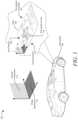
- FIG. 1illustrates an example environment 100 in which a waveguide assembly 102 is used on an automobile 104 .
- the automobile 104may use the waveguide assembly 102 to enable operations of a radar system that is configured to determine a proximity, an angle, or a velocity of at least one object.
- the waveguide assembly 102may be located on a front of the automobile 104 to detect the presence of nearby objects and avoid collisions.
- other devicese.g., desktop computers, tablets, laptops, televisions, computing watches, smartphones, gaming systems, and so forth
- the waveguide assembly 102includes a PCB 106 with at least one layer.
- the PCB 106is designed to mechanically support and electrically connect components (e.g., ICs, transistors, diodes, capacitors, resistors, and so forth) using conductive materials.
- the PCB 106includes a first surface 108 and a second surface 110 .
- the second surface 110is positioned opposite and in parallel with the first surface 108 .
- the first surface 108is aligned in parallel with a planar dimension 112 and orthogonal to a vertical dimension 114 .
- the vertical dimension 114connects the first surface 108 and the second surface 110 .
- the waveguide assembly 102also includes a waveguide cavity 116 that is mounted directly on the first surface 108 .
- the waveguide cavity 116may be mounted using, for example, a through-hole technology or a surface-mount technology (SMT).
- SMTis a process of designing the PCB 106 with flat pads covered in a conductive material (e.g., tin-lead, silver, gold, or copper) to connect components to the first surface 108 using solder
- through-hole technologyis a process of connecting components to the PCB 106 by inserting component leads into drilled holes and soldering the leads to pads on the second surface 110 .
- the waveguide cavity 116is configured to perform impedance matching of the EM energy while guiding the EM energy from the first surface 108 to the second surface 110 via a plated slot as further described in FIG. 2 - 1 .
- FIG. 2 - 1illustrates a bottom surface of the waveguide cavity 116 that is configured to be open and mounted directly to the first surface 108 of the PCB 106 .
- the bottom surfacecan be mounted using solder at a bottom-surface edge 202 to electrically and mechanically connect the waveguide cavity 116 to a conductive material 204 coated on the first surface 108 .
- the conductive material 204may comprise a metal material including tin-lead, silver, gold, copper, and so forth to enable the transport of electrical signals.
- the waveguide cavity 116is positioned over a plated slot 206 that is configured to channel the EM energy from the planar dimension 112 to the vertical dimension 114 .
- the plated slot 206includes a plated-slot opening 208 that comprises a hole in each layer of the PCB 106 , concentrically aligned along a plated-slot center 210 .
- the plated-slot opening 208 illustrated in environment 200 - 1resembles a rectangle with rounded corners. However, the plated-slot opening 208 may comprise various shapes, including a circle, an oval, a rectangle, a square, and so forth.
- the plated-slot opening 208may also comprise various sizes (e.g., diameters), which all support techniques of the waveguide assembly 102 described herein.
- the plated-slot opening 208is surrounded by the conductive material 204 to enable electrical connections between the first surface 108 and the second surface 110 .
- the EM energymay travel to the waveguide cavity 116 along the planar dimension 112 via a microstrip line 212 that comprises the conductive material 204 .
- the microstrip line 212is aligned orthogonal to and centered about a cavity front 214 .
- the waveguide cavity 116can then channel the EM energy towards the plated slot 206 , which is configured to transport the EM energy from the first surface 108 to the second surface 110 (e.g., containing the antenna) along the vertical dimension 114 via the plated-slot opening 208 .
- the waveguide cavity 116is further configured to perform impedance matching (e.g., matching an electrical resistance in series with a reactance) of the EM energy.
- impedance matchinge.g., matching an electrical resistance in series with a reactance
- a loade.g., the antenna
- a sourcee.g., a power source
- the discontinuitymay cause attenuation, distortion, standing waves, or ringing of the EM energy.
- the waveguide cavity 116may modify a source impedance (e.g., an internal or output impedance) to match the impedance of the load, including the antenna.
- a source impedancee.g., an internal or output impedance
- the waveguide assembly 102may maximize power transferred to the antenna and minimize the EM energy reflected by the discontinuity. Maximizing power to the antenna may increase the efficiency of a radar system that is configured to determine the proximity, the angle, or the velocity of the at least one object.
- the automobile 104may use such a radar system to better avoid collisions with the at least one object and protect passengers within the automobile 104 .
- FIG. 2 - 2graphically illustrates a reflected power 216 in terms of a frequency 220 .
- the reflected power 216represents power that is reflected from the load and sent back to the power source. For example, if the reflected power 216 has an amplitude 222 of zero decibels (dB), then all of the power is reflected by the load, and none of the EM energy is radiated (e.g., by the antenna).
- dBdecibels
- the waveguide cavity 116is designed to increase the amplitude 222 of the reflected power 216 by generating a first resonant peak 224 and a second resonant peak 226 by fabricating a specific geometry and size of the waveguide cavity 116 .
- the first resonant peak 224 and the second resonant peak 226increase a return-loss bandwidth 228 of the reflected power 216 .
- the return-loss bandwidthcomprises a range of the frequencies 220 at a specified amplitude 222 in which the load radiates the EM energy.
- the frequency 220may include millimeter waves (e.g., radio waves) within a range of 30-300 gigahertz (GHz) and specifically a range of 65-90 GHz.
- the frequency 220may also include a microwave range of 3-30 GHz.
- the first resonant peak 224is generated in a taper section 230 that is configured to taper a height of the waveguide cavity 116 , increasing the height from the cavity front 214 to a cavity middle 232 .
- An initial impedanceis generated at the cavity front 214 , and impedance matched to the load within the taper section 230 .
- the taper section 230comprises the microstrip line 212 and a plurality of vias 234 .
- the plurality of vias 234comprises at least one vias opening in the PCB 106 that is configured to enable electrical connections between layers of the PCB 106 .
- the plurality of vias 234may comprise several vias openings as illustrated in environment 200 - 1 .
- the vias openingcan include thru vias that are configured to electrically connect all layers of the PCB 106 .
- the thru viascan be located on both the first surface 108 of the PCB 106 and the second surface 110 .
- the vias openingcan also include blind vias configured to electrically connect at least one, but not all, of the layers of the PCB 106 .
- the blind viascan be located on either the first surface 108 of the PCB 106 or the second surface 110 but not both.
- the vias openingmay additionally include one or more buried vias or thermal vias.
- the plurality of vias 234is configured to create a boundary condition that enables the excitation of a mode of the EM energy.
- the modemay include a dominant mode (e.g., TE10) with a lowest cut-off frequency.
- the waveguide cavity 116may accommodate other modes of the EM energy (e.g., TE20, TE30, and so forth).
- the second resonant peak 226is generated in a resonant section 236 .
- the resonant section 236is connected to the taper section 230 at the cavity middle 232 and comprises a rectangular shape.
- a resonant-cavity distance 238is designed to enable the generation of the second resonant peak 226 at a specific frequency 220 .
- the resonant-cavity distance 238is a distance between the plated-slot center 210 and a cavity back 240 .
- the resonant-cavity distance 238may be designed, for example, to a length of three-quarters of a wavelength of the EM energy. However, other lengths of the resonant-cavity distance 238 can be used to enable impedance matching.
- the resonant section 236is further described in FIG. 2 - 2 .
- FIG. 2 - 3illustrates the waveguide cavity 116 from two distinct perspectives, a top view 200 - 3 and a bottom view 200 - 4 .
- Both views 200 - 3 and 200 - 4illustrate that the taper section 230 is connected to the resonant section 236 at the cavity middle 232 .
- the taper section 230comprises an entry opening 242 located at the cavity front 214 .
- the taper section 230further comprises a taper 244 associated with a taper height 246 .
- the taper height 246is configured to increase from the entry opening 242 to the resonant cavity 236 at a taper angle 248 .
- the taper angle 248is chosen to enable a gradual increase in the taper height 246 to perform impedance matching of the EM energy.
- the gradual increaseenables a smooth transmission response (e.g., between the load and the source), reduces loss of the EM energy, and increases the return-loss bandwidth 228 of the reflected power 216 .
- the entry opening 242is configured to enable the EM energy to enter the waveguide cavity 116 via the microstrip line 212 .
- the entry opening 242comprises a thin rectangular opening of the waveguide cavity 116 .
- the entry opening 242may also include other shapes including a slit, an ellipse, and so forth.
- a height of the entry opening 242(e.g., a distance from the bottom surface to a top of the entry opening 242 ) is configured to change the amplitude 222 of the first resonant peak 224 and the return-loss bandwidth 228 .
- the initial impedanceis generated by the entry opening 242 at the cavity front 214 .
- the excitation of the mode of the EM energyis generated by the boundary condition created by the plurality of vias 234 and the entry opening 242 .
- the waveguide cavity 116may comprise a metal material including a metal chemical element (e.g., copper, nickel, titanium, iron), an alloy (e.g., steel, stainless steel, cast iron), or a molecular compound (e.g., polymeric sulfur nitride).
- the waveguide cavity 116may also include a non-metal material (e.g., dielectric, non-metal elements, non-metal compounds) with a coating of the metal material that at least partially covers the non-metal material.
- the waveguide cavity 116is further described in relation to the waveguide assembly 102 in FIG. 3 .
- FIG. 3illustrates an example waveguide assembly 102 in which the PCB 106 comprises more than one layer.
- Environment 300illustrates a multi-layer PCB 302 that includes a top layer 304 and remaining layers 306 .
- the remaining layers 306comprise at least one layer. If the remaining layers 306 comprise more than one layer, then each layer is aligned in parallel with and at least partially in contact with each other.
- the top layer 304is aligned in parallel with and at least partially in contact with the remaining layers 306 .
- the multi-layer PCB 302may include a hybrid PCB stack-up in which the top layer 304 comprises a material that is distinct from the remaining layers 306 .
- the hybrid PCB stack-upmay include one or more ground planes (e.g., metal layer connected to a ground point), power planes, or signal layers.
- the top layer 304may include a dielectric material (e.g., porcelain, glass, plastic, mica, metal oxides, polymers).
- the top layer 304may comprise an I-Tera® MT40 laminate or a Rogers RO3003TM or RO4835TM laminate.
- the remaining layers 306may also include the dielectric materials but must use at least one material distinct from the top layer 304 .
- the remaining layers 306may include less expensive dielectric materials to reduce a cost of the PCB fabrication.
- the remaining layers 306may include the flame retardant 4 (FR-4) composite materials (e.g., glass-reinforced epoxy laminates). If the remaining layers 306 comprise more than one layer, then each layer may comprise a distinct material, a same material, or a combination of distinct and same material layers.
- FR-4flame retardant 4
- the waveguide assembly 102may further include an integrated circuit (IC) 308 that is electrically connected to the waveguide cavity 116 via the microstrip line 212 and can use the PCB components (e.g., transistors, diodes, capacitors, resistors) to enable operations of the waveguide assembly 102 .
- the IC 308can be mounted on the first surface 108 of the PCB 106 the multi-layer PCB 302 , or the hybrid PCB stack-up to avoid mounting the IC 308 on a same side as a load. For example, in environment 300 , the IC 308 is mounted on the first surface 108 while the antenna is mounted on the second surface 110 . Because the IC 308 is not mounted on the same side as the antenna, the IC 308 does not need to be shielded.
- the IC 308may include a monolithic microwave integrated circuit (MMIC) configured to operate at frequencies 220 in a microwave range (e.g., 300 megahertz to 300 GHz).
- MMICmonolithic microwave integrated circuit
- the MMICmay be heat sunk into the first surface 108 to distribute thermal energy generated, at least in part, by the MMIC.
- a process for creating the waveguide assembly 102is further described in FIG. 4 .
- FIG. 4illustrates an example technique for creating and performing operations of the waveguide cavity 116 .
- a process 400is shown as sets of operations (or acts) performed and is not necessarily limited to the order or combinations in which the operations are shown herein. Further, any of one or more operations may be repeated, combined, reorganized, or linked to provide a wide array of additional and/or alternative processes.
- FIGS. 1 - 3reference may be made to environments and entities detailed in FIGS. 1 - 3 , reference to which is made for example only.
- a waveguide cavityis formed.
- the waveguide cavity 116 illustrated in FIG. 2 - 2may be formed using a sheet-metal drawing process, which includes using tensile forces to stretch the metal material to a desired shape and thickness.
- the waveguide cavity 116may also be formed using a sheet-metal-stamping process, which includes applying pressure to the metal material by using a stamping press to form the desired shape and thickness.
- the sheet-metal-stamping processmay cost less than the sheet-metal-drawing process.
- the waveguide cavity 116may additionally be formed using a cast heatsink further described in FIG. 5 .
- All three processes of forming the waveguide cavity 116must produce an accurate shape on an inside of the waveguide cavity 116 to enable operations of the waveguide assembly 102 .
- the taper angle 248 , the taper height 246 , and the resonant-cavity distance 238must be accurate on the inside of the waveguide cavity 116 , regardless of process.
- An outside shape of the waveguide cavity 116can appear distinct between processes without impacting the operations of the waveguide assembly 102 .
- the waveguide cavityis mounted directly on the first surface of the PCB and positioned over the plated slot.
- the waveguide cavity 116 illustrated in FIG. 2 - 2is mounted directly on the first surface 108 of the PCB 106 , the multi-layer PCB 302 , or the hybrid PCB stack-up.
- the waveguide cavity 116is connected to the first surface 108 using the conductive material 204 .
- the waveguide cavity 116is positioned over the plated slot 206 with respect to the resonant-cavity distance 238 to enable the generation of the first resonant peak 224 and the second resonant peak 226 .
- the waveguide cavityperforms impedance matching of the EM energy while guiding the EM energy from the first surface to the second surface of the PCB via the plated slot.
- the waveguide cavity 116 illustrated in FIGS. 2 - 1 and 2 - 2performs impedance matching of the EM energy in the taper section 230 by gradually increasing the taper height 246 from the cavity front 214 to the cavity middle 232 by the taper angle 248 .
- the waveguide cavity 116also guides the EM energy from the first surface 108 to the second surface 110 via the plated slot 206 .
- Example waveguide cavities 116are further described in FIG. 5 .
- FIG. 5illustrates three types of waveguide cavities 500 - 1 , 500 - 2 , and 500 - 3 that may be formed using process 400 . While only three variations are illustrated, the waveguide cavity 116 may be formed into other shapes not shown and using other processes not illustrated in FIG. 4 .
- a drawn-waveguide cavity 500 - 1is formed using the sheet-metal-drawing process, and a stamped-waveguide cavity 500 - 2 is formed using the sheet-metal-stamping process. Both the drawn-waveguide cavity 500 - 1 and the stamped-waveguide cavity 500 - 2 have a same shape on the inside of the waveguide cavity 116 , but the outside shape appears distinct.
- a cast-waveguide cavity 500 - 3is formed by positioning the waveguide cavity 116 inside a cast heatsink.
- the cast heatsinkis surrounded by a heat-spreader wall 502 that is configured to distribute thermal energy to cool the cast-waveguide cavity 500 - 3 .
- the cast-waveguide cavity 500 - 3is located within at least one layer of the PCB 106 and does not require soldering.
- the waveguide cavity 116may further comprise an electrically conductive plastic material or a non-conductive plastic material plated in metal.
- the cast-waveguide cavity 500 - 3includes a gasket 504 positioned around the bottom-surface edge 202 and in contact with the first surface 108 of the PCB 106 .
- the gasket 504comprises a conductive material that is configured to compress under pressure (e.g., nickel and graphite filled silicone or fluorosilicone, silicone foam, closed-cell silicone or fluorosilicone sponge, wire mesh, and so forth) to provide electrical and mechanical contact with the first surface 108 .
- the gasket 504enables electrical connections and transport of the EM energy within the waveguide assembly 102 . Preliminary results of the drawn-waveguide cavity 500 - 1 and the stamped-waveguide cavity 500 - 2 are further described in FIG. 6 .
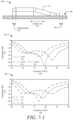
- FIG. 6Preliminary results are illustrated in FIG. 6 for both an example drawn-waveguide cavity 500 - 1 plotted in 600 and an example stamped-waveguide cavity 500 - 2 plotted in 602 .
- Both example waveguide cavities 116were fabricated with 0.3 millimeter (mm) thick metal walls.
- An inside dimension of the resonant section 236was fabricated with dimensions of 2.65 mm length, 3.1 mm width, and 0.8 mm height, where the length is measured along the resonant-cavity distance 238 of the planar dimension 112 , the width is measured along the cavity back 240 of the planar dimension 112 , and the height is measured along the vertical dimension 114 .
- the taper 244was fabricated with dimensions of 2.8 mm length, 3.1 mm width, and 0.8 mm taper height 246 measured at the cavity middle 232 .
- a resultant taper angle 248was fabricated at 16.6°.
- the resonant-cavity distance 238was fabricated at three-quarters the wavelength of the EM energy, and the waveguide cavity 116 was mounted onto the first surface 108 with a cured solder thickness of 2 mils (e.g., two thousandths of an inch).
- the waveguide cavity 116may be fabricated with other dimensions, including different lengths, widths, and heights.
- both the drawn-waveguide cavity 500 - 1 and the stamped-waveguide cavity 500 - 2perform better than the plated slot 206 in an absence of the waveguide cavity 116 .
- the plated slot 206 in the absence of the waveguide cavity 116features a transmission loss of 2 dB
- the drawn-waveguide cavity 500 - 1for example, features a transmission loss of 0.5 dB.
- the drawn-waveguide cavity 500 - 1performs better than the stamped-waveguide cavity 500 - 2 (e.g., less transmission loss, increased return-loss bandwidth) and dissipates less of the EM energy through leakage at the bottom-surface edge 202 , thereby increasing efficiency.
- Plots of 600 and 602illustrate the performance of the example drawn-waveguide cavity 500 - 1 and the example stamped-waveguide cavity 500 - 2 , respectively, in terms of scattering (S) parameters.
- the S-parametersrefer to an interaction between the EM energy and any discontinuity of the waveguide assembly 102 .
- the waves of the EM energymay encounter an impedance within the waveguide assembly 102 that is distinct from the source impedance or a load impedance of the waves.
- Three distinct S-parametersare plotted, S 11 604 , S 22 606 , and S 12 608 .
- S 11 604refers to the reflected power 216 of port 1 , where port 1 represents the power source.
- S 22 606refers to the reflected power 216 of port 2 , where port 2 represents the load (e.g., the antenna).
- S 12 608refers to a transmission power of port 1 to port 2 .
- the transmission power S 12 608 shown in plots 600 and 602indicates a smooth transmission of the EM energy across 65-90 GHz with approximately 0.5 dB of transmission loss.
- the reflected powers 216 of S 11 604 and S 22 606 of plot 600indicate the first resonant peak 224 is located at 72 GHz, and the second resonant peak 226 is located at 79 GHz with the return-loss bandwidth 228 of 12 GHz for ⁇ 15 dB and 17 GHz for ⁇ 10 dB.
- This plotindicates that the waveguide assembly 102 is most efficient at the frequencies of 72 GHz and 79 GHz but also performs well within a frequency band of 17 GHz centered approximately about 75 GHz.
- first resonant peak 224 and the second resonant peak 226 of S 11 604 and S 22 606 of plot 600are overlapped in frequency 220 .
- Plot 602indicates that the example stamped-waveguide cavity 500 - 2 is not as efficient as the example drawn-waveguide cavity 500 - 1 , but still performs better than the plated slot 206 in the absence of the waveguide cavity 116 . Alignment error results of the example drawn-waveguide cavity 500 - 1 are further described in FIGS. 7 - 1 , 7 - 2 , and 7 - 3 .
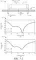
- FIG. 7 - 1illustrates how a first alignment error 700 - 1 of the waveguide cavity 116 along a length axis 702 affects the reflected power 216 of S 11 604 and S 22 606 , shown in plots 704 and 706 , respectively.
- the length axis 702is aligned with the resonant-cavity distance 238 of the planar dimension 112 .
- a first alignment error 700 - 1comprising a displacement 708 along the length axis 702 .
- the displacement 708is illustrated in 700 - 1 for +4 mil 710 .
- the displacement 708can include 0 mil 712 , ⁇ 4 mil 714 , and so forth.
- Plots 704 and 706indicate that the displacement 708 of +4 mil 710 and ⁇ 4 mil 714 along the length axis 702 results in a change in the reflected power 216 , both in amplitude 222 and frequency 220 of S 11 604 and S 22 606 .
- the example drawn-waveguide cavity 500 - 1 with the first alignment error 700 - 1still performs better than the plated slot 206 in the absence of the waveguide cavity 116 .
- FIG. 7 - 2illustrates how a second alignment error 700 - 2 of the waveguide cavity 116 along a width axis 716 affects the reflected power 216 of S 11 604 and S 22 606 , shown in plots 718 and 720 , respectively.
- the width axis 716is aligned with the entry opening 242 of the planar dimension 112 .
- Plots 718 and 720indicate that the displacement 708 of +4 mil 710 and ⁇ 4 mil 714 along the width axis 716 results in a negligible change in the reflected power 216 , both in amplitude 222 and frequency 220 of S 11 604 and S 22 606 .
- FIG. 7 - 3illustrates how a third alignment error 700 - 3 of the waveguide cavity 116 , resulting in an angular displacement 718 within the planar dimension 112 , affects the reflected power 216 of S 11 604 and S 22 606 , shown in plots 720 and 722 , respectively.
- the angular displacement 718is illustrated in 700 - 3 for ⁇ 6 degrees 724 .
- the angular displacement 718can include 0 degrees 726 , +6 degrees 728 , and so forth.
- Plots 720 and 722indicate that the angular displacement 718 of +6 degrees 728 and ⁇ 6 degrees 724 along the planar dimension 112 results in a change in the reflected power 216 , both in amplitude 222 and frequency 220 of S 11 604 and S 22 606 .
- the example drawn-waveguide cavity 500 - 1 with the third alignment error 700 - 3still performs better than the plated slot 206 in the absence of the waveguide cavity 116 .
- a waveguide assemblycomprising: a printed circuit board (PCB) comprising: at least one PCB layer that includes a first surface and a second surface positioned opposite and in parallel with the first surface; a plated slot configured to channel an electromagnetic (EM) energy from a planar dimension in parallel with the first surface to a vertical dimension that is orthogonal to the planar dimension, the plated slot comprising an opening surrounded by a conductive material to enable electrical connections between the first surface and the second surface, the opening configured to transfer the EM energy between the first surface and the second surface; and a waveguide cavity mounted directly on the first surface and positioned over the plated slot, the waveguide cavity configured to perform impedance matching of the EM energy while guiding the EM energy from the first surface to the second surface via the plated slot.
- PCBprinted circuit board
- the waveguide assembly example 1wherein: the waveguide cavity further comprises a drawn-waveguide cavity; the drawn-waveguide cavity is formed using a sheet metal drawing process; and the sheet metal drawing process comprises pulling a metal material to form the drawn-waveguide cavity.
- the waveguide cavityfurther comprises a stamped-waveguide cavity; the stamped-waveguide cavity is formed using a sheet metal stamping process; and the sheet metal stamping process comprises pressing a metal material with a stamping press to form the stamped-waveguide cavity.
- the waveguide cavityis hollow and comprises: a bottom surface configured to be open, the bottom surface mounted directly on the first surface of the PCB; a taper section configured to taper a height of the waveguide cavity, the height of the waveguide cavity increasing from a cavity front to a cavity middle, the height of the waveguide cavity is tapered to enable impedance matching of the EM energy; and a resonant section connected to the taper section at the cavity middle, the resonant section is rectangular in shape.
- the waveguide cavityfurther comprises an entry opening positioned at the cavity front, the entry opening configured to: enable the EM energy to enter the waveguide cavity via a microstrip line, the microstrip line aligned orthogonal to and centered about the entry opening, the microstrip line comprising a conductive material and configured to enable electrical connections; excite a mode of the EM energy; and generate a first resonant peak configured to increase a return-loss bandwidth, wherein an increase in the return-loss bandwidth is correlated with an increase in power supplied to at least one antenna.
- a height of the entry openingis configured to: change an amplitude of the first resonant peak; and change the return-loss bandwidth.
- a resonant-cavity distanceis defined from a center of the plated slot to a back of the waveguide cavity; the resonant-cavity distance is configured to generate a second resonant peak; and the second resonant peak is configured to increase the return-loss bandwidth.
- the PCBfurther comprises an integrated circuit (IC) mounted on the first surface of the PCB; the IC is electrically connected to the waveguide cavity via the microstrip line; and the microstrip line is further configured to enable transport of the EM energy between the waveguide cavity and the IC.
- ICintegrated circuit
- the ICis a monolithic microwave integrated circuit (MMIC) configured to operate at frequencies in a microwave range; and the MMIC is heat sunk into the first surface of the PCB, configured to distribute thermal energy that is generated at least in part by the MMIC.
- MMICmonolithic microwave integrated circuit
- the PCBfurther comprises: a top layer; and remaining layers comprising at least one layer, the remaining layers aligned in parallel and at least partially in contact, the top layer aligned in parallel with and at least partially in contact with the remaining layers.
- the PCBfurther comprises at least one vias, the at least one vias comprising: a vias opening in the at least one PCB layer, the vias opening lined with a conductive material, the vias opening configured to electrically connect layers of the PCB; and at least one of the following: a thru vias configured to electrically connect all of the layers of the PCB, the vias opening located on both the first surface of the PCB and the second surface of the PCB; and a blind vias configured to electrically connect at least one of the layers of the PCB but not all of the layers of the PCB, the vias opening located on either the first surface of the PCB or the second surface of the PCB but not both.
- the taper sectioncomprises a plurality of vias; the plurality of vias is positioned on the bottom surface; the plurality of vias comprises at least one of the following: the thru vias; or the blind vias; and the plurality of vias is configured to enable: excitation of a mode of the EM energy; and generation of a first resonant peak.
- the PCBfurther comprises a hybrid PCB stack-up comprising the top layer and the remaining layers;
- the top layercomprises a first material distinct from a second material of the remaining layers; and the first material comprises a dielectric material.
- waveguide assembly of example 6wherein the waveguide cavity further comprises a metal material configured to enable transport of the EM energy from the cavity front to the plated slot.
- the PCBfurther comprises a cast-waveguide cavity located within the at least one PCB layer
- the cast-waveguide cavitycomprises: a cast heatsink configured to distribute thermal energy via a heat-spreader wall that surrounds the cast heatsink; the waveguide cavity further configured to be positioned within the cast heatsink; and a gasket positioned around the bottom surface and in contact with the first surface of the PCB, the gasket configured to enable: compression of the gasket; and electrical connections including transport of the EM energy.
- the waveguide cavitycomprises a plated plastic material configured to enable electrical connections, the plated plastic material comprising a plastic material coated in metal.
Landscapes
- Engineering & Computer Science (AREA)
- Microelectronics & Electronic Packaging (AREA)
- Computer Security & Cryptography (AREA)
- Radar, Positioning & Navigation (AREA)
- Remote Sensing (AREA)
- Control Of Motors That Do Not Use Commutators (AREA)
- Waveguide Aerials (AREA)
- Waveguides (AREA)
Abstract
Description
Claims (20)
Priority Applications (3)
| Application Number | Priority Date | Filing Date | Title |
|---|---|---|---|
| US17/155,949US11757166B2 (en) | 2020-11-10 | 2021-01-22 | Surface-mount waveguide for vertical transitions of a printed circuit board |
| EP21203201.5AEP3996202B1 (en) | 2020-11-10 | 2021-10-18 | Surface-mount waveguide for vertical transitions of a printed circuit board |
| CN202111321802.9ACN114464975B (en) | 2020-11-10 | 2021-11-09 | Surface mount waveguide for vertical transition of printed circuit boards |
Applications Claiming Priority (2)
| Application Number | Priority Date | Filing Date | Title |
|---|---|---|---|
| US202063112013P | 2020-11-10 | 2020-11-10 | |
| US17/155,949US11757166B2 (en) | 2020-11-10 | 2021-01-22 | Surface-mount waveguide for vertical transitions of a printed circuit board |
Publications (2)
| Publication Number | Publication Date |
|---|---|
| US20220151074A1 US20220151074A1 (en) | 2022-05-12 |
| US11757166B2true US11757166B2 (en) | 2023-09-12 |
Family
ID=78332522
Family Applications (1)
| Application Number | Title | Priority Date | Filing Date |
|---|---|---|---|
| US17/155,949Active2041-12-27US11757166B2 (en) | 2020-11-10 | 2021-01-22 | Surface-mount waveguide for vertical transitions of a printed circuit board |
Country Status (3)
| Country | Link |
|---|---|
| US (1) | US11757166B2 (en) |
| EP (1) | EP3996202B1 (en) |
| CN (1) | CN114464975B (en) |
Cited By (2)
| Publication number | Priority date | Publication date | Assignee | Title |
|---|---|---|---|---|
| US20230417904A1 (en)* | 2022-06-28 | 2023-12-28 | Veoneer Us, Llc | Integrated circuit to waveguide transitional structures and related sensor assemblies |
| WO2025131615A1 (en)* | 2023-12-18 | 2025-06-26 | Robert Bosch Gmbh | Hollow waveguide element and method for producing same |
Families Citing this family (2)
| Publication number | Priority date | Publication date | Assignee | Title |
|---|---|---|---|---|
| TWI752780B (en)* | 2020-12-31 | 2022-01-11 | 啓碁科技股份有限公司 | Antenna structure with wide beamwidth |
| TWI884637B (en)* | 2023-12-18 | 2025-05-21 | 先豐通訊股份有限公司 | Circuit board assembly with waveguide and method of manufacturing the same |
Citations (206)
| Publication number | Priority date | Publication date | Assignee | Title |
|---|---|---|---|---|
| US2840818A (en) | 1954-04-15 | 1958-06-24 | Hughes Aircraft Co | Slotted antenna |
| US3462713A (en) | 1967-07-19 | 1969-08-19 | Bell Telephone Labor Inc | Waveguide-stripline transducer |
| US3579149A (en) | 1969-12-08 | 1971-05-18 | Westinghouse Electric Corp | Waveguide to stripline transition means |
| US4157516A (en) | 1976-09-07 | 1979-06-05 | U.S. Philips Corporation | Wave guide to microstrip transition |
| US4453142A (en) | 1981-11-02 | 1984-06-05 | Motorola Inc. | Microstrip to waveguide transition |
| US4562416A (en) | 1984-05-31 | 1985-12-31 | Sanders Associates, Inc. | Transition from stripline to waveguide |
| US5065123A (en) | 1990-10-01 | 1991-11-12 | Harris Corporation | Waffle wall-configured conducting structure for chip isolation in millimeter wave monolithic subsystem assemblies |
| DE4241635A1 (en) | 1992-12-10 | 1994-06-16 | Ant Nachrichtentech | Transition piece between microstrip waveguide to hollow waveguide - broadens from microstrip into unilateral suspended substrate guide to match and join hollow guide |
| US5350499A (en) | 1990-09-17 | 1994-09-27 | Matsushita Electric Industrial Co., Ltd. | Method of producing microscopic structure |
| US5414394A (en) | 1992-12-29 | 1995-05-09 | U.S. Philips Corporation | Microwave frequency device comprising at least a transition between a transmission line integrated on a substrate and a waveguide |
| US5637521A (en) | 1996-06-14 | 1997-06-10 | The United States Of America As Represented By The Secretary Of The Army | Method of fabricating an air-filled waveguide on a semiconductor body |
| US5923225A (en) | 1997-10-03 | 1999-07-13 | De Los Santos; Hector J. | Noise-reduction systems and methods using photonic bandgap crystals |
| US5929728A (en) | 1997-06-25 | 1999-07-27 | Hewlett-Packard Company | Imbedded waveguide structures for a microwave circuit package |
| US5982250A (en) | 1997-11-26 | 1999-11-09 | Twr Inc. | Millimeter-wave LTCC package |
| US5982256A (en) | 1997-04-22 | 1999-11-09 | Kyocera Corporation | Wiring board equipped with a line for transmitting a high frequency signal |
| US5986527A (en) | 1995-03-28 | 1999-11-16 | Murata Manufacturing Co., Ltd. | Planar dielectric line and integrated circuit using the same line |
| US6064350A (en) | 1997-07-25 | 2000-05-16 | Kyocera Corporation | Laminated aperture-faced antenna and multi-layered wiring board comprising the same |
| US6072375A (en) | 1998-05-12 | 2000-06-06 | Harris Corporation | Waveguide with edge grounding |
| US6127901A (en) | 1999-05-27 | 2000-10-03 | Hrl Laboratories, Llc | Method and apparatus for coupling a microstrip transmission line to a waveguide transmission line for microwave or millimeter-wave frequency range transmission |
| JP2000357916A (en) | 1999-06-15 | 2000-12-26 | Kobe Steel Ltd | Waveguide slot array antenna |
| US20020021197A1 (en) | 1999-10-29 | 2002-02-21 | Berg Technology, Inc. | Waveguides and backplane systems |
| US6414573B1 (en) | 2000-02-16 | 2002-07-02 | Hughes Electronics Corp. | Stripline signal distribution system for extremely high frequency signals |
| US6489855B1 (en) | 1998-12-25 | 2002-12-03 | Murata Manufacturing Co. Ltd | Line transition device between dielectric waveguide and waveguide, and oscillator, and transmitter using the same |
| US6535083B1 (en) | 2000-09-05 | 2003-03-18 | Northrop Grumman Corporation | Embedded ridge waveguide filters |
| KR20030031585A (en) | 2001-10-15 | 2003-04-23 | (주)지앤티웍스 | Fabrication method of double-sided dielectric PCB on waveguide for slotted waveguide array antennas |
| JP2003243902A (en) | 2002-02-18 | 2003-08-29 | Alps Electric Co Ltd | Converter for receiving satellite broadcast |
| US6622370B1 (en) | 2000-04-13 | 2003-09-23 | Raytheon Company | Method for fabricating suspended transmission line |
| JP2003289201A (en) | 2002-03-28 | 2003-10-10 | Anritsu Corp | Post-wall waveguide and junction conversion structure for cavity waveguide |
| US6658233B1 (en) | 1999-10-04 | 2003-12-02 | Alps Electric Co., Ltd. | Satellite broadcast receiving converter |
| US20040069984A1 (en) | 2001-05-21 | 2004-04-15 | Estes Michael J. | Terahertz interconnect system and applications |
| US6788918B2 (en) | 2001-01-12 | 2004-09-07 | Murata Manufacturing Co., Ltd. | Transmission line assembly, integrated circuit, and transmitter-receiver apparatus comprising a dielectric waveguide protuding for a dielectric plate |
| US6794950B2 (en) | 2000-12-21 | 2004-09-21 | Paratek Microwave, Inc. | Waveguide to microstrip transition |
| US6859114B2 (en) | 2002-05-31 | 2005-02-22 | George V. Eleftheriades | Metamaterials for controlling and guiding electromagnetic radiation and applications therefor |
| CN1620738A (en) | 2000-10-18 | 2005-05-25 | 诺基亚公司 | Waveguide to Stripline Transition |
| CN1682404A (en) | 2002-09-20 | 2005-10-12 | 伊兹德国有限公司 | Junction between a microstrip line and a waveguide |
| US6995726B1 (en) | 2004-07-15 | 2006-02-07 | Rockwell Collins | Split waveguide phased array antenna with integrated bias assembly |
| US20060113598A1 (en) | 2004-11-16 | 2006-06-01 | Chen Howard H | Device and method for fabricating double-sided SOI wafer scale package with optical through via connections |
| CN2796131Y (en) | 2005-05-30 | 2006-07-12 | 东南大学 | Multilayer substrate integrated wave guide elliptical response filter |
| US7142165B2 (en) | 2002-01-29 | 2006-11-28 | Era Patents Limited | Waveguide and slotted antenna array with moveable rows of spaced posts |
| JP3923360B2 (en) | 2002-04-26 | 2007-05-30 | 三菱電機株式会社 | Slot array antenna and slot array antenna apparatus |
| US7276988B2 (en) | 2004-06-30 | 2007-10-02 | Endwave Corporation | Multi-substrate microstrip to waveguide transition |
| CA2654470A1 (en) | 2006-06-12 | 2007-12-27 | Pacific Biosciences Of California, Inc. | Substrates for performing analytical reactions |
| KR20080044752A (en) | 2006-11-17 | 2008-05-21 | 한국전자통신연구원 | Millimeter wave transition device of dielectric waveguide vs transmission line |
| US20080129409A1 (en) | 2006-11-30 | 2008-06-05 | Hideyuki Nagaishi | Waveguide structure |
| US20080150821A1 (en) | 2006-12-22 | 2008-06-26 | Sony Deutschland Gmbh | Flexible substrate integrated waveguides |
| US7420442B1 (en) | 2005-06-08 | 2008-09-02 | Sandia Corporation | Micromachined microwave signal control device and method for making same |
| US7439822B2 (en) | 2005-06-06 | 2008-10-21 | Fujitsu Limited | Waveguide substrate having two slit-like couplings and high-frequency circuit module |
| US20090040132A1 (en) | 2007-07-24 | 2009-02-12 | Northeastern University | Anisotropic metal-dielectric metamaterials for broadband all-angle negative refraction and superlens imaging |
| US7495532B2 (en) | 2004-03-08 | 2009-02-24 | Wemtec, Inc. | Systems and methods for blocking microwave propagation in parallel plate structures |
| US20090207090A1 (en) | 2007-06-22 | 2009-08-20 | Vubiq Incorporated | Integrated antenna and chip package and method of manufacturing thereof |
| US20090243762A1 (en) | 2008-03-27 | 2009-10-01 | Xiao-Ping Chen | Waveguide filter |
| US7626476B2 (en) | 2006-04-13 | 2009-12-01 | Electronics And Telecommunications Research Institute | Multi-metal coplanar waveguide |
| CN201383535Y (en) | 2009-04-01 | 2010-01-13 | 惠州市硕贝德通讯科技有限公司 | Rectangular waveguide-substrate integrated waveguide signal conversion and power divider |
| US7659799B2 (en) | 2005-11-25 | 2010-02-09 | Electronics And Telecommunications Research Institute | Dielectric waveguide filter with cross-coupling |
| US20100193935A1 (en) | 2009-01-30 | 2010-08-05 | Infineon Technologies Ag | Integrated antennas in wafer level package |
| US20110140979A1 (en) | 2009-09-08 | 2011-06-16 | Siklu Communication ltd. | Waveguide comprising laminate structure |
| US20110140810A1 (en) | 2009-09-08 | 2011-06-16 | Siklu Communication ltd. | Waveguide-backshort comprising a printed conducting layer |
| US7973616B2 (en) | 2008-06-05 | 2011-07-05 | Kabushiki Kaisha Toshiba | Post-wall waveguide based short slot directional coupler, butler matrix using the same and automotive radar antenna |
| US8013694B2 (en) | 2006-03-31 | 2011-09-06 | Kyocera Corporation | Dielectric waveguide device, phase shifter, high frequency switch, and attenuator provided with dielectric waveguide device, high frequency transmitter, high frequency receiver, high frequency transceiver, radar device, array antenna, and method of manufacturing dielectric waveguide device |
| US8089327B2 (en) | 2009-03-09 | 2012-01-03 | Toyota Motor Engineering & Manufacturing North America, Inc. | Waveguide to plural microstrip transition |
| US20120013421A1 (en) | 2009-03-31 | 2012-01-19 | Kyocera Corporation | Waveguide Structure, High Frequency Module Including Waveguide Structure, and Radar Apparatus |
| US20120050125A1 (en) | 2010-08-31 | 2012-03-01 | Siklu Communication ltd. | Systems for interfacing waveguide antenna feeds with printed circuit boards |
| US20120068316A1 (en) | 2009-05-08 | 2012-03-22 | Telefonaktiebolaget L M Ericsson (Publ) | Transition from a chip to a waveguide port |
| US8159316B2 (en) | 2007-12-28 | 2012-04-17 | Kyocera Corporation | High-frequency transmission line connection structure, circuit board, high-frequency module, and radar device |
| US20120163811A1 (en) | 2007-03-26 | 2012-06-28 | International Business Machines Corporation | Ultra-high bandwidth, multiple-channel full-duplex, single-chip cmos optical transceiver |
| EP2500978A1 (en) | 2011-03-17 | 2012-09-19 | Sivers Ima AB | Waveguide transition |
| CN102696145A (en) | 2009-12-07 | 2012-09-26 | 卡西迪安有限公司 | Microwave transition device between a microstrip line and a rectangular waveguide |
| US20120256707A1 (en) | 2011-02-21 | 2012-10-11 | Siklu Communication ltd. | Systems and methods for millimeter-wave laminate structures |
| US20120256796A1 (en) | 2010-08-31 | 2012-10-11 | Siklu Communication ltd. | Compact millimeter-wave radio systems and methods |
| GB2489950A (en) | 2011-04-12 | 2012-10-17 | Filtronic Plc | A substrate integrated waveguide (SIW) to air filled waveguide transition comprising a tapered dielectric layer |
| US20130057358A1 (en) | 2011-09-02 | 2013-03-07 | Theodore K. Anthony | Waveguide to Co-Planar-Waveguide (CPW) ransition |
| US8395552B2 (en) | 2010-11-23 | 2013-03-12 | Metamagnetics, Inc. | Antenna module having reduced size, high gain, and increased power efficiency |
| US8451175B2 (en) | 2008-03-25 | 2013-05-28 | Tyco Electronics Services Gmbh | Advanced active metamaterial antenna systems |
| US8451189B1 (en) | 2009-04-15 | 2013-05-28 | Herbert U. Fluhler | Ultra-wide band (UWB) artificial magnetic conductor (AMC) metamaterials for electrically thin antennas and arrays |
| US20130256849A1 (en) | 2012-03-29 | 2013-10-03 | International Business Machines Corporation | High frequency transition matching in an electronic package for millimeter wave semiconductor dies |
| WO2013189513A1 (en) | 2012-06-18 | 2013-12-27 | Huawei Technologies Co., Ltd. | Directional coupler waveguide structure and method |
| CN103515682A (en) | 2013-07-24 | 2014-01-15 | 中国电子科技集团公司第五十五研究所 | Micro-strip-to-waveguide vertical transition structure achieved through multi-layer step type substrate integration waveguide |
| US20140015709A1 (en) | 2012-07-13 | 2014-01-16 | Kabushiki Kaisha Toshiba | Waveguide connecting structure, antenna device and radar device |
| US20140048310A1 (en) | 2012-08-16 | 2014-02-20 | Apple Inc. | Printed Circuit Solder Connections |
| US8680936B2 (en) | 2011-11-18 | 2014-03-25 | Delphi Technologies, Inc. | Surface mountable microwave signal transition block for microstrip to perpendicular waveguide transition |
| US8692731B2 (en) | 2011-02-16 | 2014-04-08 | Samsung Electro-Mechanics Co., Ltd. | Dielectric waveguide antenna |
| US20140106684A1 (en) | 2012-10-15 | 2014-04-17 | Qualcomm Mems Technologies, Inc. | Transparent antennas on a display device |
| US8717124B2 (en) | 2010-01-22 | 2014-05-06 | Nuvotronics, Llc | Thermal management |
| US8803638B2 (en) | 2008-07-07 | 2014-08-12 | Kildal Antenna Consulting Ab | Waveguides and transmission lines in gaps between parallel conducting surfaces |
| US8948562B2 (en) | 2008-11-25 | 2015-02-03 | Regents Of The University Of Minnesota | Replication of patterned thin-film structures for use in plasmonics and metamaterials |
| EP2843758A1 (en) | 2013-08-27 | 2015-03-04 | Microelectronics Technology Inc. | Multi-layer circuit board with waveguide to microstrip transition structure |
| US20150097633A1 (en) | 2013-10-08 | 2015-04-09 | Blackberry Limited | 60 ghz integrated circuit to printed circuit board transitions |
| US20150229017A1 (en) | 2014-02-07 | 2015-08-13 | Fujitsu Limited | High frequency module and fabrication method for high frequency module |
| CN104900956A (en) | 2015-05-06 | 2015-09-09 | 东南大学 | Device for switching waveguide to substrate integrated waveguide |
| US20150295297A1 (en) | 2014-04-09 | 2015-10-15 | Texas Instruments Incorporated | Metallic Waveguide with Dielectric Core |
| EP2945222A1 (en) | 2014-05-14 | 2015-11-18 | Gapwaves AB | A microwave or millimeter wave RF part using pin grid array (PGA) and/or ball grid array (BGA) technologies |
| CN105098295A (en) | 2014-05-16 | 2015-11-25 | 香港城市大学 | Apparatus and method for electromagnetic signal conversion |
| US9203155B2 (en) | 2011-06-27 | 2015-12-01 | Electronics And Telecommunications Research Institute | Metamaterial structure and manufacturing method of the same |
| US20150357698A1 (en) | 2013-01-10 | 2015-12-10 | Nec Corporation | Wideband transition between a planar transmission line and a waveguide |
| US20150364830A1 (en) | 2014-06-13 | 2015-12-17 | Freescale Semiconductor, Inc. | Integrated circuit package with radio frequency coupling structure |
| US20150364804A1 (en) | 2014-06-13 | 2015-12-17 | Freescale Semiconductor, Inc. | Radio frequency coupling structure |
| US9246204B1 (en) | 2012-01-19 | 2016-01-26 | Hrl Laboratories, Llc | Surface wave guiding apparatus and method for guiding the surface wave along an arbitrary path |
| US9258884B2 (en) | 2012-05-17 | 2016-02-09 | Canon Kabushiki Kaisha | Suppression of current component using EBG structure |
| US20160043455A1 (en) | 2014-08-07 | 2016-02-11 | Infineon Technologies Ag | Microwave Chip Package Device |
| US20160049714A1 (en) | 2013-03-24 | 2016-02-18 | TELEFONAKTIEBOLAGET L.M.ERICSSON (publ) | Transition Between a SIW and a Waveguide Interface |
| US20160056541A1 (en) | 2013-03-24 | 2016-02-25 | Telefonaktiebolaget L M Ericsson (Publ) | A siw antenna arrangement |
| US20160111764A1 (en) | 2014-10-16 | 2016-04-21 | Hyundai Mobis Co., Ltd. | Transit structure of waveguide and siw |
| US20160118705A1 (en) | 2014-10-23 | 2016-04-28 | Freescale Semiconductor, Inc. | Packaged integrated circuit waveguide interface and methods thereof |
| CN105609909A (en) | 2016-03-08 | 2016-05-25 | 电子科技大学 | Device for transition from rectangular waveguide to substrate integrated waveguide on Ka-band |
| CN105680133A (en) | 2016-01-11 | 2016-06-15 | 中国电子科技集团公司第十研究所 | Inter-board perpendicular interconnection circuit structure for substrate integrated ridge waveguide |
| US20160204495A1 (en) | 2013-10-01 | 2016-07-14 | Sony Corporation | Connector apparatus and communication system |
| CN105958167A (en) | 2016-07-01 | 2016-09-21 | 北京交通大学 | Vertical substrate integrated waveguide and vertical connection structure comprising the waveguide |
| US20160276727A1 (en) | 2015-03-19 | 2016-09-22 | International Business Machines Corporation | Package structures having integrated waveguides for high speed communications between package components |
| US20160293557A1 (en) | 2015-03-30 | 2016-10-06 | Sony Corporation | Package and antenna apparatus including package |
| US20160301125A1 (en) | 2015-04-13 | 2016-10-13 | Research & Business Foundation Sungkyunkwan University | On-chip waveguide feeder for millimiter wave ics and feeding methods, and multiple input and output millimeter wave transceiver system using same |
| US20170084554A1 (en) | 2015-09-21 | 2017-03-23 | Intel Corporation | Platform with thermally stable wireless interconnects |
| US20170099705A1 (en) | 2014-05-26 | 2017-04-06 | Electrolux Appliances Aktiebolag | Microwave oven with a waveguide including a reflector element |
| US9647313B2 (en) | 2012-01-19 | 2017-05-09 | Huawei Technologies Co., Ltd. | Surface mount microwave system including a transition between a multilayer arrangement and a hollow waveguide |
| US9653773B2 (en) | 2012-04-24 | 2017-05-16 | Universite Grenoble Alpes | Slow wave RF propagation line including a network of nanowires |
| US9673532B2 (en) | 2013-07-31 | 2017-06-06 | Huawei Technologies Co., Ltd. | Antenna |
| US9806393B2 (en) | 2012-06-18 | 2017-10-31 | Gapwaves Ab | Gap waveguide structures for THz applications |
| US9813042B2 (en) | 2015-08-28 | 2017-11-07 | City University Of Hong Kong | Converting a single-ended signal to a differential signal |
| US20170324135A1 (en) | 2014-12-12 | 2017-11-09 | Sony Corporation | Microwave antenna apparatus, packing and manufacturing method |
| US9843301B1 (en) | 2016-07-14 | 2017-12-12 | Northrop Grumman Systems Corporation | Silicon transformer balun |
| WO2018003932A1 (en) | 2016-06-29 | 2018-01-04 | Nidec Elesys Corporation | Waveguide device module and microwave module |
| DE102016213202A1 (en) | 2016-07-19 | 2018-01-25 | Conti Temic Microelectronic Gmbh | Multi-layer board with a transition element for transforming a waveguide shaft onto a conducted shaft |
| US9935065B1 (en) | 2016-12-21 | 2018-04-03 | Infineon Technologies Ag | Radio frequency device packages and methods of formation thereof |
| US9947981B1 (en) | 2016-05-19 | 2018-04-17 | National Technology & Engineering Solutions of Sandian, LLC | Waveguide module comprising a first plate with a waveguide channel and a second plate with a raised portion in which a sealing layer is forced into the waveguide channel by the raised portion |
| US20180131084A1 (en) | 2016-11-08 | 2018-05-10 | Korea Advanced Institute Of Science And Technology | Printed-circuit board having antennas and electromagnetic-tunnel-embedded architecture and manufacturing method thereof |
| US9991606B2 (en) | 2015-11-05 | 2018-06-05 | Nidec Corporation | Slot array antenna |
| US10027032B2 (en) | 2015-10-15 | 2018-07-17 | Nidec Corporation | Waveguide device and antenna device including the waveguide device |
| US10042045B2 (en) | 2016-01-15 | 2018-08-07 | Nidec Corporation | Waveguide device, slot array antenna, and radar, radar system, and wireless communication system including the slot array antenna |
| US20180226709A1 (en) | 2017-02-08 | 2018-08-09 | Delphi Technologies, Inc. | Radar assembly with ultra wide band waveguide to substrate integrated waveguide transition |
| US20180226727A1 (en) | 2017-02-07 | 2018-08-09 | Panasonic Corporation | Module, wireless communication apparatus, and radar apparatus |
| US20180233465A1 (en) | 2017-02-15 | 2018-08-16 | Nxp B.V. | Integrated circuit package |
| US10090600B2 (en) | 2016-02-12 | 2018-10-02 | Nidec Corporation | Waveguide device, and antenna device including the waveguide device |
| US20180284186A1 (en) | 2017-04-03 | 2018-10-04 | Nvidia Corporation | Multi-chip package with selection logic and debug ports for testing inter-chip communications |
| US10114067B2 (en) | 2016-02-04 | 2018-10-30 | Advantest Corporation | Integrated waveguide structure and socket structure for millimeter waveband testing |
| US20180343711A1 (en) | 2017-05-24 | 2018-11-29 | Miele & Cie. Kg | Device for generating and transmitting high-frequency waves (hf waves) |
| US20180351261A1 (en) | 2017-06-05 | 2018-12-06 | Nidec Corporation | Waveguide device, and antenna device including the waveguide device |
| US10153533B2 (en) | 2014-05-07 | 2018-12-11 | Hideki Kirino | Waveguide |
| US10158158B2 (en) | 2016-02-08 | 2018-12-18 | Nidec Corporation | Waveguide device, and antenna device including the waveguide device |
| US10164318B2 (en) | 2012-10-22 | 2018-12-25 | Texas Instruments Incorporated | Waveguide coupler |
| US10164344B2 (en) | 2015-12-24 | 2018-12-25 | Nidec Corporation | Waveguide device, slot antenna, and radar, radar system, and wireless communication system including the slot antenna |
| US20180375185A1 (en) | 2017-06-26 | 2018-12-27 | WGR Co., Ltd. | Electromagnetic wave transmission device |
| US20190006743A1 (en) | 2017-06-30 | 2019-01-03 | Nidec Corporation | Waveguide device module, microwave module, radar device, and radar system |
| US20190013563A1 (en) | 2016-01-20 | 2019-01-10 | Sony Corporation | Connector module, communication circuit board, and electronic device |
| EP3460903A1 (en) | 2017-09-20 | 2019-03-27 | Aptiv Technologies Limited | Antenna device with direct differential input useable on an automated vehicle |
| US10263310B2 (en) | 2014-05-14 | 2019-04-16 | Gapwaves Ab | Waveguides and transmission lines in gaps between parallel conducting surfaces |
| WO2019085368A1 (en) | 2017-10-31 | 2019-05-09 | 深圳市华讯方舟微电子科技有限公司 | Wilkinson power divider |
| CN109750201A (en) | 2019-02-22 | 2019-05-14 | 中国科学院长春应用化学研究所 | Micro-alloyed magnesium alloy sheet with high formability and preparation method thereof |
| US10312596B2 (en) | 2013-01-17 | 2019-06-04 | Hrl Laboratories, Llc | Dual-polarization, circularly-polarized, surface-wave-waveguide, artificial-impedance-surface antenna |
| US20190194452A1 (en) | 2016-08-22 | 2019-06-27 | Mep Europe B.V. | Thermoplastic composition for laser direct structuring |
| US20190207286A1 (en) | 2017-12-30 | 2019-07-04 | Texas Instruments Incorporated | Printed circuit board with substrate-integrated waveguide transition |
| US10374323B2 (en) | 2017-03-24 | 2019-08-06 | Nidec Corporation | Slot array antenna and radar having the slot array antenna |
| US10381317B2 (en) | 2016-02-12 | 2019-08-13 | Telefonaktiebolaget Lm Ericsson (Publ) | Transition arrangement comprising a contactless transition or connection between an SIW and a waveguide or an antenna |
| US10381741B2 (en) | 2015-12-24 | 2019-08-13 | Nidec Corporation | Slot array antenna, and radar, radar system, and wireless communication system including the slot array antenna |
| CN209389219U (en) | 2019-02-25 | 2019-09-13 | 贵州航天电子科技有限公司 | A kind of Waveguide slot array antenna structure suitable for increasing material manufacturing |
| US10505282B2 (en) | 2016-08-10 | 2019-12-10 | Microsoft Technology Licensing, Llc | Dielectric groove waveguide |
| US10534061B2 (en) | 2015-04-08 | 2020-01-14 | Gapwaves Ab | Calibration arrangement and a method for a microwave analyzing or measuring instrument |
| US10594045B2 (en) | 2016-04-05 | 2020-03-17 | Nidec Corporation | Waveguide device and antenna array |
| US10601144B2 (en) | 2017-04-13 | 2020-03-24 | Nidec Corporation | Slot antenna device |
| US10608345B2 (en) | 2017-04-13 | 2020-03-31 | Nidec Corporation | Slot array antenna |
| US10622696B2 (en) | 2017-09-07 | 2020-04-14 | Nidec Corporation | Directional coupler |
| US10651567B2 (en) | 2017-06-26 | 2020-05-12 | Nidec Corporation | Method of producing a horn antenna array and antenna array |
| US10651138B2 (en) | 2016-03-29 | 2020-05-12 | Nidec Corporation | Microwave IC waveguide device module |
| US20200153108A1 (en) | 2017-07-06 | 2020-05-14 | Fujikura Ltd. | Waveguide slot array antenna |
| US10658760B2 (en) | 2017-06-26 | 2020-05-19 | Nidec Corporation | Horn antenna array |
| US10670810B2 (en) | 2017-12-22 | 2020-06-02 | Huawei Technologies Canada Co., Ltd. | Polarization selective coupler |
| US10707584B2 (en) | 2017-08-18 | 2020-07-07 | Nidec Corporation | Antenna array |
| US10705294B2 (en) | 2018-03-15 | 2020-07-07 | Stmicroelectronics (Crolles 2) Sas | Waveguide termination device |
| US10714802B2 (en) | 2017-06-26 | 2020-07-14 | WGR Co., Ltd. | Transmission line device |
| DE102019200893A1 (en) | 2019-01-21 | 2020-07-23 | Infineon Technologies Ag | Method for producing a waveguide, circuit device and radar system |
| US10727561B2 (en) | 2016-04-28 | 2020-07-28 | Nidec Corporation | Mounting substrate, waveguide module, integrated circuit-mounted substrate, microwave module |
| US10763590B2 (en) | 2015-11-05 | 2020-09-01 | Nidec Corporation | Slot antenna |
| US20200287293A1 (en) | 2019-03-06 | 2020-09-10 | Aptiv Technologies Limited | Slot array antenna including parasitic features |
| US10775573B1 (en) | 2019-04-03 | 2020-09-15 | International Business Machines Corporation | Embedding mirror with metal particle coating |
| US10811373B2 (en) | 2016-10-05 | 2020-10-20 | Gapwaves Ab | Packaging structure comprising at least one transition forming a contactless interface |
| US20200343612A1 (en) | 2019-04-29 | 2020-10-29 | Aptiv Technologies Limited | Wave guide launcher |
| US10826147B2 (en) | 2017-11-10 | 2020-11-03 | Raytheon Company | Radio frequency circuit with a multi-layer transmission line assembly having a conductively filled trench surrounding the transmission line |
| US10833382B2 (en) | 2015-09-25 | 2020-11-10 | Bae Systems Australia Limited | RF structure and a method of forming an RF structure |
| US20200412012A1 (en) | 2019-06-26 | 2020-12-31 | Honeywell International Inc. | Fixing structure to enhance the mechanical reliability of plate slot array antenna based on siw technology |
| US10892536B2 (en) | 2015-09-24 | 2021-01-12 | Gapwaves Ab | Waveguides and transmission lines in gaps between parallel conducting surfaces |
| US10957971B2 (en) | 2019-07-23 | 2021-03-23 | Veoneer Us, Inc. | Feed to waveguide transition structures and related sensor assemblies |
| US10971824B2 (en) | 2016-09-30 | 2021-04-06 | Ims Connector Systems Gmbh | Antenna element |
| US10985434B2 (en) | 2017-01-24 | 2021-04-20 | Huber+Suhner Ag | Waveguide assembly including a waveguide element and a connector body, where the connector body includes recesses defining electromagnetic band gap elements therein |
| US10983194B1 (en) | 2014-06-12 | 2021-04-20 | Hrl Laboratories, Llc | Metasurfaces for improving co-site isolation for electronic warfare applications |
| US10992056B2 (en) | 2017-04-14 | 2021-04-27 | Nidec Corporation | Slot antenna device |
| US20210159577A1 (en) | 2016-05-03 | 2021-05-27 | Gapwaves Ab | Arrangement for interconnection of waveguide structures and a structure for a waveguide structure interconnecting arrangement |
| WO2021122725A1 (en) | 2019-12-20 | 2021-06-24 | Gapwaves Ab | An antenna arrangement with a low-ripple radiation pattern |
| US11061110B2 (en) | 2017-05-11 | 2021-07-13 | Nidec Corporation | Waveguide device, and antenna device including the waveguide device |
| US11088464B2 (en) | 2018-06-14 | 2021-08-10 | Nidec Corporation | Slot array antenna |
| US11114733B2 (en) | 2019-07-23 | 2021-09-07 | Veoneer Us, Inc. | Waveguide interconnect transitions and related sensor assemblies |
| US11121475B2 (en) | 2017-09-25 | 2021-09-14 | Gapwaves Ab | Phased array antenna |
| US20210305667A1 (en) | 2018-09-04 | 2021-09-30 | Gapwaves Ab | High frequency filter and phased array antenna comprising such a high frequency filter |
| US11169325B2 (en) | 2018-03-15 | 2021-11-09 | Stmicroelectronics (Crolles 2) Sas | Filtering device in a waveguide |
| US11171399B2 (en) | 2019-07-23 | 2021-11-09 | Veoneer Us, Inc. | Meandering waveguide ridges and related sensor assemblies |
| US11196171B2 (en) | 2019-07-23 | 2021-12-07 | Veoneer Us, Inc. | Combined waveguide and antenna structures and related sensor assemblies |
| US11201414B2 (en) | 2018-12-18 | 2021-12-14 | Veoneer Us, Inc. | Waveguide sensor assemblies and related methods |
| US11249011B2 (en) | 2016-10-19 | 2022-02-15 | Global Life Sciences Solutions Usa Llc | Apparatus and method for evanescent waveguide sensing |
| US11283162B2 (en) | 2019-07-23 | 2022-03-22 | Veoneer Us, Inc. | Transitional waveguide structures and related sensor assemblies |
| US11289787B2 (en) | 2017-10-25 | 2022-03-29 | Gapwaves Ab | Transition arrangement comprising a waveguide twist, a waveguide structure comprising a number of waveguide twists and a rotary joint |
| US20220109246A1 (en) | 2019-02-08 | 2022-04-07 | Gapwaves Ab | Antenna array based on one or more metamaterial structures |
| US11349220B2 (en) | 2020-02-12 | 2022-05-31 | Veoneer Us, Inc. | Oscillating waveguides and related sensor assemblies |
| US11349183B2 (en) | 2017-11-07 | 2022-05-31 | Rise Research Institutes of Sweden AB | Contactless waveguide switch and method for manufacturing a waveguide switch |
| US11378683B2 (en) | 2020-02-12 | 2022-07-05 | Veoneer Us, Inc. | Vehicle radar sensor assemblies |
| US11411292B2 (en) | 2019-01-16 | 2022-08-09 | WGR Co., Ltd. | Waveguide device, electromagnetic radiation confinement device, antenna device, microwave chemical reaction device, and radar device |
| US11495871B2 (en) | 2017-10-27 | 2022-11-08 | Metasum Ab | Waveguide device having multiple layers, where through going empty holes are in each layer and are offset in adjoining layers for leakage suppression |
| US11563259B2 (en) | 2020-02-12 | 2023-01-24 | Veoneer Us, Llc | Waveguide signal confinement structures and related sensor assemblies |
| US11611138B2 (en) | 2017-04-12 | 2023-03-21 | Nidec Corporation | Method of producing a radio frequency member |
| US11626652B2 (en) | 2018-12-06 | 2023-04-11 | Samsung Electronics Co., Ltd | Ridge gap waveguide and multilayer antenna array including the same |
Family Cites Families (4)
| Publication number | Priority date | Publication date | Assignee | Title |
|---|---|---|---|---|
| CN103762416B (en)* | 2014-02-25 | 2016-12-07 | 中国工程物理研究院电子工程研究所 | A kind of Terahertz wave plate load-waveguide-loudspeaker converting antenna |
| KR101781477B1 (en)* | 2016-09-19 | 2017-10-23 | 유한회사 에스피앤파트너스 | Microwave range and radiation module thereof |
| CN106785424B (en)* | 2016-11-29 | 2019-07-12 | 大连港森立达木材交易中心有限公司 | The two-way Uniform Irradiation antenna-feeder system of High-Power Microwave |
| HUE049220T2 (en)* | 2017-12-04 | 2020-09-28 | Grieshaber Vega Kg | Printed circuit board for use in a radar fill level measuring device with hollow wire coupling |
- 2021
- 2021-01-22USUS17/155,949patent/US11757166B2/enactiveActive
- 2021-10-18EPEP21203201.5Apatent/EP3996202B1/enactiveActive
- 2021-11-09CNCN202111321802.9Apatent/CN114464975B/enactiveActive
Patent Citations (235)
| Publication number | Priority date | Publication date | Assignee | Title |
|---|---|---|---|---|
| US2840818A (en) | 1954-04-15 | 1958-06-24 | Hughes Aircraft Co | Slotted antenna |
| US3462713A (en) | 1967-07-19 | 1969-08-19 | Bell Telephone Labor Inc | Waveguide-stripline transducer |
| US3579149A (en) | 1969-12-08 | 1971-05-18 | Westinghouse Electric Corp | Waveguide to stripline transition means |
| US4157516A (en) | 1976-09-07 | 1979-06-05 | U.S. Philips Corporation | Wave guide to microstrip transition |
| US4453142A (en) | 1981-11-02 | 1984-06-05 | Motorola Inc. | Microstrip to waveguide transition |
| US4562416A (en) | 1984-05-31 | 1985-12-31 | Sanders Associates, Inc. | Transition from stripline to waveguide |
| US5350499A (en) | 1990-09-17 | 1994-09-27 | Matsushita Electric Industrial Co., Ltd. | Method of producing microscopic structure |
| US5065123A (en) | 1990-10-01 | 1991-11-12 | Harris Corporation | Waffle wall-configured conducting structure for chip isolation in millimeter wave monolithic subsystem assemblies |
| DE4241635A1 (en) | 1992-12-10 | 1994-06-16 | Ant Nachrichtentech | Transition piece between microstrip waveguide to hollow waveguide - broadens from microstrip into unilateral suspended substrate guide to match and join hollow guide |
| US5414394A (en) | 1992-12-29 | 1995-05-09 | U.S. Philips Corporation | Microwave frequency device comprising at least a transition between a transmission line integrated on a substrate and a waveguide |
| US5986527A (en) | 1995-03-28 | 1999-11-16 | Murata Manufacturing Co., Ltd. | Planar dielectric line and integrated circuit using the same line |
| US5637521A (en) | 1996-06-14 | 1997-06-10 | The United States Of America As Represented By The Secretary Of The Army | Method of fabricating an air-filled waveguide on a semiconductor body |
| US5982256A (en) | 1997-04-22 | 1999-11-09 | Kyocera Corporation | Wiring board equipped with a line for transmitting a high frequency signal |
| US5929728A (en) | 1997-06-25 | 1999-07-27 | Hewlett-Packard Company | Imbedded waveguide structures for a microwave circuit package |
| US6064350A (en) | 1997-07-25 | 2000-05-16 | Kyocera Corporation | Laminated aperture-faced antenna and multi-layered wiring board comprising the same |
| US5923225A (en) | 1997-10-03 | 1999-07-13 | De Los Santos; Hector J. | Noise-reduction systems and methods using photonic bandgap crystals |
| US5982250A (en) | 1997-11-26 | 1999-11-09 | Twr Inc. | Millimeter-wave LTCC package |
| US6072375A (en) | 1998-05-12 | 2000-06-06 | Harris Corporation | Waveguide with edge grounding |
| US6489855B1 (en) | 1998-12-25 | 2002-12-03 | Murata Manufacturing Co. Ltd | Line transition device between dielectric waveguide and waveguide, and oscillator, and transmitter using the same |
| US6867660B2 (en) | 1998-12-25 | 2005-03-15 | Murata Manufacturing Co., Ltd. | Line transition device between dielectric waveguide and waveguide, and oscillator, and transmitter using the same |
| US6127901A (en) | 1999-05-27 | 2000-10-03 | Hrl Laboratories, Llc | Method and apparatus for coupling a microstrip transmission line to a waveguide transmission line for microwave or millimeter-wave frequency range transmission |
| JP2000357916A (en) | 1999-06-15 | 2000-12-26 | Kobe Steel Ltd | Waveguide slot array antenna |
| US6658233B1 (en) | 1999-10-04 | 2003-12-02 | Alps Electric Co., Ltd. | Satellite broadcast receiving converter |
| US20020021197A1 (en) | 1999-10-29 | 2002-02-21 | Berg Technology, Inc. | Waveguides and backplane systems |
| US6414573B1 (en) | 2000-02-16 | 2002-07-02 | Hughes Electronics Corp. | Stripline signal distribution system for extremely high frequency signals |
| US6622370B1 (en) | 2000-04-13 | 2003-09-23 | Raytheon Company | Method for fabricating suspended transmission line |
| US6535083B1 (en) | 2000-09-05 | 2003-03-18 | Northrop Grumman Corporation | Embedded ridge waveguide filters |
| US6958662B1 (en) | 2000-10-18 | 2005-10-25 | Nokia Corporation | Waveguide to stripline transition with via forming an impedance matching fence |
| CN1620738A (en) | 2000-10-18 | 2005-05-25 | 诺基亚公司 | Waveguide to Stripline Transition |
| US6794950B2 (en) | 2000-12-21 | 2004-09-21 | Paratek Microwave, Inc. | Waveguide to microstrip transition |
| US6788918B2 (en) | 2001-01-12 | 2004-09-07 | Murata Manufacturing Co., Ltd. | Transmission line assembly, integrated circuit, and transmitter-receiver apparatus comprising a dielectric waveguide protuding for a dielectric plate |
| US20040069984A1 (en) | 2001-05-21 | 2004-04-15 | Estes Michael J. | Terahertz interconnect system and applications |
| KR20030031585A (en) | 2001-10-15 | 2003-04-23 | (주)지앤티웍스 | Fabrication method of double-sided dielectric PCB on waveguide for slotted waveguide array antennas |
| US7142165B2 (en) | 2002-01-29 | 2006-11-28 | Era Patents Limited | Waveguide and slotted antenna array with moveable rows of spaced posts |
| JP2003243902A (en) | 2002-02-18 | 2003-08-29 | Alps Electric Co Ltd | Converter for receiving satellite broadcast |
| JP2003289201A (en) | 2002-03-28 | 2003-10-10 | Anritsu Corp | Post-wall waveguide and junction conversion structure for cavity waveguide |
| JP3923360B2 (en) | 2002-04-26 | 2007-05-30 | 三菱電機株式会社 | Slot array antenna and slot array antenna apparatus |
| US6859114B2 (en) | 2002-05-31 | 2005-02-22 | George V. Eleftheriades | Metamaterials for controlling and guiding electromagnetic radiation and applications therefor |
| CN1682404A (en) | 2002-09-20 | 2005-10-12 | 伊兹德国有限公司 | Junction between a microstrip line and a waveguide |
| US20060145777A1 (en)* | 2002-09-20 | 2006-07-06 | Eads Deutschland Gmbh | Junction between a microstrip line and a waveguide |
| US7495532B2 (en) | 2004-03-08 | 2009-02-24 | Wemtec, Inc. | Systems and methods for blocking microwave propagation in parallel plate structures |
| US7276988B2 (en) | 2004-06-30 | 2007-10-02 | Endwave Corporation | Multi-substrate microstrip to waveguide transition |
| US6995726B1 (en) | 2004-07-15 | 2006-02-07 | Rockwell Collins | Split waveguide phased array antenna with integrated bias assembly |
| US20060113598A1 (en) | 2004-11-16 | 2006-06-01 | Chen Howard H | Device and method for fabricating double-sided SOI wafer scale package with optical through via connections |
| CN2796131Y (en) | 2005-05-30 | 2006-07-12 | 东南大学 | Multilayer substrate integrated wave guide elliptical response filter |
| US7439822B2 (en) | 2005-06-06 | 2008-10-21 | Fujitsu Limited | Waveguide substrate having two slit-like couplings and high-frequency circuit module |
| US7420442B1 (en) | 2005-06-08 | 2008-09-02 | Sandia Corporation | Micromachined microwave signal control device and method for making same |
| US7886434B1 (en) | 2005-06-08 | 2011-02-15 | Sandia Corporation | Method for making a micromachined microwave signal control device |
| US7659799B2 (en) | 2005-11-25 | 2010-02-09 | Electronics And Telecommunications Research Institute | Dielectric waveguide filter with cross-coupling |
| US8013694B2 (en) | 2006-03-31 | 2011-09-06 | Kyocera Corporation | Dielectric waveguide device, phase shifter, high frequency switch, and attenuator provided with dielectric waveguide device, high frequency transmitter, high frequency receiver, high frequency transceiver, radar device, array antenna, and method of manufacturing dielectric waveguide device |
| US7626476B2 (en) | 2006-04-13 | 2009-12-01 | Electronics And Telecommunications Research Institute | Multi-metal coplanar waveguide |
| CA2654470A1 (en) | 2006-06-12 | 2007-12-27 | Pacific Biosciences Of California, Inc. | Substrates for performing analytical reactions |
| US7994879B2 (en) | 2006-11-17 | 2011-08-09 | Electronics And Telecommunication Research Institute | Apparatus for transitioning millimeter wave between dielectric waveguide and transmission line |
| KR100846872B1 (en) | 2006-11-17 | 2008-07-16 | 한국전자통신연구원 | Apparatus for the transition of dielectric waveguide and transmission line in millimeter wave band |
| KR20080044752A (en) | 2006-11-17 | 2008-05-21 | 한국전자통신연구원 | Millimeter wave transition device of dielectric waveguide vs transmission line |
| US20080129409A1 (en) | 2006-11-30 | 2008-06-05 | Hideyuki Nagaishi | Waveguide structure |
| US20080150821A1 (en) | 2006-12-22 | 2008-06-26 | Sony Deutschland Gmbh | Flexible substrate integrated waveguides |
| US20120163811A1 (en) | 2007-03-26 | 2012-06-28 | International Business Machines Corporation | Ultra-high bandwidth, multiple-channel full-duplex, single-chip cmos optical transceiver |
| US20090207090A1 (en) | 2007-06-22 | 2009-08-20 | Vubiq Incorporated | Integrated antenna and chip package and method of manufacturing thereof |
| US20090040132A1 (en) | 2007-07-24 | 2009-02-12 | Northeastern University | Anisotropic metal-dielectric metamaterials for broadband all-angle negative refraction and superlens imaging |
| US8159316B2 (en) | 2007-12-28 | 2012-04-17 | Kyocera Corporation | High-frequency transmission line connection structure, circuit board, high-frequency module, and radar device |
| US8451175B2 (en) | 2008-03-25 | 2013-05-28 | Tyco Electronics Services Gmbh | Advanced active metamaterial antenna systems |
| US20090243762A1 (en) | 2008-03-27 | 2009-10-01 | Xiao-Ping Chen | Waveguide filter |
| US7973616B2 (en) | 2008-06-05 | 2011-07-05 | Kabushiki Kaisha Toshiba | Post-wall waveguide based short slot directional coupler, butler matrix using the same and automotive radar antenna |
| US8803638B2 (en) | 2008-07-07 | 2014-08-12 | Kildal Antenna Consulting Ab | Waveguides and transmission lines in gaps between parallel conducting surfaces |
| US8948562B2 (en) | 2008-11-25 | 2015-02-03 | Regents Of The University Of Minnesota | Replication of patterned thin-film structures for use in plasmonics and metamaterials |
| US9356238B2 (en) | 2008-11-25 | 2016-05-31 | Regents Of The University Of Minnesota | Replication of patterned thin-film structures for use in plasmonics and metamaterials |
| US20100193935A1 (en) | 2009-01-30 | 2010-08-05 | Infineon Technologies Ag | Integrated antennas in wafer level package |
| US8089327B2 (en) | 2009-03-09 | 2012-01-03 | Toyota Motor Engineering & Manufacturing North America, Inc. | Waveguide to plural microstrip transition |
| US20120013421A1 (en) | 2009-03-31 | 2012-01-19 | Kyocera Corporation | Waveguide Structure, High Frequency Module Including Waveguide Structure, and Radar Apparatus |
| CN201383535Y (en) | 2009-04-01 | 2010-01-13 | 惠州市硕贝德通讯科技有限公司 | Rectangular waveguide-substrate integrated waveguide signal conversion and power divider |
| US8451189B1 (en) | 2009-04-15 | 2013-05-28 | Herbert U. Fluhler | Ultra-wide band (UWB) artificial magnetic conductor (AMC) metamaterials for electrically thin antennas and arrays |
| US20120068316A1 (en) | 2009-05-08 | 2012-03-22 | Telefonaktiebolaget L M Ericsson (Publ) | Transition from a chip to a waveguide port |
| US20110140979A1 (en) | 2009-09-08 | 2011-06-16 | Siklu Communication ltd. | Waveguide comprising laminate structure |
| US20110140810A1 (en) | 2009-09-08 | 2011-06-16 | Siklu Communication ltd. | Waveguide-backshort comprising a printed conducting layer |
| CN102696145A (en) | 2009-12-07 | 2012-09-26 | 卡西迪安有限公司 | Microwave transition device between a microstrip line and a rectangular waveguide |
| US20120242421A1 (en) | 2009-12-07 | 2012-09-27 | Cassidian Sas | Microwave transition device between a microstrip line and a rectangular waveguide |
| US8717124B2 (en) | 2010-01-22 | 2014-05-06 | Nuvotronics, Llc | Thermal management |
| US20120256796A1 (en) | 2010-08-31 | 2012-10-11 | Siklu Communication ltd. | Compact millimeter-wave radio systems and methods |
| US20120050125A1 (en) | 2010-08-31 | 2012-03-01 | Siklu Communication ltd. | Systems for interfacing waveguide antenna feeds with printed circuit boards |
| US8395552B2 (en) | 2010-11-23 | 2013-03-12 | Metamagnetics, Inc. | Antenna module having reduced size, high gain, and increased power efficiency |
| US9007269B2 (en) | 2011-02-16 | 2015-04-14 | Samsung Electro-Mechanics Co., Ltd. | Dielectric waveguide antenna |
| US8692731B2 (en) | 2011-02-16 | 2014-04-08 | Samsung Electro-Mechanics Co., Ltd. | Dielectric waveguide antenna |
| US20120256707A1 (en) | 2011-02-21 | 2012-10-11 | Siklu Communication ltd. | Systems and methods for millimeter-wave laminate structures |
| EP2500978A1 (en) | 2011-03-17 | 2012-09-19 | Sivers Ima AB | Waveguide transition |
| GB2489950A (en) | 2011-04-12 | 2012-10-17 | Filtronic Plc | A substrate integrated waveguide (SIW) to air filled waveguide transition comprising a tapered dielectric layer |
| US20140091884A1 (en) | 2011-04-12 | 2014-04-03 | Filtronic Plc | Substrate Integrated Waveguide to Air Filled Waveguide Transition |
| US9203155B2 (en) | 2011-06-27 | 2015-12-01 | Electronics And Telecommunications Research Institute | Metamaterial structure and manufacturing method of the same |
| US20130057358A1 (en) | 2011-09-02 | 2013-03-07 | Theodore K. Anthony | Waveguide to Co-Planar-Waveguide (CPW) ransition |
| US8680936B2 (en) | 2011-11-18 | 2014-03-25 | Delphi Technologies, Inc. | Surface mountable microwave signal transition block for microstrip to perpendicular waveguide transition |
| US9246204B1 (en) | 2012-01-19 | 2016-01-26 | Hrl Laboratories, Llc | Surface wave guiding apparatus and method for guiding the surface wave along an arbitrary path |
| US9647313B2 (en) | 2012-01-19 | 2017-05-09 | Huawei Technologies Co., Ltd. | Surface mount microwave system including a transition between a multilayer arrangement and a hollow waveguide |
| US20130256849A1 (en) | 2012-03-29 | 2013-10-03 | International Business Machines Corporation | High frequency transition matching in an electronic package for millimeter wave semiconductor dies |
| US9653773B2 (en) | 2012-04-24 | 2017-05-16 | Universite Grenoble Alpes | Slow wave RF propagation line including a network of nanowires |
| US9258884B2 (en) | 2012-05-17 | 2016-02-09 | Canon Kabushiki Kaisha | Suppression of current component using EBG structure |
| WO2013189513A1 (en) | 2012-06-18 | 2013-12-27 | Huawei Technologies Co., Ltd. | Directional coupler waveguide structure and method |
| US9806393B2 (en) | 2012-06-18 | 2017-10-31 | Gapwaves Ab | Gap waveguide structures for THz applications |
| US20140015709A1 (en) | 2012-07-13 | 2014-01-16 | Kabushiki Kaisha Toshiba | Waveguide connecting structure, antenna device and radar device |
| US20140048310A1 (en) | 2012-08-16 | 2014-02-20 | Apple Inc. | Printed Circuit Solder Connections |
| US20140106684A1 (en) | 2012-10-15 | 2014-04-17 | Qualcomm Mems Technologies, Inc. | Transparent antennas on a display device |
| US10164318B2 (en) | 2012-10-22 | 2018-12-25 | Texas Instruments Incorporated | Waveguide coupler |
| US11088432B2 (en) | 2012-10-22 | 2021-08-10 | Texas Instruments Incorporated | Waveguide coupler |
| US20150357698A1 (en) | 2013-01-10 | 2015-12-10 | Nec Corporation | Wideband transition between a planar transmission line and a waveguide |
| US10312596B2 (en) | 2013-01-17 | 2019-06-04 | Hrl Laboratories, Llc | Dual-polarization, circularly-polarized, surface-wave-waveguide, artificial-impedance-surface antenna |
| US20160049714A1 (en) | 2013-03-24 | 2016-02-18 | TELEFONAKTIEBOLAGET L.M.ERICSSON (publ) | Transition Between a SIW and a Waveguide Interface |
| US20160056541A1 (en) | 2013-03-24 | 2016-02-25 | Telefonaktiebolaget L M Ericsson (Publ) | A siw antenna arrangement |
| CN103515682A (en) | 2013-07-24 | 2014-01-15 | 中国电子科技集团公司第五十五研究所 | Micro-strip-to-waveguide vertical transition structure achieved through multi-layer step type substrate integration waveguide |
| US9673532B2 (en) | 2013-07-31 | 2017-06-06 | Huawei Technologies Co., Ltd. | Antenna |
| EP2843758A1 (en) | 2013-08-27 | 2015-03-04 | Microelectronics Technology Inc. | Multi-layer circuit board with waveguide to microstrip transition structure |
| US20160204495A1 (en) | 2013-10-01 | 2016-07-14 | Sony Corporation | Connector apparatus and communication system |
| US20150097633A1 (en) | 2013-10-08 | 2015-04-09 | Blackberry Limited | 60 ghz integrated circuit to printed circuit board transitions |
| US20150229017A1 (en) | 2014-02-07 | 2015-08-13 | Fujitsu Limited | High frequency module and fabrication method for high frequency module |
| US20150295297A1 (en) | 2014-04-09 | 2015-10-15 | Texas Instruments Incorporated | Metallic Waveguide with Dielectric Core |
| US10153533B2 (en) | 2014-05-07 | 2018-12-11 | Hideki Kirino | Waveguide |
| US10263310B2 (en) | 2014-05-14 | 2019-04-16 | Gapwaves Ab | Waveguides and transmission lines in gaps between parallel conducting surfaces |
| EP2945222A1 (en) | 2014-05-14 | 2015-11-18 | Gapwaves AB | A microwave or millimeter wave RF part using pin grid array (PGA) and/or ball grid array (BGA) technologies |
| CN105098295A (en) | 2014-05-16 | 2015-11-25 | 香港城市大学 | Apparatus and method for electromagnetic signal conversion |
| US20170099705A1 (en) | 2014-05-26 | 2017-04-06 | Electrolux Appliances Aktiebolag | Microwave oven with a waveguide including a reflector element |
| US10983194B1 (en) | 2014-06-12 | 2021-04-20 | Hrl Laboratories, Llc | Metasurfaces for improving co-site isolation for electronic warfare applications |
| US20150364804A1 (en) | 2014-06-13 | 2015-12-17 | Freescale Semiconductor, Inc. | Radio frequency coupling structure |
| US20150364830A1 (en) | 2014-06-13 | 2015-12-17 | Freescale Semiconductor, Inc. | Integrated circuit package with radio frequency coupling structure |
| US20160043455A1 (en) | 2014-08-07 | 2016-02-11 | Infineon Technologies Ag | Microwave Chip Package Device |
| US9450281B2 (en) | 2014-10-16 | 2016-09-20 | Hyundai Mobis Co., Ltd. | Transit structure of waveguide and SIW |
| US20160111764A1 (en) | 2014-10-16 | 2016-04-21 | Hyundai Mobis Co., Ltd. | Transit structure of waveguide and siw |
| US20160118705A1 (en) | 2014-10-23 | 2016-04-28 | Freescale Semiconductor, Inc. | Packaged integrated circuit waveguide interface and methods thereof |
| US20170324135A1 (en) | 2014-12-12 | 2017-11-09 | Sony Corporation | Microwave antenna apparatus, packing and manufacturing method |
| US20160276727A1 (en) | 2015-03-19 | 2016-09-22 | International Business Machines Corporation | Package structures having integrated waveguides for high speed communications between package components |
| US20160293557A1 (en) | 2015-03-30 | 2016-10-06 | Sony Corporation | Package and antenna apparatus including package |
| US10534061B2 (en) | 2015-04-08 | 2020-01-14 | Gapwaves Ab | Calibration arrangement and a method for a microwave analyzing or measuring instrument |
| US20160301125A1 (en) | 2015-04-13 | 2016-10-13 | Research & Business Foundation Sungkyunkwan University | On-chip waveguide feeder for millimiter wave ics and feeding methods, and multiple input and output millimeter wave transceiver system using same |
| CN104900956A (en) | 2015-05-06 | 2015-09-09 | 东南大学 | Device for switching waveguide to substrate integrated waveguide |
| US9813042B2 (en) | 2015-08-28 | 2017-11-07 | City University Of Hong Kong | Converting a single-ended signal to a differential signal |
| US20170084554A1 (en) | 2015-09-21 | 2017-03-23 | Intel Corporation | Platform with thermally stable wireless interconnects |
| US10892536B2 (en) | 2015-09-24 | 2021-01-12 | Gapwaves Ab | Waveguides and transmission lines in gaps between parallel conducting surfaces |
| US10833382B2 (en) | 2015-09-25 | 2020-11-10 | Bae Systems Australia Limited | RF structure and a method of forming an RF structure |
| US10320083B2 (en) | 2015-10-15 | 2019-06-11 | Nidec Corporation | Waveguide device and antenna device including the waveguide device |
| US10027032B2 (en) | 2015-10-15 | 2018-07-17 | Nidec Corporation | Waveguide device and antenna device including the waveguide device |
| US10230173B2 (en) | 2015-11-05 | 2019-03-12 | Nidec Corporation | Slot array antenna |
| US9991606B2 (en) | 2015-11-05 | 2018-06-05 | Nidec Corporation | Slot array antenna |
| US9997842B2 (en) | 2015-11-05 | 2018-06-12 | Nidec Corporation | Slot array antenna |
| US10763591B2 (en) | 2015-11-05 | 2020-09-01 | Nidec Corporation | Slot array antenna |
| US10763590B2 (en) | 2015-11-05 | 2020-09-01 | Nidec Corporation | Slot antenna |
| US10439298B2 (en) | 2015-11-05 | 2019-10-08 | Nidec Corporation | Slot array antenna |
| US10559889B2 (en) | 2015-12-24 | 2020-02-11 | Nidec Corporation | Slot array antenna, and radar, radar system, and wireless communication system including the slot array antenna |
| US10957988B2 (en) | 2015-12-24 | 2021-03-23 | Nidec Corporation | Slot array antenna, and radar, radar system, and wireless communication system including the slot array antenna |
| US10381741B2 (en) | 2015-12-24 | 2019-08-13 | Nidec Corporation | Slot array antenna, and radar, radar system, and wireless communication system including the slot array antenna |
| US10218078B2 (en) | 2015-12-24 | 2019-02-26 | Nidec Corporation | Waveguide device, slot antenna, and radar, radar system, and wireless communication system including the slot antenna |
| US10164344B2 (en) | 2015-12-24 | 2018-12-25 | Nidec Corporation | Waveguide device, slot antenna, and radar, radar system, and wireless communication system including the slot antenna |
| CN105680133A (en) | 2016-01-11 | 2016-06-15 | 中国电子科技集团公司第十研究所 | Inter-board perpendicular interconnection circuit structure for substrate integrated ridge waveguide |
| US10042045B2 (en) | 2016-01-15 | 2018-08-07 | Nidec Corporation | Waveguide device, slot array antenna, and radar, radar system, and wireless communication system including the slot array antenna |
| US10627502B2 (en) | 2016-01-15 | 2020-04-21 | Nidec Corporation | Waveguide device, slot array antenna, and radar, radar system, and wireless communication system including the slot array antenna |
| US20190013563A1 (en) | 2016-01-20 | 2019-01-10 | Sony Corporation | Connector module, communication circuit board, and electronic device |
| US10114067B2 (en) | 2016-02-04 | 2018-10-30 | Advantest Corporation | Integrated waveguide structure and socket structure for millimeter waveband testing |
| US10158158B2 (en) | 2016-02-08 | 2018-12-18 | Nidec Corporation | Waveguide device, and antenna device including the waveguide device |
| US10333227B2 (en) | 2016-02-12 | 2019-06-25 | Nidec Corporation | Waveguide device, and antenna device including the waveguide device |
| US10381317B2 (en) | 2016-02-12 | 2019-08-13 | Telefonaktiebolaget Lm Ericsson (Publ) | Transition arrangement comprising a contactless transition or connection between an SIW and a waveguide or an antenna |
| US10090600B2 (en) | 2016-02-12 | 2018-10-02 | Nidec Corporation | Waveguide device, and antenna device including the waveguide device |
| CN105609909A (en) | 2016-03-08 | 2016-05-25 | 电子科技大学 | Device for transition from rectangular waveguide to substrate integrated waveguide on Ka-band |
| US10651138B2 (en) | 2016-03-29 | 2020-05-12 | Nidec Corporation | Microwave IC waveguide device module |
| US10594045B2 (en) | 2016-04-05 | 2020-03-17 | Nidec Corporation | Waveguide device and antenna array |
| US10727611B2 (en) | 2016-04-05 | 2020-07-28 | Nidec Corporation | Waveguide device and antenna array |
| US10727561B2 (en) | 2016-04-28 | 2020-07-28 | Nidec Corporation | Mounting substrate, waveguide module, integrated circuit-mounted substrate, microwave module |
| US20210159577A1 (en) | 2016-05-03 | 2021-05-27 | Gapwaves Ab | Arrangement for interconnection of waveguide structures and a structure for a waveguide structure interconnecting arrangement |
| US9947981B1 (en) | 2016-05-19 | 2018-04-17 | National Technology & Engineering Solutions of Sandian, LLC | Waveguide module comprising a first plate with a waveguide channel and a second plate with a raised portion in which a sealing layer is forced into the waveguide channel by the raised portion |
| WO2018003932A1 (en) | 2016-06-29 | 2018-01-04 | Nidec Elesys Corporation | Waveguide device module and microwave module |
| CN105958167A (en) | 2016-07-01 | 2016-09-21 | 北京交通大学 | Vertical substrate integrated waveguide and vertical connection structure comprising the waveguide |
| US9843301B1 (en) | 2016-07-14 | 2017-12-12 | Northrop Grumman Systems Corporation | Silicon transformer balun |
| DE102016213202A1 (en) | 2016-07-19 | 2018-01-25 | Conti Temic Microelectronic Gmbh | Multi-layer board with a transition element for transforming a waveguide shaft onto a conducted shaft |
| US10505282B2 (en) | 2016-08-10 | 2019-12-10 | Microsoft Technology Licensing, Llc | Dielectric groove waveguide |
| US20190194452A1 (en) | 2016-08-22 | 2019-06-27 | Mep Europe B.V. | Thermoplastic composition for laser direct structuring |
| US10971824B2 (en) | 2016-09-30 | 2021-04-06 | Ims Connector Systems Gmbh | Antenna element |
| US10811373B2 (en) | 2016-10-05 | 2020-10-20 | Gapwaves Ab | Packaging structure comprising at least one transition forming a contactless interface |
| US11249011B2 (en) | 2016-10-19 | 2022-02-15 | Global Life Sciences Solutions Usa Llc | Apparatus and method for evanescent waveguide sensing |
| US20180131084A1 (en) | 2016-11-08 | 2018-05-10 | Korea Advanced Institute Of Science And Technology | Printed-circuit board having antennas and electromagnetic-tunnel-embedded architecture and manufacturing method thereof |
| US9935065B1 (en) | 2016-12-21 | 2018-04-03 | Infineon Technologies Ag | Radio frequency device packages and methods of formation thereof |
| US10985434B2 (en) | 2017-01-24 | 2021-04-20 | Huber+Suhner Ag | Waveguide assembly including a waveguide element and a connector body, where the connector body includes recesses defining electromagnetic band gap elements therein |
| US20180226727A1 (en) | 2017-02-07 | 2018-08-09 | Panasonic Corporation | Module, wireless communication apparatus, and radar apparatus |
| US20180226709A1 (en) | 2017-02-08 | 2018-08-09 | Delphi Technologies, Inc. | Radar assembly with ultra wide band waveguide to substrate integrated waveguide transition |
| US10833385B2 (en) | 2017-02-08 | 2020-11-10 | Aptiv Technologies Limited | Radar assembly with ultra wide band waveguide to substrate integrated waveguide transition |
| US20200021001A1 (en) | 2017-02-08 | 2020-01-16 | Aptiv Technologies Limited | Radar assembly with ultra wide band waveguide to substrate integrated waveguide transition |
| US10468736B2 (en) | 2017-02-08 | 2019-11-05 | Aptiv Technologies Limited | Radar assembly with ultra wide band waveguide to substrate integrated waveguide transition |
| US20210036393A1 (en) | 2017-02-08 | 2021-02-04 | Aptiv Technologies Limited | Radar Assembly with Rectangular Waveguide to Substrate Integrated Waveguide Transition |
| US20180233465A1 (en) | 2017-02-15 | 2018-08-16 | Nxp B.V. | Integrated circuit package |
| US10374323B2 (en) | 2017-03-24 | 2019-08-06 | Nidec Corporation | Slot array antenna and radar having the slot array antenna |
| US20180284186A1 (en) | 2017-04-03 | 2018-10-04 | Nvidia Corporation | Multi-chip package with selection logic and debug ports for testing inter-chip communications |
| US11611138B2 (en) | 2017-04-12 | 2023-03-21 | Nidec Corporation | Method of producing a radio frequency member |
| US10601144B2 (en) | 2017-04-13 | 2020-03-24 | Nidec Corporation | Slot antenna device |
| US10608345B2 (en) | 2017-04-13 | 2020-03-31 | Nidec Corporation | Slot array antenna |
| US10992056B2 (en) | 2017-04-14 | 2021-04-27 | Nidec Corporation | Slot antenna device |
| US11061110B2 (en) | 2017-05-11 | 2021-07-13 | Nidec Corporation | Waveguide device, and antenna device including the waveguide device |
| US20180343711A1 (en) | 2017-05-24 | 2018-11-29 | Miele & Cie. Kg | Device for generating and transmitting high-frequency waves (hf waves) |
| US20180351261A1 (en) | 2017-06-05 | 2018-12-06 | Nidec Corporation | Waveguide device, and antenna device including the waveguide device |
| US20180375185A1 (en) | 2017-06-26 | 2018-12-27 | WGR Co., Ltd. | Electromagnetic wave transmission device |
| US10714802B2 (en) | 2017-06-26 | 2020-07-14 | WGR Co., Ltd. | Transmission line device |
| US10658760B2 (en) | 2017-06-26 | 2020-05-19 | Nidec Corporation | Horn antenna array |
| US10651567B2 (en) | 2017-06-26 | 2020-05-12 | Nidec Corporation | Method of producing a horn antenna array and antenna array |
| US20190006743A1 (en) | 2017-06-30 | 2019-01-03 | Nidec Corporation | Waveguide device module, microwave module, radar device, and radar system |
| US20200153108A1 (en) | 2017-07-06 | 2020-05-14 | Fujikura Ltd. | Waveguide slot array antenna |
| US10707584B2 (en) | 2017-08-18 | 2020-07-07 | Nidec Corporation | Antenna array |
| US10622696B2 (en) | 2017-09-07 | 2020-04-14 | Nidec Corporation | Directional coupler |
| EP3460903A1 (en) | 2017-09-20 | 2019-03-27 | Aptiv Technologies Limited | Antenna device with direct differential input useable on an automated vehicle |
| US11121475B2 (en) | 2017-09-25 | 2021-09-14 | Gapwaves Ab | Phased array antenna |
| US11289787B2 (en) | 2017-10-25 | 2022-03-29 | Gapwaves Ab | Transition arrangement comprising a waveguide twist, a waveguide structure comprising a number of waveguide twists and a rotary joint |
| US11495871B2 (en) | 2017-10-27 | 2022-11-08 | Metasum Ab | Waveguide device having multiple layers, where through going empty holes are in each layer and are offset in adjoining layers for leakage suppression |
| WO2019085368A1 (en) | 2017-10-31 | 2019-05-09 | 深圳市华讯方舟微电子科技有限公司 | Wilkinson power divider |
| US11349183B2 (en) | 2017-11-07 | 2022-05-31 | Rise Research Institutes of Sweden AB | Contactless waveguide switch and method for manufacturing a waveguide switch |
| US10826147B2 (en) | 2017-11-10 | 2020-11-03 | Raytheon Company | Radio frequency circuit with a multi-layer transmission line assembly having a conductively filled trench surrounding the transmission line |
| US10670810B2 (en) | 2017-12-22 | 2020-06-02 | Huawei Technologies Canada Co., Ltd. | Polarization selective coupler |
| US20190207286A1 (en) | 2017-12-30 | 2019-07-04 | Texas Instruments Incorporated | Printed circuit board with substrate-integrated waveguide transition |
| US10705294B2 (en) | 2018-03-15 | 2020-07-07 | Stmicroelectronics (Crolles 2) Sas | Waveguide termination device |
| US11169325B2 (en) | 2018-03-15 | 2021-11-09 | Stmicroelectronics (Crolles 2) Sas | Filtering device in a waveguide |
| US11088464B2 (en) | 2018-06-14 | 2021-08-10 | Nidec Corporation | Slot array antenna |
| US20210305667A1 (en) | 2018-09-04 | 2021-09-30 | Gapwaves Ab | High frequency filter and phased array antenna comprising such a high frequency filter |
| US11626652B2 (en) | 2018-12-06 | 2023-04-11 | Samsung Electronics Co., Ltd | Ridge gap waveguide and multilayer antenna array including the same |
| US11201414B2 (en) | 2018-12-18 | 2021-12-14 | Veoneer Us, Inc. | Waveguide sensor assemblies and related methods |
| US20220094071A1 (en) | 2018-12-18 | 2022-03-24 | Veoneer Us, Inc. | Waveguide sensor assemblies and related methods |
| US11411292B2 (en) | 2019-01-16 | 2022-08-09 | WGR Co., Ltd. | Waveguide device, electromagnetic radiation confinement device, antenna device, microwave chemical reaction device, and radar device |
| DE102019200893A1 (en) | 2019-01-21 | 2020-07-23 | Infineon Technologies Ag | Method for producing a waveguide, circuit device and radar system |
| US20200235453A1 (en) | 2019-01-21 | 2020-07-23 | Infineon Technologies Ag | Method for producing a waveguide, circuit device and radar system |
| US20220109246A1 (en) | 2019-02-08 | 2022-04-07 | Gapwaves Ab | Antenna array based on one or more metamaterial structures |
| CN109750201A (en) | 2019-02-22 | 2019-05-14 | 中国科学院长春应用化学研究所 | Micro-alloyed magnesium alloy sheet with high formability and preparation method thereof |
| CN209389219U (en) | 2019-02-25 | 2019-09-13 | 贵州航天电子科技有限公司 | A kind of Waveguide slot array antenna structure suitable for increasing material manufacturing |
| US20200287293A1 (en) | 2019-03-06 | 2020-09-10 | Aptiv Technologies Limited | Slot array antenna including parasitic features |
| US10775573B1 (en) | 2019-04-03 | 2020-09-15 | International Business Machines Corporation | Embedding mirror with metal particle coating |
| US20200343612A1 (en) | 2019-04-29 | 2020-10-29 | Aptiv Technologies Limited | Wave guide launcher |
| US20200412012A1 (en) | 2019-06-26 | 2020-12-31 | Honeywell International Inc. | Fixing structure to enhance the mechanical reliability of plate slot array antenna based on siw technology |
| US10957971B2 (en) | 2019-07-23 | 2021-03-23 | Veoneer Us, Inc. | Feed to waveguide transition structures and related sensor assemblies |
| US11196171B2 (en) | 2019-07-23 | 2021-12-07 | Veoneer Us, Inc. | Combined waveguide and antenna structures and related sensor assemblies |
| US11114733B2 (en) | 2019-07-23 | 2021-09-07 | Veoneer Us, Inc. | Waveguide interconnect transitions and related sensor assemblies |
| US11283162B2 (en) | 2019-07-23 | 2022-03-22 | Veoneer Us, Inc. | Transitional waveguide structures and related sensor assemblies |
| US11171399B2 (en) | 2019-07-23 | 2021-11-09 | Veoneer Us, Inc. | Meandering waveguide ridges and related sensor assemblies |
| WO2021122725A1 (en) | 2019-12-20 | 2021-06-24 | Gapwaves Ab | An antenna arrangement with a low-ripple radiation pattern |
| US11349220B2 (en) | 2020-02-12 | 2022-05-31 | Veoneer Us, Inc. | Oscillating waveguides and related sensor assemblies |
| US11378683B2 (en) | 2020-02-12 | 2022-07-05 | Veoneer Us, Inc. | Vehicle radar sensor assemblies |
| US11563259B2 (en) | 2020-02-12 | 2023-01-24 | Veoneer Us, Llc | Waveguide signal confinement structures and related sensor assemblies |
Non-Patent Citations (36)
| Title |
|---|
| "Extended European Search Report", EP Application No. 18153137.7, dated Jun. 15, 2018, 8 pages. |
| "Extended European Search Report", EP Application No. 20166797, dated Sep. 16, 2020, 11 pages. |
| "Extended European Search Report", EP Application No. 21203201.5, dated Apr. 7, 2022, 12 pages. |
| "Extended European Search Report", EP Application No. 22159217.3, dated Aug. 19, 2022, 11 pages. |
| "Extended European Search Report", EP Application No. 22170487.7, dated Sep. 8, 2022, 11 pages. |
| "Extended European Search Report", EP Application No. 22188348.1, dated Mar. 14, 2023, 8 pages. |
| "Foreign Office Action", CN Application No. 201810122408.4, dated Jan. 26, 2022, 15 pages. |
| "Foreign Office Action", CN Application No. 201810122408.4, dated Jan. 30, 2023, 21 pages. |
| "Foreign Office Action", CN Application No. 201810122408.4, dated Jun. 2, 2021, 15 pages. |
| "Foreign Office Action", CN Application No. 201810122408.4, dated May 6, 2022, 15 pages. |
| "Foreign Office Action", CN Application No. 201810122408.4, dated Oct. 18, 2021, 19 pages. |
| "Foreign Office Action", CN Application No. 201810122408.4, dated Sep. 20, 2022, 19 pages. |
| "Foreign Office Action", CN Application No. 202111321802.9, dated Mar. 31, 2023, 16 pages. |
| "Foreign Office Action", CN Application No. 202111321802.9, dated Nov. 22, 2022, 17 pages. |
| "Foreign Office Action", EP Application No. 21203201.5, dated Jun. 15, 2023, 11 pages. |
| "Non-Final Office Action", U.S. Appl. No. 15/427,769, dated Nov. 13, 2018, 8 pages. |
| "Non-Final Office Action", U.S. Appl. No. 16/583,867, dated Feb. 18, 2020, 8 pages. |
| "Non-Final Office Action", U.S. Appl. No. 16/829,409, dated Oct. 14, 2021, 13 pages. |
| "Non-Final Office Action", U.S. Appl. No. 17/061,675, dated Dec. 20, 2021, 4 pages. |
| "Notice of Allowance", U.S. Appl. No. 15/427,769, dated Jun. 28, 2019, 9 pages. |
| "Notice of Allowance", U.S. Appl. No. 16/583,867, dated Jul. 8, 2020, 8 Pages. |
| Bauer, et al., "A wideband transition from substrate integrated waveguide to differential microstrip lines in multilayer substrates", Sep. 2010, pp. 811-813. |
| Dai, et al., "An Integrated Millimeter-Wave Broadband Microstrip-to-Waveguide Vertical Transition Suitable for Multilayer Planar Circuits", IEEE Microwave and Wireless Components Letters, vol. 26, No. 11, 2016, pp. 897-899. |
| Deslandes, et al., "Integrated Transition of Coplanar to Rectangular Waveguides", 2001 IEEE MTT-S International Microwave Sympsoium Digest, pp. 619-622. |
| Deutschmann, et al., "A Full W-Band Waveguide-to-Differential Microstrip Transition", Jun. 2019, pp. 335-338. |
| Ghahramani, et al., "Reducing Mutual Coupling of SIW Slot Array Antenna Using Uniplanar Compact EBG (UC-EBG) Structure", The 8th European Conference on Antennas and Propagation (EuCAP 2014), Apr. 6, 2014, pp. 2002-2004. |
| Giese, et al., "Compact Wideband Single-ended and Differential Microstrip-to-waveguide Transitions at W-band", Jul. 2015, 4 pages. |
| Henawy, et al., "Integrated Antennas in eWLB Packages for 77 GHZ and 79 GHZ Automotive Radar Sensors", 2011 41st European Microwave Conference, Oct. 10, 2011, pp. 1312-1315. |
| Jankovic, et al., "Stepped Bend Substrate Integrated Waveguide to Rectangular Waveguide Transitions", Jun. 2016, 2 pages. |
| Rajo-Iglesias, et al., "Gap Waveguide Technology for Millimeter-Wave Antenna Systems", IEEE Communications Magazine, vol. 56, No. 7, Jul. 2018, pp. 14-20. |
| Schellenberg, et al., "CAD Models for Suspended and Inverted Microstrip", IEEE Transactions on Microwave Theory and Techniques, vol. 43, No. 6, Jun. 1995, pp. 1247-1252. |
| Tong, et al., "A Vertical Transition Between Rectangular Waveguide and Coupled Microstrip Lines", IEEE Microwave and Wireless Components Letters, vol. 22, No. 5, May 2012, pp. 251-253. |
| Tong, et al., "A Wide Band Transition from Waveguide to Differential Microstrip Lines", Dec. 2008, 5 pages. |
| Topak, et al., "Compact Topside Millimeter-Wave Waveguide-to-Microstrip Transitions", IEEE Microwave and Wireless Components Letters, vol. 23, No. 12, Dec. 2013, pp. 641-643. |
| Wang, et al., "Mechanical and Dielectric Strength of Laminated Epoxy Dielectric Graded Materials", Mar. 2020, 15 pages. |
| Yuasa, et al., "A millimeter wave wideband differential line to waveguide transition using short ended slot line", Oct. 2014, pp. 1004-1007. |
Cited By (2)
| Publication number | Priority date | Publication date | Assignee | Title |
|---|---|---|---|---|
| US20230417904A1 (en)* | 2022-06-28 | 2023-12-28 | Veoneer Us, Llc | Integrated circuit to waveguide transitional structures and related sensor assemblies |
| WO2025131615A1 (en)* | 2023-12-18 | 2025-06-26 | Robert Bosch Gmbh | Hollow waveguide element and method for producing same |
Also Published As
| Publication number | Publication date |
|---|---|
| CN114464975A (en) | 2022-05-10 |
| US20220151074A1 (en) | 2022-05-12 |
| EP3996202B1 (en) | 2025-09-03 |
| CN114464975B (en) | 2024-08-30 |
| EP3996202A1 (en) | 2022-05-11 |
Similar Documents
| Publication | Publication Date | Title |
|---|---|---|
| US11757166B2 (en) | Surface-mount waveguide for vertical transitions of a printed circuit board | |
| US9647313B2 (en) | Surface mount microwave system including a transition between a multilayer arrangement and a hollow waveguide | |
| US9490768B2 (en) | High frequency band pass filter with coupled surface mount transition | |
| EP3252870B1 (en) | Antenna module | |
| US10582608B2 (en) | Interconnection between printed circuit boards | |
| CN103650235B (en) | Coupling arrangement | |
| US10897076B2 (en) | Modular antenna systems for automotive radar sensors | |
| CN114340139B (en) | Circuit board and electronic equipment | |
| CN118589177B (en) | High-power microwave millimeter wave load with electromagnetic field constraint structure | |
| CN108684139B (en) | a circuit board | |
| CN217507641U (en) | Planar microstrip-to-gap waveguide antenna | |
| KR101914014B1 (en) | Substrate Integrated Waveguide Millimeter Wave Circulator | |
| KR20180088002A (en) | Transmission line - waveguide transition device | |
| CN115207588A (en) | A switching device, electronic equipment, terminal and preparation method of switching device | |
| JP6135485B2 (en) | High frequency module | |
| JP6311822B2 (en) | High frequency module | |
| WO2021168735A1 (en) | Coupling component, microwave device, and electronic device | |
| CN214378786U (en) | Waveguide-to-strip line transition structure | |
| US20250040046A1 (en) | A printed circuit board arrangement and waveguide interface arrangement | |
| CN113540768B (en) | Connection structure applied to microwave system | |
| KR20100005616A (en) | Rf transmission line for preventing loss | |
| CN112290221B (en) | Millimeter wave composite substrate integrated waveguide slot antenna | |
| CN118104067A (en) | Integrated printed circuit board antenna for sending/receiving data | |
| US20130321105A1 (en) | Stripline connection apparatus | |
| CN219227952U (en) | Integrated coupling structure |
Legal Events
| Date | Code | Title | Description |
|---|---|---|---|
| AS | Assignment | Owner name:APTIV TECHNOLOGIES LIMITED, BARBADOS Free format text:ASSIGNMENT OF ASSIGNORS INTEREST;ASSIGNORS:GUPTA, BISWADEEP DAS;CAVAZOS, SARA J.;GILBERTSON, KURT E.;REEL/FRAME:055003/0047 Effective date:20210121 | |
| FEPP | Fee payment procedure | Free format text:ENTITY STATUS SET TO UNDISCOUNTED (ORIGINAL EVENT CODE: BIG.); ENTITY STATUS OF PATENT OWNER: LARGE ENTITY | |
| STPP | Information on status: patent application and granting procedure in general | Free format text:DOCKETED NEW CASE - READY FOR EXAMINATION | |
| STPP | Information on status: patent application and granting procedure in general | Free format text:RESPONSE TO NON-FINAL OFFICE ACTION ENTERED AND FORWARDED TO EXAMINER | |
| STPP | Information on status: patent application and granting procedure in general | Free format text:PUBLICATIONS -- ISSUE FEE PAYMENT VERIFIED | |
| STCF | Information on status: patent grant | Free format text:PATENTED CASE | |
| AS | Assignment | Owner name:APTIV TECHNOLOGIES (2) S.A R.L., LUXEMBOURG Free format text:ENTITY CONVERSION;ASSIGNOR:APTIV TECHNOLOGIES LIMITED;REEL/FRAME:066746/0001 Effective date:20230818 Owner name:APTIV MANUFACTURING MANAGEMENT SERVICES S.A R.L., LUXEMBOURG Free format text:MERGER;ASSIGNOR:APTIV TECHNOLOGIES (2) S.A R.L.;REEL/FRAME:066566/0173 Effective date:20231005 Owner name:APTIV TECHNOLOGIES AG, SWITZERLAND Free format text:ASSIGNMENT OF ASSIGNORS INTEREST;ASSIGNOR:APTIV MANUFACTURING MANAGEMENT SERVICES S.A R.L.;REEL/FRAME:066551/0219 Effective date:20231006 |