US11749645B2 - TSV as pad - Google Patents
TSV as padDownload PDFInfo
- Publication number
- US11749645B2 US11749645B2US16/439,360US201916439360AUS11749645B2US 11749645 B2US11749645 B2US 11749645B2US 201916439360 AUS201916439360 AUS 201916439360AUS 11749645 B2US11749645 B2US 11749645B2
- Authority
- US
- United States
- Prior art keywords
- substrate
- electrically conductive
- conductive via
- layer
- bonding
- Prior art date
- Legal status (The legal status is an assumption and is not a legal conclusion. Google has not performed a legal analysis and makes no representation as to the accuracy of the status listed.)
- Active
Links
Images


Classifications
- H—ELECTRICITY
- H01—ELECTRIC ELEMENTS
- H01L—SEMICONDUCTOR DEVICES NOT COVERED BY CLASS H10
- H01L23/00—Details of semiconductor or other solid state devices
- H01L23/562—Protection against mechanical damage
- H—ELECTRICITY
- H01—ELECTRIC ELEMENTS
- H01L—SEMICONDUCTOR DEVICES NOT COVERED BY CLASS H10
- H01L21/00—Processes or apparatus adapted for the manufacture or treatment of semiconductor or solid state devices or of parts thereof
- H01L21/70—Manufacture or treatment of devices consisting of a plurality of solid state components formed in or on a common substrate or of parts thereof; Manufacture of integrated circuit devices or of parts thereof
- H01L21/71—Manufacture of specific parts of devices defined in group H01L21/70
- H01L21/768—Applying interconnections to be used for carrying current between separate components within a device comprising conductors and dielectrics
- H01L21/76838—Applying interconnections to be used for carrying current between separate components within a device comprising conductors and dielectrics characterised by the formation and the after-treatment of the conductors
- H01L21/76877—Filling of holes, grooves or trenches, e.g. vias, with conductive material
- H—ELECTRICITY
- H01—ELECTRIC ELEMENTS
- H01L—SEMICONDUCTOR DEVICES NOT COVERED BY CLASS H10
- H01L25/00—Assemblies consisting of a plurality of semiconductor or other solid state devices
- H01L25/03—Assemblies consisting of a plurality of semiconductor or other solid state devices all the devices being of a type provided for in a single subclass of subclasses H10B, H10D, H10F, H10H, H10K or H10N, e.g. assemblies of rectifier diodes
- H01L25/04—Assemblies consisting of a plurality of semiconductor or other solid state devices all the devices being of a type provided for in a single subclass of subclasses H10B, H10D, H10F, H10H, H10K or H10N, e.g. assemblies of rectifier diodes the devices not having separate containers
- H01L25/065—Assemblies consisting of a plurality of semiconductor or other solid state devices all the devices being of a type provided for in a single subclass of subclasses H10B, H10D, H10F, H10H, H10K or H10N, e.g. assemblies of rectifier diodes the devices not having separate containers the devices being of a type provided for in group H10D89/00
- H01L25/0657—Stacked arrangements of devices
- H—ELECTRICITY
- H01—ELECTRIC ELEMENTS
- H01L—SEMICONDUCTOR DEVICES NOT COVERED BY CLASS H10
- H01L21/00—Processes or apparatus adapted for the manufacture or treatment of semiconductor or solid state devices or of parts thereof
- H01L21/02—Manufacture or treatment of semiconductor devices or of parts thereof
- H01L21/04—Manufacture or treatment of semiconductor devices or of parts thereof the devices having potential barriers, e.g. a PN junction, depletion layer or carrier concentration layer
- H01L21/50—Assembly of semiconductor devices using processes or apparatus not provided for in a single one of the groups H01L21/18 - H01L21/326 or H10D48/04 - H10D48/07 e.g. sealing of a cap to a base of a container
- H01L21/60—Attaching or detaching leads or other conductive members, to be used for carrying current to or from the device in operation
- H—ELECTRICITY
- H01—ELECTRIC ELEMENTS
- H01L—SEMICONDUCTOR DEVICES NOT COVERED BY CLASS H10
- H01L21/00—Processes or apparatus adapted for the manufacture or treatment of semiconductor or solid state devices or of parts thereof
- H01L21/70—Manufacture or treatment of devices consisting of a plurality of solid state components formed in or on a common substrate or of parts thereof; Manufacture of integrated circuit devices or of parts thereof
- H01L21/71—Manufacture of specific parts of devices defined in group H01L21/70
- H01L21/768—Applying interconnections to be used for carrying current between separate components within a device comprising conductors and dielectrics
- H01L21/76801—Applying interconnections to be used for carrying current between separate components within a device comprising conductors and dielectrics characterised by the formation and the after-treatment of the dielectrics, e.g. smoothing
- H01L21/76802—Applying interconnections to be used for carrying current between separate components within a device comprising conductors and dielectrics characterised by the formation and the after-treatment of the dielectrics, e.g. smoothing by forming openings in dielectrics
- H01L21/76807—Applying interconnections to be used for carrying current between separate components within a device comprising conductors and dielectrics characterised by the formation and the after-treatment of the dielectrics, e.g. smoothing by forming openings in dielectrics for dual damascene structures
- H01L21/76813—Applying interconnections to be used for carrying current between separate components within a device comprising conductors and dielectrics characterised by the formation and the after-treatment of the dielectrics, e.g. smoothing by forming openings in dielectrics for dual damascene structures involving a partial via etch
- H—ELECTRICITY
- H01—ELECTRIC ELEMENTS
- H01L—SEMICONDUCTOR DEVICES NOT COVERED BY CLASS H10
- H01L21/00—Processes or apparatus adapted for the manufacture or treatment of semiconductor or solid state devices or of parts thereof
- H01L21/70—Manufacture or treatment of devices consisting of a plurality of solid state components formed in or on a common substrate or of parts thereof; Manufacture of integrated circuit devices or of parts thereof
- H01L21/71—Manufacture of specific parts of devices defined in group H01L21/70
- H01L21/768—Applying interconnections to be used for carrying current between separate components within a device comprising conductors and dielectrics
- H01L21/76801—Applying interconnections to be used for carrying current between separate components within a device comprising conductors and dielectrics characterised by the formation and the after-treatment of the dielectrics, e.g. smoothing
- H01L21/76802—Applying interconnections to be used for carrying current between separate components within a device comprising conductors and dielectrics characterised by the formation and the after-treatment of the dielectrics, e.g. smoothing by forming openings in dielectrics
- H01L21/76816—Aspects relating to the layout of the pattern or to the size of vias or trenches
- H—ELECTRICITY
- H01—ELECTRIC ELEMENTS
- H01L—SEMICONDUCTOR DEVICES NOT COVERED BY CLASS H10
- H01L21/00—Processes or apparatus adapted for the manufacture or treatment of semiconductor or solid state devices or of parts thereof
- H01L21/70—Manufacture or treatment of devices consisting of a plurality of solid state components formed in or on a common substrate or of parts thereof; Manufacture of integrated circuit devices or of parts thereof
- H01L21/71—Manufacture of specific parts of devices defined in group H01L21/70
- H01L21/768—Applying interconnections to be used for carrying current between separate components within a device comprising conductors and dielectrics
- H01L21/76838—Applying interconnections to be used for carrying current between separate components within a device comprising conductors and dielectrics characterised by the formation and the after-treatment of the conductors
- H01L21/7684—Smoothing; Planarisation
- H—ELECTRICITY
- H01—ELECTRIC ELEMENTS
- H01L—SEMICONDUCTOR DEVICES NOT COVERED BY CLASS H10
- H01L21/00—Processes or apparatus adapted for the manufacture or treatment of semiconductor or solid state devices or of parts thereof
- H01L21/70—Manufacture or treatment of devices consisting of a plurality of solid state components formed in or on a common substrate or of parts thereof; Manufacture of integrated circuit devices or of parts thereof
- H01L21/71—Manufacture of specific parts of devices defined in group H01L21/70
- H01L21/768—Applying interconnections to be used for carrying current between separate components within a device comprising conductors and dielectrics
- H01L21/76838—Applying interconnections to be used for carrying current between separate components within a device comprising conductors and dielectrics characterised by the formation and the after-treatment of the conductors
- H01L21/76841—Barrier, adhesion or liner layers
- H01L21/76843—Barrier, adhesion or liner layers formed in openings in a dielectric
- H01L21/76846—Layer combinations
- H—ELECTRICITY
- H01—ELECTRIC ELEMENTS
- H01L—SEMICONDUCTOR DEVICES NOT COVERED BY CLASS H10
- H01L21/00—Processes or apparatus adapted for the manufacture or treatment of semiconductor or solid state devices or of parts thereof
- H01L21/70—Manufacture or treatment of devices consisting of a plurality of solid state components formed in or on a common substrate or of parts thereof; Manufacture of integrated circuit devices or of parts thereof
- H01L21/71—Manufacture of specific parts of devices defined in group H01L21/70
- H01L21/768—Applying interconnections to be used for carrying current between separate components within a device comprising conductors and dielectrics
- H01L21/76838—Applying interconnections to be used for carrying current between separate components within a device comprising conductors and dielectrics characterised by the formation and the after-treatment of the conductors
- H01L21/76841—Barrier, adhesion or liner layers
- H01L21/7685—Barrier, adhesion or liner layers the layer covering a conductive structure
- H—ELECTRICITY
- H01—ELECTRIC ELEMENTS
- H01L—SEMICONDUCTOR DEVICES NOT COVERED BY CLASS H10
- H01L21/00—Processes or apparatus adapted for the manufacture or treatment of semiconductor or solid state devices or of parts thereof
- H01L21/70—Manufacture or treatment of devices consisting of a plurality of solid state components formed in or on a common substrate or of parts thereof; Manufacture of integrated circuit devices or of parts thereof
- H01L21/71—Manufacture of specific parts of devices defined in group H01L21/70
- H01L21/768—Applying interconnections to be used for carrying current between separate components within a device comprising conductors and dielectrics
- H01L21/76838—Applying interconnections to be used for carrying current between separate components within a device comprising conductors and dielectrics characterised by the formation and the after-treatment of the conductors
- H01L21/76895—Local interconnects; Local pads, as exemplified by patent document EP0896365
- H—ELECTRICITY
- H01—ELECTRIC ELEMENTS
- H01L—SEMICONDUCTOR DEVICES NOT COVERED BY CLASS H10
- H01L21/00—Processes or apparatus adapted for the manufacture or treatment of semiconductor or solid state devices or of parts thereof
- H01L21/70—Manufacture or treatment of devices consisting of a plurality of solid state components formed in or on a common substrate or of parts thereof; Manufacture of integrated circuit devices or of parts thereof
- H01L21/71—Manufacture of specific parts of devices defined in group H01L21/70
- H01L21/768—Applying interconnections to be used for carrying current between separate components within a device comprising conductors and dielectrics
- H01L21/76898—Applying interconnections to be used for carrying current between separate components within a device comprising conductors and dielectrics formed through a semiconductor substrate
- H—ELECTRICITY
- H01—ELECTRIC ELEMENTS
- H01L—SEMICONDUCTOR DEVICES NOT COVERED BY CLASS H10
- H01L23/00—Details of semiconductor or other solid state devices
- H01L23/48—Arrangements for conducting electric current to or from the solid state body in operation, e.g. leads, terminal arrangements ; Selection of materials therefor
- H01L23/481—Internal lead connections, e.g. via connections, feedthrough structures
- H—ELECTRICITY
- H01—ELECTRIC ELEMENTS
- H01L—SEMICONDUCTOR DEVICES NOT COVERED BY CLASS H10
- H01L23/00—Details of semiconductor or other solid state devices
- H01L23/48—Arrangements for conducting electric current to or from the solid state body in operation, e.g. leads, terminal arrangements ; Selection of materials therefor
- H01L23/482—Arrangements for conducting electric current to or from the solid state body in operation, e.g. leads, terminal arrangements ; Selection of materials therefor consisting of lead-in layers inseparably applied to the semiconductor body (electrodes)
- H01L23/4824—Pads with extended contours, e.g. grid structure, branch structure, finger structure
- H—ELECTRICITY
- H01—ELECTRIC ELEMENTS
- H01L—SEMICONDUCTOR DEVICES NOT COVERED BY CLASS H10
- H01L23/00—Details of semiconductor or other solid state devices
- H01L23/52—Arrangements for conducting electric current within the device in operation from one component to another, i.e. interconnections, e.g. wires, lead frames
- H01L23/522—Arrangements for conducting electric current within the device in operation from one component to another, i.e. interconnections, e.g. wires, lead frames including external interconnections consisting of a multilayer structure of conductive and insulating layers inseparably formed on the semiconductor body
- H01L23/5226—Via connections in a multilevel interconnection structure
- H—ELECTRICITY
- H01—ELECTRIC ELEMENTS
- H01L—SEMICONDUCTOR DEVICES NOT COVERED BY CLASS H10
- H01L24/00—Arrangements for connecting or disconnecting semiconductor or solid-state bodies; Methods or apparatus related thereto
- H01L24/01—Means for bonding being attached to, or being formed on, the surface to be connected, e.g. chip-to-package, die-attach, "first-level" interconnects; Manufacturing methods related thereto
- H01L24/02—Bonding areas ; Manufacturing methods related thereto
- H01L24/04—Structure, shape, material or disposition of the bonding areas prior to the connecting process
- H01L24/05—Structure, shape, material or disposition of the bonding areas prior to the connecting process of an individual bonding area
- H—ELECTRICITY
- H01—ELECTRIC ELEMENTS
- H01L—SEMICONDUCTOR DEVICES NOT COVERED BY CLASS H10
- H01L24/00—Arrangements for connecting or disconnecting semiconductor or solid-state bodies; Methods or apparatus related thereto
- H01L24/01—Means for bonding being attached to, or being formed on, the surface to be connected, e.g. chip-to-package, die-attach, "first-level" interconnects; Manufacturing methods related thereto
- H01L24/02—Bonding areas ; Manufacturing methods related thereto
- H01L24/07—Structure, shape, material or disposition of the bonding areas after the connecting process
- H01L24/08—Structure, shape, material or disposition of the bonding areas after the connecting process of an individual bonding area
- H—ELECTRICITY
- H01—ELECTRIC ELEMENTS
- H01L—SEMICONDUCTOR DEVICES NOT COVERED BY CLASS H10
- H01L24/00—Arrangements for connecting or disconnecting semiconductor or solid-state bodies; Methods or apparatus related thereto
- H01L24/01—Means for bonding being attached to, or being formed on, the surface to be connected, e.g. chip-to-package, die-attach, "first-level" interconnects; Manufacturing methods related thereto
- H01L24/02—Bonding areas ; Manufacturing methods related thereto
- H01L24/07—Structure, shape, material or disposition of the bonding areas after the connecting process
- H01L24/09—Structure, shape, material or disposition of the bonding areas after the connecting process of a plurality of bonding areas
- H—ELECTRICITY
- H01—ELECTRIC ELEMENTS
- H01L—SEMICONDUCTOR DEVICES NOT COVERED BY CLASS H10
- H01L24/00—Arrangements for connecting or disconnecting semiconductor or solid-state bodies; Methods or apparatus related thereto
- H01L24/01—Means for bonding being attached to, or being formed on, the surface to be connected, e.g. chip-to-package, die-attach, "first-level" interconnects; Manufacturing methods related thereto
- H01L24/26—Layer connectors, e.g. plate connectors, solder or adhesive layers; Manufacturing methods related thereto
- H01L24/31—Structure, shape, material or disposition of the layer connectors after the connecting process
- H01L24/32—Structure, shape, material or disposition of the layer connectors after the connecting process of an individual layer connector
- H—ELECTRICITY
- H01—ELECTRIC ELEMENTS
- H01L—SEMICONDUCTOR DEVICES NOT COVERED BY CLASS H10
- H01L24/00—Arrangements for connecting or disconnecting semiconductor or solid-state bodies; Methods or apparatus related thereto
- H01L24/80—Methods for connecting semiconductor or other solid state bodies using means for bonding being attached to, or being formed on, the surface to be connected
- H01L24/83—Methods for connecting semiconductor or other solid state bodies using means for bonding being attached to, or being formed on, the surface to be connected using a layer connector
- H—ELECTRICITY
- H01—ELECTRIC ELEMENTS
- H01L—SEMICONDUCTOR DEVICES NOT COVERED BY CLASS H10
- H01L25/00—Assemblies consisting of a plurality of semiconductor or other solid state devices
- H01L25/50—Multistep manufacturing processes of assemblies consisting of devices, the devices being individual devices of subclass H10D or integrated devices of class H10
- H—ELECTRICITY
- H01—ELECTRIC ELEMENTS
- H01L—SEMICONDUCTOR DEVICES NOT COVERED BY CLASS H10
- H01L2224/00—Indexing scheme for arrangements for connecting or disconnecting semiconductor or solid-state bodies and methods related thereto as covered by H01L24/00
- H01L2224/01—Means for bonding being attached to, or being formed on, the surface to be connected, e.g. chip-to-package, die-attach, "first-level" interconnects; Manufacturing methods related thereto
- H01L2224/02—Bonding areas; Manufacturing methods related thereto
- H01L2224/04—Structure, shape, material or disposition of the bonding areas prior to the connecting process
- H01L2224/05—Structure, shape, material or disposition of the bonding areas prior to the connecting process of an individual bonding area
- H01L2224/05001—Internal layers
- H01L2224/05099—Material
- H01L2224/051—Material with a principal constituent of the material being a metal or a metalloid, e.g. boron [B], silicon [Si], germanium [Ge], arsenic [As], antimony [Sb], tellurium [Te] and polonium [Po], and alloys thereof
- H01L2224/05138—Material with a principal constituent of the material being a metal or a metalloid, e.g. boron [B], silicon [Si], germanium [Ge], arsenic [As], antimony [Sb], tellurium [Te] and polonium [Po], and alloys thereof the principal constituent melting at a temperature of greater than or equal to 950°C and less than 1550°C
- H01L2224/05147—Copper [Cu] as principal constituent
- H—ELECTRICITY
- H01—ELECTRIC ELEMENTS
- H01L—SEMICONDUCTOR DEVICES NOT COVERED BY CLASS H10
- H01L2224/00—Indexing scheme for arrangements for connecting or disconnecting semiconductor or solid-state bodies and methods related thereto as covered by H01L24/00
- H01L2224/01—Means for bonding being attached to, or being formed on, the surface to be connected, e.g. chip-to-package, die-attach, "first-level" interconnects; Manufacturing methods related thereto
- H01L2224/02—Bonding areas; Manufacturing methods related thereto
- H01L2224/04—Structure, shape, material or disposition of the bonding areas prior to the connecting process
- H01L2224/05—Structure, shape, material or disposition of the bonding areas prior to the connecting process of an individual bonding area
- H01L2224/05001—Internal layers
- H01L2224/05099—Material
- H01L2224/051—Material with a principal constituent of the material being a metal or a metalloid, e.g. boron [B], silicon [Si], germanium [Ge], arsenic [As], antimony [Sb], tellurium [Te] and polonium [Po], and alloys thereof
- H01L2224/05163—Material with a principal constituent of the material being a metal or a metalloid, e.g. boron [B], silicon [Si], germanium [Ge], arsenic [As], antimony [Sb], tellurium [Te] and polonium [Po], and alloys thereof the principal constituent melting at a temperature of greater than 1550°C
- H01L2224/05181—Tantalum [Ta] as principal constituent
- H—ELECTRICITY
- H01—ELECTRIC ELEMENTS
- H01L—SEMICONDUCTOR DEVICES NOT COVERED BY CLASS H10
- H01L2224/00—Indexing scheme for arrangements for connecting or disconnecting semiconductor or solid-state bodies and methods related thereto as covered by H01L24/00
- H01L2224/01—Means for bonding being attached to, or being formed on, the surface to be connected, e.g. chip-to-package, die-attach, "first-level" interconnects; Manufacturing methods related thereto
- H01L2224/02—Bonding areas; Manufacturing methods related thereto
- H01L2224/04—Structure, shape, material or disposition of the bonding areas prior to the connecting process
- H01L2224/05—Structure, shape, material or disposition of the bonding areas prior to the connecting process of an individual bonding area
- H01L2224/05001—Internal layers
- H01L2224/05099—Material
- H01L2224/051—Material with a principal constituent of the material being a metal or a metalloid, e.g. boron [B], silicon [Si], germanium [Ge], arsenic [As], antimony [Sb], tellurium [Te] and polonium [Po], and alloys thereof
- H01L2224/05163—Material with a principal constituent of the material being a metal or a metalloid, e.g. boron [B], silicon [Si], germanium [Ge], arsenic [As], antimony [Sb], tellurium [Te] and polonium [Po], and alloys thereof the principal constituent melting at a temperature of greater than 1550°C
- H01L2224/05184—Tungsten [W] as principal constituent
- H—ELECTRICITY
- H01—ELECTRIC ELEMENTS
- H01L—SEMICONDUCTOR DEVICES NOT COVERED BY CLASS H10
- H01L2224/00—Indexing scheme for arrangements for connecting or disconnecting semiconductor or solid-state bodies and methods related thereto as covered by H01L24/00
- H01L2224/01—Means for bonding being attached to, or being formed on, the surface to be connected, e.g. chip-to-package, die-attach, "first-level" interconnects; Manufacturing methods related thereto
- H01L2224/02—Bonding areas; Manufacturing methods related thereto
- H01L2224/04—Structure, shape, material or disposition of the bonding areas prior to the connecting process
- H01L2224/05—Structure, shape, material or disposition of the bonding areas prior to the connecting process of an individual bonding area
- H01L2224/0554—External layer
- H01L2224/05541—Structure
- H01L2224/05546—Dual damascene structure
- H—ELECTRICITY
- H01—ELECTRIC ELEMENTS
- H01L—SEMICONDUCTOR DEVICES NOT COVERED BY CLASS H10
- H01L2224/00—Indexing scheme for arrangements for connecting or disconnecting semiconductor or solid-state bodies and methods related thereto as covered by H01L24/00
- H01L2224/01—Means for bonding being attached to, or being formed on, the surface to be connected, e.g. chip-to-package, die-attach, "first-level" interconnects; Manufacturing methods related thereto
- H01L2224/02—Bonding areas; Manufacturing methods related thereto
- H01L2224/04—Structure, shape, material or disposition of the bonding areas prior to the connecting process
- H01L2224/05—Structure, shape, material or disposition of the bonding areas prior to the connecting process of an individual bonding area
- H01L2224/0554—External layer
- H01L2224/05599—Material
- H01L2224/056—Material with a principal constituent of the material being a metal or a metalloid, e.g. boron [B], silicon [Si], germanium [Ge], arsenic [As], antimony [Sb], tellurium [Te] and polonium [Po], and alloys thereof
- H01L2224/05638—Material with a principal constituent of the material being a metal or a metalloid, e.g. boron [B], silicon [Si], germanium [Ge], arsenic [As], antimony [Sb], tellurium [Te] and polonium [Po], and alloys thereof the principal constituent melting at a temperature of greater than or equal to 950°C and less than 1550°C
- H01L2224/05647—Copper [Cu] as principal constituent
- H—ELECTRICITY
- H01—ELECTRIC ELEMENTS
- H01L—SEMICONDUCTOR DEVICES NOT COVERED BY CLASS H10
- H01L2224/00—Indexing scheme for arrangements for connecting or disconnecting semiconductor or solid-state bodies and methods related thereto as covered by H01L24/00
- H01L2224/01—Means for bonding being attached to, or being formed on, the surface to be connected, e.g. chip-to-package, die-attach, "first-level" interconnects; Manufacturing methods related thereto
- H01L2224/02—Bonding areas; Manufacturing methods related thereto
- H01L2224/04—Structure, shape, material or disposition of the bonding areas prior to the connecting process
- H01L2224/06—Structure, shape, material or disposition of the bonding areas prior to the connecting process of a plurality of bonding areas
- H01L2224/061—Disposition
- H01L2224/0612—Layout
- H01L2224/0613—Square or rectangular array
- H01L2224/06131—Square or rectangular array being uniform, i.e. having a uniform pitch across the array
- H—ELECTRICITY
- H01—ELECTRIC ELEMENTS
- H01L—SEMICONDUCTOR DEVICES NOT COVERED BY CLASS H10
- H01L2224/00—Indexing scheme for arrangements for connecting or disconnecting semiconductor or solid-state bodies and methods related thereto as covered by H01L24/00
- H01L2224/01—Means for bonding being attached to, or being formed on, the surface to be connected, e.g. chip-to-package, die-attach, "first-level" interconnects; Manufacturing methods related thereto
- H01L2224/02—Bonding areas; Manufacturing methods related thereto
- H01L2224/07—Structure, shape, material or disposition of the bonding areas after the connecting process
- H01L2224/08—Structure, shape, material or disposition of the bonding areas after the connecting process of an individual bonding area
- H01L2224/081—Disposition
- H01L2224/0812—Disposition the bonding area connecting directly to another bonding area, i.e. connectorless bonding, e.g. bumpless bonding
- H01L2224/08135—Disposition the bonding area connecting directly to another bonding area, i.e. connectorless bonding, e.g. bumpless bonding the bonding area connecting between different semiconductor or solid-state bodies, i.e. chip-to-chip
- H01L2224/08145—Disposition the bonding area connecting directly to another bonding area, i.e. connectorless bonding, e.g. bumpless bonding the bonding area connecting between different semiconductor or solid-state bodies, i.e. chip-to-chip the bodies being stacked
- H—ELECTRICITY
- H01—ELECTRIC ELEMENTS
- H01L—SEMICONDUCTOR DEVICES NOT COVERED BY CLASS H10
- H01L2224/00—Indexing scheme for arrangements for connecting or disconnecting semiconductor or solid-state bodies and methods related thereto as covered by H01L24/00
- H01L2224/01—Means for bonding being attached to, or being formed on, the surface to be connected, e.g. chip-to-package, die-attach, "first-level" interconnects; Manufacturing methods related thereto
- H01L2224/02—Bonding areas; Manufacturing methods related thereto
- H01L2224/07—Structure, shape, material or disposition of the bonding areas after the connecting process
- H01L2224/09—Structure, shape, material or disposition of the bonding areas after the connecting process of a plurality of bonding areas
- H01L2224/0901—Structure
- H01L2224/0903—Bonding areas having different sizes, e.g. different diameters, heights or widths
- H—ELECTRICITY
- H01—ELECTRIC ELEMENTS
- H01L—SEMICONDUCTOR DEVICES NOT COVERED BY CLASS H10
- H01L2224/00—Indexing scheme for arrangements for connecting or disconnecting semiconductor or solid-state bodies and methods related thereto as covered by H01L24/00
- H01L2224/01—Means for bonding being attached to, or being formed on, the surface to be connected, e.g. chip-to-package, die-attach, "first-level" interconnects; Manufacturing methods related thereto
- H01L2224/02—Bonding areas; Manufacturing methods related thereto
- H01L2224/07—Structure, shape, material or disposition of the bonding areas after the connecting process
- H01L2224/09—Structure, shape, material or disposition of the bonding areas after the connecting process of a plurality of bonding areas
- H01L2224/0951—Function
- H01L2224/09515—Bonding areas having different functions
- H01L2224/09517—Bonding areas having different functions including bonding areas providing primarily mechanical support
- H—ELECTRICITY
- H01—ELECTRIC ELEMENTS
- H01L—SEMICONDUCTOR DEVICES NOT COVERED BY CLASS H10
- H01L2224/00—Indexing scheme for arrangements for connecting or disconnecting semiconductor or solid-state bodies and methods related thereto as covered by H01L24/00
- H01L2224/80—Methods for connecting semiconductor or other solid state bodies using means for bonding being attached to, or being formed on, the surface to be connected
- H01L2224/80001—Methods for connecting semiconductor or other solid state bodies using means for bonding being attached to, or being formed on, the surface to be connected by connecting a bonding area directly to another bonding area, i.e. connectorless bonding, e.g. bumpless bonding
- H01L2224/8034—Bonding interfaces of the bonding area
- H01L2224/80345—Shape, e.g. interlocking features
- H—ELECTRICITY
- H01—ELECTRIC ELEMENTS
- H01L—SEMICONDUCTOR DEVICES NOT COVERED BY CLASS H10
- H01L2224/00—Indexing scheme for arrangements for connecting or disconnecting semiconductor or solid-state bodies and methods related thereto as covered by H01L24/00
- H01L2224/80—Methods for connecting semiconductor or other solid state bodies using means for bonding being attached to, or being formed on, the surface to be connected
- H01L2224/80001—Methods for connecting semiconductor or other solid state bodies using means for bonding being attached to, or being formed on, the surface to be connected by connecting a bonding area directly to another bonding area, i.e. connectorless bonding, e.g. bumpless bonding
- H01L2224/8034—Bonding interfaces of the bonding area
- H01L2224/80359—Material
- H—ELECTRICITY
- H01—ELECTRIC ELEMENTS
- H01L—SEMICONDUCTOR DEVICES NOT COVERED BY CLASS H10
- H01L2224/00—Indexing scheme for arrangements for connecting or disconnecting semiconductor or solid-state bodies and methods related thereto as covered by H01L24/00
- H01L2224/80—Methods for connecting semiconductor or other solid state bodies using means for bonding being attached to, or being formed on, the surface to be connected
- H01L2224/80001—Methods for connecting semiconductor or other solid state bodies using means for bonding being attached to, or being formed on, the surface to be connected by connecting a bonding area directly to another bonding area, i.e. connectorless bonding, e.g. bumpless bonding
- H01L2224/808—Bonding techniques
- H01L2224/80894—Direct bonding, i.e. joining surfaces by means of intermolecular attracting interactions at their interfaces, e.g. covalent bonds, van der Waals forces
- H01L2224/80895—Direct bonding, i.e. joining surfaces by means of intermolecular attracting interactions at their interfaces, e.g. covalent bonds, van der Waals forces between electrically conductive surfaces, e.g. copper-copper direct bonding, surface activated bonding
- H—ELECTRICITY
- H01—ELECTRIC ELEMENTS
- H01L—SEMICONDUCTOR DEVICES NOT COVERED BY CLASS H10
- H01L2224/00—Indexing scheme for arrangements for connecting or disconnecting semiconductor or solid-state bodies and methods related thereto as covered by H01L24/00
- H01L2224/80—Methods for connecting semiconductor or other solid state bodies using means for bonding being attached to, or being formed on, the surface to be connected
- H01L2224/80001—Methods for connecting semiconductor or other solid state bodies using means for bonding being attached to, or being formed on, the surface to be connected by connecting a bonding area directly to another bonding area, i.e. connectorless bonding, e.g. bumpless bonding
- H01L2224/808—Bonding techniques
- H01L2224/80894—Direct bonding, i.e. joining surfaces by means of intermolecular attracting interactions at their interfaces, e.g. covalent bonds, van der Waals forces
- H01L2224/80896—Direct bonding, i.e. joining surfaces by means of intermolecular attracting interactions at their interfaces, e.g. covalent bonds, van der Waals forces between electrically insulating surfaces, e.g. oxide or nitride layers
- H—ELECTRICITY
- H01—ELECTRIC ELEMENTS
- H01L—SEMICONDUCTOR DEVICES NOT COVERED BY CLASS H10
- H01L2224/00—Indexing scheme for arrangements for connecting or disconnecting semiconductor or solid-state bodies and methods related thereto as covered by H01L24/00
- H01L2224/80—Methods for connecting semiconductor or other solid state bodies using means for bonding being attached to, or being formed on, the surface to be connected
- H01L2224/80001—Methods for connecting semiconductor or other solid state bodies using means for bonding being attached to, or being formed on, the surface to be connected by connecting a bonding area directly to another bonding area, i.e. connectorless bonding, e.g. bumpless bonding
- H01L2224/80986—Specific sequence of steps, e.g. repetition of manufacturing steps, time sequence
- H—ELECTRICITY
- H01—ELECTRIC ELEMENTS
- H01L—SEMICONDUCTOR DEVICES NOT COVERED BY CLASS H10
- H01L2225/00—Details relating to assemblies covered by the group H01L25/00 but not provided for in its subgroups
- H01L2225/03—All the devices being of a type provided for in the same main group of the same subclass of class H10, e.g. assemblies of rectifier diodes
- H01L2225/04—All the devices being of a type provided for in the same main group of the same subclass of class H10, e.g. assemblies of rectifier diodes the devices not having separate containers
- H01L2225/065—All the devices being of a type provided for in the same main group of the same subclass of class H10
- H01L2225/06503—Stacked arrangements of devices
- H01L2225/06524—Electrical connections formed on device or on substrate, e.g. a deposited or grown layer
- H—ELECTRICITY
- H01—ELECTRIC ELEMENTS
- H01L—SEMICONDUCTOR DEVICES NOT COVERED BY CLASS H10
- H01L2225/00—Details relating to assemblies covered by the group H01L25/00 but not provided for in its subgroups
- H01L2225/03—All the devices being of a type provided for in the same main group of the same subclass of class H10, e.g. assemblies of rectifier diodes
- H01L2225/04—All the devices being of a type provided for in the same main group of the same subclass of class H10, e.g. assemblies of rectifier diodes the devices not having separate containers
- H01L2225/065—All the devices being of a type provided for in the same main group of the same subclass of class H10
- H01L2225/06503—Stacked arrangements of devices
- H01L2225/06541—Conductive via connections through the device, e.g. vertical interconnects, through silicon via [TSV]
- H01L2225/06544—Design considerations for via connections, e.g. geometry or layout
Definitions
- the following descriptionrelates to integrated circuits (“ICs”). More particularly, the following description relates to manufacturing IC dies and wafers.
- Microelectronic elementsoften comprise a thin slab of a semiconductor material, such as silicon or gallium arsenide, commonly called a semiconductor wafer.
- a wafercan be formed to include multiple integrated chips or dies on a surface of the wafer and/or partly embedded within the wafer. Dies that are separated from a wafer are commonly provided as individual, prepackaged units. In some package designs, the die is mounted to a substrate or a chip carrier, which is in turn mounted on a circuit panel, such as a printed circuit board (PCB). For example, many dies are provided in packages suitable for surface mounting.
- PCBprinted circuit board
- Packaged semiconductor diescan also be provided in “stacked” arrangements, wherein one package is provided, for example, on a circuit board or other carrier, and another package is mounted on top of the first package. These arrangements can allow a number of different dies or devices to be mounted within a single footprint on a circuit board and can further facilitate high-speed operation by providing a short interconnection between the packages. Often, this interconnect distance can be only slightly larger than the thickness of the die itself.
- interconnection structures for mechanical and electrical connectionmay be provided on both sides (e.g., faces) of each die package (except for the topmost package).
- dies or wafersmay be stacked in a three-dimensional arrangement as part of various microelectronic packaging schemes. This can include stacking a layer of one or more dies, devices, and/or wafers on a larger base die, device, wafer, substrate, or the like, stacking multiple dies or wafers in a vertical or horizontal arrangement, and various combinations of both.
- Dies or wafersmay be bonded in a stacked arrangement using various bonding techniques, including direct dielectric bonding, non-adhesive techniques, such as ZiBond® or a hybrid bonding technique, such as DBI®, both available from Invensas Bonding Technologies, Inc. (formerly Ziptronix, Inc.), an Xperi company.
- the bondingincludes a spontaneous process that takes place at ambient conditions when two prepared surfaces are brought together (see for example, U.S. Pat. Nos. 6,864,585 and 7,485,968, which are incorporated herein in their entirety).
- Respective mating surfaces of the bonded dies or wafersoften include embedded conductive interconnect structures (which may be metal), or the like.
- the bonding surfacesare arranged and aligned so that the conductive interconnect structures from the respective surfaces are joined during the bonding.
- the joined interconnect structuresform continuous conductive interconnects (for signals, power, etc.) between the stacked dies or wafers.
- the surfaces of the dies to be bondedcan be extremely flat, smooth, and clean.
- the surfacesshould have a very low variance in surface topology (i.e., nanometer scale variance), so that the surfaces can be closely mated to form a lasting bond.
- Double-sided diescan be formed and prepared for stacking and bonding, where both sides of the dies will be bonded to other substrates or dies, such as with multiple die-to-die or die-to-wafer applications.
- Preparing both sides of the dieincludes finishing both surfaces to meet dielectric roughness specifications and metallic layer (e.g., copper, etc.) recess specifications.
- metallic layere.g., copper, etc.
- conductive interconnect structures at the bonding surfacesmay be slightly recessed, just below the insulating material of the bonding surface. The amount of recess below the bonding surface may be determined by a dimensional tolerance, specification, or physical limitation of the device or application.
- the hybrid surfacemay be prepared for bonding with another die, wafer, or other substrate using a chemical mechanical polishing (CMP) process, or the like.
- CMPchemical mechanical polishing
- the dielectric surfacesbond first at lower temperatures and the metal of the features expands afterwards, as the metal is heated during annealing.
- the expansion of the metalcan cause the metal from both bonding surfaces to join into a unified conductive structure (metal-to-metal bond).
- the coefficient of thermal expansion (CTE) of the metal relative to the CTE of the substrategenerally dictates that the metal expands much more than the substrate at a particular temperature (e.g., ⁇ 300 C).
- a particular temperaturee.g., ⁇ 300 C.
- the CTE of copperis 16.7
- the CTE of fused silicais 0.55
- the CTE of siliconis 2.56.
- the greater expansion of the metal relative to the substratecan be problematic for direct bonding stacked dies or wafers. If a metal pad is positioned over a through-silicon via (TSV), the expansion of the TSV metal can contribute to the expansion of the pad metal. In some cases, the combined metal expansion can cause localized delamination of the bonding surfaces, as the expanding metal rises above the bonding surface. For instance, the expanded metal can separate the bonded dielectric surfaces of the stacked dies.
- TSVthrough-silicon via
- the devices and systems illustrated in the figuresare shown as having a multiplicity of components.
- Various implementations of devices and/or systems, as described herein,may include fewer components and remain within the scope of the disclosure.
- other implementations of devices and/or systemsmay include additional components, or various combinations of the described components, and remain within the scope of the disclosure.
- FIG. 1 Ashows a cross-section of an example substrate with bonding pads and a TSV.
- FIG. 1 Bshows a top view of the example substrate of FIG. 1 A .
- FIG. 2shows a cross-section of two example bonded substrates with bonding pads and TSVs, and example resulting delamination.
- FIG. 3 Ashows a cross-section of an example substrate with at least one end of the TSV as a bonding surface, according to an embodiment.
- FIG. 3 Bshows a top view of the example substrate of FIG. 3 A , according to an embodiment.
- FIG. 4shows a cross-section of two example bonded substrates with at least one end of the TSV as a bonding surface, according to an embodiment.
- FIG. 5shows a cross-section of two example substrates with at least one end of the TSV as a bonding surface, according to an embodiment.
- FIG. 6shows a cross-section of two example substrates with at least one end of the TSV as a bonding surface, the bonding surfaces having an uneven surface, according to an embodiment.
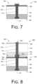
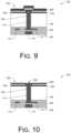
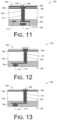
- FIGS. 7 - 13show a cross-section of an example substrate with at least one end of the TSV as a bonding surface, illustrating an example backside process of the substrate, according to an embodiment.
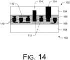
- FIG. 14shows a diagram of example TSVs used for heat management of a die, according to various embodiments.
- FIG. 15is a text flow diagram illustrating an example process of forming a microelectronic assembly to reduce or eliminate delamination of the bonded substrates, according to an embodiment.
- TSVmay extend partially or fully through the substrate of the device, and at least one end of the TSV is exposed at a bonding surface of the device.
- the exposed end of the TSVis prepared and used as a bonding surface or in place of a bonding pad for the device.
- an exposed metal end of the TSV at the bonding surfacecan become recessed relative to the dielectric, due to the softer material of the TSV relative to the material of the dielectric.
- a larger diameter TSVmay become recessed to a greater degree (e.g., a deeper recess) than a smaller diameter TSV.
- the recess of the end surface of the TSVprovides room for the metal expansion of the TSV during heated annealing, which can reduce or eliminate delamination that could occur otherwise.
- an example processincludes providing a conductive via through a first substrate having a first bonding surface.
- the conductive viaextends from the first bonding surface at least partially through the first substrate.
- the processincludes exposing the conductive via from a surface opposite the first bonding surface, and forming a second bonding surface with the conductive via at or recessed relative to the second bonding surface.
- the processincludes reducing or eliminating delamination of bonded microelectronic components by selecting the conductive via and using at least one end of the conductive via as a bonding contact surface for direct bonding (e.g., DBI).
- DBIdirect bonding
- the back side of the first substratemay also be processed for bonding.
- One or more insulating layers of preselected materialsmay be deposited on the back side of the first substrate to provide stress relief when the back side of the first substrate is to be direct bonded.
- the conductive via, as well as other conductive vias within the first substratemay be used to direct or transfer heat within the first substrate and/or away from the first substrate.
- the thermal transfer conductive viasmay extend partially or fully through a thickness of the first substrate and may include a thermally conductive barrier layer.
- barrier layers normally used around the conductive vias that tend to be thermally insulatingmay be replaced with thermally conductive layers instead.
- some conductive viasmay be used for signal transfer and thermal transfer.
- a microelectronic assemblycomprises a first substrate having a front side and a back side, where the back side has a bonding surface comprising a nonconductive bonding layer and a conductive via.
- a second substratehas a front side and a back side, and the front side includes a nonconductive bonding layer and a conductive feature.
- the front side of the second substrateis direct bonded to the back side of the first substrate such that the conductive pad contacts to the conductive feature.
- An exposed end of the conductive viacomprises a contact surface suitable for direct metal-to-metal bonding without an intervening material.
- patterned metal and oxide layersare frequently provided on a die, wafer, or other substrate (hereinafter “die 102 ”) as a hybrid bonding, or DBI®, surface layer.
- a representative device die 102may be formed using various techniques, to include a base substrate 104 and one or more insulating or dielectric layers 106 .
- the base substrate 104may be comprised of silicon, germanium, glass, quartz, a dielectric surface, direct or indirect gap semiconductor materials or layers or another suitable material.
- the insulating layer 106is deposited or formed over the substrate 104 , and may be comprised of an inorganic dielectric material layer such as oxide, nitride, oxynitride, oxycarbide, carbides, carbonitrides, diamond, diamond like materials, glasses, ceramics, glass-ceramics, and the like.
- an inorganic dielectric material layersuch as oxide, nitride, oxynitride, oxycarbide, carbides, carbonitrides, diamond, diamond like materials, glasses, ceramics, glass-ceramics, and the like.
- a bonding surface 108 of the device wafer 102can include conductive features such as contact pads 110 , traces 112 , and other interconnect structures, for example, embedded into the insulating layer 106 and arranged so that the conductive features 110 from respective bonding surfaces 108 of opposing devices can be mated and joined during bonding, if desired.
- the joined conductive features 110can form continuous conductive interconnects (for signals, power, etc.) between stacked devices.
- Damascene processesmay be used to form the embedded conductive features 110 in the insulating layer 106 .
- the conductive features 110may be comprised of metals (e.g., copper, etc.) or other conductive materials, or combinations of materials, and include structures, traces, pads, patterns, and so forth.
- a barrier layermay be deposited in the cavities for the conductive features 110 prior to depositing the material of the conductive features 110 , such that the barrier layer is disposed between the conductive features 110 and the insulating layer 106 .
- the barrier layermay be comprised of tantalum, for example, or another conductive material, to prevent or reduce diffusion of the material of the conductive features 110 into the insulating layer 106 .
- Forming the bonding surface 108includes finishing the surface 108 to meet dielectric roughness specifications and metallic layer (e.g., copper, etc.) recess specifications, to prepare the surface 108 for direct bonding.
- the bonding surface 108is formed to be as flat and smooth as possible, with very minimal surface topology variance.
- Various conventional processessuch as chemical mechanical polishing (CMP), dry or wet etching, and so forth, may be used to achieve the low surface roughness. These processes provides the flat, smooth surface 108 that results in a reliable bond.
- a patterned metal and insulating layer 106 with prepared bonding surfaces 108may be provided on both sides of the die 102 .
- the insulating layer 106is typically highly planar (usually to nm-level roughness) with the metal layer (e.g., embedded conductive features 110 ) at or recessed just below the bonding surface 108 .
- the amount of recess below the surface 108 of the insulating layer 106is typically determined by a dimensional tolerance, specification, or physical limitation.
- the bonding surfaces 108are often prepared for direct bonding with another die, wafer, or other substrate using a chemical-mechanical polishing (CMP) step and/or other preparation steps.
- CMPchemical-mechanical polishing
- Some embedded conductive features or interconnect structuresmay comprise metal pads 110 or conductive traces 112 that extend partially into the dielectric substrate 106 below the prepared surface 108 .
- some patterned metal (e.g., copper) features 110 or 112may be about 0.5-2 microns thick. The metal of these features 110 or 112 may expand as the metal is heated during annealing.
- Other conductive interconnect structuresmay comprise metal (e.g., copper) through silicon vias (TSVs) 114 or the like, that extend normal to the bonding surface 108 , partly or fully through the substrate 102 and include a larger quantity of metal.
- TSVssilicon vias
- a TSV 114may extend about 50 microns, depending on the thickness of the substrate 102 .
- the metal of the TSV 114may also expand when heated.
- Pads 110 and/or traces 112may or may not be electrically coupled to TSVs 114 , as shown in FIG. 1 A .
- dies 102may be direct bonded, for instance, without adhesive to other dies 102 with metal pads 110 , traces 112 , and/or TSVs 114 .
- a metal pad 110is positioned over a TSV 114 (overlapping and physically and electrically coupled to the TSV 114 )
- the expansion of the TSV 114 metalcan contribute to the expansion of the pad 110 metal.
- the combined metal expansioncan cause localized delamination 202 of the bonding surfaces at the location of the TSV 114 (or TSV 114 /pad 110 combination), as the expanding metal rises above the bonding surface 108 .
- the expanded metalcan separate the bonded dielectric surfaces 108 of the stacked dies 102 .
- a TSV 114may be extended through the base layer 104 of the die 102 , and through one or more insulating layers 106 to at least one bonding surface 108 .
- An end 302 (or both ends 302 ) of the TSV 114may be exposed at the bonding surface(s) 108 of the die 102 and used as a contact surface for direct bonding (e.g., DBI).
- the contact surface 302 of the TSVcan be exposed through the dielectric layer 106 at the bonding surface, prepared (e.g., planarized, etc.), and used in place of a direct bonding pad (instead of a contact pad 110 ).
- using an end surface 302 of the TSV 114 as a bonding surfacecan reduce or eliminate delamination of bonded dies 102 , when the dies 102 are heat annealed and the metal of the TSV 114 and the contact pads 110 expand.
- the metal expansion of the TSV 114may be taken into consideration, based on the volume of the TSV 114 . Accordingly, a predetermined recess “d” in the end surface 302 of the TSV 114 (as shown in FIG. 5 , for example) can be sufficient to provide room for the material expansion of the TSV 114 .
- TSVs 114 used as direct bonding contact structuresmay have diameters that are larger or smaller by a preselected amount, than other TSVs 114 disposed elsewhere within the die 102 .
- the size of the TSVs 114are selected or formed by estimating an amount that the material of the TSV 114 will expand when heated to a preselected temperature ( ⁇ 300°), based on a volume of the material of the TSV 114 and a coefficient of thermal expansion (CTE) of the material of the TSV 114 , and predicting an amount that the material of the TSV 114 will expand when heated to the preselected temperature.
- a preselected temperature⁇ 300°
- CTEcoefficient of thermal expansion
- the end 302 of the TSV 114is planarized along with the bonding surface 108 of the dielectric layer 106 , including recessing the end 302 of the TSV 114 to have a predetermined recess depth (“d”) relative to the bonding surface 108 , based on an expansion of the TSV 114 material at the predetermined temperature.
- the recess depthis determined based on the volume of the material of the TSV 114 and the coefficient of thermal expansion (CTE) of the material of the TSV 114 .
- the end 302 of a TSV 114may be selectively etched (via acid etching, plasma oxidation, etc.) to provide the desired recess depth “d” (to accommodate a predicted metal expansion).
- the end 302 of a corresponding TSV 114may be selected, formed, or processed to have an uneven top surface as an expansion buffer.
- the end surface 302 of the TSV 114may be formed or selectively etched to be rounded, domed, convex, concave, irregular, or otherwise non-flat to allow additional space 602 for material expansion.
- the additional space 602may be determined and formed based on the amount that the material of the TSV 114 will expand when heated.
- the end surface 302 of the TSV 114may be formed to be uneven during deposition, or may be etched, grinded, polished, or otherwise made uneven after forming the TSV 114 . In some cases, the end surface 302 of the TSV 114 may be made uneven during CMP of the bonding surface 108 .
- the dielectric 106 at the bonding surface 108 around the TSV 114can be formed or shaped to allow room for the metal of the TSV 114 to expand.
- a CMP processcan be used to shape the surface 108 of the dielectric 106 around the TSV 114 , or in other examples other processes can be used, so that the dielectric 106 around the TSV 114 includes a recess or other gap that provides room for metal expansion.
- the dielectric 106can be recessed (e.g., with CMP) while the bonding surface 108 is being prepared.
- the TSV 114 and the dielectric 106may be recessed concurrently (but at different rates). For instance, the process may form erosion in the dielectric 106 around the edges of the TSV 114 while recessing the metal TSV 114 .
- the TSV 114is comprised of copper, a copper alloy, or the like.
- the materials of the TSV 114may be varied to control metal expansion and potential resulting delamination.
- the TSV 114may be comprised of different conductive materials, perhaps with lower CTEs.
- the TSV 114may be comprised of a different conductive material (with a lower CTE) than the contact pads 110 .
- the TSV 114may be comprised of tungsten, an alloy, or the like.
- the volume of material of the TSV 114may be varied to control metal expansion and the potential for resulting delamination.
- a TSV 114 with a preselected material volumee.g., less volume of material
- the preselection of volume of the TSV 114may be based on anticipated material expansion of the TSV 114 .
- the die 102may be direct bonded, for instance, without adhesive to other dies 102 with metal pads 110 , traces 112 , and/or TSVs 114 .
- the material of the TSVs 114expand during heated annealing as mating TSVs 114 of opposite dies 102 bond to form a single conductive interconnect.
- the metal expansiondoes not cause delamination of the bonding surfaces when an adequate predetermined recess is provided as discussed, since the expanding metal of the TSV 114 does not exceed the space provided by the recess at the end surface 302 of the TSV 114 .
- the expanding metal of the TSVs 114fills the recess(es) without separating the bonded dielectric surfaces 108 of the stacked dies 102 .
- the TSVs 114 exposed at the bonding surface 108can become recessed (intentionally or unintentionally) relative to the dielectric 106 , due to the softness of the TSVs 114 (which may comprise copper, for instance) relative to the dielectric 106 (which may comprise an oxide, for example).
- the amount of recessing of a TSV 114may be predictable, based on the surface preparation technique used (e.g., the chemical combination used, the speed of the polishing equipment, etc.), the materials of the dielectric layer 106 and the TSV 114 , the spacing or density of the TSVs 114 (and metal pads 110 ), and the size (e.g., area or diameter) of the TSVs 114 .
- the area or diameter of the TSVs 114may be selected (e.g., for a particular material) to avoid delamination of bonded dies 102 based on the recess desired and the expected metal expansion of the TSVs 114 .
- TSVs 114may be selected when increased recessing is desired. This technique can result in reduced or eliminated delamination, as well as dependable mechanical coupling of the dielectric 106 and metal structures (e.g., TSVs 114 ) at the bonding surfaces 108 and reliable electrical continuity of the bonded metal structures.
- FIGS. 7 - 13illustrate examples of backside die 102 processing, according to various embodiments.
- the backside 702 of the die 102may receive different preparation than the topside bonding surface 108 , when the backside 702 is prepared for direct bonding.
- the backside 702may be prepared differently to reduce process steps, reduce manufacturing costs, or for other reasons.
- the backside 702is prepared so that the TSV 114 is exposed, to be used as a contact surface 302 for bonding to a conductive pad, interconnect, or other conductive bonding surface.
- the preparationmay include depositing a thin layer of insulating material and planarizing (via CMP, for example) the backside 702 (which may include planarizing the insulating material and/or the base substrate 104 ) to reveal the TSV 114 .
- CMPplanarizing
- one or more layers of materialmay be deposited on the backside 702 as a stress relief to prevent or eliminate damage to the substrate 104 and the die 102 .
- the layers of materialcan be planarized and otherwise prepared as a bonding surface on the backside 702 of the die 102 .
- the TSV 114is disposed within the die 102 , transverse to the bonding surface 108 of the die 102 .
- the TSV 114may initially extend beyond the surface of the backside 702 of the die 102 .
- a diffusion barrier and oxide liner 704surrounds the TSV 114 to prevent diffusion of the metal of the TSV 114 (e.g., copper) into the material of the base substrate 104 (e.g., silicon).
- another diffusion barrier 706is deposited on the surface of the backside 702 of the die 102 .
- the diffusion barrier 706comprises a dielectric, such as a nitride or the like.
- one or more insulating layersare then deposited onto the backside 702 of the die 102 to prevent damage to the die 102 when the material of the TSV 114 expands.
- a first layer 708comprising a first low temperature dielectric, such as an oxide, may be deposited over the backside 702 , including over the diffusion layer 706 .
- the first oxide layer 708may comprise a low temperature oxide bonding layer.
- FIG. 7shows this scenario, and includes a formed contact pad 110 on the front side bonding surface 108 over the TSV 114 .
- the backside 702is planarized (via CMP, for example), including the one or more insulating layers 708 to form a flat, smooth bonding surface for direct bonding.
- the remaining dielectric layer 708can assist with warpage control, balancing with the front side of the die 102 .
- the TSV 114is exposed by the planarizing, including a revealed contact surface 302 of the TSV 114 .
- the oxidewhen some types of low temperature oxide (e.g., silox, etc.) are used, the oxide may be less rigid and the TSV 114 may be more prone to breaking during planarization. Once planarized, the oxide is more stable.
- the oxidemay give better support to the TSV 114 , but the oxide may also relax, leaving the area around the TSV 114 higher ( ⁇ 1-10 nm) than the bonding surface, which can cause problems with direct bonding (e.g., DBI).
- the DBI bonding layerthe layer 708 , for example is added on top of the TSV 114 , as shown in FIG. 7 .
- a second die 802 similar or identical to the die 102is also shown at FIG. 8 , in dashed lines.
- the illustration of FIG. 8shows an example of a front-to back direct bonding arrangement (without adhesive), where the second die 802 is bonded (dielectric-to-dielectric) at the front side 108 of the second die 802 to the backside 702 of the first die 102 .
- the surface 302 of the revealed TSV 114 at the backside 702 of the first die 102is bonded (metal-to-metal) to the conductive pad 110 at the second die 802 .
- the dies 102 and 802may be bonded front-to-front, or back-to-back.
- multiple layersmay be added to the backside 702 to reduce metal expansion stress at the TSV 114 and to form a backside 702 bonding surface for the die 102 .
- a second dielectric layer 902(which may comprise a low temperature oxide) may be deposited over the first layer 708 . No barrier or adhesion layer is needed between the two oxide layers ( 708 and 902 ).
- the first layer 708 and the second layer 902are comprised of similar or the same materials (in varying thicknesses).
- first layer 708 and the second layer 902are comprised of different materials.
- the second oxide layer 902may have a similar or a different residue stress characteristic than the first layer 708 (for example, the first layer 708 may be compressive and the second layer 902 may be tensile, or vice versa, or both layers 708 and 902 may be compressive or tensile with similar or different values).
- additional insulating layersmay also be deposited over the first 708 and second 902 layers.
- the layers 708 and 902are planarized (e.g., CMP), revealing the TSV 114 and the end surface 302 , which can function in place of a bonding pad.
- part of the second layer 902may be left on the die 102 for warpage control.
- the end surface 302 at the backside 702may be formed to have an uneven or non-flat surface topology.
- the end surface 302may be selected, formed, or processed to have an uneven surface topology as an expansion buffer.
- the end surface 302 of the TSV 114may be formed or selectively etched to be rounded, domed, convex, concave, irregular, or otherwise non-flat to allow additional space 1102 for material expansion.
- the additional space 1102may be determined and formed based on the prediction of the amount that the material of the TSV 114 will expand when heated.
- the end surface 302 of the TSV 114may be formed to be uneven during deposition, or may be etched, grinded, polished, or otherwise made uneven after forming the TSV 114 .
- the end surface 302 of the TSV 114may be made uneven during CMP of the backside 702 bonding surface.
- FIGS. 12 - 13illustrate examples of processing the backside 702 of the die 102 , when an offset contact pad 110 is disposed on the front side 108 , according to various embodiments.
- the offset contact pad 110may be coupled to the TSV 114 using one or more traces 112 , or the like.
- one or more oxide stress layers(such as layer 708 , for example) may be deposited on the backside 702 after depositing a diffusion barrier layer 706 over the backside 702 .
- the stress layer 708may also comprise a direct bonding layer when it is the final layer on the backside 702 .
- the layer 708is planarized to form a bonding surface and to reveal the TSV 114 with a smooth contact surface 302 .
- multiple stress layersmay be deposited and planarized at the backside 702 in preparation for direct bonding.
- alternate techniquesmay be used to reduce or eliminate delamination due to metal feature expansion, and remain within the scope of the disclosure.
- one or more of the TSVs 114 of a set of stacked dies 102may be used to conduct heat in addition to or instead of electrical signals.
- a heat sinkor other heat transfer device
- other techniquesmay be looked-for to transfer heat as desired.
- various configurations of TSVs 114may be employed to conduct heat away from the dies 102 (or away from a heat-generating portion of the dies 102 ).
- the TSVs 114 of one die 102may be used in conjunction with TSVs 114 , contact pads 110 , traces 112 , and the like, of the second die 102 to complete heat transfer from one die 102 to the other die 102 , and so forth.
- the TSVs 114 of the first die 102can be direct bonded (e.g., DBI) to the TSVs 114 , contact pads 110 , traces 112 , and the like of the second die 102 for high performance thermal conductivity.
- some of the TSVs 114 , contact pads 110 , traces 112 , and the likeare electrically floating or “dummy” structures, which can be used for thermal transfer. These structures may conduct heat away from a high power die 102 to another die 102 or substrate as desired. Dummy contact pads 110 may be coupled to via last or via mid thermal TSVs 114 for thermal conduction.
- diffusion barrier layers 704which surround the TSVs 114 and can be thermally restrictive or thermal barriers may be replaced by diffusion barriers of a different material having some thermal conductivity (such as metal or alloy barriers, or the like).
- FIG. 15illustrates a representative process 1500 for preparing various microelectronic components (such as dies 102 , for example) for bonding, such as for direct bonding without adhesive, while reducing or eliminating the potential for delamination due to metal expansion of embedded structures at the bonding surface.
- various microelectronic componentssuch as dies 102 , for example
- bondingsuch as for direct bonding without adhesive
- TSVsthrough-silicon vias
- the processrefers to FIGS. 1 - 14 .
- a die, wafer, or other substrateis formed using various techniques to include a base substrate and one or more dielectric layers.
- the process 1500includes providing a conductive via (such as TSV 114 , for example) through a first substrate having a first bonding surface (such as bonding surface 108 , for example), the conductive via extending from the first bonding surface at least partially through the first substrate.
- the first viaextends at least partially through the first substrate, normal to the first bonding surface.
- the first viaextends through the first substrate to one or both surfaces of the first substrate.
- the processincludes exposing the conductive via from a surface opposite the first bonding surface.
- the processincludes forming a recess in an exposed end of the conductive via extending a predetermined depth below the second bonding surface. For example, the recess compensates for the expansion of the conductive via during a bonding process.
- the processincludes forming the exposed end of the conductive via such that there is a sloped gap between the conductive via and the second bonding surface.
- the uneven topologycreates space for via metal expansion during heated annealing.
- the processincludes forming a second bonding surface with the conductive via at or recessed relative to the second bonding surface.
- the processincludes providing a second substrate and direct bonding the second bonding surface of the first substrate to the second substrate without an intervening adhesive. In an implementation, the process includes direct bonding the first substrate to the second substrate using a direct dielectric-to-dielectric, non-adhesive bonding technique at a bonding surface of the first substrate.
- the second substratefurther includes a conductive via extending at least partially therethrough.
- the second substratefurther includes a pad over the conductive via of the second substrate, the pad contacting the conductive via of the first substrate.
- the conductive via of the first substrateis substantially aligned with the conductive via of the second substrate.
- the conductive viais configured to remove heat from the first substrate.
- process stepsmay be modified or eliminated, in comparison to the process steps described herein.
Landscapes
- Engineering & Computer Science (AREA)
- Microelectronics & Electronic Packaging (AREA)
- Power Engineering (AREA)
- Computer Hardware Design (AREA)
- Physics & Mathematics (AREA)
- Condensed Matter Physics & Semiconductors (AREA)
- General Physics & Mathematics (AREA)
- Manufacturing & Machinery (AREA)
- Internal Circuitry In Semiconductor Integrated Circuit Devices (AREA)
Abstract
Description
Claims (22)
Priority Applications (7)
| Application Number | Priority Date | Filing Date | Title |
|---|---|---|---|
| PCT/US2019/036818WO2019241417A1 (en) | 2018-06-13 | 2019-06-12 | Tsv as pad |
| US16/439,360US11749645B2 (en) | 2018-06-13 | 2019-06-12 | TSV as pad |
| KR1020217000800AKR20210009426A (en) | 2018-06-13 | 2019-06-12 | TV as a pad |
| TW113150067ATW202516641A (en) | 2018-06-13 | 2019-06-13 | Methods of forming a microelectronic assembly and microelectronic assemblies |
| TW108120530ATWI870352B (en) | 2018-06-13 | 2019-06-13 | Methods of forming a microelectronic assembly and microelectronic assemblies |
| US18/451,674US12205926B2 (en) | 2018-06-13 | 2023-08-17 | TSV as pad |
| US19/003,994US20250253294A1 (en) | 2018-06-13 | 2024-12-27 | Tsv as pad |
Applications Claiming Priority (2)
| Application Number | Priority Date | Filing Date | Title |
|---|---|---|---|
| US201862684505P | 2018-06-13 | 2018-06-13 | |
| US16/439,360US11749645B2 (en) | 2018-06-13 | 2019-06-12 | TSV as pad |
Related Child Applications (1)
| Application Number | Title | Priority Date | Filing Date |
|---|---|---|---|
| US18/451,674ContinuationUS12205926B2 (en) | 2018-06-13 | 2023-08-17 | TSV as pad |
Publications (2)
| Publication Number | Publication Date |
|---|---|
| US20190385935A1 US20190385935A1 (en) | 2019-12-19 |
| US11749645B2true US11749645B2 (en) | 2023-09-05 |
Family
ID=68840253
Family Applications (7)
| Application Number | Title | Priority Date | Filing Date |
|---|---|---|---|
| US16/439,360ActiveUS11749645B2 (en) | 2018-06-13 | 2019-06-12 | TSV as pad |
| US16/440,633ActiveUS10998292B2 (en) | 2018-06-13 | 2019-06-13 | Offset pads over TSV |
| US17/246,845ActiveUS11728313B2 (en) | 2018-06-13 | 2021-05-03 | Offset pads over TSV |
| US18/346,403ActiveUS12243851B2 (en) | 2018-06-13 | 2023-07-03 | Offset pads over TSV |
| US18/451,674ActiveUS12205926B2 (en) | 2018-06-13 | 2023-08-17 | TSV as pad |
| US19/003,994PendingUS20250253294A1 (en) | 2018-06-13 | 2024-12-27 | Tsv as pad |
| US19/068,395PendingUS20250300135A1 (en) | 2018-06-13 | 2025-03-03 | Offset pads over tsv |
Family Applications After (6)
| Application Number | Title | Priority Date | Filing Date |
|---|---|---|---|
| US16/440,633ActiveUS10998292B2 (en) | 2018-06-13 | 2019-06-13 | Offset pads over TSV |
| US17/246,845ActiveUS11728313B2 (en) | 2018-06-13 | 2021-05-03 | Offset pads over TSV |
| US18/346,403ActiveUS12243851B2 (en) | 2018-06-13 | 2023-07-03 | Offset pads over TSV |
| US18/451,674ActiveUS12205926B2 (en) | 2018-06-13 | 2023-08-17 | TSV as pad |
| US19/003,994PendingUS20250253294A1 (en) | 2018-06-13 | 2024-12-27 | Tsv as pad |
| US19/068,395PendingUS20250300135A1 (en) | 2018-06-13 | 2025-03-03 | Offset pads over tsv |
Country Status (6)
| Country | Link |
|---|---|
| US (7) | US11749645B2 (en) |
| EP (1) | EP3807927A4 (en) |
| KR (2) | KR20210009426A (en) |
| CN (4) | CN120413551A (en) |
| TW (2) | TWI870352B (en) |
| WO (2) | WO2019241417A1 (en) |
Cited By (6)
| Publication number | Priority date | Publication date | Assignee | Title |
|---|---|---|---|---|
| US11967575B2 (en) | 2018-08-29 | 2024-04-23 | Adeia Semiconductor Bonding Technologies Inc. | Bond enhancement structure in microelectronics for trapping contaminants during direct-bonding processes |
| US12051621B2 (en) | 2016-12-28 | 2024-07-30 | Adeia Semiconductor Bonding Technologies Inc. | Microelectronic assembly from processed substrate |
| US12068278B2 (en) | 2017-05-11 | 2024-08-20 | Adeia Semiconductor Bonding Technologies Inc. | Processed stacked dies |
| US12205926B2 (en) | 2018-06-13 | 2025-01-21 | Adeia Semiconductor Bonding Technologies Inc. | TSV as pad |
| US12248869B2 (en) | 2017-08-03 | 2025-03-11 | Adeia Semiconductor Inc. | Three dimensional circuit implementing machine trained network |
| US12406959B2 (en) | 2018-07-26 | 2025-09-02 | Adeia Semiconductor Bonding Technologies Inc. | Post CMP processing for hybrid bonding |
Families Citing this family (98)
| Publication number | Priority date | Publication date | Assignee | Title |
|---|---|---|---|---|
| US7109092B2 (en) | 2003-05-19 | 2006-09-19 | Ziptronix, Inc. | Method of room temperature covalent bonding |
| US7485968B2 (en) | 2005-08-11 | 2009-02-03 | Ziptronix, Inc. | 3D IC method and device |
| US8735219B2 (en) | 2012-08-30 | 2014-05-27 | Ziptronix, Inc. | Heterogeneous annealing method and device |
| US10886250B2 (en) | 2015-07-10 | 2021-01-05 | Invensas Corporation | Structures and methods for low temperature bonding using nanoparticles |
| US9953941B2 (en) | 2015-08-25 | 2018-04-24 | Invensas Bonding Technologies, Inc. | Conductive barrier direct hybrid bonding |
| US10204893B2 (en) | 2016-05-19 | 2019-02-12 | Invensas Bonding Technologies, Inc. | Stacked dies and methods for forming bonded structures |
| US10580735B2 (en) | 2016-10-07 | 2020-03-03 | Xcelsis Corporation | Stacked IC structure with system level wiring on multiple sides of the IC die |
| US10672663B2 (en) | 2016-10-07 | 2020-06-02 | Xcelsis Corporation | 3D chip sharing power circuit |
| TWI822659B (en) | 2016-10-27 | 2023-11-21 | 美商艾德亞半導體科技有限責任公司 | Structures and methods for low temperature bonding |
| US10002844B1 (en) | 2016-12-21 | 2018-06-19 | Invensas Bonding Technologies, Inc. | Bonded structures |
| CN117878055A (en) | 2016-12-28 | 2024-04-12 | 艾德亚半导体接合科技有限公司 | Stacking substrate processing |
| TWI837879B (en) | 2016-12-29 | 2024-04-01 | 美商艾德亞半導體接合科技有限公司 | Bonded structures with integrated passive component |
| WO2018169968A1 (en) | 2017-03-16 | 2018-09-20 | Invensas Corporation | Direct-bonded led arrays and applications |
| US10515913B2 (en) | 2017-03-17 | 2019-12-24 | Invensas Bonding Technologies, Inc. | Multi-metal contact structure |
| US10508030B2 (en) | 2017-03-21 | 2019-12-17 | Invensas Bonding Technologies, Inc. | Seal for microelectronic assembly |
| US10269756B2 (en) | 2017-04-21 | 2019-04-23 | Invensas Bonding Technologies, Inc. | Die processing |
| US10446441B2 (en) | 2017-06-05 | 2019-10-15 | Invensas Corporation | Flat metal features for microelectronics applications |
| US10217720B2 (en) | 2017-06-15 | 2019-02-26 | Invensas Corporation | Multi-chip modules formed using wafer-level processing of a reconstitute wafer |
| US10840205B2 (en) | 2017-09-24 | 2020-11-17 | Invensas Bonding Technologies, Inc. | Chemical mechanical polishing for hybrid bonding |
| US11031285B2 (en) | 2017-10-06 | 2021-06-08 | Invensas Bonding Technologies, Inc. | Diffusion barrier collar for interconnects |
| US10923408B2 (en) | 2017-12-22 | 2021-02-16 | Invensas Bonding Technologies, Inc. | Cavity packages |
| US11380597B2 (en) | 2017-12-22 | 2022-07-05 | Invensas Bonding Technologies, Inc. | Bonded structures |
| US10727219B2 (en) | 2018-02-15 | 2020-07-28 | Invensas Bonding Technologies, Inc. | Techniques for processing devices |
| US11169326B2 (en) | 2018-02-26 | 2021-11-09 | Invensas Bonding Technologies, Inc. | Integrated optical waveguides, direct-bonded waveguide interface joints, optical routing and interconnects |
| US11256004B2 (en) | 2018-03-20 | 2022-02-22 | Invensas Bonding Technologies, Inc. | Direct-bonded lamination for improved image clarity in optical devices |
| US10991804B2 (en) | 2018-03-29 | 2021-04-27 | Xcelsis Corporation | Transistor level interconnection methodologies utilizing 3D interconnects |
| US11056348B2 (en) | 2018-04-05 | 2021-07-06 | Invensas Bonding Technologies, Inc. | Bonding surfaces for microelectronics |
| US10790262B2 (en) | 2018-04-11 | 2020-09-29 | Invensas Bonding Technologies, Inc. | Low temperature bonded structures |
| US11244916B2 (en) | 2018-04-11 | 2022-02-08 | Invensas Bonding Technologies, Inc. | Low temperature bonded structures |
| US10964664B2 (en) | 2018-04-20 | 2021-03-30 | Invensas Bonding Technologies, Inc. | DBI to Si bonding for simplified handle wafer |
| US11004757B2 (en) | 2018-05-14 | 2021-05-11 | Invensas Bonding Technologies, Inc. | Bonded structures |
| US11276676B2 (en) | 2018-05-15 | 2022-03-15 | Invensas Bonding Technologies, Inc. | Stacked devices and methods of fabrication |
| US10923413B2 (en) | 2018-05-30 | 2021-02-16 | Xcelsis Corporation | Hard IP blocks with physically bidirectional passageways |
| US11393779B2 (en) | 2018-06-13 | 2022-07-19 | Invensas Bonding Technologies, Inc. | Large metal pads over TSV |
| US10910344B2 (en) | 2018-06-22 | 2021-02-02 | Xcelsis Corporation | Systems and methods for releveled bump planes for chiplets |
| WO2020010056A1 (en) | 2018-07-03 | 2020-01-09 | Invensas Bonding Technologies, Inc. | Techniques for joining dissimilar materials in microelectronics |
| US11158606B2 (en) | 2018-07-06 | 2021-10-26 | Invensas Bonding Technologies, Inc. | Molded direct bonded and interconnected stack |
| US11462419B2 (en) | 2018-07-06 | 2022-10-04 | Invensas Bonding Technologies, Inc. | Microelectronic assemblies |
| US11515291B2 (en) | 2018-08-28 | 2022-11-29 | Adeia Semiconductor Inc. | Integrated voltage regulator and passive components |
| US11011494B2 (en) | 2018-08-31 | 2021-05-18 | Invensas Bonding Technologies, Inc. | Layer structures for making direct metal-to-metal bonds at low temperatures in microelectronics |
| US11158573B2 (en) | 2018-10-22 | 2021-10-26 | Invensas Bonding Technologies, Inc. | Interconnect structures |
| US11244920B2 (en) | 2018-12-18 | 2022-02-08 | Invensas Bonding Technologies, Inc. | Method and structures for low temperature device bonding |
| CN113330557A (en) | 2019-01-14 | 2021-08-31 | 伊文萨思粘合技术公司 | Bonding structure |
| US11387202B2 (en) | 2019-03-01 | 2022-07-12 | Invensas Llc | Nanowire bonding interconnect for fine-pitch microelectronics |
| US11901281B2 (en) | 2019-03-11 | 2024-02-13 | Adeia Semiconductor Bonding Technologies Inc. | Bonded structures with integrated passive component |
| US10867963B2 (en)* | 2019-03-14 | 2020-12-15 | Taiwan Semiconductor Manufacturing Company, Ltd. | Die stack structure and method of fabricating the same |
| US10854578B2 (en) | 2019-03-29 | 2020-12-01 | Invensas Corporation | Diffused bitline replacement in stacked wafer memory |
| US11610846B2 (en) | 2019-04-12 | 2023-03-21 | Adeia Semiconductor Bonding Technologies Inc. | Protective elements for bonded structures including an obstructive element |
| US11373963B2 (en) | 2019-04-12 | 2022-06-28 | Invensas Bonding Technologies, Inc. | Protective elements for bonded structures |
| US11205625B2 (en) | 2019-04-12 | 2021-12-21 | Invensas Bonding Technologies, Inc. | Wafer-level bonding of obstructive elements |
| US11355404B2 (en) | 2019-04-22 | 2022-06-07 | Invensas Bonding Technologies, Inc. | Mitigating surface damage of probe pads in preparation for direct bonding of a substrate |
| US11385278B2 (en) | 2019-05-23 | 2022-07-12 | Invensas Bonding Technologies, Inc. | Security circuitry for bonded structures |
| US12374641B2 (en) | 2019-06-12 | 2025-07-29 | Adeia Semiconductor Bonding Technologies Inc. | Sealed bonded structures and methods for forming the same |
| US11315871B2 (en)* | 2019-06-13 | 2022-04-26 | Nanya Technology Corporation | Integrated circuit device with bonding structure and method of forming the same |
| US11296053B2 (en) | 2019-06-26 | 2022-04-05 | Invensas Bonding Technologies, Inc. | Direct bonded stack structures for increased reliability and improved yield in microelectronics |
| US20210320075A1 (en)* | 2019-07-26 | 2021-10-14 | Sandisk Technologies Llc | Bonded assembly containing bonding pads spaced apart by polymer material, and methods of forming the same |
| US11264343B2 (en)* | 2019-08-30 | 2022-03-01 | Taiwan Semiconductor Manufacturing Co., Ltd. | Bond pad structure for semiconductor device and method of forming same |
| US12080672B2 (en) | 2019-09-26 | 2024-09-03 | Adeia Semiconductor Bonding Technologies Inc. | Direct gang bonding methods including directly bonding first element to second element to form bonded structure without adhesive |
| US12113054B2 (en) | 2019-10-21 | 2024-10-08 | Adeia Semiconductor Technologies Llc | Non-volatile dynamic random access memory |
| US11862602B2 (en) | 2019-11-07 | 2024-01-02 | Adeia Semiconductor Technologies Llc | Scalable architecture for reduced cycles across SOC |
| US11762200B2 (en) | 2019-12-17 | 2023-09-19 | Adeia Semiconductor Bonding Technologies Inc. | Bonded optical devices |
| US11876076B2 (en) | 2019-12-20 | 2024-01-16 | Adeia Semiconductor Technologies Llc | Apparatus for non-volatile random access memory stacks |
| US11721653B2 (en) | 2019-12-23 | 2023-08-08 | Adeia Semiconductor Bonding Technologies Inc. | Circuitry for electrical redundancy in bonded structures |
| CN115088068A (en) | 2019-12-23 | 2022-09-20 | 伊文萨思粘合技术公司 | Electrical redundancy for bonded structures |
| US12148687B2 (en) | 2020-02-25 | 2024-11-19 | Tokyo Electron Limited | Split substrate interposer with integrated passive device |
| WO2021188846A1 (en) | 2020-03-19 | 2021-09-23 | Invensas Bonding Technologies, Inc. | Dimension compensation control for directly bonded structures |
| US11742314B2 (en) | 2020-03-31 | 2023-08-29 | Adeia Semiconductor Bonding Technologies Inc. | Reliable hybrid bonded apparatus |
| US11569134B2 (en)* | 2020-04-14 | 2023-01-31 | International Business Machines Corporation | Wafer backside engineering for wafer stress control |
| US20210335660A1 (en)* | 2020-04-24 | 2021-10-28 | Nanya Technology Corporation | Semiconductor structure having void between bonded wafers and manufacturing method tehreof |
| WO2021236361A1 (en)* | 2020-05-19 | 2021-11-25 | Invensas Bonding Technologies, Inc. | Laterally unconfined structure |
| KR102861815B1 (en) | 2020-06-16 | 2025-09-17 | 삼성전자주식회사 | Interposer and semiconductor package including the same |
| US11631647B2 (en) | 2020-06-30 | 2023-04-18 | Adeia Semiconductor Bonding Technologies Inc. | Integrated device packages with integrated device die and dummy element |
| US11769752B2 (en)* | 2020-07-24 | 2023-09-26 | Micron Technology, Inc. | Stacked semiconductor die assemblies with substrate heat sinks and associated systems and methods |
| US11728273B2 (en) | 2020-09-04 | 2023-08-15 | Adeia Semiconductor Bonding Technologies Inc. | Bonded structure with interconnect structure |
| US11764177B2 (en) | 2020-09-04 | 2023-09-19 | Adeia Semiconductor Bonding Technologies Inc. | Bonded structure with interconnect structure |
| US11264357B1 (en) | 2020-10-20 | 2022-03-01 | Invensas Corporation | Mixed exposure for large die |
| KR20230097121A (en) | 2020-10-29 | 2023-06-30 | 아데이아 세미컨덕터 본딩 테크놀로지스 인코포레이티드 | Direct bonding method and structure |
| KR20220068056A (en) | 2020-11-18 | 2022-05-25 | 에스케이하이닉스 주식회사 | Semiconductor memory device and manufacturing method of the same |
| KR20230125309A (en)* | 2020-12-28 | 2023-08-29 | 아데이아 세미컨덕터 본딩 테크놀로지스 인코포레이티드 | Structures having through-substrate vias and methods for forming the same |
| JP2024501017A (en) | 2020-12-28 | 2024-01-10 | アデイア セミコンダクター ボンディング テクノロジーズ インコーポレイテッド | Structure with through-substrate via and method for forming the same |
| JP2024501559A (en) | 2020-12-30 | 2024-01-12 | アデイア セミコンダクター ボンディング テクノロジーズ インコーポレイテッド | Structures with conductive features and methods of forming the same |
| KR102853124B1 (en)* | 2020-12-30 | 2025-09-02 | 에스케이하이닉스 주식회사 | Semiconductor chip including through electrode, and semiconductor package including the same |
| CN114743942A (en)* | 2021-01-07 | 2022-07-12 | 联华电子股份有限公司 | Hybrid joint structure and method of making the same |
| US12322679B2 (en)* | 2021-03-18 | 2025-06-03 | Taiwan Semiconductor Manufacturing Company Limited | Semiconductor die including through substrate via barrier structure and methods for forming the same |
| CN115602556B (en)* | 2021-07-09 | 2025-07-04 | 长鑫存储技术有限公司 | Chip bonding method and semiconductor chip structure |
| US12119315B2 (en)* | 2021-07-09 | 2024-10-15 | Changxin Memory Technologies, Inc. | Chip bonding method and semiconductor chip structure |
| KR20240036698A (en) | 2021-08-02 | 2024-03-20 | 아데이아 세미컨덕터 본딩 테크놀로지스 인코포레이티드 | Protective semiconductor elements for combined structures |
| WO2023010259A1 (en)* | 2021-08-02 | 2023-02-09 | 华为技术有限公司 | Chip stacked structure and manufacturing method therefor, and chip packaging structure, and electronic device |
| CN117795326A (en)* | 2021-08-11 | 2024-03-29 | 新唐科技日本株式会社 | Hydrogen sensor |
| CN113471083B (en)* | 2021-09-03 | 2021-11-02 | 南通汇丰电子科技有限公司 | Semiconductor stack packaging structure and preparation method thereof |
| KR20230054192A (en) | 2021-10-15 | 2023-04-24 | 에스케이하이닉스 주식회사 | Semiconductor devices including substrates bonded each other and method for fabricating the same |
| US12040300B2 (en) | 2021-11-04 | 2024-07-16 | Airoha Technology Corp. | Semiconductor package using hybrid-type adhesive |
| TWI780985B (en)* | 2021-11-16 | 2022-10-11 | 力晶積成電子製造股份有限公司 | Semiconductor structure and manufacturing method of the same |
| CN119096348A (en)* | 2022-04-25 | 2024-12-06 | 美商艾德亚半导体接合科技有限公司 | Expansion control structure for direct bonding and method of forming the same |
| US12418103B2 (en)* | 2022-06-14 | 2025-09-16 | Tron Future Tech Inc. | Antenna package structure |
| US20240120312A1 (en)* | 2022-10-05 | 2024-04-11 | Tokyo Electron Limited | Shifted multi-via connection for hybrid bonding |
| US12341083B2 (en) | 2023-02-08 | 2025-06-24 | Adeia Semiconductor Bonding Technologies Inc. | Electronic device cooling structures bonded to semiconductor elements |
| US20250079366A1 (en)* | 2023-09-05 | 2025-03-06 | Micron Technology, Inc. | Semiconductor device with layered dielectric |
Citations (383)
| Publication number | Priority date | Publication date | Assignee | Title |
|---|---|---|---|---|
| JPS6130059A (en) | 1984-07-20 | 1986-02-12 | Nec Corp | Manufacturing method of semiconductor device |
| US4818728A (en) | 1986-12-03 | 1989-04-04 | Sharp Kabushiki Kaisha | Method of making a hybrid semiconductor device |
| JPH01168040A (en) | 1987-11-18 | 1989-07-03 | Grumman Aerospace Corp | Method of forming integrated circuit for touching electrical connection to external electronic circuit |
| US4904328A (en) | 1987-09-08 | 1990-02-27 | Gencorp Inc. | Bonding of FRP parts |
| US4939568A (en) | 1986-03-20 | 1990-07-03 | Fujitsu Limited | Three-dimensional integrated circuit and manufacturing method thereof |
| US4998665A (en) | 1988-09-07 | 1991-03-12 | Nec Corporation | Bonding structure of substrates and method for bonding substrates |
| EP0465227A2 (en) | 1990-07-02 | 1992-01-08 | Kabushiki Kaisha Toshiba | Composite integrated circuit device |
| US5087585A (en) | 1989-07-11 | 1992-02-11 | Nec Corporation | Method of stacking semiconductor substrates for fabrication of three-dimensional integrated circuit |
| JPH04259249A (en) | 1991-02-14 | 1992-09-14 | Mitsubishi Electric Corp | Semiconductor device |
| JPH0529183A (en) | 1991-07-22 | 1993-02-05 | Fuji Electric Co Ltd | Joining method |
| JPH05198739A (en) | 1991-09-10 | 1993-08-06 | Mitsubishi Electric Corp | Stacked semiconductor device and manufacturing method thereof |
| US5236118A (en) | 1992-05-12 | 1993-08-17 | The Regents Of The University Of California | Aligned wafer bonding |
| JPH0613456A (en) | 1992-09-28 | 1994-01-21 | Toshiba Corp | Method for manufacturing semiconductor device |
| US5322593A (en) | 1991-11-21 | 1994-06-21 | Nec Corporation | Method for manufacturing polyimide multilayer wiring substrate |
| JPH06260594A (en) | 1993-02-11 | 1994-09-16 | Siemens Ag | Preparation of three-dimensional circuit device |
| JPH0766093A (en) | 1993-08-23 | 1995-03-10 | Sumitomo Sitix Corp | Method and device for bonding semiconductor wafers |
| US5413952A (en) | 1994-02-02 | 1995-05-09 | Motorola, Inc. | Direct wafer bonded structure method of making |
| US5442235A (en) | 1993-12-23 | 1995-08-15 | Motorola Inc. | Semiconductor device having an improved metal interconnect structure |
| JPH07249749A (en) | 1994-03-11 | 1995-09-26 | Canon Inc | Method for manufacturing SOI substrate |
| JPH07283382A (en) | 1994-04-12 | 1995-10-27 | Sony Corp | Method of pasting silicon substrates |
| US5489804A (en) | 1989-08-28 | 1996-02-06 | Lsi Logic Corporation | Flexible preformed planar structures for interposing between a chip and a substrate |
| JPH0878645A (en) | 1994-09-05 | 1996-03-22 | Mitsubishi Materials Corp | Silicon semiconductor wafer and its manufacture |
| US5501003A (en) | 1993-12-15 | 1996-03-26 | Bel Fuse Inc. | Method of assembling electronic packages for surface mount applications |
| US5503704A (en) | 1993-01-06 | 1996-04-02 | The Regents Of The University Of California | Nitrogen based low temperature direct bonding |
| US5516727A (en) | 1993-04-19 | 1996-05-14 | International Business Machines Corporation | Method for encapsulating light emitting diodes |
| JPH08125121A (en) | 1994-08-29 | 1996-05-17 | Matsushita Electric Ind Co Ltd | Semiconductor device and manufacturing method thereof |
| JPH08186235A (en) | 1994-12-16 | 1996-07-16 | Texas Instr Inc <Ti> | Manufacture of semiconductor device |
| US5563084A (en) | 1994-09-22 | 1996-10-08 | Fraunhofer-Gesellschaft zur F orderung der angewandten Forschung e.V. | Method of making a three-dimensional integrated circuit |
| US5610431A (en) | 1995-05-12 | 1997-03-11 | The Charles Stark Draper Laboratory, Inc. | Covers for micromechanical sensors and other semiconductor devices |
| JPH09120979A (en) | 1995-10-25 | 1997-05-06 | Matsushita Electric Ind Co Ltd | Semiconductor device and manufacturing method thereof |
| US5696406A (en) | 1993-10-29 | 1997-12-09 | Nec Corportion | Semiconductor device and method for fabricating the same |
| US5734199A (en) | 1995-12-18 | 1998-03-31 | Matsushita Electric Industrial Co., Ltd. | Semiconductor device having improved test electrodes |
| US5753536A (en) | 1994-08-29 | 1998-05-19 | Matsushita Electric Industrial Co., Ltd. | Semiconductor device and associated fabrication method |
| JPH10135404A (en) | 1996-10-28 | 1998-05-22 | Matsushita Electric Ind Co Ltd | Semiconductor chip module and method of manufacturing the same |
| US5771555A (en) | 1993-11-01 | 1998-06-30 | Matsushita Electric Industrial Co., Ltd. | Method for producing an electronic component using direct bonding |
| JPH10223636A (en) | 1997-02-12 | 1998-08-21 | Nec Yamagata Ltd | Manufacture of semiconductor integrated circuit device |
| JPH10242383A (en) | 1997-02-24 | 1998-09-11 | Sanyo Electric Co Ltd | Semiconductor device |
| US5821692A (en) | 1996-11-26 | 1998-10-13 | Motorola, Inc. | Organic electroluminescent device hermetic encapsulation package |
| US5866942A (en) | 1995-04-28 | 1999-02-02 | Nec Corporation | Metal base package for a semiconductor device |
| JPH11186120A (en) | 1997-12-24 | 1999-07-09 | Canon Inc | Adhesion bonding between substrates of the same or different materials |
| US5985739A (en) | 1994-09-19 | 1999-11-16 | Fraunhofer-Gesellschaft Zur Forderung Der Angewandten Forschung E.V. | Semiconductor structures having advantageous high-frequency characteristics and processes for producing such semiconductor structures |
| US5998808A (en) | 1997-06-27 | 1999-12-07 | Sony Corporation | Three-dimensional integrated circuit device and its manufacturing method |
| US6008126A (en) | 1992-04-08 | 1999-12-28 | Elm Technology Corporation | Membrane dielectric isolation IC fabrication |
| JP2000100679A (en) | 1998-09-22 | 2000-04-07 | Canon Inc | Micro-region solid-state bonding method between substrates by thinning and device structure |
| US6054363A (en) | 1996-11-15 | 2000-04-25 | Canon Kabushiki Kaisha | Method of manufacturing semiconductor article |
| US6063968A (en) | 1996-05-14 | 2000-05-16 | Degussa Aktiengesellschaft | Method for the production of trimethylhydroquinone |
| US6071761A (en) | 1997-03-18 | 2000-06-06 | Jacobs; Richard L. | Method for encapsulated integrated circuits |
| US6080640A (en) | 1997-07-11 | 2000-06-27 | Advanced Micro Devices, Inc. | Metal attachment method and structure for attaching substrates at low temperatures |
| JP2000260934A (en) | 1999-03-05 | 2000-09-22 | Seiko Epson Corp | Method for manufacturing semiconductor device |
| US6123825A (en) | 1998-12-02 | 2000-09-26 | International Business Machines Corporation | Electromigration-resistant copper microstructure and process of making |
| JP2000299379A (en) | 1999-04-13 | 2000-10-24 | Tadatomo Suga | Semiconductor device and manufacturing method thereof |
| JP2000311982A (en) | 1999-04-26 | 2000-11-07 | Toshiba Corp | Semiconductor device, semiconductor module, and manufacturing method thereof |
| US6147000A (en) | 1998-08-11 | 2000-11-14 | Advanced Micro Devices, Inc. | Method for forming low dielectric passivation of copper interconnects |
| US6183592B1 (en) | 1996-11-08 | 2001-02-06 | Mark F. Sylvester | Method for minimizing warp in the production of electronic assemblies |
| JP2001102479A (en) | 1999-09-27 | 2001-04-13 | Toshiba Corp | Semiconductor integrated circuit device and method of manufacturing the same |
| US6218203B1 (en) | 1999-06-28 | 2001-04-17 | Advantest Corp. | Method of producing a contact structure |
| US6232150B1 (en) | 1998-12-03 | 2001-05-15 | The Regents Of The University Of Michigan | Process for making microstructures and microstructures made thereby |
| US6259160B1 (en) | 1999-04-21 | 2001-07-10 | Advanced Micro Devices, Inc. | Apparatus and method of encapsulated copper (Cu) Interconnect formation |
| US6258625B1 (en) | 1999-05-18 | 2001-07-10 | International Business Machines Corporation | Method of interconnecting electronic components using a plurality of conductive studs |
| US6265775B1 (en) | 1997-01-24 | 2001-07-24 | Micron Technology, Inc. | Flip chip technique for chip assembly |
| WO2001061743A1 (en) | 2000-02-16 | 2001-08-23 | Ziptronix, Inc. | Method for low temperature bonding and bonded structure |
| US6297072B1 (en) | 1998-04-17 | 2001-10-02 | Interuniversitair Micro-Elktronica Centrum (Imec Vzw) | Method of fabrication of a microstructure having an internal cavity |
| US6316786B1 (en) | 1998-08-29 | 2001-11-13 | International Business Machines Corporation | Organic opto-electronic devices |
| JP2001326326A (en) | 2000-05-16 | 2001-11-22 | Seiko Epson Corp | Semiconductor device and manufacturing method thereof |
| US6322600B1 (en) | 1997-04-23 | 2001-11-27 | Advanced Technology Materials, Inc. | Planarization compositions and methods for removing interlayer dielectric films |
| US6333206B1 (en) | 1996-12-24 | 2001-12-25 | Nitto Denko Corporation | Process for the production of semiconductor device |
| US6333120B1 (en) | 1999-10-27 | 2001-12-25 | International Business Machines Corporation | Method for controlling the texture and microstructure of plated copper and plated structure |
| US20020000328A1 (en) | 2000-06-22 | 2002-01-03 | Kabushiki Kaisha Toshiba | Printed wiring board and manufacturing method thereof |
| US20020003307A1 (en) | 2000-07-05 | 2002-01-10 | Tadatomo Suga | Semiconductor device and method for fabricating the device |
| TW476145B (en) | 1999-06-28 | 2002-02-11 | Hyundai Electronics Ind | Chip scale stack package and method of fabricating the same |
| US6348709B1 (en) | 1999-03-15 | 2002-02-19 | Micron Technology, Inc. | Electrical contact for high dielectric constant capacitors and method for fabricating the same |
| US20020025665A1 (en) | 2000-08-29 | 2002-02-28 | Werner Juengling | Method of forming a metal to polysilicon contact in oxygen environment |
| US6359235B1 (en) | 1999-07-30 | 2002-03-19 | Kyocera Corporation | Electrical device mounting wiring board and method of producing the same |
| US6374770B1 (en) | 1995-10-26 | 2002-04-23 | Applied Materials, Inc. | Apparatus for improving film stability of halogen-doped silicon oxide films |
| JP2002516033A (en) | 1997-04-04 | 2002-05-28 | グレン ジェイ リーディ | 3D structure memory |
| US6409904B1 (en) | 1998-12-01 | 2002-06-25 | Nutool, Inc. | Method and apparatus for depositing and controlling the texture of a thin film |
| US20020094661A1 (en) | 1999-10-01 | 2002-07-18 | Ziptronix | Three dimensional device intergration method and intergrated device |
| US6423640B1 (en) | 2000-08-09 | 2002-07-23 | Taiwan Semiconductor Manufacturing Co., Ltd. | Headless CMP process for oxide planarization |
| US20020113241A1 (en) | 2000-07-24 | 2002-08-22 | Tdk Corporation | Light emitting device |
| JP2002353416A (en) | 2001-05-25 | 2002-12-06 | Sony Corp | Semiconductor storage device and method of manufacturing the same |
| JP2002368159A (en) | 2001-06-11 | 2002-12-20 | Denso Corp | Semiconductor device and manufacturing method therefor |
| JP2003023071A (en) | 2001-07-05 | 2003-01-24 | Sony Corp | Semiconductor device manufacturing method and semiconductor device |
| US6515343B1 (en) | 1998-11-19 | 2003-02-04 | Quicklogic Corporation | Metal-to-metal antifuse with non-conductive diffusion barrier |
| US6528894B1 (en) | 1996-09-20 | 2003-03-04 | Micron Technology, Inc. | Use of nitrides for flip-chip encapsulation |
| US6552436B2 (en) | 2000-12-08 | 2003-04-22 | Motorola, Inc. | Semiconductor device having a ball grid array and method therefor |
| US6555917B1 (en) | 2001-10-09 | 2003-04-29 | Amkor Technology, Inc. | Semiconductor package having stacked semiconductor chips and method of making the same |
| US20030092220A1 (en) | 2000-06-08 | 2003-05-15 | Salman Akram | Stereolithographic methods of fabricating semiconductor devices having protective layers thereon through which contact pads are exposed |
| US20030109083A1 (en) | 2000-08-23 | 2003-06-12 | Ahmad Syed Sajid | Interconnecting substrates for electrical coupling of microelectronic components |
| US6579744B1 (en) | 1998-02-27 | 2003-06-17 | Micron Technology, Inc. | Electrical interconnections, methods of conducting electricity, and methods of reducing horizontal conductivity within an anisotropic conductive adhesive |
| US6583515B1 (en) | 1999-09-03 | 2003-06-24 | Texas Instruments Incorporated | Ball grid array package for enhanced stress tolerance |
| WO2003054954A2 (en) | 2001-12-19 | 2003-07-03 | Intel Corporation | Electrical/optical integration scheme using direct copper bonding |
| US20030129796A1 (en) | 2001-06-29 | 2003-07-10 | Rainer Bruchhaus | Method for fabricating a semiconductor memory device |
| US6593645B2 (en) | 1999-09-24 | 2003-07-15 | United Microelectronics Corp. | Three-dimensional system-on-chip structure |
| US6600224B1 (en) | 2000-10-31 | 2003-07-29 | International Business Machines Corporation | Thin film attachment to laminate using a dendritic interconnection |
| US20030157748A1 (en) | 2002-02-20 | 2003-08-21 | Kim Sarah E. | Process of vertically stacking multiple wafers supporting different active integrated circuit (IC) devices |
| US6624003B1 (en) | 2002-02-06 | 2003-09-23 | Teravicta Technologies, Inc. | Integrated MEMS device and package |
| US6627814B1 (en) | 2002-03-22 | 2003-09-30 | David H. Stark | Hermetically sealed micro-device package with window |
| US6632377B1 (en) | 1998-10-23 | 2003-10-14 | International Business Machines Corporation | Chemical-mechanical planarization of metallurgy |
| US6642081B1 (en) | 2002-04-11 | 2003-11-04 | Robert Patti | Interlocking conductor method for bonding wafers to produce stacked integrated circuits |
| US6656826B2 (en) | 2000-09-27 | 2003-12-02 | Kabushiki Kaisha Toshiba | Semiconductor device with fuse to be blown with energy beam and method of manufacturing the semiconductor device |
| US6660564B2 (en) | 2002-01-25 | 2003-12-09 | Sony Corporation | Wafer-level through-wafer packaging process for MEMS and MEMS package produced thereby |
| US6667225B2 (en) | 2001-12-17 | 2003-12-23 | Intel Corporation | Wafer-bonding using solder and method of making the same |
| US6720212B2 (en) | 2002-03-14 | 2004-04-13 | Infineon Technologies Ag | Method of eliminating back-end rerouting in ball grid array packaging |
| US20040084414A1 (en) | 2002-08-19 | 2004-05-06 | Kenji Sakai | Polishing method and polishing composition used for polishing |
| US6759738B1 (en) | 1995-08-02 | 2004-07-06 | International Business Machines Corporation | Systems interconnected by bumps of joining material |
| JP2004200547A (en) | 2002-12-20 | 2004-07-15 | Seiko Epson Corp | Semiconductor chip, semiconductor wafer, semiconductor device and manufacturing method thereof, circuit board, and electronic equipment |
| US20040157407A1 (en) | 2003-02-07 | 2004-08-12 | Ziptronix | Room temperature metal direct bonding |
| US20040217483A1 (en) | 2003-04-30 | 2004-11-04 | Infineon Technologies Ag | Semiconductor device and method for fabricating the semiconductor device |
| US20040262772A1 (en) | 2003-06-30 | 2004-12-30 | Shriram Ramanathan | Methods for bonding wafers using a metal interlayer |
| US6847527B2 (en) | 2001-08-24 | 2005-01-25 | 3M Innovative Properties Company | Interconnect module with reduced power distribution impedance |
| US6864585B2 (en) | 2000-03-22 | 2005-03-08 | Ziptronix, Inc. | Three dimensional device integration method and integrated device |
| US6867073B1 (en) | 2003-10-21 | 2005-03-15 | Ziptronix, Inc. | Single mask via method and device |
| JP2005086089A (en) | 2003-09-10 | 2005-03-31 | Seiko Epson Corp | Manufacturing method of three-dimensional device |
| JP2005093486A (en) | 2003-09-12 | 2005-04-07 | Seiko Epson Corp | Semiconductor device manufacturing method and semiconductor device |
| US6887769B2 (en) | 2002-02-06 | 2005-05-03 | Intel Corporation | Dielectric recess for wafer-to-wafer and die-to-die metal bonding and method of fabricating the same |
| US20050104224A1 (en) | 2003-11-19 | 2005-05-19 | Tai-Chun Huang | Bond pad for flip chip package |
| JP2005135988A (en) | 2003-10-28 | 2005-05-26 | Toshiba Corp | Manufacturing method of semiconductor device |
| US6909194B2 (en) | 1999-08-27 | 2005-06-21 | Micron Technology, Inc. | Electronic assembly having semiconductor component with polymer support member and method of fabrication |
| US6908027B2 (en) | 2003-03-31 | 2005-06-21 | Intel Corporation | Complete device layer transfer without edge exclusion via direct wafer bonding and constrained bond-strengthening process |
| US6960492B1 (en) | 2003-01-30 | 2005-11-01 | Kabushiki Kaisha Toshiba | Semiconductor device having multilayer wiring and manufacturing method therefor |
| US6974769B2 (en) | 2000-04-27 | 2005-12-13 | Asm Nutool, Inc. | Conductive structure fabrication process using novel layered structure and conductive structure fabricated thereby for use in multi-level metallization |
| US20060024950A1 (en) | 2004-08-02 | 2006-02-02 | Suk-Hun Choi | Methods of forming metal contact structures and methods of fabricating phase-change memory devices using the same |
| US20060057945A1 (en) | 2004-09-16 | 2006-03-16 | Chia-Lin Hsu | Chemical mechanical polishing process |
| US7045453B2 (en) | 2002-10-24 | 2006-05-16 | International Business Machines Corporation | Very low effective dielectric constant interconnect structures and methods for fabricating the same |
| US7105980B2 (en) | 2002-07-03 | 2006-09-12 | Sawtek, Inc. | Saw filter device and method employing normal temperature bonding for producing desirable filter production and performance characteristics |
| US7109063B2 (en) | 2003-02-12 | 2006-09-19 | Micron Technology, Inc. | Semiconductor substrate for build-up packages |
| US7109092B2 (en) | 2003-05-19 | 2006-09-19 | Ziptronix, Inc. | Method of room temperature covalent bonding |
| WO2006100444A1 (en) | 2005-03-22 | 2006-09-28 | Cambridge Display Technology Limited | Apparatus and method for increased device lifetime in an organic electro-luminescent device. |
| US7193423B1 (en) | 2005-12-12 | 2007-03-20 | International Business Machines Corporation | Wafer-to-wafer alignments |
| US20070096294A1 (en) | 2003-06-06 | 2007-05-03 | Sanyo Electric Co., Ltd. | Semiconductor device and manufacturing method of the same |
| US20070145367A1 (en) | 2005-12-27 | 2007-06-28 | Taiwan Semiconductor Manufacturing Company, Ltd. | Three-dimensional integrated circuit structure |
| US20070212870A1 (en) | 2006-03-13 | 2007-09-13 | International Business Machines Corporation | Interconnect structure with a barrier-redundancy feature |
| US20070222048A1 (en) | 2006-03-24 | 2007-09-27 | Advanced Semiconductor Engineering, Inc. | Package structure |
| US20070295456A1 (en) | 2006-03-28 | 2007-12-27 | Innovative Micro Technology | Wafer bonding material with embedded conductive particles |
| US20070296073A1 (en)* | 2006-06-27 | 2007-12-27 | Taiwan Semiconductor Manufacturing Co., Ltd. | Three dimensional integrated circuit and method of making the same |
| US20080006938A1 (en) | 2006-07-10 | 2008-01-10 | Robert Patti | Method for bonding wafers to produce stacked integrated circuits |
| US7354798B2 (en) | 2002-12-20 | 2008-04-08 | International Business Machines Corporation | Three-dimensional device fabrication method |
| US20080122092A1 (en) | 2006-11-29 | 2008-05-29 | Ji Ho Hong | Semiconductor Device and Method of Manufacturing the Same |
| US20080142990A1 (en) | 2006-12-19 | 2008-06-19 | Chen-Hua Yu | Three-dimensional integrated circuits with protection layers |
| US7485968B2 (en) | 2005-08-11 | 2009-02-03 | Ziptronix, Inc. | 3D IC method and device |
| US20090108469A1 (en) | 2007-10-30 | 2009-04-30 | Samsung Electronics Co., Ltd. | Chip stack package |
| US20090197408A1 (en) | 2008-01-31 | 2009-08-06 | Matthias Lehr | Increasing electromigration resistance in an interconnect structure of a semiconductor device by forming an alloy |
| US20090200668A1 (en) | 2008-02-07 | 2009-08-13 | International Business Machines Corporation | Interconnect structure with high leakage resistance |
| US20100130003A1 (en) | 2008-11-25 | 2010-05-27 | Chuan-Yi Lin | Method of Forming Through-Silicon Vias |
| US20100164066A1 (en) | 2008-12-30 | 2010-07-01 | Stmicroelectronics S.R.L. | Integrated capacitor having a non-uniform thickness |
| US7803693B2 (en) | 2007-02-15 | 2010-09-28 | John Trezza | Bowed wafer hybridization compensation |
| KR20100112852A (en) | 2009-04-10 | 2010-10-20 | (주)실리콘화일 | Unit pixel of image sensor having 3 dimension structure and manufacture method thereof |
| US20110074040A1 (en) | 2009-09-29 | 2011-03-31 | Manfred Frank | Semiconductor Device And Method For Making Same |
| US7998335B2 (en) | 2005-06-13 | 2011-08-16 | Cabot Microelectronics Corporation | Controlled electrochemical polishing method |
| US20110290552A1 (en) | 2004-09-27 | 2011-12-01 | Qualcomm Mems Technologies, Inc. | Method and system for packaging mems devices with incorporated getter |
| WO2012013162A1 (en) | 2010-07-30 | 2012-02-02 | 昆山智拓达电子科技有限公司 | Tsv interconnect structure and manufacturing method thereof |
| US20120168935A1 (en) | 2011-01-03 | 2012-07-05 | Nanya Technology Corp. | Integrated circuit device and method for preparing the same |
| US8241961B2 (en) | 2008-12-09 | 2012-08-14 | Young Hae KIM | Method for manufacturing hetero-bonded wafer |
| US20120212384A1 (en) | 2011-02-17 | 2012-08-23 | International Business Machines Corporation | Integrated antenna for rfic package applications |
| US20120211894A1 (en) | 2011-02-23 | 2012-08-23 | Sony Corporation | Joining electrode, method of manufacturing the same, semiconductor device, and method of manufacturing the same |
| KR20120106366A (en) | 2011-03-18 | 2012-09-26 | 삼성전자주식회사 | Semiconductor device and method of forming the same |
| US20120241981A1 (en) | 2011-03-24 | 2012-09-27 | Sony Corporation | Semiconductor device and method for manufacturing same |
| WO2012133760A1 (en) | 2011-03-30 | 2012-10-04 | ボンドテック株式会社 | Electronic component mounting method, electronic component mounting system, and substrate |
| US8314007B2 (en) | 2009-12-23 | 2012-11-20 | Soitec | Process for fabricating a heterostructure with minimized stress |
| US20120319280A1 (en) | 2010-03-01 | 2012-12-20 | Osaka University | Semiconductor device and bonding material for semiconductor device |
| US8349635B1 (en) | 2008-05-20 | 2013-01-08 | Silicon Laboratories Inc. | Encapsulated MEMS device and method to form the same |
| US8357931B2 (en) | 2004-02-27 | 2013-01-22 | Nvidia Corporation | Flip chip semiconductor die internal signal access system and method |
| US20130020704A1 (en) | 2011-07-18 | 2013-01-24 | S.O.I.Tec Silicon On Insulator Technologies | Bonding surfaces for direct bonding of semiconductor structures |
| JP2013033786A (en) | 2011-08-01 | 2013-02-14 | Sony Corp | Semiconductor device and semiconductor device manufacturing method |
| JP2013033900A (en) | 2011-07-05 | 2013-02-14 | Sony Corp | Semiconductor device, electronic apparatus, method of fabricating semiconductor device |
| US8377798B2 (en) | 2010-11-10 | 2013-02-19 | Taiwan Semiconductor Manufacturing Co., Ltd | Method and structure for wafer to wafer bonding in semiconductor packaging |
| US20130075900A1 (en) | 2008-03-19 | 2013-03-28 | Stats Chippac, Ltd. | Semiconductor Device and Method of Forming Insulating Layer on Conductive Traces for Electrical Isolation in Fine Pitch Bonding |
| US8435421B2 (en) | 2007-11-27 | 2013-05-07 | Cabot Microelectronics Corporation | Metal-passivating CMP compositions and methods |
| US8441131B2 (en) | 2011-09-12 | 2013-05-14 | Globalfoundries Inc. | Strain-compensating fill patterns for controlling semiconductor chip package interactions |
| US20130161824A1 (en) | 2011-12-21 | 2013-06-27 | Stats Chippac, Ltd. | Semiconductor Device and Method of Forming Insulating Layer in Notches Around Conductive TSV for Stress Relief |
| US8476165B2 (en) | 2009-04-01 | 2013-07-02 | Tokyo Electron Limited | Method for thinning a bonding wafer |
| US8476146B2 (en) | 2010-12-03 | 2013-07-02 | Taiwan Semiconductor Manufacturing Company, Ltd. | Reducing wafer distortion through a low CTE layer |
| US8482132B2 (en) | 2009-10-08 | 2013-07-09 | International Business Machines Corporation | Pad bonding employing a self-aligned plated liner for adhesion enhancement |
| US20130187287A1 (en) | 2010-06-28 | 2013-07-25 | Byung-lyul Park | Semiconductor Device and Method of Fabricating the Same |
| US8501537B2 (en) | 2011-03-31 | 2013-08-06 | Soitec | Methods for bonding semiconductor structures involving annealing processes, and bonded semiconductor structures formed using such methods |
| US20130221527A1 (en) | 2012-02-24 | 2013-08-29 | International Business Machines Corporation | Metallic capped interconnect structure with high electromigration resistance and low resistivity |
| US20130256913A1 (en) | 2012-03-30 | 2013-10-03 | Bryan Black | Die stacking with coupled electrical interconnects to align proximity interconnects |
| US20130284885A1 (en) | 2012-04-27 | 2013-10-31 | Taiwan Semiconductor Manufacturing Company, Ltd. | Method and Apparatus for Image Sensor Packaging |
| JP2013243333A (en) | 2012-04-24 | 2013-12-05 | Tadatomo Suga | Chip-on wafer bonding method and bonding device and structure including chip and wafer |
| US20130320556A1 (en) | 2012-06-05 | 2013-12-05 | Taiwan Semiconductor Manufacturing Company, Ltd. | Three Dimensional Integrated Circuit Structures and Hybrid Bonding Methods for Semiconductor Wafers |
| US20130328186A1 (en)* | 2012-06-08 | 2013-12-12 | Invensas Corporation | Reduced stress tsv and interposer structures |
| US8620164B2 (en) | 2011-01-20 | 2013-12-31 | Intel Corporation | Hybrid III-V silicon laser formed by direct bonding |
| US8647987B2 (en) | 2012-04-16 | 2014-02-11 | The Institute of Microelectronics, Chinese Academy of Science | Method for improving uniformity of chemical-mechanical planarization process |
| US20140065738A1 (en) | 2011-09-15 | 2014-03-06 | International Business Machines Corporation | Leakage measurement of through silicon vias |
| US8716105B2 (en) | 2011-03-31 | 2014-05-06 | Soitec | Methods for bonding semiconductor structures involving annealing processes, and bonded semiconductor structures and intermediate structures formed using such methods |
| US20140131869A1 (en) | 2003-11-10 | 2014-05-15 | Stats Chippac, Ltd. | Semiconductor Device and Method of Self-Confinement of Conductive Bump Material During Reflow Without Solder Mask |
| US20140145338A1 (en) | 2011-05-24 | 2014-05-29 | Sony Corporation | Semiconductor device |
| US20140175655A1 (en) | 2012-12-22 | 2014-06-26 | Industrial Technology Research Institute | Chip bonding structure and manufacturing method thereof |
| US20140175614A1 (en) | 2012-12-20 | 2014-06-26 | Industrial Technology Research Institute | Wafer stacking structure and method of manufacturing the same |
| US8802538B1 (en) | 2013-03-15 | 2014-08-12 | Taiwan Semiconductor Manufacturing Company, Ltd. | Methods for hybrid wafer bonding |
| US20140225795A1 (en) | 2013-02-08 | 2014-08-14 | Sj Antenna Design | Shielding module integrating antenna and integrated circuit component |
| US20140252635A1 (en) | 2013-03-08 | 2014-09-11 | Taiwan Semiconductor Manufacturing Company, Ltd. | Bonding Structures and Methods of Forming the Same |
| US20140264948A1 (en) | 2013-03-15 | 2014-09-18 | Taiwan Semiconductor Manufacturing Company, Ltd. | Air Trench in Packages Incorporating Hybrid Bonding |
| US20140332980A1 (en) | 2008-11-25 | 2014-11-13 | Invensas Corporation | Methods of forming 3-d circuits with integrated passive devices |
| US8916448B2 (en) | 2013-01-09 | 2014-12-23 | International Business Machines Corporation | Metal to metal bonding for stacked (3D) integrated circuits |
| US20150097022A1 (en) | 2013-10-03 | 2015-04-09 | Commissariat A L'energie Atomique Et Aux Ene Alt | Process for direct bonding of two elements comprising metallic portions and dielectric materials |
| US20150108644A1 (en) | 2013-10-17 | 2015-04-23 | Taiwan Semiconductor Manufacturing Company, Ltd. | 3D Integrated Circuit and Methods of Forming the Same |
| US20150137325A1 (en) | 2013-11-15 | 2015-05-21 | Samsung Electronics Co., Ltd. | Semiconductor device having metal patterns and piezoelectric patterns |
| US9040385B2 (en) | 2013-07-24 | 2015-05-26 | Taiwan Semiconductor Manufacturing Co., Ltd. | Mechanisms for cleaning substrate surface for hybrid bonding |
| US20150155263A1 (en) | 2013-12-04 | 2015-06-04 | International Business Machines Corporation | Facilitating chip dicing for metal-metal bonding and hybrid wafer bonding |
| US9064937B2 (en) | 2013-05-30 | 2015-06-23 | International Business Machines Corporation | Substrate bonding with diffusion barrier structures |
| US9082644B2 (en) | 2013-01-18 | 2015-07-14 | Infineon Technologies Ag | Method of manufacturing and testing a chip package |
| TW201528473A (en) | 2014-01-07 | 2015-07-16 | Shu-Liang Ning | Wafer-level chip stacked assembly without MICRO-CONTACT between the chips and its fabricating method |
| US20150206823A1 (en) | 2014-01-17 | 2015-07-23 | Taiwan Semiconductor Manufacturing Company, Ltd. | Robust Through-Silicon-Via Structure |
| US9093350B2 (en) | 2010-07-09 | 2015-07-28 | Canon Kabushiki Kaisha | Member for solid-state image pickup device and method for manufacturing solid-state image pickup device having first and second wiring structures with a concave portion between first and second substrates |
| US20150214191A1 (en) | 2014-01-28 | 2015-07-30 | Taiwan Semiconductor Manufacturing Company, Ltd. | Packages with Stacked Dies and Methods of Forming the Same |
| US20150228621A1 (en) | 2013-02-26 | 2015-08-13 | Sandisk Information Technology (Shanghai) Co., Ltd. | Semiconductor device including alternating stepped semiconductor die stacks |
| KR20150097798A (en) | 2012-12-21 | 2015-08-26 | 테사 소시에타스 유로파에아 | Adhesive tape containing getter material |
| US9142517B2 (en) | 2012-06-05 | 2015-09-22 | Taiwan Semiconductor Manufacturing Company, Ltd. | Hybrid bonding mechanisms for semiconductor wafers |
| US9184125B2 (en) | 2012-08-30 | 2015-11-10 | Ziptronix, Inc. | Heterogeneous annealing method and device |
| CN105140144A (en) | 2015-09-02 | 2015-12-09 | 武汉新芯集成电路制造有限公司 | Medium pressurized thermal annealing mixed bonding method |
| US9224704B2 (en) | 2010-10-14 | 2015-12-29 | Soitec | Process for realizing a connecting structure |
| US20150380341A1 (en) | 2007-04-23 | 2015-12-31 | Taiwan Semiconductor Manufacturing Company, Ltd. | Three-Dimensional Semiconductor Device |
| US9230941B2 (en) | 2014-03-28 | 2016-01-05 | Taiwan Semiconductor Manufacturing Company, Ltd. | Bonding structure for stacked semiconductor devices |
| US20160086923A1 (en) | 2009-05-26 | 2016-03-24 | Rambus Inc. | Stacked Semiconductor Device Assembly |
| US9299736B2 (en) | 2014-03-28 | 2016-03-29 | Taiwan Semiconductor Manufacturing Company, Ltd. | Hybrid bonding with uniform pattern density |
| US9331032B2 (en) | 2013-03-06 | 2016-05-03 | Taiwan Semiconductor Manufacturing Company, Ltd. | Hybrid bonding and apparatus for performing the same |
| US9337235B2 (en) | 2013-02-18 | 2016-05-10 | Taiwan Semiconductor Manufacturing Company, Ltd. | Method and apparatus for image sensor packaging |
| US9343369B2 (en) | 2014-05-19 | 2016-05-17 | Qualcomm Incorporated | Three dimensional (3D) integrated circuits (ICs) (3DICs) and related systems |
| US9343330B2 (en) | 2006-12-06 | 2016-05-17 | Cabot Microelectronics Corporation | Compositions for polishing aluminum/copper and titanium in damascene structures |
| US20160181228A1 (en) | 2013-09-17 | 2016-06-23 | Panasonic Intellectual Property Management Co., Ltd. | Semiconductor device and method for manufacturing same |
| US20160190103A1 (en) | 2013-09-20 | 2016-06-30 | Panasonic Intellectual Property Management Co., Ltd. | Semiconductor device and manufacturing method therefor |
| US9394161B2 (en) | 2014-11-14 | 2016-07-19 | Taiwan Semiconductor Manufacturing Co., Ltd. | MEMS and CMOS integration with low-temperature bonding |
| US9425155B2 (en) | 2014-02-25 | 2016-08-23 | Taiwan Semiconductor Manufacturing Company, Ltd. | Wafer bonding process and structure |
| US9437572B2 (en) | 2013-12-18 | 2016-09-06 | Taiwan Semiconductor Manufacturing Company, Ltd. | Conductive pad structure for hybrid bonding and methods of forming same |
| US9461007B2 (en) | 2014-07-11 | 2016-10-04 | Samsung Electronics Co., Ltd. | Wafer-to-wafer bonding structure |
| US20160322414A1 (en) | 2014-03-28 | 2016-11-03 | Taiwan Semiconductor Manufacturing Company, Ltd. | Uniform-Size Bonding Patterns |
| US9496239B1 (en) | 2015-12-11 | 2016-11-15 | International Business Machines Corporation | Nitride-enriched oxide-to-oxide 3D wafer bonding |
| US20160343682A1 (en) | 2013-12-11 | 2016-11-24 | Kabushiki Kaisha Toshiba | Semiconductor device |
| WO2016185883A1 (en) | 2015-05-18 | 2016-11-24 | ソニー株式会社 | Semiconductor device and imaging device |
| US9536848B2 (en) | 2014-10-16 | 2017-01-03 | Globalfoundries Inc. | Bond pad structure for low temperature flip chip bonding |
| US9559081B1 (en) | 2015-08-21 | 2017-01-31 | Apple Inc. | Independent 3D stacking |
| US20170062366A1 (en)* | 2015-08-25 | 2017-03-02 | Ziptronix, Inc. | Conductive barrier direct hybrid bonding |
| US20170110388A1 (en)* | 2015-10-19 | 2017-04-20 | Samsung Electronics Co., Ltd. | Semiconductor device |
| CN106653720A (en) | 2016-12-30 | 2017-05-10 | 武汉新芯集成电路制造有限公司 | Mixed bonding structure and mixed bonding method |
| US9656852B2 (en) | 2015-07-06 | 2017-05-23 | Taiwan Semiconductor Manufacturing Company Ltd. | CMOS-MEMS device structure, bonding mesa structure and associated method |
| US20170179029A1 (en) | 2015-12-18 | 2017-06-22 | Ziptronix, Inc. | Increased contact alignment tolerance for direct bonding |
| CN106920795A (en) | 2017-03-08 | 2017-07-04 | 长江存储科技有限责任公司 | Memory construction and preparation method thereof, the method for testing of memory |
| US20170194271A1 (en) | 2016-01-06 | 2017-07-06 | Mediatek Inc. | Semiconductor package with three-dimensional antenna |
| US9723716B2 (en) | 2013-09-27 | 2017-08-01 | Infineon Technologies Ag | Contact pad structure, an electronic component, and a method for manufacturing a contact pad structure |
| US9728521B2 (en) | 2015-07-23 | 2017-08-08 | Taiwan Semiconductor Manufacturing Co., Ltd. | Hybrid bond using a copper alloy for yield improvement |
| CN107039380A (en) | 2015-12-28 | 2017-08-11 | 台湾积体电路制造股份有限公司 | Connected structure and forming method thereof |
| US9741620B2 (en) | 2015-06-24 | 2017-08-22 | Invensas Corporation | Structures and methods for reliable packages |
| US20170250160A1 (en) | 2016-02-26 | 2017-08-31 | Taiwan Semiconductor Manufacturing Company, Ltd. | 3DIC Structure and Methods of Forming |
| WO2017151442A1 (en) | 2016-02-29 | 2017-09-08 | Invensas Corporation | Correction die for wafer/die stack |
| WO2017155002A1 (en) | 2016-03-11 | 2017-09-14 | ボンドテック株式会社 | Substrate bonding method |
| US20170330859A1 (en)* | 2016-05-16 | 2017-11-16 | Raytheon Company | Barrier layer for interconnects in 3d integrated device |
| US20170358551A1 (en) | 2012-07-05 | 2017-12-14 | Taiwan Semiconductor Manufacturing Company, Ltd. | Hybrid Bonding Systems and Methods for Semiconductor Wafers |
| US9859254B1 (en) | 2016-06-30 | 2018-01-02 | Taiwan Semiconductor Manufacturing Company Ltd. | Semiconductor structure and a manufacturing method thereof |
| US9865581B2 (en) | 2014-11-13 | 2018-01-09 | Samsung Electronics Co., Ltd. | Method of fabricating multi-substrate semiconductor devices |
| US9893004B2 (en) | 2011-07-27 | 2018-02-13 | Broadpak Corporation | Semiconductor interposer integration |
| US9899442B2 (en) | 2014-12-11 | 2018-02-20 | Invensas Corporation | Image sensor device |
| CN107731668A (en) | 2017-08-31 | 2018-02-23 | 长江存储科技有限责任公司 | The method that wafer stress is compensated in the hybrid bonded techniques of 3D NAND |
| US9929050B2 (en) | 2013-07-16 | 2018-03-27 | Taiwan Semiconductor Manufacturing Company, Ltd. | Mechanisms for forming three-dimensional integrated circuit (3DIC) stacking structure |
| US9941243B2 (en) | 2016-06-09 | 2018-04-10 | Samsung Electronics Co., Ltd. | Wafer-to-wafer bonding structure |
| US9941241B2 (en) | 2016-06-30 | 2018-04-10 | International Business Machines Corporation | Method for wafer-wafer bonding |
| WO2018076700A1 (en) | 2016-10-26 | 2018-05-03 | 上海集成电路研发中心有限公司 | Method for hybrid bonding between silicon wafers |
| CN107993927A (en) | 2017-11-20 | 2018-05-04 | 长江存储科技有限责任公司 | The method for improving the hybrid bonded intensity of wafer |
| CN107993928A (en) | 2017-11-20 | 2018-05-04 | 长江存储科技有限责任公司 | A kind of method for suppressing the hybrid bonded middle copper electromigration of wafer |
| US10002844B1 (en) | 2016-12-21 | 2018-06-19 | Invensas Bonding Technologies, Inc. | Bonded structures |
| US20180175012A1 (en) | 2016-12-15 | 2018-06-21 | Taiwan Semiconductor Manufacturing Co., Ltd. | Seal ring structures and methods of forming same |
| US20180182666A1 (en) | 2016-12-28 | 2018-06-28 | Invensas Bonding Technologies, Inc. | Microelectronic assembly from processed substrate |
| US20180182639A1 (en) | 2016-12-28 | 2018-06-28 | Invensas Bonding Technologies, Inc. | Processing Stacked Substrates |
| US20180190580A1 (en) | 2016-12-29 | 2018-07-05 | Invensas Bonding Technologies, Inc. | Bonded structures with integrated passive component |
| US20180190583A1 (en) | 2016-12-29 | 2018-07-05 | Invensas Bonding Technologies, Inc. | Bonded structures with integrated passive component |
| US10026605B2 (en) | 2014-06-04 | 2018-07-17 | Semiconductor Components Industries, Llc | Method of reducing residual contamination in singulated semiconductor die |
| US20180204868A1 (en)* | 2016-01-12 | 2018-07-19 | Taiwan Semiconductor Manufacturing Co., Ltd. | Semiconductor device structure with stacked semiconductor dies |
| US20180219038A1 (en) | 2017-02-01 | 2018-08-02 | Semiconductor Components Industries, Llc | Edge seals for semiconductor packages |
| US20180226375A1 (en) | 2017-02-09 | 2018-08-09 | Invensas Bonding Technologies, Inc. | Bonded structures |
| US10075657B2 (en) | 2015-07-21 | 2018-09-11 | Fermi Research Alliance, Llc | Edgeless large area camera system |
| US20180273377A1 (en) | 2017-03-21 | 2018-09-27 | Invensas Bonding Technologies, Inc. | Seal for microelectronic assembly |
| US20180286805A1 (en) | 2017-03-31 | 2018-10-04 | Invensas Bonding Technologies, Inc. | Interface structures and methods for forming same |
| JP2018160519A (en) | 2017-03-22 | 2018-10-11 | 東芝メモリ株式会社 | Semiconductor device manufacturing method and semiconductor device |
| US20180323227A1 (en) | 2017-05-03 | 2018-11-08 | United Microelectronics Corp. | Wafer level packaging method |
| US20180323177A1 (en) | 2016-04-15 | 2018-11-08 | Taiwan Semiconductor Manufacturing Company, Ltd. | 3DIC Formation with Dies Bonded to Formed RDLs |
| US20180331066A1 (en) | 2017-05-11 | 2018-11-15 | Invensas Bonding Technologies, Inc. | Processed stacked dies |
| CN109155301A (en) | 2018-08-13 | 2019-01-04 | 长江存储科技有限责任公司 | Bonding contacts and forming method thereof with cap layer |
| US10204893B2 (en) | 2016-05-19 | 2019-02-12 | Invensas Bonding Technologies, Inc. | Stacked dies and methods for forming bonded structures |
| US10211166B2 (en) | 2017-03-24 | 2019-02-19 | Toshiba Memory Corporation | Semiconductor device and method of manufacturing the same |
| US20190057756A1 (en) | 2017-03-08 | 2019-02-21 | Yangtze Memory Technologies Co., Ltd. | Structure and method for testing three-dimensional memory device |
| CN109417073A (en) | 2018-09-10 | 2019-03-01 | 长江存储科技有限责任公司 | Memory Devices Using Comb Routing to Reduce Wire Loading |
| CN109417075A (en) | 2018-09-20 | 2019-03-01 | 长江存储科技有限责任公司 | Multi-layer stacked three-dimensional memory device |
| CN109417077A (en) | 2018-09-10 | 2019-03-01 | 长江存储科技有限责任公司 | The memory device of metal wire loading is reduced using pectination routing infrastructure |
| US20190088535A1 (en) | 2017-08-24 | 2019-03-21 | Yangtze Memory Technologies Co., Ltd. | Method for forming lead wires in hybrid-bonded semiconductor devices |
| US20190096842A1 (en) | 2017-09-24 | 2019-03-28 | Invensas Bonding Technologies, Inc. | Chemical mechanical polishing for hybrid bonding |
| US20190096741A1 (en) | 2017-09-27 | 2019-03-28 | Invensas Corporation | Interconnect structures and methods for forming same |
| US20190109042A1 (en) | 2017-10-06 | 2019-04-11 | Invensas Bonding Technologies, Inc. | Diffusion barrier collar for interconnects |
| CN109643643A (en) | 2018-11-30 | 2019-04-16 | 长江存储科技有限责任公司 | Bond memory part and its manufacturing method |
| US20190115277A1 (en) | 2016-12-05 | 2019-04-18 | Taiwan Semiconductor Manufacturing Company, Ltd. | Package Structure for Heat Dissipation |
| US10269778B2 (en) | 2012-12-28 | 2019-04-23 | Taiwan Semiconductor Manufacturing Company, Ltd. | Package on package (PoP) bonding structures |
| US10269756B2 (en) | 2017-04-21 | 2019-04-23 | Invensas Bonding Technologies, Inc. | Die processing |
| US10276909B2 (en) | 2016-12-30 | 2019-04-30 | Invensas Bonding Technologies, Inc. | Structure comprising at least a first element bonded to a carrier having a closed metallic channel waveguide formed therein |
| US20190131277A1 (en) | 2017-11-01 | 2019-05-02 | Taiwan Semiconductor Manufacturing Co., Ltd. | Die stack structure and method of fabricating the same and package |
| US20190157334A1 (en) | 2017-11-21 | 2019-05-23 | Taiwan Semiconductor Manufacturing Co., Ltd. | Anchor structures and methods for uniform wafer planarization and bonding |
| CN109844915A (en) | 2019-01-02 | 2019-06-04 | 长江存储科技有限责任公司 | Plasma-activated processing for wafer bonding |
| US10312275B2 (en) | 2017-04-25 | 2019-06-04 | Semiconductor Components Industries, Llc | Single-photon avalanche diode image sensor with photon counting and time-of-flight detection capabilities |
| US20190189603A1 (en) | 2017-12-15 | 2019-06-20 | Invensas Bonding Technologies, Inc. | Direct-bonded optoelectronic interconnect for high-density integrated photonics |
| US20190198407A1 (en) | 2017-12-22 | 2019-06-27 | Invensas Bonding Technologies, Inc. | Cavity packages |
| US20190198409A1 (en) | 2017-12-22 | 2019-06-27 | Invensas Bonding Technologies, Inc. | Bonded structures |
| JP2019129199A (en) | 2018-01-23 | 2019-08-01 | 東京エレクトロン株式会社 | Joining method and joining device |
| WO2019146427A1 (en) | 2018-01-23 | 2019-08-01 | 東京エレクトロン株式会社 | Bonding system and bonding method |
| US20190265411A1 (en) | 2018-02-26 | 2019-08-29 | Invensas Bonding Technologies, Inc. | Integrated optical waveguides, direct-bonded waveguide interface joints, optical routing and interconnects |
| US10418277B2 (en) | 2016-08-09 | 2019-09-17 | International Business Machines Corporation | Air gap spacer formation for nano-scale semiconductor devices |
| US10446532B2 (en) | 2016-01-13 | 2019-10-15 | Invensas Bonding Technologies, Inc. | Systems and methods for efficient transfer of semiconductor elements |
| US10446487B2 (en) | 2016-09-30 | 2019-10-15 | Invensas Bonding Technologies, Inc. | Interface structures and methods for forming same |
| US10446456B2 (en) | 2014-03-12 | 2019-10-15 | Invensas Corporation | Integrated circuits protected by substrates with cavities, and methods of manufacture |
| US20190333550A1 (en) | 2018-04-30 | 2019-10-31 | Invensas Corporation | Multi-die module with low power operation |
| US20190348336A1 (en) | 2018-05-14 | 2019-11-14 | Invensas Bonding Technologies, Inc. | Structures for bonding elements |
| US20190385966A1 (en) | 2018-06-13 | 2019-12-19 | Invensas Bonding Technologies, Inc. | Large metal pads over tsv |
| US20200013765A1 (en) | 2018-07-03 | 2020-01-09 | Invensas Bonding Technologies, Inc. | Techniques for joining dissimilar materials in microelectronics |
| US20200013637A1 (en) | 2018-07-06 | 2020-01-09 | Invensas Bonding Technologies, Inc. | Microelectronic assemblies |
| US20200035641A1 (en) | 2018-07-26 | 2020-01-30 | Invensas Bonding Technologies, Inc. | Post cmp processing for hybrid bonding |
| US20200035630A1 (en) | 2016-10-19 | 2020-01-30 | Sony Semiconductor Solutions Corporation | Semiconductor device, manufacturing method, and electronic device |
| US20200075520A1 (en) | 2018-08-29 | 2020-03-05 | Invensas Bonding Technologies, Inc. | Bond enhancement in microelectronics by trapping contaminants and arresting cracks during direct-bonding processes |
| US20200075553A1 (en) | 2018-08-28 | 2020-03-05 | Xcelsis Corporation | Integrated voltage regulator and passive components |
| US20200075534A1 (en) | 2018-08-31 | 2020-03-05 | Invensas Bonding Technologies, Inc. | Layer structures for making direct metal-to-metal bonds at low temperatures in microelectronics |
| US20200126906A1 (en) | 2018-10-22 | 2020-04-23 | Invensas Bonding Technologies, Inc. | Interconnect structures |
| US20200194396A1 (en) | 2018-12-18 | 2020-06-18 | Invensas Bonding Technologies, Inc. | Method and structures for low temperature device bonding |
| US20200227367A1 (en) | 2019-01-14 | 2020-07-16 | Invensas Bonding Technologies, Inc. | Bonded structures |
| US20200279821A1 (en) | 2019-03-01 | 2020-09-03 | Invensas Corporation | Nanowire bonding interconnect for fine-pitch microelectronics |
| US20200294908A1 (en) | 2019-03-11 | 2020-09-17 | Invensas Bonding Technologies, Inc. | Bonded structures with integrated passive component |
| US10790262B2 (en) | 2018-04-11 | 2020-09-29 | Invensas Bonding Technologies, Inc. | Low temperature bonded structures |
| US20200328164A1 (en) | 2019-04-12 | 2020-10-15 | Invensas Bonding Technologies, Inc. | Protective elements for bonded structures |
| US20200328162A1 (en) | 2019-04-12 | 2020-10-15 | Invensas Bonding Technologies, Inc. | Protective elements for bonded structures |
| US20200328165A1 (en) | 2019-04-12 | 2020-10-15 | Invensas Bonding Technologies, Inc. | Wafer-level bonding of obstructive elements |
| US20200335408A1 (en) | 2019-04-22 | 2020-10-22 | lnvensas Bonding Technologies, Inc., | Mitigating surface damage of probe pads in preparation for direct bonding of a substrate |
| US10840135B2 (en) | 2017-06-05 | 2020-11-17 | Invensas Corporation | Flat metal features for microelectronics applications |
| US20200365575A1 (en) | 2018-02-15 | 2020-11-19 | Invensas Bonding Technologies, Inc. | Techniques for processing devices |
| US20200371154A1 (en) | 2019-05-23 | 2020-11-26 | Invensas Bonding Technologies, Inc. | Security circuitry for bonded structures |
| US10854578B2 (en) | 2019-03-29 | 2020-12-01 | Invensas Corporation | Diffused bitline replacement in stacked wafer memory |
| US20200395321A1 (en) | 2019-06-12 | 2020-12-17 | Invensas Bonding Technologies, Inc. | Sealed bonded structures and methods for forming the same |
| US20200411483A1 (en) | 2019-06-26 | 2020-12-31 | Invensas Bonding Technologies, Inc. | Direct bonded stack structures for increased reliability and improved yield in microelectronics |
| US10886177B2 (en) | 2016-10-07 | 2021-01-05 | Xcelsis Corporation | 3D chip with shared clock distribution network |
| US10892246B2 (en) | 2015-07-10 | 2021-01-12 | Invensas Corporation | Structures and methods for low temperature bonding using nanoparticles |
| US10923413B2 (en) | 2018-05-30 | 2021-02-16 | Xcelsis Corporation | Hard IP blocks with physically bidirectional passageways |
| US10937755B2 (en) | 2018-06-29 | 2021-03-02 | Advanced Micro Devices, Inc. | Bond pads for low temperature hybrid bonding |
| US10950547B2 (en) | 2016-10-07 | 2021-03-16 | Xcelsis Corporation | Stacked IC structure with system level wiring on multiple sides of the IC die |
| US10964664B2 (en) | 2018-04-20 | 2021-03-30 | Invensas Bonding Technologies, Inc. | DBI to Si bonding for simplified handle wafer |
| US20210098412A1 (en) | 2019-09-26 | 2021-04-01 | Invensas Bonding Technologies, Inc. | Direct gang bonding methods and structures |
| US20210118864A1 (en) | 2019-10-21 | 2021-04-22 | Invensas Corporation | Non-Volatile Dynamic Random Access Memory |
| US10991804B2 (en) | 2018-03-29 | 2021-04-27 | Xcelsis Corporation | Transistor level interconnection methodologies utilizing 3D interconnects |
| US10998292B2 (en) | 2018-06-13 | 2021-05-04 | Invensas Bonding Technologies, Inc. | Offset pads over TSV |
| US20210143125A1 (en) | 2019-11-07 | 2021-05-13 | Invensas Corporation | Scalable Architecture for Reduced Cycles Across SoC |
| US20210181510A1 (en) | 2019-12-17 | 2021-06-17 | Invensas Bonding Technologies, Inc. | Bonded optical devices |
| US20210193624A1 (en) | 2019-12-20 | 2021-06-24 | Invensas Corporation | Apparatus For Non-Volatile Random Access Memory Stacks |
| US20210193603A1 (en) | 2019-12-23 | 2021-06-24 | Invensas Bonding Technologies, Inc. | Circuitry for electrical redundancy in bonded structures |
| US20210193625A1 (en) | 2019-12-23 | 2021-06-24 | Invensas Bonding Technologies, Inc. | Electrical redundancy for bonded structures |
| US11056348B2 (en) | 2018-04-05 | 2021-07-06 | Invensas Bonding Technologies, Inc. | Bonding surfaces for microelectronics |
| US11069734B2 (en) | 2014-12-11 | 2021-07-20 | Invensas Corporation | Image sensor device |
| US20210242152A1 (en) | 2020-02-05 | 2021-08-05 | Invensas Bonding Technologies, Inc. | Selective alteration of interconnect pads for direct bonding |
| US11088099B2 (en) | 2017-03-17 | 2021-08-10 | Invensas Bonding Technologies, Inc. | Multi-metal contact structure in microelectronic component |
| US11127738B2 (en) | 2018-02-09 | 2021-09-21 | Xcelsis Corporation | Back biasing of FD-SOI circuit blocks |
| US20210296282A1 (en) | 2020-03-19 | 2021-09-23 | Invensas Bonding Technologies, Inc. | Dimension compensation control for directly bonded structures |
| US20210305202A1 (en) | 2020-03-31 | 2021-09-30 | Invensas Bonding Technologies, Inc. | Reliable hybrid bonded apparatus |
| US11158606B2 (en) | 2018-07-06 | 2021-10-26 | Invensas Bonding Technologies, Inc. | Molded direct bonded and interconnected stack |
| US11171117B2 (en) | 2018-06-12 | 2021-11-09 | Invensas Bonding Technologies, Inc. | Interlayer connection of stacked microelectronic components |
| US11176450B2 (en) | 2017-08-03 | 2021-11-16 | Xcelsis Corporation | Three dimensional circuit implementing machine trained network |
| US20210366820A1 (en) | 2020-05-19 | 2021-11-25 | Invensas Bonding Technologies, Inc. | Laterally unconfined structure |
| US20210407941A1 (en) | 2020-06-30 | 2021-12-30 | Invensas Bonding Technologies, Inc. | Integrated device packages |
| US11256004B2 (en) | 2018-03-20 | 2022-02-22 | Invensas Bonding Technologies, Inc. | Direct-bonded lamination for improved image clarity in optical devices |
| US11264357B1 (en) | 2020-10-20 | 2022-03-01 | Invensas Corporation | Mixed exposure for large die |
| US20220077063A1 (en) | 2020-09-04 | 2022-03-10 | Invensas Bonding Technologies, Inc. | Bonded structure with interconnect structure |
| US20220077087A1 (en) | 2020-09-04 | 2022-03-10 | Invensas Bonding Technologies, Inc. | Bonded structure with interconnect structure |
| US11276676B2 (en) | 2018-05-15 | 2022-03-15 | Invensas Bonding Technologies, Inc. | Stacked devices and methods of fabrication |
| US20220139869A1 (en) | 2020-10-29 | 2022-05-05 | Invensas Bonding Technologies, Inc. | Direct bonding methods and structures |
| US20220139867A1 (en) | 2020-10-29 | 2022-05-05 | Invensas Bonding Technologies, Inc. | Direct bonding methods and structures |
| US11329034B2 (en) | 2017-03-16 | 2022-05-10 | Invensas Corporation | Direct-bonded LED structure contacts and substrate contacts |
| US11348898B2 (en) | 2018-06-22 | 2022-05-31 | Xcelsis Corporation | Systems and methods for releveled bump planes for chiplets |
| US11355443B2 (en) | 2018-05-03 | 2022-06-07 | Invensas Corporation | Dielets on flexible and stretchable packaging for microelectronics |
| US20220208650A1 (en) | 2020-12-28 | 2022-06-30 | Invensas Bonding Technologies, Inc. | Structures with through-substrate vias and methods for forming the same |
| US20220208702A1 (en) | 2020-12-30 | 2022-06-30 | Invensas Bonding Technologies, Inc. | Structure with conductive feature and method of forming same |
| US20220208723A1 (en) | 2020-12-30 | 2022-06-30 | Invensas Bonding Technologies, Inc. | Directly bonded structures |
| US20220246497A1 (en) | 2020-12-28 | 2022-08-04 | Invensas Bonding Technologies, Inc. | Structures with through-substrate vias and methods for forming the same |
| US20220285303A1 (en) | 2021-03-03 | 2022-09-08 | Invensas Bonding Technologies, Inc. | Contact structures for direct bonding |
| US20220319901A1 (en) | 2021-03-31 | 2022-10-06 | Invensas Bonding Technologies, Inc. | Direct bonding and debonding of carrier |
| US20220320036A1 (en) | 2021-03-31 | 2022-10-06 | Invensas Bonding Technologies, Inc. | Direct bonding and debonding of carrier |
| US20220320035A1 (en) | 2021-03-31 | 2022-10-06 | Invensas Bonding Technologies, Inc. | Direct bonding methods and structures |
| US20230005850A1 (en) | 2021-06-30 | 2023-01-05 | Invensas Bonding Technologies, Inc. | Element with routing structure in bonding layer |
| US20230019869A1 (en) | 2021-07-16 | 2023-01-19 | Invensas Bonding Technologies, Inc. | Optically occlusive protective element for bonded structures |
| US20230036441A1 (en) | 2021-08-02 | 2023-02-02 | Invensas Bonding Technologies, Inc. | Protective semiconductor elements for bonded structures |
| US20230067677A1 (en) | 2021-09-01 | 2023-03-02 | Invensas Bonding Technologies, Inc. | Sequences and equipment for direct bonding |
| US20230069183A1 (en) | 2021-09-01 | 2023-03-02 | Invensas Llc | Stacked structure with interposer |
| US20230100032A1 (en) | 2021-09-24 | 2023-03-30 | Adeia Semiconductor Bonding Technologies Inc. | Bonded structure with active interposer |
Family Cites Families (59)
| Publication number | Priority date | Publication date | Assignee | Title |
|---|---|---|---|---|
| US7410884B2 (en)* | 2005-11-21 | 2008-08-12 | Intel Corporation | 3D integrated circuits using thick metal for backside connections and offset bumps |
| US7939941B2 (en) | 2007-06-27 | 2011-05-10 | Taiwan Semiconductor Manufacturing Company, Ltd. | Formation of through via before contact processing |
| US8378357B2 (en)* | 2007-08-29 | 2013-02-19 | Sp3, Inc. | Multilayered structures and methods of making multilayered structures |
| US8159060B2 (en)* | 2009-10-29 | 2012-04-17 | International Business Machines Corporation | Hybrid bonding interface for 3-dimensional chip integration |
| US8338934B2 (en)* | 2010-03-18 | 2012-12-25 | Marvell World Trade Ltd. | Embedded die with protective interposer |
| US8786066B2 (en)* | 2010-09-24 | 2014-07-22 | Intel Corporation | Die-stacking using through-silicon vias on bumpless build-up layer substrates including embedded-dice, and processes of forming same |
| US8637968B2 (en)* | 2010-12-02 | 2014-01-28 | Tessera, Inc. | Stacked microelectronic assembly having interposer connecting active chips |
| US20120248621A1 (en) | 2011-03-31 | 2012-10-04 | S.O.I.Tec Silicon On Insulator Technologies | Methods of forming bonded semiconductor structures, and semiconductor structures formed by such methods |
| EP2605273A3 (en)* | 2011-12-16 | 2017-08-09 | Imec | Method for forming isolation trenches in micro-bump interconnect structures and devices obtained thereof |
| US9978637B2 (en)* | 2013-10-11 | 2018-05-22 | Taiwan Semiconductor Manufacturing Company, Ltd. | Mechanism for forming patterned metal pad connected to multiple through silicon vias (TSVs) |
| KR20160139815A (en)* | 2015-05-28 | 2016-12-07 | 삼성전자주식회사 | Integrated circuit device and method for manufacturing the same |
| US9793216B2 (en) | 2016-01-26 | 2017-10-17 | Globalfoundries Inc. | Fabrication of IC structure with metal plug |
| JP6853967B2 (en) | 2017-09-19 | 2021-04-07 | 株式会社村田製作所 | Capacitor |
| US10629592B2 (en) | 2018-05-25 | 2020-04-21 | Taiwan Semiconductor Manufacturing Co., Ltd. | Through silicon via design for stacking integrated circuits |
| EP4402717A1 (en) | 2021-09-14 | 2024-07-24 | Adeia Semiconductor Bonding Technologies Inc. | Method of bonding thin substrates |
| JP2024538179A (en) | 2021-10-18 | 2024-10-18 | アデイア セミコンダクター テクノロジーズ リミテッド ライアビリティ カンパニー | Reducing parasitic capacitance in coupling structures |
| EP4420165A4 (en) | 2021-10-19 | 2025-08-13 | Adeia Semiconductor Bonding Technologies Inc | Stacked inductors in multi-chip stacking |
| WO2023070033A1 (en) | 2021-10-22 | 2023-04-27 | Adeia Semiconductor Technologies Llc | Radio frequency device packages |
| CN118355491A (en) | 2021-10-25 | 2024-07-16 | 美商艾德亚半导体接合科技有限公司 | Power Distribution in Stacked Electronics |
| US20230125395A1 (en) | 2021-10-27 | 2023-04-27 | Adeia Semiconductor Bonding Technologies Inc. | Stacked structures with capacitive coupling connections |
| JP2024539325A (en) | 2021-10-28 | 2024-10-28 | アデイア セミコンダクター ボンディング テクノロジーズ インコーポレイテッド | Diffusion barrier and method for forming the same - Patents.com |
| US20230142680A1 (en) | 2021-10-28 | 2023-05-11 | Adeia Semiconductor Bonding Technologies Inc. | Stacked electronic devices |
| US20230140107A1 (en) | 2021-10-28 | 2023-05-04 | Adeia Semiconductor Bonding Technologies Inc. | Direct bonding methods and structures |
| KR20240094026A (en) | 2021-11-05 | 2024-06-24 | 아데이아 세미컨덕터 본딩 테크놀로지스 인코포레이티드 | Multi-channel device stacking |
| CN118476024A (en) | 2021-11-17 | 2024-08-09 | 美商艾德亚半导体接合科技有限公司 | Thermal bypass for stacked die |
| WO2023091485A1 (en) | 2021-11-18 | 2023-05-25 | Adeia Semiconductor Bonding Technologies Inc. | Fluid cooling for die stacks |
| US20230187264A1 (en) | 2021-12-13 | 2023-06-15 | Adeia Semiconductor Technologies Llc | Methods for bonding semiconductor elements |
| KR20240122826A (en) | 2021-12-13 | 2024-08-13 | 아데이아 세미컨덕터 본딩 테크놀로지스 인코포레이티드 | Interconnected structure |
| KR20240118874A (en) | 2021-12-17 | 2024-08-05 | 아데이아 세미컨덕터 본딩 테크놀로지스 인코포레이티드 | Structures with conductive features for direct bonding and methods of forming the same |
| KR20240127407A (en) | 2021-12-20 | 2024-08-22 | 아데이아 세미컨덕터 본딩 테크놀로지스 인코포레이티드 | Direct bonding and debonding of elements |
| US20230197559A1 (en) | 2021-12-20 | 2023-06-22 | Adeia Semiconductor Bonding Technologies Inc. | Thermoelectric cooling for die packages |
| CN118614163A (en) | 2021-12-20 | 2024-09-06 | 美商艾德亚半导体接合科技有限公司 | Thermoelectric Cooling in Microelectronics |
| EP4454006A1 (en) | 2021-12-22 | 2024-10-30 | Adeia Semiconductor Bonding Technologies Inc. | Low stress direct hybrid bonding |
| EP4454008A1 (en) | 2021-12-23 | 2024-10-30 | Adeia Semiconductor Bonding Technologies Inc. | Direct bonding on package substrates |
| US20240213191A1 (en) | 2021-12-23 | 2024-06-27 | Adeia Semiconductor Bonding Technologies Inc. | Controlled grain growth for bonding and bonded structure with controlled grain growth |
| KR20240128928A (en) | 2021-12-23 | 2024-08-27 | 아데이아 세미컨덕터 본딩 테크놀로지스 인코포레이티드 | Device and method for die bonding control |
| JP2024545467A (en) | 2021-12-23 | 2024-12-06 | アデイア セミコンダクター ボンディング テクノロジーズ インコーポレイテッド | Joint structure with interconnect assembly |
| EP4457860A1 (en) | 2021-12-27 | 2024-11-06 | Adeia Semiconductor Bonding Technologies Inc. | Directly bonded frame wafers |
| KR20240144961A (en) | 2022-01-31 | 2024-10-04 | 아데이아 세미컨덕터 본딩 테크놀로지스 인코포레이티드 | Heat dissipation systems for electronic devices |
| WO2023164564A1 (en) | 2022-02-24 | 2023-08-31 | Adeia Semiconductor Bonding Technologies Inc. | Bonded structures |
| EP4494184A1 (en) | 2022-03-16 | 2025-01-22 | Adeia Semiconductor Bonding Technologies Inc. | Expansion control for bonding |
| CN119096348A (en) | 2022-04-25 | 2024-12-06 | 美商艾德亚半导体接合科技有限公司 | Expansion control structure for direct bonding and method of forming the same |
| CN119110988A (en) | 2022-05-05 | 2024-12-10 | 美商艾德亚半导体接合科技有限公司 | Low temperature direct bonding |
| US20230360950A1 (en) | 2022-05-05 | 2023-11-09 | Adeia Semiconductor Bonding Technologies Inc. | Gang-flipping of dies prior to bonding |
| US20230369136A1 (en) | 2022-05-13 | 2023-11-16 | Adeia Semiconductor Bonding Technologies Inc. | Bonding surface validation on dicing tape |
| US20230375613A1 (en) | 2022-05-23 | 2023-11-23 | Adeia Semiconductor Bonding Technologies Inc. | Testing elements for bonded structures |
| US20240038702A1 (en) | 2022-07-27 | 2024-02-01 | Adeia Semiconductor Bonding Technologies Inc. | High-performance hybrid bonded interconnect systems |
| US20240055407A1 (en) | 2022-08-11 | 2024-02-15 | Adeia Semiconductor Bonding Technologies Inc. | Bonded debugging elements for integrated circuits and methods for debugging integrated circuits using same |
| WO2024054799A1 (en) | 2022-09-07 | 2024-03-14 | Adeia Semiconductor Bonding Technologies Inc. | Rapid thermal processing for direct bonding |
| US20240105674A1 (en) | 2022-09-07 | 2024-03-28 | Adeia Semiconductor Bonding Technologies Inc. | Bonded structure and method of forming same |
| US20240170411A1 (en) | 2022-11-18 | 2024-05-23 | Adeia Semiconductor Bonding Technologies Inc. | Scribe lane reinforcement |
| KR20250114543A (en) | 2022-12-01 | 2025-07-29 | 아데이아 세미컨덕터 본딩 테크놀로지스 인코포레이티드 | Direct-bonded structure with frame structure |
| US20240186248A1 (en) | 2022-12-01 | 2024-06-06 | Adeia Semiconductor Bonding Technologies Inc. | Backside power delivery network |
| US20240186269A1 (en) | 2022-12-02 | 2024-06-06 | Adeia Semiconductor Bonding Technologies Inc. | Bonded structure with security die |
| US20240213210A1 (en) | 2022-12-23 | 2024-06-27 | Adeia Semiconductor Bonding Technologies Inc. | System and method for using acoustic waves to counteract deformations during bonding |
| US20240222319A1 (en) | 2022-12-28 | 2024-07-04 | Adeia Semiconductor Bonding Technologies Inc. | Debonding repair devices |
| CN120604335A (en) | 2022-12-28 | 2025-09-05 | 美商艾德亚半导体接合科技有限公司 | Semiconductor component having a bonding layer with functional and non-functional conductive pads |
| US20240217210A1 (en) | 2022-12-29 | 2024-07-04 | Adeia Semiconductor Bonding Technologies Inc. | Directly bonded metal structures having aluminum features and methods of preparing same |
| US20240222315A1 (en) | 2022-12-29 | 2024-07-04 | Adeia Semiconductor Bonding Technologies Inc. | Directly bonded metal structures having aluminum features and methods of preparing same |
- 2019
- 2019-06-12KRKR1020217000800Apatent/KR20210009426A/enactivePending
- 2019-06-12CNCN202510536484.XApatent/CN120413551A/enactivePending
- 2019-06-12WOPCT/US2019/036818patent/WO2019241417A1/ennot_activeCeased
- 2019-06-12EPEP19819934.1Apatent/EP3807927A4/enactivePending
- 2019-06-12USUS16/439,360patent/US11749645B2/enactiveActive
- 2019-06-12CNCN201980051599.2Apatent/CN112585740B/enactiveActive
- 2019-06-13CNCN202210538162.5Apatent/CN114899166A/enactivePending
- 2019-06-13WOPCT/US2019/037055patent/WO2019241561A1/ennot_activeCeased
- 2019-06-13CNCN201980048835.5Apatent/CN112470270B/enactiveActive
- 2019-06-13USUS16/440,633patent/US10998292B2/enactiveActive
- 2019-06-13KRKR1020217000799Apatent/KR102552215B1/enactiveActive
- 2019-06-13TWTW108120530Apatent/TWI870352B/enactive
- 2019-06-13TWTW113150067Apatent/TW202516641A/enunknown
- 2021
- 2021-05-03USUS17/246,845patent/US11728313B2/enactiveActive
- 2023
- 2023-07-03USUS18/346,403patent/US12243851B2/enactiveActive
- 2023-08-17USUS18/451,674patent/US12205926B2/enactiveActive
- 2024
- 2024-12-27USUS19/003,994patent/US20250253294A1/enactivePending
- 2025
- 2025-03-03USUS19/068,395patent/US20250300135A1/enactivePending
Patent Citations (458)
| Publication number | Priority date | Publication date | Assignee | Title |
|---|---|---|---|---|
| JPS6130059A (en) | 1984-07-20 | 1986-02-12 | Nec Corp | Manufacturing method of semiconductor device |
| US4612083A (en) | 1984-07-20 | 1986-09-16 | Nec Corporation | Process of fabricating three-dimensional semiconductor device |
| US4939568A (en) | 1986-03-20 | 1990-07-03 | Fujitsu Limited | Three-dimensional integrated circuit and manufacturing method thereof |
| US4818728A (en) | 1986-12-03 | 1989-04-04 | Sharp Kabushiki Kaisha | Method of making a hybrid semiconductor device |
| US4904328A (en) | 1987-09-08 | 1990-02-27 | Gencorp Inc. | Bonding of FRP parts |
| JPH01168040A (en) | 1987-11-18 | 1989-07-03 | Grumman Aerospace Corp | Method of forming integrated circuit for touching electrical connection to external electronic circuit |
| US4998665A (en) | 1988-09-07 | 1991-03-12 | Nec Corporation | Bonding structure of substrates and method for bonding substrates |
| US5087585A (en) | 1989-07-11 | 1992-02-11 | Nec Corporation | Method of stacking semiconductor substrates for fabrication of three-dimensional integrated circuit |
| US5489804A (en) | 1989-08-28 | 1996-02-06 | Lsi Logic Corporation | Flexible preformed planar structures for interposing between a chip and a substrate |
| EP0465227A2 (en) | 1990-07-02 | 1992-01-08 | Kabushiki Kaisha Toshiba | Composite integrated circuit device |
| JPH04259249A (en) | 1991-02-14 | 1992-09-14 | Mitsubishi Electric Corp | Semiconductor device |
| JPH0529183A (en) | 1991-07-22 | 1993-02-05 | Fuji Electric Co Ltd | Joining method |
| JPH05198739A (en) | 1991-09-10 | 1993-08-06 | Mitsubishi Electric Corp | Stacked semiconductor device and manufacturing method thereof |
| US5504376A (en) | 1991-09-10 | 1996-04-02 | Mitsubishi Denki Kabushiki Kaisha | Stacked-type semiconductor device |
| US5322593A (en) | 1991-11-21 | 1994-06-21 | Nec Corporation | Method for manufacturing polyimide multilayer wiring substrate |
| US6008126A (en) | 1992-04-08 | 1999-12-28 | Elm Technology Corporation | Membrane dielectric isolation IC fabrication |
| US5236118A (en) | 1992-05-12 | 1993-08-17 | The Regents Of The University Of California | Aligned wafer bonding |
| JPH0613456A (en) | 1992-09-28 | 1994-01-21 | Toshiba Corp | Method for manufacturing semiconductor device |
| US5503704A (en) | 1993-01-06 | 1996-04-02 | The Regents Of The University Of California | Nitrogen based low temperature direct bonding |
| JPH06260594A (en) | 1993-02-11 | 1994-09-16 | Siemens Ag | Preparation of three-dimensional circuit device |
| US5419806A (en) | 1993-02-11 | 1995-05-30 | Siemens Aktiengesellschaft | Method for manufacturing a three-dimensional circuit apparatus |
| US5516727A (en) | 1993-04-19 | 1996-05-14 | International Business Machines Corporation | Method for encapsulating light emitting diodes |
| JPH0766093A (en) | 1993-08-23 | 1995-03-10 | Sumitomo Sitix Corp | Method and device for bonding semiconductor wafers |
| US5696406A (en) | 1993-10-29 | 1997-12-09 | Nec Corportion | Semiconductor device and method for fabricating the same |
| US5771555A (en) | 1993-11-01 | 1998-06-30 | Matsushita Electric Industrial Co., Ltd. | Method for producing an electronic component using direct bonding |
| US5501003A (en) | 1993-12-15 | 1996-03-26 | Bel Fuse Inc. | Method of assembling electronic packages for surface mount applications |
| US5442235A (en) | 1993-12-23 | 1995-08-15 | Motorola Inc. | Semiconductor device having an improved metal interconnect structure |
| US5413952A (en) | 1994-02-02 | 1995-05-09 | Motorola, Inc. | Direct wafer bonded structure method of making |
| JPH07249749A (en) | 1994-03-11 | 1995-09-26 | Canon Inc | Method for manufacturing SOI substrate |
| JPH07283382A (en) | 1994-04-12 | 1995-10-27 | Sony Corp | Method of pasting silicon substrates |
| JPH08125121A (en) | 1994-08-29 | 1996-05-17 | Matsushita Electric Ind Co Ltd | Semiconductor device and manufacturing method thereof |
| US5753536A (en) | 1994-08-29 | 1998-05-19 | Matsushita Electric Industrial Co., Ltd. | Semiconductor device and associated fabrication method |
| JPH0878645A (en) | 1994-09-05 | 1996-03-22 | Mitsubishi Materials Corp | Silicon semiconductor wafer and its manufacture |
| US5985739A (en) | 1994-09-19 | 1999-11-16 | Fraunhofer-Gesellschaft Zur Forderung Der Angewandten Forschung E.V. | Semiconductor structures having advantageous high-frequency characteristics and processes for producing such semiconductor structures |
| US5563084A (en) | 1994-09-22 | 1996-10-08 | Fraunhofer-Gesellschaft zur F orderung der angewandten Forschung e.V. | Method of making a three-dimensional integrated circuit |
| JPH08186235A (en) | 1994-12-16 | 1996-07-16 | Texas Instr Inc <Ti> | Manufacture of semiconductor device |
| US5866942A (en) | 1995-04-28 | 1999-02-02 | Nec Corporation | Metal base package for a semiconductor device |
| US5610431A (en) | 1995-05-12 | 1997-03-11 | The Charles Stark Draper Laboratory, Inc. | Covers for micromechanical sensors and other semiconductor devices |
| US6759738B1 (en) | 1995-08-02 | 2004-07-06 | International Business Machines Corporation | Systems interconnected by bumps of joining material |
| JPH09120979A (en) | 1995-10-25 | 1997-05-06 | Matsushita Electric Ind Co Ltd | Semiconductor device and manufacturing method thereof |
| US6374770B1 (en) | 1995-10-26 | 2002-04-23 | Applied Materials, Inc. | Apparatus for improving film stability of halogen-doped silicon oxide films |
| US5734199A (en) | 1995-12-18 | 1998-03-31 | Matsushita Electric Industrial Co., Ltd. | Semiconductor device having improved test electrodes |
| US6063968A (en) | 1996-05-14 | 2000-05-16 | Degussa Aktiengesellschaft | Method for the production of trimethylhydroquinone |
| US6528894B1 (en) | 1996-09-20 | 2003-03-04 | Micron Technology, Inc. | Use of nitrides for flip-chip encapsulation |
| JPH10135404A (en) | 1996-10-28 | 1998-05-22 | Matsushita Electric Ind Co Ltd | Semiconductor chip module and method of manufacturing the same |
| US6183592B1 (en) | 1996-11-08 | 2001-02-06 | Mark F. Sylvester | Method for minimizing warp in the production of electronic assemblies |
| US6054363A (en) | 1996-11-15 | 2000-04-25 | Canon Kabushiki Kaisha | Method of manufacturing semiconductor article |
| US5821692A (en) | 1996-11-26 | 1998-10-13 | Motorola, Inc. | Organic electroluminescent device hermetic encapsulation package |
| US6333206B1 (en) | 1996-12-24 | 2001-12-25 | Nitto Denko Corporation | Process for the production of semiconductor device |
| US6265775B1 (en) | 1997-01-24 | 2001-07-24 | Micron Technology, Inc. | Flip chip technique for chip assembly |
| JPH10223636A (en) | 1997-02-12 | 1998-08-21 | Nec Yamagata Ltd | Manufacture of semiconductor integrated circuit device |
| JPH10242383A (en) | 1997-02-24 | 1998-09-11 | Sanyo Electric Co Ltd | Semiconductor device |
| US6071761A (en) | 1997-03-18 | 2000-06-06 | Jacobs; Richard L. | Method for encapsulated integrated circuits |
| US7193239B2 (en) | 1997-04-04 | 2007-03-20 | Elm Technology Corporation | Three dimensional structure integrated circuit |
| JP2002516033A (en) | 1997-04-04 | 2002-05-28 | グレン ジェイ リーディ | 3D structure memory |
| US6322600B1 (en) | 1997-04-23 | 2001-11-27 | Advanced Technology Materials, Inc. | Planarization compositions and methods for removing interlayer dielectric films |
| US5998808A (en) | 1997-06-27 | 1999-12-07 | Sony Corporation | Three-dimensional integrated circuit device and its manufacturing method |
| US6080640A (en) | 1997-07-11 | 2000-06-27 | Advanced Micro Devices, Inc. | Metal attachment method and structure for attaching substrates at low temperatures |
| US6097096A (en) | 1997-07-11 | 2000-08-01 | Advanced Micro Devices | Metal attachment method and structure for attaching substrates at low temperatures |
| JPH11186120A (en) | 1997-12-24 | 1999-07-09 | Canon Inc | Adhesion bonding between substrates of the same or different materials |
| US6579744B1 (en) | 1998-02-27 | 2003-06-17 | Micron Technology, Inc. | Electrical interconnections, methods of conducting electricity, and methods of reducing horizontal conductivity within an anisotropic conductive adhesive |
| US6297072B1 (en) | 1998-04-17 | 2001-10-02 | Interuniversitair Micro-Elktronica Centrum (Imec Vzw) | Method of fabrication of a microstructure having an internal cavity |
| US6147000A (en) | 1998-08-11 | 2000-11-14 | Advanced Micro Devices, Inc. | Method for forming low dielectric passivation of copper interconnects |
| US6316786B1 (en) | 1998-08-29 | 2001-11-13 | International Business Machines Corporation | Organic opto-electronic devices |
| JP2000100679A (en) | 1998-09-22 | 2000-04-07 | Canon Inc | Micro-region solid-state bonding method between substrates by thinning and device structure |
| US6632377B1 (en) | 1998-10-23 | 2003-10-14 | International Business Machines Corporation | Chemical-mechanical planarization of metallurgy |
| US6515343B1 (en) | 1998-11-19 | 2003-02-04 | Quicklogic Corporation | Metal-to-metal antifuse with non-conductive diffusion barrier |
| US6837979B2 (en) | 1998-12-01 | 2005-01-04 | Asm-Nutool Inc. | Method and apparatus for depositing and controlling the texture of a thin film |
| US6409904B1 (en) | 1998-12-01 | 2002-06-25 | Nutool, Inc. | Method and apparatus for depositing and controlling the texture of a thin film |
| US6123825A (en) | 1998-12-02 | 2000-09-26 | International Business Machines Corporation | Electromigration-resistant copper microstructure and process of making |
| US6232150B1 (en) | 1998-12-03 | 2001-05-15 | The Regents Of The University Of Michigan | Process for making microstructures and microstructures made thereby |
| JP2000260934A (en) | 1999-03-05 | 2000-09-22 | Seiko Epson Corp | Method for manufacturing semiconductor device |
| US6348709B1 (en) | 1999-03-15 | 2002-02-19 | Micron Technology, Inc. | Electrical contact for high dielectric constant capacitors and method for fabricating the same |
| US6465892B1 (en) | 1999-04-13 | 2002-10-15 | Oki Electric Industry Co., Ltd. | Interconnect structure for stacked semiconductor device |
| US20020074670A1 (en) | 1999-04-13 | 2002-06-20 | Tadatomo Suga | Method for manufacturing an interconnect structure for stacked semiconductor device |
| JP2000299379A (en) | 1999-04-13 | 2000-10-24 | Tadatomo Suga | Semiconductor device and manufacturing method thereof |
| US6259160B1 (en) | 1999-04-21 | 2001-07-10 | Advanced Micro Devices, Inc. | Apparatus and method of encapsulated copper (Cu) Interconnect formation |
| JP2000311982A (en) | 1999-04-26 | 2000-11-07 | Toshiba Corp | Semiconductor device, semiconductor module, and manufacturing method thereof |
| US6258625B1 (en) | 1999-05-18 | 2001-07-10 | International Business Machines Corporation | Method of interconnecting electronic components using a plurality of conductive studs |
| US6828686B2 (en) | 1999-06-28 | 2004-12-07 | Hyundai Electronics Industries Co., Ltd. | Chip size stack package and method of fabricating the same |
| TW476145B (en) | 1999-06-28 | 2002-02-11 | Hyundai Electronics Ind | Chip scale stack package and method of fabricating the same |
| US6589813B1 (en) | 1999-06-28 | 2003-07-08 | Hyundai Electronics Industries Co., Ltd. | Chip size stack package and method of fabricating the same |
| US6218203B1 (en) | 1999-06-28 | 2001-04-17 | Advantest Corp. | Method of producing a contact structure |
| US6359235B1 (en) | 1999-07-30 | 2002-03-19 | Kyocera Corporation | Electrical device mounting wiring board and method of producing the same |
| US6909194B2 (en) | 1999-08-27 | 2005-06-21 | Micron Technology, Inc. | Electronic assembly having semiconductor component with polymer support member and method of fabrication |
| US6583515B1 (en) | 1999-09-03 | 2003-06-24 | Texas Instruments Incorporated | Ball grid array package for enhanced stress tolerance |
| US6593645B2 (en) | 1999-09-24 | 2003-07-15 | United Microelectronics Corp. | Three-dimensional system-on-chip structure |
| JP2001102479A (en) | 1999-09-27 | 2001-04-13 | Toshiba Corp | Semiconductor integrated circuit device and method of manufacturing the same |
| US9431368B2 (en) | 1999-10-01 | 2016-08-30 | Ziptronix, Inc. | Three dimensional device integration method and integrated device |
| US7126212B2 (en) | 1999-10-01 | 2006-10-24 | Ziptronix, Inc. | Three dimensional device integration method and integrated device |
| US20020094661A1 (en) | 1999-10-01 | 2002-07-18 | Ziptronix | Three dimensional device intergration method and intergrated device |
| US6333120B1 (en) | 1999-10-27 | 2001-12-25 | International Business Machines Corporation | Method for controlling the texture and microstructure of plated copper and plated structure |
| US7335572B2 (en) | 2000-02-16 | 2008-02-26 | Ziptronix, Inc. | Method for low temperature bonding and bonded structure |
| US9082627B2 (en) | 2000-02-16 | 2015-07-14 | Ziptronix, Inc. | Method for low temperature bonding and bonded structure |
| US6902987B1 (en) | 2000-02-16 | 2005-06-07 | Ziptronix, Inc. | Method for low temperature bonding and bonded structure |
| US7387944B2 (en) | 2000-02-16 | 2008-06-17 | Ziptronix, Inc. | Method for low temperature bonding and bonded structure |
| US9331149B2 (en) | 2000-02-16 | 2016-05-03 | Ziptronix, Inc. | Method for low temperature bonding and bonded structure |
| US7553744B2 (en) | 2000-02-16 | 2009-06-30 | Ziptronix, Inc. | Method for low temperature bonding and bonded structure |
| US7807549B2 (en) | 2000-02-16 | 2010-10-05 | Ziptronix, Inc. | Method for low temperature bonding and bonded structure |
| WO2001061743A1 (en) | 2000-02-16 | 2001-08-23 | Ziptronix, Inc. | Method for low temperature bonding and bonded structure |
| US6864585B2 (en) | 2000-03-22 | 2005-03-08 | Ziptronix, Inc. | Three dimensional device integration method and integrated device |
| US7037755B2 (en) | 2000-03-22 | 2006-05-02 | Ziptronix, Inc. | Three dimensional device integration method and integrated device |
| US6974769B2 (en) | 2000-04-27 | 2005-12-13 | Asm Nutool, Inc. | Conductive structure fabrication process using novel layered structure and conductive structure fabricated thereby for use in multi-level metallization |
| JP2001326326A (en) | 2000-05-16 | 2001-11-22 | Seiko Epson Corp | Semiconductor device and manufacturing method thereof |
| US20030092220A1 (en) | 2000-06-08 | 2003-05-15 | Salman Akram | Stereolithographic methods of fabricating semiconductor devices having protective layers thereon through which contact pads are exposed |
| US20020000328A1 (en) | 2000-06-22 | 2002-01-03 | Kabushiki Kaisha Toshiba | Printed wiring board and manufacturing method thereof |
| US20020003307A1 (en) | 2000-07-05 | 2002-01-10 | Tadatomo Suga | Semiconductor device and method for fabricating the device |
| US7078811B2 (en) | 2000-07-05 | 2006-07-18 | Tadatomo Suga | Semiconductor device and method for fabricating the device |
| JP2002026123A (en) | 2000-07-05 | 2002-01-25 | Tadatomo Suga | Semiconductor device and method of manufacturing the same |
| US20020113241A1 (en) | 2000-07-24 | 2002-08-22 | Tdk Corporation | Light emitting device |
| US6423640B1 (en) | 2000-08-09 | 2002-07-23 | Taiwan Semiconductor Manufacturing Co., Ltd. | Headless CMP process for oxide planarization |
| US20030109083A1 (en) | 2000-08-23 | 2003-06-12 | Ahmad Syed Sajid | Interconnecting substrates for electrical coupling of microelectronic components |
| US20020025665A1 (en) | 2000-08-29 | 2002-02-28 | Werner Juengling | Method of forming a metal to polysilicon contact in oxygen environment |
| US6656826B2 (en) | 2000-09-27 | 2003-12-02 | Kabushiki Kaisha Toshiba | Semiconductor device with fuse to be blown with energy beam and method of manufacturing the semiconductor device |
| US6600224B1 (en) | 2000-10-31 | 2003-07-29 | International Business Machines Corporation | Thin film attachment to laminate using a dendritic interconnection |
| US6552436B2 (en) | 2000-12-08 | 2003-04-22 | Motorola, Inc. | Semiconductor device having a ball grid array and method therefor |
| JP2002353416A (en) | 2001-05-25 | 2002-12-06 | Sony Corp | Semiconductor storage device and method of manufacturing the same |
| JP2002368159A (en) | 2001-06-11 | 2002-12-20 | Denso Corp | Semiconductor device and manufacturing method therefor |
| US20030129796A1 (en) | 2001-06-29 | 2003-07-10 | Rainer Bruchhaus | Method for fabricating a semiconductor memory device |
| JP2003023071A (en) | 2001-07-05 | 2003-01-24 | Sony Corp | Semiconductor device manufacturing method and semiconductor device |
| US6847527B2 (en) | 2001-08-24 | 2005-01-25 | 3M Innovative Properties Company | Interconnect module with reduced power distribution impedance |
| US6555917B1 (en) | 2001-10-09 | 2003-04-29 | Amkor Technology, Inc. | Semiconductor package having stacked semiconductor chips and method of making the same |
| US6667225B2 (en) | 2001-12-17 | 2003-12-23 | Intel Corporation | Wafer-bonding using solder and method of making the same |
| WO2003054954A2 (en) | 2001-12-19 | 2003-07-03 | Intel Corporation | Electrical/optical integration scheme using direct copper bonding |
| US6660564B2 (en) | 2002-01-25 | 2003-12-09 | Sony Corporation | Wafer-level through-wafer packaging process for MEMS and MEMS package produced thereby |
| US6887769B2 (en) | 2002-02-06 | 2005-05-03 | Intel Corporation | Dielectric recess for wafer-to-wafer and die-to-die metal bonding and method of fabricating the same |
| US6624003B1 (en) | 2002-02-06 | 2003-09-23 | Teravicta Technologies, Inc. | Integrated MEMS device and package |
| US20030157748A1 (en) | 2002-02-20 | 2003-08-21 | Kim Sarah E. | Process of vertically stacking multiple wafers supporting different active integrated circuit (IC) devices |
| US20070111386A1 (en) | 2002-02-20 | 2007-05-17 | Kim Sarah E | Process of vertically stacking multiple wafers supporting different active integrated circuit (IC) devices |
| US6720212B2 (en) | 2002-03-14 | 2004-04-13 | Infineon Technologies Ag | Method of eliminating back-end rerouting in ball grid array packaging |
| US6627814B1 (en) | 2002-03-22 | 2003-09-30 | David H. Stark | Hermetically sealed micro-device package with window |
| US6642081B1 (en) | 2002-04-11 | 2003-11-04 | Robert Patti | Interlocking conductor method for bonding wafers to produce stacked integrated circuits |
| US7105980B2 (en) | 2002-07-03 | 2006-09-12 | Sawtek, Inc. | Saw filter device and method employing normal temperature bonding for producing desirable filter production and performance characteristics |
| US20040084414A1 (en) | 2002-08-19 | 2004-05-06 | Kenji Sakai | Polishing method and polishing composition used for polishing |
| US7045453B2 (en) | 2002-10-24 | 2006-05-16 | International Business Machines Corporation | Very low effective dielectric constant interconnect structures and methods for fabricating the same |
| JP2004200547A (en) | 2002-12-20 | 2004-07-15 | Seiko Epson Corp | Semiconductor chip, semiconductor wafer, semiconductor device and manufacturing method thereof, circuit board, and electronic equipment |
| US7354798B2 (en) | 2002-12-20 | 2008-04-08 | International Business Machines Corporation | Three-dimensional device fabrication method |
| US6960492B1 (en) | 2003-01-30 | 2005-11-01 | Kabushiki Kaisha Toshiba | Semiconductor device having multilayer wiring and manufacturing method therefor |
| US6962835B2 (en) | 2003-02-07 | 2005-11-08 | Ziptronix, Inc. | Method for room temperature metal direct bonding |
| US9385024B2 (en) | 2003-02-07 | 2016-07-05 | Ziptronix, Inc. | Room temperature metal direct bonding |
| US20040157407A1 (en) | 2003-02-07 | 2004-08-12 | Ziptronix | Room temperature metal direct bonding |
| US8524533B2 (en) | 2003-02-07 | 2013-09-03 | Ziptronix, Inc. | Room temperature metal direct bonding |
| US7109063B2 (en) | 2003-02-12 | 2006-09-19 | Micron Technology, Inc. | Semiconductor substrate for build-up packages |
| US6908027B2 (en) | 2003-03-31 | 2005-06-21 | Intel Corporation | Complete device layer transfer without edge exclusion via direct wafer bonding and constrained bond-strengthening process |
| US7247948B2 (en) | 2003-04-30 | 2007-07-24 | Infineon Technologies Ag | Semiconductor device and method for fabricating the semiconductor device |
| US20040217483A1 (en) | 2003-04-30 | 2004-11-04 | Infineon Technologies Ag | Semiconductor device and method for fabricating the semiconductor device |
| US7109092B2 (en) | 2003-05-19 | 2006-09-19 | Ziptronix, Inc. | Method of room temperature covalent bonding |
| US8841002B2 (en) | 2003-05-19 | 2014-09-23 | Ziptronix, Inc. | Method of room temperature covalent bonding |
| US20150064498A1 (en) | 2003-05-19 | 2015-03-05 | Ziptronix, Inc. | Method of room temperature covalent bonding |
| US20070096294A1 (en) | 2003-06-06 | 2007-05-03 | Sanyo Electric Co., Ltd. | Semiconductor device and manufacturing method of the same |
| US20040262772A1 (en) | 2003-06-30 | 2004-12-30 | Shriram Ramanathan | Methods for bonding wafers using a metal interlayer |
| JP2005086089A (en) | 2003-09-10 | 2005-03-31 | Seiko Epson Corp | Manufacturing method of three-dimensional device |
| JP2005093486A (en) | 2003-09-12 | 2005-04-07 | Seiko Epson Corp | Semiconductor device manufacturing method and semiconductor device |
| WO2005043584A2 (en) | 2003-10-21 | 2005-05-12 | Ziptronix, Inc. | Single mask via method and device |
| US20050181542A1 (en) | 2003-10-21 | 2005-08-18 | Ziptronix, Inc. | Single mask via method and device |
| US6867073B1 (en) | 2003-10-21 | 2005-03-15 | Ziptronix, Inc. | Single mask via method and device |
| JP2005135988A (en) | 2003-10-28 | 2005-05-26 | Toshiba Corp | Manufacturing method of semiconductor device |
| US20140131869A1 (en) | 2003-11-10 | 2014-05-15 | Stats Chippac, Ltd. | Semiconductor Device and Method of Self-Confinement of Conductive Bump Material During Reflow Without Solder Mask |
| US20050104224A1 (en) | 2003-11-19 | 2005-05-19 | Tai-Chun Huang | Bond pad for flip chip package |
| US8357931B2 (en) | 2004-02-27 | 2013-01-22 | Nvidia Corporation | Flip chip semiconductor die internal signal access system and method |
| US20060024950A1 (en) | 2004-08-02 | 2006-02-02 | Suk-Hun Choi | Methods of forming metal contact structures and methods of fabricating phase-change memory devices using the same |
| US20060057945A1 (en) | 2004-09-16 | 2006-03-16 | Chia-Lin Hsu | Chemical mechanical polishing process |
| US20110290552A1 (en) | 2004-09-27 | 2011-12-01 | Qualcomm Mems Technologies, Inc. | Method and system for packaging mems devices with incorporated getter |
| WO2006100444A1 (en) | 2005-03-22 | 2006-09-28 | Cambridge Display Technology Limited | Apparatus and method for increased device lifetime in an organic electro-luminescent device. |
| US7998335B2 (en) | 2005-06-13 | 2011-08-16 | Cabot Microelectronics Corporation | Controlled electrochemical polishing method |
| US10147641B2 (en) | 2005-08-11 | 2018-12-04 | Invensas Bonding Technologies, Inc. | 3D IC method and device |
| US9171756B2 (en) | 2005-08-11 | 2015-10-27 | Ziptronix, Inc. | 3D IC method and device |
| US7485968B2 (en) | 2005-08-11 | 2009-02-03 | Ziptronix, Inc. | 3D IC method and device |
| US7193423B1 (en) | 2005-12-12 | 2007-03-20 | International Business Machines Corporation | Wafer-to-wafer alignments |
| US20070145367A1 (en) | 2005-12-27 | 2007-06-28 | Taiwan Semiconductor Manufacturing Company, Ltd. | Three-dimensional integrated circuit structure |
| US20070212870A1 (en) | 2006-03-13 | 2007-09-13 | International Business Machines Corporation | Interconnect structure with a barrier-redundancy feature |
| US20070222048A1 (en) | 2006-03-24 | 2007-09-27 | Advanced Semiconductor Engineering, Inc. | Package structure |
| US20070295456A1 (en) | 2006-03-28 | 2007-12-27 | Innovative Micro Technology | Wafer bonding material with embedded conductive particles |
| US7385283B2 (en) | 2006-06-27 | 2008-06-10 | Taiwan Semiconductor Manufacturing Co., Ltd. | Three dimensional integrated circuit and method of making the same |
| US20070296073A1 (en)* | 2006-06-27 | 2007-12-27 | Taiwan Semiconductor Manufacturing Co., Ltd. | Three dimensional integrated circuit and method of making the same |
| US8183127B2 (en) | 2006-07-10 | 2012-05-22 | Tezzaron Semiconductor, Inc. | Method for bonding wafers to produce stacked integrated circuits |
| US7750488B2 (en) | 2006-07-10 | 2010-07-06 | Tezzaron Semiconductor, Inc. | Method for bonding wafers to produce stacked integrated circuits |
| US20080006938A1 (en) | 2006-07-10 | 2008-01-10 | Robert Patti | Method for bonding wafers to produce stacked integrated circuits |
| US20080122092A1 (en) | 2006-11-29 | 2008-05-29 | Ji Ho Hong | Semiconductor Device and Method of Manufacturing the Same |
| US9343330B2 (en) | 2006-12-06 | 2016-05-17 | Cabot Microelectronics Corporation | Compositions for polishing aluminum/copper and titanium in damascene structures |
| US20080142990A1 (en) | 2006-12-19 | 2008-06-19 | Chen-Hua Yu | Three-dimensional integrated circuits with protection layers |
| US7803693B2 (en) | 2007-02-15 | 2010-09-28 | John Trezza | Bowed wafer hybridization compensation |
| US20150380341A1 (en) | 2007-04-23 | 2015-12-31 | Taiwan Semiconductor Manufacturing Company, Ltd. | Three-Dimensional Semiconductor Device |
| US20090108469A1 (en) | 2007-10-30 | 2009-04-30 | Samsung Electronics Co., Ltd. | Chip stack package |
| US8435421B2 (en) | 2007-11-27 | 2013-05-07 | Cabot Microelectronics Corporation | Metal-passivating CMP compositions and methods |
| US20090197408A1 (en) | 2008-01-31 | 2009-08-06 | Matthias Lehr | Increasing electromigration resistance in an interconnect structure of a semiconductor device by forming an alloy |
| US20090200668A1 (en) | 2008-02-07 | 2009-08-13 | International Business Machines Corporation | Interconnect structure with high leakage resistance |
| US20130075900A1 (en) | 2008-03-19 | 2013-03-28 | Stats Chippac, Ltd. | Semiconductor Device and Method of Forming Insulating Layer on Conductive Traces for Electrical Isolation in Fine Pitch Bonding |
| US8349635B1 (en) | 2008-05-20 | 2013-01-08 | Silicon Laboratories Inc. | Encapsulated MEMS device and method to form the same |
| US20100130003A1 (en) | 2008-11-25 | 2010-05-27 | Chuan-Yi Lin | Method of Forming Through-Silicon Vias |
| US20140332980A1 (en) | 2008-11-25 | 2014-11-13 | Invensas Corporation | Methods of forming 3-d circuits with integrated passive devices |
| US8241961B2 (en) | 2008-12-09 | 2012-08-14 | Young Hae KIM | Method for manufacturing hetero-bonded wafer |
| US20100164066A1 (en) | 2008-12-30 | 2010-07-01 | Stmicroelectronics S.R.L. | Integrated capacitor having a non-uniform thickness |
| US8476165B2 (en) | 2009-04-01 | 2013-07-02 | Tokyo Electron Limited | Method for thinning a bonding wafer |
| KR20100112852A (en) | 2009-04-10 | 2010-10-20 | (주)실리콘화일 | Unit pixel of image sensor having 3 dimension structure and manufacture method thereof |
| US20160086923A1 (en) | 2009-05-26 | 2016-03-24 | Rambus Inc. | Stacked Semiconductor Device Assembly |
| US20110074040A1 (en) | 2009-09-29 | 2011-03-31 | Manfred Frank | Semiconductor Device And Method For Making Same |
| US8482132B2 (en) | 2009-10-08 | 2013-07-09 | International Business Machines Corporation | Pad bonding employing a self-aligned plated liner for adhesion enhancement |
| US8314007B2 (en) | 2009-12-23 | 2012-11-20 | Soitec | Process for fabricating a heterostructure with minimized stress |
| US20120319280A1 (en) | 2010-03-01 | 2012-12-20 | Osaka University | Semiconductor device and bonding material for semiconductor device |
| US20130187287A1 (en) | 2010-06-28 | 2013-07-25 | Byung-lyul Park | Semiconductor Device and Method of Fabricating the Same |
| US9093350B2 (en) | 2010-07-09 | 2015-07-28 | Canon Kabushiki Kaisha | Member for solid-state image pickup device and method for manufacturing solid-state image pickup device having first and second wiring structures with a concave portion between first and second substrates |
| WO2012013162A1 (en) | 2010-07-30 | 2012-02-02 | 昆山智拓达电子科技有限公司 | Tsv interconnect structure and manufacturing method thereof |
| US9224704B2 (en) | 2010-10-14 | 2015-12-29 | Soitec | Process for realizing a connecting structure |
| US8377798B2 (en) | 2010-11-10 | 2013-02-19 | Taiwan Semiconductor Manufacturing Co., Ltd | Method and structure for wafer to wafer bonding in semiconductor packaging |
| US8476146B2 (en) | 2010-12-03 | 2013-07-02 | Taiwan Semiconductor Manufacturing Company, Ltd. | Reducing wafer distortion through a low CTE layer |
| US20120168935A1 (en) | 2011-01-03 | 2012-07-05 | Nanya Technology Corp. | Integrated circuit device and method for preparing the same |
| US8620164B2 (en) | 2011-01-20 | 2013-12-31 | Intel Corporation | Hybrid III-V silicon laser formed by direct bonding |
| US8988299B2 (en) | 2011-02-17 | 2015-03-24 | International Business Machines Corporation | Integrated antenna for RFIC package applications |
| US20120212384A1 (en) | 2011-02-17 | 2012-08-23 | International Business Machines Corporation | Integrated antenna for rfic package applications |
| US20120211894A1 (en) | 2011-02-23 | 2012-08-23 | Sony Corporation | Joining electrode, method of manufacturing the same, semiconductor device, and method of manufacturing the same |
| KR20120106366A (en) | 2011-03-18 | 2012-09-26 | 삼성전자주식회사 | Semiconductor device and method of forming the same |
| US20120241981A1 (en) | 2011-03-24 | 2012-09-27 | Sony Corporation | Semiconductor device and method for manufacturing same |
| WO2012133760A1 (en) | 2011-03-30 | 2012-10-04 | ボンドテック株式会社 | Electronic component mounting method, electronic component mounting system, and substrate |
| US8501537B2 (en) | 2011-03-31 | 2013-08-06 | Soitec | Methods for bonding semiconductor structures involving annealing processes, and bonded semiconductor structures formed using such methods |
| US8716105B2 (en) | 2011-03-31 | 2014-05-06 | Soitec | Methods for bonding semiconductor structures involving annealing processes, and bonded semiconductor structures and intermediate structures formed using such methods |
| US9799587B2 (en) | 2011-05-24 | 2017-10-24 | Sony Corporation | Semiconductor device |
| US20140145338A1 (en) | 2011-05-24 | 2014-05-29 | Sony Corporation | Semiconductor device |
| JP2013033900A (en) | 2011-07-05 | 2013-02-14 | Sony Corp | Semiconductor device, electronic apparatus, method of fabricating semiconductor device |
| US8697493B2 (en) | 2011-07-18 | 2014-04-15 | Soitec | Bonding surfaces for direct bonding of semiconductor structures |
| US20130020704A1 (en) | 2011-07-18 | 2013-01-24 | S.O.I.Tec Silicon On Insulator Technologies | Bonding surfaces for direct bonding of semiconductor structures |
| US9893004B2 (en) | 2011-07-27 | 2018-02-13 | Broadpak Corporation | Semiconductor interposer integration |
| JP2013033786A (en) | 2011-08-01 | 2013-02-14 | Sony Corp | Semiconductor device and semiconductor device manufacturing method |
| US8441131B2 (en) | 2011-09-12 | 2013-05-14 | Globalfoundries Inc. | Strain-compensating fill patterns for controlling semiconductor chip package interactions |
| US20140065738A1 (en) | 2011-09-15 | 2014-03-06 | International Business Machines Corporation | Leakage measurement of through silicon vias |
| US20130161824A1 (en) | 2011-12-21 | 2013-06-27 | Stats Chippac, Ltd. | Semiconductor Device and Method of Forming Insulating Layer in Notches Around Conductive TSV for Stress Relief |
| US20130221527A1 (en) | 2012-02-24 | 2013-08-29 | International Business Machines Corporation | Metallic capped interconnect structure with high electromigration resistance and low resistivity |
| US20130256913A1 (en) | 2012-03-30 | 2013-10-03 | Bryan Black | Die stacking with coupled electrical interconnects to align proximity interconnects |
| US8647987B2 (en) | 2012-04-16 | 2014-02-11 | The Institute of Microelectronics, Chinese Academy of Science | Method for improving uniformity of chemical-mechanical planarization process |
| JP2013243333A (en) | 2012-04-24 | 2013-12-05 | Tadatomo Suga | Chip-on wafer bonding method and bonding device and structure including chip and wafer |
| US20130284885A1 (en) | 2012-04-27 | 2013-10-31 | Taiwan Semiconductor Manufacturing Company, Ltd. | Method and Apparatus for Image Sensor Packaging |
| US9142517B2 (en) | 2012-06-05 | 2015-09-22 | Taiwan Semiconductor Manufacturing Company, Ltd. | Hybrid bonding mechanisms for semiconductor wafers |
| US20130320556A1 (en) | 2012-06-05 | 2013-12-05 | Taiwan Semiconductor Manufacturing Company, Ltd. | Three Dimensional Integrated Circuit Structures and Hybrid Bonding Methods for Semiconductor Wafers |
| US8809123B2 (en) | 2012-06-05 | 2014-08-19 | Taiwan Semiconductor Manufacturing Company, Ltd. | Three dimensional integrated circuit structures and hybrid bonding methods for semiconductor wafers |
| US20130328186A1 (en)* | 2012-06-08 | 2013-12-12 | Invensas Corporation | Reduced stress tsv and interposer structures |
| US10103122B2 (en) | 2012-07-05 | 2018-10-16 | Taiwan Semiconductor Manufacturing Company | Hybrid bonding systems and methods for semiconductor wafers |
| US20170358551A1 (en) | 2012-07-05 | 2017-12-14 | Taiwan Semiconductor Manufacturing Company, Ltd. | Hybrid Bonding Systems and Methods for Semiconductor Wafers |
| US9184125B2 (en) | 2012-08-30 | 2015-11-10 | Ziptronix, Inc. | Heterogeneous annealing method and device |
| US9960129B2 (en) | 2012-10-31 | 2018-05-01 | Taiwan Semiconductor Manufacturing Company, Ltd. | Hybrid bonding mechanisms for semiconductor wafers |
| US20140175614A1 (en) | 2012-12-20 | 2014-06-26 | Industrial Technology Research Institute | Wafer stacking structure and method of manufacturing the same |
| KR20150097798A (en) | 2012-12-21 | 2015-08-26 | 테사 소시에타스 유로파에아 | Adhesive tape containing getter material |
| US20140175655A1 (en) | 2012-12-22 | 2014-06-26 | Industrial Technology Research Institute | Chip bonding structure and manufacturing method thereof |
| US10269778B2 (en) | 2012-12-28 | 2019-04-23 | Taiwan Semiconductor Manufacturing Company, Ltd. | Package on package (PoP) bonding structures |
| US8916448B2 (en) | 2013-01-09 | 2014-12-23 | International Business Machines Corporation | Metal to metal bonding for stacked (3D) integrated circuits |
| US9082644B2 (en) | 2013-01-18 | 2015-07-14 | Infineon Technologies Ag | Method of manufacturing and testing a chip package |
| US9368866B2 (en) | 2013-02-08 | 2016-06-14 | Sj Antenna Design | Shielding module integrating antenna and integrated circuit component |
| US20140225795A1 (en) | 2013-02-08 | 2014-08-14 | Sj Antenna Design | Shielding module integrating antenna and integrated circuit component |
| US9337235B2 (en) | 2013-02-18 | 2016-05-10 | Taiwan Semiconductor Manufacturing Company, Ltd. | Method and apparatus for image sensor packaging |
| US20150228621A1 (en) | 2013-02-26 | 2015-08-13 | Sandisk Information Technology (Shanghai) Co., Ltd. | Semiconductor device including alternating stepped semiconductor die stacks |
| US9331032B2 (en) | 2013-03-06 | 2016-05-03 | Taiwan Semiconductor Manufacturing Company, Ltd. | Hybrid bonding and apparatus for performing the same |
| US20140252635A1 (en) | 2013-03-08 | 2014-09-11 | Taiwan Semiconductor Manufacturing Company, Ltd. | Bonding Structures and Methods of Forming the Same |
| US9960142B2 (en) | 2013-03-15 | 2018-05-01 | Taiwan Semiconductor Manufacturing Company, Ltd. | Hybrid bonding with air-gap structure |
| US20140264948A1 (en) | 2013-03-15 | 2014-09-18 | Taiwan Semiconductor Manufacturing Company, Ltd. | Air Trench in Packages Incorporating Hybrid Bonding |
| US9312229B2 (en) | 2013-03-15 | 2016-04-12 | Taiwan Semiconductor Manufacturing Company, Ltd. | Hybrid bonding with air-gap structure |
| US20150364434A1 (en) | 2013-03-15 | 2015-12-17 | Taiwan Semiconductor Manufacturing Company, Ltd. | Hybrid bonding with air-gap structure |
| US8802538B1 (en) | 2013-03-15 | 2014-08-12 | Taiwan Semiconductor Manufacturing Company, Ltd. | Methods for hybrid wafer bonding |
| US9443796B2 (en) | 2013-03-15 | 2016-09-13 | Taiwan Semiconductor Manufacturing Company, Ltd. | Air trench in packages incorporating hybrid bonding |
| US9620481B2 (en) | 2013-05-30 | 2017-04-11 | Globalfoundries Inc. | Substrate bonding with diffusion barrier structures |
| US9064937B2 (en) | 2013-05-30 | 2015-06-23 | International Business Machines Corporation | Substrate bonding with diffusion barrier structures |
| US9929050B2 (en) | 2013-07-16 | 2018-03-27 | Taiwan Semiconductor Manufacturing Company, Ltd. | Mechanisms for forming three-dimensional integrated circuit (3DIC) stacking structure |
| US9040385B2 (en) | 2013-07-24 | 2015-05-26 | Taiwan Semiconductor Manufacturing Co., Ltd. | Mechanisms for cleaning substrate surface for hybrid bonding |
| US20160181228A1 (en) | 2013-09-17 | 2016-06-23 | Panasonic Intellectual Property Management Co., Ltd. | Semiconductor device and method for manufacturing same |
| US20160190103A1 (en) | 2013-09-20 | 2016-06-30 | Panasonic Intellectual Property Management Co., Ltd. | Semiconductor device and manufacturing method therefor |
| US9723716B2 (en) | 2013-09-27 | 2017-08-01 | Infineon Technologies Ag | Contact pad structure, an electronic component, and a method for manufacturing a contact pad structure |
| US20150097022A1 (en) | 2013-10-03 | 2015-04-09 | Commissariat A L'energie Atomique Et Aux Ene Alt | Process for direct bonding of two elements comprising metallic portions and dielectric materials |
| EP2863420A1 (en) | 2013-10-03 | 2015-04-22 | Commissariat à l'Énergie Atomique et aux Énergies Alternatives | Improved method for assembly by direct bonding between two elements, each element comprising portions of metal and dielectric materials |
| US20150108644A1 (en) | 2013-10-17 | 2015-04-23 | Taiwan Semiconductor Manufacturing Company, Ltd. | 3D Integrated Circuit and Methods of Forming the Same |
| US9257399B2 (en) | 2013-10-17 | 2016-02-09 | Taiwan Semiconductor Manufacturing Company, Ltd. | 3D integrated circuit and methods of forming the same |
| US20150137325A1 (en) | 2013-11-15 | 2015-05-21 | Samsung Electronics Co., Ltd. | Semiconductor device having metal patterns and piezoelectric patterns |
| US20150155263A1 (en) | 2013-12-04 | 2015-06-04 | International Business Machines Corporation | Facilitating chip dicing for metal-metal bonding and hybrid wafer bonding |
| US20160343682A1 (en) | 2013-12-11 | 2016-11-24 | Kabushiki Kaisha Toshiba | Semiconductor device |
| US9437572B2 (en) | 2013-12-18 | 2016-09-06 | Taiwan Semiconductor Manufacturing Company, Ltd. | Conductive pad structure for hybrid bonding and methods of forming same |
| TW201528473A (en) | 2014-01-07 | 2015-07-16 | Shu-Liang Ning | Wafer-level chip stacked assembly without MICRO-CONTACT between the chips and its fabricating method |
| US20150206823A1 (en) | 2014-01-17 | 2015-07-23 | Taiwan Semiconductor Manufacturing Company, Ltd. | Robust Through-Silicon-Via Structure |
| US20150214191A1 (en) | 2014-01-28 | 2015-07-30 | Taiwan Semiconductor Manufacturing Company, Ltd. | Packages with Stacked Dies and Methods of Forming the Same |
| US9425155B2 (en) | 2014-02-25 | 2016-08-23 | Taiwan Semiconductor Manufacturing Company, Ltd. | Wafer bonding process and structure |
| US10446456B2 (en) | 2014-03-12 | 2019-10-15 | Invensas Corporation | Integrated circuits protected by substrates with cavities, and methods of manufacture |
| US9230941B2 (en) | 2014-03-28 | 2016-01-05 | Taiwan Semiconductor Manufacturing Company, Ltd. | Bonding structure for stacked semiconductor devices |
| US9299736B2 (en) | 2014-03-28 | 2016-03-29 | Taiwan Semiconductor Manufacturing Company, Ltd. | Hybrid bonding with uniform pattern density |
| US20160322414A1 (en) | 2014-03-28 | 2016-11-03 | Taiwan Semiconductor Manufacturing Company, Ltd. | Uniform-Size Bonding Patterns |
| US9343369B2 (en) | 2014-05-19 | 2016-05-17 | Qualcomm Incorporated | Three dimensional (3D) integrated circuits (ICs) (3DICs) and related systems |
| US10026605B2 (en) | 2014-06-04 | 2018-07-17 | Semiconductor Components Industries, Llc | Method of reducing residual contamination in singulated semiconductor die |
| US9461007B2 (en) | 2014-07-11 | 2016-10-04 | Samsung Electronics Co., Ltd. | Wafer-to-wafer bonding structure |
| US9536848B2 (en) | 2014-10-16 | 2017-01-03 | Globalfoundries Inc. | Bond pad structure for low temperature flip chip bonding |
| US9865581B2 (en) | 2014-11-13 | 2018-01-09 | Samsung Electronics Co., Ltd. | Method of fabricating multi-substrate semiconductor devices |
| US9394161B2 (en) | 2014-11-14 | 2016-07-19 | Taiwan Semiconductor Manufacturing Co., Ltd. | MEMS and CMOS integration with low-temperature bonding |
| US9899442B2 (en) | 2014-12-11 | 2018-02-20 | Invensas Corporation | Image sensor device |
| US11069734B2 (en) | 2014-12-11 | 2021-07-20 | Invensas Corporation | Image sensor device |
| WO2016185883A1 (en) | 2015-05-18 | 2016-11-24 | ソニー株式会社 | Semiconductor device and imaging device |
| US9741620B2 (en) | 2015-06-24 | 2017-08-22 | Invensas Corporation | Structures and methods for reliable packages |
| US9656852B2 (en) | 2015-07-06 | 2017-05-23 | Taiwan Semiconductor Manufacturing Company Ltd. | CMOS-MEMS device structure, bonding mesa structure and associated method |
| US10892246B2 (en) | 2015-07-10 | 2021-01-12 | Invensas Corporation | Structures and methods for low temperature bonding using nanoparticles |
| US10075657B2 (en) | 2015-07-21 | 2018-09-11 | Fermi Research Alliance, Llc | Edgeless large area camera system |
| US9728521B2 (en) | 2015-07-23 | 2017-08-08 | Taiwan Semiconductor Manufacturing Co., Ltd. | Hybrid bond using a copper alloy for yield improvement |
| US20170053897A1 (en) | 2015-08-21 | 2017-02-23 | Apple Inc. | Independent 3d stacking |
| US9559081B1 (en) | 2015-08-21 | 2017-01-31 | Apple Inc. | Independent 3D stacking |
| US20180226371A1 (en) | 2015-08-25 | 2018-08-09 | Invensas Bonding Technologies, Inc. | Conductive barrier direct hybrid bonding |
| US20170062366A1 (en)* | 2015-08-25 | 2017-03-02 | Ziptronix, Inc. | Conductive barrier direct hybrid bonding |
| US9953941B2 (en) | 2015-08-25 | 2018-04-24 | Invensas Bonding Technologies, Inc. | Conductive barrier direct hybrid bonding |
| CN105140144A (en) | 2015-09-02 | 2015-12-09 | 武汉新芯集成电路制造有限公司 | Medium pressurized thermal annealing mixed bonding method |
| US20170110388A1 (en)* | 2015-10-19 | 2017-04-20 | Samsung Electronics Co., Ltd. | Semiconductor device |
| US9496239B1 (en) | 2015-12-11 | 2016-11-15 | International Business Machines Corporation | Nitride-enriched oxide-to-oxide 3D wafer bonding |
| US20170179029A1 (en) | 2015-12-18 | 2017-06-22 | Ziptronix, Inc. | Increased contact alignment tolerance for direct bonding |
| US10269708B2 (en) | 2015-12-18 | 2019-04-23 | Invensas Bonding Technologies, Inc. | Increased contact alignment tolerance for direct bonding |
| US20180204798A1 (en) | 2015-12-18 | 2018-07-19 | Invensas Bonding Technologies, Inc. | Increased contact alignment tolerance for direct bonding |
| US9852988B2 (en) | 2015-12-18 | 2017-12-26 | Invensas Bonding Technologies, Inc. | Increased contact alignment tolerance for direct bonding |
| CN107039380A (en) | 2015-12-28 | 2017-08-11 | 台湾积体电路制造股份有限公司 | Connected structure and forming method thereof |
| US9881882B2 (en) | 2016-01-06 | 2018-01-30 | Mediatek Inc. | Semiconductor package with three-dimensional antenna |
| US20170194271A1 (en) | 2016-01-06 | 2017-07-06 | Mediatek Inc. | Semiconductor package with three-dimensional antenna |
| US10276619B2 (en)* | 2016-01-12 | 2019-04-30 | Taiwan Semiconductor Manufacturing Co., Ltd. | Semiconductor device structure with a conductive feature passing through a passivation layer |
| US20180204868A1 (en)* | 2016-01-12 | 2018-07-19 | Taiwan Semiconductor Manufacturing Co., Ltd. | Semiconductor device structure with stacked semiconductor dies |
| US10446532B2 (en) | 2016-01-13 | 2019-10-15 | Invensas Bonding Technologies, Inc. | Systems and methods for efficient transfer of semiconductor elements |
| US20170250160A1 (en) | 2016-02-26 | 2017-08-31 | Taiwan Semiconductor Manufacturing Company, Ltd. | 3DIC Structure and Methods of Forming |
| WO2017151442A1 (en) | 2016-02-29 | 2017-09-08 | Invensas Corporation | Correction die for wafer/die stack |
| WO2017155002A1 (en) | 2016-03-11 | 2017-09-14 | ボンドテック株式会社 | Substrate bonding method |
| US20180323177A1 (en) | 2016-04-15 | 2018-11-08 | Taiwan Semiconductor Manufacturing Company, Ltd. | 3DIC Formation with Dies Bonded to Formed RDLs |
| US20170330859A1 (en)* | 2016-05-16 | 2017-11-16 | Raytheon Company | Barrier layer for interconnects in 3d integrated device |
| US10204893B2 (en) | 2016-05-19 | 2019-02-12 | Invensas Bonding Technologies, Inc. | Stacked dies and methods for forming bonded structures |
| US9941243B2 (en) | 2016-06-09 | 2018-04-10 | Samsung Electronics Co., Ltd. | Wafer-to-wafer bonding structure |
| US9859254B1 (en) | 2016-06-30 | 2018-01-02 | Taiwan Semiconductor Manufacturing Company Ltd. | Semiconductor structure and a manufacturing method thereof |
| US9941241B2 (en) | 2016-06-30 | 2018-04-10 | International Business Machines Corporation | Method for wafer-wafer bonding |
| US10418277B2 (en) | 2016-08-09 | 2019-09-17 | International Business Machines Corporation | Air gap spacer formation for nano-scale semiconductor devices |
| US10446487B2 (en) | 2016-09-30 | 2019-10-15 | Invensas Bonding Technologies, Inc. | Interface structures and methods for forming same |
| US10886177B2 (en) | 2016-10-07 | 2021-01-05 | Xcelsis Corporation | 3D chip with shared clock distribution network |
| US10950547B2 (en) | 2016-10-07 | 2021-03-16 | Xcelsis Corporation | Stacked IC structure with system level wiring on multiple sides of the IC die |
| US20200035630A1 (en) | 2016-10-19 | 2020-01-30 | Sony Semiconductor Solutions Corporation | Semiconductor device, manufacturing method, and electronic device |
| US10796913B2 (en) | 2016-10-26 | 2020-10-06 | Shanghai Ic R&D Center Co., Ltd | Method for hybrid wafer-to-wafer bonding |
| WO2018076700A1 (en) | 2016-10-26 | 2018-05-03 | 上海集成电路研发中心有限公司 | Method for hybrid bonding between silicon wafers |
| US20190115277A1 (en) | 2016-12-05 | 2019-04-18 | Taiwan Semiconductor Manufacturing Company, Ltd. | Package Structure for Heat Dissipation |
| US20180175012A1 (en) | 2016-12-15 | 2018-06-21 | Taiwan Semiconductor Manufacturing Co., Ltd. | Seal ring structures and methods of forming same |
| US10002844B1 (en) | 2016-12-21 | 2018-06-19 | Invensas Bonding Technologies, Inc. | Bonded structures |
| US20180182639A1 (en) | 2016-12-28 | 2018-06-28 | Invensas Bonding Technologies, Inc. | Processing Stacked Substrates |
| US20180182665A1 (en) | 2016-12-28 | 2018-06-28 | Invensas Bonding Technologies, Inc. | Processed Substrate |
| US20180182666A1 (en) | 2016-12-28 | 2018-06-28 | Invensas Bonding Technologies, Inc. | Microelectronic assembly from processed substrate |
| US10707087B2 (en) | 2016-12-28 | 2020-07-07 | Invensas Bonding Technologies, Inc. | Processing stacked substrates |
| US20200243380A1 (en) | 2016-12-28 | 2020-07-30 | Invensas Bonding Technologies, Inc. | Microelectronic assembly from processed substrate |
| US20180190580A1 (en) | 2016-12-29 | 2018-07-05 | Invensas Bonding Technologies, Inc. | Bonded structures with integrated passive component |
| US20180190583A1 (en) | 2016-12-29 | 2018-07-05 | Invensas Bonding Technologies, Inc. | Bonded structures with integrated passive component |
| US10276909B2 (en) | 2016-12-30 | 2019-04-30 | Invensas Bonding Technologies, Inc. | Structure comprising at least a first element bonded to a carrier having a closed metallic channel waveguide formed therein |
| CN106653720A (en) | 2016-12-30 | 2017-05-10 | 武汉新芯集成电路制造有限公司 | Mixed bonding structure and mixed bonding method |
| US10431614B2 (en) | 2017-02-01 | 2019-10-01 | Semiconductor Components Industries, Llc | Edge seals for semiconductor packages |
| US20180219038A1 (en) | 2017-02-01 | 2018-08-02 | Semiconductor Components Industries, Llc | Edge seals for semiconductor packages |
| US20180226375A1 (en) | 2017-02-09 | 2018-08-09 | Invensas Bonding Technologies, Inc. | Bonded structures |
| CN106920795A (en) | 2017-03-08 | 2017-07-04 | 长江存储科技有限责任公司 | Memory construction and preparation method thereof, the method for testing of memory |
| US20190057756A1 (en) | 2017-03-08 | 2019-02-21 | Yangtze Memory Technologies Co., Ltd. | Structure and method for testing three-dimensional memory device |
| US11329034B2 (en) | 2017-03-16 | 2022-05-10 | Invensas Corporation | Direct-bonded LED structure contacts and substrate contacts |
| US11088099B2 (en) | 2017-03-17 | 2021-08-10 | Invensas Bonding Technologies, Inc. | Multi-metal contact structure in microelectronic component |
| US20180273377A1 (en) | 2017-03-21 | 2018-09-27 | Invensas Bonding Technologies, Inc. | Seal for microelectronic assembly |
| JP2018160519A (en) | 2017-03-22 | 2018-10-11 | 東芝メモリ株式会社 | Semiconductor device manufacturing method and semiconductor device |
| US10211166B2 (en) | 2017-03-24 | 2019-02-19 | Toshiba Memory Corporation | Semiconductor device and method of manufacturing the same |
| US20180286805A1 (en) | 2017-03-31 | 2018-10-04 | Invensas Bonding Technologies, Inc. | Interface structures and methods for forming same |
| US10269756B2 (en) | 2017-04-21 | 2019-04-23 | Invensas Bonding Technologies, Inc. | Die processing |
| US10985133B2 (en) | 2017-04-21 | 2021-04-20 | Invensas Bonding Technologies, Inc. | Die processing |
| US10312275B2 (en) | 2017-04-25 | 2019-06-04 | Semiconductor Components Industries, Llc | Single-photon avalanche diode image sensor with photon counting and time-of-flight detection capabilities |
| US20180323227A1 (en) | 2017-05-03 | 2018-11-08 | United Microelectronics Corp. | Wafer level packaging method |
| US10879212B2 (en) | 2017-05-11 | 2020-12-29 | Invensas Bonding Technologies, Inc. | Processed stacked dies |
| US20180331066A1 (en) | 2017-05-11 | 2018-11-15 | Invensas Bonding Technologies, Inc. | Processed stacked dies |
| US10840135B2 (en) | 2017-06-05 | 2020-11-17 | Invensas Corporation | Flat metal features for microelectronics applications |
| US11176450B2 (en) | 2017-08-03 | 2021-11-16 | Xcelsis Corporation | Three dimensional circuit implementing machine trained network |
| US20190088535A1 (en) | 2017-08-24 | 2019-03-21 | Yangtze Memory Technologies Co., Ltd. | Method for forming lead wires in hybrid-bonded semiconductor devices |
| CN107731668A (en) | 2017-08-31 | 2018-02-23 | 长江存储科技有限责任公司 | The method that wafer stress is compensated in the hybrid bonded techniques of 3D NAND |
| US20210066233A1 (en) | 2017-09-24 | 2021-03-04 | Invensas Bonding Technologies, Inc. | Chemical mechanical polishing for hybrid bonding |
| US10840205B2 (en) | 2017-09-24 | 2020-11-17 | Invensas Bonding Technologies, Inc. | Chemical mechanical polishing for hybrid bonding |
| US20190096842A1 (en) | 2017-09-24 | 2019-03-28 | Invensas Bonding Technologies, Inc. | Chemical mechanical polishing for hybrid bonding |
| US20190096741A1 (en) | 2017-09-27 | 2019-03-28 | Invensas Corporation | Interconnect structures and methods for forming same |
| US20190109042A1 (en) | 2017-10-06 | 2019-04-11 | Invensas Bonding Technologies, Inc. | Diffusion barrier collar for interconnects |
| US11031285B2 (en) | 2017-10-06 | 2021-06-08 | Invensas Bonding Technologies, Inc. | Diffusion barrier collar for interconnects |
| US20190131277A1 (en) | 2017-11-01 | 2019-05-02 | Taiwan Semiconductor Manufacturing Co., Ltd. | Die stack structure and method of fabricating the same and package |
| CN107993928A (en) | 2017-11-20 | 2018-05-04 | 长江存储科技有限责任公司 | A kind of method for suppressing the hybrid bonded middle copper electromigration of wafer |
| CN107993927A (en) | 2017-11-20 | 2018-05-04 | 长江存储科技有限责任公司 | The method for improving the hybrid bonded intensity of wafer |
| US20190157334A1 (en) | 2017-11-21 | 2019-05-23 | Taiwan Semiconductor Manufacturing Co., Ltd. | Anchor structures and methods for uniform wafer planarization and bonding |
| US20190189603A1 (en) | 2017-12-15 | 2019-06-20 | Invensas Bonding Technologies, Inc. | Direct-bonded optoelectronic interconnect for high-density integrated photonics |
| US11011503B2 (en) | 2017-12-15 | 2021-05-18 | Invensas Bonding Technologies, Inc. | Direct-bonded optoelectronic interconnect for high-density integrated photonics |
| US20190198409A1 (en) | 2017-12-22 | 2019-06-27 | Invensas Bonding Technologies, Inc. | Bonded structures |
| US20190198407A1 (en) | 2017-12-22 | 2019-06-27 | Invensas Bonding Technologies, Inc. | Cavity packages |
| WO2019146427A1 (en) | 2018-01-23 | 2019-08-01 | 東京エレクトロン株式会社 | Bonding system and bonding method |
| JP2019129199A (en) | 2018-01-23 | 2019-08-01 | 東京エレクトロン株式会社 | Joining method and joining device |
| US11127738B2 (en) | 2018-02-09 | 2021-09-21 | Xcelsis Corporation | Back biasing of FD-SOI circuit blocks |
| US20200365575A1 (en) | 2018-02-15 | 2020-11-19 | Invensas Bonding Technologies, Inc. | Techniques for processing devices |
| US11037919B2 (en) | 2018-02-15 | 2021-06-15 | Invensas Bonding Technologies, Inc. | Techniques for processing devices |
| US20190265411A1 (en) | 2018-02-26 | 2019-08-29 | Invensas Bonding Technologies, Inc. | Integrated optical waveguides, direct-bonded waveguide interface joints, optical routing and interconnects |
| US11256004B2 (en) | 2018-03-20 | 2022-02-22 | Invensas Bonding Technologies, Inc. | Direct-bonded lamination for improved image clarity in optical devices |
| US10991804B2 (en) | 2018-03-29 | 2021-04-27 | Xcelsis Corporation | Transistor level interconnection methodologies utilizing 3D interconnects |
| US11056348B2 (en) | 2018-04-05 | 2021-07-06 | Invensas Bonding Technologies, Inc. | Bonding surfaces for microelectronics |
| US10790262B2 (en) | 2018-04-11 | 2020-09-29 | Invensas Bonding Technologies, Inc. | Low temperature bonded structures |
| US10964664B2 (en) | 2018-04-20 | 2021-03-30 | Invensas Bonding Technologies, Inc. | DBI to Si bonding for simplified handle wafer |
| US20190333550A1 (en) | 2018-04-30 | 2019-10-31 | Invensas Corporation | Multi-die module with low power operation |
| US11355443B2 (en) | 2018-05-03 | 2022-06-07 | Invensas Corporation | Dielets on flexible and stretchable packaging for microelectronics |
| US20190348336A1 (en) | 2018-05-14 | 2019-11-14 | Invensas Bonding Technologies, Inc. | Structures for bonding elements |
| US11276676B2 (en) | 2018-05-15 | 2022-03-15 | Invensas Bonding Technologies, Inc. | Stacked devices and methods of fabrication |
| US10923413B2 (en) | 2018-05-30 | 2021-02-16 | Xcelsis Corporation | Hard IP blocks with physically bidirectional passageways |
| US11171117B2 (en) | 2018-06-12 | 2021-11-09 | Invensas Bonding Technologies, Inc. | Interlayer connection of stacked microelectronic components |
| US20220302058A1 (en) | 2018-06-13 | 2022-09-22 | Invensas Bonding Technologies, Inc. | Metal pads over tsv |
| US11393779B2 (en) | 2018-06-13 | 2022-07-19 | Invensas Bonding Technologies, Inc. | Large metal pads over TSV |
| US10998292B2 (en) | 2018-06-13 | 2021-05-04 | Invensas Bonding Technologies, Inc. | Offset pads over TSV |
| US20210257341A1 (en) | 2018-06-13 | 2021-08-19 | Invensas Bonding Technologies, Inc. | Offset pads over tsv |
| US20190385966A1 (en) | 2018-06-13 | 2019-12-19 | Invensas Bonding Technologies, Inc. | Large metal pads over tsv |
| US11348898B2 (en) | 2018-06-22 | 2022-05-31 | Xcelsis Corporation | Systems and methods for releveled bump planes for chiplets |
| US10937755B2 (en) | 2018-06-29 | 2021-03-02 | Advanced Micro Devices, Inc. | Bond pads for low temperature hybrid bonding |
| US20200013765A1 (en) | 2018-07-03 | 2020-01-09 | Invensas Bonding Technologies, Inc. | Techniques for joining dissimilar materials in microelectronics |
| US11158606B2 (en) | 2018-07-06 | 2021-10-26 | Invensas Bonding Technologies, Inc. | Molded direct bonded and interconnected stack |
| US20200013637A1 (en) | 2018-07-06 | 2020-01-09 | Invensas Bonding Technologies, Inc. | Microelectronic assemblies |
| US20200035641A1 (en) | 2018-07-26 | 2020-01-30 | Invensas Bonding Technologies, Inc. | Post cmp processing for hybrid bonding |
| CN109155301A (en) | 2018-08-13 | 2019-01-04 | 长江存储科技有限责任公司 | Bonding contacts and forming method thereof with cap layer |
| US20200075553A1 (en) | 2018-08-28 | 2020-03-05 | Xcelsis Corporation | Integrated voltage regulator and passive components |
| US20200075520A1 (en) | 2018-08-29 | 2020-03-05 | Invensas Bonding Technologies, Inc. | Bond enhancement in microelectronics by trapping contaminants and arresting cracks during direct-bonding processes |
| US20220005784A1 (en) | 2018-08-31 | 2022-01-06 | Invensas Bonding Technologies, Inc. | Layer structures for making direct metal-to-metal bonds at low temperatures in microelectronics |
| US20200075534A1 (en) | 2018-08-31 | 2020-03-05 | Invensas Bonding Technologies, Inc. | Layer structures for making direct metal-to-metal bonds at low temperatures in microelectronics |
| US11011494B2 (en) | 2018-08-31 | 2021-05-18 | Invensas Bonding Technologies, Inc. | Layer structures for making direct metal-to-metal bonds at low temperatures in microelectronics |
| CN109417073A (en) | 2018-09-10 | 2019-03-01 | 长江存储科技有限责任公司 | Memory Devices Using Comb Routing to Reduce Wire Loading |
| CN109417077A (en) | 2018-09-10 | 2019-03-01 | 长江存储科技有限责任公司 | The memory device of metal wire loading is reduced using pectination routing infrastructure |
| CN109417075A (en) | 2018-09-20 | 2019-03-01 | 长江存储科技有限责任公司 | Multi-layer stacked three-dimensional memory device |
| US20200126906A1 (en) | 2018-10-22 | 2020-04-23 | Invensas Bonding Technologies, Inc. | Interconnect structures |
| CN109643643A (en) | 2018-11-30 | 2019-04-16 | 长江存储科技有限责任公司 | Bond memory part and its manufacturing method |
| US20200194396A1 (en) | 2018-12-18 | 2020-06-18 | Invensas Bonding Technologies, Inc. | Method and structures for low temperature device bonding |
| CN109844915A (en) | 2019-01-02 | 2019-06-04 | 长江存储科技有限责任公司 | Plasma-activated processing for wafer bonding |
| US20200227367A1 (en) | 2019-01-14 | 2020-07-16 | Invensas Bonding Technologies, Inc. | Bonded structures |
| US20200279821A1 (en) | 2019-03-01 | 2020-09-03 | Invensas Corporation | Nanowire bonding interconnect for fine-pitch microelectronics |
| US20200294908A1 (en) | 2019-03-11 | 2020-09-17 | Invensas Bonding Technologies, Inc. | Bonded structures with integrated passive component |
| US10854578B2 (en) | 2019-03-29 | 2020-12-01 | Invensas Corporation | Diffused bitline replacement in stacked wafer memory |
| US20200328165A1 (en) | 2019-04-12 | 2020-10-15 | Invensas Bonding Technologies, Inc. | Wafer-level bonding of obstructive elements |
| US20200328162A1 (en) | 2019-04-12 | 2020-10-15 | Invensas Bonding Technologies, Inc. | Protective elements for bonded structures |
| US20200328164A1 (en) | 2019-04-12 | 2020-10-15 | Invensas Bonding Technologies, Inc. | Protective elements for bonded structures |
| US20200335408A1 (en) | 2019-04-22 | 2020-10-22 | lnvensas Bonding Technologies, Inc., | Mitigating surface damage of probe pads in preparation for direct bonding of a substrate |
| US20200371154A1 (en) | 2019-05-23 | 2020-11-26 | Invensas Bonding Technologies, Inc. | Security circuitry for bonded structures |
| US20200395321A1 (en) | 2019-06-12 | 2020-12-17 | Invensas Bonding Technologies, Inc. | Sealed bonded structures and methods for forming the same |
| US20200411483A1 (en) | 2019-06-26 | 2020-12-31 | Invensas Bonding Technologies, Inc. | Direct bonded stack structures for increased reliability and improved yield in microelectronics |
| US20210098412A1 (en) | 2019-09-26 | 2021-04-01 | Invensas Bonding Technologies, Inc. | Direct gang bonding methods and structures |
| US20210118864A1 (en) | 2019-10-21 | 2021-04-22 | Invensas Corporation | Non-Volatile Dynamic Random Access Memory |
| US20210143125A1 (en) | 2019-11-07 | 2021-05-13 | Invensas Corporation | Scalable Architecture for Reduced Cycles Across SoC |
| US20210181510A1 (en) | 2019-12-17 | 2021-06-17 | Invensas Bonding Technologies, Inc. | Bonded optical devices |
| US20210193624A1 (en) | 2019-12-20 | 2021-06-24 | Invensas Corporation | Apparatus For Non-Volatile Random Access Memory Stacks |
| US20210193625A1 (en) | 2019-12-23 | 2021-06-24 | Invensas Bonding Technologies, Inc. | Electrical redundancy for bonded structures |
| US20210193603A1 (en) | 2019-12-23 | 2021-06-24 | Invensas Bonding Technologies, Inc. | Circuitry for electrical redundancy in bonded structures |
| US20210242152A1 (en) | 2020-02-05 | 2021-08-05 | Invensas Bonding Technologies, Inc. | Selective alteration of interconnect pads for direct bonding |
| US20210296282A1 (en) | 2020-03-19 | 2021-09-23 | Invensas Bonding Technologies, Inc. | Dimension compensation control for directly bonded structures |
| US20210305202A1 (en) | 2020-03-31 | 2021-09-30 | Invensas Bonding Technologies, Inc. | Reliable hybrid bonded apparatus |
| US20210366820A1 (en) | 2020-05-19 | 2021-11-25 | Invensas Bonding Technologies, Inc. | Laterally unconfined structure |
| US20210407941A1 (en) | 2020-06-30 | 2021-12-30 | Invensas Bonding Technologies, Inc. | Integrated device packages |
| US20220077087A1 (en) | 2020-09-04 | 2022-03-10 | Invensas Bonding Technologies, Inc. | Bonded structure with interconnect structure |
| US20220077063A1 (en) | 2020-09-04 | 2022-03-10 | Invensas Bonding Technologies, Inc. | Bonded structure with interconnect structure |
| US11264357B1 (en) | 2020-10-20 | 2022-03-01 | Invensas Corporation | Mixed exposure for large die |
| US20220139869A1 (en) | 2020-10-29 | 2022-05-05 | Invensas Bonding Technologies, Inc. | Direct bonding methods and structures |
| US20220139867A1 (en) | 2020-10-29 | 2022-05-05 | Invensas Bonding Technologies, Inc. | Direct bonding methods and structures |
| US20220246497A1 (en) | 2020-12-28 | 2022-08-04 | Invensas Bonding Technologies, Inc. | Structures with through-substrate vias and methods for forming the same |
| US20220208650A1 (en) | 2020-12-28 | 2022-06-30 | Invensas Bonding Technologies, Inc. | Structures with through-substrate vias and methods for forming the same |
| US20220208723A1 (en) | 2020-12-30 | 2022-06-30 | Invensas Bonding Technologies, Inc. | Directly bonded structures |
| US20220208702A1 (en) | 2020-12-30 | 2022-06-30 | Invensas Bonding Technologies, Inc. | Structure with conductive feature and method of forming same |
| US20220285303A1 (en) | 2021-03-03 | 2022-09-08 | Invensas Bonding Technologies, Inc. | Contact structures for direct bonding |
| US20220319901A1 (en) | 2021-03-31 | 2022-10-06 | Invensas Bonding Technologies, Inc. | Direct bonding and debonding of carrier |
| US20220320036A1 (en) | 2021-03-31 | 2022-10-06 | Invensas Bonding Technologies, Inc. | Direct bonding and debonding of carrier |
| US20220320035A1 (en) | 2021-03-31 | 2022-10-06 | Invensas Bonding Technologies, Inc. | Direct bonding methods and structures |
| US20230005850A1 (en) | 2021-06-30 | 2023-01-05 | Invensas Bonding Technologies, Inc. | Element with routing structure in bonding layer |
| US20230019869A1 (en) | 2021-07-16 | 2023-01-19 | Invensas Bonding Technologies, Inc. | Optically occlusive protective element for bonded structures |
| US20230036441A1 (en) | 2021-08-02 | 2023-02-02 | Invensas Bonding Technologies, Inc. | Protective semiconductor elements for bonded structures |
| US20230067677A1 (en) | 2021-09-01 | 2023-03-02 | Invensas Bonding Technologies, Inc. | Sequences and equipment for direct bonding |
| US20230069183A1 (en) | 2021-09-01 | 2023-03-02 | Invensas Llc | Stacked structure with interposer |
| US20230100032A1 (en) | 2021-09-24 | 2023-03-30 | Adeia Semiconductor Bonding Technologies Inc. | Bonded structure with active interposer |
Non-Patent Citations (118)
| Title |
|---|
| "Hybrid Bonding—Patent Landscape Analysis," from Technologies to IP Business Intelligence, KnowMade Patent & Technology Intelligence, www.kmowmade.com, Nov. 2019, 81 pages. |
| Amirfeiz et al., "Formation of silicon structures by plasma-activated wafer bonding," Journal of The Electrochemical Society, 2000, vol. 147, No. 7, pp. 2693-2698. |
| Appeal Decision of Rejection dated Apr. 12, 2016 in Japanese Patent Application No. 2008-526104, in 14 pages. |
| Aspar, B. et al., "The smart-cut process: Status and developments," Proc. Electrochem Soc., 1999, vol. 99-53, pp. 48-59. |
| Bower, R. et al., "Low temperature Si3N4 direct bonding," Appl. Phys. Lett., Jun. 28, 1993, vol. 62, No. 26, pp. 3485-3487. |
| Canadian Office Action dated Aug. 1, 2013 in Canadian Patent Application No. 2,618,191, 4 pages. |
| Canadian Office Action, dated May 16, 2012 for Canadian Patent Application No. 2,515,375, with international preliminary report, 2 pages. |
| Ceramic Microstructures: Control at the Atomic Level, Recent Progress in Surface Activated Bonding, 1998, pp. 385-389. |
| Chung et al., "Room temperature GaAseu + Si and InPeu + Si wafer direct bonding by the surface activate bonding method," Nuclear Instruments and Methods in Physics Research Section B: Beam Interactions with Materials and Atoms, Jan. 2, 1997, vol. 121, Issues 1-4, pp. 203-206. |
| Chung et al., "Wafer direct bonding of compound semiconductors and silicon at room temperature by the surface activated bonding method," Applied Surface Science, Jun. 2, 1997, vols. 117-118, pp. 808-812. |
| D'Agostino, R., "Plasma etching of Si and SiO2 in SF6—O2 mixtures," J. Appl. Phys., Jan. 1981, vol. 52, No. 1, pp. 162-167. |
| Decision—Request for Trail Granted, Inter Partes Review, U.S. Pat. No. 7,485,968, Case IPR2013-00381, dated Dec. 18, 2013, in 27 pages. |
| Declaration of Richard A. Blanchard in Support of Petition for inter partes review of U.S. Pat. No. 7,485,968, dated Jun. 13, 2013, pp. 1-18. |
| Derbyshire, Katherine, "The darker side of hybrid bonding," Semiconductor Engineering, Dec. 17, 2020, https://semiengineering.com/author/katherine/, 6 pages. |
| Dysard, Jeffrey M. et al., "CMP solutions for the integration of high-k metal gate technologies," ECS Transactions, 2010, vol. 33, Issue 10, pp. 77-89. |
| Extended European Search Report dated Mar. 30, 2022, European Application No. 19820162.6, 14 pages. |
| Fan et al., "Copper water bonding," Electrochem. Solid-State Lett., U.S.A., The Electrochemical Society, Aug. 6, 1999, vol. 2, No. 10, pp. 534-536. |
| Farrens et al., "Chemical free room temperature wafer to wafer direct bonding," J. Electrochem. Soc., The Electrochemical Society, Inc., Nov. 1995, vol. 142, No. 11. pp. 3949-3955. |
| Farrens et al., "Chemical free wafer bonding of silicon to glass and sapphire," Electrochemical Society Proceedings vol. 95-7, 1995, pp. 72-77. |
| Final Written Decision, Inter PartesReview, U.S. Pat. No. 7,485,968, Case IPR2013-00381, dated Feb. 27, 2014, in 3 pages. |
| Gösele et al., "Semiconductor Wafer Bonding: A flexible approach to materials combinations in microelectronics; micromechanics and optoelectronics," IEEE, 1997, pp. 23-32. |
| Gösele et al., "Silicon layer transfer by wafer bonding," Proceedings of the Second International Symposium on Semiconductor Wafer Bonding: Science, Technology and Applications, The Electrochemical Society Proceedings, vol. 93-29 (1993), pp. 395-409. |
| Handbook of Thin Film Technology, Maissel and Glang, 1983 Reissue, pp. 12-24. |
| Harendt, C. et al., "Vertical polysilicon interconnects by aligned wafer bonding," Electrochemical Society Proceedings, 1998, vol. 97-36, pp. 501-508. |
| Hayashi, Y. et al., "Fabrication of three-dimensional IC using cumulatively bonded IC (Cubic) technology," VSLI Tech. Dog., 1990, pp. 95-96. |
| Hizukuri, M. et al., "Dynamic strain and chip damage during ultrasonic flip chip bonding," Jpn. J. Appl. Phys. 40, 2001, pp. 3044-3048. |
| Hosoda et al., "Effect of the surface treatment on the room-temperature bonding of Al to Si and SiO2," Journal of Materials Science, Jan. 1, 1998, vol. 33, Issue 1, pp. 253-258. |
| Hosoda et al., "Room temperature GaAs—Si and InP—Si wafer direct bonding by the surface activated bonding method," Nuclear Inst. And Methods in Physics Research B, 1997, vol. 121, Nos. 1-4, pp. 203-206. |
| Howlader et al., "A novel method for bonding of ionic wafers," Electronics Components and Technology Conference, 2006, IEEE, pp. 7. |
| Howlader et al., "Bonding of p-Si/n-InP wafers through surface activated bonding method at room temperature," Indium Phosphide and Related Materials, 2001, IEEE International Conference On, pp. 272-275. |
| Howlader et al., "Characterization of the bonding strength and interface current of p-Si/ n-InP wafers bonded by surface activated bonding method at room temperature," Journal of Applied Physics, Mar. 1, 2002, vol. 91, No. 5, pp. 3062-3066. |
| Howlader et al., "Investigation of the bonding strength and interface current of p-SionGaAs wafers bonded by surface activated bonding at room temperature," J. Vac. Sci. Technol. B 19, Nov./Dec. 2001, pp. 2114-2118. |
| Iida, A. et al., "The study of initial mechanism for Al—Au solid phase diffusion flip-chip bonding," Jpn. J. Appl. Phys. 40, 1997, pp. 3044-3661. |
| Image showing a partial cross-section of Omnivision OV16B10 16MP BSI image sensor from Huawei P20 Lite Phone; product believed to be released May 2018. |
| Image showing a partial cross-section of Sony IMX260 BSI image sensor from Samsung Galaxy S7; product believed to be released Mar. 2016. |
| International Search Report and Written Opinion dated Apr. 22, 2019 in International Application No. PCT/US2018/064982, 13 pages. |
| International Search Report and Written Opinion dated Mar. 7, 2019, in International Application No. PCT/US2018/060044, 14 pages. |
| International Search Report and Written Opinion for PCT/US2019/036818, dated Sep. 30, 2019, 14 pages. |
| Itoh et al., "Characteristics of fritting contacts utilized for micromachined wafer probe cards," 2000 American Institute of Physics, AIP Review of Scientific Instruments, vol. 71, 2000, pp. 2224. |
| Itoh et al., "Characteristics of low force contact process for MEMS probe cards," Sensors and Actuators A: Physical, Apr. 1, 2002, vols. 97-98, pp. 462-467. |
| Itoh et al., "Development of MEMS IC probe card utilizing fritting contact," Initiatives of Precision Engineering at the Beginning of a Millennium: 10th International Conference on Precision Engineering (ICPE) Jul. 18-20, 2001, Yokohama, Japan, 2002, Book Part 1, pp. 314-318. |
| Itoh et al., "Room temperature vacuum sealing using surface activated bonding method," The 12th International Conference on Solid State Sensors, Actuators and Microsystems, Boston, Jun. 8-12, 2003, 2003 IEEE, pp. 1828-1831. |
| Juang, Jing-Ye et al., "Copper-to-copper direct bonding on highly (111)-oriented nanotwinned copper in no-vacuum ambient," Scientific Reports, Sep. 17, 2018, vol. 8, 11 pages. |
| Ker, Ming-Dou et al., "Fully Process-Compatible Layout Design on Bond Pad to Improve Wire Bond Reliability in CMOS ICs," IEEE Transactions on Components and Packaging Technologies, Jun. 2002, vol. 25, No. 2, pp. 309-316. |
| Kim et al., "Low temperature direct Cu—Cu bonding with low energy ion activation method," Electronic Materials and Packaging, 2001, IEEE, pp. 193-195. |
| Kim et al., "Room temperature Cu—Cu direct bonding using surface activated bonding method," J. Vac. Sci. Technol., 2003 American Vacuum Society, Mar./Apr. 2003, vol. 21, No. 2, pp. 449-453. |
| Kim et al., "Wafer-scale activated bonding of Cu—CU, Cu—Si, and Cu—SiO2 at low temperature," Proceedings—Electrochemical Society, 2003, vol. 19, pp. 239-247. |
| Kissinger, G. et al., "Void-free silicon-wafer-bond stregthening in the 200-400 C range," Sensors and Actuators A, 1993, vol. 36, pp. 149-156. |
| Krauter, G. et al., "Low temperature silicon direct bonding for application in micromechanics: bonding energies for different combinations of oxides," Sensors and Actuators A, 1998, vol. 70, pp. 271-275. |
| Kumar, N et al., "Robust TSV Via-Middle and Via-Reveal Process Integration Accomplished through Characterization and Management of Sources of Variation," Electronica Components and Technology Conferenct (ECTC), 2012 IEEE 62nd, May 29, 2012-Jun. 1, 2012, pp. 787-793. |
| Kunio, Takemitsu, "Three dimensional IC technology, using cubic method," Journal of the JWS, Japan Welding Society, Apr. 5, 1994, vol. 63, No. 3, pp. 185-189. |
| Lee, D. et al., "Slurry components in metal chemical mechanical planarization (CMP) process: A review," International Journal of Precision Engineering and Manufacturing, Dec. 2016, vol. 17, No. 12, pp. 1751-1762. |
| Li, Y.A. et al., "Low temperature copper to copper direct bonding," Jpn. Appl. Phys. 37, 1998, pp. L1068-L1069. |
| Li, Y.A. et al., "Systematic low temperature silicon bonding using pressure and temperature," Jpn. J. Appl. Phys., vol. 37, 1998, pp. 737-741. |
| Li, Yuzhuo, "Key factors that influence step height reduction efficiency and defectivity during metal CMP," Clarkson University, Levitronix CMP Users' Conference 2006, 2006, 32 pages. |
| Liu, C. et al., "Low-temperature direct copper-to-copper bonding enabled by creep on (111) surfaces of nanotwinned Cu," Scientific Reports, May 12, 2015, 5:09734, pp. 1-11. |
| Liu, Zi-Yu et al. "Detection and formation mechanism of micro-defects in ultrafine pitch Cu—Cu direct bonding," Chin. Phys. B, 2016, vol. 25, No. 1, pp. 018103-1-018103-7. |
| Luo, Ying, "Slurry Chemistry Effects On Copper Chemical Mechanical Planarization," University of Central Florida STARS, Electronic Theses and Disserations, 2004, Paper 36, 111 pages. |
| Matsuzawa et al., "Room-temperature interconnection of electroplated Au microbump by means of surface activated bonding method," Electornic Components and Technology Confererence, 2001, 51st Proceedings, IEEE, pp. 384-387. |
| Monsma et al., "Development of the spin-valve transistor," IEEE Tran. Magnet., vol. 33, No. 5, Sep. 1997, pp. 3495-3499. |
| Moriceau, H. et al., "Overview of Recent Direct Wafer Bonding Advances and Applications", Advances in Natural Sciences-Nanoscience and Nanotechnology, 2010, 12 pages. |
| Mott, D. et al., "Synthesis of size-controlled and shaped copper nanoparticles," Langmuir, 2007, vol. 23, No. 10, pp. 5740-5745. |
| Nakanishi, H. et al., "Studies on SiO2—SiO2 Bonding with Hydrofluoric Acid. Room Temperature and Low Stress Bonding Technique for MEMS," Tech. Research Lab., 200, Elsevier Science S.A., 8 pages. |
| Oberhammer et al., "Sealing of Adhesive Bonded Devices on Wafer Level," in Sensors and Actuators A, vol. 110, No. 1-3, pp. 407-412, Feb. 29, 2004, see pp. 407-412; and figures 1(a)-1(l), 6 pages. |
| Onodera et al., "The effect of prebonding heat treatment on the separability of Au wire from Ag-plated Cu alloy substrate," Electronics Packaging Manufacturing, IEEE Transactions, Jan. 2002, vol. 25, Issue 1, pp. 5-12. |
| Ortleb, Thomas et al., "Controlling macro and micro surface topography for a 45nm copper CMP process using a high resolution profiler," Proc. Of SPIE, 2008, vol. 6922, 11 pages. |
| Paul, E. et al., "A model of copper CMP," J. Electrochem. Soc., 2005, vol. 152, Issue 4, pp. G322-G328. |
| Petition for Inter Partes Review of U.S. Pat. No. 7,485,968, IPR 2013-00381, filed Jun. 21, 2013, pp. 1-49. |
| Plobi et al., "Wafer Direct Bonding: Tailoring Adhesion Between Brittle Materials," Materials Science and Engineering Review Journal, 1999, 88 pages. |
| Reiche et al., "The effect of a plasma pretreatment on the Si/Si bonding behaviouir," Electrochemical Society Proceedings, 1998, vol. 97-36, pp. 437-444. |
| Roberds et al., "Low temperature , in situ, plasma activated wafer bonding," Electrochecmical Society Proceedings, 1997, vol. 97-36, pp. 598-606. |
| Rosales-Yeomans, D. et al., "Evaluation of pad groove designs under reduced slurry flow rate conditions during copper CMP," Journal of The Electrochemical Society, 2008, vol. 155, No. 10, pp. H812-H818. |
| Schmidt, Martin A., Wafer-To-Wafer Bonding for Microstructure Formation, Proceedings of the IEEE, vol. 86, No. 8, 1998, pp. 1575-1586. |
| Shigetou et al., "Cu—Cu direct bonding for bump-less interconnect," Research Center for Advanced Science and Technolog., University of Tokyo, Optoelectronic Packaging and Solder Bumps, (2002), pp. 628-639. |
| Shigetou et al., "Room temperature bonding of ultra-fine pitch and low-profiled Cu electrodes for bump-less interconnect," 2003 Electronic Components and Technology Conference, pp. 848-852. |
| Shigetou et al., "Room-temperature direct bonding of CMP—Cu film for bumpless interconnection," Electronic Components and Technology Confererence, 51st Proceedings, 2001, IEEE, pp. 755-760. |
| Shimatsu, T. et al., "Metal bonding during sputter film deposition," J. Vac. Sci. Technol. A 16(4), 1998, pp. 2125-2131. |
| Shingo et al., "Design and fabrication of an electrostatically actuated MEMS probe card," Tranducers, Solid-State Sensors, Actuators and Microsystems, 12th International Conference, Jun. 8-12, 2003, vol. 2, pp. 1522-1525. |
| Steinkirchner, J. et al., "Silicon wafer bonding via designed monolayers," Advanced Materials, 1995, vol. 7, No. 7, 7 pages. |
| Suga et al., "A new approach to Cu—Cu direct bump bonding," IEMT/IMC Symposium, 1997, Joint International Electronic Manufacturing Symposium and the International Microelectronics Conference, Apr. 16-18, 1997, IEEE, pp. 146-151. |
| Suga et al., "A new bumping process using lead-free solder paste," Electronics Packaging Manufacturing, IEEE Transactions on (vol. 25, Issue 4), IEEE, Oct. 2002, pp. 253-256. |
| Suga et al., "A new wafer-bonder of ultra-high precision using surface activated bonding (SAB) concept," Electronic Components and Technology Conference, 2001, IEEE, pp. 1013-1018. |
| Suga et al., "Bump-less interconnect for next generation system packaging," Electronic Components and Technology Conference, 2001, IEEE, pp. 1003-1008. |
| Suga et al., "Surface activated bonding for new flip chip and bumpless interconnect systems," Electronic Components and Technology Conference, 2002, IEEE, pp. 105-111. |
| Suga et al., "Surface activated bonding—an approach to joining at room temperature," Ceramic Transactions: Structural Ceramics Joining II, The American Ceramic Society, 1993, pp. 323-331. |
| Suga, "UHV room temperature joining by the surface activated bonding method," Advances in science and technology, Techna, Faenza, Italie, 1999, pp. C1079-C1089. |
| Suga, T., "Feasibility of surface activated bonding for ultra-fine pitch interconnection-A new concept of bump-less direct bonding for system level packaging," The University of Tokyo, Research Center for Science and Technology, 2000 Electronic Components and Technology Conference, 2000 IEEE, pp. 702-705. |
| Suga, T., "Room-temperature bonding on metals and ceramics," Proceedings of the Second International Symposium on Semiconductor Wafer Bonding: Science, Technology and Applications, The Electrochemical Society Proceedings, vol. 93-29 (1993), pp. 71-80. |
| Takagi et al., "Effect of surface roughness on room-temperature wafer bonding by Ar beam surface activation," Japanese Journal of Applied Physics, 1998, vol. 37, Part 1, No. 1, pp. 4197. |
| Takagi et al., "Low temperature direct bonding of silicon and silicon dioxide by the surface activation method," Solid State Sensors and Actuators, 1997, Transducers '97 Chicago, 1997 International Conference, vol. 1, pp. 657-660. |
| Takagi et al., "Room temperature silicon wafer direct bonding in vacuum by Ar beam irradiation," Micro Electro Mehcanical Systems, MEMS '97 Proceedings, 1997, IEEE, pp. 191-196. |
| Takagi et al., "Room-temperature bonding of lithium niobate and silicon wafers by argon-beam surface activation," Appl. Phys. Lett., 1999. vol. 74, pp. 2387. |
| Takagi et al., "Room-temperature wafer bonding of Si to LiNbO3, LiTaO3 and Gd3Ga5012 by Ar-beam surface activation," Journal of Micromechanics and Microengineering, 2001, vol. 11, No. 4, pp. 348. |
| Takagi et al., "Room-temperature wafer bonding of silicon and lithium niobate by means of arbon-beam surface activation," Integrated Ferroelectrics: An International Journal, 2002, vol. 50, Issue 1, pp. 53-59. |
| Takagi et al., "Surface activated bonding silicon wafers at room temperature," Appl. Phys. Lett. 68, 2222 (1996). |
| Takagi et al., "Wafer-scale room-temperature bonding between silicon and ceramic wafers by means of argon-beam surface activation," Micro Electro Mechanical Systems, 2001, MEMS 2001, The 14th IEEE International Conference, Jan. 25, 2001, IEEE, pp. 60-63. |
| Takagi et al., "Wafer-scale spontaneous bonding of silicon wafers by argon-beam surface activation at room temperature," Sensors and Actuators A: Physical, Jun. 15, 2003, vol. 105, Issue 1, pp. 98-102. |
| Tong et al., "Low temperature wafer direct bonding," Journal of Microelectomechanical systems, Mar. 1994, vol. 3, No. 1, pp. 29-35. |
| Tong et al., "Low temperature wafer direct bonding," Journal of Microelectromechanical Systems, IEEE Service Center, Piscataway, NJ, vol. 3, No. 1, Mar. 1, 1994, pp. 29-35, XP-000885425, ISSN 1057-7157. |
| TONG Q.-Y., ET AL.: "LOW TEMPERATURE WAFER DIRECT BONDING.", JOURNAL OF MICROELECTROMECHANICAL SYSTEMS., IEEE SERVICE CENTER, US, vol. 03., no. 01., 1 March 1994 (1994-03-01), US , pages 29 - 36., XP000885425, ISSN: 1057-7157, DOI: 10.1109/84.285720 |
| Tong, Q.Y. et al., "Semiconductor wafer bonding," Materials Chemistry and Physics, R25, 1999, 239 pages (exerpts). |
| Tong, Q.Y. et al., "Semiconductor wafer bonding: recent developments," Materials Chemistry and Physics, vol. 37, 1994, pp. 101-127. |
| Tong, Q.Y. et al., "Semiconductor wafer bonding: science and technology," 1999, 120 pages. |
| Tong, Q.Y. et al., "Semiconductor wafer bonding: science and technology," 1999, 159 pages. |
| Tong, Q.Y. et al., "Wafer bonding and layer splitting for microsystems," Advanced Materials, 1999, vol. 11, No. 17, pp. 1409-1425. |
| Topol et al., "Enabling technologies for wafer-level bonding of 3D MEMS and integrated circuit structures," 2004 Electronics Components and Technology Conference, 2004 IEEE, pp. 931-938. |
| Tsau et al., "Fabrication process and plasticity of gold-gold thermocompression bonds," Mater. Soc. Symp. Proc. 605, 171 (1999). |
| Tsau, C.H. et al., "Characterization of low temperature wafer-level gold-gold thermocompression bonds," Mater. Soc. Symp. Proc. 605, 1999, pp. 171-176. |
| Vossen, J. et al., "Thin Film Processes II," Academic Press, 1991, 62 pages. |
| Vossen, J. et al., "Thin Film Processes," Academic Press, 1978, 62 pages. |
| Wang et al., "Reliability and microstructure of Au—Al and Au—Cu direct bonding fabricated by the Surface Activated Bonding," Electronic Components and Technology Conference, 2002, IEEE, pp. 915-919. |
| Wang et al., "Reliability of Au bump—Cu direct interconnections fabricated by means of surface activated bonding method," Microelectronics Reliability, May 2003, vol. 43, Issue 5, pp. 751-756. |
| Warner, K. et al., "Low-temperature oxide-bonded three-dimensional integrated circuits," IEEE International SOI Conference, Oct. 2012, pp. 123-125. |
| Weldon et al., "Physics and chemistry of silicon wafer bonding investigated by infrared absorption spectroscopy," Journal of Vacuum Science & Technology B, Jul./Aug. 1996, vol. 14, No. 4, pp. 3095-3106. |
| Wikipedia, "Chemical bond," URL http://en.wikipedia.org/wiki/chemical_bond, accessed on Mar. 31, 2010, 10 pages. |
| Wikipedia, "Van der Waals force," URL https://en.wikipedia.org/wiki/Van_der Waals_force, originally accessed on Mar. 31, 2010, 7 pages. |
| Xu et al., "New Au—Al interconnect technology and its reliability by surface activated bonding," Electronic Packaging Technology Proceedings, Oct. 28-30, 2003, Shanghai, China, pp. 479-483. |
| Yablonovitch, E. et al., "Van der Waals bonding of GaAs on Pd leads to a permanent, solid-phase-topotaxial metallurgical bond," Appl. Phys. Lett. 59, 1991, pp. 3159-3161. |
Cited By (7)
| Publication number | Priority date | Publication date | Assignee | Title |
|---|---|---|---|---|
| US12051621B2 (en) | 2016-12-28 | 2024-07-30 | Adeia Semiconductor Bonding Technologies Inc. | Microelectronic assembly from processed substrate |
| US12068278B2 (en) | 2017-05-11 | 2024-08-20 | Adeia Semiconductor Bonding Technologies Inc. | Processed stacked dies |
| US12248869B2 (en) | 2017-08-03 | 2025-03-11 | Adeia Semiconductor Inc. | Three dimensional circuit implementing machine trained network |
| US12205926B2 (en) | 2018-06-13 | 2025-01-21 | Adeia Semiconductor Bonding Technologies Inc. | TSV as pad |
| US12243851B2 (en) | 2018-06-13 | 2025-03-04 | Adeia Semiconductor Bonding Technologies Inc. | Offset pads over TSV |
| US12406959B2 (en) | 2018-07-26 | 2025-09-02 | Adeia Semiconductor Bonding Technologies Inc. | Post CMP processing for hybrid bonding |
| US11967575B2 (en) | 2018-08-29 | 2024-04-23 | Adeia Semiconductor Bonding Technologies Inc. | Bond enhancement structure in microelectronics for trapping contaminants during direct-bonding processes |
Also Published As
| Publication number | Publication date |
|---|---|
| US20250300135A1 (en) | 2025-09-25 |
| US10998292B2 (en) | 2021-05-04 |
| TW202516641A (en) | 2025-04-16 |
| EP3807927A1 (en) | 2021-04-21 |
| EP3807927A4 (en) | 2022-02-23 |
| CN112585740B (en) | 2025-05-13 |
| CN112470270A (en) | 2021-03-09 |
| US12205926B2 (en) | 2025-01-21 |
| US20250253294A1 (en) | 2025-08-07 |
| US12243851B2 (en) | 2025-03-04 |
| CN112585740A (en) | 2021-03-30 |
| WO2019241417A1 (en) | 2019-12-19 |
| US20240088101A1 (en) | 2024-03-14 |
| US20190385935A1 (en) | 2019-12-19 |
| CN120413551A (en) | 2025-08-01 |
| KR102552215B1 (en) | 2023-07-05 |
| US20190385982A1 (en) | 2019-12-19 |
| US20210257341A1 (en) | 2021-08-19 |
| CN114899166A (en) | 2022-08-12 |
| KR20210008918A (en) | 2021-01-25 |
| TW202002111A (en) | 2020-01-01 |
| CN112470270B (en) | 2022-06-03 |
| TWI870352B (en) | 2025-01-21 |
| WO2019241561A1 (en) | 2019-12-19 |
| US11728313B2 (en) | 2023-08-15 |
| US20240006383A1 (en) | 2024-01-04 |
| KR20210009426A (en) | 2021-01-26 |
Similar Documents
| Publication | Publication Date | Title |
|---|---|---|
| US12205926B2 (en) | TSV as pad | |
| US11955445B2 (en) | Metal pads over TSV | |
| US11735523B2 (en) | Laterally unconfined structure | |
| US11244916B2 (en) | Low temperature bonded structures | |
| TWI892828B (en) | Contact pad for tsv and hybrid bonding |
Legal Events
| Date | Code | Title | Description |
|---|---|---|---|
| FEPP | Fee payment procedure | Free format text:ENTITY STATUS SET TO UNDISCOUNTED (ORIGINAL EVENT CODE: BIG.); ENTITY STATUS OF PATENT OWNER: LARGE ENTITY | |
| STPP | Information on status: patent application and granting procedure in general | Free format text:DOCKETED NEW CASE - READY FOR EXAMINATION | |
| AS | Assignment | Owner name:INVENSAS BONDING TECHNOLOGIES, INC., CALIFORNIA Free format text:ASSIGNMENT OF ASSIGNORS INTEREST;ASSIGNORS:GAO, GUILIAN;LEE, BONGSUB;FOUNTAIN, GAIUS GILLMAN, JR.;AND OTHERS;SIGNING DATES FROM 20191122 TO 20191220;REEL/FRAME:051546/0920 | |
| AS | Assignment | Owner name:BANK OF AMERICA, N.A., NORTH CAROLINA Free format text:SECURITY INTEREST;ASSIGNORS:ROVI SOLUTIONS CORPORATION;ROVI TECHNOLOGIES CORPORATION;ROVI GUIDES, INC.;AND OTHERS;REEL/FRAME:053468/0001 Effective date:20200601 | |
| STPP | Information on status: patent application and granting procedure in general | Free format text:NON FINAL ACTION MAILED | |
| STPP | Information on status: patent application and granting procedure in general | Free format text:RESPONSE TO NON-FINAL OFFICE ACTION ENTERED AND FORWARDED TO EXAMINER | |
| STPP | Information on status: patent application and granting procedure in general | Free format text:FINAL REJECTION MAILED | |
| STPP | Information on status: patent application and granting procedure in general | Free format text:DOCKETED NEW CASE - READY FOR EXAMINATION | |
| STPP | Information on status: patent application and granting procedure in general | Free format text:NON FINAL ACTION MAILED | |
| STPP | Information on status: patent application and granting procedure in general | Free format text:RESPONSE TO NON-FINAL OFFICE ACTION ENTERED AND FORWARDED TO EXAMINER | |
| STPP | Information on status: patent application and granting procedure in general | Free format text:FINAL REJECTION MAILED | |
| STPP | Information on status: patent application and granting procedure in general | Free format text:NOTICE OF ALLOWANCE MAILED -- APPLICATION RECEIVED IN OFFICE OF PUBLICATIONS | |
| STPP | Information on status: patent application and granting procedure in general | Free format text:DOCKETED NEW CASE - READY FOR EXAMINATION | |
| STPP | Information on status: patent application and granting procedure in general | Free format text:NON FINAL ACTION MAILED | |
| STPP | Information on status: patent application and granting procedure in general | Free format text:RESPONSE TO NON-FINAL OFFICE ACTION ENTERED AND FORWARDED TO EXAMINER | |
| STPP | Information on status: patent application and granting procedure in general | Free format text:NOTICE OF ALLOWANCE MAILED -- APPLICATION RECEIVED IN OFFICE OF PUBLICATIONS | |
| AS | Assignment | Owner name:ADEIA SEMICONDUCTOR BONDING TECHNOLOGIES INC., CALIFORNIA Free format text:CHANGE OF NAME;ASSIGNOR:INVENSAS BONDING TECHNOLOGIES, INC.;REEL/FRAME:063635/0249 Effective date:20220815 | |
| STCF | Information on status: patent grant | Free format text:PATENTED CASE |