US11734944B2 - Display device with embedded biometric detection function in active region - Google Patents
Display device with embedded biometric detection function in active regionDownload PDFInfo
- Publication number
- US11734944B2 US11734944B2US15/854,725US201715854725AUS11734944B2US 11734944 B2US11734944 B2US 11734944B2US 201715854725 AUS201715854725 AUS 201715854725AUS 11734944 B2US11734944 B2US 11734944B2
- Authority
- US
- United States
- Prior art keywords
- display
- biometric
- liquid crystal
- photo
- pixels
- Prior art date
- Legal status (The legal status is an assumption and is not a legal conclusion. Google has not performed a legal analysis and makes no representation as to the accuracy of the status listed.)
- Active, expires
Links
Images


Classifications
- G—PHYSICS
- G06—COMPUTING OR CALCULATING; COUNTING
- G06V—IMAGE OR VIDEO RECOGNITION OR UNDERSTANDING
- G06V40/00—Recognition of biometric, human-related or animal-related patterns in image or video data
- G06V40/10—Human or animal bodies, e.g. vehicle occupants or pedestrians; Body parts, e.g. hands
- G06V40/12—Fingerprints or palmprints
- G06V40/13—Sensors therefor
- G06V40/1324—Sensors therefor by using geometrical optics, e.g. using prisms
- G—PHYSICS
- G09—EDUCATION; CRYPTOGRAPHY; DISPLAY; ADVERTISING; SEALS
- G09G—ARRANGEMENTS OR CIRCUITS FOR CONTROL OF INDICATING DEVICES USING STATIC MEANS TO PRESENT VARIABLE INFORMATION
- G09G3/00—Control arrangements or circuits, of interest only in connection with visual indicators other than cathode-ray tubes
- G09G3/20—Control arrangements or circuits, of interest only in connection with visual indicators other than cathode-ray tubes for presentation of an assembly of a number of characters, e.g. a page, by composing the assembly by combination of individual elements arranged in a matrix no fixed position being assigned to or needed to be assigned to the individual characters or partial characters
- G09G3/22—Control arrangements or circuits, of interest only in connection with visual indicators other than cathode-ray tubes for presentation of an assembly of a number of characters, e.g. a page, by composing the assembly by combination of individual elements arranged in a matrix no fixed position being assigned to or needed to be assigned to the individual characters or partial characters using controlled light sources
- G09G3/30—Control arrangements or circuits, of interest only in connection with visual indicators other than cathode-ray tubes for presentation of an assembly of a number of characters, e.g. a page, by composing the assembly by combination of individual elements arranged in a matrix no fixed position being assigned to or needed to be assigned to the individual characters or partial characters using controlled light sources using electroluminescent panels
- G09G3/32—Control arrangements or circuits, of interest only in connection with visual indicators other than cathode-ray tubes for presentation of an assembly of a number of characters, e.g. a page, by composing the assembly by combination of individual elements arranged in a matrix no fixed position being assigned to or needed to be assigned to the individual characters or partial characters using controlled light sources using electroluminescent panels semiconductive, e.g. using light-emitting diodes [LED]
- G09G3/3208—Control arrangements or circuits, of interest only in connection with visual indicators other than cathode-ray tubes for presentation of an assembly of a number of characters, e.g. a page, by composing the assembly by combination of individual elements arranged in a matrix no fixed position being assigned to or needed to be assigned to the individual characters or partial characters using controlled light sources using electroluminescent panels semiconductive, e.g. using light-emitting diodes [LED] organic, e.g. using organic light-emitting diodes [OLED]
- G09G3/3225—Control arrangements or circuits, of interest only in connection with visual indicators other than cathode-ray tubes for presentation of an assembly of a number of characters, e.g. a page, by composing the assembly by combination of individual elements arranged in a matrix no fixed position being assigned to or needed to be assigned to the individual characters or partial characters using controlled light sources using electroluminescent panels semiconductive, e.g. using light-emitting diodes [LED] organic, e.g. using organic light-emitting diodes [OLED] using an active matrix
- G09G3/3233—Control arrangements or circuits, of interest only in connection with visual indicators other than cathode-ray tubes for presentation of an assembly of a number of characters, e.g. a page, by composing the assembly by combination of individual elements arranged in a matrix no fixed position being assigned to or needed to be assigned to the individual characters or partial characters using controlled light sources using electroluminescent panels semiconductive, e.g. using light-emitting diodes [LED] organic, e.g. using organic light-emitting diodes [OLED] using an active matrix with pixel circuitry controlling the current through the light-emitting element
- G—PHYSICS
- G06—COMPUTING OR CALCULATING; COUNTING
- G06V—IMAGE OR VIDEO RECOGNITION OR UNDERSTANDING
- G06V40/00—Recognition of biometric, human-related or animal-related patterns in image or video data
- G06V40/10—Human or animal bodies, e.g. vehicle occupants or pedestrians; Body parts, e.g. hands
- G06V40/12—Fingerprints or palmprints
- G06V40/13—Sensors therefor
- G06V40/1318—Sensors therefor using electro-optical elements or layers, e.g. electroluminescent sensing
- G—PHYSICS
- G09—EDUCATION; CRYPTOGRAPHY; DISPLAY; ADVERTISING; SEALS
- G09G—ARRANGEMENTS OR CIRCUITS FOR CONTROL OF INDICATING DEVICES USING STATIC MEANS TO PRESENT VARIABLE INFORMATION
- G09G3/00—Control arrangements or circuits, of interest only in connection with visual indicators other than cathode-ray tubes
- G09G3/20—Control arrangements or circuits, of interest only in connection with visual indicators other than cathode-ray tubes for presentation of an assembly of a number of characters, e.g. a page, by composing the assembly by combination of individual elements arranged in a matrix no fixed position being assigned to or needed to be assigned to the individual characters or partial characters
- G09G3/34—Control arrangements or circuits, of interest only in connection with visual indicators other than cathode-ray tubes for presentation of an assembly of a number of characters, e.g. a page, by composing the assembly by combination of individual elements arranged in a matrix no fixed position being assigned to or needed to be assigned to the individual characters or partial characters by control of light from an independent source
- G09G3/3406—Control of illumination source
- H—ELECTRICITY
- H10—SEMICONDUCTOR DEVICES; ELECTRIC SOLID-STATE DEVICES NOT OTHERWISE PROVIDED FOR
- H10K—ORGANIC ELECTRIC SOLID-STATE DEVICES
- H10K59/00—Integrated devices, or assemblies of multiple devices, comprising at least one organic light-emitting element covered by group H10K50/00
- H10K59/40—OLEDs integrated with touch screens
- H—ELECTRICITY
- H10—SEMICONDUCTOR DEVICES; ELECTRIC SOLID-STATE DEVICES NOT OTHERWISE PROVIDED FOR
- H10K—ORGANIC ELECTRIC SOLID-STATE DEVICES
- H10K59/00—Integrated devices, or assemblies of multiple devices, comprising at least one organic light-emitting element covered by group H10K50/00
- H10K59/60—OLEDs integrated with inorganic light-sensitive elements, e.g. with inorganic solar cells or inorganic photodiodes
- H10K59/65—OLEDs integrated with inorganic image sensors
- G—PHYSICS
- G06—COMPUTING OR CALCULATING; COUNTING
- G06V—IMAGE OR VIDEO RECOGNITION OR UNDERSTANDING
- G06V40/00—Recognition of biometric, human-related or animal-related patterns in image or video data
- G06V40/60—Static or dynamic means for assisting the user to position a body part for biometric acquisition
- G06V40/67—Static or dynamic means for assisting the user to position a body part for biometric acquisition by interactive indications to the user
- G—PHYSICS
- G09—EDUCATION; CRYPTOGRAPHY; DISPLAY; ADVERTISING; SEALS
- G09G—ARRANGEMENTS OR CIRCUITS FOR CONTROL OF INDICATING DEVICES USING STATIC MEANS TO PRESENT VARIABLE INFORMATION
- G09G2300/00—Aspects of the constitution of display devices
- G09G2300/08—Active matrix structure, i.e. with use of active elements, inclusive of non-linear two terminal elements, in the pixels together with light emitting or modulating elements
- G09G2300/0809—Several active elements per pixel in active matrix panels
- G09G2300/0842—Several active elements per pixel in active matrix panels forming a memory circuit, e.g. a dynamic memory with one capacitor
- G—PHYSICS
- G09—EDUCATION; CRYPTOGRAPHY; DISPLAY; ADVERTISING; SEALS
- G09G—ARRANGEMENTS OR CIRCUITS FOR CONTROL OF INDICATING DEVICES USING STATIC MEANS TO PRESENT VARIABLE INFORMATION
- G09G2320/00—Control of display operating conditions
- G09G2320/06—Adjustment of display parameters
- G09G2320/0626—Adjustment of display parameters for control of overall brightness
- G09G2320/064—Adjustment of display parameters for control of overall brightness by time modulation of the brightness of the illumination source
- G—PHYSICS
- G09—EDUCATION; CRYPTOGRAPHY; DISPLAY; ADVERTISING; SEALS
- G09G—ARRANGEMENTS OR CIRCUITS FOR CONTROL OF INDICATING DEVICES USING STATIC MEANS TO PRESENT VARIABLE INFORMATION
- G09G2354/00—Aspects of interface with display user
- G—PHYSICS
- G09—EDUCATION; CRYPTOGRAPHY; DISPLAY; ADVERTISING; SEALS
- G09G—ARRANGEMENTS OR CIRCUITS FOR CONTROL OF INDICATING DEVICES USING STATIC MEANS TO PRESENT VARIABLE INFORMATION
- G09G2380/00—Specific applications
- G09G2380/08—Biomedical applications
- G—PHYSICS
- G09—EDUCATION; CRYPTOGRAPHY; DISPLAY; ADVERTISING; SEALS
- G09G—ARRANGEMENTS OR CIRCUITS FOR CONTROL OF INDICATING DEVICES USING STATIC MEANS TO PRESENT VARIABLE INFORMATION
- G09G3/00—Control arrangements or circuits, of interest only in connection with visual indicators other than cathode-ray tubes
- G09G3/20—Control arrangements or circuits, of interest only in connection with visual indicators other than cathode-ray tubes for presentation of an assembly of a number of characters, e.g. a page, by composing the assembly by combination of individual elements arranged in a matrix no fixed position being assigned to or needed to be assigned to the individual characters or partial characters
- G09G3/34—Control arrangements or circuits, of interest only in connection with visual indicators other than cathode-ray tubes for presentation of an assembly of a number of characters, e.g. a page, by composing the assembly by combination of individual elements arranged in a matrix no fixed position being assigned to or needed to be assigned to the individual characters or partial characters by control of light from an independent source
- G09G3/36—Control arrangements or circuits, of interest only in connection with visual indicators other than cathode-ray tubes for presentation of an assembly of a number of characters, e.g. a page, by composing the assembly by combination of individual elements arranged in a matrix no fixed position being assigned to or needed to be assigned to the individual characters or partial characters by control of light from an independent source using liquid crystals
- G09G3/3611—Control of matrices with row and column drivers
- G09G3/3648—Control of matrices with row and column drivers using an active matrix
- H—ELECTRICITY
- H10—SEMICONDUCTOR DEVICES; ELECTRIC SOLID-STATE DEVICES NOT OTHERWISE PROVIDED FOR
- H10K—ORGANIC ELECTRIC SOLID-STATE DEVICES
- H10K59/00—Integrated devices, or assemblies of multiple devices, comprising at least one organic light-emitting element covered by group H10K50/00
- H10K59/30—Devices specially adapted for multicolour light emission
- H10K59/35—Devices specially adapted for multicolour light emission comprising red-green-blue [RGB] subpixels
Definitions
- the inventionrelates to a display device, and more particularly to a display device with an embedded biometric detection function in an active region thereof.
- biometric detection technologieshave been widely applied for various applications, such as identity verification, access control, or the like.
- more and more conventional mobile phones or tabletsare equipped with a fingerprint recognition function to conveniently identify a person.
- a fingerprint recognition IChas to be arrange in a non-active region of a mobile phone to avoid affecting original image display, and thus how to arrange the fingerprint recognition IC in the non-active region of such mobile phone according to a design requirement has to be taken into consideration.
- the inventionprovides a display device and an electronic device and a biometric detection method thereof.
- a biometric detection functionis embedded in an active region of a display device without requiring an additional displacement in a non-active region and affecting original image display, thus providing more conveniently and flexibly.
- One aspect of the inventionis directed to a display device, which includes an active matrix substrate and a detection circuit.
- the active matrix substratehas pixels that are configured to display an image.
- the pixelsinclude display and photo sensing pixels each including a display region and a photo sensing region.
- the display regionis configured to emit light with a predetermined emitting frequency in a blank period of the display device.
- the photo sensing regionis adjacent to the display region, and is configured to detect the light emitted by the display region and reflected from a biometric object and to convert the reflected light into photo detection signals.
- the detection circuitis coupled to the photo sensing circuit of each of the display and photo sensing pixels, and is configured to construct a biometric pattern corresponding to the biometric object based on the photo detection signals.
- the biometric patternis a fingerprint pattern.
- the display devicefurther includes a backlight module that is configured to provide backlight with the predetermined emitting frequency to the active matrix substrate in the blank period of the display device.
- the pixelsare organic light-emitting diode (OLED) pixels.
- the pixelsare micro light-emitting diode (mLED) pixels.
- mLEDmicro light-emitting diode
- a number of the display and photo sensing pixelsis less than a number of the pixels.
- each of the pixelscomprises a red subpixel, a green subpixel and a blue subpixel.
- the display deviceincludes an active matrix substrate with pixels that are configured to display an image.
- the pixelsinclude display and photo sensing pixels each including a display region and a photo sensing region.
- the display regionis configured to emit light.
- the photo sensing regionis adjacent to the display region, and is configured to detect the light emitted by the display region and reflected from a biometric object and to convert the reflected light into photo detection signals.
- the detection circuitis coupled to the photo sensing circuit of each of the display and photo sensing pixels, and is configured to construct a biometric pattern corresponding to the biometric object based on the photo detection signals.
- the processoris configured to execute instructions to: determine a biometric detecting area of the display module; control the display region of each of the determined display and photo sensing pixels to activate light emitting with a predetermined emitting frequency in a blank period of the display module; and control the photo sensing region of each of the determined display and photo sensing pixels to activate biometric object sensing. Determined ones of the display and photo sensing pixels are in the biometric detecting area.
- the processoris further configured to execute the instructions to control the display module to display a graphical user interface (GUI) that indicates the biometric detecting area.
- GUIgraphical user interface
- the biometric patternis a fingerprint pattern.
- the display moduleincludes a backlight module
- the processoris further configured to execute the instructions to control the backlight module to provide backlight with the predetermined emitting frequency to the active matrix substrate in the blank period of the display module.
- the pixelsare organic light-emitting diode (OLED) pixels.
- the pixelsare micro light-emitting diode (mLED) pixels.
- mLEDmicro light-emitting diode
- a number of the display and photo sensing pixelsis less than a number of the pixels.
- a number of the determined display and photo sensing pixelsis less than a number of the display and photo sensing pixels.
- each of the pixelscomprises a red subpixel, a green subpixel and a blue subpixel.
- the electronic devicefurther includes a memory that is configured to store the instructions.
- the display devicehas an active matrix substrate with pixels that are configured to display an image.
- the pixelsinclude display and photo sensing pixels.
- the biometric detecting methodincludes: emitting light with a predetermined emitting frequency in a blank period of the display device from a display region of each of the display and photo sensing pixels; detecting the light that is emitted from the display region and reflected from a biometric object from a photo sensing region of each of the determined display and photo sensing pixels; converting the reflected light into photo detection signals; and constructing a biometric pattern corresponding to the biometric object based on the photo detection signals.
- the biometric detection methodfurther includes: determining a biometric detecting area of the display device; and displaying a graphical user interface (GUI) by the determined display and photo sensing pixels. Determined ones of the display and photo sensing pixels are in the biometric detecting area, and the GUI indicates the biometric detecting area.
- GUIgraphical user interface
- the biometric patternis constructed as a fingerprint pattern.
- FIG. 1is a schematic diagram of a display device in accordance with some embodiments of the invention.
- FIG. 2is an exemplary structural view of a backlight module and a display panel in FIG. 1 in accordance with some embodiments of the invention.
- FIG. 3is a schematic partial view of pixels in accordance with some embodiments of the invention.
- FIG. 4is an equivalent circuit diagram of a subpixel in accordance with some embodiments of the invention.
- FIG. 5exemplarily illustrates a fingerprint detection mechanism in accordance with some embodiments of the invention.
- FIG. 6exemplarily illustrates a time sequential diagram of the light emitted by the backlight module in FIG. 1 in accordance with some embodiments of the invention.
- FIG. 7exemplarily shows a human finger placed on the display panel in FIG. 1 .
- FIG. 8is a schematic diagram of a detection circuit in FIG. 1 in accordance with some embodiments of the invention.
- FIG. 9is a variant equivalent circuit diagram of a subpixel in accordance with some embodiments of the invention.
- FIG. 10is a flowchart diagram of a biometric detection method in accordance with some embodiments of the invention.
- FIG. 11is a schematic diagram of an electronic device in accordance with some embodiments of the invention.
- FIG. 12exemplarily shows a graphical user interface (GUI) displayed on screen of the electronic device in FIG. 11 .
- GUIgraphical user interface
- FIG. 13is a flowchart diagram of a biometric detection method in accordance with some embodiments of the invention.
- Coupledalong with their derivatives, may be used.
- “coupled”may be used to indicate that two or more elements are in direct physical or electrical contact with each other, or may also mean that two or more elements may not be in direct contact with each other. “Coupled” may still be used to indicate that two or more elements cooperate or interact with each other.
- FIG. 1is a schematic diagram of a display device 100 in accordance with some embodiments of the invention.
- the display device 100may be, for example, a liquid crystal display (LCD) of twisted menatic (TN) type, vertical alignment (VA) type, in-plane switching (IPS) type, fringe-field switching (FFS) type, or the like.
- the display device 100includes a backlight module 110 , a display panel 120 and a detection circuit 130 .
- the backlight module 110is configured to output light for display and biometric detection.
- the backlight module 110may have a light source (not shown) that is configured to emit light and a light guide plate (not shown) that is disposed to guide the light to penetrate into the display panel 120 .
- the light sourcemay be one or more light-emitting diodes (LEDs), one or more cold cathode fluorescent lamps (CCFLs), or another suitable light source.
- the light generated by the light source (not shown)may be white light, red light, greed light, blue light, or the like.
- the light guide plate(not shown) may have a reflector film, microstructures and /or another element to change the light propagation path therein.
- FIG. 2is an exemplary structural view of the backlight module 110 and the display panel 120 in accordance with some embodiments of the invention.
- the display panel 120is disposed on the backlight module 110 , such that the bottom of the display panel 120 receives light from the backlight module 110 .
- the display panel 120includes an active matrix substrate 122 , a color filter substrate 124 and a liquid crystal layer 126 .
- the active matrix substrate 122includes pixels that are arranged in a matrix.
- the color filter substrate 124is disposed opposite to the active matrix substrate 122 , and the liquid crystal layer 126 is sandwiched between the active matrix substrate 122 and the color filter substrate 124 .
- FIG. 3is a schematic partial top view of the active matrix substrate 122 in accordance with some embodiments of the invention.
- the active matrix substrate 122has pixels PX that are arranged in a matrix.
- Each of display and photo sensing pixels among the pixels PXincludes a display region DR and a photo sensing region PR. That is, some of the pixels PX are display and photo sensing pixels each including a display region DR and a photo sensing region PR; the number of the display and photo sensing pixels is less than the number of the pixels PX.
- the display region DRconfigured to emit light with a predetermined emitting frequency in a blank period of the display device.
- Each display regionincludes three subpixels, i.e.
- each subpixelis associated with a data line D and a scan line S. That is, each subpixel receives a data signal from a corresponding data line D and a scan signal from a corresponding scan line S.
- FIG. 4which is an equivalent circuit diagram of a subpixel (the red subpixel R, the green subpixel G or the blue subpixel B) in accordance with some embodiments of the invention.
- Each pixelhas a transistor T, a liquid crystal capacitor C LC and a storage capacitor C S .
- the transistor Tis coupled to the data line D and the scan line S for controlling a display period and a gray level in each frame period.
- the liquid crystal capacitor C LC and the storage capacitor C Sare connected in parallel and are electrically connected to the transistor T.
- the liquid crystal capacitor C LCis formed form the pixel electrode of the active matrix substrate 122 , the common electrode of the color filter substrate 124 and the liquid crystals of the liquid crystal layer 126 interposed between the pixel electrode and the common electrode.
- the storage capacitor C Sis configured to store electrical charges during a pixel charge stage.
- each of the photo sensing regions PRhas a photodiode PD arranged therein.
- Each of the photodiodes PDis controlled by a corresponding photo sensing control line P.
- the photo sensing control line Penables the photodiode PD to perform photo sensing during each blank period of the display device 100 and disables the photodiode PD during each display period.
- the detection circuit 130is coupled to the display panel 120 to receive the photo detection signals and then performs an operation on the photo detection signals, so as to construct a biometric pattern corresponding to the biometric object based on the photo detection signals.
- the biometric patterncorresponds to the biometric object in accordance with various embodiments.
- the biometric patternis a fingerprint pattern if the biometric object is a fingerprint of a human finger.
- FIG. 5exemplarily illustrates a biometric detection mechanism in accordance with some embodiments of the invention.
- the biometric detection mechanismlight emitted by the backlight module 110 penetrates through the red subpixel R, the green subpixel G and the blue subpixel B of the display pixel DR of each of the pixels PX and towards the upper surface of the display panel 120 .
- the penetrated lightis reflected by the human finger, and then the reflected light is received in the photo sensing region PR of each of the pixels PX.
- the reflected light received in the photo sensing region PR of a pixel PXmay be originated from the light penetrating in the display region DR of the same pixel PX or different pixels PX.
- a photo sensing element in each of the photo sensing regions PRAfter receiving the reflected light, a photo sensing element in each of the photo sensing regions PR performs a light-electricity function, so as to convert the received light into the photo detection signals.
- FIG. 6exemplarily illustrates a time sequential diagram of the light emitted by the backlight module 110 in accordance with some embodiments of the invention.
- the light by the backlight module 110in the display period of the display device 100 , the light by the backlight module 110 is constantly bright for image display; in the blank period of the display device 100 , the light by the backlight module 110 changes from bright to dark and from dark to bright repeatedly for biometric detection.
- the time sequential diagram in FIG. 6may also be applied to light illuminating elements of a display device in the embodiments where the display device is an OLED display device or an mLED display device.
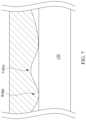
- FIG. 7exemplarily shows a human finger placed on the display panel 120 .
- the ridgestouches the top surface of the display panel 120 , and air gaps exist between the valleys and the top surface of the display panel 120 .
- a fingerprint pattern of the human fingermay be determined based on the abovementioned difference.
- the reflected light corresponding to the valleyis stronger than the reflected light corresponding to the ridge.
- FIG. 8is a schematic diagram of the detection circuit 130 in FIG. 1 in accordance with some embodiments of the invention.
- the detection circuit 130includes a narrow band pass filter 132 , an analog-to-digital converter 134 and a digital filter 136 .
- the narrow band pass filter 132passes components of the photo detection signals with a particular frequency or within a particular range and blocks the other components of the photo detection signals out of the particular frequency or the particular frequency range.
- the narrow band pass filter 132may be configured corresponding to the backlight module 110 . For example, if the predetermined emitting frequency of the backlight module 110 in the blank period is 10 5 Hz, the passing frequency range of the narrow band pass filter 132 may be with a center frequency of about 10 5 Hz.
- the analog-to-digital converter 134converts the photo detection signals from an analog form to a digital form.
- the digital filter 136is used to define regions corresponding to two opposite characteristics of the biometric object to generate a biometric image, e.g. by enhancing the differences between the photo detection signals respectively corresponding to the two opposite characteristics.
- the detection circuit 130may also be applied to another type display device. That is, the display panel 120 of the display device 100 may be another type display panel, such as an organic light-emitting diode (OLED) display panel or a micro light-emitting diode (mLED) display panel, of which a pixel arrangement is similar to that of the display panel 120 .
- OLEDorganic light-emitting diode
- mLEDmicro light-emitting diode
- the display panel 120is an OLED display panel, and an exemplary circuit diagram of each pixel in such OLED display panel is illustrated in FIG. 9 .
- each pixelincludes a data transistor T 1 , a driving transistor T 2 , a storage capacitor C and an OLED L.
- the data transistor T 1 and the driving transistor T 2can be of any type, such as thin film transistor (TFT) or the like.
- the data transistor T 1 and the driving transistor T 2are PMOS transistors.
- a gate electrode of the data transistor T 1is coupled to a scan line S for receiving a scan signal
- a first source/drain electrode of the data transistor T 1is coupled to a data line D for receiving a data signal.
- a gate of the driving transistor T 2is coupled to a second source/drain electrode of the data transistor T 1 , and a first source/drain electrode is coupled to a power supply source V DD .
- Two ends of the storage capacitor Care respectively coupled to the gate electrode and the first source/drain electrode of the driving transistor T 2 .
- An anode electrode of the OLED Lis coupled to a second source/drain electrode of the driving transistor T 2 , and a cathode electrode of the OLED L is coupled to a ground voltage V SS .
- the display panel 120is an mLED display panel.
- the OLED Lis substituted by an mLED, and the other components (e.g. the data transistor T 1 , the driving transistor T 2 and the capacitor C) may remain the same.
- FIG. 10is a flowchart of a biometric detection method 200 in accordance with one or more embodiments of the invention.
- the biometric detection method 200may be applied on various types of display devices, such as the display device 100 shown in FIG. 1 or another display device that has a pixel arrangement similar to that of the display device 100 .
- the display device on which the biometric detection method 200 is appliedhas an active matrix substrate with pixels that are configured to display an image and include display and photo sensing pixels, and each of the display and photo sensing pixels includes a display region and a photo sensing region, e.g., as shown in FIG. 3 .
- the biometric detection method 200includes the following steps.
- Step S 210light is emitted with a predetermined emitting frequency in a blank period (i.e. a non-display period) of the display device by a display region of each of the display and photo sensing pixels.
- the predetermined emitting frequency in the blank periodmay be high than a human eye is aware of, i.e., the human eyes is not aware of light hopping.
- the predetermined emitting frequency in the blank periodis higher than 60 Hz, and in particular, about 10 5 Hz.
- the lightmay be emitted by one or more backlight sources, OLEDs or mLEDs according to the type of the display device, such as an LCD device, an OLED display device, an mLED display device or the like.
- the light emitted from the display regionis then reflected by the biometric object, e.g. as shown in FIG. 5 and FIG. 7 .
- Step S 220the light emitted from the display region and then reflected from the biometric object is detected by a photo sensing region of each of the determined display and photo sensing pixels.
- the photo sensing regionmay include a photo sensing element for detecting the light, such as a photodiode, a pinned photodiode, a partially pinned photodiode, a photogate, a photo transistor, or another element that has a light sensing function.
- Step S 230the reflected light is converted into photo detection signals by the photo sensing element in each of the photo sensing region, and then the photo detection signals are transmitted to a detection circuit.
- the detection circuitmay be included the display device and may be such as the detection circuit shown in FIG. 3 or another detection circuit suitable for performing an operation on the photo detection signals.
- Step S 240the detection circuit performs an operation on the photo detection signals, so as to construct a biometric pattern corresponding to the biometric object based on the photo detection signals.
- the biometric patternmay be a fingerprint pattern if the biometric object is a fingerprint of a human finger.
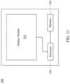
- FIG. 11is a schematic diagram of an electronic device 300 in accordance with some embodiments of the invention.
- the electronic device 300may be, for example, a mobile phone, a smartphone, a tablet, a laptop computer, or another similar portable device.
- the electrically deviceis an ATM, a kiosk, a robot, a vending machine or another device that may apply a biometric detection technology for customer services, access controls, or the like.
- the electronic device 300includes a display module 310 , a processor 320 and a memory 330 .
- the display module 310provides a display function and a light sensing function.
- the display device 100may be, for example, a liquid crystal display (LCD) of twisted menatic (TN) type, vertical alignment (VA) type, in-plane switching (IPS) type, fringe-field switching (FFS) type, or an organic light-emitting diode (OLED) display panel, a micro light-emitting diode (mLED) display panel or a display of another type.
- the display module 310may be similar to the display device 100 in FIG. 1 of another display module that is capable of performing a display function and a light sensing function.
- the display module 310includes the backlight module 110 and the display panel 120 in FIG. 1 .
- the processor 320is coupled to the display module 310 and controls operations of the display module 310 . Specifically, the processor 320 may control the display module 310 to display an image on screen of the display module 310 . For the embodiments in which the display module 310 includes an LCD display panel, the processor 320 may control the liquid crystal layer and the backlight module of the display module 310 to show a particular graphical user interface (GUI) to guide a user to perform a corresponding action.
- GUIgraphical user interface
- the processor 320may control light illuminating elements (e.g.
- the processor 320may include one or more processing units, such as a microprocessor or an application-specific integrated circuit (ASIC) and/or the like.
- the processor 320may also provide a biometric detection function. Specifically, the processor 320 may control the display module 310 to display an image on screen of the display module 310 . For the embodiments in which the display module 310 includes an LCD display panel, the processor 320 may control the liquid crystal layer and the backlight module of the display module 310 to show a particular graphical user interface (GUI) to guide a user to perform a corresponding action. Oppositely, for the embodiments in which the display module 310 includes an OLED display panel or an mLED display module, the processor 320 may control light illuminating elements (e.g.
- the processor 320may perform an operation on the photo detection signals, so as to construct a biometric pattern corresponding to the biometric object based on the photo detection signals.
- the processor 320includes the detection circuit 130 in FIG. 8 or another circuit suitable to perform similar functions to those of the detection circuit 130 .
- the biometric patternmay be a fingerprint pattern if the biometric object is a fingerprint of a human finger.
- the biometric detection functionmay be separated from the processor 320 in accordance with variant embodiments.
- a detection circuitsuch as the detection circuit 130
- the biometric detection function other than the processor 320may be included in the electronic device 300 .
- the memory 330stores the instructions that are executed by the processor 320 .
- the memory 330may store the processing result (such as data corresponding to the biometric pattern) from the processor 320 .
- the memory 330may be, for example, an erasable programmable ROM (EPROM), an electrically erasable programmable ROM (EEPROM), a random access memory (RAM), a CD-R, a magnetic tape, a hard disk, a solid state disk (SSD), a flash memory or other data storage device suitable for storing a program code, but is not limited thereto.
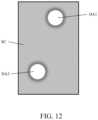
- FIG. 12exemplarily shows a graphical user interface (GUI) displayed on screen of the electronic device 300 for biometric detection in accordance with some embodiments of the invention.
- GUIgraphical user interface
- the biometric detection function for fingerprint detectionis exemplified.
- the GUIis shown on screen SC, in which detection areas DA 1 and DA 2 are brighter than the other area, so as to guide a user to press his finger onto the screen SC and in the detection area DA 1 or DA 2 for reflected light sensing.
- FIG. 13is a flowchart of a biometric detection method 400 in accordance with one or more embodiments of the invention.
- the biometric detection method 400may be applied on various types of electronic devices, such as the electronic device 300 shown in FIG. 11 or another electronic device in which the display module has a pixel arrangement similar to that of the display device 100 .
- the display module on which the biometric detection method 400 is appliedhas an active matrix substrate with pixels that are configured to display an image and include display and photo sensing pixels, and each of the display and photo sensing pixels includes a display region and a photo sensing region, e.g., as shown in FIG. 3 .
- the biometric detection method 400includes the following steps.
- Step 410a biometric detecting area of the display module is determined, in which determined ones of the display and photo sensing pixels are in the biometric detecting area.
- the number of the determined ones of the display and photo sensing pixels in the biometric detecting areamay be less than or equal to the number of the display and photo sensing pixels.
- the display region of each of the determined display and photo sensing pixelsis controlled to activate light emitting with a predetermined emitting frequency in a blank period of the display module, and the photo sensing region of each of the determined display and photo sensing pixels is control to activate biometric object sensing.
- Step S 420the display module is controlled to display a GUI that indicates the biometric detecting area, in order to guide a user to perform a corresponding action. If the biometric detection method 400 is performed to detect a fingerprint, the GUI (e.g. as shown in FIG. 12 ) may be displayed to guide a user to press his finger onto a screen of the display module for fingerprint detection.
- the GUIe.g. as shown in FIG. 12
- Step S 430light is emitted with a predetermined emitting frequency in a blank period (i.e. a non-display period) of the display device by a display region of each of the display and photo sensing pixels.
- the predetermined emitting frequency in the blank periodmay be high than a human eye is aware of, i.e., the human eyes is not aware of light hopping.
- the predetermined emitting frequency in the blank periodis higher than 60 Hz (in particular, about 10 5 Hz) and may be adjusted according to circuit characteristics.
- the lightmay be emitted by one or more backlight sources, OLEDs or mLEDs according to the type of the display device, such as an LCD device, an OLED display device, an mLED display device or the like.
- the light emitted from the display regionis then reflected by the biometric object (e.g. as shown in FIG. 5 and FIG. 7 ).
- Step S 440the light emitted from the display region and then reflected from the biometric object is detected by a photo sensing region of each of the determined display and photo sensing pixels.
- the photo sensing regionmay include a photo sensing element for detecting the light, such as a photodiode, a pinned photodiode, a partially pinned photodiode, a photogate, a photo transistor, or another element that has a light sensing function.
- Step S 450the reflected light is converted into photo detection signals by the photo sensing element in each of the photo sensing region, and then the photo detection signals are transmitted to a detection circuit.
- the detection circuitmay be included the display device and may be such as the detection circuit shown in FIG. 3 or another detection circuit suitable for performing an operation on the photo detection signals.
- Step S 460the detection circuit performs an operation on the photo detection signals, so as to construct a biometric pattern corresponding to the biometric object based on the photo detection signals.
- the biometric patternmay be a fingerprint pattern if the biometric object is a fingerprint of a human finger.
- Step S 410 and Step S 420may be performed by a processor that is configured to control the display module.
- the processormay be, for example, the processor 320 in FIG. 3 or another processor that is capable of controlling the display module (e.g. controlling a backlight module and a liquid crystal layer of the display module).
- Step S 410 and Step S 420may be compiled into a program code, and such compiled program code may be stored in a memory.
- the processormay read and execute the program code stored in the memory to perform operations of Step 410 and Step 420 .
- a biometric detection functionis embedded in a display screen without requiring additional displacement in a non-active region for biometric detection and affecting original image display, thus providing more conveniently and flexibly.
Landscapes
- Engineering & Computer Science (AREA)
- Physics & Mathematics (AREA)
- Theoretical Computer Science (AREA)
- General Physics & Mathematics (AREA)
- Chemical & Material Sciences (AREA)
- Inorganic Chemistry (AREA)
- Computer Hardware Design (AREA)
- Human Computer Interaction (AREA)
- Multimedia (AREA)
- Life Sciences & Earth Sciences (AREA)
- Sustainable Development (AREA)
- Optics & Photonics (AREA)
- Image Input (AREA)
- Devices For Indicating Variable Information By Combining Individual Elements (AREA)
- Measurement Of The Respiration, Hearing Ability, Form, And Blood Characteristics Of Living Organisms (AREA)
- Liquid Crystal Display Device Control (AREA)
Abstract
Description
Claims (16)
Priority Applications (3)
| Application Number | Priority Date | Filing Date | Title |
|---|---|---|---|
| US15/854,725US11734944B2 (en) | 2017-08-03 | 2017-12-26 | Display device with embedded biometric detection function in active region |
| CN201810201764.5ACN109389025A (en) | 2017-08-03 | 2018-03-12 | Display device, electronic device and biological characteristic detection method |
| TW107109694ATWI663456B (en) | 2017-08-03 | 2018-03-21 | Display device, electronic device and biometric detection method |
Applications Claiming Priority (2)
| Application Number | Priority Date | Filing Date | Title |
|---|---|---|---|
| US201762540577P | 2017-08-03 | 2017-08-03 | |
| US15/854,725US11734944B2 (en) | 2017-08-03 | 2017-12-26 | Display device with embedded biometric detection function in active region |
Publications (2)
| Publication Number | Publication Date |
|---|---|
| US20190042825A1 US20190042825A1 (en) | 2019-02-07 |
| US11734944B2true US11734944B2 (en) | 2023-08-22 |
Family
ID=65231060
Family Applications (1)
| Application Number | Title | Priority Date | Filing Date |
|---|---|---|---|
| US15/854,725Active2039-12-20US11734944B2 (en) | 2017-08-03 | 2017-12-26 | Display device with embedded biometric detection function in active region |
Country Status (3)
| Country | Link |
|---|---|
| US (1) | US11734944B2 (en) |
| CN (1) | CN109389025A (en) |
| TW (1) | TWI663456B (en) |
Families Citing this family (15)
| Publication number | Priority date | Publication date | Assignee | Title |
|---|---|---|---|---|
| US11734944B2 (en)* | 2017-08-03 | 2023-08-22 | Himax Technologies Limited | Display device with embedded biometric detection function in active region |
| US10915726B2 (en)* | 2017-08-03 | 2021-02-09 | Himax Technologies Limited | Display device and biometric detection method thereof |
| JPWO2019131001A1 (en)* | 2017-12-28 | 2021-03-11 | コネクテックジャパン株式会社 | Image acquisition device and display device equipped with it |
| CN108461060A (en)* | 2018-04-08 | 2018-08-28 | 北京小米移动软件有限公司 | Display panel, photoelectric detection method, device, and computer-readable storage medium |
| CN109036331B (en)* | 2018-08-24 | 2020-04-24 | 京东方科技集团股份有限公司 | Display screen brightness adjusting method and device and display screen |
| CN110163058B (en)* | 2018-10-30 | 2021-11-09 | 京东方科技集团股份有限公司 | Fingerprint identification display module and fingerprint identification method |
| CN211698994U (en)* | 2019-08-16 | 2020-10-16 | 神盾股份有限公司 | Fingerprint sensing device |
| US10937362B1 (en)* | 2019-09-23 | 2021-03-02 | Au Optronics Corporation | Electronic apparatus and operating method thereof |
| US11450088B2 (en)* | 2019-10-01 | 2022-09-20 | Innolux Corporation | Method of detecting biometric feature |
| CN111104899B (en)* | 2019-12-18 | 2024-04-16 | 京东方科技集团股份有限公司 | Fingerprint identification method, device, electronic device, and computer-readable storage medium |
| CN115066720B (en)* | 2020-02-12 | 2025-01-10 | 华为技术有限公司 | Method for driving display device, display device driving apparatus, display device and display method |
| WO2022027901A1 (en)* | 2020-08-03 | 2022-02-10 | 神盾股份有限公司 | Dual-mode display device having light sensing function |
| CN112599064B (en)* | 2020-12-03 | 2022-09-09 | 深圳市华星光电半导体显示技术有限公司 | Display device and denoising method thereof |
| US11532175B1 (en)* | 2021-05-25 | 2022-12-20 | Qualcomm Incorporated | Imaging an object on a display |
| TWI773406B (en)* | 2021-06-25 | 2022-08-01 | 凌巨科技股份有限公司 | Under-screen identification display apparatus |
Citations (39)
| Publication number | Priority date | Publication date | Assignee | Title |
|---|---|---|---|---|
| US20020030668A1 (en)* | 2000-08-21 | 2002-03-14 | Takeshi Hoshino | Pointing device and portable information terminal using the same |
| US20020167489A1 (en) | 2001-05-14 | 2002-11-14 | Jeffery Davis | Pushbutton optical screen pointing device |
| US20040252867A1 (en)* | 2000-01-05 | 2004-12-16 | Je-Hsiung Lan | Biometric sensor |
| CN1607561A (en) | 2003-10-15 | 2005-04-20 | 三星电子株式会社 | Display device with photosensor |
| US7136783B2 (en)* | 2002-07-02 | 2006-11-14 | Koninklijke Philips Electronics N.V. | Method and arrangement for processing a signal using a digital processor having a given word length |
| US20080129653A1 (en)* | 2004-07-16 | 2008-06-05 | Semiconductor Energy Laboratory Co., Ltd. | Display device mounted with read function and electric appliance |
| US20080211787A1 (en)* | 2007-02-20 | 2008-09-04 | Kenji Nakao | Liquid crystal display apparatus |
| CN102662527A (en) | 2010-12-22 | 2012-09-12 | 剑扬股份有限公司 | Touch Sensing Display Device |
| CN102736794A (en) | 2011-04-15 | 2012-10-17 | 原相科技股份有限公司 | Optical touch pad, handheld electronic device and method |
| CN105303090A (en)* | 2015-10-19 | 2016-02-03 | 广东欧珀移动通信有限公司 | Method, device and terminal for fingerprint unlocking |
| CN105511931A (en)* | 2015-12-30 | 2016-04-20 | 魅族科技(中国)有限公司 | Function triggering method and device as well as electronic equipment |
| US20160110025A1 (en)* | 2013-06-12 | 2016-04-21 | Dan Hossu | Method for optically detecting a fingerprint or an object, and device with at least one screen |
| US9361507B1 (en)* | 2015-02-06 | 2016-06-07 | Hoyos Labs Ip Ltd. | Systems and methods for performing fingerprint based user authentication using imagery captured using mobile devices |
| CN105718118A (en) | 2016-04-25 | 2016-06-29 | 京东方科技集团股份有限公司 | Array substrate, touch display panel, touch pressure detection method and display device |
| US9424458B1 (en)* | 2015-02-06 | 2016-08-23 | Hoyos Labs Ip Ltd. | Systems and methods for performing fingerprint based user authentication using imagery captured using mobile devices |
| CN105893992A (en) | 2016-05-31 | 2016-08-24 | 京东方科技集团股份有限公司 | Fingerprint identification structure and method and display device |
| US20160253544A1 (en)* | 2015-02-27 | 2016-09-01 | Fingerprint Cards Ab | Method of guiding a user of a portable electronic device |
| US20160321442A1 (en)* | 2015-04-29 | 2016-11-03 | Samsung Electronics Co., Ltd. | Electronic device |
| US20160349882A1 (en)* | 2015-06-01 | 2016-12-01 | Boe Technology Group Co., Ltd. | In-cell touch screen panel, method of driving in-cell touch screen panel, and display device |
| CN106233305A (en) | 2014-06-05 | 2016-12-14 | 斯科竣公司 | Finger sensor apparatus |
| CN106326859A (en) | 2016-08-23 | 2017-01-11 | 京东方科技集团股份有限公司 | Fingerprint identification driving circuit, array substrate, display device and fingerprint identification method |
| US20170024602A1 (en)* | 2015-07-20 | 2017-01-26 | Lg Display Co., Ltd. | Fingerprint sensor integrated type touch screen device |
| CN106598327A (en) | 2016-11-30 | 2017-04-26 | 京东方科技集团股份有限公司 | Touch display driving unit circuit, driving method, circuit and display device |
| US9639733B2 (en)* | 2014-11-25 | 2017-05-02 | Cypress Semiconductor Corporation | Methods and sensors for multiphase scanning in the fingerprint and touch applications |
| US20170154199A1 (en)* | 2015-11-26 | 2017-06-01 | Xiaomi Inc. | Liquid crystal display assembly and electronic device |
| CN106874725A (en)* | 2017-01-23 | 2017-06-20 | 广东欧珀移动通信有限公司 | A fingerprint unlocking method and mobile terminal |
| CN106886743A (en) | 2015-12-15 | 2017-06-23 | 联咏科技股份有限公司 | Display device and control apparatus thereof |
| CN106898636A (en) | 2017-04-27 | 2017-06-27 | 京东方科技集团股份有限公司 | OLED display panel and the method that fingerprint recognition is carried out using OLED display panel |
| CN107004130A (en) | 2015-06-18 | 2017-08-01 | 深圳市汇顶科技股份有限公司 | Under-screen optical sensor module for on-screen fingerprint sensing |
| US20170228579A1 (en)* | 2015-08-07 | 2017-08-10 | Shanghai Oxi Technology Co., Ltd. | Fingerprint Image Sensor and Method for Optical Wireless Communications Using the Same |
| US20170337413A1 (en)* | 2016-05-23 | 2017-11-23 | InSyte Systems | Integrated light emitting display and sensors for detecting biologic characteristics |
| US20170365588A1 (en)* | 2016-06-17 | 2017-12-21 | Ultra Display Technology Corp. | Optoelectronic semiconductor device |
| US20180046025A1 (en)* | 2016-01-04 | 2018-02-15 | Boe Technology Group Co., Ltd. | Method and Device for Modulating Backlight Source, Light Bar, Backlight Module, and Display Device |
| US20180060641A1 (en)* | 2016-08-23 | 2018-03-01 | Samsung Display Co., Ltd. | Method and apparatus to detect three-dimensional pattern information of a touch object |
| US20180225457A1 (en)* | 2017-02-04 | 2018-08-09 | International Business Machines Corporation | Enhancing security of a mobile device based on location or proximity to another device |
| US20180285619A1 (en)* | 2017-03-31 | 2018-10-04 | Samsung Display Co., Ltd. | Display device and method of driving the display device |
| US20190042825A1 (en)* | 2017-08-03 | 2019-02-07 | Himax Technologies Limited | Display device with embedded biometric detection function in active region |
| US10541280B1 (en)* | 2016-09-16 | 2020-01-21 | Apple Inc. | OLED based touch sensing and user identification |
| US20200051499A1 (en)* | 2018-08-07 | 2020-02-13 | Lg Display Co., Ltd. | Display device |
- 2017
- 2017-12-26USUS15/854,725patent/US11734944B2/enactiveActive
- 2018
- 2018-03-12CNCN201810201764.5Apatent/CN109389025A/enactivePending
- 2018-03-21TWTW107109694Apatent/TWI663456B/enactive
Patent Citations (43)
| Publication number | Priority date | Publication date | Assignee | Title |
|---|---|---|---|---|
| US20040252867A1 (en)* | 2000-01-05 | 2004-12-16 | Je-Hsiung Lan | Biometric sensor |
| US20020030668A1 (en)* | 2000-08-21 | 2002-03-14 | Takeshi Hoshino | Pointing device and portable information terminal using the same |
| US20020167489A1 (en) | 2001-05-14 | 2002-11-14 | Jeffery Davis | Pushbutton optical screen pointing device |
| US7136783B2 (en)* | 2002-07-02 | 2006-11-14 | Koninklijke Philips Electronics N.V. | Method and arrangement for processing a signal using a digital processor having a given word length |
| CN1607561A (en) | 2003-10-15 | 2005-04-20 | 三星电子株式会社 | Display device with photosensor |
| US20080129653A1 (en)* | 2004-07-16 | 2008-06-05 | Semiconductor Energy Laboratory Co., Ltd. | Display device mounted with read function and electric appliance |
| US20080211787A1 (en)* | 2007-02-20 | 2008-09-04 | Kenji Nakao | Liquid crystal display apparatus |
| CN102662527A (en) | 2010-12-22 | 2012-09-12 | 剑扬股份有限公司 | Touch Sensing Display Device |
| CN102736794A (en) | 2011-04-15 | 2012-10-17 | 原相科技股份有限公司 | Optical touch pad, handheld electronic device and method |
| US20160110025A1 (en)* | 2013-06-12 | 2016-04-21 | Dan Hossu | Method for optically detecting a fingerprint or an object, and device with at least one screen |
| CN106233305A (en) | 2014-06-05 | 2016-12-14 | 斯科竣公司 | Finger sensor apparatus |
| US9639733B2 (en)* | 2014-11-25 | 2017-05-02 | Cypress Semiconductor Corporation | Methods and sensors for multiphase scanning in the fingerprint and touch applications |
| US9361507B1 (en)* | 2015-02-06 | 2016-06-07 | Hoyos Labs Ip Ltd. | Systems and methods for performing fingerprint based user authentication using imagery captured using mobile devices |
| US9424458B1 (en)* | 2015-02-06 | 2016-08-23 | Hoyos Labs Ip Ltd. | Systems and methods for performing fingerprint based user authentication using imagery captured using mobile devices |
| US20160253544A1 (en)* | 2015-02-27 | 2016-09-01 | Fingerprint Cards Ab | Method of guiding a user of a portable electronic device |
| US20160321442A1 (en)* | 2015-04-29 | 2016-11-03 | Samsung Electronics Co., Ltd. | Electronic device |
| US20160349882A1 (en)* | 2015-06-01 | 2016-12-01 | Boe Technology Group Co., Ltd. | In-cell touch screen panel, method of driving in-cell touch screen panel, and display device |
| CN107004130A (en) | 2015-06-18 | 2017-08-01 | 深圳市汇顶科技股份有限公司 | Under-screen optical sensor module for on-screen fingerprint sensing |
| US10007828B2 (en)* | 2015-07-20 | 2018-06-26 | Lg Display Co., Ltd. | Fingerprint sensor integrated type touch screen device |
| US20170024602A1 (en)* | 2015-07-20 | 2017-01-26 | Lg Display Co., Ltd. | Fingerprint sensor integrated type touch screen device |
| TW201704969A (en) | 2015-07-20 | 2017-02-01 | Lg顯示器股份有限公司 | Fingerprint sensor integrated type touch screen device |
| US20170228579A1 (en)* | 2015-08-07 | 2017-08-10 | Shanghai Oxi Technology Co., Ltd. | Fingerprint Image Sensor and Method for Optical Wireless Communications Using the Same |
| CN105303090A (en)* | 2015-10-19 | 2016-02-03 | 广东欧珀移动通信有限公司 | Method, device and terminal for fingerprint unlocking |
| US20170154199A1 (en)* | 2015-11-26 | 2017-06-01 | Xiaomi Inc. | Liquid crystal display assembly and electronic device |
| CN106886743A (en) | 2015-12-15 | 2017-06-23 | 联咏科技股份有限公司 | Display device and control apparatus thereof |
| CN105511931A (en)* | 2015-12-30 | 2016-04-20 | 魅族科技(中国)有限公司 | Function triggering method and device as well as electronic equipment |
| US20180046025A1 (en)* | 2016-01-04 | 2018-02-15 | Boe Technology Group Co., Ltd. | Method and Device for Modulating Backlight Source, Light Bar, Backlight Module, and Display Device |
| CN105718118A (en) | 2016-04-25 | 2016-06-29 | 京东方科技集团股份有限公司 | Array substrate, touch display panel, touch pressure detection method and display device |
| US20170337413A1 (en)* | 2016-05-23 | 2017-11-23 | InSyte Systems | Integrated light emitting display and sensors for detecting biologic characteristics |
| US20180365468A1 (en)* | 2016-05-31 | 2018-12-20 | Boe Technology Group Co., Ltd. | Fingerprint recognition component, display device and fingerprint recognition method |
| CN105893992A (en) | 2016-05-31 | 2016-08-24 | 京东方科技集团股份有限公司 | Fingerprint identification structure and method and display device |
| US20170365588A1 (en)* | 2016-06-17 | 2017-12-21 | Ultra Display Technology Corp. | Optoelectronic semiconductor device |
| US20180060641A1 (en)* | 2016-08-23 | 2018-03-01 | Samsung Display Co., Ltd. | Method and apparatus to detect three-dimensional pattern information of a touch object |
| CN106326859A (en) | 2016-08-23 | 2017-01-11 | 京东方科技集团股份有限公司 | Fingerprint identification driving circuit, array substrate, display device and fingerprint identification method |
| US10541280B1 (en)* | 2016-09-16 | 2020-01-21 | Apple Inc. | OLED based touch sensing and user identification |
| US20180151122A1 (en)* | 2016-11-30 | 2018-05-31 | Boe Technology Group Co., Ltd. | Display driving unit circuit, driving method, display driving circuit and display device |
| CN106598327A (en) | 2016-11-30 | 2017-04-26 | 京东方科技集团股份有限公司 | Touch display driving unit circuit, driving method, circuit and display device |
| CN106874725A (en)* | 2017-01-23 | 2017-06-20 | 广东欧珀移动通信有限公司 | A fingerprint unlocking method and mobile terminal |
| US20180225457A1 (en)* | 2017-02-04 | 2018-08-09 | International Business Machines Corporation | Enhancing security of a mobile device based on location or proximity to another device |
| US20180285619A1 (en)* | 2017-03-31 | 2018-10-04 | Samsung Display Co., Ltd. | Display device and method of driving the display device |
| CN106898636A (en) | 2017-04-27 | 2017-06-27 | 京东方科技集团股份有限公司 | OLED display panel and the method that fingerprint recognition is carried out using OLED display panel |
| US20190042825A1 (en)* | 2017-08-03 | 2019-02-07 | Himax Technologies Limited | Display device with embedded biometric detection function in active region |
| US20200051499A1 (en)* | 2018-08-07 | 2020-02-13 | Lg Display Co., Ltd. | Display device |
Non-Patent Citations (1)
| Title |
|---|
| Sheng-yi Wu et al., "The research and implementation of visual access control system" Electronic Design Engineering, vol. 23, No. 19, Oct. 2015. |
Also Published As
| Publication number | Publication date |
|---|---|
| TWI663456B (en) | 2019-06-21 |
| US20190042825A1 (en) | 2019-02-07 |
| CN109389025A (en) | 2019-02-26 |
| TW201910892A (en) | 2019-03-16 |
Similar Documents
| Publication | Publication Date | Title |
|---|---|---|
| US11734944B2 (en) | Display device with embedded biometric detection function in active region | |
| US11009747B2 (en) | Backlight module and display device | |
| US11132526B2 (en) | Fingerprint recognition panel, fingerprint recognition method and display device | |
| US11521419B2 (en) | Display device and fingerprint recognition method | |
| US11188729B2 (en) | Display panel, fingerprint identification display module and fingerprint identification method | |
| JP7245611B2 (en) | Organic light-emitting diode panel incorporating near-infrared organic photosensor and display device including the same | |
| US11308304B2 (en) | Fingerprint detection device and display device | |
| US7321672B2 (en) | Image reading apparatus and image reading system equipped with the image reading apparatus | |
| US10713462B2 (en) | Fingerprint detection device and display device | |
| CN109359641B (en) | Display device and driving method thereof | |
| US20170199606A1 (en) | Display panel, display apparatus having the same, and driving method thereof | |
| CN109541839B (en) | Display panel and display device | |
| KR20080028270A (en) | Liquid crystal display with multi-touch sensing function and its driving method | |
| CN110199249B (en) | Integrated fingerprint detection touch display device and integration method of fingerprint detection, touch and image display | |
| US10495911B2 (en) | Liquid crystal display assembly and electronic device | |
| WO2018082401A1 (en) | Display device and electronic device | |
| US20190080137A1 (en) | Flat-panel display embedded with a fingerprint sensor and a method of forming the same | |
| CN108615033B (en) | Module, terminal equipment and fingerprint identification method supporting full-screen fingerprint identification | |
| US11227138B2 (en) | Liquid crystal display device having fingerprint sensor | |
| US20120138960A1 (en) | Light sensor and display apparatus having the same | |
| US10302484B2 (en) | Optical sensor module | |
| CN111176038A (en) | A display panel capable of recognizing external light | |
| US10915726B2 (en) | Display device and biometric detection method thereof | |
| US20220317520A1 (en) | Display system | |
| JP2023080948A (en) | Display device |
Legal Events
| Date | Code | Title | Description |
|---|---|---|---|
| FEPP | Fee payment procedure | Free format text:ENTITY STATUS SET TO UNDISCOUNTED (ORIGINAL EVENT CODE: BIG.); ENTITY STATUS OF PATENT OWNER: LARGE ENTITY | |
| AS | Assignment | Owner name:HIMAX TECHNOLOGIES LIMITED, TAIWAN Free format text:ASSIGNMENT OF ASSIGNORS INTEREST;ASSIGNORS:HE, JIA-MING;CHANG, YAW-GUANG;REEL/FRAME:044487/0267 Effective date:20171219 | |
| STPP | Information on status: patent application and granting procedure in general | Free format text:DOCKETED NEW CASE - READY FOR EXAMINATION | |
| STPP | Information on status: patent application and granting procedure in general | Free format text:NON FINAL ACTION MAILED | |
| STPP | Information on status: patent application and granting procedure in general | Free format text:RESPONSE TO NON-FINAL OFFICE ACTION ENTERED AND FORWARDED TO EXAMINER | |
| STPP | Information on status: patent application and granting procedure in general | Free format text:FINAL REJECTION MAILED | |
| STPP | Information on status: patent application and granting procedure in general | Free format text:RESPONSE AFTER FINAL ACTION FORWARDED TO EXAMINER | |
| STPP | Information on status: patent application and granting procedure in general | Free format text:ADVISORY ACTION MAILED | |
| STCV | Information on status: appeal procedure | Free format text:NOTICE OF APPEAL FILED | |
| STCV | Information on status: appeal procedure | Free format text:APPEAL BRIEF (OR SUPPLEMENTAL BRIEF) ENTERED AND FORWARDED TO EXAMINER | |
| STCV | Information on status: appeal procedure | Free format text:EXAMINER'S ANSWER TO APPEAL BRIEF MAILED | |
| STCV | Information on status: appeal procedure | Free format text:ON APPEAL -- AWAITING DECISION BY THE BOARD OF APPEALS | |
| STPP | Information on status: patent application and granting procedure in general | Free format text:NOTICE OF ALLOWANCE MAILED -- APPLICATION RECEIVED IN OFFICE OF PUBLICATIONS | |
| STPP | Information on status: patent application and granting procedure in general | Free format text:PUBLICATIONS -- ISSUE FEE PAYMENT RECEIVED | |
| STCF | Information on status: patent grant | Free format text:PATENTED CASE |