US11725279B2 - Deposition or cleaning apparatus with movable structure - Google Patents
Deposition or cleaning apparatus with movable structureDownload PDFInfo
- Publication number
- US11725279B2 US11725279B2US16/481,221US201716481221AUS11725279B2US 11725279 B2US11725279 B2US 11725279B2US 201716481221 AUS201716481221 AUS 201716481221AUS 11725279 B2US11725279 B2US 11725279B2
- Authority
- US
- United States
- Prior art keywords
- reaction chamber
- chamber
- exhaust line
- loading
- deposition
- Prior art date
- Legal status (The legal status is an assumption and is not a legal conclusion. Google has not performed a legal analysis and makes no representation as to the accuracy of the status listed.)
- Active
Links
Images


Classifications
- C—CHEMISTRY; METALLURGY
- C23—COATING METALLIC MATERIAL; COATING MATERIAL WITH METALLIC MATERIAL; CHEMICAL SURFACE TREATMENT; DIFFUSION TREATMENT OF METALLIC MATERIAL; COATING BY VACUUM EVAPORATION, BY SPUTTERING, BY ION IMPLANTATION OR BY CHEMICAL VAPOUR DEPOSITION, IN GENERAL; INHIBITING CORROSION OF METALLIC MATERIAL OR INCRUSTATION IN GENERAL
- C23C—COATING METALLIC MATERIAL; COATING MATERIAL WITH METALLIC MATERIAL; SURFACE TREATMENT OF METALLIC MATERIAL BY DIFFUSION INTO THE SURFACE, BY CHEMICAL CONVERSION OR SUBSTITUTION; COATING BY VACUUM EVAPORATION, BY SPUTTERING, BY ION IMPLANTATION OR BY CHEMICAL VAPOUR DEPOSITION, IN GENERAL
- C23C16/00—Chemical coating by decomposition of gaseous compounds, without leaving reaction products of surface material in the coating, i.e. chemical vapour deposition [CVD] processes
- C23C16/44—Chemical coating by decomposition of gaseous compounds, without leaving reaction products of surface material in the coating, i.e. chemical vapour deposition [CVD] processes characterised by the method of coating
- C23C16/4401—Means for minimising impurities, e.g. dust, moisture or residual gas, in the reaction chamber
- C23C16/4409—Means for minimising impurities, e.g. dust, moisture or residual gas, in the reaction chamber characterised by sealing means
- C—CHEMISTRY; METALLURGY
- C23—COATING METALLIC MATERIAL; COATING MATERIAL WITH METALLIC MATERIAL; CHEMICAL SURFACE TREATMENT; DIFFUSION TREATMENT OF METALLIC MATERIAL; COATING BY VACUUM EVAPORATION, BY SPUTTERING, BY ION IMPLANTATION OR BY CHEMICAL VAPOUR DEPOSITION, IN GENERAL; INHIBITING CORROSION OF METALLIC MATERIAL OR INCRUSTATION IN GENERAL
- C23C—COATING METALLIC MATERIAL; COATING MATERIAL WITH METALLIC MATERIAL; SURFACE TREATMENT OF METALLIC MATERIAL BY DIFFUSION INTO THE SURFACE, BY CHEMICAL CONVERSION OR SUBSTITUTION; COATING BY VACUUM EVAPORATION, BY SPUTTERING, BY ION IMPLANTATION OR BY CHEMICAL VAPOUR DEPOSITION, IN GENERAL
- C23C16/00—Chemical coating by decomposition of gaseous compounds, without leaving reaction products of surface material in the coating, i.e. chemical vapour deposition [CVD] processes
- C23C16/44—Chemical coating by decomposition of gaseous compounds, without leaving reaction products of surface material in the coating, i.e. chemical vapour deposition [CVD] processes characterised by the method of coating
- C23C16/455—Chemical coating by decomposition of gaseous compounds, without leaving reaction products of surface material in the coating, i.e. chemical vapour deposition [CVD] processes characterised by the method of coating characterised by the method used for introducing gases into reaction chamber or for modifying gas flows in reaction chamber
- C23C16/45523—Pulsed gas flow or change of composition over time
- C23C16/45525—Atomic layer deposition [ALD]
- C23C16/45544—Atomic layer deposition [ALD] characterized by the apparatus
- C23C16/45546—Atomic layer deposition [ALD] characterized by the apparatus specially adapted for a substrate stack in the ALD reactor
- C—CHEMISTRY; METALLURGY
- C23—COATING METALLIC MATERIAL; COATING MATERIAL WITH METALLIC MATERIAL; CHEMICAL SURFACE TREATMENT; DIFFUSION TREATMENT OF METALLIC MATERIAL; COATING BY VACUUM EVAPORATION, BY SPUTTERING, BY ION IMPLANTATION OR BY CHEMICAL VAPOUR DEPOSITION, IN GENERAL; INHIBITING CORROSION OF METALLIC MATERIAL OR INCRUSTATION IN GENERAL
- C23C—COATING METALLIC MATERIAL; COATING MATERIAL WITH METALLIC MATERIAL; SURFACE TREATMENT OF METALLIC MATERIAL BY DIFFUSION INTO THE SURFACE, BY CHEMICAL CONVERSION OR SUBSTITUTION; COATING BY VACUUM EVAPORATION, BY SPUTTERING, BY ION IMPLANTATION OR BY CHEMICAL VAPOUR DEPOSITION, IN GENERAL
- C23C16/00—Chemical coating by decomposition of gaseous compounds, without leaving reaction products of surface material in the coating, i.e. chemical vapour deposition [CVD] processes
- C23C16/44—Chemical coating by decomposition of gaseous compounds, without leaving reaction products of surface material in the coating, i.e. chemical vapour deposition [CVD] processes characterised by the method of coating
- C23C16/455—Chemical coating by decomposition of gaseous compounds, without leaving reaction products of surface material in the coating, i.e. chemical vapour deposition [CVD] processes characterised by the method of coating characterised by the method used for introducing gases into reaction chamber or for modifying gas flows in reaction chamber
- C23C16/45523—Pulsed gas flow or change of composition over time
- C23C16/45525—Atomic layer deposition [ALD]
- C23C16/45544—Atomic layer deposition [ALD] characterized by the apparatus
- C23C16/45548—Atomic layer deposition [ALD] characterized by the apparatus having arrangements for gas injection at different locations of the reactor for each ALD half-reaction
- C—CHEMISTRY; METALLURGY
- C23—COATING METALLIC MATERIAL; COATING MATERIAL WITH METALLIC MATERIAL; CHEMICAL SURFACE TREATMENT; DIFFUSION TREATMENT OF METALLIC MATERIAL; COATING BY VACUUM EVAPORATION, BY SPUTTERING, BY ION IMPLANTATION OR BY CHEMICAL VAPOUR DEPOSITION, IN GENERAL; INHIBITING CORROSION OF METALLIC MATERIAL OR INCRUSTATION IN GENERAL
- C23C—COATING METALLIC MATERIAL; COATING MATERIAL WITH METALLIC MATERIAL; SURFACE TREATMENT OF METALLIC MATERIAL BY DIFFUSION INTO THE SURFACE, BY CHEMICAL CONVERSION OR SUBSTITUTION; COATING BY VACUUM EVAPORATION, BY SPUTTERING, BY ION IMPLANTATION OR BY CHEMICAL VAPOUR DEPOSITION, IN GENERAL
- C23C16/00—Chemical coating by decomposition of gaseous compounds, without leaving reaction products of surface material in the coating, i.e. chemical vapour deposition [CVD] processes
- C23C16/44—Chemical coating by decomposition of gaseous compounds, without leaving reaction products of surface material in the coating, i.e. chemical vapour deposition [CVD] processes characterised by the method of coating
- C23C16/458—Chemical coating by decomposition of gaseous compounds, without leaving reaction products of surface material in the coating, i.e. chemical vapour deposition [CVD] processes characterised by the method of coating characterised by the method used for supporting substrates in the reaction chamber
- C—CHEMISTRY; METALLURGY
- C23—COATING METALLIC MATERIAL; COATING MATERIAL WITH METALLIC MATERIAL; CHEMICAL SURFACE TREATMENT; DIFFUSION TREATMENT OF METALLIC MATERIAL; COATING BY VACUUM EVAPORATION, BY SPUTTERING, BY ION IMPLANTATION OR BY CHEMICAL VAPOUR DEPOSITION, IN GENERAL; INHIBITING CORROSION OF METALLIC MATERIAL OR INCRUSTATION IN GENERAL
- C23C—COATING METALLIC MATERIAL; COATING MATERIAL WITH METALLIC MATERIAL; SURFACE TREATMENT OF METALLIC MATERIAL BY DIFFUSION INTO THE SURFACE, BY CHEMICAL CONVERSION OR SUBSTITUTION; COATING BY VACUUM EVAPORATION, BY SPUTTERING, BY ION IMPLANTATION OR BY CHEMICAL VAPOUR DEPOSITION, IN GENERAL
- C23C16/00—Chemical coating by decomposition of gaseous compounds, without leaving reaction products of surface material in the coating, i.e. chemical vapour deposition [CVD] processes
- C23C16/44—Chemical coating by decomposition of gaseous compounds, without leaving reaction products of surface material in the coating, i.e. chemical vapour deposition [CVD] processes characterised by the method of coating
- C23C16/54—Apparatus specially adapted for continuous coating
- H—ELECTRICITY
- H01—ELECTRIC ELEMENTS
- H01L—SEMICONDUCTOR DEVICES NOT COVERED BY CLASS H10
- H01L21/00—Processes or apparatus adapted for the manufacture or treatment of semiconductor or solid state devices or of parts thereof
- H01L21/67—Apparatus specially adapted for handling semiconductor or electric solid state devices during manufacture or treatment thereof; Apparatus specially adapted for handling wafers during manufacture or treatment of semiconductor or electric solid state devices or components ; Apparatus not specifically provided for elsewhere
- H01L21/67005—Apparatus not specifically provided for elsewhere
- H01L21/67011—Apparatus for manufacture or treatment
- H01L21/67155—Apparatus for manufacturing or treating in a plurality of work-stations
- H01L21/6719—Apparatus for manufacturing or treating in a plurality of work-stations characterized by the construction of the processing chambers, e.g. modular processing chambers
- H—ELECTRICITY
- H01—ELECTRIC ELEMENTS
- H01L—SEMICONDUCTOR DEVICES NOT COVERED BY CLASS H10
- H01L21/00—Processes or apparatus adapted for the manufacture or treatment of semiconductor or solid state devices or of parts thereof
- H01L21/67—Apparatus specially adapted for handling semiconductor or electric solid state devices during manufacture or treatment thereof; Apparatus specially adapted for handling wafers during manufacture or treatment of semiconductor or electric solid state devices or components ; Apparatus not specifically provided for elsewhere
- H01L21/677—Apparatus specially adapted for handling semiconductor or electric solid state devices during manufacture or treatment thereof; Apparatus specially adapted for handling wafers during manufacture or treatment of semiconductor or electric solid state devices or components ; Apparatus not specifically provided for elsewhere for conveying, e.g. between different workstations
- H01L21/67739—Apparatus specially adapted for handling semiconductor or electric solid state devices during manufacture or treatment thereof; Apparatus specially adapted for handling wafers during manufacture or treatment of semiconductor or electric solid state devices or components ; Apparatus not specifically provided for elsewhere for conveying, e.g. between different workstations into and out of processing chamber
- H01L21/67748—Apparatus specially adapted for handling semiconductor or electric solid state devices during manufacture or treatment thereof; Apparatus specially adapted for handling wafers during manufacture or treatment of semiconductor or electric solid state devices or components ; Apparatus not specifically provided for elsewhere for conveying, e.g. between different workstations into and out of processing chamber horizontal transfer of a single workpiece
- H—ELECTRICITY
- H01—ELECTRIC ELEMENTS
- H01L—SEMICONDUCTOR DEVICES NOT COVERED BY CLASS H10
- H01L21/00—Processes or apparatus adapted for the manufacture or treatment of semiconductor or solid state devices or of parts thereof
- H01L21/67—Apparatus specially adapted for handling semiconductor or electric solid state devices during manufacture or treatment thereof; Apparatus specially adapted for handling wafers during manufacture or treatment of semiconductor or electric solid state devices or components ; Apparatus not specifically provided for elsewhere
- H01L21/677—Apparatus specially adapted for handling semiconductor or electric solid state devices during manufacture or treatment thereof; Apparatus specially adapted for handling wafers during manufacture or treatment of semiconductor or electric solid state devices or components ; Apparatus not specifically provided for elsewhere for conveying, e.g. between different workstations
- H01L21/67739—Apparatus specially adapted for handling semiconductor or electric solid state devices during manufacture or treatment thereof; Apparatus specially adapted for handling wafers during manufacture or treatment of semiconductor or electric solid state devices or components ; Apparatus not specifically provided for elsewhere for conveying, e.g. between different workstations into and out of processing chamber
- H01L21/67757—Apparatus specially adapted for handling semiconductor or electric solid state devices during manufacture or treatment thereof; Apparatus specially adapted for handling wafers during manufacture or treatment of semiconductor or electric solid state devices or components ; Apparatus not specifically provided for elsewhere for conveying, e.g. between different workstations into and out of processing chamber vertical transfer of a batch of workpieces
- H—ELECTRICITY
- H01—ELECTRIC ELEMENTS
- H01L—SEMICONDUCTOR DEVICES NOT COVERED BY CLASS H10
- H01L21/00—Processes or apparatus adapted for the manufacture or treatment of semiconductor or solid state devices or of parts thereof
- H01L21/67—Apparatus specially adapted for handling semiconductor or electric solid state devices during manufacture or treatment thereof; Apparatus specially adapted for handling wafers during manufacture or treatment of semiconductor or electric solid state devices or components ; Apparatus not specifically provided for elsewhere
- H01L21/683—Apparatus specially adapted for handling semiconductor or electric solid state devices during manufacture or treatment thereof; Apparatus specially adapted for handling wafers during manufacture or treatment of semiconductor or electric solid state devices or components ; Apparatus not specifically provided for elsewhere for supporting or gripping
- H01L21/687—Apparatus specially adapted for handling semiconductor or electric solid state devices during manufacture or treatment thereof; Apparatus specially adapted for handling wafers during manufacture or treatment of semiconductor or electric solid state devices or components ; Apparatus not specifically provided for elsewhere for supporting or gripping using mechanical means, e.g. chucks, clamps or pinches
- H01L21/68714—Apparatus specially adapted for handling semiconductor or electric solid state devices during manufacture or treatment thereof; Apparatus specially adapted for handling wafers during manufacture or treatment of semiconductor or electric solid state devices or components ; Apparatus not specifically provided for elsewhere for supporting or gripping using mechanical means, e.g. chucks, clamps or pinches the wafers being placed on a susceptor, stage or support
- H01L21/68742—Apparatus specially adapted for handling semiconductor or electric solid state devices during manufacture or treatment thereof; Apparatus specially adapted for handling wafers during manufacture or treatment of semiconductor or electric solid state devices or components ; Apparatus not specifically provided for elsewhere for supporting or gripping using mechanical means, e.g. chucks, clamps or pinches the wafers being placed on a susceptor, stage or support characterised by a lifting arrangement, e.g. lift pins
- H—ELECTRICITY
- H01—ELECTRIC ELEMENTS
- H01L—SEMICONDUCTOR DEVICES NOT COVERED BY CLASS H10
- H01L21/00—Processes or apparatus adapted for the manufacture or treatment of semiconductor or solid state devices or of parts thereof
- H01L21/67—Apparatus specially adapted for handling semiconductor or electric solid state devices during manufacture or treatment thereof; Apparatus specially adapted for handling wafers during manufacture or treatment of semiconductor or electric solid state devices or components ; Apparatus not specifically provided for elsewhere
- H01L21/683—Apparatus specially adapted for handling semiconductor or electric solid state devices during manufacture or treatment thereof; Apparatus specially adapted for handling wafers during manufacture or treatment of semiconductor or electric solid state devices or components ; Apparatus not specifically provided for elsewhere for supporting or gripping
- H01L21/687—Apparatus specially adapted for handling semiconductor or electric solid state devices during manufacture or treatment thereof; Apparatus specially adapted for handling wafers during manufacture or treatment of semiconductor or electric solid state devices or components ; Apparatus not specifically provided for elsewhere for supporting or gripping using mechanical means, e.g. chucks, clamps or pinches
- H01L21/68714—Apparatus specially adapted for handling semiconductor or electric solid state devices during manufacture or treatment thereof; Apparatus specially adapted for handling wafers during manufacture or treatment of semiconductor or electric solid state devices or components ; Apparatus not specifically provided for elsewhere for supporting or gripping using mechanical means, e.g. chucks, clamps or pinches the wafers being placed on a susceptor, stage or support
- H01L21/68792—Apparatus specially adapted for handling semiconductor or electric solid state devices during manufacture or treatment thereof; Apparatus specially adapted for handling wafers during manufacture or treatment of semiconductor or electric solid state devices or components ; Apparatus not specifically provided for elsewhere for supporting or gripping using mechanical means, e.g. chucks, clamps or pinches the wafers being placed on a susceptor, stage or support characterised by the construction of the shaft
- C—CHEMISTRY; METALLURGY
- C23—COATING METALLIC MATERIAL; COATING MATERIAL WITH METALLIC MATERIAL; CHEMICAL SURFACE TREATMENT; DIFFUSION TREATMENT OF METALLIC MATERIAL; COATING BY VACUUM EVAPORATION, BY SPUTTERING, BY ION IMPLANTATION OR BY CHEMICAL VAPOUR DEPOSITION, IN GENERAL; INHIBITING CORROSION OF METALLIC MATERIAL OR INCRUSTATION IN GENERAL
- C23C—COATING METALLIC MATERIAL; COATING MATERIAL WITH METALLIC MATERIAL; SURFACE TREATMENT OF METALLIC MATERIAL BY DIFFUSION INTO THE SURFACE, BY CHEMICAL CONVERSION OR SUBSTITUTION; COATING BY VACUUM EVAPORATION, BY SPUTTERING, BY ION IMPLANTATION OR BY CHEMICAL VAPOUR DEPOSITION, IN GENERAL
- C23C16/00—Chemical coating by decomposition of gaseous compounds, without leaving reaction products of surface material in the coating, i.e. chemical vapour deposition [CVD] processes
- C23C16/44—Chemical coating by decomposition of gaseous compounds, without leaving reaction products of surface material in the coating, i.e. chemical vapour deposition [CVD] processes characterised by the method of coating
- C23C16/4412—Details relating to the exhausts, e.g. pumps, filters, scrubbers, particle traps
Definitions
- the aspects of the disclosed embodimentsgenerally relate to deposition or cleaning apparatuses and their methods of operation. More particularly, but not exclusively, the aspects of the disclosed embodiments relate to substrate processing reactors with movable structures.
- substratese.g., wafers
- vacuum clusters structuresThese structures should give minimum or preferably no added particles on the substrates.
- Any mechanical or moving part above the substrateis a potential particle source which may affect deposition quality.
- the moving parts in the prior artcan no longer provide an acceptable solution.
- U.S. Pat. No. 9,095,869 B2discloses a deposition reactor structure comprising a substrate transfer chamber in between a plasma source and a reaction chamber.
- the transfer chambercomprises a moving in-feed part for reactive chemical on the top side of the reaction chamber.
- the in-feed partis vertically deformable having a contracted shape and an extended shape. The contracted shape allows loading of substrates into the reaction chamber via a route formed by contracting the in-feed part.
- a deposition or cleaning apparatuscomprising:
- reaction chamberinside the outer chamber forming a double chamber structure, wherein the reaction chamber is configured to move between a processing position and a lowered position inside the outer chamber, the lowered position being for loading one or more substrates into the reaction chamber.
- the embodiments of the inventionprovide movement of the reaction chamber itself.
- the reaction chamberis movable in vertical direction, or at least partially in a vertical direction.
- the reaction chamber being movableincludes also a sidewall of the reaction chamber being movable.
- the movable reaction chamberis a monolithic structure.
- the reaction chamberforms an integral whole.
- the movement of the reaction chamberis actuated from below (of the reaction chamber).
- the moving parts of the reaction chamberare positioned under the substrate (i.e., not above).
- the reaction chamber as a wholeis configured to move.
- the side wall of the reaction chamberis configured to move together with the rest of the reaction chamber.
- the distance between a reaction chamber bottom and reaction chamber side wallis constant while moving.
- the outer chamberdoes not move, i.e., the outer chamber is stationary.
- the processing positionmay be a deposition position and/or a cleaning position.
- the apparatusis configured to form a loading opening into the reaction chamber by downward movement of the reaction chamber.
- the reaction chamberis configured to detach from an upper stationary part (i.e., a stationary part upper to the moving reaction chamber) upon downward movement of the reaction chamber to open a route for loading.
- the upper stationary partis a part providing fluid in-feed into the reaction chamber.
- the part on top of the movable reaction chambermay be an open or closed part. It may be a wide tube, for example, a radical in-feed part extending from a radical source. Or, it may be, for example, a lid-like part optionally comprising an expansion volume for downward fluid distribution.
- the reaction chamberforms a body with rotational symmetry.
- the reaction chambermay be a bowl-like part (having an exhaust opening in its bottom).
- the apparatuscomprises:
- the loading portis a load lock. In certain example embodiments, the loading port is a gate valve or a hatch.
- the apparatuscomprises:
- the moving elementconfigured to allow vertical movement of the reaction chamber.
- the moving elementis connected to the reaction chamber.
- the moving elementmay be a flexure structure.
- the moving elementmay be a gastight structure.
- the moving elementforms part of an exhaust line of the apparatus.
- the exhaust linemay be a foreline.
- the reaction chambercomprises an exhaust line opening in the bottom of the reaction chamber.
- the reaction chambercomprises an exhaust line opening symmetrically in the center of the bottom of the reaction chamber.
- the moving elementis placed symmetrically below the bottom of the reaction chamber. In certain example embodiments, the moving element is placed, when viewed in a lateral direction, at the center below the bottom of the reaction chamber.
- the moving elementis a tube-like elongated structure whose length is adjustable. Accordingly, in certain example embodiments, the moving element is a hollow deformable element. In certain example embodiments, it allows fluid to pass through it in a vertical direction, but has gastight sidewalls.
- the moving elementis a bellows. In certain example embodiments, the moving element is a vacuum bellows. In certain example embodiments, the moving element (vacuum bellows or similar) is in vacuum in its entirety.
- the moving elementis implemented by two (or more) interlaced or nested tubes which are vertically movable in relation to each other.
- the apparatuscomprises an actuating element actuating the vertical movement of the reaction chamber.
- the actuationmay occur by applying force to the reaction chamber so that the reaction chamber moves as allowed by the moving element.
- the placement of the actuating elementdepends on the implementation.
- the actuating elementis positioned on the outside of the outer chamber.
- the actuating elementis positioned within the outer chamber, but on the outside of the reaction chamber.
- the actuating elementis positioned within the exhaust line.
- the actuating elementis omitted.
- the moving element as suchmoves the reaction chamber without an external actuator (external here meaning external to the moving element).
- the movingmay be implemented due to radiation or changes in temperature, for example.
- the moving elementis formed of shape-memory alloy (smart metal) the moving element thereby being an actuator in itself.
- the apparatuscomprises a substrate holder.
- the substrate holdermay support the substrate, for example, a wafer in a horizontal orientation.
- the substrateis a 450 mm diameter wafer.
- the substrateis a wafer whose diameter is smaller than 450 mm, for example 300 mm.
- a deposition or cleaning processmay be carried out on horizontally oriented substrate(s).
- the substrate orientationis vertical.
- the substrate holdermay support one vertically oriented substrate or a plurality of vertically oriented substrates. Depending on the implementation, the substrates may be oriented either horizontally or vertically when loading them. The substrates may be loaded one at a time or as a batch.
- the substrate holderis attached to the exhaust line.
- the substrate holderis integratable or integrated to reaction chamber top part of lid.
- the substrate holdermay be movable, for example, vertically. It may be heated and/or otherwise electrically adjustable.
- the apparatusis implemented without a substrate holder.
- the substratemay be supported by reaction chamber wall(s) and/or by an upper edge of an optional protective element which is placed within the exhaust line and which is configured to prevent material from being deposited on the moving element during processing.
- the apparatuscomprises:
- the apparatuscomprises inactive gas in-feed into the outer chamber into an intermediate space formed in between the reaction chamber and outer chamber walls and outlet of the inactive gas from the intermediate space.
- the intermediate spaceherein is the volume within the outer chamber that surrounds the reaction chamber.
- the outer chambermay be formed by a pressure vessel.
- the outer chambermay be denoted as a vacuum chamber due to vacuum conditions generated therein.
- both the reaction chamber and outer chamberare in vacuum when loading the substrates (and during processing, i.e., deposition and/or cleaning).
- the outer chamber and the reaction chambercontain separate walls, i.e., they do not have common walls, but the outer chamber truly accommodates the reaction chamber (being separated by the intermediate space).
- an inner surface of the moving elementfaces an exhaust line pressure.
- an outer surface of the moving elementfaces a pressure that is higher than the pressure within the exhaust line. The higher pressure may be a pressure within the intermediate space, or an ambient pressure in some embodiments.
- the direction of gas flow within the reaction chamberis from top to bottom.
- the gas or fluid in-feed into the reaction chamberis preferably from the top side of the reaction chamber and the outlet from a lower part of the reaction chamber (below the substrate), for example, through the bottom or bottom part of the reaction chamber into an exhaust line.
- the direction of gas flow within the reaction chamberis completely or partially from side to side, over a horizontally oriented substrate.
- the gas or fluid in-feed into the reaction chamber in this embodimentis arranged from a side or off-center of the substrate.
- the movable reaction chamberencloses a reaction space (in which the desired deposition or cleaning reactions are intended to occur).
- the apparatusis an atomic layer deposition, ALD, apparatus.
- ALDcomprises ALD sub-types, such as MLD (Molecular Layer Deposition), plasma-assisted ALD, for example PEALD (Plasma Enhanced Atomic Layer Deposition), and photo-enhanced Atomic Layer Deposition (known also as flash enhanced ALD).
- MLDMolecular Layer Deposition
- PEALDPlasma-assisted Atomic Layer Deposition
- PEALDPullasma Enhanced Atomic Layer Deposition
- photo-enhanced Atomic Layer Depositionknown also as flash enhanced ALD
- the apparatusis a chemical vapor deposition, CVD, apparatus.
- the apparatusis a plasma-assisted cleaning apparatus.
- the apparatuscomprises a deformable part above the substrate(s), as in U.S. Pat. No. 9,095,869 B2, enabling listing of a reaction chamber in-feed part.
- the deformable partmay be implemented by a bellows or by interlacing tubes as deformable components.
- the pressure within both the reaction chamber and outer chamber(if any) is below ambient or atmospheric pressure, the apparatus therefore being configured to process substrates in such a reduced pressure.
- the reaction chambermoving the reaction chamber between the processing position and the lowered position, the lowered position being for loading one or more substrates into the reaction chamber.
- the methodcomprises:
- the reaction chambercomprises or is formed of a reaction chamber body or a reaction vessel. In certain example embodiments, the method comprises moving the reaction chamber body or reaction vessel as a whole.
- the methodcomprises:
- the methodcomprises:
- the methodcomprises:
- a gastight flexure elementsuch as a vacuum bellows.
- the methodcomprises:
- the methodcomprises providing an intermediate space formed in between the reaction chamber and outer chamber walls with a greater pressure compared to reaction chamber pressure.
- the methodis implemented in a deposition or cleaning reactor having an outer chamber and a reaction chamber inside the outer chamber.
- the methodcomprises practicing an atomic layer deposition, ALD, method on the one or more substrates within the reaction chamber. In certain alternative embodiments, the method comprises practicing a chemical vapor deposition, CVD, method on the one or more substrates within the reaction chamber. In certain example embodiments, the method comprises practicing a cleaning process, such as a plasma-assisted cleaning process, within the reaction chamber.
- ALDatomic layer deposition
- CVDchemical vapor deposition
- the methodcomprises practicing a cleaning process, such as a plasma-assisted cleaning process, within the reaction chamber.
- a deposition or cleaning reactorcomprising means for implementing the method of the second aspect or any of the embodiments of the second aspect.
- FIG. 1shows a schematic side view of an apparatus in a loading stage according to an embodiment of the present disclosure
- FIG. 2shows a schematic side view of the apparatus disclosed in FIG. 1 in a processing stage according to an embodiment of the present disclosure
- FIG. 3shows a schematic side view of an apparatus according to an alternative embodiment of the present disclosure
- FIG. 4shows a schematic side view of an apparatus according to yet another embodiment of the present disclosure
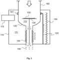
- FIG. 5shows certain details in an apparatus according to an embodiment of the present disclosure
- FIG. 6shows a schematic side view of an apparatus according to another alternative embodiment of the present disclosure.
- FIG. 7shows a schematic side view of an apparatus according to yet another alternative embodiment of the present disclosure.
- FIG. 8shows a method according to an embodiment of the present disclosure.
- Atomic Layer Deposition(ALD) technology is used as an example.
- ALDAtomic Layer Deposition
- the inventionis not limited to ALD technology, but it can be exploited in a wide variety of deposition apparatuses, for example, in Chemical Vapor Deposition (CVD) reactors as well as in cleaning reactors.
- CVDChemical Vapor Deposition
- ALDis a special chemical deposition method based on the sequential introduction of at least two reactive precursor species to at least one substrate. It is to be understood, however, that one of these reactive precursors can be substituted by energy when using photo-enhanced ALD or plasma-assisted ALD, for example PEALD, leading to single precursor ALD processes.
- PEALDplasma-assisted ALD
- Thin films grown by ALDare dense, pinhole free and have uniform thickness.
- the at least one substrateis typically exposed to temporally separated precursor pulses in a reaction vessel to deposit material on the substrate surfaces by sequential self-saturating surface reactions.
- ALDcomprises all applicable ALD based techniques and any equivalent or closely related technologies, such as, for example the following ALD sub-types: MLD (Molecular Layer Deposition) plasma-assisted ALD, for example PEALD (Plasma Enhanced Atomic Layer Deposition) and photo-enhanced Atomic Layer Deposition (known also as flash enhanced ALD).
- a basic ALD deposition cycleconsists of four sequential steps: pulse A, purge A, pulse B and purge B.
- Pulse Aconsists of a first precursor vapor and pulse B of another precursor vapor.
- Inactive gas and a vacuum pumpare typically used for purging gaseous reaction by-products and the residual reactant molecules from the reaction space during purge A and purge B.
- a deposition sequencecomprises at least one deposition cycle. Deposition cycles are repeated until the deposition sequence has produced a thin film or coating of desired thickness. Deposition cycles can also be either simpler or more complex. For example, the cycles can include three or more reactant vapor pulses separated by purging steps, or certain purge steps can be omitted. All these deposition cycles form a timed deposition sequence that is controlled by a logic unit or a microprocessor.
- FIGS. 1 and 2show schematic side views of a deposition or cleaning apparatus according to an example embodiment.
- the apparatuscomprises an outer chamber wall defining an outer chamber 110 .
- the apparatusfurther comprises a reaction chamber 120 inside the outer chamber 110 thus forming a double chamber structure.
- the space formed in between the outer chamber wall and the reaction chamber 120i.e., the space defined by the outer chamber 110 and surrounding the reaction chamber 120 ) is defined as an intermediate space 111 and the space within the reaction chamber 120 as a reaction space 112 as shown in FIG. 2 .
- the reaction chamber 120is configured to move between a deposition or cleaning position ( FIG. 2 ) and a lowered position ( FIG. 1 ) inside the outer chamber 110 .
- the lowered positionis for loading one or more substrates 105 into the reaction chamber.
- the deposition or cleaning positionis for processing the one or more substrates 105 in accordance with the selected deposition or cleaning method, for example, ALD or CVD.
- the apparatuscomprises a loading port 115 at the side of the outer chamber 110 for loading the one or more substrates 105 into the reaction chamber 120 through the side of the outer chamber 110 .
- the loading port 115 showndepicts a load lock 115 , although in alternative embodiments the load lock 115 may be omitted and replaced by a simpler structure, such as a hatch or similar. In certain example embodiments, the loading port 115 may be a gate valve or a load lock against ambient conditions or against other equipment.
- the apparatuscomprises a moving element 140 connected to the reaction chamber 120 .
- the moving element 140allows the reaction chamber 120 to move vertically between the deposition or cleaning position and the lowered position.
- the moving element 140may be a flexure structure. It may be a tube-like elongated structure whose length is adjustable.
- the moving element 140may be a deformable component.
- the moving element 140 shown in FIGS. 1 and 2is a bellows, in particular a vacuum bellows, allowing fluid to pass through in a vertical direction, but having gastight side walls.
- the moving element 140may form part of an exhaust line 150 below the reaction chamber 120 as shown in FIGS. 1 and 2 .
- the moving element 140is positioned in its entirety inside of the outer chamber 110 walls in vacuum.
- the actual movement of the reaction chamber 120may be driven by an actuator (actuating element) or by the moving element 140 itself.
- the embodiment in FIGS. 1 and 2shows an actuator 145 positioned on the outside of the outer chamber 110 .
- the actuator 145applies force to the reaction chamber 120 so that the reaction chamber moves as allowed by the moving element 140 .
- the actuator 145 shown in FIGS. 1 and 2comprises a force transmission member, such as a shaft or rod, which extends through an outer chamber feedthrough into the intermediate space between the outer chamber 110 and reaction chamber 120 .
- the force transmission memberfurther contacts the reaction chamber 120 enabling movement of the reaction chamber 120 as allowed by the moving element 140 .
- the moving element 140has a contracted shape as shown in FIG. 1 and an extended shape as shown in FIG. 2 , and it allows vertical movement of the reaction chamber 120 between positions defined by these shapes.
- the placement, form and operation of the actuating elementmay deviate from the ones shown in FIGS. 1 and 2 .
- the placement of the actuating elementdepends on the implementation. In certain example embodiments, the actuating element is positioned on the outside of the outer chamber. In certain example embodiments, the actuating element is positioned within the outer chamber, but on the outside of the reaction chamber. In certain example embodiments, the actuating element is positioned within the exhaust line 150 . Depending on the implementation the deposition or cleaning apparatus can comprise a plurality of actuating elements.
- the actuating elementis omitted altogether.
- the moving element 140as such moves the reaction chamber without an external actuator (external here meaning external to the moving element).
- the movingmay be implemented due to radiation or changes in temperature, for example.
- FIG. 3shows one such alternative embodiment in which the moving element 140 is formed of shape-memory alloy (smart metal).
- the moving element 140 in practiceis a kind of actuator in itself which moves the reaction chamber 120 between vertical positions.
- the apparatusis configured to form a loading opening into the reaction chamber 120 by downward movement of the reaction chamber 120 .
- the reaction chamber 120is configured to detach from an upper stationary part upon downward movement of the reaction chamber 120 to open a route for loading.
- the upper stationary partis a part providing fluid in-feed into the reaction chamber 120 .
- the part on top of the movable reaction chamber(i.e., upper stationary part of the apparatus) may be an open or closed part.
- FIGS. 1 and 2shows a radical in-feed tube 160 extending from a radical source (not shown).
- the radical in-feed tuberemains stationary when the reaction chamber 120 is lowered.
- the loading openingforms in between the reaction chamber 120 sidewall and the radical in-feed tube 160 ( FIG. 1 ).
- the embodiment shown in FIGS. 1 and 2further shows an in-feed line 125 which may be an in-feed line for inactive gas, or for a precursor of thermal ALD, for example.
- the in-feed line 125extends from a source (not shown) via an outer chamber feedthrough into the intermediate space. It further extends into an outlet in a fixed flange or collar 161 on top of the movable reaction chamber 120 (so as to provide entry of inactive/precursor gas or fluid into the reaction chamber 120 at that point).
- the part 161remains stationary when the reaction chamber 120 is lowered.
- the deposition or cleaning reactorcan comprise a plurality of in-feed lines 125 . In other embodiments, for example in certain cleaning embodiments, they can be omitted.
- FIG. 4shows an example of a closed upper stationary part. It may be, for example, a lid-like part 470 optionally comprising an expansion volume 475 for downward fluid distribution.
- the apparatuscomprises a substrate holder 130 which is configured to receive the one or more substrates 105 loaded through the loading port 115 .
- the substrate holder 130is attached to the exhaust line 150 .
- a substrate holder 430is integratable or integrated to reaction chamber top part of lid 470 .
- the substrate holdermay be movable within the reaction chamber 120 , for example, vertically.
- the apparatus described hereinalso comprises a heater 155 within the outer chamber 110 but on the outside of the reaction chamber 120 , although in some embodiments the heater may be omitted.
- the apparatuscomprises inactive gas in-feed into the outer chamber 110 into the intermediate space formed in between the reaction chamber 120 and outer chamber 110 walls and outlet of the inactive gas from the intermediate space (the intermediate space herein being the volume within the outer chamber that surrounds the reaction chamber).
- FIG. 5shows one such an embodiment.
- Inactive gasis fed in via an outer chamber feedthrough 581 and pumped out to the exhaust line 150 via feedthrough 582 .
- the outletcan be upstream or downstream in relation to the moving part 140 .
- the outletis to a separate pump line.
- the outletis into the reaction chamber 120 at the point where the moving reaction chamber 120 contacts the upper stationary part.
- the contact formed between the movable reaction chamber 120 and the stationary part when the reaction chamber 120 is in the deposition or cleaning positionmay be a metal-metal contact.
- the direction of gas flow within the reaction chamber 120is from top to bottom.
- the gas or fluid in-feed into the reaction chamber 120is preferably from the top side of the reaction chamber 120 and the outlet from a lower part of the reaction chamber (below the substrate), for example, through the bottom or bottom part of the reaction chamber 120 into the exhaust line 150 .
- a vacuum pump(not shown) which pumps the interior of the reaction chamber 120 into vacuum.
- the reaction chamber 120forms a body with rotational symmetry.
- the reaction chamber 120may be a bowl-like part (having an exhaust opening in its bottom).
- the outer chamber 110may be formed by a pressure vessel.
- the outer chamber 110may be denoted as a vacuum chamber due to vacuum conditions generated therein.
- both the reaction chamber 120 and outer chamber 110are in vacuum when loading the substrates (and during processing).
- the outer chamber 110 wallsform a borderline.
- the volume within the vacuum chamber wallswhich especially applies to the interior of the reaction chamber 120 , is pumped into vacuum by a vacuum pump (not shown) vacuum conditions thereby prevailing within the volume defined by the vacuum chamber walls.
- the pressure in the intermediate space 111 during processingis below atmospheric pressure. In certain example embodiments the pressure in the intermediate space is 0.9 bar or less, preferably 15 ⁇ 5 mbar the pressure in the reaction space 112 then preferably being 1.5 ⁇ 0.1 mbar.
- the pressure in the intermediate space 111is preferably at least two times the pressure in the reaction space 112 . In some embodiments, the pressure in the intermediate space 111 is 5 to 10 times the pressure in the reaction space 112 . In some other embodiments, such as when using microwave plasma, the pressure in the reaction space 112 may be 1 Pa and the pressure in the intermediate space 4 ⁇ 5 Pa.
- a turbomolecular pumpmay be applied to obtain high degrees of vacuum.
- the pressure of the reaction chamber 120in an embodiment is raised to a reading that is the same of higher compared to the pressure in the intermediate space 111 so as to push possible particles away from the substrate.
- an alternative moving elementis used.
- the moving element 640 shown in FIG. 6is implemented by two (or more) interlaced or nested tubes which are vertically movable in relation to each other.
- the embodimentotherwise contains similar elements and operates similarly as the embodiments described in the preceding.
- FIG. 7shows an optional protective element 791 which is placed within the exhaust line 150 and which is configured to prevent material from being deposited on the moving element 140 during processing.
- the protective element 791may be in the form of a tube and it may extend along the whole length of the moving element 140 , and even further. It may be fixed to the exhaust line 150 or to an edge of the outer chamber 110 .
- Inactive gasis in an embodiment fed from the intermediate space 111 into the space formed in between the protective element 791 and the moving element 140 via feedthrough 582 close to a dead lower end of the space. The inactive gas flows upwards along the formed tight space to the point in which the protective element 791 ends. The flow turns there into the downward direction and mixes with exhaust line flow. The entry of reactive gases into the space in between the protective element 791 and the moving element 140 is thereby hindered.
- the substrate(s)may be supported by an upper edge of the protective element 791 .
- a second moving element(another tubular element such as a second bellows) around the disclosed (first) moving element 140 .
- a closed spaceis formed in between the two moving elements and the formed space is pressurized with gas or fluid as required to obtain deformations in the moving elements due to changes in applied pressure thereby causing vertical movement of the reaction chamber 120 as desired.
- Said second moving elementmay be for example tightly fitted against the outer wall of the reaction chamber 120 at its one end and against the outer chamber 110 wall at its other end.
- the arrangementoperates as a pneumatic actuator.
- the outer chamber 110is omitted.
- the reaction chamber 120forms part of a single chamber reactor. A loading opening is formed by lowering the reaction chamber 120 as a whole.
- FIG. 8shows a method according to an embodiment of the present disclosure.
- the reaction chamberis lowered.
- the one or more substratesis loading in step 802 .
- the reaction chamberis raised into the deposition or cleaning position in step 803 for the deposition and/or cleaning to occur with a selected deposition or cleaning method in step 804 .
- the reaction chamberis again lowered in step 805 , and the one or more substrates are unloaded in step 806 .
- one or more of the steps 802 - 806may be omitted.
- the powdermay be loaded along a separate channel and unloaded along the same or different channel. In such an embodiment, the lowering of the reaction chamber for loading will not be needed, but the lowering of the reaction chamber may be used for a maintenance purpose only.
- a technical effectis reduced particle formation in a substrate processing apparatus, such as a deposition or cleaning apparatus, above the substrate surface by placing the moving parts of the reaction chamber below the substrate.
- Another technical effectis preventing particles from below the substrate from entering the space above the substrate, when the flow direction below the substrate is further away from the substrate (i.e., downwards).
- Another technical effectis improved loading method in a substrate processing reactor, in a double chamber substrate processing reactor in particular.
- Another technical effectis yet increased pressure difference, which can be obtained by using flexible bellows a deformable component, compared referred state of are.
Landscapes
- Chemical & Material Sciences (AREA)
- Engineering & Computer Science (AREA)
- Mechanical Engineering (AREA)
- General Chemical & Material Sciences (AREA)
- Organic Chemistry (AREA)
- Metallurgy (AREA)
- Materials Engineering (AREA)
- Chemical Kinetics & Catalysis (AREA)
- Power Engineering (AREA)
- Condensed Matter Physics & Semiconductors (AREA)
- General Physics & Mathematics (AREA)
- Microelectronics & Electronic Packaging (AREA)
- Physics & Mathematics (AREA)
- Computer Hardware Design (AREA)
- Manufacturing & Machinery (AREA)
- Chemical Vapour Deposition (AREA)
- Physical Vapour Deposition (AREA)
- Container, Conveyance, Adherence, Positioning, Of Wafer (AREA)
- Crystals, And After-Treatments Of Crystals (AREA)
Abstract
Description
Claims (10)
Applications Claiming Priority (1)
| Application Number | Priority Date | Filing Date | Title |
|---|---|---|---|
| PCT/FI2017/050071WO2018146370A1 (en) | 2017-02-08 | 2017-02-08 | Deposition or cleaning apparatus with movable structure and method of operation |
Related Parent Applications (1)
| Application Number | Title | Priority Date | Filing Date |
|---|---|---|---|
| PCT/FI2017/050071A-371-Of-InternationalWO2018146370A1 (en) | 2017-02-08 | 2017-02-08 | Deposition or cleaning apparatus with movable structure and method of operation |
Related Child Applications (1)
| Application Number | Title | Priority Date | Filing Date |
|---|---|---|---|
| US18/163,315DivisionUS11970774B2 (en) | 2017-02-08 | 2023-02-02 | Method of operating a deposition or cleaning apparatus |
Publications (2)
| Publication Number | Publication Date |
|---|---|
| US20190390339A1 US20190390339A1 (en) | 2019-12-26 |
| US11725279B2true US11725279B2 (en) | 2023-08-15 |
Family
ID=63107955
Family Applications (2)
| Application Number | Title | Priority Date | Filing Date |
|---|---|---|---|
| US16/481,221ActiveUS11725279B2 (en) | 2017-02-08 | 2017-02-08 | Deposition or cleaning apparatus with movable structure |
| US18/163,315ActiveUS11970774B2 (en) | 2017-02-08 | 2023-02-02 | Method of operating a deposition or cleaning apparatus |
Family Applications After (1)
| Application Number | Title | Priority Date | Filing Date |
|---|---|---|---|
| US18/163,315ActiveUS11970774B2 (en) | 2017-02-08 | 2023-02-02 | Method of operating a deposition or cleaning apparatus |
Country Status (10)
| Country | Link |
|---|---|
| US (2) | US11725279B2 (en) |
| EP (1) | EP3559307B1 (en) |
| JP (1) | JP6697640B2 (en) |
| KR (1) | KR102153876B1 (en) |
| CN (1) | CN110234793B (en) |
| DE (1) | DE17895903T1 (en) |
| ES (1) | ES2928391T3 (en) |
| RU (1) | RU2727634C1 (en) |
| TW (1) | TWI806848B (en) |
| WO (1) | WO2018146370A1 (en) |
Families Citing this family (11)
| Publication number | Priority date | Publication date | Assignee | Title |
|---|---|---|---|---|
| JP6681452B1 (en)* | 2018-10-19 | 2020-04-15 | 株式会社Kokusai Electric | Substrate processing apparatus and semiconductor device manufacturing method |
| CN114026268A (en)* | 2019-06-25 | 2022-02-08 | 皮考逊公司 | Substrate backside protection |
| KR102271566B1 (en)* | 2019-10-28 | 2021-07-01 | 세메스 주식회사 | Substrate treatment apparatus |
| FI129609B (en)* | 2020-01-10 | 2022-05-31 | Picosun Oy | Substrate processing apparatus |
| RU2767915C1 (en)* | 2020-12-14 | 2022-03-22 | Общество с ограниченной ответственностью "Оксифилм" (ООО "Оксифилм") | System for carrying out process of chemical precipitation from vapors of volatile precursors |
| JP7693795B2 (en)* | 2021-03-23 | 2025-06-17 | 東京エレクトロン株式会社 | Semiconductor manufacturing equipment and parts for semiconductor manufacturing equipment |
| FI130387B (en) | 2021-03-30 | 2023-08-07 | Beneq Oy | An atomic layer deposition apparatus |
| FI130021B (en)* | 2021-05-10 | 2022-12-30 | Picosun Oy | Substrate processing apparatus and method |
| FI130020B (en)* | 2021-05-10 | 2022-12-30 | Picosun Oy | Substrate processing apparatus and method |
| FI131128B1 (en)* | 2023-10-11 | 2024-10-21 | Picosun Oy | Substrate processing apparatus and heating element assembly |
| CN118653136B (en)* | 2024-08-21 | 2025-01-28 | 中科研和(宁波)科技有限公司 | Atomic layer deposition device and method for preparing pan-semiconductor material |
Citations (49)
| Publication number | Priority date | Publication date | Assignee | Title |
|---|---|---|---|---|
| US4439261A (en)* | 1983-08-26 | 1984-03-27 | International Business Machines Corporation | Composite pallet |
| US4976610A (en) | 1988-12-05 | 1990-12-11 | Cryco Twenty-Two, Inc. | Purge cantilevered wafer loading system for LP CVD processes |
| US5088444A (en) | 1989-03-15 | 1992-02-18 | Kabushiki Kaisha Toshiba | Vapor deposition system |
| US5148714A (en) | 1990-10-24 | 1992-09-22 | Ag Processing Technology, Inc. | Rotary/linear actuator for closed chamber, and reaction chamber utilizing same |
| US5156820A (en) | 1989-05-15 | 1992-10-20 | Rapro Technology, Inc. | Reaction chamber with controlled radiant energy heating and distributed reactant flow |
| US5266119A (en) | 1991-05-13 | 1993-11-30 | Mitsubishi Denki Kabushiki Kaisha | Vacuum sealing mechanism for a semiconductor device manufacturing apparatus having inner and outer bellows |
| JP2560986B2 (en) | 1993-07-27 | 1996-12-04 | 日本電気株式会社 | Tungsten CVD equipment |
| JPH10184929A (en) | 1996-12-25 | 1998-07-14 | Hitachi Electron Eng Co Ltd | Linear motion mechanism |
| JPH11116381A (en) | 1997-10-16 | 1999-04-27 | Shin Etsu Chem Co Ltd | Pyrolytic boron nitride conical cylinder and method for producing the same |
| US5904478A (en) | 1997-03-07 | 1999-05-18 | Semitool, Inc. | Semiconductor processing furnace heating subassembly |
| US6040011A (en) | 1998-06-24 | 2000-03-21 | Applied Materials, Inc. | Substrate support member with a purge gas channel and pumping system |
| US20010029971A1 (en) | 1999-08-05 | 2001-10-18 | Farmer Robert B. | Inverted pressure vessel with shielded closure mechanism |
| US6409837B1 (en) | 1999-01-13 | 2002-06-25 | Tokyo Electron Limited | Processing system and method for chemical vapor deposition of a metal layer using a liquid precursor |
| US20020157960A1 (en) | 1998-04-21 | 2002-10-31 | Applied Materials, Inc. | Electro-chemical deposition cell for face-up processing of single semiconductor substrates |
| US20020166574A1 (en) | 2001-05-10 | 2002-11-14 | Taiwan Semiconductor Manufacturing Co., Ltd. | Method and apparatus for cleaning a heater bellow in a chemical vapor deposition chamber |
| US20030143841A1 (en) | 2002-01-26 | 2003-07-31 | Yang Michael X. | Integration of titanium and titanium nitride layers |
| US20030232512A1 (en) | 2002-06-13 | 2003-12-18 | Dickinson C. John | Substrate processing apparatus and related systems and methods |
| US6818560B1 (en)* | 1999-09-22 | 2004-11-16 | Tokyo Electron Limited | Plasma processing apparatus and plasma processing method |
| US20050000425A1 (en) | 2003-07-03 | 2005-01-06 | Aeromet Technologies, Inc. | Simple chemical vapor deposition system and methods for depositing multiple-metal aluminide coatings |
| US20050072525A1 (en) | 2003-10-06 | 2005-04-07 | Applied Materials, Inc. | Apparatus to improve wafer temperature uniformity for face-up wet processing |
| US20070031609A1 (en) | 2005-07-29 | 2007-02-08 | Ajay Kumar | Chemical vapor deposition chamber with dual frequency bias and method for manufacturing a photomask using the same |
| US20070059128A1 (en) | 2005-08-31 | 2007-03-15 | Applied Materials, Inc. | Batch deposition tool and compressed boat |
| US20070116873A1 (en)* | 2005-11-18 | 2007-05-24 | Tokyo Electron Limited | Apparatus for thermal and plasma enhanced vapor deposition and method of operating |
| WO2007084493A2 (en) | 2006-01-19 | 2007-07-26 | Asm America, Inc. | High temperature ald inlet manifold |
| US20070181057A1 (en) | 2006-02-03 | 2007-08-09 | Applied Materials, Inc. | Epitaxial deposition process and apparatus |
| KR20070093820A (en) | 2006-03-15 | 2007-09-19 | 에이에스엠 저펜 가부시기가이샤 | Semiconductor Processing Equipment with Rotary Susceptors |
| KR20090118676A (en) | 2008-05-14 | 2009-11-18 | (주)퓨전에이드 | Substrate Processing Equipment |
| US20100136773A1 (en)* | 2005-08-10 | 2010-06-03 | Naonori Akae | Semiconductor Device Manufacturing Method and Substrate Processing Apparatus |
| US20100198550A1 (en) | 2009-01-30 | 2010-08-05 | Ronald Vern Schauer | Sensor system for semiconductor manufacturing apparatus |
| US20100224804A1 (en) | 2003-10-17 | 2010-09-09 | Sundew Technologies, Llc | Fail safe pneumatically actuated valve with fast time response and adjustable conductance |
| EP2249379A2 (en) | 2008-02-12 | 2010-11-10 | Kyu-Jeong Choi | Batch-type atomic layer vapour-deposition device |
| JP2011127136A (en) | 2009-12-15 | 2011-06-30 | Canon Anelva Corp | Sputtering apparatus and method of fabricating semiconductor device using the sputtering apparatus |
| JP2011132580A (en) | 2009-12-25 | 2011-07-07 | Canon Anelva Corp | Film-forming apparatus and film-forming method |
| EP2408003A1 (en) | 2009-03-10 | 2012-01-18 | Mitsui Engineering & Shipbuilding Co., Ltd. | Atomic layer deposition apparatus and thin film forming method |
| WO2012136876A1 (en) | 2011-04-07 | 2012-10-11 | Picosun Oy | Atomic layer deposition with plasma source |
| WO2012136875A1 (en) | 2011-04-07 | 2012-10-11 | Picosun Oy | Deposition reactor with plasma source |
| US20130042811A1 (en) | 2008-05-02 | 2013-02-21 | Intermolecular, Inc. | Combinatorial Plasma Enhanced Deposition Techniques |
| US20130129577A1 (en) | 2011-11-23 | 2013-05-23 | ASM Holding B.V. | Chamber sealing member |
| WO2013140021A1 (en) | 2012-03-23 | 2013-09-26 | Picosun Oy | Atomic layer deposition method and apparatuses |
| WO2014080067A1 (en) | 2012-11-23 | 2014-05-30 | Picosun Oy | Substrate loading in an ald reactor |
| WO2014147290A1 (en) | 2013-03-22 | 2014-09-25 | Beneq Oy | An apparatus for processing two or more substrates in a batch process |
| US20140311581A1 (en) | 2013-04-19 | 2014-10-23 | Applied Materials, Inc. | Pressure controller configuration for semiconductor processing applications |
| US20140318456A1 (en) | 2013-04-25 | 2014-10-30 | Ncd Co., Ltd. | Horizontal-type atomic layer deposition apparatus for large-area substrates |
| KR20150065454A (en) | 2013-12-05 | 2015-06-15 | 주식회사 썬닉스 | Bellows |
| US20150197851A1 (en) | 2012-06-27 | 2015-07-16 | Inoct Co., Ltd | Process chamber and substrate processing device |
| US20160083837A1 (en) | 2013-04-30 | 2016-03-24 | Tokyo Electron Limited | Film Formation Device |
| WO2016102748A1 (en) | 2014-12-22 | 2016-06-30 | Picosun Oy | Ald method and apparatus |
| JP6021688B2 (en) | 2013-02-25 | 2016-11-09 | ルネサスエレクトロニクス株式会社 | Semiconductor device and control method thereof |
| US20170241020A1 (en) | 2001-07-16 | 2017-08-24 | Applied Materials, Inc. | Lid assembly for a processing system to facilitate sequential deposition techniques |
Family Cites Families (3)
| Publication number | Priority date | Publication date | Assignee | Title |
|---|---|---|---|---|
| KR100782529B1 (en)* | 2001-11-08 | 2007-12-06 | 에이에스엠지니텍코리아 주식회사 | Deposition equipment |
| KR100773724B1 (en)* | 2006-08-23 | 2007-11-06 | 주식회사 아이피에스 | Thin film deposition apparatus |
| KR100991978B1 (en)* | 2009-10-30 | 2010-11-05 | (주)브이티에스 | Reactor for chemical vapor deposition |
- 2017
- 2017-02-08WOPCT/FI2017/050071patent/WO2018146370A1/ennot_activeCeased
- 2017-02-08ESES17895903Tpatent/ES2928391T3/enactiveActive
- 2017-02-08KRKR1020197025904Apatent/KR102153876B1/enactiveActive
- 2017-02-08DEDE17895903.7Tpatent/DE17895903T1/enactivePending
- 2017-02-08JPJP2019541456Apatent/JP6697640B2/enactiveActive
- 2017-02-08EPEP17895903.7Apatent/EP3559307B1/enactiveActive
- 2017-02-08USUS16/481,221patent/US11725279B2/enactiveActive
- 2017-02-08RURU2019124704Apatent/RU2727634C1/enactive
- 2017-02-08CNCN201780085412.1Apatent/CN110234793B/enactiveActive
- 2018
- 2018-01-16TWTW107101549Apatent/TWI806848B/enactive
- 2023
- 2023-02-02USUS18/163,315patent/US11970774B2/enactiveActive
Patent Citations (57)
| Publication number | Priority date | Publication date | Assignee | Title |
|---|---|---|---|---|
| US4439261A (en)* | 1983-08-26 | 1984-03-27 | International Business Machines Corporation | Composite pallet |
| US4976610A (en) | 1988-12-05 | 1990-12-11 | Cryco Twenty-Two, Inc. | Purge cantilevered wafer loading system for LP CVD processes |
| US5088444A (en) | 1989-03-15 | 1992-02-18 | Kabushiki Kaisha Toshiba | Vapor deposition system |
| US5156820A (en) | 1989-05-15 | 1992-10-20 | Rapro Technology, Inc. | Reaction chamber with controlled radiant energy heating and distributed reactant flow |
| US5148714A (en) | 1990-10-24 | 1992-09-22 | Ag Processing Technology, Inc. | Rotary/linear actuator for closed chamber, and reaction chamber utilizing same |
| US5266119A (en) | 1991-05-13 | 1993-11-30 | Mitsubishi Denki Kabushiki Kaisha | Vacuum sealing mechanism for a semiconductor device manufacturing apparatus having inner and outer bellows |
| JP2560986B2 (en) | 1993-07-27 | 1996-12-04 | 日本電気株式会社 | Tungsten CVD equipment |
| JPH10184929A (en) | 1996-12-25 | 1998-07-14 | Hitachi Electron Eng Co Ltd | Linear motion mechanism |
| US5904478A (en) | 1997-03-07 | 1999-05-18 | Semitool, Inc. | Semiconductor processing furnace heating subassembly |
| JPH11116381A (en) | 1997-10-16 | 1999-04-27 | Shin Etsu Chem Co Ltd | Pyrolytic boron nitride conical cylinder and method for producing the same |
| US20020157960A1 (en) | 1998-04-21 | 2002-10-31 | Applied Materials, Inc. | Electro-chemical deposition cell for face-up processing of single semiconductor substrates |
| US6040011A (en) | 1998-06-24 | 2000-03-21 | Applied Materials, Inc. | Substrate support member with a purge gas channel and pumping system |
| US6409837B1 (en) | 1999-01-13 | 2002-06-25 | Tokyo Electron Limited | Processing system and method for chemical vapor deposition of a metal layer using a liquid precursor |
| US20010029971A1 (en) | 1999-08-05 | 2001-10-18 | Farmer Robert B. | Inverted pressure vessel with shielded closure mechanism |
| US6818560B1 (en)* | 1999-09-22 | 2004-11-16 | Tokyo Electron Limited | Plasma processing apparatus and plasma processing method |
| US20020166574A1 (en) | 2001-05-10 | 2002-11-14 | Taiwan Semiconductor Manufacturing Co., Ltd. | Method and apparatus for cleaning a heater bellow in a chemical vapor deposition chamber |
| US20170241020A1 (en) | 2001-07-16 | 2017-08-24 | Applied Materials, Inc. | Lid assembly for a processing system to facilitate sequential deposition techniques |
| US20030143841A1 (en) | 2002-01-26 | 2003-07-31 | Yang Michael X. | Integration of titanium and titanium nitride layers |
| US20030232512A1 (en) | 2002-06-13 | 2003-12-18 | Dickinson C. John | Substrate processing apparatus and related systems and methods |
| RU2352685C2 (en) | 2003-07-03 | 2009-04-20 | Аэромет Текнолоджиз, Инк. | Simple system of chemical deposition from vapours and plating methods of many-metallic aluminide coatings |
| US20050000425A1 (en) | 2003-07-03 | 2005-01-06 | Aeromet Technologies, Inc. | Simple chemical vapor deposition system and methods for depositing multiple-metal aluminide coatings |
| US20050072525A1 (en) | 2003-10-06 | 2005-04-07 | Applied Materials, Inc. | Apparatus to improve wafer temperature uniformity for face-up wet processing |
| US20100224804A1 (en) | 2003-10-17 | 2010-09-09 | Sundew Technologies, Llc | Fail safe pneumatically actuated valve with fast time response and adjustable conductance |
| US20070031609A1 (en) | 2005-07-29 | 2007-02-08 | Ajay Kumar | Chemical vapor deposition chamber with dual frequency bias and method for manufacturing a photomask using the same |
| US20100136773A1 (en)* | 2005-08-10 | 2010-06-03 | Naonori Akae | Semiconductor Device Manufacturing Method and Substrate Processing Apparatus |
| US20070059128A1 (en) | 2005-08-31 | 2007-03-15 | Applied Materials, Inc. | Batch deposition tool and compressed boat |
| US20070116873A1 (en)* | 2005-11-18 | 2007-05-24 | Tokyo Electron Limited | Apparatus for thermal and plasma enhanced vapor deposition and method of operating |
| WO2007084493A3 (en) | 2006-01-19 | 2007-10-04 | Asm Inc | High temperature ald inlet manifold |
| WO2007084493A2 (en) | 2006-01-19 | 2007-07-26 | Asm America, Inc. | High temperature ald inlet manifold |
| US20070181057A1 (en) | 2006-02-03 | 2007-08-09 | Applied Materials, Inc. | Epitaxial deposition process and apparatus |
| KR20070093820A (en) | 2006-03-15 | 2007-09-19 | 에이에스엠 저펜 가부시기가이샤 | Semiconductor Processing Equipment with Rotary Susceptors |
| EP2249379A2 (en) | 2008-02-12 | 2010-11-10 | Kyu-Jeong Choi | Batch-type atomic layer vapour-deposition device |
| US20130042811A1 (en) | 2008-05-02 | 2013-02-21 | Intermolecular, Inc. | Combinatorial Plasma Enhanced Deposition Techniques |
| KR20090118676A (en) | 2008-05-14 | 2009-11-18 | (주)퓨전에이드 | Substrate Processing Equipment |
| US20100198550A1 (en) | 2009-01-30 | 2010-08-05 | Ronald Vern Schauer | Sensor system for semiconductor manufacturing apparatus |
| EP2408003A1 (en) | 2009-03-10 | 2012-01-18 | Mitsui Engineering & Shipbuilding Co., Ltd. | Atomic layer deposition apparatus and thin film forming method |
| JP2011127136A (en) | 2009-12-15 | 2011-06-30 | Canon Anelva Corp | Sputtering apparatus and method of fabricating semiconductor device using the sputtering apparatus |
| JP2011132580A (en) | 2009-12-25 | 2011-07-07 | Canon Anelva Corp | Film-forming apparatus and film-forming method |
| US20140087093A1 (en)* | 2011-04-07 | 2014-03-27 | Picosun Oy | Deposition reactor with plasma source |
| WO2012136875A1 (en) | 2011-04-07 | 2012-10-11 | Picosun Oy | Deposition reactor with plasma source |
| WO2012136876A1 (en) | 2011-04-07 | 2012-10-11 | Picosun Oy | Atomic layer deposition with plasma source |
| RU2571547C2 (en) | 2011-04-07 | 2015-12-20 | Пикосан Ой | Deposition reactor with plasma source |
| US9095869B2 (en) | 2011-04-07 | 2015-08-04 | Picosun Oy | Atomic layer deposition with plasma source |
| US20130129577A1 (en) | 2011-11-23 | 2013-05-23 | ASM Holding B.V. | Chamber sealing member |
| WO2013140021A1 (en) | 2012-03-23 | 2013-09-26 | Picosun Oy | Atomic layer deposition method and apparatuses |
| RU2600047C2 (en) | 2012-03-23 | 2016-10-20 | Пикосан Ой | Method and device for deposition of atomic layers |
| US20150197851A1 (en) | 2012-06-27 | 2015-07-16 | Inoct Co., Ltd | Process chamber and substrate processing device |
| JP2016503462A (en) | 2012-11-23 | 2016-02-04 | ピコサン オーワイPicosun Oy | Loading of substrates in ALD reactor |
| US20150299859A1 (en) | 2012-11-23 | 2015-10-22 | Picosun Oy | Substrate loading in an ald reactor |
| WO2014080067A1 (en) | 2012-11-23 | 2014-05-30 | Picosun Oy | Substrate loading in an ald reactor |
| JP6021688B2 (en) | 2013-02-25 | 2016-11-09 | ルネサスエレクトロニクス株式会社 | Semiconductor device and control method thereof |
| WO2014147290A1 (en) | 2013-03-22 | 2014-09-25 | Beneq Oy | An apparatus for processing two or more substrates in a batch process |
| US20140311581A1 (en) | 2013-04-19 | 2014-10-23 | Applied Materials, Inc. | Pressure controller configuration for semiconductor processing applications |
| US20140318456A1 (en) | 2013-04-25 | 2014-10-30 | Ncd Co., Ltd. | Horizontal-type atomic layer deposition apparatus for large-area substrates |
| US20160083837A1 (en) | 2013-04-30 | 2016-03-24 | Tokyo Electron Limited | Film Formation Device |
| KR20150065454A (en) | 2013-12-05 | 2015-06-15 | 주식회사 썬닉스 | Bellows |
| WO2016102748A1 (en) | 2014-12-22 | 2016-06-30 | Picosun Oy | Ald method and apparatus |
Non-Patent Citations (11)
| Title |
|---|
| Decision to Grant a Patent, Japanese Patent Application No. 2019-541456, dated Mar. 30, 2020. (English Translation Attached). |
| Extended European Search Report, Application No. 17895903.7, dated Feb. 11, 2020, 8 pages. |
| Inquiry under the Substantive Examination. Application No. PCT/FI2017/050071, dated Mar. 6, 2020. |
| International Search Report and Written Opinion of International Application No. PCT/FI2017/050071 dated Oct. 11, 2017, 11 pages. |
| Notice of Non-Final Rejection issued in Korean Patent Application No. KR1020197025904 dated Dec. 27, 2019, 10 pages including 5 pages of English Translation attached. |
| Notification of ground of rejection mailed in Japanese Patent Application No. JP2019541456 dated Dec. 25, 2019, 7 pages, 4 pages of English Translation attached. |
| Search Report, Application No. PCT/FI2017/050071. Completed Feb. 28, 2020. |
| Taiwan Patent Office, Office Action, Application No. 107101549, dated Mar. 24, 2021, 4 pages. |
| Taiwan Patent Office, Search Report, Application No. 107101549, dated Mar. 24, 2021, 1 page. |
| The Federal Institute of Industrial Property (FIIP), Inquiry under the substantive examination, Application No. 2020123573/05(040756), dated Nov. 18, 2020, 11 pages. |
| The Federal Institute of Industrial Property (FIIP), Search Report, Application No. 2020123573/05(040756), dated Nov. 12, 2020, 2 pages. |
Also Published As
| Publication number | Publication date |
|---|---|
| RU2727634C1 (en) | 2020-07-22 |
| EP3559307A4 (en) | 2020-03-11 |
| WO2018146370A1 (en) | 2018-08-16 |
| TWI806848B (en) | 2023-07-01 |
| JP2020506291A (en) | 2020-02-27 |
| TW201839164A (en) | 2018-11-01 |
| EP3559307B1 (en) | 2022-08-03 |
| CN110234793B (en) | 2020-10-02 |
| US20190390339A1 (en) | 2019-12-26 |
| US20230193461A1 (en) | 2023-06-22 |
| JP6697640B2 (en) | 2020-05-20 |
| KR102153876B1 (en) | 2020-09-10 |
| KR20190110614A (en) | 2019-09-30 |
| DE17895903T1 (en) | 2020-01-16 |
| EP3559307A1 (en) | 2019-10-30 |
| CN110234793A (en) | 2019-09-13 |
| ES2928391T3 (en) | 2022-11-17 |
| US11970774B2 (en) | 2024-04-30 |
Similar Documents
| Publication | Publication Date | Title |
|---|---|---|
| US11970774B2 (en) | Method of operating a deposition or cleaning apparatus | |
| JP6432507B2 (en) | Deposition equipment | |
| EP2694701B1 (en) | Deposition reactor with plasma source | |
| US10535501B2 (en) | Film forming apparatus, film forming method and non-transitory storage medium | |
| US12112927B2 (en) | Substrate processing apparatus and method | |
| JP7197739B2 (en) | Substrate processing apparatus and method | |
| HK40009606A (en) | Deposition or cleaning apparatus with movable structure and method of operation | |
| HK40009606B (en) | Deposition or cleaning apparatus with movable structure and method of operation | |
| RU2748658C1 (en) | Device for deposition or cleaning with mobile structure and method for its operation |
Legal Events
| Date | Code | Title | Description |
|---|---|---|---|
| FEPP | Fee payment procedure | Free format text:ENTITY STATUS SET TO UNDISCOUNTED (ORIGINAL EVENT CODE: BIG.); ENTITY STATUS OF PATENT OWNER: LARGE ENTITY | |
| FEPP | Fee payment procedure | Free format text:ENTITY STATUS SET TO SMALL (ORIGINAL EVENT CODE: SMAL); ENTITY STATUS OF PATENT OWNER: LARGE ENTITY | |
| AS | Assignment | Owner name:PICOSUN OY, FINLAND Free format text:ASSIGNMENT OF ASSIGNORS INTEREST;ASSIGNOR:MALINEN, TIMO;REEL/FRAME:050745/0881 Effective date:20190807 | |
| STPP | Information on status: patent application and granting procedure in general | Free format text:NON FINAL ACTION MAILED | |
| STPP | Information on status: patent application and granting procedure in general | Free format text:FINAL REJECTION MAILED | |
| STPP | Information on status: patent application and granting procedure in general | Free format text:ADVISORY ACTION MAILED | |
| STPP | Information on status: patent application and granting procedure in general | Free format text:NON FINAL ACTION MAILED | |
| STPP | Information on status: patent application and granting procedure in general | Free format text:RESPONSE TO NON-FINAL OFFICE ACTION ENTERED AND FORWARDED TO EXAMINER | |
| STPP | Information on status: patent application and granting procedure in general | Free format text:FINAL REJECTION MAILED | |
| STPP | Information on status: patent application and granting procedure in general | Free format text:RESPONSE AFTER FINAL ACTION FORWARDED TO EXAMINER | |
| STPP | Information on status: patent application and granting procedure in general | Free format text:ADVISORY ACTION MAILED | |
| STPP | Information on status: patent application and granting procedure in general | Free format text:DOCKETED NEW CASE - READY FOR EXAMINATION | |
| STPP | Information on status: patent application and granting procedure in general | Free format text:NON FINAL ACTION MAILED | |
| STPP | Information on status: patent application and granting procedure in general | Free format text:RESPONSE TO NON-FINAL OFFICE ACTION ENTERED AND FORWARDED TO EXAMINER | |
| STPP | Information on status: patent application and granting procedure in general | Free format text:FINAL REJECTION MAILED | |
| STPP | Information on status: patent application and granting procedure in general | Free format text:DOCKETED NEW CASE - READY FOR EXAMINATION | |
| STPP | Information on status: patent application and granting procedure in general | Free format text:NON FINAL ACTION MAILED | |
| FEPP | Fee payment procedure | Free format text:ENTITY STATUS SET TO UNDISCOUNTED (ORIGINAL EVENT CODE: BIG.); ENTITY STATUS OF PATENT OWNER: LARGE ENTITY | |
| STPP | Information on status: patent application and granting procedure in general | Free format text:NOTICE OF ALLOWANCE MAILED -- APPLICATION RECEIVED IN OFFICE OF PUBLICATIONS | |
| STPP | Information on status: patent application and granting procedure in general | Free format text:PUBLICATIONS -- ISSUE FEE PAYMENT RECEIVED | |
| STPP | Information on status: patent application and granting procedure in general | Free format text:PUBLICATIONS -- ISSUE FEE PAYMENT VERIFIED | |
| STCF | Information on status: patent grant | Free format text:PATENTED CASE |