US11720736B2 - Automation methods for 3D integrated circuits and devices - Google Patents
Automation methods for 3D integrated circuits and devicesDownload PDFInfo
- Publication number
- US11720736B2 US11720736B2US18/111,567US202318111567AUS11720736B2US 11720736 B2US11720736 B2US 11720736B2US 202318111567 AUS202318111567 AUS 202318111567AUS 11720736 B2US11720736 B2US 11720736B2
- Authority
- US
- United States
- Prior art keywords
- level
- placement
- memory
- placer
- strata
- Prior art date
- Legal status (The legal status is an assumption and is not a legal conclusion. Google has not performed a legal analysis and makes no representation as to the accuracy of the status listed.)
- Active
Links
Images


Classifications
- G—PHYSICS
- G06—COMPUTING OR CALCULATING; COUNTING
- G06F—ELECTRIC DIGITAL DATA PROCESSING
- G06F30/00—Computer-aided design [CAD]
- G06F30/30—Circuit design
- G06F30/39—Circuit design at the physical level
- G06F30/392—Floor-planning or layout, e.g. partitioning or placement
- G—PHYSICS
- G06—COMPUTING OR CALCULATING; COUNTING
- G06F—ELECTRIC DIGITAL DATA PROCESSING
- G06F30/00—Computer-aided design [CAD]
- G06F30/30—Circuit design
- G06F30/39—Circuit design at the physical level
- G06F30/394—Routing
Definitions
- This applicationrelates to the general field of computer aided design of monolithic three-dimensional integrated circuits.
- CADComputer-Aided Design
- FIG. 1A typical physical design process is illustrated in FIG. 1 . It may start with a netlist 105 made of physical objects, and a set of constraints 110 derived from the logical part of the design flow. Netlist 105 with constraints 110 may be partitioned into a small set of blocks, on the order of 1 to 100 using a program called partitioner 115 , which may produce a modified partitioned netlist 135 and modified netlist constraints 140 . These, in turn, may be fed into a floor-planner 145 that may arrange these blocks mosaic-like, while respecting design netlist constraints 140 , on a rectangular frame that may outline the physical footprint of the final integrated circuit (IC) and produce a newly modified netlist 155 and newly modified design constraints 160 .
- ICfinal integrated circuit
- the objects within each floor-planned block of newly modified netlist 155may then be assigned a location within that block, while respecting newly modified design constraints 160 , using the placer 165 .
- the placed design netlist 175 and modified design constraints 180may be passed to other CAD tools that may perform routing utilizing router 185 , and producing routed netlist 190 that may be passed downstream for rule checking and further processing 195 for the final IC manufacturing.
- the various CAD toolsmay use, in addition to the design itself and its constraints, a variety of libraries that describe the netlist objects in their various abstractions, and rules files that define the permissible actions on objects and legal relations between them, and between objects and an abstraction of the underlying technology layers. Further, user intervention may be required at the various steps above.
- TSVThrough-Silicon Vias
- the current inventionextends CAD tool functionality to operate with a monolithic three-dimensional (3D) manufacturing process.
- the key difference between a monolithic 3D process and a stacked-layer process where the layers are connected using TSVsis in the size of the inter-layer connection.
- TSVsare very large relative to advanced lithography feature size, and TSV scaling is not related to lithography but rather to the ability to etch and fill holes at very extreme aspect ratio, and the ability to handle extremely thin wafers.
- Today best etching and filling aspect ratiois roughly 10:1 and consequently the thinnest wafer that could be properly handled are roughly 50 micron thick with TSV diameter of roughly 5 micron.
- inter-layer connections of a monolithic 3D processscales with semiconductor scaling and is already below 100 nm, and will keep on scaling down as the industry continues with dimensional scaling.
- Monolithic 3D technologyWith this approach, multiple layers of transistors and wires can be monolithically constructed.
- Some monolithic 3D and 3DIC approachesare described in U.S. Pat. Nos. 8,273,610, 8,298,875, 8,362,482, 8,378,715, 8,379,458, 8,450,804, 8,557,632, 8,574,929, 8,581,349, 8,642,416, 8,669,778, 8,674,470, 8,687,399, 8,742,476, 8,803,206, 8,836,073, 8,902,663, 8,994,404, 9,023,688, 9,029,173, 9,030,858, 9,117,749, 9,142,553, 9,219,005, 9,385,058, 9,406,670, 9,460,978, 9,509,313, 9,640,531, 9,691,760, 9,711,407, 9,721,927, 9,799,761, 9,871,034, 9,953,870, 9,953,994, 10,014,292, 10,014,
- Electro-OpticsThere is also work done for integrated monolithic 3D including layers of different crystals, such as U.S. Pat. Nos. 8,283,215, 8,163,581, 8,753,913, 8,823,122, 9,197,804, 9,419,031, 9,941,319, 10,679,977, 10,943,934, 10,998,374, 11,063,071, and 11,133,344.
- optimization processes of CAD tools for TSV-based processesshould focus on minimizing the number of TSVs.
- the inter-layer connectivityis much denser and CAD tools should focus on leveraging that large inter-layer connectivity to optimally place objects on different layers based on the layers' potentially disparate characteristics, and to increase the physical proximity of objects in 3D space as compared to a 2D plane.
- the current inventiondescribes embodiments such as optimizations of CAD tools for monolithic 3D technology.
- a method of designing a 3D Integrated Circuitcomprising: performing placement using a 2D placer, performing placement for at least a first strata and a second strata, and then performing routing and completing the physical design of said 3D Integrated Circuit.
- a method of designing a 3D Integrated Circuitcomprising: performing partitioning to at least a first strata and a second strata, then performing placement using a 2D placer, and then performing routing and completing the physical design of said 3D Integrated Circuit.
- a method of designing a 3D Integrated Circuitcomprising: performing placement using a 2D placer, splitting the placed cells into at least a first group and a second group of similar total area, using said 2D placer to place said second group on a second strata, using said 2D placer to place said first group on a first strata, and then performing routing and completing the physical design of said 3D Integrated Circuit.
- a method of designing a 3D Integrated Circuitcomprising: performing partitioning to at least a first strata and a second strata; then performing a first placement of said first strata using a 2D placer executed by a computer, wherein said 2D placer is a Computer Aided Design (CAD) tool currently used in the industry for two-dimensional devices; and performing a second placement of said second strata based on said first placement, wherein said partitioning comprises a partition between logic and memory, and wherein said logic comprises at least one decoder representation for said memory.
- CADComputer Aided Design
- a method of designing a 3D Integrated Circuitcomprising: performing partitioning to at least a first strata and a second strata; then performing a first placement of said first strata using a 2D placer executed by a computer, wherein said 2D placer is a Computer Aided Design (CAD) tool currently used in the industry for two-dimensional devices; and performing a second placement of said second strata based on said first placement, wherein said partitioning comprises a partition between logic and memory, and wherein said logic comprises at least one decoder for said memory.
- CADComputer Aided Design
- a method of designing a 3D Integrated Circuitcomprising: performing partitioning to at least a first strata and a second strata; then performing a first placement of said first strata using a 2D placer executed by a computer, wherein said 2D placer is a Computer Aided Design (CAD) tool currently used in the industry for two-dimensional devices; and performing a second placement of said second strata based on said first placement, wherein said partitioning comprises splitting a plurality of cells into a high performance group to said first strata and a low performance group to said second strata.
- CADComputer Aided Design
- a method of designing a 3D Integrated Circuitcomprising: performing partitioning to at least a logic strata comprising logic and a memory strata comprising memory; then performing a first placement of said logic strata using a 2D placer executed by a computer, wherein said 2D placer is a Computer Aided Design (CAD) tool for two-dimensional devices; wherein said 3D Integrated Circuit comprises through silicon vias for connection between said logic strata and said memory strata; and performing a second placement of said memory strata based on said first placement, wherein said logic comprises at least one decoder representation for said memory, wherein said at least one decoder representation has a virtual size with width of contacts for said through silicon vias, and wherein said performing a first placement comprises using said decoder representation instead of an actual memory decoder.
- CADComputer Aided Design
- a method of designing a 3D Integrated Circuitcomprising: performing partitioning to at least a logic strata comprising logic and a memory strata comprising memory; then performing a first placement of said logic strata using a 2D placer executed by a computer, wherein said 2D placer is a Computer Aided Design (CAD) tool for two-dimensional devices; and performing a second placement of said memory strata based on said first placement, wherein said logic comprises at least one decoder for said memory, and wherein said memory comprises at least a first memory and a second memory, wherein said first memory comprises first memory decoders and said second memory comprises second memory decoders, wherein said 2D placer is set so said second memory decoders are not placed within a rectangle defined by the placement of said first memory decoders.
- CADComputer Aided Design
- a method of designing a 3D Integrated Circuitcomprising: performing partitioning to at least a logic strata comprising logic and a memory strata comprising memory; then performing a first placement of said logic strata using a 2D placer executed by a computer, wherein said 2D placer is a Computer Aided Design (CAD) tool for two-dimensional devices; and performing a second placement of said memory strata based on said first placement, wherein said partitioning comprises a step of assigning at least one memory block to said logic strata for improved balancing of said logic strata area and said memory strata area.
- CADComputer Aided Design
- a method of designing a 3D Integrated Circuitcomprising: performing partitioning to at least a logic strata comprising logic and a memory strata comprising memory; then performing a first placement of said logic strata using a 2D placer executed by a computer, wherein said 2D placer is a Computer Aided Design (CAD) tool for two-dimensional devices, wherein said 3D Integrated Circuit comprises through silicon vias for connection between said logic strata and said memory strata; and performing a second placement of said memory strata based on said first placement, wherein said memory comprises a first memory array, wherein said logic comprises a first logic circuit controlling said first memory array, wherein said first placement comprises placement of said first logic circuit, and wherein said second placement comprises placement of said first memory array based on said placement of said first logic circuit.
- CADComputer Aided Design
- a method of designing a 3D Integrated Circuitcomprising: performing partitioning to at least a logic strata comprising logic and a memory strata comprising memory; then performing a first placement of said logic strata using a 2D placer executed by a computer, wherein said 2D placer is a Computer Aided Design (CAD) tool for two-dimensional devices; and performing a second placement of said memory strata based on said first placement, wherein said logic comprises at least one decoder representation for said memory, and wherein said memory comprises at least a first memory and a second memory, wherein said first memory comprises a first memory decoder representation and said second memory comprises a second memory decoder representation, wherein said 2D placer is set so said second memory decoder representation is not placed within a rectangle defined by placement of said first memory decoder representation.
- CADComputer Aided Design
- a method of designing a 3D Integrated Circuitcomprising: performing partitioning to at least a logic strata comprising logic and a memory strata comprising memory; then performing a first placement of said logic strata using a 2D placer executed by a computer, wherein said 2D placer is a Computer Aided Design (CAD) tool for two-dimensional devices; and performing a second placement of said memory strata based on said first placement, wherein said partitioning comprises a step of assigning at least one logic block to said memory strata for improved balancing of said logic strata area and said memory strata area.
- CADComputer Aided Design
- a method of designing a 3D Integrated Circuitcomprising: performing partitioning to at least a logic strata, said logic strata comprising logic, and to a memory strata, said memory strata comprising memory; then performing a first placement of said memory strata using a 2D placer executed by a computer, wherein said 2D placer is a Computer Aided Design (CAD) tool for two-dimensional devices, wherein said 3D Integrated Circuit comprises through silicon vias for connection between said logic strata and said memory strata; and performing a second placement of said logic strata based on said first placement, wherein said memory comprises a first memory array, wherein said logic comprises a first logic circuit controlling said first memory array, wherein said first placement comprises placement of said first memory array, and wherein said second placement comprises placement of said first logic circuit based on said placement of said first memory array.
- CADComputer Aided Design
- a method of designing a 3D Integrated Circuitcomprising: wherein said 3D Integrated Circuit comprises at least a first strata and a second strata, providing placement data of said first strata; performing a placement of said second strata using a 2D placer executed by a computer, wherein said placement of said second strata is based on said placement data, wherein said 2D placer is a Computer Aided Design (CAD) tool for two-dimensional devices, and wherein said second strata comprises first routing layers; and performing a routing of said second strata routing layers using a 2D router executed by said computer, wherein said 2D router is a Computer Aided Design (CAD) tool for two-dimensional devices.
- CADComputer Aided Design
- a method of designing a 3D Integrated Circuitcomprising: providing a device design, a first library, and a second library; performing a synthesis step utilizing at least two libraries, wherein said synthesis step results in a first netlist and a second netlist; then performing a first placement of a first strata for said first netlist using a 2D placer executed by a computer, wherein said 2D placer is a Computer Aided Design (CAD) tool for two-dimensional devices; performing a second placement of a second strata for said second netlist using said 2D placer executed by said computer, wherein said 2D placer is a Computer Aided Design (CAD) tool for two-dimensional devices.
- CADComputer Aided Design
- a method of designing a 3D Integrated Circuitcomprising: performing partitioning to at least a logic strata, said logic strata comprising logic, and to a memory strata, said memory strata comprising memory; then performing a first placement of said memory strata using a 2D placer executed by a computer, wherein said 2D placer is a Computer Aided Design (CAD) tool for two-dimensional devices, wherein said 3D Integrated Circuit comprises a plurality of connections between said logic strata and said memory strata; and performing a second placement of said logic strata based on said first placement, wherein said memory comprises a first memory array, wherein said logic comprises a first logic circuit controlling said first memory array, wherein said first placement comprises placement of said first memory array, and wherein said second placement comprises placement of said first logic circuit based on said placement of said first memory array
- CADComputer Aided Design
- a method of designing a 3D Integrated Circuitcomprising: wherein said 3D Integrated Circuit comprises at least a first strata and a second strata, providing contacts placement data of said first strata; performing a placement of said second strata using a 2D placer executed by a computer, wherein said placement of said second strata is based on said contact placement data, wherein said 2D placer is a Computer Aided Design (CAD) tool for two-dimensional devices, and wherein said second strata comprises first routing layers; and performing a routing of said second strata routing layers using a 2D router executed by said computer, wherein said 2D router is a Computer Aided Design (CAD) tool for two-dimensional devices.
- CADComputer Aided Design
- a method of designing a 3D Integrated Circuitcomprising: providing a device design, a first library, and a second library; performing a synthesis step utilizing at least two libraries, wherein said synthesis step results in a first netlist and a second netlist; then performing a first placement of a first strata for said first netlist using a 2D placer executed by a computer; and performing a second placement of a second strata for said second netlist using a 2D placer executed by said computer or by another computer.
- a method of designing a 3D Integrated Circuitincluding: partitioning at least one design into at least two levels, a first and a second level, where the first level includes logic and the second level includes memory; then performing a first placement of the second level using a placer executed by a computer, where the placer is a part of a Computer Aided Design (CAD) tool, where the 3D Integrated Circuit includes a plurality of connections between the first level and the second level; and performing a second placement of the first level based on the first placement, where the memory includes a first memory array, where the logic includes a first logic circuit configured so as to write data to the first memory array, where performing the first placement includes placing the first memory array, and where performing the second placement includes placing the first logic circuit based on the first placement of the first memory array.
- CADComputer Aided Design
- a method of designing a 3D Integrated Circuitincluding: providing at least a first level and a second level; providing contact placement data of the first level; performing a placement of the second level using a placer executed by a computer, where the placement of the second level is based on the contact placement data, where the placer is part of a Computer Aided Design (CAD) tool, and where the second level includes first routing layers; and performing a routing of the second level routing layers using a router executed by the computer, where the router is a part of the Computer Aided Design (CAD) tool or a part of another CAD tool.
- CADComputer Aided Design
- a method of designing a 3D Integrated Circuitincluding: providing a device design, and a library including first library cells and second library cells; performing a synthesis step utilizing the library, where the performing a synthesis step includes execution by a computer or by another computer, where the synthesis step results in a first netlist including first library cells and a second netlist including second library cells; then performing a first placement of the first netlist on a first level using a placer; and performing a second placement of the second netlist on a second level using the placer, where the placer is executed by the computer or by another computer.
- a method of designing a 3D Integrated Circuitincluding: partitioning at least one design into at least two levels, a first and a second level, where the first level includes logic and the second level includes memory; and then receiving a first placement of at least portion of the second level, where the first placement includes a placement of a first memory array, where the 3D Integrated Circuit includes a plurality of connections between the first level and the second level; and performing a second placement of the first level based on the first placement, where the performing a second placement includes using a placer executed by a computer, where the placer is a part of a Computer Aided Design (CAD) tool, where the logic includes a first logic circuit configured so as to write data to the first memory array, and where performing the second placement includes placing the first logic circuit based on the first placement of the first memory array.
- CADComputer Aided Design
- a method of designing a 3D Integrated Circuitincluding: partitioning at least one design into at least two levels, a first and a second level, where the first level includes logic and the second level includes memory, where the 3D Integrated Circuit includes a plurality of connections between the first level and the second level; and then receiving a first placement of at least portion of the plurality of connections, where the 3D Integrated Circuit includes a plurality of connections between the first level and the second level; and performing a second placement of the first level based on the first placement, where the performing a second placement includes using a placer executed by a computer, where the placer is a part of a Computer Aided Design (CAD) tool; and performing a third placement of the second level based on the first placement, where the third placement includes a placement of a first memory array, where the logic includes a first logic circuit configured so as to write data to the first memory array.
- CADComputer Aided Design
- a method of designing a 3D Integrated Circuitincluding: partitioning at least one design into at least two levels, a first and a second level, where the first level includes logic and the second level includes memory; and then receiving a first placement of at least portion of the second level, where the first placement includes a placement of a first memory array and a second memory array, where the 3D Integrated Circuit includes a plurality of connections between the first level and the second level; and performing a second placement of the first level based on the first placement, where the performing a second placement include using a placer executed by a computer, where the placer is a part of a Computer Aided Design (CAD) tool, where the logic includes a first logic circuit configured so as to write data to the first memory array, and where performing the second placement includes placing the first logic circuit based on the first placement of the first memory array.
- CADComputer Aided Design
- a method of designing a 3D Integrated Circuitincluding: partitioning at least one design into at least two levels, a first level and a second level, wherein said first level comprises logic and said second level comprises memory; and then obtaining a first placement of at least portion of said second level, wherein said first placement comprises a placement of a first memory array, wherein said 3D Integrated Circuit comprises a plurality of connections between said first level and said second level; and performing a second placement, wherein performing said second placement comprises placing said first logic circuit based on said first placement of said first memory array, wherein said performing a second placement comprises using a placer executed by a computer, wherein said placer is a part of a Computer Aided Design (CAD) tool, and wherein said logic comprises a first logic circuit configured to read data from said first memory array
- CADComputer Aided Design
- a method of designing a 3D Integrated Circuitincluding: partitioning at least one design into at least two levels, a first level and a second level, wherein said first level comprises logic and said second level comprises memory, wherein said 3D Integrated Circuit comprises a plurality of connections between said first level and said second level; and then obtaining a first placement of at least portion of said plurality of connections, performing a second placement of said first level based on said first placement, wherein said performing a second placement comprises using a placer executed by a computer, wherein said placer is a part of a Computer Aided Design (CAD) tool; wherein said logic comprises a first logic circuit configured to read data from said first memory array.
- CADComputer Aided Design
- a method of designing a 3D Integrated Circuitincluding: partitioning at least one design into at least two levels, a first level and a second level, wherein said first level comprises logic and said second level comprises memory; and then obtaining a first placement of at least a portion of said second level, wherein said first placement comprises a placement of a first memory array and a second memory array, wherein said 3D Integrated Circuit comprises a plurality of connections between said first level and said second level; and performing a second placement of said first level based on said first placement, wherein said performing a second placement comprises using a placer executed by a computer, wherein said placer is a part of a Computer Aided Design (CAD) tool, wherein said logic comprises a first logic circuit configured to read data from said first memory array, and wherein performing said second placement comprises placing said first logic circuit based on said first placement of said first memory array.
- CADComputer Aided Design
- a method of designing a 3D Integrated Circuitincluding: partitioning at least one design into at least two levels, a first level and a second level; providing connections placement data of said second level, wherein said connections comprise planned connections between said first level and said second level; performing a placement of said first level using a placer executed by a computer, wherein said placement of said first level is based on said connections placement data, wherein said placer is part of a Computer Aided Design (CAD) tool, and wherein said first level comprises first routing layers; and performing a routing of said first level by routing layers using a router executed by a computer, wherein said router is a part of the Computer Aided Design (CAD) tool or a part of another CAD tool.
- CADComputer Aided Design
- a method of designing a 3D Integrated Circuitincluding: partitioning at least one design into at least two levels, a first level and a second level; providing connections placement data of said second level, wherein said connections comprise planned connections between said first level and said second level; performing a placement of said first level using a placer executed by a computer, wherein said placement of said first level is based on said connections placement data, wherein said placer is part of a Computer Aided Design (CAD) tool, and wherein said first level comprises first routing layers; and performing a routing of said first level by routing layers using a router executed by a computer, wherein said router is a part of the Computer Aided Design (CAD) tool or a part of another CAD tool, and wherein a majority area of said second level comprises memory circuits.
- CADComputer Aided Design
- a method of designing a 3D Integrated Circuitincluding: partitioning at least one design into at least two levels, a first level and a second level; providing connections placement data of said second level, wherein said connections comprise planned connections between said first level and said second level; performing a placement of said first level using a placer executed by a computer, wherein said placement of said first level is based on said connections placement data, wherein said placer is part of a Computer Aided Design (CAD) tool, and wherein said first level comprises first routing layers; and performing a routing of said first level routing layers using a router executed by a computer, wherein said router is a part of the Computer Aided Design (CAD) tool or a part of another CAD tool, and wherein a majority area of said second level comprises non-logic circuits such as memory circuits or Radio Frequency (“RF”) circuits or analog circuits.
- CADComputer Aided Design
- a method of designing a 3D Integrated Circuitincluding: partitioning at least one design into at least two levels, a first level and a second level; providing placement data of the second level; performing a placement of the first level using a placer executed by a computer, where the placement of the first level is based on the placement data, where the placer is part of a Computer Aided Design (CAD) tool, and where the first level includes first routing layers; and performing a routing of the first level by routing layers using a router executed by a computer, where the router is a part of the Computer Aided Design (CAD) tool or a part of another CAD tool.
- CADComputer Aided Design
- a method of designing a 3D Integrated Circuitincluding: partitioning at least one design into at least two levels, a first level and a second level, where a majority area of the first level includes logic circuits, and where a substantial area of the second level includes analog circuits; providing connections placement data of the second level, where the connections include planned connections between the first level and the second level; performing a placement of the first level using a placer executed by a computer, where the placer is part of a Computer Aided Design (CAD) tool, and where the first level includes first routing layers; and performing a routing of the first level by routing layers using a router executed by a computer, where the router is a part of the Computer Aided Design (CAD) tool or a part of another CAD tool.
- CADComputer Aided Design
- a method of designing a 3D Integrated Circuitincluding: partitioning at least one design into at least two levels, a first level and a second level; providing connections placement data of the second level, where the connections include planned connections between the first level and the second level; performing a placement of the first level using a placer executed by a computer, where the placer is part of a Computer Aided Design (CAD) tool, and where the first level includes first routing layers; and performing a routing of the first level routing layers using a router executed by a computer, where the router is a part of the Computer Aided Design (CAD) tool or a part of another CAD tool, where the second level includes circuits designed for non-advanced process nodes, and where the first level includes circuits designed for an advanced process node.
- CADComputer Aided Design
- FIG. 1is an exemplary drawing illustration of a typical CAD design flow
- FIG. 2is an exemplary drawing illustration of a flowchart to use layer attributes during a coarsening or un-coarsening stages of partitioning;
- FIG. 3is an exemplary drawing illustration of placement of a memory block split into core bit-cell array and its decoding and driving logic
- FIG. 4is an exemplary drawing illustration of a flow diagram to balance the two strata.
- FIG. 5is an exemplary drawing illustration of a flow using a 2D Placer for placing a netlist on two or more strata.
- 3D ICdifferent active logic layers in a stacked monolithic 3D IC can differ in their lithography feature sizes, the more aggressive ones being faster but more expensive to manufacture.
- every stratummay be fabricated in its own process with, for example, its own set of design rules, unlike 2D IC wherein all transistors exist on the same stratum and will be processed together with the same process.
- the 3D IC partitioning of device circuits to individual stratacould be based on which types of circuits would be efficient to process together. Such decision could be based on a criterion, for example, such as the type of lithography requirements. In a modern IC the cost of lithography dominates the end-device cost.
- stratamay include repetitive memory circuits that might use a spacer-based lithography scheme which may lower costs even further.
- the slower logic of a device circuitmight be partitioned to use older process node circuits with much lower cost lithography.
- stratacould be dedicated to I/O circuits that might also use lower cost lithography.
- Stratacan differ in their number of metal routing layers, the larger number of such offering more connectivity and hence denser area utilization, albeit at a higher manufacturing cost.
- Stratacan differ in the power dissipation and leakage of the transistors, for example, lower power consumption portions may be grouped on a strata and/or slower speed of operation portions, and/or lower leakage portions. Such differences can be translated into a “cost” of the cut under optimization and create new dimensions of optimization of monolithic 3D structures.
- Stratacan differ in the process design rules utilized to form the devices and circuits in each stratum, for example, a first stratum may have a set of design rules that is one or more process nodes more advanced than a second stratum set of design rules.
- An additional embodiment of the inventionis the partitioning of memories into different memory layers in a stacked monolithic 3D IC.
- the layerscan differ by their suitability to types of memory they can implement, such as volatile versus non-volatile, or dynamic versus static.
- the affinity of the memory type used in the design to the available memory layer characteristicsmay be translated into either a hard affinity attribute (if the object must be placed on a given layer type) or into a “cost” attribute and may be included in the partitioner.
- Hard affinity attributesmay force the partitioner to cluster only objects with compatible attributes.
- An additional embodiment of the inventionis partitioning between various analog functions, including input and output functions, and the rest of the logic and memory of the design, where the analog elements may be mapped onto one or more potentially disparate analog layers in a stacked monolithic 3D IC.
- the analog layerscan vary in their lithography processes, or in their semiconductor material bases such as Silicon, Germanium, or composite III-V semiconductors, for example, Gallium-Arsenide or Indium-Phosphide.
- the affinity of the analog object type used in the design to the available analog layer characteristicsmay be translated either into a hard affinity or into a “cost” function and may be included in the partitioner. As before, hard affinity attributes may force the partitioner to cluster only objects with compatible attributes.
- Another criterion for partitioncould be the thickness of the silicon layer.
- fully depleted transistorssuch as, for example, FinFet or planar fully depleted SOI transistors, that may require a relatively thin silicon layer, for example, as thin as 25 nm, 10 nm or 5 nm.
- I/O (Input/Output), Analog, high voltage circuits such as charge pumps, and RF (Radio Frequency) circuitsmight benefit from a thicker semiconductor material base in that strata, for example mono-crystalline silicon of for example 50 nm, 100 nm or 200 nm, and accordingly it might be preferred to have those circuits on different strata than the fully depleted devices and circuits.
- An additional embodiment of the inventionis partitioning a design that includes a feasible combination of objects described previously. More specifically, partitioning of designs may include a combination of logic elements, memory elements, and analog elements, into multiple layers of disparate characteristics of each kind.
- An additional embodiment of the inventionincludes partitioning of a memory block into its core bit-cell array that is targeted for a memory layer, and some or all of its decoding and driving logic that is targeted for a logic layer. It is the rich vertical connectivity available in a monolithic 3D process that allows such partitioning to be considered in the partitioner.
- An additional embodiment of the inventionincludes partitioning of a design into elements that span a single layer versus those that span multiple adjacent vertical layers. Similar to other specialized partitions, this characteristic can be translated into a “cost” or it can be used to drive a hard partitioning in the partitioner. Further, if both multi-layer and single-layer variants of an object are present, the partitioner can select the best-fitting variant based on global design considerations together with the overall system cost.
- FIG. 2is a drawing illustration of an exemplary flow implementing additional constraints such as those described above into the partitioner.
- Design netlist 205 with its design constraints 210may be synthesized with a synthesis program 215 producing synthesized netlist 225 .
- Timing analysis 230may be performed on the synthesized netlist 225 and a timing slack—the difference between the expected clock cycle and the intrinsic delay of the object in the path—may be annotated on each net thereby producing the annotated netlist 235 .
- estimates of net delaysmay be added based on a variety of considerations such as, for example, fanout and/or floorplan information.
- Timing slackthe difference between its budgeted time and its estimated time delay, may be computed for each net.
- a partitioner 240may then partition annotated netlist 235 into partitioned netlist 245 , producing new netlist constraints 250 .
- the newly partitioned netlist 245may now be remapped using synthesis program 215 with each partition targeted at an appropriate, and potentially different, technology producing the final heterogeneous partitioned netlist 265 .
- Synthesizing partitions to a slower and less expensive (or less power hungry) technology based on the amount of timing slackmay allow for cost optimization.
- objects with incompatible hard affinity attributesare generally not clustered together during the coarsening and uncoarsening phases and consequently may likely end up in homogenous partitions.
- Two or more librariesmay be utilized for synthesis program 215 .
- the partitioned designwill typically be followed by a floor planning stage and afterward, the design will typically move to a placement step, wherein the objects within each floor-planned block will be assigned a location within that block's boundary.
- the floor-planning of these blocksshould allow for sufficient direct vertical overlap so that a symmetrical arrangement of vertical connections between the two parts of the memory block can be guaranteed.
- the placermay use this overlap to place both parts of the memory block centered one above the other to achieve maximal symmetry. This is to facilitate relative uniformity of delays that such interconnect typically requires.
- FIG. 3is a drawing illustration describing the process of working with a split memory block.
- Memory block 300may be split into core bit-cell array 302 and memory decoder/drivers 304 . Each of those two components may end up in a different partition after a partitioning step: the core bit-cell array 302 in memory partition 312 , and the memory decoder/drivers 304 in logic partition 314 .
- the floor-plannermay place memory partition 312 and logic partition 314 on two different strata layers, layer one 322 and layer two 324 , according to partition attributes, and makes sure that their (core bit-cell array 302 and memory decoder/drivers 304 ) footprints overlap vertically in a proper orientation.
- the placermay place the core bit-cell array 302 on layer one 322 and the memory decoders/drivers 304 on layer two 324 with a common radial symmetry to facilitate uniform timing to the core bit-cell array 302 .
- FIGS. 2 and 3are exemplary only and are not drawn to scale. Such skilled persons will further appreciate that many variations may be possible such as, for example, in some cases it might be preferred to have the memory decoders in the logic stratum and to have the bit-cells in the memory stratum. Many other modifications within the scope of the illustrated embodiments of the invention described herein will suggest themselves to such skilled persons after reading this specification. Thus the invention is to be limited only by the appended claims.
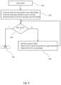
- FIG. 4illustrates a flow diagram to balance the two strata in case that the required area for the bit-cells is larger than the area required for the logic and the memory decoders. In such case an option may exist to transfer the smaller memories from one stratum to another stratum until the area for the two strata had been balanced.
- the flowAfter loading netlist 410 and estimating the total area of memory partition (FM) and of logic partition made of logic (FL) and memory decoders (FD) in step 420 , the flow systematically transfers the smallest memory blocks from the memory partition to the logic partition and adjusts the estimated costs 440 . Once the memory partition has sufficiently shrunk and its estimated size is smaller than that of the logic partition 430 , the process terminates 450 .
- a similar algorithmcan offer the choice to selectively add memory decoders, or other compatible, typically analog, circuitry to the memory stratum to better balance the utilization of the two strata. In such case, however, both strata will need to support both memory and logic and the advantage of tuning the memory stratum process and design to memory only will be mostly negated.
- the memory used in designsis assumed to be a static RAM (“SRAM”) with each SRAM cell made of more than one, for example six, or even eight, transistors.
- SRAMstatic RAM
- each SRAM cellmade of more than one, for example six, or even eight, transistors.
- the use of a DRAM cellmight be possible with the memory stratum optimized accordingly to DRAM process and design, and may use either a stack capacitor or a trench capacitor based memory cell, typically stack capacitors if it is a top stratum or trench capacitors if it is the bottom stratum.
- Other types of memoriescould also be considered, such as, for example, Spin-Transfer Torque RAM (STT-RAM) or Zeno Semiconductor's floating body RAM with two stable states. Having a stratum dedicated to memory bit-cells makes it easier to use a special memory process flow that may be required for such stratum.
- the next stepis to place and route each strata and the connection between them.
- the memory decodersmay be introduced to the Placer as specialized L-shaped cells such that other logic, but no other memory decoder, is allowed in the empty space in the rectangle defined by its L-shape.
- the 2D Placermay perform the placement on the logic stratum.
- bit-cell arraysmay be placed in the memory stratum according to the placement of their respective memory decoders on the logic stratum.
- logic stratummay be routed, with the vertical connections between memory decoders and their bit-cell arrays occurring automatically as a part of the strata abutment.
- non-memory circuitrymay be added to that memory stratum that shares some of its characteristics. Examples of such are input and output cells (“IO”) and analog functions such as Phase Lock Loop (“PLL”).
- IOinput and output cells
- PLLPhase Lock Loop
- the place and route flowcould be similar to the one above. First a 2D-Placer could be used to place the logic stratum, then the bit-cell arrays may be placed on the memory stratum according to the placement of their respective memory decoders, and then a 2D-Placer could be used to place the other elements in the memory stratum. In such case the inter-strata nets are defined as virtual IOs for each stratum 2D place and route process.
- the location of such inter-strata net virtual IO pointcan be defined as a location as directly as possible above or below, depending on the direction of the inter-strata crossing, of the source terminal of the inter-strata net. Another possible option is for this virtual IO be defined in the proximity, above or below as necessary, of the center-of-gravity of the inter-strata net on the stratum that is placed first.
- the decodersmay be placed at the bit-cell strata. This could be done also to reduce the number of connections between the strata as the decoder function is to expand the address from n lines of address lines to twice 2**(n/2) lines memory select lines.
- a simple optionis to use a similar flow as has been presented before but represent the decoders not with the actual layout size but with virtual size with width of contacts for Through Layer Vias. But keep the keep out zone for other decoders the same as before. In this way the 2D Placer can place the logic cell properly for the logic strata, and the memory strata which could include the bit-cells and the decoder would be defined according to the placed logic strata.
- partition to two stratacould be between high speed logic and low power logic or alternatively lower speed logic using older process node.
- a 2D-Placercould be used first to place the high speed logic, and then place the other, low power or lower speed logic, stratum with a 2D Placer using the placement of the high speed stratum to drive the placement on the second stratum similar to the flow described above.
- Additional advantage of the 3D IC technologyis in its ease of use for a platform-based design.
- One or more stratacould be designed, and even pre-manufactured, as a platform for multiple applications with platform's connections brought up to the top routing layer. Then, additional strata can be designed and customized for each application and placed on top of the pre-designed platform. In such process the platform strata would first be placed and routed using the 2D Placer and Router as described previously. Then the custom stratum could be placed and routed using a 2D Placer and Router with connections to the predefined contacts on the top level of the underlying platform design.
- a 2D Placercould be used also for multiple strata placement of cells that are not partitioned first by some of the methods presented here.
- One optionis to use a 2D partitioner such as Metis to partition the design into K partitions, each corresponding to one of K strata.
- FIG. 5illustrates a flow using a 2D Placer for placing a netlist on two strata. A similar flow could be used for three or more strata.
- a 2D placement 515is performed.
- a seed for the placementis picked from the center of the design and assigned to the first (red) partition 520 .
- the next cellis added to either the first (red) or the second (blue) partition.
- the blue partitionis smaller, between the cells that are currently placed in a close proximity to a Red Cell select the one with minimum connection to the red partition and add it to the blue partition 535 .
- the red partitionis smaller, between the cells that are currently placed in a close proximity to a Blue Cell select the one with minimum connection to the red partition and add it to the red partition 540 .
- Centers-of-gravity (“COG”) of all inter-strata netsare calculated based on the original 2D placement 515 and used to create virtual IOs crossing the strata boundary at that location.
- Library cellsare restored to their original sizes and 2D placement is performed on the first stratum with the first partition.
- the COGs (and virtual IOs)are adjusted based on the new placement, and the second partition placed in 2D on the second stratum.
- the COG and virtual IOsare readjusted again based on the final placement of both strata, and a 2D router is run on each stratum separately 550 , after which the place and route process terminates 555 and the physical design of the 3DIC may be competed.
- the flow of FIG. 5could be modified for steps blue partition 535 and red partition 540 so instead of using a criterion of “minimum connections” to the other partition, other criteria could be used.
- An example of alternate criteriacould be “maximum Blue connection” for step blue partition 535 : and “maximum Red connection” for step red partition 540 .
Landscapes
- Engineering & Computer Science (AREA)
- Computer Hardware Design (AREA)
- Physics & Mathematics (AREA)
- Theoretical Computer Science (AREA)
- Evolutionary Computation (AREA)
- Geometry (AREA)
- General Engineering & Computer Science (AREA)
- General Physics & Mathematics (AREA)
- Architecture (AREA)
- Computer Networks & Wireless Communication (AREA)
- Design And Manufacture Of Integrated Circuits (AREA)
Abstract
Description
This application is a continuation-in-part application of U.S. patent application Ser. No. 18/090,134, which was filed on Dec. 28, 2022, which is a continuation-in-part application of U.S. patent application Ser. No. 17/953,211, which was filed on Sep. 26, 2022 (now U.S. Pat. No. 11,574,109 issued on Feb. 7, 2023), which is a continuation-in-part application of U.S. patent application Ser. No. 17/841,619, which was filed on Jun. 15, 2022 (now U.S. Pat. No. 11,487,928 issued on Nov. 1, 2022), which is a continuation-in-part application of U.S. patent application Ser. No. 17/712,850, which was filed on Apr. 4, 2022, (now U.S. Pat. No. 11,514,221 issued on Nov. 29, 2022), which is a continuation-in-part application of U.S. patent application Ser. No. 17/581,884, which was filed on Jan. 22, 2022 (now U.S. Pat. No. 11,341,309 issued on May 24, 2022), which is a continuation-in-part application of U.S. patent application Ser. No. 17/523,904, which was filed on Nov. 10, 2021 (now U.S. Pat. No. 11,270,055 issued on Mar. 8, 2022), which is a continuation-in-part application of U.S. patent application Ser. No. 17/385,082, which was filed on Jul. 26, 2021 (now U.S. Pat. No. 11,205,034 issued on Dec. 21, 2021), which is a continuation-in-part application of U.S. patent application Ser. No. 17/306,948, which was filed on May 4, 2021 (now U.S. Pat. No. 11,106,853 issued on Aug. 31, 2021), which is a continuation-in-part application of U.S. patent application Ser. No. 16/149,517, which was filed on Oct. 2, 2018 (now U.S. Pat. No. 11,030,371 issued on Jun. 8, 2021), which is a continuation-in-part application of U.S. patent application Ser. No. 14/672,202, which was filed on Mar. 29, 2015 (now U.S. Pat. No. 10,127,344 issued on Nov. 13, 2018), which is a continuation application of U.S. patent application Ser. No. 13/862,537, which was filed on Apr. 15, 2013 (now U.S. Pat. No. 9,021,414 issued on Apr. 28, 2015), the entire contents of all of the foregoing are incorporated herein by reference.
This application relates to the general field of computer aided design of monolithic three-dimensional integrated circuits.
Use of computer programs for automating the design of electronic circuits, and particularly for assisting in the design of semiconductor integrated circuits, has been known for at least forty years. This field of Computer-Aided Design (CAD) encompasses the spectrum of engineering activities from early capture of the design idea, through its various refinements (both automatic and manual), modeling, simulations, down to its mapping to physical objects, partitioning and floor-planning, placement and routing, rule-checking and mask-making. The first part of these activities occurs in the logical domain, before mapping to physical objects (macros and cells) occurs, and is known as logic design. The part of the process after mapping the logical design to physical objects is known as physical design.
The rapid shrinking of manufacturable transistor dimensions on semiconductor wafers gave rise to a corresponding explosion of the design sizes that CAD tools need to handle. Modern designs routinely exceed tens and hundreds of millions of transistors and require massive and elaborate CAD tools to handle them.
A typical physical design process is illustrated inFIG.1 . It may start with anetlist 105 made of physical objects, and a set ofconstraints 110 derived from the logical part of the design flow. Netlist105 withconstraints 110 may be partitioned into a small set of blocks, on the order of 1 to 100 using a program calledpartitioner 115, which may produce a modifiedpartitioned netlist 135 and modifiednetlist constraints 140. These, in turn, may be fed into a floor-planner 145 that may arrange these blocks mosaic-like, while respectingdesign netlist constraints 140, on a rectangular frame that may outline the physical footprint of the final integrated circuit (IC) and produce a newly modifiednetlist 155 and newly modifieddesign constraints 160. The objects within each floor-planned block of newly modifiednetlist 155 may then be assigned a location within that block, while respecting newly modifieddesign constraints 160, using theplacer 165. Following this step the placeddesign netlist 175 and modifieddesign constraints 180 may be passed to other CAD tools that may performrouting utilizing router 185, and producing routednetlist 190 that may be passed downstream for rule checking and furtherprocessing 195 for the final IC manufacturing. Throughout the CAD process the various CAD tools may use, in addition to the design itself and its constraints, a variety of libraries that describe the netlist objects in their various abstractions, and rules files that define the permissible actions on objects and legal relations between them, and between objects and an abstraction of the underlying technology layers. Further, user intervention may be required at the various steps above.
Traditionally CAD tools operate with the understanding that the underlying transistors are arranged in a single planar layer. In recent years some tools have expanded to consider transistors arranged on multiple stacked layers, where the layers may be connected through relatively large Through-Silicon Vias (TSV) such as described in Xie, Y., Cong, J., Sapatnekar, S. “Three-Dimensional Integrated Circuit Design,” Springer, 2010. The focus of this expansion, however, is benefitting from the three-dimensional stacking while minimizing the use of the very large and expensive TSVs.
The current invention extends CAD tool functionality to operate with a monolithic three-dimensional (3D) manufacturing process. The key difference between a monolithic 3D process and a stacked-layer process where the layers are connected using TSVs is in the size of the inter-layer connection. TSVs are very large relative to advanced lithography feature size, and TSV scaling is not related to lithography but rather to the ability to etch and fill holes at very extreme aspect ratio, and the ability to handle extremely thin wafers. Today best etching and filling aspect ratio is roughly 10:1 and consequently the thinnest wafer that could be properly handled are roughly 50 micron thick with TSV diameter of roughly 5 micron. In contrast inter-layer connections of a monolithic 3D process scales with semiconductor scaling and is already below 100 nm, and will keep on scaling down as the industry continues with dimensional scaling.
Monolithic 3D technology: With this approach, multiple layers of transistors and wires can be monolithically constructed. Some monolithic 3D and 3DIC approaches are described in U.S. Pat. Nos. 8,273,610, 8,298,875, 8,362,482, 8,378,715, 8,379,458, 8,450,804, 8,557,632, 8,574,929, 8,581,349, 8,642,416, 8,669,778, 8,674,470, 8,687,399, 8,742,476, 8,803,206, 8,836,073, 8,902,663, 8,994,404, 9,023,688, 9,029,173, 9,030,858, 9,117,749, 9,142,553, 9,219,005, 9,385,058, 9,406,670, 9,460,978, 9,509,313, 9,640,531, 9,691,760, 9,711,407, 9,721,927, 9,799,761, 9,871,034, 9,953,870, 9,953,994, 10,014,292, 10,014,318, 10,515,981, 10,892,016, 10,991,675, 11,121,121, 11,502,095, 10,892,016, 11,270,988; and pending U.S. Patent Application Publications and applications, Ser. Nos. 14/642,724, 15/150,395, 15/173,686, 62/651,722; 62/681,249, 62/713,345, 62/770,751, 62/952,222, 62/824,288, 63/075,067, 63/091,307, 63/115,000, 63/220,443, 2021/0242189, 2020/0013791; and PCT Applications (and Publications): PCT/US2010/052093, PCT/US2011/042071 (WO2012/015550), PCT/US2016/52726 (WO2017053329), PCT/US2017/052359 (WO2018/071143), PCT/US2018/016759 (WO2018144957), PCT/US2018/52332 (WO 2019/060798), PCT/US2021/44110, and PCT/US22/44165. The entire contents of all of the foregoing patents, publications, and applications are incorporated herein by reference.
Electro-Optics: There is also work done for integrated monolithic 3D including layers of different crystals, such as U.S. Pat. Nos. 8,283,215, 8,163,581, 8,753,913, 8,823,122, 9,197,804, 9,419,031, 9,941,319, 10,679,977, 10,943,934, 10,998,374, 11,063,071, and 11,133,344. The entire contents of all of the foregoing patents, publications, and applications are incorporated herein by reference.
The implication of the abovementioned difference is that optimization processes of CAD tools for TSV-based processes should focus on minimizing the number of TSVs. In contrast, in monolithic 3D the inter-layer connectivity is much denser and CAD tools should focus on leveraging that large inter-layer connectivity to optimally place objects on different layers based on the layers' potentially disparate characteristics, and to increase the physical proximity of objects in 3D space as compared to a 2D plane. The current invention describes embodiments such as optimizations of CAD tools for monolithic 3D technology.
In one aspect, a method of designing a 3D Integrated Circuit, the method comprising: performing placement using a 2D placer, performing placement for at least a first strata and a second strata, and then performing routing and completing the physical design of said 3D Integrated Circuit.
In another aspect, a method of designing a 3D Integrated Circuit, the method comprising: performing partitioning to at least a first strata and a second strata, then performing placement using a 2D placer, and then performing routing and completing the physical design of said 3D Integrated Circuit.
In another aspect, a method of designing a 3D Integrated Circuit, the method comprising: performing placement using a 2D placer, splitting the placed cells into at least a first group and a second group of similar total area, using said 2D placer to place said second group on a second strata, using said 2D placer to place said first group on a first strata, and then performing routing and completing the physical design of said 3D Integrated Circuit.
In another aspect, a method of designing a 3D Integrated Circuit, the method comprising: performing partitioning to at least a first strata and a second strata; then performing a first placement of said first strata using a 2D placer executed by a computer, wherein said 2D placer is a Computer Aided Design (CAD) tool currently used in the industry for two-dimensional devices; and performing a second placement of said second strata based on said first placement, wherein said partitioning comprises a partition between logic and memory, and wherein said logic comprises at least one decoder representation for said memory.
In another aspect, a method of designing a 3D Integrated Circuit, the method comprising: performing partitioning to at least a first strata and a second strata; then performing a first placement of said first strata using a 2D placer executed by a computer, wherein said 2D placer is a Computer Aided Design (CAD) tool currently used in the industry for two-dimensional devices; and performing a second placement of said second strata based on said first placement, wherein said partitioning comprises a partition between logic and memory, and wherein said logic comprises at least one decoder for said memory.
In another aspect, a method of designing a 3D Integrated Circuit, the method comprising: performing partitioning to at least a first strata and a second strata; then performing a first placement of said first strata using a 2D placer executed by a computer, wherein said 2D placer is a Computer Aided Design (CAD) tool currently used in the industry for two-dimensional devices; and performing a second placement of said second strata based on said first placement, wherein said partitioning comprises splitting a plurality of cells into a high performance group to said first strata and a low performance group to said second strata.
In another aspect, a method of designing a 3D Integrated Circuit, the method comprising: performing partitioning to at least a logic strata comprising logic and a memory strata comprising memory; then performing a first placement of said logic strata using a 2D placer executed by a computer, wherein said 2D placer is a Computer Aided Design (CAD) tool for two-dimensional devices; wherein said 3D Integrated Circuit comprises through silicon vias for connection between said logic strata and said memory strata; and performing a second placement of said memory strata based on said first placement, wherein said logic comprises at least one decoder representation for said memory, wherein said at least one decoder representation has a virtual size with width of contacts for said through silicon vias, and wherein said performing a first placement comprises using said decoder representation instead of an actual memory decoder.
In another aspect, a method of designing a 3D Integrated Circuit, the method comprising: performing partitioning to at least a logic strata comprising logic and a memory strata comprising memory; then performing a first placement of said logic strata using a 2D placer executed by a computer, wherein said 2D placer is a Computer Aided Design (CAD) tool for two-dimensional devices; and performing a second placement of said memory strata based on said first placement, wherein said logic comprises at least one decoder for said memory, and wherein said memory comprises at least a first memory and a second memory, wherein said first memory comprises first memory decoders and said second memory comprises second memory decoders, wherein said 2D placer is set so said second memory decoders are not placed within a rectangle defined by the placement of said first memory decoders.
In another aspect, a method of designing a 3D Integrated Circuit, the method comprising: performing partitioning to at least a logic strata comprising logic and a memory strata comprising memory; then performing a first placement of said logic strata using a 2D placer executed by a computer, wherein said 2D placer is a Computer Aided Design (CAD) tool for two-dimensional devices; and performing a second placement of said memory strata based on said first placement, wherein said partitioning comprises a step of assigning at least one memory block to said logic strata for improved balancing of said logic strata area and said memory strata area.
In another aspect, a method of designing a 3D Integrated Circuit, the method comprising: performing partitioning to at least a logic strata comprising logic and a memory strata comprising memory; then performing a first placement of said logic strata using a 2D placer executed by a computer, wherein said 2D placer is a Computer Aided Design (CAD) tool for two-dimensional devices, wherein said 3D Integrated Circuit comprises through silicon vias for connection between said logic strata and said memory strata; and performing a second placement of said memory strata based on said first placement, wherein said memory comprises a first memory array, wherein said logic comprises a first logic circuit controlling said first memory array, wherein said first placement comprises placement of said first logic circuit, and wherein said second placement comprises placement of said first memory array based on said placement of said first logic circuit.
In another aspect, a method of designing a 3D Integrated Circuit, the method comprising: performing partitioning to at least a logic strata comprising logic and a memory strata comprising memory; then performing a first placement of said logic strata using a 2D placer executed by a computer, wherein said 2D placer is a Computer Aided Design (CAD) tool for two-dimensional devices; and performing a second placement of said memory strata based on said first placement, wherein said logic comprises at least one decoder representation for said memory, and wherein said memory comprises at least a first memory and a second memory, wherein said first memory comprises a first memory decoder representation and said second memory comprises a second memory decoder representation, wherein said 2D placer is set so said second memory decoder representation is not placed within a rectangle defined by placement of said first memory decoder representation.
In another aspect, a method of designing a 3D Integrated Circuit, the method comprising: performing partitioning to at least a logic strata comprising logic and a memory strata comprising memory; then performing a first placement of said logic strata using a 2D placer executed by a computer, wherein said 2D placer is a Computer Aided Design (CAD) tool for two-dimensional devices; and performing a second placement of said memory strata based on said first placement, wherein said partitioning comprises a step of assigning at least one logic block to said memory strata for improved balancing of said logic strata area and said memory strata area.
In another aspect, a method of designing a 3D Integrated Circuit, the method comprising: performing partitioning to at least a logic strata, said logic strata comprising logic, and to a memory strata, said memory strata comprising memory; then performing a first placement of said memory strata using a 2D placer executed by a computer, wherein said 2D placer is a Computer Aided Design (CAD) tool for two-dimensional devices, wherein said 3D Integrated Circuit comprises through silicon vias for connection between said logic strata and said memory strata; and performing a second placement of said logic strata based on said first placement, wherein said memory comprises a first memory array, wherein said logic comprises a first logic circuit controlling said first memory array, wherein said first placement comprises placement of said first memory array, and wherein said second placement comprises placement of said first logic circuit based on said placement of said first memory array.
In another aspect, a method of designing a 3D Integrated Circuit, the method comprising: wherein said 3D Integrated Circuit comprises at least a first strata and a second strata, providing placement data of said first strata; performing a placement of said second strata using a 2D placer executed by a computer, wherein said placement of said second strata is based on said placement data, wherein said 2D placer is a Computer Aided Design (CAD) tool for two-dimensional devices, and wherein said second strata comprises first routing layers; and performing a routing of said second strata routing layers using a 2D router executed by said computer, wherein said 2D router is a Computer Aided Design (CAD) tool for two-dimensional devices.
In another aspect, a method of designing a 3D Integrated Circuit, the method comprising: providing a device design, a first library, and a second library; performing a synthesis step utilizing at least two libraries, wherein said synthesis step results in a first netlist and a second netlist; then performing a first placement of a first strata for said first netlist using a 2D placer executed by a computer, wherein said 2D placer is a Computer Aided Design (CAD) tool for two-dimensional devices; performing a second placement of a second strata for said second netlist using said 2D placer executed by said computer, wherein said 2D placer is a Computer Aided Design (CAD) tool for two-dimensional devices.
In another aspect, a method of designing a 3D Integrated Circuit, the method comprising: performing partitioning to at least a logic strata, said logic strata comprising logic, and to a memory strata, said memory strata comprising memory; then performing a first placement of said memory strata using a 2D placer executed by a computer, wherein said 2D placer is a Computer Aided Design (CAD) tool for two-dimensional devices, wherein said 3D Integrated Circuit comprises a plurality of connections between said logic strata and said memory strata; and performing a second placement of said logic strata based on said first placement, wherein said memory comprises a first memory array, wherein said logic comprises a first logic circuit controlling said first memory array, wherein said first placement comprises placement of said first memory array, and wherein said second placement comprises placement of said first logic circuit based on said placement of said first memory array
In another aspect, a method of designing a 3D Integrated Circuit, the method comprising: wherein said 3D Integrated Circuit comprises at least a first strata and a second strata, providing contacts placement data of said first strata; performing a placement of said second strata using a 2D placer executed by a computer, wherein said placement of said second strata is based on said contact placement data, wherein said 2D placer is a Computer Aided Design (CAD) tool for two-dimensional devices, and wherein said second strata comprises first routing layers; and performing a routing of said second strata routing layers using a 2D router executed by said computer, wherein said 2D router is a Computer Aided Design (CAD) tool for two-dimensional devices.
In another aspect, a method of designing a 3D Integrated Circuit, the method comprising: providing a device design, a first library, and a second library; performing a synthesis step utilizing at least two libraries, wherein said synthesis step results in a first netlist and a second netlist; then performing a first placement of a first strata for said first netlist using a 2D placer executed by a computer; and performing a second placement of a second strata for said second netlist using a 2D placer executed by said computer or by another computer.
In another aspect, a method of designing a 3D Integrated Circuit, the method including: partitioning at least one design into at least two levels, a first and a second level, where the first level includes logic and the second level includes memory; then performing a first placement of the second level using a placer executed by a computer, where the placer is a part of a Computer Aided Design (CAD) tool, where the 3D Integrated Circuit includes a plurality of connections between the first level and the second level; and performing a second placement of the first level based on the first placement, where the memory includes a first memory array, where the logic includes a first logic circuit configured so as to write data to the first memory array, where performing the first placement includes placing the first memory array, and where performing the second placement includes placing the first logic circuit based on the first placement of the first memory array.
In another aspect, a method of designing a 3D Integrated Circuit, the method including: providing at least a first level and a second level; providing contact placement data of the first level; performing a placement of the second level using a placer executed by a computer, where the placement of the second level is based on the contact placement data, where the placer is part of a Computer Aided Design (CAD) tool, and where the second level includes first routing layers; and performing a routing of the second level routing layers using a router executed by the computer, where the router is a part of the Computer Aided Design (CAD) tool or a part of another CAD tool.
In another aspect, a method of designing a 3D Integrated Circuit, the method including: providing a device design, and a library including first library cells and second library cells; performing a synthesis step utilizing the library, where the performing a synthesis step includes execution by a computer or by another computer, where the synthesis step results in a first netlist including first library cells and a second netlist including second library cells; then performing a first placement of the first netlist on a first level using a placer; and performing a second placement of the second netlist on a second level using the placer, where the placer is executed by the computer or by another computer.
In another aspect, a method of designing a 3D Integrated Circuit, the method including: partitioning at least one design into at least two levels, a first and a second level, where the first level includes logic and the second level includes memory; and then receiving a first placement of at least portion of the second level, where the first placement includes a placement of a first memory array, where the 3D Integrated Circuit includes a plurality of connections between the first level and the second level; and performing a second placement of the first level based on the first placement, where the performing a second placement includes using a placer executed by a computer, where the placer is a part of a Computer Aided Design (CAD) tool, where the logic includes a first logic circuit configured so as to write data to the first memory array, and where performing the second placement includes placing the first logic circuit based on the first placement of the first memory array.
In another aspect, a method of designing a 3D Integrated Circuit, the method including: partitioning at least one design into at least two levels, a first and a second level, where the first level includes logic and the second level includes memory, where the 3D Integrated Circuit includes a plurality of connections between the first level and the second level; and then receiving a first placement of at least portion of the plurality of connections, where the 3D Integrated Circuit includes a plurality of connections between the first level and the second level; and performing a second placement of the first level based on the first placement, where the performing a second placement includes using a placer executed by a computer, where the placer is a part of a Computer Aided Design (CAD) tool; and performing a third placement of the second level based on the first placement, where the third placement includes a placement of a first memory array, where the logic includes a first logic circuit configured so as to write data to the first memory array.
In another aspect, a method of designing a 3D Integrated Circuit, the method including: partitioning at least one design into at least two levels, a first and a second level, where the first level includes logic and the second level includes memory; and then receiving a first placement of at least portion of the second level, where the first placement includes a placement of a first memory array and a second memory array, where the 3D Integrated Circuit includes a plurality of connections between the first level and the second level; and performing a second placement of the first level based on the first placement, where the performing a second placement include using a placer executed by a computer, where the placer is a part of a Computer Aided Design (CAD) tool, where the logic includes a first logic circuit configured so as to write data to the first memory array, and where performing the second placement includes placing the first logic circuit based on the first placement of the first memory array.
In another aspect, a method of designing a 3D Integrated Circuit, the method including: partitioning at least one design into at least two levels, a first level and a second level, wherein said first level comprises logic and said second level comprises memory; and then obtaining a first placement of at least portion of said second level, wherein said first placement comprises a placement of a first memory array, wherein said 3D Integrated Circuit comprises a plurality of connections between said first level and said second level; and performing a second placement, wherein performing said second placement comprises placing said first logic circuit based on said first placement of said first memory array, wherein said performing a second placement comprises using a placer executed by a computer, wherein said placer is a part of a Computer Aided Design (CAD) tool, and wherein said logic comprises a first logic circuit configured to read data from said first memory array
In another aspect, a method of designing a 3D Integrated Circuit, the method including: partitioning at least one design into at least two levels, a first level and a second level, wherein said first level comprises logic and said second level comprises memory, wherein said 3D Integrated Circuit comprises a plurality of connections between said first level and said second level; and then obtaining a first placement of at least portion of said plurality of connections, performing a second placement of said first level based on said first placement, wherein said performing a second placement comprises using a placer executed by a computer, wherein said placer is a part of a Computer Aided Design (CAD) tool; wherein said logic comprises a first logic circuit configured to read data from said first memory array.
In another aspect, a method of designing a 3D Integrated Circuit, the method including: partitioning at least one design into at least two levels, a first level and a second level, wherein said first level comprises logic and said second level comprises memory; and then obtaining a first placement of at least a portion of said second level, wherein said first placement comprises a placement of a first memory array and a second memory array, wherein said 3D Integrated Circuit comprises a plurality of connections between said first level and said second level; and performing a second placement of said first level based on said first placement, wherein said performing a second placement comprises using a placer executed by a computer, wherein said placer is a part of a Computer Aided Design (CAD) tool, wherein said logic comprises a first logic circuit configured to read data from said first memory array, and wherein performing said second placement comprises placing said first logic circuit based on said first placement of said first memory array.
In another aspect, a method of designing a 3D Integrated Circuit, the method including: partitioning at least one design into at least two levels, a first level and a second level; providing connections placement data of said second level, wherein said connections comprise planned connections between said first level and said second level; performing a placement of said first level using a placer executed by a computer, wherein said placement of said first level is based on said connections placement data, wherein said placer is part of a Computer Aided Design (CAD) tool, and wherein said first level comprises first routing layers; and performing a routing of said first level by routing layers using a router executed by a computer, wherein said router is a part of the Computer Aided Design (CAD) tool or a part of another CAD tool.
In another aspect, a method of designing a 3D Integrated Circuit, the method including: partitioning at least one design into at least two levels, a first level and a second level; providing connections placement data of said second level, wherein said connections comprise planned connections between said first level and said second level; performing a placement of said first level using a placer executed by a computer, wherein said placement of said first level is based on said connections placement data, wherein said placer is part of a Computer Aided Design (CAD) tool, and wherein said first level comprises first routing layers; and performing a routing of said first level by routing layers using a router executed by a computer, wherein said router is a part of the Computer Aided Design (CAD) tool or a part of another CAD tool, and wherein a majority area of said second level comprises memory circuits.
In another aspect, a method of designing a 3D Integrated Circuit, the method including: partitioning at least one design into at least two levels, a first level and a second level; providing connections placement data of said second level, wherein said connections comprise planned connections between said first level and said second level; performing a placement of said first level using a placer executed by a computer, wherein said placement of said first level is based on said connections placement data, wherein said placer is part of a Computer Aided Design (CAD) tool, and wherein said first level comprises first routing layers; and performing a routing of said first level routing layers using a router executed by a computer, wherein said router is a part of the Computer Aided Design (CAD) tool or a part of another CAD tool, and wherein a majority area of said second level comprises non-logic circuits such as memory circuits or Radio Frequency (“RF”) circuits or analog circuits.
In another aspect, a method of designing a 3D Integrated Circuit, the method including: partitioning at least one design into at least two levels, a first level and a second level; providing placement data of the second level; performing a placement of the first level using a placer executed by a computer, where the placement of the first level is based on the placement data, where the placer is part of a Computer Aided Design (CAD) tool, and where the first level includes first routing layers; and performing a routing of the first level by routing layers using a router executed by a computer, where the router is a part of the Computer Aided Design (CAD) tool or a part of another CAD tool.
In another aspect, a method of designing a 3D Integrated Circuit, the method including: partitioning at least one design into at least two levels, a first level and a second level, where a majority area of the first level includes logic circuits, and where a substantial area of the second level includes analog circuits; providing connections placement data of the second level, where the connections include planned connections between the first level and the second level; performing a placement of the first level using a placer executed by a computer, where the placer is part of a Computer Aided Design (CAD) tool, and where the first level includes first routing layers; and performing a routing of the first level by routing layers using a router executed by a computer, where the router is a part of the Computer Aided Design (CAD) tool or a part of another CAD tool.
In another aspect, a method of designing a 3D Integrated Circuit, the method including: partitioning at least one design into at least two levels, a first level and a second level; providing connections placement data of the second level, where the connections include planned connections between the first level and the second level; performing a placement of the first level using a placer executed by a computer, where the placer is part of a Computer Aided Design (CAD) tool, and where the first level includes first routing layers; and performing a routing of the first level routing layers using a router executed by a computer, where the router is a part of the Computer Aided Design (CAD) tool or a part of another CAD tool, where the second level includes circuits designed for non-advanced process nodes, and where the first level includes circuits designed for an advanced process node.
Various embodiments of the invention will be understood and appreciated more fully from the following detailed description, taken in conjunction with the drawings in which:
Embodiments of the present invention are described herein with reference to the drawing figures. Persons of ordinary skill in the art will appreciate that the description and figures illustrate rather than limit the invention and that in general the figures are not drawn to scale for clarity of presentation. Such skilled persons will also realize that many more embodiments are possible by applying the inventive principles contained herein and that such embodiments fall within the scope of the invention which is not to be limited except by the appended claims.
There are multiple known ways to partition a design, but the essential approach described in Metis (Karypis, G., Kumar, V., “METIS—Unstructured Graph Partitioning and Sparse Matrix Ordering,” 1995) subsumes most of them in modern CAD tools. It may consist of three phases: graph coarsening through clustering, followed by partitioning of the smaller resulting graph, followed by an uncoarsening phase. Most partitioners will include additional design constraints, such as timing slack of nets, in the optimization costs during the coarsening and uncoarsening phases, in addition to minimizing the number of nets crossing the partition boundary (the cut). The current invention suggests including disparate technology characteristics as an additional constraint to optimize.
More specifically, different active logic layers in a stacked monolithic 3D IC can differ in their lithography feature sizes, the more aggressive ones being faster but more expensive to manufacture. In a 3D IC device every stratum may be fabricated in its own process with, for example, its own set of design rules, unlike 2D IC wherein all transistors exist on the same stratum and will be processed together with the same process. Accordingly the 3D IC partitioning of device circuits to individual strata could be based on which types of circuits would be efficient to process together. Such decision could be based on a criterion, for example, such as the type of lithography requirements. In a modern IC the cost of lithography dominates the end-device cost. Consequently it may be effective to maximize the number of strata that utilize lower cost lithography processes and minimizing the number of strata that might require the most aggressive and expensive lithography, for example, containing high speed circuits. Yet other strata may include repetitive memory circuits that might use a spacer-based lithography scheme which may lower costs even further. The slower logic of a device circuit might be partitioned to use older process node circuits with much lower cost lithography. Yet other strata could be dedicated to I/O circuits that might also use lower cost lithography. Strata can differ in their number of metal routing layers, the larger number of such offering more connectivity and hence denser area utilization, albeit at a higher manufacturing cost. Strata can differ in the power dissipation and leakage of the transistors, for example, lower power consumption portions may be grouped on a strata and/or slower speed of operation portions, and/or lower leakage portions. Such differences can be translated into a “cost” of the cut under optimization and create new dimensions of optimization of monolithic 3D structures. Strata can differ in the process design rules utilized to form the devices and circuits in each stratum, for example, a first stratum may have a set of design rules that is one or more process nodes more advanced than a second stratum set of design rules.
An additional embodiment of the invention is the partitioning of memories into different memory layers in a stacked monolithic 3D IC. For example, the layers can differ by their suitability to types of memory they can implement, such as volatile versus non-volatile, or dynamic versus static. In this case the affinity of the memory type used in the design to the available memory layer characteristics may be translated into either a hard affinity attribute (if the object must be placed on a given layer type) or into a “cost” attribute and may be included in the partitioner. Hard affinity attributes may force the partitioner to cluster only objects with compatible attributes.
An additional embodiment of the invention is partitioning between various analog functions, including input and output functions, and the rest of the logic and memory of the design, where the analog elements may be mapped onto one or more potentially disparate analog layers in a stacked monolithic 3D IC. The analog layers can vary in their lithography processes, or in their semiconductor material bases such as Silicon, Germanium, or composite III-V semiconductors, for example, Gallium-Arsenide or Indium-Phosphide. Similar to the case of memory described above, the affinity of the analog object type used in the design to the available analog layer characteristics may be translated either into a hard affinity or into a “cost” function and may be included in the partitioner. As before, hard affinity attributes may force the partitioner to cluster only objects with compatible attributes.
Another criterion for partition could be the thickness of the silicon layer. For high speed logic it might be desirable to use fully depleted transistors, such as, for example, FinFet or planar fully depleted SOI transistors, that may require a relatively thin silicon layer, for example, as thin as 25 nm, 10 nm or 5 nm. I/O (Input/Output), Analog, high voltage circuits such as charge pumps, and RF (Radio Frequency) circuits might benefit from a thicker semiconductor material base in that strata, for example mono-crystalline silicon of for example 50 nm, 100 nm or 200 nm, and accordingly it might be preferred to have those circuits on different strata than the fully depleted devices and circuits.
An additional embodiment of the invention is partitioning a design that includes a feasible combination of objects described previously. More specifically, partitioning of designs may include a combination of logic elements, memory elements, and analog elements, into multiple layers of disparate characteristics of each kind.
An additional embodiment of the invention includes partitioning of a memory block into its core bit-cell array that is targeted for a memory layer, and some or all of its decoding and driving logic that is targeted for a logic layer. It is the rich vertical connectivity available in a monolithic 3D process that allows such partitioning to be considered in the partitioner.
An additional embodiment of the invention includes partitioning of a design into elements that span a single layer versus those that span multiple adjacent vertical layers. Similar to other specialized partitions, this characteristic can be translated into a “cost” or it can be used to drive a hard partitioning in the partitioner. Further, if both multi-layer and single-layer variants of an object are present, the partitioner can select the best-fitting variant based on global design considerations together with the overall system cost.
The partitioned design will typically be followed by a floor planning stage and afterward, the design will typically move to a placement step, wherein the objects within each floor-planned block will be assigned a location within that block's boundary.
Of unique concern during the 3D floor-planning and the placement stage may be instances where the core bit-cell array of a memory block has been separated from its decoding and driving logic, the former being placed on a memory layer and the latter on a logic layer. In particular, the floor-planning of these blocks should allow for sufficient direct vertical overlap so that a symmetrical arrangement of vertical connections between the two parts of the memory block can be guaranteed. Further, the placer may use this overlap to place both parts of the memory block centered one above the other to achieve maximal symmetry. This is to facilitate relative uniformity of delays that such interconnect typically requires.
Persons of ordinary skill in the art will appreciate that the illustrations inFIGS.2 and3 are exemplary only and are not drawn to scale. Such skilled persons will further appreciate that many variations may be possible such as, for example, in some cases it might be preferred to have the memory decoders in the logic stratum and to have the bit-cells in the memory stratum. Many other modifications within the scope of the illustrated embodiments of the invention described herein will suggest themselves to such skilled persons after reading this specification. Thus the invention is to be limited only by the appended claims.
An additional advantage of partitioning based on manufacturing consideration is that with proper set up and support utilities, existing 2D Place & Route design tools could be used for 3D IC design as outlined in the following sections.
If the area required for the bit-cells is far smaller than the area for logic and the memory decoders, then a similar algorithm can offer the choice to selectively add memory decoders, or other compatible, typically analog, circuitry to the memory stratum to better balance the utilization of the two strata. In such case, however, both strata will need to support both memory and logic and the advantage of tuning the memory stratum process and design to memory only will be mostly negated.
Typically the memory used in designs is assumed to be a static RAM (“SRAM”) with each SRAM cell made of more than one, for example six, or even eight, transistors. In a 3D IC environment it could be feasible to use a one transistor memory cell instead. For example, the use of a DRAM cell might be possible with the memory stratum optimized accordingly to DRAM process and design, and may use either a stack capacitor or a trench capacitor based memory cell, typically stack capacitors if it is a top stratum or trench capacitors if it is the bottom stratum. Other types of memories could also be considered, such as, for example, Spin-Transfer Torque RAM (STT-RAM) or Zeno Semiconductor's floating body RAM with two stable states. Having a stratum dedicated to memory bit-cells makes it easier to use a special memory process flow that may be required for such stratum.
Once the allocation of structures to the bit-cells strata and the logic and memory decoder strata has been done, the next step is to place and route each strata and the connection between them.
This could be done using 2D tools in the following exemplary manner. First, the memory decoders may be introduced to the Placer as specialized L-shaped cells such that other logic, but no other memory decoder, is allowed in the empty space in the rectangle defined by its L-shape.
In the next step the 2D Placer may perform the placement on the logic stratum.
Then the bit-cell arrays may be placed in the memory stratum according to the placement of their respective memory decoders on the logic stratum.
Finally, the logic stratum may be routed, with the vertical connections between memory decoders and their bit-cell arrays occurring automatically as a part of the strata abutment.
If the utilization of memory stratum is low, non-memory circuitry may be added to that memory stratum that shares some of its characteristics. Examples of such are input and output cells (“IO”) and analog functions such as Phase Lock Loop (“PLL”).
The place and route flow could be similar to the one above. First a 2D-Placer could be used to place the logic stratum, then the bit-cell arrays may be placed on the memory stratum according to the placement of their respective memory decoders, and then a 2D-Placer could be used to place the other elements in the memory stratum. In such case the inter-strata nets are defined as virtual IOs for eachstratum 2D place and route process.
The location of such inter-strata net virtual IO point can be defined as a location as directly as possible above or below, depending on the direction of the inter-strata crossing, of the source terminal of the inter-strata net. Another possible option is for this virtual IO be defined in the proximity, above or below as necessary, of the center-of-gravity of the inter-strata net on the stratum that is placed first.
When the bit-cell area is too small, the decoders may be placed at the bit-cell strata. This could be done also to reduce the number of connections between the strata as the decoder function is to expand the address from n lines of address lines to twice 2**(n/2) lines memory select lines. A simple option is to use a similar flow as has been presented before but represent the decoders not with the actual layout size but with virtual size with width of contacts for Through Layer Vias. But keep the keep out zone for other decoders the same as before. In this way the 2D Placer can place the logic cell properly for the logic strata, and the memory strata which could include the bit-cells and the decoder would be defined according to the placed logic strata.
Another type of partition to two strata could be between high speed logic and low power logic or alternatively lower speed logic using older process node.
In both cases a 2D-Placer could be used first to place the high speed logic, and then place the other, low power or lower speed logic, stratum with a 2D Placer using the placement of the high speed stratum to drive the placement on the second stratum similar to the flow described above.
Additional advantage of the 3D IC technology is in its ease of use for a platform-based design. One or more strata could be designed, and even pre-manufactured, as a platform for multiple applications with platform's connections brought up to the top routing layer. Then, additional strata can be designed and customized for each application and placed on top of the pre-designed platform. In such process the platform strata would first be placed and routed using the 2D Placer and Router as described previously. Then the custom stratum could be placed and routed using a 2D Placer and Router with connections to the predefined contacts on the top level of the underlying platform design.
A 2D Placer could be used also for multiple strata placement of cells that are not partitioned first by some of the methods presented here. One option is to use a 2D partitioner such as Metis to partition the design into K partitions, each corresponding to one of K strata.
After loading thenetlist 505 and resizing the dimensions of the cells by 0.71 in eachdirection 510, a2D placement 515 is performed. A seed for the placement is picked from the center of the design and assigned to the first (red)partition 520. Based on the relative size of bothpartitions 530 the next cell is added to either the first (red) or the second (blue) partition. When the blue partition is smaller, between the cells that are currently placed in a close proximity to a Red Cell select the one with minimum connection to the red partition and add it to theblue partition 535. Similarly, when the red partition is smaller, between the cells that are currently placed in a close proximity to a Blue Cell select the one with minimum connection to the red partition and add it to thered partition 540. Once the process leaves nounassigned cells 525 it moves to thenext step 545. Centers-of-gravity (“COG”) of all inter-strata nets are calculated based on theoriginal 2D placement 515 and used to create virtual IOs crossing the strata boundary at that location. Library cells are restored to their original sizes and 2D placement is performed on the first stratum with the first partition. The COGs (and virtual IOs) are adjusted based on the new placement, and the second partition placed in 2D on the second stratum. Optionally the COG and virtual IOs are readjusted again based on the final placement of both strata, and a 2D router is run on each stratum separately550, after which the place and route process terminates555 and the physical design of the 3DIC may be competed.
The flow ofFIG.5 could be modified for stepsblue partition 535 andred partition 540 so instead of using a criterion of “minimum connections” to the other partition, other criteria could be used. An example of alternate criteria could be “maximum Blue connection” for step blue partition535: and “maximum Red connection” for stepred partition 540.
It will also be appreciated by persons of ordinary skill in the art that the invention is not limited to what has been particularly shown and described hereinabove. For example, drawings or illustrations may not show all device possibilities for clarity in illustration. Rather, the scope of the invention includes both combinations and sub-combinations of the various features described herein above as well as modifications and variations which would occur to such skilled persons upon reading the foregoing description. Thus the invention is to be limited only by the appended claims.
Claims (20)
1. A method of designing a 3D Integrated Circuit, the method comprising:
partitioning at least one design into at least two levels, a first level and a second level,
wherein said first level comprises a plurality of first transistors,
wherein said second level comprises a plurality of second transistors, and
wherein said second level is on top of said first level;
providing placement data of said second level;
performing a placement of said first level using a placer program executed by a computer,
wherein said placement of said first level is based on said placement data,
wherein said placer is part of a Computer Aided Design (CAD) tool, and
wherein said first level comprises first routing layers; and
performing a routing of said first level by routing layers using a router executed by a computer,
wherein said router is a part of the Computer Aided Design (CAD) tool or a part of another CAD tool, and
wherein at least one metal routing layer is disposed in-between said plurality of first transistors and said plurality of second transistors.
2. The method according toclaim 1 ,
wherein a majority area of said second level comprises memory.
3. The method according toclaim 1 ,
wherein results of said second level is a generic structure.
4. The method according toclaim 1 ,
wherein said first level is designed to be processed with a different process node than a process node used for said second level.
5. The method according toclaim 1 , further comprising:
providing connections placement data of said second level,
wherein said connections comprise planned connections between said first level and said second level.
6. The method according toclaim 1 ,
wherein said first level comprises Input and Output cells (“IO”).
7. The method according toclaim 1 ,
wherein said second level comprises one or more RF (Radio Frequency) circuits.
8. A method of designing a 3D Integrated Circuit, the method comprising:
partitioning at least one design into at least two levels, a first level and a second level,
wherein said first level comprises a plurality of first transistors,
wherein said second level comprises a plurality of second transistors,
wherein said second level is on top of said first level,
wherein a majority area of said first level comprises logic circuits, and
wherein a substantial area of said second level comprises analog circuits;
providing connections placement data of said second level,
wherein said connections comprise planned connections between said first level and said second level;
performing a placement of said first level using a placer program executed by a computer,
wherein said placer is part of a Computer Aided Design (CAD) tool, and
wherein said first level comprises first routing layers; and
performing a routing of said first level by routing layers using a router executed by a computer,
wherein said router is a part of the Computer Aided Design (CAD) tool or a part of another CAD tool.
9. The method according toclaim 8 ,
wherein said placement of said first level is based on said connections placement data.
10. The method according toclaim 8 ,
wherein at least one metal routing layer is disposed in-between said plurality of first transistors and said plurality of second transistors.
11. The method according toclaim 8 ,
wherein said first level is designed to be processed with a different process node than a process node used for said second level.
12. The method according toclaim 8 ,
wherein said connections are located in a top layer of said second level, and
wherein said connections are available for connection to said first level.
13. The method according toclaim 8 ,
wherein said first level comprises Input and Output cells (“IO”).
14. The method according toclaim 8 ,
wherein said second level comprises one or more RF (Radio Frequency) circuits.
15. A method of designing a 3D Integrated Circuit, the method comprising:
partitioning at least one design into at least two levels, a first level and a second level,
wherein said first level comprises a plurality of first transistors,
wherein said second level comprises a plurality of second transistors,
wherein said second level is on top of said first level;
providing connections placement data of said second level,
wherein said connections comprise planned connections between said first level and said second level;
performing a placement of said first level using a placer program executed by a computer,
wherein said placer is part of a Computer Aided Design (CAD) tool, and
wherein said first level comprises first routing layers; and
performing a routing of said first routing layers using a router executed by a computer,
wherein said router is a part of the Computer Aided Design (CAD) tool or a part of another CAD tool,
wherein said second level comprises circuits designed for non-advanced process nodes, and
wherein said first level comprises circuits designed for an advanced process node.
16. The method according toclaim 15 ,
wherein a majority area of said first level comprises logic circuits.
17. The method according toclaim 15 ,
wherein at least one metal routing layer is disposed in-between said plurality of first transistors and said plurality of second transistors.
18. The method according toclaim 15 , further comprising:
providing placement data of said first level; and
performing a placement of said second level using a placer executed by a computer,
wherein said placement of said second level is based on said placement data.
19. The method according toclaim 15 ,
wherein said placement of said first level is based on said connections placement data.
20. The method according toclaim 15 ,
wherein said first level comprises Input and Output cells (“IO”).
Priority Applications (3)
| Application Number | Priority Date | Filing Date | Title |
|---|---|---|---|
| US18/111,567US11720736B2 (en) | 2013-04-15 | 2023-02-18 | Automation methods for 3D integrated circuits and devices |
| US18/208,647US12093628B2 (en) | 2013-04-15 | 2023-06-12 | Automation methods for 3D integrated circuits and devices |
| US18/800,058US20240403533A1 (en) | 2013-04-15 | 2024-08-10 | Design automation methods for 3d integrated circuits and devices |
Applications Claiming Priority (12)
| Application Number | Priority Date | Filing Date | Title |
|---|---|---|---|
| US13/862,537US9021414B1 (en) | 2013-04-15 | 2013-04-15 | Automation for monolithic 3D devices |
| US14/672,202US10127344B2 (en) | 2013-04-15 | 2015-03-29 | Automation for monolithic 3D devices |
| US16/149,517US11030371B2 (en) | 2013-04-15 | 2018-10-02 | Automation for monolithic 3D devices |
| US17/306,948US11106853B1 (en) | 2013-04-15 | 2021-05-04 | Automation for monolithic 3D devices |
| US17/385,082US11205034B2 (en) | 2013-04-15 | 2021-07-26 | Automation for monolithic 3D devices |
| US17/523,904US11270055B1 (en) | 2013-04-15 | 2021-11-10 | Automation for monolithic 3D devices |
| US17/581,884US11341309B1 (en) | 2013-04-15 | 2022-01-22 | Automation for monolithic 3D devices |
| US17/712,850US11514221B2 (en) | 2013-04-15 | 2022-04-04 | Automation for monolithic 3D devices |
| US17/841,619US11487928B2 (en) | 2013-04-15 | 2022-06-15 | Automation for monolithic 3D devices |
| US17/953,211US11574109B1 (en) | 2013-04-15 | 2022-09-26 | Automation methods for 3D integrated circuits and devices |
| US18/090,134US11615228B1 (en) | 2013-04-15 | 2022-12-28 | Automation methods for 3D integrated circuits and devices |
| US18/111,567US11720736B2 (en) | 2013-04-15 | 2023-02-18 | Automation methods for 3D integrated circuits and devices |
Related Parent Applications (1)
| Application Number | Title | Priority Date | Filing Date |
|---|---|---|---|
| US18/090,134Continuation-In-PartUS11615228B1 (en) | 2013-04-15 | 2022-12-28 | Automation methods for 3D integrated circuits and devices |
Related Child Applications (1)
| Application Number | Title | Priority Date | Filing Date |
|---|---|---|---|
| US18/208,647Continuation-In-PartUS12093628B2 (en) | 2013-04-15 | 2023-06-12 | Automation methods for 3D integrated circuits and devices |
Publications (2)
| Publication Number | Publication Date |
|---|---|
| US20230205965A1 US20230205965A1 (en) | 2023-06-29 |
| US11720736B2true US11720736B2 (en) | 2023-08-08 |
Family
ID=86897901
Family Applications (1)
| Application Number | Title | Priority Date | Filing Date |
|---|---|---|---|
| US18/111,567ActiveUS11720736B2 (en) | 2013-04-15 | 2023-02-18 | Automation methods for 3D integrated circuits and devices |
Country Status (1)
| Country | Link |
|---|---|
| US (1) | US11720736B2 (en) |
Cited By (1)
| Publication number | Priority date | Publication date | Assignee | Title |
|---|---|---|---|---|
| US20230325572A1 (en)* | 2013-04-15 | 2023-10-12 | Monolithic 3D Inc | Design automation methods for 3d integrated circuits and devices |
Citations (811)
| Publication number | Priority date | Publication date | Assignee | Title |
|---|---|---|---|---|
| US3007090A (en) | 1957-09-04 | 1961-10-31 | Ibm | Back resistance control for junction semiconductor devices |
| US3819959A (en) | 1970-12-04 | 1974-06-25 | Ibm | Two phase charge-coupled semiconductor device |
| US4009483A (en) | 1974-04-04 | 1977-02-22 | Motorola, Inc. | Implementation of surface sensitive semiconductor devices |
| US4197555A (en) | 1975-12-29 | 1980-04-08 | Fujitsu Limited | Semiconductor device |
| US4213139A (en) | 1978-05-18 | 1980-07-15 | Texas Instruments Incorporated | Double level polysilicon series transistor cell |
| US4400715A (en) | 1980-11-19 | 1983-08-23 | International Business Machines Corporation | Thin film semiconductor device and method for manufacture |
| US4487635A (en) | 1982-03-25 | 1984-12-11 | Director-General Of The Agency Of Industrial Science & Technology | Method of fabricating a multi-layer type semiconductor device including crystal growth by spirally directing energy beam |
| US4510670A (en) | 1982-03-30 | 1985-04-16 | Siemens Aktiengesellschaft | Method for the manufacture of integrated MOS-field effect transistor circuits silicon gate technology having diffusion zones coated with silicide as low-impedance printed conductors |
| US4522657A (en) | 1983-10-20 | 1985-06-11 | Westinghouse Electric Corp. | Low temperature process for annealing shallow implanted N+/P junctions |
| US4612083A (en) | 1984-07-20 | 1986-09-16 | Nec Corporation | Process of fabricating three-dimensional semiconductor device |
| US4643950A (en) | 1985-05-09 | 1987-02-17 | Agency Of Industrial Science And Technology | Semiconductor device |
| US4704785A (en) | 1986-08-01 | 1987-11-10 | Texas Instruments Incorporated | Process for making a buried conductor by fusing two wafers |
| US4711858A (en) | 1985-07-12 | 1987-12-08 | International Business Machines Corporation | Method of fabricating a self-aligned metal-semiconductor FET having an insulator spacer |
| US4721885A (en) | 1987-02-11 | 1988-01-26 | Sri International | Very high speed integrated microelectronic tubes |
| US4733288A (en) | 1982-06-30 | 1988-03-22 | Fujitsu Limited | Gate-array chip |
| US4732312A (en) | 1986-11-10 | 1988-03-22 | Grumman Aerospace Corporation | Method for diffusion bonding of alloys having low solubility oxides |
| US4829018A (en) | 1986-06-27 | 1989-05-09 | Wahlstrom Sven E | Multilevel integrated circuits employing fused oxide layers |
| US4854986A (en) | 1987-05-13 | 1989-08-08 | Harris Corporation | Bonding technique to join two or more silicon wafers |
| US4866304A (en) | 1988-05-23 | 1989-09-12 | Motorola, Inc. | BICMOS NAND gate |
| US4939568A (en) | 1986-03-20 | 1990-07-03 | Fujitsu Limited | Three-dimensional integrated circuit and manufacturing method thereof |
| US4956307A (en) | 1988-11-10 | 1990-09-11 | Texas Instruments, Incorporated | Thin oxide sidewall insulators for silicon-over-insulator transistors |
| US5012153A (en) | 1989-12-22 | 1991-04-30 | Atkinson Gary M | Split collector vacuum field effect transistor |
| US5032007A (en) | 1988-04-07 | 1991-07-16 | Honeywell, Inc. | Apparatus and method for an electronically controlled color filter for use in information display applications |
| US5047979A (en) | 1990-06-15 | 1991-09-10 | Integrated Device Technology, Inc. | High density SRAM circuit with ratio independent memory cells |
| US5087585A (en) | 1989-07-11 | 1992-02-11 | Nec Corporation | Method of stacking semiconductor substrates for fabrication of three-dimensional integrated circuit |
| US5093704A (en) | 1986-09-26 | 1992-03-03 | Canon Kabushiki Kaisha | Semiconductor device having a semiconductor region in which a band gap being continuously graded |
| US5106775A (en) | 1987-12-10 | 1992-04-21 | Hitachi, Ltd. | Process for manufacturing vertical dynamic random access memories |
| US5152857A (en) | 1990-03-29 | 1992-10-06 | Shin-Etsu Handotai Co., Ltd. | Method for preparing a substrate for semiconductor devices |
| US5162879A (en) | 1990-04-06 | 1992-11-10 | Texas Instruments Incorporated | Diffusionless conductor/oxide semiconductor field effect transistor and methods for making and using the same |
| US5189500A (en) | 1989-09-22 | 1993-02-23 | Mitsubishi Denki Kabushiki Kaisha | Multi-layer type semiconductor device with semiconductor element layers stacked in opposite directions and manufacturing method thereof |
| US5217916A (en) | 1989-10-03 | 1993-06-08 | Trw Inc. | Method of making an adaptive configurable gate array |
| US5250460A (en) | 1991-10-11 | 1993-10-05 | Canon Kabushiki Kaisha | Method of producing semiconductor substrate |
| US5258643A (en) | 1991-07-25 | 1993-11-02 | Massachusetts Institute Of Technology | Electrically programmable link structures and methods of making same |
| US5265047A (en) | 1992-03-09 | 1993-11-23 | Monolithic System Technology | High density SRAM circuit with single-ended memory cells |
| US5266511A (en) | 1991-10-02 | 1993-11-30 | Fujitsu Limited | Process for manufacturing three dimensional IC's |
| US5277748A (en) | 1992-01-31 | 1994-01-11 | Canon Kabushiki Kaisha | Semiconductor device substrate and process for preparing the same |
| US5286670A (en) | 1991-05-08 | 1994-02-15 | Korea Electronics And Telecommunications Research Institute | Method of manufacturing a semiconductor device having buried elements with electrical characteristic |
| US5294556A (en) | 1990-07-20 | 1994-03-15 | Fujitsu Limited | Method for fabricating an SOI device in alignment with a device region formed in a semiconductor substrate |
| US5308782A (en) | 1992-03-02 | 1994-05-03 | Motorola | Semiconductor memory device and method of formation |
| US5312771A (en) | 1990-03-24 | 1994-05-17 | Canon Kabushiki Kaisha | Optical annealing method for semiconductor layer and method for producing semiconductor device employing the same semiconductor layer |
| US5317236A (en) | 1990-12-31 | 1994-05-31 | Kopin Corporation | Single crystal silicon arrayed devices for display panels |
| US5355022A (en) | 1991-09-10 | 1994-10-11 | Mitsubishi Denki Kabushiki Kaisha | Stacked-type semiconductor device |
| US5371037A (en) | 1990-08-03 | 1994-12-06 | Canon Kabushiki Kaisha | Semiconductor member and process for preparing semiconductor member |
| US5374564A (en) | 1991-09-18 | 1994-12-20 | Commissariat A L'energie Atomique | Process for the production of thin semiconductor material films |
| US5374581A (en) | 1991-07-31 | 1994-12-20 | Canon Kabushiki Kaisha | Method for preparing semiconductor member |
| US5424560A (en) | 1994-05-31 | 1995-06-13 | Motorola, Inc. | Integrated multicolor organic led array |
| US5475280A (en) | 1992-03-04 | 1995-12-12 | Mcnc | Vertical microelectronic field emission devices |
| US5478762A (en) | 1995-03-16 | 1995-12-26 | Taiwan Semiconductor Manufacturing Company | Method for producing patterning alignment marks in oxide |
| US5485031A (en) | 1993-11-22 | 1996-01-16 | Actel Corporation | Antifuse structure suitable for VLSI application |
| US5498978A (en) | 1993-05-07 | 1996-03-12 | Kabushiki Kaisha Toshiba | Field programmable gate array |
| US5527423A (en) | 1994-10-06 | 1996-06-18 | Cabot Corporation | Chemical mechanical polishing slurry for metal layers |
| US5535342A (en) | 1992-11-05 | 1996-07-09 | Giga Operations Corporation | Pld connector for module having configuration of either first PLD or second PLD and reconfigurable bus for communication of two different bus protocols |
| US5554870A (en) | 1994-02-04 | 1996-09-10 | Motorola, Inc. | Integrated circuit having both vertical and horizontal devices and process for making the same |
| US5563084A (en) | 1994-09-22 | 1996-10-08 | Fraunhofer-Gesellschaft zur F orderung der angewandten Forschung e.V. | Method of making a three-dimensional integrated circuit |
| US5583350A (en) | 1995-11-02 | 1996-12-10 | Motorola | Full color light emitting diode display assembly |
| US5583349A (en) | 1995-11-02 | 1996-12-10 | Motorola | Full color light emitting diode display |
| US5586291A (en) | 1994-12-23 | 1996-12-17 | Emc Corporation | Disk controller with volatile and non-volatile cache memories |
| US5594563A (en) | 1994-05-31 | 1997-01-14 | Honeywell Inc. | High resolution subtractive color projection system |
| US5604137A (en) | 1991-09-25 | 1997-02-18 | Semiconductor Energy Laboratory Co., Ltd. | Method for forming a multilayer integrated circuit |
| US5617991A (en) | 1995-12-01 | 1997-04-08 | Advanced Micro Devices, Inc. | Method for electrically conductive metal-to-metal bonding |
| US5627106A (en) | 1994-05-06 | 1997-05-06 | United Microelectronics Corporation | Trench method for three dimensional chip connecting during IC fabrication |
| US5656553A (en) | 1994-08-22 | 1997-08-12 | International Business Machines Corporation | Method for forming a monolithic electronic module by dicing wafer stacks |
| US5656548A (en) | 1993-09-30 | 1997-08-12 | Kopin Corporation | Method for forming three dimensional processor using transferred thin film circuits |
| US5659194A (en) | 1994-01-28 | 1997-08-19 | Mitsubishi Denki Kabushiki Kaisha | Semiconductor device having metal silicide film |
| US5670411A (en) | 1992-01-31 | 1997-09-23 | Canon Kabushiki Kaisha | Process of making semiconductor-on-insulator substrate |
| US5695557A (en) | 1993-12-28 | 1997-12-09 | Canon Kabushiki Kaisha | Process for producing a semiconductor substrate |
| US5701027A (en) | 1991-04-26 | 1997-12-23 | Quicklogic Corporation | Programmable interconnect structures and programmable integrated circuits |
| US5707745A (en) | 1994-12-13 | 1998-01-13 | The Trustees Of Princeton University | Multicolor organic light emitting devices |
| US5714395A (en) | 1995-09-13 | 1998-02-03 | Commissariat A L'energie Atomique | Process for the manufacture of thin films of semiconductor material |
| US5737748A (en) | 1995-03-15 | 1998-04-07 | Texas Instruments Incorporated | Microprocessor unit having a first level write-through cache memory and a smaller second-level write-back cache memory |
| US5739552A (en) | 1994-10-24 | 1998-04-14 | Mitsubishi Denki Kabushiki Kaisha | Semiconductor light emitting diode producing visible light |
| US5744979A (en) | 1992-07-23 | 1998-04-28 | Xilinx, Inc. | FPGA having logic cells configured by SRAM memory cells and interconnect configured by antifuses |
| US5748161A (en) | 1996-03-04 | 1998-05-05 | Motorola, Inc. | Integrated electro-optical package with independent menu bar |
| US5770881A (en) | 1996-09-12 | 1998-06-23 | International Business Machines Coproration | SOI FET design to reduce transient bipolar current |
| US5770483A (en) | 1996-10-08 | 1998-06-23 | Advanced Micro Devices, Inc. | Multi-level transistor fabrication method with high performance drain-to-gate connection |
| US5781031A (en) | 1995-11-21 | 1998-07-14 | International Business Machines Corporation | Programmable logic array |
| US5817574A (en) | 1993-12-29 | 1998-10-06 | Intel Corporation | Method of forming a high surface area interconnection structure |
| US5829026A (en) | 1994-11-22 | 1998-10-27 | Monolithic System Technology, Inc. | Method and structure for implementing a cache memory using a DRAM array |
| US5835396A (en) | 1996-10-17 | 1998-11-10 | Zhang; Guobiao | Three-dimensional read-only memory |
| US5854123A (en) | 1995-10-06 | 1998-12-29 | Canon Kabushiki Kaisha | Method for producing semiconductor substrate |
| US5861929A (en) | 1990-12-31 | 1999-01-19 | Kopin Corporation | Active matrix color display with multiple cells and connection through substrate |
| US5877034A (en) | 1994-09-22 | 1999-03-02 | Fraunhofer Gesellschaft Zur Foerderung Der Angwandten Forschung E.V. | Method of making a three-dimensional integrated circuit |
| US5877070A (en) | 1997-05-31 | 1999-03-02 | Max-Planck Society | Method for the transfer of thin layers of monocrystalline material to a desirable substrate |
| US5882987A (en) | 1997-08-26 | 1999-03-16 | International Business Machines Corporation | Smart-cut process for the production of thin semiconductor material films |
| US5883525A (en) | 1994-04-01 | 1999-03-16 | Xilinx, Inc. | FPGA architecture with repeatable titles including routing matrices and logic matrices |
| US5889903A (en) | 1996-12-31 | 1999-03-30 | Intel Corporation | Method and apparatus for distributing an optical clock in an integrated circuit |
| US5893721A (en) | 1997-03-24 | 1999-04-13 | Motorola, Inc. | Method of manufacture of active matrix LED array |
| US5915167A (en) | 1997-04-04 | 1999-06-22 | Elm Technology Corporation | Three dimensional structure memory |
| US5920788A (en) | 1995-06-07 | 1999-07-06 | Micron Technology, Inc. | Chalcogenide memory cell with a plurality of chalcogenide electrodes |
| US5937312A (en) | 1995-03-23 | 1999-08-10 | Sibond L.L.C. | Single-etch stop process for the manufacture of silicon-on-insulator wafers |
| US5943574A (en) | 1998-02-23 | 1999-08-24 | Motorola, Inc. | Method of fabricating 3D multilayer semiconductor circuits |
| US5952681A (en) | 1997-11-24 | 1999-09-14 | Chen; Hsing | Light emitting diode emitting red, green and blue light |
| US5952680A (en) | 1994-10-11 | 1999-09-14 | International Business Machines Corporation | Monolithic array of light emitting diodes for the generation of light at multiple wavelengths and its use for multicolor display applications |
| US5965875A (en) | 1998-04-24 | 1999-10-12 | Foveon, Inc. | Color separation in an active pixel cell imaging array using a triple-well structure |
| US5977961A (en) | 1996-06-19 | 1999-11-02 | Sun Microsystems, Inc. | Method and apparatus for amplitude band enabled addressing arrayed elements |
| US5977579A (en) | 1998-12-03 | 1999-11-02 | Micron Technology, Inc. | Trench dram cell with vertical device and buried word lines |
| US5985742A (en) | 1997-05-12 | 1999-11-16 | Silicon Genesis Corporation | Controlled cleavage process and device for patterned films |
| US5994746A (en) | 1998-01-15 | 1999-11-30 | Siemens Aktiengesellschaft | Memory cell configuration and method for its fabrication |
| US5998808A (en) | 1997-06-27 | 1999-12-07 | Sony Corporation | Three-dimensional integrated circuit device and its manufacturing method |
| US6001693A (en) | 1994-10-06 | 1999-12-14 | Yeouchung; Yen | Method of making a metal to metal antifuse |
| US6009496A (en) | 1997-10-30 | 1999-12-28 | Winbond Electronics Corp. | Microcontroller with programmable embedded flash memory |
| US6020263A (en) | 1996-10-31 | 2000-02-01 | Taiwan Semiconductor Manufacturing Company, Ltd. | Method of recovering alignment marks after chemical mechanical polishing of tungsten |
| US6020252A (en) | 1996-05-15 | 2000-02-01 | Commissariat A L'energie Atomique | Method of producing a thin layer of semiconductor material |
| US6027958A (en) | 1996-07-11 | 2000-02-22 | Kopin Corporation | Transferred flexible integrated circuit |
| US6052498A (en) | 1997-12-19 | 2000-04-18 | Intel Corporation | Method and apparatus providing an optical input/output bus through the back side of an integrated circuit die |
| US6054370A (en) | 1998-06-30 | 2000-04-25 | Intel Corporation | Method of delaminating a pre-fabricated transistor layer from a substrate for placement on another wafer |
| US6057212A (en) | 1998-05-04 | 2000-05-02 | International Business Machines Corporation | Method for making bonded metal back-plane substrates |
| US6071795A (en) | 1998-01-23 | 2000-06-06 | The Regents Of The University Of California | Separation of thin films from transparent substrates by selective optical processing |
| US6075268A (en) | 1996-11-07 | 2000-06-13 | Advanced Micro Devices, Inc. | Ultra high density inverter using a stacked transistor arrangement |
| US6103597A (en) | 1996-04-11 | 2000-08-15 | Commissariat A L'energie Atomique | Method of obtaining a thin film of semiconductor material |
| US6111260A (en) | 1997-06-10 | 2000-08-29 | Advanced Micro Devices, Inc. | Method and apparatus for in situ anneal during ion implant |
| US6125217A (en) | 1998-06-26 | 2000-09-26 | Intel Corporation | Clock distribution network |
| US6145117A (en)* | 1998-01-30 | 2000-11-07 | Tera Systems Incorporated | Creating optimized physical implementations from high-level descriptions of electronic design using placement based information |
| US6153495A (en) | 1998-03-09 | 2000-11-28 | Intersil Corporation | Advanced methods for making semiconductor devices by low temperature direct bonding |
| US6191007B1 (en) | 1997-04-28 | 2001-02-20 | Denso Corporation | Method for manufacturing a semiconductor substrate |
| US6200878B1 (en) | 1997-12-26 | 2001-03-13 | Canon Kabushiki Kaisha | SOI substrate processing method |
| US20010000005A1 (en) | 1994-12-13 | 2001-03-15 | Forrest Stephen R. | Transparent contacts for organic devices |
| US6222203B1 (en) | 1996-06-18 | 2001-04-24 | Sony Corporation | Selfluminous display device having light emission sources having substantially non-overlapping spectra levels |
| US6226197B1 (en) | 1998-10-23 | 2001-05-01 | Canon Kabushiki Kaisha | Magnetic thin film memory, method of writing information in it, and me |
| US6229161B1 (en) | 1998-06-05 | 2001-05-08 | Stanford University | Semiconductor capacitively-coupled NDR device and its applications in high-density high-speed memories and in power switches |
| US6242778B1 (en) | 1998-09-22 | 2001-06-05 | International Business Machines Corporation | Cooling method for silicon on insulator devices |
| US6242324B1 (en) | 1999-08-10 | 2001-06-05 | The United States Of America As Represented By The Secretary Of The Navy | Method for fabricating singe crystal materials over CMOS devices |
| US6252465B1 (en) | 1999-06-25 | 2001-06-26 | Mitsubishi Denki Kabushiki Kaisha | Data phase locked loop circuit |
| US6259623B1 (en) | 1999-06-17 | 2001-07-10 | Nec Corporation | Static random access memory (SRAM) circuit |
| US6261935B1 (en) | 1999-12-13 | 2001-07-17 | Chartered Semiconductor Manufacturing Ltd. | Method of forming contact to polysilicon gate for MOS devices |
| US6264805B1 (en) | 1994-12-13 | 2001-07-24 | The Trustees Of Princeton University | Method of fabricating transparent contacts for organic devices |
| US6281102B1 (en) | 2000-01-13 | 2001-08-28 | Integrated Device Technology, Inc. | Cobalt silicide structure for improving gate oxide integrity and method for fabricating same |
| US6294018B1 (en) | 1999-09-15 | 2001-09-25 | Lucent Technologies | Alignment techniques for epitaxial growth processes |
| US20010028059A1 (en) | 1997-12-08 | 2001-10-11 | Emma Philip George | Merged logic and memory combining thin film and bulk Si transistors |
| US6306705B1 (en) | 1997-07-03 | 2001-10-23 | Micron Technology, Inc. | Methods of forming capacitors, DRAM arrays, and monolithic integrated circuits |
| US20010038612A1 (en)* | 1999-09-30 | 2001-11-08 | Darrell Vaughn | Automatic routing system for circuit layout |
| US6321134B1 (en) | 1997-07-29 | 2001-11-20 | Silicon Genesis Corporation | Clustertool system software using plasma immersion ion implantation |
| US6322903B1 (en) | 1999-12-06 | 2001-11-27 | Tru-Si Technologies, Inc. | Package of integrated circuits and vertical integration |
| US6331468B1 (en) | 1998-05-11 | 2001-12-18 | Lsi Logic Corporation | Formation of integrated circuit structure using one or more silicon layers for implantation and out-diffusion in formation of defect-free source/drain regions and also for subsequent formation of silicon nitride spacers |
| US6331943B1 (en) | 2000-08-28 | 2001-12-18 | Motorola, Inc. | MTJ MRAM series-parallel architecture |
| US6331790B1 (en) | 2000-03-10 | 2001-12-18 | Easic Corporation | Customizable and programmable cell array |
| US20020024140A1 (en) | 2000-03-31 | 2002-02-28 | Takashi Nakajima | Semiconductor device |
| US20020025604A1 (en) | 2000-08-30 | 2002-02-28 | Sandip Tiwari | Low temperature semiconductor layering and three-dimensional electronic circuits using the layering |
| US6353492B2 (en) | 1997-08-27 | 2002-03-05 | The Microoptical Corporation | Method of fabrication of a torsional micro-mechanical mirror system |
| US6355976B1 (en) | 1992-05-14 | 2002-03-12 | Reveo, Inc | Three-dimensional packaging technology for multi-layered integrated circuits |
| US6355501B1 (en) | 2000-09-21 | 2002-03-12 | International Business Machines Corporation | Three-dimensional chip stacking assembly |
| US6358631B1 (en) | 1994-12-13 | 2002-03-19 | The Trustees Of Princeton University | Mixed vapor deposited films for electroluminescent devices |
| US6376337B1 (en) | 1997-11-10 | 2002-04-23 | Nanodynamics, Inc. | Epitaxial SiOx barrier/insulation layer |
| US6377504B1 (en) | 2000-12-12 | 2002-04-23 | Tachuon Semiconductor Corp | High-density memory utilizing multiplexers to reduce bit line pitch constraints |
| US6380046B1 (en) | 1998-06-22 | 2002-04-30 | Semiconductor Energy Laboratory Co., Ltd. | Method of manufacturing a semiconductor device |
| US6392253B1 (en) | 1998-08-10 | 2002-05-21 | Arjun J. Saxena | Semiconductor device with single crystal films grown on arrayed nucleation sites on amorphous and/or non-single crystal surfaces |
| US6404043B1 (en) | 2000-06-21 | 2002-06-11 | Dense-Pac Microsystems, Inc. | Panel stacking of BGA devices to form three-dimensional modules |
| US20020074668A1 (en) | 2000-12-14 | 2002-06-20 | International Business Machines Corporation | Multi-chip integrated circuit module |
| US6417108B1 (en) | 1998-02-04 | 2002-07-09 | Canon Kabushiki Kaisha | Semiconductor substrate and method of manufacturing the same |
| US20020090758A1 (en) | 2000-09-19 | 2002-07-11 | Silicon Genesis Corporation | Method and resulting device for manufacturing for double gated transistors |
| US6420215B1 (en) | 2000-04-28 | 2002-07-16 | Matrix Semiconductor, Inc. | Three-dimensional memory array and method of fabrication |
| US6423614B1 (en) | 1998-06-30 | 2002-07-23 | Intel Corporation | Method of delaminating a thin film using non-thermal techniques |
| US20020096681A1 (en) | 1997-12-15 | 2002-07-25 | Semiconductor Energy Laboratory Co., Ltd. | Semiconductor device and method of manufacturing the semiconductor device |
| US6429484B1 (en) | 2000-08-07 | 2002-08-06 | Advanced Micro Devices, Inc. | Multiple active layer structure and a method of making such a structure |
| US6430734B1 (en) | 1999-04-15 | 2002-08-06 | Sycon Design, Inc. | Method for determining bus line routing for components of an integrated circuit |
| US6429481B1 (en) | 1997-11-14 | 2002-08-06 | Fairchild Semiconductor Corporation | Field effect transistor and method of its manufacture |
| US20020113289A1 (en) | 2000-02-04 | 2002-08-22 | Cordes Michael James | Method and apparatus for thermal management of integrated circuits |
| US6448615B1 (en) | 1998-02-26 | 2002-09-10 | Micron Technology, Inc. | Methods, structures, and circuits for transistors with gate-to-body capacitive coupling |
| US20020132465A1 (en) | 1997-04-04 | 2002-09-19 | Elm Technology Corporation | Reconfigurable integrated circuit memory |
| US20020141233A1 (en) | 2001-03-29 | 2002-10-03 | Keiji Hosotani | Semiconductor memory device including memory cell portion and peripheral circuit portion |
| US20020140091A1 (en) | 1999-07-15 | 2002-10-03 | Callahan John M. | Dual die memory |
| US20020153569A1 (en) | 2001-03-23 | 2002-10-24 | Seiko Epson Corporation | Electrooptical substrate device and manufacturing method for same, electrooptical apparatus, electronic apparatus and manufacturing method for a substrate device |
| US6476493B2 (en) | 1999-08-10 | 2002-11-05 | Easic Corp | Semiconductor device |
| US6475869B1 (en) | 2001-02-26 | 2002-11-05 | Advanced Micro Devices, Inc. | Method of forming a double gate transistor having an epitaxial silicon/germanium channel region |
| US6479821B1 (en) | 2000-09-11 | 2002-11-12 | Ultratech Stepper, Inc. | Thermally induced phase switch for laser thermal processing |
| US6483707B1 (en) | 2001-06-07 | 2002-11-19 | Loctite Corporation | Heat sink and thermal interface having shielding to attenuate electromagnetic interference |
| US20020175401A1 (en) | 2001-05-25 | 2002-11-28 | Siliconware Precision Industries Co., Ltd. | Semiconductor package with stacked chips |
| US20020180069A1 (en) | 1996-05-24 | 2002-12-05 | Houston Theodore W. | SOI DRAM having P-doped poly gate for a memory pass transistor |
| EP1267594A2 (en) | 2000-02-09 | 2002-12-18 | Matsushita Electric Industrial Co., Ltd. | Transfer material, method for producing the same and wiring substrate produced by using the same |
| US20020190232A1 (en) | 2001-06-18 | 2002-12-19 | Motorola, Inc. | Structure and method for fabricating semiconductor structures and devices for detecting smoke |
| US20020199110A1 (en) | 2001-06-13 | 2002-12-26 | Algotronix Ltd. | Method of protecting intellectual property cores on field programmable gate array |
| US20030015713A1 (en) | 2001-07-17 | 2003-01-23 | Yoo Myung Cheol | Diode having high brightness and method thereof |
| US6515334B2 (en) | 1997-01-18 | 2003-02-04 | Semiconductor Energy Laboratory Co., Ltd. | Hybrid circuit and electronic device using same |
| US6515511B2 (en) | 2000-02-17 | 2003-02-04 | Nec Corporation | Semiconductor integrated circuit and semiconductor integrated circuit device |
| US20030032262A1 (en) | 2000-08-29 | 2003-02-13 | Dennison Charles H. | Silicon on insulator DRAM process utilizing both fully and partially depleted devices |
| US6526559B2 (en) | 2001-04-13 | 2003-02-25 | Interface & Control Systems, Inc. | Method for creating circuit redundancy in programmable logic devices |
| US6534352B1 (en) | 2000-06-21 | 2003-03-18 | Hynix Semiconductor Inc. | Method for fabricating a MOSFET device |
| US6534382B1 (en) | 1996-12-18 | 2003-03-18 | Canon Kabushiki Kaisha | Process for producing semiconductor article |
| US20030060034A1 (en) | 1999-04-02 | 2003-03-27 | Imec Vzw, A Research Center In The Country Of Belgium | Method of transferring ultra-thin substrates and application of the method to the manufacture of a multi-layer thin film device |
| US20030059999A1 (en) | 2000-06-12 | 2003-03-27 | Fernando Gonzalez | Methods of forming semiconductor constructions |
| US20030061555A1 (en) | 2001-09-25 | 2003-03-27 | Kabushiki Kaisha Toshiba | Semiconductor integrated circuit |
| US6545314B2 (en) | 1997-11-13 | 2003-04-08 | Micron Technology, Inc. | Memory using insulator traps |
| US6544837B1 (en) | 2000-03-17 | 2003-04-08 | International Business Machines Corporation | SOI stacked DRAM logic |
| US20030067043A1 (en) | 2001-10-07 | 2003-04-10 | Guobiao Zhang | Three-dimensional memory |
| US20030076706A1 (en) | 2001-10-22 | 2003-04-24 | Nec Corporation | Semiconductor device |
| US6555901B1 (en) | 1996-10-04 | 2003-04-29 | Denso Corporation | Semiconductor device including eutectic bonding portion and method for manufacturing the same |
| US6563139B2 (en) | 2001-09-11 | 2003-05-13 | Chang Hsiu Hen | Package structure of full color LED form by overlap cascaded die bonding |
| US20030102079A1 (en) | 2000-01-17 | 2003-06-05 | Edvard Kalvesten | Method of joining components |
| US20030107117A1 (en) | 2000-08-21 | 2003-06-12 | Agere Systems Inc. | Semiconductor manufacturing using modular substrates |
| US6580124B1 (en) | 2000-08-14 | 2003-06-17 | Matrix Semiconductor Inc. | Multigate semiconductor device with vertical channel current and method of fabrication |
| US6580289B2 (en) | 2001-06-08 | 2003-06-17 | Viasic, Inc. | Cell architecture to reduce customization in a semiconductor device |
| US20030113963A1 (en) | 2001-07-24 | 2003-06-19 | Helmut Wurzer | Method for fabricating an integrated semiconductor circuit |
| US20030119279A1 (en) | 2000-03-22 | 2003-06-26 | Ziptronix | Three dimensional device integration method and integrated device |
| US20030153163A1 (en) | 2001-12-21 | 2003-08-14 | Fabrice Letertre | Support-integrated donor wafers for repeated thin donor layer separation |
| US20030157748A1 (en) | 2002-02-20 | 2003-08-21 | Kim Sarah E. | Process of vertically stacking multiple wafers supporting different active integrated circuit (IC) devices |
| US20030160888A1 (en) | 2002-02-26 | 2003-08-28 | Kazuo Yoshikawa | Autofocus adapter |
| US6617694B2 (en) | 2000-09-08 | 2003-09-09 | Seiko Epson Corporation | Semiconductor chip, semiconductor device, methods of fabricating thereof, circuit board and electronic device |
| US20030173631A1 (en) | 2000-06-30 | 2003-09-18 | Tadamasa Murakami | Semiconductor device for providing a noise shield |
| US6627985B2 (en) | 2001-12-05 | 2003-09-30 | Arbor Company Llp | Reconfigurable processor module comprising hybrid stacked integrated circuit die elements |
| US6627518B1 (en) | 1998-02-27 | 2003-09-30 | Seiko Epson Corporation | Method for making three-dimensional device |
| US6630713B2 (en) | 1998-11-10 | 2003-10-07 | Micron Technology, Inc. | Low temperature silicon wafer bond process with bulk material bond strength |
| US6635588B1 (en) | 2000-06-12 | 2003-10-21 | Ultratech Stepper, Inc. | Method for laser thermal processing using thermally induced reflectivity switch |
| US20030206036A1 (en) | 2000-03-10 | 2003-11-06 | Easic Corporation | Customizable and programmable cell array |
| US6653209B1 (en) | 1999-09-30 | 2003-11-25 | Canon Kabushiki Kaisha | Method of producing silicon thin film, method of constructing SOI substrate and semiconductor device |
| US6653712B2 (en) | 2000-04-28 | 2003-11-25 | Matrix Semiconductor, Inc. | Three-dimensional memory array and method of fabrication |
| US20030224582A1 (en) | 1996-08-27 | 2003-12-04 | Seiko Epson Corporation | Exfoliating method, transferring method of thin film device, and thin film device, thin film integrated circuit device, and liquid crystal display device produced by the same |
| US20030224596A1 (en) | 2002-05-29 | 2003-12-04 | Gerd Marxsen | Method and system for improving the manufacturing of metal damascene structures |
| US6661085B2 (en) | 2002-02-06 | 2003-12-09 | Intel Corporation | Barrier structure against corrosion and contamination in three-dimensional (3-D) wafer-to-wafer vertical stack |
| US20040007376A1 (en) | 2002-07-09 | 2004-01-15 | Eric Urdahl | Integrated thermal vias |
| US20040014299A1 (en) | 2000-11-06 | 2004-01-22 | Hubert Moriceau | Method for making a stacked structure comprising a thin film adhering to a target substrate |
| US6686253B2 (en) | 1999-10-28 | 2004-02-03 | Easic Corporation | Method for design and manufacture of semiconductors |
| US6689660B1 (en) | 1997-07-08 | 2004-02-10 | Micron Technology, Inc. | 4 F2 folded bit line DRAM cell structure having buried bit and word lines |
| US20040033676A1 (en) | 2002-04-23 | 2004-02-19 | Stmicroelectronics S.A. | Electronic components and method of fabricating the same |
| US20040036126A1 (en) | 2002-08-23 | 2004-02-26 | Chau Robert S. | Tri-gate devices and methods of fabrication |
| US6701071B2 (en) | 2000-01-11 | 2004-03-02 | Minolta Co., Ltd. | Lens barrel with built-in blur correction mechanism |
| US6703328B2 (en) | 2001-01-31 | 2004-03-09 | Renesas Technology Corporation | Semiconductor device manufacturing method |
| US20040047539A1 (en) | 1998-10-27 | 2004-03-11 | Akihiko Okubora | Optical waveguide and method for producing same |
| US20040061176A1 (en) | 2002-09-25 | 2004-04-01 | Yutaka Takafuji | Single-crystal silicon substrate, SOI substrate, semiconductor device, display device, and manufacturing method of semiconductor device |
| US20040113207A1 (en) | 2002-12-11 | 2004-06-17 | International Business Machines Corporation | Vertical MOSFET SRAM cell |
| US6756633B2 (en) | 2001-12-27 | 2004-06-29 | Silicon Storage Technology, Inc. | Semiconductor memory array of floating gate memory cells with horizontally oriented floating gate edges |
| US6759282B2 (en) | 2001-06-12 | 2004-07-06 | International Business Machines Corporation | Method and structure for buried circuits and devices |
| US20040143797A1 (en) | 2003-01-17 | 2004-07-22 | Infineon Technologies North America Corp. | 7-Tracks standard cell library |
| US20040150070A1 (en) | 2003-02-03 | 2004-08-05 | Nec Electronics Corporation | Semiconductor device and method for manufacturing the same |
| US20040152272A1 (en) | 2001-03-23 | 2004-08-05 | Denis Fladre | Fabrication method of so1 semiconductor devices |
| US20040150068A1 (en) | 1992-04-08 | 2004-08-05 | Elm Technology Corporation | Membrane 3D IC fabrication |
| US6774010B2 (en) | 2001-01-25 | 2004-08-10 | International Business Machines Corporation | Transferable device-containing layer for silicon-on-insulator applications |
| US20040156233A1 (en) | 2003-02-10 | 2004-08-12 | Arup Bhattacharyya | TFT-based random access memory cells comprising thyristors |
| US20040156172A1 (en) | 2003-02-07 | 2004-08-12 | Siliconware Precision Industries, Ltd., Taiwan | Thermally enhanced semicoductor package with emi shielding |
| US20040164425A1 (en) | 2001-07-10 | 2004-08-26 | Yukihiro Urakawa | Memory chip and semiconductor device using the memory chip and manufacturing method of those |
| US20040166649A1 (en) | 2003-01-24 | 2004-08-26 | Soitec & Cea | Layer transfer method |
| US20040174732A1 (en) | 2003-03-06 | 2004-09-09 | Sharp Kabushiki Kaisha | Non-volatile semiconductor memory device |
| US20040175902A1 (en) | 2001-08-14 | 2004-09-09 | Olivier Rayssac | Method of obtaining a self-supported thin semiconductor layer for electronic circuits |
| US20040178819A1 (en) | 2003-03-12 | 2004-09-16 | Xilinx, Inc. | Multi-chip programmable logic device having configurable logic circuitry and configuration data storage on different dice |
| US20040195572A1 (en) | 2003-02-12 | 2004-10-07 | Kiyoshi Kato | Semiconductor device |
| US6806171B1 (en) | 2001-08-24 | 2004-10-19 | Silicon Wafer Technologies, Inc. | Method of producing a thin layer of crystalline material |
| US6805979B2 (en) | 2001-05-18 | 2004-10-19 | Sharp Kabushiki Kaisha | Transfer film and process for producing organic electroluminescent device using the same |
| US20040219765A1 (en) | 2002-12-31 | 2004-11-04 | Rafael Reif | Method of forming a multi-layer semiconductor structure incorporating a processing handle member |
| US6815781B2 (en) | 2001-09-25 | 2004-11-09 | Matrix Semiconductor, Inc. | Inverted staggered thin film transistor with salicided source/drain structures and method of making same |
| US20040229444A1 (en) | 2003-02-18 | 2004-11-18 | Couillard James G. | Glass-based SOI structures |
| US6821826B1 (en) | 2003-09-30 | 2004-11-23 | International Business Machines Corporation | Three dimensional CMOS integrated circuits having device layers built on different crystal oriented wafers |
| US20040259312A1 (en) | 2001-05-29 | 2004-12-23 | Till Schlosser | DRAM cell arrangement with vertical MOS transistors, and method for its fabrication |
| US20040262635A1 (en) | 2003-06-24 | 2004-12-30 | Sang-Yun Lee | Three-dimensional integrated circuit structure and method of making same |
| US20040262772A1 (en) | 2003-06-30 | 2004-12-30 | Shriram Ramanathan | Methods for bonding wafers using a metal interlayer |
| US20050003592A1 (en) | 2003-06-18 | 2005-01-06 | Jones A. Brooke | All-around MOSFET gate and methods of manufacture thereof |
| US6841813B2 (en) | 2001-08-13 | 2005-01-11 | Matrix Semiconductor, Inc. | TFT mask ROM and method for making same |
| US20050010725A1 (en) | 2003-07-07 | 2005-01-13 | Eilert Sean E. | Method and apparatus for generating a device ID for stacked devices |
| US20050023656A1 (en) | 2002-08-08 | 2005-02-03 | Leedy Glenn J. | Vertical system integration |
| US20050045919A1 (en) | 2003-08-27 | 2005-03-03 | Nec Corporation | Semiconductor device |
| US6864534B2 (en) | 2000-10-25 | 2005-03-08 | Renesas Technology Corp. | Semiconductor wafer |
| US20050067625A1 (en) | 2003-09-29 | 2005-03-31 | Sanyo Electric Co., Ltd. | Semiconductor light-emitting device |
| US6875671B2 (en) | 2001-09-12 | 2005-04-05 | Reveo, Inc. | Method of fabricating vertical integrated circuits |
| US20050073060A1 (en) | 2003-10-02 | 2005-04-07 | Suman Datta | Method and apparatus for improving stability of a 6T CMOS SRAM cell |
| US20050082526A1 (en) | 2003-10-15 | 2005-04-21 | International Business Machines Corporation | Techniques for layer transfer processing |
| US6888375B2 (en) | 2000-09-02 | 2005-05-03 | Actel Corporation | Tileable field-programmable gate array architecture |
| US20050098822A1 (en) | 2003-11-10 | 2005-05-12 | Leo Mathew | Transistor having three electrically isolated electrodes and method of formation |
| US20050110041A1 (en) | 2001-05-08 | 2005-05-26 | Boutros Karim S. | Integrated semiconductor circuits on photo-active Germanium substrates |
| US20050121676A1 (en) | 2001-12-04 | 2005-06-09 | Fried David M. | FinFET SRAM cell using low mobility plane for cell stability and method for forming |
| US20050121789A1 (en) | 2003-12-04 | 2005-06-09 | Madurawe Raminda U. | Programmable structured arrays |
| US20050130351A1 (en) | 1992-04-08 | 2005-06-16 | Elm Technology Corporation | Methods for maskless lithography |
| US20050130429A1 (en) | 2003-12-10 | 2005-06-16 | Soitec | Surface treatment for multi-layer wafers formed from layers of materials chosen from among semiconducting materials |
| US20050148137A1 (en) | 2003-12-30 | 2005-07-07 | Brask Justin K. | Nonplanar transistors with metal gate electrodes |
| US6927431B2 (en) | 2001-02-28 | 2005-08-09 | Micron Technology, Inc. | Semiconductor circuit constructions |
| US6943407B2 (en) | 2003-06-17 | 2005-09-13 | International Business Machines Corporation | Low leakage heterojunction vertical transistors and high performance devices thereof |
| US6943067B2 (en) | 2002-01-08 | 2005-09-13 | Advanced Micro Devices, Inc. | Three-dimensional integrated semiconductor devices |
| US6949421B1 (en) | 2002-11-06 | 2005-09-27 | National Semiconductor Corporation | Method of forming a vertical MOS transistor |
| US20050218521A1 (en) | 2004-06-21 | 2005-10-06 | Sang-Yun Lee | Electronic circuit with embedded memory |
| US6953956B2 (en) | 2002-12-18 | 2005-10-11 | Easic Corporation | Semiconductor device having borderless logic array and flexible I/O |
| US20050225237A1 (en) | 2004-04-08 | 2005-10-13 | Eastman Kodak Company | Oled microcavity subpixels and color filter elements |
| US6967149B2 (en) | 2003-11-20 | 2005-11-22 | Hewlett-Packard Development Company, L.P. | Storage structure with cleaved layer |
| US20050266659A1 (en) | 2002-01-23 | 2005-12-01 | S.O.I.Tec Silicon On Insulator Technologies S.A. | Methods for transferring a useful layer of silicon carbide to a receiving substrate |
| US20050273749A1 (en) | 2004-06-04 | 2005-12-08 | Kirk Robert S | Structured ASIC device with configurable die size and selectable embedded functions |
| US20050282019A1 (en) | 2004-06-18 | 2005-12-22 | Sharp Kabushiki Kaisha | Method for manufacturing semiconductor substrate and semiconductor substrate |
| US20050280155A1 (en) | 2004-06-21 | 2005-12-22 | Sang-Yun Lee | Semiconductor bonding and layer transfer method |
| US20050280061A1 (en) | 2004-06-21 | 2005-12-22 | Sang-Yun Lee | Vertical memory device structures |
| US20050280154A1 (en) | 2004-06-21 | 2005-12-22 | Sang-Yun Lee | Semiconductor memory device |
| US20050280156A1 (en) | 2004-06-21 | 2005-12-22 | Sang-Yun Lee | Semiconductor device with base support structure |
| US20050280090A1 (en) | 2003-11-05 | 2005-12-22 | Anderson Brent A | Method of fabricating a FinFET |
| US20060014331A1 (en) | 2004-06-30 | 2006-01-19 | Intel Corporation | Floating-body DRAM in tri-gate technology |
| US20060024923A1 (en) | 2004-08-02 | 2006-02-02 | Chandrasekhar Sarma | Deep alignment marks on edge chips for subsequent alignment of opaque layers |
| US6995456B2 (en) | 2004-03-12 | 2006-02-07 | International Business Machines Corporation | High-performance CMOS SOI devices on hybrid crystal-oriented substrates |
| US6995430B2 (en) | 2002-06-07 | 2006-02-07 | Amberwave Systems Corporation | Strained-semiconductor-on-insulator device structures |
| US20060033110A1 (en) | 2004-08-16 | 2006-02-16 | Alam Syed M | Three dimensional integrated circuit and method of design |
| US20060043367A1 (en) | 2004-09-01 | 2006-03-02 | Mao-Yi Chang | Semiconductor device and method of fabricating a low temperature poly-silicon layer |
| US20060049449A1 (en) | 2004-09-06 | 2006-03-09 | Kabushiki Kaisha Toshiba | Non-volatile semiconductor memory and method for fabricating a non-volatile semiconductor memory |
| US7015719B1 (en) | 2000-09-02 | 2006-03-21 | Actel Corporation | Tileable field-programmable gate array architecture |
| US7016569B2 (en) | 2002-07-31 | 2006-03-21 | Georgia Tech Research Corporation | Back-side-of-die, through-wafer guided-wave optical clock distribution networks, method of fabrication thereof, and uses thereof |
| US7018875B2 (en) | 2002-07-08 | 2006-03-28 | Viciciv Technology | Insulated-gate field-effect thin film transistors |
| US7019557B2 (en) | 2003-12-24 | 2006-03-28 | Viciciv Technology | Look-up table based logic macro-cells |
| US20060067122A1 (en) | 2004-09-29 | 2006-03-30 | Martin Verhoeven | Charge-trapping memory cell |
| US20060065953A1 (en) | 2004-09-30 | 2006-03-30 | Sun-Joon Kim | Semiconductor die with protective layer and related method of processing a semiconductor wafer |
| US20060071322A1 (en) | 2004-10-05 | 2006-04-06 | Tamotsu Kitamura | Automatic trace determination method and apparatus for automatically determining optimal trace positions on substrate using computation |
| US20060071332A1 (en) | 2004-09-29 | 2006-04-06 | Actel Corporation | Face-to-face bonded I/O circuit die and functional logic circuit die system |
| US20060083280A1 (en) | 2004-10-19 | 2006-04-20 | Commissariat A L'energie Atomique | Method for producing multilayers on a substrate |
| US7043106B2 (en) | 2002-07-22 | 2006-05-09 | Applied Materials, Inc. | Optical ready wafers |
| US20060108627A1 (en) | 2004-11-24 | 2006-05-25 | Samsung Electronics Co., Ltd. | NAND flash memory devices including multi-layer memory cell transistor structures and methods of fabricating the same |
| US20060108613A1 (en) | 2004-11-25 | 2006-05-25 | Young Joo Song | CMOS image sensor |
| US20060113522A1 (en) | 2003-06-23 | 2006-06-01 | Sharp Laboratories Of America, Inc. | Strained silicon fin structure |
| US20060121690A1 (en) | 2002-12-20 | 2006-06-08 | Pogge H B | Three-dimensional device fabrication method |
| US20060118935A1 (en) | 2003-04-02 | 2006-06-08 | Eiji Kamiyama | Laminated semiconductor substrate process for producing the same |
| US7064579B2 (en) | 2002-07-08 | 2006-06-20 | Viciciv Technology | Alterable application specific integrated circuit (ASIC) |
| US7068072B2 (en) | 2003-06-30 | 2006-06-27 | Xilinx, Inc. | Integrated circuit with interface tile for coupling to a stacked-die second integrated circuit |
| US20060150137A1 (en) | 2002-07-08 | 2006-07-06 | Madurawe Raminda U | Three dimensional integrated circuits |
| US7078739B1 (en) | 2003-11-12 | 2006-07-18 | T-Ram Semiconductor, Inc. | Thyristor-based memory and its method of operation |
| US20060158511A1 (en) | 2003-07-10 | 2006-07-20 | Ocuity Limited | Alignment of elements of a display apparatus |
| US20060170046A1 (en) | 2005-01-31 | 2006-08-03 | Fujitsu Limited | Semiconductor device and manufacturing method thereof |
| US20060181202A1 (en) | 2004-02-06 | 2006-08-17 | Liang-Sheng Liao | Color organic OLED device |
| US7094667B1 (en) | 2000-12-28 | 2006-08-22 | Bower Robert W | Smooth thin film layers produced by low temperature hydrogen ion cut |
| US20060189095A1 (en) | 2000-11-27 | 2006-08-24 | S.O.I.Tec Silicon on Insulator Technologies S.A., a French company | Semiconductor substrates having useful and transfer layers |
| US7098691B2 (en) | 2004-07-27 | 2006-08-29 | Easic Corporation | Structured integrated circuit device |
| US20060195729A1 (en) | 2001-12-05 | 2006-08-31 | Arbor Company Llp | Reconfigurable processor module comprising hybrid stacked integrated circuit die elements |
| US20060194401A1 (en) | 2005-02-28 | 2006-08-31 | Texas Instruments, Incorporated | Method for manufacturing a semiconductor device having an alignment feature formed using an N-type dopant and a wet oxidation process |
| US7109092B2 (en) | 2003-05-19 | 2006-09-19 | Ziptronix, Inc. | Method of room temperature covalent bonding |
| US7110629B2 (en) | 2002-07-22 | 2006-09-19 | Applied Materials, Inc. | Optical ready substrates |
| US20060207087A1 (en) | 2005-03-21 | 2006-09-21 | Honeywell International, Inc. | Method of manufacturing vibrating micromechanical structures |
| US7112815B2 (en) | 2004-02-25 | 2006-09-26 | Micron Technology, Inc. | Multi-layer memory arrays |
| US7115966B2 (en) | 2002-10-29 | 2006-10-03 | Renesas Technology Corp. | Semiconductor device |
| US20060224814A1 (en) | 2005-02-28 | 2006-10-05 | Sung-Hoon Kim | Semiconductor memory devices having controllable input/output bit architectures and related methods |
| US20060237777A1 (en) | 2005-04-22 | 2006-10-26 | Yang-Kyu Choi | Multi-bit non-volatile memory device having a dual-gate and method of manufacturing the same, and method of multi-bit cell operation |
| US20060249859A1 (en) | 2005-05-05 | 2006-11-09 | Eiles Travis M | Metrology system and method for stacked wafer alignment |
| US7148119B1 (en) | 1994-03-10 | 2006-12-12 | Canon Kabushiki Kaisha | Process for production of semiconductor substrate |
| US20070004150A1 (en) | 2005-07-04 | 2007-01-04 | System General Corp. | Electrostatic discharge protection semiconductor structure |
| US20070014508A1 (en) | 2005-07-13 | 2007-01-18 | Young-Kai Chen | Monlithically coupled waveguide and phototransistor |
| US7166520B1 (en) | 2005-08-08 | 2007-01-23 | Silicon Genesis Corporation | Thin handle substrate method and structure for fabricating devices using one or more films provided by a layer transfer process |
| US7170807B2 (en) | 2002-04-18 | 2007-01-30 | Innovative Silicon S.A. | Data storage device and refreshing method for use with such device |
| US7180091B2 (en) | 2001-08-01 | 2007-02-20 | Semiconductor Energy Laboratory Co., Ltd. | Semiconductor device and manufacturing method thereof |
| US7180379B1 (en) | 2004-05-03 | 2007-02-20 | National Semiconductor Corporation | Laser powered clock circuit with a substantially reduced clock skew |
| US7183611B2 (en) | 2003-06-03 | 2007-02-27 | Micron Technology, Inc. | SRAM constructions, and electronic systems comprising SRAM constructions |
| US7189489B2 (en) | 2001-06-11 | 2007-03-13 | Ciba Specialty Chemicals Corporation | Oxime ester photoiniators having a combined structure |
| US20070063259A1 (en) | 2004-09-02 | 2007-03-22 | Micron Technology, Inc. | Floating-gate memory cell |
| US20070072391A1 (en) | 2003-12-23 | 2007-03-29 | Commissariat A L'energie Atomique | Method of sealing two plates with the formation of an ohmic contact therebetween |
| US20070077694A1 (en) | 2003-06-24 | 2007-04-05 | Sang-Yun Lee | Three-dimensional integrated circuit structure |
| US20070076509A1 (en) | 2002-08-28 | 2007-04-05 | Guobiao Zhang | Three-Dimensional Mask-Programmable Read-Only Memory |
| US20070077743A1 (en) | 2005-09-30 | 2007-04-05 | Rao Rajesh A | Multiple fin formation |
| US7205204B2 (en) | 2003-10-22 | 2007-04-17 | Sharp Kabushiki Kaisha | Semiconductor device and fabrication method for the same |
| US7209384B1 (en) | 2005-12-08 | 2007-04-24 | Juhan Kim | Planar capacitor memory cell and its applications |
| US20070090416A1 (en) | 2005-09-28 | 2007-04-26 | Doyle Brian S | CMOS devices with a single work function gate electrode and method of fabrication |
| US20070102737A1 (en) | 2003-09-19 | 2007-05-10 | Mitsuhiro Kashiwabara | Display unit, method of manufacturing same, organic light emitting unit, and method of manufacturing same |
| US20070103191A1 (en) | 2002-04-03 | 2007-05-10 | Sony Corporation | Semiconductor-integrated circuit utilizing magnetoresistive effect elements |
| US7217636B1 (en) | 2005-02-09 | 2007-05-15 | Translucent Inc. | Semiconductor-on-insulator silicon wafer |
| US20070109831A1 (en) | 2005-11-15 | 2007-05-17 | Siva Raghuram | Semiconductor product and method for forming a semiconductor product |
| US20070111406A1 (en) | 2003-07-21 | 2007-05-17 | Joshi Rajiv V | FET Channel Having a Strained Lattice Structure Along Multiple Surfaces |
| US7223612B2 (en) | 2004-07-26 | 2007-05-29 | Infineon Technologies Ag | Alignment of MTJ stack to conductive lines in the absence of topography |
| US20070132049A1 (en) | 2005-12-12 | 2007-06-14 | Stipe Barry C | Unipolar resistance random access memory (RRAM) device and vertically stacked architecture |
| US20070135013A1 (en) | 2001-09-12 | 2007-06-14 | Faris Sadeg M | Microchannel plate and method of manufacturing microchannel plate |
| US20070141781A1 (en) | 2005-12-20 | 2007-06-21 | Samsung Electronics Co., Ltd. | Multi-bit non-volatile memory devices and methods of fabricating the same |
| US20070158659A1 (en) | 2004-01-29 | 2007-07-12 | Rwe Space Solar Power Gmbh | Semiconductor Structure Comprising Active Zones |
| US20070158831A1 (en) | 2006-01-10 | 2007-07-12 | Samsung Electronics Co., Ltd. | Methods of manufacturing a three-dimensional semiconductor device and semiconductor devices fabricated thereby |
| US20070176214A1 (en) | 2006-01-27 | 2007-08-02 | Wook-Hyun Kwon | Multilevel integrated circuit devices and methods of forming the same |
| US7256104B2 (en) | 2003-05-21 | 2007-08-14 | Canon Kabushiki Kaisha | Substrate manufacturing method and substrate processing apparatus |
| US20070187775A1 (en) | 2006-02-16 | 2007-08-16 | Serguei Okhonin | Multi-bit memory cell having electrically floating body transistor, and method of programming and reading same |
| US7259091B2 (en) | 2004-07-30 | 2007-08-21 | Advanced Micro Devices, Inc. | Technique for forming a passivation layer prior to depositing a barrier layer in a copper metallization layer |
| US20070194453A1 (en) | 2006-01-27 | 2007-08-23 | Kanad Chakraborty | Integrated circuit architecture for reducing interconnect parasitics |
| US20070206408A1 (en) | 2006-03-02 | 2007-09-06 | Schwerin Ulrike G | Phase change memory fabricated using self-aligned processing |
| US20070210336A1 (en) | 2002-07-08 | 2007-09-13 | Madurawe Raminda U | Semiconductor devices fabricated with different processing options |
| US7271420B2 (en) | 2004-07-07 | 2007-09-18 | Cao Group, Inc. | Monolitholic LED chip to emit multiple colors |
| US20070218622A1 (en) | 2006-03-15 | 2007-09-20 | Sharp Laboratories Of America, Inc. | Method of fabricating local interconnects on a silicon-germanium 3D CMOS |
| US20070215903A1 (en) | 2006-03-15 | 2007-09-20 | Kozo Sakamoto | Power semiconductor device |
| US20070228383A1 (en) | 2006-03-31 | 2007-10-04 | Kerry Bernstein | 3-dimensional integrated circuit architecture, structure and method for fabrication thereof |
| US7284226B1 (en) | 2004-10-01 | 2007-10-16 | Xilinx, Inc. | Methods and structures of providing modular integrated circuits |
| US20070252203A1 (en) | 2004-09-30 | 2007-11-01 | International Business Machines Corporation | Structure and method for manufacturing mosfet with super-steep retrograded island |
| US20070252201A1 (en) | 2006-03-27 | 2007-11-01 | Masaru Kito | Nonvolatile semiconductor memory device and manufacturing method thereof |
| US7296201B2 (en) | 2005-10-29 | 2007-11-13 | Dafca, Inc. | Method to locate logic errors and defects in digital circuits |
| US20070262457A1 (en) | 1998-12-21 | 2007-11-15 | Mou-Shiung Lin | Top layers of metal for high performance IC's |
| US20070275520A1 (en) | 2006-05-25 | 2007-11-29 | Elpida Memory, Inc. | Method of manufacturing semiconductor device |
| US20070283298A1 (en) | 2006-03-31 | 2007-12-06 | Kerry Bernstein | Structure comprising 3-dimensional integrated circuit architecture, circuit structure, and instructions for fabrication thereof |
| US7312109B2 (en) | 2002-07-08 | 2007-12-25 | Viciciv, Inc. | Methods for fabricating fuse programmable three dimensional integrated circuits |
| US20070297232A1 (en) | 2006-06-22 | 2007-12-27 | Kabushiki Kaisha Toshiba | Nonvolatile semiconductor memory |
| US20070296073A1 (en) | 2006-06-27 | 2007-12-27 | Taiwan Semiconductor Manufacturing Co., Ltd. | Three dimensional integrated circuit and method of making the same |
| US7314788B2 (en) | 2003-09-04 | 2008-01-01 | Taiwan Semiconductor Manufacturing Company, Ltd. | Standard cell back bias architecture |
| US20080001204A1 (en) | 2006-06-29 | 2008-01-03 | Samsung Electronics Co., Ltd. | Non-volatile memory device and method for fabricating the same |
| US20080003818A1 (en) | 2006-06-30 | 2008-01-03 | Robert Seidel | Nano imprint technique with increased flexibility with respect to alignment and feature shaping |
| US20080030228A1 (en) | 2006-08-03 | 2008-02-07 | Lior Amarilio | Cells of a customizable logic array device having independently accessible circuit elements |
| US7335573B2 (en) | 2001-11-30 | 2008-02-26 | Semiconductor Energy Laboratory Co., Ltd. | Vehicle, display device and manufacturing method for a semiconductor device |
| US20080048239A1 (en) | 2006-08-23 | 2008-02-28 | Zong-Liang Huo | Semiconductor memory device having DRAM cell mode and non-volatile memory cell mode and operation method thereof |
| US7338884B2 (en) | 2001-09-03 | 2008-03-04 | Nec Corporation | Interconnecting substrate for carrying semiconductor device, method of producing thereof and package of semiconductor device |
| US20080054359A1 (en) | 2006-08-31 | 2008-03-06 | International Business Machines Corporation | Three-dimensional semiconductor structure and method for fabrication thereof |
| US7342415B2 (en) | 2004-11-08 | 2008-03-11 | Tabula, Inc. | Configurable IC with interconnect circuits that also perform storage operations |
| US20080070340A1 (en) | 2006-09-14 | 2008-03-20 | Nicholas Francis Borrelli | Image sensor using thin-film SOI |
| US20080072182A1 (en) | 2006-09-19 | 2008-03-20 | The Regents Of The University Of California | Structured and parameterized model order reduction |
| US20080067573A1 (en) | 2006-09-14 | 2008-03-20 | Young-Chul Jang | Stacked memory and method for forming the same |
| US20080099819A1 (en) | 2006-10-17 | 2008-05-01 | Kabushiki Kaisha Toshiba | Nonvolatile semiconductor storage apparatus and method for manufacturing the same |
| US20080099780A1 (en) | 2006-10-26 | 2008-05-01 | Anh Chuong Tran | Method for producing group iii - group v vertical light-emitting diodes |
| US7369435B2 (en) | 2002-06-21 | 2008-05-06 | Micron Technology, Inc. | Write once read only memory employing floating gates |
| US20080108171A1 (en) | 2006-09-20 | 2008-05-08 | Rogers John A | Release strategies for making transferable semiconductor structures, devices and device components |
| US20080124845A1 (en) | 2006-11-28 | 2008-05-29 | Taiwan Semiconductor Manufacturing Co., Ltd. | Stacked structures and methods of fabricating stacked structures |
| US20080123418A1 (en) | 2006-11-29 | 2008-05-29 | Yuniarto Widjaja | Semiconductor memory having both volatile and non-volatile functionality and method of operating |
| US7381989B2 (en) | 2005-03-07 | 2008-06-03 | Samsung Electronics Co., Ltd. | Semiconductor device including upper and lower transistors and interconnection between upper and lower transistors |
| US20080128745A1 (en) | 2006-12-04 | 2008-06-05 | Mastro Michael A | Group iii-nitride growth on silicon or silicon germanium substrates and method and devices therefor |
| US20080128780A1 (en) | 2006-11-30 | 2008-06-05 | Kiyohito Nishihara | Non-volatile semiconductor storage device |
| US20080135949A1 (en) | 2006-12-08 | 2008-06-12 | Agency For Science, Technology And Research | Stacked silicon-germanium nanowire structure and method of forming the same |
| US20080136455A1 (en) | 2005-01-21 | 2008-06-12 | Novatrans Group Sa | Electronic Device and Method and Performing Logic Functions |
| US20080143379A1 (en) | 2006-12-15 | 2008-06-19 | Richard Norman | Reprogrammable circuit board with alignment-insensitive support for multiple component contact types |
| US20080142959A1 (en) | 2005-10-11 | 2008-06-19 | Demulder Edward M | Method and Structure for Optimizing Yield of 3-D Chip Manufacture |
| US20080142937A1 (en) | 2006-12-18 | 2008-06-19 | Mediatek Inc. | Leadframe on heat sink (lohs) semiconductor packages and fabrication methods thereof |
| US7393722B1 (en) | 2001-10-02 | 2008-07-01 | Actel Corporation | Reprogrammable metal-to-metal antifuse employing carbon-containing antifuse material |
| US20080160431A1 (en) | 2006-11-22 | 2008-07-03 | Jeffrey Scott | Apparatus and method for conformal mask manufacturing |
| US20080160726A1 (en) | 2006-12-27 | 2008-07-03 | Samsung Electronics Co., Ltd. | Methods of fabricating semiconductor devices including channel layers having improved defect density and surface roughness characteristics |
| US20080165521A1 (en) | 2007-01-09 | 2008-07-10 | Kerry Bernstein | Three-dimensional architecture for self-checking and self-repairing integrated circuits |
| US7402483B2 (en) | 2004-07-30 | 2008-07-22 | Samsung Electronics Co., Ltd. | Methods of forming a multi-bridge-channel MOSFET |
| US20080175032A1 (en) | 2007-01-23 | 2008-07-24 | Kabushiki Kaisha Toshiba | Semiconductor memory and method for manufacturing the same |
| US20080179678A1 (en) | 2007-01-26 | 2008-07-31 | International Business Machines Corporation | Two-sided semiconductor-on-insulator structures and methods of manufacturing the same |
| US20080180132A1 (en) | 2007-01-25 | 2008-07-31 | Nec Electronics Corporation | Semiconductor device and method of fabricating the same |
| US20080185648A1 (en) | 2007-02-02 | 2008-08-07 | Samsung Electronics Co., Ltd. | One Transistor DRAM Device and Method of Forming the Same |
| US20080194068A1 (en) | 2007-02-13 | 2008-08-14 | Qimonda Ag | Method of manufacturing a 3-d channel field-effect transistor and an integrated circuit |
| US20080191312A1 (en) | 2003-06-24 | 2008-08-14 | Oh Choonsik | Semiconductor circuit |
| US20080191247A1 (en) | 2007-02-12 | 2008-08-14 | Samsung Electronics Co., Ltd. | Nonvolatile memory transistor having poly-silicon fin, stacked nonvolatile memory device having the transistor, method of fabricating the transistor, and method of fabricating the device |
| US20080203452A1 (en) | 2007-02-26 | 2008-08-28 | Samsung Electronics Co., Ltd. | Cmos image sensors including backside illumination structure and method of manufacturing image sensor |
| US7419844B2 (en) | 2006-03-17 | 2008-09-02 | Sharp Laboratories Of America, Inc. | Real-time CMOS imager having stacked photodiodes fabricated on SOI wafer |
| US20080213982A1 (en) | 2007-03-02 | 2008-09-04 | Samsung Electronics Co., Ltd. | Method of fabricating semiconductor wafer |
| US20080220558A1 (en) | 2007-03-08 | 2008-09-11 | Integrated Photovoltaics, Inc. | Plasma spraying for semiconductor grade silicon |
| US20080220565A1 (en) | 2007-03-09 | 2008-09-11 | Chao-Shun Hsu | Design techniques for stacking identical memory dies |
| US20080224260A1 (en) | 2007-03-13 | 2008-09-18 | Easic Corporation | Programmable Vias for Structured ASICs |
| US20080242028A1 (en) | 2007-03-27 | 2008-10-02 | Sandisk 3D Llc | Method of making three dimensional nand memory |
| US20080239818A1 (en) | 2007-03-27 | 2008-10-02 | Sandisk 3D Llc | Three dimensional nand memory |
| US7432185B2 (en) | 2005-04-18 | 2008-10-07 | Samsung Electronics Co., Ltd. | Method of forming semiconductor device having stacked transistors |
| US20080248618A1 (en) | 2005-02-10 | 2008-10-09 | Micron Technology, Inc. | ATOMIC LAYER DEPOSITION OF CeO2/Al2O3 FILMS AS GATE DIELECTRICS |
| US20080251862A1 (en) | 2007-04-12 | 2008-10-16 | Fonash Stephen J | Accumulation field effect microelectronic device and process for the formation thereof |
| US20080254623A1 (en) | 2001-05-22 | 2008-10-16 | Novellus Systems, Inc. | Methods for growing low-resistivity tungsten for high aspect ratio and small features |
| US20080254561A2 (en) | 2003-06-04 | 2008-10-16 | Myung Yoo | Method of fabricating vertical structure compound semiconductor devices |
| US7439773B2 (en) | 2005-10-11 | 2008-10-21 | Casic Corporation | Integrated circuit communication techniques |
| US20080261378A1 (en) | 2005-04-04 | 2008-10-23 | Tohoku Techno Arch Co., Ltd. | Method for Growth of Gan Single Crystal, Method for Preparation of Gan Substrate, Process for Producing Gan-Based Element, and Gan-Based Element |
| US20080266960A1 (en) | 2007-04-30 | 2008-10-30 | Macronix International Co., Ltd. | Non-volatile memory and manufacturing method and operating method thereof and circuit system including the non-volatile memory |
| US20080272492A1 (en) | 2007-05-01 | 2008-11-06 | Freescale Semiconductor, Inc. | Method of blocking a void during contact formation process and device having the same |
| US20080277778A1 (en) | 2007-05-10 | 2008-11-13 | Furman Bruce K | Layer Transfer Process and Functionally Enhanced Integrated Circuits Products Thereby |
| US20080283875A1 (en) | 2005-06-14 | 2008-11-20 | Koichi Mukasa | Field effect transistor, biosensor provided with it, and detecting method |
| US20080283873A1 (en) | 2007-05-14 | 2008-11-20 | Samsung Electronics Co., Ltd. | Semiconductor device and method of manufacturing the same |
| US7459752B2 (en) | 2004-06-30 | 2008-12-02 | International Business Machines Corporation | Ultra thin body fully-depleted SOI MOSFETs |
| US20080296681A1 (en) | 2007-05-30 | 2008-12-04 | Infineon Technologies Agam Campeon | Contact structure for finfet device |
| US7463502B2 (en) | 2003-06-03 | 2008-12-09 | Hitachi Global Storage Technologies Netherlands B.V. | Ultra low-cost solid-state memory |
| US7463062B2 (en) | 2004-07-27 | 2008-12-09 | Easic Corporation | Structured integrated circuit device |
| US20080315351A1 (en) | 2007-06-20 | 2008-12-25 | Semiconductor Energy Laboratory Co., Ltd. | Semiconductor substrate and maehtod for manufacturing the same |
| US20080315253A1 (en) | 2006-02-13 | 2008-12-25 | Wisconsin Alumni Research Foundation | Front and backside processed thin film electronic devices |
| US7470598B2 (en) | 2004-06-21 | 2008-12-30 | Sang-Yun Lee | Semiconductor layer structure and method of making the same |
| US7470142B2 (en) | 2004-06-21 | 2008-12-30 | Sang-Yun Lee | Wafer bonding method |
| US20090001504A1 (en) | 2006-03-28 | 2009-01-01 | Michiko Takei | Method for Transferring Semiconductor Element, Method for Manufacturing Semiconductor Device, and Semiconductor Device |
| US20090001469A1 (en) | 2007-06-29 | 2009-01-01 | Yasunori Yoshida | Display device and method for manufacturing the same |
| US7477540B2 (en) | 2004-12-22 | 2009-01-13 | Innovative Silicon Isi Sa | Bipolar reading technique for a memory cell having an electrically floating body transistor |
| US7476939B2 (en) | 2004-11-04 | 2009-01-13 | Innovative Silicon Isi Sa | Memory cell having an electrically floating body transistor and programming technique therefor |
| US20090016716A1 (en) | 2007-07-12 | 2009-01-15 | Aidi Corporation | Fiber array unit with integrated optical power monitor |
| US20090026541A1 (en) | 2007-07-27 | 2009-01-29 | Hynix Semiconductor Inc. | Vertical floating body cell of a semiconductor device and method for fabricating the same |
| US20090026618A1 (en) | 2007-07-25 | 2009-01-29 | Samsung Electronics Co., Ltd. | Semiconductor device including interlayer interconnecting structures and methods of forming the same |
| US7485968B2 (en) | 2005-08-11 | 2009-02-03 | Ziptronix, Inc. | 3D IC method and device |
| US7486563B2 (en) | 2004-12-13 | 2009-02-03 | Innovative Silicon Isi Sa | Sense amplifier circuitry and architecture to write data into and/or read from memory cells |
| US20090032951A1 (en) | 2007-08-02 | 2009-02-05 | International Business Machines Corporation | Small Area, Robust Silicon Via Structure and Process |
| US20090032899A1 (en) | 2007-07-31 | 2009-02-05 | Nec Electronics Corporation | Integrated circuit design based on scan design technology |
| US7488980B2 (en) | 2003-09-18 | 2009-02-10 | Sharp Kabushiki Kaisha | Thin film semiconductor device and fabrication method therefor |
| US7492632B2 (en) | 2006-04-07 | 2009-02-17 | Innovative Silicon Isi Sa | Memory array having a programmable word length, and method of operating same |
| US7495473B2 (en) | 2004-12-29 | 2009-02-24 | Actel Corporation | Non-volatile look-up table for an FPGA |
| US20090052827A1 (en) | 2006-10-09 | 2009-02-26 | Colorado School Of Mines | Silicon-Compatible Surface Plasmon Optical Elements |
| US20090055789A1 (en) | 2005-07-26 | 2009-02-26 | Mcilrath Lisa G | Methods and systems for computer aided design of 3d integrated circuits |
| US7499352B2 (en) | 2006-05-19 | 2009-03-03 | Innovative Silicon Isi Sa | Integrated circuit having memory array including row redundancy, and method of programming, controlling and/or operating same |
| US7499358B2 (en) | 2005-09-19 | 2009-03-03 | Innovative Silicon Isi Sa | Method and circuitry to generate a reference current for reading a memory cell, and device implementing same |
| US7498675B2 (en) | 2003-03-31 | 2009-03-03 | Micron Technology, Inc. | Semiconductor component having plate, stacked dice and conductive vias |
| US20090061572A1 (en) | 2003-06-27 | 2009-03-05 | Intel Corporation | Nonplanar semiconductor device with partially or fully wrapped around gate electrode and methods of fabrication |
| US20090057879A1 (en) | 2007-08-28 | 2009-03-05 | Reseach Triangle Institute | Structure and process for electrical interconnect and thermal management |
| US20090066366A1 (en) | 2007-09-12 | 2009-03-12 | Solomon Research Llc | Reprogrammable three dimensional intelligent system on a chip |
| US20090066365A1 (en) | 2007-09-12 | 2009-03-12 | Solomon Research Llc | Reprogrammable three dimensional field programmable gate arrays |
| US20090070721A1 (en) | 2007-09-12 | 2009-03-12 | Solomon Research Llc | Three dimensional memory in a system on a chip |
| US20090070727A1 (en) | 2007-09-12 | 2009-03-12 | Solomon Research Llc | Three dimensional integrated circuits and methods of fabrication |
| US20090065827A1 (en) | 2007-09-07 | 2009-03-12 | Joon Hwang | Image Sensor and Manufacturing Method Thereof |
| US20090079000A1 (en) | 2007-09-21 | 2009-03-26 | Semiconductor Energy Laboratory Co., Ltd. | Semiconductor device |
| US20090078970A1 (en) | 2007-09-21 | 2009-03-26 | Semiconductor Energy Laboratory Co., Ltd | Semiconductor device |
| US20090081848A1 (en) | 2007-09-21 | 2009-03-26 | Varian Semiconductor Equipment Associates, Inc. | Wafer bonding activated by ion implantation |
| US20090087759A1 (en) | 2005-12-01 | 2009-04-02 | Akira Matsumoto | Oxime Ester Photoinitiators |
| US7514748B2 (en) | 2002-04-18 | 2009-04-07 | Innovative Silicon Isi Sa | Semiconductor device |
| US20090096009A1 (en) | 2007-10-16 | 2009-04-16 | Promos Technologies Pte. Ltd. | Nonvolatile memories which combine a dielectric, charge-trapping layer with a floating gate |
| US20090096024A1 (en) | 2007-10-16 | 2009-04-16 | Semiconductor Energy Laboratory Co., Ltd. | Semiconductor device and manufacturing method thereof |
| US7521806B2 (en) | 2005-06-14 | 2009-04-21 | John Trezza | Chip spanning connection |
| US7525186B2 (en) | 2006-09-30 | 2009-04-28 | Hynix Semiconductor Inc. | Stack package having guard ring which insulates through-via interconnection plug and method for manufacturing the same |
| US20090108318A1 (en) | 2007-10-24 | 2009-04-30 | Samsung Electronics Co., Ltd. | Integrated Circuit Semiconductor Device Including Stacked Level Transistors and Fabrication Method Thereof |
| US20090115042A1 (en) | 2004-06-04 | 2009-05-07 | Zycube Co., Ltd. | Semiconductor device having three-dimensional stacked structure and method of fabricating the same |
| US7535089B2 (en) | 2005-11-01 | 2009-05-19 | Massachusetts Institute Of Technology | Monolithically integrated light emitting devices |
| US20090128189A1 (en) | 2007-11-19 | 2009-05-21 | Raminda Udaya Madurawe | Three dimensional programmable devices |
| US20090134397A1 (en) | 2007-11-27 | 2009-05-28 | Semiconductor Energy Laboratory Co., Ltd. | Method for manufacturing semiconductor device, semiconductor device and electronic appliance |
| US7541616B2 (en) | 2001-06-18 | 2009-06-02 | Innovative Silicon Isi Sa | Semiconductor device |
| US20090144678A1 (en) | 2007-11-30 | 2009-06-04 | International Business Machines Corporation | Method and on-chip control apparatus for enhancing process reliability and process variability through 3d integration |
| US20090144669A1 (en) | 2007-11-29 | 2009-06-04 | International Business Machines Corporation | Method and arrangement for enhancing process variability and lifetime reliability through 3d integration |
| US20090146172A1 (en) | 2007-12-05 | 2009-06-11 | Luminus Devices, Inc. | Component Attach Methods and Related Device Structures |
| US7547589B2 (en) | 2003-05-15 | 2009-06-16 | Seiko Epson Corporation | Method for fabricating semiconductor device, and electro-optical device, integrated circuit and electronic apparatus including the semiconductor device |
| US20090160482A1 (en) | 2007-12-20 | 2009-06-25 | Xilinx, Inc. | Formation of a hybrid integrated circuit device |
| US20090162993A1 (en) | 2005-11-24 | 2009-06-25 | Hajime Yui | Method for fabricating semiconductor device |
| US20090161401A1 (en) | 2007-12-24 | 2009-06-25 | Christoph Bilger | Multi-die Memory, Apparatus and Multi-die Memory Stack |
| US20090159870A1 (en) | 2007-12-20 | 2009-06-25 | Hung-Cheng Lin | Light emitting diode element and method for fabricating the same |
| US7553745B2 (en) | 2005-01-27 | 2009-06-30 | Infineon Technologies Ag | Integrated circuit package, panel and methods of manufacturing the same |
| US20090166627A1 (en) | 2007-12-27 | 2009-07-02 | Chang-Hun Han | Image sensor and method for manufacturing the same |
| US7558141B2 (en) | 2007-01-05 | 2009-07-07 | Kabushiki Kaisha Toshiba | Memory system, semiconductor memory device and method of driving same |
| US7557367B2 (en) | 2004-06-04 | 2009-07-07 | The Board Of Trustees Of The University Of Illinois | Stretchable semiconductor elements and stretchable electrical circuits |
| US20090174018A1 (en) | 2008-01-09 | 2009-07-09 | Micron Technology, Inc. | Construction methods for backside illuminated image sensors |
| US20090179268A1 (en) | 2008-01-11 | 2009-07-16 | International Business Machines Corporation | Design structures for high-voltage integrated circuits |
| US7563659B2 (en) | 2003-12-06 | 2009-07-21 | Samsung Electronics Co., Ltd. | Method of fabricating poly-crystalline silicon thin film and method of fabricating transistor using the same |
| US20090185407A1 (en) | 2005-07-28 | 2009-07-23 | Samsung Electronics Co., Ltd. | Semiconductor Memory Device Having Transistors of Stacked Structure |
| US7566974B2 (en) | 2004-09-29 | 2009-07-28 | Sandisk 3D, Llc | Doped polysilicon via connecting polysilicon layers |
| US7566855B2 (en) | 2005-08-25 | 2009-07-28 | Richard Ian Olsen | Digital camera with integrated infrared (IR) response |
| US20090194829A1 (en) | 2008-01-31 | 2009-08-06 | Shine Chung | MEMS Packaging Including Integrated Circuit Dies |
| US20090194836A1 (en) | 2007-12-27 | 2009-08-06 | Kim Jong-Man | Image sensor and method for manufacturing the same |
| US20090194152A1 (en) | 2008-02-04 | 2009-08-06 | National Taiwan University | Thin-film solar cell having hetero-junction of semiconductor and method for fabricating the same |
| US20090204933A1 (en) | 2008-01-28 | 2009-08-13 | Actel Corporation | Single event transient mitigation and measurement in integrated circuits |
| US20090212317A1 (en) | 2008-02-27 | 2009-08-27 | Lumination Llc | Circuit board for direct flip chip attachment |
| US20090218627A1 (en) | 2008-02-28 | 2009-09-03 | International Business Machines Corporation | Field effect device structure including self-aligned spacer shaped contact |
| US20090221110A1 (en) | 2006-10-23 | 2009-09-03 | Samsung Electro-Mechanics Co., Ltd. | Vertical light emitting diode and method of manufacturing the same |
| US7586778B2 (en) | 2006-10-24 | 2009-09-08 | Macronix International Co., Ltd. | Methods of operating a bistable resistance random access memory with multiple memory layers and multilevel memory states |
| US20090224330A1 (en) | 2005-07-28 | 2009-09-10 | Hong Chang Min | Semiconductor Memory Device and Method for Arranging and Manufacturing the Same |
| US20090224364A1 (en) | 2003-06-24 | 2009-09-10 | Oh Choonsik | Semiconductor circuit and method of fabricating the same |
| US7589375B2 (en) | 2005-03-22 | 2009-09-15 | Samsung Electronics Co., Ltd. | Non-volatile memory devices including etching protection layers and methods of forming the same |
| US20090234331A1 (en) | 2004-11-29 | 2009-09-17 | Koninklijke Philips Electronics, N.V. | Electronically controlled pill and system having at least one sensor for delivering at least one medicament |
| US20090230462A1 (en) | 2008-03-17 | 2009-09-17 | Kabushiki Kaisha Toshiba | Non-volatile semiconductor storage device and method of manufacturing the same |
| US20090236749A1 (en) | 2008-03-18 | 2009-09-24 | Infineon Technologies Ag | Electronic device and manufacturing thereof |
| US20090242893A1 (en) | 2005-09-05 | 2009-10-01 | Kazuhide Tomiyasu | Semiconductor device, production method thereof, and display device |
| US20090250686A1 (en) | 2008-04-04 | 2009-10-08 | The Regents Of The University Of California | METHOD FOR FABRICATION OF SEMIPOLAR (Al, In, Ga, B)N BASED LIGHT EMITTING DIODES |
| US20090263942A1 (en) | 2008-04-18 | 2009-10-22 | Semiconductor Energy Laboratory Co., Ltd. | Semiconductor device and method for manufacturing the same |
| US20090262572A1 (en) | 2008-04-22 | 2009-10-22 | International Business Machines Corporation | Multilayer storage class memory using externally heated phase change material |
| US20090262583A1 (en) | 2008-04-18 | 2009-10-22 | Macronix International Co., Ltd. | Floating gate memory device with interpoly charge trapping structure |
| US7608848B2 (en) | 2006-05-09 | 2009-10-27 | Macronix International Co., Ltd. | Bridge resistance random access memory device with a singular contact structure |
| US20090267233A1 (en) | 1996-11-04 | 2009-10-29 | Sang-Yun Lee | Bonded semiconductor structure and method of making the same |
| US20090268983A1 (en) | 2005-07-25 | 2009-10-29 | The Regents Of The University Of California | Digital imaging system and method using multiple digital image sensors to produce large high-resolution gapless mosaic images |
| US7612411B2 (en) | 2005-08-03 | 2009-11-03 | Walker Andrew J | Dual-gate device and method |
| US20090272989A1 (en) | 2008-05-01 | 2009-11-05 | Frank Shum | Light emitting device having stacked multiple leds |
| US7615462B2 (en) | 2002-02-20 | 2009-11-10 | Intel Corporation | Etch stop layer for silicon (Si) via etch in three-dimensional (3-D) wafer-to-wafer vertical stack |
| US20090290434A1 (en) | 2006-12-22 | 2009-11-26 | Sidense Corp. | Dual function data register |
| US20090294836A1 (en) | 2008-06-03 | 2009-12-03 | Kabushiki Kaisha Toshiba | Nonvolatile semiconductor storage device and method for manufacturing same |
| US20090294822A1 (en) | 2008-06-02 | 2009-12-03 | Commissariat A L'energie Atomique | Circuit with transistors integrated in three dimensions and having a dynamically adjustable threshold voltage vt |
| US20090294990A1 (en) | 2005-06-30 | 2009-12-03 | Elpida Memory, Inc. | Semiconductor memory device and manufacturing method thereof |
| US20090294861A1 (en) | 2008-06-02 | 2009-12-03 | Commissariat A L'energie Atomique | Sram memory cell having transistors integrated at several levels and the threshold voltage vt of which is dynamically adjustable |
| US20090302387A1 (en) | 2006-04-07 | 2009-12-10 | International Business Machines Corporation | Integrated circuit chip with fets having mixed body thicknesses and method of manufacture thereof |
| US20090302394A1 (en) | 2008-06-10 | 2009-12-10 | Toshiba America Research, Inc. | Cmos integrated circuits with bonded layers containing functional electronic devices |
| US20090302294A1 (en) | 2008-06-05 | 2009-12-10 | Kim Hyoung-Joon | Multi-bit phase-change memory device |
| US7632738B2 (en) | 2003-06-24 | 2009-12-15 | Sang-Yun Lee | Wafer bonding method |
| US20090309152A1 (en) | 2008-06-11 | 2009-12-17 | Roman Knoefler | Integrated Circuits Having a Contact Region and Methods for Manufacturing the Same |
| US20090317950A1 (en) | 2008-06-24 | 2009-12-24 | Oki Semiconductor Co., Ltd. | Method of manufacturing semiconductor device |
| US20090315095A1 (en) | 2008-06-20 | 2009-12-24 | Samsung Electronics Co., Ltd. | Multiple-layer non-volatile memory devices, memory systems employing such devices, and methods of fabrication thereof |
| US20090321830A1 (en) | 2006-05-15 | 2009-12-31 | Carnegie Mellon University | Integrated circuit device, system, and method of fabrication |
| US20090321853A1 (en) | 2007-06-27 | 2009-12-31 | International Business Machines Corporation | HIGH-k/METAL GATE MOSFET WITH REDUCED PARASITIC CAPACITANCE |
| US20090321948A1 (en) | 2008-06-27 | 2009-12-31 | Taiwan Semiconductor Manufacturing Company, Ltd. | Method for stacking devices |
| US20090325343A1 (en) | 2003-06-24 | 2009-12-31 | Sang-Yun Lee | Bonded semiconductor structure and method of fabricating the same |
| US20100001282A1 (en) | 2008-07-03 | 2010-01-07 | Semiconductor Manufacturing International (Shanghai) Corporation | Tft floating gate memory cell structures |
| US20100013049A1 (en) | 2008-07-18 | 2010-01-21 | Kabushiki Kaisha Toshiba | Semiconductor memory device and method for manufacturing same |
| US20100025766A1 (en) | 2006-12-15 | 2010-02-04 | Nxp, B.V. | Transistor device and method of manufacturing such a transistor device |
| US20100025825A1 (en) | 2008-08-04 | 2010-02-04 | Degraw Danielle L | Metal adhesion by induced surface roughness |
| US20100031217A1 (en) | 2008-07-30 | 2010-02-04 | Synopsys, Inc. | Method and system for facilitating floorplanning for 3d ic |
| US20100032635A1 (en) | 2008-08-08 | 2010-02-11 | Qimonda Ag | Array of low resistive vertical diodes and method of production |
| US20100038699A1 (en) | 2008-08-18 | 2010-02-18 | Kabushiki Kaisha Toshiba | Nonvolatile semiconductor memory device and method for manufacturing same |
| US20100038743A1 (en) | 2003-06-24 | 2010-02-18 | Sang-Yun Lee | Information storage system which includes a bonded semiconductor structure |
| US7666723B2 (en) | 2007-02-22 | 2010-02-23 | International Business Machines Corporation | Methods of forming wiring to transistor and related transistor |
| US20100045849A1 (en) | 2008-08-25 | 2010-02-25 | Canon Kabushiki Kaisha | Image sensing apparatus, image sensing system and focus detection method |
| US7671460B2 (en) | 2006-01-25 | 2010-03-02 | Teledyne Licensing, Llc | Buried via technology for three dimensional integrated circuits |
| US7670912B2 (en) | 2003-05-15 | 2010-03-02 | Samsung Electronics Co., Ltd. | Methods of fabricating multichannel metal oxide semiconductor (MOS) transistors |
| US20100052134A1 (en) | 2008-08-29 | 2010-03-04 | Thomas Werner | 3-d integrated semiconductor device comprising intermediate heat spreading capabilities |
| US7674687B2 (en) | 2005-07-27 | 2010-03-09 | Silicon Genesis Corporation | Method and structure for fabricating multiple tiled regions onto a plate using a controlled cleaving process |
| US20100058580A1 (en) | 2008-09-06 | 2010-03-11 | Farhang Yazdani | Stacking Integrated Circuits containing Serializer and Deserializer Blocks using Through Silicon Via |
| US20100059864A1 (en) | 2008-09-09 | 2010-03-11 | Infineon Technologies Ag | Method of manufacturing a semiconductor device including etching to etch stop regions |
| US20100059796A1 (en) | 2008-09-09 | 2010-03-11 | Sandisk 3D Llc | Shared masks for x-lines and shared masks for y-lines for fabrication of 3D memory arrays |
| US7687872B2 (en) | 2006-07-24 | 2010-03-30 | Stmicroelectronics (Crolles) 2 Sas | Back-lit image sensor with a uniform substrate temperature |
| US7687372B2 (en) | 2005-04-08 | 2010-03-30 | Versatilis Llc | System and method for manufacturing thick and thin film devices using a donee layer cleaved from a crystalline donor |
| US7688619B2 (en) | 2005-11-28 | 2010-03-30 | Macronix International Co., Ltd. | Phase change memory cell and manufacturing method |
| US20100078770A1 (en) | 2008-09-26 | 2010-04-01 | International Business Machines Corporation | Lock and Key Through-Via Method for Wafer Level 3 D Integration and Structures Produced |
| US7697316B2 (en) | 2006-12-07 | 2010-04-13 | Macronix International Co., Ltd. | Multi-level cell resistance random access memory with metal oxides |
| US20100089627A1 (en) | 2008-10-13 | 2010-04-15 | Unimicron Technology Corp. | Multilayer three-dimensional circuit structure and manufacturing method thereof |
| US20100090188A1 (en) | 2008-10-15 | 2010-04-15 | Takuya Futatsuyama | Semiconductor device |
| US7709932B2 (en) | 2003-07-01 | 2010-05-04 | Renesas Technology Corp. | Semiconductor wafer having a separation portion on a peripheral area |
| US20100112753A1 (en) | 2003-06-24 | 2010-05-06 | Sang-Yun Lee | Semiconductor memory device |
| US20100112810A1 (en) | 2007-09-13 | 2010-05-06 | Macronix International Co., Ltd. | Resistive random access memory and method for manufacturing the same |
| US20100117048A1 (en) | 2008-11-07 | 2010-05-13 | Macronix International Co., Ltd. | Memory cell access device having a pn-junction with polycrystalline and single-crystal semiconductor regions |
| US7719876B2 (en) | 2008-07-31 | 2010-05-18 | Unity Semiconductor Corporation | Preservation circuit and methods to maintain values representing data in one or more layers of memory |
| US20100123202A1 (en) | 2008-11-14 | 2010-05-20 | Qimonda Ag | Integrated circuit with stacked devices |
| US20100123480A1 (en) | 2006-12-20 | 2010-05-20 | Fujitsu Limited | Semiconductor device, method of manufacturing same, and apparatus for designing same |
| US7728326B2 (en) | 2001-06-20 | 2010-06-01 | Semiconductor Energy Laboratory Co., Ltd. | Light emitting device and electronic apparatus |
| US20100133704A1 (en) | 2008-12-01 | 2010-06-03 | Stats Chippac, Ltd. | Semiconductor Device and Method of Forming an Interposer Package with Through Silicon Vias |
| US20100137143A1 (en) | 2008-10-22 | 2010-06-03 | Ion Torrent Systems Incorporated | Methods and apparatus for measuring analytes |
| US20100133695A1 (en) | 2003-01-12 | 2010-06-03 | Sang-Yun Lee | Electronic circuit with embedded memory |
| US7732301B1 (en) | 2007-04-20 | 2010-06-08 | Pinnington Thomas Henry | Bonded intermediate substrate and method of making same |
| US20100140790A1 (en) | 2008-12-05 | 2010-06-10 | Seagate Technology Llc | Chip having thermal vias and spreaders of cvd diamond |
| US20100139836A1 (en) | 2007-08-10 | 2010-06-10 | Takahiro Horikoshi | Substrate Bonding Apparatus and Substrate Bonding Method |
| US7741673B2 (en) | 2006-12-13 | 2010-06-22 | Samsung Electronics Co., Ltd. | Floating body memory and method of fabricating the same |
| US7742331B2 (en) | 2007-03-29 | 2010-06-22 | Kabushiki Kaisha Toshiba | Nonvolatile semiconductor memory device and data erase/write method thereof |
| US20100159650A1 (en) | 2008-12-18 | 2010-06-24 | Song Ho-Ju | Methods of fabricating semiconductor device having capacitorless one-transistor memory cell |
| US20100157117A1 (en) | 2008-12-18 | 2010-06-24 | Yu Wang | Vertical stack of image sensors with cutoff color filters |
| US20100155932A1 (en) | 2008-12-24 | 2010-06-24 | International Business Machines Corporation | Bonded semiconductor substrate including a cooling mechanism |
| US7745250B2 (en) | 2006-12-27 | 2010-06-29 | Dongbu Hitek Co., Ltd. | Image sensor and method for manufacturing the same |
| US7750669B2 (en) | 2005-01-06 | 2010-07-06 | Justin Martin Spangaro | Reprogrammable integrated circuit |
| US7749884B2 (en) | 2008-05-06 | 2010-07-06 | Astrowatt, Inc. | Method of forming an electronic device using a separation-enhancing species |
| US7755622B2 (en) | 2005-12-16 | 2010-07-13 | Jean-Mark Yvon | Flattening a three-dimensional wire harness representation to two dimensions |
| US7759043B2 (en) | 2004-08-18 | 2010-07-20 | Ciba Specialty Chemicals Corp. | Oxime ester photoinitiators |
| US20100181600A1 (en) | 2009-01-22 | 2010-07-22 | Law Oscar M K | Programmable Transistor Array Design Methodology |
| US20100190334A1 (en) | 2003-06-24 | 2010-07-29 | Sang-Yun Lee | Three-dimensional semiconductor structure and method of manufacturing the same |
| US7768115B2 (en) | 2006-01-26 | 2010-08-03 | Samsung Electronics Co., Ltd. | Stack chip and stack chip package having the same |
| US20100193884A1 (en) | 2009-02-02 | 2010-08-05 | Woo Tae Park | Method of Fabricating High Aspect Ratio Transducer Using Metal Compression Bonding |
| US20100193964A1 (en) | 2009-02-03 | 2010-08-05 | International Business Machines Corporation | method of making 3d integrated circuits and structures formed thereby |
| US7772096B2 (en) | 2008-07-10 | 2010-08-10 | International Machines Corporation | Formation of SOI by oxidation of silicon with engineered porosity gradient |
| US7774735B1 (en) | 2007-03-07 | 2010-08-10 | Cadence Design Systems, Inc | Integrated circuit netlist migration |
| US7772039B2 (en) | 2004-06-04 | 2010-08-10 | Infineon Technologies Ag | Procedure for arranging chips of a first substrate on a second substrate |
| US7777330B2 (en) | 2008-02-05 | 2010-08-17 | Freescale Semiconductor, Inc. | High bandwidth cache-to-processing unit communication in a multiple processor/cache system |
| US7776715B2 (en) | 2005-07-26 | 2010-08-17 | Micron Technology, Inc. | Reverse construction memory cell |
| US7786460B2 (en) | 2005-11-15 | 2010-08-31 | Macronix International Co., Ltd. | Phase change memory device and manufacturing method |
| US20100221867A1 (en) | 2009-05-06 | 2010-09-02 | International Business Machines Corporation | Low cost soi substrates for monolithic solar cells |
| US20100219392A1 (en) | 2009-02-27 | 2010-09-02 | Nobuyoshi Awaya | Nonvolatile semiconductor memory device and manufacturing method for same |
| US7790524B2 (en) | 2008-01-11 | 2010-09-07 | International Business Machines Corporation | Device and design structures for memory cells in a non-volatile random access memory and methods of fabricating such device structures |
| US20100225002A1 (en) | 2009-03-06 | 2010-09-09 | Taiwan Semiconductor Manufacturing Company, Ltd. | Three-Dimensional System-in-Package Architecture |
| US20100224876A1 (en) | 2009-03-05 | 2010-09-09 | International Business Machines Corporation | Two-Sided Semiconductor Structure |
| US20100224915A1 (en) | 2006-01-16 | 2010-09-09 | Matsushita Electric Industrial Co., Ltd. | Method for producing semiconductor chip, and field effect transistor and method for manufacturing same |
| US20100232200A1 (en) | 2009-03-10 | 2010-09-16 | Shepard Daniel R | Vertical switch three-dimensional memory array |
| US7800099B2 (en) | 2001-10-01 | 2010-09-21 | Semiconductor Energy Laboratory Co., Ltd. | Light emitting device, electronic equipment, and organic polarizing film |
| US7800163B2 (en) | 2007-10-05 | 2010-09-21 | Kabushiki Kaisha Toshiba | Non-volatile semiconductor storage device |
| US20100252934A1 (en) | 2009-04-07 | 2010-10-07 | Taiwan Semiconductor Manufacturing Company, Ltd. | Three-Dimensional Semiconductor Architecture |
| US7816721B2 (en) | 2004-11-11 | 2010-10-19 | Semiconductor Energy Laboratory Co., Ltd. | Transmission/reception semiconductor device with memory element and antenna on same side of conductive adhesive |
| US20100264551A1 (en) | 2009-04-20 | 2010-10-21 | International Business Machines Corporation | Three dimensional integrated circuit integration using dielectric bonding first and through via formation last |
| US20100276662A1 (en) | 2008-09-05 | 2010-11-04 | University College Cork, National University Of Ireland | Junctionless metal-oxide-semiconductor transistor |
| US20100289144A1 (en) | 2009-05-14 | 2010-11-18 | International Business Machines Corporation | 3d integration structure and method using bonded metal planes |
| US20100297844A1 (en) | 2009-05-21 | 2010-11-25 | Chartered Semiconductor Manufacturing Ltd. | Integrated circuit system with through silicon via and method of manufacture thereof |
| US7843718B2 (en) | 2007-07-26 | 2010-11-30 | Samsung Electronics Co., Ltd. | Non-volatile memory devices including stacked NAND-type resistive memory cell strings and methods of fabricating the same |
| US20100308211A1 (en) | 2009-06-04 | 2010-12-09 | Samsung Electronics Co., Ltd. | Optoelectronic shutter, method of operating the same and optical apparatus including the optoelectronic shutter |
| US20100308863A1 (en) | 2004-03-24 | 2010-12-09 | Gliese Joerg | Architecture of Function Blocks and Wirings in a Structured ASIC and Configurable Driver Cell of a Logic Cell Zone |
| US20100307572A1 (en) | 2009-06-09 | 2010-12-09 | International Business Machines Corporation | Heterojunction III-V Photovoltaic Cell Fabrication |
| US20100320514A1 (en) | 2009-06-19 | 2010-12-23 | Tredwell Timothy J | Digital radiography imager with buried interconnect layer in silicon-on-glass and method of fabricating same |
| US20100320526A1 (en) | 2009-06-22 | 2010-12-23 | Kabushiki Kaisha Toshiba | Nonvolatile semiconductor memory device and method for manufacturing same |
| US20100330728A1 (en) | 2009-06-26 | 2010-12-30 | Mccarten John P | Method of aligning elements in a back-illuminated image sensor |
| US7864568B2 (en) | 2006-12-07 | 2011-01-04 | Renesas Electronics Corporation | Semiconductor storage device |
| US7863095B2 (en) | 2008-06-30 | 2011-01-04 | Headway Technologies, Inc. | Method of manufacturing layered chip package |
| US20110001172A1 (en) | 2005-03-29 | 2011-01-06 | Sang-Yun Lee | Three-dimensional integrated circuit structure |
| US20110003438A1 (en) | 2005-03-29 | 2011-01-06 | Sang-Yun Lee | Three-dimensional integrated circuit structure |
| US20110026263A1 (en) | 2008-06-27 | 2011-02-03 | Bridgelux, Inc. | Surface-textured encapsulations for use with light emitting diodes |
| US20110024724A1 (en) | 2008-02-21 | 2011-02-03 | Sunlight Photonics Inc. | Multi-layered electro-optic devices |
| US20110027967A1 (en) | 2009-07-08 | 2011-02-03 | Imec | Method for insertion bonding and device thus obtained |
| US20110037052A1 (en) | 2006-12-11 | 2011-02-17 | The Regents Of The University Of California | Metalorganic chemical vapor deposition (mocvd) growth of high performance non-polar iii-nitride optical devices |
| US20110042696A1 (en) | 2004-08-04 | 2011-02-24 | Cambridge Display Technology Limited | Organic Electroluminescent Device |
| US20110049336A1 (en) | 2009-08-28 | 2011-03-03 | Sony Corporation | Solid-state imaging device, manufacturing method therefor, and electronic device |
| US20110050125A1 (en) | 2005-01-10 | 2011-03-03 | Cree, Inc. | Multi-chip light emitting device lamps for providing high-cri warm white light and light fixtures including the same |
| US20110053332A1 (en) | 2003-06-24 | 2011-03-03 | Sang-Yun Lee | Semiconductor circuit |
| US20110101537A1 (en) | 2009-10-29 | 2011-05-05 | International Business Machines Corporation | Hybrid bonding interface for 3-dimensional chip integration |
| US20110111560A1 (en) | 2008-09-26 | 2011-05-12 | International Business Machines Corporation | Lock and Key Through-Via Method for Wafer Level 3D Integration and Structures Produced Thereby |
| US20110115023A1 (en) | 2009-11-18 | 2011-05-19 | International Business Machines Corporation | HYBRID FinFET/PLANAR SOI FETs |
| US20110128777A1 (en) | 2009-11-27 | 2011-06-02 | Semiconductor Energy Laboratory Co., Ltd. | Semiconductor device |
| US20110134683A1 (en) | 2009-11-06 | 2011-06-09 | Semiconductor Energy Laboratory Co., Ltd. | Semiconductor device |
| US20110143506A1 (en) | 2009-12-10 | 2011-06-16 | Sang-Yun Lee | Method for fabricating a semiconductor memory device |
| US7965102B1 (en) | 2006-10-02 | 2011-06-21 | Xilinx, Inc. | Formation of columnar application specific circuitry using a columnar programmable device |
| US20110147791A1 (en) | 2009-12-21 | 2011-06-23 | Alliance For Sustainable Energy, Llc | Growth of coincident site lattice matched semiconductor layers and devices on crystalline substrates |
| US20110147849A1 (en) | 2009-09-07 | 2011-06-23 | Commiss. A L'energie Atom. Et Aux Energ. Alterna. | Integrated circuit with electrostatically coupled mos transistors and method for producing such an integrated circuit |
| US7969193B1 (en) | 2010-07-06 | 2011-06-28 | National Tsing Hua University | Differential sensing and TSV timing control scheme for 3D-IC |
| US7968965B2 (en) | 2007-12-21 | 2011-06-28 | Dongbu Hitek Co., Ltd. | Semiconductor device and method for fabricating the same |
| US20110159635A1 (en) | 2009-12-30 | 2011-06-30 | Doan Hung Q | Method for forming deep isolation in imagers |
| US20110170331A1 (en) | 2010-01-08 | 2011-07-14 | Jeong-Hoon Oh | Semiconductor devices and methods of driving the same |
| US7983065B2 (en) | 2009-04-08 | 2011-07-19 | Sandisk 3D Llc | Three-dimensional array of re-programmable non-volatile memory elements having vertical bit lines |
| US7992122B1 (en)* | 2005-03-25 | 2011-08-02 | Gg Technology, Inc. | Method of placing and routing for power optimization and timing closure |
| US20110204917A1 (en) | 2010-02-25 | 2011-08-25 | Avago Technologies Enterprise IP (Singapore) Pte. Ltd. | Configurable memory sheet and package assembly |
| US8008732B2 (en) | 2006-09-21 | 2011-08-30 | Kabushiki Kaisha Toshiba | Semiconductor memory and method of manufacturing the same |
| US8014195B2 (en) | 2008-02-06 | 2011-09-06 | Micron Technology, Inc. | Single transistor memory cell |
| US20110222356A1 (en) | 2010-03-15 | 2011-09-15 | Innovative Silicon Isi Sa | Techniques for providing a semiconductor memory device |
| US20110221022A1 (en) | 2007-06-04 | 2011-09-15 | Sony Corporation | Optical member, solid-state imaging device, and manufacturing method |
| US8022493B2 (en) | 2007-09-27 | 2011-09-20 | Dongbu Hitek Co., Ltd. | Image sensor and manufacturing method thereof |
| US20110227158A1 (en) | 2009-12-04 | 2011-09-22 | Institute of Microelectronics, Chinese Academy of Sciences | 3d integrated circuit structure, semiconductor device and method of manufacturing same |
| US8030780B2 (en) | 2008-10-16 | 2011-10-04 | Micron Technology, Inc. | Semiconductor substrates with unitary vias and via terminals, and associated systems and methods |
| US8031544B2 (en) | 2008-01-15 | 2011-10-04 | Samsung Electronics Co., Ltd. | Semiconductor memory device with three-dimensional array and repair method thereof |
| US20110241082A1 (en) | 2006-05-16 | 2011-10-06 | International Business Machines Corporation | Double-sided integrated circuit chips |
| US8044448B2 (en) | 2008-07-25 | 2011-10-25 | Kabushiki Kaisha Toshiba | Nonvolatile semiconductor memory device |
| US20110284992A1 (en) | 2010-05-24 | 2011-11-24 | Institute of Microelectronics, Chinese Academy of Sciences | 3d integrated circuit and method of manufacturing the same |
| US20110284946A1 (en) | 2008-03-26 | 2011-11-24 | Kabushiki Kaisha Toshiba | Semiconductor memory and method for manufacturing same |
| US20110286283A1 (en) | 2010-05-21 | 2011-11-24 | Macronix International Co., Ltd. | 3d two-bit-per-cell nand flash memory |
| US8068364B2 (en) | 2008-04-23 | 2011-11-29 | Kabushiki Kaisha Toshiba | Three dimensional stacked nonvolatile semiconductor memory |
| US20110304765A1 (en) | 2009-02-18 | 2011-12-15 | Yogo Takanori | Imaging apparatus |
| US20110309432A1 (en) | 2010-06-22 | 2011-12-22 | Kabushiki Kaisha Toshiba | Nonvolatile semiconductor memory device and method for manufacturing the same |
| US20120003815A1 (en) | 2010-07-02 | 2012-01-05 | Besang Inc. | Semiconductor structure and method of fabricating the same |
| US20120001184A1 (en) | 2010-07-02 | 2012-01-05 | Jae-Heung Ha | Organic light-emitting display device |
| US20120013013A1 (en) | 2010-07-19 | 2012-01-19 | Mariam Sadaka | Temporary semiconductor structure bonding methods and related bonded semiconductor structures |
| US8107276B2 (en) | 2009-12-04 | 2012-01-31 | International Business Machines Corporation | Resistive memory devices having a not-and (NAND) structure |
| US8106520B2 (en) | 2008-09-11 | 2012-01-31 | Micron Technology, Inc. | Signal delivery in stacked device |
| US20120025388A1 (en) | 2010-07-29 | 2012-02-02 | Taiwan Semiconductor Manufacturing Company, Ltd. | Three-dimensional integrated circuit structure having improved power and thermal management |
| US20120034759A1 (en) | 2009-04-06 | 2012-02-09 | Canon Kabushiki Kaisha | Method of manufacturing semiconductor device |
| US20120032250A1 (en) | 2010-07-13 | 2012-02-09 | Samsung Electronics Co., Ltd. | Semiconductor devices |
| US8129258B2 (en) | 2009-12-23 | 2012-03-06 | Xerox Corporation | Method for dicing a semiconductor wafer, a chip diced from a semiconductor wafer, and an array of chips diced from a semiconductor wafer |
| US8129256B2 (en) | 2008-08-19 | 2012-03-06 | International Business Machines Corporation | 3D integrated circuit device fabrication with precisely controllable substrate removal |
| US8130547B2 (en) | 2007-11-29 | 2012-03-06 | Zeno Semiconductor, Inc. | Method of maintaining the state of semiconductor memory having electrically floating body transistor |
| US20120063090A1 (en) | 2010-09-09 | 2012-03-15 | Taiwan Semiconductor Manufacturing Company, Ltd. | Cooling mechanism for stacked die package and method of manufacturing the same |
| US8138502B2 (en) | 2005-08-05 | 2012-03-20 | Semiconductor Energy Laboratory Co., Ltd. | Light-emitting device and manufacturing method thereof |
| US20120074466A1 (en) | 2010-09-28 | 2012-03-29 | Seagate Technology Llc | 3d memory array with vertical transistor |
| US8153520B1 (en) | 2009-08-03 | 2012-04-10 | Novellus Systems, Inc. | Thinning tungsten layer after through silicon via filling |
| US20120086100A1 (en) | 2010-10-06 | 2012-04-12 | International Business Machines Corporation | Cmos structure and method of manufacture |
| US8178919B2 (en) | 2009-07-21 | 2012-05-15 | Kabushiki Kaisha Toshiba | Nonvolatile semiconductor memory device and method for manufacturing same |
| US8185685B2 (en) | 2007-12-14 | 2012-05-22 | Hitachi Global Storage Technologies Netherlands B.V. | NAND flash module replacement for DRAM module |
| US8184463B2 (en) | 2008-12-18 | 2012-05-22 | Hitachi, Ltd. | Semiconductor apparatus |
| US20120126197A1 (en) | 2010-11-19 | 2012-05-24 | National Chiao Tung University | Structure and process of basic complementary logic gate made by junctionless transistors |
| US20120146193A1 (en) | 2010-12-13 | 2012-06-14 | Io Semiconductor, Inc. | Thermal Conduction Paths for Semiconductor Structures |
| US8203187B2 (en) | 2009-03-03 | 2012-06-19 | Macronix International Co., Ltd. | 3D memory array arranged for FN tunneling program and erase |
| US8208279B2 (en) | 2009-03-03 | 2012-06-26 | Macronix International Co., Ltd. | Integrated circuit self aligned 3D memory array and manufacturing method |
| US20120161310A1 (en) | 2010-12-24 | 2012-06-28 | Io Semiconductor, Inc. | Trap Rich Layer for Semiconductor Devices |
| US20120169319A1 (en) | 2009-04-13 | 2012-07-05 | International Business Machines Corporation | Voltage conversion and integrated circuits with stacked voltage domains |
| US20120178211A1 (en) | 2008-12-23 | 2012-07-12 | Intersil Americas Inc. | Co-packaging approach for power converters based on planar devices, structure and method |
| US20120182801A1 (en) | 2011-01-19 | 2012-07-19 | Macronix International Co., Ltd. | Memory Architecture of 3D NOR Array |
| US20120181654A1 (en) | 2011-01-19 | 2012-07-19 | Macronix International Co., Ltd. | Multi-Layer Single Crystal 3D Stackable Memory |
| US8228684B2 (en)* | 2007-05-08 | 2012-07-24 | Stmicroelectronics S.R.L. | Multi chip electronic system |
| US20120187444A1 (en) | 2011-01-04 | 2012-07-26 | Semimaterials Co., Ltd. | Template, method for manufacturing the template and method for manufacturing vertical type nitride-based semiconductor light emitting device using the template |
| US20120193785A1 (en) | 2011-02-01 | 2012-08-02 | Megica Corporation | Multichip Packages |
| US8264065B2 (en) | 2009-10-23 | 2012-09-11 | Synopsys, Inc. | ESD/antenna diodes for through-silicon vias |
| US20120241919A1 (en) | 2009-12-11 | 2012-09-27 | Sharp Kabushiki Kaisha | Method for manufacturing semiconductor device, and semiconductor device |
| US8288816B2 (en) | 2010-03-05 | 2012-10-16 | Kabushiki Kaisha Toshiba | Semiconductor memory device and method for manufacturing same |
| US8294199B2 (en) | 2010-07-22 | 2012-10-23 | Kabushiki Kaisha Toshiba | Nonvolatile semiconductor memory device and method for manufacturing the same |
| US20120286822A1 (en) | 2008-09-14 | 2012-11-15 | Raminda Udaya Madurawe | Automated metal pattern generation for integrated cirucits |
| US20120304142A1 (en) | 2010-12-09 | 2012-11-29 | Panasonic Corporation | Design support device of three-dimensional integrated circuit and method thereof |
| US8338882B2 (en) | 2010-03-10 | 2012-12-25 | Kabushiki Kaisha Toshiba | Semiconductor memory device and method for manufacturing same |
| US8343851B2 (en) | 2008-09-18 | 2013-01-01 | Samsung Electronics Co., Ltd. | Wafer temporary bonding method using silicon direct bonding |
| US8355273B2 (en) | 2007-09-19 | 2013-01-15 | Micron Technology, Inc. | Variable-resistance material memories, processes of forming same, and methods of using same |
| US8354308B2 (en) | 2010-08-30 | 2013-01-15 | Samsung Electronics Co., Ltd. | Conductive layer buried-type substrate, method of forming the conductive layer buried-type substrate, and method of fabricating semiconductor device using the conductive layer buried-type substrate |
| US20130026663A1 (en) | 2011-07-28 | 2013-01-31 | Soitec | Method for curing defects in a semiconductor layer |
| US8374033B2 (en) | 2009-07-06 | 2013-02-12 | Kabushiki Kaisha Toshiba | Nonvolatile semiconductor memory device |
| US20130037802A1 (en) | 2011-08-08 | 2013-02-14 | Micron Technology, Inc. | Semiconductor die assemblies, semiconductor devices including same, and methods of fabrication |
| US20130049796A1 (en) | 2011-08-25 | 2013-02-28 | International Business Machines Corporation | Programming the behavior of individual chips or strata in a 3d stack of integrated circuits |
| US20130070506A1 (en) | 2011-09-15 | 2013-03-21 | Elpida Memory Inc. | Semiconductor device having stacked layers |
| US20130082235A1 (en) | 2011-10-04 | 2013-04-04 | Qualcomm Incorporated | Monolithic 3-d integration using graphene |
| US20130097574A1 (en) | 2011-10-18 | 2013-04-18 | National Taiwan University | Method of analytical placement with weighted-average wirelength model |
| US20130100743A1 (en) | 2011-05-02 | 2013-04-25 | Macronix International Co., Ltd. | Method for operating a semiconductor structure |
| US8432719B2 (en) | 2011-01-18 | 2013-04-30 | Macronix International Co., Ltd. | Three-dimensional stacked and-type flash memory structure and methods of manufacturing and operating the same hydride |
| US8432751B2 (en) | 2010-12-22 | 2013-04-30 | Intel Corporation | Memory cell using BTI effects in high-k metal gate MOS |
| US20130128666A1 (en) | 2011-11-21 | 2013-05-23 | Chris Avila | Scrub Techniques for Use with Dynamic Read |
| US8470689B2 (en) | 2010-11-10 | 2013-06-25 | Commissariat A L'energie Atomique Et Aux Energies Alternatives | Method for forming a multilayer structure |
| US20130187720A1 (en) | 2012-01-23 | 2013-07-25 | Nihon Dempa Kogyo Co., Ltd. | Temperature compensation type oscillator |
| US20130193550A1 (en) | 2012-02-01 | 2013-08-01 | Commissariat A L'energie Atomique Et Aux Energies Alternatives | 3d integrated circuit |
| US20130196500A1 (en) | 2012-01-31 | 2013-08-01 | Commissariat A L'energie Atomique Et Aux Energies Alternatives | Method for forming a via contacting several levels of semiconductor layers |
| US8501564B2 (en) | 2009-12-04 | 2013-08-06 | Semiconductor Energy Laboratory Co., Ltd. | Semiconductor element, semiconductor device, and method for manufacturing the same |
| US20130203248A1 (en) | 2010-06-07 | 2013-08-08 | Commissariat A L'energie Atomique Et Aux Energies Alternatives | Integrated circuit having a junctionless depletion-mode fet device |
| US8507972B2 (en) | 2009-06-25 | 2013-08-13 | Kabushiki Kaisha Toshiba | Nonvolatile semiconductor memory device |
| US8508994B2 (en) | 2009-04-30 | 2013-08-13 | Micron Technology, Inc. | Semiconductor device with floating gate and electrically floating body |
| US20130207243A1 (en) | 2012-02-15 | 2013-08-15 | Infineon Technologies Ag | Method of Manufacturing a Semiconductor Device |
| US8516408B2 (en) | 2009-05-26 | 2013-08-20 | Lsi Corporation | Optimization of circuits having repeatable circuit instances |
| US8513725B2 (en) | 2010-09-21 | 2013-08-20 | Kabushiki Kaisha Toshiba | Nonvolatile semiconductor memory device and method of manufacturing the same |
| US8525342B2 (en) | 2010-04-12 | 2013-09-03 | Qualcomm Incorporated | Dual-side interconnected CMOS for stacked integrated circuits |
| US8546956B2 (en) | 2011-11-03 | 2013-10-01 | International Business Machines Corporation | Three-dimensional (3D) integrated circuit with enhanced copper-to-copper bonding |
| US20130263393A1 (en) | 2010-12-07 | 2013-10-10 | Trustees Of Boston University | Self-cleaning solar panels and concentrators with transparent electrodynamic screens |
| US8566762B2 (en) | 2011-03-09 | 2013-10-22 | Panasonic Corportion | Three-dimensional integrated circuit design device, three-dimensional integrated circuit design, method, and program |
| US8611388B2 (en) | 2009-10-13 | 2013-12-17 | Skorpios Technologies, Inc. | Method and system for heterogeneous substrate bonding of waveguide receivers |
| US20130337601A1 (en) | 2012-02-29 | 2013-12-19 | Solexel, Inc. | Structures and methods for high efficiency compound semiconductor solar cells |
| US8619490B2 (en) | 2010-06-10 | 2013-12-31 | Samsung Electronics Co., Ltd. | Semiconductor memory devices |
| US8630326B2 (en) | 2009-10-13 | 2014-01-14 | Skorpios Technologies, Inc. | Method and system of heterogeneous substrate bonding for photonic integration |
| US20140015136A1 (en) | 2012-07-12 | 2014-01-16 | Zhenghao Gan | Ic device including package structure and method of forming the same |
| US20140030871A1 (en) | 2010-12-24 | 2014-01-30 | Io Semiconductor, Inc. | Trap Rich Layer with Through-Silicon-Vias in Semiconductor Devices |
| US8643162B2 (en) | 2007-11-19 | 2014-02-04 | Raminda Udaya Madurawe | Pads and pin-outs in three dimensional integrated circuits |
| US20140035616A1 (en) | 2012-07-31 | 2014-02-06 | Kabushiki Kaisha Toshiba | Reconfigurable integrated circuit device and writing method thereof |
| US8654584B2 (en) | 2010-05-25 | 2014-02-18 | Samsung Electronics Co., Ltd. | Three-dimensional non-volatile memory devices having highly integrated string selection and sense amplifier circuits therein |
| US20140048867A1 (en) | 2012-08-20 | 2014-02-20 | Globalfoundries Singapore Pte. Ltd. | Multi-time programmable memory |
| US8679861B2 (en) | 2007-11-29 | 2014-03-25 | International Business Machines Corporation | Semiconductor chip repair by stacking of a base semiconductor chip and a repair semiconductor chip |
| US20140099761A1 (en) | 2010-12-15 | 2014-04-10 | Samsung Electronics Co., Ltd. | Three dimensional semiconductor memory devices and methods of forming the same |
| US20140103959A1 (en) | 2012-10-11 | 2014-04-17 | Easic Corporation | Architectural Floorplan for a Structured ASIC Manufactured on a 28 NM CMOS Process Lithographic Node or Smaller |
| US20140120695A1 (en) | 2011-05-11 | 2014-05-01 | Shin-Etsu Handotai Co., Ltd. | Method for manufacturing bonded substrate having an insulator layer in part of bonded substrate |
| US20140131885A1 (en) | 2012-11-14 | 2014-05-15 | Qualcomm Incorporated | Hard macro having blockage sites, integrated circuit including same and method of routing through a hard macro |
| US8736068B2 (en) | 2010-10-26 | 2014-05-27 | International Business Machines Corporation | Hybrid bonding techniques for multi-layer semiconductor stacks |
| US20140145347A1 (en) | 2012-11-28 | 2014-05-29 | Qualcomm Incorporated | Clock distribution network for 3d integrated circuit |
| US20140149958A1 (en) | 2012-11-28 | 2014-05-29 | Qualcomm Incorporated | 3d floorplanning using 2d and 3d blocks |
| US20140151774A1 (en) | 2012-12-04 | 2014-06-05 | Mosaid Technologies Incorporated | Nand flash memory with vertical cell stack structure and method for manufacturing same |
| US8773562B1 (en) | 2013-01-31 | 2014-07-08 | Apple Inc. | Vertically stacked image sensor |
| US20140191357A1 (en) | 2011-08-08 | 2014-07-10 | Siliconfile Technologies Inc. | Multi-substrate image sensor having a dual detection function |
| US20140225235A1 (en) | 2013-02-12 | 2014-08-14 | Qualcomm Incorporated | Three-dimensional (3-d) integrated circuits (3dics) with graphene shield, and related components and methods |
| US20140225218A1 (en) | 2013-02-12 | 2014-08-14 | Qualcomm Incorporated | Ion reduced, ion cut-formed three-dimensional (3d) integrated circuits (ic) (3dics), and related methods and systems |
| US8824183B2 (en) | 2010-12-14 | 2014-09-02 | Sandisk 3D Llc | Non-volatile memory having 3D array of read/write elements with vertical bit lines and select devices and methods thereof |
| US20140253196A1 (en) | 2013-03-05 | 2014-09-11 | Qualcomm Incorporated | Flip-flops in a monolithic three-dimensional (3d) integrated circuit (ic) (3dic) and related methods |
| US20140252306A1 (en) | 2013-03-07 | 2014-09-11 | Qualcomm Incorporated | Monolithic three dimensional integration of semiconductor integrated circuits |
| US20140264228A1 (en) | 2013-03-12 | 2014-09-18 | Globalfoundries Singapore Pte. Ltd. | Fin selector with gated rram |
| US8841777B2 (en) | 2010-01-12 | 2014-09-23 | International Business Machines Corporation | Bonded structure employing metal semiconductor alloy bonding |
| US20150021785A1 (en) | 2013-07-16 | 2015-01-22 | Taiwan Semiconductor Manufacturing Co., Ltd | Hybrid bonding with through substrate via (tsv) |
| US20150034898A1 (en) | 2013-03-14 | 2015-02-05 | Intermolecular Inc. | Confined Defect Profiling within Resistive Random Memory Access Cells |
| US8971114B2 (en) | 2011-02-09 | 2015-03-03 | Samsung Electronics Co., Ltd. | Nonvolatile memory devices and driving methods thereof |
| US9021414B1 (en)* | 2013-04-15 | 2015-04-28 | Monolithic 3D Inc. | Automation for monolithic 3D devices |
| US9105689B1 (en) | 2014-03-24 | 2015-08-11 | Silanna Semiconductor U.S.A., Inc. | Bonded semiconductor structure with SiGeC layer as etch stop |
| US20150243887A1 (en) | 2014-02-25 | 2015-08-27 | Kabushiki Kaisha Toshiba | Semiconductor memory device and a method of manufacturing the same |
| US20150255418A1 (en) | 2014-03-04 | 2015-09-10 | General Electric Company | Ultra-thin embedded semiconductor device package and method of manufacturing thereof |
| US20150279829A1 (en) | 2014-03-26 | 2015-10-01 | United Microelectronics Corp. | Wafer package process |
| US9172008B2 (en) | 2013-01-24 | 2015-10-27 | Samsung Electronics Co., Ltd. | Semiconductor light emitting device |
| US20150340369A1 (en) | 2014-05-21 | 2015-11-26 | Macronix International Co., Ltd. | 3d independent double gate flash memory |
| US9227456B2 (en) | 2010-12-14 | 2016-01-05 | Sandisk 3D Llc | Memories with cylindrical read/write stacks |
| US9230973B2 (en) | 2013-09-17 | 2016-01-05 | Sandisk Technologies Inc. | Methods of fabricating a three-dimensional non-volatile memory device |
| US20160049201A1 (en) | 2014-08-12 | 2016-02-18 | Macronix International Co., Ltd. | Sub-block erase |
| US9269608B2 (en) | 2014-03-24 | 2016-02-23 | Qualcomm Switch Corp. | Bonded semiconductor structure with SiGeC/SiGeBC layer as etch stop |
| US20160104780A1 (en) | 2010-09-30 | 2016-04-14 | Infineon Technologies Ag | Semiconductor Devices and Methods of Manufacturing Thereof |
| US9334582B2 (en) | 2014-02-17 | 2016-05-10 | Samsung Electronics Co., Ltd. | Apparatus for evaluating quality of crystal, and method and apparatus for manufacturing semiconductor light-emitting device including the apparatus |
| US20160133603A1 (en) | 2013-05-15 | 2016-05-12 | Siliconfile Technologies Inc. | Stack memory |
| US20160141299A1 (en) | 2014-11-19 | 2016-05-19 | Macronix International Co., Ltd. | Vertical and 3d memory devices and methods of manufacturing the same |
| US20160141334A1 (en) | 2014-11-14 | 2016-05-19 | Sandisk 3D Llc | Monolithic three dimensional memory arrays with staggered vertical bit line select transistors and methods therfor |
| US9391090B2 (en) | 2014-08-21 | 2016-07-12 | Samsung Electronics Co., Ltd. | Integrated circuit device including polycrystalline semiconductor film and method of manufacturing the same |
| US9472568B2 (en) | 2013-10-10 | 2016-10-18 | Samsung Electronics Co., Ltd. | Semiconductor device and method of fabricating the same |
| US20160307952A1 (en) | 2015-04-17 | 2016-10-20 | Taiwan Semiconductor Manufacturing Company Ltd. | Image sensing device and manufacturing method thereof |
| US20160343687A1 (en) | 2015-05-19 | 2016-11-24 | Micron Technology, Inc. | Semiconductor device assembly with heat transfer structure formed from semiconductor material |
| US9570683B1 (en) | 2011-06-30 | 2017-02-14 | Crossbar, Inc. | Three-dimensional two-terminal memory with enhanced electric field and segmented interconnects |
| US9589982B1 (en) | 2015-09-15 | 2017-03-07 | Macronix International Co., Ltd. | Structure and method of operation for improved gate capacity for 3D NOR flash memory |
| US20170069601A1 (en) | 2015-09-09 | 2017-03-09 | Samsung Electronics Co., Ltd. | Memory device with separated capacitors |
| US9595530B1 (en) | 2016-07-07 | 2017-03-14 | Sandisk Technologies Llc | Methods and apparatus for vertical bit line structures in three-dimensional nonvolatile memory |
| US20170092371A1 (en) | 2015-09-30 | 2017-03-30 | Eli Harari | Capacitive-coupled non-volatile thin-film transistor strings in three dimensional arrays |
| US20170098596A1 (en) | 2013-11-12 | 2017-04-06 | Taiwan Semiconductor Manufacturing Co., Ltd. | Apparatus and method of three dimensional conductive lines |
| US9627287B2 (en) | 2013-10-18 | 2017-04-18 | Infineon Technologies Ag | Thinning in package using separation structure as stop |
| US20170148517A1 (en) | 2015-11-25 | 2017-05-25 | Eli Harari | Three-dimensional vertical nor flash thin film transistor strings |
| US9673257B1 (en) | 2016-06-03 | 2017-06-06 | Sandisk Technologies Llc | Vertical thin film transistors with surround gates |
| US20170179146A1 (en) | 2013-11-15 | 2017-06-22 | Samsung Electronics Co., Ltd. | Three-dimensional semiconductor devices and fabricating methods thereof |
| US20170278858A1 (en) | 2016-03-22 | 2017-09-28 | Schiltron Corporation | Monolithic 3-d dynamic memory and method |
| US20180090219A1 (en) | 2015-09-30 | 2018-03-29 | Sunrise Memory Corporation | Multi-gate nor flash thin-film transistor strings arranged in stacked horizontal active strips with vertical control gates |
| US20180090368A1 (en) | 2015-12-23 | 2018-03-29 | SK Hynix Inc. | Isolation structure and method for manufacturing the same |
| US9997530B2 (en) | 2014-06-23 | 2018-06-12 | Samsung Electronics Co., Ltd. | Three-dimensional semiconductor memory device and method of fabricating the same |
| US20180294284A1 (en) | 2017-04-11 | 2018-10-11 | Ahmad Tarakji | Approach to the manufacturing of monolithic 3-dimensional high-rise integrated-circuits with vertically-stacked double-sided fully-depleted silicon-on-insulator transistors |
| US10199354B2 (en) | 2016-12-20 | 2019-02-05 | Intel Corporation | Die sidewall interconnects for 3D chip assemblies |
| US20190043836A1 (en) | 2018-06-18 | 2019-02-07 | Intel Corporation | Three-dimensional (3d) memory with shared control circuitry using wafer-to-wafer bonding |
| US20190067327A1 (en) | 2017-08-28 | 2019-02-28 | Sunrise Memory Corporation | Staggered Word Line Architecture for Reduced Disturb in 3-Dimensional NOR Memory Arrays |
| US20190157296A1 (en) | 2017-11-17 | 2019-05-23 | Sunrise Memory Corporation | Reverse memory cell |
| US20190384884A1 (en)* | 2018-06-18 | 2019-12-19 | Commissariat à l'énergie atomique et aux énergies alternatives | Conception of a 3d circuit comprising macros |
| US20200020718A1 (en) | 2018-07-12 | 2020-01-16 | Sunrise Memory Corporation | Fabrication Method for a 3-Dimensional NOR Memory Array |
| US20200051990A1 (en) | 2018-07-12 | 2020-02-13 | Sunrise Memory Corporation | Device Structure for a 3-Dimensional NOR Memory Array and Methods for Improved Erase Operations Applied Thereto |
| US20200105773A1 (en) | 2018-09-28 | 2020-04-02 | Intel Corporation | Three-Dimensional Ferroelectric NOR-Type Memory |
| US20200227123A1 (en) | 2015-09-30 | 2020-07-16 | Sunrise Memory Corporation | Implementing logic function and generating analog signals using nor memory strings |
| US20200243486A1 (en) | 2019-01-30 | 2020-07-30 | Sunrise Memory Corporation | Device with embedded high-bandwidth, high-capacity memory using wafer bonding |
| US11030371B2 (en)* | 2013-04-15 | 2021-06-08 | Monolithic 3D Inc. | Automation for monolithic 3D devices |
| US11106853B1 (en)* | 2013-04-15 | 2021-08-31 | Monolithic 3D Inc. | Automation for monolithic 3D devices |
| US11205034B2 (en)* | 2013-04-15 | 2021-12-21 | Monolithic 3D Inc. | Automation for monolithic 3D devices |
| US11270055B1 (en)* | 2013-04-15 | 2022-03-08 | Monolithic 3D Inc. | Automation for monolithic 3D devices |
| US11341309B1 (en)* | 2013-04-15 | 2022-05-24 | Monolithic 3D Inc. | Automation for monolithic 3D devices |
| US11487928B2 (en)* | 2013-04-15 | 2022-11-01 | Monolithic 3D Inc. | Automation for monolithic 3D devices |
| US11514221B2 (en)* | 2013-04-15 | 2022-11-29 | Monolithic 3D Inc. | Automation for monolithic 3D devices |
| US11574109B1 (en)* | 2013-04-15 | 2023-02-07 | Monolithic 3D Inc | Automation methods for 3D integrated circuits and devices |
| US11615228B1 (en)* | 2013-04-15 | 2023-03-28 | Monolithic 3D Inc. | Automation methods for 3D integrated circuits and devices |
- 2023
- 2023-02-18USUS18/111,567patent/US11720736B2/enactiveActive
Patent Citations (956)
| Publication number | Priority date | Publication date | Assignee | Title |
|---|---|---|---|---|
| US3007090A (en) | 1957-09-04 | 1961-10-31 | Ibm | Back resistance control for junction semiconductor devices |
| US3819959A (en) | 1970-12-04 | 1974-06-25 | Ibm | Two phase charge-coupled semiconductor device |
| US4009483A (en) | 1974-04-04 | 1977-02-22 | Motorola, Inc. | Implementation of surface sensitive semiconductor devices |
| US4197555A (en) | 1975-12-29 | 1980-04-08 | Fujitsu Limited | Semiconductor device |
| US4213139A (en) | 1978-05-18 | 1980-07-15 | Texas Instruments Incorporated | Double level polysilicon series transistor cell |
| US4400715A (en) | 1980-11-19 | 1983-08-23 | International Business Machines Corporation | Thin film semiconductor device and method for manufacture |
| US4487635A (en) | 1982-03-25 | 1984-12-11 | Director-General Of The Agency Of Industrial Science & Technology | Method of fabricating a multi-layer type semiconductor device including crystal growth by spirally directing energy beam |
| US4510670A (en) | 1982-03-30 | 1985-04-16 | Siemens Aktiengesellschaft | Method for the manufacture of integrated MOS-field effect transistor circuits silicon gate technology having diffusion zones coated with silicide as low-impedance printed conductors |
| US4733288A (en) | 1982-06-30 | 1988-03-22 | Fujitsu Limited | Gate-array chip |
| US4522657A (en) | 1983-10-20 | 1985-06-11 | Westinghouse Electric Corp. | Low temperature process for annealing shallow implanted N+/P junctions |
| US4612083A (en) | 1984-07-20 | 1986-09-16 | Nec Corporation | Process of fabricating three-dimensional semiconductor device |
| US4643950A (en) | 1985-05-09 | 1987-02-17 | Agency Of Industrial Science And Technology | Semiconductor device |
| US4711858A (en) | 1985-07-12 | 1987-12-08 | International Business Machines Corporation | Method of fabricating a self-aligned metal-semiconductor FET having an insulator spacer |
| US4939568A (en) | 1986-03-20 | 1990-07-03 | Fujitsu Limited | Three-dimensional integrated circuit and manufacturing method thereof |
| US4829018A (en) | 1986-06-27 | 1989-05-09 | Wahlstrom Sven E | Multilevel integrated circuits employing fused oxide layers |
| US4704785A (en) | 1986-08-01 | 1987-11-10 | Texas Instruments Incorporated | Process for making a buried conductor by fusing two wafers |
| US5093704A (en) | 1986-09-26 | 1992-03-03 | Canon Kabushiki Kaisha | Semiconductor device having a semiconductor region in which a band gap being continuously graded |
| US4732312A (en) | 1986-11-10 | 1988-03-22 | Grumman Aerospace Corporation | Method for diffusion bonding of alloys having low solubility oxides |
| US4721885A (en) | 1987-02-11 | 1988-01-26 | Sri International | Very high speed integrated microelectronic tubes |
| US4854986A (en) | 1987-05-13 | 1989-08-08 | Harris Corporation | Bonding technique to join two or more silicon wafers |
| US5106775A (en) | 1987-12-10 | 1992-04-21 | Hitachi, Ltd. | Process for manufacturing vertical dynamic random access memories |
| US5032007A (en) | 1988-04-07 | 1991-07-16 | Honeywell, Inc. | Apparatus and method for an electronically controlled color filter for use in information display applications |
| US4866304A (en) | 1988-05-23 | 1989-09-12 | Motorola, Inc. | BICMOS NAND gate |
| US4956307A (en) | 1988-11-10 | 1990-09-11 | Texas Instruments, Incorporated | Thin oxide sidewall insulators for silicon-over-insulator transistors |
| US5087585A (en) | 1989-07-11 | 1992-02-11 | Nec Corporation | Method of stacking semiconductor substrates for fabrication of three-dimensional integrated circuit |
| US5324980A (en) | 1989-09-22 | 1994-06-28 | Mitsubishi Denki Kabushiki Kaisha | Multi-layer type semiconductor device with semiconductor element layers stacked in opposite direction and manufacturing method thereof |
| US5189500A (en) | 1989-09-22 | 1993-02-23 | Mitsubishi Denki Kabushiki Kaisha | Multi-layer type semiconductor device with semiconductor element layers stacked in opposite directions and manufacturing method thereof |
| US5217916A (en) | 1989-10-03 | 1993-06-08 | Trw Inc. | Method of making an adaptive configurable gate array |
| US5012153A (en) | 1989-12-22 | 1991-04-30 | Atkinson Gary M | Split collector vacuum field effect transistor |
| US5312771A (en) | 1990-03-24 | 1994-05-17 | Canon Kabushiki Kaisha | Optical annealing method for semiconductor layer and method for producing semiconductor device employing the same semiconductor layer |
| US5152857A (en) | 1990-03-29 | 1992-10-06 | Shin-Etsu Handotai Co., Ltd. | Method for preparing a substrate for semiconductor devices |
| US5162879A (en) | 1990-04-06 | 1992-11-10 | Texas Instruments Incorporated | Diffusionless conductor/oxide semiconductor field effect transistor and methods for making and using the same |
| US5047979A (en) | 1990-06-15 | 1991-09-10 | Integrated Device Technology, Inc. | High density SRAM circuit with ratio independent memory cells |
| US5294556A (en) | 1990-07-20 | 1994-03-15 | Fujitsu Limited | Method for fabricating an SOI device in alignment with a device region formed in a semiconductor substrate |
| US5371037A (en) | 1990-08-03 | 1994-12-06 | Canon Kabushiki Kaisha | Semiconductor member and process for preparing semiconductor member |
| US5317236A (en) | 1990-12-31 | 1994-05-31 | Kopin Corporation | Single crystal silicon arrayed devices for display panels |
| US5861929A (en) | 1990-12-31 | 1999-01-19 | Kopin Corporation | Active matrix color display with multiple cells and connection through substrate |
| US5701027A (en) | 1991-04-26 | 1997-12-23 | Quicklogic Corporation | Programmable interconnect structures and programmable integrated circuits |
| US5286670A (en) | 1991-05-08 | 1994-02-15 | Korea Electronics And Telecommunications Research Institute | Method of manufacturing a semiconductor device having buried elements with electrical characteristic |
| US5258643A (en) | 1991-07-25 | 1993-11-02 | Massachusetts Institute Of Technology | Electrically programmable link structures and methods of making same |
| US5374581A (en) | 1991-07-31 | 1994-12-20 | Canon Kabushiki Kaisha | Method for preparing semiconductor member |
| US5355022A (en) | 1991-09-10 | 1994-10-11 | Mitsubishi Denki Kabushiki Kaisha | Stacked-type semiconductor device |
| US5374564A (en) | 1991-09-18 | 1994-12-20 | Commissariat A L'energie Atomique | Process for the production of thin semiconductor material films |
| US5604137A (en) | 1991-09-25 | 1997-02-18 | Semiconductor Energy Laboratory Co., Ltd. | Method for forming a multilayer integrated circuit |
| US5266511A (en) | 1991-10-02 | 1993-11-30 | Fujitsu Limited | Process for manufacturing three dimensional IC's |
| US5250460A (en) | 1991-10-11 | 1993-10-05 | Canon Kabushiki Kaisha | Method of producing semiconductor substrate |
| US5277748A (en) | 1992-01-31 | 1994-01-11 | Canon Kabushiki Kaisha | Semiconductor device substrate and process for preparing the same |
| US5670411A (en) | 1992-01-31 | 1997-09-23 | Canon Kabushiki Kaisha | Process of making semiconductor-on-insulator substrate |
| US5308782A (en) | 1992-03-02 | 1994-05-03 | Motorola | Semiconductor memory device and method of formation |
| US5475280A (en) | 1992-03-04 | 1995-12-12 | Mcnc | Vertical microelectronic field emission devices |
| US5265047A (en) | 1992-03-09 | 1993-11-23 | Monolithic System Technology | High density SRAM circuit with single-ended memory cells |
| US20050130351A1 (en) | 1992-04-08 | 2005-06-16 | Elm Technology Corporation | Methods for maskless lithography |
| US7242012B2 (en) | 1992-04-08 | 2007-07-10 | Elm Technology Corporation | Lithography device for semiconductor circuit pattern generator |
| US20040150068A1 (en) | 1992-04-08 | 2004-08-05 | Elm Technology Corporation | Membrane 3D IC fabrication |
| US20050176174A1 (en) | 1992-04-08 | 2005-08-11 | Elm Technology Corporation | Methodof making an integrated circuit |
| US6355976B1 (en) | 1992-05-14 | 2002-03-12 | Reveo, Inc | Three-dimensional packaging technology for multi-layered integrated circuits |
| US5744979A (en) | 1992-07-23 | 1998-04-28 | Xilinx, Inc. | FPGA having logic cells configured by SRAM memory cells and interconnect configured by antifuses |
| US5535342A (en) | 1992-11-05 | 1996-07-09 | Giga Operations Corporation | Pld connector for module having configuration of either first PLD or second PLD and reconfigurable bus for communication of two different bus protocols |
| US5498978A (en) | 1993-05-07 | 1996-03-12 | Kabushiki Kaisha Toshiba | Field programmable gate array |
| US6624046B1 (en) | 1993-09-30 | 2003-09-23 | Kopin Corporation | Three dimensional processor using transferred thin film circuits |
| US5656548A (en) | 1993-09-30 | 1997-08-12 | Kopin Corporation | Method for forming three dimensional processor using transferred thin film circuits |
| US5485031A (en) | 1993-11-22 | 1996-01-16 | Actel Corporation | Antifuse structure suitable for VLSI application |
| US5980633A (en) | 1993-12-28 | 1999-11-09 | Canon Kabushiki Kaisha | Process for producing a semiconductor substrate |
| US5695557A (en) | 1993-12-28 | 1997-12-09 | Canon Kabushiki Kaisha | Process for producing a semiconductor substrate |
| US5817574A (en) | 1993-12-29 | 1998-10-06 | Intel Corporation | Method of forming a high surface area interconnection structure |
| US5659194A (en) | 1994-01-28 | 1997-08-19 | Mitsubishi Denki Kabushiki Kaisha | Semiconductor device having metal silicide film |
| US5554870A (en) | 1994-02-04 | 1996-09-10 | Motorola, Inc. | Integrated circuit having both vertical and horizontal devices and process for making the same |
| US7148119B1 (en) | 1994-03-10 | 2006-12-12 | Canon Kabushiki Kaisha | Process for production of semiconductor substrate |
| US5883525A (en) | 1994-04-01 | 1999-03-16 | Xilinx, Inc. | FPGA architecture with repeatable titles including routing matrices and logic matrices |
| US5627106A (en) | 1994-05-06 | 1997-05-06 | United Microelectronics Corporation | Trench method for three dimensional chip connecting during IC fabrication |
| US5424560A (en) | 1994-05-31 | 1995-06-13 | Motorola, Inc. | Integrated multicolor organic led array |
| US5681756A (en) | 1994-05-31 | 1997-10-28 | Motorola | Method of fabricating an integrated multicolor organic led array |
| US5594563A (en) | 1994-05-31 | 1997-01-14 | Honeywell Inc. | High resolution subtractive color projection system |
| US5656553A (en) | 1994-08-22 | 1997-08-12 | International Business Machines Corporation | Method for forming a monolithic electronic module by dicing wafer stacks |
| US5563084A (en) | 1994-09-22 | 1996-10-08 | Fraunhofer-Gesellschaft zur F orderung der angewandten Forschung e.V. | Method of making a three-dimensional integrated circuit |
| US5877034A (en) | 1994-09-22 | 1999-03-02 | Fraunhofer Gesellschaft Zur Foerderung Der Angwandten Forschung E.V. | Method of making a three-dimensional integrated circuit |
| US5527423A (en) | 1994-10-06 | 1996-06-18 | Cabot Corporation | Chemical mechanical polishing slurry for metal layers |
| US6001693A (en) | 1994-10-06 | 1999-12-14 | Yeouchung; Yen | Method of making a metal to metal antifuse |
| US5952680A (en) | 1994-10-11 | 1999-09-14 | International Business Machines Corporation | Monolithic array of light emitting diodes for the generation of light at multiple wavelengths and its use for multicolor display applications |
| US5739552A (en) | 1994-10-24 | 1998-04-14 | Mitsubishi Denki Kabushiki Kaisha | Semiconductor light emitting diode producing visible light |
| US5829026A (en) | 1994-11-22 | 1998-10-27 | Monolithic System Technology, Inc. | Method and structure for implementing a cache memory using a DRAM array |
| US7173369B2 (en) | 1994-12-13 | 2007-02-06 | The Trustees Of Princeton University | Transparent contacts for organic devices |
| US5721160A (en) | 1994-12-13 | 1998-02-24 | The Trustees Of Princeton University | Multicolor organic light emitting devices |
| US5707745A (en) | 1994-12-13 | 1998-01-13 | The Trustees Of Princeton University | Multicolor organic light emitting devices |
| US6264805B1 (en) | 1994-12-13 | 2001-07-24 | The Trustees Of Princeton University | Method of fabricating transparent contacts for organic devices |
| US20010014391A1 (en) | 1994-12-13 | 2001-08-16 | Stephen Ross Forrest | Organic light emitting devices |
| US20070132369A1 (en) | 1994-12-13 | 2007-06-14 | Forrest Stephen R | Transparent contacts for organic devices |
| US20030213967A1 (en) | 1994-12-13 | 2003-11-20 | Forrest Stephen R. | Transparent contacts for organic devices |
| US20010000005A1 (en) | 1994-12-13 | 2001-03-15 | Forrest Stephen R. | Transparent contacts for organic devices |
| US6030700A (en) | 1994-12-13 | 2000-02-29 | The Trustees Of Princeton University | Organic light emitting devices |
| US6358631B1 (en) | 1994-12-13 | 2002-03-19 | The Trustees Of Princeton University | Mixed vapor deposited films for electroluminescent devices |
| US6365270B2 (en) | 1994-12-13 | 2002-04-02 | The Trustees Of Princeton University | Organic light emitting devices |
| US5757026A (en) | 1994-12-13 | 1998-05-26 | The Trustees Of Princeton University | Multicolor organic light emitting devices |
| US20020153243A1 (en) | 1994-12-13 | 2002-10-24 | Stephen R Forrest | Method of fabricating transparent contacts for organic devices |
| US5586291A (en) | 1994-12-23 | 1996-12-17 | Emc Corporation | Disk controller with volatile and non-volatile cache memories |
| US5737748A (en) | 1995-03-15 | 1998-04-07 | Texas Instruments Incorporated | Microprocessor unit having a first level write-through cache memory and a smaller second-level write-back cache memory |
| US5478762A (en) | 1995-03-16 | 1995-12-26 | Taiwan Semiconductor Manufacturing Company | Method for producing patterning alignment marks in oxide |
| US5937312A (en) | 1995-03-23 | 1999-08-10 | Sibond L.L.C. | Single-etch stop process for the manufacture of silicon-on-insulator wafers |
| US5920788A (en) | 1995-06-07 | 1999-07-06 | Micron Technology, Inc. | Chalcogenide memory cell with a plurality of chalcogenide electrodes |
| US5714395A (en) | 1995-09-13 | 1998-02-03 | Commissariat A L'energie Atomique | Process for the manufacture of thin films of semiconductor material |
| US5854123A (en) | 1995-10-06 | 1998-12-29 | Canon Kabushiki Kaisha | Method for producing semiconductor substrate |
| US5583350A (en) | 1995-11-02 | 1996-12-10 | Motorola | Full color light emitting diode display assembly |
| US5583349A (en) | 1995-11-02 | 1996-12-10 | Motorola | Full color light emitting diode display |
| US5781031A (en) | 1995-11-21 | 1998-07-14 | International Business Machines Corporation | Programmable logic array |
| US5617991A (en) | 1995-12-01 | 1997-04-08 | Advanced Micro Devices, Inc. | Method for electrically conductive metal-to-metal bonding |
| US5748161A (en) | 1996-03-04 | 1998-05-05 | Motorola, Inc. | Integrated electro-optical package with independent menu bar |
| US6103597A (en) | 1996-04-11 | 2000-08-15 | Commissariat A L'energie Atomique | Method of obtaining a thin film of semiconductor material |
| US6809009B2 (en) | 1996-05-15 | 2004-10-26 | Commissariat A L'energie Atomique | Method of producing a thin layer of semiconductor material |
| US6020252A (en) | 1996-05-15 | 2000-02-01 | Commissariat A L'energie Atomique | Method of producing a thin layer of semiconductor material |
| US7067396B2 (en) | 1996-05-15 | 2006-06-27 | Commissariat A L'energie Atomique | Method of producing a thin layer of semiconductor material |
| US20020180069A1 (en) | 1996-05-24 | 2002-12-05 | Houston Theodore W. | SOI DRAM having P-doped poly gate for a memory pass transistor |
| US6222203B1 (en) | 1996-06-18 | 2001-04-24 | Sony Corporation | Selfluminous display device having light emission sources having substantially non-overlapping spectra levels |
| US5977961A (en) | 1996-06-19 | 1999-11-02 | Sun Microsystems, Inc. | Method and apparatus for amplitude band enabled addressing arrayed elements |
| US6027958A (en) | 1996-07-11 | 2000-02-22 | Kopin Corporation | Transferred flexible integrated circuit |
| US20030224582A1 (en) | 1996-08-27 | 2003-12-04 | Seiko Epson Corporation | Exfoliating method, transferring method of thin film device, and thin film device, thin film integrated circuit device, and liquid crystal display device produced by the same |
| US5770881A (en) | 1996-09-12 | 1998-06-23 | International Business Machines Coproration | SOI FET design to reduce transient bipolar current |
| US6555901B1 (en) | 1996-10-04 | 2003-04-29 | Denso Corporation | Semiconductor device including eutectic bonding portion and method for manufacturing the same |
| US5770483A (en) | 1996-10-08 | 1998-06-23 | Advanced Micro Devices, Inc. | Multi-level transistor fabrication method with high performance drain-to-gate connection |
| US5835396A (en) | 1996-10-17 | 1998-11-10 | Zhang; Guobiao | Three-dimensional read-only memory |
| US6020263A (en) | 1996-10-31 | 2000-02-01 | Taiwan Semiconductor Manufacturing Company, Ltd. | Method of recovering alignment marks after chemical mechanical polishing of tungsten |
| US20090267233A1 (en) | 1996-11-04 | 2009-10-29 | Sang-Yun Lee | Bonded semiconductor structure and method of making the same |
| US6075268A (en) | 1996-11-07 | 2000-06-13 | Advanced Micro Devices, Inc. | Ultra high density inverter using a stacked transistor arrangement |
| US6534382B1 (en) | 1996-12-18 | 2003-03-18 | Canon Kabushiki Kaisha | Process for producing semiconductor article |
| US5889903A (en) | 1996-12-31 | 1999-03-30 | Intel Corporation | Method and apparatus for distributing an optical clock in an integrated circuit |
| US6515334B2 (en) | 1997-01-18 | 2003-02-04 | Semiconductor Energy Laboratory Co., Ltd. | Hybrid circuit and electronic device using same |
| US5893721A (en) | 1997-03-24 | 1999-04-13 | Motorola, Inc. | Method of manufacture of active matrix LED array |
| US5915167A (en) | 1997-04-04 | 1999-06-22 | Elm Technology Corporation | Three dimensional structure memory |
| US8928119B2 (en) | 1997-04-04 | 2015-01-06 | Glenn J. Leedy | Three dimensional structure memory |
| US20020132465A1 (en) | 1997-04-04 | 2002-09-19 | Elm Technology Corporation | Reconfigurable integrated circuit memory |
| US6191007B1 (en) | 1997-04-28 | 2001-02-20 | Denso Corporation | Method for manufacturing a semiconductor substrate |
| US7371660B2 (en) | 1997-05-12 | 2008-05-13 | Silicon Genesis Corporation | Controlled cleaving process |
| US5985742A (en) | 1997-05-12 | 1999-11-16 | Silicon Genesis Corporation | Controlled cleavage process and device for patterned films |
| US20020081823A1 (en) | 1997-05-12 | 2002-06-27 | Silicon Genesis Corporation | Generic layer transfer methodology by controlled cleavage process |
| US6528391B1 (en) | 1997-05-12 | 2003-03-04 | Silicon Genesis, Corporation | Controlled cleavage process and device for patterned films |
| US5877070A (en) | 1997-05-31 | 1999-03-02 | Max-Planck Society | Method for the transfer of thin layers of monocrystalline material to a desirable substrate |
| US6111260A (en) | 1997-06-10 | 2000-08-29 | Advanced Micro Devices, Inc. | Method and apparatus for in situ anneal during ion implant |
| US5998808A (en) | 1997-06-27 | 1999-12-07 | Sony Corporation | Three-dimensional integrated circuit device and its manufacturing method |
| US6306705B1 (en) | 1997-07-03 | 2001-10-23 | Micron Technology, Inc. | Methods of forming capacitors, DRAM arrays, and monolithic integrated circuits |
| US6689660B1 (en) | 1997-07-08 | 2004-02-10 | Micron Technology, Inc. | 4 F2 folded bit line DRAM cell structure having buried bit and word lines |
| US6321134B1 (en) | 1997-07-29 | 2001-11-20 | Silicon Genesis Corporation | Clustertool system software using plasma immersion ion implantation |
| US5882987A (en) | 1997-08-26 | 1999-03-16 | International Business Machines Corporation | Smart-cut process for the production of thin semiconductor material films |
| US6353492B2 (en) | 1997-08-27 | 2002-03-05 | The Microoptical Corporation | Method of fabrication of a torsional micro-mechanical mirror system |
| US6009496A (en) | 1997-10-30 | 1999-12-28 | Winbond Electronics Corp. | Microcontroller with programmable embedded flash memory |
| US6376337B1 (en) | 1997-11-10 | 2002-04-23 | Nanodynamics, Inc. | Epitaxial SiOx barrier/insulation layer |
| US6545314B2 (en) | 1997-11-13 | 2003-04-08 | Micron Technology, Inc. | Memory using insulator traps |
| US6429481B1 (en) | 1997-11-14 | 2002-08-06 | Fairchild Semiconductor Corporation | Field effect transistor and method of its manufacture |
| US5952681A (en) | 1997-11-24 | 1999-09-14 | Chen; Hsing | Light emitting diode emitting red, green and blue light |
| US6620659B2 (en) | 1997-12-08 | 2003-09-16 | International Business Machines Corporation | Merged logic and memory combining thin film and bulk Si transistors |
| US20010028059A1 (en) | 1997-12-08 | 2001-10-11 | Emma Philip George | Merged logic and memory combining thin film and bulk Si transistors |
| US20020096681A1 (en) | 1997-12-15 | 2002-07-25 | Semiconductor Energy Laboratory Co., Ltd. | Semiconductor device and method of manufacturing the semiconductor device |
| US6052498A (en) | 1997-12-19 | 2000-04-18 | Intel Corporation | Method and apparatus providing an optical input/output bus through the back side of an integrated circuit die |
| US6200878B1 (en) | 1997-12-26 | 2001-03-13 | Canon Kabushiki Kaisha | SOI substrate processing method |
| US5994746A (en) | 1998-01-15 | 1999-11-30 | Siemens Aktiengesellschaft | Memory cell configuration and method for its fabrication |
| US6071795A (en) | 1998-01-23 | 2000-06-06 | The Regents Of The University Of California | Separation of thin films from transparent substrates by selective optical processing |
| US6145117A (en)* | 1998-01-30 | 2000-11-07 | Tera Systems Incorporated | Creating optimized physical implementations from high-level descriptions of electronic design using placement based information |
| US7245002B2 (en) | 1998-02-04 | 2007-07-17 | Canon Kabushiki Kaisha | Semiconductor substrate having a stepped profile |
| US6417108B1 (en) | 1998-02-04 | 2002-07-09 | Canon Kabushiki Kaisha | Semiconductor substrate and method of manufacturing the same |
| US5943574A (en) | 1998-02-23 | 1999-08-24 | Motorola, Inc. | Method of fabricating 3D multilayer semiconductor circuits |
| US6448615B1 (en) | 1998-02-26 | 2002-09-10 | Micron Technology, Inc. | Methods, structures, and circuits for transistors with gate-to-body capacitive coupling |
| US6627518B1 (en) | 1998-02-27 | 2003-09-30 | Seiko Epson Corporation | Method for making three-dimensional device |
| US6153495A (en) | 1998-03-09 | 2000-11-28 | Intersil Corporation | Advanced methods for making semiconductor devices by low temperature direct bonding |
| US5965875A (en) | 1998-04-24 | 1999-10-12 | Foveon, Inc. | Color separation in an active pixel cell imaging array using a triple-well structure |
| US6057212A (en) | 1998-05-04 | 2000-05-02 | International Business Machines Corporation | Method for making bonded metal back-plane substrates |
| US6331468B1 (en) | 1998-05-11 | 2001-12-18 | Lsi Logic Corporation | Formation of integrated circuit structure using one or more silicon layers for implantation and out-diffusion in formation of defect-free source/drain regions and also for subsequent formation of silicon nitride spacers |
| US6229161B1 (en) | 1998-06-05 | 2001-05-08 | Stanford University | Semiconductor capacitively-coupled NDR device and its applications in high-density high-speed memories and in power switches |
| US6380046B1 (en) | 1998-06-22 | 2002-04-30 | Semiconductor Energy Laboratory Co., Ltd. | Method of manufacturing a semiconductor device |
| US6125217A (en) | 1998-06-26 | 2000-09-26 | Intel Corporation | Clock distribution network |
| US6054370A (en) | 1998-06-30 | 2000-04-25 | Intel Corporation | Method of delaminating a pre-fabricated transistor layer from a substrate for placement on another wafer |
| US6423614B1 (en) | 1998-06-30 | 2002-07-23 | Intel Corporation | Method of delaminating a thin film using non-thermal techniques |
| US6392253B1 (en) | 1998-08-10 | 2002-05-21 | Arjun J. Saxena | Semiconductor device with single crystal films grown on arrayed nucleation sites on amorphous and/or non-single crystal surfaces |
| US6242778B1 (en) | 1998-09-22 | 2001-06-05 | International Business Machines Corporation | Cooling method for silicon on insulator devices |
| US6226197B1 (en) | 1998-10-23 | 2001-05-01 | Canon Kabushiki Kaisha | Magnetic thin film memory, method of writing information in it, and me |
| US20040047539A1 (en) | 1998-10-27 | 2004-03-11 | Akihiko Okubora | Optical waveguide and method for producing same |
| US6630713B2 (en) | 1998-11-10 | 2003-10-07 | Micron Technology, Inc. | Low temperature silicon wafer bond process with bulk material bond strength |
| US5977579A (en) | 1998-12-03 | 1999-11-02 | Micron Technology, Inc. | Trench dram cell with vertical device and buried word lines |
| US20070262457A1 (en) | 1998-12-21 | 2007-11-15 | Mou-Shiung Lin | Top layers of metal for high performance IC's |
| US20030060034A1 (en) | 1999-04-02 | 2003-03-27 | Imec Vzw, A Research Center In The Country Of Belgium | Method of transferring ultra-thin substrates and application of the method to the manufacture of a multi-layer thin film device |
| US6430734B1 (en) | 1999-04-15 | 2002-08-06 | Sycon Design, Inc. | Method for determining bus line routing for components of an integrated circuit |
| US6259623B1 (en) | 1999-06-17 | 2001-07-10 | Nec Corporation | Static random access memory (SRAM) circuit |
| US6252465B1 (en) | 1999-06-25 | 2001-06-26 | Mitsubishi Denki Kabushiki Kaisha | Data phase locked loop circuit |
| US20020140091A1 (en) | 1999-07-15 | 2002-10-03 | Callahan John M. | Dual die memory |
| US6242324B1 (en) | 1999-08-10 | 2001-06-05 | The United States Of America As Represented By The Secretary Of The Navy | Method for fabricating singe crystal materials over CMOS devices |
| US6476493B2 (en) | 1999-08-10 | 2002-11-05 | Easic Corp | Semiconductor device |
| US6294018B1 (en) | 1999-09-15 | 2001-09-25 | Lucent Technologies | Alignment techniques for epitaxial growth processes |
| US20010038612A1 (en)* | 1999-09-30 | 2001-11-08 | Darrell Vaughn | Automatic routing system for circuit layout |
| US6653209B1 (en) | 1999-09-30 | 2003-11-25 | Canon Kabushiki Kaisha | Method of producing silicon thin film, method of constructing SOI substrate and semiconductor device |
| US6686253B2 (en) | 1999-10-28 | 2004-02-03 | Easic Corporation | Method for design and manufacture of semiconductors |
| US6322903B1 (en) | 1999-12-06 | 2001-11-27 | Tru-Si Technologies, Inc. | Package of integrated circuits and vertical integration |
| US6261935B1 (en) | 1999-12-13 | 2001-07-17 | Chartered Semiconductor Manufacturing Ltd. | Method of forming contact to polysilicon gate for MOS devices |
| US6701071B2 (en) | 2000-01-11 | 2004-03-02 | Minolta Co., Ltd. | Lens barrel with built-in blur correction mechanism |
| US6281102B1 (en) | 2000-01-13 | 2001-08-28 | Integrated Device Technology, Inc. | Cobalt silicide structure for improving gate oxide integrity and method for fabricating same |
| US20030102079A1 (en) | 2000-01-17 | 2003-06-05 | Edvard Kalvesten | Method of joining components |
| US20020113289A1 (en) | 2000-02-04 | 2002-08-22 | Cordes Michael James | Method and apparatus for thermal management of integrated circuits |
| EP1267594A2 (en) | 2000-02-09 | 2002-12-18 | Matsushita Electric Industrial Co., Ltd. | Transfer material, method for producing the same and wiring substrate produced by using the same |
| US6515511B2 (en) | 2000-02-17 | 2003-02-04 | Nec Corporation | Semiconductor integrated circuit and semiconductor integrated circuit device |
| US6642744B2 (en) | 2000-03-10 | 2003-11-04 | Easic Corporation | Customizable and programmable cell array |
| US7068070B2 (en) | 2000-03-10 | 2006-06-27 | Easic Corporation | Customizable and programmable cell array |
| US6985012B2 (en) | 2000-03-10 | 2006-01-10 | Easic Corporation | Customizable and programmable cell array |
| US6930511B2 (en) | 2000-03-10 | 2005-08-16 | Easic Corporation | Array of programmable cells with customized interconnections |
| US6331790B1 (en) | 2000-03-10 | 2001-12-18 | Easic Corporation | Customizable and programmable cell array |
| US6756811B2 (en) | 2000-03-10 | 2004-06-29 | Easic Corporation | Customizable and programmable cell array |
| US6989687B2 (en) | 2000-03-10 | 2006-01-24 | Easic Corporation | Customizable and programmable cell array |
| US6819136B2 (en) | 2000-03-10 | 2004-11-16 | Easic Corporation | Customizable and programmable cell array |
| US20030206036A1 (en) | 2000-03-10 | 2003-11-06 | Easic Corporation | Customizable and programmable cell array |
| US6544837B1 (en) | 2000-03-17 | 2003-04-08 | International Business Machines Corporation | SOI stacked DRAM logic |
| US20030119279A1 (en) | 2000-03-22 | 2003-06-26 | Ziptronix | Three dimensional device integration method and integrated device |
| US20020024140A1 (en) | 2000-03-31 | 2002-02-28 | Takashi Nakajima | Semiconductor device |
| US6420215B1 (en) | 2000-04-28 | 2002-07-16 | Matrix Semiconductor, Inc. | Three-dimensional memory array and method of fabrication |
| US6653712B2 (en) | 2000-04-28 | 2003-11-25 | Matrix Semiconductor, Inc. | Three-dimensional memory array and method of fabrication |
| US6844243B1 (en) | 2000-06-12 | 2005-01-18 | Micron Technology, Inc. | Methods of forming semiconductor constructions |
| US6635552B1 (en) | 2000-06-12 | 2003-10-21 | Micron Technology, Inc. | Methods of forming semiconductor constructions |
| US6635588B1 (en) | 2000-06-12 | 2003-10-21 | Ultratech Stepper, Inc. | Method for laser thermal processing using thermally induced reflectivity switch |
| US6638834B2 (en) | 2000-06-12 | 2003-10-28 | Micron Technology, Inc. | Methods of forming semiconductor constructions |
| US20030059999A1 (en) | 2000-06-12 | 2003-03-27 | Fernando Gonzalez | Methods of forming semiconductor constructions |
| US6404043B1 (en) | 2000-06-21 | 2002-06-11 | Dense-Pac Microsystems, Inc. | Panel stacking of BGA devices to form three-dimensional modules |
| US6534352B1 (en) | 2000-06-21 | 2003-03-18 | Hynix Semiconductor Inc. | Method for fabricating a MOSFET device |
| US20030173631A1 (en) | 2000-06-30 | 2003-09-18 | Tadamasa Murakami | Semiconductor device for providing a noise shield |
| US6429484B1 (en) | 2000-08-07 | 2002-08-06 | Advanced Micro Devices, Inc. | Multiple active layer structure and a method of making such a structure |
| US6580124B1 (en) | 2000-08-14 | 2003-06-17 | Matrix Semiconductor Inc. | Multigate semiconductor device with vertical channel current and method of fabrication |
| US6677204B2 (en) | 2000-08-14 | 2004-01-13 | Matrix Semiconductor, Inc. | Multigate semiconductor device with vertical channel current and method of fabrication |
| US20030139011A1 (en) | 2000-08-14 | 2003-07-24 | Matrix Semiconductor, Inc. | Multigate semiconductor device with vertical channel current and method of fabrication |
| US20030107117A1 (en) | 2000-08-21 | 2003-06-12 | Agere Systems Inc. | Semiconductor manufacturing using modular substrates |
| US6331943B1 (en) | 2000-08-28 | 2001-12-18 | Motorola, Inc. | MTJ MRAM series-parallel architecture |
| US20030032262A1 (en) | 2000-08-29 | 2003-02-13 | Dennison Charles H. | Silicon on insulator DRAM process utilizing both fully and partially depleted devices |
| US6600173B2 (en) | 2000-08-30 | 2003-07-29 | Cornell Research Foundation, Inc. | Low temperature semiconductor layering and three-dimensional electronic circuits using the layering |
| US20020025604A1 (en) | 2000-08-30 | 2002-02-28 | Sandip Tiwari | Low temperature semiconductor layering and three-dimensional electronic circuits using the layering |
| US7015719B1 (en) | 2000-09-02 | 2006-03-21 | Actel Corporation | Tileable field-programmable gate array architecture |
| US6888375B2 (en) | 2000-09-02 | 2005-05-03 | Actel Corporation | Tileable field-programmable gate array architecture |
| US6617694B2 (en) | 2000-09-08 | 2003-09-09 | Seiko Epson Corporation | Semiconductor chip, semiconductor device, methods of fabricating thereof, circuit board and electronic device |
| US6479821B1 (en) | 2000-09-11 | 2002-11-12 | Ultratech Stepper, Inc. | Thermally induced phase switch for laser thermal processing |
| US20020090758A1 (en) | 2000-09-19 | 2002-07-11 | Silicon Genesis Corporation | Method and resulting device for manufacturing for double gated transistors |
| US6355501B1 (en) | 2000-09-21 | 2002-03-12 | International Business Machines Corporation | Three-dimensional chip stacking assembly |
| US6864534B2 (en) | 2000-10-25 | 2005-03-08 | Renesas Technology Corp. | Semiconductor wafer |
| US20040014299A1 (en) | 2000-11-06 | 2004-01-22 | Hubert Moriceau | Method for making a stacked structure comprising a thin film adhering to a target substrate |
| US20060189095A1 (en) | 2000-11-27 | 2006-08-24 | S.O.I.Tec Silicon on Insulator Technologies S.A., a French company | Semiconductor substrates having useful and transfer layers |
| US6377504B1 (en) | 2000-12-12 | 2002-04-23 | Tachuon Semiconductor Corp | High-density memory utilizing multiplexers to reduce bit line pitch constraints |
| US6507115B2 (en) | 2000-12-14 | 2003-01-14 | International Business Machines Corporation | Multi-chip integrated circuit module |
| US20020074668A1 (en) | 2000-12-14 | 2002-06-20 | International Business Machines Corporation | Multi-chip integrated circuit module |
| US7094667B1 (en) | 2000-12-28 | 2006-08-22 | Bower Robert W | Smooth thin film layers produced by low temperature hydrogen ion cut |
| US6774010B2 (en) | 2001-01-25 | 2004-08-10 | International Business Machines Corporation | Transferable device-containing layer for silicon-on-insulator applications |
| US6703328B2 (en) | 2001-01-31 | 2004-03-09 | Renesas Technology Corporation | Semiconductor device manufacturing method |
| US6475869B1 (en) | 2001-02-26 | 2002-11-05 | Advanced Micro Devices, Inc. | Method of forming a double gate transistor having an epitaxial silicon/germanium channel region |
| US6927431B2 (en) | 2001-02-28 | 2005-08-09 | Micron Technology, Inc. | Semiconductor circuit constructions |
| US20020153569A1 (en) | 2001-03-23 | 2002-10-24 | Seiko Epson Corporation | Electrooptical substrate device and manufacturing method for same, electrooptical apparatus, electronic apparatus and manufacturing method for a substrate device |
| US20040152272A1 (en) | 2001-03-23 | 2004-08-05 | Denis Fladre | Fabrication method of so1 semiconductor devices |
| US20020141233A1 (en) | 2001-03-29 | 2002-10-03 | Keiji Hosotani | Semiconductor memory device including memory cell portion and peripheral circuit portion |
| US6526559B2 (en) | 2001-04-13 | 2003-02-25 | Interface & Control Systems, Inc. | Method for creating circuit redundancy in programmable logic devices |
| US20050110041A1 (en) | 2001-05-08 | 2005-05-26 | Boutros Karim S. | Integrated semiconductor circuits on photo-active Germanium substrates |
| US6805979B2 (en) | 2001-05-18 | 2004-10-19 | Sharp Kabushiki Kaisha | Transfer film and process for producing organic electroluminescent device using the same |
| US20080254623A1 (en) | 2001-05-22 | 2008-10-16 | Novellus Systems, Inc. | Methods for growing low-resistivity tungsten for high aspect ratio and small features |
| US20020175401A1 (en) | 2001-05-25 | 2002-11-28 | Siliconware Precision Industries Co., Ltd. | Semiconductor package with stacked chips |
| US20040259312A1 (en) | 2001-05-29 | 2004-12-23 | Till Schlosser | DRAM cell arrangement with vertical MOS transistors, and method for its fabrication |
| US6483707B1 (en) | 2001-06-07 | 2002-11-19 | Loctite Corporation | Heat sink and thermal interface having shielding to attenuate electromagnetic interference |
| US6580289B2 (en) | 2001-06-08 | 2003-06-17 | Viasic, Inc. | Cell architecture to reduce customization in a semiconductor device |
| US7189489B2 (en) | 2001-06-11 | 2007-03-13 | Ciba Specialty Chemicals Corporation | Oxime ester photoiniators having a combined structure |
| US7141853B2 (en) | 2001-06-12 | 2006-11-28 | International Business Machines Corporation | Method and structure for buried circuits and devices |
| US6759282B2 (en) | 2001-06-12 | 2004-07-06 | International Business Machines Corporation | Method and structure for buried circuits and devices |
| US20020199110A1 (en) | 2001-06-13 | 2002-12-26 | Algotronix Ltd. | Method of protecting intellectual property cores on field programmable gate array |
| US20020190232A1 (en) | 2001-06-18 | 2002-12-19 | Motorola, Inc. | Structure and method for fabricating semiconductor structures and devices for detecting smoke |
| US7541616B2 (en) | 2001-06-18 | 2009-06-02 | Innovative Silicon Isi Sa | Semiconductor device |
| US7728326B2 (en) | 2001-06-20 | 2010-06-01 | Semiconductor Energy Laboratory Co., Ltd. | Light emitting device and electronic apparatus |
| US20040164425A1 (en) | 2001-07-10 | 2004-08-26 | Yukihiro Urakawa | Memory chip and semiconductor device using the memory chip and manufacturing method of those |
| US20030015713A1 (en) | 2001-07-17 | 2003-01-23 | Yoo Myung Cheol | Diode having high brightness and method thereof |
| US20030113963A1 (en) | 2001-07-24 | 2003-06-19 | Helmut Wurzer | Method for fabricating an integrated semiconductor circuit |
| US7180091B2 (en) | 2001-08-01 | 2007-02-20 | Semiconductor Energy Laboratory Co., Ltd. | Semiconductor device and manufacturing method thereof |
| US6841813B2 (en) | 2001-08-13 | 2005-01-11 | Matrix Semiconductor, Inc. | TFT mask ROM and method for making same |
| US20040175902A1 (en) | 2001-08-14 | 2004-09-09 | Olivier Rayssac | Method of obtaining a self-supported thin semiconductor layer for electronic circuits |
| US6806171B1 (en) | 2001-08-24 | 2004-10-19 | Silicon Wafer Technologies, Inc. | Method of producing a thin layer of crystalline material |
| US7338884B2 (en) | 2001-09-03 | 2008-03-04 | Nec Corporation | Interconnecting substrate for carrying semiconductor device, method of producing thereof and package of semiconductor device |
| US6563139B2 (en) | 2001-09-11 | 2003-05-13 | Chang Hsiu Hen | Package structure of full color LED form by overlap cascaded die bonding |
| US20070135013A1 (en) | 2001-09-12 | 2007-06-14 | Faris Sadeg M | Microchannel plate and method of manufacturing microchannel plate |
| US6875671B2 (en) | 2001-09-12 | 2005-04-05 | Reveo, Inc. | Method of fabricating vertical integrated circuits |
| US20030061555A1 (en) | 2001-09-25 | 2003-03-27 | Kabushiki Kaisha Toshiba | Semiconductor integrated circuit |
| US6815781B2 (en) | 2001-09-25 | 2004-11-09 | Matrix Semiconductor, Inc. | Inverted staggered thin film transistor with salicided source/drain structures and method of making same |
| US7800099B2 (en) | 2001-10-01 | 2010-09-21 | Semiconductor Energy Laboratory Co., Ltd. | Light emitting device, electronic equipment, and organic polarizing film |
| US7393722B1 (en) | 2001-10-02 | 2008-07-01 | Actel Corporation | Reprogrammable metal-to-metal antifuse employing carbon-containing antifuse material |
| US7459763B1 (en) | 2001-10-02 | 2008-12-02 | Actel Corporation | Reprogrammable metal-to-metal antifuse employing carbon-containing antifuse material |
| US7304355B2 (en) | 2001-10-07 | 2007-12-04 | Guobiao Zhang | Three-dimensional-memory-based self-test integrated circuits and methods |
| US20030067043A1 (en) | 2001-10-07 | 2003-04-10 | Guobiao Zhang | Three-dimensional memory |
| US20040155301A1 (en) | 2001-10-07 | 2004-08-12 | Guobiao Zhang | Three-dimensional-memory-based self-test integrated circuits and methods |
| US20030076706A1 (en) | 2001-10-22 | 2003-04-24 | Nec Corporation | Semiconductor device |
| US7335573B2 (en) | 2001-11-30 | 2008-02-26 | Semiconductor Energy Laboratory Co., Ltd. | Vehicle, display device and manufacturing method for a semiconductor device |
| US20050121676A1 (en) | 2001-12-04 | 2005-06-09 | Fried David M. | FinFET SRAM cell using low mobility plane for cell stability and method for forming |
| US20060195729A1 (en) | 2001-12-05 | 2006-08-31 | Arbor Company Llp | Reconfigurable processor module comprising hybrid stacked integrated circuit die elements |
| US7282951B2 (en) | 2001-12-05 | 2007-10-16 | Arbor Company Llp | Reconfigurable processor module comprising hybrid stacked integrated circuit die elements |
| US6627985B2 (en) | 2001-12-05 | 2003-09-30 | Arbor Company Llp | Reconfigurable processor module comprising hybrid stacked integrated circuit die elements |
| US20030153163A1 (en) | 2001-12-21 | 2003-08-14 | Fabrice Letertre | Support-integrated donor wafers for repeated thin donor layer separation |
| US6882572B2 (en) | 2001-12-27 | 2005-04-19 | Silicon Storage Technology, Inc. | Method of operating a semiconductor memory array of floating gate memory cells with horizontally oriented edges |
| US6756633B2 (en) | 2001-12-27 | 2004-06-29 | Silicon Storage Technology, Inc. | Semiconductor memory array of floating gate memory cells with horizontally oriented floating gate edges |
| US6943067B2 (en) | 2002-01-08 | 2005-09-13 | Advanced Micro Devices, Inc. | Three-dimensional integrated semiconductor devices |
| US20050266659A1 (en) | 2002-01-23 | 2005-12-01 | S.O.I.Tec Silicon On Insulator Technologies S.A. | Methods for transferring a useful layer of silicon carbide to a receiving substrate |
| US6661085B2 (en) | 2002-02-06 | 2003-12-09 | Intel Corporation | Barrier structure against corrosion and contamination in three-dimensional (3-D) wafer-to-wafer vertical stack |
| US7615462B2 (en) | 2002-02-20 | 2009-11-10 | Intel Corporation | Etch stop layer for silicon (Si) via etch in three-dimensional (3-D) wafer-to-wafer vertical stack |
| US7157787B2 (en) | 2002-02-20 | 2007-01-02 | Intel Corporation | Process of vertically stacking multiple wafers supporting different active integrated circuit (IC) devices |
| US20070111386A1 (en) | 2002-02-20 | 2007-05-17 | Kim Sarah E | Process of vertically stacking multiple wafers supporting different active integrated circuit (IC) devices |
| US6762076B2 (en) | 2002-02-20 | 2004-07-13 | Intel Corporation | Process of vertically stacking multiple wafers supporting different active integrated circuit (IC) devices |
| US20030157748A1 (en) | 2002-02-20 | 2003-08-21 | Kim Sarah E. | Process of vertically stacking multiple wafers supporting different active integrated circuit (IC) devices |
| US20030160888A1 (en) | 2002-02-26 | 2003-08-28 | Kazuo Yoshikawa | Autofocus adapter |
| US7274207B2 (en) | 2002-04-03 | 2007-09-25 | Sony Corporation | Semiconductor-integrated circuit utilizing magnetoresistive effect elements |
| US20070103191A1 (en) | 2002-04-03 | 2007-05-10 | Sony Corporation | Semiconductor-integrated circuit utilizing magnetoresistive effect elements |
| US7170807B2 (en) | 2002-04-18 | 2007-01-30 | Innovative Silicon S.A. | Data storage device and refreshing method for use with such device |
| US7514748B2 (en) | 2002-04-18 | 2009-04-07 | Innovative Silicon Isi Sa | Semiconductor device |
| US20040033676A1 (en) | 2002-04-23 | 2004-02-19 | Stmicroelectronics S.A. | Electronic components and method of fabricating the same |
| US20030224596A1 (en) | 2002-05-29 | 2003-12-04 | Gerd Marxsen | Method and system for improving the manufacturing of metal damascene structures |
| US6995430B2 (en) | 2002-06-07 | 2006-02-07 | Amberwave Systems Corporation | Strained-semiconductor-on-insulator device structures |
| US7369435B2 (en) | 2002-06-21 | 2008-05-06 | Micron Technology, Inc. | Write once read only memory employing floating gates |
| US7018875B2 (en) | 2002-07-08 | 2006-03-28 | Viciciv Technology | Insulated-gate field-effect thin film transistors |
| US20080150579A1 (en) | 2002-07-08 | 2008-06-26 | Raminda Udaya Madurawe | Alterable Application Specific Integrated Circuit (ASIC) |
| US7312109B2 (en) | 2002-07-08 | 2007-12-25 | Viciciv, Inc. | Methods for fabricating fuse programmable three dimensional integrated circuits |
| US20060179417A1 (en) | 2002-07-08 | 2006-08-10 | Madurawe Raminda U | Alterable application specific integrated circuit (ASIC) |
| US20090039918A1 (en) | 2002-07-08 | 2009-02-12 | Raminda Udaya Madurawe | Three dimensional integrated circuits |
| US20060150137A1 (en) | 2002-07-08 | 2006-07-06 | Madurawe Raminda U | Three dimensional integrated circuits |
| US7064579B2 (en) | 2002-07-08 | 2006-06-20 | Viciciv Technology | Alterable application specific integrated circuit (ASIC) |
| US20070210336A1 (en) | 2002-07-08 | 2007-09-13 | Madurawe Raminda U | Semiconductor devices fabricated with different processing options |
| US20110102014A1 (en) | 2002-07-08 | 2011-05-05 | Raminda Udaya Madurawe | Three dimensional integrated circuits |
| US7446563B2 (en) | 2002-07-08 | 2008-11-04 | Tier Logic | Three dimensional integrated circuits |
| US7362133B2 (en) | 2002-07-08 | 2008-04-22 | Viciciv Technology, Inc. | Three dimensional integrated circuits |
| US7265421B2 (en) | 2002-07-08 | 2007-09-04 | Viciciv Technology | Insulated-gate field-effect thin film transistors |
| US20040007376A1 (en) | 2002-07-09 | 2004-01-15 | Eric Urdahl | Integrated thermal vias |
| US7043106B2 (en) | 2002-07-22 | 2006-05-09 | Applied Materials, Inc. | Optical ready wafers |
| US7110629B2 (en) | 2002-07-22 | 2006-09-19 | Applied Materials, Inc. | Optical ready substrates |
| US7016569B2 (en) | 2002-07-31 | 2006-03-21 | Georgia Tech Research Corporation | Back-side-of-die, through-wafer guided-wave optical clock distribution networks, method of fabrication thereof, and uses thereof |
| US7402897B2 (en) | 2002-08-08 | 2008-07-22 | Elm Technology Corporation | Vertical system integration |
| US20080284611A1 (en) | 2002-08-08 | 2008-11-20 | Elm Technology Corporation | Vertical system integration |
| US20080254572A1 (en) | 2002-08-08 | 2008-10-16 | Elm Technology Corporation | Vertical system integration |
| US20080237591A1 (en) | 2002-08-08 | 2008-10-02 | Elm Technology Corporation | Vertical system integration |
| US20050023656A1 (en) | 2002-08-08 | 2005-02-03 | Leedy Glenn J. | Vertical system integration |
| US20090194768A1 (en) | 2002-08-08 | 2009-08-06 | Leedy Glenn J | Vertical system integration |
| US20040036126A1 (en) | 2002-08-23 | 2004-02-26 | Chau Robert S. | Tri-gate devices and methods of fabrication |
| US20070076509A1 (en) | 2002-08-28 | 2007-04-05 | Guobiao Zhang | Three-Dimensional Mask-Programmable Read-Only Memory |
| US7508034B2 (en) | 2002-09-25 | 2009-03-24 | Sharp Kabushiki Kaisha | Single-crystal silicon substrate, SOI substrate, semiconductor device, display device, and manufacturing method of semiconductor device |
| US20040061176A1 (en) | 2002-09-25 | 2004-04-01 | Yutaka Takafuji | Single-crystal silicon substrate, SOI substrate, semiconductor device, display device, and manufacturing method of semiconductor device |
| US20140117413A1 (en) | 2002-10-08 | 2014-05-01 | Yakimishu Co. Ltd. L.L.C. | Pads and pin-outs in three dimensional integrated circuits |
| US7115966B2 (en) | 2002-10-29 | 2006-10-03 | Renesas Technology Corp. | Semiconductor device |
| US6949421B1 (en) | 2002-11-06 | 2005-09-27 | National Semiconductor Corporation | Method of forming a vertical MOS transistor |
| US20040113207A1 (en) | 2002-12-11 | 2004-06-17 | International Business Machines Corporation | Vertical MOSFET SRAM cell |
| US6953956B2 (en) | 2002-12-18 | 2005-10-11 | Easic Corporation | Semiconductor device having borderless logic array and flexible I/O |
| US20060033124A1 (en) | 2002-12-18 | 2006-02-16 | Easic Corporation | Method for fabrication of semiconductor device |
| US7105871B2 (en) | 2002-12-18 | 2006-09-12 | Easic Corporation | Semiconductor device |
| US20060121690A1 (en) | 2002-12-20 | 2006-06-08 | Pogge H B | Three-dimensional device fabrication method |
| US7067909B2 (en) | 2002-12-31 | 2006-06-27 | Massachusetts Institute Of Technology | Multi-layer integrated semiconductor structure having an electrical shielding portion |
| US20040219765A1 (en) | 2002-12-31 | 2004-11-04 | Rafael Reif | Method of forming a multi-layer semiconductor structure incorporating a processing handle member |
| US20100133695A1 (en) | 2003-01-12 | 2010-06-03 | Sang-Yun Lee | Electronic circuit with embedded memory |
| US20040143797A1 (en) | 2003-01-17 | 2004-07-22 | Infineon Technologies North America Corp. | 7-Tracks standard cell library |
| US20040166649A1 (en) | 2003-01-24 | 2004-08-26 | Soitec & Cea | Layer transfer method |
| US20040150070A1 (en) | 2003-02-03 | 2004-08-05 | Nec Electronics Corporation | Semiconductor device and method for manufacturing the same |
| US20040156172A1 (en) | 2003-02-07 | 2004-08-12 | Siliconware Precision Industries, Ltd., Taiwan | Thermally enhanced semicoductor package with emi shielding |
| US20040156233A1 (en) | 2003-02-10 | 2004-08-12 | Arup Bhattacharyya | TFT-based random access memory cells comprising thyristors |
| US20040195572A1 (en) | 2003-02-12 | 2004-10-07 | Kiyoshi Kato | Semiconductor device |
| US20040229444A1 (en) | 2003-02-18 | 2004-11-18 | Couillard James G. | Glass-based SOI structures |
| US20040174732A1 (en) | 2003-03-06 | 2004-09-09 | Sharp Kabushiki Kaisha | Non-volatile semiconductor memory device |
| US20040178819A1 (en) | 2003-03-12 | 2004-09-16 | Xilinx, Inc. | Multi-chip programmable logic device having configurable logic circuitry and configuration data storage on different dice |
| US6917219B2 (en) | 2003-03-12 | 2005-07-12 | Xilinx, Inc. | Multi-chip programmable logic device having configurable logic circuitry and configuration data storage on different dice |
| US7498675B2 (en) | 2003-03-31 | 2009-03-03 | Micron Technology, Inc. | Semiconductor component having plate, stacked dice and conductive vias |
| US20060118935A1 (en) | 2003-04-02 | 2006-06-08 | Eiji Kamiyama | Laminated semiconductor substrate process for producing the same |
| US7547589B2 (en) | 2003-05-15 | 2009-06-16 | Seiko Epson Corporation | Method for fabricating semiconductor device, and electro-optical device, integrated circuit and electronic apparatus including the semiconductor device |
| US7670912B2 (en) | 2003-05-15 | 2010-03-02 | Samsung Electronics Co., Ltd. | Methods of fabricating multichannel metal oxide semiconductor (MOS) transistors |
| US7109092B2 (en) | 2003-05-19 | 2006-09-19 | Ziptronix, Inc. | Method of room temperature covalent bonding |
| US20070190746A1 (en) | 2003-05-21 | 2007-08-16 | Canon Kabushiki Kaisha | Substrate processing apparatus |
| US7256104B2 (en) | 2003-05-21 | 2007-08-14 | Canon Kabushiki Kaisha | Substrate manufacturing method and substrate processing apparatus |
| US7463502B2 (en) | 2003-06-03 | 2008-12-09 | Hitachi Global Storage Technologies Netherlands B.V. | Ultra low-cost solid-state memory |
| US7183611B2 (en) | 2003-06-03 | 2007-02-27 | Micron Technology, Inc. | SRAM constructions, and electronic systems comprising SRAM constructions |
| US20080254561A2 (en) | 2003-06-04 | 2008-10-16 | Myung Yoo | Method of fabricating vertical structure compound semiconductor devices |
| US6943407B2 (en) | 2003-06-17 | 2005-09-13 | International Business Machines Corporation | Low leakage heterojunction vertical transistors and high performance devices thereof |
| US20050003592A1 (en) | 2003-06-18 | 2005-01-06 | Jones A. Brooke | All-around MOSFET gate and methods of manufacture thereof |
| US7115945B2 (en) | 2003-06-23 | 2006-10-03 | Sharp Laboratories Of America, Inc. | Strained silicon fin structure |
| US20060113522A1 (en) | 2003-06-23 | 2006-06-01 | Sharp Laboratories Of America, Inc. | Strained silicon fin structure |
| US20090224364A1 (en) | 2003-06-24 | 2009-09-10 | Oh Choonsik | Semiconductor circuit and method of fabricating the same |
| US7888764B2 (en) | 2003-06-24 | 2011-02-15 | Sang-Yun Lee | Three-dimensional integrated circuit structure |
| US20100112753A1 (en) | 2003-06-24 | 2010-05-06 | Sang-Yun Lee | Semiconductor memory device |
| US7632738B2 (en) | 2003-06-24 | 2009-12-15 | Sang-Yun Lee | Wafer bonding method |
| US20080191312A1 (en) | 2003-06-24 | 2008-08-14 | Oh Choonsik | Semiconductor circuit |
| US20110053332A1 (en) | 2003-06-24 | 2011-03-03 | Sang-Yun Lee | Semiconductor circuit |
| US7799675B2 (en) | 2003-06-24 | 2010-09-21 | Sang-Yun Lee | Bonded semiconductor structure and method of fabricating the same |
| US7052941B2 (en) | 2003-06-24 | 2006-05-30 | Sang-Yun Lee | Method for making a three-dimensional integrated circuit structure |
| US20060275962A1 (en) | 2003-06-24 | 2006-12-07 | Sang-Yun Lee | Three-dimensional integrated circuit structure and method of making same |
| US20040262635A1 (en) | 2003-06-24 | 2004-12-30 | Sang-Yun Lee | Three-dimensional integrated circuit structure and method of making same |
| US7800199B2 (en) | 2003-06-24 | 2010-09-21 | Oh Choonsik | Semiconductor circuit |
| US20100038743A1 (en) | 2003-06-24 | 2010-02-18 | Sang-Yun Lee | Information storage system which includes a bonded semiconductor structure |
| US20090325343A1 (en) | 2003-06-24 | 2009-12-31 | Sang-Yun Lee | Bonded semiconductor structure and method of fabricating the same |
| US20070077694A1 (en) | 2003-06-24 | 2007-04-05 | Sang-Yun Lee | Three-dimensional integrated circuit structure |
| US7867822B2 (en) | 2003-06-24 | 2011-01-11 | Sang-Yun Lee | Semiconductor memory device |
| US20100190334A1 (en) | 2003-06-24 | 2010-07-29 | Sang-Yun Lee | Three-dimensional semiconductor structure and method of manufacturing the same |
| US20090061572A1 (en) | 2003-06-27 | 2009-03-05 | Intel Corporation | Nonplanar semiconductor device with partially or fully wrapped around gate electrode and methods of fabrication |
| US20040262772A1 (en) | 2003-06-30 | 2004-12-30 | Shriram Ramanathan | Methods for bonding wafers using a metal interlayer |
| US7068072B2 (en) | 2003-06-30 | 2006-06-27 | Xilinx, Inc. | Integrated circuit with interface tile for coupling to a stacked-die second integrated circuit |
| US7709932B2 (en) | 2003-07-01 | 2010-05-04 | Renesas Technology Corp. | Semiconductor wafer having a separation portion on a peripheral area |
| US20050010725A1 (en) | 2003-07-07 | 2005-01-13 | Eilert Sean E. | Method and apparatus for generating a device ID for stacked devices |
| US7111149B2 (en) | 2003-07-07 | 2006-09-19 | Intel Corporation | Method and apparatus for generating a device ID for stacked devices |
| US20060158511A1 (en) | 2003-07-10 | 2006-07-20 | Ocuity Limited | Alignment of elements of a display apparatus |
| US20070111406A1 (en) | 2003-07-21 | 2007-05-17 | Joshi Rajiv V | FET Channel Having a Strained Lattice Structure Along Multiple Surfaces |
| US20050045919A1 (en) | 2003-08-27 | 2005-03-03 | Nec Corporation | Semiconductor device |
| US7314788B2 (en) | 2003-09-04 | 2008-01-01 | Taiwan Semiconductor Manufacturing Company, Ltd. | Standard cell back bias architecture |
| US7488980B2 (en) | 2003-09-18 | 2009-02-10 | Sharp Kabushiki Kaisha | Thin film semiconductor device and fabrication method therefor |
| US20070102737A1 (en) | 2003-09-19 | 2007-05-10 | Mitsuhiro Kashiwabara | Display unit, method of manufacturing same, organic light emitting unit, and method of manufacturing same |
| US20050067625A1 (en) | 2003-09-29 | 2005-03-31 | Sanyo Electric Co., Ltd. | Semiconductor light-emitting device |
| US20050067620A1 (en) | 2003-09-30 | 2005-03-31 | International Business Machines Corporation | Three dimensional CMOS integrated circuits having device layers built on different crystal oriented wafers |
| US6821826B1 (en) | 2003-09-30 | 2004-11-23 | International Business Machines Corporation | Three dimensional CMOS integrated circuits having device layers built on different crystal oriented wafers |
| US20050073060A1 (en) | 2003-10-02 | 2005-04-07 | Suman Datta | Method and apparatus for improving stability of a 6T CMOS SRAM cell |
| US20050082526A1 (en) | 2003-10-15 | 2005-04-21 | International Business Machines Corporation | Techniques for layer transfer processing |
| US20070281439A1 (en) | 2003-10-15 | 2007-12-06 | International Business Machines Corporation | Techniques for Layer Transfer Processing |
| US7436027B2 (en) | 2003-10-22 | 2008-10-14 | Sharp Kabushiki Kaisha | Semiconductor device and fabrication method for the same |
| US20070108523A1 (en) | 2003-10-22 | 2007-05-17 | Sharp Kabushiki Kaisha | Semiconductor device and fabrication method for the same |
| US7205204B2 (en) | 2003-10-22 | 2007-04-17 | Sharp Kabushiki Kaisha | Semiconductor device and fabrication method for the same |
| US20050280090A1 (en) | 2003-11-05 | 2005-12-22 | Anderson Brent A | Method of fabricating a FinFET |
| US20050098822A1 (en) | 2003-11-10 | 2005-05-12 | Leo Mathew | Transistor having three electrically isolated electrodes and method of formation |
| US7078739B1 (en) | 2003-11-12 | 2006-07-18 | T-Ram Semiconductor, Inc. | Thyristor-based memory and its method of operation |
| US6967149B2 (en) | 2003-11-20 | 2005-11-22 | Hewlett-Packard Development Company, L.P. | Storage structure with cleaved layer |
| US20050121789A1 (en) | 2003-12-04 | 2005-06-09 | Madurawe Raminda U. | Programmable structured arrays |
| US20120319728A1 (en) | 2003-12-04 | 2012-12-20 | Raminda Udaya Madurawe | Programmable structured arrays |
| US7563659B2 (en) | 2003-12-06 | 2009-07-21 | Samsung Electronics Co., Ltd. | Method of fabricating poly-crystalline silicon thin film and method of fabricating transistor using the same |
| US20050130429A1 (en) | 2003-12-10 | 2005-06-16 | Soitec | Surface treatment for multi-layer wafers formed from layers of materials chosen from among semiconducting materials |
| US20070072391A1 (en) | 2003-12-23 | 2007-03-29 | Commissariat A L'energie Atomique | Method of sealing two plates with the formation of an ohmic contact therebetween |
| US7019557B2 (en) | 2003-12-24 | 2006-03-28 | Viciciv Technology | Look-up table based logic macro-cells |
| US20070035329A1 (en) | 2003-12-24 | 2007-02-15 | Madurawe Raminda U | Look-up table based logic macro-cells |
| US20050148137A1 (en) | 2003-12-30 | 2005-07-07 | Brask Justin K. | Nonplanar transistors with metal gate electrodes |
| US7105390B2 (en) | 2003-12-30 | 2006-09-12 | Intel Corporation | Nonplanar transistors with metal gate electrodes |
| US20070158659A1 (en) | 2004-01-29 | 2007-07-12 | Rwe Space Solar Power Gmbh | Semiconductor Structure Comprising Active Zones |
| US7692202B2 (en) | 2004-01-29 | 2010-04-06 | Azur Space Solar Power Gmbh | Semiconductor structure comprising active zones |
| US20060181202A1 (en) | 2004-02-06 | 2006-08-17 | Liang-Sheng Liao | Color organic OLED device |
| US7112815B2 (en) | 2004-02-25 | 2006-09-26 | Micron Technology, Inc. | Multi-layer memory arrays |
| US6995456B2 (en) | 2004-03-12 | 2006-02-07 | International Business Machines Corporation | High-performance CMOS SOI devices on hybrid crystal-oriented substrates |
| US20100308863A1 (en) | 2004-03-24 | 2010-12-09 | Gliese Joerg | Architecture of Function Blocks and Wirings in a Structured ASIC and Configurable Driver Cell of a Logic Cell Zone |
| US20050225237A1 (en) | 2004-04-08 | 2005-10-13 | Eastman Kodak Company | Oled microcavity subpixels and color filter elements |
| US7180379B1 (en) | 2004-05-03 | 2007-02-20 | National Semiconductor Corporation | Laser powered clock circuit with a substantially reduced clock skew |
| US20090115042A1 (en) | 2004-06-04 | 2009-05-07 | Zycube Co., Ltd. | Semiconductor device having three-dimensional stacked structure and method of fabricating the same |
| US20050273749A1 (en) | 2004-06-04 | 2005-12-08 | Kirk Robert S | Structured ASIC device with configurable die size and selectable embedded functions |
| US7772039B2 (en) | 2004-06-04 | 2010-08-10 | Infineon Technologies Ag | Procedure for arranging chips of a first substrate on a second substrate |
| US7622367B1 (en) | 2004-06-04 | 2009-11-24 | The Board Of Trustees Of The University Of Illinois | Methods and devices for fabricating and assembling printable semiconductor elements |
| US7557367B2 (en) | 2004-06-04 | 2009-07-07 | The Board Of Trustees Of The University Of Illinois | Stretchable semiconductor elements and stretchable electrical circuits |
| US7337425B2 (en) | 2004-06-04 | 2008-02-26 | Ami Semiconductor, Inc. | Structured ASIC device with configurable die size and selectable embedded functions |
| US20050282019A1 (en) | 2004-06-18 | 2005-12-22 | Sharp Kabushiki Kaisha | Method for manufacturing semiconductor substrate and semiconductor substrate |
| US20050218521A1 (en) | 2004-06-21 | 2005-10-06 | Sang-Yun Lee | Electronic circuit with embedded memory |
| US7671371B2 (en) | 2004-06-21 | 2010-03-02 | Sang-Yun Lee | Semiconductor layer structure and method of making the same |
| US20050280154A1 (en) | 2004-06-21 | 2005-12-22 | Sang-Yun Lee | Semiconductor memory device |
| US20050280156A1 (en) | 2004-06-21 | 2005-12-22 | Sang-Yun Lee | Semiconductor device with base support structure |
| US20080032463A1 (en) | 2004-06-21 | 2008-02-07 | Sang-Yun Lee | Semiconductor memory device |
| US20080038902A1 (en) | 2004-06-21 | 2008-02-14 | Sang-Yun Lee | Semiconductor bonding and layer transfer method |
| US7378702B2 (en) | 2004-06-21 | 2008-05-27 | Sang-Yun Lee | Vertical memory device structures |
| US7846814B2 (en) | 2004-06-21 | 2010-12-07 | Sang-Yun Lee | Semiconductor layer structure and method of making the same |
| US7633162B2 (en) | 2004-06-21 | 2009-12-15 | Sang-Yun Lee | Electronic circuit with embedded memory |
| US20080048327A1 (en) | 2004-06-21 | 2008-02-28 | Sang-Yun Lee | Electronic circuit with embedded memory |
| US20050280061A1 (en) | 2004-06-21 | 2005-12-22 | Sang-Yun Lee | Vertical memory device structures |
| US20050280155A1 (en) | 2004-06-21 | 2005-12-22 | Sang-Yun Lee | Semiconductor bonding and layer transfer method |
| US7718508B2 (en) | 2004-06-21 | 2010-05-18 | Sang-Yun Lee | Semiconductor bonding and layer transfer method |
| US7470598B2 (en) | 2004-06-21 | 2008-12-30 | Sang-Yun Lee | Semiconductor layer structure and method of making the same |
| US7470142B2 (en) | 2004-06-21 | 2008-12-30 | Sang-Yun Lee | Wafer bonding method |
| US20060014331A1 (en) | 2004-06-30 | 2006-01-19 | Intel Corporation | Floating-body DRAM in tri-gate technology |
| US7459752B2 (en) | 2004-06-30 | 2008-12-02 | International Business Machines Corporation | Ultra thin body fully-depleted SOI MOSFETs |
| US7271420B2 (en) | 2004-07-07 | 2007-09-18 | Cao Group, Inc. | Monolitholic LED chip to emit multiple colors |
| US7223612B2 (en) | 2004-07-26 | 2007-05-29 | Infineon Technologies Ag | Alignment of MTJ stack to conductive lines in the absence of topography |
| US7157937B2 (en) | 2004-07-27 | 2007-01-02 | Easic Corporation | Structured integrated circuit device |
| US7098691B2 (en) | 2004-07-27 | 2006-08-29 | Easic Corporation | Structured integrated circuit device |
| US7463062B2 (en) | 2004-07-27 | 2008-12-09 | Easic Corporation | Structured integrated circuit device |
| US7402483B2 (en) | 2004-07-30 | 2008-07-22 | Samsung Electronics Co., Ltd. | Methods of forming a multi-bridge-channel MOSFET |
| US7259091B2 (en) | 2004-07-30 | 2007-08-21 | Advanced Micro Devices, Inc. | Technique for forming a passivation layer prior to depositing a barrier layer in a copper metallization layer |
| US20060024923A1 (en) | 2004-08-02 | 2006-02-02 | Chandrasekhar Sarma | Deep alignment marks on edge chips for subsequent alignment of opaque layers |
| US20110042696A1 (en) | 2004-08-04 | 2011-02-24 | Cambridge Display Technology Limited | Organic Electroluminescent Device |
| US20060033110A1 (en) | 2004-08-16 | 2006-02-16 | Alam Syed M | Three dimensional integrated circuit and method of design |
| US20070287224A1 (en) | 2004-08-16 | 2007-12-13 | International Business Machines Corperation | Three dimensional integrated circuit and method of design |
| US7312487B2 (en) | 2004-08-16 | 2007-12-25 | International Business Machines Corporation | Three dimensional integrated circuit |
| US7723207B2 (en) | 2004-08-16 | 2010-05-25 | International Business Machines Corporation | Three dimensional integrated circuit and method of design |
| US7759043B2 (en) | 2004-08-18 | 2010-07-20 | Ciba Specialty Chemicals Corp. | Oxime ester photoinitiators |
| US20060043367A1 (en) | 2004-09-01 | 2006-03-02 | Mao-Yi Chang | Semiconductor device and method of fabricating a low temperature poly-silicon layer |
| US20070063259A1 (en) | 2004-09-02 | 2007-03-22 | Micron Technology, Inc. | Floating-gate memory cell |
| US20060049449A1 (en) | 2004-09-06 | 2006-03-09 | Kabushiki Kaisha Toshiba | Non-volatile semiconductor memory and method for fabricating a non-volatile semiconductor memory |
| US7358601B1 (en) | 2004-09-29 | 2008-04-15 | Actel Corporation | Architecture for face-to-face bonding between substrate and multiple daughter chips |
| US20060071332A1 (en) | 2004-09-29 | 2006-04-06 | Actel Corporation | Face-to-face bonded I/O circuit die and functional logic circuit die system |
| US7566974B2 (en) | 2004-09-29 | 2009-07-28 | Sandisk 3D, Llc | Doped polysilicon via connecting polysilicon layers |
| US7915164B2 (en) | 2004-09-29 | 2011-03-29 | Sandisk 3D Llc | Method for forming doped polysilicon via connecting polysilicon layers |
| US20060067122A1 (en) | 2004-09-29 | 2006-03-30 | Martin Verhoeven | Charge-trapping memory cell |
| US7459772B2 (en) | 2004-09-29 | 2008-12-02 | Actel Corporation | Face-to-face bonded I/O circuit die and functional logic circuit die system |
| US20060065953A1 (en) | 2004-09-30 | 2006-03-30 | Sun-Joon Kim | Semiconductor die with protective layer and related method of processing a semiconductor wafer |
| US20070252203A1 (en) | 2004-09-30 | 2007-11-01 | International Business Machines Corporation | Structure and method for manufacturing mosfet with super-steep retrograded island |
| US7284226B1 (en) | 2004-10-01 | 2007-10-16 | Xilinx, Inc. | Methods and structures of providing modular integrated circuits |
| US20060071322A1 (en) | 2004-10-05 | 2006-04-06 | Tamotsu Kitamura | Automatic trace determination method and apparatus for automatically determining optimal trace positions on substrate using computation |
| US20060083280A1 (en) | 2004-10-19 | 2006-04-20 | Commissariat A L'energie Atomique | Method for producing multilayers on a substrate |
| US7476939B2 (en) | 2004-11-04 | 2009-01-13 | Innovative Silicon Isi Sa | Memory cell having an electrically floating body transistor and programming technique therefor |
| US7342415B2 (en) | 2004-11-08 | 2008-03-11 | Tabula, Inc. | Configurable IC with interconnect circuits that also perform storage operations |
| US7816721B2 (en) | 2004-11-11 | 2010-10-19 | Semiconductor Energy Laboratory Co., Ltd. | Transmission/reception semiconductor device with memory element and antenna on same side of conductive adhesive |
| US20060108627A1 (en) | 2004-11-24 | 2006-05-25 | Samsung Electronics Co., Ltd. | NAND flash memory devices including multi-layer memory cell transistor structures and methods of fabricating the same |
| US20060108613A1 (en) | 2004-11-25 | 2006-05-25 | Young Joo Song | CMOS image sensor |
| US20090234331A1 (en) | 2004-11-29 | 2009-09-17 | Koninklijke Philips Electronics, N.V. | Electronically controlled pill and system having at least one sensor for delivering at least one medicament |
| US7486563B2 (en) | 2004-12-13 | 2009-02-03 | Innovative Silicon Isi Sa | Sense amplifier circuitry and architecture to write data into and/or read from memory cells |
| US7477540B2 (en) | 2004-12-22 | 2009-01-13 | Innovative Silicon Isi Sa | Bipolar reading technique for a memory cell having an electrically floating body transistor |
| US7495473B2 (en) | 2004-12-29 | 2009-02-24 | Actel Corporation | Non-volatile look-up table for an FPGA |
| US7750669B2 (en) | 2005-01-06 | 2010-07-06 | Justin Martin Spangaro | Reprogrammable integrated circuit |
| US20110050125A1 (en) | 2005-01-10 | 2011-03-03 | Cree, Inc. | Multi-chip light emitting device lamps for providing high-cri warm white light and light fixtures including the same |
| US20080136455A1 (en) | 2005-01-21 | 2008-06-12 | Novatrans Group Sa | Electronic Device and Method and Performing Logic Functions |
| US7553745B2 (en) | 2005-01-27 | 2009-06-30 | Infineon Technologies Ag | Integrated circuit package, panel and methods of manufacturing the same |
| US20060170046A1 (en) | 2005-01-31 | 2006-08-03 | Fujitsu Limited | Semiconductor device and manufacturing method thereof |
| US7795619B2 (en) | 2005-01-31 | 2010-09-14 | Fujitsu Semiconductor Limited | Semiconductor device |
| US7217636B1 (en) | 2005-02-09 | 2007-05-15 | Translucent Inc. | Semiconductor-on-insulator silicon wafer |
| US20080248618A1 (en) | 2005-02-10 | 2008-10-09 | Micron Technology, Inc. | ATOMIC LAYER DEPOSITION OF CeO2/Al2O3 FILMS AS GATE DIELECTRICS |
| US20060224814A1 (en) | 2005-02-28 | 2006-10-05 | Sung-Hoon Kim | Semiconductor memory devices having controllable input/output bit architectures and related methods |
| US20060194401A1 (en) | 2005-02-28 | 2006-08-31 | Texas Instruments, Incorporated | Method for manufacturing a semiconductor device having an alignment feature formed using an N-type dopant and a wet oxidation process |
| US7381989B2 (en) | 2005-03-07 | 2008-06-03 | Samsung Electronics Co., Ltd. | Semiconductor device including upper and lower transistors and interconnection between upper and lower transistors |
| US20060207087A1 (en) | 2005-03-21 | 2006-09-21 | Honeywell International, Inc. | Method of manufacturing vibrating micromechanical structures |
| US7589375B2 (en) | 2005-03-22 | 2009-09-15 | Samsung Electronics Co., Ltd. | Non-volatile memory devices including etching protection layers and methods of forming the same |
| US7992122B1 (en)* | 2005-03-25 | 2011-08-02 | Gg Technology, Inc. | Method of placing and routing for power optimization and timing closure |
| US20110001172A1 (en) | 2005-03-29 | 2011-01-06 | Sang-Yun Lee | Three-dimensional integrated circuit structure |
| US20110003438A1 (en) | 2005-03-29 | 2011-01-06 | Sang-Yun Lee | Three-dimensional integrated circuit structure |
| US20080261378A1 (en) | 2005-04-04 | 2008-10-23 | Tohoku Techno Arch Co., Ltd. | Method for Growth of Gan Single Crystal, Method for Preparation of Gan Substrate, Process for Producing Gan-Based Element, and Gan-Based Element |
| US7687372B2 (en) | 2005-04-08 | 2010-03-30 | Versatilis Llc | System and method for manufacturing thick and thin film devices using a donee layer cleaved from a crystalline donor |
| US7432185B2 (en) | 2005-04-18 | 2008-10-07 | Samsung Electronics Co., Ltd. | Method of forming semiconductor device having stacked transistors |
| US20060237777A1 (en) | 2005-04-22 | 2006-10-26 | Yang-Kyu Choi | Multi-bit non-volatile memory device having a dual-gate and method of manufacturing the same, and method of multi-bit cell operation |
| US20060249859A1 (en) | 2005-05-05 | 2006-11-09 | Eiles Travis M | Metrology system and method for stacked wafer alignment |
| US7521806B2 (en) | 2005-06-14 | 2009-04-21 | John Trezza | Chip spanning connection |
| US20080283875A1 (en) | 2005-06-14 | 2008-11-20 | Koichi Mukasa | Field effect transistor, biosensor provided with it, and detecting method |
| US20090294990A1 (en) | 2005-06-30 | 2009-12-03 | Elpida Memory, Inc. | Semiconductor memory device and manufacturing method thereof |
| US20070004150A1 (en) | 2005-07-04 | 2007-01-04 | System General Corp. | Electrostatic discharge protection semiconductor structure |
| US20070014508A1 (en) | 2005-07-13 | 2007-01-18 | Young-Kai Chen | Monlithically coupled waveguide and phototransistor |
| US20090268983A1 (en) | 2005-07-25 | 2009-10-29 | The Regents Of The University Of California | Digital imaging system and method using multiple digital image sensors to produce large high-resolution gapless mosaic images |
| US8650516B2 (en) | 2005-07-26 | 2014-02-11 | Lisa G. McIlrath | Methods and systems for computer aided design of 3D integrated circuits |
| US20110314437A1 (en) | 2005-07-26 | 2011-12-22 | R3 Logic, Inc. | Methods and systems for computer aided design of 3d integrated circuits |
| US20140137061A1 (en) | 2005-07-26 | 2014-05-15 | R3 Logic, Inc. | Methods and systems for computer aided design of 3d integrated circuits |
| US7776715B2 (en) | 2005-07-26 | 2010-08-17 | Micron Technology, Inc. | Reverse construction memory cell |
| US20120317528A1 (en) | 2005-07-26 | 2012-12-13 | R3 Logic, Inc. | Methods and systems for computer aided design of 3d integrated circuits |
| US8032857B2 (en) | 2005-07-26 | 2011-10-04 | R3 Logic, Inc. | Methods and systems for computer aided design of 3D integrated circuits |
| US20090055789A1 (en) | 2005-07-26 | 2009-02-26 | Mcilrath Lisa G | Methods and systems for computer aided design of 3d integrated circuits |
| US8266560B2 (en) | 2005-07-26 | 2012-09-11 | R3 Logic, Inc. | Methods and systems for computer aided design of 3D integrated circuits |
| US20090064058A1 (en) | 2005-07-26 | 2009-03-05 | Mcilrath Lisa G | Methods and systems for computer aided design of 3d integrated circuits |
| US8209649B2 (en) | 2005-07-26 | 2012-06-26 | R3 Logic, Inc | Methods and systems for computer aided design of 3D integrated circuits |
| US7674687B2 (en) | 2005-07-27 | 2010-03-09 | Silicon Genesis Corporation | Method and structure for fabricating multiple tiled regions onto a plate using a controlled cleaving process |
| US20090224330A1 (en) | 2005-07-28 | 2009-09-10 | Hong Chang Min | Semiconductor Memory Device and Method for Arranging and Manufacturing the Same |
| US20090185407A1 (en) | 2005-07-28 | 2009-07-23 | Samsung Electronics Co., Ltd. | Semiconductor Memory Device Having Transistors of Stacked Structure |
| US7612411B2 (en) | 2005-08-03 | 2009-11-03 | Walker Andrew J | Dual-gate device and method |
| US8497512B2 (en) | 2005-08-05 | 2013-07-30 | Semiconductor Energy Laboratory Co., Ltd. | Light-emitting device and manufacturing method thereof |
| US8138502B2 (en) | 2005-08-05 | 2012-03-20 | Semiconductor Energy Laboratory Co., Ltd. | Light-emitting device and manufacturing method thereof |
| US7351644B2 (en) | 2005-08-08 | 2008-04-01 | Silicon Genesis Corporation | Thin handle substrate method and structure for fabricating devices using one or more films provided by a layer transfer process |
| US7166520B1 (en) | 2005-08-08 | 2007-01-23 | Silicon Genesis Corporation | Thin handle substrate method and structure for fabricating devices using one or more films provided by a layer transfer process |
| US7485968B2 (en) | 2005-08-11 | 2009-02-03 | Ziptronix, Inc. | 3D IC method and device |
| US7566855B2 (en) | 2005-08-25 | 2009-07-28 | Richard Ian Olsen | Digital camera with integrated infrared (IR) response |
| US20090242893A1 (en) | 2005-09-05 | 2009-10-01 | Kazuhide Tomiyasu | Semiconductor device, production method thereof, and display device |
| US7499358B2 (en) | 2005-09-19 | 2009-03-03 | Innovative Silicon Isi Sa | Method and circuitry to generate a reference current for reading a memory cell, and device implementing same |
| US20070090416A1 (en) | 2005-09-28 | 2007-04-26 | Doyle Brian S | CMOS devices with a single work function gate electrode and method of fabrication |
| US20070077743A1 (en) | 2005-09-30 | 2007-04-05 | Rao Rajesh A | Multiple fin formation |
| US20080142959A1 (en) | 2005-10-11 | 2008-06-19 | Demulder Edward M | Method and Structure for Optimizing Yield of 3-D Chip Manufacture |
| US7439773B2 (en) | 2005-10-11 | 2008-10-21 | Casic Corporation | Integrated circuit communication techniques |
| US7296201B2 (en) | 2005-10-29 | 2007-11-13 | Dafca, Inc. | Method to locate logic errors and defects in digital circuits |
| US7535089B2 (en) | 2005-11-01 | 2009-05-19 | Massachusetts Institute Of Technology | Monolithically integrated light emitting devices |
| US20090242935A1 (en) | 2005-11-01 | 2009-10-01 | Massachusetts Institute Of Technology | Monolithically integrated photodetectors |
| US7786460B2 (en) | 2005-11-15 | 2010-08-31 | Macronix International Co., Ltd. | Phase change memory device and manufacturing method |
| US20070109831A1 (en) | 2005-11-15 | 2007-05-17 | Siva Raghuram | Semiconductor product and method for forming a semiconductor product |
| US20090162993A1 (en) | 2005-11-24 | 2009-06-25 | Hajime Yui | Method for fabricating semiconductor device |
| US7688619B2 (en) | 2005-11-28 | 2010-03-30 | Macronix International Co., Ltd. | Phase change memory cell and manufacturing method |
| US20090087759A1 (en) | 2005-12-01 | 2009-04-02 | Akira Matsumoto | Oxime Ester Photoinitiators |
| US20070211535A1 (en) | 2005-12-08 | 2007-09-13 | Juhan Kim | Dynamic random access memory |
| US7209384B1 (en) | 2005-12-08 | 2007-04-24 | Juhan Kim | Planar capacitor memory cell and its applications |
| US20070132049A1 (en) | 2005-12-12 | 2007-06-14 | Stipe Barry C | Unipolar resistance random access memory (RRAM) device and vertically stacked architecture |
| US7755622B2 (en) | 2005-12-16 | 2010-07-13 | Jean-Mark Yvon | Flattening a three-dimensional wire harness representation to two dimensions |
| US20070141781A1 (en) | 2005-12-20 | 2007-06-21 | Samsung Electronics Co., Ltd. | Multi-bit non-volatile memory devices and methods of fabricating the same |
| US20070158831A1 (en) | 2006-01-10 | 2007-07-12 | Samsung Electronics Co., Ltd. | Methods of manufacturing a three-dimensional semiconductor device and semiconductor devices fabricated thereby |
| US20100224915A1 (en) | 2006-01-16 | 2010-09-09 | Matsushita Electric Industrial Co., Ltd. | Method for producing semiconductor chip, and field effect transistor and method for manufacturing same |
| US7671460B2 (en) | 2006-01-25 | 2010-03-02 | Teledyne Licensing, Llc | Buried via technology for three dimensional integrated circuits |
| US7768115B2 (en) | 2006-01-26 | 2010-08-03 | Samsung Electronics Co., Ltd. | Stack chip and stack chip package having the same |
| US20070176214A1 (en) | 2006-01-27 | 2007-08-02 | Wook-Hyun Kwon | Multilevel integrated circuit devices and methods of forming the same |
| US20070194453A1 (en) | 2006-01-27 | 2007-08-23 | Kanad Chakraborty | Integrated circuit architecture for reducing interconnect parasitics |
| US20080315253A1 (en) | 2006-02-13 | 2008-12-25 | Wisconsin Alumni Research Foundation | Front and backside processed thin film electronic devices |
| US20070187775A1 (en) | 2006-02-16 | 2007-08-16 | Serguei Okhonin | Multi-bit memory cell having electrically floating body transistor, and method of programming and reading same |
| US20070206408A1 (en) | 2006-03-02 | 2007-09-06 | Schwerin Ulrike G | Phase change memory fabricated using self-aligned processing |
| US20070218622A1 (en) | 2006-03-15 | 2007-09-20 | Sharp Laboratories Of America, Inc. | Method of fabricating local interconnects on a silicon-germanium 3D CMOS |
| US20070215903A1 (en) | 2006-03-15 | 2007-09-20 | Kozo Sakamoto | Power semiconductor device |
| US7800148B2 (en) | 2006-03-17 | 2010-09-21 | Sharp Laboratories Of America, Inc. | CMOS active pixel sensor |
| US7419844B2 (en) | 2006-03-17 | 2008-09-02 | Sharp Laboratories Of America, Inc. | Real-time CMOS imager having stacked photodiodes fabricated on SOI wafer |
| US20070252201A1 (en) | 2006-03-27 | 2007-11-01 | Masaru Kito | Nonvolatile semiconductor memory device and manufacturing method thereof |
| US20090001504A1 (en) | 2006-03-28 | 2009-01-01 | Michiko Takei | Method for Transferring Semiconductor Element, Method for Manufacturing Semiconductor Device, and Semiconductor Device |
| US20070228383A1 (en) | 2006-03-31 | 2007-10-04 | Kerry Bernstein | 3-dimensional integrated circuit architecture, structure and method for fabrication thereof |
| US20070283298A1 (en) | 2006-03-31 | 2007-12-06 | Kerry Bernstein | Structure comprising 3-dimensional integrated circuit architecture, circuit structure, and instructions for fabrication thereof |
| US7692944B2 (en) | 2006-03-31 | 2010-04-06 | International Business Machines Corporation | 3-dimensional integrated circuit architecture, structure and method for fabrication thereof |
| US20090302387A1 (en) | 2006-04-07 | 2009-12-10 | International Business Machines Corporation | Integrated circuit chip with fets having mixed body thicknesses and method of manufacture thereof |
| US7492632B2 (en) | 2006-04-07 | 2009-02-17 | Innovative Silicon Isi Sa | Memory array having a programmable word length, and method of operating same |
| US7608848B2 (en) | 2006-05-09 | 2009-10-27 | Macronix International Co., Ltd. | Bridge resistance random access memory device with a singular contact structure |
| US20090321830A1 (en) | 2006-05-15 | 2009-12-31 | Carnegie Mellon University | Integrated circuit device, system, and method of fabrication |
| US20110241082A1 (en) | 2006-05-16 | 2011-10-06 | International Business Machines Corporation | Double-sided integrated circuit chips |
| US7499352B2 (en) | 2006-05-19 | 2009-03-03 | Innovative Silicon Isi Sa | Integrated circuit having memory array including row redundancy, and method of programming, controlling and/or operating same |
| US20070275520A1 (en) | 2006-05-25 | 2007-11-29 | Elpida Memory, Inc. | Method of manufacturing semiconductor device |
| US20070297232A1 (en) | 2006-06-22 | 2007-12-27 | Kabushiki Kaisha Toshiba | Nonvolatile semiconductor memory |
| US20070296073A1 (en) | 2006-06-27 | 2007-12-27 | Taiwan Semiconductor Manufacturing Co., Ltd. | Three dimensional integrated circuit and method of making the same |
| US7385283B2 (en) | 2006-06-27 | 2008-06-10 | Taiwan Semiconductor Manufacturing Co., Ltd. | Three dimensional integrated circuit and method of making the same |
| US20080001204A1 (en) | 2006-06-29 | 2008-01-03 | Samsung Electronics Co., Ltd. | Non-volatile memory device and method for fabricating the same |
| US20080003818A1 (en) | 2006-06-30 | 2008-01-03 | Robert Seidel | Nano imprint technique with increased flexibility with respect to alignment and feature shaping |
| US7687872B2 (en) | 2006-07-24 | 2010-03-30 | Stmicroelectronics (Crolles) 2 Sas | Back-lit image sensor with a uniform substrate temperature |
| US20080030228A1 (en) | 2006-08-03 | 2008-02-07 | Lior Amarilio | Cells of a customizable logic array device having independently accessible circuit elements |
| US20080048239A1 (en) | 2006-08-23 | 2008-02-28 | Zong-Liang Huo | Semiconductor memory device having DRAM cell mode and non-volatile memory cell mode and operation method thereof |
| US20080054359A1 (en) | 2006-08-31 | 2008-03-06 | International Business Machines Corporation | Three-dimensional semiconductor structure and method for fabrication thereof |
| US20080067573A1 (en) | 2006-09-14 | 2008-03-20 | Young-Chul Jang | Stacked memory and method for forming the same |
| US20080070340A1 (en) | 2006-09-14 | 2008-03-20 | Nicholas Francis Borrelli | Image sensor using thin-film SOI |
| US20080072182A1 (en) | 2006-09-19 | 2008-03-20 | The Regents Of The University Of California | Structured and parameterized model order reduction |
| US20080108171A1 (en) | 2006-09-20 | 2008-05-08 | Rogers John A | Release strategies for making transferable semiconductor structures, devices and device components |
| US8008732B2 (en) | 2006-09-21 | 2011-08-30 | Kabushiki Kaisha Toshiba | Semiconductor memory and method of manufacturing the same |
| US7525186B2 (en) | 2006-09-30 | 2009-04-28 | Hynix Semiconductor Inc. | Stack package having guard ring which insulates through-via interconnection plug and method for manufacturing the same |
| US7965102B1 (en) | 2006-10-02 | 2011-06-21 | Xilinx, Inc. | Formation of columnar application specific circuitry using a columnar programmable device |
| US20090052827A1 (en) | 2006-10-09 | 2009-02-26 | Colorado School Of Mines | Silicon-Compatible Surface Plasmon Optical Elements |
| US20080099819A1 (en) | 2006-10-17 | 2008-05-01 | Kabushiki Kaisha Toshiba | Nonvolatile semiconductor storage apparatus and method for manufacturing the same |
| US20090221110A1 (en) | 2006-10-23 | 2009-09-03 | Samsung Electro-Mechanics Co., Ltd. | Vertical light emitting diode and method of manufacturing the same |
| US7586778B2 (en) | 2006-10-24 | 2009-09-08 | Macronix International Co., Ltd. | Methods of operating a bistable resistance random access memory with multiple memory layers and multilevel memory states |
| US20080099780A1 (en) | 2006-10-26 | 2008-05-01 | Anh Chuong Tran | Method for producing group iii - group v vertical light-emitting diodes |
| US20080160431A1 (en) | 2006-11-22 | 2008-07-03 | Jeffrey Scott | Apparatus and method for conformal mask manufacturing |
| US20080124845A1 (en) | 2006-11-28 | 2008-05-29 | Taiwan Semiconductor Manufacturing Co., Ltd. | Stacked structures and methods of fabricating stacked structures |
| US20080123418A1 (en) | 2006-11-29 | 2008-05-29 | Yuniarto Widjaja | Semiconductor memory having both volatile and non-volatile functionality and method of operating |
| US20080128780A1 (en) | 2006-11-30 | 2008-06-05 | Kiyohito Nishihara | Non-volatile semiconductor storage device |
| US20080128745A1 (en) | 2006-12-04 | 2008-06-05 | Mastro Michael A | Group iii-nitride growth on silicon or silicon germanium substrates and method and devices therefor |
| US7864568B2 (en) | 2006-12-07 | 2011-01-04 | Renesas Electronics Corporation | Semiconductor storage device |
| US7697316B2 (en) | 2006-12-07 | 2010-04-13 | Macronix International Co., Ltd. | Multi-level cell resistance random access memory with metal oxides |
| US20080135949A1 (en) | 2006-12-08 | 2008-06-12 | Agency For Science, Technology And Research | Stacked silicon-germanium nanowire structure and method of forming the same |
| US20110037052A1 (en) | 2006-12-11 | 2011-02-17 | The Regents Of The University Of California | Metalorganic chemical vapor deposition (mocvd) growth of high performance non-polar iii-nitride optical devices |
| US7741673B2 (en) | 2006-12-13 | 2010-06-22 | Samsung Electronics Co., Ltd. | Floating body memory and method of fabricating the same |
| US20080143379A1 (en) | 2006-12-15 | 2008-06-19 | Richard Norman | Reprogrammable circuit board with alignment-insensitive support for multiple component contact types |
| US20100025766A1 (en) | 2006-12-15 | 2010-02-04 | Nxp, B.V. | Transistor device and method of manufacturing such a transistor device |
| US20080142937A1 (en) | 2006-12-18 | 2008-06-19 | Mediatek Inc. | Leadframe on heat sink (lohs) semiconductor packages and fabrication methods thereof |
| US20100123480A1 (en) | 2006-12-20 | 2010-05-20 | Fujitsu Limited | Semiconductor device, method of manufacturing same, and apparatus for designing same |
| US20090290434A1 (en) | 2006-12-22 | 2009-11-26 | Sidense Corp. | Dual function data register |
| US7745250B2 (en) | 2006-12-27 | 2010-06-29 | Dongbu Hitek Co., Ltd. | Image sensor and method for manufacturing the same |
| US20080160726A1 (en) | 2006-12-27 | 2008-07-03 | Samsung Electronics Co., Ltd. | Methods of fabricating semiconductor devices including channel layers having improved defect density and surface roughness characteristics |
| US7558141B2 (en) | 2007-01-05 | 2009-07-07 | Kabushiki Kaisha Toshiba | Memory system, semiconductor memory device and method of driving same |
| US20080165521A1 (en) | 2007-01-09 | 2008-07-10 | Kerry Bernstein | Three-dimensional architecture for self-checking and self-repairing integrated circuits |
| US20080175032A1 (en) | 2007-01-23 | 2008-07-24 | Kabushiki Kaisha Toshiba | Semiconductor memory and method for manufacturing the same |
| US20080180132A1 (en) | 2007-01-25 | 2008-07-31 | Nec Electronics Corporation | Semiconductor device and method of fabricating the same |
| US20080179678A1 (en) | 2007-01-26 | 2008-07-31 | International Business Machines Corporation | Two-sided semiconductor-on-insulator structures and methods of manufacturing the same |
| US20080185648A1 (en) | 2007-02-02 | 2008-08-07 | Samsung Electronics Co., Ltd. | One Transistor DRAM Device and Method of Forming the Same |
| US20100330752A1 (en) | 2007-02-02 | 2010-12-30 | Jae-Hun Jeong | Methods of Forming One Transistor DRAM Devices |
| US20080191247A1 (en) | 2007-02-12 | 2008-08-14 | Samsung Electronics Co., Ltd. | Nonvolatile memory transistor having poly-silicon fin, stacked nonvolatile memory device having the transistor, method of fabricating the transistor, and method of fabricating the device |
| US20080194068A1 (en) | 2007-02-13 | 2008-08-14 | Qimonda Ag | Method of manufacturing a 3-d channel field-effect transistor and an integrated circuit |
| US7666723B2 (en) | 2007-02-22 | 2010-02-23 | International Business Machines Corporation | Methods of forming wiring to transistor and related transistor |
| US20080203452A1 (en) | 2007-02-26 | 2008-08-28 | Samsung Electronics Co., Ltd. | Cmos image sensors including backside illumination structure and method of manufacturing image sensor |
| US20080213982A1 (en) | 2007-03-02 | 2008-09-04 | Samsung Electronics Co., Ltd. | Method of fabricating semiconductor wafer |
| US7774735B1 (en) | 2007-03-07 | 2010-08-10 | Cadence Design Systems, Inc | Integrated circuit netlist migration |
| US20080220558A1 (en) | 2007-03-08 | 2008-09-11 | Integrated Photovoltaics, Inc. | Plasma spraying for semiconductor grade silicon |
| US20080220565A1 (en) | 2007-03-09 | 2008-09-11 | Chao-Shun Hsu | Design techniques for stacking identical memory dies |
| US20080224260A1 (en) | 2007-03-13 | 2008-09-18 | Easic Corporation | Programmable Vias for Structured ASICs |
| US20080242028A1 (en) | 2007-03-27 | 2008-10-02 | Sandisk 3D Llc | Method of making three dimensional nand memory |
| US20080239818A1 (en) | 2007-03-27 | 2008-10-02 | Sandisk 3D Llc | Three dimensional nand memory |
| US7742331B2 (en) | 2007-03-29 | 2010-06-22 | Kabushiki Kaisha Toshiba | Nonvolatile semiconductor memory device and data erase/write method thereof |
| US20080251862A1 (en) | 2007-04-12 | 2008-10-16 | Fonash Stephen J | Accumulation field effect microelectronic device and process for the formation thereof |
| US7732301B1 (en) | 2007-04-20 | 2010-06-08 | Pinnington Thomas Henry | Bonded intermediate substrate and method of making same |
| US20080266960A1 (en) | 2007-04-30 | 2008-10-30 | Macronix International Co., Ltd. | Non-volatile memory and manufacturing method and operating method thereof and circuit system including the non-volatile memory |
| US20080272492A1 (en) | 2007-05-01 | 2008-11-06 | Freescale Semiconductor, Inc. | Method of blocking a void during contact formation process and device having the same |
| US8228684B2 (en)* | 2007-05-08 | 2012-07-24 | Stmicroelectronics S.R.L. | Multi chip electronic system |
| US20080277778A1 (en) | 2007-05-10 | 2008-11-13 | Furman Bruce K | Layer Transfer Process and Functionally Enhanced Integrated Circuits Products Thereby |
| US20100081232A1 (en) | 2007-05-10 | 2010-04-01 | International Business Machines Corporation | Layer transfer process and functionally enhanced integrated circuits produced thereby |
| US20080283873A1 (en) | 2007-05-14 | 2008-11-20 | Samsung Electronics Co., Ltd. | Semiconductor device and method of manufacturing the same |
| US7973314B2 (en) | 2007-05-14 | 2011-07-05 | Samsung Electronics Co., Ltd. | Semiconductor device and method of manufacturing the same |
| US20080296681A1 (en) | 2007-05-30 | 2008-12-04 | Infineon Technologies Agam Campeon | Contact structure for finfet device |
| US20110221022A1 (en) | 2007-06-04 | 2011-09-15 | Sony Corporation | Optical member, solid-state imaging device, and manufacturing method |
| US20080315351A1 (en) | 2007-06-20 | 2008-12-25 | Semiconductor Energy Laboratory Co., Ltd. | Semiconductor substrate and maehtod for manufacturing the same |
| US20090321853A1 (en) | 2007-06-27 | 2009-12-31 | International Business Machines Corporation | HIGH-k/METAL GATE MOSFET WITH REDUCED PARASITIC CAPACITANCE |
| US20090001469A1 (en) | 2007-06-29 | 2009-01-01 | Yasunori Yoshida | Display device and method for manufacturing the same |
| US20090016716A1 (en) | 2007-07-12 | 2009-01-15 | Aidi Corporation | Fiber array unit with integrated optical power monitor |
| US20090026618A1 (en) | 2007-07-25 | 2009-01-29 | Samsung Electronics Co., Ltd. | Semiconductor device including interlayer interconnecting structures and methods of forming the same |
| US7843718B2 (en) | 2007-07-26 | 2010-11-30 | Samsung Electronics Co., Ltd. | Non-volatile memory devices including stacked NAND-type resistive memory cell strings and methods of fabricating the same |
| US20090026541A1 (en) | 2007-07-27 | 2009-01-29 | Hynix Semiconductor Inc. | Vertical floating body cell of a semiconductor device and method for fabricating the same |
| US20090032899A1 (en) | 2007-07-31 | 2009-02-05 | Nec Electronics Corporation | Integrated circuit design based on scan design technology |
| US20090032951A1 (en) | 2007-08-02 | 2009-02-05 | International Business Machines Corporation | Small Area, Robust Silicon Via Structure and Process |
| US20100139836A1 (en) | 2007-08-10 | 2010-06-10 | Takahiro Horikoshi | Substrate Bonding Apparatus and Substrate Bonding Method |
| US20090057879A1 (en) | 2007-08-28 | 2009-03-05 | Reseach Triangle Institute | Structure and process for electrical interconnect and thermal management |
| US20090065827A1 (en) | 2007-09-07 | 2009-03-12 | Joon Hwang | Image Sensor and Manufacturing Method Thereof |
| US7692448B2 (en) | 2007-09-12 | 2010-04-06 | Neal Solomon | Reprogrammable three dimensional field programmable gate arrays |
| US20090070727A1 (en) | 2007-09-12 | 2009-03-12 | Solomon Research Llc | Three dimensional integrated circuits and methods of fabrication |
| US8136071B2 (en) | 2007-09-12 | 2012-03-13 | Neal Solomon | Three dimensional integrated circuits and methods of fabrication |
| US20090066366A1 (en) | 2007-09-12 | 2009-03-12 | Solomon Research Llc | Reprogrammable three dimensional intelligent system on a chip |
| US20090066365A1 (en) | 2007-09-12 | 2009-03-12 | Solomon Research Llc | Reprogrammable three dimensional field programmable gate arrays |
| US20090070721A1 (en) | 2007-09-12 | 2009-03-12 | Solomon Research Llc | Three dimensional memory in a system on a chip |
| US20100112810A1 (en) | 2007-09-13 | 2010-05-06 | Macronix International Co., Ltd. | Resistive random access memory and method for manufacturing the same |
| US8355273B2 (en) | 2007-09-19 | 2013-01-15 | Micron Technology, Inc. | Variable-resistance material memories, processes of forming same, and methods of using same |
| US8603888B2 (en) | 2007-09-19 | 2013-12-10 | Micron Technology, Inc. | Variable-resistance material memories, processes of forming same, and methods of using same |
| US20090081848A1 (en) | 2007-09-21 | 2009-03-26 | Varian Semiconductor Equipment Associates, Inc. | Wafer bonding activated by ion implantation |
| US20090078970A1 (en) | 2007-09-21 | 2009-03-26 | Semiconductor Energy Laboratory Co., Ltd | Semiconductor device |
| US7982250B2 (en) | 2007-09-21 | 2011-07-19 | Semiconductor Energy Laboratory Co., Ltd. | Semiconductor device |
| US20090079000A1 (en) | 2007-09-21 | 2009-03-26 | Semiconductor Energy Laboratory Co., Ltd. | Semiconductor device |
| US8044464B2 (en) | 2007-09-21 | 2011-10-25 | Semiconductor Energy Laboratory Co., Ltd. | Semiconductor device |
| US8022493B2 (en) | 2007-09-27 | 2011-09-20 | Dongbu Hitek Co., Ltd. | Image sensor and manufacturing method thereof |
| US7800163B2 (en) | 2007-10-05 | 2010-09-21 | Kabushiki Kaisha Toshiba | Non-volatile semiconductor storage device |
| US8324680B2 (en) | 2007-10-05 | 2012-12-04 | Kabushiki Kaisha Toshiba | Non-volatile semiconductor storage device with laminated vertical memory cell and select transistors |
| US20090096009A1 (en) | 2007-10-16 | 2009-04-16 | Promos Technologies Pte. Ltd. | Nonvolatile memories which combine a dielectric, charge-trapping layer with a floating gate |
| US20090096024A1 (en) | 2007-10-16 | 2009-04-16 | Semiconductor Energy Laboratory Co., Ltd. | Semiconductor device and manufacturing method thereof |
| US20090108318A1 (en) | 2007-10-24 | 2009-04-30 | Samsung Electronics Co., Ltd. | Integrated Circuit Semiconductor Device Including Stacked Level Transistors and Fabrication Method Thereof |
| US8643162B2 (en) | 2007-11-19 | 2014-02-04 | Raminda Udaya Madurawe | Pads and pin-outs in three dimensional integrated circuits |
| US20090128189A1 (en) | 2007-11-19 | 2009-05-21 | Raminda Udaya Madurawe | Three dimensional programmable devices |
| US20090134397A1 (en) | 2007-11-27 | 2009-05-28 | Semiconductor Energy Laboratory Co., Ltd. | Method for manufacturing semiconductor device, semiconductor device and electronic appliance |
| US8130547B2 (en) | 2007-11-29 | 2012-03-06 | Zeno Semiconductor, Inc. | Method of maintaining the state of semiconductor memory having electrically floating body transistor |
| US8514623B2 (en) | 2007-11-29 | 2013-08-20 | Zeno Semiconductor, Inc. | Method of maintaining the state of semiconductor memory having electrically floating body transistor |
| US8679861B2 (en) | 2007-11-29 | 2014-03-25 | International Business Machines Corporation | Semiconductor chip repair by stacking of a base semiconductor chip and a repair semiconductor chip |
| US20090144669A1 (en) | 2007-11-29 | 2009-06-04 | International Business Machines Corporation | Method and arrangement for enhancing process variability and lifetime reliability through 3d integration |
| US20170221900A1 (en) | 2007-11-29 | 2017-08-03 | Zeno Semiconductor, Inc. | Method of Maintaining the State of Semiconductor Memory Having Electrically Floating Body Transistor |
| US20090144678A1 (en) | 2007-11-30 | 2009-06-04 | International Business Machines Corporation | Method and on-chip control apparatus for enhancing process reliability and process variability through 3d integration |
| US20090146172A1 (en) | 2007-12-05 | 2009-06-11 | Luminus Devices, Inc. | Component Attach Methods and Related Device Structures |
| US8185685B2 (en) | 2007-12-14 | 2012-05-22 | Hitachi Global Storage Technologies Netherlands B.V. | NAND flash module replacement for DRAM module |
| US20090159870A1 (en) | 2007-12-20 | 2009-06-25 | Hung-Cheng Lin | Light emitting diode element and method for fabricating the same |
| US20090160482A1 (en) | 2007-12-20 | 2009-06-25 | Xilinx, Inc. | Formation of a hybrid integrated circuit device |
| US7919845B2 (en) | 2007-12-20 | 2011-04-05 | Xilinx, Inc. | Formation of a hybrid integrated circuit device |
| US7968965B2 (en) | 2007-12-21 | 2011-06-28 | Dongbu Hitek Co., Ltd. | Semiconductor device and method for fabricating the same |
| US20090161401A1 (en) | 2007-12-24 | 2009-06-25 | Christoph Bilger | Multi-die Memory, Apparatus and Multi-die Memory Stack |
| US20090194836A1 (en) | 2007-12-27 | 2009-08-06 | Kim Jong-Man | Image sensor and method for manufacturing the same |
| US20090166627A1 (en) | 2007-12-27 | 2009-07-02 | Chang-Hun Han | Image sensor and method for manufacturing the same |
| US20090174018A1 (en) | 2008-01-09 | 2009-07-09 | Micron Technology, Inc. | Construction methods for backside illuminated image sensors |
| US7790524B2 (en) | 2008-01-11 | 2010-09-07 | International Business Machines Corporation | Device and design structures for memory cells in a non-volatile random access memory and methods of fabricating such device structures |
| US20090179268A1 (en) | 2008-01-11 | 2009-07-16 | International Business Machines Corporation | Design structures for high-voltage integrated circuits |
| US7786535B2 (en) | 2008-01-11 | 2010-08-31 | International Business Machines Corporation | Design structures for high-voltage integrated circuits |
| US8031544B2 (en) | 2008-01-15 | 2011-10-04 | Samsung Electronics Co., Ltd. | Semiconductor memory device with three-dimensional array and repair method thereof |
| US20090204933A1 (en) | 2008-01-28 | 2009-08-13 | Actel Corporation | Single event transient mitigation and measurement in integrated circuits |
| US20090194829A1 (en) | 2008-01-31 | 2009-08-06 | Shine Chung | MEMS Packaging Including Integrated Circuit Dies |
| US20090194152A1 (en) | 2008-02-04 | 2009-08-06 | National Taiwan University | Thin-film solar cell having hetero-junction of semiconductor and method for fabricating the same |
| US7777330B2 (en) | 2008-02-05 | 2010-08-17 | Freescale Semiconductor, Inc. | High bandwidth cache-to-processing unit communication in a multiple processor/cache system |
| US8014195B2 (en) | 2008-02-06 | 2011-09-06 | Micron Technology, Inc. | Single transistor memory cell |
| US20110024724A1 (en) | 2008-02-21 | 2011-02-03 | Sunlight Photonics Inc. | Multi-layered electro-optic devices |
| US20090212317A1 (en) | 2008-02-27 | 2009-08-27 | Lumination Llc | Circuit board for direct flip chip attachment |
| US20090218627A1 (en) | 2008-02-28 | 2009-09-03 | International Business Machines Corporation | Field effect device structure including self-aligned spacer shaped contact |
| US20090230462A1 (en) | 2008-03-17 | 2009-09-17 | Kabushiki Kaisha Toshiba | Non-volatile semiconductor storage device and method of manufacturing the same |
| US7910432B2 (en) | 2008-03-17 | 2011-03-22 | Kabushiki Kaisha Toshiba | Non-volatile semiconductor storage device and method of manufacturing the same |
| US20090236749A1 (en) | 2008-03-18 | 2009-09-24 | Infineon Technologies Ag | Electronic device and manufacturing thereof |
| US20110284946A1 (en) | 2008-03-26 | 2011-11-24 | Kabushiki Kaisha Toshiba | Semiconductor memory and method for manufacturing same |
| US20090250686A1 (en) | 2008-04-04 | 2009-10-08 | The Regents Of The University Of California | METHOD FOR FABRICATION OF SEMIPOLAR (Al, In, Ga, B)N BASED LIGHT EMITTING DIODES |
| US20090263942A1 (en) | 2008-04-18 | 2009-10-22 | Semiconductor Energy Laboratory Co., Ltd. | Semiconductor device and method for manufacturing the same |
| US20090262583A1 (en) | 2008-04-18 | 2009-10-22 | Macronix International Co., Ltd. | Floating gate memory device with interpoly charge trapping structure |
| US20090262572A1 (en) | 2008-04-22 | 2009-10-22 | International Business Machines Corporation | Multilayer storage class memory using externally heated phase change material |
| US8068364B2 (en) | 2008-04-23 | 2011-11-29 | Kabushiki Kaisha Toshiba | Three dimensional stacked nonvolatile semiconductor memory |
| US20090272989A1 (en) | 2008-05-01 | 2009-11-05 | Frank Shum | Light emitting device having stacked multiple leds |
| US7749884B2 (en) | 2008-05-06 | 2010-07-06 | Astrowatt, Inc. | Method of forming an electronic device using a separation-enhancing species |
| US8183630B2 (en) | 2008-06-02 | 2012-05-22 | Commissariat A L'energie Atomique | Circuit with transistors integrated in three dimensions and having a dynamically adjustable threshold voltage VT |
| US20090294822A1 (en) | 2008-06-02 | 2009-12-03 | Commissariat A L'energie Atomique | Circuit with transistors integrated in three dimensions and having a dynamically adjustable threshold voltage vt |
| US20090294861A1 (en) | 2008-06-02 | 2009-12-03 | Commissariat A L'energie Atomique | Sram memory cell having transistors integrated at several levels and the threshold voltage vt of which is dynamically adjustable |
| US8013399B2 (en) | 2008-06-02 | 2011-09-06 | Commissariat A L'energie Atomique | SRAM memory cell having transistors integrated at several levels and the threshold voltage VT of which is dynamically adjustable |
| US20090294836A1 (en) | 2008-06-03 | 2009-12-03 | Kabushiki Kaisha Toshiba | Nonvolatile semiconductor storage device and method for manufacturing same |
| US20090302294A1 (en) | 2008-06-05 | 2009-12-10 | Kim Hyoung-Joon | Multi-bit phase-change memory device |
| US20090302394A1 (en) | 2008-06-10 | 2009-12-10 | Toshiba America Research, Inc. | Cmos integrated circuits with bonded layers containing functional electronic devices |
| US20090309152A1 (en) | 2008-06-11 | 2009-12-17 | Roman Knoefler | Integrated Circuits Having a Contact Region and Methods for Manufacturing the Same |
| US20090315095A1 (en) | 2008-06-20 | 2009-12-24 | Samsung Electronics Co., Ltd. | Multiple-layer non-volatile memory devices, memory systems employing such devices, and methods of fabrication thereof |
| US20090317950A1 (en) | 2008-06-24 | 2009-12-24 | Oki Semiconductor Co., Ltd. | Method of manufacturing semiconductor device |
| US20110026263A1 (en) | 2008-06-27 | 2011-02-03 | Bridgelux, Inc. | Surface-textured encapsulations for use with light emitting diodes |
| US20090321948A1 (en) | 2008-06-27 | 2009-12-31 | Taiwan Semiconductor Manufacturing Company, Ltd. | Method for stacking devices |
| US7863095B2 (en) | 2008-06-30 | 2011-01-04 | Headway Technologies, Inc. | Method of manufacturing layered chip package |
| US20100001282A1 (en) | 2008-07-03 | 2010-01-07 | Semiconductor Manufacturing International (Shanghai) Corporation | Tft floating gate memory cell structures |
| US7772096B2 (en) | 2008-07-10 | 2010-08-10 | International Machines Corporation | Formation of SOI by oxidation of silicon with engineered porosity gradient |
| US20100013049A1 (en) | 2008-07-18 | 2010-01-21 | Kabushiki Kaisha Toshiba | Semiconductor memory device and method for manufacturing same |
| US8044448B2 (en) | 2008-07-25 | 2011-10-25 | Kabushiki Kaisha Toshiba | Nonvolatile semiconductor memory device |
| US20100031217A1 (en) | 2008-07-30 | 2010-02-04 | Synopsys, Inc. | Method and system for facilitating floorplanning for 3d ic |
| US7719876B2 (en) | 2008-07-31 | 2010-05-18 | Unity Semiconductor Corporation | Preservation circuit and methods to maintain values representing data in one or more layers of memory |
| US20100025825A1 (en) | 2008-08-04 | 2010-02-04 | Degraw Danielle L | Metal adhesion by induced surface roughness |
| US20100032635A1 (en) | 2008-08-08 | 2010-02-11 | Qimonda Ag | Array of low resistive vertical diodes and method of production |
| US20100038699A1 (en) | 2008-08-18 | 2010-02-18 | Kabushiki Kaisha Toshiba | Nonvolatile semiconductor memory device and method for manufacturing same |
| US8129256B2 (en) | 2008-08-19 | 2012-03-06 | International Business Machines Corporation | 3D integrated circuit device fabrication with precisely controllable substrate removal |
| US20100045849A1 (en) | 2008-08-25 | 2010-02-25 | Canon Kabushiki Kaisha | Image sensing apparatus, image sensing system and focus detection method |
| US20100052134A1 (en) | 2008-08-29 | 2010-03-04 | Thomas Werner | 3-d integrated semiconductor device comprising intermediate heat spreading capabilities |
| US20100276662A1 (en) | 2008-09-05 | 2010-11-04 | University College Cork, National University Of Ireland | Junctionless metal-oxide-semiconductor transistor |
| US8014166B2 (en) | 2008-09-06 | 2011-09-06 | Broadpak Corporation | Stacking integrated circuits containing serializer and deserializer blocks using through silicon via |
| US20100058580A1 (en) | 2008-09-06 | 2010-03-11 | Farhang Yazdani | Stacking Integrated Circuits containing Serializer and Deserializer Blocks using Through Silicon Via |
| US20100059864A1 (en) | 2008-09-09 | 2010-03-11 | Infineon Technologies Ag | Method of manufacturing a semiconductor device including etching to etch stop regions |
| US20100059796A1 (en) | 2008-09-09 | 2010-03-11 | Sandisk 3D Llc | Shared masks for x-lines and shared masks for y-lines for fabrication of 3D memory arrays |
| US8106520B2 (en) | 2008-09-11 | 2012-01-31 | Micron Technology, Inc. | Signal delivery in stacked device |
| US20120286822A1 (en) | 2008-09-14 | 2012-11-15 | Raminda Udaya Madurawe | Automated metal pattern generation for integrated cirucits |
| US8343851B2 (en) | 2008-09-18 | 2013-01-01 | Samsung Electronics Co., Ltd. | Wafer temporary bonding method using silicon direct bonding |
| US20100078770A1 (en) | 2008-09-26 | 2010-04-01 | International Business Machines Corporation | Lock and Key Through-Via Method for Wafer Level 3 D Integration and Structures Produced |
| US20110111560A1 (en) | 2008-09-26 | 2011-05-12 | International Business Machines Corporation | Lock and Key Through-Via Method for Wafer Level 3D Integration and Structures Produced Thereby |
| US20100089627A1 (en) | 2008-10-13 | 2010-04-15 | Unimicron Technology Corp. | Multilayer three-dimensional circuit structure and manufacturing method thereof |
| US20100090188A1 (en) | 2008-10-15 | 2010-04-15 | Takuya Futatsuyama | Semiconductor device |
| US8030780B2 (en) | 2008-10-16 | 2011-10-04 | Micron Technology, Inc. | Semiconductor substrates with unitary vias and via terminals, and associated systems and methods |
| US20100137143A1 (en) | 2008-10-22 | 2010-06-03 | Ion Torrent Systems Incorporated | Methods and apparatus for measuring analytes |
| US20100117048A1 (en) | 2008-11-07 | 2010-05-13 | Macronix International Co., Ltd. | Memory cell access device having a pn-junction with polycrystalline and single-crystal semiconductor regions |
| US20100123202A1 (en) | 2008-11-14 | 2010-05-20 | Qimonda Ag | Integrated circuit with stacked devices |
| US20100133704A1 (en) | 2008-12-01 | 2010-06-03 | Stats Chippac, Ltd. | Semiconductor Device and Method of Forming an Interposer Package with Through Silicon Vias |
| US20100140790A1 (en) | 2008-12-05 | 2010-06-10 | Seagate Technology Llc | Chip having thermal vias and spreaders of cvd diamond |
| US8184463B2 (en) | 2008-12-18 | 2012-05-22 | Hitachi, Ltd. | Semiconductor apparatus |
| US20100159650A1 (en) | 2008-12-18 | 2010-06-24 | Song Ho-Ju | Methods of fabricating semiconductor device having capacitorless one-transistor memory cell |
| US20100157117A1 (en) | 2008-12-18 | 2010-06-24 | Yu Wang | Vertical stack of image sensors with cutoff color filters |
| US20120178211A1 (en) | 2008-12-23 | 2012-07-12 | Intersil Americas Inc. | Co-packaging approach for power converters based on planar devices, structure and method |
| US20100155932A1 (en) | 2008-12-24 | 2010-06-24 | International Business Machines Corporation | Bonded semiconductor substrate including a cooling mechanism |
| US20100181600A1 (en) | 2009-01-22 | 2010-07-22 | Law Oscar M K | Programmable Transistor Array Design Methodology |
| US20100193884A1 (en) | 2009-02-02 | 2010-08-05 | Woo Tae Park | Method of Fabricating High Aspect Ratio Transducer Using Metal Compression Bonding |
| US8158515B2 (en) | 2009-02-03 | 2012-04-17 | International Business Machines Corporation | Method of making 3D integrated circuits |
| US20100193964A1 (en) | 2009-02-03 | 2010-08-05 | International Business Machines Corporation | method of making 3d integrated circuits and structures formed thereby |
| US20110304765A1 (en) | 2009-02-18 | 2011-12-15 | Yogo Takanori | Imaging apparatus |
| US20100219392A1 (en) | 2009-02-27 | 2010-09-02 | Nobuyoshi Awaya | Nonvolatile semiconductor memory device and manufacturing method for same |
| US8203187B2 (en) | 2009-03-03 | 2012-06-19 | Macronix International Co., Ltd. | 3D memory array arranged for FN tunneling program and erase |
| US8208279B2 (en) | 2009-03-03 | 2012-06-26 | Macronix International Co., Ltd. | Integrated circuit self aligned 3D memory array and manufacturing method |
| US8426294B2 (en) | 2009-03-03 | 2013-04-23 | Macronix International Co., Ltd. | 3D memory array arranged for FN tunneling program and erase |
| US20100224876A1 (en) | 2009-03-05 | 2010-09-09 | International Business Machines Corporation | Two-Sided Semiconductor Structure |
| US20100225002A1 (en) | 2009-03-06 | 2010-09-09 | Taiwan Semiconductor Manufacturing Company, Ltd. | Three-Dimensional System-in-Package Architecture |
| US20100232200A1 (en) | 2009-03-10 | 2010-09-16 | Shepard Daniel R | Vertical switch three-dimensional memory array |
| US20120034759A1 (en) | 2009-04-06 | 2012-02-09 | Canon Kabushiki Kaisha | Method of manufacturing semiconductor device |
| US20100252934A1 (en) | 2009-04-07 | 2010-10-07 | Taiwan Semiconductor Manufacturing Company, Ltd. | Three-Dimensional Semiconductor Architecture |
| US7983065B2 (en) | 2009-04-08 | 2011-07-19 | Sandisk 3D Llc | Three-dimensional array of re-programmable non-volatile memory elements having vertical bit lines |
| US20120169319A1 (en) | 2009-04-13 | 2012-07-05 | International Business Machines Corporation | Voltage conversion and integrated circuits with stacked voltage domains |
| US20100264551A1 (en) | 2009-04-20 | 2010-10-21 | International Business Machines Corporation | Three dimensional integrated circuit integration using dielectric bonding first and through via formation last |
| US8508994B2 (en) | 2009-04-30 | 2013-08-13 | Micron Technology, Inc. | Semiconductor device with floating gate and electrically floating body |
| US20100221867A1 (en) | 2009-05-06 | 2010-09-02 | International Business Machines Corporation | Low cost soi substrates for monolithic solar cells |
| US20100289144A1 (en) | 2009-05-14 | 2010-11-18 | International Business Machines Corporation | 3d integration structure and method using bonded metal planes |
| US20100297844A1 (en) | 2009-05-21 | 2010-11-25 | Chartered Semiconductor Manufacturing Ltd. | Integrated circuit system with through silicon via and method of manufacture thereof |
| US8516408B2 (en) | 2009-05-26 | 2013-08-20 | Lsi Corporation | Optimization of circuits having repeatable circuit instances |
| US20100308211A1 (en) | 2009-06-04 | 2010-12-09 | Samsung Electronics Co., Ltd. | Optoelectronic shutter, method of operating the same and optical apparatus including the optoelectronic shutter |
| US20100307572A1 (en) | 2009-06-09 | 2010-12-09 | International Business Machines Corporation | Heterojunction III-V Photovoltaic Cell Fabrication |
| US20100320514A1 (en) | 2009-06-19 | 2010-12-23 | Tredwell Timothy J | Digital radiography imager with buried interconnect layer in silicon-on-glass and method of fabricating same |
| US20100320526A1 (en) | 2009-06-22 | 2010-12-23 | Kabushiki Kaisha Toshiba | Nonvolatile semiconductor memory device and method for manufacturing same |
| US8507972B2 (en) | 2009-06-25 | 2013-08-13 | Kabushiki Kaisha Toshiba | Nonvolatile semiconductor memory device |
| US20100330728A1 (en) | 2009-06-26 | 2010-12-30 | Mccarten John P | Method of aligning elements in a back-illuminated image sensor |
| US8374033B2 (en) | 2009-07-06 | 2013-02-12 | Kabushiki Kaisha Toshiba | Nonvolatile semiconductor memory device |
| US20110027967A1 (en) | 2009-07-08 | 2011-02-03 | Imec | Method for insertion bonding and device thus obtained |
| US8178919B2 (en) | 2009-07-21 | 2012-05-15 | Kabushiki Kaisha Toshiba | Nonvolatile semiconductor memory device and method for manufacturing same |
| US8153520B1 (en) | 2009-08-03 | 2012-04-10 | Novellus Systems, Inc. | Thinning tungsten layer after through silicon via filling |
| US20110049336A1 (en) | 2009-08-28 | 2011-03-03 | Sony Corporation | Solid-state imaging device, manufacturing method therefor, and electronic device |
| US8853785B2 (en) | 2009-09-07 | 2014-10-07 | Commissariat A L'energie Atomique Et Aux Energies Alternatives | Integrated circuit with electrostatically coupled MOS transistors and method for producing such an integrated circuit |
| US20110147849A1 (en) | 2009-09-07 | 2011-06-23 | Commiss. A L'energie Atom. Et Aux Energ. Alterna. | Integrated circuit with electrostatically coupled mos transistors and method for producing such an integrated circuit |
| US8630326B2 (en) | 2009-10-13 | 2014-01-14 | Skorpios Technologies, Inc. | Method and system of heterogeneous substrate bonding for photonic integration |
| US8611388B2 (en) | 2009-10-13 | 2013-12-17 | Skorpios Technologies, Inc. | Method and system for heterogeneous substrate bonding of waveguide receivers |
| US8264065B2 (en) | 2009-10-23 | 2012-09-11 | Synopsys, Inc. | ESD/antenna diodes for through-silicon vias |
| US20110101537A1 (en) | 2009-10-29 | 2011-05-05 | International Business Machines Corporation | Hybrid bonding interface for 3-dimensional chip integration |
| US20110134683A1 (en) | 2009-11-06 | 2011-06-09 | Semiconductor Energy Laboratory Co., Ltd. | Semiconductor device |
| US20110115023A1 (en) | 2009-11-18 | 2011-05-19 | International Business Machines Corporation | HYBRID FinFET/PLANAR SOI FETs |
| US20110128777A1 (en) | 2009-11-27 | 2011-06-02 | Semiconductor Energy Laboratory Co., Ltd. | Semiconductor device |
| US20110227158A1 (en) | 2009-12-04 | 2011-09-22 | Institute of Microelectronics, Chinese Academy of Sciences | 3d integrated circuit structure, semiconductor device and method of manufacturing same |
| US8501564B2 (en) | 2009-12-04 | 2013-08-06 | Semiconductor Energy Laboratory Co., Ltd. | Semiconductor element, semiconductor device, and method for manufacturing the same |
| US8107276B2 (en) | 2009-12-04 | 2012-01-31 | International Business Machines Corporation | Resistive memory devices having a not-and (NAND) structure |
| US20110143506A1 (en) | 2009-12-10 | 2011-06-16 | Sang-Yun Lee | Method for fabricating a semiconductor memory device |
| US20120241919A1 (en) | 2009-12-11 | 2012-09-27 | Sharp Kabushiki Kaisha | Method for manufacturing semiconductor device, and semiconductor device |
| US20110147791A1 (en) | 2009-12-21 | 2011-06-23 | Alliance For Sustainable Energy, Llc | Growth of coincident site lattice matched semiconductor layers and devices on crystalline substrates |
| US8129258B2 (en) | 2009-12-23 | 2012-03-06 | Xerox Corporation | Method for dicing a semiconductor wafer, a chip diced from a semiconductor wafer, and an array of chips diced from a semiconductor wafer |
| US20110159635A1 (en) | 2009-12-30 | 2011-06-30 | Doan Hung Q | Method for forming deep isolation in imagers |
| US20110170331A1 (en) | 2010-01-08 | 2011-07-14 | Jeong-Hoon Oh | Semiconductor devices and methods of driving the same |
| US8841777B2 (en) | 2010-01-12 | 2014-09-23 | International Business Machines Corporation | Bonded structure employing metal semiconductor alloy bonding |
| US20110204917A1 (en) | 2010-02-25 | 2011-08-25 | Avago Technologies Enterprise IP (Singapore) Pte. Ltd. | Configurable memory sheet and package assembly |
| US8288816B2 (en) | 2010-03-05 | 2012-10-16 | Kabushiki Kaisha Toshiba | Semiconductor memory device and method for manufacturing same |
| US8338882B2 (en) | 2010-03-10 | 2012-12-25 | Kabushiki Kaisha Toshiba | Semiconductor memory device and method for manufacturing same |
| US20110222356A1 (en) | 2010-03-15 | 2011-09-15 | Innovative Silicon Isi Sa | Techniques for providing a semiconductor memory device |
| US8525342B2 (en) | 2010-04-12 | 2013-09-03 | Qualcomm Incorporated | Dual-side interconnected CMOS for stacked integrated circuits |
| US20110286283A1 (en) | 2010-05-21 | 2011-11-24 | Macronix International Co., Ltd. | 3d two-bit-per-cell nand flash memory |
| US20110284992A1 (en) | 2010-05-24 | 2011-11-24 | Institute of Microelectronics, Chinese Academy of Sciences | 3d integrated circuit and method of manufacturing the same |
| US8654584B2 (en) | 2010-05-25 | 2014-02-18 | Samsung Electronics Co., Ltd. | Three-dimensional non-volatile memory devices having highly integrated string selection and sense amplifier circuits therein |
| US20130203248A1 (en) | 2010-06-07 | 2013-08-08 | Commissariat A L'energie Atomique Et Aux Energies Alternatives | Integrated circuit having a junctionless depletion-mode fet device |
| US8619490B2 (en) | 2010-06-10 | 2013-12-31 | Samsung Electronics Co., Ltd. | Semiconductor memory devices |
| US8455941B2 (en) | 2010-06-22 | 2013-06-04 | Kabushiki Kaisha Toshiba | Nonvolatile semiconductor memory device and method for manufacturing the same |
| US20110309432A1 (en) | 2010-06-22 | 2011-12-22 | Kabushiki Kaisha Toshiba | Nonvolatile semiconductor memory device and method for manufacturing the same |
| US20120001184A1 (en) | 2010-07-02 | 2012-01-05 | Jae-Heung Ha | Organic light-emitting display device |
| US20120003815A1 (en) | 2010-07-02 | 2012-01-05 | Besang Inc. | Semiconductor structure and method of fabricating the same |
| US7969193B1 (en) | 2010-07-06 | 2011-06-28 | National Tsing Hua University | Differential sensing and TSV timing control scheme for 3D-IC |
| US20120032250A1 (en) | 2010-07-13 | 2012-02-09 | Samsung Electronics Co., Ltd. | Semiconductor devices |
| US20140357054A1 (en) | 2010-07-13 | 2014-12-04 | Samsung Electronics Co., Ltd. | Methods for fabricating semiconductor devices |
| US20120013013A1 (en) | 2010-07-19 | 2012-01-19 | Mariam Sadaka | Temporary semiconductor structure bonding methods and related bonded semiconductor structures |
| US8294199B2 (en) | 2010-07-22 | 2012-10-23 | Kabushiki Kaisha Toshiba | Nonvolatile semiconductor memory device and method for manufacturing the same |
| US20120025388A1 (en) | 2010-07-29 | 2012-02-02 | Taiwan Semiconductor Manufacturing Company, Ltd. | Three-dimensional integrated circuit structure having improved power and thermal management |
| US8354308B2 (en) | 2010-08-30 | 2013-01-15 | Samsung Electronics Co., Ltd. | Conductive layer buried-type substrate, method of forming the conductive layer buried-type substrate, and method of fabricating semiconductor device using the conductive layer buried-type substrate |
| US20120063090A1 (en) | 2010-09-09 | 2012-03-15 | Taiwan Semiconductor Manufacturing Company, Ltd. | Cooling mechanism for stacked die package and method of manufacturing the same |
| US9564450B2 (en) | 2010-09-21 | 2017-02-07 | Kabushiki Kaisha Toshiba | Nonvolatile semiconductor memory device and method of manufacturing the same |
| US8513725B2 (en) | 2010-09-21 | 2013-08-20 | Kabushiki Kaisha Toshiba | Nonvolatile semiconductor memory device and method of manufacturing the same |
| US8896054B2 (en) | 2010-09-21 | 2014-11-25 | Kabushiki Kaisha Toshiba | Nonvolatile semiconductor memory device and method of manufacturing the same |
| US20120074466A1 (en) | 2010-09-28 | 2012-03-29 | Seagate Technology Llc | 3d memory array with vertical transistor |
| US20160104780A1 (en) | 2010-09-30 | 2016-04-14 | Infineon Technologies Ag | Semiconductor Devices and Methods of Manufacturing Thereof |
| US20120086100A1 (en) | 2010-10-06 | 2012-04-12 | International Business Machines Corporation | Cmos structure and method of manufacture |
| US8736068B2 (en) | 2010-10-26 | 2014-05-27 | International Business Machines Corporation | Hybrid bonding techniques for multi-layer semiconductor stacks |
| US8470689B2 (en) | 2010-11-10 | 2013-06-25 | Commissariat A L'energie Atomique Et Aux Energies Alternatives | Method for forming a multilayer structure |
| US20120126197A1 (en) | 2010-11-19 | 2012-05-24 | National Chiao Tung University | Structure and process of basic complementary logic gate made by junctionless transistors |
| US20130263393A1 (en) | 2010-12-07 | 2013-10-10 | Trustees Of Boston University | Self-cleaning solar panels and concentrators with transparent electrodynamic screens |
| US20120304142A1 (en) | 2010-12-09 | 2012-11-29 | Panasonic Corporation | Design support device of three-dimensional integrated circuit and method thereof |
| US8775998B2 (en) | 2010-12-09 | 2014-07-08 | Panasonic Corporation | Support device of three-dimensional integrated circuit and method thereof |
| US20120146193A1 (en) | 2010-12-13 | 2012-06-14 | Io Semiconductor, Inc. | Thermal Conduction Paths for Semiconductor Structures |
| US9227456B2 (en) | 2010-12-14 | 2016-01-05 | Sandisk 3D Llc | Memories with cylindrical read/write stacks |
| US8824183B2 (en) | 2010-12-14 | 2014-09-02 | Sandisk 3D Llc | Non-volatile memory having 3D array of read/write elements with vertical bit lines and select devices and methods thereof |
| US20140099761A1 (en) | 2010-12-15 | 2014-04-10 | Samsung Electronics Co., Ltd. | Three dimensional semiconductor memory devices and methods of forming the same |
| US8432751B2 (en) | 2010-12-22 | 2013-04-30 | Intel Corporation | Memory cell using BTI effects in high-k metal gate MOS |
| US20140030871A1 (en) | 2010-12-24 | 2014-01-30 | Io Semiconductor, Inc. | Trap Rich Layer with Through-Silicon-Vias in Semiconductor Devices |
| US20120161310A1 (en) | 2010-12-24 | 2012-06-28 | Io Semiconductor, Inc. | Trap Rich Layer for Semiconductor Devices |
| US20120187444A1 (en) | 2011-01-04 | 2012-07-26 | Semimaterials Co., Ltd. | Template, method for manufacturing the template and method for manufacturing vertical type nitride-based semiconductor light emitting device using the template |
| US8432719B2 (en) | 2011-01-18 | 2013-04-30 | Macronix International Co., Ltd. | Three-dimensional stacked and-type flash memory structure and methods of manufacturing and operating the same hydride |
| US20120182801A1 (en) | 2011-01-19 | 2012-07-19 | Macronix International Co., Ltd. | Memory Architecture of 3D NOR Array |
| US20120181654A1 (en) | 2011-01-19 | 2012-07-19 | Macronix International Co., Ltd. | Multi-Layer Single Crystal 3D Stackable Memory |
| US20120193785A1 (en) | 2011-02-01 | 2012-08-02 | Megica Corporation | Multichip Packages |
| US8971114B2 (en) | 2011-02-09 | 2015-03-03 | Samsung Electronics Co., Ltd. | Nonvolatile memory devices and driving methods thereof |
| US8566762B2 (en) | 2011-03-09 | 2013-10-22 | Panasonic Corportion | Three-dimensional integrated circuit design device, three-dimensional integrated circuit design, method, and program |
| US20130100743A1 (en) | 2011-05-02 | 2013-04-25 | Macronix International Co., Ltd. | Method for operating a semiconductor structure |
| US20140120695A1 (en) | 2011-05-11 | 2014-05-01 | Shin-Etsu Handotai Co., Ltd. | Method for manufacturing bonded substrate having an insulator layer in part of bonded substrate |
| US9570683B1 (en) | 2011-06-30 | 2017-02-14 | Crossbar, Inc. | Three-dimensional two-terminal memory with enhanced electric field and segmented interconnects |
| US20130026663A1 (en) | 2011-07-28 | 2013-01-31 | Soitec | Method for curing defects in a semiconductor layer |
| US20130037802A1 (en) | 2011-08-08 | 2013-02-14 | Micron Technology, Inc. | Semiconductor die assemblies, semiconductor devices including same, and methods of fabrication |
| US20140191357A1 (en) | 2011-08-08 | 2014-07-10 | Siliconfile Technologies Inc. | Multi-substrate image sensor having a dual detection function |
| US20130049796A1 (en) | 2011-08-25 | 2013-02-28 | International Business Machines Corporation | Programming the behavior of individual chips or strata in a 3d stack of integrated circuits |
| US20130070506A1 (en) | 2011-09-15 | 2013-03-21 | Elpida Memory Inc. | Semiconductor device having stacked layers |
| US20130082235A1 (en) | 2011-10-04 | 2013-04-04 | Qualcomm Incorporated | Monolithic 3-d integration using graphene |
| US20130097574A1 (en) | 2011-10-18 | 2013-04-18 | National Taiwan University | Method of analytical placement with weighted-average wirelength model |
| US8546956B2 (en) | 2011-11-03 | 2013-10-01 | International Business Machines Corporation | Three-dimensional (3D) integrated circuit with enhanced copper-to-copper bonding |
| US20130128666A1 (en) | 2011-11-21 | 2013-05-23 | Chris Avila | Scrub Techniques for Use with Dynamic Read |
| US20130187720A1 (en) | 2012-01-23 | 2013-07-25 | Nihon Dempa Kogyo Co., Ltd. | Temperature compensation type oscillator |
| US20130196500A1 (en) | 2012-01-31 | 2013-08-01 | Commissariat A L'energie Atomique Et Aux Energies Alternatives | Method for forming a via contacting several levels of semiconductor layers |
| US20130193550A1 (en) | 2012-02-01 | 2013-08-01 | Commissariat A L'energie Atomique Et Aux Energies Alternatives | 3d integrated circuit |
| US20130207243A1 (en) | 2012-02-15 | 2013-08-15 | Infineon Technologies Ag | Method of Manufacturing a Semiconductor Device |
| US20130337601A1 (en) | 2012-02-29 | 2013-12-19 | Solexel, Inc. | Structures and methods for high efficiency compound semiconductor solar cells |
| US20140015136A1 (en) | 2012-07-12 | 2014-01-16 | Zhenghao Gan | Ic device including package structure and method of forming the same |
| US20140035616A1 (en) | 2012-07-31 | 2014-02-06 | Kabushiki Kaisha Toshiba | Reconfigurable integrated circuit device and writing method thereof |
| US20140048867A1 (en) | 2012-08-20 | 2014-02-20 | Globalfoundries Singapore Pte. Ltd. | Multi-time programmable memory |
| US20140103959A1 (en) | 2012-10-11 | 2014-04-17 | Easic Corporation | Architectural Floorplan for a Structured ASIC Manufactured on a 28 NM CMOS Process Lithographic Node or Smaller |
| US20140131885A1 (en) | 2012-11-14 | 2014-05-15 | Qualcomm Incorporated | Hard macro having blockage sites, integrated circuit including same and method of routing through a hard macro |
| US20140146630A1 (en) | 2012-11-28 | 2014-05-29 | Qualcomm Incorporated | Data transfer across power domains |
| US20140149958A1 (en) | 2012-11-28 | 2014-05-29 | Qualcomm Incorporated | 3d floorplanning using 2d and 3d blocks |
| US20140145347A1 (en) | 2012-11-28 | 2014-05-29 | Qualcomm Incorporated | Clock distribution network for 3d integrated circuit |
| US20140151774A1 (en) | 2012-12-04 | 2014-06-05 | Mosaid Technologies Incorporated | Nand flash memory with vertical cell stack structure and method for manufacturing same |
| US9172008B2 (en) | 2013-01-24 | 2015-10-27 | Samsung Electronics Co., Ltd. | Semiconductor light emitting device |
| US8773562B1 (en) | 2013-01-31 | 2014-07-08 | Apple Inc. | Vertically stacked image sensor |
| US20140225218A1 (en) | 2013-02-12 | 2014-08-14 | Qualcomm Incorporated | Ion reduced, ion cut-formed three-dimensional (3d) integrated circuits (ic) (3dics), and related methods and systems |
| US20140225235A1 (en) | 2013-02-12 | 2014-08-14 | Qualcomm Incorporated | Three-dimensional (3-d) integrated circuits (3dics) with graphene shield, and related components and methods |
| US20140253196A1 (en) | 2013-03-05 | 2014-09-11 | Qualcomm Incorporated | Flip-flops in a monolithic three-dimensional (3d) integrated circuit (ic) (3dic) and related methods |
| US20140252306A1 (en) | 2013-03-07 | 2014-09-11 | Qualcomm Incorporated | Monolithic three dimensional integration of semiconductor integrated circuits |
| US20140264228A1 (en) | 2013-03-12 | 2014-09-18 | Globalfoundries Singapore Pte. Ltd. | Fin selector with gated rram |
| US20150034898A1 (en) | 2013-03-14 | 2015-02-05 | Intermolecular Inc. | Confined Defect Profiling within Resistive Random Memory Access Cells |
| US11030371B2 (en)* | 2013-04-15 | 2021-06-08 | Monolithic 3D Inc. | Automation for monolithic 3D devices |
| US11574109B1 (en)* | 2013-04-15 | 2023-02-07 | Monolithic 3D Inc | Automation methods for 3D integrated circuits and devices |
| US9021414B1 (en)* | 2013-04-15 | 2015-04-28 | Monolithic 3D Inc. | Automation for monolithic 3D devices |
| US11514221B2 (en)* | 2013-04-15 | 2022-11-29 | Monolithic 3D Inc. | Automation for monolithic 3D devices |
| US11341309B1 (en)* | 2013-04-15 | 2022-05-24 | Monolithic 3D Inc. | Automation for monolithic 3D devices |
| US10127344B2 (en)* | 2013-04-15 | 2018-11-13 | Monolithic 3D Inc. | Automation for monolithic 3D devices |
| US11270055B1 (en)* | 2013-04-15 | 2022-03-08 | Monolithic 3D Inc. | Automation for monolithic 3D devices |
| US11205034B2 (en)* | 2013-04-15 | 2021-12-21 | Monolithic 3D Inc. | Automation for monolithic 3D devices |
| US11106853B1 (en)* | 2013-04-15 | 2021-08-31 | Monolithic 3D Inc. | Automation for monolithic 3D devices |
| US11615228B1 (en)* | 2013-04-15 | 2023-03-28 | Monolithic 3D Inc. | Automation methods for 3D integrated circuits and devices |
| US11487928B2 (en)* | 2013-04-15 | 2022-11-01 | Monolithic 3D Inc. | Automation for monolithic 3D devices |
| US20160133603A1 (en) | 2013-05-15 | 2016-05-12 | Siliconfile Technologies Inc. | Stack memory |
| US20150021785A1 (en) | 2013-07-16 | 2015-01-22 | Taiwan Semiconductor Manufacturing Co., Ltd | Hybrid bonding with through substrate via (tsv) |
| US9230973B2 (en) | 2013-09-17 | 2016-01-05 | Sandisk Technologies Inc. | Methods of fabricating a three-dimensional non-volatile memory device |
| US9472568B2 (en) | 2013-10-10 | 2016-10-18 | Samsung Electronics Co., Ltd. | Semiconductor device and method of fabricating the same |
| US9627287B2 (en) | 2013-10-18 | 2017-04-18 | Infineon Technologies Ag | Thinning in package using separation structure as stop |
| US20170098596A1 (en) | 2013-11-12 | 2017-04-06 | Taiwan Semiconductor Manufacturing Co., Ltd. | Apparatus and method of three dimensional conductive lines |
| US20170179146A1 (en) | 2013-11-15 | 2017-06-22 | Samsung Electronics Co., Ltd. | Three-dimensional semiconductor devices and fabricating methods thereof |
| US9334582B2 (en) | 2014-02-17 | 2016-05-10 | Samsung Electronics Co., Ltd. | Apparatus for evaluating quality of crystal, and method and apparatus for manufacturing semiconductor light-emitting device including the apparatus |
| US20150243887A1 (en) | 2014-02-25 | 2015-08-27 | Kabushiki Kaisha Toshiba | Semiconductor memory device and a method of manufacturing the same |
| US20150255418A1 (en) | 2014-03-04 | 2015-09-10 | General Electric Company | Ultra-thin embedded semiconductor device package and method of manufacturing thereof |
| US9269608B2 (en) | 2014-03-24 | 2016-02-23 | Qualcomm Switch Corp. | Bonded semiconductor structure with SiGeC/SiGeBC layer as etch stop |
| US9105689B1 (en) | 2014-03-24 | 2015-08-11 | Silanna Semiconductor U.S.A., Inc. | Bonded semiconductor structure with SiGeC layer as etch stop |
| US20150279829A1 (en) | 2014-03-26 | 2015-10-01 | United Microelectronics Corp. | Wafer package process |
| US20150340369A1 (en) | 2014-05-21 | 2015-11-26 | Macronix International Co., Ltd. | 3d independent double gate flash memory |
| US9997530B2 (en) | 2014-06-23 | 2018-06-12 | Samsung Electronics Co., Ltd. | Three-dimensional semiconductor memory device and method of fabricating the same |
| US20160049201A1 (en) | 2014-08-12 | 2016-02-18 | Macronix International Co., Ltd. | Sub-block erase |
| US9391090B2 (en) | 2014-08-21 | 2016-07-12 | Samsung Electronics Co., Ltd. | Integrated circuit device including polycrystalline semiconductor film and method of manufacturing the same |
| US20160141334A1 (en) | 2014-11-14 | 2016-05-19 | Sandisk 3D Llc | Monolithic three dimensional memory arrays with staggered vertical bit line select transistors and methods therfor |
| US20160141299A1 (en) | 2014-11-19 | 2016-05-19 | Macronix International Co., Ltd. | Vertical and 3d memory devices and methods of manufacturing the same |
| US20160307952A1 (en) | 2015-04-17 | 2016-10-20 | Taiwan Semiconductor Manufacturing Company Ltd. | Image sensing device and manufacturing method thereof |
| US20160343687A1 (en) | 2015-05-19 | 2016-11-24 | Micron Technology, Inc. | Semiconductor device assembly with heat transfer structure formed from semiconductor material |
| US20170069601A1 (en) | 2015-09-09 | 2017-03-09 | Samsung Electronics Co., Ltd. | Memory device with separated capacitors |
| US9589982B1 (en) | 2015-09-15 | 2017-03-07 | Macronix International Co., Ltd. | Structure and method of operation for improved gate capacity for 3D NOR flash memory |
| US20200020408A1 (en) | 2015-09-30 | 2020-01-16 | Sunrise Memory Corporation | Memory circuit, system and method for rapid retrieval of data sets |
| US20200227123A1 (en) | 2015-09-30 | 2020-07-16 | Sunrise Memory Corporation | Implementing logic function and generating analog signals using nor memory strings |
| US20180108416A1 (en) | 2015-09-30 | 2018-04-19 | Sunrise Memory Corporation | Three-dimensional vertical nor flash thin-film transistor strings |
| US20190006009A1 (en) | 2015-09-30 | 2019-01-03 | Sunrise Memory Corporation | Three-dimensional Vertical NOR Flash Thin-Film Transistor Strings |
| US20180090219A1 (en) | 2015-09-30 | 2018-03-29 | Sunrise Memory Corporation | Multi-gate nor flash thin-film transistor strings arranged in stacked horizontal active strips with vertical control gates |
| US20170092371A1 (en) | 2015-09-30 | 2017-03-30 | Eli Harari | Capacitive-coupled non-volatile thin-film transistor strings in three dimensional arrays |
| US20170148517A1 (en) | 2015-11-25 | 2017-05-25 | Eli Harari | Three-dimensional vertical nor flash thin film transistor strings |
| US20180090368A1 (en) | 2015-12-23 | 2018-03-29 | SK Hynix Inc. | Isolation structure and method for manufacturing the same |
| US20170278858A1 (en) | 2016-03-22 | 2017-09-28 | Schiltron Corporation | Monolithic 3-d dynamic memory and method |
| US9673257B1 (en) | 2016-06-03 | 2017-06-06 | Sandisk Technologies Llc | Vertical thin film transistors with surround gates |
| US9595530B1 (en) | 2016-07-07 | 2017-03-14 | Sandisk Technologies Llc | Methods and apparatus for vertical bit line structures in three-dimensional nonvolatile memory |
| US10199354B2 (en) | 2016-12-20 | 2019-02-05 | Intel Corporation | Die sidewall interconnects for 3D chip assemblies |
| US20180294284A1 (en) | 2017-04-11 | 2018-10-11 | Ahmad Tarakji | Approach to the manufacturing of monolithic 3-dimensional high-rise integrated-circuits with vertically-stacked double-sided fully-depleted silicon-on-insulator transistors |
| US20190067327A1 (en) | 2017-08-28 | 2019-02-28 | Sunrise Memory Corporation | Staggered Word Line Architecture for Reduced Disturb in 3-Dimensional NOR Memory Arrays |
| US20190157296A1 (en) | 2017-11-17 | 2019-05-23 | Sunrise Memory Corporation | Reverse memory cell |
| US20190384884A1 (en)* | 2018-06-18 | 2019-12-19 | Commissariat à l'énergie atomique et aux énergies alternatives | Conception of a 3d circuit comprising macros |
| US20190043836A1 (en) | 2018-06-18 | 2019-02-07 | Intel Corporation | Three-dimensional (3d) memory with shared control circuitry using wafer-to-wafer bonding |
| US20200051990A1 (en) | 2018-07-12 | 2020-02-13 | Sunrise Memory Corporation | Device Structure for a 3-Dimensional NOR Memory Array and Methods for Improved Erase Operations Applied Thereto |
| US20200020718A1 (en) | 2018-07-12 | 2020-01-16 | Sunrise Memory Corporation | Fabrication Method for a 3-Dimensional NOR Memory Array |
| US20200105773A1 (en) | 2018-09-28 | 2020-04-02 | Intel Corporation | Three-Dimensional Ferroelectric NOR-Type Memory |
| US20200243486A1 (en) | 2019-01-30 | 2020-07-30 | Sunrise Memory Corporation | Device with embedded high-bandwidth, high-capacity memory using wafer bonding |
Non-Patent Citations (277)
| Title |
|---|
| Ababei, C., et al., "Exploring Potential Benefits of 3D FPGA Integration", in book by Becker, J.et al. Eds., "Field Programmable Logic 2004", LNCS 3203, pp. 874-880, 2004, Springer-Verlag Berlin Heidelberg. |
| Abramovici, Breuer and Friedman, Digital Systems Testing and Testable Design, Computer Science Press, 1990, pp. 432-447. |
| Abramovici, M., "In-system silicon validation and debug", (2008) IEEE Design and Test of Computers, 25 (3), pp. 216-223. |
| Abrmovici, M., et al., A reconfigurable design-for-debug infrastructure for SoCs, (2006) Proceedings—Design Automation Conference, pp. 7-12. |
| Agarwal, A., et al., "Efficient production of silicon-on-insulator films by co-implantation of He+ with H+" Applied Physics Letters, vol. 72, No. 9, Mar. 1998, pp. 1086-1088. |
| Agoura Technologies white paper, "Wire Grid Polarizers: a New High Contrast Polarizer Technology for Liquid Crystal Displays", 2008, pp. 1-12. |
| Ahn, J., et al., "High-quality MOSFET's with ultrathin LPCVD gate SiO2," IEEE Electron Device Lett., vol. 13, No. 4, pp. 186-188, Apr. 1992. |
| Ahn, S.W., "Fabrication of a 50 nm half-pitch wire grid polarizer using nanoimprint lithography," Nanotechnology, 2005, pp. 1874-1877, vol. 16, No. 9. |
| Akasaka, Y., "Three Dimensional IC Trends," Proceedings of the IEEE, vol. 24, No. 12, Dec. 1986. |
| Anis, E., et al., "Low cost debug architecture using lossy compression for silicon debug", (2007) Proceedings of the IEEE/ACM Design, pp. 225-230. |
| Anis, E., et al., "On using lossless compression of debug data in embedded logic analysis", (2007) Proceedings of the IEEE International Test Conference, paper 18.3, pp. 1-10. |
| Aspar, B., et al., "Transfer of structured and patterned thin silicon films using the Smart-Cut process", Electronics Letters, Oct. 10, 1996, vol. 32, No. 21, pp. 1985-1986. |
| Austin, T., et al., "Reliable Systems on Unreliable Fabrics", IEEE Design & Test of Computers, Jul./Aug. 2008, vol. 25, issue 4, pp. 322-332. |
| Auth, C., et al., "45nm High-k + Metal Gate Strain-Enchanced Transistors," Symposium on VLSI Technology Digest of Technical Papers, 2008, pp. 128-129. |
| Awano, M., et al., "Advanced DSS MOSFET Technology for Ultrahigh Performance Applications", 2008 Symposium on VLSI Technology Digest of Technical Papers, pp. 24-25. |
| Azevedo, I. L., et al., "The Transition to Solid-State Lighting", Proc. IEEE, vol. 97, No. 3, Mar. 2009, pp. 481-510. |
| Bae, Y.-D., "A Single-Chip Programmable Platform Based on a Multithreaded Processor and Configurable Logic Clusters," 2002 IEEE International Solid-State Circuits Conference, Feb. 3-7, 2002, Digest of Technical Papers, ISSCC, vol. 1, pp. 336-337. |
| Bakir and Meindl, "Integrated Interconnect Technologies for 3D Nanoelectronic Systems", Artech House, 2009, Chapter 13, pp. 389-419. |
| Bakir M., et al., "3D Device-Stacking Technology for Memory," Chptr. 13.4, pp. 407-410, in "Integrated Interconnect Technologies for 3D Nano Electronic Systems", 2009, Artech House. |
| Bangsaruntip, S., et al., "Gate-all-around Silicon Nanowire 25-Stage CMOS Ring Oscillators with Diameter Down to 3 nm", 2010 Symposium on VLSI Technology Digest of papers, pp. 21-22. |
| Bangsaruntip, S., et al., "High performance and highly uniform gate-all-around silicon nanowire MOSFETs with wire size dependent scaling," Electron Devices Meeting (IEDM), 2009 IEEE International, pp. 297-300, Dec. 7-9, 2009. |
| Batude, P., et al., "3D Monolithic Integration," ISCAS 2011 pp. 2233-2236. |
| Batude, P., et al., "3D Sequential Integration: A Key Enabling Technology for Heterogeneous C-Integration of New Function With CMOS," IEEE Journal on Emerging and Selected Topics in Circuits and Systems (JETCAS), vol. 2, No. 4, Dec. 2012, pp. 714-722. |
| Batude, P., et al., "Advances in 3D CMOS Sequential Integration," 2009 IEEE International Electron Devices Meeting (Baltimore, Maryland), Dec. 7-9, 2009, pp. 345-348. |
| Batude, P., et al., "Advances, Challenges and Opportunties in 3D CMOS Sequential Integration," 2011 IEEE International Electron Devices Meeting, paper 7.3, Dec. 2011, pp. 151-154. |
| Batude, P., et al., "Demonstration of low temperature 3D sequential FDSOI integration down to 50nm gate length," 2011 Symposium on VLSI Technology Digest of Technical Papers, pp. 158-159. |
| Bernard, E., et al., "Novel integration process and performances analysis of Low STandby Power (LSTP) 3D Multi-Channel CMOSFET (MCFET) on SOI with Metal / High-K Gate stack", 2008 Symposium on VLSI Technology Digest of Technical Papers, pp. 16-17. |
| Bernstein, K., et al., "Interconnects in the Third Dimension: Design Challenges for 3DICs," Design Automation Conference, 2007, DAC'07, 44th ACM/IEEE, vol., No., pp. 562-567, Jun. 4-8, 2007. |
| Bez, R., et al., "Introduction to Flash memory," Proceedings IEEE, 91(4), 489-502 (2003). |
| Bobba, S. et al., "CELONCEL: Effective Design Technique for 3-D Monolithic Integration targeting High Performance Integrated Circuits", Asia pacific DAC 2011, paper 4A-4. |
| Bobba, S., et al., "Performance Analysis of 3-D Monolithic Integrated Circuits," 2010 IEEE International 3D Systems Integration Conference (3DIC), Nov. 2010, Munich, pp. 1-4. |
| Borkar, S., "Designing Reliable Systems from Unreliable Components: The Challenges of Transistor Variability and Degradation", IEEE Micro, IEEE Computer Society, Nov.-Dec. 2005, pp. 10-16. |
| Borland, J.O., "Low Temperature Activation of Ion Implanted Dopants: A Review", International Workshop on Junction technology 2002, S7-3, Japan Society of Applied Physics, pp. 85-88. |
| Boule, M., et al., "Adding debug enhancements to assertion checkers for hardware emulation and silicon debug", (2006) Proceedings of the IEEE International Conference on Computer Design, pp. 294-299. |
| Boule, M., et al., "Assertion checkers in verification, silicon debug and in-field diagnosis", (2007) Proceedings—Eighth International Symposium on Quality Electronic Design, ISQED 2007, pp. 613-618. |
| Brebner, G., "Tooling up for Reconfigurable System Design," IEE Colloquium on Reconfigurable Systems, 1999, Ref. No. 1999/061, pp. 2/1-2/4. |
| Brillouet, M., "Emerging Technologies on Silicon", IEDM 2004, pp. 17-24. |
| Brumfiel, G., "Solar cells sliced and diced", May 19, 2010, Nature News. |
| Brunschweiler, T., et al., "Forced Convective Interlayer Cooling in Vertically Integrated Packages," Proc. Intersoc. Conference on Thermal Management (ITHERM), 2008, pp. 1114-1125. |
| Burr, G. W., et al., "Overview of candidate device technologies for storage-class memory," IBM Journal of Research and Development, vol. 52, No. 4.5, pp. 449-464, Jul. 2008. |
| Burtscher, M., et al., "The VPC trace-compression algorithms", (2005) IEEE Transactions on Computers, 54 (11), Nov. 2005, pp. 1329-1344. |
| Celler, G.K. et al., "Frontiers of silicon-on-insulator," J. App. Phys., May 1, 2003, pp. 4955-4978, vol. 93, No. 9. |
| Chan, M., et al., "3-Dimensional Integration for Interconnect Reduction in for Nano-CMOS Technologies", IEEE Tencon, Nov. 23, 2006, Hong Kong. |
| Chang, Wei, et al., "Drain-induced Schottky barrier source-side hot carriers and its application to program local bits of nanowire charge-trapping memories," Japanese Journal of Applied Physics 53, 094001 (2014) pp. 094001-1 to 094001-5. |
| Chen, H. Y., et al., "HfOx Based Vertical Resistive Random Access Memory for Cost Effective 3D Cross-Point Architecture without Cell Selector," Proceedings IEDM 2012, pp. 497-499. |
| Chen, P., et al., "Effects of Hydrogen Implantation Damage on the Performance of InP/InGaAs/InP p-i-n Photodiodes, Transferred on Silicon," Applied Physics Letters, vol. 94, No. 1, Jan. 2009, pp. 012101-1 to 012101-3. |
| Chen, W., et al., "InP Layer Transfer with Masked Implantation," Electrochemical and Solid-State Letters, Issue 12, No. 4, Apr. 2009, H149-150. |
| Chin, Y.K., et al., "Excimer Laser-Annealed Dopant Segregated Schottky (ELA-DSS) Si Nanowire Gate-All-Around (GAA) pFET with Near Zero Effective Schottky Barrier Height (SBH)", IEDM 2009, pp. 935-938. |
| Choi, S.-J., "A Novel TFT with a Laterally Engineered Bandgap for of 3D Logic and Flash Memory", 2010 Symposium of VLSI Technology Digest, pp. 111-112. |
| Choi, S.-J., et al., "High Speed Flash Memory and 1T-DRAM on Dopant Segregated Schottky Barrier (DSSB) FinFET SONOS Device for Multi-functional SoC Applications", 2008 IEDM, pp. 223-226. |
| Choi, S.-J., et al., "Performance Breakthrough in NOR Flash Memory with Dopant-Segregated Schottky-Barrier (DSSB) SONOS Devices", 2009 Symposium of VLSI Technology Digest, pp. 222-223. |
| Choi, Sung-Jin, et al., "Performance Breakthrough in NOR Flash Memory with Dopant-Segregated Schottky-Barrier (DSSB) SONOS Devices," paper 11B-3, 2009 Symposium on VLSI Technology, Digest of Technical Papers, pp. 222-223. |
| Choudhury, D., "3D Integration Technologies for Emerging Microsystems", IEEE Proceedings of the IMS 2010, pp. 1-4. |
| Chuai, D. X., et al., "A Trichromatic Phosphor-Free White Light-Emitting Diode by Using Adhesive Bonding Scheme," Proc. SPIE, 2009, vol. 7635. |
| Chung, S.-W., et al., "Highly Scalable Saddle-Fin (S-Fin) Transistor for Sub-50nm DRAM Technology," 2006 Symposium on VLSI Technology Digest of Technical Papers, pp. 32-33. |
| Clavelier, L., et al., "Engineered Substrates for Future More Moore and More Than Moore Integrated Devices", IEDM 2010, paper 2.6.1, pp. 42-45. |
| Colinge, J. P., et al., "Nanowire transistors without Junctions", Nature Nanotechnology, Feb. 21, 2010, pp. 1-5. |
| Cong, J., et al., "Quantitative Studies of Impact of 3D IC Design on Repeater Usage", Proceedings of International VLSI/ULSI Multilevel Interconnection Conference, pp. 344-348, 2008. |
| Cook III, G. O., et al., "Overview of transient liquid phase and partial transient liquid phase bonding," Journal of Material Science, vol. 46, 2011, pp. 5305-5323. |
| Coudrain, P. et al., "Setting up 3D Sequential Integration for Back-Illuminated CMOS Image Sensors with Highly Miniaturized Pixels with Low Temperature Fully-Depleted SOI Transistors," IEDM, 2008, pp. 1-4. |
| Crawford, M.H., "LEDs for Solid-State Lighting: Performance Challenges and Recent Advances", IEEE Journal of Selected Topics in Quantum Electronics, vol. 15, No. 4, Jul./Aug. 2009, pp. 1028-1040. |
| Crnogorac, F., et al., "Nano-graphoepitaxy of semiconductors for 3D integration", Microelectronic Engineering 84 (2007) 891-894. |
| Crnogorac, F., et al., "Semiconductor crystal islands for three-dimensional integration", J. Vac. Sci. Technol. B 28(6), Nov./Dec. 2010, pp. C6P53-C6P58. |
| Davis, J.A., et.al., "Interconnect Limits on Gigascale Integration(GSI) in the 21st Century", Proc. IEEE, vol. 89, No. 3, pp. 305-324, Mar. 2001. |
| Davis, W.R., et al., "Demystifying 3D Ics: Pros and Cons of Going Vertical", IEEE Design and Test of Computers, Nov.-Dec. 2005, pp. 498-510. |
| Delhougne, R., et al., "First Demonstration of Monocrystalline Silicon Macaroni Channel for 3-D NAND Memory Devices" IEEE VLSI Tech Digest, 2018, pp. 203-204. |
| Demeester, P. et al., "Epitaxial lift-off and its applications," Semicond. Sci. Technol., 1993, pp. 1124-1135, vol. 8. |
| Derakhshandeh, J., et al., "A Study of the CMP Effect on the Quality of Thin Silicon Films Crystallized by Using the u-Czochralski Process," Journal of the Korean Physical Society, vol. 54, No. 1, 2009, pp. 432-436. |
| Diamant, G., et al., "Integrated Circuits based on Nanoscale Vacuum Phototubes", Applied Physics Letters 92, 262903-1 to 262903-3 (2008). |
| Dicioccio, L., et al., "Direct bonding for wafer level 3D integration", ICICDT 2010, pp. 110-113. |
| Dong, C. et al., "Reconfigurable Circuit Design with Nanomaterials," Design, Automation & Test in Europe Conference & Exhibition, Apr. 20-24, 2009, pp. 442-447. |
| Dong, C., et al., "3-D nFPGA: A Reconfigurable Architecture for 3-D CMOS/Nanomaterial Hybrid Digital Circuits", IEEE Transactions on Circuits and Systems, vol. 54, No. 11, Nov. 2007, pp. 2489-2501. |
| Dong, C., et al., "Performance and Power Evaluation of a 3D CMOS/Nanomaterial Reconfigurable Architecture", ICCAD 2007, pp. 758-764. |
| Dong, X., et al., "Chapter 10: System-Level 3D IC Cost Analysis and Design Exploration", in Xie, Y., et al., "Three-Dimensional Integrated Circuit Design", book in series "Integrated Circuits and Systems" ed. A. Andrakasan, Springer 2010. |
| Doucette, P., "Integrating Photonics: Hitachi, Oki Put LEDs on Silicon," Solid State Technology, Jan. 2007, p. 22, vol. 50, No. 1. |
| Dragoi, et al., "Plasma-activated wafer bonding: the new low-temperature tool for MEMS fabrication", Proc. SPIE, vol. 6589, 65890T (2007). |
| El-Gamal, A., "Trends in CMOS Image Sensor Technology and Design," International Electron Devices Meeting Digest of Technical Papers, Dec. 2002. |
| El-Maleh, A. H., et al., "Transistor-Level Defect Tolerant Digital System Design at the Nanoscale", Research Proposal Submitted to Internal Track Research Grant Programs, 2007. Internal Track Research Grant Programs. |
| En, W. G., et al., "The Genesis Process: A New SOI wafer fabrication method", Proceedings 1998 IEEE International SOI Conference, Oct. 1998, pp. 163-164. |
| Faynot, O. et al., "Planar Fully depleted SOI technology: A Powerful architecture for the 20nm node and beyond," Electron Devices Meeting (IEDM), 2010 IEEE International, vol., No., pp. 3.2.1, 3.2.4, Dec. 6-8, 2010. |
| Feng, J., et al., "Integration of Germanium-on-Insulator and Silicon MOSFETs on a Silicon Substrate," IEEE Electron Device Letters, vol. 27, No. 11, Nov. 2006, pp. 911-913. |
| Flamand, G. et al., "Towards Highly Efficient 4-Terminal Mechanical Photovoltaic Stacks," III-Vs Review, Sep.-Oct. 2006, pp. 24-27, vol. 19, Issue 7. |
| Franzon, P.D. et al., "Design and CAD for 3D Integrated Circuits," 45th ACM/IEEE Design, Automation Conference (DAC), Jun. 8-13, 2008, pp. 668-673. |
| Frieden, B., "Trace port on powerPC 405 cores", (2007) Electronic Product Design, 28 (6), pp. 12-14. |
| Froment, B., et.al., "Nickel vs. Cobalt Silicide integration for sub-50nm CMOS", IMEC ESS Circuits, 2003. pp. 215-219. |
| Gaillardon, P-E., et al., "Can We Go Towards True 3-D Architectures?," DAC 2011, paper 58, pp. 282-283. |
| Gaudin, G., et al., "Low temperature direct wafer to wafer bonding for 3D integration", 3D Systems Integration Conference (3DIC), IEEE, 2010, Munich, Nov. 16-18, 2010, pp. 1-4. |
| Gawlik, G., et al., "GaAs on Si: towards a low-temperature "smart-cut" technology", Vacuum, vol. 70, pp. 103-107 (2003). |
| Gojman, B., et al., "3D Nanowire-Based Programmable Logic", International Conference on Nano-Networks (Nanonets 2006), Sep. 14-16, 2006. |
| Golshani, N., et al., "Monolithic 3D Integration of SRAM and Image Sensor Using Two Layers of Single Grain Silicon", 2010 IEEE International 3D Systems Integration Conference (3DIC), Nov. 16-18, 2010, pp. 1-4. |
| Goplen, B., et al., "Thermal Via Placement in 3DICs," Proceedings of the International Symposium on Physical Design, Apr. 3-6, 2005, San Francisco. |
| Gosele, U., et al., "Semiconductor Wafer Bonding," Annual Review of Materials Science, Aug. 1998, pp. 215-241, vol. 28. |
| Guarini, K. W., et al., "Electrical Integrity of State-of-the-Art 0.13um SOI Device and Circuits Transferred for Three-Dimensional (3D) Integrated Circuit (IC) Fabrication," IEDM 2002, paper 16.6, pp. 943-945. |
| Guo, X. et al., "Cascade single-chip phosphor-free white light emitting diodes," Applied Physics Letters, 2008, pp. 013507-1-013507-3, vol. 92. |
| Guseynov, N. A., et al., "Ultrasonic Treatment Restores the Photoelectric Parameters of Silicon Solar Cells Degraded under the Action of 60Cobalt Gamma Radiation," Technical Physics Letters, vol. 33, No. 1, pp. 18-21 (2007). |
| Gutmann, R.J., et al., "Wafer-Level Three-Dimensional Monolithic Integration for Intelligent Wireless Terminals", Journal of Semiconductor Technology and Science, vol. 4, No. 3, Sep. 2004, pp. 196-203. |
| Hamamoto, T., et al., "Overview and future challenges of floating body RAM (FBRAM) technology for 32 nm technology node and beyond", Solid-State Electronics, vol. 53, Issue 7, Papers Selected from the 38th European Solid-State Device Research Conference—ESSDERC'08, Jul. 2009, pp. 676-683. |
| Hayashi, Y., et al., "A New Three Dimensional IC Fabrication Technology Stacking Thin Film Dual-CMOS Layers", IEDM 1991, paper 25.6.1, pp. 657-660. |
| Hayashi, Y., et al., "Fabrication of Three Dimensional IC Using "Cumulatively Bonded IC" (CUBIC) Technology", 1990 Symposium on VLSI Technology, pp. 95-96. |
| He, M., et al., "Large Polycrystalline Silicon Grains Prepared by Excimer Laser Crystallization of Sputtered Amorphous Silicon Film with Process Temperature at 100 C," Japanese Journal of Applied Physics, vol. 46, No. 3B, 2007, pp. 1245-1249. |
| He, T., et al., "Controllable Molecular Modulation of Conductivity in Silicon-Based Devices", J. Am. Chem. Soc. 2009, 131, 10023-10030. |
| Henley, F., "Engineered Substrates Using the Nanocleave Process", SemiconWest, TechXPOT Conference—Challenges in Device Scaling, Jul. 19, 2006, San Francisco. |
| Henttinen, K. et al., "Cold ion-cutting of hydrogen implanted Si," J. Nucl. Instr. and Meth. in Phys. Res. B, 2002, pp. 761-766, vol. 190. |
| Henttinen, K. et al., "Mechanically Induced Si Layer Transfer in Hydrogen-Implanted Si Wafers," Applied Physics Letters, Apr. 24, 2000, p. 2370-2372, vol. 76, No. 17. |
| Hoechbauer, T., et al., "Comparison of thermally and mechanically induced Si layer transfer in hydrogen-implanted Si wafers", Nuclear Instruments and Methods in Physics Research B, vol. 216 (2004), pp. 257-263. |
| Hopkins, A.B.T., et al., "Debug support for complex systems on-chip: A review", (2006) IEEE Proceedings: Computers and Digital Techniques, 153 (4), Jul. 2006, pp. 197-207. |
| Hsieh, P-Y, et al.,"Monolithic 3D BEOL FinFET switch arrays using location-controlled-grain technique in voltage regulator with better FOM than 2D regulators", IEDM paper 3.1, pp. IEDM19-46 to IEDM19-49. |
| Hsu, Y.-C., et al., "Visibility enhancement for silicon debug", (2006) Proceedings—Design Automation Conference, Jul. 24-28, 2006, San Francisco, pp. 13-18. |
| Hubert, A., et al., "A Stacked SONOS Technology, Upto 4 Levels and 6nm Crystalline Nanowires, with Gate-All-Around or Independent Gates (ΦFlash), Suitable for Full 3D Integration", International Electron Devices Meeting, 2009, pp. 637-640. |
| Huet, K., "Ultra Low Thermal Budget Laser Thermal Annealing for 3D Semiconductor and Photovoltaic Applications," NCCAVS 2012 Junction Technology Group, Semicon West, San Francisco, Jul. 12, 2012. |
| Huet, K., et al., "Ultra Low Thermal Budget Anneals for 3D Memories: Access Device Formation," Ion Implantation Technology 2012, AIR Conf Proceedings 1496, 135-138 (2012). |
| Hui, K. N., et al., "Design of vertically-stacked polychromatic light-emitting diodes," Optics Express, Jun. 8, 2009, pp. 9873-9878, vol. 17, No. 12. |
| Ishihara, R., et al., "Monolithic 3D-ICs with single grain Si thin film transistors," Solid-State Electronics 71 (2012) pp. 80-87. |
| Iwai, H., et.al., "NiSi Salicide Technology for Scaled CMOS," Microelectronic Engineering, 60 (2002), pp. 157-169. |
| James, D., "65 and 45-nm Devices—an Overview", Semicon West, Jul. 2008, paper No. ctr_024377. |
| Jan, C. H., et al., "A 32nm SoC Platform Technology with 2nd Generation High-k/Metal Gate Transistors Optimized for Ultra Low Power, High Performance, and High Density Product Applications," IEEE International Electronic Devices Meeting (IEDM), Dec. 7-9, 2009, pp. 1-4. |
| Johnson, R.C., "Switching LEDs on and off to enlighten wireless communications," EE Times, Jun. 2010, last accessed Oct. 11, 2010, <http://www.embeddedinternetdesign.com/design/225402094>. |
| Josephson, D., et al., "The crazy mixed up world of silicon debug", (2004) Proceedings of the Custom Integrated Circuits Conference, paper 30-1, pp. 665-670. |
| Josephson, D.D., "The manic depression of microprocessor debug", (2002) IEEE International Test Conference (TC), paper 23.4, pp. 657-663. |
| Joyner, J.W., "Opportunities and Limitations of Three-dimensional Integration for Interconnect Design", PhD Thesis, Georgia Institute of Technology, Jul. 2003. |
| Jung, S.-M., et al., ""Three Dimensionally Stacked NAND Flash Memory Technology Using Stacking Single Crystal Si Layers on ILD and TANOS Structure for Beyond 30nm Node"", IEDM 2006, Dec. 11-13, 2006. |
| Jung, S.-M., et al., "Highly Area Efficient and Cost Effective Double Stacked S3( Stacked Single-crystal Si ) Peripheral CMOS SSTFT and SRAM Cell Technology for 512M bit density SRAM", IEDM 2003, pp. 265-268. |
| Jung, S.-M., et al., "Highly Cost Effective and High Performance 65nm S3( Stacked Single-crystal Si) SRAM Technology with 25F2, 0.16um2 cell and doubly Stacked SSTFT Cell Transistors for Ultra High Density and High Speed Applications", 2005 Symposium on VLSI Technology Digest of Technical papers, pp. 220-221. |
| Jung, S.-M., et al., "Soft Error Immune 0.46pm2 SRAM Cell with MIM Node Capacitor by 65nm CMOS Technology for Ultra High Speed SRAM", IEDM 2003, pp. 289-292. |
| Jung, S.-M., et al., "The revolutionary and truly 3-dimensional 25F2 SRAM technology with the smallest S3 (stacked single-crystal Si) cell, 0.16um2, and SSTFT (stacked single-crystal thin film transistor) for ultra high density SRAM," VLSI Technology, 2004. Digest of Technical Papers, pp. 228-229, Jun. 15-17, 2004. |
| Kada, M., "Development of functionally innovative 3D-integrated circuit (dream chip) technology / high-density 3D-integration technology for multifunctional devices", (2009) IEEE International Conference on 3D System Integration, 3DIC 2009. |
| Kada, M., "Updated results of R&D on functionally innovative 3D-integrated circuit (dream chip) technology in FY2009", (2010) International Microsystems Packaging Assembly and Circuits Technology Conference, IMPACT 2010 and International 3D IC Conference, Proceedings. |
| Kaneko, A., et al., "High-Performance FinFET with Dopant-Segregated Schottky Source/Drain", IEDM 2006. |
| Kawaguchi, N., et al., "Pulsed Green-Laser Annealing for Single-Crystalline Silicon Film Transferred onto Silicon wafer and Non-alkaline Glass by Hydrogen-Induced Exfoliation," Japanese Journal of Appl,ied Physics, vol. 46, No. 1, 2007, pp. 21-23. |
| Khakifirooz, A., "ETSOI Technology for 20nm and Beyond", SOI Consortium Workshop: Fully Depleted SOI, Apr. 28, 2011, Hsinchu Taiwan. |
| Khater, M.H., et al., "High-k/Metal-Gate Fully Depleted SOI CMOS With Single-Silicide Schottky Source/Drain With Sub-30-nm Gate Length", IEEE Electron Device Letters, vol. 31, No. 4, Apr. 2010, pp. 275-277. |
| Kim, G.-S., et al., "A 25-mV-sensitivity 2-GB/s optimum-logic-threshold capacitive-coupling receiver for wireless wafer probing systems", (2009) IEEE Transactions on Circuits and Systems II: Express Briefs, 56 (9), pp. 709-713. |
| Kim, I.-K., et al.,"Advanced Integration Technology for a Highly Scalable SOI DRAM with SOC (Silicon-On-Capacitors)", IEDM 1996, pp. 96-605-608, 22.5.4. |
| Kim, J., et al., "A Stacked Memory Device on Logic 3D Technology for Ultra-high-density Data Storage," Nanotechnology, vol. 22, 254006 (2011). |
| Kim, J., et al.; "A stacked memory device on logic 3D technology for ultra-high-density data storage"; Nanotechnology 22 (2011) 254006 (7pp). |
| Kim, J.Y., et al., "S-RCAT (sphere-shaped-recess-channel-array transistor) technology for 70nm DRAM feature size and beyond," 2005 Symposium on VLSI Technology Digest of Technical Papers, 2005 pp. 34-35, Jun. 14-16, 2005. |
| Kim, J.Y., et al., "The breakthrough in data retention time of DRAM using Recess-Channel-Array Transistor (RCAT) for 88 nm feature size and beyond," 2003 Symposium on VLSI Technology Digest of Technical Papers, pp. 11-12, Jun. 10-12, 2003. |
| Kim, J.Y., et al., "The excellent scalability of the RCAT (recess-channel-array-transistor) technology for sub-70nm DRAM feature size and beyond," 2005 IEEE VLSI-TSA International Symposium, pp. 33-34, Apr. 25-27, 2005. |
| Kim, K., "From the Future Si Technology Perspective: Challenges and Opportunities", IEDM 2010, pp. 1.1.1-1.1.9. |
| Kim, S.D., et al., "Advanced source/drain engineering for box-shaped ultra shallow junction formation using laser annealing and pre-amorphization implantation in sub-100-nm SOI CMOS," IEEE Trans. Electron Devices, vol. 49, No. 10, pp. 1748-1754, Oct. 2002. |
| Kim, W., et al., "Multi-Layered Vertical Gate NAND Flash Overcoming Stacking Limit for Terabit Density Storage," Symposium on VLSI Technology, 2009, pp. 188-189. |
| Kim, W., et al., "Multi-layered Vertical Gate NAND Flash overcoming stacking limit for terabit density storage", Symposium on VLSI Technology Digest of Technical Papers, 2009, pp. 188-189. |
| Kim, Y., et al., "Three-Dimensional NAND Flash Architecture Design Based on Single-Crystalline Stacked Array," IEEE Transactions on Electron Devices, vol. 59, No. 1, Jan. 2012, pp. 35-45. |
| Kinoshita, A., et al., "Comprehensive Study on Injection Velocity Enhancement in Dopant-Segregated Schottky MOSFETs", IEDM 2006. |
| Kinoshita, A., et al., "High-performance 50-nm-Gate-Length Schottky-Source/Drain MOSFETs with Dopant-Segregation Junctions", 2005 Symposium on VLSI Technology Digest of Technical Papers, pp. 158-159. |
| Kinoshita, A., et al., "Solution for High-Performance Schottky-Source/Drain MOSFETs: Schottky Barrier Height Engineering with Dopant Segregation Technique", 2004 Symposium on VLSI Technology Digest of Technical Papers, pp. 168-169. |
| Kinoshita, A., et al., "Ultra Low Voltage Operations in Bulk CMOS Logic Circuits with Dopant Segregated Schottky Source/Drain Transistors", IEDM 2006. |
| Ko, C.H., et al., "NiSi Schottky Barrier Process-Strained Si (SB-PSS) CMOS Technology for High Performance Applications", 2006 Symposium on VLSI Technology Digest of Technical Papers. |
| Ko, H.F., et al., "Algorithms for state restoration and trace-signal selection for data acquisition in silicon debug", (2009) IEEE Transactions on Computer-Aided Design of Integrated Circuits and Systems, 28 (2), pp. 285-297. |
| Ko, H.F., et al., "Distributed embedded logic analysis for post-silicon validation of SOCs", (2008) Proceedings of the IEEE International Test Conference, paper 16.3, pp. 755-763. |
| Ko, H.F., et al., "Functional scan chain design at RTL for skewed-load delay fault testing", (2004) Proceedings of the Asian Test Symposium, pp. 454-459. |
| Ko, H.F., et al., "Resource-efficient programmable trigger units for post-silicon validation", (2009) Proceedings of the 14th IEEE European Test Symposium, ETS 2009, pp. 17-22. |
| Koyanagi, M, "Different Approaches to 3D Chips", 3D IC Review, Stanford University, May 2005. |
| Koyanagi, M, "Three-Dimensional Integration Technology and Integrated Systems", ASPDAC 2009 presentation. |
| Koyanagi, M., et al., "Three-Dimensional Integration Technology and Integrated Systems", ASPDAC 2009, paper 4D-1, pp. 409-415. |
| Kunio, T., et al., "Three Dimensional Ics, Having Four Stacked Active Device Layers," IEDM 1989, paper 34.6, pp. 837-840. |
| Kuroda, T., "ThruChip Interface for Heterogeneous Chip Stacking," ElectroChemicalSociety Transactions, 50 (14) 63-68 (2012). |
| Kuroda, T., "Wireless Proximity Communications for 3D System Integration," Future Directions in IC and Package Design Workshop, Oct. 29, 2007. |
| Lajevardi, P., "Design of a 3-Dimension FPGA," Thesis paper, University of British Columbia, Submitted to Dept. of Electrical Engineering and Computer Science, Massachusetts Institute of Technology, Jul. 2005, pp. 1-71. |
| Landesberger, C., et al., "Carrier techniques for thin wafer processing", CS MANTECH Conference, May 14-17, 2007 Austin, Texas, pp. 33-36. |
| Larrieu, G., et al., "Arsenic-Segregated Rare-Earth Silicide Junctions: Reduction of Schottky Barrier and Integration in Metallic n-MOSFETs on SOI", IEEE Electron Device Letters, vol. 30, No. 12, Dec. 2009, pp. 1266-1268. |
| Larrieu, G., et al., "Low Temperature Implementation of Dopant-Segregated Band-edger Metallic S/D junctions in Thin-Body SOI p-MOSFETs", Proceedings IEDM, 2007, pp. 147-150. |
| Lee, B.H., et al., "A Novel CMP Method for cost-effective Bonded SOI Wafer Fabrication," Proceedings 1995 IEEE International SOI Conference, Oct. 1995, pp. 60-61. |
| Lee, B.H., et al., "A Novel Pattern Transfer Process for Bonded SOI Giga-bit DRAMs," Proceedings 1996 IEEE International SOI Conference, Oct. 1996, pp. 114-115. |
| Lee, C.-W., et al., "Junctionless multigate field-effect transistor," Applied Physics Letters, vol. 94, pp. 053511-1 to 053511-2, 2009. |
| Lee, D., et al., "Single-Crystalline Silicon Micromirrors Actuated by Self-Aligned Vertical Electrostatic Combdrives with Piston-Motion and Rotation Capability," Sensors and Actuators A114, 2004, pp. 423-428. |
| Lee, K. W., et al., "Three-dimensional shared memory fabricated using wafer stacking technology," IEDM Tech. Dig., 2000, pp. 165-168. |
| Lee, M. J., et al., "A Proposal on an Optimized Device Structure With Experimental Studies on Recent Devices for the DRAM Cell Transistor," IEEE Transactions on Electron Devices, vol. 54, No. 12, pp. 3325-3335, Dec. 2007. |
| Lee, R. T.P., et al., "Novel Epitaxial Nickel Aluminide-Silicide with Low Schottky-Barrier and Series Resistance for Enhanced Performance of Dopant-Segregated Source/Drain N-channel MuGFETs", 2007 Symposium on VLSI Technology Digest of Technical Papers, pp. 108-109. |
| Lee, S. Y., et al., "3D IC Architecture for High Density Memories," IEEE International Memory Workshop, p. 1-6, May 2010. |
| Lee, S. Y., et al., "Architecture of 3D Memory Cell Array on 3D IC," IEEE International Memory Workshop, May 20, 2012, Monterey, CA. |
| Lee, Y.-J., et al., "3D 65nm CMOS with 320° C. Microwave Dopant Activation", IEDM 2010, pp. 1-4. |
| Li, Y. A., et al., "Surface Roughness of Hydrogen Ion Cut Low Temperature Bonded Thin Film Layers", Japan Journal of Applied Physics, vol. 39 (2000), Part 1, No. 1, pp. 275-276. |
| Lin, M., et al., "Performance Benefits of Monolithically Stacked 3DFPGA", FPGA06, Feb. 22-24, 2006, Monterey, California, pp. 113-122. |
| Lin, X., et al., "Local Clustering 3-D Stacked CMOS Technology for Interconnect Loading Reduction", IEEE Transactions on electron Devices, vol. 53, No. 6, Jun. 2006, pp. 1405-1410. |
| Liu, X., et al., "On reusing test access mechanisms for debug data transfer in SoC post-silicon validation", (2008) Proceedings of the Asian Test Symposium, pp. 303-308. |
| Liu, X., et al., "Trace signal selection for visibility enhancement in post-silicon validation", (2009) Proceedings Date, pp. 1338-1343. |
| Lu, N.C.C., et al., "A Buried-Trench DRAM Cell Using a Self-aligned Epitaxy Over Trench Technology," Electron Devices Meeting, IEDM '88 Technical Digest, International, 1988, pp. 588-591. |
| Lue, H.-T., et al., "A Highly Scalable 8-Layer 3D Vertical-Gate (VG) TFT NAND Flash Using Junction-Free Buried Channel BE-SONOS Device," Symposium on VLSI Technology, 2010, pp. 131-132. |
| Luo, Z.S. et al., "Enhancement of (In, Ga)N Light-emitting Diode Performance by Laser Liftoff and Transfer from Sapphire to Silicon," Photonics Technology Letters, Oct. 2002, pp. 1400-1402, vol. 14, No. 10. |
| Ma, X., et al., "A high-quality SOI structure fabricated by low-temperature technology with B+/H+ co-implantation and plasma bonding", Semiconductor Science and Technology, vol. 21, 2006, pp. 959-963. |
| Madan, N., et al., "Leveraging 3D Technology for Improved Reliability," Proceedings of the 40th Annual IEEE/ACM International Symposium on Microarchitecture (MICRO 2007), IEEE Computer Society. |
| Maeda, N., et al., "Development of Sub 10-μm Ultra-Thinning Technology using Device Wafers for 3D Manufacturing of Terabit Memory", 2010 Symposium on VLSI Technology Digest of Technical Papers, pp. 105-106. |
| Marchal, P., et al., "3-D technology assessment: Path-finding the technology/design sweet-spot", (2009) Proceedings of the IEEE, 97 (1), pp. 96-107. |
| McLaughlin, R., et al., "Automated debug of speed path failures using functional tests", (2009) Proceedings of the IEEE VLSI Test Symposium, pp. 91-96. |
| Meindl, J. D., "Beyond Moore's Law: The Interconnect Era", IEEE Computing in Science & Engineering, Jan./Feb. 2003, pp. 20-24. |
| Miller, D.A.B., "Optical interconnects to electronic chips," Applied Optics, vol. 49, No. 25, Sep. 1, 2010, pp. F59-F70. |
| Mistry, K., "A 45nm Logic Technology With High-K+Metal Gate Transistors, Strained Silicon, 9 Cu Interconnect Layers, 193nm Dry Patterning, and 100% Pb-Free Packaging," Electron Devices Meeting, 2007, IEDM 2007, IEEE International, Dec. 10-12, 2007, p. 247. |
| Miura, N., et al., "A Scalable 3D Heterogeneous Multi-Core Processor with Inductive-Coupling ThruChip Interface," IEEE Micro Cool Chips XVI, Yokohama, Apr. 17-19, 2013, pp. 1-3(2013). |
| Moore, B., et al., "High Throughput Non-contact SiP Testing", (2007) Proceedings—International Test Conference, paper 12.3. |
| Morris, K., "On-Chip Debugging—Built-in Logic Analyzers on your FPGA", (2004) Journal of FPGA and Structured ASIC, 2 (3). |
| Motoyoshi, M., "3D-IC Integration," 3rd Stanford and Tohoku University Joint Open Workshop, Dec. 4, 2009, pp. 1-52. |
| Moustris, G. P., et al., "Evolution of autonomous and semi-autonomous robotic surgical systems: a review of the literature," International Journal of Medical Robotics and Computer Assisted Surgery, Wiley Online Library, 2011, DOI: 10.10002/rcs.408. |
| Naito, T., et al., "World's first monolithic 3D-FPGA with TFT SRAM over 90nm 9 layer Cu CMOS", 2010 Symposium on VLSI Technology Digest of Technical Papers, pp. 219-220. |
| Nguyen, P., et al., "Systematic study of the splitting kinetic of H/He co-implanted substrate", SOI Conference, 2003, pp. 132-134. |
| Nicolici, N., et al., "Design-for-debug for post-silicon validation: Can high-level descriptions help?", (2009) Proceedings—IEEE International High-Level Design Validation and Test Workshop, HLDVT, pp. 172-175. |
| Oh, H.J., et al., "High-density low-power-operating DRAM device adopting 6F2 cell scheme with novel S-RCAT structure on 80nm feature size and beyond," Solid-State Device Research Conference, ESSDERC 2005. Proceedings of 35th European , pp. 177-180, Sep. 12-16, 2005. |
| Ohsawa, et al., "Autonomous Refresh of Floating Body Cell (FBC)", International Electron Device Meeting, 2008, pp. 801-804. |
| Okhonin, S., et al., "New Generation of Z-RAM", Electron Devices Meeting, 2007. IEDM 2007. IEEE International, pp. 925-928, Dec. 10-12, 2007. |
| Park, J.-H., et al., "N-Channel Germanium MOSFET Fabricated Below 360° C. by Cobalt-Induced Dopant Activation for Monolithic Three-Dimensional-ICs", IEEE Electron Device Letters, vol. 32, No. 3, Mar. 2011, pp. 234-236. |
| Park, S. G., et al., "Implementation of HfSiON gate dielectric for sub-60nm DRAM dual gate oxide with recess channel array transistor (RCAT) and tungsten gate," International Electron Devices Meeting, IEDM 2004, pp. 515-518, Dec. 13-15, 2004. |
| Park, S.-B., et al., "IFRA: Instruction Footprint Recording and Analysis for Post-Silicon Bug Localization", (2008) Design Automation Conference (DAC08), Jun. 8-13, 2008, Anaheim, CA, USA, pp. 373-378. |
| Park, S.-B., et al., "Post-silicon bug localization in processors using instruction footprint recording and analysis (IFRA)", (2009) IEEE Transactions on Computer-Aided Design of Integrated Circuits and Systems, 28 (10), pp. 1545-1558. |
| Qiang, J-Q, "3-D Hyperintegration and Packaging Technologies for Micro-Nano Systems," Proceedings of the IEEE, 97.1 (2009) pp. 18-30. |
| Qui, Z., et al., "A Comparative Study of Two Different Schemes to Dopant Segregation at NiSi/Si and PtSi/Si Interfaces for Schottky Barrier Height Lowering", IEEE Transactions on Electron Devices, vol. 55, No. 1, Jan. 2008, pp. 396-403. |
| Rachmady, W., et al.,"300mm Heterogeneous 3D Integration of Record Performance Layer Transfer Germanium PMOS with Silicon NMOS for Low Power High Performance Logic Applications", IEDM 2019, paper 29.7, pp. IEDM19-697 to IEDM19-700. |
| Radu, I., et al., "Recent Developments of Cu-Cu non-thermo compression bonding for wafer-to-wafer 3D stacking", IEEE 3D Systems Integration Conference (3DIC), Nov. 16-18, 2010. |
| Ragnarsson, L., et al., "Ultralow-EOT (5 Å) Gate-First and Gate-Last High Performance CMOS Achieved by Gate-Electrode Optimization," IEDM Tech. Dig., pp. 663-666, 2009. |
| Rajendran, B., "Sequential 3D IC Fabrication: Challenges and Prospects", Proceedings of VLSI Multi Level Interconnect Conference 2006, pp. 57-64. |
| Rajendran, B., et al., "CMOS transistor processing compatible with monolithic 3-D Integration," Proceedings VMIC 2005. |
| Rajendran, B., et al., "Electrical Integrity of MOS Devices in Laser Annealed 3D IC Structures", proceedings VLSI Multi Level Interconnect Conference 2004, pp. 73-74. |
| Rajendran, B., et al., "Thermal Simulation of laser Annealing for 3D Integration", Proceedings VMIC 2003. |
| Ramaswami, S., "3D TSV IC Processing", 3DIC Technology Forum Semicon Taiwan 2010, Sep. 9, 2010. |
| Razavi, S.A., et al., "A Tileable Switch Module Architecture for Homogeneous 3D FPGAs," IEEE International Conference on 3D System Integration (3DIC), Sep. 28-30, 2009, 4 pages. |
| Riley, M.W., et al., "Cell broadband engine debugging for unknown events", (2007) IEEE Design and Test of Computers, 24 (5), pp. 486-493. |
| Sadaka, M., et al., "Building Blocks for wafer level 3D integration",www.electroiq.com, Aug. 18, 2010, last accessed Aug. 18, 2010. |
| Saxena, P., et al., "Repeater Scaling and its Impact on CAD", IEEE Transactions on Computer-Aided Design of Integrated Circuits and Systems, vol. 23, No. 4, Apr. 2004. |
| Sekar, D. C., et al., "A 3D-IC Technology with Integrated Microchannel Cooling", Proc. Intl. Interconnect Technology Conference, 2008, pp. 13-15. |
| Sellathamby, C.V., et al., "Non-contact wafer probe using wireless probe cards", (2005) Proceedings—International Test Conference, 2005, pp. 447-452. |
| Sen, P & Kim, C.J., "A Fast Liquid-Metal Droplet Microswitch Using EWOD-Driven Contact-Line Sliding", Journal of Microelectromechanical Systems, vol. 18, No. 1, Feb. 2009, pp. 174-185. |
| Shen, W., et al., "Mercury Droplet Micro switch for Re-configurable Circuit Interconnect", The 12th International Conference on Solid State Sensors, Actuators and Microsystems. Boston, Jun. 8-12, 2003, pp. 464-467. |
| Shi, X., et al., "Characterization of Low-Temperature Processed Single-Crystalline Silicon Thin-Film Transistor on Glass," IEEE Electron Device Letters, vol. 24, No. 9, Sep. 2003, pp. 574-576. |
| Shino, T., et al., "Floating Body RAM Technology and its Scalability to 32nm Node and Beyond," Electron Devices Meeting, 2006, IEDM '06, International, pp. 1-4, Dec. 11-13, 2006. |
| Souri, S. J., "Interconnect Performance in 3-Dimensional Integrated Circuits", PhD Thesis, Stanford, Jul. 2003. |
| Souri, S., et al., "Multiple Si layers ICs: motivation, performance analysis, and design Implications", (2000) Proceedings—Design Automation Conference, pp. 213-220. |
| Spangler, L.J. et al., "A Technology for High Performance Single-Crystal Silicon-on-Insulator Transistors," IEEE Electron Device Letters, Apr. 1987, pp. 137-139, vol. 8, No. 4. |
| Srivastava, P. et al., "Silicon Substrate Removal of GaN DHFETs for enhanced (>1100V) Breakdown Voltage," Aug. 2010, IEEE Electron Device Letters, vol. 31, No. 8, pp. 851-852. |
| Steen, S.E., et al., "Overlay as the key to drive wafer scale 3D integration", Microelectronic Engineering 84 (2007) 1412-1415. |
| Subbarao, M., et al., "Depth from Defocus: A Spatial Domain Approach," International Journal of Computer Vision, vol. 13, No. 3, pp. 271-294 (1994). |
| Subbarao, M., et al., "Focused Image Recovery from Two Defocused Images Recorded with Different Camera Settings," IEEE Transactions on Image Processing, vol. 4, No. 12, Dec. 1995, pp. 1613-1628. |
| Suk, S. D., et al., "High performance 5 nm radius twin silicon nanowire MOSFET(TSNWFET): Fabrication on bulk Si wafer, characteristics, and reliability," in Proc. IEDM Tech. Dig., 2005, pp. 717-720. |
| Suntharalingam, V. et al., "Megapixel CMOS Image Sensor Fabricated in Three-Dimensional Integrated Circuit Technology," Solid-State Circuits Conference, Digest of Technical Papers, ISSCC, Aug. 29, 2005, pp. 356-357, vol. 1. |
| Takafuji, Y. et al., "Integration of Single Crystal Si TFTs and Circuits on a Large Glass Substrate," IEEE International Electron Devices Meeting (IEDM), Dec. 7-9, 2009, pp. 1-4. |
| Tan, C.S., et al., "Wafer Level 3-D ICs Process Technology," ISBN-10: 0387765328, Springer, 1st Ed., Sep. 19, 2008, pp. v-xii, 34, 58, and 59. |
| Tanaka, H., et al., "Bit Cost Scalable Technology with Punch and Plug Process for Ultra High Density Flash Memory," VLSI Technology, 2007 IEEE Symposium on , vol., No., pp. 14-15, Jun. 12-14, 2007. |
| Then, Han Wui, et al., "3D heterogeneous integration of high performance high-K metal gate GaN NMOS and Si PMOS transistors on 300mm high resistivity Si substrate for energy-efficient and compact power delivery, RF (5G and beyond) and SoC applications", IEDM 2019, paper 17.3, pp. IEDM19-402 to IEDM19-405. |
| Tong, Q.-Y., et al., "A "smarter-cut" approach to low temperature silicon layer transfer", Applied Physics Letters, vol. 72, No. 1, Jan. 5, 1998, pp. 49-51. |
| Tong, Q.-Y., et al., "Low Temperature Si Layer Splitting", Proceedings 1997 IEEE International SOI Conference, Oct. 1997, pp. 126-127. |
| Topol, A.W., et al., "Enabling SOI-Based Assembly Technology for Three-Dimensional (3D) Integrated Circuits (ICs)," IEDM Tech. Digest, Dec. 5, 2005, pp. 363-366. |
| Uchikoga, S., et al., "Low temperature poly-Si TFT-LCD by excimer laser anneal," Thin Solid Films, vol. 383 (2001), pp. 19-24. |
| Uemoto, Y., et al., "A High-Performance Stacked-CMOS SRAM Cell by Solid Phase Growth Technique", Symposium on VLSI Technology, 2010, pp. 21-22. |
| Unipixel Displays, Inc. white paper, "Time Multi-plexed Optical Shutter (TMOS) Displays", Jun. 2007, pp. 1-49. |
| Valsamakis, E.A., "Generator for a Custom Statistical Bipolar Transistor Model," IEEE Journal of Solid-State Circuits, Apr. 1985, pp. 586-589, vol. SC-20, No. 2. |
| Vanrootselaar, G. J., et al., "Silicon debug: scan chains alone are not enough", (1999) IEEE International Test Conference (TC), pp. 892-902. |
| Vengurlekar, A., et al., "Hydrogen Plasma Enhancement of Boron Activation in Shallow Junctions", Applied Physics Letters, vol. 85, No. 18, Nov. 1, 2004, pp. 4052-4054. |
| Vengurlekar, A., et al., "Mechanism of Dopant Activation Enhancement in Shallow Junctions by Hydrogen", Proceedings of the Materials Research Society, vol. 864, Spring 2005, E9.28.1-6. |
| Vermeulen, B., "Functional debug techniques for embedded systems", (2008) IEEE Design and Test of Computers, 25 (3), pp. 208-215. |
| Vermeulen, B., et al., "Automatic Generation of Breakpoint Hardware for Silicon Debug", Proceeding of the 41st Design Automation Conference, Jun. 7-11, 2004, p. 514-517. |
| Vermeulen, B., et al., "Core-based scan architecture for silicon debug", (2002) IEEE International Test Conference (TC), pp. 638-647. |
| Vermeulen, B., et al., "Design for debug: Catching design errors in digital chips", (2002) IEEE Design and Test of Computers, 19 (3), pp. 37-45. |
| Vinet, M., et al., "3D monolithic integration: Technological challenges and electrical results", Microelectronic Engineering Apr. 2011 vol. 88, Issue 4, pp. 331-335. |
| Vinet, M., et al., "Germanium on Insulator and new 3D architectures opportunities for integration", International Journal of Nanotechnology, vol. 7, No. 4, (Aug. 2010) pp. 304-319. |
| Walker, A. J., "Sub-50nm Dual-Gate Thin-Film Transistors for Monolithic 3-D Flash", IEEE Trans. Elect. Dev., vol. 56, No. 11, pp. 2703-2710, Nov. 2009. |
| Weis, M. et al., "Stacked 3-Dimensional 6T SRAM Cell with Independent Double Gate Transistors," IC Design and Technology, May 18-20, 2009. |
| Weldon, M. K., et al., "Mechanism of Silicon Exfoliation Induced by Hydrogen/Helium Co-implantation," Applied Physics Letters, vol. 73, No. 25, pp. 3721-3723 (1998). |
| Wierer, J.J. et al., "High-power AlGaInN flip-chip light-emitting diodes," Applied Physics Letters, May 28, 2001, pp. 3379-3381, vol. 78, No. 22. |
| Wong, S., et al., "Monolithic 3D Integrated Circuits," VLSI Technology, Systems and Applications, 2007, International Symposium on VLSI-TSA 2007, pp. 1-4. |
| Woo, H.-J., et al., "Hydrogen Ion Implantation Mechanism in GaAs-on-insulator Wafer Formation by Ion-cut Process", Journal of Semiconductor Technology and Science, vol. 6, No. 2, Jun. 2006, pp. 95-100. |
| Wu, B., et al., "Extreme ultraviolet lithography and three dimensional circuits," Applied Phyisics Reviews, 1, 011104 (2014). |
| Xie, Y., et al., "Design space exploration for 3D architectures", (2006) ACM Journal on Emerging Technologies in Computing Systems, 2 (2), Apr. 2006, pp. 65-103. |
| Yamada, M. et al., "Phosphor Free High-Luminous-Efficiency White Light-Emitting Diodes Composed of InGaN Multi-Quantum Well," Japanese Journal of Applied Physics, 2002, pp. L246-L248, vol. 41. |
| Yang, M., et al., "High Performance CMOS Fabricated on Hybrid Substrate with Different Crystal Orientation," Proceedings IEDM 2003. |
| Yin, H., et al., "Scalable 3-D finlike poly-Si TFT and its nonvolatile memory application," IEEE Trans. Electron Devices, vol. 55, No. 2, pp. 578-584, Feb. 2008. |
| Yonehara, T. et al., "Eltran®, Novel SOI Wafer Technology," JSAP International, Jul. 2001, pp. 10-16, No. 4. |
| Yonehara, T., et al., "ELTRAN: SOI-Epi Wafer by Epitaxial Layer transfer from porous Silicon", the 198th Electrochemical Society Meeting, abstract No. 438 (2000). |
| Yoon, J., et al., "GaAs Photovoltaics and optoelectronics using releasable multilayer epitaxial assemblies", Nature, vol. 465, May 20, 2010, pp. 329-334. |
| Yoon, S.W. et al., "Fabrication and Packaging of Microbump Interconnections for 3D TSV," IEEE International Conference on 3D System Integration (3DIC), Sep. 28-30, 2009, pp. 1-5. |
| Yu, C.Y., et al., "Low-temperature fabrication and characterization of Ge-on-insulator structures", Applied Physics Letters, vol. 89, 101913-1 to 101913-2 (2006). |
| Yu, H., et al., "Allocating Power Ground Vias in 3D ICs for Simultaneous Power and Thermal Integrity" ACM Transactions on Design Automation of Electronic Systems (TODAES), vol. 14, No. 3, Article 41, May 2009, pp. 41.1-41.31. |
| Yun, C. H., et al., "Transfer of patterned ion-cut silicon layers", Applied Physics Letters, vol. 73, No. 19, Nov. 1998, pp. 2772-2774. |
| Yun, J-G., et al., "Single-Crystalline Si Stacked Array (STAR) NAND Flash Memory," IEEE Transactions on Electron Devices, vol. 58, No. 4, Apr. 2011, pp. 1006-1014. |
| Zahler, J.M. et al., "Wafer Bonding and Layer Transfer Processes for High Efficiency Solar Cells," NCPV and Solar Program Review Meeting, 2003, pp. 723-726. |
| Zahler, J.M. et al., "Wafer Bonding and Layer Transfer Processes for High Efficiency Solar Cells," Photovoltaic Specialists Conference, Conference Record of the Twenty-Ninth IEEE, May 19-24, 2002, pp. 1039-1042. |
| Zhang, M., et al., "Schottky barrier height modulation using dopant segregation in Schottky-barrier SOI-MOSFETs", Proceeding of ESSDERC, Grenoble, France, 2005, pp. 457-460. |
| Zhang, S., et al., "Stacked CMOS Technology on SOI Substrate," IEEE Electron Device Letters, vol. 25, No. 9, Sep. 2004, pp. 661-663. |
| Zhang, Z., et al., "Sharp Reduction of Contact Resistivities by Effective Schottky Barrier Lowering With Silicides as Diffusion Sources," IEEE Electron Device Letters, vol. 31, No. 7, Jul. 2010, pp. 731-733. |
| Zhu, S., et al., "N-Type Schottky Barrier Source/Drain MOSFET Using Ytterbium Silicide", IEEE Electron Device Letters, vol. 25, No. 8, Aug. 2004, pp. 565-567. |
Cited By (2)
| Publication number | Priority date | Publication date | Assignee | Title |
|---|---|---|---|---|
| US20230325572A1 (en)* | 2013-04-15 | 2023-10-12 | Monolithic 3D Inc | Design automation methods for 3d integrated circuits and devices |
| US12093628B2 (en)* | 2013-04-15 | 2024-09-17 | Monolithic 3D Inc. | Automation methods for 3D integrated circuits and devices |
Also Published As
| Publication number | Publication date |
|---|---|
| US20230205965A1 (en) | 2023-06-29 |
Similar Documents
| Publication | Publication Date | Title |
|---|---|---|
| US10127344B2 (en) | Automation for monolithic 3D devices | |
| US11030371B2 (en) | Automation for monolithic 3D devices | |
| US11106853B1 (en) | Automation for monolithic 3D devices | |
| US11205034B2 (en) | Automation for monolithic 3D devices | |
| US11270055B1 (en) | Automation for monolithic 3D devices | |
| US11341309B1 (en) | Automation for monolithic 3D devices | |
| US11487928B2 (en) | Automation for monolithic 3D devices | |
| US11514221B2 (en) | Automation for monolithic 3D devices | |
| US11615228B1 (en) | Automation methods for 3D integrated circuits and devices | |
| US11574109B1 (en) | Automation methods for 3D integrated circuits and devices | |
| US10997346B2 (en) | Conception of a 3D circuit comprising macros | |
| US10224310B2 (en) | Hybrid three-dimensional integrated circuit reconfigurable thermal aware and dynamic power gating interconnect architecture | |
| CN1959685A (en) | Methods and systems to improve manufacturability of semiconductor devices | |
| CN104752415B (en) | Method and apparatus for three dimensional integrated circuits | |
| TW202145373A (en) | Integrated circuit structure | |
| TW202320231A (en) | Integrated circuit including standard cell and method of fabricating the same | |
| KR102635386B1 (en) | How to Select Routing Resources in Multi-Chip Integrated Circuit Devices | |
| US11720736B2 (en) | Automation methods for 3D integrated circuits and devices | |
| US12093628B2 (en) | Automation methods for 3D integrated circuits and devices | |
| US20240403533A1 (en) | Design automation methods for 3d integrated circuits and devices | |
| Sarhan et al. | 3DCoB: A new design approach for Monolithic 3D Integrated Circuits | |
| US10157251B2 (en) | Method and system for partitioning circuit cells | |
| Wang | Reliable Design of Three-Dimensional Integrated Circuits | |
| Siozios et al. | Architectures and CAD Tools for 3D FPGAs | |
| Pangracious et al. | Three-Dimensional FPGAs: Configuration and CAD Development |
Legal Events
| Date | Code | Title | Description |
|---|---|---|---|
| FEPP | Fee payment procedure | Free format text:ENTITY STATUS SET TO UNDISCOUNTED (ORIGINAL EVENT CODE: BIG.); ENTITY STATUS OF PATENT OWNER: SMALL ENTITY | |
| FEPP | Fee payment procedure | Free format text:ENTITY STATUS SET TO SMALL (ORIGINAL EVENT CODE: SMAL); ENTITY STATUS OF PATENT OWNER: SMALL ENTITY | |
| STPP | Information on status: patent application and granting procedure in general | Free format text:PUBLICATIONS -- ISSUE FEE PAYMENT VERIFIED | |
| STCF | Information on status: patent grant | Free format text:PATENTED CASE |