US11710729B2 - Wafer bonding in fabrication of 3-dimensional NOR memory circuits - Google Patents
Wafer bonding in fabrication of 3-dimensional NOR memory circuitsDownload PDFInfo
- Publication number
- US11710729B2 US11710729B2US17/470,861US202117470861AUS11710729B2US 11710729 B2US11710729 B2US 11710729B2US 202117470861 AUS202117470861 AUS 202117470861AUS 11710729 B2US11710729 B2US 11710729B2
- Authority
- US
- United States
- Prior art keywords
- memory
- circuitry
- integrated circuit
- circuit
- substrate
- Prior art date
- Legal status (The legal status is an assumption and is not a legal conclusion. Google has not performed a legal analysis and makes no representation as to the accuracy of the status listed.)
- Active, expires
Links
Images


Classifications
- H—ELECTRICITY
- H01—ELECTRIC ELEMENTS
- H01L—SEMICONDUCTOR DEVICES NOT COVERED BY CLASS H10
- H01L25/00—Assemblies consisting of a plurality of semiconductor or other solid state devices
- H01L25/18—Assemblies consisting of a plurality of semiconductor or other solid state devices the devices being of the types provided for in two or more different main groups of the same subclass of H10B, H10D, H10F, H10H, H10K or H10N
- H—ELECTRICITY
- H01—ELECTRIC ELEMENTS
- H01L—SEMICONDUCTOR DEVICES NOT COVERED BY CLASS H10
- H01L25/00—Assemblies consisting of a plurality of semiconductor or other solid state devices
- H01L25/03—Assemblies consisting of a plurality of semiconductor or other solid state devices all the devices being of a type provided for in a single subclass of subclasses H10B, H10D, H10F, H10H, H10K or H10N, e.g. assemblies of rectifier diodes
- H01L25/04—Assemblies consisting of a plurality of semiconductor or other solid state devices all the devices being of a type provided for in a single subclass of subclasses H10B, H10D, H10F, H10H, H10K or H10N, e.g. assemblies of rectifier diodes the devices not having separate containers
- H01L25/065—Assemblies consisting of a plurality of semiconductor or other solid state devices all the devices being of a type provided for in a single subclass of subclasses H10B, H10D, H10F, H10H, H10K or H10N, e.g. assemblies of rectifier diodes the devices not having separate containers the devices being of a type provided for in group H10D89/00
- H01L25/0657—Stacked arrangements of devices
- H—ELECTRICITY
- H01—ELECTRIC ELEMENTS
- H01L—SEMICONDUCTOR DEVICES NOT COVERED BY CLASS H10
- H01L25/00—Assemblies consisting of a plurality of semiconductor or other solid state devices
- H01L25/50—Multistep manufacturing processes of assemblies consisting of devices, the devices being individual devices of subclass H10D or integrated devices of class H10
- H—ELECTRICITY
- H10—SEMICONDUCTOR DEVICES; ELECTRIC SOLID-STATE DEVICES NOT OTHERWISE PROVIDED FOR
- H10B—ELECTRONIC MEMORY DEVICES
- H10B43/00—EEPROM devices comprising charge-trapping gate insulators
- H10B43/20—EEPROM devices comprising charge-trapping gate insulators characterised by three-dimensional arrangements, e.g. with cells on different height levels
- H—ELECTRICITY
- H10—SEMICONDUCTOR DEVICES; ELECTRIC SOLID-STATE DEVICES NOT OTHERWISE PROVIDED FOR
- H10B—ELECTRONIC MEMORY DEVICES
- H10B43/00—EEPROM devices comprising charge-trapping gate insulators
- H10B43/40—EEPROM devices comprising charge-trapping gate insulators characterised by the peripheral circuit region
- H—ELECTRICITY
- H10—SEMICONDUCTOR DEVICES; ELECTRIC SOLID-STATE DEVICES NOT OTHERWISE PROVIDED FOR
- H10D—INORGANIC ELECTRIC SEMICONDUCTOR DEVICES
- H10D84/00—Integrated devices formed in or on semiconductor substrates that comprise only semiconducting layers, e.g. on Si wafers or on GaAs-on-Si wafers
- H10D84/01—Manufacture or treatment
- H10D84/02—Manufacture or treatment characterised by using material-based technologies
- H10D84/03—Manufacture or treatment characterised by using material-based technologies using Group IV technology, e.g. silicon technology or silicon-carbide [SiC] technology
- H10D84/038—Manufacture or treatment characterised by using material-based technologies using Group IV technology, e.g. silicon technology or silicon-carbide [SiC] technology using silicon technology, e.g. SiGe
- H—ELECTRICITY
- H10—SEMICONDUCTOR DEVICES; ELECTRIC SOLID-STATE DEVICES NOT OTHERWISE PROVIDED FOR
- H10D—INORGANIC ELECTRIC SEMICONDUCTOR DEVICES
- H10D88/00—Three-dimensional [3D] integrated devices
- H—ELECTRICITY
- H10—SEMICONDUCTOR DEVICES; ELECTRIC SOLID-STATE DEVICES NOT OTHERWISE PROVIDED FOR
- H10D—INORGANIC ELECTRIC SEMICONDUCTOR DEVICES
- H10D88/00—Three-dimensional [3D] integrated devices
- H10D88/01—Manufacture or treatment
- H—ELECTRICITY
- H01—ELECTRIC ELEMENTS
- H01L—SEMICONDUCTOR DEVICES NOT COVERED BY CLASS H10
- H01L2224/00—Indexing scheme for arrangements for connecting or disconnecting semiconductor or solid-state bodies and methods related thereto as covered by H01L24/00
- H01L2224/01—Means for bonding being attached to, or being formed on, the surface to be connected, e.g. chip-to-package, die-attach, "first-level" interconnects; Manufacturing methods related thereto
- H01L2224/02—Bonding areas; Manufacturing methods related thereto
- H01L2224/07—Structure, shape, material or disposition of the bonding areas after the connecting process
- H01L2224/08—Structure, shape, material or disposition of the bonding areas after the connecting process of an individual bonding area
- H01L2224/081—Disposition
- H01L2224/0812—Disposition the bonding area connecting directly to another bonding area, i.e. connectorless bonding, e.g. bumpless bonding
- H01L2224/08135—Disposition the bonding area connecting directly to another bonding area, i.e. connectorless bonding, e.g. bumpless bonding the bonding area connecting between different semiconductor or solid-state bodies, i.e. chip-to-chip
- H01L2224/08145—Disposition the bonding area connecting directly to another bonding area, i.e. connectorless bonding, e.g. bumpless bonding the bonding area connecting between different semiconductor or solid-state bodies, i.e. chip-to-chip the bodies being stacked
- H—ELECTRICITY
- H01—ELECTRIC ELEMENTS
- H01L—SEMICONDUCTOR DEVICES NOT COVERED BY CLASS H10
- H01L2224/00—Indexing scheme for arrangements for connecting or disconnecting semiconductor or solid-state bodies and methods related thereto as covered by H01L24/00
- H01L2224/01—Means for bonding being attached to, or being formed on, the surface to be connected, e.g. chip-to-package, die-attach, "first-level" interconnects; Manufacturing methods related thereto
- H01L2224/26—Layer connectors, e.g. plate connectors, solder or adhesive layers; Manufacturing methods related thereto
- H01L2224/31—Structure, shape, material or disposition of the layer connectors after the connecting process
- H01L2224/32—Structure, shape, material or disposition of the layer connectors after the connecting process of an individual layer connector
- H01L2224/321—Disposition
- H01L2224/32135—Disposition the layer connector connecting between different semiconductor or solid-state bodies, i.e. chip-to-chip
- H01L2224/32145—Disposition the layer connector connecting between different semiconductor or solid-state bodies, i.e. chip-to-chip the bodies being stacked
- H—ELECTRICITY
- H01—ELECTRIC ELEMENTS
- H01L—SEMICONDUCTOR DEVICES NOT COVERED BY CLASS H10
- H01L2224/00—Indexing scheme for arrangements for connecting or disconnecting semiconductor or solid-state bodies and methods related thereto as covered by H01L24/00
- H01L2224/80—Methods for connecting semiconductor or other solid state bodies using means for bonding being attached to, or being formed on, the surface to be connected
- H01L2224/80001—Methods for connecting semiconductor or other solid state bodies using means for bonding being attached to, or being formed on, the surface to be connected by connecting a bonding area directly to another bonding area, i.e. connectorless bonding, e.g. bumpless bonding
- H01L2224/80053—Bonding environment
- H01L2224/80095—Temperature settings
- H01L2224/80096—Transient conditions
- H01L2224/80097—Heating
- H—ELECTRICITY
- H01—ELECTRIC ELEMENTS
- H01L—SEMICONDUCTOR DEVICES NOT COVERED BY CLASS H10
- H01L2224/00—Indexing scheme for arrangements for connecting or disconnecting semiconductor or solid-state bodies and methods related thereto as covered by H01L24/00
- H01L2224/80—Methods for connecting semiconductor or other solid state bodies using means for bonding being attached to, or being formed on, the surface to be connected
- H01L2224/80001—Methods for connecting semiconductor or other solid state bodies using means for bonding being attached to, or being formed on, the surface to be connected by connecting a bonding area directly to another bonding area, i.e. connectorless bonding, e.g. bumpless bonding
- H01L2224/802—Applying energy for connecting
- H01L2224/80201—Compression bonding
- H01L2224/80203—Thermocompression bonding, e.g. diffusion bonding, pressure joining, thermocompression welding or solid-state welding
- H—ELECTRICITY
- H01—ELECTRIC ELEMENTS
- H01L—SEMICONDUCTOR DEVICES NOT COVERED BY CLASS H10
- H01L2224/00—Indexing scheme for arrangements for connecting or disconnecting semiconductor or solid-state bodies and methods related thereto as covered by H01L24/00
- H01L2224/80—Methods for connecting semiconductor or other solid state bodies using means for bonding being attached to, or being formed on, the surface to be connected
- H01L2224/80001—Methods for connecting semiconductor or other solid state bodies using means for bonding being attached to, or being formed on, the surface to be connected by connecting a bonding area directly to another bonding area, i.e. connectorless bonding, e.g. bumpless bonding
- H01L2224/808—Bonding techniques
- H01L2224/80801—Soldering or alloying
- H01L2224/80805—Soldering or alloying involving forming a eutectic alloy at the bonding interface
- H—ELECTRICITY
- H01—ELECTRIC ELEMENTS
- H01L—SEMICONDUCTOR DEVICES NOT COVERED BY CLASS H10
- H01L2224/00—Indexing scheme for arrangements for connecting or disconnecting semiconductor or solid-state bodies and methods related thereto as covered by H01L24/00
- H01L2224/80—Methods for connecting semiconductor or other solid state bodies using means for bonding being attached to, or being formed on, the surface to be connected
- H01L2224/80001—Methods for connecting semiconductor or other solid state bodies using means for bonding being attached to, or being formed on, the surface to be connected by connecting a bonding area directly to another bonding area, i.e. connectorless bonding, e.g. bumpless bonding
- H01L2224/808—Bonding techniques
- H01L2224/80893—Anodic bonding, i.e. bonding by applying a voltage across the interface in order to induce ions migration leading to an irreversible chemical bond
- H—ELECTRICITY
- H01—ELECTRIC ELEMENTS
- H01L—SEMICONDUCTOR DEVICES NOT COVERED BY CLASS H10
- H01L2224/00—Indexing scheme for arrangements for connecting or disconnecting semiconductor or solid-state bodies and methods related thereto as covered by H01L24/00
- H01L2224/80—Methods for connecting semiconductor or other solid state bodies using means for bonding being attached to, or being formed on, the surface to be connected
- H01L2224/80001—Methods for connecting semiconductor or other solid state bodies using means for bonding being attached to, or being formed on, the surface to be connected by connecting a bonding area directly to another bonding area, i.e. connectorless bonding, e.g. bumpless bonding
- H01L2224/808—Bonding techniques
- H01L2224/80894—Direct bonding, i.e. joining surfaces by means of intermolecular attracting interactions at their interfaces, e.g. covalent bonds, van der Waals forces
- H—ELECTRICITY
- H01—ELECTRIC ELEMENTS
- H01L—SEMICONDUCTOR DEVICES NOT COVERED BY CLASS H10
- H01L2224/00—Indexing scheme for arrangements for connecting or disconnecting semiconductor or solid-state bodies and methods related thereto as covered by H01L24/00
- H01L2224/80—Methods for connecting semiconductor or other solid state bodies using means for bonding being attached to, or being formed on, the surface to be connected
- H01L2224/81—Methods for connecting semiconductor or other solid state bodies using means for bonding being attached to, or being formed on, the surface to be connected using a bump connector
- H01L2224/818—Bonding techniques
- H01L2224/81801—Soldering or alloying
- H—ELECTRICITY
- H01—ELECTRIC ELEMENTS
- H01L—SEMICONDUCTOR DEVICES NOT COVERED BY CLASS H10
- H01L2224/00—Indexing scheme for arrangements for connecting or disconnecting semiconductor or solid-state bodies and methods related thereto as covered by H01L24/00
- H01L2224/93—Batch processes
- H01L2224/94—Batch processes at wafer-level, i.e. with connecting carried out on a wafer comprising a plurality of undiced individual devices
- H—ELECTRICITY
- H01—ELECTRIC ELEMENTS
- H01L—SEMICONDUCTOR DEVICES NOT COVERED BY CLASS H10
- H01L2225/00—Details relating to assemblies covered by the group H01L25/00 but not provided for in its subgroups
- H01L2225/03—All the devices being of a type provided for in the same main group of the same subclass of class H10, e.g. assemblies of rectifier diodes
- H01L2225/04—All the devices being of a type provided for in the same main group of the same subclass of class H10, e.g. assemblies of rectifier diodes the devices not having separate containers
- H01L2225/065—All the devices being of a type provided for in the same main group of the same subclass of class H10
- H01L2225/06503—Stacked arrangements of devices
- H01L2225/06513—Bump or bump-like direct electrical connections between devices, e.g. flip-chip connection, solder bumps
- H—ELECTRICITY
- H01—ELECTRIC ELEMENTS
- H01L—SEMICONDUCTOR DEVICES NOT COVERED BY CLASS H10
- H01L2225/00—Details relating to assemblies covered by the group H01L25/00 but not provided for in its subgroups
- H01L2225/03—All the devices being of a type provided for in the same main group of the same subclass of class H10, e.g. assemblies of rectifier diodes
- H01L2225/04—All the devices being of a type provided for in the same main group of the same subclass of class H10, e.g. assemblies of rectifier diodes the devices not having separate containers
- H01L2225/065—All the devices being of a type provided for in the same main group of the same subclass of class H10
- H01L2225/06503—Stacked arrangements of devices
- H01L2225/06524—Electrical connections formed on device or on substrate, e.g. a deposited or grown layer
- H—ELECTRICITY
- H01—ELECTRIC ELEMENTS
- H01L—SEMICONDUCTOR DEVICES NOT COVERED BY CLASS H10
- H01L24/00—Arrangements for connecting or disconnecting semiconductor or solid-state bodies; Methods or apparatus related thereto
- H01L24/01—Means for bonding being attached to, or being formed on, the surface to be connected, e.g. chip-to-package, die-attach, "first-level" interconnects; Manufacturing methods related thereto
- H01L24/02—Bonding areas ; Manufacturing methods related thereto
- H01L24/07—Structure, shape, material or disposition of the bonding areas after the connecting process
- H01L24/08—Structure, shape, material or disposition of the bonding areas after the connecting process of an individual bonding area
- H—ELECTRICITY
- H10—SEMICONDUCTOR DEVICES; ELECTRIC SOLID-STATE DEVICES NOT OTHERWISE PROVIDED FOR
- H10B—ELECTRONIC MEMORY DEVICES
- H10B41/00—Electrically erasable-and-programmable ROM [EEPROM] devices comprising floating gates
- H10B41/20—Electrically erasable-and-programmable ROM [EEPROM] devices comprising floating gates characterised by three-dimensional arrangements, e.g. with cells on different height levels
- H—ELECTRICITY
- H10—SEMICONDUCTOR DEVICES; ELECTRIC SOLID-STATE DEVICES NOT OTHERWISE PROVIDED FOR
- H10B—ELECTRONIC MEMORY DEVICES
- H10B41/00—Electrically erasable-and-programmable ROM [EEPROM] devices comprising floating gates
- H10B41/40—Electrically erasable-and-programmable ROM [EEPROM] devices comprising floating gates characterised by the peripheral circuit region
- H10B41/42—Simultaneous manufacture of periphery and memory cells
- H10B41/49—Simultaneous manufacture of periphery and memory cells comprising different types of peripheral transistor
Definitions
- the present inventionrelates to wafer bonding techniques in integrated circuit manufacturing.
- the present inventionrelates to wafer bonding techniques applied to high-density 3-dimensional memory circuits.
- Wafer bondingis a technique used in the manufacturing of many semiconductor devices. In wafer bonding, two wafers of near-equal area or equal areas are joined, for example, by thermocompression, adhesive, anodic, or thermal techniques. Often, all or substantially all of the substrate in one or both wafers are removed after bonding.
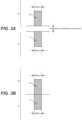
- FIG. 1illustrates, in cross section, memory structure 30 , including an array of NOR memory strings, being formed on top of CMOS circuitry and interconnect layers on a semiconductor substrate.
- memory structure 30is formed on substrate 150 .
- a suitable substratemay be, for example, a semiconductor wafer that is used for fabrication of electronic circuits, as known to those of ordinary skill in the art.
- Non semiconductor substrates, such as SiO2,may also be used.
- Semiconductor substrate 150may have fabricated thereon and therein various circuit elements (e.g., CMOS circuitry 10 represented by CMOS transistor in FIG. 1 ) interconnected by conductors 22 (e.g., copper) in conventional interconnect layers through contacts or vias 16 . These circuit elements are first fabricated on the semiconductor substrate using conventional techniques before forming memory structure 30 .
- the interconnect layers(referred herein collectively as “interconnect layers 20 ”) are typically embedded in a dielectric layer and may include conductors intended for supporting operations of memory arrays in memory structure 30 , which is to be formed over interconnect layers 20 .
- interconnect layer 24provides conductors (“global word lines 24 ”) that are intended to connect conductors 32 (e.g., heavily-doped polysilicon) serving as word lines that address storage transistors in memory structure 30 .
- conductors 32are referred to as “local word lines” in this detailed description.
- memory structure 30includes numerous stacks of “active strips” (e.g., active stacks 101 a , 101 b and 101 c ).
- FIG. 1shows stacks 101 a , 101 b and 101 c each including 4 active strips isolated from each other by isolation layers 107 .
- FIG. 1is a cross section through the active strips, which extend lengthwise into and out of the plane of cross section.
- an active stripincludes drain layer 104 , source layer 103 , body layer 102 , and channel layers 108 .
- drain layer 104 and source layer 103are both n + polysilicon
- channel layers 108are each p ⁇ polysilicon
- body layer 102is a p + polysilicon.
- a dielectric layermay be used. Also shown in the active strips of FIG. 1 are conductive layers 105 t and 105 b , adjacent respectively to source layer 103 and drain layer 104 , for reducing resistivity along the lengths of source layer 103 and drain layer 104 .
- a charge-trapping layer 107 and numerous local word lines 32are conductive columns arranged along both sides of a stack of active strips.
- a storage transistoris constituted by a local word line, a portion of channel layer 108 , the portion of charge-trapping layer 107 therebetween, and source and drain layers 103 and 104 . Drain layer 104 and source layer 103 are shared by the numerous storage transistors formed along an active strip. Adjacent storage transistors along an active strip sharing common source and drain layers form a NOR memory string. (Turning on any storage transistor in the NOR memory string results in a conducting transistor current between the common source and drain layers.)
- the memory devicestypically require a thermal budget of at least 750° C. for several hours during fabrication, due to needs in the deposition of the oxide-nitride-oxide (ONO) multi-layer or stack using low pressure chemical vapor deposition (LPCVD).
- desirable oxide and nitridemay be, respectively, high-temperature oxide (“HTO”; or SiO2) and silicon nitride (SiN).
- HTOhigh-temperature oxide
- SiNsilicon nitride
- a layer of aluminum oxide (Al 2 O 3 )is often preferred as a blocking oxide in the ONO stack.
- crystallizing Al 2 O 3which produces a desired Al 2 O 3 , from the electrical characteristics viewpoint—requires an anneal temperature of 900° C. or greater.
- a fabrication temperature exceeding 350° C.would exclude the use of copper in horizontal interconnect layers 20 embedded in associated low- ⁇ dielectric films, even when tungsten is used in vertical interconnects 16 to connect the copper horizontal interconnects.
- a fabrication temperature exceeding 500° C.would exclude the use of aluminum interconnects.
- One candidate for interconnect material for a fabrication temperature exceeding 500° C.is tungsten. However, tungsten has a higher resistivity, as shown in Table 1 below. The resulting increase in interconnect resistance increases signal delays, which adversely impact memory device performance
- CMOS circuitrye.g., CMOS transistors 10
- thermal budget for the memory devicesimpose constraints in at least two ways.
- cobalt silicide or other high temperature contact materialsuch as tungsten or tungsten silicide would have to be selected as the gate and source/drain metallization 12 in CMOS transistor 10 , so as to allow a maximum fabrication temperature of 750° C.
- cobalt silicidehas relatively low sheet and contact resistances, as compared to silicon, the relatively large consumption of underlying silicon during the silicidation step and the roughness of the resulting cobalt silicide-silicon interface require relatively deep dopant junctions in the silicon.
- nickel silicideis often used in source and drain contacts of the current generation of small transistors, cobalt silicide is preferred over nickel silicide as nickel silicide cannot withstand a temperature greater than 450° C. At a temperature greater than 450° C., a nickel silicide film would agglomerate on the silicon, which would destroy the low-sheet resistance and low-contact resistance character of the nickel silicide film.
- temperatures above 600° C.are to be avoided after junction formation to prevent dopant diffusion out of the source and drain junctions.
- CMOS devices and interconnect layersare integrated with a 3-dimensional NOR memory structure (e.g., memory structure 30 of FIG. 1 ), without the thermal budget of the memory structure constraining design choices for the CMOS devices and the interconnect layers.
- NOR memory structuree.g., memory structure 30 of FIG. 1
- a memory array and single-crystal circuitryare provided by wafer bonding (e.g., adhesive wafer bonding or anodic wafer bonding) in the same integrated circuit and interconnected by conductors of a interconnect layer.
- wafer bondinge.g., adhesive wafer bonding or anodic wafer bonding
- Additional circuitry or memory arraysmay be provided by additional wafer bonds and electrically connected by interconnect layers at the wafer bonding interface.
- the memory arraymay include storage or memory transistors having single-crystal epitaxial silicon channel material.
- FIG. 1illustrates, in cross section, memory structure 30 , including an array of NOR memory strings, being formed on top of CMOS circuitry and interconnect layers on a semiconductor substrate.
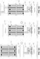
- FIG. 2 Ashows semiconductor substrate 100 on which CMOS devices and interconnect layers for supporting a 3-dimensional NOR memory structure are fabricated.
- FIG. 2 Bshows a 3-dimensional NOR memory structure (i.e., memory structure 30 ) is separately fabricated on semiconductor substrate 110 over an isolation oxide (e.g., SiO 2 ) layer 120 .
- an isolation oxidee.g., SiO 2
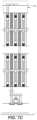
- FIG. 3 Ashows two devices A′ and B′ fabricated on wafer substrates A and B to be wafer bonded.
- FIG. 3 Bshows devices A′ and B′ being perfectly aligned and electrically connected after wafer bonding.
- FIG. 3 Cshows devices A′ and B′ being electrically connected after wafer bonding, with a 250 nm-wide misalignment.
- FIG. 3 Dshows using adhesive metal C to promote bonding between wafers A and B at devices A′ and B′ (i.e., the points of mutual contacts).
- FIG. 4shows, using as example the wafers of FIGS. 2 A and 2 B , memory structure 30 's substrate 110 may be removed.
- FIG. 5shows forming interconnect layer 40 memory structure 30 .
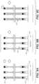
- FIGS. 6 A, 6 B, 6 C, 6 D, 6 E and 6 Fshow a sequence of steps by which wafer bonding techniques are used to fabricate both CuA and CoA circuits.
- FIGS. 7 A, 7 B and 7 Cillustrate joining memory blocks 310 and 360 using wafer bonding of substrates 300 and 350 .
- FIGS. 8 A, 8 B, 8 C, 8 D, and 8 Eillustrate a process by which CuA-type CMOS transistors are provided underneath a memory block with epitaxial single-crystal silicon channels in the memory cells, according to one embodiment of the present invention.
- FIG. 2 Ashows semiconductor substrate 100 on which CMOS devices 10 and interconnect layers 20 for supporting a 3-dimensional NOR memory structure are fabricated.
- the 3-dimensional NOR memory structurei.e., memory structure 30
- substrate 110over an isolation oxide (e.g., SiO 2 ) layer 120 , as shown in FIG. 2 B .
- Substrates 100 and 110may both be provided by silicon wafers, as known to those of ordinary skill in the art.
- the wafersare bonded together, using a “flip chip” technique, in which the surface of semiconductor substrate 100 with the interconnect layers 20 is bonded to the surface of semiconductor substrate 110 with memory structure 30 .
- a flip chiptechnique, in which the surface of semiconductor substrate 100 with the interconnect layers 20 is bonded to the surface of semiconductor substrate 110 with memory structure 30 .
- FIGS. 3 A- 3 Dillustrate exemplary wafer bonding of substrates A and B at designated wafer bonding points.
- FIG. 3 Ashows two devices A′ and B′ fabricated on wafer substrates A and B to be wafer bonded.
- Devices A′ and B′may be, for example, 300 nm-wide conductors in an interconnect system.
- FIG. 3 Bshows devices A′ and B′ being perfectly aligned and electrically connected after wafer bonding.
- 3 Cshows devices A′ and B′ being electrically connected after wafer bonding, with an 250 nm-wide misalignment. (Alignment accuracy to within ⁇ 250 nm is achievable in state-of-the-art wafer bonding techniques).
- Bonding of substrates A and Bmay be carried out using any suitable wafer bonding technique, such as thermocompression, anodic, plasma-activated, eutectic, or surface-activated wafer bonding. Among these techniques, anodic wafer bonding is preferred. With anodic wafer bonding, two wafer substrates are brought into contact and an electrostatic field is applied, which causes the apparatus to be connected electrically and physically.
- adhesive metal Cmay be used to promote bonding between wafers A and B at the point of their mutual contacts (i.e., devices A′ and B′).
- Adhesive metal Cmay be, for example, chromium, titanium, or indium, any of their alloys, or any suitable material. The principles and mechanisms of wafer bonding are known to those of ordinary skill in the art and are thus omitted in this detailed description.
- FIG. 4shows, using as example the wafers of FIGS. 2 A and 2 B , memory structure 30 's substrate 110 may be removed.
- Substrate 110may be removed by any suitable wafer thinning technique, such as laser lift-off, mechanical polishing, or chemical etch.
- mechanical polishingmay be combined with chemical etch to remove substrate 110 .
- substrate 110may be removed at a lower cost and with greater precision (i.e. no damage to memory structure 30 ) than if either technique was used alone. For example, suppose that substrate 110 is 500 micron-thick. Then, mechanical polishing may first remove about 480 microns from substrate in an initial step, thus leaving about 20 microns thick of substrate 110 to be removed by chemical etching.
- wafer-thinning by mechanical polishingthe wafer is rotated about its center against an abrasive surface. Wafer-thinning by mechanical force is sometimes referred to as “grinding,” when the resulting substrate surface is rough, and “polishing,” when the resulting substrate surface is smooth. Either the grinding or the polishing approach, or any of their combinations, may be used. After completing a mechanical grinding or polishing step, a chemical etch may remove the remaining 20 microns of memory structure 30 .
- Chemical etch of substrate 110may be accomplished using any suitable chemistry.
- suitable chemical reagents for silicon substrate 110include KOH, TMAH, HF + , HNO 3 , or HP and NH 4 F.
- An oxide layer between silicon substrate 110 and memory structure 30may server as an etch-stop layer. As shown in FIG. 4 , etch-stop layer 120 ensures memory structure 30 remain intact, undamaged from the chemical etching of substrate 110 .
- the oxide layere.g., SiO 2
- KOHmay be used, as it etches silicon about 500 times faster than it etches SiO 2 .
- the SiO 2 layertherefore acts as an efficient etch-stop for silicon etching.
- FIG. 5shows forming interconnect layer 40 memory structure 30 .
- interconnect layer 40memory structure 30 .
- either aluminum or coppermay be selected for interconnect layer 40 .
- Such interconnectsmay be formed at lower temperatures (e.g., 450° C. or less).
- wafer bondingcan be used to fabricate single-crystal transistors beneath a memory array, known as CMOS under the array (“CuA”), and above the memory array, known as CMOS over the array (“CoA”).
- FIGS. 6 A- 6 Fshow a sequence of steps by which wafer bonding techniques are used to fabricate both CuA and CoA circuits.
- CMOS transistors 210are fabricated on substrate 200 , while memory array 140 is fabricated on substrate 130 .
- Substrate 130is then flipped over, wafer-bonded to substrate 200 , such that memory array 140 is electrically connected with the CMOS transistors 210 on substrate 200 through interconnect layer 220 , as shown in FIG. 6 B .
- Substrate 200is then removed to expose memory array 140 .
- interconnect layer 150is fabricated from above the exposed side of memory array 140 , as shown in FIG. 6 C.
- a second group of CMOS transistors 290is fabricated on substrate 260 , as shown in FIG. 6 D .
- Substrate 260is most preferably silicon-on-insulator (“SOI”) wafer, where two layers of single-crystal silicon are provided on opposite sides of an oxide (SiO 2 ) layer.
- SOIsilicon-on-insulator
- CMOS transistors 290together with interconnect layer 300 above it, are formed on and above silicon layer 280 , which is separated from substrate 260 by SiO 2 layer 270 .
- Substrate 260is then flipped over and wafer-bonded to allow CMOS transistors 290 to electrically connect memory array 140 through interconnect layer 150 , as shown in FIG. 6 E .
- Substrate 260is then removed to exposed SiO 2 layer 270 and interconnect layer 310 is fabricated above and electrically connecting CMOS transistors 290 , as shown in FIG. 6 F .
- the resulting combinationis CuA-type CMOS transistors 210 built within single-crystal silicon substrate 200 , memory array 140 at least partially overlying CMOS transistors 220 , CoA-type CMOS transistors 290 at least partially overlying memory array 140 , and multiple layers of interconnect layers 150 , 200 and 310 overlying and underlying memory array 140 .
- a highly efficient memory arrayrefers to a memory array fabricated on a semiconductor die on which substantially all of its area is occupied by memory cells.
- CMOS transistors 210 under memory array 140may be high-voltage or analog transistors, while CMOS transistors 290 over memory array 140 may be low-voltage, short-channel high performance logic CMOS transistors that are desirable at the closest possible physical proximity to the input/output pads of the chip.
- FIGS. 7 A- 7 Cillustrate joining memory blocks 310 and 360 using wafer bonding of substrates 300 and 350 .
- CMOS transistors 210 , together with interconnect layer 220 , and memory block 310are fabricated on substrate 300 , while memory block 360 is fabricated on substrate 350 .
- Substrate 350is then flipped over and wafer-bonded with substrate 360 , such that memory blocks 310 and 350 are electrically connected, as shown in FIG. 7 B .
- Substrate 350is then removed and interconnect layer 370 is fabricated, as shown in FIG. 7 C .
- single-crystal silicon channels for memory cell transistorscan be formed by depositing an epitaxial silicon layer that indexes off a single-crystal substrate. Such a process is difficult for a memory block with CuA-type CMOS transistors, as a “clear” path from substrate to the source/drain layers of the memory array may not be available. Examples of forming single-crystal epitaxial silicon in thin-film storage transistors are disclosed, for example, in Provisional Application II incorporated by reference above.
- Provisional Application IIdiscloses, among other types of thin-film storage transistors, one type of thin-film storage transistors—referred herein as “quasi-volatile memory (QVM) circuits”—that has a data retention time (e.g., 100 milliseconds to one year) that is greater than that of conventional dynamic random-access memory (DRAM) circuits and less than that of conventional non-volatile memory circuits.
- the QVM circuitsmay be organized, for example, as 3-dimensional arrays of NOR memory strings.
- FIGS. 8 A- 8 Eillustrate a process by which CuA-type CMOS transistors are provided underneath a memory block with epitaxial single-crystal silicon channels in the memory cells, according to one embodiment of the present invention.
- stacks of active stripsare first formed on substrate 400 , with trenches separating adjacent stacks of active strips reaching down to substrate 400 , as shown in FIG. 8 A .
- Epitaxial silicon 430 that indexes off the silicon substrate 400are then grown from surface 402 of substrate 400 , as shown in FIG. 8 B .
- An anisotropic etchthen substantially removes all of epitaxial silicon 430 from the trenches, except for epitaxial silicon channels 440 left in the recessed area between the source and drain layers of the active strips, as shown in FIG. 8 C .
- Memory block 810 fabricationthen proceeds to completion, as shown in FIG. 8 D .
- Substrate 400is then flipped over and wafer-bonded to substrate 450 , which contains CMOS transistors 210 and interconnect layer 220 formed thereon, as shown in FIGS. 8 D- 8 E .
- substrate 450contains CMOS transistors 210 and interconnect layer 220 formed thereon, as shown in FIGS. 8 D- 8 E .
- Substrate 400can be removed, and interconnect layers may be fabricated above the memory block as has been previously described.
Landscapes
- Engineering & Computer Science (AREA)
- Microelectronics & Electronic Packaging (AREA)
- Power Engineering (AREA)
- Physics & Mathematics (AREA)
- Condensed Matter Physics & Semiconductors (AREA)
- General Physics & Mathematics (AREA)
- Computer Hardware Design (AREA)
- Manufacturing & Machinery (AREA)
- Semiconductor Memories (AREA)
- Metal-Oxide And Bipolar Metal-Oxide Semiconductor Integrated Circuits (AREA)
Abstract
Description
The present application is a continuation application of U.S. patent application (“Parent Application”), Ser. No. 16/579,329, entitled “Wafer Bonding in Fabrication of 3-Dimensional NOR Memory Circuits,” filed on Sep. 23, 2019, which is related to and claims priority of U.S. provisional patent application (“Provisional Application I”), Ser. No. 62/735,678, entitled “Wafer Bonding in Fabrication of 3-Dimensional NOR Memory Circuits,” filed on Sep. 24, 2018.
The present application is also related to U.S. patent application (“Copending Application”), Ser. No. 16/012,731, entitled “3-Dimensional NOR Memory Array Architecture and Methods for Fabrication Thereof,” filed Jun. 19, 2018. The present application is also related to U.S. provisional patent application (“Provisional Application II”), Ser. No. 63/735,622, entitled “Epitaxial Monocrystalline Channel for Storage Transistors in 3-Dimensional Memory Structures and Methods for Formation Thereof,” filed on the same day as the present application. The disclosures of the Parent Application, the Copending Application and the Provisional Applications I and II are hereby incorporated by reference in their entireties.
The present invention relates to wafer bonding techniques in integrated circuit manufacturing. In particular, the present invention relates to wafer bonding techniques applied to high-density 3-dimensional memory circuits.
Wafer bonding is a technique used in the manufacturing of many semiconductor devices. In wafer bonding, two wafers of near-equal area or equal areas are joined, for example, by thermocompression, adhesive, anodic, or thermal techniques. Often, all or substantially all of the substrate in one or both wafers are removed after bonding.
The Copending Application discloses 3-dimensional memory structures, formed on top of a monocrystalline semiconductor substrates, that are organized as arrays of NOR memory strings. In this context, the term “NOR memory string” refers to a group of thin-film storage transistors sharing common source and drain regions.FIG.1 illustrates, in cross section,memory structure 30, including an array of NOR memory strings, being formed on top of CMOS circuitry and interconnect layers on a semiconductor substrate. As shown inFIG.1 ,memory structure 30 is formed onsubstrate 150. A suitable substrate may be, for example, a semiconductor wafer that is used for fabrication of electronic circuits, as known to those of ordinary skill in the art. Non semiconductor substrates, such as SiO2, may also be used.
As shown inFIG.1 ,memory structure 30 includes numerous stacks of “active strips” (e.g.,active stacks FIG.1 showsstacks FIG.1 is a cross section through the active strips, which extend lengthwise into and out of the plane of cross section. In this context, an active strip includesdrain layer 104,source layer 103, body layer102, and channel layers108. (Channel layers108 are provided on both sides of body layer102.) In some implementations,drain layer 104 andsource layer 103 are both n+ polysilicon, channel layers108 are each p− polysilicon and body layer102 is a p+ polysilicon. In some implementations, rather than body layer102, a dielectric layer may be used. Also shown in the active strips ofFIG.1 are conductive layers105tand105b, adjacent respectively tosource layer 103 anddrain layer 104, for reducing resistivity along the lengths ofsource layer 103 anddrain layer 104. Along each side of each stack of active strips (and, hence, along each side of each active strip) is provided a charge-trapping layer 107 and numerouslocal word lines 32. InFIG.1 ,local words line 32 are conductive columns arranged along both sides of a stack of active strips. A storage transistor is constituted by a local word line, a portion of channel layer108, the portion of charge-trapping layer 107 therebetween, and source anddrain layers Drain layer 104 andsource layer 103 are shared by the numerous storage transistors formed along an active strip. Adjacent storage transistors along an active strip sharing common source and drain layers form a NOR memory string. (Turning on any storage transistor in the NOR memory string results in a conducting transistor current between the common source and drain layers.)
This sequence of fabrication steps imposes constraints on the CMOS devices, the interconnect layers, and the memory devices. For example, the memory devices typically require a thermal budget of at least 750° C. for several hours during fabrication, due to needs in the deposition of the oxide-nitride-oxide (ONO) multi-layer or stack using low pressure chemical vapor deposition (LPCVD). In the ONO multi-layer, desirable oxide and nitride may be, respectively, high-temperature oxide (“HTO”; or SiO2) and silicon nitride (SiN). Furthermore, a layer of aluminum oxide (Al2O3) is often preferred as a blocking oxide in the ONO stack. However, crystallizing Al2O3—which produces a desired Al2O3, from the electrical characteristics viewpoint—requires an anneal temperature of 900° C. or greater. However, a fabrication temperature exceeding 350° C. would exclude the use of copper inhorizontal interconnect layers 20 embedded in associated low-κ dielectric films, even when tungsten is used invertical interconnects 16 to connect the copper horizontal interconnects. Likewise, a fabrication temperature exceeding 500° C. would exclude the use of aluminum interconnects. One candidate for interconnect material for a fabrication temperature exceeding 500° C. is tungsten. However, tungsten has a higher resistivity, as shown in Table 1 below. The resulting increase in interconnect resistance increases signal delays, which adversely impact memory device performance
| material | Thin-film resistivity (μΩ-cm) |
| copper | 1.7-2.0 |
| aluminum | 2.7-3.0 |
| tungsten | 8-15 |
With respect to the underlying CMOS circuitry (e.g., CMOS transistors10), the thermal budget for the memory devices impose constraints in at least two ways. First, cobalt silicide or other high temperature contact material such as tungsten or tungsten silicide would have to be selected as the gate and source/drain metallization 12 inCMOS transistor 10, so as to allow a maximum fabrication temperature of 750° C. While cobalt silicide has relatively low sheet and contact resistances, as compared to silicon, the relatively large consumption of underlying silicon during the silicidation step and the roughness of the resulting cobalt silicide-silicon interface require relatively deep dopant junctions in the silicon. On the other hand, shallow dopant junctions are required in short-channel length transistors to reduce leakage currents. Although nickel silicide is often used in source and drain contacts of the current generation of small transistors, cobalt silicide is preferred over nickel silicide as nickel silicide cannot withstand a temperature greater than 450° C. At a temperature greater than 450° C., a nickel silicide film would agglomerate on the silicon, which would destroy the low-sheet resistance and low-contact resistance character of the nickel silicide film.
Second, for shallow junctions and narrow channel devices, temperatures above 600° C. are to be avoided after junction formation to prevent dopant diffusion out of the source and drain junctions.
Therefore, a method of fabrication is desired that allows integrating optimal CMOS devices and interconnect layers with a 3-dimensional NOR memory structure (e.g.,memory structure 30 ofFIG.1 ), without the thermal budget of the memory structure constraining design choices for the CMOS devices and the interconnect layers.
According to one embodiment of the present invention, a memory array and single-crystal circuitry are provided by wafer bonding (e.g., adhesive wafer bonding or anodic wafer bonding) in the same integrated circuit and interconnected by conductors of a interconnect layer.
Additional circuitry or memory arrays may be provided by additional wafer bonds and electrically connected by interconnect layers at the wafer bonding interface.
According to one embodiment of the present invention, the memory array may include storage or memory transistors having single-crystal epitaxial silicon channel material.
The present invention is better understood upon consideration of the detailed description below, in conjunction with the accompanying drawings.
For clarity of presentation and to allow cross referencing among the figures, like elements in the figures are assigned like reference numerals.
According to one embodiment of the present invention, rather than fabricating the CMOS devices (e.g., CMOS transistor10) and the interconnect layers (e.g., interconnect layers20) on the same silicon substrate asmemory structure 30, the CMOS devices and the interconnect layers are fabricated on a separate semiconductor substrate.FIG.2A , showssemiconductor substrate 100 on whichCMOS devices 10 andinterconnect layers 20 for supporting a 3-dimensional NOR memory structure are fabricated. The 3-dimensional NOR memory structure (i.e., memory structure30) is separately fabricated onsubstrate 110 over an isolation oxide (e.g., SiO2)layer 120, as shown inFIG.2B .Substrates
After the required fabrication steps are carried out on each ofsemiconductor substrates semiconductor substrate 100 with the interconnect layers20 is bonded to the surface ofsemiconductor substrate 110 withmemory structure 30. In this manner, fabrication of interconnect layers20 andCMOS devices 10 is not constrained by the elevated temperatures optimal to fabricatingmemory structure 30.
The wafers are bonded such that contact points in interconnect layers20 are connected electrically to corresponding contact points ofmemory structure 30. Lithographic alignment marks in each respective substrate allow the target bonding points to be aligned with minimal mismatch.FIGS.3A-3D illustrate exemplary wafer bonding of substrates A and B at designated wafer bonding points.FIG.3A shows two devices A′ and B′ fabricated on wafer substrates A and B to be wafer bonded. Devices A′ and B′ may be, for example, 300 nm-wide conductors in an interconnect system.FIG.3B shows devices A′ and B′ being perfectly aligned and electrically connected after wafer bonding.FIG.3C shows devices A′ and B′ being electrically connected after wafer bonding, with an 250 nm-wide misalignment. (Alignment accuracy to within ±250 nm is achievable in state-of-the-art wafer bonding techniques). Bonding of substrates A and B may be carried out using any suitable wafer bonding technique, such as thermocompression, anodic, plasma-activated, eutectic, or surface-activated wafer bonding. Among these techniques, anodic wafer bonding is preferred. With anodic wafer bonding, two wafer substrates are brought into contact and an electrostatic field is applied, which causes the apparatus to be connected electrically and physically.
According to one embodiment of the present invention, as illustrated byFIG.3D , adhesive metal C may be used to promote bonding between wafers A and B at the point of their mutual contacts (i.e., devices A′ and B′). Adhesive metal C may be, for example, chromium, titanium, or indium, any of their alloys, or any suitable material. The principles and mechanisms of wafer bonding are known to those of ordinary skill in the art and are thus omitted in this detailed description.
After bonding, one substrate may be removed.FIG.4 shows, using as example the wafers ofFIGS.2A and2B ,memory structure 30'ssubstrate 110 may be removed.Substrate 110 may be removed by any suitable wafer thinning technique, such as laser lift-off, mechanical polishing, or chemical etch. In one embodiment, mechanical polishing may be combined with chemical etch to removesubstrate 110. By combining mechanical polishing with chemical etching,substrate 110 may be removed at a lower cost and with greater precision (i.e. no damage to memory structure30) than if either technique was used alone. For example, suppose thatsubstrate 110 is 500 micron-thick. Then, mechanical polishing may first remove about 480 microns from substrate in an initial step, thus leaving about 20 microns thick ofsubstrate 110 to be removed by chemical etching.
In wafer-thinning by mechanical polishing, the wafer is rotated about its center against an abrasive surface. Wafer-thinning by mechanical force is sometimes referred to as “grinding,” when the resulting substrate surface is rough, and “polishing,” when the resulting substrate surface is smooth. Either the grinding or the polishing approach, or any of their combinations, may be used. After completing a mechanical grinding or polishing step, a chemical etch may remove the remaining 20 microns ofmemory structure 30.
Chemical etch ofsubstrate 110 may be accomplished using any suitable chemistry. Examples of suitable chemical reagents forsilicon substrate 110 include KOH, TMAH, HF+, HNO3, or HP and NH4F. An oxide layer betweensilicon substrate 110 andmemory structure 30 may server as an etch-stop layer. As shown inFIG.4 , etch-stop layer 120 ensuresmemory structure 30 remain intact, undamaged from the chemical etching ofsubstrate 110. When the oxide layer (e.g., SiO2) is used as an etch-stop layer, KOH may be used, as it etches silicon about 500 times faster than it etches SiO2. The SiO2layer therefore acts as an efficient etch-stop for silicon etching.
Aftersubstrate 110 is removed, further fabrication can proceed on the bonded wafers. For example,FIG.5 shows forminginterconnect layer 40memory structure 30. With the formation ofmemory structure 30 being decoupled from the formation ofinterconnect layer 40, either aluminum or copper may be selected forinterconnect layer 40. Such interconnects may be formed at lower temperatures (e.g., 450° C. or less).
According to another embodiment of the present invention, wafer bonding can be used to fabricate single-crystal transistors beneath a memory array, known as CMOS under the array (“CuA”), and above the memory array, known as CMOS over the array (“CoA”).FIGS.6A-6F show a sequence of steps by which wafer bonding techniques are used to fabricate both CuA and CoA circuits.
As shown inFIG.6A ,CMOS transistors 210 are fabricated onsubstrate 200, whilememory array 140 is fabricated onsubstrate 130.Substrate 130 is then flipped over, wafer-bonded tosubstrate 200, such thatmemory array 140 is electrically connected with theCMOS transistors 210 onsubstrate 200 throughinterconnect layer 220, as shown inFIG.6B .Substrate 200 is then removed to exposememory array 140. Thereafter,interconnect layer 150 is fabricated from above the exposed side ofmemory array 140, as shown in FIG.6C.
A second group ofCMOS transistors 290 is fabricated onsubstrate 260, as shown inFIG.6D .Substrate 260 is most preferably silicon-on-insulator (“SOI”) wafer, where two layers of single-crystal silicon are provided on opposite sides of an oxide (SiO2) layer. As shown inFIG.6D ,CMOS transistors 290, together withinterconnect layer 300 above it, are formed on and abovesilicon layer 280, which is separated fromsubstrate 260 by SiO2layer270.Substrate 260 is then flipped over and wafer-bonded to allowCMOS transistors 290 to electrically connectmemory array 140 throughinterconnect layer 150, as shown inFIG.6E .
According to yet another embodiment of the present invention, wafer bonding can be used to bond a memory block to another memory block. In this manner, a high-areal density memory structure can be achieved on a single chip, while simplifying fabrication by minimizing the aspect ratio of the memory structure that is fabricated.FIGS.7A-7C illustrate joiningmemory blocks substrates FIG.7A ,CMOS transistors 210, together withinterconnect layer 220, andmemory block 310 are fabricated onsubstrate 300, whilememory block 360 is fabricated onsubstrate 350.Substrate 350 is then flipped over and wafer-bonded withsubstrate 360, such that memory blocks310 and350 are electrically connected, as shown inFIG.7B .Substrate 350 is then removed andinterconnect layer 370 is fabricated, as shown inFIG.7C .
According to yet another embodiment of the present invention, single-crystal silicon channels for memory cell transistors can be formed by depositing an epitaxial silicon layer that indexes off a single-crystal substrate. Such a process is difficult for a memory block with CuA-type CMOS transistors, as a “clear” path from substrate to the source/drain layers of the memory array may not be available. Examples of forming single-crystal epitaxial silicon in thin-film storage transistors are disclosed, for example, in Provisional Application II incorporated by reference above. In particular, Provisional Application II discloses, among other types of thin-film storage transistors, one type of thin-film storage transistors—referred herein as “quasi-volatile memory (QVM) circuits”—that has a data retention time (e.g., 100 milliseconds to one year) that is greater than that of conventional dynamic random-access memory (DRAM) circuits and less than that of conventional non-volatile memory circuits. The QVM circuits may be organized, for example, as 3-dimensional arrays of NOR memory strings. When only the memory block is built on top of a silicon substrate (i.e., without the CuA-type CMOS transistors beneath it), a clear path is provided for epitaxial silicon deposition. The substrate with the resulting memory block can then be wafer-bonded to another substrate on which with CMOS transistors have been fabricated.FIGS.8A-8E illustrate a process by which CuA-type CMOS transistors are provided underneath a memory block with epitaxial single-crystal silicon channels in the memory cells, according to one embodiment of the present invention.
As shown inFIG.8A , stacks of active strips—each active strip having source and drainlayers 420—are first formed onsubstrate 400, with trenches separating adjacent stacks of active strips reaching down tosubstrate 400, as shown inFIG.8A .Epitaxial silicon 430 that indexes off thesilicon substrate 400 are then grown fromsurface 402 ofsubstrate 400, as shown inFIG.8B . An anisotropic etch then substantially removes all ofepitaxial silicon 430 from the trenches, except forepitaxial silicon channels 440 left in the recessed area between the source and drain layers of the active strips, as shown inFIG.8C .Memory block 810 fabrication then proceeds to completion, as shown inFIG.8D . (Exemplary fabrication processes are disclosed, for example, in the Copending Application incorporated by reference above.)Substrate 400 is then flipped over and wafer-bonded tosubstrate 450, which containsCMOS transistors 210 andinterconnect layer 220 formed thereon, as shown inFIGS.8D-8E .Substrate 400 can be removed, and interconnect layers may be fabricated above the memory block as has been previously described.
The above detailed description is provided to illustrate specific embodiments of the present invention and is not intended to be limiting. Numerous variations and modifications within the scope of the present invention are possible. The present invention is set forth in the accompanying claims.
Claims (15)
1. A memory integrated circuit, comprising:
a first semiconductor wafer, comprising (i) a monocrystalline semiconductor substrate (“first substrate”) having first and second planar surface (“first obverse surface” and “first reverse surface”, respectively), (ii) circuitry for supporting memory operations (“first circuitry”) formed in the first substrate or at the first obverse surface; (iii) a memory circuit, formed above the first obverse surface, comprising an array of thin-film storage transistors that are electrically connected to and configured to be operated at least in part by the first circuitry; and (iv) a plurality of interconnect conductors (“first interconnect conductors”) formed above the memory circuit and electrically connected to the memory circuit; and
a second semiconductor wafer, comprising (i) a monocrystalline semiconductor substrate (“second substrate”) having first and second planar surfaces (“second obverse surface” and “second reverse surface”, respectively), (ii) circuitry for supporting memory operations (“second circuitry”) formed in the second substrate or at the second obverse surface; and (iii) a plurality of interconnect conductors (“second interconnect conductors”) formed above the second circuitry, and electrically connected to the second circuitry;
wherein the first and second semiconductor wafers are joined by wafer-bonding at the first and the second interconnect conductors, such that the second circuitry is electrically connected through the first and the second interconnect conductors to the memory circuit, thereby allowing the second circuitry to operate, at least in part, the memory circuit.
2. The memory integrated circuit ofclaim 1 , wherein the second semiconductor wafer further comprising an additional plurality of interconnect conductors (“third interconnect conductors”) connected by conductor-filled vias to the second circuitry, the third interconnect conductors being exposed at least in part at the second reverse surface so as to allow access to the second circuitry by circuitry in a third semiconductor wafer through wafer-bonding with the second semiconductor wafer.
3. The memory integrated circuit ofclaim 2 , wherein third semiconductor wafer is configured to include a memory circuit (“second memory circuit”), such that the second circuit operates, at least in part, the second memory circuit.
4. The integrated memory circuit ofclaim 3 , wherein the second memory circuit is electrically connected to the first memory circuit through one or more electrical paths through the first, the second and third interconnect conductors.
5. The memory integrated circuit ofclaim 1 , wherein the second circuitry is formed in an epitaxial semiconductor layer at the second obverse surface above an insulator layer.
6. The memory integrated circuit ofclaim 1 , wherein the first and the second semiconductor wafers are each a silicon-on-insulator wafer.
7. The memory integrated circuit ofclaim 1 , wherein the wafer-bonding is one of: thermocompression, adhesive, anodic, and thermal wafer bonding.
8. The memory integrated circuit ofclaim 1 , wherein the first circuitry comprises high-voltage or analog transistors.
9. The memory integrated circuit ofclaim 1 , wherein the second circuitry is formed out of low-voltage, short-channel high performance logic CMOS transistors.
10. The memory integrated circuit ofclaim 1 , wherein the thin-film storage transistors in the memory circuit each comprise single-crystal silicon channel material.
11. The memory integrated circuit ofclaim 1 , wherein the thin-film storage transistors are organized as NOR memory strings.
12. The memory integrated circuit ofclaim 11 , wherein the thin-film storage transistors are organized into one or more non-volatile memory strings.
13. The memory integrated circuit ofclaim 11 , wherein the thin-film storage transistors are organized into one or more quasi-volatile memory strings.
14. The memory integrated circuit ofclaim 1 , wherein the thin-film storage transistors are organized into a 3-dimensional memory array.
15. The memory integrated circuit ofclaim 14 , wherein the 3-dimensional memory array comprises NOR-type memory strings.
Priority Applications (1)
| Application Number | Priority Date | Filing Date | Title |
|---|---|---|---|
| US17/470,861US11710729B2 (en) | 2018-09-24 | 2021-09-09 | Wafer bonding in fabrication of 3-dimensional NOR memory circuits |
Applications Claiming Priority (3)
| Application Number | Priority Date | Filing Date | Title |
|---|---|---|---|
| US201862735678P | 2018-09-24 | 2018-09-24 | |
| US16/579,329US11158620B2 (en) | 2018-09-24 | 2019-09-23 | Wafer bonding in fabrication of 3-dimensional NOR memory circuits |
| US17/470,861US11710729B2 (en) | 2018-09-24 | 2021-09-09 | Wafer bonding in fabrication of 3-dimensional NOR memory circuits |
Related Parent Applications (1)
| Application Number | Title | Priority Date | Filing Date |
|---|---|---|---|
| US16/579,329ContinuationUS11158620B2 (en) | 2018-09-24 | 2019-09-23 | Wafer bonding in fabrication of 3-dimensional NOR memory circuits |
Publications (2)
| Publication Number | Publication Date |
|---|---|
| US20210407983A1 US20210407983A1 (en) | 2021-12-30 |
| US11710729B2true US11710729B2 (en) | 2023-07-25 |
Family
ID=69884524
Family Applications (2)
| Application Number | Title | Priority Date | Filing Date |
|---|---|---|---|
| US16/579,329ActiveUS11158620B2 (en) | 2018-09-24 | 2019-09-23 | Wafer bonding in fabrication of 3-dimensional NOR memory circuits |
| US17/470,861Active2040-01-20US11710729B2 (en) | 2018-09-24 | 2021-09-09 | Wafer bonding in fabrication of 3-dimensional NOR memory circuits |
Family Applications Before (1)
| Application Number | Title | Priority Date | Filing Date |
|---|---|---|---|
| US16/579,329ActiveUS11158620B2 (en) | 2018-09-24 | 2019-09-23 | Wafer bonding in fabrication of 3-dimensional NOR memory circuits |
Country Status (6)
| Country | Link |
|---|---|
| US (2) | US11158620B2 (en) |
| EP (1) | EP3857598A4 (en) |
| JP (1) | JP7745322B2 (en) |
| CN (1) | CN112514067B (en) |
| TW (1) | TWI713195B (en) |
| WO (1) | WO2020068677A1 (en) |
Families Citing this family (32)
| Publication number | Priority date | Publication date | Assignee | Title |
|---|---|---|---|---|
| US9842651B2 (en) | 2015-11-25 | 2017-12-12 | Sunrise Memory Corporation | Three-dimensional vertical NOR flash thin film transistor strings |
| US9892800B2 (en) | 2015-09-30 | 2018-02-13 | Sunrise Memory Corporation | Multi-gate NOR flash thin-film transistor strings arranged in stacked horizontal active strips with vertical control gates |
| US11120884B2 (en) | 2015-09-30 | 2021-09-14 | Sunrise Memory Corporation | Implementing logic function and generating analog signals using NOR memory strings |
| US10121553B2 (en) | 2015-09-30 | 2018-11-06 | Sunrise Memory Corporation | Capacitive-coupled non-volatile thin-film transistor NOR strings in three-dimensional arrays |
| US10692874B2 (en) | 2017-06-20 | 2020-06-23 | Sunrise Memory Corporation | 3-dimensional NOR string arrays in segmented stacks |
| US10608008B2 (en) | 2017-06-20 | 2020-03-31 | Sunrise Memory Corporation | 3-dimensional nor strings with segmented shared source regions |
| KR102719982B1 (en) | 2017-06-20 | 2024-10-22 | 선라이즈 메모리 코포레이션 | 3D NOR memory array architecture and its manufacturing method |
| WO2019133534A1 (en) | 2017-12-28 | 2019-07-04 | Sunrise Memory Corporation | 3-dimensional nor memory array with very fine pitch: device and method |
| US10475812B2 (en) | 2018-02-02 | 2019-11-12 | Sunrise Memory Corporation | Three-dimensional vertical NOR flash thin-film transistor strings |
| CN112567516B (en) | 2018-07-12 | 2025-02-25 | 日升存储公司 | Method for manufacturing three-dimensional NOR memory array |
| US11751391B2 (en) | 2018-07-12 | 2023-09-05 | Sunrise Memory Corporation | Methods for fabricating a 3-dimensional memory structure of nor memory strings |
| US11069696B2 (en)* | 2018-07-12 | 2021-07-20 | Sunrise Memory Corporation | Device structure for a 3-dimensional NOR memory array and methods for improved erase operations applied thereto |
| TWI713195B (en) | 2018-09-24 | 2020-12-11 | 美商森恩萊斯記憶體公司 | Wafer bonding in fabrication of 3-dimensional nor memory circuits and integrated circuit formed therefrom |
| EP3891780A4 (en) | 2018-12-07 | 2022-12-21 | Sunrise Memory Corporation | METHOD OF FABRICATION OF MULTILAYER VERTICAL NOR STORAGE STRING ARRAYS |
| WO2020160169A1 (en) | 2019-01-30 | 2020-08-06 | Sunrise Memory Corporation | Device with embedded high-bandwidth, high-capacity memory using wafer bonding |
| EP3925004A4 (en) | 2019-02-11 | 2023-03-08 | Sunrise Memory Corporation | VERTICAL THIN-FILM TRANSISTOR AND APPLICATION AS A BITLINE CONNECTOR FOR THREE-DIMENSIONAL MEMORY ARRAYS |
| WO2021127218A1 (en) | 2019-12-19 | 2021-06-24 | Sunrise Memory Corporation | Process for preparing a channel region of a thin-film transistor |
| TWI767512B (en) | 2020-01-22 | 2022-06-11 | 美商森恩萊斯記憶體公司 | Cool electron erasing in thin-film storage transistors |
| TWI836184B (en) | 2020-02-07 | 2024-03-21 | 美商森恩萊斯記憶體公司 | High capacity memory circuit with low effective latency |
| WO2021158994A1 (en) | 2020-02-07 | 2021-08-12 | Sunrise Memory Corporation | Quasi-volatile system-level memory |
| US11507301B2 (en) | 2020-02-24 | 2022-11-22 | Sunrise Memory Corporation | Memory module implementing memory centric architecture |
| US11561911B2 (en) | 2020-02-24 | 2023-01-24 | Sunrise Memory Corporation | Channel controller for shared memory access |
| US11705496B2 (en) | 2020-04-08 | 2023-07-18 | Sunrise Memory Corporation | Charge-trapping layer with optimized number of charge-trapping sites for fast program and erase of a memory cell in a 3-dimensional NOR memory string array |
| US11937424B2 (en) | 2020-08-31 | 2024-03-19 | Sunrise Memory Corporation | Thin-film storage transistors in a 3-dimensional array of nor memory strings and process for fabricating the same |
| WO2022108848A1 (en) | 2020-11-17 | 2022-05-27 | Sunrise Memory Corporation | Methods for reducing disturb errors by refreshing data alongside programming or erase operations |
| US11848056B2 (en) | 2020-12-08 | 2023-12-19 | Sunrise Memory Corporation | Quasi-volatile memory with enhanced sense amplifier operation |
| WO2022173700A1 (en) | 2021-02-10 | 2022-08-18 | Sunrise Memory Corporation | Memory interface with configurable high-speed serial data lanes for high bandwidth memory |
| WO2023272558A1 (en)* | 2021-06-30 | 2023-01-05 | Yangtze Memory Technologies Co., Ltd. | Three-dimensional memory device and method for forming the same |
| TW202310429A (en) | 2021-07-16 | 2023-03-01 | 美商日升存儲公司 | 3-dimensional memory string array of thin-film ferroelectric transistors |
| CN113707667B (en)* | 2021-08-02 | 2023-12-19 | 中国科学院微电子研究所 | NOR type memory device, manufacturing method thereof, and electronic equipment including the memory device |
| US20230078883A1 (en)* | 2021-09-14 | 2023-03-16 | Sunrise Memory Corporation | Three-dimensional memory string array of thin-film ferroelectric transistors formed with an oxide semiconductor channel in a channel last process |
| US12402319B2 (en) | 2021-09-14 | 2025-08-26 | Sunrise Memory Corporation | Three-dimensional memory string array of thin-film ferroelectric transistors formed with an oxide semiconductor channel |
Citations (140)
| Publication number | Priority date | Publication date | Assignee | Title |
|---|---|---|---|---|
| US4213139A (en) | 1978-05-18 | 1980-07-15 | Texas Instruments Incorporated | Double level polysilicon series transistor cell |
| US5583808A (en) | 1994-09-16 | 1996-12-10 | National Semiconductor Corporation | EPROM array segmented for high performance and method for controlling same |
| US5646886A (en) | 1995-05-24 | 1997-07-08 | National Semiconductor Corporation | Flash memory having segmented array for improved operation |
| US5656842A (en) | 1995-06-20 | 1997-08-12 | Mitsubishi Denki Kabushiki Kaisha | Vertical mosfet including a back gate electrode |
| US5768192A (en) | 1996-07-23 | 1998-06-16 | Saifun Semiconductors, Ltd. | Non-volatile semiconductor memory cell utilizing asymmetrical charge trapping |
| US5789776A (en) | 1995-09-22 | 1998-08-04 | Nvx Corporation | Single poly memory cell and array |
| US5915167A (en) | 1997-04-04 | 1999-06-22 | Elm Technology Corporation | Three dimensional structure memory |
| US6040605A (en) | 1998-01-28 | 2000-03-21 | Hitachi, Ltd. | Semiconductor memory device |
| US6107133A (en) | 1998-05-28 | 2000-08-22 | International Business Machines Corporation | Method for making a five square vertical DRAM cell |
| US6118171A (en) | 1998-12-21 | 2000-09-12 | Motorola, Inc. | Semiconductor device having a pedestal structure and method of making |
| US6130838A (en) | 1997-08-12 | 2000-10-10 | Samsung Electronics, Co., Ltd. | Structure nonvolatile semiconductor memory cell array and method for fabricating same |
| US20010030340A1 (en) | 1998-11-04 | 2001-10-18 | Ichiro Fujiwara | Nonvolatile semiconductor memory device and process of production and write method thereof |
| US20010053092A1 (en) | 2000-06-12 | 2001-12-20 | Sony Corporation | Memory system and programming method thereof |
| US20020028541A1 (en) | 2000-08-14 | 2002-03-07 | Lee Thomas H. | Dense arrays and charge storage devices, and methods for making same |
| US20020051378A1 (en) | 2000-08-17 | 2002-05-02 | Takashi Ohsawa | Semiconductor memory device and method of manufacturing the same |
| US6434053B1 (en) | 1999-12-06 | 2002-08-13 | Sony Corporation | Nonvolatile semiconductor memory device and method of operation thereof |
| US20020193484A1 (en) | 2001-02-02 | 2002-12-19 | The 54 Group, Ltd. | Polymeric resins impregnated with insect repellants |
| US6580124B1 (en) | 2000-08-14 | 2003-06-17 | Matrix Semiconductor Inc. | Multigate semiconductor device with vertical channel current and method of fabrication |
| US6744094B2 (en) | 2001-08-24 | 2004-06-01 | Micron Technology Inc. | Floating gate transistor with horizontal gate layers stacked next to vertical body |
| US6774458B2 (en) | 2002-07-23 | 2004-08-10 | Hewlett Packard Development Company, L.P. | Vertical interconnection structure and methods |
| US20040214387A1 (en) | 2002-07-08 | 2004-10-28 | Madurawe Raminda Udaya | Methods for fabricating three dimensional integrated circuits |
| US20040246807A1 (en) | 2003-06-03 | 2004-12-09 | Seung-Hoon Lee | Multi-port memory device with stacked banks |
| US20040262681A1 (en) | 2003-05-28 | 2004-12-30 | Fujio Masuoka | Semiconductor device |
| US20040262772A1 (en)* | 2003-06-30 | 2004-12-30 | Shriram Ramanathan | Methods for bonding wafers using a metal interlayer |
| US20050002267A1 (en)* | 2003-06-23 | 2005-01-06 | Nve Corporation | Thermally operated switch control memory cell |
| US6873004B1 (en) | 2002-02-04 | 2005-03-29 | Nexflash Technologies, Inc. | Virtual ground single transistor memory cell, memory array incorporating same, and method of operation thereof |
| US20050128815A1 (en) | 2003-12-09 | 2005-06-16 | Renesas Technology Corp. | Semiconductor data processing device |
| US6946703B2 (en) | 2003-01-09 | 2005-09-20 | Samsung Electronics Co., Ltd. | SONOS memory device having side gate stacks and method of manufacturing the same |
| US20050280061A1 (en) | 2004-06-21 | 2005-12-22 | Sang-Yun Lee | Vertical memory device structures |
| US7005350B2 (en) | 2002-12-31 | 2006-02-28 | Matrix Semiconductor, Inc. | Method for fabricating programmable memory array structures incorporating series-connected transistor strings |
| US20060155921A1 (en) | 2004-12-16 | 2006-07-13 | Gorobets Sergey A | Non-volatile memory and method with multi-stream update tracking |
| US7307308B2 (en) | 2003-04-07 | 2007-12-11 | Silicon Storage Technology, Inc. | Buried bit line non-volatile floating gate memory cell with independent controllable control gate in a trench, and array thereof, and method of formation |
| US20080239812A1 (en) | 2007-03-30 | 2008-10-02 | Kabushiki Kaisha Toshiba | Nonvolatile semiconductor memory system |
| US7489002B2 (en) | 2001-02-09 | 2009-02-10 | Micron Technology, Inc. | Memory having a vertical transistor |
| US20090057722A1 (en) | 2007-05-30 | 2009-03-05 | Unisantis Electronics (Japan) Ltd. | Semiconductor device |
| US7524725B2 (en) | 2005-03-31 | 2009-04-28 | Hynix Semiconductor Inc. | Vertical transistor of semiconductor device and method for forming the same |
| US20090157946A1 (en) | 2007-12-12 | 2009-06-18 | Siamak Arya | Memory having improved read capability |
| US20090237996A1 (en) | 2008-03-20 | 2009-09-24 | Micron Technology, Inc. | Memory structure having volatile and non-volatile memory portions |
| US7612411B2 (en) | 2005-08-03 | 2009-11-03 | Walker Andrew J | Dual-gate device and method |
| US20090279360A1 (en) | 2008-05-07 | 2009-11-12 | Aplus Flash Technology, Inc. | NAND based NMOS NOR flash memory cell, a NAND based NMOS nor flash memory array, and a method of forming a NAND based NMOS NOR flash memory array |
| US20090290442A1 (en) | 2005-06-24 | 2009-11-26 | Rajan Suresh N | Method and circuit for configuring memory core integrated circuit dies with memory interface integrated circuit dies |
| US20090302303A1 (en)* | 2008-06-06 | 2009-12-10 | Ovonyx, Inc. | Thin film memory system |
| US20090316487A1 (en) | 2008-06-20 | 2009-12-24 | Aplus Flash Technology, Inc. | Apparatus and method for inhibiting excess leakage current in unselected nonvolatile memory cells in an array |
| US20100036960A1 (en) | 2008-08-05 | 2010-02-11 | Infineon Technologies Ag | Method for sending data, and communication device |
| US20100121994A1 (en) | 2008-11-10 | 2010-05-13 | International Business Machines Corporation | Stacked memory array |
| US20100124116A1 (en) | 2008-11-14 | 2010-05-20 | Kabushiki Kaisha Toshiba | Non-volatile semiconductor storage device |
| US20100213458A1 (en)* | 2009-02-23 | 2010-08-26 | Micron Technology, Inc. | Rigid semiconductor memory having amorphous metal oxide semiconductor channels |
| US20100219392A1 (en) | 2009-02-27 | 2010-09-02 | Nobuyoshi Awaya | Nonvolatile semiconductor memory device and manufacturing method for same |
| US20100254191A1 (en) | 2009-04-01 | 2010-10-07 | Byoungkeun Son | Semiconductor memory device comprising three-dimensional memory cell array |
| US20110115011A1 (en) | 2009-11-13 | 2011-05-19 | Fujio Masuoka | Semiconductor element and semiconductor device |
| US20110134705A1 (en) | 2009-12-07 | 2011-06-09 | Stmicroelectronics (R&D) Ltd | Integrated circuit package with multiple dies and a multiplexed communications interface |
| US20110170266A1 (en) | 2010-01-08 | 2011-07-14 | Ibm Corporation | 4d device process and structure |
| US20110208905A1 (en) | 2008-12-09 | 2011-08-25 | Rambus Inc. | Non-Volatile Memory Device For Concurrent And Pipelined Memory Operations |
| US8026521B1 (en) | 2010-10-11 | 2011-09-27 | Monolithic 3D Inc. | Semiconductor device and structure |
| US20110298013A1 (en) | 2010-06-07 | 2011-12-08 | Samsung Electronics Co., Ltd. | Vertical Structure Semiconductor Memory Devices And Methods Of Manufacturing The Same |
| US20110310683A1 (en) | 2001-09-28 | 2011-12-22 | Micron Technology, Inc. | Non-volatile memory control |
| US8139418B2 (en) | 2009-04-27 | 2012-03-20 | Micron Technology, Inc. | Techniques for controlling a direct injection semiconductor memory device |
| US8178396B2 (en) | 2009-03-11 | 2012-05-15 | Micron Technology, Inc. | Methods for forming three-dimensional memory devices, and related structures |
| US20120182801A1 (en) | 2011-01-19 | 2012-07-19 | Macronix International Co., Ltd. | Memory Architecture of 3D NOR Array |
| KR20120085591A (en) | 2011-01-24 | 2012-08-01 | 김진선 | Non-volatile memory device, method of operating the same, and method of fabricating the same |
| US20120243314A1 (en) | 2011-03-25 | 2012-09-27 | Kabushiki Kaisha Toshiba | Nonvolatile semiconductor memory device |
| US20120307568A1 (en) | 2011-06-06 | 2012-12-06 | Micron Technology, Inc. | Techniques for providing a semiconductor memory device |
| US20130256780A1 (en) | 2012-03-30 | 2013-10-03 | Kabushiki Kaisha Toshiba | Semiconductor device and manufacturing method thereof |
| US20140015036A1 (en) | 2012-07-13 | 2014-01-16 | United Silicon Carbide, Inc. | Trenched and implanted accumulation mode metal-oxide-semiconductor field-effect transistor |
| US20140040698A1 (en) | 2012-08-06 | 2014-02-06 | Advanced Micro Devices, Inc. | Stacked memory device with metadata mangement |
| US20140075135A1 (en) | 2012-09-11 | 2014-03-13 | Samsung Electronics Co., Ltd. | Semiconductor memory device with operation functions |
| US20140117366A1 (en) | 2012-10-31 | 2014-05-01 | Kabushiki Kaisha Toshiba | Semiconductor device and method for manufacturing same |
| US20140151774A1 (en) | 2012-12-04 | 2014-06-05 | Mosaid Technologies Incorporated | Nand flash memory with vertical cell stack structure and method for manufacturing same |
| US8767473B2 (en) | 2009-06-19 | 2014-07-01 | Samsung Electronics Co., Ltd. | Programming methods for three-dimensional memory devices having multi-bit programming, and three-dimensional memory devices programmed thereby |
| US20140247674A1 (en) | 2013-03-01 | 2014-09-04 | Micron Technology, Inc. | Vertical access device and apparatuses having a body connection line, and related method of operating the same |
| US8848425B2 (en) | 2008-12-19 | 2014-09-30 | Unity Semiconductor Corporation | Conductive metal oxide structures in non volatile re-writable memory devices |
| US8878278B2 (en) | 2012-03-21 | 2014-11-04 | Sandisk Technologies Inc. | Compact three dimensional vertical NAND and method of making thereof |
| US20140328128A1 (en) | 2013-05-01 | 2014-11-06 | Zeno Semiconductor, Inc. | NAND String Utilizing Floating Body Memory Cell |
| US20140340952A1 (en) | 2013-05-17 | 2014-11-20 | Micron Technology, Inc. | Apparatuses having a ferroelectric field-effect transistor memory array and related method |
| US20150155876A1 (en) | 2012-08-06 | 2015-06-04 | Advanced Micro Devices, Inc. | Die-stacked memory device with reconfigurable logic |
| US20150194440A1 (en) | 2014-01-09 | 2015-07-09 | Young-Jin Noh | Nonvolatile Memory Devices And Methods Of Fabricating The Same |
| US20150249143A1 (en) | 2014-02-28 | 2015-09-03 | Sandisk 3D Llc | Method For Forming Oxide Below Control Gate In Vertical Channel Thin Film Transistor |
| US20150263005A1 (en) | 2013-07-10 | 2015-09-17 | Galaxycore Shanghai Limited Corporation | Dynamic Random Access Memory (DRAM) and Production Method, Semiconductor Packaging Component and Packaging Method |
| US9190293B2 (en) | 2013-12-18 | 2015-11-17 | Applied Materials, Inc. | Even tungsten etch for high aspect ratio trenches |
| US9202694B2 (en) | 2013-03-04 | 2015-12-01 | Sandisk 3D Llc | Vertical bit line non-volatile memory systems and methods of fabrication |
| US20150372099A1 (en) | 2014-06-19 | 2015-12-24 | Taiwan Semiconductor Manufacturing Company, Ltd. | Contact silicide formation using a spike annealing process |
| US9230985B1 (en) | 2014-10-15 | 2016-01-05 | Sandisk 3D Llc | Vertical TFT with tunnel barrier |
| US20160013156A1 (en) | 2014-07-14 | 2016-01-14 | Apple Inc. | Package-on-package options with multiple layer 3-d stacking |
| US20160019951A1 (en) | 2014-07-18 | 2016-01-21 | Samsung Electronics Co., Ltd. | Resistive memory device, resistive memory system, and method of operating resistive memory device |
| US20160035711A1 (en) | 2014-07-29 | 2016-02-04 | Dyi-chung Hu | Stacked package-on-package memory devices |
| US20160079164A1 (en) | 2014-09-12 | 2016-03-17 | Kabushiki Kaisha Toshiba | Semiconductor memory device and method for manufacturing same |
| US20160086970A1 (en) | 2014-09-23 | 2016-03-24 | Haibing Peng | Three-dimensional non-volatile nor-type flash memory |
| US20160225860A1 (en) | 2013-08-12 | 2016-08-04 | Micron Technology, Inc. | Vertical Ferroelectric Field Effect Transistor Constructions, Constructions Comprising A Pair Of Vertical Ferroelectric Field Effect Transistors, Vertical Strings Of Ferroelectric Field Effect Transistors, And Vertical Strings Of Laterally Opposing Pairs Of Vertical Ferroelectric Field Effect Transistors |
| US9412752B1 (en) | 2015-09-22 | 2016-08-09 | Macronix International Co., Ltd. | Reference line and bit line structure for 3D memory |
| US9455268B2 (en) | 2014-02-13 | 2016-09-27 | Samsung Electronics Co., Ltd. | Staircase-shaped connection structures of three-dimensional semiconductor devices |
| US20160314042A1 (en) | 2015-04-27 | 2016-10-27 | Invensas Corporation | Preferred state encoding in non-volatile memories |
| US20170092371A1 (en) | 2015-09-30 | 2017-03-30 | Eli Harari | Capacitive-coupled non-volatile thin-film transistor strings in three dimensional arrays |
| US20170092370A1 (en) | 2015-09-30 | 2017-03-30 | Eli Harari | Multi-gate nor flash thin-film transistor strings arranged in stacked horizontal active strips with vertical control gates |
| US9620605B2 (en) | 2015-05-15 | 2017-04-11 | Taiwan Semiconductor Manufacturing Company, Ltd. | Semiconductor device structure and method |
| US9633944B2 (en) | 2015-04-28 | 2017-04-25 | SK Hynix Inc. | Semiconductor device and manufacturing method thereof |
| US20170148810A1 (en) | 2015-11-20 | 2017-05-25 | Sandisk Technologies Llc | Three-dimensional nand device containing support pedestal structures for a buried source line and method of making the same |
| US20170148517A1 (en) | 2015-11-25 | 2017-05-25 | Eli Harari | Three-dimensional vertical nor flash thin film transistor strings |
| US20170213821A1 (en) | 2014-08-26 | 2017-07-27 | Monolithic 3D Inc. | 3d semiconductor device and structure |
| US9748172B2 (en) | 2015-02-25 | 2017-08-29 | Sandisk Technologies Llc | Floating staircase word lines and process in a 3D non-volatile memory having vertical bit lines |
| US9799761B2 (en) | 2013-03-11 | 2017-10-24 | Monolithic 3D Inc. | 3DIC based system with memory cells and transistors |
| US20170358594A1 (en) | 2016-06-13 | 2017-12-14 | Sandisk Technologies Llc | Method of forming a staircase in a semiconductor device using a linear alignmnent control feature |
| CN107658317A (en) | 2017-09-15 | 2018-02-02 | 长江存储科技有限责任公司 | A kind of semiconductor device and preparation method thereof |
| US20180095127A1 (en) | 2016-09-30 | 2018-04-05 | Intel Corporation | Systems, methods, and apparatuses for implementing testing of fault repairs to a through silicon via (tsv) in two-level memory (2lm) stacked die subsystems |
| US10074667B1 (en) | 2017-03-10 | 2018-09-11 | Toshiba Memory Corporation | Semiconductor memory device |
| US20180261575A1 (en) | 2017-03-07 | 2018-09-13 | Toshiba Memory Corporation | Memory device |
| US20180269229A1 (en) | 2015-09-21 | 2018-09-20 | Monolithic 3D Inc. | 3D Semiconductor Device and Structure |
| CN108649031A (en) | 2018-04-09 | 2018-10-12 | 复旦大学 | Ultrafast quasi- nonvolatile storage of two dimension based on self-rectifying elastomeric material and preparation method thereof |
| US20180331042A1 (en) | 2015-12-23 | 2018-11-15 | Mathew J. Manusharow | Size and efficiency of dies |
| US20180366471A1 (en) | 2017-06-20 | 2018-12-20 | Sunrise Memory Corporation | 3-Dimensional NOR String Arrays in Segmented Stacks |
| US20180366485A1 (en) | 2017-06-20 | 2018-12-20 | Sunrise Memory Corporation | 3-Dimensional NOR Strings with Segmented Shared Source Regions |
| US20180366489A1 (en) | 2017-06-20 | 2018-12-20 | Sunrise Memory Corporation | 3-Dimensional NOR Memory Array Architecture and Methods for Fabrication Thereof |
| US20190019564A1 (en) | 2017-07-13 | 2019-01-17 | Qualcomm Incorporated | Multiple (multi-) level cell (mlc) non-volatile (nv) memory (nvm) matrix circuits for performing matrix computations with multi-bit input vectors |
| US20190043836A1 (en) | 2018-06-18 | 2019-02-07 | Intel Corporation | Three-dimensional (3d) memory with shared control circuitry using wafer-to-wafer bonding |
| US20190067327A1 (en) | 2017-08-28 | 2019-02-28 | Sunrise Memory Corporation | Staggered Word Line Architecture for Reduced Disturb in 3-Dimensional NOR Memory Arrays |
| US10254968B1 (en) | 2015-06-10 | 2019-04-09 | Firquest Llc | Hybrid memory device for lookup operations |
| US10283493B1 (en) | 2018-01-17 | 2019-05-07 | Sandisk Technologies Llc | Three-dimensional memory device containing bonded memory die and peripheral logic die and method of making thereof |
| US10283452B2 (en) | 2017-09-15 | 2019-05-07 | Yangtze Memory Technology Co., Ltd. | Three-dimensional memory devices having a plurality of NAND strings |
| US20190157296A1 (en) | 2017-11-17 | 2019-05-23 | Sunrise Memory Corporation | Reverse memory cell |
| US20190206890A1 (en) | 2017-12-28 | 2019-07-04 | Sunrise Memory Corporation | 3-Dimensional NOR Memory Array with Very Fine Pitch: Device and Method |
| US20190214077A1 (en) | 2005-09-30 | 2019-07-11 | Conversant Intellectual Property Management Inc. | Memory with output control |
| US20190238134A1 (en) | 2017-09-12 | 2019-08-01 | iCometrue Company Ltd. | Logic drive with brain-like elasticity and integrality based on standard commodity fpga ic chips using non-volatile memory cells |
| US10373956B2 (en) | 2011-03-01 | 2019-08-06 | Micron Technology, Inc. | Gated bipolar junction transistors, memory arrays, and methods of forming gated bipolar junction transistors |
| US20190244971A1 (en) | 2018-02-02 | 2019-08-08 | Sunrise Memory Corporation | Three-dimensional vertical NOR Flash Thin-Film Transistor Strings |
| US10381370B2 (en)* | 2013-11-08 | 2019-08-13 | Samsung Electronics Co., Ltd. | Semiconductor device |
| US20190259769A1 (en) | 2017-08-31 | 2019-08-22 | Micron Technology, Inc. | Apparatuses Having Memory Cells with Two Transistors and One Capacitor, and Having Body Regions of the Transistors Coupled with Reference Voltages |
| US20190303042A1 (en) | 2018-03-30 | 2019-10-03 | Samsung Electronics Co., Ltd. | Memory device sampling data using control signal transmitted through tsv |
| US20190319044A1 (en) | 2018-02-02 | 2019-10-17 | Sunrise Memory Corporation | Three-dimensional vertical NOR Flash Thin-Film Transistor Strings |
| US20190325945A1 (en) | 2018-04-20 | 2019-10-24 | Taiwan Semiconductor Manufacturing Company, Ltd. | Memory cell array and method of manufacturing same |
| US20190332321A1 (en) | 2018-04-27 | 2019-10-31 | Silicon Motion Inc. | Method for controlling storage device |
| US20190348424A1 (en) | 2018-05-08 | 2019-11-14 | Micron Technology, Inc. | Integrated Assemblies Having Ferroelectric Transistors with Body Regions Coupled to Carrier Reservoirs; and Methods of Forming Integrated Assemblies |
| US20190370117A1 (en) | 2016-06-28 | 2019-12-05 | International Business Machines Corporation | File level access to block level incremental backups of a virtual disk |
| US20190384884A1 (en) | 2018-06-18 | 2019-12-19 | Commissariat à l'énergie atomique et aux énergies alternatives | Conception of a 3d circuit comprising macros |
| US20200006306A1 (en) | 2018-07-02 | 2020-01-02 | Shanghai Denglin Technologies Co. Ltd | Configurable random-access memory (ram) array including through-silicon via (tsv) bypassing physical layer |
| US20200051990A1 (en) | 2018-07-12 | 2020-02-13 | Sunrise Memory Corporation | Device Structure for a 3-Dimensional NOR Memory Array and Methods for Improved Erase Operations Applied Thereto |
| US20200098738A1 (en) | 2018-09-24 | 2020-03-26 | Sunrise Memory Corporation | Wafer Bonding in Fabrication of 3-Dimensional NOR Memory Circuits |
| US20200098779A1 (en) | 2018-09-20 | 2020-03-26 | Sunrise Memory Corporation | Staircase Structures for Electrically Connecting Multiple Horizontal Conductive Layers of a 3-Dimensional Memory Device |
| US20200176468A1 (en) | 2018-12-04 | 2020-06-04 | Sunrise Memory Corporation | Methods for forming multilayer horizontal nor-type thin-film memory strings |
| US20200258897A1 (en) | 2019-02-11 | 2020-08-13 | Sunrise Memory Corporation | Device with embedded high-bandwidth, high-capacity memory using wafer bonding |
| US20200341838A1 (en) | 2008-06-11 | 2020-10-29 | Micron Technology, Inc. | Encoding data in a modified-memory system |
| US20200395328A1 (en) | 2019-06-11 | 2020-12-17 | Intel Corporation | Memory arrays with bonded and shared logic circuitry |
Family Cites Families (4)
| Publication number | Priority date | Publication date | Assignee | Title |
|---|---|---|---|---|
| US7262089B2 (en)* | 2004-03-11 | 2007-08-28 | Micron Technology, Inc. | Methods of forming semiconductor structures |
| US10043781B2 (en)* | 2009-10-12 | 2018-08-07 | Monolithic 3D Inc. | 3D semiconductor device and structure |
| KR20120006843A (en)* | 2010-07-13 | 2012-01-19 | 삼성전자주식회사 | Semiconductor device and manufacturing method thereof |
| US10262945B2 (en)* | 2016-11-28 | 2019-04-16 | Sandisk Technologies Llc | Three-dimensional array device having a metal containing barrier and method of making thereof |
- 2019
- 2019-09-19TWTW108133758Apatent/TWI713195B/enactive
- 2019-09-23JPJP2021516660Apatent/JP7745322B2/enactiveActive
- 2019-09-23CNCN201980049198.3Apatent/CN112514067B/enactiveActive
- 2019-09-23EPEP19865270.3Apatent/EP3857598A4/enactivePending
- 2019-09-23USUS16/579,329patent/US11158620B2/enactiveActive
- 2019-09-23WOPCT/US2019/052446patent/WO2020068677A1/ennot_activeCeased
- 2021
- 2021-09-09USUS17/470,861patent/US11710729B2/enactiveActive
Patent Citations (164)
| Publication number | Priority date | Publication date | Assignee | Title |
|---|---|---|---|---|
| US4213139A (en) | 1978-05-18 | 1980-07-15 | Texas Instruments Incorporated | Double level polysilicon series transistor cell |
| US5583808A (en) | 1994-09-16 | 1996-12-10 | National Semiconductor Corporation | EPROM array segmented for high performance and method for controlling same |
| US5646886A (en) | 1995-05-24 | 1997-07-08 | National Semiconductor Corporation | Flash memory having segmented array for improved operation |
| US5656842A (en) | 1995-06-20 | 1997-08-12 | Mitsubishi Denki Kabushiki Kaisha | Vertical mosfet including a back gate electrode |
| US5789776A (en) | 1995-09-22 | 1998-08-04 | Nvx Corporation | Single poly memory cell and array |
| US5768192A (en) | 1996-07-23 | 1998-06-16 | Saifun Semiconductors, Ltd. | Non-volatile semiconductor memory cell utilizing asymmetrical charge trapping |
| US5915167A (en) | 1997-04-04 | 1999-06-22 | Elm Technology Corporation | Three dimensional structure memory |
| US6130838A (en) | 1997-08-12 | 2000-10-10 | Samsung Electronics, Co., Ltd. | Structure nonvolatile semiconductor memory cell array and method for fabricating same |
| US6040605A (en) | 1998-01-28 | 2000-03-21 | Hitachi, Ltd. | Semiconductor memory device |
| US6107133A (en) | 1998-05-28 | 2000-08-22 | International Business Machines Corporation | Method for making a five square vertical DRAM cell |
| US20010030340A1 (en) | 1998-11-04 | 2001-10-18 | Ichiro Fujiwara | Nonvolatile semiconductor memory device and process of production and write method thereof |
| US6118171A (en) | 1998-12-21 | 2000-09-12 | Motorola, Inc. | Semiconductor device having a pedestal structure and method of making |
| US6434053B1 (en) | 1999-12-06 | 2002-08-13 | Sony Corporation | Nonvolatile semiconductor memory device and method of operation thereof |
| US20010053092A1 (en) | 2000-06-12 | 2001-12-20 | Sony Corporation | Memory system and programming method thereof |
| US6580124B1 (en) | 2000-08-14 | 2003-06-17 | Matrix Semiconductor Inc. | Multigate semiconductor device with vertical channel current and method of fabrication |
| US6881994B2 (en) | 2000-08-14 | 2005-04-19 | Matrix Semiconductor, Inc. | Monolithic three dimensional array of charge storage devices containing a planarized surface |
| US20020028541A1 (en) | 2000-08-14 | 2002-03-07 | Lee Thomas H. | Dense arrays and charge storage devices, and methods for making same |
| US20020051378A1 (en) | 2000-08-17 | 2002-05-02 | Takashi Ohsawa | Semiconductor memory device and method of manufacturing the same |
| US20020193484A1 (en) | 2001-02-02 | 2002-12-19 | The 54 Group, Ltd. | Polymeric resins impregnated with insect repellants |
| US7489002B2 (en) | 2001-02-09 | 2009-02-10 | Micron Technology, Inc. | Memory having a vertical transistor |
| US6744094B2 (en) | 2001-08-24 | 2004-06-01 | Micron Technology Inc. | Floating gate transistor with horizontal gate layers stacked next to vertical body |
| US20110310683A1 (en) | 2001-09-28 | 2011-12-22 | Micron Technology, Inc. | Non-volatile memory control |
| US6873004B1 (en) | 2002-02-04 | 2005-03-29 | Nexflash Technologies, Inc. | Virtual ground single transistor memory cell, memory array incorporating same, and method of operation thereof |
| US20040214387A1 (en) | 2002-07-08 | 2004-10-28 | Madurawe Raminda Udaya | Methods for fabricating three dimensional integrated circuits |
| US6774458B2 (en) | 2002-07-23 | 2004-08-10 | Hewlett Packard Development Company, L.P. | Vertical interconnection structure and methods |
| US7005350B2 (en) | 2002-12-31 | 2006-02-28 | Matrix Semiconductor, Inc. | Method for fabricating programmable memory array structures incorporating series-connected transistor strings |
| US6946703B2 (en) | 2003-01-09 | 2005-09-20 | Samsung Electronics Co., Ltd. | SONOS memory device having side gate stacks and method of manufacturing the same |
| US7307308B2 (en) | 2003-04-07 | 2007-12-11 | Silicon Storage Technology, Inc. | Buried bit line non-volatile floating gate memory cell with independent controllable control gate in a trench, and array thereof, and method of formation |
| US20040262681A1 (en) | 2003-05-28 | 2004-12-30 | Fujio Masuoka | Semiconductor device |
| US20040246807A1 (en) | 2003-06-03 | 2004-12-09 | Seung-Hoon Lee | Multi-port memory device with stacked banks |
| US20050002267A1 (en)* | 2003-06-23 | 2005-01-06 | Nve Corporation | Thermally operated switch control memory cell |
| US20040262772A1 (en)* | 2003-06-30 | 2004-12-30 | Shriram Ramanathan | Methods for bonding wafers using a metal interlayer |
| US20050128815A1 (en) | 2003-12-09 | 2005-06-16 | Renesas Technology Corp. | Semiconductor data processing device |
| US20050280061A1 (en) | 2004-06-21 | 2005-12-22 | Sang-Yun Lee | Vertical memory device structures |
| US20060155921A1 (en) | 2004-12-16 | 2006-07-13 | Gorobets Sergey A | Non-volatile memory and method with multi-stream update tracking |
| US7524725B2 (en) | 2005-03-31 | 2009-04-28 | Hynix Semiconductor Inc. | Vertical transistor of semiconductor device and method for forming the same |
| US20090290442A1 (en) | 2005-06-24 | 2009-11-26 | Rajan Suresh N | Method and circuit for configuring memory core integrated circuit dies with memory interface integrated circuit dies |
| US7612411B2 (en) | 2005-08-03 | 2009-11-03 | Walker Andrew J | Dual-gate device and method |
| US20190214077A1 (en) | 2005-09-30 | 2019-07-11 | Conversant Intellectual Property Management Inc. | Memory with output control |
| US20080239812A1 (en) | 2007-03-30 | 2008-10-02 | Kabushiki Kaisha Toshiba | Nonvolatile semiconductor memory system |
| US20090057722A1 (en) | 2007-05-30 | 2009-03-05 | Unisantis Electronics (Japan) Ltd. | Semiconductor device |
| US20090157946A1 (en) | 2007-12-12 | 2009-06-18 | Siamak Arya | Memory having improved read capability |
| US20090237996A1 (en) | 2008-03-20 | 2009-09-24 | Micron Technology, Inc. | Memory structure having volatile and non-volatile memory portions |
| US20090279360A1 (en) | 2008-05-07 | 2009-11-12 | Aplus Flash Technology, Inc. | NAND based NMOS NOR flash memory cell, a NAND based NMOS nor flash memory array, and a method of forming a NAND based NMOS NOR flash memory array |
| US20090302303A1 (en)* | 2008-06-06 | 2009-12-10 | Ovonyx, Inc. | Thin film memory system |
| US20200341838A1 (en) | 2008-06-11 | 2020-10-29 | Micron Technology, Inc. | Encoding data in a modified-memory system |
| US20090316487A1 (en) | 2008-06-20 | 2009-12-24 | Aplus Flash Technology, Inc. | Apparatus and method for inhibiting excess leakage current in unselected nonvolatile memory cells in an array |
| US20100036960A1 (en) | 2008-08-05 | 2010-02-11 | Infineon Technologies Ag | Method for sending data, and communication device |
| US20100121994A1 (en) | 2008-11-10 | 2010-05-13 | International Business Machines Corporation | Stacked memory array |
| US20100124116A1 (en) | 2008-11-14 | 2010-05-20 | Kabushiki Kaisha Toshiba | Non-volatile semiconductor storage device |
| US20110208905A1 (en) | 2008-12-09 | 2011-08-25 | Rambus Inc. | Non-Volatile Memory Device For Concurrent And Pipelined Memory Operations |
| US8848425B2 (en) | 2008-12-19 | 2014-09-30 | Unity Semiconductor Corporation | Conductive metal oxide structures in non volatile re-writable memory devices |
| US20100213458A1 (en)* | 2009-02-23 | 2010-08-26 | Micron Technology, Inc. | Rigid semiconductor memory having amorphous metal oxide semiconductor channels |
| US20100219392A1 (en) | 2009-02-27 | 2010-09-02 | Nobuyoshi Awaya | Nonvolatile semiconductor memory device and manufacturing method for same |
| US8178396B2 (en) | 2009-03-11 | 2012-05-15 | Micron Technology, Inc. | Methods for forming three-dimensional memory devices, and related structures |
| US20100254191A1 (en) | 2009-04-01 | 2010-10-07 | Byoungkeun Son | Semiconductor memory device comprising three-dimensional memory cell array |
| US8139418B2 (en) | 2009-04-27 | 2012-03-20 | Micron Technology, Inc. | Techniques for controlling a direct injection semiconductor memory device |
| US8767473B2 (en) | 2009-06-19 | 2014-07-01 | Samsung Electronics Co., Ltd. | Programming methods for three-dimensional memory devices having multi-bit programming, and three-dimensional memory devices programmed thereby |
| US20110115011A1 (en) | 2009-11-13 | 2011-05-19 | Fujio Masuoka | Semiconductor element and semiconductor device |
| US20110134705A1 (en) | 2009-12-07 | 2011-06-09 | Stmicroelectronics (R&D) Ltd | Integrated circuit package with multiple dies and a multiplexed communications interface |
| US20110170266A1 (en) | 2010-01-08 | 2011-07-14 | Ibm Corporation | 4d device process and structure |
| US20110298013A1 (en) | 2010-06-07 | 2011-12-08 | Samsung Electronics Co., Ltd. | Vertical Structure Semiconductor Memory Devices And Methods Of Manufacturing The Same |
| US8026521B1 (en) | 2010-10-11 | 2011-09-27 | Monolithic 3D Inc. | Semiconductor device and structure |
| US20120182801A1 (en) | 2011-01-19 | 2012-07-19 | Macronix International Co., Ltd. | Memory Architecture of 3D NOR Array |
| US8630114B2 (en) | 2011-01-19 | 2014-01-14 | Macronix International Co., Ltd. | Memory architecture of 3D NOR array |
| KR20120085591A (en) | 2011-01-24 | 2012-08-01 | 김진선 | Non-volatile memory device, method of operating the same, and method of fabricating the same |
| US10373956B2 (en) | 2011-03-01 | 2019-08-06 | Micron Technology, Inc. | Gated bipolar junction transistors, memory arrays, and methods of forming gated bipolar junction transistors |
| US20120243314A1 (en) | 2011-03-25 | 2012-09-27 | Kabushiki Kaisha Toshiba | Nonvolatile semiconductor memory device |
| US20120307568A1 (en) | 2011-06-06 | 2012-12-06 | Micron Technology, Inc. | Techniques for providing a semiconductor memory device |
| US8878278B2 (en) | 2012-03-21 | 2014-11-04 | Sandisk Technologies Inc. | Compact three dimensional vertical NAND and method of making thereof |
| US20130256780A1 (en) | 2012-03-30 | 2013-10-03 | Kabushiki Kaisha Toshiba | Semiconductor device and manufacturing method thereof |
| US20140015036A1 (en) | 2012-07-13 | 2014-01-16 | United Silicon Carbide, Inc. | Trenched and implanted accumulation mode metal-oxide-semiconductor field-effect transistor |
| US20140040698A1 (en) | 2012-08-06 | 2014-02-06 | Advanced Micro Devices, Inc. | Stacked memory device with metadata mangement |
| US20150155876A1 (en) | 2012-08-06 | 2015-06-04 | Advanced Micro Devices, Inc. | Die-stacked memory device with reconfigurable logic |
| US20140075135A1 (en) | 2012-09-11 | 2014-03-13 | Samsung Electronics Co., Ltd. | Semiconductor memory device with operation functions |
| US20140117366A1 (en) | 2012-10-31 | 2014-05-01 | Kabushiki Kaisha Toshiba | Semiconductor device and method for manufacturing same |
| US20140151774A1 (en) | 2012-12-04 | 2014-06-05 | Mosaid Technologies Incorporated | Nand flash memory with vertical cell stack structure and method for manufacturing same |
| US20140247674A1 (en) | 2013-03-01 | 2014-09-04 | Micron Technology, Inc. | Vertical access device and apparatuses having a body connection line, and related method of operating the same |
| US9202694B2 (en) | 2013-03-04 | 2015-12-01 | Sandisk 3D Llc | Vertical bit line non-volatile memory systems and methods of fabrication |
| US9799761B2 (en) | 2013-03-11 | 2017-10-24 | Monolithic 3D Inc. | 3DIC based system with memory cells and transistors |
| US20140328128A1 (en) | 2013-05-01 | 2014-11-06 | Zeno Semiconductor, Inc. | NAND String Utilizing Floating Body Memory Cell |
| US20140340952A1 (en) | 2013-05-17 | 2014-11-20 | Micron Technology, Inc. | Apparatuses having a ferroelectric field-effect transistor memory array and related method |
| US20150263005A1 (en) | 2013-07-10 | 2015-09-17 | Galaxycore Shanghai Limited Corporation | Dynamic Random Access Memory (DRAM) and Production Method, Semiconductor Packaging Component and Packaging Method |
| US20160225860A1 (en) | 2013-08-12 | 2016-08-04 | Micron Technology, Inc. | Vertical Ferroelectric Field Effect Transistor Constructions, Constructions Comprising A Pair Of Vertical Ferroelectric Field Effect Transistors, Vertical Strings Of Ferroelectric Field Effect Transistors, And Vertical Strings Of Laterally Opposing Pairs Of Vertical Ferroelectric Field Effect Transistors |
| US10381370B2 (en)* | 2013-11-08 | 2019-08-13 | Samsung Electronics Co., Ltd. | Semiconductor device |
| US9190293B2 (en) | 2013-12-18 | 2015-11-17 | Applied Materials, Inc. | Even tungsten etch for high aspect ratio trenches |
| US20150194440A1 (en) | 2014-01-09 | 2015-07-09 | Young-Jin Noh | Nonvolatile Memory Devices And Methods Of Fabricating The Same |
| US9455268B2 (en) | 2014-02-13 | 2016-09-27 | Samsung Electronics Co., Ltd. | Staircase-shaped connection structures of three-dimensional semiconductor devices |
| US20150249143A1 (en) | 2014-02-28 | 2015-09-03 | Sandisk 3D Llc | Method For Forming Oxide Below Control Gate In Vertical Channel Thin Film Transistor |
| US20150372099A1 (en) | 2014-06-19 | 2015-12-24 | Taiwan Semiconductor Manufacturing Company, Ltd. | Contact silicide formation using a spike annealing process |
| US20160013156A1 (en) | 2014-07-14 | 2016-01-14 | Apple Inc. | Package-on-package options with multiple layer 3-d stacking |
| US20160019951A1 (en) | 2014-07-18 | 2016-01-21 | Samsung Electronics Co., Ltd. | Resistive memory device, resistive memory system, and method of operating resistive memory device |
| US20160035711A1 (en) | 2014-07-29 | 2016-02-04 | Dyi-chung Hu | Stacked package-on-package memory devices |
| US20170213821A1 (en) | 2014-08-26 | 2017-07-27 | Monolithic 3D Inc. | 3d semiconductor device and structure |
| US20160079164A1 (en) | 2014-09-12 | 2016-03-17 | Kabushiki Kaisha Toshiba | Semiconductor memory device and method for manufacturing same |
| US20160086970A1 (en) | 2014-09-23 | 2016-03-24 | Haibing Peng | Three-dimensional non-volatile nor-type flash memory |
| US9230985B1 (en) | 2014-10-15 | 2016-01-05 | Sandisk 3D Llc | Vertical TFT with tunnel barrier |
| US9748172B2 (en) | 2015-02-25 | 2017-08-29 | Sandisk Technologies Llc | Floating staircase word lines and process in a 3D non-volatile memory having vertical bit lines |
| US20160314042A1 (en) | 2015-04-27 | 2016-10-27 | Invensas Corporation | Preferred state encoding in non-volatile memories |
| US9633944B2 (en) | 2015-04-28 | 2017-04-25 | SK Hynix Inc. | Semiconductor device and manufacturing method thereof |
| US9620605B2 (en) | 2015-05-15 | 2017-04-11 | Taiwan Semiconductor Manufacturing Company, Ltd. | Semiconductor device structure and method |
| US10254968B1 (en) | 2015-06-10 | 2019-04-09 | Firquest Llc | Hybrid memory device for lookup operations |
| US20180269229A1 (en) | 2015-09-21 | 2018-09-20 | Monolithic 3D Inc. | 3D Semiconductor Device and Structure |
| US9412752B1 (en) | 2015-09-22 | 2016-08-09 | Macronix International Co., Ltd. | Reference line and bit line structure for 3D memory |
| US10395737B2 (en) | 2015-09-30 | 2019-08-27 | Sunrise Memory Corporation | Three-dimensional vertical NOR flash thin-film transistor strings |
| US9892800B2 (en) | 2015-09-30 | 2018-02-13 | Sunrise Memory Corporation | Multi-gate NOR flash thin-film transistor strings arranged in stacked horizontal active strips with vertical control gates |
| US9911497B1 (en) | 2015-09-30 | 2018-03-06 | Sunrise Memory Corporation | Three-dimensional vertical NOR flash thin-film transistor strings |
| US20190325964A1 (en) | 2015-09-30 | 2019-10-24 | Sunrise Memory Corporation | Three-dimensional Vertical NOR Flash Thin-Film Transistor Strings |
| US20180108416A1 (en) | 2015-09-30 | 2018-04-19 | Sunrise Memory Corporation | Three-dimensional vertical nor flash thin-film transistor strings |
| US20190180821A1 (en) | 2015-09-30 | 2019-06-13 | Sunrise Memory Corporation | Three-dimensional Vertical NOR Flash Thin-Film Transistor Strings |
| US20190006009A1 (en) | 2015-09-30 | 2019-01-03 | Sunrise Memory Corporation | Three-dimensional Vertical NOR Flash Thin-Film Transistor Strings |
| US10096364B2 (en) | 2015-09-30 | 2018-10-09 | Sunrise Memory Corporation | Three-dimensional vertical NOR flash thin-film transistor strings |
| US20170092370A1 (en) | 2015-09-30 | 2017-03-30 | Eli Harari | Multi-gate nor flash thin-film transistor strings arranged in stacked horizontal active strips with vertical control gates |
| US10121553B2 (en) | 2015-09-30 | 2018-11-06 | Sunrise Memory Corporation | Capacitive-coupled non-volatile thin-film transistor NOR strings in three-dimensional arrays |
| US20170092371A1 (en) | 2015-09-30 | 2017-03-30 | Eli Harari | Capacitive-coupled non-volatile thin-film transistor strings in three dimensional arrays |
| US10249370B2 (en) | 2015-09-30 | 2019-04-02 | Sunrise Memory Corporation | Three-dimensional vertical NOR flash thing-film transistor strings |
| US20170148810A1 (en) | 2015-11-20 | 2017-05-25 | Sandisk Technologies Llc | Three-dimensional nand device containing support pedestal structures for a buried source line and method of making the same |
| US9842651B2 (en) | 2015-11-25 | 2017-12-12 | Sunrise Memory Corporation | Three-dimensional vertical NOR flash thin film transistor strings |
| US20170148517A1 (en) | 2015-11-25 | 2017-05-25 | Eli Harari | Three-dimensional vertical nor flash thin film transistor strings |
| US20180331042A1 (en) | 2015-12-23 | 2018-11-15 | Mathew J. Manusharow | Size and efficiency of dies |
| US20170358594A1 (en) | 2016-06-13 | 2017-12-14 | Sandisk Technologies Llc | Method of forming a staircase in a semiconductor device using a linear alignmnent control feature |
| US20190370117A1 (en) | 2016-06-28 | 2019-12-05 | International Business Machines Corporation | File level access to block level incremental backups of a virtual disk |
| US20180095127A1 (en) | 2016-09-30 | 2018-04-05 | Intel Corporation | Systems, methods, and apparatuses for implementing testing of fault repairs to a through silicon via (tsv) in two-level memory (2lm) stacked die subsystems |
| US20180261575A1 (en) | 2017-03-07 | 2018-09-13 | Toshiba Memory Corporation | Memory device |
| US10074667B1 (en) | 2017-03-10 | 2018-09-11 | Toshiba Memory Corporation | Semiconductor memory device |
| US20200403002A1 (en) | 2017-06-20 | 2020-12-24 | Sunrise Memory Corporation | 3-dimensional nor memory array architecture and methods for fabrication thereof |
| US10608011B2 (en) | 2017-06-20 | 2020-03-31 | Sunrise Memory Corporation | 3-dimensional NOR memory array architecture and methods for fabrication thereof |
| US20180366471A1 (en) | 2017-06-20 | 2018-12-20 | Sunrise Memory Corporation | 3-Dimensional NOR String Arrays in Segmented Stacks |
| US10692874B2 (en) | 2017-06-20 | 2020-06-23 | Sunrise Memory Corporation | 3-dimensional NOR string arrays in segmented stacks |
| US20180366489A1 (en) | 2017-06-20 | 2018-12-20 | Sunrise Memory Corporation | 3-Dimensional NOR Memory Array Architecture and Methods for Fabrication Thereof |
| US20180366485A1 (en) | 2017-06-20 | 2018-12-20 | Sunrise Memory Corporation | 3-Dimensional NOR Strings with Segmented Shared Source Regions |
| WO2018236937A1 (en) | 2017-06-20 | 2018-12-27 | Sunrise Memory Corporation | NON-THREE DIMENSIONAL MEMORY MATRIX ARCHITECTURE AND METHODS OF MAKING THE SAME |
| US20190019564A1 (en) | 2017-07-13 | 2019-01-17 | Qualcomm Incorporated | Multiple (multi-) level cell (mlc) non-volatile (nv) memory (nvm) matrix circuits for performing matrix computations with multi-bit input vectors |
| US20190067327A1 (en) | 2017-08-28 | 2019-02-28 | Sunrise Memory Corporation | Staggered Word Line Architecture for Reduced Disturb in 3-Dimensional NOR Memory Arrays |
| US20190355747A1 (en) | 2017-08-28 | 2019-11-21 | Sunrise Memory Corporation | Staggered Word Line Architecture for Reduced Disturb in 3-Dimensional NOR Memory Arrays |
| US10431596B2 (en) | 2017-08-28 | 2019-10-01 | Sunrise Memory Corporation | Staggered word line architecture for reduced disturb in 3-dimensional NOR memory arrays |
| US20190259769A1 (en) | 2017-08-31 | 2019-08-22 | Micron Technology, Inc. | Apparatuses Having Memory Cells with Two Transistors and One Capacitor, and Having Body Regions of the Transistors Coupled with Reference Voltages |
| US20190238134A1 (en) | 2017-09-12 | 2019-08-01 | iCometrue Company Ltd. | Logic drive with brain-like elasticity and integrality based on standard commodity fpga ic chips using non-volatile memory cells |
| US10283452B2 (en) | 2017-09-15 | 2019-05-07 | Yangtze Memory Technology Co., Ltd. | Three-dimensional memory devices having a plurality of NAND strings |
| CN107658317A (en) | 2017-09-15 | 2018-02-02 | 长江存储科技有限责任公司 | A kind of semiconductor device and preparation method thereof |
| EP3916784A1 (en) | 2017-09-15 | 2021-12-01 | Yangtze Memory Technologies Co., Ltd. | Three-dimensional memory devices and methods for forming the same |
| US20190157296A1 (en) | 2017-11-17 | 2019-05-23 | Sunrise Memory Corporation | Reverse memory cell |
| US20190206890A1 (en) | 2017-12-28 | 2019-07-04 | Sunrise Memory Corporation | 3-Dimensional NOR Memory Array with Very Fine Pitch: Device and Method |
| US10622377B2 (en) | 2017-12-28 | 2020-04-14 | Sunrise Memory Corporation | 3-dimensional NOR memory array with very fine pitch: device and method |
| US10283493B1 (en) | 2018-01-17 | 2019-05-07 | Sandisk Technologies Llc | Three-dimensional memory device containing bonded memory die and peripheral logic die and method of making thereof |
| US10381378B1 (en) | 2018-02-02 | 2019-08-13 | Sunrise Memory Corporation | Three-dimensional vertical NOR flash thin-film transistor strings |
| US10475812B2 (en) | 2018-02-02 | 2019-11-12 | Sunrise Memory Corporation | Three-dimensional vertical NOR flash thin-film transistor strings |
| US20190244971A1 (en) | 2018-02-02 | 2019-08-08 | Sunrise Memory Corporation | Three-dimensional vertical NOR Flash Thin-Film Transistor Strings |
| US20190319044A1 (en) | 2018-02-02 | 2019-10-17 | Sunrise Memory Corporation | Three-dimensional vertical NOR Flash Thin-Film Transistor Strings |
| US20190303042A1 (en) | 2018-03-30 | 2019-10-03 | Samsung Electronics Co., Ltd. | Memory device sampling data using control signal transmitted through tsv |
| CN108649031A (en) | 2018-04-09 | 2018-10-12 | 复旦大学 | Ultrafast quasi- nonvolatile storage of two dimension based on self-rectifying elastomeric material and preparation method thereof |
| US20190325945A1 (en) | 2018-04-20 | 2019-10-24 | Taiwan Semiconductor Manufacturing Company, Ltd. | Memory cell array and method of manufacturing same |
| US20190332321A1 (en) | 2018-04-27 | 2019-10-31 | Silicon Motion Inc. | Method for controlling storage device |
| US20190348424A1 (en) | 2018-05-08 | 2019-11-14 | Micron Technology, Inc. | Integrated Assemblies Having Ferroelectric Transistors with Body Regions Coupled to Carrier Reservoirs; and Methods of Forming Integrated Assemblies |
| US20190384884A1 (en) | 2018-06-18 | 2019-12-19 | Commissariat à l'énergie atomique et aux énergies alternatives | Conception of a 3d circuit comprising macros |
| US20190043836A1 (en) | 2018-06-18 | 2019-02-07 | Intel Corporation | Three-dimensional (3d) memory with shared control circuitry using wafer-to-wafer bonding |
| US10651153B2 (en) | 2018-06-18 | 2020-05-12 | Intel Corporation | Three-dimensional (3D) memory with shared control circuitry using wafer-to-wafer bonding |
| US20200006306A1 (en) | 2018-07-02 | 2020-01-02 | Shanghai Denglin Technologies Co. Ltd | Configurable random-access memory (ram) array including through-silicon via (tsv) bypassing physical layer |
| US20200051990A1 (en) | 2018-07-12 | 2020-02-13 | Sunrise Memory Corporation | Device Structure for a 3-Dimensional NOR Memory Array and Methods for Improved Erase Operations Applied Thereto |
| US20200098779A1 (en) | 2018-09-20 | 2020-03-26 | Sunrise Memory Corporation | Staircase Structures for Electrically Connecting Multiple Horizontal Conductive Layers of a 3-Dimensional Memory Device |
| US20200098738A1 (en) | 2018-09-24 | 2020-03-26 | Sunrise Memory Corporation | Wafer Bonding in Fabrication of 3-Dimensional NOR Memory Circuits |
| US20200176468A1 (en) | 2018-12-04 | 2020-06-04 | Sunrise Memory Corporation | Methods for forming multilayer horizontal nor-type thin-film memory strings |
| US20200258897A1 (en) | 2019-02-11 | 2020-08-13 | Sunrise Memory Corporation | Device with embedded high-bandwidth, high-capacity memory using wafer bonding |
| US20200395328A1 (en) | 2019-06-11 | 2020-12-17 | Intel Corporation | Memory arrays with bonded and shared logic circuitry |
Non-Patent Citations (20)
Also Published As
| Publication number | Publication date |
|---|---|
| WO2020068677A1 (en) | 2020-04-02 |
| CN112514067A (en) | 2021-03-16 |
| US20210407983A1 (en) | 2021-12-30 |
| TWI713195B (en) | 2020-12-11 |
| CN112514067B (en) | 2024-11-29 |
| EP3857598A1 (en) | 2021-08-04 |
| TW202030857A (en) | 2020-08-16 |
| US11158620B2 (en) | 2021-10-26 |
| JP2022502850A (en) | 2022-01-11 |
| JP7745322B2 (en) | 2025-09-29 |
| EP3857598A4 (en) | 2022-06-08 |
| US20200098738A1 (en) | 2020-03-26 |
Similar Documents
| Publication | Publication Date | Title |
|---|---|---|
| US11710729B2 (en) | Wafer bonding in fabrication of 3-dimensional NOR memory circuits | |
| US12272730B2 (en) | Transistor level interconnection methodologies utilizing 3D interconnects | |
| JP7335309B2 (en) | Hybrid bonding contact structure for three-dimensional memory devices | |
| US11444069B2 (en) | 3D semiconductor package including memory array | |
| JP7190564B2 (en) | Three-dimensional memory device with semiconductor plug formed using backside substrate thinning and method for forming same | |
| CN110637368B (en) | Nonvolatile memory device and method of manufacturing the same | |
| KR100323488B1 (en) | Contact structure for vertical chip connection | |
| US5426072A (en) | Process of manufacturing a three dimensional integrated circuit from stacked SOI wafers using a temporary silicon substrate | |
| KR20240091160A (en) | Three-dimensional memory device with backside source contact | |
| US20230017218A1 (en) | Semiconductor device and manufacturing method of semiconductor device | |
| JP7547514B2 (en) | Pad structure for semiconductor device | |
| US20210111150A1 (en) | Methods and structures for die-to-die bonding | |
| US11710717B2 (en) | Methods for multi-wafer stacking and dicing | |
| CN111540748B (en) | Three-dimensional memory structure and preparation method thereof | |
| US11450611B2 (en) | Semiconductor device and method of manufacturing the same | |
| US20250140648A1 (en) | Bonding a wafer with a substrate to a wafer with backside interconnect wiring | |
| US5589419A (en) | Process for fabricating semiconductor device having a multilevel interconnection | |
| CN110770896B (en) | Semiconductor device and method of manufacturing the same | |
| TW202230745A (en) | Memory devices | |
| US20250054871A1 (en) | Systems for visible wavelength measurement of overlay of wafer-on-wafer bonding and methods of forming the same | |
| JP2002305291A (en) | Method for manufacturing semiconductor integrated circuit device |
Legal Events
| Date | Code | Title | Description |
|---|---|---|---|
| FEPP | Fee payment procedure | Free format text:ENTITY STATUS SET TO UNDISCOUNTED (ORIGINAL EVENT CODE: BIG.); ENTITY STATUS OF PATENT OWNER: SMALL ENTITY | |
| FEPP | Fee payment procedure | Free format text:ENTITY STATUS SET TO SMALL (ORIGINAL EVENT CODE: SMAL); ENTITY STATUS OF PATENT OWNER: SMALL ENTITY | |
| STPP | Information on status: patent application and granting procedure in general | Free format text:DOCKETED NEW CASE - READY FOR EXAMINATION | |
| STPP | Information on status: patent application and granting procedure in general | Free format text:PUBLICATIONS -- ISSUE FEE PAYMENT VERIFIED | |
| STCF | Information on status: patent grant | Free format text:PATENTED CASE |