US11694876B2 - Apparatus and method for delivering a plurality of waveform signals during plasma processing - Google Patents
Apparatus and method for delivering a plurality of waveform signals during plasma processingDownload PDFInfo
- Publication number
- US11694876B2 US11694876B2US17/884,423US202217884423AUS11694876B2US 11694876 B2US11694876 B2US 11694876B2US 202217884423 AUS202217884423 AUS 202217884423AUS 11694876 B2US11694876 B2US 11694876B2
- Authority
- US
- United States
- Prior art keywords
- waveform
- stage
- pulsed
- pulsed voltage
- voltage waveform
- Prior art date
- Legal status (The legal status is an assumption and is not a legal conclusion. Google has not performed a legal analysis and makes no representation as to the accuracy of the status listed.)
- Active
Links
Images


Classifications
- H—ELECTRICITY
- H01—ELECTRIC ELEMENTS
- H01J—ELECTRIC DISCHARGE TUBES OR DISCHARGE LAMPS
- H01J37/00—Discharge tubes with provision for introducing objects or material to be exposed to the discharge, e.g. for the purpose of examination or processing thereof
- H01J37/32—Gas-filled discharge tubes
- H01J37/32009—Arrangements for generation of plasma specially adapted for examination or treatment of objects, e.g. plasma sources
- H01J37/32082—Radio frequency generated discharge
- H01J37/32128—Radio frequency generated discharge using particular waveforms, e.g. polarised waves
- H—ELECTRICITY
- H01—ELECTRIC ELEMENTS
- H01J—ELECTRIC DISCHARGE TUBES OR DISCHARGE LAMPS
- H01J37/00—Discharge tubes with provision for introducing objects or material to be exposed to the discharge, e.g. for the purpose of examination or processing thereof
- H01J37/32—Gas-filled discharge tubes
- H01J37/32009—Arrangements for generation of plasma specially adapted for examination or treatment of objects, e.g. plasma sources
- H01J37/32082—Radio frequency generated discharge
- H01J37/32091—Radio frequency generated discharge the radio frequency energy being capacitively coupled to the plasma
- H—ELECTRICITY
- H01—ELECTRIC ELEMENTS
- H01J—ELECTRIC DISCHARGE TUBES OR DISCHARGE LAMPS
- H01J37/00—Discharge tubes with provision for introducing objects or material to be exposed to the discharge, e.g. for the purpose of examination or processing thereof
- H01J37/32—Gas-filled discharge tubes
- H01J37/32009—Arrangements for generation of plasma specially adapted for examination or treatment of objects, e.g. plasma sources
- H01J37/32082—Radio frequency generated discharge
- H01J37/32137—Radio frequency generated discharge controlling of the discharge by modulation of energy
- H01J37/32146—Amplitude modulation, includes pulsing
- H—ELECTRICITY
- H01—ELECTRIC ELEMENTS
- H01J—ELECTRIC DISCHARGE TUBES OR DISCHARGE LAMPS
- H01J37/00—Discharge tubes with provision for introducing objects or material to be exposed to the discharge, e.g. for the purpose of examination or processing thereof
- H01J37/32—Gas-filled discharge tubes
- H01J37/32009—Arrangements for generation of plasma specially adapted for examination or treatment of objects, e.g. plasma sources
- H01J37/32082—Radio frequency generated discharge
- H01J37/32137—Radio frequency generated discharge controlling of the discharge by modulation of energy
- H01J37/32155—Frequency modulation
- H01J37/32165—Plural frequencies
- H—ELECTRICITY
- H01—ELECTRIC ELEMENTS
- H01J—ELECTRIC DISCHARGE TUBES OR DISCHARGE LAMPS
- H01J37/00—Discharge tubes with provision for introducing objects or material to be exposed to the discharge, e.g. for the purpose of examination or processing thereof
- H01J37/32—Gas-filled discharge tubes
- H01J37/32009—Arrangements for generation of plasma specially adapted for examination or treatment of objects, e.g. plasma sources
- H01J37/32082—Radio frequency generated discharge
- H01J37/32174—Circuits specially adapted for controlling the RF discharge
- H—ELECTRICITY
- H01—ELECTRIC ELEMENTS
- H01J—ELECTRIC DISCHARGE TUBES OR DISCHARGE LAMPS
- H01J37/00—Discharge tubes with provision for introducing objects or material to be exposed to the discharge, e.g. for the purpose of examination or processing thereof
- H01J37/32—Gas-filled discharge tubes
- H01J37/32431—Constructional details of the reactor
- H01J37/32532—Electrodes
- H01J37/32568—Relative arrangement or disposition of electrodes; moving means
- H—ELECTRICITY
- H01—ELECTRIC ELEMENTS
- H01J—ELECTRIC DISCHARGE TUBES OR DISCHARGE LAMPS
- H01J37/00—Discharge tubes with provision for introducing objects or material to be exposed to the discharge, e.g. for the purpose of examination or processing thereof
- H01J37/32—Gas-filled discharge tubes
- H01J37/32431—Constructional details of the reactor
- H01J37/32532—Electrodes
- H01J37/32577—Electrical connecting means
- H—ELECTRICITY
- H01—ELECTRIC ELEMENTS
- H01J—ELECTRIC DISCHARGE TUBES OR DISCHARGE LAMPS
- H01J37/00—Discharge tubes with provision for introducing objects or material to be exposed to the discharge, e.g. for the purpose of examination or processing thereof
- H01J37/32—Gas-filled discharge tubes
- H01J37/32431—Constructional details of the reactor
- H01J37/32697—Electrostatic control
- H01J37/32706—Polarising the substrate
- H—ELECTRICITY
- H01—ELECTRIC ELEMENTS
- H01J—ELECTRIC DISCHARGE TUBES OR DISCHARGE LAMPS
- H01J2237/00—Discharge tubes exposing object to beam, e.g. for analysis treatment, etching, imaging
- H01J2237/32—Processing objects by plasma generation
- H01J2237/33—Processing objects by plasma generation characterised by the type of processing
- H01J2237/334—Etching
- H01J2237/3341—Reactive etching
- H—ELECTRICITY
- H01—ELECTRIC ELEMENTS
- H01J—ELECTRIC DISCHARGE TUBES OR DISCHARGE LAMPS
- H01J2237/00—Discharge tubes exposing object to beam, e.g. for analysis treatment, etching, imaging
- H01J2237/32—Processing objects by plasma generation
- H01J2237/33—Processing objects by plasma generation characterised by the type of processing
- H01J2237/334—Etching
- H01J2237/3343—Problems associated with etching
- H—ELECTRICITY
- H01—ELECTRIC ELEMENTS
- H01J—ELECTRIC DISCHARGE TUBES OR DISCHARGE LAMPS
- H01J37/00—Discharge tubes with provision for introducing objects or material to be exposed to the discharge, e.g. for the purpose of examination or processing thereof
- H01J37/32—Gas-filled discharge tubes
- H01J37/32009—Arrangements for generation of plasma specially adapted for examination or treatment of objects, e.g. plasma sources
- H01J37/32082—Radio frequency generated discharge
- H01J37/32174—Circuits specially adapted for controlling the RF discharge
- H01J37/32183—Matching circuits
Definitions
- Embodiments of the present disclosuregenerally relate to a system and methods used in semiconductor device manufacturing. More specifically, embodiments provided herein generally include a system and methods for synchronizing a radio frequency (RF) pulsed waveform with a pulsed voltage (PV) waveform to one or more electrodes within a processing chamber.
- RFradio frequency
- PVpulsed voltage
- One method of forming high aspect ratio featuresuses a plasma assisted etching process, such as a reactive ion etch (RIE) plasma process, to form high aspect ratio openings in a material layer, such as a dielectric layer, of a substrate.
- RIEreactive ion etch
- a plasma assisted etching processsuch as a reactive ion etch (RIE) plasma process
- a plasmais formed in a processing chamber and ions from the plasma are accelerated towards a surface of a substrate to form openings in a material layer disposed beneath a mask layer formed on the surface of the substrate.
- a typical Reactive Ion Etch (RIE) plasma processing chamberincludes a radio frequency (RF) bias generator, which supplies an RF voltage to a power electrode.
- RFradio frequency
- the plasmais created by using a radio frequency (RF) generator that is coupled to the power electrode that is disposed within an electrostatic chuck (ESC) assembly or within another portion of the processing chamber.
- RF matching network(“RF match”) tunes an RF waveform provided from an RF generator to deliver RF power to an apparent load of 500 to minimize the reflected power and maximize the power delivery efficiency. If the impedance of the load is not properly matched to impedance of the source (e.g., the RF generator), a portion of the forward delivered RF waveform can reflect back in the opposite direction along the same transmission line.
- a number of plasma processesalso utilize DC voltage pulsing schemes to control the plasma sheath disposed over the substrate that is being processed.
- the DC voltage pulsescause a generated plasma sheath to toggle between states that includes a thick plasma sheath and state where no plasma sheath exists.
- DC pulsing techniquesare configured to deliver voltage pulses at a frequency greater than 50 kHz, such as greater than 400 kHz. The toggling of the plasma sheath due to the delivery DC pulsed voltage waveform results in the plasma load having different impedance values over time.
- the inter-modulation distortion created by the interaction between the RF and DC pulsed voltage waveformscauses the amplitude of at least the RF signal to vary over time.
- the interaction or intermodulation between the RF and DC pulsed voltage waveformscauses additional undesirable waveform components to form at frequencies that are not just at harmonic frequencies (i.e., integer multiples) of the interacting signals, such as either of the RF or DC pulsed waveforms.
- the generation of the IMD components in a power delivery systemwill reduce the actual forward RF power that is delivered to the plasma load.
- the rapidly changing plasma load impedance valuescause undesirable differences in the plasma processing results seen in a single plasma processing chamber, seen in similarly configured processing chambers on a single processing system, and also seen in similarly configured plasma processing chambers within different plasma processing systems within a semiconductor fabrication site.
- the generated IMD componentsare also not easily accounted for in most power delivery systems due to the broad range of frequencies that can develop during plasma processing in the same or different processing chambers and thus will cause unexpected variations in the power actually delivered to the plasma load during plasma processing.
- the present disclosuregenerally relates to a method for plasma processing comprising applying a voltage waveform to an electrode disposed in a substrate support, the voltage waveform having a first stage and a second stage, wherein the first stage includes a sheath collapse stage, and the second stage includes an ion current stage.
- the methodfurther includes applying a pulsed radio frequency (RF) waveform to a reactive species to generate a plasma in a processing region of a processing chamber, and synchronizing the pulsed RF waveform to the voltage waveform such that the pulsed RF waveform is provided during one of the stages and not the other stage.
- RFradio frequency
- the pulsed RF waveformis provided during the second stage and not the first stage.
- the pulsed RF waveformis provided during the first stage and not the second stage.
- the present disclosuregenerally relates to a method for plasma processing comprising applying a voltage waveform to an electrode disposed in a substrate support, the voltage waveform having a first stage and a second stage, wherein the first stage includes a sheath collapse stage, and the second stage includes an ion current stage.
- the methodfurther includes applying a pulsed radio frequency (RF) waveform to a reactive species to generate a plasma in a processing region of a processing chamber, and synchronizing the pulsed RF waveform to the voltage waveform such that the pulsed RF waveform is provided during one stage and not the other stage.
- RFradio frequency
- the present disclosurefurther includes a plasma processing system comprising a PV waveform generator coupled to a first electrode, a RF waveform generator coupled to a second electrode of the plasma processing system, wherein the RF waveform generator is configured to generate a plasma within the processing region, an impedance matching circuit, and a controller having a processor configured to execute computer readable instructions that cause the system to apply a PV waveform generated by the PV waveform generator, apply a RF waveform generated by the RF waveform generator and synchronize the PV waveform to the RF waveform.
- Embodiments of the disclosureprovide a method for plasma processing comprising applying a pulsed voltage waveform to one or more electrodes disposed in a substrate support, the voltage waveform having a first stage and a second stage, applying a pulsed radio frequency (RF) waveform to the one or more electrodes to generate a plasma in a processing region of a processing chamber, and synchronizing the pulsed RF waveform with each pulse of the pulsed voltage waveform, such that an RF waveform of the pulsed radio frequency (RF) waveform is provided only during at least a portion of the second stage of each pulse of the pulsed voltage waveform.
- RFradio frequency
- Embodiments of the disclosureprovide a method for plasma processing comprising applying a pulsed voltage waveform to one or more electrodes disposed in a substrate support, the voltage waveform having a first stage and a second stage, applying a pulsed radio frequency (RF) waveform to the one or more electrodes to generate a plasma in a processing region of a processing chamber, and synchronizing the pulsed RF waveform with each pulse of the pulsed voltage waveform, such that an RF waveform of the pulsed radio frequency (RF) waveform is provided only during at least a portion of the first stage of each pulse of the pulsed voltage waveform.
- RFradio frequency
- Embodiments of the disclosureprovide a plasma processing system, comprising a pulsed voltage waveform generator coupled to a first electrode; a radio frequency waveform generator coupled to a second electrode, wherein the radio frequency waveform generator is configured to generate a plasma within a processing volume of the plasma processing system; an impedance matching circuit coupled between the radio frequency waveform generator and the second electrode; and a controller.
- the controllerhaving a processor configured to execute computer-readable instructions stored within memory that cause the system to: apply, by use of the pulsed voltage waveform generator, a pulsed voltage waveform to the first electrode, the pulsed voltage waveform comprising a series of voltage pulses that each comprise a first stage and a second stage; apply, by use of the radio frequency waveform generator, a pulsed radio frequency waveform to the second electrode to generate a plasma in a processing region of a processing chamber; and synchronize the pulsed RF waveform with each pulse of the pulsed voltage waveform, such that an RF waveform of the pulsed radio frequency (RF) waveform is provided only during at least a portion of the second stage of each pulse of the pulsed voltage waveform.
- RFradio frequency
- FIG. 1is a schematic cross-sectional view of a processing system, according to one or more embodiments, configured to practice the methods set forth herein.
- FIG. 2illustrates two separate voltage waveforms established at a substrate disposed on a substrate support assembly of a processing chamber due to the delivery of pulsed voltage waveforms to one or more electrodes within the processing chamber, according to one or more embodiments.
- FIG. 3 Ais a plot of a forward RF bias voltage signal and an inter-modulation distortion (IMD) signal measured along a transmission line that is coupled to the one or more electrodes of the processing chamber, according to one embodiment.
- IMDinter-modulation distortion
- FIG. 3 Billustrates an RF bias voltage signal impressed on a pulsed voltage waveform delivered through the transmission line that is coupled to the one or more electrodes of the processing chamber, according to one embodiment.
- FIG. 4is a chart illustrating the percentage of wide-band reflection seen in two different conventional plasma processing chambers, according to one embodiment.
- FIG. 5 Aillustrates a pulsed RF bias voltage signal applied to an electrode within a processing chamber, according to one embodiment.
- FIG. 5 Billustrates a combined pulsed voltage waveform and pulsed RF bias voltage signal formed by the delivery of pulsed RF bias voltage signal illustrated in FIG. 5 A and a pulsed voltage waveform to the one or more electrodes of the processing chamber, according to one embodiment.
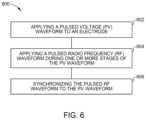
- FIG. 6is a flow diagram illustrating a method for synchronizing a PV waveform and a RF bias voltage waveform in the plasma processing system, according to one embodiment.
- Embodiments of the present disclosuregenerally relate to a system used in a semiconductor device manufacturing process. More specifically, embodiments provided herein generally include apparatus and methods for synchronizing and controlling the delivery of an RF bias voltage signal and a pulsed voltage waveform to one or more electrodes within a plasma processing chamber.
- FIG. 1is a schematic cross-sectional view of a plasma processing chamber assembly 10 configured to perform one or more of the plasma processing methods set forth herein.
- the plasma processing chamber assembly 10is configured for plasma-assisted etching processes, such as a reactive ion etch (RIE) plasma processing.
- RIEreactive ion etch
- the plasma processing chamber assembly 10can also be used in other plasma-assisted processes, such as plasma-enhanced deposition processes (for example, plasma-enhanced chemical vapor deposition (PECVD) processes, plasma-enhanced physical vapor deposition (PEPVD) processes, plasma-enhanced atomic layer deposition (PEALD) processes, plasma treatment processing, plasma-based ion implant processing, or plasma doping (PLAD) processing.
- PECVDplasma-enhanced chemical vapor deposition
- PVDplasma-enhanced physical vapor deposition
- PEALDplasma-enhanced atomic layer deposition
- PLAADplasma doping
- the plasma processing chamber assembly 10is configured to form a capacitively coupled plasma (CPP).
- a plasmamay alternately be generated by an inductively coupled source disposed over the processing region of the plasma processing chamber assembly 10 .
- a coilmay be placed on top of a ceramic lid (vacuum boundary) of the plasma processing chamber assembly 10 .
- the plasma processing chamber assembly 10includes a processing chamber 100 , a substrate support assembly 136 , a gas delivery system 182 , a DC power system 183 , an RF power system 189 , and a system controller 126 .
- the processing chamber 100includes a chamber body 113 that comprises a chamber lid 123 , one or more sidewalls 122 , and a chamber base 124 .
- the chamber lid 123 , one or more sidewalls 122 , and the chamber base 124collectively define the processing volume 129 .
- the one or more sidewalls 122 and chamber base 124generally include materials (such as aluminum, aluminum alloys, or stainless steel alloys) that are sized and shaped to form the structural support for the elements of the processing chamber 100 and are configured to withstand the pressures and added energy applied to them while a plasma 101 is generated within a vacuum environment maintained in the processing volume 129 of the processing chamber 100 during processing.
- a substrate 103is loaded into, and removed from, the processing volume 129 through an opening (not shown) in one of the sidewalls 122 . The opening is sealed with a slit valve (not shown) during plasma processing of the substrate 103 .
- a gas delivery system 182which is coupled to the processing volume 129 of the processing chamber 100 , includes a processing gas source 119 and a gas inlet 128 disposed through the chamber lid 123 .
- the gas inlet 128is configured to deliver one or more processing gases to the processing volume 129 from the plurality of processing gas sources 119 .
- the processing chamber 100further includes an upper electrode (e.g., a chamber lid 123 ) and a lower electrode (e.g., a substrate support assembly 136 ) disposed in a processing volume 129 .
- the upper electrode and lower electrodeare positioned to face each other.
- a radio frequency (RF) sourcee.g., RF power system 189
- the RF sourceis configured to deliver an RF signal to ignite and maintain a plasma (e.g., the plasma 101 ) between the upper and lower electrodes.
- the RF sourcee.g., RF power system 189
- the substrate support assembly 136includes a substrate support 105 , a substrate support base 107 , an insulator plate 111 , a ground plate 112 , a plurality of lift pins 186 , one or more substrate potential sensing assemblies 184 , and a bias electrode 104 .
- Each of the lift pins 186are disposed through a through hole 185 formed in the substrate support assembly 136 and are used to facilitate the transfer of a substrate 103 to and from a substrate receiving surface 105 A of the substrate support 105 .
- the substrate support 105is formed of a dielectric material.
- the dielectric materialcan include a bulk sintered ceramic material, a corrosion-resistant metal oxide (for example, aluminum oxide (AI 2 O 3 ), titanium oxide (TiO), yttrium oxide (Y 2 O 3 ), a metal nitride material (for example, aluminum nitride (AIN), titanium nitride (TiN)), mixtures thereof, or combinations thereof.
- a corrosion-resistant metal oxidefor example, aluminum oxide (AI 2 O 3 ), titanium oxide (TiO), yttrium oxide (Y 2 O 3 ), a metal nitride material (for example, aluminum nitride (AIN), titanium nitride (TiN)
- AINaluminum nitride
- TiNtitanium nitride
- the substrate support base 107is formed of a conductive material (for example aluminum, an aluminum alloy, or a stainless steel alloy).
- the substrate support base 107is electrically isolated from the chamber base 124 by the insulator plate 111 , and the ground plate 112 interposed between the insulator plate 111 and the chamber base 124 .
- the substrate support base 107is configured to regulate the temperature of both the substrate support 105 , and the substrate 103 disposed on the substrate support 105 during substrate processing.
- the substrate support base 107includes one or more cooling channels (not shown) disposed therein that are fluidly coupled to, and in fluid communication with, a coolant source (not shown), such as a refrigerant source or substrate source having a relatively high electrical resistance.
- the substrate support 105includes a heater (not shown) to heat the substrate support 105 and substrate 103 disposed on the substrate support 105 .
- a bias electrode 104is embedded in the dielectric material of the substrate support 105 .
- the bias electrode 104is formed of one or more electrically conductive parts.
- the electrically conductive partstypically include meshes, foils, plates, or combinations thereof.
- the bias electrode 104functions as a chucking pole (i.e., electrostatic chucking electrode) that is used to secure (e.g., electrostatically chuck) the substrate 103 to the substrate receiving surface 105 A of the substrate support 105 .
- a parallel plate like structureis formed by the bias electrode 104 and a layer of the dielectric material that is disposed between the bias electrode 104 and the substrate receiving surface 105 A.
- the dielectric materialcan typically have an effective capacitance CE of between about 5 nF and about 50 nF.
- the layer of dielectric materiale.g., aluminum nitride (AIN), aluminum oxide (AI 2 O 3 ), etc.
- the bias electrode 104is electrically coupled to a clamping network, which provides a chucking voltage thereto.
- the clamping networkincludes a DC voltage supply 173 (e.g., a high voltage DC supply) that is coupled to a filter 178 A of the filter assembly 178 that is disposed between the DC voltage supply 173 and bias electrode 104 .
- the filter 178 Ais a low-pass filter that is configured to block RF frequency and pulsed voltage (PV) waveform signals provided by other biasing components found within the processing chamber 100 from reaching the DC voltage supply 173 during plasma processing.
- the static DC voltageis between about ⁇ 5000V and about 5000V, and is delivered using an electrical conductor (such as a coaxial power delivery line 160 ).
- the bias electrode 104can also bias the substrate 103 with the respect to the plasma 101 using one or more of the pulsed-voltage biasing schemes described in further detail below.
- the substrate support assembly 136further includes an edge control electrode 115 .
- the edge control electrode 115is formed of one or more electrically conductive parts.
- the electrically conductive partstypically include meshes, foils, plates, or combinations thereof.
- the edge control electrode 115is positioned below the edge ring 114 and surrounds the bias electrode 104 and/or is disposed a distance from a center of the bias electrode 104 .
- the edge control electrode 115is annular in shape, is made from a conductive material, and is configured to surround at least a portion of the bias electrode 104 .
- the bias electrode 104when viewing the substrate supporting surface of the substrate support assembly 136 in a plan view, the bias electrode 104 is surrounded by or circumscribed by the edge control electrode 115 , and is not in direct electrical contact with the edge control electrode 115 .
- the edge control electrode 115is positioned within a region of the substrate support 105 , and is biased by use of a pulsed voltage (PV) waveform generator 175 .
- PVpulsed voltage
- the edge control electrode 115is biased by splitting part of the signal provided from the PV waveform generator 175 to the bias electrode 104 .
- the edge control electrode 115is coupled to and biased by use of a PV waveform generator 175 (not shown in FIG.
- the voltage waveform signals provided from the PV waveform generators 175can be separately adjusted, and thus have different waveform characteristics, while also being synchronized by use of a synchronization signal provided from the system controller 126 , or one of the RF or PV waveform generators, to allow the RF waveform to be provided during the same stage within the synchronized PV waveform pulses provided by each of the PV waveform generators 175 .
- the DC power system 183includes the DC voltage supply 173 , the PV waveform generator 175 , and a current source 177 .
- the RF power system 189includes a radio frequency (RF) waveform generator 171 , impedance matching circuit 172 , and a RF filter 174 .
- RFradio frequency
- a power delivery line 163electrically connects the output of the RF waveform generator 171 to an impedance matching circuit 172 , an RF filter 174 and substrate support base 107 .
- the DC voltage supply 173provides a constant chucking voltage
- the RF waveform generator 171delivers an RF signal to the processing region
- the PV waveform generator 175establishes a PV waveform at the bias electrode 104 .
- Applying a sufficient amount of RF power to an RF bias voltage signalwhich is also referred to herein as a RF waveform, is provided to an electrode (e.g., substrate support base 107 ) so as to cause the plasma 101 to be formed in the processing volume 129 of the processing chamber 100 .
- the RF waveformhas a frequency range between about 1 MHz and about 200 MHz, such as between 2 MHz and 40 MHz.
- the DC power system 183further includes a filter assembly 178 to electrically isolate one or more of the components contained within the DC power system 183 .
- Power delivery line 160electrically connects the output of the DC voltage supply 173 to a filter assembly 178 .
- Power delivery line 161electrically connects the output of the PV waveform generator 175 to the filter assembly 178 .
- Power delivery line 162connects the output of the current source 177 to the filter assembly 178 .
- the current source 177is selectively coupled to the bias electrode 104 by use of a switch (not shown) disposed in the power delivery line 162 , so as to allow the current source 177 to deliver a desired current to the bias electrode 104 during one or more stages (e.g., ion current stage) of the voltage waveform generated by the PV waveform generator 175 .
- the filter assembly 178includes multiple separate filtering components (i.e., discrete filters 178 A- 178 C) that are each electrically coupled to the output node via power delivery line 164 .
- the filter assembly 178includes one common filter electrically coupled to the output node via power delivery line 164 .
- the power delivery lines 160 - 164include electrical conductors that include a combination of coaxial cables, such as a flexible coaxial cable that is connected in series with a rigid coaxial cable, an insulated high-voltage corona-resistant hookup wire, a bare wire, a metal rod, an electrical connector, of any combination of the above.
- the system controller 126also referred to herein as a processing chamber controller, includes a central processing unit (CPU) 133 , a memory 134 , and support circuits 135 .
- the system controller 126is used to control the process sequence used to process the substrate 103 .
- the CPUis a general-purpose computer processor configured for use in an industrial setting for controlling the processing chamber and sub-processors related thereto.
- the memory 134 described herein, which is generally non-volatile memory,can include random access memory, read-only memory, hard disk drive, or other suitable forms of digital storage, local or remote.
- the support circuits 135are conventionally coupled to the CPU 133 and comprises cache, clock circuits, input/output subsystems, power supplies, and the like, and combinations thereof.
- Software instructions (program) and datacan be coded and stored within the memory 134 for instructing a processor within the CPU 133 .
- a software program (or computer instructions) readable by CPU 133 in the system controller 126determines which tasks are performable by the components in the plasma processing chamber assembly 10 .
- the programwhich is readable by the CPU 133 in the system controller 126 includes code, which, when executed by the CPU 133 , performs tasks relating to the plasma processing schemes described herein.
- the programmay include instructions that are used to control the various hardware and electrical components within the plasma processing chamber assembly 10 to perform the various process tasks and various process sequences used to implement the methods described herein.
- the programincludes instructions that are used to perform one or more of the operations described below in relation to FIGS. 9 and 10 .
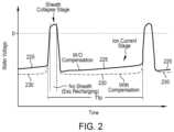
- FIG. 2illustrates two separate voltage waveforms established at a substrate 103 disposed on the substrate receiving surface 105 A of the substrate support assembly 136 of a processing chamber due to the delivery of pulsed voltage waveforms to the bias electrode 104 of the processing chamber, according to one or more embodiments.
- Waveform 225is an example of a non-compensated pulsed voltage (PV) waveform established at the substrate 103 during plasma processing.
- Waveform 230is an example of a compensated pulsed voltage (PV) waveform established at the substrate 103 by applying a negative slope waveform to the bias electrode 104 of the processing chamber during an “ion current stage” portion of the PV waveform cycle by use of the current source 177 .
- the compensated pulsed voltage (PV) waveformcan alternatively be established by applying a negative voltage ramp during the ion current stage of the pulsed voltage waveform generated by the PV waveform generator 175 .
- waveforms 225 , and 230include two main stages: an ion current stage and a sheath collapse stage. Both portions (the ion current stage and the sheath collapse stage) of the waveforms 225 and 230 , can be alternately and/or separately established at the substrate 103 during plasma processing.
- a drop in voltage at the substrate 103is created, due to the delivery of a negative portion of a PV waveform (e.g., ion current portion) provided to the bias electrode 104 by the PV waveform generator 175 , which creates a high voltage sheath above the substrate 103 .
- a PV waveforme.g., ion current portion
- the ion current stagemay generally include a region of a pulsed voltage waveform that achieves a voltage at the substrate that is stable or minimally varying throughout the stage, as illustrated in FIG. 2 by waveform 230 .
- FIG. 3 Ais a plot 301 of a forward RF voltage waveform 331 and an inter-modulation distortion (IMD) generated RF voltage waveform 326 measured along a transmission line, such as transmission line 163 or 166 in FIG. 1 .
- the plot 301was generated from measurements made at a frequency of 40 MHz +/ ⁇ 400 kHz at a node within the RF power system 189 due to the delivery and interaction created between an RF voltage waveform 326 provided from the RF power system 189 at a frequency of about 40.68 MHz and a pulsed voltage waveforms provided from the DC power system 183 , which are both illustrated in FIG. 3 B .
- the plot 301includes an envelope 370 of the forward RF voltage waveform 331 , and an envelope 376 of the IMD generated RF voltage waveform 326 all created by an interaction between the delivery of RF bias voltage waveform provided from the components within a RF power system 189 and pulsed voltage waveforms provided from the PV waveform generator of the DC power system 183 .
- the forward RF voltage waveform 331is applied to the load (e.g., gas) in the processing volume 129 of the processing chamber 100 through the transmission line, such as transmission line 165 ( FIG. 1 ). If the impedance of the load is not properly matched to impedance of the source (e.g., RF signal generator), a portion of the waveform can reflect back in the opposite direction along the same transmission line.
- the loade.g., gas
- the transmission line 165FIG. 1
- the impedance matching circuit 172and/or adjusting the frequency of the RF bias waveform supplied by the RF waveform generator 171 to match the impedance of the load to the source during plasma processing.
- the forward RF voltage and reflected RF voltageare measured at the driven RF frequency at a node within the RF power system 189 .
- Measurements made using a conventional RF power delivery system using a conventional RF power delivery methodallows the formation of the envelope 370 of the forward RF voltage waveform 331 and the envelope 376 of the IMD generated RF voltage waveform 326 that is not at one of the harmonic frequencies of the driven RF frequency.
- the magnitude of the envelope 376 of the IMD generated RF voltage waveform 326undesirably varies over time and varies from a point that is near the magnitude of the envelope 370 of the forward RF voltage waveform 331 to a magnitude of the envelope 376 of the IMD generated RF voltage waveform 326 that is near a zero RF power.
- FIG. 3 Billustrates an example of a pulsed voltage waveform 321 delivered to the bias electrode 104 ( FIG. 1 ) and a pulsed voltage waveform 322 delivered to the edge control electrode 115 ( FIG. 1 ) that both further include a higher frequency of a RF voltage waveform 326 (e.g., 40 MHz RF signal) impressed on top of the pulsed voltage waveforms 321 and 322 .
- the pulsed voltage waveformsinclude two main stages: an ion current stage, and a sheath collapse stage. Both portions (the ion current stage and the sheath collapse stage) of the pulsed voltage waveforms, are established at the substrate 103 during plasma processing.
- the etching processprimarily occurs during the second stage (e.g., the ion current stage) of the pulsed voltage waveform.
- FIG. 4is a chart illustrating the percentage of wide-band reflection as seen in two different conventional plasma processing chambers. Wide-band reflection percentage is used to measure the amount of reflected power (i.e., amount of power that was not provided to the load), due to IMD and harmonic reflections found in the plasma processing system, versus the amount of forward RF power provided from the RF source. Curve 405 illustrates the percentage of reflected RF power as function of the magnitude of the pulsed voltage waveform applied to an electrode within a first processing chamber 460 .
- Curve 410illustrates the percentage of reflected RF power as function of the magnitude of the pulsed voltage waveform applied to an electrode within a second processing chamber 470 , wherein the first and second processing chambers are substantially similarly configured and the plotted results were created by performing the same plasma processing recipes in each processing chamber.
- the percentage of RF power delivered to the loadwill vary from chamber to chamber, and especially at high pulsed waveform voltages.
- the percentage of energy lost to IMDincreases as the voltage level of a pulsed voltage waveform voltage is increased, which is determined by the magnitude of the voltage established at the substrate during the ion current stage of the pulsed voltage waveform.
- Both curves 405 and 410increase to a maximum percentage between about 4kV and 8 kV.
- a plasma processthat included the delivery of an RF power of about 1500 W, a chamber pressure of 9 mTorr, a pulsed voltage repetition frequency of 1000 Hz, and 59% DC power duty cycle, the percentage of energy lost to IMD seen within RF power delivery components in the first processing chamber 460 increased from about 2kV to a peak at about 4.5kV, and then started to fall off at voltages greater than 4.5 kV.
- the percentage of reflected RF power formed in the second processing chamber 470increases from about 2kV to about 6kV, and then falls off at about 7kV.
- the difference in the reflected RF between the first processing chamber 460 to the second processing chamber 470can be about 8 percent at the more desirable higher pulsed waveform voltage levels.
- FIG. 5 Aillustrates a pulsed RF waveform 501 applied to an electrode disposed within a processing chamber.
- the pulsed RF waveform 501includes two stages: a RF power delivery stage 512 in which RF power is provided to an electrode within the processing chamber for a first period time (T ON ) and a RF power “off” stage 517 in which no RF power is provided to the electrode for a second period of time (T OFF ).
- FIG. 5 Billustrates a plot of a pulsed voltage waveform and the pulsed RF bias voltage signal that are combined due to the delivery of the delivery of the pulsed RF bias voltage signal illustrated in FIG. 5 A and a pulsed voltage waveforms 521 and 522 , according to one embodiment.
- the pulsed voltage waveforms 521 and 522are provided to one or more electrodes within the processing chamber, such as the bias electrode 104 and edge control electrode 115 , respectively.
- the pulsed RF waveform 501is synchronized with the delivery of at least one of the pulsed voltage waveforms 521 and 522 , and overlaps with at least a portion of the pulsed voltage waveforms during the ion current stage.
- the RF power delivery stage 512and thus the only time the impedance matching circuit 172 is utilized to deliver the RF power provided from the RF waveform generator 171 is during the stable portion of the provided pulsed voltage waveform.
- the delivery of the RF power during the stable, and from an RIE etching point of view the key stage in which most of the etching occurs,will prevent the impedance matching circuit 172 from trying to find a match point when the impedance of the load is rapidly changing between and during the different stages of the delivery of the pulsed voltage waveform. It is believed that by pulsing the RF waveform on during the ion current stage, and off during the sheath collapse stage will improve the performance of the impedance matching circuit by limiting the amount of impedance variation seen by the impedance matching circuit 172 when the RF power is provided to an electrode within the processing chamber 100 . Thus, if the RF power is not pulsed, and maintained at a constant power as shown in FIG.
- the pulsed RF waveform 501comprises an RF signal that is provided for a significant portion of the ion current stage of the pulsed voltage waveform.
- the duration of the RF power delivery stage 512is configured to last the complete length of the ion current stage.
- the RF power provided during the RF power delivery stage 512is synchronized, by use of the system controller 126 , so that the RF power is provided within a region of the pulsed voltage waveform that extends between the ion current stage start 332 and the ion current stage end 333 .
- the PV waveform generator, and the RF power sourcebehave in master slave relationship.
- the masterwill provide a timing signal (e.g., square wave TTL signal) that triggers the slave to deliver a waveform at a desired time.
- the PV waveform generatoris the master and the RF power source is the slave so that the RF waveform is delivered during a desired portion of the PV waveform.
- the RF power sourceis the master, and the PV waveform generator is the slave so that the PV waveform signal is delivered during a desired portion of the RF waveform.
- the ion energy distribution function(IEDF) will be narrower than the case where the RF waveform is delivered during ion current stage, since the energy broadening effect provided to the ions in the plasma due to the delivery of the RF waveform not occurring while the sheath is formed, which is the stage where the plasma generated ions are being accelerated towards the substrate surface.
- IEDFion energy distribution function
- the pulsed RF waveform 501is synchronized with the delivery of at least one of the pulsed voltage waveforms 521 and 522 , and overlaps with at least a portion of the pulsed voltage waveforms during the sheath collapse stage.
- the performance of the impedance matching circuitwill improve by limiting the amount of impedance variation seen by the impedance matching circuit 172 when the RF power is provided to an electrode within the processing chamber 100 .
- the pulsed RF waveform 501comprises an RF signal that is provided for a significant portion of the sheath collapse stage of the pulsed voltage waveform.
- the duration of the RF power delivery stage 512is configured to only include a portion of the duration of the ion current stage.
- the RF power delivery stage 512is synchronized, by use of the system controller 126 , so that RF power is delivered after a first time delay (T DELAY ) has elapsed from the ion current stage start 332 and is stopped so that a second time delay (T PD ), or post-RF power delivery time delay, can elapse before the ion current stage end 333 has been reached and the next pulsed voltage waveform starts to be generated by the PV waveform generator 175 .
- T DELAYfirst time delay
- T PDsecond time delay
- the first time delay (T DELAY )can vary from about 1% to about 20% of the total length of the ion current stage of the pulsed voltage waveform, and can be helpful to reduce the variation in the IMD generated reflected power generated during the delivery of the RF waveform due to the natural variation (i.e., “ringing”) found in the pulsed voltage waveform during the transition from the sheath collapse stage to the ion current stage.
- the second time delay (T PD )can vary from about 0% to about 10% of the total length of the ion current stage of the pulsed voltage waveform, and can be helpful to reduce any variation in the IMD generated reflected power due to the variation in the start to the transition from the ion current stage to the sheath collapse stage.
- the second time delay (T PD )is between 0.1% and 10% of the total length of the ion current stage of the pulsed voltage waveform.
- the ion current stageaccounts for between about 30% and about 95% of the total period (T TP ) of the pulsed voltage waveform, and is typically greater than about 80 % of the total period of the pulsed voltage waveform.
- the pulsed voltage waveformcan include a series of voltage pulses that are delivered at a repetition frequency that is greater than or equal to 100 kHz, such as greater than 200 kHz, or greater than 400 kHz, or even in a range between 100 kHz and 500 kHz.
- the total period (T TP ) of the pulsed voltage waveformis about 2.5 microseconds ( ⁇ s). Whether the RF waveform is provided during the sheath collapse stage or the ion current stage, the IMD power back to the generator can be greatly reduced, for example by more than five times, which can allow the generator to reach higher delivered power before stressing the output amplifier components within the generator.
- FIG. 6is a diagram illustrating a method for synchronizing the PV waveform and the RF waveform in the plasma processing chamber, such as the processing chamber 100 of FIG. 1 .
- the method 600includes a method of processing a substrate by applying a PV waveform to an electrode, applying a pulsed RF waveform to an electrode, and synchronizing the pulsed RF waveform to the PV waveform.
- the method 600includes applying a PV waveform to an electrode, such as the bias electrode 104 .
- the PV waveformcan include a series of voltage pulses, wherein each pulse of the series of pulse includes a first stage and a second stage.
- the first stageincludes a sheath collapse stage
- the second stageincludes an ion current stage that are established at the substrate during processing.
- the sheath collapse stageincludes a large capacitance measured at the substrate, while the ion current stage includes a small capacitance measured at the substrate.
- the method 600includes generating a plasma in a processing volume of a processing chamber.
- a pulsed RF waveformis used to ignite one or more gas species flowed into the processing volume 129 of a processing chamber 100 to form a plasma over a substrate disposed on a supporting surface of a substrate support by delivering an RF signal to one or more electrodes within the processing chamber 100 .
- the RF waveform 501includes an RF signal that has a frequency between 1 MHz and 60 MHz.
- the RF waveform 501includes an RF signal that has a frequency of 40 MHz. Activities 602 and 604 can be completed substantially simultaneously, or in any desired order.
- the method 600includes synchronizing the pulsed RF waveform with the PV waveform.
- the pulsed RF waveformis pulsed so that the RF power delivery stage 512 of the pulsed RF waveform is synchronized with at least one stage of PV waveform.
- the system controller 126delivers one or more control signals to the RF waveform generator 171 and a PV waveform generator 175 so that the timing of the delivery of each of the waveforms generated by these components can be synchronized, such as synchronized as similarly described above in relation to FIG. 5 A- 5 B .
- the RF waveform generator 171acts as a master device and thus sends a control signal to a PV waveform generator 175 so that the timing of the delivery of each of the waveforms generated by these components can be synchronized.
- the PV waveform generator 175acts as a master device and thus sends a control signal to the RF waveform generator 171 so that the timing of the delivery of each of the waveforms generated by these components can be synchronized.
- the activities performed in method 600can be performed for a period of time to allow a desirable plasma process to be performed on a substrate disposed within the plasma processing chamber.
Landscapes
- Physics & Mathematics (AREA)
- Engineering & Computer Science (AREA)
- Plasma & Fusion (AREA)
- Chemical & Material Sciences (AREA)
- Analytical Chemistry (AREA)
- Plasma Technology (AREA)
- Drying Of Semiconductors (AREA)
- Chemical Vapour Deposition (AREA)
Abstract
Description
This application claims the benefit of United States provisional patent application Ser. No. 63/287,433, filed Dec. 8, 2021, which is herein incorporated by reference.
Embodiments of the present disclosure generally relate to a system and methods used in semiconductor device manufacturing. More specifically, embodiments provided herein generally include a system and methods for synchronizing a radio frequency (RF) pulsed waveform with a pulsed voltage (PV) waveform to one or more electrodes within a processing chamber.
Reliably producing high aspect ratio features is one of the key technology challenges for the next generation of semiconductor devices. One method of forming high aspect ratio features uses a plasma assisted etching process, such as a reactive ion etch (RIE) plasma process, to form high aspect ratio openings in a material layer, such as a dielectric layer, of a substrate. In a typical RIE plasma process, a plasma is formed in a processing chamber and ions from the plasma are accelerated towards a surface of a substrate to form openings in a material layer disposed beneath a mask layer formed on the surface of the substrate.
A typical Reactive Ion Etch (RIE) plasma processing chamber includes a radio frequency (RF) bias generator, which supplies an RF voltage to a power electrode. In a capacitively coupled gas discharge, the plasma is created by using a radio frequency (RF) generator that is coupled to the power electrode that is disposed within an electrostatic chuck (ESC) assembly or within another portion of the processing chamber. Typically, an RF matching network (“RF match”) tunes an RF waveform provided from an RF generator to deliver RF power to an apparent load of 500 to minimize the reflected power and maximize the power delivery efficiency. If the impedance of the load is not properly matched to impedance of the source (e.g., the RF generator), a portion of the forward delivered RF waveform can reflect back in the opposite direction along the same transmission line.
A number of plasma processes also utilize DC voltage pulsing schemes to control the plasma sheath disposed over the substrate that is being processed. During operation, the DC voltage pulses cause a generated plasma sheath to toggle between states that includes a thick plasma sheath and state where no plasma sheath exists. Typical, DC pulsing techniques are configured to deliver voltage pulses at a frequency greater than 50 kHz, such as greater than 400 kHz. The toggling of the plasma sheath due to the delivery DC pulsed voltage waveform results in the plasma load having different impedance values over time. It has been found that due to the interaction between the RF waveform and DC pulsed voltage waveform that are simultaneously provided during plasma processing can lead differing plasma processing results due in large part to the RF matching portion of the of the RF power delivery system's inability to adjust the RF matching point to account for the rapidly changing plasma load impedance values over time. Conventional impedance matching components and matching processes are unable to keep up with the rapid changes in magnitude of the plasma load impedance, thus causing the match to find undesirable matching points that typically leads to the generation of varying amounts of RF power that are actually delivered to the plasma load due to 1) inter-modulation distortion (IMD) of the RF signal, and 2) undesirably high reflected RF powers found at harmonics of the driven RF frequency. The inter-modulation distortion created by the interaction between the RF and DC pulsed voltage waveforms causes the amplitude of at least the RF signal to vary over time. The interaction or intermodulation between the RF and DC pulsed voltage waveforms causes additional undesirable waveform components to form at frequencies that are not just at harmonic frequencies (i.e., integer multiples) of the interacting signals, such as either of the RF or DC pulsed waveforms. The generation of the IMD components in a power delivery system will reduce the actual forward RF power that is delivered to the plasma load. Due at least to unavoidable differences in processing chamber power delivery configurations and differences in the power delivery components, the rapidly changing plasma load impedance values cause undesirable differences in the plasma processing results seen in a single plasma processing chamber, seen in similarly configured processing chambers on a single processing system, and also seen in similarly configured plasma processing chambers within different plasma processing systems within a semiconductor fabrication site. Moreover, the generated IMD components are also not easily accounted for in most power delivery systems due to the broad range of frequencies that can develop during plasma processing in the same or different processing chambers and thus will cause unexpected variations in the power actually delivered to the plasma load during plasma processing.
Thus, there is a need in the art for plasma processing devices and biasing methods that are at least able to resolve these issues outlined above.
The present disclosure generally relates to a method for plasma processing comprising applying a voltage waveform to an electrode disposed in a substrate support, the voltage waveform having a first stage and a second stage, wherein the first stage includes a sheath collapse stage, and the second stage includes an ion current stage. The method further includes applying a pulsed radio frequency (RF) waveform to a reactive species to generate a plasma in a processing region of a processing chamber, and synchronizing the pulsed RF waveform to the voltage waveform such that the pulsed RF waveform is provided during one of the stages and not the other stage. In one embodiment, the pulsed RF waveform is provided during the second stage and not the first stage. In another embodiment, the pulsed RF waveform is provided during the first stage and not the second stage.
The present disclosure generally relates to a method for plasma processing comprising applying a voltage waveform to an electrode disposed in a substrate support, the voltage waveform having a first stage and a second stage, wherein the first stage includes a sheath collapse stage, and the second stage includes an ion current stage. The method further includes applying a pulsed radio frequency (RF) waveform to a reactive species to generate a plasma in a processing region of a processing chamber, and synchronizing the pulsed RF waveform to the voltage waveform such that the pulsed RF waveform is provided during one stage and not the other stage.
The present disclosure further includes a plasma processing system comprising a PV waveform generator coupled to a first electrode, a RF waveform generator coupled to a second electrode of the plasma processing system, wherein the RF waveform generator is configured to generate a plasma within the processing region, an impedance matching circuit, and a controller having a processor configured to execute computer readable instructions that cause the system to apply a PV waveform generated by the PV waveform generator, apply a RF waveform generated by the RF waveform generator and synchronize the PV waveform to the RF waveform.
Embodiments of the disclosure provide a method for plasma processing comprising applying a pulsed voltage waveform to one or more electrodes disposed in a substrate support, the voltage waveform having a first stage and a second stage, applying a pulsed radio frequency (RF) waveform to the one or more electrodes to generate a plasma in a processing region of a processing chamber, and synchronizing the pulsed RF waveform with each pulse of the pulsed voltage waveform, such that an RF waveform of the pulsed radio frequency (RF) waveform is provided only during at least a portion of the second stage of each pulse of the pulsed voltage waveform.
Embodiments of the disclosure provide a method for plasma processing comprising applying a pulsed voltage waveform to one or more electrodes disposed in a substrate support, the voltage waveform having a first stage and a second stage, applying a pulsed radio frequency (RF) waveform to the one or more electrodes to generate a plasma in a processing region of a processing chamber, and synchronizing the pulsed RF waveform with each pulse of the pulsed voltage waveform, such that an RF waveform of the pulsed radio frequency (RF) waveform is provided only during at least a portion of the first stage of each pulse of the pulsed voltage waveform.
Embodiments of the disclosure provide a plasma processing system, comprising a pulsed voltage waveform generator coupled to a first electrode; a radio frequency waveform generator coupled to a second electrode, wherein the radio frequency waveform generator is configured to generate a plasma within a processing volume of the plasma processing system; an impedance matching circuit coupled between the radio frequency waveform generator and the second electrode; and a controller. The controller having a processor configured to execute computer-readable instructions stored within memory that cause the system to: apply, by use of the pulsed voltage waveform generator, a pulsed voltage waveform to the first electrode, the pulsed voltage waveform comprising a series of voltage pulses that each comprise a first stage and a second stage; apply, by use of the radio frequency waveform generator, a pulsed radio frequency waveform to the second electrode to generate a plasma in a processing region of a processing chamber; and synchronize the pulsed RF waveform with each pulse of the pulsed voltage waveform, such that an RF waveform of the pulsed radio frequency (RF) waveform is provided only during at least a portion of the second stage of each pulse of the pulsed voltage waveform.
So that the manner in which the above recited features of the present disclosure can be understood in detail, a more particular description of the disclosure, briefly summarized above, may be had by reference to embodiments, some of which are illustrated in the appended drawings. It is to be noted, however, that the appended drawings illustrate only exemplary embodiments and are therefore not to be considered limiting of its scope, may admit to other equally effective embodiments.
To facilitate understanding, identical reference numerals have been used, where possible, to designate identical elements that are common to the figures. It is contemplated that elements and features of one embodiment may be beneficially incorporated in other embodiments without further recitation.
Embodiments of the present disclosure generally relate to a system used in a semiconductor device manufacturing process. More specifically, embodiments provided herein generally include apparatus and methods for synchronizing and controlling the delivery of an RF bias voltage signal and a pulsed voltage waveform to one or more electrodes within a plasma processing chamber.
The plasmaprocessing chamber assembly 10 includes aprocessing chamber 100, asubstrate support assembly 136, agas delivery system 182, aDC power system 183, anRF power system 189, and asystem controller 126. Theprocessing chamber 100 includes achamber body 113 that comprises achamber lid 123, one or more sidewalls122, and achamber base 124. Thechamber lid 123, one or more sidewalls122, and thechamber base 124 collectively define theprocessing volume 129. The one or more sidewalls122 andchamber base 124 generally include materials (such as aluminum, aluminum alloys, or stainless steel alloys) that are sized and shaped to form the structural support for the elements of theprocessing chamber 100 and are configured to withstand the pressures and added energy applied to them while aplasma 101 is generated within a vacuum environment maintained in theprocessing volume 129 of theprocessing chamber 100 during processing. Asubstrate 103 is loaded into, and removed from, theprocessing volume 129 through an opening (not shown) in one of thesidewalls 122. The opening is sealed with a slit valve (not shown) during plasma processing of thesubstrate 103. Agas delivery system 182, which is coupled to theprocessing volume 129 of theprocessing chamber 100, includes aprocessing gas source 119 and agas inlet 128 disposed through thechamber lid 123. Thegas inlet 128 is configured to deliver one or more processing gases to theprocessing volume 129 from the plurality of processinggas sources 119.
Theprocessing chamber 100 further includes an upper electrode (e.g., a chamber lid123) and a lower electrode (e.g., a substrate support assembly136) disposed in aprocessing volume 129. The upper electrode and lower electrode are positioned to face each other. As seen inFIG.1 , in one embodiment, a radio frequency (RF) source (e.g., RF power system189) is electrically coupled to the lower electrode. The RF source is configured to deliver an RF signal to ignite and maintain a plasma (e.g., the plasma101) between the upper and lower electrodes. In some alternative configurations, the RF source (e.g., RF power system189) can also be electrically coupled to the upper electrode as shown inFIG.1 .
Thesubstrate support assembly 136 includes asubstrate support 105, asubstrate support base 107, aninsulator plate 111, aground plate 112, a plurality of lift pins186, one or more substrate potential sensing assemblies184, and abias electrode 104. Each of the lift pins186 are disposed through a through hole185 formed in thesubstrate support assembly 136 and are used to facilitate the transfer of asubstrate 103 to and from asubstrate receiving surface 105A of thesubstrate support 105. Thesubstrate support 105 is formed of a dielectric material. The dielectric material can include a bulk sintered ceramic material, a corrosion-resistant metal oxide (for example, aluminum oxide (AI2O3), titanium oxide (TiO), yttrium oxide (Y2O3), a metal nitride material (for example, aluminum nitride (AIN), titanium nitride (TiN)), mixtures thereof, or combinations thereof.
Thesubstrate support base 107 is formed of a conductive material (for example aluminum, an aluminum alloy, or a stainless steel alloy). Thesubstrate support base 107 is electrically isolated from thechamber base 124 by theinsulator plate 111, and theground plate 112 interposed between theinsulator plate 111 and thechamber base 124. In some embodiments, thesubstrate support base 107 is configured to regulate the temperature of both thesubstrate support 105, and thesubstrate 103 disposed on thesubstrate support 105 during substrate processing. In some embodiments, thesubstrate support base 107 includes one or more cooling channels (not shown) disposed therein that are fluidly coupled to, and in fluid communication with, a coolant source (not shown), such as a refrigerant source or substrate source having a relatively high electrical resistance. In other embodiments, thesubstrate support 105 includes a heater (not shown) to heat thesubstrate support 105 andsubstrate 103 disposed on thesubstrate support 105.
Abias electrode 104 is embedded in the dielectric material of thesubstrate support 105. Typically, thebias electrode 104 is formed of one or more electrically conductive parts. The electrically conductive parts typically include meshes, foils, plates, or combinations thereof. Here, thebias electrode 104 functions as a chucking pole (i.e., electrostatic chucking electrode) that is used to secure (e.g., electrostatically chuck) thesubstrate 103 to thesubstrate receiving surface 105A of thesubstrate support 105. In general, a parallel plate like structure is formed by thebias electrode 104 and a layer of the dielectric material that is disposed between thebias electrode 104 and thesubstrate receiving surface 105A. The dielectric material can typically have an effective capacitance CE of between about 5 nF and about 50 nF. Typically, the layer of dielectric material (e.g., aluminum nitride (AIN), aluminum oxide (AI2O3), etc.) has a thickness between about 0.03 mm and about 5 mm, such as between about 0.1 mm and about 3 mm, such as between about0.1 mm and about 1 mm, or even between about 0.1 mm and 0.5 mm. Thebias electrode 104 is electrically coupled to a clamping network, which provides a chucking voltage thereto. The clamping network includes a DC voltage supply173 (e.g., a high voltage DC supply) that is coupled to afilter 178A of thefilter assembly 178 that is disposed between theDC voltage supply 173 andbias electrode 104. In one example, thefilter 178A is a low-pass filter that is configured to block RF frequency and pulsed voltage (PV) waveform signals provided by other biasing components found within theprocessing chamber 100 from reaching theDC voltage supply 173 during plasma processing. In one configuration, the static DC voltage is between about −5000V and about 5000V, and is delivered using an electrical conductor (such as a coaxial power delivery line160). In some embodiments, thebias electrode 104 can also bias thesubstrate 103 with the respect to theplasma 101 using one or more of the pulsed-voltage biasing schemes described in further detail below.
In some configurations, thesubstrate support assembly 136, further includes anedge control electrode 115. Theedge control electrode 115 is formed of one or more electrically conductive parts. The electrically conductive parts typically include meshes, foils, plates, or combinations thereof. Theedge control electrode 115 is positioned below theedge ring 114 and surrounds thebias electrode 104 and/or is disposed a distance from a center of thebias electrode 104. In general, for aprocessing chamber 100 that is configured to process circular substrates, theedge control electrode 115 is annular in shape, is made from a conductive material, and is configured to surround at least a portion of thebias electrode 104. In one configuration, when viewing the substrate supporting surface of thesubstrate support assembly 136 in a plan view, thebias electrode 104 is surrounded by or circumscribed by theedge control electrode 115, and is not in direct electrical contact with theedge control electrode 115. As seen inFIG.1 , theedge control electrode 115 is positioned within a region of thesubstrate support 105, and is biased by use of a pulsed voltage (PV)waveform generator 175. In one configuration, as schematically shown inFIG.1 , theedge control electrode 115 is biased by splitting part of the signal provided from thePV waveform generator 175 to thebias electrode 104. In another configuration, theedge control electrode 115 is coupled to and biased by use of a PV waveform generator175 (not shown inFIG.1 ) that is different from thePV waveform generator 175 used tobias electrode 104. In this configuration, the voltage waveform signals provided from thePV waveform generators 175 can be separately adjusted, and thus have different waveform characteristics, while also being synchronized by use of a synchronization signal provided from thesystem controller 126, or one of the RF or PV waveform generators, to allow the RF waveform to be provided during the same stage within the synchronized PV waveform pulses provided by each of thePV waveform generators 175.
TheDC power system 183 includes theDC voltage supply 173, thePV waveform generator 175, and acurrent source 177. TheRF power system 189 includes a radio frequency (RF)waveform generator 171,impedance matching circuit 172, and aRF filter 174. In one example, as shown inFIG.1 , apower delivery line 163 electrically connects the output of theRF waveform generator 171 to animpedance matching circuit 172, anRF filter 174 andsubstrate support base 107. As previously mentioned, during plasma processing, theDC voltage supply 173 provides a constant chucking voltage, while theRF waveform generator 171 delivers an RF signal to the processing region, and thePV waveform generator 175 establishes a PV waveform at thebias electrode 104. Applying a sufficient amount of RF power to an RF bias voltage signal, which is also referred to herein as a RF waveform, is provided to an electrode (e.g., substrate support base107) so as to cause theplasma 101 to be formed in theprocessing volume 129 of theprocessing chamber 100. In one configuration, the RF waveform has a frequency range between about 1 MHz and about 200 MHz, such as between 2 MHz and 40 MHz.
In some embodiments, theDC power system 183 further includes afilter assembly 178 to electrically isolate one or more of the components contained within theDC power system 183.Power delivery line 160 electrically connects the output of theDC voltage supply 173 to afilter assembly 178.Power delivery line 161 electrically connects the output of thePV waveform generator 175 to thefilter assembly 178.Power delivery line 162 connects the output of thecurrent source 177 to thefilter assembly 178. In some embodiments, thecurrent source 177 is selectively coupled to thebias electrode 104 by use of a switch (not shown) disposed in thepower delivery line 162, so as to allow thecurrent source 177 to deliver a desired current to thebias electrode 104 during one or more stages (e.g., ion current stage) of the voltage waveform generated by thePV waveform generator 175. As seen inFIG.1 , thefilter assembly 178, includes multiple separate filtering components (i.e.,discrete filters 178A-178C) that are each electrically coupled to the output node viapower delivery line 164. In an alternative configuration, thefilter assembly 178 includes one common filter electrically coupled to the output node viapower delivery line 164. The power delivery lines160-164 include electrical conductors that include a combination of coaxial cables, such as a flexible coaxial cable that is connected in series with a rigid coaxial cable, an insulated high-voltage corona-resistant hookup wire, a bare wire, a metal rod, an electrical connector, of any combination of the above.
Thesystem controller 126, also referred to herein as a processing chamber controller, includes a central processing unit (CPU)133, amemory 134, and supportcircuits 135. Thesystem controller 126 is used to control the process sequence used to process thesubstrate 103. The CPU is a general-purpose computer processor configured for use in an industrial setting for controlling the processing chamber and sub-processors related thereto. Thememory 134 described herein, which is generally non-volatile memory, can include random access memory, read-only memory, hard disk drive, or other suitable forms of digital storage, local or remote. Thesupport circuits 135 are conventionally coupled to theCPU 133 and comprises cache, clock circuits, input/output subsystems, power supplies, and the like, and combinations thereof. Software instructions (program) and data can be coded and stored within thememory 134 for instructing a processor within theCPU 133. A software program (or computer instructions) readable byCPU 133 in thesystem controller 126 determines which tasks are performable by the components in the plasmaprocessing chamber assembly 10.
Typically, the program, which is readable by theCPU 133 in thesystem controller 126 includes code, which, when executed by theCPU 133, performs tasks relating to the plasma processing schemes described herein. The program may include instructions that are used to control the various hardware and electrical components within the plasmaprocessing chamber assembly 10 to perform the various process tasks and various process sequences used to implement the methods described herein. In one embodiment, the program includes instructions that are used to perform one or more of the operations described below in relation toFIGS.9 and10 .
InFIG.2 waveforms waveforms substrate 103 during plasma processing. At the beginning of the ion current stage, a drop in voltage at thesubstrate 103 is created, due to the delivery of a negative portion of a PV waveform (e.g., ion current portion) provided to thebias electrode 104 by thePV waveform generator 175, which creates a high voltage sheath above thesubstrate 103. The high voltage sheath allows the plasma generated positive ions to be accelerated towards the biased substrate during the ion current stage, and thus, for RIE processes, controls the amount and characteristics of the etching process that occurs on the surface of the substrate during plasma processing. In some embodiments, it is desirable for the ion current stage to generally include a region of a pulsed voltage waveform that achieves a voltage at the substrate that is stable or minimally varying throughout the stage, as illustrated inFIG.2 bywaveform 230. One will note that significant variations in voltage established at the substrate during the ion current stage, such as shown by the positive slope in thewaveform 225, will undesirably cause a variation in the ion energy distribution (IED) and thus cause undesirable characteristics of the etched features to be formed in the substrate during an RIE process.
During processing, the forwardRF voltage waveform 331 is applied to the load (e.g., gas) in theprocessing volume 129 of theprocessing chamber 100 through the transmission line, such as transmission line165 (FIG.1 ). If the impedance of the load is not properly matched to impedance of the source (e.g., RF signal generator), a portion of the waveform can reflect back in the opposite direction along the same transmission line. Thus, to prevent a substantial portion of the waveform from reflecting back along the transmission line, it is necessary to find a match impedance by adjusting one or more of the components with theimpedance matching circuit 172 and/or adjusting the frequency of the RF bias waveform supplied by theRF waveform generator 171 to match the impedance of the load to the source during plasma processing. To properly match the impedance, the forward RF voltage and reflected RF voltage are measured at the driven RF frequency at a node within theRF power system 189. Measurements made using a conventional RF power delivery system using a conventional RF power delivery method allows the formation of theenvelope 370 of the forwardRF voltage waveform 331 and theenvelope 376 of the IMD generatedRF voltage waveform 326 that is not at one of the harmonic frequencies of the driven RF frequency. As illustrated inFIG.3A , the magnitude of theenvelope 376 of the IMD generatedRF voltage waveform 326 undesirably varies over time and varies from a point that is near the magnitude of theenvelope 370 of the forwardRF voltage waveform 331 to a magnitude of theenvelope 376 of the IMD generatedRF voltage waveform 326 that is near a zero RF power.
As shown inFIGS.5A and5B , thepulsed RF waveform 501 is synchronized with the delivery of at least one of thepulsed voltage waveforms power delivery stage 512, and thus the only time theimpedance matching circuit 172 is utilized to deliver the RF power provided from theRF waveform generator 171 is during the stable portion of the provided pulsed voltage waveform. The delivery of the RF power during the stable, and from an RIE etching point of view the key stage in which most of the etching occurs, will prevent theimpedance matching circuit 172 from trying to find a match point when the impedance of the load is rapidly changing between and during the different stages of the delivery of the pulsed voltage waveform. It is believed that by pulsing the RF waveform on during the ion current stage, and off during the sheath collapse stage will improve the performance of the impedance matching circuit by limiting the amount of impedance variation seen by theimpedance matching circuit 172 when the RF power is provided to an electrode within theprocessing chamber 100. Thus, if the RF power is not pulsed, and maintained at a constant power as shown inFIG.3B , the measured reflected RF power varies in magnitude between thesheath collapse stage 327 and the ion current stage as seen in theFIG.3A . Therefore, in one embodiment of the disclosure provided herein, thepulsed RF waveform 501 comprises an RF signal that is provided for a significant portion of the ion current stage of the pulsed voltage waveform. In some embodiments, the duration of the RFpower delivery stage 512 is configured to last the complete length of the ion current stage. In one configuration, the RF power provided during the RFpower delivery stage 512 is synchronized, by use of thesystem controller 126, so that the RF power is provided within a region of the pulsed voltage waveform that extends between the ioncurrent stage start 332 and the ioncurrent stage end 333. In one configuration the PV waveform generator, and the RF power source behave in master slave relationship. Wherein the master will provide a timing signal (e.g., square wave TTL signal) that triggers the slave to deliver a waveform at a desired time. For example, the PV waveform generator is the master and the RF power source is the slave so that the RF waveform is delivered during a desired portion of the PV waveform. For example, the RF power source is the master, and the PV waveform generator is the slave so that the PV waveform signal is delivered during a desired portion of the RF waveform.
In some embodiments, where the RF waveform is only delivered during sheath collapse stage, the ion energy distribution function (IEDF) will be narrower than the case where the RF waveform is delivered during ion current stage, since the energy broadening effect provided to the ions in the plasma due to the delivery of the RF waveform not occurring while the sheath is formed, which is the stage where the plasma generated ions are being accelerated towards the substrate surface. Use of this RF waveform delivery method enables a more precise control of ion energy during the ion current stage of the waveform pulse.
In an alternative configuration, thepulsed RF waveform 501 is synchronized with the delivery of at least one of thepulsed voltage waveforms impedance matching circuit 172 when the RF power is provided to an electrode within theprocessing chamber 100. Thus, in one embodiment of the disclosure provided herein, thepulsed RF waveform 501 comprises an RF signal that is provided for a significant portion of the sheath collapse stage of the pulsed voltage waveform.
In some embodiments, as shown inFIG.5B , the duration of the RFpower delivery stage 512 is configured to only include a portion of the duration of the ion current stage. In this case, the RFpower delivery stage 512 is synchronized, by use of thesystem controller 126, so that RF power is delivered after a first time delay (TDELAY) has elapsed from the ioncurrent stage start 332 and is stopped so that a second time delay (TPD), or post-RF power delivery time delay, can elapse before the ioncurrent stage end 333 has been reached and the next pulsed voltage waveform starts to be generated by thePV waveform generator 175. The first time delay (TDELAY) can vary from about 1% to about 20% of the total length of the ion current stage of the pulsed voltage waveform, and can be helpful to reduce the variation in the IMD generated reflected power generated during the delivery of the RF waveform due to the natural variation (i.e., “ringing”) found in the pulsed voltage waveform during the transition from the sheath collapse stage to the ion current stage. The second time delay (TPD) can vary from about 0% to about 10% of the total length of the ion current stage of the pulsed voltage waveform, and can be helpful to reduce any variation in the IMD generated reflected power due to the variation in the start to the transition from the ion current stage to the sheath collapse stage. In one example, the second time delay (TPD) is between 0.1% and 10% of the total length of the ion current stage of the pulsed voltage waveform. In some embodiments, the ion current stage accounts for between about 30% and about 95% of the total period (TTP) of the pulsed voltage waveform, and is typically greater than about80% of the total period of the pulsed voltage waveform. The pulsed voltage waveform can include a series of voltage pulses that are delivered at a repetition frequency that is greater than or equal to 100 kHz, such as greater than 200 kHz, or greater than 400 kHz, or even in a range between 100 kHz and 500 kHz. In one example, the total period (TTP) of the pulsed voltage waveform is about 2.5 microseconds (μs). Whether the RF waveform is provided during the sheath collapse stage or the ion current stage, the IMD power back to the generator can be greatly reduced, for example by more than five times, which can allow the generator to reach higher delivered power before stressing the output amplifier components within the generator.
Atactivity 602, themethod 600 includes applying a PV waveform to an electrode, such as thebias electrode 104. The PV waveform can include a series of voltage pulses, wherein each pulse of the series of pulse includes a first stage and a second stage. The first stage includes a sheath collapse stage, and the second stage includes an ion current stage that are established at the substrate during processing. As noted inFIG.5B and also discussed above, the sheath collapse stage includes a large capacitance measured at the substrate, while the ion current stage includes a small capacitance measured at the substrate.
Atactivity 604, themethod 600 includes generating a plasma in a processing volume of a processing chamber. In some embodiments, a pulsed RF waveform is used to ignite one or more gas species flowed into theprocessing volume 129 of aprocessing chamber 100 to form a plasma over a substrate disposed on a supporting surface of a substrate support by delivering an RF signal to one or more electrodes within theprocessing chamber 100. In some cases, theRF waveform 501 includes an RF signal that has a frequency between 1 MHz and 60 MHz. In one example, theRF waveform 501 includes an RF signal that has a frequency of 40 MHz.Activities
Atactivity 606, themethod 600 includes synchronizing the pulsed RF waveform with the PV waveform. As discussed above, the pulsed RF waveform is pulsed so that the RFpower delivery stage 512 of the pulsed RF waveform is synchronized with at least one stage of PV waveform. In one embodiment, to perform the task of synchronizing the pulsed RF waveform and a pulsed voltage waveform thesystem controller 126 delivers one or more control signals to theRF waveform generator 171 and aPV waveform generator 175 so that the timing of the delivery of each of the waveforms generated by these components can be synchronized, such as synchronized as similarly described above in relation toFIG.5A-5B . Alternately, in another embodiment, theRF waveform generator 171 acts as a master device and thus sends a control signal to aPV waveform generator 175 so that the timing of the delivery of each of the waveforms generated by these components can be synchronized. In another embodiment, thePV waveform generator 175 acts as a master device and thus sends a control signal to theRF waveform generator 171 so that the timing of the delivery of each of the waveforms generated by these components can be synchronized.
The activities performed inmethod 600 can be performed for a period of time to allow a desirable plasma process to be performed on a substrate disposed within the plasma processing chamber.
While the foregoing is directed to embodiments of the present disclosure, other and further embodiments of the disclosure may be devised without departing from the basic scope thereof, and the scope thereof is determined by the claims that follow.
Claims (26)
1. A method for plasma processing comprising:
applying a pulsed voltage waveform to one or more electrodes disposed in a substrate support, the pulsed voltage waveform comprising a series of voltage pulses that each comprise a first stage and a second stage;
applying a pulsed radio frequency (RF) waveform to the one or more electrodes to generate a plasma in a processing region of a processing chamber; and
synchronizing the pulsed RF waveform with each pulse of the pulsed voltage waveform, such that an RF waveform of the pulsed RF waveform is provided only during at least a portion of the second stage of each pulse of the pulsed voltage waveform.
2. The method ofclaim 1 , wherein the first stage includes a sheath collapse stage and the second stage includes an ion current stage.
3. The method ofclaim 1 , wherein the series of voltage pulses are delivered at a frequency that is greater than or equal to 100 kHz.
4. The method ofclaim 3 , wherein the pulsed RF waveform comprises a series of RF pulses that are delivered at a frequency that is equal to the frequency of the series of voltage pulses.
5. The method ofclaim 1 , wherein the applying the pulsed voltage waveform to one or more electrodes further comprises:
applying a first pulsed voltage waveform to a first electrode disposed in the substrate support;
applying a second pulsed voltage waveform to a second electrode disposed in the substrate support, wherein the first and second pulsed voltage waveforms each have a first stage and a second stage; and
synchronizing the application of the first stages and the second stages of the first and second pulsed voltage waveforms to the first and second electrodes, respectively,
wherein the synchronizing the pulsed RF waveform with each pulse of the pulsed voltage waveforms further comprises synchronizing the pulsed RF waveform with each pulse of the first pulsed voltage waveform and synchronizing the pulsed RF waveform with each pulse of the second pulsed voltage waveform.
6. The method ofclaim 5 , wherein the first electrode is surrounded by the second electrode.
7. The method ofclaim 1 , wherein the RF waveform of the pulsed RF waveform is provided after a first time delay has elapsed, wherein the first time delay begins at an end of the first stage of each pulse of the pulsed voltage waveform.
8. The method ofclaim 7 , wherein the first time delay has a length that is between 1% and 20% of the total length of the second stage of the pulsed voltage waveform.
9. The method ofclaim 1 , wherein first stage of each pulse of the pulsed voltage waveform is started after a second time delay has elapsed, wherein the start of the second time delay begins at an end of the period in which the RF waveform of the pulsed RF waveform is provided during the at least a portion of the second stage.
10. The method ofclaim 9 , wherein the second time delay has a length that is between 0.1% and 10% of the total length of the second stage of the pulsed voltage waveform.
11. The method ofclaim 1 , wherein the second stage includes a sheath collapse stage and the first stage includes an ion current stage.
12. The method ofclaim 1 , wherein the pulsed voltage waveform is positive during the first stage.
13. The method ofclaim 1 , wherein the pulsed voltage waveform is negative during the second stage.
14. The method ofclaim 1 , wherein an impedance matching circuit disposed between an RF generator and one of the one or more electrodes matches the impedance of a load to the impedance of the RF generator during the second stage of each pulse of the pulsed voltage waveform when the pulsed voltage waveform is provided to one of the one or more electrodes.
15. A method for plasma processing comprising:
applying a pulsed voltage waveform to a first electrode disposed in a substrate support disposed within a plasma processing chamber, the pulsed voltage waveform comprising a series of voltage pulses that each comprise a first stage and a second stage;
applying a pulsed radio frequency (RF) waveform to a second electrode disposed within the plasma processing chamber to generate a plasma in a processing region of a processing chamber; and
synchronizing the pulsed RF waveform with each pulse of the pulsed voltage waveform, such that an RF waveform of the pulsed RF waveform is provided only during at least a portion of the second stage of each pulse of the pulsed voltage waveform.
16. The method ofclaim 15 , wherein the pulsed voltage waveform is positive during the first stage.
17. The method ofclaim 15 , wherein the pulsed voltage waveform is negative during the second stage.
18. The method ofclaim 15 , wherein the first stage includes a sheath collapse stage and the second stage includes an ion current stage.
19. The method ofclaim 15 , wherein the series of voltage pulses are delivered at a frequency that is greater than or equal to 100 kHz and less than or equal to 500 kHz.
20. The method ofclaim 19 , wherein the applied RF waveform is provided at a frequency between 1 MHz and 200 MHz.
21. A method for plasma processing comprising:
synchronizing a pulsed radio frequency (RF) waveform with each voltage pulse of a pulsed voltage waveform that comprises a first stage and a second stage, such that an RF waveform of the pulsed RF waveform is provided only during at least a portion of the second stage of each voltage pulse of the pulsed voltage waveform, wherein the synchronizing comprises:
applying the pulsed voltage waveform to a first electrode disposed in a substrate support disposed within a plasma processing chamber; and
applying the pulsed RF waveform to a second electrode disposed within the plasma processing chamber to generate a plasma in a processing region of a processing chamber.
22. The method ofclaim 21 , wherein the pulsed voltage waveform is positive during the first stage.
23. The method ofclaim 21 , wherein the pulsed voltage waveform is negative during the second stage.
24. The method ofclaim 21 , wherein the first stage includes a sheath collapse stage and the second stage includes an ion current stage.
25. The method ofclaim 21 , wherein the series of voltage pulses are delivered at a frequency that is greater than or equal to 100 kHz and less than or equal to 500 kHz.
26. The method ofclaim 25 , wherein the applied RF waveform is provided at a frequency between 1 MHz and 200 MHz.
Priority Applications (7)
| Application Number | Priority Date | Filing Date | Title |
|---|---|---|---|
| US17/884,423US11694876B2 (en) | 2021-12-08 | 2022-08-09 | Apparatus and method for delivering a plurality of waveform signals during plasma processing |
| JP2024533335AJP2024545071A (en) | 2021-12-08 | 2022-10-25 | Apparatus and method for providing multiple waveform signals during plasma processing - Patents.com |
| PCT/US2022/047677WO2023107205A1 (en) | 2021-12-08 | 2022-10-25 | Apparatus and method for delivering a plurality of waveform signals during plasma processing |
| CN202280074214.6ACN118215981A (en) | 2021-12-08 | 2022-10-25 | Apparatus and method for delivering multiple waveform signals during plasma processing |
| KR1020247018591AKR102873676B1 (en) | 2021-12-08 | 2022-10-25 | Device and method for transmitting multiple waveform signals during plasma processing |
| TW111144515ATW202341223A (en) | 2021-12-08 | 2022-11-22 | Apparatus and method for delivering a plurality of waveform signals during plasma processing |
| US18/199,519US20230298856A1 (en) | 2021-12-08 | 2023-05-19 | Apparatus and method for delivering a plurality of waveform signals during plasma processing |
Applications Claiming Priority (2)
| Application Number | Priority Date | Filing Date | Title |
|---|---|---|---|
| US202163287433P | 2021-12-08 | 2021-12-08 | |
| US17/884,423US11694876B2 (en) | 2021-12-08 | 2022-08-09 | Apparatus and method for delivering a plurality of waveform signals during plasma processing |
Related Child Applications (1)
| Application Number | Title | Priority Date | Filing Date |
|---|---|---|---|
| US18/199,519DivisionUS20230298856A1 (en) | 2021-12-08 | 2023-05-19 | Apparatus and method for delivering a plurality of waveform signals during plasma processing |
Publications (2)
| Publication Number | Publication Date |
|---|---|
| US20230178336A1 US20230178336A1 (en) | 2023-06-08 |
| US11694876B2true US11694876B2 (en) | 2023-07-04 |
Family
ID=86608022
Family Applications (2)
| Application Number | Title | Priority Date | Filing Date |
|---|---|---|---|
| US17/884,423ActiveUS11694876B2 (en) | 2021-12-08 | 2022-08-09 | Apparatus and method for delivering a plurality of waveform signals during plasma processing |
| US18/199,519PendingUS20230298856A1 (en) | 2021-12-08 | 2023-05-19 | Apparatus and method for delivering a plurality of waveform signals during plasma processing |
Family Applications After (1)
| Application Number | Title | Priority Date | Filing Date |
|---|---|---|---|
| US18/199,519PendingUS20230298856A1 (en) | 2021-12-08 | 2023-05-19 | Apparatus and method for delivering a plurality of waveform signals during plasma processing |
Country Status (5)
| Country | Link |
|---|---|
| US (2) | US11694876B2 (en) |
| JP (1) | JP2024545071A (en) |
| CN (1) | CN118215981A (en) |
| TW (1) | TW202341223A (en) |
| WO (1) | WO2023107205A1 (en) |
Cited By (4)
| Publication number | Priority date | Publication date | Assignee | Title |
|---|---|---|---|---|
| US20220157577A1 (en)* | 2020-11-16 | 2022-05-19 | Applied Materials, Inc. | Apparatus and methods for controlling ion energy distribution |
| US20220208590A1 (en)* | 2020-12-31 | 2022-06-30 | Piotech Inc. | Semiconductor processing apparatus and method |
| US20240162007A1 (en)* | 2022-11-10 | 2024-05-16 | Applied Materials, Inc. | Reducing aspect ratio dependent etch with direct current bias pulsing |
| US20250191884A1 (en)* | 2023-12-11 | 2025-06-12 | Applied Materials, Inc. | Pulsed voltage waveform biasing of plasma |
Families Citing this family (3)
| Publication number | Priority date | Publication date | Assignee | Title |
|---|---|---|---|---|
| US12255051B2 (en)* | 2022-11-09 | 2025-03-18 | Applied Materials, Inc. | Multi-shape voltage pulse trains for uniformity and etch profile tuning |
| WO2025187456A1 (en)* | 2024-03-07 | 2025-09-12 | 東京エレクトロン株式会社 | Plasma processing device, bias power supply system, and plasma processing method |
| WO2025197664A1 (en)* | 2024-03-22 | 2025-09-25 | 東京エレクトロン株式会社 | Plasma processing apparatus and electrostatic chuck |
Citations (508)
| Publication number | Priority date | Publication date | Assignee | Title |
|---|---|---|---|---|
| JPS5018244A (en) | 1973-06-13 | 1975-02-26 | ||
| US4070589A (en) | 1976-10-29 | 1978-01-24 | The Singer Company | High speed-high voltage switching with low power consumption |
| US4340462A (en) | 1981-02-13 | 1982-07-20 | Lam Research Corporation | Adjustable electrode plasma processing chamber |
| US4464223A (en) | 1983-10-03 | 1984-08-07 | Tegal Corp. | Plasma reactor apparatus and method |
| US4504895A (en) | 1982-11-03 | 1985-03-12 | General Electric Company | Regulated dc-dc converter using a resonating transformer |
| US4585516A (en) | 1985-03-04 | 1986-04-29 | Tegal Corporation | Variable duty cycle, multiple frequency, plasma reactor |
| US4683529A (en) | 1986-11-12 | 1987-07-28 | Zytec Corporation | Switching power supply with automatic power factor correction |
| US4931135A (en) | 1987-12-25 | 1990-06-05 | Tokyo Electron Limited | Etching method and etching apparatus |
| US4992919A (en) | 1989-12-29 | 1991-02-12 | Lee Chu Quon | Parallel resonant converter with zero voltage switching |
| US5099697A (en) | 1990-04-02 | 1992-03-31 | Agar Corporation Ltd. | Two and three-phase flow measurement |
| US5140510A (en) | 1991-03-04 | 1992-08-18 | Motorola, Inc. | Constant frequency power converter |
| US5242561A (en) | 1989-12-15 | 1993-09-07 | Canon Kabushiki Kaisha | Plasma processing method and plasma processing apparatus |
| US5449410A (en) | 1993-07-28 | 1995-09-12 | Applied Materials, Inc. | Plasma processing apparatus |
| US5451846A (en) | 1993-12-14 | 1995-09-19 | Aeg Automation Systems Corporation | Low current compensation control for thyristor armature power supply |
| US5464499A (en) | 1992-06-24 | 1995-11-07 | Texas Instruments Incorporated | Multi-electrode plasma processing apparatus |
| US5554959A (en) | 1994-10-25 | 1996-09-10 | Vac-Com, Inc. | Linear power amplifier with a pulse density modulated switching power supply |
| US5595627A (en) | 1995-02-07 | 1997-01-21 | Tokyo Electron Limited | Plasma etching method |
| US5597438A (en) | 1995-09-14 | 1997-01-28 | Siemens Aktiengesellschaft | Etch chamber having three independently controlled electrodes |
| US5610452A (en) | 1992-04-13 | 1997-03-11 | The United States Of America As Represented By The United States Department Of Energy | E-beam high voltage switching power supply |
| US5698062A (en) | 1993-11-05 | 1997-12-16 | Tokyo Electron Limited | Plasma treatment apparatus and method |
| US5716534A (en) | 1994-12-05 | 1998-02-10 | Tokyo Electron Limited | Plasma processing method and plasma etching method |
| JP2748213B2 (en) | 1993-05-24 | 1998-05-06 | 日本レーザ電子株式会社 | Plasma film forming equipment |
| US5770023A (en) | 1996-02-12 | 1998-06-23 | Eni A Division Of Astec America, Inc. | Etch process employing asymmetric bipolar pulsed DC |
| US5796598A (en) | 1996-01-26 | 1998-08-18 | W. Schlafhorst Ag & Co. | Voltage-converting circuit for the power supply of an electrical consumer of high output, particularly a bobbin winding machine |
| US5810982A (en) | 1994-06-17 | 1998-09-22 | Eni Technologies, Inc. | Preferential sputtering of insulators from conductive targets |
| US5882424A (en) | 1997-01-21 | 1999-03-16 | Applied Materials, Inc. | Plasma cleaning of a CVD or etch reactor using a low or mixed frequency excitation field |
| US5928963A (en) | 1995-10-26 | 1999-07-27 | Tokyo Electron Limited | Plasma etching method |
| US5933314A (en) | 1997-06-27 | 1999-08-03 | Lam Research Corp. | Method and an apparatus for offsetting plasma bias voltage in bi-polar electro-static chucks |
| US5948704A (en) | 1996-06-05 | 1999-09-07 | Lam Research Corporation | High flow vacuum chamber including equipment modules such as a plasma generating source, vacuum pumping arrangement and/or cantilevered substrate support |
| US5997687A (en) | 1996-08-23 | 1999-12-07 | Tokyo Electron Limited | Plasma processing apparatus |
| EP0983394A1 (en) | 1997-05-22 | 2000-03-08 | Tokyo Electron Limited | Method and apparatus for low pressure sputtering |
| US6043607A (en) | 1997-12-16 | 2000-03-28 | Applied Materials, Inc. | Apparatus for exciting a plasma in a semiconductor wafer processing system using a complex RF waveform |
| US6051114A (en) | 1997-06-23 | 2000-04-18 | Applied Materials, Inc. | Use of pulsed-DC wafer bias for filling vias/trenches with metal in HDP physical vapor deposition |
| US6055150A (en) | 1996-05-02 | 2000-04-25 | Applied Materials, Inc. | Multi-electrode electrostatic chuck having fuses in hollow cavities |
| US6074518A (en) | 1994-04-20 | 2000-06-13 | Tokyo Electron Limited | Plasma processing apparatus |
| US6089181A (en) | 1996-07-23 | 2000-07-18 | Tokyo Electron Limited | Plasma processing apparatus |
| US6099697A (en) | 1999-04-13 | 2000-08-08 | Applied Materials, Inc. | Method of and apparatus for restoring a support surface in a semiconductor wafer processing system |
| US6110287A (en) | 1993-03-31 | 2000-08-29 | Tokyo Electron Limited | Plasma processing method and plasma processing apparatus |
| US6117279A (en) | 1998-11-12 | 2000-09-12 | Tokyo Electron Limited | Method and apparatus for increasing the metal ion fraction in ionized physical vapor deposition |
| US6125025A (en) | 1998-09-30 | 2000-09-26 | Lam Research Corporation | Electrostatic dechucking method and apparatus for dielectric workpieces in vacuum processors |
| US6133557A (en) | 1995-01-31 | 2000-10-17 | Kyocera Corporation | Wafer holding member |
| US6187685B1 (en) | 1997-08-01 | 2001-02-13 | Surface Technology Systems Limited | Method and apparatus for etching a substrate |
| US6198616B1 (en) | 1998-04-03 | 2001-03-06 | Applied Materials, Inc. | Method and apparatus for supplying a chucking voltage to an electrostatic chuck within a semiconductor wafer processing system |
| US6201208B1 (en) | 1999-11-04 | 2001-03-13 | Wisconsin Alumni Research Foundation | Method and apparatus for plasma processing with control of ion energy distribution at the substrates |
| US20010000032A1 (en) | 1994-07-07 | 2001-03-15 | Smith John W. | Microelectronic element bonding with deformation of leads in rows |
| US20010000091A1 (en) | 1998-07-07 | 2001-04-05 | Michael Nakhamkin | Method of operating a combustion turbine power plant at full power at high ambient temperature or at low air density using supplemental compressed air |
| US6214162B1 (en) | 1996-09-27 | 2001-04-10 | Tokyo Electron Limited | Plasma processing apparatus |
| US20010000337A1 (en) | 1998-01-16 | 2001-04-19 | Mizuno Corporation | Metal golf club head |
| US6252354B1 (en) | 1996-11-04 | 2001-06-26 | Applied Materials, Inc. | RF tuning method for an RF plasma reactor using frequency servoing and power, voltage, current or DI/DT control |
| EP1119033A1 (en) | 1998-09-18 | 2001-07-25 | Tokyo Electron Limited | Plasma processing method |
| US6277506B1 (en) | 1999-03-11 | 2001-08-21 | Sumitomo Special Metals Co., Ltd. | Thin film magnetic head thin film magnetic head substrate and method for fabricating such substrate |
| US6309978B1 (en) | 1998-07-22 | 2001-10-30 | Micron Technology, Inc. | Beat frequency modulation for plasma generation |
| US6313583B1 (en) | 1998-12-01 | 2001-11-06 | Matsushita Electric Industrial Co., Ltd. | Plasma processing apparatus and method |
| US20020000699A1 (en) | 2000-06-29 | 2002-01-03 | Ruddle Adam Paul | Vehicle towing system |
| US20020000788A1 (en) | 1997-09-30 | 2002-01-03 | Kim Ostergaard | Method and apparatus for charging a rechargeable battery |
| US6355992B1 (en) | 1998-08-11 | 2002-03-12 | Utron Inc. | High voltage pulse generator |
| US6358573B1 (en) | 1997-12-01 | 2002-03-19 | Applied Materials, Inc. | Mixed frequency CVD process |
| US6367413B1 (en) | 1999-06-15 | 2002-04-09 | Tokyo Electron Limited | Apparatus for monitoring substrate biasing during plasma processing of a substrate |
| US6392187B1 (en) | 1997-10-15 | 2002-05-21 | Tokyo Electron Limited | Apparatus and method for utilizing a plasma density gradient to produce a flow of particles |
| US6395641B2 (en) | 1995-10-13 | 2002-05-28 | Mattson Techonolgy, Inc. | Apparatus and method for pulsed plasma processing of a semiconductor substrate |
| EP1214459A1 (en) | 1999-08-17 | 2002-06-19 | Tokyo Electron Limited | Pulsed plasma processing method and apparatus |
| US6413358B2 (en) | 1993-04-16 | 2002-07-02 | Micron Technology, Inc. | Method and apparatus for improving etch uniformity in remote source plasma reactors with powered wafer chucks |
| US6423192B1 (en) | 1999-10-29 | 2002-07-23 | Kabushiki Kaisha Toshiba | Sputtering apparatus and film forming method |
| WO2002059954A1 (en) | 2001-01-25 | 2002-08-01 | Tokyo Electron Limited | Plasma processing apparatus and plasma processing method |
| US6433297B1 (en) | 1999-03-19 | 2002-08-13 | Kabushiki Kaisha Toshiba | Plasma processing method and plasma processing apparatus |
| US6435131B1 (en) | 1998-06-25 | 2002-08-20 | Tokyo Electron Limited | Ion flow forming method and apparatus |
| US6456010B2 (en) | 2000-03-13 | 2002-09-24 | Mitsubishi Heavy Industries, Ltd. | Discharge plasma generating method, discharge plasma generating apparatus, semiconductor device fabrication method, and semiconductor device fabrication apparatus |
| US6483731B1 (en) | 2000-07-31 | 2002-11-19 | Vanner, Inc. | Alexander topology resonance energy conversion and inversion circuit utilizing a series capacitance multi-voltage resonance section |
| US20030000260A1 (en) | 2001-06-25 | 2003-01-02 | Roba Giacomo Stefano | Device for manufacturing a preform for optical fibres through chemical deposition |
| US20030000520A1 (en) | 1995-04-05 | 2003-01-02 | Aerogen, Inc. | Liquid dispensing apparatus and methods |
| US20030000913A1 (en) | 1999-03-25 | 2003-01-02 | Hoiman Hung | Highly selective process for etching oxide over nitride using hexafluorobutadiene |
| US20030001650A1 (en) | 2001-07-02 | 2003-01-02 | Xianguo Cao | Delay compensation circuit including a feedback loop |
| US20030002010A1 (en) | 2001-06-29 | 2003-01-02 | Jeffrey Wright | Neck leash retaining device for eye wear |
| US20030000799A1 (en) | 2001-06-29 | 2003-01-02 | David Krampl | Escalator or moving walkway with overhead support |
| US20030001513A1 (en) | 2001-06-27 | 2003-01-02 | Fujitsu Hitachi Plasma Display Limited | Plasma display apparatus |
| US20030000298A1 (en) | 2000-11-06 | 2003-01-02 | Heisler Richard R. | Rapid prototype wind tunnel model and method of making same |
| US6535785B2 (en) | 1997-09-17 | 2003-03-18 | Tokyo Electron Limited | System and method for monitoring and controlling gas plasma processes |
| US20030137791A1 (en) | 2002-01-18 | 2003-07-24 | Arnet Beat J. | Contactor feedback and precharge/discharge circuit |
| US6621674B1 (en) | 1999-08-13 | 2003-09-16 | Hüttinger Elektronik GmbH & Co. KG | Electric supply unit for plasma installations |
| US6664739B1 (en) | 1999-08-02 | 2003-12-16 | Advanced Energy Industries, Inc. | Enhanced electron emissive surfaces for a thin film deposition system using ion sources |
| US20040000666A1 (en) | 2002-04-04 | 2004-01-01 | Daniel Lidar | Encoding and error suppression for superconducting quantum computers |
| US20040001125A1 (en) | 2002-06-27 | 2004-01-01 | Brother Kogyo Kabushiki Kaisha | Ink-jet recording head and method for producing the same |
| US20040002232A1 (en) | 2002-07-01 | 2004-01-01 | Johnson Morgan T. | Electrical cable interconnections for reduced impedance mismatches |
| US20040000409A1 (en) | 2002-06-26 | 2004-01-01 | Abbott Eugene A. | Method and apparatus for containing wildfires |
| US6733624B2 (en) | 2000-07-17 | 2004-05-11 | Tokyo Electron Limited | Apparatus for holding an object to be processed |
| EP1418670A1 (en) | 2002-10-29 | 2004-05-12 | Hüttinger Elektronik GmbH & Co. Kg | Power control for a high frequency amplifier |
| US6741446B2 (en) | 2001-03-30 | 2004-05-25 | Lam Research Corporation | Vacuum plasma processor and method of operating same |
| US6740842B2 (en) | 1999-07-13 | 2004-05-25 | Tokyo Electron Limited | Radio frequency power source for generating an inductively coupled plasma |
| US6777037B2 (en) | 2001-02-21 | 2004-08-17 | Hitachi, Ltd. | Plasma processing method and apparatus |
| US6808607B2 (en) | 2002-09-25 | 2004-10-26 | Advanced Energy Industries, Inc. | High peak power plasma pulsed supply with arc handling |
| US6818103B1 (en) | 1999-10-15 | 2004-11-16 | Advanced Energy Industries, Inc. | Method and apparatus for substrate biasing in multiple electrode sputtering systems |
| US20050002869A1 (en) | 1997-10-14 | 2005-01-06 | Smithkline Beecham Corporation | Metered dose inhaler having internal surfaces coated with fluorocarbon polymer |
| US20050001521A1 (en) | 2003-07-02 | 2005-01-06 | Illingworth Mckinnon Rebecca | Computer cover |
| US20050000229A1 (en) | 2002-12-10 | 2005-01-06 | Wilhelm Schulten | Gas turbine |
| US20050000925A1 (en) | 2003-07-03 | 2005-01-06 | Michael Mueller | Stacker |
| US20050000981A1 (en) | 2003-07-02 | 2005-01-06 | Industrial Scientific Corporation | Apparatus and method for generating calibration gas |
| US20050001515A1 (en) | 2003-07-01 | 2005-01-06 | Knowles Terence J. | Torsional acoustic wave sensor |
| US20050000398A1 (en) | 2002-11-26 | 2005-01-06 | Joseph Mayers | Sectional barge and methods of use |
| US6849154B2 (en) | 1998-11-27 | 2005-02-01 | Tokyo Electron Limited | Plasma etching apparatus |
| US6861373B2 (en) | 2000-12-12 | 2005-03-01 | Canon Kabushiki Kaisha | Vacuum processing method and semiconductor device manufacturing method in which high-frequency powers having mutually different frequencies are applied to at least one electrode |
| US6896775B2 (en) | 2002-10-29 | 2005-05-24 | Zond, Inc. | High-power pulsed magnetically enhanced plasma processing |
| US6917204B2 (en) | 2001-01-08 | 2005-07-12 | Tokyo Electron Limited | Addition of power at selected harmonics of plasma processor drive frequency |
| US6947300B2 (en) | 2001-10-23 | 2005-09-20 | Delta Electronics, Inc. | Parallel DC-to-AC power inverter system with current sharing technique and method thereof |
| US6962664B2 (en) | 2000-01-10 | 2005-11-08 | Tokyo Electron Limited | Controlled method for segmented electrode apparatus and method for plasma processing |
| US6972524B1 (en) | 2004-03-24 | 2005-12-06 | Lam Research Corporation | Plasma processing system control |
| US20060002785A1 (en) | 2002-01-15 | 2006-01-05 | Cardinal Ig Company | Methods and apparatus for handling fragile bars |
| US20060001307A1 (en) | 2004-06-30 | 2006-01-05 | Embach James T | Headphone structure and storage therefor |
| US20060002191A1 (en) | 2004-06-17 | 2006-01-05 | Stmicroelectronics Sa | Random access memory cell of reduced size and complexity |
| US20060000759A1 (en) | 2004-07-01 | 2006-01-05 | Kunihiko Takao | Liquid feeding system |
| US20060001398A1 (en) | 2004-06-30 | 2006-01-05 | Nguyen Don J | Fuel cell-based charger for computer system |
| US20060001718A1 (en) | 2004-06-30 | 2006-01-05 | Brother Kogyo Kabushiki Kaisha | Inkjet printhead assembly |
| US7016620B2 (en) | 2001-07-25 | 2006-03-21 | Oce Printing Systems Gmbh | Method and device for controlling a print process with high color density |
| US7046088B2 (en) | 2002-03-12 | 2006-05-16 | Huettinger Elektronik Gmbh & Co. | Power amplifier |
| US7059267B2 (en) | 2000-08-28 | 2006-06-13 | Micron Technology, Inc. | Use of pulsed grounding source in a plasma reactor |
| EP1691481A1 (en) | 2005-02-12 | 2006-08-16 | Hüttinger Elektronik GmbH & Co. KG | Amplitude modulator |
| US7104217B2 (en) | 2000-04-18 | 2006-09-12 | Tokyo Electron Limited | Plasma processing apparatus |
| US7115185B1 (en) | 2003-09-16 | 2006-10-03 | Advanced Energy Industries, Inc. | Pulsed excitation of inductively coupled plasma sources |
| EP1708239A1 (en) | 2005-03-30 | 2006-10-04 | Hüttinger Elektronik GmbH & Co. KG | Vacuum plasma generator |
| US7126808B2 (en) | 2003-04-01 | 2006-10-24 | Varian Semiconductor Equipment Associates, Inc. | Wafer platen equipped with electrostatic clamp, wafer backside gas cooling, and high voltage operation capability for plasma doping |
| US20070001137A1 (en) | 2005-04-18 | 2007-01-04 | Saint-Gobain Perfomance Plastics Corporation | Precision metering valve |
| US20070002843A1 (en) | 2005-06-16 | 2007-01-04 | Samsung Electronics Co., Ltd. | Call originating method using phone number provided during broadcasting for digital broadcasting player and digital broadcasting system using the call originating method |
| US20070001969A1 (en) | 2005-06-30 | 2007-01-04 | Seiko Epson Corporation | Integrated circuit device and electronic instrument |
| US20070002858A1 (en) | 2003-10-07 | 2007-01-04 | Guillaume Bichot | Multicast over unicast in a network |
| US20070001149A1 (en) | 2003-07-11 | 2007-01-04 | Atsutaka Manabe | Liquid-crystal medium containing monofluoroterphenyl compounds |
| US7183177B2 (en) | 2000-08-11 | 2007-02-27 | Applied Materials, Inc. | Silicon-on-insulator wafer transfer method using surface activation plasma immersion ion implantation for wafer-to-wafer adhesion enhancement |
| US7206189B2 (en) | 2002-12-20 | 2007-04-17 | Advanced Energy Technology Inc. | Composite electrode and current collectors and processes for making the same |
| US7218872B2 (en) | 2004-05-20 | 2007-05-15 | Oki Data Corporation | Image forming apparatus |
| US7226868B2 (en) | 2001-10-31 | 2007-06-05 | Tokyo Electron Limited | Method of etching high aspect ratio features |
| US7265963B2 (en) | 2000-07-26 | 2007-09-04 | Tokyo Electron Limited | Holding mechanism of object to be processed |
| US7312974B2 (en) | 2003-05-26 | 2007-12-25 | Kyocera Corporation | Electrostatic chuck |
| US20080002727A1 (en) | 2005-03-04 | 2008-01-03 | Fujitsu Limited | Packet relay device |
| US20080002895A1 (en) | 2006-06-29 | 2008-01-03 | Microsoft Corporation | Strategies for Compressing Textures |
| US20080002364A1 (en) | 2006-06-29 | 2008-01-03 | International Business Machines Corporation | Coolant control unit, and cooled electronics system and method employing the same |
| US20080002522A1 (en) | 2004-02-04 | 2008-01-03 | Andrey Berg | System for geophysical prospecting using induced electrokinetic effect |
| US20080001855A1 (en) | 2006-06-28 | 2008-01-03 | Eastman Kodak Company | Active matrix display compensation |
| US20080001354A1 (en) | 2006-06-28 | 2008-01-03 | James Ting | Marble game machine |
| US20080002105A1 (en) | 2006-06-30 | 2008-01-03 | Lg.Philips Lcd Co., Ltd. | Liquid crystal display device |
| US20080001602A1 (en) | 2006-02-27 | 2008-01-03 | The Penn State Research Foundation | Detecting quadrupole resonance signals using high temperature superconducting resonators |
| US20080001068A1 (en) | 2005-09-01 | 2008-01-03 | Farnworth Warren M | Microelectronic imaging devices and associated methods for attaching transmissive elements |
| US20080000125A1 (en) | 2006-06-29 | 2008-01-03 | Wen-Kan Chang | Photo Frame Structure |
| US20080000371A1 (en) | 2006-06-28 | 2008-01-03 | Komori Corporation | Ink fountain key position adjusting method and apparatus for printing press |
| WO2008050619A1 (en) | 2006-10-27 | 2008-05-02 | Tokyo Electron Limited | Power supply and microwave generator using same |
| US7415940B2 (en) | 2001-05-15 | 2008-08-26 | Tokyo Electron Limited | Plasma processor |
| US20090002952A1 (en) | 2007-06-28 | 2009-01-01 | Ralph Mesmer | Interference mitigation |
| US20090000786A1 (en) | 2007-06-27 | 2009-01-01 | John Daniels | Methods of producing flow-through passages in casing, and methods of using such casing |
| US20090000594A1 (en) | 2007-05-25 | 2009-01-01 | Daniele Benassi | Control method in the case of a fault in an internal combustion engine fitted with a servo-assisted butterfly valve |
| US20090000165A1 (en) | 2007-06-29 | 2009-01-01 | Suresh Mahajan | Device for coordinating illumination of an image and sound associated with use of the image |
| US7479712B2 (en) | 2003-09-10 | 2009-01-20 | Applied Materials Gmbh & Co. Kg. | Configuration for N consumers of electric energy, of which M consumers are simultaneously supplied with energy |
| US7509105B2 (en) | 2003-08-11 | 2009-03-24 | Huettinger Elektronik Gmbh + Co. Kg | Radio frequency excitation arrangement including a limiting circuit |
| US7512387B2 (en) | 2004-05-17 | 2009-03-31 | Huettinger Elektronik Gmbh + Co. Kg | Method and control system for controlling the output power of an RF amplifier system |
| US7535688B2 (en) | 2005-03-25 | 2009-05-19 | Tokyo Electron Limited | Method for electrically discharging substrate, substrate processing apparatus and program |
| EP2096679A1 (en) | 2006-11-22 | 2009-09-02 | Tokyo Electron Limited | Method for manufacturing solar cell and apparatus for manufacturing solar cell |
| US7586210B2 (en) | 2003-02-15 | 2009-09-08 | Huettinger Elektronik Gmbh + Co. Kg | Power delivery control and balancing between multiple loads |
| US7588667B2 (en) | 2006-04-07 | 2009-09-15 | Tokyo Electron Limited | Depositing rhuthenium films using ionized physical vapor deposition (IPVD) |
| US7601246B2 (en) | 2004-09-29 | 2009-10-13 | Lam Research Corporation | Methods of sputtering a protective coating on a semiconductor substrate |
| US7609740B2 (en) | 2006-11-04 | 2009-10-27 | Huettinger Elektronik Gmbh + Co. Kg | Method and arrangement for the excitation of a gas laser arrangement |
| US7618686B2 (en) | 2001-04-27 | 2009-11-17 | European Community (Ec) | Method and apparatus for sequential plasma treatment |
| US7633319B2 (en) | 2003-11-28 | 2009-12-15 | Advantest Corporation | Digital QP detecting apparatus, spectrum analyzer having the same, and digital QP detecting method |
| US20100003269A1 (en) | 2006-07-11 | 2010-01-07 | Thomas Jefferson University | Methods and uses of cauliflower and collard for recombinant protein production |
| US20100001184A1 (en) | 2007-11-29 | 2010-01-07 | Washington University In St. Louis | Miniaturized ultrafine particle sizer and monitor |
| US20100001549A1 (en) | 2006-09-08 | 2010-01-07 | Dr. Ing. H.C. F. Porsche Aktiengesellschaft | Top for a Convertible |
| US20100001934A1 (en) | 2008-07-04 | 2010-01-07 | Hon-Yuan Leo | Display Panel and Multi-Branch Pixel Structure Thereof |
| US20100000252A1 (en) | 2008-06-20 | 2010-01-07 | Ian Morris | Comprehensive system for the storage and transportation of natural gas in a light hydrocarbon liquid medium |
| US20100000186A1 (en) | 2008-07-03 | 2010-01-07 | Illinois Tool Works Inc. | Air filtration for aircraft ground support equipment |
| US7645341B2 (en) | 2003-12-23 | 2010-01-12 | Lam Research Corporation | Showerhead electrode assembly for plasma processing apparatuses |
| JP4418424B2 (en) | 2005-11-21 | 2010-02-17 | 日本リライアンス株式会社 | AC power supply apparatus and arc suppression method in the apparatus |
| US7692936B2 (en) | 2006-05-05 | 2010-04-06 | Huettinger Elektronik Gmbh + Co. Kg | Medium frequency power generator |
| US7700474B2 (en) | 2006-04-07 | 2010-04-20 | Tokyo Electron Limited | Barrier deposition using ionized physical vapor deposition (iPVD) |
| US7705676B2 (en) | 2007-03-09 | 2010-04-27 | Huettinger Elektronik Gmbh + Co. Kg | Class D amplifier arrangement |
| US7706907B2 (en) | 2006-06-02 | 2010-04-27 | Tokyo Electron Limited | Substrate processing apparatus, substrate processing method, computer program, and storage medium |
| CN101707186A (en) | 2006-03-31 | 2010-05-12 | 东京毅力科创株式会社 | Substrate placing stage and substrate processing apparatus |
| US7718538B2 (en) | 2007-02-21 | 2010-05-18 | Applied Materials, Inc. | Pulsed-plasma system with pulsed sample bias for etching semiconductor substrates |
| US20100130018A1 (en) | 2008-11-24 | 2010-05-27 | Samsung Electronics Co., Ltd. | Synchronous pulse plasma etching equipment and method of fabricating a semiconductor device |
| US7740704B2 (en) | 2004-06-25 | 2010-06-22 | Tokyo Electron Limited | High rate atomic layer deposition apparatus and method of using |
| US7761247B2 (en) | 2005-04-22 | 2010-07-20 | Advanced Energy Industries, Inc. | Arc detection and handling in radio frequency power applications |
| US7758764B2 (en) | 2007-06-28 | 2010-07-20 | Lam Research Corporation | Methods and apparatus for substrate processing |
| US7782100B2 (en) | 2008-02-29 | 2010-08-24 | Huettinger Elektronik Gmbh + Co. Kg | Driving a full bridge circuit |
| US7821767B2 (en) | 2004-11-04 | 2010-10-26 | Ulvac, Inc. | Electrostatic chuck device |
| US20100271744A1 (en) | 2009-04-24 | 2010-10-28 | Advanced Micro-Fabrication Equipment, Inc. Asia | System and method of sensing and removing residual charge from a processed wafer |
| US7825719B2 (en) | 2008-12-29 | 2010-11-02 | Advanced Energy Industries, Inc. | System and method for wideband phase-adjustable common excitation |
| US20110001776A1 (en) | 2009-07-06 | 2011-01-06 | Brother Kogyo Kabushiki Kaisha | Image data processing apparatus and liquid ejection apparatus |
| US20110002814A1 (en) | 2005-12-29 | 2011-01-06 | Environmental Management Confederation, Inc. | Filter media for active field polarized media air cleaner |
| US20110002983A1 (en) | 2008-03-17 | 2011-01-06 | Karsten Hipler | Compound |
| US20110001577A1 (en) | 2009-07-02 | 2011-01-06 | National Taiwan University | Sequential rotated feeding circuit |
| US20110001435A1 (en) | 2009-04-09 | 2011-01-06 | Wray Donald L | System and Method For Controlling an Output Illumination Level of a Lighting System |
| US20110009999A1 (en)* | 2009-07-13 | 2011-01-13 | Applied Materials, Inc. | Plasma reactor with rf generator and automatic impedance match with minimum reflected power-seeking control |
| US7888240B2 (en) | 2006-10-10 | 2011-02-15 | Stmicroelectronics S.R.L. | Method of forming phase change memory devices in a pulsed DC deposition chamber |
| US7898238B2 (en) | 2003-03-21 | 2011-03-01 | Huettinger Elektronik Gmbh + Co. Kg | Generating an output DC voltage with a boost converter having a controlled pulse-duty factor |
| CN101990353A (en) | 2009-08-04 | 2011-03-23 | 东京毅力科创株式会社 | Plasma processing apparatus and plasma processing method |
| US7929261B2 (en) | 2007-03-08 | 2011-04-19 | Huettinger Elektronik Gmbh + Co. Kg | Suppressing arc discharges |
| US20110100954A1 (en)* | 2009-11-05 | 2011-05-05 | Hitachi High-Technologies Corporation | Plasma etching method and plasma etching apparatus |
| USRE42362E1 (en) | 2004-09-16 | 2011-05-17 | Huettinger Elektronik Gmbh + Co. Kg | Induction heating system and method |
| CN102084024A (en) | 2008-06-30 | 2011-06-01 | 株式会社爱发科 | power supply unit |
| US7977256B2 (en) | 2008-03-06 | 2011-07-12 | Tokyo Electron Limited | Method for removing a pore-generating material from an uncured low-k dielectric film |
| WO2011087984A2 (en) | 2010-01-15 | 2011-07-21 | Tokyo Electron Limited | Switchable neutral beam source |
| US8055203B2 (en) | 2007-03-14 | 2011-11-08 | Mks Instruments, Inc. | Multipoint voltage and current probe system |
| US8052798B2 (en) | 2003-08-22 | 2011-11-08 | Tokyo Electron Limited | Particle removal apparatus and method and plasma processing apparatus |
| US8083961B2 (en) | 2006-07-31 | 2011-12-27 | Tokyo Electron Limited | Method and system for controlling the uniformity of a ballistic electron beam by RF modulation |
| US20120000883A1 (en) | 2010-06-30 | 2012-01-05 | Khaled Adi | Container with internal lift |
| US20120000004A1 (en) | 2009-03-13 | 2012-01-05 | THF Innovation Pty Ltd. | Quick release garment |
| US20120000813A1 (en) | 2010-07-01 | 2012-01-05 | Robert Soto | System and Method for Casualty Treatment and Evacuation in Response to an Emergency Situation |
| US20120000979A1 (en) | 2010-06-30 | 2012-01-05 | Trijicon, Inc. | Aiming system for weapon |
| US8110992B2 (en) | 2006-11-24 | 2012-02-07 | Huettinger Elektronik Gmbh + Co. Kg | Controlled plasma power supply |
| US8128831B2 (en) | 2005-12-28 | 2012-03-06 | Tokyo Electron Limited | Plasma etching method and computer-readable storage medium |
| US8133347B2 (en) | 2005-03-05 | 2012-03-13 | Huettinger Elektronik Gmbh + Co. Kg | Vacuum plasma generator |
| US8140292B2 (en) | 2007-09-18 | 2012-03-20 | Wisconsin Alumni Research Foundation | Method and system for controlling a voltage waveform |
| US8217299B2 (en) | 2007-02-22 | 2012-07-10 | Advanced Energy Industries, Inc. | Arc recovery without over-voltage for plasma chamber power supplies using a shunt switch |
| US8221582B2 (en) | 2008-07-07 | 2012-07-17 | Lam Research Corporation | Clamped monolithic showerhead electrode |
| US8236109B2 (en) | 2008-12-18 | 2012-08-07 | Tokyo Electron Limited | Component cleaning method and storage medium |
| JP5018244B2 (en) | 2007-05-30 | 2012-09-05 | 住友大阪セメント株式会社 | Electrostatic chuck |
| US8284580B2 (en) | 2009-12-10 | 2012-10-09 | Emerson Electric Co. | Power supply discontinuous input voltage extender |
| US8313612B2 (en) | 2009-03-24 | 2012-11-20 | Lam Research Corporation | Method and apparatus for reduction of voltage potential spike during dechucking |
| US8313664B2 (en) | 2008-11-21 | 2012-11-20 | Applied Materials, Inc. | Efficient and accurate method for real-time prediction of the self-bias voltage of a wafer and feedback control of ESC voltage in plasma processing chamber |
| US8333114B2 (en) | 2007-11-26 | 2012-12-18 | Tokyo Electron Limited | Microstructure inspecting device, and microstructure inspecting method |
| EP2541584A1 (en) | 2011-06-27 | 2013-01-02 | Huettinger Electronic Sp. z o. o | Generating a highly ionized plasma in a plasma chamber |
| US20130003447A1 (en) | 2011-06-30 | 2013-01-03 | Industry-Academic Cooperation Foundation, Yonsei University | Sensing circuit |
| US20130000594A1 (en) | 2011-06-30 | 2013-01-03 | George Flenche | Desmodronic shaft and yoke assembly for translating linear to rotary motion |
| US20130002139A1 (en) | 2011-06-29 | 2013-01-03 | Samsung Electronics Co., Ltd. | Semiconductor light emitting device package |
| US20130002148A1 (en) | 2008-06-13 | 2013-01-03 | Yu-Sik Kim | Light emitting elements, light emitting devices including light emitting elements and methods of manufacturing such light emitting elements and/or device |
| US20130003409A1 (en) | 2010-03-18 | 2013-01-03 | Koninklijke Philips Electronics, N.V. | light mixing module, and a luminaire comprising such a light mixing module |
| US20130000874A1 (en) | 2011-07-01 | 2013-01-03 | Michael George Colburn | Body Temperature Regulating Garment |
| US8361906B2 (en) | 2010-05-20 | 2013-01-29 | Applied Materials, Inc. | Ultra high selectivity ashable hard mask film |
| US8382999B2 (en) | 2009-03-26 | 2013-02-26 | Applied Materials, Inc. | Pulsed plasma high aspect ratio dielectric process |
| US8384403B2 (en) | 2007-02-23 | 2013-02-26 | OCé PRINTING SYSTEMS GMBH | Method and device for detecting electric potential and electric charges in a printer or copier |
| US8383001B2 (en) | 2009-02-20 | 2013-02-26 | Tokyo Electron Limited | Plasma etching method, plasma etching apparatus and storage medium |
| US8399366B1 (en) | 2011-08-25 | 2013-03-19 | Tokyo Electron Limited | Method of depositing highly conformal amorphous carbon films over raised features |
| US8419959B2 (en) | 2009-09-18 | 2013-04-16 | Lam Research Corporation | Clamped monolithic showerhead electrode |
| US8422193B2 (en) | 2006-12-19 | 2013-04-16 | Axcelis Technologies, Inc. | Annulus clamping and backside gas cooled electrostatic chuck |
| EP2580368A1 (en) | 2010-06-11 | 2013-04-17 | Tokyo Electron Limited | Apparatus and method for chemical vapor deposition control |
| US8441772B2 (en) | 2009-10-26 | 2013-05-14 | Shinko Electric Industries Co., Ltd. | Substrate for electrostatic chuck and electrostatic chuck |
| US8456220B2 (en) | 2009-12-18 | 2013-06-04 | Huettinger Elektronik Gmbh + Co. Kg | Managing a temperature of a semiconductor switching element |
| US8460567B2 (en) | 2008-07-01 | 2013-06-11 | Tokyo Electron Limited | Method and system for etching a MEM device |
| US8542076B2 (en) | 2009-03-05 | 2013-09-24 | Huettinger Elektronik Gmbh + Co. Kg | Impedance matching |
| US8551289B2 (en) | 2009-04-28 | 2013-10-08 | Tokyo Electron Limited | Plasma processing apparatus |
| US20140000776A1 (en) | 2012-06-29 | 2014-01-02 | Bridgestone Corporation | Pneumatic tire for heavy load |
| US20140002631A1 (en) | 2011-04-28 | 2014-01-02 | Yuyama Mfg. Co., Ltd. | Medicine inspection device, and medicine packaging device |
| US20140000574A1 (en) | 2011-03-25 | 2014-01-02 | Toshinori YASUTOMI | Muffler and engine-driven work machine |
| US20140001548A1 (en) | 2012-06-29 | 2014-01-02 | Freescale Semiconductor, Inc. | Semiconductor device and driver circuit with an active device and isolation structure interconnected through a diode circuit, and method of manufacture thereof |
| US20140001771A1 (en) | 2012-06-29 | 2014-01-02 | AISIN Technical Center of America, Inc. | Vehicle door opening-closing device |
| US20140001253A1 (en) | 2012-06-24 | 2014-01-02 | Darin William Smith | Method and apparatus of processing symbology interactions between mobile stations and a control system |
| US20140001098A1 (en) | 2010-12-14 | 2014-01-02 | Shanghai Huachang Environmental Protection Co., Ltd. | Method and Device for Enclosed Recycling of Oil-Water-Sludge in Oil Shale Dry Distillation System |
| US8632537B2 (en) | 2009-01-05 | 2014-01-21 | Medtronic Advanced Energy Llc | Electrosurgical devices for tonsillectomy and adenoidectomy |
| US8641916B2 (en) | 2009-01-26 | 2014-02-04 | Tokyo Electron Limited | Plasma etching apparatus, plasma etching method and storage medium |
| US8685267B2 (en) | 2010-06-23 | 2014-04-01 | Tokyo Electron Limited | Substrate processing method |
| US8704607B2 (en) | 2009-08-07 | 2014-04-22 | Kyosan Electric Mfg. Co., Ltd. | Pulse modulated RF power control method and pulse modulated RF power supply device |
| US8716984B2 (en) | 2009-06-29 | 2014-05-06 | Advanced Energy Industries, Inc. | Method and apparatus for modifying the sensitivity of an electrical generator to a nonlinear load |
| US8716114B2 (en) | 2006-12-25 | 2014-05-06 | National University Corporation Tohoku University | Semiconductor device manufacturing method and semiconductor device |
| JP2014112644A (en) | 2012-11-06 | 2014-06-19 | Tokyo Electron Ltd | Plasma processing apparatus and plasma processing method |
| US8796933B2 (en) | 2010-12-08 | 2014-08-05 | Applied Materials, Inc. | Generating plasmas in pulsed power systems |
| US8809199B2 (en) | 2011-02-12 | 2014-08-19 | Tokyo Electron Limited | Method of etching features in silicon nitride films |
| WO2014124857A2 (en) | 2013-02-14 | 2014-08-21 | Trumpf Huettinger Sp. Z O.O. | Power supply arrangement for supplying industrial processes with power |
| US8821684B2 (en) | 2008-02-01 | 2014-09-02 | Kabushiki Kaisha Toshiba | Substrate plasma processing apparatus and plasma processing method |
| US8828883B2 (en) | 2010-08-24 | 2014-09-09 | Micron Technology, Inc. | Methods and apparatuses for energetic neutral flux generation for processing a substrate |
| US8845810B2 (en) | 2006-12-11 | 2014-09-30 | Adp Engineering Co., Ltd. | Substrate damage prevention system and method |
| US8884525B2 (en) | 2011-03-22 | 2014-11-11 | Advanced Energy Industries, Inc. | Remote plasma source generating a disc-shaped plasma |
| US8884523B2 (en) | 2006-11-04 | 2014-11-11 | Trumpf Huettinger Gmbh + Co. Kg | Driving at least two high frequency-power generators |
| US8895942B2 (en) | 2008-09-16 | 2014-11-25 | Tokyo Electron Limited | Dielectric treatment module using scanning IR radiation source |
| US20140349033A1 (en) | 2013-05-23 | 2014-11-27 | Asm Ip Holding B.V. | Method For Forming Film By Plasma-Assisted Deposition Using Two-Frequency Combined Pulsed RF Power |
| US8907259B2 (en) | 2010-09-14 | 2014-12-09 | Tokyo Electron Limited | Microwave irradiation device and microwave irradiation method |
| WO2014197145A1 (en) | 2013-05-29 | 2014-12-11 | Tokyo Electron Limited | Solid state introduction of dopants for plasma doping |
| US8916056B2 (en) | 2012-10-11 | 2014-12-23 | Varian Semiconductor Equipment Associates, Inc. | Biasing system for a plasma processing apparatus |
| US20150000020A1 (en) | 2013-06-28 | 2015-01-01 | P-Sun International Co., Ltd, Llc | Wax Free Systems with Springs for New and Existing Toilets |
| US20150001168A1 (en) | 2013-06-28 | 2015-01-01 | Celanese Acetate Llc | Modified filter rod feeding trays for porous masses |
| US20150002358A1 (en) | 2013-06-28 | 2015-01-01 | Samsung Electro-Mechanics Co., Ltd. | Radio communication module |
| US20150001113A1 (en) | 2012-10-03 | 2015-01-01 | Yun Chan Industry Co., Ltd. | Structure of Tool Holding Sheath Cross Reference To Related Application |
| US20150000845A1 (en) | 2011-11-30 | 2015-01-01 | Compagnie Generale Des Etablissements Michelin | Tire comprising a tread made up ofseveral elastomeric compounds |
| US20150001709A1 (en) | 2013-06-28 | 2015-01-01 | Stats Chippac, Ltd. | Semiconductor Device and Method of Stacking Semiconductor Die on a Fan-Out WLCSP |
| US20150003660A9 (en) | 2013-03-14 | 2015-01-01 | Cirrus Logic, Inc. | Systems and methods for using a speaker as a microphone in a mobile device |
| US8926850B2 (en) | 2007-06-29 | 2015-01-06 | Varian Semiconductor Equipment Associates, Inc. | Plasma processing with enhanced charge neutralization and process control |
| EP2838112A1 (en) | 2013-08-12 | 2015-02-18 | Tokyo Electron Limited | Etching method |
| US8979842B2 (en) | 2011-06-10 | 2015-03-17 | Medtronic Advanced Energy Llc | Wire electrode devices for tonsillectomy and adenoidectomy |
| US8993943B2 (en) | 2010-10-20 | 2015-03-31 | Trumpf Huettinger Gmbh + Co. Kg | Systems for operating multiple plasma and/or induction heating systems and related methods |
| US9011636B2 (en) | 2010-03-04 | 2015-04-21 | Tokyo Electron Limited | Automatic matching method, computer-readable storage medium, automatic matching unit, and plasma processing apparatus |
| US9042121B2 (en) | 2008-12-29 | 2015-05-26 | Advanced Energy Industries, Inc. | Power converter with preemptive protection |
| US9053908B2 (en) | 2013-09-19 | 2015-06-09 | Lam Research Corporation | Method and apparatus for controlling substrate DC-bias and ion energy and angular distribution during substrate etching |
| CN104752134A (en) | 2013-12-29 | 2015-07-01 | 北京北方微电子基地设备工艺研究中心有限责任公司 | Reaction chamber and plasma processing equipment |
| US9101038B2 (en) | 2013-12-20 | 2015-08-04 | Lam Research Corporation | Electrostatic chuck including declamping electrode and method of declamping |
| US9105452B2 (en) | 2013-03-06 | 2015-08-11 | Samsung Electronics Co., Ltd. | Etching apparatus and etching method |
| US9123762B2 (en) | 2010-10-22 | 2015-09-01 | Applied Materials, Inc. | Substrate support with symmetrical feed structure |
| US9147555B2 (en) | 2010-07-20 | 2015-09-29 | Trumpf Huettinger Gmbh + Co. Kg | Arc extinction arrangement and method for extinguishing arcs |
| US9150960B2 (en) | 2007-11-16 | 2015-10-06 | Advanced Energy Industries, Inc. | Methods and apparatus for sputtering using direct current |
| US9210790B2 (en) | 2012-08-28 | 2015-12-08 | Advanced Energy Industries, Inc. | Systems and methods for calibrating a switched mode ion energy distribution system |
| US9209032B2 (en) | 2013-03-15 | 2015-12-08 | Tokyo Electron Limited | Electric pressure systems for control of plasma properties and uniformity |
| US9209034B2 (en) | 2012-02-01 | 2015-12-08 | Tokyo Electron Limited | Plasma etching method and plasma etching apparatus |
| WO2015198854A1 (en) | 2014-06-23 | 2015-12-30 | 東京エレクトロン株式会社 | Method for processing object to be processed having graphene film |
| US9228878B2 (en) | 2012-03-19 | 2016-01-05 | Advanced Energy Industries, Inc. | Dual beam non-contact displacement sensor |
| US20160003270A1 (en) | 2013-03-15 | 2016-01-07 | L. Christopher Franklin | Mounting apparatus |
| WO2016002547A1 (en) | 2014-07-02 | 2016-01-07 | 東京エレクトロン株式会社 | Substrate treatment device |
| US20160000044A1 (en) | 2014-07-04 | 2016-01-07 | Fuyou Shi | Traction Switching Device |
| US20160003222A1 (en) | 2013-01-14 | 2016-01-07 | Alstom Renewable Technologies | Wind turbine rotational system |
| US20160002412A1 (en) | 2014-07-03 | 2016-01-07 | Momentive Performance Materials Inc. | Uv-active chromophore functionalized polysiloxanes and copolymers made therefrom |
| US20160003513A1 (en) | 2012-05-21 | 2016-01-07 | Whirlpool Corporation | Synchronous temperature rate control for refrigeration with reduced energy consumption |
| US20160000641A1 (en) | 2013-10-28 | 2016-01-07 | Dimensional Industries, Inc. | Data acquisition and analysis of human sexual response using a personal massaging device |
| US20160001969A1 (en) | 2012-12-11 | 2016-01-07 | Ohki Co., Ltd. | Drip bag |
| US20160000560A1 (en) | 2010-09-30 | 2016-01-07 | BioStable Science & Engineering, Inc. | Non-axisymmetric aortic valve devices |
| US20160000276A1 (en) | 2014-07-07 | 2016-01-07 | Georgia-Pacific Consumer Products Lp | Multiple orifice nozzle with cavity |
| US20160002845A1 (en) | 2013-07-04 | 2016-01-07 | Best Pacific Textile Ltd. | Elastic fabric maintaining silk-like visual effect and soft hand-feel after being stretched and recovered |
| US9254168B2 (en) | 2009-02-02 | 2016-02-09 | Medtronic Advanced Energy Llc | Electro-thermotherapy of tissue using penetrating microelectrode array |
| KR20160042429A (en) | 2013-08-06 | 2016-04-19 | 어플라이드 머티어리얼스, 인코포레이티드 | Locally heated multi-zone substrate support |
| US9355822B2 (en) | 2011-12-27 | 2016-05-31 | Tokyo Electron Limited | Plasma processing apparatus |
| US9384992B2 (en) | 2012-02-09 | 2016-07-05 | Tokyo Electron Limited | Plasma processing method |
| US9396960B2 (en) | 2012-11-01 | 2016-07-19 | Tokyo Electron Limited | Plasma processing method and plasma processing apparatus |
| US9404176B2 (en) | 2012-06-05 | 2016-08-02 | Applied Materials, Inc. | Substrate support with radio frequency (RF) return path |
| US9412613B2 (en) | 2014-01-08 | 2016-08-09 | Applied Materials, Inc. | Development of high etch selective hardmask material by ion implantation into amorphous carbon films |
| EP3086359A1 (en) | 2015-04-22 | 2016-10-26 | Tokyo Electron Limited | Etching method |
| US9490107B2 (en) | 2014-05-12 | 2016-11-08 | Samsung Electronics Co., Ltd. | Plasma apparatus and method of fabricating semiconductor device using the same |
| US9496150B2 (en) | 2010-02-24 | 2016-11-15 | Tokyo Electron Limited | Etching processing method |
| US9495563B2 (en) | 2013-06-04 | 2016-11-15 | Eagle Harbor Technologies, Inc. | Analog integrator system and method |
| US9503006B2 (en) | 2010-10-20 | 2016-11-22 | Trumpf Huettinger Gmbh + Co. Kg | Plasma and induction heating power supply systems and related methods |
| US9536713B2 (en) | 2013-02-27 | 2017-01-03 | Advanced Energy Industries, Inc. | Reliable plasma ignition and reignition |
| US20170000769A1 (en) | 2014-03-20 | 2017-01-05 | The Trustees Of Princeton University | NADPH Production by the 10-Formyl-THF Pathway, and Its Use in the Diagnosis and Treatment of Disease |
| US20170002366A1 (en) | 2009-11-10 | 2017-01-05 | Massachusetts Institute Of Technology | Microbial engineering for the production of chemical and pharmaceutical products from the isoprenoid pathway |
| US20170002786A1 (en) | 2015-06-30 | 2017-01-05 | Ford Global Technologies, Llc | Method and system for detection of hot spark plug fouling |
| US20170000299A1 (en) | 2012-02-21 | 2017-01-05 | Mitch Junkins | Vibratory body scrubber |
| US20170001624A1 (en) | 2013-09-09 | 2017-01-05 | Byd Company Limited | Control system and control method of hybrid electric vehicle |
| US20170001789A1 (en) | 2013-11-27 | 2017-01-05 | Zobele España, S.A. | Device and method for diffusing volatile substances |
| US20170001704A1 (en) | 2014-07-11 | 2017-01-05 | B/E Aerospace, Inc. | Telescoping aircraft panel door |
| US20170002216A1 (en) | 2014-01-23 | 2017-01-05 | Sakata Inx Corporation | Aqueous inkjet ink composition |
| US20170000985A1 (en) | 2013-03-08 | 2017-01-05 | Abbott Laboratories | Methods for manufacturing a guide wire utilizing a cold worked nickel-titanium-niobium ternary alloy |
| US20170003729A1 (en) | 2015-07-02 | 2017-01-05 | Fujitsu Limited | Apparatus and method |
| US20170002367A1 (en) | 2005-02-04 | 2017-01-05 | Cp Kelco U.S., Inc. | Targeted Gene Deletions for Polysaccharide Slime Formers |
| US20170002500A1 (en) | 2014-05-16 | 2017-01-05 | Whirlpool Corporation | Method and apparatus for using gravity to precisely dose detergent in a washing machine |
| US20170001699A1 (en) | 2015-06-30 | 2017-01-05 | Exactearth Ltd. | Systems and methods for vessel position reporting and monitoring |
| US20170000184A1 (en) | 2013-02-04 | 2017-01-05 | Nagendra B. Kodali | System and method of processing produce |
| US20170003307A1 (en) | 2015-07-01 | 2017-01-05 | Htc Corporation | Test apparatus and pressurizing assembly thereof |
| US20170003114A1 (en) | 2011-09-15 | 2017-01-05 | William Frank Budleski | Laser Scanning Micrometer Device |
| US20170003584A1 (en) | 2015-07-01 | 2017-01-05 | Shin-Etsu Chemical Co., Ltd. | Inorganic material film, photomask blank, and method for manufacturing photomask |
| US20170000118A1 (en) | 2015-07-02 | 2017-01-05 | Valent U.S.A., Corporation | Agricultural mixtures |
| US20170000694A1 (en) | 2015-07-02 | 2017-01-05 | Sue S. Lee | Oral devices |
| US20170001103A1 (en) | 2015-07-01 | 2017-01-05 | Scott J. Starley | Christmas-Themed Search and Find Game |
| US20170003169A1 (en) | 2015-07-05 | 2017-01-05 | Purdue Research Foundation | Sub-millimeter real-time circular dichroism spectrometer with metasurfaces |
| US20170002634A1 (en) | 2015-06-30 | 2017-01-05 | Plunger Lift Innovations Llc | Pad plunger |
| US9564287B2 (en) | 2009-03-31 | 2017-02-07 | Tokyo Electron Limited | Substrate processing apparatus and substrate processing method using same |
| US9576810B2 (en) | 2013-10-03 | 2017-02-21 | Applied Materials, Inc. | Process for etching metal using a combination of plasma and solid state sources |
| US9593421B2 (en) | 2013-11-06 | 2017-03-14 | Applied Materials, Inc. | Particle generation suppressor by DC bias modulation |
| US9601319B1 (en) | 2016-01-07 | 2017-03-21 | Lam Research Corporation | Systems and methods for eliminating flourine residue in a substrate processing chamber using a plasma-based process |
| US9607843B2 (en) | 2015-02-13 | 2017-03-28 | Tokyo Electron Limited | Method for roughness improvement and selectivity enhancement during arc layer etch via adjustment of carbon-fluorine content |
| US20170099722A1 (en)* | 2015-10-03 | 2017-04-06 | Applied Materials, Inc. | Rf power delivery with approximated saw tooth wave pulsing |
| US9637814B2 (en) | 2013-02-20 | 2017-05-02 | University Of West Bohemia In Pilsen | High-rate reactive sputtering of dielectric stoichiometric films |
| US9644221B2 (en) | 2012-03-30 | 2017-05-09 | Toray Industries, Inc. | Method of producing chemical by continuous fermentation and continuous fermentation apparatus |
| US9651957B1 (en) | 2012-11-01 | 2017-05-16 | Advanced Energy Industries, Inc. | Adjustable non-dissipative voltage boosting snubber network |
| TW201717247A (en) | 2015-06-02 | 2017-05-16 | 蘭姆研究公司 | Large dynamic range RF voltage sensor of plasma processing system and voltage mode RF bias application method |
| US9666447B2 (en) | 2014-10-28 | 2017-05-30 | Tokyo Electron Limited | Method for selectivity enhancement during dry plasma etching |
| US9663858B2 (en) | 2013-10-09 | 2017-05-30 | Tokyo Electron Limited | Plasma processing apparatus |
| US9673059B2 (en) | 2015-02-02 | 2017-06-06 | Tokyo Electron Limited | Method for increasing pattern density in self-aligned patterning integration schemes |
| US9673027B2 (en) | 2013-01-24 | 2017-06-06 | Tokyo Electron Limited | Test apparatus and plasma processing apparatus |
| US9728429B2 (en) | 2010-07-27 | 2017-08-08 | Lam Research Corporation | Parasitic plasma prevention in plasma processing chambers |
| US9741544B2 (en) | 2014-03-24 | 2017-08-22 | Advanced Energy Industries, Inc. | System and method for control of high efficiency generator source impedance |
| US9761419B2 (en) | 2015-02-16 | 2017-09-12 | Tokyo Electron Limited | Method for controlling potential of susceptor of plasma processing apparatus |
| US9786503B2 (en) | 2015-04-08 | 2017-10-10 | Tokyo Electron Limited | Method for increasing pattern density in self-aligned patterning schemes without using hard masks |
| US9799494B2 (en) | 2015-04-03 | 2017-10-24 | Tokyo Electron Limited | Energetic negative ion impact ionization plasma |
| US9805965B2 (en) | 2014-03-05 | 2017-10-31 | Applied Materials, Inc. | Pixelated capacitance controlled ESC |
| US9805916B2 (en) | 2013-11-05 | 2017-10-31 | Tokyo Electron Limited | Plasma processing apparatus |
| US9812305B2 (en) | 2015-04-27 | 2017-11-07 | Advanced Energy Industries, Inc. | Rate enhanced pulsed DC sputtering system |
| US9831064B2 (en) | 2013-11-05 | 2017-11-28 | Tokyo Electron Limited | Plasma processing apparatus |
| US9852890B2 (en) | 2014-06-30 | 2017-12-26 | Advanced Energy Industries, Inc. | Frequency tuning for pulsed radio frequency plasma processing |
| US20180002945A1 (en) | 2016-07-04 | 2018-01-04 | Xiamen Innovation Metal Products Co., Ltd. | Lamp-equipped tent shelf |
| US20180003506A1 (en) | 2016-06-29 | 2018-01-04 | General Electric Company | Methods and systems for optimal guidance based on energy state approximation |
| US20180003094A1 (en) | 2014-12-04 | 2018-01-04 | Honda Motor Co., Ltd. | Exhaust gas purifying device of internal-combustion engine, and method of manufacturing same |
| US20180002189A1 (en) | 2014-12-31 | 2018-01-04 | Universidad De Santiago De Chile | Method for producing gold nanoparticles in plants and gold nanoparticles produced |
| US20180001398A1 (en) | 2014-04-10 | 2018-01-04 | Kennametal Inc. | Cutting tool with enhanced chip evacuation capability and method of making same |
| US20180000760A1 (en) | 2016-07-01 | 2018-01-04 | Transdermal Biotechnology, Inc. | Systems and methods for treating vitiligo |
| US20180002047A1 (en) | 2016-07-04 | 2018-01-04 | Multivac Marking & Inspection Gmbh & Co. Kg | LABELING MACHINE AND METHOD OF PRODUCING MULTlPACKS |
| US20180001905A1 (en) | 2010-01-25 | 2018-01-04 | Jac Operations, Inc. | Open Top Hopper Railcar with Lading Shedding Top Chord and Corner Cap and Door Operating Controls with Manual Overide |
| US20180003746A1 (en) | 2009-09-25 | 2018-01-04 | Belkin International, Inc. | Self-calibrating contactless power consumption sensing |
| US20180003663A1 (en) | 2016-06-29 | 2018-01-04 | Hitachi, Ltd. | Chemical sensor, and chemical substance detection method and device |
| US9865471B2 (en) | 2015-04-30 | 2018-01-09 | Tokyo Electron Limited | Etching method and etching apparatus |
| US9872373B1 (en)* | 2016-10-25 | 2018-01-16 | Applied Materials, Inc. | Smart multi-level RF pulsing methods |
| US9881820B2 (en) | 2015-10-22 | 2018-01-30 | Lam Research Corporation | Front opening ring pod |
| US9922806B2 (en) | 2015-06-23 | 2018-03-20 | Tokyo Electron Limited | Etching method and plasma processing apparatus |
| US9929004B2 (en) | 2013-08-19 | 2018-03-27 | Eagle Harbor Technologies, Inc. | High frequency, repetitive, compact toroid-generation for radiation production |
| US9941097B2 (en) | 2009-10-27 | 2018-04-10 | Tokyo Electron Limited | Plasma processing apparatus |
| US9972503B2 (en) | 2014-08-28 | 2018-05-15 | Tokyo Electron Limited | Etching method |
| US10041174B2 (en) | 2010-04-30 | 2018-08-07 | Tokyo Electron Limited | Method for forming carbon nanotubes and carbon nanotube film forming apparatus |
| US10042407B2 (en) | 2013-12-18 | 2018-08-07 | Trumpf Huettinger Gmbh + Co. Kg | Power supply systems and methods for generating power |
| US10063062B2 (en) | 2015-06-18 | 2018-08-28 | Tokyo Electron Limited | Method of detecting plasma discharge in a plasma processing system |
| US10074518B2 (en) | 2016-02-18 | 2018-09-11 | Advanced Energy Industries, Inc. | Apparatus for controlled overshoot in a RF generator |
| US10090191B2 (en) | 2014-12-05 | 2018-10-02 | Tokyo Electron Limited | Selective plasma etching method of a first region containing a silicon atom and an oxygen atom |
| US10085796B2 (en) | 2010-03-11 | 2018-10-02 | Medtronic Advanced Energy Llc | Bipolar electrosurgical cutter with position insensitive return electrode contact |
| US10102321B2 (en) | 2014-10-24 | 2018-10-16 | Lam Research Corporation | System, method and apparatus for refining radio frequency transmission system models |
| US10109461B2 (en) | 2011-12-15 | 2018-10-23 | Tokyo Electron Limited | Plasma processing method |
| US10115567B2 (en) | 2014-09-17 | 2018-10-30 | Tokyo Electron Limited | Plasma processing apparatus |
| US10115568B2 (en) | 2016-06-22 | 2018-10-30 | Lam Research Corporation | Systems and methods for controlling directionality of ions in an edge region by using an electrode within a coupling ring |
| US20190003412A1 (en) | 2016-12-16 | 2019-01-03 | Ford Global Technologies, Llc | Systems and methods for a split exhaust engine system |
| US20190003189A1 (en) | 2015-12-23 | 2019-01-03 | Kronoplus Technical Ag | Floor panel having drainage protrusions |
| US20190000966A1 (en) | 2016-01-05 | 2019-01-03 | University Of Pittsburgh - Of The Commonwealth System Of Higher Education | Skin microenvironment targeted delivery for promoting immune and other responses |
| US20190003482A1 (en) | 2017-06-30 | 2019-01-03 | Borgwarner Inc. | Multi-Piece Compressor Wheel |
| US20190002957A1 (en) | 2000-12-22 | 2019-01-03 | Life Technologies Corporation | Nucleic acid amplification |
| US20190003337A1 (en) | 2016-02-23 | 2019-01-03 | Ihi Charging Systems International Gmbh | Rotor assembly for an exhaust gas turbocharger |
| US20190002778A1 (en) | 2015-12-21 | 2019-01-03 | Neste Corporation | Aviation fuel composition |
| US20190003858A1 (en) | 2017-06-29 | 2019-01-03 | Mitutoyo Corporation | Contamination and defect resistant optical encoder configuration for providing displacement signals |
| US20190002958A1 (en) | 2016-01-08 | 2019-01-03 | Pathoquest | Modulation of accessibility of host nucleic acids to nucleic acid digesting enzymes in acellular biological fluids |
| US20190000273A1 (en) | 2017-06-30 | 2019-01-03 | Capbran Holdings, Llc | Blender Container With Latch Release |
| US20190002672A1 (en) | 2017-07-03 | 2019-01-03 | Chin-Fu Chen | Environment-friendly material, manufacturing method of window covering slat, and window covering slat |
| US20190001726A1 (en) | 2015-08-14 | 2019-01-03 | Sig Technology Ag | Sheetlike composite, especially for dimensionally stable containers, with an outer thermoplastic sealing layer applied over part of the surface |
| US20190003633A1 (en) | 2015-08-21 | 2019-01-03 | Hewlett-Packard Development Company, L.P. | Balancing structures |
| US20190001983A1 (en) | 2017-06-30 | 2019-01-03 | Hyundai Motor Company | Vehicle and method of providing information for the same |
| US10176971B2 (en) | 2016-03-22 | 2019-01-08 | Tokyo Electron Limited | Plasma processing apparatus |
| US10176970B2 (en) | 2015-02-10 | 2019-01-08 | Trumpf Huettinger Gmbh + Co. Kg | Redundant Power Supply System for a plasma process |
| US10181392B2 (en) | 2013-10-01 | 2019-01-15 | Trumpf Huettinger Gmbh + Co. Kg | Monitoring a discharge in a plasma process |
| US10199246B2 (en) | 2013-10-25 | 2019-02-05 | Tokyo Electron Limited | Temperature control mechanism, temperature control method and substrate processing apparatus |
| WO2019036587A1 (en) | 2017-08-17 | 2019-02-21 | Tokyo Electron Limited | Apparatus and method for real-time sensing of properties in industrial manufacturing equipment |
| US10217933B2 (en) | 2014-10-15 | 2019-02-26 | Tokyo Electron Limited | Method for etching multilayer film |
| US10217618B2 (en) | 2011-05-10 | 2019-02-26 | Advanced Energy Industries, Inc. | Current threshold response mode for arc management |
| US10229819B2 (en) | 2012-06-11 | 2019-03-12 | Tokyo Electron Limited | Plasma processing apparatus and probe apparatus |
| US10249498B2 (en) | 2015-06-19 | 2019-04-02 | Tokyo Electron Limited | Method for using heated substrates for process chemistry control |
| US10269540B1 (en) | 2018-01-25 | 2019-04-23 | Advanced Energy Industries, Inc. | Impedance matching system and method of operating the same |
| US10276420B2 (en) | 2016-09-15 | 2019-04-30 | Kabushiki Kaisha Toshiba | Electrostatic chuck and semiconductor manufacturing apparatus |
| US10282567B2 (en) | 2016-12-30 | 2019-05-07 | Eagle Harbor Technologies, Inc. | High voltage inductive adder |
| US10283321B2 (en) | 2011-01-18 | 2019-05-07 | Applied Materials, Inc. | Semiconductor processing system and methods using capacitively coupled plasma |
| US10290506B2 (en) | 2011-08-25 | 2019-05-14 | Tokyo Electron Limited | Method for etching high-K dielectric using pulsed bias power |
| US10297431B2 (en) | 2015-02-03 | 2019-05-21 | Trumpf Huettinger Sp. Z O. O. | Treating arcs in a plasma process |
| US10304668B2 (en) | 2016-05-24 | 2019-05-28 | Tokyo Electron Limited | Localized process control using a plasma system |
| US10312056B2 (en) | 2017-08-10 | 2019-06-04 | Applied Materials, Inc. | Distributed electrode array for plasma processing |
| US10320373B2 (en) | 2016-10-11 | 2019-06-11 | Eagle Harbor Technologies, Inc. | RF production using nonlinear semiconductor junction capacitance |
| US10332730B2 (en) | 2013-07-17 | 2019-06-25 | Aes Global Holdings, Pte. Ltd | Method for balancing consumption of targets in pulsed dual magnetron sputtering (DMS) processes |
| US10340123B2 (en) | 2016-05-26 | 2019-07-02 | Tokyo Electron Limited | Multi-frequency power modulation for etching high aspect ratio features |
| US10348186B2 (en) | 2014-10-17 | 2019-07-09 | Trumpf Huettinger Gmbh + Co. Kg | Overvoltage limiting of AC voltage generation |
| US10354839B2 (en) | 2013-12-18 | 2019-07-16 | Trumpf Huettinger Gmbh + Co. Kg | Power supply systems and methods for generating power with multiple amplifier paths |
| US10373811B2 (en) | 2015-07-24 | 2019-08-06 | Aes Global Holdings, Pte. Ltd | Systems and methods for single magnetron sputtering |
| US10381237B2 (en) | 2015-12-18 | 2019-08-13 | Tokyo Electron Limited | Etching method |
| US10388544B2 (en) | 2008-09-24 | 2019-08-20 | Kabushiki Kaisha Toshiba | Substrate processing apparatus and substrate processing method |
| US10387166B2 (en) | 2001-04-24 | 2019-08-20 | Northwater Intellectual Property Fund L.P. 2 | Dynamic configuration of a multiprocessor system |
| US10410877B2 (en) | 2015-12-22 | 2019-09-10 | Tokyo Electron Limited | Etching method |
| US10431437B2 (en) | 2014-12-19 | 2019-10-01 | Trumpf Huettinger Sp. Z O. O. | Detecting an arc occuring during supplying power to a plasma process |
| WO2019185423A1 (en) | 2018-03-26 | 2019-10-03 | TRUMPF Hüttinger GmbH + Co. KG | Method for igniting a plasma in a plasma chamber and ignition circuit |
| US10438797B2 (en) | 2016-09-06 | 2019-10-08 | Tokyo Electron Limited | Method of quasi atomic layer etching |
| US10447174B1 (en) | 2018-11-14 | 2019-10-15 | Advanced Energy Industries, Inc. | Additive synthesis of interleaved switch mode power stages for minimal delay in set point tracking |
| US10446453B2 (en) | 2017-03-17 | 2019-10-15 | Tokyo Electron Limited | Surface modification control for etch metric enhancement |
| US10460916B2 (en) | 2017-05-15 | 2019-10-29 | Applied Materials, Inc. | Real time monitoring with closed loop chucking force control |
| US10483100B2 (en) | 2015-09-25 | 2019-11-19 | Tokyo Electron Limited | Method for forming TiON film |
| WO2019225184A1 (en) | 2018-05-21 | 2019-11-28 | 東京エレクトロン株式会社 | Film-forming device and film-forming method |
| US10510575B2 (en) | 2017-09-20 | 2019-12-17 | Applied Materials, Inc. | Substrate support with multiple embedded electrodes |
| WO2019239872A1 (en) | 2018-06-11 | 2019-12-19 | 東京エレクトロン株式会社 | Film-forming apparatus, and method for cleaning film-forming apparatus |
| WO2019245729A1 (en) | 2018-06-18 | 2019-12-26 | Tokyo Electron Limited | Reduced interference, real-time sensing of properties in manufacturing equipment |
| US10522343B2 (en) | 2014-03-02 | 2019-12-31 | Tokyo Electron Limited | Method of enhancing high-k film nucleation rate and electrical mobility in a semiconductor device by microwave plasma treatment |
| US20200003731A1 (en) | 2017-03-06 | 2020-01-02 | Nippon Steel Corporation | Ultrasonic flaw detector and ultrasonic flaw detection method |
| US20200003891A1 (en) | 2018-06-29 | 2020-01-02 | Alibaba Group Holding Limited | Method and apparatus for determining a position of a terminal |
| US20200000664A1 (en) | 2018-06-29 | 2020-01-02 | Liko Research & Development Ab | Lockable wheels and subject support lifts including a lockable wheel |
| US20200004112A1 (en) | 2018-06-28 | 2020-01-02 | Canon Kabushiki Kaisha | Imaging apparatus, interchangeable lens, intermediate accessory, and control methods therefor |
| US20200002947A1 (en) | 2017-03-14 | 2020-01-02 | Tokyo Rope Manufacturing Co., Ltd. | Stranded cable wedge |
| US20200000909A1 (en) | 2012-03-02 | 2020-01-02 | Seqirus UK Limited | Influenza virus reassortment |
| US20200004078A1 (en) | 2018-06-28 | 2020-01-02 | Panasonic Liquid Crystal Display Co., Ltd. | Liquid crystal display device |
| US20200000243A1 (en) | 2018-07-02 | 2020-01-02 | Carleton Andrew | Multi-Layered Segment Mattress |
| WO2020004048A1 (en) | 2018-06-27 | 2020-01-02 | 東京エレクトロン株式会社 | Substrate processing method |
| US20200001610A1 (en) | 2016-06-07 | 2020-01-02 | Linx Printing Technologies Ltd. | Ink jet printer and method of priming |
| US20200002433A1 (en) | 2015-11-03 | 2020-01-02 | Janssen Biotech, Inc. | Subcutaneous Formulations Of Anti-CD38 Antibodies And Their Uses |
| US20200000161A1 (en) | 2018-05-01 | 2020-01-02 | Ross Rudolph | Protective Gloves with Improved Fingertip Fitment and Methods and Mold-Forms for Manufacturing Such Gloves |
| US20200000205A1 (en) | 2017-02-28 | 2020-01-02 | L'oreal | Nonwoven solid material suitable for topical applications |
| US20200000584A1 (en) | 2007-12-14 | 2020-01-02 | Edwards Lifesciences Corporation | Leaflet attachment frame for prosthetic valve |
| US20200001611A1 (en) | 2016-12-28 | 2020-01-02 | Brother Kogyo Kabushiki Kaisha | Printing-fluid cartridge having interfering surface, and set of the printing-fluid cartridges |
| US20200001061A1 (en) | 2010-04-07 | 2020-01-02 | Proteus Digital Health, Inc. | Miniature ingestible device |
| US20200003520A1 (en) | 2018-06-28 | 2020-01-02 | Ryan L. Jezwinski | Bow release device and method |
| US20200002513A1 (en) | 2012-03-06 | 2020-01-02 | Bridgestone Corporation | Cured Guayule Rubber Containing Compositions And Method For Preparing Same |
| US20200000752A1 (en) | 2016-08-03 | 2020-01-02 | Vanderbilt University | Method for Treating Epilepsy |
| US20200002660A1 (en) | 2017-02-10 | 2020-01-02 | Locus Ip Company, Llc | Portable Device and Methods for Efficient Production of Microbes |
| US20200001268A1 (en) | 2013-06-11 | 2020-01-02 | Licella Pty Ltd | Biorefining Method |
| WO2020017328A1 (en) | 2018-07-17 | 2020-01-23 | 東京エレクトロン株式会社 | Plasma processing device and plasma processing method |
| US10553407B2 (en) | 2017-08-18 | 2020-02-04 | Tokyo Electron Limited | Plasma processing method and plasma processing apparatus |
| US10580620B2 (en) | 2011-10-05 | 2020-03-03 | Applied Materials, Inc. | Symmetric plasma process chamber |
| EP3616234A1 (en) | 2017-04-27 | 2020-03-04 | TRUMPF Huettinger Sp. Z o. o. | Power converter unit, plasma processing equipment and method of controlling several plasma processes |
| US20200075290A1 (en) | 2018-08-30 | 2020-03-05 | Applied Materials, Inc. | Radio frequency (rf) pulsing impedance tuning with multiplier mode |
| WO2020051064A1 (en) | 2018-09-05 | 2020-03-12 | Tokyo Electron Limited | Apparatus and process for electron beam mediated plasma etch and deposition processes |
| US10593519B2 (en) | 2011-12-09 | 2020-03-17 | Tokyo Electron Limited | Plasma processing apparatus |
| US10658189B2 (en) | 2016-05-30 | 2020-05-19 | Tokyo Electron Limited | Etching method |
| US10665434B2 (en) | 2015-04-20 | 2020-05-26 | Tokyo Electron Limited | Slip ring, support mechanism, and plasma processing apparatus |
| US10672596B2 (en) | 2016-03-28 | 2020-06-02 | Tokyo Electron Limited | Ionized physical vapor deposition (IPVD) apparatus and method for an inductively coupled plasma sweeping source |
| US10672616B2 (en) | 2014-12-25 | 2020-06-02 | Tokyo Electon Limited | Plasma processing apparatus and plasma processing method |
| US10672589B2 (en) | 2018-10-10 | 2020-06-02 | Tokyo Electron Limited | Plasma processing apparatus and control method |
| WO2020121819A1 (en) | 2018-12-10 | 2020-06-18 | 東京エレクトロン株式会社 | Substrate processing apparatus and substrate processing method |
| US10707053B2 (en) | 2015-02-23 | 2020-07-07 | Tokyo Electron Limited | Plasma processing method and plasma processing apparatus |
| US10707086B2 (en) | 2018-01-18 | 2020-07-07 | Applied Materials, Inc. | Etching methods |
| US10707090B2 (en) | 2015-12-03 | 2020-07-07 | Tokyo Electron Limited | Plasma etching method |
| US10714372B2 (en) | 2017-09-20 | 2020-07-14 | Applied Materials, Inc. | System for coupling a voltage to portions of a substrate |
| US10720305B2 (en) | 2018-12-21 | 2020-07-21 | Advanced Energy Industries, Inc. | Plasma delivery system for modulated plasma systems |
| US10748746B2 (en) | 2018-05-01 | 2020-08-18 | Tokyo Electron Limited | Microwave output device and plasma processing apparatus |
| JP6741461B2 (en) | 2016-04-19 | 2020-08-19 | 日本特殊陶業株式会社 | Heating member and compound heating member |
| US10755894B2 (en) | 2012-02-20 | 2020-08-25 | Tokyo Electron Limited | Power supply system |
| US10763150B2 (en) | 2017-09-20 | 2020-09-01 | Applied Materials, Inc. | System for coupling a voltage to spatially segmented portions of the wafer with variable voltage |
| US20200286714A1 (en) | 2018-06-22 | 2020-09-10 | Tokyo Electron Limited | Plasma processing apparatus and method for generating plasma |
| US10774423B2 (en) | 2008-03-20 | 2020-09-15 | Applied Materials, Inc. | Tunable ground planes in plasma chambers |
| US10773282B2 (en) | 2016-03-31 | 2020-09-15 | Tokyo Electron Limited | Controlling dry etch process characteristics using waferless dry clean optical emission spectroscopy |
| US10790816B2 (en) | 2014-01-27 | 2020-09-29 | Eagle Harbor Technologies, Inc. | Solid-state replacement for tube-based modulators |
| US10811227B2 (en) | 2017-11-17 | 2020-10-20 | Advanced Energy Industries, Inc. | Application of modulating supplies in a plasma processing system |
| US10811296B2 (en) | 2017-09-20 | 2020-10-20 | Applied Materials, Inc. | Substrate support with dual embedded electrodes |
| US20210001400A1 (en) | 2019-07-03 | 2021-01-07 | Shanghai University | Laser-solid-forming manufacturing device and method |
| US20210000826A1 (en) | 2016-12-05 | 2021-01-07 | Apros Therapeutics, Inc. | Pyrimidine compounds containing acidic groups as tlr7 modulators |
| US20210002103A1 (en) | 2019-07-05 | 2021-01-07 | Otis Elevator Company | Device for limiting sway in an elevator travelling cable |
| US20210001309A1 (en) | 2019-07-05 | 2021-01-07 | Pavel Kudryavtsev | Method of Obtaining Inorganic Sorbents for Extraction of Lithium From Lithium-Containing Natural and Technological Brines |
| US20210000517A1 (en) | 2014-08-28 | 2021-01-07 | Nextremity Solutions, Inc. | Bone fixation devices and methods |
| US20210000130A1 (en) | 2017-12-22 | 2021-01-07 | Tetra Laval Holdings & Finance S.A. | Method and system for producing milk products having different fat contents |
| US20210000434A1 (en) | 2019-07-02 | 2021-01-07 | GE Precision Healthcare LLC | Systems and methods for high-resolution spectral computed tomography imaging |
| US20210002727A1 (en) | 2019-07-01 | 2021-01-07 | Globe Biotech Ltd. | Method of determining disease-associated gene variants and its use in the diagnosis of liver cancer and for drug discovery |
| US20210002885A1 (en) | 2019-07-01 | 2021-01-07 | II Richard J. Eggleston | Stackable baffle drop shaft unit and method |
| US10896807B2 (en) | 2017-11-17 | 2021-01-19 | Advanced Energy Industries, Inc. | Synchronization between an excitation source and a substrate bias supply |
| US10904996B2 (en) | 2017-09-20 | 2021-01-26 | Applied Materials, Inc. | Substrate support with electrically floating power supply |
| US10923321B2 (en) | 2019-01-22 | 2021-02-16 | Applied Materials, Inc. | Apparatus and method of generating a pulsed waveform |
| US10923379B2 (en) | 2017-02-15 | 2021-02-16 | Lam Research Corporation | Methods for controlling clamping of insulator-type substrate on electrostatic-type substrate support structure |
| US10923320B2 (en) | 2017-02-03 | 2021-02-16 | Applied Materials, Inc. | System for tunable workpiece biasing in a plasma reactor |
| US10923367B2 (en) | 2011-10-27 | 2021-02-16 | Applied Materials, Inc. | Process chamber for etching low K and other dielectric films |
| US10991554B2 (en) | 2017-11-16 | 2021-04-27 | Tokyo Electron Limited | Plasma processing system with synchronized signal modulation |
| US10998169B2 (en) | 2018-08-14 | 2021-05-04 | Tokyo Electron Limited | Systems and methods of control for plasma processing |
| US11011349B2 (en) | 2009-05-01 | 2021-05-18 | Aes Global Holdings, Pte. Ltd. | System, method, and apparatus for controlling ion energy distribution in plasma processing systems |
| WO2021097459A1 (en) | 2019-11-15 | 2021-05-20 | Eagle Harbor Technologies, Inc. | Nanosecond pulser bias compensation with correction |
| WO2021118862A2 (en) | 2019-12-13 | 2021-06-17 | Lam Research Corporation | Multi-state pulsing for achieving a balance between bow control and mask selectivity |
| US11095280B2 (en) | 2012-01-09 | 2021-08-17 | Eagle Harbor Technologies, Inc. | Efficient IGBT switching |
| US11108384B2 (en) | 2019-09-25 | 2021-08-31 | Eagle Harbor Technologies, Inc. | Nonlinear transmission line high voltage pulse sharpening with energy recovery |
| US20220399183A1 (en)* | 2021-06-09 | 2022-12-15 | Applied Materials, Inc. | Method and apparatus to reduce feature charging in plasma processing chamber |
Family Cites Families (3)
| Publication number | Priority date | Publication date | Assignee | Title |
|---|---|---|---|---|
| WO2014159144A1 (en)* | 2013-03-13 | 2014-10-02 | Applied Materials, Inc | Uv-assisted reactive ion etch for copper |
| WO2021090516A1 (en)* | 2019-11-08 | 2021-05-14 | 東京エレクトロン株式会社 | Etching method |
| CN112786441A (en)* | 2019-11-08 | 2021-05-11 | 东京毅力科创株式会社 | Etching method and plasma processing apparatus |
- 2022
- 2022-08-09USUS17/884,423patent/US11694876B2/enactiveActive
- 2022-10-25CNCN202280074214.6Apatent/CN118215981A/enactivePending
- 2022-10-25WOPCT/US2022/047677patent/WO2023107205A1/ennot_activeCeased
- 2022-10-25JPJP2024533335Apatent/JP2024545071A/enactivePending
- 2022-11-22TWTW111144515Apatent/TW202341223A/enunknown
- 2023
- 2023-05-19USUS18/199,519patent/US20230298856A1/enactivePending
Patent Citations (516)
| Publication number | Priority date | Publication date | Assignee | Title |
|---|---|---|---|---|
| JPS5018244A (en) | 1973-06-13 | 1975-02-26 | ||
| US4070589A (en) | 1976-10-29 | 1978-01-24 | The Singer Company | High speed-high voltage switching with low power consumption |
| US4340462A (en) | 1981-02-13 | 1982-07-20 | Lam Research Corporation | Adjustable electrode plasma processing chamber |
| US4504895A (en) | 1982-11-03 | 1985-03-12 | General Electric Company | Regulated dc-dc converter using a resonating transformer |
| US4464223A (en) | 1983-10-03 | 1984-08-07 | Tegal Corp. | Plasma reactor apparatus and method |
| US4464223B1 (en) | 1983-10-03 | 1991-04-09 | Tegal Corp | |
| US4585516A (en) | 1985-03-04 | 1986-04-29 | Tegal Corporation | Variable duty cycle, multiple frequency, plasma reactor |
| US4683529A (en) | 1986-11-12 | 1987-07-28 | Zytec Corporation | Switching power supply with automatic power factor correction |
| US4931135A (en) | 1987-12-25 | 1990-06-05 | Tokyo Electron Limited | Etching method and etching apparatus |
| US5242561A (en) | 1989-12-15 | 1993-09-07 | Canon Kabushiki Kaisha | Plasma processing method and plasma processing apparatus |
| US4992919A (en) | 1989-12-29 | 1991-02-12 | Lee Chu Quon | Parallel resonant converter with zero voltage switching |
| US5099697A (en) | 1990-04-02 | 1992-03-31 | Agar Corporation Ltd. | Two and three-phase flow measurement |
| US5140510A (en) | 1991-03-04 | 1992-08-18 | Motorola, Inc. | Constant frequency power converter |
| US5610452A (en) | 1992-04-13 | 1997-03-11 | The United States Of America As Represented By The United States Department Of Energy | E-beam high voltage switching power supply |
| US5464499A (en) | 1992-06-24 | 1995-11-07 | Texas Instruments Incorporated | Multi-electrode plasma processing apparatus |
| US6110287A (en) | 1993-03-31 | 2000-08-29 | Tokyo Electron Limited | Plasma processing method and plasma processing apparatus |
| US6413358B2 (en) | 1993-04-16 | 2002-07-02 | Micron Technology, Inc. | Method and apparatus for improving etch uniformity in remote source plasma reactors with powered wafer chucks |
| JP2748213B2 (en) | 1993-05-24 | 1998-05-06 | 日本レーザ電子株式会社 | Plasma film forming equipment |
| US5449410A (en) | 1993-07-28 | 1995-09-12 | Applied Materials, Inc. | Plasma processing apparatus |
| US5698062A (en) | 1993-11-05 | 1997-12-16 | Tokyo Electron Limited | Plasma treatment apparatus and method |
| US5451846A (en) | 1993-12-14 | 1995-09-19 | Aeg Automation Systems Corporation | Low current compensation control for thyristor armature power supply |
| US6074518A (en) | 1994-04-20 | 2000-06-13 | Tokyo Electron Limited | Plasma processing apparatus |
| US5810982A (en) | 1994-06-17 | 1998-09-22 | Eni Technologies, Inc. | Preferential sputtering of insulators from conductive targets |
| US20010000032A1 (en) | 1994-07-07 | 2001-03-15 | Smith John W. | Microelectronic element bonding with deformation of leads in rows |
| US5554959A (en) | 1994-10-25 | 1996-09-10 | Vac-Com, Inc. | Linear power amplifier with a pulse density modulated switching power supply |
| US5716534A (en) | 1994-12-05 | 1998-02-10 | Tokyo Electron Limited | Plasma processing method and plasma etching method |
| US6133557A (en) | 1995-01-31 | 2000-10-17 | Kyocera Corporation | Wafer holding member |
| US5595627A (en) | 1995-02-07 | 1997-01-21 | Tokyo Electron Limited | Plasma etching method |
| US20030000520A1 (en) | 1995-04-05 | 2003-01-02 | Aerogen, Inc. | Liquid dispensing apparatus and methods |
| US5597438A (en) | 1995-09-14 | 1997-01-28 | Siemens Aktiengesellschaft | Etch chamber having three independently controlled electrodes |
| US6395641B2 (en) | 1995-10-13 | 2002-05-28 | Mattson Techonolgy, Inc. | Apparatus and method for pulsed plasma processing of a semiconductor substrate |
| US5928963A (en) | 1995-10-26 | 1999-07-27 | Tokyo Electron Limited | Plasma etching method |
| US5796598A (en) | 1996-01-26 | 1998-08-18 | W. Schlafhorst Ag & Co. | Voltage-converting circuit for the power supply of an electrical consumer of high output, particularly a bobbin winding machine |
| US5770023A (en) | 1996-02-12 | 1998-06-23 | Eni A Division Of Astec America, Inc. | Etch process employing asymmetric bipolar pulsed DC |
| US6055150A (en) | 1996-05-02 | 2000-04-25 | Applied Materials, Inc. | Multi-electrode electrostatic chuck having fuses in hollow cavities |
| US5948704A (en) | 1996-06-05 | 1999-09-07 | Lam Research Corporation | High flow vacuum chamber including equipment modules such as a plasma generating source, vacuum pumping arrangement and/or cantilevered substrate support |
| US6089181A (en) | 1996-07-23 | 2000-07-18 | Tokyo Electron Limited | Plasma processing apparatus |
| US5997687A (en) | 1996-08-23 | 1999-12-07 | Tokyo Electron Limited | Plasma processing apparatus |
| US6214162B1 (en) | 1996-09-27 | 2001-04-10 | Tokyo Electron Limited | Plasma processing apparatus |
| US6252354B1 (en) | 1996-11-04 | 2001-06-26 | Applied Materials, Inc. | RF tuning method for an RF plasma reactor using frequency servoing and power, voltage, current or DI/DT control |
| US5882424A (en) | 1997-01-21 | 1999-03-16 | Applied Materials, Inc. | Plasma cleaning of a CVD or etch reactor using a low or mixed frequency excitation field |
| EP0983394A1 (en) | 1997-05-22 | 2000-03-08 | Tokyo Electron Limited | Method and apparatus for low pressure sputtering |
| US6051114A (en) | 1997-06-23 | 2000-04-18 | Applied Materials, Inc. | Use of pulsed-DC wafer bias for filling vias/trenches with metal in HDP physical vapor deposition |
| US5933314A (en) | 1997-06-27 | 1999-08-03 | Lam Research Corp. | Method and an apparatus for offsetting plasma bias voltage in bi-polar electro-static chucks |
| US6187685B1 (en) | 1997-08-01 | 2001-02-13 | Surface Technology Systems Limited | Method and apparatus for etching a substrate |
| US6535785B2 (en) | 1997-09-17 | 2003-03-18 | Tokyo Electron Limited | System and method for monitoring and controlling gas plasma processes |
| US20020000788A1 (en) | 1997-09-30 | 2002-01-03 | Kim Ostergaard | Method and apparatus for charging a rechargeable battery |
| US20050002869A1 (en) | 1997-10-14 | 2005-01-06 | Smithkline Beecham Corporation | Metered dose inhaler having internal surfaces coated with fluorocarbon polymer |
| US6392187B1 (en) | 1997-10-15 | 2002-05-21 | Tokyo Electron Limited | Apparatus and method for utilizing a plasma density gradient to produce a flow of particles |
| US6358573B1 (en) | 1997-12-01 | 2002-03-19 | Applied Materials, Inc. | Mixed frequency CVD process |
| US6043607A (en) | 1997-12-16 | 2000-03-28 | Applied Materials, Inc. | Apparatus for exciting a plasma in a semiconductor wafer processing system using a complex RF waveform |
| US20010000337A1 (en) | 1998-01-16 | 2001-04-19 | Mizuno Corporation | Metal golf club head |
| US6198616B1 (en) | 1998-04-03 | 2001-03-06 | Applied Materials, Inc. | Method and apparatus for supplying a chucking voltage to an electrostatic chuck within a semiconductor wafer processing system |
| US6435131B1 (en) | 1998-06-25 | 2002-08-20 | Tokyo Electron Limited | Ion flow forming method and apparatus |
| US20010000091A1 (en) | 1998-07-07 | 2001-04-05 | Michael Nakhamkin | Method of operating a combustion turbine power plant at full power at high ambient temperature or at low air density using supplemental compressed air |
| US6309978B1 (en) | 1998-07-22 | 2001-10-30 | Micron Technology, Inc. | Beat frequency modulation for plasma generation |
| US6355992B1 (en) | 1998-08-11 | 2002-03-12 | Utron Inc. | High voltage pulse generator |
| EP1119033A1 (en) | 1998-09-18 | 2001-07-25 | Tokyo Electron Limited | Plasma processing method |
| US6125025A (en) | 1998-09-30 | 2000-09-26 | Lam Research Corporation | Electrostatic dechucking method and apparatus for dielectric workpieces in vacuum processors |
| US6117279A (en) | 1998-11-12 | 2000-09-12 | Tokyo Electron Limited | Method and apparatus for increasing the metal ion fraction in ionized physical vapor deposition |
| US6849154B2 (en) | 1998-11-27 | 2005-02-01 | Tokyo Electron Limited | Plasma etching apparatus |
| US6313583B1 (en) | 1998-12-01 | 2001-11-06 | Matsushita Electric Industrial Co., Ltd. | Plasma processing apparatus and method |
| US6277506B1 (en) | 1999-03-11 | 2001-08-21 | Sumitomo Special Metals Co., Ltd. | Thin film magnetic head thin film magnetic head substrate and method for fabricating such substrate |
| US6433297B1 (en) | 1999-03-19 | 2002-08-13 | Kabushiki Kaisha Toshiba | Plasma processing method and plasma processing apparatus |
| US20030000913A1 (en) | 1999-03-25 | 2003-01-02 | Hoiman Hung | Highly selective process for etching oxide over nitride using hexafluorobutadiene |
| US6099697A (en) | 1999-04-13 | 2000-08-08 | Applied Materials, Inc. | Method of and apparatus for restoring a support surface in a semiconductor wafer processing system |
| US6367413B1 (en) | 1999-06-15 | 2002-04-09 | Tokyo Electron Limited | Apparatus for monitoring substrate biasing during plasma processing of a substrate |
| US6740842B2 (en) | 1999-07-13 | 2004-05-25 | Tokyo Electron Limited | Radio frequency power source for generating an inductively coupled plasma |
| US6664739B1 (en) | 1999-08-02 | 2003-12-16 | Advanced Energy Industries, Inc. | Enhanced electron emissive surfaces for a thin film deposition system using ion sources |
| US6621674B1 (en) | 1999-08-13 | 2003-09-16 | Hüttinger Elektronik GmbH & Co. KG | Electric supply unit for plasma installations |
| EP1214459A1 (en) | 1999-08-17 | 2002-06-19 | Tokyo Electron Limited | Pulsed plasma processing method and apparatus |
| EP1214459B1 (en) | 1999-08-17 | 2009-01-07 | Tokyo Electron Limited | Pulsed plasma processing method and apparatus |
| US6818103B1 (en) | 1999-10-15 | 2004-11-16 | Advanced Energy Industries, Inc. | Method and apparatus for substrate biasing in multiple electrode sputtering systems |
| US6423192B1 (en) | 1999-10-29 | 2002-07-23 | Kabushiki Kaisha Toshiba | Sputtering apparatus and film forming method |
| US6201208B1 (en) | 1999-11-04 | 2001-03-13 | Wisconsin Alumni Research Foundation | Method and apparatus for plasma processing with control of ion energy distribution at the substrates |
| US6962664B2 (en) | 2000-01-10 | 2005-11-08 | Tokyo Electron Limited | Controlled method for segmented electrode apparatus and method for plasma processing |
| US6456010B2 (en) | 2000-03-13 | 2002-09-24 | Mitsubishi Heavy Industries, Ltd. | Discharge plasma generating method, discharge plasma generating apparatus, semiconductor device fabrication method, and semiconductor device fabrication apparatus |
| US7104217B2 (en) | 2000-04-18 | 2006-09-12 | Tokyo Electron Limited | Plasma processing apparatus |
| US20020000699A1 (en) | 2000-06-29 | 2002-01-03 | Ruddle Adam Paul | Vehicle towing system |
| US6733624B2 (en) | 2000-07-17 | 2004-05-11 | Tokyo Electron Limited | Apparatus for holding an object to be processed |
| US7265963B2 (en) | 2000-07-26 | 2007-09-04 | Tokyo Electron Limited | Holding mechanism of object to be processed |
| US6483731B1 (en) | 2000-07-31 | 2002-11-19 | Vanner, Inc. | Alexander topology resonance energy conversion and inversion circuit utilizing a series capacitance multi-voltage resonance section |
| US7183177B2 (en) | 2000-08-11 | 2007-02-27 | Applied Materials, Inc. | Silicon-on-insulator wafer transfer method using surface activation plasma immersion ion implantation for wafer-to-wafer adhesion enhancement |
| US7059267B2 (en) | 2000-08-28 | 2006-06-13 | Micron Technology, Inc. | Use of pulsed grounding source in a plasma reactor |
| US20030000298A1 (en) | 2000-11-06 | 2003-01-02 | Heisler Richard R. | Rapid prototype wind tunnel model and method of making same |
| US6861373B2 (en) | 2000-12-12 | 2005-03-01 | Canon Kabushiki Kaisha | Vacuum processing method and semiconductor device manufacturing method in which high-frequency powers having mutually different frequencies are applied to at least one electrode |
| US20190002957A1 (en) | 2000-12-22 | 2019-01-03 | Life Technologies Corporation | Nucleic acid amplification |
| US6917204B2 (en) | 2001-01-08 | 2005-07-12 | Tokyo Electron Limited | Addition of power at selected harmonics of plasma processor drive frequency |
| WO2002059954A1 (en) | 2001-01-25 | 2002-08-01 | Tokyo Electron Limited | Plasma processing apparatus and plasma processing method |
| US6777037B2 (en) | 2001-02-21 | 2004-08-17 | Hitachi, Ltd. | Plasma processing method and apparatus |
| US6741446B2 (en) | 2001-03-30 | 2004-05-25 | Lam Research Corporation | Vacuum plasma processor and method of operating same |
| US10387166B2 (en) | 2001-04-24 | 2019-08-20 | Northwater Intellectual Property Fund L.P. 2 | Dynamic configuration of a multiprocessor system |
| US7618686B2 (en) | 2001-04-27 | 2009-11-17 | European Community (Ec) | Method and apparatus for sequential plasma treatment |
| US7415940B2 (en) | 2001-05-15 | 2008-08-26 | Tokyo Electron Limited | Plasma processor |
| US20030000260A1 (en) | 2001-06-25 | 2003-01-02 | Roba Giacomo Stefano | Device for manufacturing a preform for optical fibres through chemical deposition |
| US20030001513A1 (en) | 2001-06-27 | 2003-01-02 | Fujitsu Hitachi Plasma Display Limited | Plasma display apparatus |
| US20030002010A1 (en) | 2001-06-29 | 2003-01-02 | Jeffrey Wright | Neck leash retaining device for eye wear |
| US20030000799A1 (en) | 2001-06-29 | 2003-01-02 | David Krampl | Escalator or moving walkway with overhead support |
| US20030001650A1 (en) | 2001-07-02 | 2003-01-02 | Xianguo Cao | Delay compensation circuit including a feedback loop |
| US7016620B2 (en) | 2001-07-25 | 2006-03-21 | Oce Printing Systems Gmbh | Method and device for controlling a print process with high color density |
| US6947300B2 (en) | 2001-10-23 | 2005-09-20 | Delta Electronics, Inc. | Parallel DC-to-AC power inverter system with current sharing technique and method thereof |
| US7226868B2 (en) | 2001-10-31 | 2007-06-05 | Tokyo Electron Limited | Method of etching high aspect ratio features |
| US20060002785A1 (en) | 2002-01-15 | 2006-01-05 | Cardinal Ig Company | Methods and apparatus for handling fragile bars |
| US20030137791A1 (en) | 2002-01-18 | 2003-07-24 | Arnet Beat J. | Contactor feedback and precharge/discharge circuit |
| US7046088B2 (en) | 2002-03-12 | 2006-05-16 | Huettinger Elektronik Gmbh & Co. | Power amplifier |
| US20040000666A1 (en) | 2002-04-04 | 2004-01-01 | Daniel Lidar | Encoding and error suppression for superconducting quantum computers |
| US20040000409A1 (en) | 2002-06-26 | 2004-01-01 | Abbott Eugene A. | Method and apparatus for containing wildfires |
| US20040001125A1 (en) | 2002-06-27 | 2004-01-01 | Brother Kogyo Kabushiki Kaisha | Ink-jet recording head and method for producing the same |
| US20040002232A1 (en) | 2002-07-01 | 2004-01-01 | Johnson Morgan T. | Electrical cable interconnections for reduced impedance mismatches |
| US6808607B2 (en) | 2002-09-25 | 2004-10-26 | Advanced Energy Industries, Inc. | High peak power plasma pulsed supply with arc handling |
| US6896775B2 (en) | 2002-10-29 | 2005-05-24 | Zond, Inc. | High-power pulsed magnetically enhanced plasma processing |
| EP1418670A1 (en) | 2002-10-29 | 2004-05-12 | Hüttinger Elektronik GmbH & Co. Kg | Power control for a high frequency amplifier |
| US20050000398A1 (en) | 2002-11-26 | 2005-01-06 | Joseph Mayers | Sectional barge and methods of use |
| US20050000229A1 (en) | 2002-12-10 | 2005-01-06 | Wilhelm Schulten | Gas turbine |
| US7206189B2 (en) | 2002-12-20 | 2007-04-17 | Advanced Energy Technology Inc. | Composite electrode and current collectors and processes for making the same |
| US7586210B2 (en) | 2003-02-15 | 2009-09-08 | Huettinger Elektronik Gmbh + Co. Kg | Power delivery control and balancing between multiple loads |
| US7898238B2 (en) | 2003-03-21 | 2011-03-01 | Huettinger Elektronik Gmbh + Co. Kg | Generating an output DC voltage with a boost converter having a controlled pulse-duty factor |
| US7126808B2 (en) | 2003-04-01 | 2006-10-24 | Varian Semiconductor Equipment Associates, Inc. | Wafer platen equipped with electrostatic clamp, wafer backside gas cooling, and high voltage operation capability for plasma doping |
| US7312974B2 (en) | 2003-05-26 | 2007-12-25 | Kyocera Corporation | Electrostatic chuck |
| US20050001515A1 (en) | 2003-07-01 | 2005-01-06 | Knowles Terence J. | Torsional acoustic wave sensor |
| US20050000981A1 (en) | 2003-07-02 | 2005-01-06 | Industrial Scientific Corporation | Apparatus and method for generating calibration gas |
| US20050001521A1 (en) | 2003-07-02 | 2005-01-06 | Illingworth Mckinnon Rebecca | Computer cover |
| US20050000925A1 (en) | 2003-07-03 | 2005-01-06 | Michael Mueller | Stacker |
| US20070001149A1 (en) | 2003-07-11 | 2007-01-04 | Atsutaka Manabe | Liquid-crystal medium containing monofluoroterphenyl compounds |
| US7509105B2 (en) | 2003-08-11 | 2009-03-24 | Huettinger Elektronik Gmbh + Co. Kg | Radio frequency excitation arrangement including a limiting circuit |
| US8052798B2 (en) | 2003-08-22 | 2011-11-08 | Tokyo Electron Limited | Particle removal apparatus and method and plasma processing apparatus |
| US7479712B2 (en) | 2003-09-10 | 2009-01-20 | Applied Materials Gmbh & Co. Kg. | Configuration for N consumers of electric energy, of which M consumers are simultaneously supplied with energy |
| US7115185B1 (en) | 2003-09-16 | 2006-10-03 | Advanced Energy Industries, Inc. | Pulsed excitation of inductively coupled plasma sources |
| US20070002858A1 (en) | 2003-10-07 | 2007-01-04 | Guillaume Bichot | Multicast over unicast in a network |
| US7633319B2 (en) | 2003-11-28 | 2009-12-15 | Advantest Corporation | Digital QP detecting apparatus, spectrum analyzer having the same, and digital QP detecting method |
| US7645341B2 (en) | 2003-12-23 | 2010-01-12 | Lam Research Corporation | Showerhead electrode assembly for plasma processing apparatuses |
| US20080002522A1 (en) | 2004-02-04 | 2008-01-03 | Andrey Berg | System for geophysical prospecting using induced electrokinetic effect |
| US6972524B1 (en) | 2004-03-24 | 2005-12-06 | Lam Research Corporation | Plasma processing system control |
| US7512387B2 (en) | 2004-05-17 | 2009-03-31 | Huettinger Elektronik Gmbh + Co. Kg | Method and control system for controlling the output power of an RF amplifier system |
| US7218872B2 (en) | 2004-05-20 | 2007-05-15 | Oki Data Corporation | Image forming apparatus |
| US20060002191A1 (en) | 2004-06-17 | 2006-01-05 | Stmicroelectronics Sa | Random access memory cell of reduced size and complexity |
| US7740704B2 (en) | 2004-06-25 | 2010-06-22 | Tokyo Electron Limited | High rate atomic layer deposition apparatus and method of using |
| US20060001718A1 (en) | 2004-06-30 | 2006-01-05 | Brother Kogyo Kabushiki Kaisha | Inkjet printhead assembly |
| US20060001398A1 (en) | 2004-06-30 | 2006-01-05 | Nguyen Don J | Fuel cell-based charger for computer system |
| US20060001307A1 (en) | 2004-06-30 | 2006-01-05 | Embach James T | Headphone structure and storage therefor |
| US20060000759A1 (en) | 2004-07-01 | 2006-01-05 | Kunihiko Takao | Liquid feeding system |
| USRE42362E1 (en) | 2004-09-16 | 2011-05-17 | Huettinger Elektronik Gmbh + Co. Kg | Induction heating system and method |
| US7601246B2 (en) | 2004-09-29 | 2009-10-13 | Lam Research Corporation | Methods of sputtering a protective coating on a semiconductor substrate |
| US7821767B2 (en) | 2004-11-04 | 2010-10-26 | Ulvac, Inc. | Electrostatic chuck device |
| US20170002367A1 (en) | 2005-02-04 | 2017-01-05 | Cp Kelco U.S., Inc. | Targeted Gene Deletions for Polysaccharide Slime Formers |
| EP1691481A1 (en) | 2005-02-12 | 2006-08-16 | Hüttinger Elektronik GmbH & Co. KG | Amplitude modulator |
| US20080002727A1 (en) | 2005-03-04 | 2008-01-03 | Fujitsu Limited | Packet relay device |
| US8133347B2 (en) | 2005-03-05 | 2012-03-13 | Huettinger Elektronik Gmbh + Co. Kg | Vacuum plasma generator |
| US7535688B2 (en) | 2005-03-25 | 2009-05-19 | Tokyo Electron Limited | Method for electrically discharging substrate, substrate processing apparatus and program |
| EP1708239A1 (en) | 2005-03-30 | 2006-10-04 | Hüttinger Elektronik GmbH & Co. KG | Vacuum plasma generator |
| US20070001137A1 (en) | 2005-04-18 | 2007-01-04 | Saint-Gobain Perfomance Plastics Corporation | Precision metering valve |
| US7761247B2 (en) | 2005-04-22 | 2010-07-20 | Advanced Energy Industries, Inc. | Arc detection and handling in radio frequency power applications |
| US20070002843A1 (en) | 2005-06-16 | 2007-01-04 | Samsung Electronics Co., Ltd. | Call originating method using phone number provided during broadcasting for digital broadcasting player and digital broadcasting system using the call originating method |
| US20070001969A1 (en) | 2005-06-30 | 2007-01-04 | Seiko Epson Corporation | Integrated circuit device and electronic instrument |
| US20080001068A1 (en) | 2005-09-01 | 2008-01-03 | Farnworth Warren M | Microelectronic imaging devices and associated methods for attaching transmissive elements |
| JP4418424B2 (en) | 2005-11-21 | 2010-02-17 | 日本リライアンス株式会社 | AC power supply apparatus and arc suppression method in the apparatus |
| US8128831B2 (en) | 2005-12-28 | 2012-03-06 | Tokyo Electron Limited | Plasma etching method and computer-readable storage medium |
| US20110002814A1 (en) | 2005-12-29 | 2011-01-06 | Environmental Management Confederation, Inc. | Filter media for active field polarized media air cleaner |
| US20080001602A1 (en) | 2006-02-27 | 2008-01-03 | The Penn State Research Foundation | Detecting quadrupole resonance signals using high temperature superconducting resonators |
| CN101707186A (en) | 2006-03-31 | 2010-05-12 | 东京毅力科创株式会社 | Substrate placing stage and substrate processing apparatus |
| CN101707186B (en) | 2006-03-31 | 2012-02-29 | 东京毅力科创株式会社 | Substrate placing stage and substrate processing apparatus |
| US7588667B2 (en) | 2006-04-07 | 2009-09-15 | Tokyo Electron Limited | Depositing rhuthenium films using ionized physical vapor deposition (IPVD) |
| US7700474B2 (en) | 2006-04-07 | 2010-04-20 | Tokyo Electron Limited | Barrier deposition using ionized physical vapor deposition (iPVD) |
| US7692936B2 (en) | 2006-05-05 | 2010-04-06 | Huettinger Elektronik Gmbh + Co. Kg | Medium frequency power generator |
| US7706907B2 (en) | 2006-06-02 | 2010-04-27 | Tokyo Electron Limited | Substrate processing apparatus, substrate processing method, computer program, and storage medium |
| US20080001855A1 (en) | 2006-06-28 | 2008-01-03 | Eastman Kodak Company | Active matrix display compensation |
| US20080001354A1 (en) | 2006-06-28 | 2008-01-03 | James Ting | Marble game machine |
| US20080000371A1 (en) | 2006-06-28 | 2008-01-03 | Komori Corporation | Ink fountain key position adjusting method and apparatus for printing press |
| US20080002895A1 (en) | 2006-06-29 | 2008-01-03 | Microsoft Corporation | Strategies for Compressing Textures |
| US20080002364A1 (en) | 2006-06-29 | 2008-01-03 | International Business Machines Corporation | Coolant control unit, and cooled electronics system and method employing the same |
| US20080000125A1 (en) | 2006-06-29 | 2008-01-03 | Wen-Kan Chang | Photo Frame Structure |
| US20080002105A1 (en) | 2006-06-30 | 2008-01-03 | Lg.Philips Lcd Co., Ltd. | Liquid crystal display device |
| US20100003269A1 (en) | 2006-07-11 | 2010-01-07 | Thomas Jefferson University | Methods and uses of cauliflower and collard for recombinant protein production |
| US8083961B2 (en) | 2006-07-31 | 2011-12-27 | Tokyo Electron Limited | Method and system for controlling the uniformity of a ballistic electron beam by RF modulation |
| US20100001549A1 (en) | 2006-09-08 | 2010-01-07 | Dr. Ing. H.C. F. Porsche Aktiengesellschaft | Top for a Convertible |
| US7888240B2 (en) | 2006-10-10 | 2011-02-15 | Stmicroelectronics S.R.L. | Method of forming phase change memory devices in a pulsed DC deposition chamber |
| WO2008050619A1 (en) | 2006-10-27 | 2008-05-02 | Tokyo Electron Limited | Power supply and microwave generator using same |
| US8884523B2 (en) | 2006-11-04 | 2014-11-11 | Trumpf Huettinger Gmbh + Co. Kg | Driving at least two high frequency-power generators |
| US7609740B2 (en) | 2006-11-04 | 2009-10-27 | Huettinger Elektronik Gmbh + Co. Kg | Method and arrangement for the excitation of a gas laser arrangement |
| EP2096679A1 (en) | 2006-11-22 | 2009-09-02 | Tokyo Electron Limited | Method for manufacturing solar cell and apparatus for manufacturing solar cell |
| US8110992B2 (en) | 2006-11-24 | 2012-02-07 | Huettinger Elektronik Gmbh + Co. Kg | Controlled plasma power supply |
| US8845810B2 (en) | 2006-12-11 | 2014-09-30 | Adp Engineering Co., Ltd. | Substrate damage prevention system and method |
| US8422193B2 (en) | 2006-12-19 | 2013-04-16 | Axcelis Technologies, Inc. | Annulus clamping and backside gas cooled electrostatic chuck |
| US8716114B2 (en) | 2006-12-25 | 2014-05-06 | National University Corporation Tohoku University | Semiconductor device manufacturing method and semiconductor device |
| US7718538B2 (en) | 2007-02-21 | 2010-05-18 | Applied Materials, Inc. | Pulsed-plasma system with pulsed sample bias for etching semiconductor substrates |
| US8217299B2 (en) | 2007-02-22 | 2012-07-10 | Advanced Energy Industries, Inc. | Arc recovery without over-voltage for plasma chamber power supplies using a shunt switch |
| US8384403B2 (en) | 2007-02-23 | 2013-02-26 | OCé PRINTING SYSTEMS GMBH | Method and device for detecting electric potential and electric charges in a printer or copier |
| US7929261B2 (en) | 2007-03-08 | 2011-04-19 | Huettinger Elektronik Gmbh + Co. Kg | Suppressing arc discharges |
| US7705676B2 (en) | 2007-03-09 | 2010-04-27 | Huettinger Elektronik Gmbh + Co. Kg | Class D amplifier arrangement |
| US8055203B2 (en) | 2007-03-14 | 2011-11-08 | Mks Instruments, Inc. | Multipoint voltage and current probe system |
| US20090000594A1 (en) | 2007-05-25 | 2009-01-01 | Daniele Benassi | Control method in the case of a fault in an internal combustion engine fitted with a servo-assisted butterfly valve |
| JP5018244B2 (en) | 2007-05-30 | 2012-09-05 | 住友大阪セメント株式会社 | Electrostatic chuck |
| US20090000786A1 (en) | 2007-06-27 | 2009-01-01 | John Daniels | Methods of producing flow-through passages in casing, and methods of using such casing |
| US7758764B2 (en) | 2007-06-28 | 2010-07-20 | Lam Research Corporation | Methods and apparatus for substrate processing |
| US20090002952A1 (en) | 2007-06-28 | 2009-01-01 | Ralph Mesmer | Interference mitigation |
| US8926850B2 (en) | 2007-06-29 | 2015-01-06 | Varian Semiconductor Equipment Associates, Inc. | Plasma processing with enhanced charge neutralization and process control |
| US20090000165A1 (en) | 2007-06-29 | 2009-01-01 | Suresh Mahajan | Device for coordinating illumination of an image and sound associated with use of the image |
| US8140292B2 (en) | 2007-09-18 | 2012-03-20 | Wisconsin Alumni Research Foundation | Method and system for controlling a voltage waveform |
| US9150960B2 (en) | 2007-11-16 | 2015-10-06 | Advanced Energy Industries, Inc. | Methods and apparatus for sputtering using direct current |
| US8333114B2 (en) | 2007-11-26 | 2012-12-18 | Tokyo Electron Limited | Microstructure inspecting device, and microstructure inspecting method |
| US20100001184A1 (en) | 2007-11-29 | 2010-01-07 | Washington University In St. Louis | Miniaturized ultrafine particle sizer and monitor |
| US20200000584A1 (en) | 2007-12-14 | 2020-01-02 | Edwards Lifesciences Corporation | Leaflet attachment frame for prosthetic valve |
| US8821684B2 (en) | 2008-02-01 | 2014-09-02 | Kabushiki Kaisha Toshiba | Substrate plasma processing apparatus and plasma processing method |
| US7782100B2 (en) | 2008-02-29 | 2010-08-24 | Huettinger Elektronik Gmbh + Co. Kg | Driving a full bridge circuit |
| US7977256B2 (en) | 2008-03-06 | 2011-07-12 | Tokyo Electron Limited | Method for removing a pore-generating material from an uncured low-k dielectric film |
| US20110002983A1 (en) | 2008-03-17 | 2011-01-06 | Karsten Hipler | Compound |
| US10774423B2 (en) | 2008-03-20 | 2020-09-15 | Applied Materials, Inc. | Tunable ground planes in plasma chambers |
| US20130002148A1 (en) | 2008-06-13 | 2013-01-03 | Yu-Sik Kim | Light emitting elements, light emitting devices including light emitting elements and methods of manufacturing such light emitting elements and/or device |
| US20100000252A1 (en) | 2008-06-20 | 2010-01-07 | Ian Morris | Comprehensive system for the storage and transportation of natural gas in a light hydrocarbon liquid medium |
| CN102084024A (en) | 2008-06-30 | 2011-06-01 | 株式会社爱发科 | power supply unit |
| US8460567B2 (en) | 2008-07-01 | 2013-06-11 | Tokyo Electron Limited | Method and system for etching a MEM device |
| US20100000186A1 (en) | 2008-07-03 | 2010-01-07 | Illinois Tool Works Inc. | Air filtration for aircraft ground support equipment |
| US20100001934A1 (en) | 2008-07-04 | 2010-01-07 | Hon-Yuan Leo | Display Panel and Multi-Branch Pixel Structure Thereof |
| US8221582B2 (en) | 2008-07-07 | 2012-07-17 | Lam Research Corporation | Clamped monolithic showerhead electrode |
| US8895942B2 (en) | 2008-09-16 | 2014-11-25 | Tokyo Electron Limited | Dielectric treatment module using scanning IR radiation source |
| US10388544B2 (en) | 2008-09-24 | 2019-08-20 | Kabushiki Kaisha Toshiba | Substrate processing apparatus and substrate processing method |
| US8313664B2 (en) | 2008-11-21 | 2012-11-20 | Applied Materials, Inc. | Efficient and accurate method for real-time prediction of the self-bias voltage of a wafer and feedback control of ESC voltage in plasma processing chamber |
| US20100130018A1 (en) | 2008-11-24 | 2010-05-27 | Samsung Electronics Co., Ltd. | Synchronous pulse plasma etching equipment and method of fabricating a semiconductor device |
| US8236109B2 (en) | 2008-12-18 | 2012-08-07 | Tokyo Electron Limited | Component cleaning method and storage medium |
| US7825719B2 (en) | 2008-12-29 | 2010-11-02 | Advanced Energy Industries, Inc. | System and method for wideband phase-adjustable common excitation |
| US9042121B2 (en) | 2008-12-29 | 2015-05-26 | Advanced Energy Industries, Inc. | Power converter with preemptive protection |
| US8632537B2 (en) | 2009-01-05 | 2014-01-21 | Medtronic Advanced Energy Llc | Electrosurgical devices for tonsillectomy and adenoidectomy |
| US8641916B2 (en) | 2009-01-26 | 2014-02-04 | Tokyo Electron Limited | Plasma etching apparatus, plasma etching method and storage medium |
| US9254168B2 (en) | 2009-02-02 | 2016-02-09 | Medtronic Advanced Energy Llc | Electro-thermotherapy of tissue using penetrating microelectrode array |
| US8383001B2 (en) | 2009-02-20 | 2013-02-26 | Tokyo Electron Limited | Plasma etching method, plasma etching apparatus and storage medium |
| US8542076B2 (en) | 2009-03-05 | 2013-09-24 | Huettinger Elektronik Gmbh + Co. Kg | Impedance matching |
| US20120000004A1 (en) | 2009-03-13 | 2012-01-05 | THF Innovation Pty Ltd. | Quick release garment |
| US8313612B2 (en) | 2009-03-24 | 2012-11-20 | Lam Research Corporation | Method and apparatus for reduction of voltage potential spike during dechucking |
| US8382999B2 (en) | 2009-03-26 | 2013-02-26 | Applied Materials, Inc. | Pulsed plasma high aspect ratio dielectric process |
| US9564287B2 (en) | 2009-03-31 | 2017-02-07 | Tokyo Electron Limited | Substrate processing apparatus and substrate processing method using same |
| US20110001435A1 (en) | 2009-04-09 | 2011-01-06 | Wray Donald L | System and Method For Controlling an Output Illumination Level of a Lighting System |
| US20100271744A1 (en) | 2009-04-24 | 2010-10-28 | Advanced Micro-Fabrication Equipment, Inc. Asia | System and method of sensing and removing residual charge from a processed wafer |
| US8551289B2 (en) | 2009-04-28 | 2013-10-08 | Tokyo Electron Limited | Plasma processing apparatus |
| US11011349B2 (en) | 2009-05-01 | 2021-05-18 | Aes Global Holdings, Pte. Ltd. | System, method, and apparatus for controlling ion energy distribution in plasma processing systems |
| US8716984B2 (en) | 2009-06-29 | 2014-05-06 | Advanced Energy Industries, Inc. | Method and apparatus for modifying the sensitivity of an electrical generator to a nonlinear load |
| US20110001577A1 (en) | 2009-07-02 | 2011-01-06 | National Taiwan University | Sequential rotated feeding circuit |
| US20110001776A1 (en) | 2009-07-06 | 2011-01-06 | Brother Kogyo Kabushiki Kaisha | Image data processing apparatus and liquid ejection apparatus |
| US20110009999A1 (en)* | 2009-07-13 | 2011-01-13 | Applied Materials, Inc. | Plasma reactor with rf generator and automatic impedance match with minimum reflected power-seeking control |
| CN101990353B (en) | 2009-08-04 | 2013-04-17 | 东京毅力科创株式会社 | Plasma processing apparatus and plasma processing method |
| CN101990353A (en) | 2009-08-04 | 2011-03-23 | 东京毅力科创株式会社 | Plasma processing apparatus and plasma processing method |
| US8704607B2 (en) | 2009-08-07 | 2014-04-22 | Kyosan Electric Mfg. Co., Ltd. | Pulse modulated RF power control method and pulse modulated RF power supply device |
| US8419959B2 (en) | 2009-09-18 | 2013-04-16 | Lam Research Corporation | Clamped monolithic showerhead electrode |
| US20180003746A1 (en) | 2009-09-25 | 2018-01-04 | Belkin International, Inc. | Self-calibrating contactless power consumption sensing |
| US8441772B2 (en) | 2009-10-26 | 2013-05-14 | Shinko Electric Industries Co., Ltd. | Substrate for electrostatic chuck and electrostatic chuck |
| US9941097B2 (en) | 2009-10-27 | 2018-04-10 | Tokyo Electron Limited | Plasma processing apparatus |
| US20110100954A1 (en)* | 2009-11-05 | 2011-05-05 | Hitachi High-Technologies Corporation | Plasma etching method and plasma etching apparatus |
| US20170002366A1 (en) | 2009-11-10 | 2017-01-05 | Massachusetts Institute Of Technology | Microbial engineering for the production of chemical and pharmaceutical products from the isoprenoid pathway |
| US8284580B2 (en) | 2009-12-10 | 2012-10-09 | Emerson Electric Co. | Power supply discontinuous input voltage extender |
| US8456220B2 (en) | 2009-12-18 | 2013-06-04 | Huettinger Elektronik Gmbh + Co. Kg | Managing a temperature of a semiconductor switching element |
| WO2011087984A3 (en) | 2010-01-15 | 2011-11-03 | Tokyo Electron Limited | Switchable neutral beam source |
| WO2011087984A2 (en) | 2010-01-15 | 2011-07-21 | Tokyo Electron Limited | Switchable neutral beam source |
| US20180001905A1 (en) | 2010-01-25 | 2018-01-04 | Jac Operations, Inc. | Open Top Hopper Railcar with Lading Shedding Top Chord and Corner Cap and Door Operating Controls with Manual Overide |
| US9496150B2 (en) | 2010-02-24 | 2016-11-15 | Tokyo Electron Limited | Etching processing method |
| US9011636B2 (en) | 2010-03-04 | 2015-04-21 | Tokyo Electron Limited | Automatic matching method, computer-readable storage medium, automatic matching unit, and plasma processing apparatus |
| US10085796B2 (en) | 2010-03-11 | 2018-10-02 | Medtronic Advanced Energy Llc | Bipolar electrosurgical cutter with position insensitive return electrode contact |
| US20130003409A1 (en) | 2010-03-18 | 2013-01-03 | Koninklijke Philips Electronics, N.V. | light mixing module, and a luminaire comprising such a light mixing module |
| US20200001061A1 (en) | 2010-04-07 | 2020-01-02 | Proteus Digital Health, Inc. | Miniature ingestible device |
| US10041174B2 (en) | 2010-04-30 | 2018-08-07 | Tokyo Electron Limited | Method for forming carbon nanotubes and carbon nanotube film forming apparatus |
| US8361906B2 (en) | 2010-05-20 | 2013-01-29 | Applied Materials, Inc. | Ultra high selectivity ashable hard mask film |
| EP2580368A1 (en) | 2010-06-11 | 2013-04-17 | Tokyo Electron Limited | Apparatus and method for chemical vapor deposition control |
| US8685267B2 (en) | 2010-06-23 | 2014-04-01 | Tokyo Electron Limited | Substrate processing method |
| US20120000883A1 (en) | 2010-06-30 | 2012-01-05 | Khaled Adi | Container with internal lift |
| US20120000979A1 (en) | 2010-06-30 | 2012-01-05 | Trijicon, Inc. | Aiming system for weapon |
| US20120000813A1 (en) | 2010-07-01 | 2012-01-05 | Robert Soto | System and Method for Casualty Treatment and Evacuation in Response to an Emergency Situation |
| US9147555B2 (en) | 2010-07-20 | 2015-09-29 | Trumpf Huettinger Gmbh + Co. Kg | Arc extinction arrangement and method for extinguishing arcs |
| US9728429B2 (en) | 2010-07-27 | 2017-08-08 | Lam Research Corporation | Parasitic plasma prevention in plasma processing chambers |
| US8828883B2 (en) | 2010-08-24 | 2014-09-09 | Micron Technology, Inc. | Methods and apparatuses for energetic neutral flux generation for processing a substrate |
| US8907259B2 (en) | 2010-09-14 | 2014-12-09 | Tokyo Electron Limited | Microwave irradiation device and microwave irradiation method |
| US20160000560A1 (en) | 2010-09-30 | 2016-01-07 | BioStable Science & Engineering, Inc. | Non-axisymmetric aortic valve devices |
| US9503006B2 (en) | 2010-10-20 | 2016-11-22 | Trumpf Huettinger Gmbh + Co. Kg | Plasma and induction heating power supply systems and related methods |
| US8993943B2 (en) | 2010-10-20 | 2015-03-31 | Trumpf Huettinger Gmbh + Co. Kg | Systems for operating multiple plasma and/or induction heating systems and related methods |
| US9123762B2 (en) | 2010-10-22 | 2015-09-01 | Applied Materials, Inc. | Substrate support with symmetrical feed structure |
| US8796933B2 (en) | 2010-12-08 | 2014-08-05 | Applied Materials, Inc. | Generating plasmas in pulsed power systems |
| US20140001098A1 (en) | 2010-12-14 | 2014-01-02 | Shanghai Huachang Environmental Protection Co., Ltd. | Method and Device for Enclosed Recycling of Oil-Water-Sludge in Oil Shale Dry Distillation System |
| US10283321B2 (en) | 2011-01-18 | 2019-05-07 | Applied Materials, Inc. | Semiconductor processing system and methods using capacitively coupled plasma |
| US8809199B2 (en) | 2011-02-12 | 2014-08-19 | Tokyo Electron Limited | Method of etching features in silicon nitride films |
| US8884525B2 (en) | 2011-03-22 | 2014-11-11 | Advanced Energy Industries, Inc. | Remote plasma source generating a disc-shaped plasma |
| US20140000574A1 (en) | 2011-03-25 | 2014-01-02 | Toshinori YASUTOMI | Muffler and engine-driven work machine |
| US20140002631A1 (en) | 2011-04-28 | 2014-01-02 | Yuyama Mfg. Co., Ltd. | Medicine inspection device, and medicine packaging device |
| US10217618B2 (en) | 2011-05-10 | 2019-02-26 | Advanced Energy Industries, Inc. | Current threshold response mode for arc management |
| US8979842B2 (en) | 2011-06-10 | 2015-03-17 | Medtronic Advanced Energy Llc | Wire electrode devices for tonsillectomy and adenoidectomy |
| EP2541584A1 (en) | 2011-06-27 | 2013-01-02 | Huettinger Electronic Sp. z o. o | Generating a highly ionized plasma in a plasma chamber |
| US20130002139A1 (en) | 2011-06-29 | 2013-01-03 | Samsung Electronics Co., Ltd. | Semiconductor light emitting device package |
| US20130000594A1 (en) | 2011-06-30 | 2013-01-03 | George Flenche | Desmodronic shaft and yoke assembly for translating linear to rotary motion |
| US20130003447A1 (en) | 2011-06-30 | 2013-01-03 | Industry-Academic Cooperation Foundation, Yonsei University | Sensing circuit |
| US20130000874A1 (en) | 2011-07-01 | 2013-01-03 | Michael George Colburn | Body Temperature Regulating Garment |
| US10290506B2 (en) | 2011-08-25 | 2019-05-14 | Tokyo Electron Limited | Method for etching high-K dielectric using pulsed bias power |
| US8399366B1 (en) | 2011-08-25 | 2013-03-19 | Tokyo Electron Limited | Method of depositing highly conformal amorphous carbon films over raised features |
| US20170003114A1 (en) | 2011-09-15 | 2017-01-05 | William Frank Budleski | Laser Scanning Micrometer Device |
| US10580620B2 (en) | 2011-10-05 | 2020-03-03 | Applied Materials, Inc. | Symmetric plasma process chamber |
| US10923367B2 (en) | 2011-10-27 | 2021-02-16 | Applied Materials, Inc. | Process chamber for etching low K and other dielectric films |
| US20150000845A1 (en) | 2011-11-30 | 2015-01-01 | Compagnie Generale Des Etablissements Michelin | Tire comprising a tread made up ofseveral elastomeric compounds |
| US10593519B2 (en) | 2011-12-09 | 2020-03-17 | Tokyo Electron Limited | Plasma processing apparatus |
| US10109461B2 (en) | 2011-12-15 | 2018-10-23 | Tokyo Electron Limited | Plasma processing method |
| US9355822B2 (en) | 2011-12-27 | 2016-05-31 | Tokyo Electron Limited | Plasma processing apparatus |
| US11095280B2 (en) | 2012-01-09 | 2021-08-17 | Eagle Harbor Technologies, Inc. | Efficient IGBT switching |
| US9209034B2 (en) | 2012-02-01 | 2015-12-08 | Tokyo Electron Limited | Plasma etching method and plasma etching apparatus |
| US9384992B2 (en) | 2012-02-09 | 2016-07-05 | Tokyo Electron Limited | Plasma processing method |
| US10755894B2 (en) | 2012-02-20 | 2020-08-25 | Tokyo Electron Limited | Power supply system |
| US20170000299A1 (en) | 2012-02-21 | 2017-01-05 | Mitch Junkins | Vibratory body scrubber |
| US20200000909A1 (en) | 2012-03-02 | 2020-01-02 | Seqirus UK Limited | Influenza virus reassortment |
| US20200002513A1 (en) | 2012-03-06 | 2020-01-02 | Bridgestone Corporation | Cured Guayule Rubber Containing Compositions And Method For Preparing Same |
| US9228878B2 (en) | 2012-03-19 | 2016-01-05 | Advanced Energy Industries, Inc. | Dual beam non-contact displacement sensor |
| US9644221B2 (en) | 2012-03-30 | 2017-05-09 | Toray Industries, Inc. | Method of producing chemical by continuous fermentation and continuous fermentation apparatus |
| US20160003513A1 (en) | 2012-05-21 | 2016-01-07 | Whirlpool Corporation | Synchronous temperature rate control for refrigeration with reduced energy consumption |
| US9404176B2 (en) | 2012-06-05 | 2016-08-02 | Applied Materials, Inc. | Substrate support with radio frequency (RF) return path |
| US10229819B2 (en) | 2012-06-11 | 2019-03-12 | Tokyo Electron Limited | Plasma processing apparatus and probe apparatus |
| US20140001253A1 (en) | 2012-06-24 | 2014-01-02 | Darin William Smith | Method and apparatus of processing symbology interactions between mobile stations and a control system |
| US20140001548A1 (en) | 2012-06-29 | 2014-01-02 | Freescale Semiconductor, Inc. | Semiconductor device and driver circuit with an active device and isolation structure interconnected through a diode circuit, and method of manufacture thereof |
| US20140001771A1 (en) | 2012-06-29 | 2014-01-02 | AISIN Technical Center of America, Inc. | Vehicle door opening-closing device |
| US20140000776A1 (en) | 2012-06-29 | 2014-01-02 | Bridgestone Corporation | Pneumatic tire for heavy load |
| US9210790B2 (en) | 2012-08-28 | 2015-12-08 | Advanced Energy Industries, Inc. | Systems and methods for calibrating a switched mode ion energy distribution system |
| US20150001113A1 (en) | 2012-10-03 | 2015-01-01 | Yun Chan Industry Co., Ltd. | Structure of Tool Holding Sheath Cross Reference To Related Application |
| US8916056B2 (en) | 2012-10-11 | 2014-12-23 | Varian Semiconductor Equipment Associates, Inc. | Biasing system for a plasma processing apparatus |
| US9651957B1 (en) | 2012-11-01 | 2017-05-16 | Advanced Energy Industries, Inc. | Adjustable non-dissipative voltage boosting snubber network |
| US9396960B2 (en) | 2012-11-01 | 2016-07-19 | Tokyo Electron Limited | Plasma processing method and plasma processing apparatus |
| JP2014112644A (en) | 2012-11-06 | 2014-06-19 | Tokyo Electron Ltd | Plasma processing apparatus and plasma processing method |
| US20160001969A1 (en) | 2012-12-11 | 2016-01-07 | Ohki Co., Ltd. | Drip bag |
| US20160003222A1 (en) | 2013-01-14 | 2016-01-07 | Alstom Renewable Technologies | Wind turbine rotational system |
| US9673027B2 (en) | 2013-01-24 | 2017-06-06 | Tokyo Electron Limited | Test apparatus and plasma processing apparatus |
| US20170000184A1 (en) | 2013-02-04 | 2017-01-05 | Nagendra B. Kodali | System and method of processing produce |
| WO2014124857A2 (en) | 2013-02-14 | 2014-08-21 | Trumpf Huettinger Sp. Z O.O. | Power supply arrangement for supplying industrial processes with power |
| WO2014124857A3 (en) | 2013-02-14 | 2015-05-07 | Trumpf Huettinger Sp. Z O.O. | Power supply arrangement for supplying industrial processes with power |
| US9637814B2 (en) | 2013-02-20 | 2017-05-02 | University Of West Bohemia In Pilsen | High-rate reactive sputtering of dielectric stoichiometric films |
| US9536713B2 (en) | 2013-02-27 | 2017-01-03 | Advanced Energy Industries, Inc. | Reliable plasma ignition and reignition |
| US9105452B2 (en) | 2013-03-06 | 2015-08-11 | Samsung Electronics Co., Ltd. | Etching apparatus and etching method |
| US20170000985A1 (en) | 2013-03-08 | 2017-01-05 | Abbott Laboratories | Methods for manufacturing a guide wire utilizing a cold worked nickel-titanium-niobium ternary alloy |
| US20150003660A9 (en) | 2013-03-14 | 2015-01-01 | Cirrus Logic, Inc. | Systems and methods for using a speaker as a microphone in a mobile device |
| US20160003270A1 (en) | 2013-03-15 | 2016-01-07 | L. Christopher Franklin | Mounting apparatus |
| US9209032B2 (en) | 2013-03-15 | 2015-12-08 | Tokyo Electron Limited | Electric pressure systems for control of plasma properties and uniformity |
| US20140349033A1 (en) | 2013-05-23 | 2014-11-27 | Asm Ip Holding B.V. | Method For Forming Film By Plasma-Assisted Deposition Using Two-Frequency Combined Pulsed RF Power |
| WO2014197145A1 (en) | 2013-05-29 | 2014-12-11 | Tokyo Electron Limited | Solid state introduction of dopants for plasma doping |
| US9495563B2 (en) | 2013-06-04 | 2016-11-15 | Eagle Harbor Technologies, Inc. | Analog integrator system and method |
| US20200001268A1 (en) | 2013-06-11 | 2020-01-02 | Licella Pty Ltd | Biorefining Method |
| US20150001709A1 (en) | 2013-06-28 | 2015-01-01 | Stats Chippac, Ltd. | Semiconductor Device and Method of Stacking Semiconductor Die on a Fan-Out WLCSP |
| US20150002358A1 (en) | 2013-06-28 | 2015-01-01 | Samsung Electro-Mechanics Co., Ltd. | Radio communication module |
| US20150000020A1 (en) | 2013-06-28 | 2015-01-01 | P-Sun International Co., Ltd, Llc | Wax Free Systems with Springs for New and Existing Toilets |
| US20150001168A1 (en) | 2013-06-28 | 2015-01-01 | Celanese Acetate Llc | Modified filter rod feeding trays for porous masses |
| US20160002845A1 (en) | 2013-07-04 | 2016-01-07 | Best Pacific Textile Ltd. | Elastic fabric maintaining silk-like visual effect and soft hand-feel after being stretched and recovered |
| US10332730B2 (en) | 2013-07-17 | 2019-06-25 | Aes Global Holdings, Pte. Ltd | Method for balancing consumption of targets in pulsed dual magnetron sputtering (DMS) processes |
| KR20160042429A (en) | 2013-08-06 | 2016-04-19 | 어플라이드 머티어리얼스, 인코포레이티드 | Locally heated multi-zone substrate support |
| EP2838112A1 (en) | 2013-08-12 | 2015-02-18 | Tokyo Electron Limited | Etching method |
| US9929004B2 (en) | 2013-08-19 | 2018-03-27 | Eagle Harbor Technologies, Inc. | High frequency, repetitive, compact toroid-generation for radiation production |
| US20170001624A1 (en) | 2013-09-09 | 2017-01-05 | Byd Company Limited | Control system and control method of hybrid electric vehicle |
| US9053908B2 (en) | 2013-09-19 | 2015-06-09 | Lam Research Corporation | Method and apparatus for controlling substrate DC-bias and ion energy and angular distribution during substrate etching |
| US10181392B2 (en) | 2013-10-01 | 2019-01-15 | Trumpf Huettinger Gmbh + Co. Kg | Monitoring a discharge in a plasma process |
| US9576810B2 (en) | 2013-10-03 | 2017-02-21 | Applied Materials, Inc. | Process for etching metal using a combination of plasma and solid state sources |
| US9663858B2 (en) | 2013-10-09 | 2017-05-30 | Tokyo Electron Limited | Plasma processing apparatus |
| US10199246B2 (en) | 2013-10-25 | 2019-02-05 | Tokyo Electron Limited | Temperature control mechanism, temperature control method and substrate processing apparatus |
| US20160000641A1 (en) | 2013-10-28 | 2016-01-07 | Dimensional Industries, Inc. | Data acquisition and analysis of human sexual response using a personal massaging device |
| US9831064B2 (en) | 2013-11-05 | 2017-11-28 | Tokyo Electron Limited | Plasma processing apparatus |
| US9805916B2 (en) | 2013-11-05 | 2017-10-31 | Tokyo Electron Limited | Plasma processing apparatus |
| US9593421B2 (en) | 2013-11-06 | 2017-03-14 | Applied Materials, Inc. | Particle generation suppressor by DC bias modulation |
| US20170001789A1 (en) | 2013-11-27 | 2017-01-05 | Zobele España, S.A. | Device and method for diffusing volatile substances |
| US10042407B2 (en) | 2013-12-18 | 2018-08-07 | Trumpf Huettinger Gmbh + Co. Kg | Power supply systems and methods for generating power |
| US10354839B2 (en) | 2013-12-18 | 2019-07-16 | Trumpf Huettinger Gmbh + Co. Kg | Power supply systems and methods for generating power with multiple amplifier paths |
| US9101038B2 (en) | 2013-12-20 | 2015-08-04 | Lam Research Corporation | Electrostatic chuck including declamping electrode and method of declamping |
| CN104752134A (en) | 2013-12-29 | 2015-07-01 | 北京北方微电子基地设备工艺研究中心有限责任公司 | Reaction chamber and plasma processing equipment |
| CN104752134B (en) | 2013-12-29 | 2017-02-15 | 北京北方微电子基地设备工艺研究中心有限责任公司 | Reaction chamber and plasma processing equipment |
| US9412613B2 (en) | 2014-01-08 | 2016-08-09 | Applied Materials, Inc. | Development of high etch selective hardmask material by ion implantation into amorphous carbon films |
| US20170002216A1 (en) | 2014-01-23 | 2017-01-05 | Sakata Inx Corporation | Aqueous inkjet ink composition |
| US10790816B2 (en) | 2014-01-27 | 2020-09-29 | Eagle Harbor Technologies, Inc. | Solid-state replacement for tube-based modulators |
| US10522343B2 (en) | 2014-03-02 | 2019-12-31 | Tokyo Electron Limited | Method of enhancing high-k film nucleation rate and electrical mobility in a semiconductor device by microwave plasma treatment |
| US9805965B2 (en) | 2014-03-05 | 2017-10-31 | Applied Materials, Inc. | Pixelated capacitance controlled ESC |
| US20170000769A1 (en) | 2014-03-20 | 2017-01-05 | The Trustees Of Princeton University | NADPH Production by the 10-Formyl-THF Pathway, and Its Use in the Diagnosis and Treatment of Disease |
| US9741544B2 (en) | 2014-03-24 | 2017-08-22 | Advanced Energy Industries, Inc. | System and method for control of high efficiency generator source impedance |
| US20180001398A1 (en) | 2014-04-10 | 2018-01-04 | Kennametal Inc. | Cutting tool with enhanced chip evacuation capability and method of making same |
| US9490107B2 (en) | 2014-05-12 | 2016-11-08 | Samsung Electronics Co., Ltd. | Plasma apparatus and method of fabricating semiconductor device using the same |
| US20170002500A1 (en) | 2014-05-16 | 2017-01-05 | Whirlpool Corporation | Method and apparatus for using gravity to precisely dose detergent in a washing machine |
| WO2015198854A1 (en) | 2014-06-23 | 2015-12-30 | 東京エレクトロン株式会社 | Method for processing object to be processed having graphene film |
| US9852890B2 (en) | 2014-06-30 | 2017-12-26 | Advanced Energy Industries, Inc. | Frequency tuning for pulsed radio frequency plasma processing |
| WO2016002547A1 (en) | 2014-07-02 | 2016-01-07 | 東京エレクトロン株式会社 | Substrate treatment device |
| US20160002412A1 (en) | 2014-07-03 | 2016-01-07 | Momentive Performance Materials Inc. | Uv-active chromophore functionalized polysiloxanes and copolymers made therefrom |
| US20160000044A1 (en) | 2014-07-04 | 2016-01-07 | Fuyou Shi | Traction Switching Device |
| US20160000276A1 (en) | 2014-07-07 | 2016-01-07 | Georgia-Pacific Consumer Products Lp | Multiple orifice nozzle with cavity |
| US20170001704A1 (en) | 2014-07-11 | 2017-01-05 | B/E Aerospace, Inc. | Telescoping aircraft panel door |
| US20210000517A1 (en) | 2014-08-28 | 2021-01-07 | Nextremity Solutions, Inc. | Bone fixation devices and methods |
| US9972503B2 (en) | 2014-08-28 | 2018-05-15 | Tokyo Electron Limited | Etching method |
| US10115567B2 (en) | 2014-09-17 | 2018-10-30 | Tokyo Electron Limited | Plasma processing apparatus |
| US10217933B2 (en) | 2014-10-15 | 2019-02-26 | Tokyo Electron Limited | Method for etching multilayer film |
| US10348186B2 (en) | 2014-10-17 | 2019-07-09 | Trumpf Huettinger Gmbh + Co. Kg | Overvoltage limiting of AC voltage generation |
| US10102321B2 (en) | 2014-10-24 | 2018-10-16 | Lam Research Corporation | System, method and apparatus for refining radio frequency transmission system models |
| US9666447B2 (en) | 2014-10-28 | 2017-05-30 | Tokyo Electron Limited | Method for selectivity enhancement during dry plasma etching |
| US20180003094A1 (en) | 2014-12-04 | 2018-01-04 | Honda Motor Co., Ltd. | Exhaust gas purifying device of internal-combustion engine, and method of manufacturing same |
| US10090191B2 (en) | 2014-12-05 | 2018-10-02 | Tokyo Electron Limited | Selective plasma etching method of a first region containing a silicon atom and an oxygen atom |
| US10431437B2 (en) | 2014-12-19 | 2019-10-01 | Trumpf Huettinger Sp. Z O. O. | Detecting an arc occuring during supplying power to a plasma process |
| US10672616B2 (en) | 2014-12-25 | 2020-06-02 | Tokyo Electon Limited | Plasma processing apparatus and plasma processing method |
| US20180002189A1 (en) | 2014-12-31 | 2018-01-04 | Universidad De Santiago De Chile | Method for producing gold nanoparticles in plants and gold nanoparticles produced |
| US9673059B2 (en) | 2015-02-02 | 2017-06-06 | Tokyo Electron Limited | Method for increasing pattern density in self-aligned patterning integration schemes |
| US10297431B2 (en) | 2015-02-03 | 2019-05-21 | Trumpf Huettinger Sp. Z O. O. | Treating arcs in a plasma process |
| US10176970B2 (en) | 2015-02-10 | 2019-01-08 | Trumpf Huettinger Gmbh + Co. Kg | Redundant Power Supply System for a plasma process |
| US9607843B2 (en) | 2015-02-13 | 2017-03-28 | Tokyo Electron Limited | Method for roughness improvement and selectivity enhancement during arc layer etch via adjustment of carbon-fluorine content |
| US9761419B2 (en) | 2015-02-16 | 2017-09-12 | Tokyo Electron Limited | Method for controlling potential of susceptor of plasma processing apparatus |
| US10707053B2 (en) | 2015-02-23 | 2020-07-07 | Tokyo Electron Limited | Plasma processing method and plasma processing apparatus |
| US9799494B2 (en) | 2015-04-03 | 2017-10-24 | Tokyo Electron Limited | Energetic negative ion impact ionization plasma |
| US9786503B2 (en) | 2015-04-08 | 2017-10-10 | Tokyo Electron Limited | Method for increasing pattern density in self-aligned patterning schemes without using hard masks |
| US10665434B2 (en) | 2015-04-20 | 2020-05-26 | Tokyo Electron Limited | Slip ring, support mechanism, and plasma processing apparatus |
| EP3086359A1 (en) | 2015-04-22 | 2016-10-26 | Tokyo Electron Limited | Etching method |
| US9812305B2 (en) | 2015-04-27 | 2017-11-07 | Advanced Energy Industries, Inc. | Rate enhanced pulsed DC sputtering system |
| US9865471B2 (en) | 2015-04-30 | 2018-01-09 | Tokyo Electron Limited | Etching method and etching apparatus |
| TW201717247A (en) | 2015-06-02 | 2017-05-16 | 蘭姆研究公司 | Large dynamic range RF voltage sensor of plasma processing system and voltage mode RF bias application method |
| US10063062B2 (en) | 2015-06-18 | 2018-08-28 | Tokyo Electron Limited | Method of detecting plasma discharge in a plasma processing system |
| US10249498B2 (en) | 2015-06-19 | 2019-04-02 | Tokyo Electron Limited | Method for using heated substrates for process chemistry control |
| US9922806B2 (en) | 2015-06-23 | 2018-03-20 | Tokyo Electron Limited | Etching method and plasma processing apparatus |
| US20170002634A1 (en) | 2015-06-30 | 2017-01-05 | Plunger Lift Innovations Llc | Pad plunger |
| US20170002786A1 (en) | 2015-06-30 | 2017-01-05 | Ford Global Technologies, Llc | Method and system for detection of hot spark plug fouling |
| US20170001699A1 (en) | 2015-06-30 | 2017-01-05 | Exactearth Ltd. | Systems and methods for vessel position reporting and monitoring |
| US20170003307A1 (en) | 2015-07-01 | 2017-01-05 | Htc Corporation | Test apparatus and pressurizing assembly thereof |
| US20170003584A1 (en) | 2015-07-01 | 2017-01-05 | Shin-Etsu Chemical Co., Ltd. | Inorganic material film, photomask blank, and method for manufacturing photomask |
| US20170001103A1 (en) | 2015-07-01 | 2017-01-05 | Scott J. Starley | Christmas-Themed Search and Find Game |
| US20170000118A1 (en) | 2015-07-02 | 2017-01-05 | Valent U.S.A., Corporation | Agricultural mixtures |
| US20170000694A1 (en) | 2015-07-02 | 2017-01-05 | Sue S. Lee | Oral devices |
| US20170003729A1 (en) | 2015-07-02 | 2017-01-05 | Fujitsu Limited | Apparatus and method |
| US20170003169A1 (en) | 2015-07-05 | 2017-01-05 | Purdue Research Foundation | Sub-millimeter real-time circular dichroism spectrometer with metasurfaces |
| US10373811B2 (en) | 2015-07-24 | 2019-08-06 | Aes Global Holdings, Pte. Ltd | Systems and methods for single magnetron sputtering |
| US20190001726A1 (en) | 2015-08-14 | 2019-01-03 | Sig Technology Ag | Sheetlike composite, especially for dimensionally stable containers, with an outer thermoplastic sealing layer applied over part of the surface |
| US20190003633A1 (en) | 2015-08-21 | 2019-01-03 | Hewlett-Packard Development Company, L.P. | Balancing structures |
| US10483100B2 (en) | 2015-09-25 | 2019-11-19 | Tokyo Electron Limited | Method for forming TiON film |
| US20170099722A1 (en)* | 2015-10-03 | 2017-04-06 | Applied Materials, Inc. | Rf power delivery with approximated saw tooth wave pulsing |
| US9881820B2 (en) | 2015-10-22 | 2018-01-30 | Lam Research Corporation | Front opening ring pod |
| US20200002433A1 (en) | 2015-11-03 | 2020-01-02 | Janssen Biotech, Inc. | Subcutaneous Formulations Of Anti-CD38 Antibodies And Their Uses |
| US10707090B2 (en) | 2015-12-03 | 2020-07-07 | Tokyo Electron Limited | Plasma etching method |
| US10381237B2 (en) | 2015-12-18 | 2019-08-13 | Tokyo Electron Limited | Etching method |
| US20190002778A1 (en) | 2015-12-21 | 2019-01-03 | Neste Corporation | Aviation fuel composition |
| US10410877B2 (en) | 2015-12-22 | 2019-09-10 | Tokyo Electron Limited | Etching method |
| US20190003189A1 (en) | 2015-12-23 | 2019-01-03 | Kronoplus Technical Ag | Floor panel having drainage protrusions |
| US20190000966A1 (en) | 2016-01-05 | 2019-01-03 | University Of Pittsburgh - Of The Commonwealth System Of Higher Education | Skin microenvironment targeted delivery for promoting immune and other responses |
| US9601319B1 (en) | 2016-01-07 | 2017-03-21 | Lam Research Corporation | Systems and methods for eliminating flourine residue in a substrate processing chamber using a plasma-based process |
| US20190002958A1 (en) | 2016-01-08 | 2019-01-03 | Pathoquest | Modulation of accessibility of host nucleic acids to nucleic acid digesting enzymes in acellular biological fluids |
| US10074518B2 (en) | 2016-02-18 | 2018-09-11 | Advanced Energy Industries, Inc. | Apparatus for controlled overshoot in a RF generator |
| US20190003337A1 (en) | 2016-02-23 | 2019-01-03 | Ihi Charging Systems International Gmbh | Rotor assembly for an exhaust gas turbocharger |
| US10176971B2 (en) | 2016-03-22 | 2019-01-08 | Tokyo Electron Limited | Plasma processing apparatus |
| US10672596B2 (en) | 2016-03-28 | 2020-06-02 | Tokyo Electron Limited | Ionized physical vapor deposition (IPVD) apparatus and method for an inductively coupled plasma sweeping source |
| US10773282B2 (en) | 2016-03-31 | 2020-09-15 | Tokyo Electron Limited | Controlling dry etch process characteristics using waferless dry clean optical emission spectroscopy |
| JP6741461B2 (en) | 2016-04-19 | 2020-08-19 | 日本特殊陶業株式会社 | Heating member and compound heating member |
| US10304668B2 (en) | 2016-05-24 | 2019-05-28 | Tokyo Electron Limited | Localized process control using a plasma system |
| US10340123B2 (en) | 2016-05-26 | 2019-07-02 | Tokyo Electron Limited | Multi-frequency power modulation for etching high aspect ratio features |
| US10658189B2 (en) | 2016-05-30 | 2020-05-19 | Tokyo Electron Limited | Etching method |
| US20200001610A1 (en) | 2016-06-07 | 2020-01-02 | Linx Printing Technologies Ltd. | Ink jet printer and method of priming |
| US10115568B2 (en) | 2016-06-22 | 2018-10-30 | Lam Research Corporation | Systems and methods for controlling directionality of ions in an edge region by using an electrode within a coupling ring |
| US20180003663A1 (en) | 2016-06-29 | 2018-01-04 | Hitachi, Ltd. | Chemical sensor, and chemical substance detection method and device |
| US20180003506A1 (en) | 2016-06-29 | 2018-01-04 | General Electric Company | Methods and systems for optimal guidance based on energy state approximation |
| US20180000760A1 (en) | 2016-07-01 | 2018-01-04 | Transdermal Biotechnology, Inc. | Systems and methods for treating vitiligo |
| US20180002047A1 (en) | 2016-07-04 | 2018-01-04 | Multivac Marking & Inspection Gmbh & Co. Kg | LABELING MACHINE AND METHOD OF PRODUCING MULTlPACKS |
| US20180002945A1 (en) | 2016-07-04 | 2018-01-04 | Xiamen Innovation Metal Products Co., Ltd. | Lamp-equipped tent shelf |
| US20200000752A1 (en) | 2016-08-03 | 2020-01-02 | Vanderbilt University | Method for Treating Epilepsy |
| US10438797B2 (en) | 2016-09-06 | 2019-10-08 | Tokyo Electron Limited | Method of quasi atomic layer etching |
| US10276420B2 (en) | 2016-09-15 | 2019-04-30 | Kabushiki Kaisha Toshiba | Electrostatic chuck and semiconductor manufacturing apparatus |
| US10320373B2 (en) | 2016-10-11 | 2019-06-11 | Eagle Harbor Technologies, Inc. | RF production using nonlinear semiconductor junction capacitance |
| US9872373B1 (en)* | 2016-10-25 | 2018-01-16 | Applied Materials, Inc. | Smart multi-level RF pulsing methods |
| US20210000826A1 (en) | 2016-12-05 | 2021-01-07 | Apros Therapeutics, Inc. | Pyrimidine compounds containing acidic groups as tlr7 modulators |
| US20190003412A1 (en) | 2016-12-16 | 2019-01-03 | Ford Global Technologies, Llc | Systems and methods for a split exhaust engine system |
| US20200001611A1 (en) | 2016-12-28 | 2020-01-02 | Brother Kogyo Kabushiki Kaisha | Printing-fluid cartridge having interfering surface, and set of the printing-fluid cartridges |
| US10282567B2 (en) | 2016-12-30 | 2019-05-07 | Eagle Harbor Technologies, Inc. | High voltage inductive adder |
| US10923320B2 (en) | 2017-02-03 | 2021-02-16 | Applied Materials, Inc. | System for tunable workpiece biasing in a plasma reactor |
| US20200002660A1 (en) | 2017-02-10 | 2020-01-02 | Locus Ip Company, Llc | Portable Device and Methods for Efficient Production of Microbes |
| US10923379B2 (en) | 2017-02-15 | 2021-02-16 | Lam Research Corporation | Methods for controlling clamping of insulator-type substrate on electrostatic-type substrate support structure |
| US20200000205A1 (en) | 2017-02-28 | 2020-01-02 | L'oreal | Nonwoven solid material suitable for topical applications |
| US20200003731A1 (en) | 2017-03-06 | 2020-01-02 | Nippon Steel Corporation | Ultrasonic flaw detector and ultrasonic flaw detection method |
| US20200002947A1 (en) | 2017-03-14 | 2020-01-02 | Tokyo Rope Manufacturing Co., Ltd. | Stranded cable wedge |
| US10446453B2 (en) | 2017-03-17 | 2019-10-15 | Tokyo Electron Limited | Surface modification control for etch metric enhancement |
| EP3616234A1 (en) | 2017-04-27 | 2020-03-04 | TRUMPF Huettinger Sp. Z o. o. | Power converter unit, plasma processing equipment and method of controlling several plasma processes |
| US10460916B2 (en) | 2017-05-15 | 2019-10-29 | Applied Materials, Inc. | Real time monitoring with closed loop chucking force control |
| US20190003858A1 (en) | 2017-06-29 | 2019-01-03 | Mitutoyo Corporation | Contamination and defect resistant optical encoder configuration for providing displacement signals |
| US20190000273A1 (en) | 2017-06-30 | 2019-01-03 | Capbran Holdings, Llc | Blender Container With Latch Release |
| US20190001983A1 (en) | 2017-06-30 | 2019-01-03 | Hyundai Motor Company | Vehicle and method of providing information for the same |
| US20190003482A1 (en) | 2017-06-30 | 2019-01-03 | Borgwarner Inc. | Multi-Piece Compressor Wheel |
| US20190002672A1 (en) | 2017-07-03 | 2019-01-03 | Chin-Fu Chen | Environment-friendly material, manufacturing method of window covering slat, and window covering slat |
| US10312056B2 (en) | 2017-08-10 | 2019-06-04 | Applied Materials, Inc. | Distributed electrode array for plasma processing |
| WO2019036587A1 (en) | 2017-08-17 | 2019-02-21 | Tokyo Electron Limited | Apparatus and method for real-time sensing of properties in industrial manufacturing equipment |
| US10553407B2 (en) | 2017-08-18 | 2020-02-04 | Tokyo Electron Limited | Plasma processing method and plasma processing apparatus |
| US10811296B2 (en) | 2017-09-20 | 2020-10-20 | Applied Materials, Inc. | Substrate support with dual embedded electrodes |
| US10714372B2 (en) | 2017-09-20 | 2020-07-14 | Applied Materials, Inc. | System for coupling a voltage to portions of a substrate |
| US10904996B2 (en) | 2017-09-20 | 2021-01-26 | Applied Materials, Inc. | Substrate support with electrically floating power supply |
| US10763150B2 (en) | 2017-09-20 | 2020-09-01 | Applied Materials, Inc. | System for coupling a voltage to spatially segmented portions of the wafer with variable voltage |
| US10510575B2 (en) | 2017-09-20 | 2019-12-17 | Applied Materials, Inc. | Substrate support with multiple embedded electrodes |
| US10991554B2 (en) | 2017-11-16 | 2021-04-27 | Tokyo Electron Limited | Plasma processing system with synchronized signal modulation |
| US10896807B2 (en) | 2017-11-17 | 2021-01-19 | Advanced Energy Industries, Inc. | Synchronization between an excitation source and a substrate bias supply |
| US10811227B2 (en) | 2017-11-17 | 2020-10-20 | Advanced Energy Industries, Inc. | Application of modulating supplies in a plasma processing system |
| US20210000130A1 (en) | 2017-12-22 | 2021-01-07 | Tetra Laval Holdings & Finance S.A. | Method and system for producing milk products having different fat contents |
| US10707086B2 (en) | 2018-01-18 | 2020-07-07 | Applied Materials, Inc. | Etching methods |
| US10269540B1 (en) | 2018-01-25 | 2019-04-23 | Advanced Energy Industries, Inc. | Impedance matching system and method of operating the same |
| WO2019185423A1 (en) | 2018-03-26 | 2019-10-03 | TRUMPF Hüttinger GmbH + Co. KG | Method for igniting a plasma in a plasma chamber and ignition circuit |
| US10748746B2 (en) | 2018-05-01 | 2020-08-18 | Tokyo Electron Limited | Microwave output device and plasma processing apparatus |
| US20200000161A1 (en) | 2018-05-01 | 2020-01-02 | Ross Rudolph | Protective Gloves with Improved Fingertip Fitment and Methods and Mold-Forms for Manufacturing Such Gloves |
| WO2019225184A1 (en) | 2018-05-21 | 2019-11-28 | 東京エレクトロン株式会社 | Film-forming device and film-forming method |
| WO2019239872A1 (en) | 2018-06-11 | 2019-12-19 | 東京エレクトロン株式会社 | Film-forming apparatus, and method for cleaning film-forming apparatus |
| WO2019245729A1 (en) | 2018-06-18 | 2019-12-26 | Tokyo Electron Limited | Reduced interference, real-time sensing of properties in manufacturing equipment |
| US20200286714A1 (en) | 2018-06-22 | 2020-09-10 | Tokyo Electron Limited | Plasma processing apparatus and method for generating plasma |
| US10978274B2 (en) | 2018-06-22 | 2021-04-13 | Tokyo Electron Limited | Plasma processing apparatus and method for generating plasma |
| WO2020004048A1 (en) | 2018-06-27 | 2020-01-02 | 東京エレクトロン株式会社 | Substrate processing method |
| US20200004078A1 (en) | 2018-06-28 | 2020-01-02 | Panasonic Liquid Crystal Display Co., Ltd. | Liquid crystal display device |
| US20200003520A1 (en) | 2018-06-28 | 2020-01-02 | Ryan L. Jezwinski | Bow release device and method |
| US20200004112A1 (en) | 2018-06-28 | 2020-01-02 | Canon Kabushiki Kaisha | Imaging apparatus, interchangeable lens, intermediate accessory, and control methods therefor |
| US20200003891A1 (en) | 2018-06-29 | 2020-01-02 | Alibaba Group Holding Limited | Method and apparatus for determining a position of a terminal |
| US20200000664A1 (en) | 2018-06-29 | 2020-01-02 | Liko Research & Development Ab | Lockable wheels and subject support lifts including a lockable wheel |
| US20200000243A1 (en) | 2018-07-02 | 2020-01-02 | Carleton Andrew | Multi-Layered Segment Mattress |
| WO2020017328A1 (en) | 2018-07-17 | 2020-01-23 | 東京エレクトロン株式会社 | Plasma processing device and plasma processing method |
| US10998169B2 (en) | 2018-08-14 | 2021-05-04 | Tokyo Electron Limited | Systems and methods of control for plasma processing |
| US20200075290A1 (en) | 2018-08-30 | 2020-03-05 | Applied Materials, Inc. | Radio frequency (rf) pulsing impedance tuning with multiplier mode |
| WO2020051064A1 (en) | 2018-09-05 | 2020-03-12 | Tokyo Electron Limited | Apparatus and process for electron beam mediated plasma etch and deposition processes |
| US10672589B2 (en) | 2018-10-10 | 2020-06-02 | Tokyo Electron Limited | Plasma processing apparatus and control method |
| US10447174B1 (en) | 2018-11-14 | 2019-10-15 | Advanced Energy Industries, Inc. | Additive synthesis of interleaved switch mode power stages for minimal delay in set point tracking |
| WO2020121819A1 (en) | 2018-12-10 | 2020-06-18 | 東京エレクトロン株式会社 | Substrate processing apparatus and substrate processing method |
| US10720305B2 (en) | 2018-12-21 | 2020-07-21 | Advanced Energy Industries, Inc. | Plasma delivery system for modulated plasma systems |
| US10923321B2 (en) | 2019-01-22 | 2021-02-16 | Applied Materials, Inc. | Apparatus and method of generating a pulsed waveform |
| US20210002885A1 (en) | 2019-07-01 | 2021-01-07 | II Richard J. Eggleston | Stackable baffle drop shaft unit and method |
| US20210002727A1 (en) | 2019-07-01 | 2021-01-07 | Globe Biotech Ltd. | Method of determining disease-associated gene variants and its use in the diagnosis of liver cancer and for drug discovery |
| US20210000434A1 (en) | 2019-07-02 | 2021-01-07 | GE Precision Healthcare LLC | Systems and methods for high-resolution spectral computed tomography imaging |
| US20210001400A1 (en) | 2019-07-03 | 2021-01-07 | Shanghai University | Laser-solid-forming manufacturing device and method |
| US20210001309A1 (en) | 2019-07-05 | 2021-01-07 | Pavel Kudryavtsev | Method of Obtaining Inorganic Sorbents for Extraction of Lithium From Lithium-Containing Natural and Technological Brines |
| US20210002103A1 (en) | 2019-07-05 | 2021-01-07 | Otis Elevator Company | Device for limiting sway in an elevator travelling cable |
| US11108384B2 (en) | 2019-09-25 | 2021-08-31 | Eagle Harbor Technologies, Inc. | Nonlinear transmission line high voltage pulse sharpening with energy recovery |
| WO2021097459A1 (en) | 2019-11-15 | 2021-05-20 | Eagle Harbor Technologies, Inc. | Nanosecond pulser bias compensation with correction |
| WO2021118862A2 (en) | 2019-12-13 | 2021-06-17 | Lam Research Corporation | Multi-state pulsing for achieving a balance between bow control and mask selectivity |
| US20220399183A1 (en)* | 2021-06-09 | 2022-12-15 | Applied Materials, Inc. | Method and apparatus to reduce feature charging in plasma processing chamber |
Non-Patent Citations (23)
| Title |
|---|
| Chang, Bingdong, "Oblique angled plasma etching for 3D silicon structures with wiggling geometries" 31(8), [085301]. https://doi.org/10.1088/1361-6528/ab53fb. DTU Library. 2019, 10 pages. |
| Dr. Steve Sirard, "Introduction to Plasma Etching", Lam Research Corporation. 64 pages. |
| Eagle Harbor Technologies presentation by Dr. Kenneth E. Miller—"The EHT Integrated Power Module (IPM): An IGBT-Based, High Current, Ultra-Fast, Modular, Programmable Power Supply Unit," Jun. 2013, 21 pages. |
| Eagle Harbor Technologies presentation by Dr. Kenneth E. Miller—"The EHT Long Pulse Integrator Program," ITPA Diagnostic Meeting, General Atomics, Jun. 4-7, 2013, 18 pages. |
| Eagle Harbor Technologies webpage—"EHT Integrator Demonstration at DIII-D," 2015, 1 page. |
| Eagle Harbor Technologies webpage—"High Gain and Frequency Ultra-Stable Integrators for ICC and Long Pulse ITER Applications," 2012, 1 page. |
| Eagle Harbor Technologies webpage—"In Situ Testing of EHT Integrators on a Tokamak," 2015, 1 page. |
| Eagle Harbor Technologies webpage—"Long-Pulse Integrator Testing with DIII-D Magnetic Diagnostics," 2016, 1 page. |
| Eagle Harbor Technologies webpage—High Gain and Frequency Ultra-Stable Integrators for Long Pulse and/or High Current Applications, 2018, 1 page. |
| Electrical 4 U webpage—"Clamping Circuit," Aug. 29, 2018, 9 pages. |
| International Search Report dated Feb. 27, 2023 for Application No. PCT/US2022/047677. |
| Kamada, Keiichi, et al., Editors—"New Developments of Plasma Science with Pulsed Power Technology," Research Report, NIFS-PROC-82, presented at National Institute for Fusion Science, Toki, Gifu, Japan, Mar. 5-6, 2009, 109 pages. |
| Kyung Chae Yang et al., A study on the etching characteristics of magnetic tunneling junction materials using DC pulse-biased inductively coupled plasmas, Japanese Journal of Applied Physics, vol. 54, 01AE01, Oct. 29, 2014, 6 pages. |
| Lin, Jianliang, et al.,—"Diamond like carbon films deposited by HiPIMS using oscillatory voltage pulses," Surface & Coatings Technology 258, 2014, published by Elsevier B.V., pp. 1212-1222. |
| Michael A. Lieberman, "A short course of the principles of plasma discharges and materials processing", Department of Electrical Engineering and Computer Sciences University of California, Berkeley, CA 94720, 122 pages. |
| Michael A. Lieberman, "Principles of Plasma Discharges and Material Processing", A Wiley Interscience Publication. 1994, 100 pages. |
| Prager, J.R., et al.—"A High Voltage Nanosecond Pulser with Variable Pulse Width and Pulse Repetition Frequency Control for Nonequilibrium Plasma Applications," IEEE 41st International Conference on Plasma Sciences (ICOPS) held with 2014 IEEE International Conference on High-Power Particle Beams (BEAMS), pp. 1-6, 2014. |
| Richard Barnett et al. A New Plasma Source for Next Generation MEMS Deep Si Etching: Minimal Tilt, Improved Profile Uniformity and Higher Etch Rates, SPP Process Technology Systems. 2010, 4 pages. |
| S.B. Wang et al. "Ion Bombardment Energy and SiO 2/Si Fluorocarbon Plasma Etch Selectivity", Journal of Vacuum Science & Technology A 19, 2425 (2001), 4 pages. |
| Wang, S.B., et al.—"Control of ion energy distribution at substrates during plasma processing," Journal of Applied Physics, vol. 88, No. 2, Jul. 15, 2000, pp. 643-646. |
| Yiting Zhang et al. "Investigation of feature orientation and consequences of ion tilting during plasma etching with a three-dimensional feature profile simulator", Nov. 22, 2016, 16 pages. |
| Zhen-hua Bi et al., A brief review of dual-frequency capacitively coupled discharges, Current Applied Physics, vol. 11, Issue 5, Supplement, 2011, pp. S2-S8. |
| Zhuoxing Luo, B.S., M.S, "RF Plasma Etching With A DC Bias" A Dissertation in Physics. Dec. 1994, 135 pages. |
Cited By (9)
| Publication number | Priority date | Publication date | Assignee | Title |
|---|---|---|---|---|
| US20220157577A1 (en)* | 2020-11-16 | 2022-05-19 | Applied Materials, Inc. | Apparatus and methods for controlling ion energy distribution |
| US11798790B2 (en)* | 2020-11-16 | 2023-10-24 | Applied Materials, Inc. | Apparatus and methods for controlling ion energy distribution |
| US20230420229A1 (en)* | 2020-11-16 | 2023-12-28 | Applied Materials, Inc. | Apparatus and methods for controlling ion energy distribution |
| US12183557B2 (en)* | 2020-11-16 | 2024-12-31 | Applied Materials, Inc. | Apparatus and methods for controlling ion energy distribution |
| US20220208590A1 (en)* | 2020-12-31 | 2022-06-30 | Piotech Inc. | Semiconductor processing apparatus and method |
| US12327748B2 (en)* | 2020-12-31 | 2025-06-10 | Piotech Inc. | Semiconductor processing apparatus and method |
| US20240162007A1 (en)* | 2022-11-10 | 2024-05-16 | Applied Materials, Inc. | Reducing aspect ratio dependent etch with direct current bias pulsing |
| US12237149B2 (en)* | 2022-11-10 | 2025-02-25 | Applied Materials, Inc. | Reducing aspect ratio dependent etch with direct current bias pulsing |
| US20250191884A1 (en)* | 2023-12-11 | 2025-06-12 | Applied Materials, Inc. | Pulsed voltage waveform biasing of plasma |
Also Published As
| Publication number | Publication date |
|---|---|
| JP2024545071A (en) | 2024-12-05 |
| TW202341223A (en) | 2023-10-16 |
| US20230298856A1 (en) | 2023-09-21 |
| WO2023107205A1 (en) | 2023-06-15 |
| KR20240096677A (en) | 2024-06-26 |
| CN118215981A (en) | 2024-06-18 |
| US20230178336A1 (en) | 2023-06-08 |
Similar Documents
| Publication | Publication Date | Title |
|---|---|---|
| US11694876B2 (en) | Apparatus and method for delivering a plurality of waveform signals during plasma processing | |
| US11776789B2 (en) | Plasma processing assembly using pulsed-voltage and radio-frequency power | |
| US11476090B1 (en) | Voltage pulse time-domain multiplexing | |
| US12106938B2 (en) | Distortion current mitigation in a radio frequency plasma processing chamber | |
| JP7736820B2 (en) | Apparatus and method for ion current compensation | |
| US20240194447A1 (en) | Learning based tuning in a radio frequency plasma processing chamber | |
| US12334304B2 (en) | System and methods for implementing a micro pulsing scheme using dual independent pulsers | |
| WO2025034351A1 (en) | Plasma processing assembly for rf and pvt integration | |
| TW202512252A (en) | Fast tuning radio frequency (rf) matching network | |
| US12255051B2 (en) | Multi-shape voltage pulse trains for uniformity and etch profile tuning | |
| KR102873676B1 (en) | Device and method for transmitting multiple waveform signals during plasma processing | |
| US20250087461A1 (en) | Pulsed voltage-assisted plasma strike | |
| US20250087462A1 (en) | Radio-frequency (rf) matching network and tuning technique | |
| TW202533278A (en) | Pulsed voltage-assisted plasma strike | |
| US20250239435A1 (en) | Switching circuit for multilevel plasma impedance matching | |
| TWI899477B (en) | Waveform generator and method for generating a pulsed-voltage waveform for plasma processing | |
| US20240194446A1 (en) | Chamber impedance management in a processing chamber | |
| JP2025157283A (en) | Plasma excitation with ion energy control | |
| TW202531299A (en) | Radio-frequency (rf) matching network and tuning technique |
Legal Events
| Date | Code | Title | Description |
|---|---|---|---|
| FEPP | Fee payment procedure | Free format text:ENTITY STATUS SET TO UNDISCOUNTED (ORIGINAL EVENT CODE: BIG.); ENTITY STATUS OF PATENT OWNER: LARGE ENTITY | |
| AS | Assignment | Owner name:APPLIED MATERIALS, INC., CALIFORNIA Free format text:ASSIGNMENT OF ASSIGNORS INTEREST;ASSIGNORS:ROGERS, JAMES;KAWASAKI, KATSUMASA;REEL/FRAME:061500/0243 Effective date:20220314 | |
| STCF | Information on status: patent grant | Free format text:PATENTED CASE |