US11664357B2 - Techniques for joining dissimilar materials in microelectronics - Google Patents
Techniques for joining dissimilar materials in microelectronicsDownload PDFInfo
- Publication number
- US11664357B2 US11664357B2US16/459,610US201916459610AUS11664357B2US 11664357 B2US11664357 B2US 11664357B2US 201916459610 AUS201916459610 AUS 201916459610AUS 11664357 B2US11664357 B2US 11664357B2
- Authority
- US
- United States
- Prior art keywords
- substrate
- direct
- bonding
- wafer
- thin amorphous
- Prior art date
- Legal status (The legal status is an assumption and is not a legal conclusion. Google has not performed a legal analysis and makes no representation as to the accuracy of the status listed.)
- Active
Links
Images


Classifications
- H—ELECTRICITY
- H01—ELECTRIC ELEMENTS
- H01L—SEMICONDUCTOR DEVICES NOT COVERED BY CLASS H10
- H01L21/00—Processes or apparatus adapted for the manufacture or treatment of semiconductor or solid state devices or of parts thereof
- H01L21/70—Manufacture or treatment of devices consisting of a plurality of solid state components formed in or on a common substrate or of parts thereof; Manufacture of integrated circuit devices or of parts thereof
- H01L21/71—Manufacture of specific parts of devices defined in group H01L21/70
- H01L21/76—Making of isolation regions between components
- H01L21/762—Dielectric regions, e.g. EPIC dielectric isolation, LOCOS; Trench refilling techniques, SOI technology, use of channel stoppers
- H01L21/7624—Dielectric regions, e.g. EPIC dielectric isolation, LOCOS; Trench refilling techniques, SOI technology, use of channel stoppers using semiconductor on insulator [SOI] technology
- H01L21/76251—Dielectric regions, e.g. EPIC dielectric isolation, LOCOS; Trench refilling techniques, SOI technology, use of channel stoppers using semiconductor on insulator [SOI] technology using bonding techniques
- H—ELECTRICITY
- H01—ELECTRIC ELEMENTS
- H01L—SEMICONDUCTOR DEVICES NOT COVERED BY CLASS H10
- H01L25/00—Assemblies consisting of a plurality of semiconductor or other solid state devices
- H01L25/16—Assemblies consisting of a plurality of semiconductor or other solid state devices the devices being of types provided for in two or more different subclasses of H10B, H10D, H10F, H10H, H10K or H10N, e.g. forming hybrid circuits
- H01L25/162—Assemblies consisting of a plurality of semiconductor or other solid state devices the devices being of types provided for in two or more different subclasses of H10B, H10D, H10F, H10H, H10K or H10N, e.g. forming hybrid circuits the devices being mounted on two or more different substrates
- H—ELECTRICITY
- H01—ELECTRIC ELEMENTS
- H01L—SEMICONDUCTOR DEVICES NOT COVERED BY CLASS H10
- H01L21/00—Processes or apparatus adapted for the manufacture or treatment of semiconductor or solid state devices or of parts thereof
- H01L21/02—Manufacture or treatment of semiconductor devices or of parts thereof
- H01L21/04—Manufacture or treatment of semiconductor devices or of parts thereof the devices having potential barriers, e.g. a PN junction, depletion layer or carrier concentration layer
- H01L21/18—Manufacture or treatment of semiconductor devices or of parts thereof the devices having potential barriers, e.g. a PN junction, depletion layer or carrier concentration layer the devices having semiconductor bodies comprising elements of Group IV of the Periodic Table or AIIIBV compounds with or without impurities, e.g. doping materials
- H01L21/20—Deposition of semiconductor materials on a substrate, e.g. epitaxial growth solid phase epitaxy
- H01L21/2003—Deposition of semiconductor materials on a substrate, e.g. epitaxial growth solid phase epitaxy characterised by the substrate
- H01L21/2007—Bonding of semiconductor wafers to insulating substrates or to semiconducting substrates using an intermediate insulating layer
- H—ELECTRICITY
- H01—ELECTRIC ELEMENTS
- H01L—SEMICONDUCTOR DEVICES NOT COVERED BY CLASS H10
- H01L21/00—Processes or apparatus adapted for the manufacture or treatment of semiconductor or solid state devices or of parts thereof
- H01L21/02—Manufacture or treatment of semiconductor devices or of parts thereof
- H01L21/04—Manufacture or treatment of semiconductor devices or of parts thereof the devices having potential barriers, e.g. a PN junction, depletion layer or carrier concentration layer
- H01L21/48—Manufacture or treatment of parts, e.g. containers, prior to assembly of the devices, using processes not provided for in a single one of the groups H01L21/18 - H01L21/326 or H10D48/04 - H10D48/07
- H01L21/4803—Insulating or insulated parts, e.g. mountings, containers, diamond heatsinks
- H—ELECTRICITY
- H01—ELECTRIC ELEMENTS
- H01L—SEMICONDUCTOR DEVICES NOT COVERED BY CLASS H10
- H01L21/00—Processes or apparatus adapted for the manufacture or treatment of semiconductor or solid state devices or of parts thereof
- H01L21/70—Manufacture or treatment of devices consisting of a plurality of solid state components formed in or on a common substrate or of parts thereof; Manufacture of integrated circuit devices or of parts thereof
- H01L21/71—Manufacture of specific parts of devices defined in group H01L21/70
- H01L21/76—Making of isolation regions between components
- H01L21/762—Dielectric regions, e.g. EPIC dielectric isolation, LOCOS; Trench refilling techniques, SOI technology, use of channel stoppers
- H01L21/7624—Dielectric regions, e.g. EPIC dielectric isolation, LOCOS; Trench refilling techniques, SOI technology, use of channel stoppers using semiconductor on insulator [SOI] technology
- H01L21/76264—SOI together with lateral isolation, e.g. using local oxidation of silicon, or dielectric or polycristalline material refilled trench or air gap isolation regions, e.g. completely isolated semiconductor islands
- H01L21/76275—Vertical isolation by bonding techniques
- H—ELECTRICITY
- H01—ELECTRIC ELEMENTS
- H01L—SEMICONDUCTOR DEVICES NOT COVERED BY CLASS H10
- H01L23/00—Details of semiconductor or other solid state devices
- H01L23/12—Mountings, e.g. non-detachable insulating substrates
- H01L23/14—Mountings, e.g. non-detachable insulating substrates characterised by the material or its electrical properties
- H—ELECTRICITY
- H10—SEMICONDUCTOR DEVICES; ELECTRIC SOLID-STATE DEVICES NOT OTHERWISE PROVIDED FOR
- H10N—ELECTRIC SOLID-STATE DEVICES NOT OTHERWISE PROVIDED FOR
- H10N30/00—Piezoelectric or electrostrictive devices
- H10N30/01—Manufacture or treatment
- H10N30/07—Forming of piezoelectric or electrostrictive parts or bodies on an electrical element or another base
- H10N30/072—Forming of piezoelectric or electrostrictive parts or bodies on an electrical element or another base by laminating or bonding of piezoelectric or electrostrictive bodies
- H10N30/073—Forming of piezoelectric or electrostrictive parts or bodies on an electrical element or another base by laminating or bonding of piezoelectric or electrostrictive bodies by fusion of metals or by adhesives
Definitions
- microelectronic devicesare conventionally discouraged from manufacture because they would require joining of different materials that have not yet been bonded together with very great success.
- the bonding surfaces in these micro-devicesare sometimes only a few microns across.
- the different materialshave different crystal lattice properties.
- Traditional bonding techniquesuse elevated temperature and pressure to join materials. However, after bonding, the composite system is cooled to room temperature for subsequent processing and then operation temperature (generally well below the bond temperature).
- Direct bondingoffers a way to reduce the overall stress and strain and join at lower temperatures.
- Both metals and nonmetalspossess crystal lattice unit cells, the basic structural building blocks of each material at or near the atomic level.
- the crystal lattice units of the different materialsmay differ in geometry, or they may have similar geometries, but differ in the scale of these similar units. Either way, direct face-to-face bonding between materials that have different crystal-lattice-unit cell geometries can cause strain problems at the interface.
- the thermal fluctuation between the two materials during bonding and subsequent rising temperatures in anneal or when the device is in electrical operationcan cause two materials that are bonded together to expand at different rates as the temperature rises, due to differences in their respective coefficients of thermal expansion (CTEs).
- CTEscoefficients of thermal expansion
- a first material on one side of a face-to-face bondshould possess a crystalline nature that has at least one well-defined orientation with respect to the internal crystal structure of the second material, and this orientation is sometimes called single-domain epitaxy.
- a lattice constantis a physical dimension of the unit cells in a crystal lattice of one of the materials. Lattices in three dimensions generally have three lattice constants: a, b, and c. Matching the lattice constants between materials to be bonded at small microelectronic scales is desirable for avoiding weak and defective bonds between the two different materials.
- Bonding together of different materialscan also have electronic effects that are important in microelectronic devices. For example, matching the lattice structures between two different semiconductor materials can form a region of band gap change without altering crystal structure. This enables the existence of some types of optical devices, such as light-emitting diodes, and lasers.
- Band gapis an energy range in a solid or two bonded solids where there are no electron states, and the gap can be characterized as the energy difference between a top of the valence band and a bottom of the conduction band in semiconductors and insulators, or from another view, the energy needed to free a bound (valence) electron to become a conduction electron for conducting electrical current.
- Example techniquesinclude direct-bonding of dissimilar materials to each other at room temperature using a thin amorphous layer of material added to either one or both bonding surfaces of the dissimilar materials, which may be in the form of two different substrates to be joined together.
- Silicon oxide, silicon nitride, or silicon carbide, silicon carbonitride, silicon oxynitride, and mixtures of these dielectric materialsare examples of materials for making the thin amorphous layer, which constitutes a thin film approximately 100-1000 nm thick, for example.
- the dissimilar substrate materialsmay have significantly different coefficients of thermal expansion (CTEs) and/or significantly different crystal-lattice unit cell geometries or dimensions, conventionally resulting in too much strain to make direct-bonding feasible or reliable.
- Preparation of the substrates prior to direct-bondingcan include adding dielectric layers to the backside of the substrates to reduce warpage, in order to render these substrates flat without a need for vacuum, thereby reducing the stress and strain at the bonding interface. These warpage reduction layers may be removed in the standard post-bond processing, after serving their purpose. After bonding, an annealing sequence achieves a well-bonded interface.
- the processincludes a curing period at room temperature after the direct-bonding of dissimilar materials, which can strengthen the direct bonds and the resulting direct-bond energies by over 200%.
- a relatively low temperature anneal applied slowly at a rate of 1° C. per minutefurther strengthens the direct bonds.
- the example techniquescan be utilized to direct-bond III-V semiconductors, lithium tantalate LiTaO 3 , or other non-silicon materials to silicon or other materials that previously presented bonding challenges, to various conventional substrates in wafer-to-wafer (W2 W), die-to-wafer (D2 W), and die-to-die (D2D) processes thereby enabling various novel optical, electrical, and acoustic devices.
- FIG. 1is a diagram of example substrates, such dies and/or wafers, made of dissimilar materials direct-bonded together via deposited oxide layer or native oxide film using the example techniques described herein.
- FIG. 2is a diagram of direct-bond energy versus curing time with respect to example techniques described herein.
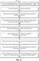
- FIG. 3is a flow diagram of an example process for direct-bonding LiTaO 3 with silicon.
- FIG. 4is a flow diagram of an example process for direct-bonding LiTaO 3 with sapphire.
- FIG. 5is a flow diagram of an example process for direct-bonding LiTaO 3 with fused silica glass.
- FIG. 6is a flow diagram of an example process for direct-bonding LiTaO 3 with silicon by creating a native oxide of the LiTaO 3 and/or the silicon.
- FIG. 7is a flow diagram of an example process for direct-bonding LiTaO 3 with sapphire by creating a native oxide of the LiTaO 3 and/or the sapphire.
- FIG. 8is a flow diagram of an example process for direct-bonding LiTaO 3 with fused silica glass by creating a native oxide of the LiTaO 3 and/or the fused silica glass.
- FIG. 9is a diagram of example direct-bond energy increases at different anneal durations and different temperatures, with slow temperature increase during anneal.
- This disclosuredescribes example techniques, processes, and methods for successfully joining diverse and dissimilar materials to each other in microelectronics, and describes resulting layer structures and devices.
- the example processes and structuresapply to materials already routinely used in semiconductor fabrication and in the microelectronic packaging arts, and to combinations of materials not conventionally used in these arts.
- the example techniques, processes, and methods described hereinare provided for fabricating novel semiconductor and microelectronic devices, and also for fabricating conventional devices with more efficient and practical designs.
- LiTaO 3Lithium tantalate
- LiTaO 3has optical, piezoelectric, and pyroelectric properties that make it useful for nonlinear optics, passive infrared sensors and motion detectors, terahertz generation and detection, surface acoustic wave applications, cell phone applications, cooling, heating, and small scale production of neutrons (atomic particles) for the nuclear industry, for example.
- LiTaO 3has a relatively large thermal expansion coefficient, with thermal expansion on the order of 12 ppm that varies along different crystalline axis directions.
- LiTaO 3If LiTaO 3 is warped during heating it develops an internal charge imbalance, which can result in residual warpage after cooling.
- LiTaO 3In a pyroelectric effect, LiTaO 3 generates a temporary voltage within itself, when heated or cooled, without any imposed physical warping. Changes in temperature slightly modify positions of atoms within its crystal structure changing the polarization of the material.
- LiTaO 3In a different but related piezoelectric effect, LiTaO 3 also generates an electric charge in response to applied mechanical stress (the imposed warpage).
- LiNbO 3lithium niobate
- LiNbO 3is a compound of lithium, niobium, and oxygen. Crystals of LiNbO 3 are useful as optical waveguides, in mobile phones, as piezoelectric sensors, optical modulators and in various other linear and non-linear optical applications. LiNbO 3 is considered an artificially made dielectric material that does not exist in nature.
- Example techniques described hereinenable direct-bonding of LiTaO 3 (or LiNbO 3 ) to other semiconductor, dielectric, and insulator materials for purposes of making practical microelectronic devices.
- LiTaO 3is described representatively for both LiTaO 3 and LiNbO 3 and for many other similar materials too.
- the example techniques, processes, and methods hereincan be applied between almost any solid materials, but LiTaO 3 is used in the descriptions representatively, as an example of a material to be joined to other materials that are dissimilar in CTEs, lattice unit cell geometries, or other properties.
- LiTaO 3has conventionally proven incompatible for direct-bonding with important semiconductor and dielectric materials such as silicon (Si), glass (amorphous silicon dioxide SiO 2 and other ingredients), fused silica (glass made of pure silicon dioxide SiO 2 ), sapphire, and other common and uncommon substrates used, or that could be used, in the semiconductor and microelectronic fabrication and packaging arts.
- semiconductor and dielectric materialssuch as silicon (Si), glass (amorphous silicon dioxide SiO 2 and other ingredients), fused silica (glass made of pure silicon dioxide SiO 2 ), sapphire, and other common and uncommon substrates used, or that could be used, in the semiconductor and microelectronic fabrication and packaging arts.
- Example techniques described belowenable practical use of LiTaO 3 in microelectronic devices, especially in wafer-level fabrication of microelectronic devices, wherein the fabrication can be greatly optimized by using direct-bonding and/or direct hybrid bonding between the surfaces of the different or incompatible materials (between substrates, such as those of dies and/or wafers made of different materials being joined to make the novel or conventional microelectronic devices).
- a low temperature bonding processenables heterogeneous integration of diverse materials within a microelectronic device.
- This low temperature bonding processcan be especially useful in fabrication processes that use substrates, such as those of dies or wafers made of two different materials that are conventionally incompatible with each other with respect to conventional direct-bonding processes.
- FIG. 1shows example structures in which a first wafer 100 of a first material is to be direct-bonded to a second wafer 102 of a second material at room temperature.
- Room temperatureis defined in its usual way as a humanly comfortable ambient temperature, generally around 70° F. or around 21.1° C.
- the first material of the first wafer 100possesses a first coefficient of thermal expansion (CTE) and a first set of physical dimensions of respective unit cells of a first crystal lattice of the first material, while the second material of the second wafer 102 possesses a second CTE and a second set of physical dimensions of respective unit cells of a second crystal lattice of the second material.
- CTEcoefficient of thermal expansion
- the second CTE of the second wafer 102is different from the first CTE of the first material and/or the second set of physical dimensions of the unit cells of the second wafer 102 is different from the first physical dimensions of the unit cells of the first material of the first wafer 100 .
- Respective thin oxide, carbide, nitride, carbonitride, oxynitride layers 104 & 106are deposited on one or both bonding surfaces of the first wafer 100 and the second wafer 102 .
- the deposited oxide, carbide, nitride, carbonitride, or oxynitride layers 104 & 106may be only 100-1000 nm thick, and serve as direct-bonding intermediaries between the wafers 100 & 102 .
- the deposited oxide, carbide, nitride, carbonitride, or oxynitride layers 104 & 106are a different compound than either the first material of the first wafer 100 or the second material of the second wafer 102 . So the direct-bonding described herein is different than conventional direct-bonding, which is often described as molecular bonding directly between two surfaces made of the same atoms or molecules: the same material being bonded to itself across an interface.
- the first wafer 100 and the second wafer 102are then direct-bonded together at room temperature to make a joined wafer, with the thin amorphous layer of oxide, carbide, nitride, carbonitride, or oxynitride intervening at the molecular bonding interface.
- the amorphous layermay comprise silicon.
- the joined waferis held for approximately 48 hours to strengthen direct bonds in a passive curing stage, wherein solid crystal bonds or other bonds at the solid bonding interface are allowed to spontaneously consolidate and seek their most stable energy levels under normal molecular kinetic motion at the room temperature level.
- the joined waferis then annealed by slowly raising the ambient temperature from room temperature level to a relatively low annealing temperature of 50° C. at a temperature increase rate of about 1° C. per minute or less, to anneal the direct bonds of the joined wafer.
- the direct-bonding of dissimilar materials at room temperature to make a microelectronic devicecan also be accomplished by creating one or more native oxide (or carbide, nitride, carbonitride, oxynitride, etc.) films 108 & 110 on one or both bonding surfaces of the first wafer 100 and second wafer 102 . This can be accomplished by exposing the bonding surface(s) to a strong oxidizing solution, or oxygen plasma, for example, or other reactive agent in the cases of native carbide generation or native nitride generation.
- a strong oxidizing solution, or oxygen plasmafor example, or other reactive agent in the cases of native carbide generation or native nitride generation.
- the example direct-bonding processthat utilizes a step of creating a native oxide layer (or carbide layer, nitride layer, carbonitride, oxynitride, etc.) aims to take advantage of two or more substrates made of different materials that have specific advantages provided by the properties of devices that can be fabricated on each respective different type of substrate, now joined in one device by the example direct-bonding process.
- the example low temperature bonding techniqueenables multiple integration possibilities for a broad field of electronic devices.
- the example processbegins by thermally equilibrating the different materials to be direct-bonded together with each other and with the environment.
- the direct-bonding processbegins with all materials and the environment at the same temperature, providing an equilibrium of molecular kinetic energy among the materials being used. This equilibrium controls/prevents uncontrolled flows of heat energy between materials or across the bonding interface during the initial contact of bonding surfaces during the direct-bonding process, resulting in extremely homogeneity of the direct-bonds formed at small scale, and results in exquisite control of the example process.
- the careful equilibrium of temperature at the start of this example direct-bonding processcan ultimately ensure a very uniform bonded interface, at the molecular level. In one implementation, this uniformity of the direct-bonded interface is limited only by the degree of flatness achievable on the surfaces to be direct-bonded together prior to contact between the two surfaces.
- the example direct-bondingis performed at room temperature, and then held at room temperature for up to 48 hours or more for curing, even before an annealing step, to greatly increase bond energy: the bond strength that will be present after a subsequent annealing step is completed.
- the wafersare kept at room temperature for a period of time after direct-bonding for a curing that allows bond energy to increase even before elevating the temperature during annealing to speed up the bond energy increase. Bond strengths of 1000 mJ/m 2 or greater have been measured with this example room temperature curing technique.
- FIG. 2shows example increase in bond energy versus curing time at room temperature after direct-bonding of dissimilar wafer materials.
- TEOStetraethoxysilane
- NH 4 OHaqueous ammonia
- Some example processes for direct-bonding dissimilar materials at room temperatureuse a thin intermediary layer less than 1 micron thick (between approximately 100-1000 nm) as an “adapter” layer between diverse oxides, carbides, nitrides, carbonitrides, or oxynitrides for the direct-bonding.
- This thin intermediary layermay be an amorphous oxide layer, such as silicon dioxide (SiO 2 ), with a thickness dimension within the range above, less than 1 micron thick.
- Silicon dioxide filmscan be grown by a plasma enhanced chemical vapor deposition (PECVD) system using liquid tetraethoxysilane (TEOS) as the source of Si, or by TEOS photochemical decomposition, for example.
- PECVDplasma enhanced chemical vapor deposition
- TEOSliquid tetraethoxysilane
- FIG. 3shows a first example process 300 , in which a LiTaO 3 wafer, substrate, or surface is direct-bonded at room temperature to a silicon wafer, substrate, or surface via an intervening thin amorphous bonding layer made of an oxide material, such as SiO 2 , or another thin amorphous dielectric intermediary for direct-bonding, such as a nitride, carbide, carbonitride, or oxynitride.
- an oxide materialsuch as SiO 2
- another thin amorphous dielectric intermediary for direct-bondingsuch as a nitride, carbide, carbonitride, or oxynitride.
- a material such as TEOS-derived amorphous SiO 2is deposited onto one or both of the LiTaO 3 wafer, substrate, or surface and/or the silicon wafer, substrate, or surface.
- the layer of oxide materialmay have a deposited thickness of approximately 100-1000 nm (0.1-1.0 microns).
- the respective surfaces of LiTaO 3 and SiO 2 , one or both of these surfaces covered with the thin amorphous film of oxide, carbide, nitride, carbonitride, and/or oxynitride,are planarized by chemical mechanical planarization (CMP) to a smooth, flat surface. Asperities including defects and rough spots that would cause bonding voids can be removed at this step.
- CMPchemical mechanical planarization
- the respective wafers, substrates, or surfacesmay be cleaned with scrubbing by PVA brush, and a deionized (DI) water rinse.
- DIdeionized
- the respective wafers, substrates, or surfacesmay be cleaned with a Megasonic SC1 process, rinsed with DI water and spin-dried on a Goldfinger® processing tool, for example, for megasonic wave particle removal without etching.
- the wafers, substrates, or surfacesare plasma-activated with nitrogen plasma in RIE mode, for example with a ⁇ 200 to ⁇ 300 volt bias.
- This nitrogen plasma activation with such parametersmay be unique when applied to LiTaO 3 direct-bonding.
- the wafers, substrates, or surfacesare spray-rinsed with 29% NH 4 OH (aqueous ammonia).
- This rinse with 29% NH 4 OHmay also be a unique process when applied to the LiTaO 3 direct-bonding.
- the NH 4 OH rinsinghelps to remove particles from the wafers, substrates, or surfaces. In some cases, depending on materials, the NH 4 OH rinsing can help to increase bond energy.
- the wafers, substrates, or surfacesmay be spin-dried on a spin bonder tool, for example.
- the wafers, substrates, or surfacesare contacted with each other for direct-bonding at room temperature, with the LiTaO 3 wafer, for example, loaded as the top wafer.
- Infrared (IR) drying lampsare not used to avoid excessive bowing and warping upon bonding.
- the room temperature bondingalso avoids excessive bowing of the wafers.
- heating during spin dryingcould also cause bowing of the LiTaO 3 , which does not fully relax after cooling due to pyroelectric charge build up in the LiTaO 3 material, so such heated spin-drying after direct bonding may be avoided.
- the wafers(or bonded substrates or bonded surfaces) are held at room temperature for 48 hours, as an example duration, to allow bond strength to increase before slowly elevating temperature for the subsequent annealing step.
- the bonding strengthincreases in relation to the time duration allowed for the room temperature curing, as shown in FIG. 2 .
- the temperature of the direct-bonded wafers, substrates, or surfacesare ramped slowly up slowly to 50° C. in an oven, in a temperature elevation process of less than 1 degree ° C. per minute.
- This relatively low temperature annealing stepavoids slippage of the bonds that are being strengthened, and minimizes bowing of the wafers (substrates or surfaces) being annealed.
- FIG. 4shows a second example process 400 , in which a LiTaO 3 wafer, substrate, or surface is direct-bonded at room temperature to a sapphire wafer, substrate, or surface via an intervening thin amorphous bonding layer made of an oxide material, such as SiO 2 , or another thin amorphous dielectric intermediary for direct-bonding, such as a nitride, carbide, carbonitride, and/or oxynitride.
- oxide materialsuch as SiO 2
- another thin amorphous dielectric intermediary for direct-bondingsuch as a nitride, carbide, carbonitride, and/or oxynitride.
- a representative materialsuch as TEOS-derived amorphous SiO 2 , or a thin amorphous layer of a carbide, nitride, carbonitride, or oxynitride dielectric, is deposited onto one or both of the LiTaO 3 wafer, substrate, or surface and/or the sapphire wafer, substrate, or surface.
- the thin layer of the amorphous materialsuch as the oxide, carbide, nitride, carbonitride, or oxynitride may have a deposited thickness of approximately 100-1000 nm.
- the respective surfaces of oxide-covered LiTaO 3 and/or oxide-covered SiO 2are planarized by chemical mechanical planarization (CMP) to a smooth, flat surface. Asperities, such as defects and rough spots, that would cause bonding voids can be removed at this step.
- CMPchemical mechanical planarization
- the respective wafers, substrates, or surfacesmay be cleaned with PVA brush scrubbing and deionized (DI) water.
- DIdeionized
- the respective wafers, substrates, or surfacesmay be cleaned with a Megasonic SC1 process, rinsed with DI water and spin-dried on a Goldfinger® processing tool, for example, for megasonic wave particle removal without etching.
- the wafers, substrates, or surfacesare plasma-activated with nitrogen plasma in RIE mode, for example with a ⁇ 200 to ⁇ 300 volt bias.
- the wafers, substrates, or surfacesare spray-rinsed with 29% NH 4 OH (aqueous ammonia, or ammonium hydroxide).
- This rinse with 29% NH 4 OHmay be a unique process when applied to the LiTaO 3 direct-bonding.
- the NH 4 OH rinsingremoves particles from the wafers, substrates, or surfaces. In some cases, depending on materials, the NH 4 OH rinsing increases bond energy.
- the wafers, substrates, or surfacesmay be spin-dried on a spin bonder tool, for example.
- the wafers, substrates, or surfacesare direct-bonded to each other at room temperature, with the LiTaO 3 wafer, for example, loaded as the top wafer.
- Infrared (IR) drying lampsare not used to avoid excessive bowing and warpage upon bonding.
- the room temperature bondingalso avoids excessive bowing of the wafers.
- heating during spin dryingmay cause bowing of the LiTaO 3 , which does not fully relax after cooling due to pyroelectric charge build up in the LiTaO 3 material, and such heating may be avoided at this step.
- the wafersare held at room temperature for at least 48 hours, as an example duration, to allow bond strength to increase and consolidate before elevating temperature for the subsequent annealing step.
- the bonding strength during the passive room temperature cureincreases in relation to the time duration allowed, as shown in FIG. 2 .
- the temperature of the direct-bonded wafers, substrates, or surfacesare ramped up to 50° C. in an oven, at a rate of temperature increase of about 1 degree ° C. per minute, or less.
- Sapphireis an extremely stiff material and if the wafers are not bonded strongly enough before increasing the temperature, wafer expansion and resulting warpage can cause the wafers to separate. So this relatively low temperature annealing step avoids slippage of the bond being strengthened, and minimizes bowing of the wafers being direct-bonded together.
- FIG. 5shows a third example process 500 , in which a LiTaO 3 wafer, substrate, or surface is direct-bonded at room temperature to a fused silica glass wafer, substrate, or surface via an intervening thin amorphous bonding layer made of an oxide material, such as SiO 2 , or made of a nitride, carbide, carbonitride, or oxynitride dielectric.
- an oxide materialsuch as SiO 2
- operations of the example process 500are shown in individual blocks.
- a material such as TEOS-derived amorphous SiO 2is deposited onto one or both of the LiTaO 3 wafer, substrate, or surface and/or the fused silica glass wafer, substrate, or surface.
- the thin layer of materialsuch as the oxide, nitride, carbide, carbonitride, or oxynitride may have a deposited thickness of approximately 100-1000 nm.
- the respective surfaces of oxide-covered LiTaO 3 and/or oxide-covered SiO 2are planarized by chemical mechanical planarization (CMP) to a smooth, flat surface. Asperities including defects and rough spots that would cause bonding voids can be removed at this step.
- CMPchemical mechanical planarization
- the respective wafers, substrates, or surfacesmay be cleaned with PVA brush scrubbing and deionized (DI) water.
- DIdeionized
- the respective wafers, substrates, or surfacesmay be cleaned with a Megasonic SC1 process, rinsed with DI water and spin-dried on a Goldfinger® processing tool, for example, for megasonic wave particle removal without etching.
- the wafers, substrates, or surfacesare plasma-activated with nitrogen plasma in RIE mode, for example with a ⁇ 200 to ⁇ 300 volt bias.
- This nitrogen plasma activation with these parametersmay be unique when applied to LiTaO 3 direct-bonding.
- the wafers, substrates, or surfacesare spray-rinsed with 29% NH 4 OH (aqueous ammonia or ammonium hydroxide).
- This rinse with 29% NH 4 OHmay be a unique process when applied to the LiTaO 3 direct-bonding.
- the NH 4 OH rinsingremoves particles from the wafers, substrates, or surfaces. In some cases, depending on materials, the NH 4 OH rinsing increases bond energy.
- the wafers, substrates, or surfacesmay be spin-dried on a spin bonder tool, for example.
- the wafers, substrates, or surfacesare direct-bonded to each other at room temperature, with the LiTaO 3 wafer, for example, loaded as the top wafer.
- Infrared (IR) drying lampsare not used to avoid excessive bowing and warpage upon bonding.
- the room temperature bondingalso avoids excessive bowing of the wafers, for example.
- heating during spin dryingmay also cause bowing of the LiTaO 3 , which does not fully relax after cooling due to pyroelectric charge build up in the LiTaO 3 material, and such heating may be avoided.
- the wafers(or substrates or surfaces) are held at room temperature for at least 48 hours, for example, to allow bond strength to increase before elevating temperature for the subsequent annealing step.
- the bonding strengthincreases in relation to the time duration allowed for room temperature curing, as shown in FIG. 2 .
- the temperature of the direct-bonded wafers, substrates, or surfacesis ramped up to 50° C. in an oven, at a rate of temperature rise that is about 1 degree per minute, or preferably less.
- This relatively low-temperature annealing stepavoids slippage of the bonds being strengthened, and minimizes bowing of the wafers being direct-bonded together.
- FIG. 6shows a fourth example process 600 , for direct-bonding a representative LiTaO 3 wafer at room temperature to a silicon wafer, without depositing a discrete layer of an oxide, carbide, nitride, carbonitride, or oxynitride material as a bonding intermediary.
- operations of the example process 600are shown in individual blocks.
- a native oxide (of silicon) or oxide patina of siliconis created on the silicon wafer.
- the native oxidemay be created by first cleaning the wafer with a piranha solution of hydrogen peroxide-sulfuric acid (H 2 O 2 :H 2 SO 4 ) in a ratio of 1:3, and then rinsing with water.
- the 1:3 H 2 O 2 :H 2 SO 4 solutiongrows or creates a native oxide film on the silicon, which is conducive to forming high strength bonds in oxide-to-oxide direct-bonding.
- the surface of the silicon wafer with native oxideis rinsed in a Megasonic deionized water process and can be spun and rinsed dry on a Goldfinger® processing tool, for example.
- the surface of the LiTaO 3 wafer(only) is plasma-activated with nitrogen plasma in RIE mode with a ⁇ 200 to ⁇ 300 volt bias.
- both wafersare spray-rinsed with deionized water.
- the silicon waferis rinsed with water to avoid pitting the silicon and native oxide surface, although the native oxide may be enough to protect the silicon surface, in which case use of NH 4 OH solution to enhance direct-bonding may be preferred.
- the LiTaO 3 waferis usually cleaned with water, cleaning with NH 4 OH solution can also be performed. In some cases, rinsing with the NH 4 OH increases direct-bond energies to more complete potential.
- the wafersare then spin-dried, for example on a bonder tool.
- the wafersare direct-bonded together at room temperature with the LiTaO 3 wafer loaded as the top wafer, for example.
- Infrared drying lampsare generally avoided to prevent excessive bowing and warpage upon direct-bonding.
- Room temperature direct-bondingalso avoids excessive bowing of the wafers. Heating during the spin-drying could cause bowing of the LiTaO 3 wafer, which does not fully relax after cooling due to pyroelectric charge build-up in the LiTaO 3 material, so can be avoided at this step.
- a block 612the joined and direct-bonded wafers are held at room temperature for at least 48 hours or more to allow bond strength to increase before elevating the temperature in a subsequent annealing step.
- the bond strengthincreases in relation to the duration of the room temperature cure, as shown in FIG. 2 .
- the joined and direct-bonded wafersare warmed and heated in an oven up to a temperature of approximately 50° C. to anneal, at a rate of temperature increase that is 1 degree ° C. per minute, or less.
- This relatively low-temperature anneal appliedgradually avoids slippage of the direct-bonds and minimizes bowing and warpage.
- FIG. 7shows a fourth example process 700 , for direct-bonding a LiTaO 3 wafer at room temperature to a sapphire wafer without depositing a discrete layer of an oxide, carbide, nitride, carbonitride, or oxynitride material as a bonding intermediary.
- operations of the example process 700are shown in individual blocks.
- the LiTaO 3 wafer and a sapphire waferare cleaned with a piranha solution of hydrogen peroxide and sulfuric acid (H 2 O 2 :H 2 SO 4 ) in a ratio of 1:3, and then rinsed with water.
- a piranha solution of hydrogen peroxide and sulfuric acidH 2 O 2 :H 2 SO 4
- the surfaces of the wafersare rinsed in a Megasonic deionized water process and can be spun and rinsed dry on a Goldfinger® processing tool, for example.
- the surface of sapphire waferis plasma-activated with oxygen in RIE mode with a ⁇ 200 to ⁇ 300 volt bias
- the surface of the LiTaO 3 waferis plasma-activated with oxygen or nitrogen plasma in RIE mode with a ⁇ 200 to ⁇ 300 volt bias.
- the wafersare spray-rinsed with 29% NH 4 OH solution to remove particles and to enhance the bond energies possible in the direct-bonding process.
- the wafersmay be spun dry.
- the wafersare contacted together for the direct-bonded at room temperature with the LiTaO 3 wafer loaded as the top wafer, for example.
- Infrared drying lampsmay be avoided to prevent excessive bowing and warpage upon direct-bonding.
- the room temperature direct-bondingavoids excessive bowing of the wafers as well as allows stronger direct-bonds to form across the dissimilar materials. Heating during the spin drying would cause bowing of the LiTaO 3 wafer, which does not fully relax after cooling due to pyroelectric charge build-up in the LiTaO 3 material, so this heating may be omitted.
- the built-up pyroelectric chargemay be discharged or dissipated by connecting an electrical circuit to parts of the LiTaO 3 wafer, or by electrically shorting, shunting, or grounding the LiTaO 3 wafer with an external conductor. Discharging the built-up pyroelectric charge may relieve bowing or warping of the LiTaO 3 wafer.
- a block 712the joined and direct-bonded wafers are held at room temperature for at least 48 hours or more to allow bond strength to increase before elevating temperature in a subsequent annealing step.
- the bond strengthincreases with greater time at room temperature, as shown in FIG. 2 .
- the joined and direct-bonded wafersare warmed and heated in an oven up to 50° C. to anneal, at a rate of temperature increase of about 1 degree ° C. per minute, or less. This relatively low-temperature anneal applied gradually avoids slippage of the direct-bonds and minimizes bowing and warpage.
- FIG. 8shows a fourth example process 800 , for direct-bonding a LiTaO 3 wafer at room temperature to a fused silica glass wafer without depositing a discrete layer of an oxide, carbide, nitride, carbonitride, or oxynitride material as a bonding intermediary.
- operations of the example process 800are shown in individual blocks.
- the LiTaO 3 wafer and a fused silica glass waferare cleaned with a piranha solution of hydrogen peroxide and sulfuric acid (H 2 O 2 :H 2 SO 4 ) in a ratio of 1:3, and then rinsed with water.
- a piranha solution of hydrogen peroxide and sulfuric acidH 2 O 2 :H 2 SO 4
- the surfaces of the wafersare rinsed in a Megasonic deionized water process and can be spun and rinsed dry on a Goldfinger® processing tool, for example.
- the bonding surfaces of fused silica glass wafer and the LiTaO 3 waferare plasma-activated with oxygen plasma or nitrogen plasma in RIE mode with a ⁇ 200 to ⁇ 300 volt bias.
- the bonding surfaces of the wafersare spray-rinsed with 29% NH 4 OH solution to remove particles and to enhance bond energy of direct-bonding.
- the wafersmay be spun dry.
- the wafersare direct-bonded together at room temperature with the LiTaO 3 wafer loaded as the top wafer, for example.
- Infrared drying lampsare avoided to prevent excessive bowing and warpage.
- Room temperature direct-bondingis used to avoid excessive bowing of wafers. Heating during the spin drying would cause bowing of the LiTaO 3 wafer, and can be avoided.
- Built-up pyroelectric charge in the LiTaO 3 wafermay be discharged or dissipated by connecting an electrical circuit to parts of the LiTaO 3 wafer, or by electrically shorting, shunting, or grounding the LiTaO 3 wafer with an external conductor. Discharging the built-up pyroelectric charge may relieve a bowing tendency or warping of the LiTaO 3 wafer due to these effects.
- a block 812the joined and direct-bonded wafers are held at room temperature for at least 48 hours or more to allow bond strength to increase before elevating temperature in a subsequent annealing step.
- the bond strengthincreases with more time held at room temperature, as shown in FIG. 2 .
- the joined and direct-bonded wafersare warmed and heated in an oven up to a temperature of 50° C. to anneal, at a rate of temperature increase of about 1 degree ° C. per minute, or less. This relatively low-temperature anneal applied slowly avoids slippage of the direct-bonds and minimizes bowing and warping.
- an oxygen plasma activationcan sometimes yield higher bond strength than nitrogen plasma activation, particularly when bonding LiTaO 3 to sapphire.
- nitrogen plasma activationmay work better for bonding LiTaO 3 to silicon without the discrete deposited oxide layer intermediary between wafers.
- Annealing of direct-bonds between LiTaO 3 and siliconmay attain higher bond strength with higher temperature. Nominally, direct-bonded wafers that have cured at room temperature for up to 48 hours are heated to 50° C. in an oven at rate of temperature increase than is about 1 degree ° C. per minute, or less. In the case of forming a native oxide, nitride, carbide, carbonitride, oxynitride, on one or both bonding surfaces as an intermediary for direct-bonding the dissimilar materials, after the annealing step at a gradual temperature increase up to 50° C., the temperature of the joined wafers can be further ramped up to 100° C. at a rate of temperature increase that is about 1 degree ° C. per minute or less to increase the bond strength even further, without significant increase in bowing or warping of the wafers, as shown in FIG. 9 .
- the materials of the first wafer and second wafer to be direct-bonded together at room temperaturemay have significantly different CTEs and lattice constants.
- the dissimilar materials to be used in a given microelectronic device constructed by the example processes described hereinmay be managed with thin film engineering principles for balancing wafer warpage of the two wafers, due to the difference in the materials used.
- different thicknesses of the different materials of the two waferscan be leveraged for the two wafers of different thicknesses of the different materials to cancel out each other's bowing and warping.
- the bowing or warpage in generalis assumed or calculated to be in the range of 25 ⁇ m per inch of diameter down to 10 ⁇ m per inch of diameter.
- the example processes described abovecan be used to make stacks of wafers of different materials for a microelectronic device or package.
- the various stack layerscan also be used to make multiple stacks of integrated circuits combined with other optical and acoustic devices, with or without direct-bonding between all the layers present.
Landscapes
- Engineering & Computer Science (AREA)
- Microelectronics & Electronic Packaging (AREA)
- Physics & Mathematics (AREA)
- Condensed Matter Physics & Semiconductors (AREA)
- General Physics & Mathematics (AREA)
- Computer Hardware Design (AREA)
- Power Engineering (AREA)
- Manufacturing & Machinery (AREA)
- Crystals, And After-Treatments Of Crystals (AREA)
- Pressure Welding/Diffusion-Bonding (AREA)
- Ceramic Products (AREA)
Abstract
Description
Claims (19)
Priority Applications (6)
| Application Number | Priority Date | Filing Date | Title |
|---|---|---|---|
| US16/459,610US11664357B2 (en) | 2018-07-03 | 2019-07-02 | Techniques for joining dissimilar materials in microelectronics |
| PCT/US2019/040255WO2020010056A1 (en) | 2018-07-03 | 2019-07-02 | Techniques for joining dissimilar materials in microelectronics |
| TW113127351ATW202449862A (en) | 2018-07-03 | 2019-07-03 | Direct bonding of heterogeneous substrates |
| TW112132361ATWI853688B (en) | 2018-07-03 | 2019-07-03 | Direct bonding of heterogeneous substrates |
| TW108123486ATWI812747B (en) | 2018-07-03 | 2019-07-03 | Techniques for joining dissimilar materials in microelectronics |
| US18/300,306US20230253383A1 (en) | 2018-07-03 | 2023-04-13 | Techniques for joining dissimilar materials in microelectronics |
Applications Claiming Priority (2)
| Application Number | Priority Date | Filing Date | Title |
|---|---|---|---|
| US201862693671P | 2018-07-03 | 2018-07-03 | |
| US16/459,610US11664357B2 (en) | 2018-07-03 | 2019-07-02 | Techniques for joining dissimilar materials in microelectronics |
Related Child Applications (1)
| Application Number | Title | Priority Date | Filing Date |
|---|---|---|---|
| US18/300,306DivisionUS20230253383A1 (en) | 2018-07-03 | 2023-04-13 | Techniques for joining dissimilar materials in microelectronics |
Publications (2)
| Publication Number | Publication Date |
|---|---|
| US20200013765A1 US20200013765A1 (en) | 2020-01-09 |
| US11664357B2true US11664357B2 (en) | 2023-05-30 |
Family
ID=69059300
Family Applications (2)
| Application Number | Title | Priority Date | Filing Date |
|---|---|---|---|
| US16/459,610ActiveUS11664357B2 (en) | 2018-07-03 | 2019-07-02 | Techniques for joining dissimilar materials in microelectronics |
| US18/300,306PendingUS20230253383A1 (en) | 2018-07-03 | 2023-04-13 | Techniques for joining dissimilar materials in microelectronics |
Family Applications After (1)
| Application Number | Title | Priority Date | Filing Date |
|---|---|---|---|
| US18/300,306PendingUS20230253383A1 (en) | 2018-07-03 | 2023-04-13 | Techniques for joining dissimilar materials in microelectronics |
Country Status (3)
| Country | Link |
|---|---|
| US (2) | US11664357B2 (en) |
| TW (3) | TWI853688B (en) |
| WO (1) | WO2020010056A1 (en) |
Cited By (11)
| Publication number | Priority date | Publication date | Assignee | Title |
|---|---|---|---|---|
| US20220139869A1 (en)* | 2020-10-29 | 2022-05-05 | Invensas Bonding Technologies, Inc. | Direct bonding methods and structures |
| US11967575B2 (en) | 2018-08-29 | 2024-04-23 | Adeia Semiconductor Bonding Technologies Inc. | Bond enhancement structure in microelectronics for trapping contaminants during direct-bonding processes |
| US12009338B2 (en) | 2020-03-19 | 2024-06-11 | Adeia Semiconductor Bonding Technologies Inc. | Dimension compensation control for directly bonded structures |
| US12051621B2 (en) | 2016-12-28 | 2024-07-30 | Adeia Semiconductor Bonding Technologies Inc. | Microelectronic assembly from processed substrate |
| US12068278B2 (en) | 2017-05-11 | 2024-08-20 | Adeia Semiconductor Bonding Technologies Inc. | Processed stacked dies |
| US12199069B2 (en) | 2012-08-30 | 2025-01-14 | Adeia Semiconductor Bonding Technologies Inc. | Heterogeneous annealing method and device |
| US12248869B2 (en) | 2017-08-03 | 2025-03-11 | Adeia Semiconductor Inc. | Three dimensional circuit implementing machine trained network |
| US12300661B2 (en) | 2020-03-31 | 2025-05-13 | Adeia Semiconductor Bonding Technologies Inc. | Reliable hybrid bonded apparatus |
| US12406959B2 (en) | 2018-07-26 | 2025-09-02 | Adeia Semiconductor Bonding Technologies Inc. | Post CMP processing for hybrid bonding |
| US12406975B2 (en) | 2018-02-15 | 2025-09-02 | Adeia Semiconductor Bonding Technologies Inc. | Techniques for processing devices |
| US12431460B2 (en) | 2017-04-21 | 2025-09-30 | Adeia Semiconductor Bonding Technologies Inc. | Die processing |
Families Citing this family (74)
| Publication number | Priority date | Publication date | Assignee | Title |
|---|---|---|---|---|
| US7109092B2 (en) | 2003-05-19 | 2006-09-19 | Ziptronix, Inc. | Method of room temperature covalent bonding |
| US7485968B2 (en) | 2005-08-11 | 2009-02-03 | Ziptronix, Inc. | 3D IC method and device |
| US20150262902A1 (en) | 2014-03-12 | 2015-09-17 | Invensas Corporation | Integrated circuits protected by substrates with cavities, and methods of manufacture |
| US11069734B2 (en) | 2014-12-11 | 2021-07-20 | Invensas Corporation | Image sensor device |
| US10886250B2 (en) | 2015-07-10 | 2021-01-05 | Invensas Corporation | Structures and methods for low temperature bonding using nanoparticles |
| US9953941B2 (en) | 2015-08-25 | 2018-04-24 | Invensas Bonding Technologies, Inc. | Conductive barrier direct hybrid bonding |
| US10204893B2 (en) | 2016-05-19 | 2019-02-12 | Invensas Bonding Technologies, Inc. | Stacked dies and methods for forming bonded structures |
| US10672663B2 (en) | 2016-10-07 | 2020-06-02 | Xcelsis Corporation | 3D chip sharing power circuit |
| US10580735B2 (en) | 2016-10-07 | 2020-03-03 | Xcelsis Corporation | Stacked IC structure with system level wiring on multiple sides of the IC die |
| TWI822659B (en) | 2016-10-27 | 2023-11-21 | 美商艾德亞半導體科技有限責任公司 | Structures and methods for low temperature bonding |
| US10002844B1 (en) | 2016-12-21 | 2018-06-19 | Invensas Bonding Technologies, Inc. | Bonded structures |
| CN117878055A (en) | 2016-12-28 | 2024-04-12 | 艾德亚半导体接合科技有限公司 | Stacking substrate processing |
| TWI837879B (en) | 2016-12-29 | 2024-04-01 | 美商艾德亞半導體接合科技有限公司 | Bonded structures with integrated passive component |
| WO2018169968A1 (en) | 2017-03-16 | 2018-09-20 | Invensas Corporation | Direct-bonded led arrays and applications |
| US10515913B2 (en) | 2017-03-17 | 2019-12-24 | Invensas Bonding Technologies, Inc. | Multi-metal contact structure |
| US10508030B2 (en) | 2017-03-21 | 2019-12-17 | Invensas Bonding Technologies, Inc. | Seal for microelectronic assembly |
| US10446441B2 (en) | 2017-06-05 | 2019-10-15 | Invensas Corporation | Flat metal features for microelectronics applications |
| US10217720B2 (en) | 2017-06-15 | 2019-02-26 | Invensas Corporation | Multi-chip modules formed using wafer-level processing of a reconstitute wafer |
| US10840205B2 (en) | 2017-09-24 | 2020-11-17 | Invensas Bonding Technologies, Inc. | Chemical mechanical polishing for hybrid bonding |
| US11195748B2 (en) | 2017-09-27 | 2021-12-07 | Invensas Corporation | Interconnect structures and methods for forming same |
| US11031285B2 (en) | 2017-10-06 | 2021-06-08 | Invensas Bonding Technologies, Inc. | Diffusion barrier collar for interconnects |
| US10923408B2 (en) | 2017-12-22 | 2021-02-16 | Invensas Bonding Technologies, Inc. | Cavity packages |
| US11380597B2 (en) | 2017-12-22 | 2022-07-05 | Invensas Bonding Technologies, Inc. | Bonded structures |
| US11169326B2 (en) | 2018-02-26 | 2021-11-09 | Invensas Bonding Technologies, Inc. | Integrated optical waveguides, direct-bonded waveguide interface joints, optical routing and interconnects |
| US11256004B2 (en) | 2018-03-20 | 2022-02-22 | Invensas Bonding Technologies, Inc. | Direct-bonded lamination for improved image clarity in optical devices |
| US10991804B2 (en) | 2018-03-29 | 2021-04-27 | Xcelsis Corporation | Transistor level interconnection methodologies utilizing 3D interconnects |
| US11056348B2 (en) | 2018-04-05 | 2021-07-06 | Invensas Bonding Technologies, Inc. | Bonding surfaces for microelectronics |
| US11244916B2 (en) | 2018-04-11 | 2022-02-08 | Invensas Bonding Technologies, Inc. | Low temperature bonded structures |
| US10790262B2 (en) | 2018-04-11 | 2020-09-29 | Invensas Bonding Technologies, Inc. | Low temperature bonded structures |
| US10964664B2 (en) | 2018-04-20 | 2021-03-30 | Invensas Bonding Technologies, Inc. | DBI to Si bonding for simplified handle wafer |
| US11004757B2 (en) | 2018-05-14 | 2021-05-11 | Invensas Bonding Technologies, Inc. | Bonded structures |
| US11276676B2 (en) | 2018-05-15 | 2022-03-15 | Invensas Bonding Technologies, Inc. | Stacked devices and methods of fabrication |
| US10923413B2 (en) | 2018-05-30 | 2021-02-16 | Xcelsis Corporation | Hard IP blocks with physically bidirectional passageways |
| KR20210009426A (en) | 2018-06-13 | 2021-01-26 | 인벤사스 본딩 테크놀로지스 인코포레이티드 | TV as a pad |
| US11393779B2 (en) | 2018-06-13 | 2022-07-19 | Invensas Bonding Technologies, Inc. | Large metal pads over TSV |
| US10910344B2 (en) | 2018-06-22 | 2021-02-02 | Xcelsis Corporation | Systems and methods for releveled bump planes for chiplets |
| US11158606B2 (en) | 2018-07-06 | 2021-10-26 | Invensas Bonding Technologies, Inc. | Molded direct bonded and interconnected stack |
| US11462419B2 (en) | 2018-07-06 | 2022-10-04 | Invensas Bonding Technologies, Inc. | Microelectronic assemblies |
| US11515291B2 (en) | 2018-08-28 | 2022-11-29 | Adeia Semiconductor Inc. | Integrated voltage regulator and passive components |
| US11011494B2 (en) | 2018-08-31 | 2021-05-18 | Invensas Bonding Technologies, Inc. | Layer structures for making direct metal-to-metal bonds at low temperatures in microelectronics |
| US11158573B2 (en) | 2018-10-22 | 2021-10-26 | Invensas Bonding Technologies, Inc. | Interconnect structures |
| US11244920B2 (en) | 2018-12-18 | 2022-02-08 | Invensas Bonding Technologies, Inc. | Method and structures for low temperature device bonding |
| CN113330557A (en) | 2019-01-14 | 2021-08-31 | 伊文萨思粘合技术公司 | Bonding structure |
| US11387202B2 (en) | 2019-03-01 | 2022-07-12 | Invensas Llc | Nanowire bonding interconnect for fine-pitch microelectronics |
| US11901281B2 (en) | 2019-03-11 | 2024-02-13 | Adeia Semiconductor Bonding Technologies Inc. | Bonded structures with integrated passive component |
| US10854578B2 (en) | 2019-03-29 | 2020-12-01 | Invensas Corporation | Diffused bitline replacement in stacked wafer memory |
| US11373963B2 (en) | 2019-04-12 | 2022-06-28 | Invensas Bonding Technologies, Inc. | Protective elements for bonded structures |
| US11205625B2 (en) | 2019-04-12 | 2021-12-21 | Invensas Bonding Technologies, Inc. | Wafer-level bonding of obstructive elements |
| US11610846B2 (en) | 2019-04-12 | 2023-03-21 | Adeia Semiconductor Bonding Technologies Inc. | Protective elements for bonded structures including an obstructive element |
| US11355404B2 (en) | 2019-04-22 | 2022-06-07 | Invensas Bonding Technologies, Inc. | Mitigating surface damage of probe pads in preparation for direct bonding of a substrate |
| US11385278B2 (en) | 2019-05-23 | 2022-07-12 | Invensas Bonding Technologies, Inc. | Security circuitry for bonded structures |
| US12374641B2 (en) | 2019-06-12 | 2025-07-29 | Adeia Semiconductor Bonding Technologies Inc. | Sealed bonded structures and methods for forming the same |
| US11296053B2 (en)* | 2019-06-26 | 2022-04-05 | Invensas Bonding Technologies, Inc. | Direct bonded stack structures for increased reliability and improved yield in microelectronics |
| US12080672B2 (en) | 2019-09-26 | 2024-09-03 | Adeia Semiconductor Bonding Technologies Inc. | Direct gang bonding methods including directly bonding first element to second element to form bonded structure without adhesive |
| US12113054B2 (en) | 2019-10-21 | 2024-10-08 | Adeia Semiconductor Technologies Llc | Non-volatile dynamic random access memory |
| US11862602B2 (en) | 2019-11-07 | 2024-01-02 | Adeia Semiconductor Technologies Llc | Scalable architecture for reduced cycles across SOC |
| US11762200B2 (en) | 2019-12-17 | 2023-09-19 | Adeia Semiconductor Bonding Technologies Inc. | Bonded optical devices |
| US11876076B2 (en) | 2019-12-20 | 2024-01-16 | Adeia Semiconductor Technologies Llc | Apparatus for non-volatile random access memory stacks |
| CN115088068A (en) | 2019-12-23 | 2022-09-20 | 伊文萨思粘合技术公司 | Electrical redundancy for bonded structures |
| US11721653B2 (en) | 2019-12-23 | 2023-08-08 | Adeia Semiconductor Bonding Technologies Inc. | Circuitry for electrical redundancy in bonded structures |
| WO2021236361A1 (en) | 2020-05-19 | 2021-11-25 | Invensas Bonding Technologies, Inc. | Laterally unconfined structure |
| TWI884167B (en)* | 2020-05-20 | 2025-05-21 | 日商日本碍子股份有限公司 | Composite substrate for electrooptical element |
| GB202008892D0 (en)* | 2020-06-11 | 2020-07-29 | Spts Technologies Ltd | Method of deposition |
| US11631647B2 (en) | 2020-06-30 | 2023-04-18 | Adeia Semiconductor Bonding Technologies Inc. | Integrated device packages with integrated device die and dummy element |
| US11764177B2 (en) | 2020-09-04 | 2023-09-19 | Adeia Semiconductor Bonding Technologies Inc. | Bonded structure with interconnect structure |
| US11728273B2 (en) | 2020-09-04 | 2023-08-15 | Adeia Semiconductor Bonding Technologies Inc. | Bonded structure with interconnect structure |
| US11264357B1 (en) | 2020-10-20 | 2022-03-01 | Invensas Corporation | Mixed exposure for large die |
| KR20230097121A (en) | 2020-10-29 | 2023-06-30 | 아데이아 세미컨덕터 본딩 테크놀로지스 인코포레이티드 | Direct bonding method and structure |
| JP2024501017A (en) | 2020-12-28 | 2024-01-10 | アデイア セミコンダクター ボンディング テクノロジーズ インコーポレイテッド | Structure with through-substrate via and method for forming the same |
| JP2024501559A (en) | 2020-12-30 | 2024-01-12 | アデイア セミコンダクター ボンディング テクノロジーズ インコーポレイテッド | Structures with conductive features and methods of forming the same |
| CN115568481A (en)* | 2021-06-21 | 2023-01-06 | 华为技术有限公司 | Heat conduction module, preparation method and application thereof, and electronic product |
| KR20240036698A (en) | 2021-08-02 | 2024-03-20 | 아데이아 세미컨덕터 본딩 테크놀로지스 인코포레이티드 | Protective semiconductor elements for combined structures |
| CN118476024A (en)* | 2021-11-17 | 2024-08-09 | 美商艾德亚半导体接合科技有限公司 | Thermal bypass for stacked die |
| US12341083B2 (en) | 2023-02-08 | 2025-06-24 | Adeia Semiconductor Bonding Technologies Inc. | Electronic device cooling structures bonded to semiconductor elements |
Citations (252)
| Publication number | Priority date | Publication date | Assignee | Title |
|---|---|---|---|---|
| US3175025A (en) | 1963-04-05 | 1965-03-23 | Chemotronics International Inc | Process for bonding and/or reticulation |
| US3423823A (en) | 1965-10-18 | 1969-01-28 | Hewlett Packard Co | Method for making thin diaphragms |
| US4612083A (en) | 1984-07-20 | 1986-09-16 | Nec Corporation | Process of fabricating three-dimensional semiconductor device |
| US4818728A (en) | 1986-12-03 | 1989-04-04 | Sharp Kabushiki Kaisha | Method of making a hybrid semiconductor device |
| US5451547A (en) | 1991-08-26 | 1995-09-19 | Nippondenso Co., Ltd. | Method of manufacturing semiconductor substrate |
| US5668057A (en) | 1991-03-13 | 1997-09-16 | Matsushita Electric Industrial Co., Ltd. | Methods of manufacture for electronic components having high-frequency elements |
| EP0823780A1 (en) | 1991-09-12 | 1998-02-11 | Matsushita Electric Industrial Co., Ltd. | Electro-acoustic hybrid integrated circuit and manufacturing method thereof |
| US5747857A (en) | 1991-03-13 | 1998-05-05 | Matsushita Electric Industrial Co., Ltd. | Electronic components having high-frequency elements and methods of manufacture therefor |
| US5753536A (en) | 1994-08-29 | 1998-05-19 | Matsushita Electric Industrial Co., Ltd. | Semiconductor device and associated fabrication method |
| US5771555A (en) | 1993-11-01 | 1998-06-30 | Matsushita Electric Industrial Co., Ltd. | Method for producing an electronic component using direct bonding |
| EP0616426B1 (en) | 1993-03-15 | 1998-09-16 | Matsushita Electric Industrial Co., Ltd. | Surface acoustic wave device having a lamination structure |
| EP0591918B1 (en) | 1992-10-05 | 1999-07-28 | Matsushita Electric Industrial Co., Ltd. | Electro-acoustic hybrid integrated circuit and manufacturing method thereof |
| US6080640A (en) | 1997-07-11 | 2000-06-27 | Advanced Micro Devices, Inc. | Metal attachment method and structure for attaching substrates at low temperatures |
| US6180496B1 (en) | 1997-08-29 | 2001-01-30 | Silicon Genesis Corporation | In situ plasma wafer bonding method |
| US20010037995A1 (en)* | 1999-06-10 | 2001-11-08 | Hiroyuki Akatsu | Hydrogen peroxide and acid etchant for a wet etch process |
| US20020030198A1 (en) | 1999-02-05 | 2002-03-14 | Carrie Carter Coman | Methods for fabricating light emitting devices having aluminum gallium indium nitride structures and mirror stacks |
| US20020048900A1 (en) | 1999-11-23 | 2002-04-25 | Nova Crystals, Inc. | Method for joining wafers at a low temperature and low stress |
| US20020068396A1 (en) | 2000-08-04 | 2002-06-06 | Fitzergald Eugene A. | Silicon wafer with embedded optoelectronic material for monolithic OEIC |
| US6423640B1 (en) | 2000-08-09 | 2002-07-23 | Taiwan Semiconductor Manufacturing Co., Ltd. | Headless CMP process for oxide planarization |
| US6465892B1 (en) | 1999-04-13 | 2002-10-15 | Oki Electric Industry Co., Ltd. | Interconnect structure for stacked semiconductor device |
| JP2002334816A (en)* | 2001-05-10 | 2002-11-22 | Toshiba Corp | Method for manufacturing compound semiconductor element and wafer bonding apparatus |
| US6495398B1 (en) | 2001-01-05 | 2002-12-17 | Clarisay, Incorporated | Wafer-scale package for surface acoustic wave circuit and method of manufacturing the same |
| US6502271B1 (en)* | 2000-01-26 | 2003-01-07 | Speedfam-Ipec Corporation | Method and apparatus for cleaning workpieces with uniform relative velocity |
| US20030022412A1 (en) | 2001-07-25 | 2003-01-30 | Motorola, Inc. | Monolithic semiconductor-piezoelectric device structures and electroacoustic charge transport devices |
| US20030030119A1 (en) | 2001-08-13 | 2003-02-13 | Motorola, Inc. | Structure and method for improved piezo electric coupled component integrated devices |
| AU2002320030A1 (en) | 2001-07-25 | 2003-02-17 | Motorola, Inc. | Monolithic semiconductor-piezoelectric and electro-acoustic charge transport devices |
| US20040084414A1 (en) | 2002-08-19 | 2004-05-06 | Kenji Sakai | Polishing method and polishing composition used for polishing |
| US6877209B1 (en) | 2002-08-28 | 2005-04-12 | Silicon Light Machines, Inc. | Method for sealing an active area of a surface acoustic wave device on a wafer |
| US6887769B2 (en) | 2002-02-06 | 2005-05-03 | Intel Corporation | Dielectric recess for wafer-to-wafer and die-to-die metal bonding and method of fabricating the same |
| WO2005043584A2 (en) | 2003-10-21 | 2005-05-12 | Ziptronix, Inc. | Single mask via method and device |
| EP1540736A2 (en) | 2002-08-28 | 2005-06-15 | Silicon Light Machines Corporation | Wafer-level seal for non-silicon-based devices |
| US6908027B2 (en) | 2003-03-31 | 2005-06-21 | Intel Corporation | Complete device layer transfer without edge exclusion via direct wafer bonding and constrained bond-strengthening process |
| US20060057945A1 (en) | 2004-09-16 | 2006-03-16 | Chia-Lin Hsu | Chemical mechanical polishing process |
| US20060076559A1 (en) | 2003-07-24 | 2006-04-13 | Bruce Faure | Method of fabricating an epitaxially grown layer |
| US7037804B2 (en) | 2002-02-06 | 2006-05-02 | Intel Corporation | Wafer bonding using a flexible bladder press for three dimensional (3D) vertical stack integration |
| US7045453B2 (en) | 2002-10-24 | 2006-05-16 | International Business Machines Corporation | Very low effective dielectric constant interconnect structures and methods for fabricating the same |
| US20060121696A1 (en) | 2004-12-02 | 2006-06-08 | Sumco Corporation | Method for manufacturing SOI wafer |
| US20060138907A1 (en)* | 2004-12-24 | 2006-06-29 | Ngk Insulators, Ltd. | Production methods of dielectric layer and dielectric element, dielectric element, and piezoelectric transformer |
| US20060199353A1 (en) | 2002-07-12 | 2006-09-07 | The Government Of The Usa, As Represented By The Secretary Of The Navy Naval Research Laboratory | Wafer bonding of thinned electronic materials and circuits to high performance substrate |
| US7105980B2 (en) | 2002-07-03 | 2006-09-12 | Sawtek, Inc. | Saw filter device and method employing normal temperature bonding for producing desirable filter production and performance characteristics |
| US7109092B2 (en) | 2003-05-19 | 2006-09-19 | Ziptronix, Inc. | Method of room temperature covalent bonding |
| WO2006100444A1 (en) | 2005-03-22 | 2006-09-28 | Cambridge Display Technology Limited | Apparatus and method for increased device lifetime in an organic electro-luminescent device. |
| US7126212B2 (en) | 1999-10-01 | 2006-10-24 | Ziptronix, Inc. | Three dimensional device integration method and integrated device |
| US20060255341A1 (en) | 2005-04-21 | 2006-11-16 | Aonex Technologies, Inc. | Bonded intermediate substrate and method of making same |
| US20060273068A1 (en) | 2004-03-30 | 2006-12-07 | Commissariat A L'energie Atomique (Cea) | Methods for preparing a bonding surface of a semiconductor wafer |
| US20060284167A1 (en)* | 2005-06-17 | 2006-12-21 | Godfrey Augustine | Multilayered substrate obtained via wafer bonding for power applications |
| US7193423B1 (en) | 2005-12-12 | 2007-03-20 | International Business Machines Corporation | Wafer-to-wafer alignments |
| US7192841B2 (en) | 2002-04-30 | 2007-03-20 | Agency For Science, Technology And Research | Method of wafer/substrate bonding |
| US20070096294A1 (en) | 2003-06-06 | 2007-05-03 | Sanyo Electric Co., Ltd. | Semiconductor device and manufacturing method of the same |
| US20070111386A1 (en) | 2002-02-20 | 2007-05-17 | Kim Sarah E | Process of vertically stacking multiple wafers supporting different active integrated circuit (IC) devices |
| US7230512B1 (en) | 2003-08-19 | 2007-06-12 | Triquint, Inc. | Wafer-level surface acoustic wave filter package with temperature-compensating characteristics |
| US20070222048A1 (en) | 2006-03-24 | 2007-09-27 | Advanced Semiconductor Engineering, Inc. | Package structure |
| US20070295456A1 (en) | 2006-03-28 | 2007-12-27 | Innovative Micro Technology | Wafer bonding material with embedded conductive particles |
| US7335572B2 (en) | 2000-02-16 | 2008-02-26 | Ziptronix, Inc. | Method for low temperature bonding and bonded structure |
| US7466022B2 (en) | 2002-08-28 | 2008-12-16 | Silicon Light Machines Corporation | Wafer-level seal for non-silicon-based devices |
| US20090004822A1 (en) | 2007-06-26 | 2009-01-01 | Semiconductor Energy Laboratory Co., Ltd. | Semiconductor substrate, manufacturing method of semiconductor substrate, and semiconductor device and electronic device using the same |
| US20090042356A1 (en) | 2001-08-22 | 2009-02-12 | Semiconductor Energy Laboratory Co., Ltd. | Peeling Method and Method of Manufacturing Semiconductor Device |
| US20090068831A1 (en) | 2005-08-11 | 2009-03-12 | Ziptronix | 3d ic method and device |
| US20090191719A1 (en) | 2004-11-09 | 2009-07-30 | S.O.I.Tec Silicon On Insulator Technologies | Methods for fabricating compound material wafers |
| US7602070B2 (en) | 2003-02-07 | 2009-10-13 | Ziptronix, Inc. | Room temperature metal direct bonding |
| US20090321869A1 (en)* | 2008-06-25 | 2009-12-31 | Semiconductor Energy Laboratory Co., Ltd. | Semiconductor device and electronic device |
| US7750488B2 (en) | 2006-07-10 | 2010-07-06 | Tezzaron Semiconductor, Inc. | Method for bonding wafers to produce stacked integrated circuits |
| US7803693B2 (en) | 2007-02-15 | 2010-09-28 | John Trezza | Bowed wafer hybridization compensation |
| US20110053339A1 (en)* | 2009-08-25 | 2011-03-03 | Yoshio Ozawa | Method for manufacturing semiconductor device |
| US20110128399A1 (en) | 2009-11-30 | 2011-06-02 | Sony Corporation | Method of manufacturing bonded substrate, bonded substrate, method of manufacturing solid-state imaging apparatus, solid-state imaging apparatus, and camera |
| US8035464B1 (en) | 2009-03-05 | 2011-10-11 | Triquint Semiconductor, Inc. | Bonded wafer SAW filters and methods |
| JP2011200933A (en) | 2010-03-26 | 2011-10-13 | Panasonic Electric Works Co Ltd | Joining method |
| US20110290552A1 (en) | 2004-09-27 | 2011-12-01 | Qualcomm Mems Technologies, Inc. | Method and system for packaging mems devices with incorporated getter |
| US20120003813A1 (en) | 2010-06-30 | 2012-01-05 | Ta Ko Chuang | Oxygen plasma conversion process for preparing a surface for bonding |
| US20120028440A1 (en) | 2009-03-12 | 2012-02-02 | S.O.I.Tec Silicon On Insulator Technologies | method of fabricating a multilayer structure with circuit layer transfer |
| US20120077329A1 (en)* | 2010-09-23 | 2012-03-29 | Marcel Broekaart | Direct bonding method with reduction in overlay misalignment |
| US20120119224A1 (en) | 2010-11-15 | 2012-05-17 | Ngk Insulators, Ltd. | Composite substrate and method for manufacturing composite substrate |
| US20120168792A1 (en) | 2010-12-31 | 2012-07-05 | Samsung Electronics Co., Ltd. | Heterojunction structures of different substrates joined and methods of fabricating the same |
| US20120212384A1 (en) | 2011-02-17 | 2012-08-23 | International Business Machines Corporation | Integrated antenna for rfic package applications |
| US20120270231A1 (en)* | 2009-11-16 | 2012-10-25 | Smith Andrew M | Lattice-mismatched core-shell quantum dots |
| US8349635B1 (en) | 2008-05-20 | 2013-01-08 | Silicon Laboratories Inc. | Encapsulated MEMS device and method to form the same |
| JP2013033786A (en) | 2011-08-01 | 2013-02-14 | Sony Corp | Semiconductor device and semiconductor device manufacturing method |
| US8377798B2 (en) | 2010-11-10 | 2013-02-19 | Taiwan Semiconductor Manufacturing Co., Ltd | Method and structure for wafer to wafer bonding in semiconductor packaging |
| US8441131B2 (en) | 2011-09-12 | 2013-05-14 | Globalfoundries Inc. | Strain-compensating fill patterns for controlling semiconductor chip package interactions |
| US20130130473A1 (en)* | 2010-06-30 | 2013-05-23 | Nadia Ben Mohamed | Semiconductor on glass substrate with stiffening layer and process of making the same |
| US8476165B2 (en) | 2009-04-01 | 2013-07-02 | Tokyo Electron Limited | Method for thinning a bonding wafer |
| US8482132B2 (en) | 2009-10-08 | 2013-07-09 | International Business Machines Corporation | Pad bonding employing a self-aligned plated liner for adhesion enhancement |
| US8501537B2 (en) | 2011-03-31 | 2013-08-06 | Soitec | Methods for bonding semiconductor structures involving annealing processes, and bonded semiconductor structures formed using such methods |
| US20130228775A1 (en)* | 2012-03-02 | 2013-09-05 | Semiconductor Energy Laboratory Co., Ltd. | Semiconductor device, method for manufacturing semiconductor device, and method for forming oxide film |
| US8620164B2 (en) | 2011-01-20 | 2013-12-31 | Intel Corporation | Hybrid III-V silicon laser formed by direct bonding |
| US8647987B2 (en) | 2012-04-16 | 2014-02-11 | The Institute of Microelectronics, Chinese Academy of Science | Method for improving uniformity of chemical-mechanical planarization process |
| US8697493B2 (en) | 2011-07-18 | 2014-04-15 | Soitec | Bonding surfaces for direct bonding of semiconductor structures |
| US8716105B2 (en) | 2011-03-31 | 2014-05-06 | Soitec | Methods for bonding semiconductor structures involving annealing processes, and bonded semiconductor structures and intermediate structures formed using such methods |
| US8735219B2 (en) | 2012-08-30 | 2014-05-27 | Ziptronix, Inc. | Heterogeneous annealing method and device |
| US20140167230A1 (en)* | 2011-06-30 | 2014-06-19 | Kyocera Corporation | Composite substrate and process for producing same |
| US20140175655A1 (en) | 2012-12-22 | 2014-06-26 | Industrial Technology Research Institute | Chip bonding structure and manufacturing method thereof |
| US8802538B1 (en) | 2013-03-15 | 2014-08-12 | Taiwan Semiconductor Manufacturing Company, Ltd. | Methods for hybrid wafer bonding |
| US20140225795A1 (en) | 2013-02-08 | 2014-08-14 | Sj Antenna Design | Shielding module integrating antenna and integrated circuit component |
| US8809123B2 (en) | 2012-06-05 | 2014-08-19 | Taiwan Semiconductor Manufacturing Company, Ltd. | Three dimensional integrated circuit structures and hybrid bonding methods for semiconductor wafers |
| US8975158B2 (en) | 2011-04-08 | 2015-03-10 | Ev Group E. Thallner Gmbh | Method for permanently bonding wafers |
| US9093350B2 (en) | 2010-07-09 | 2015-07-28 | Canon Kabushiki Kaisha | Member for solid-state image pickup device and method for manufacturing solid-state image pickup device having first and second wiring structures with a concave portion between first and second substrates |
| KR20150097798A (en) | 2012-12-21 | 2015-08-26 | 테사 소시에타스 유로파에아 | Adhesive tape containing getter material |
| US9142517B2 (en) | 2012-06-05 | 2015-09-22 | Taiwan Semiconductor Manufacturing Company, Ltd. | Hybrid bonding mechanisms for semiconductor wafers |
| WO2015191082A1 (en)* | 2014-06-13 | 2015-12-17 | Intel Corporation | Surface encapsulation for wafer bonding |
| US9224704B2 (en) | 2010-10-14 | 2015-12-29 | Soitec | Process for realizing a connecting structure |
| US9230941B2 (en) | 2014-03-28 | 2016-01-05 | Taiwan Semiconductor Manufacturing Company, Ltd. | Bonding structure for stacked semiconductor devices |
| US9257399B2 (en) | 2013-10-17 | 2016-02-09 | Taiwan Semiconductor Manufacturing Company, Ltd. | 3D integrated circuit and methods of forming the same |
| US20160049384A1 (en) | 2014-08-13 | 2016-02-18 | Taiwan Semiconductor Manufacturing Company Ltd. | Buffer layer(s) on a stacked structure having a via |
| US9299736B2 (en) | 2014-03-28 | 2016-03-29 | Taiwan Semiconductor Manufacturing Company, Ltd. | Hybrid bonding with uniform pattern density |
| US9312229B2 (en) | 2013-03-15 | 2016-04-12 | Taiwan Semiconductor Manufacturing Company, Ltd. | Hybrid bonding with air-gap structure |
| US9337235B2 (en) | 2013-02-18 | 2016-05-10 | Taiwan Semiconductor Manufacturing Company, Ltd. | Method and apparatus for image sensor packaging |
| US9394161B2 (en) | 2014-11-14 | 2016-07-19 | Taiwan Semiconductor Manufacturing Co., Ltd. | MEMS and CMOS integration with low-temperature bonding |
| US9437572B2 (en) | 2013-12-18 | 2016-09-06 | Taiwan Semiconductor Manufacturing Company, Ltd. | Conductive pad structure for hybrid bonding and methods of forming same |
| US9461007B2 (en) | 2014-07-11 | 2016-10-04 | Samsung Electronics Co., Ltd. | Wafer-to-wafer bonding structure |
| US9496239B1 (en) | 2015-12-11 | 2016-11-15 | International Business Machines Corporation | Nitride-enriched oxide-to-oxide 3D wafer bonding |
| US20160343682A1 (en) | 2013-12-11 | 2016-11-24 | Kabushiki Kaisha Toshiba | Semiconductor device |
| US9536848B2 (en) | 2014-10-16 | 2017-01-03 | Globalfoundries Inc. | Bond pad structure for low temperature flip chip bonding |
| US9559081B1 (en) | 2015-08-21 | 2017-01-31 | Apple Inc. | Independent 3D stacking |
| US20170036419A1 (en) | 2014-01-27 | 2017-02-09 | Corning Incorporated | Articles and methods for controlled bonding of thin sheets with carriers |
| US9620481B2 (en) | 2013-05-30 | 2017-04-11 | Globalfoundries Inc. | Substrate bonding with diffusion barrier structures |
| US9656852B2 (en) | 2015-07-06 | 2017-05-23 | Taiwan Semiconductor Manufacturing Company Ltd. | CMOS-MEMS device structure, bonding mesa structure and associated method |
| US20170194271A1 (en) | 2016-01-06 | 2017-07-06 | Mediatek Inc. | Semiconductor package with three-dimensional antenna |
| US9723716B2 (en) | 2013-09-27 | 2017-08-01 | Infineon Technologies Ag | Contact pad structure, an electronic component, and a method for manufacturing a contact pad structure |
| US9728521B2 (en) | 2015-07-23 | 2017-08-08 | Taiwan Semiconductor Manufacturing Co., Ltd. | Hybrid bond using a copper alloy for yield improvement |
| US9741620B2 (en) | 2015-06-24 | 2017-08-22 | Invensas Corporation | Structures and methods for reliable packages |
| WO2017151442A1 (en) | 2016-02-29 | 2017-09-08 | Invensas Corporation | Correction die for wafer/die stack |
| US9799587B2 (en) | 2011-05-24 | 2017-10-24 | Sony Corporation | Semiconductor device |
| US20170338143A1 (en)* | 2014-11-18 | 2017-11-23 | SunEdison Semiconductor Limited (UEN201334 164) | A method of manufacturing high resistivity semiconductor-on-insulator wafers with charge trapping layers |
| US9852988B2 (en) | 2015-12-18 | 2017-12-26 | Invensas Bonding Technologies, Inc. | Increased contact alignment tolerance for direct bonding |
| US9893004B2 (en) | 2011-07-27 | 2018-02-13 | Broadpak Corporation | Semiconductor interposer integration |
| US9899442B2 (en) | 2014-12-11 | 2018-02-20 | Invensas Corporation | Image sensor device |
| US9929050B2 (en) | 2013-07-16 | 2018-03-27 | Taiwan Semiconductor Manufacturing Company, Ltd. | Mechanisms for forming three-dimensional integrated circuit (3DIC) stacking structure |
| US9941243B2 (en) | 2016-06-09 | 2018-04-10 | Samsung Electronics Co., Ltd. | Wafer-to-wafer bonding structure |
| US9941241B2 (en) | 2016-06-30 | 2018-04-10 | International Business Machines Corporation | Method for wafer-wafer bonding |
| US9953941B2 (en) | 2015-08-25 | 2018-04-24 | Invensas Bonding Technologies, Inc. | Conductive barrier direct hybrid bonding |
| US10002844B1 (en) | 2016-12-21 | 2018-06-19 | Invensas Bonding Technologies, Inc. | Bonded structures |
| US20180175012A1 (en) | 2016-12-15 | 2018-06-21 | Taiwan Semiconductor Manufacturing Co., Ltd. | Seal ring structures and methods of forming same |
| US20180182639A1 (en) | 2016-12-28 | 2018-06-28 | Invensas Bonding Technologies, Inc. | Processing Stacked Substrates |
| US20180182666A1 (en) | 2016-12-28 | 2018-06-28 | Invensas Bonding Technologies, Inc. | Microelectronic assembly from processed substrate |
| US20180190583A1 (en) | 2016-12-29 | 2018-07-05 | Invensas Bonding Technologies, Inc. | Bonded structures with integrated passive component |
| US20180190580A1 (en) | 2016-12-29 | 2018-07-05 | Invensas Bonding Technologies, Inc. | Bonded structures with integrated passive component |
| US10026605B2 (en) | 2014-06-04 | 2018-07-17 | Semiconductor Components Industries, Llc | Method of reducing residual contamination in singulated semiconductor die |
| US20180219038A1 (en) | 2017-02-01 | 2018-08-02 | Semiconductor Components Industries, Llc | Edge seals for semiconductor packages |
| US10075657B2 (en) | 2015-07-21 | 2018-09-11 | Fermi Research Alliance, Llc | Edgeless large area camera system |
| JP2018160519A (en) | 2017-03-22 | 2018-10-11 | 東芝メモリ株式会社 | Semiconductor device manufacturing method and semiconductor device |
| KR20180114896A (en) | 2016-02-16 | 2018-10-19 | 에베 그룹 에. 탈너 게엠베하 | Method and apparatus for bonding substrates |
| US20180323227A1 (en) | 2017-05-03 | 2018-11-08 | United Microelectronics Corp. | Wafer level packaging method |
| US20180323177A1 (en) | 2016-04-15 | 2018-11-08 | Taiwan Semiconductor Manufacturing Company, Ltd. | 3DIC Formation with Dies Bonded to Formed RDLs |
| US20180331066A1 (en) | 2017-05-11 | 2018-11-15 | Invensas Bonding Technologies, Inc. | Processed stacked dies |
| US10177735B2 (en) | 2016-02-29 | 2019-01-08 | Avago Technologies International Sales Pte. Limited | Surface acoustic wave (SAW) resonator |
| US10204893B2 (en) | 2016-05-19 | 2019-02-12 | Invensas Bonding Technologies, Inc. | Stacked dies and methods for forming bonded structures |
| US20190096741A1 (en) | 2017-09-27 | 2019-03-28 | Invensas Corporation | Interconnect structures and methods for forming same |
| US20190115277A1 (en) | 2016-12-05 | 2019-04-18 | Taiwan Semiconductor Manufacturing Company, Ltd. | Package Structure for Heat Dissipation |
| US10269756B2 (en) | 2017-04-21 | 2019-04-23 | Invensas Bonding Technologies, Inc. | Die processing |
| US20190123709A1 (en) | 2017-10-23 | 2019-04-25 | Qorvo Us, Inc. | Quartz orientation for guided saw devices |
| US10276619B2 (en) | 2016-01-12 | 2019-04-30 | Taiwan Semiconductor Manufacturing Co., Ltd. | Semiconductor device structure with a conductive feature passing through a passivation layer |
| US10276909B2 (en) | 2016-12-30 | 2019-04-30 | Invensas Bonding Technologies, Inc. | Structure comprising at least a first element bonded to a carrier having a closed metallic channel waveguide formed therein |
| US20190131277A1 (en) | 2017-11-01 | 2019-05-02 | Taiwan Semiconductor Manufacturing Co., Ltd. | Die stack structure and method of fabricating the same and package |
| US20190157333A1 (en) | 2017-11-23 | 2019-05-23 | Taiwan Semiconductor Manufacturing Co., Ltd. | Hybrid bonded structure |
| US20190164919A1 (en) | 2017-11-30 | 2019-05-30 | Taiwan Semiconductor Manufacturing Company, Ltd. | Semiconductor Device and Method of Manufacturing |
| US20190170631A1 (en) | 2016-09-20 | 2019-06-06 | Sensor Kinesis Corporation | Surface Acoustic Wave Biosensor Employing an Analog Front End and DNA Encoded Libraries to Improved Limit of Detection (LOD) with Exemplary Apparatus of the Same |
| US20190198409A1 (en) | 2017-12-22 | 2019-06-27 | Invensas Bonding Technologies, Inc. | Bonded structures |
| US20190221607A1 (en) | 2018-01-14 | 2019-07-18 | Innovative Micro Technology | Microfabricated device with piezoelectric substrate and method of manufacture |
| US20190265411A1 (en) | 2018-02-26 | 2019-08-29 | Invensas Bonding Technologies, Inc. | Integrated optical waveguides, direct-bonded waveguide interface joints, optical routing and interconnects |
| US10418277B2 (en) | 2016-08-09 | 2019-09-17 | International Business Machines Corporation | Air gap spacer formation for nano-scale semiconductor devices |
| US20190288660A1 (en) | 2016-11-25 | 2019-09-19 | Ngk Insulators, Ltd. | Joint |
| WO2019180922A1 (en)* | 2018-03-23 | 2019-09-26 | 日本碍子株式会社 | Composite substrate for electro-optical device |
| US20190295883A1 (en)* | 2016-12-19 | 2019-09-26 | Shin-Etsu Handotai Co., Ltd. | Method for manufacturing soi wafer |
| US10446487B2 (en) | 2016-09-30 | 2019-10-15 | Invensas Bonding Technologies, Inc. | Interface structures and methods for forming same |
| US10446456B2 (en) | 2014-03-12 | 2019-10-15 | Invensas Corporation | Integrated circuits protected by substrates with cavities, and methods of manufacture |
| US10446532B2 (en) | 2016-01-13 | 2019-10-15 | Invensas Bonding Technologies, Inc. | Systems and methods for efficient transfer of semiconductor elements |
| US10454447B2 (en) | 2016-01-28 | 2019-10-22 | Qorvo Us, Inc. | Surface acoustic wave device having a piezoelectric layer on a quartz substrate and methods of manufacturing thereof |
| US20190333550A1 (en) | 2018-04-30 | 2019-10-31 | Invensas Corporation | Multi-die module with low power operation |
| US20190348336A1 (en) | 2018-05-14 | 2019-11-14 | Invensas Bonding Technologies, Inc. | Structures for bonding elements |
| US10508030B2 (en) | 2017-03-21 | 2019-12-17 | Invensas Bonding Technologies, Inc. | Seal for microelectronic assembly |
| US20190385966A1 (en) | 2018-06-13 | 2019-12-19 | Invensas Bonding Technologies, Inc. | Large metal pads over tsv |
| US20190385935A1 (en) | 2018-06-13 | 2019-12-19 | Invensas Bonding Technologies, Inc. | Tsv as pad |
| US10522499B2 (en) | 2017-02-09 | 2019-12-31 | Invensas Bonding Technologies, Inc. | Bonded structures |
| US20200006266A1 (en) | 2018-06-29 | 2020-01-02 | Taiwan Semiconductor Manufacturing Company, Ltd. | Semiconductor Interconnect Structure and Method |
| US20200006145A1 (en) | 2018-06-28 | 2020-01-02 | Taiwan Semiconductor Manufacturing Co., Ltd. | Bonding support structure (and related process) for wafer stacking |
| US20200013637A1 (en) | 2018-07-06 | 2020-01-09 | Invensas Bonding Technologies, Inc. | Microelectronic assemblies |
| US20200028486A1 (en) | 2017-02-14 | 2020-01-23 | Kyocera Corporation | Acoustic wave element |
| US20200035641A1 (en) | 2018-07-26 | 2020-01-30 | Invensas Bonding Technologies, Inc. | Post cmp processing for hybrid bonding |
| US20200075534A1 (en) | 2018-08-31 | 2020-03-05 | Invensas Bonding Technologies, Inc. | Layer structures for making direct metal-to-metal bonds at low temperatures in microelectronics |
| US20200075553A1 (en) | 2018-08-28 | 2020-03-05 | Xcelsis Corporation | Integrated voltage regulator and passive components |
| US20200075520A1 (en) | 2018-08-29 | 2020-03-05 | Invensas Bonding Technologies, Inc. | Bond enhancement in microelectronics by trapping contaminants and arresting cracks during direct-bonding processes |
| US20200118973A1 (en) | 2017-06-15 | 2020-04-16 | Invensas Corporation | Multi-chip modules formed using wafer-level processing of a reconstituted wafer |
| US20200126906A1 (en) | 2018-10-22 | 2020-04-23 | Invensas Bonding Technologies, Inc. | Interconnect structures |
| US20200194396A1 (en) | 2018-12-18 | 2020-06-18 | Invensas Bonding Technologies, Inc. | Method and structures for low temperature device bonding |
| US20200227367A1 (en) | 2019-01-14 | 2020-07-16 | Invensas Bonding Technologies, Inc. | Bonded structures |
| US10727219B2 (en) | 2018-02-15 | 2020-07-28 | Invensas Bonding Technologies, Inc. | Techniques for processing devices |
| US20200279821A1 (en) | 2019-03-01 | 2020-09-03 | Invensas Corporation | Nanowire bonding interconnect for fine-pitch microelectronics |
| US20200294908A1 (en) | 2019-03-11 | 2020-09-17 | Invensas Bonding Technologies, Inc. | Bonded structures with integrated passive component |
| US10784191B2 (en) | 2017-03-31 | 2020-09-22 | Invensas Bonding Technologies, Inc. | Interface structures and methods for forming same |
| US10790262B2 (en) | 2018-04-11 | 2020-09-29 | Invensas Bonding Technologies, Inc. | Low temperature bonded structures |
| US20200328162A1 (en) | 2019-04-12 | 2020-10-15 | Invensas Bonding Technologies, Inc. | Protective elements for bonded structures |
| US20200328165A1 (en) | 2019-04-12 | 2020-10-15 | Invensas Bonding Technologies, Inc. | Wafer-level bonding of obstructive elements |
| US20200328164A1 (en) | 2019-04-12 | 2020-10-15 | Invensas Bonding Technologies, Inc. | Protective elements for bonded structures |
| US20200335408A1 (en) | 2019-04-22 | 2020-10-22 | lnvensas Bonding Technologies, Inc., | Mitigating surface damage of probe pads in preparation for direct bonding of a substrate |
| US10840135B2 (en) | 2017-06-05 | 2020-11-17 | Invensas Corporation | Flat metal features for microelectronics applications |
| US10840205B2 (en) | 2017-09-24 | 2020-11-17 | Invensas Bonding Technologies, Inc. | Chemical mechanical polishing for hybrid bonding |
| US20200371154A1 (en) | 2019-05-23 | 2020-11-26 | Invensas Bonding Technologies, Inc. | Security circuitry for bonded structures |
| US10854578B2 (en) | 2019-03-29 | 2020-12-01 | Invensas Corporation | Diffused bitline replacement in stacked wafer memory |
| US20200395321A1 (en) | 2019-06-12 | 2020-12-17 | Invensas Bonding Technologies, Inc. | Sealed bonded structures and methods for forming the same |
| US20200411483A1 (en) | 2019-06-26 | 2020-12-31 | Invensas Bonding Technologies, Inc. | Direct bonded stack structures for increased reliability and improved yield in microelectronics |
| US10886177B2 (en) | 2016-10-07 | 2021-01-05 | Xcelsis Corporation | 3D chip with shared clock distribution network |
| US10892246B2 (en) | 2015-07-10 | 2021-01-12 | Invensas Corporation | Structures and methods for low temperature bonding using nanoparticles |
| US10923413B2 (en) | 2018-05-30 | 2021-02-16 | Xcelsis Corporation | Hard IP blocks with physically bidirectional passageways |
| US10923408B2 (en) | 2017-12-22 | 2021-02-16 | Invensas Bonding Technologies, Inc. | Cavity packages |
| US10950547B2 (en) | 2016-10-07 | 2021-03-16 | Xcelsis Corporation | Stacked IC structure with system level wiring on multiple sides of the IC die |
| US10964664B2 (en) | 2018-04-20 | 2021-03-30 | Invensas Bonding Technologies, Inc. | DBI to Si bonding for simplified handle wafer |
| US20210098412A1 (en) | 2019-09-26 | 2021-04-01 | Invensas Bonding Technologies, Inc. | Direct gang bonding methods and structures |
| US20210118864A1 (en) | 2019-10-21 | 2021-04-22 | Invensas Corporation | Non-Volatile Dynamic Random Access Memory |
| US10991804B2 (en) | 2018-03-29 | 2021-04-27 | Xcelsis Corporation | Transistor level interconnection methodologies utilizing 3D interconnects |
| US20210143125A1 (en) | 2019-11-07 | 2021-05-13 | Invensas Corporation | Scalable Architecture for Reduced Cycles Across SoC |
| US11011503B2 (en) | 2017-12-15 | 2021-05-18 | Invensas Bonding Technologies, Inc. | Direct-bonded optoelectronic interconnect for high-density integrated photonics |
| US11031285B2 (en) | 2017-10-06 | 2021-06-08 | Invensas Bonding Technologies, Inc. | Diffusion barrier collar for interconnects |
| US20210181510A1 (en) | 2019-12-17 | 2021-06-17 | Invensas Bonding Technologies, Inc. | Bonded optical devices |
| US20210193625A1 (en) | 2019-12-23 | 2021-06-24 | Invensas Bonding Technologies, Inc. | Electrical redundancy for bonded structures |
| US20210193624A1 (en) | 2019-12-20 | 2021-06-24 | Invensas Corporation | Apparatus For Non-Volatile Random Access Memory Stacks |
| US20210193603A1 (en) | 2019-12-23 | 2021-06-24 | Invensas Bonding Technologies, Inc. | Circuitry for electrical redundancy in bonded structures |
| US11056348B2 (en) | 2018-04-05 | 2021-07-06 | Invensas Bonding Technologies, Inc. | Bonding surfaces for microelectronics |
| US11069734B2 (en) | 2014-12-11 | 2021-07-20 | Invensas Corporation | Image sensor device |
| US20210242152A1 (en) | 2020-02-05 | 2021-08-05 | Invensas Bonding Technologies, Inc. | Selective alteration of interconnect pads for direct bonding |
| US11088099B2 (en) | 2017-03-17 | 2021-08-10 | Invensas Bonding Technologies, Inc. | Multi-metal contact structure in microelectronic component |
| US11127738B2 (en) | 2018-02-09 | 2021-09-21 | Xcelsis Corporation | Back biasing of FD-SOI circuit blocks |
| US20210296282A1 (en) | 2020-03-19 | 2021-09-23 | Invensas Bonding Technologies, Inc. | Dimension compensation control for directly bonded structures |
| US20210305202A1 (en) | 2020-03-31 | 2021-09-30 | Invensas Bonding Technologies, Inc. | Reliable hybrid bonded apparatus |
| US11158606B2 (en) | 2018-07-06 | 2021-10-26 | Invensas Bonding Technologies, Inc. | Molded direct bonded and interconnected stack |
| US11171117B2 (en) | 2018-06-12 | 2021-11-09 | Invensas Bonding Technologies, Inc. | Interlayer connection of stacked microelectronic components |
| US11176450B2 (en) | 2017-08-03 | 2021-11-16 | Xcelsis Corporation | Three dimensional circuit implementing machine trained network |
| US20210366820A1 (en) | 2020-05-19 | 2021-11-25 | Invensas Bonding Technologies, Inc. | Laterally unconfined structure |
| US20210407941A1 (en) | 2020-06-30 | 2021-12-30 | Invensas Bonding Technologies, Inc. | Integrated device packages |
| US11256004B2 (en) | 2018-03-20 | 2022-02-22 | Invensas Bonding Technologies, Inc. | Direct-bonded lamination for improved image clarity in optical devices |
| US11264357B1 (en) | 2020-10-20 | 2022-03-01 | Invensas Corporation | Mixed exposure for large die |
| US20220077087A1 (en) | 2020-09-04 | 2022-03-10 | Invensas Bonding Technologies, Inc. | Bonded structure with interconnect structure |
| US20220077063A1 (en) | 2020-09-04 | 2022-03-10 | Invensas Bonding Technologies, Inc. | Bonded structure with interconnect structure |
| US11276676B2 (en) | 2018-05-15 | 2022-03-15 | Invensas Bonding Technologies, Inc. | Stacked devices and methods of fabrication |
| US20220139867A1 (en) | 2020-10-29 | 2022-05-05 | Invensas Bonding Technologies, Inc. | Direct bonding methods and structures |
| US20220139869A1 (en) | 2020-10-29 | 2022-05-05 | Invensas Bonding Technologies, Inc. | Direct bonding methods and structures |
| US11329034B2 (en) | 2017-03-16 | 2022-05-10 | Invensas Corporation | Direct-bonded LED structure contacts and substrate contacts |
| US11348898B2 (en) | 2018-06-22 | 2022-05-31 | Xcelsis Corporation | Systems and methods for releveled bump planes for chiplets |
| US11355443B2 (en) | 2018-05-03 | 2022-06-07 | Invensas Corporation | Dielets on flexible and stretchable packaging for microelectronics |
| US20220208650A1 (en) | 2020-12-28 | 2022-06-30 | Invensas Bonding Technologies, Inc. | Structures with through-substrate vias and methods for forming the same |
| US20220208723A1 (en) | 2020-12-30 | 2022-06-30 | Invensas Bonding Technologies, Inc. | Directly bonded structures |
| US20220208702A1 (en) | 2020-12-30 | 2022-06-30 | Invensas Bonding Technologies, Inc. | Structure with conductive feature and method of forming same |
| US20220246497A1 (en) | 2020-12-28 | 2022-08-04 | Invensas Bonding Technologies, Inc. | Structures with through-substrate vias and methods for forming the same |
| EP3482231B1 (en) | 2016-07-05 | 2022-09-07 | Shenzhen Xpectvision Technology Co., Ltd. | Bonding of materials with dissimilar coefficients of thermal expansion |
| US20220285303A1 (en) | 2021-03-03 | 2022-09-08 | Invensas Bonding Technologies, Inc. | Contact structures for direct bonding |
| US20220320035A1 (en) | 2021-03-31 | 2022-10-06 | Invensas Bonding Technologies, Inc. | Direct bonding methods and structures |
| US20220320036A1 (en) | 2021-03-31 | 2022-10-06 | Invensas Bonding Technologies, Inc. | Direct bonding and debonding of carrier |
| US20220319901A1 (en) | 2021-03-31 | 2022-10-06 | Invensas Bonding Technologies, Inc. | Direct bonding and debonding of carrier |
| US20230019869A1 (en) | 2021-07-16 | 2023-01-19 | Invensas Bonding Technologies, Inc. | Optically occlusive protective element for bonded structures |
| US20230036441A1 (en) | 2021-08-02 | 2023-02-02 | Invensas Bonding Technologies, Inc. | Protective semiconductor elements for bonded structures |
| US20230069183A1 (en) | 2021-09-01 | 2023-03-02 | Invensas Llc | Stacked structure with interposer |
| US20230067677A1 (en) | 2021-09-01 | 2023-03-02 | Invensas Bonding Technologies, Inc. | Sequences and equipment for direct bonding |
| US20230100032A1 (en) | 2021-09-24 | 2023-03-30 | Adeia Semiconductor Bonding Technologies Inc. | Bonded structure with active interposer |
Family Cites Families (13)
| Publication number | Priority date | Publication date | Assignee | Title |
|---|---|---|---|---|
| JP3250673B2 (en)* | 1992-01-31 | 2002-01-28 | キヤノン株式会社 | Semiconductor element substrate and method of manufacturing the same |
| JP3293736B2 (en)* | 1996-02-28 | 2002-06-17 | キヤノン株式会社 | Semiconductor substrate manufacturing method and bonded substrate |
| US5877070A (en)* | 1997-05-31 | 1999-03-02 | Max-Planck Society | Method for the transfer of thin layers of monocrystalline material to a desirable substrate |
| FR2849268A1 (en)* | 2002-12-24 | 2004-06-25 | Soitec Silicon On Insulator | Fabricating collapsible substrate for electronic, opto-electronic and optic applications, by forming adhesive interface with migration of an atomic species to produce a gaseous phase at the interface |
| WO2011004211A1 (en)* | 2009-07-08 | 2011-01-13 | S.O.I.Tec Silicon On Insulator Technologies | Composite substrate with crystalline seed layer and carrier layer with a coincident cleavage plane |
| JP2014045069A (en)* | 2012-08-27 | 2014-03-13 | Toshiba Corp | Semiconductor device and method of manufacturing semiconductor device |
| CN107680918B (en)* | 2012-09-19 | 2021-02-23 | 应用材料公司 | Method for bonding substrates |
| WO2015040784A1 (en)* | 2013-09-17 | 2015-03-26 | パナソニックIpマネジメント株式会社 | Semiconductor device and method for manufacturing same |
| US10510576B2 (en)* | 2013-10-14 | 2019-12-17 | Corning Incorporated | Carrier-bonding methods and articles for semiconductor and interposer processing |
| WO2016019268A1 (en)* | 2014-08-01 | 2016-02-04 | 3M Innovative Properties Company | Substrate with amorphous, covalently-bonded layer and method of making the same |
| JP6208646B2 (en)* | 2014-09-30 | 2017-10-04 | 信越化学工業株式会社 | Bonded substrate, manufacturing method thereof, and supporting substrate for bonding |
| KR20210125602A (en)* | 2014-12-23 | 2021-10-18 | 에베 그룹 에. 탈너 게엠베하 | Method and device for prefixing substrates |
| JP6492903B2 (en)* | 2015-04-08 | 2019-04-03 | 富士電機株式会社 | Semiconductor device |
- 2019
- 2019-07-02WOPCT/US2019/040255patent/WO2020010056A1/ennot_activeCeased
- 2019-07-02USUS16/459,610patent/US11664357B2/enactiveActive
- 2019-07-03TWTW112132361Apatent/TWI853688B/enactive
- 2019-07-03TWTW113127351Apatent/TW202449862A/enunknown
- 2019-07-03TWTW108123486Apatent/TWI812747B/enactive
- 2023
- 2023-04-13USUS18/300,306patent/US20230253383A1/enactivePending
Patent Citations (278)
| Publication number | Priority date | Publication date | Assignee | Title |
|---|---|---|---|---|
| US3175025A (en) | 1963-04-05 | 1965-03-23 | Chemotronics International Inc | Process for bonding and/or reticulation |
| US3423823A (en) | 1965-10-18 | 1969-01-28 | Hewlett Packard Co | Method for making thin diaphragms |
| US4612083A (en) | 1984-07-20 | 1986-09-16 | Nec Corporation | Process of fabricating three-dimensional semiconductor device |
| US4818728A (en) | 1986-12-03 | 1989-04-04 | Sharp Kabushiki Kaisha | Method of making a hybrid semiconductor device |
| US5668057A (en) | 1991-03-13 | 1997-09-16 | Matsushita Electric Industrial Co., Ltd. | Methods of manufacture for electronic components having high-frequency elements |
| US5747857A (en) | 1991-03-13 | 1998-05-05 | Matsushita Electric Industrial Co., Ltd. | Electronic components having high-frequency elements and methods of manufacture therefor |
| US5451547A (en) | 1991-08-26 | 1995-09-19 | Nippondenso Co., Ltd. | Method of manufacturing semiconductor substrate |
| EP0823780A1 (en) | 1991-09-12 | 1998-02-11 | Matsushita Electric Industrial Co., Ltd. | Electro-acoustic hybrid integrated circuit and manufacturing method thereof |
| EP0591918B1 (en) | 1992-10-05 | 1999-07-28 | Matsushita Electric Industrial Co., Ltd. | Electro-acoustic hybrid integrated circuit and manufacturing method thereof |
| EP0616426B1 (en) | 1993-03-15 | 1998-09-16 | Matsushita Electric Industrial Co., Ltd. | Surface acoustic wave device having a lamination structure |
| US5771555A (en) | 1993-11-01 | 1998-06-30 | Matsushita Electric Industrial Co., Ltd. | Method for producing an electronic component using direct bonding |
| US5753536A (en) | 1994-08-29 | 1998-05-19 | Matsushita Electric Industrial Co., Ltd. | Semiconductor device and associated fabrication method |
| US6080640A (en) | 1997-07-11 | 2000-06-27 | Advanced Micro Devices, Inc. | Metal attachment method and structure for attaching substrates at low temperatures |
| US6908832B2 (en) | 1997-08-29 | 2005-06-21 | Silicon Genesis Corporation | In situ plasma wafer bonding method |
| US6180496B1 (en) | 1997-08-29 | 2001-01-30 | Silicon Genesis Corporation | In situ plasma wafer bonding method |
| US6645828B1 (en) | 1997-08-29 | 2003-11-11 | Silicon Genesis Corporation | In situ plasma wafer bonding method |
| US20020030198A1 (en) | 1999-02-05 | 2002-03-14 | Carrie Carter Coman | Methods for fabricating light emitting devices having aluminum gallium indium nitride structures and mirror stacks |
| US6465892B1 (en) | 1999-04-13 | 2002-10-15 | Oki Electric Industry Co., Ltd. | Interconnect structure for stacked semiconductor device |
| US20010037995A1 (en)* | 1999-06-10 | 2001-11-08 | Hiroyuki Akatsu | Hydrogen peroxide and acid etchant for a wet etch process |
| US7126212B2 (en) | 1999-10-01 | 2006-10-24 | Ziptronix, Inc. | Three dimensional device integration method and integrated device |
| US20020048900A1 (en) | 1999-11-23 | 2002-04-25 | Nova Crystals, Inc. | Method for joining wafers at a low temperature and low stress |
| US6502271B1 (en)* | 2000-01-26 | 2003-01-07 | Speedfam-Ipec Corporation | Method and apparatus for cleaning workpieces with uniform relative velocity |
| US7335572B2 (en) | 2000-02-16 | 2008-02-26 | Ziptronix, Inc. | Method for low temperature bonding and bonded structure |
| US9331149B2 (en) | 2000-02-16 | 2016-05-03 | Ziptronix, Inc. | Method for low temperature bonding and bonded structure |
| US20020068396A1 (en) | 2000-08-04 | 2002-06-06 | Fitzergald Eugene A. | Silicon wafer with embedded optoelectronic material for monolithic OEIC |
| US6423640B1 (en) | 2000-08-09 | 2002-07-23 | Taiwan Semiconductor Manufacturing Co., Ltd. | Headless CMP process for oxide planarization |
| US6495398B1 (en) | 2001-01-05 | 2002-12-17 | Clarisay, Incorporated | Wafer-scale package for surface acoustic wave circuit and method of manufacturing the same |
| JP2002334816A (en)* | 2001-05-10 | 2002-11-22 | Toshiba Corp | Method for manufacturing compound semiconductor element and wafer bonding apparatus |
| AU2002320030A1 (en) | 2001-07-25 | 2003-02-17 | Motorola, Inc. | Monolithic semiconductor-piezoelectric and electro-acoustic charge transport devices |
| US20030022412A1 (en) | 2001-07-25 | 2003-01-30 | Motorola, Inc. | Monolithic semiconductor-piezoelectric device structures and electroacoustic charge transport devices |
| US20030030119A1 (en) | 2001-08-13 | 2003-02-13 | Motorola, Inc. | Structure and method for improved piezo electric coupled component integrated devices |
| US20090042356A1 (en) | 2001-08-22 | 2009-02-12 | Semiconductor Energy Laboratory Co., Ltd. | Peeling Method and Method of Manufacturing Semiconductor Device |
| US6887769B2 (en) | 2002-02-06 | 2005-05-03 | Intel Corporation | Dielectric recess for wafer-to-wafer and die-to-die metal bonding and method of fabricating the same |
| US7037804B2 (en) | 2002-02-06 | 2006-05-02 | Intel Corporation | Wafer bonding using a flexible bladder press for three dimensional (3D) vertical stack integration |
| US20070111386A1 (en) | 2002-02-20 | 2007-05-17 | Kim Sarah E | Process of vertically stacking multiple wafers supporting different active integrated circuit (IC) devices |
| US7192841B2 (en) | 2002-04-30 | 2007-03-20 | Agency For Science, Technology And Research | Method of wafer/substrate bonding |
| US7213314B2 (en) | 2002-07-03 | 2007-05-08 | Triquint, Inc. | Method of forming a surface acoustic wave (SAW) filter device |
| US7105980B2 (en) | 2002-07-03 | 2006-09-12 | Sawtek, Inc. | Saw filter device and method employing normal temperature bonding for producing desirable filter production and performance characteristics |
| US20060199353A1 (en) | 2002-07-12 | 2006-09-07 | The Government Of The Usa, As Represented By The Secretary Of The Navy Naval Research Laboratory | Wafer bonding of thinned electronic materials and circuits to high performance substrate |
| US20040084414A1 (en) | 2002-08-19 | 2004-05-06 | Kenji Sakai | Polishing method and polishing composition used for polishing |
| US7466022B2 (en) | 2002-08-28 | 2008-12-16 | Silicon Light Machines Corporation | Wafer-level seal for non-silicon-based devices |
| EP1540736A4 (en) | 2002-08-28 | 2006-03-08 | Silicon Light Machines Corp | Wafer-level seal for non-silicon-based devices |
| US6877209B1 (en) | 2002-08-28 | 2005-04-12 | Silicon Light Machines, Inc. | Method for sealing an active area of a surface acoustic wave device on a wafer |
| EP1540736A2 (en) | 2002-08-28 | 2005-06-15 | Silicon Light Machines Corporation | Wafer-level seal for non-silicon-based devices |
| US7045453B2 (en) | 2002-10-24 | 2006-05-16 | International Business Machines Corporation | Very low effective dielectric constant interconnect structures and methods for fabricating the same |
| US8524533B2 (en) | 2003-02-07 | 2013-09-03 | Ziptronix, Inc. | Room temperature metal direct bonding |
| US9385024B2 (en) | 2003-02-07 | 2016-07-05 | Ziptronix, Inc. | Room temperature metal direct bonding |
| US7602070B2 (en) | 2003-02-07 | 2009-10-13 | Ziptronix, Inc. | Room temperature metal direct bonding |
| US6908027B2 (en) | 2003-03-31 | 2005-06-21 | Intel Corporation | Complete device layer transfer without edge exclusion via direct wafer bonding and constrained bond-strengthening process |
| US20120183808A1 (en) | 2003-05-19 | 2012-07-19 | Ziptronix, Inc. | Method of room temperature covalent bonding |
| US7109092B2 (en) | 2003-05-19 | 2006-09-19 | Ziptronix, Inc. | Method of room temperature covalent bonding |
| US20150064498A1 (en) | 2003-05-19 | 2015-03-05 | Ziptronix, Inc. | Method of room temperature covalent bonding |
| US20070096294A1 (en) | 2003-06-06 | 2007-05-03 | Sanyo Electric Co., Ltd. | Semiconductor device and manufacturing method of the same |
| US20060076559A1 (en) | 2003-07-24 | 2006-04-13 | Bruce Faure | Method of fabricating an epitaxially grown layer |
| US7230512B1 (en) | 2003-08-19 | 2007-06-12 | Triquint, Inc. | Wafer-level surface acoustic wave filter package with temperature-compensating characteristics |
| WO2005043584A2 (en) | 2003-10-21 | 2005-05-12 | Ziptronix, Inc. | Single mask via method and device |
| US20060273068A1 (en) | 2004-03-30 | 2006-12-07 | Commissariat A L'energie Atomique (Cea) | Methods for preparing a bonding surface of a semiconductor wafer |
| US20060057945A1 (en) | 2004-09-16 | 2006-03-16 | Chia-Lin Hsu | Chemical mechanical polishing process |
| US20110290552A1 (en) | 2004-09-27 | 2011-12-01 | Qualcomm Mems Technologies, Inc. | Method and system for packaging mems devices with incorporated getter |
| US20090191719A1 (en) | 2004-11-09 | 2009-07-30 | S.O.I.Tec Silicon On Insulator Technologies | Methods for fabricating compound material wafers |
| US20060121696A1 (en) | 2004-12-02 | 2006-06-08 | Sumco Corporation | Method for manufacturing SOI wafer |
| US20060138907A1 (en)* | 2004-12-24 | 2006-06-29 | Ngk Insulators, Ltd. | Production methods of dielectric layer and dielectric element, dielectric element, and piezoelectric transformer |
| WO2006100444A1 (en) | 2005-03-22 | 2006-09-28 | Cambridge Display Technology Limited | Apparatus and method for increased device lifetime in an organic electro-luminescent device. |
| US20060255341A1 (en) | 2005-04-21 | 2006-11-16 | Aonex Technologies, Inc. | Bonded intermediate substrate and method of making same |
| US20060284167A1 (en)* | 2005-06-17 | 2006-12-21 | Godfrey Augustine | Multilayered substrate obtained via wafer bonding for power applications |
| US9171756B2 (en) | 2005-08-11 | 2015-10-27 | Ziptronix, Inc. | 3D IC method and device |
| US20090068831A1 (en) | 2005-08-11 | 2009-03-12 | Ziptronix | 3d ic method and device |
| US7193423B1 (en) | 2005-12-12 | 2007-03-20 | International Business Machines Corporation | Wafer-to-wafer alignments |
| US20070222048A1 (en) | 2006-03-24 | 2007-09-27 | Advanced Semiconductor Engineering, Inc. | Package structure |
| US20070295456A1 (en) | 2006-03-28 | 2007-12-27 | Innovative Micro Technology | Wafer bonding material with embedded conductive particles |
| US7750488B2 (en) | 2006-07-10 | 2010-07-06 | Tezzaron Semiconductor, Inc. | Method for bonding wafers to produce stacked integrated circuits |
| US8183127B2 (en) | 2006-07-10 | 2012-05-22 | Tezzaron Semiconductor, Inc. | Method for bonding wafers to produce stacked integrated circuits |
| US7803693B2 (en) | 2007-02-15 | 2010-09-28 | John Trezza | Bowed wafer hybridization compensation |
| US20090004822A1 (en) | 2007-06-26 | 2009-01-01 | Semiconductor Energy Laboratory Co., Ltd. | Semiconductor substrate, manufacturing method of semiconductor substrate, and semiconductor device and electronic device using the same |
| US8349635B1 (en) | 2008-05-20 | 2013-01-08 | Silicon Laboratories Inc. | Encapsulated MEMS device and method to form the same |
| US20090321869A1 (en)* | 2008-06-25 | 2009-12-31 | Semiconductor Energy Laboratory Co., Ltd. | Semiconductor device and electronic device |
| US8035464B1 (en) | 2009-03-05 | 2011-10-11 | Triquint Semiconductor, Inc. | Bonded wafer SAW filters and methods |
| US20120028440A1 (en) | 2009-03-12 | 2012-02-02 | S.O.I.Tec Silicon On Insulator Technologies | method of fabricating a multilayer structure with circuit layer transfer |
| US8476165B2 (en) | 2009-04-01 | 2013-07-02 | Tokyo Electron Limited | Method for thinning a bonding wafer |
| US20110053339A1 (en)* | 2009-08-25 | 2011-03-03 | Yoshio Ozawa | Method for manufacturing semiconductor device |
| US8482132B2 (en) | 2009-10-08 | 2013-07-09 | International Business Machines Corporation | Pad bonding employing a self-aligned plated liner for adhesion enhancement |
| US20120270231A1 (en)* | 2009-11-16 | 2012-10-25 | Smith Andrew M | Lattice-mismatched core-shell quantum dots |
| US20110128399A1 (en) | 2009-11-30 | 2011-06-02 | Sony Corporation | Method of manufacturing bonded substrate, bonded substrate, method of manufacturing solid-state imaging apparatus, solid-state imaging apparatus, and camera |
| JP2011200933A (en) | 2010-03-26 | 2011-10-13 | Panasonic Electric Works Co Ltd | Joining method |
| US20120003813A1 (en) | 2010-06-30 | 2012-01-05 | Ta Ko Chuang | Oxygen plasma conversion process for preparing a surface for bonding |
| US20130130473A1 (en)* | 2010-06-30 | 2013-05-23 | Nadia Ben Mohamed | Semiconductor on glass substrate with stiffening layer and process of making the same |
| US9093350B2 (en) | 2010-07-09 | 2015-07-28 | Canon Kabushiki Kaisha | Member for solid-state image pickup device and method for manufacturing solid-state image pickup device having first and second wiring structures with a concave portion between first and second substrates |
| US20120077329A1 (en)* | 2010-09-23 | 2012-03-29 | Marcel Broekaart | Direct bonding method with reduction in overlay misalignment |
| US9224704B2 (en) | 2010-10-14 | 2015-12-29 | Soitec | Process for realizing a connecting structure |
| US8377798B2 (en) | 2010-11-10 | 2013-02-19 | Taiwan Semiconductor Manufacturing Co., Ltd | Method and structure for wafer to wafer bonding in semiconductor packaging |
| US20120119224A1 (en) | 2010-11-15 | 2012-05-17 | Ngk Insulators, Ltd. | Composite substrate and method for manufacturing composite substrate |
| US20120168792A1 (en) | 2010-12-31 | 2012-07-05 | Samsung Electronics Co., Ltd. | Heterojunction structures of different substrates joined and methods of fabricating the same |
| US8620164B2 (en) | 2011-01-20 | 2013-12-31 | Intel Corporation | Hybrid III-V silicon laser formed by direct bonding |
| US8988299B2 (en) | 2011-02-17 | 2015-03-24 | International Business Machines Corporation | Integrated antenna for RFIC package applications |
| US20120212384A1 (en) | 2011-02-17 | 2012-08-23 | International Business Machines Corporation | Integrated antenna for rfic package applications |
| US8716105B2 (en) | 2011-03-31 | 2014-05-06 | Soitec | Methods for bonding semiconductor structures involving annealing processes, and bonded semiconductor structures and intermediate structures formed using such methods |
| US8501537B2 (en) | 2011-03-31 | 2013-08-06 | Soitec | Methods for bonding semiconductor structures involving annealing processes, and bonded semiconductor structures formed using such methods |
| US8975158B2 (en) | 2011-04-08 | 2015-03-10 | Ev Group E. Thallner Gmbh | Method for permanently bonding wafers |
| US9799587B2 (en) | 2011-05-24 | 2017-10-24 | Sony Corporation | Semiconductor device |
| US20140167230A1 (en)* | 2011-06-30 | 2014-06-19 | Kyocera Corporation | Composite substrate and process for producing same |
| US8697493B2 (en) | 2011-07-18 | 2014-04-15 | Soitec | Bonding surfaces for direct bonding of semiconductor structures |
| US9893004B2 (en) | 2011-07-27 | 2018-02-13 | Broadpak Corporation | Semiconductor interposer integration |
| JP2013033786A (en) | 2011-08-01 | 2013-02-14 | Sony Corp | Semiconductor device and semiconductor device manufacturing method |
| US8441131B2 (en) | 2011-09-12 | 2013-05-14 | Globalfoundries Inc. | Strain-compensating fill patterns for controlling semiconductor chip package interactions |
| US20130228775A1 (en)* | 2012-03-02 | 2013-09-05 | Semiconductor Energy Laboratory Co., Ltd. | Semiconductor device, method for manufacturing semiconductor device, and method for forming oxide film |
| US8647987B2 (en) | 2012-04-16 | 2014-02-11 | The Institute of Microelectronics, Chinese Academy of Science | Method for improving uniformity of chemical-mechanical planarization process |
| US8809123B2 (en) | 2012-06-05 | 2014-08-19 | Taiwan Semiconductor Manufacturing Company, Ltd. | Three dimensional integrated circuit structures and hybrid bonding methods for semiconductor wafers |
| US9142517B2 (en) | 2012-06-05 | 2015-09-22 | Taiwan Semiconductor Manufacturing Company, Ltd. | Hybrid bonding mechanisms for semiconductor wafers |
| US9184125B2 (en) | 2012-08-30 | 2015-11-10 | Ziptronix, Inc. | Heterogeneous annealing method and device |
| US20200328193A1 (en) | 2012-08-30 | 2020-10-15 | Invensas Bonding Technologies, Inc. | Heterogeneous annealing method and device |
| US8735219B2 (en) | 2012-08-30 | 2014-05-27 | Ziptronix, Inc. | Heterogeneous annealing method and device |
| US9698126B2 (en) | 2012-08-30 | 2017-07-04 | Ziptronix, Inc. | Heterogeneous annealing method and device |
| KR20150097798A (en) | 2012-12-21 | 2015-08-26 | 테사 소시에타스 유로파에아 | Adhesive tape containing getter material |
| US20140175655A1 (en) | 2012-12-22 | 2014-06-26 | Industrial Technology Research Institute | Chip bonding structure and manufacturing method thereof |
| US9368866B2 (en) | 2013-02-08 | 2016-06-14 | Sj Antenna Design | Shielding module integrating antenna and integrated circuit component |
| US20140225795A1 (en) | 2013-02-08 | 2014-08-14 | Sj Antenna Design | Shielding module integrating antenna and integrated circuit component |
| US9337235B2 (en) | 2013-02-18 | 2016-05-10 | Taiwan Semiconductor Manufacturing Company, Ltd. | Method and apparatus for image sensor packaging |
| US8802538B1 (en) | 2013-03-15 | 2014-08-12 | Taiwan Semiconductor Manufacturing Company, Ltd. | Methods for hybrid wafer bonding |
| US9960142B2 (en) | 2013-03-15 | 2018-05-01 | Taiwan Semiconductor Manufacturing Company, Ltd. | Hybrid bonding with air-gap structure |
| US9443796B2 (en) | 2013-03-15 | 2016-09-13 | Taiwan Semiconductor Manufacturing Company, Ltd. | Air trench in packages incorporating hybrid bonding |
| US9312229B2 (en) | 2013-03-15 | 2016-04-12 | Taiwan Semiconductor Manufacturing Company, Ltd. | Hybrid bonding with air-gap structure |
| US9620481B2 (en) | 2013-05-30 | 2017-04-11 | Globalfoundries Inc. | Substrate bonding with diffusion barrier structures |
| US9929050B2 (en) | 2013-07-16 | 2018-03-27 | Taiwan Semiconductor Manufacturing Company, Ltd. | Mechanisms for forming three-dimensional integrated circuit (3DIC) stacking structure |
| US9723716B2 (en) | 2013-09-27 | 2017-08-01 | Infineon Technologies Ag | Contact pad structure, an electronic component, and a method for manufacturing a contact pad structure |
| US9257399B2 (en) | 2013-10-17 | 2016-02-09 | Taiwan Semiconductor Manufacturing Company, Ltd. | 3D integrated circuit and methods of forming the same |
| US20160343682A1 (en) | 2013-12-11 | 2016-11-24 | Kabushiki Kaisha Toshiba | Semiconductor device |
| US9437572B2 (en) | 2013-12-18 | 2016-09-06 | Taiwan Semiconductor Manufacturing Company, Ltd. | Conductive pad structure for hybrid bonding and methods of forming same |
| US20170036419A1 (en) | 2014-01-27 | 2017-02-09 | Corning Incorporated | Articles and methods for controlled bonding of thin sheets with carriers |
| US10446456B2 (en) | 2014-03-12 | 2019-10-15 | Invensas Corporation | Integrated circuits protected by substrates with cavities, and methods of manufacture |
| US9230941B2 (en) | 2014-03-28 | 2016-01-05 | Taiwan Semiconductor Manufacturing Company, Ltd. | Bonding structure for stacked semiconductor devices |
| US9299736B2 (en) | 2014-03-28 | 2016-03-29 | Taiwan Semiconductor Manufacturing Company, Ltd. | Hybrid bonding with uniform pattern density |
| US10026605B2 (en) | 2014-06-04 | 2018-07-17 | Semiconductor Components Industries, Llc | Method of reducing residual contamination in singulated semiconductor die |
| WO2015191082A1 (en)* | 2014-06-13 | 2015-12-17 | Intel Corporation | Surface encapsulation for wafer bonding |
| US9461007B2 (en) | 2014-07-11 | 2016-10-04 | Samsung Electronics Co., Ltd. | Wafer-to-wafer bonding structure |
| US20160049384A1 (en) | 2014-08-13 | 2016-02-18 | Taiwan Semiconductor Manufacturing Company Ltd. | Buffer layer(s) on a stacked structure having a via |
| US9536848B2 (en) | 2014-10-16 | 2017-01-03 | Globalfoundries Inc. | Bond pad structure for low temperature flip chip bonding |
| US9394161B2 (en) | 2014-11-14 | 2016-07-19 | Taiwan Semiconductor Manufacturing Co., Ltd. | MEMS and CMOS integration with low-temperature bonding |
| US20170338143A1 (en)* | 2014-11-18 | 2017-11-23 | SunEdison Semiconductor Limited (UEN201334 164) | A method of manufacturing high resistivity semiconductor-on-insulator wafers with charge trapping layers |
| US11069734B2 (en) | 2014-12-11 | 2021-07-20 | Invensas Corporation | Image sensor device |
| US9899442B2 (en) | 2014-12-11 | 2018-02-20 | Invensas Corporation | Image sensor device |
| US9741620B2 (en) | 2015-06-24 | 2017-08-22 | Invensas Corporation | Structures and methods for reliable packages |
| US9656852B2 (en) | 2015-07-06 | 2017-05-23 | Taiwan Semiconductor Manufacturing Company Ltd. | CMOS-MEMS device structure, bonding mesa structure and associated method |
| US10892246B2 (en) | 2015-07-10 | 2021-01-12 | Invensas Corporation | Structures and methods for low temperature bonding using nanoparticles |
| US10075657B2 (en) | 2015-07-21 | 2018-09-11 | Fermi Research Alliance, Llc | Edgeless large area camera system |
| US9728521B2 (en) | 2015-07-23 | 2017-08-08 | Taiwan Semiconductor Manufacturing Co., Ltd. | Hybrid bond using a copper alloy for yield improvement |
| US9559081B1 (en) | 2015-08-21 | 2017-01-31 | Apple Inc. | Independent 3D stacking |
| US9953941B2 (en) | 2015-08-25 | 2018-04-24 | Invensas Bonding Technologies, Inc. | Conductive barrier direct hybrid bonding |
| US9496239B1 (en) | 2015-12-11 | 2016-11-15 | International Business Machines Corporation | Nitride-enriched oxide-to-oxide 3D wafer bonding |
| US9852988B2 (en) | 2015-12-18 | 2017-12-26 | Invensas Bonding Technologies, Inc. | Increased contact alignment tolerance for direct bonding |
| US9881882B2 (en) | 2016-01-06 | 2018-01-30 | Mediatek Inc. | Semiconductor package with three-dimensional antenna |
| US20170194271A1 (en) | 2016-01-06 | 2017-07-06 | Mediatek Inc. | Semiconductor package with three-dimensional antenna |
| US10276619B2 (en) | 2016-01-12 | 2019-04-30 | Taiwan Semiconductor Manufacturing Co., Ltd. | Semiconductor device structure with a conductive feature passing through a passivation layer |
| US10446532B2 (en) | 2016-01-13 | 2019-10-15 | Invensas Bonding Technologies, Inc. | Systems and methods for efficient transfer of semiconductor elements |
| US10454447B2 (en) | 2016-01-28 | 2019-10-22 | Qorvo Us, Inc. | Surface acoustic wave device having a piezoelectric layer on a quartz substrate and methods of manufacturing thereof |
| KR20180114896A (en) | 2016-02-16 | 2018-10-19 | 에베 그룹 에. 탈너 게엠베하 | Method and apparatus for bonding substrates |
| US10177735B2 (en) | 2016-02-29 | 2019-01-08 | Avago Technologies International Sales Pte. Limited | Surface acoustic wave (SAW) resonator |
| WO2017151442A1 (en) | 2016-02-29 | 2017-09-08 | Invensas Corporation | Correction die for wafer/die stack |
| US20180323177A1 (en) | 2016-04-15 | 2018-11-08 | Taiwan Semiconductor Manufacturing Company, Ltd. | 3DIC Formation with Dies Bonded to Formed RDLs |
| US10204893B2 (en) | 2016-05-19 | 2019-02-12 | Invensas Bonding Technologies, Inc. | Stacked dies and methods for forming bonded structures |
| US9941243B2 (en) | 2016-06-09 | 2018-04-10 | Samsung Electronics Co., Ltd. | Wafer-to-wafer bonding structure |
| US9941241B2 (en) | 2016-06-30 | 2018-04-10 | International Business Machines Corporation | Method for wafer-wafer bonding |
| EP3482231B1 (en) | 2016-07-05 | 2022-09-07 | Shenzhen Xpectvision Technology Co., Ltd. | Bonding of materials with dissimilar coefficients of thermal expansion |
| US10418277B2 (en) | 2016-08-09 | 2019-09-17 | International Business Machines Corporation | Air gap spacer formation for nano-scale semiconductor devices |
| US20190170631A1 (en) | 2016-09-20 | 2019-06-06 | Sensor Kinesis Corporation | Surface Acoustic Wave Biosensor Employing an Analog Front End and DNA Encoded Libraries to Improved Limit of Detection (LOD) with Exemplary Apparatus of the Same |
| US10446487B2 (en) | 2016-09-30 | 2019-10-15 | Invensas Bonding Technologies, Inc. | Interface structures and methods for forming same |
| US10886177B2 (en) | 2016-10-07 | 2021-01-05 | Xcelsis Corporation | 3D chip with shared clock distribution network |
| US10950547B2 (en) | 2016-10-07 | 2021-03-16 | Xcelsis Corporation | Stacked IC structure with system level wiring on multiple sides of the IC die |
| US20190288660A1 (en) | 2016-11-25 | 2019-09-19 | Ngk Insulators, Ltd. | Joint |
| US20190115277A1 (en) | 2016-12-05 | 2019-04-18 | Taiwan Semiconductor Manufacturing Company, Ltd. | Package Structure for Heat Dissipation |
| US20180175012A1 (en) | 2016-12-15 | 2018-06-21 | Taiwan Semiconductor Manufacturing Co., Ltd. | Seal ring structures and methods of forming same |
| US20190295883A1 (en)* | 2016-12-19 | 2019-09-26 | Shin-Etsu Handotai Co., Ltd. | Method for manufacturing soi wafer |
| US10002844B1 (en) | 2016-12-21 | 2018-06-19 | Invensas Bonding Technologies, Inc. | Bonded structures |
| US20180182666A1 (en) | 2016-12-28 | 2018-06-28 | Invensas Bonding Technologies, Inc. | Microelectronic assembly from processed substrate |
| US20200243380A1 (en) | 2016-12-28 | 2020-07-30 | Invensas Bonding Technologies, Inc. | Microelectronic assembly from processed substrate |
| US10707087B2 (en) | 2016-12-28 | 2020-07-07 | Invensas Bonding Technologies, Inc. | Processing stacked substrates |
| US20180182639A1 (en) | 2016-12-28 | 2018-06-28 | Invensas Bonding Technologies, Inc. | Processing Stacked Substrates |
| US20180190580A1 (en) | 2016-12-29 | 2018-07-05 | Invensas Bonding Technologies, Inc. | Bonded structures with integrated passive component |
| US20180190583A1 (en) | 2016-12-29 | 2018-07-05 | Invensas Bonding Technologies, Inc. | Bonded structures with integrated passive component |
| US10276909B2 (en) | 2016-12-30 | 2019-04-30 | Invensas Bonding Technologies, Inc. | Structure comprising at least a first element bonded to a carrier having a closed metallic channel waveguide formed therein |
| US20180219038A1 (en) | 2017-02-01 | 2018-08-02 | Semiconductor Components Industries, Llc | Edge seals for semiconductor packages |
| US10522499B2 (en) | 2017-02-09 | 2019-12-31 | Invensas Bonding Technologies, Inc. | Bonded structures |
| US20200028486A1 (en) | 2017-02-14 | 2020-01-23 | Kyocera Corporation | Acoustic wave element |
| US11329034B2 (en) | 2017-03-16 | 2022-05-10 | Invensas Corporation | Direct-bonded LED structure contacts and substrate contacts |
| US11088099B2 (en) | 2017-03-17 | 2021-08-10 | Invensas Bonding Technologies, Inc. | Multi-metal contact structure in microelectronic component |
| US10508030B2 (en) | 2017-03-21 | 2019-12-17 | Invensas Bonding Technologies, Inc. | Seal for microelectronic assembly |
| JP2018160519A (en) | 2017-03-22 | 2018-10-11 | 東芝メモリ株式会社 | Semiconductor device manufacturing method and semiconductor device |
| US10784191B2 (en) | 2017-03-31 | 2020-09-22 | Invensas Bonding Technologies, Inc. | Interface structures and methods for forming same |
| US10985133B2 (en) | 2017-04-21 | 2021-04-20 | Invensas Bonding Technologies, Inc. | Die processing |
| US10269756B2 (en) | 2017-04-21 | 2019-04-23 | Invensas Bonding Technologies, Inc. | Die processing |
| US20180323227A1 (en) | 2017-05-03 | 2018-11-08 | United Microelectronics Corp. | Wafer level packaging method |
| US20180331066A1 (en) | 2017-05-11 | 2018-11-15 | Invensas Bonding Technologies, Inc. | Processed stacked dies |
| US10879212B2 (en) | 2017-05-11 | 2020-12-29 | Invensas Bonding Technologies, Inc. | Processed stacked dies |
| US10840135B2 (en) | 2017-06-05 | 2020-11-17 | Invensas Corporation | Flat metal features for microelectronics applications |
| US20200118973A1 (en) | 2017-06-15 | 2020-04-16 | Invensas Corporation | Multi-chip modules formed using wafer-level processing of a reconstituted wafer |
| US11176450B2 (en) | 2017-08-03 | 2021-11-16 | Xcelsis Corporation | Three dimensional circuit implementing machine trained network |
| US10840205B2 (en) | 2017-09-24 | 2020-11-17 | Invensas Bonding Technologies, Inc. | Chemical mechanical polishing for hybrid bonding |
| US20190096741A1 (en) | 2017-09-27 | 2019-03-28 | Invensas Corporation | Interconnect structures and methods for forming same |
| US11031285B2 (en) | 2017-10-06 | 2021-06-08 | Invensas Bonding Technologies, Inc. | Diffusion barrier collar for interconnects |
| US20190123709A1 (en) | 2017-10-23 | 2019-04-25 | Qorvo Us, Inc. | Quartz orientation for guided saw devices |
| US20190131277A1 (en) | 2017-11-01 | 2019-05-02 | Taiwan Semiconductor Manufacturing Co., Ltd. | Die stack structure and method of fabricating the same and package |
| US20190157333A1 (en) | 2017-11-23 | 2019-05-23 | Taiwan Semiconductor Manufacturing Co., Ltd. | Hybrid bonded structure |
| US20190164919A1 (en) | 2017-11-30 | 2019-05-30 | Taiwan Semiconductor Manufacturing Company, Ltd. | Semiconductor Device and Method of Manufacturing |
| US11011503B2 (en) | 2017-12-15 | 2021-05-18 | Invensas Bonding Technologies, Inc. | Direct-bonded optoelectronic interconnect for high-density integrated photonics |
| US10923408B2 (en) | 2017-12-22 | 2021-02-16 | Invensas Bonding Technologies, Inc. | Cavity packages |
| US20190198409A1 (en) | 2017-12-22 | 2019-06-27 | Invensas Bonding Technologies, Inc. | Bonded structures |
| US20190221607A1 (en) | 2018-01-14 | 2019-07-18 | Innovative Micro Technology | Microfabricated device with piezoelectric substrate and method of manufacture |
| US11127738B2 (en) | 2018-02-09 | 2021-09-21 | Xcelsis Corporation | Back biasing of FD-SOI circuit blocks |
| US10727219B2 (en) | 2018-02-15 | 2020-07-28 | Invensas Bonding Technologies, Inc. | Techniques for processing devices |
| US11037919B2 (en) | 2018-02-15 | 2021-06-15 | Invensas Bonding Technologies, Inc. | Techniques for processing devices |
| US20190265411A1 (en) | 2018-02-26 | 2019-08-29 | Invensas Bonding Technologies, Inc. | Integrated optical waveguides, direct-bonded waveguide interface joints, optical routing and interconnects |
| US11256004B2 (en) | 2018-03-20 | 2022-02-22 | Invensas Bonding Technologies, Inc. | Direct-bonded lamination for improved image clarity in optical devices |
| WO2019180922A1 (en)* | 2018-03-23 | 2019-09-26 | 日本碍子株式会社 | Composite substrate for electro-optical device |
| US10991804B2 (en) | 2018-03-29 | 2021-04-27 | Xcelsis Corporation | Transistor level interconnection methodologies utilizing 3D interconnects |
| US11056348B2 (en) | 2018-04-05 | 2021-07-06 | Invensas Bonding Technologies, Inc. | Bonding surfaces for microelectronics |
| US10790262B2 (en) | 2018-04-11 | 2020-09-29 | Invensas Bonding Technologies, Inc. | Low temperature bonded structures |
| US10964664B2 (en) | 2018-04-20 | 2021-03-30 | Invensas Bonding Technologies, Inc. | DBI to Si bonding for simplified handle wafer |
| US20190333550A1 (en) | 2018-04-30 | 2019-10-31 | Invensas Corporation | Multi-die module with low power operation |
| US11355443B2 (en) | 2018-05-03 | 2022-06-07 | Invensas Corporation | Dielets on flexible and stretchable packaging for microelectronics |
| US20190348336A1 (en) | 2018-05-14 | 2019-11-14 | Invensas Bonding Technologies, Inc. | Structures for bonding elements |
| US11276676B2 (en) | 2018-05-15 | 2022-03-15 | Invensas Bonding Technologies, Inc. | Stacked devices and methods of fabrication |
| US10923413B2 (en) | 2018-05-30 | 2021-02-16 | Xcelsis Corporation | Hard IP blocks with physically bidirectional passageways |
| US11171117B2 (en) | 2018-06-12 | 2021-11-09 | Invensas Bonding Technologies, Inc. | Interlayer connection of stacked microelectronic components |
| US20190385966A1 (en) | 2018-06-13 | 2019-12-19 | Invensas Bonding Technologies, Inc. | Large metal pads over tsv |
| US20190385935A1 (en) | 2018-06-13 | 2019-12-19 | Invensas Bonding Technologies, Inc. | Tsv as pad |
| US10998292B2 (en) | 2018-06-13 | 2021-05-04 | Invensas Bonding Technologies, Inc. | Offset pads over TSV |
| US11348898B2 (en) | 2018-06-22 | 2022-05-31 | Xcelsis Corporation | Systems and methods for releveled bump planes for chiplets |
| US20200006145A1 (en) | 2018-06-28 | 2020-01-02 | Taiwan Semiconductor Manufacturing Co., Ltd. | Bonding support structure (and related process) for wafer stacking |
| US20200006266A1 (en) | 2018-06-29 | 2020-01-02 | Taiwan Semiconductor Manufacturing Company, Ltd. | Semiconductor Interconnect Structure and Method |
| US20200013637A1 (en) | 2018-07-06 | 2020-01-09 | Invensas Bonding Technologies, Inc. | Microelectronic assemblies |
| US11158606B2 (en) | 2018-07-06 | 2021-10-26 | Invensas Bonding Technologies, Inc. | Molded direct bonded and interconnected stack |
| US20200035641A1 (en) | 2018-07-26 | 2020-01-30 | Invensas Bonding Technologies, Inc. | Post cmp processing for hybrid bonding |
| US20200075553A1 (en) | 2018-08-28 | 2020-03-05 | Xcelsis Corporation | Integrated voltage regulator and passive components |
| US20200075520A1 (en) | 2018-08-29 | 2020-03-05 | Invensas Bonding Technologies, Inc. | Bond enhancement in microelectronics by trapping contaminants and arresting cracks during direct-bonding processes |
| US11011494B2 (en) | 2018-08-31 | 2021-05-18 | Invensas Bonding Technologies, Inc. | Layer structures for making direct metal-to-metal bonds at low temperatures in microelectronics |
| US20200075534A1 (en) | 2018-08-31 | 2020-03-05 | Invensas Bonding Technologies, Inc. | Layer structures for making direct metal-to-metal bonds at low temperatures in microelectronics |
| US20200126906A1 (en) | 2018-10-22 | 2020-04-23 | Invensas Bonding Technologies, Inc. | Interconnect structures |
| US20200194396A1 (en) | 2018-12-18 | 2020-06-18 | Invensas Bonding Technologies, Inc. | Method and structures for low temperature device bonding |
| US20200227367A1 (en) | 2019-01-14 | 2020-07-16 | Invensas Bonding Technologies, Inc. | Bonded structures |
| US20200279821A1 (en) | 2019-03-01 | 2020-09-03 | Invensas Corporation | Nanowire bonding interconnect for fine-pitch microelectronics |
| US20200294908A1 (en) | 2019-03-11 | 2020-09-17 | Invensas Bonding Technologies, Inc. | Bonded structures with integrated passive component |
| US10854578B2 (en) | 2019-03-29 | 2020-12-01 | Invensas Corporation | Diffused bitline replacement in stacked wafer memory |
| US20200328164A1 (en) | 2019-04-12 | 2020-10-15 | Invensas Bonding Technologies, Inc. | Protective elements for bonded structures |
| US20200328162A1 (en) | 2019-04-12 | 2020-10-15 | Invensas Bonding Technologies, Inc. | Protective elements for bonded structures |
| US20200328165A1 (en) | 2019-04-12 | 2020-10-15 | Invensas Bonding Technologies, Inc. | Wafer-level bonding of obstructive elements |
| US20200335408A1 (en) | 2019-04-22 | 2020-10-22 | lnvensas Bonding Technologies, Inc., | Mitigating surface damage of probe pads in preparation for direct bonding of a substrate |
| US20200371154A1 (en) | 2019-05-23 | 2020-11-26 | Invensas Bonding Technologies, Inc. | Security circuitry for bonded structures |
| US20200395321A1 (en) | 2019-06-12 | 2020-12-17 | Invensas Bonding Technologies, Inc. | Sealed bonded structures and methods for forming the same |
| US20200411483A1 (en) | 2019-06-26 | 2020-12-31 | Invensas Bonding Technologies, Inc. | Direct bonded stack structures for increased reliability and improved yield in microelectronics |
| US20210098412A1 (en) | 2019-09-26 | 2021-04-01 | Invensas Bonding Technologies, Inc. | Direct gang bonding methods and structures |
| US20210118864A1 (en) | 2019-10-21 | 2021-04-22 | Invensas Corporation | Non-Volatile Dynamic Random Access Memory |
| US20210143125A1 (en) | 2019-11-07 | 2021-05-13 | Invensas Corporation | Scalable Architecture for Reduced Cycles Across SoC |
| US20210181510A1 (en) | 2019-12-17 | 2021-06-17 | Invensas Bonding Technologies, Inc. | Bonded optical devices |
| US20210193624A1 (en) | 2019-12-20 | 2021-06-24 | Invensas Corporation | Apparatus For Non-Volatile Random Access Memory Stacks |
| US20210193603A1 (en) | 2019-12-23 | 2021-06-24 | Invensas Bonding Technologies, Inc. | Circuitry for electrical redundancy in bonded structures |
| US20210193625A1 (en) | 2019-12-23 | 2021-06-24 | Invensas Bonding Technologies, Inc. | Electrical redundancy for bonded structures |
| US20210242152A1 (en) | 2020-02-05 | 2021-08-05 | Invensas Bonding Technologies, Inc. | Selective alteration of interconnect pads for direct bonding |
| US20210296282A1 (en) | 2020-03-19 | 2021-09-23 | Invensas Bonding Technologies, Inc. | Dimension compensation control for directly bonded structures |
| US20210305202A1 (en) | 2020-03-31 | 2021-09-30 | Invensas Bonding Technologies, Inc. | Reliable hybrid bonded apparatus |
| US20210366820A1 (en) | 2020-05-19 | 2021-11-25 | Invensas Bonding Technologies, Inc. | Laterally unconfined structure |
| US20210407941A1 (en) | 2020-06-30 | 2021-12-30 | Invensas Bonding Technologies, Inc. | Integrated device packages |
| US20220077063A1 (en) | 2020-09-04 | 2022-03-10 | Invensas Bonding Technologies, Inc. | Bonded structure with interconnect structure |
| US20220077087A1 (en) | 2020-09-04 | 2022-03-10 | Invensas Bonding Technologies, Inc. | Bonded structure with interconnect structure |
| US11264357B1 (en) | 2020-10-20 | 2022-03-01 | Invensas Corporation | Mixed exposure for large die |
| US20220139867A1 (en) | 2020-10-29 | 2022-05-05 | Invensas Bonding Technologies, Inc. | Direct bonding methods and structures |
| US20220139869A1 (en) | 2020-10-29 | 2022-05-05 | Invensas Bonding Technologies, Inc. | Direct bonding methods and structures |
| US20220246497A1 (en) | 2020-12-28 | 2022-08-04 | Invensas Bonding Technologies, Inc. | Structures with through-substrate vias and methods for forming the same |
| US20220208650A1 (en) | 2020-12-28 | 2022-06-30 | Invensas Bonding Technologies, Inc. | Structures with through-substrate vias and methods for forming the same |
| US20220208702A1 (en) | 2020-12-30 | 2022-06-30 | Invensas Bonding Technologies, Inc. | Structure with conductive feature and method of forming same |
| US20220208723A1 (en) | 2020-12-30 | 2022-06-30 | Invensas Bonding Technologies, Inc. | Directly bonded structures |
| US20220285303A1 (en) | 2021-03-03 | 2022-09-08 | Invensas Bonding Technologies, Inc. | Contact structures for direct bonding |
| US20220320035A1 (en) | 2021-03-31 | 2022-10-06 | Invensas Bonding Technologies, Inc. | Direct bonding methods and structures |
| US20220320036A1 (en) | 2021-03-31 | 2022-10-06 | Invensas Bonding Technologies, Inc. | Direct bonding and debonding of carrier |
| US20220319901A1 (en) | 2021-03-31 | 2022-10-06 | Invensas Bonding Technologies, Inc. | Direct bonding and debonding of carrier |
| US20230019869A1 (en) | 2021-07-16 | 2023-01-19 | Invensas Bonding Technologies, Inc. | Optically occlusive protective element for bonded structures |
| US20230036441A1 (en) | 2021-08-02 | 2023-02-02 | Invensas Bonding Technologies, Inc. | Protective semiconductor elements for bonded structures |
| US20230069183A1 (en) | 2021-09-01 | 2023-03-02 | Invensas Llc | Stacked structure with interposer |
| US20230067677A1 (en) | 2021-09-01 | 2023-03-02 | Invensas Bonding Technologies, Inc. | Sequences and equipment for direct bonding |
| US20230100032A1 (en) | 2021-09-24 | 2023-03-30 | Adeia Semiconductor Bonding Technologies Inc. | Bonded structure with active interposer |
Non-Patent Citations (25)
| Title |
|---|
| "Wafer Bonding—An Overview," ScienceDirect Topics, Journals & Books, https://www.sciencedirect.com/topics/engineering/wafer-bonding, printed Jun. 27, 2019, 12 pages. |
| Amirfeiz et al., "Formation of silicon structures by plasma-activated wafer bonding," Journal of The Electrochemical Society, 2000, vol. 147, No. 7, pp. 2693-2698. |
| Bengtsson, S. et al., "Low Temperature Bonding," International Conference on Compliant & Alternative Substrate Technology, Meeting Program & Abstract Book, Sep. 29-23, p. 10. |
| Darling, R.B., "Wafer Bonding," EE-527: Microfabrication, Winter 2013, 12 pages. |
| Farrens et al., "Chemical Free Room Temperature Wafer to Wafer Direct Bonding", J. Electrochem. Soc., vol. 142, No. 11, Nov. 1995, pp. 3949-3955. |
| Gan, Qing, "Surface activation enhanced low temperature silicon wafer bonding," Dissertation submitted in partial fulfillment of the requirements for the degree of Doctor of Philosophy, Department of Mechanical Engineering and Materials Science, Duke University, Aug. 4, 2000, 192 pages. |
| Gösele, U. et al., "Semiconductor Wafer Bonding, a Flexible Approach to Materials Combinations in Microelectronics, Micromechanics and Optoelectronics", 1997 IEEE, pp. 23-32. |
| International Search Report and Written Opinion dated Apr. 22, 2019 in International Application No. PCT/US2018/064982, 13 pages. |
| International Search Report and Written Opinion dated Feb. 7, 2014 in PCT/US2013/057536 filed Aug. 30, 2013. |
| International Search Report and Written Opinion dated Mar. 7, 2019, in International Application No. PCT/US2018/060044, 14 pages. |
| International Search Report and Written Opinion for PCT/US2019/040255, dated 2019 Oct. 25, 2019, 12 pages. |
| Ker, Ming-Dou et al., "Fully Process-Compatible Layout Design on Bond Pad to Improve Wire Bond Reliability in CMOS ICs," IEEE Transactions on Components and Packaging Technologies, Jun. 2002, vol. 25, No. 2, pp. 309-316. |
| Mizumoto et al., "Direct Wafer Bonding and Its Application to Waveguide Optical Isolators," Department of Electrical and Electronic Engineering, Tokyo Institute of Technology, Materials, ISSN: 1996-1944, www.mdpi.com/journal/materials, Mar. 31, 2012, 20 pages. |
| Moriceau, H. et al., "Overview of Recent Direct Wafer Bonding Advances and Applications", Advances in Natural Sciences-Nanoscience and Nanotechnology, 2010, 12 pages. |
| Nakanishi, H. et al., "Studies on SiO2-SiO2 Bonding with Hydrofluoric Acid. Room Temperature and Low Stress Bonding Technique for MEMS," Tech. Research Lab., 200, Elsevier Science S.A., 8 pages. |
| Oberhammer et al., "Sealing of Adhesive Bonded Devices on Wafer Level," in Sensors and Actuators A, vol. 110, No. 1-3, pp. 407-412, Feb. 29, 2004, see pp. 407-412; and figures 1(a)-1(l), 6 pages. |
| Plobi et al., "Wafer Direct Bonding: Tailoring Adhesion Between Brittle Materials," Materials Science and Engineering Review Journal, 1999, 88 pages. |
| Reiche et al., "The effect of a plasma pretreatment on the Si/Si bonding behaviouir," Electrochemical Society Proceedings, 1998, vol. 97-36, pp. 437-444. |
| Shen et al., "Structure and Magnetic Properties of Ce-Substituted Yttrium Iron Garnet Prepared by Conventional Sintering Techniques", J Supercond (2017): pp. 937. (Year: 2017).* |
| Suga et al., "Combined Process for Wafer Direct Bonding by Means of the Surface Activation Method", IEEE (2004): pp. 484-490. (Year: 2004).* |
| Taiwan Office Action dated Feb. 10, 2023, in Taiwan Application No. 108123486, 3 pages. |
| Takagi et al., "Room-temperature wafer bonding of Si to LiNbO3, LiTaO3 and Gd3Ga5O12 by Ar-beam surface activation", J. Micromech. Microeng. 11 (2001): pp. 348-352. (Year: 2001).* |
| Takei et al., "Effects of Wafer Precleaning and Plasma Irradiation to Wafer Surfaces on Plasma-Assisted Surface-Activated Direct Bonding", Japanese Journal of Applied Physics, 49 (2010): pp. 1-3 (Year: 2010).* |
| Taylor et al., "A review of plasma oxidation of silicon and its applications", Semicond. Sci. Technol. 8 (1993): pp. 1426-1433. (Year: 1993).* |
| Vasili et al, "Direct observation of multivalent states and 4 f → 3d charge transfer in Ce-doped yttrium iron garnet thin films", Physical Review (2017): pp. 1-10. (Year: 2017).* |
Cited By (12)
| Publication number | Priority date | Publication date | Assignee | Title |
|---|---|---|---|---|
| US12199069B2 (en) | 2012-08-30 | 2025-01-14 | Adeia Semiconductor Bonding Technologies Inc. | Heterogeneous annealing method and device |
| US12051621B2 (en) | 2016-12-28 | 2024-07-30 | Adeia Semiconductor Bonding Technologies Inc. | Microelectronic assembly from processed substrate |
| US12431460B2 (en) | 2017-04-21 | 2025-09-30 | Adeia Semiconductor Bonding Technologies Inc. | Die processing |
| US12068278B2 (en) | 2017-05-11 | 2024-08-20 | Adeia Semiconductor Bonding Technologies Inc. | Processed stacked dies |
| US12248869B2 (en) | 2017-08-03 | 2025-03-11 | Adeia Semiconductor Inc. | Three dimensional circuit implementing machine trained network |
| US12406975B2 (en) | 2018-02-15 | 2025-09-02 | Adeia Semiconductor Bonding Technologies Inc. | Techniques for processing devices |
| US12406959B2 (en) | 2018-07-26 | 2025-09-02 | Adeia Semiconductor Bonding Technologies Inc. | Post CMP processing for hybrid bonding |
| US11967575B2 (en) | 2018-08-29 | 2024-04-23 | Adeia Semiconductor Bonding Technologies Inc. | Bond enhancement structure in microelectronics for trapping contaminants during direct-bonding processes |
| US12009338B2 (en) | 2020-03-19 | 2024-06-11 | Adeia Semiconductor Bonding Technologies Inc. | Dimension compensation control for directly bonded structures |
| US12341125B2 (en) | 2020-03-19 | 2025-06-24 | Adeia Semiconductor Bonding Technologies Inc. | Dimension compensation control for directly bonded structures |
| US12300661B2 (en) | 2020-03-31 | 2025-05-13 | Adeia Semiconductor Bonding Technologies Inc. | Reliable hybrid bonded apparatus |
| US20220139869A1 (en)* | 2020-10-29 | 2022-05-05 | Invensas Bonding Technologies, Inc. | Direct bonding methods and structures |
Also Published As
| Publication number | Publication date |
|---|---|
| US20200013765A1 (en) | 2020-01-09 |
| WO2020010056A1 (en) | 2020-01-09 |
| TWI853688B (en) | 2024-08-21 |
| TW202449862A (en) | 2024-12-16 |
| US20230253383A1 (en) | 2023-08-10 |
| TWI812747B (en) | 2023-08-21 |
| TW202401510A (en) | 2024-01-01 |
| TW202013436A (en) | 2020-04-01 |
Similar Documents
| Publication | Publication Date | Title |
|---|---|---|
| US11664357B2 (en) | Techniques for joining dissimilar materials in microelectronics | |
| US20230197496A1 (en) | Direct bonding and debonding of elements | |
| US20250006674A1 (en) | Methods and structures for low temperature hybrid bonding | |
| JP7470233B2 (en) | Radio Frequency Silicon-on-Insulator Wafer Platform with Superior Performance, Stability and Manufacturability | |
| US20250006679A1 (en) | Conductive materials for direct bonding | |
| CN107004639A (en) | Substrate manufacture method | |
| JP2012004599A (en) | Method for directly bonding two substrates for use in electronics, optics, or optoelectronics | |
| US20080311725A1 (en) | Method For Assembling Substrates By Depositing An Oxide Or Nitride Thin Bonding Layer | |
| CN112368828A (en) | Technique for joining dissimilar materials in microelectronics | |
| CN104661786B (en) | Method for coating and bonding substrates | |
| US8853054B2 (en) | Method of manufacturing silicon-on-insulator wafers | |
| CN104555907A (en) | Bonding method and bonding structure | |
| JP5095394B2 (en) | Wafer moving method | |
| CN114175212B (en) | Method for manufacturing a composite structure including a single crystal SIC thin layer on a polycrystalline SIC carrier substrate | |
| TWI857218B (en) | Process for producing a stacked structure | |
| Kurita et al. | A Novel III-V/Si Chip-on-Wafer Direct Transfer Bonding Technology | |
| Khan et al. | Wafer Bonding Technologies for Microelectromechanical Systems and 3D ICs: Advances, Challenges, and Trends | |
| US20250201739A1 (en) | Strong bonding structures and methods of forming the same | |
| KR101841359B1 (en) | Monolithic 3D Semiconductor Structure and Method of Fabricating The Same | |
| Garnier et al. | Results on aligned SiO2/SiO2 direct wafer-to-wafer low temperature bonding for 3D integration | |
| US20250316528A1 (en) | Method for debonding wafer | |
| Dragoi et al. | Si/GaAs heterostructures fabricated by direct wafer bonding | |
| TW202531337A (en) | Strong bonding structures and methods of forming the same | |
| Eibelhuber et al. | Advanced bonding techniques for photonic integrated circuits | |
| Pelzer et al. | Advanced low temperature bonding technologies |
Legal Events
| Date | Code | Title | Description |
|---|---|---|---|
| FEPP | Fee payment procedure | Free format text:ENTITY STATUS SET TO UNDISCOUNTED (ORIGINAL EVENT CODE: BIG.); ENTITY STATUS OF PATENT OWNER: LARGE ENTITY | |
| STPP | Information on status: patent application and granting procedure in general | Free format text:DOCKETED NEW CASE - READY FOR EXAMINATION | |
| AS | Assignment | Owner name:INVENSAS BONDING TECHNOLOGIES, INC., CALIFORNIA Free format text:ASSIGNMENT OF ASSIGNORS INTEREST;ASSIGNORS:FOUNTAIN, GAIUS GILLMAN, JR.;MANDALAPU, CHANDRASEKHAR;MIRKARIMI, LAURA WILLS;SIGNING DATES FROM 20190917 TO 20191220;REEL/FRAME:051546/0207 | |
| AS | Assignment | Owner name:BANK OF AMERICA, N.A., NORTH CAROLINA Free format text:SECURITY INTEREST;ASSIGNORS:ROVI SOLUTIONS CORPORATION;ROVI TECHNOLOGIES CORPORATION;ROVI GUIDES, INC.;AND OTHERS;REEL/FRAME:053468/0001 Effective date:20200601 | |
| STPP | Information on status: patent application and granting procedure in general | Free format text:NON FINAL ACTION MAILED | |
| STPP | Information on status: patent application and granting procedure in general | Free format text:RESPONSE TO NON-FINAL OFFICE ACTION ENTERED AND FORWARDED TO EXAMINER | |
| STPP | Information on status: patent application and granting procedure in general | Free format text:FINAL REJECTION MAILED | |
| STPP | Information on status: patent application and granting procedure in general | Free format text:DOCKETED NEW CASE - READY FOR EXAMINATION | |
| STPP | Information on status: patent application and granting procedure in general | Free format text:NON FINAL ACTION MAILED | |
| STPP | Information on status: patent application and granting procedure in general | Free format text:RESPONSE TO NON-FINAL OFFICE ACTION ENTERED AND FORWARDED TO EXAMINER | |
| STPP | Information on status: patent application and granting procedure in general | Free format text:FINAL REJECTION MAILED | |
| STPP | Information on status: patent application and granting procedure in general | Free format text:RESPONSE AFTER FINAL ACTION FORWARDED TO EXAMINER | |
| AS | Assignment | Owner name:ADEIA SEMICONDUCTOR BONDING TECHNOLOGIES INC., CALIFORNIA Free format text:CHANGE OF NAME;ASSIGNOR:INVENSAS BONDING TECHNOLOGIES, INC.;REEL/FRAME:063297/0336 Effective date:20220815 | |
| STCF | Information on status: patent grant | Free format text:PATENTED CASE |