US11664347B2 - Ceramic carrier and build up carrier for light-emitting diode (LED) array - Google Patents
Ceramic carrier and build up carrier for light-emitting diode (LED) arrayDownload PDFInfo
- Publication number
- US11664347B2 US11664347B2US16/809,104US202016809104AUS11664347B2US 11664347 B2US11664347 B2US 11664347B2US 202016809104 AUS202016809104 AUS 202016809104AUS 11664347 B2US11664347 B2US 11664347B2
- Authority
- US
- United States
- Prior art keywords
- vias
- circuit board
- pairs
- dielectric layers
- led
- Prior art date
- Legal status (The legal status is an assumption and is not a legal conclusion. Google has not performed a legal analysis and makes no representation as to the accuracy of the status listed.)
- Active
Links
Images


Classifications
- H—ELECTRICITY
- H01—ELECTRIC ELEMENTS
- H01L—SEMICONDUCTOR DEVICES NOT COVERED BY CLASS H10
- H01L25/00—Assemblies consisting of a plurality of semiconductor or other solid state devices
- H01L25/03—Assemblies consisting of a plurality of semiconductor or other solid state devices all the devices being of a type provided for in a single subclass of subclasses H10B, H10D, H10F, H10H, H10K or H10N, e.g. assemblies of rectifier diodes
- H01L25/04—Assemblies consisting of a plurality of semiconductor or other solid state devices all the devices being of a type provided for in a single subclass of subclasses H10B, H10D, H10F, H10H, H10K or H10N, e.g. assemblies of rectifier diodes the devices not having separate containers
- H01L25/065—Assemblies consisting of a plurality of semiconductor or other solid state devices all the devices being of a type provided for in a single subclass of subclasses H10B, H10D, H10F, H10H, H10K or H10N, e.g. assemblies of rectifier diodes the devices not having separate containers the devices being of a type provided for in group H10D89/00
- H01L25/0655—Assemblies consisting of a plurality of semiconductor or other solid state devices all the devices being of a type provided for in a single subclass of subclasses H10B, H10D, H10F, H10H, H10K or H10N, e.g. assemblies of rectifier diodes the devices not having separate containers the devices being of a type provided for in group H10D89/00 the devices being arranged next to each other
- H—ELECTRICITY
- H10—SEMICONDUCTOR DEVICES; ELECTRIC SOLID-STATE DEVICES NOT OTHERWISE PROVIDED FOR
- H10H—INORGANIC LIGHT-EMITTING SEMICONDUCTOR DEVICES HAVING POTENTIAL BARRIERS
- H10H20/00—Individual inorganic light-emitting semiconductor devices having potential barriers, e.g. light-emitting diodes [LED]
- H10H20/80—Constructional details
- H10H20/85—Packages
- H10H20/857—Interconnections, e.g. lead-frames, bond wires or solder balls
- H—ELECTRICITY
- H01—ELECTRIC ELEMENTS
- H01L—SEMICONDUCTOR DEVICES NOT COVERED BY CLASS H10
- H01L21/00—Processes or apparatus adapted for the manufacture or treatment of semiconductor or solid state devices or of parts thereof
- H01L21/02—Manufacture or treatment of semiconductor devices or of parts thereof
- H01L21/04—Manufacture or treatment of semiconductor devices or of parts thereof the devices having potential barriers, e.g. a PN junction, depletion layer or carrier concentration layer
- H01L21/48—Manufacture or treatment of parts, e.g. containers, prior to assembly of the devices, using processes not provided for in a single one of the groups H01L21/18 - H01L21/326 or H10D48/04 - H10D48/07
- H01L21/4803—Insulating or insulated parts, e.g. mountings, containers, diamond heatsinks
- H01L21/481—Insulating layers on insulating parts, with or without metallisation
- H—ELECTRICITY
- H01—ELECTRIC ELEMENTS
- H01L—SEMICONDUCTOR DEVICES NOT COVERED BY CLASS H10
- H01L21/00—Processes or apparatus adapted for the manufacture or treatment of semiconductor or solid state devices or of parts thereof
- H01L21/02—Manufacture or treatment of semiconductor devices or of parts thereof
- H01L21/04—Manufacture or treatment of semiconductor devices or of parts thereof the devices having potential barriers, e.g. a PN junction, depletion layer or carrier concentration layer
- H01L21/48—Manufacture or treatment of parts, e.g. containers, prior to assembly of the devices, using processes not provided for in a single one of the groups H01L21/18 - H01L21/326 or H10D48/04 - H10D48/07
- H01L21/4814—Conductive parts
- H01L21/4846—Leads on or in insulating or insulated substrates, e.g. metallisation
- H01L21/4857—Multilayer substrates
- H—ELECTRICITY
- H01—ELECTRIC ELEMENTS
- H01L—SEMICONDUCTOR DEVICES NOT COVERED BY CLASS H10
- H01L23/00—Details of semiconductor or other solid state devices
- H01L23/48—Arrangements for conducting electric current to or from the solid state body in operation, e.g. leads, terminal arrangements ; Selection of materials therefor
- H01L23/488—Arrangements for conducting electric current to or from the solid state body in operation, e.g. leads, terminal arrangements ; Selection of materials therefor consisting of soldered or bonded constructions
- H01L23/498—Leads, i.e. metallisations or lead-frames on insulating substrates, e.g. chip carriers
- H01L23/49822—Multilayer substrates
- H—ELECTRICITY
- H01—ELECTRIC ELEMENTS
- H01L—SEMICONDUCTOR DEVICES NOT COVERED BY CLASS H10
- H01L23/00—Details of semiconductor or other solid state devices
- H01L23/48—Arrangements for conducting electric current to or from the solid state body in operation, e.g. leads, terminal arrangements ; Selection of materials therefor
- H01L23/488—Arrangements for conducting electric current to or from the solid state body in operation, e.g. leads, terminal arrangements ; Selection of materials therefor consisting of soldered or bonded constructions
- H01L23/498—Leads, i.e. metallisations or lead-frames on insulating substrates, e.g. chip carriers
- H01L23/49838—Geometry or layout
- H—ELECTRICITY
- H01—ELECTRIC ELEMENTS
- H01L—SEMICONDUCTOR DEVICES NOT COVERED BY CLASS H10
- H01L25/00—Assemblies consisting of a plurality of semiconductor or other solid state devices
- H01L25/03—Assemblies consisting of a plurality of semiconductor or other solid state devices all the devices being of a type provided for in a single subclass of subclasses H10B, H10D, H10F, H10H, H10K or H10N, e.g. assemblies of rectifier diodes
- H01L25/04—Assemblies consisting of a plurality of semiconductor or other solid state devices all the devices being of a type provided for in a single subclass of subclasses H10B, H10D, H10F, H10H, H10K or H10N, e.g. assemblies of rectifier diodes the devices not having separate containers
- H01L25/075—Assemblies consisting of a plurality of semiconductor or other solid state devices all the devices being of a type provided for in a single subclass of subclasses H10B, H10D, H10F, H10H, H10K or H10N, e.g. assemblies of rectifier diodes the devices not having separate containers the devices being of a type provided for in group H10H20/00
- H01L25/0753—Assemblies consisting of a plurality of semiconductor or other solid state devices all the devices being of a type provided for in a single subclass of subclasses H10B, H10D, H10F, H10H, H10K or H10N, e.g. assemblies of rectifier diodes the devices not having separate containers the devices being of a type provided for in group H10H20/00 the devices being arranged next to each other
- H—ELECTRICITY
- H01—ELECTRIC ELEMENTS
- H01L—SEMICONDUCTOR DEVICES NOT COVERED BY CLASS H10
- H01L23/00—Details of semiconductor or other solid state devices
- H01L23/12—Mountings, e.g. non-detachable insulating substrates
- H01L23/14—Mountings, e.g. non-detachable insulating substrates characterised by the material or its electrical properties
- H01L23/15—Ceramic or glass substrates
- H01L27/15—
- H—ELECTRICITY
- H10—SEMICONDUCTOR DEVICES; ELECTRIC SOLID-STATE DEVICES NOT OTHERWISE PROVIDED FOR
- H10H—INORGANIC LIGHT-EMITTING SEMICONDUCTOR DEVICES HAVING POTENTIAL BARRIERS
- H10H20/00—Individual inorganic light-emitting semiconductor devices having potential barriers, e.g. light-emitting diodes [LED]
- H10H20/01—Manufacture or treatment
- H10H20/036—Manufacture or treatment of packages
- H10H20/0364—Manufacture or treatment of packages of interconnections
- H—ELECTRICITY
- H10—SEMICONDUCTOR DEVICES; ELECTRIC SOLID-STATE DEVICES NOT OTHERWISE PROVIDED FOR
- H10H—INORGANIC LIGHT-EMITTING SEMICONDUCTOR DEVICES HAVING POTENTIAL BARRIERS
- H10H29/00—Integrated devices, or assemblies of multiple devices, comprising at least one light-emitting semiconductor element covered by group H10H20/00
- H10H29/10—Integrated devices comprising at least one light-emitting semiconductor component covered by group H10H20/00
Definitions
- a circuit boardincludes a ceramic carrier and a body on the ceramic carrier.
- the bodyincludes dielectric layers and vias formed completely through a thickness of the dielectric layers.
- the viasare filled with a dielectric material.
- a conductive padis provided on a surface of each of the slots opposite the ceramic carrier.
- FIG. 1is a top view of an example LED array
- FIG. 2is a cross-sectional view of an example circuit board
- FIG. 3is a cross-sectional view of an example LED lighting system that incorporates the circuit board of FIG. 2 ;
- FIG. 4is a diagram of an example vehicle headlamp system that incorporates the LED lighting system of FIG. 3 ;
- FIG. 5is a diagram of another example vehicle headlamp system
- FIG. 6is a block diagram of an example wireless device
- FIG. 7is a back view of another example wireless device
- FIG. 8is a flow diagram of an example method of manufacturing an LED lighting system, such as the LED lighting system of FIG. 3 ;
- FIGS. 9 A, 9 B, 9 C, 9 D, 9 E, 9 F, 9 G, 9 H, 9 I, 9 J, 9 K, 9 L, 9 M, 9 N, 9 O, 9 P and 9 Qare cross sectional views of the LED lighting system at various stages in the manufacturing method.
- first, second, third, etc.may be used herein to describe various elements, these elements should not be limited by these terms. These terms may be used to distinguish one element from another. For example, a first element may be termed a second element and a second element may be termed a first element without departing from the scope of the present invention. As used herein, the term “and/or” may include any and all combinations of one or more of the associated listed items.
- Relative terms such as “below,” “above,” “upper,”, “lower,” “horizontal” or “vertical”may be used herein to describe a relationship of one element, layer, or region to another element, layer, or region as illustrated in the figures. It will be understood that these terms are intended to encompass different orientations of the device in addition to the orientation depicted in the figures.
- LEDs, LED arrays, electrical components and/or electronic componentsare housed on one, two or more electronics boards may also depend on design constraints and/or application.
- LEDsSemiconductor light emitting devices
- UVultraviolet
- IRinfrared
- LEDsmay include light emitting diodes, resonant cavity light emitting diodes, vertical cavity laser diodes, edge emitting lasers, or the like. Due to their compact size and lower power requirements, for example, LEDs may be attractive candidates for many different applications. For example, they may be used as light sources (e.g., flash lights and camera flashes) for hand-held battery-powered devices, such as cameras and cell phones.
- light sourcese.g., flash lights and camera flashes
- HUDheads up display
- horticultural lightingstreet lighting
- torch for videogeneral illumination (e.g., home, shop, office and studio lighting, theater/stage lighting and architectural lighting), augmented reality (AR) lighting, virtual reality (VR) lighting, as back lights for displays, and IR spectroscopy.
- a single LEDmay provide light that is less bright than an incandescent light source, and, therefore, multi-junction devices or arrays of LEDs (such as monolithic LED arrays, micro LED arrays, etc.) may be used for applications where more brightness is desired or required.
- FIG. 1is a top view of an example LED array 102 .
- the LED array 102is an array of emitters 120 .
- LED arraysmay be used for any application, such as those requiring precision control of LED array emitters.
- Emitters 120 in the LED array 102may be individually addressable or may be addressable in groups/subsets.
- the LED array 102may include emitters 120 that each have a width w 1 .
- the width w 1may be approximately 100 ⁇ m or less (e.g., 30 ⁇ m).
- Lanes 122 between the emitters 120may be a width, w 2 , wide.
- the width w 2may be approximately 20 ⁇ m or less (e.g., 5 ⁇ m).
- the lanes 122may provide an air gap between adjacent emitters or may contain other material.
- a distance d 1 from the center of one emitter 120 to the center of an adjacent emitter 120may be approximately 120 ⁇ m or less (e.g., 30 ⁇ m). It will be understood that the widths and distances provided herein are examples only and that actual widths and/or dimensions may vary.
- the LED array 102 of FIG. 1may include over 20,000 emitters in any applicable arrangement, such as a 200 ⁇ 100 matrix, a symmetric matrix, a non-symmetric matrix, or the like. It will also be understood that multiple sets of emitters, matrixes, and/or boards may be arranged in any applicable format to implement the embodiments described herein.
- LED arrayssuch as the LED array 102
- An LED arraysuch as this may be referred to as a micro LED array or simply a micro LED.
- a micro LEDmay include an array of individual emitters provided on a substrate or may be a single silicon wafer or die divided into segments that form the emitters. The latter type of micro LED may be referred to as a monolithic LED.
- such arraysmay require significant power to power them, such as 60 watts or more, and, therefore, may emit significant heat duration operation. Accordingly, for such arrays, a circuit board is needed that can accommodate the fine line space and provide sufficient heat dissipation.
- Embodiments described hereinmay provide for a circuit board, an LED lighting system incorporating the circuit board and methods of manufacture that may support an LED array with a fine line space and may provide sufficient heat dissipation to meet the heat requirements of such an LED array.
- Such LED arrays and LED lighting systemsmay be used in various applications, including, for example, camera flash and vehicle lighting system applications.
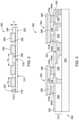
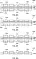
- FIG. 2is a cross sectional view of a circuit board 200 .
- the circuit board 200includes a ceramic carrier 202 .
- the ceramic carrier 202may have a top surface 218 and a bottom surface 214 .
- a body 212is disposed on the top surface 218 of the ceramic carrier 202 .
- the body 212has a top surface 220 and a bottom surface 216 , and the bottom surface 216 is disposed on the top surface 218 of the ceramic carrier 202 .
- the body 212may be formed from layers 204 of a dielectric material.
- a number vias 206are formed through the layers 204 of the dielectric material.
- the viasare formed completely through a thickness (t 1 ) of the layers 204 of the dielectric material.
- the vias 206may be filled and/or plated with a metal material. Where the vias are formed completely through the entire thickness of the layers 204 of the dielectric material, the metal in the vias 206 contacts the ceramic carrier 202 .
- a metal pad 208may be disposed on a surface of each of the vias 206 opposite the ceramic carrier 202 .
- the vias 206may be arranged in pairs to enable contacting LED devices or emitters that each may include a pair of metal contacts.
- the vias 206may be micro-vias or slots and may have a width w 3 , and a space between adjacent pairs of vias may have a width w 4 .
- w 3may be in a range of 50 ⁇ m to 200 ⁇ m
- w 4may be in a range of 20 ⁇ m to 200 ⁇ m.
- the small widths of the vias 206 and the small spacing between pairs of the vias 206may enable use of the circuit board 200 with an LED array, such as the LED array 100 of FIG. 1 , with fine line spacing.
- the vias 206may be filled and/or plated with a metal material that has good thermal conductivity.
- the metal materialmay be a copper, silver or nickel material.
- the ceramic carrier 202may be formed from a material with high thermal conductivity and high electrical resistivity.
- the ceramic carrier 202may be formed from Aluminum Nitride (AlN), Zirconia (ZrO 2 ) or Aluminum Oxide (Al 2 O 3 ). The use of such a material for the ceramic carrier 202 enables the vias 206 to be used both to make electrical connections to the conductive pads 208 and also to dissipate heat from any LED array or semiconductor device mounted on the conductive pads 208 .
- the vias 206when the vias 206 are formed through the entire thickness of the layers 204 of the dielectric material, the vias 206 may dissipate heat from an LED array or other semiconductor device mounted on the metal pads 208 to the ceramic carrier 202 , which may quickly dissipate the heat into the environment due to its high thermal conductivity. Further, because the ceramic carrier 202 has good electrical resistivity, it may prevent shorting of the vias 206 to each other.
- the body 212may have a thickness t 1 .
- the thickness t 1may be in a range 20 ⁇ m to 50 ⁇ m.
- the thickness t 1may be kept relatively thin to minimize the insulation contributed by the circuit board.
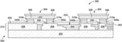
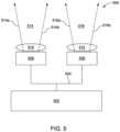
- FIG. 3is a cross sectional view of an LED lighting system 300 that includes the circuit board 202 of FIG. 2 with an array of light-emitting diode (LED) devices 304 mounted thereon. While the example illustrated in FIG. 3 includes an array of individual LED devices 304 , the embodiments described herein are applicable to any type of LED array, such as the LED array 102 of FIG. 1 , which may be an array of individual LED devices or a monolithic LED array that includes a single silicon wafer or die divided into segments that form the emitters. When a monolithic LED array is used, each of the emitters in the array may have a pair of metal contacts that may be electrically coupled to corresponding pairs of metal pads on the circuit board (e.g., via solder).
- LEDlight-emitting diode
- each of the LED devices 304includes a semiconductor structure 308 , a wavelength converting layer 306 over the semiconductor structure 308 and two metal contacts 310 a and 310 b .
- the semiconductor structuremay be any type of semiconductor structure that emits light when excited and may include one or more p-type regions, n-type regions and active, light-emitting regions.
- the two contacts 310 a and 310 bmay be a p-type electrode and an n-type electrode, respectively.
- the wavelength converting layer 306may be remote from, proximal to, or directly above the semiconductor structure 308 .
- the active layer in the semiconductor structure 308emits light into the wavelength converting layer 306 when turned on, and the wavelength converting layer 306 acts to further modify the wavelength of the light emitted by the active layer.
- the wavelength converting layer 306may include any luminescent material, such as, for example, phosphor particles in a transparent or translucent binder or matrix, or a ceramic phosphor element, which absorbs light of one wavelength and emits light of a different wavelength.
- each of the pairs of contacts 310 a and 310 b of each of the LED devices 304is electrically coupled (e.g., via solder) to a corresponding pair of the metal pads 208 on the circuit board 200 .
- a soldermask layer 302is provided on the top surface 220 of the circuit board 200 in areas that are not occupied by metal pads 208 .
- the soldermask layer 302may be any layer or type of material that protects the circuit board and/or reflects light.
- FIGS. 4 , 5 , 6 and 7are diagrams of example application systems that may incorporate LED lighting systems, such as the LED lighting system 300 of FIG. 3 .
- FIG. 4is a diagram of an example vehicle headlamp system 400 that may incorporate an LED lighting system, such as the LED lighting system 300 of FIG. 3 .
- the example vehicle headlamp system 400 illustrated in FIG. 4includes power lines 402 , a data bus 404 , an input filter and protection module 406 , a bus transceiver 408 , a sensor module 410 , an LED direct current to direct current (DC/DC) module 412 , a logic low-dropout (LDO) module 414 , a micro-controller 416 and an active head lamp 418 .
- the active head lamp 418may include an LED lighting system, such as the LED lighting system 300 of FIG. 3 .
- the power lines 402may have inputs that receive power from a vehicle, and the data bus 404 may have inputs/outputs over which data may be exchanged between the vehicle and the vehicle headlamp system 400 .
- the vehicle headlamp system 400may receive instructions from other locations in the vehicle, such as instructions to turn on turn signaling or turn on headlamps, and may send feedback to other locations in the vehicle if desired.
- the sensor module 410may be communicatively coupled to the data bus 404 and may provide additional data to the vehicle headlamp system 400 or other locations in the vehicle related to, for example, environmental conditions (e.g., time of day, rain, fog, or ambient light levels), vehicle state (e.g., parked, in-motion, speed of motion, or direction of motion), and presence/position of other objects (e.g., vehicles or pedestrians).
- a headlamp controller that is separate from any vehicle controller communicatively coupled to the vehicle data busmay also be included in the vehicle headlamp system 400 .
- the headlamp controllermay be a micro-controller, such as micro-controller ( ⁇ c) 416 .
- the micro-controller 416may be communicatively coupled to the data bus 404 .
- the input filter and protection module 406may be electrically coupled to the power lines 402 and may, for example, support various filters to reduce conducted emissions and provide power immunity. Additionally, the input filter and protection module 406 may provide electrostatic discharge (ESD) protection, load-dump protection, alternator field decay protection, and/or reverse polarity protection.
- ESDelectrostatic discharge
- the LED DC/DC module 412may be coupled between the filter and protection module 406 and the active headlamp 418 to receive filtered power and provide a drive current to power LEDs in the LED array in the active headlamp 418 .
- the LED DC/DC module 412may have an input voltage between 7 and 18 volts with a nominal voltage of approximately 13.2 volts and an output voltage that may be slightly higher (e.g., 0.3 volts) than a maximum voltage for the LED array (e.g., as determined by factor or local calibration and operating condition adjustments due to load, temperature or other factors).
- the logic LDO module 414may be coupled to the input filter and protection module 406 to receive the filtered power.
- the logic LDO module 414may also be coupled to the micro-controller 414 and the active headlamp 418 to provide power to the micro-controller 464 and/or the silicon backplane (e.g., CMOS logic) in the active headlamp 418 .
- the silicon backplanee.g., CMOS logic
- the bus transceiver 408may have, for example, a universal asynchronous receiver transmitter (UART) or serial peripheral interface (SPI) interface and may be coupled to the micro-controller 416 .
- the micro-controller 416may translate vehicle input based on, or including, data from the sensor module 410 .
- the translated vehicle inputmay include a video signal that is transferrable to an image buffer in the active headlamp module 418 .
- the micro-controller 416may load default image frames and test for open/short pixels during startup.
- an SPI interfacemay load an image buffer in CMOS. Image frames may be full frame, differential or partial frames.
- micro-controller 416may include control interface monitoring of CMOS status, including die temperature, as well as logic LDO output.
- LED DC/DC outputmay be dynamically controlled to minimize headroom.
- other headlamp functionssuch as complementary use in conjunction with side marker or turn signal lights, and/or activation of daytime running lights, may also be controlled.
- FIG. 5is a diagram of another example vehicle headlamp system 500 .
- the example vehicle headlamp system 500 illustrated in FIG. 5includes an application platform 502 , two LED lighting systems 506 and 508 , and optics 510 and 512 .
- the two LED lighting systems 506 and 508may be LED lighting systems, such as the LED lighting system 300 of FIG. 3 , or may include the LED lighting system 300 plus some of all of the other modules in the vehicle headlamp system 400 of FIG. 4 . In the latter embodiment, the LED lighting systems 506 and 508 may be vehicle headlamp sub-systems.
- the LED lighting system 508may emit light beams 514 (shown between arrows 514 a and 514 b in FIG. 5 ).
- the LED lighting system 506may emit light beams 516 (shown between arrows 516 a and 516 b in FIG. 5 ).
- a secondary optic 510is adjacent the LED lighting system 508 , and the light emitted from the LED lighting system 508 passes through the secondary optic 510 .
- a secondary optic 512is adjacent the LED lighting system 512 , and the light emitted from the LED lighting system 512 passes through the secondary optic 512 .
- no secondary optics 510 / 512are provided in the vehicle headlamp system.
- the secondary optics 510 / 512may be or include one or more light guides.
- the one or more light guidesmay be edge lit or may have an interior opening that defines an interior edge of the light guide.
- LED lighting systems 508 and 506(or the active headlamp of a vehicle headlamp sub-system) may be inserted in the interior openings of the one or more light guides such that they inject light into the interior edge (interior opening light guide) or exterior edge (edge lit light guide) of the one or more light guides.
- the one or more light guidesmay shape the light emitted by the LED lighting systems 508 and 506 in a desired manner, such as, for example, with a gradient, a chamfered distribution, a narrow distribution, a wide distribution, or an angular distribution.
- the application platform 502may provide power and/or data to the LED lighting systems 506 and/or 508 via lines 504 , which may include one or more or a portion of the power lines 402 and the data bus 404 of FIG. 4 .
- One or more sensors(which may be the sensors in the system 400 or other additional sensors) may be internal or external to the housing of the application platform 502 .
- each LED lighting system 508 and 506may include its own sensor module, connectivity and control module, power module, and/or LED array.
- the vehicle headlamp system 500may represent an automobile with steerable light beams where LEDs may be selectively activated to provide steerable light.
- an array of LEDse.g., the LED array 102
- LED array 102may be used to define or project a shape or pattern or illuminate only selected sections of a roadway.
- infrared cameras or detector pixels within LED systems 506 and 508may be sensors (e.g., similar to sensors in the sensor module 410 of FIG. 4 ) that identify portions of a scene (e.g., roadway or pedestrian crossing) that require illumination.
- FIG. 6is a diagram of an example wireless device 600 .
- the wireless device 600includes a processor 612 , a transceiver 602 , an antenna 604 , a speaker/microphone 606 , a keypad 608 , a display/touchpad 610 , a memory 616 , a power source 618 , and a camera 614 .
- the processor 612may be a general purpose processor, a special purpose processor, a conventional processor, a digital signal processor (DSP), a microprocessor, one or more microprocessors in association with a DSP core, a controller, a microcontroller, an application specific integrated circuit (ASIC), a field programmable gate array (FPGA) circuit, an integrated circuit (IC), a state machine, and the like.
- the processor 612may be coupled to, and may receive user input data from, the speaker/microphone 606 , the keypad 608 , the display/touchpad 610 and/or the camera 614 .
- the processor 612may also output user data to the speaker/microphone 606 , the keypad 608 , the display/touchpad 610 and/or the camera 614 .
- the processor 612may access information from, and store data in, any type of suitable memory, such as the memory 616 .
- the processor 612may receive power from the power source 618 and may be configured to distribute and/or control the power to the other components in the wireless device 600 .
- the processor 612may also be coupled to the camera 614 .
- the camera 614may include, for example, an image sensor, read out circuitry, a flash module and/or any other required circuitry or controls required to operate the camera 614 .
- the flash modulemay include an LED lighting system, such as the LED lighting system 300 of FIG. 3 , and a driver, one or more sensors and/or any other circuitry or controls required to operate the flash.
- FIG. 7is a back view of a wireless device 700 showing more detail of the camera 614 .
- the wireless device 700includes a casing 720 and a camera 614 .
- the camera 614include a lens 740 via which the camera's image sensor (not shown in FIG. 7 ) may capture an image of a scene.
- the camera module 614may also include a flash 750 that may include one or more LED arrays, which may be a part of one or more LED lighting systems, such the LED lighting system 300 of FIG. 3 .
- FIG. 8is a flow diagram of an example method 800 of manufacturing an LED lighting system, such as the LED lighting system 300 of FIG. 3 .
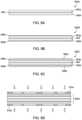
- FIGS. 9 A, 9 B, 9 C, 9 D, 9 E, 9 F, 9 G, 9 H, 9 I, 9 J, 9 K, 9 L, 9 M, 9 N, 9 O, 9 P and 9 Qare cross sectional views of the LED lighting system at various stages in the manufacturing method.
- a high density interconnect buildup process with finer geometriesis used to build up dielectric layers on the ceramic carrier.
- Various dielectric materialsmay be used, such as, for example, organic materials, or, more specifically, a Bismaleimide Triazine (BT) resin.
- the ceramic carriere.g., AlN carrier
- first metal padsare formed on a ceramic carrier ( 802 ), such as an AlN carrier, as described above.
- a ceramic carrier802
- FIGS. 9 A, 9 B, 9 C, 9 D, 9 E, 9 F and 9 Gprovide example structures at various points in the formation of first metal pads.
- the methodmay be used to simultaneously manufacture multiple circuit boards.
- two ceramic carriers 902 a and 902 bmay be attached to one another using, for example, an adhesive 904 to form a structure 900 A.
- the adhesivemay be a tape or a temporary glue.
- the adhesive 904is disposed between a first ceramic carrier 902 a and a second ceramic carrier 902 b . While the examples in FIGS. 9 A- 9 Q illustrate simultaneous manufacture of multiple circuit boards, one of ordinary skill in the art will recognize that a similar method may be used to manufacture a single circuit board (e.g., by not bonding two carriers and not performing processing on both carriers).
- a layer of a metal material 906 a and 906 bmay be formed on outer surfaces (e.g., the surfaces that are not bonded together) of the first and second carriers 902 a and 902 b .
- the metal layermay be formed by sputtering.
- copper sputteringmay be performed on the structure 900 A to form a thin film of copper on the outer surfaces of the carriers 902 a and 902 b .
- copper sputteringmay be performed on the structure 900 A to form a thin film of copper on the outer surfaces of the carriers 902 a and 902 b .
- One of ordinary skill in the artwill understand, however, that other methods and materials may be used to form the metal layer on the surfaces of the first and second carriers 902 a and 902 b.
- a film 908 a and 908 bmay be formed on each of the metal layers 906 a and 906 b to form a structure 900 C.
- the filmmay be a dry film, such as a photoresist, formed using dry film lamination.
- spin coatingmay be used to form the film 908 a and 908 b on the surfaces of the metal layers 906 a and 906 b.
- the structure 900 Cmay undergo an imaging or photolithography process to remove portions of the film 908 a and 908 b to form openings in the film and form a structure 900 D.
- thismay be performed by placing a pattern 910 a and 910 b , such as a glass pattern, over the structure 900 C and exposing the structure 900 C to light (e.g., ultraviolet (UV) light) emitted through the pattern.
- lighte.g., ultraviolet (UV) light
- desired portions of the film 908 a and 908 bmay be removed, for example, by applying a developer to the structure 900 D.
- a developermay be used.
- the portions of the film 908 a an 908 b that were exposed to the light in FIG. 9 Dmay become soluble to the developer or the portions of the film 908 a and 908 b that were not exposed to the light in FIG. 9 D may become soluble to the developer.
- Exposure of the structure 900 D to the developermay result in the structure 900 E with openings 911 a and 911 b formed in the film 908 a and 908 b .
- the openings 911 a and 911 bmay form a portion of the vias 206 in the circuit board 200 of FIG. 2 .
- the openings 911 a and 911 b in the film 908 a and 908 bmay be filled and/or plated with a metal material to form the structure 900 F.
- the openingsextend through the entirety of the film 908 a and 908 b and leave corresponding regions of the ceramic carriers 902 a and 902 b exposed.
- the openings 911 a and 911 bmay be plated and/or otherwise filled with a metal material (e.g., copper) to form metal-plated and/or filled openings 912 a and 912 b.
- the remaining portions of the film 908 a and 908 b and the portions of the metal layer 906 a and 906 b under themmay be removed, and first metal pads 912 a and 912 b remain on the carriers 902 a and 902 b to form a structure 900 G.
- Thismay be performed, for example, by stripping away the remaining portions of the film 908 a and 908 b and then performing copper or other metal etching on the portions of the metal layer 906 a and 906 b underneath.
- the resulting panelmay then be ready for further build up processes.
- FIG. 9 Hprovides an example structure 900 H showing the layers of the dielectric material 914 a and 914 b formed over the first metal pads 912 a and 912 b .
- the dielectric materialmay be laminated over the first metal pads 912 a and 912 b , although one of ordinary skill in the art will understand that other methods may be used, such as molding.
- FIG. 9 Iprovides an example structure 900 I showing the vias 916 a and 916 b formed in the layers of the dielectric material 914 a and 914 b .
- the vias 916 a and 916 bmay be micro-vias or slots and may be formed, for example, using laser ablation or drilling, although one of ordinary skill in the art will understand that other methods may be used.
- the vias 916 a and 916 bmay form another part of the vias 206 in the circuit board 200 of FIG. 2 .
- the openings 911 a and 911 b and the vias 916 a and 916 bmay form the vias 206 formed through the entire thickness t 1 of the dielectric layers 204 in FIG. 2 .
- the viasmay be filled with a metal material ( 808 ).
- FIG. 9 Jillustrates an example structure 900 J showing the vias 916 a and 916 b filled with a metal material 918 a and 918 b .
- the viasmay be filled using copper plating, which may leave a layer of the metal material 918 a and 918 b on the outer-most surfaces of the dielectric material 914 a and 914 b and the vias 916 a and 916 b , as shown.
- copper platingmay leave a layer of the metal material 918 a and 918 b on the outer-most surfaces of the dielectric material 914 a and 914 b and the vias 916 a and 916 b , as shown.
- copper platingmay leave a layer of the metal material 918 a and 918 b on the outer-most surfaces of the dielectric material 914 a and 914 b and the vias 916 a and 916 b , as shown.
- a second metal padmay be formed on each of the vias ( 810 ) to form, for example, metal pads on the outer-most surface of the circuit board.
- FIGS. 9 K, 9 L, 9 M, 9 N, 9 O, 9 P and 9 Qprovide example structures at various points in the formation of the second metal pads.
- a film 920 a and 920 bmay be formed on outer-most surfaces of the structure 900 J (e.g., over the metal 918 a and 918 b to form a structure 900 K.
- the filmmay be a dry film, such as a photoresist, formed using dry film lamination.
- spin coatingmay be used to form the film 920 a and 920 b.
- the structure 900 Kmay undergo an imaging or photolithography process to remove portions of the film 920 a and 920 b in regions between the vias 916 a and 916 b to form a structure 900 L.
- thismay be performed by placing a pattern 922 a and 922 b , such as a glass pattern, over the structure 900 K and exposing the structure 900 K to light (e.g., ultraviolet (UV) light) emitted through the pattern.
- UV lightultraviolet
- desired portions of the film 920 a and 920 bmay be removed, for example, by applying a developer to the structure 900 L.
- a developermay be used.
- the portions of the film 920 a and 920 b that were exposed to the light in FIG. 9 Lmay become soluble to the developer or the portions of the film 920 a and 920 b that were not exposed to the light in FIG. 9 L may become soluble to the developer.
- Exposure of the structure 900 L to the developermay result in the structure 900 M with portions of the film 920 a and 920 b remaining over the vias 916 a and 916 b.
- the portions of the metal layer 918 a and 918 b between the remaining portions of the film 920 a and 920 bmay be removed to form a structure 900 N. This may be performed, for example, by copper or other metal etching.
- the remaining portions of the film 920 a and 920 bmay be removed to form a structure 900 O. This may be performed, for example, by stripping away the remaining portions of the film 920 a and 920 b.
- the second metal pads 922 a and 922 bmay be provided on each of the metal-filled vias 918 a and 918 b .
- thismay be performed using NiAu plating, although one of ordinary skill in the art will recognize that other methods and/or metal materials may be used.
- the two circuit boardsmay be separated. Only one of the separated circuit boards 900 Q is shown in FIG. 9 Q .
- the circuit boardmay then be ready for individual LED device or monolithic LED array attach by, for example, soldering metal pads of the individual LED devices or the monolithic array to the metal pads 922 a and/or 922 b of the circuit board.
Landscapes
- Engineering & Computer Science (AREA)
- Microelectronics & Electronic Packaging (AREA)
- Power Engineering (AREA)
- Physics & Mathematics (AREA)
- Condensed Matter Physics & Semiconductors (AREA)
- General Physics & Mathematics (AREA)
- Computer Hardware Design (AREA)
- Manufacturing & Machinery (AREA)
- Ceramic Engineering (AREA)
- Geometry (AREA)
- Led Device Packages (AREA)
Abstract
Description
Claims (13)
Priority Applications (7)
| Application Number | Priority Date | Filing Date | Title |
|---|---|---|---|
| US16/809,104US11664347B2 (en) | 2020-01-07 | 2020-03-04 | Ceramic carrier and build up carrier for light-emitting diode (LED) array |
| JP2022541872AJP7619739B2 (en) | 2020-01-07 | 2021-01-07 | Ceramic and build-up carriers for light emitting diode (LED) arrays - Patents.com |
| PCT/US2021/012425WO2021142066A1 (en) | 2020-01-07 | 2021-01-07 | Ceramic carrier and build up carrier for light-emitting diode (led) array |
| CN202180019644.3ACN115176527A (en) | 2020-01-07 | 2021-01-07 | Ceramic carrier and laminate carrier for Light Emitting Diode (LED) array |
| KR1020227026783AKR20220123451A (en) | 2020-01-07 | 2021-01-07 | Ceramic Carriers and Build-up Carriers for Light Emitting Diode (LED) Arrays |
| EP21702353.0AEP4088555A1 (en) | 2020-01-07 | 2021-01-07 | Ceramic carrier and build up carrier for light-emitting diode (led) array |
| US18/303,378US12191280B2 (en) | 2020-01-07 | 2023-04-19 | Ceramic carrier and build up carrier for light-emitting diode (LED) array |
Applications Claiming Priority (2)
| Application Number | Priority Date | Filing Date | Title |
|---|---|---|---|
| US202062958058P | 2020-01-07 | 2020-01-07 | |
| US16/809,104US11664347B2 (en) | 2020-01-07 | 2020-03-04 | Ceramic carrier and build up carrier for light-emitting diode (LED) array |
Related Child Applications (1)
| Application Number | Title | Priority Date | Filing Date |
|---|---|---|---|
| US18/303,378DivisionUS12191280B2 (en) | 2020-01-07 | 2023-04-19 | Ceramic carrier and build up carrier for light-emitting diode (LED) array |
Publications (2)
| Publication Number | Publication Date |
|---|---|
| US20210210463A1 US20210210463A1 (en) | 2021-07-08 |
| US11664347B2true US11664347B2 (en) | 2023-05-30 |
Family
ID=76654441
Family Applications (2)
| Application Number | Title | Priority Date | Filing Date |
|---|---|---|---|
| US16/809,104ActiveUS11664347B2 (en) | 2020-01-07 | 2020-03-04 | Ceramic carrier and build up carrier for light-emitting diode (LED) array |
| US18/303,378ActiveUS12191280B2 (en) | 2020-01-07 | 2023-04-19 | Ceramic carrier and build up carrier for light-emitting diode (LED) array |
Family Applications After (1)
| Application Number | Title | Priority Date | Filing Date |
|---|---|---|---|
| US18/303,378ActiveUS12191280B2 (en) | 2020-01-07 | 2023-04-19 | Ceramic carrier and build up carrier for light-emitting diode (LED) array |
Country Status (1)
| Country | Link |
|---|---|
| US (2) | US11664347B2 (en) |
Citations (108)
| Publication number | Priority date | Publication date | Assignee | Title |
|---|---|---|---|---|
| US5073814A (en)* | 1990-07-02 | 1991-12-17 | General Electric Company | Multi-sublayer dielectric layers |
| US5336453A (en)* | 1993-06-11 | 1994-08-09 | Aerospace Coating Systems, Inc. | Method for producing ceramic-based electronic components |
| US20030020156A1 (en)* | 1999-07-02 | 2003-01-30 | International Business Machines Corporation | Electronic package with optimized lamination process |
| US20030136577A1 (en) | 2002-01-24 | 2003-07-24 | Fujitsu Limited | Circuit board and method for fabricating the same, and electronic device |
| US6730391B1 (en) | 1998-07-23 | 2004-05-04 | Toyo Kohan Co., Ltd. | Clad board for printed-circuit board, multilayered printed-circuit board, and method of manufacture thereof |
| US6936855B1 (en) | 2002-01-16 | 2005-08-30 | Shane Harrah | Bendable high flux LED array |
| US20050263867A1 (en) | 2004-05-28 | 2005-12-01 | Rokuro Kambe | Intermediate substrate |
| US20050269287A1 (en)* | 2004-06-04 | 2005-12-08 | Ngk Spark Plug Co., Ltd. | Multilayer electronic component and method for producing the same |
| US20060141851A1 (en) | 2003-02-07 | 2006-06-29 | Nobuyuki Matsui | Socket for led light source and lighting system using the socket |
| US20070080458A1 (en) | 2005-10-11 | 2007-04-12 | Tsuyoshi Ogawa | Hybrid module and method of manufacturing the same |
| TW200830975A (en) | 2007-01-02 | 2008-07-16 | Phoenix Prec Technology Corp | PCB structure having heat-dissipating member |
| JP2008283133A (en) | 2007-05-14 | 2008-11-20 | Sumitomo Metal Electronics Devices Inc | Multilayer wiring board for mounting light-emitting device, and its manufacturing method |
| US20090046432A1 (en)* | 2007-08-15 | 2009-02-19 | Phoenix Precision Technology Corporation | Packaging substrate structure with electronic components embedded therein and method for manufacturing the same |
| US7550319B2 (en) | 2005-09-01 | 2009-06-23 | E. I. Du Pont De Nemours And Company | Low temperature co-fired ceramic (LTCC) tape compositions, light emitting diode (LED) modules, lighting devices and method of forming thereof |
| US20090207630A1 (en) | 2005-06-08 | 2009-08-20 | Minebea Co., Ltd. | Planar illumination device |
| JP2009186734A (en) | 2008-02-06 | 2009-08-20 | Hitachi Displays Ltd | Liquid crystal display |
| TW200942105A (en) | 2008-03-27 | 2009-10-01 | Phoenix Prec Technology Corp | Method of fabricating package substrate having semiconductor component embedded therein |
| US20100039817A1 (en) | 2008-08-14 | 2010-02-18 | Hon Hai Precision Industry Co., Ltd. | Led module and light modulator with the same |
| US20100155746A1 (en) | 2009-04-06 | 2010-06-24 | Cree, Inc. | High voltage low current surface-emitting led |
| US20110030209A1 (en) | 2009-01-09 | 2011-02-10 | Shih Chang Chang | Method for fabricating thin touch sensor panels |
| US20110121347A1 (en) | 2009-11-24 | 2011-05-26 | Luminus Devices, Inc. | Systems and methods for managing heat from an led |
| JP2011113989A (en) | 2009-11-24 | 2011-06-09 | Oki Data Corp | Display panel and projection type display device |
| CN102315208A (en) | 2011-09-09 | 2012-01-11 | 福建省万邦光电科技有限公司 | LED (Light-Emitting Diode) light-source packaging structure with inlaid ceramic plate |
| US20120106140A1 (en)* | 2010-11-03 | 2012-05-03 | Taiwan Semiconductor Manufacturing Company, Ltd. | Light-emitting diode lamp and method of making |
| US20120175643A1 (en) | 2011-01-09 | 2012-07-12 | Bridgelux, Inc. | Packaging Photon Building Blocks Having Only Top Side Connections in an Interconnect Structure |
| US20120188734A1 (en) | 2011-01-20 | 2012-07-26 | Ibiden Co., Ltd. | Wiring board and method for manufacturing the same |
| US20120273960A1 (en) | 2011-04-30 | 2012-11-01 | Stats Chippac, Ltd. | Semiconductor Device and Method of Embedding TSV Semiconductor Die Within Encapsulant with TMV for Vertical Interconnect in POP |
| US20130075924A1 (en) | 2011-09-23 | 2013-03-28 | Stats Chippac, Ltd. | Semiconductor Device and Method of Forming Stacked Vias Within Interconnect Structure for FO-WLCSP |
| KR20130036650A (en) | 2011-10-04 | 2013-04-12 | 현대자동차주식회사 | Metal substrate module for led, method for manufacturing the same, and led package for vehicle using metal substrate module |
| US20130193463A1 (en) | 2008-08-26 | 2013-08-01 | Albeo Technologies, Inc. | Methods Of Integrating LED Chips With Heat Sinks, And Led-Based Lighting Assemblies Made Thereby |
| US8513790B2 (en) | 2008-04-22 | 2013-08-20 | Silicon Base Development Inc. | Package-base structure of luminescent diode |
| US20130221452A1 (en) | 2011-09-15 | 2013-08-29 | Stats Chippac, Ltd. | Semiconductor Device and Method of Forming Semiconductor Die with Active Region Responsive to External Stimulus |
| US8536714B2 (en) | 2011-06-21 | 2013-09-17 | Shinko Electric Industries Co., Ltd. | Interposer, its manufacturing method, and semiconductor device |
| US20130328067A1 (en) | 2012-06-08 | 2013-12-12 | Feng Chia University | Led module |
| US20140021493A1 (en)* | 2012-07-20 | 2014-01-23 | Peter Andrews | Solid state lighting component package with layer |
| US20140061930A1 (en)* | 2012-09-06 | 2014-03-06 | International Business Machines Corporation | Overlay-tolerant via mask and reactive ion etch (rie) technique |
| US20140124777A1 (en) | 2012-03-27 | 2014-05-08 | Panasonic Corporation | Built-up substrate, method for manufacturing same, and semiconductor integrated circuit package |
| US20140182896A1 (en)* | 2012-12-31 | 2014-07-03 | Samsung, Electro-Mechanics Co., Ltd. | Substrate having electronic component embedded therein and method of manufacturing the same |
| US8773006B2 (en) | 2011-08-22 | 2014-07-08 | Lg Innotek Co., Ltd. | Light emitting device package, light source module, and lighting system including the same |
| US20140251658A1 (en) | 2013-03-07 | 2014-09-11 | Bridge Semiconductor Corporation | Thermally enhanced wiring board with built-in heat sink and build-up circuitry |
| US20140268780A1 (en) | 2013-03-15 | 2014-09-18 | Power Gold LLC | Flexible electronic assembly and method of manufacturing the same |
| US20140306845A1 (en) | 2013-04-10 | 2014-10-16 | Apple Inc. | Electronic Device With Foam Antenna Carrier |
| US8912650B2 (en) | 2011-06-23 | 2014-12-16 | Stats Chippac, Ltd. | Semiconductor device and method of forming protective coating over interconnect structure to inhibit surface oxidation |
| US20150054406A1 (en) | 2013-07-19 | 2015-02-26 | Bridgelux, Inc. | LED Array Member and Integrated Control Module Assembly Having Active Circuitry |
| US20150054001A1 (en) | 2013-08-26 | 2015-02-26 | Optiz, Inc. | Integrated Camera Module And Method Of Making Same |
| US20150084206A1 (en) | 2013-09-24 | 2015-03-26 | Stats Chippac, Ltd. | Semiconductor Device and Method of Forming Dual Fan-Out Semiconductor Package |
| US9018655B2 (en) | 2005-02-03 | 2015-04-28 | Epistar Corporation | Light emitting apparatus and manufacture method thereof |
| US20150200185A1 (en) | 2014-01-16 | 2015-07-16 | Taiwan Semiconductor Manufacturing Company, Ltd. | Pad structure design in fan-out package |
| CN204641532U (en) | 2015-04-01 | 2015-09-16 | 迅驰车业江苏有限公司 | A kind of intellectual Car Front Combination Lights |
| US20150303219A1 (en) | 2012-11-22 | 2015-10-22 | Sharp Kabushiki Kaisha | Display apparatus |
| US20150319868A1 (en) | 2014-05-01 | 2015-11-05 | Tong Hsing Electronic Industries, Ltd. | Multilayer circuit board and method for manufacturing the same |
| US20150371585A1 (en) | 2014-06-18 | 2015-12-24 | X-Celeprint Limited | Micro assembled led displays and lighting elements |
| US20160050771A1 (en) | 2014-08-15 | 2016-02-18 | Unimicron Technology Corp. | Manufacturing method of circuit structure embedded with heat-dissipation block |
| US20160172402A1 (en) | 2014-12-11 | 2016-06-16 | Invensas Corporation | Image sensor device |
| US20160273741A1 (en) | 2015-03-20 | 2016-09-22 | Suk-ho JUNG | Light module, illumination apparatus comprising one-body type molding substrate, and method for fabricating the light module |
| US20160316565A1 (en) | 2015-04-24 | 2016-10-27 | Unimicron Technology Corp. | Circuit board and method for manufacturing the same |
| US20160324004A1 (en) | 2013-12-12 | 2016-11-03 | At&S Austria Technologie & Systemtechnik Aktiengesellschaft | Method for Embedding a Component in a Printed Circuit Board |
| EP3113236A1 (en) | 2015-06-30 | 2017-01-04 | LG Innotek Co., Ltd. | Light emitting device and lighting module having the light emitting device |
| US20170009978A1 (en) | 2015-07-06 | 2017-01-12 | Lg Electronics Inc. | Light source module, fabrication method therefor, and lighting device including the same |
| US20170025593A1 (en) | 2014-09-25 | 2017-01-26 | X-Celeprint Limited | Redistribution layer for substrate contacts |
| US20170033062A1 (en) | 2015-07-29 | 2017-02-02 | STATS ChipPAC Pte. Ltd. | Antenna In Embedded Wafer-Level Ball-Grid Array Package |
| US20170040306A1 (en) | 2015-06-30 | 2017-02-09 | Apple Inc. | Electronic Devices With Soft Input-Output Components |
| US20170062383A1 (en) | 2015-08-31 | 2017-03-02 | Taiwan Semiconductor Manufacturing Company, Ltd. | Package Structures and Methods of Making the Same |
| US9615453B2 (en) | 2012-09-26 | 2017-04-04 | Ping-Jung Yang | Method for fabricating glass substrate package |
| US9653397B2 (en) | 2014-10-01 | 2017-05-16 | Nepes Co., Ltd. | Semiconductor package and method of manufacturing the same |
| US20170140202A1 (en) | 2015-11-17 | 2017-05-18 | Taiwan Semiconductor Manufacturing Company, Ltd. | Fingerprint Sensor Device and Method |
| US20170358562A1 (en) | 2016-05-18 | 2017-12-14 | Globalfoundries Inc. | INTEGRATED DISPLAY SYSTEM WITH MULTI-COLOR LIGHT EMITTING DIODES (LEDs) |
| CN107580385A (en) | 2017-08-25 | 2018-01-12 | 成都华科威电子科技有限公司 | A kind of vehicle front lighting lamp control system |
| US20180166373A1 (en) | 2014-03-07 | 2018-06-14 | Bridge Semiconductor Corp. | Method of making wiring board with interposer and electronic component incorporated with base board |
| US20180175262A1 (en) | 2016-12-21 | 2018-06-21 | Glo Ab | Micro-lensed light emitting device |
| US10005384B2 (en) | 2016-03-02 | 2018-06-26 | Valeo Vision | Anti-dazzle headlamp |
| WO2018116814A1 (en) | 2016-12-22 | 2018-06-28 | シャープ株式会社 | Display device and manufacturing method |
| US20180197471A1 (en) | 2017-01-10 | 2018-07-12 | X-Celeprint Limited | Digital-drive pulse-width-modulated output system |
| US20180226386A1 (en) | 2017-02-08 | 2018-08-09 | X-Celeprint Limited | Inorganic light-emitting-diode displays with multi-iled pixels |
| US20180269188A1 (en) | 2017-03-15 | 2018-09-20 | Taiwan Semiconductor Manufacturing Company, Ltd. | Semiconductor packages and methods of forming same |
| US20180269191A1 (en) | 2017-03-15 | 2018-09-20 | Globalfoundries Inc. | Micro-led display assembly |
| WO2018172152A1 (en) | 2017-03-21 | 2018-09-27 | Lumileds Holding B.V. | Mounting an led element on a flat carrier |
| US20180337142A1 (en) | 2017-05-18 | 2018-11-22 | Xintec Inc. | Chip package and method for forming the same |
| US20180337135A1 (en) | 2015-12-22 | 2018-11-22 | Intel Corporation | Ultra small molded module integrated with die by module-on-wafer assembly |
| US20180358317A1 (en) | 2015-12-23 | 2018-12-13 | Intel IP Corporation | Wafer level package structure with internal conductive layer |
| US20190006283A1 (en) | 2017-06-30 | 2019-01-03 | Taiwan Semiconductor Manufacturing Company, Ltd. | Semiconductor Package and Method |
| WO2019013469A1 (en) | 2017-07-10 | 2019-01-17 | 삼성전자주식회사 | Micro-led display and manufacturing method therefor |
| US10205055B2 (en) | 2014-06-14 | 2019-02-12 | Hiphoton Co., Ltd. | Light engine array |
| US20190056067A1 (en) | 2017-08-17 | 2019-02-21 | Microsoft Technology Licensing, Llc | Active illumination source and pcb components having mountings for reduced z-height and improved thermal conductivity |
| US20190066571A1 (en) | 2017-08-23 | 2019-02-28 | Facebook Technologies, Llc | Interposer for multi-layer display architecture |
| US20190075656A1 (en) | 2017-09-01 | 2019-03-07 | Magnachip Semiconductor, Ltd. | Flexible semiconductor package and method for fabricating the same |
| US20190088603A1 (en) | 2015-07-29 | 2019-03-21 | STATS ChipPAC Pte. Ltd. | Antenna in Embedded Wafer-Level Ball-Grid Array Package |
| US20190096864A1 (en) | 2015-09-24 | 2019-03-28 | Apple Inc. | Display with embedded pixel driver chips |
| US10262977B2 (en) | 2014-07-31 | 2019-04-16 | Facebook Technologies, Llc | Colour inorganic LED display for display devices with a high number of pixel |
| US20190181315A1 (en)* | 2017-12-11 | 2019-06-13 | Unimicron Technology Corp. | Circuit board and method for manufacturing the same |
| US20190206833A1 (en) | 2015-12-23 | 2019-07-04 | Intel IP Corporation | Eplb/ewlb based pop for hbm or customized package stack |
| US10347509B1 (en) | 2018-02-09 | 2019-07-09 | Didrew Technology (Bvi) Limited | Molded cavity fanout package without using a carrier and method of manufacturing the same |
| WO2019168763A1 (en) | 2018-02-28 | 2019-09-06 | Apple Inc. | Display with embedded pixel driver chips |
| US10420204B2 (en) | 2014-03-07 | 2019-09-17 | Bridge Semiconductor Corporation | Wiring board having electrical isolator and moisture inhibiting cap incorporated therein and method of making the same |
| US20190305205A1 (en) | 2016-11-16 | 2019-10-03 | Tdk Electronics Ag | Power Module Having Reduced Susceptibility to Defects, and Use Thereof |
| US20190319020A1 (en) | 2018-04-17 | 2019-10-17 | Shaoher Pan | Integrated multi-color light-emitting pixel arrays based devices by bonding |
| US20190333444A1 (en) | 2018-04-25 | 2019-10-31 | Raxium, Inc. | Architecture for light emitting elements in a light field display |
| US20190360673A1 (en) | 2018-05-28 | 2019-11-28 | Lumens Co., Ltd. | Micro-led module and method for fabricating the same |
| EP3582593A1 (en) | 2018-06-11 | 2019-12-18 | AT & S Austria Technologie & Systemtechnik Aktiengesellschaft | Component carrier with a stepped cavity and a stepped component assembly being embedded within the stepped cavity |
| US10529690B2 (en) | 2016-11-14 | 2020-01-07 | Taiwan Semiconductor Manufacturing Company, Ltd. | Package structures and methods of forming the same |
| US20200105638A1 (en) | 2018-09-27 | 2020-04-02 | Taiwan Semiconductor Manufacturing Company, Ltd. | Sensor Package and Method |
| US20200119235A1 (en) | 2018-10-11 | 2020-04-16 | Intel Corporation | Laser printing of color converter devices on micro led display devices and methods |
| US20200176346A1 (en) | 2018-11-29 | 2020-06-04 | Taiwan Semiconductor Manufacturing Co., Ltd. | Semiconductor packages and methods of manufacturing the same |
| US10683986B2 (en) | 2016-09-15 | 2020-06-16 | Valeo Vision | Luminous module comprising a monolithic electroluminescent source |
| US20200251626A1 (en) | 2017-08-31 | 2020-08-06 | Lg Innotek Co., Ltd. | Semiconductor device and head lamp comprising same |
| US20210028766A1 (en) | 2019-07-25 | 2021-01-28 | Zhuhai Crystal Resonance Technologies Co., Ltd. | Packages with Organic Back Ends for Electronic Components |
| US20210074645A1 (en) | 2019-09-05 | 2021-03-11 | Powertech Technology Inc. | Chip package structure using silicon interposer as interconnection bridge |
| US20210125971A1 (en) | 2014-05-24 | 2021-04-29 | Hiphoton Co., Ltd. | Structure of a semiconductor array |
Family Cites Families (39)
| Publication number | Priority date | Publication date | Assignee | Title |
|---|---|---|---|---|
| US5621225A (en) | 1996-01-18 | 1997-04-15 | Motorola | Light emitting diode display package |
| JPH11163412A (en) | 1997-11-25 | 1999-06-18 | Matsushita Electric Works Ltd | Led illuminator |
| GB9811328D0 (en)* | 1998-05-27 | 1998-07-22 | Exitech Ltd | The use of mid-infrared lasers for drilling microvia holes in printed circuit (wiring) boards and other electrical circuit interconnection packages |
| DE19936924C1 (en)* | 1999-08-05 | 2001-06-13 | Georg Bernitz | High temperature detection device and method for manufacturing same |
| US6531328B1 (en)* | 2001-10-11 | 2003-03-11 | Solidlite Corporation | Packaging of light-emitting diode |
| JP5080758B2 (en) | 2005-10-07 | 2012-11-21 | 日立マクセル株式会社 | Semiconductor device |
| JP4804109B2 (en) | 2005-10-27 | 2011-11-02 | 京セラ株式会社 | LIGHT EMITTING DEVICE WIRING BOARD, LIGHT EMITTING DEVICE, AND LIGHT EMITTING DEVICE WIRING BOARD MANUFACTURING METHOD |
| JP5102605B2 (en) | 2007-12-25 | 2012-12-19 | パナソニック株式会社 | Light emitting device and manufacturing method thereof |
| KR101043463B1 (en)* | 2009-05-28 | 2011-06-23 | 삼성전기주식회사 | Multilayer ceramic substrate and its manufacturing method |
| JP2012015148A (en) | 2010-06-29 | 2012-01-19 | Rohm Co Ltd | Led module and led lighting system |
| US8652860B2 (en) | 2011-01-09 | 2014-02-18 | Bridgelux, Inc. | Packaging photon building blocks having only top side connections in a molded interconnect structure |
| US9516713B2 (en) | 2011-01-25 | 2016-12-06 | Semiconductor Energy Laboratory Co., Ltd. | Light-emitting device |
| JP5643720B2 (en) | 2011-06-30 | 2014-12-17 | 株式会社沖データ | Display module, manufacturing method thereof and display device |
| US9147663B2 (en) | 2013-05-28 | 2015-09-29 | Intel Corporation | Bridge interconnection with layered interconnect structures |
| US9275967B2 (en)* | 2014-01-06 | 2016-03-01 | Taiwan Semiconductor Manufacturing Company, Ltd. | Protrusion bump pads for bond-on-trace processing |
| US20170263546A1 (en) | 2014-03-07 | 2017-09-14 | Bridge Semiconductor Corporation | Wiring board with electrical isolator and base board incorporated therein and semiconductor assembly and manufacturing method thereof |
| US9799829B2 (en) | 2014-07-25 | 2017-10-24 | Semiconductor Energy Laboratory Co., Ltd. | Separation method, light-emitting device, module, and electronic device |
| CN104241219B (en) | 2014-08-26 | 2019-06-21 | 日月光半导体制造股份有限公司 | Element embedded packaging structure and manufacturing method thereof |
| US9478583B2 (en) | 2014-12-08 | 2016-10-25 | Apple Inc. | Wearable display having an array of LEDs on a conformable silicon substrate |
| US9252337B1 (en) | 2014-12-22 | 2016-02-02 | Bridgelux, Inc. | Composite substrate for light emitting diodes |
| KR102344533B1 (en) | 2015-02-12 | 2021-12-29 | 엘지이노텍 주식회사 | Lighting emitting device package |
| US10600823B2 (en) | 2015-09-02 | 2020-03-24 | Facebook Technologies, Llc | Assembly of semiconductor devices |
| US10297711B2 (en) | 2015-12-30 | 2019-05-21 | Globalfoundries Singapore Pte. Ltd. | Integrated LED and LED driver units and methods for fabricating the same |
| US10529696B2 (en) | 2016-04-12 | 2020-01-07 | Cree, Inc. | High density pixelated LED and devices and methods thereof |
| KR102617466B1 (en) | 2016-07-18 | 2023-12-26 | 주식회사 루멘스 | Micro led array display apparatus |
| KR102595309B1 (en) | 2016-07-20 | 2023-10-31 | 삼성전자주식회사 | method for detecting misalignment of chips, manufacturing method of fan-out panel level package using the same, and fan-out panel level package |
| US9960328B2 (en) | 2016-09-06 | 2018-05-01 | Amkor Technology, Inc. | Semiconductor device and manufacturing method thereof |
| US10325893B2 (en) | 2016-12-13 | 2019-06-18 | Hong Kong Beida Jade Bird Display Limited | Mass transfer of micro structures using adhesives |
| US9978707B1 (en) | 2017-03-23 | 2018-05-22 | Delphi Technologies, Inc. | Electrical-device adhesive barrier |
| JP2019046835A (en) | 2017-08-30 | 2019-03-22 | 株式会社沖データ | Semiconductor light emitting element, semiconductor composite device, optical print head, and image forming apparatus |
| KR102456882B1 (en) | 2017-11-24 | 2022-10-21 | 주식회사 루멘스 | method for making high efficiency micro LED module |
| US11749790B2 (en) | 2017-12-20 | 2023-09-05 | Lumileds Llc | Segmented LED with embedded transistors |
| US10437402B1 (en) | 2018-03-27 | 2019-10-08 | Shaoher Pan | Integrated light-emitting pixel arrays based devices by bonding |
| US11145583B2 (en)* | 2018-05-03 | 2021-10-12 | Intel Corporation | Method to achieve variable dielectric thickness in packages for better electrical performance |
| JP7106364B2 (en) | 2018-06-18 | 2022-07-26 | 株式会社ジャパンディスプレイ | Display device |
| JP6669208B2 (en) | 2018-08-02 | 2020-03-18 | 日亜化学工業株式会社 | Light emitting device |
| US11626448B2 (en) | 2019-03-29 | 2023-04-11 | Lumileds Llc | Fan-out light-emitting diode (LED) device substrate with embedded backplane, lighting system and method of manufacture |
| US11721632B2 (en)* | 2019-10-28 | 2023-08-08 | Intel Corporation | Hybrid core substrate architecture for high speed signaling and FLI/SLI reliability and its making |
| US11631594B2 (en) | 2019-11-19 | 2023-04-18 | Lumileds Llc | Fan out structure for light-emitting diode (LED) device and lighting system |
- 2020
- 2020-03-04USUS16/809,104patent/US11664347B2/enactiveActive
- 2023
- 2023-04-19USUS18/303,378patent/US12191280B2/enactiveActive
Patent Citations (112)
| Publication number | Priority date | Publication date | Assignee | Title |
|---|---|---|---|---|
| US5073814A (en)* | 1990-07-02 | 1991-12-17 | General Electric Company | Multi-sublayer dielectric layers |
| US5336453A (en)* | 1993-06-11 | 1994-08-09 | Aerospace Coating Systems, Inc. | Method for producing ceramic-based electronic components |
| US5336453B1 (en)* | 1993-06-11 | 1996-07-23 | Connecticut Innovations Inc | Method for producing ceramic-based electronic components |
| US6730391B1 (en) | 1998-07-23 | 2004-05-04 | Toyo Kohan Co., Ltd. | Clad board for printed-circuit board, multilayered printed-circuit board, and method of manufacture thereof |
| US20030020156A1 (en)* | 1999-07-02 | 2003-01-30 | International Business Machines Corporation | Electronic package with optimized lamination process |
| US6936855B1 (en) | 2002-01-16 | 2005-08-30 | Shane Harrah | Bendable high flux LED array |
| US20030136577A1 (en) | 2002-01-24 | 2003-07-24 | Fujitsu Limited | Circuit board and method for fabricating the same, and electronic device |
| US20060141851A1 (en) | 2003-02-07 | 2006-06-29 | Nobuyuki Matsui | Socket for led light source and lighting system using the socket |
| US20050263867A1 (en) | 2004-05-28 | 2005-12-01 | Rokuro Kambe | Intermediate substrate |
| US20050269287A1 (en)* | 2004-06-04 | 2005-12-08 | Ngk Spark Plug Co., Ltd. | Multilayer electronic component and method for producing the same |
| US9018655B2 (en) | 2005-02-03 | 2015-04-28 | Epistar Corporation | Light emitting apparatus and manufacture method thereof |
| US20090207630A1 (en) | 2005-06-08 | 2009-08-20 | Minebea Co., Ltd. | Planar illumination device |
| US7550319B2 (en) | 2005-09-01 | 2009-06-23 | E. I. Du Pont De Nemours And Company | Low temperature co-fired ceramic (LTCC) tape compositions, light emitting diode (LED) modules, lighting devices and method of forming thereof |
| US20070080458A1 (en) | 2005-10-11 | 2007-04-12 | Tsuyoshi Ogawa | Hybrid module and method of manufacturing the same |
| TW200830975A (en) | 2007-01-02 | 2008-07-16 | Phoenix Prec Technology Corp | PCB structure having heat-dissipating member |
| JP2008283133A (en) | 2007-05-14 | 2008-11-20 | Sumitomo Metal Electronics Devices Inc | Multilayer wiring board for mounting light-emitting device, and its manufacturing method |
| US20090046432A1 (en)* | 2007-08-15 | 2009-02-19 | Phoenix Precision Technology Corporation | Packaging substrate structure with electronic components embedded therein and method for manufacturing the same |
| JP2009186734A (en) | 2008-02-06 | 2009-08-20 | Hitachi Displays Ltd | Liquid crystal display |
| TW200942105A (en) | 2008-03-27 | 2009-10-01 | Phoenix Prec Technology Corp | Method of fabricating package substrate having semiconductor component embedded therein |
| US8513790B2 (en) | 2008-04-22 | 2013-08-20 | Silicon Base Development Inc. | Package-base structure of luminescent diode |
| US20100039817A1 (en) | 2008-08-14 | 2010-02-18 | Hon Hai Precision Industry Co., Ltd. | Led module and light modulator with the same |
| US20130193463A1 (en) | 2008-08-26 | 2013-08-01 | Albeo Technologies, Inc. | Methods Of Integrating LED Chips With Heat Sinks, And Led-Based Lighting Assemblies Made Thereby |
| US20110030209A1 (en) | 2009-01-09 | 2011-02-10 | Shih Chang Chang | Method for fabricating thin touch sensor panels |
| US20100155746A1 (en) | 2009-04-06 | 2010-06-24 | Cree, Inc. | High voltage low current surface-emitting led |
| US20110121347A1 (en) | 2009-11-24 | 2011-05-26 | Luminus Devices, Inc. | Systems and methods for managing heat from an led |
| JP2011113989A (en) | 2009-11-24 | 2011-06-09 | Oki Data Corp | Display panel and projection type display device |
| US20120106140A1 (en)* | 2010-11-03 | 2012-05-03 | Taiwan Semiconductor Manufacturing Company, Ltd. | Light-emitting diode lamp and method of making |
| US20120175643A1 (en) | 2011-01-09 | 2012-07-12 | Bridgelux, Inc. | Packaging Photon Building Blocks Having Only Top Side Connections in an Interconnect Structure |
| US20120188734A1 (en) | 2011-01-20 | 2012-07-26 | Ibiden Co., Ltd. | Wiring board and method for manufacturing the same |
| US20120273960A1 (en) | 2011-04-30 | 2012-11-01 | Stats Chippac, Ltd. | Semiconductor Device and Method of Embedding TSV Semiconductor Die Within Encapsulant with TMV for Vertical Interconnect in POP |
| US8536714B2 (en) | 2011-06-21 | 2013-09-17 | Shinko Electric Industries Co., Ltd. | Interposer, its manufacturing method, and semiconductor device |
| US8912650B2 (en) | 2011-06-23 | 2014-12-16 | Stats Chippac, Ltd. | Semiconductor device and method of forming protective coating over interconnect structure to inhibit surface oxidation |
| US8773006B2 (en) | 2011-08-22 | 2014-07-08 | Lg Innotek Co., Ltd. | Light emitting device package, light source module, and lighting system including the same |
| CN102315208A (en) | 2011-09-09 | 2012-01-11 | 福建省万邦光电科技有限公司 | LED (Light-Emitting Diode) light-source packaging structure with inlaid ceramic plate |
| US20130221452A1 (en) | 2011-09-15 | 2013-08-29 | Stats Chippac, Ltd. | Semiconductor Device and Method of Forming Semiconductor Die with Active Region Responsive to External Stimulus |
| US20130075924A1 (en) | 2011-09-23 | 2013-03-28 | Stats Chippac, Ltd. | Semiconductor Device and Method of Forming Stacked Vias Within Interconnect Structure for FO-WLCSP |
| KR20130036650A (en) | 2011-10-04 | 2013-04-12 | 현대자동차주식회사 | Metal substrate module for led, method for manufacturing the same, and led package for vehicle using metal substrate module |
| US20140124777A1 (en) | 2012-03-27 | 2014-05-08 | Panasonic Corporation | Built-up substrate, method for manufacturing same, and semiconductor integrated circuit package |
| US20130328067A1 (en) | 2012-06-08 | 2013-12-12 | Feng Chia University | Led module |
| US20140021493A1 (en)* | 2012-07-20 | 2014-01-23 | Peter Andrews | Solid state lighting component package with layer |
| US20140061930A1 (en)* | 2012-09-06 | 2014-03-06 | International Business Machines Corporation | Overlay-tolerant via mask and reactive ion etch (rie) technique |
| US9615453B2 (en) | 2012-09-26 | 2017-04-04 | Ping-Jung Yang | Method for fabricating glass substrate package |
| US20150303219A1 (en) | 2012-11-22 | 2015-10-22 | Sharp Kabushiki Kaisha | Display apparatus |
| US20140182896A1 (en)* | 2012-12-31 | 2014-07-03 | Samsung, Electro-Mechanics Co., Ltd. | Substrate having electronic component embedded therein and method of manufacturing the same |
| US20140251658A1 (en) | 2013-03-07 | 2014-09-11 | Bridge Semiconductor Corporation | Thermally enhanced wiring board with built-in heat sink and build-up circuitry |
| US20140268780A1 (en) | 2013-03-15 | 2014-09-18 | Power Gold LLC | Flexible electronic assembly and method of manufacturing the same |
| US20140306845A1 (en) | 2013-04-10 | 2014-10-16 | Apple Inc. | Electronic Device With Foam Antenna Carrier |
| US20150054406A1 (en) | 2013-07-19 | 2015-02-26 | Bridgelux, Inc. | LED Array Member and Integrated Control Module Assembly Having Active Circuitry |
| US20150054001A1 (en) | 2013-08-26 | 2015-02-26 | Optiz, Inc. | Integrated Camera Module And Method Of Making Same |
| US20150084206A1 (en) | 2013-09-24 | 2015-03-26 | Stats Chippac, Ltd. | Semiconductor Device and Method of Forming Dual Fan-Out Semiconductor Package |
| US20160324004A1 (en) | 2013-12-12 | 2016-11-03 | At&S Austria Technologie & Systemtechnik Aktiengesellschaft | Method for Embedding a Component in a Printed Circuit Board |
| US20150200185A1 (en) | 2014-01-16 | 2015-07-16 | Taiwan Semiconductor Manufacturing Company, Ltd. | Pad structure design in fan-out package |
| US20180166373A1 (en) | 2014-03-07 | 2018-06-14 | Bridge Semiconductor Corp. | Method of making wiring board with interposer and electronic component incorporated with base board |
| US10420204B2 (en) | 2014-03-07 | 2019-09-17 | Bridge Semiconductor Corporation | Wiring board having electrical isolator and moisture inhibiting cap incorporated therein and method of making the same |
| US20150319868A1 (en) | 2014-05-01 | 2015-11-05 | Tong Hsing Electronic Industries, Ltd. | Multilayer circuit board and method for manufacturing the same |
| US20210125971A1 (en) | 2014-05-24 | 2021-04-29 | Hiphoton Co., Ltd. | Structure of a semiconductor array |
| US10205055B2 (en) | 2014-06-14 | 2019-02-12 | Hiphoton Co., Ltd. | Light engine array |
| US20150371585A1 (en) | 2014-06-18 | 2015-12-24 | X-Celeprint Limited | Micro assembled led displays and lighting elements |
| US10262977B2 (en) | 2014-07-31 | 2019-04-16 | Facebook Technologies, Llc | Colour inorganic LED display for display devices with a high number of pixel |
| US20160050771A1 (en) | 2014-08-15 | 2016-02-18 | Unimicron Technology Corp. | Manufacturing method of circuit structure embedded with heat-dissipation block |
| US20170025593A1 (en) | 2014-09-25 | 2017-01-26 | X-Celeprint Limited | Redistribution layer for substrate contacts |
| US9899465B2 (en) | 2014-09-25 | 2018-02-20 | X-Celeprint Limited | Redistribution layer for substrate contacts |
| US9653397B2 (en) | 2014-10-01 | 2017-05-16 | Nepes Co., Ltd. | Semiconductor package and method of manufacturing the same |
| US20160172402A1 (en) | 2014-12-11 | 2016-06-16 | Invensas Corporation | Image sensor device |
| US20160273741A1 (en) | 2015-03-20 | 2016-09-22 | Suk-ho JUNG | Light module, illumination apparatus comprising one-body type molding substrate, and method for fabricating the light module |
| CN204641532U (en) | 2015-04-01 | 2015-09-16 | 迅驰车业江苏有限公司 | A kind of intellectual Car Front Combination Lights |
| US20160316565A1 (en) | 2015-04-24 | 2016-10-27 | Unimicron Technology Corp. | Circuit board and method for manufacturing the same |
| US20170040306A1 (en) | 2015-06-30 | 2017-02-09 | Apple Inc. | Electronic Devices With Soft Input-Output Components |
| EP3113236A1 (en) | 2015-06-30 | 2017-01-04 | LG Innotek Co., Ltd. | Light emitting device and lighting module having the light emitting device |
| US20170009978A1 (en) | 2015-07-06 | 2017-01-12 | Lg Electronics Inc. | Light source module, fabrication method therefor, and lighting device including the same |
| US20170033062A1 (en) | 2015-07-29 | 2017-02-02 | STATS ChipPAC Pte. Ltd. | Antenna In Embedded Wafer-Level Ball-Grid Array Package |
| US20190088603A1 (en) | 2015-07-29 | 2019-03-21 | STATS ChipPAC Pte. Ltd. | Antenna in Embedded Wafer-Level Ball-Grid Array Package |
| US20170062383A1 (en) | 2015-08-31 | 2017-03-02 | Taiwan Semiconductor Manufacturing Company, Ltd. | Package Structures and Methods of Making the Same |
| US10665578B2 (en) | 2015-09-24 | 2020-05-26 | Apple Inc. | Display with embedded pixel driver chips |
| US20190096864A1 (en) | 2015-09-24 | 2019-03-28 | Apple Inc. | Display with embedded pixel driver chips |
| US20170140202A1 (en) | 2015-11-17 | 2017-05-18 | Taiwan Semiconductor Manufacturing Company, Ltd. | Fingerprint Sensor Device and Method |
| US20180337135A1 (en) | 2015-12-22 | 2018-11-22 | Intel Corporation | Ultra small molded module integrated with die by module-on-wafer assembly |
| US20180358317A1 (en) | 2015-12-23 | 2018-12-13 | Intel IP Corporation | Wafer level package structure with internal conductive layer |
| US20190206833A1 (en) | 2015-12-23 | 2019-07-04 | Intel IP Corporation | Eplb/ewlb based pop for hbm or customized package stack |
| US10005384B2 (en) | 2016-03-02 | 2018-06-26 | Valeo Vision | Anti-dazzle headlamp |
| US20170358562A1 (en) | 2016-05-18 | 2017-12-14 | Globalfoundries Inc. | INTEGRATED DISPLAY SYSTEM WITH MULTI-COLOR LIGHT EMITTING DIODES (LEDs) |
| US10683986B2 (en) | 2016-09-15 | 2020-06-16 | Valeo Vision | Luminous module comprising a monolithic electroluminescent source |
| US10529690B2 (en) | 2016-11-14 | 2020-01-07 | Taiwan Semiconductor Manufacturing Company, Ltd. | Package structures and methods of forming the same |
| US20190305205A1 (en) | 2016-11-16 | 2019-10-03 | Tdk Electronics Ag | Power Module Having Reduced Susceptibility to Defects, and Use Thereof |
| US20180175262A1 (en) | 2016-12-21 | 2018-06-21 | Glo Ab | Micro-lensed light emitting device |
| WO2018116814A1 (en) | 2016-12-22 | 2018-06-28 | シャープ株式会社 | Display device and manufacturing method |
| US20190385513A1 (en) | 2016-12-22 | 2019-12-19 | Sharp Kabushiki Kaisha | Display device |
| US20180197471A1 (en) | 2017-01-10 | 2018-07-12 | X-Celeprint Limited | Digital-drive pulse-width-modulated output system |
| US20180226386A1 (en) | 2017-02-08 | 2018-08-09 | X-Celeprint Limited | Inorganic light-emitting-diode displays with multi-iled pixels |
| US20180269188A1 (en) | 2017-03-15 | 2018-09-20 | Taiwan Semiconductor Manufacturing Company, Ltd. | Semiconductor packages and methods of forming same |
| US20180269191A1 (en) | 2017-03-15 | 2018-09-20 | Globalfoundries Inc. | Micro-led display assembly |
| WO2018172152A1 (en) | 2017-03-21 | 2018-09-27 | Lumileds Holding B.V. | Mounting an led element on a flat carrier |
| US20180337142A1 (en) | 2017-05-18 | 2018-11-22 | Xintec Inc. | Chip package and method for forming the same |
| US20190006283A1 (en) | 2017-06-30 | 2019-01-03 | Taiwan Semiconductor Manufacturing Company, Ltd. | Semiconductor Package and Method |
| WO2019013469A1 (en) | 2017-07-10 | 2019-01-17 | 삼성전자주식회사 | Micro-led display and manufacturing method therefor |
| US20190056067A1 (en) | 2017-08-17 | 2019-02-21 | Microsoft Technology Licensing, Llc | Active illumination source and pcb components having mountings for reduced z-height and improved thermal conductivity |
| US20190066571A1 (en) | 2017-08-23 | 2019-02-28 | Facebook Technologies, Llc | Interposer for multi-layer display architecture |
| CN107580385A (en) | 2017-08-25 | 2018-01-12 | 成都华科威电子科技有限公司 | A kind of vehicle front lighting lamp control system |
| US20200251626A1 (en) | 2017-08-31 | 2020-08-06 | Lg Innotek Co., Ltd. | Semiconductor device and head lamp comprising same |
| US20190075656A1 (en) | 2017-09-01 | 2019-03-07 | Magnachip Semiconductor, Ltd. | Flexible semiconductor package and method for fabricating the same |
| US20190181315A1 (en)* | 2017-12-11 | 2019-06-13 | Unimicron Technology Corp. | Circuit board and method for manufacturing the same |
| US10347509B1 (en) | 2018-02-09 | 2019-07-09 | Didrew Technology (Bvi) Limited | Molded cavity fanout package without using a carrier and method of manufacturing the same |
| WO2019168763A1 (en) | 2018-02-28 | 2019-09-06 | Apple Inc. | Display with embedded pixel driver chips |
| US20190319020A1 (en) | 2018-04-17 | 2019-10-17 | Shaoher Pan | Integrated multi-color light-emitting pixel arrays based devices by bonding |
| US20190333444A1 (en) | 2018-04-25 | 2019-10-31 | Raxium, Inc. | Architecture for light emitting elements in a light field display |
| US20190360673A1 (en) | 2018-05-28 | 2019-11-28 | Lumens Co., Ltd. | Micro-led module and method for fabricating the same |
| EP3582593A1 (en) | 2018-06-11 | 2019-12-18 | AT & S Austria Technologie & Systemtechnik Aktiengesellschaft | Component carrier with a stepped cavity and a stepped component assembly being embedded within the stepped cavity |
| US20200105638A1 (en) | 2018-09-27 | 2020-04-02 | Taiwan Semiconductor Manufacturing Company, Ltd. | Sensor Package and Method |
| US20200119235A1 (en) | 2018-10-11 | 2020-04-16 | Intel Corporation | Laser printing of color converter devices on micro led display devices and methods |
| US20200176346A1 (en) | 2018-11-29 | 2020-06-04 | Taiwan Semiconductor Manufacturing Co., Ltd. | Semiconductor packages and methods of manufacturing the same |
| US20210028766A1 (en) | 2019-07-25 | 2021-01-28 | Zhuhai Crystal Resonance Technologies Co., Ltd. | Packages with Organic Back Ends for Electronic Components |
| US20210074645A1 (en) | 2019-09-05 | 2021-03-11 | Powertech Technology Inc. | Chip package structure using silicon interposer as interconnection bridge |
Non-Patent Citations (12)
| Title |
|---|
| Annex to Form PCT/ISA/206, Communication Relating to the Results of the Partial International Search issued Mar. 4, 2021 for PCT International Application No. PCT/US2020/061201. |
| Extended European Search Report dated Jul. 30, 2020 for European Patent Application No. 20158288.9. |
| Extended European Search Report dated Jul. 7, 2020 for European Patent Application No. 20157985.1. |
| Extended European Search Report dated Oct. 19, 2020 for the European Patent Application No. 20169027.8. |
| Extended European Search Report dated Sep. 11, 2020 for European Patent Application No. 20166601.3. |
| Extended European Search Report dated Sep. 2, 2020 for European Patent Application No. 20158481.0. |
| International Search Report and Written Opinion dated Apr. 16, 2021 for PCT International Application No. PCT/US2020/066998. |
| International Search Report and Written Opinion dated Apr. 28, 2021 for PCT International Application No. PCT/US2020/061201. |
| International Search Report and Written Opinion dated Apr. 8, 2021 for PCT International Application No. PCT/US2021/012425. |
| International Search Report and Written Opinion dated Feb. 11, 2021 for PCT International Application No. PCT/US2020/061205. |
| International Search Report and Written Opinion dated Feb. 17, 2021 for PCT International Application No. PCT/US2020/061206. |
| International Search Report and Written Opinion dated Jun. 29, 2021 for PCT International Application No. PCT/US2021/021702. |
Also Published As
| Publication number | Publication date |
|---|---|
| US12191280B2 (en) | 2025-01-07 |
| US20230253365A1 (en) | 2023-08-10 |
| US20210210463A1 (en) | 2021-07-08 |
Similar Documents
| Publication | Publication Date | Title |
|---|---|---|
| US12224182B2 (en) | Fan out structure for light-emitting diode (LED) device and lighting system | |
| KR20210134989A (en) | A light emitting diode (LED) lighting system comprising a panel of light emitting diode (LED) arrays including a plurality of backplanes embedded in a substrate and a backplane embedded in a substrate | |
| JP7619739B2 (en) | Ceramic and build-up carriers for light emitting diode (LED) arrays - Patents.com | |
| JP2023514987A (en) | Light-emitting diode lighting system with wire-bonded hybrid devices | |
| JP7590060B2 (en) | FAN-OUT STRUCTURE FOR LIGHT EMITTING DIODE DEVICES AND LIGHTING SYSTEMS - Patent application | |
| US12191280B2 (en) | Ceramic carrier and build up carrier for light-emitting diode (LED) array | |
| CN114930529B (en) | Fan-out structure and lighting system of light-emitting diode (LED) devices | |
| EP3890451A1 (en) | Ceramic carrier and build up carrier for light-emitting diode (led) array | |
| TWI824197B (en) | Method of manufacturing an led lighting system |
Legal Events
| Date | Code | Title | Description |
|---|---|---|---|
| FEPP | Fee payment procedure | Free format text:ENTITY STATUS SET TO UNDISCOUNTED (ORIGINAL EVENT CODE: BIG.); ENTITY STATUS OF PATENT OWNER: LARGE ENTITY | |
| AS | Assignment | Owner name:LUMILEDS HOLDING B.V., NETHERLANDS Free format text:ASSIGNMENT OF ASSIGNORS INTEREST;ASSIGNORS:TAN, LOON-KWANG;HIN, TZE YANG;SIGNING DATES FROM 20200804 TO 20200805;REEL/FRAME:053453/0848 | |
| AS | Assignment | Owner name:LUMILEDS LLC, CALIFORNIA Free format text:ASSIGNMENT OF ASSIGNORS INTEREST;ASSIGNOR:LUMILEDS HOLDING B.V.;REEL/FRAME:054817/0612 Effective date:20210105 | |
| STPP | Information on status: patent application and granting procedure in general | Free format text:NON FINAL ACTION MAILED | |
| STPP | Information on status: patent application and granting procedure in general | Free format text:RESPONSE TO NON-FINAL OFFICE ACTION ENTERED AND FORWARDED TO EXAMINER | |
| STPP | Information on status: patent application and granting procedure in general | Free format text:FINAL REJECTION MAILED | |
| STPP | Information on status: patent application and granting procedure in general | Free format text:DOCKETED NEW CASE - READY FOR EXAMINATION | |
| STPP | Information on status: patent application and granting procedure in general | Free format text:NON FINAL ACTION MAILED | |
| STPP | Information on status: patent application and granting procedure in general | Free format text:RESPONSE TO NON-FINAL OFFICE ACTION ENTERED AND FORWARDED TO EXAMINER | |
| STPP | Information on status: patent application and granting procedure in general | Free format text:FINAL REJECTION MAILED | |
| STPP | Information on status: patent application and granting procedure in general | Free format text:ADVISORY ACTION MAILED | |
| STPP | Information on status: patent application and granting procedure in general | Free format text:DOCKETED NEW CASE - READY FOR EXAMINATION | |
| AS | Assignment | Owner name:DEUTSCHE BANK AG NEW YORK BRANCH, NEW YORK Free format text:PATENT SECURITY AGREEMENT;ASSIGNOR:LUMILEDS, LLC;REEL/FRAME:062114/0001 Effective date:20221208 | |
| AS | Assignment | Owner name:SOUND POINT AGENCY LLC, NEW YORK Free format text:SECURITY INTEREST;ASSIGNORS:LUMILEDS LLC;LUMILEDS HOLDING B.V.;REEL/FRAME:062299/0338 Effective date:20221230 | |
| STCF | Information on status: patent grant | Free format text:PATENTED CASE | |
| AS | Assignment | Owner name:LUMILEDS HOLDING B.V., NETHERLANDS Free format text:RELEASE BY SECURED PARTY;ASSIGNOR:SOUND POINT AGENCY LLC;REEL/FRAME:070046/0001 Effective date:20240731 Owner name:LUMILEDS LLC, CALIFORNIA Free format text:RELEASE BY SECURED PARTY;ASSIGNOR:SOUND POINT AGENCY LLC;REEL/FRAME:070046/0001 Effective date:20240731 | |
| AS | Assignment | Owner name:LUMILEDS SINGAPORE PTE. LTD., SINGAPORE Free format text:ASSIGNMENT OF ASSIGNORS INTEREST;ASSIGNOR:LUMILEDS LLC;REEL/FRAME:071888/0086 Effective date:20250708 |