US11664219B2 - Selective deposition of SiOC thin films - Google Patents
Selective deposition of SiOC thin filmsDownload PDFInfo
- Publication number
- US11664219B2 US11664219B2US17/463,813US202117463813AUS11664219B2US 11664219 B2US11664219 B2US 11664219B2US 202117463813 AUS202117463813 AUS 202117463813AUS 11664219 B2US11664219 B2US 11664219B2
- Authority
- US
- United States
- Prior art keywords
- sioc
- substrate
- plasma
- gas
- reactant
- Prior art date
- Legal status (The legal status is an assumption and is not a legal conclusion. Google has not performed a legal analysis and makes no representation as to the accuracy of the status listed.)
- Active
Links
- 239000010409thin filmSubstances0.000titleclaimsabstractdescription17
- 230000008021depositionEffects0.000titleclaimsdescription61
- 239000000758substrateSubstances0.000claimsabstractdescription78
- 239000002184metalSubstances0.000claimsabstractdescription74
- 229910052751metalInorganic materials0.000claimsabstractdescription74
- 238000000151depositionMethods0.000claimsabstractdescription61
- 238000000034methodMethods0.000claimsabstractdescription60
- 239000012686silicon precursorSubstances0.000claimsabstractdescription35
- 229910052710siliconInorganic materials0.000claimsabstractdescription32
- XUIMIQQOPSSXEZ-UHFFFAOYSA-NSiliconChemical compound[Si]XUIMIQQOPSSXEZ-UHFFFAOYSA-N0.000claimsabstractdescription30
- 239000010703siliconSubstances0.000claimsabstractdescription30
- 238000000231atomic layer depositionMethods0.000claimsabstractdescription12
- 239000000376reactantSubstances0.000claimsdescription82
- IJGRMHOSHXDMSA-UHFFFAOYSA-NAtomic nitrogenChemical compoundN#NIJGRMHOSHXDMSA-UHFFFAOYSA-N0.000claimsdescription70
- 239000010408filmSubstances0.000claimsdescription69
- 239000007789gasSubstances0.000claimsdescription55
- XKRFYHLGVUSROY-UHFFFAOYSA-NArgonChemical compound[Ar]XKRFYHLGVUSROY-UHFFFAOYSA-N0.000claimsdescription48
- 238000006243chemical reactionMethods0.000claimsdescription46
- 229910052757nitrogenInorganic materials0.000claimsdescription35
- 239000001257hydrogenSubstances0.000claimsdescription31
- 229910052739hydrogenInorganic materials0.000claimsdescription31
- 229910052760oxygenInorganic materials0.000claimsdescription26
- 229910052786argonInorganic materials0.000claimsdescription25
- QVGXLLKOCUKJST-UHFFFAOYSA-Natomic oxygenChemical compound[O]QVGXLLKOCUKJST-UHFFFAOYSA-N0.000claimsdescription24
- 239000001301oxygenSubstances0.000claimsdescription24
- UFHFLCQGNIYNRP-UHFFFAOYSA-NHydrogenChemical compound[H][H]UFHFLCQGNIYNRP-UHFFFAOYSA-N0.000claimsdescription22
- VYPSYNLAJGMNEJ-UHFFFAOYSA-NSilicium dioxideChemical compoundO=[Si]=OVYPSYNLAJGMNEJ-UHFFFAOYSA-N0.000claimsdescription11
- JPMBLOQPQSYOMC-UHFFFAOYSA-Ntrimethoxy(3-methoxypropyl)silaneChemical compoundCOCCC[Si](OC)(OC)OCJPMBLOQPQSYOMC-UHFFFAOYSA-N0.000claimsdescription10
- 239000012808vapor phaseSubstances0.000claimsdescription10
- 229910052802copperInorganic materials0.000claimsdescription7
- 229910052756noble gasInorganic materials0.000claimsdescription7
- 239000000377silicon dioxideSubstances0.000claimsdescription5
- 229910052681coesiteInorganic materials0.000claimsdescription4
- 229910052906cristobaliteInorganic materials0.000claimsdescription4
- 150000004820halidesChemical class0.000claimsdescription4
- 229910052682stishoviteInorganic materials0.000claimsdescription4
- 229910052905tridymiteInorganic materials0.000claimsdescription4
- FOQJQXVUMYLJSU-UHFFFAOYSA-Ntriethoxy(1-triethoxysilylethyl)silaneChemical compoundCCO[Si](OCC)(OCC)C(C)[Si](OCC)(OCC)OCCFOQJQXVUMYLJSU-UHFFFAOYSA-N0.000claimsdescription4
- ATJFFYVFTNAWJD-UHFFFAOYSA-NTinChemical compound[Sn]ATJFFYVFTNAWJD-UHFFFAOYSA-N0.000claimsdescription2
- 229910052736halogenInorganic materials0.000claimsdescription2
- 150000002367halogensChemical class0.000claimsdescription2
- 210000002381plasmaAnatomy0.000description89
- 239000012071phaseSubstances0.000description39
- 239000000463materialSubstances0.000description25
- 238000005137deposition processMethods0.000description17
- 239000002243precursorSubstances0.000description16
- 239000006227byproductSubstances0.000description14
- 238000005530etchingMethods0.000description12
- 238000009832plasma treatmentMethods0.000description11
- 238000010926purgeMethods0.000description11
- 230000015572biosynthetic processEffects0.000description9
- 150000002431hydrogenChemical class0.000description9
- 239000010410layerSubstances0.000description8
- LIVNPJMFVYWSIS-UHFFFAOYSA-Nsilicon monoxideInorganic materials[Si-]#[O+]LIVNPJMFVYWSIS-UHFFFAOYSA-N0.000description8
- 229910018557Si OInorganic materials0.000description6
- 229910052799carbonInorganic materials0.000description6
- 239000010949copperSubstances0.000description6
- 239000003989dielectric materialSubstances0.000description6
- 229910010271silicon carbideInorganic materials0.000description6
- OKTJSMMVPCPJKN-UHFFFAOYSA-NCarbonChemical compound[C]OKTJSMMVPCPJKN-UHFFFAOYSA-N0.000description5
- RYGMFSIKBFXOCR-UHFFFAOYSA-NCopperChemical compound[Cu]RYGMFSIKBFXOCR-UHFFFAOYSA-N0.000description5
- 229910018540Si CInorganic materials0.000description5
- 239000000203mixtureSubstances0.000description5
- 208000012868OvergrowthDiseases0.000description4
- NINIDFKCEFEMDL-UHFFFAOYSA-NSulfurChemical compound[S]NINIDFKCEFEMDL-UHFFFAOYSA-N0.000description4
- 238000010586diagramMethods0.000description4
- 229910052717sulfurInorganic materials0.000description4
- 239000011593sulfurSubstances0.000description4
- 239000011261inert gasSubstances0.000description3
- 150000003254radicalsChemical class0.000description3
- 235000001674Agaricus brunnescensNutrition0.000description2
- KZBUYRJDOAKODT-UHFFFAOYSA-NChlorineChemical compoundClClKZBUYRJDOAKODT-UHFFFAOYSA-N0.000description2
- -1TiNChemical class0.000description2
- 229910052734heliumInorganic materials0.000description2
- 150000002500ionsChemical class0.000description2
- 238000004519manufacturing processMethods0.000description2
- 238000012986modificationMethods0.000description2
- 230000004048modificationEffects0.000description2
- 238000002161passivationMethods0.000description2
- 235000012239silicon dioxideNutrition0.000description2
- 229910052814silicon oxideInorganic materials0.000description2
- 238000006557surface reactionMethods0.000description2
- 238000011144upstream manufacturingMethods0.000description2
- ZAMOUSCENKQFHK-UHFFFAOYSA-NChlorine atomChemical compound[Cl]ZAMOUSCENKQFHK-UHFFFAOYSA-N0.000description1
- PXGOKWXKJXAPGV-UHFFFAOYSA-NFluorineChemical compoundFFPXGOKWXKJXAPGV-UHFFFAOYSA-N0.000description1
- 229910007991Si-NInorganic materials0.000description1
- 229910008048Si-SInorganic materials0.000description1
- 229910004541SiNInorganic materials0.000description1
- 229910006294Si—NInorganic materials0.000description1
- 229910006336Si—SInorganic materials0.000description1
- 239000002253acidSubstances0.000description1
- 125000004429atomChemical group0.000description1
- 230000000903blocking effectEffects0.000description1
- 239000012159carrier gasSubstances0.000description1
- 239000003795chemical substances by applicationSubstances0.000description1
- 239000000460chlorineSubstances0.000description1
- 229910052801chlorineInorganic materials0.000description1
- 125000004122cyclic groupChemical group0.000description1
- 230000009699differential effectEffects0.000description1
- 239000011737fluorineSubstances0.000description1
- 229910052731fluorineInorganic materials0.000description1
- 238000010574gas phase reactionMethods0.000description1
- 239000001307heliumSubstances0.000description1
- SWQJXJOGLNCZEY-UHFFFAOYSA-Nhelium atomChemical compound[He]SWQJXJOGLNCZEY-UHFFFAOYSA-N0.000description1
- 239000012535impuritySubstances0.000description1
- 238000011065in-situ storageMethods0.000description1
- 229910052743kryptonInorganic materials0.000description1
- 239000007791liquid phaseSubstances0.000description1
- 229910001092metal group alloyInorganic materials0.000description1
- 150000002739metalsChemical class0.000description1
- 229910003465moissaniteInorganic materials0.000description1
- 229910052754neonInorganic materials0.000description1
- 125000004433nitrogen atomChemical groupN*0.000description1
- 150000002831nitrogen free-radicalsChemical class0.000description1
- 150000002835noble gasesChemical class0.000description1
- 239000013110organic ligandSubstances0.000description1
- 230000003647oxidationEffects0.000description1
- 238000007254oxidation reactionMethods0.000description1
- 239000004065semiconductorSubstances0.000description1
- 239000002356single layerSubstances0.000description1
- 125000006850spacer groupChemical group0.000description1
- 239000000126substanceSubstances0.000description1
- 230000008685targetingEffects0.000description1
Images


Classifications
- H—ELECTRICITY
- H01—ELECTRIC ELEMENTS
- H01L—SEMICONDUCTOR DEVICES NOT COVERED BY CLASS H10
- H01L21/00—Processes or apparatus adapted for the manufacture or treatment of semiconductor or solid state devices or of parts thereof
- H01L21/02—Manufacture or treatment of semiconductor devices or of parts thereof
- H01L21/02104—Forming layers
- H01L21/02107—Forming insulating materials on a substrate
- H01L21/02109—Forming insulating materials on a substrate characterised by the type of layer, e.g. type of material, porous/non-porous, pre-cursors, mixtures or laminates
- H01L21/02112—Forming insulating materials on a substrate characterised by the type of layer, e.g. type of material, porous/non-porous, pre-cursors, mixtures or laminates characterised by the material of the layer
- H01L21/02123—Forming insulating materials on a substrate characterised by the type of layer, e.g. type of material, porous/non-porous, pre-cursors, mixtures or laminates characterised by the material of the layer the material containing silicon
- H01L21/02164—Forming insulating materials on a substrate characterised by the type of layer, e.g. type of material, porous/non-porous, pre-cursors, mixtures or laminates characterised by the material of the layer the material containing silicon the material being a silicon oxide, e.g. SiO2
- H—ELECTRICITY
- H01—ELECTRIC ELEMENTS
- H01L—SEMICONDUCTOR DEVICES NOT COVERED BY CLASS H10
- H01L21/00—Processes or apparatus adapted for the manufacture or treatment of semiconductor or solid state devices or of parts thereof
- H01L21/02—Manufacture or treatment of semiconductor devices or of parts thereof
- H01L21/02104—Forming layers
- H01L21/02107—Forming insulating materials on a substrate
- H01L21/02225—Forming insulating materials on a substrate characterised by the process for the formation of the insulating layer
- H01L21/0226—Forming insulating materials on a substrate characterised by the process for the formation of the insulating layer formation by a deposition process
- H01L21/02263—Forming insulating materials on a substrate characterised by the process for the formation of the insulating layer formation by a deposition process deposition from the gas or vapour phase
- H01L21/02271—Forming insulating materials on a substrate characterised by the process for the formation of the insulating layer formation by a deposition process deposition from the gas or vapour phase deposition by decomposition or reaction of gaseous or vapour phase compounds, i.e. chemical vapour deposition
- H01L21/0228—Forming insulating materials on a substrate characterised by the process for the formation of the insulating layer formation by a deposition process deposition from the gas or vapour phase deposition by decomposition or reaction of gaseous or vapour phase compounds, i.e. chemical vapour deposition deposition by cyclic CVD, e.g. ALD, ALE, pulsed CVD
- C—CHEMISTRY; METALLURGY
- C23—COATING METALLIC MATERIAL; COATING MATERIAL WITH METALLIC MATERIAL; CHEMICAL SURFACE TREATMENT; DIFFUSION TREATMENT OF METALLIC MATERIAL; COATING BY VACUUM EVAPORATION, BY SPUTTERING, BY ION IMPLANTATION OR BY CHEMICAL VAPOUR DEPOSITION, IN GENERAL; INHIBITING CORROSION OF METALLIC MATERIAL OR INCRUSTATION IN GENERAL
- C23C—COATING METALLIC MATERIAL; COATING MATERIAL WITH METALLIC MATERIAL; SURFACE TREATMENT OF METALLIC MATERIAL BY DIFFUSION INTO THE SURFACE, BY CHEMICAL CONVERSION OR SUBSTITUTION; COATING BY VACUUM EVAPORATION, BY SPUTTERING, BY ION IMPLANTATION OR BY CHEMICAL VAPOUR DEPOSITION, IN GENERAL
- C23C16/00—Chemical coating by decomposition of gaseous compounds, without leaving reaction products of surface material in the coating, i.e. chemical vapour deposition [CVD] processes
- C23C16/22—Chemical coating by decomposition of gaseous compounds, without leaving reaction products of surface material in the coating, i.e. chemical vapour deposition [CVD] processes characterised by the deposition of inorganic material, other than metallic material
- C23C16/30—Deposition of compounds, mixtures or solid solutions, e.g. borides, carbides, nitrides
- C23C16/42—Silicides
- C—CHEMISTRY; METALLURGY
- C23—COATING METALLIC MATERIAL; COATING MATERIAL WITH METALLIC MATERIAL; CHEMICAL SURFACE TREATMENT; DIFFUSION TREATMENT OF METALLIC MATERIAL; COATING BY VACUUM EVAPORATION, BY SPUTTERING, BY ION IMPLANTATION OR BY CHEMICAL VAPOUR DEPOSITION, IN GENERAL; INHIBITING CORROSION OF METALLIC MATERIAL OR INCRUSTATION IN GENERAL
- C23C—COATING METALLIC MATERIAL; COATING MATERIAL WITH METALLIC MATERIAL; SURFACE TREATMENT OF METALLIC MATERIAL BY DIFFUSION INTO THE SURFACE, BY CHEMICAL CONVERSION OR SUBSTITUTION; COATING BY VACUUM EVAPORATION, BY SPUTTERING, BY ION IMPLANTATION OR BY CHEMICAL VAPOUR DEPOSITION, IN GENERAL
- C23C16/00—Chemical coating by decomposition of gaseous compounds, without leaving reaction products of surface material in the coating, i.e. chemical vapour deposition [CVD] processes
- C23C16/44—Chemical coating by decomposition of gaseous compounds, without leaving reaction products of surface material in the coating, i.e. chemical vapour deposition [CVD] processes characterised by the method of coating
- C23C16/455—Chemical coating by decomposition of gaseous compounds, without leaving reaction products of surface material in the coating, i.e. chemical vapour deposition [CVD] processes characterised by the method of coating characterised by the method used for introducing gases into reaction chamber or for modifying gas flows in reaction chamber
- C23C16/45523—Pulsed gas flow or change of composition over time
- C23C16/45525—Atomic layer deposition [ALD]
- C23C16/45527—Atomic layer deposition [ALD] characterized by the ALD cycle, e.g. different flows or temperatures during half-reactions, unusual pulsing sequence, use of precursor mixtures or auxiliary reactants or activations
- C23C16/45536—Use of plasma, radiation or electromagnetic fields
- C23C16/4554—Plasma being used non-continuously in between ALD reactions
- C—CHEMISTRY; METALLURGY
- C23—COATING METALLIC MATERIAL; COATING MATERIAL WITH METALLIC MATERIAL; CHEMICAL SURFACE TREATMENT; DIFFUSION TREATMENT OF METALLIC MATERIAL; COATING BY VACUUM EVAPORATION, BY SPUTTERING, BY ION IMPLANTATION OR BY CHEMICAL VAPOUR DEPOSITION, IN GENERAL; INHIBITING CORROSION OF METALLIC MATERIAL OR INCRUSTATION IN GENERAL
- C23C—COATING METALLIC MATERIAL; COATING MATERIAL WITH METALLIC MATERIAL; SURFACE TREATMENT OF METALLIC MATERIAL BY DIFFUSION INTO THE SURFACE, BY CHEMICAL CONVERSION OR SUBSTITUTION; COATING BY VACUUM EVAPORATION, BY SPUTTERING, BY ION IMPLANTATION OR BY CHEMICAL VAPOUR DEPOSITION, IN GENERAL
- C23C16/00—Chemical coating by decomposition of gaseous compounds, without leaving reaction products of surface material in the coating, i.e. chemical vapour deposition [CVD] processes
- C23C16/56—After-treatment
- H—ELECTRICITY
- H01—ELECTRIC ELEMENTS
- H01L—SEMICONDUCTOR DEVICES NOT COVERED BY CLASS H10
- H01L21/00—Processes or apparatus adapted for the manufacture or treatment of semiconductor or solid state devices or of parts thereof
- H01L21/02—Manufacture or treatment of semiconductor devices or of parts thereof
- H01L21/02104—Forming layers
- H01L21/02107—Forming insulating materials on a substrate
- H01L21/02109—Forming insulating materials on a substrate characterised by the type of layer, e.g. type of material, porous/non-porous, pre-cursors, mixtures or laminates
- H01L21/02112—Forming insulating materials on a substrate characterised by the type of layer, e.g. type of material, porous/non-porous, pre-cursors, mixtures or laminates characterised by the material of the layer
- H01L21/02123—Forming insulating materials on a substrate characterised by the type of layer, e.g. type of material, porous/non-porous, pre-cursors, mixtures or laminates characterised by the material of the layer the material containing silicon
- H01L21/02126—Forming insulating materials on a substrate characterised by the type of layer, e.g. type of material, porous/non-porous, pre-cursors, mixtures or laminates characterised by the material of the layer the material containing silicon the material containing Si, O, and at least one of H, N, C, F, or other non-metal elements, e.g. SiOC, SiOC:H or SiONC
- H—ELECTRICITY
- H01—ELECTRIC ELEMENTS
- H01L—SEMICONDUCTOR DEVICES NOT COVERED BY CLASS H10
- H01L21/00—Processes or apparatus adapted for the manufacture or treatment of semiconductor or solid state devices or of parts thereof
- H01L21/02—Manufacture or treatment of semiconductor devices or of parts thereof
- H01L21/02104—Forming layers
- H01L21/02107—Forming insulating materials on a substrate
- H01L21/02109—Forming insulating materials on a substrate characterised by the type of layer, e.g. type of material, porous/non-porous, pre-cursors, mixtures or laminates
- H01L21/02205—Forming insulating materials on a substrate characterised by the type of layer, e.g. type of material, porous/non-porous, pre-cursors, mixtures or laminates the layer being characterised by the precursor material for deposition
- H01L21/02208—Forming insulating materials on a substrate characterised by the type of layer, e.g. type of material, porous/non-porous, pre-cursors, mixtures or laminates the layer being characterised by the precursor material for deposition the precursor containing a compound comprising Si
- H01L21/02211—Forming insulating materials on a substrate characterised by the type of layer, e.g. type of material, porous/non-porous, pre-cursors, mixtures or laminates the layer being characterised by the precursor material for deposition the precursor containing a compound comprising Si the compound being a silane, e.g. disilane, methylsilane or chlorosilane
- H—ELECTRICITY
- H01—ELECTRIC ELEMENTS
- H01L—SEMICONDUCTOR DEVICES NOT COVERED BY CLASS H10
- H01L21/00—Processes or apparatus adapted for the manufacture or treatment of semiconductor or solid state devices or of parts thereof
- H01L21/02—Manufacture or treatment of semiconductor devices or of parts thereof
- H01L21/02104—Forming layers
- H01L21/02107—Forming insulating materials on a substrate
- H01L21/02109—Forming insulating materials on a substrate characterised by the type of layer, e.g. type of material, porous/non-porous, pre-cursors, mixtures or laminates
- H01L21/02205—Forming insulating materials on a substrate characterised by the type of layer, e.g. type of material, porous/non-porous, pre-cursors, mixtures or laminates the layer being characterised by the precursor material for deposition
- H01L21/02208—Forming insulating materials on a substrate characterised by the type of layer, e.g. type of material, porous/non-porous, pre-cursors, mixtures or laminates the layer being characterised by the precursor material for deposition the precursor containing a compound comprising Si
- H01L21/02214—Forming insulating materials on a substrate characterised by the type of layer, e.g. type of material, porous/non-porous, pre-cursors, mixtures or laminates the layer being characterised by the precursor material for deposition the precursor containing a compound comprising Si the compound comprising silicon and oxygen
- H01L21/02216—Forming insulating materials on a substrate characterised by the type of layer, e.g. type of material, porous/non-porous, pre-cursors, mixtures or laminates the layer being characterised by the precursor material for deposition the precursor containing a compound comprising Si the compound comprising silicon and oxygen the compound being a molecule comprising at least one silicon-oxygen bond and the compound having hydrogen or an organic group attached to the silicon or oxygen, e.g. a siloxane
- H—ELECTRICITY
- H01—ELECTRIC ELEMENTS
- H01L—SEMICONDUCTOR DEVICES NOT COVERED BY CLASS H10
- H01L21/00—Processes or apparatus adapted for the manufacture or treatment of semiconductor or solid state devices or of parts thereof
- H01L21/02—Manufacture or treatment of semiconductor devices or of parts thereof
- H01L21/02104—Forming layers
- H01L21/02107—Forming insulating materials on a substrate
- H01L21/02225—Forming insulating materials on a substrate characterised by the process for the formation of the insulating layer
- H01L21/0226—Forming insulating materials on a substrate characterised by the process for the formation of the insulating layer formation by a deposition process
- H01L21/02263—Forming insulating materials on a substrate characterised by the process for the formation of the insulating layer formation by a deposition process deposition from the gas or vapour phase
- H01L21/02271—Forming insulating materials on a substrate characterised by the process for the formation of the insulating layer formation by a deposition process deposition from the gas or vapour phase deposition by decomposition or reaction of gaseous or vapour phase compounds, i.e. chemical vapour deposition
- H01L21/02274—Forming insulating materials on a substrate characterised by the process for the formation of the insulating layer formation by a deposition process deposition from the gas or vapour phase deposition by decomposition or reaction of gaseous or vapour phase compounds, i.e. chemical vapour deposition in the presence of a plasma [PECVD]
- H—ELECTRICITY
- H01—ELECTRIC ELEMENTS
- H01L—SEMICONDUCTOR DEVICES NOT COVERED BY CLASS H10
- H01L21/00—Processes or apparatus adapted for the manufacture or treatment of semiconductor or solid state devices or of parts thereof
- H01L21/02—Manufacture or treatment of semiconductor devices or of parts thereof
- H01L21/04—Manufacture or treatment of semiconductor devices or of parts thereof the devices having potential barriers, e.g. a PN junction, depletion layer or carrier concentration layer
- H01L21/18—Manufacture or treatment of semiconductor devices or of parts thereof the devices having potential barriers, e.g. a PN junction, depletion layer or carrier concentration layer the devices having semiconductor bodies comprising elements of Group IV of the Periodic Table or AIIIBV compounds with or without impurities, e.g. doping materials
- H01L21/30—Treatment of semiconductor bodies using processes or apparatus not provided for in groups H01L21/20 - H01L21/26
- H01L21/31—Treatment of semiconductor bodies using processes or apparatus not provided for in groups H01L21/20 - H01L21/26 to form insulating layers thereon, e.g. for masking or by using photolithographic techniques; After treatment of these layers; Selection of materials for these layers
- H01L21/3105—After-treatment
- H01L21/311—Etching the insulating layers by chemical or physical means
- H01L21/31105—Etching inorganic layers
- H01L21/31111—Etching inorganic layers by chemical means
- H01L21/31116—Etching inorganic layers by chemical means by dry-etching
Definitions
- the present disclosurerelates generally to the field of semiconductor device manufacturing and, more particularly, to selective deposition of silicon oxycarbide (SiOC) films on dielectric materials.
- SiOCsilicon oxycarbide
- SiOCsilicon oxycarbide
- One of the challenges with area selective deposition of dielectric materials such as SiOCis overgrowth on the adjacent surfaces, such as on adjacent metal areas. Such overgrowth can, for example, reduce the area available to make a via with a low series resistance on a BEOL structure.
- FIG. 1 A and FIG. 1 Bshow a flow diagram utilizing schematic cross sections of a portion of a substrate having first and second surfaces of low-k material and copper, and generally illustrate area selective deposition in which undesirable overgrowth on the metal area is visible ( FIG. 1 A ) and the more desirable deposition in which no deposited material is present on the metal surface ( FIG. 1 B ).
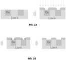
- FIG. 2 A and FIG. 2 Bshow a flow diagram utilizing schematic cross sections of a portion of a substrate having first and second surfaces of low-k material and copper, and generally illustrate an area selective deposition according to some embodiments utilizing a plasma treatment and subsequent etch to remove overhangs on the copper surface.
- FIG. 3is a flow diagram illustrating a process flow for selectively forming a SiOC film on a dielectric surface relative to a metal surface according to some embodiments utilizing a plasma treatment and subsequent etch to remove overhanging material from the metal surface.
- FIG. 4is a flow diagram illustrating a process flow for selectively forming a SiOC film on a dielectric surface relative to a metal surface according to some embodiments utilizing a plasma treatment and subsequent etch to remove overhanging material from the metal surface.
- SiOC filmshave a wide variety of applications, for example in integrated circuit fabrication. SiOC films may be useful as, for example, etch stop layers, sacrificial layers, low-k spacers, anti-reflection layers (ARL), and passivation layers. SiOC can be deposited selectively, for example on dielectric or low-k materials relative to metal, as described, for example, in U.S. application Ser. No. 16/588,600, incorporated by reference herein. This can be referred to as area selective deposition. Area selective deposition of SiOC on a flat patterned surface generally proceeds in an isotropic way, resulting in “mushroom” type growth, as is illustrated in FIG. 1 A .
- the deposited materialtypically grows both vertically and horizontally from the area in which the growth selectively takes place. In many applications this lateral growth is undesirable. Vertical growth is preferred to maintain the dimension of the original structure on which the growth takes place and not to cover the neighboring area, as is shown in FIG. 1 B .
- a dielectricfor example a low k dielectric such as SiOC
- a first surfacesuch as a dielectric or low-k surface
- the first surfacecomprises an inorganic dielectric surface, such as low-k material
- the second surfacecomprises a metallic surface, such as an elemental metal or metal alloy.
- low-k materialinclude silicon oxide-based materials, including grown or deposited silicon dioxide, doped and/or porous oxides, native oxide on silicon, etc.
- area selective deposition of a dielectricis conducted using a PEALD process that includes one or more plasma treatment and/or etch steps that preferentially remove material grown laterally over a neighboring metal surface.
- a wet etchsuch as in dilute HF, and/or a dry etch may be utilized in the process to remove SiOC from adjacent metal surfaces and obtain a desired structure.
- SiOCis selectively deposited on a dielectric surface of a substrate relative to a different surface of the substrate, such as a metal surface.
- SiOCmay be preferentially deposited on dielectrics like SiO 2 or SiN relative to metals like TiN, W, Co, Cu, or Ru.
- the area selective PEALD deposition processcan be a SiOC deposition process using (3-methoxypropyl) trimethoxysilane (MPTMS) as a silicon precursor and a hydrogen plasma reactant. The deposition conditions may be selected such that the top surface of the SiOC has a lower etch rate than the SiOC on the sidewalls.
- MTMS(3-methoxypropyl) trimethoxysilane
- the plasma used in the reaction with the silicon precursormay be anisotropic and can result in inhomogeneous characteristics of the deposited material.
- the wet etch rate of SiO2, SiN or SiOC in diluted HFis known to be very sensitive to e.g. the density of the material and the hydrogen impurity content in the material, which depend on how direct the grown material is exposed to the plasm ions.
- the top surfaceis directly exposed to the ions of the incoming plasma, while the material at the sidewall is more indirectly exposed to the plasma.
- the plasma used to react with the silicon precursor to form SiOCcan be tuned in such a way that the top surface of the deposited SiOC has a low wet etch rate, while material on the sidewall has a higher wet etch rate.
- the material at the side of the overhang on the metal surfacealso referred to as the “mushroom” shape is less directly exposed to the incoming plasma and as a result, the portion of the film that overhangs the metal surface will generally have a higher etch rate than the portion of the film overlying the dielectric material.
- This characteristiccan be used to etch and reshape the area selectively grown material by preferentially etching away the material that is grown laterally over the neighboring metal surface, as is depicted in FIG. 2 B .
- the deposition processmay include a plasma treatment that removes material preferentially from an overhanging portion on the metal surface.
- the deposition processmay also include an etching process, such as a diluted wet etch, and/or a dry or plasma etch to remove deposited SiOC from over the metal surface.
- etching processsuch as a diluted wet etch, and/or a dry or plasma etch to remove deposited SiOC from over the metal surface.
- the entire processcan be performed in a cyclic manner, repeating several deposition and etch cycles. The result is a structure with a minimal amount of lateral growth over the neighboring metal surfaces, as illustrated in FIG. 2 B .
- the PEALD processes for selectively forming a SiOC film on a dielectric surface relative to a metal surfacemay be used in a variety of applications.
- the processesare used in various back end of line (BEOL) or middle-of-line (MOL) applications.
- BEOLback end of line
- MOLmiddle-of-line
- a PEALD process as described hereinmay be used in the formation of low-k dielectric layers on top of existing dielectric material in the formation of a back end of line (BEOL) structure.
- SiOC on the metal surfaceis reduced relative to SiOC on the dielectric surface or avoided completely.
- SiOC thin filmsare formed on a first dielectric surface of a substrate relative to a second metal surface by plasma-enhanced atomic layer deposition (PEALD) processes.
- PEALDplasma-enhanced atomic layer deposition
- SiOC thin filmsare not deposited by liquid phase methods.
- methods for selectively forming SiOC films on a first surface relative to a second surface, wherein the first and second surfaces are different from each other,are provided.
- SiOCsilicon oxycarbide films
- SiOC thin filmsmay comprise one or more elements in addition to Si, O, and/or C, such as S.
- the SiOC filmsmay comprise Si—C bonds and/or Si—O bonds.
- the SiOC filmsmay comprise Si—C bonds and Si—O bonds and may not comprise Si—N bonds.
- the SiOC filmsmay comprise Si—S bonds in addition to Si—C and/or Si—O bonds.
- the SiOC filmsmay comprise more Si—O bonds than Si—C bonds, for example a ratio of Si—O bonds to Si—C bonds may be from about 1:1 to about 10:1.
- the SiOCmay comprise from about 0% to about 40% carbon on an atomic basis.
- the SiOCmay comprise from about 0.1% to about 40%, from about 0.5% to about 30%, from about 1% to about 30%, or from about 5% to about 20% carbon on an atomic basis.
- the SiOC filmsmay comprise from about 0% to about 70% oxygen on an atomic basis.
- the SiOCmay comprise from about 10% to about 70%, from about 15% to about 50%, or from about 20% to about 40% oxygen on an atomic basis.
- the SiOC filmsmay comprise about 0% to about 50% silicon on an atomic basis. In some embodiments the SiOC may comprise from about 10% to about 50%, from about 15% to about 40%, or from about 20% to about 35% silicon on an atomic basis. In some embodiments the SiOC may comprise from about 0.1% to about 40%, from about 0.5% to about 30%, from about 1% to about 30%, or from about 5% to about 20% sulfur on an atomic basis. In some embodiments the SiOC films may not comprise nitrogen. In some other embodiments the SiOC films may comprise from about 0% to about 5% nitrogen on an atomic basis (at %).
- ALD-type processesare based on controlled, generally self-limiting surface reactions. Gas phase reactions are typically avoided by contacting the substrate alternately and sequentially with the reactants. Vapor phase reactants are separated from each other in the reaction chamber, for example, by removing excess reactants and/or reactant byproducts between reactant pulses. The reactants may be removed from proximity with the substrate surface with the aid of a purge gas and/or vacuum. In some embodiments, excess reactants and/or reactant byproducts are removed from the reaction space by purging, for example with an inert gas.
- PEALDplasma enhanced ALD
- Selectivity of deposition on a first surface A relative to second surface Bcan be given as a percentage calculated by [(deposition on surface A) ⁇ (deposition on surface B)]/(deposition on the surface A).
- Depositioncan be measured in any of a variety of ways known in the art or as described herein. For example, deposition may be given as the measured thickness of the deposited material or may be given as the measured amount of material deposited.
- selectivity of formation of SiOC on a first surface relative to a second surface, such as on a dielectric surface relative to a metal surfaceis >20%, >25%, >50%, >80%, >90%, >93%, >95%, >97%, >98%, or even greater than >99%.
- the deposition processmay include the use of plasma to form the SiOC, as well as a plasma treatment and subsequent etch treatment to remove SiOC that has been formed on the metal surface and thereby enhance the selectivity.
- the plasma conditions in the deposition processmay be selected to achieve a desired etch selectivity in the deposited SiOC and to facilitate the removal of SiOC that has undesirably formed on the metal surface.
- thin SiOC filmsare selectively formed on the dielectric surface of a substrate relative to a metal surface by repetition of a PEALD cycle.
- each PEALD cyclecomprises at least four distinct phases.
- An exemplary cycle 100 for selectively forming SiOC on a dielectric surface relative to a metal surfaceis illustrated in FIG. 3 . Briefly, a substrate or workpiece comprising a dielectric surface and a metal surface is placed in a reaction chamber and subjected to alternately repeated surface reactions. In a first phase ( 110 , 120 ), a vapor phase first reactant or precursor comprising silicon contacts the substrate 110 and forms no more than about one monolayer of silicon species on the substrate surface.
- the silicon precursoris also referred to herein as “the silicon precursor,” “silicon-containing precursor,” or “silicon reactant” and may be, for example, a silicon precursor comprising organic ligands or a silicon precursor comprising Si—O bonds.
- the silicon precursorcomprises 3-methoxypropyltrimethoxysilane (MPTMS) or bis(triethoxysilyl)ethane (BTESE).
- MPTMS3-methoxypropyltrimethoxysilane
- BTESEbis(triethoxysilyl)ethane
- the first silicon reactant pulsecan be supplied in gaseous form.
- the silicon precursor gasis considered “volatile” for purposes of the present description if the species exhibits sufficient vapor pressure under the process conditions to transport the species to the substrate surface in sufficient concentration to saturate exposed surfaces.
- the silicon reactantcontacts the substrate surface for about 0.05 seconds to about 5.0 seconds, about 0.1 seconds to about 3 seconds or about 0.2 seconds to about 1.0 seconds.
- the optimum contacting timecan be determined by the skilled artisan based on the particular circumstances.
- excess first vapor phase reactant and any reaction byproductsare subsequently removed from the proximity of the substrate surface 120 .
- the first vapor phase reactant and any reaction byproductsmay be removed from proximity with the substrate surface with the aid of a purge gas and/or vacuum.
- excess reactant and/or reactant byproductsare removed from the reaction space by purging, for example with an inert gas. The removal may, in some embodiments, be carried out for about 0.1 seconds to about 10 seconds, about 0.1 seconds to about 4 seconds or about 0.1 seconds to about 0.5 seconds.
- the substratemay be moved in order to facilitate removal of the reactant and/or reactant byproducts from the vicinity of the substrate surface, for example by moving the substrate to a different reaction chamber or a separate portion of the reaction chamber.
- a second reactantcomprising a reactive species from a plasma contacts the substrate and converts adsorbed silicon species to SiOC 130 , such that SiOC is preferentially deposited on the dielectric surface relative to the metal surface. Some deposition may, however, occur on the metal surface, for example as illustrated schematically in FIG. 1 A .
- the first phase and second phase( 110 , 120 , 130 , 140 ) may together be referred to as the SiOC deposition portion of the overall cycle 100 .
- the second reactantmay comprise a hydrogen precursor and may comprise a reactive hydrogen species.
- a reactive speciesincludes, but is not limited to, radicals, plasmas, and/or excited atoms or species. Such reactive species may be generated by, for example, plasma discharge, hot-wire, or other suitable methods.
- the reactive speciesmay be generated remotely from the reaction chamber, for example up-stream from the reaction chamber (“remote plasma”). In some embodiments the reactive species may be generated in the reaction chamber, in the direct vicinity of the substrate, or directly above the substrate (“direct plasma”).
- the second reactantmay comprise other species that are not hydrogen species.
- the second reactantmay comprise reactive species from a noble gas, such as one or more of He, Ne, Ar, Kr, or Xe, for example as radicals, in plasma form, or in elemental form.
- the second reactantcomprises reactive species from an Ar plasma. These reactive species from noble gases do not necessarily contribute material to the deposited film but can in some circumstances contribute to film growth as well as help in the formation and ignition of plasma.
- the substrateis contacted with a reactant comprising H 2 and Ar plasma.
- the plasmasuch as hydrogen and argon plasma may be formed by generating a plasma in a reactant gas, such as hydrogen and argon gas, in the reaction chamber or upstream of the reaction chamber, for example by flowing the hydrogen (H 2 ) and Ar through a remote plasma generator.
- one or more gases that are used to form a plasmamay flow constantly throughout the deposition process but only be activated intermittently.
- H 2 and/or Ar gasmay flow continuously throughout the deposition process.
- the gasmay serve as a carrier gas for the silicon reactant and as a plasma reactant.
- the second reactantcomprises plasma generated in flowing H 2 and Ar gas.
- H 2 and Ar containing gasis provided to the reaction chamber before the plasma is ignited.
- the H 2 and Ar gasis provided to the reaction chamber continuously and hydrogen and argon containing plasma is created or supplied when needed.
- N 2is provided to the reaction chamber before the plasma is ignited. In some embodiments also only N 2 is provided to the reaction chamber before the plasma is ignited.
- the second reactantmay be generated from a gas containing more than about 1 atomic % (at %) hydrogen, more than about 10 atomic % (at %) hydrogen more than about 25 atomic % (at %) hydrogen, more than about 25 atomic % (at %) hydrogen, more than about 50 at % hydrogen, more than about 75 at % hydrogen, more than about 85 at % hydrogen, more than about 90 at % hydrogen, more than about 95 at % hydrogen, more than about 96 at %, 97 at %, 98 at %, or more than about 99 at % hydrogen.
- the second reactantmay be generated from a gas containing more than about 1 atomic % (at %) argon, more than about 10 atomic % (at %) argon more than about 25 atomic % (at %) argon, more than about 25 atomic % (at %) argon, more than about 50 at % argon, more than about 75 at % argon, more than about 85 at % argon, more than about 90 at % argon, more than about 95 at % argon, more than about 96 at %, 97 at %, 98 at %, or more than about 99 at % argon.
- the second reactantfor example hydrogen and argon plasma
- the second reactantsuch as hydrogen and argon plasma
- the second reactant contacting timemay be even higher than about 10 seconds.
- contacting timescan be on the order of minutes. The optimum contacting time can be readily determined by the skilled artisan based on the particular circumstances.
- the second reactantis provided in two or more distinct pulses, without introducing another reactant in between any of the two or more pulses.
- a plasmasuch as a hydrogen and argon plasma, is provided in two or more sequential pulses, without introducing a Si-precursor in between the sequential pulses.
- two or more sequential plasma pulsesare generated by providing a plasma discharge for a first period of time, extinguishing the plasma discharge for a second period of time, for example from about 0.1 seconds to about 10 seconds, from about 0.5 seconds to about 5 seconds or about 1.0 seconds to about 4.0 seconds, and exciting it again for a third period of time before introduction of another precursor or a removal step, such as before the Si-precursor or a purge step. Additional pulses of plasma can be introduced in the same way.
- a plasmais ignited for an equivalent period of time in each of the pulses.
- a gas that is used to form a plasmadoes not comprise oxygen.
- the adsorbed silicon precursoris not contacted with a reactive species generated by a plasma from oxygen.
- a second reactant comprising reactive speciesis generated in a gas that does not comprise oxygen.
- a second reactantmay comprise a plasma generated in a gas that does not comprise oxygen.
- the second reactantmay be generated in a gas comprising less than about 50 atomic % (at %) oxygen, less than about 30 at % oxygen, less than about 10 at % oxygen, less than about 5 at % oxygen, less than about 1 at % oxygen, less than about 0.1 at % oxygen, less than about 0.01 at % oxygen, or less than about 0.001 at % oxygen.
- a gas that is used to form a plasmadoes not comprise nitrogen.
- the adsorbed silicon precursoris not contacted with a reactive species generated by a plasma from nitrogen.
- a second reactant comprising reactive speciesis generated in a gas that does not comprise nitrogen.
- a second reactantmay comprise a plasma generated in a gas that does not comprise nitrogen.
- a gas that is used to form a plasmamay comprise nitrogen.
- the second reactantmay comprise nitrogen radicals, nitrogen atoms and/or nitrogen plasma.
- the second reactantmay be generated in a gas comprising less than about 25 atomic % (at %) nitrogen, less than about 20 at % nitrogen, less than about 15 at % nitrogen, less than about 10 at % nitrogen, less than about 5 at % nitrogen, less than about 1 at % nitrogen, less than about 0.1 at % nitrogen, less than about 0.01 at % nitrogen, or less than about 0.001 at % nitrogen.
- the second reactantmay be generated in a gas comprising hydrogen and nitrogen, for example the second reactant may comprise H 2 and N 2 .
- the second reactantmay be generated in a gas having a ratio of N 2 to H 2 (N 2 /H 2 ) of less than about 20%, less than about 10%, or less than about 5%.
- a gas that is used to form a plasmadoes not comprise nitrogen or oxygen.
- the adsorbed silicon precursoris not contacted with a reactive species generated by a plasma from nitrogen or oxygen.
- a second reactant comprising reactive speciesis generated in a gas that does not comprise nitrogen or oxygen.
- a second reactantmay comprise a plasma generated in a gas that does not comprise nitrogen or oxygen.
- the plasmais anisotropic.
- the plasma power, composition and reaction parametersare tuned such that the SiOC is deposited selectively on the dielectric surface relative to the metal surface and has desired etch rate characteristics.
- SiOC deposited on a dielectric surfacehas different characteristics from SiOC that may be deposited on metal surfaces.
- SiOC that is selectively deposited on a dielectric surfacemay have higher density and lower etch rates than SiOC that is deposited on a metal surface during the same deposition process.
- horizontal or top surfaces of a deposited SiOC filmhave a lower etch rate, such as a lower wet etch rate in dilute HF, than the non-horizontal or sidewall surface of the same SiOC film.
- these differential propertiescan be used to preferentially etch SiOC from the metal surface and create a desired deposition profile.
- the second reactantmay be free or substantially free of oxygen-containing species (e.g., oxygen ions, radicals, atomic oxygen). In some embodiments, the second reactant does not comprise any species generated from nitrogen.
- oxygen-containing speciese.g., oxygen ions, radicals, atomic oxygen.
- the plasma power, plasma composition and/or the temperature of the susceptoris tuned to achieve desired selectivity and desired etch rate characteristics in the deposited SiOC film.
- the plasma poweris tuned to achieve selective deposition of SiOC on a dielectric surface relative to a metal surface. In some embodiments the plasma power is tuned such that SiOC deposited on the metal surface has a higher etch rate than the SiOC deposited on the dielectric surface.
- a plasma power used for generating a second reactant plasmacan be about 5 Watts (W) to about 5000 W, 10 W to about 2,000 W, about 50 W to about 1000 W, about 100 W to about 1000 W or about 100 W to about 500 W. In some embodiments, a plasma power can be about 100 W to about 300 W.
- the temperature of the susceptor supporting the substratemay be selected to achieve the desired selective deposition of SiOC on a dielectric surface relative to a metal surface and to achieve the desired etch rate characteristics in the SiOC on the different surfaces. In some embodiments the temperature is selected such that SiOC that is formed on a dielectric surface has a lower etch rate than SiOC that is formed on a metal surface by the same process. In some embodiments the susceptor temperature is from about 20 to about 700 C, from about 50 to about 600 C, from about 100 to about 550 C or from about 200 to 500 C.
- the amount of each of H 2 and Ar in the gas in which the plasma is generatedis selected to achieve the desired selectivity and etch rate characteristics in the SiOC.
- the H/R ratiois less than 1:1 but not 0:1, less than about 1:2 but not 0:1, less than about 1:5 but not 0:1, less than about 1:10 but not 0:1 or less than about 1:20, but not 0:1.
- excess second reactant and any reaction byproductsare removed 140 from the proximity of the substrate surface.
- the second reactant and any reaction byproductsmay be removed from proximity with the substrate surface with the aid of a purge gas and/or vacuum.
- excess reactant and/or reactant byproductsare removed from the reaction space by purging, for example with an inert gas.
- the removalmay, in some embodiments, be carried out for about 0.1 seconds to about 10 seconds, about 0.1 seconds to about 4 seconds or about 0.1 seconds to about 0.5 seconds.
- the substratemay be moved in order to facilitate removal of the reactant and/or reactant byproducts, for example by moving the substrate to a different reaction chamber or a separate portion of the reaction chamber.
- the first and second phases ( 110 , 120 , 130 , 140 ), the SiOC deposition portion of the deposition cycle,may be repeated 180 one, two or more times consecutively prior to beginning the third ( 150 , 160 ) and/or fourth ( 170 ) phase of the entire SiOC formation cycle 100 .
- the first and second phasesmay be repeated until a SiOC layer of a desired thickness has been formed on the dielectric surface.
- overhangs of SiOCmay be present on the metal surface. This is illustrated in FIG. 2 A , which shows the deposition of SiOC on a low-k material relative to copper, with the formation of overhangs of SiOC on the copper surface.
- the overhangsmay be reduced or eliminated by including the third and/or fourth phases, as described below, in one or more deposition cycles.
- one or more SiOC deposition cycles 100begins with the first phase by contacting the substrate with the silicon precursor, followed by the second precursor. In other embodiments one or more SiOC deposition cycles 100 may begin with the second phase by contacting the substrate with the second reactant, followed by the silicon precursor.
- the substratemay be contacted 150 with a reactant comprising a plasma.
- a reactantcomprising a plasma.
- the substratemay be contacted with a plasma generated in a noble gas, such as Ar plasma.
- the plasmais directional, and preferentially attacks SiOC that has been formed on the metal surface relative to SiOC that has been formed on the dielectric surface. This is illustrated in the right-hand panel of FIG. 2 A , where the arrows represent the plasma treatment of the surfaces.
- Plasma power and durationcan be tuned to increase the preferential targeting of the SiOC overhangs on the metal surface.
- the third phasepreferentially removes SiOC from the metal surface relative to the dielectric surface.
- excess third reactant and reaction byproductsmay be removed from the proximity of the substrate surface 160 , such as with the aid of a purge gas and/or vacuum, or by moving the substrate to a different reaction chamber or a separate portion of the reaction chamber.
- the removalmay, in some embodiments, be carried out for about 0.1 seconds to about 10 seconds, about 0.1 seconds to about 4 seconds or about 0.1 seconds to about 0.5 seconds.
- the third phasemay be repeated 190 two or more times in each complete deposition cycle 100 .
- the third phasemay be included in each deposition cycle.
- the third phaseis not included in every deposition cycle but is provided one or more times in the deposition process.
- An optional fourth phase ( 170 )may be included to further etch SiOC from the metal surface, for example if it is not removed to a desired extent in the third phase.
- the substrateis contacted with an etchant 170 to preferentially remove SiOC from over the metal surface relative to the dielectric surface. This is illustrated in FIG. 2 B , which shows the preferential etching of the overhangs relative to the top surface of the deposited SiOC film.
- the etchantis directional.
- the fourth phasemay be included in the SiOC formation cycle 100 , for example, if the plasma treatment in the third phase is not sufficient to achieve the desired level of removal of SiOC overhangs from the metal surface.
- the fourth phasemay be included in every cycle 100 .
- the fourth phaseis not included in every cycle 100 but is provided one or more times in the SiOC deposition process.
- the fourth phasemay be included after a certain number of repetitions of a cycle that includes only the first three phases, such as after every one, two, three, four, five or more such deposition cycles.
- the etchantmay be a reactive gas, such as a reactive halide gas such as CF 4 , SF 6 , HF, Cl 2 or NF 3 .
- a wet etchis used to preferentially remove the SiOC overhangs from the metal surface.
- etching in dilute HFmay be used to preferentially remove SiOC from the metal surface.
- the etchantpreferentially removes SiOC from the metal surface, leaving a desired SiOC structure on the dielectric surface, for example as illustrated in FIG. 2 B .
- the etchantmay comprise, for example, a plasma generated in a halide gas such as CF 4 , SF 6 , HF, Cl 2 or NF 3 .
- the plasma power and timemay be selected to achieve the desired amount of etching.
- the etching plasmamay be directional. The etching plasma preferentially attacks the SiOC on the metal surface relative to the bulk portion of the SiOC deposited on the dielectric surface, leaving a desired structure as illustrated in FIG. 2 B .
- Additional phasesmay be added and phases may be removed as desired to adjust the composition and selectivity of the SiOC film.
- the entire SiOC formation cyclemay be repeated 200 two, three or more times to achieve a desired amount of SiOC on the metal surface relative to the dielectric surface.
- two of the phasesmay overlap, or be combined.
- the silicon precursor and the second reactantmay contact the substrate simultaneously in phases that partially or completely overlap.
- the order of the phasesmay be varied, and an ALD cycle may begin with any one of the phases. That is, unless specified otherwise, the reactants can contact the substrate in any order, and the process may begin with any of the reactants.
- N, M and Yare integers that can be selected independently. In some embodiments any of N, M and Y may be zero in one or more deposition cycles in a complete deposition process.
- the selective SiOC depositiontakes place on a substrate in a reaction space or reactor.
- each of the four phasestakes place in the same reaction space and/or reactor.
- the reactormay be part of a cluster tool in which a variety of different processes in the formation of an integrated circuit are carried out.
- a flow-type reactoris utilized.
- a shower head type of reactoris utilized.
- a space-divided reactoris utilized.
- a high-volume manufacturing-capable single wafer ALD reactoris used.
- a batch reactor comprising multiple substratesis used.
- the number of substratesmay be in the range of 10 to 200, in the range of 50 to 150, or in the range of 100 to 130.
- the exposed surfaces of the substratecan be pretreated to provide reactive sites to react with the first phase of the ALD process. In some embodiments a separate pretreatment step is not required.
- the substrateis pretreated to provide a desired surface termination on one or more surfaces.
- the substratemay be treated to provide surface terminations on the dielectric surface to enhance selectivity.
- the substratemay be treated to provide a blocking or passivation layer on the metal surface to increase selectivity of the deposition on the dielectric surface.
- a gasis provided to the reaction chamber continuously during one or more phases of the deposition cycle, or during the entire deposition cycle, or even throughout the entire deposition process.
- Reactive speciesmay be provided by generating a plasma in a gas, either in the reaction chamber or upstream of the reaction chamber.
- the gasdoes not comprise nitrogen.
- the gasmay comprise a noble gas, such as argon or helium.
- the gasis argon.
- the flowing gasmay also serve as a purge gas.
- flowing argonmay serve as a purge gas for a first silicon precursor and also serve as a source of reactive species second reactant and a third reactant (as a source of reactive species).
- argonmay serve as a purge gas for a first precursor and a source of excited species for converting the silicon precursor to the SiOC film and as the source of reactive species for a plasma treatment, such as in the second and third phases described above.
- the deposition parameterssuch as the precursor flow rate, contacting time, removal time, reactants themselves, plasma power, reaction chamber temperature and susceptor temperature may be selected in order to selectively form a SiOC film with the desired characteristics on a dielectric surface relative to a metal surface.
- one or more of these parametersmay be selected to reduce, minimize or prevent deposition of SiOC on a metal surface of the substrate and/or to preferentially remove SiOC from the metal surface.
- plasmafor example hydrogen and argon containing plasma, argon plasma, or etching plasma may be generated by applying RF power of from about 5 W to about 5000 W, 10 W to about 2000 W, from about 50 W to about 1000 W, or from about 200 W to about 800 W.
- the RF power densitymay be from about 0.02 W/cm 2 to about 2.0 W/cm 2 , or from about 0.05 W/cm 2 to about 1.5 W/cm 2 .
- the RF powermay be applied to a reactant gas that flows during the plasma contacting time, that flows continuously through the reaction chamber, and/or that flows through a remote plasma generator.
- the plasmais generated in situ, while in other embodiments the plasma is generated remotely.
- a showerhead reactoris utilized and plasma is generated between a susceptor (on top of which the substrate is located) and a showerhead plate.
- the gap between the susceptor and showerhead plateis from about 0.1 cm to about 20 cm, from about 0.5 cm to about 5 cm, or from about 0.8 cm to about 3.0 cm.
- the PEALD reactionsmay be performed at temperatures ranging from about 25° C. to about 700° C., from about 50° C. to about 600° C., from about 100° C. to about 450° C., or from about 200° C. to about 400° C.
- the optimum reactor temperaturemay be limited by the maximum allowed thermal budget. Therefore, in some embodiments the reaction temperature is from about 100° C. to about 300° C. In some applications, the maximum temperature is around about 200° C., and, therefore the PEALD process is run at that reaction temperature.
- the susceptor temperatureis the same as the reaction space temperature. In some embodiments the susceptor temperature is within 100 C or within 50 C of the reaction space temperature.
- the pressure of the reaction chamber during processingis maintained at from about 0.01 Torr to about 50 Torr, or from about 0.1 Torr to about 10 Torr. In some embodiments the pressure of the reaction chamber is greater than about 6 Torr, or about 20 Torr. In some embodiments, a SiOC deposition process can be performed at a pressure of about 20 Torr to about 500 Torr, about 20 Torr to about 50 Torr, or about 20 Torr to about 30 Torr.
- a SiOC deposition processcan comprise a plurality of deposition cycles, wherein at least one deposition cycle is performed in an elevated pressure regime.
- a deposition cycle of a PEALD processmay comprise alternately and sequentially contacting the substrate with a silicon precursor and a second reactant under the elevated pressure.
- one or more deposition cycles of the PEALD processcan be performed at a process pressure of about 6 Torr to about 500 Torr, about 6 Torr to about 50 Torr, or about 6 Torr to about 100 Torr.
- the one or more deposition cyclescan be performed at a process pressure of greater than about 20 Torr, including about 20 Torr to about 500 Torr, about 30 Torr to about 500 Torr, about 40 Torr to about 500 Torr, or about 50 Torr to about 500 Torr. In some embodiments, the one or more deposition cycles can be performed at a process pressure of about 20 Torr to about 30 Torr, about 20 Torr to about 100 Torr, about 30 Torr to about 100 Torr, about 40 Torr to about 100 Torr or about 50 Torr to about 100 Torr.
- a SiOC thin filmis selectively deposited on a dielectric surface relative to a metal surface on a substrate in a reaction space by a PEALD process 300 comprising at least one cycle comprising:
- step 380optionally repeating the contacting and removing steps at step 380 to form a SiOC thin film of a desired thickness and composition.
- the deposited SiOCis treated by contacting it with an Ar plasma at step 350 .
- the Ar plasmamay preferentially remove SiOC from the metal surface and may also make the SiOC over the metal surface more susceptible to a subsequent etching process. Excess Ar plasma and reaction byproducts, if any, may be removed from the substrate surface at step 360 , for example by shutting off the plasma power and continuing to flow the Ar gas.
- the Ar plasma treatmentmay be repeated 390 one, two or more times in sequence.
- the plasma treatment step 350may be included in each deposition cycle or may be provided intermittently in one or more deposition cycles.
- the substratemay be contacted with an etchant such as a plasma generated in a halide gas.
- the etching processmay remove additional SiOC preferentially from over the metal surface relative to the dielectric surface.
- the etching process 370may be included in every deposition cycle 300 or intermittently in one or more deposition cycles.
- the deposition cycle 300is repeated 400 one, two or more times to selectively form a SiOC layer on the dielectric surface relative to the metal surface.
- suitable Si precursorscan be used in the presently disclosed PEALD processes.
- the suitable Si precursorsmay not comprise nitrogen.
- a suitable Si precursormay comprise MPTMS.
- the silicon precursoris a silicon precursor as described in U.S. patent application Ser. No. 15/588,026, filed May 5, 2017, which is hereby incorporated by reference in its entirety.
- more than one silicon precursormay contact the substrate surface at the same time during an ALD phase.
- the silicon precursormay comprise more than one of the silicon precursors described herein.
- a first silicon precursoris used in a first ALD cycle and a second, different silicon precursor is used in a later ALD cycle.
- multiple silicon precursorsmay be used during a single ALD phase, for example in order to optimize certain properties of the deposited SiOC film.
- only one silicon precursormay contact the substrate during the deposition.
- the silicon precursoris not used as a silylating agent.
- the deposition temperature and/or the duration of the silicon precursor contacting stepare selected such that the silicon precursor does not decompose.
- the silicon precursormay decompose during the silicon precursor contacting step.
- the silicon precursordoes not comprise a halogen, such as chlorine or fluorine.
- SiOC filmsare deposited to a thickness of from about 3 nm to about 50 nm, from about 5 nm to about 30 nm, from about 5 nm to about 20 nm. These thicknesses can be achieved in feature sizes (width) below about 100 nm, about 50 nm, below about 30 nm, below about 20 nm, and in some cases below about 15 nm. According to some embodiments, a SiOC film is deposited on a three-dimensional structure and the thickness at a sidewall may be slightly even more than 10 nm. In some embodiments SiOC films of greater than 50 nm can be deposited. In some embodiments SiOC films of greater than 100 nm can be deposited. In some embodiments, SiOC films are deposited to a thickness of more than about 1 nm, more than about 2 nm, more than about 3 nm, more than about 5 nm, more than about 10 nm.
- SiOC films with differential wet etch ratesmay be deposited.
- SiOC formed according to one or more processes described hereincan advantageously demonstrate a ratio of a WER of a substantially vertical region to a WER of a substantially horizontal region of about 1, for example in 0.5 wt % dHF.
- a ratio of a wet etch rate of a SiOC thin film formed over substantially vertical surfaces (e.g., sidewall surfaces) to a wet etch rate of the SiOC thin film formed over substantially horizontal surfaces (e.g., top surfaces) of three-dimensional structures on a substrate surfacecan be the same or substantially the same.
- the ratiocan be about 4 to about 0.5, about 2 to about 0.75, about 1.25 to about 0.8, or about 1.1 to about 0.9. These ratios can be achieved in features with aspect ratios of about 2 or more, about 3 or more, about 5 or more or even about 8 or more.
- the deposited SiOC thin filmmay contain up to about 40% carbon on an atomic basis (at %).
- a SiOC filmmay comprise carbon from about 0.1% to about 40%, from about 0.5% to about 40%, from about 1% to about 30%, or from about 5% to about 20% on an atomic basis.
- a SiOC filmmay comprise at least about 1%, about 10% or about 20% carbon on an atomic basis.
- the deposited SiOC thin filmmay contain up to about 50% silicon on an atomic basis (at %).
- a SiOC filmmay comprise silicon from about 10% to about 50%, from about 15% to about 40%, or from about 20% to about 35% on an atomic basis.
- a SiOC filmmay comprise at least about 15%, about 20%, about 25% or about 30% silicon on an atomic basis.
- the deposited SiOC thin filmmay contain up to about 40% sulfur on an atomic basis (at %).
- a SiOC filmmay comprise sulfur from about 0.01% to about 40%, from about 0.1% to about 40%, from about 0.5% to about 30%, or from about 1% to about 20% on an atomic basis.
- a SiOC filmmay comprise at least about 1%, about 10% or about 20% sulfur on an atomic basis.
- the deposited SiOC filmsdo not comprise an appreciable amount of nitrogen. However, in some embodiments a SiOC film comprising nitrogen is deposited.
- the deposited SiOC filmscomprises less than about 30 at %, less than about 20 at %, less than about 15 at %, less than about 10 at %, less than about 5 at % of nitrogen, less than about 1 at % nitrogen, or less than about 0.1 at % nitrogen. In some embodiments the SiOC thin films do not comprise nitrogen.
- the hydrogen content of the filmsis less than about 20 at %, less than about 10 at % or less than about 5 at %.
- the deposited SiOC thin filmmay contain up to about 70% oxygen on an atomic basis (at %).
- a SiOC filmmay comprise oxygen from about 10% to about 70%, from about 15% to about 50%, or from about 20% to about 40% on an atomic basis.
- a SiOC filmmay comprise at least about 20%, about 40% or about 50% oxygen on an atomic basis.
- a SiOC filmmay comprise one or more of SiN, SiO, SiC, SiCN, SiON, SiOSC, SiSC, SiOS, and/or SiOC. In some embodiments SiOC films deposited according to the disclosed methods do not comprise a laminate or nanolaminate structure.
- a SiOC filmis not a low-k film, for example a SiOC film is not a porous film.
- a SiOCis a continuous film.
- a SiOC filmhas a k-value that is less than about 10.
- a SiOC filmhas a k-value that is less than about 7.
- a SiOC filmhas a k-values from about 2 to about 10.
- a SiOC filmhas a k-value that is less than about 5.0, less than about 4.5, less than about 4.3, less than about 4.1.
- a SiOC filmhas a k-value that from about 3.0 to about 7, from about 3.0 to about 5.5, from about 3.0 to about 5.0, from about 3.5 to about 4.8, from about 3.5 to about 4.7. In some embodiments a SiOC film has a k-value that is more than the k-value of any low-k film. In some embodiments a SiOC film has a k-value that is more than pure SiO 2 .
Landscapes
- Engineering & Computer Science (AREA)
- Chemical & Material Sciences (AREA)
- Physics & Mathematics (AREA)
- Condensed Matter Physics & Semiconductors (AREA)
- General Physics & Mathematics (AREA)
- Manufacturing & Machinery (AREA)
- Computer Hardware Design (AREA)
- Microelectronics & Electronic Packaging (AREA)
- Power Engineering (AREA)
- Chemical Kinetics & Catalysis (AREA)
- General Chemical & Material Sciences (AREA)
- Inorganic Chemistry (AREA)
- Plasma & Fusion (AREA)
- Materials Engineering (AREA)
- Mechanical Engineering (AREA)
- Metallurgy (AREA)
- Organic Chemistry (AREA)
- Spectroscopy & Molecular Physics (AREA)
- Electromagnetism (AREA)
- Chemical Vapour Deposition (AREA)
- Formation Of Insulating Films (AREA)
Abstract
Description
The present application is a continuation of U.S. application Ser. No. 17/064,865, filed Oct. 7, 2020, which claims priority to U.S. Provisional Application No. 62/928,978, filed Oct. 31, 2019, which is incorporated by reference herein.
The present disclosure relates generally to the field of semiconductor device manufacturing and, more particularly, to selective deposition of silicon oxycarbide (SiOC) films on dielectric materials.
There is increasing need for dielectric materials with relatively low dielectric constant (k) values and relatively low acid-based wet etch rates. Silicon oxycarbide (SiOC) may satisfy certain of these requirements. Selective deposition of dielectric films like SiOC on a patterned surface, such as on a dielectric surface relative to a metal surface can be advantageous in a number of settings. For example, in the case of the case of self-aligned vias in Back End of Line (BEOL) processing area selective growth of a low k dielectric like SiOC on top of the existing dielectric areas of a BEOL structure is desirable.
One of the challenges with area selective deposition of dielectric materials such as SiOC is overgrowth on the adjacent surfaces, such as on adjacent metal areas. Such overgrowth can, for example, reduce the area available to make a via with a low series resistance on a BEOL structure.
Silicon oxycarbide (SiOC) films have a wide variety of applications, for example in integrated circuit fabrication. SiOC films may be useful as, for example, etch stop layers, sacrificial layers, low-k spacers, anti-reflection layers (ARL), and passivation layers. SiOC can be deposited selectively, for example on dielectric or low-k materials relative to metal, as described, for example, in U.S. application Ser. No. 16/588,600, incorporated by reference herein. This can be referred to as area selective deposition. Area selective deposition of SiOC on a flat patterned surface generally proceeds in an isotropic way, resulting in “mushroom” type growth, as is illustrated inFIG.1A . The deposited material typically grows both vertically and horizontally from the area in which the growth selectively takes place. In many applications this lateral growth is undesirable. Vertical growth is preferred to maintain the dimension of the original structure on which the growth takes place and not to cover the neighboring area, as is shown inFIG.1B .
In some embodiments, area selective growth of a dielectric, for example a low k dielectric such as SiOC, takes place selectively on a first surface, such as a dielectric or low-k surface, without undesirable levels of overgrowth on a second surface, such as a metal surface. In some embodiments the first surface comprises an inorganic dielectric surface, such as low-k material, while the second surface comprises a metallic surface, such as an elemental metal or metal alloy. Examples of low-k material include silicon oxide-based materials, including grown or deposited silicon dioxide, doped and/or porous oxides, native oxide on silicon, etc. In some embodiments, area selective deposition of a dielectric is conducted using a PEALD process that includes one or more plasma treatment and/or etch steps that preferentially remove material grown laterally over a neighboring metal surface. In some embodiments a wet etch, such as in dilute HF, and/or a dry etch may be utilized in the process to remove SiOC from adjacent metal surfaces and obtain a desired structure.
In some embodiments SiOC is selectively deposited on a dielectric surface of a substrate relative to a different surface of the substrate, such as a metal surface. For example, SiOC may be preferentially deposited on dielectrics like SiO2or SiN relative to metals like TiN, W, Co, Cu, or Ru. In some embodiments the area selective PEALD deposition process can be a SiOC deposition process using (3-methoxypropyl) trimethoxysilane (MPTMS) as a silicon precursor and a hydrogen plasma reactant. The deposition conditions may be selected such that the top surface of the SiOC has a lower etch rate than the SiOC on the sidewalls. For example, the plasma used in the reaction with the silicon precursor may be anisotropic and can result in inhomogeneous characteristics of the deposited material. The wet etch rate of SiO2, SiN or SiOC in diluted HF is known to be very sensitive to e.g. the density of the material and the hydrogen impurity content in the material, which depend on how direct the grown material is exposed to the plasm ions. The top surface is directly exposed to the ions of the incoming plasma, while the material at the sidewall is more indirectly exposed to the plasma. Thus, the plasma used to react with the silicon precursor to form SiOC can be tuned in such a way that the top surface of the deposited SiOC has a low wet etch rate, while material on the sidewall has a higher wet etch rate.
The material at the side of the overhang on the metal surface, also referred to as the “mushroom” shape is less directly exposed to the incoming plasma and as a result, the portion of the film that overhangs the metal surface will generally have a higher etch rate than the portion of the film overlying the dielectric material. This characteristic can be used to etch and reshape the area selectively grown material by preferentially etching away the material that is grown laterally over the neighboring metal surface, as is depicted inFIG.2B . The deposition process may include a plasma treatment that removes material preferentially from an overhanging portion on the metal surface. The deposition process may also include an etching process, such as a diluted wet etch, and/or a dry or plasma etch to remove deposited SiOC from over the metal surface. The entire process can be performed in a cyclic manner, repeating several deposition and etch cycles. The result is a structure with a minimal amount of lateral growth over the neighboring metal surfaces, as illustrated inFIG.2B .
The PEALD processes for selectively forming a SiOC film on a dielectric surface relative to a metal surface may be used in a variety of applications. In some embodiments the processes are used in various back end of line (BEOL) or middle-of-line (MOL) applications. For example, a PEALD process as described herein may be used in the formation of low-k dielectric layers on top of existing dielectric material in the formation of a back end of line (BEOL) structure.
According to some embodiments methods for selectively forming SiOC films on dielectric or low-k surface relative to metal surfaces are provided. In some embodiments SiOC on the metal surface is reduced relative to SiOC on the dielectric surface or avoided completely. In some embodiments SiOC thin films are formed on a first dielectric surface of a substrate relative to a second metal surface by plasma-enhanced atomic layer deposition (PEALD) processes. In some embodiments SiOC thin films are not deposited by liquid phase methods. According to some embodiments methods for selectively forming SiOC films on a first surface relative to a second surface, wherein the first and second surfaces are different from each other, are provided.
The formula of the silicon oxycarbide films is generally referred to herein as SiOC for convenience and simplicity. As used herein, SiOC is not intended to limit, restrict, or define the bonding or chemical state, for example the oxidation state of any of Si, O, C, and/or any other element in the film. Further, in some embodiments SiOC thin films may comprise one or more elements in addition to Si, O, and/or C, such as S. In some embodiments the SiOC films may comprise Si—C bonds and/or Si—O bonds. In some embodiments the SiOC films may comprise Si—C bonds and Si—O bonds and may not comprise Si—N bonds. In some embodiments the SiOC films may comprise Si—S bonds in addition to Si—C and/or Si—O bonds. In some embodiments the SiOC films may comprise more Si—O bonds than Si—C bonds, for example a ratio of Si—O bonds to Si—C bonds may be from about 1:1 to about 10:1. In some embodiments the SiOC may comprise from about 0% to about 40% carbon on an atomic basis. In some embodiments the SiOC may comprise from about 0.1% to about 40%, from about 0.5% to about 30%, from about 1% to about 30%, or from about 5% to about 20% carbon on an atomic basis. In some embodiments the SiOC films may comprise from about 0% to about 70% oxygen on an atomic basis. In some embodiments the SiOC may comprise from about 10% to about 70%, from about 15% to about 50%, or from about 20% to about 40% oxygen on an atomic basis. In some embodiments the SiOC films may comprise about 0% to about 50% silicon on an atomic basis. In some embodiments the SiOC may comprise from about 10% to about 50%, from about 15% to about 40%, or from about 20% to about 35% silicon on an atomic basis. In some embodiments the SiOC may comprise from about 0.1% to about 40%, from about 0.5% to about 30%, from about 1% to about 30%, or from about 5% to about 20% sulfur on an atomic basis. In some embodiments the SiOC films may not comprise nitrogen. In some other embodiments the SiOC films may comprise from about 0% to about 5% nitrogen on an atomic basis (at %).
ALD-type processes are based on controlled, generally self-limiting surface reactions. Gas phase reactions are typically avoided by contacting the substrate alternately and sequentially with the reactants. Vapor phase reactants are separated from each other in the reaction chamber, for example, by removing excess reactants and/or reactant byproducts between reactant pulses. The reactants may be removed from proximity with the substrate surface with the aid of a purge gas and/or vacuum. In some embodiments, excess reactants and/or reactant byproducts are removed from the reaction space by purging, for example with an inert gas.
In some embodiments, plasma enhanced ALD (PEALD) processes are used to selectively form SiOC films on a dielectric surface relative to a metal surface. Selectivity of deposition on a first surface A relative to second surface B can be given as a percentage calculated by [(deposition on surface A)−(deposition on surface B)]/(deposition on the surface A). Deposition can be measured in any of a variety of ways known in the art or as described herein. For example, deposition may be given as the measured thickness of the deposited material or may be given as the measured amount of material deposited. In some embodiments selectivity of formation of SiOC on a first surface relative to a second surface, such as on a dielectric surface relative to a metal surface is >20%, >25%, >50%, >80%, >90%, >93%, >95%, >97%, >98%, or even greater than >99%.
The deposition process may include the use of plasma to form the SiOC, as well as a plasma treatment and subsequent etch treatment to remove SiOC that has been formed on the metal surface and thereby enhance the selectivity. The plasma conditions in the deposition process may be selected to achieve a desired etch selectivity in the deposited SiOC and to facilitate the removal of SiOC that has undesirably formed on the metal surface.
In some embodiments, thin SiOC films are selectively formed on the dielectric surface of a substrate relative to a metal surface by repetition of a PEALD cycle. In some embodiments for forming SiOC films, each PEALD cycle comprises at least four distinct phases. Anexemplary cycle 100 for selectively forming SiOC on a dielectric surface relative to a metal surface is illustrated inFIG.3 . Briefly, a substrate or workpiece comprising a dielectric surface and a metal surface is placed in a reaction chamber and subjected to alternately repeated surface reactions. In a first phase (110,120), a vapor phase first reactant or precursor comprising silicon contacts thesubstrate 110 and forms no more than about one monolayer of silicon species on the substrate surface. This reactant is also referred to herein as “the silicon precursor,” “silicon-containing precursor,” or “silicon reactant” and may be, for example, a silicon precursor comprising organic ligands or a silicon precursor comprising Si—O bonds. In some embodiments the silicon precursor comprises 3-methoxypropyltrimethoxysilane (MPTMS) or bis(triethoxysilyl)ethane (BTESE). The deposition conditions, such as the temperature, are selected such that species of the first reactant adsorb preferentially on the dielectric surface of the substrate relative to the metal surface.
The first silicon reactant pulse can be supplied in gaseous form. The silicon precursor gas is considered “volatile” for purposes of the present description if the species exhibits sufficient vapor pressure under the process conditions to transport the species to the substrate surface in sufficient concentration to saturate exposed surfaces.
In some embodiments the silicon reactant contacts the substrate surface for about 0.05 seconds to about 5.0 seconds, about 0.1 seconds to about 3 seconds or about 0.2 seconds to about 1.0 seconds. The optimum contacting time can be determined by the skilled artisan based on the particular circumstances.
In some embodiments excess first vapor phase reactant and any reaction byproducts are subsequently removed from the proximity of thesubstrate surface 120. The first vapor phase reactant and any reaction byproducts may be removed from proximity with the substrate surface with the aid of a purge gas and/or vacuum. In some embodiments, excess reactant and/or reactant byproducts are removed from the reaction space by purging, for example with an inert gas. The removal may, in some embodiments, be carried out for about 0.1 seconds to about 10 seconds, about 0.1 seconds to about 4 seconds or about 0.1 seconds to about 0.5 seconds. In some embodiments the substrate may be moved in order to facilitate removal of the reactant and/or reactant byproducts from the vicinity of the substrate surface, for example by moving the substrate to a different reaction chamber or a separate portion of the reaction chamber.
In a second phase (130,140), a second reactant comprising a reactive species from a plasma contacts the substrate and converts adsorbed silicon species toSiOC 130, such that SiOC is preferentially deposited on the dielectric surface relative to the metal surface. Some deposition may, however, occur on the metal surface, for example as illustrated schematically inFIG.1A . The first phase and second phase (110,120,130,140) may together be referred to as the SiOC deposition portion of theoverall cycle 100.
The second reactant may comprise a hydrogen precursor and may comprise a reactive hydrogen species. In some embodiments a reactive species includes, but is not limited to, radicals, plasmas, and/or excited atoms or species. Such reactive species may be generated by, for example, plasma discharge, hot-wire, or other suitable methods. In some embodiments the reactive species may be generated remotely from the reaction chamber, for example up-stream from the reaction chamber (“remote plasma”). In some embodiments the reactive species may be generated in the reaction chamber, in the direct vicinity of the substrate, or directly above the substrate (“direct plasma”).
The second reactant may comprise other species that are not hydrogen species. In some embodiments, the second reactant may comprise reactive species from a noble gas, such as one or more of He, Ne, Ar, Kr, or Xe, for example as radicals, in plasma form, or in elemental form. In some embodiments the second reactant comprises reactive species from an Ar plasma. These reactive species from noble gases do not necessarily contribute material to the deposited film but can in some circumstances contribute to film growth as well as help in the formation and ignition of plasma.
In some embodiments the substrate is contacted with a reactant comprising H2and Ar plasma. The plasma, such as hydrogen and argon plasma may be formed by generating a plasma in a reactant gas, such as hydrogen and argon gas, in the reaction chamber or upstream of the reaction chamber, for example by flowing the hydrogen (H2) and Ar through a remote plasma generator.
In some embodiments one or more gases that are used to form a plasma may flow constantly throughout the deposition process but only be activated intermittently. For example, H2and/or Ar gas may flow continuously throughout the deposition process. In some embodiments the gas may serve as a carrier gas for the silicon reactant and as a plasma reactant.
In some embodiments, the second reactant comprises plasma generated in flowing H2and Ar gas. In some embodiments H2and Ar containing gas is provided to the reaction chamber before the plasma is ignited. In some embodiments the H2and Ar gas is provided to the reaction chamber continuously and hydrogen and argon containing plasma is created or supplied when needed. In some embodiments also in addition to H2and/or Ar, N2is provided to the reaction chamber before the plasma is ignited. In some embodiments also only N2is provided to the reaction chamber before the plasma is ignited.
In some embodiments the second reactant may be generated from a gas containing more than about 1 atomic % (at %) hydrogen, more than about 10 atomic % (at %) hydrogen more than about 25 atomic % (at %) hydrogen, more than about 25 atomic % (at %) hydrogen, more than about 50 at % hydrogen, more than about 75 at % hydrogen, more than about 85 at % hydrogen, more than about 90 at % hydrogen, more than about 95 at % hydrogen, more than about 96 at %, 97 at %, 98 at %, or more than about 99 at % hydrogen.
In some embodiments the second reactant may be generated from a gas containing more than about 1 atomic % (at %) argon, more than about 10 atomic % (at %) argon more than about 25 atomic % (at %) argon, more than about 25 atomic % (at %) argon, more than about 50 at % argon, more than about 75 at % argon, more than about 85 at % argon, more than about 90 at % argon, more than about 95 at % argon, more than about 96 at %, 97 at %, 98 at %, or more than about 99 at % argon.
Typically, the second reactant, for example hydrogen and argon plasma, contacts the substrate for about 0.1 seconds to about 10 seconds. In some embodiments the second reactant, such as hydrogen and argon plasma, contacts the substrate for about 0.1 seconds to about 10 seconds, 0.5 seconds to about 5 seconds or 0.5 seconds to about 2.0 seconds. However, depending on the reactor type, substrate type and its surface area, the second reactant contacting time may be even higher than about 10 seconds. In some embodiments, contacting times can be on the order of minutes. The optimum contacting time can be readily determined by the skilled artisan based on the particular circumstances.
In some embodiments the second reactant is provided in two or more distinct pulses, without introducing another reactant in between any of the two or more pulses. For example, in some embodiments a plasma, such as a hydrogen and argon plasma, is provided in two or more sequential pulses, without introducing a Si-precursor in between the sequential pulses. In some embodiments two or more sequential plasma pulses are generated by providing a plasma discharge for a first period of time, extinguishing the plasma discharge for a second period of time, for example from about 0.1 seconds to about 10 seconds, from about 0.5 seconds to about 5 seconds or about 1.0 seconds to about 4.0 seconds, and exciting it again for a third period of time before introduction of another precursor or a removal step, such as before the Si-precursor or a purge step. Additional pulses of plasma can be introduced in the same way. In some embodiments a plasma is ignited for an equivalent period of time in each of the pulses.
In some embodiments a gas that is used to form a plasma does not comprise oxygen. In some embodiments the adsorbed silicon precursor is not contacted with a reactive species generated by a plasma from oxygen. In some embodiments a second reactant comprising reactive species is generated in a gas that does not comprise oxygen. For example, in some embodiments a second reactant may comprise a plasma generated in a gas that does not comprise oxygen. In some embodiments the second reactant may be generated in a gas comprising less than about 50 atomic % (at %) oxygen, less than about 30 at % oxygen, less than about 10 at % oxygen, less than about 5 at % oxygen, less than about 1 at % oxygen, less than about 0.1 at % oxygen, less than about 0.01 at % oxygen, or less than about 0.001 at % oxygen.
In some embodiments a gas that is used to form a plasma does not comprise nitrogen. In some embodiments the adsorbed silicon precursor is not contacted with a reactive species generated by a plasma from nitrogen. In some embodiments a second reactant comprising reactive species is generated in a gas that does not comprise nitrogen. For example, in some embodiments a second reactant may comprise a plasma generated in a gas that does not comprise nitrogen. However, in some embodiments a gas that is used to form a plasma may comprise nitrogen. In some other embodiments the second reactant may comprise nitrogen radicals, nitrogen atoms and/or nitrogen plasma. In some embodiments the second reactant may be generated in a gas comprising less than about 25 atomic % (at %) nitrogen, less than about 20 at % nitrogen, less than about 15 at % nitrogen, less than about 10 at % nitrogen, less than about 5 at % nitrogen, less than about 1 at % nitrogen, less than about 0.1 at % nitrogen, less than about 0.01 at % nitrogen, or less than about 0.001 at % nitrogen. In some embodiments the second reactant may be generated in a gas comprising hydrogen and nitrogen, for example the second reactant may comprise H2and N2. In some embodiments the second reactant may be generated in a gas having a ratio of N2to H2(N2/H2) of less than about 20%, less than about 10%, or less than about 5%.
In some embodiments a gas that is used to form a plasma does not comprise nitrogen or oxygen. In some embodiments the adsorbed silicon precursor is not contacted with a reactive species generated by a plasma from nitrogen or oxygen. In some embodiments a second reactant comprising reactive species is generated in a gas that does not comprise nitrogen or oxygen. For example, in some embodiments a second reactant may comprise a plasma generated in a gas that does not comprise nitrogen or oxygen.
In some embodiments the plasma is anisotropic. In some embodiments the plasma power, composition and reaction parameters are tuned such that the SiOC is deposited selectively on the dielectric surface relative to the metal surface and has desired etch rate characteristics. In particular, in some embodiments SiOC deposited on a dielectric surface has different characteristics from SiOC that may be deposited on metal surfaces. For example, SiOC that is selectively deposited on a dielectric surface may have higher density and lower etch rates than SiOC that is deposited on a metal surface during the same deposition process. In some embodiments horizontal or top surfaces of a deposited SiOC film have a lower etch rate, such as a lower wet etch rate in dilute HF, than the non-horizontal or sidewall surface of the same SiOC film. As discussed herein, these differential properties can be used to preferentially etch SiOC from the metal surface and create a desired deposition profile.
In some embodiments, the second reactant may be free or substantially free of oxygen-containing species (e.g., oxygen ions, radicals, atomic oxygen). In some embodiments, the second reactant does not comprise any species generated from nitrogen.
In some embodiments the plasma power, plasma composition and/or the temperature of the susceptor is tuned to achieve desired selectivity and desired etch rate characteristics in the deposited SiOC film.
In some embodiments the plasma power is tuned to achieve selective deposition of SiOC on a dielectric surface relative to a metal surface. In some embodiments the plasma power is tuned such that SiOC deposited on the metal surface has a higher etch rate than the SiOC deposited on the dielectric surface. In some embodiments, a plasma power used for generating a second reactant plasma can be about 5 Watts (W) to about 5000 W, 10 W to about 2,000 W, about 50 W to about 1000 W, about 100 W to about 1000 W or about 100 W to about 500 W. In some embodiments, a plasma power can be about 100 W to about 300 W.
In some embodiments the temperature of the susceptor supporting the substrate may be selected to achieve the desired selective deposition of SiOC on a dielectric surface relative to a metal surface and to achieve the desired etch rate characteristics in the SiOC on the different surfaces. In some embodiments the temperature is selected such that SiOC that is formed on a dielectric surface has a lower etch rate than SiOC that is formed on a metal surface by the same process. In some embodiments the susceptor temperature is from about 20 to about 700 C, from about 50 to about 600 C, from about 100 to about 550 C or from about 200 to 500 C.
In some embodiments the amount of each of H2and Ar in the gas in which the plasma is generated is selected to achieve the desired selectivity and etch rate characteristics in the SiOC. In some embodiments the H/R ratio is less than 1:1 but not 0:1, less than about 1:2 but not 0:1, less than about 1:5 but not 0:1, less than about 1:10 but not 0:1 or less than about 1:20, but not 0:1.
In some embodiments excess second reactant and any reaction byproducts are removed140 from the proximity of the substrate surface. The second reactant and any reaction byproducts may be removed from proximity with the substrate surface with the aid of a purge gas and/or vacuum. In some embodiments, excess reactant and/or reactant byproducts are removed from the reaction space by purging, for example with an inert gas. The removal may, in some embodiments, be carried out for about 0.1 seconds to about 10 seconds, about 0.1 seconds to about 4 seconds or about 0.1 seconds to about 0.5 seconds. In some embodiments the substrate may be moved in order to facilitate removal of the reactant and/or reactant byproducts, for example by moving the substrate to a different reaction chamber or a separate portion of the reaction chamber.
The first and second phases (110,120,130,140), the SiOC deposition portion of the deposition cycle, may be repeated180 one, two or more times consecutively prior to beginning the third (150,160) and/or fourth (170) phase of the entireSiOC formation cycle 100. For example, the first and second phases may be repeated until a SiOC layer of a desired thickness has been formed on the dielectric surface.
While the SiOC deposition is selective on the dielectric or low-k surface relative to the metal surface, in some embodiments overhangs of SiOC may be present on the metal surface. This is illustrated inFIG.2A , which shows the deposition of SiOC on a low-k material relative to copper, with the formation of overhangs of SiOC on the copper surface. The overhangs may be reduced or eliminated by including the third and/or fourth phases, as described below, in one or more deposition cycles.
Although referred to as the first phase and second phase, in some embodiments for forming a SiOC film, one or more SiOC deposition cycles100 begins with the first phase by contacting the substrate with the silicon precursor, followed by the second precursor. In other embodiments one or more SiOC deposition cycles100 may begin with the second phase by contacting the substrate with the second reactant, followed by the silicon precursor.
In a third phase (150,160), the substrate may be contacted150 with a reactant comprising a plasma. For example, the substrate may be contacted with a plasma generated in a noble gas, such as Ar plasma. In some embodiments the plasma is directional, and preferentially attacks SiOC that has been formed on the metal surface relative to SiOC that has been formed on the dielectric surface. This is illustrated in the right-hand panel ofFIG.2A , where the arrows represent the plasma treatment of the surfaces.
Plasma power and duration can be tuned to increase the preferential targeting of the SiOC overhangs on the metal surface. In some embodiments the third phase preferentially removes SiOC from the metal surface relative to the dielectric surface.
In some embodiments excess third reactant and reaction byproducts may be removed from the proximity of thesubstrate surface 160, such as with the aid of a purge gas and/or vacuum, or by moving the substrate to a different reaction chamber or a separate portion of the reaction chamber. The removal may, in some embodiments, be carried out for about 0.1 seconds to about 10 seconds, about 0.1 seconds to about 4 seconds or about 0.1 seconds to about 0.5 seconds. The third phase may be repeated190 two or more times in eachcomplete deposition cycle 100. In some embodiments the third phase may be included in each deposition cycle. In some embodiments the third phase is not included in every deposition cycle but is provided one or more times in the deposition process.
An optional fourth phase (170) may be included to further etch SiOC from the metal surface, for example if it is not removed to a desired extent in the third phase. In the fourth phase, the substrate is contacted with anetchant 170 to preferentially remove SiOC from over the metal surface relative to the dielectric surface. This is illustrated inFIG.2B , which shows the preferential etching of the overhangs relative to the top surface of the deposited SiOC film. In some embodiments the etchant is directional. The fourth phase may be included in theSiOC formation cycle 100, for example, if the plasma treatment in the third phase is not sufficient to achieve the desired level of removal of SiOC overhangs from the metal surface. The fourth phase may be included in everycycle 100. In some embodiments the fourth phase is not included in everycycle 100 but is provided one or more times in the SiOC deposition process. For example, the fourth phase may be included after a certain number of repetitions of a cycle that includes only the first three phases, such as after every one, two, three, four, five or more such deposition cycles.
In some embodiments the etchant may be a reactive gas, such as a reactive halide gas such as CF4, SF6, HF, Cl2or NF3. In some embodiments a wet etch is used to preferentially remove the SiOC overhangs from the metal surface. For example, etching in dilute HF may be used to preferentially remove SiOC from the metal surface. The etchant preferentially removes SiOC from the metal surface, leaving a desired SiOC structure on the dielectric surface, for example as illustrated inFIG.2B .
In some embodiments, the etchant may comprise, for example, a plasma generated in a halide gas such as CF4, SF6, HF, Cl2or NF3. The plasma power and time may be selected to achieve the desired amount of etching. The etching plasma may be directional. The etching plasma preferentially attacks the SiOC on the metal surface relative to the bulk portion of the SiOC deposited on the dielectric surface, leaving a desired structure as illustrated inFIG.2B .
Additional phases may be added and phases may be removed as desired to adjust the composition and selectivity of the SiOC film.
The entire SiOC formation cycle may be repeated200 two, three or more times to achieve a desired amount of SiOC on the metal surface relative to the dielectric surface.
In some embodiments, two of the phases may overlap, or be combined. For example, the silicon precursor and the second reactant may contact the substrate simultaneously in phases that partially or completely overlap. In addition, the order of the phases may be varied, and an ALD cycle may begin with any one of the phases. That is, unless specified otherwise, the reactants can contact the substrate in any order, and the process may begin with any of the reactants.
A complete PEALD cycle according to some embodiments may be written as:
[Si reactant+Ar/H2plasma]×N+[Ar plasma]×M+[Etchant]×Y, where N, M and Y are integers that can be selected independently. In some embodiments any of N, M and Y may be zero in one or more deposition cycles in a complete deposition process.
The selective SiOC deposition takes place on a substrate in a reaction space or reactor. In some embodiments each of the four phases takes place in the same reaction space and/or reactor. The reactor may be part of a cluster tool in which a variety of different processes in the formation of an integrated circuit are carried out. In some embodiments a flow-type reactor is utilized. In some embodiments a shower head type of reactor is utilized. In some embodiments, a space-divided reactor is utilized. In some embodiments a high-volume manufacturing-capable single wafer ALD reactor is used. In other embodiments a batch reactor comprising multiple substrates is used. For embodiments in which batch ALD reactors are used, the number of substrates may be in the range of 10 to 200, in the range of 50 to 150, or in the range of 100 to 130.
In some embodiments, if necessary, the exposed surfaces of the substrate can be pretreated to provide reactive sites to react with the first phase of the ALD process. In some embodiments a separate pretreatment step is not required. In some embodiments the substrate is pretreated to provide a desired surface termination on one or more surfaces. For example, the substrate may be treated to provide surface terminations on the dielectric surface to enhance selectivity. In some embodiments the substrate may be treated to provide a blocking or passivation layer on the metal surface to increase selectivity of the deposition on the dielectric surface.
As mentioned above, in some embodiments a gas is provided to the reaction chamber continuously during one or more phases of the deposition cycle, or during the entire deposition cycle, or even throughout the entire deposition process. Reactive species may be provided by generating a plasma in a gas, either in the reaction chamber or upstream of the reaction chamber. In some embodiments the gas does not comprise nitrogen. In some embodiments the gas may comprise a noble gas, such as argon or helium. In some embodiments the gas is argon. The flowing gas may also serve as a purge gas. For example, flowing argon may serve as a purge gas for a first silicon precursor and also serve as a source of reactive species second reactant and a third reactant (as a source of reactive species). In some embodiments, argon may serve as a purge gas for a first precursor and a source of excited species for converting the silicon precursor to the SiOC film and as the source of reactive species for a plasma treatment, such as in the second and third phases described above.
In some embodiments the deposition parameters, such as the precursor flow rate, contacting time, removal time, reactants themselves, plasma power, reaction chamber temperature and susceptor temperature may be selected in order to selectively form a SiOC film with the desired characteristics on a dielectric surface relative to a metal surface. In particular, one or more of these parameters may be selected to reduce, minimize or prevent deposition of SiOC on a metal surface of the substrate and/or to preferentially remove SiOC from the metal surface.
In some embodiments plasma, for example hydrogen and argon containing plasma, argon plasma, or etching plasma may be generated by applying RF power of from about 5 W to about 5000 W, 10 W to about 2000 W, from about 50 W to about 1000 W, or from about 200 W to about 800 W. In some embodiments the RF power density may be from about 0.02 W/cm2to about 2.0 W/cm2, or from about 0.05 W/cm2to about 1.5 W/cm2. The RF power may be applied to a reactant gas that flows during the plasma contacting time, that flows continuously through the reaction chamber, and/or that flows through a remote plasma generator. Thus, in some embodiments the plasma is generated in situ, while in other embodiments the plasma is generated remotely. In some embodiments a showerhead reactor is utilized and plasma is generated between a susceptor (on top of which the substrate is located) and a showerhead plate. In some embodiments the gap between the susceptor and showerhead plate is from about 0.1 cm to about 20 cm, from about 0.5 cm to about 5 cm, or from about 0.8 cm to about 3.0 cm.
According to some embodiments, the PEALD reactions may be performed at temperatures ranging from about 25° C. to about 700° C., from about 50° C. to about 600° C., from about 100° C. to about 450° C., or from about 200° C. to about 400° C. In some embodiments, the optimum reactor temperature may be limited by the maximum allowed thermal budget. Therefore, in some embodiments the reaction temperature is from about 100° C. to about 300° C. In some applications, the maximum temperature is around about 200° C., and, therefore the PEALD process is run at that reaction temperature. In some embodiments the susceptor temperature is the same as the reaction space temperature. In some embodiments the susceptor temperature is within 100 C or within 50 C of the reaction space temperature.
According to some embodiments of the present disclosure, the pressure of the reaction chamber during processing is maintained at from about 0.01 Torr to about 50 Torr, or from about 0.1 Torr to about 10 Torr. In some embodiments the pressure of the reaction chamber is greater than about 6 Torr, or about 20 Torr. In some embodiments, a SiOC deposition process can be performed at a pressure of about 20 Torr to about 500 Torr, about 20 Torr to about 50 Torr, or about 20 Torr to about 30 Torr.
In some embodiments a SiOC deposition process can comprise a plurality of deposition cycles, wherein at least one deposition cycle is performed in an elevated pressure regime. For example, a deposition cycle of a PEALD process may comprise alternately and sequentially contacting the substrate with a silicon precursor and a second reactant under the elevated pressure. In some embodiments, one or more deposition cycles of the PEALD process can be performed at a process pressure of about 6 Torr to about 500 Torr, about 6 Torr to about 50 Torr, or about 6 Torr to about 100 Torr. In some embodiments, the one or more deposition cycles can be performed at a process pressure of greater than about 20 Torr, including about 20 Torr to about 500 Torr, about 30 Torr to about 500 Torr, about 40 Torr to about 500 Torr, or about 50 Torr to about 500 Torr. In some embodiments, the one or more deposition cycles can be performed at a process pressure of about 20 Torr to about 30 Torr, about 20 Torr to about 100 Torr, about 30 Torr to about 100 Torr, about 40 Torr to about 100 Torr or about 50 Torr to about 100 Torr.
Referring toFIG.4 and according to some embodiments a SiOC thin film is selectively deposited on a dielectric surface relative to a metal surface on a substrate in a reaction space by aPEALD process 300 comprising at least one cycle comprising:
contacting the substrate with a vapor phase silicon-containing precursor comprising MPTMS atstep 310 such that silicon species adsorb onto the surface of the substrate;
removing excess silicon-containing precursor and reaction byproducts, if any, from the substrate surface atstep 320;
contacting the substrate with a second reactant comprising H2and Ar plasma atstep 330, thereby converting the adsorbed silicon species into SiOC;
removing excess second reactant and reaction byproducts, if any, from the substrate surface atstep 340; and
optionally repeating the contacting and removing steps atstep 380 to form a SiOC thin film of a desired thickness and composition.
With continued reference toFIG.4 , the deposited SiOC is treated by contacting it with an Ar plasma atstep 350. The Ar plasma may preferentially remove SiOC from the metal surface and may also make the SiOC over the metal surface more susceptible to a subsequent etching process. Excess Ar plasma and reaction byproducts, if any, may be removed from the substrate surface at step360, for example by shutting off the plasma power and continuing to flow the Ar gas. The Ar plasma treatment may be repeated390 one, two or more times in sequence. Theplasma treatment step 350 may be included in each deposition cycle or may be provided intermittently in one or more deposition cycles.
In anoptional etching process 370, the substrate may be contacted with an etchant such as a plasma generated in a halide gas. The etching process may remove additional SiOC preferentially from over the metal surface relative to the dielectric surface. Theetching process 370 may be included in everydeposition cycle 300 or intermittently in one or more deposition cycles.
Thedeposition cycle 300 is repeated400 one, two or more times to selectively form a SiOC layer on the dielectric surface relative to the metal surface.
A number of different suitable Si precursors can be used in the presently disclosed PEALD processes. In some embodiments the suitable Si precursors may not comprise nitrogen. In some embodiments a suitable Si precursor may comprise MPTMS. In some embodiments the silicon precursor is a silicon precursor as described in U.S. patent application Ser. No. 15/588,026, filed May 5, 2017, which is hereby incorporated by reference in its entirety.
In some embodiments more than one silicon precursor may contact the substrate surface at the same time during an ALD phase. In some embodiments the silicon precursor may comprise more than one of the silicon precursors described herein. In some embodiments a first silicon precursor is used in a first ALD cycle and a second, different silicon precursor is used in a later ALD cycle. In some embodiments multiple silicon precursors may be used during a single ALD phase, for example in order to optimize certain properties of the deposited SiOC film. In some embodiments only one silicon precursor may contact the substrate during the deposition. In some embodiments there may only be one silicon precursor and one second reactant or composition of second reactants in the deposition process. In some embodiments there is no metal precursor in the deposition process. In some embodiments the silicon precursor is not used as a silylating agent. In some embodiments the deposition temperature and/or the duration of the silicon precursor contacting step are selected such that the silicon precursor does not decompose. In some embodiments the silicon precursor may decompose during the silicon precursor contacting step. In some embodiments the silicon precursor does not comprise a halogen, such as chlorine or fluorine.
In some embodiments, SiOC films are deposited to a thickness of from about 3 nm to about 50 nm, from about 5 nm to about 30 nm, from about 5 nm to about 20 nm. These thicknesses can be achieved in feature sizes (width) below about 100 nm, about 50 nm, below about 30 nm, below about 20 nm, and in some cases below about 15 nm. According to some embodiments, a SiOC film is deposited on a three-dimensional structure and the thickness at a sidewall may be slightly even more than 10 nm. In some embodiments SiOC films of greater than 50 nm can be deposited. In some embodiments SiOC films of greater than 100 nm can be deposited. In some embodiments, SiOC films are deposited to a thickness of more than about 1 nm, more than about 2 nm, more than about 3 nm, more than about 5 nm, more than about 10 nm.
According to some embodiments SiOC films with differential wet etch rates (WER) may be deposited. In some embodiments, SiOC formed according to one or more processes described herein can advantageously demonstrate a ratio of a WER of a substantially vertical region to a WER of a substantially horizontal region of about 1, for example in 0.5 wt % dHF. For example, a ratio of a wet etch rate of a SiOC thin film formed over substantially vertical surfaces (e.g., sidewall surfaces) to a wet etch rate of the SiOC thin film formed over substantially horizontal surfaces (e.g., top surfaces) of three-dimensional structures on a substrate surface can be the same or substantially the same. In some embodiments, the ratio can be about 4 to about 0.5, about 2 to about 0.75, about 1.25 to about 0.8, or about 1.1 to about 0.9. These ratios can be achieved in features with aspect ratios of about 2 or more, about 3 or more, about 5 or more or even about 8 or more.
In some embodiments the deposited SiOC thin film may contain up to about 40% carbon on an atomic basis (at %). In some embodiments a SiOC film may comprise carbon from about 0.1% to about 40%, from about 0.5% to about 40%, from about 1% to about 30%, or from about 5% to about 20% on an atomic basis. In some embodiments a SiOC film may comprise at least about 1%, about 10% or about 20% carbon on an atomic basis.
In some embodiments the deposited SiOC thin film may contain up to about 50% silicon on an atomic basis (at %). In some embodiments a SiOC film may comprise silicon from about 10% to about 50%, from about 15% to about 40%, or from about 20% to about 35% on an atomic basis. In some embodiments a SiOC film may comprise at least about 15%, about 20%, about 25% or about 30% silicon on an atomic basis.
In some embodiments the deposited SiOC thin film may contain up to about 40% sulfur on an atomic basis (at %). In some embodiments a SiOC film may comprise sulfur from about 0.01% to about 40%, from about 0.1% to about 40%, from about 0.5% to about 30%, or from about 1% to about 20% on an atomic basis. In some embodiments a SiOC film may comprise at least about 1%, about 10% or about 20% sulfur on an atomic basis. In some embodiments, the deposited SiOC films do not comprise an appreciable amount of nitrogen. However, in some embodiments a SiOC film comprising nitrogen is deposited. In some embodiments, the deposited SiOC films comprises less than about 30 at %, less than about 20 at %, less than about 15 at %, less than about 10 at %, less than about 5 at % of nitrogen, less than about 1 at % nitrogen, or less than about 0.1 at % nitrogen. In some embodiments the SiOC thin films do not comprise nitrogen.
All atomic percentage (i.e., at %) values provided herein exclude hydrogen for simplicity and because hydrogen is difficult to accurately analyze quantitatively, unless otherwise indicated. However, in some embodiments, if it is possible to analyze the hydrogen with reasonable accuracy, the hydrogen content of the films is less than about 20 at %, less than about 10 at % or less than about 5 at %. In some embodiments the deposited SiOC thin film may contain up to about 70% oxygen on an atomic basis (at %). In some embodiments a SiOC film may comprise oxygen from about 10% to about 70%, from about 15% to about 50%, or from about 20% to about 40% on an atomic basis. In some embodiments a SiOC film may comprise at least about 20%, about 40% or about 50% oxygen on an atomic basis.
In some embodiments a SiOC film may comprise one or more of SiN, SiO, SiC, SiCN, SiON, SiOSC, SiSC, SiOS, and/or SiOC. In some embodiments SiOC films deposited according to the disclosed methods do not comprise a laminate or nanolaminate structure.
In some embodiments a SiOC film is not a low-k film, for example a SiOC film is not a porous film. In some embodiments a SiOC is a continuous film. In some embodiments a SiOC film has a k-value that is less than about 10. In some embodiments a SiOC film has a k-value that is less than about 7. In some embodiments a SiOC film has a k-values from about 2 to about 10. In some embodiments a SiOC film has a k-value that is less than about 5.0, less than about 4.5, less than about 4.3, less than about 4.1. In some embodiments a SiOC film has a k-value that from about 3.0 to about 7, from about 3.0 to about 5.5, from about 3.0 to about 5.0, from about 3.5 to about 4.8, from about 3.5 to about 4.7. In some embodiments a SiOC film has a k-value that is more than the k-value of any low-k film. In some embodiments a SiOC film has a k-value that is more than pure SiO2.
It will be understood by those of skill in the art that numerous and various modifications can be made without departing from the spirit of the present invention. The described features, structures, characteristics and precursors can be combined in any suitable manner. Therefore, it should be clearly understood that the forms of the present invention are illustrative only and are not intended to limit the scope of the present invention. All modifications and changes are intended to fall within the scope of the invention, as defined by the appended claims.
Claims (20)
1. A method of selectively forming a silicon oxycarbide (SiOC) thin film on a dielectric surface of a substrate relative to a second surface of the substrate by a plasma enhanced atomic layer deposition (PEALD) process, wherein the PEALD process comprises at least one deposition cycle comprising:
contacting the substrate with a first vapor phase silicon reactant;
contacting the substrate with a second reactant comprising reactive species from a first plasma generated in a gas that does not comprise nitrogen;
contacting the substrate with a second plasma generated in a noble gas; and
contacting the substrate with an etchant; and
repeating the contacting steps until a silicon oxycarbide film of a desired thickness has been formed on the dielectric surface.
2. The method ofclaim 1 , wherein the second surface is a metal surface.
3. The method ofclaim 1 , wherein the second surface comprises TiN, W, Co, Cu, or Ru.
4. The method ofclaim 1 , wherein the dielectric surface comprises SiO2or SiN.
5. The method ofclaim 1 , wherein the noble gas is Ar gas.
6. The method ofclaim 1 , wherein the etchant comprises dilute HF.
7. The method ofclaim 1 , wherein the etchant comprises a plasma generated in a halide gas.
8. The method ofclaim 1 , wherein the etchant comprises a vapor phase halogen.
9. The method ofclaim 1 , wherein the reactive species are from a plasma generated in a gas that does not comprise nitrogen or oxygen.
10. The method ofclaim 9 , wherein the gas flows continuously throughout the deposition cycle.
11. The method ofclaim 1 , wherein the second reactant comprises reactive hydrogen species.
12. The method ofclaim 11 , wherein the reactive hydrogen species are from hydrogen and argon plasma.
13. The method ofclaim 1 , wherein the first plasma is generated in a gas comprising H2and Ar.
14. The method ofclaim 13 , wherein the first plasma is generated by applying RF power of 5 Watts (W) to about 5000 W to the gas.
15. The method ofclaim 1 , wherein the first vapor phase silicon reactant comprises 3-methoxypropyltrimethoxysilane (MPTMS) or bis(triethoxysilyl)ethane (BTESE).
16. The method ofclaim 1 , wherein the first vapor phase silicon reactant does not comprise nitrogen.
17. The method ofclaim 1 , wherein the deposition cycle is carried out at a process temperature of about 100° C. to about 300° C.
18. The method ofclaim 1 , wherein contacting the substrate with the first vapor phase silicon reactant and contacting the substrate with the second reactant are repeated two or more times in sequence prior to contacting the substrate with the plasma generated in a noble gas and the etchant.
19. A method of selectively forming a silicon oxycarbide (SiOC) thin film on a dielectric surface of a substrate in a reaction space relative to a metal surface of the substrate comprising a plurality of deposition cycles, wherein at least one deposition cycle comprises:
contacting the metal and dielectric surfaces of the substrate with a silicon precursor comprising 3-methoxypropyltrimethoxysilane (MPTMS);
contacting the metal and dielectric surfaces of the substrate with a first plasma generated in a gas that does not comprise nitrogen;
contacting the metal and dielectric surfaces of the substrate with a second plasma generated in argon gas; and
contacting the metal and dielectric surfaces of the substrate with an etchant wherein the deposition cycle is repeated two or more times to form the SiOC thin film.
20. The method ofclaim 19 , wherein the first plasma is generated in a gas comprising H2and Ar.
Priority Applications (2)
| Application Number | Priority Date | Filing Date | Title |
|---|---|---|---|
| US17/463,813US11664219B2 (en) | 2019-10-31 | 2021-09-01 | Selective deposition of SiOC thin films |
| US18/305,875US12068156B2 (en) | 2019-10-31 | 2023-04-24 | Selective deposition of SiOC thin films |
Applications Claiming Priority (3)
| Application Number | Priority Date | Filing Date | Title |
|---|---|---|---|
| US201962928978P | 2019-10-31 | 2019-10-31 | |
| US17/064,865US11139163B2 (en) | 2019-10-31 | 2020-10-07 | Selective deposition of SiOC thin films |
| US17/463,813US11664219B2 (en) | 2019-10-31 | 2021-09-01 | Selective deposition of SiOC thin films |
Related Parent Applications (1)
| Application Number | Title | Priority Date | Filing Date |
|---|---|---|---|
| US17/064,865ContinuationUS11139163B2 (en) | 2019-10-31 | 2020-10-07 | Selective deposition of SiOC thin films |
Related Child Applications (1)
| Application Number | Title | Priority Date | Filing Date |
|---|---|---|---|
| US18/305,875ContinuationUS12068156B2 (en) | 2019-10-31 | 2023-04-24 | Selective deposition of SiOC thin films |
Publications (2)
| Publication Number | Publication Date |
|---|---|
| US20210398797A1 US20210398797A1 (en) | 2021-12-23 |
| US11664219B2true US11664219B2 (en) | 2023-05-30 |
Family
ID=75686370
Family Applications (3)
| Application Number | Title | Priority Date | Filing Date |
|---|---|---|---|
| US17/064,865ActiveUS11139163B2 (en) | 2019-10-31 | 2020-10-07 | Selective deposition of SiOC thin films |
| US17/463,813ActiveUS11664219B2 (en) | 2019-10-31 | 2021-09-01 | Selective deposition of SiOC thin films |
| US18/305,875ActiveUS12068156B2 (en) | 2019-10-31 | 2023-04-24 | Selective deposition of SiOC thin films |
Family Applications Before (1)
| Application Number | Title | Priority Date | Filing Date |
|---|---|---|---|
| US17/064,865ActiveUS11139163B2 (en) | 2019-10-31 | 2020-10-07 | Selective deposition of SiOC thin films |
Family Applications After (1)
| Application Number | Title | Priority Date | Filing Date |
|---|---|---|---|
| US18/305,875ActiveUS12068156B2 (en) | 2019-10-31 | 2023-04-24 | Selective deposition of SiOC thin films |
Country Status (2)
| Country | Link |
|---|---|
| US (3) | US11139163B2 (en) |
| KR (1) | KR20210053190A (en) |
Cited By (1)
| Publication number | Priority date | Publication date | Assignee | Title |
|---|---|---|---|---|
| US20210301392A1 (en)* | 2020-03-30 | 2021-09-30 | Asm Ip Holding B.V. | Selective deposition of silicon oxide on dielectric surfaces relative to metal surfaces |
Families Citing this family (9)
| Publication number | Priority date | Publication date | Assignee | Title |
|---|---|---|---|---|
| US10428421B2 (en) | 2015-08-03 | 2019-10-01 | Asm Ip Holding B.V. | Selective deposition on metal or metallic surfaces relative to dielectric surfaces |
| US11081342B2 (en) | 2016-05-05 | 2021-08-03 | Asm Ip Holding B.V. | Selective deposition using hydrophobic precursors |
| JP2020056104A (en) | 2018-10-02 | 2020-04-09 | エーエスエム アイピー ホールディング ビー.ブイ. | Selective passivation and selective deposition |
| US12142479B2 (en) | 2020-01-17 | 2024-11-12 | Asm Ip Holding B.V. | Formation of SiOCN thin films |
| US12341005B2 (en) | 2020-01-17 | 2025-06-24 | Asm Ip Holding B.V. | Formation of SiCN thin films |
| KR20220081907A (en) | 2020-12-09 | 2022-06-16 | 에이에스엠 아이피 홀딩 비.브이. | Toposelective vapor deposition using an inhibitor |
| US11990369B2 (en) | 2021-08-20 | 2024-05-21 | Applied Materials, Inc. | Selective patterning with molecular layer deposition |
| TW202511524A (en)* | 2023-09-06 | 2025-03-16 | 美商蓋列斯特股份有限公司 | Inherent area selective deposition of silicon-containing dielectric on metal substrate |
| WO2025207487A1 (en) | 2024-03-26 | 2025-10-02 | Gelest, Inc. | Low temperature thermal deposition of silicon-containing films using low water content hydrogen peroxide |
Citations (279)
| Publication number | Priority date | Publication date | Assignee | Title |
|---|---|---|---|---|
| US4804640A (en) | 1985-08-27 | 1989-02-14 | General Electric Company | Method of forming silicon and aluminum containing dielectric film and semiconductor device including said film |
| US4863879A (en) | 1987-12-16 | 1989-09-05 | Ford Microelectronics, Inc. | Method of manufacturing self-aligned GaAs MESFET |
| US4948755A (en) | 1987-10-08 | 1990-08-14 | Standard Microsystems Corporation | Method of manufacturing self-aligned conformal metallization of semiconductor wafer by selective metal deposition |
| EP0469456A1 (en) | 1990-07-30 | 1992-02-05 | Mitsubishi Gas Chemical Company, Inc. | Process for producing copper-clad laminate |
| US5288697A (en) | 1991-05-15 | 1994-02-22 | Basf Aktiengesellschaft | Production of thin protective polyimide layers on high temperature superconductors |
| US5447887A (en) | 1994-04-01 | 1995-09-05 | Motorola, Inc. | Method for capping copper in semiconductor devices |
| US5604153A (en) | 1992-04-28 | 1997-02-18 | Tsubouchi; Kazuo | Process for thin film formation |
| US5633036A (en) | 1995-04-21 | 1997-05-27 | The Board Of Trustees Of The University Of Illinois | Selective low temperature chemical vapor deposition of titanium disilicide onto silicon regions |
| EP0880168A2 (en) | 1997-05-22 | 1998-11-25 | Sharp Kabushiki Kaisha | System and method of selectively cleaning copper substrate surfaces, in-situ, to remove copper oxides |
| US5869135A (en) | 1997-10-03 | 1999-02-09 | Massachusetts Institute Of Technology | Selective chemical vapor deposition of polymers |
| US5925494A (en) | 1996-02-16 | 1999-07-20 | Massachusetts Institute Of Technology | Vapor deposition of polymer films for photolithography |
| US6046108A (en) | 1999-06-25 | 2000-04-04 | Taiwan Semiconductor Manufacturing Company | Method for selective growth of Cu3 Ge or Cu5 Si for passivation of damascene copper structures and device manufactured thereby |
| KR20010001072A (en) | 1999-06-01 | 2001-01-05 | 부원영 | A Football Game on Online Network |
| JP2001127068A (en) | 1999-10-29 | 2001-05-11 | Nec Corp | Method of hydrogenation treatment of polycrystalline silicon film and method of manufacturing thin film transistor |
| US20010019803A1 (en) | 1999-12-06 | 2001-09-06 | The Regents Of The University Of California | Mitigation of substrate defects in reflective reticles using sequential coating and annealing |
| US20010021414A1 (en) | 2000-03-07 | 2001-09-13 | Masato Morishima | CVD method |
| US20010025205A1 (en) | 1994-11-14 | 2001-09-27 | Applied Materials, Inc. | Construction of a film on a semiconductor wafer |
| KR20020010821A (en) | 2000-07-31 | 2002-02-06 | 박종섭 | Method for forming tungsten layer by using selective ALD method |
| US20020027261A1 (en) | 2000-01-18 | 2002-03-07 | Besser Paul R. | Selective Deposition Process For Passivating Top Interface Of Damascene-Type Cu Interconnect Lines |
| WO2002045167A2 (en) | 2000-11-30 | 2002-06-06 | Asm International N.V. | Thin films for magnetic devices |
| US20020068458A1 (en) | 2000-12-06 | 2002-06-06 | Chiang Tony P. | Method for integrated in-situ cleaning and susequent atomic layer deposition within a single processing chamber |
| US6416577B1 (en) | 1997-12-09 | 2002-07-09 | Asm Microchemistry Ltd. | Method for coating inner surfaces of equipment |
| US20020090777A1 (en) | 2001-01-05 | 2002-07-11 | Leonard Forbes | Methods of forming capacitor structures, and capacitor structures |
| US6426015B1 (en) | 1999-12-14 | 2002-07-30 | Applied Materials, Inc. | Method of reducing undesired etching of insulation due to elevated boron concentrations |
| US20020107316A1 (en) | 1999-08-19 | 2002-08-08 | Bice Jo-Ann E. | Hydrophobic particulate inorganic oxides and polymeric compositions containing same |
| US6455414B1 (en) | 2000-11-28 | 2002-09-24 | Tokyo Electron Limited | Method for improving the adhesion of sputtered copper films to CVD transition metal based underlayers |
| US6482740B2 (en) | 2000-05-15 | 2002-11-19 | Asm Microchemistry Oy | Method of growing electrical conductors by reducing metal oxide film with organic compound containing -OH, -CHO, or -COOH |
| US20030027431A1 (en) | 1999-12-22 | 2003-02-06 | Ofer Sneh | Apparatus and method to achieve continuous interface and ultrathin film during atomic layer deposition |
| KR20030027392A (en) | 2001-09-28 | 2003-04-07 | 삼성전자주식회사 | Method for forming a titanium silicide thin film |
| US20030066487A1 (en) | 2001-09-28 | 2003-04-10 | Nobumasa Suzuki | Plasma processing system and surface processing method |
| US6586330B1 (en) | 2002-05-07 | 2003-07-01 | Tokyo Electron Limited | Method for depositing conformal nitrified tantalum silicide films by thermal CVD |
| US20030143839A1 (en) | 2000-05-15 | 2003-07-31 | Ivo Raaijmakers | Sealing porous structures |
| US20030176559A1 (en) | 1999-08-19 | 2003-09-18 | Bice Jo-Ann E. | Hydrophobic particulate inorganic oxides and polymeric compositions containing same |
| US20030181035A1 (en) | 2001-12-21 | 2003-09-25 | Applied Materials, Inc. | Selective deposition of abarrier layer on a metal film |
| US20030185997A1 (en) | 2001-12-11 | 2003-10-02 | Yen-Wu Hsieh | Method of reducing the chamber particle level |
| US20030192090P1 (en) | 2002-04-03 | 2003-10-09 | Meilland Alain A. | Hybrid tea rose plant named 'Meibderos' |
| US20030193090A1 (en) | 2000-09-06 | 2003-10-16 | Miharu Otani | Semiconductor device and method of manufacturing the semiconductor device |
| US6679951B2 (en) | 2000-05-15 | 2004-01-20 | Asm Intenational N.V. | Metal anneal with oxidation prevention |
| US20040092073A1 (en) | 2002-11-08 | 2004-05-13 | Cyril Cabral | Deposition of hafnium oxide and/or zirconium oxide and fabrication of passivated electronic structures |
| KR20040056026A (en) | 2002-12-23 | 2004-06-30 | 주식회사 하이닉스반도체 | Method of forming a capping layer |
| US20040129558A1 (en) | 2003-01-06 | 2004-07-08 | Megic Corporation | Method of metal sputtering for integrated circuit metal routing |
| US6811448B1 (en) | 2003-07-15 | 2004-11-02 | Advanced Micro Devices, Inc. | Pre-cleaning for silicidation in an SMOS process |
| US20040219746A1 (en) | 2003-04-29 | 2004-11-04 | Micron Technology, Inc. | Systems and methods for forming metal oxide layers |
| US6844258B1 (en) | 2003-05-09 | 2005-01-18 | Novellus Systems, Inc. | Selective refractory metal and nitride capping |
| US20050012975A1 (en) | 2002-12-17 | 2005-01-20 | George Steven M. | Al2O3 atomic layer deposition to enhance the deposition of hydrophobic or hydrophilic coatings on micro-electromechcanical devices |
| US6852635B2 (en) | 1999-08-24 | 2005-02-08 | Interuniversitair Nizroelecmica | Method for bottomless deposition of barrier layers in integrated circuit metallization schemes |
| US6858533B2 (en) | 2002-09-11 | 2005-02-22 | Samsung Electronics Co., Ltd. | Semiconductor device having an etch stopper formed of a sin layer by low temperature ALD and method of fabricating the same |
| US6878628B2 (en) | 2000-05-15 | 2005-04-12 | Asm International Nv | In situ reduction of copper oxide prior to silicon carbide deposition |
| US20050136604A1 (en) | 2000-08-10 | 2005-06-23 | Amir Al-Bayati | Semiconductor on insulator vertical transistor fabrication and doping process |
| US20050160575A1 (en) | 2004-01-22 | 2005-07-28 | International Business Machines Corporation | Integration of high performance copper inductors with bond pads |
| US20050223989A1 (en) | 2004-03-31 | 2005-10-13 | Lee Chung J | System for forming composite polymer dielectric film |
| US6958174B1 (en) | 1999-03-15 | 2005-10-25 | Regents Of The University Of Colorado | Solid material comprising a thin metal film on its surface and methods for producing the same |
| KR20050103811A (en) | 2004-04-27 | 2005-11-01 | 삼성에스디아이 주식회사 | Thin film transistor fabricated by plasma deposition process |
| TW200539321A (en) | 2004-05-28 | 2005-12-01 | Applied Materials Inc | Method for improving high density plasmachemical vapor deposition process |
| US20060019493A1 (en) | 2004-07-15 | 2006-01-26 | Li Wei M | Methods of metallization for microelectronic devices utilizing metal oxide |
| US20060047132A1 (en) | 2004-09-02 | 2006-03-02 | Rohm And Haas Electronic Materials Llc | Method |
| US7041609B2 (en) | 2002-08-28 | 2006-05-09 | Micron Technology, Inc. | Systems and methods for forming metal oxides using alcohols |
| US20060121271A1 (en) | 2004-12-03 | 2006-06-08 | 3M Innovative Properties Company | Microfabrication using patterned topography and self-assembled monolayers |
| US20060121677A1 (en) | 2004-12-03 | 2006-06-08 | Micron Technology, Inc. | Methods of forming integrated circuitry, methods of forming memory circuitry, and methods of forming field effect transistors |
| US20060121733A1 (en) | 2004-10-26 | 2006-06-08 | Kilpela Olli V | Selective formation of metal layers in an integrated circuit |
| US20060128150A1 (en) | 2004-12-10 | 2006-06-15 | Applied Materials, Inc. | Ruthenium as an underlayer for tungsten film deposition |
| US7067407B2 (en) | 2003-08-04 | 2006-06-27 | Asm International, N.V. | Method of growing electrical conductors |
| US20060141155A1 (en) | 2002-11-15 | 2006-06-29 | Havard University | Atomic layer deposition using metal amidinates |
| US20060156979A1 (en) | 2004-11-22 | 2006-07-20 | Applied Materials, Inc. | Substrate processing apparatus using a batch processing chamber |
| US7084060B1 (en) | 2005-05-04 | 2006-08-01 | International Business Machines Corporation | Forming capping layer over metal wire structure using selective atomic layer deposition |
| US20060176559A1 (en) | 2005-02-04 | 2006-08-10 | Matsushita Electric Industrial Co., Ltd. | Diffractive element, method of manufacturing the same, optical pickup device, and optical disc apparatus |
| US20060199399A1 (en) | 2005-02-22 | 2006-09-07 | Muscat Anthony J | Surface manipulation and selective deposition processes using adsorbed halogen atoms |
| US7118779B2 (en) | 2003-05-09 | 2006-10-10 | Asm America, Inc. | Reactor surface passivation through chemical deactivation |
| US20060226409A1 (en) | 2005-04-06 | 2006-10-12 | International Business Machines Corporation | Structure for confining the switching current in phase memory (PCM) cells |
| US20060292845A1 (en) | 2004-09-17 | 2006-12-28 | Chiang Tony P | Processing substrates using site-isolated processing |
| US20070014919A1 (en) | 2005-07-15 | 2007-01-18 | Jani Hamalainen | Atomic layer deposition of noble metal oxides |
| US20070026654A1 (en) | 2005-03-15 | 2007-02-01 | Hannu Huotari | Systems and methods for avoiding base address collisions |
| US20070036892A1 (en) | 2005-03-15 | 2007-02-15 | Haukka Suvi P | Enhanced deposition of noble metals |
| US20070063317A1 (en) | 2005-06-24 | 2007-03-22 | Samsung Electronics Co., Ltd. | Overlay key, method of forming the overlay key, semiconductor device including the overlay key and method of manufacturing the semiconductor device |
| US20070099422A1 (en) | 2005-10-28 | 2007-05-03 | Kapila Wijekoon | Process for electroless copper deposition |
| US20070098894A1 (en) | 2003-05-09 | 2007-05-03 | Mohith Verghese | Reactor surface passivation through chemical deactivation |
| US20070232082A1 (en) | 2006-03-31 | 2007-10-04 | Mihaela Balseanu | Method to improve the step coverage and pattern loading for dielectric films |
| US20070241390A1 (en) | 2006-04-14 | 2007-10-18 | Masayuki Tanaka | Semiconductor device and method for manufacturing the same |
| US20070251444A1 (en) | 2006-04-25 | 2007-11-01 | Stmicroelectronics S.A. | PEALD Deposition of a Silicon-Based Material |
| US20070292604A1 (en) | 2005-08-31 | 2007-12-20 | Lam Research Corporation | Processes and systems for engineering a copper surface for selective metal deposition |
| US7323411B1 (en) | 2003-09-26 | 2008-01-29 | Cypress Semiconductor Corporation | Method of selective tungsten deposition on a silicon surface |
| US20080066680A1 (en) | 1996-06-21 | 2008-03-20 | Asm America, Inc. | Sequential chemical vapor deposition |
| US20080072819A1 (en) | 1998-09-11 | 2008-03-27 | Asm International N.V. | Metal oxide films |
| US20080124932A1 (en) | 2006-11-28 | 2008-05-29 | Hideki Tateishi | Apparatus and method for surface treatment of substrate, and substrate processing apparatus and method |
| US7405143B2 (en) | 2004-03-25 | 2008-07-29 | Asm International N.V. | Method for fabricating a seed layer |
| US20080179741A1 (en) | 2007-01-31 | 2008-07-31 | Christof Streck | Increasing reliability of copper-based metallization structures in a microstructure device by using aluminum nitride |
| US7425350B2 (en) | 2005-04-29 | 2008-09-16 | Asm Japan K.K. | Apparatus, precursors and deposition methods for silicon-containing materials |
| US20080241575A1 (en) | 2007-03-28 | 2008-10-02 | Lavoie Adrein R | Selective aluminum doping of copper interconnects and structures formed thereby |
| US20080282970A1 (en) | 2005-11-16 | 2008-11-20 | Peter Nicholas Heys | Cyclopentadienyl Type Hafnium and Zirconium Precursors and Use Thereof in Atomic Layer Deposition |
| JP2008311603A (en) | 2006-11-28 | 2008-12-25 | Ebara Corp | Substrate surface treatment apparatus and method, and substrate treatment apparatus and method |
| US20090035949A1 (en) | 2001-08-03 | 2009-02-05 | Jaakko Niinisto | Method of depositing rare earth oxide thin films |
| US7494927B2 (en) | 2000-05-15 | 2009-02-24 | Asm International N.V. | Method of growing electrical conductors |
| US20090071505A1 (en) | 2007-09-19 | 2009-03-19 | Hitachi-Kokusai Electric Inc. | Cleaning method and substrate processing apparatus |
| US20090081385A1 (en) | 2007-09-14 | 2009-03-26 | Peter Nicholas Heys | Methods of atomic layer deposition using hafnium and zirconium-based precursors |
| US20090203222A1 (en) | 2006-06-02 | 2009-08-13 | Christian Dussarrat | Method of forming dielectric films, new precursors and their use in semiconductor manufacturing |
| US7595271B2 (en) | 2005-12-01 | 2009-09-29 | Asm America, Inc. | Polymer coating for vapor deposition tool |
| KR100920033B1 (en) | 2007-12-10 | 2009-10-07 | (주)피앤테크 | Thin Film Formation Method Using Precursor for SIO Thin Film Manufacturing |
| US20090269507A1 (en) | 2008-04-29 | 2009-10-29 | Sang-Ho Yu | Selective cobalt deposition on copper surfaces |
| US7611751B2 (en) | 2006-11-01 | 2009-11-03 | Asm America, Inc. | Vapor deposition of metal carbide films |
| US20090275163A1 (en) | 2008-04-30 | 2009-11-05 | Joseph Damian Gordon Lacey | System and Method of Encapsulation |
| US20090274887A1 (en) | 2008-05-02 | 2009-11-05 | Millward Dan B | Graphoepitaxial Self-Assembly of Arrays of Downward Facing Half-Cylinders |
| US20100015756A1 (en) | 2008-07-16 | 2010-01-21 | Applied Materials, Inc. | Hybrid heterojunction solar cell fabrication using a doping layer mask |
| TW201005827A (en) | 2008-03-25 | 2010-02-01 | Tokyo Electron Ltd | Film formation device and film formation method |
| US7695567B2 (en) | 2006-02-10 | 2010-04-13 | Applied Materials, Inc. | Water vapor passivation of a wall facing a plasma |
| US20100102417A1 (en) | 2008-10-27 | 2010-04-29 | Applied Materials, Inc. | Vapor deposition method for ternary compounds |
| US20100147396A1 (en) | 2008-12-15 | 2010-06-17 | Asm Japan K.K. | Multiple-Substrate Transfer Apparatus and Multiple-Substrate Processing Apparatus |
| US7754621B2 (en) | 2000-04-14 | 2010-07-13 | Asm International N.V. | Process for producing zirconium oxide thin films |
| US20100178468A1 (en) | 2006-02-13 | 2010-07-15 | Jiang Ying-Bing | Ultra-thin microporous/hybrid materials |
| US7790631B2 (en) | 2006-11-21 | 2010-09-07 | Intel Corporation | Selective deposition of a dielectric on a self-assembled monolayer-adsorbed metal |
| US20100248473A1 (en) | 2009-03-31 | 2010-09-30 | Tokyo Electron Limited | Selective deposition of metal-containing cap layers for semiconductor devices |
| US20100270626A1 (en) | 2009-04-27 | 2010-10-28 | Raisanen Petri I | Atomic layer deposition of hafnium lanthanum oxides |
| US20100297474A1 (en) | 2007-11-06 | 2010-11-25 | Hcf Partners, Lp. | Atomic Layer Deposition Process |
| US20100314765A1 (en) | 2009-06-16 | 2010-12-16 | Liang Wen-Ping | Interconnection structure of semiconductor integrated circuit and method for making the same |
| JP2011018742A (en) | 2009-07-08 | 2011-01-27 | Renesas Electronics Corp | Method of manufacturing semiconductor device |
| US20110053800A1 (en) | 2009-09-01 | 2011-03-03 | Sungkyunkwan University Foundation For Corporate Collaboration | Method of manufacturing patterned subtrate for culturing cells, patterned subtrate for culturing cells, patterning method of culturing cells, and patterned cell chip |
| US7910177B2 (en) | 2001-02-13 | 2011-03-22 | Mosaid Technologies Incorporated | Sequential pulse deposition |
| US7927942B2 (en) | 2008-12-19 | 2011-04-19 | Asm International N.V. | Selective silicide process |
| US20110124192A1 (en) | 2006-04-11 | 2011-05-26 | Seshadri Ganguli | Process for forming cobalt-containing materials |
| US20110120542A1 (en) | 2009-11-20 | 2011-05-26 | Levy David H | Method for selective deposition and devices |
| US7951637B2 (en) | 2008-08-27 | 2011-05-31 | Applied Materials, Inc. | Back contact solar cells using printed dielectric barrier |
| US7964505B2 (en) | 2005-01-19 | 2011-06-21 | Applied Materials, Inc. | Atomic layer deposition of tungsten materials |
| US20110146568A1 (en) | 2007-12-21 | 2011-06-23 | Asm International N.V. | Modification of nanoimprint lithography templates by atomic layer deposition |
| US20110146703A1 (en) | 2009-12-17 | 2011-06-23 | Lam Research Corporation | Method and apparatus for processing bevel edge |
| US20110198756A1 (en) | 2005-11-28 | 2011-08-18 | Thenappan Ue | Organometallic Precursors and Related Intermediates for Deposition Processes, Their Production and Methods of Use |
| US20110221061A1 (en) | 2008-12-01 | 2011-09-15 | Shiva Prakash | Anode for an organic electronic device |
| JP2011187583A (en) | 2010-03-05 | 2011-09-22 | Tokyo Electron Ltd | Method of manufacturing semiconductor device |
| US20110244680A1 (en) | 2010-03-30 | 2011-10-06 | Tokyo Electron Limited | Surface cleaning and selective deposition of metal-containing cap layers for semiconductor devices |
| WO2011156705A2 (en) | 2010-06-10 | 2011-12-15 | Asm International N.V. | Selective formation of metallic films on metallic surfaces |
| US20110311726A1 (en) | 2010-06-18 | 2011-12-22 | Cambridge Nanotech Inc. | Method and apparatus for precursor delivery |
| US20120032311A1 (en) | 2010-08-09 | 2012-02-09 | International Business Machines Corporation | Multi component dielectric layer |
| US20120046421A1 (en) | 2010-08-17 | 2012-02-23 | Uchicago Argonne, Llc | Ordered Nanoscale Domains by Infiltration of Block Copolymers |
| US20120052681A1 (en) | 2010-08-31 | 2012-03-01 | Micron Technology, Inc. | Methods of selectively forming a material |
| US20120088369A1 (en) | 2010-10-06 | 2012-04-12 | Applied Materials, Inc. | Atomic Layer Deposition Of Photoresist Materials And Hard Mask Precursors |
| US20120091541A1 (en) | 2009-04-08 | 2012-04-19 | The University Of Liverpool | Mixed metal oxides |
| US8173554B2 (en) | 2009-10-14 | 2012-05-08 | Asm Japan K.K. | Method of depositing dielectric film having Si-N bonds by modified peald method |
| US20120189868A1 (en) | 2009-07-31 | 2012-07-26 | Akzo Nobel Chemicals International B.V. | Process for the preparation of a coated substrate, coated substrate, and use thereof |
| US20120219824A1 (en) | 2011-02-28 | 2012-08-30 | Uchicago Argonne Llc | Atomic layer deposition of super-conducting niobium silicide |
| US20120241411A1 (en) | 2011-03-24 | 2012-09-27 | Uchicago Argonne Llc | Sequential infiltration synthesis for advanced lithography |
| US20120264291A1 (en) | 2001-07-25 | 2012-10-18 | Applied Materials, Inc. | Process for forming cobalt-containing materials |
| US8293658B2 (en) | 2010-02-17 | 2012-10-23 | Asm America, Inc. | Reactive site deactivation against vapor deposition |
| US20120269970A1 (en) | 2011-03-29 | 2012-10-25 | Tokyo Electron Limited | Cleaning method and film depositing method |
| US20130005133A1 (en) | 2011-06-28 | 2013-01-03 | Samsung Electronics Co., Ltd. | Method of manufacturing a semiconductor device |
| US20130078793A1 (en) | 2011-09-23 | 2013-03-28 | Qingqing Sun | Method for depositing a gate oxide and a gate electrode selectively |
| US20130084700A1 (en) | 2011-10-04 | 2013-04-04 | Imec | Method for Selectively Depositing Noble Metals on Metal/Metal Nitride Substrates |
| US20130089983A1 (en) | 2010-07-01 | 2013-04-11 | Tokyo Electron Limited | Method of manufacturing semiconductor device |
| US20130095664A1 (en) | 2011-10-12 | 2013-04-18 | ASM International. N.V. | Atomic layer deposition of antimony oxide films |
| US8425739B1 (en) | 2008-09-30 | 2013-04-23 | Stion Corporation | In chamber sodium doping process and system for large scale cigs based thin film photovoltaic materials |
| US20130115763A1 (en) | 2011-11-04 | 2013-05-09 | ASM International. N.V. | Methods for forming doped silicon oxide thin films |
| US20130115768A1 (en) | 2008-12-19 | 2013-05-09 | Viljami J. Pore | Methods for depositing nickel films and for making nickel silicide and nickel germanide |
| US20130126815A1 (en) | 2011-11-22 | 2013-05-23 | Jin Hyock KIM | Semiconductor device and method of fabricating the same |
| US20130143401A1 (en) | 2011-06-03 | 2013-06-06 | Jengyi Yu | Metal and silicon containing capping layers for interconnects |
| US20130146881A1 (en) | 2000-08-10 | 2013-06-13 | Semiconductor Energy Laboratory Co., Ltd. | Area sensor and display apparatus provided with an area sensor |
| US8466052B2 (en) | 2009-02-17 | 2013-06-18 | Samsung Electronics Co., Ltd. | Method of fabricating semiconductor device having buried wiring |
| US20130157409A1 (en) | 2011-12-16 | 2013-06-20 | Kaushik Vaidya | Selective atomic layer deposition of passivation layers for silicon-based photovoltaic devices |
| US20130189790A1 (en) | 2012-01-19 | 2013-07-25 | Life Technologies Corporation | Sensor arrays and methods for making same |
| US20130196502A1 (en) | 2011-12-09 | 2013-08-01 | ASM International. N.V. | Selective formation of metallic films on metallic surfaces |
| US20130203267A1 (en) | 2012-02-06 | 2013-08-08 | Asm Ip Holding B.V. | Multiple vapor sources for vapor deposition |
| US20130280919A1 (en) | 2010-11-19 | 2013-10-24 | Hitachi Kokusai Electric Inc. | Method of manufacturing semiconductor device, substrate processing method and substrate processing apparatus |
| US20130284094A1 (en) | 2009-12-15 | 2013-10-31 | Primestar Solar, Inc. | Modular System for Continuous Deposition of a Thin Film Layer on a Substrate |
| WO2013161772A1 (en) | 2012-04-27 | 2013-10-31 | 東京エレクトロン株式会社 | Film-forming method and film-forming device |
| US20130309457A1 (en) | 2012-05-15 | 2013-11-21 | Tokyo Electron Limited | Method of forming patterns using block copolymers and articles thereof |
| US20130316080A1 (en) | 2012-05-28 | 2013-11-28 | Tokyo Electron Limited | Film forming method |
| US20130319290A1 (en) | 2012-06-01 | 2013-12-05 | Air Products And Chemicals, Inc. | Organoaminodisilane precursors and methods for depositing films comprising same |
| US20130323930A1 (en) | 2012-05-29 | 2013-12-05 | Kaushik Chattopadhyay | Selective Capping of Metal Interconnect Lines during Air Gap Formation |
| US20140001572A1 (en) | 2012-06-29 | 2014-01-02 | Mark T. Bohr | Through gate fin isolation |
| US8623468B2 (en) | 2012-01-05 | 2014-01-07 | Taiwan Semiconductor Manufacturing Company, Ltd. | Methods of fabricating metal hard masks |
| US20140024200A1 (en) | 2012-07-20 | 2014-01-23 | Tokyo Electron Limited | Film deposition apparatus and film deposition method |
| US20140091308A1 (en) | 2012-09-28 | 2014-04-03 | Sansaptak DASGUPTA | Self-aligned structures and methods for asymmetric gan transistors & enhancement mode operation |
| US20140120738A1 (en) | 2012-11-01 | 2014-05-01 | Asm Ip Holding B.V. | Method of depositing thin film |
| JP2014093331A (en) | 2012-10-31 | 2014-05-19 | Tokyo Electron Ltd | Deposition method of polymerized film, environment maintenance method of deposition device, deposition device and manufacturing method of electronic product |
| US20140152383A1 (en) | 2012-11-30 | 2014-06-05 | Dmitri E. Nikonov | Integrated circuits and systems and methods for producing the same |
| US20140190409A1 (en) | 2009-07-22 | 2014-07-10 | Tokyo Electron Limited | Device and method for forming film |
| US20140193598A1 (en) | 2011-08-10 | 2014-07-10 | 3M Innovative Properties Company | Multilayer Adhesive Film, in Particular for Bonding Optical Sensors |
| US8778815B2 (en) | 2012-05-28 | 2014-07-15 | Tokyo Electron Limited | Film forming method |
| US20140205766A1 (en) | 2013-01-24 | 2014-07-24 | Jennifer Lynn Lyon | Surface nanoreplication using polymer nanomasks |
| US20140209022A1 (en) | 2013-01-31 | 2014-07-31 | Tokyo Electron Limited | Raw material gas supply device, film forming apparatus, raw material gas supply method, and non-transitory storage medium |
| US20140227461A1 (en) | 2013-02-14 | 2014-08-14 | Dillard University | Multiple Beam Pulsed Laser Deposition Of Composite Films |
| US20140252487A1 (en) | 2013-03-08 | 2014-09-11 | Freescale Semiconductor, Inc. | Gate Security Feature |
| US20140272194A1 (en) | 2011-05-24 | 2014-09-18 | Air Products And Chemicals, Inc. | Organoaminosilane precursors and methods for making and using same |
| US20140273477A1 (en) | 2013-03-14 | 2014-09-18 | Asm Ip Holding B.V. | Si PRECURSORS FOR DEPOSITION OF SiN AT LOW TEMPERATURES |
| US20140273514A1 (en) | 2013-03-14 | 2014-09-18 | Tokyo Electron Limited | Topography minimization of neutral layer overcoats in directed self-assembly applications |
| US20140273527A1 (en) | 2013-03-13 | 2014-09-18 | Asm Ip Holding B.V. | Methods for forming silicon nitride thin films |
| US20140273523A1 (en) | 2013-03-15 | 2014-09-18 | Tokyo Electron Limited | Multi-step bake apparatus and method for directed self-assembly lithography control |
| US20140273290A1 (en) | 2013-03-15 | 2014-09-18 | Tokyo Electron Limited | Solvent anneal processing for directed-self assembly applications |
| WO2014156782A1 (en) | 2013-03-28 | 2014-10-02 | 東京エレクトロン株式会社 | Method for manufacturing hollow structure |
| US8890264B2 (en) | 2012-09-26 | 2014-11-18 | Intel Corporation | Non-planar III-V field effect transistors with conformal metal gate electrode and nitrogen doping of gate dielectric interface |
| WO2014209390A1 (en) | 2013-06-28 | 2014-12-31 | Intel Corporation | Selective epitaxially grown iii-v materials based devices |
| US20150004317A1 (en) | 2012-07-20 | 2015-01-01 | American Air Liquide, Inc. | Organosilane precursors for ald/cvd silicon-containing film applications |
| US20150004319A1 (en) | 2013-06-28 | 2015-01-01 | Sumitomo Electric Industries, Ltd. | Vapor phase growth method |
| US20150004806A1 (en) | 2006-11-01 | 2015-01-01 | Lam Research Corporation | Low-k oxide deposition by hydrolysis and condensation |
| US20150011093A1 (en) | 2013-07-08 | 2015-01-08 | Lam Research Corporation | Ion beam etching system |
| US20150011032A1 (en) | 2010-02-17 | 2015-01-08 | Japan Display Inc. | Method for fabricating a liquid crystal display device comprising an alignment film that includes a photolytic polymer and a non-photolytic polymer |
| US20150037972A1 (en) | 2013-07-30 | 2015-02-05 | Lam Research Corporation | Methods and apparatuses for atomic layer cleaning of contacts and vias |
| US8962482B2 (en) | 2003-11-14 | 2015-02-24 | Micron Technology, Inc. | Multi-layer interconnect with isolation layer |
| US20150064931A1 (en) | 2013-09-02 | 2015-03-05 | Tokyo Electron Limited | Film formation method and film formation apparatus |
| US20150083415A1 (en) | 2013-09-20 | 2015-03-26 | Baker Hughes Incorporated | Composites for use in stimulation and sand control operations |
| US8993404B2 (en) | 2013-01-23 | 2015-03-31 | Intel Corporation | Metal-insulator-metal capacitor formation techniques |
| WO2015047345A1 (en) | 2013-09-27 | 2015-04-02 | Intel Corporation | Forming layers of materials over small regions by selective chemical reaction including limiting encroachment of the layers over adjacent regions |
| US20150093890A1 (en) | 2013-09-27 | 2015-04-02 | James M. Blackwell | Cobalt metal precursors |
| US20150097292A1 (en) | 2005-06-03 | 2015-04-09 | Intel Corporation | Interconnects having sealing structures to enable selective metal capping layers |
| US20150118863A1 (en) | 2013-10-25 | 2015-04-30 | Lam Research Corporation | Methods and apparatus for forming flowable dielectric films having low porosity |
| US20150162214A1 (en) | 2013-12-09 | 2015-06-11 | Applied Materials, Inc. | Methods Of Selective Layer Deposition |
| US20150170961A1 (en) | 2013-12-18 | 2015-06-18 | Patricio E. Romero | Selective area deposition of metal films by atomic layer deposition (ald) and chemical vapor deposition (cvd) |
| US20150179798A1 (en) | 2013-12-24 | 2015-06-25 | Scott B. Clendenning | Conformal thin film deposition of electropositive metal alloy films |
| WO2015094305A1 (en) | 2013-12-19 | 2015-06-25 | Intel Corporation | Self-aligned gate edge and local interconnect and method to fabricate same |
| US9067958B2 (en) | 2013-10-14 | 2015-06-30 | Intel Corporation | Scalable and high yield synthesis of transition metal bis-diazabutadienes |
| US20150217330A1 (en) | 2014-02-04 | 2015-08-06 | Asm Ip Holding B.V. | Selective deposition of metals, metal oxides, and dielectrics |
| US20150240121A1 (en) | 2014-02-27 | 2015-08-27 | Tokyo Electron Limited | Method for Improving Chemical Resistance of Polymerized Film, Polymerized Film Forming Method, Film Forming Apparatus, and Electronic Product Manufacturing Method |
| US9129897B2 (en) | 2008-12-19 | 2015-09-08 | Asm International N.V. | Metal silicide, metal germanide, methods for making the same |
| US20150275355A1 (en) | 2014-03-26 | 2015-10-01 | Air Products And Chemicals, Inc. | Compositions and methods for the deposition of silicon oxide films |
| WO2015147843A1 (en) | 2014-03-27 | 2015-10-01 | Intel Corporation | Precursor and process design for photo-assisted metal atomic layer deposition (ald) and chemical vapor deposition (cvd) |
| WO2015147858A1 (en) | 2014-03-28 | 2015-10-01 | Intel Corporation | Selective epitaxially grown iii-v materials based devices |
| US9159558B2 (en) | 2013-03-15 | 2015-10-13 | International Business Machines Corporation | Methods of reducing defects in directed self-assembled structures |
| US20150299848A1 (en) | 2014-04-16 | 2015-10-22 | Asm Ip Holding B.V. | Dual selective deposition |
| US20150372205A1 (en) | 2013-01-31 | 2015-12-24 | Dai Nippon Printing Co., Ltd. | Electron beam curable resin composition, reflector resin frame, reflector, semiconductor light-emitting device, and molded article production method |
| US20150371866A1 (en) | 2014-06-19 | 2015-12-24 | Applied Materials, Inc. | Highly selective doped oxide removal method |
| US20150376211A1 (en) | 2015-03-30 | 2015-12-31 | L'Air Liquide, Société Anonyme pour l'Etude et l'Exploitation des Procédés Georges Claude | Si-CONTAINING FILM FORMING PRECURSORS AND METHODS OF USING THE SAME |
| US20160079524A1 (en) | 2014-09-15 | 2016-03-17 | SK Hynix Inc. | Electronic device and method for fabricating the same |
| US20160075884A1 (en) | 2014-02-10 | 2016-03-17 | National Tsing Hua University | Inorganic-organic Hybrid Oxide Polymer and Manufacturing Method thereof |
| US9312131B2 (en) | 2006-06-07 | 2016-04-12 | Asm America, Inc. | Selective epitaxial formation of semiconductive films |
| US9349687B1 (en) | 2015-12-19 | 2016-05-24 | International Business Machines Corporation | Advanced manganese/manganese nitride cap/etch mask for air gap formation scheme in nanocopper low-K interconnect |
| US9353139B2 (en) | 2011-02-25 | 2016-05-31 | Umicore Ag & Co. Kg | Metal complexes with N-Aminoamidinate ligands |
| EP3026055A1 (en) | 2014-11-28 | 2016-06-01 | Umicore AG & Co. KG | New metal N-aminoguanidinate complexes for use in thin film fabrication and catalysis |
| US20160152640A1 (en) | 2013-07-19 | 2016-06-02 | L'Air Liquide, Societe Anonymepour L'Etude et L'Exploitation des Procedes Georges Claude | Hexacoordinate silicon-containing precursors for ald/cvd silicon-containing film applications |
| US20160172189A1 (en) | 2014-12-15 | 2016-06-16 | Tokyo Electron Limited | Method of selective gas phase film deposition on a substrate |
| US20160186004A1 (en) | 2014-12-30 | 2016-06-30 | Rohm And Haas Electronic Materials Llc | Copolymer formulation for directed self assembly, methods of manufacture thereof and articles comprising the same |
| US20160222504A1 (en) | 2015-02-03 | 2016-08-04 | Asm Ip Holding B.V. | Selective deposition |
| US20160247695A1 (en) | 2015-02-23 | 2016-08-25 | Asm Ip Holding B.V. | Removal of surface passivation |
| US9455138B1 (en) | 2015-11-10 | 2016-09-27 | Asm Ip Holding B.V. | Method for forming dielectric film in trenches by PEALD using H-containing gas |
| US20160284568A1 (en) | 2015-03-25 | 2016-09-29 | Rf Micro Devices, Inc. | Encapsulated dies with enhanced thermal performance |
| US20160293398A1 (en) | 2015-04-03 | 2016-10-06 | Lam Research Corporation | Deposition of conformal films by atomic layer deposition and atomic layer etch |
| US20160293384A1 (en) | 2015-04-03 | 2016-10-06 | Applied Materials, Inc. | Methods for removing contamination from surfaces in substrate processing systems |
| US20160315191A1 (en) | 2015-04-22 | 2016-10-27 | Taiwan Semiconductor Manufacturing Co., Ltd. | Semiconductor structure and manufacturing method thereof |
| WO2016178978A1 (en) | 2015-05-01 | 2016-11-10 | Applied Materials, Inc. | Selective deposition of thin film dielectrics using surface blocking chemistry |
| US20160346838A1 (en) | 2013-11-06 | 2016-12-01 | Dowa Electronics Materials Co., Ltd. | Copper particle dispersing solution and method for producing conductive film using same |
| US20160365280A1 (en) | 2015-06-12 | 2016-12-15 | International Business Machines Corporation | Chemoepitaxy etch trim using a self aligned hard mask for metal line to via |
| US9552979B2 (en) | 2013-05-31 | 2017-01-24 | Asm Ip Holding B.V. | Cyclic aluminum nitride deposition in a batch reactor |
| US20170040164A1 (en) | 2015-08-05 | 2017-02-09 | Asm Ip Holding B.V. | Selective deposition of aluminum and nitrogen containing material |
| US20170037513A1 (en) | 2015-08-03 | 2017-02-09 | Asm Ip Holding B.V. | Selective deposition on metal or metallic surfaces relative to dielectric surfaces |
| US20170051405A1 (en) | 2015-08-18 | 2017-02-23 | Asm Ip Holding B.V. | Method for forming sin or sicn film in trenches by peald |
| US20170100742A1 (en) | 2015-10-09 | 2017-04-13 | Asm Ip Holding B.V. | Vapor phase deposition of organic films |
| US20170100743A1 (en) | 2015-10-09 | 2017-04-13 | Asm Ip Holding B.V. | Vapor phase deposition of organic films |
| US20170107413A1 (en) | 2015-10-19 | 2017-04-20 | Liang Wang | Anti-icing composition driven by catalytic hydrogen generation under subzero temperatures |
| US20170154806A1 (en) | 2015-08-05 | 2017-06-01 | Asm Ip Holding B.V. | Selective deposition of aluminum and nitrogen containing material |
| US9786492B2 (en) | 2015-11-12 | 2017-10-10 | Asm Ip Holding B.V. | Formation of SiOCN thin films |
| US9786491B2 (en) | 2015-11-12 | 2017-10-10 | Asm Ip Holding B.V. | Formation of SiOCN thin films |
| US20170298503A1 (en) | 2016-04-18 | 2017-10-19 | Asm Ip Holding B.V. | Combined anneal and selective deposition systems |
| US20170301542A1 (en) | 2016-04-18 | 2017-10-19 | Asm Ip Holding B.V. | Combined anneal and selective deposition process |
| WO2017184357A1 (en) | 2016-04-18 | 2017-10-26 | Asm Ip Holding B.V. | Method of forming a directed self-assembled layer on a substrate |
| US9805974B1 (en) | 2016-06-08 | 2017-10-31 | Asm Ip Holding B.V. | Selective deposition of metallic films |
| US9803277B1 (en) | 2016-06-08 | 2017-10-31 | Asm Ip Holding B.V. | Reaction chamber passivation and selective deposition of metallic films |
| US20170323776A1 (en) | 2016-05-05 | 2017-11-09 | Asm Ip Holding B.V. | Selective deposition using hydrophobic precursors |
| US20170323782A1 (en) | 2016-05-06 | 2017-11-09 | Asm Ip Holding B.V. | FORMATION OF SiOC THIN FILMS |
| US20170332179A1 (en) | 2016-05-16 | 2017-11-16 | The Regents Of The University Of Colorado, A Body Corporate | Thermal and thermoacoustic nanodevices and methods of making and using same |
| US20170352533A1 (en) | 2016-06-01 | 2017-12-07 | Asm Ip Holding B.V. | Deposition of organic films |
| US20170352550A1 (en) | 2016-06-01 | 2017-12-07 | Asm Ip Holding B.V. | Deposition of organic films |
| US20170358482A1 (en) | 2016-06-08 | 2017-12-14 | Asm Ip Holding B.V. | Selective deposition of metallic films |
| US20180010247A1 (en) | 2016-07-08 | 2018-01-11 | Asm Ip Holding B.V. | Organic reactants for atomic layer deposition |
| US20180040708A1 (en) | 2016-08-04 | 2018-02-08 | International Business Machines Corporation | Binary metal oxide based interlayer for high mobility channels |
| US9911595B1 (en) | 2017-03-17 | 2018-03-06 | Lam Research Corporation | Selective growth of silicon nitride |
| US20180096888A1 (en) | 2016-10-02 | 2018-04-05 | Applied Materials, Inc. | Doped selective metal caps to improve copper electromigration with ruthenium liner |
| US20180142348A1 (en) | 2016-11-23 | 2018-05-24 | Applied Materials, Inc. | Selective Deposition Of Aluminum Oxide On Metal Surfaces |
| US20180151345A1 (en) | 2016-11-29 | 2018-05-31 | Asm Ip Holding B.V. | Deposition of oxide thin films |
| US20180151355A1 (en) | 2016-11-29 | 2018-05-31 | Asm Ip Holding B.V. | Formation of silicon-containing thin films |
| US20180182618A1 (en) | 2016-12-22 | 2018-06-28 | Asm Ip Holding B.V. | Method of forming a structure on a substrate |
| US20180222933A1 (en) | 2015-06-18 | 2018-08-09 | Intel Corporation | Inherently selective precursors for deposition of second or third row transition metal thin films |
| US20180233350A1 (en) | 2017-02-14 | 2018-08-16 | Asm Ip Holding B.V. | Selective passivation and selective deposition |
| WO2018204709A1 (en) | 2017-05-05 | 2018-11-08 | Asm Ip Holding B.V. | Plasma enhanced deposition processes for controlled formation of oxygen containing thin films |
| WO2018213018A1 (en) | 2017-05-16 | 2018-11-22 | Asm Ip Holding B.V. | Selective peald of oxide on dielectric |
| US20190017170A1 (en) | 2017-07-14 | 2019-01-17 | Asm Ip Holding B.V. | Passivation against vapor deposition |
| US20190057858A1 (en) | 2017-08-18 | 2019-02-21 | Lam Research Corporation | Geometrically selective deposition of a dielectric film |
| US20190074441A1 (en) | 2017-09-05 | 2019-03-07 | Sandisk Technologies Llc | Resistive random access memory device containing replacement word lines and method of making thereof |
| US10325773B2 (en)* | 2012-06-12 | 2019-06-18 | Novellus Systems, Inc. | Conformal deposition of silicon carbide films |
| US20190283077A1 (en) | 2015-10-09 | 2019-09-19 | Asm Ip Holding B.V. | Vapor phase deposition of organic films |
| US20190341245A1 (en) | 2018-05-02 | 2019-11-07 | Asm Ip Holding B.V. | Selective layer formation using deposition and removing |
| US10546741B2 (en) | 2017-03-30 | 2020-01-28 | Tokyo Electron Limited | Selective growth method |
| US20200105515A1 (en) | 2018-10-02 | 2020-04-02 | Asm Ip Holding B.V. | Selective passivation and selective deposition |
| US10847363B2 (en) | 2017-11-20 | 2020-11-24 | Tokyo Electron Limited | Method of selective deposition for forming fully self-aligned vias |
| US10991573B2 (en) | 2017-12-04 | 2021-04-27 | Asm Ip Holding B.V. | Uniform deposition of SiOC on dielectric and metal surfaces |
Family Cites Families (1)
| Publication number | Priority date | Publication date | Assignee | Title |
|---|---|---|---|---|
| TWI730990B (en)* | 2015-10-04 | 2021-06-21 | 美商應用材料股份有限公司 | Methods for depositing dielectric barrier layers and aluminum containing etch stop layers |
- 2020
- 2020-10-07USUS17/064,865patent/US11139163B2/enactiveActive
- 2020-10-14KRKR1020200132514Apatent/KR20210053190A/enactivePending
- 2021
- 2021-09-01USUS17/463,813patent/US11664219B2/enactiveActive
- 2023
- 2023-04-24USUS18/305,875patent/US12068156B2/enactiveActive
Patent Citations (338)
| Publication number | Priority date | Publication date | Assignee | Title |
|---|---|---|---|---|
| US4804640A (en) | 1985-08-27 | 1989-02-14 | General Electric Company | Method of forming silicon and aluminum containing dielectric film and semiconductor device including said film |
| US4948755A (en) | 1987-10-08 | 1990-08-14 | Standard Microsystems Corporation | Method of manufacturing self-aligned conformal metallization of semiconductor wafer by selective metal deposition |
| US4863879A (en) | 1987-12-16 | 1989-09-05 | Ford Microelectronics, Inc. | Method of manufacturing self-aligned GaAs MESFET |
| EP0469456A1 (en) | 1990-07-30 | 1992-02-05 | Mitsubishi Gas Chemical Company, Inc. | Process for producing copper-clad laminate |
| US5288697A (en) | 1991-05-15 | 1994-02-22 | Basf Aktiengesellschaft | Production of thin protective polyimide layers on high temperature superconductors |
| US5604153A (en) | 1992-04-28 | 1997-02-18 | Tsubouchi; Kazuo | Process for thin film formation |
| US5447887A (en) | 1994-04-01 | 1995-09-05 | Motorola, Inc. | Method for capping copper in semiconductor devices |
| US20010025205A1 (en) | 1994-11-14 | 2001-09-27 | Applied Materials, Inc. | Construction of a film on a semiconductor wafer |
| US5633036A (en) | 1995-04-21 | 1997-05-27 | The Board Of Trustees Of The University Of Illinois | Selective low temperature chemical vapor deposition of titanium disilicide onto silicon regions |
| US5925494A (en) | 1996-02-16 | 1999-07-20 | Massachusetts Institute Of Technology | Vapor deposition of polymer films for photolithography |
| US20080066680A1 (en) | 1996-06-21 | 2008-03-20 | Asm America, Inc. | Sequential chemical vapor deposition |
| US20020047144A1 (en) | 1997-05-22 | 2002-04-25 | Tue Nguyen | Integrated circuit prepared by selectively cleaning copper substrates, in-situ, to remove copper oxides |
| EP0880168A2 (en) | 1997-05-22 | 1998-11-25 | Sharp Kabushiki Kaisha | System and method of selectively cleaning copper substrate surfaces, in-situ, to remove copper oxides |
| US5869135A (en) | 1997-10-03 | 1999-02-09 | Massachusetts Institute Of Technology | Selective chemical vapor deposition of polymers |
| US6416577B1 (en) | 1997-12-09 | 2002-07-09 | Asm Microchemistry Ltd. | Method for coating inner surfaces of equipment |
| US20080072819A1 (en) | 1998-09-11 | 2008-03-27 | Asm International N.V. | Metal oxide films |
| US6958174B1 (en) | 1999-03-15 | 2005-10-25 | Regents Of The University Of Colorado | Solid material comprising a thin metal film on its surface and methods for producing the same |
| KR20010001072A (en) | 1999-06-01 | 2001-01-05 | 부원영 | A Football Game on Online Network |
| US6046108A (en) | 1999-06-25 | 2000-04-04 | Taiwan Semiconductor Manufacturing Company | Method for selective growth of Cu3 Ge or Cu5 Si for passivation of damascene copper structures and device manufactured thereby |
| US20030176559A1 (en) | 1999-08-19 | 2003-09-18 | Bice Jo-Ann E. | Hydrophobic particulate inorganic oxides and polymeric compositions containing same |
| US20020107316A1 (en) | 1999-08-19 | 2002-08-08 | Bice Jo-Ann E. | Hydrophobic particulate inorganic oxides and polymeric compositions containing same |
| US6852635B2 (en) | 1999-08-24 | 2005-02-08 | Interuniversitair Nizroelecmica | Method for bottomless deposition of barrier layers in integrated circuit metallization schemes |
| JP2001127068A (en) | 1999-10-29 | 2001-05-11 | Nec Corp | Method of hydrogenation treatment of polycrystalline silicon film and method of manufacturing thin film transistor |
| US20010019803A1 (en) | 1999-12-06 | 2001-09-06 | The Regents Of The University Of California | Mitigation of substrate defects in reflective reticles using sequential coating and annealing |
| US6426015B1 (en) | 1999-12-14 | 2002-07-30 | Applied Materials, Inc. | Method of reducing undesired etching of insulation due to elevated boron concentrations |
| US20030027431A1 (en) | 1999-12-22 | 2003-02-06 | Ofer Sneh | Apparatus and method to achieve continuous interface and ultrathin film during atomic layer deposition |
| US20020027261A1 (en) | 2000-01-18 | 2002-03-07 | Besser Paul R. | Selective Deposition Process For Passivating Top Interface Of Damascene-Type Cu Interconnect Lines |
| US20010021414A1 (en) | 2000-03-07 | 2001-09-13 | Masato Morishima | CVD method |
| US7754621B2 (en) | 2000-04-14 | 2010-07-13 | Asm International N.V. | Process for producing zirconium oxide thin films |
| US6887795B2 (en) | 2000-05-15 | 2005-05-03 | Asm International N.V. | Method of growing electrical conductors |
| US7955979B2 (en) | 2000-05-15 | 2011-06-07 | Asm International N.V. | Method of growing electrical conductors |
| US7241677B2 (en) | 2000-05-15 | 2007-07-10 | Asm International N.V. | Process for producing integrated circuits including reduction using gaseous organic compounds |
| US20030143839A1 (en) | 2000-05-15 | 2003-07-31 | Ivo Raaijmakers | Sealing porous structures |
| US8536058B2 (en) | 2000-05-15 | 2013-09-17 | Asm International N.V. | Method of growing electrical conductors |
| US7494927B2 (en) | 2000-05-15 | 2009-02-24 | Asm International N.V. | Method of growing electrical conductors |
| US6921712B2 (en) | 2000-05-15 | 2005-07-26 | Asm International Nv | Process for producing integrated circuits including reduction using gaseous organic compounds |
| US6878628B2 (en) | 2000-05-15 | 2005-04-12 | Asm International Nv | In situ reduction of copper oxide prior to silicon carbide deposition |
| US6482740B2 (en) | 2000-05-15 | 2002-11-19 | Asm Microchemistry Oy | Method of growing electrical conductors by reducing metal oxide film with organic compound containing -OH, -CHO, or -COOH |
| US6759325B2 (en) | 2000-05-15 | 2004-07-06 | Asm Microchemistry Oy | Sealing porous structures |
| US6679951B2 (en) | 2000-05-15 | 2004-01-20 | Asm Intenational N.V. | Metal anneal with oxidation prevention |
| KR20020010821A (en) | 2000-07-31 | 2002-02-06 | 박종섭 | Method for forming tungsten layer by using selective ALD method |
| US20130146881A1 (en) | 2000-08-10 | 2013-06-13 | Semiconductor Energy Laboratory Co., Ltd. | Area sensor and display apparatus provided with an area sensor |
| US20050136604A1 (en) | 2000-08-10 | 2005-06-23 | Amir Al-Bayati | Semiconductor on insulator vertical transistor fabrication and doping process |
| US20030193090A1 (en) | 2000-09-06 | 2003-10-16 | Miharu Otani | Semiconductor device and method of manufacturing the semiconductor device |
| US6455414B1 (en) | 2000-11-28 | 2002-09-24 | Tokyo Electron Limited | Method for improving the adhesion of sputtered copper films to CVD transition metal based underlayers |
| US7220669B2 (en) | 2000-11-30 | 2007-05-22 | Asm International N.V. | Thin films for magnetic device |
| EP1340269A2 (en) | 2000-11-30 | 2003-09-03 | ASM Microchemistry Oy | Thin films for magnetic devices |
| WO2002045167A2 (en) | 2000-11-30 | 2002-06-06 | Asm International N.V. | Thin films for magnetic devices |
| US20020068458A1 (en) | 2000-12-06 | 2002-06-06 | Chiang Tony P. | Method for integrated in-situ cleaning and susequent atomic layer deposition within a single processing chamber |
| US20020090777A1 (en) | 2001-01-05 | 2002-07-11 | Leonard Forbes | Methods of forming capacitor structures, and capacitor structures |
| US7910177B2 (en) | 2001-02-13 | 2011-03-22 | Mosaid Technologies Incorporated | Sequential pulse deposition |
| US20120264291A1 (en) | 2001-07-25 | 2012-10-18 | Applied Materials, Inc. | Process for forming cobalt-containing materials |
| US20090035949A1 (en) | 2001-08-03 | 2009-02-05 | Jaakko Niinisto | Method of depositing rare earth oxide thin films |
| KR20030027392A (en) | 2001-09-28 | 2003-04-07 | 삼성전자주식회사 | Method for forming a titanium silicide thin film |
| US20030066487A1 (en) | 2001-09-28 | 2003-04-10 | Nobumasa Suzuki | Plasma processing system and surface processing method |
| US20030185997A1 (en) | 2001-12-11 | 2003-10-02 | Yen-Wu Hsieh | Method of reducing the chamber particle level |
| US20030181035A1 (en) | 2001-12-21 | 2003-09-25 | Applied Materials, Inc. | Selective deposition of abarrier layer on a metal film |
| US20030192090P1 (en) | 2002-04-03 | 2003-10-09 | Meilland Alain A. | Hybrid tea rose plant named 'Meibderos' |
| US6586330B1 (en) | 2002-05-07 | 2003-07-01 | Tokyo Electron Limited | Method for depositing conformal nitrified tantalum silicide films by thermal CVD |
| US7041609B2 (en) | 2002-08-28 | 2006-05-09 | Micron Technology, Inc. | Systems and methods for forming metal oxides using alcohols |
| US6858533B2 (en) | 2002-09-11 | 2005-02-22 | Samsung Electronics Co., Ltd. | Semiconductor device having an etch stopper formed of a sin layer by low temperature ALD and method of fabricating the same |
| US20040092073A1 (en) | 2002-11-08 | 2004-05-13 | Cyril Cabral | Deposition of hafnium oxide and/or zirconium oxide and fabrication of passivated electronic structures |
| US20060141155A1 (en) | 2002-11-15 | 2006-06-29 | Havard University | Atomic layer deposition using metal amidinates |
| US20050012975A1 (en) | 2002-12-17 | 2005-01-20 | George Steven M. | Al2O3 atomic layer deposition to enhance the deposition of hydrophobic or hydrophilic coatings on micro-electromechcanical devices |
| KR20040056026A (en) | 2002-12-23 | 2004-06-30 | 주식회사 하이닉스반도체 | Method of forming a capping layer |
| US20040129558A1 (en) | 2003-01-06 | 2004-07-08 | Megic Corporation | Method of metal sputtering for integrated circuit metal routing |
| US20040219746A1 (en) | 2003-04-29 | 2004-11-04 | Micron Technology, Inc. | Systems and methods for forming metal oxide layers |
| US6844258B1 (en) | 2003-05-09 | 2005-01-18 | Novellus Systems, Inc. | Selective refractory metal and nitride capping |
| US20070098894A1 (en) | 2003-05-09 | 2007-05-03 | Mohith Verghese | Reactor surface passivation through chemical deactivation |
| US7914847B2 (en) | 2003-05-09 | 2011-03-29 | Asm America, Inc. | Reactor surface passivation through chemical deactivation |
| US7799135B2 (en) | 2003-05-09 | 2010-09-21 | Asm America, Inc. | Reactor surface passivation through chemical deactivation |
| US7118779B2 (en) | 2003-05-09 | 2006-10-10 | Asm America, Inc. | Reactor surface passivation through chemical deactivation |
| US6811448B1 (en) | 2003-07-15 | 2004-11-02 | Advanced Micro Devices, Inc. | Pre-cleaning for silicidation in an SMOS process |
| US7067407B2 (en) | 2003-08-04 | 2006-06-27 | Asm International, N.V. | Method of growing electrical conductors |
| US7323411B1 (en) | 2003-09-26 | 2008-01-29 | Cypress Semiconductor Corporation | Method of selective tungsten deposition on a silicon surface |
| US8962482B2 (en) | 2003-11-14 | 2015-02-24 | Micron Technology, Inc. | Multi-layer interconnect with isolation layer |
| US20050160575A1 (en) | 2004-01-22 | 2005-07-28 | International Business Machines Corporation | Integration of high performance copper inductors with bond pads |
| US7405143B2 (en) | 2004-03-25 | 2008-07-29 | Asm International N.V. | Method for fabricating a seed layer |
| US20050223989A1 (en) | 2004-03-31 | 2005-10-13 | Lee Chung J | System for forming composite polymer dielectric film |
| KR20050103811A (en) | 2004-04-27 | 2005-11-01 | 삼성에스디아이 주식회사 | Thin film transistor fabricated by plasma deposition process |
| TW200539321A (en) | 2004-05-28 | 2005-12-01 | Applied Materials Inc | Method for improving high density plasmachemical vapor deposition process |
| US20060019493A1 (en) | 2004-07-15 | 2006-01-26 | Li Wei M | Methods of metallization for microelectronic devices utilizing metal oxide |
| US20060047132A1 (en) | 2004-09-02 | 2006-03-02 | Rohm And Haas Electronic Materials Llc | Method |
| US20060292845A1 (en) | 2004-09-17 | 2006-12-28 | Chiang Tony P | Processing substrates using site-isolated processing |
| US7476618B2 (en) | 2004-10-26 | 2009-01-13 | Asm Japan K.K. | Selective formation of metal layers in an integrated circuit |
| US20060121733A1 (en) | 2004-10-26 | 2006-06-08 | Kilpela Olli V | Selective formation of metal layers in an integrated circuit |
| US20060156979A1 (en) | 2004-11-22 | 2006-07-20 | Applied Materials, Inc. | Substrate processing apparatus using a batch processing chamber |
| US20060121271A1 (en) | 2004-12-03 | 2006-06-08 | 3M Innovative Properties Company | Microfabrication using patterned topography and self-assembled monolayers |
| US20060121677A1 (en) | 2004-12-03 | 2006-06-08 | Micron Technology, Inc. | Methods of forming integrated circuitry, methods of forming memory circuitry, and methods of forming field effect transistors |
| US20060128150A1 (en) | 2004-12-10 | 2006-06-15 | Applied Materials, Inc. | Ruthenium as an underlayer for tungsten film deposition |
| US7964505B2 (en) | 2005-01-19 | 2011-06-21 | Applied Materials, Inc. | Atomic layer deposition of tungsten materials |
| US20060176559A1 (en) | 2005-02-04 | 2006-08-10 | Matsushita Electric Industrial Co., Ltd. | Diffractive element, method of manufacturing the same, optical pickup device, and optical disc apparatus |
| US20060199399A1 (en) | 2005-02-22 | 2006-09-07 | Muscat Anthony J | Surface manipulation and selective deposition processes using adsorbed halogen atoms |
| US20070036892A1 (en) | 2005-03-15 | 2007-02-15 | Haukka Suvi P | Enhanced deposition of noble metals |
| US20070026654A1 (en) | 2005-03-15 | 2007-02-01 | Hannu Huotari | Systems and methods for avoiding base address collisions |
| US20060226409A1 (en) | 2005-04-06 | 2006-10-12 | International Business Machines Corporation | Structure for confining the switching current in phase memory (PCM) cells |
| US7425350B2 (en) | 2005-04-29 | 2008-09-16 | Asm Japan K.K. | Apparatus, precursors and deposition methods for silicon-containing materials |
| US7084060B1 (en) | 2005-05-04 | 2006-08-01 | International Business Machines Corporation | Forming capping layer over metal wire structure using selective atomic layer deposition |
| US20150097292A1 (en) | 2005-06-03 | 2015-04-09 | Intel Corporation | Interconnects having sealing structures to enable selective metal capping layers |
| US20070063317A1 (en) | 2005-06-24 | 2007-03-22 | Samsung Electronics Co., Ltd. | Overlay key, method of forming the overlay key, semiconductor device including the overlay key and method of manufacturing the semiconductor device |
| US20070014919A1 (en) | 2005-07-15 | 2007-01-18 | Jani Hamalainen | Atomic layer deposition of noble metal oxides |
| US20070292604A1 (en) | 2005-08-31 | 2007-12-20 | Lam Research Corporation | Processes and systems for engineering a copper surface for selective metal deposition |
| US20070099422A1 (en) | 2005-10-28 | 2007-05-03 | Kapila Wijekoon | Process for electroless copper deposition |
| US20080282970A1 (en) | 2005-11-16 | 2008-11-20 | Peter Nicholas Heys | Cyclopentadienyl Type Hafnium and Zirconium Precursors and Use Thereof in Atomic Layer Deposition |
| US20110198756A1 (en) | 2005-11-28 | 2011-08-18 | Thenappan Ue | Organometallic Precursors and Related Intermediates for Deposition Processes, Their Production and Methods of Use |
| US7595271B2 (en) | 2005-12-01 | 2009-09-29 | Asm America, Inc. | Polymer coating for vapor deposition tool |
| US7695567B2 (en) | 2006-02-10 | 2010-04-13 | Applied Materials, Inc. | Water vapor passivation of a wall facing a plasma |
| US20100178468A1 (en) | 2006-02-13 | 2010-07-15 | Jiang Ying-Bing | Ultra-thin microporous/hybrid materials |
| US20070232082A1 (en) | 2006-03-31 | 2007-10-04 | Mihaela Balseanu | Method to improve the step coverage and pattern loading for dielectric films |
| US20110124192A1 (en) | 2006-04-11 | 2011-05-26 | Seshadri Ganguli | Process for forming cobalt-containing materials |
| US20070241390A1 (en) | 2006-04-14 | 2007-10-18 | Masayuki Tanaka | Semiconductor device and method for manufacturing the same |
| US20070251444A1 (en) | 2006-04-25 | 2007-11-01 | Stmicroelectronics S.A. | PEALD Deposition of a Silicon-Based Material |
| US20090203222A1 (en) | 2006-06-02 | 2009-08-13 | Christian Dussarrat | Method of forming dielectric films, new precursors and their use in semiconductor manufacturing |
| US20090311879A1 (en) | 2006-06-02 | 2009-12-17 | L'air Liquide, Societe Anonyme Pour L'etude Et L'exploitation Des Procedes Georges Claude | Method of forming high-k dielectric films based on novel titanium, zirconium, and hafnium precursors and their use for semiconductor manufacturing |
| US9312131B2 (en) | 2006-06-07 | 2016-04-12 | Asm America, Inc. | Selective epitaxial formation of semiconductive films |
| US7611751B2 (en) | 2006-11-01 | 2009-11-03 | Asm America, Inc. | Vapor deposition of metal carbide films |
| US20150004806A1 (en) | 2006-11-01 | 2015-01-01 | Lam Research Corporation | Low-k oxide deposition by hydrolysis and condensation |
| US7790631B2 (en) | 2006-11-21 | 2010-09-07 | Intel Corporation | Selective deposition of a dielectric on a self-assembled monolayer-adsorbed metal |
| US20080124932A1 (en) | 2006-11-28 | 2008-05-29 | Hideki Tateishi | Apparatus and method for surface treatment of substrate, and substrate processing apparatus and method |
| JP2008311603A (en) | 2006-11-28 | 2008-12-25 | Ebara Corp | Substrate surface treatment apparatus and method, and substrate treatment apparatus and method |
| US20080179741A1 (en) | 2007-01-31 | 2008-07-31 | Christof Streck | Increasing reliability of copper-based metallization structures in a microstructure device by using aluminum nitride |
| US20080241575A1 (en) | 2007-03-28 | 2008-10-02 | Lavoie Adrein R | Selective aluminum doping of copper interconnects and structures formed thereby |
| US20090081385A1 (en) | 2007-09-14 | 2009-03-26 | Peter Nicholas Heys | Methods of atomic layer deposition using hafnium and zirconium-based precursors |
| US20090071505A1 (en) | 2007-09-19 | 2009-03-19 | Hitachi-Kokusai Electric Inc. | Cleaning method and substrate processing apparatus |
| US20100297474A1 (en) | 2007-11-06 | 2010-11-25 | Hcf Partners, Lp. | Atomic Layer Deposition Process |
| KR100920033B1 (en) | 2007-12-10 | 2009-10-07 | (주)피앤테크 | Thin Film Formation Method Using Precursor for SIO Thin Film Manufacturing |
| US20110146568A1 (en) | 2007-12-21 | 2011-06-23 | Asm International N.V. | Modification of nanoimprint lithography templates by atomic layer deposition |
| US20110039420A1 (en) | 2008-03-25 | 2011-02-17 | Tokyo Electron Limited | Film forming apparatus and film forming method |
| TW201005827A (en) | 2008-03-25 | 2010-02-01 | Tokyo Electron Ltd | Film formation device and film formation method |
| US20090269507A1 (en) | 2008-04-29 | 2009-10-29 | Sang-Ho Yu | Selective cobalt deposition on copper surfaces |
| US20090275163A1 (en) | 2008-04-30 | 2009-11-05 | Joseph Damian Gordon Lacey | System and Method of Encapsulation |
| US20090274887A1 (en) | 2008-05-02 | 2009-11-05 | Millward Dan B | Graphoepitaxial Self-Assembly of Arrays of Downward Facing Half-Cylinders |
| US20100015756A1 (en) | 2008-07-16 | 2010-01-21 | Applied Materials, Inc. | Hybrid heterojunction solar cell fabrication using a doping layer mask |
| US7951637B2 (en) | 2008-08-27 | 2011-05-31 | Applied Materials, Inc. | Back contact solar cells using printed dielectric barrier |
| US8425739B1 (en) | 2008-09-30 | 2013-04-23 | Stion Corporation | In chamber sodium doping process and system for large scale cigs based thin film photovoltaic materials |
| US20100102417A1 (en) | 2008-10-27 | 2010-04-29 | Applied Materials, Inc. | Vapor deposition method for ternary compounds |
| US20110221061A1 (en) | 2008-12-01 | 2011-09-15 | Shiva Prakash | Anode for an organic electronic device |
| US20100147396A1 (en) | 2008-12-15 | 2010-06-17 | Asm Japan K.K. | Multiple-Substrate Transfer Apparatus and Multiple-Substrate Processing Apparatus |
| US7927942B2 (en) | 2008-12-19 | 2011-04-19 | Asm International N.V. | Selective silicide process |
| US9129897B2 (en) | 2008-12-19 | 2015-09-08 | Asm International N.V. | Metal silicide, metal germanide, methods for making the same |
| US8293597B2 (en) | 2008-12-19 | 2012-10-23 | Asm International N.V. | Selective silicide process |
| US20130115768A1 (en) | 2008-12-19 | 2013-05-09 | Viljami J. Pore | Methods for depositing nickel films and for making nickel silicide and nickel germanide |
| US8466052B2 (en) | 2009-02-17 | 2013-06-18 | Samsung Electronics Co., Ltd. | Method of fabricating semiconductor device having buried wiring |
| US20100248473A1 (en) | 2009-03-31 | 2010-09-30 | Tokyo Electron Limited | Selective deposition of metal-containing cap layers for semiconductor devices |
| US20120091541A1 (en) | 2009-04-08 | 2012-04-19 | The University Of Liverpool | Mixed metal oxides |
| US20100270626A1 (en) | 2009-04-27 | 2010-10-28 | Raisanen Petri I | Atomic layer deposition of hafnium lanthanum oxides |
| US20100314765A1 (en) | 2009-06-16 | 2010-12-16 | Liang Wen-Ping | Interconnection structure of semiconductor integrated circuit and method for making the same |
| JP2011018742A (en) | 2009-07-08 | 2011-01-27 | Renesas Electronics Corp | Method of manufacturing semiconductor device |
| US20140190409A1 (en) | 2009-07-22 | 2014-07-10 | Tokyo Electron Limited | Device and method for forming film |
| US20120189868A1 (en) | 2009-07-31 | 2012-07-26 | Akzo Nobel Chemicals International B.V. | Process for the preparation of a coated substrate, coated substrate, and use thereof |
| US20110053800A1 (en) | 2009-09-01 | 2011-03-03 | Sungkyunkwan University Foundation For Corporate Collaboration | Method of manufacturing patterned subtrate for culturing cells, patterned subtrate for culturing cells, patterning method of culturing cells, and patterned cell chip |
| US8173554B2 (en) | 2009-10-14 | 2012-05-08 | Asm Japan K.K. | Method of depositing dielectric film having Si-N bonds by modified peald method |
| US20110120542A1 (en) | 2009-11-20 | 2011-05-26 | Levy David H | Method for selective deposition and devices |
| US20130284094A1 (en) | 2009-12-15 | 2013-10-31 | Primestar Solar, Inc. | Modular System for Continuous Deposition of a Thin Film Layer on a Substrate |
| US20110146703A1 (en) | 2009-12-17 | 2011-06-23 | Lam Research Corporation | Method and apparatus for processing bevel edge |
| US8293658B2 (en) | 2010-02-17 | 2012-10-23 | Asm America, Inc. | Reactive site deactivation against vapor deposition |
| US20150011032A1 (en) | 2010-02-17 | 2015-01-08 | Japan Display Inc. | Method for fabricating a liquid crystal display device comprising an alignment film that includes a photolytic polymer and a non-photolytic polymer |
| JP2011187583A (en) | 2010-03-05 | 2011-09-22 | Tokyo Electron Ltd | Method of manufacturing semiconductor device |
| US20110244680A1 (en) | 2010-03-30 | 2011-10-06 | Tokyo Electron Limited | Surface cleaning and selective deposition of metal-containing cap layers for semiconductor devices |
| US20130189837A1 (en) | 2010-06-10 | 2013-07-25 | Asm International N.V. | Selective formation of metallic films on metallic surfaces |
| US9257303B2 (en) | 2010-06-10 | 2016-02-09 | Asm International N.V. | Selective formation of metallic films on metallic surfaces |
| WO2011156705A2 (en) | 2010-06-10 | 2011-12-15 | Asm International N.V. | Selective formation of metallic films on metallic surfaces |
| US20160276208A1 (en) | 2010-06-10 | 2016-09-22 | Asm International N.V. | Selective formation of metallic films on metallic surfaces |
| US9679808B2 (en) | 2010-06-10 | 2017-06-13 | Asm International N.V. | Selective formation of metallic films on metallic surfaces |
| US8956971B2 (en) | 2010-06-10 | 2015-02-17 | Asm International N.V. | Selective formation of metallic films on metallic surfaces |
| US10049924B2 (en) | 2010-06-10 | 2018-08-14 | Asm International N.V. | Selective formation of metallic films on metallic surfaces |
| US20110311726A1 (en) | 2010-06-18 | 2011-12-22 | Cambridge Nanotech Inc. | Method and apparatus for precursor delivery |
| US20130089983A1 (en) | 2010-07-01 | 2013-04-11 | Tokyo Electron Limited | Method of manufacturing semiconductor device |
| US20120032311A1 (en) | 2010-08-09 | 2012-02-09 | International Business Machines Corporation | Multi component dielectric layer |
| US20120046421A1 (en) | 2010-08-17 | 2012-02-23 | Uchicago Argonne, Llc | Ordered Nanoscale Domains by Infiltration of Block Copolymers |
| US20120052681A1 (en) | 2010-08-31 | 2012-03-01 | Micron Technology, Inc. | Methods of selectively forming a material |
| US20120088369A1 (en) | 2010-10-06 | 2012-04-12 | Applied Materials, Inc. | Atomic Layer Deposition Of Photoresist Materials And Hard Mask Precursors |
| US20130280919A1 (en) | 2010-11-19 | 2013-10-24 | Hitachi Kokusai Electric Inc. | Method of manufacturing semiconductor device, substrate processing method and substrate processing apparatus |
| US9353139B2 (en) | 2011-02-25 | 2016-05-31 | Umicore Ag & Co. Kg | Metal complexes with N-Aminoamidinate ligands |
| US20120219824A1 (en) | 2011-02-28 | 2012-08-30 | Uchicago Argonne Llc | Atomic layer deposition of super-conducting niobium silicide |
| US8980418B2 (en) | 2011-03-24 | 2015-03-17 | Uchicago Argonne, Llc | Sequential infiltration synthesis for advanced lithography |
| US20120241411A1 (en) | 2011-03-24 | 2012-09-27 | Uchicago Argonne Llc | Sequential infiltration synthesis for advanced lithography |
| US20120269970A1 (en) | 2011-03-29 | 2012-10-25 | Tokyo Electron Limited | Cleaning method and film depositing method |
| US20140272194A1 (en) | 2011-05-24 | 2014-09-18 | Air Products And Chemicals, Inc. | Organoaminosilane precursors and methods for making and using same |
| US20130143401A1 (en) | 2011-06-03 | 2013-06-06 | Jengyi Yu | Metal and silicon containing capping layers for interconnects |
| US20130005133A1 (en) | 2011-06-28 | 2013-01-03 | Samsung Electronics Co., Ltd. | Method of manufacturing a semiconductor device |
| US20140193598A1 (en) | 2011-08-10 | 2014-07-10 | 3M Innovative Properties Company | Multilayer Adhesive Film, in Particular for Bonding Optical Sensors |
| US20130078793A1 (en) | 2011-09-23 | 2013-03-28 | Qingqing Sun | Method for depositing a gate oxide and a gate electrode selectively |
| US20130084700A1 (en) | 2011-10-04 | 2013-04-04 | Imec | Method for Selectively Depositing Noble Metals on Metal/Metal Nitride Substrates |
| US20130095664A1 (en) | 2011-10-12 | 2013-04-18 | ASM International. N.V. | Atomic layer deposition of antimony oxide films |
| US20130115763A1 (en) | 2011-11-04 | 2013-05-09 | ASM International. N.V. | Methods for forming doped silicon oxide thin films |
| US20130126815A1 (en) | 2011-11-22 | 2013-05-23 | Jin Hyock KIM | Semiconductor device and method of fabricating the same |
| US10157786B2 (en) | 2011-12-09 | 2018-12-18 | Asm International N.V. | Selective formation of metallic films on metallic surfaces |
| US9112003B2 (en) | 2011-12-09 | 2015-08-18 | Asm International N.V. | Selective formation of metallic films on metallic surfaces |
| US20130196502A1 (en) | 2011-12-09 | 2013-08-01 | ASM International. N.V. | Selective formation of metallic films on metallic surfaces |
| US9502289B2 (en) | 2011-12-09 | 2016-11-22 | Asm International N.V. | Selective formation of metallic films on metallic surfaces |
| US20170069527A1 (en) | 2011-12-09 | 2017-03-09 | Asm International N.V. | Selective formation of metallic films on metallic surfaces |
| US20130157409A1 (en) | 2011-12-16 | 2013-06-20 | Kaushik Vaidya | Selective atomic layer deposition of passivation layers for silicon-based photovoltaic devices |
| US8623468B2 (en) | 2012-01-05 | 2014-01-07 | Taiwan Semiconductor Manufacturing Company, Ltd. | Methods of fabricating metal hard masks |
| US20130189790A1 (en) | 2012-01-19 | 2013-07-25 | Life Technologies Corporation | Sensor arrays and methods for making same |
| US20130203267A1 (en) | 2012-02-06 | 2013-08-08 | Asm Ip Holding B.V. | Multiple vapor sources for vapor deposition |
| WO2013161772A1 (en) | 2012-04-27 | 2013-10-31 | 東京エレクトロン株式会社 | Film-forming method and film-forming device |
| US20150087158A1 (en) | 2012-04-27 | 2015-03-26 | Tokyo Electron Limited | Method for depositing a film and film deposition apparatus |
| US20130309457A1 (en) | 2012-05-15 | 2013-11-21 | Tokyo Electron Limited | Method of forming patterns using block copolymers and articles thereof |
| US20130316080A1 (en) | 2012-05-28 | 2013-11-28 | Tokyo Electron Limited | Film forming method |
| US8778815B2 (en) | 2012-05-28 | 2014-07-15 | Tokyo Electron Limited | Film forming method |
| US20130323930A1 (en) | 2012-05-29 | 2013-12-05 | Kaushik Chattopadhyay | Selective Capping of Metal Interconnect Lines during Air Gap Formation |
| US20130319290A1 (en) | 2012-06-01 | 2013-12-05 | Air Products And Chemicals, Inc. | Organoaminodisilane precursors and methods for depositing films comprising same |
| US10325773B2 (en)* | 2012-06-12 | 2019-06-18 | Novellus Systems, Inc. | Conformal deposition of silicon carbide films |
| US20140001572A1 (en) | 2012-06-29 | 2014-01-02 | Mark T. Bohr | Through gate fin isolation |
| US20150004317A1 (en) | 2012-07-20 | 2015-01-01 | American Air Liquide, Inc. | Organosilane precursors for ald/cvd silicon-containing film applications |
| US20140024200A1 (en) | 2012-07-20 | 2014-01-23 | Tokyo Electron Limited | Film deposition apparatus and film deposition method |
| US8890264B2 (en) | 2012-09-26 | 2014-11-18 | Intel Corporation | Non-planar III-V field effect transistors with conformal metal gate electrode and nitrogen doping of gate dielectric interface |
| US20140091308A1 (en) | 2012-09-28 | 2014-04-03 | Sansaptak DASGUPTA | Self-aligned structures and methods for asymmetric gan transistors & enhancement mode operation |
| JP2014093331A (en) | 2012-10-31 | 2014-05-19 | Tokyo Electron Ltd | Deposition method of polymerized film, environment maintenance method of deposition device, deposition device and manufacturing method of electronic product |
| US20140120738A1 (en) | 2012-11-01 | 2014-05-01 | Asm Ip Holding B.V. | Method of depositing thin film |
| US20140152383A1 (en) | 2012-11-30 | 2014-06-05 | Dmitri E. Nikonov | Integrated circuits and systems and methods for producing the same |
| US8993404B2 (en) | 2013-01-23 | 2015-03-31 | Intel Corporation | Metal-insulator-metal capacitor formation techniques |
| US20140205766A1 (en) | 2013-01-24 | 2014-07-24 | Jennifer Lynn Lyon | Surface nanoreplication using polymer nanomasks |
| TW201439365A (en) | 2013-01-31 | 2014-10-16 | Tokyo Electron Ltd | Raw material gas supply device, film forming apparatus, raw material gas supply method, and non-transitory storage medium |
| US20150372205A1 (en) | 2013-01-31 | 2015-12-24 | Dai Nippon Printing Co., Ltd. | Electron beam curable resin composition, reflector resin frame, reflector, semiconductor light-emitting device, and molded article production method |
| US20140209022A1 (en) | 2013-01-31 | 2014-07-31 | Tokyo Electron Limited | Raw material gas supply device, film forming apparatus, raw material gas supply method, and non-transitory storage medium |
| US20140227461A1 (en) | 2013-02-14 | 2014-08-14 | Dillard University | Multiple Beam Pulsed Laser Deposition Of Composite Films |
| US20140252487A1 (en) | 2013-03-08 | 2014-09-11 | Freescale Semiconductor, Inc. | Gate Security Feature |
| US20140273527A1 (en) | 2013-03-13 | 2014-09-18 | Asm Ip Holding B.V. | Methods for forming silicon nitride thin films |
| US20140273514A1 (en) | 2013-03-14 | 2014-09-18 | Tokyo Electron Limited | Topography minimization of neutral layer overcoats in directed self-assembly applications |
| US20140273477A1 (en) | 2013-03-14 | 2014-09-18 | Asm Ip Holding B.V. | Si PRECURSORS FOR DEPOSITION OF SiN AT LOW TEMPERATURES |
| US9159558B2 (en) | 2013-03-15 | 2015-10-13 | International Business Machines Corporation | Methods of reducing defects in directed self-assembled structures |
| US20140273523A1 (en) | 2013-03-15 | 2014-09-18 | Tokyo Electron Limited | Multi-step bake apparatus and method for directed self-assembly lithography control |
| US9136110B2 (en) | 2013-03-15 | 2015-09-15 | Tokyo Electron Limited | Multi-step bake apparatus and method for directed self-assembly lithography control |
| US20140273290A1 (en) | 2013-03-15 | 2014-09-18 | Tokyo Electron Limited | Solvent anneal processing for directed-self assembly applications |
| WO2014156782A1 (en) | 2013-03-28 | 2014-10-02 | 東京エレクトロン株式会社 | Method for manufacturing hollow structure |
| US9552979B2 (en) | 2013-05-31 | 2017-01-24 | Asm Ip Holding B.V. | Cyclic aluminum nitride deposition in a batch reactor |
| US20150004319A1 (en) | 2013-06-28 | 2015-01-01 | Sumitomo Electric Industries, Ltd. | Vapor phase growth method |
| WO2014209390A1 (en) | 2013-06-28 | 2014-12-31 | Intel Corporation | Selective epitaxially grown iii-v materials based devices |
| US20150011093A1 (en) | 2013-07-08 | 2015-01-08 | Lam Research Corporation | Ion beam etching system |
| US20160152640A1 (en) | 2013-07-19 | 2016-06-02 | L'Air Liquide, Societe Anonymepour L'Etude et L'Exploitation des Procedes Georges Claude | Hexacoordinate silicon-containing precursors for ald/cvd silicon-containing film applications |
| US20150037972A1 (en) | 2013-07-30 | 2015-02-05 | Lam Research Corporation | Methods and apparatuses for atomic layer cleaning of contacts and vias |
| US20150064931A1 (en) | 2013-09-02 | 2015-03-05 | Tokyo Electron Limited | Film formation method and film formation apparatus |
| US20150083415A1 (en) | 2013-09-20 | 2015-03-26 | Baker Hughes Incorporated | Composites for use in stimulation and sand control operations |
| US20150093890A1 (en) | 2013-09-27 | 2015-04-02 | James M. Blackwell | Cobalt metal precursors |
| US20160190060A1 (en) | 2013-09-27 | 2016-06-30 | Rami Hourani | Forming layers of materials over small regions by selectiv chemical reaction including limiting enchroachment of the layers over adjacent regions |
| WO2015047345A1 (en) | 2013-09-27 | 2015-04-02 | Intel Corporation | Forming layers of materials over small regions by selective chemical reaction including limiting encroachment of the layers over adjacent regions |
| US9067958B2 (en) | 2013-10-14 | 2015-06-30 | Intel Corporation | Scalable and high yield synthesis of transition metal bis-diazabutadienes |
| US20150118863A1 (en) | 2013-10-25 | 2015-04-30 | Lam Research Corporation | Methods and apparatus for forming flowable dielectric films having low porosity |
| US20160346838A1 (en) | 2013-11-06 | 2016-12-01 | Dowa Electronics Materials Co., Ltd. | Copper particle dispersing solution and method for producing conductive film using same |
| US20150162214A1 (en) | 2013-12-09 | 2015-06-11 | Applied Materials, Inc. | Methods Of Selective Layer Deposition |
| US20160086850A1 (en) | 2013-12-18 | 2016-03-24 | Patricio E. Romero | Selective area deposition of metal films by atomic layer deposition (ald) and chemical vapor deposition (cvd) |
| US9236292B2 (en) | 2013-12-18 | 2016-01-12 | Intel Corporation | Selective area deposition of metal films by atomic layer deposition (ALD) and chemical vapor deposition (CVD) |
| US20150170961A1 (en) | 2013-12-18 | 2015-06-18 | Patricio E. Romero | Selective area deposition of metal films by atomic layer deposition (ald) and chemical vapor deposition (cvd) |
| WO2015094305A1 (en) | 2013-12-19 | 2015-06-25 | Intel Corporation | Self-aligned gate edge and local interconnect and method to fabricate same |
| US20150179798A1 (en) | 2013-12-24 | 2015-06-25 | Scott B. Clendenning | Conformal thin film deposition of electropositive metal alloy films |
| US20180243787A1 (en) | 2014-02-04 | 2018-08-30 | Asm Ip Holding B.V. | Selective deposition of metals, metal oxides, and dielectrics |
| US20150217330A1 (en) | 2014-02-04 | 2015-08-06 | Asm Ip Holding B.V. | Selective deposition of metals, metal oxides, and dielectrics |
| US9895715B2 (en) | 2014-02-04 | 2018-02-20 | Asm Ip Holding B.V. | Selective deposition of metals, metal oxides, and dielectrics |
| US20160075884A1 (en) | 2014-02-10 | 2016-03-17 | National Tsing Hua University | Inorganic-organic Hybrid Oxide Polymer and Manufacturing Method thereof |
| US20150240121A1 (en) | 2014-02-27 | 2015-08-27 | Tokyo Electron Limited | Method for Improving Chemical Resistance of Polymerized Film, Polymerized Film Forming Method, Film Forming Apparatus, and Electronic Product Manufacturing Method |
| US20150275355A1 (en) | 2014-03-26 | 2015-10-01 | Air Products And Chemicals, Inc. | Compositions and methods for the deposition of silicon oxide films |
| WO2015147843A1 (en) | 2014-03-27 | 2015-10-01 | Intel Corporation | Precursor and process design for photo-assisted metal atomic layer deposition (ald) and chemical vapor deposition (cvd) |
| US20170058401A1 (en) | 2014-03-27 | 2017-03-02 | Intel Corporation | Precursor and Process Design for Photo-Assisted Metal Atomic Layer Deposition (ALD) and Chemical Vapor Deposition (CVD) |
| WO2015147858A1 (en) | 2014-03-28 | 2015-10-01 | Intel Corporation | Selective epitaxially grown iii-v materials based devices |
| US10443123B2 (en) | 2014-04-16 | 2019-10-15 | Asm Ip Holding B.V. | Dual selective deposition |
| US10047435B2 (en) | 2014-04-16 | 2018-08-14 | Asm Ip Holding B.V. | Dual selective deposition |
| US20150299848A1 (en) | 2014-04-16 | 2015-10-22 | Asm Ip Holding B.V. | Dual selective deposition |
| US20190100837A1 (en) | 2014-04-16 | 2019-04-04 | Asm Ip Holding B.V. | Dual selective deposition |
| US20150371866A1 (en) | 2014-06-19 | 2015-12-24 | Applied Materials, Inc. | Highly selective doped oxide removal method |
| US20160079524A1 (en) | 2014-09-15 | 2016-03-17 | SK Hynix Inc. | Electronic device and method for fabricating the same |
| EP3026055A1 (en) | 2014-11-28 | 2016-06-01 | Umicore AG & Co. KG | New metal N-aminoguanidinate complexes for use in thin film fabrication and catalysis |
| US20160172189A1 (en) | 2014-12-15 | 2016-06-16 | Tokyo Electron Limited | Method of selective gas phase film deposition on a substrate |
| US20160186004A1 (en) | 2014-12-30 | 2016-06-30 | Rohm And Haas Electronic Materials Llc | Copolymer formulation for directed self assembly, methods of manufacture thereof and articles comprising the same |
| US20180073136A1 (en) | 2015-02-03 | 2018-03-15 | Asm Ip Holding B.V. | Selective deposition |
| US9816180B2 (en) | 2015-02-03 | 2017-11-14 | Asm Ip Holding B.V. | Selective deposition |
| US20160222504A1 (en) | 2015-02-03 | 2016-08-04 | Asm Ip Holding B.V. | Selective deposition |
| US10115603B2 (en) | 2015-02-23 | 2018-10-30 | Asm Ip Holding B.V. | Removal of surface passivation |
| US9490145B2 (en) | 2015-02-23 | 2016-11-08 | Asm Ip Holding B.V. | Removal of surface passivation |
| US20160247695A1 (en) | 2015-02-23 | 2016-08-25 | Asm Ip Holding B.V. | Removal of surface passivation |
| US20160284568A1 (en) | 2015-03-25 | 2016-09-29 | Rf Micro Devices, Inc. | Encapsulated dies with enhanced thermal performance |
| US20150376211A1 (en) | 2015-03-30 | 2015-12-31 | L'Air Liquide, Société Anonyme pour l'Etude et l'Exploitation des Procédés Georges Claude | Si-CONTAINING FILM FORMING PRECURSORS AND METHODS OF USING THE SAME |
| US20160293384A1 (en) | 2015-04-03 | 2016-10-06 | Applied Materials, Inc. | Methods for removing contamination from surfaces in substrate processing systems |
| US20160293398A1 (en) | 2015-04-03 | 2016-10-06 | Lam Research Corporation | Deposition of conformal films by atomic layer deposition and atomic layer etch |
| US20160315191A1 (en) | 2015-04-22 | 2016-10-27 | Taiwan Semiconductor Manufacturing Co., Ltd. | Semiconductor structure and manufacturing method thereof |
| WO2016178978A1 (en) | 2015-05-01 | 2016-11-10 | Applied Materials, Inc. | Selective deposition of thin film dielectrics using surface blocking chemistry |
| US20160365280A1 (en) | 2015-06-12 | 2016-12-15 | International Business Machines Corporation | Chemoepitaxy etch trim using a self aligned hard mask for metal line to via |
| US20180222933A1 (en) | 2015-06-18 | 2018-08-09 | Intel Corporation | Inherently selective precursors for deposition of second or third row transition metal thin films |
| US10428421B2 (en) | 2015-08-03 | 2019-10-01 | Asm Ip Holding B.V. | Selective deposition on metal or metallic surfaces relative to dielectric surfaces |
| US20170037513A1 (en) | 2015-08-03 | 2017-02-09 | Asm Ip Holding B.V. | Selective deposition on metal or metallic surfaces relative to dielectric surfaces |
| US20170154806A1 (en) | 2015-08-05 | 2017-06-01 | Asm Ip Holding B.V. | Selective deposition of aluminum and nitrogen containing material |
| US20170040164A1 (en) | 2015-08-05 | 2017-02-09 | Asm Ip Holding B.V. | Selective deposition of aluminum and nitrogen containing material |
| US20170051405A1 (en) | 2015-08-18 | 2017-02-23 | Asm Ip Holding B.V. | Method for forming sin or sicn film in trenches by peald |
| US20190283077A1 (en) | 2015-10-09 | 2019-09-19 | Asm Ip Holding B.V. | Vapor phase deposition of organic films |
| US10695794B2 (en) | 2015-10-09 | 2020-06-30 | Asm Ip Holding B.V. | Vapor phase deposition of organic films |
| US20170100743A1 (en) | 2015-10-09 | 2017-04-13 | Asm Ip Holding B.V. | Vapor phase deposition of organic films |
| US20170100742A1 (en) | 2015-10-09 | 2017-04-13 | Asm Ip Holding B.V. | Vapor phase deposition of organic films |
| US10343186B2 (en) | 2015-10-09 | 2019-07-09 | Asm Ip Holding B.V. | Vapor phase deposition of organic films |
| US20170107413A1 (en) | 2015-10-19 | 2017-04-20 | Liang Wang | Anti-icing composition driven by catalytic hydrogen generation under subzero temperatures |
| US9455138B1 (en) | 2015-11-10 | 2016-09-27 | Asm Ip Holding B.V. | Method for forming dielectric film in trenches by PEALD using H-containing gas |
| US9786492B2 (en) | 2015-11-12 | 2017-10-10 | Asm Ip Holding B.V. | Formation of SiOCN thin films |
| US9786491B2 (en) | 2015-11-12 | 2017-10-10 | Asm Ip Holding B.V. | Formation of SiOCN thin films |
| US9349687B1 (en) | 2015-12-19 | 2016-05-24 | International Business Machines Corporation | Advanced manganese/manganese nitride cap/etch mask for air gap formation scheme in nanocopper low-K interconnect |
| WO2017184357A1 (en) | 2016-04-18 | 2017-10-26 | Asm Ip Holding B.V. | Method of forming a directed self-assembled layer on a substrate |
| WO2017184358A1 (en) | 2016-04-18 | 2017-10-26 | Asm Ip Holding B.V. | Combined anneal and selective deposition process |
| US10204782B2 (en) | 2016-04-18 | 2019-02-12 | Imec Vzw | Combined anneal and selective deposition process |
| US20190155159A1 (en) | 2016-04-18 | 2019-05-23 | Asm Ip Holding B.V. | Method of forming a directed self-assembled layer on a substrate |
| US20170298503A1 (en) | 2016-04-18 | 2017-10-19 | Asm Ip Holding B.V. | Combined anneal and selective deposition systems |
| US20170301542A1 (en) | 2016-04-18 | 2017-10-19 | Asm Ip Holding B.V. | Combined anneal and selective deposition process |
| US20170323776A1 (en) | 2016-05-05 | 2017-11-09 | Asm Ip Holding B.V. | Selective deposition using hydrophobic precursors |
| US20170323782A1 (en) | 2016-05-06 | 2017-11-09 | Asm Ip Holding B.V. | FORMATION OF SiOC THIN FILMS |
| US10600637B2 (en) | 2016-05-06 | 2020-03-24 | Asm Ip Holding B.V. | Formation of SiOC thin films |
| US20170332179A1 (en) | 2016-05-16 | 2017-11-16 | The Regents Of The University Of Colorado, A Body Corporate | Thermal and thermoacoustic nanodevices and methods of making and using same |
| US20200051829A1 (en) | 2016-06-01 | 2020-02-13 | Asm Ip Holding B.V. | Deposition of organic films |
| US20190333761A1 (en) | 2016-06-01 | 2019-10-31 | Asm Ip Holding B.V. | Deposition of organic films |
| US10453701B2 (en) | 2016-06-01 | 2019-10-22 | Asm Ip Holding B.V. | Deposition of organic films |
| US20170352533A1 (en) | 2016-06-01 | 2017-12-07 | Asm Ip Holding B.V. | Deposition of organic films |
| US20170352550A1 (en) | 2016-06-01 | 2017-12-07 | Asm Ip Holding B.V. | Deposition of organic films |
| US10373820B2 (en) | 2016-06-01 | 2019-08-06 | Asm Ip Holding B.V. | Deposition of organic films |
| US10480064B2 (en) | 2016-06-08 | 2019-11-19 | Asm Ip Holding B.V. | Reaction chamber passivation and selective deposition of metallic films |
| US10014212B2 (en) | 2016-06-08 | 2018-07-03 | Asm Ip Holding B.V. | Selective deposition of metallic films |
| US10041166B2 (en) | 2016-06-08 | 2018-08-07 | Asm Ip Holding B.V. | Reaction chamber passivation and selective deposition of metallic films |
| US9803277B1 (en) | 2016-06-08 | 2017-10-31 | Asm Ip Holding B.V. | Reaction chamber passivation and selective deposition of metallic films |
| US20170358482A1 (en) | 2016-06-08 | 2017-12-14 | Asm Ip Holding B.V. | Selective deposition of metallic films |
| US9805974B1 (en) | 2016-06-08 | 2017-10-31 | Asm Ip Holding B.V. | Selective deposition of metallic films |
| US20180080121A1 (en) | 2016-06-08 | 2018-03-22 | Asm Ip Holding B.V. | Reaction chamber passivation and selective deposition of metallic films |
| US20180010247A1 (en) | 2016-07-08 | 2018-01-11 | Asm Ip Holding B.V. | Organic reactants for atomic layer deposition |
| US20180040708A1 (en) | 2016-08-04 | 2018-02-08 | International Business Machines Corporation | Binary metal oxide based interlayer for high mobility channels |
| US20180096888A1 (en) | 2016-10-02 | 2018-04-05 | Applied Materials, Inc. | Doped selective metal caps to improve copper electromigration with ruthenium liner |
| US20180142348A1 (en) | 2016-11-23 | 2018-05-24 | Applied Materials, Inc. | Selective Deposition Of Aluminum Oxide On Metal Surfaces |
| US20180151345A1 (en) | 2016-11-29 | 2018-05-31 | Asm Ip Holding B.V. | Deposition of oxide thin films |
| US20180151355A1 (en) | 2016-11-29 | 2018-05-31 | Asm Ip Holding B.V. | Formation of silicon-containing thin films |
| US10186420B2 (en) | 2016-11-29 | 2019-01-22 | Asm Ip Holding B.V. | Formation of silicon-containing thin films |
| US20180182618A1 (en) | 2016-12-22 | 2018-06-28 | Asm Ip Holding B.V. | Method of forming a structure on a substrate |
| US20180233350A1 (en) | 2017-02-14 | 2018-08-16 | Asm Ip Holding B.V. | Selective passivation and selective deposition |
| US9911595B1 (en) | 2017-03-17 | 2018-03-06 | Lam Research Corporation | Selective growth of silicon nitride |
| US10546741B2 (en) | 2017-03-30 | 2020-01-28 | Tokyo Electron Limited | Selective growth method |
| WO2018204709A1 (en) | 2017-05-05 | 2018-11-08 | Asm Ip Holding B.V. | Plasma enhanced deposition processes for controlled formation of oxygen containing thin films |
| WO2018213018A1 (en) | 2017-05-16 | 2018-11-22 | Asm Ip Holding B.V. | Selective peald of oxide on dielectric |
| US10900120B2 (en) | 2017-07-14 | 2021-01-26 | Asm Ip Holding B.V. | Passivation against vapor deposition |
| US20190017170A1 (en) | 2017-07-14 | 2019-01-17 | Asm Ip Holding B.V. | Passivation against vapor deposition |
| US20190057858A1 (en) | 2017-08-18 | 2019-02-21 | Lam Research Corporation | Geometrically selective deposition of a dielectric film |
| US20190074441A1 (en) | 2017-09-05 | 2019-03-07 | Sandisk Technologies Llc | Resistive random access memory device containing replacement word lines and method of making thereof |
| US10847363B2 (en) | 2017-11-20 | 2020-11-24 | Tokyo Electron Limited | Method of selective deposition for forming fully self-aligned vias |
| US10991573B2 (en) | 2017-12-04 | 2021-04-27 | Asm Ip Holding B.V. | Uniform deposition of SiOC on dielectric and metal surfaces |
| US20190341245A1 (en) | 2018-05-02 | 2019-11-07 | Asm Ip Holding B.V. | Selective layer formation using deposition and removing |
| US20200105515A1 (en) | 2018-10-02 | 2020-04-02 | Asm Ip Holding B.V. | Selective passivation and selective deposition |
Non-Patent Citations (116)
| Title |
|---|
| "Tungsten and Tungsten Silicide Chemical Vapor Deposition", TimeDomain CVD, Inc., retrieved from link: http://www.timedomaincvd.com/CVD_Fundamentals/films/W_WSi.html, Last modified Jul. 11, 2008. |
| Aaltonen et al., "Atomic Layer Deposition of Iridium Thin Films", Journal of the Electrochemical Society, 151 (8) G489-G492 (2004). |
| Au et al., "Selective Chemical Vapor Deposition of Manganese Self-Aligned Capping Layer for Cu Interconnections in Microelectronics", Journal of the Electrochemical Society, vol. 157, No. 6, 2010, pp. D341-D345. |
| Benzotriazole, Wikipedia via https://en.wikipedia.org/wiki/Benzotriazole; pp. 1-5, no date available. |
| Bernal-Ramos, et al., "Atomic Layer Deposition of Cobalt Silicide Thin Films Studied by in Situ Infrared Spectroscopy", Chem. Mater. 2015, 27, pp. 4943-4949. |
| Bouteville et al., "Selective R.T.L.P.C.V.D. of Tungsten by Silane Reduction on Patterned PPQ/Si Wafers" Journal De Physique IV, Colloque C2, suppl. au Journal de Physique II, vol. 1, Sep. 1991, pp. C2-857-C2-864. |
| Burton, B.B et al., "Atomic Layer Deposition of MgO Using Bis(ethylcyclopentadienyl)magnesium and H20". J. Phys. Chem. C, 2009, 113, 1939-1946. |
| Burton, B.B., et al., "Si02 Atomic Layer Deposition Using Tris(dimethylamino)silane and Hydrogen Peroxide Studied by in Situ Transmission FTIR Spectroscopy". J. Phys. Chem. C, 2009, 113, 8249-8257. |
| Carlsson, J., "Precursor Design for Chemical Vapour Deposition", Acta Chemica Scandinavica, vol. 45, 1991, pp. 864-869. |
| Chang et al., "Influences of damage and contamination from reactive ion etching on selective tungsten deposition in a low-pressure chemical-vapor-deposition reactor", J. Appl. Phys., vol. 80, No. 5, Sep. 1, 1996, pp. 3056-3061. |
| Chen et al., Highly Stable Monolayer Resists for Atomic Layer Deposition on Germanium and Silicon, Chem. Matter, vol. 18, No. 16, pp. 3733-3741, 2006. |
| Cho et al., "Atomic layer deposition of Al2O3 thin films using dimethylaluminum isopropoxide and water", Journal of Vacuum Science & Technology A 21, (2003), doi: 10.1116/1.1562184, pp. 1366-1370. |
| Coclite, et al.; 25th Anniversary Article: CVD Polymers: A New Paradigm for Surface Modification and Device Fabrication; Advanced Materials; Oct. 2013; 25; pp. 5392-5423. |
| Elam et al., "Kinetics of the WF6 and Si2H6 surface reactions during tungsten atomic layer deposition", Surface Science, vol. 479, 2001, pp. 121-135. |
| Elam et al., "Nucleation and growth during tungsten atomic layer deposition on SiO2 surfaces", Thin Solid Films, vol. 386, 2001 pp. 41-52. |
| Ellinger et al., "Selective Area Spatial Atomic Layer Deposition of ZnO, Al2O3, and Aluminum-Doped ZnO Using Poly(vinyl pyrrolidone)", Chem. Mater. 2014, 26, pp. 1514-1522. |
| Fabreguette et al., Quartz crystal microbalance study of tungsten atomic layer deposition using WF6 and Si2H6, Thin Solid Films, vol. 488, 2005, pp. 103-110. |
| Farm et al. Selective-Area Atomic Layer Deposition Using Poly( methyl methacrylate) Films as Mask Layers, J. Phys. Chem. C, 2008, 112, pp. 15791-15795. (Year: 2008). |
| Farm et al., "Self-Assembled Octadecyltrimethoxysilane Monolayers Enabling Selective-Area Atomic Layer Deposition of Iridium", Chem. Vap. Deposition, 2006, 12, pp. 415-417. |
| Farr, Isaac Vincent; Synthesis and Characterization of Novel Polyimide Gas Separation Membrane Material Systems, Chapter 2; Virginia Tech Chemistry PhD Dissertation; URN# etd-080999-123034; Jul. 26, 1999. |
| File History of U.S. Appl. No. 13/702,992, filed Mar. 26, 2013. |
| File History of U.S. Appl. No. 13/708,863, filed Dec. 7, 2012. |
| File History of U.S. Appl. No. 14/612,784, filed Feb. 3, 2015. |
| File History of U.S. Appl. No. 14/613,183, filed Feb. 3, 2015. |
| File History of U.S. Appl. No. 14/628,799, filed Feb. 23, 2015. |
| File History of U.S. Appl. No. 14/687,833, filed Apr. 15, 2015. |
| File History of U.S. Appl. No. 14/737,293, filed Jun. 11, 2015. |
| File History of U.S. Appl. No. 14/817,161, filed Aug. 3, 2015. |
| File History of U.S. Appl. No. 14/819,274, filed Aug. 5, 2015. |
| File History of U.S. Appl. No. 14/988,374, filed Jan. 5, 2016. |
| File History of U.S. Appl. No. 15/177,195, filed Jun. 8, 2016. |
| File History of U.S. Appl. No. 15/221,453, filed Jul. 27, 2016. |
| File History of U.S. Appl. No. 15/331,366, filed Oct. 21, 2016. |
| File History of U.S. Appl. No. 15/356,306, filed Nov. 18, 2016. |
| File History of U.S. Appl. No. 15/364,024, filed Nov. 29, 2016. |
| File History of U.S. Appl. No. 15/432,263, filed Feb. 14, 2017. |
| File History of U.S. Appl. No. 15/581,726, filed Apr. 28, 2017. |
| File History of U.S. Appl. No. 15/609,497, filed May 31, 2017. |
| File History of U.S. Appl. No. 15/795,768, filed Oct. 27, 2017. |
| File History of U.S. Appl. No. 15/877,632, filed Jan. 23, 2018. |
| File History of U.S. Appl. No. 15/892,728, filed Feb. 9, 2018. |
| File History of U.S. Appl. No. 15/971,601, filed May 4, 2018. |
| File History of U.S. Appl. No. 16/033,952, filed Jul. 12, 2018. |
| File History of U.S. Appl. No. 16/040,844, filed Jul. 20, 2018. |
| File History of U.S. Appl. No. 16/100,581, filed Aug. 10, 2018. |
| File History of U.S. Appl. No. 16/100,855, filed Aug. 10, 2018. |
| File History of U.S. Appl. No. 16/143,888, filed Sep. 27, 2018. |
| File History of U.S. Appl. No. 16/158,780, filed Oct. 12, 2018. |
| File History of U.S. Appl. No. 16/213,479, filed Dec. 7, 2018. |
| File History of U.S. Appl. No. 16/399,328, filed Apr. 30, 2019. |
| File History of U.S. Appl. No. 16/575,112, filed Sep. 18, 2019. |
| File History of U.S. Appl. No. 16/588,600, filed Sep. 30, 2019. |
| File History of U.S. Appl. No. 16/594,365, filed Oct. 7, 2019. |
| File History of U.S. Appl. No. 16/605,475, filed Oct. 15, 2019. |
| File History of U.S. Appl. No. 16/657,307, filed Oct. 18, 2019. |
| File History of U.S. Appl. No. 16/676,017, filed Nov. 6, 2019. |
| File History of U.S. Appl. No. 16/773,064, filed Jan. 27, 2020. |
| File History of U.S. Appl. No. 16/787,672, filed Feb. 11, 2020. |
| File History of U.S. Appl. No. 16/836,151, filed Mar. 31, 2020. |
| File History of U.S. Appl. No. 16/987,990, filed Aug. 7, 2020. |
| File History of U.S. Appl. No. 17/113,383, filed Dec. 7, 2020. |
| File History of U.S. Appl. No. 17/135,001, filed Dec. 28, 2020. |
| Formic Acid, Wikipedia via https://en.wikipedia.org/wiki/Formic_acid; pp. 1-5, no date available. |
| George, Steven M., "Atomic Layer Deposition: An Overview", Chem. Rev. 2010, 110, pp. 111-113. |
| Ghosal et al., Controlling Atomic Layer Deposition of Ti02 in Aerogels through Surface Functionalization, Chem. Matter, vol. 21, pp. 1989-1992, 2009. |
| Grubbs et al., "Nucleation and growth during the atomic layer deposition of W on Al2O3 and Al2O3 on W", Thin Solid Films, vol. 467, 2004, pp. 16-27. |
| Hashemi et al., "A New Resist for Area Selective Atomic and Molecular Layer Deposition on Metal-Dielectric Patterns", J. Phys. Chem. C 2014, 118, pp. 10957-10962. |
| Hashemi et al., "Selective Deposition of Dieletrics: Limits and Advantages of Alkanethiol Blocking Agents on Metal-Dielectric Patterns", ACS Appl. Mater. Interfaces 2016, 8, pp. 33264-33272. |
| Hu et al. "Coating strategies for atomic layer deposition", Nanotechnol. Rev. 2017; 6(6): pp. 527-547. |
| Hymes et al., "Surface cleaning of copper by thermal and plasma treatment in reducing and inert ambients", J. Vac. Sci. Technol. B, vol. 16, No. 3, May/Jun. 1998, pp. 1107-1109. |
| International Search Report and Written Opinion dated Aug. 8, 2018 in Application No. PCT/US2018/030974, filed May 3, 2018. |
| International Search Report and Written Opinion dated Feb. 17, 2012 in Application No. PCT/US2011/039970, filed Jun. 10, 2011. |
| International Search Report and Written Opinion dated Jul. 24, 2018 in Application No. PCT/US2018/030979, filed May 3, 2018. |
| King, "Dielectric Barrier, Etch Stop, and Metal Capping Materials for State of the Art and beyond Metal Interconnects", ECS Journal of Solid State Science and Technology, vol. 4, Issue 1, pp. N3029-N3047, 2015. |
| Klaus et al., "Atomic layer deposition of tungsten using sequential surface chemistry with a sacrificial stripping reaction", Thin Solid Films, vol. 360, 2000, pp. 145-153. |
| Klaus et al., "Atomically controlled growth of tungsten and tungsten nitride using sequential surface reactions", Applied Surface Science 162-163, 2000, pp. 479-491. |
| Kukli et al., "Properties of hafnium oxide films grown by atomic layer deposition from hafnium tetraiodide and oxygen", J. Appl. Phys., vol. 92, No. 10, Nov. 15, 2002, pp. 5698-5703. |
| Lecordier et al., "Vapor-deposited octadecanethlol masking layer on copper to enable area selective Hf3N4 atomic layer deposition on dielectrics studied by in situ spectroscopic ellipsometry", J. Vac. Sci. Technol. A36(3), May/Jun. 2018, pp. 031605-1-031605-8. |
| Lee et al., Area-Selective Atomic Layor Deposition Using Self-Assembled Monolayer and Scanning Probe Lithography, Journal of the Electrochemical Society, vol. 156, Issue 9, pp. G125-G128, 2009. |
| Lei et al., "Real-time observation and opitimization of tungsten atomic layer deposition process cycle", J. Vac. Sci. Technol. B, vol. 24, No. 2, Mar./Apr. 2006, pp. 780-789. |
| Lemonds, A.M., "Atomic layer deposition of TaSix thin films on SiO2 using TaF5 and Si2H6", Thin Solid Films 488, 2005 pp. 9-14. |
| Lemonds, Andrew Michael, "Atomic Layer Deposition and Properties of Refractory Transition Metal-Based Copper-Diffusion Barriers for ULSI Interconnect", The University of Texas at Austin, 2003, pp. 1-197. |
| Leusink et al., "Growth kinetics and inhibition of growth of chemical vapor deposited thin tungsten films on silicon from tungsten hexafluoride", J. Appl. Phys., vol. 72, No. 2, Jul. 15, 1992, pp. 490-498. |
| Liang, Xuehai, et al., "Growth of Ge Nanofilms Using Electrochemical Atomic Layer Deposition, with a "Bait and Switch" Surface-Limited Reaction". Journal of the American Chemical Society, 2011, 133, 8199-8024. |
| Lin et al., "Selective Deposition of Multiple Sensing Materials on Si Nanobelt Devices through Plasma-Enhanced Chemical Vapor Deposition and Device-Localized Joule Heating", ACS Appl. Mater. Interfaces 2017, 9, 39935-39939, DOI: 10.1021/acsami.7b13896. |
| Lohokare et al., "Reactions of Disilane on Cu(111): Direct Observation of Competitive Dissociation, Disproportionation, and Thin Film Growth Processes", Langmuir 1995, vol. 11, pp. 3902-3912. |
| Low et al., Selective deposition of CVD iron on silicon dioxide and tungsten, Microelectronic Engineering 83, pp. 2229-2233, 2006. |
| Mackus et al., "The use of atomic layer deposition in advanced nanopatterning", Nanoscale, 2014, 6, pp. 10941-10960. |
| Mackus et al., Influence of Oxygen Exposure on the Nucleation of Platinum Atomic Layer Deposition: Consequences for Film Growth, Nanopatterning, and Nanoparticle Synthesis, Chem. Matter, vol. 25, pp. 1905-1911, 2013. |
| Mackus et al., Local deposition of high-purity Pt nanostructures by combining electron beam induced deposition and atomic layer deposition, Journal of Applied Physics, vol. 107, pp. 116102-1-116102-3, 2010. |
| Maluf et al., "Selective tungsten filling of sub-0.25μm trenches for the fabrication of scaled contacts and x-ray masks", J. Vac. Sci. Technol. B, vol. 8, No. 3, May/Jun. 1990, pp. 568-569. |
| Norrman, et al.; 6 Studies of Spin-Coated Polymer Films; Annu. Rep. Prag. Chem.; Sect. C; 2005; 101; pp. 174-201. |
| Office Action dated Jun. 8, 2017 in Korean Application No. 2013-7000596. |
| Overhage et al., Selective Atomic Layer Deposition (SALD) of Titanium Dioxide on Silicon and Copper Patterned Substrates, Journal of Undergraduate Research 4, 29, Mar. 2011 in 4 pages. |
| Parulekar et al., Atomic Layer Deposition of Zirconium Oxide on Copper Patterned Silicon Substrate, Journal of Undergraduate Research, vol. 7, pp. 15-17, 2014. |
| Parulekar et al., Selective atomic layer deposition of zirconium oxide on copper patterned silicon substrate, pp. 1-6, 2013. |
| Prasittichai et al., "Area Selective Molecular Layer Deposition of Polyurea Film", Applied Materials & Interfaces, 2013, vol. 5, pp. 13391-13396. |
| Proslier et al., "Atomic Layer Deposition and Superconducting Properties of NbSi Films", The Journal of Physical Chemistry C, 2011, vol. 115, No. 50, pp. 1-26. |
| Putkonen, et al.; Atomic Layer Deposition of Polyimide Thin Films; Journal of Materials Chemistry; 2007, 17, pp. 664-669. |
| Ratta, Varun; Crystallization, Morphology, Thermal Stability and Adhesive Properties of Novel High Performance Semicrystalline Polyimides, Chapter 1; Virginia Tech Chemistry PhD Dissertation; URN #etd-051799-162256; Apr. 26, 1999. |
| Roberts et al., "Selective Mn deposition on Cu lines", poster presentation, 12th International Conference on Atomic Layer Deposition, Jun. 19, 2012, Dresden, Germany. |
| Sapp, et al.; Thermo-Mechanical and Electrical Characterization of Through-Silicon Vias with a Vapor Deposited Polyimide Dielectric Liner; IEEE; 2012. |
| Schmeiβer, Decomposition of formic acid, Chemnitz University of Technology, pp. 1-13, Aug. 31, 2011. |
| Schmeiβer, Reduction of Copper Oxide by Formic Acid an ab-initio study, Chemnitz University of Technology, pp. 1-42, Sep. 2011. |
| Schuiskly et al., "Atomic Layer Deposition of Thin Films Using O2 as Oxygen Source", Langmuir, vol. 17, No. 18, 2001, pp. 5508-5512. |
| Selvaraj et al., Selective atomic layer deposition of zirconia on copper patterned silicon substrates using ethanol as oxygen source as well as copper reductant, Journal of Vacuum Science & Technology A, vol. 32, No. 1, pp. 010601-1-010601-4, Jan. 2014. |
| Senesky et al., "Aluminum nitride as a masking material for the plasma etching of silicon carbide structures," 2010, IEEE, pp. 352-355. |
| Sundberg, et al.; Organic and Inorganic-Organic Thin Film Structures by Molecular Layer Deposition: A Review; Beilstein J. Nanotechnol; 2014, 5, pp. 1104-1136. |
| Suntola, Tuomo, "Thin Films and Epitaxy Part B: Grown mechanism and Dynamics", Handbook of Crystal Growth vol. 3, Elsevier, 1994, 33 pages. |
| Ting, et al., "Selective Electroless Metal Deposition for Integrated Circuit Fabrication", J. Electrochem. Soc., vol. 136, No. 2, Feb. 1989, pp. 456-462. |
| Toirov, et al.; Thermal Cyclodehydration of Polyamic Acid Initiated by UV-Irradiation; Iranian Polymer Journal; vol. 5, No. 1; pp. 1A323:C3286-22; 1996; Iran. |
| Vallat et al., Selective deposition of Ta205 by adding plasma etching super-cycles in plasma enhanced atomic layer deposition steps, Journal of Vacuum Science & Technology A, vol. 35, No. 1, pp. 01B104-1-01B104-7, Jan. 2017. |
| Vervuurt et al., "Area-selective atomic layer deposition of platinum using photosensitive polyimide", Nanotechnology 27, 2016, in 6 pages. |
| Wang et al., "Low-temperature plasma-enhanced atomic layer deposition of tin oxide electron selective layers for highly efficient planar perovskite solar cells", Journal of Materials Chemistry A, 2016, 4, pp. 12080-12087. |
| Yu et al., "Gas/surface reactions in the chemical vapor deposition of tungsten using WF6/SiH4 mixtures", J. Vac. Sci. Technol. A, vol. 7, No. 3, May/Jun. 1989, pp. 625-629. |
| Zhou, et al.; Fabrication of Organic Interfacial Layers by Molecular Layer Deposition: Present Status and Future Opportunities; Journal of Vacuum Science & Technology; A 31 (4), 040801-1 to 040801-18; 2013. |
Cited By (2)
| Publication number | Priority date | Publication date | Assignee | Title |
|---|---|---|---|---|
| US20210301392A1 (en)* | 2020-03-30 | 2021-09-30 | Asm Ip Holding B.V. | Selective deposition of silicon oxide on dielectric surfaces relative to metal surfaces |
| US11898240B2 (en)* | 2020-03-30 | 2024-02-13 | Asm Ip Holding B.V. | Selective deposition of silicon oxide on dielectric surfaces relative to metal surfaces |
Also Published As
| Publication number | Publication date |
|---|---|
| US11139163B2 (en) | 2021-10-05 |
| US20230260782A1 (en) | 2023-08-17 |
| KR20210053190A (en) | 2021-05-11 |
| US20210134586A1 (en) | 2021-05-06 |
| US12068156B2 (en) | 2024-08-20 |
| US20210398797A1 (en) | 2021-12-23 |
Similar Documents
| Publication | Publication Date | Title |
|---|---|---|
| US12068156B2 (en) | Selective deposition of SiOC thin films | |
| US20220076946A1 (en) | FORMATION OF SiOCN THIN FILMS | |
| KR102837302B1 (en) | Formation of SiOCN thin films | |
| US11776807B2 (en) | Plasma enhanced deposition processes for controlled formation of oxygen containing thin films | |
| US12272546B2 (en) | Formation of SiOC thin films | |
| US10186420B2 (en) | Formation of silicon-containing thin films | |
| US10991573B2 (en) | Uniform deposition of SiOC on dielectric and metal surfaces | |
| CN110408906B (en) | Plasma-Enhanced Atomic Layer Deposition (PEALD) of SiN Using Silicon Hydrohalide Precursors | |
| TWI394858B (en) | Method of depositing tungsten film with reduced resistivity and improved surface morphology | |
| KR102489044B1 (en) | Deposition Methods for Uniform and Conformal Hybrid Titanium Oxide Films | |
| KR20170138954A (en) | Reaction chamber passivation and selective deposition of metallic films | |
| KR20170138950A (en) | Selective deposition of metallic films | |
| JP2024541810A (en) | Plasma enhanced film formation method |
Legal Events
| Date | Code | Title | Description |
|---|---|---|---|
| FEPP | Fee payment procedure | Free format text:ENTITY STATUS SET TO UNDISCOUNTED (ORIGINAL EVENT CODE: BIG.); ENTITY STATUS OF PATENT OWNER: LARGE ENTITY | |
| AS | Assignment | Owner name:ASM IP HOLDING B.V., NETHERLANDS Free format text:ASSIGNMENT OF ASSIGNORS INTEREST;ASSIGNORS:MADIA, ORESTE;MAES, JAN WILLEM;DE ROEST, DAVID KURT;SIGNING DATES FROM 20200828 TO 20200911;REEL/FRAME:057644/0754 | |
| STPP | Information on status: patent application and granting procedure in general | Free format text:DOCKETED NEW CASE - READY FOR EXAMINATION | |
| STPP | Information on status: patent application and granting procedure in general | Free format text:NON FINAL ACTION MAILED | |
| STPP | Information on status: patent application and granting procedure in general | Free format text:RESPONSE TO NON-FINAL OFFICE ACTION ENTERED AND FORWARDED TO EXAMINER | |
| STPP | Information on status: patent application and granting procedure in general | Free format text:FINAL REJECTION MAILED | |
| STCF | Information on status: patent grant | Free format text:PATENTED CASE |