US11647678B2 - Compact integrated device packages - Google Patents
Compact integrated device packagesDownload PDFInfo
- Publication number
- US11647678B2 US11647678B2US15/681,904US201715681904AUS11647678B2US 11647678 B2US11647678 B2US 11647678B2US 201715681904 AUS201715681904 AUS 201715681904AUS 11647678 B2US11647678 B2US 11647678B2
- Authority
- US
- United States
- Prior art keywords
- package
- integrated device
- dies
- longitudinal axis
- substrate
- Prior art date
- Legal status (The legal status is an assumption and is not a legal conclusion. Google has not performed a legal analysis and makes no representation as to the accuracy of the status listed.)
- Active, expires
Links
Images


Classifications
- H—ELECTRICITY
- H01—ELECTRIC ELEMENTS
- H01L—SEMICONDUCTOR DEVICES NOT COVERED BY CLASS H10
- H01L23/00—Details of semiconductor or other solid state devices
- H01L23/28—Encapsulations, e.g. encapsulating layers, coatings, e.g. for protection
- H01L23/31—Encapsulations, e.g. encapsulating layers, coatings, e.g. for protection characterised by the arrangement or shape
- H01L43/02—
- H—ELECTRICITY
- H10—SEMICONDUCTOR DEVICES; ELECTRIC SOLID-STATE DEVICES NOT OTHERWISE PROVIDED FOR
- H10N—ELECTRIC SOLID-STATE DEVICES NOT OTHERWISE PROVIDED FOR
- H10N50/00—Galvanomagnetic devices
- H10N50/80—Constructional details
- A—HUMAN NECESSITIES
- A61—MEDICAL OR VETERINARY SCIENCE; HYGIENE
- A61B—DIAGNOSIS; SURGERY; IDENTIFICATION
- A61B5/00—Measuring for diagnostic purposes; Identification of persons
- A61B5/06—Devices, other than using radiation, for detecting or locating foreign bodies ; Determining position of diagnostic devices within or on the body of the patient
- A61B5/061—Determining position of a probe within the body employing means separate from the probe, e.g. sensing internal probe position employing impedance electrodes on the surface of the body
- A61B5/062—Determining position of a probe within the body employing means separate from the probe, e.g. sensing internal probe position employing impedance electrodes on the surface of the body using magnetic field
- A—HUMAN NECESSITIES
- A61—MEDICAL OR VETERINARY SCIENCE; HYGIENE
- A61B—DIAGNOSIS; SURGERY; IDENTIFICATION
- A61B5/00—Measuring for diagnostic purposes; Identification of persons
- A61B5/06—Devices, other than using radiation, for detecting or locating foreign bodies ; Determining position of diagnostic devices within or on the body of the patient
- A61B5/061—Determining position of a probe within the body employing means separate from the probe, e.g. sensing internal probe position employing impedance electrodes on the surface of the body
- A61B5/063—Determining position of a probe within the body employing means separate from the probe, e.g. sensing internal probe position employing impedance electrodes on the surface of the body using impedance measurements
- G—PHYSICS
- G01—MEASURING; TESTING
- G01R—MEASURING ELECTRIC VARIABLES; MEASURING MAGNETIC VARIABLES
- G01R33/00—Arrangements or instruments for measuring magnetic variables
- G01R33/0047—Housings or packaging of magnetic sensors ; Holders
- G—PHYSICS
- G01—MEASURING; TESTING
- G01R—MEASURING ELECTRIC VARIABLES; MEASURING MAGNETIC VARIABLES
- G01R33/00—Arrangements or instruments for measuring magnetic variables
- G01R33/02—Measuring direction or magnitude of magnetic fields or magnetic flux
- G01R33/06—Measuring direction or magnitude of magnetic fields or magnetic flux using galvano-magnetic devices
- G01R33/09—Magnetoresistive devices
- G01R33/091—Constructional adaptation of the sensor to specific applications
- H—ELECTRICITY
- H01—ELECTRIC ELEMENTS
- H01L—SEMICONDUCTOR DEVICES NOT COVERED BY CLASS H10
- H01L23/00—Details of semiconductor or other solid state devices
- H01L23/12—Mountings, e.g. non-detachable insulating substrates
- H01L23/13—Mountings, e.g. non-detachable insulating substrates characterised by the shape
- H—ELECTRICITY
- H01—ELECTRIC ELEMENTS
- H01L—SEMICONDUCTOR DEVICES NOT COVERED BY CLASS H10
- H01L23/00—Details of semiconductor or other solid state devices
- H01L23/28—Encapsulations, e.g. encapsulating layers, coatings, e.g. for protection
- H01L23/31—Encapsulations, e.g. encapsulating layers, coatings, e.g. for protection characterised by the arrangement or shape
- H01L23/3107—Encapsulations, e.g. encapsulating layers, coatings, e.g. for protection characterised by the arrangement or shape the device being completely enclosed
- H01L23/3121—Encapsulations, e.g. encapsulating layers, coatings, e.g. for protection characterised by the arrangement or shape the device being completely enclosed a substrate forming part of the encapsulation
- H—ELECTRICITY
- H01—ELECTRIC ELEMENTS
- H01L—SEMICONDUCTOR DEVICES NOT COVERED BY CLASS H10
- H01L23/00—Details of semiconductor or other solid state devices
- H01L23/52—Arrangements for conducting electric current within the device in operation from one component to another, i.e. interconnections, e.g. wires, lead frames
- H01L23/538—Arrangements for conducting electric current within the device in operation from one component to another, i.e. interconnections, e.g. wires, lead frames the interconnection structure between a plurality of semiconductor chips being formed on, or in, insulating substrates
- H01L23/5386—Geometry or layout of the interconnection structure
- H—ELECTRICITY
- H01—ELECTRIC ELEMENTS
- H01L—SEMICONDUCTOR DEVICES NOT COVERED BY CLASS H10
- H01L23/00—Details of semiconductor or other solid state devices
- H01L23/52—Arrangements for conducting electric current within the device in operation from one component to another, i.e. interconnections, e.g. wires, lead frames
- H01L23/538—Arrangements for conducting electric current within the device in operation from one component to another, i.e. interconnections, e.g. wires, lead frames the interconnection structure between a plurality of semiconductor chips being formed on, or in, insulating substrates
- H01L23/5387—Flexible insulating substrates
- H—ELECTRICITY
- H01—ELECTRIC ELEMENTS
- H01L—SEMICONDUCTOR DEVICES NOT COVERED BY CLASS H10
- H01L25/00—Assemblies consisting of a plurality of semiconductor or other solid state devices
- H01L25/03—Assemblies consisting of a plurality of semiconductor or other solid state devices all the devices being of a type provided for in a single subclass of subclasses H10B, H10D, H10F, H10H, H10K or H10N, e.g. assemblies of rectifier diodes
- H01L25/04—Assemblies consisting of a plurality of semiconductor or other solid state devices all the devices being of a type provided for in a single subclass of subclasses H10B, H10D, H10F, H10H, H10K or H10N, e.g. assemblies of rectifier diodes the devices not having separate containers
- H—ELECTRICITY
- H01—ELECTRIC ELEMENTS
- H01L—SEMICONDUCTOR DEVICES NOT COVERED BY CLASS H10
- H01L25/00—Assemblies consisting of a plurality of semiconductor or other solid state devices
- H01L25/16—Assemblies consisting of a plurality of semiconductor or other solid state devices the devices being of types provided for in two or more different subclasses of H10B, H10D, H10F, H10H, H10K or H10N, e.g. forming hybrid circuits
- H01L43/08—
- H—ELECTRICITY
- H10—SEMICONDUCTOR DEVICES; ELECTRIC SOLID-STATE DEVICES NOT OTHERWISE PROVIDED FOR
- H10N—ELECTRIC SOLID-STATE DEVICES NOT OTHERWISE PROVIDED FOR
- H10N50/00—Galvanomagnetic devices
- H10N50/10—Magnetoresistive devices
- A—HUMAN NECESSITIES
- A61—MEDICAL OR VETERINARY SCIENCE; HYGIENE
- A61B—DIAGNOSIS; SURGERY; IDENTIFICATION
- A61B17/00—Surgical instruments, devices or methods
- A61B2017/00526—Methods of manufacturing
- A—HUMAN NECESSITIES
- A61—MEDICAL OR VETERINARY SCIENCE; HYGIENE
- A61B—DIAGNOSIS; SURGERY; IDENTIFICATION
- A61B34/00—Computer-aided surgery; Manipulators or robots specially adapted for use in surgery
- A61B34/20—Surgical navigation systems; Devices for tracking or guiding surgical instruments, e.g. for frameless stereotaxis
- A61B2034/2046—Tracking techniques
- A61B2034/2048—Tracking techniques using an accelerometer or inertia sensor
- A—HUMAN NECESSITIES
- A61—MEDICAL OR VETERINARY SCIENCE; HYGIENE
- A61B—DIAGNOSIS; SURGERY; IDENTIFICATION
- A61B34/00—Computer-aided surgery; Manipulators or robots specially adapted for use in surgery
- A61B34/20—Surgical navigation systems; Devices for tracking or guiding surgical instruments, e.g. for frameless stereotaxis
- A61B2034/2046—Tracking techniques
- A61B2034/2051—Electromagnetic tracking systems
- A—HUMAN NECESSITIES
- A61—MEDICAL OR VETERINARY SCIENCE; HYGIENE
- A61B—DIAGNOSIS; SURGERY; IDENTIFICATION
- A61B90/00—Instruments, implements or accessories specially adapted for surgery or diagnosis and not covered by any of the groups A61B1/00 - A61B50/00, e.g. for luxation treatment or for protecting wound edges
- A61B90/06—Measuring instruments not otherwise provided for
- A61B2090/064—Measuring instruments not otherwise provided for for measuring force, pressure or mechanical tension
- A—HUMAN NECESSITIES
- A61—MEDICAL OR VETERINARY SCIENCE; HYGIENE
- A61B—DIAGNOSIS; SURGERY; IDENTIFICATION
- A61B90/00—Instruments, implements or accessories specially adapted for surgery or diagnosis and not covered by any of the groups A61B1/00 - A61B50/00, e.g. for luxation treatment or for protecting wound edges
- A61B90/39—Markers, e.g. radio-opaque or breast lesions markers
- A61B2090/397—Markers, e.g. radio-opaque or breast lesions markers electromagnetic other than visible, e.g. microwave
- A—HUMAN NECESSITIES
- A61—MEDICAL OR VETERINARY SCIENCE; HYGIENE
- A61B—DIAGNOSIS; SURGERY; IDENTIFICATION
- A61B5/00—Measuring for diagnostic purposes; Identification of persons
- A61B5/68—Arrangements of detecting, measuring or recording means, e.g. sensors, in relation to patient
- A61B5/6846—Arrangements of detecting, measuring or recording means, e.g. sensors, in relation to patient specially adapted to be brought in contact with an internal body part, i.e. invasive
- A61B5/6847—Arrangements of detecting, measuring or recording means, e.g. sensors, in relation to patient specially adapted to be brought in contact with an internal body part, i.e. invasive mounted on an invasive device
- A61B5/6852—Catheters
Definitions
- the fieldrelates to compact integrated device packages, and, in particular, to compact position sensor packages (e.g., magnetic sensors) sized and shaped to fit in a small space, such as within a body lumen, a hollow guidewire, a catheter lumen, minimally invasive surgical or diagnostic instrument or a cavity of a human patient.
- compact position sensor packagese.g., magnetic sensors
- a cliniciancan insert a guidewire through a body lumen of the patient and can deliver a distal end of the guidewire to a location within the patient.
- cardiac treatment proceduressuch as stent delivery, percutaneous transluminal angioplasty, cardiac mapping and ablation, cardiac pumping, or other percutaneous procedures
- the cliniciancan use the Seldinger technique to access the patient's vascular system (e.g., the femoral artery) for insertion of the guidewire.
- the cliniciancan insert a catheter system or other elongate structure over the guidewire to guide the catheter system to the treatment site.
- the treatment or diagnosis sitemay be remote from the insertion site, it can be challenging to monitor the location and/or orientation of the distal end of the guidewire and/or the working end of the catheter system.
- the small diameter of the patient's blood vesselscan limit the maximum diameter of the catheter system, which in turn makes it challenging to incorporate sensor device dies and associated packaging structures.
- the sensor device dies and other electronicsmay dissipate power and may be used in the human body, it can be important to provide a device package that does not generate significant heat, particularly as a point source, but rather spreads the heat over more area, to lower point temperatures.
- the skilled artisanwill recognize other applications in which very small tools or devices should be located with precision.
- an integrated device packagein one aspect, includes a package substrate, a first integrated device die mounted to the substrate, a second integrated device die also mounted to the substrate, and a molding material.
- the first and second device diesare longitudinally spaced from each other and the dies are angled relative to one another about the longitudinal axis by a fixed non-parallel angle.
- the molding compoundis disposed over the package substrate at least partially between the dies to maintain the fixed non-parallel angle.
- the first and second device diesare sensor dies.
- the sensor diescan include magnetoresistance sensors, such as, for example, anisotropic magnetoresistance (AMR) sensors, tunneling magnetoresistance (TMR) sensors, and giant magnetoresistance (GMR) sensors.
- AMRanisotropic magnetoresistance
- TMRtunneling magnetoresistance
- GMRgiant magnetoresistance
- the first integrated device diecan be configured to sense a position of the package along first and second orthogonal axes.
- the second integrated device diecan be configured to sense the position of the package along a third axis orthogonal to the first and second axes.
- a third integrated device diecan be mounted to the package substrate and can be configured to process data, such as the transduced magnetic flux intensity and position information by the first and second integrated device dies.
- the third integrated device diecan be an amplifier, and/or analog-to-digital converter (ADC) or other signal conditioning circuitry.
- ADCanalog-to-digital converter
- one or more of the first and second integrated device diescan be flip chip mounted, or wire bonded to the package substrate.
- the integrated device package along the longitudinal axiscan be in a range of 3 mm to 15 mm.
- the packagecan have a width along a transverse axis that is perpendicular to the longitudinal axis, and the width can be in a range of 50 microns to 600 microns.
- the fixed non-parallel anglecan be formed by a twisted section.
- the twisted sectioncan be embedded in the molding material.
- the fixed non-parallel anglecan be in a range of 89° to 91°.
- the molding materialcan be disposed over the first and second integrated device dies.
- the packagecan further include a bracket assembly extending along a longitudinal axis configured to provide stiffness for the first and second integrated device dies.
- the bracket assemblycan comprise a plurality of brackets that are separated from one another.
- the bracket materialsare made with materials with low magnetic susceptibility.
- another integrated device packagein another aspect, includes a package substrate, a first integrated device die mounted to the substrate, a second integrated device die also mounted to the substrate, and a molding material.
- the first and second device diesare longitudinally spaced from each other and the dies are angled relative to one another about the longitudinal axis by a fixed non-parallel angle.
- the packagehas a width along a transverse axis that is perpendicular to the longitudinal axis, the width being in a range of 50 microns to 600 microns.
- the packagecan further include a molding material that fixes the fixed non-parallel angle.
- the first and second diescan be sensor dies.
- the sensor diescan include magnetoresistance sensors, such as, for example, anisotropic magnetoresistance (AMR) sensors, tunneling magnetoresistance (TMR) sensors, and giant magnetoresistance (GMR) sensors.
- AMRanisotropic magnetoresistance
- TMRtunneling magnetoresistance
- GMRgiant magnetoresistance
- a method for manufacturing an integrated device packageincludes mounting a first integrated die and a second integrated device die on a package substrate.
- the first integrated device dieis longitudinally spaced from the second integrated device die.
- the methodfurther includes deforming the package substrate so as to make the first and second integrated device dies angled relative to one another about the longitudinal axis by a fixed non-parallel angle.
- the methodcan further include applying a molding material at least to a portion of the package substrate to maintain the fixed non-parallel angle by a molding material.
- the first and second integrated device diescomprise sensor dies.
- the deforming the package substratecan include offsetting the first and second dies in a transverse axis, twisting the package substrate, and/or adhering the package substrate to a bracket assembly.
- the packageincluded an elongate bracket extending along a longitudinal axis that has a first support and second support surfaces. The surfaces are placed at a fixed non-parallel angle about the longitudinal axis relative to the first support surface.
- the packagealso includes a package substrate comprising a first portion and a second portion. The first portion is mechanically connected to the first support surface. The second portion is mechanically connected to the second support surface.
- the packagealso includes a first integrated device die and a second integrated device die that are mounted to the first portion and the second portion respectively.
- the package transverse dimensionis less than 600 microns, where the transverse dimension is a dimension transverse to the longitudinal axis.
- first portion and the second portionform part of a single package and/or are defined by separate package substrates.
- the first integrated device diecan be spaced from the second integrated device die along the longitudinal axis.
- the package substratecan comprise one or more bends.
- the bendscan comprise a twisted section.
- the twisted sectionis placed between the first and second portions so as to position the first and second portions at the fixed non-parallel angle relative to one another.
- the first and second integrated device diesare sensor dies.
- the sensor diesmay be magnetoresistance sensors.
- the magnetoresistance sensorsmay be anisotropic magnetoresistance (AMR) sensors, tunneling magnetoresistance (TMR) sensors, and giant magnetoresistance (GMR) sensors.
- AMRanisotropic magnetoresistance
- TMRtunneling magnetoresistance
- GMRgiant magnetoresistance
- the first integrated device diecan be configured to sense a position of the package along first and second orthogonal axes and the second integrated device die can be configured to sense the position of the package along a third axis orthogonal to the first and second axes.
- the packagecan also include a third integrated device die mounted to the package substrate that can be configured to process position data transduced by the first and second integrated device dies.
- the bracketcan include a transverse portion placed between and connecting the first and second support surfaces.
- one or more of the first and second integrated device diescan be flip chip mounted to and/or wire bonded to the package substrate.
- a length of the bracket along the longitudinal axiscan be in a range of 1 mm to 8 mm, 1 mm to 6 mm, 2 mm to 6 mm, or 3 mm to 5 mm.
- the packagecan have a width along a transverse axis that is perpendicular to the longitudinal axis, the width being in a range of 50 microns to 600 microns, 100 microns to 450 microns, or 100 microns to 400 microns.
- the fixed non-parallel angleis in a range of 89° to 91° or 89.5° to 90.5°.
- the package substratecan be adhered to the bracket. In some embodiments, the package substrate can extend beyond the bracket along the longitudinal axis.
- the bracketcan be a non-magnetic material. In some embodiments, the bracket can be copper.
- the packagecan also include a package body in which the first and second integrated device dies are disposed.
- the elongate bracketcan comprise a first bracket component having the first support surface and a second bracket component having the second support surface, where the first and second bracket components are separated by the package substrate along a longitudinal axis.
- the packagecan further comprise a molding material that fixes the fixed non-parallel angle.
- the integrated packageincludes a package substrate, a first magnetic sensor die mounted to the package substrate, and a second magnetic sensor die mounted to the package substrate.
- the first magnetic sensor dieis spaced from the second magnetic sensor die along a longitudinal axis.
- the first and second magnetic sensor diesare angled relative to one another about the longitudinal axis by a fixed non-parallel angle.
- the integrated device packagehas a width along a transverse axis that is perpendicular to the longitudinal axis. The width can be in a range of 50 microns to 600 microns.
- the packagecan also include an elongate bracket extending along the longitudinal axis.
- the elongate bracketcan include a first support surface and a second support surface disposed at the fixed non-parallel angle about the longitudinal axis relative to the first support surface.
- the elongate bracketcan include a first bracket component having the first support surface and a second bracket component having the second support surface.
- the package substratecan include one or a plurality of package substrates.
- the packagecan also include a molding material that fixes the fixed non-parallel angle.
- a medical devicein some aspects, includes an elongate body that has a proximal portion and a distal portion spaced from the proximal portion along a longitudinal axis.
- the medical devicealso includes an integrated device package coupled with the elongate body.
- the integrated device packageincludes a first integrated device die and a second integrated device die spaced from the first integrated device die along the longitudinal axis.
- the integrated device packagehas a width along a transverse axis that is perpendicular to the longitudinal axis. The width being in a range of 50 microns to 600 microns.
- the first and second integrated device diesare angled relative to one another about the longitudinal axis by a fixed non-parallel angle.
- the integrated device packagehas a length along the longitudinal axis in a range of 1 mm to 8 mm.
- the elongate bodycan include a catheter, and the integrated device package can be placed in a lumen of the catheter.
- the elongate bodycan include a guidewire, and the integrated device package can be coupled with the guidewire.
- the medical devicecan also include a cable extending proximally from the integrated device package along the elongate body, and the cable can be electrically connected to leads of the integrated device package.
- the medical devicecan also include a controller in electrical communication with the integrated device package.
- the integrated device packagecan be configured to transmit a signal to the controller indicative of a position of the integrated device package.
- the controllercan include processing electronics configured to analyze the signal to determine the position of the integrated device package.
- the controllercan be configured to provide power and ground to the electronic device package by way of one or more cables.
- the first and second integrated device diescan include anisotropic magnetoresistance (AMR) sensor dies.
- AMRanisotropic magnetoresistance
- the medical devicecan also include a magnetic generator that can be configured to generate a magnetic field to be sensed by the first and second integrated device dies.
- the magnetic generatorcan include a plurality of magnetic generators spaced from one another. Each magnetic generator of the plurality of magnetic generators can be configured to generate the respective magnetic field at different frequencies.
- the first and second integrated device diescan be configured to transduce the magnetic field generated by the magnetic generator into respective position signals representative of the respective positions of the first and second integrated device dies.
- the controllercan include processing electronics that can be configured to determine the position of the integrated device package based on a comparison of the respective position signals.
- the medical devicecan also include a molding material that fixes the fixed non-parallel angle.
- the integrated device packageincludes an elongate bracket extending along a longitudinal axis, a package substrate that has a first portion and a second portion, a first integrated device die mounted to the first portion of the package substrate, and a second integrated device die mounted to the second portion of the package substrate.
- the elongate bracketincludes a first bracket component having a first support surface and a second bracket component having a second support surface. The second support surface is placed at a fixed non-parallel angle about the longitudinal axis relative to the first support surface.
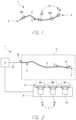
- FIG. 1is a schematic system diagram of a device comprising an elongate body and compact integrated device packages coupled to the elongate body.
- FIG. 2is a schematic system diagram of the device during use in a procedure.
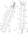
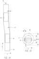
- FIG. 3is a schematic front perspective view of an integrated device package having a bracket assembly coupled with the elongate body and disposed within a lumen in accordance with an embodiment.
- FIG. 4is a schematic rear perspective view of the integrated device package of FIG. 3 disposed within the lumen.
- FIG. 5is a schematic front perspective view of the integrated device package of FIG. 3 outside of the lumen.
- FIG. 6is a schematic end view of the integrated device package disposed within the lumen, as viewed along the longitudinal axis of the package.
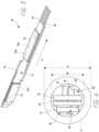
- FIG. 7is a schematic perspective exploded view of the integrated device package of FIG. 5 .
- FIG. 8is schematic front view of the integrated device package having a bracket assembly, in accordance with another embodiment.
- FIG. 9is schematic backside view of the integrated device package of FIG. 8 .
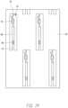
- FIG. 10is a top perspective view of the integrated device packages coupled with a frame during a manufacturing process.
- FIG. 11is an enlarged view of an exemplary integrated device package of FIG. 10 shown with portions of the frame.
- FIG. 12is a schematic front perspective view of the integrated device package including a third integrated device die and at least partially surrounded by a molding material in accordance with another embodiment.
- FIG. 13is a schematic end view of the integrated device package, as viewed along the longitudinal axis of the package, disposed within the molding material.
- FIG. 14is a schematic top-down plan view of the package showing the dies mounted in a common plane on a substrate, in a stage of manufacturing prior to twisting the substrate.
- FIG. 15is a schematic end view of the device package of FIG. 14 , as viewed along the longitudinal axis of the package.
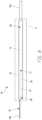
- FIG. 16is a schematic front perspective view of an integrated device package, according to another embodiment.
- FIG. 17is a schematic back perspective view of the integrated device package of FIG. 16 .
- FIG. 18is a schematic end view of the integrated device package of FIGS. 16 and 17 , as viewed along the longitudinal axis of the package.
- FIG. 19is a top perspective view of the integrated device packages of FIGS. 16 and 17 coupled with a frame during a manufacturing process prior to forming a twisted section.
- Various embodiments disclosed hereinrelate to integrated device packages that have a compact or low profile and that may be used to sense the location of small devices.
- various packages disclosed hereincan be configured for use in devices that are inserted into a body lumen or body cavity of a human patient.
- the integrated device packagesare configured to be coupled to a guidewire that is for insertion into a body lumen or body cavity of a human patient.
- the embodiments disclosed hereinmay be particularly beneficial for use with systems that are used at a location remote from the clinician and/or access site, e.g., when the treatment or diagnosis location is not easily visible from outside the body.
- the packages disclosed hereincan be used in any suitable type of medical treatment or diagnostic procedure, including, e.g., cardiac catheter-based treatments, pill-based diagnostic and treatment techniques, endoscopy treatments, urinary catheters and endoscopes, ultrasonic imaging catheters, ear-nose-and-throat based catheters, gastroenterology treatments, colonoscopy treatments, etc.
- cardiac treatmentsthe packages disclosed herein can be used in cardiac diagnostic catheters, die delivery catheters, catheter-based pumps, optical coherence tomography (OCT) catheters, valve delivery catheters, intracardiac echocardiography (ICE) catheters, transesophageal echocardiography (TEE) catheter, diagnostic catheters, PICC lines or any other suitable device.
- the packages disclosed hereincan be coupled with the guidewire, in addition to, or as an alternative to, coupling the package to the catheter.
- the working endcan be included on an elongate bracket assembly.
- the elongate bracket assemblycan be comprised of one or more brackets.
- the bracketsmay be separated along the longitudinal axis.
- various embodiments hereinprovide an elongate bracket assembly extending along a longitudinal axis of the tool or device.
- the elongate bracket assemblycan include a first support surface and a second support surface disposed at a fixed non-parallel angle about the longitudinal axis relative to the first support surface.
- the fixed non-parallel anglecan be about 90° in some arrangements, e.g., in a range from 89° to 91°, or in a range from 89.5° to 90.5°.
- a package substratecan comprise a first portion and a second portion, the first portion mechanically connected to the first support surface and the second portion mechanically connected to the second support surface.
- a first integrated device diecan be mounted to the first portion of the package substrate.
- a second integrated device diecan be mounted to the second portion of the package substrate.
- the first and second device diescan be disposed relative to one another at the fixed non-parallel angle.
- each of the first and second device diescomprises a magnetic sensor, such as an anisotropic magnetoresistance (AMR) sensor, a tunneling magnetoresistance (TMR) sensor, or a giant magnetoresistance (GMR) sensor.
- AMRanisotropic magnetoresistance
- TMRtunneling magnetoresistance
- GMRgiant magnetoresistance
- the first diecan measure the position of the package along two coordinates
- the second device diecan measure the position of the package along a third coordinate.
- Angling the device dies relative to one another by way of deforming the package substratecan beneficially enable three-dimensional position detection of the package within the anatomy.
- the two diescan be angled approximately perpendicular to one another to enable position sensing along three orthogonal axes.
- the sensor packages disclosed hereincan be used in various applications, including medical devices or other technologies in which sensors are provided in small spaces.
- the sensorscan be used to sense various characteristics of the human body.
- position sensingit should be appreciated that other types of sensors may be used, such as sensors that detect velocity, acceleration (e.g., accelerometers), orientation (e.g., gyroscopes), temperature, pressure, pH, etc.
- FIG. 1is a schematic system diagram of a device 1 , such as a medical device, comprising an elongate body 2 having a proximal portion 3 and a distal portion 4 spaced from the proximal portion 3 along a longitudinal axis x.
- the longitudinal axis xmay be defined in local coordinates of the elongate body 2 , and may not necessarily correspond to fixed Cartesian coordinates.
- the elongate body 2can comprise a medical device, such as a catheter or a guidewire.
- the device 1can comprise one or a plurality of compact integrated device packages 10 , such as packages 10 A, 10 B, 10 C, 10 D, coupled with the elongate body 2 .
- the packages 10can be disposed in a lumen of the elongate body 2 , or can be attached to an outside surface of the elongate body 2 . In some embodiments, only a single device package 10 may be coupled with the elongate body 2 .
- the device package 10can be configured to provide the clinician with an indication of the position of the package 10 (and hence the portion of the elongate body 2 to which the package 10 is coupled) within the patient's anatomy. The indicated position can be provided relative to a three-dimensional coordinate system in some embodiments, so that the clinician can beneficially determine the precise location of the working end and/or a path of the elongate body 2 within the body.
- a plurality of device packages 10may be disposed along a length of the elongate body 2 .
- Utilizing a plurality of packages 10may advantageously provide the clinician with position information of different portions of the elongate body 2 .
- Information about the position of multiple portions of the elongate body 2can assist the clinician in positioning the working end of the elongate body 2 relative to the anatomy.
- multiple packages 10can be used to guide different branches of the elongate body 10 into lateral vessels (such as Y-shaped branches), and/or to position the elongate body 10 (or portions thereof) across a cardiac valve.
- FIG. 2is a schematic system diagram of the device 1 during use in a procedure, according to various embodiments.
- the device 1can include the elongate body 2 shown in FIG. 1 , with only a single integrated device package 10 coupled with the elongate body 2 . It should be appreciated that multiple packages 10 can also be used in connection with FIG. 2 .
- the elongate body 2can be disposed within an object 5 during a procedure, such as within a body of a human patient during a treatment or diagnostic procedure.
- the proximal portion 3can be disposed at or near an access site 23 (such as the femoral artery for cardiac catheterization procedures).
- One or more conduits 25can connect the proximal portion 3 of the elongate body 2 with a console 9 .
- the one or more conduits 25may comprise one or more fluid conduits configured to deliver fluid to and/or remove fluid from the elongate body 2 .
- the one or more conduits 25may also include one or more electrical cables to provide electrical communication between the console 9 and various electrical and electronic components of the elongate body 2 (including, e.g., the package 10 ).
- the console 9can comprise a controller that can provide power and/or ground to the device package 10 by way of the one or more conduits 25 (e.g., electrical cables).
- the controllercan comprise processing electronics configured to control the operation of the device 1 .
- the processing electronicscan be programmed by way of software to implement instructions that operate the device 1 .
- the console 9may also include various fluid reservoirs, pumps, sensors, and other devices used in connection with the operation of the device 1 .
- the console 9can transmit signals to and receive signals from the package 10 at the working end of the device 1 .
- the console 9can comprise a user interface (such as a display or touch-screen display, a keypad, etc.) that informs the clinician about the status of the procedure and/or the location of the working end of the device 1 .
- the cliniciancan input instructions to the console 9 by way of the user interface to select various settings and/or operational modes of the device 1 during and/or before use.
- the console 9can be connected to an external processing device (e.g., a computer) that can, for example, act as the user interface and/or analyze operation data.
- the console 9can receive the signals from the package 10 , and can provide feedback to the package 10 with further instructions based on the received signals.
- the package 10can comprise a position sensor package configured to determine an approximate position of the package 10 , and therefore the portion of the elongate body 2 to which the package is connected.
- the package 10can comprise a magnetic sensor package, and particularly a magnetoresistance sensor package, e.g., an anisotropic magnetoresistance (AMR) sensor package, a tunneling magnetoresistance (TMR) package, or a giant magnetoresistance (GMR) package.
- AMRanisotropic magnetoresistance
- TMRtunneling magnetoresistance
- GMRgiant magnetoresistance
- AMR packagessuch as the packages 10 disclosed herein, can comprise a plurality of AMR sensor dies having an anisotropic material in which electrical resistance depends on an angle between the direction of electrical current and the direction of the magnetic fields sensed by the anisotropic material.
- the resistancemay be maximized when the direction of current is parallel to the magnetic field, and the resistance may be reduced at other angles.
- a magnetic generator 7may be provided with the device 1 so as to generate a magnetic field 8 to be transduced by the package 10 .
- the magnetic generator 7may comprise one or a plurality of magnetic generators, each of which may comprise one or a plurality of coiled wires.
- the magnetic generator 7comprises a plurality of magnetic generators 7 A, 7 B, 7 C spaced from one another by predetermined spacings.
- Each magnetic generator 7 A- 7 C of the plurality of magnetic generatorscan be configured to generate a respective magnetic field 8 A- 8 C at different frequencies.
- the console 9can control the operation of the magnetic generator 7 , while in other embodiments, the magnetic generator 7 may be controlled separately from the console 9 to which the elongate body 2 is connected.
- the generated magnetic fields 8 A- 8 Cmay be sufficiently strong so as to penetrate the object 5 and to be sensed by the package 10 .
- the object 5e.g., human patient
- the magnetic generators 7 A- 7 Cmay lie on a table, with the magnetic generators 7 A- 7 C disposed under the table and object 5 .
- the package 10can be configured to detect the generated magnetic fields 8 A- 8 C.
- the integrated device package 10can be configured to transmit a signal to the controller of the console 9 that is indicative of a position of the integrated device package 10 .
- the package 10can comprise one or a plurality of integrated device dies that can detect the components of the magnetic fields 8 A- 8 C in three dimensions.
- the signalcan be transmitted to the controller by way of the conduit(s) 25 .
- the controllercan include processing electronics configured to analyze the signal to determine the position of the integrated device package 10 .
- the controllercan be configured to compare the signal transmitted by the package 10 with the data about the fields 8 A- 8 C generated by the magnetic generators 7 A- 7 C, and/or to compare the signals transmitted from each die of the package 10 with one another.
- the magnetic fields 8 A- 8 Cmay comprise different frequencies that are detectable by the processing electronics. The controller can therefore associate each of the fields 8 A- 8 C detected by the package 10 with an associated magnetic generator 7 A- 7 C, based at least in part on the associated frequency of the fields 8 A- 8 C.
- the known positions of the magnetic generators 7 A- 7 C in a global set of Cartesian coordinates (e.g., X, Y, Z) set by the console 9can be used to triangulate the position, rotation, and/or orientation of the package 10 in and about three dimensions.
- the processing electronics of the controllercan therefore be configured to determine the position of the integrated device package 10 based on a comparison of the respective position signals of each sensor die in the package 10 .
- the differential output signals from the diesmay comprise a pair of twisted wires or a pair of wires spaced closely to one another. Such an arrangement may beneficially reduce any inductance from the magnetic generator 7 in the differential output signal.
- FIG. 3is a schematic front perspective view of the integrated device package 10 coupled with the elongate body 2 , according to various embodiments.
- FIG. 4is a schematic rear perspective view of the package 10 of FIG. 3 .
- the package 10is shown inside a lumen 11 of the elongate body 2 (which may have a single lumen or multiple different lumens therein).
- the package 10is disposed inside of a lumen of a catheter.
- the package 10can be disposed on an outer surface of the elongate body 2 , or otherwise coupled with the elongate body 2 , or could be employed independently of any lumens.
- the elongate body 2 as shown in some Figureshas a cylindrical shape but the elongate body 2 may have any suitable shape for receiving or coupling to the package 10 .
- FIG. 5is a schematic front perspective view of the integrated device package 10 .
- FIG. 6is a schematic end view of the integrated device package 10 , as viewed along the longitudinal axis of the package 10 , with the package 10 shown disposed within the lumen 11 of the elongate body 2 .
- FIG. 7is a schematic perspective, exploded view of the integrated device package 10 .
- the package 10can comprise an elongate bracket assembly 14 extending along a longitudinal axis x, the elongate bracket assembly 14 comprising a first support surface 19 and a second support surface 20 disposed at a fixed non-parallel angle about the longitudinal axis x relative to the first support surface 19 .
- the longitudinal axis xmay be defined in local coordinates of the integrated device package 10 , and may not necessarily correspond to fixed Cartesian coordinates.
- the first and second support surfaces 19 , 20can be disposed generally perpendicular to one another about the longitudinal axis x.
- a package substrate 15can include a first portion 26 and a second portion 27 , the first portion 26 mechanically connected to the first support surface 19 and the second portion 27 mechanically connected to the second support surface 20 .
- the first and second portions 26 , 27can be adhered to the first and second support surfaces 19 , 20 of the bracket assembly 14 by way of an adhesive.
- a first integrated device die 13can be mounted to the first portion 26 of the package substrate 15 .
- a second integrated device die 12can be mounted to the second portion 27 of the package substrate 15 .
- the first and second device dies 13 , 12can be attached to the substrate 15 using a suitable die attach material.
- the first and second device dies 13 , 12can be spaced from one another along the longitudinal axis x of the package 10 .
- the first and second device dies 13 , 12can comprise any suitable type of device die, such as a motion or position sensor die, a processor die, a microelectromechanical systems (MEMS) die, etc.
- MEMSmicroelectromechanical systems
- the first and second dies 13 , 12comprise magnetic sensor dies, e.g., magnetoresistance sensors such as AMR, GMR, or TMR sensor dies, that can serve as position and/or rotation sensors in combination with known external magnetic field source(s).
- the first integrated device die 13can be configured to sense a position and/or orientation of the package 10 along and about first and second orthogonal axes (e.g., X and Y axes)
- the second integrated device die 12can be configured to sense the position and/or orientation of the package 10 along and about a third axis (e.g., Z axis) orthogonal to the first and second axes, or vice versa.
- a third axise.g., Z axis
- the first die 13can have first and second sensing regions 31 a , 31 b that are configured to sense the position and orientation of the package 10 along and about X and Y axes, respectively.
- the second die 12can have a third sensing region 31 c that is configured to sense the position and orientation of the package 10 along and about the Z axis.
- the sensing regions 31 a - 31 cmay be sensitive to magnetic fields, as described above, and can estimate the position and/or orientation of the dies 13 , 12 based on the detected magnetic field. In some embodiments, the sensing regions 31 a - 31 c may be separated within the package 10 by various non-magnetic materials.
- the portions of the dies 13 , 12 , and/or the portions of the substrate 15 (such as the twisted section 17 ), that intervene between the regions 31 a - 31 cmay be non-magnetic.
- the bracket assembly 14may be non-magnetic. While FIGS. 3 , 5 , and 7 show the die 13 having one sensing region 31 a , and the die 12 having two sensing regions 31 b , 31 c , the dies 13 , 12 can have any suitable number of regions. Further, the die 13 as shown in FIGS.
- the sensing region 31 cat a distal portion of the die 13 , but the region 31 c may instead be disposed nearer a proximal portion of the die 13 (e.g., the die 13 could be rotated by 180° about an axis perpendicular to the major surface of the die 13 ).
- Such an alternative arrangementmay position contact pads of the die 13 nearer the proximal portion of the die 13 may reduce substrate costs and noise coupling into the sensing region 31 c.
- the dies 13 , 12can be angled relative to one another about the longitudinal axis x by a fixed non-parallel angle of about 90°, e.g., in a range of 89° to 91°, or in a range of 89.5° to 90.5°.
- the fixed non-parallel anglecan be any angle so long as the AMR sensor dies detect enough difference in magnetic field to accurately calculate the three-dimensional position of the package 10 .
- the bracket assembly 14can provide a stiff support structure to support the integrated device dies 13 , 12 .
- the bracket assembly 14can include a transverse portion 18 disposed between and connecting the first and second support surfaces 19 , 20 .
- the transverse portion 18can act as a transition to precisely orient the first and second support surfaces 19 , 20 by the fixed non-parallel angle.
- the transverse portion 18may be eliminated.
- the bracket assembly 14can comprise multiple bracket components that are spaced and/or separated, for example, brackets 14 a , 14 b shown in FIG. 8 , as explained below.
- the bracket assembly 14can comprise a non-magnetic material in some embodiments, such as copper or aluminum.
- the bracket assembly 14can be shaped from a single piece of material in some embodiments. In some other embodiments, multiple pieces can be connected to define the bracket assembly 14 .
- the angled surfaces 19 , 20can be precisely positioned, which can advantageously lower the resolution and increase the dynamic range of the sensor dies.
- the package substrate 15can comprise a single package substrate sufficiently flexible to comprise one or more bends.
- the package substrate 15can comprise one or more bends that enable the substrate 15 to conform to the angled surfaces 19 , 20 of the bracket assembly.
- the substrate 15can comprise a twisted section 17 .
- the twisted section 17can be disposed between the first portion 26 and the second portion 27 of the substrate 15 so as to position the first and second portions 26 , 27 at the fixed non-parallel angle relative to one another. It should be understood that, for some embodiments, the twisted section 17 may not be fixed in all directions as long as the relative angle of the portions 26 , 27 is fixed.
- the first and second portions 26 , 27may be allowed to bend relative to one another about an x-z line or about an x-y line.
- the package substrate 15can comprise a laminate substrate in some embodiments, with conductors embedded in an insulator. In some embodiments, the package substrate 15 can comprise a plurality of substrates. For example, in such embodiments, the first and second portions 26 , 27 can be defined by separate substrates that may or may not be connected to one another.
- the substrate 15can be sufficiently flexible such that the bend(s) (e.g., the twisted section 17 ) can be formed by a user or a machine applying a twisting force to the substrate 15 about the longitudinal axis x without breaking and/or shorting internal conductors.
- the portions of the substrate 15 that are not attached to the bracket assembly 14may remain flexible so as to be compressed and/or bent to accommodate different package geometries.
- the package substrate 15can comprise a flexible insulator (e.g., polyimide) with embedded metal traces that provide electrical connectivity through the substrate 15 .
- the package substrate 15can comprise a plurality of conductive leads 16 configured to provide electrical communication with a cable or other interconnect that connects with the console 9 .
- the six signal linesmay comprise two terminals for each position signal to be transduced.
- two leads 16may be provided for each Cartesian coordinate (X, Y, Z).
- the two device dies 13 , 12may be electrically connected to one another through the substrate 15 in some embodiments. In other embodiments, the dies 13 , 12 are not electrically connected to one another.
- the conductive leads 16may be disposed proximal the dies 13 , 12 .
- the integrated device dies 13 , 12may be mechanically and electrically connected to the substrate 15 in any suitable manner.
- the dies 13 , 12may be flip chip mounted to the substrate 15 by way of a plurality of solder balls 21 .
- the dies 13 , 12can be connected to the substrate 15 by way of anisotropic conductive film, non-conductive paste, or a thermocompression bond.
- the dies 13 , 12can be wire bonded to the substrate 15 using conductive bonding wires.
- the substrate 15may be densely patterned in various arrangements, and can be bendable so as to form the twisted section 17 .
- the package 10may be disposed in a package housing or package body (not shown).
- the package 10 illustrated in FIGS. 3 - 7may be entirely or partially encapsulated with a molding material 32 in some embodiments so as to protect the components from fluids and other materials during use and/or to fix the fixed non-parallel angle.
- the molding material 32can be any suitable material, e.g., thermosetting or ultraviolet (UV) cured epoxy, injection molded compound, transfer molded compound, glob top, laminated layers, gravity poured epoxies, melted sheets, encapsulant, plastic, etc.
- UVultraviolet
- the elongate body 2may be guided through various curves and bends, such as through parts of the anatomy for medical diagnostic or treatment procedures. It can be important to ensure that the elongate body 2 is sufficiently flexible so as to traverse such non-linear paths. Accordingly, it can be important to provide a package 10 that minimizes a length L of the bracket assembly 14 , since the bracket assembly 14 may drive the overall stiffness of the package 10 (see FIG. 7 ).
- length L of the bracket assembly 14 along the longitudinal axis xcan be no more than 8 mm, e.g., in a range of 1 mm to 8 mm, in a range of 1 mm to 6 mm, in a range of 2 mm to 6 mm, or in a range of 3 mm to 5 mm.
- Dimensioning the bracket assembly 14 and the package 10 to have a short stiff lengthcan enable the elongate body 2 to traverse curved pathways in the body.
- the elongate body 2has a diameter d for receiving or coupling the package 10 within the body 2 , as viewed along the longitudinal axis x of the package 10 (see FIG. 6 ).
- the diameter dcan be in a range of 0.6 millimeters to 2.5 millimeters, in a range of 1 millimeter to 2.5 millimeters, or in a range of 1 millimeter to 2 millimeters.
- the molding material 32 that surrounds the package 10can have a width W along a transverse axis that is perpendicular to the longitudinal axis x.
- the width Wdefines the largest transverse dimension of the package.
- the width Wcorresponds to the diameter of the molding material 32 because the molding material 32 has a cylindrical shape.
- the width Wcan be in a range of 300 microns to 800 microns, in a range of 400 microns to 800 microns, or in a range of 400 microns to 600 microns (see FIG. 6 ).
- the width Wcan represent the largest extent of the package 10 along the direction transverse to the longitudinal axis x.
- the diameter d of the elongate body 2may determine the maximum width W of the molding material 32 for the package 10 .
- additional integrated device dies and electrical componentsmay be provided in the package 10 .
- a third integrated device diesuch as a processor die, an amplifier, a filter, an analog-to-digital converter (ADC), etc.
- ADCanalog-to-digital converter
- the third integrated device diecan process signals transmitted from the first and second dies 13 , 12 .
- the third die 28can provide various pre-processing capabilities (e.g., analog to digital conversion and/or signal amplification) in the package 10 , which can increase the accuracy of the measurements. Positioning the third die 28 (see the die 28 of FIG.
- the three device dies 13 , 12 , 28may be electrically connected to one another through traces embedded in the substrate 15 .
- the substrate 15can extend beyond the bracket assembly 14 along the longitudinal axis x.
- the substrate 15may extend beyond the bracket assembly 14 so as to provide electrical communication between electrical cables and the leads 16 .
- the package substrate 15can extend within the elongate body 2 for a substantial distance.
- the package substrate 15can extend proximally from the package 10 to the proximal portion 3 of the device 1 .
- the package substrate 15can extend at least halfway from the package 10 to the proximal portion 3 .
- the package substrate 15can extend at least a third or at least a quarter of the distance from the package 10 to the proximal portion 3 .
- the extended length of the package substrate 15can enable the integration of additional integrated device dies and electrical components into the device 1 .
- additional device diessuch as the third die referenced above
- additional device diessuch as the third die referenced above
- the increased temperature due to power dissipationcan be undesirable for the application of interest, such as use in a patient's body for medical diagnostic or treatment applications.
- Spreading the additional device dies (such as processing dies) along the length of the device 1 and connected with an extended length substrate 15can beneficially disperse the generated heat so that the temperature in a particular location does not appreciably increase.
- the additional diesmay not be disposed within the package 10 , the additional dies may still be nearer the package 10 than they otherwise would be if housed in the console 9 . Positioning the additional dies between the proximal portion 3 of the device 1 and the package 10 can therefore improve the signal quality of the sensed position data while maintaining the desired temperature.
- FIGS. 8 - 9illustrate another embodiment of a device 1 having a package 10 with a plurality of integrated device dies 13 , 12 angled relative to one another by a fixed angle. Unless otherwise noted, components of FIGS. 8 - 9 are the same as or generally similar to like-numbered components shown in FIGS. 1 - 7 .
- FIG. 8is a schematic front view of an integrated device package 10 having a substrate 15 and integrated device dies 13 , 12 , mounted thereto. As with the embodiment of FIGS. 1 - 7 , the substrate 15 can be mounted to a bracket assembly 14 . However, unlike the embodiment of FIGS.
- the bracket assembly 14may comprise multiple brackets 14 a , 14 b that are separated and spaced from one another, e.g., the bracket assembly 14 may omit the transverse portion 18 shown, e.g., in FIG. 4 .
- FIG. 9is schematic rear view of the integrated device package 10 of FIG. 8 .
- the integrated device package 10has separated brackets 14 a , 14 b that define the bracket assembly 14 .
- the brackets 14 a , 14 b depicted in FIGS. 8 and 9are separate from and spaced from each other along the longitudinal axis x.
- the bracket 14 ahas a first support surface 19 and the bracket 14 b has a second support surface 20 .
- the substrate 15can include a first portion 26 and a second portion 27 , the first portion 26 mechanically connected to the first support surface 19 and the second portion 27 mechanically connected to the second support surface 20 .
- the first and second portions 26 , 27can be adhered or bonded to the first and second support surfaces 19 , 20 , respectively, by way of an adhesive.
- the first integrated device die 13can be mounted to the first portion 26 of the package substrate 15 .
- the second integrated device die 12can be mounted to the second portion 27 of the package substrate 15 .
- the bracket assembly 14can have more than two brackets 14 a , 14 b . While shown for purposes of illustration with ends of the two brackets 14 a , 14 b protruding out of the elongate body 2 , it will be understood that in use the entire package 10 can be within the elongate element 2 .
- the substrate 15can comprise a twisted section 17 .
- the twisted section 17can be disposed between the first portion 26 and the second portion 27 of the substrate 15 and be twisted about the longitudinal axis so as to position the first and second portions 26 , 27 at a fixed non-parallel angle relative to one another.
- the twisted section 17may also be disposed between the brackets 14 a , 14 b to connect the brackets 14 a , 14 b .
- the twisted section 17may not be connected to a corresponding twisted or transverse portion of the bracket assembly 14 .
- the twisted section 17 of FIGS. 8 - 9may be unconnected to the bracket assembly 14 since the bracket assembly 14 may not include the transverse portion 18 .
- the bracket assembly 14 having the brackets 14 a , 14 bcan provide a stiff support structure to support the integrated device dies 13 , 12 .
- the fixed angle between the dies 13 , 12can be provided by applying a molding material 32 over the dies 13 , 12 .
- the molding material 32can be disposed entirely or partially around the package 10 to define the fixed non-parallel angle and/or protect the components from fluids and other materials during use.
- the mold 32may entirely envelope the twisted section 17 , and only partially envelope the brackets 14 a , 14 b .
- the fixed non-parallel anglecan be about 90° in some arrangements, e.g., in a range from 89° to 91°, or in a range from 89.5° to 90.5°.
- the fixed non-parallel anglecan comprise other numerical values.
- Embodiments of the package 10 with the bracket assembly 14 that do not include the transverse portion 18 of FIGS. 1 - 7can be beneficial because the overall size of the package 10 of FIGS. 8 - 9 can be smaller than the overall size of the package 10 of FIGS. 1 - 7 that includes the transverse portion 18 .
- the first and second support surfaces 19 , 20 of the bracket assembly 14form an L-shape. In such embodiments deforming (e.g., twisting) the substrate 15 and/or the dies 13 , 12 depends on the shape and dimensions of the bracket assembly 14 .
- the package 10may be deformed more freely at the twisted section 17 of the substrate 15 and would not be limited to the L-shape.
- the width W of the molding material 32 for the package 10 after deformationcan be generally similar to the width W before deformation, which can beneficially enable the package 10 to fit within the elongate body 2 .
- FIG. 10is a top perspective view of the integrated device packages 10 coupled with a frame 33 during a process for manufacturing the package 10 , according to the embodiments of FIGS. 1 - 9 .
- FIG. 11is an enlarged view of an exemplary integrated device package 10 of FIG. 10 coupled with portions of the frame 33 .
- the frame 33may comprise a metal frame or any suitable frame to assist in simultaneously manufacturing numerous packages.
- one or multiple substrates 15can be placed on bracket assembly 14 , corresponding to portions of the frame 33 .
- the bracket assembly 14can include a transverse portion 18 disposed between and connecting the first and second support surfaces 19 , 20 .
- the transverse section 18may be omitted and have brackets 14 a and 14 b as shown in FIGS. 8 - 9 .
- the bracket assembly 14can, for example, comprise brackets 14 a , 14 b separated from and/or spaced from each other along the axis x.
- the integrated device packages 10can be separated from the frame 33 by punching, sawing, laser cutting or any other suitable methods of dividing the frame 33 .
- FIGS. 12 - 15illustrate another embodiment of a device having an integrated device package 10 with dies 13 , 12 that are angled relative to one another by a fixed non-parallel angle. Unlike the embodiments of FIGS. 1 - 11 , in which the substrate 15 is coupled to a bracket assembly 14 , in FIGS. 12 - 15 , the package 10 may not include a bracket assembly 14 .
- FIG. 12is a schematic front perspective view of the integrated device package 10 partially surrounded by the molding material 32 , according to various embodiments.
- FIG. 13is a schematic end view of the integrated device package 10 with molding material 32 surrounding the package 10 , as viewed along the longitudinal axis x of the package 10 .
- a third integrated device die 28(which may comprise an Application Specific Integrated Circuit, or ASIC) may be mounted to the substrate 15 proximal the dies 13 , 12 , and may electrically connect to the dies 13 , 12 through the substrate 15 .
- ASICApplication Specific Integrated Circuit
- the package 10is shown inside various portions of the molding material 32 .
- the molding material 32may be applied separately around the device dies 13 , 12 , and the third die 28 .
- a first portion of the molding material 32may be applied over both dies 13 , 12
- a second portion of the molding materialmay be applied over the third die 28 .
- the molding material 32may not be applied around a section 30 of the substrate 15 which can beneficially improve the flexibility of the package 10 .
- the uncovered section 30 of the substrate 15can enable the package 10 to traverse curved or non-linear sections of the anatomy.
- the molding material 32may be applied around the section 30 such that the molding material 32 is disposed about the entire package 10 .
- the embodiment shown in FIG. 12which is generally similar to the embodiments shown and described in FIGS. 3 - 7 , can comprise the substrate 15 with leads 16 , and the first and second integrated device dies 13 , 12 can be mechanically and electrically connected to the substrate 15 .
- the embodiment in FIG. 12further includes the third integrated device die 28 (such as a processor die, an amplifier, a filter, an analog-to-digital converter (ADC), etc.) mounted to the substrate 15 along the first or second portions 26 , 27 .
- the third integrated device die 28can process signals transmitted from the first and second dies 13 , 12 .
- the device dies 13 , 12can be magnetoresistance sensors such as AMR, GMR, or TMR sensor dies and the third device die 28 can be an ADC.
- the dies 13 , 12can transmit the sensed data signal to the third die 28 (e.g. an ADC) for converting the sensed analog signal to a digital signal.
- the processed signal from the third die 28can be sent via the plurality of conductive leads 16 and a cable or other interconnects to the console 9 .
- the package 10 in FIGS. 12 and 13does not include the bracket assembly 14 , as shown in embodiments in FIGS. 3 - 7 , or the assembly without the transverse portion 18 (i.e., the brackets 14 a , 14 b ), as shown in embodiments in FIGS. 8 and 9 .
- the dies 13 , 12are mounted to the substrate 15 , and a molding material 32 is disposed about portions of the dies 13 , 12 and the substrate 15 to fix the dies 13 , 12 at the fixed non-parallel angle.
- a molding material 32is disposed about portions of the dies 13 , 12 and the substrate 15 to fix the dies 13 , 12 at the fixed non-parallel angle.
- the molding compound 32rather than a bracket assembly 14 or other structure, effects or defines the fixed non-parallel angle between the dies 13 , 12 .
- the third integrated device die 28can be spaced from the first integrated device die 12 by the section 30 of the substrate 15 along the longitudinal axis x.
- the section 30 of the substrate 15 shown in FIG. 12is substantially flat. However, it should be understood that the section 30 may form any shape.
- the section 30can be fixed by applying the molding material 32 .
- a length of the package 10 along the longitudinal axiscan be in a range of 7 mm to 11 mm, in a range of 7 mm to 10 mm, or in a range of 8 mm to 10 mm.
- the molding material 32can be applied over portions of the dies 13 , 12 , 28 and the substrate 15 . In some embodiments, the molding material 32 can be disposed entirely around the package 10 . In some other embodiments, the molding material 32 can be disposed partially around the package 10 . For example, in the embodiment of FIGS. 12 - 13 , a first portion of the molding material can be disposed over the first die 13 , the second die 12 , and the intervening twisted section 17 of the substrate 15 . In some embodiments the molding material 32 can be disposed only over the twisted section 17 . In some embodiments, the molding material 32 can be disposed over the twisted section 17 and one or more of the dies 13 , 12 , 28 . Thus, the molding material 32 can be disposed over any portion of the package 10 so as to define or maintain the fixed non-parallel angle and/or protect the first die 13 , the second die 12 and/or the third die 28 .
- FIG. 14is a schematic top-down plan view of the package 10 with an offset before forming the fixed non-parallel angle, e.g., before twisting the dies 13 , 12 relative to one another.
- FIG. 15is a schematic end view of the device package 10 of FIG. 14 overlaid within the lumen 11 of the body 2 .
- the molding compoundis omitted for ease of illustration.
- FIG. 15therefore illustrates a schematic rendering of how, prior to twisting the substrate 15 , the package 10 is wider than the lumen 11 of the elongate body 2 (e.g., the catheter). As shown in FIGS.
- the substrate 15is shifted or laterally offset at the twisted section 17 so as to make the integrated dies 12 , 13 offset along a transverse axis y to create a lateral offset ⁇ between the dies 13 , 12 before twisting.
- the lateral offset ⁇ between the dies 13 , 12allows the dies 13 , 12 to fit within the diameter d of the elongate body 2 after twisting.
- the offset ⁇can be selected such that, after twisting the substrate 15 to define the twisted section 17 , the dies 13 , 12 and substrate 15 can fit within the diameter d of the elongate body 2 , despite the fact that it could not fit prior to twisting.
- the offset ⁇can typically be determined by sizes of the substrate 15 and other components of the package 10 along the transverse axis, but other factors may affect the determination of the offset ⁇ .
- the offset ⁇can be in a range of 10 microns to 200 microns, in a range of 20 microns to 150 microns, or in a range of 40 microns to 100 microns.
- the package 10can be manufactured by mounting the first and second integrated device dies 13 , 12 on the substrate 15 .
- the dies 13 , 12can be spaced apart from each other along the longitudinal axis x, and along the transverse axis x by an offset ⁇ .
- the substrate 15can be deformed (e.g., twisted) so as to angle the dies 13 , 12 relative to one another about the longitudinal axis x by the fixed non-parallel angle (about 90° in some arrangements, e.g., in a range from 89° to 91°, or in a range from 89.5° to 90.5°).
- the molding material 32can be applied to the package 10 to fix the fixed non-parallel angle (in the absence of a bracket assembly or another structure that fixes the angle) and/or to protect the dies 13 , 12 , 28 at a molding step.
- the first and second integrated device dies 13 , 12can be electrically connected to the substrate 15 .
- the dies 13 , 12may be flip chip mounted to the substrate 15 by way of a plurality of solder balls.
- the dies 13 , 12can be wire bonded to the substrate 15 using conductive bonding wires.
- the third die 28can also be mounted on and electrically connected to the substrate 15 .
- the deforming stepcan include offsetting the substrate 15 in the transverse axis y, twisting the substrate 15 , and/or adhering the substrate 15 to the bracket assembly 14 .
- FIG. 16is a schematic front perspective view of an integrated device package 10 , according to another embodiment.
- the package 10can include first and second integrated device dies 13 , 12 (which may comprise motion sensor dies as explained above), a third integrated device die 28 (which can comprise a processor die or ASIC configured to process signals transduced by the dies 13 , 12 ) with the dies 13 , 12 , 28 at least partially surrounded by a molding material 32 .
- the molding material 32can be the structure that maintains the fixed non-parallel angle between the dies 13 , 12 .
- the package 10 of FIG. 16is generally similar to the package 10 illustrated in FIG. 12 .
- the third integrated device die 28 of FIG. 16can be stacked over the second die 12 .
- the embodiment shown in FIG. 16includes a bracket assembly 14 , although in other embodiments, the package 10 of FIG. 16 may not include any brackets or other structures that separately support or stiffen the dies 13 , 12 , 28 .
- a first bracket 14 acan be connected to the first die 13 and the opposite side of the portion of the substrate 15 to which the die 13 is mounted, such that the first die 13 and the substrate 15 are disposed between the first brackets.
- one or more passive components 35may be mounted to and electrically connected to the substrate 15 adjacent the second and third dies 12 , 28 .
- the passive component(s) 35can be configured to smooth signals prior to or after processing by the third die 28 .
- the dimension of the passive component 35can be less than 0.3 mm along the transverse axis, less than 0.5 mm along the longitudinal axis and less than 0.3 mm in height.
- the third integrated device die 28(for example, a processor die or ASIC) can be electrically connected to the substrate by any suitable method, e.g., by way of solder balls 55 ).
- the solder balls 55can provide vertical standoff of the third die 28 relative to the substrate 15 , e.g., to provide clearance or a cavity sufficiently sized to receive the second die 12 between the third die 28 and the substrate 15 .
- the third die 28can contact the second die 12 , but in other embodiments, the third die 28 can be vertically spaced above the second die 12 , e.g., the solder balls 55 can space the third die 28 above the second die 12 in some embodiments.
- the third integrated device die 28may be, for example, wire bonded to the substrate 15 .
- Stacking the third integrated device die 28 over the second integrated device die 12can advantageously shorten the length of the package along the longitudinal axis x, as compared with the embodiments of FIG. 12 , since the second and third dies 12 , 28 can be positioned at about the same longitudinal position along the elongate body 2 .
- a length of the package 10 along the longitudinal axiscan be in a range of 3 mm to 6 mm, in a range of 3.5 mm to 5.5 mm, in a range of 3.5 mm to 5 mm, in a range of 4 mm to 5.5 mm, or in a range of 4 mm to 5 mm, e.g., about 4.5 mm in one embodiment.
- Stacking the third integrated device die 28 over the second integrated device die 12can also advantageously reduce a total length of traces embedded in the substrate 15 by making the substrate 15 more compact as compared with the embodiment of FIG. 12 .
- the bracket assembly 14can be used for twisting the substrate 15 , for protecting the dies 13 , 12 , 28 , and/or for supporting the dies 13 , 12 , 28 and substrate 15 during molding.
- the final package 10can include the bracket assembly 14 .
- the bracket assembly 14can be eliminated in a final product.
- FIG. 17is a schematic back perspective view of the integrated device package 10 of FIG. 16 .
- the package 10 as illustrated in FIG. 17has conductive leads 16 on the substrate 15 .
- the number of the conductive leads 16 shownis six, however, there can be any suitable number of conductive leads 16 .
- FIG. 18is a schematic end view of the integrated device package 10 of FIGS. 16 and 17 , as viewed along the longitudinal axis x of the package.
- the molding material 32 that surrounds the package 10can have a height H (as measured from a flat surface of the octagonal shape to an opposing flat surface as shown in FIG. 18 ) along a transverse axis that is perpendicular to the longitudinal axis x.
- the height Hcan be around 450 microns:
- the height Hcan be in a range of 300 microns to 600 microns, in a range of 300 microns to 550 microns, in a range of 350 microns to 550 microns, in a range of 350 microns to 500 microns, in a range of 400 microns to 550 microns, or in a range of 400 microns to 500 microns.
- portions of the molding material 32(which may originally have a circular profile) can be trimmed to form an octagonal shape, which can beneficially reduce the overall lateral dimensions of the package 10 and to improve the fit of the package 10 within the elongate body 2 .
- the width W for the embodiment illustrated in FIG. 18can be generally similar to the width W for the embodiment illustrated in FIG. 6 .
- the width Wcan be a dimension measured from a vertex to another vertex farthest from the vertex, e.g., the width W can define a major lateral or transverse dimension of the package 10 .
- FIG. 19is a top perspective view of the integrated device packages 10 of FIGS. 16 and 17 coupled with a frame 33 during a manufacturing process prior to forming the twisted section 17 .
- the substrate 15can have a winding 37 for easily twisting the first integrated device die 13 relative to the second and third integrated device die 12 , 28 . It should be understood that the winding 37 can be disposed at a different portion of the substrate 15 from what is illustrated in FIG. 19 .
Landscapes
- Engineering & Computer Science (AREA)
- Physics & Mathematics (AREA)
- Health & Medical Sciences (AREA)
- Life Sciences & Earth Sciences (AREA)
- Microelectronics & Electronic Packaging (AREA)
- Condensed Matter Physics & Semiconductors (AREA)
- General Physics & Mathematics (AREA)
- Power Engineering (AREA)
- Computer Hardware Design (AREA)
- Pathology (AREA)
- Molecular Biology (AREA)
- Biophysics (AREA)
- Veterinary Medicine (AREA)
- Biomedical Technology (AREA)
- Heart & Thoracic Surgery (AREA)
- Medical Informatics (AREA)
- Public Health (AREA)
- Surgery (AREA)
- Animal Behavior & Ethology (AREA)
- General Health & Medical Sciences (AREA)
- Human Computer Interaction (AREA)
- Geometry (AREA)
- Measuring Magnetic Variables (AREA)
- Measurement And Recording Of Electrical Phenomena And Electrical Characteristics Of The Living Body (AREA)
- Measurement Of Length, Angles, Or The Like Using Electric Or Magnetic Means (AREA)
Abstract
Description
Claims (15)
Priority Applications (1)
| Application Number | Priority Date | Filing Date | Title |
|---|---|---|---|
| US15/681,904US11647678B2 (en) | 2016-08-23 | 2017-08-21 | Compact integrated device packages |
Applications Claiming Priority (2)
| Application Number | Priority Date | Filing Date | Title |
|---|---|---|---|
| US201662378587P | 2016-08-23 | 2016-08-23 | |
| US15/681,904US11647678B2 (en) | 2016-08-23 | 2017-08-21 | Compact integrated device packages |
Publications (2)
| Publication Number | Publication Date |
|---|---|
| US20180062071A1 US20180062071A1 (en) | 2018-03-01 |
| US11647678B2true US11647678B2 (en) | 2023-05-09 |
Family
ID=61243541
Family Applications (1)
| Application Number | Title | Priority Date | Filing Date |
|---|---|---|---|
| US15/681,904Active2042-01-08US11647678B2 (en) | 2016-08-23 | 2017-08-21 | Compact integrated device packages |
Country Status (2)
| Country | Link |
|---|---|
| US (1) | US11647678B2 (en) |
| CN (1) | CN107768315B (en) |
Families Citing this family (7)
| Publication number | Priority date | Publication date | Assignee | Title |
|---|---|---|---|---|
| US11647678B2 (en) | 2016-08-23 | 2023-05-09 | Analog Devices International Unlimited Company | Compact integrated device packages |
| US10697800B2 (en) | 2016-11-04 | 2020-06-30 | Analog Devices Global | Multi-dimensional measurement using magnetic sensors and related systems, methods, and integrated circuits |
| EP3520695A3 (en) | 2018-01-31 | 2019-11-06 | Analog Devices, Inc. | Electronic devices |
| WO2019198061A1 (en) | 2018-04-13 | 2019-10-17 | Universidade Do Minho | Guidance system, method and devices thereof |
| JP6874782B2 (en)* | 2019-03-11 | 2021-05-19 | Tdk株式会社 | Magnetic sensor |
| US12032041B2 (en)* | 2022-03-17 | 2024-07-09 | Globalfoundries Singapore Pte. Ltd. | Magnetic field sensor |
| US12251171B2 (en) | 2022-10-14 | 2025-03-18 | Covidien Lp | Surgical item detection system for in vivo foreign object detection by magnetic flux leakage |
Citations (183)
| Publication number | Priority date | Publication date | Assignee | Title |
|---|---|---|---|---|
| US3724274A (en) | 1971-02-11 | 1973-04-03 | Millar Instruments | Pressure transducers and method of physiological pressure transducers |
| US3949274A (en) | 1974-05-30 | 1976-04-06 | International Business Machines Corporation | Packaging and interconnection for superconductive circuitry |
| US4006394A (en) | 1972-08-21 | 1977-02-01 | Information Storage Systems, Inc. | Coarse and fine control for position servo |
| US4742183A (en) | 1986-10-24 | 1988-05-03 | Napco Security Systems, Inc. | Methods and techniques for fabricating foldable printed circuit boards |
| US4928206A (en) | 1988-11-23 | 1990-05-22 | Ncr Corporation | Foldable printed circuit board |
| US5074863A (en) | 1990-10-12 | 1991-12-24 | Dines Lenna V | Disposable retractable surgical instrument |
| US5126286A (en) | 1990-10-05 | 1992-06-30 | Micron Technology, Inc. | Method of manufacturing edge connected semiconductor die |
| EP0575800A2 (en) | 1992-06-12 | 1993-12-29 | Thomson And Nielsen Electronics Limited | Flexible radiation probe |
| US5289122A (en) | 1991-06-17 | 1994-02-22 | Murata Mfg. Co., Ltd. | Magnetic sensor for detecting coarse and fine magnetic patterns |
| US5405337A (en) | 1993-02-24 | 1995-04-11 | The Board Of Trustees Of The Leland Stanford Junior University | Spatially distributed SMA actuator film providing unrestricted movement in three dimensional space |
| US5452182A (en) | 1990-04-05 | 1995-09-19 | Martin Marietta Corporation | Flexible high density interconnect structure and flexibly interconnected system |
| WO1996010731A1 (en) | 1994-09-30 | 1996-04-11 | Honeywell Inc. | Position detection apparatus |
| US5554806A (en) | 1994-06-15 | 1996-09-10 | Nippondenso Co., Ltd. | Physical-quantity detecting device |
| US5555159A (en) | 1993-12-17 | 1996-09-10 | Schneider Electric Sa | Add-on module for variable speed drives |
| US5616863A (en) | 1994-02-01 | 1997-04-01 | Ic Sensors, Inc. | Side surface mounted accelerometer assembly |
| JPH09121015A (en) | 1995-10-25 | 1997-05-06 | Hitachi Ltd | Semiconductor device |
| US5644230A (en)* | 1994-07-20 | 1997-07-01 | Honeywell Inc. | Miniature magnetometer and flexible circuit |
| US5731222A (en) | 1995-08-01 | 1998-03-24 | Hughes Aircraft Company | Externally connected thin electronic circuit having recessed bonding pads |
| US5833608A (en) | 1993-10-06 | 1998-11-10 | Biosense, Inc. | Magnetic determination of position and orientation |
| US5903440A (en) | 1998-01-30 | 1999-05-11 | Delco Electronics Corporaiton | Method of forming assemblies of circuit boards in different planes |
| US6040624A (en) | 1997-10-02 | 2000-03-21 | Motorola, Inc. | Semiconductor device package and method |
| US6052610A (en) | 1998-01-09 | 2000-04-18 | International Business Machines Corporation | Magnetic catheter tracker and method therefor |
| WO2000027281A1 (en) | 1998-11-06 | 2000-05-18 | Lucent Medical Systems, Inc. | Determining the location and orientation of an indwelling medical device |
| US6075708A (en) | 1997-09-04 | 2000-06-13 | Rohm Co., Ltd. | Partly bent electric circuit substrate and method for manufacturing the same |
| US6078102A (en) | 1998-03-03 | 2000-06-20 | Silicon Bandwidth, Inc. | Semiconductor die package for mounting in horizontal and upright configurations |
| US6097183A (en) | 1998-04-14 | 2000-08-01 | Honeywell International Inc. | Position detection apparatus with correction for non-linear sensor regions |
| US6106476A (en) | 1994-09-02 | 2000-08-22 | Endosonics Corporation | Ultra miniature pressure sensor and guide wire using the same and method |
| US6169254B1 (en) | 1994-07-20 | 2001-01-02 | Honeywell, Inc. | Three axis sensor package on flexible substrate |
| WO2001004656A1 (en) | 1999-07-13 | 2001-01-18 | Alliedsignal Inc. | Multi-axis magnetic field sensing device and methods for fabricating the same |
| US6184680B1 (en) | 1997-03-28 | 2001-02-06 | Tdk Corporation | Magnetic field sensor with components formed on a flexible substrate |
| US6225688B1 (en) | 1997-12-11 | 2001-05-01 | Tessera, Inc. | Stacked microelectronic assembly and method therefor |
| US6278271B1 (en) | 1998-03-30 | 2001-08-21 | Sentron Ag | Three dimensional magnetic field sensor |
| US6291894B1 (en) | 1998-08-31 | 2001-09-18 | Micron Technology, Inc. | Method and apparatus for a semiconductor package for vertical surface mounting |
| US6326908B1 (en) | 1998-09-04 | 2001-12-04 | Trilogy Systems Corp | Precision position encoder using coarse position indicator |
| US6339191B1 (en) | 1994-03-11 | 2002-01-15 | Silicon Bandwidth Inc. | Prefabricated semiconductor chip carrier |
| US20020005715A1 (en) | 2000-07-13 | 2002-01-17 | Tokyo Keiso Kabushiki-Kaisha | Apparatus and method for detecting the displacement |
| US6348427B1 (en) | 1999-02-01 | 2002-02-19 | Kyocera Corporation | High-thermal-expansion glass ceramic sintered product |
| US20020077752A1 (en) | 2000-09-28 | 2002-06-20 | Bernard Burreson | Noncontacting position indicating system |
| WO2002052221A1 (en) | 2000-12-27 | 2002-07-04 | Kabushiki Kaisha Bridgestone | Displacement sensor |
| US20020180605A1 (en) | 1997-11-11 | 2002-12-05 | Ozguz Volkan H. | Wearable biomonitor with flexible thinned integrated circuit |
| US6536123B2 (en) | 2000-10-16 | 2003-03-25 | Sensation, Inc. | Three-axis magnetic sensor, an omnidirectional magnetic sensor and an azimuth measuring method using the same |
| US6570246B1 (en) | 2002-06-12 | 2003-05-27 | United Microelectronics Corp. | Multi-die package |
| EP1321743A1 (en) | 2001-12-20 | 2003-06-25 | Sensitec Gmbh | Length measuring system with a measuring rod moving with respect to mutually spaced length sensors |
| US20030120150A1 (en) | 2001-12-21 | 2003-06-26 | Assaf Govari | Wireless position sensor |
| US6591492B2 (en) | 2001-08-30 | 2003-07-15 | Micron Technology, Inc. | Angled edge connections for multichip structures |
| US20030146332A1 (en) | 2002-02-07 | 2003-08-07 | Vinding Donald R. | Retractable reel for flexible tubing |
| US20030209789A1 (en) | 2002-05-09 | 2003-11-13 | Hanson David S. | Coplanar mounting member for a mem sensor |
| US6721189B1 (en) | 2002-03-13 | 2004-04-13 | Rambus, Inc. | Memory module |
| US20040157410A1 (en) | 2003-01-16 | 2004-08-12 | Seiko Epson Corporation | Semiconductor device, semiconductor module, electronic equipment, method for manufacturing semiconductor device, and method for manufacturing semiconductor module |
| US6777261B2 (en) | 2000-12-26 | 2004-08-17 | Micron Technology, Inc. | Method and apparatus for a semiconductor package for vertical surface mounting |
| US6784659B2 (en) | 2001-12-05 | 2004-08-31 | Honeywell International Inc. | Magnetoresistive speed and direction sensing method and apparatus |
| US20040169244A1 (en) | 2003-02-28 | 2004-09-02 | Honeywell International, Inc. | Miniature 3-dimensional package for MEMS sensors |
| US6852607B2 (en) | 2001-05-31 | 2005-02-08 | Samsung Electronics., Ltd | Wafer level package having a side package |
| US20050184187A1 (en) | 2002-01-24 | 2005-08-25 | Incumed, Inc. | Guidewire reel and related methods |
| US20050230795A1 (en) | 2004-03-30 | 2005-10-20 | Kabushiki Kaisha Toshiba | LSI package provided with interface module, and transmission line header employed in the package |
| US6993443B2 (en) | 2003-02-22 | 2006-01-31 | Rheinmetall Defence Electronics Gmbh | Method for determining and tracking the position and orientation of a magnetic field sensor |
| US6993974B2 (en) | 2003-07-02 | 2006-02-07 | Radi Medical Systems Ab | Sensor and guide wire assembly |
| US20060082363A1 (en) | 2004-10-18 | 2006-04-20 | Honeywell International, Inc. | Position detection apparatus and method for linear and rotary sensing applications |
| US20060129061A1 (en) | 2004-12-15 | 2006-06-15 | Masayuki Kaneto | Catheter and production method thereof |
| US20060151864A1 (en) | 2005-01-11 | 2006-07-13 | Rosemount Inc. | MEMS packaging with improved reaction to temperature changes |
| US7115984B2 (en) | 2002-06-18 | 2006-10-03 | Micron Technology, Inc. | Semiconductor devices including peripherally located bond pads, intermediates thereof, assemblies, and packages including the semiconductor devices, and support elements for the semiconductor devices |
| US20060261453A1 (en) | 2005-03-16 | 2006-11-23 | Yonggill Lee | Semiconductor package and stack arrangement thereof |
| US20070035294A1 (en) | 2004-06-03 | 2007-02-15 | Honeywell International Inc. | Integrated Three-Dimensional Magnetic Sensing Device and Method to Fabricate an Integrated Three-Dimensional Magnetic Sensing Device |
| US20070053504A1 (en) | 2003-10-31 | 2007-03-08 | Matsushita Electric Industrial Co., Ltd. | Connection device, electronic apparatus with the same, and folding portable terminal device |
| US7202552B2 (en) | 2005-07-15 | 2007-04-10 | Silicon Matrix Pte. Ltd. | MEMS package using flexible substrates, and method thereof |
| US7211886B2 (en) | 2004-04-01 | 2007-05-01 | Industrial Technology Research Institute | Three-dimensional multichip stack electronic package structure |
| US7265719B1 (en) | 2006-05-11 | 2007-09-04 | Ball Aerospace & Technologies Corp. | Packaging technique for antenna systems |
| US7301332B2 (en) | 2005-10-06 | 2007-11-27 | Biosense Webster, Inc. | Magnetic sensor assembly |
| US7307415B2 (en) | 2002-02-14 | 2007-12-11 | Bvr Technologies Co. | Contactless angular position sensor and method for sensing angular position of a rotatable shaft |
| US20080052932A1 (en)* | 2006-09-01 | 2008-03-06 | Song Sheng Xue | Magnetic MEMS sensors |
| US7375009B2 (en) | 2002-06-14 | 2008-05-20 | Micron Technology, Inc. | Method of forming a conductive via through a wafer |
| US20080175425A1 (en) | 2006-11-30 | 2008-07-24 | Analog Devices, Inc. | Microphone System with Silicon Microphone Secured to Package Lid |
| US7408342B2 (en) | 2003-10-08 | 2008-08-05 | Centre National D'etudes Spatiales | Device for measuring a component of current based on magnetic fields |
| US7408343B2 (en) | 2004-11-18 | 2008-08-05 | Honeywell International Inc. | Position detection utilizing an array of magnetic sensors with irregular spacing between sensing elements |
| US7420262B2 (en) | 2003-02-27 | 2008-09-02 | Infineon Technologies Ag | Electronic component and semiconductor wafer, and method for producing the same |
| US7429788B2 (en) | 2006-03-08 | 2008-09-30 | Microelectronics Assembly Technologies, Inc. | Thin multichip flex-module |
| US20080285111A1 (en) | 2006-08-30 | 2008-11-20 | Fusao Ishii | Mirror device |
| JP2008305395A (en) | 2008-05-15 | 2008-12-18 | Psa Corp Ltd | Magnetic sensor for automatic vehicle guidance system |
| US7467552B2 (en) | 2005-11-10 | 2008-12-23 | Honeywell International Inc. | Miniature package for translation of sensor sense axis |
| US20090027048A1 (en) | 2005-03-17 | 2009-01-29 | Hideki Sato | Three-Axis Magnetic Sensor and Method for Manufacturing the Same |
| US7525309B2 (en) | 2005-12-30 | 2009-04-28 | Depuy Products, Inc. | Magnetic sensor array |
| WO2009052537A1 (en) | 2007-10-25 | 2009-04-30 | Sensordynamics Ag Entwicklungs- Und Produktionsgesellschaft | Method and device for contactless sensing rotation and angular position using orientation tracking |
| US20090121342A1 (en) | 2007-11-14 | 2009-05-14 | Minakawa Atsushi | Semiconductor device including main substrate and sub substrates and fabrication method of the same |
| US20090243402A1 (en) | 2008-03-25 | 2009-10-01 | Bose Corporation | Position measurement using magnetic fields |
| US20090268019A1 (en) | 2007-01-16 | 2009-10-29 | Olympus Medical Systems Corp. | Image pickup apparatus and endoscope |
| US20090295381A1 (en) | 2008-05-27 | 2009-12-03 | Infineon Technologies Ag | Magnetic sensor integrated circuit device and method |
| JP2009289724A (en) | 2008-05-28 | 2009-12-10 | Sigma Denki Kogyo Kk | Method for manufacturing cylindrical decorative illumination body and method of controlling light emitting direction of cylindrical decorative illumination body |
| US20090315554A1 (en) | 2008-06-20 | 2009-12-24 | Honeywell International Inc. | Integrated three-dimensional magnetic sensing device and method to fabricate an integrated three-dimensional magnetic sensing device |
| US20100072992A1 (en) | 2008-09-08 | 2010-03-25 | Christian Bauer | Magnetic field sensor array for measuring spatial components of a magnetic field |
| US20100078739A1 (en) | 2008-09-30 | 2010-04-01 | Analog Devices, Inc. | Vertical Mount Package for MEMS Sensors |
| US20100090295A1 (en) | 2008-10-09 | 2010-04-15 | Silicon Matrix Pte. Ltd. | Folded lead-frame packages for MEMS devices |
| US20100130923A1 (en) | 2008-11-26 | 2010-05-27 | B. Braun Medical Inc. | Apparatus and method for inserting a catheter |
| US20100155863A1 (en) | 2005-08-11 | 2010-06-24 | Koninklijke Philips Electronics, N.V. | Method for manufacturing a microelectronic package comprising a silicon mems microphone |
| US20100197148A1 (en) | 2009-02-02 | 2010-08-05 | Apex Technologies, Inc. | Flexible magnetic interconnects |
| US7812596B2 (en) | 2007-08-16 | 2010-10-12 | Honeywell International Inc. | Two-dimensional position sensing system |
| JP2010258038A (en) | 2009-04-21 | 2010-11-11 | Olympus Corp | Substrate with built-in component |
| US7839657B2 (en) | 2006-04-28 | 2010-11-23 | Continental Automotive Systems Us, Inc. | Position adjustable printed circuit board |
| US20100331635A1 (en) | 2008-05-20 | 2010-12-30 | Beijing Choice Electronic Technology Co., Ltd. | Finger-Clipped Oximeter with Finger Pressed Plate |
| US20110074406A1 (en) | 2009-09-25 | 2011-03-31 | Everspin Technologies, Inc. | Three axis magnetic field sensor |
| US20110132643A1 (en)* | 2008-06-30 | 2011-06-09 | Koichi Hattori | Flexible circuit board and method for producing same and bend structure of flexible circuit board |
| US20110147921A1 (en)* | 2009-12-18 | 2011-06-23 | Infineon Technologies North America Corp. | Flange for Semiconductor Die |
| US20110149522A1 (en) | 2009-12-22 | 2011-06-23 | Christian Johann | Electronic control unit and method for producing component of same |
| WO2011080935A1 (en) | 2009-12-28 | 2011-07-07 | 株式会社ショーワ | Relative angle detection device, rotation angle detection device, relative angle detection method, and rotation angle detection method |
| CN102129053A (en) | 2011-01-20 | 2011-07-20 | 清华大学 | Giant magnetoresistance effect based sensor for measuring directions and intensity of magnetic fields |
| US20110227569A1 (en) | 2010-03-19 | 2011-09-22 | Yongyao Cai | Magnetometer |
| US20110234218A1 (en) | 2010-03-24 | 2011-09-29 | Matthieu Lagouge | Integrated multi-axis hybrid magnetic field sensor |
| US20110248706A1 (en) | 2010-04-09 | 2011-10-13 | Raytheon UTD, Inc. | Method and system for navigation using magnetic dipoles |
| JP2011220977A (en) | 2010-04-14 | 2011-11-04 | Fujikura Ltd | Magnetic field detector |
| US8115480B2 (en) | 2008-07-15 | 2012-02-14 | Deed Corporation | Magnetic body detector |
| US8134361B2 (en) | 2007-06-13 | 2012-03-13 | Ricoh Company, Ltd. | Magnetic sensor including magnetic field detectors and field resistors arranged on inclined surfaces |
| CN202393897U (en) | 2011-12-05 | 2012-08-22 | 同济大学 | System for synchronously detecting array signals of nine-channel magnetic field |
| US20120217960A1 (en) | 2011-02-28 | 2012-08-30 | Infineon Technologies Ag | 3-d magnetic sensor |
| DE102011001422A1 (en) | 2011-03-21 | 2012-09-27 | Fraunhofer-Gesellschaft zur Förderung der angewandten Forschung e.V. | Sensor module has three sensors electrically connected with electric wires that are provided at mounting substrate and sensors are mounted at mounting substrate |
| CN202604785U (en) | 2012-05-21 | 2012-12-19 | 珠海庆鸿药业有限公司 | Endoscope with light guide sleeve |
| US20130023769A1 (en) | 2010-01-25 | 2013-01-24 | Ming Lin Julius Tsai | Tissue Penetration Device Coupled with Ultrasound Scanner |
| CN103038782A (en) | 2010-06-18 | 2013-04-10 | 奥森泰克公司 | Finger sensor including encapsulating layer over sensing area and related methods |
| US20130134969A1 (en) | 2011-11-24 | 2013-05-30 | Tdk Corporation | Three-dimensional magnetic field sensor and method of producing same |
| US20130249542A1 (en) | 2012-03-21 | 2013-09-26 | Yang Zhao | Foldable substrate |
| CN103403627A (en) | 2010-11-01 | 2013-11-20 | 耐克国际有限公司 | Wearable device components with motion capabilities |
| US20130313130A1 (en) | 2012-05-25 | 2013-11-28 | Medtronic Minimed, Inc. | Foldover sensors and methods for making and using them |
| US20130320969A1 (en) | 2012-05-31 | 2013-12-05 | Robert Bosch Gmbh | Magnetic field sensor |
| US20130335072A1 (en) | 2012-06-15 | 2013-12-19 | Wolfram Malzfeldt | Steering torque angle sensor having a processor and a magneto-resistive element configured in a monolithic architecture |
| US20140005521A1 (en) | 2010-11-18 | 2014-01-02 | Koninklijke Philips Electronics N.V. | Catheter comprising capacitive micromachined ultrasonic transducers with an adjustable focus |
| CN103622688A (en) | 2013-01-10 | 2014-03-12 | 中国科学院电子学研究所 | Attachable type electrocardiogram and impedance cardiogram integration monitoring sensor |
| US8692366B2 (en) | 2010-09-30 | 2014-04-08 | Analog Device, Inc. | Apparatus and method for microelectromechanical systems device packaging |
| CN103720461A (en) | 2014-01-07 | 2014-04-16 | 北京微心百源科技发展有限公司 | Wearable type multi-parameter physiological index collector |
| CN103826528A (en) | 2011-07-26 | 2014-05-28 | 格里森思公司 | Tissue implantable sensor with hermetically sealed housing |
| US8750961B1 (en) | 2013-03-07 | 2014-06-10 | Medtronic, Inc. | Implantable medical device having a multi-axis magnetic sensor |
| CN103889308A (en) | 2011-11-15 | 2014-06-25 | 株式会社藤仓 | Image capture element chip mounting method, endoscope assembly method, image capture module, and endoscope |
| US20140197531A1 (en)* | 2013-01-11 | 2014-07-17 | Analog Devices, Inc. | Compact device package |
| US8836132B2 (en) | 2012-04-03 | 2014-09-16 | Analog Devices, Inc. | Vertical mount package and wafer level packaging therefor |
| US20140266187A1 (en) | 2013-03-15 | 2014-09-18 | Phil Mather | Magnetic sensor utilizing magnetization reset for sense axis selection |
| US8957679B2 (en) | 2009-02-10 | 2015-02-17 | Sensitec Gmbh | Assembly for measuring at least one component of a magnetic field |
| US20150066007A1 (en) | 2013-08-30 | 2015-03-05 | Medtronic Ardian Luxembourg S.A.R.L. | Neuromodulation catheters with nerve monitoring features for transmitting digital neural signals and associated systems and methods |
| US20150084619A1 (en) | 2012-04-11 | 2015-03-26 | Tyco Electronics Amp Gmbh | Displacement sensor for contactlessly measuring a position by means of a plurality of magnetic field sensors arranged in series |
| US9030194B2 (en) | 2009-03-02 | 2015-05-12 | Rls Merilna Tehnika D.O.O. | Position encoder apparatus |
| US20150164469A1 (en) | 2012-05-11 | 2015-06-18 | Volcano Corporation | Circuit architectures and electrical interfaces for rotational intravascular ultra-sound (ivus) devices |
| US9069033B2 (en) | 2013-03-26 | 2015-06-30 | Industrial Technology Research Institute | 3-axis magnetic field sensor, method for fabricating magnetic field sensing structure and magnetic field sensing circuit |
| US9103657B2 (en) | 2012-09-26 | 2015-08-11 | Nxp B.V. | Magnetic field sensor system with a biasing magnet producing a spatially symmetric magnetic field within a plane being defined by magnetoresistive sensor elements |
| US9116022B2 (en) | 2012-12-07 | 2015-08-25 | Analog Devices, Inc. | Compact sensor module |
| US20150285611A1 (en) | 2013-04-26 | 2015-10-08 | Andrew D. Lowery | Near-field magnetic object tracking |
| US9234736B2 (en) | 2010-08-10 | 2016-01-12 | Carl Zeiss Industrielle Messtechnik Gmbh | Sensor assembly for determining a spatial position of a first part relative to a second part |
| GB2528251A (en) | 2014-07-13 | 2016-01-20 | Ay Capital Ltd | Lighting apparatus |
| WO2016020326A1 (en) | 2014-08-04 | 2016-02-11 | Fraunhofer-Gesellschaft zur Förderung der angewandten Forschung e.V. | Coil overlap |
| US9268001B2 (en) | 2013-07-17 | 2016-02-23 | Infineon Technologies Ag | Differential perpendicular on-axis angle sensor |
| US20160056091A1 (en)* | 2014-08-24 | 2016-02-25 | Hyuk-Su Kim | Semiconductor package and electronic apparatus including the same |
| US9286924B1 (en) | 2014-12-03 | 2016-03-15 | Kabushiki Kaisha Toshiba | Flexible printed circuit assembly and disk drive including the same |
| US9297863B2 (en) | 2013-03-15 | 2016-03-29 | Meng-Huang Lai | Planarized three-dimensional (3D) magnetic sensor chip |
| CN105452812A (en) | 2013-08-06 | 2016-03-30 | 不列颠哥伦比亚大学 | Displacement devices and methods and apparatus for detecting and estimating motion associated with same |
| US9332940B1 (en) | 2015-01-05 | 2016-05-10 | Analog Devices, Inc. | Compact wearable biological sensor modules |
| US20160169985A1 (en) | 2013-07-22 | 2016-06-16 | Sensitec Gmbh | Multicomponent magnetic field sensor |
| US9372064B2 (en) | 2013-03-14 | 2016-06-21 | Sensata Technologies, Inc. | Method and apparatus for sensing positions of a plurality of magnets |
| US20160178397A1 (en) | 2014-12-23 | 2016-06-23 | Infineon Technologies Ag | Sensor circuit, a sensor device and a method for forming a sensor circuit |
| WO2016127130A1 (en) | 2015-02-06 | 2016-08-11 | Nalu Medical, Inc. | Medical apparatus including an implantable system and an external system |
| US20160249817A1 (en) | 2011-11-28 | 2016-09-01 | Scott T. Mazar | Steerable guide wire with pressure sensor and methods of use |
| JP2016169685A (en) | 2015-03-13 | 2016-09-23 | トヨタ自動車株式会社 | Control device of vehicle |
| US9470552B2 (en) | 2014-02-06 | 2016-10-18 | Infineon Technologies Ag | Axial and perpendicular angle sensor in single package |
| US9475694B2 (en) | 2013-01-14 | 2016-10-25 | Analog Devices Global | Two-axis vertical mount package assembly |
| WO2016171597A1 (en) | 2015-04-24 | 2016-10-27 | Cathprint Ab | Flexible pcb with mounted components |
| US20160327618A1 (en)* | 2015-05-08 | 2016-11-10 | Isentek Inc. | Magnetic field sensing apparatus and magnetic field sensing module |
| US9494661B2 (en) | 2013-05-22 | 2016-11-15 | Micronas Gmbh | Three-dimensional hall sensor for detecting a spatial magnetic field |
| US20170014198A1 (en) | 2015-07-17 | 2017-01-19 | Thincubus, LLC | Wearable protective articles donning system |
| US9601455B2 (en) | 2014-07-04 | 2017-03-21 | Rohm Co., Ltd. | Semiconductor device and method for making semiconductor device |
| US9624095B2 (en) | 2012-12-28 | 2017-04-18 | Volcano Corporation | Capacitive intravascular pressure-sensing devices and associated systems and methods |
| US20170108354A1 (en) | 2014-03-26 | 2017-04-20 | Robert Bosch Gmbh | Sensor Assembly for Ascertaining the Path of a Moved Part |
| US9658298B2 (en) | 2012-10-12 | 2017-05-23 | Memsic, Inc | Monolithic three-axis magnetic field sensor |
| US20170164867A1 (en) | 2014-01-30 | 2017-06-15 | 3Dt Holdings, Llc | Luminal impedance device with integrated circuit modules |
| US20170276738A1 (en) | 2016-03-24 | 2017-09-28 | Freescale Semiconductor, Inc. | Multiple axis magnetic sensor |
| US9780471B2 (en) | 2014-05-22 | 2017-10-03 | Philips Lighting Holding B.V. | Printed circuit board arrangement and method for mounting a product to a main printed circuit board |
| US20170356764A1 (en) | 2014-08-18 | 2017-12-14 | MultiDimension Technology Co., Ltd. | Dual z-axis magnetoresistive angle sensor |
| US20180021545A1 (en) | 2016-07-21 | 2018-01-25 | Redsmith, Inc. | Guidewire Advancing Device and Method |
| US9877660B2 (en) | 2013-11-14 | 2018-01-30 | Medtronic Vascular Galway | Systems and methods for determining fractional flow reserve without adenosine or other pharmalogical agent |
| US20180042518A1 (en)* | 2016-08-12 | 2018-02-15 | Cardiac Pacemakers, Inc. | Position sensor for a medical probe |
| US9895053B2 (en) | 2011-08-31 | 2018-02-20 | Olympus Corporation | Capsule type medical device |
| US20180062071A1 (en) | 2016-08-23 | 2018-03-01 | Analog Devices Global | Compact integrated device packages |
| US20180113176A1 (en) | 2016-10-25 | 2018-04-26 | Tdk Corporation | Magnetic field detection device |
| US20180122784A1 (en) | 2016-10-27 | 2018-05-03 | Analog Devices, Inc. | Compact integrated device packages |
| DE102017125732A1 (en) | 2016-11-04 | 2018-05-09 | Analog Devices Global Unlimited Company | Multidimensional measurement using magnetic sensors and related systems, methods and integrated circuits |
| US9995600B2 (en) | 2015-09-01 | 2018-06-12 | General Electric Company | Multi-axis magneto-resistance sensor package |
| US20180216967A1 (en) | 2017-01-31 | 2018-08-02 | Rockwell Automation Technologies, Inc. | Hybrid Encoder System for Position Determination |
| US20180274896A1 (en) | 2017-03-22 | 2018-09-27 | Tdk Corporation | Angle sensor and angle sensor system |
| US10201311B2 (en) | 2013-02-08 | 2019-02-12 | Acutus Medical, Inc. | Expandable catheter assembly with flexible printed circuit board (PCB) electrical pathways |
| US10281710B2 (en) | 2013-09-30 | 2019-05-07 | Olympus Corporation | Imaging module and endoscope apparatus each having a flexible substrate divided into different regions where a chip having a transmission buffer and a drive signal cable are connected to the different regions |
Family Cites Families (5)
| Publication number | Priority date | Publication date | Assignee | Title |
|---|---|---|---|---|
| US5646446A (en)* | 1995-12-22 | 1997-07-08 | Fairchild Space And Defense Corporation | Three-dimensional flexible assembly of integrated circuits |
| JP3721893B2 (en)* | 1999-10-20 | 2005-11-30 | セイコーエプソン株式会社 | Semiconductor devices and electronic devices |
| JP2004534404A (en)* | 2001-07-04 | 2004-11-11 | 株式会社荏原製作所 | Solar cell module and method of manufacturing the same |
| JP4285339B2 (en)* | 2004-06-15 | 2009-06-24 | パナソニック株式会社 | Circuit module and method of manufacturing circuit module |
| EP2333831B1 (en)* | 2009-12-10 | 2016-03-02 | ST-Ericsson SA | Method for packaging an electronic device |
- 2017
- 2017-08-21USUS15/681,904patent/US11647678B2/enactiveActive
- 2017-08-23CNCN201710726748.3Apatent/CN107768315B/enactiveActive
Patent Citations (215)
| Publication number | Priority date | Publication date | Assignee | Title |
|---|---|---|---|---|
| US3724274A (en) | 1971-02-11 | 1973-04-03 | Millar Instruments | Pressure transducers and method of physiological pressure transducers |
| US4006394A (en) | 1972-08-21 | 1977-02-01 | Information Storage Systems, Inc. | Coarse and fine control for position servo |
| US3949274A (en) | 1974-05-30 | 1976-04-06 | International Business Machines Corporation | Packaging and interconnection for superconductive circuitry |
| US4742183A (en) | 1986-10-24 | 1988-05-03 | Napco Security Systems, Inc. | Methods and techniques for fabricating foldable printed circuit boards |
| US4928206A (en) | 1988-11-23 | 1990-05-22 | Ncr Corporation | Foldable printed circuit board |
| US5452182A (en) | 1990-04-05 | 1995-09-19 | Martin Marietta Corporation | Flexible high density interconnect structure and flexibly interconnected system |
| US5126286A (en) | 1990-10-05 | 1992-06-30 | Micron Technology, Inc. | Method of manufacturing edge connected semiconductor die |
| US5074863A (en) | 1990-10-12 | 1991-12-24 | Dines Lenna V | Disposable retractable surgical instrument |
| US5289122A (en) | 1991-06-17 | 1994-02-22 | Murata Mfg. Co., Ltd. | Magnetic sensor for detecting coarse and fine magnetic patterns |
| EP0575800A2 (en) | 1992-06-12 | 1993-12-29 | Thomson And Nielsen Electronics Limited | Flexible radiation probe |
| EP0575800A3 (en) | 1992-06-12 | 1996-10-02 | Thomson & Nielsen Electronic | Flexible radiation probe |
| US5405337A (en) | 1993-02-24 | 1995-04-11 | The Board Of Trustees Of The Leland Stanford Junior University | Spatially distributed SMA actuator film providing unrestricted movement in three dimensional space |
| US5833608A (en) | 1993-10-06 | 1998-11-10 | Biosense, Inc. | Magnetic determination of position and orientation |
| US5555159A (en) | 1993-12-17 | 1996-09-10 | Schneider Electric Sa | Add-on module for variable speed drives |
| US5616863A (en) | 1994-02-01 | 1997-04-01 | Ic Sensors, Inc. | Side surface mounted accelerometer assembly |
| US6339191B1 (en) | 1994-03-11 | 2002-01-15 | Silicon Bandwidth Inc. | Prefabricated semiconductor chip carrier |
| US5554806A (en) | 1994-06-15 | 1996-09-10 | Nippondenso Co., Ltd. | Physical-quantity detecting device |
| US5644230A (en)* | 1994-07-20 | 1997-07-01 | Honeywell Inc. | Miniature magnetometer and flexible circuit |
| US6169254B1 (en) | 1994-07-20 | 2001-01-02 | Honeywell, Inc. | Three axis sensor package on flexible substrate |
| US6106476A (en) | 1994-09-02 | 2000-08-22 | Endosonics Corporation | Ultra miniature pressure sensor and guide wire using the same and method |
| WO1996010731A1 (en) | 1994-09-30 | 1996-04-11 | Honeywell Inc. | Position detection apparatus |
| EP0783666B1 (en) | 1994-09-30 | 1999-06-16 | Honeywell Inc. | Position detection apparatus |
| US5731222A (en) | 1995-08-01 | 1998-03-24 | Hughes Aircraft Company | Externally connected thin electronic circuit having recessed bonding pads |
| JPH09121015A (en) | 1995-10-25 | 1997-05-06 | Hitachi Ltd | Semiconductor device |
| US6184680B1 (en) | 1997-03-28 | 2001-02-06 | Tdk Corporation | Magnetic field sensor with components formed on a flexible substrate |
| US6075708A (en) | 1997-09-04 | 2000-06-13 | Rohm Co., Ltd. | Partly bent electric circuit substrate and method for manufacturing the same |
| US6040624A (en) | 1997-10-02 | 2000-03-21 | Motorola, Inc. | Semiconductor device package and method |
| US20020180605A1 (en) | 1997-11-11 | 2002-12-05 | Ozguz Volkan H. | Wearable biomonitor with flexible thinned integrated circuit |
| US6225688B1 (en) | 1997-12-11 | 2001-05-01 | Tessera, Inc. | Stacked microelectronic assembly and method therefor |
| US6052610A (en) | 1998-01-09 | 2000-04-18 | International Business Machines Corporation | Magnetic catheter tracker and method therefor |
| US5903440A (en) | 1998-01-30 | 1999-05-11 | Delco Electronics Corporaiton | Method of forming assemblies of circuit boards in different planes |
| US6705005B1 (en) | 1998-01-30 | 2004-03-16 | Delphi Technologies, Inc. | Method of forming assemblies of circuit boards in different planes |
| US6078102A (en) | 1998-03-03 | 2000-06-20 | Silicon Bandwidth, Inc. | Semiconductor die package for mounting in horizontal and upright configurations |
| US6278271B1 (en) | 1998-03-30 | 2001-08-21 | Sentron Ag | Three dimensional magnetic field sensor |
| US6097183A (en) | 1998-04-14 | 2000-08-01 | Honeywell International Inc. | Position detection apparatus with correction for non-linear sensor regions |
| US6903465B2 (en) | 1998-08-31 | 2005-06-07 | Micron Technology, Inc. | Method and apparatus for a semiconductor package for vertical surface mounting |
| US6291894B1 (en) | 1998-08-31 | 2001-09-18 | Micron Technology, Inc. | Method and apparatus for a semiconductor package for vertical surface mounting |
| US6511863B2 (en) | 1998-08-31 | 2003-01-28 | Micron Technology, Inc. | Method and apparatus for a semiconductor package for vertical surface mounting |
| US6326908B1 (en) | 1998-09-04 | 2001-12-04 | Trilogy Systems Corp | Precision position encoder using coarse position indicator |
| WO2000027281A1 (en) | 1998-11-06 | 2000-05-18 | Lucent Medical Systems, Inc. | Determining the location and orientation of an indwelling medical device |
| JP2002529133A (en) | 1998-11-06 | 2002-09-10 | ルーセント メディカル システムズ, インコーポレイテッド | Determining the position and orientation of an indwelling medical device |
| US6348427B1 (en) | 1999-02-01 | 2002-02-19 | Kyocera Corporation | High-thermal-expansion glass ceramic sintered product |
| US6304082B1 (en) | 1999-07-13 | 2001-10-16 | Honeywell International Inc. | Printed circuit boards multi-axis magnetometer |
| WO2001004656A1 (en) | 1999-07-13 | 2001-01-18 | Alliedsignal Inc. | Multi-axis magnetic field sensing device and methods for fabricating the same |
| JP2002022403A (en) | 2000-07-13 | 2002-01-23 | Tokyo Keiso Co Ltd | Displacement detector and displacement detecting method |
| US20020005715A1 (en) | 2000-07-13 | 2002-01-17 | Tokyo Keiso Kabushiki-Kaisha | Apparatus and method for detecting the displacement |
| US20020077752A1 (en) | 2000-09-28 | 2002-06-20 | Bernard Burreson | Noncontacting position indicating system |
| US6536123B2 (en) | 2000-10-16 | 2003-03-25 | Sensation, Inc. | Three-axis magnetic sensor, an omnidirectional magnetic sensor and an azimuth measuring method using the same |
| US6777261B2 (en) | 2000-12-26 | 2004-08-17 | Micron Technology, Inc. | Method and apparatus for a semiconductor package for vertical surface mounting |
| WO2002052221A1 (en) | 2000-12-27 | 2002-07-04 | Kabushiki Kaisha Bridgestone | Displacement sensor |
| EP1365208A1 (en) | 2000-12-27 | 2003-11-26 | Kabushiki Kaisha Bridgestone | Displacement sensor |
| US6852607B2 (en) | 2001-05-31 | 2005-02-08 | Samsung Electronics., Ltd | Wafer level package having a side package |
| US6591492B2 (en) | 2001-08-30 | 2003-07-15 | Micron Technology, Inc. | Angled edge connections for multichip structures |
| US6784659B2 (en) | 2001-12-05 | 2004-08-31 | Honeywell International Inc. | Magnetoresistive speed and direction sensing method and apparatus |
| EP1321743A1 (en) | 2001-12-20 | 2003-06-25 | Sensitec Gmbh | Length measuring system with a measuring rod moving with respect to mutually spaced length sensors |
| US20030120150A1 (en) | 2001-12-21 | 2003-06-26 | Assaf Govari | Wireless position sensor |
| US20050184187A1 (en) | 2002-01-24 | 2005-08-25 | Incumed, Inc. | Guidewire reel and related methods |
| US20030146332A1 (en) | 2002-02-07 | 2003-08-07 | Vinding Donald R. | Retractable reel for flexible tubing |
| US7307415B2 (en) | 2002-02-14 | 2007-12-11 | Bvr Technologies Co. | Contactless angular position sensor and method for sensing angular position of a rotatable shaft |
| US6721189B1 (en) | 2002-03-13 | 2004-04-13 | Rambus, Inc. | Memory module |
| US7012812B2 (en) | 2002-03-13 | 2006-03-14 | Rambus, Inc. | Memory module |
| US20030209789A1 (en) | 2002-05-09 | 2003-11-13 | Hanson David S. | Coplanar mounting member for a mem sensor |
| US6570246B1 (en) | 2002-06-12 | 2003-05-27 | United Microelectronics Corp. | Multi-die package |
| US20110018143A1 (en) | 2002-06-14 | 2011-01-27 | Swee Kwang Chua | Wafer level packaging |
| US7375009B2 (en) | 2002-06-14 | 2008-05-20 | Micron Technology, Inc. | Method of forming a conductive via through a wafer |
| US7115984B2 (en) | 2002-06-18 | 2006-10-03 | Micron Technology, Inc. | Semiconductor devices including peripherally located bond pads, intermediates thereof, assemblies, and packages including the semiconductor devices, and support elements for the semiconductor devices |
| US20040157410A1 (en) | 2003-01-16 | 2004-08-12 | Seiko Epson Corporation | Semiconductor device, semiconductor module, electronic equipment, method for manufacturing semiconductor device, and method for manufacturing semiconductor module |
| US6993443B2 (en) | 2003-02-22 | 2006-01-31 | Rheinmetall Defence Electronics Gmbh | Method for determining and tracking the position and orientation of a magnetic field sensor |
| US7420262B2 (en) | 2003-02-27 | 2008-09-02 | Infineon Technologies Ag | Electronic component and semiconductor wafer, and method for producing the same |
| US20040169244A1 (en) | 2003-02-28 | 2004-09-02 | Honeywell International, Inc. | Miniature 3-dimensional package for MEMS sensors |
| US6993974B2 (en) | 2003-07-02 | 2006-02-07 | Radi Medical Systems Ab | Sensor and guide wire assembly |
| US7408342B2 (en) | 2003-10-08 | 2008-08-05 | Centre National D'etudes Spatiales | Device for measuring a component of current based on magnetic fields |
| US20070053504A1 (en) | 2003-10-31 | 2007-03-08 | Matsushita Electric Industrial Co., Ltd. | Connection device, electronic apparatus with the same, and folding portable terminal device |
| US20050230795A1 (en) | 2004-03-30 | 2005-10-20 | Kabushiki Kaisha Toshiba | LSI package provided with interface module, and transmission line header employed in the package |
| US7211886B2 (en) | 2004-04-01 | 2007-05-01 | Industrial Technology Research Institute | Three-dimensional multichip stack electronic package structure |
| US20070035294A1 (en) | 2004-06-03 | 2007-02-15 | Honeywell International Inc. | Integrated Three-Dimensional Magnetic Sensing Device and Method to Fabricate an Integrated Three-Dimensional Magnetic Sensing Device |
| US20060082363A1 (en) | 2004-10-18 | 2006-04-20 | Honeywell International, Inc. | Position detection apparatus and method for linear and rotary sensing applications |
| US8018223B2 (en) | 2004-11-18 | 2011-09-13 | Honeywell International Inc. | Position detection utilizing a rotary array of magnetic sensors with irregular spacing between sensing elements |
| US7408343B2 (en) | 2004-11-18 | 2008-08-05 | Honeywell International Inc. | Position detection utilizing an array of magnetic sensors with irregular spacing between sensing elements |
| US20060129061A1 (en) | 2004-12-15 | 2006-06-15 | Masayuki Kaneto | Catheter and production method thereof |
| US20060151864A1 (en) | 2005-01-11 | 2006-07-13 | Rosemount Inc. | MEMS packaging with improved reaction to temperature changes |
| US20060261453A1 (en) | 2005-03-16 | 2006-11-23 | Yonggill Lee | Semiconductor package and stack arrangement thereof |
| US20120268113A1 (en) | 2005-03-17 | 2012-10-25 | Yamaha Corporation | Three-axis magnetic sensor and method for manufacturing the same |
| US20090027048A1 (en) | 2005-03-17 | 2009-01-29 | Hideki Sato | Three-Axis Magnetic Sensor and Method for Manufacturing the Same |
| US7202552B2 (en) | 2005-07-15 | 2007-04-10 | Silicon Matrix Pte. Ltd. | MEMS package using flexible substrates, and method thereof |
| US20100155863A1 (en) | 2005-08-11 | 2010-06-24 | Koninklijke Philips Electronics, N.V. | Method for manufacturing a microelectronic package comprising a silicon mems microphone |
| US7301332B2 (en) | 2005-10-06 | 2007-11-27 | Biosense Webster, Inc. | Magnetic sensor assembly |
| US7467552B2 (en) | 2005-11-10 | 2008-12-23 | Honeywell International Inc. | Miniature package for translation of sensor sense axis |
| US7525309B2 (en) | 2005-12-30 | 2009-04-28 | Depuy Products, Inc. | Magnetic sensor array |
| US8148978B2 (en) | 2005-12-30 | 2012-04-03 | Depuy Products, Inc. | Magnetic sensor array |
| US7429788B2 (en) | 2006-03-08 | 2008-09-30 | Microelectronics Assembly Technologies, Inc. | Thin multichip flex-module |
| US7839657B2 (en) | 2006-04-28 | 2010-11-23 | Continental Automotive Systems Us, Inc. | Position adjustable printed circuit board |
| US7265719B1 (en) | 2006-05-11 | 2007-09-04 | Ball Aerospace & Technologies Corp. | Packaging technique for antenna systems |
| US20080285111A1 (en) | 2006-08-30 | 2008-11-20 | Fusao Ishii | Mirror device |
| US20080052932A1 (en)* | 2006-09-01 | 2008-03-06 | Song Sheng Xue | Magnetic MEMS sensors |
| US20080175425A1 (en) | 2006-11-30 | 2008-07-24 | Analog Devices, Inc. | Microphone System with Silicon Microphone Secured to Package Lid |
| US20090268019A1 (en) | 2007-01-16 | 2009-10-29 | Olympus Medical Systems Corp. | Image pickup apparatus and endoscope |
| US8134361B2 (en) | 2007-06-13 | 2012-03-13 | Ricoh Company, Ltd. | Magnetic sensor including magnetic field detectors and field resistors arranged on inclined surfaces |
| US7812596B2 (en) | 2007-08-16 | 2010-10-12 | Honeywell International Inc. | Two-dimensional position sensing system |
| WO2009052537A1 (en) | 2007-10-25 | 2009-04-30 | Sensordynamics Ag Entwicklungs- Und Produktionsgesellschaft | Method and device for contactless sensing rotation and angular position using orientation tracking |
| JP2011501163A (en) | 2007-10-25 | 2011-01-06 | センサーダイナミックス エージー | Method and apparatus for non-contact sensing of rotational and angular positions using directional tracking |
| US20090121342A1 (en) | 2007-11-14 | 2009-05-14 | Minakawa Atsushi | Semiconductor device including main substrate and sub substrates and fabrication method of the same |
| US20090243402A1 (en) | 2008-03-25 | 2009-10-01 | Bose Corporation | Position measurement using magnetic fields |
| JP2008305395A (en) | 2008-05-15 | 2008-12-18 | Psa Corp Ltd | Magnetic sensor for automatic vehicle guidance system |
| US20100331635A1 (en) | 2008-05-20 | 2010-12-30 | Beijing Choice Electronic Technology Co., Ltd. | Finger-Clipped Oximeter with Finger Pressed Plate |
| US20090295381A1 (en) | 2008-05-27 | 2009-12-03 | Infineon Technologies Ag | Magnetic sensor integrated circuit device and method |
| JP2009289724A (en) | 2008-05-28 | 2009-12-10 | Sigma Denki Kogyo Kk | Method for manufacturing cylindrical decorative illumination body and method of controlling light emitting direction of cylindrical decorative illumination body |
| US20090315554A1 (en) | 2008-06-20 | 2009-12-24 | Honeywell International Inc. | Integrated three-dimensional magnetic sensing device and method to fabricate an integrated three-dimensional magnetic sensing device |
| US20110132643A1 (en)* | 2008-06-30 | 2011-06-09 | Koichi Hattori | Flexible circuit board and method for producing same and bend structure of flexible circuit board |
| US8115480B2 (en) | 2008-07-15 | 2012-02-14 | Deed Corporation | Magnetic body detector |
| US8421453B2 (en) | 2008-09-08 | 2013-04-16 | Robert Bosch Gmbh | Magnetic field sensor array for measuring spatial components of a magnetic field |
| US20100072992A1 (en) | 2008-09-08 | 2010-03-25 | Christian Bauer | Magnetic field sensor array for measuring spatial components of a magnetic field |
| US20100078739A1 (en) | 2008-09-30 | 2010-04-01 | Analog Devices, Inc. | Vertical Mount Package for MEMS Sensors |
| US20100090295A1 (en) | 2008-10-09 | 2010-04-15 | Silicon Matrix Pte. Ltd. | Folded lead-frame packages for MEMS devices |
| US20100130923A1 (en) | 2008-11-26 | 2010-05-27 | B. Braun Medical Inc. | Apparatus and method for inserting a catheter |
| US20100197148A1 (en) | 2009-02-02 | 2010-08-05 | Apex Technologies, Inc. | Flexible magnetic interconnects |
| US8957679B2 (en) | 2009-02-10 | 2015-02-17 | Sensitec Gmbh | Assembly for measuring at least one component of a magnetic field |
| US9030194B2 (en) | 2009-03-02 | 2015-05-12 | Rls Merilna Tehnika D.O.O. | Position encoder apparatus |
| JP2010258038A (en) | 2009-04-21 | 2010-11-11 | Olympus Corp | Substrate with built-in component |
| US20110074406A1 (en) | 2009-09-25 | 2011-03-31 | Everspin Technologies, Inc. | Three axis magnetic field sensor |
| US20110147921A1 (en)* | 2009-12-18 | 2011-06-23 | Infineon Technologies North America Corp. | Flange for Semiconductor Die |
| US20110149522A1 (en) | 2009-12-22 | 2011-06-23 | Christian Johann | Electronic control unit and method for producing component of same |
| US20120256619A1 (en) | 2009-12-28 | 2012-10-11 | Showa Corporation | Relative angle detection device, rotation angle detection device, relative angle detection method, and rotation angle detection method |
| WO2011080935A1 (en) | 2009-12-28 | 2011-07-07 | 株式会社ショーワ | Relative angle detection device, rotation angle detection device, relative angle detection method, and rotation angle detection method |
| US20130023769A1 (en) | 2010-01-25 | 2013-01-24 | Ming Lin Julius Tsai | Tissue Penetration Device Coupled with Ultrasound Scanner |
| US20110227569A1 (en) | 2010-03-19 | 2011-09-22 | Yongyao Cai | Magnetometer |
| US20110234218A1 (en) | 2010-03-24 | 2011-09-29 | Matthieu Lagouge | Integrated multi-axis hybrid magnetic field sensor |
| US20110248706A1 (en) | 2010-04-09 | 2011-10-13 | Raytheon UTD, Inc. | Method and system for navigation using magnetic dipoles |
| JP2011220977A (en) | 2010-04-14 | 2011-11-04 | Fujikura Ltd | Magnetic field detector |
| CN103038782A (en) | 2010-06-18 | 2013-04-10 | 奥森泰克公司 | Finger sensor including encapsulating layer over sensing area and related methods |
| US9234736B2 (en) | 2010-08-10 | 2016-01-12 | Carl Zeiss Industrielle Messtechnik Gmbh | Sensor assembly for determining a spatial position of a first part relative to a second part |
| US8692366B2 (en) | 2010-09-30 | 2014-04-08 | Analog Device, Inc. | Apparatus and method for microelectromechanical systems device packaging |
| CN103403627A (en) | 2010-11-01 | 2013-11-20 | 耐克国际有限公司 | Wearable device components with motion capabilities |
| US20140005521A1 (en) | 2010-11-18 | 2014-01-02 | Koninklijke Philips Electronics N.V. | Catheter comprising capacitive micromachined ultrasonic transducers with an adjustable focus |
| CN102129053A (en) | 2011-01-20 | 2011-07-20 | 清华大学 | Giant magnetoresistance effect based sensor for measuring directions and intensity of magnetic fields |
| US20150204950A1 (en) | 2011-02-28 | 2015-07-23 | Infineon Technologies Ag | 3-d magnetic sensor |
| US9000763B2 (en) | 2011-02-28 | 2015-04-07 | Infineon Technologies Ag | 3-D magnetic sensor |
| US20120217960A1 (en) | 2011-02-28 | 2012-08-30 | Infineon Technologies Ag | 3-d magnetic sensor |
| US9513344B2 (en) | 2011-02-28 | 2016-12-06 | Infineon Technologies Ag | 3-D magnetic sensor |
| DE102011001422A1 (en) | 2011-03-21 | 2012-09-27 | Fraunhofer-Gesellschaft zur Förderung der angewandten Forschung e.V. | Sensor module has three sensors electrically connected with electric wires that are provided at mounting substrate and sensors are mounted at mounting substrate |
| CN103826528A (en) | 2011-07-26 | 2014-05-28 | 格里森思公司 | Tissue implantable sensor with hermetically sealed housing |
| US9895053B2 (en) | 2011-08-31 | 2018-02-20 | Olympus Corporation | Capsule type medical device |
| CN103889308A (en) | 2011-11-15 | 2014-06-25 | 株式会社藤仓 | Image capture element chip mounting method, endoscope assembly method, image capture module, and endoscope |
| US8786278B2 (en) | 2011-11-24 | 2014-07-22 | Tdk Corporation | Three-dimensional magnetic field sensor and method of producing same |
| US20130134969A1 (en) | 2011-11-24 | 2013-05-30 | Tdk Corporation | Three-dimensional magnetic field sensor and method of producing same |
| US20160249817A1 (en) | 2011-11-28 | 2016-09-01 | Scott T. Mazar | Steerable guide wire with pressure sensor and methods of use |
| CN202393897U (en) | 2011-12-05 | 2012-08-22 | 同济大学 | System for synchronously detecting array signals of nine-channel magnetic field |
| US20130249542A1 (en) | 2012-03-21 | 2013-09-26 | Yang Zhao | Foldable substrate |
| US8836132B2 (en) | 2012-04-03 | 2014-09-16 | Analog Devices, Inc. | Vertical mount package and wafer level packaging therefor |
| US9278851B2 (en) | 2012-04-03 | 2016-03-08 | Analog Devices, Inc. | Vertical mount package and wafer level packaging therefor |
| US9335149B2 (en) | 2012-04-11 | 2016-05-10 | Te Connectivity Germany Gmbh | Displacement sensor for contactlessly measuring a position by means of a plurality of magnetic field sensors arranged in series |
| US20150084619A1 (en) | 2012-04-11 | 2015-03-26 | Tyco Electronics Amp Gmbh | Displacement sensor for contactlessly measuring a position by means of a plurality of magnetic field sensors arranged in series |
| US20150164469A1 (en) | 2012-05-11 | 2015-06-18 | Volcano Corporation | Circuit architectures and electrical interfaces for rotational intravascular ultra-sound (ivus) devices |
| CN202604785U (en) | 2012-05-21 | 2012-12-19 | 珠海庆鸿药业有限公司 | Endoscope with light guide sleeve |
| US20130313130A1 (en) | 2012-05-25 | 2013-11-28 | Medtronic Minimed, Inc. | Foldover sensors and methods for making and using them |
| US20130320969A1 (en) | 2012-05-31 | 2013-12-05 | Robert Bosch Gmbh | Magnetic field sensor |
| US20130335072A1 (en) | 2012-06-15 | 2013-12-19 | Wolfram Malzfeldt | Steering torque angle sensor having a processor and a magneto-resistive element configured in a monolithic architecture |
| US9103657B2 (en) | 2012-09-26 | 2015-08-11 | Nxp B.V. | Magnetic field sensor system with a biasing magnet producing a spatially symmetric magnetic field within a plane being defined by magnetoresistive sensor elements |
| US9658298B2 (en) | 2012-10-12 | 2017-05-23 | Memsic, Inc | Monolithic three-axis magnetic field sensor |
| US9116022B2 (en) | 2012-12-07 | 2015-08-25 | Analog Devices, Inc. | Compact sensor module |
| US9624095B2 (en) | 2012-12-28 | 2017-04-18 | Volcano Corporation | Capacitive intravascular pressure-sensing devices and associated systems and methods |
| CN103622688A (en) | 2013-01-10 | 2014-03-12 | 中国科学院电子学研究所 | Attachable type electrocardiogram and impedance cardiogram integration monitoring sensor |
| US9093360B2 (en) | 2013-01-11 | 2015-07-28 | Analog Devices, Inc. | Compact device package |
| US20140197531A1 (en)* | 2013-01-11 | 2014-07-17 | Analog Devices, Inc. | Compact device package |
| US9475694B2 (en) | 2013-01-14 | 2016-10-25 | Analog Devices Global | Two-axis vertical mount package assembly |
| US10201311B2 (en) | 2013-02-08 | 2019-02-12 | Acutus Medical, Inc. | Expandable catheter assembly with flexible printed circuit board (PCB) electrical pathways |
| US8750961B1 (en) | 2013-03-07 | 2014-06-10 | Medtronic, Inc. | Implantable medical device having a multi-axis magnetic sensor |
| US9372064B2 (en) | 2013-03-14 | 2016-06-21 | Sensata Technologies, Inc. | Method and apparatus for sensing positions of a plurality of magnets |
| US20140266187A1 (en) | 2013-03-15 | 2014-09-18 | Phil Mather | Magnetic sensor utilizing magnetization reset for sense axis selection |
| US9297863B2 (en) | 2013-03-15 | 2016-03-29 | Meng-Huang Lai | Planarized three-dimensional (3D) magnetic sensor chip |
| US9069033B2 (en) | 2013-03-26 | 2015-06-30 | Industrial Technology Research Institute | 3-axis magnetic field sensor, method for fabricating magnetic field sensing structure and magnetic field sensing circuit |
| US20150285611A1 (en) | 2013-04-26 | 2015-10-08 | Andrew D. Lowery | Near-field magnetic object tracking |
| US9494661B2 (en) | 2013-05-22 | 2016-11-15 | Micronas Gmbh | Three-dimensional hall sensor for detecting a spatial magnetic field |
| US9268001B2 (en) | 2013-07-17 | 2016-02-23 | Infineon Technologies Ag | Differential perpendicular on-axis angle sensor |
| US20160169985A1 (en) | 2013-07-22 | 2016-06-16 | Sensitec Gmbh | Multicomponent magnetic field sensor |
| CN105452812A (en) | 2013-08-06 | 2016-03-30 | 不列颠哥伦比亚大学 | Displacement devices and methods and apparatus for detecting and estimating motion associated with same |
| US20160161288A1 (en) | 2013-08-06 | 2016-06-09 | The University Of British Columbia | Displacement devices and methods and apparatus for detecting and estimating motion associated with same |
| US20150066007A1 (en) | 2013-08-30 | 2015-03-05 | Medtronic Ardian Luxembourg S.A.R.L. | Neuromodulation catheters with nerve monitoring features for transmitting digital neural signals and associated systems and methods |
| US10281710B2 (en) | 2013-09-30 | 2019-05-07 | Olympus Corporation | Imaging module and endoscope apparatus each having a flexible substrate divided into different regions where a chip having a transmission buffer and a drive signal cable are connected to the different regions |
| US9877660B2 (en) | 2013-11-14 | 2018-01-30 | Medtronic Vascular Galway | Systems and methods for determining fractional flow reserve without adenosine or other pharmalogical agent |
| CN103720461A (en) | 2014-01-07 | 2014-04-16 | 北京微心百源科技发展有限公司 | Wearable type multi-parameter physiological index collector |
| US20170164867A1 (en) | 2014-01-30 | 2017-06-15 | 3Dt Holdings, Llc | Luminal impedance device with integrated circuit modules |
| US9470552B2 (en) | 2014-02-06 | 2016-10-18 | Infineon Technologies Ag | Axial and perpendicular angle sensor in single package |
| US9625276B2 (en) | 2014-02-06 | 2017-04-18 | Infineon Technologies Ag | Axial and perpendicular angle sensor in single package |
| US20170108354A1 (en) | 2014-03-26 | 2017-04-20 | Robert Bosch Gmbh | Sensor Assembly for Ascertaining the Path of a Moved Part |
| US9780471B2 (en) | 2014-05-22 | 2017-10-03 | Philips Lighting Holding B.V. | Printed circuit board arrangement and method for mounting a product to a main printed circuit board |
| US9941237B2 (en) | 2014-07-04 | 2018-04-10 | Rohm Co., Ltd. | Semiconductor device and method for making semiconductor device |
| US9601455B2 (en) | 2014-07-04 | 2017-03-21 | Rohm Co., Ltd. | Semiconductor device and method for making semiconductor device |
| GB2528251A (en) | 2014-07-13 | 2016-01-20 | Ay Capital Ltd | Lighting apparatus |
| WO2016020326A1 (en) | 2014-08-04 | 2016-02-11 | Fraunhofer-Gesellschaft zur Förderung der angewandten Forschung e.V. | Coil overlap |
| US20170136906A1 (en) | 2014-08-04 | 2017-05-18 | Fraunhofer-Gesellschaft Zur Foerderung Der Angewandten Forschung E.V. | Coil coverage |
| US10081266B2 (en) | 2014-08-04 | 2018-09-25 | Fraunhofer-Gesellschaft Zur Foerderung Der Angewandten Forschung E.V. | Coil coverage |
| US20170356764A1 (en) | 2014-08-18 | 2017-12-14 | MultiDimension Technology Co., Ltd. | Dual z-axis magnetoresistive angle sensor |
| US20160056091A1 (en)* | 2014-08-24 | 2016-02-25 | Hyuk-Su Kim | Semiconductor package and electronic apparatus including the same |
| US9286924B1 (en) | 2014-12-03 | 2016-03-15 | Kabushiki Kaisha Toshiba | Flexible printed circuit assembly and disk drive including the same |
| US20160178397A1 (en) | 2014-12-23 | 2016-06-23 | Infineon Technologies Ag | Sensor circuit, a sensor device and a method for forming a sensor circuit |
| US10337888B2 (en) | 2014-12-23 | 2019-07-02 | Infineon Technologies Ag | Sensor circuit, a sensor device and a method for forming a sensor circuit |
| US9332940B1 (en) | 2015-01-05 | 2016-05-10 | Analog Devices, Inc. | Compact wearable biological sensor modules |
| WO2016127130A1 (en) | 2015-02-06 | 2016-08-11 | Nalu Medical, Inc. | Medical apparatus including an implantable system and an external system |
| JP2016169685A (en) | 2015-03-13 | 2016-09-23 | トヨタ自動車株式会社 | Control device of vehicle |
| WO2016171597A1 (en) | 2015-04-24 | 2016-10-27 | Cathprint Ab | Flexible pcb with mounted components |
| US20160327618A1 (en)* | 2015-05-08 | 2016-11-10 | Isentek Inc. | Magnetic field sensing apparatus and magnetic field sensing module |
| US20170014198A1 (en) | 2015-07-17 | 2017-01-19 | Thincubus, LLC | Wearable protective articles donning system |
| US9995600B2 (en) | 2015-09-01 | 2018-06-12 | General Electric Company | Multi-axis magneto-resistance sensor package |
| US20170276738A1 (en) | 2016-03-24 | 2017-09-28 | Freescale Semiconductor, Inc. | Multiple axis magnetic sensor |
| US20180021545A1 (en) | 2016-07-21 | 2018-01-25 | Redsmith, Inc. | Guidewire Advancing Device and Method |
| US20180042518A1 (en)* | 2016-08-12 | 2018-02-15 | Cardiac Pacemakers, Inc. | Position sensor for a medical probe |
| US20180062071A1 (en) | 2016-08-23 | 2018-03-01 | Analog Devices Global | Compact integrated device packages |
| US20180113176A1 (en) | 2016-10-25 | 2018-04-26 | Tdk Corporation | Magnetic field detection device |
| US20180122784A1 (en) | 2016-10-27 | 2018-05-03 | Analog Devices, Inc. | Compact integrated device packages |
| DE102017125732A1 (en) | 2016-11-04 | 2018-05-09 | Analog Devices Global Unlimited Company | Multidimensional measurement using magnetic sensors and related systems, methods and integrated circuits |
| US20180128648A1 (en) | 2016-11-04 | 2018-05-10 | Analog Devices Global | Multi-dimensional measurement using magnetic sensors and related systems, methods, and integrated circuits |
| JP2018072344A (en) | 2016-11-04 | 2018-05-10 | アナログ・ディヴァイシス・グローバル・アンリミテッド・カンパニー | Multi-dimensional measurement system using magnetic sensors, and related systems, methods, and integrated circuits |
| US20180216967A1 (en) | 2017-01-31 | 2018-08-02 | Rockwell Automation Technologies, Inc. | Hybrid Encoder System for Position Determination |
| US20180274896A1 (en) | 2017-03-22 | 2018-09-27 | Tdk Corporation | Angle sensor and angle sensor system |
Non-Patent Citations (7)
| Title |
|---|
| Images obtained on Jun. 13, 2011 from a web search related to three-dimensional packaging. |
| Li, "Polymer Flip-chip Bonding of Pressure Sensors on Flexible Kapton Film for Neonatal Catheters", A thesis submitted to the Division of Research and Advanced Studies of the University of Cincinnati (2004). |
| Office Action in Chinese Patent Application No. 201710726748.3 dated May 11, 2020. |
| Office Action in Chinese Patent Application No. 201710726748.3 dated Oct. 12, 2020. |
| Office Action issued in Chinese application No. 201710726748.3 dated Sep. 24, 2019. |
| Sensors—HARTING Mitronics, HARTING Pushing Performance, in 2 pages (downloaded from World Wide Web page: harting-mitronics.ch/en/produkte/anwendungen/sensorik/index.php on Jul. 11, 2011). |
| Tanase et al., "Multi-parameter sensor system with intravascular navigation for catheter/guide wire application", Sensors and Actuators A 97-98:116-124 (2002). |
Also Published As
| Publication number | Publication date |
|---|---|
| CN107768315A (en) | 2018-03-06 |
| CN107768315B (en) | 2021-06-25 |
| US20180062071A1 (en) | 2018-03-01 |
Similar Documents
| Publication | Publication Date | Title |
|---|---|---|
| US11647678B2 (en) | Compact integrated device packages | |
| CN106482755B (en) | Multi-axis magnetoresistive sensor package | |
| US8372017B2 (en) | Multi-stranded trackable guidewire | |
| US10130344B2 (en) | Magnetic field-compatible components of a medical diagnostic and/or therapeutic system | |
| JP2016508051A (en) | Intravascular device having stored information and / or wireless communication function, and related device, system and method | |
| WO2018145010A1 (en) | Sensor assemblies for electromagnetic navigation systems | |
| US10629574B2 (en) | Compact integrated device packages | |
| JP6290250B2 (en) | Pressure sensing endovascular device, system, and method | |
| WO2018145022A1 (en) | Sensor assemblies for electromagnetic navigation systems | |
| JP7708871B2 (en) | Flexible electronic circuits for ultrasound catheters. | |
| US11628275B2 (en) | Electronic devices | |
| EP4093313B1 (en) | Catheter tip with integrated electronics package and catheter incorporating the same |
Legal Events
| Date | Code | Title | Description |
|---|---|---|---|
| AS | Assignment | Owner name:ANALOG DEVICES GLOBAL, BERMUDA Free format text:ASSIGNMENT OF ASSIGNORS INTEREST;ASSIGNORS:BOLOGNIA, DAVID FRANK;HYDE, CHRISTOPHER W.;SCHMITT, JOCHEN;AND OTHERS;SIGNING DATES FROM 20170726 TO 20170807;REEL/FRAME:043371/0762 | |
| STPP | Information on status: patent application and granting procedure in general | Free format text:DOCKETED NEW CASE - READY FOR EXAMINATION | |
| STPP | Information on status: patent application and granting procedure in general | Free format text:NON FINAL ACTION MAILED | |
| AS | Assignment | Owner name:ANALOG DEVICES INTERNATIONAL UNLIMITED COMPANY, IRELAND Free format text:ASSIGNMENT OF ASSIGNORS INTEREST;ASSIGNOR:ANALOG DEVICES GLOBAL UNLIMITED COMPANY;REEL/FRAME:058350/0694 Effective date:20181105 Owner name:ANALOG DEVICES GLOBAL UNLIMITED COMPANY, IRELAND Free format text:CHANGE OF NAME;ASSIGNOR:ANALOG DEVICES GLOBAL;REEL/FRAME:058347/0902 Effective date:20161130 | |
| STPP | Information on status: patent application and granting procedure in general | Free format text:RESPONSE TO NON-FINAL OFFICE ACTION ENTERED AND FORWARDED TO EXAMINER | |
| STPP | Information on status: patent application and granting procedure in general | Free format text:NON FINAL ACTION MAILED | |
| AS | Assignment | Owner name:ANALOG DEVICES GLOBAL UNLIMITED COMPANY, BERMUDA Free format text:CHANGE OF NAME;ASSIGNOR:ANALOG DEVICES GLOBAL;REEL/FRAME:059095/0929 Effective date:20161130 | |
| AS | Assignment | Owner name:ANALOG DEVICES INTERNATIONAL UNLIMITED COMPANY, IRELAND Free format text:ASSIGNMENT OF ASSIGNORS INTEREST;ASSIGNOR:ANALOG DEVICES GLOBAL UNLIMITED COMPANY;REEL/FRAME:059107/0942 Effective date:20181105 | |
| STPP | Information on status: patent application and granting procedure in general | Free format text:RESPONSE TO NON-FINAL OFFICE ACTION ENTERED AND FORWARDED TO EXAMINER | |
| STPP | Information on status: patent application and granting procedure in general | Free format text:FINAL REJECTION MAILED | |
| STPP | Information on status: patent application and granting procedure in general | Free format text:DOCKETED NEW CASE - READY FOR EXAMINATION | |
| STCF | Information on status: patent grant | Free format text:PATENTED CASE |