US11631647B2 - Integrated device packages with integrated device die and dummy element - Google Patents
Integrated device packages with integrated device die and dummy elementDownload PDFInfo
- Publication number
- US11631647B2 US11631647B2US16/917,686US202016917686AUS11631647B2US 11631647 B2US11631647 B2US 11631647B2US 202016917686 AUS202016917686 AUS 202016917686AUS 11631647 B2US11631647 B2US 11631647B2
- Authority
- US
- United States
- Prior art keywords
- carrier
- electronic component
- integrated device
- dummy
- elements
- Prior art date
- Legal status (The legal status is an assumption and is not a legal conclusion. Google has not performed a legal analysis and makes no representation as to the accuracy of the status listed.)
- Active, expires
Links
Images


Classifications
- H—ELECTRICITY
- H01—ELECTRIC ELEMENTS
- H01L—SEMICONDUCTOR DEVICES NOT COVERED BY CLASS H10
- H01L21/00—Processes or apparatus adapted for the manufacture or treatment of semiconductor or solid state devices or of parts thereof
- H01L21/67—Apparatus specially adapted for handling semiconductor or electric solid state devices during manufacture or treatment thereof; Apparatus specially adapted for handling wafers during manufacture or treatment of semiconductor or electric solid state devices or components ; Apparatus not specifically provided for elsewhere
- H01L21/683—Apparatus specially adapted for handling semiconductor or electric solid state devices during manufacture or treatment thereof; Apparatus specially adapted for handling wafers during manufacture or treatment of semiconductor or electric solid state devices or components ; Apparatus not specifically provided for elsewhere for supporting or gripping
- H01L21/6835—Apparatus specially adapted for handling semiconductor or electric solid state devices during manufacture or treatment thereof; Apparatus specially adapted for handling wafers during manufacture or treatment of semiconductor or electric solid state devices or components ; Apparatus not specifically provided for elsewhere for supporting or gripping using temporarily an auxiliary support
- H—ELECTRICITY
- H01—ELECTRIC ELEMENTS
- H01L—SEMICONDUCTOR DEVICES NOT COVERED BY CLASS H10
- H01L24/00—Arrangements for connecting or disconnecting semiconductor or solid-state bodies; Methods or apparatus related thereto
- H01L24/01—Means for bonding being attached to, or being formed on, the surface to be connected, e.g. chip-to-package, die-attach, "first-level" interconnects; Manufacturing methods related thereto
- H01L24/02—Bonding areas ; Manufacturing methods related thereto
- H01L24/07—Structure, shape, material or disposition of the bonding areas after the connecting process
- H01L24/08—Structure, shape, material or disposition of the bonding areas after the connecting process of an individual bonding area
- H—ELECTRICITY
- H01—ELECTRIC ELEMENTS
- H01L—SEMICONDUCTOR DEVICES NOT COVERED BY CLASS H10
- H01L21/00—Processes or apparatus adapted for the manufacture or treatment of semiconductor or solid state devices or of parts thereof
- H01L21/02—Manufacture or treatment of semiconductor devices or of parts thereof
- H01L21/04—Manufacture or treatment of semiconductor devices or of parts thereof the devices having potential barriers, e.g. a PN junction, depletion layer or carrier concentration layer
- H01L21/50—Assembly of semiconductor devices using processes or apparatus not provided for in a single one of the groups H01L21/18 - H01L21/326 or H10D48/04 - H10D48/07 e.g. sealing of a cap to a base of a container
- H01L21/56—Encapsulations, e.g. encapsulation layers, coatings
- H01L21/561—Batch processing
- H—ELECTRICITY
- H01—ELECTRIC ELEMENTS
- H01L—SEMICONDUCTOR DEVICES NOT COVERED BY CLASS H10
- H01L21/00—Processes or apparatus adapted for the manufacture or treatment of semiconductor or solid state devices or of parts thereof
- H01L21/02—Manufacture or treatment of semiconductor devices or of parts thereof
- H01L21/04—Manufacture or treatment of semiconductor devices or of parts thereof the devices having potential barriers, e.g. a PN junction, depletion layer or carrier concentration layer
- H01L21/50—Assembly of semiconductor devices using processes or apparatus not provided for in a single one of the groups H01L21/18 - H01L21/326 or H10D48/04 - H10D48/07 e.g. sealing of a cap to a base of a container
- H01L21/56—Encapsulations, e.g. encapsulation layers, coatings
- H01L21/565—Moulds
- H—ELECTRICITY
- H01—ELECTRIC ELEMENTS
- H01L—SEMICONDUCTOR DEVICES NOT COVERED BY CLASS H10
- H01L21/00—Processes or apparatus adapted for the manufacture or treatment of semiconductor or solid state devices or of parts thereof
- H01L21/02—Manufacture or treatment of semiconductor devices or of parts thereof
- H01L21/04—Manufacture or treatment of semiconductor devices or of parts thereof the devices having potential barriers, e.g. a PN junction, depletion layer or carrier concentration layer
- H01L21/50—Assembly of semiconductor devices using processes or apparatus not provided for in a single one of the groups H01L21/18 - H01L21/326 or H10D48/04 - H10D48/07 e.g. sealing of a cap to a base of a container
- H01L21/56—Encapsulations, e.g. encapsulation layers, coatings
- H01L21/568—Temporary substrate used as encapsulation process aid
- H—ELECTRICITY
- H01—ELECTRIC ELEMENTS
- H01L—SEMICONDUCTOR DEVICES NOT COVERED BY CLASS H10
- H01L21/00—Processes or apparatus adapted for the manufacture or treatment of semiconductor or solid state devices or of parts thereof
- H01L21/70—Manufacture or treatment of devices consisting of a plurality of solid state components formed in or on a common substrate or of parts thereof; Manufacture of integrated circuit devices or of parts thereof
- H01L21/77—Manufacture or treatment of devices consisting of a plurality of solid state components or integrated circuits formed in, or on, a common substrate
- H01L21/78—Manufacture or treatment of devices consisting of a plurality of solid state components or integrated circuits formed in, or on, a common substrate with subsequent division of the substrate into plural individual devices
- H—ELECTRICITY
- H01—ELECTRIC ELEMENTS
- H01L—SEMICONDUCTOR DEVICES NOT COVERED BY CLASS H10
- H01L23/00—Details of semiconductor or other solid state devices
- H01L23/28—Encapsulations, e.g. encapsulating layers, coatings, e.g. for protection
- H01L23/31—Encapsulations, e.g. encapsulating layers, coatings, e.g. for protection characterised by the arrangement or shape
- H01L23/3107—Encapsulations, e.g. encapsulating layers, coatings, e.g. for protection characterised by the arrangement or shape the device being completely enclosed
- H01L23/3121—Encapsulations, e.g. encapsulating layers, coatings, e.g. for protection characterised by the arrangement or shape the device being completely enclosed a substrate forming part of the encapsulation
- H—ELECTRICITY
- H01—ELECTRIC ELEMENTS
- H01L—SEMICONDUCTOR DEVICES NOT COVERED BY CLASS H10
- H01L23/00—Details of semiconductor or other solid state devices
- H01L23/562—Protection against mechanical damage
- H—ELECTRICITY
- H01—ELECTRIC ELEMENTS
- H01L—SEMICONDUCTOR DEVICES NOT COVERED BY CLASS H10
- H01L24/00—Arrangements for connecting or disconnecting semiconductor or solid-state bodies; Methods or apparatus related thereto
- H01L24/80—Methods for connecting semiconductor or other solid state bodies using means for bonding being attached to, or being formed on, the surface to be connected
- H—ELECTRICITY
- H01—ELECTRIC ELEMENTS
- H01L—SEMICONDUCTOR DEVICES NOT COVERED BY CLASS H10
- H01L24/00—Arrangements for connecting or disconnecting semiconductor or solid-state bodies; Methods or apparatus related thereto
- H01L24/93—Batch processes
- H01L24/95—Batch processes at chip-level, i.e. with connecting carried out on a plurality of singulated devices, i.e. on diced chips
- H01L24/96—Batch processes at chip-level, i.e. with connecting carried out on a plurality of singulated devices, i.e. on diced chips the devices being encapsulated in a common layer, e.g. neo-wafer or pseudo-wafer, said common layer being separable into individual assemblies after connecting
- H—ELECTRICITY
- H01—ELECTRIC ELEMENTS
- H01L—SEMICONDUCTOR DEVICES NOT COVERED BY CLASS H10
- H01L25/00—Assemblies consisting of a plurality of semiconductor or other solid state devices
- H01L25/03—Assemblies consisting of a plurality of semiconductor or other solid state devices all the devices being of a type provided for in a single subclass of subclasses H10B, H10D, H10F, H10H, H10K or H10N, e.g. assemblies of rectifier diodes
- H01L25/04—Assemblies consisting of a plurality of semiconductor or other solid state devices all the devices being of a type provided for in a single subclass of subclasses H10B, H10D, H10F, H10H, H10K or H10N, e.g. assemblies of rectifier diodes the devices not having separate containers
- H01L25/065—Assemblies consisting of a plurality of semiconductor or other solid state devices all the devices being of a type provided for in a single subclass of subclasses H10B, H10D, H10F, H10H, H10K or H10N, e.g. assemblies of rectifier diodes the devices not having separate containers the devices being of a type provided for in group H10D89/00
- H01L25/0655—Assemblies consisting of a plurality of semiconductor or other solid state devices all the devices being of a type provided for in a single subclass of subclasses H10B, H10D, H10F, H10H, H10K or H10N, e.g. assemblies of rectifier diodes the devices not having separate containers the devices being of a type provided for in group H10D89/00 the devices being arranged next to each other
- H—ELECTRICITY
- H01—ELECTRIC ELEMENTS
- H01L—SEMICONDUCTOR DEVICES NOT COVERED BY CLASS H10
- H01L25/00—Assemblies consisting of a plurality of semiconductor or other solid state devices
- H01L25/03—Assemblies consisting of a plurality of semiconductor or other solid state devices all the devices being of a type provided for in a single subclass of subclasses H10B, H10D, H10F, H10H, H10K or H10N, e.g. assemblies of rectifier diodes
- H01L25/04—Assemblies consisting of a plurality of semiconductor or other solid state devices all the devices being of a type provided for in a single subclass of subclasses H10B, H10D, H10F, H10H, H10K or H10N, e.g. assemblies of rectifier diodes the devices not having separate containers
- H01L25/065—Assemblies consisting of a plurality of semiconductor or other solid state devices all the devices being of a type provided for in a single subclass of subclasses H10B, H10D, H10F, H10H, H10K or H10N, e.g. assemblies of rectifier diodes the devices not having separate containers the devices being of a type provided for in group H10D89/00
- H01L25/0657—Stacked arrangements of devices
- H—ELECTRICITY
- H01—ELECTRIC ELEMENTS
- H01L—SEMICONDUCTOR DEVICES NOT COVERED BY CLASS H10
- H01L21/00—Processes or apparatus adapted for the manufacture or treatment of semiconductor or solid state devices or of parts thereof
- H01L21/70—Manufacture or treatment of devices consisting of a plurality of solid state components formed in or on a common substrate or of parts thereof; Manufacture of integrated circuit devices or of parts thereof
- H01L21/71—Manufacture of specific parts of devices defined in group H01L21/70
- H01L21/768—Applying interconnections to be used for carrying current between separate components within a device comprising conductors and dielectrics
- H01L21/76898—Applying interconnections to be used for carrying current between separate components within a device comprising conductors and dielectrics formed through a semiconductor substrate
- H—ELECTRICITY
- H01—ELECTRIC ELEMENTS
- H01L—SEMICONDUCTOR DEVICES NOT COVERED BY CLASS H10
- H01L2221/00—Processes or apparatus adapted for the manufacture or treatment of semiconductor or solid state devices or of parts thereof covered by H01L21/00
- H01L2221/67—Apparatus for handling semiconductor or electric solid state devices during manufacture or treatment thereof; Apparatus for handling wafers during manufacture or treatment of semiconductor or electric solid state devices or components; Apparatus not specifically provided for elsewhere
- H01L2221/683—Apparatus for handling semiconductor or electric solid state devices during manufacture or treatment thereof; Apparatus for handling wafers during manufacture or treatment of semiconductor or electric solid state devices or components; Apparatus not specifically provided for elsewhere for supporting or gripping
- H01L2221/68304—Apparatus for handling semiconductor or electric solid state devices during manufacture or treatment thereof; Apparatus for handling wafers during manufacture or treatment of semiconductor or electric solid state devices or components; Apparatus not specifically provided for elsewhere for supporting or gripping using temporarily an auxiliary support
- H01L2221/68327—Apparatus for handling semiconductor or electric solid state devices during manufacture or treatment thereof; Apparatus for handling wafers during manufacture or treatment of semiconductor or electric solid state devices or components; Apparatus not specifically provided for elsewhere for supporting or gripping using temporarily an auxiliary support used during dicing or grinding
- H—ELECTRICITY
- H01—ELECTRIC ELEMENTS
- H01L—SEMICONDUCTOR DEVICES NOT COVERED BY CLASS H10
- H01L2223/00—Details relating to semiconductor or other solid state devices covered by the group H01L23/00
- H01L2223/544—Marks applied to semiconductor devices or parts
- H01L2223/54426—Marks applied to semiconductor devices or parts for alignment
- H—ELECTRICITY
- H01—ELECTRIC ELEMENTS
- H01L—SEMICONDUCTOR DEVICES NOT COVERED BY CLASS H10
- H01L2224/00—Indexing scheme for arrangements for connecting or disconnecting semiconductor or solid-state bodies and methods related thereto as covered by H01L24/00
- H01L2224/01—Means for bonding being attached to, or being formed on, the surface to be connected, e.g. chip-to-package, die-attach, "first-level" interconnects; Manufacturing methods related thereto
- H01L2224/02—Bonding areas; Manufacturing methods related thereto
- H01L2224/07—Structure, shape, material or disposition of the bonding areas after the connecting process
- H01L2224/08—Structure, shape, material or disposition of the bonding areas after the connecting process of an individual bonding area
- H01L2224/0805—Shape
- H01L2224/08057—Shape in side view
- H01L2224/08058—Shape in side view being non uniform along the bonding area
- H—ELECTRICITY
- H01—ELECTRIC ELEMENTS
- H01L—SEMICONDUCTOR DEVICES NOT COVERED BY CLASS H10
- H01L2224/00—Indexing scheme for arrangements for connecting or disconnecting semiconductor or solid-state bodies and methods related thereto as covered by H01L24/00
- H01L2224/01—Means for bonding being attached to, or being formed on, the surface to be connected, e.g. chip-to-package, die-attach, "first-level" interconnects; Manufacturing methods related thereto
- H01L2224/02—Bonding areas; Manufacturing methods related thereto
- H01L2224/07—Structure, shape, material or disposition of the bonding areas after the connecting process
- H01L2224/08—Structure, shape, material or disposition of the bonding areas after the connecting process of an individual bonding area
- H01L2224/081—Disposition
- H01L2224/0812—Disposition the bonding area connecting directly to another bonding area, i.e. connectorless bonding, e.g. bumpless bonding
- H01L2224/08121—Disposition the bonding area connecting directly to another bonding area, i.e. connectorless bonding, e.g. bumpless bonding the connected bonding areas being not aligned with respect to each other
- H—ELECTRICITY
- H01—ELECTRIC ELEMENTS
- H01L—SEMICONDUCTOR DEVICES NOT COVERED BY CLASS H10
- H01L2224/00—Indexing scheme for arrangements for connecting or disconnecting semiconductor or solid-state bodies and methods related thereto as covered by H01L24/00
- H01L2224/01—Means for bonding being attached to, or being formed on, the surface to be connected, e.g. chip-to-package, die-attach, "first-level" interconnects; Manufacturing methods related thereto
- H01L2224/02—Bonding areas; Manufacturing methods related thereto
- H01L2224/07—Structure, shape, material or disposition of the bonding areas after the connecting process
- H01L2224/08—Structure, shape, material or disposition of the bonding areas after the connecting process of an individual bonding area
- H01L2224/081—Disposition
- H01L2224/0812—Disposition the bonding area connecting directly to another bonding area, i.e. connectorless bonding, e.g. bumpless bonding
- H01L2224/08135—Disposition the bonding area connecting directly to another bonding area, i.e. connectorless bonding, e.g. bumpless bonding the bonding area connecting between different semiconductor or solid-state bodies, i.e. chip-to-chip
- H01L2224/08145—Disposition the bonding area connecting directly to another bonding area, i.e. connectorless bonding, e.g. bumpless bonding the bonding area connecting between different semiconductor or solid-state bodies, i.e. chip-to-chip the bodies being stacked
- H01L2224/08146—Disposition the bonding area connecting directly to another bonding area, i.e. connectorless bonding, e.g. bumpless bonding the bonding area connecting between different semiconductor or solid-state bodies, i.e. chip-to-chip the bodies being stacked the bonding area connecting to a via connection in the body
- H—ELECTRICITY
- H01—ELECTRIC ELEMENTS
- H01L—SEMICONDUCTOR DEVICES NOT COVERED BY CLASS H10
- H01L2224/00—Indexing scheme for arrangements for connecting or disconnecting semiconductor or solid-state bodies and methods related thereto as covered by H01L24/00
- H01L2224/80—Methods for connecting semiconductor or other solid state bodies using means for bonding being attached to, or being formed on, the surface to be connected
- H01L2224/80001—Methods for connecting semiconductor or other solid state bodies using means for bonding being attached to, or being formed on, the surface to be connected by connecting a bonding area directly to another bonding area, i.e. connectorless bonding, e.g. bumpless bonding
- H01L2224/80003—Methods for connecting semiconductor or other solid state bodies using means for bonding being attached to, or being formed on, the surface to be connected by connecting a bonding area directly to another bonding area, i.e. connectorless bonding, e.g. bumpless bonding involving a temporary auxiliary member not forming part of the bonding apparatus
- H01L2224/80006—Methods for connecting semiconductor or other solid state bodies using means for bonding being attached to, or being formed on, the surface to be connected by connecting a bonding area directly to another bonding area, i.e. connectorless bonding, e.g. bumpless bonding involving a temporary auxiliary member not forming part of the bonding apparatus being a temporary or sacrificial substrate
- H—ELECTRICITY
- H01—ELECTRIC ELEMENTS
- H01L—SEMICONDUCTOR DEVICES NOT COVERED BY CLASS H10
- H01L2224/00—Indexing scheme for arrangements for connecting or disconnecting semiconductor or solid-state bodies and methods related thereto as covered by H01L24/00
- H01L2224/80—Methods for connecting semiconductor or other solid state bodies using means for bonding being attached to, or being formed on, the surface to be connected
- H01L2224/80001—Methods for connecting semiconductor or other solid state bodies using means for bonding being attached to, or being formed on, the surface to be connected by connecting a bonding area directly to another bonding area, i.e. connectorless bonding, e.g. bumpless bonding
- H01L2224/80053—Bonding environment
- H01L2224/80095—Temperature settings
- H01L2224/80096—Transient conditions
- H01L2224/80097—Heating
- H—ELECTRICITY
- H01—ELECTRIC ELEMENTS
- H01L—SEMICONDUCTOR DEVICES NOT COVERED BY CLASS H10
- H01L2224/00—Indexing scheme for arrangements for connecting or disconnecting semiconductor or solid-state bodies and methods related thereto as covered by H01L24/00
- H01L2224/80—Methods for connecting semiconductor or other solid state bodies using means for bonding being attached to, or being formed on, the surface to be connected
- H01L2224/80001—Methods for connecting semiconductor or other solid state bodies using means for bonding being attached to, or being formed on, the surface to be connected by connecting a bonding area directly to another bonding area, i.e. connectorless bonding, e.g. bumpless bonding
- H01L2224/808—Bonding techniques
- H01L2224/80894—Direct bonding, i.e. joining surfaces by means of intermolecular attracting interactions at their interfaces, e.g. covalent bonds, van der Waals forces
- H01L2224/80895—Direct bonding, i.e. joining surfaces by means of intermolecular attracting interactions at their interfaces, e.g. covalent bonds, van der Waals forces between electrically conductive surfaces, e.g. copper-copper direct bonding, surface activated bonding
- H—ELECTRICITY
- H01—ELECTRIC ELEMENTS
- H01L—SEMICONDUCTOR DEVICES NOT COVERED BY CLASS H10
- H01L2224/00—Indexing scheme for arrangements for connecting or disconnecting semiconductor or solid-state bodies and methods related thereto as covered by H01L24/00
- H01L2224/80—Methods for connecting semiconductor or other solid state bodies using means for bonding being attached to, or being formed on, the surface to be connected
- H01L2224/80001—Methods for connecting semiconductor or other solid state bodies using means for bonding being attached to, or being formed on, the surface to be connected by connecting a bonding area directly to another bonding area, i.e. connectorless bonding, e.g. bumpless bonding
- H01L2224/808—Bonding techniques
- H01L2224/80894—Direct bonding, i.e. joining surfaces by means of intermolecular attracting interactions at their interfaces, e.g. covalent bonds, van der Waals forces
- H01L2224/80896—Direct bonding, i.e. joining surfaces by means of intermolecular attracting interactions at their interfaces, e.g. covalent bonds, van der Waals forces between electrically insulating surfaces, e.g. oxide or nitride layers
- H—ELECTRICITY
- H01—ELECTRIC ELEMENTS
- H01L—SEMICONDUCTOR DEVICES NOT COVERED BY CLASS H10
- H01L2224/00—Indexing scheme for arrangements for connecting or disconnecting semiconductor or solid-state bodies and methods related thereto as covered by H01L24/00
- H01L2224/93—Batch processes
- H01L2224/95—Batch processes at chip-level, i.e. with connecting carried out on a plurality of singulated devices, i.e. on diced chips
- H01L2224/96—Batch processes at chip-level, i.e. with connecting carried out on a plurality of singulated devices, i.e. on diced chips the devices being encapsulated in a common layer, e.g. neo-wafer or pseudo-wafer, said common layer being separable into individual assemblies after connecting
- H—ELECTRICITY
- H01—ELECTRIC ELEMENTS
- H01L—SEMICONDUCTOR DEVICES NOT COVERED BY CLASS H10
- H01L2225/00—Details relating to assemblies covered by the group H01L25/00 but not provided for in its subgroups
- H01L2225/03—All the devices being of a type provided for in the same main group of the same subclass of class H10, e.g. assemblies of rectifier diodes
- H01L2225/04—All the devices being of a type provided for in the same main group of the same subclass of class H10, e.g. assemblies of rectifier diodes the devices not having separate containers
- H01L2225/065—All the devices being of a type provided for in the same main group of the same subclass of class H10
- H01L2225/06503—Stacked arrangements of devices
- H01L2225/06513—Bump or bump-like direct electrical connections between devices, e.g. flip-chip connection, solder bumps
- H—ELECTRICITY
- H01—ELECTRIC ELEMENTS
- H01L—SEMICONDUCTOR DEVICES NOT COVERED BY CLASS H10
- H01L2225/00—Details relating to assemblies covered by the group H01L25/00 but not provided for in its subgroups
- H01L2225/03—All the devices being of a type provided for in the same main group of the same subclass of class H10, e.g. assemblies of rectifier diodes
- H01L2225/04—All the devices being of a type provided for in the same main group of the same subclass of class H10, e.g. assemblies of rectifier diodes the devices not having separate containers
- H01L2225/065—All the devices being of a type provided for in the same main group of the same subclass of class H10
- H01L2225/06503—Stacked arrangements of devices
- H01L2225/06541—Conductive via connections through the device, e.g. vertical interconnects, through silicon via [TSV]
- H—ELECTRICITY
- H01—ELECTRIC ELEMENTS
- H01L—SEMICONDUCTOR DEVICES NOT COVERED BY CLASS H10
- H01L23/00—Details of semiconductor or other solid state devices
- H01L23/34—Arrangements for cooling, heating, ventilating or temperature compensation ; Temperature sensing arrangements
- H01L23/36—Selection of materials, or shaping, to facilitate cooling or heating, e.g. heatsinks
- H01L23/373—Cooling facilitated by selection of materials for the device or materials for thermal expansion adaptation, e.g. carbon
- H01L23/3737—Organic materials with or without a thermoconductive filler
- H—ELECTRICITY
- H01—ELECTRIC ELEMENTS
- H01L—SEMICONDUCTOR DEVICES NOT COVERED BY CLASS H10
- H01L23/00—Details of semiconductor or other solid state devices
- H01L23/544—Marks applied to semiconductor devices or parts, e.g. registration marks, alignment structures, wafer maps
Definitions
- the fieldrelates to integrated device packages and methods for forming the same.
- SIPssystem-in-package
- some packagesinclude different types of active chips or integrated device dies spaced apart from one another along a package substrate.
- 3D integration techniquesoften utilize packages in which two or more integrated device dies are stacked on top of and electrically connected to one another.
- a molding compound or encapsulantcan be provided over the integrated device dies, which can generate stresses in the package. Accordingly, there remains a continuing need for improved integrated device packages.
- FIGS. 1 A- 1 Cschematically illustrates the use of a sacrificial carrier in various direct bonding processes.
- FIG. 2illustrates a plurality of elements directly bonded to a carrier.
- FIGS. 3 A- 3 Cshow various examples in which elements are directly bonded to a carrier without an adhesive.
- FIG. 4 Ais a schematic side view of a plurality of elements directly bonded to a carrier and with a protective material applied over the elements and within gaps between the elements.
- FIG. 4 Bis a schematic side view of a plurality of elements that include one or more dummy elements directly bonded to a carrier.
- FIGS. 5 A- 5 Cillustrate a series of processing steps for forming a reconstituted wafer.
- FIG. 6is a schematic side sectional view of a reconstituted wafer having a bonding layer configured to directly bond to another reconstituted wafer or substrate.
- FIG. 7 Aillustrates two opposing reconstituted wafers prior to direct bonding.
- FIG. 7 Billustrates the two opposing reconstituted wafers after being directly bonded to one another.
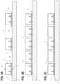
- FIG. 8 A- 8 Billustrate methods and structures for stacking more than two reconstituted wafers, according to various embodiments.
- FIGS. 9 A- 9 Fillustrate various face up bonded structures, according to various embodiments.
- FIGS. 10 A- 10 Eillustrate various face down bonded structures, according to various embodiments.
- FIG. 11illustrates another embodiment in which an additional filler material can serve as a second protective material and may be provided over a conformal protective material in the gaps between adjacent elements.
- FIGS. 12 A- 12 Cillustrate a method for forming a reconstituted wafer according to various embodiments.
- FIGS. 13 A- 13 Billustrate a method for forming a reconstituted wafer according to various embodiments.
- FIGS. 14 A- 14 Cillustrate another embodiment in which a mold compound can be provided between adjacent elements directly bonded to a carrier, and a metal can be provided on the mold compound.
- FIGS. 15 A- 15 Cillustrate another embodiment in which a mold compound can be provided between adjacent elements directly bonded to a carrier, and a metal can be provided on both sides of the mold compound.
- FIGS. 16 A- 16 Cillustrate another embodiment in which a protective coating or layer can be provided between the mold compound and the carrier.
- FIGS. 17 A- 17 Dillustrates additional bonded structures that can be provided with the methods disclosed herein.
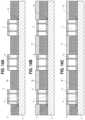
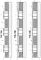
- FIG. 18 Ais a schematic side sectional view of an integrated device package, according to another embodiment.
- FIG. 18 Bis a schematic top plan view of the integrated device package of FIG. 18 A , with the molding compound hidden for ease of illustration.
- FIG. 18 Cis a schematic top plan view of an integrated device package that includes increased lateral overlap among stress compensation elements.
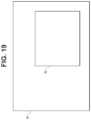
- FIG. 19is a schematic diagram of a system incorporating one or more bonded structures, according to various embodiments.
- a bonded structurecomprising a first element (e.g., a first integrated device die) having a first side and a second side opposite the first side.
- the bonded structurecan include a second element (e.g., a second integrated device die) having a first side and a second side opposite the first side.
- the first side of the second integrated device diecan be directly bonded to the first side of the first integrated device die without an intervening adhesive along a bonding interface.
- a protective materialcan be disposed about a periphery (e.g., respective sidewalls) of the first and second integrated device dies. The protective material can extend from the second side of the first integrated device die to the second side of the second integrated device die.
- portions of the protective materialcan be disposed within gaps between adjacent first integrated device dies or elements.
- the protective materialcan comprise an inorganic dielectric, such as silicon dioxide, silicon nitride, polysilicon, amorphous silicon, etc.
- the embodiments disclosed hereincan comprise wafer-level processes in which wafers or substrates, serving as carriers, are provided with a plurality of integrated device dies and a protective material (which can comprise one or a plurality of protective layers) over the integrated device dies.
- the die(s) and protective materialcan form at least a portion of a reconstituted wafer which can be bonded (e.g., directly bonded without an adhesive) to another reconstituted wafer formed by a similar process.
- the bonded reconstituted waferscan be singulated to form a plurality of bonded structures, for example after removal of the carriers.
- the bonded structurescan comprise packaging structures in some embodiments.
- direct bond interconnectscan comprise bonded structures in which densely dispersed conductive contacts are bonded to one another without an intervening adhesive.
- the surrounding dielectric or nonconductive materialscan also be directly bonded without an intervening adhesive.
- a ZiBond® processcan comprise a direct bond between nonconductive materials without an intervening adhesive. Examples of DBI and ZiBond processes and structures may be found throughout at least U.S. Pat. Nos. 9,391,143; 10,141,218; 10,147,641; 9,431,368; and 7,126,212, the entire contents of each of which are incorporated by reference herein in their entireties and for all purposes.
- Each of the singulated dies mounted on the carrierscan be tested prior to mounting, such that all dies in the reconstituted wafer can be Known Good Dies (KGD).
- FIGS. 1 A- 1 Cschematically illustrate the use of a sacrificial carrier 3 in various direct bonding processes.
- an element 2can be directly bonded to a carrier 3 without an adhesive.
- the element 2(or any of the other elements described herein) can comprise any suitable type of element, such as a semiconductor element (e.g., an integrated device die), an optical element, etc.
- the carrier 3can comprise any suitable type of carrier, such as a carrier with one or more logic or processing devices, and/or a sacrificial carrier (e.g., a carrier without active processing circuitry) that is to be removed at some point during processing.
- the element 2can comprise a front side 9 and a back side 10 opposite the front side 9 .
- the front side 9can comprise a surface nearest to active circuitry or devices formed in the element 2 .
- a first front bonding layer 4can be provided at the front side 9 of the element 2 .
- the bonding layer 4is shown at the front side 9 of the element 2 , a bonding layer may also or alternatively be provided on the back side 10 for bonding.
- the bonding layer 4can comprise one or a plurality of contact pads 6 disposed within or surrounded by a nonconductive field region 5 .
- the contact padscan comprise copper, although other conductive materials are suitable.
- the nonconductive field regioncan comprise a dielectric such as silicon oxide, silicon nitride, etc.
- the back side 10may or may not include active circuitry or devices.
- the element 2can comprise a singulated element (such as a singulated device die) having a side surface 8 .
- the side surface 8can comprise markings indicative of a singulation process, for example, saw markings, etch patterns, etc.
- the element 2e.g., a die
- the front bonding layer 4can be prepared for bonding, as explained above.
- the front bonding layer 4can be polished to a very low surface roughness and processed so as to enhance dielectric-to-dielectric direct bonding.
- the surfaces to be bondedmay be terminated with a suitable species and activated prior to bonding.
- the surfaces to be bondedmay be very lightly etched for activation and exposed to a nitrogen-containing solution and terminated with a nitrogen-containing species.
- the surfaces to be bondedmay be exposed to an ammonia dip after a very slight etch, and/or a nitrogen-containing plasma (with or without a separate etch).
- the nonconductive field region 5 of the element 2can be brought into contact with corresponding nonconductive regions of the carrier 3 .
- the interaction of the activated surfacescan cause the nonconductive region 5 of the element 2 to directly bond with the corresponding nonconductive regions of the carrier 3 without an intervening adhesive, without application of external pressure, without application of voltage, and at room temperature.
- the bonding forces of the nonconductive regionscan be covalent bonds that are greater than Van der Waals bonds.
- only nonconductive field regions of the element 2are directly bonded to corresponding nonconductive regions of the carrier 3 .
- contact pads 6 of the element 2can be directly bonded to corresponding conductive contacts of the carrier 3 , and the nonconductive region 5 can also be directly bonded to the nonconductive regions of the carrier 3 .
- direct bonding of the contactscan improve alignment of the element 2 relative to the carrier 3 .
- the use of direct bondingcan reduce movement during assembly as compared to implementations that utilize an intervening adhesive.
- a protective material 7can be applied over at least a portion of the element 2 , including about at least a periphery or side surface 8 of the element 2 .
- the protective material 7can be deposited along the side surface 8 and over an upper surface of the carrier 3 .
- the protective material 7can comprise one or more protective layers, including one or more inorganic layers, such as silicon oxide, silicon nitride, polysilicon, amorphous silicon, a metal, etc.
- the carrier 3can be removed from the element 2 and the protective material 7 in any suitable manner.
- the carrier 3can comprise a silicon substrate or element with a nano oxide layer 11 , which as used herein can include at least one of a native silicon oxide layer and a thermal silicon oxide layer.
- the carrier 3can be selectively etched using the silicon nano oxide layer 11 as an etch stop.
- at least a portion of the nano oxide 11 layercan remain after removing the silicon base material of the carrier 3 .
- the entirety of the carrier 3(e.g., the silicon base material and the nano oxide layer 11 ) can be removed.
- the element 2can be planarized for bonding, but the carrier 3 may not be planarized prior to direct bonding.
- both the element 2 and carrier 3can be planarized for direct bonding.
- Direct bonding and subsequent removal of the carrier 3 as described hereincan advantageously leave a planar surface for a reconstituted wafer for further processing as desired, including for additional direct bonding processes.
- reconstituted wafers formed on sacrificial or temporary adhesive layersdo not reliably provide planar surfaces and thus can lead to subsequent alignment issues, e.g., for subsequent direct bonding of dies for stacking.
- Such stacking with direct bondingcould be by way of direct bonding individual second dies on a first reconstituted wafer, or simultaneously bonding multiple second dies in a second reconstituted wafer.
- FIGS. 1 A- 1 Ccan enable the reconstitution of wafers for direct bonding with improved alignment accuracy.
- an array of multiple diescan be provided, and as shown below.
- the elements 2 or diesmay become misaligned relative to the carrier 3 due to movement or migration of the adhesive, for example, during or after heating or during placement for bonding.
- Such misalignmentscan result in misalignment for subsequently bonded structures and negatively affect the performance of the bonded structures.
- the embodiments disclosed hereincan beneficially reduce misalignment by providing a direct bond interconnection with the carrier 3 , which can serve to effectively fix the element 2 or die relative to the carrier 3 for subsequent processing, such as providing a protective material 7 (inorganic or organic) over the element 2 , or any other suitable processing.
- FIG. 2illustrates a plurality of elements 2 directly bonded to a carrier 3 , such as a wafer.
- reference numerals in FIG. 2may represent components that are the same as or generally similar to like-numbered components of FIGS. 1 A- 1 C .
- each element 2can include one or more conductive vias 13 connected to back side(s) of corresponding contact pads 6 .
- the conductive viasmay initially extend upwardly from the contact pad and terminate within the body of the element 2 .
- the dies or elements 2can be diced or singulated into a plurality of diced or singulated elements 2 .
- the removal of a silicon substrate using the nano oxide layer 11may leave a substantially smooth surface for subsequent direct bonding.
- FIGS. 3 A- 3 Cshow various examples in which elements 2 (e.g., integrated device dies) are directly bonded to a carrier 3 (e.g., a silicon substrate with nano oxide layer 11 ) without an intervening adhesive.
- FIG. 3 Aillustrates a relatively wide separation or gap G between elements 2
- FIG. 3 Billustrates a relatively narrow separation or gap G between elements 2
- FIG. 3 Cillustrates additional dummy elements 2 ′ or dies disposed between active elements 2 or dies, with relatively narrow gaps G therebetween.
- Providing the narrow gaps G in FIGS. 3 B and 3 Ccan beneficially reduce the amount of protective material 7 used to fill the gaps G in subsequent steps and can enable conformal filling of the gaps G.
- one or more alignment feature(s) 14can be provide on the upper surface of the carrier 3 .
- the alignment features 14can be selectively positioned on the carrier 3 to assist in accurate placement of the elements 2 .
- FIG. 4 Ais a schematic side view of a plurality of elements 2 directly bonded to a carrier 3 and with a protective material 7 applied over the elements 2 and within the gaps G between the elements 2 .
- the elements 2are illustrated as being all active integrated device dies.
- some of the elementscomprise dummy elements 2 ′, such as inactive blocks of semiconductor material (e.g., silicon).
- a protective layer 7(such as an inorganic protective layer) can be provided over portions of the elements 2 , including around a portion of the periphery (e.g., the side surface 8 ) within the gaps G and over upper surfaces (which are the back sides 10 in FIGS. 4 A- 4 B ) of the elements 2 . Seams 15 such as voids or discontinuities may be present in the protective material 7 .
- the protective layer 7can include one or a plurality of protective layers, including, e.g., inorganic or organic protective layer(s).
- the protective layer 7can comprise inorganic layer(s) such as silicon oxide, silicon nitride, polysilicon, amorphous silicon, or a metal.
- at least a portion of the protective material 7can comprise an organic material, such as a molding compound or epoxy.
- the protective material 7comprises both a conformal layer and a gap-fill layer.
- the protective material 7can assist in affixing the elements 2 to the carrier 3 such that the elements 2 do not shift during subsequent direct bonding processes.
- the protective material 7can also assist in protecting the elements 2 during polishing and other processing techniques to prevent damage to the dies (e.g., chipping).
- Examples of structures and processes for providing protective material 7 on and between adjacent directly bonded dies over a carrier, for use in conjunction with post-bonding thinning and/or singulation processes,are disclosed in U.S. Pat. No. 10,204,893, the entire contents of which are hereby incorporated by reference herein in their entirety and for all purposes.
- FIGS. 5 A- 5 Cillustrate a series of processing steps for forming a reconstituted wafer 20 .
- the reconstituted wafer 20can be bonded (e.g., directly bonded) to another reconstituted wafer 20 or to other substrates in subsequent steps.
- the upper surfaces of the conformal protective material 7can be removed, e.g., by etching, lapping, grinding, polishing, etc.
- the removal of the protective material 7can also remove a portion of the back side 10 of the elements 2 .
- the removal stepcan terminate at the back side 10 of the element 2 .
- a portion of the element 2 from the back side 10can be removed by etching, lapping, chemical mechanical polishing (CMP), or any other suitable method, to form a thinned back side 10 ′ of the element 2 .
- this removal stepcan expose the conductive through substrate vias (TSVs) 13 or other electrical interconnects formed within the elements.
- the removal stepcan also form a cavity 16 defined at least in part by the thinned back side 10 ′ of the element 2 and side walls of the protective material 7 .
- TSVsthrough substrate vias
- a nonconductive layer 18(e.g., a second oxide layer) can be provided (e.g., deposited) over the thinned back sides 10 ′ of the elements 2 and around the exposed vias 13 .
- the provided nonconductive layer 18(for example, silicon oxide) can be lapped or polished to generate a planar surface and to ensure that the nonconductive layer 18 is generally planar relative to the exposed ends of the vias 13 and the protective material.
- the reconstituted wafer 20can comprise a front surface 22 configured to be bonded (e.g., direct bonded) to another reconstituted wafer or other type of substrate.
- the reconstituted wafer 20can also comprise a back surface 23 .
- the protective material 7can be disposed between adjacent elements 2 and can extend from the front surface 22 of the reconstituted wafer 20 to the upper surface of the carrier 3 .
- a vertical interface 19can be defined between the nonconductive layer 18 over the element 2 and the protective material 7 .
- a vertical interface 21can be defined between the bonding layer 4 and the protective material 7 .
- FIG. 6is a schematic side sectional view of a reconstituted wafer having a second bonding layer 4 b configured to directly bond to another reconstituted wafer or substrate.
- the first bonding layer 4 , the contacts 6 , and the nonconductive field region 5 of FIGS. 1 A- 5have been renumbered as reference numerals 4 a , 6 a , and 5 a , respectively, in FIG. 6 .
- FIG. 6As shown in FIG.
- the second bonding layer 4 be.g., a DBI layer having alternating conductive contacts 6 b and nonconductive bonding portions (e.g., field regions 5 b ), can be provided over the nonconductive layer 18 (e.g., a second oxide layer) to facilitate additional bonding connections, if desired, to provide bonding pads conducive to DBI alignment.
- the second bonding layer 4 bcan extend across multiple (e.g., all) of the elements 2 of the reconstituted wafer 20 .
- a horizontal interface 19can be formed between the second bonding layer 4 b and the nonconductive layer 18 , and between the second bonding layer 4 b and the underlying protective material 7 .
- FIGS. 7 A- 7 Btwo opposing reconstituted wafers 20 a , 20 b can be provided and can be directly bonded to form a pair of bonded reconstituted wafers 1 ′.
- the reference numeralshave been appended with “a” or “b” to denote their respective associations with the reconstituted wafers 20 a or 20 b .
- FIG. 7 Aillustrates the two opposing reconstituted wafers 20 a , 20 b prior to direct bonding.
- FIG. 7 Billustrates the two opposing reconstituted wafers 20 a , 20 b after being directly bonded to one another.
- the carriers 3 a , 3 bprovides the planarity desired at the die bonding surfaces for die-to-die direct bonding of conductive and non-conductive surfaces.
- the carriersmay not be used and instead the reconstituted wafers may comprise elements (e.g., dies) at least partially embedded in a molding compound or encapsulant without the use of a carrier.
- the nonconductive protective layerscan be directly bonded to one another without an adhesive along the bond interface 12 .
- non-conductive field regions of the reconstituted wafers 20 a , 20 bcan also be bonded to one another by an adhesive.
- the conductive contacts 6 a , 6 bcan be directly bonded without an adhesive.
- some or all of the conductive contacts 6 a , 6 bcan be initially recessed relative to the bonding surfaces.
- the bonded wafers 20 a , 20 bcan be heated to cause the contacts 6 a , 6 b to expand and form an electrical contact. After heating, the interface between the contacts 6 a and 6 b may not be in the same plane as the bond interface 12 .
- Additional reconstituted wafers 20 a , 20 bcan be provided as shown in FIGS. 8 A- 8 B to provide any number of stacked reconstituted wafers 1 ′.
- the stacked reconstituted wafers 1 ′can be singulated along singulation streets S to provide a plurality of bonded structures 1 .
- Any suitable number of reconstituted wafers 20 a , 20 bcan be provided to form the stacked reconstituted wafers 1 ′, which can also be singulated to form any suitable number of bonded structures 1 .
- the singulationcan be before removal of the carriers 3 as shown (if sacrificial), or after singulation. In some embodiments, as shown in FIG.
- both carriers 3 a , 3 bmay not be removed prior to singulation.
- one carrier 3 acan be removed prior to singulation.
- both carriers 3 a , 3 bcan be removed prior to singulation.
- removal of the carriers 3 a and/or 3 b using, for example, an etch processmay leave behind a nano oxide layer 11 to facilitate additional direct bonding.
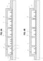
- FIGS. 9 A- 9 F and 10 A- 10 Eillustrate various face up or face down bonded structures 1 that can result from the methods described herein.
- the bonded structures 1 shown in FIGS. 9 A- 9 F and 10 A- 10 Ecan comprise singulated reconstituted elements 24 , such as singulated reconstituted integrated device dies.
- the singulated reconstituted elements 24are shown in FIGS. 9 A, 9 E and 9 F for illustrative purposes to show what structures may result from a singulated reconstituted wafer 20 , according to various embodiments. As shown in FIGS.
- the surfaces nearest to active circuitry or devicescan be the front surfaces 22 of the bonded structures 1 , while the surfaces opposite the front surfaces 22 can be the back surfaces 23 .
- the directly bonded reconstituted elements 24 of the illustrated embodimentscan have coplanar side surfaces as well as a direct bonding interface 12 between conductive (e.g., metal) and nonconductive (e.g., inorganic dielectrics such as oxides, including nitrogen and/or fluorine content to aid direct bonding) surfaces of the reconstituted elements 24 , with no intervening adhesives.
- FIGS. 9 A- 9 Fillustrate examples of face down bonded structures.
- the singulated reconstituted element 24can comprise the element 2 , the nonconductive layer 18 disposed on the thinned back side 10 ′ of the element 2 , and bonding layers 4 a , 4 b at the front and back surfaces 22 , 23 , respectively.
- the protective material 7can extend from the back side 23 to the front side 22 of the reconstituted element 24 .
- the singulated reconstituted element 24can have a sidewall 25 defined by the outer exposed surface of the protective material.
- a vertical interface 26can be defined between the protective material 7 and the element 2 , the nonconductive layer 8 , and the first and second bonding layers 4 a , 4 b .
- the protective material 7accordingly abuts the bonding layers 4 a , 4 b , which may be applied before the protective material 7 is provided.
- one or more of the bonding layers 4 a , 4 bcan extend over the protective material 7 such that the sidewall 25 includes the protective material 7 and a side edge of the bonding layers 4 a and/or 4 b.
- FIG. 9 Billustrates a front-to-back bonding arrangement in which the front surface 22 a of the reconstituted element 24 a is directly bonded to the back surface 23 b of the reconstituted element 24 b without an intervening adhesive to form the bonded structure 1 .
- a first portion 7 a of protective materialcan extend from the back surface 23 a of the reconstituted element 24 a to the bonding interface 12 .
- a second portion 7 b of protective materialcan extend from the bonding interface 12 to the front surface 22 b of the reconstituted element 24 b.
- FIG. 9 Cillustrates a front-to-front bonding arrangement in which the front surface 22 a of the reconstituted element 24 a is directly bonded to the front surface 23 a of the reconstituted element 24 b without an intervening adhesive to form the bonded structure 1 .
- the first portion 7 a of protective materialcan extend from the back surface 23 a of the reconstituted element 24 a to the bonding interface 12 .
- the second portion 7 b of protective materialcan extend from the bonding interface 12 to the back surface 23 b of the reconstituted element 24 b.
- FIG. 9 Dillustrates a back-to-back bonding arrangement in which the back surface 23 a of the reconstituted element 24 a is directly bonded to the back surface 23 b of the reconstituted element 24 b without an intervening adhesive to form the bonded structure 1 .
- the first portion 7 a of protective materialcan extend from the front surface 22 a of the reconstituted element 24 a to the bonding interface 12 .
- the second portion 7 b of protective materialcan extend from the bonding interface 12 to the front surface 22 b of the reconstituted element 24 b.
- FIGS. 9 E and 9 Fillustrate additional examples of singulated reconstituted elements 24 that utilize a second protective layer 40 . Additional details regarding methods of forming the reconstituted element 24 of FIGS. 9 E and 9 F may be found below in, for example, FIGS. 11 - 12 C .
- the second protective material 40can be applied over the protective material 7 .
- the second protective material 40may be exposed at the back surface 23 of the reconstituted element 24 adjacent the bonding layer 4 b .
- the protective material 7can be exposed at the front surface 22 adjacent the bonding layer 4 a and underlying the second protective layer 40 .
- the sidewall 25can include a horizontal interface 42 between the first and second protective materials 7 , 25 .
- a vertical interface 41can be provided between the first and second protective materials 7 , 25 .
- the second protective material 40can also be applied over the protective material 7 .
- a third protective layer 43can be provided over the second protective material 40 .
- the third protective layer 43may be exposed at the back surface 23 of the reconstituted element 24 .
- a vertical interface 45can be provided between the protective material 7 and the third protective material 43 .
- a horizontal interface 46can be provided between the second protective material 40 and the third protective material 43 .
- FIGS. 10 A- 10 Eillustrate examples of face up bonded structures 1 .
- reference numerals in FIGS. 10 A- 10 Emay refer to the same or generally similar components as reference numerals in FIGS. 9 A- 9 F .
- FIG. 10 Aa singulated reconstituted element 24 is shown in a face up orientation.
- FIGS. 10 B- 10 Drespective reconstituted elements 24 a , 24 b are directly bonded to one another to form bonded structures.
- FIG. 10 Billustrates a front-to-back bonding arrangement in which the front surface 22 a of the reconstituted element 24 a is directly bonded to the back surface 23 b of the reconstituted element 24 b without an intervening adhesive to form the bonded structure 1 .
- a first portion 7 a of protective materialcan extend from the back surface 23 a of the reconstituted element 24 a to the bonding interface 12 .
- a second portion 7 b of protective materialcan extend from the bonding interface 12 to the front surface 22 b of the reconstituted element 24 b.
- FIG. 10 Cillustrates a back-to-back bonding arrangement in which the back surface 23 a of the reconstituted element 24 a is directly bonded to the back surface 23 b of the reconstituted element 24 b without an intervening adhesive to form the bonded structure 1 .
- the first portion 7 a of protective materialcan extend from the front surface 22 a of the reconstituted element 24 a to the bonding interface 12 .
- the second portion 7 b of protective materialcan extend from the bonding interface 12 to the front surface 22 b of the reconstituted element 24 b.
- FIG. 10 Dillustrates a front-to-front bonding arrangement in which the front surface 22 a of the reconstituted element 24 a is directly bonded to the front surface 22 b of the reconstituted element 24 b without an intervening adhesive to form the bonded structure 1 .
- the first portion 7 a of protective materialcan extend from the back surface 23 a of the reconstituted element 24 a to the bonding interface 12 .
- the second portion 7 b of protective materialcan extend from the bonding interface 12 to the back surface 23 b of the reconstituted element 24 b .
- the bonding layers 4 acan extend over the protective material 7 a , 7 b and can be exposed on the sidewall 25 .
- the bonding layer 4 acan be provided across the wafer over the protective material 7 such that, when the reconstituted wafer is singulated, the bonding layer 4 a is exposed at the sidewall and flush with the protective material 7 at the sidewall 25 .
- FIG. 10 Eillustrates a singulated reconstituted element 24 that has a second protective material 40 disposed over side and upper surfaces of the protective material 7 .
- the first front bonding layer 4 acan be coplanar or flush with the second protective material 40 .
- the second back bonding layer 4 bcan be coplanar or flush with the protective material 7 .
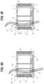
- FIG. 11illustrates another embodiment similar to those described above, except an additional filler material can serve as a second protective material 40 and may be provided over a conformal protective material 7 in the gaps G between adjacent elements 2 .
- the protective material 7can be deposited conformally over the back sides 10 and side surface 8 of the elements 2 and over the upper surface of the carrier 3 .
- the conformal protective material 7can have gaps G between portions of the protective material 7 disposed on the side surfaces 8 of the elements 2 .
- the second protective material 40can serve to fill the gaps G.
- the second filler protective material 40can comprise any suitable material, including organic or inorganic materials.
- FIGS. 12 A- 12 Cillustrate a method for forming a reconstituted wafer 20 according to various embodiments.
- FIG. 12 Ais generally similar to FIG. 11 , except additional portions of the second protective material 40 are provided on the ends of the outer elements 2 .
- FIG. 12 Ba portion of the protective material 7 and a portion of the second filler protective material 40 can be removed to provide a generally planar surface.
- the respective portions of the filler and conformal protective materials 40 , 7can be removed by etching, lapping, grinding, chemical mechanical polishing (CMP), etc.
- CMPchemical mechanical polishing
- a portion of the bulk semiconductor material of the elements 2 or diescan be removed to form a cavity 16 , for example, by etching, lapping, CMP, etc., to expose the conductive vias 13 .
- the conformal and/or gap-fill protective materialsmay have coefficient(s) of thermal expansion that is (are) within 5 ppm/° C. of a coefficient of thermal expansion of the elements 2 (e.g., integrated device dies).
- the second filler protective material 40can be removed from the structure shown in FIG. 12 C , and an additional protective material 48 can be provided over the elements 2 and the exposed vias 13 .
- the provided additional protective material 48 and a portion of the protective material 7can be removed or planarized to form a bonding surface 49 with the vias exposed on the upper surface.
- FIGS. 14 A- 14 Cillustrate another embodiment in which a mold compound 50 can be provided between adjacent elements 2 directly bonded to a carrier 3 without an adhesive.
- the vias 13are shown as being exposed on the back side, but in other embodiments, the vias 13 can be buried as illustrated above.
- a metal 51(such as copper) can be provided over the mold compound 51 as shown in FIG. 14 B .
- the metal 51can be provided using an electroless plating process, a sputtering process, or any other suitable method.
- the metal 51can be planarized, for example, by chemical mechanical polishing (CMP), or any other suitable method.
- CMPchemical mechanical polishing
- structures that utilize an organic material for the mold compoundmay be challenging to planarize using CMP to sufficient smoothness (e.g., less than 5 nm, etc.).
- CMPchemical vapor deposition
- a metal 51such as copper
- CMP or other planarization processescan be used to planarize to sufficient smoothness for direct bonding.
- FIGS. 15 A- 15 Care generally similar to FIGS. 14 A- 14 C , except in FIGS. 15 A- 15 C , a second metal 52 can be provided over the carrier 3 between the carrier 3 and the mold compound 50 .
- FIGS. 16 A- 16 Cillustrate another embodiment in which a protective coating 53 or layer (e.g., silicon oxide) can be provided between the mold compound 50 and the carrier 3 .
- a protective coatingcan also be provided after die placement and before metal deposition in various embodiments.
- the protective coating 53can conformally coat the upper surface of the carrier 3 and upper and side surfaces of the elements 3 .
- the mold compound 50can be provided over the protective coating 53 and between the elements 2 .
- the metal 51can be provided over the mold compound 50 as explained above.
- the portions of the protective coating 53 that overlie the elements 2can be removed using a polishing, grinding, or lapping process to expose the vias 13 .
- the metal 51 and element 2can be planarized to form a smooth surface for bonding.
- FIGS. 17 A- 17 Dillustrates additional bonded structures 1 that can be provided with the methods disclosed herein.
- the bonded structure 1can include a plurality of elements 2 , which can include combinations of integrated device dies and interposers. Thus, the methods disclosed herein can be used for active and/or inactive devices.
- an insulating column 55can be provided to separate the adjacent elements 2 in the upper reconstituted element.
- the bonded structure 1can include one or more redistribution layers (RDLs) 57 which can include lateral conductive routing traces to carry signals laterally inward or outward.
- the RDLs 57can enable fan-in or fan-out arrangements for connecting to an external package substrate.
- a conductive via 56can be provided in the insulating column 56 to carry signals from the lower element 2 to the upper surface of the bonded structure 1 .
- the bonded structure 1can include both the via 56 in the insulating column 56 and the RDL(s) 57 . Skilled artisans will understand that additional combinations may be suitable.
- Integrated device packagescan include one or multiple integrated device dies (e.g., chips) that have active circuitry, such as transistors and other types of active devices.
- the integrated device diescan be mounted to a carrier, such as a semiconductor interposer, a semiconductor or dielectric (e.g., glass) substrate, another integrated device die, a reconstituted wafer or element, etc.
- a molding compound or encapsulantcan be provided over the integrated device dies and exposed surfaces of the package substrate.
- the molding compoundcan comprise a polymer material, such as an epoxy or potting compound.
- the material of the molding compoundcan have a coefficient of thermal expansion (CTE) that differs from the CTE of the carrier and/or of the integrated device die(s).
- CTEcoefficient of thermal expansion
- the CTE mismatch between the molding compound and the carrier (and/or integrated device die(s))may induce stresses in the carrier and/or integrated device die(s).
- the stresses induced by CTE mismatchcan cause cracking and/or warpage of the carrier and/or integrated device die(s), which can reduce package yield and/or affect system performance. Accordingly, there remains a continuing need for improved packages that reduce stresses due to C mismatch between molding compound and the carrier (and/or integrated device die(s)).
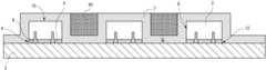
- FIG. 18 Ais a schematic side sectional view of an integrated device package 82 , according to various embodiments.
- FIG. 18 Bis a schematic top plan view of the integrated device package 82 of FIG. 18 A .
- the package 82can comprise a carrier 103 and a plurality of integrated device dies 102 mounted to an upper surface of the carrier 103 .
- the integrated device dies 102can comprise active circuitry.
- the integrated device dies 102can comprise processor die(s), memory die(s), sensor die(s), microelectromechanical systems (MEMS) dies, or any other suitable device that includes active circuitry (such as transistors or other active devices).
- MEMSmicroelectromechanical systems
- any suitable number of device dies 102can be provided.
- one or two integrated device dies 102can be mounted to the carrier 103 , or more than three integrated device dies 102 can be mounted to the carrier.
- the integrated device dies 102are spaced apart laterally along the carrier 103 .
- integrated device dies 102can be stacked vertically in order to reduce package footprint.
- the carrier 103can comprise any suitable support structure for the integrated device dies 102 .
- the carrier 103can comprise an interposer (such as a semiconductor interposer), a semiconductor or dielectric (e.g., glass) substrate, another integrated device die (e.g., an active chip with active electronic circuitry), a reconstituted wafer or element, etc.
- the carrier 103can comprise a material (e.g., a semiconductor material, a dielectric material, etc.) having a first CTE.
- the integrated device dies 102can have a CTE that is substantially similar to the first CTE of the carrier 103 .
- bulk material of one or more of the dies 102may be the same material as corresponding bulk material of the carrier 103 .
- the carrier 103can comprise silicon, glass, or any other suitable material.
- the carrier 103can comprise an integrated device die (such as a processor die) that has a larger lateral footprint than the dies 102 .
- the integrated device dies 102can be mounted to the carrier 103 in any suitable manner.
- the dies 102can be directly hybrid bonded to the carrier 103 without an adhesive, as explained herein.
- nonconductive field regions of the dies 102can be directly bonded to corresponding nonconductive field regions of the carrier 103 without an adhesive.
- conductive contacts of the dies 102can be directly bonded to corresponding conductive contacts of the carrier 103 without an adhesive.
- the dies 102can be mounted to the carrier 103 with an adhesive.
- the carrier 103can remain coupled to the dies 102 such that the carrier 103 remains present in the larger electronic system.
- the carrier 103can comprise a temporary structure (such as a mounting tape or sacrificial substrate) that is removed (e.g., lifted off or etched away) and not present in the final electronic package or system.
- a molding compound 108can be provided over the integrated device dies 102 and over an exposed upper surface of the carrier 103 .
- the molding compound 108is hidden in the top view of FIG. 18 B for ease of illustration.
- the integrated device dies 102can be at least partially embedded (e.g., completely embedded or buried) within the molding compound 108 .
- the molding compound 108can comprise a polymer material (such as an epoxy or potting compound) that has a second CTE that is different from the first CTE of the carrier 103 (and/or of the dies 102 ).
- the second CTE of the molding compound 108can differ from the first CTE of the carrier 103 (and/or of the dies 102 ) by an amount that is sufficiently large so as cause CTE-induced stresses on the carrier 103 and/or dies 102 (e.g., the CTE mismatch can be up to about 12 ppm in some cases).
- the CTE mismatch between the molding compound 108 and the carrier 103 (and/or dies 102 )can induce stresses that cause warpage, cracks, or other types of damage to the components of the package 82 .
- the package 82can include one or a plurality of stress compensation elements 104 a - 104 d mounted to the upper surface of the carrier 103 .
- the stress compensation elements 104 a - 104 dcan be disposed around the integrated device dies 102 , such that the integrated device dies 102 are disposed within an interior region of the package 82 surrounded by the stress compensation elements 104 a - 104 d .
- the molding compound 108can also be provided or applied over the stress compensation elements 104 a - 104 d , such that the stress compensation elements 104 a - 104 d are at least partially embedded in the molding compound 108 .
- the stress compensation elements 104 a - 104 dcan be spaced apart from one another and from the dies 102 by intervening portions of the molding compound 108 .
- the stress compensation elements 104 a - 104 dcan comprise a semiconductor material (e.g., silicon), an insulating material (e.g., glass), or any other suitable material type that has a CTE that substantially matches (or is close to) the second CTE of the carrier 103 and/or the dies 102 .
- the stress compensation elements 104 a - 104 dcan comprise the same material as the carrier 103 and/or the dies 102 . In other embodiments, the stress compensation elements 104 a - 104 d can comprise a material that is different from that of the carrier 103 and/or the dies 102 . Each stress compensation element 104 a - 104 d can comprise the same material, or some (or all) can comprise different materials. In various embodiments, the CTE of the stress compensation elements 104 a - 104 d can be within 10% of the second CTE of the carrier 103 and/or of the integrated device dies 102 , within 5% of the second CTE, or within 1% of the second CTE.
- the CTE of the stress compensation elements 104 a - 104 dcan be less than 10 ppm, less than 8 ppm, or less than 7 ppm.
- the CTE of the stress compensation elements 104 a - 104 dcan be in a range of 3 ppm to 7 ppm.
- the stress compensation elements 104 a - 104 dcan reduce the stresses imparted to the carrier 103 and/or the dies 102 , since the material composition of the stress compensation elements 104 a - 104 d is selected to have a CTE that substantially matches that of the carrier 103 and/or the dies 102 .
- the CTE-matched stress compensation elements 104 a - 104 dcan be provided over a large area of the carrier 103 so as to serve as a stress-matched filler that compensates or reduces any stresses induced by the CTE mismatch between the molding compound 108 and the carrier 103 and/or dies 102 .
- the stress compensation elements 104 a - 104 dcan be mounted so as to cover most of an unoccupied area of the carrier 103 (e.g., regions of the carrier 103 that do not support the dies 102 or other electronic components or devices), e.g., at least 20%, at least 50%, at least 75%, at least 85%, or at least 90% of the unoccupied area of the carrier 103 .
- the stress compensation elements 104 a - 104 dcan be mounted so as to cover a range of 20% to 90% of the unoccupied area of the carrier 103 , a range of 35% to 90% of the unoccupied area of the carrier 103 , or a range of 50% to 90% of the unoccupied area of the carrier 103 .
- the stress compensation elements 104 a - 104 dcan laterally overlap such that all lines perpendicular to opposing side edges 105 a , 105 b can pass through or intersect at least one stress compensation element 104 a - 104 d .
- the stress compensation elements 104 a - 104 dcan serve to prevent or arrest cracks from propagating through the carrier 103 .
- the stress compensation elements 104 a - 104 dcan be disposed between the outer side edges 105 a - 105 d of the package 82 and the integrated device dies 102 such that at least one lateral side edge 109 of each integrated device die 102 lies in a corresponding plane that intersects at least one stress compensation element 104 a - 104 d .
- a majority (or all) of the side edges 109 of the dies 102can lie in respective planes that intersect at least one stress compensation element 104 a - 104 d.
- FIG. 18 Cis a schematic top plan view of an integrated device package 82 , that includes increased lateral overlap among the stress compensation elements 104 a - 104 d .
- the components of FIG. 18 Cmay be the same as or generally similar to like-numbered components of FIGS. 18 A- 18 B .
- stress compensation element 104 bis vertically (as shown in the top view) shortened, and stress compensation element 104 d is horizontally (as shown in the top view) lengthened as compared to FIG. 18 B .
- stress compensation element 104 dcan extend to and be exposed along side edge 105 b .
- all lines perpendicular to each side edge 105 a - 105 dcan pass through or intersect with at least one stress compensation element 104 a - 104 d , which can prevent or arrest crack propagation.
- the stress compensation elements 104 a - 104 dcan comprise dummy stress compensation elements that are devoid of active circuitry, e.g., there are no active devices in the dummy stress compensation elements.
- the dummy stress compensation elementscan comprise dummy pieces or blocks of a semiconductor material (such as silicon) or a dielectric material (such as glass) without any active circuitry.
- the use of dummy elementscan provide further benefits because no circuitry or devices need be patterned or formed in the elements 104 a - 104 d , which can reduce processing costs and complexity.
- one or more of the stress compensation elements 104 a - 104 dmay comprise an active integrated device die with active circuitry or devices.
- the use of multiple stress compensation elements 104 a - 104 dcan beneficially enable the package assembler to pick and place the elements 104 a - 104 d at desired locations, e.g., at locations with high susceptibility to cracking and/or in targeted spaces over the carrier 103 .
- the stress compensation elements 104 a - 104 dcan be mounted to the carrier 103 in any suitable manner.
- the stress compensation elements 104 a - 104 dcan be directly bonded to the carrier 103 without an adhesive.
- the stress compensation elements 104 a - 104 dcan comprise dummy stress compensation elements without active circuitry.
- the stress compensation elements 104 a - 104 dcan comprise nonconductive field regions that are directly bonded to corresponding nonconductive field regions of the carrier 103 along a bond interface without au adhesive.
- the stress compensation elements 104 a - 104 dmay be directly bonded such that the bond interface between the elements 104 a - 104 d and the carrier 103 includes only nonconductive-to-nonconductive direct bonds (e.g., the bond interface is devoid of conductor-to-conductor or metal-to-metal direct bonds).
- the stress compensation elements 104 a - 104 dcan be directly bonded to the carrier 103 utilizing only nonconductive-to-nonconductive direct bonds, e.g., a nonconductive or dielectric bonding layer of the elements 104 a - 104 d can be directly bonded to a corresponding nonconductive or dielectric bonding layer of the carrier 103 without an adhesive.
- the nonconductive-to-nonconductive direct bondscan comprise one type or multiple different types of nonconductive material(s) along the bond interface.
- one or more elementscan be hybrid direct bonded to the carrier 103 along a bond interface without an adhesive such that nonconductive field regions and conductive contact pads of the one or more elements (e.g., dies 102 ) are directly bonded to corresponding nonconductive field regions and conductive contacts of the carrier 103 .
- One or more other elementscan be directly bonded to the carrier 103 without an adhesive along the bond interface such that the bond interface between the stress compensation elements 104 a - 104 d and the carrier 103 includes only nonconductive-to-nonconductive direct bonds (e.g., directly bonded dielectric bonding layers of the elements 104 a - 104 d and carrier 103 ).
- some elements 104 a - 104 dmay not include any conductive contacts that are directly bonded to the carrier 103 .
- the nonconductive field regions of the dies 102 , stress compensation elements 104 a - 104 d , and/or carrier 103can comprise an inorganic dielectric material (e.g., silicon oxide).
- the nonconductive field regionscan comprise unpatterned portions of the dies 102 , stress compensation elements 104 a - 104 d , and/or carrier 103 .
- the bond interfacecan include signature indicative of direct nonconductive bonds, such as nitrogen terminated surfaces, fluorine peak(s) at the bond interface and at upper and/or lower interfaces of dielectric bonding layers of the elements.
- both nonconductive field regions and contact pads of the stress compensation elements 104 a - 104 dcan be directly bonded to corresponding nonconductive field regions and contact pads of the carrier 103 .
- the stress compensation elements 104 a - 104 dcan be bonded to the carrier 103 with an adhesive.
- the carrier 103can be mounted to an external device, such as a system motherboard, or to another structure.
- the carrier 103can comprise a temporary support structure that can be removed after the molding compound 108 is applied.
- Four stress compensation elements 104 a - 104 dare shown in FIG. 18 B , but it should be appreciated that fewer than four, or more than four, stress compensation elements 104 a - 104 d can be provided.
- the package 82can comprise outer side edges 105 a - 105 d .
- the package 82can be formed from a singulation process by which a larger wafer or reconstituted wafer is singulated along singulation streets S to yield a plurality of singulated packages 82 .
- singulationcan comprise a sawing process, an etching process, or any other suitable process by which packages 82 can be formed from a larger wafer or reconstituted wafer.
- the outer side edges 105 a - 105 dcan comprise singulation markings indicative of the singulation process.
- the singulation markingscan comprise saw markings, such as striations in the singulated surface.
- the singulation markingscan comprise marks or microstructures indicative of the etch pathway.
- the outer side edge 105 bcan include an outer edge of stress compensation element 104 d , an edge of the carrier 103 and the molding compound, each of which may include markings indicative of the singulation process.
- the stress compensation elements 104 a - 104 dcan be positioned anywhere along the carrier 103 .
- some or all of the stress compensation elements 104 a - 104 dcan be positioned laterally inset relative to the outer side edges 105 a - 105 d of the package 82 such that the stress compensation elements 104 a - 104 d are embedded in the molding compound 108 .
- the singulation streets Scan pass through one or more of the stress compensation elements 104 a - 104 d such that, upon singulation, the molding compound 108 and one or more stress compensation elements 104 a - 104 d can be exposed along one or more outer side edges 105 a - 105 d of the package 82 .
- stress compensation elements 104 a , 104 ccan comprise side edges 106 a , 106 c that are exposed at the corresponding outer side edges 105 a , 105 c of the package 82 .
- side edges 107 of the molding compound 108can be exposed along the outer side edges 105 a - 105 d of the package 82 .
- the exposed side edges 106 a , 106 c of the stress compensation elements 104 a , 104 ccan be flush with the side edges 107 of the molding compound 108 , including portions of the molding compound 108 that are over the stress compensation elements 104 a , 104 c and portions of the molding compound 108 that are laterally adjacent the stress compensation elements 104 a , 104 c .
- some stress compensation elements 104 b , 104 dcan be laterally inset relative to the outer side edges 105 b , 105 d of the package 82 , such that the elements 104 b , 104 d may be completely embedded in the molding compound 108 .
- all of the stress compensation elements 104 a - 104 dcan be laterally inset relative to the outer side edges 105 a - 105 d.
- FIG. 19is a schematic diagram of a system 80 incorporating one or more integrated device packages 82 , according to various embodiments.
- the system 80can comprise any suitable type of electronic device, such as a mobile electronic device (e.g., a smartphone, a tablet computing device, a laptop computer, etc.), a desktop computer, an automobile or components thereof, a stereo system, a medical device, a camera, or any other suitable type of system.
- the electronic devicecan comprise a microprocessor, a graphics processor, an electronic recording device, or digital memory.
- the system 80can include one or more device packages 82 which are mechanically and electrically connected to the system 80 , e.g., by way of one or more motherboards.
- Each package 82can comprise one or more integrated device dies and/or bonded structures 1 .
- the integrated device dies and/or bonded structurescan comprise any of the integrated device packages and/or bonded structures shown and described above in connection with FIGS. 1 A- 18 B .
- an integrated device packagecan comprise a carrier an a molding compound over a portion of an upper surface of the carrier.
- the integrated device packagecan comprise an integrated device die mounted to the carrier and at least partially embedded in the molding compound, the integrated device die comprising active circuitry.
- the integrated device packagecan comprise a stress compensation element mounted to the carrier and at least partially embedded in the molding compound, the stress compensation element spaced apart from the integrated device die, the stress compensation element comprising a dummy stress compensation element devoid of active circuitry. At least one of the stress compensation element and the integrated device die can be directly bonded to the carrier without an adhesive.
- an integrated device packagein another embodiment, can include a molding compound and an integrated device die at least partially embedded in the molding compound, the integrated device die comprising active circuitry.
- the integrated device packagecan include a plurality of dummy stress compensation elements at least partially embedded in the molding compound, the plurality of dummy stress compensation elements devoid of active circuitry, the plurality of dummy stress compensation element spaced apart from one another by the molding compound.
- a method of forming an integrated device packagecan include providing a molding compound over an integrated device die and a plurality of dummy stress compensation elements, the plurality of dummy stress compensation elements spaced apart from one another by the molding compound.
- the integrated device diecan comprise active circuitry.
- the plurality of dummy stress compensation elementscan be devoid of active circuitry.
- an integrated device packagein another embodiment, can comprise a molding compound and an integrated device die at least partially embedded in the molding compound, the integrated device die comprising active circuitry.
- the integrated device packagecan comprise a stress compensation element at least partially embedded in the molding compound and spaced apart from the integrated device die. The molding compound and the stress compensation element can be exposed at an outer side edge of the integrated device package.
- an electronic componentin another embodiment, can comprise a carrier having a first nonconductive field region and a first conductive contact.
- the electronic componentcan comprise a first element directly hybrid bonded to the carrier without an adhesive, a second nonconductive field region of the first element directly bonded to the first nonconductive field region of the carrier without an adhesive and a second conductive contact of the first element directly bonded to the first conductive contact of the carrier.
- the electronic componentcan comprise a second element directly bonded to the carrier without an adhesive such that only a third nonconductive field region of the second element is directly bonded to the first nonconductive field region of the carrier.
- an electronic componentin another embodiment, can include a carrier having a first nonconductive field region and a first conductive contact.
- the electronic componentcan include a first element directly hybrid bonded to the carrier without an adhesive, a second nonconductive field region of the first element directly bonded to the first nonconductive field region of the carrier without an adhesive and a second conductive contact of the first element directly bonded to the first conductive contact of the carrier.
- the electronic componentcan include a second element directly bonded to the carrier without an adhesive, wherein the second element does not include any conductive contacts that are directly bonded to the carrier.
- a bonded structurein one embodiment, can include a first reconstituted element comprising a first element and having a first side comprising a first bonding surface and a second side opposite the first side.
- the first reconstituted elementcan comprise a first protective material disposed about a first sidewall surface of the first element.
- the bonded structurecan comprise a second reconstituted element comprising a second element and having a first side comprising a second bonding surface and a second side opposite the first side.
- the first reconstituted elementcan comprise a second protective material disposed about a second sidewall surface of the second element.
- the second bonding surface of the first side of the second reconstituted elementcan be directly bonded to the first bonding surface of the first side of the first reconstituted element without an intervening adhesive along a bonding interface.
- the first protective materialcan be flush with the first bonding surface and the second protective material can be flush with the second bonding surface.
- a bonded structurein another embodiment, can include a first reconstituted element comprising a first element and having a first side and a second side opposite the first side.
- the bonded structurecan include a second reconstituted element comprising a second element and having a first side and a second side opposite the first side, the first side of the second reconstituted element directly bonded to the first side of the first reconstituted element without an intervening adhesive along a bonding interface.
- the bonded structurecan include a protective material disposed about respective first and second side surfaces of the first and second elements.
- the bonded structurecan include a nonconductive layer disposed between the first and second elements, the nonconductive layer flush with at least one of the first and second side surfaces of the first and second elements such that an interface is provided between the protective material and the nonconductive layer.
- a bonded structurein another embodiment, can include a first reconstituted wafer comprising a plurality of first elements.
- the bonded structurecan comprise a second reconstituted wafer comprising a plurality of second elements.
- the first and second reconstituted waferscan be directly bonded to one another without an adhesive.
- a bonding methodin another embodiment, can include applying a first protective material over a plurality of first elements to form a first reconstituted wafer.
- the bonding methodcan include applying a second protective material over a plurality of second elements to form a second reconstituted wafer.
- the bonding methodcan include directly bonding the first reconstituted wafer to the second reconstituted wafer without an adhesive.
- a bonding methodcan include directly bonding a first element to a carrier without an adhesive.
- the carriercan comprise a silicon carrier with a silicon oxide layer disposed directly onto a surface of the silicon carrier.
- the silicon oxide layercan be directly bonded to the first element.
- the silicon oxide layercan comprise a native oxide layer or a thermal oxide layer.
Landscapes
- Engineering & Computer Science (AREA)
- Microelectronics & Electronic Packaging (AREA)
- Power Engineering (AREA)
- Computer Hardware Design (AREA)
- Physics & Mathematics (AREA)
- Condensed Matter Physics & Semiconductors (AREA)
- General Physics & Mathematics (AREA)
- Manufacturing & Machinery (AREA)
- Structures Or Materials For Encapsulating Or Coating Semiconductor Devices Or Solid State Devices (AREA)
- Micromachines (AREA)
- Semiconductor Integrated Circuits (AREA)
Abstract
Description
The field relates to integrated device packages and methods for forming the same.
In various packaging arrangements, it can be advantageous to arrange multiple integrated device dies within a package, e.g., system-in-package (SIPs). For example, some packages include different types of active chips or integrated device dies spaced apart from one another along a package substrate. In addition, three-dimensional (3D) integration techniques often utilize packages in which two or more integrated device dies are stacked on top of and electrically connected to one another. A molding compound or encapsulant can be provided over the integrated device dies, which can generate stresses in the package. Accordingly, there remains a continuing need for improved integrated device packages.
These aspects and others will be apparent from the following description of preferred embodiments and the accompanying drawing, which is meant to illustrate and not to limit the invention, wherein:
Various embodiments disclosed herein relate to a bonded structure comprising a first element (e.g., a first integrated device die) having a first side and a second side opposite the first side. The bonded structure can include a second element (e.g., a second integrated device die) having a first side and a second side opposite the first side. The first side of the second integrated device die can be directly bonded to the first side of the first integrated device die without an intervening adhesive along a bonding interface. A protective material can be disposed about a periphery (e.g., respective sidewalls) of the first and second integrated device dies. The protective material can extend from the second side of the first integrated device die to the second side of the second integrated device die. In various embodiments, portions of the protective material can be disposed within gaps between adjacent first integrated device dies or elements. In some embodiments, the protective material can comprise an inorganic dielectric, such as silicon dioxide, silicon nitride, polysilicon, amorphous silicon, etc.
The embodiments disclosed herein can comprise wafer-level processes in which wafers or substrates, serving as carriers, are provided with a plurality of integrated device dies and a protective material (which can comprise one or a plurality of protective layers) over the integrated device dies. The die(s) and protective material can form at least a portion of a reconstituted wafer which can be bonded (e.g., directly bonded without an adhesive) to another reconstituted wafer formed by a similar process. The bonded reconstituted wafers can be singulated to form a plurality of bonded structures, for example after removal of the carriers. The bonded structures can comprise packaging structures in some embodiments. As used herein, direct bond interconnects, or DBI®, can comprise bonded structures in which densely dispersed conductive contacts are bonded to one another without an intervening adhesive. In various embodiments, the surrounding dielectric or nonconductive materials can also be directly bonded without an intervening adhesive. A ZiBond® process can comprise a direct bond between nonconductive materials without an intervening adhesive. Examples of DBI and ZiBond processes and structures may be found throughout at least U.S. Pat. Nos. 9,391,143; 10,141,218; 10,147,641; 9,431,368; and 7,126,212, the entire contents of each of which are incorporated by reference herein in their entireties and for all purposes. Each of the singulated dies mounted on the carriers can be tested prior to mounting, such that all dies in the reconstituted wafer can be Known Good Dies (KGD).
Theelement 2 can comprise afront side 9 and aback side 10 opposite thefront side 9. In various embodiments, thefront side 9 can comprise a surface nearest to active circuitry or devices formed in theelement 2. A firstfront bonding layer 4 can be provided at thefront side 9 of theelement 2. Although thebonding layer 4 is shown at thefront side 9 of theelement 2, a bonding layer may also or alternatively be provided on theback side 10 for bonding. Thebonding layer 4 can comprise one or a plurality ofcontact pads 6 disposed within or surrounded by anonconductive field region 5. In some embodiments, the contact pads can comprise copper, although other conductive materials are suitable. In some embodiments, the nonconductive field region can comprise a dielectric such as silicon oxide, silicon nitride, etc. Theback side 10 may or may not include active circuitry or devices. In various embodiments, theelement 2 can comprise a singulated element (such as a singulated device die) having aside surface 8. Theside surface 8 can comprise markings indicative of a singulation process, for example, saw markings, etch patterns, etc.
As explained above, and as shown inFIG.1A , the element2 (e.g., a die) can be directly bonded to thecarrier 3 without an intervening adhesive along abond interface 12. Thefront bonding layer 4 can be prepared for bonding, as explained above. For example, thefront bonding layer 4 can be polished to a very low surface roughness and processed so as to enhance dielectric-to-dielectric direct bonding. In some embodiments, the surfaces to be bonded may be terminated with a suitable species and activated prior to bonding. For example, in some embodiments, the surfaces to be bonded may be very lightly etched for activation and exposed to a nitrogen-containing solution and terminated with a nitrogen-containing species. As one example, the surfaces to be bonded may be exposed to an ammonia dip after a very slight etch, and/or a nitrogen-containing plasma (with or without a separate etch).
Once the surfaces are prepared, thenonconductive field region 5 of theelement 2 can be brought into contact with corresponding nonconductive regions of thecarrier 3. The interaction of the activated surfaces can cause thenonconductive region 5 of theelement 2 to directly bond with the corresponding nonconductive regions of thecarrier 3 without an intervening adhesive, without application of external pressure, without application of voltage, and at room temperature. In various embodiments, the bonding forces of the nonconductive regions can be covalent bonds that are greater than Van der Waals bonds. In some embodiments, only nonconductive field regions of theelement 2 are directly bonded to corresponding nonconductive regions of thecarrier 3. In other embodiments, however,contact pads 6 of theelement 2 can be directly bonded to corresponding conductive contacts of thecarrier 3, and thenonconductive region 5 can also be directly bonded to the nonconductive regions of thecarrier 3. In such embodiments, direct bonding of the contacts can improve alignment of theelement 2 relative to thecarrier 3. In the embodiments disclosed herein, the use of direct bonding can reduce movement during assembly as compared to implementations that utilize an intervening adhesive.
As shown inFIG.1B , aprotective material 7 can be applied over at least a portion of theelement 2, including about at least a periphery orside surface 8 of theelement 2. In some embodiments, theprotective material 7 can be deposited along theside surface 8 and over an upper surface of thecarrier 3. Theprotective material 7 can comprise one or more protective layers, including one or more inorganic layers, such as silicon oxide, silicon nitride, polysilicon, amorphous silicon, a metal, etc.
As shown inFIG.1C , thecarrier 3 can be removed from theelement 2 and theprotective material 7 in any suitable manner. In the illustrated embodiment, thecarrier 3 can comprise a silicon substrate or element with anano oxide layer 11, which as used herein can include at least one of a native silicon oxide layer and a thermal silicon oxide layer. Each of the embodiments disclosed herein can utilize such a carrier withnano oxide layer 11. In some embodiments, in the carrier removal process thecarrier 3 can be selectively etched using the siliconnano oxide layer 11 as an etch stop. In some embodiments, at least a portion of thenano oxide 11 layer can remain after removing the silicon base material of thecarrier 3. In other embodiments, the entirety of the carrier3 (e.g., the silicon base material and the nano oxide layer11) can be removed. In embodiments that utilize anano oxide layer 11, theelement 2 can be planarized for bonding, but thecarrier 3 may not be planarized prior to direct bonding. In other embodiments, both theelement 2 andcarrier 3 can be planarized for direct bonding. Direct bonding and subsequent removal of thecarrier 3 as described herein can advantageously leave a planar surface for a reconstituted wafer for further processing as desired, including for additional direct bonding processes. In contrast, reconstituted wafers formed on sacrificial or temporary adhesive layers (e.g., tape or film) do not reliably provide planar surfaces and thus can lead to subsequent alignment issues, e.g., for subsequent direct bonding of dies for stacking. Such stacking with direct bonding could be by way of direct bonding individual second dies on a first reconstituted wafer, or simultaneously bonding multiple second dies in a second reconstituted wafer.
Beneficially, the embodiment ofFIGS.1A-1C can enable the reconstitution of wafers for direct bonding with improved alignment accuracy. For example, although only oneelement 2 or die is shown inFIGS.1A-1C , it should be appreciated that an array of multiple dies can be provided, and as shown below. In other applications in which an adhesive is used to bond the elements2 (e.g., dies) to thecarrier 3, theelements 2 or dies may become misaligned relative to thecarrier 3 due to movement or migration of the adhesive, for example, during or after heating or during placement for bonding. Such misalignments can result in misalignment for subsequently bonded structures and negatively affect the performance of the bonded structures. The embodiments disclosed herein can beneficially reduce misalignment by providing a direct bond interconnection with thecarrier 3, which can serve to effectively fix theelement 2 or die relative to thecarrier 3 for subsequent processing, such as providing a protective material7 (inorganic or organic) over theelement 2, or any other suitable processing.
Theprotective layer 7 can include one or a plurality of protective layers, including, e.g., inorganic or organic protective layer(s). In the illustrated embodiment, for example, theprotective layer 7 can comprise inorganic layer(s) such as silicon oxide, silicon nitride, polysilicon, amorphous silicon, or a metal. In other embodiments, at least a portion of theprotective material 7 can comprise an organic material, such as a molding compound or epoxy. In some embodiments, theprotective material 7 comprises both a conformal layer and a gap-fill layer. Beneficially, theprotective material 7 can assist in affixing theelements 2 to thecarrier 3 such that theelements 2 do not shift during subsequent direct bonding processes. Theprotective material 7 can also assist in protecting theelements 2 during polishing and other processing techniques to prevent damage to the dies (e.g., chipping). Examples of structures and processes for providingprotective material 7 on and between adjacent directly bonded dies over a carrier, for use in conjunction with post-bonding thinning and/or singulation processes, are disclosed in U.S. Pat. No. 10,204,893, the entire contents of which are hereby incorporated by reference herein in their entirety and for all purposes.
Turning toFIG.5B , a portion of theelement 2 from theback side 10 can be removed by etching, lapping, chemical mechanical polishing (CMP), or any other suitable method, to form a thinned backside 10′ of theelement 2. As shown inFIG.5A , this removal step can expose the conductive through substrate vias (TSVs)13 or other electrical interconnects formed within the elements. The removal step can also form acavity 16 defined at least in part by the thinned backside 10′ of theelement 2 and side walls of theprotective material 7. InFIG.5C , a nonconductive layer18 (e.g., a second oxide layer) can be provided (e.g., deposited) over the thinned back sides10′ of theelements 2 and around the exposedvias 13. In some embodiments, the provided nonconductive layer18 (for example, silicon oxide) can be lapped or polished to generate a planar surface and to ensure that thenonconductive layer 18 is generally planar relative to the exposed ends of thevias 13 and the protective material.
InFIG.5C , the reconstitutedwafer 20 can comprise afront surface 22 configured to be bonded (e.g., direct bonded) to another reconstituted wafer or other type of substrate. The reconstitutedwafer 20 can also comprise aback surface 23. In the reconstitutedwafer 20 ofFIG.5C , theprotective material 7 can be disposed betweenadjacent elements 2 and can extend from thefront surface 22 of the reconstitutedwafer 20 to the upper surface of thecarrier 3. Avertical interface 19 can be defined between thenonconductive layer 18 over theelement 2 and theprotective material 7. Similarly, avertical interface 21 can be defined between thebonding layer 4 and theprotective material 7.
InFIGS.7A-7B , two opposingreconstituted wafers reconstituted wafers 1′. The reference numerals have been appended with “a” or “b” to denote their respective associations with the reconstitutedwafers FIG.7A illustrates the two opposingreconstituted wafers FIG.7B illustrates the two opposingreconstituted wafers carriers FIG.7B , the nonconductive protective layers can be directly bonded to one another without an adhesive along thebond interface 12. Other non-conductive field regions of the reconstitutedwafers nonconductive field regions bonding layers conductive contacts conductive contacts wafers contacts contacts bond interface 12.
Additionalreconstituted wafers FIGS.8A-8B to provide any number of stackedreconstituted wafers 1′. The stackedreconstituted wafers 1′ can be singulated along singulation streets S to provide a plurality of bondedstructures 1. Any suitable number of reconstitutedwafers reconstituted wafers 1′, which can also be singulated to form any suitable number of bondedstructures 1. The singulation can be before removal of thecarriers 3 as shown (if sacrificial), or after singulation. In some embodiments, as shown inFIG.8A , bothcarriers FIG.8B , onecarrier 3acan be removed prior to singulation. In other embodiments, bothcarriers carriers 3aand/or3busing, for example, an etch process, may leave behind anano oxide layer 11 to facilitate additional direct bonding.
In the embodiment ofFIG.9F the secondprotective material 40 can also be applied over theprotective material 7. However, unlike the embodiment ofFIG.9E , inFIG.9F , a thirdprotective layer 43 can be provided over the secondprotective material 40. The thirdprotective layer 43 may be exposed at theback surface 23 of the reconstitutedelement 24. Thus, inFIG.9F , avertical interface 45 can be provided between theprotective material 7 and the thirdprotective material 43. Ahorizontal interface 46 can be provided between the secondprotective material 40 and the thirdprotective material 43.
As withFIG.9B ,FIG.10B illustrates a front-to-back bonding arrangement in which thefront surface 22aof the reconstitutedelement 24ais directly bonded to theback surface 23bof the reconstitutedelement 24bwithout an intervening adhesive to form the bondedstructure 1. InFIG.10B , afirst portion 7aof protective material can extend from theback surface 23aof the reconstitutedelement 24ato thebonding interface 12. Asecond portion 7bof protective material can extend from thebonding interface 12 to thefront surface 22bof the reconstitutedelement 24b.
InFIG.13A , the second fillerprotective material 40 can be removed from the structure shown inFIG.12C , and an additionalprotective material 48 can be provided over theelements 2 and the exposedvias 13. InFIG.13B , the provided additionalprotective material 48 and a portion of theprotective material 7 can be removed or planarized to form abonding surface 49 with the vias exposed on the upper surface.
Integrated device packages can include one or multiple integrated device dies (e.g., chips) that have active circuitry, such as transistors and other types of active devices. The integrated device dies can be mounted to a carrier, such as a semiconductor interposer, a semiconductor or dielectric (e.g., glass) substrate, another integrated device die, a reconstituted wafer or element, etc. In various arrangements, a molding compound or encapsulant can be provided over the integrated device dies and exposed surfaces of the package substrate. The molding compound can comprise a polymer material, such as an epoxy or potting compound. The material of the molding compound can have a coefficient of thermal expansion (CTE) that differs from the CTE of the carrier and/or of the integrated device die(s). During process steps at elevated temperatures, the CTE mismatch between the molding compound and the carrier (and/or integrated device die(s)) may induce stresses in the carrier and/or integrated device die(s). For example, the stresses induced by CTE mismatch can cause cracking and/or warpage of the carrier and/or integrated device die(s), which can reduce package yield and/or affect system performance. Accordingly, there remains a continuing need for improved packages that reduce stresses due to C mismatch between molding compound and the carrier (and/or integrated device die(s)).
Thecarrier 103 can comprise any suitable support structure for the integrated device dies102. For example, in some embodiments, thecarrier 103 can comprise an interposer (such as a semiconductor interposer), a semiconductor or dielectric (e.g., glass) substrate, another integrated device die (e.g., an active chip with active electronic circuitry), a reconstituted wafer or element, etc. Thecarrier 103 can comprise a material (e.g., a semiconductor material, a dielectric material, etc.) having a first CTE. In various embodiments, the integrated device dies102 can have a CTE that is substantially similar to the first CTE of thecarrier 103. In some embodiments, bulk material of one or more of the dies102 may be the same material as corresponding bulk material of thecarrier 103. In various embodiments, thecarrier 103 can comprise silicon, glass, or any other suitable material. In some embodiments, thecarrier 103 can comprise an integrated device die (such as a processor die) that has a larger lateral footprint than the dies102. The integrated device dies102 can be mounted to thecarrier 103 in any suitable manner. For example, the dies102 can be directly hybrid bonded to thecarrier 103 without an adhesive, as explained herein. In such embodiments, nonconductive field regions of the dies102 can be directly bonded to corresponding nonconductive field regions of thecarrier 103 without an adhesive. Moreover, conductive contacts of the dies102 can be directly bonded to corresponding conductive contacts of thecarrier 103 without an adhesive. In other embodiments, however, the dies102 can be mounted to thecarrier 103 with an adhesive. In some embodiments, thecarrier 103 can remain coupled to the dies102 such that thecarrier 103 remains present in the larger electronic system. In still other embodiments, thecarrier 103 can comprise a temporary structure (such as a mounting tape or sacrificial substrate) that is removed (e.g., lifted off or etched away) and not present in the final electronic package or system.
As shown inFIG.18A , amolding compound 108 can be provided over the integrated device dies102 and over an exposed upper surface of thecarrier 103. Themolding compound 108 is hidden in the top view ofFIG.18B for ease of illustration. The integrated device dies102 can be at least partially embedded (e.g., completely embedded or buried) within themolding compound 108. As explained above, themolding compound 108 can comprise a polymer material (such as an epoxy or potting compound) that has a second CTE that is different from the first CTE of the carrier103 (and/or of the dies102). For example, the second CTE of themolding compound 108 can differ from the first CTE of the carrier103 (and/or of the dies102) by an amount that is sufficiently large so as cause CTE-induced stresses on thecarrier 103 and/or dies102 (e.g., the CTE mismatch can be up to about 12 ppm in some cases). As explained above, during process steps at elevated temperatures, the CTE mismatch between themolding compound 108 and the carrier103 (and/or dies102) can induce stresses that cause warpage, cracks, or other types of damage to the components of thepackage 82.
To reduce the effects of CTE mismatch between themolding compound 108 and the carrier103 (and/or dies102), thepackage 82 can include one or a plurality of stress compensation elements104a-104dmounted to the upper surface of thecarrier 103. As shown, the stress compensation elements104a-104dcan be disposed around the integrated device dies102, such that the integrated device dies102 are disposed within an interior region of thepackage 82 surrounded by the stress compensation elements104a-104d. Themolding compound 108 can also be provided or applied over the stress compensation elements104a-104d, such that the stress compensation elements104a-104dare at least partially embedded in themolding compound 108. The stress compensation elements104a-104dcan be spaced apart from one another and from the dies102 by intervening portions of themolding compound 108. The stress compensation elements104a-104dcan comprise a semiconductor material (e.g., silicon), an insulating material (e.g., glass), or any other suitable material type that has a CTE that substantially matches (or is close to) the second CTE of thecarrier 103 and/or the dies102. In some embodiments, the stress compensation elements104a-104dcan comprise the same material as thecarrier 103 and/or the dies102. In other embodiments, the stress compensation elements104a-104dcan comprise a material that is different from that of thecarrier 103 and/or the dies102. Each stress compensation element104a-104dcan comprise the same material, or some (or all) can comprise different materials. In various embodiments, the CTE of the stress compensation elements104a-104dcan be within 10% of the second CTE of thecarrier 103 and/or of the integrated device dies102, within 5% of the second CTE, or within 1% of the second CTE. In various embodiments, the CTE of the stress compensation elements104a-104dcan be less than 10 ppm, less than 8 ppm, or less than 7 ppm. For example, the CTE of the stress compensation elements104a-104dcan be in a range of 3 ppm to 7 ppm.
Beneficially, the stress compensation elements104a-104dcan reduce the stresses imparted to thecarrier 103 and/or the dies102, since the material composition of the stress compensation elements104a-104dis selected to have a CTE that substantially matches that of thecarrier 103 and/or the dies102. The CTE-matched stress compensation elements104a-104dcan be provided over a large area of thecarrier 103 so as to serve as a stress-matched filler that compensates or reduces any stresses induced by the CTE mismatch between themolding compound 108 and thecarrier 103 and/or dies102. For example, in some embodiments, the stress compensation elements104a-104dcan be mounted so as to cover most of an unoccupied area of the carrier103 (e.g., regions of thecarrier 103 that do not support the dies102 or other electronic components or devices), e.g., at least 20%, at least 50%, at least 75%, at least 85%, or at least 90% of the unoccupied area of thecarrier 103. In some embodiments, the stress compensation elements104a-104dcan be mounted so as to cover a range of 20% to 90% of the unoccupied area of thecarrier 103, a range of 35% to 90% of the unoccupied area of thecarrier 103, or a range of 50% to 90% of the unoccupied area of thecarrier 103. In some embodiments, as shown in the top view ofFIG.18B , the stress compensation elements104a-104dcan laterally overlap such that all lines perpendicular to opposing side edges105a,105bcan pass through or intersect at least one stress compensation element104a-104d. In such arrangements, the stress compensation elements104a-104dcan serve to prevent or arrest cracks from propagating through thecarrier 103.
Further, as shown in the top plan view ofFIG.18B , the stress compensation elements104a-104dcan be disposed between the outer side edges105a-105dof thepackage 82 and the integrated device dies102 such that at least onelateral side edge 109 of each integrated device die102 lies in a corresponding plane that intersects at least one stress compensation element104a-104d. In some embodiments, a majority (or all) of the side edges109 of the dies102 can lie in respective planes that intersect at least one stress compensation element104a-104d.
In some embodiments, the stress compensation elements104a-104dcan comprise dummy stress compensation elements that are devoid of active circuitry, e.g., there are no active devices in the dummy stress compensation elements. In such embodiments, the dummy stress compensation elements can comprise dummy pieces or blocks of a semiconductor material (such as silicon) or a dielectric material (such as glass) without any active circuitry. The use of dummy elements can provide further benefits because no circuitry or devices need be patterned or formed in the elements104a-104d, which can reduce processing costs and complexity. However, in other embodiments, one or more of the stress compensation elements104a-104dmay comprise an active integrated device die with active circuitry or devices. The use of multiple stress compensation elements104a-104dcan beneficially enable the package assembler to pick and place the elements104a-104dat desired locations, e.g., at locations with high susceptibility to cracking and/or in targeted spaces over thecarrier 103.
As with the integrated device dies102, the stress compensation elements104a-104dcan be mounted to thecarrier 103 in any suitable manner. For example, the stress compensation elements104a-104dcan be directly bonded to thecarrier 103 without an adhesive. As explained above, the stress compensation elements104a-104dcan comprise dummy stress compensation elements without active circuitry. In such embodiments, the stress compensation elements104a-104dcan comprise nonconductive field regions that are directly bonded to corresponding nonconductive field regions of thecarrier 103 along a bond interface without au adhesive. Further, in some embodiments, the stress compensation elements104a-104dmay be directly bonded such that the bond interface between the elements104a-104dand thecarrier 103 includes only nonconductive-to-nonconductive direct bonds (e.g., the bond interface is devoid of conductor-to-conductor or metal-to-metal direct bonds). For example, in embodiments that utilize dummy stress compensation elements without active circuitry and/or contact pads, the stress compensation elements104a-104dcan be directly bonded to thecarrier 103 utilizing only nonconductive-to-nonconductive direct bonds, e.g., a nonconductive or dielectric bonding layer of the elements104a-104dcan be directly bonded to a corresponding nonconductive or dielectric bonding layer of thecarrier 103 without an adhesive. In such embodiments, the nonconductive-to-nonconductive direct bonds can comprise one type or multiple different types of nonconductive material(s) along the bond interface. Thus, in various embodiments disclosed herein, one or more elements (such as dies102) can be hybrid direct bonded to thecarrier 103 along a bond interface without an adhesive such that nonconductive field regions and conductive contact pads of the one or more elements (e.g., dies102) are directly bonded to corresponding nonconductive field regions and conductive contacts of thecarrier 103. One or more other elements (such as stress compensation elements104a-104d) can be directly bonded to thecarrier 103 without an adhesive along the bond interface such that the bond interface between the stress compensation elements104a-104dand thecarrier 103 includes only nonconductive-to-nonconductive direct bonds (e.g., directly bonded dielectric bonding layers of the elements104a-104dand carrier103). For example, some elements104a-104dmay not include any conductive contacts that are directly bonded to thecarrier 103. The nonconductive field regions of the dies102, stress compensation elements104a-104d, and/orcarrier 103 can comprise an inorganic dielectric material (e.g., silicon oxide). The nonconductive field regions can comprise unpatterned portions of the dies102, stress compensation elements104a-104d, and/orcarrier 103. The bond interface can include signature indicative of direct nonconductive bonds, such as nitrogen terminated surfaces, fluorine peak(s) at the bond interface and at upper and/or lower interfaces of dielectric bonding layers of the elements.
In other embodiments, such as those in which the stress compensation elements104a-104dcomprise circuitry and contact pads, both nonconductive field regions and contact pads of the stress compensation elements104a-104dcan be directly bonded to corresponding nonconductive field regions and contact pads of thecarrier 103. In still other embodiments, the stress compensation elements104a-104dcan be bonded to thecarrier 103 with an adhesive. In some embodiments, thecarrier 103 can be mounted to an external device, such as a system motherboard, or to another structure. In other embodiments, thecarrier 103 can comprise a temporary support structure that can be removed after themolding compound 108 is applied. Four stress compensation elements104a-104dare shown inFIG.18B , but it should be appreciated that fewer than four, or more than four, stress compensation elements104a-104dcan be provided.
As shown inFIGS.18A-18B , thepackage 82 can comprise outer side edges105a-105d. Thepackage 82 can be formed from a singulation process by which a larger wafer or reconstituted wafer is singulated along singulation streets S to yield a plurality ofsingulated packages 82. In some embodiments, singulation can comprise a sawing process, an etching process, or any other suitable process by which packages82 can be formed from a larger wafer or reconstituted wafer. After singulation, the outer side edges105a-105d(including, e.g., outer edges of thestress compensation elements carrier 103, and/or themolding compound 108 as shown inFIG.18B ) can comprise singulation markings indicative of the singulation process. For example, for saw singulation processes, the singulation markings can comprise saw markings, such as striations in the singulated surface. For etch singulation processes, the singulation markings can comprise marks or microstructures indicative of the etch pathway. In the embodiment ofFIG.18C , theouter side edge 105bcan include an outer edge ofstress compensation element 104d, an edge of thecarrier 103 and the molding compound, each of which may include markings indicative of the singulation process. It should be appreciated that the stress compensation elements104a-104dcan be positioned anywhere along thecarrier 103. For example, in other embodiments, some or all of the stress compensation elements104a-104dcan be positioned laterally inset relative to the outer side edges105a-105dof thepackage 82 such that the stress compensation elements104a-104dare embedded in themolding compound 108.
In various embodiments, the singulation streets S can pass through one or more of the stress compensation elements104a-104dsuch that, upon singulation, themolding compound 108 and one or more stress compensation elements104a-104dcan be exposed along one or more outer side edges105a-105dof thepackage 82. For example, as shown inFIGS.18A-18B ,stress compensation elements package 82. In addition, side edges107 of themolding compound 108 can be exposed along the outer side edges105a-105dof thepackage 82. As shown, the exposed side edges106a,106cof thestress compensation elements molding compound 108, including portions of themolding compound 108 that are over thestress compensation elements molding compound 108 that are laterally adjacent thestress compensation elements stress compensation elements package 82, such that theelements molding compound 108. In some embodiments, all of the stress compensation elements104a-104dcan be laterally inset relative to the outer side edges105a-105d.
In one embodiment, an integrated device package is disclosed. The integrated device package can comprise a carrier an a molding compound over a portion of an upper surface of the carrier. The integrated device package can comprise an integrated device die mounted to the carrier and at least partially embedded in the molding compound, the integrated device die comprising active circuitry. The integrated device package can comprise a stress compensation element mounted to the carrier and at least partially embedded in the molding compound, the stress compensation element spaced apart from the integrated device die, the stress compensation element comprising a dummy stress compensation element devoid of active circuitry. At least one of the stress compensation element and the integrated device die can be directly bonded to the carrier without an adhesive.
In another embodiment, an integrated device package is disclosed. The integrated device package can include a molding compound and an integrated device die at least partially embedded in the molding compound, the integrated device die comprising active circuitry. The integrated device package can include a plurality of dummy stress compensation elements at least partially embedded in the molding compound, the plurality of dummy stress compensation elements devoid of active circuitry, the plurality of dummy stress compensation element spaced apart from one another by the molding compound.
In another embodiment, a method of forming an integrated device package is disclosed. The method can include providing a molding compound over an integrated device die and a plurality of dummy stress compensation elements, the plurality of dummy stress compensation elements spaced apart from one another by the molding compound. The integrated device die can comprise active circuitry. The plurality of dummy stress compensation elements can be devoid of active circuitry.
In another embodiment, an integrated device package is disclosed. The integrated device package can comprise a molding compound and an integrated device die at least partially embedded in the molding compound, the integrated device die comprising active circuitry. The integrated device package can comprise a stress compensation element at least partially embedded in the molding compound and spaced apart from the integrated device die. The molding compound and the stress compensation element can be exposed at an outer side edge of the integrated device package.
In another embodiment, an electronic component is disclosed. The electronic component can comprise a carrier having a first nonconductive field region and a first conductive contact. The electronic component can comprise a first element directly hybrid bonded to the carrier without an adhesive, a second nonconductive field region of the first element directly bonded to the first nonconductive field region of the carrier without an adhesive and a second conductive contact of the first element directly bonded to the first conductive contact of the carrier. The electronic component can comprise a second element directly bonded to the carrier without an adhesive such that only a third nonconductive field region of the second element is directly bonded to the first nonconductive field region of the carrier.
In another embodiment, an electronic component is disclosed. The electronic component can include a carrier having a first nonconductive field region and a first conductive contact. The electronic component can include a first element directly hybrid bonded to the carrier without an adhesive, a second nonconductive field region of the first element directly bonded to the first nonconductive field region of the carrier without an adhesive and a second conductive contact of the first element directly bonded to the first conductive contact of the carrier. The electronic component can include a second element directly bonded to the carrier without an adhesive, wherein the second element does not include any conductive contacts that are directly bonded to the carrier.
In one embodiment, a bonded structure is disclosed. The bonded structure can include a first reconstituted element comprising a first element and having a first side comprising a first bonding surface and a second side opposite the first side. The first reconstituted element can comprise a first protective material disposed about a first sidewall surface of the first element. The bonded structure can comprise a second reconstituted element comprising a second element and having a first side comprising a second bonding surface and a second side opposite the first side. The first reconstituted element can comprise a second protective material disposed about a second sidewall surface of the second element. The second bonding surface of the first side of the second reconstituted element can be directly bonded to the first bonding surface of the first side of the first reconstituted element without an intervening adhesive along a bonding interface. The first protective material can be flush with the first bonding surface and the second protective material can be flush with the second bonding surface.
In another embodiment, a bonded structure is disclosed. The bonded structure can include a first reconstituted element comprising a first element and having a first side and a second side opposite the first side. The bonded structure can include a second reconstituted element comprising a second element and having a first side and a second side opposite the first side, the first side of the second reconstituted element directly bonded to the first side of the first reconstituted element without an intervening adhesive along a bonding interface. The bonded structure can include a protective material disposed about respective first and second side surfaces of the first and second elements. The bonded structure can include a nonconductive layer disposed between the first and second elements, the nonconductive layer flush with at least one of the first and second side surfaces of the first and second elements such that an interface is provided between the protective material and the nonconductive layer.
In another embodiment, a bonded structure is disclosed. The bonded structure can include a first reconstituted wafer comprising a plurality of first elements. The bonded structure can comprise a second reconstituted wafer comprising a plurality of second elements. The first and second reconstituted wafers can be directly bonded to one another without an adhesive.
In another embodiment, a bonding method is disclosed. The bonding method can include applying a first protective material over a plurality of first elements to form a first reconstituted wafer. The bonding method can include applying a second protective material over a plurality of second elements to form a second reconstituted wafer. The bonding method can include directly bonding the first reconstituted wafer to the second reconstituted wafer without an adhesive.
In another embodiment, a bonding method is disclosed. The bonding method can include directly bonding a first element to a carrier without an adhesive. The carrier can comprise a silicon carrier with a silicon oxide layer disposed directly onto a surface of the silicon carrier. The silicon oxide layer can be directly bonded to the first element. The silicon oxide layer can comprise a native oxide layer or a thermal oxide layer.
All of these embodiments are intended to be within the scope of this disclosure. These and other embodiments will become readily apparent to those skilled in the art from the following detailed description of the embodiments having reference to the attached figures, the claims not being limited to any particular embodiment(s) disclosed. Although this certain embodiments and examples have been disclosed herein, it will be understood by those skilled in the art that the disclosed implementations extend beyond the specifically disclosed embodiments to other alternative embodiments and/or uses and obvious modifications and equivalents thereof. In addition, while several variations have been shown and described in detail, other modifications will be readily apparent to those of skill in the art based upon this disclosure. It is also contemplated that various combinations or sub-combinations of the specific features and aspects of the embodiments may be made and still fall within the scope. It should be understood that various features and aspects of the disclosed embodiments can be combined with, or substituted for, one another in order to form varying modes of the disclosed implementations. Thus, it is intended that the scope of the subject matter herein disclosed should not be limited by the particular disclosed embodiments described above, but should be determined only by a fair reading of the claims that follow.
Claims (31)
1. An electronic component comprising:
a carrier;
an insulating material;
an integrated device die mounted to the carrier and at least partially embedded in the insulating material, the integrated device die comprising active circuitry; and
a dummy element mounted to the carrier and at least partially embedded in the insulating material, the dummy element spaced apart from the integrated device die, the dummy element devoid of active circuitry,
wherein at least one of the dummy element and the integrated device die are directly bonded to the carrier without an adhesive along a bonding interface, the at least one of the dummy element and the integrated device die having a planarized bonding surface along the bonding interface,
wherein the carrier has a larger lateral area than the integrated device die, and
wherein the dummy element is laterally inset from an outer side edge of the electronic component, a portion of the insulating material disposed between the outer side edge and the dummy element.
2. The electronic component ofclaim 1 , wherein the carrier comprises a second integrated device die.
3. The electronic component ofclaim 1 , wherein the carrier comprises a substrate.
4. The electronic component ofclaim 1 , wherein a coefficient of thermal expansion (CTE) of the dummy element is less than about 7 ppm.
5. The electronic component ofclaim 1 , wherein the insulating material is exposed at the outer side edge of the electronic component.
6. The electronic component ofclaim 5 , further comprising singulation markings along side edges of the insulating material, the singulation markings indicative of a singulation process.
7. The electronic component ofclaim 6 , wherein the singulation markings comprise saw markings.
8. The electronic component ofclaim 1 , wherein the dummy element is directly bonded to the carrier without an intervening adhesive.
9. The electronic component ofclaim 1 , further comprising a plurality of dummy elements at least partially embedded in the insulating material, the plurality of dummy elements devoid of active circuitry.
10. The electronic component ofclaim 9 , wherein at least one dummy element of the plurality of dummy elements comprises a stress compensation element.
11. The electronic component ofclaim 1 , wherein, as viewed from a top plan view, the dummy element is disposed between the outer side edge of the electronic component and the integrated device die such that at least one lateral side edge of the integrated device die lies in a plane that intersects the dummy element.
12. The electronic component ofclaim 1 , wherein the integrated device die is at least partially embedded in the insulating material.
13. The electronic component ofclaim 1 , wherein the insulating material comprises a molding compound.
14. The electronic component ofclaim 1 , wherein the at least one of the dummy element and the integrated device die has an activated bonding surface.
15. An electronic component comprising:
a carrier;
an insulating material;
an integrated device die mounted to the carrier and at least partially embedded in the insulating material, the integrated device die comprising active circuitry; and
a plurality of dummy elements at least partially embedded in the insulating material, the plurality of dummy elements devoid of active circuitry, the plurality of dummy elements spaced apart from one another by at least the insulating material, the plurality of dummy elements directly bonded to the carrier along a bonding interface without an intervening adhesive, each dummy element of the plurality of dummy elements having a planarized bonding surface along the bonding interface,
wherein at least one dummy element of the plurality of dummy elements is laterally inset from an outer side edge of the electronic component, a portion of the insulating material disposed between the outer side edge and the at least one dummy element.
16. The electronic component ofclaim 15 , wherein the insulating material is exposed at the outer side edge of the electronic component.
17. The electronic component ofclaim 16 , further comprising singulation markings along exposed side edges of the insulating material and the at least one dummy element, the singulation markings indicative of a singulation process.
18. The electronic component ofclaim 15 , wherein at least one dummy element of the plurality of dummy elements comprises a stress compensation element.
19. The electronic component ofclaim 15 , wherein the plurality of dummy elements are disposed around the integrated device die.
20. The electronic component ofclaim 15 , wherein the carrier comprises active circuitry.
21. The electronic component ofclaim 15 , wherein each dummy element of the plurality of dummy elements has an activated bonding surface.
22. An electronic component comprising:
a carrier having a first nonconductive field region and a first conductive contact;
a first element directly hybrid bonded to the carrier without an adhesive, a second nonconductive field region of the first element directly bonded to the first nonconductive field region of the carrier without an adhesive along a bonding interface such that the first nonconductive field region contacts the second nonconductive field region and a second conductive contact of the first element directly bonded to the first conductive contact of the carrier, the first element having a planarized bonding surface along the bonding interface; and
a second element directly bonded to the carrier along the bonding interface without an adhesive such that only a third nonconductive field region of the second element is directly bonded to the first nonconductive field region of the carrier and such that the third nonconductive field region contacts the first nonconductive field region, the second element having a planarized bonding surface along the bonding interface.
23. The electronic component ofclaim 22 , wherein the first element comprises an integrated device die and the second element comprises a dummy element devoid of active circuitry.
24. The electronic component ofclaim 23 , further comprising an insulating material, the first and second elements at least partially embedded in the insulating material.
25. The electronic component ofclaim 24 , wherein the insulating material is exposed at an outer side edge of the electronic component.
26. The electronic component ofclaim 22 , wherein the third nonconductive field region comprises an unpatterned insulating layer.
27. The electronic component ofclaim 22 , wherein each of the first and second elements has an activated bonding surface.
28. An electronic component comprising:
a carrier having a first nonconductive field region and a first plurality of conductive contacts;
a first element directly hybrid bonded to the carrier without an adhesive, a second nonconductive field region of the first element directly bonded to the first nonconductive field region of the carrier without an adhesive along a bonding interface such that the first nonconductive field region contacts the second nonconductive field region and a second plurality of conductive contacts of the first element are directly bonded to the first plurality of conductive contacts of the carrier without an adhesive, the first element having a planarized bonding surface along the bonding interface; and
a second element directly bonded to the carrier without an adhesive such that the second element contacts the carrier, wherein the second element does not include any conductive contacts that are directly bonded to the carrier, the second element having a planarized bonding surface along the bonding interface.
29. The electronic component ofclaim 28 , wherein the first element comprises an integrated device die and the second element comprises a dummy element devoid of active circuitry.
30. The electronic component ofclaim 28 , further comprising an insulating material over the carrier, the first and second elements at least partially embedded in the insulating material.
31. The electronic component ofclaim 28 , wherein each of the first and second elements has an activated bonding surface.
Priority Applications (12)
| Application Number | Priority Date | Filing Date | Title |
|---|---|---|---|
| US16/917,686US11631647B2 (en) | 2020-06-30 | 2020-06-30 | Integrated device packages with integrated device die and dummy element |
| JP2022581735AJP7441979B2 (en) | 2020-06-30 | 2021-06-23 | integrated device package |
| EP21833640.2AEP4173032A4 (en) | 2020-06-30 | 2021-06-23 | EMBEDDED DEVICE ENCLOSURES |
| KR1020237003430AKR102750432B1 (en) | 2020-06-30 | 2021-06-23 | Integrated Device Package |
| CN202180055333.2ACN116157918A (en) | 2020-06-30 | 2021-06-23 | Integrated Device Package |
| PCT/US2021/038696WO2022005846A1 (en) | 2020-06-30 | 2021-06-23 | Integrated device packages |
| KR1020247043566AKR20250010110A (en) | 2020-06-30 | 2021-06-23 | Integrated device packages |
| TW110123204ATW202211398A (en) | 2020-06-30 | 2021-06-24 | Integrated device packages |
| US17/646,238US11538781B2 (en) | 2020-06-30 | 2021-12-28 | Integrated device packages including bonded structures |
| US18/295,776US12046569B2 (en) | 2020-06-30 | 2023-04-04 | Integrated device packages with integrated device die and dummy element |
| JP2024023028AJP2024055908A (en) | 2020-06-30 | 2024-02-19 | Integrated Device Package |
| US18/770,099US20250149483A1 (en) | 2020-06-30 | 2024-07-11 | Integrated device packages with integrated device die and dummy element |
Applications Claiming Priority (1)
| Application Number | Priority Date | Filing Date | Title |
|---|---|---|---|
| US16/917,686US11631647B2 (en) | 2020-06-30 | 2020-06-30 | Integrated device packages with integrated device die and dummy element |
Related Child Applications (2)
| Application Number | Title | Priority Date | Filing Date |
|---|---|---|---|
| US17/646,238ContinuationUS11538781B2 (en) | 2020-06-30 | 2021-12-28 | Integrated device packages including bonded structures |
| US18/295,776ContinuationUS12046569B2 (en) | 2020-06-30 | 2023-04-04 | Integrated device packages with integrated device die and dummy element |
Publications (2)
| Publication Number | Publication Date |
|---|---|
| US20210407941A1 US20210407941A1 (en) | 2021-12-30 |
| US11631647B2true US11631647B2 (en) | 2023-04-18 |
Family
ID=79031452
Family Applications (4)
| Application Number | Title | Priority Date | Filing Date |
|---|---|---|---|
| US16/917,686Active2041-01-03US11631647B2 (en) | 2020-06-30 | 2020-06-30 | Integrated device packages with integrated device die and dummy element |
| US17/646,238ActiveUS11538781B2 (en) | 2020-06-30 | 2021-12-28 | Integrated device packages including bonded structures |
| US18/295,776ActiveUS12046569B2 (en) | 2020-06-30 | 2023-04-04 | Integrated device packages with integrated device die and dummy element |
| US18/770,099PendingUS20250149483A1 (en) | 2020-06-30 | 2024-07-11 | Integrated device packages with integrated device die and dummy element |
Family Applications After (3)
| Application Number | Title | Priority Date | Filing Date |
|---|---|---|---|
| US17/646,238ActiveUS11538781B2 (en) | 2020-06-30 | 2021-12-28 | Integrated device packages including bonded structures |
| US18/295,776ActiveUS12046569B2 (en) | 2020-06-30 | 2023-04-04 | Integrated device packages with integrated device die and dummy element |
| US18/770,099PendingUS20250149483A1 (en) | 2020-06-30 | 2024-07-11 | Integrated device packages with integrated device die and dummy element |
Country Status (7)
| Country | Link |
|---|---|
| US (4) | US11631647B2 (en) |
| EP (1) | EP4173032A4 (en) |
| JP (2) | JP7441979B2 (en) |
| KR (2) | KR102750432B1 (en) |
| CN (1) | CN116157918A (en) |
| TW (1) | TW202211398A (en) |
| WO (1) | WO2022005846A1 (en) |
Cited By (18)
| Publication number | Priority date | Publication date | Assignee | Title |
|---|---|---|---|---|
| US11929347B2 (en) | 2020-10-20 | 2024-03-12 | Adeia Semiconductor Technologies Llc | Mixed exposure for large die |
| US11955463B2 (en) | 2019-06-26 | 2024-04-09 | Adeia Semiconductor Bonding Technologies Inc. | Direct bonded stack structures for increased reliability and improved yield in microelectronics |
| US11967575B2 (en) | 2018-08-29 | 2024-04-23 | Adeia Semiconductor Bonding Technologies Inc. | Bond enhancement structure in microelectronics for trapping contaminants during direct-bonding processes |
| US12046482B2 (en) | 2018-07-06 | 2024-07-23 | Adeia Semiconductor Bonding Technologies, Inc. | Microelectronic assemblies |
| US12046569B2 (en) | 2020-06-30 | 2024-07-23 | Adeia Semiconductor Bonding Technologies Inc. | Integrated device packages with integrated device die and dummy element |
| US12051621B2 (en) | 2016-12-28 | 2024-07-30 | Adeia Semiconductor Bonding Technologies Inc. | Microelectronic assembly from processed substrate |
| US12068278B2 (en) | 2017-05-11 | 2024-08-20 | Adeia Semiconductor Bonding Technologies Inc. | Processed stacked dies |
| US12074092B2 (en) | 2018-05-30 | 2024-08-27 | Adeia Semiconductor Inc. | Hard IP blocks with physically bidirectional passageways |
| US12113056B2 (en) | 2016-05-19 | 2024-10-08 | Adeia Semiconductor Bonding Technologies Inc. | Stacked dies and methods for forming bonded structures |
| US12142528B2 (en) | 2016-10-07 | 2024-11-12 | Adeia Semiconductor Inc. | 3D chip with shared clock distribution network |
| US12176294B2 (en) | 2020-09-04 | 2024-12-24 | Adeia Semiconductor Bonding Technologies, Inc. | Bonded structure with interconnect structure |
| US12248869B2 (en) | 2017-08-03 | 2025-03-11 | Adeia Semiconductor Inc. | Three dimensional circuit implementing machine trained network |
| US12266640B2 (en) | 2018-07-06 | 2025-04-01 | Adeia Semiconductor Bonding Technologies Inc. | Molded direct bonded and interconnected stack |
| US12322718B2 (en) | 2020-09-04 | 2025-06-03 | Adeia Semiconductor Bonding Technologies Inc. | Bonded structure with interconnect structure |
| US12347820B2 (en) | 2018-05-15 | 2025-07-01 | Adeia Semiconductor Bonding Technologies Inc. | Stacked devices and methods of fabrication |
| US12374656B2 (en) | 2017-06-15 | 2025-07-29 | Adeia Semiconductor Bonding Technologies Inc. | Multi-chip modules formed using wafer-level processing of a reconstituted wafer |
| US12381173B2 (en) | 2017-09-24 | 2025-08-05 | Adeia Semiconductor Bonding Technologies Inc. | Direct hybrid bonding of substrates having microelectronic components with different profiles and/or pitches at the bonding interface |
| US12406959B2 (en) | 2018-07-26 | 2025-09-02 | Adeia Semiconductor Bonding Technologies Inc. | Post CMP processing for hybrid bonding |
Families Citing this family (76)
| Publication number | Priority date | Publication date | Assignee | Title |
|---|---|---|---|---|
| US7109092B2 (en) | 2003-05-19 | 2006-09-19 | Ziptronix, Inc. | Method of room temperature covalent bonding |
| US7485968B2 (en) | 2005-08-11 | 2009-02-03 | Ziptronix, Inc. | 3D IC method and device |
| US8735219B2 (en) | 2012-08-30 | 2014-05-27 | Ziptronix, Inc. | Heterogeneous annealing method and device |
| US10886250B2 (en) | 2015-07-10 | 2021-01-05 | Invensas Corporation | Structures and methods for low temperature bonding using nanoparticles |
| US9953941B2 (en) | 2015-08-25 | 2018-04-24 | Invensas Bonding Technologies, Inc. | Conductive barrier direct hybrid bonding |
| US10580735B2 (en) | 2016-10-07 | 2020-03-03 | Xcelsis Corporation | Stacked IC structure with system level wiring on multiple sides of the IC die |
| TWI822659B (en) | 2016-10-27 | 2023-11-21 | 美商艾德亞半導體科技有限責任公司 | Structures and methods for low temperature bonding |
| US10002844B1 (en) | 2016-12-21 | 2018-06-19 | Invensas Bonding Technologies, Inc. | Bonded structures |
| CN117878055A (en) | 2016-12-28 | 2024-04-12 | 艾德亚半导体接合科技有限公司 | Stacking substrate processing |
| TWI837879B (en) | 2016-12-29 | 2024-04-01 | 美商艾德亞半導體接合科技有限公司 | Bonded structures with integrated passive component |
| WO2018169968A1 (en) | 2017-03-16 | 2018-09-20 | Invensas Corporation | Direct-bonded led arrays and applications |
| US10515913B2 (en) | 2017-03-17 | 2019-12-24 | Invensas Bonding Technologies, Inc. | Multi-metal contact structure |
| US10508030B2 (en) | 2017-03-21 | 2019-12-17 | Invensas Bonding Technologies, Inc. | Seal for microelectronic assembly |
| US10269756B2 (en) | 2017-04-21 | 2019-04-23 | Invensas Bonding Technologies, Inc. | Die processing |
| US10446441B2 (en) | 2017-06-05 | 2019-10-15 | Invensas Corporation | Flat metal features for microelectronics applications |
| US11031285B2 (en) | 2017-10-06 | 2021-06-08 | Invensas Bonding Technologies, Inc. | Diffusion barrier collar for interconnects |
| WO2019090057A1 (en)* | 2017-11-02 | 2019-05-09 | Nextinput, Inc. | Sealed force sensor with etch stop layer |
| US10923408B2 (en) | 2017-12-22 | 2021-02-16 | Invensas Bonding Technologies, Inc. | Cavity packages |
| US11380597B2 (en) | 2017-12-22 | 2022-07-05 | Invensas Bonding Technologies, Inc. | Bonded structures |
| US10727219B2 (en) | 2018-02-15 | 2020-07-28 | Invensas Bonding Technologies, Inc. | Techniques for processing devices |
| US11169326B2 (en) | 2018-02-26 | 2021-11-09 | Invensas Bonding Technologies, Inc. | Integrated optical waveguides, direct-bonded waveguide interface joints, optical routing and interconnects |
| US11256004B2 (en) | 2018-03-20 | 2022-02-22 | Invensas Bonding Technologies, Inc. | Direct-bonded lamination for improved image clarity in optical devices |
| US10991804B2 (en) | 2018-03-29 | 2021-04-27 | Xcelsis Corporation | Transistor level interconnection methodologies utilizing 3D interconnects |
| US11056348B2 (en) | 2018-04-05 | 2021-07-06 | Invensas Bonding Technologies, Inc. | Bonding surfaces for microelectronics |
| US10790262B2 (en) | 2018-04-11 | 2020-09-29 | Invensas Bonding Technologies, Inc. | Low temperature bonded structures |
| US11244916B2 (en) | 2018-04-11 | 2022-02-08 | Invensas Bonding Technologies, Inc. | Low temperature bonded structures |
| US10964664B2 (en) | 2018-04-20 | 2021-03-30 | Invensas Bonding Technologies, Inc. | DBI to Si bonding for simplified handle wafer |
| US11004757B2 (en) | 2018-05-14 | 2021-05-11 | Invensas Bonding Technologies, Inc. | Bonded structures |
| KR20210009426A (en) | 2018-06-13 | 2021-01-26 | 인벤사스 본딩 테크놀로지스 인코포레이티드 | TV as a pad |
| US11393779B2 (en) | 2018-06-13 | 2022-07-19 | Invensas Bonding Technologies, Inc. | Large metal pads over TSV |
| US10910344B2 (en) | 2018-06-22 | 2021-02-02 | Xcelsis Corporation | Systems and methods for releveled bump planes for chiplets |
| WO2020010056A1 (en) | 2018-07-03 | 2020-01-09 | Invensas Bonding Technologies, Inc. | Techniques for joining dissimilar materials in microelectronics |
| US11515291B2 (en) | 2018-08-28 | 2022-11-29 | Adeia Semiconductor Inc. | Integrated voltage regulator and passive components |
| US11011494B2 (en) | 2018-08-31 | 2021-05-18 | Invensas Bonding Technologies, Inc. | Layer structures for making direct metal-to-metal bonds at low temperatures in microelectronics |
| US11158573B2 (en) | 2018-10-22 | 2021-10-26 | Invensas Bonding Technologies, Inc. | Interconnect structures |
| US11244920B2 (en) | 2018-12-18 | 2022-02-08 | Invensas Bonding Technologies, Inc. | Method and structures for low temperature device bonding |
| CN113330557A (en) | 2019-01-14 | 2021-08-31 | 伊文萨思粘合技术公司 | Bonding structure |
| US11387202B2 (en) | 2019-03-01 | 2022-07-12 | Invensas Llc | Nanowire bonding interconnect for fine-pitch microelectronics |
| US11901281B2 (en) | 2019-03-11 | 2024-02-13 | Adeia Semiconductor Bonding Technologies Inc. | Bonded structures with integrated passive component |
| US10854578B2 (en) | 2019-03-29 | 2020-12-01 | Invensas Corporation | Diffused bitline replacement in stacked wafer memory |
| US11610846B2 (en) | 2019-04-12 | 2023-03-21 | Adeia Semiconductor Bonding Technologies Inc. | Protective elements for bonded structures including an obstructive element |
| US11373963B2 (en) | 2019-04-12 | 2022-06-28 | Invensas Bonding Technologies, Inc. | Protective elements for bonded structures |
| US11205625B2 (en) | 2019-04-12 | 2021-12-21 | Invensas Bonding Technologies, Inc. | Wafer-level bonding of obstructive elements |
| US11355404B2 (en) | 2019-04-22 | 2022-06-07 | Invensas Bonding Technologies, Inc. | Mitigating surface damage of probe pads in preparation for direct bonding of a substrate |
| US11385278B2 (en) | 2019-05-23 | 2022-07-12 | Invensas Bonding Technologies, Inc. | Security circuitry for bonded structures |
| US12374641B2 (en) | 2019-06-12 | 2025-07-29 | Adeia Semiconductor Bonding Technologies Inc. | Sealed bonded structures and methods for forming the same |
| US12080672B2 (en) | 2019-09-26 | 2024-09-03 | Adeia Semiconductor Bonding Technologies Inc. | Direct gang bonding methods including directly bonding first element to second element to form bonded structure without adhesive |
| US12113054B2 (en) | 2019-10-21 | 2024-10-08 | Adeia Semiconductor Technologies Llc | Non-volatile dynamic random access memory |
| TW202522760A (en)* | 2019-10-29 | 2025-06-01 | 日商東京威力科創股份有限公司 | Method of manufacturing chip-mounting substrate |
| US11862602B2 (en) | 2019-11-07 | 2024-01-02 | Adeia Semiconductor Technologies Llc | Scalable architecture for reduced cycles across SOC |
| US11762200B2 (en) | 2019-12-17 | 2023-09-19 | Adeia Semiconductor Bonding Technologies Inc. | Bonded optical devices |
| US11876076B2 (en) | 2019-12-20 | 2024-01-16 | Adeia Semiconductor Technologies Llc | Apparatus for non-volatile random access memory stacks |
| CN115088068A (en) | 2019-12-23 | 2022-09-20 | 伊文萨思粘合技术公司 | Electrical redundancy for bonded structures |
| US11721653B2 (en) | 2019-12-23 | 2023-08-08 | Adeia Semiconductor Bonding Technologies Inc. | Circuitry for electrical redundancy in bonded structures |
| WO2021188846A1 (en) | 2020-03-19 | 2021-09-23 | Invensas Bonding Technologies, Inc. | Dimension compensation control for directly bonded structures |
| US11742314B2 (en) | 2020-03-31 | 2023-08-29 | Adeia Semiconductor Bonding Technologies Inc. | Reliable hybrid bonded apparatus |
| WO2021236361A1 (en) | 2020-05-19 | 2021-11-25 | Invensas Bonding Technologies, Inc. | Laterally unconfined structure |
| US12199018B2 (en) | 2020-09-18 | 2025-01-14 | Intel Corporation | Direct bonding in microelectronic assemblies |
| US11990448B2 (en)* | 2020-09-18 | 2024-05-21 | Intel Corporation | Direct bonding in microelectronic assemblies |
| TW202236439A (en)* | 2020-10-29 | 2022-09-16 | 美商英帆薩斯邦德科技有限公司 | Direct bonding methods and structures |
| KR20230097121A (en)* | 2020-10-29 | 2023-06-30 | 아데이아 세미컨덕터 본딩 테크놀로지스 인코포레이티드 | Direct bonding method and structure |
| EP3993021A1 (en)* | 2020-11-03 | 2022-05-04 | Infineon Technologies AG | Method of manufacturing a bonded substrate stack |
| JP2024501017A (en) | 2020-12-28 | 2024-01-10 | アデイア セミコンダクター ボンディング テクノロジーズ インコーポレイテッド | Structure with through-substrate via and method for forming the same |
| JP2024501559A (en) | 2020-12-30 | 2024-01-12 | アデイア セミコンダクター ボンディング テクノロジーズ インコーポレイテッド | Structures with conductive features and methods of forming the same |
| CN116724389A (en)* | 2021-01-26 | 2023-09-08 | 华为技术有限公司 | Chip stack structure and preparation method thereof, chip stack packaging, electronic equipment |
| KR20240036698A (en) | 2021-08-02 | 2024-03-20 | 아데이아 세미컨덕터 본딩 테크놀로지스 인코포레이티드 | Protective semiconductor elements for combined structures |
| KR20230025587A (en)* | 2021-08-13 | 2023-02-22 | 삼성전자주식회사 | Method for manufacturing semiconductor package |
| JP2023043671A (en)* | 2021-09-16 | 2023-03-29 | キオクシア株式会社 | Semiconductor memory device and its design method |
| WO2023164564A1 (en)* | 2022-02-24 | 2023-08-31 | Adeia Semiconductor Bonding Technologies Inc. | Bonded structures |
| JP2023137395A (en)* | 2022-03-18 | 2023-09-29 | キオクシア株式会社 | Semiconductor device and semiconductor manufacturing device |
| US20230369070A1 (en)* | 2022-05-12 | 2023-11-16 | Taiwan Semiconductor Manufacturing Company, Ltd. | Semiconductor package structure and method of manufacturing thereof |
| US20230395563A1 (en)* | 2022-06-02 | 2023-12-07 | Taiwan Semiconductor Manufacturing Company, Ltd. | Multiple non-active dies in a multi-die package |
| KR20250114543A (en)* | 2022-12-01 | 2025-07-29 | 아데이아 세미컨덕터 본딩 테크놀로지스 인코포레이티드 | Direct-bonded structure with frame structure |
| US12341083B2 (en) | 2023-02-08 | 2025-06-24 | Adeia Semiconductor Bonding Technologies Inc. | Electronic device cooling structures bonded to semiconductor elements |
| US20250079366A1 (en)* | 2023-09-05 | 2025-03-06 | Micron Technology, Inc. | Semiconductor device with layered dielectric |
| US20250226308A1 (en)* | 2024-01-08 | 2025-07-10 | Micron Technology, Inc. | Semiconductor device with backside connection mechanism and methods for manufacturing the same |
Citations (360)
| Publication number | Priority date | Publication date | Assignee | Title |
|---|---|---|---|---|
| US4998665A (en) | 1988-09-07 | 1991-03-12 | Nec Corporation | Bonding structure of substrates and method for bonding substrates |
| US5019673A (en) | 1990-08-22 | 1991-05-28 | Motorola, Inc. | Flip-chip package for integrated circuits |
| US5051802A (en) | 1988-01-22 | 1991-09-24 | Thomson-Csf | Compact image sensor |
| US5087585A (en) | 1989-07-11 | 1992-02-11 | Nec Corporation | Method of stacking semiconductor substrates for fabrication of three-dimensional integrated circuit |
| JPH04337694A (en) | 1991-05-15 | 1992-11-25 | Nec Yamagata Ltd | Resin film protecting electronic component |
| US5322593A (en) | 1991-11-21 | 1994-06-21 | Nec Corporation | Method for manufacturing polyimide multilayer wiring substrate |
| US5753536A (en) | 1994-08-29 | 1998-05-19 | Matsushita Electric Industrial Co., Ltd. | Semiconductor device and associated fabrication method |
| US5771555A (en) | 1993-11-01 | 1998-06-30 | Matsushita Electric Industrial Co., Ltd. | Method for producing an electronic component using direct bonding |
| US5854507A (en) | 1998-07-21 | 1998-12-29 | Hewlett-Packard Company | Multiple chip assembly |
| US5956605A (en) | 1996-09-20 | 1999-09-21 | Micron Technology, Inc. | Use of nitrides for flip-chip encapsulation |
| US5985739A (en) | 1994-09-19 | 1999-11-16 | Fraunhofer-Gesellschaft Zur Forderung Der Angewandten Forschung E.V. | Semiconductor structures having advantageous high-frequency characteristics and processes for producing such semiconductor structures |
| US5998808A (en) | 1997-06-27 | 1999-12-07 | Sony Corporation | Three-dimensional integrated circuit device and its manufacturing method |
| US6008126A (en) | 1992-04-08 | 1999-12-28 | Elm Technology Corporation | Membrane dielectric isolation IC fabrication |
| JP2000100679A (en) | 1998-09-22 | 2000-04-07 | Canon Inc | Micro-region solid-state bonding method between substrates by thinning and device structure |
| EP1011133A1 (en) | 1998-12-14 | 2000-06-21 | Ela Medical | Encapsulated microelectronic SMD component, especially for an active implantable medical device and method for its manufacture |
| US6080640A (en) | 1997-07-11 | 2000-06-27 | Advanced Micro Devices, Inc. | Metal attachment method and structure for attaching substrates at low temperatures |
| US6121688A (en) | 1996-01-19 | 2000-09-19 | Shinko Electric Industries Co., Ltd. | Anisotropic conductive sheet and printed circuit board |
| JP2001102479A (en) | 1999-09-27 | 2001-04-13 | Toshiba Corp | Semiconductor integrated circuit device and method of manufacturing the same |
| US6265775B1 (en) | 1997-01-24 | 2001-07-24 | Micron Technology, Inc. | Flip chip technique for chip assembly |
| JP2001284520A (en) | 2000-04-04 | 2001-10-12 | Matsushita Electric Ind Co Ltd | Wiring board for mounting semiconductor chip, manufacturing method of wiring board, wiring board for relay connection, semiconductor device and connection structure between semiconductor devices |
| KR20010104643A (en) | 2000-04-28 | 2001-11-26 | 이데이 노부유끼 | Chip-like electronic components, a method of manufacturing the same, a pseudo wafer therefor and a method of manufacturing thereof |
| US20020000328A1 (en) | 2000-06-22 | 2002-01-03 | Kabushiki Kaisha Toshiba | Printed wiring board and manufacturing method thereof |
| US20020003307A1 (en) | 2000-07-05 | 2002-01-10 | Tadatomo Suga | Semiconductor device and method for fabricating the device |
| US6374770B1 (en) | 1995-10-26 | 2002-04-23 | Applied Materials, Inc. | Apparatus for improving film stability of halogen-doped silicon oxide films |
| US20020074668A1 (en) | 2000-12-14 | 2002-06-20 | International Business Machines Corporation | Multi-chip integrated circuit module |
| US6423640B1 (en) | 2000-08-09 | 2002-07-23 | Taiwan Semiconductor Manufacturing Co., Ltd. | Headless CMP process for oxide planarization |
| US6465892B1 (en) | 1999-04-13 | 2002-10-15 | Oki Electric Industry Co., Ltd. | Interconnect structure for stacked semiconductor device |
| JP2002353416A (en) | 2001-05-25 | 2002-12-06 | Sony Corp | Semiconductor storage device and method of manufacturing the same |
| JP2002359345A (en) | 2001-03-30 | 2002-12-13 | Toshiba Corp | Semiconductor device and manufacturing method thereof |
| US6582991B1 (en) | 2000-12-14 | 2003-06-24 | Matsushita Electric Industrial Co., Ltd. | Semiconductor device and method for fabricating the same |
| US20040084414A1 (en) | 2002-08-19 | 2004-05-06 | Kenji Sakai | Polishing method and polishing composition used for polishing |
| JP2004193493A (en) | 2002-12-13 | 2004-07-08 | Nec Machinery Corp | Method and device for picking up die |
| US6768208B2 (en) | 2000-05-19 | 2004-07-27 | Megic Corporation | Multiple chips bonded to packaging structure with low noise and multiple selectable functions |
| US6782610B1 (en) | 1999-05-21 | 2004-08-31 | North Corporation | Method for fabricating a wiring substrate by electroplating a wiring film on a metal base |
| US20040238927A1 (en) | 2003-03-17 | 2004-12-02 | Ikuya Miyazawa | Method of manufacturing semiconductor device, semiconductor device, circuit substrate and electronic apparatus |
| US20050040530A1 (en) | 2003-07-31 | 2005-02-24 | Fong Shi | Near hermetic power chip on board device and manufacturing method therefor |
| US6887769B2 (en) | 2002-02-06 | 2005-05-03 | Intel Corporation | Dielectric recess for wafer-to-wafer and die-to-die metal bonding and method of fabricating the same |
| WO2005043584A2 (en) | 2003-10-21 | 2005-05-12 | Ziptronix, Inc. | Single mask via method and device |
| US6908027B2 (en) | 2003-03-31 | 2005-06-21 | Intel Corporation | Complete device layer transfer without edge exclusion via direct wafer bonding and constrained bond-strengthening process |
| US20050153522A1 (en) | 2004-01-09 | 2005-07-14 | Hyeon Hwang | Wafer level chip stack method |
| US20050218518A1 (en) | 2002-01-07 | 2005-10-06 | Tongbi Jiang | Semiconductor device assemblies and packages including multiple semiconductor device components |
| US20060057945A1 (en) | 2004-09-16 | 2006-03-16 | Chia-Lin Hsu | Chemical mechanical polishing process |
| US20060087042A1 (en) | 2004-10-26 | 2006-04-27 | Sanyo Electric Co., Ltd. | Semiconductor device and manufacturing method of the same |
| US7045453B2 (en) | 2002-10-24 | 2006-05-16 | International Business Machines Corporation | Very low effective dielectric constant interconnect structures and methods for fabricating the same |
| US7105980B2 (en) | 2002-07-03 | 2006-09-12 | Sawtek, Inc. | Saw filter device and method employing normal temperature bonding for producing desirable filter production and performance characteristics |
| WO2006100444A1 (en) | 2005-03-22 | 2006-09-28 | Cambridge Display Technology Limited | Apparatus and method for increased device lifetime in an organic electro-luminescent device. |
| US7126212B2 (en) | 1999-10-01 | 2006-10-24 | Ziptronix, Inc. | Three dimensional device integration method and integrated device |
| US20060278331A1 (en) | 2005-06-14 | 2006-12-14 | Roger Dugas | Membrane-based chip tooling |
| US7193423B1 (en) | 2005-12-12 | 2007-03-20 | International Business Machines Corporation | Wafer-to-wafer alignments |
| US20070080442A1 (en) | 2004-03-18 | 2007-04-12 | Georg Meyer-Berg | Semiconductor module having a coupling substrate, and methods for its production |
| US20070096294A1 (en) | 2003-06-06 | 2007-05-03 | Sanyo Electric Co., Ltd. | Semiconductor device and manufacturing method of the same |
| US20070111386A1 (en) | 2002-02-20 | 2007-05-17 | Kim Sarah E | Process of vertically stacking multiple wafers supporting different active integrated circuit (IC) devices |
| US20070158827A1 (en) | 2005-12-15 | 2007-07-12 | Josef Schuster | Electronic device comprising at least one printed circuit board and comprising a plurality of semiconductor components of identical type, and method |
| US20070158024A1 (en) | 2006-01-11 | 2007-07-12 | Symbol Technologies, Inc. | Methods and systems for removing multiple die(s) from a surface |
| US20070222048A1 (en) | 2006-03-24 | 2007-09-27 | Advanced Semiconductor Engineering, Inc. | Package structure |
| US20070295456A1 (en) | 2006-03-28 | 2007-12-27 | Innovative Micro Technology | Wafer bonding material with embedded conductive particles |
| US7319197B2 (en) | 2002-05-23 | 2008-01-15 | International Business Machines Corporation | Structure of stacked vias in multiple layer electrode device carriers |
| US20080079105A1 (en) | 2006-09-28 | 2008-04-03 | Siliconware Precision Industries Co., Ltd. | Sensor-type package and fabrication method thereof |
| US7354798B2 (en) | 2002-12-20 | 2008-04-08 | International Business Machines Corporation | Three-dimensional device fabrication method |
| JP2008130603A (en) | 2006-11-16 | 2008-06-05 | Toshiba Corp | Wafer level package for image sensor and manufacturing method thereof |
| WO2008112101A2 (en) | 2007-03-14 | 2008-09-18 | Aptina Imaging Corporation | Packaging methods for imager devices |
| US20080231311A1 (en) | 2005-12-21 | 2008-09-25 | International Business Machines Corp. | Physically highly secure multi-chip assembly |
| US20080265421A1 (en) | 2007-04-30 | 2008-10-30 | Infineon Technologies Ag | Structure for Electrostatic Discharge in Embedded Wafer Level Packages |
| US20080308928A1 (en) | 2007-06-13 | 2008-12-18 | Industrial Technology Research Institute | Image sensor module with a three-dimensional die-stacking structure |
| US20090068831A1 (en) | 2005-08-11 | 2009-03-12 | Ziptronix | 3d ic method and device |
| US20090149023A1 (en) | 2004-08-20 | 2009-06-11 | Zycube Co., Ltd. | Method of fabricating semiconductor device having three-dimensional stacked structure |
| US7554203B2 (en) | 2006-06-30 | 2009-06-30 | Intel Corporation | Electronic assembly with stacked IC's using two or more different connection technologies and methods of manufacture |
| US20090227089A1 (en) | 2008-03-07 | 2009-09-10 | Plaut David J | Dicing tape and die attach adhesive with patterned backing |
| US7589409B2 (en) | 2003-11-04 | 2009-09-15 | Tessera, Inc. | Stacked packages and microelectronic assemblies incorporating the same |
| US20090252939A1 (en) | 2008-04-07 | 2009-10-08 | Samsung Electronics Co., Ltd. | Wafer structures and wafer bonding methods |
| US20090283898A1 (en) | 2008-05-15 | 2009-11-19 | Janzen Jeffery W | Disabling electrical connections using pass-through 3d interconnects and associated systems and methods |
| US20090321939A1 (en) | 2008-06-30 | 2009-12-31 | Qualcomm Incorporated | Through Silicon via Bridge Interconnect |
| WO2010024678A1 (en) | 2008-09-01 | 2010-03-04 | Nederlandse Organisatie Voor Toegepast-Natuurwetenschappelijk Onderzoek Tno | Chip die clamping device and transfer method |
| US20100123268A1 (en) | 2008-11-19 | 2010-05-20 | Etienne Menard | Printing Semiconductor Elements by Shear-Assisted Elastomeric Stamp Transfer |
| US20100167534A1 (en) | 2007-11-21 | 2010-07-01 | Ronald Takao Iwata | Method for fabricating a semiconductor chip device having through-silicon-via (tsv) |
| US7750488B2 (en) | 2006-07-10 | 2010-07-06 | Tezzaron Semiconductor, Inc. | Method for bonding wafers to produce stacked integrated circuits |
| US7759751B2 (en) | 2006-04-11 | 2010-07-20 | Sharp Kabushiki Kaisha | Module for optical apparatus and method of producing module for optical apparatus |
| US7786572B2 (en) | 2005-09-13 | 2010-08-31 | Taiwan Semiconductor Manufacturing Company, Ltd. | System in package (SIP) structure |
| US7803693B2 (en) | 2007-02-15 | 2010-09-28 | John Trezza | Bowed wafer hybridization compensation |
| KR20100123755A (en) | 2008-03-05 | 2010-11-24 | 더 보드 오브 트러스티즈 오브 더 유니버시티 오브 일리노이 | Stretchable and foldable electronic devies |
| US20100327424A1 (en) | 2009-06-24 | 2010-12-30 | Henning Braunisch | Multi-chip package and method of providing die-to-die interconnects in same |
| US20110074033A1 (en) | 2008-02-13 | 2011-03-31 | Erdem Kaltalioglu | Crack Stop Trenches |
| US7977789B2 (en) | 2005-12-02 | 2011-07-12 | Nepes Corporation | Bump with multiple vias for semiconductor package and fabrication method thereof, and semiconductor package utilizing the same |
| JP2011171614A (en) | 2010-02-22 | 2011-09-01 | Casio Computer Co Ltd | Semiconductor device, and method of manufacturing the same |
| US8049303B2 (en) | 2007-04-23 | 2011-11-01 | Hitachi, Ltd. | Semiconductor device with power noise suppression |
| US8064224B2 (en) | 2008-03-31 | 2011-11-22 | Intel Corporation | Microelectronic package containing silicon patches for high density interconnects, and method of manufacturing same |
| US20110290552A1 (en) | 2004-09-27 | 2011-12-01 | Qualcomm Mems Technologies, Inc. | Method and system for packaging mems devices with incorporated getter |
| US20120074585A1 (en) | 2010-09-24 | 2012-03-29 | Stats Chippac, Ltd. | Semiconductor Device and Method of Forming TSV Interposer With Semiconductor Die and Build-Up Interconnect Structure on Opposing Surfaces of the Interposer |
| US8168458B2 (en) | 2008-12-08 | 2012-05-01 | Stats Chippac, Ltd. | Semiconductor device and method of forming bond wires and stud bumps in recessed region of peripheral area around the device for electrical interconnection to other devices |
| US8178964B2 (en) | 2007-03-30 | 2012-05-15 | Advanced Chip Engineering Technology, Inc. | Semiconductor device package with die receiving through-hole and dual build-up layers over both side-surfaces for WLP and method of the same |
| US8178963B2 (en) | 2007-01-03 | 2012-05-15 | Advanced Chip Engineering Technology Inc. | Wafer level package with die receiving through-hole and method of the same |
| US8193632B2 (en) | 2008-08-06 | 2012-06-05 | Industrial Technology Research Institute | Three-dimensional conducting structure and method of fabricating the same |
| US20120187516A1 (en) | 2011-01-25 | 2012-07-26 | Sony Corporation | Solid-state imaging elements, method for manufacturing solid-state imaging element, and electronic device |
| US20120194719A1 (en) | 2011-02-01 | 2012-08-02 | Scott Churchwell | Image sensor units with stacked image sensors and image processors |
| US20120199960A1 (en) | 2011-02-07 | 2012-08-09 | Texas Instruments Incorporated | Wire bonding for interconnection between interposer and flip chip die |
| US8241961B2 (en) | 2008-12-09 | 2012-08-14 | Young Hae KIM | Method for manufacturing hetero-bonded wafer |
| US20120212384A1 (en) | 2011-02-17 | 2012-08-23 | International Business Machines Corporation | Integrated antenna for rfic package applications |
| US8263434B2 (en) | 2009-07-31 | 2012-09-11 | Stats Chippac, Ltd. | Semiconductor device and method of mounting die with TSV in cavity of substrate for electrical interconnect of Fi-PoP |
| US8314007B2 (en) | 2009-12-23 | 2012-11-20 | Soitec | Process for fabricating a heterostructure with minimized stress |
| US8349635B1 (en) | 2008-05-20 | 2013-01-08 | Silicon Laboratories Inc. | Encapsulated MEMS device and method to form the same |
| US20130037962A1 (en) | 2011-08-09 | 2013-02-14 | Yan Xun Xue | Wafer level packaging structure with large contact area and preparation method thereof |
| JP2013033786A (en) | 2011-08-01 | 2013-02-14 | Sony Corp | Semiconductor device and semiconductor device manufacturing method |
| US8377798B2 (en) | 2010-11-10 | 2013-02-19 | Taiwan Semiconductor Manufacturing Co., Ltd | Method and structure for wafer to wafer bonding in semiconductor packaging |
| US8441131B2 (en) | 2011-09-12 | 2013-05-14 | Globalfoundries Inc. | Strain-compensating fill patterns for controlling semiconductor chip package interactions |
| US20130122655A1 (en) | 2010-07-30 | 2013-05-16 | Taiwan Semiconductor Manufacturing Company, Ltd. | Embedded Wafer-Level Bonding Approaches |
| US8476146B2 (en) | 2010-12-03 | 2013-07-02 | Taiwan Semiconductor Manufacturing Company, Ltd. | Reducing wafer distortion through a low CTE layer |
| US8476165B2 (en) | 2009-04-01 | 2013-07-02 | Tokyo Electron Limited | Method for thinning a bonding wafer |
| US8482132B2 (en) | 2009-10-08 | 2013-07-09 | International Business Machines Corporation | Pad bonding employing a self-aligned plated liner for adhesion enhancement |
| US8501537B2 (en) | 2011-03-31 | 2013-08-06 | Soitec | Methods for bonding semiconductor structures involving annealing processes, and bonded semiconductor structures formed using such methods |
| US8519514B2 (en) | 2009-10-09 | 2013-08-27 | Elpida Memory, Inc. | Semiconductor device and manufacturing method thereof |
| US8524533B2 (en) | 2003-02-07 | 2013-09-03 | Ziptronix, Inc. | Room temperature metal direct bonding |
| US20130265733A1 (en) | 2012-04-04 | 2013-10-10 | Texas Instruments Incorporated | Interchip communication using an embedded dielectric waveguide |
| US20130299997A1 (en) | 2010-07-15 | 2013-11-14 | Soitec | Methods of forming bonded semiconductor structures |
| US8620164B2 (en) | 2011-01-20 | 2013-12-31 | Intel Corporation | Hybrid III-V silicon laser formed by direct bonding |
| US20140013606A1 (en) | 2012-07-16 | 2014-01-16 | International Business Machines Corporation | Underfill material dispensing for stacked semiconductor chips |
| US8647987B2 (en) | 2012-04-16 | 2014-02-11 | The Institute of Microelectronics, Chinese Academy of Science | Method for improving uniformity of chemical-mechanical planarization process |
| CN103681646A (en) | 2012-09-13 | 2014-03-26 | 格罗方德半导体公司 | Stacked semiconductor devices and method of making same |
| US8691601B2 (en) | 2010-02-19 | 2014-04-08 | Sony Corporation | Semiconductor device and penetrating electrode testing method |
| US8697493B2 (en) | 2011-07-18 | 2014-04-15 | Soitec | Bonding surfaces for direct bonding of semiconductor structures |
| US8716105B2 (en) | 2011-03-31 | 2014-05-06 | Soitec | Methods for bonding semiconductor structures involving annealing processes, and bonded semiconductor structures and intermediate structures formed using such methods |
| US20140154839A1 (en) | 2011-05-02 | 2014-06-05 | Jung-seok Ahn | Method of manufacturing chip-stacked semiconductor package |
| US20140175655A1 (en) | 2012-12-22 | 2014-06-26 | Industrial Technology Research Institute | Chip bonding structure and manufacturing method thereof |
| US8791575B2 (en) | 2010-07-23 | 2014-07-29 | Tessera, Inc. | Microelectronic elements having metallic pads overlying vias |
| US8802538B1 (en) | 2013-03-15 | 2014-08-12 | Taiwan Semiconductor Manufacturing Company, Ltd. | Methods for hybrid wafer bonding |
| US20140225795A1 (en) | 2013-02-08 | 2014-08-14 | Sj Antenna Design | Shielding module integrating antenna and integrated circuit component |
| US8809123B2 (en) | 2012-06-05 | 2014-08-19 | Taiwan Semiconductor Manufacturing Company, Ltd. | Three dimensional integrated circuit structures and hybrid bonding methods for semiconductor wafers |
| US8841002B2 (en) | 2003-05-19 | 2014-09-23 | Ziptronix, Inc. | Method of room temperature covalent bonding |
| US20140299981A1 (en) | 2013-04-05 | 2014-10-09 | Infineon Technologies Ag | High Power Single-Die Semiconductor Package |
| US20140312511A1 (en) | 2011-11-11 | 2014-10-23 | Sumitomo Bakelite Co., Ltd | Manufacturing method for semiconductor device |
| US8878353B2 (en) | 2012-12-20 | 2014-11-04 | Invensas Corporation | Structure for microelectronic packaging with bond elements to encapsulation surface |
| US8901748B2 (en) | 2013-03-14 | 2014-12-02 | Intel Corporation | Direct external interconnect for embedded interconnect bridge package |
| US8912670B2 (en) | 2012-09-28 | 2014-12-16 | Intel Corporation | Bumpless build-up layer package including an integrated heat spreader |
| US20150021754A1 (en) | 2009-11-25 | 2015-01-22 | Stats Chippac, Ltd. | Semiconductor Device and Method of Forming Thermal Lid for Balancing Warpage and Thermal Management |
| US8975726B2 (en) | 2012-10-11 | 2015-03-10 | Taiwan Semiconductor Manufacturing Company, Ltd. | POP structures and methods of forming the same |
| US8987137B2 (en) | 2010-12-16 | 2015-03-24 | Lsi Corporation | Method of fabrication of through-substrate vias |
| US20150102468A1 (en) | 2013-10-16 | 2015-04-16 | Un-Byoung Kang | Chip-stacked semiconductor package and method of manufacturing the same |
| US20150171050A1 (en) | 2013-12-18 | 2015-06-18 | Taiwan Semiconductor Manufacturing Company, Ltd. | Conductive Pad Structure for Hybrid Bonding and Methods of Forming Same |
| US20150179481A1 (en) | 2013-12-23 | 2015-06-25 | Stats Chippac, Ltd. | Semiconductor Device and Method of Making Embedded Wafer Level Chip Scale Packages |
| US20150194406A1 (en) | 2012-12-06 | 2015-07-09 | Intel Corporation | High density substrate routing in bbul package |
| US9093350B2 (en) | 2010-07-09 | 2015-07-28 | Canon Kabushiki Kaisha | Member for solid-state image pickup device and method for manufacturing solid-state image pickup device having first and second wiring structures with a concave portion between first and second substrates |
| KR20150097798A (en) | 2012-12-21 | 2015-08-26 | 테사 소시에타스 유로파에아 | Adhesive tape containing getter material |
| US9126236B2 (en) | 2009-02-27 | 2015-09-08 | Mineral Separation Technologies, Inc. | Methods for sorting materials |
| US9136293B2 (en) | 2012-09-07 | 2015-09-15 | Taiwan Semiconductor Manufacturing Company, Ltd. | Methods and apparatus for sensor module |
| US20150262845A1 (en)* | 2013-09-27 | 2015-09-17 | Taiwan Semiconductor Manufacturing Company, Ltd. | Methods for Controlling Warpage in Packaging |
| US9142517B2 (en) | 2012-06-05 | 2015-09-22 | Taiwan Semiconductor Manufacturing Company, Ltd. | Hybrid bonding mechanisms for semiconductor wafers |
| US9159690B2 (en) | 2013-09-25 | 2015-10-13 | Intel Corporation | Tall solders for through-mold interconnect |
| US9184125B2 (en) | 2012-08-30 | 2015-11-10 | Ziptronix, Inc. | Heterogeneous annealing method and device |
| US9224704B2 (en) | 2010-10-14 | 2015-12-29 | Soitec | Process for realizing a connecting structure |
| US9230941B2 (en) | 2014-03-28 | 2016-01-05 | Taiwan Semiconductor Manufacturing Company, Ltd. | Bonding structure for stacked semiconductor devices |
| US9252172B2 (en) | 2011-05-31 | 2016-02-02 | Stats Chippac, Ltd. | Semiconductor device and method of forming EWLB semiconductor package with vertical interconnect structure and cavity region |
| US9257399B2 (en) | 2013-10-17 | 2016-02-09 | Taiwan Semiconductor Manufacturing Company, Ltd. | 3D integrated circuit and methods of forming the same |
| US9269701B2 (en) | 2012-09-28 | 2016-02-23 | Intel Corporation | Localized high density substrate routing |
| US9275971B2 (en) | 2012-09-11 | 2016-03-01 | Intel Corporation | Bridge interconnect with air gap in package assembly |
| US9299736B2 (en) | 2014-03-28 | 2016-03-29 | Taiwan Semiconductor Manufacturing Company, Ltd. | Hybrid bonding with uniform pattern density |
| US9312229B2 (en) | 2013-03-15 | 2016-04-12 | Taiwan Semiconductor Manufacturing Company, Ltd. | Hybrid bonding with air-gap structure |
| US9331149B2 (en) | 2000-02-16 | 2016-05-03 | Ziptronix, Inc. | Method for low temperature bonding and bonded structure |
| US20160126634A1 (en)* | 2012-11-30 | 2016-05-05 | Taiwan Semiconductor Manufacturing Company, Ltd. | Embedding Low-K Materials in Antennas |
| US9337235B2 (en) | 2013-02-18 | 2016-05-10 | Taiwan Semiconductor Manufacturing Company, Ltd. | Method and apparatus for image sensor packaging |
| US9349703B2 (en) | 2013-09-25 | 2016-05-24 | Intel Corporation | Method for making high density substrate interconnect using inkjet printing |
| US9355997B2 (en) | 2014-03-12 | 2016-05-31 | Invensas Corporation | Integrated circuit assemblies with reinforcement frames, and methods of manufacture |
| US20160163650A1 (en) | 2014-12-04 | 2016-06-09 | Invensas Corporation | Integrated circuit assemblies with rigid layers used for protection against mechanical thinning and for other purposes, and methods of fabricating such assemblies |
| US9394161B2 (en) | 2014-11-14 | 2016-07-19 | Taiwan Semiconductor Manufacturing Co., Ltd. | MEMS and CMOS integration with low-temperature bonding |
| US20160260684A1 (en) | 2015-03-04 | 2016-09-08 | Apple Inc. | System in package fan out stacking architecture and process flow |
| US9443824B1 (en) | 2015-03-30 | 2016-09-13 | Qualcomm Incorporated | Cavity bridge connection for die split architecture |
| US9461007B2 (en) | 2014-07-11 | 2016-10-04 | Samsung Electronics Co., Ltd. | Wafer-to-wafer bonding structure |
| US9466586B1 (en) | 2015-06-04 | 2016-10-11 | Sts Semiconductor & Telecommunications Co., Ltd. | Method for manufacturing wafer-level fan-out package |
| US20160300817A1 (en) | 2015-04-09 | 2016-10-13 | Stats Chippac, Ltd. | Semiconductor Device and Method of Forming a Package In-Fan Out Package |
| US20160300813A1 (en) | 2015-04-07 | 2016-10-13 | Apple Inc. | Double side mounting memory integration in thin low warpage fanout package |
| US9476898B2 (en) | 2009-11-19 | 2016-10-25 | Dai Nippon Printing Co., Ltd. | Sensor device and manufacturing method thereof |
| US20160322330A1 (en) | 2015-04-30 | 2016-11-03 | Taiwan Semiconductor Manufacturing Company, Ltd. | Fan-out stacked system in package (sip) having dummy dies and methods of making the same |
| US20160329284A1 (en) | 2015-05-04 | 2016-11-10 | Qualcomm Incorporated | Semiconductor package with high density die to die connection and method of making the same |
| US9496239B1 (en) | 2015-12-11 | 2016-11-15 | International Business Machines Corporation | Nitride-enriched oxide-to-oxide 3D wafer bonding |
| US20160343685A1 (en) | 2015-05-21 | 2016-11-24 | Mediatek Inc. | Semiconductor package assembly and method for forming the same |
| US20160343682A1 (en) | 2013-12-11 | 2016-11-24 | Kabushiki Kaisha Toshiba | Semiconductor device |
| US9536848B2 (en) | 2014-10-16 | 2017-01-03 | Globalfoundries Inc. | Bond pad structure for low temperature flip chip bonding |
| US9559081B1 (en) | 2015-08-21 | 2017-01-31 | Apple Inc. | Independent 3D stacking |
| US20170062383A1 (en) | 2015-08-31 | 2017-03-02 | Taiwan Semiconductor Manufacturing Company, Ltd. | Package Structures and Methods of Making the Same |
| US20170062366A1 (en) | 2015-08-25 | 2017-03-02 | Ziptronix, Inc. | Conductive barrier direct hybrid bonding |
| US9601353B2 (en) | 2014-07-30 | 2017-03-21 | Taiwan Semiconductor Manufacturing Company, Ltd. | Packages with molding structures and methods of forming the same |
| WO2017052652A1 (en) | 2015-09-25 | 2017-03-30 | Intel Corporation | Combination of semiconductor die with another die by hybrid bonding |
| US9620481B2 (en) | 2013-05-30 | 2017-04-11 | Globalfoundries Inc. | Substrate bonding with diffusion barrier structures |
| US9627365B1 (en) | 2015-11-30 | 2017-04-18 | Taiwan Semiconductor Manufacturing Company, Ltd. | Tri-layer CoWoS structure |
| US20170125379A1 (en) | 2015-10-30 | 2017-05-04 | Taiwan Semiconductor Manufacturing Company, Ltd. | Stacked Integrated Circuit Structure and Method of Forming |
| US9656852B2 (en) | 2015-07-06 | 2017-05-23 | Taiwan Semiconductor Manufacturing Company Ltd. | CMOS-MEMS device structure, bonding mesa structure and associated method |
| US20170148764A1 (en) | 2015-11-25 | 2017-05-25 | Invensas Corporation | Multi-chip microelectronic assembly with built-up fine-patterned circuit structure |
| US9666559B2 (en) | 2014-09-05 | 2017-05-30 | Invensas Corporation | Multichip modules and methods of fabrication |
| US9666502B2 (en) | 2015-04-17 | 2017-05-30 | Taiwan Semiconductor Manufacturing Company, Ltd. | Discrete polymer in fan-out packages |
| US20170179078A1 (en) | 2015-12-22 | 2017-06-22 | SK Hynix Inc. | Semiconductor packages and methods of manufacturing the same |
| US20170179029A1 (en) | 2015-12-18 | 2017-06-22 | Ziptronix, Inc. | Increased contact alignment tolerance for direct bonding |
| US20170194271A1 (en) | 2016-01-06 | 2017-07-06 | Mediatek Inc. | Semiconductor package with three-dimensional antenna |
| US9704827B2 (en) | 2015-06-25 | 2017-07-11 | Taiwan Semiconductor Manufacturing Co., Ltd. | Hybrid bond pad structure |
| US20170200711A1 (en) | 2016-01-13 | 2017-07-13 | Ziptronix, Inc. | Systems and methods for efficient transfer of semiconductor elements |
| US9723716B2 (en) | 2013-09-27 | 2017-08-01 | Infineon Technologies Ag | Contact pad structure, an electronic component, and a method for manufacturing a contact pad structure |
| US9722098B1 (en) | 2016-10-18 | 2017-08-01 | Ase Electronics (M) Sdn Bhd | Semiconductor device package and method of manufacturing the same |
| US9728521B2 (en) | 2015-07-23 | 2017-08-08 | Taiwan Semiconductor Manufacturing Co., Ltd. | Hybrid bond using a copper alloy for yield improvement |
| US9741620B2 (en) | 2015-06-24 | 2017-08-22 | Invensas Corporation | Structures and methods for reliable packages |
| WO2017151442A1 (en) | 2016-02-29 | 2017-09-08 | Invensas Corporation | Correction die for wafer/die stack |
| US9799587B2 (en) | 2011-05-24 | 2017-10-24 | Sony Corporation | Semiconductor device |
| US20170338214A1 (en) | 2016-05-19 | 2017-11-23 | Ziptronix, Inc. | Stacked dies and methods for forming bonded structures |
| US20170365580A1 (en) | 2016-04-21 | 2017-12-21 | Micron Technology, Inc. | Semiconductor package and fabrication method thereof |
| US20180005992A1 (en) | 2016-06-30 | 2018-01-04 | Taiwan Semiconductor Manufacturing Company Ltd. | Semiconductor structure and a manufacturing method thereof |
| US20180012787A1 (en) | 2015-03-13 | 2018-01-11 | Furukawa Electric Co., Ltd. | Method of processing a semiconductor wafer, semiconductor chip, and surface protective tape |
| US20180026008A1 (en) | 2010-02-26 | 2018-01-25 | Taiwan Semiconductor Manufacturing Company, Ltd. | 3D Semiconductor Package Interposer with Die Cavity |
| US9893004B2 (en) | 2011-07-27 | 2018-02-13 | Broadpak Corporation | Semiconductor interposer integration |
| US9899442B2 (en) | 2014-12-11 | 2018-02-20 | Invensas Corporation | Image sensor device |
| US20180053746A1 (en) | 2016-08-18 | 2018-02-22 | Taiwan Semiconductor Manufacturing Company, Ltd. | Semiconductor packages with thermal-electrical-mechanical chips and methods of forming the same |
| US9929050B2 (en) | 2013-07-16 | 2018-03-27 | Taiwan Semiconductor Manufacturing Company, Ltd. | Mechanisms for forming three-dimensional integrated circuit (3DIC) stacking structure |
| US20180096931A1 (en) | 2016-09-30 | 2018-04-05 | Invensas Bonding Technologies, Inc. | Interface structures and methods for forming same |
| US9941241B2 (en) | 2016-06-30 | 2018-04-10 | International Business Machines Corporation | Method for wafer-wafer bonding |
| US9941243B2 (en) | 2016-06-09 | 2018-04-10 | Samsung Electronics Co., Ltd. | Wafer-to-wafer bonding structure |
| US20180122774A1 (en) | 2016-10-31 | 2018-05-03 | Taiwan Semiconductor Manufacturing Company, Ltd. | Redistribution Layers in Semiconductor Packages and Methods of Forming Same |
| US9966360B2 (en) | 2016-07-05 | 2018-05-08 | Taiwan Semiconductor Manufacturing Co., Ltd. | Semiconductor package and manufacturing method thereof |
| US20180130769A1 (en) | 2016-11-09 | 2018-05-10 | Unisem (M) Berhad | Substrate Based Fan-Out Wafer Level Packaging |
| US20180138101A1 (en)* | 2016-11-14 | 2018-05-17 | Taiwan Semiconductor Manufacturing Company, Ltd. | Package structures and methods of forming the same |
| US20180175012A1 (en) | 2016-12-15 | 2018-06-21 | Taiwan Semiconductor Manufacturing Co., Ltd. | Seal ring structures and methods of forming same |
| US20180174995A1 (en) | 2016-12-21 | 2018-06-21 | Invensas Bonding Technologies Inc. | Bonded structures |
| US10008844B2 (en) | 2015-03-06 | 2018-06-26 | HARTING Electronics GmbH | Cable seal |
| US20180182666A1 (en) | 2016-12-28 | 2018-06-28 | Invensas Bonding Technologies, Inc. | Microelectronic assembly from processed substrate |
| US20180182639A1 (en) | 2016-12-28 | 2018-06-28 | Invensas Bonding Technologies, Inc. | Processing Stacked Substrates |
| US20180190580A1 (en) | 2016-12-29 | 2018-07-05 | Invensas Bonding Technologies, Inc. | Bonded structures with integrated passive component |
| US20180190583A1 (en) | 2016-12-29 | 2018-07-05 | Invensas Bonding Technologies, Inc. | Bonded structures with integrated passive component |
| US20180191047A1 (en) | 2016-12-30 | 2018-07-05 | Invensas Bonding Technologies, Inc. | Structure with integrated metallic waveguide |
| US10026605B2 (en) | 2014-06-04 | 2018-07-17 | Semiconductor Components Industries, Llc | Method of reducing residual contamination in singulated semiconductor die |
| US10032722B2 (en) | 2016-05-31 | 2018-07-24 | Taiwan Semiconductor Manufacturing Co., Ltd. | Semiconductor package structure having am antenna pattern and manufacturing method thereof |
| US20180219038A1 (en) | 2017-02-01 | 2018-08-02 | Semiconductor Components Industries, Llc | Edge seals for semiconductor packages |
| US20180226375A1 (en) | 2017-02-09 | 2018-08-09 | Invensas Bonding Technologies, Inc. | Bonded structures |
| US10075657B2 (en) | 2015-07-21 | 2018-09-11 | Fermi Research Alliance, Llc | Edgeless large area camera system |
| US20180273377A1 (en) | 2017-03-21 | 2018-09-27 | Invensas Bonding Technologies, Inc. | Seal for microelectronic assembly |
| US20180286805A1 (en) | 2017-03-31 | 2018-10-04 | Invensas Bonding Technologies, Inc. | Interface structures and methods for forming same |
| JP2018160519A (en) | 2017-03-22 | 2018-10-11 | 東芝メモリ株式会社 | Semiconductor device manufacturing method and semiconductor device |
| US20180323177A1 (en) | 2016-04-15 | 2018-11-08 | Taiwan Semiconductor Manufacturing Company, Ltd. | 3DIC Formation with Dies Bonded to Formed RDLs |
| US20180323227A1 (en) | 2017-05-03 | 2018-11-08 | United Microelectronics Corp. | Wafer level packaging method |
| US20180331066A1 (en) | 2017-05-11 | 2018-11-15 | Invensas Bonding Technologies, Inc. | Processed stacked dies |
| US20180366446A1 (en) | 2015-09-28 | 2018-12-20 | Invensas Corporation | Ultrathin Layer for Forming a Capacitive Interface Between Joined Integrated Circuit Component |
| US20180366442A1 (en) | 2017-06-16 | 2018-12-20 | Futurewei Technologies, Inc. | Heterogenous 3d chip stack for a mobile processor |
| US20180366437A1 (en) | 2017-06-15 | 2018-12-20 | Taiwan Semiconductor Manufacturing Company, Ltd. | Packages Formed Using RDL-Last Process |
| US20190096741A1 (en) | 2017-09-27 | 2019-03-28 | Invensas Corporation | Interconnect structures and methods for forming same |
| US20190096842A1 (en) | 2017-09-24 | 2019-03-28 | Invensas Bonding Technologies, Inc. | Chemical mechanical polishing for hybrid bonding |
| US20190115277A1 (en) | 2016-12-05 | 2019-04-18 | Taiwan Semiconductor Manufacturing Company, Ltd. | Package Structure for Heat Dissipation |
| US10269756B2 (en) | 2017-04-21 | 2019-04-23 | Invensas Bonding Technologies, Inc. | Die processing |
| US10276619B2 (en) | 2016-01-12 | 2019-04-30 | Taiwan Semiconductor Manufacturing Co., Ltd. | Semiconductor device structure with a conductive feature passing through a passivation layer |
| US20190131277A1 (en) | 2017-11-01 | 2019-05-02 | Taiwan Semiconductor Manufacturing Co., Ltd. | Die stack structure and method of fabricating the same and package |
| US20190198407A1 (en) | 2017-12-22 | 2019-06-27 | Invensas Bonding Technologies, Inc. | Cavity packages |
| US20190198409A1 (en) | 2017-12-22 | 2019-06-27 | Invensas Bonding Technologies, Inc. | Bonded structures |
| US20190265411A1 (en) | 2018-02-26 | 2019-08-29 | Invensas Bonding Technologies, Inc. | Integrated optical waveguides, direct-bonded waveguide interface joints, optical routing and interconnects |
| US10418277B2 (en) | 2016-08-09 | 2019-09-17 | International Business Machines Corporation | Air gap spacer formation for nano-scale semiconductor devices |
| US10446456B2 (en) | 2014-03-12 | 2019-10-15 | Invensas Corporation | Integrated circuits protected by substrates with cavities, and methods of manufacture |
| US20190333550A1 (en) | 2018-04-30 | 2019-10-31 | Invensas Corporation | Multi-die module with low power operation |
| US20190333871A1 (en) | 2018-04-30 | 2019-10-31 | Taiwan Semiconductor Manufacturing Company, Ltd. | Mixing organic materials into hybrid packages |
| US20190348336A1 (en) | 2018-05-14 | 2019-11-14 | Invensas Bonding Technologies, Inc. | Structures for bonding elements |
| US20190371763A1 (en) | 2018-05-29 | 2019-12-05 | Rahul Agarwal | Die stacking for multi-tier 3d integration |
| US20190385935A1 (en) | 2018-06-13 | 2019-12-19 | Invensas Bonding Technologies, Inc. | Tsv as pad |
| US20190385966A1 (en) | 2018-06-13 | 2019-12-19 | Invensas Bonding Technologies, Inc. | Large metal pads over tsv |
| US20190385981A1 (en) | 2018-06-15 | 2019-12-19 | Taiwan Semiconductor Manufacturing Company, Ltd. | Integrated circuit package having dummy structures and method of forming same |
| US20200006309A1 (en) | 2018-06-29 | 2020-01-02 | Taiwan Semiconductor Manufacturing Company, Ltd. | Buffer Design for Package Integration |
| US20200013765A1 (en) | 2018-07-03 | 2020-01-09 | Invensas Bonding Technologies, Inc. | Techniques for joining dissimilar materials in microelectronics |
| US20200013637A1 (en) | 2018-07-06 | 2020-01-09 | Invensas Bonding Technologies, Inc. | Microelectronic assemblies |
| US20200035641A1 (en) | 2018-07-26 | 2020-01-30 | Invensas Bonding Technologies, Inc. | Post cmp processing for hybrid bonding |
| US10559507B1 (en) | 2018-02-06 | 2020-02-11 | Facebook Technologies, Llc | Direct wafer mapping and selective elastomer deposition |
| US20200058617A1 (en) | 2018-08-15 | 2020-02-20 | Taiwan Semiconductor Manufacturing Co., Ltd. | Hybrid bonding technology for stacking integrated circuits |
| US20200075534A1 (en) | 2018-08-31 | 2020-03-05 | Invensas Bonding Technologies, Inc. | Layer structures for making direct metal-to-metal bonds at low temperatures in microelectronics |
| US20200075520A1 (en) | 2018-08-29 | 2020-03-05 | Invensas Bonding Technologies, Inc. | Bond enhancement in microelectronics by trapping contaminants and arresting cracks during direct-bonding processes |
| US20200075553A1 (en) | 2018-08-28 | 2020-03-05 | Xcelsis Corporation | Integrated voltage regulator and passive components |
| US20200118973A1 (en) | 2017-06-15 | 2020-04-16 | Invensas Corporation | Multi-chip modules formed using wafer-level processing of a reconstituted wafer |
| US20200126906A1 (en) | 2018-10-22 | 2020-04-23 | Invensas Bonding Technologies, Inc. | Interconnect structures |
| US20200135684A1 (en) | 2018-10-24 | 2020-04-30 | Samsung Electronics Co., Ltd. | Semiconductor package |
| US20200176419A1 (en) | 2018-11-29 | 2020-06-04 | Apple Inc. | Wafer reconstitution and die-stitching |
| US20200194396A1 (en) | 2018-12-18 | 2020-06-18 | Invensas Bonding Technologies, Inc. | Method and structures for low temperature device bonding |
| US20200227367A1 (en) | 2019-01-14 | 2020-07-16 | Invensas Bonding Technologies, Inc. | Bonded structures |
| US10727219B2 (en) | 2018-02-15 | 2020-07-28 | Invensas Bonding Technologies, Inc. | Techniques for processing devices |
| US20200279821A1 (en) | 2019-03-01 | 2020-09-03 | Invensas Corporation | Nanowire bonding interconnect for fine-pitch microelectronics |
| US20200294920A1 (en) | 2019-03-12 | 2020-09-17 | Intel Corporation | Substrate patch reconstitution options |
| US20200294908A1 (en) | 2019-03-11 | 2020-09-17 | Invensas Bonding Technologies, Inc. | Bonded structures with integrated passive component |
| US10790262B2 (en) | 2018-04-11 | 2020-09-29 | Invensas Bonding Technologies, Inc. | Low temperature bonded structures |
| US20200328165A1 (en) | 2019-04-12 | 2020-10-15 | Invensas Bonding Technologies, Inc. | Wafer-level bonding of obstructive elements |
| US20200328162A1 (en) | 2019-04-12 | 2020-10-15 | Invensas Bonding Technologies, Inc. | Protective elements for bonded structures |
| US20200328164A1 (en) | 2019-04-12 | 2020-10-15 | Invensas Bonding Technologies, Inc. | Protective elements for bonded structures |
| US20200335408A1 (en) | 2019-04-22 | 2020-10-22 | lnvensas Bonding Technologies, Inc., | Mitigating surface damage of probe pads in preparation for direct bonding of a substrate |
| US10840135B2 (en) | 2017-06-05 | 2020-11-17 | Invensas Corporation | Flat metal features for microelectronics applications |
| US20200371154A1 (en) | 2019-05-23 | 2020-11-26 | Invensas Bonding Technologies, Inc. | Security circuitry for bonded structures |
| US10854578B2 (en) | 2019-03-29 | 2020-12-01 | Invensas Corporation | Diffused bitline replacement in stacked wafer memory |
| US20200395300A1 (en) | 2019-06-13 | 2020-12-17 | Intel Corporation | Substrateless double-sided embedded multi-die interconnect bridge |
| US20200395321A1 (en) | 2019-06-12 | 2020-12-17 | Invensas Bonding Technologies, Inc. | Sealed bonded structures and methods for forming the same |
| US20200403006A1 (en) | 2018-08-08 | 2020-12-24 | Xcelsis Corporation | Device Disaggregation For Improved Performance |
| US20200411483A1 (en) | 2019-06-26 | 2020-12-31 | Invensas Bonding Technologies, Inc. | Direct bonded stack structures for increased reliability and improved yield in microelectronics |
| US10886177B2 (en) | 2016-10-07 | 2021-01-05 | Xcelsis Corporation | 3D chip with shared clock distribution network |
| US10892246B2 (en) | 2015-07-10 | 2021-01-12 | Invensas Corporation | Structures and methods for low temperature bonding using nanoparticles |
| US20210020577A1 (en) | 2019-07-16 | 2021-01-21 | Dyi-chung Hu | Semiconductor package and manufacturing method thereof |
| US20210028080A1 (en) | 2019-07-25 | 2021-01-28 | Intel Corporation | Glass core patch with in situ fabricated fan-out layer to enable die tiling applications |
| US10923413B2 (en) | 2018-05-30 | 2021-02-16 | Xcelsis Corporation | Hard IP blocks with physically bidirectional passageways |
| US20210057352A1 (en) | 2019-08-19 | 2021-02-25 | Advanced Micro Devices, Inc. | Fan-out package with reinforcing rivets |
| US20210066219A1 (en) | 2019-08-29 | 2021-03-04 | Taiwan Semiconductor Manufacturing Company Ltd. | Semiconductor package for high-speed data transmission and manufacturing method thereof |
| US10950547B2 (en) | 2016-10-07 | 2021-03-16 | Xcelsis Corporation | Stacked IC structure with system level wiring on multiple sides of the IC die |
| US20210082825A1 (en) | 2019-09-17 | 2021-03-18 | Intel Corporation | High-density interconnects for integrated circuit packages |
| US20210082822A1 (en) | 2019-09-17 | 2021-03-18 | Intel Corporation | Organic interposers for integrated circuit packages |
| US20210082797A1 (en) | 2017-09-29 | 2021-03-18 | Intel Corporation | Semiconductor packages with embedded interconnects |
| US10964664B2 (en) | 2018-04-20 | 2021-03-30 | Invensas Bonding Technologies, Inc. | DBI to Si bonding for simplified handle wafer |
| US20210098421A1 (en) | 2019-09-27 | 2021-04-01 | Taiwan Semiconductor Manufacturing Co., Ltd. | Package component, electronic device and manufacturing method thereof |
| US20210098412A1 (en) | 2019-09-26 | 2021-04-01 | Invensas Bonding Technologies, Inc. | Direct gang bonding methods and structures |
| US20210111125A1 (en) | 2019-10-09 | 2021-04-15 | Industrial Technology Research Institute | Multi-chip package and manufacture method thereof |
| US20210118864A1 (en) | 2019-10-21 | 2021-04-22 | Invensas Corporation | Non-Volatile Dynamic Random Access Memory |
| US10991804B2 (en) | 2018-03-29 | 2021-04-27 | Xcelsis Corporation | Transistor level interconnection methodologies utilizing 3D interconnects |
| US20210125965A1 (en) | 2019-10-24 | 2021-04-29 | Advanced Semiconductor Engineering, Inc. | Semiconductor device package and method of manufacturing the same |
| US20210125933A1 (en) | 2019-10-29 | 2021-04-29 | Taiwan Semiconductor Manufacturing Company, Ltd. | Semiconductor Packages and Method of Manufacture |
| US20210134724A1 (en) | 2019-11-01 | 2021-05-06 | International Business Machines Corporation | Multi-chip package structures formed with interconnect bridge devices and chip packages with discrete redistribution layers |
| US20210143125A1 (en) | 2019-11-07 | 2021-05-13 | Invensas Corporation | Scalable Architecture for Reduced Cycles Across SoC |
| US11011503B2 (en) | 2017-12-15 | 2021-05-18 | Invensas Bonding Technologies, Inc. | Direct-bonded optoelectronic interconnect for high-density integrated photonics |
| US11031285B2 (en) | 2017-10-06 | 2021-06-08 | Invensas Bonding Technologies, Inc. | Diffusion barrier collar for interconnects |
| US20210181510A1 (en) | 2019-12-17 | 2021-06-17 | Invensas Bonding Technologies, Inc. | Bonded optical devices |
| US20210193603A1 (en) | 2019-12-23 | 2021-06-24 | Invensas Bonding Technologies, Inc. | Circuitry for electrical redundancy in bonded structures |
| US20210193624A1 (en) | 2019-12-20 | 2021-06-24 | Invensas Corporation | Apparatus For Non-Volatile Random Access Memory Stacks |
| US20210193625A1 (en) | 2019-12-23 | 2021-06-24 | Invensas Bonding Technologies, Inc. | Electrical redundancy for bonded structures |
| US20210202396A1 (en) | 2019-12-27 | 2021-07-01 | Taiwan Semiconductor Manufacturing Co., Ltd. | Semiconductor Device and Method of Manufacturing |
| US11056348B2 (en) | 2018-04-05 | 2021-07-06 | Invensas Bonding Technologies, Inc. | Bonding surfaces for microelectronics |
| US11069734B2 (en) | 2014-12-11 | 2021-07-20 | Invensas Corporation | Image sensor device |
| US20210225780A1 (en) | 2020-01-17 | 2021-07-22 | Taiwan Semiconductor Manufacturing Company, Ltd. | Semiconductor device and method of manufacture |
| US20210242152A1 (en) | 2020-02-05 | 2021-08-05 | Invensas Bonding Technologies, Inc. | Selective alteration of interconnect pads for direct bonding |
| US11088099B2 (en) | 2017-03-17 | 2021-08-10 | Invensas Bonding Technologies, Inc. | Multi-metal contact structure in microelectronic component |
| US20210280517A1 (en) | 2016-09-30 | 2021-09-09 | Intel Corporation | Device and method of very high density routing used with embedded multi-die interconnect bridge |
| US20210280522A1 (en) | 2020-03-04 | 2021-09-09 | Powertech Technology Inc. | Multi-molding method for fan-out stacked semiconductor package |
| US20210280507A1 (en) | 2020-03-05 | 2021-09-09 | Qualcomm Incorporated | Package comprising dummy interconnects |
| US11127738B2 (en) | 2018-02-09 | 2021-09-21 | Xcelsis Corporation | Back biasing of FD-SOI circuit blocks |
| US20210296282A1 (en) | 2020-03-19 | 2021-09-23 | Invensas Bonding Technologies, Inc. | Dimension compensation control for directly bonded structures |
| US20210305202A1 (en) | 2020-03-31 | 2021-09-30 | Invensas Bonding Technologies, Inc. | Reliable hybrid bonded apparatus |
| US20210305122A1 (en) | 2020-03-31 | 2021-09-30 | Taiwan Semiconductor Manufacturing Co., Ltd. | Semiconductor package and manufacturing method thereof |
| US11145626B2 (en) | 2018-10-24 | 2021-10-12 | Samsung Electronics Co., Ltd. | Semiconductor package |
| US11158606B2 (en) | 2018-07-06 | 2021-10-26 | Invensas Bonding Technologies, Inc. | Molded direct bonded and interconnected stack |
| US20210335726A1 (en) | 2020-04-27 | 2021-10-28 | Taiwan Semiconductor Manufacturing Co., Ltd. | Semiconductor Package and Method |
| US11171117B2 (en) | 2018-06-12 | 2021-11-09 | Invensas Bonding Technologies, Inc. | Interlayer connection of stacked microelectronic components |
| US11176450B2 (en) | 2017-08-03 | 2021-11-16 | Xcelsis Corporation | Three dimensional circuit implementing machine trained network |
| US20210366820A1 (en) | 2020-05-19 | 2021-11-25 | Invensas Bonding Technologies, Inc. | Laterally unconfined structure |
| US20210375708A1 (en) | 2020-05-28 | 2021-12-02 | Taiwan Semiconductor Manufacturing Co., Ltd. | Package structure having taper-shaped conductive pillar and method of forming thereof |
| US20210375737A1 (en) | 2020-05-28 | 2021-12-02 | Unimicron Technology Corporation | Embedded component substrate structure and method for manufacturing the same |
| US20210384135A1 (en) | 2020-06-05 | 2021-12-09 | Intel Corporation | Stacked semiconductor package and method of forming the same |
| US20210384133A1 (en) | 2020-06-05 | 2021-12-09 | Intel Corporation | Interposer structures and methods for 2.5d and 3d packaging |
| US20210391284A1 (en) | 2020-06-11 | 2021-12-16 | Advanced Semiconductor Engineering, Inc. | Package substrate, electronic device package and method for manufacturing the same |
| US20210391283A1 (en) | 2020-06-11 | 2021-12-16 | Advanced Semiconductor Engineering, Inc. | Package substrate, electronic device package and method for manufacturing the same |
| US20210391271A1 (en) | 2020-06-11 | 2021-12-16 | Advanced Semiconductor Engineering, Inc. | Substrate structures, and methods for forming the same and semiconductor package structures |
| US20210391272A1 (en) | 2020-06-12 | 2021-12-16 | Taiwan Semiconductor Manufacturing Co., Ltd. | Package structure and method of fabricating the same |
| US20220005787A1 (en) | 2020-07-01 | 2022-01-06 | Amkor Technology Singapore Holding Pte. Ltd. | Semiconductor devices and methods of manufacturing semiconductor devices |
| US11256004B2 (en) | 2018-03-20 | 2022-02-22 | Invensas Bonding Technologies, Inc. | Direct-bonded lamination for improved image clarity in optical devices |
| US11264357B1 (en) | 2020-10-20 | 2022-03-01 | Invensas Corporation | Mixed exposure for large die |
| US20220077063A1 (en) | 2020-09-04 | 2022-03-10 | Invensas Bonding Technologies, Inc. | Bonded structure with interconnect structure |
| US20220077087A1 (en) | 2020-09-04 | 2022-03-10 | Invensas Bonding Technologies, Inc. | Bonded structure with interconnect structure |
| US11276676B2 (en) | 2018-05-15 | 2022-03-15 | Invensas Bonding Technologies, Inc. | Stacked devices and methods of fabrication |
| US20220122934A1 (en) | 2020-06-30 | 2022-04-21 | Invensas Bonding Technologies, Inc. | Integrated device packages |
| US20220139867A1 (en) | 2020-10-29 | 2022-05-05 | Invensas Bonding Technologies, Inc. | Direct bonding methods and structures |
| US20220139869A1 (en) | 2020-10-29 | 2022-05-05 | Invensas Bonding Technologies, Inc. | Direct bonding methods and structures |
| US11329034B2 (en) | 2017-03-16 | 2022-05-10 | Invensas Corporation | Direct-bonded LED structure contacts and substrate contacts |
| US11348898B2 (en) | 2018-06-22 | 2022-05-31 | Xcelsis Corporation | Systems and methods for releveled bump planes for chiplets |
| US11355443B2 (en) | 2018-05-03 | 2022-06-07 | Invensas Corporation | Dielets on flexible and stretchable packaging for microelectronics |
| US20220208650A1 (en) | 2020-12-28 | 2022-06-30 | Invensas Bonding Technologies, Inc. | Structures with through-substrate vias and methods for forming the same |
| US20220208723A1 (en) | 2020-12-30 | 2022-06-30 | Invensas Bonding Technologies, Inc. | Directly bonded structures |
| US20220208702A1 (en) | 2020-12-30 | 2022-06-30 | Invensas Bonding Technologies, Inc. | Structure with conductive feature and method of forming same |
| US20220246497A1 (en) | 2020-12-28 | 2022-08-04 | Invensas Bonding Technologies, Inc. | Structures with through-substrate vias and methods for forming the same |
| US20220278084A1 (en) | 2019-09-25 | 2022-09-01 | Intel Corporation | Molded interconnects in bridges for integrated-circuit packages |
| US20220285303A1 (en) | 2021-03-03 | 2022-09-08 | Invensas Bonding Technologies, Inc. | Contact structures for direct bonding |
| US20220320035A1 (en) | 2021-03-31 | 2022-10-06 | Invensas Bonding Technologies, Inc. | Direct bonding methods and structures |
| US20220319901A1 (en) | 2021-03-31 | 2022-10-06 | Invensas Bonding Technologies, Inc. | Direct bonding and debonding of carrier |
| US20220320036A1 (en) | 2021-03-31 | 2022-10-06 | Invensas Bonding Technologies, Inc. | Direct bonding and debonding of carrier |
Family Cites Families (253)
| Publication number | Priority date | Publication date | Assignee | Title |
|---|---|---|---|---|
| US5729896A (en) | 1996-10-31 | 1998-03-24 | International Business Machines Corporation | Method for attaching a flip chip on flexible circuit carrier using chip with metallic cap on solder |
| US6049124A (en) | 1997-12-10 | 2000-04-11 | Intel Corporation | Semiconductor package |
| JP3767246B2 (en) | 1999-05-26 | 2006-04-19 | 富士通株式会社 | Composite module and printed circuit board unit |
| US6500694B1 (en) | 2000-03-22 | 2002-12-31 | Ziptronix, Inc. | Three dimensional device integration method and integrated device |
| US6686588B1 (en) | 2001-01-16 | 2004-02-03 | Amkor Technology, Inc. | Optical module with lens integral holder |
| TWI309074B (en) | 2002-02-07 | 2009-04-21 | Advanced Epitaxy Technology | Method of forming semiconductor device |
| JP4579489B2 (en) | 2002-09-02 | 2010-11-10 | 新光電気工業株式会社 | Semiconductor chip manufacturing method and semiconductor chip |
| US6713857B1 (en) | 2002-12-05 | 2004-03-30 | Ultra Tera Corporation | Low profile stacked multi-chip semiconductor package with chip carrier having opening and fabrication method of the semiconductor package |
| TW586677U (en) | 2003-01-22 | 2004-05-01 | Via Tech Inc | Stack structure of chip package |
| US7205233B2 (en) | 2003-11-07 | 2007-04-17 | Applied Materials, Inc. | Method for forming CoWRe alloys by electroless deposition |
| JP2005175423A (en) | 2003-11-18 | 2005-06-30 | Denso Corp | Semiconductor package |
| TWI228286B (en) | 2003-11-24 | 2005-02-21 | Ind Tech Res Inst | Bonding structure with buffer layer and method of forming the same |
| US7060601B2 (en) | 2003-12-17 | 2006-06-13 | Tru-Si Technologies, Inc. | Packaging substrates for integrated circuits and soldering methods |
| US20050161808A1 (en) | 2004-01-22 | 2005-07-28 | Anderson Douglas G. | Wafer, intermediate wafer assembly and associated method for fabricating a silicon on insulator wafer having an improved edge profile |
| JP4865197B2 (en) | 2004-06-30 | 2012-02-01 | ルネサスエレクトロニクス株式会社 | Semiconductor device and manufacturing method thereof |
| US7566634B2 (en) | 2004-09-24 | 2009-07-28 | Interuniversitair Microelektronica Centrum (Imec) | Method for chip singulation |
| US7262492B2 (en) | 2004-09-28 | 2007-08-28 | Intel Corporation | Semiconducting device that includes wirebonds |
| WO2006043122A1 (en) | 2004-10-21 | 2006-04-27 | Infineon Technologies Ag | Semiconductor package and method to produce the same |
| FR2880184B1 (en) | 2004-12-28 | 2007-03-30 | Commissariat Energie Atomique | METHOD OF SORTING A STRUCTURE OBTAINED BY ASSEMBLING TWO PLATES |
| TWI242820B (en) | 2005-03-29 | 2005-11-01 | Siliconware Precision Industries Co Ltd | Sensor semiconductor device and method for fabricating the same |
| US7364945B2 (en) | 2005-03-31 | 2008-04-29 | Stats Chippac Ltd. | Method of mounting an integrated circuit package in an encapsulant cavity |
| JP4275096B2 (en) | 2005-04-14 | 2009-06-10 | パナソニック株式会社 | Manufacturing method of semiconductor chip |
| US7354862B2 (en) | 2005-04-18 | 2008-04-08 | Intel Corporation | Thin passivation layer on 3D devices |
| US7671449B2 (en) | 2005-05-04 | 2010-03-02 | Sun Microsystems, Inc. | Structures and methods for an application of a flexible bridge |
| JP4983049B2 (en) | 2005-06-24 | 2012-07-25 | セイコーエプソン株式会社 | Semiconductor device and electronic equipment |
| US7682937B2 (en) | 2005-11-25 | 2010-03-23 | Advanced Laser Separation International B.V. | Method of treating a substrate, method of processing a substrate using a laser beam, and arrangement |
| US7781309B2 (en) | 2005-12-22 | 2010-08-24 | Sumco Corporation | Method for manufacturing direct bonded SOI wafer and direct bonded SOI wafer manufactured by the method |
| JP4844216B2 (en) | 2006-04-26 | 2011-12-28 | 凸版印刷株式会社 | Multilayer circuit wiring board and semiconductor device |
| US7385283B2 (en) | 2006-06-27 | 2008-06-10 | Taiwan Semiconductor Manufacturing Co., Ltd. | Three dimensional integrated circuit and method of making the same |
| KR100809696B1 (en) | 2006-08-08 | 2008-03-06 | 삼성전자주식회사 | Multi-chip package in which a plurality of semiconductor chips of different sizes are stacked and manufacturing method thereof |
| US7901989B2 (en) | 2006-10-10 | 2011-03-08 | Tessera, Inc. | Reconstituted wafer level stacking |
| JP5011981B2 (en) | 2006-11-30 | 2012-08-29 | 富士通株式会社 | Device element manufacturing method and dicing method |
| US7812459B2 (en) | 2006-12-19 | 2010-10-12 | Taiwan Semiconductor Manufacturing Company, Ltd. | Three-dimensional integrated circuits with protection layers |
| US20080165521A1 (en) | 2007-01-09 | 2008-07-10 | Kerry Bernstein | Three-dimensional architecture for self-checking and self-repairing integrated circuits |
| US8609463B2 (en) | 2007-03-16 | 2013-12-17 | Stats Chippac Ltd. | Integrated circuit package system employing multi-package module techniques |
| JP2008258383A (en) | 2007-04-04 | 2008-10-23 | Spansion Llc | Semiconductor device and its manufacturing method |
| US7977211B2 (en) | 2007-04-17 | 2011-07-12 | Imec | Method for reducing the thickness of substrates |
| US8119500B2 (en) | 2007-04-25 | 2012-02-21 | Taiwan Semiconductor Manufacturing Company, Ltd. | Wafer bonding |
| US7723159B2 (en) | 2007-05-04 | 2010-05-25 | Stats Chippac, Ltd. | Package-on-package using through-hole via die on saw streets |
| US7553752B2 (en) | 2007-06-20 | 2009-06-30 | Stats Chippac, Ltd. | Method of making a wafer level integration package |
| US20090001599A1 (en) | 2007-06-28 | 2009-01-01 | Spansion Llc | Die attachment, die stacking, and wire embedding using film |
| US20090029274A1 (en) | 2007-07-25 | 2009-01-29 | 3M Innovative Properties Company | Method for removing contamination with fluorinated compositions |
| US8044497B2 (en) | 2007-09-10 | 2011-10-25 | Intel Corporation | Stacked die package |
| JP2009135348A (en) | 2007-12-03 | 2009-06-18 | Panasonic Corp | Semiconductor chip, semiconductor device and manufacturing method thereof |
| US8120186B2 (en) | 2008-02-15 | 2012-02-21 | Qimonda Ag | Integrated circuit and method |
| JP2009212315A (en)* | 2008-03-04 | 2009-09-17 | Elpida Memory Inc | Semiconductor device and manufacturing method thereof |
| US7968373B2 (en) | 2008-05-02 | 2011-06-28 | Stats Chippac Ltd. | Integrated circuit package on package system |
| JP2010034294A (en)* | 2008-07-29 | 2010-02-12 | Nec Electronics Corp | Semiconductor device and method of designing the same |
| US9818680B2 (en) | 2011-07-27 | 2017-11-14 | Broadpak Corporation | Scalable semiconductor interposer integration |
| JP2010073964A (en) | 2008-09-19 | 2010-04-02 | Fujitsu Microelectronics Ltd | Method of manufacturing semiconductor device |
| KR20100037300A (en) | 2008-10-01 | 2010-04-09 | 삼성전자주식회사 | Method of forming semiconductor device having embedded interposer |
| US7843052B1 (en) | 2008-11-13 | 2010-11-30 | Amkor Technology, Inc. | Semiconductor devices and fabrication methods thereof |
| FR2938976A1 (en) | 2008-11-24 | 2010-05-28 | St Microelectronics Grenoble | SEMICONDUCTOR DEVICE WITH STACKED COMPONENTS |
| US7897481B2 (en) | 2008-12-05 | 2011-03-01 | Taiwan Semiconductor Manufacturing Company, Ltd. | High throughput die-to-wafer bonding using pre-alignment |
| US20100164083A1 (en) | 2008-12-29 | 2010-07-01 | Numonyx B.V. | Protective thin film coating in chip packaging |
| US7816856B2 (en) | 2009-02-25 | 2010-10-19 | Global Oled Technology Llc | Flexible oled display with chiplets |
| KR101307490B1 (en) | 2009-03-30 | 2013-12-11 | 메기가 코포레이션 | Integrated circuit chip using top post-passivation technology and bottom structure technology |
| JP2010245383A (en) | 2009-04-08 | 2010-10-28 | Elpida Memory Inc | Semiconductor device and method of manufacturing the same |
| US20100258952A1 (en) | 2009-04-08 | 2010-10-14 | Interconnect Portfolio Llc | Interconnection of IC Chips by Flex Circuit Superstructure |
| US8013525B2 (en) | 2009-04-09 | 2011-09-06 | Global Oled Technology Llc | Flexible OLED display with chiplets |
| US8072056B2 (en) | 2009-06-10 | 2011-12-06 | Medtronic, Inc. | Apparatus for restricting moisture ingress |
| JP5304536B2 (en) | 2009-08-24 | 2013-10-02 | ソニー株式会社 | Semiconductor device |
| EP2339614A1 (en) | 2009-12-22 | 2011-06-29 | Imec | Method for stacking semiconductor chips |
| US8138014B2 (en) | 2010-01-29 | 2012-03-20 | Stats Chippac, Ltd. | Method of forming thin profile WLCSP with vertical interconnect over package footprint |
| WO2011114774A1 (en) | 2010-03-18 | 2011-09-22 | 日本電気株式会社 | Substrate having integrated semiconductor element, and manufacturing method for same |
| US8241964B2 (en) | 2010-05-13 | 2012-08-14 | Stats Chippac, Ltd. | Semiconductor device and method of embedding bumps formed on semiconductor die into penetrable adhesive layer to reduce die shifting during encapsulation |
| US8674513B2 (en) | 2010-05-13 | 2014-03-18 | Taiwan Semiconductor Manufacturing Company, Ltd. | Interconnect structures for substrate |
| SG177816A1 (en) | 2010-07-15 | 2012-02-28 | Soitec Silicon On Insulator | Methods of forming bonded semiconductor structures, and semiconductor structures formed by such methods |
| US8415808B2 (en) | 2010-07-28 | 2013-04-09 | Sandisk Technologies Inc. | Semiconductor device with die stack arrangement including staggered die and efficient wire bonding |
| US8288201B2 (en) | 2010-08-25 | 2012-10-16 | Stats Chippac, Ltd. | Semiconductor device and method of forming FO-WLCSP with discrete semiconductor components mounted under and over semiconductor die |
| US8435835B2 (en) | 2010-09-02 | 2013-05-07 | Stats Chippac, Ltd. | Semiconductor device and method of forming base leads from base substrate as standoff for stacking semiconductor die |
| KR20120032254A (en) | 2010-09-28 | 2012-04-05 | 삼성전자주식회사 | Semiconductor stack package and method of fabricating the same |
| TWI538071B (en) | 2010-11-16 | 2016-06-11 | 星科金朋有限公司 | Integrated circuit packaging system with connection structure and method of manufacture thereof |
| JP5659033B2 (en) | 2011-02-04 | 2015-01-28 | 株式会社東芝 | Manufacturing method of semiconductor device |
| US8623702B2 (en) | 2011-02-24 | 2014-01-07 | Stats Chippac, Ltd. | Semiconductor device and method of forming conductive THV and RDL on opposite sides of semiconductor die for RDL-to-RDL bonding |
| WO2012125632A1 (en) | 2011-03-16 | 2012-09-20 | Memc Electronic Materials, Inc. | Silicon on insulator structures having high resistivity regions in the handle wafer and methods for producing such structures |
| US9029242B2 (en) | 2011-06-15 | 2015-05-12 | Applied Materials, Inc. | Damage isolation by shaped beam delivery in laser scribing process |
| KR20130007371A (en) | 2011-07-01 | 2013-01-18 | 삼성전자주식회사 | Semiconductor package |
| US9190297B2 (en) | 2011-08-11 | 2015-11-17 | Stats Chippac, Ltd. | Semiconductor device and method of forming a stackable semiconductor package with vertically-oriented discrete electrical devices as interconnect structures |
| US8816404B2 (en) | 2011-09-16 | 2014-08-26 | Stats Chippac, Ltd. | Semiconductor device and method of forming stacked semiconductor die and conductive interconnect structure through an encapsulant |
| US20130075923A1 (en) | 2011-09-23 | 2013-03-28 | YeongIm Park | Integrated circuit packaging system with encapsulation and method of manufacture thereof |
| KR101906408B1 (en) | 2011-10-04 | 2018-10-11 | 삼성전자주식회사 | Semiconductor package and method of manufacturing the same |
| TWI467736B (en) | 2012-01-04 | 2015-01-01 | Univ Nat Chiao Tung | Three-dimensional integrated circuit device |
| US8686570B2 (en) | 2012-01-20 | 2014-04-01 | Taiwan Semiconductor Manufacturing Company, Ltd. | Multi-dimensional integrated circuit structures and methods of forming the same |
| US8698308B2 (en) | 2012-01-31 | 2014-04-15 | Taiwan Semiconductor Manufacturing Company, Ltd. | Bump structural designs to minimize package defects |
| JP5994274B2 (en) | 2012-02-14 | 2016-09-21 | ソニー株式会社 | SEMICONDUCTOR DEVICE, SEMICONDUCTOR DEVICE MANUFACTURING METHOD, AND ELECTRONIC DEVICE |
| TWI469312B (en) | 2012-03-09 | 2015-01-11 | Ind Tech Res Inst | Chip stack structure and method of fabricating the same |
| US9111949B2 (en) | 2012-04-09 | 2015-08-18 | Taiwan Semiconductor Manufacturing Company, Ltd. | Methods and apparatus of wafer level package for heterogeneous integration technology |
| US20130277855A1 (en) | 2012-04-24 | 2013-10-24 | Terry (Teckgyu) Kang | High density 3d package |
| US8723309B2 (en) | 2012-06-14 | 2014-05-13 | Stats Chippac Ltd. | Integrated circuit packaging system with through silicon via and method of manufacture thereof |
| KR20140006587A (en) | 2012-07-06 | 2014-01-16 | 삼성전자주식회사 | Semiconductor package |
| US9006908B2 (en) | 2012-08-01 | 2015-04-14 | Marvell Israel (M.I.S.L) Ltd. | Integrated circuit interposer and method of manufacturing the same |
| US8963336B2 (en) | 2012-08-03 | 2015-02-24 | Samsung Electronics Co., Ltd. | Semiconductor packages, methods of manufacturing the same, and semiconductor package structures including the same |
| US9099475B2 (en)* | 2012-09-12 | 2015-08-04 | Freescale Semiconductor, Inc. | Techniques for reducing inductance in through-die vias of an electronic assembly |
| US8963335B2 (en) | 2012-09-13 | 2015-02-24 | Invensas Corporation | Tunable composite interposer |
| US9368404B2 (en) | 2012-09-28 | 2016-06-14 | Plasma-Therm Llc | Method for dicing a substrate with back metal |
| US9177884B2 (en) | 2012-10-09 | 2015-11-03 | Avago Technologies General Ip (Singapore) Pte. Ltd. | Two-sided-access extended wafer-level ball grid array (eWLB) package, assembly and method |
| KR20140058020A (en) | 2012-11-05 | 2014-05-14 | 삼성전자주식회사 | Light emitting device and method of fabricating light emitting device |
| US8970023B2 (en) | 2013-02-04 | 2015-03-03 | Taiwan Semiconductor Manufacturing Company, Ltd. | Package structure and methods of forming same |
| US9312198B2 (en) | 2013-03-15 | 2016-04-12 | Intel Deutschland Gmbh | Chip package-in-package and method thereof |
| US9087765B2 (en) | 2013-03-15 | 2015-07-21 | Qualcomm Incorporated | System-in-package with interposer pitch adapter |
| US10269619B2 (en) | 2013-03-15 | 2019-04-23 | Taiwan Semiconductor Manufacturing Company, Ltd. | Wafer level chip scale packaging intermediate structure apparatus and method |
| FR3007403B1 (en) | 2013-06-20 | 2016-08-05 | Commissariat Energie Atomique | METHOD FOR PRODUCING A MECHANICALLY AUTONOMOUS MICROELECTRONIC DEVICE |
| KR102077153B1 (en) | 2013-06-21 | 2020-02-14 | 삼성전자주식회사 | Semiconductor packages having through electrodes and methods for fabricating the same |
| JP2015012244A (en) | 2013-07-01 | 2015-01-19 | 株式会社東芝 | Semiconductor light emitting device |
| US9324698B2 (en) | 2013-08-13 | 2016-04-26 | Taiwan Semiconductor Manufacturing Company, Ltd. | Multi-chip structure and method of forming same |
| US9633869B2 (en) | 2013-08-16 | 2017-04-25 | Taiwan Semiconductor Manufacturing Company, Ltd. | Packages with interposers and methods for forming the same |
| WO2015040798A1 (en) | 2013-09-20 | 2015-03-26 | パナソニックIpマネジメント株式会社 | Semiconductor device and manufacturing method therefor |
| FR3011679B1 (en) | 2013-10-03 | 2017-01-27 | Commissariat Energie Atomique | IMPROVED METHOD FOR DIRECT COLLAR ASSEMBLY BETWEEN TWO ELEMENTS, EACH ELEMENT COMPRISING METAL PORTIONS AND DIELECTRIC MATERIALS |
| KR102149150B1 (en)* | 2013-10-21 | 2020-08-28 | 삼성전자주식회사 | Electronic Device |
| US9373527B2 (en) | 2013-10-30 | 2016-06-21 | Taiwan Semiconductor Manufacturing Company, Ltd. | Chip on package structure and method |
| US9530730B2 (en) | 2013-11-08 | 2016-12-27 | Taiwan Semiconductor Manufacturing Company, Ltd. | Configurable routing for packaging applications |
| JP6441025B2 (en) | 2013-11-13 | 2018-12-19 | 株式会社東芝 | Manufacturing method of semiconductor chip |
| KR102147354B1 (en) | 2013-11-14 | 2020-08-24 | 삼성전자 주식회사 | Semiconductor package and method for manufacturing the same |
| US9570421B2 (en) | 2013-11-14 | 2017-02-14 | Taiwan Semiconductor Manufacturing Co., Ltd. | Stacking of multiple dies for forming three dimensional integrated circuit (3DIC) structure |
| US9583456B2 (en) | 2013-11-22 | 2017-02-28 | Invensas Corporation | Multiple bond via arrays of different wire heights on a same substrate |
| US9330954B2 (en) | 2013-11-22 | 2016-05-03 | Invensas Corporation | Substrate-to-carrier adhesion without mechanical adhesion between abutting surfaces thereof |
| US9224697B1 (en) | 2013-12-09 | 2015-12-29 | Xilinx, Inc. | Multi-die integrated circuits implemented using spacer dies |
| US9318474B2 (en) | 2013-12-16 | 2016-04-19 | Apple Inc. | Thermally enhanced wafer level fan-out POP package |
| US10170409B2 (en) | 2013-12-23 | 2019-01-01 | Intel Corporation | Package on package architecture and method for making |
| US9396300B2 (en) | 2014-01-16 | 2016-07-19 | Taiwan Semiconductor Manufacturing Company, Ltd. | Packaging methods for semiconductor devices, packaged semiconductor devices, and design methods thereof |
| CN103730379A (en) | 2014-01-16 | 2014-04-16 | 苏州晶方半导体科技股份有限公司 | Chip packaging method and structure |
| US9653442B2 (en) | 2014-01-17 | 2017-05-16 | Taiwan Semiconductor Manufacturing Company, Ltd. | Integrated circuit package and methods of forming same |
| US9343433B2 (en) | 2014-01-28 | 2016-05-17 | Taiwan Semiconductor Manufacturing Company, Ltd. | Packages with stacked dies and methods of forming the same |
| US20150287697A1 (en) | 2014-04-02 | 2015-10-08 | Taiwan Semiconductor Manufacturing Company, Ltd. | Semiconductor Device and Method |
| US10971476B2 (en) | 2014-02-18 | 2021-04-06 | Qualcomm Incorporated | Bottom package with metal post interconnections |
| US9293437B2 (en) | 2014-02-20 | 2016-03-22 | Taiwan Semiconductor Manufacturing Company, Ltd. | Functional block stacked 3DIC and method of making same |
| US20150255349A1 (en) | 2014-03-07 | 2015-09-10 | JAMES Matthew HOLDEN | Approaches for cleaning a wafer during hybrid laser scribing and plasma etching wafer dicing processes |
| US9418924B2 (en) | 2014-03-20 | 2016-08-16 | Invensas Corporation | Stacked die integrated circuit |
| US9076860B1 (en) | 2014-04-04 | 2015-07-07 | Applied Materials, Inc. | Residue removal from singulated die sidewall |
| US8975163B1 (en) | 2014-04-10 | 2015-03-10 | Applied Materials, Inc. | Laser-dominated laser scribing and plasma etch hybrid wafer dicing |
| US9601463B2 (en) | 2014-04-17 | 2017-03-21 | Taiwan Semiconductor Manufacturing Company, Ltd. | Fan-out stacked system in package (SIP) and the methods of making the same |
| US9385110B2 (en) | 2014-06-18 | 2016-07-05 | Taiwan Semiconductor Manufacturing Company, Ltd. | Semiconductor device and method |
| US9601437B2 (en) | 2014-09-09 | 2017-03-21 | Nxp B.V. | Plasma etching and stealth dicing laser process |
| US10468381B2 (en) | 2014-09-29 | 2019-11-05 | Apple Inc. | Wafer level integration of passive devices |
| US9673096B2 (en) | 2014-11-14 | 2017-06-06 | Infineon Technologies Ag | Method for processing a semiconductor substrate and a method for processing a semiconductor wafer |
| KR102360381B1 (en) | 2014-12-01 | 2022-02-11 | 삼성전자주식회사 | Semiconductor devices having stacking structures and methods for fabricating the same |
| BR112015028568A2 (en) | 2014-12-15 | 2017-07-25 | Intel Corp | package apparatus in inverted suspension mold package. |
| US9583462B2 (en) | 2015-01-22 | 2017-02-28 | Qualcomm Incorporated | Damascene re-distribution layer (RDL) in fan out split die application |
| KR101672622B1 (en) | 2015-02-09 | 2016-11-03 | 앰코 테크놀로지 코리아 주식회사 | Semiconductor device and manufacturing method thereof |
| US9508660B2 (en) | 2015-02-10 | 2016-11-29 | Intel Corporation | Microelectronic die having chamfered corners |
| US10074630B2 (en) | 2015-04-14 | 2018-09-11 | Amkor Technology, Inc. | Semiconductor package with high routing density patch |
| US9601471B2 (en) | 2015-04-23 | 2017-03-21 | Apple Inc. | Three layer stack structure |
| US10032756B2 (en) | 2015-05-21 | 2018-07-24 | Mediatek Inc. | Semiconductor package assembly with facing active surfaces of first and second semiconductor die and method for forming the same |
| JP6468071B2 (en) | 2015-05-25 | 2019-02-13 | 富士通株式会社 | Semiconductor device, electronic device, and method of manufacturing semiconductor device |
| US10043769B2 (en)* | 2015-06-03 | 2018-08-07 | Micron Technology, Inc. | Semiconductor devices including dummy chips |
| US10352991B2 (en) | 2015-07-21 | 2019-07-16 | Fermi Research Alliance, Llc | Edgeless large area ASIC |
| US10049953B2 (en) | 2015-09-21 | 2018-08-14 | Taiwan Semiconductor Manufacturing Company, Ltd. | Method of manufacturing an integrated fan-out package having fan-out redistribution layer (RDL) to accommodate electrical connectors |
| US9917072B2 (en) | 2015-09-21 | 2018-03-13 | Taiwan Semiconductor Manufacturing Company, Ltd. | Method of manufacturing an integrated stacked package with a fan-out redistribution layer (RDL) and a same encapsulating process |
| US9754891B2 (en) | 2015-09-23 | 2017-09-05 | International Business Machines Corporation | Low-temperature diffusion doping of copper interconnects independent of seed layer composition |
| KR101787832B1 (en) | 2015-10-22 | 2017-10-19 | 앰코 테크놀로지 코리아 주식회사 | Method for fabricating semiconductor package and semiconductor package using the same |
| US9524959B1 (en)* | 2015-11-04 | 2016-12-20 | Taiwan Semiconductor Manufacturing Company, Ltd. | System on integrated chips and methods of forming same |
| US9711458B2 (en) | 2015-11-13 | 2017-07-18 | Taiwan Semiconductor Manufacturing Company, Ltd. | Structure and formation method for chip package |
| FR3044167B1 (en) | 2015-11-20 | 2018-01-05 | Commissariat A L'energie Atomique Et Aux Energies Alternatives | OPTOELECTRONIC LIGHT EMITTING DIODE DEVICE COMPRISING AT LEAST ONE ZENER DIODE |
| US20170200659A1 (en) | 2016-01-08 | 2017-07-13 | International Business Machines Corporation | Porous underfill enabling rework |
| JP2017130610A (en) | 2016-01-22 | 2017-07-27 | ソニー株式会社 | Image sensor, manufacturing method, and electronic apparatus |
| US20170243845A1 (en) | 2016-02-19 | 2017-08-24 | Qualcomm Incorporated | Fan-out wafer-level packages with improved topology |
| US10050018B2 (en) | 2016-02-26 | 2018-08-14 | Taiwan Semiconductor Manufacturing Company, Ltd. | 3DIC structure and methods of forming |
| US9831148B2 (en) | 2016-03-11 | 2017-11-28 | Taiwan Semiconductor Manufacturing Company, Ltd. | Integrated fan-out package including voltage regulators and methods forming same |
| JP6453796B2 (en) | 2016-03-14 | 2019-01-16 | 株式会社東芝 | Semiconductor device and manufacturing method thereof |
| SG10201913140RA (en) | 2016-03-21 | 2020-03-30 | Agency Science Tech & Res | Semiconductor package and method of forming the same |
| US10186468B2 (en) | 2016-03-31 | 2019-01-22 | Infineon Technologies Ag | System and method for a transducer in an eWLB package |
| CN108701690B (en) | 2016-04-01 | 2023-10-27 | 英特尔公司 | Techniques and associated configurations for die stacking |
| TWI606563B (en) | 2016-04-01 | 2017-11-21 | 力成科技股份有限公司 | Thin stacked chip package and the method for manufacturing the same |
| US10002857B2 (en) | 2016-04-12 | 2018-06-19 | Qualcomm Incorporated | Package on package (PoP) device comprising thermal interface material (TIM) in cavity of an encapsulation layer |
| US20170330855A1 (en) | 2016-05-13 | 2017-11-16 | Taiwan Semiconductor Manufacturing Company, Ltd. | System and Method for Immersion Bonding |
| US9972565B1 (en) | 2016-06-07 | 2018-05-15 | National Technology & Engineering Solutions Of Sandia, Llc | Lateral vias for connections to buried microconductors |
| KR102521881B1 (en) | 2016-06-15 | 2023-04-18 | 삼성전자주식회사 | Semiconductor device and method for fabricating the same |
| US9865566B1 (en)* | 2016-06-15 | 2018-01-09 | Taiwan Semiconductor Manufacturing Company Ltd. | Semiconductor structure and manufacturing method thereof |
| US9818729B1 (en) | 2016-06-16 | 2017-11-14 | Taiwan Semiconductor Manufacturing Company, Ltd. | Package-on-package structure and method |
| KR102538175B1 (en) | 2016-06-20 | 2023-06-01 | 삼성전자주식회사 | Semiconductor package |
| US10431738B2 (en) | 2016-06-24 | 2019-10-01 | Taiwan Semiconductor Manufacturing Co., Ltd. | Integrated fan-out package and method for fabricating the same |
| KR102570582B1 (en) | 2016-06-30 | 2023-08-24 | 삼성전자 주식회사 | Semiconductor package and method of manufacturing the same |
| EP3479398B1 (en) | 2016-07-01 | 2025-02-19 | Intel Corporation | Molded embedded bridge for enhanced emib applications |
| US11355427B2 (en) | 2016-07-01 | 2022-06-07 | Intel Corporation | Device, method and system for providing recessed interconnect structures of a substrate |
| EP3288076B1 (en) | 2016-08-25 | 2021-06-23 | IMEC vzw | A semiconductor die package and method of producing the package |
| KR102548835B1 (en) | 2016-08-26 | 2023-06-30 | 인텔 코포레이션 | Integrated circuit device structures and double sided fabrication techniques |
| US10535632B2 (en) | 2016-09-02 | 2020-01-14 | Taiwan Semiconductor Manufacturing Company Ltd. | Semiconductor package structure and method of manufacturing the same |
| KR102649471B1 (en) | 2016-09-05 | 2024-03-21 | 삼성전자주식회사 | Semiconductor package and method of fabricating the same |
| US9768133B1 (en) | 2016-09-22 | 2017-09-19 | Taiwan Semiconductor Manufacturing Company, Ltd. | Semiconductor package and method of forming the same |
| US10748864B2 (en) | 2016-10-05 | 2020-08-18 | Semiconductor Components Industries, Llc | Bonded semiconductor package and related methods |
| US10872852B2 (en) | 2016-10-12 | 2020-12-22 | Micron Technology, Inc. | Wafer level package utilizing molded interposer |
| US10529690B2 (en)* | 2016-11-14 | 2020-01-07 | Taiwan Semiconductor Manufacturing Company, Ltd. | Package structures and methods of forming the same |
| US10177078B2 (en) | 2016-11-28 | 2019-01-08 | Taiwan Semiconductor Manufacturing Co., Ltd. | Method for forming chip package structure |
| US9865567B1 (en) | 2017-02-02 | 2018-01-09 | Xilinx, Inc. | Heterogeneous integration of integrated circuit device and companion device |
| US10483187B2 (en)* | 2017-06-30 | 2019-11-19 | Taiwan Semiconductor Manufacturing Company, Ltd. | Heat spreading device and method |
| US10304805B2 (en) | 2017-08-24 | 2019-05-28 | Micron Technology, Inc. | Dual sided fan-out package having low warpage across all temperatures |
| US10707145B2 (en) | 2017-09-08 | 2020-07-07 | Kemet Electronics Corporation | High density multi-component packages |
| JP6854905B2 (en) | 2017-09-14 | 2021-04-07 | 京セラ株式会社 | Elastic wave devices and communication devices |
| US10468384B2 (en) | 2017-09-15 | 2019-11-05 | STATS ChipPAC Pte. Ltd. | Semiconductor device and method of forming embedded die substrate, and system-in-package modules with the same |
| KR101901711B1 (en)* | 2017-09-27 | 2018-09-27 | 삼성전기 주식회사 | Fan-out semiconductor package |
| US10332899B2 (en) | 2017-09-29 | 2019-06-25 | Intel Corporation | 3D package having edge-aligned die stack with direct inter-die wire connections |
| US10818624B2 (en) | 2017-10-24 | 2020-10-27 | Taiwan Semiconductor Manufacturing Company Ltd. | Semiconductor structure and method for manufacturing the same |
| US10672820B2 (en) | 2017-11-23 | 2020-06-02 | Taiwan Semiconductor Manufacturing Co., Ltd. | Hybrid bonded structure |
| US10483156B2 (en) | 2017-11-29 | 2019-11-19 | International Business Machines Corporation | Non-embedded silicon bridge chip for multi-chip module |
| US10312221B1 (en) | 2017-12-17 | 2019-06-04 | Advanced Micro Devices, Inc. | Stacked dies and dummy components for improved thermal performance |
| TWI643307B (en) | 2018-01-30 | 2018-12-01 | 矽品精密工業股份有限公司 | Electronic package and method for fabricating the same |
| US10847478B2 (en) | 2018-02-27 | 2020-11-24 | Amkor Technology Singapore Holding Pte. Ltd. | Method of forming an electronic device structure having an electronic component with an on-edge orientation and related structures |
| US10825772B2 (en) | 2018-04-30 | 2020-11-03 | Xilinx, Inc. | Redundancy scheme for multi-chip stacked devices |
| US11469138B2 (en) | 2018-05-04 | 2022-10-11 | Taiwan Semiconductor Manufacturing Company, Ltd. | Via for coupling attached component upper electrode to substrate |
| US10510629B2 (en)* | 2018-05-18 | 2019-12-17 | Taiwan Semiconductor Manufacturing Company, Ltd. | Integrated circuit package and method of forming same |
| US10333623B1 (en) | 2018-06-25 | 2019-06-25 | Taiwan Semiconductor Manufacturing Co., Ltd. | Optical transceiver |
| KR102560697B1 (en) | 2018-07-31 | 2023-07-27 | 삼성전자주식회사 | Semiconductor package having interposer |
| US10797031B2 (en) | 2018-09-20 | 2020-10-06 | Taiwan Semiconductor Manufacturing Company, Ltd. | Semiconductor package |
| US10504824B1 (en) | 2018-09-21 | 2019-12-10 | Taiwan Semiconductor Manufacturing Company, Ltd. | Integrated circuit package and method |
| US10868353B2 (en) | 2018-09-27 | 2020-12-15 | Taiwan Semiconductor Manufacturing Company, Ltd. | Electronic device and manufacturing method thereof |
| US10861808B2 (en)* | 2018-11-21 | 2020-12-08 | Taiwan Semiconductor Manufacturing Company, Ltd. | Bonding structure of dies with dangling bonds |
| US10867978B2 (en) | 2018-12-11 | 2020-12-15 | Advanced Micro Devices, Inc. | Integrated circuit module with integrated discrete devices |
| KR102803426B1 (en) | 2019-01-24 | 2025-05-07 | 삼성전기주식회사 | Bridge embedded interposer, and package substrate and semiconductor package comprising the same |
| US10770430B1 (en) | 2019-03-22 | 2020-09-08 | Xilinx, Inc. | Package integration for memory devices |
| US11145623B2 (en) | 2019-06-14 | 2021-10-12 | Taiwan Semiconductor Manufacturing Company, Ltd. | Integrated circuit packages and methods of forming the same |
| US11094635B2 (en) | 2019-08-22 | 2021-08-17 | Taiwan Semiconductor Manufacturing Co., Ltd. | Package structure and method for forming the same |
| US11094613B2 (en) | 2019-08-22 | 2021-08-17 | Taiwan Semiconductor Manufacturing Company, Ltd. | Semiconductor structure and manufacturing method thereof |
| US11183477B2 (en) | 2019-09-26 | 2021-11-23 | Intel Corporation | Mixed hybrid bonding structures and methods of forming the same |
| US11600526B2 (en) | 2020-01-22 | 2023-03-07 | iCometrue Company Ltd. | Chip package based on through-silicon-via connector and silicon interconnection bridge |
| EP4364194A4 (en) | 2021-06-30 | 2025-05-28 | Adeia Semiconductor Bonding Technologies Inc. | ELEMENT WITH ROUTING STRUCTURE IN THE LINK LAYER |
| KR20240036032A (en) | 2021-07-16 | 2024-03-19 | 아데이아 세미컨덕터 본딩 테크놀로지스 인코포레이티드 | Optically blocking protective elements in bonded structures |
| KR20240036698A (en) | 2021-08-02 | 2024-03-20 | 아데이아 세미컨덕터 본딩 테크놀로지스 인코포레이티드 | Protective semiconductor elements for combined structures |
| US20230067677A1 (en) | 2021-09-01 | 2023-03-02 | Invensas Bonding Technologies, Inc. | Sequences and equipment for direct bonding |
| CN118302858A (en) | 2021-09-01 | 2024-07-05 | 美商艾德亚半导体科技有限责任公司 | Stacked structure with interposer |
| EP4402717A1 (en) | 2021-09-14 | 2024-07-24 | Adeia Semiconductor Bonding Technologies Inc. | Method of bonding thin substrates |
| KR20240059637A (en) | 2021-09-24 | 2024-05-07 | 아데이아 세미컨덕터 본딩 테크놀로지스 인코포레이티드 | Combination structure with active interposer |
| JP2024538179A (en) | 2021-10-18 | 2024-10-18 | アデイア セミコンダクター テクノロジーズ リミテッド ライアビリティ カンパニー | Reducing parasitic capacitance in coupling structures |
| EP4420165A4 (en) | 2021-10-19 | 2025-08-13 | Adeia Semiconductor Bonding Technologies Inc | Stacked inductors in multi-chip stacking |
| WO2023070033A1 (en) | 2021-10-22 | 2023-04-27 | Adeia Semiconductor Technologies Llc | Radio frequency device packages |
| CN118355491A (en) | 2021-10-25 | 2024-07-16 | 美商艾德亚半导体接合科技有限公司 | Power Distribution in Stacked Electronics |
| US20230125395A1 (en) | 2021-10-27 | 2023-04-27 | Adeia Semiconductor Bonding Technologies Inc. | Stacked structures with capacitive coupling connections |
| US20230140107A1 (en) | 2021-10-28 | 2023-05-04 | Adeia Semiconductor Bonding Technologies Inc. | Direct bonding methods and structures |
| US20230142680A1 (en) | 2021-10-28 | 2023-05-11 | Adeia Semiconductor Bonding Technologies Inc. | Stacked electronic devices |
| JP2024539325A (en) | 2021-10-28 | 2024-10-28 | アデイア セミコンダクター ボンディング テクノロジーズ インコーポレイテッド | Diffusion barrier and method for forming the same - Patents.com |
| KR20240094026A (en) | 2021-11-05 | 2024-06-24 | 아데이아 세미컨덕터 본딩 테크놀로지스 인코포레이티드 | Multi-channel device stacking |
| CN118476024A (en) | 2021-11-17 | 2024-08-09 | 美商艾德亚半导体接合科技有限公司 | Thermal bypass for stacked die |
| WO2023091485A1 (en) | 2021-11-18 | 2023-05-25 | Adeia Semiconductor Bonding Technologies Inc. | Fluid cooling for die stacks |
| KR20240122826A (en) | 2021-12-13 | 2024-08-13 | 아데이아 세미컨덕터 본딩 테크놀로지스 인코포레이티드 | Interconnected structure |
| US20230187264A1 (en) | 2021-12-13 | 2023-06-15 | Adeia Semiconductor Technologies Llc | Methods for bonding semiconductor elements |
| KR20240118874A (en) | 2021-12-17 | 2024-08-05 | 아데이아 세미컨덕터 본딩 테크놀로지스 인코포레이티드 | Structures with conductive features for direct bonding and methods of forming the same |
| KR20240127407A (en) | 2021-12-20 | 2024-08-22 | 아데이아 세미컨덕터 본딩 테크놀로지스 인코포레이티드 | Direct bonding and debonding of elements |
| US20230197559A1 (en) | 2021-12-20 | 2023-06-22 | Adeia Semiconductor Bonding Technologies Inc. | Thermoelectric cooling for die packages |
| CN118614163A (en) | 2021-12-20 | 2024-09-06 | 美商艾德亚半导体接合科技有限公司 | Thermoelectric Cooling in Microelectronics |
| EP4454006A1 (en) | 2021-12-22 | 2024-10-30 | Adeia Semiconductor Bonding Technologies Inc. | Low stress direct hybrid bonding |
| EP4454008A1 (en) | 2021-12-23 | 2024-10-30 | Adeia Semiconductor Bonding Technologies Inc. | Direct bonding on package substrates |
| KR20240128928A (en) | 2021-12-23 | 2024-08-27 | 아데이아 세미컨덕터 본딩 테크놀로지스 인코포레이티드 | Device and method for die bonding control |
| JP2024545467A (en) | 2021-12-23 | 2024-12-06 | アデイア セミコンダクター ボンディング テクノロジーズ インコーポレイテッド | Joint structure with interconnect assembly |
| EP4457860A1 (en) | 2021-12-27 | 2024-11-06 | Adeia Semiconductor Bonding Technologies Inc. | Directly bonded frame wafers |
| KR20240144961A (en) | 2022-01-31 | 2024-10-04 | 아데이아 세미컨덕터 본딩 테크놀로지스 인코포레이티드 | Heat dissipation systems for electronic devices |
| WO2023164564A1 (en) | 2022-02-24 | 2023-08-31 | Adeia Semiconductor Bonding Technologies Inc. | Bonded structures |
| EP4494184A1 (en) | 2022-03-16 | 2025-01-22 | Adeia Semiconductor Bonding Technologies Inc. | Expansion control for bonding |
| CN119096348A (en) | 2022-04-25 | 2024-12-06 | 美商艾德亚半导体接合科技有限公司 | Expansion control structure for direct bonding and method of forming the same |
| US20230360950A1 (en) | 2022-05-05 | 2023-11-09 | Adeia Semiconductor Bonding Technologies Inc. | Gang-flipping of dies prior to bonding |
| CN119110988A (en) | 2022-05-05 | 2024-12-10 | 美商艾德亚半导体接合科技有限公司 | Low temperature direct bonding |
| US20230369136A1 (en) | 2022-05-13 | 2023-11-16 | Adeia Semiconductor Bonding Technologies Inc. | Bonding surface validation on dicing tape |
| US20230375613A1 (en) | 2022-05-23 | 2023-11-23 | Adeia Semiconductor Bonding Technologies Inc. | Testing elements for bonded structures |
| US20240038702A1 (en) | 2022-07-27 | 2024-02-01 | Adeia Semiconductor Bonding Technologies Inc. | High-performance hybrid bonded interconnect systems |
- 2020
- 2020-06-30USUS16/917,686patent/US11631647B2/enactiveActive
- 2021
- 2021-06-23KRKR1020237003430Apatent/KR102750432B1/enactiveActive
- 2021-06-23CNCN202180055333.2Apatent/CN116157918A/enactivePending
- 2021-06-23WOPCT/US2021/038696patent/WO2022005846A1/ennot_activeCeased
- 2021-06-23KRKR1020247043566Apatent/KR20250010110A/enactivePending
- 2021-06-23JPJP2022581735Apatent/JP7441979B2/enactiveActive
- 2021-06-23EPEP21833640.2Apatent/EP4173032A4/enactivePending
- 2021-06-24TWTW110123204Apatent/TW202211398A/enunknown
- 2021-12-28USUS17/646,238patent/US11538781B2/enactiveActive
- 2023
- 2023-04-04USUS18/295,776patent/US12046569B2/enactiveActive
- 2024
- 2024-02-19JPJP2024023028Apatent/JP2024055908A/enactivePending
- 2024-07-11USUS18/770,099patent/US20250149483A1/enactivePending
Patent Citations (401)
| Publication number | Priority date | Publication date | Assignee | Title |
|---|---|---|---|---|
| US5051802A (en) | 1988-01-22 | 1991-09-24 | Thomson-Csf | Compact image sensor |
| US4998665A (en) | 1988-09-07 | 1991-03-12 | Nec Corporation | Bonding structure of substrates and method for bonding substrates |
| US5087585A (en) | 1989-07-11 | 1992-02-11 | Nec Corporation | Method of stacking semiconductor substrates for fabrication of three-dimensional integrated circuit |
| US5019673A (en) | 1990-08-22 | 1991-05-28 | Motorola, Inc. | Flip-chip package for integrated circuits |
| JPH04337694A (en) | 1991-05-15 | 1992-11-25 | Nec Yamagata Ltd | Resin film protecting electronic component |
| US5322593A (en) | 1991-11-21 | 1994-06-21 | Nec Corporation | Method for manufacturing polyimide multilayer wiring substrate |
| US6008126A (en) | 1992-04-08 | 1999-12-28 | Elm Technology Corporation | Membrane dielectric isolation IC fabrication |
| US5771555A (en) | 1993-11-01 | 1998-06-30 | Matsushita Electric Industrial Co., Ltd. | Method for producing an electronic component using direct bonding |
| US5753536A (en) | 1994-08-29 | 1998-05-19 | Matsushita Electric Industrial Co., Ltd. | Semiconductor device and associated fabrication method |
| US5985739A (en) | 1994-09-19 | 1999-11-16 | Fraunhofer-Gesellschaft Zur Forderung Der Angewandten Forschung E.V. | Semiconductor structures having advantageous high-frequency characteristics and processes for producing such semiconductor structures |
| US6374770B1 (en) | 1995-10-26 | 2002-04-23 | Applied Materials, Inc. | Apparatus for improving film stability of halogen-doped silicon oxide films |
| US6121688A (en) | 1996-01-19 | 2000-09-19 | Shinko Electric Industries Co., Ltd. | Anisotropic conductive sheet and printed circuit board |
| US5956605A (en) | 1996-09-20 | 1999-09-21 | Micron Technology, Inc. | Use of nitrides for flip-chip encapsulation |
| US6265775B1 (en) | 1997-01-24 | 2001-07-24 | Micron Technology, Inc. | Flip chip technique for chip assembly |
| US5998808A (en) | 1997-06-27 | 1999-12-07 | Sony Corporation | Three-dimensional integrated circuit device and its manufacturing method |
| US6080640A (en) | 1997-07-11 | 2000-06-27 | Advanced Micro Devices, Inc. | Metal attachment method and structure for attaching substrates at low temperatures |
| US5854507A (en) | 1998-07-21 | 1998-12-29 | Hewlett-Packard Company | Multiple chip assembly |
| JP2000100679A (en) | 1998-09-22 | 2000-04-07 | Canon Inc | Micro-region solid-state bonding method between substrates by thinning and device structure |
| EP1011133A1 (en) | 1998-12-14 | 2000-06-21 | Ela Medical | Encapsulated microelectronic SMD component, especially for an active implantable medical device and method for its manufacture |
| US6465892B1 (en) | 1999-04-13 | 2002-10-15 | Oki Electric Industry Co., Ltd. | Interconnect structure for stacked semiconductor device |
| US6782610B1 (en) | 1999-05-21 | 2004-08-31 | North Corporation | Method for fabricating a wiring substrate by electroplating a wiring film on a metal base |
| JP2001102479A (en) | 1999-09-27 | 2001-04-13 | Toshiba Corp | Semiconductor integrated circuit device and method of manufacturing the same |
| US7126212B2 (en) | 1999-10-01 | 2006-10-24 | Ziptronix, Inc. | Three dimensional device integration method and integrated device |
| US9331149B2 (en) | 2000-02-16 | 2016-05-03 | Ziptronix, Inc. | Method for low temperature bonding and bonded structure |
| JP2001284520A (en) | 2000-04-04 | 2001-10-12 | Matsushita Electric Ind Co Ltd | Wiring board for mounting semiconductor chip, manufacturing method of wiring board, wiring board for relay connection, semiconductor device and connection structure between semiconductor devices |
| US20020004288A1 (en) | 2000-04-28 | 2002-01-10 | Kazuo Nishiyama | Chip-like electronic components, a method of manufacturing the same, a pseudo wafer therefor and a method of manufacturing thereof |
| KR20010104643A (en) | 2000-04-28 | 2001-11-26 | 이데이 노부유끼 | Chip-like electronic components, a method of manufacturing the same, a pseudo wafer therefor and a method of manufacturing thereof |
| US6768208B2 (en) | 2000-05-19 | 2004-07-27 | Megic Corporation | Multiple chips bonded to packaging structure with low noise and multiple selectable functions |
| US20020000328A1 (en) | 2000-06-22 | 2002-01-03 | Kabushiki Kaisha Toshiba | Printed wiring board and manufacturing method thereof |
| US7078811B2 (en) | 2000-07-05 | 2006-07-18 | Tadatomo Suga | Semiconductor device and method for fabricating the device |
| US20020003307A1 (en) | 2000-07-05 | 2002-01-10 | Tadatomo Suga | Semiconductor device and method for fabricating the device |
| US6423640B1 (en) | 2000-08-09 | 2002-07-23 | Taiwan Semiconductor Manufacturing Co., Ltd. | Headless CMP process for oxide planarization |
| US6582991B1 (en) | 2000-12-14 | 2003-06-24 | Matsushita Electric Industrial Co., Ltd. | Semiconductor device and method for fabricating the same |
| US20020074668A1 (en) | 2000-12-14 | 2002-06-20 | International Business Machines Corporation | Multi-chip integrated circuit module |
| JP2002359345A (en) | 2001-03-30 | 2002-12-13 | Toshiba Corp | Semiconductor device and manufacturing method thereof |
| JP2002353416A (en) | 2001-05-25 | 2002-12-06 | Sony Corp | Semiconductor storage device and method of manufacturing the same |
| US20050218518A1 (en) | 2002-01-07 | 2005-10-06 | Tongbi Jiang | Semiconductor device assemblies and packages including multiple semiconductor device components |
| US6887769B2 (en) | 2002-02-06 | 2005-05-03 | Intel Corporation | Dielectric recess for wafer-to-wafer and die-to-die metal bonding and method of fabricating the same |
| US20070111386A1 (en) | 2002-02-20 | 2007-05-17 | Kim Sarah E | Process of vertically stacking multiple wafers supporting different active integrated circuit (IC) devices |
| US7319197B2 (en) | 2002-05-23 | 2008-01-15 | International Business Machines Corporation | Structure of stacked vias in multiple layer electrode device carriers |
| US7105980B2 (en) | 2002-07-03 | 2006-09-12 | Sawtek, Inc. | Saw filter device and method employing normal temperature bonding for producing desirable filter production and performance characteristics |
| US20040084414A1 (en) | 2002-08-19 | 2004-05-06 | Kenji Sakai | Polishing method and polishing composition used for polishing |
| US7045453B2 (en) | 2002-10-24 | 2006-05-16 | International Business Machines Corporation | Very low effective dielectric constant interconnect structures and methods for fabricating the same |
| JP2004193493A (en) | 2002-12-13 | 2004-07-08 | Nec Machinery Corp | Method and device for picking up die |
| US7354798B2 (en) | 2002-12-20 | 2008-04-08 | International Business Machines Corporation | Three-dimensional device fabrication method |
| US8524533B2 (en) | 2003-02-07 | 2013-09-03 | Ziptronix, Inc. | Room temperature metal direct bonding |
| US20140370658A1 (en) | 2003-02-07 | 2014-12-18 | Ziptronix, Inc. | Room temperature metal direct bonding |
| US9385024B2 (en) | 2003-02-07 | 2016-07-05 | Ziptronix, Inc. | Room temperature metal direct bonding |
| US20040238927A1 (en) | 2003-03-17 | 2004-12-02 | Ikuya Miyazawa | Method of manufacturing semiconductor device, semiconductor device, circuit substrate and electronic apparatus |
| US6908027B2 (en) | 2003-03-31 | 2005-06-21 | Intel Corporation | Complete device layer transfer without edge exclusion via direct wafer bonding and constrained bond-strengthening process |
| US8841002B2 (en) | 2003-05-19 | 2014-09-23 | Ziptronix, Inc. | Method of room temperature covalent bonding |
| US20150064498A1 (en) | 2003-05-19 | 2015-03-05 | Ziptronix, Inc. | Method of room temperature covalent bonding |
| US20070096294A1 (en) | 2003-06-06 | 2007-05-03 | Sanyo Electric Co., Ltd. | Semiconductor device and manufacturing method of the same |
| US20050040530A1 (en) | 2003-07-31 | 2005-02-24 | Fong Shi | Near hermetic power chip on board device and manufacturing method therefor |
| WO2005043584A2 (en) | 2003-10-21 | 2005-05-12 | Ziptronix, Inc. | Single mask via method and device |
| US7589409B2 (en) | 2003-11-04 | 2009-09-15 | Tessera, Inc. | Stacked packages and microelectronic assemblies incorporating the same |
| US20050153522A1 (en) | 2004-01-09 | 2005-07-14 | Hyeon Hwang | Wafer level chip stack method |
| US20070080442A1 (en) | 2004-03-18 | 2007-04-12 | Georg Meyer-Berg | Semiconductor module having a coupling substrate, and methods for its production |
| US20090149023A1 (en) | 2004-08-20 | 2009-06-11 | Zycube Co., Ltd. | Method of fabricating semiconductor device having three-dimensional stacked structure |
| US20060057945A1 (en) | 2004-09-16 | 2006-03-16 | Chia-Lin Hsu | Chemical mechanical polishing process |
| US20110290552A1 (en) | 2004-09-27 | 2011-12-01 | Qualcomm Mems Technologies, Inc. | Method and system for packaging mems devices with incorporated getter |
| US20060087042A1 (en) | 2004-10-26 | 2006-04-27 | Sanyo Electric Co., Ltd. | Semiconductor device and manufacturing method of the same |
| US7582971B2 (en) | 2004-10-26 | 2009-09-01 | Sanyo Electric Co., Ltd. | Semiconductor device and manufacturing method of the same |
| WO2006100444A1 (en) | 2005-03-22 | 2006-09-28 | Cambridge Display Technology Limited | Apparatus and method for increased device lifetime in an organic electro-luminescent device. |
| US20060278331A1 (en) | 2005-06-14 | 2006-12-14 | Roger Dugas | Membrane-based chip tooling |
| US9171756B2 (en) | 2005-08-11 | 2015-10-27 | Ziptronix, Inc. | 3D IC method and device |
| US20150340285A1 (en) | 2005-08-11 | 2015-11-26 | Ziptronix, Inc. | 3d ic method and device |
| US20090068831A1 (en) | 2005-08-11 | 2009-03-12 | Ziptronix | 3d ic method and device |
| EP2685491A2 (en) | 2005-08-11 | 2014-01-15 | Ziptronix, Inc. | 3D IC method and device |
| US7786572B2 (en) | 2005-09-13 | 2010-08-31 | Taiwan Semiconductor Manufacturing Company, Ltd. | System in package (SIP) structure |
| US7977789B2 (en) | 2005-12-02 | 2011-07-12 | Nepes Corporation | Bump with multiple vias for semiconductor package and fabrication method thereof, and semiconductor package utilizing the same |
| US7193423B1 (en) | 2005-12-12 | 2007-03-20 | International Business Machines Corporation | Wafer-to-wafer alignments |
| US20070158827A1 (en) | 2005-12-15 | 2007-07-12 | Josef Schuster | Electronic device comprising at least one printed circuit board and comprising a plurality of semiconductor components of identical type, and method |
| US20080231311A1 (en) | 2005-12-21 | 2008-09-25 | International Business Machines Corp. | Physically highly secure multi-chip assembly |
| US20070158024A1 (en) | 2006-01-11 | 2007-07-12 | Symbol Technologies, Inc. | Methods and systems for removing multiple die(s) from a surface |
| US20070222048A1 (en) | 2006-03-24 | 2007-09-27 | Advanced Semiconductor Engineering, Inc. | Package structure |
| US20070295456A1 (en) | 2006-03-28 | 2007-12-27 | Innovative Micro Technology | Wafer bonding material with embedded conductive particles |
| US7759751B2 (en) | 2006-04-11 | 2010-07-20 | Sharp Kabushiki Kaisha | Module for optical apparatus and method of producing module for optical apparatus |
| US7554203B2 (en) | 2006-06-30 | 2009-06-30 | Intel Corporation | Electronic assembly with stacked IC's using two or more different connection technologies and methods of manufacture |
| US7750488B2 (en) | 2006-07-10 | 2010-07-06 | Tezzaron Semiconductor, Inc. | Method for bonding wafers to produce stacked integrated circuits |
| US8183127B2 (en) | 2006-07-10 | 2012-05-22 | Tezzaron Semiconductor, Inc. | Method for bonding wafers to produce stacked integrated circuits |
| US20080079105A1 (en) | 2006-09-28 | 2008-04-03 | Siliconware Precision Industries Co., Ltd. | Sensor-type package and fabrication method thereof |
| JP2008130603A (en) | 2006-11-16 | 2008-06-05 | Toshiba Corp | Wafer level package for image sensor and manufacturing method thereof |
| US8178963B2 (en) | 2007-01-03 | 2012-05-15 | Advanced Chip Engineering Technology Inc. | Wafer level package with die receiving through-hole and method of the same |
| US7803693B2 (en) | 2007-02-15 | 2010-09-28 | John Trezza | Bowed wafer hybridization compensation |
| WO2008112101A2 (en) | 2007-03-14 | 2008-09-18 | Aptina Imaging Corporation | Packaging methods for imager devices |
| US8178964B2 (en) | 2007-03-30 | 2012-05-15 | Advanced Chip Engineering Technology, Inc. | Semiconductor device package with die receiving through-hole and dual build-up layers over both side-surfaces for WLP and method of the same |
| US8049303B2 (en) | 2007-04-23 | 2011-11-01 | Hitachi, Ltd. | Semiconductor device with power noise suppression |
| US20080265421A1 (en) | 2007-04-30 | 2008-10-30 | Infineon Technologies Ag | Structure for Electrostatic Discharge in Embedded Wafer Level Packages |
| US7663231B2 (en) | 2007-06-13 | 2010-02-16 | Industrial Technology Research Institute | Image sensor module with a three-dimensional die-stacking structure |
| US20080308928A1 (en) | 2007-06-13 | 2008-12-18 | Industrial Technology Research Institute | Image sensor module with a three-dimensional die-stacking structure |
| US20100167534A1 (en) | 2007-11-21 | 2010-07-01 | Ronald Takao Iwata | Method for fabricating a semiconductor chip device having through-silicon-via (tsv) |
| US20110074033A1 (en) | 2008-02-13 | 2011-03-31 | Erdem Kaltalioglu | Crack Stop Trenches |
| KR20100123755A (en) | 2008-03-05 | 2010-11-24 | 더 보드 오브 트러스티즈 오브 더 유니버시티 오브 일리노이 | Stretchable and foldable electronic devies |
| US20090227089A1 (en) | 2008-03-07 | 2009-09-10 | Plaut David J | Dicing tape and die attach adhesive with patterned backing |
| US8064224B2 (en) | 2008-03-31 | 2011-11-22 | Intel Corporation | Microelectronic package containing silicon patches for high density interconnects, and method of manufacturing same |
| US20090252939A1 (en) | 2008-04-07 | 2009-10-08 | Samsung Electronics Co., Ltd. | Wafer structures and wafer bonding methods |
| US20090283898A1 (en) | 2008-05-15 | 2009-11-19 | Janzen Jeffery W | Disabling electrical connections using pass-through 3d interconnects and associated systems and methods |
| US8349635B1 (en) | 2008-05-20 | 2013-01-08 | Silicon Laboratories Inc. | Encapsulated MEMS device and method to form the same |
| US20090321939A1 (en) | 2008-06-30 | 2009-12-31 | Qualcomm Incorporated | Through Silicon via Bridge Interconnect |
| US8193632B2 (en) | 2008-08-06 | 2012-06-05 | Industrial Technology Research Institute | Three-dimensional conducting structure and method of fabricating the same |
| WO2010024678A1 (en) | 2008-09-01 | 2010-03-04 | Nederlandse Organisatie Voor Toegepast-Natuurwetenschappelijk Onderzoek Tno | Chip die clamping device and transfer method |
| US20100123268A1 (en) | 2008-11-19 | 2010-05-20 | Etienne Menard | Printing Semiconductor Elements by Shear-Assisted Elastomeric Stamp Transfer |
| US8168458B2 (en) | 2008-12-08 | 2012-05-01 | Stats Chippac, Ltd. | Semiconductor device and method of forming bond wires and stud bumps in recessed region of peripheral area around the device for electrical interconnection to other devices |
| US8241961B2 (en) | 2008-12-09 | 2012-08-14 | Young Hae KIM | Method for manufacturing hetero-bonded wafer |
| US9126236B2 (en) | 2009-02-27 | 2015-09-08 | Mineral Separation Technologies, Inc. | Methods for sorting materials |
| US8476165B2 (en) | 2009-04-01 | 2013-07-02 | Tokyo Electron Limited | Method for thinning a bonding wafer |
| US8227904B2 (en) | 2009-06-24 | 2012-07-24 | Intel Corporation | Multi-chip package and method of providing die-to-die interconnects in same |
| US20100327424A1 (en) | 2009-06-24 | 2010-12-30 | Henning Braunisch | Multi-chip package and method of providing die-to-die interconnects in same |
| US8263434B2 (en) | 2009-07-31 | 2012-09-11 | Stats Chippac, Ltd. | Semiconductor device and method of mounting die with TSV in cavity of substrate for electrical interconnect of Fi-PoP |
| US8482132B2 (en) | 2009-10-08 | 2013-07-09 | International Business Machines Corporation | Pad bonding employing a self-aligned plated liner for adhesion enhancement |
| US8519514B2 (en) | 2009-10-09 | 2013-08-27 | Elpida Memory, Inc. | Semiconductor device and manufacturing method thereof |
| US9476898B2 (en) | 2009-11-19 | 2016-10-25 | Dai Nippon Printing Co., Ltd. | Sensor device and manufacturing method thereof |
| US20150021754A1 (en) | 2009-11-25 | 2015-01-22 | Stats Chippac, Ltd. | Semiconductor Device and Method of Forming Thermal Lid for Balancing Warpage and Thermal Management |
| US8314007B2 (en) | 2009-12-23 | 2012-11-20 | Soitec | Process for fabricating a heterostructure with minimized stress |
| US8691601B2 (en) | 2010-02-19 | 2014-04-08 | Sony Corporation | Semiconductor device and penetrating electrode testing method |
| JP2011171614A (en) | 2010-02-22 | 2011-09-01 | Casio Computer Co Ltd | Semiconductor device, and method of manufacturing the same |
| US20180026008A1 (en) | 2010-02-26 | 2018-01-25 | Taiwan Semiconductor Manufacturing Company, Ltd. | 3D Semiconductor Package Interposer with Die Cavity |
| US9093350B2 (en) | 2010-07-09 | 2015-07-28 | Canon Kabushiki Kaisha | Member for solid-state image pickup device and method for manufacturing solid-state image pickup device having first and second wiring structures with a concave portion between first and second substrates |
| US20130299997A1 (en) | 2010-07-15 | 2013-11-14 | Soitec | Methods of forming bonded semiconductor structures |
| US8791575B2 (en) | 2010-07-23 | 2014-07-29 | Tessera, Inc. | Microelectronic elements having metallic pads overlying vias |
| US20130122655A1 (en) | 2010-07-30 | 2013-05-16 | Taiwan Semiconductor Manufacturing Company, Ltd. | Embedded Wafer-Level Bonding Approaches |
| US20120074585A1 (en) | 2010-09-24 | 2012-03-29 | Stats Chippac, Ltd. | Semiconductor Device and Method of Forming TSV Interposer With Semiconductor Die and Build-Up Interconnect Structure on Opposing Surfaces of the Interposer |
| US9224704B2 (en) | 2010-10-14 | 2015-12-29 | Soitec | Process for realizing a connecting structure |
| US8377798B2 (en) | 2010-11-10 | 2013-02-19 | Taiwan Semiconductor Manufacturing Co., Ltd | Method and structure for wafer to wafer bonding in semiconductor packaging |
| US8476146B2 (en) | 2010-12-03 | 2013-07-02 | Taiwan Semiconductor Manufacturing Company, Ltd. | Reducing wafer distortion through a low CTE layer |
| US8987137B2 (en) | 2010-12-16 | 2015-03-24 | Lsi Corporation | Method of fabrication of through-substrate vias |
| US8620164B2 (en) | 2011-01-20 | 2013-12-31 | Intel Corporation | Hybrid III-V silicon laser formed by direct bonding |
| US20120187516A1 (en) | 2011-01-25 | 2012-07-26 | Sony Corporation | Solid-state imaging elements, method for manufacturing solid-state imaging element, and electronic device |
| US20120194719A1 (en) | 2011-02-01 | 2012-08-02 | Scott Churchwell | Image sensor units with stacked image sensors and image processors |
| US20120199960A1 (en) | 2011-02-07 | 2012-08-09 | Texas Instruments Incorporated | Wire bonding for interconnection between interposer and flip chip die |
| US8988299B2 (en) | 2011-02-17 | 2015-03-24 | International Business Machines Corporation | Integrated antenna for RFIC package applications |
| US20120212384A1 (en) | 2011-02-17 | 2012-08-23 | International Business Machines Corporation | Integrated antenna for rfic package applications |
| US8716105B2 (en) | 2011-03-31 | 2014-05-06 | Soitec | Methods for bonding semiconductor structures involving annealing processes, and bonded semiconductor structures and intermediate structures formed using such methods |
| US8501537B2 (en) | 2011-03-31 | 2013-08-06 | Soitec | Methods for bonding semiconductor structures involving annealing processes, and bonded semiconductor structures formed using such methods |
| US20140154839A1 (en) | 2011-05-02 | 2014-06-05 | Jung-seok Ahn | Method of manufacturing chip-stacked semiconductor package |
| US9799587B2 (en) | 2011-05-24 | 2017-10-24 | Sony Corporation | Semiconductor device |
| US9252172B2 (en) | 2011-05-31 | 2016-02-02 | Stats Chippac, Ltd. | Semiconductor device and method of forming EWLB semiconductor package with vertical interconnect structure and cavity region |
| US8697493B2 (en) | 2011-07-18 | 2014-04-15 | Soitec | Bonding surfaces for direct bonding of semiconductor structures |
| US9893004B2 (en) | 2011-07-27 | 2018-02-13 | Broadpak Corporation | Semiconductor interposer integration |
| JP2013033786A (en) | 2011-08-01 | 2013-02-14 | Sony Corp | Semiconductor device and semiconductor device manufacturing method |
| US20130037962A1 (en) | 2011-08-09 | 2013-02-14 | Yan Xun Xue | Wafer level packaging structure with large contact area and preparation method thereof |
| US8441131B2 (en) | 2011-09-12 | 2013-05-14 | Globalfoundries Inc. | Strain-compensating fill patterns for controlling semiconductor chip package interactions |
| US20140312511A1 (en) | 2011-11-11 | 2014-10-23 | Sumitomo Bakelite Co., Ltd | Manufacturing method for semiconductor device |
| US20130265733A1 (en) | 2012-04-04 | 2013-10-10 | Texas Instruments Incorporated | Interchip communication using an embedded dielectric waveguide |
| US8647987B2 (en) | 2012-04-16 | 2014-02-11 | The Institute of Microelectronics, Chinese Academy of Science | Method for improving uniformity of chemical-mechanical planarization process |
| US9142517B2 (en) | 2012-06-05 | 2015-09-22 | Taiwan Semiconductor Manufacturing Company, Ltd. | Hybrid bonding mechanisms for semiconductor wafers |
| US8809123B2 (en) | 2012-06-05 | 2014-08-19 | Taiwan Semiconductor Manufacturing Company, Ltd. | Three dimensional integrated circuit structures and hybrid bonding methods for semiconductor wafers |
| US20140013606A1 (en) | 2012-07-16 | 2014-01-16 | International Business Machines Corporation | Underfill material dispensing for stacked semiconductor chips |
| US9184125B2 (en) | 2012-08-30 | 2015-11-10 | Ziptronix, Inc. | Heterogeneous annealing method and device |
| US9136293B2 (en) | 2012-09-07 | 2015-09-15 | Taiwan Semiconductor Manufacturing Company, Ltd. | Methods and apparatus for sensor module |
| US9275971B2 (en) | 2012-09-11 | 2016-03-01 | Intel Corporation | Bridge interconnect with air gap in package assembly |
| CN103681646A (en) | 2012-09-13 | 2014-03-26 | 格罗方德半导体公司 | Stacked semiconductor devices and method of making same |
| US9269701B2 (en) | 2012-09-28 | 2016-02-23 | Intel Corporation | Localized high density substrate routing |
| US9153552B2 (en) | 2012-09-28 | 2015-10-06 | Intel Corporation | Bumpless build-up layer package including an integrated heat spreader |
| US8912670B2 (en) | 2012-09-28 | 2014-12-16 | Intel Corporation | Bumpless build-up layer package including an integrated heat spreader |
| US8975726B2 (en) | 2012-10-11 | 2015-03-10 | Taiwan Semiconductor Manufacturing Company, Ltd. | POP structures and methods of forming the same |
| US20160126634A1 (en)* | 2012-11-30 | 2016-05-05 | Taiwan Semiconductor Manufacturing Company, Ltd. | Embedding Low-K Materials in Antennas |
| US9190380B2 (en) | 2012-12-06 | 2015-11-17 | Intel Corporation | High density substrate routing in BBUL package |
| US20150194406A1 (en) | 2012-12-06 | 2015-07-09 | Intel Corporation | High density substrate routing in bbul package |
| US9171816B2 (en) | 2012-12-06 | 2015-10-27 | Intel Corporation | High density substrate routing in BBUL package |
| US8878353B2 (en) | 2012-12-20 | 2014-11-04 | Invensas Corporation | Structure for microelectronic packaging with bond elements to encapsulation surface |
| KR20150097798A (en) | 2012-12-21 | 2015-08-26 | 테사 소시에타스 유로파에아 | Adhesive tape containing getter material |
| US20140175655A1 (en) | 2012-12-22 | 2014-06-26 | Industrial Technology Research Institute | Chip bonding structure and manufacturing method thereof |
| US9368866B2 (en) | 2013-02-08 | 2016-06-14 | Sj Antenna Design | Shielding module integrating antenna and integrated circuit component |
| US20140225795A1 (en) | 2013-02-08 | 2014-08-14 | Sj Antenna Design | Shielding module integrating antenna and integrated circuit component |
| US9337235B2 (en) | 2013-02-18 | 2016-05-10 | Taiwan Semiconductor Manufacturing Company, Ltd. | Method and apparatus for image sensor packaging |
| US8901748B2 (en) | 2013-03-14 | 2014-12-02 | Intel Corporation | Direct external interconnect for embedded interconnect bridge package |
| US9960142B2 (en) | 2013-03-15 | 2018-05-01 | Taiwan Semiconductor Manufacturing Company, Ltd. | Hybrid bonding with air-gap structure |
| US9312229B2 (en) | 2013-03-15 | 2016-04-12 | Taiwan Semiconductor Manufacturing Company, Ltd. | Hybrid bonding with air-gap structure |
| US8802538B1 (en) | 2013-03-15 | 2014-08-12 | Taiwan Semiconductor Manufacturing Company, Ltd. | Methods for hybrid wafer bonding |
| US9443796B2 (en) | 2013-03-15 | 2016-09-13 | Taiwan Semiconductor Manufacturing Company, Ltd. | Air trench in packages incorporating hybrid bonding |
| US20140299981A1 (en) | 2013-04-05 | 2014-10-09 | Infineon Technologies Ag | High Power Single-Die Semiconductor Package |
| US9620481B2 (en) | 2013-05-30 | 2017-04-11 | Globalfoundries Inc. | Substrate bonding with diffusion barrier structures |
| US9929050B2 (en) | 2013-07-16 | 2018-03-27 | Taiwan Semiconductor Manufacturing Company, Ltd. | Mechanisms for forming three-dimensional integrated circuit (3DIC) stacking structure |
| US9159690B2 (en) | 2013-09-25 | 2015-10-13 | Intel Corporation | Tall solders for through-mold interconnect |
| US9349703B2 (en) | 2013-09-25 | 2016-05-24 | Intel Corporation | Method for making high density substrate interconnect using inkjet printing |
| US20150262845A1 (en)* | 2013-09-27 | 2015-09-17 | Taiwan Semiconductor Manufacturing Company, Ltd. | Methods for Controlling Warpage in Packaging |
| US9723716B2 (en) | 2013-09-27 | 2017-08-01 | Infineon Technologies Ag | Contact pad structure, an electronic component, and a method for manufacturing a contact pad structure |
| US20150102468A1 (en) | 2013-10-16 | 2015-04-16 | Un-Byoung Kang | Chip-stacked semiconductor package and method of manufacturing the same |
| US9257399B2 (en) | 2013-10-17 | 2016-02-09 | Taiwan Semiconductor Manufacturing Company, Ltd. | 3D integrated circuit and methods of forming the same |
| US20160343682A1 (en) | 2013-12-11 | 2016-11-24 | Kabushiki Kaisha Toshiba | Semiconductor device |
| US9437572B2 (en) | 2013-12-18 | 2016-09-06 | Taiwan Semiconductor Manufacturing Company, Ltd. | Conductive pad structure for hybrid bonding and methods of forming same |
| US20150171050A1 (en) | 2013-12-18 | 2015-06-18 | Taiwan Semiconductor Manufacturing Company, Ltd. | Conductive Pad Structure for Hybrid Bonding and Methods of Forming Same |
| US20150179481A1 (en) | 2013-12-23 | 2015-06-25 | Stats Chippac, Ltd. | Semiconductor Device and Method of Making Embedded Wafer Level Chip Scale Packages |
| US9355997B2 (en) | 2014-03-12 | 2016-05-31 | Invensas Corporation | Integrated circuit assemblies with reinforcement frames, and methods of manufacture |
| US10446456B2 (en) | 2014-03-12 | 2019-10-15 | Invensas Corporation | Integrated circuits protected by substrates with cavities, and methods of manufacture |
| US9230941B2 (en) | 2014-03-28 | 2016-01-05 | Taiwan Semiconductor Manufacturing Company, Ltd. | Bonding structure for stacked semiconductor devices |
| US9299736B2 (en) | 2014-03-28 | 2016-03-29 | Taiwan Semiconductor Manufacturing Company, Ltd. | Hybrid bonding with uniform pattern density |
| US10026605B2 (en) | 2014-06-04 | 2018-07-17 | Semiconductor Components Industries, Llc | Method of reducing residual contamination in singulated semiconductor die |
| US9461007B2 (en) | 2014-07-11 | 2016-10-04 | Samsung Electronics Co., Ltd. | Wafer-to-wafer bonding structure |
| US9601353B2 (en) | 2014-07-30 | 2017-03-21 | Taiwan Semiconductor Manufacturing Company, Ltd. | Packages with molding structures and methods of forming the same |
| US9666559B2 (en) | 2014-09-05 | 2017-05-30 | Invensas Corporation | Multichip modules and methods of fabrication |
| US9536848B2 (en) | 2014-10-16 | 2017-01-03 | Globalfoundries Inc. | Bond pad structure for low temperature flip chip bonding |
| US9394161B2 (en) | 2014-11-14 | 2016-07-19 | Taiwan Semiconductor Manufacturing Co., Ltd. | MEMS and CMOS integration with low-temperature bonding |
| US20160163650A1 (en) | 2014-12-04 | 2016-06-09 | Invensas Corporation | Integrated circuit assemblies with rigid layers used for protection against mechanical thinning and for other purposes, and methods of fabricating such assemblies |
| US11069734B2 (en) | 2014-12-11 | 2021-07-20 | Invensas Corporation | Image sensor device |
| US20210366970A1 (en) | 2014-12-11 | 2021-11-25 | Invensas Corporation | Image sensor device |
| US9899442B2 (en) | 2014-12-11 | 2018-02-20 | Invensas Corporation | Image sensor device |
| US10269853B2 (en) | 2014-12-11 | 2019-04-23 | Invensas Corporation | Image sensor device |
| US20160260684A1 (en) | 2015-03-04 | 2016-09-08 | Apple Inc. | System in package fan out stacking architecture and process flow |
| US10008844B2 (en) | 2015-03-06 | 2018-06-26 | HARTING Electronics GmbH | Cable seal |
| US20180012787A1 (en) | 2015-03-13 | 2018-01-11 | Furukawa Electric Co., Ltd. | Method of processing a semiconductor wafer, semiconductor chip, and surface protective tape |
| US9443824B1 (en) | 2015-03-30 | 2016-09-13 | Qualcomm Incorporated | Cavity bridge connection for die split architecture |
| US20160300813A1 (en) | 2015-04-07 | 2016-10-13 | Apple Inc. | Double side mounting memory integration in thin low warpage fanout package |
| US20160300817A1 (en) | 2015-04-09 | 2016-10-13 | Stats Chippac, Ltd. | Semiconductor Device and Method of Forming a Package In-Fan Out Package |
| US9666502B2 (en) | 2015-04-17 | 2017-05-30 | Taiwan Semiconductor Manufacturing Company, Ltd. | Discrete polymer in fan-out packages |
| US20160322330A1 (en) | 2015-04-30 | 2016-11-03 | Taiwan Semiconductor Manufacturing Company, Ltd. | Fan-out stacked system in package (sip) having dummy dies and methods of making the same |
| US20160329284A1 (en) | 2015-05-04 | 2016-11-10 | Qualcomm Incorporated | Semiconductor package with high density die to die connection and method of making the same |
| US20160343685A1 (en) | 2015-05-21 | 2016-11-24 | Mediatek Inc. | Semiconductor package assembly and method for forming the same |
| US9466586B1 (en) | 2015-06-04 | 2016-10-11 | Sts Semiconductor & Telecommunications Co., Ltd. | Method for manufacturing wafer-level fan-out package |
| US11056390B2 (en) | 2015-06-24 | 2021-07-06 | Invensas Corporation | Structures and methods for reliable packages |
| US9741620B2 (en) | 2015-06-24 | 2017-08-22 | Invensas Corporation | Structures and methods for reliable packages |
| US20190221548A1 (en) | 2015-06-25 | 2019-07-18 | Taiwan Semiconductor Manufacturing Co., Ltd. | Hybrid bond pad structure |
| US9704827B2 (en) | 2015-06-25 | 2017-07-11 | Taiwan Semiconductor Manufacturing Co., Ltd. | Hybrid bond pad structure |
| US9656852B2 (en) | 2015-07-06 | 2017-05-23 | Taiwan Semiconductor Manufacturing Company Ltd. | CMOS-MEMS device structure, bonding mesa structure and associated method |
| US10892246B2 (en) | 2015-07-10 | 2021-01-12 | Invensas Corporation | Structures and methods for low temperature bonding using nanoparticles |
| US10075657B2 (en) | 2015-07-21 | 2018-09-11 | Fermi Research Alliance, Llc | Edgeless large area camera system |
| US9728521B2 (en) | 2015-07-23 | 2017-08-08 | Taiwan Semiconductor Manufacturing Co., Ltd. | Hybrid bond using a copper alloy for yield improvement |
| US9559081B1 (en) | 2015-08-21 | 2017-01-31 | Apple Inc. | Independent 3D stacking |
| WO2017034654A1 (en) | 2015-08-21 | 2017-03-02 | Apple Inc. | Independent 3d stacking |
| US9953941B2 (en) | 2015-08-25 | 2018-04-24 | Invensas Bonding Technologies, Inc. | Conductive barrier direct hybrid bonding |
| US20170062366A1 (en) | 2015-08-25 | 2017-03-02 | Ziptronix, Inc. | Conductive barrier direct hybrid bonding |
| US20180005984A1 (en) | 2015-08-31 | 2018-01-04 | Taiwan Semiconductor Manufacturing Company, Ltd. | Methods of Forming Multi-Die Package Structures Including Redistribution Layers |
| US20170062383A1 (en) | 2015-08-31 | 2017-03-02 | Taiwan Semiconductor Manufacturing Company, Ltd. | Package Structures and Methods of Making the Same |
| WO2017052652A1 (en) | 2015-09-25 | 2017-03-30 | Intel Corporation | Combination of semiconductor die with another die by hybrid bonding |
| US20180366446A1 (en) | 2015-09-28 | 2018-12-20 | Invensas Corporation | Ultrathin Layer for Forming a Capacitive Interface Between Joined Integrated Circuit Component |
| US20170125379A1 (en) | 2015-10-30 | 2017-05-04 | Taiwan Semiconductor Manufacturing Company, Ltd. | Stacked Integrated Circuit Structure and Method of Forming |
| US20170148764A1 (en) | 2015-11-25 | 2017-05-25 | Invensas Corporation | Multi-chip microelectronic assembly with built-up fine-patterned circuit structure |
| US9627365B1 (en) | 2015-11-30 | 2017-04-18 | Taiwan Semiconductor Manufacturing Company, Ltd. | Tri-layer CoWoS structure |
| US9496239B1 (en) | 2015-12-11 | 2016-11-15 | International Business Machines Corporation | Nitride-enriched oxide-to-oxide 3D wafer bonding |
| US9852988B2 (en) | 2015-12-18 | 2017-12-26 | Invensas Bonding Technologies, Inc. | Increased contact alignment tolerance for direct bonding |
| US20170179029A1 (en) | 2015-12-18 | 2017-06-22 | Ziptronix, Inc. | Increased contact alignment tolerance for direct bonding |
| US20170179078A1 (en) | 2015-12-22 | 2017-06-22 | SK Hynix Inc. | Semiconductor packages and methods of manufacturing the same |
| US9881882B2 (en) | 2016-01-06 | 2018-01-30 | Mediatek Inc. | Semiconductor package with three-dimensional antenna |
| US20170194271A1 (en) | 2016-01-06 | 2017-07-06 | Mediatek Inc. | Semiconductor package with three-dimensional antenna |
| US10276619B2 (en) | 2016-01-12 | 2019-04-30 | Taiwan Semiconductor Manufacturing Co., Ltd. | Semiconductor device structure with a conductive feature passing through a passivation layer |
| US20170200711A1 (en) | 2016-01-13 | 2017-07-13 | Ziptronix, Inc. | Systems and methods for efficient transfer of semiconductor elements |
| WO2017151442A1 (en) | 2016-02-29 | 2017-09-08 | Invensas Corporation | Correction die for wafer/die stack |
| US20180323177A1 (en) | 2016-04-15 | 2018-11-08 | Taiwan Semiconductor Manufacturing Company, Ltd. | 3DIC Formation with Dies Bonded to Formed RDLs |
| US20170365580A1 (en) | 2016-04-21 | 2017-12-21 | Micron Technology, Inc. | Semiconductor package and fabrication method thereof |
| US20210183847A1 (en) | 2016-05-19 | 2021-06-17 | Invensas Bonding Technologies, Inc. | Stacked dies and methods for forming bonded structures |
| US10204893B2 (en) | 2016-05-19 | 2019-02-12 | Invensas Bonding Technologies, Inc. | Stacked dies and methods for forming bonded structures |
| US20170338214A1 (en) | 2016-05-19 | 2017-11-23 | Ziptronix, Inc. | Stacked dies and methods for forming bonded structures |
| US10032722B2 (en) | 2016-05-31 | 2018-07-24 | Taiwan Semiconductor Manufacturing Co., Ltd. | Semiconductor package structure having am antenna pattern and manufacturing method thereof |
| US9941243B2 (en) | 2016-06-09 | 2018-04-10 | Samsung Electronics Co., Ltd. | Wafer-to-wafer bonding structure |
| US9941241B2 (en) | 2016-06-30 | 2018-04-10 | International Business Machines Corporation | Method for wafer-wafer bonding |
| US20180005992A1 (en) | 2016-06-30 | 2018-01-04 | Taiwan Semiconductor Manufacturing Company Ltd. | Semiconductor structure and a manufacturing method thereof |
| US9966360B2 (en) | 2016-07-05 | 2018-05-08 | Taiwan Semiconductor Manufacturing Co., Ltd. | Semiconductor package and manufacturing method thereof |
| US10418277B2 (en) | 2016-08-09 | 2019-09-17 | International Business Machines Corporation | Air gap spacer formation for nano-scale semiconductor devices |
| US20180053746A1 (en) | 2016-08-18 | 2018-02-22 | Taiwan Semiconductor Manufacturing Company, Ltd. | Semiconductor packages with thermal-electrical-mechanical chips and methods of forming the same |
| US20180096931A1 (en) | 2016-09-30 | 2018-04-05 | Invensas Bonding Technologies, Inc. | Interface structures and methods for forming same |
| US20210280517A1 (en) | 2016-09-30 | 2021-09-09 | Intel Corporation | Device and method of very high density routing used with embedded multi-die interconnect bridge |
| US10950547B2 (en) | 2016-10-07 | 2021-03-16 | Xcelsis Corporation | Stacked IC structure with system level wiring on multiple sides of the IC die |
| US10886177B2 (en) | 2016-10-07 | 2021-01-05 | Xcelsis Corporation | 3D chip with shared clock distribution network |
| US9722098B1 (en) | 2016-10-18 | 2017-08-01 | Ase Electronics (M) Sdn Bhd | Semiconductor device package and method of manufacturing the same |
| US20180122774A1 (en) | 2016-10-31 | 2018-05-03 | Taiwan Semiconductor Manufacturing Company, Ltd. | Redistribution Layers in Semiconductor Packages and Methods of Forming Same |
| US20180130769A1 (en) | 2016-11-09 | 2018-05-10 | Unisem (M) Berhad | Substrate Based Fan-Out Wafer Level Packaging |
| US20180138101A1 (en)* | 2016-11-14 | 2018-05-17 | Taiwan Semiconductor Manufacturing Company, Ltd. | Package structures and methods of forming the same |
| US20190115277A1 (en) | 2016-12-05 | 2019-04-18 | Taiwan Semiconductor Manufacturing Company, Ltd. | Package Structure for Heat Dissipation |
| US20180175012A1 (en) | 2016-12-15 | 2018-06-21 | Taiwan Semiconductor Manufacturing Co., Ltd. | Seal ring structures and methods of forming same |
| US20180174995A1 (en) | 2016-12-21 | 2018-06-21 | Invensas Bonding Technologies Inc. | Bonded structures |
| US20180182666A1 (en) | 2016-12-28 | 2018-06-28 | Invensas Bonding Technologies, Inc. | Microelectronic assembly from processed substrate |
| US20180182639A1 (en) | 2016-12-28 | 2018-06-28 | Invensas Bonding Technologies, Inc. | Processing Stacked Substrates |
| US20200243380A1 (en) | 2016-12-28 | 2020-07-30 | Invensas Bonding Technologies, Inc. | Microelectronic assembly from processed substrate |
| US10707087B2 (en) | 2016-12-28 | 2020-07-07 | Invensas Bonding Technologies, Inc. | Processing stacked substrates |
| US20180190580A1 (en) | 2016-12-29 | 2018-07-05 | Invensas Bonding Technologies, Inc. | Bonded structures with integrated passive component |
| US20180190583A1 (en) | 2016-12-29 | 2018-07-05 | Invensas Bonding Technologies, Inc. | Bonded structures with integrated passive component |
| US20180191047A1 (en) | 2016-12-30 | 2018-07-05 | Invensas Bonding Technologies, Inc. | Structure with integrated metallic waveguide |
| US10276909B2 (en) | 2016-12-30 | 2019-04-30 | Invensas Bonding Technologies, Inc. | Structure comprising at least a first element bonded to a carrier having a closed metallic channel waveguide formed therein |
| US20180219038A1 (en) | 2017-02-01 | 2018-08-02 | Semiconductor Components Industries, Llc | Edge seals for semiconductor packages |
| US20180226375A1 (en) | 2017-02-09 | 2018-08-09 | Invensas Bonding Technologies, Inc. | Bonded structures |
| US11329034B2 (en) | 2017-03-16 | 2022-05-10 | Invensas Corporation | Direct-bonded LED structure contacts and substrate contacts |
| US11088099B2 (en) | 2017-03-17 | 2021-08-10 | Invensas Bonding Technologies, Inc. | Multi-metal contact structure in microelectronic component |
| US20180273377A1 (en) | 2017-03-21 | 2018-09-27 | Invensas Bonding Technologies, Inc. | Seal for microelectronic assembly |
| JP2018160519A (en) | 2017-03-22 | 2018-10-11 | 東芝メモリ株式会社 | Semiconductor device manufacturing method and semiconductor device |
| US20180286805A1 (en) | 2017-03-31 | 2018-10-04 | Invensas Bonding Technologies, Inc. | Interface structures and methods for forming same |
| US10985133B2 (en) | 2017-04-21 | 2021-04-20 | Invensas Bonding Technologies, Inc. | Die processing |
| US10269756B2 (en) | 2017-04-21 | 2019-04-23 | Invensas Bonding Technologies, Inc. | Die processing |
| US20180323227A1 (en) | 2017-05-03 | 2018-11-08 | United Microelectronics Corp. | Wafer level packaging method |
| US20180331066A1 (en) | 2017-05-11 | 2018-11-15 | Invensas Bonding Technologies, Inc. | Processed stacked dies |
| US10879212B2 (en) | 2017-05-11 | 2020-12-29 | Invensas Bonding Technologies, Inc. | Processed stacked dies |
| US10840135B2 (en) | 2017-06-05 | 2020-11-17 | Invensas Corporation | Flat metal features for microelectronics applications |
| US11387214B2 (en) | 2017-06-15 | 2022-07-12 | Invensas Llc | Multi-chip modules formed using wafer-level processing of a reconstituted wafer |
| US20180366437A1 (en) | 2017-06-15 | 2018-12-20 | Taiwan Semiconductor Manufacturing Company, Ltd. | Packages Formed Using RDL-Last Process |
| US20200118973A1 (en) | 2017-06-15 | 2020-04-16 | Invensas Corporation | Multi-chip modules formed using wafer-level processing of a reconstituted wafer |
| US20180366442A1 (en) | 2017-06-16 | 2018-12-20 | Futurewei Technologies, Inc. | Heterogenous 3d chip stack for a mobile processor |
| US11176450B2 (en) | 2017-08-03 | 2021-11-16 | Xcelsis Corporation | Three dimensional circuit implementing machine trained network |
| US20190096842A1 (en) | 2017-09-24 | 2019-03-28 | Invensas Bonding Technologies, Inc. | Chemical mechanical polishing for hybrid bonding |
| US10840205B2 (en) | 2017-09-24 | 2020-11-17 | Invensas Bonding Technologies, Inc. | Chemical mechanical polishing for hybrid bonding |
| US20190096741A1 (en) | 2017-09-27 | 2019-03-28 | Invensas Corporation | Interconnect structures and methods for forming same |
| US20210082797A1 (en) | 2017-09-29 | 2021-03-18 | Intel Corporation | Semiconductor packages with embedded interconnects |
| US11031285B2 (en) | 2017-10-06 | 2021-06-08 | Invensas Bonding Technologies, Inc. | Diffusion barrier collar for interconnects |
| US20190131277A1 (en) | 2017-11-01 | 2019-05-02 | Taiwan Semiconductor Manufacturing Co., Ltd. | Die stack structure and method of fabricating the same and package |
| US11011503B2 (en) | 2017-12-15 | 2021-05-18 | Invensas Bonding Technologies, Inc. | Direct-bonded optoelectronic interconnect for high-density integrated photonics |
| US20190198407A1 (en) | 2017-12-22 | 2019-06-27 | Invensas Bonding Technologies, Inc. | Cavity packages |
| US20190198409A1 (en) | 2017-12-22 | 2019-06-27 | Invensas Bonding Technologies, Inc. | Bonded structures |
| US10559507B1 (en) | 2018-02-06 | 2020-02-11 | Facebook Technologies, Llc | Direct wafer mapping and selective elastomer deposition |
| US11127738B2 (en) | 2018-02-09 | 2021-09-21 | Xcelsis Corporation | Back biasing of FD-SOI circuit blocks |
| US10727219B2 (en) | 2018-02-15 | 2020-07-28 | Invensas Bonding Technologies, Inc. | Techniques for processing devices |
| US20190265411A1 (en) | 2018-02-26 | 2019-08-29 | Invensas Bonding Technologies, Inc. | Integrated optical waveguides, direct-bonded waveguide interface joints, optical routing and interconnects |
| US11256004B2 (en) | 2018-03-20 | 2022-02-22 | Invensas Bonding Technologies, Inc. | Direct-bonded lamination for improved image clarity in optical devices |
| US10991804B2 (en) | 2018-03-29 | 2021-04-27 | Xcelsis Corporation | Transistor level interconnection methodologies utilizing 3D interconnects |
| US11056348B2 (en) | 2018-04-05 | 2021-07-06 | Invensas Bonding Technologies, Inc. | Bonding surfaces for microelectronics |
| US10790262B2 (en) | 2018-04-11 | 2020-09-29 | Invensas Bonding Technologies, Inc. | Low temperature bonded structures |
| US10964664B2 (en) | 2018-04-20 | 2021-03-30 | Invensas Bonding Technologies, Inc. | DBI to Si bonding for simplified handle wafer |
| US20190333550A1 (en) | 2018-04-30 | 2019-10-31 | Invensas Corporation | Multi-die module with low power operation |
| US20190333871A1 (en) | 2018-04-30 | 2019-10-31 | Taiwan Semiconductor Manufacturing Company, Ltd. | Mixing organic materials into hybrid packages |
| US11355443B2 (en) | 2018-05-03 | 2022-06-07 | Invensas Corporation | Dielets on flexible and stretchable packaging for microelectronics |
| US20190348336A1 (en) | 2018-05-14 | 2019-11-14 | Invensas Bonding Technologies, Inc. | Structures for bonding elements |
| US11276676B2 (en) | 2018-05-15 | 2022-03-15 | Invensas Bonding Technologies, Inc. | Stacked devices and methods of fabrication |
| US20190371763A1 (en) | 2018-05-29 | 2019-12-05 | Rahul Agarwal | Die stacking for multi-tier 3d integration |
| US10727204B2 (en) | 2018-05-29 | 2020-07-28 | Advances Micro Devices, Inc. | Die stacking for multi-tier 3D integration |
| US10923413B2 (en) | 2018-05-30 | 2021-02-16 | Xcelsis Corporation | Hard IP blocks with physically bidirectional passageways |
| US11171117B2 (en) | 2018-06-12 | 2021-11-09 | Invensas Bonding Technologies, Inc. | Interlayer connection of stacked microelectronic components |
| US20190385935A1 (en) | 2018-06-13 | 2019-12-19 | Invensas Bonding Technologies, Inc. | Tsv as pad |
| US10998292B2 (en) | 2018-06-13 | 2021-05-04 | Invensas Bonding Technologies, Inc. | Offset pads over TSV |
| US20190385966A1 (en) | 2018-06-13 | 2019-12-19 | Invensas Bonding Technologies, Inc. | Large metal pads over tsv |
| US20190385981A1 (en) | 2018-06-15 | 2019-12-19 | Taiwan Semiconductor Manufacturing Company, Ltd. | Integrated circuit package having dummy structures and method of forming same |
| US11348898B2 (en) | 2018-06-22 | 2022-05-31 | Xcelsis Corporation | Systems and methods for releveled bump planes for chiplets |
| US20200006309A1 (en) | 2018-06-29 | 2020-01-02 | Taiwan Semiconductor Manufacturing Company, Ltd. | Buffer Design for Package Integration |
| US20200013765A1 (en) | 2018-07-03 | 2020-01-09 | Invensas Bonding Technologies, Inc. | Techniques for joining dissimilar materials in microelectronics |
| US20200013637A1 (en) | 2018-07-06 | 2020-01-09 | Invensas Bonding Technologies, Inc. | Microelectronic assemblies |
| US11462419B2 (en) | 2018-07-06 | 2022-10-04 | Invensas Bonding Technologies, Inc. | Microelectronic assemblies |
| US11158606B2 (en) | 2018-07-06 | 2021-10-26 | Invensas Bonding Technologies, Inc. | Molded direct bonded and interconnected stack |
| US20200035641A1 (en) | 2018-07-26 | 2020-01-30 | Invensas Bonding Technologies, Inc. | Post cmp processing for hybrid bonding |
| US20200403006A1 (en) | 2018-08-08 | 2020-12-24 | Xcelsis Corporation | Device Disaggregation For Improved Performance |
| US20200058617A1 (en) | 2018-08-15 | 2020-02-20 | Taiwan Semiconductor Manufacturing Co., Ltd. | Hybrid bonding technology for stacking integrated circuits |
| US20200075553A1 (en) | 2018-08-28 | 2020-03-05 | Xcelsis Corporation | Integrated voltage regulator and passive components |
| US20200075520A1 (en) | 2018-08-29 | 2020-03-05 | Invensas Bonding Technologies, Inc. | Bond enhancement in microelectronics by trapping contaminants and arresting cracks during direct-bonding processes |
| US20200075534A1 (en) | 2018-08-31 | 2020-03-05 | Invensas Bonding Technologies, Inc. | Layer structures for making direct metal-to-metal bonds at low temperatures in microelectronics |
| US20200126906A1 (en) | 2018-10-22 | 2020-04-23 | Invensas Bonding Technologies, Inc. | Interconnect structures |
| US20200135684A1 (en) | 2018-10-24 | 2020-04-30 | Samsung Electronics Co., Ltd. | Semiconductor package |
| US11145626B2 (en) | 2018-10-24 | 2021-10-12 | Samsung Electronics Co., Ltd. | Semiconductor package |
| US20200176419A1 (en) | 2018-11-29 | 2020-06-04 | Apple Inc. | Wafer reconstitution and die-stitching |
| US20200194396A1 (en) | 2018-12-18 | 2020-06-18 | Invensas Bonding Technologies, Inc. | Method and structures for low temperature device bonding |
| US20200227367A1 (en) | 2019-01-14 | 2020-07-16 | Invensas Bonding Technologies, Inc. | Bonded structures |
| US20200279821A1 (en) | 2019-03-01 | 2020-09-03 | Invensas Corporation | Nanowire bonding interconnect for fine-pitch microelectronics |
| US20200294908A1 (en) | 2019-03-11 | 2020-09-17 | Invensas Bonding Technologies, Inc. | Bonded structures with integrated passive component |
| US20200294920A1 (en) | 2019-03-12 | 2020-09-17 | Intel Corporation | Substrate patch reconstitution options |
| US10854578B2 (en) | 2019-03-29 | 2020-12-01 | Invensas Corporation | Diffused bitline replacement in stacked wafer memory |
| US20200328162A1 (en) | 2019-04-12 | 2020-10-15 | Invensas Bonding Technologies, Inc. | Protective elements for bonded structures |
| US20200328165A1 (en) | 2019-04-12 | 2020-10-15 | Invensas Bonding Technologies, Inc. | Wafer-level bonding of obstructive elements |
| US20200328164A1 (en) | 2019-04-12 | 2020-10-15 | Invensas Bonding Technologies, Inc. | Protective elements for bonded structures |
| US20200335408A1 (en) | 2019-04-22 | 2020-10-22 | lnvensas Bonding Technologies, Inc., | Mitigating surface damage of probe pads in preparation for direct bonding of a substrate |
| US20200371154A1 (en) | 2019-05-23 | 2020-11-26 | Invensas Bonding Technologies, Inc. | Security circuitry for bonded structures |
| US20200395321A1 (en) | 2019-06-12 | 2020-12-17 | Invensas Bonding Technologies, Inc. | Sealed bonded structures and methods for forming the same |
| US20200395300A1 (en) | 2019-06-13 | 2020-12-17 | Intel Corporation | Substrateless double-sided embedded multi-die interconnect bridge |
| US20200411483A1 (en) | 2019-06-26 | 2020-12-31 | Invensas Bonding Technologies, Inc. | Direct bonded stack structures for increased reliability and improved yield in microelectronics |
| US20210020577A1 (en) | 2019-07-16 | 2021-01-21 | Dyi-chung Hu | Semiconductor package and manufacturing method thereof |
| US20210028080A1 (en) | 2019-07-25 | 2021-01-28 | Intel Corporation | Glass core patch with in situ fabricated fan-out layer to enable die tiling applications |
| US20210057352A1 (en) | 2019-08-19 | 2021-02-25 | Advanced Micro Devices, Inc. | Fan-out package with reinforcing rivets |
| US20210066219A1 (en) | 2019-08-29 | 2021-03-04 | Taiwan Semiconductor Manufacturing Company Ltd. | Semiconductor package for high-speed data transmission and manufacturing method thereof |
| US20210082825A1 (en) | 2019-09-17 | 2021-03-18 | Intel Corporation | High-density interconnects for integrated circuit packages |
| US20210082822A1 (en) | 2019-09-17 | 2021-03-18 | Intel Corporation | Organic interposers for integrated circuit packages |
| US20220278084A1 (en) | 2019-09-25 | 2022-09-01 | Intel Corporation | Molded interconnects in bridges for integrated-circuit packages |
| US20210098412A1 (en) | 2019-09-26 | 2021-04-01 | Invensas Bonding Technologies, Inc. | Direct gang bonding methods and structures |
| US20210098421A1 (en) | 2019-09-27 | 2021-04-01 | Taiwan Semiconductor Manufacturing Co., Ltd. | Package component, electronic device and manufacturing method thereof |
| US20210111125A1 (en) | 2019-10-09 | 2021-04-15 | Industrial Technology Research Institute | Multi-chip package and manufacture method thereof |
| US20210118864A1 (en) | 2019-10-21 | 2021-04-22 | Invensas Corporation | Non-Volatile Dynamic Random Access Memory |
| US20210125965A1 (en) | 2019-10-24 | 2021-04-29 | Advanced Semiconductor Engineering, Inc. | Semiconductor device package and method of manufacturing the same |
| US20210125933A1 (en) | 2019-10-29 | 2021-04-29 | Taiwan Semiconductor Manufacturing Company, Ltd. | Semiconductor Packages and Method of Manufacture |
| US20210134724A1 (en) | 2019-11-01 | 2021-05-06 | International Business Machines Corporation | Multi-chip package structures formed with interconnect bridge devices and chip packages with discrete redistribution layers |
| US20210143125A1 (en) | 2019-11-07 | 2021-05-13 | Invensas Corporation | Scalable Architecture for Reduced Cycles Across SoC |
| US20210181510A1 (en) | 2019-12-17 | 2021-06-17 | Invensas Bonding Technologies, Inc. | Bonded optical devices |
| US20210193624A1 (en) | 2019-12-20 | 2021-06-24 | Invensas Corporation | Apparatus For Non-Volatile Random Access Memory Stacks |
| US20210193625A1 (en) | 2019-12-23 | 2021-06-24 | Invensas Bonding Technologies, Inc. | Electrical redundancy for bonded structures |
| US20210193603A1 (en) | 2019-12-23 | 2021-06-24 | Invensas Bonding Technologies, Inc. | Circuitry for electrical redundancy in bonded structures |
| US20210202396A1 (en) | 2019-12-27 | 2021-07-01 | Taiwan Semiconductor Manufacturing Co., Ltd. | Semiconductor Device and Method of Manufacturing |
| US20210225780A1 (en) | 2020-01-17 | 2021-07-22 | Taiwan Semiconductor Manufacturing Company, Ltd. | Semiconductor device and method of manufacture |
| US20210242152A1 (en) | 2020-02-05 | 2021-08-05 | Invensas Bonding Technologies, Inc. | Selective alteration of interconnect pads for direct bonding |
| US20210280522A1 (en) | 2020-03-04 | 2021-09-09 | Powertech Technology Inc. | Multi-molding method for fan-out stacked semiconductor package |
| US20210280507A1 (en) | 2020-03-05 | 2021-09-09 | Qualcomm Incorporated | Package comprising dummy interconnects |
| US20210296282A1 (en) | 2020-03-19 | 2021-09-23 | Invensas Bonding Technologies, Inc. | Dimension compensation control for directly bonded structures |
| US20210305122A1 (en) | 2020-03-31 | 2021-09-30 | Taiwan Semiconductor Manufacturing Co., Ltd. | Semiconductor package and manufacturing method thereof |
| US20210305202A1 (en) | 2020-03-31 | 2021-09-30 | Invensas Bonding Technologies, Inc. | Reliable hybrid bonded apparatus |
| US20210335726A1 (en) | 2020-04-27 | 2021-10-28 | Taiwan Semiconductor Manufacturing Co., Ltd. | Semiconductor Package and Method |
| US20210366820A1 (en) | 2020-05-19 | 2021-11-25 | Invensas Bonding Technologies, Inc. | Laterally unconfined structure |
| US20210375737A1 (en) | 2020-05-28 | 2021-12-02 | Unimicron Technology Corporation | Embedded component substrate structure and method for manufacturing the same |
| US20210375708A1 (en) | 2020-05-28 | 2021-12-02 | Taiwan Semiconductor Manufacturing Co., Ltd. | Package structure having taper-shaped conductive pillar and method of forming thereof |
| US20210384133A1 (en) | 2020-06-05 | 2021-12-09 | Intel Corporation | Interposer structures and methods for 2.5d and 3d packaging |
| US20210384135A1 (en) | 2020-06-05 | 2021-12-09 | Intel Corporation | Stacked semiconductor package and method of forming the same |
| US20210391271A1 (en) | 2020-06-11 | 2021-12-16 | Advanced Semiconductor Engineering, Inc. | Substrate structures, and methods for forming the same and semiconductor package structures |
| US20210391283A1 (en) | 2020-06-11 | 2021-12-16 | Advanced Semiconductor Engineering, Inc. | Package substrate, electronic device package and method for manufacturing the same |
| US20210391284A1 (en) | 2020-06-11 | 2021-12-16 | Advanced Semiconductor Engineering, Inc. | Package substrate, electronic device package and method for manufacturing the same |
| US20210391272A1 (en) | 2020-06-12 | 2021-12-16 | Taiwan Semiconductor Manufacturing Co., Ltd. | Package structure and method of fabricating the same |
| US20220122934A1 (en) | 2020-06-30 | 2022-04-21 | Invensas Bonding Technologies, Inc. | Integrated device packages |
| US20220005787A1 (en) | 2020-07-01 | 2022-01-06 | Amkor Technology Singapore Holding Pte. Ltd. | Semiconductor devices and methods of manufacturing semiconductor devices |
| US20220077087A1 (en) | 2020-09-04 | 2022-03-10 | Invensas Bonding Technologies, Inc. | Bonded structure with interconnect structure |
| US20220077063A1 (en) | 2020-09-04 | 2022-03-10 | Invensas Bonding Technologies, Inc. | Bonded structure with interconnect structure |
| US11264357B1 (en) | 2020-10-20 | 2022-03-01 | Invensas Corporation | Mixed exposure for large die |
| US20220139869A1 (en) | 2020-10-29 | 2022-05-05 | Invensas Bonding Technologies, Inc. | Direct bonding methods and structures |
| US20220139867A1 (en) | 2020-10-29 | 2022-05-05 | Invensas Bonding Technologies, Inc. | Direct bonding methods and structures |
| US20220208650A1 (en) | 2020-12-28 | 2022-06-30 | Invensas Bonding Technologies, Inc. | Structures with through-substrate vias and methods for forming the same |
| US20220246497A1 (en) | 2020-12-28 | 2022-08-04 | Invensas Bonding Technologies, Inc. | Structures with through-substrate vias and methods for forming the same |
| US20220208723A1 (en) | 2020-12-30 | 2022-06-30 | Invensas Bonding Technologies, Inc. | Directly bonded structures |
| US20220208702A1 (en) | 2020-12-30 | 2022-06-30 | Invensas Bonding Technologies, Inc. | Structure with conductive feature and method of forming same |
| US20220285303A1 (en) | 2021-03-03 | 2022-09-08 | Invensas Bonding Technologies, Inc. | Contact structures for direct bonding |
| US20220320035A1 (en) | 2021-03-31 | 2022-10-06 | Invensas Bonding Technologies, Inc. | Direct bonding methods and structures |
| US20220319901A1 (en) | 2021-03-31 | 2022-10-06 | Invensas Bonding Technologies, Inc. | Direct bonding and debonding of carrier |
| US20220320036A1 (en) | 2021-03-31 | 2022-10-06 | Invensas Bonding Technologies, Inc. | Direct bonding and debonding of carrier |
Non-Patent Citations (69)
| Title |
|---|
| "Photo Etching DBC for Power Circuits—Direct Bond Copper (DBG) on Ceramic Used for Power Circuits," Conard Corporation, 2021, downloaded Nov. 9, 2021, https://www.conardcorp.com/photo-etching-dbc-for-power-circuits/, 2 pages. |
| Amirfeiz et al., "Formation of silicon structures by plasma-activated wafer bonding," Journal of The Electrochemical Society, 2000, vol. 147, No. 7, pp. 2693-2698. |
| Braunisch, H. et al., "High-speed performance of silicon bridge die-to-die interconnects," 2011 IEEE, pp. 95-98. |
| Ceramic Microstructures: Control at the Atomic Level, Recent Progress in Surface Activated Bonding, 1998, pp. 385-389. |
| Chung et al., "Room temperature GaAseu +Si and InPeu +Si wafer direct bonding by the surface activate bonding method," Nuclear Instruments and Methods in Physics Research Section B: Beam Interactions with Materials and Atoms, Jan. 2, 1997, vol. 121, Issues 1-4, pp. 203-206. |
| Chung et al., "Wafer direct bonding of compound semiconductors and silicon at room temperature by the surface activated bonding method," Applied Surface Science, Jun. 2, 1997, vols. 117-118, pp. 808-812. |
| Farrens et al., "Chemical free room temperature wafer to wafer direct bonding," J. Electrochem. Soc., The Electrochemical Society, Inc., Nov. 1995, vol. 142, No. 11. pp. 3949-3955. |
| Farrens et al., "Chemical free wafer bonding of silicon to glass and sapphire," Electrochemical Society Proceedings vol. 95-7, 1995, pp. 72-77. |
| Frumusanu, Andrei, "TSMC's version of EMIB is ‘LSI’: Currently in pre-qualification," AnaandTech, https://www.anandtech.com/show/16031/tsmcs-version-of-emib-lsi-3dfabric, Aug. 25, 2020, 6 pages. |
| Fukushima, T. et al., "New three-dimensional integration technology using self-assembly technique," International Electron Devices Meeting 5—Jul. 12, 2005, IEEE, Dec. 5, 2005, pp. 348-351. |
| Gösele et al., "Semiconductor Wafer Bonding: A flexible approach to materials combinations in microelectronics; micromechanics and optoelectronics," IEEE, 1997, pp. 23-32. |
| Hosoda et al., "Effect of the surface treatment on the room-temperature bonding of Al to Si and SiO2," Journal of Materials Science, Jan. 1, 1998, vol. 33, Issue 1, pp. 253-258. |
| Hosoda et al., "Room temperature GaAs—Si and InP—Si wafer direct bonding by the surface activated bonding method," Nuclear Inst. And Methods in Physics Research B, 1997, vol. 121, Nos. 1-4, pp. 203-206. |
| Howlader et al., "A novel method for bonding of ionic wafers," Electronics Components and Technology Conference, 2006, IEEE, pp. 7-pp. |
| Howlader et al., "Bonding of p-Si/n-InP wafers through surface activated bonding method at room temperature," Indium Phosphide and Related Materials, 2001, IEEE International Conference On, pp. 272-275. |
| Howlader et al., "Characterization of the bonding strength and interface current of p-Si/ n-InP wafers bonded by surface activated bonding method at room temperature," Journal of Applied Physics, Mar. 1, 2002, vol. 91, No. 5, pp. 3062-3066. |
| Howlader et al., "Investigation of the bonding strength and interface current of p-SionGaAs wafers bonded by surface activated bonding at room temperature," J. Vac. Sci. Technol. B 19, Nov./Dec. 2001, pp. 2114-2118. |
| International Search Report and Written Opinion dated Apr. 17, 2017, issued in International Application No. PCT/US2016/068577, 16 pages. |
| International Search Report and Written Opinion dated Apr. 22, 2019 in International Application No. PCT/US2018/064982, 13 pages. |
| International Search Report and Written Opinion dated Mar. 7, 2019, in International Application No. PCT/US2018/060044, 14 pages. |
| International Search Report and Written Opinion dated Oct. 22, 2021, issued in International Application No. PCT/US2021/038696, 10 pages. |
| International Search Report and Written Opinion dated Oct. 25, 2019, issued in International Application No. PCT/US2019/040622, 12 pages. |
| International Search Report and Written Opinion dated Sep. 22, 2017, issued in International Application No. PCT/US2017/029187, 20 pages. |
| Itoh et al., "Characteristics of fritting contacts utilized for micromachined wafer probe cards," 2000 American Institute of Physics, AIP Review of Scientific Instruments, vol. 71, 2000, pp. 2224. |
| Itoh et al., "Characteristics of low force contact process for MEMS probe cards," Sensors and Actuators A: Physical, Apr. 1, 2002, vols. 97-98, pp. 462-467. |
| Itoh et al., "Development of MEMS IC probe card utilizing fritting contact," Initiatives of Precision Engineering at the Beginning of a Millennium: 10th International Conference on Precision Engineering (ICPE) Jul. 18-20, 2001, Yokohama, Japan, 2002, Book Part 1, pp. 314-318. |
| Itoh et al., "Room temperature vacuum sealing using surface activated bonding method," The 12th International Conference on Solid State Sensors, Actuators and Microsystems, Boston, Jun. 8-12, 2003, 2003 IEEE, pp. 1828-1831. |
| Ker, Ming-Dou et al., "Fully process-compatible layout design on bond pad to improve wire bond reliability in CMOS lcs," IEEE Transactions on Components and Packaging Technologies, Jun. 2002, vol. 25, No. 2, pp. 309-316. |
| Kim et al., "Low temperature direct Cu—Cu bonding with low energy ion activation method," Electronic Materials and Packaging, 2001, IEEE, pp. 193-195. |
| Kim et al., "Room temperature Cu—Cu direct bonding using surface activated bonding method," J. Vac. Sci. Technol., 2003 American Vacuum Society, Mar./Apr. 2003, vol. 21, No. 2, pp. 449-453. |
| Kim et al., "Wafer-scale activated bonding of Cu—CU, Cu—Si, and Cu—SiO2 at low temperature," Proceedings—Electrochemical Society, 2003, vol. 19, pp. 239-247. |
| Matsuzawa et al., "Room-temperature interconnection of electroplated Au microbump by means of surface activated bonding method," Electornic Components and Technology Confererence, 2001, 51st Proceedings, IEEE, pp. 384-387. |
| Moriceau, H. et al., "Overview of recent direct wafer bonding advances and applications," Advances in Natural Sciences—Nanoscience and Nanotechnology, 2010, 11 pages. |
| Nakanishi, H. et al., "Studies on SiO2—SiO2 bonding with hydrofluoric acid. Room temperature and low stress bonding technique for MEMS," Sensors and Actuators, 2000, vol. 79, pp. 237-244. |
| NASA SBIR/STTR Technologies, Proposal No. 09-1 S5.05-9060—Reliable Direct Bond Copper Ceramic Packages for High Temperature Power Electronics, Contract No. NNX10CE23P, PI: Ender Savrun, PhD, Sienna Technologies, Inc.—Woodinville, WA, 1 page. |
| Oberhammer, J. et al., "Sealing of adhesive bonded devices on wafer level," Sensors and Actuators A, 2004, vol. 110, No. 1-3, pp. 407-412, see pp. 407-412, and Figures 1(a)-1(I), 6 pages. |
| Onodera et al., "The effect of prebonding heat treatment on the separability of Au wire from Ag-plated Cu alloy substrate," Electronics Packaging Manufacturing, IEEE Transactions, Jan. 2002, vol. 25, Issue 1, pp. 5-12. |
| Plobi, A. et al., "Wafer direct bonding: tailoring adhesion between brittle materials," Materials Science and Engineering Review Journal, 1999, R25, 88 pages. |
| Reiche et al., "The effect of a plasma pretreatment on the Si/Si bonding behaviouir," Electrochemical Society Proceedings, 1998, vol. 97-36, pp. 437-444. |
| Roberds et al., "Low temperature , in situ, plasma activated wafer bonding," Electrochecmical Society Proceedings, 1997, vol. 97-36, pp. 598-606. |
| Shigetou et al., "Room temperature bonding of ultra-fine pitch and low-profiled Cu electrodes for bump-less interconnect," 2003 Electronic Components and Technology Conference, pp. 848-852. |
| Shigetou et al., "Room-temperature direct bonding of CMP-Cu film for bumpless interconnection," Electronic Components and Technology Confererence, 51st Proceedings, 2001, IEEE, pp. 755-760. |
| Shingo et al., "Design and fabrication of an electrostatically actuated MEMS probe card," TRANDUCERS, Solid-State Sensors, Actuators and Microsystems, 12th International Conference, Jun. 8-12, 2003, vol. 2, pp. 1522-1525. |
| Suga et al., "A new approach to Cu—Cu direct bump bonding," IEMT/IMC Symposium, 1997, Joint International Electronic Manufacturing Symposium and the International Microelectronics Conference, Apr. 16-18, 1997, IEEE, pp. 146-151. |
| Suga et al., "A new bumping process using lead-free solder paste," Electronics Packaging Manufacturing, IEEE Transactions on (vol. 25, Issue 4), IEEE, Oct. 2002, pp. 253-256. |
| Suga et al., "A new wafer-bonder of ultra-high precision using surface activated bonding (SAB) concept," Electronic Components and Technology Conference, 2001, IEEE, pp. 1013-1018. |
| Suga et al., "Bump-less interconnect for next generation system packaging," Electronic Components and Technology Conference, 2001, IEEE, pp. 1003-1008. |
| Suga et al., "Surface activated bonding for new flip chip and bumpless interconnect systems," Electronic Components and Technology Conference, 2002, IEEE, pp. 105-111. |
| Suga et al., "Surface activated bonding—an approach to joining at room temperature," Ceramic Transactions: Structural Ceramics Joining II, The American Ceramic Society, 1993, pp. 323-331. |
| Suga, "UHV room temperature joining by the surface activated bonding method," Advances in science and technology, Techna, Faenza, Italie, 1999, pp. C1079-C1089. |
| Suga, T., "Feasibility of surface activated bonding for ultra-fine pitch interconnection—A new concept of bump-less direct bonding for system level packaging," The University of Tokyo, Research Center for Science and Technology, 2000 Electronic Components and Technology Conference, 2000 IEEE, pp. 702-705. |
| Suga, T., "Room-temperature bonding on metals and ceramics," Proceedings of the Second International Symposium on Semiconductor Wafer Bonding: Science, Technology and Applications, The Electrochemical Society Proceedings, vol. 93-29 (1993), pp. 71-80. |
| Takagi et al., "Effect of surface roughness on room-temperature wafer bonding by Ar beam surface activation," Japanese Journal of Applied Physics, 1998, vol. 37, Part 1, No. 1, pp. 4197. |
| Takagi et al., "Low temperature direct bonding of silicon and silicon dioxide by the surface activation method," Solid State Sensors and Actuators, 1997, TRANSDUCERS '97 Chicago, 1997 International Conference, vol. 1, pp. 657-660. |
| Takagi et al., "Room temperature silicon wafer direct bonding in vacuum by Ar beam irradiation," Micro Electro Mehcanical Systems, MEMS '97 Proceedings, 1997, IEEE, pp. 191-196. |
| Takagi et al., "Room-temperature bonding of lithium niobate and silicon wafers by argon-beam surface activation," Appl. Phys. Lett., 1999. vol. 74, pp. 2387. |
| Takagi et al., "Room-temperature wafer bonding of Si to LiNbO3, LiTaO3 and Gd3Ga5O12 by Ar-beam surface activation," Journal of Micromechanics and Microengineering, 2001, vol. 11, No. 4, pp. 348. |
| Takagi et al., "Room-temperature wafer bonding of silicon and lithium niobate by means of arbon-beam surface activation," Integrated Ferroelectrics: An International Journal, 2002, vol. 50, Issue 1, pp. 53-59. |
| Takagi et al., "Surface activated bonding silicon wafers at room temperature," Appl. Phys. Lett. 68, 2222 (1996). |
| Takagi et al., "Wafer-scale room-temperature bonding between silicon and ceramic wafers by means of argon-beam surface activation," Micro Electro Mechanical Systems, 2001, MEMS 2001, The 14th IEEE International Conference, Jan. 25, 2001, IEEE, pp. 60-63. |
| Takagi et al., "Wafer-scale spontaneous bonding of silicon wafers by argon-beam surface activation at room temperature," Sensors and Actuators A: Physical, Jun. 15, 2003, vol. 105, Issue 1, pp. 98-102. |
| Tong et al., "Low temperature wafer direct bonding," Journal of Microelectomechanical systems, Mar. 1994, vol. 3, No. 1, pp. 29-35. |
| Topol et al., "Enabling technologies for wafer-level bonding of 3D MEMS and integrated circuit structures," 2004 Electronics Components and Technology Conference, 2004 IEEE, pp. 931-938. |
| Uhrmann, T. et al., "Heterogeneous integration by collective die-to-wafer bonding," Chip Scale Review, Nov./Dec. 2018, vol. 22, No. 6, pp. 10-12. |
| Urteaga, M. et al., "THz bandwidth InP HBT technologies and heterogeneous integration with Si CMOS," 2016 IEEE Bipolar/BiCMOS Circuits and Technology Meeting (BCTM), 2016, pp. 35-41, doi: 10.1109/BCTM.2016.7738973. |
| Wang et al., "Reliability and microstructure of Au—Al and Au—Cu direct bonding fabricated by the Surface Activated Bonding," Electronic Components and Technology Conference, 2002, IEEE, pp. 915-919. |
| Wang et al., "Reliability of Au bump—Cu direct interconnections fabricated by means of surface activated bonding method," Microelectronics Reliability, May 2003, vol. 43, Issue 5, pp. 751-756. |
| Weldon et al., "Physics and chemistry of silicon wafer bonding investigated by infrared absorption spectroscopy," Journal of Vacuum Science & Technology B, Jul./Aug. 1996, vol. 14, No. 4, pp. 3095-3106. |
| Xu et al., "New Au—Al interconnect technology and its reliability by surface activated bonding," Electronic Packaging Technology Proceedings, Oct. 28-30, 2003, Shanghai, China, pp. 479-483. |
Cited By (22)
| Publication number | Priority date | Publication date | Assignee | Title |
|---|---|---|---|---|
| US12266650B2 (en) | 2016-05-19 | 2025-04-01 | Adeia Semiconductor Bonding Technologies Inc. | Stacked dies and methods for forming bonded structures |
| US12113056B2 (en) | 2016-05-19 | 2024-10-08 | Adeia Semiconductor Bonding Technologies Inc. | Stacked dies and methods for forming bonded structures |
| US12142528B2 (en) | 2016-10-07 | 2024-11-12 | Adeia Semiconductor Inc. | 3D chip with shared clock distribution network |
| US12051621B2 (en) | 2016-12-28 | 2024-07-30 | Adeia Semiconductor Bonding Technologies Inc. | Microelectronic assembly from processed substrate |
| US12068278B2 (en) | 2017-05-11 | 2024-08-20 | Adeia Semiconductor Bonding Technologies Inc. | Processed stacked dies |
| US12374656B2 (en) | 2017-06-15 | 2025-07-29 | Adeia Semiconductor Bonding Technologies Inc. | Multi-chip modules formed using wafer-level processing of a reconstituted wafer |
| US12248869B2 (en) | 2017-08-03 | 2025-03-11 | Adeia Semiconductor Inc. | Three dimensional circuit implementing machine trained network |
| US12381173B2 (en) | 2017-09-24 | 2025-08-05 | Adeia Semiconductor Bonding Technologies Inc. | Direct hybrid bonding of substrates having microelectronic components with different profiles and/or pitches at the bonding interface |
| US12347820B2 (en) | 2018-05-15 | 2025-07-01 | Adeia Semiconductor Bonding Technologies Inc. | Stacked devices and methods of fabrication |
| US12401011B2 (en) | 2018-05-15 | 2025-08-26 | Adeia Semiconductor Bonding Technologies Inc. | Stacked devices and methods of fabrication |
| US12074092B2 (en) | 2018-05-30 | 2024-08-27 | Adeia Semiconductor Inc. | Hard IP blocks with physically bidirectional passageways |
| US12266640B2 (en) | 2018-07-06 | 2025-04-01 | Adeia Semiconductor Bonding Technologies Inc. | Molded direct bonded and interconnected stack |
| US12046482B2 (en) | 2018-07-06 | 2024-07-23 | Adeia Semiconductor Bonding Technologies, Inc. | Microelectronic assemblies |
| US12341025B2 (en) | 2018-07-06 | 2025-06-24 | Adeia Semiconductor Bonding Technologies Inc. | Microelectronic assemblies |
| US12406959B2 (en) | 2018-07-26 | 2025-09-02 | Adeia Semiconductor Bonding Technologies Inc. | Post CMP processing for hybrid bonding |
| US11967575B2 (en) | 2018-08-29 | 2024-04-23 | Adeia Semiconductor Bonding Technologies Inc. | Bond enhancement structure in microelectronics for trapping contaminants during direct-bonding processes |
| US12272677B2 (en) | 2019-06-26 | 2025-04-08 | Adeia Semiconductor Bonding Technologies Inc. | Direct bonded stack structures for increased reliability and improved yield in microelectronics |
| US11955463B2 (en) | 2019-06-26 | 2024-04-09 | Adeia Semiconductor Bonding Technologies Inc. | Direct bonded stack structures for increased reliability and improved yield in microelectronics |
| US12046569B2 (en) | 2020-06-30 | 2024-07-23 | Adeia Semiconductor Bonding Technologies Inc. | Integrated device packages with integrated device die and dummy element |
| US12176294B2 (en) | 2020-09-04 | 2024-12-24 | Adeia Semiconductor Bonding Technologies, Inc. | Bonded structure with interconnect structure |
| US12322718B2 (en) | 2020-09-04 | 2025-06-03 | Adeia Semiconductor Bonding Technologies Inc. | Bonded structure with interconnect structure |
| US11929347B2 (en) | 2020-10-20 | 2024-03-12 | Adeia Semiconductor Technologies Llc | Mixed exposure for large die |
Also Published As
| Publication number | Publication date |
|---|---|
| JP2024055908A (en) | 2024-04-19 |
| US20220122934A1 (en) | 2022-04-21 |
| EP4173032A4 (en) | 2024-11-27 |
| US20210407941A1 (en) | 2021-12-30 |
| US12046569B2 (en) | 2024-07-23 |
| JP7441979B2 (en) | 2024-03-01 |
| EP4173032A1 (en) | 2023-05-03 |
| WO2022005846A1 (en) | 2022-01-06 |
| KR102750432B1 (en) | 2025-01-03 |
| JP2023525403A (en) | 2023-06-15 |
| CN116157918A (en) | 2023-05-23 |
| KR20230029960A (en) | 2023-03-03 |
| US20250149483A1 (en) | 2025-05-08 |
| TW202211398A (en) | 2022-03-16 |
| KR20250010110A (en) | 2025-01-20 |
| US11538781B2 (en) | 2022-12-27 |
| US20230420398A1 (en) | 2023-12-28 |
Similar Documents
| Publication | Publication Date | Title |
|---|---|---|
| US11538781B2 (en) | Integrated device packages including bonded structures | |
| US11817409B2 (en) | Directly bonded structures without intervening adhesive and methods for forming the same | |
| US11837596B2 (en) | Stacked dies and methods for forming bonded structures | |
| US12341025B2 (en) | Microelectronic assemblies | |
| CN112701088A (en) | Secondary plastic package structure and manufacturing method thereof | |
| WO2024258567A1 (en) | Edge recess design for molded and fusion or hybrid bonded integrated circuit | |
| KR20240176460A (en) | Semiconductor device with enhanced thermal mitigation |
Legal Events
| Date | Code | Title | Description |
|---|---|---|---|
| FEPP | Fee payment procedure | Free format text:ENTITY STATUS SET TO UNDISCOUNTED (ORIGINAL EVENT CODE: BIG.); ENTITY STATUS OF PATENT OWNER: LARGE ENTITY | |
| STPP | Information on status: patent application and granting procedure in general | Free format text:NON FINAL ACTION MAILED | |
| STPP | Information on status: patent application and granting procedure in general | Free format text:NON FINAL ACTION MAILED | |
| STPP | Information on status: patent application and granting procedure in general | Free format text:RESPONSE TO NON-FINAL OFFICE ACTION ENTERED AND FORWARDED TO EXAMINER | |
| AS | Assignment | Owner name:ADEIA SEMICONDUCTOR BONDING TECHNOLOGIES INC., CALIFORNIA Free format text:CHANGE OF NAME;ASSIGNOR:INVENSAS BONDING TECHNOLOGIES, INC.;REEL/FRAME:061824/0324 Effective date:20220815 | |
| STCF | Information on status: patent grant | Free format text:PATENTED CASE | |
| AS | Assignment | Owner name:BANK OF AMERICA, N.A., AS COLLATERAL AGENT, NORTH CAROLINA Free format text:SECURITY INTEREST;ASSIGNORS:ADEIA GUIDES INC.;ADEIA IMAGING LLC;ADEIA MEDIA HOLDINGS LLC;AND OTHERS;REEL/FRAME:063529/0272 Effective date:20230501 |