US11622419B2 - Azimuthally tunable multi-zone electrostatic chuck - Google Patents
Azimuthally tunable multi-zone electrostatic chuckDownload PDFInfo
- Publication number
- US11622419B2 US11622419B2US16/595,801US201916595801AUS11622419B2US 11622419 B2US11622419 B2US 11622419B2US 201916595801 AUS201916595801 AUS 201916595801AUS 11622419 B2US11622419 B2US 11622419B2
- Authority
- US
- United States
- Prior art keywords
- substrate
- spatially tunable
- data
- heaters
- temperature
- Prior art date
- Legal status (The legal status is an assumption and is not a legal conclusion. Google has not performed a legal analysis and makes no representation as to the accuracy of the status listed.)
- Active, expires
Links
Images


Classifications
- H—ELECTRICITY
- H05—ELECTRIC TECHNIQUES NOT OTHERWISE PROVIDED FOR
- H05B—ELECTRIC HEATING; ELECTRIC LIGHT SOURCES NOT OTHERWISE PROVIDED FOR; CIRCUIT ARRANGEMENTS FOR ELECTRIC LIGHT SOURCES, IN GENERAL
- H05B1/00—Details of electric heating devices
- H05B1/02—Automatic switching arrangements specially adapted to apparatus ; Control of heating devices
- H05B1/0227—Applications
- H05B1/023—Industrial applications
- H05B1/0233—Industrial applications for semiconductors manufacturing
- H—ELECTRICITY
- H01—ELECTRIC ELEMENTS
- H01L—SEMICONDUCTOR DEVICES NOT COVERED BY CLASS H10
- H01L21/00—Processes or apparatus adapted for the manufacture or treatment of semiconductor or solid state devices or of parts thereof
- H01L21/67—Apparatus specially adapted for handling semiconductor or electric solid state devices during manufacture or treatment thereof; Apparatus specially adapted for handling wafers during manufacture or treatment of semiconductor or electric solid state devices or components ; Apparatus not specifically provided for elsewhere
- H01L21/683—Apparatus specially adapted for handling semiconductor or electric solid state devices during manufacture or treatment thereof; Apparatus specially adapted for handling wafers during manufacture or treatment of semiconductor or electric solid state devices or components ; Apparatus not specifically provided for elsewhere for supporting or gripping
- H01L21/6831—Apparatus specially adapted for handling semiconductor or electric solid state devices during manufacture or treatment thereof; Apparatus specially adapted for handling wafers during manufacture or treatment of semiconductor or electric solid state devices or components ; Apparatus not specifically provided for elsewhere for supporting or gripping using electrostatic chucks
- H—ELECTRICITY
- H01—ELECTRIC ELEMENTS
- H01L—SEMICONDUCTOR DEVICES NOT COVERED BY CLASS H10
- H01L21/00—Processes or apparatus adapted for the manufacture or treatment of semiconductor or solid state devices or of parts thereof
- H01L21/67—Apparatus specially adapted for handling semiconductor or electric solid state devices during manufacture or treatment thereof; Apparatus specially adapted for handling wafers during manufacture or treatment of semiconductor or electric solid state devices or components ; Apparatus not specifically provided for elsewhere
- H01L21/67005—Apparatus not specifically provided for elsewhere
- H01L21/67011—Apparatus for manufacture or treatment
- H01L21/67098—Apparatus for thermal treatment
- H01L21/67103—Apparatus for thermal treatment mainly by conduction
- H—ELECTRICITY
- H01—ELECTRIC ELEMENTS
- H01L—SEMICONDUCTOR DEVICES NOT COVERED BY CLASS H10
- H01L21/00—Processes or apparatus adapted for the manufacture or treatment of semiconductor or solid state devices or of parts thereof
- H01L21/67—Apparatus specially adapted for handling semiconductor or electric solid state devices during manufacture or treatment thereof; Apparatus specially adapted for handling wafers during manufacture or treatment of semiconductor or electric solid state devices or components ; Apparatus not specifically provided for elsewhere
- H01L21/67005—Apparatus not specifically provided for elsewhere
- H01L21/67011—Apparatus for manufacture or treatment
- H01L21/67098—Apparatus for thermal treatment
- H01L21/67109—Apparatus for thermal treatment mainly by convection
- H—ELECTRICITY
- H01—ELECTRIC ELEMENTS
- H01L—SEMICONDUCTOR DEVICES NOT COVERED BY CLASS H10
- H01L21/00—Processes or apparatus adapted for the manufacture or treatment of semiconductor or solid state devices or of parts thereof
- H01L21/67—Apparatus specially adapted for handling semiconductor or electric solid state devices during manufacture or treatment thereof; Apparatus specially adapted for handling wafers during manufacture or treatment of semiconductor or electric solid state devices or components ; Apparatus not specifically provided for elsewhere
- H01L21/67005—Apparatus not specifically provided for elsewhere
- H01L21/67242—Apparatus for monitoring, sorting or marking
- H01L21/67248—Temperature monitoring
- H—ELECTRICITY
- H01—ELECTRIC ELEMENTS
- H01L—SEMICONDUCTOR DEVICES NOT COVERED BY CLASS H10
- H01L22/00—Testing or measuring during manufacture or treatment; Reliability measurements, i.e. testing of parts without further processing to modify the parts as such; Structural arrangements therefor
- H01L22/20—Sequence of activities consisting of a plurality of measurements, corrections, marking or sorting steps
Definitions
- Implementations described hereingenerally relate to semiconductor manufacturing and more particularly to real-time temperature control of an electrostatic chuck and method of using the same.
- CDcritical dimension
- uniformity of temperature control across the surface of the substrateis even more challenging due to the non-homogeneous construction of the chuck below the substrate.
- some regions of the electrostatic chuckhave gas holes, while other regions have lift pin holes that are laterally offset from the gas holes.
- Still other regionshave chucking electrodes, while other regions have heater electrodes that are laterally offset from the chucking electrodes. Since the structure of the electrostatic chuck can vary both laterally and azimuthally, uniformity of heat transfer between the chuck and substrate is complicated and very difficult to obtain, resulting in local hot and cold spots across the chuck surface, which consequently result in non-uniformity of processing results along the surface of the substrate.
- the lateral and azimuthal uniformity of heat transfer between the chuck and substrateis further complicated by heat transfer schemes commonly utilized in conventional cooling plates to which the electrostatic chuck is mounted to form a substrate support assembly.
- conventional cooling platestypically have only edge to center temperature control.
- the temperature profile of the cooling platesmay vary from substrate to substrate as substrates are moved into and out of the processing chamber.
- local hot and cold spots within the electrostatic chuckare difficult to control while utilizing the heat transfer features of conventional substrate supports over the production runtime.
- Implementations described hereinprovide a method for processing a substrate on a substrate support assembly which enables both lateral and azimuthal tuning of the heat transfer between an electrostatic chuck and a substrate.
- the methodincludes processing a first substrate using a first temperature profile on a substrate support assembly having primary heaters and spatially tunable heaters. A deviation profile is determined from a result of processing the first substrate.
- the spatially tunable heatersare controlled in response to the deviation profile to enable discrete lateral and azimuthal tuning of local hot or cold spots on the substrate support assembly in forming a second temperature profile.
- a second substrateis then processed using the second temperature profile.
- FIG. 1is schematic top view of a multi-chamber vacuum processing system having at least one processing chamber
- FIG. 2is a partial cross-sectional schematic side view detailing portions of a substrate support assembly having spatially tunable heaters
- FIGS. 3 A- 3 Dare top views of the substrate support assembly illustrating example layouts for the spatially tunable heaters
- FIG. 4is a graphical depiction for one architecture of a system suitable for storing and executing software routines in which embodiments of the present invention may be implemented;
- FIG. 5is a flow diagram for determining a process recipe for the spatially tunable heaters according to one embodiment
- FIG. 6is a flow diagram for determining a process recipe for the spatially tunable heaters according to another embodiment
- FIG. 7is a flow diagram for determining a process recipe for the spatially tunable heaters according to yet another embodiment.
- Implementations described hereinprovide a method for controlling spatially tunable heaters which enables discrete lateral and azimuthal tuning of the temperature profile of a substrate support assembly, which in turn, allows both lateral and azimuthal tuning of the lateral temperature profile of a substrate processed on the substrate support assembly. Moreover, the method enables local hot or cold spots on the substrate to be substantially eliminated.
- the substrate support assembly having the spatially tunable heatersis described below in an etch processing chamber, the substrate support assembly may be utilized in other types of plasma processing chambers, such as physical vapor deposition chambers, chemical vapor deposition chambers, ion implantation chambers, among others, and other systems where azimuthal tuning of a lateral temperature profile is desirable. It is also contemplated that the spatially tunable heaters may also be utilized to control the temperature of other surfaces, including those not used for semiconductor processing.
- the method for controlling the temperature profile of the substrate support assemblyallows for the correction of critical dimension (CD) variation at the edge of the substrate during vacuum process, such as etching, deposition, implantation and the like, by allowing the substrate temperature to be utilized to compensate for chamber non-uniformities, such as temperature, flow conductance, electrical fields, plasma density and the like.
- CDcritical dimension
- aspects of the present inventionmay be embodied as a system, method or computer program product. Accordingly, implementations of the present disclosure may take the form of an entirely hardware embodiment, an entirely software embodiment (including firmware, resident software, micro-code, etc.) or an embodiment combining software and hardware aspects that may be referred to herein as a “circuit,” “module” or “system.” Furthermore, implementations of the present disclosure may take the form of a computer program product embodied in one or more computer readable medium(s) having computer readable program code embodied thereon.
- the computer readable mediummay be a computer readable signal medium or a computer readable storage medium.
- a computer readable storage mediummay be, for example, but not limited to, an electronic, magnetic, optical, electromagnetic, infrared, or semiconductor system, apparatus, or device, or any suitable combination of the foregoing.
- a computer readable storage mediummay be any tangible medium that can contain, or store a program for use by or in connection with an instruction execution system, apparatus, or device.
- a computer readable signal mediummay include a propagated data signal with computer readable program code embodied therein, for example, in baseband or as part of a carrier wave. Such a propagated signal may take any of a variety of forms, including, but not limited to, electro-magnetic, optical, radio, or any suitable combination thereof.
- a computer readable signal mediummay be any computer readable medium that is not a computer readable storage medium and that can communicate, propagate, or transport a program for use by or in connection with an instruction execution system, apparatus, or device.
- Program code embodied on a computer readable mediummay be transmitted using any appropriate medium, including but not limited to wireless, wireline, optical fiber cable, RF, etc., or any suitable combination of the foregoing.
- Computer program code for carrying out operations for aspects of the present inventionmay be written in any combination of one or more programming languages, including an object oriented programming language such as JAVATM SMALLTALKTM, C++ or the like and conventional procedural programming languages, such as the “C” programming language or similar programming languages.
- the program codemay execute entirely on the user's computer, partly on the user's computer, as a stand-alone software package, partly on the user's computer and partly on a remote computer or entirely on the remote computer or server.
- the remote computermay be connected to the user's computer through any type of network, including a local area network (LAN) or a wide area network (WAN), or the connection may be made to an external computer (for example, through the Internet using an Internet Service Provider).
- LANlocal area network
- WANwide area network
- Internet Service Providerfor example, AT&T, MCI, Sprint, EarthLink, MSN, GTE, etc.
- the computer program instructionsmay also be loaded onto a computer, other programmable data processing apparatus, or other devices to cause a series of operational steps to be performed on the computer, other programmable apparatus or other devices to produce a computer implemented process such that the instructions which execute on the computer or other programmable apparatus provide processes for implementing the functions/acts specified in the flowchart and/or block diagram block or blocks.
- Embodiments of the disclosuremay be provided to end users through a cloud computing infrastructure.
- Cloud computingrefers to the provision of scalable computing resources as a service over a network.
- Cloud computingmay be defined as a computing capability that provides an abstraction between the computing resource and its underlying technical architecture (e.g., servers, storage, networks), enabling convenient, on-demand network access to a shared pool of configurable computing resources that can be rapidly provisioned and released with minimal management effort or service provider interaction.
- cloud computingallows a user to access virtual computing resources (e.g., storage, data, applications, and even complete virtualized computing systems) in “the cloud,” without regard for the underlying physical systems (or locations of those systems) used to provide the computing resources.
- cloud computing resourcesare provided to a user on a pay-per-use basis, where users are charged only for the computing resources actually used (e.g., an amount of storage space consumed by a user or a number of virtualized systems instantiated by the user).
- a usercan access any of the resources that reside in the cloud at any time, and from anywhere across the Internet.
- a usermay access software routines (e.g., a method for detecting the breakage of one or more of the grounding straps) or related data available in the cloud.
- the software routinescould execute on a computing system in the cloud. In such a case, the software routines could maintain spatial and non-spatial data at a storage location in the cloud. Doing so allows a user to access this information from any computing system attached to a network connected to the cloud (e.g., the Internet).
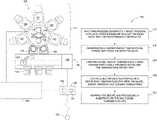
- FIG. 1is schematic top view of a multi-chamber vacuum processing system 100 having at least one processing chamber 120 .
- the multi-chamber vacuum processing system 100also includes a system controller 160 , a vacuum-tight processing platform 110 and a factory interface 140 .
- the multi-chamber vacuum processing system 100may additionally be attached to an advance process controller (APC) 180 .
- the APC 180may have a database 182 and a computing platform 184 .
- the APC 180may optionally be used in addition to the system controller 160 and integrates a plurality of process tools 102 at a manufacturing facility.
- the APC 180may tracking operations and store metrics on substrates undergoing fabrication therein.
- the factory interface (FI) 140may have a plurality of front opening universal pods (FOUPs) 144 and at least one FI robot 142 .
- the FI 140may also have additional stations such as a metrology station 150 .
- the metrology station 150may be alternately be located adjacent the FOUPs 144 .
- the FI robot 1420may have rails and a moveable end effector, which may be a blade, plurality of fingers, gripper or other suitable apparatus for transferring a substrate 118 thereon.
- the FI robot 142is operable at atmospheric conditions and is configured to have a range of motion sufficient to transfer substrates 118 disposed on the moveable end effector between the FOUPs 144 , the metrology station 150 and one or more load lock chambers 134 , 132 of the processing system 100 .
- the FOUPs 144may hold a plurality of substrates 118 for transferring the substrates 118 to and from the multi-chamber vacuum processing system 100 .
- the FOUPs 144may move the substrates 118 processed on the multi-chamber vacuum processing system 100 to a separate metrology station, chemical polishing station or other apparatus for further processing.
- the load lock chambers 134 , 132are disposed between the factory interface 140 and the vacuum-tight processing platform 110 to facilitate substrate 118 transfers between a substantially ambient environment maintained in the factory interface 140 and a vacuum environment maintained in the vacuum-tight processing platform 110 .
- the load lock chambers 134 , 132have one or more entry/exit slots (not shown) through which the substrate 118 may transfer into and out of the load lock chambers 134 , 132 from the FI 140 .
- the load lock chambers 134 , 132have the same number of entry/exit slots through which the substrate 118 may transfer between the interior of the load lock chambers 134 , 132 and the vacuum-tight processing platform 110 .
- Each of the entry/exit slots of the load lock chambers 134 , 132is selectively sealed by a slit valve (not shown) to isolate the interior of the load lock chambers 134 , 132 from the interiors of either the FI 140 or the vacuum-tight processing platform 110 .
- the vacuum-tight processing platform 110has a plurality of attached chambers 120 disposed around a transfer chamber 130 in addition to the load lock chambers 134 , 132 .
- the transfer chamber 130is coupled to a vacuum system (not shown) for providing a reduced atmosphere condition in the vacuum-tight processing platform 110 .
- the transfer chamber 130houses at least one transfer chamber robot 114 .
- the transfer chamber robot 114can rotate to transfer the substrate 118 with any of the chambers 120 .
- One or more of the attached chambers 120may include etch chambers or deposition chambers such as chemical vapor deposition chambers, physical vapor deposition chambers, or atomic layer deposition chambers, having a substrate support assembly 200 (shown in FIG. 2 ) for processing a substrate 118 thereon.
- one of the attached chambers 120may be a metrology chamber 152 having metrology equipment for measuring an attribute of the substrate 118 , an orientation chamber, de-gas chamber or other suitable chamber for processing the substrate 118 .
- one chamber 120may both etch and measure the substrate 118 .
- metrology equipment for measuring an attribute of the substrate 118may be incorporated into the chamber 120 .
- metrology equipment for measuring an attribute of the substrate 118may be located with the transfer chamber 130 , the FI 140 or other convenience location.
- the system controller 160is coupled to and controls each chamber 120 and/or module(s) of the multi-chamber vacuum processing system 100 .
- the system controller 160may control all aspects of operation of the processing system 100 using direct control of chambers and apparatus of the processing system 100 or, alternatively, by controlling the computers associated with these chambers and apparatus.
- the system controller 160may also be configured to communicate with a control unit associated with the transfer chamber robot 114 and other controllers through the APC 180 . For example, movements of the transfer chamber robot 114 , transferring the substrate 118 to and from the processing chambers 120 and performing process sequences, coordinating operations of the various components of the multi-chamber vacuum processing system 100 , and so on, may be controlled by the system controller 160 .
- system controller 160may control the process recipes in the processing chamber 120 .
- the system controllermay control the vacuum, chamber temperature, substrate support surface temperature profile, gas flow rate and various other processing parameters of the process recipe.
- the system controller 160enables feedback from the respective chambers and apparatus to optimize substrate throughput.
- the system controller 160is discussed below with respect to FIG. 4 .
- the system controller 160may alter the process recipe for the substrate 118 undergoing processing in the chamber 120 .
- the system controller 160may use feedback from the metrology equipment to determine changes in the processing recipe.
- the metrology equipmentmay measure critical dimensions across the substrate 118 and alter process parameters, such as localized temperatures across the substrate support assembly, to change localized processing.
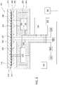
- FIG. 2is a partial cross-sectional schematic side view detailing portions of a substrate support assembly 200 configured to provide azimuthal tuning of the temperature profile across the substrate support assembly.
- the azimuthal tuning of the temperature profile across the substrate support assembly 200may be controlled by software routines running on the controller 160 .
- the software routinesmay also or alternately be stored and/or executed by a second controller (not shown) that is located remotely from the multi-chamber vacuum processing system 100 , such as at the processing chamber 120 or the APC 180 .
- the substrate support assembly 200generally includes at least a substrate support 210 .
- the substrate support 210may be a vacuum chuck, an electrostatic chuck, a susceptor, or other work-piece support surface. In one embodiment, the substrate support 210 is an electrostatic chuck and will be described hereinafter as the electrostatic chuck 210 .
- the substrate support assembly 200may also include a cooling base 260 .
- the cooling base 260may alternately be separate from the substrate support assembly 200 .
- the substrate support assembly 200may be removably coupled to a support pedestal 205 .
- the support pedestal 205which may include a pedestal base 244 .
- the substrate support assembly 200may be periodically removed from the support pedestal 205 to allow for refurbishment of one or more components of the substrate support assembly 200 .
- the electrostatic chuck 210has a mounting surface 203 and a work-piece support surface 202 opposite the mounting surface 203 where the substrate 118 is removably disposed upon the work-piece support surface 202 .
- the electrostatic chuck 210generally includes a chucking electrode 207 embedded in a dielectric body 208 . Although the chucking electrode 207 is shown proximate the mounting surface 203 of the electrostatic chuck 210 , the chucking electrode 207 may be embedded in other portions of the electrostatic chuck 210 , such as just under the work-piece support surface 202 .
- the chucking electrode 207may be configured as a mono polar or bipolar electrode, or other suitable arrangement.
- the chucking electrode 207is coupled through an RF filter 204 to a chucking power source 206 which provides a RF or DC power to electrostatically secure the substrate 118 to the work-piece support surface 202 of the electrostatic chuck 210 .
- the RF filter 204prevents RF power utilized to form a plasma within the processing chamber 120 from damaging electrical equipment or presenting an electrical hazard outside the chamber.
- the dielectric body 208 of the electrostatic chuck 210may be fabricated from a ceramic material, such as AlN or Al 2 O 3 . Alternately, the dielectric body 208 may be fabricated from a polymer, such as polyimide, polyetheretherketone, polyaryletherketone and the like. Heaters may be embedded within the dielectric body 208 .
- the dielectric body 208may include one or more main resistive heaters 212 and/or a plurality of spatially tunable heaters 214 .
- the main resistive heaters 212may be provided to elevate the temperature of the substrate support assembly 200 to a temperature for conducting chamber processes, such as processing the substrate 118 and/or cleaning the interior of the processing chamber 120 .
- the main resistive heater 212may be configured to provide any one or more laterally separated heating zones, for example, a plurality of concentric ring-shaped zones.
- the spatially tunable heaters 214are complimentary to the main resistive heaters 212 and configured to adjust the localized temperature of the electrostatic chuck 210 in a plurality of discrete locations within any one or more of a plurality of laterally separated heating zones defined by the main resistive heaters 212 .
- the spatially tunable heaters 214may be arranged in a polar array, Cartesian grid of columns and rows, a hexagonal grid, or other suitable matrix. The spatially tunable heaters 214 thus provide localized adjustments to the temperature profile of the substrate 118 placed on the substrate support assembly 200 .
- the main resistive heaters 212operate to maintain the temperature profile of the work-piece support surface 202 on a globalized macro scale, while the spatially tunable heaters 214 operate to adjust the temperature at discreet locations of the temperature profile of the work-piece support surface 202 on a localized micro scale.
- the main resistive heaters 212 and spatially tunable heaters 214are coupled through an RF filter 218 to a heater power source 222 .
- the heater power source 222may provide 900 watts or more power to the heaters 212 , 214 .
- the controller 160may control the operation of the heater power source 222 , which is generally set provide power to individual heaters 212 , 214 for heating the substrate 118 to a predefined temperature profile.
- the main resistive heaters 212include laterally separated heating zones, wherein the controller 160 enables one zone of the main resistive heaters 212 or even single spatially tunable heaters 214 to be preferentially heated relative to adjacent heaters 212 , 214 .
- each spatially tunable heater 214may be independently controlled to provide a temperature different than that of another one of the spatially tunable heaters 214 .
- a plurality, such as at least two and as many as all, of the spatially tunable heaters 214are independently and simultaneously powered to provide a temperature profiled which is very stable and does not jump in around, which results in a steady and easily controlled temperature profile, which contributes to enhanced uniformity and predictability of substrate processing results.
- the electrostatic chuck 210may include one or more temperature sensors 254 .
- the temperature sensors 254may measure temperature at a plurality of discrete locations on the work-piece support surface 202 .
- the temperature sensors 254may provide temperature feedback information to the controller 160 for controlling the power applied by the heater power source 222 to the main resistive heaters 212 and the spatially tunable heaters 214 . Additionally, the feedback information may be used to control the operations of the cooling base 260 .
- the electrostatic chuck 210may be disposed on the temperature controlled cooling base 260 .
- the temperature controlled cooling base 260is coupled to a heat transfer fluid source 262 .
- the heat transfer fluid source 262provides a heat transfer fluid, such as a liquid, gas or combination thereof, which is circulated through one or more conduits 290 disposed in the cooling base 260 .
- the controller 160may control the fluid flowing through isolated neighboring conduits 290 to enabling local control of the heat transfer between the electrostatic chuck 210 and different regions of the cooling base 260 , which assists in controlling the lateral temperature profile of the substrate 118 .
- the pedestal base 244is disposed below the cooling base 260 and is configured to accommodate a plurality of driving mechanisms configured to raise and lower a plurality of lifting pins. Additionally, the pedestal base 244 is configured to accommodate the plurality of fluid connections from the electrostatic chuck 210 and the cooling base 260 . The pedestal base 244 is also configured to accommodate the plurality of electrical connections from the electrostatic chuck 210 .
- the myriad of connections, for example fluids, electrical, data signals,may run externally or internally of the substrate support assembly 200 .
- the system controller 160may include a controller board 250 that may be disposed in the pedestal base 244 . Alternately, the controller board 250 may be disposed elsewhere inside or outside the substrate support assembly 200 .
- the controller board 250may have a pulse width modification (PWM) heater controller 216 .
- the controller board 250may also have an optical communication interface board 256 .
- the controller board 250also may optionally have a temperature sensor controller 252 .
- the temperature sensor controller 252may be communicatively coupled to the temperature sensors 254 for measuring the substrate 118 temperature.
- the temperature sensor controller 252may convert the signals from the temperature sensors 254 to actual temperature readings in discrete locations about the work-piece support surface 202 .
- the controller board 250also may optionally have a metrology controller (not shown) for determining the thickness of a substrate 118 disposed on the work-piece support surface 202 .
- the PWM heater controller 216may connect to the heaters 212 , 214 .
- the PWM heater controller 216may modify the power coming from the heater power source 222 to the individual heaters 212 , 214 .
- the PWM heater controller 216may be programmed and calibrated by measuring the temperature at each spatially tunable heater 214 . That is, each spatially tunable heater 214 has its own independent PWM control.
- the PWM heater controller 216may control the temperature by adjusting the power parameters for individual spatially tunable heaters 214 . For example, 100 percent power to one of the spatially tunable heater 214 may result in about 5 degrees Celsius of heat output for increasing the temperature set by the main heater for the surface location above the spatially tunable heater 214 .
- 20 percent power to one or more of the spatially tunable heaters 214may result in about a 1 degree Celsius heat output for increasing the temperature set by the main heater for the surface location above the spatially tunable heater 214 .
- the powermay be reduced to 20% for several of the spatially tunable heater 214 and maintained at that level throughout a processing operation.
- the PWM heater controller 216may operate one or more spatially tunable heaters 214 at a first power level, for example 80 percent, while simultaneously operating one or more separate spatially tunable heaters 214 at a second power level, for example about 20 percent.
- the temperaturemay be regulated with incremental power increases to the spatially tunable heaters 214 .
- a temperature risemay be obtained with a percentage increase, for example 9% increase, in the power supplied to the spatially tunable heater 214 during the course of a process.
- the temperaturemay be regulated by cycling the spatially tunable heater 214 on and off, while the other tunable heaters 214 also cycled on and off, either in-phase, or out of phase.
- the temperaturemay be regulated by a combination of adjusting the power levels, cycling and incrementally adjusting the power to the spatially tunable heater 214 as needed to maintain a desired temperature profile.
- a temperature mapmay be obtained by varying the heat output of each individual spatially tuning heater 214 all at one instance.
- the mapmay correlate the CD or substrate temperature profile to the power distribution curve for each spatially tunable heater 214 .
- the spatially tunable heater 214may be used to generate a temperature profile on the substrate based on a program regulating power settings for the individual spatially tunable heaters 214 .
- the logiccan be placed directly in the PWM heater controller 216 or in an externally connected controller, such as the controller 160 .
- the PWM heater controller 216is configured to independently control an output of one of the plurality of spatially tunable heaters 214 relative to another of the plurality of spatially tunable heaters 214 as well as the main resistive heaters 212 .
- the optical communication interface board 256may interface with the PWM heater controller 216 .
- the optical communication interface board 256may also interface with other controllers such as the temperature sensor controller 252 .
- the optical communication interface board 256may have an optical connection to an optical converter 258 .
- the optical interface board 256may send an optical signal to the optical converter 258 for communicating with the controller 160 .
- communication between the PWM heater controller 216 and the controller 160may be performed by optical signals which are free of damaging RF energy.
- the controller 160may send a signal control the heat output from one or more of the spatially tunable heaters 214 for adjusting the temperature profile of the substrate 118 disposed on the electrostatic chuck 210 .
- the signal instruction from the controller 160may enter the optical converter 258 for transmission to the optical communication interface board 256 before delivery of the instruction to the PWM heater controller 216 for controlling the heating profile of the substrate 118 during processing.
- a benefit of the optical communication interface board 256is the ability to prevent RF power from traveling through control circuitry leaving the substrate support assembly 200 .
- the temperature of the surface for the substrate 118 in the processing chamber 120may be influenced by the evacuation of the process gasses by the pump, the slit valve door, the plasma and other factors.
- the controller 160may have a temperature profile map for the substrate 118 for obtaining high quality processing results.
- the controller 160may receive input from the metrology equipment or other processing equipment to correct for deviation or adverse trends in the process results of the substrate 118 . For example, one area of the substrate 118 may etch faster than another area of the substrate 118 .
- the controller 160may signal the spatially tunable heaters 214 to adjust the surface temperature of the substrate 118 in the area deviating in the etch rate.
- the controller 160may activate the spatially tunable heaters 214 in a pattern similar in shape to these areas.
- the spatially tunable heaters 214improve the temperature profile of the surface of the substrate 118 produced by the main resistive heaters 212 by reducing variations in the temperature profile to about +/ ⁇ 0.3 degrees Celsius.
- the temperature profilemay be made uniform or to vary precisely in a predetermined manner across regions of the substrate 118 through the use of the spatially tunable heaters 214 to obtain desired results.
- the use of independently controllable spatially tunable heaters 214 to smooth out or correct the temperature profile generated by the main resistive heaters 212enable control of the local temperature uniformity across the substrate to very small tolerances, thereby enabling precise process and CD control when processing the substrate 118 .
- the small size and high density of the spatially tunable heaters 214 relative to the main resistive heaters 212enables temperature control at specific locations on the substrate support assembly 126 , substantially without affecting the temperature of neighboring areas, thereby allowing local hot and cool spots to be compensated for without introducing skewing or other temperature asymmetries.
- spatially tunable heaters 214there may be about 200 to about 400, or even more spatially tunable heaters 214 in a given embodiment of a substrate support assembly 200 configured for use with a 300 mm substrate. Even more spatially tunable heaters 214 are contemplated for substrates of 450 mm or larger. Exemplary distribution of the spatially tunable heaters 214 are described further below with reference to FIGS. 3 A- 3 D .
- FIGS. 3 A- 3 Dare top views of the electrostatic chuck 210 illustrating example layouts of cells 390 having the spatially tunable heaters 214 therein.
- FIG. 3 Ais a top view of the electrostatic chuck 210 of FIG. 2 , according to one embodiment.
- FIGS. 3 B- 3 Dare top views of the electrostatic chuck 210 of FIG. 2 , according to alternate embodiments.
- the cells 390may have material (or gaps) which act as a thermal choke 316 between adjacent cells 390 .
- the thermal chokes 316separate and reduce conduction between adjacent cells 300 .
- each spatially tunable heaters 214 in each cell 390by individually and independently controlling the power provided to each spatially tunable heaters 214 in each cell 390 , a localized approach is achieved for controlling the temperature which enables specific points of the substrate 118 to be heated or cooled, thereby enabling a truly addressable lateral temperature profile tuning and control of the surface of the substrate 118 .
- the thermal choke 316is disposed between each neighboring cell 390 .
- Each cell 390has associated therewith at least one of the spatially tunable heaters 214 .
- the number of cells 390 shownis for illustration only, and any number of embodiments may have substantially more (or less) cells 390 .
- the number of spatially tunable heaters 214may be at least an order of magnitude greater than the number of main resistive heaters 212 .
- the number of spatially tunable heaters 214 located across the substrate support assembly 200may easily be in excess of several hundred.
- the spatially tunable heaters 214may be configured in a pattern 399 to efficiently generate a heat profile along the surface of the electrostatic chuck 210 .
- the pattern 399may be symmetric about a midpoint 392 , while providing clearance in and around holes 322 for lift pins or other mechanical, fluid or electrical connections.
- Each spatially tunable heater 214may be controlled by the controller 160 through the PWM controller 216 .
- the PWM controller 216may turn on a single spatially tunable heater 214 defining a local area 340 ; or a plurality of spatially tunable heaters 214 grouped to define an inner wedge 362 , a perimeter group 364 , a pie shaped area 330 , or other desired geometric configuration, including non-contiguous configurations for determining a desired temperature profile. In this manner, temperature can be precisely controlled at independent locations along the surface of the electrostatic chuck 210 , such independent locations not limited to concentric rings, or other center to edge configurations known in the art.
- the pattern 399 shownis comprised of discontinuous smaller units, the pattern 399 may alternatively have larger and/or smaller units, extend to the edge, or have other forms.
- the pattern 399 of spatially tunable heaters 214are arranged in a polar array about the midpoint 392 , which in some embodiments, may coincide with the centerline of the electrostatic chuck 210 .
- FIG. 3 Bis a top view of the electrostatic chuck 210 depicted in FIG. 2 , according to another embodiment.
- the spatially tunable heaters 214are arranged in the form of a grid, thus defining an array of temperature control cells 390 also arranged in the grid pattern.
- the grid pattern of spatially tunable heaters 214is shown as an X/Y (Cartesian) grid comprised of rows and columns, the grid pattern of spatially tunable heaters 214 may alternatively have some other uniformly packed form, such as a hexagon close pack. It should be appreciated, as discussed supra, the spatially tunable heaters 214 may be activated in groups or singularly.
- FIG. 3 Cis a top view of the electrostatic chuck 210 depicted in FIG. 2 , according to another embodiment.
- FIG. 3 Cillustrates a plurality of spatially tunable heaters 214 arranged in a polar array.
- one or more of thermal chokes 316may be disposed between the spatially tunable heaters 214 .
- the polar array pattern of the spatially tunable heaters 214defines the neighboring cells 390 , which are thus also be arranged in a polar array.
- thermal chokes 316may be utilized to isolate each cell 390 from the adjacent cell 390 .
- FIG. 3 Dis a top view of the electrostatic chuck 210 depicted in FIG. 2 , according to another embodiment.
- FIG. 3 Dillustrates a plurality of spatially tunable heaters 214 arranged in concentric channels.
- the concentric channel pattern of the spatially tunable heaters 214may be optionally separated by thermal chokes 316 . It is contemplated that the spatially tunable heaters 214 and cells 390 may be arranged in other orientations.
- the number and density of the spatially tunable heaters 214contribute to the ability for controlling the temperature uniformity across the substrate to very small tolerances which enables precise process and CD control when processing the substrate 118 . Additionally, individual control for one of the spatially tunable heaters 214 relative to another spatially tunable heater 214 enables temperature control at discrete locations along the surface of the substrate support assembly 200 without substantially affecting the temperature of neighboring or adjacent areas of the surface. This feature allows local hot and cool spots to be compensated for without introducing skewing or other temperature asymmetries.
- the spatially tunable heaters 214may have an individual temperature range between about 0.0 degrees Celsius and about 10.0 degrees Celsius with the ability to control the temperature rise in increments of about 0.1 degrees Celsius.
- the plurality of spatially tunable heaters 214 in the substrate support assembly 200 in conjunction with the main resistive heaters 212have demonstrated the ability to control the temperature uniformity of a substrate 118 processed thereon to less than about ⁇ 0.3 degrees Celsius.
- the spatially tunable heaters 214allow both lateral and azimuthal tuning of the lateral temperature profile of the substrate 118 processed on the substrate support assembly 200 .
- the heaters 214 , 212may be controlled by a software routine.
- the softwaremay incorporate current substrate CD measurements and process results along with the process recipes and other parameters to tune the temperature profile for the substrate 118 undergoing processing in the process chamber 120 .
- the software routinesmay include embodiments for controlling the temperature in multiple zones and discretely along the substrate surface.
- the system 400may be a personal computer, industrial processor, personal digital assistant, mobile phone, mobile device or any other device suitable for practicing one or more embodiments.
- the controller 160may have a similar architecture to that of the system 400 .
- the system 400may run a software routine for controlling the temperature profile of substrates 118 undergoing processing in one or more of the process chambers 120 of the processing system 100 .
- an secondary or external controllersuch as APC 180 , may have a similar architecture as system 400 and provide support, such as data or software, for controlling the temperature profile of the substrate 118 .
- the system 400includes a central processing unit (CPU) 402 and a system memory 404 communicating via a bus path that may include a memory bridge 405 .
- CPU 402includes one or more processing cores, and, in operation, CPU 402 is the master processor of the system 400 , controlling and coordinating operations of other system components.
- System memory 404stores a software application 406 , and data, for use by CPU 402 .
- CPU 402runs software applications and optionally an operating system.
- Memory bridge 405which may be, e.g., a Northbridge chip, is connected via a bus or other communication path (e.g., a HyperTransport link) to an I/O (input/output) bridge 407 .
- I/O bridge 407which may be, e.g., a Southbridge chip, receives user input from one or more user input devices 408 (e.g., keyboard, mouse, joystick, digitizer tablets, touch pads, touch screens, still or video cameras, motion sensors, and/or microphones) and forwards the input to CPU 402 via memory bridge 405 .
- user input devices 408e.g., keyboard, mouse, joystick, digitizer tablets, touch pads, touch screens, still or video cameras, motion sensors, and/or microphones
- a display processor 412is coupled to a memory bridge 405 via a bus or other communication path (e.g., a PCI Express, Accelerated Graphics Port, or HyperTransport link); in one embodiment display processor 412 is a graphics subsystem that includes at least one graphics processing unit (GPU) and graphics memory. Graphics memory includes a display memory (e.g., a frame buffer) used for storing pixel data for each pixel of an output image. Graphics memory can be integrated in the same device as the GPU, connected as a separate device with the GPU, and/or implemented within system memory 404 .
- a bus or other communication pathe.g., a PCI Express, Accelerated Graphics Port, or HyperTransport link
- Graphics memoryincludes a display memory (e.g., a frame buffer) used for storing pixel data for each pixel of an output image. Graphics memory can be integrated in the same device as the GPU, connected as a separate device with the GPU, and/or implemented within system memory 404 .
- Display processor 412periodically delivers pixels to a display device 410 (e.g., a screen or conventional CRT, plasma, OLED, SED or LCD based monitor or television). Additionally, display processor 412 may output pixels to film recorders adapted to reproduce computer generated images on photographic film. Display processor 412 can provide display device 410 with an analog or digital signal.
- a display device 410e.g., a screen or conventional CRT, plasma, OLED, SED or LCD based monitor or television. Additionally, display processor 412 may output pixels to film recorders adapted to reproduce computer generated images on photographic film. Display processor 412 can provide display device 410 with an analog or digital signal.
- a system disk 414is also connected to an I/O bridge 407 and may be configured to store content and applications and data, such as a database library 415 , for use by CPU 402 and display processor 412 .
- System disk 414provides non-volatile storage for applications and data and may include fixed or removable hard disk drives, flash memory devices, and CD-ROM, DVD-ROM, Blu-ray, HD-DVD, or other magnetic, optical, or solid state storage devices.
- a switch 416provides connections between the I/O bridge 407 and other components such as a network adapter 418 and various add-in cards 420 and 421 .
- Network adapter 418allows the system 400 to communicate with other systems via an electronic communications network, and may include wired or wireless communication over local area networks 440 and wide area networks such as the Internet.
- I/O bridge 407Other components (not shown), including USB or other port connections, film recording devices, and the like, may also be connected to I/O bridge 407 .
- process equipment 470may operate from instructions and/or data provided by CPU 402 , system memory 404 , or system disk 414 .
- Communication paths interconnecting the various components in FIG. 4may be implemented using any suitable protocols, such as PCI (Peripheral Component Interconnect), PCI Express (PCI-E), AGP (Accelerated Graphics Port), HyperTransport, or any other bus or point-to-point communication protocol(s), and connections between different devices may use different protocols, as is known in the art.
- PCIPeripheral Component Interconnect
- PCI-EPCI Express
- AGPAccelerated Graphics Port
- HyperTransportor any other bus or point-to-point communication protocol(s)
- the process equipment 470may be one or more semiconductor processing chamber, such as the processing chamber 120 .
- display processor 412incorporates circuitry optimized for performing mathematical operations, including, for example, math co-processor, and may additionally constitute a graphics processing unit (GPU).
- graphics processing unitGPU
- display processor 412incorporates circuitry optimized for general purpose processing.
- display processor 412may be integrated with one or more other system elements, such as the memory bridge 405 , CPU 402 , and I/O bridge 407 to form a system on chip (SoC).
- SoCsystem on chip
- display processor 412is omitted and software executed by CPU 402 performs the functions of display processor 412 .
- Pixel datacan be provided to display processor 412 directly from CPU 402 .
- instructions and/or data representing a predictive analysisis provided to set of server computers, each similar to the system 400 , via network adapter 418 or system disk 414 .
- the serversmay perform operations on subsets of the data using the provided instructions for analysis. The results from these operations may be stored on computer-readable media in a digital format and optionally returned to the system 400 for further analysis or display. Similarly, data may be output to other systems for display, stored in a database library 415 on the system disk 414 , or stored on computer-readable media in a digital format.
- CPU 402provides display processor 412 with data and/or instructions defining the desired output images, from which display processor 412 generates the pixel data of one or more output images, including characterizing and/or adjusting the offset between stereo image pairs.
- the data and/or instructions defining the desired output imagescan be stored in system memory 404 or graphics memory within display processor 412 .
- CPU 402 and/or display processor 412can employ any mathematical, function or technique known in the art to create one or more results from the provided data and instructions, including predictive analysis relating facility state information to maintenance information to predict the need for maintenance events.
- system memory 404is connected to CPU 402 directly rather than through a bridge, and other devices communicate with the system memory 404 via the memory bridge 405 and the CPU 402 .
- display processor 412is connected to the I/O bridge 407 or directly to CPU 402 , rather than to memory bridge 405 .
- I/O bridge 407 and memory bridge 405might be integrated into a single chip.
- the particular components shown hereinare optional; for instance, any number of add-in cards or peripheral devices might be supported.
- the process equipment 470may be connected directly to the I/O bridge 407 .
- switch 416is eliminated, and network adapter 418 and add-in cards 420 , 421 connect directly to the I/O bridge 407 .
- Various embodiments of the inventionmay be implemented as a program product for use with a computer system.
- the software routines of the program productdefine functions of the embodiments (including the methods described herein) and can be contained on a variety of computer-readable storage media.
- Illustrative computer-readable storage mediainclude, but are not limited to: (i) non-writable storage media (e.g., read-only memory devices within a computer such as CD-ROM disks readable by a CD-ROM drive, flash memory, ROM chips or any type of solid-state non-volatile semiconductor memory) on which information is permanently stored; and (ii) writable storage media (e.g., floppy disks within a diskette drive or hard-disk drive or any type of solid-state random-access semiconductor memory) on which alterable information is stored.
- non-writable storage mediae.g., read-only memory devices within a computer such as CD-ROM disks readable by a CD-ROM drive, flash memory,
- Feedback control and feedforward control designsmay both be utilized in the method run by the program code for adjusting the temperature profile of a substrate.
- Metrology data from processing a current substrateis fed back to the controller (either look up tables, PID, MPC or iterative learning controller).
- Upstream metrology datamay also be input to the feedforward controller routine.
- Either the feedback or feedforward controller routine, or both,can determine a desired offset temperature profile for processing a subsequent substrate.
- the offset temperature profileis then input to the model based temperature tuner, the results of the tuner will generate the next run recipe parameters inclusive of the determined offsets at discrete locations throughout the temperature profile.
- Such a processwill enable process tuning with the control of electrostatic chuck temperature via adjusting the spatially tunable heaters and cooling components.
- a model based substrate temperature profileis made possible given the multiple zone temperature controlled electrostatic chuck having large resistive heaters for main tuning, and small size uniform or non-uniform pattern spatially tunable heaters for fine resolution control.
- the electrostatic chuckmay have primary heaters forming four zones and multiple small spatially tunable heaters overlapping the four zones.
- a substrate temperature modelis developed from physical modeling and calibrated with experimentation data. In production, an 14 wafer is used to calibrate the model further due to electrostatic chuck to electrostatic chuck and RF hour variations.
- a multi-zone and high resolution temperature control electrostatic chuck for process tuning temperature profile controlcan be heated or cooled or both.
- the electrostatic chuckmay have a non-uniform pattern for the activating the spatially tunable heaters with each spatially tunable heater having a unique heat output depending on a programmed power output to the spatially tunable heater.
- the temperature profilemay be adjusted for tuning a process for achieving critical dimension (CD) uniformity tuning, incoming CD compensation, etch rate (ER) tuning, etc.
- the temperature profile control methodcan be feedback from current metrology data, or feedforward from previous metrology data or upstream process data.
- the control methoddoes not limit to iterative learning control (which is non-model based). Typical control tuning like PID, LUT (look up table), or advanced model based control can be used.
- Multi-zone primary heaters and resolution temperature control achieved by spatially tunable heaters in the ESCcan be used to maintain consistent substrate temperatures given differences from one ESC to another ESC as well as RF hour dependency.
- the multi-zone and resolution temperature control of the ESCcan be used to match a temperature profile for a substrate to a model profile under varying chamber conditions.
- edge zone temperature controlcan used to minimize process kit erosion or compensate edge process drift to increase mean time between cleaning the chamber.
- the ability to affect non-uniform shapes for the temperature control profileis designed to correct inherent non-uniformity of chamber hardware.
- the spatially tunable heatersmay be used as a probe for temperature or heat flux measurement for developing real-time temperature profiles.
- FIG. 5is a flow diagram of a method 500 for processing a substrate using a process recipe according to a first embodiment, wherein the process recipe is determined using a feedforward controller routine.
- the flow diagrammay be implemented as a software routine on a computing device, such as described by system 400 .
- the spatially tunable heatersare independently controllable and determine a temperature profile of substrates processed thereon.
- the controllermay alter the heat generated by one spatially tunable heater relative another by controlling at least one or more of the duty cycle, voltage, current, duration of power applied separately to each individual spatially tunable heater relative another.
- the power supplied to the spatially tunable heatersmay also be provides simultaneously between a plurality of heaters as described above, or alternatively, sequentially scanned across individual spatially tunable heaters.
- a work-piecesuch as the substrate 118 , may be processed on the substrate support assembly.
- the substratemay be processed in a vacuum chamber, for example using a plasma process.
- the vacuum processwhich may be optionally performed in the presence of a plasma within the processing chamber, may be one of etching, chemical vapor deposition, physical vapor deposition, ion implantation, plasma treating, annealing, oxide removal, abatement or other plasma process. It is contemplated that the work-piece may be processed on the temperature controlled surface in other environments, for example, at atmospheric conditions, for other applications.
- the method 500begins at operation 510 by inputting one or more of process sensitivity, target process data and upstream metrology process data into the feedforward controller routine.
- the feedforward controller routineis set up that it takes the upstream metrology data, target process data and process sensitivity and directly outputs the desired wafer temp offset map.
- a desired wafer temperature offset mapis determined from the inputted data.
- model wafer temperature tuning parametersare created from a process recipe and the temperature offset map.
- the temperature offset mapis feedback to the temp tuner based on the feedforward of wafer temp and process recipe.
- the heating profile of the multi-zone temperature ESCis controlled using the model wafer temperature tuning parameters.
- the control for each spatially tunable heatercan be performed simultaneous in the electrostatic chuck 210 allowing any selection of spatially tunable heaters to quickly generate a specific temperature profile.
- Control of the power provided to the individual spatially tunable heatersmay be provide through an external controller interfacing over an optical connection to the tuning heater controller disposed in the substrate support assembly.
- the tuning heater controllermay simultaneously provide power to one spatially tunable heater while cycling another spatially tunable heater and cycling still other spatially tunable heaters at different overlapping time intervals. In this manner, the spatially controllable heaters may have a temperature profile across the substrate support made to match the model wafer temperature tuning parameters.
- the model based wafer temp tunerthen outputs the desired process parameter to form a new recipe.
- the recipeis run and the substrate is processed on the multi-zone temperature ESC.
- FIG. 6is a second embodiment of a method 600 for processing a substrate using the spatially tunable heaters in conjunction a feedback controller routine.
- the processbegins at operation 610 wherein the process sensitivity, target process data and k th run metrology process data are inputted into the iterative learning controller.
- a feedback controller routineis set up to have the inputs of the delta metrology data, i.e., the k th run metrology data, target process data, is applied to obtain the desired substrate temperature profile based on process to temperature sensitivity and substrate temp data.
- the feedback controller routinemay be an iterative learning controller or other type of controller such as a LUT, PID, MPC or other suitable controller.
- a desired substrate temperature offset mapis determined from the inputted data.
- the desired substrate temperature offset mapbecomes an input for the controller to adjust the recipe parameters such as directing the PWM controller to modify the output from the spatially tunable heaters so that the next substrate is run with a temperature profile as close as possible to that of the desired substrate temperature profile.
- the iterationis ongoing till desired process performance is achieved.
- the processmay involve multiple iterations with multiple substrates.
- a model substrate temperature tuning parametermay be created from a process recipe and the temperature offset map.
- the key recipe outputs, such as temperature,may be adjusted every time a new desired process target and process sensitivity changes.
- the heating profile of a multi-zone and spatially tunable temperature electrostatic chuckmay be controlled with the model substrate temperature tuning parameters.
- the model substrate temperature tuning parametersmay include a uniquely incremental increase in power to several individual spatially tunable heaters while additionally decreasing the power to other individual spatially tunable heaters to attain a correction to achieve a desired temperature profile.
- the processis run with the K th iteration recipe on the K+1 substrate. That is, the process recipe is modified after measuring the substrate.
- the process recipeis then used for processing the next substrate.
- the process recipemay be determined from measurements of a prior group of substrates. For example, the substrates may be placed in a FOUP and moved to a separate metrology device. The recipe may be determined from the last substrate processed in the FOUP. Alternatively, the controller may look at a trend of the metrology for the substrates in the FOUP and make adjustments to the current process recipe based on the trend.
- the metrology data for the (K+1) th substrateis determined.
- the metrology datamay be stored in a database, such as at the APC, for future use.
- the (K+1) th run metrology process datais provided to the iterative learning controller. The controller may adjust the current process recipe (K+2) th based on the metrology process data.
- FIG. 7is a flow diagram of a method 700 for processing a substrate, wherein a process recipe is determined for the spatially tunable heaters using a feedback and feedforward controller routine.
- the process recipe for a current substratemay be modified based on both the feedback current process data and feed-forward upper ream metrology data.
- the method 700begins at operation 710 wherein the process sensitivity, target process data and k th run metrology process data are inputted into the iterative learning controller, i.e., the feedback controller routine.
- the process sensitivity, target process data and upstream metrology dataare inputted into the feedforward controller routine.
- a desired substrate temperature offset mapis created from the inputted data from the feed forward controller routine and the iterative learning controller routine.
- both current process data and upper ream metrology dataare used.
- model substrate temperature tuning parametersare created from a process recipe and the temperature offset map in addition to the desired temperature offset map.
- the model substrate tuning parametersare used to determine desired heat output for individual spatially tunable heaters for achieving the desired temperature profile for the substrate.
- the heating profile of a multi-zone temperature electrostatic chuckis controlled using the model wafer temperature tuning parameters.
- the PWM controlleradjusts the power to each individual spatially tunable heater for achieving the desired temperature profile. While the power to one spatially tunable heater is being adjusted, the other spatially tunable heaters may be turned off or held at a given output. Alternatively, the power to a plurality, such as two, more or all, of the spatially tunable heater may be adjusted simultaneously. There may be 140 or more spatially tunable heaters with each spatially tunable heater being individually controlled for obtaining customizable heat output.
- the controllermay indicate to the PWM controller to provided 20 percent power to one spatially tunable heater, e.g.
- spatially tunable heater xto achieve about a 1 degree Celsius temperature increase in a first location adjacent that heater.
- the controllermay simultaneously instructing the PWM to provide 80 percent power to a second spatially tunable heater, e.g. spatially tunable heater y , to achieve about a 4 degree Celsius increase in a second location adjacent that heater.
- a second spatially tunable heatere.g. spatially tunable heater y
- up to 100 percent of the spatially tunable heatersmay be individually controlled simultaneously for creating a unique temperature profile.
- the process with the K th iteration recipeis run on the K+1 substrate.
- the recipemay be tuned for each subsequent substrate to uniquely tailor the temperature profile to achieve a desired result.
- the metrology data for the (K+1) th substrateis determined.
- the (K+1) th run metrology process datais provided into the iterative learning controller routine for use in determining the substrate temperature offset map for the (K+2) th substrate.
- the process tuningcan control the critical dimension uniformity, incoming critical dimension compensation, and etch rate.
- the spatially tunable heatersmaintain consistent substrate temperature in various chamber environments from one ESC to another ESC.
- the spatially tunable heatersmay be used to promote edge zone temperature control configured to minimize process kit erosion or compensate edge process drift and increase mean time between cleaning.
- the spatially tunable heatersmay have non-uniform shape to correct inherent non-uniformity of the processing chamber.
- the spatially tunable heatersare used as a probe for temperature or heat flux measurement. Thus, the spatially tunable heaters tune the process results to compensate for variation over time.
Landscapes
- Engineering & Computer Science (AREA)
- Manufacturing & Machinery (AREA)
- Computer Hardware Design (AREA)
- Microelectronics & Electronic Packaging (AREA)
- Power Engineering (AREA)
- Physics & Mathematics (AREA)
- Condensed Matter Physics & Semiconductors (AREA)
- General Physics & Mathematics (AREA)
- Container, Conveyance, Adherence, Positioning, Of Wafer (AREA)
- Drying Of Semiconductors (AREA)
- Resistance Heating (AREA)
- Control Of Resistance Heating (AREA)
Abstract
Description
Claims (17)
Priority Applications (1)
| Application Number | Priority Date | Filing Date | Title |
|---|---|---|---|
| US16/595,801US11622419B2 (en) | 2015-01-18 | 2019-10-08 | Azimuthally tunable multi-zone electrostatic chuck |
Applications Claiming Priority (3)
| Application Number | Priority Date | Filing Date | Title |
|---|---|---|---|
| US201514997842A | 2015-01-18 | 2015-01-18 | |
| US201562165572P | 2015-05-22 | 2015-05-22 | |
| US16/595,801US11622419B2 (en) | 2015-01-18 | 2019-10-08 | Azimuthally tunable multi-zone electrostatic chuck |
Related Parent Applications (2)
| Application Number | Title | Priority Date | Filing Date |
|---|---|---|---|
| US201514997842AContinuation | 2015-01-18 | 2015-01-18 | |
| US14/997,842ContinuationUS10440777B2 (en) | 2015-05-22 | 2016-01-18 | Azimuthally tunable multi-zone electrostatic chuck |
Publications (2)
| Publication Number | Publication Date |
|---|---|
| US20200037399A1 US20200037399A1 (en) | 2020-01-30 |
| US11622419B2true US11622419B2 (en) | 2023-04-04 |
Family
ID=57393586
Family Applications (2)
| Application Number | Title | Priority Date | Filing Date |
|---|---|---|---|
| US14/997,842Active2037-08-24US10440777B2 (en) | 2015-05-22 | 2016-01-18 | Azimuthally tunable multi-zone electrostatic chuck |
| US16/595,801Active2035-05-06US11622419B2 (en) | 2015-01-18 | 2019-10-08 | Azimuthally tunable multi-zone electrostatic chuck |
Family Applications Before (1)
| Application Number | Title | Priority Date | Filing Date |
|---|---|---|---|
| US14/997,842Active2037-08-24US10440777B2 (en) | 2015-05-22 | 2016-01-18 | Azimuthally tunable multi-zone electrostatic chuck |
Country Status (6)
| Country | Link |
|---|---|
| US (2) | US10440777B2 (en) |
| JP (2) | JP6806704B2 (en) |
| KR (2) | KR102321919B1 (en) |
| CN (2) | CN107636817B (en) |
| TW (2) | TWI677049B (en) |
| WO (1) | WO2016190905A1 (en) |
Families Citing this family (333)
| Publication number | Priority date | Publication date | Assignee | Title |
|---|---|---|---|---|
| US20130023129A1 (en) | 2011-07-20 | 2013-01-24 | Asm America, Inc. | Pressure transmitter for a semiconductor processing environment |
| JP5973731B2 (en) | 2012-01-13 | 2016-08-23 | 東京エレクトロン株式会社 | Plasma processing apparatus and heater temperature control method |
| US10714315B2 (en) | 2012-10-12 | 2020-07-14 | Asm Ip Holdings B.V. | Semiconductor reaction chamber showerhead |
| US20160376700A1 (en) | 2013-02-01 | 2016-12-29 | Asm Ip Holding B.V. | System for treatment of deposition reactor |
| US11015245B2 (en) | 2014-03-19 | 2021-05-25 | Asm Ip Holding B.V. | Gas-phase reactor and system having exhaust plenum and components thereof |
| KR101758087B1 (en)* | 2014-07-23 | 2017-07-14 | 어플라이드 머티어리얼스, 인코포레이티드 | Tunable temperature controlled substrate support assembly |
| US10941490B2 (en) | 2014-10-07 | 2021-03-09 | Asm Ip Holding B.V. | Multiple temperature range susceptor, assembly, reactor and system including the susceptor, and methods of using the same |
| US10276355B2 (en) | 2015-03-12 | 2019-04-30 | Asm Ip Holding B.V. | Multi-zone reactor, system including the reactor, and method of using the same |
| CN107636817B (en)* | 2015-05-22 | 2021-08-27 | 应用材料公司 | Azimuth adjustable multi-zone electrostatic chuck |
| US10386821B2 (en) | 2015-06-22 | 2019-08-20 | Lam Research Corporation | Systems and methods for calibrating scalar field contribution values for a limited number of sensors including a temperature value of an electrostatic chuck and estimating temperature distribution profiles based on calibrated values |
| US10381248B2 (en)* | 2015-06-22 | 2019-08-13 | Lam Research Corporation | Auto-correction of electrostatic chuck temperature non-uniformity |
| US10763142B2 (en)* | 2015-06-22 | 2020-09-01 | Lam Research Corporation | System and method for determining field non-uniformities of a wafer processing chamber using a wafer processing parameter |
| US10458018B2 (en) | 2015-06-26 | 2019-10-29 | Asm Ip Holding B.V. | Structures including metal carbide material, devices including the structures, and methods of forming same |
| US10211308B2 (en) | 2015-10-21 | 2019-02-19 | Asm Ip Holding B.V. | NbMC layers |
| US11139308B2 (en) | 2015-12-29 | 2021-10-05 | Asm Ip Holding B.V. | Atomic layer deposition of III-V compounds to form V-NAND devices |
| US10529554B2 (en) | 2016-02-19 | 2020-01-07 | Asm Ip Holding B.V. | Method for forming silicon nitride film selectively on sidewalls or flat surfaces of trenches |
| US10343920B2 (en) | 2016-03-18 | 2019-07-09 | Asm Ip Holding B.V. | Aligned carbon nanotubes |
| US10367080B2 (en) | 2016-05-02 | 2019-07-30 | Asm Ip Holding B.V. | Method of forming a germanium oxynitride film |
| US11453943B2 (en) | 2016-05-25 | 2022-09-27 | Asm Ip Holding B.V. | Method for forming carbon-containing silicon/metal oxide or nitride film by ALD using silicon precursor and hydrocarbon precursor |
| US10908195B2 (en)* | 2016-06-15 | 2021-02-02 | Watlow Electric Manufacturing Company | System and method for controlling power to a heater |
| US9859151B1 (en) | 2016-07-08 | 2018-01-02 | Asm Ip Holding B.V. | Selective film deposition method to form air gaps |
| US10612137B2 (en) | 2016-07-08 | 2020-04-07 | Asm Ip Holdings B.V. | Organic reactants for atomic layer deposition |
| KR102532607B1 (en) | 2016-07-28 | 2023-05-15 | 에이에스엠 아이피 홀딩 비.브이. | Substrate processing apparatus and method of operating the same |
| US9812320B1 (en) | 2016-07-28 | 2017-11-07 | Asm Ip Holding B.V. | Method and apparatus for filling a gap |
| US9887082B1 (en) | 2016-07-28 | 2018-02-06 | Asm Ip Holding B.V. | Method and apparatus for filling a gap |
| US11532757B2 (en) | 2016-10-27 | 2022-12-20 | Asm Ip Holding B.V. | Deposition of charge trapping layers |
| US10714350B2 (en) | 2016-11-01 | 2020-07-14 | ASM IP Holdings, B.V. | Methods for forming a transition metal niobium nitride film on a substrate by atomic layer deposition and related semiconductor device structures |
| KR102546317B1 (en) | 2016-11-15 | 2023-06-21 | 에이에스엠 아이피 홀딩 비.브이. | Gas supply unit and substrate processing apparatus including the same |
| KR102762543B1 (en) | 2016-12-14 | 2025-02-05 | 에이에스엠 아이피 홀딩 비.브이. | Substrate processing apparatus |
| US11447861B2 (en) | 2016-12-15 | 2022-09-20 | Asm Ip Holding B.V. | Sequential infiltration synthesis apparatus and a method of forming a patterned structure |
| US11581186B2 (en) | 2016-12-15 | 2023-02-14 | Asm Ip Holding B.V. | Sequential infiltration synthesis apparatus |
| KR102700194B1 (en) | 2016-12-19 | 2024-08-28 | 에이에스엠 아이피 홀딩 비.브이. | Substrate processing apparatus |
| US10269558B2 (en) | 2016-12-22 | 2019-04-23 | Asm Ip Holding B.V. | Method of forming a structure on a substrate |
| US11390950B2 (en) | 2017-01-10 | 2022-07-19 | Asm Ip Holding B.V. | Reactor system and method to reduce residue buildup during a film deposition process |
| US10468261B2 (en) | 2017-02-15 | 2019-11-05 | Asm Ip Holding B.V. | Methods for forming a metallic film on a substrate by cyclical deposition and related semiconductor device structures |
| US10763141B2 (en)* | 2017-03-17 | 2020-09-01 | Applied Materials, Inc. | Non-contact temperature calibration tool for a substrate support and method of using the same |
| US10529563B2 (en) | 2017-03-29 | 2020-01-07 | Asm Ip Holdings B.V. | Method for forming doped metal oxide films on a substrate by cyclical deposition and related semiconductor device structures |
| US10770286B2 (en) | 2017-05-08 | 2020-09-08 | Asm Ip Holdings B.V. | Methods for selectively forming a silicon nitride film on a substrate and related semiconductor device structures |
| US12040200B2 (en) | 2017-06-20 | 2024-07-16 | Asm Ip Holding B.V. | Semiconductor processing apparatus and methods for calibrating a semiconductor processing apparatus |
| US10361099B2 (en)* | 2017-06-23 | 2019-07-23 | Applied Materials, Inc. | Systems and methods of gap calibration via direct component contact in electronic device manufacturing systems |
| US11306395B2 (en) | 2017-06-28 | 2022-04-19 | Asm Ip Holding B.V. | Methods for depositing a transition metal nitride film on a substrate by atomic layer deposition and related deposition apparatus |
| KR102435888B1 (en)* | 2017-07-04 | 2022-08-25 | 삼성전자주식회사 | Electro-static chuck, apparatus for processing substrate and manufacturing method of semiconductor device using the same |
| KR20190009245A (en) | 2017-07-18 | 2019-01-28 | 에이에스엠 아이피 홀딩 비.브이. | Methods for forming a semiconductor device structure and related semiconductor device structures |
| US11374112B2 (en) | 2017-07-19 | 2022-06-28 | Asm Ip Holding B.V. | Method for depositing a group IV semiconductor and related semiconductor device structures |
| US11018002B2 (en) | 2017-07-19 | 2021-05-25 | Asm Ip Holding B.V. | Method for selectively depositing a Group IV semiconductor and related semiconductor device structures |
| US10541333B2 (en) | 2017-07-19 | 2020-01-21 | Asm Ip Holding B.V. | Method for depositing a group IV semiconductor and related semiconductor device structures |
| US10590535B2 (en) | 2017-07-26 | 2020-03-17 | Asm Ip Holdings B.V. | Chemical treatment, deposition and/or infiltration apparatus and method for using the same |
| TWI815813B (en) | 2017-08-04 | 2023-09-21 | 荷蘭商Asm智慧財產控股公司 | Showerhead assembly for distributing a gas within a reaction chamber |
| US10770336B2 (en) | 2017-08-08 | 2020-09-08 | Asm Ip Holding B.V. | Substrate lift mechanism and reactor including same |
| US10692741B2 (en) | 2017-08-08 | 2020-06-23 | Asm Ip Holdings B.V. | Radiation shield |
| US11139191B2 (en) | 2017-08-09 | 2021-10-05 | Asm Ip Holding B.V. | Storage apparatus for storing cassettes for substrates and processing apparatus equipped therewith |
| US11769682B2 (en) | 2017-08-09 | 2023-09-26 | Asm Ip Holding B.V. | Storage apparatus for storing cassettes for substrates and processing apparatus equipped therewith |
| KR102670057B1 (en)* | 2017-08-10 | 2024-05-29 | 와틀로 일렉트릭 매뉴팩츄어링 컴파니 | System and method for controlling power to a heater |
| US11830730B2 (en) | 2017-08-29 | 2023-11-28 | Asm Ip Holding B.V. | Layer forming method and apparatus |
| US11056344B2 (en) | 2017-08-30 | 2021-07-06 | Asm Ip Holding B.V. | Layer forming method |
| US11295980B2 (en) | 2017-08-30 | 2022-04-05 | Asm Ip Holding B.V. | Methods for depositing a molybdenum metal film over a dielectric surface of a substrate by a cyclical deposition process and related semiconductor device structures |
| KR102491945B1 (en) | 2017-08-30 | 2023-01-26 | 에이에스엠 아이피 홀딩 비.브이. | Substrate processing apparatus |
| US10658205B2 (en) | 2017-09-28 | 2020-05-19 | Asm Ip Holdings B.V. | Chemical dispensing apparatus and methods for dispensing a chemical to a reaction chamber |
| US10403504B2 (en) | 2017-10-05 | 2019-09-03 | Asm Ip Holding B.V. | Method for selectively depositing a metallic film on a substrate |
| US10923344B2 (en) | 2017-10-30 | 2021-02-16 | Asm Ip Holding B.V. | Methods for forming a semiconductor structure and related semiconductor structures |
| US11236422B2 (en)* | 2017-11-17 | 2022-02-01 | Lam Research Corporation | Multi zone substrate support for ALD film property correction and tunability |
| US11022879B2 (en) | 2017-11-24 | 2021-06-01 | Asm Ip Holding B.V. | Method of forming an enhanced unexposed photoresist layer |
| CN111344522B (en) | 2017-11-27 | 2022-04-12 | 阿斯莫Ip控股公司 | Including clean mini-environment device |
| WO2019103613A1 (en) | 2017-11-27 | 2019-05-31 | Asm Ip Holding B.V. | A storage device for storing wafer cassettes for use with a batch furnace |
| US11062886B2 (en)* | 2017-11-28 | 2021-07-13 | Taiwan Semiconductor Manufacturing Co., Ltd. | Apparatus and method for controlling wafer uniformity |
| US10651065B2 (en)* | 2017-12-06 | 2020-05-12 | Lam Research Corporation | Auto-calibration to a station of a process module that spins a wafer |
| US10872771B2 (en) | 2018-01-16 | 2020-12-22 | Asm Ip Holding B. V. | Method for depositing a material film on a substrate within a reaction chamber by a cyclical deposition process and related device structures |
| TWI799494B (en) | 2018-01-19 | 2023-04-21 | 荷蘭商Asm 智慧財產控股公司 | Deposition method |
| KR102695659B1 (en) | 2018-01-19 | 2024-08-14 | 에이에스엠 아이피 홀딩 비.브이. | Method for depositing a gap filling layer by plasma assisted deposition |
| US11081345B2 (en) | 2018-02-06 | 2021-08-03 | Asm Ip Holding B.V. | Method of post-deposition treatment for silicon oxide film |
| WO2019158960A1 (en) | 2018-02-14 | 2019-08-22 | Asm Ip Holding B.V. | A method for depositing a ruthenium-containing film on a substrate by a cyclical deposition process |
| US10896820B2 (en) | 2018-02-14 | 2021-01-19 | Asm Ip Holding B.V. | Method for depositing a ruthenium-containing film on a substrate by a cyclical deposition process |
| US10731249B2 (en) | 2018-02-15 | 2020-08-04 | Asm Ip Holding B.V. | Method of forming a transition metal containing film on a substrate by a cyclical deposition process, a method for supplying a transition metal halide compound to a reaction chamber, and related vapor deposition apparatus |
| KR102636427B1 (en) | 2018-02-20 | 2024-02-13 | 에이에스엠 아이피 홀딩 비.브이. | Substrate processing method and apparatus |
| US10975470B2 (en) | 2018-02-23 | 2021-04-13 | Asm Ip Holding B.V. | Apparatus for detecting or monitoring for a chemical precursor in a high temperature environment |
| US11473195B2 (en) | 2018-03-01 | 2022-10-18 | Asm Ip Holding B.V. | Semiconductor processing apparatus and a method for processing a substrate |
| US11629406B2 (en) | 2018-03-09 | 2023-04-18 | Asm Ip Holding B.V. | Semiconductor processing apparatus comprising one or more pyrometers for measuring a temperature of a substrate during transfer of the substrate |
| US11114283B2 (en) | 2018-03-16 | 2021-09-07 | Asm Ip Holding B.V. | Reactor, system including the reactor, and methods of manufacturing and using same |
| KR102646467B1 (en) | 2018-03-27 | 2024-03-11 | 에이에스엠 아이피 홀딩 비.브이. | Method of forming an electrode on a substrate and a semiconductor device structure including an electrode |
| US11230766B2 (en) | 2018-03-29 | 2022-01-25 | Asm Ip Holding B.V. | Substrate processing apparatus and method |
| US11088002B2 (en) | 2018-03-29 | 2021-08-10 | Asm Ip Holding B.V. | Substrate rack and a substrate processing system and method |
| US10903097B2 (en)* | 2018-03-30 | 2021-01-26 | Axcelis Technologies, Inc. | In-situ wafer temperature measurement and control |
| KR102600229B1 (en) | 2018-04-09 | 2023-11-10 | 에이에스엠 아이피 홀딩 비.브이. | Substrate supporting device, substrate processing apparatus including the same and substrate processing method |
| US12025484B2 (en) | 2018-05-08 | 2024-07-02 | Asm Ip Holding B.V. | Thin film forming method |
| TWI811348B (en) | 2018-05-08 | 2023-08-11 | 荷蘭商Asm 智慧財產控股公司 | Methods for depositing an oxide film on a substrate by a cyclical deposition process and related device structures |
| US12272527B2 (en) | 2018-05-09 | 2025-04-08 | Asm Ip Holding B.V. | Apparatus for use with hydrogen radicals and method of using same |
| KR102757324B1 (en)* | 2018-05-24 | 2025-01-20 | 어플라이드 머티어리얼스, 인코포레이티드 | Virtual sensors for spatially resolved wafer temperature control |
| KR102596988B1 (en) | 2018-05-28 | 2023-10-31 | 에이에스엠 아이피 홀딩 비.브이. | Method of processing a substrate and a device manufactured by the same |
| TWI840362B (en) | 2018-06-04 | 2024-05-01 | 荷蘭商Asm Ip私人控股有限公司 | Wafer handling chamber with moisture reduction |
| US11718913B2 (en) | 2018-06-04 | 2023-08-08 | Asm Ip Holding B.V. | Gas distribution system and reactor system including same |
| US11286562B2 (en) | 2018-06-08 | 2022-03-29 | Asm Ip Holding B.V. | Gas-phase chemical reactor and method of using same |
| US10797133B2 (en) | 2018-06-21 | 2020-10-06 | Asm Ip Holding B.V. | Method for depositing a phosphorus doped silicon arsenide film and related semiconductor device structures |
| KR102568797B1 (en) | 2018-06-21 | 2023-08-21 | 에이에스엠 아이피 홀딩 비.브이. | Substrate processing system |
| US10698392B2 (en) | 2018-06-22 | 2020-06-30 | Applied Materials, Inc. | Using graphics processing unit for substrate routing and throughput modeling |
| TWI873894B (en) | 2018-06-27 | 2025-02-21 | 荷蘭商Asm Ip私人控股有限公司 | Cyclic deposition methods for forming metal-containing material and films and structures including the metal-containing material |
| KR102854019B1 (en) | 2018-06-27 | 2025-09-02 | 에이에스엠 아이피 홀딩 비.브이. | Periodic deposition method for forming a metal-containing material and films and structures comprising the metal-containing material |
| US10612136B2 (en) | 2018-06-29 | 2020-04-07 | ASM IP Holding, B.V. | Temperature-controlled flange and reactor system including same |
| US10755922B2 (en) | 2018-07-03 | 2020-08-25 | Asm Ip Holding B.V. | Method for depositing silicon-free carbon-containing film as gap-fill layer by pulse plasma-assisted deposition |
| US10388513B1 (en) | 2018-07-03 | 2019-08-20 | Asm Ip Holding B.V. | Method for depositing silicon-free carbon-containing film as gap-fill layer by pulse plasma-assisted deposition |
| KR20250048603A (en) | 2018-07-05 | 2025-04-09 | 램 리써치 코포레이션 | Dynamic temperature control of substrate support in substrate processing system |
| US11053591B2 (en) | 2018-08-06 | 2021-07-06 | Asm Ip Holding B.V. | Multi-port gas injection system and reactor system including same |
| US11183400B2 (en) | 2018-08-08 | 2021-11-23 | Lam Research Corporation | Progressive heating of components of substrate processing systems using TCR element-based heaters |
| US11430674B2 (en) | 2018-08-22 | 2022-08-30 | Asm Ip Holding B.V. | Sensor array, apparatus for dispensing a vapor phase reactant to a reaction chamber and related methods |
| KR102707956B1 (en) | 2018-09-11 | 2024-09-19 | 에이에스엠 아이피 홀딩 비.브이. | Method for deposition of a thin film |
| US11024523B2 (en) | 2018-09-11 | 2021-06-01 | Asm Ip Holding B.V. | Substrate processing apparatus and method |
| US11049751B2 (en) | 2018-09-14 | 2021-06-29 | Asm Ip Holding B.V. | Cassette supply system to store and handle cassettes and processing apparatus equipped therewith |
| KR102225682B1 (en)* | 2018-09-28 | 2021-03-12 | 세메스 주식회사 | Heat treating method of substrate |
| CN110970344B (en) | 2018-10-01 | 2024-10-25 | Asmip控股有限公司 | Substrate holding apparatus, system comprising the same and method of using the same |
| US11232963B2 (en)* | 2018-10-03 | 2022-01-25 | Asm Ip Holding B.V. | Substrate processing apparatus and method |
| KR102592699B1 (en) | 2018-10-08 | 2023-10-23 | 에이에스엠 아이피 홀딩 비.브이. | Substrate support unit and apparatuses for depositing thin film and processing the substrate including the same |
| US10930531B2 (en) | 2018-10-09 | 2021-02-23 | Applied Materials, Inc. | Adaptive control of wafer-to-wafer variability in device performance in advanced semiconductor processes |
| KR102546322B1 (en) | 2018-10-19 | 2023-06-21 | 에이에스엠 아이피 홀딩 비.브이. | Substrate processing apparatus and substrate processing method |
| KR102605121B1 (en) | 2018-10-19 | 2023-11-23 | 에이에스엠 아이피 홀딩 비.브이. | Substrate processing apparatus and substrate processing method |
| USD948463S1 (en) | 2018-10-24 | 2022-04-12 | Asm Ip Holding B.V. | Susceptor for semiconductor substrate supporting apparatus |
| US12378665B2 (en) | 2018-10-26 | 2025-08-05 | Asm Ip Holding B.V. | High temperature coatings for a preclean and etch apparatus and related methods |
| US11087997B2 (en) | 2018-10-31 | 2021-08-10 | Asm Ip Holding B.V. | Substrate processing apparatus for processing substrates |
| KR102748291B1 (en) | 2018-11-02 | 2024-12-31 | 에이에스엠 아이피 홀딩 비.브이. | Substrate support unit and substrate processing apparatus including the same |
| US11572620B2 (en) | 2018-11-06 | 2023-02-07 | Asm Ip Holding B.V. | Methods for selectively depositing an amorphous silicon film on a substrate |
| US11031242B2 (en) | 2018-11-07 | 2021-06-08 | Asm Ip Holding B.V. | Methods for depositing a boron doped silicon germanium film |
| US10818758B2 (en) | 2018-11-16 | 2020-10-27 | Asm Ip Holding B.V. | Methods for forming a metal silicate film on a substrate in a reaction chamber and related semiconductor device structures |
| US10847366B2 (en) | 2018-11-16 | 2020-11-24 | Asm Ip Holding B.V. | Methods for depositing a transition metal chalcogenide film on a substrate by a cyclical deposition process |
| US12040199B2 (en) | 2018-11-28 | 2024-07-16 | Asm Ip Holding B.V. | Substrate processing apparatus for processing substrates |
| JP2022510260A (en)* | 2018-11-30 | 2022-01-26 | ラム リサーチ コーポレーション | Ceramic pedestal with multi-layer heater for enhanced thermal uniformity |
| US11217444B2 (en) | 2018-11-30 | 2022-01-04 | Asm Ip Holding B.V. | Method for forming an ultraviolet radiation responsive metal oxide-containing film |
| KR102636428B1 (en) | 2018-12-04 | 2024-02-13 | 에이에스엠 아이피 홀딩 비.브이. | A method for cleaning a substrate processing apparatus |
| US11158513B2 (en) | 2018-12-13 | 2021-10-26 | Asm Ip Holding B.V. | Methods for forming a rhenium-containing film on a substrate by a cyclical deposition process and related semiconductor device structures |
| TWI874340B (en) | 2018-12-14 | 2025-03-01 | 荷蘭商Asm Ip私人控股有限公司 | Method of forming device structure, structure formed by the method and system for performing the method |
| CN113169099B (en)* | 2018-12-17 | 2024-12-17 | 应用材料公司 | Method for controlling etching depth by local heating |
| TWI866480B (en) | 2019-01-17 | 2024-12-11 | 荷蘭商Asm Ip 私人控股有限公司 | Methods of forming a transition metal containing film on a substrate by a cyclical deposition process |
| KR102727227B1 (en) | 2019-01-22 | 2024-11-07 | 에이에스엠 아이피 홀딩 비.브이. | Semiconductor processing device |
| CN111524788B (en) | 2019-02-01 | 2023-11-24 | Asm Ip私人控股有限公司 | Method for forming topologically selective films of silicon oxide |
| KR102626263B1 (en) | 2019-02-20 | 2024-01-16 | 에이에스엠 아이피 홀딩 비.브이. | Cyclical deposition method including treatment step and apparatus for same |
| TWI838458B (en) | 2019-02-20 | 2024-04-11 | 荷蘭商Asm Ip私人控股有限公司 | Apparatus and methods for plug fill deposition in 3-d nand applications |
| TWI873122B (en) | 2019-02-20 | 2025-02-21 | 荷蘭商Asm Ip私人控股有限公司 | Method of filling a recess formed within a surface of a substrate, semiconductor structure formed according to the method, and semiconductor processing apparatus |
| TWI845607B (en) | 2019-02-20 | 2024-06-21 | 荷蘭商Asm Ip私人控股有限公司 | Cyclical deposition method and apparatus for filling a recess formed within a substrate surface |
| TWI842826B (en) | 2019-02-22 | 2024-05-21 | 荷蘭商Asm Ip私人控股有限公司 | Substrate processing apparatus and method for processing substrate |
| KR102858005B1 (en) | 2019-03-08 | 2025-09-09 | 에이에스엠 아이피 홀딩 비.브이. | Method for Selective Deposition of Silicon Nitride Layer and Structure Including Selectively-Deposited Silicon Nitride Layer |
| KR102782593B1 (en) | 2019-03-08 | 2025-03-14 | 에이에스엠 아이피 홀딩 비.브이. | Structure Including SiOC Layer and Method of Forming Same |
| US11742198B2 (en) | 2019-03-08 | 2023-08-29 | Asm Ip Holding B.V. | Structure including SiOCN layer and method of forming same |
| US11367645B2 (en)* | 2019-03-13 | 2022-06-21 | Applied Materials, Inc. | Temperature tunable multi-zone electrostatic chuck |
| JP2020167398A (en) | 2019-03-28 | 2020-10-08 | エーエスエム・アイピー・ホールディング・ベー・フェー | Door openers and substrate processing equipment provided with door openers |
| KR102809999B1 (en) | 2019-04-01 | 2025-05-19 | 에이에스엠 아이피 홀딩 비.브이. | Method of manufacturing semiconductor device |
| KR20200123380A (en) | 2019-04-19 | 2020-10-29 | 에이에스엠 아이피 홀딩 비.브이. | Layer forming method and apparatus |
| KR20200125453A (en) | 2019-04-24 | 2020-11-04 | 에이에스엠 아이피 홀딩 비.브이. | Gas-phase reactor system and method of using same |
| US11562913B2 (en)* | 2019-04-25 | 2023-01-24 | Watlow Electric Manufacturing Company | Multi-zone azimuthal heater |
| US11289326B2 (en) | 2019-05-07 | 2022-03-29 | Asm Ip Holding B.V. | Method for reforming amorphous carbon polymer film |
| KR20200130121A (en) | 2019-05-07 | 2020-11-18 | 에이에스엠 아이피 홀딩 비.브이. | Chemical source vessel with dip tube |
| KR20200130652A (en) | 2019-05-10 | 2020-11-19 | 에이에스엠 아이피 홀딩 비.브이. | Method of depositing material onto a surface and structure formed according to the method |
| JP7612342B2 (en) | 2019-05-16 | 2025-01-14 | エーエスエム・アイピー・ホールディング・ベー・フェー | Wafer boat handling apparatus, vertical batch furnace and method |
| JP7598201B2 (en) | 2019-05-16 | 2024-12-11 | エーエスエム・アイピー・ホールディング・ベー・フェー | Wafer boat handling apparatus, vertical batch furnace and method |
| USD975665S1 (en) | 2019-05-17 | 2023-01-17 | Asm Ip Holding B.V. | Susceptor shaft |
| USD947913S1 (en) | 2019-05-17 | 2022-04-05 | Asm Ip Holding B.V. | Susceptor shaft |
| USD935572S1 (en) | 2019-05-24 | 2021-11-09 | Asm Ip Holding B.V. | Gas channel plate |
| US11004710B2 (en)* | 2019-06-04 | 2021-05-11 | Applied Materials, Inc. | Wafer placement error detection based on measuring a current through an electrostatic chuck and solution for intervention |
| USD922229S1 (en) | 2019-06-05 | 2021-06-15 | Asm Ip Holding B.V. | Device for controlling a temperature of a gas supply unit |
| KR20200141002A (en) | 2019-06-06 | 2020-12-17 | 에이에스엠 아이피 홀딩 비.브이. | Method of using a gas-phase reactor system including analyzing exhausted gas |
| KR20200141931A (en) | 2019-06-10 | 2020-12-21 | 에이에스엠 아이피 홀딩 비.브이. | Method for cleaning quartz epitaxial chambers |
| KR20200143254A (en) | 2019-06-11 | 2020-12-23 | 에이에스엠 아이피 홀딩 비.브이. | Method of forming an electronic structure using an reforming gas, system for performing the method, and structure formed using the method |
| USD944946S1 (en) | 2019-06-14 | 2022-03-01 | Asm Ip Holding B.V. | Shower plate |
| USD931978S1 (en) | 2019-06-27 | 2021-09-28 | Asm Ip Holding B.V. | Showerhead vacuum transport |
| KR20210005515A (en) | 2019-07-03 | 2021-01-14 | 에이에스엠 아이피 홀딩 비.브이. | Temperature control assembly for substrate processing apparatus and method of using same |
| JP7499079B2 (en) | 2019-07-09 | 2024-06-13 | エーエスエム・アイピー・ホールディング・ベー・フェー | Plasma device using coaxial waveguide and substrate processing method |
| CN112216646A (en) | 2019-07-10 | 2021-01-12 | Asm Ip私人控股有限公司 | Substrate supporting assembly and substrate processing device comprising same |
| KR20210010307A (en) | 2019-07-16 | 2021-01-27 | 에이에스엠 아이피 홀딩 비.브이. | Substrate processing apparatus |
| KR102860110B1 (en) | 2019-07-17 | 2025-09-16 | 에이에스엠 아이피 홀딩 비.브이. | Methods of forming silicon germanium structures |
| KR20210010816A (en) | 2019-07-17 | 2021-01-28 | 에이에스엠 아이피 홀딩 비.브이. | Radical assist ignition plasma system and method |
| US11643724B2 (en) | 2019-07-18 | 2023-05-09 | Asm Ip Holding B.V. | Method of forming structures using a neutral beam |
| KR20210010817A (en) | 2019-07-19 | 2021-01-28 | 에이에스엠 아이피 홀딩 비.브이. | Method of Forming Topology-Controlled Amorphous Carbon Polymer Film |
| TWI839544B (en) | 2019-07-19 | 2024-04-21 | 荷蘭商Asm Ip私人控股有限公司 | Method of forming topology-controlled amorphous carbon polymer film |
| TWI851767B (en) | 2019-07-29 | 2024-08-11 | 荷蘭商Asm Ip私人控股有限公司 | Methods for selective deposition utilizing n-type dopants and/or alternative dopants to achieve high dopant incorporation |
| US12169361B2 (en) | 2019-07-30 | 2024-12-17 | Asm Ip Holding B.V. | Substrate processing apparatus and method |
| CN112309899A (en) | 2019-07-30 | 2021-02-02 | Asm Ip私人控股有限公司 | Substrate processing apparatus |
| CN112309900A (en) | 2019-07-30 | 2021-02-02 | Asm Ip私人控股有限公司 | Substrate processing apparatus |
| US11587815B2 (en) | 2019-07-31 | 2023-02-21 | Asm Ip Holding B.V. | Vertical batch furnace assembly |
| US11227782B2 (en) | 2019-07-31 | 2022-01-18 | Asm Ip Holding B.V. | Vertical batch furnace assembly |
| US11587814B2 (en) | 2019-07-31 | 2023-02-21 | Asm Ip Holding B.V. | Vertical batch furnace assembly |
| CN112323048B (en) | 2019-08-05 | 2024-02-09 | Asm Ip私人控股有限公司 | Liquid level sensor for chemical source container |
| WO2021030833A1 (en)* | 2019-08-09 | 2021-02-18 | Lam Research Corporation | Model based control of wafer non-uniformity |
| CN112342526A (en) | 2019-08-09 | 2021-02-09 | Asm Ip私人控股有限公司 | Heater assembly including cooling device and method of using same |
| USD965524S1 (en) | 2019-08-19 | 2022-10-04 | Asm Ip Holding B.V. | Susceptor support |
| USD965044S1 (en) | 2019-08-19 | 2022-09-27 | Asm Ip Holding B.V. | Susceptor shaft |
| JP2021031769A (en) | 2019-08-21 | 2021-03-01 | エーエスエム アイピー ホールディング ビー.ブイ. | Production apparatus of mixed gas of film deposition raw material and film deposition apparatus |
| USD940837S1 (en) | 2019-08-22 | 2022-01-11 | Asm Ip Holding B.V. | Electrode |
| USD930782S1 (en) | 2019-08-22 | 2021-09-14 | Asm Ip Holding B.V. | Gas distributor |
| USD979506S1 (en) | 2019-08-22 | 2023-02-28 | Asm Ip Holding B.V. | Insulator |
| KR20210024423A (en) | 2019-08-22 | 2021-03-05 | 에이에스엠 아이피 홀딩 비.브이. | Method for forming a structure with a hole |
| USD949319S1 (en) | 2019-08-22 | 2022-04-19 | Asm Ip Holding B.V. | Exhaust duct |
| US11286558B2 (en) | 2019-08-23 | 2022-03-29 | Asm Ip Holding B.V. | Methods for depositing a molybdenum nitride film on a surface of a substrate by a cyclical deposition process and related semiconductor device structures including a molybdenum nitride film |
| KR20210024420A (en) | 2019-08-23 | 2021-03-05 | 에이에스엠 아이피 홀딩 비.브이. | Method for depositing silicon oxide film having improved quality by peald using bis(diethylamino)silane |
| KR102806450B1 (en) | 2019-09-04 | 2025-05-12 | 에이에스엠 아이피 홀딩 비.브이. | Methods for selective deposition using a sacrificial capping layer |
| KR102733104B1 (en) | 2019-09-05 | 2024-11-22 | 에이에스엠 아이피 홀딩 비.브이. | Substrate processing apparatus |
| US11562901B2 (en) | 2019-09-25 | 2023-01-24 | Asm Ip Holding B.V. | Substrate processing method |
| CN112593212B (en) | 2019-10-02 | 2023-12-22 | Asm Ip私人控股有限公司 | Method for forming topologically selective silicon oxide film by cyclic plasma enhanced deposition process |
| KR20210042810A (en) | 2019-10-08 | 2021-04-20 | 에이에스엠 아이피 홀딩 비.브이. | Reactor system including a gas distribution assembly for use with activated species and method of using same |
| TWI846953B (en) | 2019-10-08 | 2024-07-01 | 荷蘭商Asm Ip私人控股有限公司 | Substrate processing device |
| TW202128273A (en) | 2019-10-08 | 2021-08-01 | 荷蘭商Asm Ip私人控股有限公司 | Gas injection system, reactor system, and method of depositing material on surface of substratewithin reaction chamber |
| TWI846966B (en) | 2019-10-10 | 2024-07-01 | 荷蘭商Asm Ip私人控股有限公司 | Method of forming a photoresist underlayer and structure including same |
| US12009241B2 (en) | 2019-10-14 | 2024-06-11 | Asm Ip Holding B.V. | Vertical batch furnace assembly with detector to detect cassette |
| TWI834919B (en) | 2019-10-16 | 2024-03-11 | 荷蘭商Asm Ip私人控股有限公司 | Method of topology-selective film formation of silicon oxide |
| US11637014B2 (en) | 2019-10-17 | 2023-04-25 | Asm Ip Holding B.V. | Methods for selective deposition of doped semiconductor material |
| KR102845724B1 (en) | 2019-10-21 | 2025-08-13 | 에이에스엠 아이피 홀딩 비.브이. | Apparatus and methods for selectively etching films |
| KR20210050453A (en) | 2019-10-25 | 2021-05-07 | 에이에스엠 아이피 홀딩 비.브이. | Methods for filling a gap feature on a substrate surface and related semiconductor structures |
| US11646205B2 (en) | 2019-10-29 | 2023-05-09 | Asm Ip Holding B.V. | Methods of selectively forming n-type doped material on a surface, systems for selectively forming n-type doped material, and structures formed using same |
| CN114787839A (en) | 2019-11-04 | 2022-07-22 | 沃特洛电气制造公司 | Control and monitoring systems for gas delivery systems |
| KR20210054983A (en) | 2019-11-05 | 2021-05-14 | 에이에스엠 아이피 홀딩 비.브이. | Structures with doped semiconductor layers and methods and systems for forming same |
| US11501968B2 (en) | 2019-11-15 | 2022-11-15 | Asm Ip Holding B.V. | Method for providing a semiconductor device with silicon filled gaps |
| KR102861314B1 (en) | 2019-11-20 | 2025-09-17 | 에이에스엠 아이피 홀딩 비.브이. | Method of depositing carbon-containing material on a surface of a substrate, structure formed using the method, and system for forming the structure |
| CN112951697B (en) | 2019-11-26 | 2025-07-29 | Asmip私人控股有限公司 | Substrate processing apparatus |
| US11450529B2 (en) | 2019-11-26 | 2022-09-20 | Asm Ip Holding B.V. | Methods for selectively forming a target film on a substrate comprising a first dielectric surface and a second metallic surface |
| CN112885692B (en) | 2019-11-29 | 2025-08-15 | Asmip私人控股有限公司 | Substrate processing apparatus |
| CN120432376A (en) | 2019-11-29 | 2025-08-05 | Asm Ip私人控股有限公司 | Substrate processing apparatus |
| JP7527928B2 (en) | 2019-12-02 | 2024-08-05 | エーエスエム・アイピー・ホールディング・ベー・フェー | Substrate processing apparatus and substrate processing method |
| KR20210070898A (en) | 2019-12-04 | 2021-06-15 | 에이에스엠 아이피 홀딩 비.브이. | Substrate processing apparatus |
| KR20210078405A (en) | 2019-12-17 | 2021-06-28 | 에이에스엠 아이피 홀딩 비.브이. | Method of forming vanadium nitride layer and structure including the vanadium nitride layer |
| KR20210080214A (en) | 2019-12-19 | 2021-06-30 | 에이에스엠 아이피 홀딩 비.브이. | Methods for filling a gap feature on a substrate and related semiconductor structures |
| KR102720570B1 (en)* | 2019-12-24 | 2024-10-21 | 에스케이하이닉스 주식회사 | System and Method for Testing Semiconductor |
| JP7730637B2 (en) | 2020-01-06 | 2025-08-28 | エーエスエム・アイピー・ホールディング・ベー・フェー | Gas delivery assembly, components thereof, and reactor system including same |
| JP7636892B2 (en) | 2020-01-06 | 2025-02-27 | エーエスエム・アイピー・ホールディング・ベー・フェー | Channeled Lift Pins |
| US11993847B2 (en) | 2020-01-08 | 2024-05-28 | Asm Ip Holding B.V. | Injector |
| KR20210093163A (en) | 2020-01-16 | 2021-07-27 | 에이에스엠 아이피 홀딩 비.브이. | Method of forming high aspect ratio features |
| KR102675856B1 (en) | 2020-01-20 | 2024-06-17 | 에이에스엠 아이피 홀딩 비.브이. | Method of forming thin film and method of modifying surface of thin film |
| TWI889744B (en) | 2020-01-29 | 2025-07-11 | 荷蘭商Asm Ip私人控股有限公司 | Contaminant trap system, and baffle plate stack |
| TW202513845A (en) | 2020-02-03 | 2025-04-01 | 荷蘭商Asm Ip私人控股有限公司 | Semiconductor structures and methods for forming the same |
| KR20210100010A (en) | 2020-02-04 | 2021-08-13 | 에이에스엠 아이피 홀딩 비.브이. | Method and apparatus for transmittance measurements of large articles |
| US11776846B2 (en) | 2020-02-07 | 2023-10-03 | Asm Ip Holding B.V. | Methods for depositing gap filling fluids and related systems and devices |
| TW202146691A (en) | 2020-02-13 | 2021-12-16 | 荷蘭商Asm Ip私人控股有限公司 | Gas distribution assembly, shower plate assembly, and method of adjusting conductance of gas to reaction chamber |
| KR20210103956A (en) | 2020-02-13 | 2021-08-24 | 에이에스엠 아이피 홀딩 비.브이. | Substrate processing apparatus including light receiving device and calibration method of light receiving device |
| TWI855223B (en) | 2020-02-17 | 2024-09-11 | 荷蘭商Asm Ip私人控股有限公司 | Method for growing phosphorous-doped silicon layer |
| JP7539236B2 (en)* | 2020-02-21 | 2024-08-23 | 東京エレクトロン株式会社 | Substrate Processing Equipment |
| CN115211228A (en) | 2020-02-24 | 2022-10-18 | 沃特洛电气制造公司 | Dynamic calibration of control system for controlling heater |
| CN113410160A (en) | 2020-02-28 | 2021-09-17 | Asm Ip私人控股有限公司 | System specially used for cleaning parts |
| US11353364B2 (en) | 2020-03-02 | 2022-06-07 | Lam Research Corporation | Thermal imaging for within wafer variability feedforward or feedback information |
| KR20210113043A (en) | 2020-03-04 | 2021-09-15 | 에이에스엠 아이피 홀딩 비.브이. | Alignment fixture for a reactor system |
| US11876356B2 (en) | 2020-03-11 | 2024-01-16 | Asm Ip Holding B.V. | Lockout tagout assembly and system and method of using same |
| KR20210116240A (en) | 2020-03-11 | 2021-09-27 | 에이에스엠 아이피 홀딩 비.브이. | Substrate handling device with adjustable joints |
| KR102775390B1 (en) | 2020-03-12 | 2025-02-28 | 에이에스엠 아이피 홀딩 비.브이. | Method for Fabricating Layer Structure Having Target Topological Profile |
| US12173404B2 (en) | 2020-03-17 | 2024-12-24 | Asm Ip Holding B.V. | Method of depositing epitaxial material, structure formed using the method, and system for performing the method |
| KR102755229B1 (en) | 2020-04-02 | 2025-01-14 | 에이에스엠 아이피 홀딩 비.브이. | Thin film forming method |
| TWI887376B (en) | 2020-04-03 | 2025-06-21 | 荷蘭商Asm Ip私人控股有限公司 | Method for manufacturing semiconductor device |
| TWI888525B (en) | 2020-04-08 | 2025-07-01 | 荷蘭商Asm Ip私人控股有限公司 | Apparatus and methods for selectively etching silcon oxide films |
| US11821078B2 (en) | 2020-04-15 | 2023-11-21 | Asm Ip Holding B.V. | Method for forming precoat film and method for forming silicon-containing film |
| KR20210128343A (en) | 2020-04-15 | 2021-10-26 | 에이에스엠 아이피 홀딩 비.브이. | Method of forming chromium nitride layer and structure including the chromium nitride layer |
| US11996289B2 (en) | 2020-04-16 | 2024-05-28 | Asm Ip Holding B.V. | Methods of forming structures including silicon germanium and silicon layers, devices formed using the methods, and systems for performing the methods |
| KR20210130646A (en) | 2020-04-21 | 2021-11-01 | 에이에스엠 아이피 홀딩 비.브이. | Method for processing a substrate |
| KR102866804B1 (en) | 2020-04-24 | 2025-09-30 | 에이에스엠 아이피 홀딩 비.브이. | Vertical batch furnace assembly comprising a cooling gas supply |
| KR20210132600A (en) | 2020-04-24 | 2021-11-04 | 에이에스엠 아이피 홀딩 비.브이. | Methods and systems for depositing a layer comprising vanadium, nitrogen, and a further element |
| TW202208671A (en) | 2020-04-24 | 2022-03-01 | 荷蘭商Asm Ip私人控股有限公司 | Methods of forming structures including vanadium boride and vanadium phosphide layers |
| KR20210132612A (en) | 2020-04-24 | 2021-11-04 | 에이에스엠 아이피 홀딩 비.브이. | Methods and apparatus for stabilizing vanadium compounds |
| CN113555279A (en) | 2020-04-24 | 2021-10-26 | Asm Ip私人控股有限公司 | Methods of forming vanadium nitride-containing layers and structures comprising the same |
| KR102783898B1 (en) | 2020-04-29 | 2025-03-18 | 에이에스엠 아이피 홀딩 비.브이. | Solid source precursor vessel |
| KR20210134869A (en) | 2020-05-01 | 2021-11-11 | 에이에스엠 아이피 홀딩 비.브이. | Fast FOUP swapping with a FOUP handler |
| JP7726664B2 (en) | 2020-05-04 | 2025-08-20 | エーエスエム・アイピー・ホールディング・ベー・フェー | Substrate processing system for processing a substrate |
| KR102788543B1 (en) | 2020-05-13 | 2025-03-27 | 에이에스엠 아이피 홀딩 비.브이. | Laser alignment fixture for a reactor system |
| TW202146699A (en) | 2020-05-15 | 2021-12-16 | 荷蘭商Asm Ip私人控股有限公司 | Method of forming a silicon germanium layer, semiconductor structure, semiconductor device, method of forming a deposition layer, and deposition system |
| KR20210143653A (en) | 2020-05-19 | 2021-11-29 | 에이에스엠 아이피 홀딩 비.브이. | Substrate processing apparatus |
| KR102795476B1 (en) | 2020-05-21 | 2025-04-11 | 에이에스엠 아이피 홀딩 비.브이. | Structures including multiple carbon layers and methods of forming and using same |
| KR20210145079A (en) | 2020-05-21 | 2021-12-01 | 에이에스엠 아이피 홀딩 비.브이. | Flange and apparatus for processing substrates |
| TWI873343B (en) | 2020-05-22 | 2025-02-21 | 荷蘭商Asm Ip私人控股有限公司 | Reaction system for forming thin film on substrate |
| KR20210146802A (en) | 2020-05-26 | 2021-12-06 | 에이에스엠 아이피 홀딩 비.브이. | Method for depositing boron and gallium containing silicon germanium layers |
| US11449026B2 (en)* | 2020-05-27 | 2022-09-20 | Applied Materials, Inc. | Variable loop control feature |
| TWI876048B (en) | 2020-05-29 | 2025-03-11 | 荷蘭商Asm Ip私人控股有限公司 | Substrate processing device |
| TW202212620A (en) | 2020-06-02 | 2022-04-01 | 荷蘭商Asm Ip私人控股有限公司 | Apparatus for processing substrate, method of forming film, and method of controlling apparatus for processing substrate |
| TW202208659A (en) | 2020-06-16 | 2022-03-01 | 荷蘭商Asm Ip私人控股有限公司 | Method for depositing boron containing silicon germanium layers |
| TW202218133A (en) | 2020-06-24 | 2022-05-01 | 荷蘭商Asm Ip私人控股有限公司 | Method for forming a layer provided with silicon |
| EP3928897A1 (en)* | 2020-06-24 | 2021-12-29 | Siemens Aktiengesellschaft | Preheating a build plate for additive manufacturing |
| TWI873359B (en) | 2020-06-30 | 2025-02-21 | 荷蘭商Asm Ip私人控股有限公司 | Substrate processing method |
| US12431354B2 (en) | 2020-07-01 | 2025-09-30 | Asm Ip Holding B.V. | Silicon nitride and silicon oxide deposition methods using fluorine inhibitor |
| TW202202649A (en) | 2020-07-08 | 2022-01-16 | 荷蘭商Asm Ip私人控股有限公司 | Substrate processing method |
| KR102776505B1 (en)* | 2020-07-09 | 2025-03-07 | 삼성전자주식회사 | Plasma processing apparatus and method of fabricating semiconductor device using the same |
| KR20220010438A (en) | 2020-07-17 | 2022-01-25 | 에이에스엠 아이피 홀딩 비.브이. | Structures and methods for use in photolithography |
| TWI878570B (en) | 2020-07-20 | 2025-04-01 | 荷蘭商Asm Ip私人控股有限公司 | Method and system for depositing molybdenum layers |
| KR20220011092A (en) | 2020-07-20 | 2022-01-27 | 에이에스엠 아이피 홀딩 비.브이. | Method and system for forming structures including transition metal layers |
| US12283503B2 (en) | 2020-07-22 | 2025-04-22 | Applied Materials, Inc. | Substrate measurement subsystem |
| US11688616B2 (en)* | 2020-07-22 | 2023-06-27 | Applied Materials, Inc. | Integrated substrate measurement system to improve manufacturing process performance |
| US12322591B2 (en) | 2020-07-27 | 2025-06-03 | Asm Ip Holding B.V. | Thin film deposition process |
| US11749542B2 (en)* | 2020-07-27 | 2023-09-05 | Applied Materials, Inc. | Apparatus, system, and method for non-contact temperature monitoring of substrate supports |
| JP7311469B2 (en)* | 2020-08-11 | 2023-07-19 | Ckd株式会社 | vaporizer |
| KR20220021863A (en) | 2020-08-14 | 2022-02-22 | 에이에스엠 아이피 홀딩 비.브이. | Method for processing a substrate |
| US12040177B2 (en) | 2020-08-18 | 2024-07-16 | Asm Ip Holding B.V. | Methods for forming a laminate film by cyclical plasma-enhanced deposition processes |
| TW202228863A (en) | 2020-08-25 | 2022-08-01 | 荷蘭商Asm Ip私人控股有限公司 | Method for cleaning a substrate, method for selectively depositing, and reaction system |
| US11725280B2 (en) | 2020-08-26 | 2023-08-15 | Asm Ip Holding B.V. | Method for forming metal silicon oxide and metal silicon oxynitride layers |
| TW202229601A (en) | 2020-08-27 | 2022-08-01 | 荷蘭商Asm Ip私人控股有限公司 | Method of forming patterned structures, method of manipulating mechanical property, device structure, and substrate processing system |
| TW202217045A (en) | 2020-09-10 | 2022-05-01 | 荷蘭商Asm Ip私人控股有限公司 | Methods for depositing gap filing fluids and related systems and devices |
| USD990534S1 (en) | 2020-09-11 | 2023-06-27 | Asm Ip Holding B.V. | Weighted lift pin |
| KR20220036866A (en) | 2020-09-16 | 2022-03-23 | 에이에스엠 아이피 홀딩 비.브이. | Silicon oxide deposition method |
| USD1012873S1 (en) | 2020-09-24 | 2024-01-30 | Asm Ip Holding B.V. | Electrode for semiconductor processing apparatus |
| TWI889903B (en) | 2020-09-25 | 2025-07-11 | 荷蘭商Asm Ip私人控股有限公司 | Semiconductor processing method |
| US12009224B2 (en) | 2020-09-29 | 2024-06-11 | Asm Ip Holding B.V. | Apparatus and method for etching metal nitrides |
| KR20220045900A (en) | 2020-10-06 | 2022-04-13 | 에이에스엠 아이피 홀딩 비.브이. | Deposition method and an apparatus for depositing a silicon-containing material |
| CN114293174A (en) | 2020-10-07 | 2022-04-08 | Asm Ip私人控股有限公司 | Gas supply unit and substrate processing apparatus including the same |
| TW202229613A (en) | 2020-10-14 | 2022-08-01 | 荷蘭商Asm Ip私人控股有限公司 | Method of depositing material on stepped structure |
| TW202232565A (en) | 2020-10-15 | 2022-08-16 | 荷蘭商Asm Ip私人控股有限公司 | Method of manufacturing semiconductor device, and substrate treatment apparatus using ether-cat |
| TW202217037A (en) | 2020-10-22 | 2022-05-01 | 荷蘭商Asm Ip私人控股有限公司 | Method of depositing vanadium metal, structure, device and a deposition assembly |
| TW202223136A (en) | 2020-10-28 | 2022-06-16 | 荷蘭商Asm Ip私人控股有限公司 | Method for forming layer on substrate, and semiconductor processing system |
| TW202229620A (en) | 2020-11-12 | 2022-08-01 | 特文特大學 | Deposition system, method for controlling reaction condition, method for depositing |
| US11776793B2 (en) | 2020-11-13 | 2023-10-03 | Applied Materials, Inc. | Plasma source with ceramic electrode plate |
| TW202229795A (en) | 2020-11-23 | 2022-08-01 | 荷蘭商Asm Ip私人控股有限公司 | A substrate processing apparatus with an injector |
| US12237158B2 (en) | 2020-11-24 | 2025-02-25 | Applied Materials, Inc. | Etch feedback for control of upstream process |
| TW202235649A (en) | 2020-11-24 | 2022-09-16 | 荷蘭商Asm Ip私人控股有限公司 | Methods for filling a gap and related systems and devices |
| TW202235675A (en) | 2020-11-30 | 2022-09-16 | 荷蘭商Asm Ip私人控股有限公司 | Injector, and substrate processing apparatus |
| US12351917B2 (en)* | 2020-12-01 | 2025-07-08 | Applied Materials, Inc. | Multi-zone heater tuning in substrate heater |
| US12255053B2 (en) | 2020-12-10 | 2025-03-18 | Asm Ip Holding B.V. | Methods and systems for depositing a layer |
| TW202233884A (en) | 2020-12-14 | 2022-09-01 | 荷蘭商Asm Ip私人控股有限公司 | Method of forming structures for threshold voltage control |
| US11946137B2 (en) | 2020-12-16 | 2024-04-02 | Asm Ip Holding B.V. | Runout and wobble measurement fixtures |
| TW202232639A (en) | 2020-12-18 | 2022-08-16 | 荷蘭商Asm Ip私人控股有限公司 | Wafer processing apparatus with a rotatable table |
| TW202242184A (en) | 2020-12-22 | 2022-11-01 | 荷蘭商Asm Ip私人控股有限公司 | Precursor capsule, precursor vessel, vapor deposition assembly, and method of loading solid precursor into precursor vessel |
| TW202226899A (en) | 2020-12-22 | 2022-07-01 | 荷蘭商Asm Ip私人控股有限公司 | Plasma treatment device having matching box |
| TW202231903A (en) | 2020-12-22 | 2022-08-16 | 荷蘭商Asm Ip私人控股有限公司 | Transition metal deposition method, transition metal layer, and deposition assembly for depositing transition metal on substrate |
| US11709477B2 (en) | 2021-01-06 | 2023-07-25 | Applied Materials, Inc. | Autonomous substrate processing system |
| JP7407752B2 (en)* | 2021-02-05 | 2024-01-04 | 日本碍子株式会社 | wafer support stand |
| US12360510B2 (en) | 2021-04-20 | 2025-07-15 | Lam Research Corporation | Large spot spectral sensing to control spatial setpoints |
| USD980813S1 (en) | 2021-05-11 | 2023-03-14 | Asm Ip Holding B.V. | Gas flow control plate for substrate processing apparatus |
| USD980814S1 (en) | 2021-05-11 | 2023-03-14 | Asm Ip Holding B.V. | Gas distributor for substrate processing apparatus |
| USD981973S1 (en) | 2021-05-11 | 2023-03-28 | Asm Ip Holding B.V. | Reactor wall for substrate processing apparatus |
| USD1023959S1 (en) | 2021-05-11 | 2024-04-23 | Asm Ip Holding B.V. | Electrode for substrate processing apparatus |
| US12062565B2 (en)* | 2021-06-29 | 2024-08-13 | Asm Ip Holding B.V. | Electrostatic chuck, assembly including the electrostatic chuck, and method of controlling temperature of the electrostatic chuck |
| JP7213592B1 (en) | 2021-08-19 | 2023-01-27 | アダプティブ プラズマ テクノロジー コーポレーション | Electrostatic chuck with multiple heating zone structure |
| USD990441S1 (en) | 2021-09-07 | 2023-06-27 | Asm Ip Holding B.V. | Gas flow control plate |
| USD1060598S1 (en) | 2021-12-03 | 2025-02-04 | Asm Ip Holding B.V. | Split showerhead cover |
| CN114496889B (en)* | 2022-01-21 | 2025-09-16 | 北京北方华创微电子装备有限公司 | Electrostatic chuck device and temperature control method |
| US12216455B2 (en)* | 2022-01-25 | 2025-02-04 | Applied Materials, Inc. | Chamber component condition estimation using substrate measurements |
| US12339645B2 (en)* | 2022-01-25 | 2025-06-24 | Applied Materials, Inc. | Estimation of chamber component conditions using substrate measurements |
| KR102789092B1 (en)* | 2022-05-03 | 2025-03-28 | 세메스 주식회사 | Semiconductor manufacturing equipment with optical communcation |
| JP7590591B2 (en)* | 2022-09-26 | 2024-11-26 | 株式会社日立ハイテク | Semiconductor device manufacturing system and method |
| CN116200730B (en)* | 2023-03-03 | 2024-06-11 | 福建华佳彩有限公司 | Grounding wire structure of plasma enhanced chemical vapor deposition |
| CN120584402A (en)* | 2023-03-28 | 2025-09-02 | 应用材料公司 | Machine Learning Models for Semiconductor Manufacturing Processes |
| TW202509701A (en)* | 2023-04-17 | 2025-03-01 | 日商東京威力科創股份有限公司 | Computer program, information processing device, and information processing method |
| US12400896B2 (en) | 2023-05-24 | 2025-08-26 | Applied Materials, Inc. | Fabrication of substrate support devices using inorganic dielectric bonding |
| US20240408712A1 (en)* | 2023-06-06 | 2024-12-12 | Applied Materials, Inc. | Ceramic cooling base |
| JP2025003042A (en)* | 2023-06-23 | 2025-01-09 | 東京エレクトロン株式会社 | CONTROL DEVICE, SUBSTRATE PROCESSING APPARATUS, AND SUBSTRATE PROCESSING METHOD |
| WO2025053868A1 (en)* | 2023-09-08 | 2025-03-13 | Applied Materials, Inc. | Heat transfer management in substrate support systems |
| WO2025169732A1 (en)* | 2024-02-05 | 2025-08-14 | 東京エレクトロン株式会社 | Substrate support, electrostatic chuck, plasma processing apparatus, and method for manufacturing electrostatic chuck |
| WO2025177874A1 (en)* | 2024-02-21 | 2025-08-28 | 東京エレクトロン株式会社 | Plasma etching apparatus and substrate processing apparatus |
Citations (71)
| Publication number | Priority date | Publication date | Assignee | Title |
|---|---|---|---|---|
| US6238936B1 (en) | 1999-03-08 | 2001-05-29 | Advanced Micro Devices, Inc. | Method of using critical dimension mapping to qualify a new integrated circuit fabrication etch process |
| US6345211B1 (en) | 1999-03-08 | 2002-02-05 | Advanced Micro Devices, Inc. | Method of using critical dimension mapping to optimize speed performance of microprocessor produced using an integrated circuit manufacturing process |
| US6388253B1 (en) | 1999-06-29 | 2002-05-14 | Applied Materials, Inc. | Integrated critical dimension control for semiconductor device manufacturing |
| US20020132377A1 (en) | 2001-03-19 | 2002-09-19 | International Business Machines Corporation | Effective channel length control using ion implant feed forward |
| US20030015521A1 (en)* | 1999-11-19 | 2003-01-23 | Ibiden Co., Ltd. | Ceramic heater |
| US20030074098A1 (en) | 2001-09-18 | 2003-04-17 | Cheung Robin W. | Integrated equipment set for forming an interconnect on a substrate |
| US20030071032A1 (en)* | 2001-10-17 | 2003-04-17 | Ngk Insulators, Ltd. | Heating system |
| US6625497B2 (en) | 2000-11-20 | 2003-09-23 | Applied Materials Inc. | Semiconductor processing module with integrated feedback/feed forward metrology |
| US20030186545A1 (en) | 2002-04-02 | 2003-10-02 | Lam Research Corporation, A Delaware Corporation | Variable temperature processes for tunable electrostatic chuck |
| US6641746B2 (en) | 2001-09-28 | 2003-11-04 | Agere Systems, Inc. | Control of semiconductor processing |
| US6721616B1 (en) | 2002-02-27 | 2004-04-13 | Advanced Micro Devices, Inc. | Method and apparatus for determining control actions based on tool health and metrology data |
| US20040077160A1 (en) | 2002-10-22 | 2004-04-22 | Koninklijke Philips Electronics N.V. | Method to control dimensions of features on a substrate with an organic anti-reflective coating |
| US6770852B1 (en) | 2003-02-27 | 2004-08-03 | Lam Research Corporation | Critical dimension variation compensation across a wafer by means of local wafer temperature control |
| US6847014B1 (en) | 2001-04-30 | 2005-01-25 | Lam Research Corporation | Method and apparatus for controlling the spatial temperature distribution across the surface of a workpiece support |
| US6858361B2 (en) | 2002-03-01 | 2005-02-22 | David S. L. Mui | Methodology for repeatable post etch CD in a production tool |
| US20050064714A1 (en) | 2003-09-19 | 2005-03-24 | Applied Materials, Inc. | Method for controlling critical dimensions during an etch process |
| US6895295B1 (en) | 2002-05-06 | 2005-05-17 | Advanced Micro Devices, Inc. | Method and apparatus for controlling a multi-chamber processing tool |
| US6924088B2 (en) | 2002-06-20 | 2005-08-02 | Applied Materials, Inc. | Method and system for realtime CD microloading control |
| US6943053B2 (en) | 2002-03-20 | 2005-09-13 | Applied Materials, Inc. | System, method and medium for modeling, monitoring and/or controlling plasma based semiconductor manufacturing processes |
| US6960416B2 (en) | 2002-03-01 | 2005-11-01 | Applied Materials, Inc. | Method and apparatus for controlling etch processes during fabrication of semiconductor devices |
| US6999848B2 (en) | 2003-12-19 | 2006-02-14 | Intel Corporation | Process control apparatus, systems, and methods |
| US7020535B1 (en) | 2003-11-06 | 2006-03-28 | Advanced Micro Devices, Inc. | Method and apparatus for providing excitation for a process controller |
| US7067333B1 (en) | 2002-06-28 | 2006-06-27 | Advanced Micro Devices, Inc. | Method and apparatus for implementing competing control models |
| US7094613B2 (en) | 2003-10-21 | 2006-08-22 | Applied Materials, Inc. | Method for controlling accuracy and repeatability of an etch process |
| USRE39518E1 (en) | 1997-05-28 | 2007-03-13 | Advanced Micro Devices, Inc. | Run to run control process for controlling critical dimensions |
| CN1323437C (en) | 2003-09-25 | 2007-06-27 | 三星电子株式会社 | Semiconductor device having fuse and capacitor at the same level and method of fabricating the same |
| US7250309B2 (en) | 2004-01-09 | 2007-07-31 | Applied Materials, Inc. | Integrated phase angle and optical critical dimension measurement metrology for feed forward and feedback process control |
| JP2007214562A (en) | 2006-02-07 | 2007-08-23 | Asml Netherlands Bv | Lithographic apparatus and device manufacturing method |
| US7265382B2 (en) | 2002-11-12 | 2007-09-04 | Applied Materials, Inc. | Method and apparatus employing integrated metrology for improved dielectric etch efficiency |
| JP2007317772A (en) | 2006-05-24 | 2007-12-06 | Shinko Electric Ind Co Ltd | Electrostatic chuck device |
| US7306746B2 (en) | 2004-01-30 | 2007-12-11 | Taiwan Semiconductor Manufacturing Co. Ltd. | Critical dimension control in a semiconductor fabrication process |
| US7328418B2 (en) | 2005-02-01 | 2008-02-05 | Tokyo Electron Limited | Iso/nested control for soft mask processing |
| US20080156785A1 (en)* | 2006-12-28 | 2008-07-03 | Tokyo Electron Limited | Temperature control for performing heat process on resist film |
| US20080228308A1 (en) | 2007-03-13 | 2008-09-18 | Tokyo Electron Limited | Critical dimension uniformity optimization |
| KR20080085727A (en) | 2007-03-20 | 2008-09-24 | 가부시키가이샤 소쿠도 | Substrate Transfer Equipment and Heat Treatment Equipment |
| US7482178B2 (en) | 2003-08-06 | 2009-01-27 | Applied Materials, Inc. | Chamber stability monitoring using an integrated metrology tool |
| US7517708B2 (en) | 2007-01-30 | 2009-04-14 | Tokyo Electron Limited | Real-time parameter tuning using wafer temperature |
| US7567700B2 (en) | 2006-03-28 | 2009-07-28 | Tokyo Electron Limited | Dynamic metrology sampling with wafer uniformity control |
| US7601240B2 (en) | 2001-06-29 | 2009-10-13 | Hitachi, Ltd. | Disturbance-free, recipe-controlled plasma processing system and method |
| US7642102B2 (en) | 2007-01-30 | 2010-01-05 | Tokyo Electron Limited | Real-time parameter tuning using wafer thickness |
| US7713758B2 (en) | 2007-06-13 | 2010-05-11 | Tokyo Electon Limited | Method and apparatus for optimizing a gate channel |
| US20100193501A1 (en) | 2009-02-04 | 2010-08-05 | Mattson Technology, Inc. | Electrostatic chuck system and process for radially tuning the temperature profile across the surface of a substrate |
| US7801635B2 (en) | 2007-01-30 | 2010-09-21 | Tokyo Electron Limited | Real-time parameter tuning for etch processes |
| US20100241250A1 (en) | 2009-03-18 | 2010-09-23 | TECH Semiconductor Singapore Ptd Ltd | Feedback and feedforward control of a semiconductor process without output values from upstream processes |
| US7838433B2 (en) | 2005-07-29 | 2010-11-23 | Applied Materials, Inc. | Cluster tool and method for process integration in manufacturing of a photomask |
| US7844357B2 (en) | 2006-10-20 | 2010-11-30 | Tokyo Electron Limited | Controlling device for substrate processing apparatus and method therefor |
| US7877161B2 (en) | 2003-03-17 | 2011-01-25 | Tokyo Electron Limited | Method and system for performing a chemical oxide removal process |
| TWI358785B (en) | 2003-12-05 | 2012-02-21 | Tokyo Electron Ltd | |
| US8158526B2 (en) | 2006-10-30 | 2012-04-17 | Applied Materials, Inc. | Endpoint detection for photomask etching |
| US8232212B2 (en) | 2008-07-11 | 2012-07-31 | Applied Materials, Inc. | Within-sequence metrology based process tuning for adaptive self-aligned double patterning |
| US8236700B2 (en) | 2009-08-17 | 2012-08-07 | Tokyo Electron Limited | Method for patterning an ARC layer using SF6 and a hydrocarbon gas |
| JP4995419B2 (en) | 2002-06-28 | 2012-08-08 | 東京エレクトロン株式会社 | Method and system for controlling a process using material process tools and performance data |
| US8257546B2 (en) | 2003-04-11 | 2012-09-04 | Applied Materials, Inc. | Method and system for monitoring an etch process |
| KR20120103596A (en) | 2009-10-21 | 2012-09-19 | 램 리써치 코포레이션 | Heating plate with planar heater zones for semiconductor processing |
| US8394722B2 (en) | 2008-11-03 | 2013-03-12 | Lam Research Corporation | Bi-layer, tri-layer mask CD control |
| US8409993B2 (en) | 2007-06-07 | 2013-04-02 | Taiwan Semiconductor Manufacturing Company, Ltd. | Method and system for controlling copper chemical mechanical polish uniformity |
| US8417362B2 (en) | 2007-03-21 | 2013-04-09 | Taiwan Semiconductor Manufacturing Company, Ltd. | Advanced process control for semiconductor processing |
| US20130098895A1 (en) | 2011-08-30 | 2013-04-25 | Watlow Electric Manufacturing Company | Thermal array system |
| US20130171746A1 (en) | 2009-02-13 | 2013-07-04 | Taiwan Semiconductor Manufacturing Co., Ltd. | Multi-zone temperature control for semiconductor wafer |
| US8546732B2 (en) | 2010-11-10 | 2013-10-01 | Lam Research Corporation | Heating plate with planar heater zones for semiconductor processing |
| US8624168B2 (en) | 2011-09-20 | 2014-01-07 | Lam Research Corporation | Heating plate with diode planar heater zones for semiconductor processing |
| TWI424524B (en) | 2006-10-04 | 2014-01-21 | Applied Materials Inc | Apparatus and method for substrate clamping in a plasma chamber |
| US8642480B2 (en) | 2009-12-15 | 2014-02-04 | Lam Research Corporation | Adjusting substrate temperature to improve CD uniformity |
| US20140048529A1 (en) | 2011-08-17 | 2014-02-20 | Lam Research Corporation | System and method for monitoring temperatures of and controlling multiplexed heater array |
| US20140220709A1 (en) | 2013-02-04 | 2014-08-07 | Lam Research Corporation | Controlling cd and cd uniformity with trim time and temperature on a wafer by wafer basis |
| US8937800B2 (en) | 2012-04-24 | 2015-01-20 | Applied Materials, Inc. | Electrostatic chuck with advanced RF and temperature uniformity |
| US8963052B2 (en) | 2001-04-30 | 2015-02-24 | Lam Research Corporation | Method for controlling spatial temperature distribution across a semiconductor wafer |
| US20150249016A1 (en) | 2014-02-28 | 2015-09-03 | Lam Research Corporation | Method of planarizing an upper surface of a semiconductor substrate in a plasma etch chamber |
| US10440777B2 (en)* | 2015-05-22 | 2019-10-08 | Applied Materials, Inc. | Azimuthally tunable multi-zone electrostatic chuck |
| US20200091017A1 (en) | 2018-09-14 | 2020-03-19 | Lam Research Corporation | Methods and Systems for Controlling Wafer Fabrication Process |
| US20200090968A1 (en) | 2018-09-13 | 2020-03-19 | Lam Research Corporation | Auto-calibrated process independent feedforward control |
Family Cites Families (9)
| Publication number | Priority date | Publication date | Assignee | Title |
|---|---|---|---|---|
| JPH11111823A (en)* | 1997-10-06 | 1999-04-23 | Dainippon Screen Mfg Co Ltd | Heat treatment device for substrate |
| DE19907497C2 (en)* | 1999-02-22 | 2003-05-28 | Steag Hamatech Ag | Device and method for heat treatment of substrates |
| JP2001118662A (en)* | 1999-08-09 | 2001-04-27 | Ibiden Co Ltd | Ceramic heater |
| JP4470274B2 (en)* | 2000-04-26 | 2010-06-02 | 東京エレクトロン株式会社 | Heat treatment equipment |
| JP4615335B2 (en)* | 2005-03-11 | 2011-01-19 | 東京エレクトロン株式会社 | Temperature control system and substrate processing apparatus |
| US10242890B2 (en)* | 2011-08-08 | 2019-03-26 | Applied Materials, Inc. | Substrate support with heater |
| US10049948B2 (en)* | 2012-11-30 | 2018-08-14 | Lam Research Corporation | Power switching system for ESC with array of thermal control elements |
| WO2016069808A1 (en)* | 2014-10-31 | 2016-05-06 | Watlow Electric Manufacturing Company | Thermal dynamic response sensing systems for heaters |
| JP2015092580A (en)* | 2014-11-28 | 2015-05-14 | 株式会社日立ハイテクノロジーズ | TEMPERATURE CONTROL DEVICE FOR CONTROLLING TEMPERATURE OF SAMPLE, SAMPLE STAND FOR LOADING SAMPLE, AND PLASMA PROCESSING DEVICE PROVIDED WITH THE SAME |
- 2016
- 2016-01-13CNCN201680023970.0Apatent/CN107636817B/enactiveActive
- 2016-01-13JPJP2017554579Apatent/JP6806704B2/enactiveActive
- 2016-01-13KRKR1020197017233Apatent/KR102321919B1/enactiveActive
- 2016-01-13KRKR1020177034310Apatent/KR20180011119A/ennot_activeCeased
- 2016-01-13CNCN202110960034.5Apatent/CN113675115B/enactiveActive
- 2016-01-13WOPCT/US2016/013156patent/WO2016190905A1/ennot_activeCeased
- 2016-01-15TWTW105101249Apatent/TWI677049B/enactive
- 2016-01-15TWTW108135905Apatent/TWI731429B/enactive
- 2016-01-18USUS14/997,842patent/US10440777B2/enactiveActive
- 2019
- 2019-07-31JPJP2019141139Apatent/JP2020021939A/enactivePending
- 2019-10-08USUS16/595,801patent/US11622419B2/enactiveActive
Patent Citations (85)
| Publication number | Priority date | Publication date | Assignee | Title |
|---|---|---|---|---|
| USRE39518E1 (en) | 1997-05-28 | 2007-03-13 | Advanced Micro Devices, Inc. | Run to run control process for controlling critical dimensions |
| US6238936B1 (en) | 1999-03-08 | 2001-05-29 | Advanced Micro Devices, Inc. | Method of using critical dimension mapping to qualify a new integrated circuit fabrication etch process |
| US6345211B1 (en) | 1999-03-08 | 2002-02-05 | Advanced Micro Devices, Inc. | Method of using critical dimension mapping to optimize speed performance of microprocessor produced using an integrated circuit manufacturing process |
| US6388253B1 (en) | 1999-06-29 | 2002-05-14 | Applied Materials, Inc. | Integrated critical dimension control for semiconductor device manufacturing |
| US6486492B1 (en) | 1999-06-29 | 2002-11-26 | Applied Materials, Inc. | Integrated critical dimension control for semiconductor device manufacturing |
| US20030015521A1 (en)* | 1999-11-19 | 2003-01-23 | Ibiden Co., Ltd. | Ceramic heater |
| US6625497B2 (en) | 2000-11-20 | 2003-09-23 | Applied Materials Inc. | Semiconductor processing module with integrated feedback/feed forward metrology |
| US20020132377A1 (en) | 2001-03-19 | 2002-09-19 | International Business Machines Corporation | Effective channel length control using ion implant feed forward |
| US8963052B2 (en) | 2001-04-30 | 2015-02-24 | Lam Research Corporation | Method for controlling spatial temperature distribution across a semiconductor wafer |
| US6847014B1 (en) | 2001-04-30 | 2005-01-25 | Lam Research Corporation | Method and apparatus for controlling the spatial temperature distribution across the surface of a workpiece support |
| US7601240B2 (en) | 2001-06-29 | 2009-10-13 | Hitachi, Ltd. | Disturbance-free, recipe-controlled plasma processing system and method |
| US20030074098A1 (en) | 2001-09-18 | 2003-04-17 | Cheung Robin W. | Integrated equipment set for forming an interconnect on a substrate |
| US6641746B2 (en) | 2001-09-28 | 2003-11-04 | Agere Systems, Inc. | Control of semiconductor processing |
| US20030071032A1 (en)* | 2001-10-17 | 2003-04-17 | Ngk Insulators, Ltd. | Heating system |
| US6721616B1 (en) | 2002-02-27 | 2004-04-13 | Advanced Micro Devices, Inc. | Method and apparatus for determining control actions based on tool health and metrology data |
| US7498106B2 (en) | 2002-03-01 | 2009-03-03 | Applied Materials, Inc. | Method and apparatus for controlling etch processes during fabrication of semiconductor devices |
| US6960416B2 (en) | 2002-03-01 | 2005-11-01 | Applied Materials, Inc. | Method and apparatus for controlling etch processes during fabrication of semiconductor devices |
| US6858361B2 (en) | 2002-03-01 | 2005-02-22 | David S. L. Mui | Methodology for repeatable post etch CD in a production tool |
| US6943053B2 (en) | 2002-03-20 | 2005-09-13 | Applied Materials, Inc. | System, method and medium for modeling, monitoring and/or controlling plasma based semiconductor manufacturing processes |
| US20030186545A1 (en) | 2002-04-02 | 2003-10-02 | Lam Research Corporation, A Delaware Corporation | Variable temperature processes for tunable electrostatic chuck |
| US6921724B2 (en) | 2002-04-02 | 2005-07-26 | Lam Research Corporation | Variable temperature processes for tunable electrostatic chuck |
| US6895295B1 (en) | 2002-05-06 | 2005-05-17 | Advanced Micro Devices, Inc. | Method and apparatus for controlling a multi-chamber processing tool |
| US6924088B2 (en) | 2002-06-20 | 2005-08-02 | Applied Materials, Inc. | Method and system for realtime CD microloading control |
| JP4995419B2 (en) | 2002-06-28 | 2012-08-08 | 東京エレクトロン株式会社 | Method and system for controlling a process using material process tools and performance data |
| US7067333B1 (en) | 2002-06-28 | 2006-06-27 | Advanced Micro Devices, Inc. | Method and apparatus for implementing competing control models |
| US20040077160A1 (en) | 2002-10-22 | 2004-04-22 | Koninklijke Philips Electronics N.V. | Method to control dimensions of features on a substrate with an organic anti-reflective coating |
| US7265382B2 (en) | 2002-11-12 | 2007-09-04 | Applied Materials, Inc. | Method and apparatus employing integrated metrology for improved dielectric etch efficiency |
| EP1599891A2 (en) | 2003-02-27 | 2005-11-30 | Lam Research Corporation | Critical dimension variation compensation across a wafer by means of local wafer temperature control |
| US6770852B1 (en) | 2003-02-27 | 2004-08-03 | Lam Research Corporation | Critical dimension variation compensation across a wafer by means of local wafer temperature control |
| KR20050106457A (en) | 2003-02-27 | 2005-11-09 | 램 리서치 코포레이션 | Critical dimension variation compensation across a wafer by means of local wafer temperature control |
| US7877161B2 (en) | 2003-03-17 | 2011-01-25 | Tokyo Electron Limited | Method and system for performing a chemical oxide removal process |
| US8257546B2 (en) | 2003-04-11 | 2012-09-04 | Applied Materials, Inc. | Method and system for monitoring an etch process |
| US7482178B2 (en) | 2003-08-06 | 2009-01-27 | Applied Materials, Inc. | Chamber stability monitoring using an integrated metrology tool |
| US20050064714A1 (en) | 2003-09-19 | 2005-03-24 | Applied Materials, Inc. | Method for controlling critical dimensions during an etch process |
| CN1323437C (en) | 2003-09-25 | 2007-06-27 | 三星电子株式会社 | Semiconductor device having fuse and capacitor at the same level and method of fabricating the same |
| US7094613B2 (en) | 2003-10-21 | 2006-08-22 | Applied Materials, Inc. | Method for controlling accuracy and repeatability of an etch process |
| US7020535B1 (en) | 2003-11-06 | 2006-03-28 | Advanced Micro Devices, Inc. | Method and apparatus for providing excitation for a process controller |
| TWI358785B (en) | 2003-12-05 | 2012-02-21 | Tokyo Electron Ltd | |
| US6999848B2 (en) | 2003-12-19 | 2006-02-14 | Intel Corporation | Process control apparatus, systems, and methods |
| US7250309B2 (en) | 2004-01-09 | 2007-07-31 | Applied Materials, Inc. | Integrated phase angle and optical critical dimension measurement metrology for feed forward and feedback process control |
| US7306746B2 (en) | 2004-01-30 | 2007-12-11 | Taiwan Semiconductor Manufacturing Co. Ltd. | Critical dimension control in a semiconductor fabrication process |
| US7328418B2 (en) | 2005-02-01 | 2008-02-05 | Tokyo Electron Limited | Iso/nested control for soft mask processing |
| US7838433B2 (en) | 2005-07-29 | 2010-11-23 | Applied Materials, Inc. | Cluster tool and method for process integration in manufacturing of a photomask |
| JP2007214562A (en) | 2006-02-07 | 2007-08-23 | Asml Netherlands Bv | Lithographic apparatus and device manufacturing method |
| US7567700B2 (en) | 2006-03-28 | 2009-07-28 | Tokyo Electron Limited | Dynamic metrology sampling with wafer uniformity control |
| JP2007317772A (en) | 2006-05-24 | 2007-12-06 | Shinko Electric Ind Co Ltd | Electrostatic chuck device |
| TWI424524B (en) | 2006-10-04 | 2014-01-21 | Applied Materials Inc | Apparatus and method for substrate clamping in a plasma chamber |
| US7844357B2 (en) | 2006-10-20 | 2010-11-30 | Tokyo Electron Limited | Controlling device for substrate processing apparatus and method therefor |
| US8158526B2 (en) | 2006-10-30 | 2012-04-17 | Applied Materials, Inc. | Endpoint detection for photomask etching |
| US20080156785A1 (en)* | 2006-12-28 | 2008-07-03 | Tokyo Electron Limited | Temperature control for performing heat process on resist film |
| US7801635B2 (en) | 2007-01-30 | 2010-09-21 | Tokyo Electron Limited | Real-time parameter tuning for etch processes |
| US7642102B2 (en) | 2007-01-30 | 2010-01-05 | Tokyo Electron Limited | Real-time parameter tuning using wafer thickness |
| US7517708B2 (en) | 2007-01-30 | 2009-04-14 | Tokyo Electron Limited | Real-time parameter tuning using wafer temperature |
| US20080228308A1 (en) | 2007-03-13 | 2008-09-18 | Tokyo Electron Limited | Critical dimension uniformity optimization |
| KR20080085727A (en) | 2007-03-20 | 2008-09-24 | 가부시키가이샤 소쿠도 | Substrate Transfer Equipment and Heat Treatment Equipment |
| US8417362B2 (en) | 2007-03-21 | 2013-04-09 | Taiwan Semiconductor Manufacturing Company, Ltd. | Advanced process control for semiconductor processing |
| US8409993B2 (en) | 2007-06-07 | 2013-04-02 | Taiwan Semiconductor Manufacturing Company, Ltd. | Method and system for controlling copper chemical mechanical polish uniformity |
| US7713758B2 (en) | 2007-06-13 | 2010-05-11 | Tokyo Electon Limited | Method and apparatus for optimizing a gate channel |
| US8232212B2 (en) | 2008-07-11 | 2012-07-31 | Applied Materials, Inc. | Within-sequence metrology based process tuning for adaptive self-aligned double patterning |
| US8394722B2 (en) | 2008-11-03 | 2013-03-12 | Lam Research Corporation | Bi-layer, tri-layer mask CD control |
| CN102308380A (en) | 2009-02-04 | 2012-01-04 | 马特森技术有限公司 | Electrocstatic chuck system and process for radially tuning the temperature profile across the surface of a substrate |
| US20100193501A1 (en) | 2009-02-04 | 2010-08-05 | Mattson Technology, Inc. | Electrostatic chuck system and process for radially tuning the temperature profile across the surface of a substrate |
| US20130171746A1 (en) | 2009-02-13 | 2013-07-04 | Taiwan Semiconductor Manufacturing Co., Ltd. | Multi-zone temperature control for semiconductor wafer |
| US20100241250A1 (en) | 2009-03-18 | 2010-09-23 | TECH Semiconductor Singapore Ptd Ltd | Feedback and feedforward control of a semiconductor process without output values from upstream processes |
| US8236700B2 (en) | 2009-08-17 | 2012-08-07 | Tokyo Electron Limited | Method for patterning an ARC layer using SF6 and a hydrocarbon gas |
| US20140096909A1 (en) | 2009-10-21 | 2014-04-10 | Lam Research Corporation | Heating plate with planar heater zones for semiconductor processing |
| JP2013508968A (en) | 2009-10-21 | 2013-03-07 | ラム リサーチ コーポレーション | Heating plate with planar heater zone for semiconductor processing |
| KR20120103596A (en) | 2009-10-21 | 2012-09-19 | 램 리써치 코포레이션 | Heating plate with planar heater zones for semiconductor processing |
| US8637794B2 (en) | 2009-10-21 | 2014-01-28 | Lam Research Corporation | Heating plate with planar heating zones for semiconductor processing |
| US20140045337A1 (en) | 2009-10-21 | 2014-02-13 | Lam Research Corporation | Heating plate with planar heater zones for semiconductor processing |
| US8642480B2 (en) | 2009-12-15 | 2014-02-04 | Lam Research Corporation | Adjusting substrate temperature to improve CD uniformity |
| US8546732B2 (en) | 2010-11-10 | 2013-10-01 | Lam Research Corporation | Heating plate with planar heater zones for semiconductor processing |
| US20140048529A1 (en) | 2011-08-17 | 2014-02-20 | Lam Research Corporation | System and method for monitoring temperatures of and controlling multiplexed heater array |
| KR20140086959A (en) | 2011-08-30 | 2014-07-08 | 와틀로 일렉트릭 매뉴팩츄어링 컴파니 | Thermal array system |
| JP2014525663A (en) | 2011-08-30 | 2014-09-29 | ワトロウ エレクトリック マニュファクチュアリング カンパニー | Thermal array control system and method |
| US20130098895A1 (en) | 2011-08-30 | 2013-04-25 | Watlow Electric Manufacturing Company | Thermal array system |
| US8624168B2 (en) | 2011-09-20 | 2014-01-07 | Lam Research Corporation | Heating plate with diode planar heater zones for semiconductor processing |
| US8937800B2 (en) | 2012-04-24 | 2015-01-20 | Applied Materials, Inc. | Electrostatic chuck with advanced RF and temperature uniformity |
| US20140220709A1 (en) | 2013-02-04 | 2014-08-07 | Lam Research Corporation | Controlling cd and cd uniformity with trim time and temperature on a wafer by wafer basis |
| US8852964B2 (en) | 2013-02-04 | 2014-10-07 | Lam Research Corporation | Controlling CD and CD uniformity with trim time and temperature on a wafer by wafer basis |
| US9012243B2 (en) | 2013-02-04 | 2015-04-21 | Lam Research Corporation | Controlling CD and CD uniformity with trim time and temperature on a wafer by wafer basis |
| US20150249016A1 (en) | 2014-02-28 | 2015-09-03 | Lam Research Corporation | Method of planarizing an upper surface of a semiconductor substrate in a plasma etch chamber |
| US10440777B2 (en)* | 2015-05-22 | 2019-10-08 | Applied Materials, Inc. | Azimuthally tunable multi-zone electrostatic chuck |
| US20200090968A1 (en) | 2018-09-13 | 2020-03-19 | Lam Research Corporation | Auto-calibrated process independent feedforward control |
| US20200091017A1 (en) | 2018-09-14 | 2020-03-19 | Lam Research Corporation | Methods and Systems for Controlling Wafer Fabrication Process |
Non-Patent Citations (16)
| Title |
|---|
| A learning approach of wafer temperature control in a rapid thermal processing system, Jin-Young Choi; Hyun Min Do, IEEE Transactions on Semiconductor Manufacturing, vol. 14, No. 1, Feb. 2001; DOI: 10.1109/66.909649 pp. 1-10. |
| Adaptive control of wafer temperature in RTP; Jin-Young Choi; Hyun Min Do; Hong Seok Choi; , 2001. Proceedings. ISIE 2001. IEEE International Symposium on Industrial Electronics. |
| Appeal Decision for Japanese Patent No. 2019-141139 dated Nov. 4, 2022. |
| Decision to Dismiss an Amendment from Korean Patent Application No. 10-2017-7034310 dated May 15, 2019, with translation. |
| Direct wafer temperature measurements for etch chamber diagnostics and process control, Mei Sun; Calvin Gabriel; , Advanced Semiconductor Manufacturing 2002 IEEE/SEMI Conference and Workshop, DOI: 0.1109/ASMC.2002.1001589, Publication Year: 2002 , pp. 134-139. |
| Final Office Action from Korean Patent Application No. 10-2017-7034310 dated May 15, 2019, with translation. |
| International Search Report and Written Opinion for PCT/US2016/013156 dated Apr. 26, 2016 (10 pgs.). |
| Office Action from Chinese Patent No. 201680023970.0 dated Nov. 20, 2020. |
| Office Action from Japanese Patent No. 2017-554579 dated Jul. 10, 2018. |
| Office Action from Japanese Patent No. 2019-141139 dated Oct. 14, 2021. |
| Office Action from Japanese Patent No. 2019-141139 dated Oct. 21, 2020. |
| Office Action from Korean Patent Application No. 10-2017-7034310 dated Jun. 25, 2018. |
| Office Action from Korean Patent Application No. 10-2019-7017233 dated Jan. 29, 2021. |
| Office Action from Korean Patent Application No. 10-2019-7017233 dated Jul. 8, 2021. |
| Office Action from Taiwan Patent No. 108135905 dated Oct. 20, 2020. |
| Wafer Temperature Measurement and Control During Laser Spike Annealing, Shaoyin Chen; Hebb, J.; Jain, A.; Shetty, S.; Yun Wang, Advanced Thermal Processing of Semiconductors, 2007. RTP 2007. 15th International Conference on Advanced Thermal Processing of Semiconductors, DOI: 10.1109/RTP.2007.4383848, Publication Year: 2007, pp. 239-244. |
Also Published As
| Publication number | Publication date |
|---|---|
| TW201642384A (en) | 2016-12-01 |
| CN113675115A (en) | 2021-11-19 |
| JP2020021939A (en) | 2020-02-06 |
| JP2018522393A (en) | 2018-08-09 |
| WO2016190905A1 (en) | 2016-12-01 |
| CN107636817A (en) | 2018-01-26 |
| TWI731429B (en) | 2021-06-21 |
| US20160345384A1 (en) | 2016-11-24 |
| US20200037399A1 (en) | 2020-01-30 |
| TWI677049B (en) | 2019-11-11 |
| CN113675115B (en) | 2025-08-08 |
| TW202015171A (en) | 2020-04-16 |
| JP6806704B2 (en) | 2021-01-06 |
| US10440777B2 (en) | 2019-10-08 |
| KR102321919B1 (en) | 2021-11-03 |
| KR20190071016A (en) | 2019-06-21 |
| CN107636817B (en) | 2021-08-27 |
| KR20180011119A (en) | 2018-01-31 |
Similar Documents
| Publication | Publication Date | Title |
|---|---|---|
| US11622419B2 (en) | Azimuthally tunable multi-zone electrostatic chuck | |
| JP7670760B2 (en) | Temperature adjustable multi-zone electrostatic chuck | |
| CN114127904B (en) | Model-Based Control of Multi-Zone Heaters in Semiconductor Manufacturing | |
| JP6986947B2 (en) | Substrate processing equipment, temperature control method and temperature control program | |
| CN108335999B (en) | Substrate processing apparatus, temperature control method, and storage medium | |
| KR20180073477A (en) | Heat treatment apparatus, heat treatment method and computer storage medium | |
| US20240329626A1 (en) | Digital simulation for semiconductor manufacturing processes | |
| US12444655B2 (en) | Machine learning model for semiconductor manufacturing processes | |
| US20240332092A1 (en) | Machine learning model for semiconductor manufacturing processes |
Legal Events
| Date | Code | Title | Description |
|---|---|---|---|
| FEPP | Fee payment procedure | Free format text:ENTITY STATUS SET TO UNDISCOUNTED (ORIGINAL EVENT CODE: BIG.); ENTITY STATUS OF PATENT OWNER: LARGE ENTITY | |
| AS | Assignment | Owner name:APPLIED MATERIALS, INC., CALIFORNIA Free format text:ASSIGNMENT OF ASSIGNORS INTEREST;ASSIGNORS:ZHANG, CHUNLEI;CRIMINALE, PHILLIP;BABAYAN, STEVEN E.;AND OTHERS;REEL/FRAME:050736/0656 Effective date:20150528 | |
| STPP | Information on status: patent application and granting procedure in general | Free format text:DOCKETED NEW CASE - READY FOR EXAMINATION | |
| STPP | Information on status: patent application and granting procedure in general | Free format text:NON FINAL ACTION MAILED | |
| STPP | Information on status: patent application and granting procedure in general | Free format text:RESPONSE TO NON-FINAL OFFICE ACTION ENTERED AND FORWARDED TO EXAMINER | |
| STPP | Information on status: patent application and granting procedure in general | Free format text:FINAL REJECTION MAILED | |
| STPP | Information on status: patent application and granting procedure in general | Free format text:ADVISORY ACTION MAILED | |
| STPP | Information on status: patent application and granting procedure in general | Free format text:DOCKETED NEW CASE - READY FOR EXAMINATION | |
| STPP | Information on status: patent application and granting procedure in general | Free format text:NON FINAL ACTION MAILED | |
| STPP | Information on status: patent application and granting procedure in general | Free format text:RESPONSE TO NON-FINAL OFFICE ACTION ENTERED AND FORWARDED TO EXAMINER | |
| STPP | Information on status: patent application and granting procedure in general | Free format text:FINAL REJECTION MAILED | |
| STPP | Information on status: patent application and granting procedure in general | Free format text:RESPONSE AFTER FINAL ACTION FORWARDED TO EXAMINER | |
| STPP | Information on status: patent application and granting procedure in general | Free format text:NOTICE OF ALLOWANCE MAILED -- APPLICATION RECEIVED IN OFFICE OF PUBLICATIONS | |
| STCF | Information on status: patent grant | Free format text:PATENTED CASE |