US11616004B1 - 3D semiconductor device and structure with metal layers and a connective path - Google Patents
3D semiconductor device and structure with metal layers and a connective pathDownload PDFInfo
- Publication number
- US11616004B1 US11616004B1US18/070,422US202218070422AUS11616004B1US 11616004 B1US11616004 B1US 11616004B1US 202218070422 AUS202218070422 AUS 202218070422AUS 11616004 B1US11616004 B1US 11616004B1
- Authority
- US
- United States
- Prior art keywords
- layer
- transistors
- level
- wafer
- silicon
- Prior art date
- Legal status (The legal status is an assumption and is not a legal conclusion. Google has not performed a legal analysis and makes no representation as to the accuracy of the status listed.)
- Active
Links
- 229910052751metalInorganic materials0.000titleclaimsabstractdescription147
- 239000002184metalSubstances0.000titleclaimsabstractdescription147
- 239000004065semiconductorSubstances0.000titleclaimsabstractdescription38
- 229910021421monocrystalline siliconInorganic materials0.000claimsabstractdescription61
- 238000002955isolationMethods0.000claimsabstractdescription20
- 239000013078crystalSubstances0.000claimsabstractdescription19
- 239000010410layerSubstances0.000description498
- 235000012431wafersNutrition0.000description231
- XUIMIQQOPSSXEZ-UHFFFAOYSA-NSiliconChemical compound[Si]XUIMIQQOPSSXEZ-UHFFFAOYSA-N0.000description123
- 230000015654memoryEffects0.000description106
- 229910052710siliconInorganic materials0.000description102
- 239000010703siliconSubstances0.000description102
- 238000000034methodMethods0.000description89
- VYPSYNLAJGMNEJ-UHFFFAOYSA-NSilicium dioxideChemical compoundO=[Si]=OVYPSYNLAJGMNEJ-UHFFFAOYSA-N0.000description88
- 238000012546transferMethods0.000description88
- 239000000758substrateSubstances0.000description80
- 108091006146ChannelsProteins0.000description59
- 230000008569processEffects0.000description47
- 229910052681coesiteInorganic materials0.000description38
- 229910052906cristobaliteInorganic materials0.000description38
- 238000005516engineering processMethods0.000description38
- 239000000463materialSubstances0.000description38
- 239000000377silicon dioxideSubstances0.000description38
- 229910052682stishoviteInorganic materials0.000description38
- 229910052905tridymiteInorganic materials0.000description38
- 235000012239silicon dioxideNutrition0.000description37
- 230000002093peripheral effectEffects0.000description35
- 230000006870functionEffects0.000description27
- 238000012545processingMethods0.000description22
- 229910000577Silicon-germaniumInorganic materials0.000description21
- 229910021420polycrystalline siliconInorganic materials0.000description21
- 238000004891communicationMethods0.000description18
- 230000008859changeEffects0.000description16
- 238000000151depositionMethods0.000description16
- 230000008021depositionEffects0.000description15
- 239000007943implantSubstances0.000description15
- 238000000231atomic layer depositionMethods0.000description13
- 230000015572biosynthetic processEffects0.000description13
- 238000004519manufacturing processMethods0.000description13
- 239000002019doping agentSubstances0.000description12
- 230000003647oxidationEffects0.000description12
- 238000007254oxidation reactionMethods0.000description12
- 229910052782aluminiumInorganic materials0.000description11
- XAGFODPZIPBFFR-UHFFFAOYSA-NaluminiumChemical compound[Al]XAGFODPZIPBFFR-UHFFFAOYSA-N0.000description11
- 238000005498polishingMethods0.000description11
- UFHFLCQGNIYNRP-UHFFFAOYSA-NHydrogenChemical compound[H][H]UFHFLCQGNIYNRP-UHFFFAOYSA-N0.000description10
- 238000007667floatingMethods0.000description10
- 239000001257hydrogenSubstances0.000description10
- 229910052739hydrogenInorganic materials0.000description10
- 239000012212insulatorSubstances0.000description10
- 229910052814silicon oxideInorganic materials0.000description10
- WFKWXMTUELFFGS-UHFFFAOYSA-NtungstenChemical compound[W]WFKWXMTUELFFGS-UHFFFAOYSA-N0.000description10
- 229910052721tungstenInorganic materials0.000description10
- 239000010937tungstenSubstances0.000description10
- 229910021417amorphous siliconInorganic materials0.000description9
- 238000010295mobile communicationMethods0.000description9
- 239000000126substanceSubstances0.000description9
- 238000013459approachMethods0.000description8
- 230000008878couplingEffects0.000description8
- 238000010168coupling processMethods0.000description8
- 238000005859coupling reactionMethods0.000description8
- 238000002513implantationMethods0.000description8
- 230000000873masking effectEffects0.000description8
- 238000001465metallisationMethods0.000description8
- 238000003860storageMethods0.000description8
- RYGMFSIKBFXOCR-UHFFFAOYSA-NCopperChemical compound[Cu]RYGMFSIKBFXOCR-UHFFFAOYSA-N0.000description7
- 230000008901benefitEffects0.000description7
- 229910052802copperInorganic materials0.000description7
- 239000010949copperSubstances0.000description7
- 238000005468ion implantationMethods0.000description7
- 238000012986modificationMethods0.000description7
- 230000004048modificationEffects0.000description7
- 239000002070nanowireSubstances0.000description7
- 239000007772electrode materialSubstances0.000description6
- 239000007789gasSubstances0.000description6
- 229910052735hafniumInorganic materials0.000description6
- VBJZVLUMGGDVMO-UHFFFAOYSA-Nhafnium atomChemical compound[Hf]VBJZVLUMGGDVMO-UHFFFAOYSA-N0.000description6
- 230000003287optical effectEffects0.000description6
- 239000000047productSubstances0.000description6
- 230000002829reductive effectEffects0.000description6
- 230000003213activating effectEffects0.000description5
- -1for exampleSubstances0.000description5
- 230000008439repair processEffects0.000description5
- 241000894007speciesSpecies0.000description5
- XKRFYHLGVUSROY-UHFFFAOYSA-NArgonChemical compound[Ar]XKRFYHLGVUSROY-UHFFFAOYSA-N0.000description4
- VEXZGXHMUGYJMC-UHFFFAOYSA-NHydrochloric acidChemical compoundClVEXZGXHMUGYJMC-UHFFFAOYSA-N0.000description4
- 239000004020conductorSubstances0.000description4
- 238000013461designMethods0.000description4
- 238000000407epitaxyMethods0.000description4
- 238000005530etchingMethods0.000description4
- WIHZLLGSGQNAGK-UHFFFAOYSA-Nhafnium(4+);oxygen(2-)Chemical compound[O-2].[O-2].[Hf+4]WIHZLLGSGQNAGK-UHFFFAOYSA-N0.000description4
- 230000010354integrationEffects0.000description4
- 229910021426porous siliconInorganic materials0.000description4
- 238000001953recrystallisationMethods0.000description4
- 238000000137annealingMethods0.000description3
- 230000002860competitive effectEffects0.000description3
- 238000011109contaminationMethods0.000description3
- 230000007547defectEffects0.000description3
- 238000001514detection methodMethods0.000description3
- 238000011161developmentMethods0.000description3
- 238000011982device technologyMethods0.000description3
- 238000010586diagramMethods0.000description3
- 239000003989dielectric materialSubstances0.000description3
- 239000011521glassSubstances0.000description3
- 229910000449hafnium oxideInorganic materials0.000description3
- 239000011229interlayerSubstances0.000description3
- 150000002739metalsChemical class0.000description3
- 239000001301oxygenSubstances0.000description3
- 229910052760oxygenInorganic materials0.000description3
- 229920002120photoresistant polymerPolymers0.000description3
- 229920005591polysiliconPolymers0.000description3
- 239000011148porous materialSubstances0.000description3
- 238000002360preparation methodMethods0.000description3
- 230000009467reductionEffects0.000description3
- 125000006850spacer groupChemical group0.000description3
- VHUUQVKOLVNVRT-UHFFFAOYSA-NAmmonium hydroxideChemical compound[NH4+].[OH-]VHUUQVKOLVNVRT-UHFFFAOYSA-N0.000description2
- OKTJSMMVPCPJKN-UHFFFAOYSA-NCarbonChemical compound[C]OKTJSMMVPCPJKN-UHFFFAOYSA-N0.000description2
- LFQSCWFLJHTTHZ-UHFFFAOYSA-NEthanolChemical compoundCCOLFQSCWFLJHTTHZ-UHFFFAOYSA-N0.000description2
- BPQQTUXANYXVAA-UHFFFAOYSA-NOrthosilicateChemical compound[O-][Si]([O-])([O-])[O-]BPQQTUXANYXVAA-UHFFFAOYSA-N0.000description2
- 239000000908ammonium hydroxideSubstances0.000description2
- 229910052786argonInorganic materials0.000description2
- 229910052785arsenicInorganic materials0.000description2
- RQNWIZPPADIBDY-UHFFFAOYSA-Narsenic atomChemical compound[As]RQNWIZPPADIBDY-UHFFFAOYSA-N0.000description2
- QVGXLLKOCUKJST-UHFFFAOYSA-Natomic oxygenChemical compound[O]QVGXLLKOCUKJST-UHFFFAOYSA-N0.000description2
- 230000005540biological transmissionEffects0.000description2
- 239000003990capacitorSubstances0.000description2
- 230000001413cellular effectEffects0.000description2
- 238000010276constructionMethods0.000description2
- 238000002425crystallisationMethods0.000description2
- 230000008025crystallizationEffects0.000description2
- 230000001419dependent effectEffects0.000description2
- 230000000694effectsEffects0.000description2
- 239000001307heliumSubstances0.000description2
- 229910052734heliumInorganic materials0.000description2
- SWQJXJOGLNCZEY-UHFFFAOYSA-Nhelium atomChemical compound[He]SWQJXJOGLNCZEY-UHFFFAOYSA-N0.000description2
- 239000011810insulating materialSubstances0.000description2
- 150000002500ionsChemical class0.000description2
- 239000003607modifierSubstances0.000description2
- 238000007781pre-processingMethods0.000description2
- 238000000926separation methodMethods0.000description2
- 238000004088simulationMethods0.000description2
- 230000003068static effectEffects0.000description2
- 238000004381surface treatmentMethods0.000description2
- ZOXJGFHDIHLPTG-UHFFFAOYSA-NBoronChemical compound[B]ZOXJGFHDIHLPTG-UHFFFAOYSA-N0.000description1
- 229910001218Gallium arsenideInorganic materials0.000description1
- 229910004129HfSiOInorganic materials0.000description1
- 102000004129N-Type Calcium ChannelsHuman genes0.000description1
- 108090000699N-Type Calcium ChannelsProteins0.000description1
- 229910052581Si3N4Inorganic materials0.000description1
- 229910010038TiAlInorganic materials0.000description1
- 229910010037TiAlNInorganic materials0.000description1
- ATJFFYVFTNAWJD-UHFFFAOYSA-NTinChemical compound[Sn]ATJFFYVFTNAWJD-UHFFFAOYSA-N0.000description1
- 101150058395US22 geneProteins0.000description1
- LEVVHYCKPQWKOP-UHFFFAOYSA-N[Si].[Ge]Chemical compound[Si].[Ge]LEVVHYCKPQWKOP-UHFFFAOYSA-N0.000description1
- 239000002253acidSubstances0.000description1
- 230000004888barrier functionEffects0.000description1
- 229910052796boronInorganic materials0.000description1
- 239000005388borosilicate glassSubstances0.000description1
- 229910052799carbonInorganic materials0.000description1
- 239000000969carrierSubstances0.000description1
- 239000002800charge carrierSubstances0.000description1
- 239000007795chemical reaction productSubstances0.000description1
- 238000005229chemical vapour depositionMethods0.000description1
- 238000004140cleaningMethods0.000description1
- 230000006835compressionEffects0.000description1
- 238000007906compressionMethods0.000description1
- 230000003750conditioning effectEffects0.000description1
- 229910021419crystalline siliconInorganic materials0.000description1
- 239000011532electronic conductorSubstances0.000description1
- 230000005669field effectEffects0.000description1
- 238000011049fillingMethods0.000description1
- 229910052732germaniumInorganic materials0.000description1
- GNPVGFCGXDBREM-UHFFFAOYSA-Ngermanium atomChemical compound[Ge]GNPVGFCGXDBREM-UHFFFAOYSA-N0.000description1
- 229910021389grapheneInorganic materials0.000description1
- CJNBYAVZURUTKZ-UHFFFAOYSA-Nhafnium(IV) oxideInorganic materialsO=[Hf]=OCJNBYAVZURUTKZ-UHFFFAOYSA-N0.000description1
- BHEPBYXIRTUNPN-UHFFFAOYSA-Nhydridophosphorus(.) (triplet)Chemical compound[PH]BHEPBYXIRTUNPN-UHFFFAOYSA-N0.000description1
- 238000003780insertionMethods0.000description1
- 230000037431insertionEffects0.000description1
- 230000003993interactionEffects0.000description1
- 230000002452interceptive effectEffects0.000description1
- 238000010884ion-beam techniqueMethods0.000description1
- 238000004093laser heatingMethods0.000description1
- 239000007788liquidSubstances0.000description1
- 230000007774longtermEffects0.000description1
- 238000004518low pressure chemical vapour depositionMethods0.000description1
- 229910044991metal oxideInorganic materials0.000description1
- 150000004706metal oxidesChemical class0.000description1
- 239000000203mixtureSubstances0.000description1
- 239000002159nanocrystalSubstances0.000description1
- SOQBVABWOPYFQZ-UHFFFAOYSA-Noxygen(2-);titanium(4+)Chemical class[O-2].[O-2].[Ti+4]SOQBVABWOPYFQZ-UHFFFAOYSA-N0.000description1
- 230000003071parasitic effectEffects0.000description1
- 238000009832plasma treatmentMethods0.000description1
- 238000000623plasma-assisted chemical vapour depositionMethods0.000description1
- 238000011160researchMethods0.000description1
- 238000012827research and developmentMethods0.000description1
- HQVNEWCFYHHQES-UHFFFAOYSA-Nsilicon nitrideChemical compoundN12[Si]34N5[Si]62N3[Si]51N64HQVNEWCFYHHQES-UHFFFAOYSA-N0.000description1
- 239000002356single layerSubstances0.000description1
- 239000007787solidSubstances0.000description1
- 239000007784solid electrolyteSubstances0.000description1
- 238000001228spectrumMethods0.000description1
- 230000003746surface roughnessEffects0.000description1
- 210000003813thumbAnatomy0.000description1
- OGIDPMRJRNCKJF-UHFFFAOYSA-Ntitanium oxideInorganic materials[Ti]=OOGIDPMRJRNCKJF-UHFFFAOYSA-N0.000description1
- 238000013519translationMethods0.000description1
- 238000011282treatmentMethods0.000description1
- 239000002699waste materialSubstances0.000description1
- XLYOFNOQVPJJNP-UHFFFAOYSA-NwaterSubstancesOXLYOFNOQVPJJNP-UHFFFAOYSA-N0.000description1
- 238000007704wet chemistry methodMethods0.000description1
Images


Classifications
- H—ELECTRICITY
- H01—ELECTRIC ELEMENTS
- H01L—SEMICONDUCTOR DEVICES NOT COVERED BY CLASS H10
- H01L21/00—Processes or apparatus adapted for the manufacture or treatment of semiconductor or solid state devices or of parts thereof
- H01L21/67—Apparatus specially adapted for handling semiconductor or electric solid state devices during manufacture or treatment thereof; Apparatus specially adapted for handling wafers during manufacture or treatment of semiconductor or electric solid state devices or components ; Apparatus not specifically provided for elsewhere
- H01L21/683—Apparatus specially adapted for handling semiconductor or electric solid state devices during manufacture or treatment thereof; Apparatus specially adapted for handling wafers during manufacture or treatment of semiconductor or electric solid state devices or components ; Apparatus not specifically provided for elsewhere for supporting or gripping
- H01L21/6835—Apparatus specially adapted for handling semiconductor or electric solid state devices during manufacture or treatment thereof; Apparatus specially adapted for handling wafers during manufacture or treatment of semiconductor or electric solid state devices or components ; Apparatus not specifically provided for elsewhere for supporting or gripping using temporarily an auxiliary support
- H—ELECTRICITY
- H01—ELECTRIC ELEMENTS
- H01L—SEMICONDUCTOR DEVICES NOT COVERED BY CLASS H10
- H01L23/00—Details of semiconductor or other solid state devices
- H01L23/48—Arrangements for conducting electric current to or from the solid state body in operation, e.g. leads, terminal arrangements ; Selection of materials therefor
- H01L23/481—Internal lead connections, e.g. via connections, feedthrough structures
- H—ELECTRICITY
- H01—ELECTRIC ELEMENTS
- H01L—SEMICONDUCTOR DEVICES NOT COVERED BY CLASS H10
- H01L21/00—Processes or apparatus adapted for the manufacture or treatment of semiconductor or solid state devices or of parts thereof
- H01L21/70—Manufacture or treatment of devices consisting of a plurality of solid state components formed in or on a common substrate or of parts thereof; Manufacture of integrated circuit devices or of parts thereof
- H01L21/71—Manufacture of specific parts of devices defined in group H01L21/70
- H01L21/74—Making of localized buried regions, e.g. buried collector layers, internal connections substrate contacts
- H01L21/743—Making of internal connections, substrate contacts
- H—ELECTRICITY
- H01—ELECTRIC ELEMENTS
- H01L—SEMICONDUCTOR DEVICES NOT COVERED BY CLASS H10
- H01L23/00—Details of semiconductor or other solid state devices
- H01L23/34—Arrangements for cooling, heating, ventilating or temperature compensation ; Temperature sensing arrangements
- H—ELECTRICITY
- H01—ELECTRIC ELEMENTS
- H01L—SEMICONDUCTOR DEVICES NOT COVERED BY CLASS H10
- H01L23/00—Details of semiconductor or other solid state devices
- H01L23/48—Arrangements for conducting electric current to or from the solid state body in operation, e.g. leads, terminal arrangements ; Selection of materials therefor
- H01L23/50—Arrangements for conducting electric current to or from the solid state body in operation, e.g. leads, terminal arrangements ; Selection of materials therefor for integrated circuit devices, e.g. power bus, number of leads
- H01L27/0207—
- H01L27/0688—
- H01L27/088—
- H01L27/0886—
- H01L27/10802—
- H01L27/10894—
- H01L27/10897—
- H01L27/11526—
- H01L27/11551—
- H01L27/11573—
- H01L27/11578—
- H01L27/11807—
- H01L29/1066—
- H01L29/66272—
- H01L29/66704—
- H01L29/66825—
- H01L29/66901—
- H01L29/732—
- H01L29/7841—
- H01L29/808—
- H—ELECTRICITY
- H10—SEMICONDUCTOR DEVICES; ELECTRIC SOLID-STATE DEVICES NOT OTHERWISE PROVIDED FOR
- H10B—ELECTRONIC MEMORY DEVICES
- H10B12/00—Dynamic random access memory [DRAM] devices
- H10B12/01—Manufacture or treatment
- H10B12/09—Manufacture or treatment with simultaneous manufacture of the peripheral circuit region and memory cells
- H—ELECTRICITY
- H10—SEMICONDUCTOR DEVICES; ELECTRIC SOLID-STATE DEVICES NOT OTHERWISE PROVIDED FOR
- H10B—ELECTRONIC MEMORY DEVICES
- H10B12/00—Dynamic random access memory [DRAM] devices
- H10B12/20—DRAM devices comprising floating-body transistors, e.g. floating-body cells
- H—ELECTRICITY
- H10—SEMICONDUCTOR DEVICES; ELECTRIC SOLID-STATE DEVICES NOT OTHERWISE PROVIDED FOR
- H10B—ELECTRONIC MEMORY DEVICES
- H10B12/00—Dynamic random access memory [DRAM] devices
- H10B12/50—Peripheral circuit region structures
- H—ELECTRICITY
- H10—SEMICONDUCTOR DEVICES; ELECTRIC SOLID-STATE DEVICES NOT OTHERWISE PROVIDED FOR
- H10B—ELECTRONIC MEMORY DEVICES
- H10B41/00—Electrically erasable-and-programmable ROM [EEPROM] devices comprising floating gates
- H10B41/20—Electrically erasable-and-programmable ROM [EEPROM] devices comprising floating gates characterised by three-dimensional arrangements, e.g. with cells on different height levels
- H—ELECTRICITY
- H10—SEMICONDUCTOR DEVICES; ELECTRIC SOLID-STATE DEVICES NOT OTHERWISE PROVIDED FOR
- H10B—ELECTRONIC MEMORY DEVICES
- H10B41/00—Electrically erasable-and-programmable ROM [EEPROM] devices comprising floating gates
- H10B41/40—Electrically erasable-and-programmable ROM [EEPROM] devices comprising floating gates characterised by the peripheral circuit region
- H—ELECTRICITY
- H10—SEMICONDUCTOR DEVICES; ELECTRIC SOLID-STATE DEVICES NOT OTHERWISE PROVIDED FOR
- H10B—ELECTRONIC MEMORY DEVICES
- H10B43/00—EEPROM devices comprising charge-trapping gate insulators
- H10B43/20—EEPROM devices comprising charge-trapping gate insulators characterised by three-dimensional arrangements, e.g. with cells on different height levels
- H—ELECTRICITY
- H10—SEMICONDUCTOR DEVICES; ELECTRIC SOLID-STATE DEVICES NOT OTHERWISE PROVIDED FOR
- H10B—ELECTRONIC MEMORY DEVICES
- H10B43/00—EEPROM devices comprising charge-trapping gate insulators
- H10B43/40—EEPROM devices comprising charge-trapping gate insulators characterised by the peripheral circuit region
- H—ELECTRICITY
- H10—SEMICONDUCTOR DEVICES; ELECTRIC SOLID-STATE DEVICES NOT OTHERWISE PROVIDED FOR
- H10B—ELECTRONIC MEMORY DEVICES
- H10B61/00—Magnetic memory devices, e.g. magnetoresistive RAM [MRAM] devices
- H10B61/20—Magnetic memory devices, e.g. magnetoresistive RAM [MRAM] devices comprising components having three or more electrodes, e.g. transistors
- H10B61/22—Magnetic memory devices, e.g. magnetoresistive RAM [MRAM] devices comprising components having three or more electrodes, e.g. transistors of the field-effect transistor [FET] type
- H—ELECTRICITY
- H10—SEMICONDUCTOR DEVICES; ELECTRIC SOLID-STATE DEVICES NOT OTHERWISE PROVIDED FOR
- H10B—ELECTRONIC MEMORY DEVICES
- H10B80/00—Assemblies of multiple devices comprising at least one memory device covered by this subclass
- H—ELECTRICITY
- H10—SEMICONDUCTOR DEVICES; ELECTRIC SOLID-STATE DEVICES NOT OTHERWISE PROVIDED FOR
- H10D—INORGANIC ELECTRIC SEMICONDUCTOR DEVICES
- H10D10/00—Bipolar junction transistors [BJT]
- H10D10/01—Manufacture or treatment
- H10D10/051—Manufacture or treatment of vertical BJTs
- H—ELECTRICITY
- H10—SEMICONDUCTOR DEVICES; ELECTRIC SOLID-STATE DEVICES NOT OTHERWISE PROVIDED FOR
- H10D—INORGANIC ELECTRIC SEMICONDUCTOR DEVICES
- H10D10/00—Bipolar junction transistors [BJT]
- H10D10/40—Vertical BJTs
- H—ELECTRICITY
- H10—SEMICONDUCTOR DEVICES; ELECTRIC SOLID-STATE DEVICES NOT OTHERWISE PROVIDED FOR
- H10D—INORGANIC ELECTRIC SEMICONDUCTOR DEVICES
- H10D30/00—Field-effect transistors [FET]
- H10D30/01—Manufacture or treatment
- H10D30/014—Manufacture or treatment of FETs having zero-dimensional [0D] or one-dimensional [1D] channels, e.g. quantum wire FETs, single-electron transistors [SET] or Coulomb blockade transistors
- H—ELECTRICITY
- H10—SEMICONDUCTOR DEVICES; ELECTRIC SOLID-STATE DEVICES NOT OTHERWISE PROVIDED FOR
- H10D—INORGANIC ELECTRIC SEMICONDUCTOR DEVICES
- H10D30/00—Field-effect transistors [FET]
- H10D30/01—Manufacture or treatment
- H10D30/021—Manufacture or treatment of FETs having insulated gates [IGFET]
- H10D30/026—Manufacture or treatment of FETs having insulated gates [IGFET] having laterally-coplanar source and drain regions, a gate at the sides of the bulk channel, and both horizontal and vertical current flow
- H—ELECTRICITY
- H10—SEMICONDUCTOR DEVICES; ELECTRIC SOLID-STATE DEVICES NOT OTHERWISE PROVIDED FOR
- H10D—INORGANIC ELECTRIC SEMICONDUCTOR DEVICES
- H10D30/00—Field-effect transistors [FET]
- H10D30/01—Manufacture or treatment
- H10D30/021—Manufacture or treatment of FETs having insulated gates [IGFET]
- H10D30/028—Manufacture or treatment of FETs having insulated gates [IGFET] of double-diffused metal oxide semiconductor [DMOS] FETs
- H10D30/0281—Manufacture or treatment of FETs having insulated gates [IGFET] of double-diffused metal oxide semiconductor [DMOS] FETs of lateral DMOS [LDMOS] FETs
- H10D30/0289—Manufacture or treatment of FETs having insulated gates [IGFET] of double-diffused metal oxide semiconductor [DMOS] FETs of lateral DMOS [LDMOS] FETs using recessing of the gate electrodes, e.g. to form trench gate electrodes
- H—ELECTRICITY
- H10—SEMICONDUCTOR DEVICES; ELECTRIC SOLID-STATE DEVICES NOT OTHERWISE PROVIDED FOR
- H10D—INORGANIC ELECTRIC SEMICONDUCTOR DEVICES
- H10D30/00—Field-effect transistors [FET]
- H10D30/01—Manufacture or treatment
- H10D30/021—Manufacture or treatment of FETs having insulated gates [IGFET]
- H10D30/0411—Manufacture or treatment of FETs having insulated gates [IGFET] of FETs having floating gates
- H—ELECTRICITY
- H10—SEMICONDUCTOR DEVICES; ELECTRIC SOLID-STATE DEVICES NOT OTHERWISE PROVIDED FOR
- H10D—INORGANIC ELECTRIC SEMICONDUCTOR DEVICES
- H10D30/00—Field-effect transistors [FET]
- H10D30/01—Manufacture or treatment
- H10D30/051—Manufacture or treatment of FETs having PN junction gates
- H10D30/0512—Manufacture or treatment of FETs having PN junction gates of FETs having PN homojunction gates
- H—ELECTRICITY
- H10—SEMICONDUCTOR DEVICES; ELECTRIC SOLID-STATE DEVICES NOT OTHERWISE PROVIDED FOR
- H10D—INORGANIC ELECTRIC SEMICONDUCTOR DEVICES
- H10D30/00—Field-effect transistors [FET]
- H10D30/40—FETs having zero-dimensional [0D], one-dimensional [1D] or two-dimensional [2D] charge carrier gas channels
- H10D30/43—FETs having zero-dimensional [0D], one-dimensional [1D] or two-dimensional [2D] charge carrier gas channels having 1D charge carrier gas channels, e.g. quantum wire FETs or transistors having 1D quantum-confined channels
- H—ELECTRICITY
- H10—SEMICONDUCTOR DEVICES; ELECTRIC SOLID-STATE DEVICES NOT OTHERWISE PROVIDED FOR
- H10D—INORGANIC ELECTRIC SEMICONDUCTOR DEVICES
- H10D30/00—Field-effect transistors [FET]
- H10D30/60—Insulated-gate field-effect transistors [IGFET]
- H10D30/711—Insulated-gate field-effect transistors [IGFET] having floating bodies
- H—ELECTRICITY
- H10—SEMICONDUCTOR DEVICES; ELECTRIC SOLID-STATE DEVICES NOT OTHERWISE PROVIDED FOR
- H10D—INORGANIC ELECTRIC SEMICONDUCTOR DEVICES
- H10D30/00—Field-effect transistors [FET]
- H10D30/80—FETs having rectifying junction gate electrodes
- H10D30/83—FETs having PN junction gate electrodes
- H—ELECTRICITY
- H10—SEMICONDUCTOR DEVICES; ELECTRIC SOLID-STATE DEVICES NOT OTHERWISE PROVIDED FOR
- H10D—INORGANIC ELECTRIC SEMICONDUCTOR DEVICES
- H10D62/00—Semiconductor bodies, or regions thereof, of devices having potential barriers
- H10D62/10—Shapes, relative sizes or dispositions of the regions of the semiconductor bodies; Shapes of the semiconductor bodies
- H10D62/117—Shapes of semiconductor bodies
- H10D62/118—Nanostructure semiconductor bodies
- H10D62/119—Nanowire, nanosheet or nanotube semiconductor bodies
- H10D62/121—Nanowire, nanosheet or nanotube semiconductor bodies oriented parallel to substrates
- H—ELECTRICITY
- H10—SEMICONDUCTOR DEVICES; ELECTRIC SOLID-STATE DEVICES NOT OTHERWISE PROVIDED FOR
- H10D—INORGANIC ELECTRIC SEMICONDUCTOR DEVICES
- H10D62/00—Semiconductor bodies, or regions thereof, of devices having potential barriers
- H10D62/10—Shapes, relative sizes or dispositions of the regions of the semiconductor bodies; Shapes of the semiconductor bodies
- H10D62/17—Semiconductor regions connected to electrodes not carrying current to be rectified, amplified or switched, e.g. channel regions
- H10D62/343—Gate regions of field-effect devices having PN junction gates
- H—ELECTRICITY
- H10—SEMICONDUCTOR DEVICES; ELECTRIC SOLID-STATE DEVICES NOT OTHERWISE PROVIDED FOR
- H10D—INORGANIC ELECTRIC SEMICONDUCTOR DEVICES
- H10D84/00—Integrated devices formed in or on semiconductor substrates that comprise only semiconducting layers, e.g. on Si wafers or on GaAs-on-Si wafers
- H10D84/01—Manufacture or treatment
- H10D84/0123—Integrating together multiple components covered by H10D12/00 or H10D30/00, e.g. integrating multiple IGBTs
- H10D84/0126—Integrating together multiple components covered by H10D12/00 or H10D30/00, e.g. integrating multiple IGBTs the components including insulated gates, e.g. IGFETs
- H10D84/0128—Manufacturing their channels
- H—ELECTRICITY
- H10—SEMICONDUCTOR DEVICES; ELECTRIC SOLID-STATE DEVICES NOT OTHERWISE PROVIDED FOR
- H10D—INORGANIC ELECTRIC SEMICONDUCTOR DEVICES
- H10D84/00—Integrated devices formed in or on semiconductor substrates that comprise only semiconducting layers, e.g. on Si wafers or on GaAs-on-Si wafers
- H10D84/01—Manufacture or treatment
- H10D84/02—Manufacture or treatment characterised by using material-based technologies
- H10D84/03—Manufacture or treatment characterised by using material-based technologies using Group IV technology, e.g. silicon technology or silicon-carbide [SiC] technology
- H10D84/038—Manufacture or treatment characterised by using material-based technologies using Group IV technology, e.g. silicon technology or silicon-carbide [SiC] technology using silicon technology, e.g. SiGe
- H—ELECTRICITY
- H10—SEMICONDUCTOR DEVICES; ELECTRIC SOLID-STATE DEVICES NOT OTHERWISE PROVIDED FOR
- H10D—INORGANIC ELECTRIC SEMICONDUCTOR DEVICES
- H10D84/00—Integrated devices formed in or on semiconductor substrates that comprise only semiconducting layers, e.g. on Si wafers or on GaAs-on-Si wafers
- H10D84/80—Integrated devices formed in or on semiconductor substrates that comprise only semiconducting layers, e.g. on Si wafers or on GaAs-on-Si wafers characterised by the integration of at least one component covered by groups H10D12/00 or H10D30/00, e.g. integration of IGFETs
- H10D84/82—Integrated devices formed in or on semiconductor substrates that comprise only semiconducting layers, e.g. on Si wafers or on GaAs-on-Si wafers characterised by the integration of at least one component covered by groups H10D12/00 or H10D30/00, e.g. integration of IGFETs of only field-effect components
- H10D84/83—Integrated devices formed in or on semiconductor substrates that comprise only semiconducting layers, e.g. on Si wafers or on GaAs-on-Si wafers characterised by the integration of at least one component covered by groups H10D12/00 or H10D30/00, e.g. integration of IGFETs of only field-effect components of only insulated-gate FETs [IGFET]
- H10D84/834—Integrated devices formed in or on semiconductor substrates that comprise only semiconducting layers, e.g. on Si wafers or on GaAs-on-Si wafers characterised by the integration of at least one component covered by groups H10D12/00 or H10D30/00, e.g. integration of IGFETs of only field-effect components of only insulated-gate FETs [IGFET] comprising FinFETs
- H—ELECTRICITY
- H10—SEMICONDUCTOR DEVICES; ELECTRIC SOLID-STATE DEVICES NOT OTHERWISE PROVIDED FOR
- H10D—INORGANIC ELECTRIC SEMICONDUCTOR DEVICES
- H10D84/00—Integrated devices formed in or on semiconductor substrates that comprise only semiconducting layers, e.g. on Si wafers or on GaAs-on-Si wafers
- H10D84/90—Masterslice integrated circuits
- H10D84/903—Masterslice integrated circuits comprising field effect technology
- H10D84/907—CMOS gate arrays
- H—ELECTRICITY
- H10—SEMICONDUCTOR DEVICES; ELECTRIC SOLID-STATE DEVICES NOT OTHERWISE PROVIDED FOR
- H10D—INORGANIC ELECTRIC SEMICONDUCTOR DEVICES
- H10D88/00—Three-dimensional [3D] integrated devices
- H—ELECTRICITY
- H10—SEMICONDUCTOR DEVICES; ELECTRIC SOLID-STATE DEVICES NOT OTHERWISE PROVIDED FOR
- H10D—INORGANIC ELECTRIC SEMICONDUCTOR DEVICES
- H10D88/00—Three-dimensional [3D] integrated devices
- H10D88/01—Manufacture or treatment
- H—ELECTRICITY
- H10—SEMICONDUCTOR DEVICES; ELECTRIC SOLID-STATE DEVICES NOT OTHERWISE PROVIDED FOR
- H10D—INORGANIC ELECTRIC SEMICONDUCTOR DEVICES
- H10D89/00—Aspects of integrated devices not covered by groups H10D84/00 - H10D88/00
- H10D89/10—Integrated device layouts
- B—PERFORMING OPERATIONS; TRANSPORTING
- B82—NANOTECHNOLOGY
- B82Y—SPECIFIC USES OR APPLICATIONS OF NANOSTRUCTURES; MEASUREMENT OR ANALYSIS OF NANOSTRUCTURES; MANUFACTURE OR TREATMENT OF NANOSTRUCTURES
- B82Y10/00—Nanotechnology for information processing, storage or transmission, e.g. quantum computing or single electron logic
- H—ELECTRICITY
- H01—ELECTRIC ELEMENTS
- H01L—SEMICONDUCTOR DEVICES NOT COVERED BY CLASS H10
- H01L21/00—Processes or apparatus adapted for the manufacture or treatment of semiconductor or solid state devices or of parts thereof
- H01L21/70—Manufacture or treatment of devices consisting of a plurality of solid state components formed in or on a common substrate or of parts thereof; Manufacture of integrated circuit devices or of parts thereof
- H01L21/71—Manufacture of specific parts of devices defined in group H01L21/70
- H01L21/76—Making of isolation regions between components
- H01L21/762—Dielectric regions, e.g. EPIC dielectric isolation, LOCOS; Trench refilling techniques, SOI technology, use of channel stoppers
- H01L21/7624—Dielectric regions, e.g. EPIC dielectric isolation, LOCOS; Trench refilling techniques, SOI technology, use of channel stoppers using semiconductor on insulator [SOI] technology
- H01L21/76251—Dielectric regions, e.g. EPIC dielectric isolation, LOCOS; Trench refilling techniques, SOI technology, use of channel stoppers using semiconductor on insulator [SOI] technology using bonding techniques
- H01L21/76254—Dielectric regions, e.g. EPIC dielectric isolation, LOCOS; Trench refilling techniques, SOI technology, use of channel stoppers using semiconductor on insulator [SOI] technology using bonding techniques with separation/delamination along an ion implanted layer, e.g. Smart-cut, Unibond
- H—ELECTRICITY
- H01—ELECTRIC ELEMENTS
- H01L—SEMICONDUCTOR DEVICES NOT COVERED BY CLASS H10
- H01L2221/00—Processes or apparatus adapted for the manufacture or treatment of semiconductor or solid state devices or of parts thereof covered by H01L21/00
- H01L2221/67—Apparatus for handling semiconductor or electric solid state devices during manufacture or treatment thereof; Apparatus for handling wafers during manufacture or treatment of semiconductor or electric solid state devices or components; Apparatus not specifically provided for elsewhere
- H01L2221/683—Apparatus for handling semiconductor or electric solid state devices during manufacture or treatment thereof; Apparatus for handling wafers during manufacture or treatment of semiconductor or electric solid state devices or components; Apparatus not specifically provided for elsewhere for supporting or gripping
- H01L2221/68304—Apparatus for handling semiconductor or electric solid state devices during manufacture or treatment thereof; Apparatus for handling wafers during manufacture or treatment of semiconductor or electric solid state devices or components; Apparatus not specifically provided for elsewhere for supporting or gripping using temporarily an auxiliary support
- H01L2221/6835—Apparatus for handling semiconductor or electric solid state devices during manufacture or treatment thereof; Apparatus for handling wafers during manufacture or treatment of semiconductor or electric solid state devices or components; Apparatus not specifically provided for elsewhere for supporting or gripping using temporarily an auxiliary support used as a support during build up manufacturing of active devices
- H—ELECTRICITY
- H01—ELECTRIC ELEMENTS
- H01L—SEMICONDUCTOR DEVICES NOT COVERED BY CLASS H10
- H01L2223/00—Details relating to semiconductor or other solid state devices covered by the group H01L23/00
- H01L2223/544—Marks applied to semiconductor devices or parts
- H01L2223/54426—Marks applied to semiconductor devices or parts for alignment
- H—ELECTRICITY
- H01—ELECTRIC ELEMENTS
- H01L—SEMICONDUCTOR DEVICES NOT COVERED BY CLASS H10
- H01L2223/00—Details relating to semiconductor or other solid state devices covered by the group H01L23/00
- H01L2223/544—Marks applied to semiconductor devices or parts
- H01L2223/54453—Marks applied to semiconductor devices or parts for use prior to dicing
- H—ELECTRICITY
- H01—ELECTRIC ELEMENTS
- H01L—SEMICONDUCTOR DEVICES NOT COVERED BY CLASS H10
- H01L2224/00—Indexing scheme for arrangements for connecting or disconnecting semiconductor or solid-state bodies and methods related thereto as covered by H01L24/00
- H01L2224/01—Means for bonding being attached to, or being formed on, the surface to be connected, e.g. chip-to-package, die-attach, "first-level" interconnects; Manufacturing methods related thereto
- H01L2224/10—Bump connectors; Manufacturing methods related thereto
- H01L2224/15—Structure, shape, material or disposition of the bump connectors after the connecting process
- H01L2224/16—Structure, shape, material or disposition of the bump connectors after the connecting process of an individual bump connector
- H01L2224/161—Disposition
- H01L2224/16151—Disposition the bump connector connecting between a semiconductor or solid-state body and an item not being a semiconductor or solid-state body, e.g. chip-to-substrate, chip-to-passive
- H01L2224/16221—Disposition the bump connector connecting between a semiconductor or solid-state body and an item not being a semiconductor or solid-state body, e.g. chip-to-substrate, chip-to-passive the body and the item being stacked
- H01L2224/16225—Disposition the bump connector connecting between a semiconductor or solid-state body and an item not being a semiconductor or solid-state body, e.g. chip-to-substrate, chip-to-passive the body and the item being stacked the item being non-metallic, e.g. insulating substrate with or without metallisation
- H—ELECTRICITY
- H01—ELECTRIC ELEMENTS
- H01L—SEMICONDUCTOR DEVICES NOT COVERED BY CLASS H10
- H01L2224/00—Indexing scheme for arrangements for connecting or disconnecting semiconductor or solid-state bodies and methods related thereto as covered by H01L24/00
- H01L2224/73—Means for bonding being of different types provided for in two or more of groups H01L2224/10, H01L2224/18, H01L2224/26, H01L2224/34, H01L2224/42, H01L2224/50, H01L2224/63, H01L2224/71
- H01L2224/732—Location after the connecting process
- H01L2224/73251—Location after the connecting process on different surfaces
- H01L2224/73253—Bump and layer connectors
- H—ELECTRICITY
- H01—ELECTRIC ELEMENTS
- H01L—SEMICONDUCTOR DEVICES NOT COVERED BY CLASS H10
- H01L23/00—Details of semiconductor or other solid state devices
- H01L23/544—Marks applied to semiconductor devices or parts, e.g. registration marks, alignment structures, wafer maps
- H01L27/0623—
- H01L27/2436—
- H01L27/249—
- H—ELECTRICITY
- H01—ELECTRIC ELEMENTS
- H01L—SEMICONDUCTOR DEVICES NOT COVERED BY CLASS H10
- H01L2924/00—Indexing scheme for arrangements or methods for connecting or disconnecting semiconductor or solid-state bodies as covered by H01L24/00
- H01L2924/10—Details of semiconductor or other solid state devices to be connected
- H01L2924/11—Device type
- H01L2924/12—Passive devices, e.g. 2 terminal devices
- H01L2924/1203—Rectifying Diode
- H01L2924/12032—Schottky diode
- H—ELECTRICITY
- H01—ELECTRIC ELEMENTS
- H01L—SEMICONDUCTOR DEVICES NOT COVERED BY CLASS H10
- H01L2924/00—Indexing scheme for arrangements or methods for connecting or disconnecting semiconductor or solid-state bodies as covered by H01L24/00
- H01L2924/10—Details of semiconductor or other solid state devices to be connected
- H01L2924/11—Device type
- H01L2924/13—Discrete devices, e.g. 3 terminal devices
- H01L2924/1304—Transistor
- H01L2924/1305—Bipolar Junction Transistor [BJT]
- H—ELECTRICITY
- H01—ELECTRIC ELEMENTS
- H01L—SEMICONDUCTOR DEVICES NOT COVERED BY CLASS H10
- H01L2924/00—Indexing scheme for arrangements or methods for connecting or disconnecting semiconductor or solid-state bodies as covered by H01L24/00
- H01L2924/10—Details of semiconductor or other solid state devices to be connected
- H01L2924/11—Device type
- H01L2924/13—Discrete devices, e.g. 3 terminal devices
- H01L2924/1304—Transistor
- H01L2924/1306—Field-effect transistor [FET]
- H01L2924/13062—Junction field-effect transistor [JFET]
- H—ELECTRICITY
- H01—ELECTRIC ELEMENTS
- H01L—SEMICONDUCTOR DEVICES NOT COVERED BY CLASS H10
- H01L2924/00—Indexing scheme for arrangements or methods for connecting or disconnecting semiconductor or solid-state bodies as covered by H01L24/00
- H01L2924/10—Details of semiconductor or other solid state devices to be connected
- H01L2924/11—Device type
- H01L2924/13—Discrete devices, e.g. 3 terminal devices
- H01L2924/1304—Transistor
- H01L2924/1306—Field-effect transistor [FET]
- H01L2924/13091—Metal-Oxide-Semiconductor Field-Effect Transistor [MOSFET]
- H—ELECTRICITY
- H01—ELECTRIC ELEMENTS
- H01L—SEMICONDUCTOR DEVICES NOT COVERED BY CLASS H10
- H01L2924/00—Indexing scheme for arrangements or methods for connecting or disconnecting semiconductor or solid-state bodies as covered by H01L24/00
- H01L2924/10—Details of semiconductor or other solid state devices to be connected
- H01L2924/146—Mixed devices
- H01L2924/1461—MEMS
- H—ELECTRICITY
- H01—ELECTRIC ELEMENTS
- H01L—SEMICONDUCTOR DEVICES NOT COVERED BY CLASS H10
- H01L2924/00—Indexing scheme for arrangements or methods for connecting or disconnecting semiconductor or solid-state bodies as covered by H01L24/00
- H01L2924/15—Details of package parts other than the semiconductor or other solid state devices to be connected
- H01L2924/161—Cap
- H01L2924/1615—Shape
- H01L2924/16152—Cap comprising a cavity for hosting the device, e.g. U-shaped cap
- H—ELECTRICITY
- H10—SEMICONDUCTOR DEVICES; ELECTRIC SOLID-STATE DEVICES NOT OTHERWISE PROVIDED FOR
- H10B—ELECTRONIC MEMORY DEVICES
- H10B63/00—Resistance change memory devices, e.g. resistive RAM [ReRAM] devices
- H10B63/30—Resistance change memory devices, e.g. resistive RAM [ReRAM] devices comprising selection components having three or more electrodes, e.g. transistors
- H—ELECTRICITY
- H10—SEMICONDUCTOR DEVICES; ELECTRIC SOLID-STATE DEVICES NOT OTHERWISE PROVIDED FOR
- H10B—ELECTRONIC MEMORY DEVICES
- H10B63/00—Resistance change memory devices, e.g. resistive RAM [ReRAM] devices
- H10B63/80—Arrangements comprising multiple bistable or multi-stable switching components of the same type on a plane parallel to the substrate, e.g. cross-point arrays
- H10B63/84—Arrangements comprising multiple bistable or multi-stable switching components of the same type on a plane parallel to the substrate, e.g. cross-point arrays arranged in a direction perpendicular to the substrate, e.g. 3D cell arrays
- H10B63/845—Arrangements comprising multiple bistable or multi-stable switching components of the same type on a plane parallel to the substrate, e.g. cross-point arrays arranged in a direction perpendicular to the substrate, e.g. 3D cell arrays the switching components being connected to a common vertical conductor
- H—ELECTRICITY
- H10—SEMICONDUCTOR DEVICES; ELECTRIC SOLID-STATE DEVICES NOT OTHERWISE PROVIDED FOR
- H10D—INORGANIC ELECTRIC SEMICONDUCTOR DEVICES
- H10D30/00—Field-effect transistors [FET]
- H10D30/60—Insulated-gate field-effect transistors [IGFET]
- H10D30/62—Fin field-effect transistors [FinFET]
- H—ELECTRICITY
- H10—SEMICONDUCTOR DEVICES; ELECTRIC SOLID-STATE DEVICES NOT OTHERWISE PROVIDED FOR
- H10D—INORGANIC ELECTRIC SEMICONDUCTOR DEVICES
- H10D62/00—Semiconductor bodies, or regions thereof, of devices having potential barriers
- H10D62/10—Shapes, relative sizes or dispositions of the regions of the semiconductor bodies; Shapes of the semiconductor bodies
- H10D62/124—Shapes, relative sizes or dispositions of the regions of semiconductor bodies or of junctions between the regions
- H10D62/126—Top-view geometrical layouts of the regions or the junctions
- H—ELECTRICITY
- H10—SEMICONDUCTOR DEVICES; ELECTRIC SOLID-STATE DEVICES NOT OTHERWISE PROVIDED FOR
- H10D—INORGANIC ELECTRIC SEMICONDUCTOR DEVICES
- H10D64/00—Electrodes of devices having potential barriers
- H10D64/20—Electrodes characterised by their shapes, relative sizes or dispositions
- H10D64/27—Electrodes not carrying the current to be rectified, amplified, oscillated or switched, e.g. gates
- H10D64/311—Gate electrodes for field-effect devices
- H10D64/411—Gate electrodes for field-effect devices for FETs
- H10D64/511—Gate electrodes for field-effect devices for FETs for IGFETs
- H10D64/517—Gate electrodes for field-effect devices for FETs for IGFETs characterised by the conducting layers
- H10D64/518—Gate electrodes for field-effect devices for FETs for IGFETs characterised by the conducting layers characterised by their lengths or sectional shapes
- H—ELECTRICITY
- H10—SEMICONDUCTOR DEVICES; ELECTRIC SOLID-STATE DEVICES NOT OTHERWISE PROVIDED FOR
- H10D—INORGANIC ELECTRIC SEMICONDUCTOR DEVICES
- H10D84/00—Integrated devices formed in or on semiconductor substrates that comprise only semiconducting layers, e.g. on Si wafers or on GaAs-on-Si wafers
- H10D84/40—Integrated devices formed in or on semiconductor substrates that comprise only semiconducting layers, e.g. on Si wafers or on GaAs-on-Si wafers characterised by the integration of at least one component covered by groups H10D12/00 or H10D30/00 with at least one component covered by groups H10D10/00 or H10D18/00, e.g. integration of IGFETs with BJTs
- H10D84/401—Combinations of FETs or IGBTs with BJTs
Definitions
- This applicationrelates to the general field of Integrated Circuit (IC) devices and fabrication methods, and more particularly to multilayer or Three Dimensional Integrated Circuit (3D IC) devices and fabrication methods.
- ICIntegrated Circuit
- 3D ICThree Dimensional Integrated Circuit
- Performance enhancements and cost reductions in generations of electronic device technologyhas generally been achieved by reducing the size of the device, resulting in an enhancement in device speed and a reduction in the area of the device, and hence, its cost. This may be generally referred to as ‘device scaling’.
- the dominant electronic device technology in use todaymay be the Metal-Oxide-Semiconductor field effect transistor (MOSFET) technology.
- MOSFETMetal-Oxide-Semiconductor field effect transistor
- 3D ICsthree dimensional integrated circuits
- 3D integrationwould provide shorter interconnect wiring and hence improved performance, lower power consumption, and higher density devices.
- TSVThru Silicon Vias
- SOISilicon On Insulator
- Another approachmay be to monolithically build transistors on top of a wafer of interconnected transistors.
- the utility of this approachmay be limited by the requirement to maintain the reliability of the high performance lower layer interconnect metallization, such as, for example, aluminum and copper, and low-k intermetal dielectrics, and hence limits the allowable temperature exposure to below approximately 400° C.
- Some of the processing steps to create useful transistor elementsmay require temperatures above about 700° C., such as activating semiconductor doping or crystallization of a previously deposited amorphous material such as silicon to create a poly-crystalline silicon (polysilicon or poly) layer. It may be very difficult to achieve high performance transistors with only low temperature processing and without mono-crystalline silicon channels. However, this approach may be useful to construct memory devices where the transistor performance may not be critical.
- Sang-Yun Lee in U.S. Pat. No. 7,052,941discloses methods to construct vertical transistors by preprocessing a single crystal silicon wafer with doping layers activated at high temperature, layer transferring the wafer to another wafer with preprocessed circuitry and metallization, and then forming vertical transistors from those doping layers with low temperature processing, such as etching silicon.
- Thismay be less than satisfactory as the semiconductor devices in the market today utilize horizontal or horizontally oriented transistors and it would be very difficult to convince the industry to move away from the horizontal. Additionally, the transistor performance may be less than satisfactory as a result from large parasitic capacitances and resistances in the vertical structures, and the lack of self-alignment of the transistor gate.
- a key technology for 3D IC constructionmay be layer transfer, whereby a thin layer of a silicon wafer, called the donor wafer, may be transferred to another wafer, called the acceptor wafer, or target wafer.
- the transfer of a thin (about tens of microns to tens of nanometers) layer of mono-crystalline silicon at low temperatures (below approximately 400° C.)may be performed with low temperature direct oxide-oxide bonding, wafer thinning, and surface conditioning. This process is called “Smart Stacking” by Soitec (Crolles, France).
- the “SmartCut” processis a well understood technology used for fabrication of SOI wafers.
- the “SmartCut” processemploys a hydrogen implant to enable cleaving of the donor wafer after the layer transfer.
- SiGenSilicon Genesis Corporation, San Jose, Calif.
- a room temperature wafer bonding process utilizing ion-beam preparation of the wafer surfaces in a vacuumhas been recently demonstrated by Mitsubishi Heavy Industries Ltd., Tokyo, Japan. This process allows room temperature layer transfer.
- TSVThrough-silicon via
- Monolithic 3D technologyWith this approach, multiple layers of transistors and wires can be monolithically constructed.
- Some monolithic 3D and 3DIC approachesare described in U.S. Pat. Nos. 8,273,610, 8,298,875, 8,362,482, 8,378,715, 8,379,458, 8,450,804, 8,557,632, 8,574,929, 8,581,349, 8,642,416, 8,669,778, 8,674,470, 8,687,399, 8,742,476, 8,803,206, 8,836,073, 8,902,663, 8,994,404, 9,023,688, 9,029,173, 9,030,858, 9,117,749, 9,142,553, 9,219,005, 9,385,058, 9,406,670, 9,460,978, 9,509,313, 9,640,531, 9,691,760, 9,711,407, 9,721,927, 9,799,761, 9,871,034, 9,953,870, 9,953,994, 10,014,292, 10,014,
- Electro-OpticsThere is also work done for integrated monolithic 3D including layers of different crystals, such as U.S. Pat. Nos. 8,283,215, 8,163,581, 8,753,913, 8,823,122, 9,197,804, 9,419,031, 9,941,319, 10,679,977, 10,943,934, 10,998,374, 11,063,071, and 11,133,344.
- 3D technologymay enable some very innovative IC alternatives with reduced development costs, increased yield, and other illustrative benefits.
- the inventionmay be directed to multilayer or Three Dimensional Integrated Circuit (3D IC) devices and fabrication methods.
- 3D ICThree Dimensional Integrated Circuit
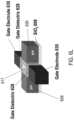
- a 3D semiconductor deviceincluding: a first level including a plurality of first metal layers; a second level, where the second level overlays the first level, where the second level includes at least one single crystal silicon layer, where the second level includes a plurality of transistors, where each transistor of the plurality of transistors includes a single crystal channel, where the second level includes a plurality of second metal layers, where the plurality of second metal layers include interconnections between the transistors of the plurality of transistors, and where the second level is overlaid by a first isolation layer; and a connective path between the plurality of transistors and the plurality of first metal layers, where the connective path includes a via disposed through at least the single crystal silicon layer, and where at least one of the plurality of transistors includes a gate all around structure.
- a 3D semiconductor deviceincluding: a first level including a plurality of first metal layers; a second level, where the second level overlays the first level, where the second level includes at least one single crystal silicon layer, where the second level includes a plurality of transistors, where each transistor of the plurality of transistors includes a single crystal channel, where the second level includes a plurality of second metal layers, where the plurality of second metal layers include interconnections between the transistors of the plurality of transistors, and where the second level is overlaid by a first isolation layer; and a connective path between the plurality of transistors and the plurality of first metal layers, where the connective path includes a via disposed through at least the single crystal silicon layer, and where the transistors of the plurality of transistors are aligned to the first metal layers with a less than 40 nm alignment error.
- a 3D semiconductor deviceincluding: a first level including a plurality of first metal layers; a second level, where the second level overlays the first level, where the second level includes at least one single crystal silicon layer, where the second level includes a plurality of transistors, where each transistor of the plurality of transistors includes a single crystal channel, where the second level includes a plurality of second metal layers, where the plurality of second metal layers include interconnections between the transistors of the plurality of transistors, and where the second level is overlaid by a first isolation layer; and a connective path between the plurality of transistors and the plurality of first metal layers, where the connective path includes a via disposed through at least the single crystal silicon layer, and where at least one of the plurality of transistors includes a first single crystal channel and an overlaying second single crystal channel.
- a 3D semiconductor deviceincluding: a first level comprising a single crystal silicon layer and a plurality of first transistors, said plurality of first transistors each comprising a single crystal channel; a first metal layer overlaying said plurality of first transistors; a second metal layer overlaying said first metal layer; a third metal layer overlaying said second metal layer; a second level, wherein said second level overlays said first level, wherein said second level comprises a plurality of second transistors; a fourth metal layer overlaying said second level; and a connective path between said fourth metal layer and either said third metal layer or said second metal layer, wherein said connective path comprises a via disposed through said second level, wherein said via has a diameter of less than 500 nm and greater than 5 nm, and wherein said third metal layer is connected to provide a power or ground signal to at least one of said plurality of second transistors.
- a 3D semiconductor deviceincluding: a first level comprising a single crystal silicon layer and a plurality of first transistors, said plurality of first transistors each comprising a single crystal channel; a first metal layer overlaying said plurality of first transistors; a second metal layer overlaying said first metal layer; a third metal layer overlaying said second metal layer; a second level, wherein said second level overlays said first level, wherein said second level comprises a plurality of second transistors; a fourth metal layer overlaying said second level; a connective path between said fourth metal layer and said third metal layer or said second metal layer, wherein said connective path comprises a via disposed through said second level, wherein said via has a diameter of less than 500 nm and greater than 5 nm, wherein at least one of said plurality of second transistors is vertically oriented, and wherein said third metal layer is connected to provide a power or a ground signal to at least one of said plurality of second transistors.
- a 3D semiconductor deviceincluding: a first level comprising a single crystal silicon layer and plurality of first transistors, said plurality of first transistors each comprising a single crystal channel; a first metal layer overlaying said plurality of first transistors; a second metal layer overlaying said first metal layer; a third metal layer overlaying said second metal layer; a second level, wherein said second level overlays said first level, wherein said second level comprises a plurality of second transistors; a fourth metal layer overlaying said second level; and a connective path between said fourth metal layer and said third metal layer or said second metal layer, wherein said connective path comprises a via disposed through said second level, wherein said via has a diameter of less than 500 nm and greater than 5 nm, wherein at least one of said plurality of second transistors comprises a metal gate, and wherein said third metal layer is connected to provide a power or a ground signal to at least one of said plurality of second transistors.
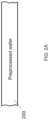
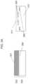
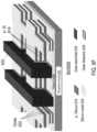
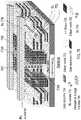
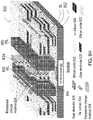
- FIG. 1is an exemplary drawing illustration of a layer transfer process flow
- FIGS. 2 A- 2 Hare exemplary drawing illustrations of the preprocessed wafers and layers and generalized layer transfer
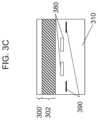
- FIGS. 3 A- 3 Dare exemplary drawing illustrations of a generalized layer transfer process flow
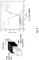
- FIG. 4is an exemplary drawing illustration and a transistor characteristic graph of a junction-less transistor
- FIGS. 5 A- 5 Bare exemplary device simulations of a junction-less transistor
- FIGS. 6 A- 6 K , 6 K 1 , 6 K 2 , and 6 Lare exemplary drawing illustrations of the formation of a floating body DRAM transistor and device
- FIGS. 7 A- 7 J , 7 J 1 , 7 J 2 , and 7 Kare exemplary drawing illustrations of the formation of a resistive memory transistor and device
- FIGS. 8 A- 8 J , 8 J 1 , 8 J 2 , and 8 Kare exemplary drawing illustrations of the formation of a resistive memory transistor and device
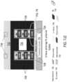
- FIG. 9is a block diagram representation of an exemplary mobile computing device (MCD).
- FIGS. 10 A- 10 Gare exemplary drawing illustrations of the formation of a charge trap memory transistor, array and device.
- FIG. 11 A- 11 Jare exemplary drawing illustrations of the formation of a junction-less transistor.
- process flows for building devicesmay be a sequence of steps for building a device. These process flows, which may be a sequence of steps for building a device, may have many structures, numerals and labels that may be common between two or more adjacent steps. In such cases, some labels, numerals and structures used for a certain step's figure may have been described in the previous steps' figures.
- acceptor substrate 100which may be a preprocessed CMOS silicon wafer, or a partially processed CMOS, or other prepared silicon or semiconductor substrate.
- CMOSmay include n-type transistors and p-type transistors.
- Acceptor substrate 100may include elements such as, for example, transistors, alignment marks, metal layers, and metal connection strips. The metal layers may be utilized to interconnect the transistors.
- the acceptor substratemay also be called target wafer.
- the acceptor substrate 100may be prepared for oxide to oxide wafer bonding by a deposition of an oxide 102 , and the acceptor substrate surface 104 may be made ready for low temperature bonding by various surface treatments, such as, for example, an RCA pre-clean that may include dilute ammonium hydroxide or hydrochloric acid, and may include plasma surface preparations, wherein gases such as oxygen, argon, and other gases or combinations of gases and plasma energies that changes the oxide surfaces so to lower the oxide to oxide bonding energy. In addition, polishes may be employed to achieve satisfactory flatness.
- an RCA pre-cleanthat may include dilute ammonium hydroxide or hydrochloric acid
- plasma surface preparationswherein gases such as oxygen, argon, and other gases or combinations of gases and plasma energies that changes the oxide surfaces so to lower the oxide to oxide bonding energy.
- polishesmay be employed to achieve satisfactory flatness.
- a donor wafer or substrate 110may be prepared for cleaving by an implant or implants of atomic species, such as, for example, Hydrogen and Helium, to form a layer transfer demarcation plane 199 , shown as a dashed line.
- Layer transfer demarcation plane 199may be formed before or after other processing on the donor wafer or substrate 110 .
- the donor wafer or substrate 110may be prepared for oxide to oxide wafer bonding by a deposition of an oxide 112 , and the donor wafer surface 114 may be made ready for low temperature bonding by various surface treatments, such as, for example, an RCA pre-clean that may include dilute ammonium hydroxide or hydrochloric acid, and may include plasma surface preparations, wherein gases such as oxygen, argon, and other gases or combinations of gases and plasma energies that change the oxide surfaces so to lower the oxide to oxide bonding energy. In addition, polishes may be employed to achieve satisfactory flatness.
- the donor wafer or substrate 110may have prefabricated layers, structures, alignment marks, transistors or circuits.
- Donor wafer or substrate 110may be bonded to acceptor substrate 100 , or target wafer, by bringing the donor wafer surface 114 in physical contact with acceptor substrate surface 104 , and then applying mechanical force and/or thermal annealing to strengthen the oxide to oxide bond. Alignment of the donor wafer or substrate 110 with the acceptor substrate 100 may be performed immediately prior to the wafer bonding. Acceptable bond strengths may be obtained with bonding thermal cycles that do not exceed approximately 400° C.
- the donor wafer or substrate 110may be cleaved at or near the layer transfer demarcation plane 199 and removed leaving transferred layer 120 bonded and attached to acceptor substrate 100 , or target wafer.
- the cleavingmay be accomplished by various applications of energy to the layer transfer demarcation plane, such as, for example, a mechanical strike by a knife, or jet of liquid or jet of air, or by local laser heating, or other suitable cleaving methods that propagate a fracture or separation approximately at the layer transfer demarcation plane 199 .
- the transferred layer 120may be polished chemically and mechanically to provide a suitable surface for further processing.
- the transferred layer 120may be of thickness approximately 200 nm or less to enable formation of nanometer sized thru layer vias and create a high density of interconnects between the donor wafer and acceptor wafer.
- the thinner the transferred layer 120the smaller the thru layer via diameter obtainable, as a result of maintaining manufacturable via aspect ratios.
- the transferred layer 120may be, for example, less than about 2 microns thick, less than about 1 micron thick, less than about 0.4 microns thick, less than about 200 nm thick, less than about 150 nm thick, or less than about 100 nm thick.
- the thickness of the layer or layers transferred according to some embodiments of the inventionmay be designed as such to match and enable the most suitable lithographic resolution capability of the manufacturing process employed to create the thru layer vias or any other structures on the transferred layer or layers.
- the donor wafer or substrate 110may now also be processed and reused for more layer transfers.
- Transferred layer 120may then be further processed to create a monolithic layer of interconnected devices 120 ′ and the formation of thru layer vias (TLVs, or through-layer vias) to electrically couple (connection path) donor wafer circuitry with acceptor wafer circuitry.
- TLVsthru layer vias
- Alignment marks in acceptor substrate 100 and/or in transferred layer 120may be utilized to contact transistors and circuitry in transferred layer 120 and electrically couple them to transistors and circuitry in the acceptor substrate 100 .
- an implanted atomic speciessuch as, for example, Hydrogen or Helium or a combination
- a cleaving planesuch as, for example, layer transfer demarcation plane 199
- the subsequent cleaving at or near the cleaving plane as described abovemay be referred to in this document as “ion-cut”, and may be the typically illustrated layer transfer method.
- the thickness of the TLVsmay be, for example, less than about 2 microns thick, less than about 1 micron thick, less than about 0.4 microns thick, less than about 200 nm thick, less than about 150 nm thick, or less than about 100 nm thick.
- TLVsmay be constructed mostly out of electrically conductive materials including, for example, copper, aluminum, conductive carbon, or tungsten.
- Barrier metalsincluding, for example, TiN and TaN, may be utilized to form TLVs.
- FIG. 1is exemplary only and are not drawn to scale.
- a heavily doped (greater than 1 e20 atoms/cm3) boron layer or a silicon germanium (SiGe) layermay be utilized as an etch stop layer either within the ion-cut process flow, wherein the layer transfer demarcation plane may be placed within the etch stop layer or into the substrate material below, or the etch stop layers may be utilized without an implant cleave or ion-cut process and the donor wafer may be preferentially etched away until the etch stop layer may be reached.
- the IBM's layer transfer methodemploys a SOI technology and utilizes glass handle wafers.
- the donor circuitmay be high-temperature processed on an SOI wafer, temporarily bonded to a borosilicate glass handle wafer, backside thinned by chemical mechanical polishing of the silicon and then the Buried Oxide (BOX) may be selectively etched off.
- the now thinned donor wafermay be subsequently aligned and low-temperature oxide-to-oxide bonded to the acceptor wafer topside.
- a low temperature release of the glass handle wafer from the thinned donor wafermay be next performed, and then thru layer via (or layer to layer) connections may be made.
- ELOepitaxial liftoff
- P. Demeester, et. al, of IMEC in Semiconductor Science Technology 1993may be utilized for layer transfer.
- ELOmakes use of the selective removal of a very thin sacrificial layer between the substrate and the layer structure to be transferred.
- the to-be-transferred layer of GaAs or siliconmay be adhesively ‘rolled’ up on a cylinder or removed from the substrate by utilizing a flexible carrier, such as, for example, black wax, to bow up the to-be-transferred layer structure when the selective etch, such as, for example, diluted Hydrofluoric (HF) Acid, etches the exposed release layer, such as, for example, the silicon oxide in SOI or a layer of AlAs. After liftoff, the transferred layer may be then aligned and bonded to the desired acceptor substrate or wafer.
- a flexible carriersuch as, for example, black wax
- ELTRANepitaxial Layer TRANsfer from porous silicon.
- ELTRANmay be utilized as a layer transfer method.
- the Electrochemical Society Meeting abstract No. 438 from year 2000 and the JSAP International July 2001 papershow a seed wafer being anodized in an HF/ethanol solution to create pores in the top layer of silicon, the pores may be treated with a low temperature oxidation and then high temperature hydrogen annealed to seal the pores.
- Epitaxial siliconmay then be deposited on top of the porous silicon and then oxidized to form the SOI BOX.
- the seed wafermay be bonded to a handle wafer and the seed wafer may be split off by high pressure water directed at the porous silicon layer.
- the porous siliconmay then be selectively etched off leaving a uniform silicon layer.
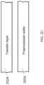
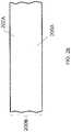
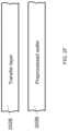
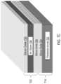
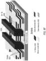
- FIG. 2 Ais a drawing illustration of a generalized preprocessed wafer or layer 200 .
- the wafer or layer 200may have preprocessed circuitry, such as, for example, logic circuitry, microprocessors, circuitry including transistors of various types, and other types of digital or analog circuitry including, but not limited to, the various embodiments described herein.
- Preprocessed wafer or layer 200may have preprocessed metal interconnects, such as, for example, of copper or aluminum.
- the preprocessed metal interconnectssuch as, for example, metal strips pads, or lines, may be designed and prepared for layer transfer and electrical coupling from preprocessed wafer or layer 200 to the layer or layers to be transferred.
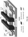
- FIG. 2 Bis a drawing illustration of a generalized transfer layer 202 prior to being attached to preprocessed wafer or layer 200 .
- Preprocessed wafer or layer 200may be called a target wafer or acceptor substrate.
- Transfer layer 202may be attached to a carrier wafer or substrate during layer transfer.
- Transfer layer 202may have metal interconnects, such as, for example, metal strips, pads, or lines, designed and prepared for layer transfer and electrical coupling to preprocessed wafer or layer 200 .
- Transfer layer 202which may also be called the second semiconductor layer, may include mono-crystalline silicon, or doped mono-crystalline silicon layer or layers, or other semiconductor, metal (including such as aluminum or copper interconnect layers), and insulator materials, layers; or multiple regions of single crystal silicon, or mono-crystalline silicon, or dope mono-crystalline silicon, or other semiconductor, metal, or insulator materials.
- a preprocessed wafer that can withstand subsequent processing of transistors on top at high temperaturesmay be a called the “Foundation” or a foundation wafer, layer or circuitry.
- the terms ‘mono-crystalline silicon’ and ‘single crystal silicon’may be used interchangeably.
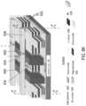
- FIG. 2 Cis a drawing illustration of a preprocessed wafer or layer 200 A created by the layer transfer of transfer layer 202 on top of preprocessed wafer or layer 200 .
- the top of preprocessed wafer or layer 200 Amay be further processed with metal interconnects, such as, for example, metal strips, pads, or lines, designed and prepared for layer transfer and electrical coupling from preprocessed wafer or layer 200 A to the next layer or layers to be transferred.
- FIG. 2 Dis a drawing illustration of a generalized transfer layer 202 A prior to being attached to preprocessed wafer or layer 200 A.
- Transfer layer 202 Amay be attached to a carrier wafer or substrate during layer transfer.
- Transfer layer 202 Amay have metal interconnects, such as, for example, metal strips, pads, or lines, designed and prepared for layer transfer and electrical coupling to preprocessed wafer or layer 200 A.
- Transfer layer 202 Amay include mono-crystalline silicon, or doped mono-crystalline silicon layer or layers, or other semiconductor, metal, and insulator materials, layers; or multiple regions of single crystal silicon, or mono-crystalline silicon, or dope mono-crystalline silicon, or other semiconductor, metal, or insulator materials.
- FIG. 2 Eis a drawing illustration of a preprocessed wafer or layer 200 B created by the layer transfer of transfer layer 202 A on top of preprocessed wafer or layer 200 A. Transfer layer 202 A may also be called the third semiconductor layer.
- the top of preprocessed wafer or layer 200 Bmay be further processed with metal interconnects, such as, for example, metal strips, pads, or lines, designed and prepared for layer transfer and electrical coupling from preprocessed wafer or layer 200 B to the next layer or layers to be transferred.
- FIG. 2 Fis a drawing illustration of a generalized transfer layer 202 B prior to being attached to preprocessed wafer or layer 200 B.
- Transfer layer 202 Bmay be attached to a carrier wafer or substrate during layer transfer.
- Transfer layer 202 Bmay have metal interconnects, such as, for example, metal strips, pads, or lines, designed and prepared for layer transfer and electrical coupling to preprocessed wafer or layer 200 B.
- Transfer layer 202 Bmay include mono-crystalline silicon, or doped mono-crystalline silicon layer or layers, or other semiconductor, metal, and insulator materials, layers; or multiple regions of single crystal silicon, or mono-crystalline silicon, or dope mono-crystalline silicon, or other semiconductor, metal, or insulator materials.
- FIG. 2 Gis a drawing illustration of preprocessed wafer or layer 200 C created by the layer transfer of transfer layer 202 B on top of preprocessed wafer or layer 200 B.
- the top of preprocessed wafer or layer 200 Cmay be further processed with metal interconnect, such as, for example, metal strips, pads, or lines, designed and prepared for layer transfer and electrical coupling from preprocessed wafer or layer 200 C to the next layer or layers to be transferred.
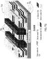
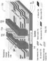
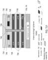
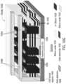
- FIG. 2 His a drawing illustration of preprocessed wafer or layer 200 C, a 3D IC stack, which may include transferred layers 202 A and 202 B on top of the original preprocessed wafer or layer 200 .
- Transferred layers 202 A and 202 B and the original preprocessed wafer or layer 200may include transistors of one or more types in one or more layers, metallization such as, for example, copper or aluminum in one or more layers, interconnections to and among layers above and below (connection paths, such as TLVs or TSVs), and interconnections within the layer.
- the transistorsmay be of various types that may be different from layer to layer or within the same layer.
- the transistorsmay be in various organized patterns.
- the transistorsmay be in various pattern repeats or bands.
- the transistorsmay be in multiple layers involved in the transfer layer.
- the transistorsmay be, for example, junction-less transistors or recessed channel transistors or other types of transistors described in this document.
- Transferred layers 202 A and 202 B and the original preprocessed wafer or layer 200may further include semiconductor devices such as, for example, resistors and capacitors and inductors, one or more programmable interconnects, memory structures and devices, sensors, radio frequency devices, or optical interconnect with associated transceivers.
- semiconductor devicessuch as, for example, resistors and capacitors and inductors, one or more programmable interconnects, memory structures and devices, sensors, radio frequency devices, or optical interconnect with associated transceivers.
- carrier wafer or carrier substratemay also be called holder wafer or holder substrate.
- This layer transfer processcan be repeated many times, thereby creating preprocessed wafers that may include many different transferred layers which, when combined, can then become preprocessed wafers or layers for future transfers.
- This layer transfer processmay be sufficiently flexible that preprocessed wafers and transfer layers, if properly prepared, can be flipped over and processed on either side with further transfers in either direction as a matter of design choice.
- FIGS. 2 A through 2 Hare exemplary only and are not drawn to scale.
- the preprocessed wafer or layer 200may act as a base or substrate layer in a wafer transfer flow, or as a preprocessed or partially preprocessed circuitry acceptor wafer in a wafer transfer process flow.
- the inventionis to be limited only by the appended claims.
- the high-k metal gate structuremay be formed as follows. Following an industry standard HF/SC1/SC2 cleaning to create an atomically smooth surface, a high-k dielectric may be deposited.
- the semiconductor industryhas chosen Hafnium-based dielectrics as the leading material of choice to replace SiO 2 and Silicon oxynitride.
- the Hafnium-based family of dielectricsincludes hafnium oxide and hafnium silicate/hafnium silicon oxynitride.
- Hafnium oxide, HfO 2may have a dielectric constant twice as much as that of hafnium silicate/hafnium silicon oxynitride (HfSiO/HfSiON k ⁇ 15).
- the choice of the metalmay be critical for the device to perform properly.
- a metal replacing N + poly as the gate electrodemay need to have a work function of approximately 4.2 eV for the device to operate properly and at the right threshold voltage.
- a metal replacing P + poly as the gate electrodemay need to have a work function of approximately 5.2 eV to operate properly.
- a low temperature gate stackmay be formed with a gate oxide formed by a microwave oxidation technique, such as, for example, the TEL SPA (Tokyo Electron Limited Slot Plane Antenna) oxygen radical plasma, that grows or deposits a low temperature Gate Dielectric to serve as the MOSFET gate oxide, or an atomic layer deposition (ALD) deposition technique may be utilized.
- a metal gate of proper work functionsuch as, for example, aluminum or tungsten, or low temperature doped amorphous silicon gate electrode, may then be deposited.
- Transistors constructed in this documentcan be considered “planar transistors” when the current flow in the transistor channel may be substantially in the horizontal direction.
- the horizontal directionmay be defined as the direction being parallel to the largest area of surface of the substrate or wafer that the transistor may be built or layer transferred onto. These transistors can also be referred to as horizontal transistors, horizontally oriented transistors, or lateral transistors.
- the horizontal transistormay be constructed in a two-dimensional plane where the source and the drain are in the same two dimensional horizontal plane.
- An embodiment of the inventionis to pre-process a donor wafer by forming wafer sized layers of various materials without a process temperature restriction, then layer transferring the pre-processed donor wafer to the acceptor wafer, and processing at either low temperature (below approximately 400° C.) or high temperature (greater than approximately 400° C.) after the layer transfer to form device structures, such as, for example, transistors and metal interconnect, on or in the donor wafer that may be physically aligned and may be electrically coupled or connected to the acceptor wafer.
- a wafer sized layerdenotes a continuous layer of material or combination of materials that may extend across the wafer to substantially the full extent of the wafer edges and may be approximately uniform in thickness. If the wafer sized layer compromises dopants, then the dopant concentration may be substantially the same in the x and y direction across the wafer, but can vary in the z direction perpendicular to the wafer surface.
- a generalized process flowmay begin with a donor wafer 300 that may be preprocessed with wafer sized layers 302 of conducting, semi-conducting or insulating materials that may be formed by deposition, ion implantation and anneal, oxidation, epitaxial growth, combinations of above, or other semiconductor processing steps and methods.
- the donor wafer 300may be preprocessed with a layer transfer demarcation plane (shown as dashed line) 399 , such as, for example, a hydrogen implant cleave plane, before or after layers 302 are formed.
- Acceptor wafer 310may be a preprocessed wafer that may have fully functional circuitry including metal layers (including aluminum or copper metal interconnect layers that may connect acceptor wafer 310 transistors) or may be a wafer with previously transferred layers, or may be a blank carrier or holder wafer, or other kinds of substrates suitable for layer transfer processing. Acceptor wafer 310 may have alignment marks 390 and metal connect pads or strips 380 . Acceptor wafer 310 and the donor wafer 300 may be a bulk mono-crystalline silicon wafer or a Silicon On Insulator (SOI) wafer or a Germanium on Insulator (GeOI) wafer.
- SOISilicon On Insulator
- GaOIGermanium on Insulator
- Both bonding surfaces 301 and 311may be prepared for wafer bonding by depositions, polishes, plasma, or wet chemistry treatments to facilitate successful wafer to wafer bonding.
- the donor wafer 300 with layers 302 and layer transfer demarcation plane 399may then be flipped over, aligned, and bonded to the acceptor wafer 310 .
- the donor wafer 300 with layers 302may have alignment marks (not shown).
- the donor wafer 300may be cleaved at or thinned to the layer transfer demarcation plane 399 , leaving a portion of the donor wafer 300 ′ and the pre-processed layers 302 bonded to the acceptor wafer 310 , by methods such as, for example, ion-cut or other layer transfer methods.
- Donor wafer device structures 350may include, for example, CMOS transistors such as N type and P type transistors, or any of the other transistor or device types discussed herein this document. These donor wafer device structures 350 may utilize thru layer vias (TLVs) 360 to electrically couple (connection paths) the donor wafer device structures 350 to the acceptor wafer metal connect pads or strips 380 . TLVs 360 may be formed through the transferred layers 302 .
- TLVsthru layer vias
- the TLVsmay be easily manufactured as a typical metal to metal via may be, and said TLV may have state of the art diameters such as nanometers or tens to a few hundreds of nanometers, such as, for example about 150 nm or about 100 nm or about 50 nm.
- the thinner the transferred layers 302the smaller the thru layer via diameter obtainable, which may result from maintaining manufacturable via aspect ratios.
- the transferred layers 302may be, for example, less than about 2 microns thick, less than about 1 micron thick, less than about 0.4 microns thick, less than about 200 nm thick, less than about 150 nm thick, or less than about 100 nm thick.
- the thickness of the layer or layers transferred according to some embodiments of the inventionmay be designed as such to match and enable the most suitable obtainable lithographic resolution, such as, for example, less than about 10 nm, 14 nm, 22 nm or 28 nm linewidth resolution and alignment capability, such as, for example, less than about 5 nm, 10 nm, 20 nm, or 40 nm alignment accuracy/precision/error, of the manufacturing process employed to create the thru layer vias or any other structures on the transferred layer or layers.
- Transferred layers 302may be considered to be overlying the metal layer or layers of acceptor wafer 310 .
- Alignment marks in acceptor substrate 310 and/or in transferred layers 302may be utilized to enable reliable contact to transistors and circuitry in transferred layers 302 and donor wafer device structures 350 and electrically couple them to the transistors and circuitry in the acceptor substrate 310 .
- the donor wafer 300may now also be processed and reused for more layer transfers.
- a transistor or other devicesmay be formed to enable a 3D IC.
- junction-less Transistorsare another transistor family that may utilize layer transfer and etch definition to construct a low-temperature monolithic 3D IC.
- the junction-less transistor structureavoids the increasingly sharply graded junctions necessary for sufficient separation between source and drain regions as silicon technology scales. This allows the JLT to have a thicker gate oxide than a conventional MOSFET for an equivalent performance.
- the junction-less transistormay also be known as a nanowire transistor without junctions, or gated resistor, or nanowire transistor as described in a paper by Jean-Pierre Colinge, et. al., (Colinge) published in Nature Nanotechnology on Feb. 21, 2010.
- the junction-less transistormay be constructed whereby the transistor channel may be a thin solid piece of evenly and heavily doped single crystal silicon.
- Single crystal siliconmay also be referred to as mono-crystalline silicon.
- the doping concentration of the channel underneath the gate 406 and gate dielectric 408may be identical to that of the source 404 and drain 402 .
- the channelmust be thin and narrow enough to allow for full depletion of the carriers when the device may be turned off. Additionally, the channel doping must be high enough to allow a reasonable current to flow when the device may be on.
- a multi-sided gatemay provide increased control of the channel.
- the JLTmay have a very small channel area (typically less than about 20 nm on one or more sides), so the gate can deplete the channel of charge carriers at approximately 0V and turn the source to drain current substantially off. I-V curves from Colinge of n channel and p channel junction-less transistors are shown in FIG. 4 . This illustrates that the JLT can obtain comparable performance to the tri-gate transistor (junction-ed) that may be commonly researched and reported by transistor developers.
- the channelmay be doped unevenly; whereby the heaviest doping may be closest to the gate or gates and the channel doping may be lighter farther away from the gate electrode.
- the cross-sectional center of a 2, 3, or 4 gate sided junction-less transistor channelmay be more lightly doped than the edges. This may enable much lower transistor off currents for the same gate work function and control.
- drain to source current (Ids) as a function of the gate voltage (Vg) for various junction-less transistor channel doping levelsmay be simulated where the total thickness of the n-type channel may be about 20 nm.
- the y-axis of FIG. 5 Ais plotted as logarithmic and FIG. 5 B as linear. Two of the four curves in each figure correspond to evenly doping the 20 nm channel thickness to 1 E17 and 1 E18 atoms/cm3, respectively. The remaining two curves show simulation results where the 20 nm channel has two layers of 10 nm thickness each.
- the first numbercorresponds to the 10 nm portion of the channel that is the closest to the gate electrode.
- FIG. 5 Billustrates that at a Vg of 1 volt, the Ids of both doping patterns are within a few percent of each other.
- the junction-less transistor channelmay be constructed with even, graded, or discrete layers of doping.
- the channelmay be constructed with materials other than doped mono-crystalline silicon, such as, for example, poly-crystalline silicon, or other semi-conducting, insulating, or conducting material, such as, for example, graphene or other graphitic material, and may be in combination with other layers of similar or different material.
- the center of the channelmay include a layer of oxide, or of lightly doped silicon, and the edges more heavily doped single crystal silicon. This may enhance the gate control effectiveness for the off state of the resistor, and may increase the on-current as a result of strain effects on the other layer or layers in the channel.
- Strain techniquesmay be employed from covering and insulator material above, below, and surrounding the transistor channel and gate.
- Lattice modifiersmay be employed to strain the silicon, such as, for example, an embedded SiGe implantation and anneal.
- the cross section of the transistor channelmay be rectangular, circular, or oval shaped, to enhance the gate control of the channel.
- the donor wafermay be rotated with respect to the acceptor wafer prior to bonding to facilitate the creation of the P-channel in the ⁇ 110> silicon plane direction or may include other silicon crystal orientations such as ⁇ 511>.
- 3D memory device structuresmay also be constructed in layers of mono-crystalline silicon and utilize pre-processing a donor wafer by forming wafer sized layers of various materials without a process temperature restriction, then layer transferring the pre-processed donor wafer to the acceptor wafer, followed by some processing steps, and repeating this procedure multiple times, and then processing with either low temperature (below approximately 400° C.) or high temperature (greater than approximately 400° C.) after the final layer transfer to form memory device structures, such as, for example, transistors, capacitors, resistors, or memristors, on or in the multiple transferred layers that may be physically aligned and may be electrically coupled to the acceptor wafer.
- pre-processing a donor waferby forming wafer sized layers of various materials without a process temperature restriction, then layer transferring the pre-processed donor wafer to the acceptor wafer, followed by some processing steps, and repeating this procedure multiple times, and then processing with either low temperature (below approximately 400° C.) or high temperature (greater
- Novel monolithic 3D Dynamic Random Access Memoriesmay be constructed in the above manner. Some embodiments of the invention utilize the floating body DRAM type.
- a horizontally-oriented monolithic 3D DRAMthat utilizes zero additional masking steps per memory layer by sharing mask steps after substantially all the layers have been transferred may be constructed that may be suitable for 3D IC manufacturing.
- a silicon substrate with peripheral circuitry 602may be constructed with high temperature (greater than approximately 400° C.) resistant wiring, such as, for example, Tungsten.
- the peripheral circuitry substrate 602may include memory control circuits as well as circuitry for other purposes and of various types, such as, for example, analog, digital, RF, or memory.
- the peripheral circuitry substrate 602may include peripheral circuits that can withstand an additional rapid-thermal-anneal (RTA) and still remain operational and retain good performance.
- RTArapid-thermal-anneal
- the peripheral circuitsmay be formed such that they have not been subjected to a weak RTA or no RTA for activating dopants in anticipation of anneals later in the process flow.
- the top surface of the peripheral circuitry substrate 602may be prepared for oxide wafer bonding with a deposition of a silicon oxide layer 604 , thus forming acceptor wafer 614 .
- a mono-crystalline silicon donor wafer 612may be processed to include a wafer sized layer of P ⁇ doping (not shown) which may have a different dopant concentration than the P ⁇ substrate 606 .
- the P ⁇ doping layermay be formed by ion implantation and thermal anneal.
- a screen oxide layer 608may be grown or deposited prior to the implant to protect the silicon from implant contamination and to provide an oxide surface for later wafer to wafer bonding.
- a layer transfer demarcation plane 610(shown as a dashed line) may be formed in donor wafer 612 within the P ⁇ substrate 606 or the P ⁇ doping layer (not shown) by hydrogen implantation or other methods as previously described.
- Both the donor wafer 612 and acceptor wafer 614may be prepared for wafer bonding as previously described and then bonded at the surfaces of oxide layer 604 and oxide layer 608 , for example, at a low temperature (less than approximately 400° C.) for lowest stresses, or a moderate temperature (less than approximately 900° C.).
- the portion of the P ⁇ layer (not shown) and the P ⁇ substrate 606 that may be above the layer transfer demarcation plane 610may be removed by cleaving and polishing, or other processes as previously described, such as, for example, ion-cut or other methods, thus forming the remaining mono-crystalline silicon P ⁇ layer 606 ′.
- Remaining P ⁇ layer 606 ′ and oxide layer 608have been layer transferred to acceptor wafer 614 .
- the top surface of P ⁇ layer 606 ′may be chemically or mechanically polished smooth and flat.
- transistors or portions of transistorsmay be formed and aligned to the acceptor wafer 614 alignment marks (not shown).
- Oxide layer 620may be deposited to prepare the surface for later oxide to oxide bonding. This now forms the first Si/SiO2 layer 623 which includes silicon oxide layer 620 , P ⁇ layer 606 ′, and oxide layer 608 .
- additional Si/SiO2 layerssuch as, for example, second Si/SiO2 layer 625 and third Si/SiO2 layer 627 , may each be formed as described in FIGS. 6 A to 6 C .
- Oxide layer 629may be deposited to electrically isolate the top silicon layer.
- oxide layer 629 , third Si/SiO2 layer 627 , second Si/SiO2 layer 625 and first Si/SiO2 layer 623may be lithographically defined and plasma/RIE etched to form a portion of the memory cell structure, which may include regions of P ⁇ silicon 616 and oxide 622 .
- a gate dielectric and gate electrode materialmay be deposited, planarized with a chemical mechanical polish (CMP), and then lithographically defined and plasma/RIE etched to form gate dielectric regions 628 which may either be self-aligned to and substantially covered by gate electrodes 630 (shown), or substantially cover the entire silicon/oxide multi-layer structure.
- CMPchemical mechanical polish
- the gate stack including gate electrode 630 and gate dielectric regions 628may be formed with a gate dielectric, such as, for example, thermal oxide, and a gate electrode material, such as, for example, poly-crystalline silicon.
- the gate dielectricmay be an atomic layer deposited (ALD) material that may be paired with a work function specific gate metal in the industry standard high k metal gate process schemes described previously. Further, the gate dielectric may be formed with a rapid thermal oxidation (RTO), a low temperature oxide deposition or low temperature microwave plasma oxidation of the silicon surfaces and then a gate electrode such as, for example, tungsten or aluminum may be deposited.
- ALDatomic layer deposited
- N+ silicon regions 626may be formed in a self-aligned manner to the gate electrodes 630 by ion implantation of an N type species, such as, for example, Arsenic, into the portions of P ⁇ silicon regions 616 that may not be blocked by the gate electrodes 630 . This forms remaining regions of P ⁇ silicon 617 (not shown) in the gate electrode 630 blocked areas.
- N type speciessuch as, for example, Arsenic
- Different implant energies or angles, or multiples of each,may be utilized to place the N type species into each layer of P ⁇ silicon regions 616 .
- Spacers(not shown) may be utilized during this multi-step implantation process and layers of silicon present in different layers of the stack may have different spacer widths to account for the differing lateral straggle of N type species implants.
- Bottom layerssuch as, for example, first Si/SiO2 layer 623 , could have larger spacer widths than top layers, such as, for example, third Si/SiO2 layer 627 .
- angular ion implantation with substrate rotationmay be utilized to compensate for the differing implant straggle.
- the top layer implantationmay have a steeper angle than perpendicular to the wafer surface and hence land ions slightly underneath the gate electrode 630 edges and closely match a more perpendicular lower layer implantation which may land ions slightly underneath the gate electrode 630 edge as a result of the straggle effects of the greater implant energy necessary to reach the lower layer.
- a rapid thermal annealmay be conducted to activate the dopants in substantially all of the memory layers 623 , 625 , 627 and in the peripheral circuitry substrate 602 .
- RTArapid thermal anneal
- optical annealssuch as, for example, a laser based anneal, may be performed.
- the entire structuremay be substantially covered with a gap fill oxide 632 , which be planarized with chemical mechanical polishing.
- the oxide 632is shown transparent in the figure for clarity.
- Word-line regions (WL) 650coupled with and composed of gate electrodes 630 , and source-line regions (SL) 652 , composed of indicated N+ silicon regions 626 , are shown.
- bit-line (BL) contacts 634may be lithographically defined, etched with plasma/RIE, photoresist removed, and then metal, such as, for example, copper, aluminum, or tungsten, may be deposited to fill the contact and etched or polished to the top of oxide 632 .
- Each BL contact 634may be shared among substantially all layers of memory, shown as three layers of memory in FIG. 6 I .
- a thru layer via(not shown) may be formed to electrically couple the BL, SL, and WL metallization to the acceptor wafer 614 peripheral circuitry via an acceptor wafer metal connect pad (not shown).
- BL metal lines 636may be formed and connect to the associated BL contacts 634 .
- Contacts and associated metal interconnect linesmay be formed for the WL and SL at the memory array edges.
- FIGS. 6 K , 6 K 1 and 6 K 2cross section cut II of FIG. 6 K is shown in FIG. 6 K 1
- cross section cut III of FIG. 6 Kis shown in FIG. 6 K 2
- BL metal lines 636 , oxide 632 , BL contact 634 , WL regions 650 , gate dielectric regions 628 , N+ silicon regions 626 , P ⁇ silicon regions 617 , and peripheral circuitry substrate 602are shown in FIG. 6 K 1 .
- the BL contact 634couples to one side of the three levels of floating body transistors that may include two N+ silicon regions 626 in each level with their associated P ⁇ silicon region 617 .
- BL metal lines 636 , oxide 632 , gate electrode 630 , gate dielectric regions 628 , P ⁇ silicon regions 617 , interlayer oxide region (‘ox’), and peripheral circuitry substrate 602are shown in FIG. 6 K 2 .
- the gate electrode 630may be common to substantially all six P ⁇ silicon regions 617 and forms six two-sided gated floating body transistors.
- a single exemplary floating body two gate transistor on the first Si/SiO2 layer 623may include P ⁇ silicon region 617 (functioning as the floating body transistor channel), N+ silicon regions 626 (functioning as source and drain), and two gate electrodes 630 with associated gate dielectric regions 628 .
- the transistormay be electrically isolated from beneath by oxide layer 608 .
- This flowenables the formation of a horizontally-oriented monolithic 3D DRAM that utilizes zero additional masking steps per memory layer and may be constructed by layer transfers of wafer sized doped mono-crystalline silicon layers and may be connected to an underlying multi-metal layer semiconductor device.
- FIGS. 6 A through 6 Lare exemplary only and are not drawn to scale.
- the transistorsmay be of another type such as RCATs, or junction-less.
- the contactsmay utilize doped poly-crystalline silicon, or other conductive materials.
- the stacked memory layermay be connected to a periphery circuit that may be above the memory stack.
- each gate of the double gate 3D DRAMcan be independently controlled for increased control of the memory cell.
- Novel monolithic 3D memory technologies utilizing material resistance changesmay be constructed in a similar manner.
- resistance-based memoriesincluding phase change memory, Metal Oxide memory, resistive RAM (RRAM), memristors, solid-electrolyte memory, ferroelectric RAM, and MRAM. Background information on these resistive-memory types is given in “Overview of candidate device technologies for storage-class memory,” IBM Journal of Research and Development , vol. 52, no. 4.5, pp. 449-464, July 2008 by Burr, G. W., et al. The contents of this document are incorporated in this specification by reference.
- a resistance-based zero additional masking steps per memory layer 3D memorymay be constructed that may be suitable for 3D IC manufacturing.
- This 3D memoryutilizes junction-less transistors and may have a resistance-based memory element in series with a select or access transistor.
- a silicon substrate with peripheral circuitry 702may be constructed with high temperature (greater than approximately 400° C.) resistant wiring, such as, for example, Tungsten.
- the peripheral circuitry substrate 702may include memory control circuits as well as circuitry for other purposes and of various types, such as, for example, analog, digital, RF, or memory.
- the peripheral circuitry substrate 702may include peripheral circuits that can withstand an additional rapid-thermal-anneal (RTA) and still remain operational and retain good performance.
- RTArapid-thermal-anneal
- the peripheral circuitsmay be formed such that they have not been subjected to a weak RTA or no RTA for activating dopants in anticipation of anneals later in the process flow.
- the top surface of the peripheral circuitry substrate 702may be prepared for oxide wafer bonding with a deposition of a silicon oxide layer 704 , thus forming acceptor wafer 714 .
- a mono-crystalline silicon donor wafer 712may be processed to include a wafer sized layer of N+ doping (not shown) which may have a different dopant concentration than the N+ substrate 706 .
- the N+ doping layermay be formed by ion implantation and thermal anneal.
- a screen oxide layer 708may be grown or deposited prior to the implant to protect the silicon from implant contamination and to provide an oxide surface for later wafer to wafer bonding.
- a layer transfer demarcation plane 710(shown as a dashed line) may be formed in donor wafer 712 within the N+ substrate 706 or the N+ doping layer (not shown) by hydrogen implantation or other methods as previously described.
- Both the donor wafer 712 and acceptor wafer 714may be prepared for wafer bonding as previously described and then bonded at the surfaces of oxide layer 704 and oxide layer 708 , for example, at a low temperature (less than approximately 400° C.) for lowest stresses, or a moderate temperature (less than approximately 900° C.).
- the portion of the N+ layer (not shown) and the N+ wafer substrate 706 that may be above the layer transfer demarcation plane 710may be removed by cleaving and polishing, or other processes as previously described, such as, for example, ion-cut or other methods, thus forming the remaining mono-crystalline silicon N+ layer 706 ′.
- Remaining N+ layer 706 ′ and oxide layer 708have been layer transferred to acceptor wafer 714 .
- the top surface of N+ layer 706 ′may be chemically or mechanically polished smooth and flat.
- transistors or portions of transistorsmay be formed and aligned to the acceptor wafer 714 alignment marks (not shown).
- Oxide layer 720may be deposited to prepare the surface for later oxide to oxide bonding. This now forms the first Si/SiO2 layer 723 which includes silicon oxide layer 720 , N+ silicon layer 706 ′, and oxide layer 708 .
- additional Si/SiO2 layerssuch as, for example, second Si/SiO2 layer 725 and third Si/SiO2 layer 727 , may each be formed as described in FIGS. 7 A to 7 C .
- Oxide layer 729may be deposited to electrically isolate the top N+ silicon layer.
- oxide layer 729 , third Si/SiO2 layer 727 , second Si/SiO2 layer 725 and first Si/SiO2 layer 723may be lithographically defined and plasma/RIE etched to form a portion of the memory cell structure, which now includes regions of N+ silicon 726 and oxide 722 .
- a gate dielectric and gate electrode materialmay be deposited, planarized with a chemical mechanical polish (CMP), and then lithographically defined and plasma/RIE etched to form gate dielectric regions 728 which may either be self-aligned to and substantially covered by gate electrodes 730 (shown), or substantially cover the entire N+ silicon 726 and oxide 722 multi-layer structure.
- the gate stack including gate electrodes 730 and gate dielectric regions 728may be formed with a gate dielectric, such as, for example, thermal oxide, and a gate electrode material, such as, for example, poly-crystalline silicon.
- the gate dielectricmay be an atomic layer deposited (ALD) material that may be paired with a work function specific gate metal in the industry standard high k metal gate process schemes described previously. Further, the gate dielectric may be formed with a rapid thermal oxidation (RTO), a low temperature oxide deposition or low temperature microwave plasma oxidation of the silicon surfaces and then a gate electrode such as, for example, tungsten or aluminum may be deposited.
- ALDatomic layer deposited
- the entire structuremay be substantially covered with a gap fill oxide 732 , which may be planarized with chemical mechanical polishing.
- the oxide 732is shown transparent in the figure for clarity.
- Word-line regions (WL) 750coupled with and composed of gate electrodes 730 , and source-line regions (SL) 752 , composed of N+ silicon regions 726 , are shown.
- bit-line (BL) contacts 734may be lithographically defined, etched with plasma/RIE through oxide 732 , the three N+ silicon regions 726 , and associated oxide vertical isolation regions to connect substantially all memory layers vertically, and photoresist removed.
- Resistance change material 738such as, for example, hafnium oxide, may then be deposited, for example, with atomic layer deposition (ALD).
- the electrode for the resistance change memory elementmay then be deposited by ALD to form the electrode/BL contact 734 .
- the excess deposited materialmay be polished to planarity at or below the top of oxide 732 .
- Each BL contact 734 with resistive change material 738may be shared among substantially all layers of memory, shown as three layers of memory in FIG. 7 H .
- BL metal lines 736may be formed and connect to the associated BL contacts 734 with resistive change material 738 .
- Contacts and associated metal interconnect linesmay be formed for the WL and SL at the memory array edges.
- a thru layer via(not shown) may be formed to electrically couple the BL, SL, and WL metallization to the acceptor wafer 714 peripheral circuitry via an acceptor wafer metal connect pad (not shown).
- FIGS. 7 J , 7 J 1 and 7 J 2cross section cut II of FIG. 7 J is shown in FIG. 7 J 1
- cross section cut III of FIG. 7 Jis shown in FIG. 7 J 2
- BL metal lines 736 , oxide 732 , BL contact/electrode 2534 , resistive change material 738 , WL regions 750 , gate dielectric regions 728 , N+ silicon regions 726 , and peripheral circuitry substrate 702are shown in FIG. 7 J 1 .
- the BL contact/electrode 2534couples to one side of the three levels of resistive change material 738 .
- the other side of the resistive change material 738may be coupled to N+ regions 726 .
- BL metal lines 736 , oxide 732 , gate electrodes 730 , gate dielectric regions 728 , N+ silicon regions 726 , interlayer oxide region (ox′), and peripheral circuitry substrate 702are shown in FIG. 7 J 2 .
- the gate electrode 730may be common to substantially all six N+ silicon regions 726 and forms six two-sided gated junction-less transistors as memory select transistors.
- a single exemplary two-sided gated junction-less transistor on the first Si/SiO2 layer 723may include N+ silicon region 726 (functioning as the source, drain, and transistor channel), and two gate electrodes 730 with associated gate dielectric regions 728 .
- the transistormay be electrically isolated from beneath by oxide layer 708 .
- This flowenables the formation of a resistance-based multi-layer or 3D memory array with zero additional masking steps per memory layer, which utilizes junction-less transistors and may have a resistance-based memory element in series with a select transistor, and may be constructed by layer transfers of wafer sized doped mono-crystalline silicon layers, and this 3D memory array may be connected to an underlying multi-metal layer semiconductor device.
- FIGS. 7 A through 7 Kare exemplary only and are not drawn to scale.
- the transistorsmay be of another type such as RCATs.
- doping of each N+ layermay be slightly different to compensate for interconnect resistances.
- the stacked memory layermay be connected to a periphery circuit that may be above the memory stack.
- each gate of the double gate 3D resistance based memorycan be independently controlled for increased control of the memory cell.
- a resistance-based 3D memory with zero additional masking steps per memory layermay be constructed with methods that may be suitable for 3D IC manufacturing.
- This 3D memoryutilizes poly-crystalline silicon junction-less transistors that may have either a positive or a negative threshold voltage and may have a resistance-based memory element in series with a select or access transistor.
- a silicon substrate with peripheral circuitry 802may be constructed with high temperature (greater than approximately 400° C.) resistant wiring, such as, for example, Tungsten.
- the peripheral circuitry substrate 802may include memory control circuits as well as circuitry for other purposes and of various types, such as, for example, analog, digital, RF, or memory.
- the peripheral circuitry substrate 802may include peripheral circuits that can withstand an additional rapid-thermal-anneal (RTA) and still remain operational and retain good performance.
- RTArapid-thermal-anneal
- the peripheral circuitsmay be formed such that they have not been subjected to a weak RTA or no RTA for activating dopants.
- Silicon oxide layer 804may be deposited on the top surface of the peripheral circuitry substrate.
- a layer of N+ doped poly-crystalline or amorphous silicon 806may be deposited.
- the amorphous silicon or poly-crystalline silicon layer 806may be deposited using a chemical vapor deposition process, such as, for example, LPCVD or PECVD, or other process methods, and may be deposited doped with N+ dopants, such as, for example, Arsenic or Phosphorous, or may be deposited un-doped and subsequently doped with, such as, for example, ion implantation or PLAD (PLasma Assisted Doping) techniques.
- Silicon Oxide 820may then be deposited or grown. This now forms the first Si/SiO2 layer 823 which includes N+ doped poly-crystalline or amorphous silicon layer 806 and silicon oxide layer 820 .
- additional Si/SiO2 layerssuch as, for example, second Si/SiO2 layer 825 and third Si/SiO2 layer 827 , may each be formed as described in FIG. 8 B .
- Oxide layer 829may be deposited to electrically isolate the top N+ doped poly-crystalline or amorphous silicon layer.
- a Rapid Thermal Annealmay be conducted to crystallize the N+ doped poly-crystalline silicon or amorphous silicon layers 806 of first Si/SiO2 layer 823 , second Si/SiO2 layer 825 , and third Si/SiO2 layer 827 , forming crystallized N+ silicon layers 816 .
- Temperatures during this RTAmay be as high as approximately 800° C.
- an optical annealsuch as, for example, a laser anneal, could be performed alone or in combination with the RTA or other annealing processes.
- oxide layer 829 , third Si/SiO2 layer 827 , second Si/SiO2 layer 825 and first Si/SiO2 layer 823may be lithographically defined and plasma/RIE etched to form a portion of the memory cell structure, which now includes multiple layers of regions of crystallized N+ silicon 826 (previously crystallized N+ silicon layers 816 ) and oxide 822 .
- a gate dielectric and gate electrode materialmay be deposited, planarized with a chemical mechanical polish (CMP), and then lithographically defined and plasma/RIE etched to form gate dielectric regions 828 which may either be self-aligned to and substantially covered by gate electrodes 830 (shown), or substantially cover the entire crystallized N+ silicon regions 826 and oxide regions 822 multi-layer structure.
- the gate stackmay include gate electrodes 830 and gate dielectric regions 828 , and may be formed with a gate dielectric, such as, for example, thermal oxide, and a gate electrode material, such as, for example, poly-crystalline silicon.
- the gate dielectricmay be an atomic layer deposited (ALD) material that may be paired with a work function specific gate metal in the industry standard high k metal gate process schemes described previously. Further, the gate dielectric may be formed with a rapid thermal oxidation (RTO), a low temperature oxide deposition or low temperature microwave plasma oxidation of the silicon surfaces and then a gate electrode such as, for example, tungsten or aluminum may be deposited.
- ALDatomic layer deposited
- the entire structuremay be substantially covered with a gap fill oxide 832 , which may be planarized with chemical mechanical polishing.
- the oxide 832is shown transparently in the figure for clarity.
- Word-line regions (WL) 850coupled with and composed of gate electrodes 830 , and source-line regions (SL) 852 , composed of crystallized N+ silicon regions 826 , are shown.
- bit-line (BL) contacts 834may be lithographically defined, etched with plasma/RIE through oxide 832 , the three crystallized N+ silicon regions 826 , and associated oxide vertical isolation regions to connect substantially all memory layers vertically, and photoresist removed.
- Resistance change material 838such as, for example, hafnium oxides or titanium oxides, may then be deposited, for example, with atomic layer deposition (ALD).
- ALDatomic layer deposition
- the electrode for the resistance change memory elementmay then be deposited by ALD to form the electrode/BL contact 834 .
- the excess deposited materialmay be polished to planarity at or below the top of oxide 832 .
- Each BL contact 834 with resistive change material 838may be shared among substantially all layers of memory, shown as three layers of memory in FIG. 8 H .
- BL metal lines 836may be formed and connect to the associated BL contacts 834 with resistive change material 838 .
- Contacts and associated metal interconnect linesmay be formed for the WL and SL at the memory array edges.
- Thru layer viasmay be formed to electrically couple the BL, SL, and WL metallization to the acceptor substrate peripheral circuitry via acceptor wafer metal connect pads (not shown).
- FIGS. 8 J , 8 J 1 and 8 J 2cross section cut II of FIG. 8 J is shown in FIG. 8 J 1
- cross section cut III of FIG. 8 Jis shown in FIG. 8 J 2
- BL metal line 836 , oxide 832 , BL contact/electrode 4934 , resistive change material 838 , WL regions 850 , gate dielectric regions 828 , crystallized N+ silicon regions 826 , and peripheral circuitry substrate 802are shown in FIG. 8 J 1 .
- the BL contact/electrode 4934couples to one side of the three levels of resistive change material 838 .
- the other side of the resistive change material 838may be coupled to crystallized N+ regions 826 .
- BL metal lines 836 , oxide 832 , gate electrode 830 , gate dielectric regions 828 , crystallized N+ silicon regions 826 , interlayer oxide region (‘ox’), and peripheral circuitry substrate 802are shown in FIG. 8 J 2 .
- the gate electrode 830may be common to substantially all six crystallized N+ silicon regions 826 and forms six two-sided gated junction-less transistors as memory select transistors.
- a single exemplary two-sided gated junction-less transistor on the first Si/SiO2 layer 823may include crystallized N+ silicon region 826 (functioning as the source, drain, and transistor channel), and two gate electrodes 830 with associated gate dielectric regions 828 .
- the transistormay be electrically isolated from beneath by oxide layer 808 .
- This flowenables the formation of a resistance-based multi-layer or 3D memory array with zero additional masking steps per memory layer, which utilizes poly-crystalline silicon junction-less transistors and may have a resistance-based memory element in series with a select transistor, and may be constructed by layer transfers of wafer sized doped poly-crystalline silicon layers, and this 3D memory array may be connected to an underlying multi-metal layer semiconductor device.
- FIGS. 8 A through 8 Kare exemplary only and are not drawn to scale. Such skilled persons will further appreciate that many variations are possible such as, for example, the RTAs and/or optical anneals of the N+ doped poly-crystalline or amorphous silicon layers 806 as described for FIG. 8 D may be performed after each Si/SiO2 layer is formed in FIG. 8 C . Additionally, N+ doped poly-crystalline or amorphous silicon layers 806 may be doped P+, or with a combination of dopants and other polysilicon network modifiers to enhance the RTA or optical annealing and subsequent crystallization and lower the N+ silicon layer 816 resistivity.
- each crystallized N+ layermay be slightly different to compensate for interconnect resistances.
- each gate of the double gated 3D resistance based memorymay be independently controlled for increased control of the memory cell.
- Some embodiments of the inventionmay include alternative techniques to build IC (Integrated Circuit) devices including techniques and methods to construct 3D IC systems. Some embodiments of the invention may enable device solutions with far less power consumption than prior art. These device solutions could be very useful for the growing application of mobile electronic devices and mobile systems such as, for example, mobile phones, smart phone, and cameras, those mobile systems may also connect to the internet. For example, incorporating the 3D IC semiconductor devices according to some embodiments of the invention within these mobile electronic devices and mobile systems could provide superior mobile units that could operate much more efficiently and for a much longer time than with prior art technology.
- Smart mobile systemsmay be greatly enhanced by complex electronics at a limited power budget.
- the 3D technology described in the multiple embodiments of the inventionwould allow the construction of low power high complexity mobile electronic systems. For example, it would be possible to integrate into a small form function a complex logic circuit with high density high speed memory utilizing some of the 3D DRAM embodiments of the invention and add some non-volatile 3D NAND charge trap or RRAM described in some embodiments of the invention.
- the 3D image sensor described in the Ser. No. 12/903,862 applicationwould be very effective for day/night and multi-spectrum surveillance applications.
- the 3D image sensorcould be supported by integrated logic and memory such as, for example, a monolithic 3D IC with a combination of image processing and image compression logic and memory, both high speed memory such as 3D DRAM and high density non-volatile memory such as 3D NAND or RRAM or other memory, and other combinations.
- This street corner camera applicationwould require low power, low cost, and low size or any combination of these features, and could be highly benefitted from the 3D technologies described herein.
- 3D ICs according to some embodiments of the inventioncould enable electronic and semiconductor devices with much a higher performance as a result from the shorter interconnect as well as semiconductor devices with far more complexity via multiple levels of logic and providing the ability to repair or use redundancy.
- the achievable complexity of the semiconductor devices according to some embodiments of the inventioncould far exceed what may be practical with the prior art technology.
- Some embodiments of the inventionmay enable the design of state of the art electronic systems at a greatly reduced non-recurring engineering (NRE) cost by the use of high density 3D FPGAs or various forms of 3D array based ICs with reduced custom masks as described herein. These systems could be deployed in many products and in many market segments. Reduction of the NRE may enable new product family or application development and deployment early in the product lifecycle by lowering the risk of upfront investment prior to a market being developed. The above potential advantages may also be provided by various mixes such as reduced NRE using generic masks for layers of logic and other generic masks for layers of memories and building a very complex system using the repair technology to overcome the inherent yield difficulties.
- NREnon-recurring engineering
- Another form of mixcould be building a 3D FPGA and add on it 3D layers of customizable logic and memory so the end system could have field programmable logic on top of the factory customized logic.
- An end systemcould benefit from a memory devices utilizing the 3D memory of some embodiments of the invention together with high performance 3D FPGA of some of the embodiments of the invention together with high density 3D logic and so forth.
- Using devices that can use one or multiple elements according to some embodiments of the inventionmay allow for increased performance or lower power and other potential advantages resulting from the use of some embodiments of the inventions to provide the end system with a competitive edge.
- Such end systemcould be electronic based products or other types of systems that may include some level of embedded electronics, such as, for example, cars and remote controlled vehicles.
- the mobile wireless terminal devicehas become part of our life, as well as the Internet, and the mobile wireless terminal device may continue to have a more important role on a worldwide basis.
- the mobile phone networkis a network such as a GSM, GPRS, or WCDMA, 3G and 4G standards, and the network may allow mobile phones to communicate with each other.
- the base stationmay be for transmitting (and receiving) information to the mobile phone.
- a typical mobile phone systemmay include, for example, a processor, a flash memory, a static random access memory, a display, a removable memory, a radio frequency (RF) receiver/transmitter, an analog base band (ABB), a digital base band (DBB), an image sensor, a high-speed bi-directional interface, a keypad, a microphone, and a speaker.
- RFradio frequency
- ABBanalog base band
- DBBdigital base band
- a typical mobile phone systemmay include a multiplicity of an element, for example, two or more static random access memories, two or more displays, two or more RF receiver/transmitters, and so on.
- radios used in wireless communicationstypically may include several discrete RF circuit components.
- Some receiver architecturesmay employ superhetrodyne techniques.
- a superhetrodyne architecturean incoming signal may be frequency translated from its radio frequency (RF) to a lower intermediate frequency (IF).
- the signal at IFmay be subsequently translated to baseband where further digital signal processing or demodulation may take place.
- Receiver designsmay have multiple IF stages. The reason for using such a frequency translation scheme is that circuit design at the lower IF frequency may be more manageable for signal processing. It is at these IF frequencies that the selectivity of the receiver may be implemented, automatic gain control (AGC) may be introduced, etc.
- AGCautomatic gain control
- GSMGlobal System for Mobile communications
- GPRSGeneral Packet Radio Service
- EDGEEnhanced Data for GSM Evolution
- 4th Generation (4G) mobile systemsaim to provide broadband wireless access with nominal data rates of 100 Mbit/s.
- 4G systemsmay be based on the 3GPP LTE (Long Term Evolution) cellular standard, WiMax or Flash-OFDM wireless metropolitan area network technologies.
- the radio interface in these systemsmay be based on all-IP packet switching, MIMO diversity, multi-carrier modulation schemes, Dynamic Channel Assignment (DCA) and channel-dependent scheduling.
- DCADynamic Channel Assignment
- MCDMobile computing/communication device
- MCDis a device that may be a mobile communication device, such as a cell phone, or a mobile computer that performs wired and/or wireless communication via a connected wireless/wired network.
- the MCDmay include a combination of the functionality associated with both types of devices within a single standard device (e.g., a smart phones or personal digital assistant (PDA)) for use as both a communication device and a computing device.
- PDApersonal digital assistant
- MCD 900may be a desktop computer, a portable computing device, such as a laptop, personal digital assistant (PDA), a smart phone, and/or other types of electronic devices that may generally be considered processing devices.
- MCD 900may include at least one processor or central processing unit (CPU) 902 which may be connected to system memory 906 via system interconnect/bus 904 .
- CPU 902may include at least one digital signal processing unit (DSP).
- DSPdigital signal processing unit
- I/O controller 915Also connected to system interconnect/bus 904 may be input/output (I/O) controller 915 , which may provide connectivity and control for input devices, of which pointing device (or mouse) 916 and keyboard 917 are illustrated. I/O controller 915 may also provide connectivity and control for output devices, of which display 918 is illustrated. Additionally, a multimedia drive 919 (e.g., compact disk read/write (CDRW) or digital video disk (DVD) drive) and USB (universal serial bus) port 920 are illustrated, and may be coupled to I/O controller 915 .
- CDRWcompact disk read/write
- DVDdigital video disk
- USBuniversal serial bus
- Multimedia drive 919 and USB port 920may enable insertion of a removable storage device (e.g., optical disk or “thumb” drive) on which data/instructions/code may be stored and/or from which data/instructions/code may be retrieved.
- MCD 900may also include storage 922 , within/from which data/instructions/code may also be stored/retrieved.
- MCD 900may further include a global positioning system (GPS) or local position system (LPS) detection component 924 by which MCD 900 may be able to detect its current location (e.g., a geographical position) and movement of MCD 900 , in real time.
- GPSglobal positioning system
- LPSlocal position system
- MCD 900may include a network/communication interface 925 , by which MCD 900 may connect to one or more second communication devices 932 or to wireless service provider server 937 , or to a third party server 938 via one or more access/external communication networks, of which a wireless Communication Network 930 is provided as one example and the Internet 936 is provided as a second example. It is appreciated that MCD 900 may connect to third party server 938 through an initial connection with Communication Network 930 , which in turn may connect to third party server 938 via the Internet 936 .
- system memory 906or other storage (e.g., storage 922 ) and may be executed by CPU 902 .
- OSoperating system
- FIG. 908illustrated within system memory 906 are a number of software/firmware/logic components, including operating system (OS) 908 (e.g., Microsoft WindowsTM or Windows MobileTM, trademarks of Microsoft Corp, or GNUTM/LinuxTM, registered trademarks of the Free Software Foundation and The Linux Mark Institute, and AIXTM, registered trademark of International Business Machines), and (word processing and/or other) application(s) 909 .
- OSoperating system
- word processing and/or other application(s) 909e.g., Microsoft WindowsTM or Windows MobileTM, trademarks of Microsoft Corp, or GNUTM/LinuxTM, registered trademarks of the Free Software Foundation and The Linux Mark Institute
- AIXTMregistered trademark of International Business Machines
- STWSimultaneous Text Waiting
- DCPDynamic Area Code Pre-pending
- AEIAdvanced Editing and Interfacing
- STDUSafe Texting Device Usage
- MCD utility 910may, in some embodiments, be combined with one or more other software modules, including for example, word processing application(s) 909 and/or OS 908 to provide a single executable component, which then may provide the collective functions of each individual software component when the corresponding combined code of the single executable component is executed by CPU 902 .
- Each separate utility 111 / 112 / 113 / 114is illustrated and described as a standalone or separate software/firmware component/module, which provides specific functions, as described below.
- MCD utility 910may be acquired as an off-the-shelf or after-market or downloadable enhancement to existing program applications or device functions, such as voice call waiting functionality (not shown) and user interactive applications with editable content, such as, for example, an application within the Windows MobileTM suite of applications.
- MCD utility 910may be downloaded from a server or website of a wireless provider (e.g., wireless service provider server 937 ) or a third party server 938 , and either installed on MCD 900 or executed from the wireless service provider server 937 or third party server 913 .
- CPU 902may execute MCD utility 910 as well as OS 908 , which, in one embodiment, may support the user interface features of MCD utility 910 , such as generation of a graphical user interface (GUI), where required/supported within MCD utility code.
- MCD utility 910may generate/provide one or more GUIs to enable user interaction with, or manipulation of, functional features of MCD utility 910 and/or of MCD 900 .
- MCD utility 910may, in certain embodiments, enable certain hardware and firmware functions and may thus be generally referred to as MCD logic.
- MCD utility 910may be enabled as processing code/instructions/logic executing on DSP/CPU 902 and/or other device hardware, and the processor thus may complete the implementation of those function(s).
- the software code/instructions/logic provided by MCD utility 910may be code/logic for performing several (one or a plurality) of the following functions: (1) Simultaneous texting during ongoing voice communication providing a text waiting mode for both single number mobile communication devices and multiple number mobile communication devices; (2) Dynamic area code determination and automatic back-filling of area codes when a requested/desired voice or text communication is initiated without the area code while the mobile communication device is outside of its home-base area code toll area; (3) Enhanced editing functionality for applications on mobile computing devices; (4) Automatic toggle from manual texting mode to voice-to-text based communication mode on detection of high velocity movement of the mobile communication device; and (5) Enhanced e-
- MCD 900Utilizing monolithic 3D IC technology described herein and in related application Ser. Nos. 12/903,862, 12/903,847, 12/904,103 and 13/041,405 significant power and cost could be saved. Most of the elements in MCD 900 could be integrated in one 3D IC. Some of the MCD 900 elements may be logic functions which could utilize monolithic 3D transistors such as, for example, RCAT or Gate-Last. Some of the MCD 900 elements are storage devices and could be integrated on a 3D non-volatile memory device, such as, for example, 3D NAND or 3D RRAM, or volatile memory such as, for example, 3D DRAM or SRAM formed from RCAT or gate-last transistors, as been described herein.
- 3D non-volatile memory devicesuch as, for example, 3D NAND or 3D RRAM, or volatile memory such as, for example, 3D DRAM or SRAM formed from RCAT or gate-last transistors, as been described herein.
- Storage 922 elements formed in monolithic 3Dcould be integrated on top or under a logic layer to reduce power and space.
- Keyboard 917could be integrated as a touch screen or combination of image sensor and some light projection and could utilize structures described in some of the above mentioned related applications.
- the network/communication interface 925could utilize another layer of silicon optimized for RF and gigahertz speed analog circuits or even may be integrated on substrates, such as GaN, that may be a better fit for such circuits. As more and more transistors might be integrated to achieve a high complexity 3D IC system there might be a need to use some embodiments of the invention such as what were called repair and redundancy so to achieve good product yield.
- system elementsincluding non-mobile elements, such as the 3rd Party Server 938 , might also make use of some embodiments of the 3D IC inventions including repair and redundancy to achieve good product yield for high complexity and large integration. Such large integration may reduce power and cost of the end product which is most attractive and most desired by the system end-use customers.
- Some embodiments of the 3D IC inventioncould be used to integrate many of the MCD 900 blocks or elements into one or a few devices. As various blocks get tightly integrated, much of the power required to transfer signals between these elements may be reduced and similarly costs associated with these connections may be saved. Form factor may be compacted as the space associated with the individual substrate and the associated connections may be reduced by use of some embodiments of the 3D IC invention. For mobile device these may be very important competitive advantages. Some of these blocks might be better processed in different process flow or wafer fab location. For example the DSP/CPU 902 is a logic function that might use a logic process flow while the storage 922 might better be done using a NAND Flash technology process flow or wafer fab.
- An important advantage of some of the embodiments of the monolithic 3D inventionsmay be to allow some of the layers in the 3D structure to be processed using a logic process flow while another layer in the 3D structure might utilize a memory process flow, and then some other function the modems of the GPS or local position system (LPS) detection component 924 might use a high speed analog process flow or wafer fab.
- LPSlocal position system
- Charge trap NANDNon-volatile memory devices are another form of popular commercial non-volatile memories. Charge trap device store their charge in a charge trap layer, wherein this charge trap layer then influences the channel of a transistor.
- Background information on charge-trap memorycan be found in “Integrated Interconnect Technologies for 3D Nanoelectronic Systems”, Artech House, 2009 by Bakir and Meindl (“Bakir”), “A Highly Scalable 8-Layer 3D Vertical-Gate (VG) TFT NAND Flash Using Junction-Free Buried Channel BE-SONOS Device,” Symposium on VLSI Technology, 2010 by Hang-Ting Lue, et al., and “Introduction to Flash memory”, Proc. IEEE91, 489-502 (2003) by R. Bez, et al. Work described in Bakir utilized selective epitaxy, laser recrystallization, or polysilicon to form the transistor channel, which results in less than satisfactory transistor performance.
- the architectures shown in FIGS. 10 A- 10 Gmay be relevant for any type of charge-trap memory.
- a charge trap based 3D memory with zero additional masking steps per memory layer 3D memorymay be constructed that may be suitable for 3D IC manufacturing.
- This 3D memoryutilizes NAND strings of charge trap junction-less transistors with junction-less select transistors constructed in mono-crystalline silicon.
- a silicon substrate with peripheral circuitry 1002may be constructed with high temperature (greater than approximately 400° C.) resistant wiring, such as, for example, Tungsten.
- the peripheral circuitry substrate 1002may include memory control circuits as well as circuitry for other purposes and of various types, such as, for example, analog, digital, RF, or memory.
- the peripheral circuitry substrate 1002may include peripheral circuits that can withstand an additional rapid-thermal-anneal (RTA) and still remain operational and retain good performance.
- RTArapid-thermal-anneal
- the peripheral circuitsmay be formed such that they have not been subjected to a weak RTA or no RTA for activating dopants in anticipation of anneals later in the process flow.
- the top surface of the peripheral circuitry substrate 1002may be prepared for oxide wafer bonding with a deposition of a silicon oxide layer 1004 , thus forming acceptor wafer 1014 .
- a mono-crystalline silicon donor wafer 1012may be processed to include a wafer sized layer of N+ doping (not shown) which may have a different dopant concentration than the N+ substrate 1006 .
- the N+ doping layermay be formed by ion implantation and thermal anneal.
- a screen oxide layer 1008may be grown or deposited prior to the implant to protect the silicon from implant contamination and to provide an oxide surface for later wafer to wafer bonding.
- a layer transfer demarcation plane 1010(shown as a dashed line) may be formed in donor wafer 1012 within the N+ substrate 1006 or the N+ doping layer (not shown) by hydrogen implantation or other methods as previously described.
- Both the donor wafer 1012 and acceptor wafer 1014may be prepared for wafer bonding as previously described and then bonded at the surfaces of oxide layer 1004 and oxide layer 1008 , for example, at a low temperature (less than approximately 400° C.) for lowest stresses, or a moderate temperature (less than approximately 900° C.).
- the portion of the N+ layer (not shown) and the N+ wafer substrate 1006 that may be above the layer transfer demarcation plane 1010may be removed by cleaving and polishing, or other processes as previously described, such as, for example, ion-cut or other methods, thus forming the remaining mono-crystalline silicon N+ layer 1006 ′.
- Remaining N+ layer 1006 ′ and oxide layer 1008have been layer transferred to acceptor wafer 1014 .
- the top surface of N+ layer 1006 ′may be chemically or mechanically polished smooth and flat.
- Oxide layer 1020may be deposited to prepare the surface for later oxide to oxide bonding. This now forms the first Si/SiO2 layer 1023 which includes silicon oxide layer 1020 , N+ silicon layer 1006 ′, and oxide layer 1008 .
- additional Si/SiO2 layerssuch as, for example, second Si/SiO2 layer 1025 and third Si/SiO2 layer 1027 , may each be formed as described in FIGS. 10 A to 10 C .
- Oxide layer 1029may be deposited to electrically isolate the top N+ silicon layer.
- oxide layer 1029 , third Si/SiO2 layer 1027 , second Si/SiO2 layer 1025 and first Si/SiO2 layer 1023may be lithographically defined and plasma/RIE etched to form a portion of the memory cell structure, which now includes regions of N+ silicon 1026 and oxide 1022 .
- a gate stackmay be formed with growth or deposition of a charge trap gate dielectric layer, such as, for example, thermal oxide and silicon nitride layers (ONO: Oxide-Nitride-Oxide), and a gate metal electrode layer, such as, for example, doped or undoped poly-crystalline silicon.
- the gate metal electrode layermay then be planarized with chemical mechanical polishing.
- the charge trap gate dielectric layermay include silicon or III-V nano-crystals encased in an oxide.
- the select transistor gate area 1038may include a non-charge trap dielectric.
- the gate metal electrode regions 1030 and gate dielectric regions 1028 of both the NAND string area 1036 and select transistor gate area 1038may be lithographically defined and plasma/RIE etched.
- the entire structuremay be substantially covered with a gap fill oxide 1032 , which may be planarized with chemical mechanical polishing.
- the oxide 1032is shown transparent in the figure for clarity.
- Select metal lines 1046may be formed and connect to the associated select gate contacts 1034 .
- Contacts and associated metal interconnect lines(not shown) may be formed for the WL and SL at the memory array edges.
- Word-line regions (WL) 1036coupled with and composed of gate metal electrode regions 1030 , and bit-line regions (BL) 1052 , composed of indicated N+ silicon regions 1026 , are shown.
- Source regions 1044may be formed by trench contact etch and fill to couple to the N+ silicon regions on the source end of the NAND string.
- a thru layer via(not shown) may be formed to electrically couple the BL, SL, and WL metallization to the acceptor wafer 1014 peripheral circuitry via an acceptor wafer metal connect pad (not shown).
- This flowenables the formation of a charge trap based 3D memory with zero additional masking steps per memory layer constructed by layer transfers of wafer sized doped layers of mono-crystalline silicon and this 3D memory may be connected to an underlying multi-metal layer semiconductor device.
- FIGS. 10 A through 10 Gare exemplary only and are not drawn to scale. Such skilled persons will further appreciate that many variations are possible such as, for example, BL or SL contacts may be constructed in a staircase manner as described previously. Additionally, the stacked memory layer may be connected to a periphery circuit that may be above the memory stack. Moreover, each tier of memory could be configured with a slightly different donor wafer N+ layer doping profile. Further, the memory could be organized in a different manner, such as BL and SL interchanged, or where buried wiring for the memory array may be below the memory layers but above the periphery.
- 3D charge trap memoriesmay be constructed by layer transfer of mono-crystalline silicon; for example, those found in “A Highly Scalable 8-Layer 3D Vertical-Gate (VG) TFT NAND Flash Using Junction-Free Buried Channel BE-SONOS Device,” Symposium on VLSI Technology, 2010 by Hang-Ting Lue, et al. and “Multi-layered Vertical Gate NAND Flash overcoming stacking limit for terabit density storage”, Symposium on VLSI Technology, 2009 by W. Kim, S. Choi, et al. Many other modifications within the scope of the invention will suggest themselves to such skilled persons after reading this specification. Thus the invention is to be limited only by the appended claims.
- an n-channel 4-sided gated junction-less transistormay be constructed that may be suitable for 3D IC manufacturing.
- 4-sided gated JLTscan also be referred to as gate-all around JLTs or silicon nanowire JLTs.
- a P ⁇ (shown) or N ⁇ substrate donor wafer 1200may be processed to include wafer sized layers of N+ doped silicon 1202 and 1206 , and wafer sized layers of n+ SiGe 1204 and 1208 .
- Layers 1202 , 1204 , 1206 , and 1208may be grown epitaxially and may be carefully engineered in terms of thickness and stoichiometry to keep the defect density that may result from the lattice mismatch between Si and SiGe low.
- the stoichiometry of the SiGemay be unique to each SiGe layer to provide for different etch rates as may be described later.
- the top surface of P ⁇ substrate donor wafer 1200may be prepared for oxide wafer bonding with a deposition of an oxide 1213 . These processes may be done at temperatures above approximately 400° C. as the layer transfer to the processed substrate with metal interconnects has yet to be done.
- the N+ doping layers 1202 and 1206may have a doping concentration that may be more than 10 ⁇ the doping concentration of P ⁇ substrate donor wafer 1200 .
- a layer transfer demarcation plane 1299may be formed in P ⁇ substrate donor wafer 1200 by hydrogen implantation or other methods as previously described.
- both the P ⁇ substrate donor wafer 1200 and acceptor wafer 1210 top layers and surfacesmay be prepared for wafer bonding as previously described and then P ⁇ substrate donor wafer donor wafer 1200 may be flipped over, aligned to the acceptor wafer 1210 alignment marks (not shown) and bonded together at a low temperature (less than approximately 400° C.).
- Oxide 1213 from the donor wafer and the oxide of the surface of the acceptor wafer 1210may thus be atomically bonded together are designated as oxide 1214 .
- the portion of the P ⁇ donor wafer substrate 1200 that is above the layer transfer demarcation plane 1299may be removed by cleaving and polishing, or other low temperature processes as previously described, such as, for example, ion-cut or other layer transfer methods.
- a CMP processmay be used to remove the remaining P ⁇ layer until the N+ silicon layer 1202 may be reached.
- stacks of N+ silicon and n+ SiGe regions that may become transistor channels and gate areasmay be formed by lithographic definition and plasma/RIE etching of N+ silicon layers 1202 & 1206 and n+ SiGe layers 1204 & 1208 .
- the resultmay be stacks of n+ SiGe 1216 and N+ silicon 1218 regions.
- the isolation among stacksmay be filled with a low temperature gap fill oxide 1220 and chemically and mechanically polished (CMP'ed) flat. This may fully isolate the transistors from each other.
- CMP'edchemically and mechanically polished
- eventual ganged or common gate area 1230may be lithographically defined and oxide etched. This may expose the transistor channels and gate area stack sidewalls of alternating N+ silicon 1218 and n+ SiGe 1216 regions to the eventual ganged or common gate area 1230 . The stack ends are exposed in the illustration for clarity of understanding.
- the exposed n+ SiGe regions 1216may be removed by a selective etch recipe that does not attack the N+ silicon regions 1218 . This creates air gaps among the N+ silicon regions 1218 in the eventual ganged or common gate area 1230 .
- etching recipesare described in at least “High performance 5 nm radius twin silicon nanowire MOSFET (TSNWFET): Fabrication on bulk Si wafer, characteristics, and reliability,” in Proc. IEDMTech. Dig., 2005, pp. 717-720 by S. D. Suk, et al.
- n+ SiGe layers farthest from the top edgemay be stoichiometrically crafted such that the etch rate of the layer (now region) farthest from the top (such as n+ SiGe layer 1208 ) may etch slightly faster than the layer (now region) closer to the top (such as n+ SiGe layer 1204 ), thereby equalizing the eventual gate lengths of the two stacked transistors.
- the stack endsare exposed in the illustration for clarity of understanding.
- a step of reducing the surface roughness, rounding the edges, and thinning the diameter of the N+ silicon regions 1218 that may be exposed in the ganged or common gate areamay utilize a low temperature oxidation and subsequent HF etch removal of the oxide just formed. This step may be repeated multiple times. Hydrogen may be added to the oxidation or separately utilized as a plasma treatment to the exposed N+ silicon surfaces. The result may be a rounded silicon nanowire-like structure to form the eventual transistor gated channel 1236 . The stack ends are exposed in the illustration for clarity of understanding.
- a low temperature based Gate Dielectric(not shown in this Fig.) may be deposited and densified to serve as the junction-less transistor gate oxide.
- a low temperature microwave plasma oxidation of the eventual transistor gated channel 1236 silicon surfacesmay serve as the JLT gate oxide or an atomic layer deposition (ALD) technique may be utilized to form the HKMG gate oxide as previously described.
- ALDatomic layer deposition
- deposition of a low temperature gate material with proper work function and less than approximately 400° C. deposition temperature, such as, for example, P+ doped amorphous siliconmay be performed, to form gate 1212 .
- a HKMG gate structuremay be formed as described previously.
- a CMPmay be performed after the gate material deposition. The stack ends are exposed in the illustration for clarity of understanding.
- FIG. 11 Jillustrates the JLT transistor stack formed in FIG. 11 I with the oxide removed for clarity of viewing, and a cross-sectional cut I of FIG. 11 I .
- Gate 1212 and gate dielectric 1211surrounds the transistor gated channel 1236 and each ganged or common transistor stack may be isolated from one another by oxide 1222 .
- the source and drain connections of the transistor stackscan be made to the N+ Silicon 1218 and n+ SiGe 1216 regions that may not be covered by the gate 1212 .
- Contacts to the 4-sided gated JLT source, drain, and gatemay be made with conventional Back end of Line (BEOL) processing as described previously and coupling from the formed JLTs to the acceptor wafer may be accomplished with formation of a thru layer via connection to an acceptor wafer metal interconnect pad also described previously.
- BEOLBack end of Line
- This flowenables the formation of a mono-crystalline silicon channel 4-sided gated junction-less transistor that may be formed and connected to the underlying multi-metal layer semiconductor device without exposing the underlying devices to a high temperature.
- a p channel 4-sided gated JLTmay be constructed as above with the N+ silicon layers 1202 and 1208 formed as P+ doped, and the gate metals of gate 1212 may be of appropriate work function to shutoff the p channel at a gate voltage of zero.
- FIGS. 11 A- 11 Jillustrates the key steps involved in forming a four-sided gated JLT with 3D stacked components
- process steps and additional materials/regionssuch as a stressed oxide within the transistor isolation regions, to add strain to JLTs may be added.
- N+ SiGe layers 1204 and 1208may instead include p+ SiGe or undoped SiGe and the selective etchant formula adjusted.
- more than two layers of chips or circuitscan be 3D stacked.
- the channelmay be doped unevenly; whereby the heaviest doping may be closest to the gate or gates and the channel doping may be lighter farther away from the gate electrode.
- the cross-sectional center of a 2, 3, or 4 gate sided junction-less transistor channelmay be more lightly doped than the edges. This may enable much lower transistor off currents for the same gate work function and control.
Landscapes
- Engineering & Computer Science (AREA)
- Physics & Mathematics (AREA)
- Condensed Matter Physics & Semiconductors (AREA)
- General Physics & Mathematics (AREA)
- Computer Hardware Design (AREA)
- Microelectronics & Electronic Packaging (AREA)
- Power Engineering (AREA)
- Manufacturing & Machinery (AREA)
- General Engineering & Computer Science (AREA)
- Metal-Oxide And Bipolar Metal-Oxide Semiconductor Integrated Circuits (AREA)
Abstract
Description
This application is a continuation-in-part application of U.S. patent application Ser. No. 17/941,891 which was filed on Sep. 9, 2022, which is a continuation-in-part application of U.S. patent application Ser. No. 17/850,819 which was filed on Jun. 7, 2022 (now U.S. Pat. No. 11,476,181 issued on Oct. 18, 2022), which is a continuation-in-part application of U.S. patent application Ser. No. 17/492,577 which was filed on Oct. 2, 2021 (now U.S. Pat. No. 11,410,912 issued on Aug. 9, 2022), which is a continuation-in-part application of U.S. patent application Ser. No. 17/313,986, which was filed on May 6, 2021 (now U.S. Pat. No. 11,164,811 issued on Nov. 2, 2021), which is a continuation-in-part application of U.S. patent application Ser. No. 16/852,506, which was filed on Apr. 19, 2020 (now U.S. Pat. No. 11,088,050 issued on Aug. 10, 2021), which is a continuation-in-part application of U.S. patent application Ser. No. 16/536,606, which was filed on Aug. 9, 2019 (now U.S. Pat. No. 10,665,695 issued on May 26, 2020), which is a continuation-in-part application of U.S. patent application Ser. No. 16/004,404, which was filed on Jun. 10, 2018 (now U.S. Pat. No. 10,600,888 issued on Mar. 24, 2020), which is a continuation-in-part application of U.S. patent application Ser. No. 15/917,629, which was filed on Mar. 10, 2018 (now U.S. Pat. No. 10,038,073 issued on Jul. 31, 2018), which is a continuation-in-part application of U.S. patent application Ser. No. 15/622,124, which was filed on Jun. 14, 2017 (now U.S. Pat. No. 9,954,080 issued on Apr. 24, 2018), which is a continuation-in-part application of U.S. patent application Ser. No. 14/880,276, which was filed on Oct. 11, 2015 (now U.S. Pat. No. 9,691,869 issued on Jun. 27, 2017), which is a continuation-in-part application of U.S. patent application Ser. No. 14/472,108, which was filed on Aug. 28, 2014 (now U.S. Pat. No. 9,305,867 issued on Apr. 5, 2016), which is a continuation application of U.S. patent application Ser. No. 13/959,994, which was filed on Aug. 6, 2013 (now U.S. Pat. No. 8,836,073 issued on Sep. 25, 2014), which is a continuation application of U.S. patent application Ser. No. 13/441,923, which was filed on Apr. 9, 2012 (now U.S. Pat. No. 8,557,632 issued on Oct. 15, 2013); the entire contents of the foregoing are incorporated herein by reference.
This application relates to the general field of Integrated Circuit (IC) devices and fabrication methods, and more particularly to multilayer or Three Dimensional Integrated Circuit (3D IC) devices and fabrication methods.
Performance enhancements and cost reductions in generations of electronic device technology has generally been achieved by reducing the size of the device, resulting in an enhancement in device speed and a reduction in the area of the device, and hence, its cost. This may be generally referred to as ‘device scaling’. The dominant electronic device technology in use today may be the Metal-Oxide-Semiconductor field effect transistor (MOSFET) technology.
Performance and cost are driven by transistor scaling and the interconnection, or wiring, between those transistors. As the dimensions of the device elements have approached the nanometer scale, the interconnection wiring now dominates the performance, power, and density of integrated circuit devices as described in J. A. Davis, et. al., Proc. IEEE, vol. 89, no. 3, pp. 305-324, March 2001 (Davis).
Davis further teaches that three dimensional integrated circuits (3D ICs), i.e. electronic chips in which active layers of transistors are stacked one above the other, separated by insulating oxides and connected to each other by metal interconnect wires, may be the best way to continue Moore's Law, especially as device scaling slows, stops, or becomes too costly to continue. 3D integration would provide shorter interconnect wiring and hence improved performance, lower power consumption, and higher density devices.
One approach to a practical implementation of a 3D IC independently processes two fully interconnected integrated circuits including transistors and wiring, thins one of the wafers, bonds the two wafers together, and then makes electrical connections between the bonded wafers with Thru Silicon Vias (TSV) that may be fabricated prior to or after the bonding. This approach may be less than satisfactory as the density of TSVs may be limited, because they may require large landing pads for the TSVs to overcome the poor wafer to wafer alignment and to allow for the large (about one to ten micron) diameter of the TSVs as a result of the thickness of the wafers bonded together. Additionally, handling and processing thinned silicon wafers may be very difficult and prone to yield loss. Current prototypes of this approach only obtain TSV densities of 10,000s per chip, in comparison to the millions of interconnections currently obtainable within a single chip.
By utilizing Silicon On Insulator (SOI) wafers and glass handle wafers, A. W. Topol, et. al, in the IEDM Tech Digest, p363-5 (2005), describe attaining TSVs of tenths of microns. The TSV density may be still limited as a result from misalignment issues resulting from pre-forming the random circuitry on both wafers prior to wafer bonding. In addition, SOI wafers are more costly than bulk silicon wafers.
Another approach may be to monolithically build transistors on top of a wafer of interconnected transistors. The utility of this approach may be limited by the requirement to maintain the reliability of the high performance lower layer interconnect metallization, such as, for example, aluminum and copper, and low-k intermetal dielectrics, and hence limits the allowable temperature exposure to below approximately 400° C. Some of the processing steps to create useful transistor elements may require temperatures above about 700° C., such as activating semiconductor doping or crystallization of a previously deposited amorphous material such as silicon to create a poly-crystalline silicon (polysilicon or poly) layer. It may be very difficult to achieve high performance transistors with only low temperature processing and without mono-crystalline silicon channels. However, this approach may be useful to construct memory devices where the transistor performance may not be critical.
Bakir and Meindl in the textbook “Integrated Interconnect Technologies for 3D Nanosystems”, Artech House, 2009,Chapter 13, illustrate a 3D stacked Dynamic Random Access Memory (DRAM) where the silicon for the stacked transistors is produced using selective epitaxy technology or laser recrystallization. This concept may be unsatisfactory as the silicon processed in this manner may have a higher defect density when compared to single crystal silicon and hence may suffer in performance, stability, and control. It may also require higher temperatures than the underlying metallization or low-k intermetal dielectric could be exposed to without reliability concerns.
Sang-Yun Lee in U.S. Pat. No. 7,052,941 discloses methods to construct vertical transistors by preprocessing a single crystal silicon wafer with doping layers activated at high temperature, layer transferring the wafer to another wafer with preprocessed circuitry and metallization, and then forming vertical transistors from those doping layers with low temperature processing, such as etching silicon. This may be less than satisfactory as the semiconductor devices in the market today utilize horizontal or horizontally oriented transistors and it would be very difficult to convince the industry to move away from the horizontal. Additionally, the transistor performance may be less than satisfactory as a result from large parasitic capacitances and resistances in the vertical structures, and the lack of self-alignment of the transistor gate.
A key technology for 3D IC construction may be layer transfer, whereby a thin layer of a silicon wafer, called the donor wafer, may be transferred to another wafer, called the acceptor wafer, or target wafer. As described by L. DiCioccio, et. al., at ICICDT 2010pg 110, the transfer of a thin (about tens of microns to tens of nanometers) layer of mono-crystalline silicon at low temperatures (below approximately 400° C.) may be performed with low temperature direct oxide-oxide bonding, wafer thinning, and surface conditioning. This process is called “Smart Stacking” by Soitec (Crolles, France). In addition, the “SmartCut” process is a well understood technology used for fabrication of SOI wafers. The “SmartCut” process employs a hydrogen implant to enable cleaving of the donor wafer after the layer transfer. These processes with some variations and under different names may be commercially available from SiGen (Silicon Genesis Corporation, San Jose, Calif.). A room temperature wafer bonding process utilizing ion-beam preparation of the wafer surfaces in a vacuum has been recently demonstrated by Mitsubishi Heavy Industries Ltd., Tokyo, Japan. This process allows room temperature layer transfer.
There are many techniques to construct 3D stacked integrated circuits or chips including:
Through-silicon via (TSV) technology: Multiple layers of transistors (with or without wiring levels) can be constructed separately. Following this, they can be bonded to each other and connected to each other with through-silicon vias (TSVs).
Monolithic 3D technology: With this approach, multiple layers of transistors and wires can be monolithically constructed. Some monolithic 3D and 3DIC approaches are described in U.S. Pat. Nos. 8,273,610, 8,298,875, 8,362,482, 8,378,715, 8,379,458, 8,450,804, 8,557,632, 8,574,929, 8,581,349, 8,642,416, 8,669,778, 8,674,470, 8,687,399, 8,742,476, 8,803,206, 8,836,073, 8,902,663, 8,994,404, 9,023,688, 9,029,173, 9,030,858, 9,117,749, 9,142,553, 9,219,005, 9,385,058, 9,406,670, 9,460,978, 9,509,313, 9,640,531, 9,691,760, 9,711,407, 9,721,927, 9,799,761, 9,871,034, 9,953,870, 9,953,994, 10,014,292, 10,014,318, 10,515,981, 10,892,016; and pending U.S. Patent Application Publications and applications, Ser. Nos. 14/642,724, 15/150,395, 15/173,686, 16/337,665, 16/558,304, 16/649,660, 16/836,659, 17/151,867, 62/651,722; 62/681,249, 62/713,345, 62/770,751, 62/952,222, 62/824,288, 63/075,067, 63/091,307, 63/115,000, 63/220,443, 2021/0242189, 2020/0013791, 16/558,304; and PCT Applications (and Publications): PCT/US2010/052093, PCT/US2011/042071 (WO2012/015550), PCT/US2016/52726 (WO2017053329), PCT/US2017/052359 (WO2018/071143), PCT/US2018/016759 (WO2018144957), PCT/US2018/52332 (WO 2019/060798), PCT/US2021/44110, and PCT/US22/44165. The entire contents of all of the foregoing patents, publications, and applications are incorporated herein by reference.
Electro-Optics: There is also work done for integrated monolithic 3D including layers of different crystals, such as U.S. Pat. Nos. 8,283,215, 8,163,581, 8,753,913, 8,823,122, 9,197,804, 9,419,031, 9,941,319, 10,679,977, 10,943,934, 10,998,374, 11,063,071, and 11,133,344. The entire contents of all of the foregoing patents, publications, and applications are incorporated herein by reference.
In addition, the entire contents of U.S. Pat. Nos. 10,600,888, 10,038,073, 9,954,080, 9,691,869, 9,305,867, 8,836,073, 8,557,632, U.S. patent application publication 2019/0363179 and U.S. patent application Ser. No. 17/151,867 are incorporated herein by reference.
Additionally the 3D technology according to some embodiments of the invention may enable some very innovative IC alternatives with reduced development costs, increased yield, and other illustrative benefits.
The invention may be directed to multilayer or Three Dimensional Integrated Circuit (3D IC) devices and fabrication methods.
In one aspect, a 3D semiconductor device, the device including: a first level including a plurality of first metal layers; a second level, where the second level overlays the first level, where the second level includes at least one single crystal silicon layer, where the second level includes a plurality of transistors, where each transistor of the plurality of transistors includes a single crystal channel, where the second level includes a plurality of second metal layers, where the plurality of second metal layers include interconnections between the transistors of the plurality of transistors, and where the second level is overlaid by a first isolation layer; and a connective path between the plurality of transistors and the plurality of first metal layers, where the connective path includes a via disposed through at least the single crystal silicon layer, and where at least one of the plurality of transistors includes a gate all around structure.
In another aspect, a 3D semiconductor device, the device including: a first level including a plurality of first metal layers; a second level, where the second level overlays the first level, where the second level includes at least one single crystal silicon layer, where the second level includes a plurality of transistors, where each transistor of the plurality of transistors includes a single crystal channel, where the second level includes a plurality of second metal layers, where the plurality of second metal layers include interconnections between the transistors of the plurality of transistors, and where the second level is overlaid by a first isolation layer; and a connective path between the plurality of transistors and the plurality of first metal layers, where the connective path includes a via disposed through at least the single crystal silicon layer, and where the transistors of the plurality of transistors are aligned to the first metal layers with a less than 40 nm alignment error.
In another aspect, a 3D semiconductor device, the device including: a first level including a plurality of first metal layers; a second level, where the second level overlays the first level, where the second level includes at least one single crystal silicon layer, where the second level includes a plurality of transistors, where each transistor of the plurality of transistors includes a single crystal channel, where the second level includes a plurality of second metal layers, where the plurality of second metal layers include interconnections between the transistors of the plurality of transistors, and where the second level is overlaid by a first isolation layer; and a connective path between the plurality of transistors and the plurality of first metal layers, where the connective path includes a via disposed through at least the single crystal silicon layer, and where at least one of the plurality of transistors includes a first single crystal channel and an overlaying second single crystal channel.
In another aspect, a 3D semiconductor device, the device including: a first level comprising a single crystal silicon layer and a plurality of first transistors, said plurality of first transistors each comprising a single crystal channel; a first metal layer overlaying said plurality of first transistors; a second metal layer overlaying said first metal layer; a third metal layer overlaying said second metal layer; a second level, wherein said second level overlays said first level, wherein said second level comprises a plurality of second transistors; a fourth metal layer overlaying said second level; and a connective path between said fourth metal layer and either said third metal layer or said second metal layer, wherein said connective path comprises a via disposed through said second level, wherein said via has a diameter of less than 500 nm and greater than 5 nm, and wherein said third metal layer is connected to provide a power or ground signal to at least one of said plurality of second transistors.
In another aspect, a 3D semiconductor device, the device including: a first level comprising a single crystal silicon layer and a plurality of first transistors, said plurality of first transistors each comprising a single crystal channel; a first metal layer overlaying said plurality of first transistors; a second metal layer overlaying said first metal layer; a third metal layer overlaying said second metal layer; a second level, wherein said second level overlays said first level, wherein said second level comprises a plurality of second transistors; a fourth metal layer overlaying said second level; a connective path between said fourth metal layer and said third metal layer or said second metal layer, wherein said connective path comprises a via disposed through said second level, wherein said via has a diameter of less than 500 nm and greater than 5 nm, wherein at least one of said plurality of second transistors is vertically oriented, and wherein said third metal layer is connected to provide a power or a ground signal to at least one of said plurality of second transistors.
In another aspect, a 3D semiconductor device, the device including: a first level comprising a single crystal silicon layer and plurality of first transistors, said plurality of first transistors each comprising a single crystal channel; a first metal layer overlaying said plurality of first transistors; a second metal layer overlaying said first metal layer; a third metal layer overlaying said second metal layer; a second level, wherein said second level overlays said first level, wherein said second level comprises a plurality of second transistors; a fourth metal layer overlaying said second level; and a connective path between said fourth metal layer and said third metal layer or said second metal layer, wherein said connective path comprises a via disposed through said second level, wherein said via has a diameter of less than 500 nm and greater than 5 nm, wherein at least one of said plurality of second transistors comprises a metal gate, and wherein said third metal layer is connected to provide a power or a ground signal to at least one of said plurality of second transistors.
Various embodiments of the invention will be understood and appreciated more fully from the following detailed description, taken in conjunction with the drawings in which:
Some embodiments of the invention are described herein with reference to the drawing figures. Persons of ordinary skill in the art will appreciate that the description and figures illustrate rather than limit the invention and that in general the figures are not drawn to scale for clarity of presentation. Such skilled persons will also realize that many more embodiments are possible by applying the inventive principles contained herein and that such embodiments fall within the scope of the invention which is not to be limited except by the appended claims.
Many figures may describe process flows for building devices. These process flows, which may be a sequence of steps for building a device, may have many structures, numerals and labels that may be common between two or more adjacent steps. In such cases, some labels, numerals and structures used for a certain step's figure may have been described in the previous steps' figures.
As illustrated inFIG.1 , a generalized single layer transfer procedure that utilizes the above techniques may begin withacceptor substrate 100, which may be a preprocessed CMOS silicon wafer, or a partially processed CMOS, or other prepared silicon or semiconductor substrate. CMOS may include n-type transistors and p-type transistors.Acceptor substrate 100 may include elements such as, for example, transistors, alignment marks, metal layers, and metal connection strips. The metal layers may be utilized to interconnect the transistors. The acceptor substrate may also be called target wafer. Theacceptor substrate 100 may be prepared for oxide to oxide wafer bonding by a deposition of anoxide 102, and theacceptor substrate surface 104 may be made ready for low temperature bonding by various surface treatments, such as, for example, an RCA pre-clean that may include dilute ammonium hydroxide or hydrochloric acid, and may include plasma surface preparations, wherein gases such as oxygen, argon, and other gases or combinations of gases and plasma energies that changes the oxide surfaces so to lower the oxide to oxide bonding energy. In addition, polishes may be employed to achieve satisfactory flatness.
A donor wafer orsubstrate 110 may be prepared for cleaving by an implant or implants of atomic species, such as, for example, Hydrogen and Helium, to form a layertransfer demarcation plane 199, shown as a dashed line. Layertransfer demarcation plane 199 may be formed before or after other processing on the donor wafer orsubstrate 110. The donor wafer orsubstrate 110 may be prepared for oxide to oxide wafer bonding by a deposition of anoxide 112, and thedonor wafer surface 114 may be made ready for low temperature bonding by various surface treatments, such as, for example, an RCA pre-clean that may include dilute ammonium hydroxide or hydrochloric acid, and may include plasma surface preparations, wherein gases such as oxygen, argon, and other gases or combinations of gases and plasma energies that change the oxide surfaces so to lower the oxide to oxide bonding energy. In addition, polishes may be employed to achieve satisfactory flatness. The donor wafer orsubstrate 110 may have prefabricated layers, structures, alignment marks, transistors or circuits.
Donor wafer orsubstrate 110 may be bonded toacceptor substrate 100, or target wafer, by bringing thedonor wafer surface 114 in physical contact withacceptor substrate surface 104, and then applying mechanical force and/or thermal annealing to strengthen the oxide to oxide bond. Alignment of the donor wafer orsubstrate 110 with theacceptor substrate 100 may be performed immediately prior to the wafer bonding. Acceptable bond strengths may be obtained with bonding thermal cycles that do not exceed approximately 400° C.
The donor wafer orsubstrate 110 may be cleaved at or near the layertransfer demarcation plane 199 and removed leaving transferredlayer 120 bonded and attached toacceptor substrate 100, or target wafer. The cleaving may be accomplished by various applications of energy to the layer transfer demarcation plane, such as, for example, a mechanical strike by a knife, or jet of liquid or jet of air, or by local laser heating, or other suitable cleaving methods that propagate a fracture or separation approximately at the layertransfer demarcation plane 199. The transferredlayer 120 may be polished chemically and mechanically to provide a suitable surface for further processing. The transferredlayer 120 may be of thickness approximately 200 nm or less to enable formation of nanometer sized thru layer vias and create a high density of interconnects between the donor wafer and acceptor wafer. The thinner the transferredlayer 120, the smaller the thru layer via diameter obtainable, as a result of maintaining manufacturable via aspect ratios. Thus, the transferredlayer 120 may be, for example, less than about 2 microns thick, less than about 1 micron thick, less than about 0.4 microns thick, less than about 200 nm thick, less than about 150 nm thick, or less than about 100 nm thick. The thickness of the layer or layers transferred according to some embodiments of the invention may be designed as such to match and enable the most suitable lithographic resolution capability of the manufacturing process employed to create the thru layer vias or any other structures on the transferred layer or layers. The donor wafer orsubstrate 110 may now also be processed and reused for more layer transfers.
Transferredlayer 120 may then be further processed to create a monolithic layer ofinterconnected devices 120′ and the formation of thru layer vias (TLVs, or through-layer vias) to electrically couple (connection path) donor wafer circuitry with acceptor wafer circuitry. Alignment marks inacceptor substrate 100 and/or in transferredlayer 120 may be utilized to contact transistors and circuitry in transferredlayer 120 and electrically couple them to transistors and circuitry in theacceptor substrate 100. The use of an implanted atomic species, such as, for example, Hydrogen or Helium or a combination, to create a cleaving plane, such as, for example, layertransfer demarcation plane 199, and the subsequent cleaving at or near the cleaving plane as described above may be referred to in this document as “ion-cut”, and may be the typically illustrated layer transfer method. As the TLVs are formed through the transferredlayer 120, the thickness of the TLVs may be, for example, less than about 2 microns thick, less than about 1 micron thick, less than about 0.4 microns thick, less than about 200 nm thick, less than about 150 nm thick, or less than about 100 nm thick. TLVs may be constructed mostly out of electrically conductive materials including, for example, copper, aluminum, conductive carbon, or tungsten. Barrier metals, including, for example, TiN and TaN, may be utilized to form TLVs.
Persons of ordinary skill in the art will appreciate that the illustrations inFIG.1 are exemplary only and are not drawn to scale. Such skilled persons will further appreciate that many variations are possible such as, for example, a heavily doped (greater than 1 e20 atoms/cm3) boron layer or a silicon germanium (SiGe) layer may be utilized as an etch stop layer either within the ion-cut process flow, wherein the layer transfer demarcation plane may be placed within the etch stop layer or into the substrate material below, or the etch stop layers may be utilized without an implant cleave or ion-cut process and the donor wafer may be preferentially etched away until the etch stop layer may be reached. Such skilled persons will further appreciate that the oxide layer within an SOI or GeOI donor wafer may serve as the etch stop layer. Many other modifications within the scope of the invention will suggest themselves to such skilled persons after reading this specification. Thus the invention is to be limited only by the appended claims.
Alternatively, other technologies and techniques may be utilized for layer transfer as described in, for example, IBM's layer transfer method shown at IEDM 2005 by A. W. Topol, et. al. The IBM's layer transfer method employs a SOI technology and utilizes glass handle wafers. The donor circuit may be high-temperature processed on an SOI wafer, temporarily bonded to a borosilicate glass handle wafer, backside thinned by chemical mechanical polishing of the silicon and then the Buried Oxide (BOX) may be selectively etched off. The now thinned donor wafer may be subsequently aligned and low-temperature oxide-to-oxide bonded to the acceptor wafer topside. A low temperature release of the glass handle wafer from the thinned donor wafer may be next performed, and then thru layer via (or layer to layer) connections may be made.
Additionally, the inventors contemplate that other technology can be used. For example, an epitaxial liftoff (ELO) technology as shown by P. Demeester, et. al, of IMEC in Semiconductor Science Technology 1993 may be utilized for layer transfer. ELO makes use of the selective removal of a very thin sacrificial layer between the substrate and the layer structure to be transferred. The to-be-transferred layer of GaAs or silicon may be adhesively ‘rolled’ up on a cylinder or removed from the substrate by utilizing a flexible carrier, such as, for example, black wax, to bow up the to-be-transferred layer structure when the selective etch, such as, for example, diluted Hydrofluoric (HF) Acid, etches the exposed release layer, such as, for example, the silicon oxide in SOI or a layer of AlAs. After liftoff, the transferred layer may be then aligned and bonded to the desired acceptor substrate or wafer. The manufacturability of the ELO process for multilayer layer transfer use was recently improved by J. Yoon, et. al., of the University of Illinois at Urbana-Champaign as described in Nature May 20, 2010.
Canon developed a layer transfer technology called ELTRAN—Epitaxial Layer TRANsfer from porous silicon. ELTRAN may be utilized as a layer transfer method. The Electrochemical Society Meeting abstract No. 438 from year 2000 and the JSAP International July 2001 paper show a seed wafer being anodized in an HF/ethanol solution to create pores in the top layer of silicon, the pores may be treated with a low temperature oxidation and then high temperature hydrogen annealed to seal the pores. Epitaxial silicon may then be deposited on top of the porous silicon and then oxidized to form the SOI BOX. The seed wafer may be bonded to a handle wafer and the seed wafer may be split off by high pressure water directed at the porous silicon layer. The porous silicon may then be selectively etched off leaving a uniform silicon layer.
This layer transfer process can be repeated many times, thereby creating preprocessed wafers that may include many different transferred layers which, when combined, can then become preprocessed wafers or layers for future transfers. This layer transfer process may be sufficiently flexible that preprocessed wafers and transfer layers, if properly prepared, can be flipped over and processed on either side with further transfers in either direction as a matter of design choice.
Persons of ordinary skill in the art will appreciate that the illustrations inFIGS.2A through2H are exemplary only and are not drawn to scale. Such skilled persons will further appreciate that many variations are possible such as, for example, the preprocessed wafer orlayer 200 may act as a base or substrate layer in a wafer transfer flow, or as a preprocessed or partially preprocessed circuitry acceptor wafer in a wafer transfer process flow. Many other modifications within the scope of the invention will suggest themselves to such skilled persons after reading this specification. Thus the invention is to be limited only by the appended claims.
One industry method to form a low temperature gate stack may be called a high-k metal gate (HKMG) and may be referred to in later discussions. The high-k metal gate structure may be formed as follows. Following an industry standard HF/SC1/SC2 cleaning to create an atomically smooth surface, a high-k dielectric may be deposited. The semiconductor industry has chosen Hafnium-based dielectrics as the leading material of choice to replace SiO2and Silicon oxynitride. The Hafnium-based family of dielectrics includes hafnium oxide and hafnium silicate/hafnium silicon oxynitride. Hafnium oxide, HfO2, may have a dielectric constant twice as much as that of hafnium silicate/hafnium silicon oxynitride (HfSiO/HfSiON k˜15). The choice of the metal may be critical for the device to perform properly. A metal replacing N+ poly as the gate electrode may need to have a work function of approximately 4.2 eV for the device to operate properly and at the right threshold voltage. Alternatively, a metal replacing P+ poly as the gate electrode may need to have a work function of approximately 5.2 eV to operate properly. The TiAl and TiAlN based family of metals, for example, could be used to tune the work function of the metal from 4.2 eV to 5.2 eV.
Alternatively, a low temperature gate stack may be formed with a gate oxide formed by a microwave oxidation technique, such as, for example, the TEL SPA (Tokyo Electron Limited Slot Plane Antenna) oxygen radical plasma, that grows or deposits a low temperature Gate Dielectric to serve as the MOSFET gate oxide, or an atomic layer deposition (ALD) deposition technique may be utilized. A metal gate of proper work function, such as, for example, aluminum or tungsten, or low temperature doped amorphous silicon gate electrode, may then be deposited.
Transistors constructed in this document can be considered “planar transistors” when the current flow in the transistor channel may be substantially in the horizontal direction. The horizontal direction may be defined as the direction being parallel to the largest area of surface of the substrate or wafer that the transistor may be built or layer transferred onto. These transistors can also be referred to as horizontal transistors, horizontally oriented transistors, or lateral transistors. In some embodiments of the invention the horizontal transistor may be constructed in a two-dimensional plane where the source and the drain are in the same two dimensional horizontal plane.
An embodiment of the invention is to pre-process a donor wafer by forming wafer sized layers of various materials without a process temperature restriction, then layer transferring the pre-processed donor wafer to the acceptor wafer, and processing at either low temperature (below approximately 400° C.) or high temperature (greater than approximately 400° C.) after the layer transfer to form device structures, such as, for example, transistors and metal interconnect, on or in the donor wafer that may be physically aligned and may be electrically coupled or connected to the acceptor wafer. A wafer sized layer denotes a continuous layer of material or combination of materials that may extend across the wafer to substantially the full extent of the wafer edges and may be approximately uniform in thickness. If the wafer sized layer compromises dopants, then the dopant concentration may be substantially the same in the x and y direction across the wafer, but can vary in the z direction perpendicular to the wafer surface.
As illustrated inFIG.3A , a generalized process flow may begin with adonor wafer 300 that may be preprocessed with wafersized layers 302 of conducting, semi-conducting or insulating materials that may be formed by deposition, ion implantation and anneal, oxidation, epitaxial growth, combinations of above, or other semiconductor processing steps and methods. Thedonor wafer 300 may be preprocessed with a layer transfer demarcation plane (shown as dashed line)399, such as, for example, a hydrogen implant cleave plane, before or afterlayers 302 are formed.Acceptor wafer 310 may be a preprocessed wafer that may have fully functional circuitry including metal layers (including aluminum or copper metal interconnect layers that may connectacceptor wafer 310 transistors) or may be a wafer with previously transferred layers, or may be a blank carrier or holder wafer, or other kinds of substrates suitable for layer transfer processing.Acceptor wafer 310 may havealignment marks 390 and metal connect pads or strips380.Acceptor wafer 310 and thedonor wafer 300 may be a bulk mono-crystalline silicon wafer or a Silicon On Insulator (SOI) wafer or a Germanium on Insulator (GeOI) wafer.
Both bondingsurfaces
As illustrated inFIG.3B , thedonor wafer 300 withlayers 302 and layertransfer demarcation plane 399 may then be flipped over, aligned, and bonded to theacceptor wafer 310. Thedonor wafer 300 withlayers 302 may have alignment marks (not shown).
As illustrated inFIG.3C , thedonor wafer 300 may be cleaved at or thinned to the layertransfer demarcation plane 399, leaving a portion of thedonor wafer 300′ and thepre-processed layers 302 bonded to theacceptor wafer 310, by methods such as, for example, ion-cut or other layer transfer methods.
As illustrated inFIG.3D , the remainingdonor wafer portion 300′ may be removed by polishing or etching and the transferredlayers 302 may be further processed to create donorwafer device structures 350 that may be precisely aligned to the acceptor wafer alignment marks390. Donorwafer device structures 350 may include, for example, CMOS transistors such as N type and P type transistors, or any of the other transistor or device types discussed herein this document. These donorwafer device structures 350 may utilize thru layer vias (TLVs)360 to electrically couple (connection paths) the donorwafer device structures 350 to the acceptor wafer metal connect pads or strips380.TLVs 360 may be formed through the transferred layers302. As the transferredlayers 302 may be thin, on the order of about 200 nm or less in thickness, the TLVs may be easily manufactured as a typical metal to metal via may be, and said TLV may have state of the art diameters such as nanometers or tens to a few hundreds of nanometers, such as, for example about 150 nm or about 100 nm or about 50 nm. The thinner the transferredlayers 302, the smaller the thru layer via diameter obtainable, which may result from maintaining manufacturable via aspect ratios. Thus, the transferred layers302 (and hence, TLVs360) may be, for example, less than about 2 microns thick, less than about 1 micron thick, less than about 0.4 microns thick, less than about 200 nm thick, less than about 150 nm thick, or less than about 100 nm thick. The thickness of the layer or layers transferred according to some embodiments of the invention may be designed as such to match and enable the most suitable obtainable lithographic resolution, such as, for example, less than about 10 nm, 14 nm, 22 nm or 28 nm linewidth resolution and alignment capability, such as, for example, less than about 5 nm, 10 nm, 20 nm, or 40 nm alignment accuracy/precision/error, of the manufacturing process employed to create the thru layer vias or any other structures on the transferred layer or layers. Transferredlayers 302 may be considered to be overlying the metal layer or layers ofacceptor wafer 310. Alignment marks inacceptor substrate 310 and/or in transferredlayers 302 may be utilized to enable reliable contact to transistors and circuitry in transferredlayers 302 and donorwafer device structures 350 and electrically couple them to the transistors and circuitry in theacceptor substrate 310. Thedonor wafer 300 may now also be processed and reused for more layer transfers.
There may be multiple methods by which a transistor or other devices may be formed to enable a 3D IC.
Junction-less Transistors (JLTs) are another transistor family that may utilize layer transfer and etch definition to construct a low-temperature monolithic 3D IC. The junction-less transistor structure avoids the increasingly sharply graded junctions necessary for sufficient separation between source and drain regions as silicon technology scales. This allows the JLT to have a thicker gate oxide than a conventional MOSFET for an equivalent performance. The junction-less transistor may also be known as a nanowire transistor without junctions, or gated resistor, or nanowire transistor as described in a paper by Jean-Pierre Colinge, et. al., (Colinge) published in Nature Nanotechnology on Feb. 21, 2010.
As illustrated inFIG.4 the junction-less transistor may be constructed whereby the transistor channel may be a thin solid piece of evenly and heavily doped single crystal silicon. Single crystal silicon may also be referred to as mono-crystalline silicon. The doping concentration of the channel underneath thegate 406 andgate dielectric 408 may be identical to that of thesource 404 and drain402. As a result of the high channel doping, the channel must be thin and narrow enough to allow for full depletion of the carriers when the device may be turned off. Additionally, the channel doping must be high enough to allow a reasonable current to flow when the device may be on. A multi-sided gate may provide increased control of the channel. The JLT may have a very small channel area (typically less than about 20 nm on one or more sides), so the gate can deplete the channel of charge carriers at approximately 0V and turn the source to drain current substantially off. I-V curves from Colinge of n channel and p channel junction-less transistors are shown inFIG.4 . This illustrates that the JLT can obtain comparable performance to the tri-gate transistor (junction-ed) that may be commonly researched and reported by transistor developers.
Turning the channel off with minimal leakage at an approximately zero gate bias may be a major challenge for a junction-less transistor device. To enhance gate control over the transistor channel, the channel may be doped unevenly; whereby the heaviest doping may be closest to the gate or gates and the channel doping may be lighter farther away from the gate electrode. For example, the cross-sectional center of a 2, 3, or 4 gate sided junction-less transistor channel may be more lightly doped than the edges. This may enable much lower transistor off currents for the same gate work function and control.
As illustrated inFIGS.5A and5B , drain to source current (Ids) as a function of the gate voltage (Vg) for various junction-less transistor channel doping levels may be simulated where the total thickness of the n-type channel may be about 20 nm. The y-axis ofFIG.5A is plotted as logarithmic andFIG.5B as linear. Two of the four curves in each figure correspond to evenly doping the 20 nm channel thickness to 1 E17 and 1 E18 atoms/cm3, respectively. The remaining two curves show simulation results where the 20 nm channel has two layers of 10 nm thickness each. In the legend denotations for the remaining two curves, the first number corresponds to the 10 nm portion of the channel that is the closest to the gate electrode. For example, the curve D=1 E18/1 E17 illustrates the simulated results where the 10 nm channel portion doped at 1 E18 is closest to the gate electrode while the 10 nm channel portion doped at 1 E17 is farthest away from the gate electrode. InFIG.5A , curves502 and504 correspond to doping patterns of D=1 E18/1 E17 and D=1 E17/1 E18, respectively. According toFIG.5A , at a Vg of 0 volts, the off current for the doping pattern of D=1 E18/1 E17 is approximately 50 times lower than that of the reversed doping pattern of D=1 E17/1 E18. Likewise, inFIG.5B , curves506 and508 correspond to doping patterns of D=1 E18/1 E17 and D=1 E17/1 E18, respectively.FIG.5B illustrates that at a Vg of 1 volt, the Ids of both doping patterns are within a few percent of each other.
The junction-less transistor channel may be constructed with even, graded, or discrete layers of doping. The channel may be constructed with materials other than doped mono-crystalline silicon, such as, for example, poly-crystalline silicon, or other semi-conducting, insulating, or conducting material, such as, for example, graphene or other graphitic material, and may be in combination with other layers of similar or different material. For example, the center of the channel may include a layer of oxide, or of lightly doped silicon, and the edges more heavily doped single crystal silicon. This may enhance the gate control effectiveness for the off state of the resistor, and may increase the on-current as a result of strain effects on the other layer or layers in the channel. Strain techniques may be employed from covering and insulator material above, below, and surrounding the transistor channel and gate. Lattice modifiers may be employed to strain the silicon, such as, for example, an embedded SiGe implantation and anneal. The cross section of the transistor channel may be rectangular, circular, or oval shaped, to enhance the gate control of the channel. Alternatively, to optimize the mobility of the P-channel junction-less transistor in the 3D layer transfer method, the donor wafer may be rotated with respect to the acceptor wafer prior to bonding to facilitate the creation of the P-channel in the <110> silicon plane direction or may include other silicon crystal orientations such as <511>.
3D memory device structures may also be constructed in layers of mono-crystalline silicon and utilize pre-processing a donor wafer by forming wafer sized layers of various materials without a process temperature restriction, then layer transferring the pre-processed donor wafer to the acceptor wafer, followed by some processing steps, and repeating this procedure multiple times, and then processing with either low temperature (below approximately 400° C.) or high temperature (greater than approximately 400° C.) after the final layer transfer to form memory device structures, such as, for example, transistors, capacitors, resistors, or memristors, on or in the multiple transferred layers that may be physically aligned and may be electrically coupled to the acceptor wafer.
Novel monolithic 3D Dynamic Random Access Memories (DRAMs) may be constructed in the above manner. Some embodiments of the invention utilize the floating body DRAM type.
Further details of a floating body DRAM and its operation modes can be found in U.S. Pat. Nos. 7,541,616, 7,514,748, 7,499,358, 7,499,352, 7,492,632, 7,486,563, 7,477,540, and 7,476,939. Background information on floating body DRAM and its operation is given in “Floating Body RAM Technology and its Scalability to 32 nm Node and Beyond,”Electron Devices Meeting,2006. IEDM '06. International, vol., no., pp. 1-4, 11-13 Dec. 2006 by T. Shino, et. al.; “Overview and future challenges of floating body RAM (FBRAM) technology for 32 nm technology node and beyond”,Solid-State Electronics, Volume 53, Issue 7; “Papers Selected from the 38th European Solid-State Device Research Conference”—ESSDERC'08, July 2009, pages 676-683, ISSN 0038-1101, DOI: 10.1016/j.sse.2009.03.010 by Takeshi Hamamoto, et al.; “New Generation of Z-RAM,”Electron Devices Meeting,2007. IEDM2007. IEEE International, vol., no., pp. 925-928, 10-12 Dec. 2007 by Okhonin, S., et al. Prior art for constructing monolithic 3D DRAMs used planar transistors where crystalline silicon layers were formed with either selective epitaxy technology or laser recrystallization. Both selective epitaxy technology and laser recrystallization may not provide perfectly mono-crystalline silicon and often may require a high thermal budget. A description of these processes is given in the book entitled “Integrated Interconnect Technologies for 3D Nanoelectronic Systems” by Bakir and Meindl. The contents of these documents are incorporated in this specification by reference.
As illustrated inFIGS.6A to6L , a horizontally-oriented monolithic 3D DRAM that utilizes zero additional masking steps per memory layer by sharing mask steps after substantially all the layers have been transferred may be constructed that may be suitable for 3D IC manufacturing.
As illustrated inFIG.6A , a silicon substrate withperipheral circuitry 602 may be constructed with high temperature (greater than approximately 400° C.) resistant wiring, such as, for example, Tungsten. Theperipheral circuitry substrate 602 may include memory control circuits as well as circuitry for other purposes and of various types, such as, for example, analog, digital, RF, or memory. Theperipheral circuitry substrate 602 may include peripheral circuits that can withstand an additional rapid-thermal-anneal (RTA) and still remain operational and retain good performance. For this purpose, the peripheral circuits may be formed such that they have not been subjected to a weak RTA or no RTA for activating dopants in anticipation of anneals later in the process flow. The top surface of theperipheral circuitry substrate 602 may be prepared for oxide wafer bonding with a deposition of asilicon oxide layer 604, thus formingacceptor wafer 614.
As illustrated inFIG.6B , a mono-crystallinesilicon donor wafer 612 may be processed to include a wafer sized layer of P− doping (not shown) which may have a different dopant concentration than the P−substrate 606. The P− doping layer may be formed by ion implantation and thermal anneal. Ascreen oxide layer 608 may be grown or deposited prior to the implant to protect the silicon from implant contamination and to provide an oxide surface for later wafer to wafer bonding. A layer transfer demarcation plane610 (shown as a dashed line) may be formed indonor wafer 612 within the P−substrate 606 or the P− doping layer (not shown) by hydrogen implantation or other methods as previously described. Both thedonor wafer 612 andacceptor wafer 614 may be prepared for wafer bonding as previously described and then bonded at the surfaces ofoxide layer 604 andoxide layer 608, for example, at a low temperature (less than approximately 400° C.) for lowest stresses, or a moderate temperature (less than approximately 900° C.).
As illustrated inFIG.6C , the portion of the P− layer (not shown) and the P−substrate 606 that may be above the layertransfer demarcation plane 610 may be removed by cleaving and polishing, or other processes as previously described, such as, for example, ion-cut or other methods, thus forming the remaining mono-crystalline silicon P−layer 606′. Remaining P−layer 606′ andoxide layer 608 have been layer transferred toacceptor wafer 614. The top surface of P−layer 606′ may be chemically or mechanically polished smooth and flat. Now transistors or portions of transistors may be formed and aligned to theacceptor wafer 614 alignment marks (not shown).Oxide layer 620 may be deposited to prepare the surface for later oxide to oxide bonding. This now forms the first Si/SiO2 layer 623 which includessilicon oxide layer 620, P−layer 606′, andoxide layer 608.
As illustrated inFIG.6D , additional Si/SiO2 layers, such as, for example, second Si/SiO2 layer 625 and third Si/SiO2 layer 627, may each be formed as described inFIGS.6A to6C .Oxide layer 629 may be deposited to electrically isolate the top silicon layer.
As illustrated inFIG.6E ,oxide layer 629, third Si/SiO2 layer 627, second Si/SiO2 layer 625 and first Si/SiO2 layer 623 may be lithographically defined and plasma/RIE etched to form a portion of the memory cell structure, which may include regions of P−silicon 616 andoxide 622.
As illustrated inFIG.6F , a gate dielectric and gate electrode material may be deposited, planarized with a chemical mechanical polish (CMP), and then lithographically defined and plasma/RIE etched to form gatedielectric regions 628 which may either be self-aligned to and substantially covered by gate electrodes630 (shown), or substantially cover the entire silicon/oxide multi-layer structure. The gate stack includinggate electrode 630 and gatedielectric regions 628 may be formed with a gate dielectric, such as, for example, thermal oxide, and a gate electrode material, such as, for example, poly-crystalline silicon. Alternatively, the gate dielectric may be an atomic layer deposited (ALD) material that may be paired with a work function specific gate metal in the industry standard high k metal gate process schemes described previously. Further, the gate dielectric may be formed with a rapid thermal oxidation (RTO), a low temperature oxide deposition or low temperature microwave plasma oxidation of the silicon surfaces and then a gate electrode such as, for example, tungsten or aluminum may be deposited.
As illustrated inFIG.6G ,N+ silicon regions 626 may be formed in a self-aligned manner to thegate electrodes 630 by ion implantation of an N type species, such as, for example, Arsenic, into the portions of P−silicon regions 616 that may not be blocked by thegate electrodes 630. This forms remaining regions of P− silicon617 (not shown) in thegate electrode 630 blocked areas. Different implant energies or angles, or multiples of each, may be utilized to place the N type species into each layer of P−silicon regions 616. Spacers (not shown) may be utilized during this multi-step implantation process and layers of silicon present in different layers of the stack may have different spacer widths to account for the differing lateral straggle of N type species implants. Bottom layers, such as, for example, first Si/SiO2 layer 623, could have larger spacer widths than top layers, such as, for example, third Si/SiO2 layer 627. Alternatively, angular ion implantation with substrate rotation may be utilized to compensate for the differing implant straggle. The top layer implantation may have a steeper angle than perpendicular to the wafer surface and hence land ions slightly underneath thegate electrode 630 edges and closely match a more perpendicular lower layer implantation which may land ions slightly underneath thegate electrode 630 edge as a result of the straggle effects of the greater implant energy necessary to reach the lower layer. A rapid thermal anneal (RTA) may be conducted to activate the dopants in substantially all of the memory layers623,625,627 and in theperipheral circuitry substrate 602. Alternatively, optical anneals, such as, for example, a laser based anneal, may be performed.
As illustrated inFIG.6H , the entire structure may be substantially covered with agap fill oxide 632, which be planarized with chemical mechanical polishing. Theoxide 632 is shown transparent in the figure for clarity. Word-line regions (WL)650, coupled with and composed ofgate electrodes 630, and source-line regions (SL)652, composed of indicatedN+ silicon regions 626, are shown.
As illustrated inFIG.6I , bit-line (BL)contacts 634 may be lithographically defined, etched with plasma/RIE, photoresist removed, and then metal, such as, for example, copper, aluminum, or tungsten, may be deposited to fill the contact and etched or polished to the top ofoxide 632. EachBL contact 634 may be shared among substantially all layers of memory, shown as three layers of memory inFIG.6I . A thru layer via (not shown) may be formed to electrically couple the BL, SL, and WL metallization to theacceptor wafer 614 peripheral circuitry via an acceptor wafer metal connect pad (not shown).
As illustrated inFIG.6J ,BL metal lines 636 may be formed and connect to the associatedBL contacts 634. Contacts and associated metal interconnect lines (not shown) may be formed for the WL and SL at the memory array edges.
As illustrated inFIGS.6K ,6K1 and6K2, cross section cut II ofFIG.6K is shown in FIG.6K1, and cross section cut III ofFIG.6K is shown in FIG.6K2.BL metal lines 636,oxide 632,BL contact 634,WL regions 650, gatedielectric regions 628,N+ silicon regions 626, P−silicon regions 617, andperipheral circuitry substrate 602 are shown in FIG.6K1. TheBL contact 634 couples to one side of the three levels of floating body transistors that may include twoN+ silicon regions 626 in each level with their associated P−silicon region 617.BL metal lines 636,oxide 632,gate electrode 630, gatedielectric regions 628, P−silicon regions 617, interlayer oxide region (‘ox’), andperipheral circuitry substrate 602 are shown in FIG.6K2. Thegate electrode 630 may be common to substantially all six P−silicon regions 617 and forms six two-sided gated floating body transistors.
As illustrated inFIG.6L , a single exemplary floating body two gate transistor on the first Si/SiO2 layer 623 may include P− silicon region617 (functioning as the floating body transistor channel), N+ silicon regions626 (functioning as source and drain), and twogate electrodes 630 with associated gatedielectric regions 628. The transistor may be electrically isolated from beneath byoxide layer 608.
This flow enables the formation of a horizontally-oriented monolithic 3D DRAM that utilizes zero additional masking steps per memory layer and may be constructed by layer transfers of wafer sized doped mono-crystalline silicon layers and may be connected to an underlying multi-metal layer semiconductor device.
Persons of ordinary skill in the art will appreciate that the illustrations inFIGS.6A through6L are exemplary only and are not drawn to scale. Such skilled persons will further appreciate that many variations are possible such as, for example, the transistors may be of another type such as RCATs, or junction-less. Additionally, the contacts may utilize doped poly-crystalline silicon, or other conductive materials. Moreover, the stacked memory layer may be connected to a periphery circuit that may be above the memory stack. Further, each gate of the double gate 3D DRAM can be independently controlled for increased control of the memory cell. Many other modifications within the scope of the invention will suggest themselves to such skilled persons after reading this specification. Thus the invention is to be limited only by the appended claims.
Novel monolithic 3D memory technologies utilizing material resistance changes may be constructed in a similar manner. There are many types of resistance-based memories including phase change memory, Metal Oxide memory, resistive RAM (RRAM), memristors, solid-electrolyte memory, ferroelectric RAM, and MRAM. Background information on these resistive-memory types is given in “Overview of candidate device technologies for storage-class memory,”IBM Journal of Research and Development, vol. 52, no. 4.5, pp. 449-464, July 2008 by Burr, G. W., et al. The contents of this document are incorporated in this specification by reference.
As illustrated inFIGS.7A to7K , a resistance-based zero additional masking steps per memory layer 3D memory may be constructed that may be suitable for 3D IC manufacturing. This 3D memory utilizes junction-less transistors and may have a resistance-based memory element in series with a select or access transistor.
As illustrated inFIG.7A , a silicon substrate withperipheral circuitry 702 may be constructed with high temperature (greater than approximately 400° C.) resistant wiring, such as, for example, Tungsten. Theperipheral circuitry substrate 702 may include memory control circuits as well as circuitry for other purposes and of various types, such as, for example, analog, digital, RF, or memory. Theperipheral circuitry substrate 702 may include peripheral circuits that can withstand an additional rapid-thermal-anneal (RTA) and still remain operational and retain good performance. For this purpose, the peripheral circuits may be formed such that they have not been subjected to a weak RTA or no RTA for activating dopants in anticipation of anneals later in the process flow. The top surface of theperipheral circuitry substrate 702 may be prepared for oxide wafer bonding with a deposition of asilicon oxide layer 704, thus formingacceptor wafer 714.
As illustrated inFIG.7B , a mono-crystallinesilicon donor wafer 712 may be processed to include a wafer sized layer of N+ doping (not shown) which may have a different dopant concentration than theN+ substrate 706. The N+ doping layer may be formed by ion implantation and thermal anneal. Ascreen oxide layer 708 may be grown or deposited prior to the implant to protect the silicon from implant contamination and to provide an oxide surface for later wafer to wafer bonding. A layer transfer demarcation plane710 (shown as a dashed line) may be formed indonor wafer 712 within theN+ substrate 706 or the N+ doping layer (not shown) by hydrogen implantation or other methods as previously described. Both thedonor wafer 712 andacceptor wafer 714 may be prepared for wafer bonding as previously described and then bonded at the surfaces ofoxide layer 704 andoxide layer 708, for example, at a low temperature (less than approximately 400° C.) for lowest stresses, or a moderate temperature (less than approximately 900° C.).
As illustrated inFIG.7C , the portion of the N+ layer (not shown) and theN+ wafer substrate 706 that may be above the layertransfer demarcation plane 710 may be removed by cleaving and polishing, or other processes as previously described, such as, for example, ion-cut or other methods, thus forming the remaining mono-crystallinesilicon N+ layer 706′. RemainingN+ layer 706′ andoxide layer 708 have been layer transferred toacceptor wafer 714. The top surface ofN+ layer 706′ may be chemically or mechanically polished smooth and flat. Now transistors or portions of transistors may be formed and aligned to theacceptor wafer 714 alignment marks (not shown).Oxide layer 720 may be deposited to prepare the surface for later oxide to oxide bonding. This now forms the first Si/SiO2 layer 723 which includessilicon oxide layer 720,N+ silicon layer 706′, andoxide layer 708.
As illustrated inFIG.7D , additional Si/SiO2 layers, such as, for example, second Si/SiO2 layer 725 and third Si/SiO2 layer 727, may each be formed as described inFIGS.7A to7C .Oxide layer 729 may be deposited to electrically isolate the top N+ silicon layer.
As illustrated inFIG.7E ,oxide layer 729, third Si/SiO2 layer 727, second Si/SiO2 layer 725 and first Si/SiO2 layer 723 may be lithographically defined and plasma/RIE etched to form a portion of the memory cell structure, which now includes regions ofN+ silicon 726 andoxide 722.
As illustrated inFIG.7F , a gate dielectric and gate electrode material may be deposited, planarized with a chemical mechanical polish (CMP), and then lithographically defined and plasma/RIE etched to form gatedielectric regions 728 which may either be self-aligned to and substantially covered by gate electrodes730 (shown), or substantially cover theentire N+ silicon 726 andoxide 722 multi-layer structure. The gate stack includinggate electrodes 730 and gatedielectric regions 728 may be formed with a gate dielectric, such as, for example, thermal oxide, and a gate electrode material, such as, for example, poly-crystalline silicon. Alternatively, the gate dielectric may be an atomic layer deposited (ALD) material that may be paired with a work function specific gate metal in the industry standard high k metal gate process schemes described previously. Further, the gate dielectric may be formed with a rapid thermal oxidation (RTO), a low temperature oxide deposition or low temperature microwave plasma oxidation of the silicon surfaces and then a gate electrode such as, for example, tungsten or aluminum may be deposited.
As illustrated inFIG.7G , the entire structure may be substantially covered with agap fill oxide 732, which may be planarized with chemical mechanical polishing. Theoxide 732 is shown transparent in the figure for clarity. Word-line regions (WL)750, coupled with and composed ofgate electrodes 730, and source-line regions (SL)752, composed ofN+ silicon regions 726, are shown.
As illustrated inFIG.7H , bit-line (BL)contacts 734 may be lithographically defined, etched with plasma/RIE throughoxide 732, the threeN+ silicon regions 726, and associated oxide vertical isolation regions to connect substantially all memory layers vertically, and photoresist removed.Resistance change material 738, such as, for example, hafnium oxide, may then be deposited, for example, with atomic layer deposition (ALD). The electrode for the resistance change memory element may then be deposited by ALD to form the electrode/BL contact 734. The excess deposited material may be polished to planarity at or below the top ofoxide 732. EachBL contact 734 withresistive change material 738 may be shared among substantially all layers of memory, shown as three layers of memory inFIG.7H .
As illustrated inFIG.7I ,BL metal lines 736 may be formed and connect to the associatedBL contacts 734 withresistive change material 738. Contacts and associated metal interconnect lines (not shown) may be formed for the WL and SL at the memory array edges. A thru layer via (not shown) may be formed to electrically couple the BL, SL, and WL metallization to theacceptor wafer 714 peripheral circuitry via an acceptor wafer metal connect pad (not shown).
As illustrated inFIGS.7J ,7J1 and7J2, cross section cut II ofFIG.7J is shown in FIG.7J1, and cross section cut III ofFIG.7J is shown in FIG.7J2.BL metal lines 736,oxide 732, BL contact/electrode2534,resistive change material 738,WL regions 750, gatedielectric regions 728,N+ silicon regions 726, andperipheral circuitry substrate 702 are shown in FIG.7J1. The BL contact/electrode2534 couples to one side of the three levels ofresistive change material 738. The other side of theresistive change material 738 may be coupled toN+ regions 726.BL metal lines 736,oxide 732,gate electrodes 730, gatedielectric regions 728,N+ silicon regions 726, interlayer oxide region (ox′), andperipheral circuitry substrate 702 are shown in FIG.7J2. Thegate electrode 730 may be common to substantially all sixN+ silicon regions 726 and forms six two-sided gated junction-less transistors as memory select transistors.
As illustrated inFIG.7K , a single exemplary two-sided gated junction-less transistor on the first Si/SiO2 layer 723 may include N+ silicon region726 (functioning as the source, drain, and transistor channel), and twogate electrodes 730 with associated gatedielectric regions 728. The transistor may be electrically isolated from beneath byoxide layer 708.
This flow enables the formation of a resistance-based multi-layer or 3D memory array with zero additional masking steps per memory layer, which utilizes junction-less transistors and may have a resistance-based memory element in series with a select transistor, and may be constructed by layer transfers of wafer sized doped mono-crystalline silicon layers, and this 3D memory array may be connected to an underlying multi-metal layer semiconductor device.
Persons of ordinary skill in the art will appreciate that the illustrations inFIGS.7A through7K are exemplary only and are not drawn to scale. Such skilled persons will further appreciate that many variations are possible such as, for example, the transistors may be of another type such as RCATs. Additionally, doping of each N+ layer may be slightly different to compensate for interconnect resistances. Moreover, the stacked memory layer may be connected to a periphery circuit that may be above the memory stack. Further, each gate of the double gate 3D resistance based memory can be independently controlled for increased control of the memory cell. Many other modifications within the scope of the invention will suggest themselves to such skilled persons after reading this specification. Thus the invention is to be limited only by the appended claims.
The monolithic 3D integration concepts described in this patent application can lead to novel embodiments of poly-crystalline silicon based memory architectures. While the below concepts inFIG.8 are explained by using resistive memory architectures as an example, it will be clear to one skilled in the art that similar concepts can be applied to the NAND flash, charge trap, and DRAM memory architectures and process flows described previously in this patent application and incorporated by reference co-owned applications.
As illustrated inFIGS.8A to8K , a resistance-based 3D memory with zero additional masking steps per memory layer may be constructed with methods that may be suitable for 3D IC manufacturing. This 3D memory utilizes poly-crystalline silicon junction-less transistors that may have either a positive or a negative threshold voltage and may have a resistance-based memory element in series with a select or access transistor.
As illustrated inFIG.8A , a silicon substrate withperipheral circuitry 802 may be constructed with high temperature (greater than approximately 400° C.) resistant wiring, such as, for example, Tungsten. Theperipheral circuitry substrate 802 may include memory control circuits as well as circuitry for other purposes and of various types, such as, for example, analog, digital, RF, or memory. Theperipheral circuitry substrate 802 may include peripheral circuits that can withstand an additional rapid-thermal-anneal (RTA) and still remain operational and retain good performance. For this purpose, the peripheral circuits may be formed such that they have not been subjected to a weak RTA or no RTA for activating dopants.Silicon oxide layer 804 may be deposited on the top surface of the peripheral circuitry substrate.
As illustrated inFIG.8B , a layer of N+ doped poly-crystalline oramorphous silicon 806 may be deposited. The amorphous silicon or poly-crystalline silicon layer 806 may be deposited using a chemical vapor deposition process, such as, for example, LPCVD or PECVD, or other process methods, and may be deposited doped with N+ dopants, such as, for example, Arsenic or Phosphorous, or may be deposited un-doped and subsequently doped with, such as, for example, ion implantation or PLAD (PLasma Assisted Doping) techniques.Silicon Oxide 820 may then be deposited or grown. This now forms the first Si/SiO2 layer 823 which includes N+ doped poly-crystalline oramorphous silicon layer 806 andsilicon oxide layer 820.
As illustrated inFIG.8C , additional Si/SiO2 layers, such as, for example, second Si/SiO2 layer 825 and third Si/SiO2 layer 827, may each be formed as described inFIG.8B .Oxide layer 829 may be deposited to electrically isolate the top N+ doped poly-crystalline or amorphous silicon layer.
As illustrated inFIG.8D , a Rapid Thermal Anneal (RTA) may be conducted to crystallize the N+ doped poly-crystalline silicon or amorphous silicon layers806 of first Si/SiO2 layer 823, second Si/SiO2 layer 825, and third Si/SiO2 layer 827, forming crystallized N+ silicon layers816. Temperatures during this RTA may be as high as approximately 800° C. Alternatively, an optical anneal, such as, for example, a laser anneal, could be performed alone or in combination with the RTA or other annealing processes.
As illustrated inFIG.8E ,oxide layer 829, third Si/SiO2 layer 827, second Si/SiO2 layer 825 and first Si/SiO2 layer 823 may be lithographically defined and plasma/RIE etched to form a portion of the memory cell structure, which now includes multiple layers of regions of crystallized N+ silicon826 (previously crystallized N+ silicon layers816) andoxide 822.
As illustrated inFIG.8F , a gate dielectric and gate electrode material may be deposited, planarized with a chemical mechanical polish (CMP), and then lithographically defined and plasma/RIE etched to form gatedielectric regions 828 which may either be self-aligned to and substantially covered by gate electrodes830 (shown), or substantially cover the entire crystallizedN+ silicon regions 826 andoxide regions 822 multi-layer structure. The gate stack may includegate electrodes 830 and gatedielectric regions 828, and may be formed with a gate dielectric, such as, for example, thermal oxide, and a gate electrode material, such as, for example, poly-crystalline silicon. Alternatively, the gate dielectric may be an atomic layer deposited (ALD) material that may be paired with a work function specific gate metal in the industry standard high k metal gate process schemes described previously. Further, the gate dielectric may be formed with a rapid thermal oxidation (RTO), a low temperature oxide deposition or low temperature microwave plasma oxidation of the silicon surfaces and then a gate electrode such as, for example, tungsten or aluminum may be deposited.
As illustrated inFIG.8G , the entire structure may be substantially covered with agap fill oxide 832, which may be planarized with chemical mechanical polishing. Theoxide 832 is shown transparently in the figure for clarity. Word-line regions (WL)850, coupled with and composed ofgate electrodes 830, and source-line regions (SL)852, composed of crystallizedN+ silicon regions 826, are shown.
As illustrated inFIG.8H , bit-line (BL)contacts 834 may be lithographically defined, etched with plasma/RIE throughoxide 832, the three crystallizedN+ silicon regions 826, and associated oxide vertical isolation regions to connect substantially all memory layers vertically, and photoresist removed.Resistance change material 838, such as, for example, hafnium oxides or titanium oxides, may then be deposited, for example, with atomic layer deposition (ALD). The electrode for the resistance change memory element may then be deposited by ALD to form the electrode/BL contact 834. The excess deposited material may be polished to planarity at or below the top ofoxide 832.
EachBL contact 834 withresistive change material 838 may be shared among substantially all layers of memory, shown as three layers of memory inFIG.8H .
As illustrated inFIG.8I ,BL metal lines 836 may be formed and connect to the associatedBL contacts 834 withresistive change material 838. Contacts and associated metal interconnect lines (not shown) may be formed for the WL and SL at the memory array edges. Thru layer vias (not shown) may be formed to electrically couple the BL, SL, and WL metallization to the acceptor substrate peripheral circuitry via acceptor wafer metal connect pads (not shown).
As illustrated inFIGS.8J ,8J1 and8J2, cross section cut II ofFIG.8J is shown in FIG.8J1, and cross section cut III ofFIG.8J is shown in FIG.8J2.BL metal line 836,oxide 832, BL contact/electrode4934,resistive change material 838,WL regions 850, gatedielectric regions 828, crystallizedN+ silicon regions 826, andperipheral circuitry substrate 802 are shown in FIG.8J1. The BL contact/electrode4934 couples to one side of the three levels ofresistive change material 838. The other side of theresistive change material 838 may be coupled to crystallizedN+ regions 826.BL metal lines 836,oxide 832,gate electrode 830, gatedielectric regions 828, crystallizedN+ silicon regions 826, interlayer oxide region (‘ox’), andperipheral circuitry substrate 802 are shown in FIG.8J2. Thegate electrode 830 may be common to substantially all six crystallizedN+ silicon regions 826 and forms six two-sided gated junction-less transistors as memory select transistors.
As illustrated inFIG.8K , a single exemplary two-sided gated junction-less transistor on the first Si/SiO2 layer 823 may include crystallized N+ silicon region826 (functioning as the source, drain, and transistor channel), and twogate electrodes 830 with associated gatedielectric regions 828. The transistor may be electrically isolated from beneath byoxide layer 808.
This flow enables the formation of a resistance-based multi-layer or 3D memory array with zero additional masking steps per memory layer, which utilizes poly-crystalline silicon junction-less transistors and may have a resistance-based memory element in series with a select transistor, and may be constructed by layer transfers of wafer sized doped poly-crystalline silicon layers, and this 3D memory array may be connected to an underlying multi-metal layer semiconductor device.
Persons of ordinary skill in the art will appreciate that the illustrations inFIGS.8A through8K are exemplary only and are not drawn to scale. Such skilled persons will further appreciate that many variations are possible such as, for example, the RTAs and/or optical anneals of the N+ doped poly-crystalline or amorphous silicon layers806 as described forFIG.8D may be performed after each Si/SiO2 layer is formed inFIG.8C . Additionally, N+ doped poly-crystalline or amorphous silicon layers806 may be doped P+, or with a combination of dopants and other polysilicon network modifiers to enhance the RTA or optical annealing and subsequent crystallization and lower theN+ silicon layer 816 resistivity. Moreover, the doping of each crystallized N+ layer may be slightly different to compensate for interconnect resistances. Further, each gate of the double gated 3D resistance based memory may be independently controlled for increased control of the memory cell. Many other modifications within the scope of the invention will suggest themselves to such skilled persons after reading this specification. Thus the invention is to be limited only by the appended claims.
Some embodiments of the invention may include alternative techniques to build IC (Integrated Circuit) devices including techniques and methods to construct 3D IC systems. Some embodiments of the invention may enable device solutions with far less power consumption than prior art. These device solutions could be very useful for the growing application of mobile electronic devices and mobile systems such as, for example, mobile phones, smart phone, and cameras, those mobile systems may also connect to the internet. For example, incorporating the 3D IC semiconductor devices according to some embodiments of the invention within these mobile electronic devices and mobile systems could provide superior mobile units that could operate much more efficiently and for a much longer time than with prior art technology.
Smart mobile systems may be greatly enhanced by complex electronics at a limited power budget. The 3D technology described in the multiple embodiments of the invention would allow the construction of low power high complexity mobile electronic systems. For example, it would be possible to integrate into a small form function a complex logic circuit with high density high speed memory utilizing some of the 3D DRAM embodiments of the invention and add some non-volatile 3D NAND charge trap or RRAM described in some embodiments of the invention.
In U.S. application Ser. No. 12/903,862, filed by some of the inventors and assigned to the same assignee, a 3D micro display and a 3D image sensor are presented. Integrating one or both of these with complex logic and or memory could be very effective for mobile system. Additionally, mobile systems could be customized to some specific market applications by integrating some embodiments of the invention.
Moreover, utilizing 3D programmable logic or 3D gate array as had been described in some embodiments of the invention could be very effective in forming flexible mobile systems.
The need to reduce power to allow effective use of limited battery energy and also the lightweight and small form factor derived by highly integrating functions with low waste of interconnect and substrate could be highly benefitted by the redundancy and repair idea of the 3D monolithic technology as has been presented in embodiments of the invention. This unique technology could enable a mobile device that would be lower cost to produce or would require lower power to operate or would provide a lower size or lighter carry weight, and combinations of these 3D monolithic technology features may provide a competitive or desirable mobile system.
Another unique market that may be addressed by some of the embodiments of the invention could be a street corner camera with supporting electronics. The 3D image sensor described in the Ser. No. 12/903,862 application would be very effective for day/night and multi-spectrum surveillance applications. The 3D image sensor could be supported by integrated logic and memory such as, for example, a monolithic 3D IC with a combination of image processing and image compression logic and memory, both high speed memory such as 3D DRAM and high density non-volatile memory such as 3D NAND or RRAM or other memory, and other combinations. This street corner camera application would require low power, low cost, and low size or any combination of these features, and could be highly benefitted from the 3D technologies described herein.
3D ICs according to some embodiments of the invention could enable electronic and semiconductor devices with much a higher performance as a result from the shorter interconnect as well as semiconductor devices with far more complexity via multiple levels of logic and providing the ability to repair or use redundancy. The achievable complexity of the semiconductor devices according to some embodiments of the invention could far exceed what may be practical with the prior art technology. These potential advantages could lead to more powerful computer systems and improved systems that have embedded computers.
Some embodiments of the invention may enable the design of state of the art electronic systems at a greatly reduced non-recurring engineering (NRE) cost by the use of high density 3D FPGAs or various forms of 3D array based ICs with reduced custom masks as described herein. These systems could be deployed in many products and in many market segments. Reduction of the NRE may enable new product family or application development and deployment early in the product lifecycle by lowering the risk of upfront investment prior to a market being developed. The above potential advantages may also be provided by various mixes such as reduced NRE using generic masks for layers of logic and other generic masks for layers of memories and building a very complex system using the repair technology to overcome the inherent yield difficulties. Another form of mix could be building a 3D FPGA and add on it 3D layers of customizable logic and memory so the end system could have field programmable logic on top of the factory customized logic. There may be many ways to mix the many innovative elements to form 3D IC to support the needs of an end system, including using multiple devices wherein more than one device incorporates elements of embodiments of the invention. An end system could benefit from a memory devices utilizing the 3D memory of some embodiments of the invention together with high performance 3D FPGA of some of the embodiments of the invention together with high density 3D logic and so forth. Using devices that can use one or multiple elements according to some embodiments of the invention may allow for increased performance or lower power and other potential advantages resulting from the use of some embodiments of the inventions to provide the end system with a competitive edge. Such end system could be electronic based products or other types of systems that may include some level of embedded electronics, such as, for example, cars and remote controlled vehicles.
Commercial wireless mobile communications have been developed for almost thirty years, and play a special role in today's information and communication technology Industries. The mobile wireless terminal device has become part of our life, as well as the Internet, and the mobile wireless terminal device may continue to have a more important role on a worldwide basis. Currently, mobile (wireless) phones are undergoing much development to provide advanced functionality. The mobile phone network is a network such as a GSM, GPRS, or WCDMA, 3G and 4G standards, and the network may allow mobile phones to communicate with each other. The base station may be for transmitting (and receiving) information to the mobile phone.
A typical mobile phone system may include, for example, a processor, a flash memory, a static random access memory, a display, a removable memory, a radio frequency (RF) receiver/transmitter, an analog base band (ABB), a digital base band (DBB), an image sensor, a high-speed bi-directional interface, a keypad, a microphone, and a speaker. A typical mobile phone system may include a multiplicity of an element, for example, two or more static random access memories, two or more displays, two or more RF receiver/transmitters, and so on.
Conventional radios used in wireless communications, such as radios used in conventional cellular telephones, typically may include several discrete RF circuit components. Some receiver architectures may employ superhetrodyne techniques. In a superhetrodyne architecture an incoming signal may be frequency translated from its radio frequency (RF) to a lower intermediate frequency (IF). The signal at IF may be subsequently translated to baseband where further digital signal processing or demodulation may take place. Receiver designs may have multiple IF stages. The reason for using such a frequency translation scheme is that circuit design at the lower IF frequency may be more manageable for signal processing. It is at these IF frequencies that the selectivity of the receiver may be implemented, automatic gain control (AGC) may be introduced, etc.
A mobile phone's need of a high-speed data communication capability in addition to a speech communication capability has increased in recent years. In GSM (Global System for Mobile communications), one of European Mobile Communications Standards, GPRS (General Packet Radio Service) has been developed for speeding up data communication by allowing a plurality of time slot transmissions for one time slot transmission in the GSM with the multiplexing TDMA (Time Division Multiple Access) architecture. EDGE (Enhanced Data for GSM Evolution) architecture provides faster communications over GPRS.
4th Generation (4G) mobile systems aim to provide broadband wireless access with nominal data rates of 100 Mbit/s. 4G systems may be based on the 3GPP LTE (Long Term Evolution) cellular standard, WiMax or Flash-OFDM wireless metropolitan area network technologies. The radio interface in these systems may be based on all-IP packet switching, MIMO diversity, multi-carrier modulation schemes, Dynamic Channel Assignment (DCA) and channel-dependent scheduling.
Prior art such as U.S. application Ser. No. 12/871,984 may provide a description of a mobile device and its block-diagram.
It is understood that the use of specific component, device and/or parameter names (such as those of the executing utility/logic described herein) are for example only and not meant to imply any limitations on the invention. The invention may thus be implemented with different nomenclature/terminology utilized to describe the components/devices/parameters herein, without limitation. Each term utilized herein is to be given its broadest interpretation given the context in which that term is utilized. For example, as utilized herein, the following terms are generally defined:
(1) Mobile computing/communication device (MCD): is a device that may be a mobile communication device, such as a cell phone, or a mobile computer that performs wired and/or wireless communication via a connected wireless/wired network. In some embodiments, the MCD may include a combination of the functionality associated with both types of devices within a single standard device (e.g., a smart phones or personal digital assistant (PDA)) for use as both a communication device and a computing device.
A block diagram representation of an exemplary mobile computing device (MCD) is illustrated inFIG.9 , within which several of the features of the described embodiments may be implemented.MCD 900 may be a desktop computer, a portable computing device, such as a laptop, personal digital assistant (PDA), a smart phone, and/or other types of electronic devices that may generally be considered processing devices. As illustrated,MCD 900 may include at least one processor or central processing unit (CPU)902 which may be connected tosystem memory 906 via system interconnect/bus904.CPU 902 may include at least one digital signal processing unit (DSP). Also connected to system interconnect/bus904 may be input/output (I/O)controller 915, which may provide connectivity and control for input devices, of which pointing device (or mouse)916 andkeyboard 917 are illustrated. I/O controller 915 may also provide connectivity and control for output devices, of which display918 is illustrated. Additionally, a multimedia drive919 (e.g., compact disk read/write (CDRW) or digital video disk (DVD) drive) and USB (universal serial bus) port920 are illustrated, and may be coupled to I/O controller 915.Multimedia drive 919 and USB port920 may enable insertion of a removable storage device (e.g., optical disk or “thumb” drive) on which data/instructions/code may be stored and/or from which data/instructions/code may be retrieved.MCD 900 may also includestorage 922, within/from which data/instructions/code may also be stored/retrieved.MCD 900 may further include a global positioning system (GPS) or local position system (LPS)detection component 924 by whichMCD 900 may be able to detect its current location (e.g., a geographical position) and movement ofMCD 900, in real time.MCD 900 may include a network/communication interface 925, by whichMCD 900 may connect to one or moresecond communication devices 932 or to wirelessservice provider server 937, or to athird party server 938 via one or more access/external communication networks, of which awireless Communication Network 930 is provided as one example and theInternet 936 is provided as a second example. It is appreciated thatMCD 900 may connect tothird party server 938 through an initial connection withCommunication Network 930, which in turn may connect tothird party server 938 via theInternet 936.
In addition to the above described hardware components ofMCD 900, various features of the described embodiments may be completed/supported via software (or firmware) code or logic stored withinsystem memory 906 or other storage (e.g., storage922) and may be executed byCPU 902. Thus, for example, illustrated withinsystem memory 906 are a number of software/firmware/logic components, including operating system (OS)908 (e.g., Microsoft Windows™ or Windows Mobile™, trademarks of Microsoft Corp, or GNU™/Linux™, registered trademarks of the Free Software Foundation and The Linux Mark Institute, and AIX™, registered trademark of International Business Machines), and (word processing and/or other) application(s)909. Also illustrated are a plurality (four illustrated) software implemented utilities, each providing different one of the various functions (or advanced features) described herein. Including within these various functional utilities are: Simultaneous Text Waiting (STW)utility 911, Dynamic Area Code Pre-pending (DACP)utility 912, Advanced Editing and Interfacing (AEI)utility 912 and Safe Texting Device Usage (STDU)utility 914. In actual implementation and for simplicity in the following descriptions, each of these different functional utilities are assumed to be packaged together as sub-components of ageneral MCD utility 910, and the various utilities are interchangeably referred to asMCD utility 910 when describing the utilities within the figures and claims. For simplicity, the following description will refer to a single utility, namelyMCD utility 910.MCD utility 910 may, in some embodiments, be combined with one or more other software modules, including for example, word processing application(s)909 and/orOS 908 to provide a single executable component, which then may provide the collective functions of each individual software component when the corresponding combined code of the single executable component is executed byCPU 902. Each separate utility111/112/113/114 is illustrated and described as a standalone or separate software/firmware component/module, which provides specific functions, as described below. As a standalone component/module,MCD utility 910 may be acquired as an off-the-shelf or after-market or downloadable enhancement to existing program applications or device functions, such as voice call waiting functionality (not shown) and user interactive applications with editable content, such as, for example, an application within the Windows Mobile™ suite of applications. In at least one implementation,MCD utility 910 may be downloaded from a server or website of a wireless provider (e.g., wireless service provider server937) or athird party server 938, and either installed onMCD 900 or executed from the wirelessservice provider server 937 orthird party server 913.
Some of the functions supported and/or provided byMCD utility 910 may be enabled as processing code/instructions/logic executing on DSP/CPU 902 and/or other device hardware, and the processor thus may complete the implementation of those function(s). Among, for example, the software code/instructions/logic provided byMCD utility 910, and which are specific to some of the described embodiments of the invention, may be code/logic for performing several (one or a plurality) of the following functions: (1) Simultaneous texting during ongoing voice communication providing a text waiting mode for both single number mobile communication devices and multiple number mobile communication devices; (2) Dynamic area code determination and automatic back-filling of area codes when a requested/desired voice or text communication is initiated without the area code while the mobile communication device is outside of its home-base area code toll area; (3) Enhanced editing functionality for applications on mobile computing devices; (4) Automatic toggle from manual texting mode to voice-to-text based communication mode on detection of high velocity movement of the mobile communication device; and (5) Enhanced e-mail notification system providing advanced e-mail notification via (sender or recipient directed) texting to a mobile communication device.
Utilizing monolithic 3D IC technology described herein and in related application Ser. Nos. 12/903,862, 12/903,847, 12/904,103 and 13/041,405 significant power and cost could be saved. Most of the elements inMCD 900 could be integrated in one 3D IC. Some of theMCD 900 elements may be logic functions which could utilize monolithic 3D transistors such as, for example, RCAT or Gate-Last. Some of theMCD 900 elements are storage devices and could be integrated on a 3D non-volatile memory device, such as, for example, 3D NAND or 3D RRAM, or volatile memory such as, for example, 3D DRAM or SRAM formed from RCAT or gate-last transistors, as been described herein.Storage 922 elements formed in monolithic 3D could be integrated on top or under a logic layer to reduce power and space.Keyboard 917 could be integrated as a touch screen or combination of image sensor and some light projection and could utilize structures described in some of the above mentioned related applications. The network/communication interface 925 could utilize another layer of silicon optimized for RF and gigahertz speed analog circuits or even may be integrated on substrates, such as GaN, that may be a better fit for such circuits. As more and more transistors might be integrated to achieve a high complexity 3D IC system there might be a need to use some embodiments of the invention such as what were called repair and redundancy so to achieve good product yield.
Some of the system elements including non-mobile elements, such as the3rd Party Server 938, might also make use of some embodiments of the 3D IC inventions including repair and redundancy to achieve good product yield for high complexity and large integration. Such large integration may reduce power and cost of the end product which is most attractive and most desired by the system end-use customers.
Some embodiments of the 3D IC invention could be used to integrate many of theMCD 900 blocks or elements into one or a few devices. As various blocks get tightly integrated, much of the power required to transfer signals between these elements may be reduced and similarly costs associated with these connections may be saved. Form factor may be compacted as the space associated with the individual substrate and the associated connections may be reduced by use of some embodiments of the 3D IC invention. For mobile device these may be very important competitive advantages. Some of these blocks might be better processed in different process flow or wafer fab location. For example the DSP/CPU 902 is a logic function that might use a logic process flow while thestorage 922 might better be done using a NAND Flash technology process flow or wafer fab. An important advantage of some of the embodiments of the monolithic 3D inventions may be to allow some of the layers in the 3D structure to be processed using a logic process flow while another layer in the 3D structure might utilize a memory process flow, and then some other function the modems of the GPS or local position system (LPS)detection component 924 might use a high speed analog process flow or wafer fab. As those diverse functions may be structured in one device onto many different layers, these diverse functions could be very effectively and densely vertically interconnected.
Charge trap NAND (Negated AND) memory devices are another form of popular commercial non-volatile memories. Charge trap device store their charge in a charge trap layer, wherein this charge trap layer then influences the channel of a transistor. Background information on charge-trap memory can be found in “Integrated Interconnect Technologies for 3D Nanoelectronic Systems”, Artech House, 2009 by Bakir and Meindl (“Bakir”), “A Highly Scalable 8-Layer 3D Vertical-Gate (VG) TFT NAND Flash Using Junction-Free Buried Channel BE-SONOS Device,” Symposium on VLSI Technology, 2010 by Hang-Ting Lue, et al., and “Introduction to Flash memory”, Proc. IEEE91, 489-502 (2003) by R. Bez, et al. Work described in Bakir utilized selective epitaxy, laser recrystallization, or polysilicon to form the transistor channel, which results in less than satisfactory transistor performance. The architectures shown inFIGS.10A-10G may be relevant for any type of charge-trap memory.
As illustrated inFIGS.10A to10G , a charge trap based 3D memory with zero additional masking steps per memory layer 3D memory may be constructed that may be suitable for 3D IC manufacturing. This 3D memory utilizes NAND strings of charge trap junction-less transistors with junction-less select transistors constructed in mono-crystalline silicon.
As illustrated inFIG.10A , a silicon substrate withperipheral circuitry 1002 may be constructed with high temperature (greater than approximately 400° C.) resistant wiring, such as, for example, Tungsten. Theperipheral circuitry substrate 1002 may include memory control circuits as well as circuitry for other purposes and of various types, such as, for example, analog, digital, RF, or memory. Theperipheral circuitry substrate 1002 may include peripheral circuits that can withstand an additional rapid-thermal-anneal (RTA) and still remain operational and retain good performance. For this purpose, the peripheral circuits may be formed such that they have not been subjected to a weak RTA or no RTA for activating dopants in anticipation of anneals later in the process flow. The top surface of theperipheral circuitry substrate 1002 may be prepared for oxide wafer bonding with a deposition of asilicon oxide layer 1004, thus formingacceptor wafer 1014.
As illustrated inFIG.10B , a mono-crystallinesilicon donor wafer 1012 may be processed to include a wafer sized layer of N+ doping (not shown) which may have a different dopant concentration than theN+ substrate 1006. The N+ doping layer may be formed by ion implantation and thermal anneal. Ascreen oxide layer 1008 may be grown or deposited prior to the implant to protect the silicon from implant contamination and to provide an oxide surface for later wafer to wafer bonding. A layer transfer demarcation plane1010 (shown as a dashed line) may be formed indonor wafer 1012 within theN+ substrate 1006 or the N+ doping layer (not shown) by hydrogen implantation or other methods as previously described. Both thedonor wafer 1012 andacceptor wafer 1014 may be prepared for wafer bonding as previously described and then bonded at the surfaces ofoxide layer 1004 andoxide layer 1008, for example, at a low temperature (less than approximately 400° C.) for lowest stresses, or a moderate temperature (less than approximately 900° C.).
As illustrated inFIG.10C , the portion of the N+ layer (not shown) and theN+ wafer substrate 1006 that may be above the layertransfer demarcation plane 1010 may be removed by cleaving and polishing, or other processes as previously described, such as, for example, ion-cut or other methods, thus forming the remaining mono-crystallinesilicon N+ layer 1006′. RemainingN+ layer 1006′ andoxide layer 1008 have been layer transferred toacceptor wafer 1014. The top surface ofN+ layer 1006′ may be chemically or mechanically polished smooth and flat.Oxide layer 1020 may be deposited to prepare the surface for later oxide to oxide bonding. This now forms the first Si/SiO2 layer 1023 which includessilicon oxide layer 1020,N+ silicon layer 1006′, andoxide layer 1008.
As illustrated inFIG.10D , additional Si/SiO2 layers, such as, for example, second Si/SiO2 layer 1025 and third Si/SiO2 layer 1027, may each be formed as described inFIGS.10A to10C .Oxide layer 1029 may be deposited to electrically isolate the top N+ silicon layer.
As illustrated inFIG.10E ,oxide layer 1029, third Si/SiO2 layer 1027, second Si/SiO2 layer 1025 and first Si/SiO2 layer 1023 may be lithographically defined and plasma/RIE etched to form a portion of the memory cell structure, which now includes regions ofN+ silicon 1026 andoxide 1022.
As illustrated inFIG.10F , a gate stack may be formed with growth or deposition of a charge trap gate dielectric layer, such as, for example, thermal oxide and silicon nitride layers (ONO: Oxide-Nitride-Oxide), and a gate metal electrode layer, such as, for example, doped or undoped poly-crystalline silicon. The gate metal electrode layer may then be planarized with chemical mechanical polishing. Alternatively, the charge trap gate dielectric layer may include silicon or III-V nano-crystals encased in an oxide. The selecttransistor gate area 1038 may include a non-charge trap dielectric. The gatemetal electrode regions 1030 and gatedielectric regions 1028 of both theNAND string area 1036 and selecttransistor gate area 1038 may be lithographically defined and plasma/RIE etched.
As illustrated inFIG.10G , the entire structure may be substantially covered with agap fill oxide 1032, which may be planarized with chemical mechanical polishing. Theoxide 1032 is shown transparent in the figure for clarity.Select metal lines 1046 may be formed and connect to the associatedselect gate contacts 1034. Contacts and associated metal interconnect lines (not shown) may be formed for the WL and SL at the memory array edges. Word-line regions (WL)1036, coupled with and composed of gatemetal electrode regions 1030, and bit-line regions (BL)1052, composed of indicatedN+ silicon regions 1026, are shown. Source regions1044 may be formed by trench contact etch and fill to couple to the N+ silicon regions on the source end of the NAND string. A thru layer via (not shown) may be formed to electrically couple the BL, SL, and WL metallization to theacceptor wafer 1014 peripheral circuitry via an acceptor wafer metal connect pad (not shown).
This flow enables the formation of a charge trap based 3D memory with zero additional masking steps per memory layer constructed by layer transfers of wafer sized doped layers of mono-crystalline silicon and this 3D memory may be connected to an underlying multi-metal layer semiconductor device.
Persons of ordinary skill in the art will appreciate that the illustrations inFIGS.10A through10G are exemplary only and are not drawn to scale. Such skilled persons will further appreciate that many variations are possible such as, for example, BL or SL contacts may be constructed in a staircase manner as described previously. Additionally, the stacked memory layer may be connected to a periphery circuit that may be above the memory stack. Moreover, each tier of memory could be configured with a slightly different donor wafer N+ layer doping profile. Further, the memory could be organized in a different manner, such as BL and SL interchanged, or where buried wiring for the memory array may be below the memory layers but above the periphery. Additional types of 3D charge trap memories may be constructed by layer transfer of mono-crystalline silicon; for example, those found in “A Highly Scalable 8-Layer 3D Vertical-Gate (VG) TFT NAND Flash Using Junction-Free Buried Channel BE-SONOS Device,” Symposium on VLSI Technology, 2010 by Hang-Ting Lue, et al. and “Multi-layered Vertical Gate NAND Flash overcoming stacking limit for terabit density storage”, Symposium on VLSI Technology, 2009 by W. Kim, S. Choi, et al. Many other modifications within the scope of the invention will suggest themselves to such skilled persons after reading this specification. Thus the invention is to be limited only by the appended claims.
As illustrated inFIGS.11A to11J , an n-channel 4-sided gated junction-less transistor (JLT) may be constructed that may be suitable for 3D IC manufacturing. 4-sided gated JLTs can also be referred to as gate-all around JLTs or silicon nanowire JLTs.
As illustrated inFIG.11A , a P− (shown) or N− substrate donor wafer1200 may be processed to include wafer sized layers of N+ dopedsilicon n+ SiGe 1204 and1208.Layers oxide 1213. These processes may be done at temperatures above approximately 400° C. as the layer transfer to the processed substrate with metal interconnects has yet to be done. TheN+ doping layers
As illustrated inFIG.11B , a layer transfer demarcation plane1299 (shown as a dashed line) may be formed in P− substrate donor wafer1200 by hydrogen implantation or other methods as previously described.
As illustrated inFIG.11C , both the P− substrate donor wafer1200 andacceptor wafer 1210 top layers and surfaces may be prepared for wafer bonding as previously described and then P− substrate donor wafer donor wafer1200 may be flipped over, aligned to theacceptor wafer 1210 alignment marks (not shown) and bonded together at a low temperature (less than approximately 400° C.).Oxide 1213 from the donor wafer and the oxide of the surface of theacceptor wafer 1210 may thus be atomically bonded together are designated asoxide 1214.
As illustrated inFIG.11D , the portion of the P− donor wafer substrate1200 that is above the layertransfer demarcation plane 1299 may be removed by cleaving and polishing, or other low temperature processes as previously described, such as, for example, ion-cut or other layer transfer methods. A CMP process may be used to remove the remaining P− layer until theN+ silicon layer 1202 may be reached.
As illustrated inFIG.11E , stacks of N+ silicon and n+ SiGe regions that may become transistor channels and gate areas may be formed by lithographic definition and plasma/RIE etching ofN+ silicon layers 1202 &1206 andn+ SiGe layers 1204 &1208. The result may be stacks ofn+ SiGe 1216 andN+ silicon 1218 regions. The isolation among stacks may be filled with a low temperaturegap fill oxide 1220 and chemically and mechanically polished (CMP'ed) flat. This may fully isolate the transistors from each other. The stack ends are exposed in the illustration for clarity of understanding.
As illustrated inFIG.11F , eventual ganged orcommon gate area 1230 may be lithographically defined and oxide etched. This may expose the transistor channels and gate area stack sidewalls of alternatingN+ silicon 1218 andn+ SiGe 1216 regions to the eventual ganged orcommon gate area 1230. The stack ends are exposed in the illustration for clarity of understanding.
As illustrated inFIG.11G , the exposed n+SiGe regions 1216 may be removed by a selective etch recipe that does not attack theN+ silicon regions 1218. This creates air gaps among theN+ silicon regions 1218 in the eventual ganged orcommon gate area 1230. Such etching recipes are described in at least “High performance 5 nm radius twin silicon nanowire MOSFET (TSNWFET): Fabrication on bulk Si wafer, characteristics, and reliability,” inProc. IEDMTech. Dig.,2005, pp. 717-720 by S. D. Suk, et al. The n+ SiGe layers farthest from the top edge may be stoichiometrically crafted such that the etch rate of the layer (now region) farthest from the top (such as n+ SiGe layer1208) may etch slightly faster than the layer (now region) closer to the top (such as n+ SiGe layer1204), thereby equalizing the eventual gate lengths of the two stacked transistors. The stack ends are exposed in the illustration for clarity of understanding.
As illustrated inFIG.11H , a step of reducing the surface roughness, rounding the edges, and thinning the diameter of theN+ silicon regions 1218 that may be exposed in the ganged or common gate area may utilize a low temperature oxidation and subsequent HF etch removal of the oxide just formed. This step may be repeated multiple times. Hydrogen may be added to the oxidation or separately utilized as a plasma treatment to the exposed N+ silicon surfaces. The result may be a rounded silicon nanowire-like structure to form the eventual transistor gatedchannel 1236. The stack ends are exposed in the illustration for clarity of understanding.
As illustrated inFIG.11I a low temperature based Gate Dielectric (not shown in this Fig.) may be deposited and densified to serve as the junction-less transistor gate oxide. Alternatively, a low temperature microwave plasma oxidation of the eventual transistor gatedchannel 1236 silicon surfaces may serve as the JLT gate oxide or an atomic layer deposition (ALD) technique may be utilized to form the HKMG gate oxide as previously described. Then deposition of a low temperature gate material with proper work function and less than approximately 400° C. deposition temperature, such as, for example, P+ doped amorphous silicon, may be performed, to formgate 1212. Alternatively, a HKMG gate structure may be formed as described previously. A CMP may be performed after the gate material deposition. The stack ends are exposed in the illustration for clarity of understanding.
Contacts to the 4-sided gated JLT source, drain, and gate may be made with conventional Back end of Line (BEOL) processing as described previously and coupling from the formed JLTs to the acceptor wafer may be accomplished with formation of a thru layer via connection to an acceptor wafer metal interconnect pad also described previously. This flow enables the formation of a mono-crystalline silicon channel 4-sided gated junction-less transistor that may be formed and connected to the underlying multi-metal layer semiconductor device without exposing the underlying devices to a high temperature.
A p channel 4-sided gated JLT may be constructed as above with theN+ silicon layers 1202 and1208 formed as P+ doped, and the gate metals ofgate 1212 may be of appropriate work function to shutoff the p channel at a gate voltage of zero.
While the process flow shown inFIGS.11A-11J illustrates the key steps involved in forming a four-sided gated JLT with 3D stacked components, it is conceivable to one skilled in the art that changes to the process can be made. For example, process steps and additional materials/regions, such as a stressed oxide within the transistor isolation regions, to add strain to JLTs may be added. Additionally, N+ SiGe layers1204 and1208 may instead include p+ SiGe or undoped SiGe and the selective etchant formula adjusted. Furthermore, more than two layers of chips or circuits can be 3D stacked. Moreover there may be many methods to construct silicon nanowire transistors. These are described in at least “High performance and highly uniform gate-all-around silicon nanowire MOSFETs with wire size dependent scaling,”Electron Devices Meeting(IEDM), 2009IEEE International, vol., no., pp. 1-4, 7-9 Dec. 2009 by Bangsaruntip, S.; Cohen, G. M.; Majumdar, A.; et al. (“Bangsaruntip”) and in “High performance 5 nm radius twin silicon nanowire MOSFET (TSNWFET): Fabrication on bulk Si wafer, characteristics, and reliability,” inProc. IEDMTech. Dig.,2005, pp. 717-720 by S. D. Suk, S.-Y. Lee, S.-M. Kim, et al. (“Suk”). Contents of these publications are incorporated by reference in this document. The techniques described in these publications can be utilized for fabricating four-sided gated JLTs.
Turning the channel off with minimal leakage at an approximately zero gate bias may be a major challenge for a junction-less transistor device. To enhance gate control over the transistor channel, the channel may be doped unevenly; whereby the heaviest doping may be closest to the gate or gates and the channel doping may be lighter farther away from the gate electrode. For example, the cross-sectional center of a 2, 3, or 4 gate sided junction-less transistor channel may be more lightly doped than the edges. This may enable much lower transistor off currents for the same gate work function and control.
It will also be appreciated by persons of ordinary skill in the art that the invention is not limited to what has been particularly shown and described hereinabove. For example, drawings or illustrations may not show n or p wells for clarity in illustration. Further, combinations and sub-combinations of the various features described hereinabove may be utilized to form a 3D IC based system. Rather, the scope of the invention includes both combinations and sub-combinations of the various features described hereinabove as well as modifications and variations which would occur to such skilled persons upon reading the foregoing description. Thus the invention is to be limited only by the appended claims.
Claims (20)
1. A 3D semiconductor device, the device comprising:
a first level comprising a plurality of first metal layers;
a second level,
wherein said second level overlays said first level,
wherein said second level comprises at least one single crystal silicon layer,
wherein said second level comprises a plurality of transistors,
wherein each transistor of said plurality of transistors comprises a single crystal channel,
wherein said second level comprises a plurality of second metal layers,
wherein said plurality of second metal layers comprise interconnections between said transistors of said plurality of transistors, and
wherein said second level is overlaid by a first isolation layer; and
a connective path between said plurality of transistors and said plurality of first metal layers,
wherein said connective path comprises a via disposed through at least said single crystal silicon layer, and
wherein at least one of said plurality of transistors comprises a gate all around structure.
2. The device according toclaim 1 ,
wherein said single crystal silicon layer has a thickness of less than 2,000 nm and greater than 5 nm.
3. The device according toclaim 1 , further comprising:
a third level comprising single crystal third transistors,
wherein said first isolation layer is overlaid by said third level,
wherein said third level is overlaid by a second isolation layer,
wherein said third level is bonded to said first isolation layer, and
wherein said bonded comprises at least one oxide to oxide bond.
4. The device according toclaim 1 ,
wherein said via has a diameter of less than 400 nm and greater than 5 nm.
5. The device according toclaim 1 ,
wherein at least one of said plurality of transistors comprises a first channel and an overlaying second channel.
6. The device according toclaim 1 ,
wherein said first metal layers comprise Vdd supply lines.
7. The device according toclaim 1 ,
wherein said first metal layers comprise Vss supply lines.
8. A 3D semiconductor device, the device comprising:
a first level comprising a plurality of first metal layers;
a second level,
wherein said second level overlays said first level,
wherein said second level comprises at least one single crystal silicon layer,
wherein said second level comprises a plurality of transistors,
wherein each transistor of said plurality of transistors comprises a single crystal channel,
wherein said second level comprises a plurality of second metal layers,
wherein said plurality of second metal layers comprise interconnections between said transistors of said plurality of transistors, and
wherein said second level is overlaid by a first isolation layer; and
a connective path between said plurality of transistors and said plurality of first metal layers,
wherein said connective path comprises a via disposed through at least said single crystal silicon layer, and
wherein said transistors of said plurality of transistors are aligned to said first metal layers with a less than 40 nm alignment error.
9. The device according toclaim 8 ,
wherein said single crystal silicon layer has a thickness of less than 2,000 nm and greater than 5 nm.
10. The device according toclaim 8 , further comprising:
a third level comprising single crystal third transistors,
wherein said first isolation layer is overlaid by said third level,
wherein said third level is overlaid by a second isolation layer,
wherein said third level is bonded to said first isolation layer, and
wherein said bonded comprises at least one oxide to oxide bond.
11. The device according toclaim 8 ,
wherein said via has a diameter of less than 400 nm and greater than 5 nm.
12. The device according toclaim 8 ,
wherein at least one of said plurality of transistors comprise a gate all around structure.
13. The device according toclaim 8 ,
wherein said first metal layers comprise Vdd supply lines.
14. The device according toclaim 8 ,
wherein said first metal layers comprise Vss supply lines.
15. A 3D semiconductor device, the device comprising:
a first level comprising a plurality of first metal layers;
a second level,
wherein said second level overlays said first level,
wherein said second level comprises at least one single crystal silicon layer,
wherein said second level comprises a plurality of transistors,
wherein each transistor of said plurality of transistors comprises a single crystal channel,
wherein said second level comprises a plurality of second metal layers,
wherein said plurality of second metal layers comprise interconnections between said transistors of said plurality of transistors, and
wherein said second level is overlaid by a first isolation layer; and
a connective path between said plurality of transistors and said plurality of first metal layers,
wherein said connective path comprises a via disposed through at least said single crystal silicon layer, and
wherein at least one of said plurality of transistors comprises a first single crystal channel and an overlaying second single crystal channel.
16. The device according toclaim 15 ,
wherein said single crystal silicon layer has a thickness of less than 2,000 nm and greater than 5 nm.
17. The device according toclaim 15 , further comprising:
a third level comprising single crystal third transistors,
wherein said first isolation layer is overlaid by said third level,
wherein said third level is overlaid by a second isolation layer,
wherein said third level is bonded to said first isolation layer, and
wherein said bonded comprises at least one oxide to oxide bond.
18. The device according toclaim 15 ,
wherein said via has a diameter of less than 400 nm and greater than 5 nm.
19. The device according toclaim 15 ,
wherein said transistors are aligned to said first metal layers with less than 40 nm alignment error.
20. The device according toclaim 15 ,
wherein said first metal layers comprise Vdd supply lines and Vss supply lines.
Priority Applications (6)
| Application Number | Priority Date | Filing Date | Title |
|---|---|---|---|
| US18/070,422US11616004B1 (en) | 2012-04-09 | 2022-11-28 | 3D semiconductor device and structure with metal layers and a connective path |
| US18/109,254US11694944B1 (en) | 2012-04-09 | 2023-02-13 | 3D semiconductor device and structure with metal layers and a connective path |
| US18/136,336US11735501B1 (en) | 2012-04-09 | 2023-04-19 | 3D semiconductor device and structure with metal layers and a connective path |
| US18/215,631US11881443B2 (en) | 2012-04-09 | 2023-06-28 | 3D semiconductor device and structure with metal layers and a connective path |
| US18/534,433US12080630B2 (en) | 2012-04-09 | 2023-12-08 | 3D semiconductor device and structure with metal layers and a connective path |
| US18/778,977US20240379502A1 (en) | 2012-04-09 | 2024-07-20 | 3d semiconductor device and structure with three levels and isolation layers |
Applications Claiming Priority (14)
| Application Number | Priority Date | Filing Date | Title |
|---|---|---|---|
| US13/441,923US8557632B1 (en) | 2012-04-09 | 2012-04-09 | Method for fabrication of a semiconductor device and structure |
| US13/959,994US8836073B1 (en) | 2012-04-09 | 2013-08-06 | Semiconductor device and structure |
| US14/472,108US9305867B1 (en) | 2012-04-09 | 2014-08-28 | Semiconductor devices and structures |
| US14/880,276US9691869B2 (en) | 2012-04-09 | 2015-10-11 | Semiconductor devices and structures |
| US15/622,124US9954080B2 (en) | 2012-04-09 | 2017-06-14 | 3D integrated circuit device |
| US15/917,629US10038073B1 (en) | 2012-04-09 | 2018-03-10 | 3D integrated circuit device |
| US16/004,404US10600888B2 (en) | 2012-04-09 | 2018-06-10 | 3D semiconductor device |
| US16/536,606US10665695B2 (en) | 2012-04-09 | 2019-08-09 | 3D semiconductor device with isolation layers |
| US16/852,506US11088050B2 (en) | 2012-04-09 | 2020-04-19 | 3D semiconductor device with isolation layers |
| US17/313,986US11164811B2 (en) | 2012-04-09 | 2021-05-06 | 3D semiconductor device with isolation layers and oxide-to-oxide bonding |
| US17/492,577US11410912B2 (en) | 2012-04-09 | 2021-10-02 | 3D semiconductor device with vias and isolation layers |
| US17/850,819US11476181B1 (en) | 2012-04-09 | 2022-06-27 | 3D semiconductor device and structure with metal layers |
| US17/941,891US11594473B2 (en) | 2012-04-09 | 2022-09-09 | 3D semiconductor device and structure with metal layers and a connective path |
| US18/070,422US11616004B1 (en) | 2012-04-09 | 2022-11-28 | 3D semiconductor device and structure with metal layers and a connective path |
Related Parent Applications (1)
| Application Number | Title | Priority Date | Filing Date |
|---|---|---|---|
| US17/941,891Continuation-In-PartUS11594473B2 (en) | 2012-04-09 | 2022-09-09 | 3D semiconductor device and structure with metal layers and a connective path |
Related Child Applications (1)
| Application Number | Title | Priority Date | Filing Date |
|---|---|---|---|
| US18/109,254Continuation-In-PartUS11694944B1 (en) | 2012-04-09 | 2023-02-13 | 3D semiconductor device and structure with metal layers and a connective path |
Publications (2)
| Publication Number | Publication Date |
|---|---|
| US20230087787A1 US20230087787A1 (en) | 2023-03-23 |
| US11616004B1true US11616004B1 (en) | 2023-03-28 |
Family
ID=85572135
Family Applications (1)
| Application Number | Title | Priority Date | Filing Date |
|---|---|---|---|
| US18/070,422ActiveUS11616004B1 (en) | 2012-04-09 | 2022-11-28 | 3D semiconductor device and structure with metal layers and a connective path |
Country Status (1)
| Country | Link |
|---|---|
| US (1) | US11616004B1 (en) |
Cited By (4)
| Publication number | Priority date | Publication date | Assignee | Title |
|---|---|---|---|---|
| US20230197573A1 (en)* | 2012-04-09 | 2023-06-22 | Monolithic 3D Inc. | 3d semiconductor device and structure with metal layers and a connective path |
| US20230223469A1 (en)* | 2013-03-11 | 2023-07-13 | Monolithic 3D Inc. | 3d semiconductor device and structure with oxide bonding |
| US20240120332A1 (en)* | 2009-10-12 | 2024-04-11 | Monolithic 3D Inc. | 3d semiconductor devices and structures with metal layers |
| US12027518B1 (en)* | 2009-10-12 | 2024-07-02 | Monolithic 3D Inc. | 3D semiconductor devices and structures with metal layers |
Citations (799)
| Publication number | Priority date | Publication date | Assignee | Title |
|---|---|---|---|---|
| US3007090A (en) | 1957-09-04 | 1961-10-31 | Ibm | Back resistance control for junction semiconductor devices |
| US3819959A (en) | 1970-12-04 | 1974-06-25 | Ibm | Two phase charge-coupled semiconductor device |
| US4009483A (en) | 1974-04-04 | 1977-02-22 | Motorola, Inc. | Implementation of surface sensitive semiconductor devices |
| US4197555A (en) | 1975-12-29 | 1980-04-08 | Fujitsu Limited | Semiconductor device |
| US4213139A (en) | 1978-05-18 | 1980-07-15 | Texas Instruments Incorporated | Double level polysilicon series transistor cell |
| US4400715A (en) | 1980-11-19 | 1983-08-23 | International Business Machines Corporation | Thin film semiconductor device and method for manufacture |
| US4487635A (en) | 1982-03-25 | 1984-12-11 | Director-General Of The Agency Of Industrial Science & Technology | Method of fabricating a multi-layer type semiconductor device including crystal growth by spirally directing energy beam |
| US4510670A (en) | 1982-03-30 | 1985-04-16 | Siemens Aktiengesellschaft | Method for the manufacture of integrated MOS-field effect transistor circuits silicon gate technology having diffusion zones coated with silicide as low-impedance printed conductors |
| US4522657A (en) | 1983-10-20 | 1985-06-11 | Westinghouse Electric Corp. | Low temperature process for annealing shallow implanted N+/P junctions |
| US4612083A (en) | 1984-07-20 | 1986-09-16 | Nec Corporation | Process of fabricating three-dimensional semiconductor device |
| US4643950A (en) | 1985-05-09 | 1987-02-17 | Agency Of Industrial Science And Technology | Semiconductor device |
| US4704785A (en) | 1986-08-01 | 1987-11-10 | Texas Instruments Incorporated | Process for making a buried conductor by fusing two wafers |
| US4711858A (en) | 1985-07-12 | 1987-12-08 | International Business Machines Corporation | Method of fabricating a self-aligned metal-semiconductor FET having an insulator spacer |
| US4721885A (en) | 1987-02-11 | 1988-01-26 | Sri International | Very high speed integrated microelectronic tubes |
| US4732312A (en) | 1986-11-10 | 1988-03-22 | Grumman Aerospace Corporation | Method for diffusion bonding of alloys having low solubility oxides |
| US4733288A (en) | 1982-06-30 | 1988-03-22 | Fujitsu Limited | Gate-array chip |
| US4829018A (en) | 1986-06-27 | 1989-05-09 | Wahlstrom Sven E | Multilevel integrated circuits employing fused oxide layers |
| US4854986A (en) | 1987-05-13 | 1989-08-08 | Harris Corporation | Bonding technique to join two or more silicon wafers |
| US4866304A (en) | 1988-05-23 | 1989-09-12 | Motorola, Inc. | BICMOS NAND gate |
| US4939568A (en) | 1986-03-20 | 1990-07-03 | Fujitsu Limited | Three-dimensional integrated circuit and manufacturing method thereof |
| US4956307A (en) | 1988-11-10 | 1990-09-11 | Texas Instruments, Incorporated | Thin oxide sidewall insulators for silicon-over-insulator transistors |
| US5012153A (en) | 1989-12-22 | 1991-04-30 | Atkinson Gary M | Split collector vacuum field effect transistor |
| US5032007A (en) | 1988-04-07 | 1991-07-16 | Honeywell, Inc. | Apparatus and method for an electronically controlled color filter for use in information display applications |
| US5047979A (en) | 1990-06-15 | 1991-09-10 | Integrated Device Technology, Inc. | High density SRAM circuit with ratio independent memory cells |
| US5087585A (en) | 1989-07-11 | 1992-02-11 | Nec Corporation | Method of stacking semiconductor substrates for fabrication of three-dimensional integrated circuit |
| US5093704A (en) | 1986-09-26 | 1992-03-03 | Canon Kabushiki Kaisha | Semiconductor device having a semiconductor region in which a band gap being continuously graded |
| US5106775A (en) | 1987-12-10 | 1992-04-21 | Hitachi, Ltd. | Process for manufacturing vertical dynamic random access memories |
| US5152857A (en) | 1990-03-29 | 1992-10-06 | Shin-Etsu Handotai Co., Ltd. | Method for preparing a substrate for semiconductor devices |
| US5162879A (en) | 1990-04-06 | 1992-11-10 | Texas Instruments Incorporated | Diffusionless conductor/oxide semiconductor field effect transistor and methods for making and using the same |
| US5189500A (en) | 1989-09-22 | 1993-02-23 | Mitsubishi Denki Kabushiki Kaisha | Multi-layer type semiconductor device with semiconductor element layers stacked in opposite directions and manufacturing method thereof |
| US5217916A (en) | 1989-10-03 | 1993-06-08 | Trw Inc. | Method of making an adaptive configurable gate array |
| US5250460A (en) | 1991-10-11 | 1993-10-05 | Canon Kabushiki Kaisha | Method of producing semiconductor substrate |
| US5258643A (en) | 1991-07-25 | 1993-11-02 | Massachusetts Institute Of Technology | Electrically programmable link structures and methods of making same |
| US5265047A (en) | 1992-03-09 | 1993-11-23 | Monolithic System Technology | High density SRAM circuit with single-ended memory cells |
| US5266511A (en) | 1991-10-02 | 1993-11-30 | Fujitsu Limited | Process for manufacturing three dimensional IC's |
| US5277748A (en) | 1992-01-31 | 1994-01-11 | Canon Kabushiki Kaisha | Semiconductor device substrate and process for preparing the same |
| US5286670A (en) | 1991-05-08 | 1994-02-15 | Korea Electronics And Telecommunications Research Institute | Method of manufacturing a semiconductor device having buried elements with electrical characteristic |
| US5294556A (en) | 1990-07-20 | 1994-03-15 | Fujitsu Limited | Method for fabricating an SOI device in alignment with a device region formed in a semiconductor substrate |
| US5308782A (en) | 1992-03-02 | 1994-05-03 | Motorola | Semiconductor memory device and method of formation |
| US5312771A (en) | 1990-03-24 | 1994-05-17 | Canon Kabushiki Kaisha | Optical annealing method for semiconductor layer and method for producing semiconductor device employing the same semiconductor layer |
| US5317236A (en) | 1990-12-31 | 1994-05-31 | Kopin Corporation | Single crystal silicon arrayed devices for display panels |
| US5355022A (en) | 1991-09-10 | 1994-10-11 | Mitsubishi Denki Kabushiki Kaisha | Stacked-type semiconductor device |
| US5371037A (en) | 1990-08-03 | 1994-12-06 | Canon Kabushiki Kaisha | Semiconductor member and process for preparing semiconductor member |
| US5374581A (en) | 1991-07-31 | 1994-12-20 | Canon Kabushiki Kaisha | Method for preparing semiconductor member |
| US5374564A (en) | 1991-09-18 | 1994-12-20 | Commissariat A L'energie Atomique | Process for the production of thin semiconductor material films |
| US5424560A (en) | 1994-05-31 | 1995-06-13 | Motorola, Inc. | Integrated multicolor organic led array |
| US5475280A (en) | 1992-03-04 | 1995-12-12 | Mcnc | Vertical microelectronic field emission devices |
| US5478762A (en) | 1995-03-16 | 1995-12-26 | Taiwan Semiconductor Manufacturing Company | Method for producing patterning alignment marks in oxide |
| US5485031A (en) | 1993-11-22 | 1996-01-16 | Actel Corporation | Antifuse structure suitable for VLSI application |
| US5498978A (en) | 1993-05-07 | 1996-03-12 | Kabushiki Kaisha Toshiba | Field programmable gate array |
| US5527423A (en) | 1994-10-06 | 1996-06-18 | Cabot Corporation | Chemical mechanical polishing slurry for metal layers |
| US5535342A (en) | 1992-11-05 | 1996-07-09 | Giga Operations Corporation | Pld connector for module having configuration of either first PLD or second PLD and reconfigurable bus for communication of two different bus protocols |
| US5554870A (en) | 1994-02-04 | 1996-09-10 | Motorola, Inc. | Integrated circuit having both vertical and horizontal devices and process for making the same |
| US5563084A (en) | 1994-09-22 | 1996-10-08 | Fraunhofer-Gesellschaft zur F orderung der angewandten Forschung e.V. | Method of making a three-dimensional integrated circuit |
| US5583350A (en) | 1995-11-02 | 1996-12-10 | Motorola | Full color light emitting diode display assembly |
| US5583349A (en) | 1995-11-02 | 1996-12-10 | Motorola | Full color light emitting diode display |
| US5586291A (en) | 1994-12-23 | 1996-12-17 | Emc Corporation | Disk controller with volatile and non-volatile cache memories |
| US5594563A (en) | 1994-05-31 | 1997-01-14 | Honeywell Inc. | High resolution subtractive color projection system |
| US5604137A (en) | 1991-09-25 | 1997-02-18 | Semiconductor Energy Laboratory Co., Ltd. | Method for forming a multilayer integrated circuit |
| US5617991A (en) | 1995-12-01 | 1997-04-08 | Advanced Micro Devices, Inc. | Method for electrically conductive metal-to-metal bonding |
| US5627106A (en) | 1994-05-06 | 1997-05-06 | United Microelectronics Corporation | Trench method for three dimensional chip connecting during IC fabrication |
| US5656553A (en) | 1994-08-22 | 1997-08-12 | International Business Machines Corporation | Method for forming a monolithic electronic module by dicing wafer stacks |
| US5656548A (en) | 1993-09-30 | 1997-08-12 | Kopin Corporation | Method for forming three dimensional processor using transferred thin film circuits |
| US5659194A (en) | 1994-01-28 | 1997-08-19 | Mitsubishi Denki Kabushiki Kaisha | Semiconductor device having metal silicide film |
| US5670411A (en) | 1992-01-31 | 1997-09-23 | Canon Kabushiki Kaisha | Process of making semiconductor-on-insulator substrate |
| US5695557A (en) | 1993-12-28 | 1997-12-09 | Canon Kabushiki Kaisha | Process for producing a semiconductor substrate |
| US5701027A (en) | 1991-04-26 | 1997-12-23 | Quicklogic Corporation | Programmable interconnect structures and programmable integrated circuits |
| US5707745A (en) | 1994-12-13 | 1998-01-13 | The Trustees Of Princeton University | Multicolor organic light emitting devices |
| US5714395A (en) | 1995-09-13 | 1998-02-03 | Commissariat A L'energie Atomique | Process for the manufacture of thin films of semiconductor material |
| US5737748A (en) | 1995-03-15 | 1998-04-07 | Texas Instruments Incorporated | Microprocessor unit having a first level write-through cache memory and a smaller second-level write-back cache memory |
| US5739552A (en) | 1994-10-24 | 1998-04-14 | Mitsubishi Denki Kabushiki Kaisha | Semiconductor light emitting diode producing visible light |
| US5744979A (en) | 1992-07-23 | 1998-04-28 | Xilinx, Inc. | FPGA having logic cells configured by SRAM memory cells and interconnect configured by antifuses |
| US5748161A (en) | 1996-03-04 | 1998-05-05 | Motorola, Inc. | Integrated electro-optical package with independent menu bar |
| US5770881A (en) | 1996-09-12 | 1998-06-23 | International Business Machines Coproration | SOI FET design to reduce transient bipolar current |
| US5770483A (en) | 1996-10-08 | 1998-06-23 | Advanced Micro Devices, Inc. | Multi-level transistor fabrication method with high performance drain-to-gate connection |
| US5781031A (en) | 1995-11-21 | 1998-07-14 | International Business Machines Corporation | Programmable logic array |
| US5817574A (en) | 1993-12-29 | 1998-10-06 | Intel Corporation | Method of forming a high surface area interconnection structure |
| US5829026A (en) | 1994-11-22 | 1998-10-27 | Monolithic System Technology, Inc. | Method and structure for implementing a cache memory using a DRAM array |
| US5835396A (en) | 1996-10-17 | 1998-11-10 | Zhang; Guobiao | Three-dimensional read-only memory |
| US5854123A (en) | 1995-10-06 | 1998-12-29 | Canon Kabushiki Kaisha | Method for producing semiconductor substrate |
| US5861929A (en) | 1990-12-31 | 1999-01-19 | Kopin Corporation | Active matrix color display with multiple cells and connection through substrate |
| US5877034A (en) | 1994-09-22 | 1999-03-02 | Fraunhofer Gesellschaft Zur Foerderung Der Angwandten Forschung E.V. | Method of making a three-dimensional integrated circuit |
| US5877070A (en) | 1997-05-31 | 1999-03-02 | Max-Planck Society | Method for the transfer of thin layers of monocrystalline material to a desirable substrate |
| US5883525A (en) | 1994-04-01 | 1999-03-16 | Xilinx, Inc. | FPGA architecture with repeatable titles including routing matrices and logic matrices |
| US5882987A (en) | 1997-08-26 | 1999-03-16 | International Business Machines Corporation | Smart-cut process for the production of thin semiconductor material films |
| US5889903A (en) | 1996-12-31 | 1999-03-30 | Intel Corporation | Method and apparatus for distributing an optical clock in an integrated circuit |
| US5893721A (en) | 1997-03-24 | 1999-04-13 | Motorola, Inc. | Method of manufacture of active matrix LED array |
| US5915167A (en) | 1997-04-04 | 1999-06-22 | Elm Technology Corporation | Three dimensional structure memory |
| US5920788A (en) | 1995-06-07 | 1999-07-06 | Micron Technology, Inc. | Chalcogenide memory cell with a plurality of chalcogenide electrodes |
| US5937312A (en) | 1995-03-23 | 1999-08-10 | Sibond L.L.C. | Single-etch stop process for the manufacture of silicon-on-insulator wafers |
| US5943574A (en) | 1998-02-23 | 1999-08-24 | Motorola, Inc. | Method of fabricating 3D multilayer semiconductor circuits |
| US5952680A (en) | 1994-10-11 | 1999-09-14 | International Business Machines Corporation | Monolithic array of light emitting diodes for the generation of light at multiple wavelengths and its use for multicolor display applications |
| US5952681A (en) | 1997-11-24 | 1999-09-14 | Chen; Hsing | Light emitting diode emitting red, green and blue light |
| US5965875A (en) | 1998-04-24 | 1999-10-12 | Foveon, Inc. | Color separation in an active pixel cell imaging array using a triple-well structure |
| US5977579A (en) | 1998-12-03 | 1999-11-02 | Micron Technology, Inc. | Trench dram cell with vertical device and buried word lines |
| US5977961A (en) | 1996-06-19 | 1999-11-02 | Sun Microsystems, Inc. | Method and apparatus for amplitude band enabled addressing arrayed elements |
| US5985742A (en) | 1997-05-12 | 1999-11-16 | Silicon Genesis Corporation | Controlled cleavage process and device for patterned films |
| US5994746A (en) | 1998-01-15 | 1999-11-30 | Siemens Aktiengesellschaft | Memory cell configuration and method for its fabrication |
| US5998808A (en) | 1997-06-27 | 1999-12-07 | Sony Corporation | Three-dimensional integrated circuit device and its manufacturing method |
| US6001693A (en) | 1994-10-06 | 1999-12-14 | Yeouchung; Yen | Method of making a metal to metal antifuse |
| US6009496A (en) | 1997-10-30 | 1999-12-28 | Winbond Electronics Corp. | Microcontroller with programmable embedded flash memory |
| US6020252A (en) | 1996-05-15 | 2000-02-01 | Commissariat A L'energie Atomique | Method of producing a thin layer of semiconductor material |
| US6020263A (en) | 1996-10-31 | 2000-02-01 | Taiwan Semiconductor Manufacturing Company, Ltd. | Method of recovering alignment marks after chemical mechanical polishing of tungsten |
| US6027958A (en) | 1996-07-11 | 2000-02-22 | Kopin Corporation | Transferred flexible integrated circuit |
| US6052498A (en) | 1997-12-19 | 2000-04-18 | Intel Corporation | Method and apparatus providing an optical input/output bus through the back side of an integrated circuit die |
| US6054370A (en) | 1998-06-30 | 2000-04-25 | Intel Corporation | Method of delaminating a pre-fabricated transistor layer from a substrate for placement on another wafer |
| US6057212A (en) | 1998-05-04 | 2000-05-02 | International Business Machines Corporation | Method for making bonded metal back-plane substrates |
| US6071795A (en) | 1998-01-23 | 2000-06-06 | The Regents Of The University Of California | Separation of thin films from transparent substrates by selective optical processing |
| US6075268A (en) | 1996-11-07 | 2000-06-13 | Advanced Micro Devices, Inc. | Ultra high density inverter using a stacked transistor arrangement |
| US6103597A (en) | 1996-04-11 | 2000-08-15 | Commissariat A L'energie Atomique | Method of obtaining a thin film of semiconductor material |
| US6111260A (en) | 1997-06-10 | 2000-08-29 | Advanced Micro Devices, Inc. | Method and apparatus for in situ anneal during ion implant |
| US6125217A (en) | 1998-06-26 | 2000-09-26 | Intel Corporation | Clock distribution network |
| US6153495A (en) | 1998-03-09 | 2000-11-28 | Intersil Corporation | Advanced methods for making semiconductor devices by low temperature direct bonding |
| US6191007B1 (en) | 1997-04-28 | 2001-02-20 | Denso Corporation | Method for manufacturing a semiconductor substrate |
| US6200878B1 (en) | 1997-12-26 | 2001-03-13 | Canon Kabushiki Kaisha | SOI substrate processing method |
| US20010000005A1 (en) | 1994-12-13 | 2001-03-15 | Forrest Stephen R. | Transparent contacts for organic devices |
| US6222203B1 (en) | 1996-06-18 | 2001-04-24 | Sony Corporation | Selfluminous display device having light emission sources having substantially non-overlapping spectra levels |
| US6226197B1 (en) | 1998-10-23 | 2001-05-01 | Canon Kabushiki Kaisha | Magnetic thin film memory, method of writing information in it, and me |
| US6229161B1 (en) | 1998-06-05 | 2001-05-08 | Stanford University | Semiconductor capacitively-coupled NDR device and its applications in high-density high-speed memories and in power switches |
| US6242778B1 (en) | 1998-09-22 | 2001-06-05 | International Business Machines Corporation | Cooling method for silicon on insulator devices |
| US6242324B1 (en) | 1999-08-10 | 2001-06-05 | The United States Of America As Represented By The Secretary Of The Navy | Method for fabricating singe crystal materials over CMOS devices |
| US6252465B1 (en) | 1999-06-25 | 2001-06-26 | Mitsubishi Denki Kabushiki Kaisha | Data phase locked loop circuit |
| US6259623B1 (en) | 1999-06-17 | 2001-07-10 | Nec Corporation | Static random access memory (SRAM) circuit |
| US6261935B1 (en) | 1999-12-13 | 2001-07-17 | Chartered Semiconductor Manufacturing Ltd. | Method of forming contact to polysilicon gate for MOS devices |
| US6264805B1 (en) | 1994-12-13 | 2001-07-24 | The Trustees Of Princeton University | Method of fabricating transparent contacts for organic devices |
| US6281102B1 (en) | 2000-01-13 | 2001-08-28 | Integrated Device Technology, Inc. | Cobalt silicide structure for improving gate oxide integrity and method for fabricating same |
| US6294018B1 (en) | 1999-09-15 | 2001-09-25 | Lucent Technologies | Alignment techniques for epitaxial growth processes |
| US20010028059A1 (en) | 1997-12-08 | 2001-10-11 | Emma Philip George | Merged logic and memory combining thin film and bulk Si transistors |
| US6306705B1 (en) | 1997-07-03 | 2001-10-23 | Micron Technology, Inc. | Methods of forming capacitors, DRAM arrays, and monolithic integrated circuits |
| US6321134B1 (en) | 1997-07-29 | 2001-11-20 | Silicon Genesis Corporation | Clustertool system software using plasma immersion ion implantation |
| US6322903B1 (en) | 1999-12-06 | 2001-11-27 | Tru-Si Technologies, Inc. | Package of integrated circuits and vertical integration |
| US6331790B1 (en) | 2000-03-10 | 2001-12-18 | Easic Corporation | Customizable and programmable cell array |
| US6331468B1 (en) | 1998-05-11 | 2001-12-18 | Lsi Logic Corporation | Formation of integrated circuit structure using one or more silicon layers for implantation and out-diffusion in formation of defect-free source/drain regions and also for subsequent formation of silicon nitride spacers |
| US6331943B1 (en) | 2000-08-28 | 2001-12-18 | Motorola, Inc. | MTJ MRAM series-parallel architecture |
| US20020025604A1 (en) | 2000-08-30 | 2002-02-28 | Sandip Tiwari | Low temperature semiconductor layering and three-dimensional electronic circuits using the layering |
| US20020024140A1 (en) | 2000-03-31 | 2002-02-28 | Takashi Nakajima | Semiconductor device |
| US6353492B2 (en) | 1997-08-27 | 2002-03-05 | The Microoptical Corporation | Method of fabrication of a torsional micro-mechanical mirror system |
| US6355501B1 (en) | 2000-09-21 | 2002-03-12 | International Business Machines Corporation | Three-dimensional chip stacking assembly |
| US6355976B1 (en) | 1992-05-14 | 2002-03-12 | Reveo, Inc | Three-dimensional packaging technology for multi-layered integrated circuits |
| US6358631B1 (en) | 1994-12-13 | 2002-03-19 | The Trustees Of Princeton University | Mixed vapor deposited films for electroluminescent devices |
| US6377504B1 (en) | 2000-12-12 | 2002-04-23 | Tachuon Semiconductor Corp | High-density memory utilizing multiplexers to reduce bit line pitch constraints |
| US6376337B1 (en) | 1997-11-10 | 2002-04-23 | Nanodynamics, Inc. | Epitaxial SiOx barrier/insulation layer |
| US6380046B1 (en) | 1998-06-22 | 2002-04-30 | Semiconductor Energy Laboratory Co., Ltd. | Method of manufacturing a semiconductor device |
| US6392253B1 (en) | 1998-08-10 | 2002-05-21 | Arjun J. Saxena | Semiconductor device with single crystal films grown on arrayed nucleation sites on amorphous and/or non-single crystal surfaces |
| US6404043B1 (en) | 2000-06-21 | 2002-06-11 | Dense-Pac Microsystems, Inc. | Panel stacking of BGA devices to form three-dimensional modules |
| US20020074668A1 (en) | 2000-12-14 | 2002-06-20 | International Business Machines Corporation | Multi-chip integrated circuit module |
| US6417108B1 (en) | 1998-02-04 | 2002-07-09 | Canon Kabushiki Kaisha | Semiconductor substrate and method of manufacturing the same |
| US20020090758A1 (en) | 2000-09-19 | 2002-07-11 | Silicon Genesis Corporation | Method and resulting device for manufacturing for double gated transistors |
| US6420215B1 (en) | 2000-04-28 | 2002-07-16 | Matrix Semiconductor, Inc. | Three-dimensional memory array and method of fabrication |
| US6423614B1 (en) | 1998-06-30 | 2002-07-23 | Intel Corporation | Method of delaminating a thin film using non-thermal techniques |
| US20020096681A1 (en) | 1997-12-15 | 2002-07-25 | Semiconductor Energy Laboratory Co., Ltd. | Semiconductor device and method of manufacturing the semiconductor device |
| US6429481B1 (en) | 1997-11-14 | 2002-08-06 | Fairchild Semiconductor Corporation | Field effect transistor and method of its manufacture |
| US6429484B1 (en) | 2000-08-07 | 2002-08-06 | Advanced Micro Devices, Inc. | Multiple active layer structure and a method of making such a structure |
| US6430734B1 (en) | 1999-04-15 | 2002-08-06 | Sycon Design, Inc. | Method for determining bus line routing for components of an integrated circuit |
| US20020113289A1 (en) | 2000-02-04 | 2002-08-22 | Cordes Michael James | Method and apparatus for thermal management of integrated circuits |
| US6448615B1 (en) | 1998-02-26 | 2002-09-10 | Micron Technology, Inc. | Methods, structures, and circuits for transistors with gate-to-body capacitive coupling |
| US20020132465A1 (en) | 1997-04-04 | 2002-09-19 | Elm Technology Corporation | Reconfigurable integrated circuit memory |
| US20020140091A1 (en) | 1999-07-15 | 2002-10-03 | Callahan John M. | Dual die memory |
| US20020141233A1 (en) | 2001-03-29 | 2002-10-03 | Keiji Hosotani | Semiconductor memory device including memory cell portion and peripheral circuit portion |
| US20020153569A1 (en) | 2001-03-23 | 2002-10-24 | Seiko Epson Corporation | Electrooptical substrate device and manufacturing method for same, electrooptical apparatus, electronic apparatus and manufacturing method for a substrate device |
| US6476493B2 (en) | 1999-08-10 | 2002-11-05 | Easic Corp | Semiconductor device |
| US6475869B1 (en) | 2001-02-26 | 2002-11-05 | Advanced Micro Devices, Inc. | Method of forming a double gate transistor having an epitaxial silicon/germanium channel region |
| US6479821B1 (en) | 2000-09-11 | 2002-11-12 | Ultratech Stepper, Inc. | Thermally induced phase switch for laser thermal processing |
| US6483707B1 (en) | 2001-06-07 | 2002-11-19 | Loctite Corporation | Heat sink and thermal interface having shielding to attenuate electromagnetic interference |
| US20020175401A1 (en) | 2001-05-25 | 2002-11-28 | Siliconware Precision Industries Co., Ltd. | Semiconductor package with stacked chips |
| US20020180069A1 (en) | 1996-05-24 | 2002-12-05 | Houston Theodore W. | SOI DRAM having P-doped poly gate for a memory pass transistor |
| EP1267594A2 (en) | 2000-02-09 | 2002-12-18 | Matsushita Electric Industrial Co., Ltd. | Transfer material, method for producing the same and wiring substrate produced by using the same |
| US20020190232A1 (en) | 2001-06-18 | 2002-12-19 | Motorola, Inc. | Structure and method for fabricating semiconductor structures and devices for detecting smoke |
| US20020199110A1 (en) | 2001-06-13 | 2002-12-26 | Algotronix Ltd. | Method of protecting intellectual property cores on field programmable gate array |
| US20030015713A1 (en) | 2001-07-17 | 2003-01-23 | Yoo Myung Cheol | Diode having high brightness and method thereof |
| US6515511B2 (en) | 2000-02-17 | 2003-02-04 | Nec Corporation | Semiconductor integrated circuit and semiconductor integrated circuit device |
| US6515334B2 (en) | 1997-01-18 | 2003-02-04 | Semiconductor Energy Laboratory Co., Ltd. | Hybrid circuit and electronic device using same |
| US20030032262A1 (en) | 2000-08-29 | 2003-02-13 | Dennison Charles H. | Silicon on insulator DRAM process utilizing both fully and partially depleted devices |
| US6526559B2 (en) | 2001-04-13 | 2003-02-25 | Interface & Control Systems, Inc. | Method for creating circuit redundancy in programmable logic devices |
| US6534352B1 (en) | 2000-06-21 | 2003-03-18 | Hynix Semiconductor Inc. | Method for fabricating a MOSFET device |
| US6534382B1 (en) | 1996-12-18 | 2003-03-18 | Canon Kabushiki Kaisha | Process for producing semiconductor article |
| US20030061555A1 (en) | 2001-09-25 | 2003-03-27 | Kabushiki Kaisha Toshiba | Semiconductor integrated circuit |
| US20030060034A1 (en) | 1999-04-02 | 2003-03-27 | Imec Vzw, A Research Center In The Country Of Belgium | Method of transferring ultra-thin substrates and application of the method to the manufacture of a multi-layer thin film device |
| US20030059999A1 (en) | 2000-06-12 | 2003-03-27 | Fernando Gonzalez | Methods of forming semiconductor constructions |
| US6544837B1 (en) | 2000-03-17 | 2003-04-08 | International Business Machines Corporation | SOI stacked DRAM logic |
| US6545314B2 (en) | 1997-11-13 | 2003-04-08 | Micron Technology, Inc. | Memory using insulator traps |
| US20030067043A1 (en) | 2001-10-07 | 2003-04-10 | Guobiao Zhang | Three-dimensional memory |
| US20030076706A1 (en) | 2001-10-22 | 2003-04-24 | Nec Corporation | Semiconductor device |
| US6555901B1 (en) | 1996-10-04 | 2003-04-29 | Denso Corporation | Semiconductor device including eutectic bonding portion and method for manufacturing the same |
| US6563139B2 (en) | 2001-09-11 | 2003-05-13 | Chang Hsiu Hen | Package structure of full color LED form by overlap cascaded die bonding |
| US20030102079A1 (en) | 2000-01-17 | 2003-06-05 | Edvard Kalvesten | Method of joining components |
| US20030107117A1 (en) | 2000-08-21 | 2003-06-12 | Agere Systems Inc. | Semiconductor manufacturing using modular substrates |
| US6580289B2 (en) | 2001-06-08 | 2003-06-17 | Viasic, Inc. | Cell architecture to reduce customization in a semiconductor device |
| US6580124B1 (en) | 2000-08-14 | 2003-06-17 | Matrix Semiconductor Inc. | Multigate semiconductor device with vertical channel current and method of fabrication |
| US20030113963A1 (en) | 2001-07-24 | 2003-06-19 | Helmut Wurzer | Method for fabricating an integrated semiconductor circuit |
| US20030119279A1 (en) | 2000-03-22 | 2003-06-26 | Ziptronix | Three dimensional device integration method and integrated device |
| US20030153163A1 (en) | 2001-12-21 | 2003-08-14 | Fabrice Letertre | Support-integrated donor wafers for repeated thin donor layer separation |
| US20030157748A1 (en) | 2002-02-20 | 2003-08-21 | Kim Sarah E. | Process of vertically stacking multiple wafers supporting different active integrated circuit (IC) devices |
| US20030160888A1 (en) | 2002-02-26 | 2003-08-28 | Kazuo Yoshikawa | Autofocus adapter |
| US6617694B2 (en) | 2000-09-08 | 2003-09-09 | Seiko Epson Corporation | Semiconductor chip, semiconductor device, methods of fabricating thereof, circuit board and electronic device |
| US20030173631A1 (en) | 2000-06-30 | 2003-09-18 | Tadamasa Murakami | Semiconductor device for providing a noise shield |
| US6627518B1 (en) | 1998-02-27 | 2003-09-30 | Seiko Epson Corporation | Method for making three-dimensional device |
| US6627985B2 (en) | 2001-12-05 | 2003-09-30 | Arbor Company Llp | Reconfigurable processor module comprising hybrid stacked integrated circuit die elements |
| US6630713B2 (en) | 1998-11-10 | 2003-10-07 | Micron Technology, Inc. | Low temperature silicon wafer bond process with bulk material bond strength |
| US6635588B1 (en) | 2000-06-12 | 2003-10-21 | Ultratech Stepper, Inc. | Method for laser thermal processing using thermally induced reflectivity switch |
| US20030206036A1 (en) | 2000-03-10 | 2003-11-06 | Easic Corporation | Customizable and programmable cell array |
| US6653712B2 (en) | 2000-04-28 | 2003-11-25 | Matrix Semiconductor, Inc. | Three-dimensional memory array and method of fabrication |
| US6653209B1 (en) | 1999-09-30 | 2003-11-25 | Canon Kabushiki Kaisha | Method of producing silicon thin film, method of constructing SOI substrate and semiconductor device |
| US20030224582A1 (en) | 1996-08-27 | 2003-12-04 | Seiko Epson Corporation | Exfoliating method, transferring method of thin film device, and thin film device, thin film integrated circuit device, and liquid crystal display device produced by the same |
| US20030224596A1 (en) | 2002-05-29 | 2003-12-04 | Gerd Marxsen | Method and system for improving the manufacturing of metal damascene structures |
| US6661085B2 (en) | 2002-02-06 | 2003-12-09 | Intel Corporation | Barrier structure against corrosion and contamination in three-dimensional (3-D) wafer-to-wafer vertical stack |
| US20040007376A1 (en) | 2002-07-09 | 2004-01-15 | Eric Urdahl | Integrated thermal vias |
| US20040014299A1 (en) | 2000-11-06 | 2004-01-22 | Hubert Moriceau | Method for making a stacked structure comprising a thin film adhering to a target substrate |
| US6686253B2 (en) | 1999-10-28 | 2004-02-03 | Easic Corporation | Method for design and manufacture of semiconductors |
| US6689660B1 (en) | 1997-07-08 | 2004-02-10 | Micron Technology, Inc. | 4 F2 folded bit line DRAM cell structure having buried bit and word lines |
| US20040033676A1 (en) | 2002-04-23 | 2004-02-19 | Stmicroelectronics S.A. | Electronic components and method of fabricating the same |
| US20040036126A1 (en) | 2002-08-23 | 2004-02-26 | Chau Robert S. | Tri-gate devices and methods of fabrication |
| US6701071B2 (en) | 2000-01-11 | 2004-03-02 | Minolta Co., Ltd. | Lens barrel with built-in blur correction mechanism |
| US6703328B2 (en) | 2001-01-31 | 2004-03-09 | Renesas Technology Corporation | Semiconductor device manufacturing method |
| US20040047539A1 (en) | 1998-10-27 | 2004-03-11 | Akihiko Okubora | Optical waveguide and method for producing same |
| US20040061176A1 (en) | 2002-09-25 | 2004-04-01 | Yutaka Takafuji | Single-crystal silicon substrate, SOI substrate, semiconductor device, display device, and manufacturing method of semiconductor device |
| US20040113207A1 (en) | 2002-12-11 | 2004-06-17 | International Business Machines Corporation | Vertical MOSFET SRAM cell |
| US6756633B2 (en) | 2001-12-27 | 2004-06-29 | Silicon Storage Technology, Inc. | Semiconductor memory array of floating gate memory cells with horizontally oriented floating gate edges |
| US6759282B2 (en) | 2001-06-12 | 2004-07-06 | International Business Machines Corporation | Method and structure for buried circuits and devices |
| US20040143797A1 (en) | 2003-01-17 | 2004-07-22 | Infineon Technologies North America Corp. | 7-Tracks standard cell library |
| US20040150068A1 (en) | 1992-04-08 | 2004-08-05 | Elm Technology Corporation | Membrane 3D IC fabrication |
| US20040150070A1 (en) | 2003-02-03 | 2004-08-05 | Nec Electronics Corporation | Semiconductor device and method for manufacturing the same |
| US20040152272A1 (en) | 2001-03-23 | 2004-08-05 | Denis Fladre | Fabrication method of so1 semiconductor devices |
| US6774010B2 (en) | 2001-01-25 | 2004-08-10 | International Business Machines Corporation | Transferable device-containing layer for silicon-on-insulator applications |
| US20040156172A1 (en) | 2003-02-07 | 2004-08-12 | Siliconware Precision Industries, Ltd., Taiwan | Thermally enhanced semicoductor package with emi shielding |
| US20040156233A1 (en) | 2003-02-10 | 2004-08-12 | Arup Bhattacharyya | TFT-based random access memory cells comprising thyristors |
| US20040166649A1 (en) | 2003-01-24 | 2004-08-26 | Soitec & Cea | Layer transfer method |
| US20040164425A1 (en) | 2001-07-10 | 2004-08-26 | Yukihiro Urakawa | Memory chip and semiconductor device using the memory chip and manufacturing method of those |
| US20040175902A1 (en) | 2001-08-14 | 2004-09-09 | Olivier Rayssac | Method of obtaining a self-supported thin semiconductor layer for electronic circuits |
| US20040174732A1 (en) | 2003-03-06 | 2004-09-09 | Sharp Kabushiki Kaisha | Non-volatile semiconductor memory device |
| US20040178819A1 (en) | 2003-03-12 | 2004-09-16 | Xilinx, Inc. | Multi-chip programmable logic device having configurable logic circuitry and configuration data storage on different dice |
| US20040195572A1 (en) | 2003-02-12 | 2004-10-07 | Kiyoshi Kato | Semiconductor device |
| US6805979B2 (en) | 2001-05-18 | 2004-10-19 | Sharp Kabushiki Kaisha | Transfer film and process for producing organic electroluminescent device using the same |
| US6806171B1 (en) | 2001-08-24 | 2004-10-19 | Silicon Wafer Technologies, Inc. | Method of producing a thin layer of crystalline material |
| US20040219765A1 (en) | 2002-12-31 | 2004-11-04 | Rafael Reif | Method of forming a multi-layer semiconductor structure incorporating a processing handle member |
| US6815781B2 (en) | 2001-09-25 | 2004-11-09 | Matrix Semiconductor, Inc. | Inverted staggered thin film transistor with salicided source/drain structures and method of making same |
| US20040229444A1 (en) | 2003-02-18 | 2004-11-18 | Couillard James G. | Glass-based SOI structures |
| US6821826B1 (en) | 2003-09-30 | 2004-11-23 | International Business Machines Corporation | Three dimensional CMOS integrated circuits having device layers built on different crystal oriented wafers |
| US20040259312A1 (en) | 2001-05-29 | 2004-12-23 | Till Schlosser | DRAM cell arrangement with vertical MOS transistors, and method for its fabrication |
| US20040262635A1 (en) | 2003-06-24 | 2004-12-30 | Sang-Yun Lee | Three-dimensional integrated circuit structure and method of making same |
| US20040262772A1 (en) | 2003-06-30 | 2004-12-30 | Shriram Ramanathan | Methods for bonding wafers using a metal interlayer |
| US20050003592A1 (en) | 2003-06-18 | 2005-01-06 | Jones A. Brooke | All-around MOSFET gate and methods of manufacture thereof |
| US6841813B2 (en) | 2001-08-13 | 2005-01-11 | Matrix Semiconductor, Inc. | TFT mask ROM and method for making same |
| US20050010725A1 (en) | 2003-07-07 | 2005-01-13 | Eilert Sean E. | Method and apparatus for generating a device ID for stacked devices |
| US20050023656A1 (en) | 2002-08-08 | 2005-02-03 | Leedy Glenn J. | Vertical system integration |
| US20050045919A1 (en) | 2003-08-27 | 2005-03-03 | Nec Corporation | Semiconductor device |
| US6864534B2 (en) | 2000-10-25 | 2005-03-08 | Renesas Technology Corp. | Semiconductor wafer |
| US20050067625A1 (en) | 2003-09-29 | 2005-03-31 | Sanyo Electric Co., Ltd. | Semiconductor light-emitting device |
| US6875671B2 (en) | 2001-09-12 | 2005-04-05 | Reveo, Inc. | Method of fabricating vertical integrated circuits |
| US20050073060A1 (en) | 2003-10-02 | 2005-04-07 | Suman Datta | Method and apparatus for improving stability of a 6T CMOS SRAM cell |
| US20050082526A1 (en) | 2003-10-15 | 2005-04-21 | International Business Machines Corporation | Techniques for layer transfer processing |
| US6888375B2 (en) | 2000-09-02 | 2005-05-03 | Actel Corporation | Tileable field-programmable gate array architecture |
| US20050098822A1 (en) | 2003-11-10 | 2005-05-12 | Leo Mathew | Transistor having three electrically isolated electrodes and method of formation |
| US20050110041A1 (en) | 2001-05-08 | 2005-05-26 | Boutros Karim S. | Integrated semiconductor circuits on photo-active Germanium substrates |
| US20050121676A1 (en) | 2001-12-04 | 2005-06-09 | Fried David M. | FinFET SRAM cell using low mobility plane for cell stability and method for forming |
| US20050121789A1 (en) | 2003-12-04 | 2005-06-09 | Madurawe Raminda U. | Programmable structured arrays |
| US20050130429A1 (en) | 2003-12-10 | 2005-06-16 | Soitec | Surface treatment for multi-layer wafers formed from layers of materials chosen from among semiconducting materials |
| US20050130351A1 (en) | 1992-04-08 | 2005-06-16 | Elm Technology Corporation | Methods for maskless lithography |
| US20050148137A1 (en) | 2003-12-30 | 2005-07-07 | Brask Justin K. | Nonplanar transistors with metal gate electrodes |
| US6927431B2 (en) | 2001-02-28 | 2005-08-09 | Micron Technology, Inc. | Semiconductor circuit constructions |
| US6943407B2 (en) | 2003-06-17 | 2005-09-13 | International Business Machines Corporation | Low leakage heterojunction vertical transistors and high performance devices thereof |
| US6943067B2 (en) | 2002-01-08 | 2005-09-13 | Advanced Micro Devices, Inc. | Three-dimensional integrated semiconductor devices |
| US6949421B1 (en) | 2002-11-06 | 2005-09-27 | National Semiconductor Corporation | Method of forming a vertical MOS transistor |
| US20050218521A1 (en) | 2004-06-21 | 2005-10-06 | Sang-Yun Lee | Electronic circuit with embedded memory |
| US6953956B2 (en) | 2002-12-18 | 2005-10-11 | Easic Corporation | Semiconductor device having borderless logic array and flexible I/O |
| US20050225237A1 (en) | 2004-04-08 | 2005-10-13 | Eastman Kodak Company | Oled microcavity subpixels and color filter elements |
| US6967149B2 (en) | 2003-11-20 | 2005-11-22 | Hewlett-Packard Development Company, L.P. | Storage structure with cleaved layer |
| US20050266659A1 (en) | 2002-01-23 | 2005-12-01 | S.O.I.Tec Silicon On Insulator Technologies S.A. | Methods for transferring a useful layer of silicon carbide to a receiving substrate |
| US20050273749A1 (en) | 2004-06-04 | 2005-12-08 | Kirk Robert S | Structured ASIC device with configurable die size and selectable embedded functions |
| US20050282019A1 (en) | 2004-06-18 | 2005-12-22 | Sharp Kabushiki Kaisha | Method for manufacturing semiconductor substrate and semiconductor substrate |
| US20050280154A1 (en) | 2004-06-21 | 2005-12-22 | Sang-Yun Lee | Semiconductor memory device |
| US20050280155A1 (en) | 2004-06-21 | 2005-12-22 | Sang-Yun Lee | Semiconductor bonding and layer transfer method |
| US20050280061A1 (en) | 2004-06-21 | 2005-12-22 | Sang-Yun Lee | Vertical memory device structures |
| US20050280090A1 (en) | 2003-11-05 | 2005-12-22 | Anderson Brent A | Method of fabricating a FinFET |
| US20050280156A1 (en) | 2004-06-21 | 2005-12-22 | Sang-Yun Lee | Semiconductor device with base support structure |
| US20060014331A1 (en) | 2004-06-30 | 2006-01-19 | Intel Corporation | Floating-body DRAM in tri-gate technology |
| US20060024923A1 (en) | 2004-08-02 | 2006-02-02 | Chandrasekhar Sarma | Deep alignment marks on edge chips for subsequent alignment of opaque layers |
| US6995456B2 (en) | 2004-03-12 | 2006-02-07 | International Business Machines Corporation | High-performance CMOS SOI devices on hybrid crystal-oriented substrates |
| US6995430B2 (en) | 2002-06-07 | 2006-02-07 | Amberwave Systems Corporation | Strained-semiconductor-on-insulator device structures |
| US20060033110A1 (en) | 2004-08-16 | 2006-02-16 | Alam Syed M | Three dimensional integrated circuit and method of design |
| US20060043367A1 (en) | 2004-09-01 | 2006-03-02 | Mao-Yi Chang | Semiconductor device and method of fabricating a low temperature poly-silicon layer |
| US20060049449A1 (en) | 2004-09-06 | 2006-03-09 | Kabushiki Kaisha Toshiba | Non-volatile semiconductor memory and method for fabricating a non-volatile semiconductor memory |
| US7015719B1 (en) | 2000-09-02 | 2006-03-21 | Actel Corporation | Tileable field-programmable gate array architecture |
| US7016569B2 (en) | 2002-07-31 | 2006-03-21 | Georgia Tech Research Corporation | Back-side-of-die, through-wafer guided-wave optical clock distribution networks, method of fabrication thereof, and uses thereof |
| US7018875B2 (en) | 2002-07-08 | 2006-03-28 | Viciciv Technology | Insulated-gate field-effect thin film transistors |
| US7019557B2 (en) | 2003-12-24 | 2006-03-28 | Viciciv Technology | Look-up table based logic macro-cells |
| US20060065953A1 (en) | 2004-09-30 | 2006-03-30 | Sun-Joon Kim | Semiconductor die with protective layer and related method of processing a semiconductor wafer |
| US20060067122A1 (en) | 2004-09-29 | 2006-03-30 | Martin Verhoeven | Charge-trapping memory cell |
| US20060071332A1 (en) | 2004-09-29 | 2006-04-06 | Actel Corporation | Face-to-face bonded I/O circuit die and functional logic circuit die system |
| US20060071322A1 (en) | 2004-10-05 | 2006-04-06 | Tamotsu Kitamura | Automatic trace determination method and apparatus for automatically determining optimal trace positions on substrate using computation |
| US20060083280A1 (en) | 2004-10-19 | 2006-04-20 | Commissariat A L'energie Atomique | Method for producing multilayers on a substrate |
| US7043106B2 (en) | 2002-07-22 | 2006-05-09 | Applied Materials, Inc. | Optical ready wafers |
| US20060108613A1 (en) | 2004-11-25 | 2006-05-25 | Young Joo Song | CMOS image sensor |
| US20060108627A1 (en) | 2004-11-24 | 2006-05-25 | Samsung Electronics Co., Ltd. | NAND flash memory devices including multi-layer memory cell transistor structures and methods of fabricating the same |
| US20060113522A1 (en) | 2003-06-23 | 2006-06-01 | Sharp Laboratories Of America, Inc. | Strained silicon fin structure |
| US20060121690A1 (en) | 2002-12-20 | 2006-06-08 | Pogge H B | Three-dimensional device fabrication method |
| US20060118935A1 (en) | 2003-04-02 | 2006-06-08 | Eiji Kamiyama | Laminated semiconductor substrate process for producing the same |
| US7064579B2 (en) | 2002-07-08 | 2006-06-20 | Viciciv Technology | Alterable application specific integrated circuit (ASIC) |
| US7068072B2 (en) | 2003-06-30 | 2006-06-27 | Xilinx, Inc. | Integrated circuit with interface tile for coupling to a stacked-die second integrated circuit |
| US20060150137A1 (en) | 2002-07-08 | 2006-07-06 | Madurawe Raminda U | Three dimensional integrated circuits |
| US7078739B1 (en) | 2003-11-12 | 2006-07-18 | T-Ram Semiconductor, Inc. | Thyristor-based memory and its method of operation |
| US20060158511A1 (en) | 2003-07-10 | 2006-07-20 | Ocuity Limited | Alignment of elements of a display apparatus |
| US20060170046A1 (en) | 2005-01-31 | 2006-08-03 | Fujitsu Limited | Semiconductor device and manufacturing method thereof |
| US20060181202A1 (en) | 2004-02-06 | 2006-08-17 | Liang-Sheng Liao | Color organic OLED device |
| US7094667B1 (en) | 2000-12-28 | 2006-08-22 | Bower Robert W | Smooth thin film layers produced by low temperature hydrogen ion cut |
| US20060189095A1 (en) | 2000-11-27 | 2006-08-24 | S.O.I.Tec Silicon on Insulator Technologies S.A., a French company | Semiconductor substrates having useful and transfer layers |
| US7098691B2 (en) | 2004-07-27 | 2006-08-29 | Easic Corporation | Structured integrated circuit device |
| US20060194401A1 (en) | 2005-02-28 | 2006-08-31 | Texas Instruments, Incorporated | Method for manufacturing a semiconductor device having an alignment feature formed using an N-type dopant and a wet oxidation process |
| US20060195729A1 (en) | 2001-12-05 | 2006-08-31 | Arbor Company Llp | Reconfigurable processor module comprising hybrid stacked integrated circuit die elements |
| US7109092B2 (en) | 2003-05-19 | 2006-09-19 | Ziptronix, Inc. | Method of room temperature covalent bonding |
| US7110629B2 (en) | 2002-07-22 | 2006-09-19 | Applied Materials, Inc. | Optical ready substrates |
| US20060207087A1 (en) | 2005-03-21 | 2006-09-21 | Honeywell International, Inc. | Method of manufacturing vibrating micromechanical structures |
| US7112815B2 (en) | 2004-02-25 | 2006-09-26 | Micron Technology, Inc. | Multi-layer memory arrays |
| US7115966B2 (en) | 2002-10-29 | 2006-10-03 | Renesas Technology Corp. | Semiconductor device |
| US20060224814A1 (en) | 2005-02-28 | 2006-10-05 | Sung-Hoon Kim | Semiconductor memory devices having controllable input/output bit architectures and related methods |
| US20060237777A1 (en) | 2005-04-22 | 2006-10-26 | Yang-Kyu Choi | Multi-bit non-volatile memory device having a dual-gate and method of manufacturing the same, and method of multi-bit cell operation |
| US20060249859A1 (en) | 2005-05-05 | 2006-11-09 | Eiles Travis M | Metrology system and method for stacked wafer alignment |
| US7148119B1 (en) | 1994-03-10 | 2006-12-12 | Canon Kabushiki Kaisha | Process for production of semiconductor substrate |
| US20070004150A1 (en) | 2005-07-04 | 2007-01-04 | System General Corp. | Electrostatic discharge protection semiconductor structure |
| US20070014508A1 (en) | 2005-07-13 | 2007-01-18 | Young-Kai Chen | Monlithically coupled waveguide and phototransistor |
| US7166520B1 (en) | 2005-08-08 | 2007-01-23 | Silicon Genesis Corporation | Thin handle substrate method and structure for fabricating devices using one or more films provided by a layer transfer process |
| US7170807B2 (en) | 2002-04-18 | 2007-01-30 | Innovative Silicon S.A. | Data storage device and refreshing method for use with such device |
| US7180379B1 (en) | 2004-05-03 | 2007-02-20 | National Semiconductor Corporation | Laser powered clock circuit with a substantially reduced clock skew |
| US7180091B2 (en) | 2001-08-01 | 2007-02-20 | Semiconductor Energy Laboratory Co., Ltd. | Semiconductor device and manufacturing method thereof |
| US7183611B2 (en) | 2003-06-03 | 2007-02-27 | Micron Technology, Inc. | SRAM constructions, and electronic systems comprising SRAM constructions |
| US7189489B2 (en) | 2001-06-11 | 2007-03-13 | Ciba Specialty Chemicals Corporation | Oxime ester photoiniators having a combined structure |
| US20070063259A1 (en) | 2004-09-02 | 2007-03-22 | Micron Technology, Inc. | Floating-gate memory cell |
| US20070072391A1 (en) | 2003-12-23 | 2007-03-29 | Commissariat A L'energie Atomique | Method of sealing two plates with the formation of an ohmic contact therebetween |
| US20070077694A1 (en) | 2003-06-24 | 2007-04-05 | Sang-Yun Lee | Three-dimensional integrated circuit structure |
| US20070076509A1 (en) | 2002-08-28 | 2007-04-05 | Guobiao Zhang | Three-Dimensional Mask-Programmable Read-Only Memory |
| US20070077743A1 (en) | 2005-09-30 | 2007-04-05 | Rao Rajesh A | Multiple fin formation |
| US7205204B2 (en) | 2003-10-22 | 2007-04-17 | Sharp Kabushiki Kaisha | Semiconductor device and fabrication method for the same |
| US7209384B1 (en) | 2005-12-08 | 2007-04-24 | Juhan Kim | Planar capacitor memory cell and its applications |
| US20070090416A1 (en) | 2005-09-28 | 2007-04-26 | Doyle Brian S | CMOS devices with a single work function gate electrode and method of fabrication |
| US20070103191A1 (en) | 2002-04-03 | 2007-05-10 | Sony Corporation | Semiconductor-integrated circuit utilizing magnetoresistive effect elements |
| US20070102737A1 (en) | 2003-09-19 | 2007-05-10 | Mitsuhiro Kashiwabara | Display unit, method of manufacturing same, organic light emitting unit, and method of manufacturing same |
| US7217636B1 (en) | 2005-02-09 | 2007-05-15 | Translucent Inc. | Semiconductor-on-insulator silicon wafer |
| US20070109831A1 (en) | 2005-11-15 | 2007-05-17 | Siva Raghuram | Semiconductor product and method for forming a semiconductor product |
| US20070111406A1 (en) | 2003-07-21 | 2007-05-17 | Joshi Rajiv V | FET Channel Having a Strained Lattice Structure Along Multiple Surfaces |
| US7223612B2 (en) | 2004-07-26 | 2007-05-29 | Infineon Technologies Ag | Alignment of MTJ stack to conductive lines in the absence of topography |
| US20070132049A1 (en) | 2005-12-12 | 2007-06-14 | Stipe Barry C | Unipolar resistance random access memory (RRAM) device and vertically stacked architecture |
| US20070135013A1 (en) | 2001-09-12 | 2007-06-14 | Faris Sadeg M | Microchannel plate and method of manufacturing microchannel plate |
| US20070141781A1 (en) | 2005-12-20 | 2007-06-21 | Samsung Electronics Co., Ltd. | Multi-bit non-volatile memory devices and methods of fabricating the same |
| US20070158831A1 (en) | 2006-01-10 | 2007-07-12 | Samsung Electronics Co., Ltd. | Methods of manufacturing a three-dimensional semiconductor device and semiconductor devices fabricated thereby |
| US20070158659A1 (en) | 2004-01-29 | 2007-07-12 | Rwe Space Solar Power Gmbh | Semiconductor Structure Comprising Active Zones |
| US20070176214A1 (en) | 2006-01-27 | 2007-08-02 | Wook-Hyun Kwon | Multilevel integrated circuit devices and methods of forming the same |
| US7256104B2 (en) | 2003-05-21 | 2007-08-14 | Canon Kabushiki Kaisha | Substrate manufacturing method and substrate processing apparatus |
| US20070187775A1 (en) | 2006-02-16 | 2007-08-16 | Serguei Okhonin | Multi-bit memory cell having electrically floating body transistor, and method of programming and reading same |
| US7259091B2 (en) | 2004-07-30 | 2007-08-21 | Advanced Micro Devices, Inc. | Technique for forming a passivation layer prior to depositing a barrier layer in a copper metallization layer |
| US20070194453A1 (en) | 2006-01-27 | 2007-08-23 | Kanad Chakraborty | Integrated circuit architecture for reducing interconnect parasitics |
| US20070206408A1 (en) | 2006-03-02 | 2007-09-06 | Schwerin Ulrike G | Phase change memory fabricated using self-aligned processing |
| US20070210336A1 (en) | 2002-07-08 | 2007-09-13 | Madurawe Raminda U | Semiconductor devices fabricated with different processing options |
| US7271420B2 (en) | 2004-07-07 | 2007-09-18 | Cao Group, Inc. | Monolitholic LED chip to emit multiple colors |
| US20070218622A1 (en) | 2006-03-15 | 2007-09-20 | Sharp Laboratories Of America, Inc. | Method of fabricating local interconnects on a silicon-germanium 3D CMOS |
| US20070215903A1 (en) | 2006-03-15 | 2007-09-20 | Kozo Sakamoto | Power semiconductor device |
| US20070228383A1 (en) | 2006-03-31 | 2007-10-04 | Kerry Bernstein | 3-dimensional integrated circuit architecture, structure and method for fabrication thereof |
| US7284226B1 (en) | 2004-10-01 | 2007-10-16 | Xilinx, Inc. | Methods and structures of providing modular integrated circuits |
| US20070252201A1 (en) | 2006-03-27 | 2007-11-01 | Masaru Kito | Nonvolatile semiconductor memory device and manufacturing method thereof |
| US20070252203A1 (en) | 2004-09-30 | 2007-11-01 | International Business Machines Corporation | Structure and method for manufacturing mosfet with super-steep retrograded island |
| US7296201B2 (en) | 2005-10-29 | 2007-11-13 | Dafca, Inc. | Method to locate logic errors and defects in digital circuits |
| US20070262457A1 (en) | 1998-12-21 | 2007-11-15 | Mou-Shiung Lin | Top layers of metal for high performance IC's |
| US20070275520A1 (en) | 2006-05-25 | 2007-11-29 | Elpida Memory, Inc. | Method of manufacturing semiconductor device |
| US20070283298A1 (en) | 2006-03-31 | 2007-12-06 | Kerry Bernstein | Structure comprising 3-dimensional integrated circuit architecture, circuit structure, and instructions for fabrication thereof |
| US7312109B2 (en) | 2002-07-08 | 2007-12-25 | Viciciv, Inc. | Methods for fabricating fuse programmable three dimensional integrated circuits |
| US20070297232A1 (en) | 2006-06-22 | 2007-12-27 | Kabushiki Kaisha Toshiba | Nonvolatile semiconductor memory |
| US20070296073A1 (en) | 2006-06-27 | 2007-12-27 | Taiwan Semiconductor Manufacturing Co., Ltd. | Three dimensional integrated circuit and method of making the same |
| US7314788B2 (en) | 2003-09-04 | 2008-01-01 | Taiwan Semiconductor Manufacturing Company, Ltd. | Standard cell back bias architecture |
| US20080003818A1 (en) | 2006-06-30 | 2008-01-03 | Robert Seidel | Nano imprint technique with increased flexibility with respect to alignment and feature shaping |
| US20080001204A1 (en) | 2006-06-29 | 2008-01-03 | Samsung Electronics Co., Ltd. | Non-volatile memory device and method for fabricating the same |
| US20080030228A1 (en) | 2006-08-03 | 2008-02-07 | Lior Amarilio | Cells of a customizable logic array device having independently accessible circuit elements |
| US7335573B2 (en) | 2001-11-30 | 2008-02-26 | Semiconductor Energy Laboratory Co., Ltd. | Vehicle, display device and manufacturing method for a semiconductor device |
| US20080048239A1 (en) | 2006-08-23 | 2008-02-28 | Zong-Liang Huo | Semiconductor memory device having DRAM cell mode and non-volatile memory cell mode and operation method thereof |
| US7338884B2 (en) | 2001-09-03 | 2008-03-04 | Nec Corporation | Interconnecting substrate for carrying semiconductor device, method of producing thereof and package of semiconductor device |
| US20080054359A1 (en) | 2006-08-31 | 2008-03-06 | International Business Machines Corporation | Three-dimensional semiconductor structure and method for fabrication thereof |
| US7342415B2 (en) | 2004-11-08 | 2008-03-11 | Tabula, Inc. | Configurable IC with interconnect circuits that also perform storage operations |
| US20080067573A1 (en) | 2006-09-14 | 2008-03-20 | Young-Chul Jang | Stacked memory and method for forming the same |
| US20080072182A1 (en) | 2006-09-19 | 2008-03-20 | The Regents Of The University Of California | Structured and parameterized model order reduction |
| US20080070340A1 (en) | 2006-09-14 | 2008-03-20 | Nicholas Francis Borrelli | Image sensor using thin-film SOI |
| US20080099780A1 (en) | 2006-10-26 | 2008-05-01 | Anh Chuong Tran | Method for producing group iii - group v vertical light-emitting diodes |
| US20080099819A1 (en) | 2006-10-17 | 2008-05-01 | Kabushiki Kaisha Toshiba | Nonvolatile semiconductor storage apparatus and method for manufacturing the same |
| US7369435B2 (en) | 2002-06-21 | 2008-05-06 | Micron Technology, Inc. | Write once read only memory employing floating gates |
| US20080108171A1 (en) | 2006-09-20 | 2008-05-08 | Rogers John A | Release strategies for making transferable semiconductor structures, devices and device components |
| US20080123418A1 (en) | 2006-11-29 | 2008-05-29 | Yuniarto Widjaja | Semiconductor memory having both volatile and non-volatile functionality and method of operating |
| US20080124845A1 (en) | 2006-11-28 | 2008-05-29 | Taiwan Semiconductor Manufacturing Co., Ltd. | Stacked structures and methods of fabricating stacked structures |
| US7381989B2 (en) | 2005-03-07 | 2008-06-03 | Samsung Electronics Co., Ltd. | Semiconductor device including upper and lower transistors and interconnection between upper and lower transistors |
| US20080128780A1 (en) | 2006-11-30 | 2008-06-05 | Kiyohito Nishihara | Non-volatile semiconductor storage device |
| US20080128745A1 (en) | 2006-12-04 | 2008-06-05 | Mastro Michael A | Group iii-nitride growth on silicon or silicon germanium substrates and method and devices therefor |
| US20080135949A1 (en) | 2006-12-08 | 2008-06-12 | Agency For Science, Technology And Research | Stacked silicon-germanium nanowire structure and method of forming the same |
| US20080136455A1 (en) | 2005-01-21 | 2008-06-12 | Novatrans Group Sa | Electronic Device and Method and Performing Logic Functions |
| US20080142959A1 (en) | 2005-10-11 | 2008-06-19 | Demulder Edward M | Method and Structure for Optimizing Yield of 3-D Chip Manufacture |
| US20080142937A1 (en) | 2006-12-18 | 2008-06-19 | Mediatek Inc. | Leadframe on heat sink (lohs) semiconductor packages and fabrication methods thereof |
| US20080143379A1 (en) | 2006-12-15 | 2008-06-19 | Richard Norman | Reprogrammable circuit board with alignment-insensitive support for multiple component contact types |
| US7393722B1 (en) | 2001-10-02 | 2008-07-01 | Actel Corporation | Reprogrammable metal-to-metal antifuse employing carbon-containing antifuse material |
| US20080160726A1 (en) | 2006-12-27 | 2008-07-03 | Samsung Electronics Co., Ltd. | Methods of fabricating semiconductor devices including channel layers having improved defect density and surface roughness characteristics |
| US20080160431A1 (en) | 2006-11-22 | 2008-07-03 | Jeffrey Scott | Apparatus and method for conformal mask manufacturing |
| US20080165521A1 (en) | 2007-01-09 | 2008-07-10 | Kerry Bernstein | Three-dimensional architecture for self-checking and self-repairing integrated circuits |
| US7402483B2 (en) | 2004-07-30 | 2008-07-22 | Samsung Electronics Co., Ltd. | Methods of forming a multi-bridge-channel MOSFET |
| US20080175032A1 (en) | 2007-01-23 | 2008-07-24 | Kabushiki Kaisha Toshiba | Semiconductor memory and method for manufacturing the same |
| US20080180132A1 (en) | 2007-01-25 | 2008-07-31 | Nec Electronics Corporation | Semiconductor device and method of fabricating the same |
| US20080179678A1 (en) | 2007-01-26 | 2008-07-31 | International Business Machines Corporation | Two-sided semiconductor-on-insulator structures and methods of manufacturing the same |
| US20080185648A1 (en) | 2007-02-02 | 2008-08-07 | Samsung Electronics Co., Ltd. | One Transistor DRAM Device and Method of Forming the Same |
| US20080191312A1 (en) | 2003-06-24 | 2008-08-14 | Oh Choonsik | Semiconductor circuit |
| US20080194068A1 (en) | 2007-02-13 | 2008-08-14 | Qimonda Ag | Method of manufacturing a 3-d channel field-effect transistor and an integrated circuit |
| US20080191247A1 (en) | 2007-02-12 | 2008-08-14 | Samsung Electronics Co., Ltd. | Nonvolatile memory transistor having poly-silicon fin, stacked nonvolatile memory device having the transistor, method of fabricating the transistor, and method of fabricating the device |
| US20080203452A1 (en) | 2007-02-26 | 2008-08-28 | Samsung Electronics Co., Ltd. | Cmos image sensors including backside illumination structure and method of manufacturing image sensor |
| US7419844B2 (en) | 2006-03-17 | 2008-09-02 | Sharp Laboratories Of America, Inc. | Real-time CMOS imager having stacked photodiodes fabricated on SOI wafer |
| US20080213982A1 (en) | 2007-03-02 | 2008-09-04 | Samsung Electronics Co., Ltd. | Method of fabricating semiconductor wafer |
| US20080220558A1 (en) | 2007-03-08 | 2008-09-11 | Integrated Photovoltaics, Inc. | Plasma spraying for semiconductor grade silicon |
| US20080220565A1 (en) | 2007-03-09 | 2008-09-11 | Chao-Shun Hsu | Design techniques for stacking identical memory dies |
| US20080224260A1 (en) | 2007-03-13 | 2008-09-18 | Easic Corporation | Programmable Vias for Structured ASICs |
| US20080242028A1 (en) | 2007-03-27 | 2008-10-02 | Sandisk 3D Llc | Method of making three dimensional nand memory |
| US20080239818A1 (en) | 2007-03-27 | 2008-10-02 | Sandisk 3D Llc | Three dimensional nand memory |
| US7432185B2 (en) | 2005-04-18 | 2008-10-07 | Samsung Electronics Co., Ltd. | Method of forming semiconductor device having stacked transistors |
| US20080248618A1 (en) | 2005-02-10 | 2008-10-09 | Micron Technology, Inc. | ATOMIC LAYER DEPOSITION OF CeO2/Al2O3 FILMS AS GATE DIELECTRICS |
| US20080251862A1 (en) | 2007-04-12 | 2008-10-16 | Fonash Stephen J | Accumulation field effect microelectronic device and process for the formation thereof |
| US20080254561A2 (en) | 2003-06-04 | 2008-10-16 | Myung Yoo | Method of fabricating vertical structure compound semiconductor devices |
| US20080254623A1 (en) | 2001-05-22 | 2008-10-16 | Novellus Systems, Inc. | Methods for growing low-resistivity tungsten for high aspect ratio and small features |
| US7439773B2 (en) | 2005-10-11 | 2008-10-21 | Casic Corporation | Integrated circuit communication techniques |
| US20080261378A1 (en) | 2005-04-04 | 2008-10-23 | Tohoku Techno Arch Co., Ltd. | Method for Growth of Gan Single Crystal, Method for Preparation of Gan Substrate, Process for Producing Gan-Based Element, and Gan-Based Element |
| US20080266960A1 (en) | 2007-04-30 | 2008-10-30 | Macronix International Co., Ltd. | Non-volatile memory and manufacturing method and operating method thereof and circuit system including the non-volatile memory |
| US20080272492A1 (en) | 2007-05-01 | 2008-11-06 | Freescale Semiconductor, Inc. | Method of blocking a void during contact formation process and device having the same |
| US20080277778A1 (en) | 2007-05-10 | 2008-11-13 | Furman Bruce K | Layer Transfer Process and Functionally Enhanced Integrated Circuits Products Thereby |
| US20080283873A1 (en) | 2007-05-14 | 2008-11-20 | Samsung Electronics Co., Ltd. | Semiconductor device and method of manufacturing the same |
| US20080283875A1 (en) | 2005-06-14 | 2008-11-20 | Koichi Mukasa | Field effect transistor, biosensor provided with it, and detecting method |
| US7459752B2 (en) | 2004-06-30 | 2008-12-02 | International Business Machines Corporation | Ultra thin body fully-depleted SOI MOSFETs |
| US20080296681A1 (en) | 2007-05-30 | 2008-12-04 | Infineon Technologies Agam Campeon | Contact structure for finfet device |
| US7463062B2 (en) | 2004-07-27 | 2008-12-09 | Easic Corporation | Structured integrated circuit device |
| US7463502B2 (en) | 2003-06-03 | 2008-12-09 | Hitachi Global Storage Technologies Netherlands B.V. | Ultra low-cost solid-state memory |
| US20080315253A1 (en) | 2006-02-13 | 2008-12-25 | Wisconsin Alumni Research Foundation | Front and backside processed thin film electronic devices |
| US20080315351A1 (en) | 2007-06-20 | 2008-12-25 | Semiconductor Energy Laboratory Co., Ltd. | Semiconductor substrate and maehtod for manufacturing the same |
| US7470142B2 (en) | 2004-06-21 | 2008-12-30 | Sang-Yun Lee | Wafer bonding method |
| US7470598B2 (en) | 2004-06-21 | 2008-12-30 | Sang-Yun Lee | Semiconductor layer structure and method of making the same |
| US20090001504A1 (en) | 2006-03-28 | 2009-01-01 | Michiko Takei | Method for Transferring Semiconductor Element, Method for Manufacturing Semiconductor Device, and Semiconductor Device |
| US20090001469A1 (en) | 2007-06-29 | 2009-01-01 | Yasunori Yoshida | Display device and method for manufacturing the same |
| US7477540B2 (en) | 2004-12-22 | 2009-01-13 | Innovative Silicon Isi Sa | Bipolar reading technique for a memory cell having an electrically floating body transistor |
| US7476939B2 (en) | 2004-11-04 | 2009-01-13 | Innovative Silicon Isi Sa | Memory cell having an electrically floating body transistor and programming technique therefor |
| US20090016716A1 (en) | 2007-07-12 | 2009-01-15 | Aidi Corporation | Fiber array unit with integrated optical power monitor |
| US20090026541A1 (en) | 2007-07-27 | 2009-01-29 | Hynix Semiconductor Inc. | Vertical floating body cell of a semiconductor device and method for fabricating the same |
| US20090026618A1 (en) | 2007-07-25 | 2009-01-29 | Samsung Electronics Co., Ltd. | Semiconductor device including interlayer interconnecting structures and methods of forming the same |
| US7485968B2 (en) | 2005-08-11 | 2009-02-03 | Ziptronix, Inc. | 3D IC method and device |
| US7486563B2 (en) | 2004-12-13 | 2009-02-03 | Innovative Silicon Isi Sa | Sense amplifier circuitry and architecture to write data into and/or read from memory cells |
| US20090032899A1 (en) | 2007-07-31 | 2009-02-05 | Nec Electronics Corporation | Integrated circuit design based on scan design technology |
| US20090032951A1 (en) | 2007-08-02 | 2009-02-05 | International Business Machines Corporation | Small Area, Robust Silicon Via Structure and Process |
| US7488980B2 (en) | 2003-09-18 | 2009-02-10 | Sharp Kabushiki Kaisha | Thin film semiconductor device and fabrication method therefor |
| US7492632B2 (en) | 2006-04-07 | 2009-02-17 | Innovative Silicon Isi Sa | Memory array having a programmable word length, and method of operating same |
| US7495473B2 (en) | 2004-12-29 | 2009-02-24 | Actel Corporation | Non-volatile look-up table for an FPGA |
| US20090055789A1 (en) | 2005-07-26 | 2009-02-26 | Mcilrath Lisa G | Methods and systems for computer aided design of 3d integrated circuits |
| US20090052827A1 (en) | 2006-10-09 | 2009-02-26 | Colorado School Of Mines | Silicon-Compatible Surface Plasmon Optical Elements |
| US7499352B2 (en) | 2006-05-19 | 2009-03-03 | Innovative Silicon Isi Sa | Integrated circuit having memory array including row redundancy, and method of programming, controlling and/or operating same |
| US7499358B2 (en) | 2005-09-19 | 2009-03-03 | Innovative Silicon Isi Sa | Method and circuitry to generate a reference current for reading a memory cell, and device implementing same |
| US7498675B2 (en) | 2003-03-31 | 2009-03-03 | Micron Technology, Inc. | Semiconductor component having plate, stacked dice and conductive vias |
| US20090057879A1 (en) | 2007-08-28 | 2009-03-05 | Reseach Triangle Institute | Structure and process for electrical interconnect and thermal management |
| US20090061572A1 (en) | 2003-06-27 | 2009-03-05 | Intel Corporation | Nonplanar semiconductor device with partially or fully wrapped around gate electrode and methods of fabrication |
| US20090070721A1 (en) | 2007-09-12 | 2009-03-12 | Solomon Research Llc | Three dimensional memory in a system on a chip |
| US20090070727A1 (en) | 2007-09-12 | 2009-03-12 | Solomon Research Llc | Three dimensional integrated circuits and methods of fabrication |
| US20090066366A1 (en) | 2007-09-12 | 2009-03-12 | Solomon Research Llc | Reprogrammable three dimensional intelligent system on a chip |
| US20090066365A1 (en) | 2007-09-12 | 2009-03-12 | Solomon Research Llc | Reprogrammable three dimensional field programmable gate arrays |
| US20090065827A1 (en) | 2007-09-07 | 2009-03-12 | Joon Hwang | Image Sensor and Manufacturing Method Thereof |
| US20090081848A1 (en) | 2007-09-21 | 2009-03-26 | Varian Semiconductor Equipment Associates, Inc. | Wafer bonding activated by ion implantation |
| US20090078970A1 (en) | 2007-09-21 | 2009-03-26 | Semiconductor Energy Laboratory Co., Ltd | Semiconductor device |
| US20090079000A1 (en) | 2007-09-21 | 2009-03-26 | Semiconductor Energy Laboratory Co., Ltd. | Semiconductor device |
| US20090087759A1 (en) | 2005-12-01 | 2009-04-02 | Akira Matsumoto | Oxime Ester Photoinitiators |
| US7514748B2 (en) | 2002-04-18 | 2009-04-07 | Innovative Silicon Isi Sa | Semiconductor device |
| US20090096024A1 (en) | 2007-10-16 | 2009-04-16 | Semiconductor Energy Laboratory Co., Ltd. | Semiconductor device and manufacturing method thereof |
| US20090096009A1 (en) | 2007-10-16 | 2009-04-16 | Promos Technologies Pte. Ltd. | Nonvolatile memories which combine a dielectric, charge-trapping layer with a floating gate |
| US7521806B2 (en) | 2005-06-14 | 2009-04-21 | John Trezza | Chip spanning connection |
| US7525186B2 (en) | 2006-09-30 | 2009-04-28 | Hynix Semiconductor Inc. | Stack package having guard ring which insulates through-via interconnection plug and method for manufacturing the same |
| US20090108318A1 (en) | 2007-10-24 | 2009-04-30 | Samsung Electronics Co., Ltd. | Integrated Circuit Semiconductor Device Including Stacked Level Transistors and Fabrication Method Thereof |
| US20090115042A1 (en) | 2004-06-04 | 2009-05-07 | Zycube Co., Ltd. | Semiconductor device having three-dimensional stacked structure and method of fabricating the same |
| US7535089B2 (en) | 2005-11-01 | 2009-05-19 | Massachusetts Institute Of Technology | Monolithically integrated light emitting devices |
| US20090128189A1 (en) | 2007-11-19 | 2009-05-21 | Raminda Udaya Madurawe | Three dimensional programmable devices |
| US20090134397A1 (en) | 2007-11-27 | 2009-05-28 | Semiconductor Energy Laboratory Co., Ltd. | Method for manufacturing semiconductor device, semiconductor device and electronic appliance |
| US7541616B2 (en) | 2001-06-18 | 2009-06-02 | Innovative Silicon Isi Sa | Semiconductor device |
| US20090144669A1 (en) | 2007-11-29 | 2009-06-04 | International Business Machines Corporation | Method and arrangement for enhancing process variability and lifetime reliability through 3d integration |
| US20090144678A1 (en) | 2007-11-30 | 2009-06-04 | International Business Machines Corporation | Method and on-chip control apparatus for enhancing process reliability and process variability through 3d integration |
| US20090146172A1 (en) | 2007-12-05 | 2009-06-11 | Luminus Devices, Inc. | Component Attach Methods and Related Device Structures |
| US7547589B2 (en) | 2003-05-15 | 2009-06-16 | Seiko Epson Corporation | Method for fabricating semiconductor device, and electro-optical device, integrated circuit and electronic apparatus including the semiconductor device |
| US20090160482A1 (en) | 2007-12-20 | 2009-06-25 | Xilinx, Inc. | Formation of a hybrid integrated circuit device |
| US20090159870A1 (en) | 2007-12-20 | 2009-06-25 | Hung-Cheng Lin | Light emitting diode element and method for fabricating the same |
| US20090161401A1 (en) | 2007-12-24 | 2009-06-25 | Christoph Bilger | Multi-die Memory, Apparatus and Multi-die Memory Stack |
| US20090162993A1 (en) | 2005-11-24 | 2009-06-25 | Hajime Yui | Method for fabricating semiconductor device |
| US7553745B2 (en) | 2005-01-27 | 2009-06-30 | Infineon Technologies Ag | Integrated circuit package, panel and methods of manufacturing the same |
| US20090166627A1 (en) | 2007-12-27 | 2009-07-02 | Chang-Hun Han | Image sensor and method for manufacturing the same |
| US7558141B2 (en) | 2007-01-05 | 2009-07-07 | Kabushiki Kaisha Toshiba | Memory system, semiconductor memory device and method of driving same |
| US7557367B2 (en) | 2004-06-04 | 2009-07-07 | The Board Of Trustees Of The University Of Illinois | Stretchable semiconductor elements and stretchable electrical circuits |
| US20090174018A1 (en) | 2008-01-09 | 2009-07-09 | Micron Technology, Inc. | Construction methods for backside illuminated image sensors |
| US20090179268A1 (en) | 2008-01-11 | 2009-07-16 | International Business Machines Corporation | Design structures for high-voltage integrated circuits |
| US7563659B2 (en) | 2003-12-06 | 2009-07-21 | Samsung Electronics Co., Ltd. | Method of fabricating poly-crystalline silicon thin film and method of fabricating transistor using the same |
| US20090185407A1 (en) | 2005-07-28 | 2009-07-23 | Samsung Electronics Co., Ltd. | Semiconductor Memory Device Having Transistors of Stacked Structure |
| US7566974B2 (en) | 2004-09-29 | 2009-07-28 | Sandisk 3D, Llc | Doped polysilicon via connecting polysilicon layers |
| US7566855B2 (en) | 2005-08-25 | 2009-07-28 | Richard Ian Olsen | Digital camera with integrated infrared (IR) response |
| US20090194836A1 (en) | 2007-12-27 | 2009-08-06 | Kim Jong-Man | Image sensor and method for manufacturing the same |
| US20090194152A1 (en) | 2008-02-04 | 2009-08-06 | National Taiwan University | Thin-film solar cell having hetero-junction of semiconductor and method for fabricating the same |
| US20090194829A1 (en) | 2008-01-31 | 2009-08-06 | Shine Chung | MEMS Packaging Including Integrated Circuit Dies |
| US20090204933A1 (en) | 2008-01-28 | 2009-08-13 | Actel Corporation | Single event transient mitigation and measurement in integrated circuits |
| US20090212317A1 (en) | 2008-02-27 | 2009-08-27 | Lumination Llc | Circuit board for direct flip chip attachment |
| US20090218627A1 (en) | 2008-02-28 | 2009-09-03 | International Business Machines Corporation | Field effect device structure including self-aligned spacer shaped contact |
| US20090221110A1 (en) | 2006-10-23 | 2009-09-03 | Samsung Electro-Mechanics Co., Ltd. | Vertical light emitting diode and method of manufacturing the same |
| US7586778B2 (en) | 2006-10-24 | 2009-09-08 | Macronix International Co., Ltd. | Methods of operating a bistable resistance random access memory with multiple memory layers and multilevel memory states |
| US20090224364A1 (en) | 2003-06-24 | 2009-09-10 | Oh Choonsik | Semiconductor circuit and method of fabricating the same |
| US20090224330A1 (en) | 2005-07-28 | 2009-09-10 | Hong Chang Min | Semiconductor Memory Device and Method for Arranging and Manufacturing the Same |
| US7589375B2 (en) | 2005-03-22 | 2009-09-15 | Samsung Electronics Co., Ltd. | Non-volatile memory devices including etching protection layers and methods of forming the same |
| US20090230462A1 (en) | 2008-03-17 | 2009-09-17 | Kabushiki Kaisha Toshiba | Non-volatile semiconductor storage device and method of manufacturing the same |
| US20090234331A1 (en) | 2004-11-29 | 2009-09-17 | Koninklijke Philips Electronics, N.V. | Electronically controlled pill and system having at least one sensor for delivering at least one medicament |
| US20090236749A1 (en) | 2008-03-18 | 2009-09-24 | Infineon Technologies Ag | Electronic device and manufacturing thereof |
| US20090242893A1 (en) | 2005-09-05 | 2009-10-01 | Kazuhide Tomiyasu | Semiconductor device, production method thereof, and display device |
| US20090250686A1 (en) | 2008-04-04 | 2009-10-08 | The Regents Of The University Of California | METHOD FOR FABRICATION OF SEMIPOLAR (Al, In, Ga, B)N BASED LIGHT EMITTING DIODES |
| US20090262583A1 (en) | 2008-04-18 | 2009-10-22 | Macronix International Co., Ltd. | Floating gate memory device with interpoly charge trapping structure |
| US20090262572A1 (en) | 2008-04-22 | 2009-10-22 | International Business Machines Corporation | Multilayer storage class memory using externally heated phase change material |
| US20090263942A1 (en) | 2008-04-18 | 2009-10-22 | Semiconductor Energy Laboratory Co., Ltd. | Semiconductor device and method for manufacturing the same |
| US7608848B2 (en) | 2006-05-09 | 2009-10-27 | Macronix International Co., Ltd. | Bridge resistance random access memory device with a singular contact structure |
| US20090267233A1 (en) | 1996-11-04 | 2009-10-29 | Sang-Yun Lee | Bonded semiconductor structure and method of making the same |
| US20090268983A1 (en) | 2005-07-25 | 2009-10-29 | The Regents Of The University Of California | Digital imaging system and method using multiple digital image sensors to produce large high-resolution gapless mosaic images |
| US7612411B2 (en) | 2005-08-03 | 2009-11-03 | Walker Andrew J | Dual-gate device and method |
| US20090272989A1 (en) | 2008-05-01 | 2009-11-05 | Frank Shum | Light emitting device having stacked multiple leds |
| US7615462B2 (en) | 2002-02-20 | 2009-11-10 | Intel Corporation | Etch stop layer for silicon (Si) via etch in three-dimensional (3-D) wafer-to-wafer vertical stack |
| US20090290434A1 (en) | 2006-12-22 | 2009-11-26 | Sidense Corp. | Dual function data register |
| US20090294822A1 (en) | 2008-06-02 | 2009-12-03 | Commissariat A L'energie Atomique | Circuit with transistors integrated in three dimensions and having a dynamically adjustable threshold voltage vt |
| US20090294836A1 (en) | 2008-06-03 | 2009-12-03 | Kabushiki Kaisha Toshiba | Nonvolatile semiconductor storage device and method for manufacturing same |
| US20090294990A1 (en) | 2005-06-30 | 2009-12-03 | Elpida Memory, Inc. | Semiconductor memory device and manufacturing method thereof |
| US20090294861A1 (en) | 2008-06-02 | 2009-12-03 | Commissariat A L'energie Atomique | Sram memory cell having transistors integrated at several levels and the threshold voltage vt of which is dynamically adjustable |
| US20090302294A1 (en) | 2008-06-05 | 2009-12-10 | Kim Hyoung-Joon | Multi-bit phase-change memory device |
| US20090302387A1 (en) | 2006-04-07 | 2009-12-10 | International Business Machines Corporation | Integrated circuit chip with fets having mixed body thicknesses and method of manufacture thereof |
| US20090302394A1 (en) | 2008-06-10 | 2009-12-10 | Toshiba America Research, Inc. | Cmos integrated circuits with bonded layers containing functional electronic devices |
| US7632738B2 (en) | 2003-06-24 | 2009-12-15 | Sang-Yun Lee | Wafer bonding method |
| US20090309152A1 (en) | 2008-06-11 | 2009-12-17 | Roman Knoefler | Integrated Circuits Having a Contact Region and Methods for Manufacturing the Same |
| US20090315095A1 (en) | 2008-06-20 | 2009-12-24 | Samsung Electronics Co., Ltd. | Multiple-layer non-volatile memory devices, memory systems employing such devices, and methods of fabrication thereof |
| US20090317950A1 (en) | 2008-06-24 | 2009-12-24 | Oki Semiconductor Co., Ltd. | Method of manufacturing semiconductor device |
| US20090321853A1 (en) | 2007-06-27 | 2009-12-31 | International Business Machines Corporation | HIGH-k/METAL GATE MOSFET WITH REDUCED PARASITIC CAPACITANCE |
| US20090321830A1 (en) | 2006-05-15 | 2009-12-31 | Carnegie Mellon University | Integrated circuit device, system, and method of fabrication |
| US20090321948A1 (en) | 2008-06-27 | 2009-12-31 | Taiwan Semiconductor Manufacturing Company, Ltd. | Method for stacking devices |
| US20090325343A1 (en) | 2003-06-24 | 2009-12-31 | Sang-Yun Lee | Bonded semiconductor structure and method of fabricating the same |
| US20100001282A1 (en) | 2008-07-03 | 2010-01-07 | Semiconductor Manufacturing International (Shanghai) Corporation | Tft floating gate memory cell structures |
| US20100013049A1 (en) | 2008-07-18 | 2010-01-21 | Kabushiki Kaisha Toshiba | Semiconductor memory device and method for manufacturing same |
| US20100025825A1 (en) | 2008-08-04 | 2010-02-04 | Degraw Danielle L | Metal adhesion by induced surface roughness |
| US20100025766A1 (en) | 2006-12-15 | 2010-02-04 | Nxp, B.V. | Transistor device and method of manufacturing such a transistor device |
| US20100031217A1 (en) | 2008-07-30 | 2010-02-04 | Synopsys, Inc. | Method and system for facilitating floorplanning for 3d ic |
| US20100032635A1 (en) | 2008-08-08 | 2010-02-11 | Qimonda Ag | Array of low resistive vertical diodes and method of production |
| US20100038699A1 (en) | 2008-08-18 | 2010-02-18 | Kabushiki Kaisha Toshiba | Nonvolatile semiconductor memory device and method for manufacturing same |
| US20100038743A1 (en) | 2003-06-24 | 2010-02-18 | Sang-Yun Lee | Information storage system which includes a bonded semiconductor structure |
| US7666723B2 (en) | 2007-02-22 | 2010-02-23 | International Business Machines Corporation | Methods of forming wiring to transistor and related transistor |
| US20100045849A1 (en) | 2008-08-25 | 2010-02-25 | Canon Kabushiki Kaisha | Image sensing apparatus, image sensing system and focus detection method |
| US7671460B2 (en) | 2006-01-25 | 2010-03-02 | Teledyne Licensing, Llc | Buried via technology for three dimensional integrated circuits |
| US7670912B2 (en) | 2003-05-15 | 2010-03-02 | Samsung Electronics Co., Ltd. | Methods of fabricating multichannel metal oxide semiconductor (MOS) transistors |
| US20100052134A1 (en) | 2008-08-29 | 2010-03-04 | Thomas Werner | 3-d integrated semiconductor device comprising intermediate heat spreading capabilities |
| US7674687B2 (en) | 2005-07-27 | 2010-03-09 | Silicon Genesis Corporation | Method and structure for fabricating multiple tiled regions onto a plate using a controlled cleaving process |
| US20100058580A1 (en) | 2008-09-06 | 2010-03-11 | Farhang Yazdani | Stacking Integrated Circuits containing Serializer and Deserializer Blocks using Through Silicon Via |
| US20100059864A1 (en) | 2008-09-09 | 2010-03-11 | Infineon Technologies Ag | Method of manufacturing a semiconductor device including etching to etch stop regions |
| US20100059796A1 (en) | 2008-09-09 | 2010-03-11 | Sandisk 3D Llc | Shared masks for x-lines and shared masks for y-lines for fabrication of 3D memory arrays |
| US7687372B2 (en) | 2005-04-08 | 2010-03-30 | Versatilis Llc | System and method for manufacturing thick and thin film devices using a donee layer cleaved from a crystalline donor |
| US7687872B2 (en) | 2006-07-24 | 2010-03-30 | Stmicroelectronics (Crolles) 2 Sas | Back-lit image sensor with a uniform substrate temperature |
| US7688619B2 (en) | 2005-11-28 | 2010-03-30 | Macronix International Co., Ltd. | Phase change memory cell and manufacturing method |
| US20100078770A1 (en) | 2008-09-26 | 2010-04-01 | International Business Machines Corporation | Lock and Key Through-Via Method for Wafer Level 3 D Integration and Structures Produced |
| US7697316B2 (en) | 2006-12-07 | 2010-04-13 | Macronix International Co., Ltd. | Multi-level cell resistance random access memory with metal oxides |
| US20100090188A1 (en) | 2008-10-15 | 2010-04-15 | Takuya Futatsuyama | Semiconductor device |
| US20100089627A1 (en) | 2008-10-13 | 2010-04-15 | Unimicron Technology Corp. | Multilayer three-dimensional circuit structure and manufacturing method thereof |
| US7709932B2 (en) | 2003-07-01 | 2010-05-04 | Renesas Technology Corp. | Semiconductor wafer having a separation portion on a peripheral area |
| US20100112810A1 (en) | 2007-09-13 | 2010-05-06 | Macronix International Co., Ltd. | Resistive random access memory and method for manufacturing the same |
| US20100112753A1 (en) | 2003-06-24 | 2010-05-06 | Sang-Yun Lee | Semiconductor memory device |
| US20100117048A1 (en) | 2008-11-07 | 2010-05-13 | Macronix International Co., Ltd. | Memory cell access device having a pn-junction with polycrystalline and single-crystal semiconductor regions |
| US7719876B2 (en) | 2008-07-31 | 2010-05-18 | Unity Semiconductor Corporation | Preservation circuit and methods to maintain values representing data in one or more layers of memory |
| US20100123480A1 (en) | 2006-12-20 | 2010-05-20 | Fujitsu Limited | Semiconductor device, method of manufacturing same, and apparatus for designing same |
| US20100123202A1 (en) | 2008-11-14 | 2010-05-20 | Qimonda Ag | Integrated circuit with stacked devices |
| US7728326B2 (en) | 2001-06-20 | 2010-06-01 | Semiconductor Energy Laboratory Co., Ltd. | Light emitting device and electronic apparatus |
| US20100133704A1 (en) | 2008-12-01 | 2010-06-03 | Stats Chippac, Ltd. | Semiconductor Device and Method of Forming an Interposer Package with Through Silicon Vias |
| US20100133695A1 (en) | 2003-01-12 | 2010-06-03 | Sang-Yun Lee | Electronic circuit with embedded memory |
| US20100137143A1 (en) | 2008-10-22 | 2010-06-03 | Ion Torrent Systems Incorporated | Methods and apparatus for measuring analytes |
| US7732301B1 (en) | 2007-04-20 | 2010-06-08 | Pinnington Thomas Henry | Bonded intermediate substrate and method of making same |
| US20100140790A1 (en) | 2008-12-05 | 2010-06-10 | Seagate Technology Llc | Chip having thermal vias and spreaders of cvd diamond |
| US20100139836A1 (en) | 2007-08-10 | 2010-06-10 | Takahiro Horikoshi | Substrate Bonding Apparatus and Substrate Bonding Method |
| US7741673B2 (en) | 2006-12-13 | 2010-06-22 | Samsung Electronics Co., Ltd. | Floating body memory and method of fabricating the same |
| US7742331B2 (en) | 2007-03-29 | 2010-06-22 | Kabushiki Kaisha Toshiba | Nonvolatile semiconductor memory device and data erase/write method thereof |
| US20100159650A1 (en) | 2008-12-18 | 2010-06-24 | Song Ho-Ju | Methods of fabricating semiconductor device having capacitorless one-transistor memory cell |
| US20100155932A1 (en) | 2008-12-24 | 2010-06-24 | International Business Machines Corporation | Bonded semiconductor substrate including a cooling mechanism |
| US20100157117A1 (en) | 2008-12-18 | 2010-06-24 | Yu Wang | Vertical stack of image sensors with cutoff color filters |
| US7745250B2 (en) | 2006-12-27 | 2010-06-29 | Dongbu Hitek Co., Ltd. | Image sensor and method for manufacturing the same |
| US7750669B2 (en) | 2005-01-06 | 2010-07-06 | Justin Martin Spangaro | Reprogrammable integrated circuit |
| US7749884B2 (en) | 2008-05-06 | 2010-07-06 | Astrowatt, Inc. | Method of forming an electronic device using a separation-enhancing species |
| US7755622B2 (en) | 2005-12-16 | 2010-07-13 | Jean-Mark Yvon | Flattening a three-dimensional wire harness representation to two dimensions |
| US7759043B2 (en) | 2004-08-18 | 2010-07-20 | Ciba Specialty Chemicals Corp. | Oxime ester photoinitiators |
| US20100181600A1 (en) | 2009-01-22 | 2010-07-22 | Law Oscar M K | Programmable Transistor Array Design Methodology |
| US20100190334A1 (en) | 2003-06-24 | 2010-07-29 | Sang-Yun Lee | Three-dimensional semiconductor structure and method of manufacturing the same |
| US7768115B2 (en) | 2006-01-26 | 2010-08-03 | Samsung Electronics Co., Ltd. | Stack chip and stack chip package having the same |
| US20100193884A1 (en) | 2009-02-02 | 2010-08-05 | Woo Tae Park | Method of Fabricating High Aspect Ratio Transducer Using Metal Compression Bonding |
| US20100193964A1 (en) | 2009-02-03 | 2010-08-05 | International Business Machines Corporation | method of making 3d integrated circuits and structures formed thereby |
| US7774735B1 (en) | 2007-03-07 | 2010-08-10 | Cadence Design Systems, Inc | Integrated circuit netlist migration |
| US7772096B2 (en) | 2008-07-10 | 2010-08-10 | International Machines Corporation | Formation of SOI by oxidation of silicon with engineered porosity gradient |
| US7772039B2 (en) | 2004-06-04 | 2010-08-10 | Infineon Technologies Ag | Procedure for arranging chips of a first substrate on a second substrate |
| US7776715B2 (en) | 2005-07-26 | 2010-08-17 | Micron Technology, Inc. | Reverse construction memory cell |
| US7777330B2 (en) | 2008-02-05 | 2010-08-17 | Freescale Semiconductor, Inc. | High bandwidth cache-to-processing unit communication in a multiple processor/cache system |
| US7786460B2 (en) | 2005-11-15 | 2010-08-31 | Macronix International Co., Ltd. | Phase change memory device and manufacturing method |
| US20100219392A1 (en) | 2009-02-27 | 2010-09-02 | Nobuyoshi Awaya | Nonvolatile semiconductor memory device and manufacturing method for same |
| US20100221867A1 (en) | 2009-05-06 | 2010-09-02 | International Business Machines Corporation | Low cost soi substrates for monolithic solar cells |
| US7790524B2 (en) | 2008-01-11 | 2010-09-07 | International Business Machines Corporation | Device and design structures for memory cells in a non-volatile random access memory and methods of fabricating such device structures |
| US20100225002A1 (en) | 2009-03-06 | 2010-09-09 | Taiwan Semiconductor Manufacturing Company, Ltd. | Three-Dimensional System-in-Package Architecture |
| US20100224876A1 (en) | 2009-03-05 | 2010-09-09 | International Business Machines Corporation | Two-Sided Semiconductor Structure |
| US20100224915A1 (en) | 2006-01-16 | 2010-09-09 | Matsushita Electric Industrial Co., Ltd. | Method for producing semiconductor chip, and field effect transistor and method for manufacturing same |
| US20100232200A1 (en) | 2009-03-10 | 2010-09-16 | Shepard Daniel R | Vertical switch three-dimensional memory array |
| US7800099B2 (en) | 2001-10-01 | 2010-09-21 | Semiconductor Energy Laboratory Co., Ltd. | Light emitting device, electronic equipment, and organic polarizing film |
| US7800163B2 (en) | 2007-10-05 | 2010-09-21 | Kabushiki Kaisha Toshiba | Non-volatile semiconductor storage device |
| US20100252934A1 (en) | 2009-04-07 | 2010-10-07 | Taiwan Semiconductor Manufacturing Company, Ltd. | Three-Dimensional Semiconductor Architecture |
| US7816721B2 (en) | 2004-11-11 | 2010-10-19 | Semiconductor Energy Laboratory Co., Ltd. | Transmission/reception semiconductor device with memory element and antenna on same side of conductive adhesive |
| US20100264551A1 (en) | 2009-04-20 | 2010-10-21 | International Business Machines Corporation | Three dimensional integrated circuit integration using dielectric bonding first and through via formation last |
| US20100276662A1 (en) | 2008-09-05 | 2010-11-04 | University College Cork, National University Of Ireland | Junctionless metal-oxide-semiconductor transistor |
| US20100289144A1 (en) | 2009-05-14 | 2010-11-18 | International Business Machines Corporation | 3d integration structure and method using bonded metal planes |
| US20100297844A1 (en) | 2009-05-21 | 2010-11-25 | Chartered Semiconductor Manufacturing Ltd. | Integrated circuit system with through silicon via and method of manufacture thereof |
| US7843718B2 (en) | 2007-07-26 | 2010-11-30 | Samsung Electronics Co., Ltd. | Non-volatile memory devices including stacked NAND-type resistive memory cell strings and methods of fabricating the same |
| US20100308863A1 (en) | 2004-03-24 | 2010-12-09 | Gliese Joerg | Architecture of Function Blocks and Wirings in a Structured ASIC and Configurable Driver Cell of a Logic Cell Zone |
| US20100308211A1 (en) | 2009-06-04 | 2010-12-09 | Samsung Electronics Co., Ltd. | Optoelectronic shutter, method of operating the same and optical apparatus including the optoelectronic shutter |
| US20100307572A1 (en) | 2009-06-09 | 2010-12-09 | International Business Machines Corporation | Heterojunction III-V Photovoltaic Cell Fabrication |
| US20100320526A1 (en) | 2009-06-22 | 2010-12-23 | Kabushiki Kaisha Toshiba | Nonvolatile semiconductor memory device and method for manufacturing same |
| US20100320514A1 (en) | 2009-06-19 | 2010-12-23 | Tredwell Timothy J | Digital radiography imager with buried interconnect layer in silicon-on-glass and method of fabricating same |
| US20100330728A1 (en) | 2009-06-26 | 2010-12-30 | Mccarten John P | Method of aligning elements in a back-illuminated image sensor |
| US7863095B2 (en) | 2008-06-30 | 2011-01-04 | Headway Technologies, Inc. | Method of manufacturing layered chip package |
| US7864568B2 (en) | 2006-12-07 | 2011-01-04 | Renesas Electronics Corporation | Semiconductor storage device |
| US20110003438A1 (en) | 2005-03-29 | 2011-01-06 | Sang-Yun Lee | Three-dimensional integrated circuit structure |
| US20110001172A1 (en) | 2005-03-29 | 2011-01-06 | Sang-Yun Lee | Three-dimensional integrated circuit structure |
| US20110027967A1 (en) | 2009-07-08 | 2011-02-03 | Imec | Method for insertion bonding and device thus obtained |
| US20110024724A1 (en) | 2008-02-21 | 2011-02-03 | Sunlight Photonics Inc. | Multi-layered electro-optic devices |
| US20110026263A1 (en) | 2008-06-27 | 2011-02-03 | Bridgelux, Inc. | Surface-textured encapsulations for use with light emitting diodes |
| US20110037052A1 (en) | 2006-12-11 | 2011-02-17 | The Regents Of The University Of California | Metalorganic chemical vapor deposition (mocvd) growth of high performance non-polar iii-nitride optical devices |
| US20110042696A1 (en) | 2004-08-04 | 2011-02-24 | Cambridge Display Technology Limited | Organic Electroluminescent Device |
| US20110049336A1 (en) | 2009-08-28 | 2011-03-03 | Sony Corporation | Solid-state imaging device, manufacturing method therefor, and electronic device |
| US20110050125A1 (en) | 2005-01-10 | 2011-03-03 | Cree, Inc. | Multi-chip light emitting device lamps for providing high-cri warm white light and light fixtures including the same |
| US20110053332A1 (en) | 2003-06-24 | 2011-03-03 | Sang-Yun Lee | Semiconductor circuit |
| US20110101537A1 (en) | 2009-10-29 | 2011-05-05 | International Business Machines Corporation | Hybrid bonding interface for 3-dimensional chip integration |
| US20110111560A1 (en) | 2008-09-26 | 2011-05-12 | International Business Machines Corporation | Lock and Key Through-Via Method for Wafer Level 3D Integration and Structures Produced Thereby |
| US20110115023A1 (en) | 2009-11-18 | 2011-05-19 | International Business Machines Corporation | HYBRID FinFET/PLANAR SOI FETs |
| US20110128777A1 (en) | 2009-11-27 | 2011-06-02 | Semiconductor Energy Laboratory Co., Ltd. | Semiconductor device |
| US20110134683A1 (en) | 2009-11-06 | 2011-06-09 | Semiconductor Energy Laboratory Co., Ltd. | Semiconductor device |
| US20110143506A1 (en) | 2009-12-10 | 2011-06-16 | Sang-Yun Lee | Method for fabricating a semiconductor memory device |
| US7965102B1 (en) | 2006-10-02 | 2011-06-21 | Xilinx, Inc. | Formation of columnar application specific circuitry using a columnar programmable device |
| US20110147849A1 (en) | 2009-09-07 | 2011-06-23 | Commiss. A L'energie Atom. Et Aux Energ. Alterna. | Integrated circuit with electrostatically coupled mos transistors and method for producing such an integrated circuit |
| US20110147791A1 (en) | 2009-12-21 | 2011-06-23 | Alliance For Sustainable Energy, Llc | Growth of coincident site lattice matched semiconductor layers and devices on crystalline substrates |
| US7969193B1 (en) | 2010-07-06 | 2011-06-28 | National Tsing Hua University | Differential sensing and TSV timing control scheme for 3D-IC |
| US7968965B2 (en) | 2007-12-21 | 2011-06-28 | Dongbu Hitek Co., Ltd. | Semiconductor device and method for fabricating the same |
| US20110159635A1 (en) | 2009-12-30 | 2011-06-30 | Doan Hung Q | Method for forming deep isolation in imagers |
| US20110170331A1 (en) | 2010-01-08 | 2011-07-14 | Jeong-Hoon Oh | Semiconductor devices and methods of driving the same |
| US7983065B2 (en) | 2009-04-08 | 2011-07-19 | Sandisk 3D Llc | Three-dimensional array of re-programmable non-volatile memory elements having vertical bit lines |
| US20110204917A1 (en) | 2010-02-25 | 2011-08-25 | Avago Technologies Enterprise IP (Singapore) Pte. Ltd. | Configurable memory sheet and package assembly |
| US8008732B2 (en) | 2006-09-21 | 2011-08-30 | Kabushiki Kaisha Toshiba | Semiconductor memory and method of manufacturing the same |
| US8014195B2 (en) | 2008-02-06 | 2011-09-06 | Micron Technology, Inc. | Single transistor memory cell |
| US20110221022A1 (en) | 2007-06-04 | 2011-09-15 | Sony Corporation | Optical member, solid-state imaging device, and manufacturing method |
| US20110222356A1 (en) | 2010-03-15 | 2011-09-15 | Innovative Silicon Isi Sa | Techniques for providing a semiconductor memory device |
| US8022493B2 (en) | 2007-09-27 | 2011-09-20 | Dongbu Hitek Co., Ltd. | Image sensor and manufacturing method thereof |
| US20110227158A1 (en) | 2009-12-04 | 2011-09-22 | Institute of Microelectronics, Chinese Academy of Sciences | 3d integrated circuit structure, semiconductor device and method of manufacturing same |
| US8026521B1 (en)* | 2010-10-11 | 2011-09-27 | Monolithic 3D Inc. | Semiconductor device and structure |
| US8031544B2 (en) | 2008-01-15 | 2011-10-04 | Samsung Electronics Co., Ltd. | Semiconductor memory device with three-dimensional array and repair method thereof |
| US8030780B2 (en) | 2008-10-16 | 2011-10-04 | Micron Technology, Inc. | Semiconductor substrates with unitary vias and via terminals, and associated systems and methods |
| US20110241082A1 (en) | 2006-05-16 | 2011-10-06 | International Business Machines Corporation | Double-sided integrated circuit chips |
| US8044448B2 (en) | 2008-07-25 | 2011-10-25 | Kabushiki Kaisha Toshiba | Nonvolatile semiconductor memory device |
| US20110284992A1 (en) | 2010-05-24 | 2011-11-24 | Institute of Microelectronics, Chinese Academy of Sciences | 3d integrated circuit and method of manufacturing the same |
| US20110286283A1 (en) | 2010-05-21 | 2011-11-24 | Macronix International Co., Ltd. | 3d two-bit-per-cell nand flash memory |
| US20110284946A1 (en) | 2008-03-26 | 2011-11-24 | Kabushiki Kaisha Toshiba | Semiconductor memory and method for manufacturing same |
| US8068364B2 (en) | 2008-04-23 | 2011-11-29 | Kabushiki Kaisha Toshiba | Three dimensional stacked nonvolatile semiconductor memory |
| US20110304765A1 (en) | 2009-02-18 | 2011-12-15 | Yogo Takanori | Imaging apparatus |
| US20110309432A1 (en) | 2010-06-22 | 2011-12-22 | Kabushiki Kaisha Toshiba | Nonvolatile semiconductor memory device and method for manufacturing the same |
| US20120003815A1 (en) | 2010-07-02 | 2012-01-05 | Besang Inc. | Semiconductor structure and method of fabricating the same |
| US20120001184A1 (en) | 2010-07-02 | 2012-01-05 | Jae-Heung Ha | Organic light-emitting display device |
| US20120013013A1 (en)* | 2010-07-19 | 2012-01-19 | Mariam Sadaka | Temporary semiconductor structure bonding methods and related bonded semiconductor structures |
| US8106520B2 (en) | 2008-09-11 | 2012-01-31 | Micron Technology, Inc. | Signal delivery in stacked device |
| US8107276B2 (en) | 2009-12-04 | 2012-01-31 | International Business Machines Corporation | Resistive memory devices having a not-and (NAND) structure |
| US20120025388A1 (en) | 2010-07-29 | 2012-02-02 | Taiwan Semiconductor Manufacturing Company, Ltd. | Three-dimensional integrated circuit structure having improved power and thermal management |
| US20120034759A1 (en) | 2009-04-06 | 2012-02-09 | Canon Kabushiki Kaisha | Method of manufacturing semiconductor device |
| US20120032250A1 (en) | 2010-07-13 | 2012-02-09 | Samsung Electronics Co., Ltd. | Semiconductor devices |
| US8130547B2 (en) | 2007-11-29 | 2012-03-06 | Zeno Semiconductor, Inc. | Method of maintaining the state of semiconductor memory having electrically floating body transistor |
| US8129258B2 (en) | 2009-12-23 | 2012-03-06 | Xerox Corporation | Method for dicing a semiconductor wafer, a chip diced from a semiconductor wafer, and an array of chips diced from a semiconductor wafer |
| US8129256B2 (en) | 2008-08-19 | 2012-03-06 | International Business Machines Corporation | 3D integrated circuit device fabrication with precisely controllable substrate removal |
| US20120063090A1 (en) | 2010-09-09 | 2012-03-15 | Taiwan Semiconductor Manufacturing Company, Ltd. | Cooling mechanism for stacked die package and method of manufacturing the same |
| US8138502B2 (en) | 2005-08-05 | 2012-03-20 | Semiconductor Energy Laboratory Co., Ltd. | Light-emitting device and manufacturing method thereof |
| US20120074466A1 (en) | 2010-09-28 | 2012-03-29 | Seagate Technology Llc | 3d memory array with vertical transistor |
| US8153520B1 (en) | 2009-08-03 | 2012-04-10 | Novellus Systems, Inc. | Thinning tungsten layer after through silicon via filling |
| US20120086100A1 (en) | 2010-10-06 | 2012-04-12 | International Business Machines Corporation | Cmos structure and method of manufacture |
| US8178919B2 (en) | 2009-07-21 | 2012-05-15 | Kabushiki Kaisha Toshiba | Nonvolatile semiconductor memory device and method for manufacturing same |
| US8184463B2 (en) | 2008-12-18 | 2012-05-22 | Hitachi, Ltd. | Semiconductor apparatus |
| US8185685B2 (en) | 2007-12-14 | 2012-05-22 | Hitachi Global Storage Technologies Netherlands B.V. | NAND flash module replacement for DRAM module |
| US20120126197A1 (en) | 2010-11-19 | 2012-05-24 | National Chiao Tung University | Structure and process of basic complementary logic gate made by junctionless transistors |
| US20120146193A1 (en) | 2010-12-13 | 2012-06-14 | Io Semiconductor, Inc. | Thermal Conduction Paths for Semiconductor Structures |
| US8203187B2 (en) | 2009-03-03 | 2012-06-19 | Macronix International Co., Ltd. | 3D memory array arranged for FN tunneling program and erase |
| US8208279B2 (en) | 2009-03-03 | 2012-06-26 | Macronix International Co., Ltd. | Integrated circuit self aligned 3D memory array and manufacturing method |
| US20120161310A1 (en) | 2010-12-24 | 2012-06-28 | Io Semiconductor, Inc. | Trap Rich Layer for Semiconductor Devices |
| US20120169319A1 (en) | 2009-04-13 | 2012-07-05 | International Business Machines Corporation | Voltage conversion and integrated circuits with stacked voltage domains |
| US20120178211A1 (en) | 2008-12-23 | 2012-07-12 | Intersil Americas Inc. | Co-packaging approach for power converters based on planar devices, structure and method |
| US20120181654A1 (en) | 2011-01-19 | 2012-07-19 | Macronix International Co., Ltd. | Multi-Layer Single Crystal 3D Stackable Memory |
| US20120182801A1 (en) | 2011-01-19 | 2012-07-19 | Macronix International Co., Ltd. | Memory Architecture of 3D NOR Array |
| US8228684B2 (en) | 2007-05-08 | 2012-07-24 | Stmicroelectronics S.R.L. | Multi chip electronic system |
| US20120187444A1 (en) | 2011-01-04 | 2012-07-26 | Semimaterials Co., Ltd. | Template, method for manufacturing the template and method for manufacturing vertical type nitride-based semiconductor light emitting device using the template |
| US20120193785A1 (en) | 2011-02-01 | 2012-08-02 | Megica Corporation | Multichip Packages |
| US8264065B2 (en) | 2009-10-23 | 2012-09-11 | Synopsys, Inc. | ESD/antenna diodes for through-silicon vias |
| US20120241919A1 (en) | 2009-12-11 | 2012-09-27 | Sharp Kabushiki Kaisha | Method for manufacturing semiconductor device, and semiconductor device |
| US8288816B2 (en) | 2010-03-05 | 2012-10-16 | Kabushiki Kaisha Toshiba | Semiconductor memory device and method for manufacturing same |
| US8294199B2 (en) | 2010-07-22 | 2012-10-23 | Kabushiki Kaisha Toshiba | Nonvolatile semiconductor memory device and method for manufacturing the same |
| US20120286822A1 (en) | 2008-09-14 | 2012-11-15 | Raminda Udaya Madurawe | Automated metal pattern generation for integrated cirucits |
| US20120304142A1 (en) | 2010-12-09 | 2012-11-29 | Panasonic Corporation | Design support device of three-dimensional integrated circuit and method thereof |
| US8338882B2 (en) | 2010-03-10 | 2012-12-25 | Kabushiki Kaisha Toshiba | Semiconductor memory device and method for manufacturing same |
| US8343851B2 (en) | 2008-09-18 | 2013-01-01 | Samsung Electronics Co., Ltd. | Wafer temporary bonding method using silicon direct bonding |
| US8355273B2 (en) | 2007-09-19 | 2013-01-15 | Micron Technology, Inc. | Variable-resistance material memories, processes of forming same, and methods of using same |
| US8354308B2 (en) | 2010-08-30 | 2013-01-15 | Samsung Electronics Co., Ltd. | Conductive layer buried-type substrate, method of forming the conductive layer buried-type substrate, and method of fabricating semiconductor device using the conductive layer buried-type substrate |
| US20130026663A1 (en) | 2011-07-28 | 2013-01-31 | Soitec | Method for curing defects in a semiconductor layer |
| US8374033B2 (en) | 2009-07-06 | 2013-02-12 | Kabushiki Kaisha Toshiba | Nonvolatile semiconductor memory device |
| US20130037802A1 (en) | 2011-08-08 | 2013-02-14 | Micron Technology, Inc. | Semiconductor die assemblies, semiconductor devices including same, and methods of fabrication |
| US20130049796A1 (en) | 2011-08-25 | 2013-02-28 | International Business Machines Corporation | Programming the behavior of individual chips or strata in a 3d stack of integrated circuits |
| US20130070506A1 (en) | 2011-09-15 | 2013-03-21 | Elpida Memory Inc. | Semiconductor device having stacked layers |
| US20130082235A1 (en) | 2011-10-04 | 2013-04-04 | Qualcomm Incorporated | Monolithic 3-d integration using graphene |
| US20130097574A1 (en) | 2011-10-18 | 2013-04-18 | National Taiwan University | Method of analytical placement with weighted-average wirelength model |
| US20130100743A1 (en) | 2011-05-02 | 2013-04-25 | Macronix International Co., Ltd. | Method for operating a semiconductor structure |
| US8432719B2 (en) | 2011-01-18 | 2013-04-30 | Macronix International Co., Ltd. | Three-dimensional stacked and-type flash memory structure and methods of manufacturing and operating the same hydride |
| US8432751B2 (en) | 2010-12-22 | 2013-04-30 | Intel Corporation | Memory cell using BTI effects in high-k metal gate MOS |
| US20130128666A1 (en) | 2011-11-21 | 2013-05-23 | Chris Avila | Scrub Techniques for Use with Dynamic Read |
| US8470689B2 (en) | 2010-11-10 | 2013-06-25 | Commissariat A L'energie Atomique Et Aux Energies Alternatives | Method for forming a multilayer structure |
| US20130187720A1 (en) | 2012-01-23 | 2013-07-25 | Nihon Dempa Kogyo Co., Ltd. | Temperature compensation type oscillator |
| US20130193550A1 (en) | 2012-02-01 | 2013-08-01 | Commissariat A L'energie Atomique Et Aux Energies Alternatives | 3d integrated circuit |
| US20130196500A1 (en) | 2012-01-31 | 2013-08-01 | Commissariat A L'energie Atomique Et Aux Energies Alternatives | Method for forming a via contacting several levels of semiconductor layers |
| US8501564B2 (en) | 2009-12-04 | 2013-08-06 | Semiconductor Energy Laboratory Co., Ltd. | Semiconductor element, semiconductor device, and method for manufacturing the same |
| US20130203248A1 (en) | 2010-06-07 | 2013-08-08 | Commissariat A L'energie Atomique Et Aux Energies Alternatives | Integrated circuit having a junctionless depletion-mode fet device |
| US8508994B2 (en) | 2009-04-30 | 2013-08-13 | Micron Technology, Inc. | Semiconductor device with floating gate and electrically floating body |
| US8507972B2 (en) | 2009-06-25 | 2013-08-13 | Kabushiki Kaisha Toshiba | Nonvolatile semiconductor memory device |
| US20130207243A1 (en) | 2012-02-15 | 2013-08-15 | Infineon Technologies Ag | Method of Manufacturing a Semiconductor Device |
| US8516408B2 (en) | 2009-05-26 | 2013-08-20 | Lsi Corporation | Optimization of circuits having repeatable circuit instances |
| US8513725B2 (en) | 2010-09-21 | 2013-08-20 | Kabushiki Kaisha Toshiba | Nonvolatile semiconductor memory device and method of manufacturing the same |
| US8525342B2 (en) | 2010-04-12 | 2013-09-03 | Qualcomm Incorporated | Dual-side interconnected CMOS for stacked integrated circuits |
| US8546956B2 (en) | 2011-11-03 | 2013-10-01 | International Business Machines Corporation | Three-dimensional (3D) integrated circuit with enhanced copper-to-copper bonding |
| US20130263393A1 (en) | 2010-12-07 | 2013-10-10 | Trustees Of Boston University | Self-cleaning solar panels and concentrators with transparent electrodynamic screens |
| US8566762B2 (en) | 2011-03-09 | 2013-10-22 | Panasonic Corportion | Three-dimensional integrated circuit design device, three-dimensional integrated circuit design, method, and program |
| US8611388B2 (en) | 2009-10-13 | 2013-12-17 | Skorpios Technologies, Inc. | Method and system for heterogeneous substrate bonding of waveguide receivers |
| US20130337601A1 (en) | 2012-02-29 | 2013-12-19 | Solexel, Inc. | Structures and methods for high efficiency compound semiconductor solar cells |
| US8619490B2 (en) | 2010-06-10 | 2013-12-31 | Samsung Electronics Co., Ltd. | Semiconductor memory devices |
| US8630326B2 (en) | 2009-10-13 | 2014-01-14 | Skorpios Technologies, Inc. | Method and system of heterogeneous substrate bonding for photonic integration |
| US20140015136A1 (en) | 2012-07-12 | 2014-01-16 | Zhenghao Gan | Ic device including package structure and method of forming the same |
| US20140030871A1 (en) | 2010-12-24 | 2014-01-30 | Io Semiconductor, Inc. | Trap Rich Layer with Through-Silicon-Vias in Semiconductor Devices |
| US8643162B2 (en) | 2007-11-19 | 2014-02-04 | Raminda Udaya Madurawe | Pads and pin-outs in three dimensional integrated circuits |
| US20140035616A1 (en) | 2012-07-31 | 2014-02-06 | Kabushiki Kaisha Toshiba | Reconfigurable integrated circuit device and writing method thereof |
| US8654584B2 (en) | 2010-05-25 | 2014-02-18 | Samsung Electronics Co., Ltd. | Three-dimensional non-volatile memory devices having highly integrated string selection and sense amplifier circuits therein |
| US20140048867A1 (en) | 2012-08-20 | 2014-02-20 | Globalfoundries Singapore Pte. Ltd. | Multi-time programmable memory |
| US8679861B2 (en) | 2007-11-29 | 2014-03-25 | International Business Machines Corporation | Semiconductor chip repair by stacking of a base semiconductor chip and a repair semiconductor chip |
| US20140099761A1 (en) | 2010-12-15 | 2014-04-10 | Samsung Electronics Co., Ltd. | Three dimensional semiconductor memory devices and methods of forming the same |
| US20140103959A1 (en) | 2012-10-11 | 2014-04-17 | Easic Corporation | Architectural Floorplan for a Structured ASIC Manufactured on a 28 NM CMOS Process Lithographic Node or Smaller |
| US20140120695A1 (en) | 2011-05-11 | 2014-05-01 | Shin-Etsu Handotai Co., Ltd. | Method for manufacturing bonded substrate having an insulator layer in part of bonded substrate |
| US20140131885A1 (en) | 2012-11-14 | 2014-05-15 | Qualcomm Incorporated | Hard macro having blockage sites, integrated circuit including same and method of routing through a hard macro |
| US8736068B2 (en) | 2010-10-26 | 2014-05-27 | International Business Machines Corporation | Hybrid bonding techniques for multi-layer semiconductor stacks |
| US20140145347A1 (en) | 2012-11-28 | 2014-05-29 | Qualcomm Incorporated | Clock distribution network for 3d integrated circuit |
| US20140149958A1 (en) | 2012-11-28 | 2014-05-29 | Qualcomm Incorporated | 3d floorplanning using 2d and 3d blocks |
| US20140151774A1 (en) | 2012-12-04 | 2014-06-05 | Mosaid Technologies Incorporated | Nand flash memory with vertical cell stack structure and method for manufacturing same |
| US8773562B1 (en) | 2013-01-31 | 2014-07-08 | Apple Inc. | Vertically stacked image sensor |
| US20140191357A1 (en) | 2011-08-08 | 2014-07-10 | Siliconfile Technologies Inc. | Multi-substrate image sensor having a dual detection function |
| US20140225235A1 (en) | 2013-02-12 | 2014-08-14 | Qualcomm Incorporated | Three-dimensional (3-d) integrated circuits (3dics) with graphene shield, and related components and methods |
| US20140225218A1 (en) | 2013-02-12 | 2014-08-14 | Qualcomm Incorporated | Ion reduced, ion cut-formed three-dimensional (3d) integrated circuits (ic) (3dics), and related methods and systems |
| US8824183B2 (en) | 2010-12-14 | 2014-09-02 | Sandisk 3D Llc | Non-volatile memory having 3D array of read/write elements with vertical bit lines and select devices and methods thereof |
| US20140253196A1 (en) | 2013-03-05 | 2014-09-11 | Qualcomm Incorporated | Flip-flops in a monolithic three-dimensional (3d) integrated circuit (ic) (3dic) and related methods |
| US20140252306A1 (en) | 2013-03-07 | 2014-09-11 | Qualcomm Incorporated | Monolithic three dimensional integration of semiconductor integrated circuits |
| US20140264228A1 (en) | 2013-03-12 | 2014-09-18 | Globalfoundries Singapore Pte. Ltd. | Fin selector with gated rram |
| US8841777B2 (en) | 2010-01-12 | 2014-09-23 | International Business Machines Corporation | Bonded structure employing metal semiconductor alloy bonding |
| US20150021785A1 (en) | 2013-07-16 | 2015-01-22 | Taiwan Semiconductor Manufacturing Co., Ltd | Hybrid bonding with through substrate via (tsv) |
| US20150034898A1 (en) | 2013-03-14 | 2015-02-05 | Intermolecular Inc. | Confined Defect Profiling within Resistive Random Memory Access Cells |
| US8971114B2 (en) | 2011-02-09 | 2015-03-03 | Samsung Electronics Co., Ltd. | Nonvolatile memory devices and driving methods thereof |
| US9105689B1 (en) | 2014-03-24 | 2015-08-11 | Silanna Semiconductor U.S.A., Inc. | Bonded semiconductor structure with SiGeC layer as etch stop |
| US20150243887A1 (en) | 2014-02-25 | 2015-08-27 | Kabushiki Kaisha Toshiba | Semiconductor memory device and a method of manufacturing the same |
| US20150255418A1 (en) | 2014-03-04 | 2015-09-10 | General Electric Company | Ultra-thin embedded semiconductor device package and method of manufacturing thereof |
| US20150279829A1 (en) | 2014-03-26 | 2015-10-01 | United Microelectronics Corp. | Wafer package process |
| US9172008B2 (en) | 2013-01-24 | 2015-10-27 | Samsung Electronics Co., Ltd. | Semiconductor light emitting device |
| US20150340369A1 (en) | 2014-05-21 | 2015-11-26 | Macronix International Co., Ltd. | 3d independent double gate flash memory |
| US9230973B2 (en) | 2013-09-17 | 2016-01-05 | Sandisk Technologies Inc. | Methods of fabricating a three-dimensional non-volatile memory device |
| US9227456B2 (en) | 2010-12-14 | 2016-01-05 | Sandisk 3D Llc | Memories with cylindrical read/write stacks |
| US20160049201A1 (en) | 2014-08-12 | 2016-02-18 | Macronix International Co., Ltd. | Sub-block erase |
| US9269608B2 (en) | 2014-03-24 | 2016-02-23 | Qualcomm Switch Corp. | Bonded semiconductor structure with SiGeC/SiGeBC layer as etch stop |
| US20160104780A1 (en) | 2010-09-30 | 2016-04-14 | Infineon Technologies Ag | Semiconductor Devices and Methods of Manufacturing Thereof |
| US9334582B2 (en) | 2014-02-17 | 2016-05-10 | Samsung Electronics Co., Ltd. | Apparatus for evaluating quality of crystal, and method and apparatus for manufacturing semiconductor light-emitting device including the apparatus |
| US20160133603A1 (en) | 2013-05-15 | 2016-05-12 | Siliconfile Technologies Inc. | Stack memory |
| US20160141334A1 (en) | 2014-11-14 | 2016-05-19 | Sandisk 3D Llc | Monolithic three dimensional memory arrays with staggered vertical bit line select transistors and methods therfor |
| US20160141299A1 (en) | 2014-11-19 | 2016-05-19 | Macronix International Co., Ltd. | Vertical and 3d memory devices and methods of manufacturing the same |
| US9391090B2 (en) | 2014-08-21 | 2016-07-12 | Samsung Electronics Co., Ltd. | Integrated circuit device including polycrystalline semiconductor film and method of manufacturing the same |
| US9472568B2 (en) | 2013-10-10 | 2016-10-18 | Samsung Electronics Co., Ltd. | Semiconductor device and method of fabricating the same |
| US20160307952A1 (en) | 2015-04-17 | 2016-10-20 | Taiwan Semiconductor Manufacturing Company Ltd. | Image sensing device and manufacturing method thereof |
| US20160343687A1 (en) | 2015-05-19 | 2016-11-24 | Micron Technology, Inc. | Semiconductor device assembly with heat transfer structure formed from semiconductor material |
| US9570683B1 (en) | 2011-06-30 | 2017-02-14 | Crossbar, Inc. | Three-dimensional two-terminal memory with enhanced electric field and segmented interconnects |
| US9589982B1 (en) | 2015-09-15 | 2017-03-07 | Macronix International Co., Ltd. | Structure and method of operation for improved gate capacity for 3D NOR flash memory |
| US20170069601A1 (en) | 2015-09-09 | 2017-03-09 | Samsung Electronics Co., Ltd. | Memory device with separated capacitors |
| US9595530B1 (en) | 2016-07-07 | 2017-03-14 | Sandisk Technologies Llc | Methods and apparatus for vertical bit line structures in three-dimensional nonvolatile memory |
| US20170092371A1 (en) | 2015-09-30 | 2017-03-30 | Eli Harari | Capacitive-coupled non-volatile thin-film transistor strings in three dimensional arrays |
| US20170098596A1 (en) | 2013-11-12 | 2017-04-06 | Taiwan Semiconductor Manufacturing Co., Ltd. | Apparatus and method of three dimensional conductive lines |
| US9627287B2 (en) | 2013-10-18 | 2017-04-18 | Infineon Technologies Ag | Thinning in package using separation structure as stop |
| US20170148517A1 (en) | 2015-11-25 | 2017-05-25 | Eli Harari | Three-dimensional vertical nor flash thin film transistor strings |
| US9673257B1 (en) | 2016-06-03 | 2017-06-06 | Sandisk Technologies Llc | Vertical thin film transistors with surround gates |
| US20170179146A1 (en) | 2013-11-15 | 2017-06-22 | Samsung Electronics Co., Ltd. | Three-dimensional semiconductor devices and fabricating methods thereof |
| US20170278858A1 (en) | 2016-03-22 | 2017-09-28 | Schiltron Corporation | Monolithic 3-d dynamic memory and method |
| US20180090219A1 (en) | 2015-09-30 | 2018-03-29 | Sunrise Memory Corporation | Multi-gate nor flash thin-film transistor strings arranged in stacked horizontal active strips with vertical control gates |
| US20180090368A1 (en) | 2015-12-23 | 2018-03-29 | SK Hynix Inc. | Isolation structure and method for manufacturing the same |
| US9997530B2 (en) | 2014-06-23 | 2018-06-12 | Samsung Electronics Co., Ltd. | Three-dimensional semiconductor memory device and method of fabricating the same |
| US20180294284A1 (en) | 2017-04-11 | 2018-10-11 | Ahmad Tarakji | Approach to the manufacturing of monolithic 3-dimensional high-rise integrated-circuits with vertically-stacked double-sided fully-depleted silicon-on-insulator transistors |
| US10199354B2 (en) | 2016-12-20 | 2019-02-05 | Intel Corporation | Die sidewall interconnects for 3D chip assemblies |
| US20190043836A1 (en) | 2018-06-18 | 2019-02-07 | Intel Corporation | Three-dimensional (3d) memory with shared control circuitry using wafer-to-wafer bonding |
| US20190067327A1 (en) | 2017-08-28 | 2019-02-28 | Sunrise Memory Corporation | Staggered Word Line Architecture for Reduced Disturb in 3-Dimensional NOR Memory Arrays |
| US20190157296A1 (en) | 2017-11-17 | 2019-05-23 | Sunrise Memory Corporation | Reverse memory cell |
| US20200020718A1 (en) | 2018-07-12 | 2020-01-16 | Sunrise Memory Corporation | Fabrication Method for a 3-Dimensional NOR Memory Array |
| US20200051990A1 (en) | 2018-07-12 | 2020-02-13 | Sunrise Memory Corporation | Device Structure for a 3-Dimensional NOR Memory Array and Methods for Improved Erase Operations Applied Thereto |
| US20200105773A1 (en) | 2018-09-28 | 2020-04-02 | Intel Corporation | Three-Dimensional Ferroelectric NOR-Type Memory |
| US20200227123A1 (en) | 2015-09-30 | 2020-07-16 | Sunrise Memory Corporation | Implementing logic function and generating analog signals using nor memory strings |
| US20200243486A1 (en) | 2019-01-30 | 2020-07-30 | Sunrise Memory Corporation | Device with embedded high-bandwidth, high-capacity memory using wafer bonding |
| US11410912B2 (en)* | 2012-04-09 | 2022-08-09 | Monolithic 3D Inc. | 3D semiconductor device with vias and isolation layers |
- 2022
- 2022-11-28USUS18/070,422patent/US11616004B1/enactiveActive
Patent Citations (943)
| Publication number | Priority date | Publication date | Assignee | Title |
|---|---|---|---|---|
| US3007090A (en) | 1957-09-04 | 1961-10-31 | Ibm | Back resistance control for junction semiconductor devices |
| US3819959A (en) | 1970-12-04 | 1974-06-25 | Ibm | Two phase charge-coupled semiconductor device |
| US4009483A (en) | 1974-04-04 | 1977-02-22 | Motorola, Inc. | Implementation of surface sensitive semiconductor devices |
| US4197555A (en) | 1975-12-29 | 1980-04-08 | Fujitsu Limited | Semiconductor device |
| US4213139A (en) | 1978-05-18 | 1980-07-15 | Texas Instruments Incorporated | Double level polysilicon series transistor cell |
| US4400715A (en) | 1980-11-19 | 1983-08-23 | International Business Machines Corporation | Thin film semiconductor device and method for manufacture |
| US4487635A (en) | 1982-03-25 | 1984-12-11 | Director-General Of The Agency Of Industrial Science & Technology | Method of fabricating a multi-layer type semiconductor device including crystal growth by spirally directing energy beam |
| US4510670A (en) | 1982-03-30 | 1985-04-16 | Siemens Aktiengesellschaft | Method for the manufacture of integrated MOS-field effect transistor circuits silicon gate technology having diffusion zones coated with silicide as low-impedance printed conductors |
| US4733288A (en) | 1982-06-30 | 1988-03-22 | Fujitsu Limited | Gate-array chip |
| US4522657A (en) | 1983-10-20 | 1985-06-11 | Westinghouse Electric Corp. | Low temperature process for annealing shallow implanted N+/P junctions |
| US4612083A (en) | 1984-07-20 | 1986-09-16 | Nec Corporation | Process of fabricating three-dimensional semiconductor device |
| US4643950A (en) | 1985-05-09 | 1987-02-17 | Agency Of Industrial Science And Technology | Semiconductor device |
| US4711858A (en) | 1985-07-12 | 1987-12-08 | International Business Machines Corporation | Method of fabricating a self-aligned metal-semiconductor FET having an insulator spacer |
| US4939568A (en) | 1986-03-20 | 1990-07-03 | Fujitsu Limited | Three-dimensional integrated circuit and manufacturing method thereof |
| US4829018A (en) | 1986-06-27 | 1989-05-09 | Wahlstrom Sven E | Multilevel integrated circuits employing fused oxide layers |
| US4704785A (en) | 1986-08-01 | 1987-11-10 | Texas Instruments Incorporated | Process for making a buried conductor by fusing two wafers |
| US5093704A (en) | 1986-09-26 | 1992-03-03 | Canon Kabushiki Kaisha | Semiconductor device having a semiconductor region in which a band gap being continuously graded |
| US4732312A (en) | 1986-11-10 | 1988-03-22 | Grumman Aerospace Corporation | Method for diffusion bonding of alloys having low solubility oxides |
| US4721885A (en) | 1987-02-11 | 1988-01-26 | Sri International | Very high speed integrated microelectronic tubes |
| US4854986A (en) | 1987-05-13 | 1989-08-08 | Harris Corporation | Bonding technique to join two or more silicon wafers |
| US5106775A (en) | 1987-12-10 | 1992-04-21 | Hitachi, Ltd. | Process for manufacturing vertical dynamic random access memories |
| US5032007A (en) | 1988-04-07 | 1991-07-16 | Honeywell, Inc. | Apparatus and method for an electronically controlled color filter for use in information display applications |
| US4866304A (en) | 1988-05-23 | 1989-09-12 | Motorola, Inc. | BICMOS NAND gate |
| US4956307A (en) | 1988-11-10 | 1990-09-11 | Texas Instruments, Incorporated | Thin oxide sidewall insulators for silicon-over-insulator transistors |
| US5087585A (en) | 1989-07-11 | 1992-02-11 | Nec Corporation | Method of stacking semiconductor substrates for fabrication of three-dimensional integrated circuit |
| US5189500A (en) | 1989-09-22 | 1993-02-23 | Mitsubishi Denki Kabushiki Kaisha | Multi-layer type semiconductor device with semiconductor element layers stacked in opposite directions and manufacturing method thereof |
| US5324980A (en) | 1989-09-22 | 1994-06-28 | Mitsubishi Denki Kabushiki Kaisha | Multi-layer type semiconductor device with semiconductor element layers stacked in opposite direction and manufacturing method thereof |
| US5217916A (en) | 1989-10-03 | 1993-06-08 | Trw Inc. | Method of making an adaptive configurable gate array |
| US5012153A (en) | 1989-12-22 | 1991-04-30 | Atkinson Gary M | Split collector vacuum field effect transistor |
| US5312771A (en) | 1990-03-24 | 1994-05-17 | Canon Kabushiki Kaisha | Optical annealing method for semiconductor layer and method for producing semiconductor device employing the same semiconductor layer |
| US5152857A (en) | 1990-03-29 | 1992-10-06 | Shin-Etsu Handotai Co., Ltd. | Method for preparing a substrate for semiconductor devices |
| US5162879A (en) | 1990-04-06 | 1992-11-10 | Texas Instruments Incorporated | Diffusionless conductor/oxide semiconductor field effect transistor and methods for making and using the same |
| US5047979A (en) | 1990-06-15 | 1991-09-10 | Integrated Device Technology, Inc. | High density SRAM circuit with ratio independent memory cells |
| US5294556A (en) | 1990-07-20 | 1994-03-15 | Fujitsu Limited | Method for fabricating an SOI device in alignment with a device region formed in a semiconductor substrate |
| US5371037A (en) | 1990-08-03 | 1994-12-06 | Canon Kabushiki Kaisha | Semiconductor member and process for preparing semiconductor member |
| US5317236A (en) | 1990-12-31 | 1994-05-31 | Kopin Corporation | Single crystal silicon arrayed devices for display panels |
| US5861929A (en) | 1990-12-31 | 1999-01-19 | Kopin Corporation | Active matrix color display with multiple cells and connection through substrate |
| US5701027A (en) | 1991-04-26 | 1997-12-23 | Quicklogic Corporation | Programmable interconnect structures and programmable integrated circuits |
| US5286670A (en) | 1991-05-08 | 1994-02-15 | Korea Electronics And Telecommunications Research Institute | Method of manufacturing a semiconductor device having buried elements with electrical characteristic |
| US5258643A (en) | 1991-07-25 | 1993-11-02 | Massachusetts Institute Of Technology | Electrically programmable link structures and methods of making same |
| US5374581A (en) | 1991-07-31 | 1994-12-20 | Canon Kabushiki Kaisha | Method for preparing semiconductor member |
| US5355022A (en) | 1991-09-10 | 1994-10-11 | Mitsubishi Denki Kabushiki Kaisha | Stacked-type semiconductor device |
| US5374564A (en) | 1991-09-18 | 1994-12-20 | Commissariat A L'energie Atomique | Process for the production of thin semiconductor material films |
| US5604137A (en) | 1991-09-25 | 1997-02-18 | Semiconductor Energy Laboratory Co., Ltd. | Method for forming a multilayer integrated circuit |
| US5266511A (en) | 1991-10-02 | 1993-11-30 | Fujitsu Limited | Process for manufacturing three dimensional IC's |
| US5250460A (en) | 1991-10-11 | 1993-10-05 | Canon Kabushiki Kaisha | Method of producing semiconductor substrate |
| US5670411A (en) | 1992-01-31 | 1997-09-23 | Canon Kabushiki Kaisha | Process of making semiconductor-on-insulator substrate |
| US5277748A (en) | 1992-01-31 | 1994-01-11 | Canon Kabushiki Kaisha | Semiconductor device substrate and process for preparing the same |
| US5308782A (en) | 1992-03-02 | 1994-05-03 | Motorola | Semiconductor memory device and method of formation |
| US5475280A (en) | 1992-03-04 | 1995-12-12 | Mcnc | Vertical microelectronic field emission devices |
| US5265047A (en) | 1992-03-09 | 1993-11-23 | Monolithic System Technology | High density SRAM circuit with single-ended memory cells |
| US20040150068A1 (en) | 1992-04-08 | 2004-08-05 | Elm Technology Corporation | Membrane 3D IC fabrication |
| US7242012B2 (en) | 1992-04-08 | 2007-07-10 | Elm Technology Corporation | Lithography device for semiconductor circuit pattern generator |
| US20050130351A1 (en) | 1992-04-08 | 2005-06-16 | Elm Technology Corporation | Methods for maskless lithography |
| US20050176174A1 (en) | 1992-04-08 | 2005-08-11 | Elm Technology Corporation | Methodof making an integrated circuit |
| US6355976B1 (en) | 1992-05-14 | 2002-03-12 | Reveo, Inc | Three-dimensional packaging technology for multi-layered integrated circuits |
| US5744979A (en) | 1992-07-23 | 1998-04-28 | Xilinx, Inc. | FPGA having logic cells configured by SRAM memory cells and interconnect configured by antifuses |
| US5535342A (en) | 1992-11-05 | 1996-07-09 | Giga Operations Corporation | Pld connector for module having configuration of either first PLD or second PLD and reconfigurable bus for communication of two different bus protocols |
| US5498978A (en) | 1993-05-07 | 1996-03-12 | Kabushiki Kaisha Toshiba | Field programmable gate array |
| US5656548A (en) | 1993-09-30 | 1997-08-12 | Kopin Corporation | Method for forming three dimensional processor using transferred thin film circuits |
| US6624046B1 (en) | 1993-09-30 | 2003-09-23 | Kopin Corporation | Three dimensional processor using transferred thin film circuits |
| US5485031A (en) | 1993-11-22 | 1996-01-16 | Actel Corporation | Antifuse structure suitable for VLSI application |
| US5695557A (en) | 1993-12-28 | 1997-12-09 | Canon Kabushiki Kaisha | Process for producing a semiconductor substrate |
| US5980633A (en) | 1993-12-28 | 1999-11-09 | Canon Kabushiki Kaisha | Process for producing a semiconductor substrate |
| US5817574A (en) | 1993-12-29 | 1998-10-06 | Intel Corporation | Method of forming a high surface area interconnection structure |
| US5659194A (en) | 1994-01-28 | 1997-08-19 | Mitsubishi Denki Kabushiki Kaisha | Semiconductor device having metal silicide film |
| US5554870A (en) | 1994-02-04 | 1996-09-10 | Motorola, Inc. | Integrated circuit having both vertical and horizontal devices and process for making the same |
| US7148119B1 (en) | 1994-03-10 | 2006-12-12 | Canon Kabushiki Kaisha | Process for production of semiconductor substrate |
| US5883525A (en) | 1994-04-01 | 1999-03-16 | Xilinx, Inc. | FPGA architecture with repeatable titles including routing matrices and logic matrices |
| US5627106A (en) | 1994-05-06 | 1997-05-06 | United Microelectronics Corporation | Trench method for three dimensional chip connecting during IC fabrication |
| US5594563A (en) | 1994-05-31 | 1997-01-14 | Honeywell Inc. | High resolution subtractive color projection system |
| US5424560A (en) | 1994-05-31 | 1995-06-13 | Motorola, Inc. | Integrated multicolor organic led array |
| US5681756A (en) | 1994-05-31 | 1997-10-28 | Motorola | Method of fabricating an integrated multicolor organic led array |
| US5656553A (en) | 1994-08-22 | 1997-08-12 | International Business Machines Corporation | Method for forming a monolithic electronic module by dicing wafer stacks |
| US5563084A (en) | 1994-09-22 | 1996-10-08 | Fraunhofer-Gesellschaft zur F orderung der angewandten Forschung e.V. | Method of making a three-dimensional integrated circuit |
| US5877034A (en) | 1994-09-22 | 1999-03-02 | Fraunhofer Gesellschaft Zur Foerderung Der Angwandten Forschung E.V. | Method of making a three-dimensional integrated circuit |
| US6001693A (en) | 1994-10-06 | 1999-12-14 | Yeouchung; Yen | Method of making a metal to metal antifuse |
| US5527423A (en) | 1994-10-06 | 1996-06-18 | Cabot Corporation | Chemical mechanical polishing slurry for metal layers |
| US5952680A (en) | 1994-10-11 | 1999-09-14 | International Business Machines Corporation | Monolithic array of light emitting diodes for the generation of light at multiple wavelengths and its use for multicolor display applications |
| US5739552A (en) | 1994-10-24 | 1998-04-14 | Mitsubishi Denki Kabushiki Kaisha | Semiconductor light emitting diode producing visible light |
| US5829026A (en) | 1994-11-22 | 1998-10-27 | Monolithic System Technology, Inc. | Method and structure for implementing a cache memory using a DRAM array |
| US5721160A (en) | 1994-12-13 | 1998-02-24 | The Trustees Of Princeton University | Multicolor organic light emitting devices |
| US20010014391A1 (en) | 1994-12-13 | 2001-08-16 | Stephen Ross Forrest | Organic light emitting devices |
| US20070132369A1 (en) | 1994-12-13 | 2007-06-14 | Forrest Stephen R | Transparent contacts for organic devices |
| US7173369B2 (en) | 1994-12-13 | 2007-02-06 | The Trustees Of Princeton University | Transparent contacts for organic devices |
| US6358631B1 (en) | 1994-12-13 | 2002-03-19 | The Trustees Of Princeton University | Mixed vapor deposited films for electroluminescent devices |
| US5707745A (en) | 1994-12-13 | 1998-01-13 | The Trustees Of Princeton University | Multicolor organic light emitting devices |
| US20020153243A1 (en) | 1994-12-13 | 2002-10-24 | Stephen R Forrest | Method of fabricating transparent contacts for organic devices |
| US5757026A (en) | 1994-12-13 | 1998-05-26 | The Trustees Of Princeton University | Multicolor organic light emitting devices |
| US6264805B1 (en) | 1994-12-13 | 2001-07-24 | The Trustees Of Princeton University | Method of fabricating transparent contacts for organic devices |
| US6365270B2 (en) | 1994-12-13 | 2002-04-02 | The Trustees Of Princeton University | Organic light emitting devices |
| US20030213967A1 (en) | 1994-12-13 | 2003-11-20 | Forrest Stephen R. | Transparent contacts for organic devices |
| US6030700A (en) | 1994-12-13 | 2000-02-29 | The Trustees Of Princeton University | Organic light emitting devices |
| US20010000005A1 (en) | 1994-12-13 | 2001-03-15 | Forrest Stephen R. | Transparent contacts for organic devices |
| US5586291A (en) | 1994-12-23 | 1996-12-17 | Emc Corporation | Disk controller with volatile and non-volatile cache memories |
| US5737748A (en) | 1995-03-15 | 1998-04-07 | Texas Instruments Incorporated | Microprocessor unit having a first level write-through cache memory and a smaller second-level write-back cache memory |
| US5478762A (en) | 1995-03-16 | 1995-12-26 | Taiwan Semiconductor Manufacturing Company | Method for producing patterning alignment marks in oxide |
| US5937312A (en) | 1995-03-23 | 1999-08-10 | Sibond L.L.C. | Single-etch stop process for the manufacture of silicon-on-insulator wafers |
| US5920788A (en) | 1995-06-07 | 1999-07-06 | Micron Technology, Inc. | Chalcogenide memory cell with a plurality of chalcogenide electrodes |
| US5714395A (en) | 1995-09-13 | 1998-02-03 | Commissariat A L'energie Atomique | Process for the manufacture of thin films of semiconductor material |
| US5854123A (en) | 1995-10-06 | 1998-12-29 | Canon Kabushiki Kaisha | Method for producing semiconductor substrate |
| US5583349A (en) | 1995-11-02 | 1996-12-10 | Motorola | Full color light emitting diode display |
| US5583350A (en) | 1995-11-02 | 1996-12-10 | Motorola | Full color light emitting diode display assembly |
| US5781031A (en) | 1995-11-21 | 1998-07-14 | International Business Machines Corporation | Programmable logic array |
| US5617991A (en) | 1995-12-01 | 1997-04-08 | Advanced Micro Devices, Inc. | Method for electrically conductive metal-to-metal bonding |
| US5748161A (en) | 1996-03-04 | 1998-05-05 | Motorola, Inc. | Integrated electro-optical package with independent menu bar |
| US6103597A (en) | 1996-04-11 | 2000-08-15 | Commissariat A L'energie Atomique | Method of obtaining a thin film of semiconductor material |
| US7067396B2 (en) | 1996-05-15 | 2006-06-27 | Commissariat A L'energie Atomique | Method of producing a thin layer of semiconductor material |
| US6020252A (en) | 1996-05-15 | 2000-02-01 | Commissariat A L'energie Atomique | Method of producing a thin layer of semiconductor material |
| US6809009B2 (en) | 1996-05-15 | 2004-10-26 | Commissariat A L'energie Atomique | Method of producing a thin layer of semiconductor material |
| US20020180069A1 (en) | 1996-05-24 | 2002-12-05 | Houston Theodore W. | SOI DRAM having P-doped poly gate for a memory pass transistor |
| US6222203B1 (en) | 1996-06-18 | 2001-04-24 | Sony Corporation | Selfluminous display device having light emission sources having substantially non-overlapping spectra levels |
| US5977961A (en) | 1996-06-19 | 1999-11-02 | Sun Microsystems, Inc. | Method and apparatus for amplitude band enabled addressing arrayed elements |
| US6027958A (en) | 1996-07-11 | 2000-02-22 | Kopin Corporation | Transferred flexible integrated circuit |
| US20030224582A1 (en) | 1996-08-27 | 2003-12-04 | Seiko Epson Corporation | Exfoliating method, transferring method of thin film device, and thin film device, thin film integrated circuit device, and liquid crystal display device produced by the same |
| US5770881A (en) | 1996-09-12 | 1998-06-23 | International Business Machines Coproration | SOI FET design to reduce transient bipolar current |
| US6555901B1 (en) | 1996-10-04 | 2003-04-29 | Denso Corporation | Semiconductor device including eutectic bonding portion and method for manufacturing the same |
| US5770483A (en) | 1996-10-08 | 1998-06-23 | Advanced Micro Devices, Inc. | Multi-level transistor fabrication method with high performance drain-to-gate connection |
| US5835396A (en) | 1996-10-17 | 1998-11-10 | Zhang; Guobiao | Three-dimensional read-only memory |
| US6020263A (en) | 1996-10-31 | 2000-02-01 | Taiwan Semiconductor Manufacturing Company, Ltd. | Method of recovering alignment marks after chemical mechanical polishing of tungsten |
| US20090267233A1 (en) | 1996-11-04 | 2009-10-29 | Sang-Yun Lee | Bonded semiconductor structure and method of making the same |
| US6075268A (en) | 1996-11-07 | 2000-06-13 | Advanced Micro Devices, Inc. | Ultra high density inverter using a stacked transistor arrangement |
| US6534382B1 (en) | 1996-12-18 | 2003-03-18 | Canon Kabushiki Kaisha | Process for producing semiconductor article |
| US5889903A (en) | 1996-12-31 | 1999-03-30 | Intel Corporation | Method and apparatus for distributing an optical clock in an integrated circuit |
| US6515334B2 (en) | 1997-01-18 | 2003-02-04 | Semiconductor Energy Laboratory Co., Ltd. | Hybrid circuit and electronic device using same |
| US5893721A (en) | 1997-03-24 | 1999-04-13 | Motorola, Inc. | Method of manufacture of active matrix LED array |
| US5915167A (en) | 1997-04-04 | 1999-06-22 | Elm Technology Corporation | Three dimensional structure memory |
| US20020132465A1 (en) | 1997-04-04 | 2002-09-19 | Elm Technology Corporation | Reconfigurable integrated circuit memory |
| US8928119B2 (en) | 1997-04-04 | 2015-01-06 | Glenn J. Leedy | Three dimensional structure memory |
| US6191007B1 (en) | 1997-04-28 | 2001-02-20 | Denso Corporation | Method for manufacturing a semiconductor substrate |
| US20020081823A1 (en) | 1997-05-12 | 2002-06-27 | Silicon Genesis Corporation | Generic layer transfer methodology by controlled cleavage process |
| US5985742A (en) | 1997-05-12 | 1999-11-16 | Silicon Genesis Corporation | Controlled cleavage process and device for patterned films |
| US7371660B2 (en) | 1997-05-12 | 2008-05-13 | Silicon Genesis Corporation | Controlled cleaving process |
| US6528391B1 (en) | 1997-05-12 | 2003-03-04 | Silicon Genesis, Corporation | Controlled cleavage process and device for patterned films |
| US5877070A (en) | 1997-05-31 | 1999-03-02 | Max-Planck Society | Method for the transfer of thin layers of monocrystalline material to a desirable substrate |
| US6111260A (en) | 1997-06-10 | 2000-08-29 | Advanced Micro Devices, Inc. | Method and apparatus for in situ anneal during ion implant |
| US5998808A (en) | 1997-06-27 | 1999-12-07 | Sony Corporation | Three-dimensional integrated circuit device and its manufacturing method |
| US6306705B1 (en) | 1997-07-03 | 2001-10-23 | Micron Technology, Inc. | Methods of forming capacitors, DRAM arrays, and monolithic integrated circuits |
| US6689660B1 (en) | 1997-07-08 | 2004-02-10 | Micron Technology, Inc. | 4 F2 folded bit line DRAM cell structure having buried bit and word lines |
| US6321134B1 (en) | 1997-07-29 | 2001-11-20 | Silicon Genesis Corporation | Clustertool system software using plasma immersion ion implantation |
| US5882987A (en) | 1997-08-26 | 1999-03-16 | International Business Machines Corporation | Smart-cut process for the production of thin semiconductor material films |
| US6353492B2 (en) | 1997-08-27 | 2002-03-05 | The Microoptical Corporation | Method of fabrication of a torsional micro-mechanical mirror system |
| US6009496A (en) | 1997-10-30 | 1999-12-28 | Winbond Electronics Corp. | Microcontroller with programmable embedded flash memory |
| US6376337B1 (en) | 1997-11-10 | 2002-04-23 | Nanodynamics, Inc. | Epitaxial SiOx barrier/insulation layer |
| US6545314B2 (en) | 1997-11-13 | 2003-04-08 | Micron Technology, Inc. | Memory using insulator traps |
| US6429481B1 (en) | 1997-11-14 | 2002-08-06 | Fairchild Semiconductor Corporation | Field effect transistor and method of its manufacture |
| US5952681A (en) | 1997-11-24 | 1999-09-14 | Chen; Hsing | Light emitting diode emitting red, green and blue light |
| US6620659B2 (en) | 1997-12-08 | 2003-09-16 | International Business Machines Corporation | Merged logic and memory combining thin film and bulk Si transistors |
| US20010028059A1 (en) | 1997-12-08 | 2001-10-11 | Emma Philip George | Merged logic and memory combining thin film and bulk Si transistors |
| US20020096681A1 (en) | 1997-12-15 | 2002-07-25 | Semiconductor Energy Laboratory Co., Ltd. | Semiconductor device and method of manufacturing the semiconductor device |
| US6052498A (en) | 1997-12-19 | 2000-04-18 | Intel Corporation | Method and apparatus providing an optical input/output bus through the back side of an integrated circuit die |
| US6200878B1 (en) | 1997-12-26 | 2001-03-13 | Canon Kabushiki Kaisha | SOI substrate processing method |
| US5994746A (en) | 1998-01-15 | 1999-11-30 | Siemens Aktiengesellschaft | Memory cell configuration and method for its fabrication |
| US6071795A (en) | 1998-01-23 | 2000-06-06 | The Regents Of The University Of California | Separation of thin films from transparent substrates by selective optical processing |
| US6417108B1 (en) | 1998-02-04 | 2002-07-09 | Canon Kabushiki Kaisha | Semiconductor substrate and method of manufacturing the same |
| US7245002B2 (en) | 1998-02-04 | 2007-07-17 | Canon Kabushiki Kaisha | Semiconductor substrate having a stepped profile |
| US5943574A (en) | 1998-02-23 | 1999-08-24 | Motorola, Inc. | Method of fabricating 3D multilayer semiconductor circuits |
| US6448615B1 (en) | 1998-02-26 | 2002-09-10 | Micron Technology, Inc. | Methods, structures, and circuits for transistors with gate-to-body capacitive coupling |
| US6627518B1 (en) | 1998-02-27 | 2003-09-30 | Seiko Epson Corporation | Method for making three-dimensional device |
| US6153495A (en) | 1998-03-09 | 2000-11-28 | Intersil Corporation | Advanced methods for making semiconductor devices by low temperature direct bonding |
| US5965875A (en) | 1998-04-24 | 1999-10-12 | Foveon, Inc. | Color separation in an active pixel cell imaging array using a triple-well structure |
| US6057212A (en) | 1998-05-04 | 2000-05-02 | International Business Machines Corporation | Method for making bonded metal back-plane substrates |
| US6331468B1 (en) | 1998-05-11 | 2001-12-18 | Lsi Logic Corporation | Formation of integrated circuit structure using one or more silicon layers for implantation and out-diffusion in formation of defect-free source/drain regions and also for subsequent formation of silicon nitride spacers |
| US6229161B1 (en) | 1998-06-05 | 2001-05-08 | Stanford University | Semiconductor capacitively-coupled NDR device and its applications in high-density high-speed memories and in power switches |
| US6380046B1 (en) | 1998-06-22 | 2002-04-30 | Semiconductor Energy Laboratory Co., Ltd. | Method of manufacturing a semiconductor device |
| US6125217A (en) | 1998-06-26 | 2000-09-26 | Intel Corporation | Clock distribution network |
| US6423614B1 (en) | 1998-06-30 | 2002-07-23 | Intel Corporation | Method of delaminating a thin film using non-thermal techniques |
| US6054370A (en) | 1998-06-30 | 2000-04-25 | Intel Corporation | Method of delaminating a pre-fabricated transistor layer from a substrate for placement on another wafer |
| US6392253B1 (en) | 1998-08-10 | 2002-05-21 | Arjun J. Saxena | Semiconductor device with single crystal films grown on arrayed nucleation sites on amorphous and/or non-single crystal surfaces |
| US6242778B1 (en) | 1998-09-22 | 2001-06-05 | International Business Machines Corporation | Cooling method for silicon on insulator devices |
| US6226197B1 (en) | 1998-10-23 | 2001-05-01 | Canon Kabushiki Kaisha | Magnetic thin film memory, method of writing information in it, and me |
| US20040047539A1 (en) | 1998-10-27 | 2004-03-11 | Akihiko Okubora | Optical waveguide and method for producing same |
| US6630713B2 (en) | 1998-11-10 | 2003-10-07 | Micron Technology, Inc. | Low temperature silicon wafer bond process with bulk material bond strength |
| US5977579A (en) | 1998-12-03 | 1999-11-02 | Micron Technology, Inc. | Trench dram cell with vertical device and buried word lines |
| US20070262457A1 (en) | 1998-12-21 | 2007-11-15 | Mou-Shiung Lin | Top layers of metal for high performance IC's |
| US20030060034A1 (en) | 1999-04-02 | 2003-03-27 | Imec Vzw, A Research Center In The Country Of Belgium | Method of transferring ultra-thin substrates and application of the method to the manufacture of a multi-layer thin film device |
| US6430734B1 (en) | 1999-04-15 | 2002-08-06 | Sycon Design, Inc. | Method for determining bus line routing for components of an integrated circuit |
| US6259623B1 (en) | 1999-06-17 | 2001-07-10 | Nec Corporation | Static random access memory (SRAM) circuit |
| US6252465B1 (en) | 1999-06-25 | 2001-06-26 | Mitsubishi Denki Kabushiki Kaisha | Data phase locked loop circuit |
| US20020140091A1 (en) | 1999-07-15 | 2002-10-03 | Callahan John M. | Dual die memory |
| US6242324B1 (en) | 1999-08-10 | 2001-06-05 | The United States Of America As Represented By The Secretary Of The Navy | Method for fabricating singe crystal materials over CMOS devices |
| US6476493B2 (en) | 1999-08-10 | 2002-11-05 | Easic Corp | Semiconductor device |
| US6294018B1 (en) | 1999-09-15 | 2001-09-25 | Lucent Technologies | Alignment techniques for epitaxial growth processes |
| US6653209B1 (en) | 1999-09-30 | 2003-11-25 | Canon Kabushiki Kaisha | Method of producing silicon thin film, method of constructing SOI substrate and semiconductor device |
| US6686253B2 (en) | 1999-10-28 | 2004-02-03 | Easic Corporation | Method for design and manufacture of semiconductors |
| US6322903B1 (en) | 1999-12-06 | 2001-11-27 | Tru-Si Technologies, Inc. | Package of integrated circuits and vertical integration |
| US6261935B1 (en) | 1999-12-13 | 2001-07-17 | Chartered Semiconductor Manufacturing Ltd. | Method of forming contact to polysilicon gate for MOS devices |
| US6701071B2 (en) | 2000-01-11 | 2004-03-02 | Minolta Co., Ltd. | Lens barrel with built-in blur correction mechanism |
| US6281102B1 (en) | 2000-01-13 | 2001-08-28 | Integrated Device Technology, Inc. | Cobalt silicide structure for improving gate oxide integrity and method for fabricating same |
| US20030102079A1 (en) | 2000-01-17 | 2003-06-05 | Edvard Kalvesten | Method of joining components |
| US20020113289A1 (en) | 2000-02-04 | 2002-08-22 | Cordes Michael James | Method and apparatus for thermal management of integrated circuits |
| EP1267594A2 (en) | 2000-02-09 | 2002-12-18 | Matsushita Electric Industrial Co., Ltd. | Transfer material, method for producing the same and wiring substrate produced by using the same |
| US6515511B2 (en) | 2000-02-17 | 2003-02-04 | Nec Corporation | Semiconductor integrated circuit and semiconductor integrated circuit device |
| US6930511B2 (en) | 2000-03-10 | 2005-08-16 | Easic Corporation | Array of programmable cells with customized interconnections |
| US6819136B2 (en) | 2000-03-10 | 2004-11-16 | Easic Corporation | Customizable and programmable cell array |
| US7068070B2 (en) | 2000-03-10 | 2006-06-27 | Easic Corporation | Customizable and programmable cell array |
| US6331790B1 (en) | 2000-03-10 | 2001-12-18 | Easic Corporation | Customizable and programmable cell array |
| US6756811B2 (en) | 2000-03-10 | 2004-06-29 | Easic Corporation | Customizable and programmable cell array |
| US20030206036A1 (en) | 2000-03-10 | 2003-11-06 | Easic Corporation | Customizable and programmable cell array |
| US6642744B2 (en) | 2000-03-10 | 2003-11-04 | Easic Corporation | Customizable and programmable cell array |
| US6985012B2 (en) | 2000-03-10 | 2006-01-10 | Easic Corporation | Customizable and programmable cell array |
| US6989687B2 (en) | 2000-03-10 | 2006-01-24 | Easic Corporation | Customizable and programmable cell array |
| US6544837B1 (en) | 2000-03-17 | 2003-04-08 | International Business Machines Corporation | SOI stacked DRAM logic |
| US20030119279A1 (en) | 2000-03-22 | 2003-06-26 | Ziptronix | Three dimensional device integration method and integrated device |
| US20020024140A1 (en) | 2000-03-31 | 2002-02-28 | Takashi Nakajima | Semiconductor device |
| US6420215B1 (en) | 2000-04-28 | 2002-07-16 | Matrix Semiconductor, Inc. | Three-dimensional memory array and method of fabrication |
| US6653712B2 (en) | 2000-04-28 | 2003-11-25 | Matrix Semiconductor, Inc. | Three-dimensional memory array and method of fabrication |
| US6635552B1 (en) | 2000-06-12 | 2003-10-21 | Micron Technology, Inc. | Methods of forming semiconductor constructions |
| US20030059999A1 (en) | 2000-06-12 | 2003-03-27 | Fernando Gonzalez | Methods of forming semiconductor constructions |
| US6635588B1 (en) | 2000-06-12 | 2003-10-21 | Ultratech Stepper, Inc. | Method for laser thermal processing using thermally induced reflectivity switch |
| US6638834B2 (en) | 2000-06-12 | 2003-10-28 | Micron Technology, Inc. | Methods of forming semiconductor constructions |
| US6844243B1 (en) | 2000-06-12 | 2005-01-18 | Micron Technology, Inc. | Methods of forming semiconductor constructions |
| US6534352B1 (en) | 2000-06-21 | 2003-03-18 | Hynix Semiconductor Inc. | Method for fabricating a MOSFET device |
| US6404043B1 (en) | 2000-06-21 | 2002-06-11 | Dense-Pac Microsystems, Inc. | Panel stacking of BGA devices to form three-dimensional modules |
| US20030173631A1 (en) | 2000-06-30 | 2003-09-18 | Tadamasa Murakami | Semiconductor device for providing a noise shield |
| US6429484B1 (en) | 2000-08-07 | 2002-08-06 | Advanced Micro Devices, Inc. | Multiple active layer structure and a method of making such a structure |
| US20030139011A1 (en) | 2000-08-14 | 2003-07-24 | Matrix Semiconductor, Inc. | Multigate semiconductor device with vertical channel current and method of fabrication |
| US6677204B2 (en) | 2000-08-14 | 2004-01-13 | Matrix Semiconductor, Inc. | Multigate semiconductor device with vertical channel current and method of fabrication |
| US6580124B1 (en) | 2000-08-14 | 2003-06-17 | Matrix Semiconductor Inc. | Multigate semiconductor device with vertical channel current and method of fabrication |
| US20030107117A1 (en) | 2000-08-21 | 2003-06-12 | Agere Systems Inc. | Semiconductor manufacturing using modular substrates |
| US6331943B1 (en) | 2000-08-28 | 2001-12-18 | Motorola, Inc. | MTJ MRAM series-parallel architecture |
| US20030032262A1 (en) | 2000-08-29 | 2003-02-13 | Dennison Charles H. | Silicon on insulator DRAM process utilizing both fully and partially depleted devices |
| US20020025604A1 (en) | 2000-08-30 | 2002-02-28 | Sandip Tiwari | Low temperature semiconductor layering and three-dimensional electronic circuits using the layering |
| US6600173B2 (en) | 2000-08-30 | 2003-07-29 | Cornell Research Foundation, Inc. | Low temperature semiconductor layering and three-dimensional electronic circuits using the layering |
| US6888375B2 (en) | 2000-09-02 | 2005-05-03 | Actel Corporation | Tileable field-programmable gate array architecture |
| US7015719B1 (en) | 2000-09-02 | 2006-03-21 | Actel Corporation | Tileable field-programmable gate array architecture |
| US6617694B2 (en) | 2000-09-08 | 2003-09-09 | Seiko Epson Corporation | Semiconductor chip, semiconductor device, methods of fabricating thereof, circuit board and electronic device |
| US6479821B1 (en) | 2000-09-11 | 2002-11-12 | Ultratech Stepper, Inc. | Thermally induced phase switch for laser thermal processing |
| US20020090758A1 (en) | 2000-09-19 | 2002-07-11 | Silicon Genesis Corporation | Method and resulting device for manufacturing for double gated transistors |
| US6355501B1 (en) | 2000-09-21 | 2002-03-12 | International Business Machines Corporation | Three-dimensional chip stacking assembly |
| US6864534B2 (en) | 2000-10-25 | 2005-03-08 | Renesas Technology Corp. | Semiconductor wafer |
| US20040014299A1 (en) | 2000-11-06 | 2004-01-22 | Hubert Moriceau | Method for making a stacked structure comprising a thin film adhering to a target substrate |
| US20060189095A1 (en) | 2000-11-27 | 2006-08-24 | S.O.I.Tec Silicon on Insulator Technologies S.A., a French company | Semiconductor substrates having useful and transfer layers |
| US6377504B1 (en) | 2000-12-12 | 2002-04-23 | Tachuon Semiconductor Corp | High-density memory utilizing multiplexers to reduce bit line pitch constraints |
| US20020074668A1 (en) | 2000-12-14 | 2002-06-20 | International Business Machines Corporation | Multi-chip integrated circuit module |
| US6507115B2 (en) | 2000-12-14 | 2003-01-14 | International Business Machines Corporation | Multi-chip integrated circuit module |
| US7094667B1 (en) | 2000-12-28 | 2006-08-22 | Bower Robert W | Smooth thin film layers produced by low temperature hydrogen ion cut |
| US6774010B2 (en) | 2001-01-25 | 2004-08-10 | International Business Machines Corporation | Transferable device-containing layer for silicon-on-insulator applications |
| US6703328B2 (en) | 2001-01-31 | 2004-03-09 | Renesas Technology Corporation | Semiconductor device manufacturing method |
| US6475869B1 (en) | 2001-02-26 | 2002-11-05 | Advanced Micro Devices, Inc. | Method of forming a double gate transistor having an epitaxial silicon/germanium channel region |
| US6927431B2 (en) | 2001-02-28 | 2005-08-09 | Micron Technology, Inc. | Semiconductor circuit constructions |
| US20040152272A1 (en) | 2001-03-23 | 2004-08-05 | Denis Fladre | Fabrication method of so1 semiconductor devices |
| US20020153569A1 (en) | 2001-03-23 | 2002-10-24 | Seiko Epson Corporation | Electrooptical substrate device and manufacturing method for same, electrooptical apparatus, electronic apparatus and manufacturing method for a substrate device |
| US20020141233A1 (en) | 2001-03-29 | 2002-10-03 | Keiji Hosotani | Semiconductor memory device including memory cell portion and peripheral circuit portion |
| US6526559B2 (en) | 2001-04-13 | 2003-02-25 | Interface & Control Systems, Inc. | Method for creating circuit redundancy in programmable logic devices |
| US20050110041A1 (en) | 2001-05-08 | 2005-05-26 | Boutros Karim S. | Integrated semiconductor circuits on photo-active Germanium substrates |
| US6805979B2 (en) | 2001-05-18 | 2004-10-19 | Sharp Kabushiki Kaisha | Transfer film and process for producing organic electroluminescent device using the same |
| US20080254623A1 (en) | 2001-05-22 | 2008-10-16 | Novellus Systems, Inc. | Methods for growing low-resistivity tungsten for high aspect ratio and small features |
| US20020175401A1 (en) | 2001-05-25 | 2002-11-28 | Siliconware Precision Industries Co., Ltd. | Semiconductor package with stacked chips |
| US20040259312A1 (en) | 2001-05-29 | 2004-12-23 | Till Schlosser | DRAM cell arrangement with vertical MOS transistors, and method for its fabrication |
| US6483707B1 (en) | 2001-06-07 | 2002-11-19 | Loctite Corporation | Heat sink and thermal interface having shielding to attenuate electromagnetic interference |
| US6580289B2 (en) | 2001-06-08 | 2003-06-17 | Viasic, Inc. | Cell architecture to reduce customization in a semiconductor device |
| US7189489B2 (en) | 2001-06-11 | 2007-03-13 | Ciba Specialty Chemicals Corporation | Oxime ester photoiniators having a combined structure |
| US7141853B2 (en) | 2001-06-12 | 2006-11-28 | International Business Machines Corporation | Method and structure for buried circuits and devices |
| US6759282B2 (en) | 2001-06-12 | 2004-07-06 | International Business Machines Corporation | Method and structure for buried circuits and devices |
| US20020199110A1 (en) | 2001-06-13 | 2002-12-26 | Algotronix Ltd. | Method of protecting intellectual property cores on field programmable gate array |
| US7541616B2 (en) | 2001-06-18 | 2009-06-02 | Innovative Silicon Isi Sa | Semiconductor device |
| US20020190232A1 (en) | 2001-06-18 | 2002-12-19 | Motorola, Inc. | Structure and method for fabricating semiconductor structures and devices for detecting smoke |
| US7728326B2 (en) | 2001-06-20 | 2010-06-01 | Semiconductor Energy Laboratory Co., Ltd. | Light emitting device and electronic apparatus |
| US20040164425A1 (en) | 2001-07-10 | 2004-08-26 | Yukihiro Urakawa | Memory chip and semiconductor device using the memory chip and manufacturing method of those |
| US20030015713A1 (en) | 2001-07-17 | 2003-01-23 | Yoo Myung Cheol | Diode having high brightness and method thereof |
| US20030113963A1 (en) | 2001-07-24 | 2003-06-19 | Helmut Wurzer | Method for fabricating an integrated semiconductor circuit |
| US7180091B2 (en) | 2001-08-01 | 2007-02-20 | Semiconductor Energy Laboratory Co., Ltd. | Semiconductor device and manufacturing method thereof |
| US6841813B2 (en) | 2001-08-13 | 2005-01-11 | Matrix Semiconductor, Inc. | TFT mask ROM and method for making same |
| US20040175902A1 (en) | 2001-08-14 | 2004-09-09 | Olivier Rayssac | Method of obtaining a self-supported thin semiconductor layer for electronic circuits |
| US6806171B1 (en) | 2001-08-24 | 2004-10-19 | Silicon Wafer Technologies, Inc. | Method of producing a thin layer of crystalline material |
| US7338884B2 (en) | 2001-09-03 | 2008-03-04 | Nec Corporation | Interconnecting substrate for carrying semiconductor device, method of producing thereof and package of semiconductor device |
| US6563139B2 (en) | 2001-09-11 | 2003-05-13 | Chang Hsiu Hen | Package structure of full color LED form by overlap cascaded die bonding |
| US20070135013A1 (en) | 2001-09-12 | 2007-06-14 | Faris Sadeg M | Microchannel plate and method of manufacturing microchannel plate |
| US6875671B2 (en) | 2001-09-12 | 2005-04-05 | Reveo, Inc. | Method of fabricating vertical integrated circuits |
| US6815781B2 (en) | 2001-09-25 | 2004-11-09 | Matrix Semiconductor, Inc. | Inverted staggered thin film transistor with salicided source/drain structures and method of making same |
| US20030061555A1 (en) | 2001-09-25 | 2003-03-27 | Kabushiki Kaisha Toshiba | Semiconductor integrated circuit |
| US7800099B2 (en) | 2001-10-01 | 2010-09-21 | Semiconductor Energy Laboratory Co., Ltd. | Light emitting device, electronic equipment, and organic polarizing film |
| US7459763B1 (en) | 2001-10-02 | 2008-12-02 | Actel Corporation | Reprogrammable metal-to-metal antifuse employing carbon-containing antifuse material |
| US7393722B1 (en) | 2001-10-02 | 2008-07-01 | Actel Corporation | Reprogrammable metal-to-metal antifuse employing carbon-containing antifuse material |
| US7304355B2 (en) | 2001-10-07 | 2007-12-04 | Guobiao Zhang | Three-dimensional-memory-based self-test integrated circuits and methods |
| US20030067043A1 (en) | 2001-10-07 | 2003-04-10 | Guobiao Zhang | Three-dimensional memory |
| US20040155301A1 (en) | 2001-10-07 | 2004-08-12 | Guobiao Zhang | Three-dimensional-memory-based self-test integrated circuits and methods |
| US20030076706A1 (en) | 2001-10-22 | 2003-04-24 | Nec Corporation | Semiconductor device |
| US7335573B2 (en) | 2001-11-30 | 2008-02-26 | Semiconductor Energy Laboratory Co., Ltd. | Vehicle, display device and manufacturing method for a semiconductor device |
| US20050121676A1 (en) | 2001-12-04 | 2005-06-09 | Fried David M. | FinFET SRAM cell using low mobility plane for cell stability and method for forming |
| US7282951B2 (en) | 2001-12-05 | 2007-10-16 | Arbor Company Llp | Reconfigurable processor module comprising hybrid stacked integrated circuit die elements |
| US6627985B2 (en) | 2001-12-05 | 2003-09-30 | Arbor Company Llp | Reconfigurable processor module comprising hybrid stacked integrated circuit die elements |
| US20060195729A1 (en) | 2001-12-05 | 2006-08-31 | Arbor Company Llp | Reconfigurable processor module comprising hybrid stacked integrated circuit die elements |
| US20030153163A1 (en) | 2001-12-21 | 2003-08-14 | Fabrice Letertre | Support-integrated donor wafers for repeated thin donor layer separation |
| US6882572B2 (en) | 2001-12-27 | 2005-04-19 | Silicon Storage Technology, Inc. | Method of operating a semiconductor memory array of floating gate memory cells with horizontally oriented edges |
| US6756633B2 (en) | 2001-12-27 | 2004-06-29 | Silicon Storage Technology, Inc. | Semiconductor memory array of floating gate memory cells with horizontally oriented floating gate edges |
| US6943067B2 (en) | 2002-01-08 | 2005-09-13 | Advanced Micro Devices, Inc. | Three-dimensional integrated semiconductor devices |
| US20050266659A1 (en) | 2002-01-23 | 2005-12-01 | S.O.I.Tec Silicon On Insulator Technologies S.A. | Methods for transferring a useful layer of silicon carbide to a receiving substrate |
| US6661085B2 (en) | 2002-02-06 | 2003-12-09 | Intel Corporation | Barrier structure against corrosion and contamination in three-dimensional (3-D) wafer-to-wafer vertical stack |
| US7157787B2 (en) | 2002-02-20 | 2007-01-02 | Intel Corporation | Process of vertically stacking multiple wafers supporting different active integrated circuit (IC) devices |
| US20070111386A1 (en) | 2002-02-20 | 2007-05-17 | Kim Sarah E | Process of vertically stacking multiple wafers supporting different active integrated circuit (IC) devices |
| US6762076B2 (en) | 2002-02-20 | 2004-07-13 | Intel Corporation | Process of vertically stacking multiple wafers supporting different active integrated circuit (IC) devices |
| US20030157748A1 (en) | 2002-02-20 | 2003-08-21 | Kim Sarah E. | Process of vertically stacking multiple wafers supporting different active integrated circuit (IC) devices |
| US7615462B2 (en) | 2002-02-20 | 2009-11-10 | Intel Corporation | Etch stop layer for silicon (Si) via etch in three-dimensional (3-D) wafer-to-wafer vertical stack |
| US20030160888A1 (en) | 2002-02-26 | 2003-08-28 | Kazuo Yoshikawa | Autofocus adapter |
| US7274207B2 (en) | 2002-04-03 | 2007-09-25 | Sony Corporation | Semiconductor-integrated circuit utilizing magnetoresistive effect elements |
| US20070103191A1 (en) | 2002-04-03 | 2007-05-10 | Sony Corporation | Semiconductor-integrated circuit utilizing magnetoresistive effect elements |
| US7514748B2 (en) | 2002-04-18 | 2009-04-07 | Innovative Silicon Isi Sa | Semiconductor device |
| US7170807B2 (en) | 2002-04-18 | 2007-01-30 | Innovative Silicon S.A. | Data storage device and refreshing method for use with such device |
| US20040033676A1 (en) | 2002-04-23 | 2004-02-19 | Stmicroelectronics S.A. | Electronic components and method of fabricating the same |
| US20030224596A1 (en) | 2002-05-29 | 2003-12-04 | Gerd Marxsen | Method and system for improving the manufacturing of metal damascene structures |
| US6995430B2 (en) | 2002-06-07 | 2006-02-07 | Amberwave Systems Corporation | Strained-semiconductor-on-insulator device structures |
| US7369435B2 (en) | 2002-06-21 | 2008-05-06 | Micron Technology, Inc. | Write once read only memory employing floating gates |
| US7446563B2 (en) | 2002-07-08 | 2008-11-04 | Tier Logic | Three dimensional integrated circuits |
| US20070210336A1 (en) | 2002-07-08 | 2007-09-13 | Madurawe Raminda U | Semiconductor devices fabricated with different processing options |
| US20110102014A1 (en) | 2002-07-08 | 2011-05-05 | Raminda Udaya Madurawe | Three dimensional integrated circuits |
| US7312109B2 (en) | 2002-07-08 | 2007-12-25 | Viciciv, Inc. | Methods for fabricating fuse programmable three dimensional integrated circuits |
| US7362133B2 (en) | 2002-07-08 | 2008-04-22 | Viciciv Technology, Inc. | Three dimensional integrated circuits |
| US7064579B2 (en) | 2002-07-08 | 2006-06-20 | Viciciv Technology | Alterable application specific integrated circuit (ASIC) |
| US7018875B2 (en) | 2002-07-08 | 2006-03-28 | Viciciv Technology | Insulated-gate field-effect thin film transistors |
| US20060179417A1 (en) | 2002-07-08 | 2006-08-10 | Madurawe Raminda U | Alterable application specific integrated circuit (ASIC) |
| US20080150579A1 (en) | 2002-07-08 | 2008-06-26 | Raminda Udaya Madurawe | Alterable Application Specific Integrated Circuit (ASIC) |
| US7265421B2 (en) | 2002-07-08 | 2007-09-04 | Viciciv Technology | Insulated-gate field-effect thin film transistors |
| US20060150137A1 (en) | 2002-07-08 | 2006-07-06 | Madurawe Raminda U | Three dimensional integrated circuits |
| US20090039918A1 (en) | 2002-07-08 | 2009-02-12 | Raminda Udaya Madurawe | Three dimensional integrated circuits |
| US20040007376A1 (en) | 2002-07-09 | 2004-01-15 | Eric Urdahl | Integrated thermal vias |
| US7043106B2 (en) | 2002-07-22 | 2006-05-09 | Applied Materials, Inc. | Optical ready wafers |
| US7110629B2 (en) | 2002-07-22 | 2006-09-19 | Applied Materials, Inc. | Optical ready substrates |
| US7016569B2 (en) | 2002-07-31 | 2006-03-21 | Georgia Tech Research Corporation | Back-side-of-die, through-wafer guided-wave optical clock distribution networks, method of fabrication thereof, and uses thereof |
| US20090194768A1 (en) | 2002-08-08 | 2009-08-06 | Leedy Glenn J | Vertical system integration |
| US7402897B2 (en) | 2002-08-08 | 2008-07-22 | Elm Technology Corporation | Vertical system integration |
| US20080254572A1 (en) | 2002-08-08 | 2008-10-16 | Elm Technology Corporation | Vertical system integration |
| US20080237591A1 (en) | 2002-08-08 | 2008-10-02 | Elm Technology Corporation | Vertical system integration |
| US20050023656A1 (en) | 2002-08-08 | 2005-02-03 | Leedy Glenn J. | Vertical system integration |
| US20080284611A1 (en) | 2002-08-08 | 2008-11-20 | Elm Technology Corporation | Vertical system integration |
| US20040036126A1 (en) | 2002-08-23 | 2004-02-26 | Chau Robert S. | Tri-gate devices and methods of fabrication |
| US20070076509A1 (en) | 2002-08-28 | 2007-04-05 | Guobiao Zhang | Three-Dimensional Mask-Programmable Read-Only Memory |
| US7508034B2 (en) | 2002-09-25 | 2009-03-24 | Sharp Kabushiki Kaisha | Single-crystal silicon substrate, SOI substrate, semiconductor device, display device, and manufacturing method of semiconductor device |
| US20040061176A1 (en) | 2002-09-25 | 2004-04-01 | Yutaka Takafuji | Single-crystal silicon substrate, SOI substrate, semiconductor device, display device, and manufacturing method of semiconductor device |
| US20140117413A1 (en) | 2002-10-08 | 2014-05-01 | Yakimishu Co. Ltd. L.L.C. | Pads and pin-outs in three dimensional integrated circuits |
| US7115966B2 (en) | 2002-10-29 | 2006-10-03 | Renesas Technology Corp. | Semiconductor device |
| US6949421B1 (en) | 2002-11-06 | 2005-09-27 | National Semiconductor Corporation | Method of forming a vertical MOS transistor |
| US20040113207A1 (en) | 2002-12-11 | 2004-06-17 | International Business Machines Corporation | Vertical MOSFET SRAM cell |
| US7105871B2 (en) | 2002-12-18 | 2006-09-12 | Easic Corporation | Semiconductor device |
| US6953956B2 (en) | 2002-12-18 | 2005-10-11 | Easic Corporation | Semiconductor device having borderless logic array and flexible I/O |
| US20060033124A1 (en) | 2002-12-18 | 2006-02-16 | Easic Corporation | Method for fabrication of semiconductor device |
| US20060121690A1 (en) | 2002-12-20 | 2006-06-08 | Pogge H B | Three-dimensional device fabrication method |
| US7067909B2 (en) | 2002-12-31 | 2006-06-27 | Massachusetts Institute Of Technology | Multi-layer integrated semiconductor structure having an electrical shielding portion |
| US20040219765A1 (en) | 2002-12-31 | 2004-11-04 | Rafael Reif | Method of forming a multi-layer semiconductor structure incorporating a processing handle member |
| US20100133695A1 (en) | 2003-01-12 | 2010-06-03 | Sang-Yun Lee | Electronic circuit with embedded memory |
| US20040143797A1 (en) | 2003-01-17 | 2004-07-22 | Infineon Technologies North America Corp. | 7-Tracks standard cell library |
| US20040166649A1 (en) | 2003-01-24 | 2004-08-26 | Soitec & Cea | Layer transfer method |
| US20040150070A1 (en) | 2003-02-03 | 2004-08-05 | Nec Electronics Corporation | Semiconductor device and method for manufacturing the same |
| US20040156172A1 (en) | 2003-02-07 | 2004-08-12 | Siliconware Precision Industries, Ltd., Taiwan | Thermally enhanced semicoductor package with emi shielding |
| US20040156233A1 (en) | 2003-02-10 | 2004-08-12 | Arup Bhattacharyya | TFT-based random access memory cells comprising thyristors |
| US20040195572A1 (en) | 2003-02-12 | 2004-10-07 | Kiyoshi Kato | Semiconductor device |
| US20040229444A1 (en) | 2003-02-18 | 2004-11-18 | Couillard James G. | Glass-based SOI structures |
| US20040174732A1 (en) | 2003-03-06 | 2004-09-09 | Sharp Kabushiki Kaisha | Non-volatile semiconductor memory device |
| US20040178819A1 (en) | 2003-03-12 | 2004-09-16 | Xilinx, Inc. | Multi-chip programmable logic device having configurable logic circuitry and configuration data storage on different dice |
| US6917219B2 (en) | 2003-03-12 | 2005-07-12 | Xilinx, Inc. | Multi-chip programmable logic device having configurable logic circuitry and configuration data storage on different dice |
| US7498675B2 (en) | 2003-03-31 | 2009-03-03 | Micron Technology, Inc. | Semiconductor component having plate, stacked dice and conductive vias |
| US20060118935A1 (en) | 2003-04-02 | 2006-06-08 | Eiji Kamiyama | Laminated semiconductor substrate process for producing the same |
| US7670912B2 (en) | 2003-05-15 | 2010-03-02 | Samsung Electronics Co., Ltd. | Methods of fabricating multichannel metal oxide semiconductor (MOS) transistors |
| US7547589B2 (en) | 2003-05-15 | 2009-06-16 | Seiko Epson Corporation | Method for fabricating semiconductor device, and electro-optical device, integrated circuit and electronic apparatus including the semiconductor device |
| US7109092B2 (en) | 2003-05-19 | 2006-09-19 | Ziptronix, Inc. | Method of room temperature covalent bonding |
| US7256104B2 (en) | 2003-05-21 | 2007-08-14 | Canon Kabushiki Kaisha | Substrate manufacturing method and substrate processing apparatus |
| US20070190746A1 (en) | 2003-05-21 | 2007-08-16 | Canon Kabushiki Kaisha | Substrate processing apparatus |
| US7463502B2 (en) | 2003-06-03 | 2008-12-09 | Hitachi Global Storage Technologies Netherlands B.V. | Ultra low-cost solid-state memory |
| US7183611B2 (en) | 2003-06-03 | 2007-02-27 | Micron Technology, Inc. | SRAM constructions, and electronic systems comprising SRAM constructions |
| US20080254561A2 (en) | 2003-06-04 | 2008-10-16 | Myung Yoo | Method of fabricating vertical structure compound semiconductor devices |
| US6943407B2 (en) | 2003-06-17 | 2005-09-13 | International Business Machines Corporation | Low leakage heterojunction vertical transistors and high performance devices thereof |
| US20050003592A1 (en) | 2003-06-18 | 2005-01-06 | Jones A. Brooke | All-around MOSFET gate and methods of manufacture thereof |
| US20060113522A1 (en) | 2003-06-23 | 2006-06-01 | Sharp Laboratories Of America, Inc. | Strained silicon fin structure |
| US7115945B2 (en) | 2003-06-23 | 2006-10-03 | Sharp Laboratories Of America, Inc. | Strained silicon fin structure |
| US7867822B2 (en) | 2003-06-24 | 2011-01-11 | Sang-Yun Lee | Semiconductor memory device |
| US20070077694A1 (en) | 2003-06-24 | 2007-04-05 | Sang-Yun Lee | Three-dimensional integrated circuit structure |
| US20040262635A1 (en) | 2003-06-24 | 2004-12-30 | Sang-Yun Lee | Three-dimensional integrated circuit structure and method of making same |
| US7888764B2 (en) | 2003-06-24 | 2011-02-15 | Sang-Yun Lee | Three-dimensional integrated circuit structure |
| US20100038743A1 (en) | 2003-06-24 | 2010-02-18 | Sang-Yun Lee | Information storage system which includes a bonded semiconductor structure |
| US7799675B2 (en) | 2003-06-24 | 2010-09-21 | Sang-Yun Lee | Bonded semiconductor structure and method of fabricating the same |
| US20090224364A1 (en) | 2003-06-24 | 2009-09-10 | Oh Choonsik | Semiconductor circuit and method of fabricating the same |
| US7052941B2 (en) | 2003-06-24 | 2006-05-30 | Sang-Yun Lee | Method for making a three-dimensional integrated circuit structure |
| US20090325343A1 (en) | 2003-06-24 | 2009-12-31 | Sang-Yun Lee | Bonded semiconductor structure and method of fabricating the same |
| US20080191312A1 (en) | 2003-06-24 | 2008-08-14 | Oh Choonsik | Semiconductor circuit |
| US20100190334A1 (en) | 2003-06-24 | 2010-07-29 | Sang-Yun Lee | Three-dimensional semiconductor structure and method of manufacturing the same |
| US7632738B2 (en) | 2003-06-24 | 2009-12-15 | Sang-Yun Lee | Wafer bonding method |
| US20060275962A1 (en) | 2003-06-24 | 2006-12-07 | Sang-Yun Lee | Three-dimensional integrated circuit structure and method of making same |
| US20110053332A1 (en) | 2003-06-24 | 2011-03-03 | Sang-Yun Lee | Semiconductor circuit |
| US20100112753A1 (en) | 2003-06-24 | 2010-05-06 | Sang-Yun Lee | Semiconductor memory device |
| US7800199B2 (en) | 2003-06-24 | 2010-09-21 | Oh Choonsik | Semiconductor circuit |
| US20090061572A1 (en) | 2003-06-27 | 2009-03-05 | Intel Corporation | Nonplanar semiconductor device with partially or fully wrapped around gate electrode and methods of fabrication |
| US20040262772A1 (en) | 2003-06-30 | 2004-12-30 | Shriram Ramanathan | Methods for bonding wafers using a metal interlayer |
| US7068072B2 (en) | 2003-06-30 | 2006-06-27 | Xilinx, Inc. | Integrated circuit with interface tile for coupling to a stacked-die second integrated circuit |
| US7709932B2 (en) | 2003-07-01 | 2010-05-04 | Renesas Technology Corp. | Semiconductor wafer having a separation portion on a peripheral area |
| US20050010725A1 (en) | 2003-07-07 | 2005-01-13 | Eilert Sean E. | Method and apparatus for generating a device ID for stacked devices |
| US7111149B2 (en) | 2003-07-07 | 2006-09-19 | Intel Corporation | Method and apparatus for generating a device ID for stacked devices |
| US20060158511A1 (en) | 2003-07-10 | 2006-07-20 | Ocuity Limited | Alignment of elements of a display apparatus |
| US20070111406A1 (en) | 2003-07-21 | 2007-05-17 | Joshi Rajiv V | FET Channel Having a Strained Lattice Structure Along Multiple Surfaces |
| US20050045919A1 (en) | 2003-08-27 | 2005-03-03 | Nec Corporation | Semiconductor device |
| US7314788B2 (en) | 2003-09-04 | 2008-01-01 | Taiwan Semiconductor Manufacturing Company, Ltd. | Standard cell back bias architecture |
| US7488980B2 (en) | 2003-09-18 | 2009-02-10 | Sharp Kabushiki Kaisha | Thin film semiconductor device and fabrication method therefor |
| US20070102737A1 (en) | 2003-09-19 | 2007-05-10 | Mitsuhiro Kashiwabara | Display unit, method of manufacturing same, organic light emitting unit, and method of manufacturing same |
| US20050067625A1 (en) | 2003-09-29 | 2005-03-31 | Sanyo Electric Co., Ltd. | Semiconductor light-emitting device |
| US20050067620A1 (en) | 2003-09-30 | 2005-03-31 | International Business Machines Corporation | Three dimensional CMOS integrated circuits having device layers built on different crystal oriented wafers |
| US6821826B1 (en) | 2003-09-30 | 2004-11-23 | International Business Machines Corporation | Three dimensional CMOS integrated circuits having device layers built on different crystal oriented wafers |
| US20050073060A1 (en) | 2003-10-02 | 2005-04-07 | Suman Datta | Method and apparatus for improving stability of a 6T CMOS SRAM cell |
| US20050082526A1 (en) | 2003-10-15 | 2005-04-21 | International Business Machines Corporation | Techniques for layer transfer processing |
| US20070281439A1 (en) | 2003-10-15 | 2007-12-06 | International Business Machines Corporation | Techniques for Layer Transfer Processing |
| US20070108523A1 (en) | 2003-10-22 | 2007-05-17 | Sharp Kabushiki Kaisha | Semiconductor device and fabrication method for the same |
| US7436027B2 (en) | 2003-10-22 | 2008-10-14 | Sharp Kabushiki Kaisha | Semiconductor device and fabrication method for the same |
| US7205204B2 (en) | 2003-10-22 | 2007-04-17 | Sharp Kabushiki Kaisha | Semiconductor device and fabrication method for the same |
| US20050280090A1 (en) | 2003-11-05 | 2005-12-22 | Anderson Brent A | Method of fabricating a FinFET |
| US20050098822A1 (en) | 2003-11-10 | 2005-05-12 | Leo Mathew | Transistor having three electrically isolated electrodes and method of formation |
| US7078739B1 (en) | 2003-11-12 | 2006-07-18 | T-Ram Semiconductor, Inc. | Thyristor-based memory and its method of operation |
| US6967149B2 (en) | 2003-11-20 | 2005-11-22 | Hewlett-Packard Development Company, L.P. | Storage structure with cleaved layer |
| US20120319728A1 (en) | 2003-12-04 | 2012-12-20 | Raminda Udaya Madurawe | Programmable structured arrays |
| US20050121789A1 (en) | 2003-12-04 | 2005-06-09 | Madurawe Raminda U. | Programmable structured arrays |
| US7563659B2 (en) | 2003-12-06 | 2009-07-21 | Samsung Electronics Co., Ltd. | Method of fabricating poly-crystalline silicon thin film and method of fabricating transistor using the same |
| US20050130429A1 (en) | 2003-12-10 | 2005-06-16 | Soitec | Surface treatment for multi-layer wafers formed from layers of materials chosen from among semiconducting materials |
| US20070072391A1 (en) | 2003-12-23 | 2007-03-29 | Commissariat A L'energie Atomique | Method of sealing two plates with the formation of an ohmic contact therebetween |
| US7019557B2 (en) | 2003-12-24 | 2006-03-28 | Viciciv Technology | Look-up table based logic macro-cells |
| US20070035329A1 (en) | 2003-12-24 | 2007-02-15 | Madurawe Raminda U | Look-up table based logic macro-cells |
| US20050148137A1 (en) | 2003-12-30 | 2005-07-07 | Brask Justin K. | Nonplanar transistors with metal gate electrodes |
| US7105390B2 (en) | 2003-12-30 | 2006-09-12 | Intel Corporation | Nonplanar transistors with metal gate electrodes |
| US7692202B2 (en) | 2004-01-29 | 2010-04-06 | Azur Space Solar Power Gmbh | Semiconductor structure comprising active zones |
| US20070158659A1 (en) | 2004-01-29 | 2007-07-12 | Rwe Space Solar Power Gmbh | Semiconductor Structure Comprising Active Zones |
| US20060181202A1 (en) | 2004-02-06 | 2006-08-17 | Liang-Sheng Liao | Color organic OLED device |
| US7112815B2 (en) | 2004-02-25 | 2006-09-26 | Micron Technology, Inc. | Multi-layer memory arrays |
| US6995456B2 (en) | 2004-03-12 | 2006-02-07 | International Business Machines Corporation | High-performance CMOS SOI devices on hybrid crystal-oriented substrates |
| US20100308863A1 (en) | 2004-03-24 | 2010-12-09 | Gliese Joerg | Architecture of Function Blocks and Wirings in a Structured ASIC and Configurable Driver Cell of a Logic Cell Zone |
| US20050225237A1 (en) | 2004-04-08 | 2005-10-13 | Eastman Kodak Company | Oled microcavity subpixels and color filter elements |
| US7180379B1 (en) | 2004-05-03 | 2007-02-20 | National Semiconductor Corporation | Laser powered clock circuit with a substantially reduced clock skew |
| US7622367B1 (en) | 2004-06-04 | 2009-11-24 | The Board Of Trustees Of The University Of Illinois | Methods and devices for fabricating and assembling printable semiconductor elements |
| US7772039B2 (en) | 2004-06-04 | 2010-08-10 | Infineon Technologies Ag | Procedure for arranging chips of a first substrate on a second substrate |
| US20090115042A1 (en) | 2004-06-04 | 2009-05-07 | Zycube Co., Ltd. | Semiconductor device having three-dimensional stacked structure and method of fabricating the same |
| US7557367B2 (en) | 2004-06-04 | 2009-07-07 | The Board Of Trustees Of The University Of Illinois | Stretchable semiconductor elements and stretchable electrical circuits |
| US7337425B2 (en) | 2004-06-04 | 2008-02-26 | Ami Semiconductor, Inc. | Structured ASIC device with configurable die size and selectable embedded functions |
| US20050273749A1 (en) | 2004-06-04 | 2005-12-08 | Kirk Robert S | Structured ASIC device with configurable die size and selectable embedded functions |
| US20050282019A1 (en) | 2004-06-18 | 2005-12-22 | Sharp Kabushiki Kaisha | Method for manufacturing semiconductor substrate and semiconductor substrate |
| US7470142B2 (en) | 2004-06-21 | 2008-12-30 | Sang-Yun Lee | Wafer bonding method |
| US7846814B2 (en) | 2004-06-21 | 2010-12-07 | Sang-Yun Lee | Semiconductor layer structure and method of making the same |
| US20050280154A1 (en) | 2004-06-21 | 2005-12-22 | Sang-Yun Lee | Semiconductor memory device |
| US7633162B2 (en) | 2004-06-21 | 2009-12-15 | Sang-Yun Lee | Electronic circuit with embedded memory |
| US20080032463A1 (en) | 2004-06-21 | 2008-02-07 | Sang-Yun Lee | Semiconductor memory device |
| US20080038902A1 (en) | 2004-06-21 | 2008-02-14 | Sang-Yun Lee | Semiconductor bonding and layer transfer method |
| US7718508B2 (en) | 2004-06-21 | 2010-05-18 | Sang-Yun Lee | Semiconductor bonding and layer transfer method |
| US20050218521A1 (en) | 2004-06-21 | 2005-10-06 | Sang-Yun Lee | Electronic circuit with embedded memory |
| US7378702B2 (en) | 2004-06-21 | 2008-05-27 | Sang-Yun Lee | Vertical memory device structures |
| US20080048327A1 (en) | 2004-06-21 | 2008-02-28 | Sang-Yun Lee | Electronic circuit with embedded memory |
| US20050280155A1 (en) | 2004-06-21 | 2005-12-22 | Sang-Yun Lee | Semiconductor bonding and layer transfer method |
| US20050280061A1 (en) | 2004-06-21 | 2005-12-22 | Sang-Yun Lee | Vertical memory device structures |
| US7671371B2 (en) | 2004-06-21 | 2010-03-02 | Sang-Yun Lee | Semiconductor layer structure and method of making the same |
| US7470598B2 (en) | 2004-06-21 | 2008-12-30 | Sang-Yun Lee | Semiconductor layer structure and method of making the same |
| US20050280156A1 (en) | 2004-06-21 | 2005-12-22 | Sang-Yun Lee | Semiconductor device with base support structure |
| US7459752B2 (en) | 2004-06-30 | 2008-12-02 | International Business Machines Corporation | Ultra thin body fully-depleted SOI MOSFETs |
| US20060014331A1 (en) | 2004-06-30 | 2006-01-19 | Intel Corporation | Floating-body DRAM in tri-gate technology |
| US7271420B2 (en) | 2004-07-07 | 2007-09-18 | Cao Group, Inc. | Monolitholic LED chip to emit multiple colors |
| US7223612B2 (en) | 2004-07-26 | 2007-05-29 | Infineon Technologies Ag | Alignment of MTJ stack to conductive lines in the absence of topography |
| US7098691B2 (en) | 2004-07-27 | 2006-08-29 | Easic Corporation | Structured integrated circuit device |
| US7463062B2 (en) | 2004-07-27 | 2008-12-09 | Easic Corporation | Structured integrated circuit device |
| US7157937B2 (en) | 2004-07-27 | 2007-01-02 | Easic Corporation | Structured integrated circuit device |
| US7402483B2 (en) | 2004-07-30 | 2008-07-22 | Samsung Electronics Co., Ltd. | Methods of forming a multi-bridge-channel MOSFET |
| US7259091B2 (en) | 2004-07-30 | 2007-08-21 | Advanced Micro Devices, Inc. | Technique for forming a passivation layer prior to depositing a barrier layer in a copper metallization layer |
| US20060024923A1 (en) | 2004-08-02 | 2006-02-02 | Chandrasekhar Sarma | Deep alignment marks on edge chips for subsequent alignment of opaque layers |
| US20110042696A1 (en) | 2004-08-04 | 2011-02-24 | Cambridge Display Technology Limited | Organic Electroluminescent Device |
| US20070287224A1 (en) | 2004-08-16 | 2007-12-13 | International Business Machines Corperation | Three dimensional integrated circuit and method of design |
| US7312487B2 (en) | 2004-08-16 | 2007-12-25 | International Business Machines Corporation | Three dimensional integrated circuit |
| US7723207B2 (en) | 2004-08-16 | 2010-05-25 | International Business Machines Corporation | Three dimensional integrated circuit and method of design |
| US20060033110A1 (en) | 2004-08-16 | 2006-02-16 | Alam Syed M | Three dimensional integrated circuit and method of design |
| US7759043B2 (en) | 2004-08-18 | 2010-07-20 | Ciba Specialty Chemicals Corp. | Oxime ester photoinitiators |
| US20060043367A1 (en) | 2004-09-01 | 2006-03-02 | Mao-Yi Chang | Semiconductor device and method of fabricating a low temperature poly-silicon layer |
| US20070063259A1 (en) | 2004-09-02 | 2007-03-22 | Micron Technology, Inc. | Floating-gate memory cell |
| US20060049449A1 (en) | 2004-09-06 | 2006-03-09 | Kabushiki Kaisha Toshiba | Non-volatile semiconductor memory and method for fabricating a non-volatile semiconductor memory |
| US20060071332A1 (en) | 2004-09-29 | 2006-04-06 | Actel Corporation | Face-to-face bonded I/O circuit die and functional logic circuit die system |
| US7358601B1 (en) | 2004-09-29 | 2008-04-15 | Actel Corporation | Architecture for face-to-face bonding between substrate and multiple daughter chips |
| US7459772B2 (en) | 2004-09-29 | 2008-12-02 | Actel Corporation | Face-to-face bonded I/O circuit die and functional logic circuit die system |
| US7915164B2 (en) | 2004-09-29 | 2011-03-29 | Sandisk 3D Llc | Method for forming doped polysilicon via connecting polysilicon layers |
| US7566974B2 (en) | 2004-09-29 | 2009-07-28 | Sandisk 3D, Llc | Doped polysilicon via connecting polysilicon layers |
| US20060067122A1 (en) | 2004-09-29 | 2006-03-30 | Martin Verhoeven | Charge-trapping memory cell |
| US20060065953A1 (en) | 2004-09-30 | 2006-03-30 | Sun-Joon Kim | Semiconductor die with protective layer and related method of processing a semiconductor wafer |
| US20070252203A1 (en) | 2004-09-30 | 2007-11-01 | International Business Machines Corporation | Structure and method for manufacturing mosfet with super-steep retrograded island |
| US7284226B1 (en) | 2004-10-01 | 2007-10-16 | Xilinx, Inc. | Methods and structures of providing modular integrated circuits |
| US20060071322A1 (en) | 2004-10-05 | 2006-04-06 | Tamotsu Kitamura | Automatic trace determination method and apparatus for automatically determining optimal trace positions on substrate using computation |
| US20060083280A1 (en) | 2004-10-19 | 2006-04-20 | Commissariat A L'energie Atomique | Method for producing multilayers on a substrate |
| US7476939B2 (en) | 2004-11-04 | 2009-01-13 | Innovative Silicon Isi Sa | Memory cell having an electrically floating body transistor and programming technique therefor |
| US7342415B2 (en) | 2004-11-08 | 2008-03-11 | Tabula, Inc. | Configurable IC with interconnect circuits that also perform storage operations |
| US7816721B2 (en) | 2004-11-11 | 2010-10-19 | Semiconductor Energy Laboratory Co., Ltd. | Transmission/reception semiconductor device with memory element and antenna on same side of conductive adhesive |
| US20060108627A1 (en) | 2004-11-24 | 2006-05-25 | Samsung Electronics Co., Ltd. | NAND flash memory devices including multi-layer memory cell transistor structures and methods of fabricating the same |
| US20060108613A1 (en) | 2004-11-25 | 2006-05-25 | Young Joo Song | CMOS image sensor |
| US20090234331A1 (en) | 2004-11-29 | 2009-09-17 | Koninklijke Philips Electronics, N.V. | Electronically controlled pill and system having at least one sensor for delivering at least one medicament |
| US7486563B2 (en) | 2004-12-13 | 2009-02-03 | Innovative Silicon Isi Sa | Sense amplifier circuitry and architecture to write data into and/or read from memory cells |
| US7477540B2 (en) | 2004-12-22 | 2009-01-13 | Innovative Silicon Isi Sa | Bipolar reading technique for a memory cell having an electrically floating body transistor |
| US7495473B2 (en) | 2004-12-29 | 2009-02-24 | Actel Corporation | Non-volatile look-up table for an FPGA |
| US7750669B2 (en) | 2005-01-06 | 2010-07-06 | Justin Martin Spangaro | Reprogrammable integrated circuit |
| US20110050125A1 (en) | 2005-01-10 | 2011-03-03 | Cree, Inc. | Multi-chip light emitting device lamps for providing high-cri warm white light and light fixtures including the same |
| US20080136455A1 (en) | 2005-01-21 | 2008-06-12 | Novatrans Group Sa | Electronic Device and Method and Performing Logic Functions |
| US7553745B2 (en) | 2005-01-27 | 2009-06-30 | Infineon Technologies Ag | Integrated circuit package, panel and methods of manufacturing the same |
| US7795619B2 (en) | 2005-01-31 | 2010-09-14 | Fujitsu Semiconductor Limited | Semiconductor device |
| US20060170046A1 (en) | 2005-01-31 | 2006-08-03 | Fujitsu Limited | Semiconductor device and manufacturing method thereof |
| US7217636B1 (en) | 2005-02-09 | 2007-05-15 | Translucent Inc. | Semiconductor-on-insulator silicon wafer |
| US20080248618A1 (en) | 2005-02-10 | 2008-10-09 | Micron Technology, Inc. | ATOMIC LAYER DEPOSITION OF CeO2/Al2O3 FILMS AS GATE DIELECTRICS |
| US20060194401A1 (en) | 2005-02-28 | 2006-08-31 | Texas Instruments, Incorporated | Method for manufacturing a semiconductor device having an alignment feature formed using an N-type dopant and a wet oxidation process |
| US20060224814A1 (en) | 2005-02-28 | 2006-10-05 | Sung-Hoon Kim | Semiconductor memory devices having controllable input/output bit architectures and related methods |
| US7381989B2 (en) | 2005-03-07 | 2008-06-03 | Samsung Electronics Co., Ltd. | Semiconductor device including upper and lower transistors and interconnection between upper and lower transistors |
| US20060207087A1 (en) | 2005-03-21 | 2006-09-21 | Honeywell International, Inc. | Method of manufacturing vibrating micromechanical structures |
| US7589375B2 (en) | 2005-03-22 | 2009-09-15 | Samsung Electronics Co., Ltd. | Non-volatile memory devices including etching protection layers and methods of forming the same |
| US20110001172A1 (en) | 2005-03-29 | 2011-01-06 | Sang-Yun Lee | Three-dimensional integrated circuit structure |
| US20110003438A1 (en) | 2005-03-29 | 2011-01-06 | Sang-Yun Lee | Three-dimensional integrated circuit structure |
| US20080261378A1 (en) | 2005-04-04 | 2008-10-23 | Tohoku Techno Arch Co., Ltd. | Method for Growth of Gan Single Crystal, Method for Preparation of Gan Substrate, Process for Producing Gan-Based Element, and Gan-Based Element |
| US7687372B2 (en) | 2005-04-08 | 2010-03-30 | Versatilis Llc | System and method for manufacturing thick and thin film devices using a donee layer cleaved from a crystalline donor |
| US7432185B2 (en) | 2005-04-18 | 2008-10-07 | Samsung Electronics Co., Ltd. | Method of forming semiconductor device having stacked transistors |
| US20060237777A1 (en) | 2005-04-22 | 2006-10-26 | Yang-Kyu Choi | Multi-bit non-volatile memory device having a dual-gate and method of manufacturing the same, and method of multi-bit cell operation |
| US20060249859A1 (en) | 2005-05-05 | 2006-11-09 | Eiles Travis M | Metrology system and method for stacked wafer alignment |
| US7521806B2 (en) | 2005-06-14 | 2009-04-21 | John Trezza | Chip spanning connection |
| US20080283875A1 (en) | 2005-06-14 | 2008-11-20 | Koichi Mukasa | Field effect transistor, biosensor provided with it, and detecting method |
| US20090294990A1 (en) | 2005-06-30 | 2009-12-03 | Elpida Memory, Inc. | Semiconductor memory device and manufacturing method thereof |
| US20070004150A1 (en) | 2005-07-04 | 2007-01-04 | System General Corp. | Electrostatic discharge protection semiconductor structure |
| US20070014508A1 (en) | 2005-07-13 | 2007-01-18 | Young-Kai Chen | Monlithically coupled waveguide and phototransistor |
| US20090268983A1 (en) | 2005-07-25 | 2009-10-29 | The Regents Of The University Of California | Digital imaging system and method using multiple digital image sensors to produce large high-resolution gapless mosaic images |
| US8209649B2 (en) | 2005-07-26 | 2012-06-26 | R3 Logic, Inc | Methods and systems for computer aided design of 3D integrated circuits |
| US20090055789A1 (en) | 2005-07-26 | 2009-02-26 | Mcilrath Lisa G | Methods and systems for computer aided design of 3d integrated circuits |
| US8032857B2 (en) | 2005-07-26 | 2011-10-04 | R3 Logic, Inc. | Methods and systems for computer aided design of 3D integrated circuits |
| US8650516B2 (en) | 2005-07-26 | 2014-02-11 | Lisa G. McIlrath | Methods and systems for computer aided design of 3D integrated circuits |
| US20110314437A1 (en) | 2005-07-26 | 2011-12-22 | R3 Logic, Inc. | Methods and systems for computer aided design of 3d integrated circuits |
| US20120317528A1 (en) | 2005-07-26 | 2012-12-13 | R3 Logic, Inc. | Methods and systems for computer aided design of 3d integrated circuits |
| US8266560B2 (en) | 2005-07-26 | 2012-09-11 | R3 Logic, Inc. | Methods and systems for computer aided design of 3D integrated circuits |
| US7776715B2 (en) | 2005-07-26 | 2010-08-17 | Micron Technology, Inc. | Reverse construction memory cell |
| US20090064058A1 (en) | 2005-07-26 | 2009-03-05 | Mcilrath Lisa G | Methods and systems for computer aided design of 3d integrated circuits |
| US20140137061A1 (en) | 2005-07-26 | 2014-05-15 | R3 Logic, Inc. | Methods and systems for computer aided design of 3d integrated circuits |
| US7674687B2 (en) | 2005-07-27 | 2010-03-09 | Silicon Genesis Corporation | Method and structure for fabricating multiple tiled regions onto a plate using a controlled cleaving process |
| US20090185407A1 (en) | 2005-07-28 | 2009-07-23 | Samsung Electronics Co., Ltd. | Semiconductor Memory Device Having Transistors of Stacked Structure |
| US20090224330A1 (en) | 2005-07-28 | 2009-09-10 | Hong Chang Min | Semiconductor Memory Device and Method for Arranging and Manufacturing the Same |
| US7612411B2 (en) | 2005-08-03 | 2009-11-03 | Walker Andrew J | Dual-gate device and method |
| US8138502B2 (en) | 2005-08-05 | 2012-03-20 | Semiconductor Energy Laboratory Co., Ltd. | Light-emitting device and manufacturing method thereof |
| US8497512B2 (en) | 2005-08-05 | 2013-07-30 | Semiconductor Energy Laboratory Co., Ltd. | Light-emitting device and manufacturing method thereof |
| US7351644B2 (en) | 2005-08-08 | 2008-04-01 | Silicon Genesis Corporation | Thin handle substrate method and structure for fabricating devices using one or more films provided by a layer transfer process |
| US7166520B1 (en) | 2005-08-08 | 2007-01-23 | Silicon Genesis Corporation | Thin handle substrate method and structure for fabricating devices using one or more films provided by a layer transfer process |
| US7485968B2 (en) | 2005-08-11 | 2009-02-03 | Ziptronix, Inc. | 3D IC method and device |
| US7566855B2 (en) | 2005-08-25 | 2009-07-28 | Richard Ian Olsen | Digital camera with integrated infrared (IR) response |
| US20090242893A1 (en) | 2005-09-05 | 2009-10-01 | Kazuhide Tomiyasu | Semiconductor device, production method thereof, and display device |
| US7499358B2 (en) | 2005-09-19 | 2009-03-03 | Innovative Silicon Isi Sa | Method and circuitry to generate a reference current for reading a memory cell, and device implementing same |
| US20070090416A1 (en) | 2005-09-28 | 2007-04-26 | Doyle Brian S | CMOS devices with a single work function gate electrode and method of fabrication |
| US20070077743A1 (en) | 2005-09-30 | 2007-04-05 | Rao Rajesh A | Multiple fin formation |
| US20080142959A1 (en) | 2005-10-11 | 2008-06-19 | Demulder Edward M | Method and Structure for Optimizing Yield of 3-D Chip Manufacture |
| US7439773B2 (en) | 2005-10-11 | 2008-10-21 | Casic Corporation | Integrated circuit communication techniques |
| US7296201B2 (en) | 2005-10-29 | 2007-11-13 | Dafca, Inc. | Method to locate logic errors and defects in digital circuits |
| US7535089B2 (en) | 2005-11-01 | 2009-05-19 | Massachusetts Institute Of Technology | Monolithically integrated light emitting devices |
| US20090242935A1 (en) | 2005-11-01 | 2009-10-01 | Massachusetts Institute Of Technology | Monolithically integrated photodetectors |
| US20070109831A1 (en) | 2005-11-15 | 2007-05-17 | Siva Raghuram | Semiconductor product and method for forming a semiconductor product |
| US7786460B2 (en) | 2005-11-15 | 2010-08-31 | Macronix International Co., Ltd. | Phase change memory device and manufacturing method |
| US20090162993A1 (en) | 2005-11-24 | 2009-06-25 | Hajime Yui | Method for fabricating semiconductor device |
| US7688619B2 (en) | 2005-11-28 | 2010-03-30 | Macronix International Co., Ltd. | Phase change memory cell and manufacturing method |
| US20090087759A1 (en) | 2005-12-01 | 2009-04-02 | Akira Matsumoto | Oxime Ester Photoinitiators |
| US7209384B1 (en) | 2005-12-08 | 2007-04-24 | Juhan Kim | Planar capacitor memory cell and its applications |
| US20070211535A1 (en) | 2005-12-08 | 2007-09-13 | Juhan Kim | Dynamic random access memory |
| US20070132049A1 (en) | 2005-12-12 | 2007-06-14 | Stipe Barry C | Unipolar resistance random access memory (RRAM) device and vertically stacked architecture |
| US7755622B2 (en) | 2005-12-16 | 2010-07-13 | Jean-Mark Yvon | Flattening a three-dimensional wire harness representation to two dimensions |
| US20070141781A1 (en) | 2005-12-20 | 2007-06-21 | Samsung Electronics Co., Ltd. | Multi-bit non-volatile memory devices and methods of fabricating the same |
| US20070158831A1 (en) | 2006-01-10 | 2007-07-12 | Samsung Electronics Co., Ltd. | Methods of manufacturing a three-dimensional semiconductor device and semiconductor devices fabricated thereby |
| US20100224915A1 (en) | 2006-01-16 | 2010-09-09 | Matsushita Electric Industrial Co., Ltd. | Method for producing semiconductor chip, and field effect transistor and method for manufacturing same |
| US7671460B2 (en) | 2006-01-25 | 2010-03-02 | Teledyne Licensing, Llc | Buried via technology for three dimensional integrated circuits |
| US7768115B2 (en) | 2006-01-26 | 2010-08-03 | Samsung Electronics Co., Ltd. | Stack chip and stack chip package having the same |
| US20070194453A1 (en) | 2006-01-27 | 2007-08-23 | Kanad Chakraborty | Integrated circuit architecture for reducing interconnect parasitics |
| US20070176214A1 (en) | 2006-01-27 | 2007-08-02 | Wook-Hyun Kwon | Multilevel integrated circuit devices and methods of forming the same |
| US20080315253A1 (en) | 2006-02-13 | 2008-12-25 | Wisconsin Alumni Research Foundation | Front and backside processed thin film electronic devices |
| US20070187775A1 (en) | 2006-02-16 | 2007-08-16 | Serguei Okhonin | Multi-bit memory cell having electrically floating body transistor, and method of programming and reading same |
| US20070206408A1 (en) | 2006-03-02 | 2007-09-06 | Schwerin Ulrike G | Phase change memory fabricated using self-aligned processing |
| US20070215903A1 (en) | 2006-03-15 | 2007-09-20 | Kozo Sakamoto | Power semiconductor device |
| US20070218622A1 (en) | 2006-03-15 | 2007-09-20 | Sharp Laboratories Of America, Inc. | Method of fabricating local interconnects on a silicon-germanium 3D CMOS |
| US7419844B2 (en) | 2006-03-17 | 2008-09-02 | Sharp Laboratories Of America, Inc. | Real-time CMOS imager having stacked photodiodes fabricated on SOI wafer |
| US7800148B2 (en) | 2006-03-17 | 2010-09-21 | Sharp Laboratories Of America, Inc. | CMOS active pixel sensor |
| US20070252201A1 (en) | 2006-03-27 | 2007-11-01 | Masaru Kito | Nonvolatile semiconductor memory device and manufacturing method thereof |
| US20090001504A1 (en) | 2006-03-28 | 2009-01-01 | Michiko Takei | Method for Transferring Semiconductor Element, Method for Manufacturing Semiconductor Device, and Semiconductor Device |
| US20070283298A1 (en) | 2006-03-31 | 2007-12-06 | Kerry Bernstein | Structure comprising 3-dimensional integrated circuit architecture, circuit structure, and instructions for fabrication thereof |
| US20070228383A1 (en) | 2006-03-31 | 2007-10-04 | Kerry Bernstein | 3-dimensional integrated circuit architecture, structure and method for fabrication thereof |
| US7692944B2 (en) | 2006-03-31 | 2010-04-06 | International Business Machines Corporation | 3-dimensional integrated circuit architecture, structure and method for fabrication thereof |
| US7492632B2 (en) | 2006-04-07 | 2009-02-17 | Innovative Silicon Isi Sa | Memory array having a programmable word length, and method of operating same |
| US20090302387A1 (en) | 2006-04-07 | 2009-12-10 | International Business Machines Corporation | Integrated circuit chip with fets having mixed body thicknesses and method of manufacture thereof |
| US7608848B2 (en) | 2006-05-09 | 2009-10-27 | Macronix International Co., Ltd. | Bridge resistance random access memory device with a singular contact structure |
| US20090321830A1 (en) | 2006-05-15 | 2009-12-31 | Carnegie Mellon University | Integrated circuit device, system, and method of fabrication |
| US20110241082A1 (en) | 2006-05-16 | 2011-10-06 | International Business Machines Corporation | Double-sided integrated circuit chips |
| US7499352B2 (en) | 2006-05-19 | 2009-03-03 | Innovative Silicon Isi Sa | Integrated circuit having memory array including row redundancy, and method of programming, controlling and/or operating same |
| US20070275520A1 (en) | 2006-05-25 | 2007-11-29 | Elpida Memory, Inc. | Method of manufacturing semiconductor device |
| US20070297232A1 (en) | 2006-06-22 | 2007-12-27 | Kabushiki Kaisha Toshiba | Nonvolatile semiconductor memory |
| US7385283B2 (en) | 2006-06-27 | 2008-06-10 | Taiwan Semiconductor Manufacturing Co., Ltd. | Three dimensional integrated circuit and method of making the same |
| US20070296073A1 (en) | 2006-06-27 | 2007-12-27 | Taiwan Semiconductor Manufacturing Co., Ltd. | Three dimensional integrated circuit and method of making the same |
| US20080001204A1 (en) | 2006-06-29 | 2008-01-03 | Samsung Electronics Co., Ltd. | Non-volatile memory device and method for fabricating the same |
| US20080003818A1 (en) | 2006-06-30 | 2008-01-03 | Robert Seidel | Nano imprint technique with increased flexibility with respect to alignment and feature shaping |
| US7687872B2 (en) | 2006-07-24 | 2010-03-30 | Stmicroelectronics (Crolles) 2 Sas | Back-lit image sensor with a uniform substrate temperature |
| US20080030228A1 (en) | 2006-08-03 | 2008-02-07 | Lior Amarilio | Cells of a customizable logic array device having independently accessible circuit elements |
| US20080048239A1 (en) | 2006-08-23 | 2008-02-28 | Zong-Liang Huo | Semiconductor memory device having DRAM cell mode and non-volatile memory cell mode and operation method thereof |
| US20080054359A1 (en) | 2006-08-31 | 2008-03-06 | International Business Machines Corporation | Three-dimensional semiconductor structure and method for fabrication thereof |
| US20080070340A1 (en) | 2006-09-14 | 2008-03-20 | Nicholas Francis Borrelli | Image sensor using thin-film SOI |
| US20080067573A1 (en) | 2006-09-14 | 2008-03-20 | Young-Chul Jang | Stacked memory and method for forming the same |
| US20080072182A1 (en) | 2006-09-19 | 2008-03-20 | The Regents Of The University Of California | Structured and parameterized model order reduction |
| US20080108171A1 (en) | 2006-09-20 | 2008-05-08 | Rogers John A | Release strategies for making transferable semiconductor structures, devices and device components |
| US8008732B2 (en) | 2006-09-21 | 2011-08-30 | Kabushiki Kaisha Toshiba | Semiconductor memory and method of manufacturing the same |
| US7525186B2 (en) | 2006-09-30 | 2009-04-28 | Hynix Semiconductor Inc. | Stack package having guard ring which insulates through-via interconnection plug and method for manufacturing the same |
| US7965102B1 (en) | 2006-10-02 | 2011-06-21 | Xilinx, Inc. | Formation of columnar application specific circuitry using a columnar programmable device |
| US20090052827A1 (en) | 2006-10-09 | 2009-02-26 | Colorado School Of Mines | Silicon-Compatible Surface Plasmon Optical Elements |
| US20080099819A1 (en) | 2006-10-17 | 2008-05-01 | Kabushiki Kaisha Toshiba | Nonvolatile semiconductor storage apparatus and method for manufacturing the same |
| US20090221110A1 (en) | 2006-10-23 | 2009-09-03 | Samsung Electro-Mechanics Co., Ltd. | Vertical light emitting diode and method of manufacturing the same |
| US7586778B2 (en) | 2006-10-24 | 2009-09-08 | Macronix International Co., Ltd. | Methods of operating a bistable resistance random access memory with multiple memory layers and multilevel memory states |
| US20080099780A1 (en) | 2006-10-26 | 2008-05-01 | Anh Chuong Tran | Method for producing group iii - group v vertical light-emitting diodes |
| US20080160431A1 (en) | 2006-11-22 | 2008-07-03 | Jeffrey Scott | Apparatus and method for conformal mask manufacturing |
| US20080124845A1 (en) | 2006-11-28 | 2008-05-29 | Taiwan Semiconductor Manufacturing Co., Ltd. | Stacked structures and methods of fabricating stacked structures |
| US20080123418A1 (en) | 2006-11-29 | 2008-05-29 | Yuniarto Widjaja | Semiconductor memory having both volatile and non-volatile functionality and method of operating |
| US20080128780A1 (en) | 2006-11-30 | 2008-06-05 | Kiyohito Nishihara | Non-volatile semiconductor storage device |
| US20080128745A1 (en) | 2006-12-04 | 2008-06-05 | Mastro Michael A | Group iii-nitride growth on silicon or silicon germanium substrates and method and devices therefor |
| US7864568B2 (en) | 2006-12-07 | 2011-01-04 | Renesas Electronics Corporation | Semiconductor storage device |
| US7697316B2 (en) | 2006-12-07 | 2010-04-13 | Macronix International Co., Ltd. | Multi-level cell resistance random access memory with metal oxides |
| US20080135949A1 (en) | 2006-12-08 | 2008-06-12 | Agency For Science, Technology And Research | Stacked silicon-germanium nanowire structure and method of forming the same |
| US20110037052A1 (en) | 2006-12-11 | 2011-02-17 | The Regents Of The University Of California | Metalorganic chemical vapor deposition (mocvd) growth of high performance non-polar iii-nitride optical devices |
| US7741673B2 (en) | 2006-12-13 | 2010-06-22 | Samsung Electronics Co., Ltd. | Floating body memory and method of fabricating the same |
| US20080143379A1 (en) | 2006-12-15 | 2008-06-19 | Richard Norman | Reprogrammable circuit board with alignment-insensitive support for multiple component contact types |
| US20100025766A1 (en) | 2006-12-15 | 2010-02-04 | Nxp, B.V. | Transistor device and method of manufacturing such a transistor device |
| US20080142937A1 (en) | 2006-12-18 | 2008-06-19 | Mediatek Inc. | Leadframe on heat sink (lohs) semiconductor packages and fabrication methods thereof |
| US20100123480A1 (en) | 2006-12-20 | 2010-05-20 | Fujitsu Limited | Semiconductor device, method of manufacturing same, and apparatus for designing same |
| US20090290434A1 (en) | 2006-12-22 | 2009-11-26 | Sidense Corp. | Dual function data register |
| US7745250B2 (en) | 2006-12-27 | 2010-06-29 | Dongbu Hitek Co., Ltd. | Image sensor and method for manufacturing the same |
| US20080160726A1 (en) | 2006-12-27 | 2008-07-03 | Samsung Electronics Co., Ltd. | Methods of fabricating semiconductor devices including channel layers having improved defect density and surface roughness characteristics |
| US7558141B2 (en) | 2007-01-05 | 2009-07-07 | Kabushiki Kaisha Toshiba | Memory system, semiconductor memory device and method of driving same |
| US20080165521A1 (en) | 2007-01-09 | 2008-07-10 | Kerry Bernstein | Three-dimensional architecture for self-checking and self-repairing integrated circuits |
| US20080175032A1 (en) | 2007-01-23 | 2008-07-24 | Kabushiki Kaisha Toshiba | Semiconductor memory and method for manufacturing the same |
| US20080180132A1 (en) | 2007-01-25 | 2008-07-31 | Nec Electronics Corporation | Semiconductor device and method of fabricating the same |
| US20080179678A1 (en) | 2007-01-26 | 2008-07-31 | International Business Machines Corporation | Two-sided semiconductor-on-insulator structures and methods of manufacturing the same |
| US20080185648A1 (en) | 2007-02-02 | 2008-08-07 | Samsung Electronics Co., Ltd. | One Transistor DRAM Device and Method of Forming the Same |
| US20100330752A1 (en) | 2007-02-02 | 2010-12-30 | Jae-Hun Jeong | Methods of Forming One Transistor DRAM Devices |
| US20080191247A1 (en) | 2007-02-12 | 2008-08-14 | Samsung Electronics Co., Ltd. | Nonvolatile memory transistor having poly-silicon fin, stacked nonvolatile memory device having the transistor, method of fabricating the transistor, and method of fabricating the device |
| US20080194068A1 (en) | 2007-02-13 | 2008-08-14 | Qimonda Ag | Method of manufacturing a 3-d channel field-effect transistor and an integrated circuit |
| US7666723B2 (en) | 2007-02-22 | 2010-02-23 | International Business Machines Corporation | Methods of forming wiring to transistor and related transistor |
| US20080203452A1 (en) | 2007-02-26 | 2008-08-28 | Samsung Electronics Co., Ltd. | Cmos image sensors including backside illumination structure and method of manufacturing image sensor |
| US20080213982A1 (en) | 2007-03-02 | 2008-09-04 | Samsung Electronics Co., Ltd. | Method of fabricating semiconductor wafer |
| US7774735B1 (en) | 2007-03-07 | 2010-08-10 | Cadence Design Systems, Inc | Integrated circuit netlist migration |
| US20080220558A1 (en) | 2007-03-08 | 2008-09-11 | Integrated Photovoltaics, Inc. | Plasma spraying for semiconductor grade silicon |
| US20080220565A1 (en) | 2007-03-09 | 2008-09-11 | Chao-Shun Hsu | Design techniques for stacking identical memory dies |
| US20080224260A1 (en) | 2007-03-13 | 2008-09-18 | Easic Corporation | Programmable Vias for Structured ASICs |
| US20080242028A1 (en) | 2007-03-27 | 2008-10-02 | Sandisk 3D Llc | Method of making three dimensional nand memory |
| US20080239818A1 (en) | 2007-03-27 | 2008-10-02 | Sandisk 3D Llc | Three dimensional nand memory |
| US7742331B2 (en) | 2007-03-29 | 2010-06-22 | Kabushiki Kaisha Toshiba | Nonvolatile semiconductor memory device and data erase/write method thereof |
| US20080251862A1 (en) | 2007-04-12 | 2008-10-16 | Fonash Stephen J | Accumulation field effect microelectronic device and process for the formation thereof |
| US7732301B1 (en) | 2007-04-20 | 2010-06-08 | Pinnington Thomas Henry | Bonded intermediate substrate and method of making same |
| US20080266960A1 (en) | 2007-04-30 | 2008-10-30 | Macronix International Co., Ltd. | Non-volatile memory and manufacturing method and operating method thereof and circuit system including the non-volatile memory |
| US20080272492A1 (en) | 2007-05-01 | 2008-11-06 | Freescale Semiconductor, Inc. | Method of blocking a void during contact formation process and device having the same |
| US8228684B2 (en) | 2007-05-08 | 2012-07-24 | Stmicroelectronics S.R.L. | Multi chip electronic system |
| US20100081232A1 (en) | 2007-05-10 | 2010-04-01 | International Business Machines Corporation | Layer transfer process and functionally enhanced integrated circuits produced thereby |
| US20080277778A1 (en) | 2007-05-10 | 2008-11-13 | Furman Bruce K | Layer Transfer Process and Functionally Enhanced Integrated Circuits Products Thereby |
| US20080283873A1 (en) | 2007-05-14 | 2008-11-20 | Samsung Electronics Co., Ltd. | Semiconductor device and method of manufacturing the same |
| US7973314B2 (en) | 2007-05-14 | 2011-07-05 | Samsung Electronics Co., Ltd. | Semiconductor device and method of manufacturing the same |
| US20080296681A1 (en) | 2007-05-30 | 2008-12-04 | Infineon Technologies Agam Campeon | Contact structure for finfet device |
| US20110221022A1 (en) | 2007-06-04 | 2011-09-15 | Sony Corporation | Optical member, solid-state imaging device, and manufacturing method |
| US20080315351A1 (en) | 2007-06-20 | 2008-12-25 | Semiconductor Energy Laboratory Co., Ltd. | Semiconductor substrate and maehtod for manufacturing the same |
| US20090321853A1 (en) | 2007-06-27 | 2009-12-31 | International Business Machines Corporation | HIGH-k/METAL GATE MOSFET WITH REDUCED PARASITIC CAPACITANCE |
| US20090001469A1 (en) | 2007-06-29 | 2009-01-01 | Yasunori Yoshida | Display device and method for manufacturing the same |
| US20090016716A1 (en) | 2007-07-12 | 2009-01-15 | Aidi Corporation | Fiber array unit with integrated optical power monitor |
| US20090026618A1 (en) | 2007-07-25 | 2009-01-29 | Samsung Electronics Co., Ltd. | Semiconductor device including interlayer interconnecting structures and methods of forming the same |
| US7843718B2 (en) | 2007-07-26 | 2010-11-30 | Samsung Electronics Co., Ltd. | Non-volatile memory devices including stacked NAND-type resistive memory cell strings and methods of fabricating the same |
| US20090026541A1 (en) | 2007-07-27 | 2009-01-29 | Hynix Semiconductor Inc. | Vertical floating body cell of a semiconductor device and method for fabricating the same |
| US20090032899A1 (en) | 2007-07-31 | 2009-02-05 | Nec Electronics Corporation | Integrated circuit design based on scan design technology |
| US20090032951A1 (en) | 2007-08-02 | 2009-02-05 | International Business Machines Corporation | Small Area, Robust Silicon Via Structure and Process |
| US20100139836A1 (en) | 2007-08-10 | 2010-06-10 | Takahiro Horikoshi | Substrate Bonding Apparatus and Substrate Bonding Method |
| US20090057879A1 (en) | 2007-08-28 | 2009-03-05 | Reseach Triangle Institute | Structure and process for electrical interconnect and thermal management |
| US20090065827A1 (en) | 2007-09-07 | 2009-03-12 | Joon Hwang | Image Sensor and Manufacturing Method Thereof |
| US20090066365A1 (en) | 2007-09-12 | 2009-03-12 | Solomon Research Llc | Reprogrammable three dimensional field programmable gate arrays |
| US20090066366A1 (en) | 2007-09-12 | 2009-03-12 | Solomon Research Llc | Reprogrammable three dimensional intelligent system on a chip |
| US20090070721A1 (en) | 2007-09-12 | 2009-03-12 | Solomon Research Llc | Three dimensional memory in a system on a chip |
| US20090070727A1 (en) | 2007-09-12 | 2009-03-12 | Solomon Research Llc | Three dimensional integrated circuits and methods of fabrication |
| US8136071B2 (en) | 2007-09-12 | 2012-03-13 | Neal Solomon | Three dimensional integrated circuits and methods of fabrication |
| US7692448B2 (en) | 2007-09-12 | 2010-04-06 | Neal Solomon | Reprogrammable three dimensional field programmable gate arrays |
| US20100112810A1 (en) | 2007-09-13 | 2010-05-06 | Macronix International Co., Ltd. | Resistive random access memory and method for manufacturing the same |
| US8603888B2 (en) | 2007-09-19 | 2013-12-10 | Micron Technology, Inc. | Variable-resistance material memories, processes of forming same, and methods of using same |
| US8355273B2 (en) | 2007-09-19 | 2013-01-15 | Micron Technology, Inc. | Variable-resistance material memories, processes of forming same, and methods of using same |
| US20090081848A1 (en) | 2007-09-21 | 2009-03-26 | Varian Semiconductor Equipment Associates, Inc. | Wafer bonding activated by ion implantation |
| US20090079000A1 (en) | 2007-09-21 | 2009-03-26 | Semiconductor Energy Laboratory Co., Ltd. | Semiconductor device |
| US8044464B2 (en) | 2007-09-21 | 2011-10-25 | Semiconductor Energy Laboratory Co., Ltd. | Semiconductor device |
| US20090078970A1 (en) | 2007-09-21 | 2009-03-26 | Semiconductor Energy Laboratory Co., Ltd | Semiconductor device |
| US7982250B2 (en) | 2007-09-21 | 2011-07-19 | Semiconductor Energy Laboratory Co., Ltd. | Semiconductor device |
| US8022493B2 (en) | 2007-09-27 | 2011-09-20 | Dongbu Hitek Co., Ltd. | Image sensor and manufacturing method thereof |
| US7800163B2 (en) | 2007-10-05 | 2010-09-21 | Kabushiki Kaisha Toshiba | Non-volatile semiconductor storage device |
| US8324680B2 (en) | 2007-10-05 | 2012-12-04 | Kabushiki Kaisha Toshiba | Non-volatile semiconductor storage device with laminated vertical memory cell and select transistors |
| US20090096009A1 (en) | 2007-10-16 | 2009-04-16 | Promos Technologies Pte. Ltd. | Nonvolatile memories which combine a dielectric, charge-trapping layer with a floating gate |
| US20090096024A1 (en) | 2007-10-16 | 2009-04-16 | Semiconductor Energy Laboratory Co., Ltd. | Semiconductor device and manufacturing method thereof |
| US20090108318A1 (en) | 2007-10-24 | 2009-04-30 | Samsung Electronics Co., Ltd. | Integrated Circuit Semiconductor Device Including Stacked Level Transistors and Fabrication Method Thereof |
| US20090128189A1 (en) | 2007-11-19 | 2009-05-21 | Raminda Udaya Madurawe | Three dimensional programmable devices |
| US8643162B2 (en) | 2007-11-19 | 2014-02-04 | Raminda Udaya Madurawe | Pads and pin-outs in three dimensional integrated circuits |
| US20090134397A1 (en) | 2007-11-27 | 2009-05-28 | Semiconductor Energy Laboratory Co., Ltd. | Method for manufacturing semiconductor device, semiconductor device and electronic appliance |
| US8130547B2 (en) | 2007-11-29 | 2012-03-06 | Zeno Semiconductor, Inc. | Method of maintaining the state of semiconductor memory having electrically floating body transistor |
| US20170221900A1 (en) | 2007-11-29 | 2017-08-03 | Zeno Semiconductor, Inc. | Method of Maintaining the State of Semiconductor Memory Having Electrically Floating Body Transistor |
| US8679861B2 (en) | 2007-11-29 | 2014-03-25 | International Business Machines Corporation | Semiconductor chip repair by stacking of a base semiconductor chip and a repair semiconductor chip |
| US20090144669A1 (en) | 2007-11-29 | 2009-06-04 | International Business Machines Corporation | Method and arrangement for enhancing process variability and lifetime reliability through 3d integration |
| US8514623B2 (en) | 2007-11-29 | 2013-08-20 | Zeno Semiconductor, Inc. | Method of maintaining the state of semiconductor memory having electrically floating body transistor |
| US20090144678A1 (en) | 2007-11-30 | 2009-06-04 | International Business Machines Corporation | Method and on-chip control apparatus for enhancing process reliability and process variability through 3d integration |
| US20090146172A1 (en) | 2007-12-05 | 2009-06-11 | Luminus Devices, Inc. | Component Attach Methods and Related Device Structures |
| US8185685B2 (en) | 2007-12-14 | 2012-05-22 | Hitachi Global Storage Technologies Netherlands B.V. | NAND flash module replacement for DRAM module |
| US20090159870A1 (en) | 2007-12-20 | 2009-06-25 | Hung-Cheng Lin | Light emitting diode element and method for fabricating the same |
| US20090160482A1 (en) | 2007-12-20 | 2009-06-25 | Xilinx, Inc. | Formation of a hybrid integrated circuit device |
| US7919845B2 (en) | 2007-12-20 | 2011-04-05 | Xilinx, Inc. | Formation of a hybrid integrated circuit device |
| US7968965B2 (en) | 2007-12-21 | 2011-06-28 | Dongbu Hitek Co., Ltd. | Semiconductor device and method for fabricating the same |
| US20090161401A1 (en) | 2007-12-24 | 2009-06-25 | Christoph Bilger | Multi-die Memory, Apparatus and Multi-die Memory Stack |
| US20090166627A1 (en) | 2007-12-27 | 2009-07-02 | Chang-Hun Han | Image sensor and method for manufacturing the same |
| US20090194836A1 (en) | 2007-12-27 | 2009-08-06 | Kim Jong-Man | Image sensor and method for manufacturing the same |
| US20090174018A1 (en) | 2008-01-09 | 2009-07-09 | Micron Technology, Inc. | Construction methods for backside illuminated image sensors |
| US7786535B2 (en) | 2008-01-11 | 2010-08-31 | International Business Machines Corporation | Design structures for high-voltage integrated circuits |
| US7790524B2 (en) | 2008-01-11 | 2010-09-07 | International Business Machines Corporation | Device and design structures for memory cells in a non-volatile random access memory and methods of fabricating such device structures |
| US20090179268A1 (en) | 2008-01-11 | 2009-07-16 | International Business Machines Corporation | Design structures for high-voltage integrated circuits |
| US8031544B2 (en) | 2008-01-15 | 2011-10-04 | Samsung Electronics Co., Ltd. | Semiconductor memory device with three-dimensional array and repair method thereof |
| US20090204933A1 (en) | 2008-01-28 | 2009-08-13 | Actel Corporation | Single event transient mitigation and measurement in integrated circuits |
| US20090194829A1 (en) | 2008-01-31 | 2009-08-06 | Shine Chung | MEMS Packaging Including Integrated Circuit Dies |
| US20090194152A1 (en) | 2008-02-04 | 2009-08-06 | National Taiwan University | Thin-film solar cell having hetero-junction of semiconductor and method for fabricating the same |
| US7777330B2 (en) | 2008-02-05 | 2010-08-17 | Freescale Semiconductor, Inc. | High bandwidth cache-to-processing unit communication in a multiple processor/cache system |
| US8014195B2 (en) | 2008-02-06 | 2011-09-06 | Micron Technology, Inc. | Single transistor memory cell |
| US20110024724A1 (en) | 2008-02-21 | 2011-02-03 | Sunlight Photonics Inc. | Multi-layered electro-optic devices |
| US20090212317A1 (en) | 2008-02-27 | 2009-08-27 | Lumination Llc | Circuit board for direct flip chip attachment |
| US20090218627A1 (en) | 2008-02-28 | 2009-09-03 | International Business Machines Corporation | Field effect device structure including self-aligned spacer shaped contact |
| US20090230462A1 (en) | 2008-03-17 | 2009-09-17 | Kabushiki Kaisha Toshiba | Non-volatile semiconductor storage device and method of manufacturing the same |
| US7910432B2 (en) | 2008-03-17 | 2011-03-22 | Kabushiki Kaisha Toshiba | Non-volatile semiconductor storage device and method of manufacturing the same |
| US20090236749A1 (en) | 2008-03-18 | 2009-09-24 | Infineon Technologies Ag | Electronic device and manufacturing thereof |
| US20110284946A1 (en) | 2008-03-26 | 2011-11-24 | Kabushiki Kaisha Toshiba | Semiconductor memory and method for manufacturing same |
| US20090250686A1 (en) | 2008-04-04 | 2009-10-08 | The Regents Of The University Of California | METHOD FOR FABRICATION OF SEMIPOLAR (Al, In, Ga, B)N BASED LIGHT EMITTING DIODES |
| US20090262583A1 (en) | 2008-04-18 | 2009-10-22 | Macronix International Co., Ltd. | Floating gate memory device with interpoly charge trapping structure |
| US20090263942A1 (en) | 2008-04-18 | 2009-10-22 | Semiconductor Energy Laboratory Co., Ltd. | Semiconductor device and method for manufacturing the same |
| US20090262572A1 (en) | 2008-04-22 | 2009-10-22 | International Business Machines Corporation | Multilayer storage class memory using externally heated phase change material |
| US8068364B2 (en) | 2008-04-23 | 2011-11-29 | Kabushiki Kaisha Toshiba | Three dimensional stacked nonvolatile semiconductor memory |
| US20090272989A1 (en) | 2008-05-01 | 2009-11-05 | Frank Shum | Light emitting device having stacked multiple leds |
| US7749884B2 (en) | 2008-05-06 | 2010-07-06 | Astrowatt, Inc. | Method of forming an electronic device using a separation-enhancing species |
| US8013399B2 (en) | 2008-06-02 | 2011-09-06 | Commissariat A L'energie Atomique | SRAM memory cell having transistors integrated at several levels and the threshold voltage VT of which is dynamically adjustable |
| US8183630B2 (en) | 2008-06-02 | 2012-05-22 | Commissariat A L'energie Atomique | Circuit with transistors integrated in three dimensions and having a dynamically adjustable threshold voltage VT |
| US20090294822A1 (en) | 2008-06-02 | 2009-12-03 | Commissariat A L'energie Atomique | Circuit with transistors integrated in three dimensions and having a dynamically adjustable threshold voltage vt |
| US20090294861A1 (en) | 2008-06-02 | 2009-12-03 | Commissariat A L'energie Atomique | Sram memory cell having transistors integrated at several levels and the threshold voltage vt of which is dynamically adjustable |
| US20090294836A1 (en) | 2008-06-03 | 2009-12-03 | Kabushiki Kaisha Toshiba | Nonvolatile semiconductor storage device and method for manufacturing same |
| US20090302294A1 (en) | 2008-06-05 | 2009-12-10 | Kim Hyoung-Joon | Multi-bit phase-change memory device |
| US20090302394A1 (en) | 2008-06-10 | 2009-12-10 | Toshiba America Research, Inc. | Cmos integrated circuits with bonded layers containing functional electronic devices |
| US20090309152A1 (en) | 2008-06-11 | 2009-12-17 | Roman Knoefler | Integrated Circuits Having a Contact Region and Methods for Manufacturing the Same |
| US20090315095A1 (en) | 2008-06-20 | 2009-12-24 | Samsung Electronics Co., Ltd. | Multiple-layer non-volatile memory devices, memory systems employing such devices, and methods of fabrication thereof |
| US20090317950A1 (en) | 2008-06-24 | 2009-12-24 | Oki Semiconductor Co., Ltd. | Method of manufacturing semiconductor device |
| US20110026263A1 (en) | 2008-06-27 | 2011-02-03 | Bridgelux, Inc. | Surface-textured encapsulations for use with light emitting diodes |
| US20090321948A1 (en) | 2008-06-27 | 2009-12-31 | Taiwan Semiconductor Manufacturing Company, Ltd. | Method for stacking devices |
| US7863095B2 (en) | 2008-06-30 | 2011-01-04 | Headway Technologies, Inc. | Method of manufacturing layered chip package |
| US20100001282A1 (en) | 2008-07-03 | 2010-01-07 | Semiconductor Manufacturing International (Shanghai) Corporation | Tft floating gate memory cell structures |
| US7772096B2 (en) | 2008-07-10 | 2010-08-10 | International Machines Corporation | Formation of SOI by oxidation of silicon with engineered porosity gradient |
| US20100013049A1 (en) | 2008-07-18 | 2010-01-21 | Kabushiki Kaisha Toshiba | Semiconductor memory device and method for manufacturing same |
| US8044448B2 (en) | 2008-07-25 | 2011-10-25 | Kabushiki Kaisha Toshiba | Nonvolatile semiconductor memory device |
| US20100031217A1 (en) | 2008-07-30 | 2010-02-04 | Synopsys, Inc. | Method and system for facilitating floorplanning for 3d ic |
| US7719876B2 (en) | 2008-07-31 | 2010-05-18 | Unity Semiconductor Corporation | Preservation circuit and methods to maintain values representing data in one or more layers of memory |
| US20100025825A1 (en) | 2008-08-04 | 2010-02-04 | Degraw Danielle L | Metal adhesion by induced surface roughness |
| US20100032635A1 (en) | 2008-08-08 | 2010-02-11 | Qimonda Ag | Array of low resistive vertical diodes and method of production |
| US20100038699A1 (en) | 2008-08-18 | 2010-02-18 | Kabushiki Kaisha Toshiba | Nonvolatile semiconductor memory device and method for manufacturing same |
| US8129256B2 (en) | 2008-08-19 | 2012-03-06 | International Business Machines Corporation | 3D integrated circuit device fabrication with precisely controllable substrate removal |
| US20100045849A1 (en) | 2008-08-25 | 2010-02-25 | Canon Kabushiki Kaisha | Image sensing apparatus, image sensing system and focus detection method |
| US20100052134A1 (en) | 2008-08-29 | 2010-03-04 | Thomas Werner | 3-d integrated semiconductor device comprising intermediate heat spreading capabilities |
| US20100276662A1 (en) | 2008-09-05 | 2010-11-04 | University College Cork, National University Of Ireland | Junctionless metal-oxide-semiconductor transistor |
| US20100058580A1 (en) | 2008-09-06 | 2010-03-11 | Farhang Yazdani | Stacking Integrated Circuits containing Serializer and Deserializer Blocks using Through Silicon Via |
| US8014166B2 (en) | 2008-09-06 | 2011-09-06 | Broadpak Corporation | Stacking integrated circuits containing serializer and deserializer blocks using through silicon via |
| US20100059796A1 (en) | 2008-09-09 | 2010-03-11 | Sandisk 3D Llc | Shared masks for x-lines and shared masks for y-lines for fabrication of 3D memory arrays |
| US20100059864A1 (en) | 2008-09-09 | 2010-03-11 | Infineon Technologies Ag | Method of manufacturing a semiconductor device including etching to etch stop regions |
| US8106520B2 (en) | 2008-09-11 | 2012-01-31 | Micron Technology, Inc. | Signal delivery in stacked device |
| US20120286822A1 (en) | 2008-09-14 | 2012-11-15 | Raminda Udaya Madurawe | Automated metal pattern generation for integrated cirucits |
| US8343851B2 (en) | 2008-09-18 | 2013-01-01 | Samsung Electronics Co., Ltd. | Wafer temporary bonding method using silicon direct bonding |
| US20110111560A1 (en) | 2008-09-26 | 2011-05-12 | International Business Machines Corporation | Lock and Key Through-Via Method for Wafer Level 3D Integration and Structures Produced Thereby |
| US20100078770A1 (en) | 2008-09-26 | 2010-04-01 | International Business Machines Corporation | Lock and Key Through-Via Method for Wafer Level 3 D Integration and Structures Produced |
| US20100089627A1 (en) | 2008-10-13 | 2010-04-15 | Unimicron Technology Corp. | Multilayer three-dimensional circuit structure and manufacturing method thereof |
| US20100090188A1 (en) | 2008-10-15 | 2010-04-15 | Takuya Futatsuyama | Semiconductor device |
| US8030780B2 (en) | 2008-10-16 | 2011-10-04 | Micron Technology, Inc. | Semiconductor substrates with unitary vias and via terminals, and associated systems and methods |
| US20100137143A1 (en) | 2008-10-22 | 2010-06-03 | Ion Torrent Systems Incorporated | Methods and apparatus for measuring analytes |
| US20100117048A1 (en) | 2008-11-07 | 2010-05-13 | Macronix International Co., Ltd. | Memory cell access device having a pn-junction with polycrystalline and single-crystal semiconductor regions |
| US20100123202A1 (en) | 2008-11-14 | 2010-05-20 | Qimonda Ag | Integrated circuit with stacked devices |
| US20100133704A1 (en) | 2008-12-01 | 2010-06-03 | Stats Chippac, Ltd. | Semiconductor Device and Method of Forming an Interposer Package with Through Silicon Vias |
| US20100140790A1 (en) | 2008-12-05 | 2010-06-10 | Seagate Technology Llc | Chip having thermal vias and spreaders of cvd diamond |
| US8184463B2 (en) | 2008-12-18 | 2012-05-22 | Hitachi, Ltd. | Semiconductor apparatus |
| US20100159650A1 (en) | 2008-12-18 | 2010-06-24 | Song Ho-Ju | Methods of fabricating semiconductor device having capacitorless one-transistor memory cell |
| US20100157117A1 (en) | 2008-12-18 | 2010-06-24 | Yu Wang | Vertical stack of image sensors with cutoff color filters |
| US20120178211A1 (en) | 2008-12-23 | 2012-07-12 | Intersil Americas Inc. | Co-packaging approach for power converters based on planar devices, structure and method |
| US20100155932A1 (en) | 2008-12-24 | 2010-06-24 | International Business Machines Corporation | Bonded semiconductor substrate including a cooling mechanism |
| US20100181600A1 (en) | 2009-01-22 | 2010-07-22 | Law Oscar M K | Programmable Transistor Array Design Methodology |
| US20100193884A1 (en) | 2009-02-02 | 2010-08-05 | Woo Tae Park | Method of Fabricating High Aspect Ratio Transducer Using Metal Compression Bonding |
| US8158515B2 (en) | 2009-02-03 | 2012-04-17 | International Business Machines Corporation | Method of making 3D integrated circuits |
| US20100193964A1 (en) | 2009-02-03 | 2010-08-05 | International Business Machines Corporation | method of making 3d integrated circuits and structures formed thereby |
| US20110304765A1 (en) | 2009-02-18 | 2011-12-15 | Yogo Takanori | Imaging apparatus |
| US20100219392A1 (en) | 2009-02-27 | 2010-09-02 | Nobuyoshi Awaya | Nonvolatile semiconductor memory device and manufacturing method for same |
| US8208279B2 (en) | 2009-03-03 | 2012-06-26 | Macronix International Co., Ltd. | Integrated circuit self aligned 3D memory array and manufacturing method |
| US8426294B2 (en) | 2009-03-03 | 2013-04-23 | Macronix International Co., Ltd. | 3D memory array arranged for FN tunneling program and erase |
| US8203187B2 (en) | 2009-03-03 | 2012-06-19 | Macronix International Co., Ltd. | 3D memory array arranged for FN tunneling program and erase |
| US20100224876A1 (en) | 2009-03-05 | 2010-09-09 | International Business Machines Corporation | Two-Sided Semiconductor Structure |
| US20100225002A1 (en) | 2009-03-06 | 2010-09-09 | Taiwan Semiconductor Manufacturing Company, Ltd. | Three-Dimensional System-in-Package Architecture |
| US20100232200A1 (en) | 2009-03-10 | 2010-09-16 | Shepard Daniel R | Vertical switch three-dimensional memory array |
| US20120034759A1 (en) | 2009-04-06 | 2012-02-09 | Canon Kabushiki Kaisha | Method of manufacturing semiconductor device |
| US20100252934A1 (en) | 2009-04-07 | 2010-10-07 | Taiwan Semiconductor Manufacturing Company, Ltd. | Three-Dimensional Semiconductor Architecture |
| US7983065B2 (en) | 2009-04-08 | 2011-07-19 | Sandisk 3D Llc | Three-dimensional array of re-programmable non-volatile memory elements having vertical bit lines |
| US20120169319A1 (en) | 2009-04-13 | 2012-07-05 | International Business Machines Corporation | Voltage conversion and integrated circuits with stacked voltage domains |
| US20100264551A1 (en) | 2009-04-20 | 2010-10-21 | International Business Machines Corporation | Three dimensional integrated circuit integration using dielectric bonding first and through via formation last |
| US8508994B2 (en) | 2009-04-30 | 2013-08-13 | Micron Technology, Inc. | Semiconductor device with floating gate and electrically floating body |
| US20100221867A1 (en) | 2009-05-06 | 2010-09-02 | International Business Machines Corporation | Low cost soi substrates for monolithic solar cells |
| US20100289144A1 (en) | 2009-05-14 | 2010-11-18 | International Business Machines Corporation | 3d integration structure and method using bonded metal planes |
| US20100297844A1 (en) | 2009-05-21 | 2010-11-25 | Chartered Semiconductor Manufacturing Ltd. | Integrated circuit system with through silicon via and method of manufacture thereof |
| US8516408B2 (en) | 2009-05-26 | 2013-08-20 | Lsi Corporation | Optimization of circuits having repeatable circuit instances |
| US20100308211A1 (en) | 2009-06-04 | 2010-12-09 | Samsung Electronics Co., Ltd. | Optoelectronic shutter, method of operating the same and optical apparatus including the optoelectronic shutter |
| US20100307572A1 (en) | 2009-06-09 | 2010-12-09 | International Business Machines Corporation | Heterojunction III-V Photovoltaic Cell Fabrication |
| US20100320514A1 (en) | 2009-06-19 | 2010-12-23 | Tredwell Timothy J | Digital radiography imager with buried interconnect layer in silicon-on-glass and method of fabricating same |
| US20100320526A1 (en) | 2009-06-22 | 2010-12-23 | Kabushiki Kaisha Toshiba | Nonvolatile semiconductor memory device and method for manufacturing same |
| US8507972B2 (en) | 2009-06-25 | 2013-08-13 | Kabushiki Kaisha Toshiba | Nonvolatile semiconductor memory device |
| US20100330728A1 (en) | 2009-06-26 | 2010-12-30 | Mccarten John P | Method of aligning elements in a back-illuminated image sensor |
| US8374033B2 (en) | 2009-07-06 | 2013-02-12 | Kabushiki Kaisha Toshiba | Nonvolatile semiconductor memory device |
| US20110027967A1 (en) | 2009-07-08 | 2011-02-03 | Imec | Method for insertion bonding and device thus obtained |
| US8178919B2 (en) | 2009-07-21 | 2012-05-15 | Kabushiki Kaisha Toshiba | Nonvolatile semiconductor memory device and method for manufacturing same |
| US8153520B1 (en) | 2009-08-03 | 2012-04-10 | Novellus Systems, Inc. | Thinning tungsten layer after through silicon via filling |
| US20110049336A1 (en) | 2009-08-28 | 2011-03-03 | Sony Corporation | Solid-state imaging device, manufacturing method therefor, and electronic device |
| US8853785B2 (en) | 2009-09-07 | 2014-10-07 | Commissariat A L'energie Atomique Et Aux Energies Alternatives | Integrated circuit with electrostatically coupled MOS transistors and method for producing such an integrated circuit |
| US20110147849A1 (en) | 2009-09-07 | 2011-06-23 | Commiss. A L'energie Atom. Et Aux Energ. Alterna. | Integrated circuit with electrostatically coupled mos transistors and method for producing such an integrated circuit |
| US8611388B2 (en) | 2009-10-13 | 2013-12-17 | Skorpios Technologies, Inc. | Method and system for heterogeneous substrate bonding of waveguide receivers |
| US8630326B2 (en) | 2009-10-13 | 2014-01-14 | Skorpios Technologies, Inc. | Method and system of heterogeneous substrate bonding for photonic integration |
| US8264065B2 (en) | 2009-10-23 | 2012-09-11 | Synopsys, Inc. | ESD/antenna diodes for through-silicon vias |
| US20110101537A1 (en) | 2009-10-29 | 2011-05-05 | International Business Machines Corporation | Hybrid bonding interface for 3-dimensional chip integration |
| US20110134683A1 (en) | 2009-11-06 | 2011-06-09 | Semiconductor Energy Laboratory Co., Ltd. | Semiconductor device |
| US20110115023A1 (en) | 2009-11-18 | 2011-05-19 | International Business Machines Corporation | HYBRID FinFET/PLANAR SOI FETs |
| US20110128777A1 (en) | 2009-11-27 | 2011-06-02 | Semiconductor Energy Laboratory Co., Ltd. | Semiconductor device |
| US8501564B2 (en) | 2009-12-04 | 2013-08-06 | Semiconductor Energy Laboratory Co., Ltd. | Semiconductor element, semiconductor device, and method for manufacturing the same |
| US8107276B2 (en) | 2009-12-04 | 2012-01-31 | International Business Machines Corporation | Resistive memory devices having a not-and (NAND) structure |
| US20110227158A1 (en) | 2009-12-04 | 2011-09-22 | Institute of Microelectronics, Chinese Academy of Sciences | 3d integrated circuit structure, semiconductor device and method of manufacturing same |
| US20110143506A1 (en) | 2009-12-10 | 2011-06-16 | Sang-Yun Lee | Method for fabricating a semiconductor memory device |
| US20120241919A1 (en) | 2009-12-11 | 2012-09-27 | Sharp Kabushiki Kaisha | Method for manufacturing semiconductor device, and semiconductor device |
| US20110147791A1 (en) | 2009-12-21 | 2011-06-23 | Alliance For Sustainable Energy, Llc | Growth of coincident site lattice matched semiconductor layers and devices on crystalline substrates |
| US8129258B2 (en) | 2009-12-23 | 2012-03-06 | Xerox Corporation | Method for dicing a semiconductor wafer, a chip diced from a semiconductor wafer, and an array of chips diced from a semiconductor wafer |
| US20110159635A1 (en) | 2009-12-30 | 2011-06-30 | Doan Hung Q | Method for forming deep isolation in imagers |
| US20110170331A1 (en) | 2010-01-08 | 2011-07-14 | Jeong-Hoon Oh | Semiconductor devices and methods of driving the same |
| US8841777B2 (en) | 2010-01-12 | 2014-09-23 | International Business Machines Corporation | Bonded structure employing metal semiconductor alloy bonding |
| US20110204917A1 (en) | 2010-02-25 | 2011-08-25 | Avago Technologies Enterprise IP (Singapore) Pte. Ltd. | Configurable memory sheet and package assembly |
| US8288816B2 (en) | 2010-03-05 | 2012-10-16 | Kabushiki Kaisha Toshiba | Semiconductor memory device and method for manufacturing same |
| US8338882B2 (en) | 2010-03-10 | 2012-12-25 | Kabushiki Kaisha Toshiba | Semiconductor memory device and method for manufacturing same |
| US20110222356A1 (en) | 2010-03-15 | 2011-09-15 | Innovative Silicon Isi Sa | Techniques for providing a semiconductor memory device |
| US8525342B2 (en) | 2010-04-12 | 2013-09-03 | Qualcomm Incorporated | Dual-side interconnected CMOS for stacked integrated circuits |
| US20110286283A1 (en) | 2010-05-21 | 2011-11-24 | Macronix International Co., Ltd. | 3d two-bit-per-cell nand flash memory |
| US20110284992A1 (en) | 2010-05-24 | 2011-11-24 | Institute of Microelectronics, Chinese Academy of Sciences | 3d integrated circuit and method of manufacturing the same |
| US8654584B2 (en) | 2010-05-25 | 2014-02-18 | Samsung Electronics Co., Ltd. | Three-dimensional non-volatile memory devices having highly integrated string selection and sense amplifier circuits therein |
| US20130203248A1 (en) | 2010-06-07 | 2013-08-08 | Commissariat A L'energie Atomique Et Aux Energies Alternatives | Integrated circuit having a junctionless depletion-mode fet device |
| US8619490B2 (en) | 2010-06-10 | 2013-12-31 | Samsung Electronics Co., Ltd. | Semiconductor memory devices |
| US8455941B2 (en) | 2010-06-22 | 2013-06-04 | Kabushiki Kaisha Toshiba | Nonvolatile semiconductor memory device and method for manufacturing the same |
| US20110309432A1 (en) | 2010-06-22 | 2011-12-22 | Kabushiki Kaisha Toshiba | Nonvolatile semiconductor memory device and method for manufacturing the same |
| US20120001184A1 (en) | 2010-07-02 | 2012-01-05 | Jae-Heung Ha | Organic light-emitting display device |
| US20120003815A1 (en) | 2010-07-02 | 2012-01-05 | Besang Inc. | Semiconductor structure and method of fabricating the same |
| US7969193B1 (en) | 2010-07-06 | 2011-06-28 | National Tsing Hua University | Differential sensing and TSV timing control scheme for 3D-IC |
| US20120032250A1 (en) | 2010-07-13 | 2012-02-09 | Samsung Electronics Co., Ltd. | Semiconductor devices |
| US20140357054A1 (en) | 2010-07-13 | 2014-12-04 | Samsung Electronics Co., Ltd. | Methods for fabricating semiconductor devices |
| US20120013013A1 (en)* | 2010-07-19 | 2012-01-19 | Mariam Sadaka | Temporary semiconductor structure bonding methods and related bonded semiconductor structures |
| US8294199B2 (en) | 2010-07-22 | 2012-10-23 | Kabushiki Kaisha Toshiba | Nonvolatile semiconductor memory device and method for manufacturing the same |
| US20120025388A1 (en) | 2010-07-29 | 2012-02-02 | Taiwan Semiconductor Manufacturing Company, Ltd. | Three-dimensional integrated circuit structure having improved power and thermal management |
| US8354308B2 (en) | 2010-08-30 | 2013-01-15 | Samsung Electronics Co., Ltd. | Conductive layer buried-type substrate, method of forming the conductive layer buried-type substrate, and method of fabricating semiconductor device using the conductive layer buried-type substrate |
| US20120063090A1 (en) | 2010-09-09 | 2012-03-15 | Taiwan Semiconductor Manufacturing Company, Ltd. | Cooling mechanism for stacked die package and method of manufacturing the same |
| US8513725B2 (en) | 2010-09-21 | 2013-08-20 | Kabushiki Kaisha Toshiba | Nonvolatile semiconductor memory device and method of manufacturing the same |
| US9564450B2 (en) | 2010-09-21 | 2017-02-07 | Kabushiki Kaisha Toshiba | Nonvolatile semiconductor memory device and method of manufacturing the same |
| US8896054B2 (en) | 2010-09-21 | 2014-11-25 | Kabushiki Kaisha Toshiba | Nonvolatile semiconductor memory device and method of manufacturing the same |
| US20120074466A1 (en) | 2010-09-28 | 2012-03-29 | Seagate Technology Llc | 3d memory array with vertical transistor |
| US20160104780A1 (en) | 2010-09-30 | 2016-04-14 | Infineon Technologies Ag | Semiconductor Devices and Methods of Manufacturing Thereof |
| US20120086100A1 (en) | 2010-10-06 | 2012-04-12 | International Business Machines Corporation | Cmos structure and method of manufacture |
| US8026521B1 (en)* | 2010-10-11 | 2011-09-27 | Monolithic 3D Inc. | Semiconductor device and structure |
| US8736068B2 (en) | 2010-10-26 | 2014-05-27 | International Business Machines Corporation | Hybrid bonding techniques for multi-layer semiconductor stacks |
| US8470689B2 (en) | 2010-11-10 | 2013-06-25 | Commissariat A L'energie Atomique Et Aux Energies Alternatives | Method for forming a multilayer structure |
| US20120126197A1 (en) | 2010-11-19 | 2012-05-24 | National Chiao Tung University | Structure and process of basic complementary logic gate made by junctionless transistors |
| US20130263393A1 (en) | 2010-12-07 | 2013-10-10 | Trustees Of Boston University | Self-cleaning solar panels and concentrators with transparent electrodynamic screens |
| US8775998B2 (en) | 2010-12-09 | 2014-07-08 | Panasonic Corporation | Support device of three-dimensional integrated circuit and method thereof |
| US20120304142A1 (en) | 2010-12-09 | 2012-11-29 | Panasonic Corporation | Design support device of three-dimensional integrated circuit and method thereof |
| US20120146193A1 (en) | 2010-12-13 | 2012-06-14 | Io Semiconductor, Inc. | Thermal Conduction Paths for Semiconductor Structures |
| US9227456B2 (en) | 2010-12-14 | 2016-01-05 | Sandisk 3D Llc | Memories with cylindrical read/write stacks |
| US8824183B2 (en) | 2010-12-14 | 2014-09-02 | Sandisk 3D Llc | Non-volatile memory having 3D array of read/write elements with vertical bit lines and select devices and methods thereof |
| US20140099761A1 (en) | 2010-12-15 | 2014-04-10 | Samsung Electronics Co., Ltd. | Three dimensional semiconductor memory devices and methods of forming the same |
| US8432751B2 (en) | 2010-12-22 | 2013-04-30 | Intel Corporation | Memory cell using BTI effects in high-k metal gate MOS |
| US20140030871A1 (en) | 2010-12-24 | 2014-01-30 | Io Semiconductor, Inc. | Trap Rich Layer with Through-Silicon-Vias in Semiconductor Devices |
| US20120161310A1 (en) | 2010-12-24 | 2012-06-28 | Io Semiconductor, Inc. | Trap Rich Layer for Semiconductor Devices |
| US20120187444A1 (en) | 2011-01-04 | 2012-07-26 | Semimaterials Co., Ltd. | Template, method for manufacturing the template and method for manufacturing vertical type nitride-based semiconductor light emitting device using the template |
| US8432719B2 (en) | 2011-01-18 | 2013-04-30 | Macronix International Co., Ltd. | Three-dimensional stacked and-type flash memory structure and methods of manufacturing and operating the same hydride |
| US20120182801A1 (en) | 2011-01-19 | 2012-07-19 | Macronix International Co., Ltd. | Memory Architecture of 3D NOR Array |
| US20120181654A1 (en) | 2011-01-19 | 2012-07-19 | Macronix International Co., Ltd. | Multi-Layer Single Crystal 3D Stackable Memory |
| US20120193785A1 (en) | 2011-02-01 | 2012-08-02 | Megica Corporation | Multichip Packages |
| US8971114B2 (en) | 2011-02-09 | 2015-03-03 | Samsung Electronics Co., Ltd. | Nonvolatile memory devices and driving methods thereof |
| US8566762B2 (en) | 2011-03-09 | 2013-10-22 | Panasonic Corportion | Three-dimensional integrated circuit design device, three-dimensional integrated circuit design, method, and program |
| US20130100743A1 (en) | 2011-05-02 | 2013-04-25 | Macronix International Co., Ltd. | Method for operating a semiconductor structure |
| US20140120695A1 (en) | 2011-05-11 | 2014-05-01 | Shin-Etsu Handotai Co., Ltd. | Method for manufacturing bonded substrate having an insulator layer in part of bonded substrate |
| US9570683B1 (en) | 2011-06-30 | 2017-02-14 | Crossbar, Inc. | Three-dimensional two-terminal memory with enhanced electric field and segmented interconnects |
| US20130026663A1 (en) | 2011-07-28 | 2013-01-31 | Soitec | Method for curing defects in a semiconductor layer |
| US20130037802A1 (en) | 2011-08-08 | 2013-02-14 | Micron Technology, Inc. | Semiconductor die assemblies, semiconductor devices including same, and methods of fabrication |
| US20140191357A1 (en) | 2011-08-08 | 2014-07-10 | Siliconfile Technologies Inc. | Multi-substrate image sensor having a dual detection function |
| US20130049796A1 (en) | 2011-08-25 | 2013-02-28 | International Business Machines Corporation | Programming the behavior of individual chips or strata in a 3d stack of integrated circuits |
| US20130070506A1 (en) | 2011-09-15 | 2013-03-21 | Elpida Memory Inc. | Semiconductor device having stacked layers |
| US20130082235A1 (en) | 2011-10-04 | 2013-04-04 | Qualcomm Incorporated | Monolithic 3-d integration using graphene |
| US20130097574A1 (en) | 2011-10-18 | 2013-04-18 | National Taiwan University | Method of analytical placement with weighted-average wirelength model |
| US8546956B2 (en) | 2011-11-03 | 2013-10-01 | International Business Machines Corporation | Three-dimensional (3D) integrated circuit with enhanced copper-to-copper bonding |
| US20130128666A1 (en) | 2011-11-21 | 2013-05-23 | Chris Avila | Scrub Techniques for Use with Dynamic Read |
| US20130187720A1 (en) | 2012-01-23 | 2013-07-25 | Nihon Dempa Kogyo Co., Ltd. | Temperature compensation type oscillator |
| US20130196500A1 (en) | 2012-01-31 | 2013-08-01 | Commissariat A L'energie Atomique Et Aux Energies Alternatives | Method for forming a via contacting several levels of semiconductor layers |
| US20130193550A1 (en) | 2012-02-01 | 2013-08-01 | Commissariat A L'energie Atomique Et Aux Energies Alternatives | 3d integrated circuit |
| US20130207243A1 (en) | 2012-02-15 | 2013-08-15 | Infineon Technologies Ag | Method of Manufacturing a Semiconductor Device |
| US20130337601A1 (en) | 2012-02-29 | 2013-12-19 | Solexel, Inc. | Structures and methods for high efficiency compound semiconductor solar cells |
| US11410912B2 (en)* | 2012-04-09 | 2022-08-09 | Monolithic 3D Inc. | 3D semiconductor device with vias and isolation layers |
| US20140015136A1 (en) | 2012-07-12 | 2014-01-16 | Zhenghao Gan | Ic device including package structure and method of forming the same |
| US20140035616A1 (en) | 2012-07-31 | 2014-02-06 | Kabushiki Kaisha Toshiba | Reconfigurable integrated circuit device and writing method thereof |
| US20140048867A1 (en) | 2012-08-20 | 2014-02-20 | Globalfoundries Singapore Pte. Ltd. | Multi-time programmable memory |
| US20140103959A1 (en) | 2012-10-11 | 2014-04-17 | Easic Corporation | Architectural Floorplan for a Structured ASIC Manufactured on a 28 NM CMOS Process Lithographic Node or Smaller |
| US20140131885A1 (en) | 2012-11-14 | 2014-05-15 | Qualcomm Incorporated | Hard macro having blockage sites, integrated circuit including same and method of routing through a hard macro |
| US20140146630A1 (en) | 2012-11-28 | 2014-05-29 | Qualcomm Incorporated | Data transfer across power domains |
| US20140145347A1 (en) | 2012-11-28 | 2014-05-29 | Qualcomm Incorporated | Clock distribution network for 3d integrated circuit |
| US20140149958A1 (en) | 2012-11-28 | 2014-05-29 | Qualcomm Incorporated | 3d floorplanning using 2d and 3d blocks |
| US20140151774A1 (en) | 2012-12-04 | 2014-06-05 | Mosaid Technologies Incorporated | Nand flash memory with vertical cell stack structure and method for manufacturing same |
| US9172008B2 (en) | 2013-01-24 | 2015-10-27 | Samsung Electronics Co., Ltd. | Semiconductor light emitting device |
| US8773562B1 (en) | 2013-01-31 | 2014-07-08 | Apple Inc. | Vertically stacked image sensor |
| US20140225235A1 (en) | 2013-02-12 | 2014-08-14 | Qualcomm Incorporated | Three-dimensional (3-d) integrated circuits (3dics) with graphene shield, and related components and methods |
| US20140225218A1 (en) | 2013-02-12 | 2014-08-14 | Qualcomm Incorporated | Ion reduced, ion cut-formed three-dimensional (3d) integrated circuits (ic) (3dics), and related methods and systems |
| US20140253196A1 (en) | 2013-03-05 | 2014-09-11 | Qualcomm Incorporated | Flip-flops in a monolithic three-dimensional (3d) integrated circuit (ic) (3dic) and related methods |
| US20140252306A1 (en) | 2013-03-07 | 2014-09-11 | Qualcomm Incorporated | Monolithic three dimensional integration of semiconductor integrated circuits |
| US20140264228A1 (en) | 2013-03-12 | 2014-09-18 | Globalfoundries Singapore Pte. Ltd. | Fin selector with gated rram |
| US20150034898A1 (en) | 2013-03-14 | 2015-02-05 | Intermolecular Inc. | Confined Defect Profiling within Resistive Random Memory Access Cells |
| US20160133603A1 (en) | 2013-05-15 | 2016-05-12 | Siliconfile Technologies Inc. | Stack memory |
| US20150021785A1 (en) | 2013-07-16 | 2015-01-22 | Taiwan Semiconductor Manufacturing Co., Ltd | Hybrid bonding with through substrate via (tsv) |
| US9230973B2 (en) | 2013-09-17 | 2016-01-05 | Sandisk Technologies Inc. | Methods of fabricating a three-dimensional non-volatile memory device |
| US9472568B2 (en) | 2013-10-10 | 2016-10-18 | Samsung Electronics Co., Ltd. | Semiconductor device and method of fabricating the same |
| US9627287B2 (en) | 2013-10-18 | 2017-04-18 | Infineon Technologies Ag | Thinning in package using separation structure as stop |
| US20170098596A1 (en) | 2013-11-12 | 2017-04-06 | Taiwan Semiconductor Manufacturing Co., Ltd. | Apparatus and method of three dimensional conductive lines |
| US20170179146A1 (en) | 2013-11-15 | 2017-06-22 | Samsung Electronics Co., Ltd. | Three-dimensional semiconductor devices and fabricating methods thereof |
| US9334582B2 (en) | 2014-02-17 | 2016-05-10 | Samsung Electronics Co., Ltd. | Apparatus for evaluating quality of crystal, and method and apparatus for manufacturing semiconductor light-emitting device including the apparatus |
| US20150243887A1 (en) | 2014-02-25 | 2015-08-27 | Kabushiki Kaisha Toshiba | Semiconductor memory device and a method of manufacturing the same |
| US20150255418A1 (en) | 2014-03-04 | 2015-09-10 | General Electric Company | Ultra-thin embedded semiconductor device package and method of manufacturing thereof |
| US9269608B2 (en) | 2014-03-24 | 2016-02-23 | Qualcomm Switch Corp. | Bonded semiconductor structure with SiGeC/SiGeBC layer as etch stop |
| US9105689B1 (en) | 2014-03-24 | 2015-08-11 | Silanna Semiconductor U.S.A., Inc. | Bonded semiconductor structure with SiGeC layer as etch stop |
| US20150279829A1 (en) | 2014-03-26 | 2015-10-01 | United Microelectronics Corp. | Wafer package process |
| US20150340369A1 (en) | 2014-05-21 | 2015-11-26 | Macronix International Co., Ltd. | 3d independent double gate flash memory |
| US9997530B2 (en) | 2014-06-23 | 2018-06-12 | Samsung Electronics Co., Ltd. | Three-dimensional semiconductor memory device and method of fabricating the same |
| US20160049201A1 (en) | 2014-08-12 | 2016-02-18 | Macronix International Co., Ltd. | Sub-block erase |
| US9391090B2 (en) | 2014-08-21 | 2016-07-12 | Samsung Electronics Co., Ltd. | Integrated circuit device including polycrystalline semiconductor film and method of manufacturing the same |
| US20160141334A1 (en) | 2014-11-14 | 2016-05-19 | Sandisk 3D Llc | Monolithic three dimensional memory arrays with staggered vertical bit line select transistors and methods therfor |
| US20160141299A1 (en) | 2014-11-19 | 2016-05-19 | Macronix International Co., Ltd. | Vertical and 3d memory devices and methods of manufacturing the same |
| US20160307952A1 (en) | 2015-04-17 | 2016-10-20 | Taiwan Semiconductor Manufacturing Company Ltd. | Image sensing device and manufacturing method thereof |
| US20160343687A1 (en) | 2015-05-19 | 2016-11-24 | Micron Technology, Inc. | Semiconductor device assembly with heat transfer structure formed from semiconductor material |
| US20170069601A1 (en) | 2015-09-09 | 2017-03-09 | Samsung Electronics Co., Ltd. | Memory device with separated capacitors |
| US9589982B1 (en) | 2015-09-15 | 2017-03-07 | Macronix International Co., Ltd. | Structure and method of operation for improved gate capacity for 3D NOR flash memory |
| US20170092371A1 (en) | 2015-09-30 | 2017-03-30 | Eli Harari | Capacitive-coupled non-volatile thin-film transistor strings in three dimensional arrays |
| US20200020408A1 (en) | 2015-09-30 | 2020-01-16 | Sunrise Memory Corporation | Memory circuit, system and method for rapid retrieval of data sets |
| US20180090219A1 (en) | 2015-09-30 | 2018-03-29 | Sunrise Memory Corporation | Multi-gate nor flash thin-film transistor strings arranged in stacked horizontal active strips with vertical control gates |
| US20180108416A1 (en) | 2015-09-30 | 2018-04-19 | Sunrise Memory Corporation | Three-dimensional vertical nor flash thin-film transistor strings |
| US20190006009A1 (en) | 2015-09-30 | 2019-01-03 | Sunrise Memory Corporation | Three-dimensional Vertical NOR Flash Thin-Film Transistor Strings |
| US20200227123A1 (en) | 2015-09-30 | 2020-07-16 | Sunrise Memory Corporation | Implementing logic function and generating analog signals using nor memory strings |
| US20170148517A1 (en) | 2015-11-25 | 2017-05-25 | Eli Harari | Three-dimensional vertical nor flash thin film transistor strings |
| US20180090368A1 (en) | 2015-12-23 | 2018-03-29 | SK Hynix Inc. | Isolation structure and method for manufacturing the same |
| US20170278858A1 (en) | 2016-03-22 | 2017-09-28 | Schiltron Corporation | Monolithic 3-d dynamic memory and method |
| US9673257B1 (en) | 2016-06-03 | 2017-06-06 | Sandisk Technologies Llc | Vertical thin film transistors with surround gates |
| US9595530B1 (en) | 2016-07-07 | 2017-03-14 | Sandisk Technologies Llc | Methods and apparatus for vertical bit line structures in three-dimensional nonvolatile memory |
| US10199354B2 (en) | 2016-12-20 | 2019-02-05 | Intel Corporation | Die sidewall interconnects for 3D chip assemblies |
| US20180294284A1 (en) | 2017-04-11 | 2018-10-11 | Ahmad Tarakji | Approach to the manufacturing of monolithic 3-dimensional high-rise integrated-circuits with vertically-stacked double-sided fully-depleted silicon-on-insulator transistors |
| US20190067327A1 (en) | 2017-08-28 | 2019-02-28 | Sunrise Memory Corporation | Staggered Word Line Architecture for Reduced Disturb in 3-Dimensional NOR Memory Arrays |
| US20190157296A1 (en) | 2017-11-17 | 2019-05-23 | Sunrise Memory Corporation | Reverse memory cell |
| US20190043836A1 (en) | 2018-06-18 | 2019-02-07 | Intel Corporation | Three-dimensional (3d) memory with shared control circuitry using wafer-to-wafer bonding |
| US20200051990A1 (en) | 2018-07-12 | 2020-02-13 | Sunrise Memory Corporation | Device Structure for a 3-Dimensional NOR Memory Array and Methods for Improved Erase Operations Applied Thereto |
| US20200020718A1 (en) | 2018-07-12 | 2020-01-16 | Sunrise Memory Corporation | Fabrication Method for a 3-Dimensional NOR Memory Array |
| US20200105773A1 (en) | 2018-09-28 | 2020-04-02 | Intel Corporation | Three-Dimensional Ferroelectric NOR-Type Memory |
| US20200243486A1 (en) | 2019-01-30 | 2020-07-30 | Sunrise Memory Corporation | Device with embedded high-bandwidth, high-capacity memory using wafer bonding |
Non-Patent Citations (278)
| Title |
|---|
| Ababei, C., et al., "Exploring Potential Benefits of 3D FPGA Integration", in book by Becker, J. et al. Eds., "Field Programmable Logic 2004", LNCS 3203, pp. 874-880, 2004, Springer-Verlag Berlin Heidelberg. |
| Abramovici, Breuer and Friedman, Digital Systems Testing and Testable Design, Computer Science Press, 1990, pp. 432-447. |
| Abramovici, M., "In-system silicon validation and debug", (2008) IEEE Design and Test of Computers, 25 (3), pp. 216-223. |
| Abrmovici, M., et al., A reconfigurable design-for-debug infrastructure for SoCs, (2006) Proceedings—Design Automation Conference, pp. 7-12. |
| Agarwal, A., et al., "Efficient production of silicon-on-insulator films by co-implantation of He+ with H+'" Applied Physics Letters, vol. 72, No. 9, Mar. 1998, pp. 1086-1088. |
| Agoura Technologies white paper, "Wire Grid Polarizers: a New High Contrast Polarizer Technology for Liquid Crystal Displays", 2008, pp. 1-12. |
| Ahn, J., et al., "High-quality MOSFET's with ultrathin LPCVD gate SiO2," IEEE Electron Device Lett., vol. 13, No. 4, pp. 186-188, Apr. 1992. |
| Ahn, S.W., "Fabrication of a 50 nm half-pitch wire grid polarizer using nanoimprint lithography," Nanotechnology, 2005, pp. 1874-1877, vol. 16, No. 9. |
| Akasaka, Y., "Three Dimensional IC Trends," Proceedings of the IEEE, vol. 24, No. 12, Dec. 1986. |
| Anis, E., et al., "Low cost debug architecture using lossy compression for silicon debug", (2007) Proceedings of the IEEE/ACM Design, pp. 225-230. |
| Anis, E., et al., "On using lossless compression of debug data in embedded logic analysis", (2007) Proceedings of the IEEE International Test Conference, paper 18.3, pp. 1-10. |
| Aspar, B., et al., "Transfer of structured and patterned thin silicon films using the Smart-Cut process", Electronics Letters, Oct. 10, 1996, vol. 32, No. 21, pp. 1985-1986. |
| Austin, T., et al., "Reliable Systems on Unreliable Fabrics", IEEE Design & Test of Computers, Jul./Aug. 2008, vol. 25, issue 4, pp. 322-332. |
| Auth, C., et al., "45nm High-k + Metal Gate Strain-Enchanced Transistors," Symposium on VLSI Technology Digest of Technical Papers, 2008, pp. 128-129. |
| Awano, M., et al., "Advanced DSS MOSFET Technology for Ultrahigh Performance Applications", 2008 Symposium on VLSI Technology Digest of Technical Papers, pp. 24-25. |
| Azevedo, I. L., et al., "The Transition to Solid-State Lighting", Proc. IEEE, vol. 97, No. 3, Mar. 2009, pp. 481-510. |
| Bae, Y.-D., "A Single-Chip Programmable Platform Based on a Multithreaded Processor and Configurable Logic Clusters," 2002 IEEE International Solid-State Circuits Conference, Feb. 3-7, 2002, Digest of Technical Papers, ISSCC, vol. 1, pp. 336-337. |
| Bakir and Meindl, "Integrated Interconnect Technologies for 3D Nanoelectronic Systems", Artech House, 2009, Chapter 13, pp. 389-419. |
| Bakir M., et al., "3D Device-Stacking Technology for Memory," Chptr. 13.4, pp. 407-410, in "Integrated Interconnect Technologies for 3D Nano Electronic Systems", 2009, Artech House. |
| Bangsaruntip, S., et al., "Gate-all-around Silicon Nanowire 25-Stage CMOS Ring Oscillators with Diameter Down to 3 nm", 2010 Symposium on VLSI Technology Digest of papers, pp. 21-22. |
| Bangsaruntip, S., et al., "High performance and highly uniform gate-all-around silicon nanowire MOSFETs with wire size dependent scaling," Electron Devices Meeting (IEDM), 2009 IEEE International, pp. 297-300, Dec. 7-9, 2009. |
| Batude, P., et al., "3D Monolithic Integration," ISCAS 2011 pp. 2233-2236. |
| Batude, P., et al., "3D Sequential Integration: A Key Enabling Technology for Heterogeneous C-Integration of New Function With CMOS," IEEE Journal on Emerging and Selected Topics in Circuits and Systems (JETCAS), vol. 2, No. 4, Dec. 2012, pp. 714-722. |
| Batude, P., et al., "Advances in 3D CMOS Sequential Integration," 2009 IEEE International Electron Devices Meeting (Baltimore, Maryland), Dec. 7-9, 2009, pp. 345-348. |
| Batude, P., et al., "Advances, Challenges and Opportunties in 3D CMOS Sequential Integration," 2011 IEEE International Electron Devices Meeting, paper 7.3, Dec. 2011, pp. 151-154. |
| Batude, P., et al., "Demonstration of low temperature 3D sequential FDSOI integration down to 50nm gate length," 2011 Symposium on VLSI Technology Digest of Technical Papers, pp. 158-159. |
| Bernard, E., et al., "Novel integration process and performances analysis of Low STandby Power (LSTP) 3D Multi-Channel CMOSFET (MCFET) on SOI with Metal / High-K Gate stack", 2008 Symposium on VLSI Technology Digest of Technical Papers, pp. 16-17. |
| Bernstein, K., et al., "Interconnects in the Third Dimension: Design Challenges for 3DICs," Design Automation Conference, 2007, DAC'07, 44th ACM/IEEE, vol. No., pp. 562-567,Jun. 4-8, 2007. |
| Bez, R., et al., "Introduction to Flash memory," Proceedings IEEE, 91(4), 489-502 (2003). |
| Bobba, S et al., "CELONCEL: Effective Design Technique for 3-D Monolithic Integration targeting High Performance Integrated Circuits", Asia pacific DAC 2011, paper 4A-4. |
| Bobba, S., et al., "Performance Analysis of 3-D Monolithic Integrated Circuits," 2010 IEEE International 3D Systems Integration Conference (3DIC), Nov. 2010, Munich, pp. 1-4. |
| Borkar, S., "Designing Reliable Systems from Unreliable Components: The Challenges of Transistor Variability and Degradation", IEEE Micro, IEEE Computer Society, Nov.-Dec. 2005, pp. 10-16. |
| Borland, J.O., "Low Temperature Activation of Ion Implanted Dopants: A Review", International Workshop on Junction technology 2002, S7-3, Japan Society of Applied Physics, pp. 85-88. |
| Boule, M., et al., "Adding debug enhancements to assertion checkers for hardware emulation and silicon debug", (2006) Proceedings of the IEEE International Conference on Computer Design, pp. 294-299. |
| Boule, M., et al., "Assertion checkers in verification, silicon debug and in-field diagnosis", (2007) Proceedings—Eighth International Symposium on Quality Electronic Design, ISQED 2007, pp. 613-618. |
| Brebner, G., "Tooling up for Reconfigurable System Design," IEE Colloquium on Reconfigurable Systems, 1999, Ref. No. 1999/061, pp. 2/1-2/4. |
| Brillouet, M., "Emerging Technologies on Silicon", IEDM 2004, pp. 17-24. |
| Brumfiel, G., "Solar cells sliced and diced", May 19, 2010, Nature News. |
| Brunschweiler, T., et al., "Forced Convective Interlayer Cooling in Vertically Integrated Packages," Proc. Intersoc. Conference on Thermal Management (ITHERM), 2008, pp. 1114-1125. |
| Burr, G. W., et al., "Overview of candidate device technologies for storage-class memory," IBM Journal of Research and Development, vol. 52, No. 4.5, pp. 449-464, Jul. 2008. |
| Burtscher, M., et al., "The VPC trace-compression algorithms", (2005) IEEE Transactions on Computers, 54 (11), Nov. 2005, pp. 1329-1344. |
| Celler, G.K. et al., "Frontiers of silicon-on-insulator," J. App. Phys., May 1, 2003, pp. 4955-4978, vol. 93, No. 9. |
| Chan, M., et al., "3-Dimensional Integration for Interconnect Reduction in for Nano-CMOS Technologies", IEEE Tencon, Nov. 23, 2006, Hong Kong. |
| Chang, Wei, et al., "Drain-induced Schottky barrier source-side hot carriers and its application to program local bits of nanowire charge-trapping memories," Japanese Journal of Applied Physics 53, 094001 (2014) pp. 094001-1 to 094001-5. |
| Chen, H. Y., et al., "HfOx Based Vertical Resistive Random Access Memory for Cost Effective 3D Cross-Point Architecture without Cell Selector," Proceedings IEDM 2012, pp. 497-499. |
| Chen, P., et al., "Effects of Hydrogen Implantation Damage on the Performance of InP/InGaAs/InP p-i-n Photodiodes, Transferred on Silicon," Applied Physics Letters, vol. 94, No. 1, Jan. 2009, pp. 012101-1 to 012101-3. |
| Chen, W., et al., "InP Layer Transfer with Masked Implantation," Electrochemical and Solid-State Letters, Issue 12, No. 4, Apr. 2009, H149-150. |
| Chin, Y.K., et al., "Excimer Laser-Annealed Dopant Segregated Schottky (ELA-DSS) Si Nanowire Gate-All-Around (GAA) pFET with Near Zero Effective Schottky Barrier Height (SBH)", IEDM 2009, pp. 935-938. |
| Choi, S.-J., "A Novel TFT with a Laterally Engineered Bandgap for of 3D Logic and Flash Memory", 2010 Symposium of VLSI Technology Digest, pp. 111-112. |
| Choi, S.-J., et al., "High Speed Flash Memory and 1T-DRAM on Dopant Segregated Schottky Barrier (DSSB) FinFET SONOS Device for Multi-functional SoC Applications", 2008 IEDM, pp. 223-226. |
| Choi, S.-J., et al., "Performance Breakthrough in NOR Flash Memory with Dopant-Segregated Schottky-Barrier (DSSB) SONOS Devices", 2009 Symposium of VLSI Technology Digest, pp. 222-223. |
| Choi, Sung-Jin, et al., "Performance Breakthrough in NOR Flash Memory with Dopant-Segregated Schottky-Barrier (DSSB) SONOS Devices," paper 11B-3, 2009 Symposium on VLSI Technology, Digest of Technical Papers, pp. 222-223. |
| Choudhury, D., "3D Integration Technologies for Emerging Microsystems", IEEE Proceedings of the IMS 2010, pp. 1-4. |
| Chuai, D. X., et al., "A Trichromatic Phosphor-Free White Light-Emitting Diode by Using Adhesive Bonding Scheme," Proc. SPIE, 2009, vol. 7635. |
| Chung, S.-W., et al., "Highly Scalable Saddle-Fin (S-Fin) Transistor for Sub-50nm DRAM Technology," 2006 Symposium on VLSI Technology Digest of Technical Papers, pp. 32-33. |
| Clavelier, L., et al., "Engineered Substrates for Future More Moore and More Than Moore Integrated Devices", IEDM 2010, paper 2.6.1, pp. 42-45. |
| Colinge, J. P., et al., "Nanowire transistors without Junctions", Nature Nanotechnology, Feb. 21, 2010, pp. 1-5. |
| Cong, J., et al., "Quantitative Studies of Impact of 3D IC Design on Repeater Usage", Proceedings of International VLSI/ULSI Multilevel Interconnection Conference, pp. 344-348, 2008. |
| Cook III, G. O., et al., "Overview of transient liquid phase and partial transient liquid phase bonding," Journal of Material Science, vol. 46, 2011, pp. 5305-5323. |
| Coudrain, P. et al., "Setting up 3D Sequential Integration for Back-Illuminated CMOS Image Sensors with Highly Miniaturized Pixels with Low Temperature Fully-Depleted SOI Transistors," IEDM, 2008, pp. 1-4. |
| Crawford, M.H., "LEDs for Solid-State Lighting: Performance Challenges and Recent Advances", IEEE Journal of Selected Topics in Quantum Electronics, vol. 15, No. 4, Jul./Aug. 2009, pp. 1028-1040. |
| Crnogorac, F., et al., "Nano-graphoepitaxy of semiconductors for 3D integration", Microelectronic Engineering 84 (2007) 891-894. |
| Crnogorac, F., et al., "Semiconductor crystal islands for three-dimensional integration", J. Vac. Sci. Technol. B 28(6), Nov./Dec. 2010, pp. C6P53-58. |
| Davis, J.A., et.al., "Interconnect Limits on Gigascale Integration(GSI) in the 21st Century", Proc. IEEE, vol. 89, No. 3, pp. 305-324, Mar. 2001. |
| Davis, W.R., et al., "Demystifying 3D lcs: Pros and Cons of Going Vertical", IEEE Design and Test of Computers, Nov.-Dec. 2005, pp. 498-510. |
| Delhougne, R., et al., "First Demonstration of Monocrystalline Silicon Macaroni Channel for 3-D NAND Memory Devices" IEEE VLSI Tech Digest, 2018, pp. 203-204. |
| Demeester, P. et al., "Epitaxial lift-off and its applications," Semicond. Sci. Technol., 1993, pp. 1124-1135, vol. 8. |
| Derakhshandeh, J., et al., "A Study of the CMP Effect on the Quality of Thin Silicon Films Crystallized by Using the u-Czochralski Process," Journal of the Korean Physical Society, vol. 54, No. 1, 2009, pp. 432-436. |
| Diamant, G., et al., "Integrated Circuits based on Nanoscale Vacuum Phototubes", Applied Physics Letters 92, 262903-1 to 262903-3 (2008). |
| Dicioccio, L., et al., "Direct bonding for wafer level 3D integration", ICICDT 2010, pp. 110-113. |
| Dong, C. et al., "Reconfigurable Circuit Design with Nanomaterials," Design, Automation & Test in Europe Conference & Exhibition, Apr. 20-24, 2009, pp. 442-447. |
| Dong, C., et al., "3-D nFPGA: A Reconfigurable Architecture for 3-D CMOS/Nanomaterial Hybrid Digital Circuits", IEEE Transactions on Circuits and Systems, vol. 54, No. 11, Nov. 2007, pp. 2489-2501. |
| Dong, C., et al., "Performance and Power Evaluation of a 3D CMOS/Nanomaterial Reconfigurable Architecture", ICCAD 2007, pp. 758-764. |
| Dong, X., et al., "Chapter 10: System-Level 3D IC Cost Analysis and Design Exploration", in Xie, Y., et al., "Three-Dimensional Integrated Circuit Design", book in series "Integrated Circuits and Systems" ed. A. Andrakasan, Springer 2010. |
| Doucette, P., "Integrating Photonics: Hitachi, Oki Put LEDs on Silicon," Solid State Technology, Jan. 2007, p. 22, vol. 50, No. 1. |
| Dragoi, et al., "Plasma-activated wafer bonding: the new low-temperature tool for MEMS fabrication", Proc. SPIE, vol. 6589, 65890T (2007). |
| El-Gamal, A., "Trends in CMOS Image Sensor Technology and Design," International Electron Devices Meeting Digest of Technical Papers, Dec. 2002. |
| El-Maleh, A. H., et al., "Transistor-Level Defect Tolerant Digital System Design at the Nanoscale", Research Proposal Submitted to Internal Track Research Grant Programs, 2007. Internal Track Research Grant Programs. |
| En, W. G., et al., "The Genesis Process": A New SOI wafer fabrication method, Proceedings 1998 IEEE International SOI Conference, Oct. 1998, pp. 163-164. |
| Faynot, O. et al., "Planar Fully depleted SOI technology: A Powerful architecture for the 20nm node and beyond," Electron Devices Meeting (IEDM), 2010 IEEE International, vol. No., pp. 3.2.1, 3.2.4, Dec. 6-8, 2010. |
| Feng, J., et al., "Integration of Germanium-on-Insulator and Silicon MOSFETs on a Silicon Substrate," IEEE Electron Device Letters, vol. 27, No. 11, Nov. 2006, pp. 911-913. |
| Flamand, G. et al., "Towards Highly Efficient 4-Terminal Mechanical Photovoltaic Stacks," III-Vs Review, Sep.-Oct. 2006, pp. 24-27, vol. 19, Issue 7. |
| Franzon, P.D. et al., "Design and CAD for 3D Integrated Circuits," 45th ACM/IEEE Design, Automation Conference (DAC), Jun. 8-13, 2008, pp. 668-673. |
| Frieden, B., "Trace port on powerPC 405 cores", (2007) Electronic Product Design, 28 (6), pp. 12-14. |
| Froment, B., et.al., "Nickel vs. Cobalt Silicide integration forsub-50nm CMOS", IMEC ESS Circuits, 2003. pp. 215-219. |
| Gaillardon, P-E., et al., "Can We Go Towards True 3-D Architectures?," DAC 2011, paper 58, pp. 282-283. |
| Gaudin, G., et al., "Low temperature direct wafer to wafer bonding for 3D integration", 3D Systems Integration Conference (3DIC), IEEE, 2010, Munich, Nov. 16-18, 2010, pp. 1-4. |
| Gawlik, G., et al., "GaAs on Si: towards a low-temperature "smart-cut" technology", Vacuum, vol. 70, pp. 103-107 (2003). |
| Gojman, B., et al., "3D Nanowire-Based Programmable Logic", International Conference on Nano-Networks (Nanonets 2006), Sep. 14-16, 2006. |
| Golshani, N., et al., "Monolithic 3D Integration of SRAM and Image Sensor Using Two Layers of Single Grain Silicon", 2010 IEEE International 3D Systems Integration Conference (3DIC), Nov. 16-18, 2010, pp. 1-4. |
| Goplen, B., et al., "Thermal Via Placement in 3DICs," Proceedings of the International Symposium on Physical Design, Apr. 3-6, 2005, San Francisco. |
| Gosele, U., et al., "Semiconductor Wafer Bonding," Annual Review of Materials Science, Aug. 1998, pp. 215-241, vol. 28. |
| Guarini, K. W., et al., "Electrical Integrity of State-of-the-Art 0.13um SOI Device and Circuits Transferred for Three-Dimensional (3D) Integrated Circuit (IC) Fabrication," IEDM 2002, paper 16.6, pp. 943-945. |
| Guo, X. et al., "Cascade single-chip phosphor-free white light emitting diodes," Applied Physics Letters, 2008, pp. 013507-1-013507-3, vol. 92. |
| Guseynov, N. A., et al., "Ultrasonic Treatment Restores the Photoelectric Parameters of Silicon Solar Cells Degraded under the Action of 60Cobalt Gamma Radiation," Technical Physics Letters, vol. 33, No. 1, pp. 18-21 (2007). |
| Gutmann, R.J., et al., "Wafer-Level Three-Dimensional Monolithic Integration for Intelligent Wireless Terminals", Journal of Semiconductor Technology and Science, vol. 4, No. 3, Sep. 2004, pp. 196-203. |
| Hamamoto, T., et al., "Overview and future challenges of floating body Ram (FBRAM) technology for 32 nm technology node and beyond", Solid-State Electronics, vol. 53, Issue 7, Papers Selected from the 38th European Solid-State Device Research Conference—ESSDERC'08, Jul. 2009, pp. 676-683. |
| Hayashi, Y., et al., "A New Three Dimensional IC Fabrication Technology Stacking Thin Film Dual-CMOS Layers", IEDM 1991, paper 25.6.1, pp. 657-660. |
| Hayashi, Y., et al., "Fabrication of Three Dimensional IC Using "Cumulatively Bonded IC" (CUBIC) Technology", 1990 Symposium on VLSI Technology, pp. 95-96. |
| He, M., et al., "Large Polycrystalline Silicon Grains Prepared by Excimer Laser Crystallization of Sputtered Amorphous Silicon Film with Process Temperature at 100 C.," Japanese Journal of Applied Physics, vol. 46, No. 3B, 2007, pp. 1245-1249. |
| He, M., et al., "Large Polycrystalline Silicon Grains Prepared by Excimer Laser Crystallization of Sputtered Amorphous Silicon Film with Process Temperature at 100 C.," Japanese Journal of Applied Physics, vol. 46, No. 3B, 2007, pp. 1245-1249. |
| He, T., et al., "Controllable Molecular Modulation of Conductivity in Silicon-Based Devices", J. Am. Chem. Soc. 2009, 131, 10023-10030. |
| Henley, F., "Engineered Substrates Using the Nanocleave Process", SemiconWest, TechXPOT Conference—Challenges in Device Scaling, Jul. 19, 2006, San Francisco. |
| Henttinen, K. et al., "Cold ion-cutting of hydrogen implanted Si," J. Nucl. Instr, and Meth. in Phys. Res. B, 2002, pp. 761-766, vol. 190. |
| Henttinen, K. et al., "Mechanically Induced Si Layer Transfer in Hydrogen-Implanted Si Wafers," Applied Physics Letters, Apr. 24, 2000, p. 2370-2372, vol. 76, No. 17. |
| Hoechbauer, T., et al., "Comparison of thermally and mechanically induced Si layer transfer in hydrogen-implanted Si wafers", Nuclear Instruments and Methods in Physics Research B, vol. 216 (2004), pp. 257-263. |
| Hopkins, A.B.T., et al., "Debug support for complex systems on-chip: A review", (2006) IEEE Proceedings: Computers and Digital Techniques, 153 (4), Jul. 2006, pp. 197-207. |
| Hsieh, P-Y, et al.."Monolithic 3D BEOL FinFET switch arrays using location-controlled-grain technique in voltage regulator with better FOM than 2D regulators", IEDM paper 3.1, pp. IEDM19-46 to -49. |
| Hsu, Y.-C., et al., "Visibility enhancement for silicon debug", (2006) Proceedings—Design Automation Conference, Jul. 24-28, 2006, San Francisco, pp. 13-18. |
| Hubert, A., et al., "A Stacked SONOS Technology, Upto 4 Levels and 6nm Crystalline Nanowires, with Gate-All-Around or Independent Gates (ΦFlash), Suitable for Full 3D Integration", International Electron Devices Meeting, 2009, pp. 637-640. |
| Huet, K., "Ultra Low Thermal Budget Laser Thermal Annealing for 3D Semiconductor and Photovoltaic Applications," NCCAVS 2012 Junction Technology Group, Semicon West, San Francisco, Jul. 12, 2012. |
| Huet, K., et al., "Ultra Low Thermal Budget Anneals for 3D Memories: Access Device Formation," Ion Implantation Technology 2012, AIR Conf Proceedings 1496, 135-138 (2012). |
| Hui, K. N., et al., "Design of vertically-stacked polychromatic light-emitting diodes," Optics Express, Jun. 8, 2009, pp. 9873-9878, vol. 17, No. 12. |
| Ishihara, R., et al., "Monolithic 3D-ICs with single grain Si thin film transistors," Solid-State Electronics 71 (2012) pp. 80-87. |
| Iwai, H., et.al., "NiSi Salicide Technology for Scaled CMOS," Microelectronic Engineering, 60 (2002), pp. 157-169. |
| James, D., "65 and 45-nm Devices—an Overview", Semicon West, Jul. 2008, paper No. ctr_024377. |
| Jan, C. H., et al., "A 32nm SoC Platform Technology with 2nd Generation High-k/Metal Gate Transistors Optimized for Ultra Low Power, High Performance, and High Density Product Applications," IEEE International Electronic Devices Meeting (IEDM), Dec. 7-9, 2009, pp. 1-4. |
| Johnson, R.C., "Switching LEDs on and off to enlighten wireless communications," EE Times, Jun. 2010, last accessed Oct. 11, 2010, <http://www.embeddedinternetdesign.com/design/225402094>. |
| Josephson, D., et al., "The crazy mixed up world of silicon debug", (2004) Proceedings of the Custom Integrated Circuits Conference, paper 30-1, pp. 665-670. |
| Josephson, D.D., "The manic depression of microprocessor debug", (2002) IEEE International Test Conference (TC), paper 23.4, pp. 657-663. |
| Joyner, J.W., "Opportunities and Limitations of Three-dimensional Integration for Interconnect Design", PhD Thesis, Georgia Institute of Technology, Jul. 2003. |
| Jung, S.-M., et al., ""Three Dimensionally Stacked NAND Flash Memory Technology Using Stacking Single Crystal Si Layers on ILD and TANOS Structure for Beyond 30nm Node"", IEDM 2006, Dec. 11-13, 2006. |
| Jung, S.-M., et al., "Highly Area Efficient and Cost Effective Double Stacked S3( Stacked Single-crystal Si) Peripheral CMOS SSTFT and SRAM Cell Technology for 512M bit density SRAM", IEDM 2003, pp. 265-268. |
| Jung, S.-M., et al., "Highly Cost Effective and High Performance 65nm S3( Stacked Single-crystal Si) SRAM Technology with 25F2, 0.16um2 cell and doubly Stacked SSTFT Cell Transistors for Ultra High Density and High Speed Applications", 2005 Symposium on VLSI Technology Digest of Technical papers, pp. 220-221. |
| Jung, S.-M., et al., "Soft Error Immune 0.46pm2 SRAM Cell with MIM Node Capacitor by 65nm CMOS Technology for Ultra High Speed SRAM", IEDM 2003, pp. 289-292. |
| Jung, S.-M., et al., "The revolutionary and truly 3-dimensional 25F2 SRAM technology with the smallest S3 (stacked single-crystal Si) cell, 0.16um2, and SSTFT (stacked single-crystal thin film transistor) for ultra high density SRAM," VLSI Technology, 2004. Digest of Technical Papers, pp. 228-229, Jun. 15-17, 2004. |
| Kada, M., "Development of functionally innovative 3D-integrated circuit (dream chip) technology / high-density 3D-integration technology for multifunctional devices", (2009) IEEE International Conference on 3D System Integration, 3DIC 2009. |
| Kada, M., "Updated results of R&D on functionally innovative 3D-integrated circuit (dream chip) technology in FY2009", (2010) International Microsystems Packaging Assembly and Circuits Technology Conference, IMPACT 2010 and International 3D IC Conference, Proceedings. |
| Kaneko, A., et al., "High-Performance FinFET with Dopant-Segregated Schottky Source/Drain", IEDM 2006. |
| Kawaguchi, N., et al., "Pulsed Green-Laser Annealing for Single-Crystalline Silicon Film Transferred onto Silicon wafer and Non-alkaline Glass by Hydrogen-Induced Exfoliation," Japanese Journal of Appl,ied Physics, vol. 46, No. 1, 2007, pp. 21-23. |
| Khakifirooz, A., "ETSOI Technology for 20nm and Beyond", SOI Consortium Workshop: Fully Depleted SOI, Apr. 28, 2011, Hsinchu Taiwan. |
| Khater, M.H., et al., "High-k/Metal-Gate Fully Depleted SOI CMOS With Single-Silicide Schottky Source/Drain With Sub-30-nm Gate Length", IEEE Electron Device Letters, vol. 31, No. 4, Apr. 2010, pp. 275-277. |
| Kim, G.-S., et al., "A 25-mV-sensitivity 2-GB/s optimum-logic-threshold capacitive-coupling receiver for wireless wafer probing systems", (2009) IEEE Transactions on Circuits and Systems II: Express Briefs, 56 (9), pp. 709-713. |
| Kim, I.-K., et al.,"Advanced Integration Technology for a Highly Scalable SOI DRAM with SOC (Silicon-On-Capacitors)", IEDM 1996, pp. 96-605-608, 22.5.4. |
| Kim, J., et al., "A Stacked Memory Device on Logic 3D Technology for Ultra-high-density Data Storage," Nanotechnology, vol. 22, 254006 (2011). |
| Kim, J., et al.; "A stacked memory device on logic 3D technology for ultra-high-density data storage"; Nanotechnology 22 (2011) 254006 (7pp). |
| Kim, J.Y., et al., "S-RCAT (sphere-shaped-recess-channel-array transistor) technology for 70nm DRAM feature size and beyond," 2005 Symposium on VLSI Technology Digest of Technical Papers, 2005 pp. 34-35, Jun. 14-16, 2005. |
| Kim, J.Y., et al., "The breakthrough in data retention time of DRAM using Recess-Channel-Array Transistor (RCAT) for 88 nm feature size and beyond," 2003 Symposium on VLSI Technology Digest of Technical Papers, pp. 11-12, Jun. 10-12, 2003. |
| Kim, J.Y., et al., "The excellent scalability of the RCAT (recess-channel-array-transistor) technology for sub-70nm DRAM feature size and beyond," 2005 IEEE VLSI-TSA International Symposium, pp. 33-34, Apr. 25-27, 2005. |
| Kim, K., "From The Future Si Technology Perspective: Challenges and Opportunities", IEDM 2010, pp. 1.1.1-1.1.9. |
| Kim, S.D., et al., "Advanced source/drain engineering for box-shaped ultra shallow junction formation using laser annealing and pre-amorphization implantation in sub-100-nm SOI CMOS," IEEE Trans. Electron Devices, vol. 49, No. 10, pp. 1748-1754, Oct. 2002. |
| Kim, W., et al., "Multi-Layered Vertical Gate NAND Flash Overcoming Stacking Limit for Terabit Density Storage," Symposium on VLSI Technology, 2009, pp. 188-189. |
| Kim, W., et al., "Multi-layered Vertical Gate NAND Flash overcoming stacking limit for terabit density storage", Symposium on VLSI Technology Digest of Technical Papers, 2009, pp. 188-189. |
| Kim, Y., et al., "Three-Dimensional NAND Flash Architecture Design Based on Single-Crystalline Stacked Array," IEEE Transactions on Electron Devices, vol. 59, No. 1, Jan. 2012, pp. 35-45. |
| Kinoshita, A., et al., "Comprehensive Study on Injection Velocity Enhancement in Dopant-Segregated Schottky MOSFETs", IEDM 2006. |
| Kinoshita, A., et al., "High-performance 50-nm-Gate-Length Schottky-Source/Drain MOSFETs with Dopant-Segregation Junctions", 2005 Symposium on VLSI Technology Digest of Technical Papers, pp. 158-159. |
| Kinoshita, A., et al., "Solution for High-Performance Schottky-Source/Drain MOSFETs: Schottky Barrier Height Engineering with Dopant Segregation Technique", 2004 Symposium on VLSI Technology Digest of Technical Papers, pp. 168-169. |
| Kinoshita, A., et al., "Ultra Low Voltage Operations in Bulk CMOS Logic Circuits with Dopant Segregated Schottky Source/Drain Transistors", IEDM 2006. |
| Ko, C.H., et al., "NiSi Schottky Barrier Process-Strained Si (SB-PSS) CMOS Technology for High Performance Applications", 2006 Symposium on VLSI Technology Digest of Technical Papers. |
| Ko, H.F., et al., "Algorithms for state restoration and trace-signal selection for data acquisition in silicon debug", (2009) IEEE Transactions on Computer-Aided Design of Integrated Circuits and Systems, 28 (2), pp. 285-297. |
| Ko, H.F., et al., "Distributed embedded logic analysis for post-silicon validation of SOCs", (2008) Proceedings of the IEEE International Test Conference, paper 16.3, pp. 755-763. |
| Ko, H.F., et al., "Functional scan chain design at RTL for skewed-load delay fault testing", (2004) Proceedings of the Asian Test Symposium, pp. 454-459. |
| Ko, H.F., et al., "Resource-efficient programmable trigger units for post-silicon validation", (2009) Proceedings of the 14th IEEE European Test Symposium, ETS 2009, pp. 17-22. |
| Koyanagi, M, "Different Approaches to 3D Chips", 3D IC Review, Stanford University, May 2005. |
| Koyanagi, M, "Three-Dimensional Integration Technology and Integrated Systems", ASPDAC 2009 presentation. |
| Koyanagi, M., et al., "Three-Dimensional Integration Technology and Integrated Systems", ASPDAC 2009, paper 4D-1, pp. 409-415. |
| Kunio, T., et al., "Three Dimensional lcs, Having Four Stacked Active Device Layers," IEDM 1989, paper 34.6, pp. 837-840. |
| Kuroda, T., "ThruChip Interface for Heterogeneous Chip Stacking," ElectroChemicalSociety Transactions, 50 (14) 63-68 (2012). |
| Kuroda, T., "Wireless Proximity Communications for 3D System Integration," Future Directions in IC and Package Design Workshop, Oct. 29, 2007. |
| Lajevardi, P., "Design of a 3-Dimension FPGA," Thesis paper, University of British Columbia, Submitted to Dept. of Electrical Engineering and Computer Science, Massachusetts Institute of Technology, Jul. 2005, pp. 1-71. |
| Landesberger, C., et al., "Carrier techniques for thin wafer processing", CS MANTECH Conference, May 14-17, 2007 Austin, Texas, pp. 33-36. |
| Larrieu, G., et al., "Arsenic-Segregated Rare-Earth Silicide Junctions: Reduction of Schottky Barrier and Integration in Metallic n-MOSFETs on SOI", IEEE Electron Device Letters, vol. 30, No. 12, Dec. 2009, pp. 1266-1268. |
| Larrieu, G., et al., "Low Temperature Implementation of Dopant-Segregated Band-edger Metallic S/D junctions in Thin-Body SOI p-MOSFETs", Proceedings IEDM, 2007, pp. 147-150. |
| Lee, B.H., et al., "A Novel CMP Method for cost-effective Bonded SOI Wafer Fabrication," Proceedings 1995 IEEE International SOI Conference, Oct. 1995, pp. 60-61. |
| Lee, B.H., et al., "A Novel Pattern Transfer Process for Bonded SOI Giga-bit DRAMs," Proceedings 1996 IEEE International SOI Conference, Oct. 1996, pp. 114-115. |
| Lee, C.-W., et al., "Junctionless multigate field-effect transistor," Applied Physics Letters, vol. 94, pp. 053511-1 to -2, 2009. |
| Lee, D., et al., "Single-Crystalline Silicon Micromirrors Actuated by Self-Aligned Vertical Electrostatic Combdrives with Piston-Motion and Rotation Capability," Sensors and Actuators A114, 2004, pp. 423-428. |
| Lee, K. W., et al., "Three-dimensional shared memory fabricated using wafer stacking technology," IEDM Tech. Dig., 2000, pp. 165-168. |
| Lee, M. J., et al., "A Proposal on an Optimized Device Structure With Experimental Studies on Recent Devices for the DRAM Cell Transistor," IEEE Transactions on Electron Devices, vol. 54, No. 12, pp. 3325-3335, Dec. 2007. |
| Lee, R. T.P., et al., "Novel Epitaxial Nickel Aluminide-Silicide with Low Schottky-Barrier and Series Resistance for Enhanced Performance of Dopant-Segregated Source/Drain N-channel MuGFETs", 2007 Symposium on VLSI Technology Digest of Technical Papers, pp. 108-109. |
| Lee, S. Y., et al., "3D IC Architecture for High Density Memories," IEEE International Memory Workshop, p. 1-6, May 2010. |
| Lee, S. Y., et al., "Architecture of 3D Memory Cell Array on 3D IC," IEEE International Memory Workshop, May 20, 2012, Monterey, CA. |
| Lee, Y.-J., et al., "3D 65nm CMOS with 320° C. Microwave Dopant Activation", IEDM 2010, pp. 1-4. |
| Li, Y. A., et al., "Surface Roughness of Hydrogen Ion Cut Low Temperature Bonded Thin Film Layers", Japan Journal of Applied Physics, vol. 39 (2000), Part 1, No. 1, pp. 275-276. |
| Lin, M., et al., "Performance Benefits of Monolithically Stacked 3DFPGA", FPGA06, Feb. 22-24, 2006, Monterey, California, pp. 113-122. |
| Lin, X., et al., "Local Clustering 3-D Stacked CMOS Technology for Interconnect Loading Reduction", IEEE Transactions on electron Devices, vol. 53, No. 6, Jun. 2006, pp. 1405-1410. |
| Liu, X., et al., "On reusing test access mechanisms for debug data transfer in SoC post-silicon validation", (2008) Proceedings of the Asian Test Symposium, pp. 303-308. |
| Liu, X., et al., "Trace signal selection for visibility enhancement in post-silicon validation", (2009) Proceedings DATE, pp. 1338-1343. |
| Lu, N.C.C., et al., "A Buried-Trench DRAM Cell Using a Self-aligned Epitaxy Over Trench Technology," Electron Devices Meeting, IEDM '88 Technical Digest, International, 1988, pp. 588-591. |
| Lue, H.-T., et al., "A Highly Scalable 8-Layer 3D Vertical-Gate (VG) TFT NAND Flash Using Junction-Free Buried Channel BE-SONOS Device," Symposium on VLSI Technology, 2010, pp. 131-132. |
| Luo, Z.S. et al., "Enhancement of (In, Ga)N Light-emitting Diode Performance by Laser Liftoff and Transfer from Sapphire to Silicon," Photonics Technology Letters, Oct. 2002, pp. 1400-1402, vol. 14, No. 10. |
| Ma, X., et al., "A high-quality SOI structure fabricated by low-temperature technology with B+/H+ co-implantation and plasma bonding", Semiconductor Science and Technology, vol. 21, 2006, pp. 959-963. |
| Madan, N., et al., "Leveraging 3D Technology for Improved Reliability," Proceedings of the 40th Annual IEEE/ACM International Symposium on Microarchitecture (MICRO 2007), IEEE Computer Society. |
| Maeda, N., et al., "Development of Sub 10-μm Ultra-Thinning Technology using Device Wafers for 3D Manufacturing of Terabit Memory", 2010 Symposium on VLSI Technology Digest of Technical Papers, pp. 105-106. |
| Marchal, P., et al., "3-D technology assessment: Path-finding the technology/design sweet-spot", (2009) Proceedings of the IEEE, 97 (1), pp. 96-107. |
| McLaughlin, R., et al., "Automated debug of speed path failures using functional tests", (2009) Proceedings of the IEEE VLSI Test Symposium, pp. 91-96. |
| Meindl, J. D., "Beyond Moore's Law: the Interconnect Era", IEEE Computing in Science & Engineering, Jan./Feb. 2003, pp. 20-24. |
| Miller, D.A.B., "Optical interconnects to electronic chips," Applied Optics, vol. 49, No. 25, Sep. 1, 2010, pp. F59-F70. |
| Mistry, K., "A 45nm Logic Technology With High-K+Metal Gate Transistors, Strained Silicon, 9 Cu Interconnect Layers, 193nm Dry Patterning, and 100% Pb-Free Packaging," Electron Devices Meeting, 2007, IEDM 2007, IEEE International, Dec. 10-12, 2007, p. 247. |
| Miura, N., et al., "A Scalable 3D Heterogeneous Multi-Core Processor with Inductive-Coupling ThruChip Interface," IEEE Micro Cool Chips XVI, Yokohama, Apr. 17-19, 2013, pp. 1-3(2013). |
| Moore, B., et al., "High Throughput Non-contact SiP Testing", (2007) Proceedings—International Test Conference, paper 12.3. |
| Morris, K., "On-Chip Debugging—Built-in Logic Analyzers on your FPGA", (2004) Journal of FPGA and Structured ASIC, 2 (3). |
| Motoyoshi, M., "3D-IC Integration," 3rd Stanford and Tohoku University Joint Open Workshop, Dec. 4, 2009, pp. 1-52. |
| Moustris, G. P., et al., "Evolution of autonomous and semi-autonomous robotic surgical systems: a review of the literature," International Journal of Medical Robotics and Computer Assisted Surgery, Wiley Online Library, 2011, DOI: 10.10002/rcs.408. |
| Naito, T., et al., "World's first monolithic 3D-FPGA with TFT SRAM over 90nm 9 layer Cu CMOS", 2010 Symposium on VLSI Technology Digest of Technical Papers, pp. 219-220. |
| Nguyen, P., et al., "Systematic study of the splitting kinetic of H/He co-implanted substrate", SOI Conference, 2003, pp. 132-134. |
| Nicolici, N., et al., "Design-for-debug for post-silicon validation: Can high-level descriptions help?", (2009) Proceedings—IEEE International High-Level Design Validation and Test Workshop, HLDVT, pp. 172-175. |
| Oh, H.J., et al., "High-density low-power-operating DRAM device adopting 6F2 cell scheme with novel S-RCAT structure on 80nm feature size and beyond," Solid-State Device Research Conference, ESSDERC 2005. Proceedings of 35th European , pp. 177-180, Sep. 12-16, 2005. |
| Ohsawa, et al., "Autonomous Refresh of Floating Body Cell (FBC)", International Electron Device Meeting, 2008, pp. 801-804. |
| Okhonin, S., et al., "New Generation of Z-RAM", Electron Devices Meeting, 2007. IEDM 2007. IEEE International, pp. 925-928, Dec. 10-12, 2007. |
| Park, J.-H., et al., "N-Channel Germanium MOSFET Fabricated Below 360° C. by Cobalt-Induced Dopant Activation for Monolithic Three-Dimensional-ICs", IEEE Electron Device Letters, vol. 32, No. 3, Mar. 2011, pp. 234-236. |
| Park, S. G., et al., "Implementation of HfSiON gate dielectric for sub-60nm DRAM dual gate oxide with recess channel array transistor (RCAT) and tungsten gate," International Electron Devices Meeting, IEDM 2004, pp. 515-518,13-15, Dec. 13-15, 2004. |
| Park, S.-B., et al., "IFRA: Instruction Footprint Recording and Analysis for Post-Silicon Bug Localization", (2008) Design Automation Conference (DAC08), Jun. 8-13, 2008, Anaheim, CA, USA, pp. 373-378. |
| Park, S.-B., et al., "Post-silicon bug localization in processors using instruction footprint recording and analysis (IFRA)", (2009) IEEE Transactions on Computer-Aided Design of Integrated Circuits and Systems, 28 (10), pp. 1545-1558. |
| Qiang, J-Q, "3-D Hyperintegration and Packaging Technologies for Micro-Nano Systems," Proceedings of the IEEE, 97.1 (2009) pp. 18-30. |
| Qui, Z., et al., "A Comparative Study of Two Different Schemes to Dopant Segregation at NiSi/Si and PtSi/Si Interfaces for Schottky Barrier Height Lowering", IEEE Transactions on Electron Devices, vol. 55, No. 1, Jan. 2008, pp. 396-403. |
| Rachmady, W., et al.,"300mm Heterogeneous 3D Integration of Record Performance Layer Transfer Germanium PMOS with Silicon NMOS for Low Power High Performance Logic Applications", IEDM 2019, paper 29.7, pp. IEDM19-697 to 700. |
| Radu, I., et al., "Recent Developments of Cu-Cu non-thermo compression bonding for wafer-to-wafer 3D stacking", IEEE 3D Systems Integration Conference (3DIC), Nov. 16-18, 2010. |
| Ragnarsson, L., et al., "Ultralow-EOT (5 Å) Gate-First and Gate-Last High Performance CMOS Achieved by Gate-Electrode Optimization," IEDM Tech. Dig., pp. 663-666, 2009. |
| Rajendran, B., "Sequential 3D IC Fabrication: Challenges and Prospects", Proceedings of VLSI Multi Level Interconnect Conference 2006, pp. 57-64. |
| Rajendran, B., et al., "CMOS transistor processing compatible with monolithic 3-D Integration," Proceedings VMIC 2005. |
| Rajendran, B., et al., "Electrical Integrity of MOS Devices in Laser Annealed 3D IC Structures", proceedings VLSI Multi Level Interconnect Conference 2004, pp. 73-74. |
| Rajendran, B., et al., "Thermal Simulation of laser Annealing for 3D Integration", Proceedings VMIC 2003. |
| Ramaswami, S., "3D TSV IC Processing", 3DIC Technology Forum Semicon Taiwan 2010, Sep. 9, 2010. |
| Razavi, S.A., et al., "A Tileable Switch Module Architecture for Homogeneous 3D FPGAs," IEEE International Conference on 3D System Integration (3DIC), Sep. 28-30, 2009, 4 pages. |
| Riley, M.W., et al., "Cell broadband engine debugging for unknown events", (2007) IEEE Design and Test of Computers, 24 (5), pp. 486-493. |
| Sadaka, M., et al., "Building Blocks for wafer level 3D integration",www.electroiq.com, Aug. 18, 2010, last accessed Aug. 18, 2010. |
| Saxena, P., et al., "Repeater Scaling and Its Impact on CAD", IEEE Transactions on Computer-Aided Design of Integrated Circuits and Systems, vol. 23, No. 4, Apr. 2004. |
| Sekar, D. C., et al., "A 3D-IC Technology with Integrated Microchannel Cooling", Proc. Intl. Interconnect Technology Conference, 2008, pp. 13-15. |
| Sellathamby, C.V., et al., "Non-contact wafer probe using wireless probe cards", (2005) Proceedings—International Test Conference, 2005, pp. 447-452. |
| Sen, P & Kim, C.J., "A Fast Liquid-Metal Droplet Microswitch Using EWOD-Driven Contact-Line Sliding", Journal of Microelectromechanical Systems, vol. 18, No. 1, Feb. 2009, pp. 174-185. |
| Shen, W., et al., "Mercury Droplet Micro switch for Re-configurable Circuit Interconnect", The 12th International Conference on Solid State Sensors, Actuators and Microsystems. Boston, Jun. 8-12, 2003, pp. 464-467. |
| Shi, X., et al., "Characterization of Low-Temperature Processed Single-Crystalline Silicon Thin-Film Transistor on Glass," IEEE Electron Device Letters, vol. 24, No. 9, Sep. 2003, pp. 574-576. |
| Shino, T., et al., "Floating Body RAM Technology and its Scalability to 32nm Node and Beyond," Electron Devices Meeting, 2006, IEDM '06, International, pp. 1-4, Dec. 11-13, 2006. |
| Souri, S. J., "Interconnect Performance in 3-Dimensional Integrated Circuits", PhD Thesis, Stanford, Jul. 2003. |
| Souri, S., et al., "Multiple Si layers ICs: motivation, performance analysis, and design Implications", (2000) Proceedings—Design Automation Conference, pp. 213-220. |
| Spangler, L.J. et al., "A Technology for High Performance Single-Crystal Silicon-on-Insulator Transistors," IEEE Electron Device Letters, Apr. 1987, pp. 137-139, vol. 8, No. 4. |
| Srivastava, P. et al., "Silicon Substrate Removal of GaN DHFETs for enhanced (>1100V) Breakdown Voltage," Aug. 2010, IEEE Electron Device Letters, vol. 31, No. 8, pp. 851-852. |
| Steen, S.E., et al., "Overlay as the key to drive wafer scale 3D integration", Microelectronic Engineering 84 (2007) 1412-1415. |
| Subbarao, M., et al., "Depth from Defocus: A Spatial Domain Approach," International Journal of Computer Vision, vol. 13, No. 3, pp. 271-294 (1994). |
| Subbarao, M., et al., "Focused Image Recovery from Two Defocused Images Recorded with Different Camera Settings," IEEE Transactions on Image Processing, vol. 4, No. 12, Dec. 1995, pp. 1613-1628. |
| Suk, S. D., et al., "High performance 5 nm radius twin silicon nanowire MOSFET(TSNWFET): Fabrication on bulk Si wafer, characteristics, and reliability," in Proc. IEDM Tech. Dig., 2005, pp. 717-720. |
| Suntharalingam, V. et al., "Megapixel CMOS Image Sensor Fabricated in Three-Dimensional Integrated Circuit Technology," Solid-State Circuits Conference, Digest of Technical Papers, ISSCC, Aug. 29, 2005, pp. 356-357, vol. 1. |
| Takafuji, Y. et al., "Integration of Single Crystal Si TFTs and Circuits on a Large Glass Substrate," IEEE International Electron Devices Meeting (IEDM), Dec. 7-9, 2009, pp. 1-4. |
| Tan, C.S., et al., "Wafer Level 3-D ICs Process Technology," ISBN-10: 0387765328, Springer, 1st Ed., Sep. 19, 2008, pp. v-xii, 34, 58, and 59. |
| Tanaka, H., et al., "Bit Cost Scalable Technology with Punch and Plug Process for Ultra High Density Flash Memory," VLSI Technology, 2007 IEEE Symposium on , vol. No., pp. 14-15, Jun. 12-14, 2007. |
| Then, Han Wui, et al., "3D heterogeneous integration of high performance high-K metal gate GaN NMOS and Si PMOS transistors on 300mm high resistivity Si substrate for energy-efficient and compact power delivery, RF (5G and beyond) and SoC applications", IEDM 2019, paper 17.3, pp. IEDM19-402 to 405. |
| Tong, Q.-Y., et al., "A "smarter-cut" approach to low temperature silicon layer transfer", Applied Physics Letters, vol. 72, No. 1, Jan. 5, 1998, pp. 49-51. |
| Tong, Q.-Y., et al., "Low Temperature Si Layer Splitting", Proceedings 1997 IEEE International SOI Conference, Oct. 1997, pp. 126-127. |
| Topol, A.W., et al., "Enabling SOI-Based Assembly Technology for Three-Dimensional (3D) Integrated Circuits (ICs)," IEDM Tech. Digest, Dec. 5, 2005, pp. 363-366. |
| Uchikoga, S., et al., "Low temperature poly-Si TFT-LCD by excimer laser anneal," Thin Solid Films, vol. 383 (2001), pp. 19-24. |
| Uemoto, Y., et al., "A High-Performance Stacked-CMOS SRAM Cell by Solid Phase Growth Technique", Symposium on VLSI Technology, 2010, pp. 21-22. |
| Unipixel Displays, Inc. white paper, "Time Multi-plexed Optical Shutter (TMOS) Displays", Jun. 2007, pp. 1-49. |
| Valsamakis, E.A., "Generator for a Custom Statistical Bipolar Transistor Model," IEEE Journal of Solid-State Circuits, Apr. 1985, pp. 586-589, vol. SC-20, No. 2. |
| Vanrootselaar, G. J., et al., "Silicon debug: scan chains alone are not enough", (1999) IEEE International Test Conference (TC), pp. 892-902. |
| Vengurlekar, A., et al., "Hydrogen Plasma Enhancement of Boron Activation in Shallow Junctions", Applied Physics Letters, vol. 85, No. 18, Nov. 1, 2004, pp. 4052-4054. |
| Vengurlekar, A., et al., "Mechanism of Dopant Activation Enhancement in Shallow Junctions by Hydrogen", Proceedings of the Materials Research Society, vol. 864, Spring 2005, E9.28.1-6. |
| Vermeulen, B., "Functional debug techniques for embedded systems", (2008) IEEE Design and Test of Computers, 25 (3), pp. 208-215. |
| Vermeulen, B., et al., "Automatic Generation of Breakpoint Hardware for Silicon Debug", Proceeding of the 41st Design Automation Conference, Jun. 7-11, 2004, p. 514-517. |
| Vermeulen, B., et al., "Core-based scan architecture for silicon debug", (2002) IEEE International Test Conference (TC), pp. 638-647. |
| Vermeulen, B., et al., "Design for debug: Catching design errors in digital chips", (2002) IEEE Design and Test of Computers, 19 (3), pp. 37-45. |
| Vinet, M., et al., "3D monolithic integration: Technological challenges and electrical results", Microelectronic Engineering Apr. 2011 vol. 88, Issue 4, pp. 331-335. |
| Vinet, M., et al., "Germanium on Insulator and new 3D architectures opportunities for integration", International Journal of Nanotechnology, vol. 7, No. 4, (Aug. 2010) pp. 304-319. |
| Walker, A. J., "Sub-50nm Dual-Gate Thin-Film Transistors for Monolithic 3-D Flash", IEEE Trans. Elect. Dev., vol. 56, No. 11, pp. 2703-2710, Nov. 2009. |
| Weis, M. et al., "Stacked 3-Dimensional 6T SRAM Cell with Independent Double Gate Transistors," IC Design and Technology, May 18-20, 2009. |
| Weldon, M. K., et al., "Mechanism of Silicon Exfoliation Induced by Hydrogen/Helium Co-implantation," Applied Physics Letters, vol. 73, No. 25, pp. 3721-3723 (1998). |
| Wierer, J.J. et al., "High-power AIGalnN flip-chip light-emitting diodes," Applied Physics Letters, May 28, 2001, pp. 3379-3381, vol. 78, No. 22. |
| Wong, S., et al., "Monolithic 3D Integrated Circuits," VLSI Technology, Systems and Applications, 2007, International Symposium on VLSI-TSA 2007, pp. 1-4. |
| Woo, H.-J., et al., "Hydrogen Ion Implantation Mechanism in GaAs-on-insulator Wafer Formation by Ion-cut Process", Journal of Semiconductor Technology and Science, vol. 6, No. 2, Jun. 2006, pp. 95-100. |
| Wu, B., et al., "Extreme ultraviolet lithography and three dimensional circuits," Applied Phyisics Reviews, 1, 011104 (2014). |
| Xie, Y., et al., "Design space exploration for 3D architectures", (2006) ACM Journal on Emerging Technologies in Computing Systems, 2 (2), Apr. 2006, pp. 65-103. |
| Yamada, M. et al., "Phosphor Free High-Luminous-Efficiency White Light-Emitting Diodes Composed of InGaN Multi-Quantum Well," Japanese Journal of Applied Physics, 2002, pp. L246-L248, vol. 41. |
| Yang, M., et al., "High Performance CMOS Fabricated on Hybrid Substrate with Different Crystal Orientation," Proceedings IEDM 2003. |
| Yin, H., et al., "Scalable 3-D finlike poly-Si TFT and its nonvolatile memory application," IEEE Trans. Electron Devices, vol. 55, No. 2, pp. 578-584, Feb. 2008. |
| Yonehara, T. et al., "Eltran®, Novel SOI Wafer Technology," JSAP International, Jul. 2001, pp. 10-16, No. 4. |
| Yonehara, T., et al., "ELTRAN: SOI-Epi Wafer by Epitaxial Layer transfer from porous Silicon", the 198th Electrochemical Society Meeting, abstract No. 438 (2000). |
| Yoon, J., et al., "GaAs Photovoltaics and optoelectronics using releasable multilayer epitaxial assemblies", Nature, vol. 465, May 20, 2010, pp. 329-334. |
| Yoon, S.W. et al., "Fabrication and Packaging of Microbump Interconnections for 3D TSV," IEEE International Conference on 3D System Integration (3DIC), Sep. 28-30, 2009, pp. 1-5. |
| Yu, C.Y., et al., "Low-temperature fabrication and characterization of Ge-on-insulator structures", Applied Physics Letters, vol. 89, 101913-1 to 101913-2 (2006). |
| Yu, H., et al., "Allocating Power Ground Vias in 3D ICs for Simultaneous Power and Thermal Integrity" ACM Transactions on Design Automation of Electronic Systems (TODAES), vol. 14, No. 3, Article 41, May 2009, p. 41.1-41.31. |
| Yun, C. H., et al., "Transfer of patterned ion-cut silicon layers", Applied Physics Letters, vol. 73, No. 19, Nov. 1998, pp. 2772-2774. |
| Yun, J-G., et al., "Single-Crystalline Si Stacked Array (Star) NAND Flash Memory," IEEE Transactions on Electron Devices, vol. 58, No. 4, Apr. 2011, pp. 1006-1014. |
| Zahler, J.M. et al., "Wafer Bonding and Layer Transfer Processes for High Efficiency Solar Cells," NCPV and Solar Program Review Meeting, 2003, pp. 723-726. |
| Zahler, J.M. et al., "Wafer Bonding and Layer Transfer Processes for High Efficiency Solar Cells," Photovoltaic Specialists Conference, Conference Record of the Twenty-Ninth IEEE, May 19-24, 2002, pp. 1039-1042. |
| Zhang, M., et al., "Schottky barrier height modulation using dopant segregation in Schottky-barrier SOI-MOSFETs", Proceeding of ESSDERC, Grenoble, France, 2005, pp. 457-460. |
| Zhang, S., et al., "Stacked CMOS Technology on SOI Substrate," IEEE Electron Device Letters, vol. 25, No. 9, Sep. 2004, pp. 661-663. |
| Zhang, Z., et al., "Sharp Reduction of Contact Resistivities by Effective Schottky Barrier Lowering With Silicides as Diffusion Sources," IEEE Electron Device Letters, vol. 31, No. 7, Jul. 2010, pp. 731-733. |
| Zhu, S., et al., "N-Type Schottky Barrier Source/Drain MOSFET Using Ytterbium Silicide", IEEE Electron Device Letters, vol. 25, No. 8, Aug. 2004, pp. 565-567. |
Cited By (7)
| Publication number | Priority date | Publication date | Assignee | Title |
|---|---|---|---|---|
| US20240120332A1 (en)* | 2009-10-12 | 2024-04-11 | Monolithic 3D Inc. | 3d semiconductor devices and structures with metal layers |
| US11984445B2 (en)* | 2009-10-12 | 2024-05-14 | Monolithic 3D Inc. | 3D semiconductor devices and structures with metal layers |
| US12027518B1 (en)* | 2009-10-12 | 2024-07-02 | Monolithic 3D Inc. | 3D semiconductor devices and structures with metal layers |
| US20230197573A1 (en)* | 2012-04-09 | 2023-06-22 | Monolithic 3D Inc. | 3d semiconductor device and structure with metal layers and a connective path |
| US11694944B1 (en)* | 2012-04-09 | 2023-07-04 | Monolithic 3D Inc. | 3D semiconductor device and structure with metal layers and a connective path |
| US20230223469A1 (en)* | 2013-03-11 | 2023-07-13 | Monolithic 3D Inc. | 3d semiconductor device and structure with oxide bonding |
| US11757030B2 (en)* | 2013-03-11 | 2023-09-12 | Monolithic 3D Inc. | 3D semiconductor device and structure with oxide bonding |
Also Published As
| Publication number | Publication date |
|---|---|
| US20230087787A1 (en) | 2023-03-23 |
Similar Documents
| Publication | Publication Date | Title |
|---|---|---|
| US9954080B2 (en) | 3D integrated circuit device | |
| US11410912B2 (en) | 3D semiconductor device with vias and isolation layers | |
| US9691869B2 (en) | Semiconductor devices and structures | |
| US9099526B2 (en) | Integrated circuit device and structure | |
| US9305867B1 (en) | Semiconductor devices and structures | |
| US9000557B2 (en) | Semiconductor device and structure | |
| US10600888B2 (en) | 3D semiconductor device | |
| US11616004B1 (en) | 3D semiconductor device and structure with metal layers and a connective path | |
| US10665695B2 (en) | 3D semiconductor device with isolation layers | |
| US8703597B1 (en) | Method for fabrication of a semiconductor device and structure | |
| US11694944B1 (en) | 3D semiconductor device and structure with metal layers and a connective path | |
| US10038073B1 (en) | 3D integrated circuit device | |
| US20200335399A1 (en) | 3d semiconductor device and structure | |
| US11088050B2 (en) | 3D semiconductor device with isolation layers | |
| US11594473B2 (en) | 3D semiconductor device and structure with metal layers and a connective path | |
| US11476181B1 (en) | 3D semiconductor device and structure with metal layers | |
| US20190067110A1 (en) | 3d semiconductor device and system | |
| US12080630B2 (en) | 3D semiconductor device and structure with metal layers and a connective path | |
| US20190074222A1 (en) | 3d semiconductor device and system | |
| US20190057903A1 (en) | 3d semiconductor device and system | |
| US20180350689A1 (en) | 3d semiconductor device and system | |
| US11881443B2 (en) | 3D semiconductor device and structure with metal layers and a connective path | |
| US11735501B1 (en) | 3D semiconductor device and structure with metal layers and a connective path | |
| US9853089B2 (en) | Semiconductor device and structure | |
| US11164811B2 (en) | 3D semiconductor device with isolation layers and oxide-to-oxide bonding |
Legal Events
| Date | Code | Title | Description |
|---|---|---|---|
| FEPP | Fee payment procedure | Free format text:ENTITY STATUS SET TO UNDISCOUNTED (ORIGINAL EVENT CODE: BIG.); ENTITY STATUS OF PATENT OWNER: SMALL ENTITY | |
| FEPP | Fee payment procedure | Free format text:ENTITY STATUS SET TO SMALL (ORIGINAL EVENT CODE: SMAL); ENTITY STATUS OF PATENT OWNER: SMALL ENTITY | |
| STCF | Information on status: patent grant | Free format text:PATENTED CASE |