US11611002B2 - Photodiode and/or pin diode structures - Google Patents
Photodiode and/or pin diode structuresDownload PDFInfo
- Publication number
- US11611002B2 US11611002B2US16/935,854US202016935854AUS11611002B2US 11611002 B2US11611002 B2US 11611002B2US 202016935854 AUS202016935854 AUS 202016935854AUS 11611002 B2US11611002 B2US 11611002B2
- Authority
- US
- United States
- Prior art keywords
- semiconductor material
- semiconductor
- spiral fin
- trench isolation
- shallow trench
- Prior art date
- Legal status (The legal status is an assumption and is not a legal conclusion. Google has not performed a legal analysis and makes no representation as to the accuracy of the status listed.)
- Active, expires
Links
Images


Classifications
- H—ELECTRICITY
- H10—SEMICONDUCTOR DEVICES; ELECTRIC SOLID-STATE DEVICES NOT OTHERWISE PROVIDED FOR
- H10D—INORGANIC ELECTRIC SEMICONDUCTOR DEVICES
- H10D8/00—Diodes
- H10D8/50—PIN diodes
- H01L29/868—
- H01L29/0649—
- H01L29/66136—
- H01L31/107—
- H—ELECTRICITY
- H10—SEMICONDUCTOR DEVICES; ELECTRIC SOLID-STATE DEVICES NOT OTHERWISE PROVIDED FOR
- H10D—INORGANIC ELECTRIC SEMICONDUCTOR DEVICES
- H10D62/00—Semiconductor bodies, or regions thereof, of devices having potential barriers
- H10D62/10—Shapes, relative sizes or dispositions of the regions of the semiconductor bodies; Shapes of the semiconductor bodies
- H10D62/113—Isolations within a component, i.e. internal isolations
- H10D62/115—Dielectric isolations, e.g. air gaps
- H—ELECTRICITY
- H10—SEMICONDUCTOR DEVICES; ELECTRIC SOLID-STATE DEVICES NOT OTHERWISE PROVIDED FOR
- H10D—INORGANIC ELECTRIC SEMICONDUCTOR DEVICES
- H10D8/00—Diodes
- H10D8/01—Manufacture or treatment
- H10D8/045—Manufacture or treatment of PN junction diodes
- H—ELECTRICITY
- H10—SEMICONDUCTOR DEVICES; ELECTRIC SOLID-STATE DEVICES NOT OTHERWISE PROVIDED FOR
- H10F—INORGANIC SEMICONDUCTOR DEVICES SENSITIVE TO INFRARED RADIATION, LIGHT, ELECTROMAGNETIC RADIATION OF SHORTER WAVELENGTH OR CORPUSCULAR RADIATION
- H10F30/00—Individual radiation-sensitive semiconductor devices in which radiation controls the flow of current through the devices, e.g. photodetectors
- H10F30/20—Individual radiation-sensitive semiconductor devices in which radiation controls the flow of current through the devices, e.g. photodetectors the devices having potential barriers, e.g. phototransistors
- H10F30/21—Individual radiation-sensitive semiconductor devices in which radiation controls the flow of current through the devices, e.g. photodetectors the devices having potential barriers, e.g. phototransistors the devices being sensitive to infrared, visible or ultraviolet radiation
- H10F30/22—Individual radiation-sensitive semiconductor devices in which radiation controls the flow of current through the devices, e.g. photodetectors the devices having potential barriers, e.g. phototransistors the devices being sensitive to infrared, visible or ultraviolet radiation the devices having only one potential barrier, e.g. photodiodes
- H10F30/223—Individual radiation-sensitive semiconductor devices in which radiation controls the flow of current through the devices, e.g. photodetectors the devices having potential barriers, e.g. phototransistors the devices being sensitive to infrared, visible or ultraviolet radiation the devices having only one potential barrier, e.g. photodiodes the potential barrier being a PIN barrier
- H—ELECTRICITY
- H10—SEMICONDUCTOR DEVICES; ELECTRIC SOLID-STATE DEVICES NOT OTHERWISE PROVIDED FOR
- H10F—INORGANIC SEMICONDUCTOR DEVICES SENSITIVE TO INFRARED RADIATION, LIGHT, ELECTROMAGNETIC RADIATION OF SHORTER WAVELENGTH OR CORPUSCULAR RADIATION
- H10F30/00—Individual radiation-sensitive semiconductor devices in which radiation controls the flow of current through the devices, e.g. photodetectors
- H10F30/20—Individual radiation-sensitive semiconductor devices in which radiation controls the flow of current through the devices, e.g. photodetectors the devices having potential barriers, e.g. phototransistors
- H10F30/21—Individual radiation-sensitive semiconductor devices in which radiation controls the flow of current through the devices, e.g. photodetectors the devices having potential barriers, e.g. phototransistors the devices being sensitive to infrared, visible or ultraviolet radiation
- H10F30/22—Individual radiation-sensitive semiconductor devices in which radiation controls the flow of current through the devices, e.g. photodetectors the devices having potential barriers, e.g. phototransistors the devices being sensitive to infrared, visible or ultraviolet radiation the devices having only one potential barrier, e.g. photodiodes
- H10F30/225—Individual radiation-sensitive semiconductor devices in which radiation controls the flow of current through the devices, e.g. photodetectors the devices having potential barriers, e.g. phototransistors the devices being sensitive to infrared, visible or ultraviolet radiation the devices having only one potential barrier, e.g. photodiodes the potential barrier working in avalanche mode, e.g. avalanche photodiodes
- H—ELECTRICITY
- H10—SEMICONDUCTOR DEVICES; ELECTRIC SOLID-STATE DEVICES NOT OTHERWISE PROVIDED FOR
- H10F—INORGANIC SEMICONDUCTOR DEVICES SENSITIVE TO INFRARED RADIATION, LIGHT, ELECTROMAGNETIC RADIATION OF SHORTER WAVELENGTH OR CORPUSCULAR RADIATION
- H10F71/00—Manufacture or treatment of devices covered by this subclass
- H10F71/121—The active layers comprising only Group IV materials
- H—ELECTRICITY
- H10—SEMICONDUCTOR DEVICES; ELECTRIC SOLID-STATE DEVICES NOT OTHERWISE PROVIDED FOR
- H10F—INORGANIC SEMICONDUCTOR DEVICES SENSITIVE TO INFRARED RADIATION, LIGHT, ELECTROMAGNETIC RADIATION OF SHORTER WAVELENGTH OR CORPUSCULAR RADIATION
- H10F77/00—Constructional details of devices covered by this subclass
- H10F77/10—Semiconductor bodies
- H10F77/14—Shape of semiconductor bodies; Shapes, relative sizes or dispositions of semiconductor regions within semiconductor bodies
- H10F77/147—Shapes of bodies
- H—ELECTRICITY
- H10—SEMICONDUCTOR DEVICES; ELECTRIC SOLID-STATE DEVICES NOT OTHERWISE PROVIDED FOR
- H10F—INORGANIC SEMICONDUCTOR DEVICES SENSITIVE TO INFRARED RADIATION, LIGHT, ELECTROMAGNETIC RADIATION OF SHORTER WAVELENGTH OR CORPUSCULAR RADIATION
- H10F77/00—Constructional details of devices covered by this subclass
- H10F77/10—Semiconductor bodies
- H10F77/14—Shape of semiconductor bodies; Shapes, relative sizes or dispositions of semiconductor regions within semiconductor bodies
- H10F77/148—Shapes of potential barriers
- H—ELECTRICITY
- H10—SEMICONDUCTOR DEVICES; ELECTRIC SOLID-STATE DEVICES NOT OTHERWISE PROVIDED FOR
- H10F—INORGANIC SEMICONDUCTOR DEVICES SENSITIVE TO INFRARED RADIATION, LIGHT, ELECTROMAGNETIC RADIATION OF SHORTER WAVELENGTH OR CORPUSCULAR RADIATION
- H10F77/00—Constructional details of devices covered by this subclass
- H10F77/10—Semiconductor bodies
- H10F77/16—Material structures, e.g. crystalline structures, film structures or crystal plane orientations
- H10F77/169—Thin semiconductor films on metallic or insulating substrates
- H10F77/1692—Thin semiconductor films on metallic or insulating substrates the films including only Group IV materials
- H—ELECTRICITY
- H10—SEMICONDUCTOR DEVICES; ELECTRIC SOLID-STATE DEVICES NOT OTHERWISE PROVIDED FOR
- H10F—INORGANIC SEMICONDUCTOR DEVICES SENSITIVE TO INFRARED RADIATION, LIGHT, ELECTROMAGNETIC RADIATION OF SHORTER WAVELENGTH OR CORPUSCULAR RADIATION
- H10F77/00—Constructional details of devices covered by this subclass
- H10F77/40—Optical elements or arrangements
- H10F77/413—Optical elements or arrangements directly associated or integrated with the devices, e.g. back reflectors
Definitions
- the present disclosurerelates to semiconductor structures and, more particularly, to photodiodes and/or PIN diode structures and methods of manufacture.
- An avalanche photodiodeis a highly sensitive semiconductor photodiode that exploits the photoelectric effect to convert light into electricity. From a functional standpoint, the avalanche photodiode can be regarded as the semiconductor analog of photomultipliers. Typical applications for avalanche photodiodes are long-range fiber-optic telecommunication and quantum sensing for control algorithms. Newer applications include positron emission tomography and particle physics.
- Avalanche photodiode applicability and usefulnessdepends on many parameters. Two factors, for example, are quantum efficiency and total leakage. Quantum efficiency indicates how well incident optical photons are absorbed and then used to generate primary charge carriers; whereas, total leakage current is the sum of the dark current, photocurrent and noise.
- Photodiode sensitivityis dependent on the length of the path of light through the photosensitive material and the ability of generated carrier pairs to reach the electrode/contact/cathode.
- the carrierstravel in a two dimensional pathway, e.g., vertically or laterally, which results in a long pathway. Due to the longer pathways of conventional avalanche photodiodes, there is a high frequency of photon recombination within the photosensitive material resulting in signal loss or weakening of the signal, itself.
- the photosensitive material itselfneeds to be very thick, which is expensive and time consuming to grow, and which can make integration with other circuit elements more challenging.
- a structurecomprises: a spiral fin structure comprising semiconductor substrate material and dielectric material; a photosensitive semiconductor material over sidewalls and a top surface of the spiral fin structure, the photosensitive semiconductor material positioned to capture laterally emitted incident light; a doped semiconductor material above the photosensitive semiconductor material; and contacts electrically contacting the semiconductor substrate material and the doped semiconductor material from a top surface thereof.
- a structurecomprises: a spiral fin structure comprising semiconductor substrate material of substrate on insulator (SOI) technology; a shallow trench isolation region within a body of the spiral fin structure; a first semiconductor material lining sidewalls and a top surface of the spiral fin structure; a photosensitive semiconductor material over the doped semiconductor material and an insulator layer of the SOI technology; a doped semiconductor material above the photosensitive semiconductor material; and contacts electrically contacting the semiconductor substrate material and the second semiconductor material.
- SOIsubstrate on insulator
- a methodcomprises: forming a first shallow trench isolation structure in a spiral configuration within semiconductor material of substrate on insulator (SOI) technology; forming a second shallow trench isolation structure adjacent to the first shallow trench isolation structure; forming a spiral fin structure comprising the semiconductor material and the first shallow trench isolation structure, the spiral fin structure being formed above an insulator layer of the SOI technology and bounded by the second shallow trench isolation structure; lining sidewalls and a top surface of the spiral fin structure with a first semiconductor material; forming a photosensitive semiconductor material over the first semiconductor material and the insulator layer; forming a second semiconductor material above the photosensitive semiconductor material; and forming a first contact electrically contacting the semiconductor substrate material, on a side of the spiral fin structure, and a second contact electrically contacting the second semiconductor material.
- SOIsubstrate on insulator
- FIG. 1shows a substrate with shallow trench isolation regions, amongst other features, and respective fabrication processes in accordance with aspects of the present disclosure.
- FIG. 2shows a spiral fin structure formed from the substrate, amongst other features, and respective fabrication processes in accordance with aspects of the present disclosure.
- FIG. 3shows photodiode material filling spaces between the spiral fin structure, amongst other features, and respective fabrication processes in accordance with aspects of the present disclosure.
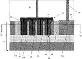
- FIG. 4shows a spiral photodiode in accordance with aspects of the present disclosure.
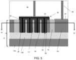
- FIG. 5shows contact formation to the spiral photodiode, amongst other features, and respective fabrication processes in accordance with aspects of the present disclosure.
- FIG. 6is a top view of the photodiode structure along line “A”-“A” of FIG. 5 .
- FIG. 7shows photodiodes coupled to a demultiplexer/splitter in accordance with an aspects of the present disclosure.
- the present disclosurerelates to semiconductor structures and, more particularly, to photodiodes and/or PIN diode structures and methods of manufacture. More specifically, the present disclosure relates to spiral shaped photodiodes and/or pin diode structures composed from semiconductor fin structures.
- the present disclosureprovides a decrease time for growth of photodiode material (e.g., Ge) by providing an increased semiconductor seed surface area, while also allowing a thinner photodiode material (e.g., Ge) region needed to absorb light and an overall reduction of area versus linear photodetectors.
- the structures described hereinprovide an increase in detection efficiency due to a shorter pathway for carrier formation and a longer pathway for light absorption through the photodetector material, e.g., Ge.
- the photodiodeis a spiral configured photodiode composed of photodetector material, e.g., Ge, formed on a spiral fin structure of substrate material.
- the spiral fin structureincludes insulator material within the body of the fin structure, itself, and is surrounded by a shallow trench isolation region outside of the spiral fin structure. The shallow trench isolation region outside of the spiral fin structure will guide light to the photodetector material to “trap” the incident light thereby maximizing chances of carrier formation.
- the photodiodeis also integrated into semiconductor on insulator (SOI) technologies suitable for lateral illumination.
- SOIsemiconductor on insulator
- the photodiodecan be integrated with waveguide structures, laterally spaced therefrom.
- the larger surface area of the spiral fin structurewill facilitate the growth of the photodetector material, e.g., Ge.
- the spiral fin structure within the Ge detector regionwill provide for improved efficiency by increasing a surface capture area.
- the spiral shaped capture areawill have a larger surface area compared to linear shapes. Accordingly, the spiral shaped photodiode can provide improved efficiency by increasing the surface area compared to a concentric circle configuration, as well as avoiding the risk of a destructive interference present in a concentric circle or simple ring configurations.
- the structures of the present disclosurecan be manufactured in a number of ways using a number of different tools.
- the methodologies and toolsare used to form structures with dimensions in the micrometer and nanometer scale.
- the methodologies, i.e., technologies, employed to manufacture the structures of the present disclosurehave been adopted from integrated circuit (IC) technology.
- the structuresare built on wafers and are realized in films of material patterned by photolithographic processes on the top of a wafer.
- the fabrication of the structuresuse three basic building blocks: (i) deposition of thin films of material on a substrate, (ii) applying a patterned mask on top of the films by photolithographic imaging, and (iii) etching the films selectively to the mask.
- FIG. 1shows a substrate with shallow trench isolation regions, amongst other features, and respective fabrication processes in accordance with aspects of the present disclosure.
- the structure 10includes a substrate 12 preferably comprising semiconductor on insulator (SOI) technologies.
- the substrate 12can be a BULK Si implementation.
- the substrate 12incudes a semiconductor wafer 12 a with an insulator layer 12 b and semiconductor substrate 12 c .
- the insulator layer 12 bcan be any suitable insulator material including silicon oxide, sapphire, other suitable insulating materials, and/or combinations thereof.
- An exemplary insulator layer 12 bis buried oxide (BOX) formed on the semiconductor wafer 12 a using separation by implantation of oxygen (SIMOX), oxidation, deposition, and/or other suitable processes.
- the semiconductor wafer 12 a and semiconductor substrate 12 ccan include any suitable semiconductor material, e.g., single crystalline Si material, by way of further examples, the semiconductor substrate 12 c can be composed of SiC, GaAs, InAs, InP, and other III/V or II/VI compound semiconductors. In preferred embodiments, the semiconductor substrate 12 c is a n-type substrate.
- trenchesare formed in the semiconductor substrate 12 c using conventional lithography and etching processes known to those of skill in the art.
- the trenchesextend to the underlying insulator layer 12 b , with one trench being in a spiral pattern.
- a resist formed over the semiconductor substrate 12 cis exposed to energy (light) to form a pattern (opening).
- An etching process with a selective chemistry, e.g., reactive ion etching (RIE),will be used to form the trenches in the semiconductor substrate 12 c .
- a post-etch cleansuch as HF will remove contaminants from the surfaces of the trenches, thereby ensuring a clean surface of exposed semiconductor material of the bottom surface and sidewalls of the trenches.
- an insulator materialcan be deposited within the trenches to form the shallow trench isolation regions 14 , 16 .
- the shallow trench isolation region 14is provided in a spiral configuration; whereas, the shallow trench isolation region 16 is formed outside (adjacent) of the shallow trench isolation region 14 .
- the insulator materialcan be an oxide material deposited by conventional deposition methods including, e.g., a chemical vapor deposition (CVD) process.
- the insulator materialexhibits reflective properties, which is designed to reflect light back into photodiode material.
- a pad nitride layer on top of the semiconductor substrate 12 ccan be removed, resulting in the shallow trench isolation regions 14 , 16 extending above a surface of the semiconductor substrate 12 c.
- a hardmask 18is deposited on the semiconductor substrate 12 c .
- the hardmask 18can be nitride or other hardmask material deposited by known deposition methods such as, e.g., a CVD process.
- the hardmask 18will prevent epitaxial growth of semiconductor material on the semiconductor substrate 12 c in subsequent processes.
- a spiral fin structure 22will be formed in the semiconductor substrate 12 c using conventional etching processes.
- the spiral fin structure 22can be formed by a secondary etching process using resist material 20 to form a spiral trench 24 , thereby defining the spiral fin structure 22 .
- the spiral fin structure 22can be formed by a sidewall imaging technique (SIT) as is known in the art such that no further explanation is required for a complete understanding of the present disclosure.
- SITsidewall imaging technique
- the body of the spiral fin structure 22includes the spiral shallow trench isolation region 14 , while also being bounded by the shallow trench isolation structure 16 and the underlying insulator material 12 b .
- the resist 20can be removed by conventional oxygen ashing or use of other stripants.
- the hardmask 18 over the spiral fin structure 22can be removed by conventional patterning processes, e.g., lithography and etching process, to expose the semiconductor material 12 c of the spiral fin structure 22 .
- the removal of the hardmask 18will allow epitaxially grown semiconductor material to deposit on all exposed surfaces of the spiral fin structure 22 .
- photodiode material 26e.g., Ge based material
- an optional liner 28can be grown within the spiral trench 24 , e.g., on sidewalls and a top surface of the spiral fin structure 22 .
- the remaining hardmask 18will prevent growth of the epitaxially semiconductor material outside of the spiral fin structure 22 .
- the liner 28can be an epitaxial grown semiconductor material, e.g., a P-type semiconductor material, preferably composed of the same material as the substrate 12 c , e.g., Si.
- the photodiode material 26is epitaxially grown on the liner 28 or, optionally, directly on the semiconductor material 12 c of the spiral fin structure 22 .
- the photodiode material 26is an intrinsic photosensitive semiconductor material (non-doped), preferably comprising Ge material which offers superior responsivity.
- the photodiode material 26can be Si, SiGe, etc.
- the epitaxial growth of the photodiode material 26will not result in a pinch-off phenomenon, thereby leaving an opening 30 within spaces formed between the spiral fin structure 22 .
- the photodiode material 26will be bounded (e.g., surrounded) by the shallow trench isolation region 14 within the body of the spiral fin structure 22 , the shallow trench isolation region 16 adjacent to the spiral fin structure 22 and the underlying insulator material 12 c .
- the reflective surfaces of the insulator materialswill surround, e.g., be provided on all sides, the photodiode material 26 such that light can be guided back into the photodiode material 26 to maximize carrier formation, i.e., achieve high efficiency.
- the photodiode material 26will also be in a spiral shape due its placement within the spiral trench, which provides a longer path (from one end to its center) to maximize absorption of any incident light.
- a semiconductor material 32is deposited in the opening 30 directly on the photodiode material 26 (e.g., Ge). In embodiments, the semiconductor material 32 will also grow on the upper, exposed surface of the photodiode material 26 (e.g., Ge).
- the semiconductor material 32is preferably the same material as the liner 28 .
- the semiconductor material 32is a P+ type semiconductor material (e.g., epitaxial Si or polysilicon).
- the hardmask 18is removed by a selective etching process, after the growth of the semiconductor material 32 .
- the semiconductor material 32is a P+ plug to provide biasing for operation of an avalanche photodiode 25 .
- a N-P-I-P photodiode 25can be formed.
- the P+ material, e.g., semiconductor material 32 and the P+ material (e.g., liner 28 ) on the sides and bottom of the Ge material (e.g., semiconductor material 26 )create an avalanche photodiode 25 , which is biased in three dimensions, increasing the likelihood of picking up a signal before carrier recombination.
- FIG. 5shows contact formation to the photodiode 25 , amongst other features, and respective fabrication processes.
- a silicide contact 34is formed on an exposed surface of the semiconductor substrate 12 c and top of the photodiode 25 , e.g., on semiconductor material 32 .
- the silicide processbegins with deposition and patterning of a thin transition metal layer, e.g., nickel, cobalt or titanium, over the semiconductor substrate 12 c and top of the photodiode 25 . After deposition and patterning of the material, the structure is heated allowing the transition metal to react with exposed silicon (or other semiconductor material as described herein) forming a low-resistance transition metal silicide. Following the reaction, any remaining transition metal is removed by chemical etching, leaving the silicide contacts 34 .
- a thin transition metal layere.g., nickel, cobalt or titanium
- an interlevel dielectric material (e.g., oxide) 36is deposited over the structure.
- a trenchis formed in the interlevel dielectric material (e.g., oxide) 36 , aligned with and exposing a top surface of silicide contacts 34 .
- the trenchis formed by conventional lithography and etching processes as already described herein.
- the trenchis filled with a metal material, e.g., tungsten, to form contacts 38 .
- the contact 38 on the side of the photodiode 25will detect the current generated by the photons hitting the photodiode 25 .
- the photodiode 25is primarily designed for lateral illumination, it is recognized that the contact 38 over the photodiode 25 can be arranged at an edge of the photodiode 25 for frontside illumination. This frontside illumination is possible due to the fact that the contact 38 will not significantly interfere with light entering into the photodiode 25 from the frontside (e.g., top).
- the photodiode 25can also be used for backside illumination.
- FIG. 6is a top view of the photodiode 25 along the plane denoted by line “A”-“A” of FIG. 5 .
- FIG. 6shows a cut-away top view of the spiral fin structure 22 with the liner 28 , photodetector material 26 and P+ plug material 32 deposited within the space 24 .
- the spiral fin structure 22is a continuous structure which is bounded by the shallow trench isolation regions 14 , 16 , over the insulator layer 12 c .
- the body of the spiral fin structure 22includes the shallow trench isolation region 14 along its length.
- the spiral fin structure 22will be located on the insulator material 12 b of the SOI technologies. Accordingly, in this manner, the photodiode 25 will be surrounded by reflective material that will reflect light back into the photodetector material 26 .
- the photodetector material 28can include a cone or tapered section 28 a , which laterally guides light into the photodiode 25 to the center of the spiral configuration.
- the incident lightcan be provided laterally to the photodiode 25 by a waveguide structure, fiber or other lateral incident light (each of which is represented by the arrow) located on the same plane as the photodiode 25 .
- FIG. 7shows photodiodes 25 , 25 a coupled to a waveguide 100 by a demultiplexer/splitter 102 .
- different photodiodes 25 , 25 acan detect different wavelengths using the demultiplexer/splitter 102 . More specifically, light from a waveguide 100 can be split into different wavelengths by the demultiplexer/splitter 102 and then each separate wavelength can be laterally guided to a different photodiode 25 , 25 a for detection.
- the different photodiodes 25 , 25 aare detecting the separate wavelength through lateral illumination.
- SoCsystem on chip
- SoCis an integrated circuit (also known as a “chip”) that integrates all components of an electronic system on a single chip or substrate. As the components are integrated on a single substrate, SoCs consume much less power and take up much less area than multi-chip designs with equivalent functionality. Because of this, SoCs are becoming the dominant force in the mobile computing (such as in Smartphones) and edge computing markets. SoC is also commonly used in embedded systems and the Internet of Things.
- the method(s) as described aboveis used in the fabrication of integrated circuit chips.
- the resulting integrated circuit chipscan be distributed by the fabricator in raw wafer form (that is, as a single wafer that has multiple unpackaged chips), as a bare die, or in a packaged form.
- the chipis mounted in a single chip package (such as a plastic carrier, with leads that are affixed to a motherboard or other higher level carrier) or in a multichip package (such as a ceramic carrier that has either or both surface interconnections or buried interconnections).
- the chipis then integrated with other chips, discrete circuit elements, and/or other signal processing devices as part of either (a) an intermediate product, such as a motherboard, or (b) an end product.
- the end productcan be any product that includes integrated circuit chips, ranging from toys and other low-end applications to advanced computer products having a display, a keyboard or other input device, and a central processor.
Landscapes
- Light Receiving Elements (AREA)
- Element Separation (AREA)
Abstract
Description
Claims (19)
Priority Applications (2)
| Application Number | Priority Date | Filing Date | Title |
|---|---|---|---|
| US16/935,854US11611002B2 (en) | 2020-07-22 | 2020-07-22 | Photodiode and/or pin diode structures |
| CN202110725425.9ACN113972297B (en) | 2020-07-22 | 2021-06-29 | Photodiode and/or PIN diode structures |
Applications Claiming Priority (1)
| Application Number | Priority Date | Filing Date | Title |
|---|---|---|---|
| US16/935,854US11611002B2 (en) | 2020-07-22 | 2020-07-22 | Photodiode and/or pin diode structures |
Publications (2)
| Publication Number | Publication Date |
|---|---|
| US20220029032A1 US20220029032A1 (en) | 2022-01-27 |
| US11611002B2true US11611002B2 (en) | 2023-03-21 |
Family
ID=79586153
Family Applications (1)
| Application Number | Title | Priority Date | Filing Date |
|---|---|---|---|
| US16/935,854Active2040-11-23US11611002B2 (en) | 2020-07-22 | 2020-07-22 | Photodiode and/or pin diode structures |
Country Status (2)
| Country | Link |
|---|---|
| US (1) | US11611002B2 (en) |
| CN (1) | CN113972297B (en) |
Families Citing this family (4)
| Publication number | Priority date | Publication date | Assignee | Title |
|---|---|---|---|---|
| US11424377B2 (en) | 2020-10-08 | 2022-08-23 | Globalfoundries U.S. Inc. | Photodiode with integrated, light focusing element |
| US12310124B2 (en) | 2022-03-30 | 2025-05-20 | Globalfoundries U.S. Inc. | Photodiodes |
| US11949034B2 (en) | 2022-06-24 | 2024-04-02 | Globalfoundries U.S. Inc. | Photodetector with dual doped semiconductor material |
| WO2024141103A1 (en)* | 2022-12-30 | 2024-07-04 | 上海联影微电子科技有限公司 | Photodiode and manufacturing method therefor |
Citations (50)
| Publication number | Priority date | Publication date | Assignee | Title |
|---|---|---|---|---|
| US2557110A (en) | 1945-02-17 | 1951-06-19 | Sperry Corp | Wave guide attenuator apparatus |
| US2619538A (en) | 1944-05-23 | 1952-11-25 | Westinghouse Electric Corp | Wave guide attenuator |
| US3787871A (en) | 1971-03-03 | 1974-01-22 | Us Navy | Terminator for spiral antenna |
| US4481523A (en) | 1980-12-02 | 1984-11-06 | Fujitsu Limited | Avalanche photodiodes |
| US4799031A (en) | 1986-12-02 | 1989-01-17 | Spinner Gmbh, Elektrotechnische Fabrik | Waveguide device for producing absorption or attenuation |
| US4847210A (en) | 1988-08-05 | 1989-07-11 | Motorola Inc. | Integrated pin photo-detector method |
| US5994724A (en) | 1996-12-03 | 1999-11-30 | Nec Corporation | Photodetector |
| US6147349A (en) | 1998-07-31 | 2000-11-14 | Raytheon Company | Method for fabricating a self-focusing detector pixel and an array fabricated in accordance with the method |
| US6180945B1 (en) | 1984-08-31 | 2001-01-30 | Lockheed Martin Corporation | Dual spiral photoconductive detector |
| WO2001047034A2 (en) | 1999-12-22 | 2001-06-28 | Micronas Gmbh | Optical transmitting and receiving device and a production method therefor |
| US20030030814A1 (en) | 2001-07-11 | 2003-02-13 | Osinski Marek A. | Gyroscope with at least one rotation sensing element and detector of sagnac-shifted frequencies |
| US7002429B2 (en) | 2003-07-23 | 2006-02-21 | Mitsubishi Denki Kabushiki Kaisha | Nonreflective waveguide terminator and waveguide circuit |
| US20070099315A1 (en) | 2005-10-27 | 2007-05-03 | Sharp Laboratories Of America, Inc. | Germanium photo detector having planar surface through germanium epitaxial overgrowth |
| US20080070355A1 (en) | 2006-09-18 | 2008-03-20 | Amberwave Systems Corporation | Aspect ratio trapping for mixed signal applications |
| US7397101B1 (en) | 2004-07-08 | 2008-07-08 | Luxtera, Inc. | Germanium silicon heterostructure photodetectors |
| EP1982356A2 (en) | 2006-02-01 | 2008-10-22 | Koninklijke Philips Electronics N.V. | Geiger mode avalanche photodiode |
| US20080257409A1 (en) | 2007-04-09 | 2008-10-23 | Amberwave Systems Corporation | Photovoltaics on silicon |
| KR20100070601A (en)* | 2008-12-18 | 2010-06-28 | 재단법인대구경북과학기술원 | Method for producing solar cell device |
| KR20100070610A (en) | 2008-12-18 | 2010-06-28 | 희성전자 주식회사 | Complex light guide sheet for backlight unit |
| US7777250B2 (en) | 2006-03-24 | 2010-08-17 | Taiwan Semiconductor Manufacturing Company, Ltd. | Lattice-mismatched semiconductor structures and related methods for device fabrication |
| US7790495B2 (en) | 2007-10-26 | 2010-09-07 | International Business Machines Corporation | Optoelectronic device with germanium photodetector |
| US7795064B2 (en) | 2007-11-14 | 2010-09-14 | Jds Uniphase Corporation | Front-illuminated avalanche photodiode |
| US7871854B1 (en) | 2009-08-19 | 2011-01-18 | Freescale Semiconductor, Inc. | Method of making a vertical photodetector |
| US20110037133A1 (en) | 2009-08-17 | 2011-02-17 | Tzung-I Su | Semiconductor Photodetector Structure and the Fabrication Method Thereof |
| US7902540B2 (en) | 2008-05-21 | 2011-03-08 | International Business Machines Corporation | Fast P-I-N photodetector with high responsitivity |
| US20120213468A1 (en) | 2011-02-17 | 2012-08-23 | Cornell University | Polysilicon photodetector, methods and applications |
| US20130149806A1 (en) | 2011-12-07 | 2013-06-13 | Electronics And Telecommunications Research Institute | Methods of forming photo detectors |
| US20130241021A1 (en) | 2012-03-16 | 2013-09-19 | Analog Devices, Inc. | Integrated circuit having a semiconducting via; an integrated circuit including a sensor, such as a photosensitive device, and a method of making said integrated circuit |
| US20140159183A1 (en) | 2012-12-10 | 2014-06-12 | National Tsing Hua University | High-efficiency bandwidth product germanium photodetector |
| US20140185979A1 (en) | 2012-12-31 | 2014-07-03 | Infinera Corporation | Light absorption and scattering devices in a photonic integrated circuit |
| US20140197507A1 (en) | 2013-01-15 | 2014-07-17 | International Business Machines Corporation | Buried waveguide photodetector |
| US20140217269A1 (en) | 2013-02-01 | 2014-08-07 | The Board Of Trustees Of The Leland Stanford Junior University | Coupled waveguides for slow light sensor applications |
| US20150075599A1 (en) | 2013-09-19 | 2015-03-19 | Zena Technologies, Inc. | Pillar structured multijunction photovoltaic devices |
| US20150091065A1 (en) | 2013-09-30 | 2015-04-02 | Semiconductor Manufacturing International (Beijing) Corporation | Pixel structures of cmos imaging sensors and fabrication method thereof |
| US20150097256A1 (en) | 2013-10-03 | 2015-04-09 | Globalfoundries Singapore Pte. Ltd. | Semiconductor devices including avalanche photodetector diodes integrated on waveguides and methods for fabricating the same |
| US20150115333A1 (en) | 2009-11-30 | 2015-04-30 | Madhur Bobde | Lateral super junctions with high substrate breakdown and build in avalanche clamp diode |
| US9064699B2 (en) | 2013-09-30 | 2015-06-23 | Samsung Electronics Co., Ltd. | Methods of forming semiconductor patterns including reduced dislocation defects and devices formed using such methods |
| US20160155884A1 (en) | 2014-12-01 | 2016-06-02 | Luxtera, Inc. | Method And System For Germanium-On-Silicon Photodetectors Without Germanium Layer Contacts |
| US20170365636A1 (en) | 2016-06-21 | 2017-12-21 | Stmicroelectronics S.R.L. | Multiband optoelectronic device for colorimetric applications and related manufacturing process |
| US9864138B2 (en) | 2015-01-05 | 2018-01-09 | The Research Foundation For The State University Of New York | Integrated photonics including germanium |
| US20180204761A1 (en) | 2014-09-03 | 2018-07-19 | Globalfoundries Inc. | LATERAL PiN DIODES AND SCHOTTKY DIODES |
| US10157947B2 (en) | 2012-11-27 | 2018-12-18 | Artilux Inc. | Photonic lock based high bandwidth photodetector |
| US10359569B2 (en) | 2016-05-09 | 2019-07-23 | Huawei Technologies Co., Ltd. | Optical waveguide termination having a doped, light-absorbing slab |
| US20200020734A1 (en) | 2018-07-16 | 2020-01-16 | Taiwan Semiconductor Manufacturing Company, Ltd. | Image sensor with sidewall protection and method of making same |
| US10600839B2 (en) | 2014-12-10 | 2020-03-24 | Semiconductor Energy Laboratory Co., Ltd. | Semiconductor device including oxide semiconductor |
| US20200105812A1 (en) | 2018-09-28 | 2020-04-02 | Taiwan Semiconductor Manufacturing Co., Ltd. | Image sensor including silicon over germanium layer |
| US20210223478A1 (en) | 2020-01-17 | 2021-07-22 | Taiwan Semiconductor Manufacturing Co., Ltd. | Germanium Photodetector Embedded in a Multi-Mode Interferometer |
| US20210305313A1 (en) | 2020-03-27 | 2021-09-30 | Harvatek Corporation | Light-emitting diode (led) assembly and method of manufacturing an led cell of the same |
| US20210305449A1 (en) | 2020-03-27 | 2021-09-30 | Harvatek Corporation | Light source assembly, optical sensor assembly, and method of manufacturing a cell of the same |
| US11316064B2 (en)* | 2020-05-29 | 2022-04-26 | Globalfoundries U.S. Inc. | Photodiode and/or PIN diode structures |
Family Cites Families (9)
| Publication number | Priority date | Publication date | Assignee | Title |
|---|---|---|---|---|
| US7112455B2 (en)* | 2004-06-10 | 2006-09-26 | Freescale Semiconductor, Inc | Semiconductor optical devices and method for forming |
| US8426224B2 (en)* | 2006-12-18 | 2013-04-23 | The Regents Of The University Of California | Nanowire array-based light emitting diodes and lasers |
| US7560784B2 (en)* | 2007-02-01 | 2009-07-14 | International Business Machines Corporation | Fin PIN diode |
| WO2010027322A1 (en)* | 2008-09-04 | 2010-03-11 | Qunano Ab | Nanostructured photodiode |
| WO2011067872A1 (en)* | 2009-12-01 | 2011-06-09 | 国立大学法人北海道大学 | Light emitting element and method for manufacturing same |
| JP2016054274A (en)* | 2014-09-04 | 2016-04-14 | 学校法人 関西大学 | Photoelectric conversion element and method for manufacturing photoelectric conversion element |
| EP3145038A1 (en)* | 2015-09-15 | 2017-03-22 | Technische Universität München | Nanowire laser structure and fabrication method |
| JP2017224686A (en)* | 2016-06-14 | 2017-12-21 | ルネサスエレクトロニクス株式会社 | Semiconductor device and manufacturing method of semiconductor device |
| US10396121B2 (en)* | 2017-08-18 | 2019-08-27 | Globalfoundries Inc. | FinFETs for light emitting diode displays |
- 2020
- 2020-07-22USUS16/935,854patent/US11611002B2/enactiveActive
- 2021
- 2021-06-29CNCN202110725425.9Apatent/CN113972297B/enactiveActive
Patent Citations (51)
| Publication number | Priority date | Publication date | Assignee | Title |
|---|---|---|---|---|
| US2619538A (en) | 1944-05-23 | 1952-11-25 | Westinghouse Electric Corp | Wave guide attenuator |
| US2557110A (en) | 1945-02-17 | 1951-06-19 | Sperry Corp | Wave guide attenuator apparatus |
| US3787871A (en) | 1971-03-03 | 1974-01-22 | Us Navy | Terminator for spiral antenna |
| US4481523A (en) | 1980-12-02 | 1984-11-06 | Fujitsu Limited | Avalanche photodiodes |
| US6180945B1 (en) | 1984-08-31 | 2001-01-30 | Lockheed Martin Corporation | Dual spiral photoconductive detector |
| US4799031A (en) | 1986-12-02 | 1989-01-17 | Spinner Gmbh, Elektrotechnische Fabrik | Waveguide device for producing absorption or attenuation |
| US4847210A (en) | 1988-08-05 | 1989-07-11 | Motorola Inc. | Integrated pin photo-detector method |
| US5994724A (en) | 1996-12-03 | 1999-11-30 | Nec Corporation | Photodetector |
| US6147349A (en) | 1998-07-31 | 2000-11-14 | Raytheon Company | Method for fabricating a self-focusing detector pixel and an array fabricated in accordance with the method |
| WO2001047034A2 (en) | 1999-12-22 | 2001-06-28 | Micronas Gmbh | Optical transmitting and receiving device and a production method therefor |
| US20030030814A1 (en) | 2001-07-11 | 2003-02-13 | Osinski Marek A. | Gyroscope with at least one rotation sensing element and detector of sagnac-shifted frequencies |
| US7002429B2 (en) | 2003-07-23 | 2006-02-21 | Mitsubishi Denki Kabushiki Kaisha | Nonreflective waveguide terminator and waveguide circuit |
| US7397101B1 (en) | 2004-07-08 | 2008-07-08 | Luxtera, Inc. | Germanium silicon heterostructure photodetectors |
| US20070099315A1 (en) | 2005-10-27 | 2007-05-03 | Sharp Laboratories Of America, Inc. | Germanium photo detector having planar surface through germanium epitaxial overgrowth |
| US7361526B2 (en) | 2005-10-27 | 2008-04-22 | Sharp Laboratories Of America, Inc. | Germanium photo detector having planar surface through germanium epitaxial overgrowth |
| EP1982356A2 (en) | 2006-02-01 | 2008-10-22 | Koninklijke Philips Electronics N.V. | Geiger mode avalanche photodiode |
| US7777250B2 (en) | 2006-03-24 | 2010-08-17 | Taiwan Semiconductor Manufacturing Company, Ltd. | Lattice-mismatched semiconductor structures and related methods for device fabrication |
| US20080070355A1 (en) | 2006-09-18 | 2008-03-20 | Amberwave Systems Corporation | Aspect ratio trapping for mixed signal applications |
| US20080257409A1 (en) | 2007-04-09 | 2008-10-23 | Amberwave Systems Corporation | Photovoltaics on silicon |
| US7790495B2 (en) | 2007-10-26 | 2010-09-07 | International Business Machines Corporation | Optoelectronic device with germanium photodetector |
| US7795064B2 (en) | 2007-11-14 | 2010-09-14 | Jds Uniphase Corporation | Front-illuminated avalanche photodiode |
| US7902540B2 (en) | 2008-05-21 | 2011-03-08 | International Business Machines Corporation | Fast P-I-N photodetector with high responsitivity |
| KR20100070601A (en)* | 2008-12-18 | 2010-06-28 | 재단법인대구경북과학기술원 | Method for producing solar cell device |
| KR20100070610A (en) | 2008-12-18 | 2010-06-28 | 희성전자 주식회사 | Complex light guide sheet for backlight unit |
| US20110037133A1 (en) | 2009-08-17 | 2011-02-17 | Tzung-I Su | Semiconductor Photodetector Structure and the Fabrication Method Thereof |
| US7871854B1 (en) | 2009-08-19 | 2011-01-18 | Freescale Semiconductor, Inc. | Method of making a vertical photodetector |
| US20150115333A1 (en) | 2009-11-30 | 2015-04-30 | Madhur Bobde | Lateral super junctions with high substrate breakdown and build in avalanche clamp diode |
| US20120213468A1 (en) | 2011-02-17 | 2012-08-23 | Cornell University | Polysilicon photodetector, methods and applications |
| US20130149806A1 (en) | 2011-12-07 | 2013-06-13 | Electronics And Telecommunications Research Institute | Methods of forming photo detectors |
| US20130241021A1 (en) | 2012-03-16 | 2013-09-19 | Analog Devices, Inc. | Integrated circuit having a semiconducting via; an integrated circuit including a sensor, such as a photosensitive device, and a method of making said integrated circuit |
| US10157947B2 (en) | 2012-11-27 | 2018-12-18 | Artilux Inc. | Photonic lock based high bandwidth photodetector |
| US20140159183A1 (en) | 2012-12-10 | 2014-06-12 | National Tsing Hua University | High-efficiency bandwidth product germanium photodetector |
| US20140185979A1 (en) | 2012-12-31 | 2014-07-03 | Infinera Corporation | Light absorption and scattering devices in a photonic integrated circuit |
| US20140197507A1 (en) | 2013-01-15 | 2014-07-17 | International Business Machines Corporation | Buried waveguide photodetector |
| US20140217269A1 (en) | 2013-02-01 | 2014-08-07 | The Board Of Trustees Of The Leland Stanford Junior University | Coupled waveguides for slow light sensor applications |
| US20150075599A1 (en) | 2013-09-19 | 2015-03-19 | Zena Technologies, Inc. | Pillar structured multijunction photovoltaic devices |
| US9064699B2 (en) | 2013-09-30 | 2015-06-23 | Samsung Electronics Co., Ltd. | Methods of forming semiconductor patterns including reduced dislocation defects and devices formed using such methods |
| US20150091065A1 (en) | 2013-09-30 | 2015-04-02 | Semiconductor Manufacturing International (Beijing) Corporation | Pixel structures of cmos imaging sensors and fabrication method thereof |
| US20150097256A1 (en) | 2013-10-03 | 2015-04-09 | Globalfoundries Singapore Pte. Ltd. | Semiconductor devices including avalanche photodetector diodes integrated on waveguides and methods for fabricating the same |
| US20180204761A1 (en) | 2014-09-03 | 2018-07-19 | Globalfoundries Inc. | LATERAL PiN DIODES AND SCHOTTKY DIODES |
| US20160155884A1 (en) | 2014-12-01 | 2016-06-02 | Luxtera, Inc. | Method And System For Germanium-On-Silicon Photodetectors Without Germanium Layer Contacts |
| US10600839B2 (en) | 2014-12-10 | 2020-03-24 | Semiconductor Energy Laboratory Co., Ltd. | Semiconductor device including oxide semiconductor |
| US9864138B2 (en) | 2015-01-05 | 2018-01-09 | The Research Foundation For The State University Of New York | Integrated photonics including germanium |
| US10359569B2 (en) | 2016-05-09 | 2019-07-23 | Huawei Technologies Co., Ltd. | Optical waveguide termination having a doped, light-absorbing slab |
| US20170365636A1 (en) | 2016-06-21 | 2017-12-21 | Stmicroelectronics S.R.L. | Multiband optoelectronic device for colorimetric applications and related manufacturing process |
| US20200020734A1 (en) | 2018-07-16 | 2020-01-16 | Taiwan Semiconductor Manufacturing Company, Ltd. | Image sensor with sidewall protection and method of making same |
| US20200105812A1 (en) | 2018-09-28 | 2020-04-02 | Taiwan Semiconductor Manufacturing Co., Ltd. | Image sensor including silicon over germanium layer |
| US20210223478A1 (en) | 2020-01-17 | 2021-07-22 | Taiwan Semiconductor Manufacturing Co., Ltd. | Germanium Photodetector Embedded in a Multi-Mode Interferometer |
| US20210305313A1 (en) | 2020-03-27 | 2021-09-30 | Harvatek Corporation | Light-emitting diode (led) assembly and method of manufacturing an led cell of the same |
| US20210305449A1 (en) | 2020-03-27 | 2021-09-30 | Harvatek Corporation | Light source assembly, optical sensor assembly, and method of manufacturing a cell of the same |
| US11316064B2 (en)* | 2020-05-29 | 2022-04-26 | Globalfoundries U.S. Inc. | Photodiode and/or PIN diode structures |
Non-Patent Citations (30)
| Title |
|---|
| Application and Drawings for U.S. Appl. No. 16/531,819, filed Aug. 5, 2019, 25 pages. |
| Application and Drawings for U.S. Appl. No. 16/544,074, filed Aug. 19, 2019, 26 pages. |
| Application and Drawings for U.S. Appl. No. 16/741,792, filed Jan. 14, 2020, 38 pages. |
| Application and Drawings for U.S. Appl. No. 16/844,606, filed Apr. 9, 2020, 30 pages. |
| Application and Drawings for U.S. Appl. No. 16/887,375, filed May 29, 2020, 26 pages. |
| Application and Drawings for U.S. Appl. No. 17/065,862, filed Oct. 8, 2020, 22 pages. |
| Final Office Action in U.S. Appl. No. 16/844,606 dated Oct. 29, 2021, 9 pages. |
| Foreign Office Action dated Jul. 29, 2022 in related Germany Application No. 10 2021 122 575.2, 6 pages. |
| Huang et al., "Germanium on Silicon Avalanche Photodiode", IEEE Journal of Selected Topics in Quantum Electronics, vol. 24, No. 2, Mar./Apr. 2018, 11 pages. |
| Jutzi et al., "Ge-on-Si Vertical Incidence Photodiodes With 39-GHz Bandwidth", IEEE Photonics Technology Letters, vol. 17, Issue 7, Jul. 2005, 3 pages. |
| Knoll, "High-Performance BiCMOS Si Photonics Platform", IEEE, 2015, 9 pages. |
| Koester et al., "Germanium-on-Insulator Photodetectors", IEEE, Oct. 2005, 3 pages. |
| Liao et al., "36 GHz submicron silicon waveguide germanium photodetector", Optics Express, vol. 19, Issue 11, May 20, 2011, 6 pages. |
| Notice of Allowance in U.S. Appl. No. 16/531,819 dated Apr. 28, 2021, 9 pages. |
| Notice of Allowance in U.S. Appl. No. 16/844,606 dated Feb. 1, 2022, 9 pages. |
| Notice of Allowance in U.S. Appl. No. 16/887,375 dated Jan. 20, 2022, 9 pages. |
| Notice of Allowance in U.S. Appl. No. 17/065,862 dated May 18, 2022, 7 pages. |
| Office Action in U.S. Appl. No. 16/531,819 dated Jul. 1, 2021, 12 pages. |
| Office Action in U.S. Appl. No. 16/887,375 dated Oct. 13, 2021, 13 pages. |
| Office Action in U.S. Appl. No. 17/065,862 dated Jan. 27, 2022, 14 pages. |
| Office Action in U.S. Appl. No. 17/863,922 dated Nov. 8, 2022, 8 pages. |
| Response to Final Office Action in U.S. Appl. No. 16/844,606 dated Nov. 23, 2021, 9 pages. |
| Response to Office Action in U.S. Appl. No. 16/844,606 dated Oct. 1, 2021, 14 pages. |
| Response to Office Action in U.S. Appl. No. 16/887,375 dated Jan. 13, 2022, 8 pages. |
| Response to Office Action in U.S. Appl. No. 17/065,862 dated Mar. 25, 2022, 11 pages. |
| Response to Office Action in U.S. Appl. No. 17/863,922 dated Feb. 7, 2023, 8 pages. |
| Second Response to Final Office Action in U.S. Appl. No. 16/844,606 dated Jan. 5, 2022, 9 pages. |
| Taiwanese Notice of Allowance in TW Application No. 110108280 dated May 4, 2022, 4 pages. |
| Taiwanese Office Action in TW Application No. 110108280 dated Jan. 13, 2022, 16 pages. |
| Yu, "High-Efficiency p-i-n Photodetectors on Selective-Area-Grown Ge for Monolithic Integration", IEEE Electron Device Letters, vol. 30, Issue 11, Nov. 2009, 4 pages. |
Also Published As
| Publication number | Publication date |
|---|---|
| US20220029032A1 (en) | 2022-01-27 |
| CN113972297B (en) | 2024-12-20 |
| CN113972297A (en) | 2022-01-25 |
Similar Documents
| Publication | Publication Date | Title |
|---|---|---|
| US11322639B2 (en) | Avalanche photodiode | |
| US11611002B2 (en) | Photodiode and/or pin diode structures | |
| CN113745364B (en) | Photodiode and/or PIN diode structures | |
| CN115176346B (en) | Single Photon Avalanche Diode Devices | |
| JP7665577B2 (en) | Semiconductor device having germanium region disposed in semiconductor substrate | |
| KR100977199B1 (en) | Photosensitive device having increased blue light sensitivity and manufacturing method thereof | |
| US11949034B2 (en) | Photodetector with dual doped semiconductor material | |
| US11581450B2 (en) | Photodiode and/or pin diode structures with one or more vertical surfaces | |
| EP4266384A1 (en) | Photodiodes with serpentine shaped electrical junction | |
| US12310124B2 (en) | Photodiodes | |
| US20250241075A1 (en) | Structure and formation method of semiconductor device with photosensing structure | |
| CN117038777B (en) | Avalanche photodiode | |
| KR102863724B1 (en) | Photodiode with insulator layer along intrinsic region sidewall | |
| US11784196B2 (en) | Trenchless single-photon avalanche diodes | |
| KR102623757B1 (en) | Channel pattern design to improve carrier transfer efficiency | |
| US20240088173A1 (en) | Single-photon avalanche diode with isolated junctions | |
| US20250130367A1 (en) | Waveguide photodetector and method for forming the same | |
| US20250142983A1 (en) | Single-photon avalanche diodes with hybrid trench isolation structures | |
| CN119384051A (en) | Photodetector and method of forming the same |
Legal Events
| Date | Code | Title | Description |
|---|---|---|---|
| AS | Assignment | Owner name:GLOBALFOUNDRIES INC., CAYMAN ISLANDS Free format text:ASSIGNMENT OF ASSIGNORS INTEREST;ASSIGNORS:LEVY, MARK D.;KIEWRA, EDWARD W.;ADUSUMILLI, SIVA P.;AND OTHERS;SIGNING DATES FROM 20200715 TO 20200720;REEL/FRAME:053282/0805 | |
| FEPP | Fee payment procedure | Free format text:ENTITY STATUS SET TO UNDISCOUNTED (ORIGINAL EVENT CODE: BIG.); ENTITY STATUS OF PATENT OWNER: LARGE ENTITY | |
| AS | Assignment | Owner name:GLOBALFOUNDRIES U.S. INC., CALIFORNIA Free format text:ASSIGNMENT OF ASSIGNORS INTEREST;ASSIGNOR:GLOBALFOUNDRIES INC.;REEL/FRAME:054633/0001 Effective date:20201022 | |
| AS | Assignment | Owner name:GLOBALFOUNDRIES U.S. INC., NEW YORK Free format text:RELEASE BY SECURED PARTY;ASSIGNOR:WILMINGTON TRUST, NATIONAL ASSOCIATION;REEL/FRAME:056987/0001 Effective date:20201117 | |
| STPP | Information on status: patent application and granting procedure in general | Free format text:NON FINAL ACTION MAILED | |
| STPP | Information on status: patent application and granting procedure in general | Free format text:RESPONSE TO NON-FINAL OFFICE ACTION ENTERED AND FORWARDED TO EXAMINER | |
| STPP | Information on status: patent application and granting procedure in general | Free format text:FINAL REJECTION MAILED | |
| STPP | Information on status: patent application and granting procedure in general | Free format text:ADVISORY ACTION MAILED | |
| STPP | Information on status: patent application and granting procedure in general | Free format text:RESPONSE AFTER FINAL ACTION FORWARDED TO EXAMINER | |
| STPP | Information on status: patent application and granting procedure in general | Free format text:NOTICE OF ALLOWANCE MAILED -- APPLICATION RECEIVED IN OFFICE OF PUBLICATIONS | |
| STCF | Information on status: patent grant | Free format text:PATENTED CASE |