US11610918B2 - Display device - Google Patents
Display deviceDownload PDFInfo
- Publication number
- US11610918B2 US11610918B2US16/704,462US201916704462AUS11610918B2US 11610918 B2US11610918 B2US 11610918B2US 201916704462 AUS201916704462 AUS 201916704462AUS 11610918 B2US11610918 B2US 11610918B2
- Authority
- US
- United States
- Prior art keywords
- thin film
- layer
- film transistor
- electrode layer
- display device
- Prior art date
- Legal status (The legal status is an assumption and is not a legal conclusion. Google has not performed a legal analysis and makes no representation as to the accuracy of the status listed.)
- Active
Links
Images


Classifications
- H01L27/1225—
- H—ELECTRICITY
- H10—SEMICONDUCTOR DEVICES; ELECTRIC SOLID-STATE DEVICES NOT OTHERWISE PROVIDED FOR
- H10D—INORGANIC ELECTRIC SEMICONDUCTOR DEVICES
- H10D86/00—Integrated devices formed in or on insulating or conducting substrates, e.g. formed in silicon-on-insulator [SOI] substrates or on stainless steel or glass substrates
- H10D86/40—Integrated devices formed in or on insulating or conducting substrates, e.g. formed in silicon-on-insulator [SOI] substrates or on stainless steel or glass substrates characterised by multiple TFTs
- H10D86/421—Integrated devices formed in or on insulating or conducting substrates, e.g. formed in silicon-on-insulator [SOI] substrates or on stainless steel or glass substrates characterised by multiple TFTs having a particular composition, shape or crystalline structure of the active layer
- H10D86/423—Integrated devices formed in or on insulating or conducting substrates, e.g. formed in silicon-on-insulator [SOI] substrates or on stainless steel or glass substrates characterised by multiple TFTs having a particular composition, shape or crystalline structure of the active layer comprising semiconductor materials not belonging to the Group IV, e.g. InGaZnO
- G—PHYSICS
- G02—OPTICS
- G02F—OPTICAL DEVICES OR ARRANGEMENTS FOR THE CONTROL OF LIGHT BY MODIFICATION OF THE OPTICAL PROPERTIES OF THE MEDIA OF THE ELEMENTS INVOLVED THEREIN; NON-LINEAR OPTICS; FREQUENCY-CHANGING OF LIGHT; OPTICAL LOGIC ELEMENTS; OPTICAL ANALOGUE/DIGITAL CONVERTERS
- G02F1/00—Devices or arrangements for the control of the intensity, colour, phase, polarisation or direction of light arriving from an independent light source, e.g. switching, gating or modulating; Non-linear optics
- G02F1/01—Devices or arrangements for the control of the intensity, colour, phase, polarisation or direction of light arriving from an independent light source, e.g. switching, gating or modulating; Non-linear optics for the control of the intensity, phase, polarisation or colour
- G02F1/13—Devices or arrangements for the control of the intensity, colour, phase, polarisation or direction of light arriving from an independent light source, e.g. switching, gating or modulating; Non-linear optics for the control of the intensity, phase, polarisation or colour based on liquid crystals, e.g. single liquid crystal display cells
- G02F1/133—Constructional arrangements; Operation of liquid crystal cells; Circuit arrangements
- G02F1/1333—Constructional arrangements; Manufacturing methods
- G02F1/1339—Gaskets; Spacers; Sealing of cells
- G02F1/13392—Gaskets; Spacers; Sealing of cells spacers dispersed on the cell substrate, e.g. spherical particles, microfibres
- G—PHYSICS
- G02—OPTICS
- G02F—OPTICAL DEVICES OR ARRANGEMENTS FOR THE CONTROL OF LIGHT BY MODIFICATION OF THE OPTICAL PROPERTIES OF THE MEDIA OF THE ELEMENTS INVOLVED THEREIN; NON-LINEAR OPTICS; FREQUENCY-CHANGING OF LIGHT; OPTICAL LOGIC ELEMENTS; OPTICAL ANALOGUE/DIGITAL CONVERTERS
- G02F1/00—Devices or arrangements for the control of the intensity, colour, phase, polarisation or direction of light arriving from an independent light source, e.g. switching, gating or modulating; Non-linear optics
- G02F1/01—Devices or arrangements for the control of the intensity, colour, phase, polarisation or direction of light arriving from an independent light source, e.g. switching, gating or modulating; Non-linear optics for the control of the intensity, phase, polarisation or colour
- G02F1/13—Devices or arrangements for the control of the intensity, colour, phase, polarisation or direction of light arriving from an independent light source, e.g. switching, gating or modulating; Non-linear optics for the control of the intensity, phase, polarisation or colour based on liquid crystals, e.g. single liquid crystal display cells
- G02F1/133—Constructional arrangements; Operation of liquid crystal cells; Circuit arrangements
- G02F1/1333—Constructional arrangements; Manufacturing methods
- G02F1/1345—Conductors connecting electrodes to cell terminals
- G02F1/13458—Terminal pads
- H01L27/124—
- H01L27/3276—
- H01L29/04—
- H01L29/24—
- H01L29/41733—
- H01L29/66969—
- H01L29/7869—
- H—ELECTRICITY
- H10—SEMICONDUCTOR DEVICES; ELECTRIC SOLID-STATE DEVICES NOT OTHERWISE PROVIDED FOR
- H10D—INORGANIC ELECTRIC SEMICONDUCTOR DEVICES
- H10D30/00—Field-effect transistors [FET]
- H10D30/01—Manufacture or treatment
- H10D30/021—Manufacture or treatment of FETs having insulated gates [IGFET]
- H10D30/031—Manufacture or treatment of FETs having insulated gates [IGFET] of thin-film transistors [TFT]
- H—ELECTRICITY
- H10—SEMICONDUCTOR DEVICES; ELECTRIC SOLID-STATE DEVICES NOT OTHERWISE PROVIDED FOR
- H10D—INORGANIC ELECTRIC SEMICONDUCTOR DEVICES
- H10D30/00—Field-effect transistors [FET]
- H10D30/60—Insulated-gate field-effect transistors [IGFET]
- H10D30/67—Thin-film transistors [TFT]
- H10D30/6729—Thin-film transistors [TFT] characterised by the electrodes
- H—ELECTRICITY
- H10—SEMICONDUCTOR DEVICES; ELECTRIC SOLID-STATE DEVICES NOT OTHERWISE PROVIDED FOR
- H10D—INORGANIC ELECTRIC SEMICONDUCTOR DEVICES
- H10D30/00—Field-effect transistors [FET]
- H10D30/60—Insulated-gate field-effect transistors [IGFET]
- H10D30/67—Thin-film transistors [TFT]
- H10D30/674—Thin-film transistors [TFT] characterised by the active materials
- H10D30/6755—Oxide semiconductors, e.g. zinc oxide, copper aluminium oxide or cadmium stannate
- H—ELECTRICITY
- H10—SEMICONDUCTOR DEVICES; ELECTRIC SOLID-STATE DEVICES NOT OTHERWISE PROVIDED FOR
- H10D—INORGANIC ELECTRIC SEMICONDUCTOR DEVICES
- H10D62/00—Semiconductor bodies, or regions thereof, of devices having potential barriers
- H10D62/40—Crystalline structures
- H—ELECTRICITY
- H10—SEMICONDUCTOR DEVICES; ELECTRIC SOLID-STATE DEVICES NOT OTHERWISE PROVIDED FOR
- H10D—INORGANIC ELECTRIC SEMICONDUCTOR DEVICES
- H10D62/00—Semiconductor bodies, or regions thereof, of devices having potential barriers
- H10D62/80—Semiconductor bodies, or regions thereof, of devices having potential barriers characterised by the materials
- H—ELECTRICITY
- H10—SEMICONDUCTOR DEVICES; ELECTRIC SOLID-STATE DEVICES NOT OTHERWISE PROVIDED FOR
- H10D—INORGANIC ELECTRIC SEMICONDUCTOR DEVICES
- H10D86/00—Integrated devices formed in or on insulating or conducting substrates, e.g. formed in silicon-on-insulator [SOI] substrates or on stainless steel or glass substrates
- H10D86/40—Integrated devices formed in or on insulating or conducting substrates, e.g. formed in silicon-on-insulator [SOI] substrates or on stainless steel or glass substrates characterised by multiple TFTs
- H10D86/441—Interconnections, e.g. scanning lines
- H10D86/443—Interconnections, e.g. scanning lines adapted for preventing breakage, peeling or short circuiting
- H—ELECTRICITY
- H10—SEMICONDUCTOR DEVICES; ELECTRIC SOLID-STATE DEVICES NOT OTHERWISE PROVIDED FOR
- H10D—INORGANIC ELECTRIC SEMICONDUCTOR DEVICES
- H10D86/00—Integrated devices formed in or on insulating or conducting substrates, e.g. formed in silicon-on-insulator [SOI] substrates or on stainless steel or glass substrates
- H10D86/40—Integrated devices formed in or on insulating or conducting substrates, e.g. formed in silicon-on-insulator [SOI] substrates or on stainless steel or glass substrates characterised by multiple TFTs
- H10D86/60—Integrated devices formed in or on insulating or conducting substrates, e.g. formed in silicon-on-insulator [SOI] substrates or on stainless steel or glass substrates characterised by multiple TFTs wherein the TFTs are in active matrices
- H—ELECTRICITY
- H10—SEMICONDUCTOR DEVICES; ELECTRIC SOLID-STATE DEVICES NOT OTHERWISE PROVIDED FOR
- H10D—INORGANIC ELECTRIC SEMICONDUCTOR DEVICES
- H10D99/00—Subject matter not provided for in other groups of this subclass
- H—ELECTRICITY
- H10—SEMICONDUCTOR DEVICES; ELECTRIC SOLID-STATE DEVICES NOT OTHERWISE PROVIDED FOR
- H10K—ORGANIC ELECTRIC SOLID-STATE DEVICES
- H10K59/00—Integrated devices, or assemblies of multiple devices, comprising at least one organic light-emitting element covered by group H10K50/00
- H10K59/10—OLED displays
- H10K59/12—Active-matrix OLED [AMOLED] displays
- H10K59/131—Interconnections, e.g. wiring lines or terminals
- G—PHYSICS
- G02—OPTICS
- G02F—OPTICAL DEVICES OR ARRANGEMENTS FOR THE CONTROL OF LIGHT BY MODIFICATION OF THE OPTICAL PROPERTIES OF THE MEDIA OF THE ELEMENTS INVOLVED THEREIN; NON-LINEAR OPTICS; FREQUENCY-CHANGING OF LIGHT; OPTICAL LOGIC ELEMENTS; OPTICAL ANALOGUE/DIGITAL CONVERTERS
- G02F1/00—Devices or arrangements for the control of the intensity, colour, phase, polarisation or direction of light arriving from an independent light source, e.g. switching, gating or modulating; Non-linear optics
- G02F1/01—Devices or arrangements for the control of the intensity, colour, phase, polarisation or direction of light arriving from an independent light source, e.g. switching, gating or modulating; Non-linear optics for the control of the intensity, phase, polarisation or colour
- G02F1/13—Devices or arrangements for the control of the intensity, colour, phase, polarisation or direction of light arriving from an independent light source, e.g. switching, gating or modulating; Non-linear optics for the control of the intensity, phase, polarisation or colour based on liquid crystals, e.g. single liquid crystal display cells
- G02F1/133—Constructional arrangements; Operation of liquid crystal cells; Circuit arrangements
- G02F1/1333—Constructional arrangements; Manufacturing methods
- G02F1/1339—Gaskets; Spacers; Sealing of cells
- G02F1/13398—Spacer materials; Spacer properties
- G—PHYSICS
- G09—EDUCATION; CRYPTOGRAPHY; DISPLAY; ADVERTISING; SEALS
- G09G—ARRANGEMENTS OR CIRCUITS FOR CONTROL OF INDICATING DEVICES USING STATIC MEANS TO PRESENT VARIABLE INFORMATION
- G09G2300/00—Aspects of the constitution of display devices
- G09G2300/08—Active matrix structure, i.e. with use of active elements, inclusive of non-linear two terminal elements, in the pixels together with light emitting or modulating elements
- G09G2300/0804—Sub-multiplexed active matrix panel, i.e. wherein one active driving circuit is used at pixel level for multiple image producing elements
- H01L27/3262—
- H01L51/5221—
- H—ELECTRICITY
- H10—SEMICONDUCTOR DEVICES; ELECTRIC SOLID-STATE DEVICES NOT OTHERWISE PROVIDED FOR
- H10K—ORGANIC ELECTRIC SOLID-STATE DEVICES
- H10K50/00—Organic light-emitting devices
- H10K50/80—Constructional details
- H10K50/805—Electrodes
- H10K50/82—Cathodes
- H—ELECTRICITY
- H10—SEMICONDUCTOR DEVICES; ELECTRIC SOLID-STATE DEVICES NOT OTHERWISE PROVIDED FOR
- H10K—ORGANIC ELECTRIC SOLID-STATE DEVICES
- H10K59/00—Integrated devices, or assemblies of multiple devices, comprising at least one organic light-emitting element covered by group H10K50/00
- H10K59/10—OLED displays
- H10K59/12—Active-matrix OLED [AMOLED] displays
- H10K59/121—Active-matrix OLED [AMOLED] displays characterised by the geometry or disposition of pixel elements
- H10K59/1213—Active-matrix OLED [AMOLED] displays characterised by the geometry or disposition of pixel elements the pixel elements being TFTs
- H—ELECTRICITY
- H10—SEMICONDUCTOR DEVICES; ELECTRIC SOLID-STATE DEVICES NOT OTHERWISE PROVIDED FOR
- H10K—ORGANIC ELECTRIC SOLID-STATE DEVICES
- H10K59/00—Integrated devices, or assemblies of multiple devices, comprising at least one organic light-emitting element covered by group H10K50/00
- H10K59/80—Constructional details
- H10K59/805—Electrodes
- H10K59/8052—Cathodes
Definitions
- the present inventionrelates to a display device using an oxide semiconductor and a method for manufacturing the same.
- a thin film transistor formed on a flat plate such as a glass substrateis manufactured using amorphous silicon or polycrystalline silicon.
- a thin film transistor using amorphous siliconhas a low field effect mobility, but can be formed on a large glass substrate.
- a thin film transistor using crystalline siliconhas a high field effect mobility, but cannot always be formed on a large glass substrate because of a need of a crystallization process such as laser annealing.
- Patent Document 1examples of the techniques are disclosed in Patent Document 1 and Patent Document 2, where a thin film transistor is manufactured with zinc oxide or an In—Ga—Zn—O based oxide semiconductor used for an oxide semiconductor film and is used as a switching element or the like of an image display device.
- the field effect mobility of a thin film transistor using an oxide semiconductor in a channel formation regionis higher than that of a thin film transistor using amorphous silicon.
- the oxide semiconductor filmcan be formed by sputtering or the like at a temperature of 300° C. or lower. Its manufacturing process is easier than that of a thin film transistor using polycrystalline silicon.
- Such an oxide semiconductoris expected to be used for forming a thin film transistor on a glass substrate, a plastic substrate, or the like, and to be applied to a liquid crystal display device, an electroluminescent display device, electronic paper, or the like.
- the oxide semiconductor thin film transistorhas superior operating characteristics and can be manufactured at a low temperature.
- the structure and manufacturing conditions of elementsneed to be optimized, and it is also necessary to consider the structure of wirings needed to input and output signals and the connection structure of the wirings.
- an oxide semiconductor filmcan be formed at a low temperature, a product can be defective if a thin film of a metal or the like used for a wiring or an electrode, or an insulating film such as an interlayer insulating film, is separated.
- the connection resistance of electrodes in a common connection portion provided on an element substrate side of a display panelis high, there is a problem that spots appear on a display screen and thus the luminance is decreased.
- An object of an embodiment of the present inventionis to provide a structure suitable for a common connection portion provided in a display panel.
- Another object of an embodiment of the present inventionis to prevent a defect due to the separation of a thin film in various kinds of display devices that are manufactured using stacked layers of an oxide semiconductor, an insulating film, and a conductive film.
- a display deviceincludes a pixel portion in which a scan line and a signal line cross each other and a pixel electrode layer is arranged in a matrix, and an inverted staggered thin film transistor having a combination of at least two kinds of oxide semiconductor layers with different amounts of oxygen is provided corresponding to the pixel electrode layer.
- a pad portionis provided to be electrically connected to a common electrode layer facing the pixel electrode layer through a conductive layer made of the same material as the scan line and the signal line.
- a display deviceincludes a pixel portion having a thin film transistor connected to a pixel electrode, and a pad portion electrically connected to a common electrode facing the pixel electrode, and the display device includes the following structures.
- a scan line and a signal linecross each other and a pixel electrode layer is arranged in a matrix.
- the thin film transistoris provided corresponding to the pixel electrode layer, and includes a gate electrode layer connected to the scan line, a gate insulating layer covering the gate electrode layer, a first oxide semiconductor layer to be a channel formation region, a second oxide semiconductor layer over the first oxide semiconductor layer, which is to be a source region and a drain region, and a source electrode layer and a drain electrode layer over the first oxide semiconductor layer and the second oxide semiconductor layer.
- the pad portionis provided in the periphery of the pixel portion, and includes an insulating layer formed using the same layer as the gate insulating layer, a conductive layer over the insulating layer, which is formed using the same layer as the source electrode layer and the drain electrode layer, and an interlayer insulating layer over the conductive layer.
- the pad portioncan be electrically connected to a common electrode layer facing the pixel electrode layer through an opening in the interlayer insulating layer.
- the pad portion provided in the periphery of the pixel portionmay have another structure: a first conductive layer formed using the same layer as the gate electrode layer, an insulating layer formed using the same layer as the gate insulating layer, and a second conductive layer formed using the same layer as the source electrode layer and the drain electrode layer are stacked in this order.
- the pad portioncan be electrically connected to a common electrode layer facing the pixel electrode layer through an opening in an interlayer insulating layer provided over the second conductive layer.
- the pad portionmay have a structure in which an oxide semiconductor layer formed using the same layer as the second oxide semiconductor layer is provided between the insulating layer formed using the same layer as the gate insulating layer and the conductive layer (or the second conductive layer).
- the oxide semiconductor layer (the first oxide semiconductor layer) used as a channel formation region of the semiconductor layerhas a higher oxygen concentration than the oxide semiconductor layer (the second oxide semiconductor layer) used as a source region and a drain region. It can be said that the first oxide semiconductor layer is an oxygen-excess oxide semiconductor layer and the second oxide semiconductor layer is an oxygen-deficient oxide semiconductor layer.
- the second oxide semiconductor layerhas n-type conductivity and has a higher electric conductivity than the first oxide semiconductor layer. Therefore, the source region and the drain region using the second oxide semiconductor layer have a lower resistance than the semiconductor layer using the first oxide semiconductor layer.
- the first oxide semiconductor layerhas an amorphous structure
- the second oxide semiconductor layerincludes a crystal grain (nanocrystal) in the amorphous structure in some cases.
- the crystal grain (nanocrystal) in the second oxide semiconductor layerhas a diameter of 1 nm to 10 nm, and typically about 2 nm to 4 nm.
- an oxide semiconductor film containing In, Ga, and Zncan be used as the first oxide semiconductor layer to be a channel formation region and/or the second oxide semiconductor layer to be a source region and a drain region. Any one of the elements In, Ga, and Zn may be substituted by tungsten, molybdenum, titanium, nickel, or aluminum.
- a semiconductor layer formed using an oxide semiconductor film containing In, Ga, and Znis also referred to as an “IGZO semiconductor layer”.
- the IGZO semiconductor layeris a non-single-crystal semiconductor layer and includes as least an amorphous component.
- a substrate having a surface on which a pixel electrode layer and a thin film transistor electrically connected to the pixel electrode layer are formedis fixed to a counter substrate with an adhesive called a sealant.
- a liquid crystal materialis sealed between two substrates with a sealant.
- the sealantis mixed with a plurality of conductive particles (such as particles plated with gold), whereby a counter electrode (also referred to as a common electrode) provided on the counter substrate is electrically connected a common electrode or a common potential line on the other substrate.
- a counter electrodealso referred to as a common electrode
- the common potential linecan be formed over the same substrate through the same manufacturing process as the thin film transistor.
- a portion where the common potential line overlaps the conductive particles in the sealantcan be called a common connection portion.
- the portion where the common potential line overlaps the conductive particlescan also be called a common electrode.
- the common potential line formed over the same substrate as the thin film transistorcan be referred to as a line to supply a voltage to be used as a reference when a liquid crystal is driven by an alternating current.
- a capacitor wiring connected to one electrode of a storage capacitorcan be regarded as a variation of the common potential line and formed over the same substrate as the thin film transistor in a similar way.
- a display device using an electrophoretic display elementwhich is also referred to as electronic paper, has a structure in which white particles, black particles having a polarity opposite to the white particles, and a dispersion medium (gas or liquid) for dispersing them are included between a pair of substrates.
- An electrode provided over one of the pair of substratesis a common electrode.
- Pixel electrodesare provided over the other substrate so as to face the common electrode, and a plurality of thin film transistors electrically connected to the pixel electrodes are also arranged over the substrate.
- a voltage positive to the common potential applied to the common electrodeis applied to the pixel electrode for turning a white display to a black display; a voltage negative to the common potential applied to the common electrode is applied to the pixel electrode for turning the black display to the white display; and the pixel electrode for not changing the display is set at the same potential as the common potential.
- the common potential line formed over the same substrate as the thin film transistorcan be referred to as a line to supply a voltage to be used as a reference when the electrophoretic display element is operated.
- the display device using an electrophoretic display elementincludes a plurality of separated spaces of a uniform size formed by the pair of substrates and partitions provided between the pair of substrates.
- a separated spaceserves as a pixel unit for displaying part of an image.
- a separated spaceincludes a plurality of white particles, black particles having a polarity opposite to the white particles, and a dispersion medium (gas or liquid) for dispersing them.
- a plurality of colored particles having different polarities and the dispersion medium for dispersing themare sealed between the two substrates with a sealant.
- a common electrode provided over one substrate and a common potential line formed over the other substrateare electrically connected through conductive particles in a common connection portion.
- a plastic filmcan be used as a material for the pair of substrates used in the liquid crystal display device or the display device using an electrophoretic display element, depending on a temperature of the manufacturing process.
- the gate insulating layer, the first oxide semiconductor layer to be a channel formation region, the second oxide semiconductor layer to be a source region and a drain region, and the source electrode layer and the drain electrode layermay be formed by sputtering (a sputter method).
- Examples of sputteringinclude an RF sputtering in which a high-frequency power source is used for a sputtering power source, a DC sputtering, and a pulsed DC sputtering in which a bias is applied in a pulsed manner.
- the RF sputteringis mainly used in the case of forming an insulating film
- the DC sputteringis mainly used in the case of forming a metal film.
- multi-source sputtering apparatusin which a plurality of targets of different materials can be set.
- films of different materialscan be deposited to be stacked in the same chamber, or a plurality of kinds of materials can be deposited by electric discharge at the same time in the same chamber.
- a sputtering apparatusprovided with a magnet system inside the chamber and used for a magnetron sputtering, and a sputtering apparatus used for an ECR sputtering in which plasma generated with the use of microwaves is used without using glow discharge.
- a deposition method by sputteringthere are also a reactive sputtering in which a target substance and a sputtering gas component are chemically reacted with each other during deposition to form a thin compound film thereof, and a bias sputtering in which voltage is also applied to a substrate during deposition.
- the gate insulating layer, the semiconductor layer, the source region and the drain region, and the source electrode layer and the drain electrode layerare formed.
- the first oxide semiconductor layer and the second oxide semiconductor layerare formed under different deposition conditions.
- the second oxide semiconductor layer to be a source region and a drain regionis deposited under such conditions that a crystal grain having a diameter of 1 nm to 10 nm is contained immediately after the deposition.
- the first oxide semiconductor layer to be a channel formation region and the second oxide semiconductor layer to be a source region and a drain regionbe separately formed by using the same target and changing only the introduced gas.
- a titanium filmis preferably formed for the source electrode layer and the drain electrode layer.
- a high energyis applied to a target by Ar ions; therefore, it is considered that a high strain energy exists in the deposited oxide semiconductor layer (typically, the IGZO semiconductor layer).
- heat treatmentis preferably performed at 200° C. to 600° C., and typically 300° C. to 500° C. This heat treatment involves the rearrangement at the atomic level. The deposition and heat treatment (including light annealing) are important because the strain that inhibits the movement of carriers can be released by this heat treatment.
- semiconductor devices in this specificationindicate all the devices that can operate by using semiconductor characteristics, and an electro-optical device, a semiconductor circuit, and an electronic appliance are all included in the semiconductor devices.
- a structure suitable for a pad portion provided in a display panelcan be provided.
- the oxide semiconductor layer and the conductive layerare stacked in the pad portion provided in the periphery of the pixel portion, whereby a defect due to separation of a thin film can be prevented.
- the thickness of the pad portionincreases and the resistance thereof decreases, resulting in an increase in the strength of the structure.
- a thin film transistorhaving a small amount of photocurrent, low parasitic capacitance, a high on-off ratio, and good dynamic characteristics can be manufactured.
- a display device having high electrical properties and high reliabilitycan be provided according to an embodiment of the present invention.
- FIGS. 1 A and 1 Bare diagrams illustrating a semiconductor device
- FIGS. 2 A and 2 Bare diagrams illustrating a semiconductor device
- FIGS. 3 A and 3 Bare diagrams illustrating a semiconductor device
- FIGS. 4 A to 4 Care diagrams illustrating a method for manufacturing a semiconductor device
- FIGS. 5 A to 5 Care diagrams illustrating a method for manufacturing a semiconductor device
- FIG. 6is a diagram illustrating a method for manufacturing a semiconductor device
- FIG. 7is a diagram illustrating a method for manufacturing a semiconductor device
- FIG. 8is a diagram illustrating a method for manufacturing a semiconductor device
- FIG. 9is a diagram illustrating a semiconductor device
- FIGS. 10 A to 10 Dare diagrams illustrating a semiconductor device
- FIG. 11is a diagram illustrating a semiconductor device
- FIG. 12is a diagram illustrating a semiconductor device
- FIGS. 13 A and 13 Bare block diagrams of a semiconductor device
- FIG. 14is a diagram illustrating a configuration of a signal line driver circuit
- FIG. 15is a timing chart illustrating operation of a signal line driver circuit
- FIG. 16is a timing chart illustrating operation of a signal line driver circuit
- FIG. 17is a diagram illustrating a configuration of a shift register
- FIG. 18is a diagram illustrating a connection structure of the flip flop illustrated in FIG. 17 ;
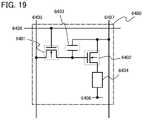
- FIG. 19is an equivalent circuit diagram of a pixel of a semiconductor device
- FIGS. 20 A to 20 Care diagrams each illustrating a semiconductor device
- FIGS. 21 A to 21 Care diagrams illustrating a semiconductor device
- FIG. 22is a diagram illustrating a semiconductor device
- FIGS. 23 A and 23 Bare diagrams illustrating a semiconductor device
- FIGS. 24 A and 24 Bare views illustrating applications of electronic paper
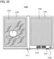
- FIG. 25is an external view illustrating an example of e-book reader
- FIGS. 26 A and 26 Bare external views illustrating a television set and a digital photo frame, respectively;
- FIGS. 27 A and 27 Bare external views illustrating examples of an amusement machine
- FIG. 28is an external view illustrating a cellular phone
- FIGS. 29 A and 29 Bare diagrams illustrating a semiconductor device
- FIGS. 30 A and 30 Bare diagrams illustrating a semiconductor device
- FIGS. 31 A and 31 Bare diagrams illustrating a semiconductor device
- FIG. 32is a diagram illustrating electrical connection through conductive particles.
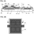
- This embodimentshows an example of a liquid crystal display device in which a liquid crystal layer is sealed between a first substrate and a second substrate, and a common connection portion (a pad portion) is formed over the first substrate to be electrically connected to a counter electrode provided on the second substrate.
- a thin film transistoris formed as a switching element over the first substrate, and the common connection portion is manufactured in the same process as the switching element in a pixel portion, resulting in simplified process.
- the common connection portionis provided in a position overlapping a sealant for bonding the first substrate and the second substrate and is electrically connected to a counter electrode through conductive particles in the sealant.
- the common connection portionis provided in a position which does not overlap the sealant (except for the pixel portion) and a paste including conductive particles is provided separately from the sealant so as to overlap the common connection portion, whereby the common connection portion can be electrically connected to the counter electrode through the conductive particles in the paste (see e.g., FIG. 32 ).
- FIG. 1 Ais a cross-sectional view of a semiconductor device in which a thin film transistor and a common connection portion are formed over the same substrate.
- the thin film transistor illustrated in FIG. 1 Ais an inverted staggered thin film transistor, and includes source and drain electrode layers 105 a and 105 b over a semiconductor layer 103 with source and drain regions 104 a and 104 b interposed therebetween.
- the semiconductor layer 103 having a channel formation regionis a non-single-crystal semiconductor layer (a first oxide semiconductor layer) containing In, Ga, Zn, and O, and includes at least an amorphous component.
- the source and drain regions 104 a and 104 bare an oxide semiconductor layer (a second oxide semiconductor layer) containing In, Ga, Zn, and O, which is formed under different conditions from the IGZO semiconductor layer 103 and has a lower oxygen concentration and lower resistance than the semiconductor layer 103 .
- the source and drain regions 104 a and 104 bhas n-type conductivity and an activation energy ( ⁇ E) of 0.01 eV to 0.1 eV, and can also be referred to as an n + region.
- the source and drain regions 104 a and 104 bare a non-single-crystal semiconductor layer containing In, Ga, Zn, and O, and include at least an amorphous component.
- the oxide semiconductor layer used for the semiconductor layer 103is an oxygen-excess oxide semiconductor layer
- the oxide semiconductor layer used for the source and drain regionsis an oxygen-deficient semiconductor layer.
- a junction between the source and drain electrode layers 105 a and 105 b that are metal layers and the semiconductor layer 103is favorable and has higher thermal stability than Schottky junction.
- FIG. 1 Billustrates an example of a top view of the common connection portion
- dashed line G 1 -G 2 in FIG. 1 Bcorresponds to a cross section of the common connection portion of FIG. 1 A .
- FIG. 1 Bportions similar to those in FIG. 1 A are denoted by the same reference numerals.
- the common potential line 185is provided over the gate insulating layer 102 and manufactured of the same material and in the same process as the source and drain electrode layers 105 a and 105 b.
- the common potential line 185is covered with the protective insulating layer 107 , and the protective insulating layer 107 has a plurality of openings at positions overlapping the common potential line 185 . These openings are manufactured in the same process as a contact hole for connecting the source or drain electrode layer 105 b and the pixel electrode layer 110 .
- the contact hole in the pixel portion and the openings in the common connection portionare distinctively described because their sizes differ considerably.
- the pixel portion and the common connection portionare not illustrated on the same scale.
- the length of dashed line G 1 -G 2 in the common connection portionis about 500 ⁇ m, and the width of the thin film transistor is less than 50 ⁇ m; thus, the area of the common connection portion is ten times or more as large as that of the thin film transistor.
- the scales of the pixel portion and the common connection portionare changed in FIG. 1 A for simplification.
- the common electrode layer 190is provided over the protective insulating layer 107 and manufactured of the same material and in the same process as the pixel electrode layer 110 in the pixel portion.
- the common connection portionis manufactured in the same process as the switching element in the pixel portion.
- the first substrate 100 provided with the pixel portion and the common connection portionis fixed to a second substrate provided with a counter electrode with a sealant.
- the pair of substratesare aligned so that the sealant overlaps the common connection portion.
- the sealantcontains conductive particles
- the pair of substratesare aligned so that the sealant overlaps the common connection portion.
- two common connection portionsoverlap the sealant at opposite corners of the pixel portion and the like.
- four or more common connection portionsoverlap the sealant.
- the common electrode layer 190is an electrode in contact with the conductive particles contained in the sealant, and is electrically connected to the counter electrode of the second substrate.
- the pair of substratesare fixed with a sealant, and then a liquid crystal is injected between the pair of substrates.
- a sealantis drawn on the second substrate or the first substrate and a liquid crystal is dropped thereon; then, the pair of substrates are bonded to each other under a reduced pressure.
- This embodimentshows an example of the common connection portion electrically connected to the counter electrode.
- the present inventionis not particularly limited to this example and can be applied to a connection portion connected to another wiring or a connection portion connected to an external connection terminal or the like.
- the light-emitting display deviceunlike a liquid crystal display device, there is no connection portion to be connected to a counter electrode.
- the light-emitting display devicehas a portion to connect a cathode (negative electrode) of a light-emitting element to a common wiring, and the portion may have the same connection structure as that illustrated in FIG. 1 A .
- the cathode of the light-emitting elementmay have a connection portion for each pixel.
- the connection portionmay be provided between a pixel portion and a driver circuit portion.
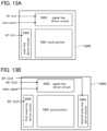
- FIGS. 2 A and 2 Ban example of manufacturing a common connection portion (a pad portion), in which a wiring formed of the same material and in the same process as a gate wiring is used as a common potential line, will be illustrated in FIGS. 2 A and 2 B .
- FIG. 2 Billustrates an example of a top view of a common connection portion
- dashed line E 1 -E 2 in FIG. 2 Bcorresponds to a cross section of the common connection portion of FIG. 2 A .
- a thin film transistor in a pixel portionhas the same structure as that of Embodiment 1; thus, portions similar to those in FIG. 1 A are denoted by the same reference numerals and detailed description is omitted here.
- a common potential line 181is provided over the substrate 100 and manufactured of the same material and in the same process as a gate electrode layer 101 .
- the common potential line 181is covered with the gate insulating layer 102 and the protective insulating layer 107 .
- the gate insulating layer 102 and the protective insulating layer 107have a plurality of openings at positions overlapping the common potential line 181 . These openings, unlike in Embodiment 1, have a large depth which corresponds to the thickness of the two insulating layers. Note that these openings are manufactured by etching in the same process as a contact hole for connecting the source electrode layer 105 a or drain electrode layer 105 b and the pixel electrode layer 110 , and then further etching the gate insulating layer 102 selectively.
- the common electrode layer 190is provided over the protective insulating layer 107 and manufactured of the same material and in the same process as the pixel electrode layer 110 in the pixel portion.
- the common connection portionis manufactured in the same process as the switching element in the pixel portion.
- the first substrate 100 provided with the pixel portion and the common connection portionis fixed to a second substrate provided with a counter electrode with a sealant.
- the pair of substratesare aligned so that the sealant overlaps the common connection portion.
- the common electrode layer 190is an electrode in contact with the conductive particles contained in the sealant, and is electrically connected to the counter electrode of the second substrate.
- the pair of substratesare fixed with a sealant, and then a liquid crystal is injected between the pair of substrates.
- a sealantis drawn on the second substrate or the first substrate and a liquid crystal is dropped thereon; then, the pair of substrates are bonded to each other under a reduced pressure.
- This embodimentshows an example of the common connection portion electrically connected to the counter electrode.
- the present inventionis not particularly limited to this example and can be applied to a connection portion connected to another wiring or a connection portion connected to an external connection terminal or the like.
- FIGS. 3 A and 3 Ban example of manufacturing a common connection portion (a pad portion), in which an electrode formed of the same material and in the same process as a gate wiring is formed and a wiring formed of the same material and in the same process as a source electrode layer is provided as a common potential line over the electrode, will be illustrated in FIGS. 3 A and 3 B .
- FIG. 3 Billustrates an example of a top view of a common connection portion
- dashed line F 1 -F 2 in FIG. 3 Bcorresponds to a cross section of the common connection portion of FIG. 3 A .
- a thin film transistor in a pixel portionhas the same structure as that of Embodiment 1; thus, portions similar to those in FIG. 1 A are denoted by the same reference numerals and detailed description is omitted here.
- connection electrode layer 191is provided over the substrate 100 and manufactured of the same material and in the same process as the gate electrode layer 101 .
- connection electrode layer 191is covered with the gate insulating layer 102 and the protective insulating layer 107 .
- the gate insulating layer 102 and the protective insulating layer 107have an opening at a position overlapping the common electrode layer 190 .
- This openingunlike in Embodiment 1, has a large depth which corresponds to the thickness of the two insulating layers. Note that this opening is manufactured by etching in the same process as a contact hole for connecting the source electrode layer 105 a or drain electrode layer 105 b and the pixel electrode layer 110 , and then further etching the gate insulating layer 102 selectively.
- the common potential line 185is provided over the gate insulating layer 102 and manufactured of the same material and in the same process as the source and drain electrode layers 105 a and 105 b.
- the common potential line 185is covered with the protective insulating layer 107 , and the protective insulating layer 107 has a plurality of openings at positions overlapping the common potential line 185 . These openings are manufactured in the same process as a contact hole for connecting the source electrode layer 105 a or drain electrode layer 105 b and the pixel electrode layer 110 .
- the common electrode layer 190is provided over the protective insulating layer 107 and manufactured of the same material and in the same process as the pixel electrode layer 110 in the pixel portion.
- the common connection portionis manufactured in the same process as the switching element in the pixel portion.
- the first substrate 100 provided with the pixel portion and the common connection portionis fixed to a second substrate provided with a counter electrode with a sealant.
- a plurality of conductive particlesare selectively disposed in the opening of the gate insulating layer. That is, the plurality of conductive particles are disposed in a region where the common electrode layer 190 and the connection electrode layer 191 are in contact with each other.
- the common electrode layer 190 touching both the connection electrode layer 191 and the common potential line 185is an electrode in contact with the conductive particles, and is electrically connected to the counter electrode of the second substrate.
- the pair of substratesare fixed with a sealant, and then a liquid crystal is injected between the pair of substrates.
- a sealantis drawn on the second substrate or the first substrate and a liquid crystal is dropped thereon; then, the pair of substrates are bonded to each other under a reduced pressure.
- This embodimentshows an example of the common connection portion electrically connected to the counter electrode.
- the present inventionis not particularly limited to this example and can be applied to a connection portion connected to another wiring or a connection portion connected to an external connection terminal or the like.
- FIGS. 29 A and 29 Banother example of the display device shown in Embodiment 1, in which source and drain electrode layers and source and drain regions are formed by etching using the same mask, will be illustrated in FIGS. 29 A and 29 B .
- FIG. 29 Ais a cross-sectional view of a semiconductor device in which a thin film transistor and a common connection portion (a pad portion) are manufactured over the same substrate.
- a thin film transistor 172 illustrated in FIG. 29 Ais an inverted staggered thin film transistor and is an example of a thin film transistor in which the source and drain electrode layers 105 a and 105 b are provided over the semiconductor layer 103 with the source and drain regions 104 a and 104 b interposed therebetween.
- an oxide semiconductor layer forming the source and drain regions 104 a and 104 b and a conductive layer forming the source and drain electrode layers 105 a and 105 bare etched using the same mask.
- the source and drain electrode layers 105 a and 105 b and the source and drain regions 104 a and 104 bhave the same shape, and the source and drain regions 104 a and 104 b are placed under the source and drain electrode layers 105 a and 105 b.
- an oxide semiconductor layer 186 manufactured of the same material and in the same process as the source and drain regions 104 a and 104 bis formed between the gate insulating layer 102 and the common potential line 185 .
- FIG. 29 Billustrates an example of a top view of the common connection portion
- dashed line G 1 -G 2 in FIG. 29 Bcorresponds to a cross section of the common connection portion of FIG. 29 A .
- FIG. 29 Bthe top view of the common connection portion has the same structure as that of Embodiment 1; thus, portions similar to those in FIG. 1 B are denoted by the same reference numerals and detailed description is omitted here.
- the oxide semiconductor layer and the conductive layerare stacked in the common connection portion (the pad portion) provided in the periphery of the pixel portion, whereby a defect due to separation of a thin film can be prevented, resulting in an increase in the strength of the structure.
- the thickness of the pad portionincreases and the resistance thereof decreases.
- FIGS. 30 A and 30 Banother example of the display device shown in Embodiment 3, in which source and drain electrode layers and source and drain regions are formed by etching using the same mask, will be illustrated in FIGS. 30 A and 30 B .
- FIG. 30 Ais a cross-sectional view of a semiconductor device in which a thin film transistor and a common connection portion (a pad portion) are manufactured over the same substrate.
- a thin film transistor in a pixel portionhas the same structure as that of Embodiment 4; thus, portions similar to those in FIG. 29 A are denoted by the same reference numerals and detailed description is omitted here.
- an oxide semiconductor layer forming the source and drain regions 104 a and 104 b and a conductive layer forming the source and drain electrode layers 105 a and 105 bare etched using the same mask. Therefore, in the thin film transistor 172 , the source and drain electrode layers 105 a and 105 b and the source and drain regions 104 a and 104 b have the same shape, and the source and drain regions 104 a and 104 b are placed under the source and drain electrode layers 105 a and 105 b.
- the oxide semiconductor layer 186 manufactured of the same material and in the same process as the source and drain regions 104 a and 104 bis formed between the gate insulating layer 102 and the common potential line 185 .
- FIG. 30 Billustrates an example of a top view of a common connection portion, and dashed line F 1 -F 2 in FIG. 30 B corresponds to a cross section of the common connection portion of FIG. 30 A .
- the top view of the common connection portionhas the same structure as that of Embodiment 3; thus, portions similar to those in FIG. 3 B are denoted by the same reference numerals and detailed description is omitted here.
- the oxide semiconductor layer and the conductive layerare stacked in the common connection portion (the pad portion) provided in the periphery of the pixel portion, whereby a defect due to separation of a thin film can be prevented, resulting in an increase in the strength of the structure.
- the thickness of the pad portionincreases and the resistance thereof decreases.
- FIGS. 4 A to 4 Ca manufacturing process of a display device including a thin film transistor of one embodiment of the present invention will be described with reference to FIGS. 4 A to 4 C , FIGS. 5 A to 5 C , FIGS. 6 to 9 , FIGS. 10 A to 10 D , and FIG. 11 .
- the light transmitting substrate 100it is possible to use a glass substrate made of barium borosilicate glass, aluminoborosilicate glass, or the like typified by #7059 glass, #1737 glass, or the like manufactured by Corning Incorporated.
- a resist maskis formed by a first photolithography step. Then, unnecessary portions are removed by etching, thereby forming wirings and electrodes (a gate wiring including the gate electrode layer 101 , a capacitor wiring 108 , and a first terminal 121 ). At that time, etching is performed so that at least the edge of the gate electrode layer 101 is tapered.
- FIG. 4 AA cross-sectional view at this stage is illustrated in FIG. 4 A . Note that FIG. 6 is a top view at this stage.
- the gate wiring including the gate electrode layer 101 , the capacitor wiring 108 , and the first terminal 121 in the terminal portionare preferably formed of a low-resistant conductive material such as aluminum (Al) or copper (Cu).
- a low-resistant conductive materialsuch as aluminum (Al) or copper (Cu).
- Alaluminum alone has the disadvantages of low heat resistance, being easily corroded, and the like; thus, it is used in combination with a conductive material having heat resistance.
- the conductive material having heat resistanceit is possible to use an element selected from titanium (Ti), tantalum (Ta), tungsten (W), molybdenum (Mo), chromium (Cr), neodymium (Nd), and scandium (Sc), an alloy containing any of these elements as its component, an alloy containing a combination of any of these elements, or a nitride containing any of these elements as its component.
- the gate insulating layer 102is formed on the entire surface of the gate electrode layer 101 .
- the gate insulating layer 102is formed to a thickness of 50 nm to 250 nm by sputtering or the like.
- a silicon oxide filmis formed to a thickness of 100 nm by sputtering. It is needless to say that the gate insulating layer 102 is not limited to such a silicon oxide film, and other insulating films such as a silicon oxynitride film, a silicon nitride film, an aluminum oxide film, or a tantalum oxide film may be used to form a single-layer structure or a multi-layer structure.
- the surface of the gate insulating layermay be cleaned by plasma treatment before forming an oxide semiconductor layer (an IGZO semiconductor layer) that is to be a channel formation region. It is effective to perform plasma treatment to remove dust such as organic substances on the surface of the gate insulating layer. It is also effective that the surface of the gate insulating layer is subjected to plasma treatment to be an oxygen-excess region, which serves as an oxygen supply source to modify the interface between the gate insulating layer and the IGZO semiconductor layer in heat treatment (200° C. to 600° C.) to increase reliability in subsequent steps.
- an oxide semiconductor layeris preferably deposited by sputtering without being exposed to the atmosphere. If a deposition target substrate is exposed to the atmosphere before an oxide semiconductor layer is deposited, moisture or the like is attached to the deposition target substrate, which may adversely affect the interface state leading to variations in threshold values, degradation of electrical properties, production of a normally-on TFT, and the like.
- the plasma treatmentis performed using oxygen gas or argon gas. Instead of argon gas, other rare gases may be used.
- the IGZO semiconductor layerIn order to form the IGZO semiconductor layer to be a channel formation region by a sputtering method without exposure to the air after plasma treatment, it is preferable to perform a kind of plasma treatment called reverse sputtering which can be performed in the same chamber as that used in the formation of the IGZO semiconductor layer.
- the reverse sputtering treatmentis a method in which voltage is applied to a substrate side in an oxygen atmosphere or an oxygen and argon atmosphere without applying voltage to a target side, so that plasma is generated to modify the surface of a thin film on the substrate.
- the surface of the gate insulating layeris exposed to oxygen radicals to be modified into an oxygen-excess region, thereby increasing the oxygen concentration at the interface with an oxide semiconductor layer which is deposited later to be a channel formation region.
- oxygen radical treatmentis performed on the gate insulating layer and an oxide semiconductor layer is stacked thereon, and then heat treatment is performed, the oxygen concentration of the oxide semiconductor layer to be a channel formation region on the gate insulating layer side can also be increased.
- the oxygen concentrationreaches a peak at the interface between the gate insulating layer and the oxide semiconductor layer to be a channel formation region
- the oxygen concentration of the gate insulating layerhas a concentration gradient which increases toward the interface between the gate insulating layer and the oxide semiconductor layer to be a channel formation region.
- the gate insulating layer including an oxygen-excess regionis compatible with the oxide semiconductor layer to be a channel formation region that is an oxygen-excess oxide semiconductor layer, so that favorable interface properties can be obtained.
- Oxygen radicalsmay be produced in a plasma generation apparatus with the use of a gas containing oxygen, or in an ozone generation apparatus. By exposing a thin film to the produced oxygen radicals or oxygen, the surface of the film can be modified.
- the plasma treatmentis not limited to one using oxygen radicals, and may be performed using argon and oxygen radicals.
- the treatment using argon and oxygen radicalsis treatment in which argon gas and oxygen gas are introduced to generate plasma, thereby modifying the surface of a thin film.
- Argon atoms (Ar) in a reaction space where an electric field is applied to generate discharge plasmaare excited or ionized by electrons (e) in the discharge plasma, thereby being converted into argon radicals (Ar*), argon ions (Ar + ), or electrons (e).
- Argon radicals (Ar*)which are in a high-energy metastable state, react with the peripheral atoms of the same kind or of different kinds to be returned to a stable state by exciting or ionizing the atoms, whereby a reaction occurs like an avalanche.
- oxygen atoms (O)are excited or ionized to be converted into oxygen radicals (O*), oxygen ions (O + ), or oxygen (O).
- the oxygen radicals (O*)react with a material on the surface of a thin film that is to be processed, so that the surface is modified, and the oxygen radicals also react with an organic substance on the surface, so that the organic substance is removed.
- the plasma treatmentis thus performed.
- radicals of argon gashave the properties of being kept in a metastable state for a longer time than radicals of reactive gas (oxygen gas). Therefore, it is general to use argon gas to generate plasma.
- a first oxide semiconductor film(in this embodiment, a first IGZO film) is deposited on the gate insulating layer 102 .
- the first IGZO filmis deposited without being exposed to the air after the plasma treatment, which is advantageous in that dust or moisture is not attached to the interface between the gate insulating layer and the semiconductor film.
- depositionis performed in an argon atmosphere or an oxygen atmosphere at a distance between the substrate and the target of 170 mm, a pressure of 0.4 Pa, and a direct current (DC) power supply of 0.5 kW.
- a pulsed direct current (DC) power supplyis preferably used to reduce dust and obtain a uniform distribution of film thickness.
- the thickness of the first IGZO filmis 5 nm to 200 nm, and in this embodiment, the thickness of the first IGZO film is 100 nm.
- the gate insulating layer and the first IGZO filmcan be successively deposited by sputtering without being exposed to the air by changing a gas introduced into a chamber or a target placed in the chamber as appropriate.
- a gas introduced into a chamber or a target placed in the chamberas appropriate.
- impuritiescan be prevented from entering the films.
- a multi-chamber manufacturing apparatusis preferably used.
- a second oxide semiconductor film(in this embodiment, a second IGZO film) is deposited by sputtering without being exposed to the air.
- the presence, density, and diameter of crystal grainscan be controlled by adjusting the deposition conditions of reactive sputtering as appropriate, such as the composition ratio of a target, the deposition pressure (0.1 Pa to 2.0 Pa), the power (250 W to 3000 W: 8 inches ⁇ ), or the temperature (room temperature to 100° C.).
- the diameter of crystal grainsis controlled within a range of 1 nm to 10 nm.
- the thickness of the second IGZO filmis 5 nm to 20 nm. It is needless to say that, if the film includes crystal grains, the diameter of the crystal grains does not exceed the thickness of the film. In this embodiment, the thickness of the second IGZO film is 5 nm.
- the first IGZO film and the second IGZO filmare deposited under different conditions, so that the oxygen concentration of the first IGZO film is higher than that of the second IGZO film.
- the flow rate ratio of oxygen gas to argon gas under the deposition conditions of the first IGZO filmis higher than that under the deposition conditions of the second IGZO film.
- the second IGZO filmis deposited in a rare gas (such as argon or helium) atmosphere (or an atmosphere containing oxygen at 10% or less and an argon gas at 90% or more), and the first IGZO film is deposited in an oxygen atmosphere (or a flow rate of oxygen gas is equal to or more than a flow rate of argon gas).
- the conductivity of the first IGZO filmcan be made lower than that of the second IGZO film.
- the off-current of the first IGZO filmcan be reduced when the first IGZO film contains more oxygen, whereby a thin film transistor having a high on/off ratio can be obtained.
- the second IGZO filmmay be deposited in the same chamber as that used in the preceding reverse sputtering treatment, or may be deposited in a different chamber as long as it can be deposited without being exposed to the air.
- heat treatmentis preferably performed at 200° C. to 600° C., and typically, 300° C. to 500° C.
- heat treatment at 350° C. for one houris performed in a furnace in a nitrogen atmosphere.
- This heat treatmentinvolves the rearrangement at the atomic level in the IGZO film.
- the heat treatment (including light annealing) in this stepis important because the strain that inhibits the movement of carriers can be released. Note that there is no particular limitation on the timing of the heat treatment, and the heat treatment may be performed at any time after the deposition of the second IGZO film, for example, after the formation of a pixel electrode.
- a second photolithography stepis performed to form a resist mask, and the first IGZO film and the second IGZO film are etched.
- unnecessary portionsare removed by wet etching using ITO07N (manufactured by KANTO CHEMICAL CO., INC.), thereby forming an IGZO film 109 that is an oxygen-excess first IGZO film and an IGZO film 111 that is an oxygen-deficient second IGZO film.
- this etching stepis not limited to wet etching and dry etching may also be performed.
- a cross-sectional view at this stageis illustrated in FIG. 4 B . Note that FIG. 7 is a top view at this stage.
- a conductive film 132 made of a metal materialis formed over the IGZO film 109 and the IGZO film 111 by sputtering or vacuum evaporation.
- a cross-sectional view at this stageis illustrated in FIG. 4 C .
- the material of the conductive film 132there are an element selected from Al, Cr, Ta, Ti, Mo, and W, an alloy containing any of these elements as its component, an alloy containing a combination of any of these elements, and the like. If heat treatment at 200° C. to 600° C. is performed, the conductive film preferably has heat resistance enough to withstand the heat treatment. Since aluminum alone has the disadvantages of low heat resistance, being easily corroded, and the like, it is used in combination with a conductive material having heat resistance.
- the conductive material having heat resistance which is combined with aluminumit is possible to use an element selected from titanium (Ti), tantalum (Ta), tungsten (W), molybdenum (Mo), chromium (Cr), neodymium (Nd), and scandium (Sc), an alloy containing any of these elements as its component, an alloy containing a combination of any of these elements, or a nitride containing any of these elements as its component.
- the conductive film 132has a single-layer structure of a titanium film.
- the conductive film 132may also have a two-layer structure in which a titanium film is stacked on an aluminum film.
- the conductive film 132may have a three-layer structure in which a titanium film, an aluminum film containing neodymium (an Al—Nd film), and a titanium film are stacked in order.
- the conductive film 132may have a single-layer structure of an aluminum film containing silicon.
- a third photolithography stepis performed to form a resist mask 131 , and unnecessary portions are removed by etching, thereby forming the source and drain electrode layers 105 a and 105 b and the source and drain regions 104 a and 104 b .
- This etching stepis performed by wet etching or dry etching.
- wet etchingcan be performed using a solution in which phosphoric acid, acetic acid, and nitric acid are mixed.
- the conductive film 132 made of titaniumis wet-etched to form the source and drain electrode layers 105 a and 105 b
- the IGZO film 111is wet-etched to form the source and drain regions 104 a and 104 b .
- an exposed region of the IGZO film 109is partly etched to be the semiconductor layer 103 .
- a channel region of the semiconductor layer 103 between the source and drain regions 104 a and 104 bhas a small thickness.
- the source and drain electrode layers 105 a and 105 b and the source and drain regions 104 a and 104 bare simultaneously etched using an ammonia hydrogen peroxide mixture; therefore, the edges of the source and drain electrode layers 105 a and 105 b are aligned with the edges of the source and drain regions 104 a and 104 b to have a continuous structure.
- wet etchingallows the layers to be etched isotropically, so that the edges of the source and drain electrode layers 105 a and 105 b are recessed from the resist mask 131 .
- the exposed channel formation region of the semiconductor layer 103may be subjected to oxygen radical treatment, so that a normally-off thin film transistor can be obtained.
- the radical treatmentcan repair damage due to the etching of the semiconductor layer 103 .
- the radical treatmentis preferably performed in an atmosphere of O 2 or N 2 O, and preferably an atmosphere of N 2 , He, or Ar each containing oxygen.
- the radical treatmentmay also be performed in an atmosphere in which Cl 2 or CF 4 is added to the above atmosphere. Note that the radical treatment is preferably performed with no bias applied.
- a second terminal 122that is made of the same material as the source and drain electrode layers 105 a and 105 b remains in the terminal portion. Note that the second terminal 122 is electrically connected to a source wiring (a source wiring including the source and drain electrode layers 105 a and 105 b ).
- the number of resist maskscan be reduced, resulting in simplified process and lower cost.
- the protective insulating layer 107can be formed of a silicon nitride film, a silicon oxide film, a silicon oxynitride film, an aluminum oxide film, a tantalum oxide film, or the like which is obtained by sputtering.
- a fourth photolithography stepis performed to form a resist mask, and the protective insulating layer 107 is etched to form a contact hole 125 reaching the source electrode layer 105 a or drain electrode layer 105 b .
- a contact hole 127 reaching the second terminal 122is also formed in the same etching step.
- the gate insulating layeris preferably etched using the same resist mask so that a contact hole 126 reaching the gate electrode is formed using the same resist mask. A cross-sectional view at this stage is illustrated in FIG. 5 B .
- the transparent conductive filmis formed of indium oxide (In 2 O 3 ), indium oxide-tin oxide alloy (In 2 O 3 —SnO 2 , abbreviated to ITO), or the like by sputtering, vacuum evaporation, or the like. Such a material is etched with a hydrochloric acid-based solution. However, since a residue is easily generated particularly in etching ITO, indium oxide-zinc oxide alloy (In 2 O 3 —ZnO) may be used to improve etching processability.
- indium oxide-zinc oxide alloyIn 2 O 3 —ZnO
- a fifth photolithography stepis performed to form a resist mask, and unnecessary portions are removed by etching, thereby forming the pixel electrode layer 110 .
- a storage capacitoris formed between the capacitor wiring 108 and the pixel electrode layer 110 by using the gate insulating layer 102 and the protective insulating layer 107 in the capacitor portion as a dielectric.
- the first terminal and the second terminalare covered with the resist mask so that transparent conductive films 128 and 129 remain in the terminal portion.
- the transparent conductive films 128 and 129serve as an electrode or a wiring connected to an FPC.
- the transparent conductive film 129 formed over the second terminal 122is a connecting terminal electrode serving as an input terminal of a source wiring.
- FIG. 5 CA cross-sectional view at this stage is illustrated in FIG. 5 C .
- FIG. 9is a top view at this stage.
- FIGS. 10 A to 10 Dare respectively a cross-sectional view and a top view of a gate wiring terminal portion at this stage.
- FIG. 10 Ais a cross-sectional view taken along line C 1 -C 2 of FIG. 10 B
- a transparent conductive film 155 formed over the protective insulating film 154is a connecting terminal electrode serving as an input terminal.
- a first terminal 151 made of the same material as the gate wiring and a connection electrode layer 153 made of the same material as the source wiringoverlap each other with a gate insulating layer 152 interposed therebetween, and are electrically connected to each other through the transparent conductive film 155 .
- FIG. 5 Cwhere the transparent conductive film 128 is in contact with the first terminal 121 corresponds to a part of FIG. 10 A where the transparent conductive film 155 is in contact with the first terminal 151 .
- FIGS. 10 C and 10 Dare respectively a cross-sectional view and a top view of a source wiring terminal portion which is different from that illustrated in FIG. 5 C .
- FIG. 10 Cis a cross-sectional view taken along line D 1 -D 2 of FIG. 10 D .
- the transparent conductive film 155 formed over the protective insulating film 154is a connecting terminal electrode serving as an input terminal.
- an electrode layer 156 made of the same material as the gate wiringis formed under a second terminal 150 electrically connected to the source wiring and overlaps the second terminal 150 with the gate insulating layer 152 interposed therebetween.
- the electrode layer 156is not electrically connected to the second terminal 150 , and a capacitor to prevent noise or static electricity can be formed if the potential of the electrode layer 156 is set to a potential different from that of the second terminal 150 , such as floating, GND, or 0 V.
- the second terminal 150is electrically connected to the transparent conductive film 155 with an opening of the protective insulating film 154 interposed therebetween.
- a plurality of gate wirings, source wirings, and capacitor wiringsare provided depending on the pixel density. Also in the terminal portion, the first terminal at the same potential as the gate wiring, the second terminal at the same potential as the source wiring, the third terminal at the same potential as the capacitor wiring, and the like are each arranged in plurality. There is no particular limitation on the number of each of the terminals, and the number of the terminals may be determined by a practitioner as appropriate.
- a pixel thin film transistor portion including the thin film transistor 170 which is a bottom-gate n-channel thin film transistor, and the storage capacitorcan be completed using the five photomasks.
- these pixel thin film transistor portion and storage capacitorare arranged in a matrix corresponding to respective pixels, a pixel portion can be formed and one of the substrates for manufacturing an active matrix display device can be obtained.
- a substrateis referred to as an active matrix substrate for convenience.
- an active matrix substrate and a counter substrate provided with a counter electrodeare bonded to each other with a liquid crystal layer interposed therebetween.
- a common electrode electrically connected to the counter electrode on the counter substrateis provided over the active matrix substrate, and a fourth terminal electrically connected to the common electrode is provided in the terminal portion. The fourth terminal is provided so that the common electrode is fixed to a predetermined potential such as GND or 0 V.
- FIG. 11illustrates an example in which a capacitor wiring is not provided and a pixel electrode layer overlaps a gate wiring of an adjacent pixel with a protective insulating film and a gate insulating layer interposed therebetween to form a storage capacitor. In that case, the capacitor wiring and the third terminal connected to the capacitor wiring can be omitted. Note that in FIG. 11 , portions similar to those in FIG. 9 are denoted by the same reference numerals.
- pixel electrodes arranged in a matrixare driven to form a display pattern on a screen. Specifically, voltage is applied between a selected pixel electrode and a counter electrode corresponding to the pixel electrode, so that a liquid crystal layer provided between the pixel electrode and the counter electrode is optically modulated and this optical modulation is recognized as a display pattern by an observer.
- a liquid crystal display deviceIn displaying moving images, a liquid crystal display device has a problem that a long response time of liquid crystal molecules themselves causes afterimages or blurring of moving images.
- a driving method called black insertionis employed in which black is displayed on the whole screen every other frame period.
- double-frame rate drivingthere is another driving technique which is so-called double-frame rate driving.
- a vertical cycleis set 1.5 times as much as a normal vertical cycle or more (preferably 2 times or more), whereby moving image characteristics are improved.
- a driving methodmay be employed in which a plurality of LEDs (light-emitting diodes) or a plurality of EL light sources are used to form a surface light source as a backlight, and each light source of the surface light source is independently driven in a pulsed manner in one frame period.
- the surface light sourcethree or more kinds of LEDs may be used and an LED emitting white light may be used. Since a plurality of LEDs can be controlled independently, the light emission timing of LEDs can be synchronized with the timing at which a liquid crystal layer is optically modulated. According to this driving method, LEDs can be partly turned off; therefore, an effect of reducing power consumption can be obtained particularly in the case of displaying an image having a large part on which black is displayed.
- the display characteristics of a liquid crystal display devicesuch as moving-image characteristics, can be improved as compared to those of conventional liquid crystal display devices.
- the n-channel transistor of this embodimentincludes an IGZO semiconductor layer in a channel formation region and has good dynamic characteristics. Accordingly, these driving methods can be applied in combination to the n-channel transistor of this embodiment.
- one electrode (also referred to as a cathode) of an organic light-emitting elementis set to a low power supply potential such as GND or 0 V; thus, a terminal portion is provided with a fourth terminal for setting the cathode to a low power supply potential such as GND or 0 V.
- a power supply lineis provided in addition to a source wiring and a gate wiring. Accordingly, a terminal portion is provided with a fifth terminal electrically connected to the power supply line.
- a gate electrode layer, a gate insulating layer, a semiconductor layer (an oxygen-excess oxide semiconductor layer containing In, Ga, and Zn), and source and drain electrode layersare stacked without providing source and drain regions (oxygen-deficient oxide semiconductor layers containing In, Ga, and Zn), the distance between the gate electrode layer and the source and drain electrode layers is reduced to increase the parasitic capacitance therebetween. In addition, the parasitic capacitance is further increased by a reduction in the thickness of the semiconductor layer.
- a thin film transistorhas a stacked structure in which a gate electrode layer, a gate insulating layer, a semiconductor layer, source and drain electrode regions, and source and drain electrode layers are stacked, parasitic capacitance can be suppressed even when the thickness of the semiconductor layer is small.
- a thin film transistor having a small amount of photocurrent, low parasitic capacitance, a high on-off ratio, and good dynamic characteristicscan be manufactured.
- a semiconductor device including a thin film transistor having high electrical properties and high reliabilitycan be provided.
- FIGS. 31 A and 31 Banother example of the display device shown in Embodiment 3, which includes a thin film transistor in which source and drain electrode layers are in contact with a semiconductor layer, will be illustrated in FIGS. 31 A and 31 B .
- FIG. 31 Ais a cross-sectional view of a semiconductor device in which a thin film transistor and a common connection portion (a pad portion) are manufactured over the same substrate.
- a thin film transistor 171 illustrated in FIG. 31 Ais an inverted staggered thin film transistor and is an example of a thin film transistor in which the source and drain electrode layers 105 a and 105 b are provided in contact with the semiconductor layer 103 .
- a contact region between the semiconductor layer 103 and the source and drain electrode layers 105 a and 105 bis preferably modified by plasma treatment.
- an oxide semiconductor layer(an IGZO semiconductor layer in this embodiment) is subjected to plasma treatment.
- the plasma treatmentis performed using argon gas, hydrogen gas, or a mixture gas of argon and hydrogen.
- Oxygen gasmay be added to these gases.
- argon gasother rare gases may be used.
- an exposed region of the semiconductor layer that is an IGZO semiconductor layeris partly etched to be the semiconductor layer 103 .
- a channel region of the semiconductor layer 103 between the source and drain electrode layers 105 a and 105 bhas a small thickness.
- a conductive layeris formed in contact with the semiconductor layer 103 modified by the plasma treatment, thereby forming the source and drain electrode layers 105 a and 105 b . Accordingly, the contact resistance between the semiconductor layer 103 and the source and drain electrode layers 105 a and 105 b can be reduced.
- a display devicewhich is one example of a semiconductor device of the present invention will be described.
- the display deviceat least a part of a driver circuit and a thin film transistor to be disposed in a pixel portion are formed over one substrate.
- the thin film transistor to be disposed in the pixel portionis formed according to Embodiment 6 or 7. Further, the thin film transistor described in Embodiment 6 or 7 is an n-channel TFT, and thus a part of a driver circuit that can include an n-channel TFT among driver circuits is formed over the same substrate as the thin film transistor in the pixel portion.
- FIG. 13 Aillustrates an example of a block diagram of an active matrix liquid crystal display device which is an example of a semiconductor device of the present invention.
- the display device illustrated in FIG. 13 Aincludes, over a substrate 5300 , a pixel portion 5301 including a plurality of pixels each provided with a display element; a scan line driver circuit 5302 for selecting a pixel; and a signal line driver circuit 5303 for controlling a video signal input to the selected pixel.
- the pixel portion 5301is connected to the signal line driver circuit 5303 by a plurality of signal lines Si to Sm (not illustrated) that extend in a column direction from the signal line driver circuit 5303 , and to the scan line driver circuit 5302 by a plurality of scan lines G 1 to Gn (not illustrated) that extend in a row direction from the scan line driver circuit 5302 .
- the pixel portion 5301includes a plurality of pixels (not illustrated) arranged in a matrix so as to correspond to the signal lines S 1 to Sm and the scan lines G 1 to Gn. Each pixel is connected to a signal line Sj (one of the signal lines S 1 to Sm) and a scan line Gj (one of the scan lines G 1 to Gn).
- the thin film transistor described in Embodiment 6 or 7is an n-channel TFT, and a signal line driver circuit including an n-channel TFT will be described with reference to FIG. 14 .
- the signal line driver circuit illustrated in FIG. 14includes a driver IC 5601 , switch groups 5602 - 1 to 5602 -M, a first wiring 5611 , a second wiring 5612 , a third wiring 5613 , and wirings 5621 - 1 to 5621 -M.
- Each of the switch groups 5602 - 1 to 5602 -Mincludes a first thin film transistor 5603 a , a second thin film transistor 5603 b , and a third thin film transistor 5603 c.
- the driver IC 5601is connected to the first wiring 5611 , the second wiring 5612 , the third wiring 5613 , and the wirings 5621 - 1 to 5621 -M.
- Each of the switch groups 5602 - 1 to 5602 -Mis connected to the first wiring 5611 , the second wiring 5612 , and the third wiring 5613 , and the switch groups 5602 - 1 to 5602 -M are connected to the wirings 5621 - 1 to 5621 -M, respectively.
- Each of the wirings 5621 - 1 to 5621 -Mis connected to three signal lines via the first thin film transistor 5603 a , the second thin film transistor 5603 b , and the third thin film transistor 5603 c .
- the wiring 5621 -J of the J-th column(one of the wirings 5621 - 1 to 5621 -M) is connected to a signal line Sj ⁇ 1, a signal line Sj, and a signal line Sj+1 via the first thin film transistor 5603 a , the second thin film transistor 5603 b , and the third thin film transistor 5603 c which are included in the switch group 5602 -J.
- a signalis input to each of the first wiring 5611 , the second wiring 5612 , and the third wiring 5613 .
- the driver IC 5601is preferably formed over a single crystal substrate. Further, the switch groups 5602 - 1 to 5602 -M are preferably formed over the same substrate as the pixel portion. Therefore, the driver IC 5601 is preferably connected to the switch groups 5602 - 1 to 5602 -M through an FPC or the like.
- the timing chart of FIG. 15illustrates a case where the scan line Gi of the i-th row is selected.
- a selection period of the scan line Gi of the i-th rowis divided into a first sub-selection period T 1 , a second sub-selection period T 2 , and a third sub-selection period T 3 .
- the signal line driver circuit in FIG. 14operates in a manner similar to that of FIG. 15 even when a scan line of another row is selected.
- the timing chart of FIG. 15illustrates a case where the wiring 5621 -J of the J-th column is connected to the signal line Sj ⁇ 1, the signal line Sj, and the signal line Sj+1 via the first thin film transistor 5603 a , the second thin film transistor 5603 b , and the third thin film transistor 5603 c.
- the timing chart of FIG. 15shows the timing at which the scan line Gi of the i-th row is selected, timing 5703 a at which the first thin film transistor 5603 a is turned on/off, timing 5703 b at which the second thin film transistor 5603 b is turned on/off, timing 5703 c at which the third thin film transistor 5603 c is turned on/off, and a signal 5721 -J input to the wiring 5621 -J of the J-th column.
- the first sub-selection period T 1 , the second sub-selection period T 2 , and the third sub-selection period T 3different video signals are input to the wirings 5621 - 1 to 5621 -M.
- a video signal input to the wiring 5621 -J in the first sub-selection period T 1is input to the signal line Sj ⁇ 1
- a video signal input to the wiring 5621 -J in the second sub-selection period T 2is input to the signal line Sj
- a video signal input to the wiring 5621 -J in the third sub-selection period T 3is input to the signal line Sj+1.
- the video signals input to the wiring 5621 -J in the first sub-selection period T 1 , the second sub-selection period T 2 , and the third sub-selection period T 3are denoted by Data-j ⁇ 1, Data-j, and Data-j+1, respectively.
- the first thin film transistor 5603 ais turned on, and the second thin film transistor 5603 b and the third thin film transistor 5603 c are turned off.
- Data-j ⁇ 1 input to the wiring 5621 -Jis input to the signal line Sj ⁇ 1 via the first thin film transistor 5603 a .
- the second thin film transistor 5603 bis turned on, and the first thin film transistor 5603 a and the third thin film transistor 5603 c are turned off.
- Data-j input to the wiring 5621 -Jis input to the signal line Sj via the second thin film transistor 5603 b .
- the third thin film transistor 5603 cis turned on, and the first thin film transistor 5603 a and the second thin film transistor 5603 b are turned off.
- Data j+1 input to the wiring 5621 -Jis input to the signal line Sj+1 via the third thin film transistor 5603 c.
- the signal line driver circuit of FIG. 14by dividing one gate selection period into three, video signals can be input to three signal lines from one wiring 5621 in one gate selection period. Therefore, in the signal line driver circuit of FIG. 14 , the number of connections between the substrate provided with the driver IC 5601 and the substrate provided with the pixel portion can be reduced to approximately one third of the number of signal lines. When the number of connections is reduced to approximately one third of the number of the signal lines, the reliability, yield, and the like of the signal line driver circuit of FIG. 14 can be improved.
- one gate selection periodis divided into a plurality of sub-selection periods and video signals are input to a plurality of signal lines from one wiring in the respective sub-selection periods as illustrated in FIG. 14 .
- one gate selection periodis divided into four or more sub-selection periods, one sub-selection period becomes shorter. Therefore, one gate selection period is preferably divided into two or three sub-selection periods.
- one selection periodmay be divided into a precharge period Tp, the first sub-selection period T 1 , the second sub-selection period T 2 , and the third sub-selection period T 3 as illustrated in a timing chart of FIG. 16 .
- the timing chart of FIG. 16illustrates the timing at which the scan line Gi of the i-th row is selected, timing 5803 a at which the first thin film transistor 5603 a is turned on/off, timing 5803 b at which the second thin film transistor 5603 b is turned on/off, timing 5803 c at which the third thin film transistor 5603 c is turned on/off, and a signal 5821 -J input to the wiring 5621 -J of the J-th column.
- the first thin film transistor 5603 a , the second thin film transistor 5603 b , and the third thin film transistor 5603 care tuned on in the precharge period Tp.
- precharge voltage Vp input to the wiring 5621 -Jis input to each of the signal line Sj ⁇ 1, the signal line Sj, and the signal line Sj+1 via the first thin film transistor 5603 a , the second thin film transistor 5603 b , and the third thin film transistor 5603 c .
- the first thin film transistor 5603 ais turned on, and the second thin film transistor 5603 b and the third thin film transistor 5603 c are turned off.
- Data-j ⁇ 1 input to the wiring 5621 -Jis input to the signal line Sj ⁇ 1 via the first thin film transistor 5603 a .
- the second thin film transistor 5603 bis turned on, and the first thin film transistor 5603 a and the third thin film transistor 5603 c are turned off.
- Data-j input to the wiring 5621 -Jis input to the signal line Sj via the second thin film transistor 5603 b .
- the third thin film transistor 5603 cis turned on, and the first thin film transistor 5603 a and the second thin film transistor 5603 b are turned off.
- Data j+1 input to the wiring 5621 -Jis input to the signal line Sj+1 via the third thin film transistor 5603 c.
- the video signalcan be written to the pixel at high speed because the signal line can be precharged by providing a precharge selection period before a sub-selection period.
- FIG. 16portions of FIG. 16 which are similar to those of FIG. 15 are denoted by common reference numerals and detailed description of like portions and portions having a similar function is omitted.
- the scan line driver circuitincludes a shift register and a buffer. Additionally, the scan line driver circuit may include a level shifter in some cases.
- CLKclock signal
- SPstart pulse signal
- a selection signalis generated.
- the generated selection signalis buffered and amplified by the buffer, and the resulting signal is supplied to a corresponding scan line.
- Gate electrodes of transistors in pixels of one lineare connected to the scan line. Since the transistors in the pixels of one line have to be turned on all at once, a buffer which can supply a large current is used.
- FIG. 17illustrates a circuit configuration of the shift register.
- the shift register illustrated in FIG. 17includes a plurality of flip-flops (flip-flops 5701 - 1 to 5701 - n ).
- the shift registeroperates with the input of a first clock signal, a second clock signal, a start pulse signal, and a reset signal.
- a first wiring 5501 illustrated in FIG. 18is connected to a seventh wiring 5717 - i ⁇ 1; a second wiring 5502 illustrated in FIG. 18 is connected to a seventh wiring 5717 - i+ 1; a third wiring 5503 illustrated in FIG. 18 is connected to a seventh wiring 5717 - i ; and a sixth wiring 5506 illustrated in FIG. 18 is connected to a fifth wiring 5715 .
- a fourth wiring 5504 illustrated in FIG. 18is connected to a second wiring 5712 in flip-flops of odd-numbered stages, and is connected to a third wiring 5713 in flip-flops of even-numbered stages.
- a fifth wiring 5505 illustrated in FIG. 18is connected to a fourth wiring 5714 .
- first wiring 5501 of the first stage flip-flop 5701 - 1 illustrated in FIG. 18is connected to a first wiring 5711 .
- second wiring 5502 of the n-th stage flip-flop 5701 - n illustrated in FIG. 18is connected to a sixth wiring 5716 .
- first wiring 5711 , the second wiring 5712 , the third wiring 5713 , and the sixth wiring 5716may be referred to as a first signal line, a second signal line, a third signal line, and a fourth signal line, respectively.
- the fourth wiring 5714 and the fifth wiring 5715may be referred to as a first power supply line and a second power supply line, respectively.
- FIG. 18illustrates details of the flip-flop illustrated in FIG. 17 .
- a flip-flop illustrated in FIG. 18includes a first thin film transistor 5571 , a second thin film transistor 5572 , a third thin film transistor 5573 , a fourth thin film transistor 5574 , a fifth thin film transistor 5575 , a sixth thin film transistor 5576 , a seventh thin film transistor 5577 , and an eighth thin film transistor 5578 .
- Each of the first thin film transistor 5571 , the second thin film transistor 5572 , the third thin film transistor 5573 , the fourth thin film transistor 5574 , the fifth thin film transistor 5575 , the sixth thin film transistor 5576 , the seventh thin film transistor 5577 , and the eighth thin film transistor 5578is an n-channel transistor and is turned on when the gate-source voltage (V gs ) exceeds the threshold voltage (V th ).
- connection structures of the flip-flop illustrated in FIG. 18will be described below.
- a first electrode (one of a source electrode and a drain electrode) of the first thin film transistor 5571is connected to the fourth wiring 5504 .
- a second electrode (the other of the source electrode and the drain electrode) of the first thin film transistor 5571is connected to the third wiring 5503 .
- a first electrode of the second thin film transistor 5572is connected to the sixth wiring 5506 .
- a second electrode of the second thin film transistor 5572is connected to the third wiring 5503 .
- a first electrode of the third thin film transistor 5573is connected to the fifth wiring 5505 and a second electrode of the third thin film transistor is connected to a gate electrode of the second thin film transistor 5572 .
- a gate electrode of the third thin film transistor 5573is connected to the fifth wiring 5505 .
- a first electrode of the fourth thin film transistor 5574is connected to the sixth wiring 5506 .
- a second electrode of the fourth thin film transistor 5574is connected to a gate electrode of the second thin film transistor 5572 .
- a gate electrode of the fourth thin film transistor 5574is connected to a gate electrode of the first thin film transistor 5571 .
- a first electrode of the fifth thin film transistor 5575is connected to the fifth wiring 5505 .
- a second electrode of the fifth thin film transistor 5575is connected to the gate electrode of the first thin film transistor 5571 .
- a gate electrode of the fifth thin film transistor 5575is connected to the first wiring 5501 .
- a first electrode of the sixth thin film transistor 5576is connected to the sixth wiring 5506 .
- a second electrode of the sixth thin film transistor 5576is connected to the gate electrode of the first thin film transistor 5571 .
- a gate electrode of the sixth thin film transistor 5576is connected to the gate electrode of the second thin film transistor 5572 .
- a first electrode of the seventh thin film transistor 5577is connected to the sixth wiring 5506 .
- a second electrode of the seventh thin film transistor 5577is connected to the gate electrode of the first thin film transistor 5571 .
- a gate electrode of the seventh thin film transistor 5577is connected to the second wiring 5502 .
- a first electrode of the eighth thin film transistor 5578is connected to the sixth wiring 5506 .
- a second electrode of the eighth thin film transistor 5578is connected to the gate electrode of the second thin film transistor 5572 .
- a gate electrode of the eighth thin film transistor 5578is connected to the first wiring 5501 .
- the points at which the gate electrode of the first thin film transistor 5571 , the gate electrode of the fourth thin film transistor 5574 , the second electrode of the fifth thin film transistor 5575 , the second electrode of the sixth thin film transistor 5576 , and the second electrode of the seventh thin film transistor 5577 are connectedare each referred to as a node 5543 .
- the points at which the gate electrode of the second thin film transistor 5572 , the second electrode of the third thin film transistor 5573 , the second electrode of the fourth thin film transistor 5574 , the gate electrode of the sixth thin film transistor 5576 , and the second electrode of the eighth thin film transistor 5578 are connectedare each referred to as a node 5544 .
- first wiring 5501 , the second wiring 5502 , the third wiring 5503 , and the fourth wiring 5504may be referred to as a first signal line, a second signal line, a third signal line, and a fourth signal line, respectively.
- the fifth wiring 5505 and the sixth wiring 5506may be referred to as a first power supply line and a second power supply line, respectively.
- the signal line driver circuit and the scan line driver circuitcan be formed using only n-channel TFTs described in Embodiment 6. Since the n-channel TFT described in Embodiment 6 has a high mobility, the driving frequency of a driver circuit can be increased. In addition, in the n-channel TFT described in Embodiment 6, since parasitic capacitance is reduced by the source or drain region that is an oxide-deficient oxide semiconductor layer containing indium, gallium, and zinc, high frequency characteristics (referred to as F characteristics) can be obtained. For example, a scan line driver circuit using the n-channel TFT described in Embodiment 6 can operate at high speed, and thus a frame frequency can be increased and insertion of black images can be realized.
- F characteristicshigh frequency characteristics
- the channel width of the transistor in the scan line driver circuitis increased or a plurality of scan line driver circuits are provided, higher frame frequency can be realized.
- a scan line driver circuit for driving even-numbered scan linesis provided on one side and a scan line driver circuit for driving odd-numbered scan lines is provided on the opposite side; thus, an increase in frame frequency can be realized.
- FIG. 13 Bis an example of a block diagram of an active matrix light-emitting display device.
- the light-emitting display device illustrated in FIG. 13 Bincludes, over a substrate 5400 , a pixel portion 5401 having a plurality of pixels each provided with a display element, a first scan line driver circuit 5402 and a second scan line driver circuit 5404 for selecting a pixel, and a signal line driver circuit 5403 for controlling input of a video signal to the selected pixel.
- grayscalecan be displayed using an area grayscale method or a time grayscale method.
- An area grayscale methodrefers to a driving method in which one pixel is divided into a plurality of subpixels and the respective subpixels are driven independently based on video signals so that grayscale is displayed.
- a time grayscale methodrefers to a driving method in which a period during which a pixel emits light is controlled so that grayscale is displayed.
- the light-emitting elementis more suitable for a time grayscale method than the liquid crystal element.
- one frame periodis divided into a plurality of subframe periods.
- the light-emitting element in the pixelis brought into a light-emitting state or a non-light-emitting state in each subframe period.
- the first scan line driver circuit 5402in a case where two TFTs of a switching TFT and a current control TFT are arranged in one pixel, the first scan line driver circuit 5402 generates a signal which is input to a first scan line serving as a gate wiring of the switching TFT, and the second scan line driver circuit 5404 generates a signal which is input to a second scan line serving as a gate wiring of the current control TFT; however, one scan line driver circuit may generate both the signal which is input to the first scan line and the signal which is input to the second scan line.
- one scan line driver circuitmay generate all signals that are input to the plurality of first scan lines, or a plurality of scan line driver circuits may generate signals that are input to the plurality of first scan lines.
- a part of a driver circuit that can include n-channel TFTs among driver circuitscan be formed over the same substrate as the thin film transistors of the pixel portion.
- the signal line driver circuit and the scan line driver circuitcan be formed using only the n-channel TFTs described in Embodiment 6 or 7.
- the above-described driver circuitcan be used for electronic paper that drives electronic ink using an element electrically connected to a switching element, without being limited to applications to a liquid crystal display device or a light-emitting display device.
- the electronic paperis also referred to as an electrophoretic display device (electrophoretic display) and is advantageous in that it has the same level of readability as plain paper, it has lower power consumption than other display devices, and it can be made thin and lightweight.
- Electrophoretic displayscan have various modes. Electrophoretic displays contain a plurality of microcapsules dispersed in a solvent or a solute, each microcapsule containing first particles which are positively charged and second particles which are negatively charged. By applying an electric field to the microcapsules, the particles in the microcapsules move in opposite directions to each other and only the color of the particles gathering on one side is displayed. Note that the first particles and the second particles each contain pigment and do not move without an electric field. Moreover, the first particles and the second particles have different colors (which may be colorless).
- an electrophoretic displayis a display that utilizes a so-called dielectrophoretic effect by which a substance having a high dielectric constant moves to a high-electric field region.
- An electrophoretic display devicedoes not need to use a polarizer or a counter substrate, which is required in a liquid crystal display device, and both the thickness and weight of the electrophoretic display device can be reduced to a half of those of a liquid crystal display device.
- a solution in which the above microcapsules are dispersed in a solventis referred to as electronic ink.
- This electronic inkcan be printed on a surface of glass, plastic, cloth, paper, or the like. Furthermore, by using a color filter or particles that have a pigment, color display can also be achieved.
- an active matrix display devicecan be completed, and display can be performed by application of an electric field to the microcapsules.
- the active matrix substrate obtained by the thin film transistors described in Embodiment 6 or 7can be used.
- first particles and the second particles in the microcapsulesmay each be formed of a single material selected from a conductive material, an insulating material, a semiconductor material, a magnetic material, a liquid crystal material, a ferroelectric material, an electroluminescent material, an electrochromic material, and a magnetophoretic material, or formed of a composite material of any of these.
- a semiconductor device having a display function(also referred to as a display device) can be manufactured. Furthermore, when part or whole of a driver circuit using a thin film transistor of one embodiment of the present invention is formed over the same substrate as a pixel portion, a system-on-panel can be obtained.
- the display deviceincludes a display element.
- a liquid crystal elementalso referred to as a liquid crystal display element
- a light-emitting elementalso referred to as a light-emitting display element
- Light-emitting elementsinclude, in its category, an element whose luminance is controlled by current or voltage, and specifically include an inorganic electroluminescent (EL) element, an organic EL element, and the like.
- a display medium whose contrast is changed by an electric effect, such as an electronic ink,can be used.
- the display deviceincludes a panel in which the display element is sealed, and a module in which an IC or the like including a controller is mounted on the panel.
- An embodiment of the present inventionalso relates to an element substrate, which corresponds to one mode before the display element is completed in a manufacturing process of the display device, and the element substrate is provided with means for supplying current to the display element in each of a plurality of pixels.
- the element substratemay be in a state after only a pixel electrode of the display element is formed, a state after a conductive film to be a pixel electrode is formed and before the conductive film is etched to form the pixel electrode, or any of other states.
- a display device in this specificationmeans an image display device, a display device, or a light source (including a lighting device). Furthermore, the display device also includes the following modules in its category: a module to which a connector such as a flexible printed circuit (FPC), a tape automated bonding (TAB) tape, or a tape carrier package (TCP) is attached; a module having a TAB tape or a TCP at the tip of which a printed wiring board is provided; and a module in which an integrated circuit (IC) is directly mounted on a display element by chip on glass (COG).
- a connectorsuch as a flexible printed circuit (FPC), a tape automated bonding (TAB) tape, or a tape carrier package (TCP)
- TABtape automated bonding
- TCPtape carrier package
- COGchip on glass
- FIGS. 21 A 1 and 21 A 2are top views of a panel in which highly reliable thin film transistors 4010 and 4011 shown in Embodiment 6, each of which includes an oxygen-excess oxide semiconductor layer as a channel formation region and an oxygen-deficient oxide semiconductor layer as source and drain regions, and a liquid crystal element 4013 are sealed between a first substrate 4001 and a second substrate 4006 with a sealant 4005 .
- FIG. 21 Bis a cross-sectional view taken along line M-N of FIGS. 21 A 1 and 21 A 2 .
- the sealant 4005is provided to surround a pixel portion 4002 and a scanning line driver circuit 4004 that are provided over the first substrate 4001 .
- the second substrate 4006is provided over the pixel portion 4002 and the scanning line driver circuit 4004 . Therefore, the pixel portion 4002 and the scanning line driver circuit 4004 are sealed together with a liquid crystal layer 4008 , by the first substrate 4001 , the sealant 4005 , and the second substrate 4006 .
- a signal line driver circuit 4003that is formed using a single crystal semiconductor film or a polycrystalline semiconductor film over a substrate separately prepared is mounted in a region different from the region surrounded by the sealant 4005 over the first substrate 4001 .
- FIG. 21 A 1illustrates an example of mounting the signal line driver circuit 4003 by COG
- FIG. 21 A 2illustrates an example of mounting the signal line driver circuit 4003 by TAB.
- the pixel portion 4002 and the scanning line driver circuit 4004 provided over the first substrate 4001each include a plurality of thin film transistors.
- FIG. 21 Billustrates the thin film transistor 4010 included in the pixel portion 4002 and the thin film transistor 4011 included in the scanning line driver circuit 4004 .
- Insulating layers 4020 and 4021are provided over the thin film transistors 4010 and 4011 .
- the thin film transistors 4010 and 4011the highly reliable thin film transistor shown in Embodiment 6, which includes an oxygen-excess oxide semiconductor layer as a channel formation region and an oxygen-deficient oxide semiconductor layer as source and drain regions may be employed.
- the thin film transistor shown in Embodiment 7may be employed as the thin film transistors 4010 and 4011 .
- the thin film transistors 4010 and 4011are n-channel thin film transistors.
- a pixel electrode layer 4030 included in the liquid crystal element 4013is electrically connected to the thin film transistor 4010 .
- a counter electrode layer 4031 of the liquid crystal element 4013is formed on the second substrate 4006 .
- a portion where the pixel electrode layer 4030 , the counter electrode layer 4031 , and the liquid crystal layer 4008 overlap with one anothercorresponds to the liquid crystal element 4013 .
- the pixel electrode layer 4030 and the counter electrode layer 4031are provided with an insulating layer 4032 and an insulating layer 4033 , respectively, each of which functions as an alignment film.
- the liquid crystal layer 4008is sandwiched between the pixel electrode layer 4030 and the counter electrode layer 4031 with the insulating layers 4032 and 4033 interposed therebetween.
- first substrate 4001 and the second substrate 4006can be made of glass, metal (typically, stainless steel), ceramic, or plastic.
- plastica fiberglass-reinforced plastics (FRP) plate, a polyvinyl fluoride (PVF) film, a polyester film, or an acrylic resin film can be used.
- FRPfiberglass-reinforced plastics
- PVFpolyvinyl fluoride
- polyester filma polyester film
- acrylic resin filmacrylic resin film
- Reference numeral 4035denotes a columnar spacer obtained by selectively etching an insulating film and is provided to control the distance between the pixel electrode layer 4030 and the counter electrode layer 4031 (a cell gap). Alternatively, a spherical spacer may be used.
- the counter electrode layer 4031is electrically connected to a common potential line provided over the same substrate as the thin film transistor 4010 . With the use of the common connection portion show in any of Embodiments 1 to 3, the counter electrode layer 4031 is electrically connected to the common potential line through conductive particles provided between the pair of substrates. Note that the conductive particles are contained in the sealant 4005 .
- a liquid crystal showing a blue phase for which an alignment film is unnecessarymay be used.
- a blue phaseis one of the liquid crystal phases, which is generated just before a cholesteric phase changes into an isotropic phase while temperature of cholesteric liquid crystal is increased. Since the blue phase is only generated within a narrow range of temperature, a liquid crystal composition containing a chiral agent at 5 wt % or more is used for the liquid crystal layer 4008 in order to improve the temperature range.
- the liquid crystal composition which includes a liquid crystal showing a blue phase and a chiral agenthas a small response time of 10 ⁇ s to 100 ⁇ s, has optical isotropy, which makes the alignment process unneeded, and has a small viewing angle dependence
- an embodiment of the present inventioncan also be applied to a reflective liquid crystal display device or a transflective liquid crystal display device.
- a polarizing plateis provided on the outer surface of the substrate (on the viewer side) and a coloring layer and an electrode layer used for a display element are provided on the inner surface of the substrate in this order; however, the polarizing plate may be provided on the inner surface of the substrate.
- the stacked structure of the polarizing plate and the coloring layeris not limited to that shown in this embodiment and may be set as appropriate depending on materials of the polarizing plate and the coloring layer or conditions of manufacturing steps.
- a light-blocking film serving as a black matrixmay be provided.
- the thin film transistor obtained by Embodiment 6is covered with the insulating layers (the insulating layer 4020 and the insulating layer 4021 ) serving as a protective film or a planarizing insulating film.
- the protective filmis provided to prevent entry of impurities floating in the air, such as an organic substance, a metal substance, or moisture, and is preferably a dense film.
- the protective filmmay be formed by sputtering to be a single-layer film or a multi-layer film of a silicon oxide film, a silicon nitride film, a silicon oxynitride film, a silicon nitride oxide film, an aluminum oxide film, an aluminum nitride film, an aluminum oxynitride film, and/or an aluminum nitride oxide film.
- this embodimentshows an example of forming the protective film by sputtering, the present invention is not limited to this method and a variety of methods may be employed.
- the insulating layer having a multi-layer structureis formed as the protective film.
- a silicon oxide filmis formed by sputtering.
- the use of the silicon oxide film as the protective filmhas an effect of preventing a hillock of an aluminum film used for the source and drain electrode layers.
- the insulating layeris also formed as a second layer of the protective film.
- a silicon nitride filmis formed by sputtering. The use of the silicon nitride film as the protective film can prevent mobile ions such as sodium ions from entering a semiconductor region, thereby suppressing variations in electrical properties of the TFT.
- the IGZO semiconductor layermay be annealed (at 300° C. to 400° C.).
- the insulating layer 4021is formed as the planarizing insulating film.
- an organic material having heat resistancesuch as polyimide, acrylic, polyimide, benzocyclobutene, polyamide, or epoxy, can be used.
- a low-dielectric constant materiala low-k material
- a siloxane-based resinPSG (phosphosilicate glass), BPSG (borophosphosilicate glass), or the like.
- a siloxane-based resinmay include as a substituent at least one of fluorine, an alkyl group, and an aryl group, as well as hydrogen.
- the insulating layer 4021may be formed by stacking a plurality of insulating films formed of these materials.
- a siloxane-based resinis a resin formed from a siloxane material as a starting material and having the bond of Si—O—Si.
- the siloxane-based resinmay include as a substituent at least one of fluorine, an alkyl group, and aromatic hydrocarbon, as well as hydrogen.
- the insulating layer 4021can be formed, depending on the material, by sputtering, SOG, spin coating, dipping, spray coating, droplet discharging (e.g., ink-jet, screen printing, or offset printing), doctor knife, roll coater, curtain coater, knife coater, or the like.
- the IGZO semiconductor layermay be annealed (at 300° C. to 400° C.) at the same time of a baking step.
- the baking step of the insulating layer 4021also serves as the annealing step of the IGZO semiconductor layer, whereby a semiconductor device can be manufactured efficiently.
- the pixel electrode layer 4030 and the counter electrode layer 4031can be made of a light-transmitting conductive material such as indium oxide containing tungsten oxide, indium zinc oxide containing tungsten oxide, indium oxide containing titanium oxide, indium tin oxide containing titanium oxide, indium tin oxide (hereinafter referred to as ITO), indium zinc oxide, or indium tin oxide to which silicon oxide is added.
- a light-transmitting conductive materialsuch as indium oxide containing tungsten oxide, indium zinc oxide containing tungsten oxide, indium oxide containing titanium oxide, indium tin oxide containing titanium oxide, indium tin oxide (hereinafter referred to as ITO), indium zinc oxide, or indium tin oxide to which silicon oxide is added.
- a conductive composition containing a conductive high molecule(also referred to as a conductive polymer) can be used for the pixel electrode layer 4030 and the counter electrode layer 4031 .
- the pixel electrode made of the conductive compositionpreferably has a sheet resistance of 10000 ohms per square or less and a transmittance of 70% or more at a wavelength of 550 nm.
- the resistivity of the conductive high molecule contained in the conductive compositionis preferably 0.1 ⁇ cm or less.
- a so-called ⁇ -electron conjugated conductive polymercan be used.
- a so-called ⁇ -electron conjugated conductive polymercan be used.
- a connecting terminal electrode 4015is formed using the same conductive film as that of the pixel electrode layer 4030 included in the liquid crystal element 4013
- a terminal electrode 4016is formed using the same conductive film as that of source and drain electrode layers of the thin film transistors 4010 and 4011 .
- the connecting terminal electrode 4015is electrically connected to a terminal included in the FPC 4018 through an anisotropic conductive film 4019 .
- FIGS. 21 A and 21 Billustrate an example in which the signal line driver circuit 4003 is formed separately and mounted on the first substrate 4001 ; however, this embodiment is not limited to this structure.
- the scanning line driver circuitmay be separately formed and then mounted, or only part of the signal line driver circuit or part of the scanning line driver circuit may be separately formed and then mounted.
- FIG. 22illustrates an example of a liquid crystal display module which is formed as a semiconductor device by using a TFT substrate 2600 manufactured by the present invention.
- FIG. 22illustrates an example of a liquid crystal display module, in which the TFT substrate 2600 and a counter substrate 2601 are bonded to each other with a sealant 2602 , and a pixel portion 2603 including a TFT or the like, a display element 2604 including a liquid crystal layer, and a coloring layer 2605 are provided between the substrates to form a display region.
- the coloring layer 2605is necessary to perform color display. In the case of the RGB system, respective coloring layers corresponding to colors of red, green, and blue are provided for respective pixels.
- Polarizing plates 2606 and 2607 and a diffusion plate 2613are provided outside the TFT substrate 2600 and the counter substrate 2601 .
- a light sourceincludes a cold cathode tube 2610 and a reflective plate 2611 .
- a circuit board 2612is connected to a wiring circuit portion 2608 of the TFT substrate 2600 through a flexible wiring board 2609 and includes an external circuit such as a control circuit or a power source circuit.
- the polarizing plate and the liquid crystal layermay be stacked with a retardation plate interposed therebetween.
- a TN (twisted nematic) mode, an IPS (in-plane-switching) mode, an FFS (fringe field switching) mode, an MVA (multi-domain vertical alignment) mode, a PVA (patterned vertical alignment) mode, an ASM (axially symmetric aligned micro-cell) mode, an OCB (optical compensated birefringence) mode, an FLC (ferroelectric liquid crystal) mode, an AFLC (antiferroelectric liquid crystal) mode, or the likecan be used.
- FIG. 12illustrates active matrix electronic paper as an example of a semiconductor device to which the present invention is applied.
- a thin film transistor 581 used for the semiconductor devicecan be manufactured in a manner similar to the thin film transistor shown in Embodiment 6 and is a highly reliable thin film transistor including an oxygen-excess oxide semiconductor layer as a channel formation region and an oxygen-deficient oxide semiconductor layer as source and drain regions.
- the thin film transistor shown in Embodiment 7can also be used as the thin film transistor 581 of this embodiment.
- the electronic paper in FIG. 12is an example of a display device using a twisting ball display system.
- the twisting ball display systemrefers to a method in which spherical particles each colored in black and white are arranged between a first electrode layer and a second electrode layer which are electrode layers used for a display element, and a potential difference is generated between the first electrode layer and the second electrode layer to control the orientation of the spherical particles, so that display is performed.
- the thin film transistor 581 which is sealed between a substrate 580 and a substrate 596is a bottom-gate thin film transistor, and a source or drain electrode layer is in contact with a first electrode layer 587 through an opening formed in an insulating layer 585 , whereby the thin film transistor 581 is electrically connected to the first electrode layer 587 .
- a second electrode layer 588Between the first electrode layer 587 and a second electrode layer 588 , spherical particles 589 each having a black region 590 a , a white region 590 b , and a cavity 594 around the regions which is filled with liquid are provided.
- a space around the spherical particles 589is filled with a filler 595 such as a resin (see FIG. 12 ).
- the first electrode layer 587corresponds to the pixel electrode and the second electrode layer 588 corresponds to the common electrode.
- the second electrode layer 588is electrically connected to a common potential line provided over the same substrate as the thin film transistor 581 .
- the common connection portionshow in any of Embodiments 1 to 3, the second electrode layer 588 is electrically connected to the common potential line through conductive particles provided between the pair of substrates.
- an electrophoretic elementcan also be used.
- the white microparticles and the black microparticlesmove to opposite sides from each other, so that white or black can be displayed.
- a display element using this principleis an electrophoretic display element and is generally called electronic paper.
- the electrophoretic display elementhas higher reflectance than a liquid crystal display element, and thus, an auxiliary light is unnecessary, power consumption is low, and a display portion can be recognized in a dim place. In addition, even when power is not supplied to the display portion, an image which has been displayed once can be maintained. Accordingly, a displayed image can be stored even if a semiconductor device having a display function (which may be referred to simply as a display device or a semiconductor device provided with a display device) is distanced from an electric wave source.
- a semiconductor device having a display functionwhich may be referred to simply as a display device or a semiconductor device provided with a display device
- This embodimentcan be implemented in appropriate combination with the structures of the common connection portion described in any one of embodiments 1 to 5.
- a light-emitting display deviceAs a display element included in a display device, a light-emitting element utilizing electroluminescence is described here. Light-emitting elements utilizing electroluminescence are classified according to whether a light-emitting material is an organic compound or an inorganic compound. In general, the former is referred to as an organic EL element, and the latter is referred to as an inorganic EL element.
- an organic EL elementby application of voltage to a light-emitting element, electrons and holes are separately injected from a pair of electrodes into a layer containing a light-emitting organic compound, and current flows. Then, the carriers (electrons and holes) are recombined, so that the light-emitting organic compound is excited. The light-emitting organic compound returns to a ground state from the excited state, thereby emitting light. Owing to such a mechanism, this light-emitting element is referred to as a current-excitation light-emitting element.
- the inorganic EL elementsare classified according to their element structures into a dispersion-type inorganic EL element and a thin-film inorganic EL element.
- a dispersion-type inorganic EL elementhas a light-emitting layer where particles of a light-emitting material are dispersed in a binder, and its light emission mechanism is donor-acceptor recombination type light emission that utilizes a donor level and an acceptor level.
- a thin-film inorganic EL elementhas a structure where a light-emitting layer is sandwiched between dielectric layers, which are further sandwiched between electrodes, and its light emission mechanism is localized type light emission that utilizes inner-shell electron transition of metal ions. Note that description is made here using an organic EL element as a light-emitting element.
- FIG. 19illustrates an example of a pixel structure as an example of a semiconductor device of the present invention, which can be driven by a digital time grayscale method.
- one pixelincludes two n-channel transistors using an oxide semiconductor layer (an IGZO semiconductor layer) in a channel formation region.
- oxide semiconductor layeran IGZO semiconductor layer
- a pixel 6400includes a switching transistor 6401 , a driving transistor 6402 , a light-emitting element 6404 , and a capacitor 6403 .
- a gate of the switching transistor 6401is connected to a scan line 6406
- a first electrode (one of a source electrode and a drain electrode) of the switching transistor 6401is connected to a signal line 6405
- a second electrode (the other of the source electrode and the drain electrode) of the switching transistor 6401is connected to a gate of the driving transistor 6402 .
- the gate of the driving transistor 6402is connected to a power supply line 6407 through the capacitor 6403 , a first electrode of the driving transistor 6402 is connected to the power supply line 6407 , and a second electrode of the driving transistor 6402 is connected to a first electrode (pixel electrode) of the light-emitting element 6404 .
- a second electrode of the light-emitting element 6404corresponds to a common electrode 6408 .
- the common electrode 6408is electrically connected to a common potential line provided over the same substrate, and the structure illustrated in FIG. 1 A , FIG. 2 A , or FIG. 3 A may be obtained using the connection portion as a common connection portion.
- the second electrode (the common electrode 6408 ) of the light-emitting element 6404is set to a low power supply potential.
- the low power supply potentialis lower than a high power supply potential which is supplied to the power supply line 6407 .
- GND or 0 Vmay be set as the low power supply potential.
- the difference between the high power supply potential and the low power supply potentialis applied to the light-emitting element 6404 to flow current in the light-emitting element 6404 , whereby the light-emitting element 6404 emits light.
- each potentialis set so that the difference between the high power supply potential and the low power supply potential is equal to or higher than a forward threshold voltage.
- the capacitor 6403can be omitted.
- the gate capacitance of the driving transistor 6402may be formed between a channel region and a gate electrode.
- a video signalis input to the gate of the driving transistor 6402 to make the driving transistor 6402 completely turn on or off. That is, the driving transistor 6402 operates in a linear region, and thus, a voltage higher than the voltage of the power supply line 6407 is applied to the gate of the driving transistor 6402 . Note that a voltage higher than or equal to (power supply line voltage+V th of the driving transistor 6402 ) is applied to the signal line 6405 .
- the same pixel structure as in FIG. 19can be employed by inputting signals in a different way.
- a voltage higher than or equal to(forward voltage of the light-emitting element 6404 +V th of the driving transistor 6402 ) is applied to the gate of the driving transistor 6402 .
- the forward voltage of the light-emitting element 6404refers to a voltage to obtain a desired luminance, and includes at least a forward threshold voltage.
- the potential of the power supply line 6407is higher than a gate potential of the driving transistor 6402 . Since the video signal is an analog signal, a current in accordance with the video signal flows in the light-emitting element 6404 , and the analog grayscale method can be performed.
- the pixel structureis not limited to that illustrated in FIG. 19 .
- the pixel in FIG. 26can further include a switch, a resistor, a capacitor, a transistor, a logic circuit, or the like.
- Driving TFTs 7001 , 7011 , and 7021 used for semiconductor devices illustrated in FIGS. 20 A to 20 Ccan be manufactured in a manner similar to the thin film transistor described in Embodiment 6 and are highly reliable thin film transistors each including an oxygen-excess oxide semiconductor layer as a channel formation region and an oxygen-deficient oxide semiconductor layer as source and drain regions.
- the thin film transistor described in Embodiment 7can be employed as the driving TFTs 7001 , 7011 , and 7021 .
- At least one of the anode and the cathodeis required to transmit light.
- a thin film transistor and a light-emitting elementare formed over a substrate.
- a light-emitting elementcan have a top emission structure in which light is extracted through the surface opposite to the substrate; a bottom emission structure in which light is extracted through the surface on the substrate side; or a dual emission structure in which light is extracted through the surface opposite to the substrate and the surface on the substrate side.
- the pixel structure of an embodiment of the present inventioncan be applied to a light-emitting element having any of these emission structures.
- a light-emitting element having a top emission structurewill be described with reference to FIG. 20 A .
- FIG. 20 Ais a cross-sectional view of a pixel in the case where the driving TFT 7001 is of an n-type and light is emitted from a light-emitting element 7002 to an anode 7005 side.
- a cathode 7003 of the light-emitting element 7002is electrically connected to the driving TFT 7001 , and a light-emitting layer 7004 and the anode 7005 are stacked in this order over the cathode 7003 .
- the cathode 7003can be made of a variety of conductive materials as long as they have a low work function and reflect light. For example, Ca, Al, CaF, MgAg, AlLi, or the like is preferably used.
- the light-emitting layer 7004may be formed using a single layer or a plurality of layers stacked. When the light-emitting layer 7004 is formed using a plurality of layers, the light-emitting layer 7004 is formed by stacking an electron-injecting layer, an electron-transporting layer, a light-emitting layer, a hole-transporting layer, and a hole-injecting layer in this order over the cathode 7003 . Not all of these layers need to be provided.
- the anode 7005is made of a light-transmitting conductive material such as indium oxide including tungsten oxide, indium zinc oxide including tungsten oxide, indium oxide including titanium oxide, indium tin oxide including titanium oxide, indium tin oxide (hereinafter referred to as ITO), indium zinc oxide, or indium tin oxide to which silicon oxide is added.
- a light-transmitting conductive materialsuch as indium oxide including tungsten oxide, indium zinc oxide including tungsten oxide, indium oxide including titanium oxide, indium tin oxide including titanium oxide, indium tin oxide (hereinafter referred to as ITO), indium zinc oxide, or indium tin oxide to which silicon oxide is added.
- the light-emitting element 7002corresponds to a region where the cathode 7003 and the anode 7005 sandwich the light-emitting layer 7004 .
- lightis emitted from the light-emitting element 7002 to the anode 7005 side as indicated by an arrow.
- FIG. 20 Bis a cross-sectional view of a pixel in the case where the driving TFT 7011 is of an n-type and light is emitted from a light-emitting element 7012 to a cathode 7013 side.
- the cathode 7013 of the light-emitting element 7012is formed over a light-transmitting conductive film 7017 which is electrically connected to the driving TFT 7011 , and a light-emitting layer 7014 and an anode 7015 are stacked in this order over the cathode 7013 .
- a light-blocking film 7016 for reflecting or blocking lightmay be formed to cover the anode 7015 when the anode 7015 has a light-transmitting property.
- various materialscan be used, like in the case of FIG. 20 A , as long as they are conductive materials having a low work function.
- the cathode 7013is formed to have a thickness that can transmit light (preferably, approximately 5 nm to 30 nm).
- an aluminum film with a thickness of 20 nmcan be used as the cathode 7013 .
- the light-emitting layer 7014may be formed using either a single layer or a plurality of layers stacked.
- the anode 7015is not required to transmit light, but can be made of a light-transmitting conductive material like in the case of FIG. 20 A .
- a metal which reflects lightcan be used for example; however, it is not limited to a metal film.
- a resin to which black pigments are addedcan also be used.
- the light-emitting element 7012corresponds to a region where the cathode 7013 and the anode 7015 sandwich the light-emitting layer 7014 .
- lightis emitted from the light-emitting element 7012 to the cathode 7013 side as indicated by an arrow.
- a cathode 7023 of a light-emitting element 7022is formed over a light-transmitting conductive film 7027 which is electrically connected to the driving TFT 7021 , and a light-emitting layer 7024 and an anode 7025 are stacked in this order over the cathode 7023 .
- the cathode 7023can be made of a variety of conductive materials as long as they have a low work function. Note that the cathode 7023 is formed to have a thickness that can transmit light.
- the cathode 7023a film of Al having a thickness of 20 nm can be used as the cathode 7023 .
- the light-emitting layer 7024may be formed using either a single layer or a plurality of layers stacked.
- the anode 7025can be made of a light-transmitting conductive material like in the case of FIG. 20 A .
- the light-emitting element 7022corresponds to a region where the cathode 7023 , the light-emitting layer 7024 , and the anode 7025 overlap with one another. In the case of the pixel illustrated in FIG. 20 C , light is emitted from the light-emitting element 7022 to both the anode 7025 side and the cathode 7023 side as indicated by arrows.
- an organic EL elementis described here as a light-emitting element, an inorganic EL element can also be provided as a light-emitting element.
- a thin film transistor(a driving TFT) which controls the driving of a light-emitting element is electrically connected to the light-emitting element; however, a structure may be employed in which a TFT for current control is connected between the driving TFT and the light-emitting element.
- the structure of the semiconductor device described in this embodimentis not limited to those illustrated in FIGS. 20 A to 20 C and can be modified in various ways based on the spirit of techniques of the present invention.
- FIG. 23 Ais a top view of a panel in which a thin film transistor and a light-emitting element are sealed between a first substrate and a second substrate with a sealant.
- FIG. 23 Bis a cross-sectional view taken along line H-I of FIG. 23 A .
- a sealant 4505is provided to surround a pixel portion 4502 , signal line driver circuits 4503 a and 4503 b , and scanning line driver circuits 4504 a and 4504 b , which are provided over a first substrate 4501 .
- a second substrate 4506is provided over the pixel portion 4502 , the signal line driver circuits 4503 a and 4503 b , and the scanning line driver circuits 4504 a and 4504 b .
- the pixel portion 4502 , the signal line driver circuits 4503 a and 4503 b , and the scanning line driver circuits 4504 a and 4504 bare sealed together with a filler 4507 , by the first substrate 4501 , the sealant 4505 , and the second substrate 4506 .
- a display devicebe thus packaged (sealed) with a protective film (such as a bonding film or an ultraviolet curable resin film) or a cover material with high air-tightness and little degasification so that the display device is not exposed to the outside air.
- the pixel portion 4502 , the signal line driver circuits 4503 a and 4503 b , and the scanning line driver circuits 4504 a and 4504 b formed over the first substrate 4501each include a plurality of thin film transistors, and a thin film transistor 4510 included in the pixel portion 4502 and a thin film transistor 4509 included in the signal line driver circuit 4503 a are illustrated as an example in FIG. 23 B .
- the thin film transistors 4509 and 4510the thin film transistor described in Embodiment 6, which includes an oxygen-excess oxide semiconductor layer as a channel formation region and an oxygen-deficient oxide semiconductor layer as source and drain regions, can be employed.
- the thin film transistor described in Embodiment 7may be used as the thin film transistors 4509 and 4510 .
- the thin film transistors 4509 and 4510are n-channel thin film transistors.
- reference numeral 4511denotes a light-emitting element.
- a first electrode layer 4517 that is a pixel electrode included in the light-emitting element 4511is electrically connected to a source electrode layer or a drain electrode layer of the thin film transistor 4510 .
- a structure of the light-emitting element 4511is not limited to the stacked structure shown in this embodiment, which includes the first electrode layer 4517 , an electroluminescent layer 4512 , and the second electrode layer 4513 .
- the structure of the light-emitting element 4511can be changed as appropriate depending on the direction in which light is extracted from the light-emitting element 4511 , or the like.
- a partition wall 4520is made of an organic resin film, an inorganic insulating film, or organic polysiloxane. It is particularly preferable that the partition wall 4520 be formed of a photosensitive material to have an opening over the first electrode layer 4517 so that a sidewall of the opening is formed as an inclined surface with continuous curvature.
- the electroluminescent layer 4512may be formed using a single layer or a plurality of layers stacked.
- a protective filmmay be formed over the second electrode layer 4513 and the partition wall 4520 in order to prevent oxygen, hydrogen, moisture, carbon dioxide, or the like from entering into the light-emitting element 4511 .
- a silicon nitride film, a silicon nitride oxide film, a DLC film, or the likecan be formed.
- a variety of signals and potentialsare supplied to the signal line driver circuits 4503 a and 4503 b , the scanning line driver circuits 4504 a and 4504 b , or the pixel portion 4502 from FPCs 4518 a and 4518 b.
- connection terminal electrode 4515is formed using the same conductive film as the first electrode layer 4517 include in the light-emitting element 4511
- a terminal electrode 4516is formed using the same conductive film as the source and drain electrode layers included in the thin film transistors 4509 and 4510 .
- connection terminal electrode 4515is electrically connected to a terminal of the FPC 4518 a through an anisotropic conductive film 4519 .
- the second substrate 4506 located in the direction in which light is extracted from the light-emitting element 4511needs to have a light-transmitting property.
- a light-transmitting materialsuch as a glass plate, a plastic plate, a polyester film, or an acrylic film is used.
- an ultraviolet curable resin or a thermosetting resincan be used, in addition to an inert gas such as nitrogen or argon.
- an inert gassuch as nitrogen or argon.
- PVCpolyvinyl chloride
- acrylicpolyimide
- epoxy resinpolyimide
- silicone resinpolyimide
- EVAethylene vinyl acetate
- nitrogenis used for the filler 4507 .
- an optical filmsuch as a polarizing plate, a circularly polarizing plate (including an elliptically polarizing plate), a retardation plate (a quarter-wave plate or a half-wave plate), or a color filter, may be provided as appropriate on a light-emitting surface of the light-emitting element.
- the polarizing plate or the circularly polarizing platemay be provided with an anti-reflection film.
- anti-glare treatmentby which reflected light can be diffused by projections and depressions on the surface so as to reduce the glare can be performed.
- the signal line driver circuits 4503 a and 4503 b and the scanning line driver circuits 4504 a and 4504 bmay be mounted as driver circuits formed using a single crystal semiconductor film or a polycrystalline semiconductor film over a substrate separately prepared. Alternatively, only the signal line driver circuits or part thereof, or only the scanning line driver circuits or part thereof may be separately formed and mounted. This embodiment is not limited to the structure illustrated in FIGS. 23 A and 23 B .
- a semiconductor device of one embodiment of the present inventioncan be applied to electronic paper.
- Electronic papercan be used for electronic appliances of a variety of fields as long as they can display data.
- electronic papercan be applied to an e-book reader (electronic book), a poster, an advertisement in a vehicle such as a train, or displays of various cards such as a credit card. Examples of the electronic appliances are illustrated in FIGS. 24 A and 24 B and FIG. 25 .
- FIG. 24 Aillustrates a poster 2631 using electronic paper.
- the advertisementis replaced by hands; however, by using electronic paper to which the present invention is applied, the advertising display can be changed in a short time. Furthermore, stable images can be obtained without display defects.
- the postermay have a configuration capable of wirelessly transmitting and receiving data.
- FIG. 24 Billustrates an advertisement 2632 in a vehicle such as a train.
- the advertisementis replaced by hands; however, by using electronic paper to which the present invention is applied, the advertising display can be changed in a short time with less manpower. Furthermore, stable images can be obtained without display defects.
- the advertisement in a vehiclemay have a configuration capable of wirelessly transmitting and receiving data.
- FIG. 25illustrates an example of an e-book reader 2700 .
- the e-book reader 2700includes two housings, a housing 2701 and a housing 2703 .
- the housing 2701 and the housing 2703are combined with a hinge 2711 so that the e-book reader 2700 can be opened and closed with the hinge 2711 as an axis.
- the e-book reader 2700can be operated like a paper book.
- a display portion 2705 and a display portion 2707are incorporated in the housing 2701 and the housing 2703 , respectively.
- the display portion 2705 and the display portion 2707may display one image or different images.
- textcan be displayed on a display portion on the right side (the display portion 2705 in FIG. 25 ) and graphics can be displayed on a display portion on the left side (the display portion 2707 in FIG. 25 ).
- FIG. 25illustrates an example in which the housing 2701 is provided with an operation portion and the like.
- the housing 2701is provided with a power switch 2721 , an operation key 2723 , a speaker 2725 , and the like.
- the operation key 2723pages can be turned.
- a keyboard, a pointing device, and the likemay be provided on the same surface as the display portion of the housing.
- an external connection terminal(an earphone terminal, a USB terminal, a terminal that can be connected to various cables such as an AC adapter and a USB cable, or the like), a recording medium insertion portion, and the like may be provided on the back surface or the side surface of the housing.
- the e-book reader 2700may have a function of an electronic dictionary.
- the e-book reader 2700may have a configuration capable of wirelessly transmitting and receiving data. Through wireless communication, desired book data or the like can be purchased and downloaded from an electronic book server.
- a semiconductor device of the present inventioncan be applied to a variety of electronic appliances (including an amusement machine).
- electronic appliancesare a television set (also referred to as a television or a television receiver), a monitor of a computer or the like, a camera such as a digital camera or a digital video camera, a digital photo frame, a cellular phone (also referred to as a mobile phone or a mobile phone set), a portable game console, a portable information terminal, an audio reproducing device, a large-sized game machine such as a pachinko machine, and the like.
- a television setalso referred to as a television or a television receiver
- a monitor of a computer or the likea camera such as a digital camera or a digital video camera, a digital photo frame, a cellular phone (also referred to as a mobile phone or a mobile phone set), a portable game console, a portable information terminal, an audio reproducing device, a large-sized game machine such as a pachinko machine, and the
- FIG. 26 Aillustrates an example of a television set 9600 .
- a display portion 9603is incorporated in a housing 9601 . Images can be displayed on the display portion 9603 .
- the housing 9601is supported by a stand 9605 .
- the television set 9600can be operated by an operation switch of the housing 9601 or a separate remote controller 9610 .
- Channels and volumecan be controlled by an operation key 9609 of the remote controller 9610 so that an image displayed on the display portion 9603 can be controlled.
- the remote controller 9610may be provided with a display portion 9607 for displaying data output from the remote controller 9610 .
- the television set 9600is provided with a receiver, a modem, and the like. With the receiver, a general television broadcast can be received. Furthermore, when the television set 9600 is connected to a communication network by wired or wireless connection via the modem, one-way (from a transmitter to a receiver) or two-way (between a transmitter and a receiver, between receivers, or the like) data communication can be performed.
- FIG. 26 Billustrates an example of a digital photo frame 9700 .
- a display portion 9703is incorporated in a housing 9701 .
- Various imagescan be displayed on the display portion 9703 .
- the display portion 9703can display data of an image shot by a digital camera or the like to function as a normal photo frame.
- the digital photo frame 9700is provided with an operation portion, an external connection portion (a USB terminal, a terminal that can be connected to various cables such as a USB cable, or the like), a recording medium insertion portion, and the like. Although they may be provided on the same surface as the display portion, it is preferable to provide them on the side surface or the back surface for the design of the digital photo frame 9700 .
- a memory storing data of an image shot by a digital camerais inserted in the recording medium insertion portion of the digital photo frame, whereby the image data can be downloaded and displayed on the display portion 9703 .
- FIG. 27 Ais a portable amusement machine including two housings, a housing 9881 and a housing 9891 .
- the housings 9881 and 9891are connected with a connection portion 9893 so as to be opened and closed.
- a display portion 9882 and a display portion 9883are incorporated in the housing 9881 and the housing 9891 , respectively.
- 27 Aincludes a speaker portion 9884 , a recording medium insertion portion 9886 , an LED lamp 9890 , an input means (an operation key 9885 , a connection terminal 9887 , a sensor 9888 (a sensor having a function of measuring force, displacement, position, speed, acceleration, angular velocity, rotational frequency, distance, light, liquid, magnetism, temperature, chemical substance, sound, time, hardness, electric field, current, voltage, electric power, radiation, flow rate, humidity, gradient, oscillation, odor, or infrared rays), or a microphone 9889 ), and the like.
- an operation key 9885a sensor 9888 (a sensor having a function of measuring force, displacement, position, speed, acceleration, angular velocity, rotational frequency, distance, light, liquid, magnetism, temperature, chemical substance, sound, time, hardness, electric field, current, voltage, electric power, radiation, flow rate, humidity, gradient, oscillation, odor, or infrared rays), or
- the structure of the portable amusement machineis not limited to the above and other structures provided with at least a semiconductor device of the present invention may be employed.
- the portable amusement machinemay include other accessory equipment as appropriate.
- the portable amusement machine illustrated in FIG. 27 Ahas a function of reading a program or data stored in a recording medium to display it on the display portion, and a function of sharing information with another portable amusement machine by wireless communication.
- the portable amusement machine illustrated in FIG. 27 Acan have various functions without limitation to the above.
- FIG. 27 Billustrates an example of a slot machine 9900 which is a large-sized amusement machine.
- a display portion 9903is incorporated in a housing 9901 .
- the slot machine 9900includes an operation means such as a start lever or a stop switch, a coin slot, a speaker, and the like. It is needless to say that the structure of the slot machine 9900 is not limited to the above and other structures provided with at least a semiconductor device of the present invention may be employed.
- the slot machine 9900may include other accessory equipment as appropriate.
- FIG. 28illustrates an example of a cellular phone 1000 .
- the cellular phone 1000is provided with a display portion 1002 incorporated in a housing 1001 , operation buttons 1003 , an external connection port 1004 , a speaker 1005 , a microphone 1006 , and the like.
- the first modeis a display mode mainly for displaying images.
- the second modeis an input mode mainly for inputting data such as text.
- the third modeis a display-and-input mode in which two modes of the display mode and the input mode are combined.
- a text input mode mainly for inputting textis selected for the display portion 1002 so that text displayed on a screen can be input.
- a detection deviceincluding a sensor for detecting inclination, such as a gyroscope or an acceleration sensor, is provided inside the cellular phone 1000
- display on the screen of the display portion 1002can be automatically switched by determining the direction of the cellular phone 1000 (whether the cellular phone 1000 is placed horizontally or vertically for a landscape mode or a portrait mode).
- the screen modeis switched by touching the display portion 1002 or operating the operation buttons 1003 of the housing 1001 .
- the screen modemay be switched depending on the kind of images displayed on the display portion 1002 . For example, when a signal of an image displayed on the display portion is of moving image data, the screen mode is switched to the display mode. When the signal is of text data, the screen mode is switched to the input mode.
- the screen modewhen input by touching the display portion 1002 is not performed for a certain period while a signal is detected by the optical sensor in the display portion 1002 , the screen mode may be controlled so as to be switched from the input mode to the display mode.
- the display portion 1002may function as an image sensor. For example, an image of a palm print, a fingerprint, or the like is taken by touching the display portion 1002 with the palm or the finger, whereby personal authentication can be performed. Furthermore, by providing a backlight or sensing light source emitting a near-infrared light for the display portion, an image of a finger vein, a palm vein, or the like can also be taken.
Landscapes
- Physics & Mathematics (AREA)
- Nonlinear Science (AREA)
- Optics & Photonics (AREA)
- Chemical & Material Sciences (AREA)
- Crystallography & Structural Chemistry (AREA)
- Mathematical Physics (AREA)
- General Physics & Mathematics (AREA)
- Engineering & Computer Science (AREA)
- Microelectronics & Electronic Packaging (AREA)
- Geometry (AREA)
- Thin Film Transistor (AREA)
- Liquid Crystal (AREA)
- Devices For Indicating Variable Information By Combining Individual Elements (AREA)
- Electroluminescent Light Sources (AREA)
- Electrodes Of Semiconductors (AREA)
- Internal Circuitry In Semiconductor Integrated Circuit Devices (AREA)
- Vehicle Body Suspensions (AREA)
- Diaphragms For Electromechanical Transducers (AREA)
- Measuring Pulse, Heart Rate, Blood Pressure Or Blood Flow (AREA)
- Electrochromic Elements, Electrophoresis, Or Variable Reflection Or Absorption Elements (AREA)
- Physical Deposition Of Substances That Are Components Of Semiconductor Devices (AREA)
Abstract
Description
- [Patent Document 1] Japanese Published Patent Application No. 2007-123861
- [Patent Document 2] Japanese Published Patent Application No. 2007-96055
Claims (14)
Priority Applications (2)
| Application Number | Priority Date | Filing Date | Title |
|---|---|---|---|
| US16/704,462US11610918B2 (en) | 2008-09-19 | 2019-12-05 | Display device |
| US18/106,072US20230187453A1 (en) | 2008-09-19 | 2023-02-06 | Display device |
Applications Claiming Priority (8)
| Application Number | Priority Date | Filing Date | Title |
|---|---|---|---|
| JPJP2008-241335 | 2008-09-19 | ||
| JP2008-241335 | 2008-09-19 | ||
| JP2008241335 | 2008-09-19 | ||
| US12/556,594US8304765B2 (en) | 2008-09-19 | 2009-09-10 | Display device |
| US13/020,216US9343517B2 (en) | 2008-09-19 | 2011-02-03 | Display device |
| US15/063,737US10032796B2 (en) | 2008-09-19 | 2016-03-08 | Display device |
| US16/014,367US10559599B2 (en) | 2008-09-19 | 2018-06-21 | Display device |
| US16/704,462US11610918B2 (en) | 2008-09-19 | 2019-12-05 | Display device |
Related Parent Applications (1)
| Application Number | Title | Priority Date | Filing Date |
|---|---|---|---|
| US16/014,367ContinuationUS10559599B2 (en) | 2008-09-19 | 2018-06-21 | Display device |
Related Child Applications (1)
| Application Number | Title | Priority Date | Filing Date |
|---|---|---|---|
| US18/106,072ContinuationUS20230187453A1 (en) | 2008-09-19 | 2023-02-06 | Display device |
Publications (2)
| Publication Number | Publication Date |
|---|---|
| US20200111816A1 US20200111816A1 (en) | 2020-04-09 |
| US11610918B2true US11610918B2 (en) | 2023-03-21 |
Family
ID=42036714
Family Applications (6)
| Application Number | Title | Priority Date | Filing Date |
|---|---|---|---|
| US12/556,594Active2031-01-12US8304765B2 (en) | 2008-09-19 | 2009-09-10 | Display device |
| US13/020,216ActiveUS9343517B2 (en) | 2008-09-19 | 2011-02-03 | Display device |
| US15/063,737Active2029-09-19US10032796B2 (en) | 2008-09-19 | 2016-03-08 | Display device |
| US16/014,367ActiveUS10559599B2 (en) | 2008-09-19 | 2018-06-21 | Display device |
| US16/704,462ActiveUS11610918B2 (en) | 2008-09-19 | 2019-12-05 | Display device |
| US18/106,072PendingUS20230187453A1 (en) | 2008-09-19 | 2023-02-06 | Display device |
Family Applications Before (4)
| Application Number | Title | Priority Date | Filing Date |
|---|---|---|---|
| US12/556,594Active2031-01-12US8304765B2 (en) | 2008-09-19 | 2009-09-10 | Display device |
| US13/020,216ActiveUS9343517B2 (en) | 2008-09-19 | 2011-02-03 | Display device |
| US15/063,737Active2029-09-19US10032796B2 (en) | 2008-09-19 | 2016-03-08 | Display device |
| US16/014,367ActiveUS10559599B2 (en) | 2008-09-19 | 2018-06-21 | Display device |
Family Applications After (1)
| Application Number | Title | Priority Date | Filing Date |
|---|---|---|---|
| US18/106,072PendingUS20230187453A1 (en) | 2008-09-19 | 2023-02-06 | Display device |
Country Status (7)
| Country | Link |
|---|---|
| US (6) | US8304765B2 (en) |
| EP (2) | EP2421030B1 (en) |
| JP (14) | JP4959037B2 (en) |
| KR (11) | KR102113024B1 (en) |
| CN (3) | CN102160184B (en) |
| TW (13) | TWI793047B (en) |
| WO (1) | WO2010032640A1 (en) |
Families Citing this family (136)
| Publication number | Priority date | Publication date | Assignee | Title |
|---|---|---|---|---|
| TWI575293B (en)* | 2007-07-20 | 2017-03-21 | 半導體能源研究所股份有限公司 | Liquid crystal display device |
| KR101670695B1 (en) | 2008-09-19 | 2016-10-31 | 가부시키가이샤 한도오따이 에네루기 켄큐쇼 | Semiconductor device |
| CN102160184B (en)* | 2008-09-19 | 2014-07-09 | 株式会社半导体能源研究所 | Display device |
| CN102160105B (en)* | 2008-09-19 | 2014-06-11 | 株式会社半导体能源研究所 | Display device and manufacturing method thereof |
| CN101719493B (en) | 2008-10-08 | 2014-05-14 | 株式会社半导体能源研究所 | Display device |
| JP5361651B2 (en) | 2008-10-22 | 2013-12-04 | 株式会社半導体エネルギー研究所 | Method for manufacturing semiconductor device |
| US8741702B2 (en)* | 2008-10-24 | 2014-06-03 | Semiconductor Energy Laboratory Co., Ltd. | Method for manufacturing semiconductor device |
| EP2180518B1 (en) | 2008-10-24 | 2018-04-25 | Semiconductor Energy Laboratory Co, Ltd. | Method for manufacturing semiconductor device |
| KR101667909B1 (en) | 2008-10-24 | 2016-10-28 | 가부시키가이샤 한도오따이 에네루기 켄큐쇼 | Method for manufacturing semiconductor device |
| JP5442234B2 (en) | 2008-10-24 | 2014-03-12 | 株式会社半導体エネルギー研究所 | Semiconductor device and display device |
| JP5616012B2 (en)* | 2008-10-24 | 2014-10-29 | 株式会社半導体エネルギー研究所 | Method for manufacturing semiconductor device |
| KR20170021903A (en)* | 2008-11-07 | 2017-02-28 | 가부시키가이샤 한도오따이 에네루기 켄큐쇼 | Method of manufacturing a semiconductor device |
| TWI749283B (en) | 2008-11-28 | 2021-12-11 | 日商半導體能源研究所股份有限公司 | Liquid crystal display device |
| US8114720B2 (en) | 2008-12-25 | 2012-02-14 | Semiconductor Energy Laboratory Co., Ltd. | Semiconductor device and manufacturing method thereof |
| TWI501319B (en) | 2008-12-26 | 2015-09-21 | Semiconductor Energy Lab | Semiconductor device and manufacturing method thereof |
| KR102391280B1 (en) | 2009-03-12 | 2022-04-28 | 가부시키가이샤 한도오따이 에네루기 켄큐쇼 | Semiconductor device |
| JP2010230740A (en) | 2009-03-26 | 2010-10-14 | Hitachi Displays Ltd | Liquid crystal display device and manufacturing method thereof |
| WO2011001881A1 (en) | 2009-06-30 | 2011-01-06 | Semiconductor Energy Laboratory Co., Ltd. | Method for manufacturing semiconductor device |
| KR101857405B1 (en) | 2009-07-10 | 2018-05-11 | 가부시키가이샤 한도오따이 에네루기 켄큐쇼 | Semiconductor device and method for manufacturing the same |
| KR101791370B1 (en)* | 2009-07-10 | 2017-10-27 | 가부시키가이샤 한도오따이 에네루기 켄큐쇼 | Semiconductor device |
| WO2011010541A1 (en) | 2009-07-18 | 2011-01-27 | Semiconductor Energy Laboratory Co., Ltd. | Semiconductor device and method for manufacturing the same |
| KR101073543B1 (en)* | 2009-09-04 | 2011-10-17 | 삼성모바일디스플레이주식회사 | Organic light emitting diode display |
| KR20230165355A (en)* | 2009-09-16 | 2023-12-05 | 가부시키가이샤 한도오따이 에네루기 켄큐쇼 | Display device |
| KR20190045396A (en) | 2009-09-16 | 2019-05-02 | 가부시키가이샤 한도오따이 에네루기 켄큐쇼 | Transistor |
| KR102219095B1 (en)* | 2009-09-24 | 2021-02-23 | 가부시키가이샤 한도오따이 에네루기 켄큐쇼 | Semiconductor device and method for manufacturing the same |
| KR20220127372A (en) | 2009-09-24 | 2022-09-19 | 가부시키가이샤 한도오따이 에네루기 켄큐쇼 | Oxide semiconductor film and semiconductor device |
| KR20120084751A (en) | 2009-10-05 | 2012-07-30 | 가부시키가이샤 한도오따이 에네루기 켄큐쇼 | Semiconductor device and manufacturing method thereof |
| EP2486594B1 (en) | 2009-10-08 | 2017-10-25 | Semiconductor Energy Laboratory Co., Ltd. | Oxide semiconductor device |
| KR102246127B1 (en) | 2009-10-08 | 2021-04-29 | 가부시키가이샤 한도오따이 에네루기 켄큐쇼 | Semiconductor device |
| KR101396096B1 (en) | 2009-10-09 | 2014-05-15 | 가부시키가이샤 한도오따이 에네루기 켄큐쇼 | Semiconductor device and manufacturing method thereof |
| CN107731931B (en) | 2009-10-21 | 2021-03-23 | 株式会社半导体能源研究所 | Display device and electronic equipment including display device |
| CN102687400B (en) | 2009-10-30 | 2016-08-24 | 株式会社半导体能源研究所 | Logic circuit and semiconductor device |
| WO2011052384A1 (en) | 2009-10-30 | 2011-05-05 | Semiconductor Energy Laboratory Co., Ltd. | Semiconductor device and method for manufacturing the same |
| KR102148664B1 (en) | 2009-11-06 | 2020-08-28 | 가부시키가이샤 한도오따이 에네루기 켄큐쇼 | Semiconductor device and manufacturing method thereof |
| KR101849321B1 (en) | 2009-11-06 | 2018-04-16 | 가부시키가이샤 한도오따이 에네루기 켄큐쇼 | Semiconductor device and manufacturing method thereof |
| KR102393447B1 (en) | 2009-11-13 | 2022-05-03 | 가부시키가이샤 한도오따이 에네루기 켄큐쇼 | Semiconductor device and manufacturing method thereof |
| KR102241766B1 (en) | 2009-12-04 | 2021-04-19 | 가부시키가이샤 한도오따이 에네루기 켄큐쇼 | Semiconductor device and manufacturing method thereof |
| KR101523358B1 (en) | 2009-12-04 | 2015-05-27 | 가부시키가이샤 한도오따이 에네루기 켄큐쇼 | Display device |
| US20130026462A1 (en)* | 2010-03-04 | 2013-01-31 | Sharp Kabushiki Kaisha | Method for manufacturing thin film transistor and thin film transistor manufactured by the same, and active matrix substrate |
| KR101324760B1 (en)* | 2010-04-23 | 2013-11-05 | 가부시키가이샤 한도오따이 에네루기 켄큐쇼 | Method for manufacturing semiconductor device |
| CN105390402B (en)* | 2010-04-23 | 2018-09-07 | 株式会社半导体能源研究所 | The manufacturing method of semiconductor device and semiconductor device |
| TWI406415B (en)* | 2010-05-12 | 2013-08-21 | Prime View Int Co Ltd | Thin film transistor array substrate and manufacturing method thereof |
| EP2573752A4 (en) | 2010-05-21 | 2013-11-13 | Sharp Kk | Display device and method of driving the same, and display system |
| CN102906881B (en)* | 2010-05-21 | 2016-02-10 | 株式会社半导体能源研究所 | Semiconductor device |
| WO2011145634A1 (en)* | 2010-05-21 | 2011-11-24 | Semiconductor Energy Laboratory Co., Ltd. | Semiconductor device |
| US8552425B2 (en) | 2010-06-18 | 2013-10-08 | Semiconductor Energy Laboratory Co., Ltd. | Semiconductor device |
| KR20130116857A (en)* | 2010-06-25 | 2013-10-24 | 가부시키가이샤 한도오따이 에네루기 켄큐쇼 | Liquid crystal display device and electronic appliance |
| WO2012002040A1 (en)* | 2010-07-01 | 2012-01-05 | Semiconductor Energy Laboratory Co., Ltd. | Driving method of liquid crystal display device |
| US8988337B2 (en)* | 2010-07-02 | 2015-03-24 | Semiconductor Energy Laboratory Co., Ltd. | Driving method of liquid crystal display device |
| JP2012048220A (en)* | 2010-07-26 | 2012-03-08 | Semiconductor Energy Lab Co Ltd | Liquid crystal display device and its driving method |
| US8634228B2 (en)* | 2010-09-02 | 2014-01-21 | Semiconductor Energy Laboratory Co., Ltd. | Driving method of semiconductor device |
| WO2012029612A1 (en)* | 2010-09-03 | 2012-03-08 | Semiconductor Energy Laboratory Co., Ltd. | Sputtering target and method for manufacturing semiconductor device |
| US8558960B2 (en)* | 2010-09-13 | 2013-10-15 | Semiconductor Energy Laboratory Co., Ltd. | Liquid crystal display device and method for manufacturing the same |
| KR101932576B1 (en) | 2010-09-13 | 2018-12-26 | 가부시키가이샤 한도오따이 에네루기 켄큐쇼 | Semiconductor device and method for manufacturing the same |
| JP2012256012A (en) | 2010-09-15 | 2012-12-27 | Semiconductor Energy Lab Co Ltd | Display device |
| US9230994B2 (en) | 2010-09-15 | 2016-01-05 | Semiconductor Energy Laboratory Co., Ltd. | Liquid crystal display device |
| US20130188324A1 (en)* | 2010-09-29 | 2013-07-25 | Posco | Method for Manufacturing a Flexible Electronic Device Using a Roll-Shaped Motherboard, Flexible Electronic Device, and Flexible Substrate |
| US8569754B2 (en) | 2010-11-05 | 2013-10-29 | Semiconductor Energy Laboratory Co., Ltd. | Semiconductor device and manufacturing method thereof |
| TWI541981B (en)* | 2010-11-12 | 2016-07-11 | 半導體能源研究所股份有限公司 | Semiconductor device |
| KR101318601B1 (en) | 2010-12-01 | 2013-10-15 | 샤프 가부시키가이샤 | Tft substrate and method for manufacturing tft substrate |
| CN103500712B (en) | 2010-12-03 | 2016-05-25 | 株式会社半导体能源研究所 | Semiconductor device |
| US9911858B2 (en) | 2010-12-28 | 2018-03-06 | Semiconductor Energy Laboratory Co., Ltd. | Semiconductor device and method for manufacturing the same |
| JP5975635B2 (en) | 2010-12-28 | 2016-08-23 | 株式会社半導体エネルギー研究所 | Semiconductor device |
| WO2012096208A1 (en) | 2011-01-13 | 2012-07-19 | シャープ株式会社 | Semiconductor device |
| JP5798933B2 (en)* | 2011-01-26 | 2015-10-21 | 株式会社半導体エネルギー研究所 | Signal processing circuit |
| KR101555113B1 (en)* | 2011-02-28 | 2015-09-22 | 샤프 가부시키가이샤 | Semiconductor device and process of producing same, and display device |
| TWI624878B (en)* | 2011-03-11 | 2018-05-21 | 半導體能源研究所股份有限公司 | Semiconductor device manufacturing method |
| US8541266B2 (en)* | 2011-04-01 | 2013-09-24 | Semiconductor Energy Laboratory Co., Ltd. | Method for manufacturing semiconductor device |
| TWI614995B (en)* | 2011-05-20 | 2018-02-11 | 半導體能源研究所股份有限公司 | Phase-locked loop and semiconductor device using the same |
| JP5319816B2 (en)* | 2011-05-21 | 2013-10-16 | 双葉電子工業株式会社 | Thin film semiconductor device and display device using thin film semiconductor device |
| US9553195B2 (en)* | 2011-06-30 | 2017-01-24 | Applied Materials, Inc. | Method of IGZO and ZNO TFT fabrication with PECVD SiO2 passivation |
| CN102629574A (en)* | 2011-08-22 | 2012-08-08 | 京东方科技集团股份有限公司 | Oxide TFT array substrate and manufacturing method thereof and electronic device |
| US8969154B2 (en)* | 2011-08-23 | 2015-03-03 | Micron Technology, Inc. | Methods for fabricating semiconductor device structures and arrays of vertical transistor devices |
| KR102504604B1 (en) | 2011-09-29 | 2023-02-27 | 가부시키가이샤 한도오따이 에네루기 켄큐쇼 | Semiconductor device |
| JP2013093561A (en)* | 2011-10-07 | 2013-05-16 | Semiconductor Energy Lab Co Ltd | Oxide semiconductor film and semiconductor device |
| WO2013054933A1 (en) | 2011-10-14 | 2013-04-18 | Semiconductor Energy Laboratory Co., Ltd. | Semiconductor device |
| KR20130040706A (en) | 2011-10-14 | 2013-04-24 | 가부시키가이샤 한도오따이 에네루기 켄큐쇼 | Semiconductor device and method of manufacturing semiconductor device |
| TWI446539B (en)* | 2011-12-23 | 2014-07-21 | Au Optronics Corp | Semiconductor structure |
| CN104024996B (en)* | 2011-12-28 | 2016-10-05 | 夏普株式会社 | Touch panel and the display device with touch panel |
| JP6259575B2 (en)* | 2012-02-23 | 2018-01-10 | 株式会社半導体エネルギー研究所 | Method for manufacturing semiconductor device |
| CN202443973U (en)* | 2012-02-28 | 2012-09-19 | 北京京东方光电科技有限公司 | Oxide semiconductor thin film transistor and display device |
| JP6220526B2 (en) | 2012-02-29 | 2017-10-25 | 株式会社半導体エネルギー研究所 | Method for manufacturing semiconductor device |
| JP6199583B2 (en)* | 2012-04-27 | 2017-09-20 | 株式会社半導体エネルギー研究所 | Semiconductor device |
| US8860022B2 (en) | 2012-04-27 | 2014-10-14 | Semiconductor Energy Laboratory Co., Ltd. | Oxide semiconductor film and semiconductor device |
| JP5795551B2 (en)* | 2012-05-14 | 2015-10-14 | 富士フイルム株式会社 | Method for manufacturing field effect transistor |
| JP2014021170A (en)* | 2012-07-12 | 2014-02-03 | Panasonic Liquid Crystal Display Co Ltd | Liquid crystal display device and manufacturing method thereof |
| WO2014013958A1 (en) | 2012-07-20 | 2014-01-23 | Semiconductor Energy Laboratory Co., Ltd. | Display device |
| KR102226090B1 (en)* | 2012-10-12 | 2021-03-09 | 가부시키가이샤 한도오따이 에네루기 켄큐쇼 | Method for manufacturing semiconductor device and manufacturing apparatus of semiconductor device |
| JP6351947B2 (en) | 2012-10-12 | 2018-07-04 | 株式会社半導体エネルギー研究所 | Method for manufacturing liquid crystal display device |
| TWI681233B (en) | 2012-10-12 | 2020-01-01 | 日商半導體能源研究所股份有限公司 | Liquid crystal display device, touch panel and method for manufacturing liquid crystal display device |
| CN102891183B (en)* | 2012-10-25 | 2015-09-30 | 深圳市华星光电技术有限公司 | Thin-film transistor and active matrix flat panel display device |
| WO2014073585A1 (en) | 2012-11-08 | 2014-05-15 | Semiconductor Energy Laboratory Co., Ltd. | Metal oxide film and method for forming metal oxide film |
| TWI607510B (en)* | 2012-12-28 | 2017-12-01 | 半導體能源研究所股份有限公司 | Semiconductor device and method of manufacturing semiconductor device |
| WO2014104265A1 (en) | 2012-12-28 | 2014-07-03 | Semiconductor Energy Laboratory Co., Ltd. | Semiconductor device and manufacturing method thereof |
| CN103094353B (en)* | 2013-01-23 | 2016-06-29 | 深圳市华星光电技术有限公司 | A kind of thin-film transistor structure, liquid crystal indicator and a kind of manufacture method |
| TWI651839B (en)* | 2013-02-27 | 2019-02-21 | 半導體能源研究所股份有限公司 | Semiconductor device, drive circuit and display device |
| US9153650B2 (en) | 2013-03-19 | 2015-10-06 | Semiconductor Energy Laboratory Co., Ltd. | Oxide semiconductor |
| JP6236827B2 (en)* | 2013-03-27 | 2017-11-29 | セイコーエプソン株式会社 | Electro-optical device, method of manufacturing electro-optical device, and electronic apparatus |
| TWI652822B (en) | 2013-06-19 | 2019-03-01 | 日商半導體能源研究所股份有限公司 | Oxide semiconductor film and formation method thereof |
| US9293480B2 (en)* | 2013-07-10 | 2016-03-22 | Semiconductor Energy Laboratory Co., Ltd. | Semiconductor device and display device including the semiconductor device |
| TWI608523B (en) | 2013-07-19 | 2017-12-11 | 半導體能源研究所股份有限公司 | Oxide semiconductor film, method of manufacturing oxide semiconductor film, and semiconductor device |
| KR20150011702A (en)* | 2013-07-23 | 2015-02-02 | 삼성디스플레이 주식회사 | Thin film transistor, organic light emitting display apparatus including thereof, method of manufacturing for thin film transistor |
| US20150187574A1 (en)* | 2013-12-26 | 2015-07-02 | Lg Display Co. Ltd. | IGZO with Intra-Layer Variations and Methods for Forming the Same |
| JP6506545B2 (en)* | 2013-12-27 | 2019-04-24 | 株式会社半導体エネルギー研究所 | Semiconductor device |
| WO2015132697A1 (en) | 2014-03-07 | 2015-09-11 | Semiconductor Energy Laboratory Co., Ltd. | Semiconductor device |
| CN103996792B (en)* | 2014-04-30 | 2016-04-27 | 京东方科技集团股份有限公司 | Organic luminescent device and manufacture method and organic light-emitting display device and driving method |
| KR101669060B1 (en)* | 2014-05-02 | 2016-11-10 | 엘지디스플레이 주식회사 | Display device and method for fabricating the same |
| US20160155803A1 (en)* | 2014-11-28 | 2016-06-02 | Semiconductor Energy Laboratory Co., Ltd. | Semiconductor Device, Method for Manufacturing the Semiconductor Device, and Display Device Including the Semiconductor Device |
| US10403646B2 (en) | 2015-02-20 | 2019-09-03 | Semiconductor Energy Laboratory Co., Ltd. | Semiconductor device and method for manufacturing the same |
| US10126899B2 (en)* | 2016-04-04 | 2018-11-13 | Japan Display Inc. | Detection device and display device |
| US11302717B2 (en)* | 2016-04-08 | 2022-04-12 | Semiconductor Energy Laboratory Co., Ltd. | Transistor and method for manufacturing the same |
| TWI727041B (en)* | 2016-05-20 | 2021-05-11 | 日商半導體能源研究所股份有限公司 | Display device |
| CN106024706B (en)* | 2016-06-22 | 2019-02-19 | 深圳市华星光电技术有限公司 | Array substrate and manufacturing method thereof |
| JP6715708B2 (en)* | 2016-07-08 | 2020-07-01 | 株式会社ジャパンディスプレイ | Display device |
| JP6962673B2 (en) | 2016-09-12 | 2021-11-05 | 株式会社ジャパンディスプレイ | Resin substrate |
| JP6818512B2 (en)* | 2016-10-27 | 2021-01-20 | 株式会社ジャパンディスプレイ | Display device and manufacturing method of display device |
| US20180323239A1 (en)* | 2017-05-03 | 2018-11-08 | Innolux Corporation | Display device |
| CN107195635B (en)* | 2017-05-12 | 2020-05-12 | 深圳市华星光电半导体显示技术有限公司 | Thin film transistor array substrate and preparation method thereof |
| CN107093610B (en)* | 2017-05-24 | 2020-09-25 | 厦门天马微电子有限公司 | Array substrate, display panel and display device |
| KR102097812B1 (en) | 2017-07-27 | 2020-04-07 | 주식회사 엘지화학 | Substrate |
| CN108766972B (en) | 2018-05-11 | 2021-10-22 | 京东方科技集团股份有限公司 | Thin film transistor, method for making the same, and display substrate |
| CN108766387B (en)* | 2018-05-30 | 2021-01-22 | 京东方科技集团股份有限公司 | Display device, method for automatically adjusting brightness of display screen, and terminal device |
| KR101995922B1 (en)* | 2018-10-01 | 2019-07-04 | 삼성디스플레이 주식회사 | Manufacturing method of thin film transistor array panel |
| KR101954372B1 (en) | 2018-10-12 | 2019-03-05 | 한국벤토나이트 주식회사 | Manufacturing Method of Fuel Solid Comprising Organic Waste |
| KR102606687B1 (en)* | 2018-12-12 | 2023-11-28 | 삼성디스플레이 주식회사 | Display apparatus and method of manufacturing the same |
| CN109742149A (en)* | 2018-12-14 | 2019-05-10 | 华南理工大学 | A double-layer silicon-doped tin oxide-based thin film transistor and its preparation method and application |
| JP2020112690A (en)* | 2019-01-11 | 2020-07-27 | ヒューレット−パッカード デベロップメント カンパニー エル.ピー.Hewlett‐Packard Development Company, L.P. | Image forming system |
| JP2020145233A (en)* | 2019-03-04 | 2020-09-10 | キオクシア株式会社 | Semiconductor device and manufacturing method thereof |
| CN110045555B (en)* | 2019-05-10 | 2021-08-24 | Tcl华星光电技术有限公司 | A wiring structure of a display panel and a display panel |
| TWI798491B (en)* | 2019-07-07 | 2023-04-11 | 奕力科技股份有限公司 | Display device having pixel structure and fingerprint identification chip |
| KR20220085933A (en)* | 2020-12-15 | 2022-06-23 | 삼성디스플레이 주식회사 | Display apparatus |
| US12113115B2 (en)* | 2021-02-09 | 2024-10-08 | Taiwan Semiconductor Manufacturing Company Limited | Thin film transistor including a compositionally-graded gate dielectric and methods for forming the same |
| TWI789748B (en)* | 2021-04-26 | 2023-01-11 | 友達光電股份有限公司 | Electronic device and manufacturing method thereof |
| TWI792493B (en)* | 2021-08-13 | 2023-02-11 | 友達光電股份有限公司 | Total internal reflection display |
| US20230378179A1 (en)* | 2022-05-17 | 2023-11-23 | Taiwan Semiconductor Manufacturing Co.,Ltd. | Semiconductor Device and Method of Manufacturing the Same |
| CN116322143A (en)* | 2023-03-13 | 2023-06-23 | 京东方科技集团股份有限公司 | Array substrate, display device and method for manufacturing array substrate |
Citations (248)
| Publication number | Priority date | Publication date | Assignee | Title |
|---|---|---|---|---|
| JPS6017962A (en) | 1983-07-11 | 1985-01-29 | Canon Inc | Thin film transistor |
| JPS60198861A (en) | 1984-03-23 | 1985-10-08 | Fujitsu Ltd | Thin film transistor |
| JPS63210023A (en) | 1987-02-24 | 1988-08-31 | Natl Inst For Res In Inorg Mater | Compound having a hexagonal layered structure represented by InGaZn↓4O↓7 and its manufacturing method |
| JPS63210022A (en) | 1987-02-24 | 1988-08-31 | Natl Inst For Res In Inorg Mater | Compound having hexagonal layered structure represented by InGaZn↓3O↓6 and method for producing the same |
| JPS63210024A (en) | 1987-02-24 | 1988-08-31 | Natl Inst For Res In Inorg Mater | Compound having a hexagonal layered structure represented by InGaZn↓5O↓8 and its manufacturing method |
| JPS63215519A (en) | 1987-02-27 | 1988-09-08 | Natl Inst For Res In Inorg Mater | Compound having hexagonal layered structure represented by InGaZn↓6O↓9 and method for producing the same |
| JPS63239117A (en) | 1987-01-28 | 1988-10-05 | Natl Inst For Res In Inorg Mater | Compound having hexagonal layered structure represented by InGaZn↓2O↓5 and method for producing the same |
| JPS63265818A (en) | 1987-04-22 | 1988-11-02 | Natl Inst For Res In Inorg Mater | Compound having a hexagonal layered structure represented by InGaZn↓7O↓1↓0 and its manufacturing method |
| EP0372821A2 (en) | 1988-11-30 | 1990-06-13 | Nec Corporation | Liquid crystal display panel with reduced pixel defects |
| JPH02157827A (en) | 1988-12-12 | 1990-06-18 | Nec Corp | Thin film transistor array device |
| JPH03231472A (en) | 1990-02-06 | 1991-10-15 | Semiconductor Energy Lab Co Ltd | Manufacture of thin-film transistor |
| US5166085A (en) | 1987-09-09 | 1992-11-24 | Casio Computer Co., Ltd. | Method of manufacturing a thin film transistor |
| JPH05243333A (en) | 1992-02-26 | 1993-09-21 | Nec Corp | Thin film field-effect transistor substrate |
| JPH05251705A (en) | 1992-03-04 | 1993-09-28 | Fuji Xerox Co Ltd | Thin-film transistor |
| JPH088439A (en) | 1994-06-23 | 1996-01-12 | Semiconductor Energy Lab Co Ltd | Semiconductor device and manufacturing method thereof |
| JPH08264794A (en) | 1995-03-27 | 1996-10-11 | Res Dev Corp Of Japan | Metal oxide semiconductor device in which a pn junction is formed with a thin film transistor made of a metal oxide semiconductor such as cuprous oxide, and methods for manufacturing the same |
| JPH09160076A (en) | 1995-10-05 | 1997-06-20 | Toshiba Corp | Array substrate for display device and method of manufacturing the same |
| US5712503A (en) | 1994-01-05 | 1998-01-27 | Lg Semicon Co., Ltd. | Metal oxide semiconductor and method of making the same |
| US5731856A (en) | 1995-12-30 | 1998-03-24 | Samsung Electronics Co., Ltd. | Methods for forming liquid crystal displays including thin film transistors and gate pads having a particular structure |
| US5744864A (en) | 1995-08-03 | 1998-04-28 | U.S. Philips Corporation | Semiconductor device having a transparent switching element |
| KR19980025840A (en) | 1996-10-05 | 1998-07-15 | 김광호 | Manufacturing Method of Liquid Crystal Display |
| US5811846A (en) | 1993-04-03 | 1998-09-22 | Kabushiki Kaisha Toshiba | Thin-film transistor and display device using the same |
| JPH10268335A (en) | 1997-03-27 | 1998-10-09 | Semiconductor Energy Lab Co Ltd | Contact structure |
| KR19980072529A (en) | 1997-03-06 | 1998-11-05 | 구자홍 | Wiring connection structure of thin film transistor array and manufacturing method thereof |
| US5835177A (en) | 1995-10-05 | 1998-11-10 | Kabushiki Kaisha Toshiba | Array substrate with bus lines takeout/terminal sections having multiple conductive layers |
| KR19980077678A (en) | 1997-04-22 | 1998-11-16 | 구자홍 | Structure of Liquid Crystal Display and Manufacturing Method of Liquid Crystal Display |
| US5847410A (en) | 1995-11-24 | 1998-12-08 | Semiconductor Energy Laboratory Co. | Semiconductor electro-optical device |
| JPH1115022A (en) | 1997-06-26 | 1999-01-22 | Nec Corp | Liquid crystal display device and manufacturing method therefor |
| JPH1140814A (en) | 1997-07-18 | 1999-02-12 | Furontetsuku:Kk | Thin film transistor substrate, liquid crystal display device, and method of manufacturing thin film transistor substrate |
| JPH1195255A (en) | 1997-09-24 | 1999-04-09 | Toshiba Corp | Array substrate of liquid crystal display device and liquid crystal display device having the same |
| JPH11202366A (en) | 1998-01-09 | 1999-07-30 | Seiko Epson Corp | Electro-optical devices and electronic equipment |
| JPH11258632A (en) | 1998-03-13 | 1999-09-24 | Toshiba Corp | Array substrate for display device |
| US6016174A (en) | 1997-03-27 | 2000-01-18 | Advanced Display Inc. | Method for manufacturing electro-optic element |
| JP2000044236A (en) | 1998-07-24 | 2000-02-15 | Hoya Corp | Article having transparent conductive oxide thin film and method for producing the same |
| JP2000089247A (en) | 1998-09-07 | 2000-03-31 | Nec Corp | Liquid crystal display panel |
| JP2000111958A (en) | 1998-10-01 | 2000-04-21 | Samsung Electronics Co Ltd | Method of manufacturing thin film transistor substrate for liquid crystal display device using four masks and thin film transistor substrate for liquid crystal display device |
| JP2000150900A (en) | 1998-11-17 | 2000-05-30 | Japan Science & Technology Corp | Transistor and semiconductor device |
| JP2000180890A (en) | 1998-12-10 | 2000-06-30 | Advanced Display Inc | Tft array substrate, liquid crystal display device using the same and production of tft array substrate |
| JP2000267595A (en) | 1999-03-15 | 2000-09-29 | Toshiba Corp | Method of manufacturing array substrate for display device |
| JP2001053283A (en) | 1999-08-12 | 2001-02-23 | Semiconductor Energy Lab Co Ltd | Semiconductor device and manufacturing method thereof |
| JP2001147649A (en) | 1999-11-19 | 2001-05-29 | Fujitsu Ltd | Display device and defect repair method thereof |
| WO2001066832A2 (en) | 2000-03-07 | 2001-09-13 | Asm America, Inc. | Graded thin films |
| JP2001250949A (en) | 2000-03-02 | 2001-09-14 | Semiconductor Energy Lab Co Ltd | Semiconductor device |
| US6294274B1 (en) | 1998-11-16 | 2001-09-25 | Tdk Corporation | Oxide thin film |
| US20010046027A1 (en) | 1999-09-03 | 2001-11-29 | Ya-Hsiang Tai | Liquid crystal display having stripe-shaped common electrodes formed above plate-shaped pixel electrodes |
| JP2001339072A (en) | 2000-03-15 | 2001-12-07 | Advanced Display Inc | Liquid crystal display device |
| JP2002006773A (en) | 2000-06-19 | 2002-01-11 | Advanced Display Inc | Array substrate, display device using the same, and method of manufacturing array substrate |
| US6353464B1 (en) | 1998-11-20 | 2002-03-05 | Kabushiki Kaisha Advanced Display | TFT array substrate, liquid crystal display using TFT array substrate, and manufacturing method thereof in which the interlayer insulating film covers the guard resistance and the short ring |
| US6356331B1 (en) | 1999-09-21 | 2002-03-12 | Hitachi Ltd. | Liquid crystal display device |
| JP2002076356A (en) | 2000-09-01 | 2002-03-15 | Japan Science & Technology Corp | Semiconductor device |
| JP2002116451A (en) | 2000-07-27 | 2002-04-19 | Samsung Electronics Co Ltd | Liquid crystal display device |
| US20020056838A1 (en) | 2000-11-15 | 2002-05-16 | Matsushita Electric Industrial Co., Ltd. | Thin film transistor array, method of producing the same, and display panel using the same |
| JP2002198311A (en) | 2000-12-25 | 2002-07-12 | Sony Corp | Method for forming polycrystalline semiconductor thin film and method for manufacturing semiconductor device and equipment and electro-optical system for putting these methods into practice |
| US20020109796A1 (en) | 2001-02-09 | 2002-08-15 | Prime View International Co., Ltd., | Metal contact structure and method for thin film transistor array in liquid crystal display |
| US20020135709A1 (en) | 2001-03-21 | 2002-09-26 | Gee Sung Chae | Liquid crystal display device and fabricating method thereof |
| JP2002289859A (en) | 2001-03-23 | 2002-10-04 | Minolta Co Ltd | Thin film transistor |
| JP2003037268A (en) | 2001-07-24 | 2003-02-07 | Minolta Co Ltd | Semiconductor device and method of manufacturing the same |
| US6528357B2 (en) | 1998-03-13 | 2003-03-04 | Kabushiki Kaisha Toshiba | Method of manufacturing array substrate |
| JP2003069028A (en) | 2001-08-27 | 2003-03-07 | Casio Comput Co Ltd | Thin film transistor panel |
| US6531346B1 (en) | 1999-08-31 | 2003-03-11 | Lg. Philips Lcd Co., Ltd. | Fabrication method of thin film transistor substrate for X-ray detector |
| JP2003086000A (en) | 2001-09-10 | 2003-03-20 | Sharp Corp | Semiconductor memory device and test method therefor |
| JP2003086808A (en) | 2001-09-10 | 2003-03-20 | Masashi Kawasaki | Thin film transistor and matrix display device |
| JP2003098975A (en) | 2001-09-21 | 2003-04-04 | Seiko Epson Corp | Electro-optical device and method of manufacturing the same |
| JP2003161957A (en) | 2001-11-26 | 2003-06-06 | Toshiba Corp | Liquid crystal display device and method of manufacturing the same |
| JP2003167258A (en) | 2001-12-03 | 2003-06-13 | Hitachi Ltd | Liquid crystal display |
| US6586346B1 (en) | 1990-02-06 | 2003-07-01 | Semiconductor Energy Lab | Method of forming an oxide film |
| US6587160B2 (en) | 1997-10-14 | 2003-07-01 | Samsung Electronics Co., Ltd. | Liquid crystal displays |
| US20030122978A1 (en) | 2001-12-29 | 2003-07-03 | Lim Joo Soo | Liquid crystal display device having single bodied compensating pattern and method of fabricating the same |
| US6600524B1 (en) | 1999-10-05 | 2003-07-29 | Hitachi, Ltd. | Active matrix type liquid crystal display apparatus with silicon oxide at different portions |
| US20030189401A1 (en) | 2002-03-26 | 2003-10-09 | International Manufacturing And Engineering Services Co., Ltd. | Organic electroluminescent device |
| US20030210557A1 (en) | 2002-05-09 | 2003-11-13 | Rong-Yaw Wu | Linear light source device for image reading |
| US6674495B1 (en) | 1999-09-30 | 2004-01-06 | Samsung Electronics Co., Ltd. | Thin film transistor array panel for a liquid crystal display and methods for manufacturing the same |
| US6680242B2 (en) | 2001-03-19 | 2004-01-20 | Fuji Xerox Co., Ltd. | Method of forming crystalline semiconductor thin film on base substrate, lamination formed with crystalline semiconductor thin film and color filter |
| US6690442B1 (en) | 1999-06-15 | 2004-02-10 | Advanced Display Inc. | Liquid crystal display device |
| US20040038446A1 (en)* | 2002-03-15 | 2004-02-26 | Sanyo Electric Co., Ltd.- | Method for forming ZnO film, method for forming ZnO semiconductor layer, method for fabricating semiconductor device, and semiconductor device |
| US6707107B2 (en) | 2000-06-26 | 2004-03-16 | Nec Lcd Technologies, Ltd. | Method of deforming a pattern and semiconductor device formed by utilizing deformed pattern |
| JP2004103957A (en) | 2002-09-11 | 2004-04-02 | Japan Science & Technology Corp | Transparent thin film field effect transistor using homologous thin film as active layer |
| CN1512253A (en) | 2002-12-30 | 2004-07-14 | Lg.������Lcd��ʽ���� | Method for manufacturing liquid crystal display device |
| JP2004273732A (en) | 2003-03-07 | 2004-09-30 | Sharp Corp | Active matrix substrate and manufacturing method thereof |
| JP2004273614A (en) | 2003-03-06 | 2004-09-30 | Sharp Corp | Semiconductor device and method of manufacturing the same |
| US6836301B1 (en) | 1999-06-15 | 2004-12-28 | Advanced Display Inc. | Liquid crystal display device |
| WO2004114391A1 (en) | 2003-06-20 | 2004-12-29 | Sharp Kabushiki Kaisha | Semiconductor device, its manufacturing method, and electronic device |
| US6838696B2 (en) | 2000-03-15 | 2005-01-04 | Advanced Display Inc. | Liquid crystal display |
| US20050012097A1 (en) | 2003-07-14 | 2005-01-20 | Semiconductor Energy Laboratory Co., Ltd. | Light-emitting device |
| CN1577027A (en) | 2003-07-14 | 2005-02-09 | 株式会社半导体能源研究所 | Liquid crystal display device |
| JP2005037413A (en) | 2003-05-16 | 2005-02-10 | Semiconductor Energy Lab Co Ltd | Light emitting device and electronic apparatus using light emitting device |
| JP2005049832A (en) | 2003-07-14 | 2005-02-24 | Semiconductor Energy Lab Co Ltd | Liquid crystal display device |
| US20050041170A1 (en) | 2001-12-27 | 2005-02-24 | Chae Gee Sung | Array substrate for a liquid crystal display device having an improved contact property and fabricating method thereof |
| WO2005041311A1 (en) | 2003-10-28 | 2005-05-06 | Semiconductor Energy Laboratory Co., Ltd. | Liquid crystal display device and method for manufacturing the same, and liquid crystal television reciever |
| WO2005041310A1 (en) | 2003-10-28 | 2005-05-06 | Semiconductor Energy Laboratory Co., Ltd. | Display device and method for manufacturing the same, and television receiver |
| US20050104069A1 (en) | 2003-10-13 | 2005-05-19 | Samsung Electronics Co., Ltd. | Thin film transistor array panel and manufacturing method thereof |
| WO2005048353A1 (en) | 2003-11-14 | 2005-05-26 | Semiconductor Energy Laboratory Co., Ltd. | Method for manufacturing liquid crystal display device |
| US20050173734A1 (en) | 2002-05-22 | 2005-08-11 | Hiroto Yoshioka | Semiconductor device and display comprising same |
| US20050199960A1 (en) | 2004-03-12 | 2005-09-15 | Hoffman Randy L. | Semiconductor device |
| CN1677209A (en) | 2004-04-01 | 2005-10-05 | Lg.菲利浦Lcd株式会社 | Liquid crystal display device and manufacturing method thereof |
| US20050285111A1 (en) | 2004-06-28 | 2005-12-29 | Shinzo Tsuboi | Semiconductor apparatus and manufacturing method thereof |
| JP2006106106A (en) | 2004-09-30 | 2006-04-20 | Semiconductor Energy Lab Co Ltd | Liquid crystal display and method for fabricating the same, and liquid crystal television set |
| JP2006106187A (en) | 2004-10-01 | 2006-04-20 | Sharp Corp | Liquid crystal panel and inspection method and inspection apparatus thereof |
| WO2006051993A2 (en) | 2004-11-10 | 2006-05-18 | Canon Kabushiki Kaisha | Amorphous oxide and field effect transistor |
| US20060110867A1 (en) | 2004-11-10 | 2006-05-25 | Canon Kabushiki Kaisha | Field effect transistor manufacturing method |
| EP1662300A1 (en) | 2004-11-24 | 2006-05-31 | Sanyo Electric Co., Ltd | Active matrix display device and method for manufacturing the same |
| US20060121745A1 (en) | 2004-10-08 | 2006-06-08 | Semiconductor Energy Laboratory Co., Ltd. | Method for manufacturing display device |
| US7061014B2 (en) | 2001-11-05 | 2006-06-13 | Japan Science And Technology Agency | Natural-superlattice homologous single crystal thin film, method for preparation thereof, and device using said single crystal thin film |
| JP2006165529A (en) | 2004-11-10 | 2006-06-22 | Canon Inc | Amorphous oxide and field effect transistor |
| US7067843B2 (en) | 2002-10-11 | 2006-06-27 | E. I. Du Pont De Nemours And Company | Transparent oxide semiconductor thin film transistors |
| CN1794048A (en) | 2004-12-23 | 2006-06-28 | Lg.菲利浦Lcd株式会社 | Liquid crystal display panel and method of fabricating the same |
| US20060138424A1 (en) | 2002-10-08 | 2006-06-29 | Bo Sung Kim | Contact portion of semiconductor device, and thin film transistor array panel for display device including the contact portion |
| US20060145157A1 (en) | 2004-12-30 | 2006-07-06 | Choi Young S | TFT array substrate and fabrication method thereof |
| US20060197092A1 (en) | 2005-03-03 | 2006-09-07 | Randy Hoffman | System and method for forming conductive material on a substrate |
| US7105868B2 (en) | 2002-06-24 | 2006-09-12 | Cermet, Inc. | High-electron mobility transistor with zinc oxide |
| US20060208977A1 (en) | 2005-03-18 | 2006-09-21 | Semiconductor Energy Laboratory Co., Ltd. | Semiconductor device, and display device, driving method and electronic apparatus thereof |
| US20060232740A1 (en) | 2005-04-18 | 2006-10-19 | Nec Corporation | Liquid crystal display device and method for manufacturing the same |
| US20060238135A1 (en) | 2005-04-20 | 2006-10-26 | Semiconductor Energy Laboratory Co., Ltd. | Semiconductor device and display device |
| CN1858911A (en) | 2005-05-02 | 2006-11-08 | 三星电子株式会社 | Tft array panel, liquid crystal display including same, and method of manufacturing tft array panel |
| US7145174B2 (en) | 2004-03-12 | 2006-12-05 | Hewlett-Packard Development Company, Lp. | Semiconductor device |
| EP1737044A1 (en) | 2004-03-12 | 2006-12-27 | Japan Science and Technology Agency | Amorphous oxide and thin film transistor |
| US20070002084A1 (en)* | 2005-07-04 | 2007-01-04 | Semiconductor Energy Laboratory Co., Ltd. | Display device, electronic device and method of driving display device |
| US20070052025A1 (en) | 2005-09-06 | 2007-03-08 | Canon Kabushiki Kaisha | Oxide semiconductor thin film transistor and method of manufacturing the same |
| US20070063211A1 (en)* | 2005-09-06 | 2007-03-22 | Canon Kabushiki Kaisha | Thin-film transistor and thin-film diode having amorphous-oxide semiconductor layer |
| JP2007073560A (en) | 2005-09-02 | 2007-03-22 | Kochi Prefecture Sangyo Shinko Center | Thin film transistor manufacturing method |
| CN1941299A (en) | 2005-09-29 | 2007-04-04 | 株式会社半导体能源研究所 | Semiconductor device and manufacturing method thereof |
| JP2007096055A (en) | 2005-09-29 | 2007-04-12 | Semiconductor Energy Lab Co Ltd | Semiconductor device and manufacturing method of semiconductor device |
| WO2007043493A1 (en) | 2005-10-14 | 2007-04-19 | Semiconductor Energy Laboratory Co., Ltd. | Semiconductor device and manufacturing method thereof |
| US20070090365A1 (en) | 2005-10-20 | 2007-04-26 | Canon Kabushiki Kaisha | Field-effect transistor including transparent oxide and light-shielding member, and display utilizing the transistor |
| US7211825B2 (en) | 2004-06-14 | 2007-05-01 | Yi-Chi Shih | Indium oxide-based thin film transistors and circuits |
| KR20070045618A (en) | 2005-10-28 | 2007-05-02 | 엘지.필립스 엘시디 주식회사 | Liquid crystal display and manufacturing method thereof |
| JP2007123861A (en) | 2005-09-29 | 2007-05-17 | Semiconductor Energy Lab Co Ltd | Semiconductor device and manufacturing method thereof |
| US20070108446A1 (en) | 2005-11-15 | 2007-05-17 | Semiconductor Energy Laboratory Co., Ltd. | Semiconductor device and manufacturing method thereof |
| US20070115219A1 (en) | 2005-11-22 | 2007-05-24 | Matsushita Electric Industrial Co., Ltd. | Apparatus for driving plasma display panel and plasma display |
| US20070120152A1 (en) | 2005-11-30 | 2007-05-31 | Byung-Hoon Chang | Gate-in-panel type liquid crystal display device and method of fabricating the same |
| JP2007134687A (en) | 2005-10-14 | 2007-05-31 | Semiconductor Energy Lab Co Ltd | Semiconductor device and manufacturing method thereof |
| JP2007142382A (en) | 2005-10-18 | 2007-06-07 | Semiconductor Energy Lab Co Ltd | Semiconductor device, and method of manufacturing same |
| JP2007142195A (en) | 2005-11-18 | 2007-06-07 | Idemitsu Kosan Co Ltd | Semiconductor thin film, manufacturing method thereof, thin film transistor, active matrix drive display panel |
| JP2007150158A (en) | 2005-11-30 | 2007-06-14 | Toppan Printing Co Ltd | Transistor and manufacturing method thereof |
| US20070134883A1 (en) | 2005-12-06 | 2007-06-14 | Jun-Woo Lee | Display device and a method of driving the same |
| US20070139600A1 (en) | 2005-12-20 | 2007-06-21 | Lg.Philips Lcd Co., Ltd. | Liquid crystal display device and method of fabricating the same |
| US20070146566A1 (en) | 2005-12-26 | 2007-06-28 | Semiconductor Energy Laboratory Co., Ltd. | Semiconductor device and method for manufacturing the same |
| US20070152217A1 (en) | 2005-12-29 | 2007-07-05 | Chih-Ming Lai | Pixel structure of active matrix organic light-emitting diode and method for fabricating the same |
| US20070172591A1 (en) | 2006-01-21 | 2007-07-26 | Samsung Electronics Co., Ltd. | METHOD OF FABRICATING ZnO FILM AND THIN FILM TRANSISTOR ADOPTING THE ZnO FILM |
| JP2007199687A (en) | 2005-12-26 | 2007-08-09 | Semiconductor Energy Lab Co Ltd | Semiconductor device and method for manufacturing the same |
| TW200730985A (en) | 2005-10-05 | 2007-08-16 | Idemitsu Kosan Co | Thin film transistor substrate and manufacturing method thereof |
| US20070187678A1 (en) | 2006-02-15 | 2007-08-16 | Kochi Industrial Promotion Center | Semiconductor device including active layer made of zinc oxide with controlled orientations and manufacturing method thereof |
| US7262463B2 (en) | 2003-07-25 | 2007-08-28 | Hewlett-Packard Development Company, L.P. | Transistor including a deposited channel region having a doped portion |
| TW200735371A (en) | 2005-12-02 | 2007-09-16 | Idemitsu Kosan Co | Thin film transistor substrate and thin film transistor substrate manufacturing method |
| KR20070093831A (en) | 2006-03-14 | 2007-09-19 | 세이코 엡슨 가부시키가이샤 | Organic Electroluminescent Devices and Electronic Devices |
| WO2007108293A1 (en) | 2006-03-17 | 2007-09-27 | Canon Kabushiki Kaisha | Thin-film transistor and display device oxide semiconductor and gate dielectric having an oxygen concentration gradient |
| JP2007250983A (en) | 2006-03-17 | 2007-09-27 | Canon Inc | FIELD EFFECT TRANSISTOR USING OXIDE FILM FOR CHANNEL AND METHOD FOR MANUFACTURING SAME |
| JP2007250984A (en) | 2006-03-17 | 2007-09-27 | Canon Inc | LIGHT EMITTING ELEMENT USING OXIDE SEMICONDUCTOR THIN FILM TRANSISTOR AND IMAGE DISPLAY DEVICE USING THE SAME |
| US20070236624A1 (en) | 2006-04-11 | 2007-10-11 | Samsung Electronics Co., Ltd. | Contact pad for thin film transistor substrate and liquid crystal display |
| US7282782B2 (en) | 2004-03-12 | 2007-10-16 | Hewlett-Packard Development Company, L.P. | Combined binary oxide semiconductor device |
| CN101060139A (en) | 2006-04-17 | 2007-10-24 | 三星电子株式会社 | Amorphous zinc oxide thin film transistor and method of manufacturing the same |
| WO2007120010A1 (en) | 2006-04-17 | 2007-10-25 | Samsung Electronics Co., Ltd | Semiconductor device and method of manufacturing the same |
| US20070252928A1 (en) | 2006-04-28 | 2007-11-01 | Toppan Printing Co., Ltd. | Structure, transmission type liquid crystal display, reflection type display and manufacturing method thereof |
| JP2007298601A (en) | 2006-04-28 | 2007-11-15 | Toppan Printing Co Ltd | Structure, reflective display device, semiconductor circuit manufacturing method, and reflective display device manufacturing method |
| US7298084B2 (en) | 2004-11-02 | 2007-11-20 | 3M Innovative Properties Company | Methods and displays utilizing integrated zinc oxide row and column drivers in conjunction with organic light emitting diodes |
| US20070272922A1 (en) | 2006-04-11 | 2007-11-29 | Samsung Electronics Co. Ltd. | ZnO thin film transistor and method of forming the same |
| US20070287296A1 (en) | 2006-06-13 | 2007-12-13 | Canon Kabushiki Kaisha | Dry etching method for oxide semiconductor film |
| US20080006877A1 (en) | 2004-09-17 | 2008-01-10 | Peter Mardilovich | Method of Forming a Solution Processed Device |
| JP2008003134A (en) | 2006-06-20 | 2008-01-10 | Mitsubishi Electric Corp | Wiring structure and display device |
| US7323356B2 (en) | 2002-02-21 | 2008-01-29 | Japan Science And Technology Agency | LnCuO(S,Se,Te)monocrystalline thin film, its manufacturing method, and optical device or electronic device using the monocrystalline thin film |
| US20080038882A1 (en) | 2006-08-09 | 2008-02-14 | Kazushige Takechi | Thin-film device and method of fabricating the same |
| US20080044935A1 (en) | 2004-12-14 | 2008-02-21 | Quanta Display Inc. | Method for manufacturing contact structure of pixel electrode of liquid crystal display device |
| US20080048184A1 (en) | 2006-08-25 | 2008-02-28 | Samsung Electronics Co., Ltd. | Method of forming contact for organic active layer, method of manufacturing flat panel display, organic thin film transistor display, and organic light emitting diode display |
| US20080048190A1 (en) | 2006-08-24 | 2008-02-28 | Seiko Epson Corporation | Circuit board for electro-optical device, electro-optical device, and electronic apparatus |
| US7339187B2 (en) | 2002-05-21 | 2008-03-04 | State Of Oregon Acting By And Through The Oregon State Board Of Higher Education On Behalf Of Oregon State University | Transistor structures |
| TW200814326A (en) | 2006-09-08 | 2008-03-16 | Wintek Corp | Thin film transistor liquid crystal display panel and the method of making same |
| US20080068550A1 (en) | 2006-08-16 | 2008-03-20 | Jong-Woong Chang | Liquid crystal display panel having floating electrode |
| TW200815883A (en) | 2006-09-26 | 2008-04-01 | Samsung Electronics Co Ltd | Thin film transistor substrate, method of manufacturing the same, and liquid crystal display panel having the same |
| US7351623B2 (en) | 2004-05-27 | 2008-04-01 | Lg.Philips Lcd Co., Ltd. | Liquid crystal display device and fabricating method thereof |
| WO2008041716A1 (en) | 2006-10-04 | 2008-04-10 | Semiconductor Energy Laboratory Co., Ltd. | Semiconductor device and manufacturing method thereof |
| US20080106191A1 (en) | 2006-09-27 | 2008-05-08 | Seiko Epson Corporation | Electronic device, organic electroluminescence device, and organic thin film semiconductor device |
| TW200824165A (en) | 2006-11-20 | 2008-06-01 | Univision Technology Inc | Pixel circuit of an organic light emitting diode display |
| US20080129195A1 (en) | 2006-12-04 | 2008-06-05 | Toppan Printing Co., Ltd. | Color el display and method for producing the same |
| US7385224B2 (en) | 2004-09-02 | 2008-06-10 | Casio Computer Co., Ltd. | Thin film transistor having an etching protection film and manufacturing method thereof |
| WO2008069056A1 (en) | 2006-12-05 | 2008-06-12 | Canon Kabushiki Kaisha | Bottom gate type thin film transistor, method of manufacturing the same, and display apparatus |
| WO2008069255A1 (en) | 2006-12-05 | 2008-06-12 | Canon Kabushiki Kaisha | Method for manufacturing thin film transistor using oxide semiconductor and display apparatus |
| TW200825520A (en) | 2006-12-15 | 2008-06-16 | Innolux Display Corp | Liquid crystal panel |
| TW200827826A (en) | 2006-12-29 | 2008-07-01 | Innolux Display Corp | Multi-domain vertical alignment liquid crystal display panel |
| CN101210845A (en) | 2006-12-27 | 2008-07-02 | 株式会社半导体能源研究所 | Semiconductor device and electronic equipment using same |
| JP2008153535A (en) | 2006-12-19 | 2008-07-03 | Seiko Epson Corp | Semiconductor device, semiconductor device manufacturing method, electro-optical device, and electronic apparatus |
| US20080166834A1 (en) | 2007-01-05 | 2008-07-10 | Samsung Electronics Co., Ltd. | Thin film etching method |
| US7402506B2 (en) | 2005-06-16 | 2008-07-22 | Eastman Kodak Company | Methods of making thin film transistors comprising zinc-oxide-based semiconductor materials and transistors made thereby |
| US20080182358A1 (en) | 2007-01-26 | 2008-07-31 | Cowdery-Corvan Peter J | Process for atomic layer deposition |
| WO2008093741A1 (en) | 2007-02-02 | 2008-08-07 | Bridgestone Corporation | Thin film transistor and its manufacturing method |
| US20080185589A1 (en) | 2007-02-07 | 2008-08-07 | Kyoung-Ju Shin | Display substrate having the same and method of manufacturing the display substrate |
| US7411209B2 (en) | 2006-09-15 | 2008-08-12 | Canon Kabushiki Kaisha | Field-effect transistor and method for manufacturing the same |
| US20080191981A1 (en) | 2007-02-08 | 2008-08-14 | Chun-Gi You | Display substrate and method for manufacturing the same |
| US20080197350A1 (en) | 2007-02-16 | 2008-08-21 | Samsung Electronics Co., Ltd. | Thin film transistor and method of forming the same |
| JP2008192715A (en) | 2007-02-02 | 2008-08-21 | Ips Alpha Technology Ltd | Display device and manufacturing method thereof |
| US20080204618A1 (en) | 2007-02-22 | 2008-08-28 | Min-Kyung Jung | Display substrate, method for manufacturing the same, and display apparatus having the same |
| US20080203387A1 (en) | 2007-02-28 | 2008-08-28 | Samsung Electronics Co., Ltd | Thin film transistor and method of manufacturing the same |
| US7419903B2 (en) | 2000-03-07 | 2008-09-02 | Asm International N.V. | Thin films |
| WO2008105250A1 (en) | 2007-02-28 | 2008-09-04 | Canon Kabushiki Kaisha | Thin-film transistor and method of manufacturing same |
| US20080224142A1 (en) | 2007-03-14 | 2008-09-18 | Au Optronics Corporation | Semiconductor Structure of Liquid Crystal Display and Manufacturing Method Thereof |
| US20080224133A1 (en) | 2007-03-14 | 2008-09-18 | Jin-Seong Park | Thin film transistor and organic light-emitting display device having the thin film transistor |
| US7435633B2 (en) | 2006-03-14 | 2008-10-14 | Seiko Epson Corporation | Electroluminescence device, manufacturing method thereof, and electronic apparatus |
| US20080258140A1 (en) | 2007-04-20 | 2008-10-23 | Samsung Electronics Co., Ltd. | Thin film transistor including selectively crystallized channel layer and method of manufacturing the thin film transistor |
| US20080258141A1 (en) | 2007-04-19 | 2008-10-23 | Samsung Electronics Co., Ltd. | Thin film transistor, method of manufacturing the same, and flat panel display having the same |
| US20080258143A1 (en) | 2007-04-18 | 2008-10-23 | Samsung Electronics Co., Ltd. | Thin film transitor substrate and method of manufacturing the same |
| US7453065B2 (en) | 2004-11-10 | 2008-11-18 | Canon Kabushiki Kaisha | Sensor and image pickup device |
| US20080296568A1 (en) | 2007-05-29 | 2008-12-04 | Samsung Electronics Co., Ltd | Thin film transistors and methods of manufacturing the same |
| US7468304B2 (en) | 2005-09-06 | 2008-12-23 | Canon Kabushiki Kaisha | Method of fabricating oxide semiconductor device |
| US20090002591A1 (en) | 2007-06-29 | 2009-01-01 | Semiconductor Energy Laboratory Co., Ltd. | Liquid crystal display device |
| US20090001375A1 (en) | 2007-06-29 | 2009-01-01 | Semiconductor Energy Laboratory Co., Ltd. | Light-emitting device |
| US7491634B2 (en) | 2006-04-28 | 2009-02-17 | Asm International N.V. | Methods for forming roughened surfaces and applications thereof |
| US7501293B2 (en) | 2002-06-13 | 2009-03-10 | Murata Manufacturing Co., Ltd. | Semiconductor device in which zinc oxide is used as a semiconductor material and method for manufacturing the semiconductor device |
| US20090073325A1 (en) | 2005-01-21 | 2009-03-19 | Semiconductor Energy Laboratory Co., Ltd. | Semiconductor device and method for manufacturing the same, and electric device |
| US7507618B2 (en) | 2005-06-27 | 2009-03-24 | 3M Innovative Properties Company | Method for making electronic devices using metal oxide nanoparticles |
| US20090114910A1 (en) | 2005-09-06 | 2009-05-07 | Canon Kabushiki Kaisha | Semiconductor device |
| US20090134399A1 (en) | 2005-02-18 | 2009-05-28 | Semiconductor Energy Laboratory Co., Ltd. | Semiconductor Device and Method for Manufacturing the Same |
| US7544967B2 (en) | 2005-03-28 | 2009-06-09 | Massachusetts Institute Of Technology | Low voltage flexible organic/transparent transistor for selective gas sensing, photodetecting and CMOS device applications |
| US20090152506A1 (en) | 2007-12-17 | 2009-06-18 | Fujifilm Corporation | Process for producing oriented inorganic crystalline film, and semiconductor device using the oriented inorganic crystalline film |
| US20090152541A1 (en) | 2005-02-03 | 2009-06-18 | Semiconductor Energy Laboratory Co., Ltd. | Electronic device, semiconductor device and manufacturing method thereof |
| US7563715B2 (en) | 2005-12-05 | 2009-07-21 | Asm International N.V. | Method of producing thin films |
| US7566904B2 (en) | 2005-06-10 | 2009-07-28 | Casio Computer Co., Ltd. | Thin film transistor having oxide semiconductor layer and manufacturing method thereof |
| US7576394B2 (en) | 2006-02-02 | 2009-08-18 | Kochi Industrial Promotion Center | Thin film transistor including low resistance conductive thin films and manufacturing method thereof |
| US7601566B2 (en) | 2005-10-18 | 2009-10-13 | Semiconductor Energy Laboratory Co., Ltd. | Semiconductor device and manufacturing method thereof |
| US7608531B2 (en) | 2005-01-28 | 2009-10-27 | Semiconductor Energy Laboratory Co., Ltd. | Semiconductor device, electronic device, and method of manufacturing semiconductor device |
| US7611930B2 (en) | 2007-08-17 | 2009-11-03 | Semiconductor Energy Laboratory Co., Ltd. | Method of manufacturing display device |
| JP2009260002A (en) | 2008-04-16 | 2009-11-05 | Hitachi Ltd | Semiconductor device, and method for manufacturing the same |
| US7619608B2 (en) | 2003-04-22 | 2009-11-17 | Samsung Electronics Co., Ltd. | Electrophoretic display device |
| US7622371B2 (en) | 2006-10-10 | 2009-11-24 | Hewlett-Packard Development Company, L.P. | Fused nanocrystal thin film semiconductor and method |
| US7635889B2 (en) | 2005-01-28 | 2009-12-22 | Semiconductor Energy Laboratory Co., Ltd. | Semiconductor device, electronic device, and method of manufacturing semiconductor device |
| US7645478B2 (en) | 2005-03-31 | 2010-01-12 | 3M Innovative Properties Company | Methods of making displays |
| US20100025678A1 (en) | 2008-07-31 | 2010-02-04 | Shunpei Yamazaki | Semiconductor device and method for manufacturing the same |
| US7663302B2 (en) | 2005-07-28 | 2010-02-16 | Samsung Mobile Display Co., Ltd. | Organic light emitting display (OLED) and its method of fabrication |
| US20100065844A1 (en) | 2008-09-18 | 2010-03-18 | Sony Corporation | Thin film transistor and method of manufacturing thin film transistor |
| WO2010032640A1 (en) | 2008-09-19 | 2010-03-25 | Semiconductor Energy Laboratory Co., Ltd. | Display device |
| US20100072467A1 (en) | 2008-09-19 | 2010-03-25 | Semiconductor Energy Laboratory Co., Ltd. | Semiconductor device |
| US20100072469A1 (en) | 2008-09-19 | 2010-03-25 | Semiconductor Energy Laboratory Co., Ltd. | Display device and manufacturing method of the same |
| US7691666B2 (en) | 2005-06-16 | 2010-04-06 | Eastman Kodak Company | Methods of making thin film transistors comprising zinc-oxide-based semiconductor materials and transistors made thereby |
| US20100092800A1 (en) | 2008-10-09 | 2010-04-15 | Canon Kabushiki Kaisha | Substrate for growing wurtzite type crystal and method for manufacturing the same and semiconductor device |
| US20100109002A1 (en) | 2007-04-25 | 2010-05-06 | Canon Kabushiki Kaisha | Oxynitride semiconductor |
| US7733015B2 (en) | 2005-08-23 | 2010-06-08 | Canon Kabushiki Kaisha | Organic electroluminescent display device having a planarizing layer and manufacturing method thereof |
| US7767106B2 (en) | 2006-08-09 | 2010-08-03 | Canon Kabushiki Kaisha | Method of dry etching oxide semiconductor film |
| US7772021B2 (en) | 2006-11-29 | 2010-08-10 | Samsung Electronics Co., Ltd. | Flat panel displays comprising a thin-film transistor having a semiconductive oxide in its channel and methods of fabricating the same for use in flat panel displays |
| US7791082B2 (en) | 2006-09-27 | 2010-09-07 | Canon Kabushiki Kaisha | Semiconductor apparatus and method of manufacturing the same |
| US7791072B2 (en) | 2004-11-10 | 2010-09-07 | Canon Kabushiki Kaisha | Display |
| US7795613B2 (en) | 2007-04-17 | 2010-09-14 | Toppan Printing Co., Ltd. | Structure with transistor |
| US7863611B2 (en) | 2004-11-10 | 2011-01-04 | Canon Kabushiki Kaisha | Integrated circuits utilizing amorphous oxides |
| US7868326B2 (en) | 2004-11-10 | 2011-01-11 | Canon Kabushiki Kaisha | Field effect transistor |
| US7867636B2 (en) | 2006-01-11 | 2011-01-11 | Murata Manufacturing Co., Ltd. | Transparent conductive film and method for manufacturing the same |
| US7872259B2 (en) | 2004-11-10 | 2011-01-18 | Canon Kabushiki Kaisha | Light-emitting device |
| US7940345B2 (en) | 2007-07-20 | 2011-05-10 | Semiconductor Energy Laboratory Co., Ltd. | Liquid crystal display device |
| US7998372B2 (en) | 2005-11-18 | 2011-08-16 | Idemitsu Kosan Co., Ltd. | Semiconductor thin film, method for manufacturing the same, thin film transistor, and active-matrix-driven display panel |
| US8022405B2 (en) | 2007-07-20 | 2011-09-20 | Semiconductor Energy Laboratory Co., Ltd. | Light-emitting device |
| US8030655B2 (en) | 2007-12-03 | 2011-10-04 | Semiconductor Energy Laboratory Co., Ltd. | Thin film transistor, display device having thin film transistor |
| US9139906B2 (en) | 2001-03-06 | 2015-09-22 | Asm America, Inc. | Doping with ALD technology |
Family Cites Families (13)
| Publication number | Priority date | Publication date | Assignee | Title |
|---|---|---|---|---|
| JPS6017962Y2 (en) | 1980-10-08 | 1985-05-31 | 十条エンジニアリング株式会社 | Original detection device in facsimile machine |
| US6087229A (en)* | 1998-03-09 | 2000-07-11 | Lsi Logic Corporation | Composite semiconductor gate dielectrics |
| DE10042962C1 (en)* | 2000-08-31 | 2002-05-02 | Siemens Ag | Magnetic bearing to support a rotatable shaft using high-T¶c¶ superconductor material |
| JP4092894B2 (en)* | 2001-06-29 | 2008-05-28 | カシオ計算機株式会社 | Liquid crystal cell and assembly thereof |
| US20060132454A1 (en)* | 2004-12-16 | 2006-06-22 | Deng-Peng Chen | Systems and methods for high resolution optical touch position systems |
| JP2007123672A (en)* | 2005-10-31 | 2007-05-17 | Mitsubishi Electric Corp | Conductor structure, method for manufacturing conductor structure, element substrate, and method for manufacturing element substrate |
| US20090237000A1 (en) | 2005-11-22 | 2009-09-24 | Matsushita Electric Industrial Co., Ltd. | Pdp driving apparatus and plasma display |
| KR101115026B1 (en)* | 2006-01-10 | 2012-03-06 | 삼성전자주식회사 | Gate driver, thin film transistor substrate and liquid crystal display having the same |
| KR100920482B1 (en)* | 2006-11-28 | 2009-10-08 | 엘지디스플레이 주식회사 | An array substrate for LCD and method of fabricating the same |
| JP5051690B2 (en)* | 2007-01-30 | 2012-10-17 | 株式会社ジャパンディスプレイウェスト | Display device with input function |
| JP4560633B2 (en) | 2007-03-26 | 2010-10-13 | 国立大学法人埼玉大学 | Chemical sensor |
| JP5059628B2 (en) | 2008-01-10 | 2012-10-24 | 株式会社日立製作所 | Semiconductor device |
| US8434563B2 (en)* | 2010-02-26 | 2013-05-07 | Schiller Grounds Care, Inc. | Device for cultivating soil or brushing debris |
- 2009
- 2009-09-01CNCN200980137843.3Apatent/CN102160184B/enactiveActive
- 2009-09-01EPEP11008869.7Apatent/EP2421030B1/enactiveActive
- 2009-09-01CNCN201410239406.5Apatent/CN103985718B/enactiveActive
- 2009-09-01KRKR1020187022387Apatent/KR102113024B1/enactiveActive
- 2009-09-01WOPCT/JP2009/065560patent/WO2010032640A1/enactiveApplication Filing
- 2009-09-01KRKR1020117026089Apatent/KR101313126B1/enactiveActive
- 2009-09-01EPEP09814485.0Apatent/EP2342754A4/ennot_activeWithdrawn
- 2009-09-01KRKR1020207013425Apatent/KR102246123B1/enactiveActive
- 2009-09-01KRKR1020167025727Apatent/KR101774212B1/enactiveActive
- 2009-09-01KRKR1020117008425Apatent/KR101660327B1/enactiveActive
- 2009-09-01KRKR1020227025679Apatent/KR102668391B1/enactiveActive
- 2009-09-01KRKR1020147018423Apatent/KR101889287B1/enactiveActive
- 2009-09-01KRKR1020167008206Apatent/KR101999970B1/enactiveActive
- 2009-09-01KRKR1020177023961Apatent/KR101831167B1/ennot_activeExpired - Fee Related
- 2009-09-01KRKR1020197016258Apatent/KR102094683B1/enactiveActive
- 2009-09-01CNCN201110373876.7Apatent/CN102496628B/enactiveActive
- 2009-09-01KRKR1020217012218Apatent/KR102426826B1/enactiveActive
- 2009-09-10USUS12/556,594patent/US8304765B2/enactiveActive
- 2009-09-15TWTW111126900Apatent/TWI793047B/enactive
- 2009-09-15TWTW105108559Apatent/TWI628770B/enactive
- 2009-09-15TWTW98131099Apatent/TWI469297B/enactive
- 2009-09-15TWTW107135622Apatent/TWI652785B/enactive
- 2009-09-15TWTW108105446Apatent/TWI694568B/enactive
- 2009-09-15TWTW109142197Apatent/TWI775228B/enactive
- 2009-09-15TWTW108114009Apatent/TWI714063B/enactive
- 2009-09-15TWTW100105067Apatent/TWI453885B/enactive
- 2009-09-15TWTW106128784Apatent/TWI657558B/enactive
- 2009-09-15TWTW104129342Apatent/TWI536530B/enactive
- 2009-09-15TWTW106128289Apatent/TWI620294B/enactive
- 2009-09-15TWTW103123458Apatent/TWI509766B/enactive
- 2009-09-15TWTW112100909Apatent/TWI836853B/enactive
- 2009-09-17JPJP2009215560Apatent/JP4959037B2/enactiveActive
- 2011
- 2011-02-01JPJP2011019467Apatent/JP5303586B2/enactiveActive
- 2011-02-03USUS13/020,216patent/US9343517B2/enactiveActive
- 2012
- 2012-03-20JPJP2012062940Apatent/JP2012160745A/ennot_activeWithdrawn
- 2013
- 2013-11-15JPJP2013236996Apatent/JP5550777B2/enactiveActive
- 2014
- 2014-05-16JPJP2014102479Apatent/JP5917598B2/enactiveActive
- 2014-05-21JPJP2014104837Apatent/JP5871405B2/enactiveActive
- 2016
- 2016-01-08JPJP2016002413Apatent/JP6268203B2/ennot_activeExpired - Fee Related
- 2016-01-12JPJP2016003375Apatent/JP6154919B2/enactiveActive
- 2016-03-08USUS15/063,737patent/US10032796B2/enactiveActive
- 2017
- 2017-08-10JPJP2017155022Apatent/JP6359737B2/enactiveActive
- 2018
- 2018-06-20JPJP2018117334Apatent/JP2018159947A/ennot_activeWithdrawn
- 2018-06-21USUS16/014,367patent/US10559599B2/enactiveActive
- 2019
- 2019-03-21JPJP2019053972Apatent/JP2019145806A/ennot_activeWithdrawn
- 2019-12-05USUS16/704,462patent/US11610918B2/enactiveActive
- 2020
- 2020-09-23JPJP2020158567Apatent/JP2021006916A/ennot_activeWithdrawn
- 2022
- 2022-04-22JPJP2022070997Apatent/JP2022105518A/ennot_activeWithdrawn
- 2023
- 2023-02-06USUS18/106,072patent/US20230187453A1/enactivePending
- 2024
- 2024-04-22JPJP2024068908Apatent/JP2024097800A/enactivePending
Patent Citations (444)
| Publication number | Priority date | Publication date | Assignee | Title |
|---|---|---|---|---|
| JPS6017962A (en) | 1983-07-11 | 1985-01-29 | Canon Inc | Thin film transistor |
| JPS60198861A (en) | 1984-03-23 | 1985-10-08 | Fujitsu Ltd | Thin film transistor |
| JPS63239117A (en) | 1987-01-28 | 1988-10-05 | Natl Inst For Res In Inorg Mater | Compound having hexagonal layered structure represented by InGaZn↓2O↓5 and method for producing the same |
| JPS63210023A (en) | 1987-02-24 | 1988-08-31 | Natl Inst For Res In Inorg Mater | Compound having a hexagonal layered structure represented by InGaZn↓4O↓7 and its manufacturing method |
| JPS63210022A (en) | 1987-02-24 | 1988-08-31 | Natl Inst For Res In Inorg Mater | Compound having hexagonal layered structure represented by InGaZn↓3O↓6 and method for producing the same |
| JPS63210024A (en) | 1987-02-24 | 1988-08-31 | Natl Inst For Res In Inorg Mater | Compound having a hexagonal layered structure represented by InGaZn↓5O↓8 and its manufacturing method |
| JPS63215519A (en) | 1987-02-27 | 1988-09-08 | Natl Inst For Res In Inorg Mater | Compound having hexagonal layered structure represented by InGaZn↓6O↓9 and method for producing the same |
| JPS63265818A (en) | 1987-04-22 | 1988-11-02 | Natl Inst For Res In Inorg Mater | Compound having a hexagonal layered structure represented by InGaZn↓7O↓1↓0 and its manufacturing method |
| US5166085A (en) | 1987-09-09 | 1992-11-24 | Casio Computer Co., Ltd. | Method of manufacturing a thin film transistor |
| US5166816A (en) | 1988-11-30 | 1992-11-24 | Nec Corporation | Liquid crystal display panel with reduced pixel defects |
| EP0372821A2 (en) | 1988-11-30 | 1990-06-13 | Nec Corporation | Liquid crystal display panel with reduced pixel defects |
| JPH02157827A (en) | 1988-12-12 | 1990-06-18 | Nec Corp | Thin film transistor array device |
| US6586346B1 (en) | 1990-02-06 | 2003-07-01 | Semiconductor Energy Lab | Method of forming an oxide film |
| JPH03231472A (en) | 1990-02-06 | 1991-10-15 | Semiconductor Energy Lab Co Ltd | Manufacture of thin-film transistor |
| US7301211B2 (en) | 1990-02-06 | 2007-11-27 | Semiconductor Energy Laboratory Co. Ltd. | Method of forming an oxide film |
| US6960812B2 (en) | 1990-02-06 | 2005-11-01 | Semiconductor Energy Laboratory Co., Ltd. | Method of forming an oxide film |
| JPH05243333A (en) | 1992-02-26 | 1993-09-21 | Nec Corp | Thin film field-effect transistor substrate |
| JPH05251705A (en) | 1992-03-04 | 1993-09-28 | Fuji Xerox Co Ltd | Thin-film transistor |
| US5811846A (en) | 1993-04-03 | 1998-09-22 | Kabushiki Kaisha Toshiba | Thin-film transistor and display device using the same |
| US5712503A (en) | 1994-01-05 | 1998-01-27 | Lg Semicon Co., Ltd. | Metal oxide semiconductor and method of making the same |
| JPH088439A (en) | 1994-06-23 | 1996-01-12 | Semiconductor Energy Lab Co Ltd | Semiconductor device and manufacturing method thereof |
| US5620910A (en) | 1994-06-23 | 1997-04-15 | Semiconductor Energy Laboratory Co., Ltd. | Method for producing semiconductor device with a gate insulating film consisting of silicon oxynitride |
| JPH08264794A (en) | 1995-03-27 | 1996-10-11 | Res Dev Corp Of Japan | Metal oxide semiconductor device in which a pn junction is formed with a thin film transistor made of a metal oxide semiconductor such as cuprous oxide, and methods for manufacturing the same |
| JPH11505377A (en) | 1995-08-03 | 1999-05-18 | フィリップス エレクトロニクス ネムローゼ フェンノートシャップ | Semiconductor device |
| US5744864A (en) | 1995-08-03 | 1998-04-28 | U.S. Philips Corporation | Semiconductor device having a transparent switching element |
| JPH09160076A (en) | 1995-10-05 | 1997-06-20 | Toshiba Corp | Array substrate for display device and method of manufacturing the same |
| US5835177A (en) | 1995-10-05 | 1998-11-10 | Kabushiki Kaisha Toshiba | Array substrate with bus lines takeout/terminal sections having multiple conductive layers |
| US6078366A (en) | 1995-10-05 | 2000-06-20 | Kabushiki Kaisha Toshiba | Array substrate comprising semiconductor contact layers having same outline as signal lines |
| US6028652A (en) | 1995-10-05 | 2000-02-22 | Kabushiki Kaisha Toshiba | Array substrate for display device and manufacturing method thereof |
| US5966190A (en) | 1995-10-05 | 1999-10-12 | Kabushiki Kaisha Toshiba | Array substrate for displaying device with capacitor lines having particular connections |
| US5847410A (en) | 1995-11-24 | 1998-12-08 | Semiconductor Energy Laboratory Co. | Semiconductor electro-optical device |
| US5731856A (en) | 1995-12-30 | 1998-03-24 | Samsung Electronics Co., Ltd. | Methods for forming liquid crystal displays including thin film transistors and gate pads having a particular structure |
| KR19980025840A (en) | 1996-10-05 | 1998-07-15 | 김광호 | Manufacturing Method of Liquid Crystal Display |
| US6011309A (en) | 1997-03-06 | 2000-01-04 | Lg Electronics Inc. | Wiring structure of thin film transistor array and method of manufacturing the same |
| US6444484B1 (en) | 1997-03-06 | 2002-09-03 | Lg Electronics, Inc. | Wiring structure of thin film transistor array and method of manufacturing the same |
| KR19980072529A (en) | 1997-03-06 | 1998-11-05 | 구자홍 | Wiring connection structure of thin film transistor array and manufacturing method thereof |
| US20090244423A1 (en) | 1997-03-27 | 2009-10-01 | Semiconductor Energy Laboratory Co., Ltd. | Contact structure |
| US7443478B2 (en) | 1997-03-27 | 2008-10-28 | Semiconductor Energy Laboratory Co., Ltd. | Contact structure |
| US6016174A (en) | 1997-03-27 | 2000-01-18 | Advanced Display Inc. | Method for manufacturing electro-optic element |
| US20030210357A1 (en) | 1997-03-27 | 2003-11-13 | Semiconductor Energy Laboratory Co., Ltd. | Contact structure |
| JPH10268335A (en) | 1997-03-27 | 1998-10-09 | Semiconductor Energy Lab Co Ltd | Contact structure |
| US5982471A (en) | 1997-03-27 | 1999-11-09 | Semiconductor Energy Laboratory Co., Ltd. | Liquid crystal display contact structure having conducting spacers and plural conducting films |
| US6404480B2 (en) | 1997-03-27 | 2002-06-11 | Semiconductor Energy Laboratory Co., Ltd. | Contact structure |
| US7561242B2 (en) | 1997-03-27 | 2009-07-14 | Semiconductor Energy Laboratory Co., Ltd. | Contact structure |
| US20020109815A1 (en) | 1997-03-27 | 2002-08-15 | Semiconductor Energy Laboratory Co., Ltd. | Contact structure |
| US20090050890A1 (en) | 1997-03-27 | 2009-02-26 | Semiconductor Energy Laboratory Co., Ltd. | Contact structure |
| US20090061569A1 (en) | 1997-03-27 | 2009-03-05 | Semiconductor Energy Laboratory Co., Ltd. | Contact structure |
| US6177974B1 (en) | 1997-03-27 | 2001-01-23 | Semiconductor Energy Laboratory Co., Ltd. | Contact structure |
| US7697102B2 (en) | 1997-03-27 | 2010-04-13 | Semiconductor Energy Laboratory Co., Ltd | Contact structure |
| US7616273B2 (en) | 1997-03-27 | 2009-11-10 | Semiconductor Energy Laboratory Co., Ltd. | Contact structure |
| KR19980077678A (en) | 1997-04-22 | 1998-11-16 | 구자홍 | Structure of Liquid Crystal Display and Manufacturing Method of Liquid Crystal Display |
| JPH1115022A (en) | 1997-06-26 | 1999-01-22 | Nec Corp | Liquid crystal display device and manufacturing method therefor |
| JPH1140814A (en) | 1997-07-18 | 1999-02-12 | Furontetsuku:Kk | Thin film transistor substrate, liquid crystal display device, and method of manufacturing thin film transistor substrate |
| US6303946B1 (en) | 1997-07-18 | 2001-10-16 | Lg. Philips Lcd Co., Ltd. | Thin film transistor substrate and liquid crystal display unit having a low-resistance silicon compound film |
| US6451632B1 (en) | 1997-07-18 | 2002-09-17 | Lg Philips Lcd Co., Ltd. | Method for manufacturing thin-film transistor substrate, liquid crystal display unit |
| JPH1195255A (en) | 1997-09-24 | 1999-04-09 | Toshiba Corp | Array substrate of liquid crystal display device and liquid crystal display device having the same |
| US7139044B2 (en) | 1997-10-14 | 2006-11-21 | Samsung Electronics Co., Ltd. | Thin film transistor array panel |
| US7710506B2 (en) | 1997-10-14 | 2010-05-04 | Samsung Electronics Co., Ltd. | Thin film transistor array panel |
| US6587160B2 (en) | 1997-10-14 | 2003-07-01 | Samsung Electronics Co., Ltd. | Liquid crystal displays |
| JPH11202366A (en) | 1998-01-09 | 1999-07-30 | Seiko Epson Corp | Electro-optical devices and electronic equipment |
| US6429057B1 (en) | 1998-01-10 | 2002-08-06 | Samsung Electronics Co., Ltd. | Method for manufacturing thin film transistor array panel for liquid crystal display |
| JPH11258632A (en) | 1998-03-13 | 1999-09-24 | Toshiba Corp | Array substrate for display device |
| US6528357B2 (en) | 1998-03-13 | 2003-03-04 | Kabushiki Kaisha Toshiba | Method of manufacturing array substrate |
| JP2000044236A (en) | 1998-07-24 | 2000-02-15 | Hoya Corp | Article having transparent conductive oxide thin film and method for producing the same |
| US6268898B1 (en) | 1998-09-07 | 2001-07-31 | Nec Corporation | Liquid crystal display device and method of manufacturing the same |
| JP2000089247A (en) | 1998-09-07 | 2000-03-31 | Nec Corp | Liquid crystal display panel |
| US20060228821A1 (en) | 1998-10-01 | 2006-10-12 | Hong Mun-Pyo | Thin film transistor array panel for a liquid crystal display and a method for manufacturing the same |
| US7504290B2 (en) | 1998-10-01 | 2009-03-17 | Samsung Electronics Co., Ltd. | Thin film transistor array panel for a liquid crystal display and a method for manufacturing the same |
| US6642074B2 (en) | 1998-10-01 | 2003-11-04 | Samsung Electronics Co., Ltd. | Method for manufacturing thin film transistor array panel for LCD having a quadruple layer by a second photolithography process |
| US6787809B2 (en) | 1998-10-01 | 2004-09-07 | Samsung Electronics Co., Ltd. | Thin film transistor array panel |
| US20090179202A1 (en) | 1998-10-01 | 2009-07-16 | Samsung Electronics Co., Ltd. | Thin film transistor array panel for a liquid crystal display and a method for manufacturing the same |
| JP2000111958A (en) | 1998-10-01 | 2000-04-21 | Samsung Electronics Co Ltd | Method of manufacturing thin film transistor substrate for liquid crystal display device using four masks and thin film transistor substrate for liquid crystal display device |
| US7078255B2 (en) | 1998-10-01 | 2006-07-18 | Samsung Electronics Co., Ltd. | Thin film transistor array panel for a liquid crystal display and a method for manufacturing the same |
| US6294274B1 (en) | 1998-11-16 | 2001-09-25 | Tdk Corporation | Oxide thin film |
| US6727522B1 (en) | 1998-11-17 | 2004-04-27 | Japan Science And Technology Corporation | Transistor and semiconductor device |
| JP2000150900A (en) | 1998-11-17 | 2000-05-30 | Japan Science & Technology Corp | Transistor and semiconductor device |
| US7064346B2 (en) | 1998-11-17 | 2006-06-20 | Japan Science And Technology Agency | Transistor and semiconductor device |
| US6353464B1 (en) | 1998-11-20 | 2002-03-05 | Kabushiki Kaisha Advanced Display | TFT array substrate, liquid crystal display using TFT array substrate, and manufacturing method thereof in which the interlayer insulating film covers the guard resistance and the short ring |
| JP2000180890A (en) | 1998-12-10 | 2000-06-30 | Advanced Display Inc | Tft array substrate, liquid crystal display device using the same and production of tft array substrate |
| JP2000267595A (en) | 1999-03-15 | 2000-09-29 | Toshiba Corp | Method of manufacturing array substrate for display device |
| US20040125318A1 (en) | 1999-06-15 | 2004-07-01 | Advanced Display Inc. | Liquid crystal display device |
| JP3916349B2 (en) | 1999-06-15 | 2007-05-16 | 株式会社アドバンスト・ディスプレイ | Liquid crystal display |
| US6690442B1 (en) | 1999-06-15 | 2004-02-10 | Advanced Display Inc. | Liquid crystal display device |
| US6836301B1 (en) | 1999-06-15 | 2004-12-28 | Advanced Display Inc. | Liquid crystal display device |
| US6882377B2 (en) | 1999-06-15 | 2005-04-19 | Advanced Display Inc. | Liquid crystal display device |
| US8023055B2 (en) | 1999-08-12 | 2011-09-20 | Semiconductor Energy Laboratory Co., Ltd. | Semiconductor device and method of manufacturing the semiconductor device |
| US20150255562A1 (en) | 1999-08-12 | 2015-09-10 | Semiconductor Energy Laboratory Co., Ltd. | Semiconductor Device and Method of Manufacturing the Semiconductor Device |
| US8654270B2 (en) | 1999-08-12 | 2014-02-18 | Semiconductor Energy Laboratory Co., Ltd. | Semiconductor device and method of manufacturing the semiconductor device |
| US8003989B2 (en) | 1999-08-12 | 2011-08-23 | Semiconductor Energy Laboratory Co., Ltd. | Thin film semiconductor device having a terminal portion |
| JP2001053283A (en) | 1999-08-12 | 2001-02-23 | Semiconductor Energy Lab Co Ltd | Semiconductor device and manufacturing method thereof |
| US9041875B2 (en) | 1999-08-12 | 2015-05-26 | Semiconductor Energy Laboratory Co., Ltd. | Semiconductor device and method of manufacturing the semiconductor device |
| US6531346B1 (en) | 1999-08-31 | 2003-03-11 | Lg. Philips Lcd Co., Ltd. | Fabrication method of thin film transistor substrate for X-ray detector |
| US20010046027A1 (en) | 1999-09-03 | 2001-11-29 | Ya-Hsiang Tai | Liquid crystal display having stripe-shaped common electrodes formed above plate-shaped pixel electrodes |
| US6356331B1 (en) | 1999-09-21 | 2002-03-12 | Hitachi Ltd. | Liquid crystal display device |
| US20060231846A1 (en) | 1999-09-30 | 2006-10-19 | Samsung Electronics Co., Ltd. | Thin film transistor array panel for liquid crystal display |
| US6674495B1 (en) | 1999-09-30 | 2004-01-06 | Samsung Electronics Co., Ltd. | Thin film transistor array panel for a liquid crystal display and methods for manufacturing the same |
| US7675062B2 (en) | 1999-09-30 | 2010-03-09 | Samsung Electronics Co., Ltd. | Thin film transistor array panel for liquid crystal display |
| US6600524B1 (en) | 1999-10-05 | 2003-07-29 | Hitachi, Ltd. | Active matrix type liquid crystal display apparatus with silicon oxide at different portions |
| US7187423B2 (en) | 1999-11-19 | 2007-03-06 | Sharp Kabushiki Kaisha | Display and method for repairing defects thereof |
| JP2001147649A (en) | 1999-11-19 | 2001-05-29 | Fujitsu Ltd | Display device and defect repair method thereof |
| US6856374B1 (en) | 1999-11-19 | 2005-02-15 | Fujitsu Display Technologies Corporation | Display and method for repairing defects thereof |
| JP2001250949A (en) | 2000-03-02 | 2001-09-14 | Semiconductor Energy Lab Co Ltd | Semiconductor device |
| US6703708B2 (en) | 2000-03-07 | 2004-03-09 | Asm International N.V. | Graded thin films |
| US7981791B2 (en) | 2000-03-07 | 2011-07-19 | Asm International N.V. | Thin films |
| US7419903B2 (en) | 2000-03-07 | 2008-09-02 | Asm International N.V. | Thin films |
| US6933225B2 (en) | 2000-03-07 | 2005-08-23 | Asm International N.V. | Graded thin films |
| WO2001066832A2 (en) | 2000-03-07 | 2001-09-13 | Asm America, Inc. | Graded thin films |
| US20110256718A1 (en) | 2000-03-07 | 2011-10-20 | Asm International N.V. | Thin films |
| US6534395B2 (en) | 2000-03-07 | 2003-03-18 | Asm Microchemistry Oy | Method of forming graded thin films using alternating pulses of vapor phase reactants |
| JP2003526218A (en) | 2000-03-07 | 2003-09-02 | エーエスエム アメリカ インコーポレイテッド | Graded thin film |
| JP2001339072A (en) | 2000-03-15 | 2001-12-07 | Advanced Display Inc | Liquid crystal display device |
| US7755088B2 (en) | 2000-03-15 | 2010-07-13 | Mitsubishi Electric Corporation | Liquid crystal display |
| US7084017B2 (en) | 2000-03-15 | 2006-08-01 | Advanced Display Inc. | Liquid crystal display |
| US7645648B2 (en) | 2000-03-15 | 2010-01-12 | Mitsubishi Electric Corporation | Liquid crystal display |
| US6838696B2 (en) | 2000-03-15 | 2005-01-04 | Advanced Display Inc. | Liquid crystal display |
| US7394097B2 (en) | 2000-03-15 | 2008-07-01 | Mitsubishi Electric Corporation | Liquid crystal display |
| US20080198108A1 (en) | 2000-06-19 | 2008-08-21 | Mitsubishi Electric Corporation | Array substrate and display unit using it and production method for array substrate |
| US20020113934A1 (en) | 2000-06-19 | 2002-08-22 | Hironori Aoki | Array substrate and display unit using it and production method for array substrate |
| JP2002006773A (en) | 2000-06-19 | 2002-01-11 | Advanced Display Inc | Array substrate, display device using the same, and method of manufacturing array substrate |
| US6707107B2 (en) | 2000-06-26 | 2004-03-16 | Nec Lcd Technologies, Ltd. | Method of deforming a pattern and semiconductor device formed by utilizing deformed pattern |
| JP2002116451A (en) | 2000-07-27 | 2002-04-19 | Samsung Electronics Co Ltd | Liquid crystal display device |
| US6636288B2 (en) | 2000-07-27 | 2003-10-21 | Samsung Electronics Co., Ltd. | Liquid crystal display |
| US6741309B2 (en) | 2000-07-27 | 2004-05-25 | Samsung Electronics Co., Ltd. | Liquid crystal display |
| US9001300B2 (en) | 2000-07-27 | 2015-04-07 | Samsung Display Co., Ltd. | Liquid crystal display |
| US7170570B2 (en) | 2000-07-27 | 2007-01-30 | Samsung Electronics Co., Ltd. | Liquid crystal display |
| US20070121022A1 (en) | 2000-07-27 | 2007-05-31 | Dong-Gyu Kim | Liquid crystal display |
| US7477351B2 (en) | 2000-07-27 | 2009-01-13 | Samsung Electronics Co., Ltd. | Liquid crystal display |
| JP2002076356A (en) | 2000-09-01 | 2002-03-15 | Japan Science & Technology Corp | Semiconductor device |
| US20020056838A1 (en) | 2000-11-15 | 2002-05-16 | Matsushita Electric Industrial Co., Ltd. | Thin film transistor array, method of producing the same, and display panel using the same |
| JP2002198311A (en) | 2000-12-25 | 2002-07-12 | Sony Corp | Method for forming polycrystalline semiconductor thin film and method for manufacturing semiconductor device and equipment and electro-optical system for putting these methods into practice |
| US20020109796A1 (en) | 2001-02-09 | 2002-08-15 | Prime View International Co., Ltd., | Metal contact structure and method for thin film transistor array in liquid crystal display |
| US9139906B2 (en) | 2001-03-06 | 2015-09-22 | Asm America, Inc. | Doping with ALD technology |
| US6680242B2 (en) | 2001-03-19 | 2004-01-20 | Fuji Xerox Co., Ltd. | Method of forming crystalline semiconductor thin film on base substrate, lamination formed with crystalline semiconductor thin film and color filter |
| US20020135709A1 (en) | 2001-03-21 | 2002-09-26 | Gee Sung Chae | Liquid crystal display device and fabricating method thereof |
| JP2002289859A (en) | 2001-03-23 | 2002-10-04 | Minolta Co Ltd | Thin film transistor |
| JP2003037268A (en) | 2001-07-24 | 2003-02-07 | Minolta Co Ltd | Semiconductor device and method of manufacturing the same |
| JP2003069028A (en) | 2001-08-27 | 2003-03-07 | Casio Comput Co Ltd | Thin film transistor panel |
| JP2003086808A (en) | 2001-09-10 | 2003-03-20 | Masashi Kawasaki | Thin film transistor and matrix display device |
| JP2003086000A (en) | 2001-09-10 | 2003-03-20 | Sharp Corp | Semiconductor memory device and test method therefor |
| US6563174B2 (en) | 2001-09-10 | 2003-05-13 | Sharp Kabushiki Kaisha | Thin film transistor and matrix display device |
| JP2003098975A (en) | 2001-09-21 | 2003-04-04 | Seiko Epson Corp | Electro-optical device and method of manufacturing the same |
| US7061014B2 (en) | 2001-11-05 | 2006-06-13 | Japan Science And Technology Agency | Natural-superlattice homologous single crystal thin film, method for preparation thereof, and device using said single crystal thin film |
| US20080145980A1 (en) | 2001-11-12 | 2008-06-19 | Samsung Electronics Co., Ltd. | Contact portion of semiconductor device, and thin film transistor array panel for display device including the contact portion |
| JP2003161957A (en) | 2001-11-26 | 2003-06-06 | Toshiba Corp | Liquid crystal display device and method of manufacturing the same |
| KR100475552B1 (en) | 2001-11-26 | 2005-03-11 | 가부시끼가이샤 도시바 | Liquid crystal display device and method for manufacturing the same |
| US6897907B2 (en) | 2001-11-26 | 2005-05-24 | Kabushiki Kaisha Toshiba | Liquid crystal display device and method of manufacturing the same |
| US7009664B2 (en) | 2001-12-03 | 2006-03-07 | Hitachi, Ltd. | Liquid crystal display device with organic protective film which structure connecting around sealing material |
| JP2003167258A (en) | 2001-12-03 | 2003-06-13 | Hitachi Ltd | Liquid crystal display |
| US6819389B2 (en) | 2001-12-03 | 2004-11-16 | Hitachi, Ltd. | Liquid crystal display device with a substrate having an opening on an organic film thereof to accommodate sealing material therethrough |
| US20050041170A1 (en) | 2001-12-27 | 2005-02-24 | Chae Gee Sung | Array substrate for a liquid crystal display device having an improved contact property and fabricating method thereof |
| US20030122978A1 (en) | 2001-12-29 | 2003-07-03 | Lim Joo Soo | Liquid crystal display device having single bodied compensating pattern and method of fabricating the same |
| US7323356B2 (en) | 2002-02-21 | 2008-01-29 | Japan Science And Technology Agency | LnCuO(S,Se,Te)monocrystalline thin film, its manufacturing method, and optical device or electronic device using the monocrystalline thin film |
| US7049190B2 (en) | 2002-03-15 | 2006-05-23 | Sanyo Electric Co., Ltd. | Method for forming ZnO film, method for forming ZnO semiconductor layer, method for fabricating semiconductor device, and semiconductor device |
| US20040038446A1 (en)* | 2002-03-15 | 2004-02-26 | Sanyo Electric Co., Ltd.- | Method for forming ZnO film, method for forming ZnO semiconductor layer, method for fabricating semiconductor device, and semiconductor device |
| US20030189401A1 (en) | 2002-03-26 | 2003-10-09 | International Manufacturing And Engineering Services Co., Ltd. | Organic electroluminescent device |
| US20030210557A1 (en) | 2002-05-09 | 2003-11-13 | Rong-Yaw Wu | Linear light source device for image reading |
| US7339187B2 (en) | 2002-05-21 | 2008-03-04 | State Of Oregon Acting By And Through The Oregon State Board Of Higher Education On Behalf Of Oregon State University | Transistor structures |
| US20050173734A1 (en) | 2002-05-22 | 2005-08-11 | Hiroto Yoshioka | Semiconductor device and display comprising same |
| US7501293B2 (en) | 2002-06-13 | 2009-03-10 | Murata Manufacturing Co., Ltd. | Semiconductor device in which zinc oxide is used as a semiconductor material and method for manufacturing the semiconductor device |
| US7105868B2 (en) | 2002-06-24 | 2006-09-12 | Cermet, Inc. | High-electron mobility transistor with zinc oxide |
| JP2004103957A (en) | 2002-09-11 | 2004-04-02 | Japan Science & Technology Corp | Transparent thin film field effect transistor using homologous thin film as active layer |
| US20060138424A1 (en) | 2002-10-08 | 2006-06-29 | Bo Sung Kim | Contact portion of semiconductor device, and thin film transistor array panel for display device including the contact portion |
| US7470607B2 (en) | 2002-10-11 | 2008-12-30 | E.I. Du Pont De Nemours & Company | Transparent oxide semiconductor thin film transistor |
| US7067843B2 (en) | 2002-10-11 | 2006-06-27 | E. I. Du Pont De Nemours And Company | Transparent oxide semiconductor thin film transistors |
| CN1512253A (en) | 2002-12-30 | 2004-07-14 | Lg.������Lcd��ʽ���� | Method for manufacturing liquid crystal display device |
| US6960484B2 (en) | 2002-12-30 | 2005-11-01 | Lg.Philips Lcd Co., Ltd. | Method of manufacturing liquid crystal display device |
| JP2004273614A (en) | 2003-03-06 | 2004-09-30 | Sharp Corp | Semiconductor device and method of manufacturing the same |
| JP2004273732A (en) | 2003-03-07 | 2004-09-30 | Sharp Corp | Active matrix substrate and manufacturing method thereof |
| US7619608B2 (en) | 2003-04-22 | 2009-11-17 | Samsung Electronics Co., Ltd. | Electrophoretic display device |
| US8957836B2 (en) | 2003-05-16 | 2015-02-17 | Semiconductor Energy Laboratory Co., Ltd. | Method for driving light-emitting device |
| JP2005037413A (en) | 2003-05-16 | 2005-02-10 | Semiconductor Energy Lab Co Ltd | Light emitting device and electronic apparatus using light emitting device |
| US7218294B2 (en) | 2003-05-16 | 2007-05-15 | Semiconductor Energy Laboratory Co., Ltd. | Electroluminescent display having 4 TFTs for rotation between vertical and horizontal image states. |
| US20060244107A1 (en) | 2003-06-20 | 2006-11-02 | Toshinori Sugihara | Semiconductor device, manufacturing method, and electronic device |
| WO2004114391A1 (en) | 2003-06-20 | 2004-12-29 | Sharp Kabushiki Kaisha | Semiconductor device, its manufacturing method, and electronic device |
| JP2005049832A (en) | 2003-07-14 | 2005-02-24 | Semiconductor Energy Lab Co Ltd | Liquid crystal display device |
| US20080284709A1 (en) | 2003-07-14 | 2008-11-20 | Semiconductor Energy Laboratory Co., Ltd. | Light-emitting device |
| CN1577027A (en) | 2003-07-14 | 2005-02-09 | 株式会社半导体能源研究所 | Liquid crystal display device |
| US20050012097A1 (en) | 2003-07-14 | 2005-01-20 | Semiconductor Energy Laboratory Co., Ltd. | Light-emitting device |
| US7262463B2 (en) | 2003-07-25 | 2007-08-28 | Hewlett-Packard Development Company, L.P. | Transistor including a deposited channel region having a doped portion |
| US20050104069A1 (en) | 2003-10-13 | 2005-05-19 | Samsung Electronics Co., Ltd. | Thin film transistor array panel and manufacturing method thereof |
| US7709843B2 (en) | 2003-10-28 | 2010-05-04 | Semiconductor Energy Laboratory Co., Ltd. | Display device and method for manufacturing the same, and television receiver |
| US8629442B2 (en) | 2003-10-28 | 2014-01-14 | Semiconductor Energy Laboratory Co., Ltd. | Display device |
| US20070051958A1 (en) | 2003-10-28 | 2007-03-08 | Semiconductor Energy Laboratory Co., Ltd. | Display device and method for manufacturing the same, and television receiver |
| WO2005041311A1 (en) | 2003-10-28 | 2005-05-06 | Semiconductor Energy Laboratory Co., Ltd. | Liquid crystal display device and method for manufacturing the same, and liquid crystal television reciever |
| WO2005041310A1 (en) | 2003-10-28 | 2005-05-06 | Semiconductor Energy Laboratory Co., Ltd. | Display device and method for manufacturing the same, and television receiver |
| US8987068B2 (en) | 2003-10-28 | 2015-03-24 | Semiconductor Energy Laboratory Co., Ltd. | Method for manufacturing display device |
| US8101467B2 (en) | 2003-10-28 | 2012-01-24 | Semiconductor Energy Laboratory Co., Ltd. | Liquid crystal display device and method for manufacturing the same, and liquid crystal television receiver |
| KR20060133981A (en) | 2003-11-14 | 2006-12-27 | 가부시키가이샤 한도오따이 에네루기 켄큐쇼 | Method for manufacturing liquid crystal display device |
| US7439086B2 (en) | 2003-11-14 | 2008-10-21 | Semiconductor Energy Laboratory Co., Ltd. | Method for manufacturing liquid crystal display device |
| WO2005048353A1 (en) | 2003-11-14 | 2005-05-26 | Semiconductor Energy Laboratory Co., Ltd. | Method for manufacturing liquid crystal display device |
| US7462862B2 (en) | 2004-03-12 | 2008-12-09 | Hewlett-Packard Development Company, L.P. | Transistor using an isovalent semiconductor oxide as the active channel layer |
| US20120208318A1 (en) | 2004-03-12 | 2012-08-16 | Hoffman Randy L | Semiconductor device having a metal oxide channel |
| EP1737044A1 (en) | 2004-03-12 | 2006-12-27 | Japan Science and Technology Agency | Amorphous oxide and thin film transistor |
| US20080254569A1 (en) | 2004-03-12 | 2008-10-16 | Hoffman Randy L | Semiconductor Device |
| US20090278122A1 (en) | 2004-03-12 | 2009-11-12 | Japan Science And Technology Agency | Amorphous oxide and thin film transistor |
| US20090280600A1 (en) | 2004-03-12 | 2009-11-12 | Japan Science And Technology Agency | Amorphous oxide and thin film transistor |
| US7297977B2 (en) | 2004-03-12 | 2007-11-20 | Hewlett-Packard Development Company, L.P. | Semiconductor device |
| US7732251B2 (en) | 2004-03-12 | 2010-06-08 | Hewlett-Packard Development Company, L.P. | Method of making a semiconductor device having a multicomponent oxide |
| EP2226847A2 (en) | 2004-03-12 | 2010-09-08 | Japan Science And Technology Agency | Amorphous oxide and thin film transistor |
| US20050199960A1 (en) | 2004-03-12 | 2005-09-15 | Hoffman Randy L. | Semiconductor device |
| US20100219411A1 (en) | 2004-03-12 | 2010-09-02 | Hoffman Randy L | Semiconductor device having a metal oxide channel |
| US20070194379A1 (en) | 2004-03-12 | 2007-08-23 | Japan Science And Technology Agency | Amorphous Oxide And Thin Film Transistor |
| US7145174B2 (en) | 2004-03-12 | 2006-12-05 | Hewlett-Packard Development Company, Lp. | Semiconductor device |
| US7282782B2 (en) | 2004-03-12 | 2007-10-16 | Hewlett-Packard Development Company, L.P. | Combined binary oxide semiconductor device |
| US7511782B2 (en) | 2004-04-01 | 2009-03-31 | Lg Display Co., Ltd. | Liquid crystal display device and fabrication method having open gate/data pads with transparent conductive layer thereon to an edge thereof |
| CN1677209A (en) | 2004-04-01 | 2005-10-05 | Lg.菲利浦Lcd株式会社 | Liquid crystal display device and manufacturing method thereof |
| US7351623B2 (en) | 2004-05-27 | 2008-04-01 | Lg.Philips Lcd Co., Ltd. | Liquid crystal display device and fabricating method thereof |
| US7211825B2 (en) | 2004-06-14 | 2007-05-01 | Yi-Chi Shih | Indium oxide-based thin film transistors and circuits |
| US20050285111A1 (en) | 2004-06-28 | 2005-12-29 | Shinzo Tsuboi | Semiconductor apparatus and manufacturing method thereof |
| US7385224B2 (en) | 2004-09-02 | 2008-06-10 | Casio Computer Co., Ltd. | Thin film transistor having an etching protection film and manufacturing method thereof |
| US20080006877A1 (en) | 2004-09-17 | 2008-01-10 | Peter Mardilovich | Method of Forming a Solution Processed Device |
| JP2006106106A (en) | 2004-09-30 | 2006-04-20 | Semiconductor Energy Lab Co Ltd | Liquid crystal display and method for fabricating the same, and liquid crystal television set |
| JP2006106187A (en) | 2004-10-01 | 2006-04-20 | Sharp Corp | Liquid crystal panel and inspection method and inspection apparatus thereof |
| US20060121745A1 (en) | 2004-10-08 | 2006-06-08 | Semiconductor Energy Laboratory Co., Ltd. | Method for manufacturing display device |
| US7298084B2 (en) | 2004-11-02 | 2007-11-20 | 3M Innovative Properties Company | Methods and displays utilizing integrated zinc oxide row and column drivers in conjunction with organic light emitting diodes |
| EP2453481A2 (en) | 2004-11-10 | 2012-05-16 | Canon Kabushiki Kaisha | Amorphous oxide and field effect transistor |
| JP2006165529A (en) | 2004-11-10 | 2006-06-22 | Canon Inc | Amorphous oxide and field effect transistor |
| US7863611B2 (en) | 2004-11-10 | 2011-01-04 | Canon Kabushiki Kaisha | Integrated circuits utilizing amorphous oxides |
| US20060110867A1 (en) | 2004-11-10 | 2006-05-25 | Canon Kabushiki Kaisha | Field effect transistor manufacturing method |
| US7868326B2 (en) | 2004-11-10 | 2011-01-11 | Canon Kabushiki Kaisha | Field effect transistor |
| US7872259B2 (en) | 2004-11-10 | 2011-01-18 | Canon Kabushiki Kaisha | Light-emitting device |
| WO2006051993A2 (en) | 2004-11-10 | 2006-05-18 | Canon Kabushiki Kaisha | Amorphous oxide and field effect transistor |
| US7829444B2 (en) | 2004-11-10 | 2010-11-09 | Canon Kabushiki Kaisha | Field effect transistor manufacturing method |
| EP2453480A2 (en) | 2004-11-10 | 2012-05-16 | Canon Kabushiki Kaisha | Amorphous oxide and field effect transistor |
| EP2455975A2 (en) | 2004-11-10 | 2012-05-23 | Canon Kabushiki Kaisha | Amorphous oxide and field effect transistor |
| US20130277672A1 (en) | 2004-11-10 | 2013-10-24 | Tokyo Institute Of Technology | Amorphous oxide and field effect transistor |
| US20090179199A1 (en) | 2004-11-10 | 2009-07-16 | Canon Kabushiki Kaisha | Field effect transistor with amorphous oxide layer containing microcrystals |
| US7453065B2 (en) | 2004-11-10 | 2008-11-18 | Canon Kabushiki Kaisha | Sensor and image pickup device |
| US7791072B2 (en) | 2004-11-10 | 2010-09-07 | Canon Kabushiki Kaisha | Display |
| US7601984B2 (en) | 2004-11-10 | 2009-10-13 | Canon Kabushiki Kaisha | Field effect transistor with amorphous oxide active layer containing microcrystals and gate electrode opposed to active layer through gate insulator |
| US20060119778A1 (en) | 2004-11-24 | 2006-06-08 | Nobuhiko Oda | Active matrix display device and method for manufacturing the same |
| EP1662300A1 (en) | 2004-11-24 | 2006-05-31 | Sanyo Electric Co., Ltd | Active matrix display device and method for manufacturing the same |
| TW200625652A (en) | 2004-11-24 | 2006-07-16 | Sanyo Electric Co | Display device and manufacturing method therefor |
| US20080044935A1 (en) | 2004-12-14 | 2008-02-21 | Quanta Display Inc. | Method for manufacturing contact structure of pixel electrode of liquid crystal display device |
| CN1794048A (en) | 2004-12-23 | 2006-06-28 | Lg.菲利浦Lcd株式会社 | Liquid crystal display panel and method of fabricating the same |
| US7528921B2 (en) | 2004-12-23 | 2009-05-05 | Lg Display Co., Ltd. | Liquid crystal display panel and method of fabricating the same |
| JP2006191015A (en) | 2004-12-30 | 2006-07-20 | Lg Phillips Lcd Co Ltd | Thin film transistor array substrate and manufacturing method thereof |
| US20060145157A1 (en) | 2004-12-30 | 2006-07-06 | Choi Young S | TFT array substrate and fabrication method thereof |
| US20090073325A1 (en) | 2005-01-21 | 2009-03-19 | Semiconductor Energy Laboratory Co., Ltd. | Semiconductor device and method for manufacturing the same, and electric device |
| US7608531B2 (en) | 2005-01-28 | 2009-10-27 | Semiconductor Energy Laboratory Co., Ltd. | Semiconductor device, electronic device, and method of manufacturing semiconductor device |
| US7635889B2 (en) | 2005-01-28 | 2009-12-22 | Semiconductor Energy Laboratory Co., Ltd. | Semiconductor device, electronic device, and method of manufacturing semiconductor device |
| US20090152541A1 (en) | 2005-02-03 | 2009-06-18 | Semiconductor Energy Laboratory Co., Ltd. | Electronic device, semiconductor device and manufacturing method thereof |
| US20090134399A1 (en) | 2005-02-18 | 2009-05-28 | Semiconductor Energy Laboratory Co., Ltd. | Semiconductor Device and Method for Manufacturing the Same |
| US20060197092A1 (en) | 2005-03-03 | 2006-09-07 | Randy Hoffman | System and method for forming conductive material on a substrate |
| US20060208977A1 (en) | 2005-03-18 | 2006-09-21 | Semiconductor Energy Laboratory Co., Ltd. | Semiconductor device, and display device, driving method and electronic apparatus thereof |
| US7544967B2 (en) | 2005-03-28 | 2009-06-09 | Massachusetts Institute Of Technology | Low voltage flexible organic/transparent transistor for selective gas sensing, photodetecting and CMOS device applications |
| US7645478B2 (en) | 2005-03-31 | 2010-01-12 | 3M Innovative Properties Company | Methods of making displays |
| US20060232740A1 (en) | 2005-04-18 | 2006-10-19 | Nec Corporation | Liquid crystal display device and method for manufacturing the same |
| US20060238135A1 (en) | 2005-04-20 | 2006-10-26 | Semiconductor Energy Laboratory Co., Ltd. | Semiconductor device and display device |
| CN1858911A (en) | 2005-05-02 | 2006-11-08 | 三星电子株式会社 | Tft array panel, liquid crystal display including same, and method of manufacturing tft array panel |
| US7646023B2 (en) | 2005-05-02 | 2010-01-12 | Samsung Electronics Co., Ltd. | TFT array panel, liquid crystal display including same, and method of manufacturing TFT array panel |
| US7566904B2 (en) | 2005-06-10 | 2009-07-28 | Casio Computer Co., Ltd. | Thin film transistor having oxide semiconductor layer and manufacturing method thereof |
| US7691666B2 (en) | 2005-06-16 | 2010-04-06 | Eastman Kodak Company | Methods of making thin film transistors comprising zinc-oxide-based semiconductor materials and transistors made thereby |
| US7402506B2 (en) | 2005-06-16 | 2008-07-22 | Eastman Kodak Company | Methods of making thin film transistors comprising zinc-oxide-based semiconductor materials and transistors made thereby |
| US7507618B2 (en) | 2005-06-27 | 2009-03-24 | 3M Innovative Properties Company | Method for making electronic devices using metal oxide nanoparticles |
| US20070002084A1 (en)* | 2005-07-04 | 2007-01-04 | Semiconductor Energy Laboratory Co., Ltd. | Display device, electronic device and method of driving display device |
| US7663302B2 (en) | 2005-07-28 | 2010-02-16 | Samsung Mobile Display Co., Ltd. | Organic light emitting display (OLED) and its method of fabrication |
| US7733015B2 (en) | 2005-08-23 | 2010-06-08 | Canon Kabushiki Kaisha | Organic electroluminescent display device having a planarizing layer and manufacturing method thereof |
| JP2007073560A (en) | 2005-09-02 | 2007-03-22 | Kochi Prefecture Sangyo Shinko Center | Thin film transistor manufacturing method |
| US7468304B2 (en) | 2005-09-06 | 2008-12-23 | Canon Kabushiki Kaisha | Method of fabricating oxide semiconductor device |
| US20070063211A1 (en)* | 2005-09-06 | 2007-03-22 | Canon Kabushiki Kaisha | Thin-film transistor and thin-film diode having amorphous-oxide semiconductor layer |
| US7453087B2 (en) | 2005-09-06 | 2008-11-18 | Canon Kabushiki Kaisha | Thin-film transistor and thin-film diode having amorphous-oxide semiconductor layer |
| US20070052025A1 (en) | 2005-09-06 | 2007-03-08 | Canon Kabushiki Kaisha | Oxide semiconductor thin film transistor and method of manufacturing the same |
| US20090114910A1 (en) | 2005-09-06 | 2009-05-07 | Canon Kabushiki Kaisha | Semiconductor device |
| US20090305461A1 (en) | 2005-09-29 | 2009-12-10 | Semiconductor Energy Laboratory Co,. Ltd. | Semiconductor Device And Manufacturing Method Thereof |
| US8796069B2 (en) | 2005-09-29 | 2014-08-05 | Semiconductor Energy Laboratory Co., Ltd. | Semiconductor device and manufacturing method thereof |
| US7732819B2 (en) | 2005-09-29 | 2010-06-08 | Semiconductor Energy Laboratory Co., Ltd. | Semiconductor device and manufacturing method thereof |
| CN1941299A (en) | 2005-09-29 | 2007-04-04 | 株式会社半导体能源研究所 | Semiconductor device and manufacturing method thereof |
| EP1770788A2 (en) | 2005-09-29 | 2007-04-04 | Semiconductor Energy Laboratory Co., Ltd. | Semiconductor device having oxide semiconductor layer and manufacturing method thereof |
| JP2007096055A (en) | 2005-09-29 | 2007-04-12 | Semiconductor Energy Lab Co Ltd | Semiconductor device and manufacturing method of semiconductor device |
| US7932521B2 (en) | 2005-09-29 | 2011-04-26 | Semiconductor Energy Laboratory Co., Ltd. | Semiconductor device and manufacturing method thereof |
| US20110121290A1 (en) | 2005-09-29 | 2011-05-26 | Semiconductor Energy Laboratory Co., Ltd. | Semiconductor Device and Manufacturing Method Thereof |
| US7910490B2 (en) | 2005-09-29 | 2011-03-22 | Semiconductor Energy Laboratory Co., Ltd. | Semiconductor device and manufacturing method thereof |
| US20090008639A1 (en) | 2005-09-29 | 2009-01-08 | Semiconductor Energy Laboratory Co., Ltd. | Semiconductor Device and Manufacturing Method Thereof |
| US20110104851A1 (en) | 2005-09-29 | 2011-05-05 | Semiconductor Energy Laboratory Co., Ltd. | Semiconductor Device and Manufacturing Method Thereof |
| US8274077B2 (en) | 2005-09-29 | 2012-09-25 | Semiconductor Energy Laboratory Co., Ltd. | Semiconductor device and manufacturing method thereof |
| US7674650B2 (en) | 2005-09-29 | 2010-03-09 | Semiconductor Energy Laboratory Co., Ltd. | Semiconductor device and manufacturing method thereof |
| US20080308796A1 (en) | 2005-09-29 | 2008-12-18 | Semiconductor Energy Laboratory Co., Ltd. | Semiconductor Device and Manufacturing Method Thereof |
| US8790959B2 (en) | 2005-09-29 | 2014-07-29 | Semiconductor Energy Laboratory Co., Ltd. | Semiconductor device and manufacturing method thereof |
| US8466463B2 (en) | 2005-09-29 | 2013-06-18 | Semiconductor Energy Laboratory Co., Ltd. | Semiconductor device and manufacturing method thereof |
| US8669550B2 (en) | 2005-09-29 | 2014-03-11 | Semiconductor Energy Laboratory Co., Ltd. | Semiconductor device and manufacturing method thereof |
| JP2007123861A (en) | 2005-09-29 | 2007-05-17 | Semiconductor Energy Lab Co Ltd | Semiconductor device and manufacturing method thereof |
| EP1995787A2 (en) | 2005-09-29 | 2008-11-26 | Semiconductor Energy Laboratory Co, Ltd. | Semiconductor device having oxide semiconductor layer and manufacturing method therof |
| EP1998374A2 (en) | 2005-09-29 | 2008-12-03 | Semiconductor Energy Laboratory Co, Ltd. | Semiconductor device having oxide semiconductor layer and manufacturing method thereof |
| EP1998373A2 (en) | 2005-09-29 | 2008-12-03 | Semiconductor Energy Laboratory Co, Ltd. | Semiconductor device having oxide semiconductor layer and manufacturing method thereof |
| EP1998375A2 (en) | 2005-09-29 | 2008-12-03 | Semiconductor Energy Laboratory Co, Ltd. | Semiconductor device having oxide semiconductor layer and manufacturing method |
| US20080308797A1 (en) | 2005-09-29 | 2008-12-18 | Semiconductor Energy Laboratory Co., Ltd. | Semiconductor Device and Manufacturing Method Thereof |
| US8629069B2 (en) | 2005-09-29 | 2014-01-14 | Semiconductor Energy Laboratory Co., Ltd. | Semiconductor device and manufacturing method thereof |
| US20080308806A1 (en) | 2005-09-29 | 2008-12-18 | Semiconductor Energy Laboratory Co., Ltd. | Semiconductor Device and Manufacturing Method Thereof |
| US20080308805A1 (en) | 2005-09-29 | 2008-12-18 | Semiconductor Energy Laboratory Co., Ltd. | Semiconductor Device and Manufacturing Method Thereof |
| TW200730985A (en) | 2005-10-05 | 2007-08-16 | Idemitsu Kosan Co | Thin film transistor substrate and manufacturing method thereof |
| EP1933293A1 (en) | 2005-10-05 | 2008-06-18 | Idemitsu Kosan Co., Ltd. | Tft substrate and method for manufacturing tft substrate |
| US7982215B2 (en) | 2005-10-05 | 2011-07-19 | Idemitsu Kosan Co., Ltd. | TFT substrate and method for manufacturing TFT substrate |
| US8030195B2 (en) | 2005-10-05 | 2011-10-04 | Idemitsu Kosan Co., Ltd. | TFT substrate and method for manufacturing TFT substrate |
| JP2007134687A (en) | 2005-10-14 | 2007-05-31 | Semiconductor Energy Lab Co Ltd | Semiconductor device and manufacturing method thereof |
| US20120097964A1 (en) | 2005-10-14 | 2012-04-26 | Semiconductor Energy Laboratory Co., Ltd. | Semiconductor Device and Manufacturing Method Thereof |
| US8222098B2 (en) | 2005-10-14 | 2012-07-17 | Semiconductor Energy Laboratory Co., Ltd. | Semiconductor device having first and second source and drain electrodes sandwiched between an island-shaped semiconductor film |
| US7749825B2 (en) | 2005-10-14 | 2010-07-06 | Semiconductor Energy Laboratory Co., Ltd. | Forming a thin transistor with a redundant source of drain electrode |
| WO2007043493A1 (en) | 2005-10-14 | 2007-04-19 | Semiconductor Energy Laboratory Co., Ltd. | Semiconductor device and manufacturing method thereof |
| US8804060B2 (en) | 2005-10-18 | 2014-08-12 | Semiconductor Energy Laboratory Co., Ltd. | Semiconductor device and manufacturing method thereof |
| US7601566B2 (en) | 2005-10-18 | 2009-10-13 | Semiconductor Energy Laboratory Co., Ltd. | Semiconductor device and manufacturing method thereof |
| JP2007142382A (en) | 2005-10-18 | 2007-06-07 | Semiconductor Energy Lab Co Ltd | Semiconductor device, and method of manufacturing same |
| US20140332867A1 (en) | 2005-10-18 | 2014-11-13 | Semiconductor Energy Laboratory Co., Ltd. | Semiconductor device and manufacturing method thereof |
| JP2007115902A (en) | 2005-10-20 | 2007-05-10 | Canon Inc | Field effect transistor using amorphous oxide, and display device using the transistor |
| US20070090365A1 (en) | 2005-10-20 | 2007-04-26 | Canon Kabushiki Kaisha | Field-effect transistor including transparent oxide and light-shielding member, and display utilizing the transistor |
| US20070097306A1 (en) | 2005-10-28 | 2007-05-03 | Lg Philips Lcd Co., Ltd. | Liquid crystal display device and method of manufacturing the same |
| US7843545B2 (en) | 2005-10-28 | 2010-11-30 | Lg. Display Co., Ltd. | Liquid crystal display comprising a first dummy pattern formed alternately and apart from a second dummy pattern and method of manufacturing the same |
| KR20070045618A (en) | 2005-10-28 | 2007-05-02 | 엘지.필립스 엘시디 주식회사 | Liquid crystal display and manufacturing method thereof |
| US20070108446A1 (en) | 2005-11-15 | 2007-05-17 | Semiconductor Energy Laboratory Co., Ltd. | Semiconductor device and manufacturing method thereof |
| JP2007142195A (en) | 2005-11-18 | 2007-06-07 | Idemitsu Kosan Co Ltd | Semiconductor thin film, manufacturing method thereof, thin film transistor, active matrix drive display panel |
| US7998372B2 (en) | 2005-11-18 | 2011-08-16 | Idemitsu Kosan Co., Ltd. | Semiconductor thin film, method for manufacturing the same, thin film transistor, and active-matrix-driven display panel |
| US20070115219A1 (en) | 2005-11-22 | 2007-05-24 | Matsushita Electric Industrial Co., Ltd. | Apparatus for driving plasma display panel and plasma display |
| US20070120152A1 (en) | 2005-11-30 | 2007-05-31 | Byung-Hoon Chang | Gate-in-panel type liquid crystal display device and method of fabricating the same |
| JP2007150158A (en) | 2005-11-30 | 2007-06-14 | Toppan Printing Co Ltd | Transistor and manufacturing method thereof |
| TW200735371A (en) | 2005-12-02 | 2007-09-16 | Idemitsu Kosan Co | Thin film transistor substrate and thin film transistor substrate manufacturing method |
| US8263977B2 (en) | 2005-12-02 | 2012-09-11 | Idemitsu Kosan Co., Ltd. | TFT substrate and TFT substrate manufacturing method |
| US8778722B2 (en) | 2005-12-02 | 2014-07-15 | Idemitsu Kosan Co., Ltd. | TFT substrate and method for producing TFT substrate |
| US7563715B2 (en) | 2005-12-05 | 2009-07-21 | Asm International N.V. | Method of producing thin films |
| US20070134883A1 (en) | 2005-12-06 | 2007-06-14 | Jun-Woo Lee | Display device and a method of driving the same |
| US7714974B2 (en) | 2005-12-20 | 2010-05-11 | Lg Display Co., Ltd. | Liquid crystal display device and method of fabricating the same |
| US20070139600A1 (en) | 2005-12-20 | 2007-06-21 | Lg.Philips Lcd Co., Ltd. | Liquid crystal display device and method of fabricating the same |
| US20070146566A1 (en) | 2005-12-26 | 2007-06-28 | Semiconductor Energy Laboratory Co., Ltd. | Semiconductor device and method for manufacturing the same |
| US20120270348A1 (en) | 2005-12-26 | 2012-10-25 | Semiconductor Energy Laboratory Co., Ltd. | Semiconductor Device and Method for Manufacturing the Same |
| KR20070068261A (en) | 2005-12-26 | 2007-06-29 | 가부시키가이샤 한도오따이 에네루기 켄큐쇼 | Semiconductor device and manufacturing method |
| JP2007199687A (en) | 2005-12-26 | 2007-08-09 | Semiconductor Energy Lab Co Ltd | Semiconductor device and method for manufacturing the same |
| US8976308B2 (en) | 2005-12-26 | 2015-03-10 | Semiconductor Energy Laboratory Co., Ltd. | Semiconductor device and method for manufacturing the same |
| US8212953B2 (en) | 2005-12-26 | 2012-07-03 | Semiconductor Energy Laboratory Co., Ltd. | Semiconductor device and method for manufacturing the same |
| US9437623B2 (en) | 2005-12-26 | 2016-09-06 | Semiconductor Energy Laboratory Co., Ltd. | Semiconductor device and method for manufacturing the same |
| US20070152217A1 (en) | 2005-12-29 | 2007-07-05 | Chih-Ming Lai | Pixel structure of active matrix organic light-emitting diode and method for fabricating the same |
| US7575966B2 (en) | 2005-12-29 | 2009-08-18 | Industrial Technology Research Institute | Method for fabricating pixel structure of active matrix organic light-emitting diode |
| US7867636B2 (en) | 2006-01-11 | 2011-01-11 | Murata Manufacturing Co., Ltd. | Transparent conductive film and method for manufacturing the same |
| US20070172591A1 (en) | 2006-01-21 | 2007-07-26 | Samsung Electronics Co., Ltd. | METHOD OF FABRICATING ZnO FILM AND THIN FILM TRANSISTOR ADOPTING THE ZnO FILM |
| US7576394B2 (en) | 2006-02-02 | 2009-08-18 | Kochi Industrial Promotion Center | Thin film transistor including low resistance conductive thin films and manufacturing method thereof |
| US20070187678A1 (en) | 2006-02-15 | 2007-08-16 | Kochi Industrial Promotion Center | Semiconductor device including active layer made of zinc oxide with controlled orientations and manufacturing method thereof |
| US7435633B2 (en) | 2006-03-14 | 2008-10-14 | Seiko Epson Corporation | Electroluminescence device, manufacturing method thereof, and electronic apparatus |
| KR20070093831A (en) | 2006-03-14 | 2007-09-19 | 세이코 엡슨 가부시키가이샤 | Organic Electroluminescent Devices and Electronic Devices |
| US7781964B2 (en) | 2006-03-14 | 2010-08-24 | Seiko Epson Corporation | Organic electroluminescent device and electronic apparatus |
| JP2007250982A (en) | 2006-03-17 | 2007-09-27 | Canon Inc | Thin film transistor and display device using oxide semiconductor |
| US7696513B2 (en) | 2006-03-17 | 2010-04-13 | Canon Kabushiki Kaisha | Light-emitting device using oxide semiconductor thin-film transistor and image display apparatus using the same |
| WO2007119321A2 (en) | 2006-03-17 | 2007-10-25 | Canon Kabushiki Kaisha | Light-emitting device using oxide semiconductor thin-film transistor and image display apparatus using the same |
| US20090072232A1 (en) | 2006-03-17 | 2009-03-19 | Canon Kabushiki Kaisha | Thin-Film Transistor and Display Device using Oxide Semiconductor |
| JP2007250983A (en) | 2006-03-17 | 2007-09-27 | Canon Inc | FIELD EFFECT TRANSISTOR USING OXIDE FILM FOR CHANNEL AND METHOD FOR MANUFACTURING SAME |
| WO2007119386A1 (en) | 2006-03-17 | 2007-10-25 | Canon Kabushiki Kaisha | Field effect transistor using oxide film for channel and method of manufacturing the same |
| US20090065771A1 (en) | 2006-03-17 | 2009-03-12 | Canon Kabushiki Kaisha | Field effect transistor using oxide film for channel and method of manufacturing the same |
| JP2007250984A (en) | 2006-03-17 | 2007-09-27 | Canon Inc | LIGHT EMITTING ELEMENT USING OXIDE SEMICONDUCTOR THIN FILM TRANSISTOR AND IMAGE DISPLAY DEVICE USING THE SAME |
| WO2007108293A1 (en) | 2006-03-17 | 2007-09-27 | Canon Kabushiki Kaisha | Thin-film transistor and display device oxide semiconductor and gate dielectric having an oxygen concentration gradient |
| US20070236624A1 (en) | 2006-04-11 | 2007-10-11 | Samsung Electronics Co., Ltd. | Contact pad for thin film transistor substrate and liquid crystal display |
| US20070272922A1 (en) | 2006-04-11 | 2007-11-29 | Samsung Electronics Co. Ltd. | ZnO thin film transistor and method of forming the same |
| WO2007120010A1 (en) | 2006-04-17 | 2007-10-25 | Samsung Electronics Co., Ltd | Semiconductor device and method of manufacturing the same |
| US20110101342A1 (en) | 2006-04-17 | 2011-05-05 | Chang-Jung Kim | ZnO based semiconductor devices and methods of manufacturing the same |
| US8421070B2 (en) | 2006-04-17 | 2013-04-16 | Samsung Electronics Co., Ltd. | ZnO based semiconductor devices and methods of manufacturing the same |
| CN101060139A (en) | 2006-04-17 | 2007-10-24 | 三星电子株式会社 | Amorphous zinc oxide thin film transistor and method of manufacturing the same |
| US7893431B2 (en) | 2006-04-17 | 2011-02-22 | Samsung Electronics Co., Ltd. | ZnO based semiconductor devices and methods of manufacturing the same |
| US7491634B2 (en) | 2006-04-28 | 2009-02-17 | Asm International N.V. | Methods for forming roughened surfaces and applications thereof |
| US7923382B2 (en) | 2006-04-28 | 2011-04-12 | Asm International N.V. | Method for forming roughened surface |
| JP2007298601A (en) | 2006-04-28 | 2007-11-15 | Toppan Printing Co Ltd | Structure, reflective display device, semiconductor circuit manufacturing method, and reflective display device manufacturing method |
| US8252703B2 (en) | 2006-04-28 | 2012-08-28 | Asm International N.V. | Methods for forming roughened surfaces and applications thereof |
| US20070252928A1 (en) | 2006-04-28 | 2007-11-01 | Toppan Printing Co., Ltd. | Structure, transmission type liquid crystal display, reflection type display and manufacturing method thereof |
| US20070287296A1 (en) | 2006-06-13 | 2007-12-13 | Canon Kabushiki Kaisha | Dry etching method for oxide semiconductor film |
| US20080007683A1 (en) | 2006-06-20 | 2008-01-10 | Mitsubishi Electric Corporation | Wiring structure and display device |
| JP2008003134A (en) | 2006-06-20 | 2008-01-10 | Mitsubishi Electric Corp | Wiring structure and display device |
| US7767106B2 (en) | 2006-08-09 | 2010-08-03 | Canon Kabushiki Kaisha | Method of dry etching oxide semiconductor film |
| US8889480B2 (en) | 2006-08-09 | 2014-11-18 | Nlt Technologies, Ltd. | Method of fabricating a thin-film device |
| JP2008042088A (en) | 2006-08-09 | 2008-02-21 | Nec Corp | Thin film device and manufacturing method thereof |
| US8420442B2 (en) | 2006-08-09 | 2013-04-16 | Nlt Technologies, Ltd. | Method of fabricating a thin-film device |
| US9209026B2 (en) | 2006-08-09 | 2015-12-08 | Nlt Technologies, Ltd. | Method of fabricating a thin-film device |
| US20080038882A1 (en) | 2006-08-09 | 2008-02-14 | Kazushige Takechi | Thin-film device and method of fabricating the same |
| US7884360B2 (en) | 2006-08-09 | 2011-02-08 | Nec Lcd Technologies, Ltd. | Thin-film device and method of fabricating the same |
| US20080068550A1 (en) | 2006-08-16 | 2008-03-20 | Jong-Woong Chang | Liquid crystal display panel having floating electrode |
| US20080048190A1 (en) | 2006-08-24 | 2008-02-28 | Seiko Epson Corporation | Circuit board for electro-optical device, electro-optical device, and electronic apparatus |
| US20080048184A1 (en) | 2006-08-25 | 2008-02-28 | Samsung Electronics Co., Ltd. | Method of forming contact for organic active layer, method of manufacturing flat panel display, organic thin film transistor display, and organic light emitting diode display |
| TW200814326A (en) | 2006-09-08 | 2008-03-16 | Wintek Corp | Thin film transistor liquid crystal display panel and the method of making same |
| US7411209B2 (en) | 2006-09-15 | 2008-08-12 | Canon Kabushiki Kaisha | Field-effect transistor and method for manufacturing the same |
| TW200815883A (en) | 2006-09-26 | 2008-04-01 | Samsung Electronics Co Ltd | Thin film transistor substrate, method of manufacturing the same, and liquid crystal display panel having the same |
| US8031285B2 (en) | 2006-09-26 | 2011-10-04 | Samsung Electronics Co., Ltd. | Thin film transistor substrate, method of manufacturing the same, and liquid crystal display panel having the same |
| US7791082B2 (en) | 2006-09-27 | 2010-09-07 | Canon Kabushiki Kaisha | Semiconductor apparatus and method of manufacturing the same |
| US20080106191A1 (en) | 2006-09-27 | 2008-05-08 | Seiko Epson Corporation | Electronic device, organic electroluminescence device, and organic thin film semiconductor device |
| TW200828595A (en) | 2006-10-04 | 2008-07-01 | Semiconductor Energy Lab | Semiconductor device and manufacturing method thereof |
| US8330249B2 (en) | 2006-10-04 | 2012-12-11 | Semiconductor Energy Laboratory Co., Ltd. | Semiconductor device with driver circuit and memory element |
| US7714408B2 (en) | 2006-10-04 | 2010-05-11 | Semiconductor Energy Laboratory Co., Ltd | Semiconductor device and manufacturing method thereof |
| WO2008041716A1 (en) | 2006-10-04 | 2008-04-10 | Semiconductor Energy Laboratory Co., Ltd. | Semiconductor device and manufacturing method thereof |
| US7622371B2 (en) | 2006-10-10 | 2009-11-24 | Hewlett-Packard Development Company, L.P. | Fused nanocrystal thin film semiconductor and method |
| TW200824165A (en) | 2006-11-20 | 2008-06-01 | Univision Technology Inc | Pixel circuit of an organic light emitting diode display |
| US7772021B2 (en) | 2006-11-29 | 2010-08-10 | Samsung Electronics Co., Ltd. | Flat panel displays comprising a thin-film transistor having a semiconductive oxide in its channel and methods of fabricating the same for use in flat panel displays |
| US20080129195A1 (en) | 2006-12-04 | 2008-06-05 | Toppan Printing Co., Ltd. | Color el display and method for producing the same |
| WO2008069255A1 (en) | 2006-12-05 | 2008-06-12 | Canon Kabushiki Kaisha | Method for manufacturing thin film transistor using oxide semiconductor and display apparatus |
| JP2008166716A (en) | 2006-12-05 | 2008-07-17 | Canon Inc | Bottom-gate thin film transistor, method for manufacturing bottom-gate thin film transistor, and display device |
| WO2008069056A1 (en) | 2006-12-05 | 2008-06-12 | Canon Kabushiki Kaisha | Bottom gate type thin film transistor, method of manufacturing the same, and display apparatus |
| US20080143902A1 (en) | 2006-12-15 | 2008-06-19 | Innolux Display Corp. | Liquid crystal panel having common electrode connecting units in liquid crystal layer thereof |
| TW200825520A (en) | 2006-12-15 | 2008-06-16 | Innolux Display Corp | Liquid crystal panel |
| US8039835B2 (en) | 2006-12-19 | 2011-10-18 | Shinshu University, National University Corporation | Semiconductor device, method for manufacturing the same, electro-optical device and electronic apparatus |
| JP2008153535A (en) | 2006-12-19 | 2008-07-03 | Seiko Epson Corp | Semiconductor device, semiconductor device manufacturing method, electro-optical device, and electronic apparatus |
| US20080246064A1 (en) | 2006-12-27 | 2008-10-09 | Semiconductor Energy Laboratory Co., Ltd. | Semiconductor device and electronic device using the same |
| JP2008182209A (en) | 2006-12-27 | 2008-08-07 | Semiconductor Energy Lab Co Ltd | Semiconductor device and electronic apparatus using the same |
| US8288807B2 (en) | 2006-12-27 | 2012-10-16 | Semiconductor Energy Laboratory Co., Ltd. | Semiconductor device and electronic device using the same |
| CN101210845A (en) | 2006-12-27 | 2008-07-02 | 株式会社半导体能源研究所 | Semiconductor device and electronic equipment using same |
| US8058675B2 (en) | 2006-12-27 | 2011-11-15 | Semiconductor Energy Laboratory Co., Ltd. | Semiconductor device and electronic device using the same |
| US7898609B2 (en) | 2006-12-29 | 2011-03-01 | Chimel Innolux Corporation | Multi-domain vertical alignment liquid crystal display having dielectric medium with nonuniform thickness |
| TW200827826A (en) | 2006-12-29 | 2008-07-01 | Innolux Display Corp | Multi-domain vertical alignment liquid crystal display panel |
| US20080166834A1 (en) | 2007-01-05 | 2008-07-10 | Samsung Electronics Co., Ltd. | Thin film etching method |
| US20080182358A1 (en) | 2007-01-26 | 2008-07-31 | Cowdery-Corvan Peter J | Process for atomic layer deposition |
| WO2008093741A1 (en) | 2007-02-02 | 2008-08-07 | Bridgestone Corporation | Thin film transistor and its manufacturing method |
| EP2110855A1 (en) | 2007-02-02 | 2009-10-21 | Bridgestone Corporation | Thin film transistor and its manufacturing method |
| US8026506B2 (en) | 2007-02-02 | 2011-09-27 | Bridgestone Corporation | Thin-film transistor with channel layer formed by metal oxide film including indium, and method of manufacturing the same |
| JP2008192715A (en) | 2007-02-02 | 2008-08-21 | Ips Alpha Technology Ltd | Display device and manufacturing method thereof |
| US20080185589A1 (en) | 2007-02-07 | 2008-08-07 | Kyoung-Ju Shin | Display substrate having the same and method of manufacturing the display substrate |
| US20080191981A1 (en) | 2007-02-08 | 2008-08-14 | Chun-Gi You | Display substrate and method for manufacturing the same |
| US20080197350A1 (en) | 2007-02-16 | 2008-08-21 | Samsung Electronics Co., Ltd. | Thin film transistor and method of forming the same |
| US20080204618A1 (en) | 2007-02-22 | 2008-08-28 | Min-Kyung Jung | Display substrate, method for manufacturing the same, and display apparatus having the same |
| US20080203387A1 (en) | 2007-02-28 | 2008-08-28 | Samsung Electronics Co., Ltd | Thin film transistor and method of manufacturing the same |
| US20100051937A1 (en) | 2007-02-28 | 2010-03-04 | Canon Kabushiki Kaisha | Thin-film transistor and method of manufacturing same |
| JP2008218495A (en) | 2007-02-28 | 2008-09-18 | Canon Inc | Thin film transistor and manufacturing method thereof |
| WO2008105250A1 (en) | 2007-02-28 | 2008-09-04 | Canon Kabushiki Kaisha | Thin-film transistor and method of manufacturing same |
| US20080224142A1 (en) | 2007-03-14 | 2008-09-18 | Au Optronics Corporation | Semiconductor Structure of Liquid Crystal Display and Manufacturing Method Thereof |
| US20080224133A1 (en) | 2007-03-14 | 2008-09-18 | Jin-Seong Park | Thin film transistor and organic light-emitting display device having the thin film transistor |
| US7795613B2 (en) | 2007-04-17 | 2010-09-14 | Toppan Printing Co., Ltd. | Structure with transistor |
| US20080258143A1 (en) | 2007-04-18 | 2008-10-23 | Samsung Electronics Co., Ltd. | Thin film transitor substrate and method of manufacturing the same |
| US20080258141A1 (en) | 2007-04-19 | 2008-10-23 | Samsung Electronics Co., Ltd. | Thin film transistor, method of manufacturing the same, and flat panel display having the same |
| US20080258140A1 (en) | 2007-04-20 | 2008-10-23 | Samsung Electronics Co., Ltd. | Thin film transistor including selectively crystallized channel layer and method of manufacturing the thin film transistor |
| US20100109002A1 (en) | 2007-04-25 | 2010-05-06 | Canon Kabushiki Kaisha | Oxynitride semiconductor |
| US20080296568A1 (en) | 2007-05-29 | 2008-12-04 | Samsung Electronics Co., Ltd | Thin film transistors and methods of manufacturing the same |
| US20090002591A1 (en) | 2007-06-29 | 2009-01-01 | Semiconductor Energy Laboratory Co., Ltd. | Liquid crystal display device |
| US20090001375A1 (en) | 2007-06-29 | 2009-01-01 | Semiconductor Energy Laboratory Co., Ltd. | Light-emitting device |
| US7940345B2 (en) | 2007-07-20 | 2011-05-10 | Semiconductor Energy Laboratory Co., Ltd. | Liquid crystal display device |
| US20110278577A1 (en) | 2007-07-20 | 2011-11-17 | Semiconductor Energy Laboratory Co., Ltd. | Light-emitting device |
| US8022405B2 (en) | 2007-07-20 | 2011-09-20 | Semiconductor Energy Laboratory Co., Ltd. | Light-emitting device |
| US20110198595A1 (en) | 2007-07-20 | 2011-08-18 | Semiconductor Energy Laboratory Co., Ltd. | Liquid crystal display device |
| US7611930B2 (en) | 2007-08-17 | 2009-11-03 | Semiconductor Energy Laboratory Co., Ltd. | Method of manufacturing display device |
| US20120009742A1 (en) | 2007-12-03 | 2012-01-12 | Semiconductor Energy Laboratory Co., Ltd. | Thin Film Transistor, Display Device Having Thin Film Transistor, And Method For Manufacturing The Same |
| US8030655B2 (en) | 2007-12-03 | 2011-10-04 | Semiconductor Energy Laboratory Co., Ltd. | Thin film transistor, display device having thin film transistor |
| US20090152506A1 (en) | 2007-12-17 | 2009-06-18 | Fujifilm Corporation | Process for producing oriented inorganic crystalline film, and semiconductor device using the oriented inorganic crystalline film |
| US7977675B2 (en) | 2008-04-16 | 2011-07-12 | Hitachi, Ltd. | Semiconductor device and method for manufacturing the same |
| JP2009260002A (en) | 2008-04-16 | 2009-11-05 | Hitachi Ltd | Semiconductor device, and method for manufacturing the same |
| US20100025678A1 (en) | 2008-07-31 | 2010-02-04 | Shunpei Yamazaki | Semiconductor device and method for manufacturing the same |
| US20100065844A1 (en) | 2008-09-18 | 2010-03-18 | Sony Corporation | Thin film transistor and method of manufacturing thin film transistor |
| US8304765B2 (en) | 2008-09-19 | 2012-11-06 | Semiconductor Energy Laboratory Co., Ltd. | Display device |
| EP2421030A2 (en) | 2008-09-19 | 2012-02-22 | Semiconductor Energy Laboratory Co. Ltd. | Display device |
| US20100072469A1 (en) | 2008-09-19 | 2010-03-25 | Semiconductor Energy Laboratory Co., Ltd. | Display device and manufacturing method of the same |
| US20100072467A1 (en) | 2008-09-19 | 2010-03-25 | Semiconductor Energy Laboratory Co., Ltd. | Semiconductor device |
| WO2010032640A1 (en) | 2008-09-19 | 2010-03-25 | Semiconductor Energy Laboratory Co., Ltd. | Display device |
| US9343517B2 (en) | 2008-09-19 | 2016-05-17 | Semiconductor Energy Laboratory Co., Ltd. | Display device |
| US10032796B2 (en) | 2008-09-19 | 2018-07-24 | Semiconductor Energy Laboratory Co., Ltd. | Display device |
| JP2018159947A (en) | 2008-09-19 | 2018-10-11 | 株式会社半導体エネルギー研究所 | Display device |
| US20100092800A1 (en) | 2008-10-09 | 2010-04-15 | Canon Kabushiki Kaisha | Substrate for growing wurtzite type crystal and method for manufacturing the same and semiconductor device |
Non-Patent Citations (88)
| Title |
|---|
| Asakuma.N et al., "Crystallization and Reduction of SOL-GEL-Derived Zinc Oxide Films by Irradiation With Ultraviolet Lamp", Journal of SOL-GEL Science and Technology, 2003, vol. 26, pp. 181-184. |
| Asaoka.Y et al., "29.1:Polarizer-FREE Reflective LCD Combined With Ultra Low-Power Driving Technology", SID Digest '09: SID International Symposium Digest of Technical Papers, May 31, 2009, pp. 395-398. |
| Chern.H et al., "An Analytical Model for the Above-Threshold Characteristics of Polysilicon Thin-Film Transistors", IEEE Transactions on Electron Devices, Jul. 1, 1995, vol. 42, No. 7, pp. 1240-1246. |
| Chinese Office Action (Application No. 200980137843.3) dated Jan. 23, 2013. |
| Chinese Office Action (Application No. 200980137843.3) dated Sep. 17, 2013. |
| Chinese Office Action (Application No. 201110373876.7) dated Dec. 12, 2013. |
| Chinese Office Action (Application No. 201110373876.7) dated Jul. 14, 2014. |
| Chinese Office Action (Application No. 201410239406.5) dated Mar. 2, 2016. |
| Cho.D et al. "21.2:Al and Sn-Doped Zinc Indium Oxide Thin Film Transistors for Amoled Back-Plane", SID Digest '09 : SID International Symposium Digest of Technical Papers, May 31, 2009, pp. 280-283. |
| Clark.S et al., "First Principles Methods Using CASTEP", Zeitschrift fur Kristallographie, 2005, vol. 220, pp. 567-570. |
| Coates.D et al., "Optical Studies of the Amorphous Liquid-Cholesteric Liquid Crystal Transition:The "Blue Phase"", Physics Letters, Sep. 10, 1973, vol. 45A, No. 2, pp. 115-116. |
| Costello.M et al., "Electron Microscopy of a Cholesteric Liquid Crystal and Its Blue Phase", Phys. Rev. A (Physical Review. A), May 1, 1984, vol. 29, No. 5, pp. 2957-2959. |
| Dembo.H et al., "RFCPUS on Glass and Plastic Substrates Fabricated by TFT Transfer Technology", IEDM 05: Technical Digest of International Electron Devices Meeting, Dec. 5, 2005, pp. 1067-1069. |
| European Office Action (Application No. 11008869.7) dated Aug. 22, 2017. |
| European Office Action (Application No. 11008869.7) dated Sep. 12, 2016. |
| European Search Report (Application No. 11008869.7) dated Apr. 29, 2015. |
| Fortunato.E et al., "Wide-Bandgap High-Mobility ZnO Thin-Film Transistors Produced at Room Temperature", Appl. Phys. Lett. (Applied Physics Letters) , Sep. 27, 2004, vol. 85, No. 13, pp. 2541-2543. |
| Fung.T et al., "2-D Numerical Simulation of High Performance Amorphous In—Ga—Zn—O TFTs for Flat Panel Displays", AM-FPD '08 Digest of Technical Papers, Jul. 2, 2008, pp. 251-252, The Japan Society of Applied Physics. |
| Godo.H et al., "P-9:Numerical Analysis on Temperature Dependence of Characteristics of Amorphous In—Ga—Zn-Oxide TFT", SID Digest '09: SID International Symposium Digest of Technical Papers, May 31, 2009, pp. 1110-1112. |
| Godo.H et al., "Temperature Dependence of Characteristics and Electronic Structure for Amorphous In—Ga—Zn-Oxide TFT", AM-FPD '09 Digest of Technical Papers, Jul. 1, 2009, pp. 41-44. |
| Hayashi.R et al., "42.1: Invited Paper: Improved Amorphous In—Ga—Zn—O TFTs", SID Digest '08 : SID International Symposium Digest of Technical Papers, May 20, 2008, vol. 39, pp. 621-624. |
| Hirao.T et al., "Novel Top-Gate Zinc Oxide Thin-Film Transistors (ZnO TFTs) for Amlcds", J. Soc. Inf. Display (Journal of the Society for Information Display), 2007, vol. 15, No. 1, pp. 17-22. |
| Hosono.H et al., "Working hypothesis to explore novel wide band gap electrically conducting amorphous oxides and examples", J. Non-Cryst. Solids (Journal of Non-Crystalline Solids), 1996, vol. 198-200, pp. 165-169. |
| Hosono.H, "68.3:Invited Paper:Transparent Amorphous Oxide Semiconductors for High Performance TFT", SID Digest '07 : SID International Symposium Digest of Technical Papers, 2007, vol. 38, pp. 1830-1833. |
| Hsieh.H et al., "P-29:Modeling of Amorphous Oxide Semiconductor Thin Film Transistors and Subgap Density of States", SID Digest '08: SID International Symposium Digest of Technical Papers, May 20, 2008, vol. 39, pp. 1277-1280. |
| Ikeda.T et al., "Full-Functional System Liquid Crystal Display Using CG-Silicon Technology", SID Digest '04: SID International Symposium Digest of Technical Papers, 2004, vol. 35, pp. 860-863. |
| International Search Report (Application No. PCT/JP2009/065560) dated Dec. 1, 2009. |
| Janottla et al., "Native Point Defects in ZnO", Phys. Rev. B (Physical Review. B), Oct. 4, 2007, vol. 76, No. 16, pp. 165202-1-165202-22. |
| Janottla et al., "Oxygen Vacancies in ZnO", Appl. Phys. Lett. (Applied Physics Letters) , 2005, vol. 87, pp. 122102-1-122102-3. |
| Jeong.J et al., "3.1: Distinguished Paper: 12.1-Inch WXGA AMOLED Display Driven by Indium-Gallium-Zinc Oxide TFTs Array", SID Digest '08: SID International Symposium Digest of Technical Papers, May 20, 2008, vol. 39, No. 1, pp. 1-4. |
| Jin.D et al., "65.2:Distinguished Paper:World-Largest (6.5″) Flexible Full Color Top Emission Amoled Display on Plastic Film and Its Bending Properties", SID Digest '09 : SID International Symposium Digest of Technical Papers, May 31, 2009, pp. 983-985. |
| Kanno.H et al., "White Stacked Electrophosphorecent Organic Light-Emitting Devices Employing M0O3 as a Charge-Generation Layer", Adv. Mater. (Advanced Materials), 2006, vol. 18, No. 3, pp. 339-342. |
| Kikuchi.H et al., "39.1:Invited Paper:Optically Isotropic Nano-Structured Liquid Crystal Composites for Display Applications", SID Digest '09 : SID International Symposium Digest of Technical Papers, May 31, 2009, pp. 578-581. |
| Kikuchi.H et al., "62.2:Invited Paper:Fast Electro-Optical Switching in Polymer-Stabilized Liquid Crystalline Blue Phases for Display Application", SID Digest '07: SID International Symposium Digest of Technical Papers, 2007, vol. 38, pp. 1737-1740. |
| Kikuchi.H et al., "Polymer-Stabilized Liquid Crystal Blue Phases", Nature Materials, Sep. 2, 2002, vol. 1, pp. 64-68. |
| Kim.S et al., "High-Performance oxide thin film transistors passivated by various gas plasmas", 214th ECS Meeting, 2008, No. 2317, ECS. |
| Kimizuka.N et al., "SPINEL,YbFe204, and Yb2Fe3O7 Types of Structures for Compounds in the In2O3 and Sc2O3—A2O3—Bo Systems [A; Fe, Ga, or Al; B: Mg, Mn, Fe, Ni, Cu, or Zn] at Temperatures Over 1000°C", Journal of Solid State Chemistry, 1985, vol. 60, pp. 382-384. |
| Kimizuka.N et al., "Syntheses and Single-Crystal Data of Homologous Compounds, In2O3(ZnO)m (m=3, 4, and 5), InGaO3(ZnO)3, and Ga2O3(ZnO)m (m=7, 8, 9, and 16) in the In2O3-ZnGa2O4—ZnO System", Journal of Solid State Chemistry, Apr. 1, 1995, vol. 116, No. 1, pp. 170-178. |
| Kitzerow.H et al., "Observation of Blue Phases in Chiral Networks", Liquid Crystals, 1993, vol. 14, No. 3, pp. 911-916. |
| Korean Office Action (Application No. 2011-7026089) dated Dec. 10, 2012. |
| Korean Office Action (Application No. 2014-7018423) dated Jan. 8, 2018. |
| Korean Office Action (Application No. 2016-7008206) dated Nov. 20, 2018. |
| Korean Office Action (Application No. 2018-7022387) dated Sep. 28, 2018. |
| Kurokawa.Y et al., "UHF RFCPUS on Flexible and Glass Substrates for Secure RFID Systems", Journal of Solid-State Circuits, 2008, vol. 43, No. 1, pp. 292-299. |
| Lany.S et al., "Dopability, Intrinsic Conductivity, and Nonstoichiometry of Transparent Conducting Oxides", Phys. Rev. Lett. (Physical Review Letters), Jan. 26, 2007, vol. 98, pp. 045501-1-045501-4. |
| Lee.H et al., "Current Status of, Challenges to, and Perspective View of AM-OLED", IDW '06 : Proceedings of the 13th International Display Workshops, Dec. 7, 2006, pp. 663-666. |
| Lee.J et al., "World's Largest (15-Inch) XGA AMLCD Panel Using IGZO Oxide TFT", SID Digest '08: SID International Symposium Digest of Technical Papers, May 20, 2008, vol. 39, pp. 625-628. |
| Lee.M et al., "15.4:Excellent Performance of Indium-Oxide-Based Thin-Film Transistors by DC Sputtering", SID Digest '09: SID International Symposium Digest of Technical Papers, May 31, 2009, pp. 191-193. |
| Li.C et al., "Modulated Structures of Homologous Compounds InMO3(ZnO)m (M=In,Ga; m=Integer) Described by Four-Dimensional Superspace Group", Journal of Solid State Chemistry, 1998, vol. 139, pp. 347-355. |
| Masuda.S et al., "Transparent thin film transistors using ZnO as an active channel layer and their electrical properties", J. Appl. Phys. (Journal of Applied Physics), Feb. 1, 2003, vol. 93, No. 3, pp. 1624-1630. |
| Meiboom.S et al., "Theory of the Blue Phase of Cholesteric Liquid Crystals", Phys. Rev. Lett. (Physical Review Letters), May 4, 1981, vol. 46, No. 18, pp. 1216-1219. |
| Miyasaka.M, "SUFTLA Flexible Microelectronics on Their Way to Business", SID Digest '07 : SID International Symposium Digest of Technical Papers, 2007, vol. 38, pp. 1673-1676. |
| Mo.Y et al., "Amorphous Oxide TFT Backplanes for Large Size AMOLED Displays", IDW '08: Proceedings of the 6th International Display Workshops, Dec. 3, 2008, pp. 581-584. |
| Nakamura.M et al., "The phase relations in the In2O3—Ga2ZnO4—ZnO system at 1350° C.", Journal of Solid State Chemistry, Aug. 1, 1991, vol. 93, No. 2, pp. 298-315. |
| Nakamura.M, "Synthesis of Homologous Compound with New Long-Period Structure", NIRIM Newsletter, Mar. 1, 1995, vol. 150, pp. 1-4. |
| Nomura.K et al., "Amorphous Oxide Semiconductors for High-Performance Flexible Thin-Film Transistors", Jpn. J. Appl. Phys. (Japanese Journal of Applied Physics), 2006, vol. 45, No. 5B, pp. 4303-4308. |
| Nomura.K et al., "Carrier transport in transparent oxide semiconductor with intrinsic structural randomness probed using single-crystalline InGaO3(ZnO)5 films", Appl. Phys. Lett. (Applied Physics Letters), Sep. 13, 2004, vol. 85, No. 11, pp. 1993-1995. |
| Nomura.K et al., "Room-Temperature Fabrication of Transparent Flexible Thin-Film Transistors Using Amorphous Oxide Semiconductors", Nature, Nov. 25, 2004, vol. 432, pp. 488-492. |
| Nomura.K et al., "Thin-Film Transistor Fabricated in Single-Crystalline Transparent Oxide Semiconductor", Science, May 23, 2003, vol. 300, No. 5623, pp. 1269-1272. |
| Nowatari.H et al., "60.2: Intermediate Connector With Suppressed Voltage Loss for White Tandem Oleds", SID Digest '09 : SID International Symposium Digest of Technical Papers, May 31, 2009, vol. 40, pp. 899-902. |
| Oba.F et al., "Defect energetics in ZnO: A hybrid Hartree-Fock density functional study", Phys. Rev. B (Physical Review. B), 2008, vol. 77, pp. 245202-1-245202-6. |
| Oh.M et al., "Improving the Gate Stability of ZnO Thin-Film Transistors With Aluminum Oxide Dielectric Layers", J. Electrochem. Soc. (Journal of the Electrochemical Society), 2008, vol. 155, No. 12, pp. H1009-H1014. |
| Ohara.H et al., "21.3:4.0 In. QVGA AMOLED Display Using In—Ga—Zn-Oxide TFTs With a Novel Passivation Layer", SID Digest '09: SID International Symposium Digest of Technical Papers, May 31, 2009, pp. 284-287. |
| Ohara.H et al., "Amorphous In—Ga—Zn-Oxide TFTs with Suppressed Variation for 4.0 inch QVGA AMOLED Display", AM-FPD '09 Digest of Technical Papers, Jul. 1, 2009, pp. 227-230, The Japan Society of Applied Physics. |
| Orita.M et al., "Amorphous transparent conductive oxide InGaO3(ZnO)m (m<4):a Zn4s conductor", Philosophical Magazine, 2001, vol. 81, No. 5, pp. 501-515. |
| Orita.M et al., "Mechanism of Electrical Conductivity of Transparent InGaZnO4", Phys. Rev. B (Physical Review. B), Jan. 15, 2000, vol. 61, No. 3, pp. 1811-1816. |
| Osada.T et al., "15.2: Development of Driver-Integrated Panel using Amorphous In—Ga—Zn-Oxide TFT", SID Digest '09 : SID International Symposium Digest of Technical Papers, May 31, 2009, vol. 40, pp. 184-187. |
| Osada.T et al., "Development of Driver-Integrated Panel Using Amorphous In—Ga—Zn-Oxide TFT", AM-FPD '09 Digest of Technical Papers, Jul. 1, 2009, pp. 33-36. |
| Park.J et al., "Amorphous Indium-Gallium-Zinc Oxide TFTs and Their Application for Large Size AMOLED", AM-FPD '08 Digest of Technical Papers, Jul. 2, 2008, pp. 275-278. |
| Park.J et al., "Dry etching of ZnO films and plasma-induced damage to optical properties", J. Vac. Sci. Technol. B (Journal of Vacuum Science & Technology B), Mar. 1, 2003, vol. 21, No. 2, pp. 800-803. |
| Park.J et al., "Electronic Transport Properties of Amorphous Indium-Gallium-Zinc Oxide Semiconductor Upon Exposure to Water", Appl. Phys. Lett. (Applied Physics Letters) , 2008, vol. 92, pp. 072104-1-072104-3. |
| Park.J et al., "High performance amorphous oxide thin film transistors with self-aligned top-gate structure", IEDM 09: Technical Digest of International Electron Devices Meeting, Dec. 7, 2009, pp. 191-194. |
| Park.J et al., "Improvements in the Device Characteristics of Amorphous Indium Gallium Zinc Oxide Thin-Film Transistors by Ar Plasma Treatment", Appl. Phys. Lett. (Applied Physics Letters) , Jun. 26, 2007, vol. 90, No. 26, pp. 262106-1-262106-3. |
| Park.S et al., "42.3: Transparent ZnO Thin Film Transistor for the Application of High Aperture Ratio Bottom Emission AM-OLED Display", SID Digest '08: SID International Symposium Digest of Technical Papers, May 20, 2008, vol. 39, pp. 629-632. |
| Park.S et al., "Challenge to Future Displays: Transparent AM-OLED Driven by Peald Grown ZnO TFT", IMID '07 Digest, 2007, pp. 1249-1252. |
| Prins.M et al., "A Ferroelectric Transparent Thin-Film Transistor", Appl. Phys. Lett. (Applied Physics Letters), Jun. 17, 1996, vol. 68, No. 25, pp. 3650-3652. |
| Sakata.J et al. "Development of 4.0-In. AMOLED Display With Driver Circuit Using Amorphous In—Ga—Zn-Oxide TFTs", IDW '09: Proceedings of the 16th International Display Workshops, 2009, pp. 689-692. |
| Son.K et al., "42.4L: Late-News Paper: 4 Inch QVGA AMOLED Driven by the Threshold Voltage Controlled Amorphous Gizo (Ga2O3—In2O3—ZnO) TFT", SID Digest '08: SID International Symposium Digest of Technical Papers, May 20, 2008, vol. 39, pp. 633-636. |
| Song.I et al., "Short Channel Characteristics of Gallium-Indium-Zinc-Oxide Thin Film Transistors for Three-Dimensional Stacking Memory", IEEE Electron Device Letters, Jun. 1, 2008, vol. 29, No. 6, pp. 549-552. |
| Taiwanese Office Action (Application No. 106128784) dated Nov. 29, 2017. |
| Taiwanese Office Action (Application No. 108105446) dated Nov. 29, 2019. |
| Taiwanese Office Action (Application No. 109142197) dated Jan. 28, 2022. |
| Takahashi.M et al., "Theoretical Analysis of IGZO Transparent Amorphous Oxide Semiconductor", IDW '08: Proceedings of the 15th International Display Workshops, Dec. 3, 2008, pp. 1637-1640. |
| Tsubuku.M et al., "Photo-Current Response and Negative Bias Stability Under Light Irradiation in IGZO-TFT", IDW '10: Proceedings of the 16th International Display Workshops, Dec. 1, 2010, pp. 1841-1844. |
| Tsuda.K et al., "Ultra Low Power Consumption Technologies for Mobile TFT-LCDs", IDW '02: Proceedings of the 9th International Display Workshops, Dec. 4, 2002, pp. 295-298. |
| Ueno.K et al., "Field-Effect Transistor on SrTiO3 With Sputtered Al2O3 Gate Insulator", Appl. Phys. Lett. (Applied Physics Letters) , Sep. 1, 2003, vol. 83, No. 9, pp. 1755-1757. |
| Van de Walle.C, "Hydrogen as a Cause of Doping in Zinc Oxide", Phys. Rev. Lett. (Physical Review Letters), Jul. 31, 2000, vol. 85, No. 5, pp. 1012-1015. |
| Written Opinion (Application No. PCT/JP2009/065560) dated Dec. 1, 2009. |
Also Published As
Similar Documents
| Publication | Publication Date | Title |
|---|---|---|
| US12250855B2 (en) | Semiconductor device | |
| US11610918B2 (en) | Display device | |
| US12230638B2 (en) | Display device | |
| US12094884B2 (en) | Display device | |
| US11024763B2 (en) | Semiconductor device and method for manufacturing the same | |
| US8427595B2 (en) | Display device with pixel portion and common connection portion having oxide semiconductor layers | |
| US8501555B2 (en) | Semiconductor device and manufacturing method thereof |
Legal Events
| Date | Code | Title | Description |
|---|---|---|---|
| FEPP | Fee payment procedure | Free format text:ENTITY STATUS SET TO UNDISCOUNTED (ORIGINAL EVENT CODE: BIG.); ENTITY STATUS OF PATENT OWNER: LARGE ENTITY | |
| STPP | Information on status: patent application and granting procedure in general | Free format text:DOCKETED NEW CASE - READY FOR EXAMINATION | |
| STPP | Information on status: patent application and granting procedure in general | Free format text:RESPONSE TO NON-FINAL OFFICE ACTION ENTERED AND FORWARDED TO EXAMINER | |
| STPP | Information on status: patent application and granting procedure in general | Free format text:FINAL REJECTION MAILED | |
| STPP | Information on status: patent application and granting procedure in general | Free format text:RESPONSE AFTER FINAL ACTION FORWARDED TO EXAMINER | |
| STPP | Information on status: patent application and granting procedure in general | Free format text:ADVISORY ACTION MAILED | |
| STPP | Information on status: patent application and granting procedure in general | Free format text:RESPONSE AFTER FINAL ACTION FORWARDED TO EXAMINER | |
| STPP | Information on status: patent application and granting procedure in general | Free format text:ADVISORY ACTION MAILED | |
| STCV | Information on status: appeal procedure | Free format text:NOTICE OF APPEAL FILED | |
| STCV | Information on status: appeal procedure | Free format text:APPEAL BRIEF (OR SUPPLEMENTAL BRIEF) ENTERED AND FORWARDED TO EXAMINER | |
| STCV | Information on status: appeal procedure | Free format text:EXAMINER'S ANSWER TO APPEAL BRIEF MAILED | |
| STCV | Information on status: appeal procedure | Free format text:APPEAL READY FOR REVIEW | |
| STCV | Information on status: appeal procedure | Free format text:ON APPEAL -- AWAITING DECISION BY THE BOARD OF APPEALS | |
| STCV | Information on status: appeal procedure | Free format text:BOARD OF APPEALS DECISION RENDERED | |
| STPP | Information on status: patent application and granting procedure in general | Free format text:NOTICE OF ALLOWANCE MAILED -- APPLICATION RECEIVED IN OFFICE OF PUBLICATIONS | |
| STPP | Information on status: patent application and granting procedure in general | Free format text:NOTICE OF ALLOWANCE MAILED -- APPLICATION RECEIVED IN OFFICE OF PUBLICATIONS | |
| STCF | Information on status: patent grant | Free format text:PATENTED CASE |