US11610846B2 - Protective elements for bonded structures including an obstructive element - Google Patents
Protective elements for bonded structures including an obstructive elementDownload PDFInfo
- Publication number
- US11610846B2 US11610846B2US16/844,932US202016844932AUS11610846B2US 11610846 B2US11610846 B2US 11610846B2US 202016844932 AUS202016844932 AUS 202016844932AUS 11610846 B2US11610846 B2US 11610846B2
- Authority
- US
- United States
- Prior art keywords
- obstructive
- semiconductor element
- bonding
- bonded structure
- bonded
- Prior art date
- Legal status (The legal status is an assumption and is not a legal conclusion. Google has not performed a legal analysis and makes no representation as to the accuracy of the status listed.)
- Active
Links
Images


Classifications
- H—ELECTRICITY
- H01—ELECTRIC ELEMENTS
- H01L—SEMICONDUCTOR DEVICES NOT COVERED BY CLASS H10
- H01L23/00—Details of semiconductor or other solid state devices
- H01L23/57—Protection from inspection, reverse engineering or tampering
- H—ELECTRICITY
- H01—ELECTRIC ELEMENTS
- H01L—SEMICONDUCTOR DEVICES NOT COVERED BY CLASS H10
- H01L23/00—Details of semiconductor or other solid state devices
- H01L23/552—Protection against radiation, e.g. light or electromagnetic waves
- H—ELECTRICITY
- H01—ELECTRIC ELEMENTS
- H01L—SEMICONDUCTOR DEVICES NOT COVERED BY CLASS H10
- H01L23/00—Details of semiconductor or other solid state devices
- H01L23/48—Arrangements for conducting electric current to or from the solid state body in operation, e.g. leads, terminal arrangements ; Selection of materials therefor
- H01L23/488—Arrangements for conducting electric current to or from the solid state body in operation, e.g. leads, terminal arrangements ; Selection of materials therefor consisting of soldered or bonded constructions
- H01L23/498—Leads, i.e. metallisations or lead-frames on insulating substrates, e.g. chip carriers
- H01L23/49811—Additional leads joined to the metallisation on the insulating substrate, e.g. pins, bumps, wires, flat leads
- H01L23/49816—Spherical bumps on the substrate for external connection, e.g. ball grid arrays [BGA]
- H—ELECTRICITY
- H01—ELECTRIC ELEMENTS
- H01L—SEMICONDUCTOR DEVICES NOT COVERED BY CLASS H10
- H01L23/00—Details of semiconductor or other solid state devices
- H01L23/57—Protection from inspection, reverse engineering or tampering
- H01L23/573—Protection from inspection, reverse engineering or tampering using passive means
- H—ELECTRICITY
- H01—ELECTRIC ELEMENTS
- H01L—SEMICONDUCTOR DEVICES NOT COVERED BY CLASS H10
- H01L24/00—Arrangements for connecting or disconnecting semiconductor or solid-state bodies; Methods or apparatus related thereto
- H01L24/01—Means for bonding being attached to, or being formed on, the surface to be connected, e.g. chip-to-package, die-attach, "first-level" interconnects; Manufacturing methods related thereto
- H01L24/02—Bonding areas ; Manufacturing methods related thereto
- H01L24/04—Structure, shape, material or disposition of the bonding areas prior to the connecting process
- H01L24/05—Structure, shape, material or disposition of the bonding areas prior to the connecting process of an individual bonding area
- H—ELECTRICITY
- H01—ELECTRIC ELEMENTS
- H01L—SEMICONDUCTOR DEVICES NOT COVERED BY CLASS H10
- H01L24/00—Arrangements for connecting or disconnecting semiconductor or solid-state bodies; Methods or apparatus related thereto
- H01L24/01—Means for bonding being attached to, or being formed on, the surface to be connected, e.g. chip-to-package, die-attach, "first-level" interconnects; Manufacturing methods related thereto
- H01L24/02—Bonding areas ; Manufacturing methods related thereto
- H01L24/07—Structure, shape, material or disposition of the bonding areas after the connecting process
- H01L24/08—Structure, shape, material or disposition of the bonding areas after the connecting process of an individual bonding area
- H—ELECTRICITY
- H01—ELECTRIC ELEMENTS
- H01L—SEMICONDUCTOR DEVICES NOT COVERED BY CLASS H10
- H01L24/00—Arrangements for connecting or disconnecting semiconductor or solid-state bodies; Methods or apparatus related thereto
- H01L24/01—Means for bonding being attached to, or being formed on, the surface to be connected, e.g. chip-to-package, die-attach, "first-level" interconnects; Manufacturing methods related thereto
- H01L24/26—Layer connectors, e.g. plate connectors, solder or adhesive layers; Manufacturing methods related thereto
- H01L24/28—Structure, shape, material or disposition of the layer connectors prior to the connecting process
- H01L24/29—Structure, shape, material or disposition of the layer connectors prior to the connecting process of an individual layer connector
- H—ELECTRICITY
- H01—ELECTRIC ELEMENTS
- H01L—SEMICONDUCTOR DEVICES NOT COVERED BY CLASS H10
- H01L24/00—Arrangements for connecting or disconnecting semiconductor or solid-state bodies; Methods or apparatus related thereto
- H01L24/80—Methods for connecting semiconductor or other solid state bodies using means for bonding being attached to, or being formed on, the surface to be connected
- H01L24/83—Methods for connecting semiconductor or other solid state bodies using means for bonding being attached to, or being formed on, the surface to be connected using a layer connector
- H—ELECTRICITY
- H01—ELECTRIC ELEMENTS
- H01L—SEMICONDUCTOR DEVICES NOT COVERED BY CLASS H10
- H01L2224/00—Indexing scheme for arrangements for connecting or disconnecting semiconductor or solid-state bodies and methods related thereto as covered by H01L24/00
- H01L2224/01—Means for bonding being attached to, or being formed on, the surface to be connected, e.g. chip-to-package, die-attach, "first-level" interconnects; Manufacturing methods related thereto
- H01L2224/02—Bonding areas; Manufacturing methods related thereto
- H01L2224/07—Structure, shape, material or disposition of the bonding areas after the connecting process
- H01L2224/08—Structure, shape, material or disposition of the bonding areas after the connecting process of an individual bonding area
- H01L2224/081—Disposition
- H01L2224/0812—Disposition the bonding area connecting directly to another bonding area, i.e. connectorless bonding, e.g. bumpless bonding
- H01L2224/08135—Disposition the bonding area connecting directly to another bonding area, i.e. connectorless bonding, e.g. bumpless bonding the bonding area connecting between different semiconductor or solid-state bodies, i.e. chip-to-chip
- H01L2224/08145—Disposition the bonding area connecting directly to another bonding area, i.e. connectorless bonding, e.g. bumpless bonding the bonding area connecting between different semiconductor or solid-state bodies, i.e. chip-to-chip the bodies being stacked
- H—ELECTRICITY
- H01—ELECTRIC ELEMENTS
- H01L—SEMICONDUCTOR DEVICES NOT COVERED BY CLASS H10
- H01L2224/00—Indexing scheme for arrangements for connecting or disconnecting semiconductor or solid-state bodies and methods related thereto as covered by H01L24/00
- H01L2224/01—Means for bonding being attached to, or being formed on, the surface to be connected, e.g. chip-to-package, die-attach, "first-level" interconnects; Manufacturing methods related thereto
- H01L2224/10—Bump connectors; Manufacturing methods related thereto
- H01L2224/12—Structure, shape, material or disposition of the bump connectors prior to the connecting process
- H01L2224/13—Structure, shape, material or disposition of the bump connectors prior to the connecting process of an individual bump connector
- H01L2224/13001—Core members of the bump connector
- H01L2224/13099—Material
- H01L2224/131—Material with a principal constituent of the material being a metal or a metalloid, e.g. boron [B], silicon [Si], germanium [Ge], arsenic [As], antimony [Sb], tellurium [Te] and polonium [Po], and alloys thereof
- H—ELECTRICITY
- H01—ELECTRIC ELEMENTS
- H01L—SEMICONDUCTOR DEVICES NOT COVERED BY CLASS H10
- H01L2224/00—Indexing scheme for arrangements for connecting or disconnecting semiconductor or solid-state bodies and methods related thereto as covered by H01L24/00
- H01L2224/01—Means for bonding being attached to, or being formed on, the surface to be connected, e.g. chip-to-package, die-attach, "first-level" interconnects; Manufacturing methods related thereto
- H01L2224/10—Bump connectors; Manufacturing methods related thereto
- H01L2224/15—Structure, shape, material or disposition of the bump connectors after the connecting process
- H01L2224/16—Structure, shape, material or disposition of the bump connectors after the connecting process of an individual bump connector
- H01L2224/161—Disposition
- H01L2224/16151—Disposition the bump connector connecting between a semiconductor or solid-state body and an item not being a semiconductor or solid-state body, e.g. chip-to-substrate, chip-to-passive
- H01L2224/16221—Disposition the bump connector connecting between a semiconductor or solid-state body and an item not being a semiconductor or solid-state body, e.g. chip-to-substrate, chip-to-passive the body and the item being stacked
- H01L2224/16225—Disposition the bump connector connecting between a semiconductor or solid-state body and an item not being a semiconductor or solid-state body, e.g. chip-to-substrate, chip-to-passive the body and the item being stacked the item being non-metallic, e.g. insulating substrate with or without metallisation
- H01L2224/16227—Disposition the bump connector connecting between a semiconductor or solid-state body and an item not being a semiconductor or solid-state body, e.g. chip-to-substrate, chip-to-passive the body and the item being stacked the item being non-metallic, e.g. insulating substrate with or without metallisation the bump connector connecting to a bond pad of the item
- H—ELECTRICITY
- H01—ELECTRIC ELEMENTS
- H01L—SEMICONDUCTOR DEVICES NOT COVERED BY CLASS H10
- H01L2224/00—Indexing scheme for arrangements for connecting or disconnecting semiconductor or solid-state bodies and methods related thereto as covered by H01L24/00
- H01L2224/01—Means for bonding being attached to, or being formed on, the surface to be connected, e.g. chip-to-package, die-attach, "first-level" interconnects; Manufacturing methods related thereto
- H01L2224/26—Layer connectors, e.g. plate connectors, solder or adhesive layers; Manufacturing methods related thereto
- H01L2224/28—Structure, shape, material or disposition of the layer connectors prior to the connecting process
- H01L2224/29—Structure, shape, material or disposition of the layer connectors prior to the connecting process of an individual layer connector
- H01L2224/29001—Core members of the layer connector
- H01L2224/2902—Disposition
- H—ELECTRICITY
- H01—ELECTRIC ELEMENTS
- H01L—SEMICONDUCTOR DEVICES NOT COVERED BY CLASS H10
- H01L2224/00—Indexing scheme for arrangements for connecting or disconnecting semiconductor or solid-state bodies and methods related thereto as covered by H01L24/00
- H01L2224/01—Means for bonding being attached to, or being formed on, the surface to be connected, e.g. chip-to-package, die-attach, "first-level" interconnects; Manufacturing methods related thereto
- H01L2224/42—Wire connectors; Manufacturing methods related thereto
- H01L2224/47—Structure, shape, material or disposition of the wire connectors after the connecting process
- H01L2224/48—Structure, shape, material or disposition of the wire connectors after the connecting process of an individual wire connector
- H01L2224/481—Disposition
- H01L2224/48151—Connecting between a semiconductor or solid-state body and an item not being a semiconductor or solid-state body, e.g. chip-to-substrate, chip-to-passive
- H01L2224/48221—Connecting between a semiconductor or solid-state body and an item not being a semiconductor or solid-state body, e.g. chip-to-substrate, chip-to-passive the body and the item being stacked
- H01L2224/48225—Connecting between a semiconductor or solid-state body and an item not being a semiconductor or solid-state body, e.g. chip-to-substrate, chip-to-passive the body and the item being stacked the item being non-metallic, e.g. insulating substrate with or without metallisation
- H01L2224/48227—Connecting between a semiconductor or solid-state body and an item not being a semiconductor or solid-state body, e.g. chip-to-substrate, chip-to-passive the body and the item being stacked the item being non-metallic, e.g. insulating substrate with or without metallisation connecting the wire to a bond pad of the item
- H—ELECTRICITY
- H01—ELECTRIC ELEMENTS
- H01L—SEMICONDUCTOR DEVICES NOT COVERED BY CLASS H10
- H01L2224/00—Indexing scheme for arrangements for connecting or disconnecting semiconductor or solid-state bodies and methods related thereto as covered by H01L24/00
- H01L2224/73—Means for bonding being of different types provided for in two or more of groups H01L2224/10, H01L2224/18, H01L2224/26, H01L2224/34, H01L2224/42, H01L2224/50, H01L2224/63, H01L2224/71
- H01L2224/732—Location after the connecting process
- H01L2224/73251—Location after the connecting process on different surfaces
- H—ELECTRICITY
- H01—ELECTRIC ELEMENTS
- H01L—SEMICONDUCTOR DEVICES NOT COVERED BY CLASS H10
- H01L2224/00—Indexing scheme for arrangements for connecting or disconnecting semiconductor or solid-state bodies and methods related thereto as covered by H01L24/00
- H01L2224/80—Methods for connecting semiconductor or other solid state bodies using means for bonding being attached to, or being formed on, the surface to be connected
- H01L2224/80001—Methods for connecting semiconductor or other solid state bodies using means for bonding being attached to, or being formed on, the surface to be connected by connecting a bonding area directly to another bonding area, i.e. connectorless bonding, e.g. bumpless bonding
- H01L2224/808—Bonding techniques
- H01L2224/80894—Direct bonding, i.e. joining surfaces by means of intermolecular attracting interactions at their interfaces, e.g. covalent bonds, van der Waals forces
- H01L2224/80896—Direct bonding, i.e. joining surfaces by means of intermolecular attracting interactions at their interfaces, e.g. covalent bonds, van der Waals forces between electrically insulating surfaces, e.g. oxide or nitride layers
- H—ELECTRICITY
- H01—ELECTRIC ELEMENTS
- H01L—SEMICONDUCTOR DEVICES NOT COVERED BY CLASS H10
- H01L2224/00—Indexing scheme for arrangements for connecting or disconnecting semiconductor or solid-state bodies and methods related thereto as covered by H01L24/00
- H01L2224/80—Methods for connecting semiconductor or other solid state bodies using means for bonding being attached to, or being formed on, the surface to be connected
- H01L2224/83—Methods for connecting semiconductor or other solid state bodies using means for bonding being attached to, or being formed on, the surface to be connected using a layer connector
- H01L2224/838—Bonding techniques
- H01L2224/83894—Direct bonding, i.e. joining surfaces by means of intermolecular attracting interactions at their interfaces, e.g. covalent bonds, van der Waals forces
- H01L2224/83896—Direct bonding, i.e. joining surfaces by means of intermolecular attracting interactions at their interfaces, e.g. covalent bonds, van der Waals forces between electrically insulating surfaces, e.g. oxide or nitride layers
- H—ELECTRICITY
- H01—ELECTRIC ELEMENTS
- H01L—SEMICONDUCTOR DEVICES NOT COVERED BY CLASS H10
- H01L24/00—Arrangements for connecting or disconnecting semiconductor or solid-state bodies; Methods or apparatus related thereto
- H01L24/01—Means for bonding being attached to, or being formed on, the surface to be connected, e.g. chip-to-package, die-attach, "first-level" interconnects; Manufacturing methods related thereto
- H01L24/10—Bump connectors ; Manufacturing methods related thereto
- H01L24/15—Structure, shape, material or disposition of the bump connectors after the connecting process
- H01L24/16—Structure, shape, material or disposition of the bump connectors after the connecting process of an individual bump connector
- H—ELECTRICITY
- H01—ELECTRIC ELEMENTS
- H01L—SEMICONDUCTOR DEVICES NOT COVERED BY CLASS H10
- H01L24/00—Arrangements for connecting or disconnecting semiconductor or solid-state bodies; Methods or apparatus related thereto
- H01L24/01—Means for bonding being attached to, or being formed on, the surface to be connected, e.g. chip-to-package, die-attach, "first-level" interconnects; Manufacturing methods related thereto
- H01L24/42—Wire connectors; Manufacturing methods related thereto
- H01L24/47—Structure, shape, material or disposition of the wire connectors after the connecting process
- H01L24/48—Structure, shape, material or disposition of the wire connectors after the connecting process of an individual wire connector
Definitions
- the fieldrelates to protective or obstructive elements for bonded structures and, in particular, to protective elements that include an obstructive material.
- Semiconductor chipsmay include active circuitry containing security-sensitive components which contain valuable and/or proprietary information, structures or devices.
- security-sensitive componentsmay include an entity's intellectual property, software or hardware security (e.g., encryption) features, privacy data, or any other components or data that the entity may wish to remain secure and hidden from third parties.
- third party bad actorsmay utilize various techniques to attempt to access security-sensitive components for economic and/or geopolitical advantage. Accordingly, there remains a continuing need for improving the security of semiconductor chips from being accessed by third parties.
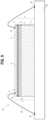
- FIG. 1 Ais a schematic side sectional view of a protective element, according to one embodiment.
- FIG. 1 Bis a schematic side sectional view of a bonded structure that includes a plurality of protective elements directly bonded to a semiconductor element.
- FIG. 2is a schematic side sectional view of a protective element comprising an obstructive material, according to another embodiment.
- FIG. 3is a schematic side sectional view of a protective element including routing circuitry and contact pads configured to be directly bonded to a semiconductor element.
- FIG. 4is a schematic side sectional view showing protective elements and semiconductor elements in wafer form, according to various embodiments.
- FIG. 5 Ais a schematic side sectional view of a bonded structure having a plurality of protective elements directly bonded to opposing sides of a semiconductor element.
- FIG. 5 Bis a schematic side sectional view of a bonded structure with protective elements directly bonded to opposing sides of a semiconductor element, according to another embodiment.
- FIG. 5 Cis a schematic side sectional view of a bonded structure with protective elements directly bonded to opposing sides of a semiconductor element, according to another embodiment.
- FIG. 6is a schematic side sectional view of a bonded structure that includes a silicon-on-insulator (SOI) structure, according to another embodiment.
- SOIsilicon-on-insulator
- FIG. 7is a schematic side sectional view of a bonded structure that includes an obstructive material with a roughened surface.
- FIG. 8is a schematic side sectional view of a bonded structure that includes an obstructive material comprising a roughened upper surface of a carrier.
- FIG. 9illustrates an integrated device package in which a bonded structure is mounted and wire bonded to an external device such as a package substrate.
- FIG. 10illustrates an integrated device package in which a bonded structure is mounted and connected to an external device such as a package substrate in a flip chip arrangement, according to another embodiment.
- FIG. 11 Aillustrates an integrated device package in which protective elements are provided on opposing sides of a semiconductor element, according to one embodiment.
- FIG. 11 Billustrates an integrated device package in which protective elements are provided on opposing sides of a semiconductor element, according to another embodiment.
- FIG. 12is a schematic diagram of an electronic system incorporating one or more bonded structures, according to various embodiments.
- third partiesmay attempt to access security-sensitive components on elements such as integrated device dies.
- the security-sensitive componentsmay be protected by a combination of netlist and non-volatile memory (NVM) data.
- NVMnon-volatile memory
- third partiesmay attempt to hack the security-sensitive components by a combination of destructive and non-destructive techniques, e.g., probing and/or delayering the element to expose or otherwise gain access to the security-sensitive components.
- the third partymay attempt to hack the security-sensitive components by pulsing electromagnetic (EM) waves onto active circuitry of the element, using fault injection techniques, employing near infrared (NIR) triggering or focused ion beam (FIB) modification of circuits, chemical etching techniques, and other physical, chemical, and/or electromagnetic hacking tools and even reverse engineering.
- NIRnear infrared
- FIBfocused ion beam
- These techniquescan be used to physically access sensitive circuits of microdevices such as integrated circuits to directly read encrypted information, to trigger circuits externally to release information otherwise encrypted, to understand manufacturing processes, or even to extract enough information to be able to eventually replicate sensitive designs.
- hackersmay attempt to access the encryption key, which can be stored in the circuit design, in memory, or in a combination of both.
- Techniquescan also be used to indirectly read sensitive information by analyzing the resultant output based upon fault injection inputs, and through recursive analysis determine the encryption key or data contents. It is challenging to structurally protect the security-sensitive components
- One way to physically protect chips from such unauthorized accessis to provide materials that are difficult to remove or penetrate by grinding, polishing, chemical etching or by any other technique.
- some such materialse.g., abrasive materials
- the processing of some materialscan also be chemically incompatible with typical semiconductor processing foundries.
- the obstructive materialsmay not be typically used or found in standard semiconductor processing foundries, and/or the obstructive materials may utilize non-standard processing.
- a chip or chiplet having a protective element 3also referred to herein as an obstructive element
- a protective element 3also referred to herein as an obstructive element
- the obstructive material 4can include a physically destructive material (e.g., an abrasive and/or hard material) configured to physically damage or destroy tooling that attempts to access sensitive circuitry 6 , to physically damage or destroy the sensitive circuitry 6 itself, or otherwise prevent physical or mechanical access to the sensitive circuitry 6 .
- the obstructive material 4can additionally or alternatively comprise a light-blocking material configured to block incident electromagnetic radiation (e.g., infrared radiation, such as near infrared light) from accessing the sensitive circuitry 6 .
- the obstructive material 4can comprise a light-blocking material that is also a destructive material, such that the obstructive material 4 can prevent physical and electromagnetic access to the sensitive circuitry 6 .
- the obstructive material 4can comprise a light-blocking material that is not also a destructive material.
- the obstructive material 4can comprise a destructive material that is not also a light-blocking material.
- the obstructive material 4can comprise a light-scattering, light diffusing or light filtering material.
- the obstructive material 4(which can comprise, e.g., a diamond based material like synthetic diamond, diamond-like carbon or industrial diamond, tungsten, a synthetic fiber, carbides (e.g., silicon carbide, tungsten carbide, boron carbide), borides (e.g., tungsten boride, rhenium boride, aluminum magnesium boride, etc.), boron nitride, carbon nitride, sapphire, and some types of ceramics or other suitably destructive material or combination of materials) can be provided adjacent to a bond interface 8 .
- a diamond based materiallike synthetic diamond, diamond-like carbon or industrial diamond, tungsten, a synthetic fiber
- carbidese.g., silicon carbide, tungsten carbide, boron carbide
- boridese.g., tungsten boride, rhenium boride, aluminum magnesium boride, etc.
- boron nitridecarbon nitrid
- particles of these destructive materialsmay be dispensed into a mixture to form the obstructive material 4 .
- the obstructive material 4can be unpatterned and/or a blanket material layer, as opposed to a patterned layer.
- the obstructive layer 4can comprise a blanket layer over the entire protective element 3 , or a blanket layer over the sensitive region 6 of the circuitry to be protected.
- a bonding layer 5e.g., a semiconductor material or inorganic dielectric
- the obstructive material 4can be directly bonded without an adhesive to a semiconductor element 2 to form a bonded structure 1 in various arrangements.
- the semiconductor element 2can comprise any suitable type of semiconductor element, such as an integrated device die, an interposer, a semiconductor wafer, a reconstituted wafer, etc.
- the chosen obstructive material 4may have a high shear modulus, a high bulk modulus and may not exhibit plastic deformation.
- materials with a hardness of greater than 80 GPacan be used for the destructive material 4 .
- the destructive materialcan have a hardness of at least 12 GPa, at least 13 GPa, at least 15 GPa, at least 20 GPa, at least 30 GPa, or at least 50 GPa, as measured on the Vickers scale.
- the destructive materialcan have a hardness in a range of 12.5 GPa to 150 GPa, in a range of 13 GPa to 150 GPa, in a range of 15 GPa to 150 GPa, in a range of 20 GPa to 150 GPa, in a range of 40 GPa to 150 GPa, or in a range of 80 GPa to 150 GPa as measured on the Vickers scale.
- the abrasive or destructive materialmay have a hardness higher than typical materials used in semiconductor chip.
- the hardness of the destructive materialmay be higher than that of Si, SiO, SiN, SiON, SiCN, etc.
- the obstructive material 4may comprise one or more materials or layers deposited over one another in some embodiments. Moreover, the obstructive material 4 may comprise one continuous, non-continuous or patterned layer, or the obstructive material 4 may comprise several such continuous, non-continuous or patterned layers. In some embodiments, there may not be any circuitry or wiring within the obstructive material 4 . In other embodiments, the obstructive material 4 may include electrical circuitry embedded in the material 4 , or conductive vias partially or fully penetrating the obstructive material 4 .
- the obstructive or protective element 3(e.g., a chip or chiplet) can be directly bonded (e.g., using dielectric-to-dielectric bonding techniques, such as the ZiBond® techniques used by Xperi Corporation of San Jose, Calif.) to at least sensitive areas 6 (for example, areas that include security-sensitive components) of an element 2 (such as a semiconductor chip) that can benefit from high security protection from third party tampering.
- the dielectric-to-dielectric bondsmay be formed without an adhesive using the direct bonding techniques disclosed at least in U.S. Pat. Nos. 9,391,143 and 10,434,749, the entire contents of each of which are incorporated by reference herein in their entirety and for all purposes.
- the one or more layers of the obstructive material 4may be positioned proximate the bond interface 8 , for example, as close as possible to the bond interface 8 .
- the obstructive material 4may be positioned less than 50 microns from the bond interface 8 , less than 25 microns from the bond interface, or less than 10 microns from the bond interface 8 , for example less than 5 microns from the bond interface 8 .
- the obstructive material 4may be positioned in a range of about 1 micron to about 10 microns, or in a range of about 1 micron to about 5 microns, from the bond interface 8 . In other embodiments, two or more obstructive or protective element 3 are directly bonded to the element 2 .
- the direct bondscan be formed without an intervening adhesive.
- the protective element 3 and the semiconductor element 2can each have a bonding layer (such as bonding layer 5 ) with associated dielectric bonding surfaces.
- the respective dielectric bonding surfaces 9 , 10 of the protective element 3 and the semiconductor element 2can be polished to a high degree of smoothness.
- the bonding surfaces 9 , 10can be cleaned and exposed to a plasma and/or suitable chemistries (e.g., etchants) to activate the surfaces 9 , 10 .
- the surfaces 9 , 10can be terminated with a species after activation or during activation (e.g., during the plasma and/or chemical processes).
- the terminating speciescan comprise nitrogen.
- the bonding surfaces 9 , 10can be exposed to fluorine.
- fluorinethere may be one or multiple fluorine peaks near layer and/or bonding interface 8 .
- the bonding interface 8 between two dielectric materialscan comprise a very smooth interface with higher nitrogen content and/or fluorine peaks at the bonding interface 8 .
- direct bonding of separately fabricated protective elements 3facilitates using separate processing that cannot be directly applied to a fabricated integrated circuit or otherwise sensitive microelectronic element, due to thermal budget, chemical compatibility constraints, or other technical reasons.
- the obstructive materials 4can be formed on a separate protective element 3 at a higher temperature than the direct bonding temperatures.
- the direct bonding processitself consumes relatively little thermal budget, including both room temperature initial covalent bonding between dielectric bonding layers, and possible annealing to strengthen the bonds and/or facilitate metal bonding in a hybrid bonding process.
- the removal toolscan be damaged (by abrasive obstructive materials) and/or the underlying active circuitry may be damaged by the removal attempt.
- the obstructive material 4can thus be “destructive” to either the removal tools or the protected circuit. Either result can introduce significant resistance to or entirely prevent reverse engineering, hacking, inspection, or other breach of the secured area, circuitry or devices.
- the obstructive material 4can comprise an abrasive and/or destructive layer on a chiplet.
- the chipletitself may comprise an abrasive and/or destructive material, and/or a hard material. Multiple abrasive and/or destructive materials may be combined in multiple layers or patterns within a layer to enhance the destructive effect.
- the destructive materiale.g., abrasive and/or hard material
- the destructive materialmay be very close to the bond interface 8 .
- the destructive materialmay be positioned within 5 microns from the bond interface 8 .
- the third partymay attempt to etch or grind away the protective chiplet. If the destructive material is very close to the bond interface 8 between the protective element 3 (chiplet) and the semiconductor element 2 , the method to remove or grind away the chiplet becomes significantly difficult.
- the obstructive material 4can alternatively or additionally comprise a light-blocking material configured to block light or electromagnetic waves.
- the obstructive material 4can be selected to block light at wavelengths in a range of 700 nm to 1 mm, in a range of 750 nm to 2500 nm, or in a range of 800 nm to 2500 nm.
- the obstructive material 4can alternatively or additionally be selected or shaped to scatter, filter or diffuse incident light.
- the obstructive material 4can alternatively or additionally be electrically conductive, and may effectively act as electromagnetic shield.
- the obstructive material 4can be selected to block near infrared (NIR) and focused ion beam (FIB) fault intrusion attempts.
- the obstructive material 4may comprise or may be deposited with one or more layers of optical or infrared filters.
- the thin film optical filtersmay act to filter out or modify the optical or IR light irradiated through them in either direction, e.g., light incident upon the circuit to trigger a response or the light emitted from the circuit to detect a response to a hacking technique.
- a portion of the security structure or circuitmay be shared between the protective element 3 (e.g., the chiplet with the abrasive and/or destructive material) and the element 2 to be protected (e.g., the integrated device die with secure active areas 6 ).
- a hybrid bonding techniquecan be used to provide conductor-to-conductor direct bonds along a bond interface 8 that includes covalently direct bonded dielectric-to-dielectric surfaces 9 , 10 .
- the conductor-to-conductor (e.g., contact pad to contact pad) direct bonds and the dielectric-to-dielectric bondscan be formed using the direct bonding techniques disclosed at least in U.S. Pat. Nos. 9,716,033 and 9,852,988, the entire contents of each of which are incorporated by reference herein in their entirety and for all purposes.
- dielectric bonding surfaces 9 , 10can be prepared and directly bonded to one another without an intervening adhesive.
- Conductive contact pads 14(which may be surrounded by nonconductive dielectric field regions of the bonding layer 5 ) may also directly bond to one another without an intervening adhesive.
- the respective contact pads 14can be flush with the surface of the dielectric surfaces 9 , 10 or recessed below the dielectric field regions, for example, recessed in a range of 1 nm to 20 nm, or in a range of 4 nm to 10 nm.
- the bonding surfaces 9 , 10 of the dielectric field regionscan be directly bonded to one another without an adhesive at room temperature in some embodiments and, subsequently, the bonded structure 1 can be annealed. Upon annealing, the contact pads 14 can expand and contact one another to form a metal-to-metal direct bond.
- the processes disclosed hereincan utilize wafer-to-wafer (W2W) bonding process for three-dimensional (3D) integration applications.
- protective materialscan be printed over security-sensitive components or regions 6 .
- FIG. 1 Ais a schematic side sectional view of a protective element 3 , according to one embodiment.
- the protective element 3includes a semiconductor (e.g., silicon) base or substrate 7 (also referred to herein as a carrier).
- the substrate 7 for the security chipletneed not be semiconductor, as it serves primarily as a carrier for an obstructive material 4 and bonding layer 5 , as explained below, and can instead be other materials, such as glass or quartz.
- semiconductor substratesare provided in formats convenient for processing and handling with existing equipment and also with sufficient flatness and smoothness to simplify subsequent polishing of the bonding layer 5 .
- a security or obstructive material 4can be provided over an exterior surface of the carrier or substrate 7 .
- the obstructive material 4can function to obstruct physical access to a protected circuit or sensitive circuit region 6 , and can thus be considered an “obstructive material.”
- the obstructive material 4can comprise an abrasive and/or destructive material (e.g., a material having a high mechanical hardness compared to the materials commonly used in semiconductor fabrication, such as silicon, silicon oxide, silicon nitride, aluminum and copper).
- the obstructive material 4may be difficult to remove via standard techniques, for example, grinding, polishing, wet or dry etching, etc., when compared to the standard materials used in semiconductor fabrication.
- the obstructive material 4can additionally or alternatively be selected so as to block impinging electromagnetic radiation.
- the obstructive material 4can comprise, for example, ceramic materials, composite materials, diamond, a combination of diamond and tungsten, or any other suitable type of obstructive material that can prevent external access to active circuitry on the semiconductor element 2 to which the protective element 3 is to be bonded.
- the obstructive material 4can comprise a material for which selective etchants may be unavailable to remove the obstructive material 4 without removing inorganic dielectrics common to semiconductor fabrication.
- the obstructive material 4can be fabricated and assembled onto the carrier or substrate 7 in a first facility at one or more first processing temperatures.
- the obstructive material 4may be deposited onto the carrier or substrate 7 at temperature(s) of at least 400° C., or at least 800° C., for example, in a range of 400° C. to 1000° C. or higher.
- Such high processing temperaturesmay not be suitable in foundries that are used to manufacture the semiconductor element 2 , e.g., a wafer or an integrated device die (which after fabrication should not be exposed to temperatures of greater than 300° C., or greater than 400° C. for prolonged periods of time), because such high temperatures may damage the active circuitry 6 and other components of the semiconductor element 2 .
- the materials employed for obstruction layersmay be incompatible with semiconductor fabrication facilities due to concerns with contamination.
- obstructive material 4may be deposited.
- an obstruction functionmay be performed by one layer of materials, while in some other embodiments, several layers of different materials (or of the same material) may serve to obstruct third party access to the sensitive circuitry 6 .
- several layers of materials having certain properties (e.g., refractive index) and thicknessmay be provided to introduce optical filtering, scattering or blocking functionality.
- one or more such layers of obstructive materials 4may be deposited on top of another one or more layers of destructive materials.
- one or more such layers of obstructive materials 4may be separated by one or more layers of standard semiconductor materials, for example, silicon, silicon oxide, silicon nitride, etc.
- a bonding layer 5can be provided on the obstructive material 4 .
- one or more buffer layersmay be deposited on the obstructive material 4 , before depositing the bonding layer 5 .
- One or more buffer layersmay be used due to process limitations (e.g., low adhesion between bonding layer 5 and obstructive material 4 ), in which it may be challenging to directly deposit the bonding layer 5 on the obstructive material 4 .
- the bonding layer 5can include any suitable type of nonconductive or dielectric material, particularly inorganic dielectrics compatible with integrated circuit fabrication, such as silicon oxide, silicon nitride, etc.
- a bonding layer 11can also be provided on the semiconductor element 2 .
- the bonding layer 5(e.g., silicon oxide) can be thin such that the layer 5 does not adequately protect or shield the secure circuitry 6 from third party access.
- the protective element 3can be directly bonded to the semiconductor element 2 without an adhesive.
- the respective bonding layers 5 , 11can be prepared for bonding.
- the bonding layers 5 , 11can have bonding surfaces 9 , 10 that are planarized to a high degree of surface smoothness and exposed to a terminating treatment (e.g., a nitrogen termination treatment).
- the bonding layers 5 , 11 of the protective element 3 and the semiconductor element 2can be brought into contact with one another at room temperature, and without application of an adhesive or voltage.
- the bonding layers 5 , 11can form a strong covalent bond along a bond interface 8 .
- the strong covalent bondsmay be sufficient for handling and even for post-bonding processing, such as grinding, polishing or otherwise thinning substrates, singulation, etc., but a post-bonding anneal can increase the strength of the bonds even further.
- the bonding layer 11can be directly bonded to the obstructive material 4 , and the bonding layer 5 on the protective element 3 may not be provided.
- a plurality of semiconductor elements 2 in some embodimentscan be provided in wafer form as a wafer 2 ′, and a plurality of singulated protective elements 3 can be directly bonded to the wafer 2 ′ in a die-to-wafer (D2W) process.
- the wafer 2 ′can be singulated along saw streets S to form a plurality of bonded structures 1 , each of which includes one or more protective elements 3 directly bonded to a singulated semiconductor element 2 .
- the protective elements 3can be provided over sensitive areas of the semiconductor elements 2 so as to protect security-sensitive components 6 from external access.
- the protective elements 3can be provided over only a portion of the active surface of the semiconductor element 2 .
- the protective element 3can be provided over an entirety of the semiconductor element 2 .
- the protective element 3 and/or obstructive layer 4can comprise a continuous or discontinuous pattern, such as a screen, grid, array of discrete obstructive features, etc.
- the obstructive material 4would destroy or damage the tools used to remove the protective element 3 .
- attempts the remove the protective element 3would destroy the underlying sensitive circuitry 6 .
- attempts to access the secure datafor example, via NIR triggering, may be prohibited due to the presence of protective element 3 .
- FIG. 2illustrates another example of a protective element 3 comprising an obstructive material 4 ′.
- the components of FIG. 2may be the same as or generally similar to like components of FIGS. 1 A- 1 B .
- the protective element 3 of FIG. 2may not include a carrier (e.g., a silicon substrate 7 or base shown in FIG. 1 A ). Rather, the protective element 3 may comprise a bulk material or block of obstructive material to define an obstructive chiplet 4 ′ (e.g., an abrasive material, light-blocking material, etc.).
- the bonding layer 5can be provided over the hard or obstructive chiplet 4 ′ of FIG.
- the bonding layer 5 of the obstructive chiplet 4 ′can be prepared for direct bonding, and the bonding layer 5 can be directly bonded to a semiconductor element 2 without an adhesive.
- the use of a larger bulk obstructive materialmay be more difficult to remove and/or more likely to cause destruction of the underlying sensitive circuitry 6 upon physical access attempts by a third party.
- FIG. 3illustrates another embodiment of a protective element 3 comprising an obstructive material 4 .
- the components of FIG. 3may be the same as or generally similar to like components of FIGS. 1 A- 1 B .
- the protective element 3can include a carrier (such as a silicon base or substrate 7 ), an obstructive material 4 on the carrier or substrate 7 , and a bonding layer 5 configured to directly bond to a semiconductor element 2 (such as an integrated device die, wafer, etc.) without an adhesive. Similar to the arrangement of FIG.
- the bonding layer 5can be prepared for direct bonding, and the bonding layer 5 can be directly bonded to a semiconductor element 2 without an adhesive to form a covalent, dielectric-to-dielectric direct bond.
- a nonconductive routing layer 12can be provided over the obstructive material 4 between the obstructive material 4 and the bonding layer 5 .
- conductive routing circuitry 13can extend through the bonding layer 5 and along the nonconductive routing layer 12 .
- the conductive routing circuitry 13 disposed in the protective element 3can be configured to directly bond to corresponding circuitry in the semiconductor element 2 (see FIG. 1 B ).
- wiring routing circuitry 13 and contact pads 14can be fabricated over the obstructive material 4 and or within the non-conductive layer 12 in forming the protective element 3 , using back end metallization techniques common in semiconductor fabrication, and terminating with a polished bonding layer 5 (e.g., silicon oxide, silicon nitride, silicon oxynitride, silicon carbonitride, which may be fluorinated and include nitrogen terminations) with exposed contact pads 14 , which may be recessed prior to bonding.
- the contact pads 14 of the protective element 3 connected to the routing circuitry 13can be directly bonded and electrically connected to corresponding contact pads (not shown) on the semiconductor element 2 .
- the direct bonding of the contact pads 14 on the protective element 3 to corresponding contact pads (not shown) of the semiconductor element 2can be accomplished using hybrid dielectric-to-dielectric and conductor-to-conductor bonding processes, such as Direct Bond Interconnect, or DBI® processes, developed by Xperi Corporation of San Jose, Calif., described herein.
- the routing circuitry 13is schematically illustrated as extending outside (e.g., below) the bonding surface 9 , but it should be appreciated that the portion of the routing circuitry 13 shown below the bonding surface 9 would instead extend through the corresponding bonding surface 10 of the semiconductor element 2 .
- the routing circuitry 13can extend across the bond interface 8 in various embodiments.
- the routing circuitry 13may be one daisy chain distributed between the protective element 3 and the semiconductor element 4 , or it may include several such independent daisy chains. In some embodiments, the routing circuitry 13 may only include a passive daisy chain, while in some other embodiments, one or more intact daisy chains may enable one or more functions within the semiconductor element 2 .
- Providing a portion of the circuitry 13 on the protective element 3can beneficially improve the security of the bonded structure 1 .
- the routing circuitry 13 shared between the protective element 3 and the protected circuitry 6 and crossing the bonding interface 8may be part of the protected circuitry's power mesh. Delayering to remove the protective element 3 may thus interrupt the power supply to the protected circuit 6 and prevent operation by fault injection to bypass security measures.
- FIG. 4a wafer-to-wafer (W2W) approach is illustrated.
- both the protective element 3 and the semiconductor element 2can be fabricated in wafer form.
- the protective element 3can include the obstructive material 4 shown in FIG. 1 A , but which is not illustrated in FIG. 4 due to the relative sizing of the elements 3 , 2 shown.
- a first wafer 3 ′ that includes regions that define the protective elements 3 and a second wafer 2 ′ that includes regions that define the semiconductor elements 2can be directly bonded to one another without an adhesive along a direct bonding interface 8 .
- the bonded waferscan be singulated along saw streets S to form a plurality of bonded structures 1 .
- the bonded wafers 2 ′, 3 ′can be singulated using special saws, laser singulation, chemical etching, plasma etching, scored-and-fractured (e.g., scribe and break), phantom scribed, or a combination thereof.
- the semiconductor elements 2can include sensitive circuit regions 6 and any other suitable wiring, such as conductive vias 15 .
- an outer portion of wafer 3 ′may be etched away after wafer-to-wafer (W2W) bonding, such that the protective element 3 is protecting only a portion of the semiconductor element 2 .
- W2Wwafer-to-wafer
- FIGS. 5 A- 5 Cillustrate additional embodiments of bonded structures 1 in which protective element(s) 3 are directly bonded to opposing sides 17 , 18 of a semiconductor element 2 . This could enabled by W2W (and etching non-required portion of 3 ′) or D2W (die to wafer) direct bonding.
- reference numerals in FIGS. 5 A- 5 Crefer to components that may be generally similar to or the same as like-numbered components of FIGS. 1 A- 4 .
- the protective elements 3can protect both a top side 17 and a bottom side 18 of the semiconductor element 2 to obviate external attacks against both sides 17 , 18 of the semiconductor element 2 .
- FIG. 5 A- 5 Bthe protective elements 3 can protect both a top side 17 and a bottom side 18 of the semiconductor element 2 to obviate external attacks against both sides 17 , 18 of the semiconductor element 2 .
- a plurality of singulated protective elements 3 b , 3 ccan be directly bonded to the bottom side 18 of the semiconductor element 2 .
- a singulated protective element 3 acan also be directly bonded to the top side 17 of the semiconductor element 2 .
- a molding compound or other filler materialcan also be provided over the top and bottom sides 17 , 18 of the semiconductor element 2 , and alongside surfaces of the protective elements 3 a - 3 c .
- a first molding compound 16 acan be provided over the top side 17 of the semiconductor element 2 and alongside surfaces of the protective element 3 a .
- a second molding compound 16 bcan be provided over the bottom side 18 of the semiconductor element 2 and alongside surfaces of the protective elements 3 b , 3 c , including at locations between the adjacent protective elements 3 b , 3 c .
- portions of the molding compound(s) 16 a and/or 16 bcan be provided over top and bottom sides of the protective elements 3 a - 3 c .
- the molding compound(s) 16 a and/or 16 bcan comprise an insulating filler material, such as an epoxy or other encapsulant
- the protective element 3 bcan cover and protect substantially an entirety of one side (e.g., the bottom side 18 ) of the semiconductor element 2 .
- One singulated protective element 3 a ( FIG. 5 B ) or a plurality of singulated protective elements 3 a , 3 c ( FIG. 5 C )can be provided over portions of the top side 17 of the semiconductor element 2 which include sensitive area(s) 6 of active circuitry.
- no molding compoundmay be provided over the semiconductor element 2 and around the protective element(s) 3 .
- a molding compoundmay be provided.
- the obstructive material 4can be printed on the protective element 3 , or directly over active circuitry 6 of the semiconductor element 2 .
- the obstructive material 4can be screen printed, ink-jet printed, or otherwise deposited on the protective element 3 or the semiconductor element 2 .
- the obstructive material 4can be printed on the protective element 3 , and the protective element 3 can be directly bonded to the semiconductor element 2 .
- third partiescan attempt fault injection through a back or bottom side 18 of a semiconductor element (e.g., an integrated device die), which is opposite a front or top side 17 of the element with active devices.
- Backside fault injectioncan flip transistors or otherwise falsely trigger operation of a device without authorization.
- the front side 17 of the diecan include bond or contact pads to connect to an external device (such as a package substrate) by, for example, wire bonding or a flip chip connection using solder balls.
- Third partiescan attempt back side luminescence techniques to try to optically image security-sensitive components of the semiconductor element to reverse engineer the circuitry.
- third partiescan detect small infrared (IR) emissions through silicon after injecting a stimulus. After a sufficient number of attacks, the third party may be able to determine sensitive information, such as encryption keys.
- IRinfrared
- FIGS. 5 A- 5 Ccan prevent such backside attacks.
- various embodiments disclosed hereincan simultaneously provide a silicon-on-oxide (SOI) structure and an integrated obstructive layer that can provide backside protection.
- SOIsilicon-on-oxide
- a bulk silicon carrier or substrate 7can include an obstructive layer in a handle wafer for backside protection.
- the front sidecan be additionally protected through bonded chiplets as explained above.
- FIG. 6illustrates one embodiment of a bonded structure 1 in which a semiconductor element 2 is directly bonded to a protective element 3 .
- the semiconductor element 2can comprise an integrated circuit or device die having active circuitry with one or more security-sensitive area(s) 6 .
- active circuitrycan be disposed at or near a front side A of the semiconductor element 2 and/or at or near a back side B of the semiconductor element 2 .
- bond pads 19may be provided on the front side A of the semiconductor element 2 .
- the semiconductor element 2 of FIG. 6can comprise a thinned device die. The thinning of the device die can occur before or after directly bonding the semiconductor element 2 to the protective element 3 .
- the semiconductor element 2can include a first bonding layer 11 , such as a dielectric material, e.g., silicon oxide.
- the protective element 3can include a handle or carrier 7 , an obstructive material 4 over the handle or carrier 7 , and a second bonding layer 5 (e.g., silicon oxide) over the obstructive material 4 .
- the first and second bonding layers 11 , 5can be directly bonded to one another without an adhesive to bond the semiconductor element 2 to the protective element 3 .
- contact padsmay be provided on or in the insulating bonding layers 11 , 5 .
- the contact padsmay also be directly bonded to one another without an adhesive using a suitable hybrid direct bonding technique in some embodiments.
- the obstructive material 4can comprise one or more of an abrasive material, a light blocking material, a conductive material, an insulating material, a light or electromagnetic (EM) wave scattering material, etc.
- the obstructive material 4can accordingly prevent third parties from accessing the security-sensitive area(s) 6 of the semiconductor element 2 .
- the obstructive material 4can prevent the observation of light emissions from the back side B, and/or can disrupt a material removal operation from the back side B.
- SOI substratescan be formed by bonding a handle wafer to an active device wafer with buried oxide (BOX) therebetween.
- BOXburied oxide
- a similar processcan provide the buried oxide (BOX) and the obstruction material 4 by using direct bonding of bonding layers comprises inorganic dielectrics, and particularly silicon oxide (including, for example, fluorination and/or nitrogen terminations that leave signatures at the bonding interface 8 in FIG. 6 ).
- the bonding layers 11 , 5together serve as the BOX for an SOI layer, where the BOX layer can include signature fluorine and/or nitrogen profiles from direct bonding at the interface 8 between the bonding layers 11 , 5 (and within the BOX).
- the active device wafercan then be thinned and processed to form active devices in the semiconductor element 2 such as transistors in the thin remaining active silicon (or other semiconductor) and conventional metallization layers formed over that.
- the carrier or handle wafercan also be thinned before or after singulation.
- the thick portion of active device layermay be removed using a technique similar to a smart cut, leaving a very thin active device wafer.
- FIG. 7a bonded structure 1 similar to that shown in FIG. 6 is illustrated.
- the components of FIG. 7may be the same as or generally similar to like components of FIG. 6 .
- the obstructive material 4may be deposited on the carrier 7 , for example, using chemical vapor deposition (CVD), physical vapor deposition (PVD), or any other suitable technique.
- the depositionmay be designed so as to leave a rough upper surface 20 onto which the second bonding layer 5 is provided, which is then directly bonded to the bonding layer 11 of the semiconductor element 2 , which can include an active silicon (or other semiconductor) substrate.
- the surface of the obstructive material 4may be roughened by any suitable technique after its deposition. As the second bonding layer 5 is deposited over this rough surface, one or more polishing techniques including chemical mechanical polishing may be used to provide a bondable surface of dielectric bonding layer 5 . As explained above, the semiconductor element 2 with the active silicon can be thinned. The rough upper surface 20 of the obstructive material 4 may introduce light scattering or diffusion of any incident light going from one side to another across the rough interface. The rough upper surface 20 of the obstructive material 4 may also enhance the abrasiveness or hardness of the protective element 3 so as to further improve security of the sensitive area(s) 6 of the semiconductor element 2 .
- the rough upper surface 20 of the obstructive material 4may also make polishing, grinding or etching away of the obstruction material even more difficult. Further, the use of both the bonding layer 5 (e.g., silicon oxide) and the obstructive material 4 can complicate the removal process since attempts to remove the obstructive material 4 may destroy the bonding layer 5 and attempts to remove the bonding layer 5 may destroy or damage the obstructive material 4 .
- the bonding layer 5e.g., silicon oxide
- FIG. 8illustrates a bonded structure 1 similar to that shown in FIGS. 6 and 7 .
- the components of FIG. 8may be the same as or generally similar to like components of FIGS. 6 - 7 .
- the protective element 3may comprise a bulk handle or carrier 7 and a bonding layer 5 (e.g., an oxide layer) disposed on the bulk handle or carrier 7 .
- the upper surface of the handle or carrier 7can comprise a roughened upper surface 21 , with the second bonding layer 5 applied over the roughened upper surface 21 .
- the obstructive material 4can comprise the roughened upper surface 21 of the handle or carrier 7 and portions 22 of material (e.g., portions 22 of the dielectric bonding layer 5 ) within recesses of the roughened upper surface 21 .
- the roughened interface between the second bonding layer 5 (e.g., an oxide layer) and the roughened upper surface 21 of the bulk handle or carrier 7may provide a light scattering, diffusion and/or lensing effect in which light incident on the semiconductor element 2 may be scattered through the backside of the protective element 3 .
- Such optical scatteringcan obviate attempts to access the sensitive area(s) 6 of the semiconductor element 2 using optical or electromagnetic (EM) techniques.
- EMelectromagnetic
- FIG. 9illustrates an integrated device package 30 in which a bonded structure 1 is mounted to an external device, for example, a package substrate 32 .
- the package substrate 32can comprise a laminate substrate (such as a printed circuit board, or PCB), a lead frame, a molded lead frame, a ceramic substrate, or any other suitable type of substrate.
- bond pads 19 on the front side A of the semiconductor element 2are wire bonded to corresponding leads or contact pads 33 on the package substrate 32 by way of one or more bonding wires 34 .
- the back side B of the semiconductor element 2can be protected by the protective element 3 (which includes the obstructive material 4 ) from external access from the back side B.
- the protective element 3can be provided at the wafer level (and thus can be laterally coextensive with the active silicon of the semiconductor element 2 or die) but may not interfere with bonding, including the bonding wires 34 as shown, on the front side A of the semiconductor element 2 .
- FIG. 10illustrates an integrated device package 30 in which a bonded structure 1 is mounted to an external device, for example, a package substrate 32 , according to another embodiment.
- the back side B of the semiconductor element 2can be protected from external access by way of the protective element 3 (which includes the obstructive material 4 ).
- the front side A of the semiconductor element 2may face the external device (e.g., package substrate 32 ). Bond pads 19 on the front side A of the semiconductor element 2 can be connected to the package substrate 32 by way of a plurality of solder balls 35 in a flip chip connection.
- the bonded structure 1may also include a fan-out arrangement employing a redistribution layer between the active silicon of the semiconductor element 2 and the package substrate 32 .
- FIGS. 11 A and 11 Billustrate various embodiments in which both the front side A and the back side B of the semiconductor element 2 can be protected by the protective element 3 with a protective material 4 that can include an obstructive material.
- FIG. 11 Ais generally similar to the embodiment of FIG. 9 , in which the front side A of the semiconductor element 2 is wire bonded to the package substrate 32 .
- a first protective element 3 a(which can include an obstructive material 4 ) can be provided over the back side B of the semiconductor element 2 as in FIG. 9 .
- FIG. 9illustrates in which both the front side A and the back side B of the semiconductor element 2 can be protected by the protective element 3 with
- a second protective element 3 b(which may be similar to any of the protective elements 3 described herein) can be bonded over the front side A of the semiconductor element 2 to protect the front side A from external attacks on sensitive area(s) 6 of the semiconductor element 2
- sensitive area(s) 6may be provided at or near one or both of the front and back sides A, B of the semiconductor element 2 .
- bonding layerscan be provided on both the front and back sides A, B of the semiconductor element 2 .
- the first and second protective elements 3 a , 3 bcan be directly bonded to the bonding layers on the front and back sides A, B of the semiconductor element 2 without an adhesive.
- the back side obstruction layer 4can be is integrated with or coupled to the BOX layer of an SOI substrate.
- FIG. 11 Bis generally similar to the embodiment of FIG. 10 , in which the front side A of the semiconductor element 2 is connected to the package substrate 32 by way of a flip-chip connection in which a plurality of solder balls 35 electrically and mechanically connect the semiconductor element 2 to the package substrate 32 .
- a first protective element 3 a(which can include an obstructive material) can be provided over the back side B of the semiconductor element 2 as in FIG. 10 .
- FIG. 10can include an obstructive material
- a second protective element 3 b(which may be similar to any of the protective elements 3 described herein) can be bonded over the front side A of the semiconductor element 2 to protect the front side A from external attacks on sensitive area(s) 6 of the semiconductor element 2 (which may be provided at or near one or both the front and back sides A, B of the element 2 ).
- bonding layerscan be provided on both the front and back sides A, B of the semiconductor element 2 .
- the first and second protective elements 3 a , 3 bcan be directly bonded to the bonding layers on the front and back sides A, B of the semiconductor element 2 without an adhesive.
- the second protective element 3 bcan be provided in a possum package arrangement in which the second protective element 3 b is disposed in a space or cavity 37 between solder balls 35 and above the package substrate 32 .
- FIG. 12is a schematic diagram of an electronic system 80 incorporating one or more bonded structures 1 , according to various embodiments.
- the system 80can comprise any suitable type of electronic device, such as a mobile electronic device (e.g., a smartphone, a tablet computing device, a laptop computer, etc.), a desktop computer, an automobile or components thereof, a stereo system, a medical device, a camera, or any other suitable type of system.
- the electronic system 80can comprise a microprocessor, a graphics processor, an electronic recording device, or digital memory.
- the system 80can include one or more device packages 82 which are mechanically and electrically connected to the system 80 , e.g., by way of one or more motherboards. Each package 82 can comprise one or more bonded structures 1 .
- the package 82may be similar to or the same as the packages 30 described herein.
- the system 80 shown in FIG. 12can comprise any of the bonded structures 1 and associated protective elements 3 as shown and described herein.
- a bonded structurecan include a semiconductor element comprising active circuitry and a first bonding layer.
- the bonded structurecan include an obstructive element directly bonded to the semiconductor element without an adhesive along a bonding interface.
- the obstructive elementcan include an obstructive material disposed over the active circuitry and a second bonding layer on the obstructive material.
- the second bonding layercan be directly bonded to the first bonding layer without an adhesive, the obstructive material having a higher hardness than the semiconductor element and being configured to obstruct external access to the active circuitry.
- the obstructive materialcan be positioned at a distance less than 10 microns from the bonding interface.
- the obstructive materialcan be positioned at a distance less than 5 microns from the bonding interface.
- a first hardness of the obstructive materialcan be greater than a second hardness of the semiconductor element.
- the first hardnesscan be at least 1.2 times the second hardness, at least 1.25 times the second hardness, at least 1.3 times the second hardness, at least 1.4 times the second hardness, or at least 1.5 times the second hardness.
- the first hardnesscan be in a range of 1.2 to 2.5 times the second hardness, in a range of 1.2 to 2 times the second hardness, or in a range of 1.2 to 1.8 times the second hardness.
- the obstructive materialcan include at least some diamond, and the semiconductor element can comprise at least some silicon.
- the obstructive materialcan comprise destructive material such as an abrasive material.
- the abrasive materialmay or may not comprise a continuous solid material.
- the abrasive materialcan comprise particulates of an abrasive material (e.g., silicon carbide, etc.) in a compact area that can create an aggregate in a polishing slurry, which can form the abrasive material.
- the obstructive materialcan comprise a destructive material having a hardness in a range of 20 GPa to 150 GPa as measured on the Vickers scale.
- the obstructive materialcan comprise a destructive material having a hardness of at least 80 GPa as measured on the Vickers scale.
- the obstructive materialcan comprise a light-blocking material.
- the light-blocking materialcan be configured to block light at wavelengths in a range of 700 nm to 1 mm, in a range of 750 nm to 2500 nm, or in a range of 800 nm to 2500 nm.
- the light-blocking materialcan be configured to block light at near infrared (NIR) wavelengths.
- NIRnear infrared
- the obstructive materialadditionally or alternatively can be configured to prevent physical access to the active circuitry.
- the obstructive materialcan be configured to physically destroy hardware use for controlled removal of semiconductor material from the bonded structure.
- the obstructive materialcan be configured to block electromagnetic waves from reaching the active circuitry.
- the semiconductor elementcomprises an integrated circuit die.
- the obstructive elementcan include a bonding layer between the obstructive material and the semiconductor element.
- the bonding layercan comprise silicon oxide.
- routing circuitrycan extend through the bonding layer to first contact pads of the semiconductor element.
- a nonconductive routing layercan be disposed between the bonding layer and the obstructive material, with a portion of the routing circuitry disposed along the nonconductive routing layer.
- Second contact pads of the bonding layercan be directly bonded to corresponding first contact pads of the semiconductor element without an adhesive.
- the semiconductor elementcomprises a second bonding layer directly bonded to the bonding layer.
- the obstructive elementfurther includes a substrate, and the obstructive material comprises an obstructive layer disposed on the substrate.
- the obstructive layercan be patterned so as to cover less than an entirety of an active surface of the semiconductor element. In some embodiments, the obstructive layer covers an entirety of an active surface of the semiconductor element.
- the obstructive materialcomprises a chiplet having a bonding layer formed thereon.
- the obstructive elementcan be directly bonded to a first surface of the semiconductor element.
- the bonded structurecan further comprise a second obstructive element directly bonded to a second surface of the semiconductor element opposite the first surface without an adhesive.
- the second obstructive elementcan include a second obstructive material disposed over the active circuitry.
- the second obstructive materialcan be configured to obstruct external access to the active circuitry.
- the second obstructive elementcovers only a portion of the second surface of the semiconductor element.
- the second obstructive elementcovers an entirety of the second surface of the semiconductor element.
- a plurality of obstructive elementscan be directly bonded to the semiconductor element without an adhesive, with the plurality of obstructive elements including one or more obstructive materials configured to obstruct external access to active circuitry.
- a bonded structurecan include a semiconductor element comprising active circuitry and a first bonding layer.
- the bonded structurecan include an obstructive element directly bonded to the semiconductor element without an adhesive along a bonding interface, the obstructive element including an optical obstructive material disposed over the active circuitry and a second bonding layer on the obstructive material, the second bonding layer directly bonded to the first bonding layer without an adhesive, the optical obstructive material configured to obstruct external optical access to the active circuitry.
- the optical obstructive materialcomprises a light-blocking material.
- the light-blocking materialis configured to block light at wavelengths in a range of 750 nm to 1500 nm.
- the light-blocking materialis configured to block light at near infrared (NIR) wavelengths.
- the optical obstructive materialcomprises an optical filter.
- the optical obstructive materialcomprises a light-scattering material.
- a method of forming a bonded structurecan include directly bonding an obstructive element to a semiconductor element without an adhesive, the semiconductor element comprising active circuitry.
- the obstructive elementcan include an obstructive material disposed over the active circuitry, the obstructive material having a hardness higher than the semiconductor element and being configured to obstruct external access to the active circuitry.
- the methodcan include forming a bonding layer over the obstructive material to form the obstructive element.
- Forming the bonding layercan comprise depositing an oxide layer on the obstructive material.
- contact pads of the bonding layercan be directly bonded to corresponding contact pads of the semiconductor element without an adhesive.
- Active circuitrycan be formed in the semiconductor element. In some embodiments, the active circuitry can be formed before directly bonding. In some embodiments, the active circuitry can be formed after directly bonding.
- the obstructive materialcan be formed as an obstructive layer on a substrate. In various embodiments, the obstructive material can be printed on a substrate.
- the obstructive elementcan be singulated before the directly bonding.
- directly bonding the obstructive elementcan comprise directly bonding a first wafer comprising the obstructive material to a second wafer comprising the semiconductor element.
- the bonded first and second waferscan be singulated to form a plurality of bonded structures.
- the methodcan comprise directly bonding a plurality of obstructive elements to the semiconductor element without an adhesive.
- the plurality of obstructive elementscan include one or more obstructive materials configured to obstruct external access to active circuitry.
- the first obstructive elementcan be directly bonded to a first surface of the semiconductor element.
- the methodcan further include directly bonding a second obstructive element to a second surface of the semiconductor element opposite the first surface without an adhesive.
- the second obstructive elementcan include a second obstructive material disposed over the active circuitry, the second obstructive material configured to obstruct external access to the active circuitry.
- the methodcan include forming the obstructive element in a first manufacturing facility and forming the semiconductor element in a second manufacturing facility different from the first manufacturing facility.
- the methodcan include processing the obstructive element at a first maximum temperature and processing the semiconductor element at a second maximum temperature, the first maximum temperature greater than the second maximum temperature.
- the first maximum temperaturecan be at least 400° C., or in a range of 400° C. to 1000° C.
- the first maximum temperaturecan be in a range of 1.2 to 4 times the second maximum temperature.
- a method of forming a bonded structurecan include directly bonding a first bonding layer of a semiconductor element to a second bonding layer of an obstructive element without an adhesive, the semiconductor element comprising active circuitry.
- the obstructive elementcan include an optical obstructive material disposed over the active circuitry, the optical obstructive material configured to obstruct external optical access to the active circuitry.
- the optical obstructive materialis at least one of a light-blocking material, a light-scattering material, and an optical filter.
- a bonded structurein another embodiment, can include a semiconductor element including active circuitry.
- the semiconductor elementcan have a front side and a back side opposite the front side, with the front side including a plurality of bond pads configured to electrically connect to an external element.
- the bonded structurecan include an obstructive element having an obstructive material formed on the back side of the semiconductor element, with the back side opposite the front side. The obstructive material can be configured to obstruct external access to the active device layer.
- the semiconductor elementcomprises a first bonding layer on the back side and the obstructive element comprises a second bonding layer, with the first and second bonding layers directly bonded to one another without an adhesive.
- the first and second bonding layerscomprise silicon oxide.
- the active circuitrycan be disposed at or near the back side of the semiconductor element. Additionally or alternatively, the active circuitry can be disposed at or near a front side of the semiconductor element.
- the bonded structurecan comprise a substrate, with the obstructive element formed on the substrate.
- a first hardness of the obstructive materialis greater than a second hardness of the semiconductor element.
- the first hardnesscan be at least 1.2 times the second hardness, at least 1.25 times the second hardness, at least 1.3 times the second hardness, at least 1.4 times the second hardness, or at least 1.5 times the second hardness.
- the first hardnesscan be in a range of 1.2 to 2.5 times the second hardness, in a range of 1.2 to 2 times the second hardness, or in a range of 1.2 to 1.8 times the second hardness.
- the obstructive materialcan include at least some diamond, and the semiconductor element can comprise at least some silicon.
- the obstructive materialcan comprise an abrasive material.
- the abrasive materialmay or may not comprise a continuous solid material. Rather, the abrasive material can comprise particulates of an abrasive material (e.g., silicon carbide, etc.) in a compact area that can create an aggregate in a polishing slurry, which can form the abrasive material.
- the obstructive materialcomprises a light-blocking material.
- the light-blocking materialcan be configured to block light at wavelengths in a range of 750 nm to 2500 nm.
- the light-blocking materialcan be configured to block light at near infrared (NIR) wavelengths.
- the obstructive materialcan comprise a roughened surface, with the second bonding layer disposed on the roughened surface.
- an integrated device packagecan include the external element and the bonded structure.
- the external elementcan comprise a package substrate in some embodiments.
- the bonded structurecan be mounted to the package substrate.
- plurality of bond padscan be wire bonded to the package substrate by way of bonding wires. Additionally or alternatively, the plurality of bond pads can be mounted to the package substrate in a flip chip arrangement by way of a plurality of solder balls.
- a method of forming a bonded structurecan include providing a first bonding layer on a back side of a semiconductor element including active circuitry.
- the semiconductor elementcan have a front side opposite the back side.
- the front sidecan include a plurality of bond pads configured to electrically connect to an external element.
- the methodcan include providing a second bonding layer on an obstructive material.
- the first and second bonding layerscan be bonded to one another.
- the obstructive materialcan be configured to obstruct external access to the active circuitry.
- bonding the first and second bonding layerscan comprise directly bonding the first and second bonding layers without an adhesive.
- the active circuitrycan be formed after the directly bonding. In some embodiments, the active circuitry can be formed before the directly bonding.
- the methodcan include thinning the semiconductor element.
- the thinningcan be performed before the bonding in some embodiments.
- the active circuitrycan be formed at or near the front side of the semiconductor element. Additionally or alternatively, the active circuitry can be formed at or near the back side of the semiconductor element.
- the first and second bonding layersform a buried oxide (BOX) layer for a semiconductor-on-insulator (SOI) structure.
- BOXburied oxide
- SOIsemiconductor-on-insulator
- the methodcan include forming the semiconductor element by growing epitaxial silicon on a silicon substrate. At least a portion of the silicon substrate can be removed after the bonding.
- a packaging methodcan include mounting the bonded structure to a package substrate and electrically connecting the bonded structure to the package substrate.
- the packaging methodcan include wire bonding the plurality of bond pads to the package substrate. Additionally or alternatively, the method can include electrically connecting the bond pads to the package substrate by way of a plurality of solder balls.
Landscapes
- Power Engineering (AREA)
- Engineering & Computer Science (AREA)
- Computer Hardware Design (AREA)
- Microelectronics & Electronic Packaging (AREA)
- Physics & Mathematics (AREA)
- General Physics & Mathematics (AREA)
- Condensed Matter Physics & Semiconductors (AREA)
- Electromagnetism (AREA)
- Health & Medical Sciences (AREA)
- Toxicology (AREA)
- Mechanical Treatment Of Semiconductor (AREA)
- Dicing (AREA)
- Internal Circuitry In Semiconductor Integrated Circuit Devices (AREA)
- Micromachines (AREA)
Abstract
Description
Claims (18)
Priority Applications (6)
| Application Number | Priority Date | Filing Date | Title |
|---|---|---|---|
| US16/844,932US11610846B2 (en) | 2019-04-12 | 2020-04-09 | Protective elements for bonded structures including an obstructive element |
| CN202310380475.7ACN116417425A (en) | 2019-04-12 | 2020-04-10 | Protective elements for bonded structures |
| KR1020217035236AKR20210139461A (en) | 2019-04-12 | 2020-04-10 | Protection element for junction structure |
| CN202080027953.0ACN113678243B (en) | 2019-04-12 | 2020-04-10 | Protective element for a bond structure |
| PCT/US2020/027732WO2020210676A1 (en) | 2019-04-12 | 2020-04-10 | Protective elements for bonded structures |
| US18/087,705US20230317628A1 (en) | 2019-04-12 | 2022-12-22 | Protective elements for bonded structures |
Applications Claiming Priority (3)
| Application Number | Priority Date | Filing Date | Title |
|---|---|---|---|
| US201962833491P | 2019-04-12 | 2019-04-12 | |
| US201962953058P | 2019-12-23 | 2019-12-23 | |
| US16/844,932US11610846B2 (en) | 2019-04-12 | 2020-04-09 | Protective elements for bonded structures including an obstructive element |
Related Child Applications (1)
| Application Number | Title | Priority Date | Filing Date |
|---|---|---|---|
| US18/087,705ContinuationUS20230317628A1 (en) | 2019-04-12 | 2022-12-22 | Protective elements for bonded structures |
Publications (2)
| Publication Number | Publication Date |
|---|---|
| US20200328162A1 US20200328162A1 (en) | 2020-10-15 |
| US11610846B2true US11610846B2 (en) | 2023-03-21 |
Family
ID=72748191
Family Applications (2)
| Application Number | Title | Priority Date | Filing Date |
|---|---|---|---|
| US16/844,932ActiveUS11610846B2 (en) | 2019-04-12 | 2020-04-09 | Protective elements for bonded structures including an obstructive element |
| US18/087,705PendingUS20230317628A1 (en) | 2019-04-12 | 2022-12-22 | Protective elements for bonded structures |
Family Applications After (1)
| Application Number | Title | Priority Date | Filing Date |
|---|---|---|---|
| US18/087,705PendingUS20230317628A1 (en) | 2019-04-12 | 2022-12-22 | Protective elements for bonded structures |
Country Status (4)
| Country | Link |
|---|---|
| US (2) | US11610846B2 (en) |
| KR (1) | KR20210139461A (en) |
| CN (2) | CN113678243B (en) |
| WO (1) | WO2020210676A1 (en) |
Cited By (5)
| Publication number | Priority date | Publication date | Assignee | Title |
|---|---|---|---|---|
| US20230317628A1 (en)* | 2019-04-12 | 2023-10-05 | Adeia Semiconductor Bonding Technologies Inc. | Protective elements for bonded structures |
| US11848284B2 (en) | 2019-04-12 | 2023-12-19 | Adeia Semiconductor Bonding Technologies Inc. | Protective elements for bonded structures |
| US12176303B2 (en) | 2019-04-12 | 2024-12-24 | Adeia Semiconductor Bonding Technologies Inc. | Wafer-level bonding of obstructive elements |
| US12174246B2 (en) | 2019-05-23 | 2024-12-24 | Adeia Semiconductor Bonding Technologies Inc. | Security circuitry for bonded structures |
| US12300634B2 (en) | 2021-08-02 | 2025-05-13 | Adeia Semiconductor Bonding Technologies Inc. | Protective semiconductor elements for bonded structures |
Families Citing this family (86)
| Publication number | Priority date | Publication date | Assignee | Title |
|---|---|---|---|---|
| US7109092B2 (en) | 2003-05-19 | 2006-09-19 | Ziptronix, Inc. | Method of room temperature covalent bonding |
| US7485968B2 (en) | 2005-08-11 | 2009-02-03 | Ziptronix, Inc. | 3D IC method and device |
| US8735219B2 (en) | 2012-08-30 | 2014-05-27 | Ziptronix, Inc. | Heterogeneous annealing method and device |
| US20150262902A1 (en) | 2014-03-12 | 2015-09-17 | Invensas Corporation | Integrated circuits protected by substrates with cavities, and methods of manufacture |
| US11069734B2 (en) | 2014-12-11 | 2021-07-20 | Invensas Corporation | Image sensor device |
| US9741620B2 (en) | 2015-06-24 | 2017-08-22 | Invensas Corporation | Structures and methods for reliable packages |
| US10886250B2 (en) | 2015-07-10 | 2021-01-05 | Invensas Corporation | Structures and methods for low temperature bonding using nanoparticles |
| US9953941B2 (en) | 2015-08-25 | 2018-04-24 | Invensas Bonding Technologies, Inc. | Conductive barrier direct hybrid bonding |
| US10204893B2 (en) | 2016-05-19 | 2019-02-12 | Invensas Bonding Technologies, Inc. | Stacked dies and methods for forming bonded structures |
| US10446487B2 (en) | 2016-09-30 | 2019-10-15 | Invensas Bonding Technologies, Inc. | Interface structures and methods for forming same |
| US10672663B2 (en) | 2016-10-07 | 2020-06-02 | Xcelsis Corporation | 3D chip sharing power circuit |
| US11176450B2 (en) | 2017-08-03 | 2021-11-16 | Xcelsis Corporation | Three dimensional circuit implementing machine trained network |
| US10580735B2 (en) | 2016-10-07 | 2020-03-03 | Xcelsis Corporation | Stacked IC structure with system level wiring on multiple sides of the IC die |
| TWI822659B (en) | 2016-10-27 | 2023-11-21 | 美商艾德亞半導體科技有限責任公司 | Structures and methods for low temperature bonding |
| US10002844B1 (en) | 2016-12-21 | 2018-06-19 | Invensas Bonding Technologies, Inc. | Bonded structures |
| US20180182665A1 (en) | 2016-12-28 | 2018-06-28 | Invensas Bonding Technologies, Inc. | Processed Substrate |
| CN117878055A (en) | 2016-12-28 | 2024-04-12 | 艾德亚半导体接合科技有限公司 | Stacking substrate processing |
| TWI837879B (en) | 2016-12-29 | 2024-04-01 | 美商艾德亞半導體接合科技有限公司 | Bonded structures with integrated passive component |
| WO2018169968A1 (en) | 2017-03-16 | 2018-09-20 | Invensas Corporation | Direct-bonded led arrays and applications |
| US10515913B2 (en) | 2017-03-17 | 2019-12-24 | Invensas Bonding Technologies, Inc. | Multi-metal contact structure |
| US10508030B2 (en) | 2017-03-21 | 2019-12-17 | Invensas Bonding Technologies, Inc. | Seal for microelectronic assembly |
| US10269756B2 (en) | 2017-04-21 | 2019-04-23 | Invensas Bonding Technologies, Inc. | Die processing |
| US10879212B2 (en) | 2017-05-11 | 2020-12-29 | Invensas Bonding Technologies, Inc. | Processed stacked dies |
| US10446441B2 (en) | 2017-06-05 | 2019-10-15 | Invensas Corporation | Flat metal features for microelectronics applications |
| US10217720B2 (en) | 2017-06-15 | 2019-02-26 | Invensas Corporation | Multi-chip modules formed using wafer-level processing of a reconstitute wafer |
| US10840205B2 (en) | 2017-09-24 | 2020-11-17 | Invensas Bonding Technologies, Inc. | Chemical mechanical polishing for hybrid bonding |
| US11195748B2 (en) | 2017-09-27 | 2021-12-07 | Invensas Corporation | Interconnect structures and methods for forming same |
| US11031285B2 (en) | 2017-10-06 | 2021-06-08 | Invensas Bonding Technologies, Inc. | Diffusion barrier collar for interconnects |
| US11380597B2 (en) | 2017-12-22 | 2022-07-05 | Invensas Bonding Technologies, Inc. | Bonded structures |
| US10923408B2 (en) | 2017-12-22 | 2021-02-16 | Invensas Bonding Technologies, Inc. | Cavity packages |
| US10727219B2 (en) | 2018-02-15 | 2020-07-28 | Invensas Bonding Technologies, Inc. | Techniques for processing devices |
| US11169326B2 (en) | 2018-02-26 | 2021-11-09 | Invensas Bonding Technologies, Inc. | Integrated optical waveguides, direct-bonded waveguide interface joints, optical routing and interconnects |
| US11256004B2 (en) | 2018-03-20 | 2022-02-22 | Invensas Bonding Technologies, Inc. | Direct-bonded lamination for improved image clarity in optical devices |
| US10991804B2 (en) | 2018-03-29 | 2021-04-27 | Xcelsis Corporation | Transistor level interconnection methodologies utilizing 3D interconnects |
| US11056348B2 (en) | 2018-04-05 | 2021-07-06 | Invensas Bonding Technologies, Inc. | Bonding surfaces for microelectronics |
| US10790262B2 (en) | 2018-04-11 | 2020-09-29 | Invensas Bonding Technologies, Inc. | Low temperature bonded structures |
| US11244916B2 (en) | 2018-04-11 | 2022-02-08 | Invensas Bonding Technologies, Inc. | Low temperature bonded structures |
| US10964664B2 (en) | 2018-04-20 | 2021-03-30 | Invensas Bonding Technologies, Inc. | DBI to Si bonding for simplified handle wafer |
| US11004757B2 (en) | 2018-05-14 | 2021-05-11 | Invensas Bonding Technologies, Inc. | Bonded structures |
| US11276676B2 (en) | 2018-05-15 | 2022-03-15 | Invensas Bonding Technologies, Inc. | Stacked devices and methods of fabrication |
| US10923413B2 (en) | 2018-05-30 | 2021-02-16 | Xcelsis Corporation | Hard IP blocks with physically bidirectional passageways |
| KR20210009426A (en) | 2018-06-13 | 2021-01-26 | 인벤사스 본딩 테크놀로지스 인코포레이티드 | TV as a pad |
| US11393779B2 (en) | 2018-06-13 | 2022-07-19 | Invensas Bonding Technologies, Inc. | Large metal pads over TSV |
| US10910344B2 (en) | 2018-06-22 | 2021-02-02 | Xcelsis Corporation | Systems and methods for releveled bump planes for chiplets |
| WO2020010056A1 (en) | 2018-07-03 | 2020-01-09 | Invensas Bonding Technologies, Inc. | Techniques for joining dissimilar materials in microelectronics |
| US11158606B2 (en) | 2018-07-06 | 2021-10-26 | Invensas Bonding Technologies, Inc. | Molded direct bonded and interconnected stack |
| US11462419B2 (en) | 2018-07-06 | 2022-10-04 | Invensas Bonding Technologies, Inc. | Microelectronic assemblies |
| US12406959B2 (en) | 2018-07-26 | 2025-09-02 | Adeia Semiconductor Bonding Technologies Inc. | Post CMP processing for hybrid bonding |
| US11515291B2 (en) | 2018-08-28 | 2022-11-29 | Adeia Semiconductor Inc. | Integrated voltage regulator and passive components |
| US20200075533A1 (en) | 2018-08-29 | 2020-03-05 | Invensas Bonding Technologies, Inc. | Bond enhancement in microelectronics by trapping contaminants and arresting cracks during direct-bonding processes |
| US11011494B2 (en) | 2018-08-31 | 2021-05-18 | Invensas Bonding Technologies, Inc. | Layer structures for making direct metal-to-metal bonds at low temperatures in microelectronics |
| US11158573B2 (en) | 2018-10-22 | 2021-10-26 | Invensas Bonding Technologies, Inc. | Interconnect structures |
| US11244920B2 (en) | 2018-12-18 | 2022-02-08 | Invensas Bonding Technologies, Inc. | Method and structures for low temperature device bonding |
| CN113330557A (en) | 2019-01-14 | 2021-08-31 | 伊文萨思粘合技术公司 | Bonding structure |
| US11387202B2 (en) | 2019-03-01 | 2022-07-12 | Invensas Llc | Nanowire bonding interconnect for fine-pitch microelectronics |
| US11901281B2 (en) | 2019-03-11 | 2024-02-13 | Adeia Semiconductor Bonding Technologies Inc. | Bonded structures with integrated passive component |
| US10854578B2 (en) | 2019-03-29 | 2020-12-01 | Invensas Corporation | Diffused bitline replacement in stacked wafer memory |
| US11355404B2 (en) | 2019-04-22 | 2022-06-07 | Invensas Bonding Technologies, Inc. | Mitigating surface damage of probe pads in preparation for direct bonding of a substrate |
| US12374641B2 (en) | 2019-06-12 | 2025-07-29 | Adeia Semiconductor Bonding Technologies Inc. | Sealed bonded structures and methods for forming the same |
| US11296053B2 (en) | 2019-06-26 | 2022-04-05 | Invensas Bonding Technologies, Inc. | Direct bonded stack structures for increased reliability and improved yield in microelectronics |
| US12080672B2 (en) | 2019-09-26 | 2024-09-03 | Adeia Semiconductor Bonding Technologies Inc. | Direct gang bonding methods including directly bonding first element to second element to form bonded structure without adhesive |
| US12113054B2 (en) | 2019-10-21 | 2024-10-08 | Adeia Semiconductor Technologies Llc | Non-volatile dynamic random access memory |
| US11862602B2 (en) | 2019-11-07 | 2024-01-02 | Adeia Semiconductor Technologies Llc | Scalable architecture for reduced cycles across SOC |
| US11762200B2 (en) | 2019-12-17 | 2023-09-19 | Adeia Semiconductor Bonding Technologies Inc. | Bonded optical devices |
| US11876076B2 (en) | 2019-12-20 | 2024-01-16 | Adeia Semiconductor Technologies Llc | Apparatus for non-volatile random access memory stacks |
| CN115088068A (en) | 2019-12-23 | 2022-09-20 | 伊文萨思粘合技术公司 | Electrical redundancy for bonded structures |
| US11721653B2 (en) | 2019-12-23 | 2023-08-08 | Adeia Semiconductor Bonding Technologies Inc. | Circuitry for electrical redundancy in bonded structures |
| WO2021188846A1 (en) | 2020-03-19 | 2021-09-23 | Invensas Bonding Technologies, Inc. | Dimension compensation control for directly bonded structures |
| US11742314B2 (en) | 2020-03-31 | 2023-08-29 | Adeia Semiconductor Bonding Technologies Inc. | Reliable hybrid bonded apparatus |
| WO2021236361A1 (en) | 2020-05-19 | 2021-11-25 | Invensas Bonding Technologies, Inc. | Laterally unconfined structure |
| US11121097B1 (en)* | 2020-05-22 | 2021-09-14 | Globalfoundries U.S. Inc. | Active x-ray attack prevention device |
| US11631647B2 (en) | 2020-06-30 | 2023-04-18 | Adeia Semiconductor Bonding Technologies Inc. | Integrated device packages with integrated device die and dummy element |
| US11728273B2 (en) | 2020-09-04 | 2023-08-15 | Adeia Semiconductor Bonding Technologies Inc. | Bonded structure with interconnect structure |
| US11764177B2 (en) | 2020-09-04 | 2023-09-19 | Adeia Semiconductor Bonding Technologies Inc. | Bonded structure with interconnect structure |
| US11437329B2 (en) | 2020-10-14 | 2022-09-06 | Globalfoundries U.S. Inc. | Anti-tamper x-ray blocking package |
| US11264357B1 (en) | 2020-10-20 | 2022-03-01 | Invensas Corporation | Mixed exposure for large die |
| KR20230097121A (en)* | 2020-10-29 | 2023-06-30 | 아데이아 세미컨덕터 본딩 테크놀로지스 인코포레이티드 | Direct bonding method and structure |
| JP2024501017A (en) | 2020-12-28 | 2024-01-10 | アデイア セミコンダクター ボンディング テクノロジーズ インコーポレイテッド | Structure with through-substrate via and method for forming the same |
| US12068257B1 (en)* | 2020-12-29 | 2024-08-20 | Xilinx, Inc. | Integrated circuit (IC) structure protection scheme |
| JP2024501559A (en) | 2020-12-30 | 2024-01-12 | アデイア セミコンダクター ボンディング テクノロジーズ インコーポレイテッド | Structures with conductive features and methods of forming the same |
| EP4364194A4 (en)* | 2021-06-30 | 2025-05-28 | Adeia Semiconductor Bonding Technologies Inc. | ELEMENT WITH ROUTING STRUCTURE IN THE LINK LAYER |
| KR20240036032A (en)* | 2021-07-16 | 2024-03-19 | 아데이아 세미컨덕터 본딩 테크놀로지스 인코포레이티드 | Optically blocking protective elements in bonded structures |
| US20230128166A1 (en)* | 2021-10-26 | 2023-04-27 | Intel Corporation | Ic structures with improved bonding between a semiconductor layer and a non-semiconductor support structure |
| US12204144B2 (en) | 2021-11-12 | 2025-01-21 | Globalfoundries U.S. Inc. | Bragg reflector for photonic chip security structure |
| US11815717B2 (en) | 2021-11-12 | 2023-11-14 | Globalfoundries U.S. Inc. | Photonic chip security structure |
| US12341083B2 (en) | 2023-02-08 | 2025-06-24 | Adeia Semiconductor Bonding Technologies Inc. | Electronic device cooling structures bonded to semiconductor elements |
Citations (176)
| Publication number | Priority date | Publication date | Assignee | Title |
|---|---|---|---|---|
| US5451547A (en) | 1991-08-26 | 1995-09-19 | Nippondenso Co., Ltd. | Method of manufacturing semiconductor substrate |
| US5753536A (en) | 1994-08-29 | 1998-05-19 | Matsushita Electric Industrial Co., Ltd. | Semiconductor device and associated fabrication method |
| US5771555A (en) | 1993-11-01 | 1998-06-30 | Matsushita Electric Industrial Co., Ltd. | Method for producing an electronic component using direct bonding |
| US6080640A (en) | 1997-07-11 | 2000-06-27 | Advanced Micro Devices, Inc. | Metal attachment method and structure for attaching substrates at low temperatures |
| US6180496B1 (en) | 1997-08-29 | 2001-01-30 | Silicon Genesis Corporation | In situ plasma wafer bonding method |
| US20020003307A1 (en) | 2000-07-05 | 2002-01-10 | Tadatomo Suga | Semiconductor device and method for fabricating the device |
| US6423640B1 (en) | 2000-08-09 | 2002-07-23 | Taiwan Semiconductor Manufacturing Co., Ltd. | Headless CMP process for oxide planarization |
| US6465892B1 (en) | 1999-04-13 | 2002-10-15 | Oki Electric Industry Co., Ltd. | Interconnect structure for stacked semiconductor device |
| JP2002353416A (en) | 2001-05-25 | 2002-12-06 | Sony Corp | Semiconductor storage device and method of manufacturing the same |
| US20040084414A1 (en) | 2002-08-19 | 2004-05-06 | Kenji Sakai | Polishing method and polishing composition used for polishing |
| US20040188819A1 (en) | 2003-03-31 | 2004-09-30 | Farnworth Warren M. | Wafer level methods for fabricating multi-dice chip scale semiconductor components |
| US6887769B2 (en) | 2002-02-06 | 2005-05-03 | Intel Corporation | Dielectric recess for wafer-to-wafer and die-to-die metal bonding and method of fabricating the same |
| WO2005043584A2 (en) | 2003-10-21 | 2005-05-12 | Ziptronix, Inc. | Single mask via method and device |
| US6908027B2 (en) | 2003-03-31 | 2005-06-21 | Intel Corporation | Complete device layer transfer without edge exclusion via direct wafer bonding and constrained bond-strengthening process |
| US20060057945A1 (en) | 2004-09-16 | 2006-03-16 | Chia-Lin Hsu | Chemical mechanical polishing process |
| US7045453B2 (en) | 2002-10-24 | 2006-05-16 | International Business Machines Corporation | Very low effective dielectric constant interconnect structures and methods for fabricating the same |
| US7105980B2 (en) | 2002-07-03 | 2006-09-12 | Sawtek, Inc. | Saw filter device and method employing normal temperature bonding for producing desirable filter production and performance characteristics |
| US20070030022A1 (en)* | 2000-06-23 | 2007-02-08 | International Business Machines Corporation | Device for defeating reverse engineering of integrated circuits by optical means |
| US7193423B1 (en) | 2005-12-12 | 2007-03-20 | International Business Machines Corporation | Wafer-to-wafer alignments |
| US20070111386A1 (en) | 2002-02-20 | 2007-05-17 | Kim Sarah E | Process of vertically stacking multiple wafers supporting different active integrated circuit (IC) devices |
| US20080006938A1 (en)* | 2006-07-10 | 2008-01-10 | Robert Patti | Method for bonding wafers to produce stacked integrated circuits |
| US20080088996A1 (en) | 2004-07-16 | 2008-04-17 | Beatrice Bonvalot | Active Protection Device for Protecting Circuit Against Mechanical and Electromagnetic Attack |
| US20080251906A1 (en)* | 2007-04-13 | 2008-10-16 | Zilog, Inc. | Package-on-package secure module having BGA mesh cap |
| US7489013B1 (en)* | 2005-10-17 | 2009-02-10 | Teledyne Technologies Incorporated | Destructor integrated circuit chip, interposer electronic device and methods |
| US20090072343A1 (en)* | 2007-09-14 | 2009-03-19 | Semiconductor Energy Laboratory Co., Ltd. | Semiconductor device and electronic appliance |
| US20090246355A9 (en)* | 2006-08-23 | 2009-10-01 | Rockwell Collins, Inc. | Integrated circuit tampering protection and reverse engineering prevention coatings and methods |
| US20100032776A1 (en)* | 2005-01-25 | 2010-02-11 | Teledyne Technologies Incoporated | Destructor integrated circuit chip, interposer electronic device and methods |
| US20100171202A1 (en) | 2009-01-07 | 2010-07-08 | Tian Weicheng | Method of securely data protecting arrangement for electronic device |
| US20100190334A1 (en)* | 2003-06-24 | 2010-07-29 | Sang-Yun Lee | Three-dimensional semiconductor structure and method of manufacturing the same |
| US20100216294A1 (en)* | 2007-10-12 | 2010-08-26 | Marc Rabarot | Method of fabricating a microelectronic structure involving molecular bonding |
| US7803693B2 (en) | 2007-02-15 | 2010-09-28 | John Trezza | Bowed wafer hybridization compensation |
| JP2010272622A (en) | 2009-05-20 | 2010-12-02 | Renesas Electronics Corp | Semiconductor device |
| US20100315108A1 (en)* | 2009-06-15 | 2010-12-16 | Stmicroelectronics (Rousset) Sas | Device for detecting the thinning down of the substrate of an integrated circuit chip |
| US20100314149A1 (en)* | 2009-06-10 | 2010-12-16 | Medtronic, Inc. | Hermetically-sealed electrical circuit apparatus |
| US20110090658A1 (en) | 2009-10-14 | 2011-04-21 | Lockheed Martin Corporation | Protective circuit board cover |
| US20120256305A1 (en) | 2007-12-06 | 2012-10-11 | Broadcom Corporation | Integrated Circuit Package Security Fence |
| US8349635B1 (en) | 2008-05-20 | 2013-01-08 | Silicon Laboratories Inc. | Encapsulated MEMS device and method to form the same |
| JP2013033786A (en) | 2011-08-01 | 2013-02-14 | Sony Corp | Semiconductor device and semiconductor device manufacturing method |
| US8377798B2 (en) | 2010-11-10 | 2013-02-19 | Taiwan Semiconductor Manufacturing Co., Ltd | Method and structure for wafer to wafer bonding in semiconductor packaging |
| US8441131B2 (en) | 2011-09-12 | 2013-05-14 | Globalfoundries Inc. | Strain-compensating fill patterns for controlling semiconductor chip package interactions |
| US8476165B2 (en) | 2009-04-01 | 2013-07-02 | Tokyo Electron Limited | Method for thinning a bonding wafer |
| US8482132B2 (en) | 2009-10-08 | 2013-07-09 | International Business Machines Corporation | Pad bonding employing a self-aligned plated liner for adhesion enhancement |
| US8501537B2 (en) | 2011-03-31 | 2013-08-06 | Soitec | Methods for bonding semiconductor structures involving annealing processes, and bonded semiconductor structures formed using such methods |
| US8524533B2 (en) | 2003-02-07 | 2013-09-03 | Ziptronix, Inc. | Room temperature metal direct bonding |
| US8581108B1 (en)* | 2006-08-23 | 2013-11-12 | Rockwell Collins, Inc. | Method for providing near-hermetically coated integrated circuit assemblies |
| US8620164B2 (en) | 2011-01-20 | 2013-12-31 | Intel Corporation | Hybrid III-V silicon laser formed by direct bonding |
| US20140035136A1 (en) | 2007-12-06 | 2014-02-06 | Broadcom Corporation | Embedded Package Security Tamper Mesh |
| US8647987B2 (en) | 2012-04-16 | 2014-02-11 | The Institute of Microelectronics, Chinese Academy of Science | Method for improving uniformity of chemical-mechanical planarization process |
| US8697493B2 (en) | 2011-07-18 | 2014-04-15 | Soitec | Bonding surfaces for direct bonding of semiconductor structures |
| US8716105B2 (en) | 2011-03-31 | 2014-05-06 | Soitec | Methods for bonding semiconductor structures involving annealing processes, and bonded semiconductor structures and intermediate structures formed using such methods |
| US20140175655A1 (en) | 2012-12-22 | 2014-06-26 | Industrial Technology Research Institute | Chip bonding structure and manufacturing method thereof |
| US8802538B1 (en) | 2013-03-15 | 2014-08-12 | Taiwan Semiconductor Manufacturing Company, Ltd. | Methods for hybrid wafer bonding |
| US8809123B2 (en) | 2012-06-05 | 2014-08-19 | Taiwan Semiconductor Manufacturing Company, Ltd. | Three dimensional integrated circuit structures and hybrid bonding methods for semiconductor wafers |
| US8841002B2 (en) | 2003-05-19 | 2014-09-23 | Ziptronix, Inc. | Method of room temperature covalent bonding |
| US9093350B2 (en) | 2010-07-09 | 2015-07-28 | Canon Kabushiki Kaisha | Member for solid-state image pickup device and method for manufacturing solid-state image pickup device having first and second wiring structures with a concave portion between first and second substrates |
| US20150262976A1 (en)* | 2013-05-30 | 2015-09-17 | International Business Machines Corporation | Substrate bonding with diffusion barrier structures |
| US9142517B2 (en) | 2012-06-05 | 2015-09-22 | Taiwan Semiconductor Manufacturing Company, Ltd. | Hybrid bonding mechanisms for semiconductor wafers |
| US9171756B2 (en) | 2005-08-11 | 2015-10-27 | Ziptronix, Inc. | 3D IC method and device |
| US9184125B2 (en) | 2012-08-30 | 2015-11-10 | Ziptronix, Inc. | Heterogeneous annealing method and device |
| US9196555B1 (en)* | 2006-08-23 | 2015-11-24 | Rockwell Collins, Inc. | Integrated circuit protection and ruggedization coatings and methods |
| US9224704B2 (en) | 2010-10-14 | 2015-12-29 | Soitec | Process for realizing a connecting structure |
| US9230941B2 (en) | 2014-03-28 | 2016-01-05 | Taiwan Semiconductor Manufacturing Company, Ltd. | Bonding structure for stacked semiconductor devices |
| US9246311B1 (en) | 2014-11-06 | 2016-01-26 | Soraa Laser Diode, Inc. | Method of manufacture for an ultraviolet laser diode |
| US9257399B2 (en) | 2013-10-17 | 2016-02-09 | Taiwan Semiconductor Manufacturing Company, Ltd. | 3D integrated circuit and methods of forming the same |
| US9299736B2 (en) | 2014-03-28 | 2016-03-29 | Taiwan Semiconductor Manufacturing Company, Ltd. | Hybrid bonding with uniform pattern density |
| US9312229B2 (en) | 2013-03-15 | 2016-04-12 | Taiwan Semiconductor Manufacturing Company, Ltd. | Hybrid bonding with air-gap structure |
| US9331149B2 (en) | 2000-02-16 | 2016-05-03 | Ziptronix, Inc. | Method for low temperature bonding and bonded structure |
| US9337235B2 (en) | 2013-02-18 | 2016-05-10 | Taiwan Semiconductor Manufacturing Company, Ltd. | Method and apparatus for image sensor packaging |
| US9394161B2 (en) | 2014-11-14 | 2016-07-19 | Taiwan Semiconductor Manufacturing Co., Ltd. | MEMS and CMOS integration with low-temperature bonding |
| US9431368B2 (en) | 1999-10-01 | 2016-08-30 | Ziptronix, Inc. | Three dimensional device integration method and integrated device |
| US9437572B2 (en) | 2013-12-18 | 2016-09-06 | Taiwan Semiconductor Manufacturing Company, Ltd. | Conductive pad structure for hybrid bonding and methods of forming same |
| US9461007B2 (en) | 2014-07-11 | 2016-10-04 | Samsung Electronics Co., Ltd. | Wafer-to-wafer bonding structure |
| US20160315055A1 (en)* | 2015-04-21 | 2016-10-27 | Honeywell International Inc. | Integrated circuit stack including a patterned array of electrically conductive pillars |
| US9496239B1 (en) | 2015-12-11 | 2016-11-15 | International Business Machines Corporation | Nitride-enriched oxide-to-oxide 3D wafer bonding |
| US20160343682A1 (en) | 2013-12-11 | 2016-11-24 | Kabushiki Kaisha Toshiba | Semiconductor device |
| US9536848B2 (en) | 2014-10-16 | 2017-01-03 | Globalfoundries Inc. | Bond pad structure for low temperature flip chip bonding |
| US9559081B1 (en) | 2015-08-21 | 2017-01-31 | Apple Inc. | Independent 3D stacking |
| US9656852B2 (en) | 2015-07-06 | 2017-05-23 | Taiwan Semiconductor Manufacturing Company Ltd. | CMOS-MEMS device structure, bonding mesa structure and associated method |
| US9723716B2 (en) | 2013-09-27 | 2017-08-01 | Infineon Technologies Ag | Contact pad structure, an electronic component, and a method for manufacturing a contact pad structure |
| US9728521B2 (en) | 2015-07-23 | 2017-08-08 | Taiwan Semiconductor Manufacturing Co., Ltd. | Hybrid bond using a copper alloy for yield improvement |
| US9741620B2 (en) | 2015-06-24 | 2017-08-22 | Invensas Corporation | Structures and methods for reliable packages |
| US9799587B2 (en) | 2011-05-24 | 2017-10-24 | Sony Corporation | Semiconductor device |
| US9852988B2 (en) | 2015-12-18 | 2017-12-26 | Invensas Bonding Technologies, Inc. | Increased contact alignment tolerance for direct bonding |
| US20170373024A1 (en)* | 2016-06-28 | 2017-12-28 | Globalfoundries Inc. | Tamper detection for a chip package |
| US9893004B2 (en) | 2011-07-27 | 2018-02-13 | Broadpak Corporation | Semiconductor interposer integration |
| US9899442B2 (en) | 2014-12-11 | 2018-02-20 | Invensas Corporation | Image sensor device |
| US20180061781A1 (en)* | 2016-08-31 | 2018-03-01 | Stmicroelectronics (Crolles 2) Sas | Chip protected against back-face attacks |
| US9929050B2 (en) | 2013-07-16 | 2018-03-27 | Taiwan Semiconductor Manufacturing Company, Ltd. | Mechanisms for forming three-dimensional integrated circuit (3DIC) stacking structure |
| US9941243B2 (en) | 2016-06-09 | 2018-04-10 | Samsung Electronics Co., Ltd. | Wafer-to-wafer bonding structure |
| US9941241B2 (en) | 2016-06-30 | 2018-04-10 | International Business Machines Corporation | Method for wafer-wafer bonding |
| CN107946249A (en) | 2017-11-22 | 2018-04-20 | 华进半导体封装先导技术研发中心有限公司 | A kind of fan-out-type wafer stage chip encapsulating structure and method for packing |
| US9953941B2 (en) | 2015-08-25 | 2018-04-24 | Invensas Bonding Technologies, Inc. | Conductive barrier direct hybrid bonding |
| US10002844B1 (en) | 2016-12-21 | 2018-06-19 | Invensas Bonding Technologies, Inc. | Bonded structures |
| US20180175012A1 (en) | 2016-12-15 | 2018-06-21 | Taiwan Semiconductor Manufacturing Co., Ltd. | Seal ring structures and methods of forming same |
| US20180182666A1 (en) | 2016-12-28 | 2018-06-28 | Invensas Bonding Technologies, Inc. | Microelectronic assembly from processed substrate |
| US20180182639A1 (en) | 2016-12-28 | 2018-06-28 | Invensas Bonding Technologies, Inc. | Processing Stacked Substrates |
| US10014429B2 (en)* | 2014-06-26 | 2018-07-03 | Soitec | Semiconductor structures including bonding layers, multi-junction photovoltaic cells and related methods |
| US20180190583A1 (en) | 2016-12-29 | 2018-07-05 | Invensas Bonding Technologies, Inc. | Bonded structures with integrated passive component |
| US20180190580A1 (en) | 2016-12-29 | 2018-07-05 | Invensas Bonding Technologies, Inc. | Bonded structures with integrated passive component |
| US10026716B2 (en) | 2016-04-15 | 2018-07-17 | Taiwan Semiconductor Manufacturing Company, Ltd. | 3DIC formation with dies bonded to formed RDLs |
| US10026605B2 (en) | 2014-06-04 | 2018-07-17 | Semiconductor Components Industries, Llc | Method of reducing residual contamination in singulated semiconductor die |
| US20180219038A1 (en) | 2017-02-01 | 2018-08-02 | Semiconductor Components Industries, Llc | Edge seals for semiconductor packages |
| US20180226375A1 (en) | 2017-02-09 | 2018-08-09 | Invensas Bonding Technologies, Inc. | Bonded structures |
| US10075657B2 (en) | 2015-07-21 | 2018-09-11 | Fermi Research Alliance, Llc | Edgeless large area camera system |
| US20180273377A1 (en) | 2017-03-21 | 2018-09-27 | Invensas Bonding Technologies, Inc. | Seal for microelectronic assembly |
| US20180286805A1 (en) | 2017-03-31 | 2018-10-04 | Invensas Bonding Technologies, Inc. | Interface structures and methods for forming same |
| JP2018160519A (en) | 2017-03-22 | 2018-10-11 | 東芝メモリ株式会社 | Semiconductor device manufacturing method and semiconductor device |
| US20180323227A1 (en) | 2017-05-03 | 2018-11-08 | United Microelectronics Corp. | Wafer level packaging method |
| US20180331066A1 (en) | 2017-05-11 | 2018-11-15 | Invensas Bonding Technologies, Inc. | Processed stacked dies |
| US10204893B2 (en)* | 2016-05-19 | 2019-02-12 | Invensas Bonding Technologies, Inc. | Stacked dies and methods for forming bonded structures |
| US20190096741A1 (en) | 2017-09-27 | 2019-03-28 | Invensas Corporation | Interconnect structures and methods for forming same |
| US20190096842A1 (en) | 2017-09-24 | 2019-03-28 | Invensas Bonding Technologies, Inc. | Chemical mechanical polishing for hybrid bonding |
| US20190115277A1 (en) | 2016-12-05 | 2019-04-18 | Taiwan Semiconductor Manufacturing Company, Ltd. | Package Structure for Heat Dissipation |
| US10269756B2 (en) | 2017-04-21 | 2019-04-23 | Invensas Bonding Technologies, Inc. | Die processing |
| US10276909B2 (en) | 2016-12-30 | 2019-04-30 | Invensas Bonding Technologies, Inc. | Structure comprising at least a first element bonded to a carrier having a closed metallic channel waveguide formed therein |
| US10276619B2 (en) | 2016-01-12 | 2019-04-30 | Taiwan Semiconductor Manufacturing Co., Ltd. | Semiconductor device structure with a conductive feature passing through a passivation layer |
| US20190131277A1 (en) | 2017-11-01 | 2019-05-02 | Taiwan Semiconductor Manufacturing Co., Ltd. | Die stack structure and method of fabricating the same and package |
| US20190198407A1 (en) | 2017-12-22 | 2019-06-27 | Invensas Bonding Technologies, Inc. | Cavity packages |
| US20190198409A1 (en) | 2017-12-22 | 2019-06-27 | Invensas Bonding Technologies, Inc. | Bonded structures |
| US20190265411A1 (en) | 2018-02-26 | 2019-08-29 | Invensas Bonding Technologies, Inc. | Integrated optical waveguides, direct-bonded waveguide interface joints, optical routing and interconnects |
| US10418277B2 (en) | 2016-08-09 | 2019-09-17 | International Business Machines Corporation | Air gap spacer formation for nano-scale semiconductor devices |
| US10446456B2 (en) | 2014-03-12 | 2019-10-15 | Invensas Corporation | Integrated circuits protected by substrates with cavities, and methods of manufacture |
| US10446487B2 (en) | 2016-09-30 | 2019-10-15 | Invensas Bonding Technologies, Inc. | Interface structures and methods for forming same |
| US10446532B2 (en) | 2016-01-13 | 2019-10-15 | Invensas Bonding Technologies, Inc. | Systems and methods for efficient transfer of semiconductor elements |
| US20190333550A1 (en) | 2018-04-30 | 2019-10-31 | Invensas Corporation | Multi-die module with low power operation |
| US20190348336A1 (en) | 2018-05-14 | 2019-11-14 | Invensas Bonding Technologies, Inc. | Structures for bonding elements |
| US20190385966A1 (en) | 2018-06-13 | 2019-12-19 | Invensas Bonding Technologies, Inc. | Large metal pads over tsv |
| US20190385935A1 (en) | 2018-06-13 | 2019-12-19 | Invensas Bonding Technologies, Inc. | Tsv as pad |
| US20200013637A1 (en) | 2018-07-06 | 2020-01-09 | Invensas Bonding Technologies, Inc. | Microelectronic assemblies |
| US20200013765A1 (en) | 2018-07-03 | 2020-01-09 | Invensas Bonding Technologies, Inc. | Techniques for joining dissimilar materials in microelectronics |
| US20200035641A1 (en) | 2018-07-26 | 2020-01-30 | Invensas Bonding Technologies, Inc. | Post cmp processing for hybrid bonding |
| WO2020034063A1 (en) | 2018-08-13 | 2020-02-20 | Yangtze Memory Technologies Co., Ltd. | Bonding contacts having capping layer and method for forming the same |
| US20200075520A1 (en) | 2018-08-29 | 2020-03-05 | Invensas Bonding Technologies, Inc. | Bond enhancement in microelectronics by trapping contaminants and arresting cracks during direct-bonding processes |
| US20200075534A1 (en) | 2018-08-31 | 2020-03-05 | Invensas Bonding Technologies, Inc. | Layer structures for making direct metal-to-metal bonds at low temperatures in microelectronics |
| US20200118973A1 (en) | 2017-06-15 | 2020-04-16 | Invensas Corporation | Multi-chip modules formed using wafer-level processing of a reconstituted wafer |
| US20200126906A1 (en) | 2018-10-22 | 2020-04-23 | Invensas Bonding Technologies, Inc. | Interconnect structures |
| US20200135698A1 (en) | 2018-10-30 | 2020-04-30 | Samsung Electronics Co., Ltd. | Die stack structure, semiconductor package having the same and method of manufacturing the same |
| US20200194396A1 (en) | 2018-12-18 | 2020-06-18 | Invensas Bonding Technologies, Inc. | Method and structures for low temperature device bonding |
| US20200227367A1 (en) | 2019-01-14 | 2020-07-16 | Invensas Bonding Technologies, Inc. | Bonded structures |
| US20200235059A1 (en) | 2019-01-22 | 2020-07-23 | X-Celeprint Limited | Secure integrated-circuit systems |
| US10727219B2 (en) | 2018-02-15 | 2020-07-28 | Invensas Bonding Technologies, Inc. | Techniques for processing devices |
| US20200249324A1 (en) | 2017-09-26 | 2020-08-06 | Innoviz Technologies Ltd | Distributing lidar system components |
| US20200279821A1 (en) | 2019-03-01 | 2020-09-03 | Invensas Corporation | Nanowire bonding interconnect for fine-pitch microelectronics |
| US20200294908A1 (en) | 2019-03-11 | 2020-09-17 | Invensas Bonding Technologies, Inc. | Bonded structures with integrated passive component |
| US10790262B2 (en) | 2018-04-11 | 2020-09-29 | Invensas Bonding Technologies, Inc. | Low temperature bonded structures |
| US20200328165A1 (en) | 2019-04-12 | 2020-10-15 | Invensas Bonding Technologies, Inc. | Wafer-level bonding of obstructive elements |
| US20200328164A1 (en) | 2019-04-12 | 2020-10-15 | Invensas Bonding Technologies, Inc. | Protective elements for bonded structures |
| US20200335408A1 (en) | 2019-04-22 | 2020-10-22 | lnvensas Bonding Technologies, Inc., | Mitigating surface damage of probe pads in preparation for direct bonding of a substrate |
| US20200335450A1 (en)* | 2019-01-30 | 2020-10-22 | Yangtze Memory Technologies Co., Ltd. | Hybrid bonding using dummy bonding contacts and dummy interconnects |
| US20200371154A1 (en) | 2019-05-23 | 2020-11-26 | Invensas Bonding Technologies, Inc. | Security circuitry for bonded structures |
| US20200395321A1 (en) | 2019-06-12 | 2020-12-17 | Invensas Bonding Technologies, Inc. | Sealed bonded structures and methods for forming the same |
| US20200411483A1 (en) | 2019-06-26 | 2020-12-31 | Invensas Bonding Technologies, Inc. | Direct bonded stack structures for increased reliability and improved yield in microelectronics |
| US10964664B2 (en) | 2018-04-20 | 2021-03-30 | Invensas Bonding Technologies, Inc. | DBI to Si bonding for simplified handle wafer |
| US20210098412A1 (en) | 2019-09-26 | 2021-04-01 | Invensas Bonding Technologies, Inc. | Direct gang bonding methods and structures |
| US11031285B2 (en) | 2017-10-06 | 2021-06-08 | Invensas Bonding Technologies, Inc. | Diffusion barrier collar for interconnects |
| US20210181510A1 (en) | 2019-12-17 | 2021-06-17 | Invensas Bonding Technologies, Inc. | Bonded optical devices |
| US20210193625A1 (en) | 2019-12-23 | 2021-06-24 | Invensas Bonding Technologies, Inc. | Electrical redundancy for bonded structures |
| US20210193603A1 (en) | 2019-12-23 | 2021-06-24 | Invensas Bonding Technologies, Inc. | Circuitry for electrical redundancy in bonded structures |
| US11056348B2 (en) | 2018-04-05 | 2021-07-06 | Invensas Bonding Technologies, Inc. | Bonding surfaces for microelectronics |
| US20210242152A1 (en) | 2020-02-05 | 2021-08-05 | Invensas Bonding Technologies, Inc. | Selective alteration of interconnect pads for direct bonding |
| US11088099B2 (en) | 2017-03-17 | 2021-08-10 | Invensas Bonding Technologies, Inc. | Multi-metal contact structure in microelectronic component |
| US20210296282A1 (en) | 2020-03-19 | 2021-09-23 | Invensas Bonding Technologies, Inc. | Dimension compensation control for directly bonded structures |
| US20210305202A1 (en) | 2020-03-31 | 2021-09-30 | Invensas Bonding Technologies, Inc. | Reliable hybrid bonded apparatus |
| US11158606B2 (en) | 2018-07-06 | 2021-10-26 | Invensas Bonding Technologies, Inc. | Molded direct bonded and interconnected stack |
| US11171117B2 (en) | 2018-06-12 | 2021-11-09 | Invensas Bonding Technologies, Inc. | Interlayer connection of stacked microelectronic components |
| US20210366820A1 (en) | 2020-05-19 | 2021-11-25 | Invensas Bonding Technologies, Inc. | Laterally unconfined structure |
| US20210407941A1 (en) | 2020-06-30 | 2021-12-30 | Invensas Bonding Technologies, Inc. | Integrated device packages |
| US11256004B2 (en) | 2018-03-20 | 2022-02-22 | Invensas Bonding Technologies, Inc. | Direct-bonded lamination for improved image clarity in optical devices |
| US20220077087A1 (en) | 2020-09-04 | 2022-03-10 | Invensas Bonding Technologies, Inc. | Bonded structure with interconnect structure |
| US20220077063A1 (en) | 2020-09-04 | 2022-03-10 | Invensas Bonding Technologies, Inc. | Bonded structure with interconnect structure |
| US11276676B2 (en) | 2018-05-15 | 2022-03-15 | Invensas Bonding Technologies, Inc. | Stacked devices and methods of fabrication |
| US20220139869A1 (en) | 2020-10-29 | 2022-05-05 | Invensas Bonding Technologies, Inc. | Direct bonding methods and structures |
| US20220139867A1 (en) | 2020-10-29 | 2022-05-05 | Invensas Bonding Technologies, Inc. | Direct bonding methods and structures |
| US20220208650A1 (en) | 2020-12-28 | 2022-06-30 | Invensas Bonding Technologies, Inc. | Structures with through-substrate vias and methods for forming the same |
| US20220208723A1 (en) | 2020-12-30 | 2022-06-30 | Invensas Bonding Technologies, Inc. | Directly bonded structures |
| US20220208702A1 (en) | 2020-12-30 | 2022-06-30 | Invensas Bonding Technologies, Inc. | Structure with conductive feature and method of forming same |
Family Cites Families (2)
| Publication number | Priority date | Publication date | Assignee | Title |
|---|---|---|---|---|
| US9850126B2 (en)* | 2015-12-31 | 2017-12-26 | Taiwan Semiconductor Manufacturing Company, Ltd. | Integrated circuit package and method of forming same |
| US11610846B2 (en)* | 2019-04-12 | 2023-03-21 | Adeia Semiconductor Bonding Technologies Inc. | Protective elements for bonded structures including an obstructive element |
- 2020
- 2020-04-09USUS16/844,932patent/US11610846B2/enactiveActive
- 2020-04-10KRKR1020217035236Apatent/KR20210139461A/enactivePending
- 2020-04-10CNCN202080027953.0Apatent/CN113678243B/enactiveActive
- 2020-04-10CNCN202310380475.7Apatent/CN116417425A/enactivePending
- 2020-04-10WOPCT/US2020/027732patent/WO2020210676A1/ennot_activeCeased
- 2022
- 2022-12-22USUS18/087,705patent/US20230317628A1/enactivePending
Patent Citations (197)
| Publication number | Priority date | Publication date | Assignee | Title |
|---|---|---|---|---|
| US5451547A (en) | 1991-08-26 | 1995-09-19 | Nippondenso Co., Ltd. | Method of manufacturing semiconductor substrate |
| US5771555A (en) | 1993-11-01 | 1998-06-30 | Matsushita Electric Industrial Co., Ltd. | Method for producing an electronic component using direct bonding |
| US5753536A (en) | 1994-08-29 | 1998-05-19 | Matsushita Electric Industrial Co., Ltd. | Semiconductor device and associated fabrication method |
| US6080640A (en) | 1997-07-11 | 2000-06-27 | Advanced Micro Devices, Inc. | Metal attachment method and structure for attaching substrates at low temperatures |
| US6645828B1 (en) | 1997-08-29 | 2003-11-11 | Silicon Genesis Corporation | In situ plasma wafer bonding method |
| US6908832B2 (en) | 1997-08-29 | 2005-06-21 | Silicon Genesis Corporation | In situ plasma wafer bonding method |
| US6180496B1 (en) | 1997-08-29 | 2001-01-30 | Silicon Genesis Corporation | In situ plasma wafer bonding method |
| US6465892B1 (en) | 1999-04-13 | 2002-10-15 | Oki Electric Industry Co., Ltd. | Interconnect structure for stacked semiconductor device |
| US9431368B2 (en) | 1999-10-01 | 2016-08-30 | Ziptronix, Inc. | Three dimensional device integration method and integrated device |
| US9331149B2 (en) | 2000-02-16 | 2016-05-03 | Ziptronix, Inc. | Method for low temperature bonding and bonded structure |
| US20070030022A1 (en)* | 2000-06-23 | 2007-02-08 | International Business Machines Corporation | Device for defeating reverse engineering of integrated circuits by optical means |
| US20020003307A1 (en) | 2000-07-05 | 2002-01-10 | Tadatomo Suga | Semiconductor device and method for fabricating the device |
| US6423640B1 (en) | 2000-08-09 | 2002-07-23 | Taiwan Semiconductor Manufacturing Co., Ltd. | Headless CMP process for oxide planarization |
| JP2002353416A (en) | 2001-05-25 | 2002-12-06 | Sony Corp | Semiconductor storage device and method of manufacturing the same |
| US6887769B2 (en) | 2002-02-06 | 2005-05-03 | Intel Corporation | Dielectric recess for wafer-to-wafer and die-to-die metal bonding and method of fabricating the same |
| US20070111386A1 (en) | 2002-02-20 | 2007-05-17 | Kim Sarah E | Process of vertically stacking multiple wafers supporting different active integrated circuit (IC) devices |
| US7105980B2 (en) | 2002-07-03 | 2006-09-12 | Sawtek, Inc. | Saw filter device and method employing normal temperature bonding for producing desirable filter production and performance characteristics |
| US20040084414A1 (en) | 2002-08-19 | 2004-05-06 | Kenji Sakai | Polishing method and polishing composition used for polishing |
| US7045453B2 (en) | 2002-10-24 | 2006-05-16 | International Business Machines Corporation | Very low effective dielectric constant interconnect structures and methods for fabricating the same |
| US8524533B2 (en) | 2003-02-07 | 2013-09-03 | Ziptronix, Inc. | Room temperature metal direct bonding |
| US9385024B2 (en) | 2003-02-07 | 2016-07-05 | Ziptronix, Inc. | Room temperature metal direct bonding |
| US6908027B2 (en) | 2003-03-31 | 2005-06-21 | Intel Corporation | Complete device layer transfer without edge exclusion via direct wafer bonding and constrained bond-strengthening process |
| US20040188819A1 (en) | 2003-03-31 | 2004-09-30 | Farnworth Warren M. | Wafer level methods for fabricating multi-dice chip scale semiconductor components |
| US8841002B2 (en) | 2003-05-19 | 2014-09-23 | Ziptronix, Inc. | Method of room temperature covalent bonding |
| US20150064498A1 (en) | 2003-05-19 | 2015-03-05 | Ziptronix, Inc. | Method of room temperature covalent bonding |
| US20100190334A1 (en)* | 2003-06-24 | 2010-07-29 | Sang-Yun Lee | Three-dimensional semiconductor structure and method of manufacturing the same |
| WO2005043584A2 (en) | 2003-10-21 | 2005-05-12 | Ziptronix, Inc. | Single mask via method and device |
| US20080088996A1 (en) | 2004-07-16 | 2008-04-17 | Beatrice Bonvalot | Active Protection Device for Protecting Circuit Against Mechanical and Electromagnetic Attack |
| US20060057945A1 (en) | 2004-09-16 | 2006-03-16 | Chia-Lin Hsu | Chemical mechanical polishing process |
| US20100032776A1 (en)* | 2005-01-25 | 2010-02-11 | Teledyne Technologies Incoporated | Destructor integrated circuit chip, interposer electronic device and methods |
| US9171756B2 (en) | 2005-08-11 | 2015-10-27 | Ziptronix, Inc. | 3D IC method and device |
| US7489013B1 (en)* | 2005-10-17 | 2009-02-10 | Teledyne Technologies Incorporated | Destructor integrated circuit chip, interposer electronic device and methods |
| US7193423B1 (en) | 2005-12-12 | 2007-03-20 | International Business Machines Corporation | Wafer-to-wafer alignments |
| US20080006938A1 (en)* | 2006-07-10 | 2008-01-10 | Robert Patti | Method for bonding wafers to produce stacked integrated circuits |
| US8183127B2 (en) | 2006-07-10 | 2012-05-22 | Tezzaron Semiconductor, Inc. | Method for bonding wafers to produce stacked integrated circuits |
| US7750488B2 (en) | 2006-07-10 | 2010-07-06 | Tezzaron Semiconductor, Inc. | Method for bonding wafers to produce stacked integrated circuits |
| US20090246355A9 (en)* | 2006-08-23 | 2009-10-01 | Rockwell Collins, Inc. | Integrated circuit tampering protection and reverse engineering prevention coatings and methods |
| US9196555B1 (en)* | 2006-08-23 | 2015-11-24 | Rockwell Collins, Inc. | Integrated circuit protection and ruggedization coatings and methods |
| US8581108B1 (en)* | 2006-08-23 | 2013-11-12 | Rockwell Collins, Inc. | Method for providing near-hermetically coated integrated circuit assemblies |
| US7803693B2 (en) | 2007-02-15 | 2010-09-28 | John Trezza | Bowed wafer hybridization compensation |
| US20080251906A1 (en)* | 2007-04-13 | 2008-10-16 | Zilog, Inc. | Package-on-package secure module having BGA mesh cap |
| US20090072343A1 (en)* | 2007-09-14 | 2009-03-19 | Semiconductor Energy Laboratory Co., Ltd. | Semiconductor device and electronic appliance |
| US20100216294A1 (en)* | 2007-10-12 | 2010-08-26 | Marc Rabarot | Method of fabricating a microelectronic structure involving molecular bonding |
| US20120256305A1 (en) | 2007-12-06 | 2012-10-11 | Broadcom Corporation | Integrated Circuit Package Security Fence |
| US20140035136A1 (en) | 2007-12-06 | 2014-02-06 | Broadcom Corporation | Embedded Package Security Tamper Mesh |
| US8349635B1 (en) | 2008-05-20 | 2013-01-08 | Silicon Laboratories Inc. | Encapsulated MEMS device and method to form the same |
| US20100171202A1 (en) | 2009-01-07 | 2010-07-08 | Tian Weicheng | Method of securely data protecting arrangement for electronic device |
| US8476165B2 (en) | 2009-04-01 | 2013-07-02 | Tokyo Electron Limited | Method for thinning a bonding wafer |
| JP2010272622A (en) | 2009-05-20 | 2010-12-02 | Renesas Electronics Corp | Semiconductor device |
| US20100314149A1 (en)* | 2009-06-10 | 2010-12-16 | Medtronic, Inc. | Hermetically-sealed electrical circuit apparatus |
| US20100315108A1 (en)* | 2009-06-15 | 2010-12-16 | Stmicroelectronics (Rousset) Sas | Device for detecting the thinning down of the substrate of an integrated circuit chip |
| US8482132B2 (en) | 2009-10-08 | 2013-07-09 | International Business Machines Corporation | Pad bonding employing a self-aligned plated liner for adhesion enhancement |
| US20110090658A1 (en) | 2009-10-14 | 2011-04-21 | Lockheed Martin Corporation | Protective circuit board cover |
| US9093350B2 (en) | 2010-07-09 | 2015-07-28 | Canon Kabushiki Kaisha | Member for solid-state image pickup device and method for manufacturing solid-state image pickup device having first and second wiring structures with a concave portion between first and second substrates |
| US9224704B2 (en) | 2010-10-14 | 2015-12-29 | Soitec | Process for realizing a connecting structure |
| US8377798B2 (en) | 2010-11-10 | 2013-02-19 | Taiwan Semiconductor Manufacturing Co., Ltd | Method and structure for wafer to wafer bonding in semiconductor packaging |
| US8620164B2 (en) | 2011-01-20 | 2013-12-31 | Intel Corporation | Hybrid III-V silicon laser formed by direct bonding |
| US8501537B2 (en) | 2011-03-31 | 2013-08-06 | Soitec | Methods for bonding semiconductor structures involving annealing processes, and bonded semiconductor structures formed using such methods |
| US8716105B2 (en) | 2011-03-31 | 2014-05-06 | Soitec | Methods for bonding semiconductor structures involving annealing processes, and bonded semiconductor structures and intermediate structures formed using such methods |
| US9799587B2 (en) | 2011-05-24 | 2017-10-24 | Sony Corporation | Semiconductor device |
| US8697493B2 (en) | 2011-07-18 | 2014-04-15 | Soitec | Bonding surfaces for direct bonding of semiconductor structures |
| US9893004B2 (en) | 2011-07-27 | 2018-02-13 | Broadpak Corporation | Semiconductor interposer integration |
| JP2013033786A (en) | 2011-08-01 | 2013-02-14 | Sony Corp | Semiconductor device and semiconductor device manufacturing method |
| US8441131B2 (en) | 2011-09-12 | 2013-05-14 | Globalfoundries Inc. | Strain-compensating fill patterns for controlling semiconductor chip package interactions |
| US8647987B2 (en) | 2012-04-16 | 2014-02-11 | The Institute of Microelectronics, Chinese Academy of Science | Method for improving uniformity of chemical-mechanical planarization process |
| US9142517B2 (en) | 2012-06-05 | 2015-09-22 | Taiwan Semiconductor Manufacturing Company, Ltd. | Hybrid bonding mechanisms for semiconductor wafers |
| US8809123B2 (en) | 2012-06-05 | 2014-08-19 | Taiwan Semiconductor Manufacturing Company, Ltd. | Three dimensional integrated circuit structures and hybrid bonding methods for semiconductor wafers |
| US9184125B2 (en) | 2012-08-30 | 2015-11-10 | Ziptronix, Inc. | Heterogeneous annealing method and device |
| US20140175655A1 (en) | 2012-12-22 | 2014-06-26 | Industrial Technology Research Institute | Chip bonding structure and manufacturing method thereof |
| US9337235B2 (en) | 2013-02-18 | 2016-05-10 | Taiwan Semiconductor Manufacturing Company, Ltd. | Method and apparatus for image sensor packaging |
| US9960142B2 (en) | 2013-03-15 | 2018-05-01 | Taiwan Semiconductor Manufacturing Company, Ltd. | Hybrid bonding with air-gap structure |
| US9312229B2 (en) | 2013-03-15 | 2016-04-12 | Taiwan Semiconductor Manufacturing Company, Ltd. | Hybrid bonding with air-gap structure |
| US8802538B1 (en) | 2013-03-15 | 2014-08-12 | Taiwan Semiconductor Manufacturing Company, Ltd. | Methods for hybrid wafer bonding |
| US9443796B2 (en) | 2013-03-15 | 2016-09-13 | Taiwan Semiconductor Manufacturing Company, Ltd. | Air trench in packages incorporating hybrid bonding |
| US9620481B2 (en) | 2013-05-30 | 2017-04-11 | Globalfoundries Inc. | Substrate bonding with diffusion barrier structures |
| US20150262976A1 (en)* | 2013-05-30 | 2015-09-17 | International Business Machines Corporation | Substrate bonding with diffusion barrier structures |
| US9929050B2 (en) | 2013-07-16 | 2018-03-27 | Taiwan Semiconductor Manufacturing Company, Ltd. | Mechanisms for forming three-dimensional integrated circuit (3DIC) stacking structure |
| US9723716B2 (en) | 2013-09-27 | 2017-08-01 | Infineon Technologies Ag | Contact pad structure, an electronic component, and a method for manufacturing a contact pad structure |
| US9257399B2 (en) | 2013-10-17 | 2016-02-09 | Taiwan Semiconductor Manufacturing Company, Ltd. | 3D integrated circuit and methods of forming the same |
| US20160343682A1 (en) | 2013-12-11 | 2016-11-24 | Kabushiki Kaisha Toshiba | Semiconductor device |
| US9437572B2 (en) | 2013-12-18 | 2016-09-06 | Taiwan Semiconductor Manufacturing Company, Ltd. | Conductive pad structure for hybrid bonding and methods of forming same |
| US10446456B2 (en) | 2014-03-12 | 2019-10-15 | Invensas Corporation | Integrated circuits protected by substrates with cavities, and methods of manufacture |
| US9230941B2 (en) | 2014-03-28 | 2016-01-05 | Taiwan Semiconductor Manufacturing Company, Ltd. | Bonding structure for stacked semiconductor devices |
| US9299736B2 (en) | 2014-03-28 | 2016-03-29 | Taiwan Semiconductor Manufacturing Company, Ltd. | Hybrid bonding with uniform pattern density |
| US10026605B2 (en) | 2014-06-04 | 2018-07-17 | Semiconductor Components Industries, Llc | Method of reducing residual contamination in singulated semiconductor die |
| US10014429B2 (en)* | 2014-06-26 | 2018-07-03 | Soitec | Semiconductor structures including bonding layers, multi-junction photovoltaic cells and related methods |
| US9461007B2 (en) | 2014-07-11 | 2016-10-04 | Samsung Electronics Co., Ltd. | Wafer-to-wafer bonding structure |
| US9536848B2 (en) | 2014-10-16 | 2017-01-03 | Globalfoundries Inc. | Bond pad structure for low temperature flip chip bonding |
| US9246311B1 (en) | 2014-11-06 | 2016-01-26 | Soraa Laser Diode, Inc. | Method of manufacture for an ultraviolet laser diode |
| US9394161B2 (en) | 2014-11-14 | 2016-07-19 | Taiwan Semiconductor Manufacturing Co., Ltd. | MEMS and CMOS integration with low-temperature bonding |
| US9899442B2 (en) | 2014-12-11 | 2018-02-20 | Invensas Corporation | Image sensor device |
| US20160315055A1 (en)* | 2015-04-21 | 2016-10-27 | Honeywell International Inc. | Integrated circuit stack including a patterned array of electrically conductive pillars |
| US9741620B2 (en) | 2015-06-24 | 2017-08-22 | Invensas Corporation | Structures and methods for reliable packages |
| US9656852B2 (en) | 2015-07-06 | 2017-05-23 | Taiwan Semiconductor Manufacturing Company Ltd. | CMOS-MEMS device structure, bonding mesa structure and associated method |
| US10075657B2 (en) | 2015-07-21 | 2018-09-11 | Fermi Research Alliance, Llc | Edgeless large area camera system |
| US9728521B2 (en) | 2015-07-23 | 2017-08-08 | Taiwan Semiconductor Manufacturing Co., Ltd. | Hybrid bond using a copper alloy for yield improvement |
| US9559081B1 (en) | 2015-08-21 | 2017-01-31 | Apple Inc. | Independent 3D stacking |
| US9953941B2 (en) | 2015-08-25 | 2018-04-24 | Invensas Bonding Technologies, Inc. | Conductive barrier direct hybrid bonding |
| US9496239B1 (en) | 2015-12-11 | 2016-11-15 | International Business Machines Corporation | Nitride-enriched oxide-to-oxide 3D wafer bonding |
| US10269708B2 (en) | 2015-12-18 | 2019-04-23 | Invensas Bonding Technologies, Inc. | Increased contact alignment tolerance for direct bonding |
| US9852988B2 (en) | 2015-12-18 | 2017-12-26 | Invensas Bonding Technologies, Inc. | Increased contact alignment tolerance for direct bonding |
| US10276619B2 (en) | 2016-01-12 | 2019-04-30 | Taiwan Semiconductor Manufacturing Co., Ltd. | Semiconductor device structure with a conductive feature passing through a passivation layer |
| US10446532B2 (en) | 2016-01-13 | 2019-10-15 | Invensas Bonding Technologies, Inc. | Systems and methods for efficient transfer of semiconductor elements |
| US10026716B2 (en) | 2016-04-15 | 2018-07-17 | Taiwan Semiconductor Manufacturing Company, Ltd. | 3DIC formation with dies bonded to formed RDLs |
| US20180323177A1 (en) | 2016-04-15 | 2018-11-08 | Taiwan Semiconductor Manufacturing Company, Ltd. | 3DIC Formation with Dies Bonded to Formed RDLs |
| US10204893B2 (en)* | 2016-05-19 | 2019-02-12 | Invensas Bonding Technologies, Inc. | Stacked dies and methods for forming bonded structures |
| US9941243B2 (en) | 2016-06-09 | 2018-04-10 | Samsung Electronics Co., Ltd. | Wafer-to-wafer bonding structure |
| US20170373024A1 (en)* | 2016-06-28 | 2017-12-28 | Globalfoundries Inc. | Tamper detection for a chip package |
| US9941241B2 (en) | 2016-06-30 | 2018-04-10 | International Business Machines Corporation | Method for wafer-wafer bonding |
| US10418277B2 (en) | 2016-08-09 | 2019-09-17 | International Business Machines Corporation | Air gap spacer formation for nano-scale semiconductor devices |
| US20180061781A1 (en)* | 2016-08-31 | 2018-03-01 | Stmicroelectronics (Crolles 2) Sas | Chip protected against back-face attacks |
| US10446487B2 (en) | 2016-09-30 | 2019-10-15 | Invensas Bonding Technologies, Inc. | Interface structures and methods for forming same |
| US20190115277A1 (en) | 2016-12-05 | 2019-04-18 | Taiwan Semiconductor Manufacturing Company, Ltd. | Package Structure for Heat Dissipation |
| US20180175012A1 (en) | 2016-12-15 | 2018-06-21 | Taiwan Semiconductor Manufacturing Co., Ltd. | Seal ring structures and methods of forming same |
| US10002844B1 (en) | 2016-12-21 | 2018-06-19 | Invensas Bonding Technologies, Inc. | Bonded structures |
| US10707087B2 (en) | 2016-12-28 | 2020-07-07 | Invensas Bonding Technologies, Inc. | Processing stacked substrates |
| US20200243380A1 (en) | 2016-12-28 | 2020-07-30 | Invensas Bonding Technologies, Inc. | Microelectronic assembly from processed substrate |
| US20180182639A1 (en) | 2016-12-28 | 2018-06-28 | Invensas Bonding Technologies, Inc. | Processing Stacked Substrates |
| US20180182666A1 (en) | 2016-12-28 | 2018-06-28 | Invensas Bonding Technologies, Inc. | Microelectronic assembly from processed substrate |
| US20180190580A1 (en) | 2016-12-29 | 2018-07-05 | Invensas Bonding Technologies, Inc. | Bonded structures with integrated passive component |
| US20180190583A1 (en) | 2016-12-29 | 2018-07-05 | Invensas Bonding Technologies, Inc. | Bonded structures with integrated passive component |
| US10276909B2 (en) | 2016-12-30 | 2019-04-30 | Invensas Bonding Technologies, Inc. | Structure comprising at least a first element bonded to a carrier having a closed metallic channel waveguide formed therein |
| US20180219038A1 (en) | 2017-02-01 | 2018-08-02 | Semiconductor Components Industries, Llc | Edge seals for semiconductor packages |
| US10522499B2 (en) | 2017-02-09 | 2019-12-31 | Invensas Bonding Technologies, Inc. | Bonded structures |
| US20180226375A1 (en) | 2017-02-09 | 2018-08-09 | Invensas Bonding Technologies, Inc. | Bonded structures |
| US11088099B2 (en) | 2017-03-17 | 2021-08-10 | Invensas Bonding Technologies, Inc. | Multi-metal contact structure in microelectronic component |
| US20180273377A1 (en) | 2017-03-21 | 2018-09-27 | Invensas Bonding Technologies, Inc. | Seal for microelectronic assembly |
| JP2018160519A (en) | 2017-03-22 | 2018-10-11 | 東芝メモリ株式会社 | Semiconductor device manufacturing method and semiconductor device |
| US20180286805A1 (en) | 2017-03-31 | 2018-10-04 | Invensas Bonding Technologies, Inc. | Interface structures and methods for forming same |
| US10269756B2 (en) | 2017-04-21 | 2019-04-23 | Invensas Bonding Technologies, Inc. | Die processing |
| US20180323227A1 (en) | 2017-05-03 | 2018-11-08 | United Microelectronics Corp. | Wafer level packaging method |
| US20180331066A1 (en) | 2017-05-11 | 2018-11-15 | Invensas Bonding Technologies, Inc. | Processed stacked dies |
| US10879212B2 (en) | 2017-05-11 | 2020-12-29 | Invensas Bonding Technologies, Inc. | Processed stacked dies |
| US20200118973A1 (en) | 2017-06-15 | 2020-04-16 | Invensas Corporation | Multi-chip modules formed using wafer-level processing of a reconstituted wafer |
| US20190096842A1 (en) | 2017-09-24 | 2019-03-28 | Invensas Bonding Technologies, Inc. | Chemical mechanical polishing for hybrid bonding |
| US10840205B2 (en) | 2017-09-24 | 2020-11-17 | Invensas Bonding Technologies, Inc. | Chemical mechanical polishing for hybrid bonding |
| US20200249324A1 (en) | 2017-09-26 | 2020-08-06 | Innoviz Technologies Ltd | Distributing lidar system components |
| US20190096741A1 (en) | 2017-09-27 | 2019-03-28 | Invensas Corporation | Interconnect structures and methods for forming same |
| US11031285B2 (en) | 2017-10-06 | 2021-06-08 | Invensas Bonding Technologies, Inc. | Diffusion barrier collar for interconnects |
| US20190131277A1 (en) | 2017-11-01 | 2019-05-02 | Taiwan Semiconductor Manufacturing Co., Ltd. | Die stack structure and method of fabricating the same and package |
| CN107946249A (en) | 2017-11-22 | 2018-04-20 | 华进半导体封装先导技术研发中心有限公司 | A kind of fan-out-type wafer stage chip encapsulating structure and method for packing |
| US10923408B2 (en) | 2017-12-22 | 2021-02-16 | Invensas Bonding Technologies, Inc. | Cavity packages |
| US20190198409A1 (en) | 2017-12-22 | 2019-06-27 | Invensas Bonding Technologies, Inc. | Bonded structures |
| US20190198407A1 (en) | 2017-12-22 | 2019-06-27 | Invensas Bonding Technologies, Inc. | Cavity packages |
| US10727219B2 (en) | 2018-02-15 | 2020-07-28 | Invensas Bonding Technologies, Inc. | Techniques for processing devices |
| US20190265411A1 (en) | 2018-02-26 | 2019-08-29 | Invensas Bonding Technologies, Inc. | Integrated optical waveguides, direct-bonded waveguide interface joints, optical routing and interconnects |
| US11256004B2 (en) | 2018-03-20 | 2022-02-22 | Invensas Bonding Technologies, Inc. | Direct-bonded lamination for improved image clarity in optical devices |
| US11056348B2 (en) | 2018-04-05 | 2021-07-06 | Invensas Bonding Technologies, Inc. | Bonding surfaces for microelectronics |
| US10790262B2 (en) | 2018-04-11 | 2020-09-29 | Invensas Bonding Technologies, Inc. | Low temperature bonded structures |
| US10964664B2 (en) | 2018-04-20 | 2021-03-30 | Invensas Bonding Technologies, Inc. | DBI to Si bonding for simplified handle wafer |
| US20190333550A1 (en) | 2018-04-30 | 2019-10-31 | Invensas Corporation | Multi-die module with low power operation |
| US20190348336A1 (en) | 2018-05-14 | 2019-11-14 | Invensas Bonding Technologies, Inc. | Structures for bonding elements |
| US11276676B2 (en) | 2018-05-15 | 2022-03-15 | Invensas Bonding Technologies, Inc. | Stacked devices and methods of fabrication |
| US11171117B2 (en) | 2018-06-12 | 2021-11-09 | Invensas Bonding Technologies, Inc. | Interlayer connection of stacked microelectronic components |
| US10998292B2 (en) | 2018-06-13 | 2021-05-04 | Invensas Bonding Technologies, Inc. | Offset pads over TSV |
| US20190385935A1 (en) | 2018-06-13 | 2019-12-19 | Invensas Bonding Technologies, Inc. | Tsv as pad |
| US20190385966A1 (en) | 2018-06-13 | 2019-12-19 | Invensas Bonding Technologies, Inc. | Large metal pads over tsv |
| US20200013765A1 (en) | 2018-07-03 | 2020-01-09 | Invensas Bonding Technologies, Inc. | Techniques for joining dissimilar materials in microelectronics |
| US20200013637A1 (en) | 2018-07-06 | 2020-01-09 | Invensas Bonding Technologies, Inc. | Microelectronic assemblies |
| US11158606B2 (en) | 2018-07-06 | 2021-10-26 | Invensas Bonding Technologies, Inc. | Molded direct bonded and interconnected stack |
| US20200035641A1 (en) | 2018-07-26 | 2020-01-30 | Invensas Bonding Technologies, Inc. | Post cmp processing for hybrid bonding |
| WO2020034063A1 (en) | 2018-08-13 | 2020-02-20 | Yangtze Memory Technologies Co., Ltd. | Bonding contacts having capping layer and method for forming the same |
| US20200075520A1 (en) | 2018-08-29 | 2020-03-05 | Invensas Bonding Technologies, Inc. | Bond enhancement in microelectronics by trapping contaminants and arresting cracks during direct-bonding processes |
| US20200075534A1 (en) | 2018-08-31 | 2020-03-05 | Invensas Bonding Technologies, Inc. | Layer structures for making direct metal-to-metal bonds at low temperatures in microelectronics |
| US20200126906A1 (en) | 2018-10-22 | 2020-04-23 | Invensas Bonding Technologies, Inc. | Interconnect structures |
| US10886255B2 (en) | 2018-10-30 | 2021-01-05 | Samsung Electronics Co., Ltd. | Die stack structure, semiconductor package having the same and method of manufacturing the same |
| US20200135698A1 (en) | 2018-10-30 | 2020-04-30 | Samsung Electronics Co., Ltd. | Die stack structure, semiconductor package having the same and method of manufacturing the same |
| US20200194396A1 (en) | 2018-12-18 | 2020-06-18 | Invensas Bonding Technologies, Inc. | Method and structures for low temperature device bonding |
| US20200227367A1 (en) | 2019-01-14 | 2020-07-16 | Invensas Bonding Technologies, Inc. | Bonded structures |
| US20200235059A1 (en) | 2019-01-22 | 2020-07-23 | X-Celeprint Limited | Secure integrated-circuit systems |
| US20200335450A1 (en)* | 2019-01-30 | 2020-10-22 | Yangtze Memory Technologies Co., Ltd. | Hybrid bonding using dummy bonding contacts and dummy interconnects |
| US20200279821A1 (en) | 2019-03-01 | 2020-09-03 | Invensas Corporation | Nanowire bonding interconnect for fine-pitch microelectronics |
| US20200294908A1 (en) | 2019-03-11 | 2020-09-17 | Invensas Bonding Technologies, Inc. | Bonded structures with integrated passive component |
| US20220139849A1 (en) | 2019-04-12 | 2022-05-05 | Invensas Bonding Technologies, Inc. | Wafer-level bonding of obstructive elements |
| US20200328165A1 (en) | 2019-04-12 | 2020-10-15 | Invensas Bonding Technologies, Inc. | Wafer-level bonding of obstructive elements |
| US20200328164A1 (en) | 2019-04-12 | 2020-10-15 | Invensas Bonding Technologies, Inc. | Protective elements for bonded structures |
| US11205625B2 (en) | 2019-04-12 | 2021-12-21 | Invensas Bonding Technologies, Inc. | Wafer-level bonding of obstructive elements |
| US20200335408A1 (en) | 2019-04-22 | 2020-10-22 | lnvensas Bonding Technologies, Inc., | Mitigating surface damage of probe pads in preparation for direct bonding of a substrate |
| US20200371154A1 (en) | 2019-05-23 | 2020-11-26 | Invensas Bonding Technologies, Inc. | Security circuitry for bonded structures |
| US20200395321A1 (en) | 2019-06-12 | 2020-12-17 | Invensas Bonding Technologies, Inc. | Sealed bonded structures and methods for forming the same |
| US20200411483A1 (en) | 2019-06-26 | 2020-12-31 | Invensas Bonding Technologies, Inc. | Direct bonded stack structures for increased reliability and improved yield in microelectronics |
| US20210098412A1 (en) | 2019-09-26 | 2021-04-01 | Invensas Bonding Technologies, Inc. | Direct gang bonding methods and structures |
| US20210181510A1 (en) | 2019-12-17 | 2021-06-17 | Invensas Bonding Technologies, Inc. | Bonded optical devices |
| US20210193625A1 (en) | 2019-12-23 | 2021-06-24 | Invensas Bonding Technologies, Inc. | Electrical redundancy for bonded structures |
| US20210193603A1 (en) | 2019-12-23 | 2021-06-24 | Invensas Bonding Technologies, Inc. | Circuitry for electrical redundancy in bonded structures |
| US20210242152A1 (en) | 2020-02-05 | 2021-08-05 | Invensas Bonding Technologies, Inc. | Selective alteration of interconnect pads for direct bonding |
| US20210296282A1 (en) | 2020-03-19 | 2021-09-23 | Invensas Bonding Technologies, Inc. | Dimension compensation control for directly bonded structures |
| US20210305202A1 (en) | 2020-03-31 | 2021-09-30 | Invensas Bonding Technologies, Inc. | Reliable hybrid bonded apparatus |
| US20210366820A1 (en) | 2020-05-19 | 2021-11-25 | Invensas Bonding Technologies, Inc. | Laterally unconfined structure |
| US20210407941A1 (en) | 2020-06-30 | 2021-12-30 | Invensas Bonding Technologies, Inc. | Integrated device packages |
| US20220077063A1 (en) | 2020-09-04 | 2022-03-10 | Invensas Bonding Technologies, Inc. | Bonded structure with interconnect structure |
| US20220077087A1 (en) | 2020-09-04 | 2022-03-10 | Invensas Bonding Technologies, Inc. | Bonded structure with interconnect structure |
| US20220139869A1 (en) | 2020-10-29 | 2022-05-05 | Invensas Bonding Technologies, Inc. | Direct bonding methods and structures |
| US20220139867A1 (en) | 2020-10-29 | 2022-05-05 | Invensas Bonding Technologies, Inc. | Direct bonding methods and structures |
| US20220208650A1 (en) | 2020-12-28 | 2022-06-30 | Invensas Bonding Technologies, Inc. | Structures with through-substrate vias and methods for forming the same |
| US20220208723A1 (en) | 2020-12-30 | 2022-06-30 | Invensas Bonding Technologies, Inc. | Directly bonded structures |
| US20220208702A1 (en) | 2020-12-30 | 2022-06-30 | Invensas Bonding Technologies, Inc. | Structure with conductive feature and method of forming same |
Non-Patent Citations (22)
| Title |
|---|
| Amirfeiz et al., "Formation of silicon structures by plasma-activated wafer bonding," Journal of The Electochemical Society, 2000, vol. 147, No. 7, pp. 2693-2698. |
| Bengtsson et al., "Low temperature bonding," International Conference on Compliant & Alternative SubsLiaLe Technology, Sep. 1999, p. 10. |
| Daneman, "Applying the CMOS Test Flow to MEMS Manufacturing", InvenSense, Inc., accessed on Apr. 5, 2020. |
| Farrens et al., "Chemical free room temperature wafer to wafer direct bonding," J. Electrochem. Soc., The Electrochemical Society, Inc., Nov. 1995, vol. 142, No. 11. pp. 3949-3955. |
| Gan, Qing, "Surface activation enhanced low temperature silicon wafer bonding," Dissertation submitted in partial fulfillment of the requirements for the degree of Doctor of Philosophy, Department of Mechanical Engineering and Materials Science, Duke University, Aug. 4, 2000, 192 pages. |
| Gösele et al., "Semiconductor Wafer Bonding: A flexible approach to materials combinations in microelectronics; micromechanics and optoelectronics," IEEE, 1997, pp. 23-32. |
| International Search Report and Written Opinion dated Jul. 29, 2020, in International Application No. PCT/US2020/027732, 2 pages. |
| International Search Report and Written Opinion dated Jul. 29, 2020, in International Application No. PCT/US2020/027772, 8 pages. |
| Ker, Ming-Dou et al., "Fully process-compatible layout design on bond pad to improve wire bond reliability in CMOS Ics," IEEE Transactions on Components and Packaging Technologies, Jun. 2002, vol. 25, No. 2, pp. 309-316. |
| Knechtel, J. et al., "3D integration: Another dimension toward hardware security," 2019 IEEE 25th International Symposium on On-Line Testing and Robust System Design, Jul. 2019, 5 pages. |
| Lohrke, H et al., "No place to hide: Contactless probing of secret data on FPGAs," International Association for Cryptologic Research 2016, Gierlichs B., Poschmann A. (eds) Cryptographic Hardware and Embedded Systems—CHES 2016, pp. 147-167. |
| Moriceau, H. et al., "Overview of recent direct wafer bonding advances and applications," Advances in Natural Sciences-Nanoscience and Nanotechnology, 2010, 11 pages. |
| Nakanishi, H. et al., "Studies on SiO2—SiO2 bonding with hydrofluroic acid. Room temperature and low stress bonding technique for MEMS," Sensors and Actuators, 2000, vol. 79, pp. 237-244. |
| Non-Final Office Action dated Apr. 1, 2021, U.S. Appl. No. 16/846,177, 16 pages. |
| Non-Final Office Action dated Aug. 26, 2021, U.S. Appl. No. 16/881,621, 20 pages. |
| Notice of Allowance dated Aug. 17, 2021, U.S. Appl. No. 16/846,177, 10 pages. |
| Oberhammer, J. et al., "Sealing of adhesive bonded devices on wafer level," Sensors and Actuators A, 2004, vol. 110, No. 1-3, pp. 407-412, see pp. 407-412, and Figures 1(a)-1((I), 6 pages. |
| Plobi, A. et al., "Wafer direct bonding: tailoring adhesion between brittle materials," Materials Science and Engineering Review Journal, 1999, R25, 88 pages. |
| Reiche et al., "The effect of a plasma pretreatment on the Si/Si bonding behaviouir," Electrochemical Society Proceedings, 1998, vol. 97-36, pp. 437-444. |
| Suga et al., "Bump-less interconnect for next generation system packaging," Electronic Components and Technology Conference, 2001, IEEE, pp. 1003-1008. |
| Suga, T., "Feasibility of surface activated bonding for ultra-fine pitch interconnection—A new concept of bump-less direct bonding for system level packaging," The University of Tokyo, Research Center for Science and Technology, 2000 Electronic Components and Technology Conference, 2000 IEEE, pp. 702-705. |
| Wang et al., Probing attacks on integrated circuits: Challenges and research opportunities, IEEE Design & Test, Sep./Oct. 2017, vol. 34, No. 5, pp. 63-71. |
Cited By (5)
| Publication number | Priority date | Publication date | Assignee | Title |
|---|---|---|---|---|
| US20230317628A1 (en)* | 2019-04-12 | 2023-10-05 | Adeia Semiconductor Bonding Technologies Inc. | Protective elements for bonded structures |
| US11848284B2 (en) | 2019-04-12 | 2023-12-19 | Adeia Semiconductor Bonding Technologies Inc. | Protective elements for bonded structures |
| US12176303B2 (en) | 2019-04-12 | 2024-12-24 | Adeia Semiconductor Bonding Technologies Inc. | Wafer-level bonding of obstructive elements |
| US12174246B2 (en) | 2019-05-23 | 2024-12-24 | Adeia Semiconductor Bonding Technologies Inc. | Security circuitry for bonded structures |
| US12300634B2 (en) | 2021-08-02 | 2025-05-13 | Adeia Semiconductor Bonding Technologies Inc. | Protective semiconductor elements for bonded structures |
Also Published As
| Publication number | Publication date |
|---|---|
| CN113678243B (en) | 2023-05-05 |
| CN113678243A (en) | 2021-11-19 |
| US20230317628A1 (en) | 2023-10-05 |
| WO2020210676A1 (en) | 2020-10-15 |
| US20200328162A1 (en) | 2020-10-15 |
| KR20210139461A (en) | 2021-11-22 |
| CN116417425A (en) | 2023-07-11 |
Similar Documents
| Publication | Publication Date | Title |
|---|---|---|
| US11610846B2 (en) | Protective elements for bonded structures including an obstructive element | |
| US12176303B2 (en) | Wafer-level bonding of obstructive elements | |
| US11848284B2 (en) | Protective elements for bonded structures | |
| US20240186269A1 (en) | Bonded structure with security die | |
| TW202312358A (en) | Protective semiconductor elements for bonded structures | |
| US12266650B2 (en) | Stacked dies and methods for forming bonded structures | |
| US11062990B2 (en) | Semiconductor package of using insulating frame | |
| KR20240036032A (en) | Optically blocking protective elements in bonded structures | |
| TWI710070B (en) | Guard ring design enabling in-line testing of silicon bridges for semiconductor packages | |
| HK1212096A1 (en) | Semiconductor device on cover substrate and method of making same | |
| CN112397447A (en) | Semiconductor wafer and method for dicing semiconductor wafer | |
| CN115223954A (en) | Method of manufacturing a microelectronic device, and related microelectronic device, tool and apparatus | |
| US20240145411A1 (en) | INTEGRATED CIRCUIT (IC) Protections | |
| CN1278364A (en) | Device with security integrated circuit and method for making same | |
| JP2000112825A (en) | Semiconductor device |
Legal Events
| Date | Code | Title | Description |
|---|---|---|---|
| FEPP | Fee payment procedure | Free format text:ENTITY STATUS SET TO UNDISCOUNTED (ORIGINAL EVENT CODE: BIG.); ENTITY STATUS OF PATENT OWNER: LARGE ENTITY | |
| STPP | Information on status: patent application and granting procedure in general | Free format text:APPLICATION DISPATCHED FROM PREEXAM, NOT YET DOCKETED | |
| AS | Assignment | Owner name:BANK OF AMERICA, N.A., NORTH CAROLINA Free format text:SECURITY INTEREST;ASSIGNORS:ROVI SOLUTIONS CORPORATION;ROVI TECHNOLOGIES CORPORATION;ROVI GUIDES, INC.;AND OTHERS;REEL/FRAME:053468/0001 Effective date:20200601 | |
| STPP | Information on status: patent application and granting procedure in general | Free format text:DOCKETED NEW CASE - READY FOR EXAMINATION | |
| STPP | Information on status: patent application and granting procedure in general | Free format text:NON FINAL ACTION MAILED | |
| STPP | Information on status: patent application and granting procedure in general | Free format text:RESPONSE TO NON-FINAL OFFICE ACTION ENTERED AND FORWARDED TO EXAMINER | |
| STPP | Information on status: patent application and granting procedure in general | Free format text:FINAL REJECTION MAILED | |
| STPP | Information on status: patent application and granting procedure in general | Free format text:RESPONSE AFTER FINAL ACTION FORWARDED TO EXAMINER | |
| STPP | Information on status: patent application and granting procedure in general | Free format text:DOCKETED NEW CASE - READY FOR EXAMINATION | |
| STPP | Information on status: patent application and granting procedure in general | Free format text:NON FINAL ACTION MAILED | |
| STPP | Information on status: patent application and granting procedure in general | Free format text:RESPONSE TO NON-FINAL OFFICE ACTION ENTERED AND FORWARDED TO EXAMINER | |
| STPP | Information on status: patent application and granting procedure in general | Free format text:NOTICE OF ALLOWANCE MAILED -- APPLICATION RECEIVED IN OFFICE OF PUBLICATIONS | |
| AS | Assignment | Owner name:ADEIA SEMICONDUCTOR BONDING TECHNOLOGIES INC., CALIFORNIA Free format text:CHANGE OF NAME;ASSIGNOR:INVENSAS BONDING TECHNOLOGIES, INC.;REEL/FRAME:061931/0820 Effective date:20220815 Owner name:INVENSAS BONDING TECHNOLOGIES, INC., CALIFORNIA Free format text:ASSIGNMENT OF ASSIGNORS INTEREST;ASSIGNORS:HABA, BELGACEM;DELACRUZ, JAVIER A.;KATKAR, RAJESH;AND OTHERS;SIGNING DATES FROM 20200401 TO 20200402;REEL/FRAME:061744/0509 | |
| STCF | Information on status: patent grant | Free format text:PATENTED CASE |