US11594428B2 - Low temperature chuck for plasma processing systems - Google Patents
Low temperature chuck for plasma processing systemsDownload PDFInfo
- Publication number
- US11594428B2 US11594428B2US15/581,497US201715581497AUS11594428B2US 11594428 B2US11594428 B2US 11594428B2US 201715581497 AUS201715581497 AUS 201715581497AUS 11594428 B2US11594428 B2US 11594428B2
- Authority
- US
- United States
- Prior art keywords
- puck
- processing system
- plasma processing
- wafer
- electrically conductive
- Prior art date
- Legal status (The legal status is an assumption and is not a legal conclusion. Google has not performed a legal analysis and makes no representation as to the accuracy of the status listed.)
- Active
Links
Images


Classifications
- H—ELECTRICITY
- H01—ELECTRIC ELEMENTS
- H01L—SEMICONDUCTOR DEVICES NOT COVERED BY CLASS H10
- H01L21/00—Processes or apparatus adapted for the manufacture or treatment of semiconductor or solid state devices or of parts thereof
- H01L21/67—Apparatus specially adapted for handling semiconductor or electric solid state devices during manufacture or treatment thereof; Apparatus specially adapted for handling wafers during manufacture or treatment of semiconductor or electric solid state devices or components ; Apparatus not specifically provided for elsewhere
- H01L21/67005—Apparatus not specifically provided for elsewhere
- H01L21/67011—Apparatus for manufacture or treatment
- H01L21/67017—Apparatus for fluid treatment
- H01L21/67063—Apparatus for fluid treatment for etching
- H01L21/67069—Apparatus for fluid treatment for etching for drying etching
- H—ELECTRICITY
- H01—ELECTRIC ELEMENTS
- H01J—ELECTRIC DISCHARGE TUBES OR DISCHARGE LAMPS
- H01J37/00—Discharge tubes with provision for introducing objects or material to be exposed to the discharge, e.g. for the purpose of examination or processing thereof
- H01J37/32—Gas-filled discharge tubes
- H01J37/32431—Constructional details of the reactor
- H01J37/32715—Workpiece holder
- H—ELECTRICITY
- H01—ELECTRIC ELEMENTS
- H01L—SEMICONDUCTOR DEVICES NOT COVERED BY CLASS H10
- H01L21/00—Processes or apparatus adapted for the manufacture or treatment of semiconductor or solid state devices or of parts thereof
- H01L21/02—Manufacture or treatment of semiconductor devices or of parts thereof
- H01L21/04—Manufacture or treatment of semiconductor devices or of parts thereof the devices having potential barriers, e.g. a PN junction, depletion layer or carrier concentration layer
- H01L21/18—Manufacture or treatment of semiconductor devices or of parts thereof the devices having potential barriers, e.g. a PN junction, depletion layer or carrier concentration layer the devices having semiconductor bodies comprising elements of Group IV of the Periodic Table or AIIIBV compounds with or without impurities, e.g. doping materials
- H01L21/30—Treatment of semiconductor bodies using processes or apparatus not provided for in groups H01L21/20 - H01L21/26
- H01L21/302—Treatment of semiconductor bodies using processes or apparatus not provided for in groups H01L21/20 - H01L21/26 to change their surface-physical characteristics or shape, e.g. etching, polishing, cutting
- H01L21/306—Chemical or electrical treatment, e.g. electrolytic etching
- H01L21/3065—Plasma etching; Reactive-ion etching
- H—ELECTRICITY
- H01—ELECTRIC ELEMENTS
- H01L—SEMICONDUCTOR DEVICES NOT COVERED BY CLASS H10
- H01L21/00—Processes or apparatus adapted for the manufacture or treatment of semiconductor or solid state devices or of parts thereof
- H01L21/67—Apparatus specially adapted for handling semiconductor or electric solid state devices during manufacture or treatment thereof; Apparatus specially adapted for handling wafers during manufacture or treatment of semiconductor or electric solid state devices or components ; Apparatus not specifically provided for elsewhere
- H01L21/67005—Apparatus not specifically provided for elsewhere
- H01L21/67011—Apparatus for manufacture or treatment
- H01L21/67098—Apparatus for thermal treatment
- H01L21/67103—Apparatus for thermal treatment mainly by conduction
- H—ELECTRICITY
- H01—ELECTRIC ELEMENTS
- H01L—SEMICONDUCTOR DEVICES NOT COVERED BY CLASS H10
- H01L21/00—Processes or apparatus adapted for the manufacture or treatment of semiconductor or solid state devices or of parts thereof
- H01L21/67—Apparatus specially adapted for handling semiconductor or electric solid state devices during manufacture or treatment thereof; Apparatus specially adapted for handling wafers during manufacture or treatment of semiconductor or electric solid state devices or components ; Apparatus not specifically provided for elsewhere
- H01L21/67005—Apparatus not specifically provided for elsewhere
- H01L21/67242—Apparatus for monitoring, sorting or marking
- H01L21/67248—Temperature monitoring
- H—ELECTRICITY
- H01—ELECTRIC ELEMENTS
- H01L—SEMICONDUCTOR DEVICES NOT COVERED BY CLASS H10
- H01L21/00—Processes or apparatus adapted for the manufacture or treatment of semiconductor or solid state devices or of parts thereof
- H01L21/67—Apparatus specially adapted for handling semiconductor or electric solid state devices during manufacture or treatment thereof; Apparatus specially adapted for handling wafers during manufacture or treatment of semiconductor or electric solid state devices or components ; Apparatus not specifically provided for elsewhere
- H01L21/683—Apparatus specially adapted for handling semiconductor or electric solid state devices during manufacture or treatment thereof; Apparatus specially adapted for handling wafers during manufacture or treatment of semiconductor or electric solid state devices or components ; Apparatus not specifically provided for elsewhere for supporting or gripping
- H01L21/6831—Apparatus specially adapted for handling semiconductor or electric solid state devices during manufacture or treatment thereof; Apparatus specially adapted for handling wafers during manufacture or treatment of semiconductor or electric solid state devices or components ; Apparatus not specifically provided for elsewhere for supporting or gripping using electrostatic chucks
- H—ELECTRICITY
- H01—ELECTRIC ELEMENTS
- H01L—SEMICONDUCTOR DEVICES NOT COVERED BY CLASS H10
- H01L21/00—Processes or apparatus adapted for the manufacture or treatment of semiconductor or solid state devices or of parts thereof
- H01L21/67—Apparatus specially adapted for handling semiconductor or electric solid state devices during manufacture or treatment thereof; Apparatus specially adapted for handling wafers during manufacture or treatment of semiconductor or electric solid state devices or components ; Apparatus not specifically provided for elsewhere
- H01L21/683—Apparatus specially adapted for handling semiconductor or electric solid state devices during manufacture or treatment thereof; Apparatus specially adapted for handling wafers during manufacture or treatment of semiconductor or electric solid state devices or components ; Apparatus not specifically provided for elsewhere for supporting or gripping
- H01L21/687—Apparatus specially adapted for handling semiconductor or electric solid state devices during manufacture or treatment thereof; Apparatus specially adapted for handling wafers during manufacture or treatment of semiconductor or electric solid state devices or components ; Apparatus not specifically provided for elsewhere for supporting or gripping using mechanical means, e.g. chucks, clamps or pinches
- H01L21/68714—Apparatus specially adapted for handling semiconductor or electric solid state devices during manufacture or treatment thereof; Apparatus specially adapted for handling wafers during manufacture or treatment of semiconductor or electric solid state devices or components ; Apparatus not specifically provided for elsewhere for supporting or gripping using mechanical means, e.g. chucks, clamps or pinches the wafers being placed on a susceptor, stage or support
- H01L21/68757—Apparatus specially adapted for handling semiconductor or electric solid state devices during manufacture or treatment thereof; Apparatus specially adapted for handling wafers during manufacture or treatment of semiconductor or electric solid state devices or components ; Apparatus not specifically provided for elsewhere for supporting or gripping using mechanical means, e.g. chucks, clamps or pinches the wafers being placed on a susceptor, stage or support characterised by a coating or a hardness or a material
- H—ELECTRICITY
- H01—ELECTRIC ELEMENTS
- H01L—SEMICONDUCTOR DEVICES NOT COVERED BY CLASS H10
- H01L21/00—Processes or apparatus adapted for the manufacture or treatment of semiconductor or solid state devices or of parts thereof
- H01L21/67—Apparatus specially adapted for handling semiconductor or electric solid state devices during manufacture or treatment thereof; Apparatus specially adapted for handling wafers during manufacture or treatment of semiconductor or electric solid state devices or components ; Apparatus not specifically provided for elsewhere
- H01L21/683—Apparatus specially adapted for handling semiconductor or electric solid state devices during manufacture or treatment thereof; Apparatus specially adapted for handling wafers during manufacture or treatment of semiconductor or electric solid state devices or components ; Apparatus not specifically provided for elsewhere for supporting or gripping
- H01L21/687—Apparatus specially adapted for handling semiconductor or electric solid state devices during manufacture or treatment thereof; Apparatus specially adapted for handling wafers during manufacture or treatment of semiconductor or electric solid state devices or components ; Apparatus not specifically provided for elsewhere for supporting or gripping using mechanical means, e.g. chucks, clamps or pinches
- H01L21/68714—Apparatus specially adapted for handling semiconductor or electric solid state devices during manufacture or treatment thereof; Apparatus specially adapted for handling wafers during manufacture or treatment of semiconductor or electric solid state devices or components ; Apparatus not specifically provided for elsewhere for supporting or gripping using mechanical means, e.g. chucks, clamps or pinches the wafers being placed on a susceptor, stage or support
- H01L21/68785—Apparatus specially adapted for handling semiconductor or electric solid state devices during manufacture or treatment thereof; Apparatus specially adapted for handling wafers during manufacture or treatment of semiconductor or electric solid state devices or components ; Apparatus not specifically provided for elsewhere for supporting or gripping using mechanical means, e.g. chucks, clamps or pinches the wafers being placed on a susceptor, stage or support characterised by the mechanical construction of the susceptor, stage or support
- H—ELECTRICITY
- H01—ELECTRIC ELEMENTS
- H01L—SEMICONDUCTOR DEVICES NOT COVERED BY CLASS H10
- H01L21/00—Processes or apparatus adapted for the manufacture or treatment of semiconductor or solid state devices or of parts thereof
- H01L21/67—Apparatus specially adapted for handling semiconductor or electric solid state devices during manufacture or treatment thereof; Apparatus specially adapted for handling wafers during manufacture or treatment of semiconductor or electric solid state devices or components ; Apparatus not specifically provided for elsewhere
- H01L21/683—Apparatus specially adapted for handling semiconductor or electric solid state devices during manufacture or treatment thereof; Apparatus specially adapted for handling wafers during manufacture or treatment of semiconductor or electric solid state devices or components ; Apparatus not specifically provided for elsewhere for supporting or gripping
- H01L21/687—Apparatus specially adapted for handling semiconductor or electric solid state devices during manufacture or treatment thereof; Apparatus specially adapted for handling wafers during manufacture or treatment of semiconductor or electric solid state devices or components ; Apparatus not specifically provided for elsewhere for supporting or gripping using mechanical means, e.g. chucks, clamps or pinches
- H01L21/68714—Apparatus specially adapted for handling semiconductor or electric solid state devices during manufacture or treatment thereof; Apparatus specially adapted for handling wafers during manufacture or treatment of semiconductor or electric solid state devices or components ; Apparatus not specifically provided for elsewhere for supporting or gripping using mechanical means, e.g. chucks, clamps or pinches the wafers being placed on a susceptor, stage or support
- H01L21/68792—Apparatus specially adapted for handling semiconductor or electric solid state devices during manufacture or treatment thereof; Apparatus specially adapted for handling wafers during manufacture or treatment of semiconductor or electric solid state devices or components ; Apparatus not specifically provided for elsewhere for supporting or gripping using mechanical means, e.g. chucks, clamps or pinches the wafers being placed on a susceptor, stage or support characterised by the construction of the shaft
- H—ELECTRICITY
- H01—ELECTRIC ELEMENTS
- H01L—SEMICONDUCTOR DEVICES NOT COVERED BY CLASS H10
- H01L21/00—Processes or apparatus adapted for the manufacture or treatment of semiconductor or solid state devices or of parts thereof
- H01L21/02—Manufacture or treatment of semiconductor devices or of parts thereof
- H01L21/04—Manufacture or treatment of semiconductor devices or of parts thereof the devices having potential barriers, e.g. a PN junction, depletion layer or carrier concentration layer
- H01L21/18—Manufacture or treatment of semiconductor devices or of parts thereof the devices having potential barriers, e.g. a PN junction, depletion layer or carrier concentration layer the devices having semiconductor bodies comprising elements of Group IV of the Periodic Table or AIIIBV compounds with or without impurities, e.g. doping materials
- H01L21/30—Treatment of semiconductor bodies using processes or apparatus not provided for in groups H01L21/20 - H01L21/26
- H01L21/31—Treatment of semiconductor bodies using processes or apparatus not provided for in groups H01L21/20 - H01L21/26 to form insulating layers thereon, e.g. for masking or by using photolithographic techniques; After treatment of these layers; Selection of materials for these layers
- H01L21/3105—After-treatment
- H01L21/311—Etching the insulating layers by chemical or physical means
- H01L21/31105—Etching inorganic layers
- H01L21/31111—Etching inorganic layers by chemical means
- H01L21/31116—Etching inorganic layers by chemical means by dry-etching
- H—ELECTRICITY
- H01—ELECTRIC ELEMENTS
- H01L—SEMICONDUCTOR DEVICES NOT COVERED BY CLASS H10
- H01L21/00—Processes or apparatus adapted for the manufacture or treatment of semiconductor or solid state devices or of parts thereof
- H01L21/02—Manufacture or treatment of semiconductor devices or of parts thereof
- H01L21/04—Manufacture or treatment of semiconductor devices or of parts thereof the devices having potential barriers, e.g. a PN junction, depletion layer or carrier concentration layer
- H01L21/18—Manufacture or treatment of semiconductor devices or of parts thereof the devices having potential barriers, e.g. a PN junction, depletion layer or carrier concentration layer the devices having semiconductor bodies comprising elements of Group IV of the Periodic Table or AIIIBV compounds with or without impurities, e.g. doping materials
- H01L21/30—Treatment of semiconductor bodies using processes or apparatus not provided for in groups H01L21/20 - H01L21/26
- H01L21/31—Treatment of semiconductor bodies using processes or apparatus not provided for in groups H01L21/20 - H01L21/26 to form insulating layers thereon, e.g. for masking or by using photolithographic techniques; After treatment of these layers; Selection of materials for these layers
- H01L21/3105—After-treatment
- H01L21/311—Etching the insulating layers by chemical or physical means
- H01L21/31127—Etching organic layers
- H01L21/31133—Etching organic layers by chemical means
- H01L21/31138—Etching organic layers by chemical means by dry-etching
Definitions
- the present disclosureapplies broadly to the field of plasma processing equipment. More specifically, systems and methods for providing spatially uniform plasma processing on a workpiece are disclosed.
- wafersIntegrated circuits and other semiconductor products are often fabricated on surfaces of substrates called “wafers.” Sometimes processing is performed on groups of wafers held in a carrier, while other times processing and testing are performed on one wafer at a time. When single wafer processing or testing is performed, the wafer may be positioned on a wafer chuck. Other workpieces may also be processed on similar chucks.
- a wafer chuck assemblyincludes a puck, a shaft and a base.
- the puckincludes an electrically insulating material that defines a top surface of the puck; a plurality of electrodes are embedded within the electrically insulating material.
- the puckalso includes an inner puck element that forms one or more channels for a heat exchange fluid, the inner puck element being in thermal communication with the electrically insulating material, and an electrically conductive plate disposed proximate to the inner puck element.
- the shaftincludes an electrically conductive shaft housing that is electrically coupled with the plate, and a plurality of connectors, including electrical connectors for the electrodes.
- the baseincludes an electrically conductive base housing that is electrically coupled with the shaft housing, and an electrically insulating terminal block disposed within the base housing, the plurality of connectors passing through the terminal block.
- a method of plasma processingincludes stabilizing temperature of a chuck by a heat exchange fluid through an inner puck element of the chuck, the chuck having an electrically insulating top surface in thermal communication with the inner puck element, loading a workpiece onto the chuck, and providing a DC voltage differential across two spatially separated electrodes within the electrically insulating top surface, to clamp the workpiece to the chuck.
- the methodfurther includes providing process gases in a chamber surrounding the chuck, and providing an RF voltage between a conductive plate beneath the chuck, and one or more walls of the chamber, to ignite a plasma from the process gases.
- FIG. 1schematically illustrates major elements of a wafer processing system, according to an embodiment.
- FIG. 2is a schematic illustration of a wafer chuck shown in FIG. 1 , showing exemplary component parts thereof, according to an embodiment.
- FIG. 3is a schematic illustration of a plasma wafer processing system including a wafer chuck, showing exemplary component parts thereof, according to an embodiment.
- FIG. 4is a schematic illustration of part of the plasma wafer processing system of FIG. 3 , including portions of a wafer chuck and a diffuser therein, and illustrating exemplary power supply connections thereto.
- FIG. 5illustrates a portion of a wafer in process, according to an embodiment.
- FIG. 6illustrates a hypothetical result when the wafer portion of FIG. 5 is exposed to a plasma that does not steer ions.
- FIG. 7illustrates the result when the wafer of FIG. 5 is exposed to a plasma that steers ions, according to an embodiment.
- Embodiments hereinprovide new and useful functionality for wafer processing systems.
- Semiconductor wafer sizeshave increased while feature sizes have decreased significantly over the years, so that more integrated circuits with greater functionality can be harvested per wafer processed.
- Typical wafer diametersincreased from about 2 or 3 inches in the 1970s to 12 inches or more in the 2010s.
- typical minimum feature sizes of commercial integrated circuitsdecreased from about 5 microns to about 0.015 microns. Processing smaller features while wafers grow larger requires significant improvements in processing uniformity. Because chemical reaction rates are often temperature sensitive, point to point temperature control across wafers during processing is becoming more important.
- chucksfor holding “wafers” should be understood as equivalent to “chucks” for holding “workpieces” of any sort, and “wafer processing systems” as similarly equivalent to “processing systems.”
- FIG. 1schematically illustrates major elements of a wafer processing system 100 .
- System 100is depicted as a single wafer, semiconductor wafer processing system, but it will be apparent to one skilled in the art that the techniques and principles herein are applicable to plasma processing systems of any type (e.g., systems that process workpieces of other types, not necessarily semiconductors or wafers).
- FIG. 1is a diagram that only schematically illustrates selected, major elements of system 100 ; an actual processing system will accordingly look different and likely contain additional elements as compared with system 100 .
- Wafer processing system 100is serviced by one or more utilities such as process fluid(s) 10 , external power 20 , vacuum 30 and heat exchange fluid(s) 35 .
- Wafer processing system 100includes a housing 110 and a wafer interface 115 that receives wafers 50 from external sources and positions them within a processing location 160 .
- Wafer processing system 100may also include a user interface 145 , and a controller 135 that typically includes a microprocessor, memory and the like, may take input from user interface 145 and/or other sources, and provides computer based control over the hardware elements of wafer processing system 100 .
- Controller 135may interface with external networks and/or computers over one or more data links 40 that may be physical (wires or optical connectors) or wireless connections.
- Wafer processing system 100may also include one or more internal power supplies 150 that transform or condition power supplied by external power 20 for use by the hardware elements of the system.
- Processing location 160receives each wafer 50 onto a wafer chuck 170 that, in embodiments, includes three portions: a puck 175 , a shaft 180 that supports puck 175 , and a base 185 that supports shaft 180 .
- Wafer 50is physically positioned on, and in embodiments is heated, cooled and/or mechanically held by, puck 175 .
- Wafer chuck 170is also configured to couple radio frequency (RF) and/or direct current (DC) voltages to wafer 50 , for electrostatic clamping of wafer 50 to puck 175 , for generating a plasma within processing location 160 and/or for directing reactive ions from the plasma to wafer 50 .
- RFradio frequency
- DCdirect current
- Processing location 160thus exposes wafer 50 to “plasma products,” defined herein as any material that is, or has at one time been, part of a plasma.
- Plasma productsmay include any or all of ions, radicals, molecular fragments of source gases, other activated species, and/or source gas atoms or molecules that were part of a plasma but were not transformed into ions, radicals and so forth. Gases that have not formed part of a plasma at any time are defined herein as “unactivated gases.”
- Puck 175 and/or shaft 180are also, in embodiments, configured to manipulate wafer 50 for access to wafer handling tools.
- shaft 180may raise puck 175 for a wafer 50 to be received thereon, and subsequently lower puck 175 to another height for processing, or the reverse.
- puck 175 and/or shaft 180may include actuators that raise or lower wafer 50 relative to a top surface of puck 175 , such as lift pins that can extend from or retract within puck 175 , such that a wafer tool may be inserted between wafer 50 and the top surface.
- Shaft 180may also facilitate electrical and/or fluid connections with puck 175 .
- Base 185mechanically anchors shaft 180 within housing 110 and, in embodiments, provides interfaces for electrical utilities and/or fluids to shaft 180 .
- Portions of base 185 , shaft 180 and puck 175 , or any combination thereof,may be formed monolithically with one another, or may be assembled partially or completely from component parts, as further described below.
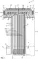
- FIG. 2is a schematic illustration of wafer chuck 170 , showing exemplary component parts thereof.
- FIG. 2is not drawn to scale, certain components of wafer chuck 170 are exaggerated or diminished in size, not every instance of each component is labeled, and not all internal connections among components are shown, for illustrative clarity.
- Regions of wafer chuck 170are identified as puck 175 , shaft 180 and base 185 , as per FIG. 1 , although certain components of wafer chuck 170 may overlap two or more of these regions.
- Puck 175includes an insulating top 205 in which are embedded electrodes 210 .
- Top 205may be formed of ceramic or other electrically insulating material; for example, in embodiments, top 205 is formed of aluminum nitride or alumina. Electrodes 210 may be formed of conductive and/or resistive materials that can withstand moderate to high temperatures, such as tungsten oxide, for example.
- An optional channel 207 within top 205brings a heat transfer gas such as helium into contact with a backside of wafer 50 to improve heat transfer between top 205 and wafer 50 .
- the improved heat transfercan help in cases where a wafer is not perfectly flat, and thus is not in uniform contact with the top surface of top 205 , and/or to improve thermal uniformity from the range of a few degrees point-to-point on a wafer, to the range of one degree or less.
- Optional channels 208interconnect with channel 207 and with one another within a top surface of top 205 , so that the heat transfer gas can spread between the bottom surface of wafer 50 and top 205 until the gas passes an outer edge of wafer 50 .
- An electrically conductive plate 220that may be formed of metal, for example, of aluminum or alloys thereof, is disposed beneath top 205 .
- Plate 220supports an inner puck element 212 in which one or more heat exchange channels 215 are defined.
- Heat exchange channels 215may, for example, be defined in a spiral configuration within inner puck element 212 .
- Heat exchange channels 215may define internal fins 218 , as shown, to improve thermal coupling between heat exchange fluid 35 (see FIG. 1 ) flowing within channels 215 , and inner puck element 212 .
- Connective element 214is advantageously formed of a material that has both high thermal conductivity and reasonably high ductility, to accommodate mechanical stresses and/or thermal expansion mismatch with adjacent components during temperature changes.
- fabrication of connective element 214is advantageously fabricated of aluminum silicon carbide (AlSiC), which features high thermal conductivity and at least higher ductility than puck inner element 212 and top 205 .
- AlSiCaluminum silicon carbide
- Connective element 214may fasten to plate 220 using bolts 219 , as shown.
- top 205is held in place over connective element 214 with a ring 211 , made for example of ceramic.
- Ring 211may be press-fit over top 205 and about connective element 214 , as shown, to provide mechanical stability and good thermal coupling, while not fastening ring 211 and/or top 205 rigidly with connective element 214 or plate 220 . Attaching top 205 in this manner advantageously accommodates slight thermal expansion mismatches among top 205 , ring 211 and connective element 214 during heating or cooling.
- Ring 211also protects bolts 219 from exposure to plasma and/or plasma products outside chuck 170 .
- an electrically conductive shaft housing 222is below top 205 and forms a housing for shaft 180 .
- Shaft housing 222may also be made, for example, of aluminum; plate 220 and shaft housing 222 are electrically coupled and may be integrally formed, as shown in FIG. 2 , or assembled by fastening or joining component parts.
- Shaft housing 222houses an optional insulating liner 225 , made for example of a ceramic material such as AlN or Al 2 O 3 , that helps keep internal components from shorting or arcing to shaft housing 222 .
- Insulating liner 225may be integrally formed with inner puck element 212 , as shown in FIG. 2 , or may be formed separately therefrom.
- Interior surfaces of insulating liner 225may, optionally, be flushed with inert gases such as helium or nitrogen to remove heat or to dilute and remove process gases that may enter the chuck surface as wafers are transferred to and from chuck 170 .
- inert gasessuch as helium or nitrogen to remove heat or to dilute and remove process gases that may enter the chuck surface as wafers are transferred to and from chuck 170 .
- Shaft 180also houses a variety of connectors 230 between power supplies and other facilities of equipment in which chuck 170 is located, and features of puck 175 .
- Exemplary connectors 230 shown in FIG. 2include radio-frequency/direct current (RF/DC) connectors 230 ( 1 ), 230 ( 2 ); a heat exchange fluid inlet and outlet 230 ( 3 ), 230 ( 4 ); a probe center-tap terminal 230 ( 5 ); and a thermocouple (TC) or resistance temperature detector (RTD) wire 230 ( 6 ) (e.g., a two-element wire, shown schematically as a single connector in FIG. 2 ).
- RF/DCradio-frequency/direct current
- TCthermocouple
- RTDresistance temperature detector
- Other connectors 230are possible, in embodiments.
- Connectors 230may be single or twisted pair wires, rods, coaxial or other connectors, insulated or uninsulated wires, or fluid conduits.
- radio-frequency/direct current (RF/DC) connectors 230 ( 1 ), 230 ( 2 )include an inner conductor, an insulating layer about the inner conductor, a ground tube about the insulating layer, and a ceramic tube about the ground tube.
- Connectors 230 that are fluid conduitsmay be integrally formed with puck and/or base elements, such as heat exchange fluid inlet and outlet 230 ( 3 ), 230 ( 4 ) integrally formed with inner puck element 212 , as shown in FIG. 2 .
- TCs or RTDsmay be implemented in any number and may optionally be organized for sensitivity to temperature variations caused by temperature and flow rate of heat exchange fluid 35 , heating by plasma or plasma products, heating or cooling caused by interaction with flowing gases or plasma products, or other causes.
- characterization of chuck 170may lead to a determination that temperature is uniform across a given configuration of chuck 170 , such that a single TC or RTD accurately represents the temperature of chuck 170 .
- multiple TCs or RTDscan be used to monitor temperature uniformity across chuck 170 , providing information that can be used to automatically and/or manually adjust operation of heat exchange fluids 35 or other aspects of a plasma processing system in which chuck 170 is located, to promote temperature uniformity.
- Connectors 230may also be fluid conduits. Additionally, or instead of connectors 230 being configured as fluid conduits, shaft housing 222 , insulating liner 225 and/or spaces among or between them may be configured with fluid passages. For example, a backside gas source 285 supplies He or other inert gas to channel 207 , for improved thermal control across wafer 50 .
- heat exchange fluid(s) 35to heat and/or cool puck 175 simplifies thermal management of chuck 170 , and a wafer 50 processed thereon, in a relatively low temperature regime, such as the range of about 20 C to 150 C.
- an external heat exchangermay be set to provide a heating/cooling fluid such as a mixture of 50% water, 50% ethylene or propylene glycol at the desired chuck temperature.
- Puck 175is provided with a high thermal mass that wafer 50 loaded onto puck 175 rapidly comes into thermal equilibrium with puck 175 at the desired temperature; inclusion of a connective element 214 formed of AlSiC helps to provide the high thermal mass.
- Thermal conductivity of puck 175 and flow rate of the heat exchange fluidare great enough that puck 175 and wafer 50 remain at the desired temperature despite heating and/or cooling effects of plasma generation, gas flows within processing location 160 , and the like.
- connectors 230 in FIG. 2are schematic only; connectors 230 may, and usually will, be arranged differently for purposes such as minimizing size of shaft 180 , maximizing space between adjacent connectors 230 , improving temperature uniformity and/or heat dissipation, and other reasons.
- Base 185 of chuck 170includes an electrically conductive base housing 270 that may be made of metal (for example, of aluminum) and may be may be integrally formed with shaft housing 222 or assembled to it by fasteners, welding or the like.
- base housing 270includes an electrically insulating terminal block 275 through which connectors 230 pass.
- Terminal block 275serves to align connectors 230 - 265 such that their respective distal ends are arranged to mate with corresponding sockets within puck 175 .
- Terminal block 275may be formed of an insulator such as polyether ether ketone (PEEK) or ceramic, which both provide good electrical resistance and stability at high temperatures.
- PEEKpolyether ether ketone
- Base housing 270may include channels such as channel 280 therein for heat exchange fluid 35 ( FIG. 1 ), as shown.
- Heat exchange fluid 35 passing through channel 280may be either a gas or a liquid.
- heat exchange fluid 35 passed through channel 280is a mixture of water and ethylene glycol or propylene glycol, having a mix ratio of approximately 50% water, 50% glycol.
- cooling provided through channel 280cools not only base housing 270 , but also shaft housing 222 and conductive plate 220 mechanically connected therewith.
- Base 185may be fixed within an associated piece of wafer processing equipment, or may be movably mounted using slides, hinges, stages or other devices to position puck 175 to send or receive a wafer or other workpiece, and/or to align the wafer or workpiece as needed.
- FIG. 3is a schematic illustration of a plasma wafer processing system 300 including wafer chuck 170 , showing exemplary component parts thereof.
- FIG. 3is not drawn to scale, certain components of plasma wafer processing system 300 are exaggerated or diminished in size, not every instance of each component is labeled, and not all internal connections among components are shown, for illustrative clarity.
- Plasma wafer processing system 300is an example of wafer processing system 100 , FIG. 1 .
- Plasma wafer processing system 300processes a wafer 50 within a process chamber 305 using plasma products and/or unactivated gases;
- FIG. 3shows flows of plasma products as open arrows and of unactivated gases as solid arrows.
- An optional remote plasma source 310generates a first plasma (not shown) from a first input gas stream 10 ( 1 ) and optionally mixes resulting plasma products with a second input gas stream 10 ( 2 ), passing the plasma products toward a diffuser 320 .
- the plasma productsmay pass through further, optional diffusers 320 , 325 and 340 that serve at least to distribute the plasma products uniformly before they are introduced into process chamber 305 .
- a first power supply 150 ( 1 )provides RF energy across a space 330 between diffusers 325 and 340 , forming a second plasma 335 in space 330 .
- Plasma products from the first and second plasmasmay optionally mix with a further input gas stream 10 ( 3 ) through a further diffuser 350 (sometimes referred to as a “showerhead”).
- Diffuser 350is configured with large ports for passing the plasma products therethrough, and gas passages 360 that transmit input gas stream 10 ( 3 ) through only the side of diffuser 350 that faces process chamber 305 . It will be appreciated that the use of any or all of remote plasma source 310 and diffusers 320 , 325 , 340 and 350 is optional.
- a second power supply 150 ( 2 )is controllably configured to provide RF energy and/or DC bias to electrodes 210 ( 1 ) and 210 ( 2 ) within chuck 170 , through connectors 230 ( 1 ) and 230 ( 2 ), as schematically shown, and to other parts of processing system 300 .
- Specific connections of the RF energy and/or DC biasmay vary, as discussed further below.
- Power supply 150 ( 2 )may provide, for example, DC bias across electrodes 210 ( 1 ) and 210 ( 2 ), and may provide RF energy and/or DC bias between electrodes 210 ( 1 ) and 210 ( 2 ) and other parts of processing system 300 , as indicated by connection 151 between power supply 150 ( 2 ) and diffuser 350 .
- Providing both RF energy and DC biasis especially useful for both electrostatically clamping wafer 50 (or any other workpiece) to chuck 170 , for generating a plasma within process chamber 305 , and for directing ions of the plasma to certain processing sites on wafer 50 , as discussed further below.
- Typical DC clamping voltagesare ⁇ 200V delivered to opposite electrodes 210 ( 1 ) and 210 ( 2 ), while typical RF voltages are ⁇ 75V across process chamber 305 , corresponding to power delivery of about 100-500 W to the plasma.
- a portion of processing system 300is shown in greater detail in FIG. 4 .
- FIG. 4is a schematic illustration of part of plasma wafer processing system 300 including portions of wafer chuck 170 and diffuser 350 , and illustrating exemplary power supply connections thereto.
- FIG. 4is not drawn to scale, certain components of plasma wafer processing system 300 are exaggerated or diminished in size, not every instance of each component is labeled, and not all internal connections among components are shown, for illustrative clarity.
- FIG. 4shows a portion of process chamber 305 bounded by respective portions of diffuser 350 and chuck 170 , wafer 50 , a plasma 355 within process chamber 305 , and exemplary details of power supply 150 ( 2 ).
- Plasma 355is generated from gas streams 10 ( 1 ), 10 ( 2 ) and/or 10 ( 3 ), either in their original, unactivated forms, or as plasma products formed in remote plasma source 310 or within space 330 ( FIG. 3 ).
- RF energy for forming plasma 355is supplied by RF source 390 within power supply 150 ( 2 ).
- power supply 150 ( 2 )also provides a DC bias 370 across electrodes 210 ( 1 ) and 210 ( 2 ), that serves to electrostatically clamp wafer 50 to wafer chuck 170 .
- DC electric fieldsare shown in FIG. 4 with dotted arrows.
- the embodiment shown in FIG. 4also includes an optional DC bias 380 between electrodes 210 and diffuser 350 .
- DC bias 380can steer ions formed in plasma 355 (or existing in plasma products from other locations, as discussed above) toward wafer 50 to influence directionality of plasma processing on wafer 50 (see FIG. 5 ).
- FIG. 4also shows a center tap DC probe 395 that can be monitored to determine the actual backside DC voltage of wafer 50 .
- Voltage measured on DC probe 395can be measured and used to control DC bias 380 , in order to control and optimize process results on wafer 50 .
- reactive species within the plasma productsare often negatively charged ions, which can transfer negative charge to wafer 50 when they react. This leads to charging of wafer 50 ; a typical DC voltage acquired by wafer 50 during processing may be about ⁇ 50V.
- Center tap DC probe 395allows this voltage to be sensed and thus compensated by adjusting DC bias 380 accordingly.
- DC probe 395couples with a high impedance circuit 398 that measures the voltage on DC probe 395 and provides appropriate information for power supply 150 ( 2 ) to adjust DC bias 380 .
- All of the components of, and integrated with, wafer chuck 170are compatible with operation in a temperature range of about 20 C to 150 C, in contrast to earlier systems that may utilize materials that are not compatible with the 20 C to 150 C temperature range, such as certain polymers or plastics, rubber, and the like.
- the components that are exposed to plasmaare also capable of surviving very harsh plasma environments, such as H* or F* radicals, and others, produced when NH 3 or NF 3 respectively are utilized as source gases.
- O 2is also commonly added as a source gas (to supply electrons, facilitating plasma initiation) creating further ionic species and radicals.
- Earlier systemsoften used stainless steel chucks, but stainless generally corrodes in such environments, causing particulate contamination.
- wafer chuck 170 within processing system 300is unique in that it allows for processing to take place at a uniform temperature while also providing firm electrostatic clamping for heat transfer, and the ability to steer reactive ionic species toward the workpiece, without corrosion or thermal degradation.
- embodiments hereinare capable of plasma etching of certain metallic and/or ceramic materials on wafer 50 .
- FIGS. 5 , 6 and 7illustrate exemplary processing results obtainable with the wafer chucks and wafer processing systems described herein.
- FIG. 5illustrates a portion of a wafer 50 ( 1 ) in process. Wafer 50 ( 1 ) has already been processed to form deep trenches 410 therein, and a film 400 ( 1 ) has been deposited on both top surfaces of wafer 50 ( 1 ) and in trenches 410 . Subsequent processing is intended to remove film 400 ( 1 ) from certain regions of wafer 50 ( 1 ) but leave film 400 ( 1 ) on other regions; photoresist 420 is therefore provided in the regions where film 400 ( 1 ) is to remain.
- FIG. 6illustrates a hypothetical result when wafer 50 ( 1 ) is exposed to a plasma that does not steer ions, for example by exposing wafer 50 ( 1 ) to a plasma where reactive species are simply directed randomly by diffusion. Surfaces of film 400 ( 1 ) that are readily exposed to the reactive species are etched, while wafer 50 ( 1 ) does not react with the reactive species. This process leaves the resulting wafer 50 ( 2 ) with film 400 ( 4 ) protected by photoresist 420 , but also leaving residual material 400 ( 3 ) within trenches 410 . This occurs because the reactive species simply travel until they meet something, then react where they land. Few reactive species happen to be traveling in the exact direction required to penetrate deeply into trenches 410 . It may or may not be possible, and is usually impractical, to etch wafer 50 ( 1 ) long enough to remove residual material 400 ( 3 ) using randomly directed reactive species.
- FIG. 7illustrates the result when wafer 50 ( 1 ) is exposed to a plasma that steers ions by providing an electric field that directs ions toward wafer 50 ( 1 ); that is, as shown in FIGS. 3 and 4 using wafer chuck 170 .
- the electric field indicated in FIG. 4directs negatively charged reactive species downward in the orientation of FIG. 7 , such that more of the reactive species reach lower regions of film 400 ( 1 ) within trenches 410 .
- the resulting wafer 50 ( 3 )retains film 400 ( 4 ) only in locations where original film 400 ( 1 ) is protected by photoresist 420 , as shown.
- wafer chuckshave often been quite simple affairs ranging from mere slabs of metal to slightly more complicated systems that provide vacuum or electrostatic clamping, adjustable wafer alignment/positioning, and the like. Designs that retain all of these functions and yet operate with precise cross-wafer temperature control in highly corrosive plasma environments without degradation, are not known.
Landscapes
- Engineering & Computer Science (AREA)
- Physics & Mathematics (AREA)
- Microelectronics & Electronic Packaging (AREA)
- General Physics & Mathematics (AREA)
- Manufacturing & Machinery (AREA)
- Computer Hardware Design (AREA)
- Condensed Matter Physics & Semiconductors (AREA)
- Power Engineering (AREA)
- Plasma & Fusion (AREA)
- Chemical & Material Sciences (AREA)
- Analytical Chemistry (AREA)
- Container, Conveyance, Adherence, Positioning, Of Wafer (AREA)
- Drying Of Semiconductors (AREA)
- Plasma Technology (AREA)
Abstract
Description
Claims (16)
Priority Applications (2)
| Application Number | Priority Date | Filing Date | Title |
|---|---|---|---|
| US15/581,497US11594428B2 (en) | 2015-02-03 | 2017-04-28 | Low temperature chuck for plasma processing systems |
| US18/175,104US12009228B2 (en) | 2015-02-03 | 2023-02-27 | Low temperature chuck for plasma processing systems |
Applications Claiming Priority (2)
| Application Number | Priority Date | Filing Date | Title |
|---|---|---|---|
| US14/612,857US20160225652A1 (en) | 2015-02-03 | 2015-02-03 | Low temperature chuck for plasma processing systems |
| US15/581,497US11594428B2 (en) | 2015-02-03 | 2017-04-28 | Low temperature chuck for plasma processing systems |
Related Parent Applications (1)
| Application Number | Title | Priority Date | Filing Date |
|---|---|---|---|
| US14/612,857ContinuationUS20160225652A1 (en) | 2015-02-03 | 2015-02-03 | Low temperature chuck for plasma processing systems |
Related Child Applications (1)
| Application Number | Title | Priority Date | Filing Date |
|---|---|---|---|
| US18/175,104ContinuationUS12009228B2 (en) | 2015-02-03 | 2023-02-27 | Low temperature chuck for plasma processing systems |
Publications (2)
| Publication Number | Publication Date |
|---|---|
| US20170229326A1 US20170229326A1 (en) | 2017-08-10 |
| US11594428B2true US11594428B2 (en) | 2023-02-28 |
Family
ID=56554680
Family Applications (3)
| Application Number | Title | Priority Date | Filing Date |
|---|---|---|---|
| US14/612,857AbandonedUS20160225652A1 (en) | 2015-02-03 | 2015-02-03 | Low temperature chuck for plasma processing systems |
| US15/581,497ActiveUS11594428B2 (en) | 2015-02-03 | 2017-04-28 | Low temperature chuck for plasma processing systems |
| US18/175,104ActiveUS12009228B2 (en) | 2015-02-03 | 2023-02-27 | Low temperature chuck for plasma processing systems |
Family Applications Before (1)
| Application Number | Title | Priority Date | Filing Date |
|---|---|---|---|
| US14/612,857AbandonedUS20160225652A1 (en) | 2015-02-03 | 2015-02-03 | Low temperature chuck for plasma processing systems |
Family Applications After (1)
| Application Number | Title | Priority Date | Filing Date |
|---|---|---|---|
| US18/175,104ActiveUS12009228B2 (en) | 2015-02-03 | 2023-02-27 | Low temperature chuck for plasma processing systems |
Country Status (6)
| Country | Link |
|---|---|
| US (3) | US20160225652A1 (en) |
| JP (1) | JP6710217B2 (en) |
| KR (1) | KR102553118B1 (en) |
| CN (1) | CN107533945B (en) |
| TW (1) | TWI726860B (en) |
| WO (1) | WO2016126425A1 (en) |
Cited By (5)
| Publication number | Priority date | Publication date | Assignee | Title |
|---|---|---|---|---|
| US20200098588A1 (en)* | 2018-05-30 | 2020-03-26 | Taiwan Semiconductor Manufacturing Company, Ltd. | Dry Ashing by Secondary Excitation |
| US20230058692A1 (en)* | 2019-08-05 | 2023-02-23 | Hitachi High-Tech Corporation | Plasma processing apparatus |
| US20230060486A1 (en)* | 2021-08-27 | 2023-03-02 | Samsung Electronics Co., Ltd. | Plasma generator |
| US20240297024A1 (en)* | 2022-05-18 | 2024-09-05 | Toshiba Mitsubishi-Electric Industrial Systems Corporation | Active gas generation apparatus |
| US12444572B2 (en)* | 2024-04-03 | 2025-10-14 | Hitachi High-Tech Corporation | Plasma processing apparatus |
Families Citing this family (114)
| Publication number | Priority date | Publication date | Assignee | Title |
|---|---|---|---|---|
| US9324576B2 (en) | 2010-05-27 | 2016-04-26 | Applied Materials, Inc. | Selective etch for silicon films |
| US10283321B2 (en) | 2011-01-18 | 2019-05-07 | Applied Materials, Inc. | Semiconductor processing system and methods using capacitively coupled plasma |
| US9064815B2 (en) | 2011-03-14 | 2015-06-23 | Applied Materials, Inc. | Methods for etch of metal and metal-oxide films |
| US8999856B2 (en) | 2011-03-14 | 2015-04-07 | Applied Materials, Inc. | Methods for etch of sin films |
| US9267739B2 (en) | 2012-07-18 | 2016-02-23 | Applied Materials, Inc. | Pedestal with multi-zone temperature control and multiple purge capabilities |
| US9373517B2 (en) | 2012-08-02 | 2016-06-21 | Applied Materials, Inc. | Semiconductor processing with DC assisted RF power for improved control |
| US9132436B2 (en) | 2012-09-21 | 2015-09-15 | Applied Materials, Inc. | Chemical control features in wafer process equipment |
| US10256079B2 (en) | 2013-02-08 | 2019-04-09 | Applied Materials, Inc. | Semiconductor processing systems having multiple plasma configurations |
| US9362130B2 (en) | 2013-03-01 | 2016-06-07 | Applied Materials, Inc. | Enhanced etching processes using remote plasma sources |
| US20140271097A1 (en) | 2013-03-15 | 2014-09-18 | Applied Materials, Inc. | Processing systems and methods for halide scavenging |
| US9773648B2 (en) | 2013-08-30 | 2017-09-26 | Applied Materials, Inc. | Dual discharge modes operation for remote plasma |
| US9576809B2 (en) | 2013-11-04 | 2017-02-21 | Applied Materials, Inc. | Etch suppression with germanium |
| US9520303B2 (en) | 2013-11-12 | 2016-12-13 | Applied Materials, Inc. | Aluminum selective etch |
| US9299537B2 (en) | 2014-03-20 | 2016-03-29 | Applied Materials, Inc. | Radial waveguide systems and methods for post-match control of microwaves |
| US9903020B2 (en) | 2014-03-31 | 2018-02-27 | Applied Materials, Inc. | Generation of compact alumina passivation layers on aluminum plasma equipment components |
| US9309598B2 (en) | 2014-05-28 | 2016-04-12 | Applied Materials, Inc. | Oxide and metal removal |
| US9496167B2 (en) | 2014-07-31 | 2016-11-15 | Applied Materials, Inc. | Integrated bit-line airgap formation and gate stack post clean |
| US9613822B2 (en) | 2014-09-25 | 2017-04-04 | Applied Materials, Inc. | Oxide etch selectivity enhancement |
| US9355922B2 (en) | 2014-10-14 | 2016-05-31 | Applied Materials, Inc. | Systems and methods for internal surface conditioning in plasma processing equipment |
| US9966240B2 (en) | 2014-10-14 | 2018-05-08 | Applied Materials, Inc. | Systems and methods for internal surface conditioning assessment in plasma processing equipment |
| US11637002B2 (en) | 2014-11-26 | 2023-04-25 | Applied Materials, Inc. | Methods and systems to enhance process uniformity |
| US10224210B2 (en) | 2014-12-09 | 2019-03-05 | Applied Materials, Inc. | Plasma processing system with direct outlet toroidal plasma source |
| US10573496B2 (en) | 2014-12-09 | 2020-02-25 | Applied Materials, Inc. | Direct outlet toroidal plasma source |
| US11257693B2 (en) | 2015-01-09 | 2022-02-22 | Applied Materials, Inc. | Methods and systems to improve pedestal temperature control |
| US9728437B2 (en) | 2015-02-03 | 2017-08-08 | Applied Materials, Inc. | High temperature chuck for plasma processing systems |
| US20160225652A1 (en) | 2015-02-03 | 2016-08-04 | Applied Materials, Inc. | Low temperature chuck for plasma processing systems |
| US9881805B2 (en) | 2015-03-02 | 2018-01-30 | Applied Materials, Inc. | Silicon selective removal |
| US9741593B2 (en) | 2015-08-06 | 2017-08-22 | Applied Materials, Inc. | Thermal management systems and methods for wafer processing systems |
| US9691645B2 (en) | 2015-08-06 | 2017-06-27 | Applied Materials, Inc. | Bolted wafer chuck thermal management systems and methods for wafer processing systems |
| US9349605B1 (en) | 2015-08-07 | 2016-05-24 | Applied Materials, Inc. | Oxide etch selectivity systems and methods |
| US10504700B2 (en) | 2015-08-27 | 2019-12-10 | Applied Materials, Inc. | Plasma etching systems and methods with secondary plasma injection |
| US10522371B2 (en) | 2016-05-19 | 2019-12-31 | Applied Materials, Inc. | Systems and methods for improved semiconductor etching and component protection |
| US10504754B2 (en) | 2016-05-19 | 2019-12-10 | Applied Materials, Inc. | Systems and methods for improved semiconductor etching and component protection |
| US9865484B1 (en) | 2016-06-29 | 2018-01-09 | Applied Materials, Inc. | Selective etch using material modification and RF pulsing |
| US10629473B2 (en) | 2016-09-09 | 2020-04-21 | Applied Materials, Inc. | Footing removal for nitride spacer |
| US10062575B2 (en) | 2016-09-09 | 2018-08-28 | Applied Materials, Inc. | Poly directional etch by oxidation |
| US9721789B1 (en) | 2016-10-04 | 2017-08-01 | Applied Materials, Inc. | Saving ion-damaged spacers |
| US10062585B2 (en) | 2016-10-04 | 2018-08-28 | Applied Materials, Inc. | Oxygen compatible plasma source |
| US10546729B2 (en) | 2016-10-04 | 2020-01-28 | Applied Materials, Inc. | Dual-channel showerhead with improved profile |
| US9934942B1 (en) | 2016-10-04 | 2018-04-03 | Applied Materials, Inc. | Chamber with flow-through source |
| US10062579B2 (en) | 2016-10-07 | 2018-08-28 | Applied Materials, Inc. | Selective SiN lateral recess |
| US9947549B1 (en) | 2016-10-10 | 2018-04-17 | Applied Materials, Inc. | Cobalt-containing material removal |
| US9768034B1 (en) | 2016-11-11 | 2017-09-19 | Applied Materials, Inc. | Removal methods for high aspect ratio structures |
| US10163696B2 (en) | 2016-11-11 | 2018-12-25 | Applied Materials, Inc. | Selective cobalt removal for bottom up gapfill |
| US10242908B2 (en) | 2016-11-14 | 2019-03-26 | Applied Materials, Inc. | Airgap formation with damage-free copper |
| US10026621B2 (en) | 2016-11-14 | 2018-07-17 | Applied Materials, Inc. | SiN spacer profile patterning |
| US10566206B2 (en) | 2016-12-27 | 2020-02-18 | Applied Materials, Inc. | Systems and methods for anisotropic material breakthrough |
| US10431429B2 (en) | 2017-02-03 | 2019-10-01 | Applied Materials, Inc. | Systems and methods for radial and azimuthal control of plasma uniformity |
| US10403507B2 (en) | 2017-02-03 | 2019-09-03 | Applied Materials, Inc. | Shaped etch profile with oxidation |
| US10043684B1 (en) | 2017-02-06 | 2018-08-07 | Applied Materials, Inc. | Self-limiting atomic thermal etching systems and methods |
| US10319739B2 (en) | 2017-02-08 | 2019-06-11 | Applied Materials, Inc. | Accommodating imperfectly aligned memory holes |
| US10943834B2 (en) | 2017-03-13 | 2021-03-09 | Applied Materials, Inc. | Replacement contact process |
| US10319649B2 (en) | 2017-04-11 | 2019-06-11 | Applied Materials, Inc. | Optical emission spectroscopy (OES) for remote plasma monitoring |
| US11276590B2 (en) | 2017-05-17 | 2022-03-15 | Applied Materials, Inc. | Multi-zone semiconductor substrate supports |
| US11276559B2 (en) | 2017-05-17 | 2022-03-15 | Applied Materials, Inc. | Semiconductor processing chamber for multiple precursor flow |
| JP7176860B6 (en) | 2017-05-17 | 2022-12-16 | アプライド マテリアルズ インコーポレイテッド | Semiconductor processing chamber to improve precursor flow |
| US10147610B1 (en)* | 2017-05-30 | 2018-12-04 | Lam Research Corporation | Substrate pedestal module including metallized ceramic tubes for RF and gas delivery |
| US10497579B2 (en) | 2017-05-31 | 2019-12-03 | Applied Materials, Inc. | Water-free etching methods |
| US10049891B1 (en) | 2017-05-31 | 2018-08-14 | Applied Materials, Inc. | Selective in situ cobalt residue removal |
| US11289355B2 (en) | 2017-06-02 | 2022-03-29 | Lam Research Corporation | Electrostatic chuck for use in semiconductor processing |
| US10920320B2 (en) | 2017-06-16 | 2021-02-16 | Applied Materials, Inc. | Plasma health determination in semiconductor substrate processing reactors |
| US10541246B2 (en) | 2017-06-26 | 2020-01-21 | Applied Materials, Inc. | 3D flash memory cells which discourage cross-cell electrical tunneling |
| US10727080B2 (en) | 2017-07-07 | 2020-07-28 | Applied Materials, Inc. | Tantalum-containing material removal |
| US10541184B2 (en) | 2017-07-11 | 2020-01-21 | Applied Materials, Inc. | Optical emission spectroscopic techniques for monitoring etching |
| US10354889B2 (en) | 2017-07-17 | 2019-07-16 | Applied Materials, Inc. | Non-halogen etching of silicon-containing materials |
| US10043674B1 (en) | 2017-08-04 | 2018-08-07 | Applied Materials, Inc. | Germanium etching systems and methods |
| US10170336B1 (en) | 2017-08-04 | 2019-01-01 | Applied Materials, Inc. | Methods for anisotropic control of selective silicon removal |
| US10297458B2 (en) | 2017-08-07 | 2019-05-21 | Applied Materials, Inc. | Process window widening using coated parts in plasma etch processes |
| US11469084B2 (en) | 2017-09-05 | 2022-10-11 | Lam Research Corporation | High temperature RF connection with integral thermal choke |
| US10128086B1 (en) | 2017-10-24 | 2018-11-13 | Applied Materials, Inc. | Silicon pretreatment for nitride removal |
| US10283324B1 (en) | 2017-10-24 | 2019-05-07 | Applied Materials, Inc. | Oxygen treatment for nitride etching |
| US10256112B1 (en) | 2017-12-08 | 2019-04-09 | Applied Materials, Inc. | Selective tungsten removal |
| US10903054B2 (en) | 2017-12-19 | 2021-01-26 | Applied Materials, Inc. | Multi-zone gas distribution systems and methods |
| US11328909B2 (en) | 2017-12-22 | 2022-05-10 | Applied Materials, Inc. | Chamber conditioning and removal processes |
| US10854426B2 (en) | 2018-01-08 | 2020-12-01 | Applied Materials, Inc. | Metal recess for semiconductor structures |
| US11990360B2 (en)* | 2018-01-31 | 2024-05-21 | Lam Research Corporation | Electrostatic chuck (ESC) pedestal voltage isolation |
| US10679870B2 (en) | 2018-02-15 | 2020-06-09 | Applied Materials, Inc. | Semiconductor processing chamber multistage mixing apparatus |
| US10964512B2 (en) | 2018-02-15 | 2021-03-30 | Applied Materials, Inc. | Semiconductor processing chamber multistage mixing apparatus and methods |
| TWI766433B (en) | 2018-02-28 | 2022-06-01 | 美商應用材料股份有限公司 | Systems and methods to form airgaps |
| US10593560B2 (en) | 2018-03-01 | 2020-03-17 | Applied Materials, Inc. | Magnetic induction plasma source for semiconductor processes and equipment |
| US10319600B1 (en) | 2018-03-12 | 2019-06-11 | Applied Materials, Inc. | Thermal silicon etch |
| US10497573B2 (en) | 2018-03-13 | 2019-12-03 | Applied Materials, Inc. | Selective atomic layer etching of semiconductor materials |
| US10573527B2 (en) | 2018-04-06 | 2020-02-25 | Applied Materials, Inc. | Gas-phase selective etching systems and methods |
| US10490406B2 (en) | 2018-04-10 | 2019-11-26 | Appled Materials, Inc. | Systems and methods for material breakthrough |
| US10699879B2 (en) | 2018-04-17 | 2020-06-30 | Applied Materials, Inc. | Two piece electrode assembly with gap for plasma control |
| US10886137B2 (en) | 2018-04-30 | 2021-01-05 | Applied Materials, Inc. | Selective nitride removal |
| JP6773917B2 (en)* | 2018-07-04 | 2020-10-21 | 日本碍子株式会社 | Wafer support |
| US10872778B2 (en) | 2018-07-06 | 2020-12-22 | Applied Materials, Inc. | Systems and methods utilizing solid-phase etchants |
| US10755941B2 (en) | 2018-07-06 | 2020-08-25 | Applied Materials, Inc. | Self-limiting selective etching systems and methods |
| US10672642B2 (en) | 2018-07-24 | 2020-06-02 | Applied Materials, Inc. | Systems and methods for pedestal configuration |
| US11183368B2 (en) | 2018-08-02 | 2021-11-23 | Lam Research Corporation | RF tuning systems including tuning circuits having impedances for setting and adjusting parameters of electrodes in electrostatic chucks |
| US11049755B2 (en) | 2018-09-14 | 2021-06-29 | Applied Materials, Inc. | Semiconductor substrate supports with embedded RF shield |
| US10892198B2 (en) | 2018-09-14 | 2021-01-12 | Applied Materials, Inc. | Systems and methods for improved performance in semiconductor processing |
| US11062887B2 (en) | 2018-09-17 | 2021-07-13 | Applied Materials, Inc. | High temperature RF heater pedestals |
| US11417534B2 (en) | 2018-09-21 | 2022-08-16 | Applied Materials, Inc. | Selective material removal |
| US11682560B2 (en) | 2018-10-11 | 2023-06-20 | Applied Materials, Inc. | Systems and methods for hafnium-containing film removal |
| US11121002B2 (en) | 2018-10-24 | 2021-09-14 | Applied Materials, Inc. | Systems and methods for etching metals and metal derivatives |
| US11437242B2 (en) | 2018-11-27 | 2022-09-06 | Applied Materials, Inc. | Selective removal of silicon-containing materials |
| US11721527B2 (en) | 2019-01-07 | 2023-08-08 | Applied Materials, Inc. | Processing chamber mixing systems |
| US10920319B2 (en) | 2019-01-11 | 2021-02-16 | Applied Materials, Inc. | Ceramic showerheads with conductive electrodes |
| CN113544837A (en)* | 2019-03-08 | 2021-10-22 | 朗姆研究公司 | Chuck for plasma processing chamber |
| CN112216585B (en)* | 2019-07-11 | 2022-12-30 | 中微半导体设备(上海)股份有限公司 | Plasma processor and base temperature control method |
| CN111446199B (en)* | 2020-03-25 | 2023-05-16 | 北京北方华创微电子装备有限公司 | Reaction chamber of semiconductor device and semiconductor device |
| US11615966B2 (en) | 2020-07-19 | 2023-03-28 | Applied Materials, Inc. | Flowable film formation and treatments |
| US11699571B2 (en)* | 2020-09-08 | 2023-07-11 | Applied Materials, Inc. | Semiconductor processing chambers for deposition and etch |
| US11887811B2 (en) | 2020-09-08 | 2024-01-30 | Applied Materials, Inc. | Semiconductor processing chambers for deposition and etch |
| US12142459B2 (en) | 2020-09-08 | 2024-11-12 | Applied Materials, Inc. | Single chamber flowable film formation and treatments |
| JP7729764B2 (en)* | 2021-10-06 | 2025-08-26 | 日本特殊陶業株式会社 | Substrate holding member |
| JP7733531B2 (en)* | 2021-10-08 | 2025-09-03 | 日本特殊陶業株式会社 | Substrate holding member |
| US20230162955A1 (en)* | 2021-11-24 | 2023-05-25 | Applied Materials, Inc. | Electrostatic chuck with detachable shaft |
| KR102732074B1 (en)* | 2022-02-22 | 2024-11-20 | 주식회사 테스 | Substrate supporting unit |
| WO2023219727A1 (en)* | 2022-05-12 | 2023-11-16 | Lam Research Corporation | Semiconductor processing chamber components with cladding |
| KR102650161B1 (en)* | 2023-01-05 | 2024-03-22 | 주식회사 미코세라믹스 | Ceramic susceptor |
| US20250069864A1 (en)* | 2023-08-21 | 2025-02-27 | Applied Materials, Inc. | Susceptor heat transfer |
Citations (2043)
| Publication number | Priority date | Publication date | Assignee | Title |
|---|---|---|---|---|
| US2369620A (en) | 1941-03-07 | 1945-02-13 | Battelle Development Corp | Method of coating cupreous metal with tin |
| US3401302A (en) | 1965-11-01 | 1968-09-10 | Humphreys Corp | Induction plasma generator including cooling means, gas flow means, and operating means therefor |
| US3451840A (en) | 1965-10-06 | 1969-06-24 | Us Air Force | Wire coated with boron nitride and boron |
| US3537474A (en) | 1968-02-19 | 1970-11-03 | Varian Associates | Push button vacuum control valve and vacuum system using same |
| US3756511A (en) | 1971-02-02 | 1973-09-04 | Kogyo Kaihatsu Kenyusho | Nozzle and torch for plasma jet |
| US3937857A (en) | 1974-07-22 | 1976-02-10 | Amp Incorporated | Catalyst for electroless deposition of metals |
| US3969077A (en) | 1971-12-16 | 1976-07-13 | Varian Associates | Alkali metal leak detection method and apparatus |
| US4006047A (en) | 1974-07-22 | 1977-02-01 | Amp Incorporated | Catalysts for electroless deposition of metals on comparatively low-temperature polyolefin and polyester substrates |
| US4190488A (en) | 1978-08-21 | 1980-02-26 | International Business Machines Corporation | Etching method using noble gas halides |
| US4209357A (en) | 1979-05-18 | 1980-06-24 | Tegal Corporation | Plasma reactor apparatus |
| US4214946A (en) | 1979-02-21 | 1980-07-29 | International Business Machines Corporation | Selective reactive ion etching of polysilicon against SiO2 utilizing SF6 -Cl2 -inert gas etchant |
| US4232060A (en) | 1979-01-22 | 1980-11-04 | Richardson Chemical Company | Method of preparing substrate surface for electroless plating and products produced thereby |
| US4234628A (en) | 1978-11-28 | 1980-11-18 | The Harshaw Chemical Company | Two-step preplate system for polymeric surfaces |
| US4265943A (en) | 1978-11-27 | 1981-05-05 | Macdermid Incorporated | Method and composition for continuous electroless copper deposition using a hypophosphite reducing agent in the presence of cobalt or nickel ions |
| US4340462A (en) | 1981-02-13 | 1982-07-20 | Lam Research Corporation | Adjustable electrode plasma processing chamber |
| US4341592A (en) | 1975-08-04 | 1982-07-27 | Texas Instruments Incorporated | Method for removing photoresist layer from substrate by ozone treatment |
| US4361418A (en) | 1980-05-06 | 1982-11-30 | Risdon Corporation | High vacuum processing system having improved recycle draw-down capability under high humidity ambient atmospheric conditions |
| US4361441A (en) | 1979-04-17 | 1982-11-30 | Plasma Holdings N.V. | Treatment of matter in low temperature plasmas |
| US4364803A (en) | 1980-03-11 | 1982-12-21 | Oronzio De Nora Impianti Elettrochimici S.P.A. | Deposition of catalytic electrodes on ion-exchange membranes |
| US4368223A (en) | 1981-06-01 | 1983-01-11 | Asahi Glass Company, Ltd. | Process for preparing nickel layer |
| US4374698A (en) | 1980-07-11 | 1983-02-22 | U.S. Philips Corporation | Method of manufacturing a semiconductor device |
| US4397812A (en) | 1974-05-24 | 1983-08-09 | Richardson Chemical Company | Electroless nickel polyalloys |
| JPS59126778A (en) | 1983-01-11 | 1984-07-21 | Tokyo Denshi Kagaku Kabushiki | Method and device for plasma etching |
| US4468413A (en) | 1982-02-15 | 1984-08-28 | U.S. Philips Corporation | Method of manufacturing fluorine-doped optical fibers |
| US4503807A (en) | 1983-06-01 | 1985-03-12 | Nippon Telegraph & Telephone Public Corporation | Chemical vapor deposition apparatus |
| US4543110A (en) | 1983-07-06 | 1985-09-24 | Kraftwerk Union Aktiengesellschaft | Method and plant for reheating flue gases behind a wet flue-gas desulfurization plant |
| US4565601A (en) | 1983-09-12 | 1986-01-21 | Hitachi, Ltd. | Method and apparatus for controlling sample temperature |
| US4579618A (en) | 1984-01-06 | 1986-04-01 | Tegal Corporation | Plasma reactor apparatus |
| US4585920A (en) | 1982-05-21 | 1986-04-29 | Tegal Corporation | Plasma reactor removable insert |
| US4600464A (en) | 1985-05-01 | 1986-07-15 | International Business Machines Corporation | Plasma etching reactor with reduced plasma potential |
| US4610775A (en) | 1985-07-26 | 1986-09-09 | Westinghouse Electric Corp. | Method and apparatus for clearing short-circuited, high-voltage cathodes in a sputtering chamber |
| US4625678A (en) | 1982-05-28 | 1986-12-02 | Fujitsu Limited | Apparatus for plasma chemical vapor deposition |
| US4632857A (en) | 1974-05-24 | 1986-12-30 | Richardson Chemical Company | Electrolessly plated product having a polymetallic catalytic film underlayer |
| JPS6245119A (en) | 1985-08-23 | 1987-02-27 | Matsushita Electric Ind Co Ltd | Dry etching device |
| US4656052A (en) | 1984-02-13 | 1987-04-07 | Kyocera Corporation | Process for production of high-hardness boron nitride film |
| US4656076A (en) | 1985-04-26 | 1987-04-07 | Triquint Semiconductors, Inc. | Self-aligned recessed gate process |
| US4668335A (en) | 1985-08-30 | 1987-05-26 | Advanced Micro Devices, Inc. | Anti-corrosion treatment for patterning of metallic layers |
| US4690746A (en) | 1986-02-24 | 1987-09-01 | Genus, Inc. | Interlayer dielectric process |
| US4715937A (en) | 1986-05-05 | 1987-12-29 | The Board Of Trustees Of The Leland Stanford Junior University | Low-temperature direct nitridation of silicon in nitrogen plasma generated by microwave discharge |
| US4749440A (en) | 1985-08-28 | 1988-06-07 | Fsi Corporation | Gaseous process and apparatus for removing films from substrates |
| US4753898A (en) | 1987-07-09 | 1988-06-28 | Motorola, Inc. | LDD CMOS process |
| US4786360A (en) | 1987-03-30 | 1988-11-22 | International Business Machines Corporation | Anisotropic etch process for tungsten metallurgy |
| JPS63301051A (en) | 1987-06-01 | 1988-12-08 | Fujitsu Ltd | Manufacture of photosensitive body |
| US4792378A (en) | 1987-12-15 | 1988-12-20 | Texas Instruments Incorporated | Gas dispersion disk for use in plasma enhanced chemical vapor deposition reactor |
| US4793897A (en) | 1987-03-20 | 1988-12-27 | Applied Materials, Inc. | Selective thin film etch process |
| US4807016A (en) | 1985-07-15 | 1989-02-21 | Texas Instruments Incorporated | Dry etch of phosphosilicate glass with selectivity to undoped oxide |
| US4810520A (en) | 1987-09-23 | 1989-03-07 | Magnetic Peripherals Inc. | Method for controlling electroless magnetic plating |
| US4816638A (en) | 1987-02-20 | 1989-03-28 | Anelva Corporation | Vacuum processing apparatus |
| US4820377A (en) | 1987-07-16 | 1989-04-11 | Texas Instruments Incorporated | Method for cleanup processing chamber and vacuum process module |
| US4828649A (en) | 1987-07-16 | 1989-05-09 | Texas Instruments Incorporated | Method for etching an aluminum film doped with silicon |
| JPH01200627A (en) | 1988-02-05 | 1989-08-11 | Toshiba Corp | Apparatus and method of dry etching |
| US4857140A (en) | 1987-07-16 | 1989-08-15 | Texas Instruments Incorporated | Method for etching silicon nitride |
| US4867841A (en) | 1987-07-16 | 1989-09-19 | Texas Instruments Incorporated | Method for etch of polysilicon film |
| US4904621A (en) | 1987-07-16 | 1990-02-27 | Texas Instruments Incorporated | Remote plasma generation process using a two-stage showerhead |
| US4913929A (en) | 1987-04-21 | 1990-04-03 | The Board Of Trustees Of The Leland Stanford Junior University | Thermal/microwave remote plasma multiprocessing reactor and method of use |
| US4919750A (en) | 1987-09-14 | 1990-04-24 | International Business Machines Corporation | Etching metal films with complexing chloride plasma |
| JPH02114525A (en) | 1988-10-24 | 1990-04-26 | Toshiba Corp | Organic compound film removal method and removal device |
| US4946903A (en) | 1989-03-27 | 1990-08-07 | The Research Foundation Of State University Of Ny | Oxyfluoropolymers having chemically reactive surface functionality and increased surface energies |
| US4951601A (en) | 1986-12-19 | 1990-08-28 | Applied Materials, Inc. | Multi-chamber integrated process system |
| US4960488A (en) | 1986-12-19 | 1990-10-02 | Applied Materials, Inc. | Reactor chamber self-cleaning process |
| US4980018A (en) | 1989-11-14 | 1990-12-25 | Intel Corporation | Plasma etching process for refractory metal vias |
| US4981551A (en) | 1987-11-03 | 1991-01-01 | North Carolina State University | Dry etching of silicon carbide |
| US4985372A (en) | 1989-02-17 | 1991-01-15 | Tokyo Electron Limited | Method of forming conductive layer including removal of native oxide |
| US4992136A (en) | 1987-07-29 | 1991-02-12 | Hitachi, Ltd. | Dry etching method |
| US4991542A (en) | 1987-10-14 | 1991-02-12 | The Furukawa Electric Co., Ltd. | Method of forming a thin film by plasma CVD and apapratus for forming a thin film |
| US4994404A (en) | 1989-08-28 | 1991-02-19 | Motorola, Inc. | Method for forming a lightly-doped drain (LDD) structure in a semiconductor device |
| US4993358A (en) | 1989-07-28 | 1991-02-19 | Watkins-Johnson Company | Chemical vapor deposition reactor and method of operation |
| US5000113A (en) | 1986-12-19 | 1991-03-19 | Applied Materials, Inc. | Thermal CVD/PECVD reactor and use for thermal chemical vapor deposition of silicon dioxide and in-situ multi-step planarized process |
| US5006192A (en) | 1988-06-28 | 1991-04-09 | Mitsubishi Denki Kabushiki Kaisha | Apparatus for producing semiconductor devices |
| US5010842A (en) | 1988-10-25 | 1991-04-30 | Mitsubishi Denki Kabushiki Kaisha | Apparatus for forming thin film |
| US5013691A (en) | 1989-07-31 | 1991-05-07 | At&T Bell Laboratories | Anisotropic deposition of silicon dioxide |
| US5028565A (en) | 1989-08-25 | 1991-07-02 | Applied Materials, Inc. | Process for CVD deposition of tungsten layer on semiconductor wafer |
| US5030319A (en) | 1988-12-27 | 1991-07-09 | Kabushiki Kaisha Toshiba | Method of oxide etching with condensed plasma reaction product |
| US5038713A (en) | 1988-05-25 | 1991-08-13 | Canon Kabushiki Kaisha | Microwave plasma treating apparatus |
| US5045244A (en) | 1988-05-26 | 1991-09-03 | Ethyl Corporation | Preparation of metal halide-amine complexes |
| US5061838A (en) | 1989-06-23 | 1991-10-29 | Massachusetts Institute Of Technology | Toroidal electron cyclotron resonance reactor |
| US5069938A (en) | 1990-06-07 | 1991-12-03 | Applied Materials, Inc. | Method of forming a corrosion-resistant protective coating on aluminum substrate |
| US5074456A (en) | 1990-09-18 | 1991-12-24 | Lam Research Corporation | Composite electrode for plasma processes |
| JPH044516A (en) | 1990-04-20 | 1992-01-09 | Yazaki Corp | Shielded cable with drain wire |
| JPH0410307A (en) | 1990-04-25 | 1992-01-14 | Tokin Corp | Noise preventing shielded wire |
| US5083030A (en) | 1990-07-18 | 1992-01-21 | Applied Photonics Research | Double-sided radiation-assisted processing apparatus |
| US5089441A (en) | 1990-04-16 | 1992-02-18 | Texas Instruments Incorporated | Low-temperature in-situ dry cleaning process for semiconductor wafers |
| US5089442A (en) | 1990-09-20 | 1992-02-18 | At&T Bell Laboratories | Silicon dioxide deposition method using a magnetic field and both sputter deposition and plasma-enhanced cvd |
| US5147692A (en) | 1990-05-08 | 1992-09-15 | Macdermid, Incorporated | Electroless plating of nickel onto surfaces such as copper or fused tungston |
| US5156881A (en) | 1987-03-18 | 1992-10-20 | Kabushiki Kaisha Toshiba | Method for forming a film on a substrate by activating a reactive gas |
| US5180435A (en) | 1987-09-24 | 1993-01-19 | Research Triangle Institute, Inc. | Remote plasma enhanced CVD method and apparatus for growing an epitaxial semiconductor layer |
| US5186718A (en) | 1989-05-19 | 1993-02-16 | Applied Materials, Inc. | Staged-vacuum wafer processing system and method |
| US5188706A (en) | 1989-03-18 | 1993-02-23 | Kabushiki Kaisha Toshiba | Method of manufacturing an x-ray exposure mask and device for controlling the internal stress of thin films |
| US5198034A (en) | 1987-03-31 | 1993-03-30 | Epsilon Technology, Inc. | Rotatable substrate supporting mechanism with temperature sensing device for use in chemical vapor deposition equipment |
| US5200016A (en) | 1990-10-12 | 1993-04-06 | Seiko Epson Corporation | Semiconductor device manufacturing apparatus |
| US5203911A (en) | 1991-06-24 | 1993-04-20 | Shipley Company Inc. | Controlled electroless plating |
| US5215787A (en) | 1991-01-23 | 1993-06-01 | Nec Corporation | Method of forming silicon oxide film containing fluorine |
| US5217559A (en) | 1990-12-10 | 1993-06-08 | Texas Instruments Incorporated | Apparatus and method for in-situ deep ultraviolet photon-assisted semiconductor wafer processing |
| US5221427A (en) | 1990-12-31 | 1993-06-22 | Semiconductor Energy Laboratory Co., Ltd. | Plasma generating device and method of plasma processing |
| US5228501A (en) | 1986-12-19 | 1993-07-20 | Applied Materials, Inc. | Physical vapor deposition clamping mechanism and heater/cooler |
| US5231690A (en) | 1990-03-12 | 1993-07-27 | Ngk Insulators, Ltd. | Wafer heaters for use in semiconductor-producing apparatus and heating units using such wafer heaters |
| US5235139A (en) | 1990-09-12 | 1993-08-10 | Macdermid, Incorprated | Method for fabricating printed circuits |
| US5238499A (en) | 1990-07-16 | 1993-08-24 | Novellus Systems, Inc. | Gas-based substrate protection during processing |
| US5240497A (en) | 1991-10-08 | 1993-08-31 | Cornell Research Foundation, Inc. | Alkaline free electroless deposition |
| US5248371A (en) | 1992-08-13 | 1993-09-28 | General Signal Corporation | Hollow-anode glow discharge apparatus |
| US5248527A (en) | 1991-03-01 | 1993-09-28 | C. Uyemura And Company, Limited | Process for electroless plating tin, lead or tin-lead alloy |
| US5252178A (en) | 1992-06-24 | 1993-10-12 | Texas Instruments Incorporated | Multi-zone plasma processing method and apparatus |
| US5266157A (en) | 1990-10-04 | 1993-11-30 | Sony Corporation | Dry etching method |
| US5269881A (en) | 1991-09-03 | 1993-12-14 | Mitsubishi Denki Kabushiki Kaisha | Plasma processing apparatus and plasma cleaning method |
| US5270125A (en) | 1989-07-11 | 1993-12-14 | Redwood Microsystems, Inc. | Boron nutride membrane in wafer structure |
| US5271972A (en) | 1992-08-17 | 1993-12-21 | Applied Materials, Inc. | Method for depositing ozone/TEOS silicon oxide films of reduced surface sensitivity |
| US5274917A (en) | 1992-06-08 | 1994-01-04 | The Whitaker Corporation | Method of making connector with monolithic multi-contact array |
| US5275977A (en) | 1990-03-19 | 1994-01-04 | Hitachi, Ltd. | Insulating film forming method for semiconductor device interconnection |
| US5277750A (en) | 1991-03-05 | 1994-01-11 | Siemens Aktiengesellschaft | Method for anisotropic dry etching of metallization layers, containing aluminum or aluminum alloys, in integrated semiconductor circuits |
| US5279865A (en) | 1991-06-28 | 1994-01-18 | Digital Equipment Corporation | High throughput interlevel dielectric gap filling process |
| US5279669A (en) | 1991-12-13 | 1994-01-18 | International Business Machines Corporation | Plasma reactor for processing substrates comprising means for inducing electron cyclotron resonance (ECR) and ion cyclotron resonance (ICR) conditions |
| US5279705A (en) | 1990-11-28 | 1994-01-18 | Dainippon Screen Mfg. Co., Ltd. | Gaseous process for selectively removing silicon nitride film |
| US5288518A (en) | 1991-06-07 | 1994-02-22 | Nec Corproation | Chemical vapor deposition method for forming fluorine containing silicon oxide film |
| US5290382A (en) | 1991-12-13 | 1994-03-01 | Hughes Aircraft Company | Methods and apparatus for generating a plasma for "downstream" rapid shaping of surfaces of substrates and films |
| US5290383A (en) | 1991-03-24 | 1994-03-01 | Tokyo Electron Limited | Plasma-process system with improved end-point detecting scheme |
| US5292370A (en) | 1992-08-14 | 1994-03-08 | Martin Marietta Energy Systems, Inc. | Coupled microwave ECR and radio-frequency plasma source for plasma processing |
| US5292682A (en) | 1993-07-06 | 1994-03-08 | Eastman Kodak Company | Method of making two-phase charge coupled device |
| US5300463A (en) | 1992-03-06 | 1994-04-05 | Micron Technology, Inc. | Method of selectively etching silicon dioxide dielectric layers on semiconductor wafers |
| US5302233A (en) | 1993-03-19 | 1994-04-12 | Micron Semiconductor, Inc. | Method for shaping features of a semiconductor structure using chemical mechanical planarization (CMP) |
| US5304250A (en) | 1991-07-11 | 1994-04-19 | Sony Corporation | Plasma system comprising hollow mesh plate electrode |
| US5306530A (en) | 1992-11-23 | 1994-04-26 | Associated Universities, Inc. | Method for producing high quality thin layer films on substrates |
| US5314724A (en) | 1991-01-08 | 1994-05-24 | Fujitsu Limited | Process for forming silicon oxide film |
| US5319247A (en) | 1990-10-30 | 1994-06-07 | Mitsubishi Denki Kabushiki Kaisha | Semiconductor device having an interlayer insulating film of high crack resistance |
| US5318668A (en) | 1991-10-24 | 1994-06-07 | Matsushita Electric Industrial Co., Ltd. | Dry etching method |
| US5326427A (en) | 1992-09-11 | 1994-07-05 | Lsi Logic Corporation | Method of selectively etching titanium-containing materials on a semiconductor wafer using remote plasma generation |
| US5328558A (en) | 1992-03-25 | 1994-07-12 | Tokyo Electron Limited | Method for etching an SiO2 film |
| US5328810A (en) | 1990-05-07 | 1994-07-12 | Micron Technology, Inc. | Method for reducing, by a factor or 2-N, the minimum masking pitch of a photolithographic process |
| US5330578A (en) | 1991-03-12 | 1994-07-19 | Semiconductor Energy Laboratory Co., Ltd. | Plasma treatment apparatus |
| US5334552A (en) | 1991-12-04 | 1994-08-02 | Nec Corporation | Method for fabricating a semiconductor device having a multi-layered interconnection structure |
| US5345999A (en) | 1993-03-17 | 1994-09-13 | Applied Materials, Inc. | Method and apparatus for cooling semiconductor wafers |
| US5352636A (en) | 1992-01-16 | 1994-10-04 | Applied Materials, Inc. | In situ method for cleaning silicon surface and forming layer thereon in same chamber |
| US5356478A (en) | 1992-06-22 | 1994-10-18 | Lam Research Corporation | Plasma cleaning method for removing residues in a plasma treatment chamber |
| US5366585A (en) | 1993-01-28 | 1994-11-22 | Applied Materials, Inc. | Method and apparatus for protection of conductive surfaces in a plasma processing reactor |
| US5368897A (en) | 1987-04-03 | 1994-11-29 | Fujitsu Limited | Method for arc discharge plasma vapor deposition of diamond |
| US5378316A (en) | 1991-04-03 | 1995-01-03 | Eastman Kodak Company | High durability mask for dry etch processing of GaAs |
| US5380560A (en) | 1992-07-28 | 1995-01-10 | International Business Machines Corporation | Palladium sulfate solution for the selective seeding of the metal interconnections on polyimide dielectrics for electroless metal deposition |
| US5382311A (en) | 1992-12-17 | 1995-01-17 | Tokyo Electron Limited | Stage having electrostatic chuck and plasma processing apparatus using same |
| US5384284A (en) | 1993-10-01 | 1995-01-24 | Micron Semiconductor, Inc. | Method to form a low resistant bond pad interconnect |
| US5399237A (en) | 1994-01-27 | 1995-03-21 | Applied Materials, Inc. | Etching titanium nitride using carbon-fluoride and carbon-oxide gas |
| US5399529A (en) | 1992-05-27 | 1995-03-21 | Nec Corporation | Process for producing semiconductor devices |
| US5403434A (en) | 1994-01-06 | 1995-04-04 | Texas Instruments Incorporated | Low-temperature in-situ dry cleaning process for semiconductor wafer |
| US5413670A (en) | 1993-07-08 | 1995-05-09 | Air Products And Chemicals, Inc. | Method for plasma etching or cleaning with diluted NF3 |
| US5413967A (en) | 1991-05-16 | 1995-05-09 | Kabushiki Kaisha Toshiba | Method of manufacturing semiconductor devices |
| US5416048A (en) | 1993-04-16 | 1995-05-16 | Micron Semiconductor, Inc. | Method to slope conductor profile prior to dielectric deposition to improve dielectric step-coverage |
| US5415890A (en) | 1994-01-03 | 1995-05-16 | Eaton Corporation | Modular apparatus and method for surface treatment of parts with liquid baths |
| US5420075A (en) | 1992-04-15 | 1995-05-30 | Nec Corporation | Forming multi-layered interconnections with fluorine compound treatment permitting selective deposition of insulator |
| US5429995A (en) | 1992-07-17 | 1995-07-04 | Kabushiki Kaisha Toshiba | Method of manufacturing silicon oxide film containing fluorine |
| US5439553A (en) | 1994-03-30 | 1995-08-08 | Penn State Research Foundation | Controlled etching of oxides via gas phase reactions |
| US5451259A (en) | 1994-02-17 | 1995-09-19 | Krogh; Ole D. | ECR plasma source for remote processing |
| US5453124A (en) | 1992-12-30 | 1995-09-26 | Texas Instruments Incorporated | Programmable multizone gas injector for single-wafer semiconductor processing equipment |
| US5464499A (en) | 1992-06-24 | 1995-11-07 | Texas Instruments Incorporated | Multi-electrode plasma processing apparatus |
| US5468342A (en) | 1994-04-28 | 1995-11-21 | Cypress Semiconductor Corp. | Method of etching an oxide layer |
| US5474589A (en) | 1990-11-28 | 1995-12-12 | Sumitomo Electric Industries, Ltd. | UV light-permeable glass and article comprising the same |
| US5478403A (en) | 1988-10-31 | 1995-12-26 | Fujitsu Limited | Process and apparatus for ashing treatment |
| US5478462A (en) | 1987-02-24 | 1995-12-26 | Polyonics Corporation, Inc. | Process for forming polyimide-metal laminates |
| US5483920A (en) | 1993-08-05 | 1996-01-16 | Board Of Governors Of Wayne State University | Method of forming cubic boron nitride films |
| JPH0831755A (en) | 1994-07-08 | 1996-02-02 | Tokyo Electron Ltd | Processing equipment |
| US5494494A (en) | 1992-06-24 | 1996-02-27 | Anelva Corporation | Integrated module multi-chamber CVD processing system and its method for processing substrates |
| US5500249A (en) | 1992-12-22 | 1996-03-19 | Applied Materials, Inc. | Uniform tungsten silicide films produced by chemical vapor deposition |
| US5505816A (en) | 1993-12-16 | 1996-04-09 | International Business Machines Corporation | Etching of silicon dioxide selectively to silicon nitride and polysilicon |
| US5510216A (en) | 1993-08-25 | 1996-04-23 | Shipley Company Inc. | Selective metallization process |
| JPH08107101A (en) | 1994-10-03 | 1996-04-23 | Fujitsu Ltd | Plasma processing apparatus and plasma processing method |
| US5516367A (en) | 1993-04-05 | 1996-05-14 | Applied Materials, Inc. | Chemical vapor deposition chamber with a purge guide |
| US5518962A (en) | 1992-11-26 | 1996-05-21 | Nec Corporation | Planarized interlayer insulating film formed of stacked BPSG film and ozone-teos NSG film in semiconductor device and method for forming the same |
| CN1124364A (en) | 1994-12-09 | 1996-06-12 | 中国科学院微电子中心 | Beam caused electrographic technology |
| US5531835A (en) | 1994-05-18 | 1996-07-02 | Applied Materials, Inc. | Patterned susceptor to reduce electrostatic force in a CVD chamber |
| US5534070A (en) | 1993-03-31 | 1996-07-09 | Canon Kabushiki Kaisha | Plasma CVD process using a very-high-frequency and plasma CVD apparatus |
| US5536360A (en) | 1993-04-09 | 1996-07-16 | International Business Machines Corporation | Method for etching boron nitride |
| US5549780A (en) | 1990-10-23 | 1996-08-27 | Semiconductor Energy Laboratory Co., Ltd. | Method for plasma processing and apparatus for plasma processing |
| US5556521A (en) | 1995-03-24 | 1996-09-17 | Sony Corporation | Sputter etching apparatus with plasma source having a dielectric pocket and contoured plasma source |
| US5558717A (en) | 1994-11-30 | 1996-09-24 | Applied Materials | CVD Processing chamber |
| US5560779A (en) | 1993-07-12 | 1996-10-01 | Olin Corporation | Apparatus for synthesizing diamond films utilizing an arc plasma |
| US5563105A (en) | 1994-09-30 | 1996-10-08 | International Business Machines Corporation | PECVD method of depositing fluorine doped oxide using a fluorine precursor containing a glass-forming element |
| JPH08264510A (en) | 1995-03-27 | 1996-10-11 | Toshiba Corp | Silicon nitride film etching method and etching apparatus |
| US5567243A (en) | 1994-06-03 | 1996-10-22 | Sony Corporation | Apparatus for producing thin films by low temperature plasma-enhanced chemical vapor deposition using a rotating susceptor reactor |
| US5571576A (en) | 1995-02-10 | 1996-11-05 | Watkins-Johnson | Method of forming a fluorinated silicon oxide layer using plasma chemical vapor deposition |
| US5575853A (en) | 1994-07-01 | 1996-11-19 | Tokyo Electron Limited | Vacuum exhaust system for processing apparatus |
| US5578161A (en) | 1991-04-30 | 1996-11-26 | International Business Machines Corporation | Method and apparatus for in-situ and on-line monitoring of trench formation process |
| US5578130A (en) | 1990-12-12 | 1996-11-26 | Semiconductor Energy Laboratory Co., Ltd. | Apparatus and method for depositing a film |
| US5580421A (en) | 1994-06-14 | 1996-12-03 | Fsi International | Apparatus for surface conditioning |
| US5580385A (en) | 1994-06-30 | 1996-12-03 | Texas Instruments, Incorporated | Structure and method for incorporating an inductively coupled plasma source in a plasma processing chamber |
| US5592358A (en) | 1994-07-18 | 1997-01-07 | Applied Materials, Inc. | Electrostatic chuck for magnetic flux processing |
| US5591269A (en) | 1993-06-24 | 1997-01-07 | Tokyo Electron Limited | Vacuum processing apparatus |
| US5595606A (en) | 1995-04-20 | 1997-01-21 | Tokyo Electron Limited | Shower head and film forming apparatus using the same |
| US5597439A (en) | 1994-10-26 | 1997-01-28 | Applied Materials, Inc. | Process gas inlet and distribution passages |
| US5599740A (en) | 1995-11-16 | 1997-02-04 | Taiwan Semiconductor Manufacturing Company, Ltd. | Deposit-etch-deposit ozone/teos insulator layer method |
| US5605637A (en) | 1994-12-15 | 1997-02-25 | Applied Materials Inc. | Adjustable dc bias control in a plasma reactor |
| US5614055A (en) | 1993-08-27 | 1997-03-25 | Applied Materials, Inc. | High density plasma CVD and etching reactor |
| US5616518A (en) | 1990-09-27 | 1997-04-01 | Lucent Technologies Inc. | Process for fabricating integrating circuits |
| US5624582A (en) | 1993-01-21 | 1997-04-29 | Vlsi Technology, Inc. | Optimization of dry etching through the control of helium backside pressure |
| US5626922A (en) | 1990-09-25 | 1997-05-06 | Semiconductor Energy Laboratory Co., Ltd. | Plasma processing method |
| US5628829A (en) | 1994-06-03 | 1997-05-13 | Materials Research Corporation | Method and apparatus for low temperature deposition of CVD and PECVD films |
| US5635086A (en) | 1995-10-10 | 1997-06-03 | The Esab Group, Inc. | Laser-plasma arc metal cutting apparatus |
| US5645645A (en) | 1995-04-07 | 1997-07-08 | Board Of Trustees Operating Michigan State University | Method and apparatus for plasma treatment of a surface |
| US5648175A (en) | 1996-02-14 | 1997-07-15 | Applied Materials, Inc. | Chemical vapor deposition reactor system and integrated circuit |
| US5648125A (en) | 1995-11-16 | 1997-07-15 | Cane; Frank N. | Electroless plating process for the manufacture of printed circuit boards |
| US5656093A (en) | 1996-03-08 | 1997-08-12 | Applied Materials, Inc. | Wafer spacing mask for a substrate support chuck and method of fabricating same |
| US5660957A (en) | 1996-05-16 | 1997-08-26 | Fujitsu Limited | Electron-beam treatment procedure for patterned mask layers |
| US5661093A (en) | 1996-09-12 | 1997-08-26 | Applied Materials, Inc. | Method for the stabilization of halogen-doped films through the use of multiple sealing layers |
| US5670066A (en) | 1995-03-17 | 1997-09-23 | Lam Research Corporation | Vacuum plasma processing wherein workpiece position is detected prior to chuck being activated |
| JPH09260356A (en) | 1996-03-22 | 1997-10-03 | Toshiba Corp | Dry etching method |
| US5674787A (en) | 1996-01-16 | 1997-10-07 | Sematech, Inc. | Selective electroless copper deposited interconnect plugs for ULSI applications |
| US5676758A (en) | 1995-06-08 | 1997-10-14 | Anelva Corporation | CVD apparatus |
| US5679606A (en) | 1995-12-27 | 1997-10-21 | Taiwan Semiconductor Manufacturing Company, Ltd. | method of forming inter-metal-dielectric structure |
| US5685946A (en) | 1993-08-11 | 1997-11-11 | The United States Of America As Represented By The Administrator Of The National Aeronautics And Space Administration | Method of producing buried porous silicon-geramanium layers in monocrystalline silicon lattices |
| US5688331A (en) | 1993-05-27 | 1997-11-18 | Applied Materisls, Inc. | Resistance heated stem mounted aluminum susceptor assembly |
| US5695810A (en) | 1996-11-20 | 1997-12-09 | Cornell Research Foundation, Inc. | Use of cobalt tungsten phosphide as a barrier material for copper metallization |
| US5712185A (en) | 1996-04-23 | 1998-01-27 | United Microelectronics | Method for forming shallow trench isolation |
| US5716500A (en) | 1993-10-18 | 1998-02-10 | Surfcoat Oy | Method and an apparatus for generation of a discharge in own vapors of a radio frequency electrode for sustained self-sputtering and evaporation of the electrode |
| US5716506A (en) | 1995-10-06 | 1998-02-10 | Board Of Trustees Of The University Of Illinois | Electrochemical sensors for gas detection |
| US5719085A (en) | 1995-09-29 | 1998-02-17 | Intel Corporation | Shallow trench isolation technique |
| US5733816A (en) | 1995-12-13 | 1998-03-31 | Micron Technology, Inc. | Method for depositing a tungsten layer on silicon |
| US5747373A (en) | 1996-09-24 | 1998-05-05 | Taiwan Semiconductor Manufacturing Company Ltd. | Nitride-oxide sidewall spacer for salicide formation |
| US5753886A (en) | 1995-02-07 | 1998-05-19 | Seiko Epson Corporation | Plasma treatment apparatus and method |
| US5755859A (en) | 1995-08-24 | 1998-05-26 | International Business Machines Corporation | Cobalt-tin alloys and their applications for devices, chip interconnections and packaging |
| US5756400A (en) | 1995-12-08 | 1998-05-26 | Applied Materials, Inc. | Method and apparatus for cleaning by-products from plasma chamber surfaces |
| US5756402A (en) | 1992-12-28 | 1998-05-26 | Kabushiki Kaisha Toshiba | Method of etching silicon nitride film |
| US5772770A (en) | 1995-01-27 | 1998-06-30 | Kokusai Electric Co, Ltd. | Substrate processing apparatus |
| US5781693A (en) | 1996-07-24 | 1998-07-14 | Applied Materials, Inc. | Gas introduction showerhead for an RTP chamber with upper and lower transparent plates and gas flow therebetween |
| US5786276A (en) | 1997-03-31 | 1998-07-28 | Applied Materials, Inc. | Selective plasma etching of silicon nitride in presence of silicon or silicon oxides using mixture of CH3F or CH2F2 and CF4 and O2 |
| US5788825A (en) | 1996-12-30 | 1998-08-04 | Samsung Electronics Co., Ltd. | Vacuum pumping system for a sputtering device |
| US5789300A (en) | 1997-02-25 | 1998-08-04 | Advanced Micro Devices, Inc. | Method of making IGFETs in densely and sparsely populated areas of a substrate |
| US5792376A (en) | 1995-01-06 | 1998-08-11 | Kabushiki Kaisha Toshiba | Plasma processing apparatus and plasma processing method |
| US5804259A (en) | 1996-11-07 | 1998-09-08 | Applied Materials, Inc. | Method and apparatus for depositing a multilayered low dielectric constant film |
| US5812403A (en) | 1996-11-13 | 1998-09-22 | Applied Materials, Inc. | Methods and apparatus for cleaning surfaces in a substrate processing system |
| US5814365A (en) | 1997-08-15 | 1998-09-29 | Micro C Technologies, Inc. | Reactor and method of processing a semiconductor substate |
| US5814238A (en) | 1995-10-12 | 1998-09-29 | Sandia Corporation | Method for dry etching of transition metals |
| US5820723A (en) | 1996-06-05 | 1998-10-13 | Lam Research Corporation | Universal vacuum chamber including equipment modules such as a plasma generating source, vacuum pumping arrangement and/or cantilevered substrate support |
| US5824599A (en) | 1996-01-16 | 1998-10-20 | Cornell Research Foundation, Inc. | Protected encapsulation of catalytic layer for electroless copper interconnect |
| US5830805A (en) | 1996-11-18 | 1998-11-03 | Cornell Research Foundation | Electroless deposition equipment or apparatus and method of performing electroless deposition |
| US5835334A (en) | 1996-09-30 | 1998-11-10 | Lam Research | Variable high temperature chuck for high density plasma chemical vapor deposition |
| US5844195A (en) | 1996-11-18 | 1998-12-01 | Applied Materials, Inc. | Remote plasma source |
| US5843538A (en) | 1996-12-09 | 1998-12-01 | John L. Raymond | Method for electroless nickel plating of metal substrates |
| US5843847A (en) | 1996-04-29 | 1998-12-01 | Applied Materials, Inc. | Method for etching dielectric layers with high selectivity and low microloading |
| US5846332A (en) | 1996-07-12 | 1998-12-08 | Applied Materials, Inc. | Thermally floating pedestal collar in a chemical vapor deposition chamber |
| US5846375A (en) | 1996-09-26 | 1998-12-08 | Micron Technology, Inc. | Area specific temperature control for electrode plates and chucks used in semiconductor processing equipment |
| US5846598A (en) | 1995-11-30 | 1998-12-08 | International Business Machines Corporation | Electroless plating of metallic features on nonmetallic or semiconductor layer without extraneous plating |
| US5846373A (en) | 1996-06-28 | 1998-12-08 | Lam Research Corporation | Method for monitoring process endpoints in a plasma chamber and a process monitoring arrangement in a plasma chamber |
| US5850105A (en) | 1997-03-21 | 1998-12-15 | Advanced Micro Devices, Inc. | Substantially planar semiconductor topography using dielectrics and chemical mechanical polish |
| US5849639A (en) | 1997-11-26 | 1998-12-15 | Lucent Technologies Inc. | Method for removing etching residues and contaminants |
| US5855681A (en) | 1996-11-18 | 1999-01-05 | Applied Materials, Inc. | Ultra high throughput wafer vacuum processing system |
| US5855685A (en) | 1995-10-09 | 1999-01-05 | Anelva Corporation | Plasma enhanced CVD apparatus, plasma enhanced processing apparatus and plasma enhanced CVD method |
| US5858876A (en) | 1996-04-01 | 1999-01-12 | Chartered Semiconductor Manufacturing, Ltd. | Simultaneous deposit and etch method for forming a void-free and gap-filling insulator layer upon a patterned substrate layer |
| US5863376A (en) | 1996-06-05 | 1999-01-26 | Lam Research Corporation | Temperature controlling method and apparatus for a plasma processing chamber |
| US5865896A (en) | 1993-08-27 | 1999-02-02 | Applied Materials, Inc. | High density plasma CVD reactor with combined inductive and capacitive coupling |
| US5866483A (en) | 1997-04-04 | 1999-02-02 | Applied Materials, Inc. | Method for anisotropically etching tungsten using SF6, CHF3, and N2 |
| US5868897A (en) | 1996-07-31 | 1999-02-09 | Toyo Technologies, Inc. | Device and method for processing a plasma to alter the surface of a substrate using neutrals |
| US5872052A (en) | 1996-02-12 | 1999-02-16 | Micron Technology, Inc. | Planarization using plasma oxidized amorphous silicon |
| US5872058A (en) | 1997-06-17 | 1999-02-16 | Novellus Systems, Inc. | High aspect ratio gapfill process by using HDP |
| US5882424A (en) | 1997-01-21 | 1999-03-16 | Applied Materials, Inc. | Plasma cleaning of a CVD or etch reactor using a low or mixed frequency excitation field |
| US5882786A (en) | 1996-11-15 | 1999-03-16 | C3, Inc. | Gemstones formed of silicon carbide with diamond coating |
| US5883012A (en) | 1995-12-21 | 1999-03-16 | Motorola, Inc. | Method of etching a trench into a semiconductor substrate |
| US5885358A (en) | 1996-07-09 | 1999-03-23 | Applied Materials, Inc. | Gas injection slit nozzle for a plasma process reactor |
| US5885749A (en) | 1997-06-20 | 1999-03-23 | Clear Logic, Inc. | Method of customizing integrated circuits by selective secondary deposition of layer interconnect material |
| US5885404A (en) | 1996-11-05 | 1999-03-23 | Samsung Electronics Co., Ltd. | Pedestal with self retaining sealing ring for semiconductor device etching system |
| US5888906A (en) | 1996-09-16 | 1999-03-30 | Micron Technology, Inc. | Plasmaless dry contact cleaning method using interhalogen compounds |
| US5891349A (en) | 1995-10-11 | 1999-04-06 | Anelva Corporation | Plasma enhanced CVD apparatus and process, and dry etching apparatus and process |
| US5891513A (en) | 1996-01-16 | 1999-04-06 | Cornell Research Foundation | Electroless CU deposition on a barrier layer by CU contact displacement for ULSI applications |
| US5897751A (en) | 1991-03-11 | 1999-04-27 | Regents Of The University Of California | Method of fabricating boron containing coatings |
| US5899752A (en) | 1993-07-30 | 1999-05-04 | Applied Materials, Inc. | Method for in-situ cleaning of native oxide from silicon surfaces |
| US5900163A (en) | 1996-05-08 | 1999-05-04 | Samsung Electronics Co., Ltd. | Methods for performing plasma etching operations on microelectronic structures |
| US5904827A (en) | 1996-10-15 | 1999-05-18 | Reynolds Tech Fabricators, Inc. | Plating cell with rotary wiper and megasonic transducer |
| US5907790A (en) | 1993-07-15 | 1999-05-25 | Astarix Inc. | Aluminum-palladium alloy for initiation of electroless plating |
| US5910340A (en) | 1995-10-23 | 1999-06-08 | C. Uyemura & Co., Ltd. | Electroless nickel plating solution and method |
| US5913147A (en) | 1997-01-21 | 1999-06-15 | Advanced Micro Devices, Inc. | Method for fabricating copper-aluminum metallization |
| US5915190A (en) | 1995-12-27 | 1999-06-22 | Lam Research Corporation | Methods for filling trenches in a semiconductor wafer |
| US5913978A (en) | 1995-04-20 | 1999-06-22 | Tokyo Electron Ltd. | Apparatus and method for regulating pressure in two chambers |
| US5918116A (en) | 1994-11-30 | 1999-06-29 | Lucent Technologies Inc. | Process for forming gate oxides possessing different thicknesses on a semiconductor substrate |
| US5920792A (en) | 1998-03-19 | 1999-07-06 | Winbond Electronics Corp | High density plasma enhanced chemical vapor deposition process in combination with chemical mechanical polishing process for preparation and planarization of intemetal dielectric layers |
| US5919332A (en) | 1995-06-07 | 1999-07-06 | Tokyo Electron Limited | Plasma processing apparatus |
| US5926737A (en) | 1997-08-19 | 1999-07-20 | Tokyo Electron Limited | Use of TiCl4 etchback process during integrated CVD-Ti/TiN wafer processing |
| US5928528A (en) | 1996-09-03 | 1999-07-27 | Matsushita Electric Industrial Co., Ltd. | Plasma treatment method and plasma treatment system |
| US5933757A (en) | 1997-06-23 | 1999-08-03 | Lsi Logic Corporation | Etch process selective to cobalt silicide for formation of integrated circuit structures |
| US5932077A (en) | 1998-02-09 | 1999-08-03 | Reynolds Tech Fabricators, Inc. | Plating cell with horizontal product load mechanism |
| US5937323A (en) | 1997-06-03 | 1999-08-10 | Applied Materials, Inc. | Sequencing of the recipe steps for the optimal low-k HDP-CVD processing |
| US5935340A (en) | 1996-11-13 | 1999-08-10 | Applied Materials, Inc. | Method and apparatus for gettering fluorine from chamber material surfaces |
| US5935334A (en) | 1996-11-13 | 1999-08-10 | Applied Materials, Inc. | Substrate processing apparatus with bottom-mounted remote plasma system |
| US5939831A (en) | 1996-11-13 | 1999-08-17 | Applied Materials, Inc. | Methods and apparatus for pre-stabilized plasma generation for microwave clean applications |
| US5942075A (en) | 1995-06-18 | 1999-08-24 | Tokyo Electron Limited | Plasma processing apparatus |
| US5944049A (en) | 1997-07-15 | 1999-08-31 | Applied Materials, Inc. | Apparatus and method for regulating a pressure in a chamber |
| US5944902A (en) | 1997-02-10 | 1999-08-31 | Applied Materials, Inc. | Plasma source for HDP-CVD chamber |
| US5948702A (en) | 1996-12-19 | 1999-09-07 | Texas Instruments Incorporated | Selective removal of TixNy |
| US5951776A (en) | 1996-10-25 | 1999-09-14 | Applied Materials, Inc. | Self aligning lift mechanism |
| US5953591A (en) | 1995-12-28 | 1999-09-14 | Nippon Sanso Corporation | Process for laser detection of gas and contaminants in a wafer transport gas tunnel |
| US5951601A (en) | 1996-03-25 | 1999-09-14 | Lesinski; S. George | Attaching an implantable hearing aid microactuator |
| US5953635A (en) | 1996-12-19 | 1999-09-14 | Intel Corporation | Interlayer dielectric with a composite dielectric stack |
| US5951896A (en) | 1996-12-04 | 1999-09-14 | Micro C Technologies, Inc. | Rapid thermal processing heater technology and method of use |
| US5963840A (en) | 1996-11-13 | 1999-10-05 | Applied Materials, Inc. | Methods for depositing premetal dielectric layer at sub-atmospheric and high temperature conditions |
| US5968587A (en) | 1996-11-13 | 1999-10-19 | Applied Materials, Inc. | Systems and methods for controlling the temperature of a vapor deposition apparatus |
| US5968379A (en) | 1995-07-14 | 1999-10-19 | Applied Materials, Inc. | High temperature ceramic heater assembly with RF capability and related methods |
| US5968610A (en) | 1997-04-02 | 1999-10-19 | United Microelectronics Corp. | Multi-step high density plasma chemical vapor deposition process |
| US5969422A (en) | 1997-05-15 | 1999-10-19 | Advanced Micro Devices, Inc. | Plated copper interconnect structure |
| US5976327A (en) | 1997-12-12 | 1999-11-02 | Applied Materials, Inc. | Step coverage and overhang improvement by pedestal bias voltage modulation |
| US5982100A (en) | 1997-07-28 | 1999-11-09 | Pars, Inc. | Inductively coupled plasma reactor |
| US5990013A (en) | 1996-12-04 | 1999-11-23 | France Telecom | Process for treating a semiconductor substrate comprising a surface-treatment step |
| US5990000A (en) | 1997-02-20 | 1999-11-23 | Applied Materials, Inc. | Method and apparatus for improving gap-fill capability using chemical and physical etchbacks |
| US5994209A (en) | 1996-11-13 | 1999-11-30 | Applied Materials, Inc. | Methods and apparatus for forming ultra-shallow doped regions using doped silicon oxide films |
| US5993916A (en) | 1996-07-12 | 1999-11-30 | Applied Materials, Inc. | Method for substrate processing with improved throughput and yield |
| US5997962A (en) | 1995-06-30 | 1999-12-07 | Tokyo Electron Limited | Plasma process utilizing an electrostatic chuck |
| US5997649A (en) | 1998-04-09 | 1999-12-07 | Tokyo Electron Limited | Stacked showerhead assembly for delivering gases and RF power to a reaction chamber |
| US6004884A (en) | 1996-02-15 | 1999-12-21 | Lam Research Corporation | Methods and apparatus for etching semiconductor wafers |
| US6007785A (en) | 1998-05-20 | 1999-12-28 | Academia Sinica | Apparatus for efficient ozone generation |
| US6007635A (en) | 1997-11-26 | 1999-12-28 | Micro C Technologies, Inc. | Platform for supporting a semiconductor substrate and method of supporting a substrate during rapid high temperature processing |
| US6010962A (en) | 1999-02-12 | 2000-01-04 | Taiwan Semiconductor Manufacturing Company | Copper chemical-mechanical-polishing (CMP) dishing |
| US6013584A (en) | 1997-02-19 | 2000-01-11 | Applied Materials, Inc. | Methods and apparatus for forming HDP-CVD PSG film used for advanced pre-metal dielectric layer applications |
| US6013191A (en) | 1997-10-27 | 2000-01-11 | Advanced Refractory Technologies, Inc. | Method of polishing CVD diamond films by oxygen plasma |
| US6015724A (en) | 1995-11-02 | 2000-01-18 | Semiconductor Energy Laboratory Co. | Manufacturing method of a semiconductor device |
| US6015747A (en) | 1998-12-07 | 2000-01-18 | Advanced Micro Device | Method of metal/polysilicon gate formation in a field effect transistor |
| US6017414A (en) | 1997-03-31 | 2000-01-25 | Lam Research Corporation | Method of and apparatus for detecting and controlling in situ cleaning time of vacuum processing chambers |
| US6020271A (en) | 1997-02-04 | 2000-02-01 | Sony Corporation | Manufacturing method of semiconductor device |
| US6019848A (en) | 1996-11-13 | 2000-02-01 | Applied Materials, Inc. | Lid assembly for high temperature processing chamber |
| KR20000008278A (en) | 1998-07-11 | 2000-02-07 | 황철주 | Apparatus for fabricating semiconductor |
| US6022446A (en) | 1995-08-21 | 2000-02-08 | Shan; Hongching | Shallow magnetic fields for generating circulating electrons to enhance plasma processing |
| US6030881A (en) | 1998-05-05 | 2000-02-29 | Novellus Systems, Inc. | High throughput chemical vapor deposition process capable of filling high aspect ratio structures |
| US6030666A (en) | 1997-03-31 | 2000-02-29 | Lam Research Corporation | Method for microwave plasma substrate heating |
| US6035101A (en) | 1997-02-12 | 2000-03-07 | Applied Materials, Inc. | High temperature multi-layered alloy heater assembly and related methods |
| US6037266A (en) | 1998-09-28 | 2000-03-14 | Taiwan Semiconductor Manufacturing Company | Method for patterning a polysilicon gate with a thin gate oxide in a polysilicon etcher |
| US6036878A (en) | 1996-02-02 | 2000-03-14 | Applied Materials, Inc. | Low density high frequency process for a parallel-plate electrode plasma reactor having an inductive antenna |
| US6037018A (en) | 1998-07-01 | 2000-03-14 | Taiwan Semiconductor Maufacturing Company | Shallow trench isolation filled by high density plasma chemical vapor deposition |
| US6037273A (en) | 1997-07-11 | 2000-03-14 | Applied Materials, Inc. | Method and apparatus for insitu vapor generation |
| US6039834A (en) | 1997-03-05 | 2000-03-21 | Applied Materials, Inc. | Apparatus and methods for upgraded substrate processing system with microwave plasma source |
| US6039851A (en) | 1995-03-22 | 2000-03-21 | Micron Technology, Inc. | Reactive sputter faceting of silicon dioxide to enhance gap fill of spaces between metal lines |
| US6050085A (en) | 1996-12-12 | 2000-04-18 | Deutsches Zentrum Fuer Luft- Und Raumfahrt E.V. | Method of injecting a first and a second fuel component and injection head for a rocket |
| US6053982A (en) | 1995-09-01 | 2000-04-25 | Asm America, Inc. | Wafer support system |
| US6059643A (en) | 1997-02-21 | 2000-05-09 | Aplex, Inc. | Apparatus and method for polishing a flat surface using a belted polishing pad |
| US6063683A (en) | 1998-07-27 | 2000-05-16 | Acer Semiconductor Manufacturing, Inc. | Method of fabricating a self-aligned crown-shaped capacitor for high density DRAM cells |
| US6063712A (en) | 1997-11-25 | 2000-05-16 | Micron Technology, Inc. | Oxide etch and method of etching |
| US6065425A (en) | 1996-03-25 | 2000-05-23 | Canon Kabushiki Kaisha | Plasma process apparatus and plasma process method |
| US6065424A (en) | 1995-12-19 | 2000-05-23 | Cornell Research Foundation, Inc. | Electroless deposition of metal films with spray processor |
| US6072227A (en) | 1998-02-11 | 2000-06-06 | Applied Materials, Inc. | Low power method of depositing a low k dielectric with organo silane |
| US6072147A (en) | 1996-12-05 | 2000-06-06 | Tokyo Electron Limited | Plasma processing system |
| US6074514A (en) | 1998-02-09 | 2000-06-13 | Applied Materials, Inc. | High selectivity etch using an external plasma discharge |
| US6074512A (en) | 1991-06-27 | 2000-06-13 | Applied Materials, Inc. | Inductively coupled RF plasma reactor having an overhead solenoidal antenna and modular confinement magnet liners |
| US6077384A (en) | 1994-08-11 | 2000-06-20 | Applied Materials, Inc. | Plasma reactor having an inductive antenna coupling power through a parallel plate electrode |
| US6077386A (en) | 1998-04-23 | 2000-06-20 | Sandia Corporation | Method and apparatus for monitoring plasma processing operations |
| US6077780A (en) | 1997-12-03 | 2000-06-20 | Advanced Micro Devices, Inc. | Method for filling high aspect ratio openings of an integrated circuit to minimize electromigration failure |
| US6079356A (en) | 1997-12-02 | 2000-06-27 | Applied Materials, Inc. | Reactor optimized for chemical vapor deposition of titanium |
| US6081414A (en)* | 1998-05-01 | 2000-06-27 | Applied Materials, Inc. | Apparatus for improved biasing and retaining of a workpiece in a workpiece processing system |
| US6080446A (en) | 1997-08-21 | 2000-06-27 | Anelva Corporation | Method of depositing titanium nitride thin film and CVD deposition apparatus |
| US6080529A (en) | 1997-12-12 | 2000-06-27 | Applied Materials, Inc. | Method of etching patterned layers useful as masking during subsequent etching or for damascene structures |
| US6083344A (en) | 1997-05-29 | 2000-07-04 | Applied Materials, Inc. | Multi-zone RF inductively coupled source configuration |
| US6083844A (en) | 1997-12-22 | 2000-07-04 | Lam Research Corporation | Techniques for etching an oxide layer |
| US6087278A (en) | 1998-06-16 | 2000-07-11 | Hyundai Electronics Industries Co., Ltd. | Method for fabricating semiconductor devices having an HDP-CVD oxide layer as a passivation layer |
| US6086677A (en) | 1998-06-16 | 2000-07-11 | Applied Materials, Inc. | Dual gas faceplate for a showerhead in a semiconductor wafer processing system |
| US6090212A (en) | 1997-08-15 | 2000-07-18 | Micro C Technologies, Inc. | Substrate platform for a semiconductor substrate during rapid high temperature processing and method of supporting a substrate |
| US6093594A (en) | 1998-04-29 | 2000-07-25 | Advanced Micro Devices, Inc. | CMOS optimization method utilizing sacrificial sidewall spacer |
| US6093457A (en) | 1997-03-27 | 2000-07-25 | Matsushita Electric Industrial Co., Ltd. | Method for plasma processing |
| US6099697A (en) | 1999-04-13 | 2000-08-08 | Applied Materials, Inc. | Method of and apparatus for restoring a support surface in a semiconductor wafer processing system |
| US6107199A (en) | 1998-10-24 | 2000-08-22 | International Business Machines Corporation | Method for improving the morphology of refractory metal thin films |
| US6110556A (en) | 1997-10-17 | 2000-08-29 | Applied Materials, Inc. | Lid assembly for a process chamber employing asymmetric flow geometries |
| US6110836A (en) | 1999-04-22 | 2000-08-29 | Applied Materials, Inc. | Reactive plasma etch cleaning of high aspect ratio openings |
| US6110838A (en) | 1994-04-29 | 2000-08-29 | Texas Instruments Incorporated | Isotropic polysilicon plus nitride stripping |
| US6110530A (en) | 1999-06-25 | 2000-08-29 | Applied Materials, Inc. | CVD method of depositing copper films by using improved organocopper precursor blend |
| US6110832A (en) | 1999-04-28 | 2000-08-29 | International Business Machines Corporation | Method and apparatus for slurry polishing |
| US6113771A (en) | 1998-04-21 | 2000-09-05 | Applied Materials, Inc. | Electro deposition chemistry |
| US6114216A (en) | 1996-11-13 | 2000-09-05 | Applied Materials, Inc. | Methods for shallow trench isolation |
| US6117245A (en) | 1998-04-08 | 2000-09-12 | Applied Materials, Inc. | Method and apparatus for controlling cooling and heating fluids for a gas distribution plate |
| US6120640A (en) | 1996-12-19 | 2000-09-19 | Applied Materials, Inc. | Boron carbide parts and coatings in a plasma reactor |
| US6124003A (en) | 1998-04-02 | 2000-09-26 | Nissin Electric Co., Ltd. | Film depositing method and film depositing apparatus |
| US6126753A (en) | 1998-05-13 | 2000-10-03 | Tokyo Electron Limited | Single-substrate-processing CVD apparatus and method |
| US6132512A (en) | 1997-01-08 | 2000-10-17 | Ebara Corporation | Vapor-phase film growth apparatus and gas ejection head |
| US6136685A (en) | 1997-06-03 | 2000-10-24 | Applied Materials, Inc. | High deposition rate recipe for low dielectric constant films |
| US6136693A (en) | 1997-10-27 | 2000-10-24 | Chartered Semiconductor Manufacturing Ltd. | Method for planarized interconnect vias using electroless plating and CMP |
| US6136165A (en) | 1997-11-26 | 2000-10-24 | Cvc Products, Inc. | Apparatus for inductively-coupled-plasma-enhanced ionized physical-vapor deposition |
| US6136163A (en) | 1999-03-05 | 2000-10-24 | Applied Materials, Inc. | Apparatus for electro-chemical deposition with thermal anneal chamber |
| US6140234A (en) | 1998-01-20 | 2000-10-31 | International Business Machines Corporation | Method to selectively fill recesses with conductive metal |
| KR20000064946A (en) | 1997-02-20 | 2000-11-06 | 클라우스 포스, 게오르그 뮐러 | Anisotropic Fluorine Plasma Etching Method for Silicon |
| US6143158A (en) | 1997-04-25 | 2000-11-07 | Fuji Photo Film Co., Ltd. | Method for producing an aluminum support for a lithographic printing plate |
| US6144099A (en) | 1999-03-30 | 2000-11-07 | Advanced Micro Devices, Inc. | Semiconductor metalization barrier |
| US6147009A (en) | 1998-06-29 | 2000-11-14 | International Business Machines Corporation | Hydrogenated oxidized silicon carbon material |
| US6148761A (en) | 1998-06-16 | 2000-11-21 | Applied Materials, Inc. | Dual channel gas distribution plate |
| US6150628A (en) | 1997-06-26 | 2000-11-21 | Applied Science And Technology, Inc. | Toroidal low-field reactive gas source |
| US6149828A (en) | 1997-05-05 | 2000-11-21 | Micron Technology, Inc. | Supercritical etching compositions and method of using same |
| US6153935A (en) | 1999-09-30 | 2000-11-28 | International Business Machines Corporation | Dual etch stop/diffusion barrier for damascene interconnects |
| US6161500A (en) | 1997-09-30 | 2000-12-19 | Tokyo Electron Limited | Apparatus and method for preventing the premature mixture of reactant gases in CVD and PECVD reactions |
| US6162302A (en) | 1999-11-16 | 2000-12-19 | Agilent Technologies | Method of cleaning quartz substrates using conductive solutions |
| US6161576A (en) | 1999-06-23 | 2000-12-19 | Mks Instruments, Inc. | Integrated turbo pump and control valve system |
| US6162370A (en) | 1998-08-28 | 2000-12-19 | Ashland Inc. | Composition and method for selectively etching a silicon nitride film |
| US6165912A (en) | 1998-09-17 | 2000-12-26 | Cfmt, Inc. | Electroless metal deposition of electronic components in an enclosable vessel |
| US6169021B1 (en) | 1998-07-06 | 2001-01-02 | Micron Technology, Inc. | Method of making a metallized recess in a substrate |
| US6171661B1 (en) | 1998-02-25 | 2001-01-09 | Applied Materials, Inc. | Deposition of copper with increased adhesion |
| US6170429B1 (en) | 1998-09-30 | 2001-01-09 | Lam Research Corporation | Chamber liner for semiconductor process chambers |
| US6170428B1 (en) | 1996-07-15 | 2001-01-09 | Applied Materials, Inc. | Symmetric tunable inductively coupled HDP-CVD reactor |
| US6174812B1 (en) | 1999-06-08 | 2001-01-16 | United Microelectronics Corp. | Copper damascene technology for ultra large scale integration circuits |
| US6174450B1 (en) | 1997-04-16 | 2001-01-16 | Lam Research Corporation | Methods and apparatus for controlling ion energy and plasma density in a plasma processing system |
| US6174810B1 (en) | 1998-04-06 | 2001-01-16 | Motorola, Inc. | Copper interconnect structure and method of formation |
| US6176198B1 (en) | 1998-11-02 | 2001-01-23 | Applied Materials, Inc. | Apparatus and method for depositing low K dielectric materials |
| US6177245B1 (en) | 1994-06-16 | 2001-01-23 | Novartis Finance Corporation | Manipulation of protoporphyrinogen oxidase enzyme activity in eukaryotic organisms |
| US6176667B1 (en) | 1996-04-30 | 2001-01-23 | Applied Materials, Inc. | Multideck wafer processing system |
| US6178919B1 (en) | 1998-12-28 | 2001-01-30 | Lam Research Corporation | Perforated plasma confinement ring in plasma reactors |
| US6180523B1 (en) | 1998-10-13 | 2001-01-30 | Industrial Technology Research Institute | Copper metallization of USLI by electroless process |
| US6179924B1 (en) | 1998-04-28 | 2001-01-30 | Applied Materials, Inc. | Heater for use in substrate processing apparatus to deposit tungsten |
| US6184121B1 (en) | 1997-07-10 | 2001-02-06 | International Business Machines Corporation | Chip interconnect wiring structure with low dielectric constant insulator and methods for fabricating the same |
| US6184489B1 (en) | 1998-04-13 | 2001-02-06 | Nec Corporation | Particle-removing apparatus for a semiconductor device manufacturing apparatus and method of removing particles |
| US6182603B1 (en) | 1998-07-13 | 2001-02-06 | Applied Komatsu Technology, Inc. | Surface-treated shower head for use in a substrate processing chamber |
| US6186091B1 (en) | 1998-02-11 | 2001-02-13 | Silicon Genesis Corporation | Shielded platen design for plasma immersion ion implantation |
| US6189483B1 (en) | 1997-05-29 | 2001-02-20 | Applied Materials, Inc. | Process kit |
| US6190233B1 (en) | 1997-02-20 | 2001-02-20 | Applied Materials, Inc. | Method and apparatus for improving gap-fill capability using chemical and physical etchbacks |
| US6194038B1 (en) | 1998-03-20 | 2001-02-27 | Applied Materials, Inc. | Method for deposition of a conformal layer on a substrate |
| US6197688B1 (en) | 1998-02-12 | 2001-03-06 | Motorola Inc. | Interconnect structure in a semiconductor device and method of formation |
| US6198616B1 (en)* | 1998-04-03 | 2001-03-06 | Applied Materials, Inc. | Method and apparatus for supplying a chucking voltage to an electrostatic chuck within a semiconductor wafer processing system |
| US6197705B1 (en) | 1999-03-18 | 2001-03-06 | Chartered Semiconductor Manufacturing Ltd. | Method of silicon oxide and silicon glass films deposition |
| US6197680B1 (en) | 1999-01-25 | 2001-03-06 | United Semiconductor Corp. | Method for forming conductive line |
| US6197364B1 (en) | 1995-08-22 | 2001-03-06 | International Business Machines Corporation | Production of electroless Co(P) with designed coercivity |
| US6197151B1 (en) | 1996-03-01 | 2001-03-06 | Hitachi, Ltd. | Plasma processing apparatus and plasma processing method |
| US6197181B1 (en) | 1998-03-20 | 2001-03-06 | Semitool, Inc. | Apparatus and method for electrolytically depositing a metal on a microelectronic workpiece |
| US6200412B1 (en) | 1996-02-16 | 2001-03-13 | Novellus Systems, Inc. | Chemical vapor deposition system including dedicated cleaning gas injection |
| US6203620B1 (en) | 1996-07-10 | 2001-03-20 | Cvc Products Inc | Hermetically-sealed inductively-coupled plasma source structure and method of use |
| US6203863B1 (en) | 1998-11-27 | 2001-03-20 | United Microelectronics Corp. | Method of gap filling |
| US6204200B1 (en) | 1997-05-05 | 2001-03-20 | Texas Instruments Incorporated | Process scheme to form controlled airgaps between interconnect lines to reduce capacitance |
| JP2001085393A (en) | 1999-09-10 | 2001-03-30 | Hitachi Ltd | Surface processing method |
| US6210486B1 (en) | 1997-07-16 | 2001-04-03 | Tokyo Electron Limited | CVD film forming method in which a film formation preventing gas is supplied in a direction from a rear surface of an object to be processed |
| US6225745B1 (en) | 1999-12-17 | 2001-05-01 | Axcelis Technologies, Inc. | Dual plasma source for plasma process chamber |
| US6228758B1 (en) | 1998-10-14 | 2001-05-08 | Advanced Micro Devices, Inc. | Method of making dual damascene conductive interconnections and integrated circuit device comprising same |
| US6228233B1 (en) | 1998-11-30 | 2001-05-08 | Applied Materials, Inc. | Inflatable compliant bladder assembly |
| US6228751B1 (en) | 1995-09-08 | 2001-05-08 | Semiconductor Energy Laboratory Co., Ltd. | Method of manufacturing a semiconductor device |
| US6235643B1 (en) | 1999-08-10 | 2001-05-22 | Applied Materials, Inc. | Method for etching a trench having rounded top and bottom corners in a silicon substrate |
| US6237527B1 (en) | 1999-08-06 | 2001-05-29 | Axcelis Technologies, Inc. | System for improving energy purity and implant consistency, and for minimizing charge accumulation of an implanted substrate |
| US6238582B1 (en) | 1999-03-30 | 2001-05-29 | Veeco Instruments, Inc. | Reactive ion beam etching method and a thin film head fabricated using the method |
| US6238513B1 (en) | 1999-12-28 | 2001-05-29 | International Business Machines Corporation | Wafer lift assembly |
| US6242360B1 (en)* | 1999-06-29 | 2001-06-05 | Lam Research Corporation | Plasma processing system apparatus, and method for delivering RF power to a plasma processing |
| US6241845B1 (en) | 1996-06-05 | 2001-06-05 | Lam Research Corporation | Apparatus for reducing process drift in inductive coupled plasma etching such as oxide layer |
| US6242349B1 (en) | 1998-12-09 | 2001-06-05 | Advanced Micro Devices, Inc. | Method of forming copper/copper alloy interconnection with reduced electromigration |
| US20010003014A1 (en) | 1999-12-07 | 2001-06-07 | Nec Corporation | Plasma CVD apparatus and plasma CVD method |
| US6244211B1 (en) | 1999-05-19 | 2001-06-12 | Mitsubishi Denki Kabushiki Kaisha | Plasma processing apparatus |
| US6245670B1 (en) | 1999-02-19 | 2001-06-12 | Advanced Micro Devices, Inc. | Method for filling a dual damascene opening having high aspect ratio to minimize electromigration failure |
| US6245396B1 (en) | 1998-02-26 | 2001-06-12 | Anelva Corporation | CVD apparatus and method of using same |
| US6251236B1 (en) | 1998-11-30 | 2001-06-26 | Applied Materials, Inc. | Cathode contact ring for electrochemical deposition |
| US6251802B1 (en) | 1998-10-19 | 2001-06-26 | Micron Technology, Inc. | Methods of forming carbon-containing layers |
| KR20010056735A (en) | 1999-12-16 | 2001-07-04 | 서평원 | System of Multiplexing and Demultiplexing Cell in the Switching System |
| US20010006093A1 (en) | 1999-12-07 | 2001-07-05 | Toshihiro Tabuchi | Surface treatment apparatus |
| US6258223B1 (en) | 1999-07-09 | 2001-07-10 | Applied Materials, Inc. | In-situ electroless copper seed layer enhancement in an electroplating system |
| US6258170B1 (en) | 1997-09-11 | 2001-07-10 | Applied Materials, Inc. | Vaporization and deposition apparatus |
| US6258220B1 (en) | 1998-11-30 | 2001-07-10 | Applied Materials, Inc. | Electro-chemical deposition system |
| US6258270B1 (en) | 1997-01-07 | 2001-07-10 | Gkss-Forschungszentrum Geesthacht Gmbh | Filtration apparatus having channeled flow guide elements |
| US6261637B1 (en) | 1995-12-15 | 2001-07-17 | Enthone-Omi, Inc. | Use of palladium immersion deposition to selectively initiate electroless plating on Ti and W alloys for wafer fabrication |
| US20010008803A1 (en) | 1998-03-17 | 2001-07-19 | Toshi Takamatsu | Plasma surface treatment method and resulting device |
| US6267074B1 (en) | 1997-02-24 | 2001-07-31 | Foi Corporation | Plasma treatment systems |
| US6277763B1 (en) | 1999-12-16 | 2001-08-21 | Applied Materials, Inc. | Plasma processing of tungsten using a gas mixture comprising a fluorinated gas and oxygen |
| US6277752B1 (en) | 1999-06-28 | 2001-08-21 | Taiwan Semiconductor Manufacturing Company | Multiple etch method for forming residue free patterned hard mask layer |
| US6277733B1 (en) | 1998-10-05 | 2001-08-21 | Texas Instruments Incorporated | Oxygen-free, dry plasma process for polymer removal |
| US20010015261A1 (en) | 1997-06-04 | 2001-08-23 | Tokyo Electro Limited | Processing method and apparatus for removing oxide film |
| US20010015175A1 (en) | 2000-02-21 | 2001-08-23 | Toshio Masuda | Plasma processing system and apparatus and a sample processing method |
| US6281135B1 (en) | 1999-08-05 | 2001-08-28 | Axcelis Technologies, Inc. | Oxygen free plasma stripping process |
| US6281072B1 (en) | 1998-05-11 | 2001-08-28 | Micron Technology, Inc. | Multiple step methods for forming conformal layers |
| US6284146B1 (en) | 1996-06-13 | 2001-09-04 | Samsung Electronics Co., Ltd. | Etching gas mixture for transition metal thin film and method for etching transition metal thin film using the same |
| US6287643B1 (en) | 1999-09-30 | 2001-09-11 | Novellus Systems, Inc. | Apparatus and method for injecting and modifying gas concentration of a meta-stable or atomic species in a downstream plasma reactor |
| US6291282B1 (en) | 1999-02-26 | 2001-09-18 | Texas Instruments Incorporated | Method of forming dual metal gate structures or CMOS devices |
| US6291348B1 (en) | 2000-11-30 | 2001-09-18 | Advanced Micro Devices, Inc. | Method of forming Cu-Ca-O thin films on Cu surfaces in a chemical solution and semiconductor device thereby formed |
| US20010023741A1 (en) | 1998-03-31 | 2001-09-27 | Collison Wenli Z. | Inductively coupled plasma downstream strip module |
| US20010028093A1 (en) | 2000-03-30 | 2001-10-11 | Kazuo Yamazaki | Fabrication method for semiconductor integrated circuit devices and semiconductor integrated circuit device |
| US20010029112A1 (en) | 2000-03-30 | 2001-10-11 | Hitachi Kokusai Electric Inc. | Apparatus and method for use in manufacturing a semiconductor device |
| US20010028922A1 (en) | 1995-06-07 | 2001-10-11 | Sandhu Gurtej S. | High throughput ILD fill process for high aspect ratio gap fill |
| US6303418B1 (en) | 2000-06-30 | 2001-10-16 | Chartered Semiconductor Manufacturing Ltd. | Method of fabricating CMOS devices featuring dual gate structures and a high dielectric constant gate insulator layer |
| US6302964B1 (en) | 1998-06-16 | 2001-10-16 | Applied Materials, Inc. | One-piece dual gas faceplate for a showerhead in a semiconductor wafer processing system |
| US20010029891A1 (en) | 2000-04-18 | 2001-10-18 | Jusung Engineering Co., Ltd. | Apparatus and method for forming ultra-thin film of semiconductor device |
| US20010030366A1 (en) | 2000-03-08 | 2001-10-18 | Hiroshi Nakano | Semiconducting system and production method |
| US6306246B1 (en) | 2000-01-14 | 2001-10-23 | Advanced Micro Devices, Inc. | Dual window optical port for improved end point detection |
| US6306772B1 (en) | 2000-03-31 | 2001-10-23 | Promos Technology, Inc | Deep trench bottle-shaped etching using Cl2 gas |
| US20010034106A1 (en) | 1999-12-22 | 2001-10-25 | Theodore Moise | Hardmask designs for dry etching FeRAM capacitor stacks |
| US20010034121A1 (en) | 1999-02-05 | 2001-10-25 | Taiwan Semiconductor Manufacturing Company | High selectivity Si-rich SiON etch-stop layer |
| US6308654B1 (en) | 1996-10-18 | 2001-10-30 | Applied Materials, Inc. | Inductively coupled parallel-plate plasma reactor with a conical dome |
| US6308776B1 (en) | 1994-01-21 | 2001-10-30 | Fsi International, Inc. | Temperature control apparatus with recirculated coolant |
| US20010035127A1 (en) | 1998-10-27 | 2001-11-01 | Craig R. Metzner | Deposition reactor having vaporizing, mixing and cleaning capabilities |
| US20010036706A1 (en) | 2000-04-21 | 2001-11-01 | Masayuki Kitamura | Thermal processing apparatus for introducing gas between a target object and a cooling unit for cooling the target object |
| US20010035124A1 (en) | 2000-03-02 | 2001-11-01 | Satohiro Okayama | Substrate processing apparatus and semiconductor manufacturing method |
| US6312554B1 (en) | 1996-12-05 | 2001-11-06 | Applied Materials, Inc. | Apparatus and method for controlling the ratio of reactive to non-reactive ions in a semiconductor wafer processing chamber |
| US6312995B1 (en) | 1999-03-08 | 2001-11-06 | Advanced Micro Devices, Inc. | MOS transistor with assisted-gates and ultra-shallow “Psuedo” source and drain extensions for ultra-large-scale integration |
| US20010037856A1 (en) | 1996-12-24 | 2001-11-08 | Choul-Gue Park | Etching apparatus for manufacturing semiconductor devices |
| US20010037941A1 (en) | 1999-05-14 | 2001-11-08 | Thompson Donald E. | Electrostatic filter for dielectric fluid |
| JP2001313282A (en) | 2000-04-28 | 2001-11-09 | Nec Corp | Method of dry etching |
| US20010039921A1 (en) | 1997-02-21 | 2001-11-15 | J. Brett Rolfson | Method and apparatus for controlling rate of pressure change in a vacuum process chamber |
| US6319387B1 (en) | 1998-06-30 | 2001-11-20 | Semitool, Inc. | Copper alloy electroplating bath for microelectronic applications |
| US20010042512A1 (en) | 1998-02-26 | 2001-11-22 | Ge Xu | CVD apparatus |
| US6321587B1 (en) | 1999-10-15 | 2001-11-27 | Radian International Llc | Solid state fluorine sensor system and method |
| US6322716B1 (en) | 1999-08-30 | 2001-11-27 | Cypress Semiconductor Corp. | Method for conditioning a plasma etch chamber |
| US6323128B1 (en) | 1999-05-26 | 2001-11-27 | International Business Machines Corporation | Method for forming Co-W-P-Au films |
| JP2001332608A (en) | 2000-05-25 | 2001-11-30 | Sumitomo Heavy Ind Ltd | Cooling plate for wafer chuck and wafer chuck |
| US20010047760A1 (en) | 1996-07-10 | 2001-12-06 | Moslehi Mehrdad M. | Apparatus and method for multi-zone high-density inductively-coupled plasma generation |
| JP2001338917A (en) | 2000-03-24 | 2001-12-07 | Hitachi Ltd | Semiconductor manufacturing apparatus and processing method, and wafer potential probe |
| US6329297B1 (en) | 2000-04-21 | 2001-12-11 | Applied Materials, Inc. | Dilute remote plasma clean |
| US20010053585A1 (en) | 2000-05-09 | 2001-12-20 | M-Fsi Ltd. | Cleaning process for substrate surface |
| US20010053610A1 (en) | 1999-09-14 | 2001-12-20 | Satish D. Athavale | Method of plasma etching thin films of difficult to dry etch materials |
| US20010054381A1 (en) | 1998-12-14 | 2001-12-27 | Salvador P Umotoy | High temperature chemical vapor deposition chamber |
| US20010054387A1 (en) | 1996-11-14 | 2001-12-27 | Jonathan Frankel | Heater/lift assembly for high temperature processing chamber |
| US6335288B1 (en) | 2000-08-24 | 2002-01-01 | Applied Materials, Inc. | Gas chemistry cycling to achieve high aspect ratio gapfill with HDP-CVD |
| US20020000202A1 (en) | 2000-06-29 | 2002-01-03 | Katsuhisa Yuda | Remote plasma apparatus for processing sustrate with two types of gases |
| US20020001778A1 (en) | 2000-06-08 | 2002-01-03 | Applied Materials, Inc. | Photolithography scheme using a silicon containing resist |
| US6340435B1 (en) | 1998-02-11 | 2002-01-22 | Applied Materials, Inc. | Integrated low K dielectrics and etch stops |
| US20020009560A1 (en) | 2000-05-30 | 2002-01-24 | Kyocera Corporation | Container for treating with corrosive-gas and plasma and method for manufacturing the same |
| US20020009885A1 (en) | 1999-11-29 | 2002-01-24 | Brankner Keith J. | Method of growing surface aluminum nitride on aluminum films with low energy barrier |
| JP2002025992A (en) | 2000-05-26 | 2002-01-25 | Tokyo Electron Ltd | Improved device and method for monitoring substrate bias during plasma treatment of substrate |
| US6342733B1 (en) | 1999-07-27 | 2002-01-29 | International Business Machines Corporation | Reduced electromigration and stressed induced migration of Cu wires by surface coating |
| US20020011210A1 (en) | 2000-01-18 | 2002-01-31 | Kiyoshi Satoh | Semiconductor-processing device provided with a remote plasma source for self-cleaning |
| US20020011214A1 (en) | 1999-04-12 | 2002-01-31 | Mohammad Kamarehi | Remote plasma mixer |
| US20020015791A1 (en) | 1999-03-17 | 2002-02-07 | Ryoki Tobe | Method and manufacturing device for manufacturing a titanium nitride thin film |
| US20020016080A1 (en) | 2000-02-25 | 2002-02-07 | Anisul Khan | Two etchant etch method |
| US20020016085A1 (en) | 2000-07-14 | 2002-02-07 | Kegang Huang | Method and apparatus for treating low k dielectric layers to reduce diffusion |
| US20020017243A1 (en) | 2000-06-15 | 2002-02-14 | Pyo Sung Gyu | Showerhead in chemical-enhanced chemical vapor deposition equipment |
| US6348407B1 (en) | 2001-03-15 | 2002-02-19 | Chartered Semiconductor Manufacturing Inc. | Method to improve adhesion of organic dielectrics in dual damascene interconnects |
| US6351013B1 (en) | 1999-07-13 | 2002-02-26 | Advanced Micro Devices, Inc. | Low-K sub spacer pocket formation for gate capacitance reduction |
| US6350320B1 (en) | 2000-02-22 | 2002-02-26 | Applied Materials, Inc. | Heater for processing chamber |
| US6350697B1 (en) | 1999-12-22 | 2002-02-26 | Lam Research Corporation | Method of cleaning and conditioning plasma reaction chamber |
| US20020023899A1 (en) | 2000-08-25 | 2002-02-28 | Khater Marwan H. | Transmission line based inductively coupled plasma source with stable impedance |
| US6352081B1 (en) | 1999-07-09 | 2002-03-05 | Applied Materials, Inc. | Method of cleaning a semiconductor device processing chamber after a copper etch process |
| US20020028582A1 (en) | 2000-07-12 | 2002-03-07 | Applied Materials, Inc. | Method of etching tungsten or tungsten nitride electrode gates in semiconductor structures |
| US20020028585A1 (en) | 2000-07-18 | 2002-03-07 | Samsung Electronics Co., Ltd. | Method of removing contaminants from integrated circuit substrates using cleaning solutions |
| US6355573B1 (en) | 1999-05-10 | 2002-03-12 | Matsushita Electric Industrial Co., Ltd. | Plasma processing method and apparatus |
| JP2002075972A (en) | 2000-09-04 | 2002-03-15 | Hitachi Ltd | Method for manufacturing semiconductor device |
| US6358827B1 (en) | 2001-01-19 | 2002-03-19 | Taiwan Semiconductor Manufacturing Company | Method of forming a squared-off, vertically oriented polysilicon spacer gate |
| US20020033233A1 (en) | 1999-06-08 | 2002-03-21 | Stephen E. Savas | Icp reactor having a conically-shaped plasma-generating section |
| JP2002083869A (en) | 2000-09-11 | 2002-03-22 | Tokyo Electron Ltd | Semiconductor device and production method therefor |
| US20020036143A1 (en) | 2000-04-10 | 2002-03-28 | Yuji Segawa | Method of electroless plating and electroless plating apparatus |
| US6364958B1 (en) | 2000-05-24 | 2002-04-02 | Applied Materials, Inc. | Plasma assisted semiconductor substrate processing chamber having a plurality of ground path bridges |
| US6364957B1 (en) | 1997-10-09 | 2002-04-02 | Applied Materials, Inc. | Support assembly with thermal expansion compensation |
| US6364949B1 (en) | 1999-10-19 | 2002-04-02 | Applied Materials, Inc. | 300 mm CVD chamber design for metal-organic thin film deposition |
| US20020038791A1 (en) | 2000-10-03 | 2002-04-04 | Tomohiro Okumura | Plasma processing method and apparatus |
| US20020042192A1 (en) | 2000-10-11 | 2002-04-11 | Applied Materials. Inc. | Shower head, substrate treatment apparatus and substrate manufacturing method |
| US20020040766A1 (en) | 1998-10-12 | 2002-04-11 | Kazue Takahashi | Plasma processing apparatus and a plasma processing method |
| US6372657B1 (en) | 2000-08-31 | 2002-04-16 | Micron Technology, Inc. | Method for selective etching of oxides |
| US20020045966A1 (en) | 2000-10-18 | 2002-04-18 | Hee-Tae Lee | Chemical vapor deposition process and apparatus for performing the same |
| US20020043690A1 (en) | 1997-09-29 | 2002-04-18 | Doyle Brian S. | Fabrication of deep submicron structures and quantum wire transistors using hard-mask transistor width definition |
| US6375748B1 (en) | 1999-09-01 | 2002-04-23 | Applied Materials, Inc. | Method and apparatus for preventing edge deposition |
| US6376386B1 (en) | 1997-02-25 | 2002-04-23 | Fujitsu Limited | Method of etching silicon nitride by a mixture of CH2 F2, CH3F or CHF3 and an inert gas |
| US20020046991A1 (en) | 1997-06-26 | 2002-04-25 | Smith Donald K. | Toroidal low-field reactive gas source |
| US6379575B1 (en) | 1997-10-21 | 2002-04-30 | Applied Materials, Inc. | Treatment of etching chambers using activated cleaning gas |
| US20020050246A1 (en)* | 2000-06-09 | 2002-05-02 | Applied Materials, Inc. | Full area temperature controlled electrostatic chuck and method of fabricating same |
| US6383951B1 (en) | 1998-09-03 | 2002-05-07 | Micron Technology, Inc. | Low dielectric constant material for integrated circuit fabrication |
| US6383896B1 (en) | 1999-09-16 | 2002-05-07 | Nissan Electric Co., Ltd. | Thin film forming method and thin film forming apparatus |
| US20020054962A1 (en) | 1999-06-18 | 2002-05-09 | Judy Huang | Plasma treatment to enhance adhesion and to minimize oxidation of carbon-containing layers |
| US6387182B1 (en) | 1999-03-03 | 2002-05-14 | Ebara Corporation | Apparatus and method for processing substrate |
| US6387207B1 (en) | 2000-04-28 | 2002-05-14 | Applied Materials, Inc. | Integration of remote plasma generator with semiconductor processing chamber |
| US6391753B1 (en) | 2000-06-20 | 2002-05-21 | Advanced Micro Devices, Inc. | Process for forming gate conductors |
| US6395150B1 (en) | 1998-04-01 | 2002-05-28 | Novellus Systems, Inc. | Very high aspect ratio gapfill using HDP |
| US20020062954A1 (en) | 1997-12-31 | 2002-05-30 | Getchel Paul A. | Temperature control system for a workpiece chuck |
| US6403491B1 (en) | 2000-11-01 | 2002-06-11 | Applied Materials, Inc. | Etch method using a dielectric etch chamber with expanded process window |
| US20020070414A1 (en) | 1999-01-14 | 2002-06-13 | Dirk Drescher | Semiconductor component and process for its fabrication |
| US20020069820A1 (en) | 2000-12-08 | 2002-06-13 | Applied Materials, Inc. | Heater with detachable ceramic top plate |
| US20020074573A1 (en) | 1998-09-29 | 2002-06-20 | Yuji Takeuchi | Semiconductor device and semiconductor integrated circuit having a conductive film on element region |
| US20020073925A1 (en) | 1999-04-22 | 2002-06-20 | David B. Noble | Apparatus and method for exposing a substrate to plasma radicals |
| US20020075624A1 (en) | 1999-05-07 | 2002-06-20 | Applied Materials, Inc. | Electrostatic chuck bonded to base with a bond layer and method |
| US20020086501A1 (en) | 2000-12-29 | 2002-07-04 | O'donnell Robert J. | Diamond coatings on reactor wall and method of manufacturing thereof |
| US6415736B1 (en) | 1999-06-30 | 2002-07-09 | Lam Research Corporation | Gas distribution apparatus for semiconductor processing |
| US6416647B1 (en) | 1998-04-21 | 2002-07-09 | Applied Materials, Inc. | Electro-chemical deposition cell for face-up processing of single semiconductor substrates |
| US20020090835A1 (en) | 2001-01-08 | 2002-07-11 | Chakravarti Ashima B. | Methods and materials for depositing films on semiconductor substrates |
| US20020090781A1 (en) | 2001-01-11 | 2002-07-11 | Stmicroelectronics S.A. | DRAM cell with high integration density, and associated method |
| US6418874B1 (en) | 2000-05-25 | 2002-07-16 | Applied Materials, Inc. | Toroidal plasma source for plasma processing |
| US20020094591A1 (en) | 1999-06-15 | 2002-07-18 | Tokyo Electron Limited Of Tbs Broadcast Center | Apparatus and method for monitoring substrate biasing during plasma processing of a substrate |
| US20020094378A1 (en) | 2000-12-29 | 2002-07-18 | O'donnell Robert J. | Carbonitride coated component of semiconductor processing equipment and method of manufacturing thereof |
| US6423284B1 (en) | 1999-10-18 | 2002-07-23 | Advanced Technology Materials, Inc. | Fluorine abatement using steam injection in oxidation treatment of semiconductor manufacturing effluent gases |
| US20020096493A1 (en) | 2000-03-28 | 2002-07-25 | Kazuhiro Hattori | Dry etching method, microfabrication process and dry etching mask |
| US6427623B2 (en) | 2000-06-23 | 2002-08-06 | Anelva Corporation | Chemical vapor deposition system |
| US6429465B1 (en) | 1999-12-13 | 2002-08-06 | Fuji Xerox Co., Ltd. | Nitride semiconductor device and method of manufacturing the same |
| US20020106845A1 (en) | 1999-11-29 | 2002-08-08 | John Chao | Method for rounding corners and removing damaged outer surfaces of a trench |
| US6432819B1 (en) | 1999-09-27 | 2002-08-13 | Applied Materials, Inc. | Method and apparatus of forming a sputtered doped seed layer |
| US6432831B2 (en) | 1999-06-30 | 2002-08-13 | Lam Research Corporation | Gas distribution apparatus for semiconductor processing |
| US6437512B1 (en) | 2000-05-31 | 2002-08-20 | Nanya Technology Corporation | Plasma generator |
| US6436816B1 (en) | 1998-07-31 | 2002-08-20 | Industrial Technology Research Institute | Method of electroless plating copper on nitride barrier |
| US6436193B1 (en) | 1999-04-07 | 2002-08-20 | Tokyo Electron Limited | Gas processing apparatus baffle member, and gas processing method |
| US6440863B1 (en) | 1998-09-04 | 2002-08-27 | Taiwan Semiconductor Manufacturing Company | Plasma etch method for forming patterned oxygen containing plasma etchable layer |
| US6441492B1 (en) | 1999-09-10 | 2002-08-27 | James A. Cunningham | Diffusion barriers for copper interconnect systems |
| US6447636B1 (en) | 2000-02-16 | 2002-09-10 | Applied Materials, Inc. | Plasma reactor with dynamic RF inductive and capacitive coupling control |
| US6448537B1 (en) | 2000-12-11 | 2002-09-10 | Eric Anton Nering | Single-wafer process chamber thermal convection processes |
| US6446572B1 (en) | 2000-08-18 | 2002-09-10 | Tokyo Electron Limited | Embedded plasma source for plasma density improvement |
| US20020124867A1 (en) | 2001-01-08 | 2002-09-12 | Apl Co., Ltd. | Apparatus and method for surface cleaning using plasma |
| US20020129769A1 (en) | 2001-03-19 | 2002-09-19 | Apex Co. Ltd. | Chemical vapor deposition apparatus |
| US20020129902A1 (en) | 1999-05-14 | 2002-09-19 | Babayan Steven E. | Low-temperature compatible wide-pressure-range plasma flow device |
| US6458718B1 (en) | 2000-04-28 | 2002-10-01 | Asm Japan K.K. | Fluorine-containing materials and processes |
| US6462372B1 (en) | 2001-10-09 | 2002-10-08 | Silicon-Based Technology Corp. | Scaled stack-gate flash memory device |
| US6461974B1 (en) | 2000-10-06 | 2002-10-08 | Lam Research Corporation | High temperature tungsten etching process |
| US6462371B1 (en) | 1998-11-24 | 2002-10-08 | Micron Technology Inc. | Films doped with carbon for use in integrated circuit technology |
| US20020144657A1 (en) | 2001-04-05 | 2002-10-10 | Chiang Tony P. | ALD reactor employing electrostatic chuck |
| US6465366B1 (en) | 2000-09-12 | 2002-10-15 | Applied Materials, Inc. | Dual frequency plasma enhanced chemical vapor deposition of silicon carbide layers |
| US6464795B1 (en) | 1999-05-21 | 2002-10-15 | Applied Materials, Inc. | Substrate support member for a processing chamber |
| US6465051B1 (en) | 1994-04-28 | 2002-10-15 | Applied Materials, Inc. | Method of operating high density plasma CVD reactor with combined inductive and capacitive coupling |
| US6463782B1 (en) | 2000-01-13 | 2002-10-15 | Taiwan Semiconductor Manufacturing Co., Ltd. | Self-centering calibration tool and method of calibrating |
| US6465350B1 (en) | 1999-11-29 | 2002-10-15 | Texas Instruments Incorporated | Aluminum nitride thin film formation on integrated circuits |
| US20020153808A1 (en) | 2001-04-03 | 2002-10-24 | Thomas Skotnicki | Vibratory beam electromechanical resonator |
| US6471779B1 (en) | 1999-04-30 | 2002-10-29 | Ngk Insulators, Ltd. | Gas feed ceramic structure for semiconductor-producing apparatus |
| US20020164885A1 (en) | 2001-05-07 | 2002-11-07 | Lill Thorsten B. | Method of making small transistor lengths |
| US6477980B1 (en) | 2000-01-20 | 2002-11-12 | Applied Materials, Inc. | Flexibly suspended gas distribution manifold for plasma chamber |
| US6479373B2 (en) | 1997-02-20 | 2002-11-12 | Infineon Technologies Ag | Method of structuring layers with a polysilicon layer and an overlying metal or metal silicide layer using a three step etching process with fluorine, chlorine, bromine containing gases |
| US20020170678A1 (en) | 2001-05-18 | 2002-11-21 | Toshio Hayashi | Plasma processing apparatus |
| US20020177322A1 (en) | 2001-03-30 | 2002-11-28 | Li Si Yi | Method of plasma etching of silicon carbide |
| US6488984B1 (en) | 1998-10-29 | 2002-12-03 | Applied Materials Inc. | Film deposition method and apparatus |
| US20020179248A1 (en) | 2000-12-22 | 2002-12-05 | Alex Kabansky | Integrated circuit fabrication dual plasma process with separate introduction of different gases into gas flow |
| US20020182878A1 (en) | 1999-12-14 | 2002-12-05 | Eiji Hirose | Pressure control method |
| US20020187655A1 (en) | 2001-05-11 | 2002-12-12 | Applied Materials, Inc. | HDP-CVD deposition process for filling high aspect ratio gaps |
| US20020187280A1 (en) | 1999-12-22 | 2002-12-12 | Tokyo Electron Limited | Method and system for reducing damage to substrates during plasma processing with a resonator source |
| US6494959B1 (en) | 2000-01-28 | 2002-12-17 | Applied Materials, Inc. | Process and apparatus for cleaning a silicon surface |
| US20020197823A1 (en) | 2001-05-18 | 2002-12-26 | Yoo Jae-Yoon | Isolation method for semiconductor device |
| US6500728B1 (en) | 2002-05-24 | 2002-12-31 | Taiwan Semiconductor Manufacturing Company | Shallow trench isolation (STI) module to improve contact etch process window |
| US6499425B1 (en) | 1999-01-22 | 2002-12-31 | Micron Technology, Inc. | Quasi-remote plasma processing method and apparatus |
| US20030000473A1 (en) | 1999-01-18 | 2003-01-02 | Chae Yun-Sook | Method of delivering gas into reaction chamber and shower head used to deliver gas |
| US20030000647A1 (en) | 2001-06-29 | 2003-01-02 | Applied Materials, Inc. | Substrate processing chamber |
| US6503843B1 (en) | 1999-09-21 | 2003-01-07 | Applied Materials, Inc. | Multistep chamber cleaning and film deposition process using a remote plasma that also enhances film gap fill |
| US20030007910A1 (en) | 2001-06-22 | 2003-01-09 | Stela Diamant Lazarovich | Plasma treatment of processing gases |
| US6506291B2 (en) | 2001-06-14 | 2003-01-14 | Applied Materials, Inc. | Substrate support with multilevel heat transfer mechanism |
| US20030010645A1 (en) | 2001-06-14 | 2003-01-16 | Mattson Technology, Inc. | Barrier enhancement process for copper interconnects |
| US20030010452A1 (en) | 2001-07-16 | 2003-01-16 | Jong-Chul Park | Shower head of a wafer treatment apparatus having a gap controller |
| US6509283B1 (en) | 1998-05-13 | 2003-01-21 | National Semiconductor Corporation | Thermal oxidation method utilizing atomic oxygen to reduce dangling bonds in silicon dioxide grown on silicon |
| US6509623B2 (en) | 2000-06-15 | 2003-01-21 | Newport Fab, Llc | Microelectronic air-gap structures and methods of forming the same |
| US20030015515A1 (en) | 2000-07-25 | 2003-01-23 | Yasutaka Ito | Ceramic substrate for semiconductor manufacture/inspection apparatus, ceramic heater, electrostatic clampless holder, and substrate for wafer prober |
| US20030019428A1 (en) | 2001-04-28 | 2003-01-30 | Applied Materials, Inc. | Chemical vapor deposition chamber |
| US20030019580A1 (en) | 2000-03-30 | 2003-01-30 | Strang Eric J. | Method of and apparatus for tunable gas injection in a plasma processing system |
| US6514377B1 (en) | 1999-09-08 | 2003-02-04 | Tokyo Electron Limited | Apparatus for and method of processing an object to be processed |
| US20030026060A1 (en) | 2000-05-10 | 2003-02-06 | Yasuji Hiramatsu | Electrostatic chuck |
| US6518548B2 (en) | 1997-04-02 | 2003-02-11 | Hitachi, Ltd. | Substrate temperature control system and method for controlling temperature of substrate |
| US6516815B1 (en) | 1999-07-09 | 2003-02-11 | Applied Materials, Inc. | Edge bead removal/spin rinse dry (EBR/SRD) module |
| US20030029566A1 (en) | 1998-01-08 | 2003-02-13 | The University Of Tennessee Research Corporation | Remote exposure of workpieces using a plasma |
| US20030032284A1 (en) | 2001-08-07 | 2003-02-13 | Hiroyuki Enomoto | Fabrication method of semiconductor integrated circuit device |
| US20030029715A1 (en) | 2001-07-25 | 2003-02-13 | Applied Materials, Inc. | An Apparatus For Annealing Substrates In Physical Vapor Deposition Systems |
| US20030031905A1 (en) | 2001-08-10 | 2003-02-13 | Tomohiro Saito | Fuel cell system |
| US20030029567A1 (en) | 2001-08-08 | 2003-02-13 | Rajinder Dhindsa | Dual frequency plasma processor |
| US20030038305A1 (en) | 2001-08-21 | 2003-02-27 | Wasshuber Christoph A. | Method for manufacturing and structure of transistor with low-k spacer |
| US20030038127A1 (en) | 2001-08-23 | 2003-02-27 | Yong Liu | System and method of fast ambient switching for rapid thermal processing |
| US6528751B1 (en) | 2000-03-17 | 2003-03-04 | Applied Materials, Inc. | Plasma reactor with overhead RF electrode tuned to the plasma |
| US6527968B1 (en) | 2000-03-27 | 2003-03-04 | Applied Materials Inc. | Two-stage self-cleaning silicon etch process |
| US6528409B1 (en) | 2002-04-29 | 2003-03-04 | Advanced Micro Devices, Inc. | Interconnect structure formed in porous dielectric material with minimized degradation and electromigration |
| US6531069B1 (en) | 2000-06-22 | 2003-03-11 | International Business Machines Corporation | Reactive Ion Etching chamber design for flip chip interconnections |
| US20030054608A1 (en) | 2001-09-17 | 2003-03-20 | Vanguard International Semiconductor Corporation | Method for forming shallow trench isolation in semiconductor device |
| US6537733B2 (en) | 2001-02-23 | 2003-03-25 | Applied Materials, Inc. | Method of depositing low dielectric constant silicon carbide layers |
| US6537707B1 (en) | 2000-03-15 | 2003-03-25 | Agilent Technologies, Inc. | Two-stage roughing and controlled deposition rates for fabricating laser ablation masks |
| KR20030023964A (en) | 2001-09-14 | 2003-03-26 | 주성엔지니어링(주) | Remote plasma-Assisted CCP type PECVD apparatus |
| US6541671B1 (en) | 2002-02-13 | 2003-04-01 | The Regents Of The University Of California | Synthesis of 2H- and 13C-substituted dithanes |
| US6541397B1 (en) | 2002-03-29 | 2003-04-01 | Applied Materials, Inc. | Removable amorphous carbon CMP stop |
| US20030066482A1 (en) | 1999-08-17 | 2003-04-10 | Applied Materials, Inc. | Lid cooling mechanism and method for optimized deposition of low-K dielectric using TRI methylsilane-ozone based processes |
| US6547977B1 (en) | 1998-04-02 | 2003-04-15 | Applied Materials Inc. | Method for etching low k dielectrics |
| US20030071035A1 (en) | 2001-10-16 | 2003-04-17 | Brailove Adam Alexander | Induction plasma reactor |
| US20030072639A1 (en) | 2001-10-17 | 2003-04-17 | Applied Materials, Inc. | Substrate support |
| US20030070761A1 (en) | 2000-04-26 | 2003-04-17 | Unaxis Balzers Aktiengesellschaft | RF plasma reactor |
| US6551924B1 (en) | 1999-11-02 | 2003-04-22 | International Business Machines Corporation | Post metalization chem-mech polishing dielectric etch |
| US20030077909A1 (en) | 2001-10-24 | 2003-04-24 | Nobuhiro Jiwari | Etching method |
| US20030075808A1 (en) | 2001-08-13 | 2003-04-24 | Hiroaki Inoue | Semiconductor device, method for manufacturing the same, and plating solution |
| US20030077857A1 (en) | 1999-08-17 | 2003-04-24 | Applied Materials, Inc. | Post-deposition treatment to enhance properties of SI-O-C low films |
| US20030079686A1 (en) | 2001-10-26 | 2003-05-01 | Ling Chen | Gas delivery apparatus and method for atomic layer deposition |
| US6558564B1 (en) | 2000-04-05 | 2003-05-06 | Applied Materials Inc. | Plasma energy control by inducing plasma instability |
| US20030087531A1 (en) | 2001-03-30 | 2003-05-08 | Lam Research Corporation | Method for etching silicon carbide |
| US20030087488A1 (en) | 2001-11-07 | 2003-05-08 | Tokyo Electron Limited | Inductively coupled plasma source for improved process uniformity |
| US20030091938A1 (en) | 2000-02-17 | 2003-05-15 | Applied Materials, Inc. | Method of depositing an amorphous carbon layer |
| US6565729B2 (en) | 1998-03-20 | 2003-05-20 | Semitool, Inc. | Method for electrochemically depositing metal on a semiconductor workpiece |
| US6565661B1 (en) | 1999-06-04 | 2003-05-20 | Simplus Systems Corporation | High flow conductance and high thermal conductance showerhead system and method |
| US20030094134A1 (en) | 2001-11-22 | 2003-05-22 | Mitsubishi Denki Kabushiki Kaisha | Semiconductor manufacturing system with exhaust pipe, deposit elimination method for use with semiconductor manufacturing system, and method of manufacturing semiconductor device |
| US6569773B1 (en) | 1998-12-24 | 2003-05-27 | Temic Semiconductor Gmbh | Method for anisotropic plasma-chemical dry etching of silicon nitride layers using a gas mixture containing fluorine |
| US20030098125A1 (en) | 2001-11-29 | 2003-05-29 | Jae-Hyuck An | Method of and apparatus for performing sequential processes requiring different amounts of time in the manufacturing of semiconductor devices |
| US6573606B2 (en) | 2001-06-14 | 2003-06-03 | International Business Machines Corporation | Chip to wiring interface with single metal alloy layer applied to surface of copper interconnect |
| US6572937B2 (en) | 1999-11-30 | 2003-06-03 | The Regents Of The University Of California | Method for producing fluorinated diamond-like carbon films |
| US6576151B1 (en) | 1999-09-10 | 2003-06-10 | Internuiversitair Microelektronica Centrum | Etching of silicon nitride by anhydrous halogen gas |
| US20030109143A1 (en) | 2001-12-12 | 2003-06-12 | Applied Materials, Inc. | Process for selectively etching dielectric layers |
| JP2003174020A (en) | 2001-12-07 | 2003-06-20 | Tokyo Electron Ltd | Exhaust ring mechanism used for plasma treatment device and plasma treatment device |
| US20030116439A1 (en) | 2001-12-21 | 2003-06-26 | International Business Machines Corporation | Method for forming encapsulated metal interconnect structures in semiconductor integrated circuit devices |
| US20030116087A1 (en) | 2001-12-21 | 2003-06-26 | Nguyen Anh N. | Chamber hardware design for titanium nitride atomic layer deposition |
| US6585851B1 (en) | 1997-03-07 | 2003-07-01 | Tadahiro Ohmi | Plasma etching device |
| US6586163B1 (en) | 1999-06-02 | 2003-07-01 | Semiconductor Leading Edge Technologies Inc. | Method of forming fine pattern |
| KR20030054726A (en) | 2001-12-26 | 2003-07-02 | 주성엔지니어링(주) | Method of removing native oxide film |
| US20030124842A1 (en) | 2001-12-27 | 2003-07-03 | Applied Materials, Inc. | Dual-gas delivery system for chemical vapor deposition processes |
| US20030121609A1 (en) | 1999-11-26 | 2003-07-03 | Tadahiro Ohmi | Plasma etching device |
| US20030124465A1 (en) | 2001-12-27 | 2003-07-03 | Sung-Kwon Lee | Method for fabricating semiconductor device capable of covering facet on plug |
| US20030121608A1 (en) | 2001-10-26 | 2003-07-03 | Applied Materials, Inc. | Gas delivery apparatus for atomic layer deposition |
| US20030129106A1 (en) | 2001-08-29 | 2003-07-10 | Applied Materials, Inc. | Semiconductor processing using an efficiently coupled gas source |
| US20030127740A1 (en) | 2001-09-28 | 2003-07-10 | Sharp Laboratories Of America, Inc. | Air gaps copper interconnect structure |
| US20030129827A1 (en) | 2001-12-14 | 2003-07-10 | Applied Materials, Inc. | Method of depositing dielectric materials in damascene applications |
| US20030127049A1 (en) | 2002-01-08 | 2003-07-10 | Applied Materials, Inc. | Process chamber having component with yttrium-aluminum coating |
| US20030132319A1 (en) | 2002-01-15 | 2003-07-17 | Hytros Mark M. | Showerhead assembly for a processing chamber |
| US6596599B1 (en) | 2001-07-16 | 2003-07-22 | Taiwan Semiconductor Manufacturing Company | Gate stack for high performance sub-micron CMOS devices |
| US6596654B1 (en) | 2001-08-24 | 2003-07-22 | Novellus Systems, Inc. | Gap fill for high aspect ratio structures |
| US20030136520A1 (en) | 2002-01-22 | 2003-07-24 | Applied Materials, Inc. | Ceramic substrate support |
| US20030143328A1 (en) | 2002-01-26 | 2003-07-31 | Applied Materials, Inc. | Apparatus and method for plasma assisted deposition |
| US20030140844A1 (en) | 2002-01-31 | 2003-07-31 | Maa Jer-Shen | Method to form thick relaxed SiGe Layer with trench structure |
| US6602806B1 (en) | 1999-08-17 | 2003-08-05 | Applied Materials, Inc. | Thermal CVD process for depositing a low dielectric constant carbon-doped silicon oxide film |
| US6602434B1 (en) | 1998-03-27 | 2003-08-05 | Applied Materials, Inc. | Process for etching oxide using hexafluorobutadiene or related fluorocarbons and manifesting a wide process window |
| US6603269B1 (en) | 2000-06-13 | 2003-08-05 | Applied Materials, Inc. | Resonant chamber applicator for remote plasma source |
| US20030148035A1 (en) | 2002-02-07 | 2003-08-07 | Applied Materials, Inc. | Article for use in a semiconductor processing chamber and method of fabricating same |
| US6605874B2 (en) | 2001-12-19 | 2003-08-12 | Intel Corporation | Method of making semiconductor device using an interconnect |
| US20030150530A1 (en) | 2002-02-08 | 2003-08-14 | Applied Materials, Inc. | Halogen-resistant, anodized aluminum for use in semiconductor processing apparatus |
| US20030152691A1 (en) | 2002-02-14 | 2003-08-14 | 3M Innovative Properties Company | In-line deposition processes for circuit fabrication |
| US20030159307A1 (en) | 2002-02-28 | 2003-08-28 | Anelva Corporation | Substrate processing apparatus |
| US20030164226A1 (en)* | 2002-03-04 | 2003-09-04 | Seiichiro Kanno | Wafer processing apparatus and a wafer stage and a wafer processing method |
| US6616967B1 (en) | 2002-04-15 | 2003-09-09 | Texas Instruments Incorporated | Method to achieve continuous hydrogen saturation in sparingly used electroless nickel plating process |
| US20030170945A1 (en) | 2001-12-07 | 2003-09-11 | Tokyo Electron Limited | Radical processing of a sub-nanometer insulation film |
| US20030168439A1 (en) | 2002-03-05 | 2003-09-11 | Seiichiro Kanno | Wafer stage for wafer processing apparatus and wafer processing method |
| US20030173347A1 (en) | 2002-03-15 | 2003-09-18 | Guiver Harold Chris | Vacuum thermal annealer |
| US20030173675A1 (en) | 2002-03-15 | 2003-09-18 | Fujitsu Limited | Semiconductor device, method of manufacturing the same, and phase shift mask |
| US20030181040A1 (en) | 2002-03-22 | 2003-09-25 | Igor Ivanov | Apparatus and method for electroless deposition of materials on semiconductor substrates |
| US6627532B1 (en) | 1998-02-11 | 2003-09-30 | Applied Materials, Inc. | Method of decreasing the K value in SiOC layer deposited by chemical vapor deposition |
| US20030183244A1 (en) | 2002-04-02 | 2003-10-02 | Applied Materials, Inc. | Method of cleaning a semiconductor processing chamber |
| JP2003282591A (en) | 2002-03-27 | 2003-10-03 | Toshiba Corp | Method for manufacturing thin film transistor |
| US20030190426A1 (en) | 2002-04-03 | 2003-10-09 | Deenesh Padhi | Electroless deposition method |
| US6635578B1 (en) | 1998-02-09 | 2003-10-21 | Applied Materials, Inc | Method of operating a dual chamber reactor with neutral density decoupled from ion density |
| US6635575B1 (en) | 1999-08-17 | 2003-10-21 | Applied Materials, Inc. | Methods and apparatus to enhance properties of Si-O-C low K films |
| US20030196757A1 (en) | 2002-04-19 | 2003-10-23 | Applied Materials, Inc. | Method and apparatus for tuning an RF matching network in a plasma enhanced semiconductor wafer processing system |
| US20030196760A1 (en) | 2002-04-19 | 2003-10-23 | Nordson Corporation | Plasma treatment system |
| US6638810B2 (en) | 2000-02-22 | 2003-10-28 | Applied Materials, Inc. | Tantalum nitride CVD deposition by tantalum oxide densification |
| US6638855B1 (en) | 1999-02-10 | 2003-10-28 | Samsung Electronics Co., Ltd. | Method of filling contact hole of semiconductor device |
| US20030200929A1 (en) | 1999-12-10 | 2003-10-30 | Hayashi Otsuki | Processing apparatus with a chamber having therein a high-corrosion-resistant sprayed film |
| KR20030083663A (en) | 2003-10-04 | 2003-10-30 | 삼영플랜트주식회사 | Method and apparatus for manufacturing a sand and stone using a construction waste matter |
| US20030205479A1 (en) | 2002-02-08 | 2003-11-06 | Yixing Lin | Halogen-resistant, anodized aluminium for use in semiconductor processing apparatus |
| US20030205329A1 (en) | 2000-02-28 | 2003-11-06 | Rudolf Gujer | Semiconductor wafer support lift-pin assembly |
| US6645550B1 (en) | 2000-06-22 | 2003-11-11 | Applied Materials, Inc. | Method of treating a substrate |
| US6645301B2 (en) | 2000-11-30 | 2003-11-11 | Saintech Pty Limited | Ion source |
| US20030209323A1 (en) | 2002-05-07 | 2003-11-13 | Nec Electronics Corporation | Production apparatus for manufacturing semiconductor device |
| US20030215963A1 (en) | 2002-05-17 | 2003-11-20 | Amrhein Fred | Plasma etch resistant coating and process |
| US20030215570A1 (en) | 2002-05-16 | 2003-11-20 | Applied Materials, Inc. | Deposition of silicon nitride |
| US20030216044A1 (en) | 2002-05-16 | 2003-11-20 | Nanya Technology Corporation | Method for forming bottle trenches |
| US20030217810A1 (en) | 2002-05-24 | 2003-11-27 | Winbond Electronic Corp. | Baffle device |
| US20030217812A1 (en) | 2002-05-21 | 2003-11-27 | Mitsubishi Denki Kabushiki Kaisha | Plasma etching equipment and method for manufacturing semiconductor device |
| US6656831B1 (en) | 2000-01-26 | 2003-12-02 | Applied Materials, Inc. | Plasma-enhanced chemical vapor deposition of a metal nitride layer |
| US6656848B1 (en) | 2002-02-22 | 2003-12-02 | Scientific Systems Research Limited | Plasma chamber conditioning |
| US6656837B2 (en) | 2001-10-11 | 2003-12-02 | Applied Materials, Inc. | Method of eliminating photoresist poisoning in damascene applications |
| US20030224217A1 (en) | 2002-05-31 | 2003-12-04 | Applied Materials, Inc. | Metal nitride formation |
| US20030224617A1 (en) | 2002-06-04 | 2003-12-04 | Eun-Kyung Baek | Method of manufacturing a semiconductor device |
| US20030221780A1 (en) | 2002-01-26 | 2003-12-04 | Lei Lawrence C. | Clamshell and small volume chamber with fixed substrate support |
| US6663715B1 (en) | 1999-11-10 | 2003-12-16 | Nec Corporation | Plasma CVD apparatus for large area CVD film |
| US20030230385A1 (en) | 2002-06-13 | 2003-12-18 | Applied Materials, Inc. | Electro-magnetic configuration for uniformity enhancement in a dual chamber plasma processing system |
| US20040002221A1 (en) | 2002-06-27 | 2004-01-01 | O'donnell Robert J. | Productivity enhancing thermal sprayed yttria-containing coating for plasma reactor |
| US6673200B1 (en) | 2002-05-30 | 2004-01-06 | Lsi Logic Corporation | Method of reducing process plasma damage using optical spectroscopy |
| US20040003828A1 (en) | 2002-03-21 | 2004-01-08 | Jackson David P. | Precision surface treatments using dense fluids and a plasma |
| US20040005726A1 (en) | 2002-07-03 | 2004-01-08 | Taiwan Semiconductor Manufacturing Co., Ltd. | Plasma chamber equipped with temperature-controlled focus ring and method of operating |
| US6677242B1 (en) | 2000-08-12 | 2004-01-13 | Applied Materials Inc. | Integrated shallow trench isolation approach |
| US6679981B1 (en) | 2000-05-11 | 2004-01-20 | Applied Materials, Inc. | Inductive plasma loop enhancing magnetron sputtering |
| US20040018304A1 (en) | 2002-07-10 | 2004-01-29 | Applied Materials, Inc. | Method of film deposition using activated precursor gases |
| US20040020801A1 (en) | 2000-10-08 | 2004-02-05 | Tino Solling | Storage device for a data carrier |
| US6688375B1 (en) | 1997-10-14 | 2004-02-10 | Applied Materials, Inc. | Vacuum processing system having improved substrate heating and cooling |
| US20040025788A1 (en) | 2000-11-10 | 2004-02-12 | Masahiro Ogasawara | Plasma processing device and exhaust ring |
| US20040026371A1 (en) | 2002-08-06 | 2004-02-12 | Tue Nguyen | Two-compartment chamber for sequential processing method |
| US20040033678A1 (en) | 2002-08-14 | 2004-02-19 | Reza Arghavani | Method and apparatus to prevent lateral oxidation in a transistor utilizing an ultra thin oxygen-diffusion barrier |
| US20040033684A1 (en) | 2002-08-13 | 2004-02-19 | Li Li | Methods for forming openings in doped silicon dioxide |
| US20040035364A1 (en) | 2000-11-13 | 2004-02-26 | Riki Tomoyoshi | Plasma processing apparatus and method for asssembling the plasma processing apparatus |
| US20040050328A1 (en) | 2002-09-17 | 2004-03-18 | Akira Kumagai | Film-forming system and film-forming method |
| US20040058070A1 (en) | 2002-09-20 | 2004-03-25 | Jun Takeuchi | Method for coating internal member having holes in vacuum processing apparatus and the internal member having holes coated by using the coating method |
| US20040058293A1 (en) | 2002-08-06 | 2004-03-25 | Tue Nguyen | Assembly line processing system |
| US6713835B1 (en) | 2003-05-22 | 2004-03-30 | International Business Machines Corporation | Method for manufacturing a multi-level interconnect structure |
| US6713356B1 (en) | 1999-06-28 | 2004-03-30 | FRANCE TéLéCOM | Method for making a semiconductor device comprising a stack alternately consisting of silicon layers and dielectric material layers |
| US20040061447A1 (en) | 2002-09-30 | 2004-04-01 | Tokyo Electron Limited | Method and apparatus for an improved upper electrode plate in a plasma processing system |
| US20040060514A1 (en) | 2002-01-25 | 2004-04-01 | Applied Materials, Inc. A Delaware Corporation | Gas distribution showerhead |
| US6717189B2 (en) | 2001-06-01 | 2004-04-06 | Ebara Corporation | Electroless plating liquid and semiconductor device |
| US6720213B1 (en) | 2003-01-15 | 2004-04-13 | International Business Machines Corporation | Low-K gate spacers by fluorine implantation |
| US20040070346A1 (en) | 2002-10-10 | 2004-04-15 | Dae-Kyu Choi | Remote plasma generator |
| US20040069225A1 (en) | 1996-11-18 | 2004-04-15 | Applied Materials, Inc. | Tandem process chamber |
| US20040072446A1 (en) | 2002-07-02 | 2004-04-15 | Applied Materials, Inc. | Method for fabricating an ultra shallow junction of a field effect transistor |
| US20040076529A1 (en) | 2000-07-07 | 2004-04-22 | Peter Gnauck | Particle beam device with a particle source to be operated in high vacuum and cascade-type pump arrangement for such a particle beam device |
| US20040087139A1 (en) | 2002-11-04 | 2004-05-06 | Applied Materials, Inc. | Nitrogen-free antireflective coating for use with photolithographic patterning |
| US20040083962A1 (en) | 2002-08-15 | 2004-05-06 | Applied Materials, Inc. | Clog-resistant gas delivery system |
| US6733620B1 (en) | 1998-03-06 | 2004-05-11 | Tokyo Electron Limited | Process apparatus |
| US20040092063A1 (en) | 2002-11-12 | 2004-05-13 | Renesas Technology Corp. | Semiconductor device and manufacturing method thereof |
| US6736987B1 (en) | 2000-07-12 | 2004-05-18 | Techbank Corporation | Silicon etching apparatus using XeF2 |
| US6740247B1 (en) | 1999-02-05 | 2004-05-25 | Massachusetts Institute Of Technology | HF vapor phase wafer cleaning and oxide etching |
| US6740977B2 (en) | 2002-04-24 | 2004-05-25 | Samsung Electronics Co., Ltd. | Insulating layers in semiconductor devices having a multi-layer nanolaminate structure of SiNx thin film and BN thin film and methods for forming the same |
| US20040099285A1 (en) | 2002-11-25 | 2004-05-27 | Applied Materials, Inc. | Method of cleaning a coated process chamber component |
| US20040101667A1 (en) | 2002-11-27 | 2004-05-27 | O'loughlin Jennifer | Adhesion between dielectric materials |
| US20040099378A1 (en) | 2002-11-15 | 2004-05-27 | Tae-Wan Kim | Gas injection apparatus for semiconductor processing system |
| US6743732B1 (en) | 2001-01-26 | 2004-06-01 | Taiwan Semiconductor Manufacturing Company | Organic low K dielectric etch with NH3 chemistry |
| US6743473B1 (en) | 2000-02-16 | 2004-06-01 | Applied Materials, Inc. | Chemical vapor deposition of barriers from novel precursors |
| US20040103844A1 (en) | 2002-10-18 | 2004-06-03 | Chung-Yen Chou | [gas distributing system for delivering plasma gas to a wafer reaction chamber] |
| US20040108067A1 (en) | 2002-08-02 | 2004-06-10 | Fischione Paul E. | Method and apparatus for preparing specimens for microscopy |
| US20040107908A1 (en) | 2002-06-05 | 2004-06-10 | Applied Materials, Inc. | Plasma immersion ion implantation apparatus including an inductively coupled plasma source having low dissociation and low minimum plasma voltage |
| US20040108068A1 (en) | 2000-05-17 | 2004-06-10 | Shigeru Senzaki | Processing device and method of maintaining the device, mechanism and method for assembling processing device part, and lock mechanism and method for locking the lock mechanism |
| US20040115947A1 (en)* | 2002-11-29 | 2004-06-17 | Tokyo Electron Limited | Thermally zoned substrate holder assembly |
| US20040115876A1 (en) | 2002-10-10 | 2004-06-17 | Asm Japan K.K. | Method of manufacturing silicon carbide film |
| US20040118519A1 (en) | 2002-12-20 | 2004-06-24 | Applied Materials, Inc. | Blocker plate bypass design to improve clean rate at the edge of the chamber |
| US6756235B1 (en) | 1999-08-20 | 2004-06-29 | Tokyo Electron Limited | Metal oxide film formation method and apparatus |
| US20040124280A1 (en) | 2002-11-29 | 2004-07-01 | Cheng-Lung Shih | Anti-corrosion shower head used in dry etching process and method of manufacturing the same |
| US20040123800A1 (en) | 2002-08-08 | 2004-07-01 | Ole Schlottmann | Showerheads |
| US6759261B2 (en) | 1999-05-07 | 2004-07-06 | Tokyo Institute Of Technology | Thin film-structure and a method for producing the same |
| US20040129671A1 (en) | 2002-07-18 | 2004-07-08 | Bing Ji | Method for etching high dielectric constant materials and for cleaning deposition chambers for high dielectric constant materials |
| US6762127B2 (en) | 2001-08-23 | 2004-07-13 | Yves Pierre Boiteux | Etch process for dielectric materials comprising oxidized organo silane materials |
| US6762435B2 (en) | 2000-11-20 | 2004-07-13 | Intel Corporation | Semiconductor device with boron containing carbon doped silicon oxide layer |
| US20040137161A1 (en) | 2001-04-06 | 2004-07-15 | Yuji Segawa | Device and method for electroless plating |
| US6765273B1 (en) | 1997-06-30 | 2004-07-20 | Intel Corporation | Device structure and method for reducing silicide encroachment |
| US6764958B1 (en) | 2000-07-28 | 2004-07-20 | Applied Materials Inc. | Method of depositing dielectric films |
| US20040140053A1 (en) | 2001-04-06 | 2004-07-22 | Srivastava Aseem Kumar | Method and apparatus for micro-jet enabled, low-energy ion generation and transport in plasma processing |
| US6768079B2 (en) | 2001-11-08 | 2004-07-27 | Sumitomo Osaka Cement Co. Ltd. | Susceptor with built-in plasma generation electrode and manufacturing method therefor |
| US6767834B2 (en) | 2000-11-24 | 2004-07-27 | Samsung Electronics Co., Ltd. | Method of manufacturing a contact of a semiconductor device using cluster apparatus having at least one plasma pretreatment module |
| US20040144311A1 (en) | 2002-11-14 | 2004-07-29 | Ling Chen | Apparatus and method for hybrid chemical processing |
| US20040147126A1 (en) | 2000-04-19 | 2004-07-29 | Matsushita Electric Industrial Co., Ltd. | Dry etching method, fabrication method for semiconductor device, and dry etching apparatus |
| US20040144490A1 (en) | 2003-01-27 | 2004-07-29 | Applied Materials, Inc. | Method and apparatus for cleaning a CVD chamber |
| US6770166B1 (en) | 2001-06-29 | 2004-08-03 | Lam Research Corp. | Apparatus and method for radio frequency de-coupling and bias voltage control in a plasma reactor |
| US20040149699A1 (en) | 2000-03-17 | 2004-08-05 | Applied Materials, Inc. | Plasma reactor with overhead RF source power electrode with low loss, low arcing tendency and low contamination |
| US20040149394A1 (en) | 2003-02-03 | 2004-08-05 | Applied Materials, Inc. | Apparatus for uniformly etching a dielectric layer |
| US20040152342A1 (en) | 2003-02-04 | 2004-08-05 | Micron Technology, Inc. | Method of eliminating residual carbon from flowable oxide fill |
| US20040149387A1 (en) | 2003-01-03 | 2004-08-05 | Tae-Wan Kim | Inductively coupled antenna and plasma processing apparatus using the same |
| US6772827B2 (en) | 2000-01-20 | 2004-08-10 | Applied Materials, Inc. | Suspended gas distribution manifold for plasma chamber |
| US20040157444A1 (en) | 2003-02-10 | 2004-08-12 | Taiwan Semiconductor Manufacturing Company | Photoresist intensive patterning and processing |
| US20040154535A1 (en) | 2002-10-18 | 2004-08-12 | Applied Materials, Inc. | Modular electrochemical processing system |
| US20040161921A1 (en) | 2001-10-23 | 2004-08-19 | Hynix Semiconductor Inc. | Method for forming conductive wires of semiconductor device |
| US6779481B2 (en) | 2000-04-27 | 2004-08-24 | Tokyo Electron Limited | Electrical coupling between chamber parts in electronic device processing equipment |
| US20040163590A1 (en) | 2003-02-24 | 2004-08-26 | Applied Materials, Inc. | In-situ health check of liquid injection vaporizer |
| US20040163594A1 (en) | 2003-02-25 | 2004-08-26 | Tokyo Electron Limited | Method and assembly for providing impedance matching network and network assembly |
| US20040163601A1 (en) | 2003-02-26 | 2004-08-26 | Masanori Kadotani | Plasma processing apparatus |
| US20040175929A1 (en) | 2003-03-07 | 2004-09-09 | Applied Materials, Inc. | Method of improving interlayer adhesion |
| US20040175913A1 (en) | 2003-02-14 | 2004-09-09 | David Johnson | End point detection in time division multiplexed etch processes |
| US6794290B1 (en) | 2001-12-03 | 2004-09-21 | Novellus Systems, Inc. | Method of chemical modification of structure topography |
| US6792889B2 (en) | 2002-01-30 | 2004-09-21 | Alps Electric Co., Ltd. | Plasma processing apparatus and method capable of performing uniform plasma treatment by control of excitation power |
| US20040182315A1 (en) | 2003-03-17 | 2004-09-23 | Tokyo Electron Limited | Reduced maintenance chemical oxide removal (COR) processing system |
| US6797189B2 (en) | 1999-03-25 | 2004-09-28 | Hoiman (Raymond) Hung | Enhancement of silicon oxide etch rate and nitride selectivity using hexafluorobutadiene or other heavy perfluorocarbon |
| US6797634B2 (en) | 2001-04-20 | 2004-09-28 | Kawasaki Microelectronics, Inc. | Method of conditioning an etching chamber and method of processing semiconductor substrate using the etching chamber |
| US6796314B1 (en) | 2001-09-07 | 2004-09-28 | Novellus Systems, Inc. | Using hydrogen gas in a post-etch radio frequency-plasma contact cleaning process |
| US20040192032A1 (en) | 2002-10-17 | 2004-09-30 | Renesas Technology Corp. | Semiconductor device and manufacturing method thereof |
| US20040187787A1 (en) | 2003-03-31 | 2004-09-30 | Dawson Keith E. | Substrate support having temperature controlled substrate support surface |
| US6800830B2 (en) | 2000-08-18 | 2004-10-05 | Hitachi Kokusai Electric, Inc. | Chemistry for boron diffusion barrier layer and method of application in semiconductor device fabrication |
| US6800336B1 (en) | 1999-10-30 | 2004-10-05 | Foernsel Peter | Method and device for plasma coating surfaces |
| US20040195216A1 (en) | 2001-08-29 | 2004-10-07 | Strang Eric J. | Apparatus and method for plasma processing |
| US20040195208A1 (en) | 2003-02-15 | 2004-10-07 | Pavel Elizabeth G. | Method and apparatus for performing hydrogen optical emission endpoint detection for photoresist strip and residue removal |
| US6802944B2 (en) | 2002-10-23 | 2004-10-12 | Applied Materials, Inc. | High density plasma CVD process for gapfill into high aspect ratio features |
| US20040201843A1 (en) | 2003-04-09 | 2004-10-14 | Phase Shift Technology, Inc. | Apparatus and method for holding and transporting thin opaque plates |
| US20040200499A1 (en) | 2003-04-11 | 2004-10-14 | Applied Materials, Inc. | Backflush chamber clean |
| US20040206730A1 (en) | 2003-04-16 | 2004-10-21 | Applied Science & Technology | Toroidal low-field reactive gas and plasma source having a dielectric vacuum vessel |
| JP2004296467A (en) | 2003-03-25 | 2004-10-21 | Hitachi Kokusai Electric Inc | Substrate processing equipment |
| US6808748B2 (en) | 2003-01-23 | 2004-10-26 | Applied Materials, Inc. | Hydrogen assisted HDP-CVD deposition process for aggressive gap-fill technology |
| US6808564B2 (en) | 1998-06-30 | 2004-10-26 | Seh America, Inc. | In-situ post epitaxial treatment process |
| US20040211357A1 (en) | 2003-04-24 | 2004-10-28 | Gadgil Pradad N. | Method of manufacturing a gap-filled structure of a semiconductor device |
| US20040219737A1 (en) | 2001-12-20 | 2004-11-04 | Tokyo Electron Limited | Method and apparatus for processing a workpiece with a plasma |
| US20040219789A1 (en) | 2003-02-14 | 2004-11-04 | Applied Materials, Inc. | Cleaning of native oxide with hydrogen-containing radicals |
| US20040219723A1 (en) | 2003-04-16 | 2004-11-04 | Chia-Tien Peng | [low temperature polysilicon thin film transistor and method of manufacturing the same] |
| US6815633B1 (en) | 1997-06-26 | 2004-11-09 | Applied Science & Technology, Inc. | Inductively-coupled toroidal plasma source |
| US20040221809A1 (en) | 1999-05-26 | 2004-11-11 | Tadahiro Ohmi | Plasma processing apparatus |
| US6818561B1 (en) | 2002-07-30 | 2004-11-16 | Advanced Micro Devices, Inc. | Control methodology using optical emission spectroscopy derived data, system for performing same |
| US20040231706A1 (en) | 2003-05-22 | 2004-11-25 | Applied Materials, Inc. | Cleaning a component of a process chamber |
| US6826451B2 (en) | 2002-07-29 | 2004-11-30 | Asml Holding N.V. | Lithography tool having a vacuum reticle library coupled to a vacuum chamber |
| US20040237897A1 (en) | 2003-05-27 | 2004-12-02 | Hiroji Hanawa | High-Frequency electrostatically shielded toroidal plasma and radical source |
| US20040238123A1 (en) | 2003-05-22 | 2004-12-02 | Axcelis Technologies, Inc. | Plasma apparatus, gas distribution assembly for a plasma apparatus and processes therewith |
| US6828241B2 (en) | 2002-01-07 | 2004-12-07 | Applied Materials, Inc. | Efficient cleaning by secondary in-situ activation of etch precursor from remote plasma source |
| US6830624B2 (en) | 2003-05-02 | 2004-12-14 | Applied Materials, Inc. | Blocker plate by-pass for remote plasma clean |
| US20040259367A1 (en) | 2003-05-05 | 2004-12-23 | Christopher Constantine | Etching of chromium layers on photomasks utilizing high density plasma and low frequency RF bias |
| US20040263827A1 (en) | 2003-06-26 | 2004-12-30 | Applied Materials, Inc. | Novel methodology for in-situ and real-time chamber condition monitoring and process recovery during plasma processing |
| US20040261721A1 (en) | 2003-06-30 | 2004-12-30 | Steger Robert J. | Substrate support having dynamic temperature control |
| US6838684B2 (en) | 2002-08-23 | 2005-01-04 | Asml Netherlands B.V. | Lithographic projection apparatus and particle barrier for use therein |
| US20050000358A1 (en) | 2002-04-16 | 2005-01-06 | Bryden Wayne A | Method and apparatus for enhanced particle collection efficiency |
| US20050003676A1 (en) | 2001-02-12 | 2005-01-06 | Ho Chok W. | Use of ammonia for etching organic low-k dielectrics |
| US20050000340A1 (en) | 2003-06-30 | 2005-01-06 | Kara Petersen | Cutting device for rolled media having dual cutters |
| US20050000430A1 (en) | 2003-05-22 | 2005-01-06 | Jang Geun-Ha | Showerhead assembly and apparatus for manufacturing semiconductor device having the same |
| US20050001276A1 (en) | 2003-07-03 | 2005-01-06 | The Regents Of The University Of California | Selective etching of silicon carbide films |
| KR20050007143A (en) | 2003-07-10 | 2005-01-17 | 어플라이드 머티어리얼스, 인코포레이티드 | Method of fabricating a gate structure of a field effect transistor having a metal-containing gate electrode |
| US6846745B1 (en) | 2001-08-03 | 2005-01-25 | Novellus Systems, Inc. | High-density plasma process for filling high aspect ratio structures |
| US6849854B2 (en) | 2001-01-18 | 2005-02-01 | Saintech Pty Ltd. | Ion source |
| US20050026431A1 (en) | 2003-07-30 | 2005-02-03 | Hitachi High-Technologies Corporation | LSI device etching method and apparatus thereof |
| US20050026430A1 (en) | 2003-08-01 | 2005-02-03 | Applied Materials, Inc. | Selective etching of carbon-doped low-k dielectrics |
| US6852584B1 (en) | 2004-01-14 | 2005-02-08 | Tokyo Electron Limited | Method of trimming a gate electrode structure |
| US6852550B2 (en) | 2002-08-29 | 2005-02-08 | Micron Technology, Inc. | MRAM sense layer area control |
| US20050035455A1 (en) | 2003-08-14 | 2005-02-17 | Chenming Hu | Device with low-k dielectric in close proximity thereto and its method of fabrication |
| US20050039679A1 (en) | 2003-08-18 | 2005-02-24 | Tokyo Electron Limited | Particulate reduction using temperature-controlled chamber shield |
| US6861097B1 (en) | 1997-10-17 | 2005-03-01 | Shipley Company, L.L.C. | Electroless plating processes |
| US6861332B2 (en) | 2002-11-21 | 2005-03-01 | Intel Corporation | Air gap interconnect method |
| US20050051094A1 (en) | 2003-09-05 | 2005-03-10 | Mark Schaepkens | Replaceable plate expanded thermal plasma apparatus and method |
| US20050054167A1 (en) | 2003-09-09 | 2005-03-10 | Samsung Electronics Co., Ltd. | Local SONOS-type nonvolatile memory device and method of manufacturing the same |
| US20050056218A1 (en) | 2002-02-14 | 2005-03-17 | Applied Materials, Inc. | Gas distribution plate fabricated from a solid yttrium oxide-comprising substrate |
| US6869880B2 (en) | 2002-01-24 | 2005-03-22 | Applied Materials, Inc. | In situ application of etch back for improved deposition into high-aspect-ratio features |
| US6875280B2 (en) | 2000-02-10 | 2005-04-05 | Hitachi Kokusai Electric Inc | Substrate processing apparatus and substrate processing method |
| US20050073051A1 (en) | 2003-09-24 | 2005-04-07 | Naoki Yamamoto | Semiconductor integrated circuit device and manufacturing method thereof |
| US6878206B2 (en) | 2001-07-16 | 2005-04-12 | Applied Materials, Inc. | Lid assembly for a processing system to facilitate sequential deposition techniques |
| US6879981B2 (en) | 2001-01-16 | 2005-04-12 | Corigin Ltd. | Sharing live data with a non cooperative DBMS |
| US20050079706A1 (en) | 2003-10-14 | 2005-04-14 | Kaushik Kumar | Dual damascene structure and method |
| US20050077284A1 (en) | 2002-09-18 | 2005-04-14 | Masuhiro Natsuhara | Wafer holder and system for producing semiconductor |
| US6883733B1 (en) | 2002-03-28 | 2005-04-26 | Novellus Systems, Inc. | Tapered post, showerhead design to improve mixing on dual plenum showerheads |
| US20050090078A1 (en) | 2003-10-22 | 2005-04-28 | Canon Kabushiki Kaisha | Processing apparatus and method |
| US20050087517A1 (en) | 2003-10-09 | 2005-04-28 | Andrew Ott | Adhesion between carbon doped oxide and etch stop layers |
| US20050090120A1 (en) | 2003-10-23 | 2005-04-28 | Norio Hasegawa | Manufacturing method of semiconductor integrated circuit device |
| KR20050042701A (en) | 2003-11-04 | 2005-05-10 | 삼성전자주식회사 | Helical resonator type plasma processing apparatus |
| US20050098111A1 (en) | 2002-04-12 | 2005-05-12 | Asm Japan K.K. | Apparatus for single-wafer-processing type CVD |
| US20050098265A1 (en) | 2003-11-12 | 2005-05-12 | Tokyo Electron Limited | Method and apparatus for improved baffle plate |
| US6893967B1 (en) | 2004-01-13 | 2005-05-17 | Advanced Micro Devices, Inc. | L-shaped spacer incorporating or patterned using amorphous carbon or CVD organic materials |
| US20050103267A1 (en) | 2003-11-14 | 2005-05-19 | Hur Gwang H. | Flat panel display manufacturing apparatus |
| US20050105991A1 (en) | 2002-07-22 | 2005-05-19 | Christopher Hofmeister | Substrate processing apparatus |
| US20050103440A1 (en) | 2002-06-21 | 2005-05-19 | Tokyo Electron Limited | Magnetron plasma processing apparatus |
| US6897532B1 (en) | 2002-04-15 | 2005-05-24 | Cypress Semiconductor Corp. | Magnetic tunneling junction configuration and a method for making the same |
| US20050109279A1 (en) | 2003-11-07 | 2005-05-26 | Shimadzu Corporation | Surface wave excitation plasma CVD system |
| US20050112876A1 (en) | 2003-11-26 | 2005-05-26 | Chih-Ta Wu | Method to form a robust TiCI4 based CVD TiN film |
| US20050112901A1 (en) | 2003-09-30 | 2005-05-26 | Bing Ji | Removal of transition metal ternary and/or quaternary barrier materials from a substrate |
| KR20050049903A (en) | 2003-11-24 | 2005-05-27 | 세메스 주식회사 | Wafer edge etcher |
| US6900596B2 (en) | 2002-07-09 | 2005-05-31 | Applied Materials, Inc. | Capacitively coupled plasma reactor with uniform radial distribution of plasma |
| US6903511B2 (en) | 2003-05-06 | 2005-06-07 | Zond, Inc. | Generation of uniformly-distributed plasma |
| US20050123690A1 (en) | 2003-12-09 | 2005-06-09 | Derderian Garo J. | Atomic layer deposition method of depositing an oxide on a substrate |
| US6908862B2 (en) | 2002-05-03 | 2005-06-21 | Applied Materials, Inc. | HDP-CVD dep/etch/dep process for improved deposition into high aspect ratio features |
| US20050133849A1 (en) | 2003-12-17 | 2005-06-23 | Hee-Seog Jeon | Semiconductor memory device having self-aligned charge trapping layer and method of manufacturing the same |
| US20050136188A1 (en) | 2003-12-18 | 2005-06-23 | Chris Chang | Yttria-coated ceramic components of semiconductor material processing apparatuses and methods of manufacturing the components |
| US6911401B2 (en) | 1999-12-03 | 2005-06-28 | Applied Materials, Inc. | Method for CVD process control for enhancing device performance |
| US20050139578A1 (en) | 2000-02-24 | 2005-06-30 | Asm Japan K.K. | Thin-film forming apparatus having an automatic cleaning function for cleaning the inside |
| US20050145341A1 (en) | 2003-11-19 | 2005-07-07 | Masaki Suzuki | Plasma processing apparatus |
| US6916399B1 (en) | 1999-06-03 | 2005-07-12 | Applied Materials Inc | Temperature controlled window with a fluid supply system |
| US20050164479A1 (en) | 2004-01-27 | 2005-07-28 | Taiwan Semiconductor Manufacturing Co. | Zirconium oxide and hafnium oxide etching using halogen containing chemicals |
| US6924191B2 (en) | 2002-06-20 | 2005-08-02 | Applied Materials, Inc. | Method for fabricating a gate structure of a field effect transistor |
| US20050167052A1 (en) | 2002-03-29 | 2005-08-04 | Tokyo Electron Limited | Plasma processing device and baffle plate thereof |
| US20050167394A1 (en) | 2004-01-30 | 2005-08-04 | Wei Liu | Techniques for the use of amorphous carbon (APF) for various etch and litho integration scheme |
| US6930047B2 (en) | 2000-10-04 | 2005-08-16 | Semiconductor Energy Laboratory Co., Ltd. | Dry etching apparatus, etching method, and method of forming a wiring |
| US20050181588A1 (en) | 2004-02-13 | 2005-08-18 | Kim Jeong-Ho | Method to form a contact hole |
| US20050178746A1 (en) | 2004-02-18 | 2005-08-18 | Gorin Georges J. | Higher power density downstream plasma |
| US20050178748A1 (en) | 2000-03-17 | 2005-08-18 | Applied Materials, Inc. | Plasma reactor overhead source power electrode with low arcing tendency, cylindrical gas outlets and shaped surface |
| US20050183827A1 (en) | 2004-02-24 | 2005-08-25 | Applied Materials, Inc. | Showerhead mounting to accommodate thermal expansion |
| US20050183666A1 (en) | 2004-02-20 | 2005-08-25 | Asm Japan K.K. | Shower plate having projections and plasma CVD apparatus using same |
| US6935269B2 (en) | 2000-05-02 | 2005-08-30 | Sem Technology Co., Ltd. | Apparatus for treating the surface with neutral particle beams |
| US20050194094A1 (en) | 2002-04-24 | 2005-09-08 | Mitsuo Yasaka | Window type probe, plasma monitoring device, and plasma processing device |
| US20050196967A1 (en) | 2004-01-20 | 2005-09-08 | Savas Stephen E. | System and method for removal of photoresist and residues following contact etch with a stop layer present |
| US6942753B2 (en) | 2003-04-16 | 2005-09-13 | Applied Materials, Inc. | Gas distribution plate assembly for large area plasma enhanced chemical vapor deposition |
| US20050199489A1 (en) | 2002-01-28 | 2005-09-15 | Applied Materials, Inc. | Electroless deposition apparatus |
| US6946033B2 (en) | 2002-09-16 | 2005-09-20 | Applied Materials Inc. | Heated gas distribution plate for a processing chamber |
| US20050205862A1 (en) | 2004-03-17 | 2005-09-22 | Lam Research Corporation | Dual doped polysilicon and silicon germanium etch |
| US20050208215A1 (en) | 2002-06-14 | 2005-09-22 | Yuji Eguchi | Oxide film forming method and oxide film forming apparatus |
| US20050205110A1 (en) | 2004-02-26 | 2005-09-22 | Applied Materials, Inc. | Method for front end of line fabrication |
| US20050208217A1 (en) | 2003-10-09 | 2005-09-22 | Asm Japan K.K. | Apparatus and method for forming thin film using upstream and downstream exhaust mechanisms |
| US20050214477A1 (en) | 2004-03-26 | 2005-09-29 | Applied Materials, Inc. | Chemical vapor deposition plasma process using an ion shower grid |
| US6951821B2 (en) | 2003-03-17 | 2005-10-04 | Tokyo Electron Limited | Processing system and method for chemically treating a substrate |
| US20050219786A1 (en)* | 2004-03-31 | 2005-10-06 | Applied Materials, Inc. | Detachable electrostatic chuck |
| US20050224181A1 (en) | 2004-04-08 | 2005-10-13 | Applied Materials, Inc. | Method and apparatus for in-situ film stack processing |
| US20050229848A1 (en) | 2004-04-15 | 2005-10-20 | Asm Japan K.K. | Thin-film deposition apparatus |
| US6958286B2 (en) | 2004-01-02 | 2005-10-25 | International Business Machines Corporation | Method of preventing surface roughening during hydrogen prebake of SiGe substrates |
| US6958175B2 (en) | 2001-03-28 | 2005-10-25 | Kabushiki Kaisha Watanabe Shoko | Film forming method and film forming device |
| US20050239282A1 (en) | 2004-04-23 | 2005-10-27 | Meng-Hung Chen | Method for forming self-aligned contact in semiconductor device |
| US20050238807A1 (en) | 2004-04-27 | 2005-10-27 | Applied Materials, Inc. | Refurbishment of a coated chamber component |
| US20050236694A1 (en) | 2004-04-27 | 2005-10-27 | Zhen-Cheng Wu | Silicon oxycarbide and silicon carbonitride based materials for MOS devices |
| US20050241763A1 (en) | 2004-04-30 | 2005-11-03 | Zhisong Huang | Gas distribution system having fast gas switching capabilities |
| US20050247672A1 (en) | 2004-04-23 | 2005-11-10 | Tetsuya Tatsumi | Plasma etching method |
| US20050251990A1 (en) | 2004-05-12 | 2005-11-17 | Applied Materials, Inc. | Plasma uniformity control by gas diffuser hole design |
| US20050258160A1 (en) | 2004-04-12 | 2005-11-24 | Ngk Insulators, Ltd. | Substrate heating device |
| US6969619B1 (en) | 2003-02-18 | 2005-11-29 | Novellus Systems, Inc. | Full spectrum endpoint detection |
| US20050266650A1 (en) | 2004-05-31 | 2005-12-01 | Hynix Semiconductor Inc. | Semiconductor device with flowable insulation layer formed on capacitor and method for fabricating the same |
| US20050266622A1 (en) | 2004-05-25 | 2005-12-01 | Applied Materials, Inc., A Delaware Corporation | Method for forming a low thermal budget spacer |
| US20050266691A1 (en) | 2004-05-11 | 2005-12-01 | Applied Materials Inc. | Carbon-doped-Si oxide etch using H2 additive in fluorocarbon etch chemistry |
| US20050269030A1 (en) | 2004-06-04 | 2005-12-08 | Tokyo Electron Limited | Processing system and method for treating a substrate |
| US20050268856A1 (en) | 2004-06-02 | 2005-12-08 | Miller Matthew W | Reactors, systems and methods for depositing thin films onto microfeature workpieces |
| US20050271812A1 (en) | 2004-05-12 | 2005-12-08 | Myo Nyi O | Apparatuses and methods for atomic layer deposition of hafnium-containing high-k dielectric materials |
| US6974523B2 (en) | 2001-05-16 | 2005-12-13 | Lam Research Corporation | Hollow anode plasma reactor and method |
| US20050274324A1 (en) | 2004-06-04 | 2005-12-15 | Tokyo Electron Limited | Plasma processing apparatus and mounting unit thereof |
| US20050274396A1 (en) | 2004-06-09 | 2005-12-15 | Hong Shih | Methods for wet cleaning quartz surfaces of components for plasma processing chambers |
| US20050279454A1 (en) | 2004-06-17 | 2005-12-22 | Snijders Gert J | Pressure control system |
| US20050283321A1 (en) | 2004-06-16 | 2005-12-22 | Tokyo Electron Limited | Method and apparatus for using a pressure control system to monitor a plasma processing system |
| US20050287755A1 (en) | 2002-12-20 | 2005-12-29 | Jens Bachmann | Capacitor assemblies |
| US20050287771A1 (en) | 2004-03-05 | 2005-12-29 | Applied Materials, Inc. | Liquid precursors for the CVD deposition of amorphous carbon films |
| US20050287688A1 (en) | 2004-06-25 | 2005-12-29 | Applied Materials, Inc. | Water-barrier performance of an encapsulating film |
| US20060000802A1 (en) | 2004-06-30 | 2006-01-05 | Ajay Kumar | Method and apparatus for photomask plasma etching |
| US20060000805A1 (en) | 2004-06-30 | 2006-01-05 | Applied Materials, Inc. | Method and apparatus for stable plasma processing |
| US20060005856A1 (en) | 2004-06-29 | 2006-01-12 | Applied Materials, Inc. | Reduction of reactive gas attack on substrate heater |
| US20060008676A1 (en) | 2004-07-07 | 2006-01-12 | General Electric Company | Protective coating on a substrate and method of making thereof |
| US20060006057A1 (en) | 2002-06-28 | 2006-01-12 | Robert Bosch Gmbh | Device and method for the production of chlorotriflouride and system for etching semiconductor substrates using said device |
| US20060005930A1 (en)* | 2003-03-12 | 2006-01-12 | Tokyo Electron Limited | Substrate supporting structure for semiconductor processing, and plasma processing device |
| US20060011299A1 (en) | 2004-07-13 | 2006-01-19 | Condrashoff Robert S | Ultra high speed uniform plasma processing system |
| US20060011298A1 (en) | 2004-07-15 | 2006-01-19 | Ji-Eun Lim | Showerhead with branched gas receiving channel and apparatus including the same for use in manufacturing semiconductor substrates |
| US20060019456A1 (en) | 2004-07-26 | 2006-01-26 | Haowen Bu | Transistor fabrication methods using dual sidewall spacers |
| US20060019477A1 (en) | 2004-07-20 | 2006-01-26 | Hiroji Hanawa | Plasma immersion ion implantation reactor having an ion shower grid |
| US20060019486A1 (en) | 2003-09-24 | 2006-01-26 | Novellus Systems, Inc. | Novel film for copper diffusion barrier |
| US20060016783A1 (en) | 2004-07-22 | 2006-01-26 | Dingjun Wu | Process for titanium nitride removal |
| US20060021574A1 (en) | 2004-08-02 | 2006-02-02 | Veeco Instruments Inc. | Multi-gas distribution injector for chemical vapor deposition reactors |
| US20060024954A1 (en) | 2004-08-02 | 2006-02-02 | Zhen-Cheng Wu | Copper damascene barrier and capping layer |
| US20060021703A1 (en) | 2004-07-29 | 2006-02-02 | Applied Materials, Inc. | Dual gas faceplate for a showerhead in a semiconductor wafer processing system |
| US20060021701A1 (en) | 2004-07-29 | 2006-02-02 | Asm Japan K.K. | Dual-chamber plasma processing apparatus |
| US20060024956A1 (en) | 2004-07-30 | 2006-02-02 | Lu Zhijian | Method of eliminating etch ridges in a dual damascene process |
| US6995073B2 (en) | 2003-07-16 | 2006-02-07 | Intel Corporation | Air gap integration |
| JP2006041039A (en) | 2004-07-23 | 2006-02-09 | Nec Electronics Corp | Manufacturing method of semiconductor device |
| US20060032833A1 (en) | 2004-08-10 | 2006-02-16 | Applied Materials, Inc. | Encapsulation of post-etch halogenic residue |
| US20060033678A1 (en) | 2004-01-26 | 2006-02-16 | Applied Materials, Inc. | Integrated electroless deposition system |
| US20060040055A1 (en) | 2002-08-06 | 2006-02-23 | Tegal Corporation | Method and system for sequential processing in a two-compartment chamber |
| US20060042545A1 (en) | 2003-05-27 | 2006-03-02 | Tetsuji Shibata | Plasma treatment apparatus, method of producing reaction vessel for plasma generation, and plasma treatment method |
| US20060046412A1 (en) | 2002-08-06 | 2006-03-02 | Tegal Corporation | Method and system for sequential processing in a two-compartment chamber |
| US20060046419A1 (en) | 2004-09-02 | 2006-03-02 | Sandhu Gurtej S | Double-sided container capacitors using a sacrificial layer |
| US20060043066A1 (en) | 2004-08-26 | 2006-03-02 | Kamp Thomas A | Processes for pre-tapering silicon or silicon-germanium prior to etching shallow trenches |
| US20060046470A1 (en) | 2004-09-01 | 2006-03-02 | Becknell Alan F | Apparatus and plasma ashing process for increasing photoresist removal rate |
| JP2006066408A (en) | 2004-07-26 | 2006-03-09 | Hitachi High-Technologies Corp | Dry etching method |
| US20060051966A1 (en) | 2004-02-26 | 2006-03-09 | Applied Materials, Inc. | In-situ chamber clean process to remove by-product deposits from chemical vapor etch chamber |
| US20060051968A1 (en) | 2001-12-13 | 2006-03-09 | Joshi Ajey M | Self-aligned contact etch with high sensitivity to nitride shoulder |
| US20060054184A1 (en) | 2003-05-08 | 2006-03-16 | Miran Mozetic | Plasma treatment for purifying copper or nickel |
| US20060057828A1 (en) | 2004-09-10 | 2006-03-16 | Mitsuhiro Omura | Method of manufacturing semiconductor device |
| US20060054280A1 (en) | 2004-02-23 | 2006-03-16 | Jang Geun-Ha | Apparatus of manufacturing display substrate and showerhead assembly equipped therein |
| US20060060942A1 (en) | 2003-02-28 | 2006-03-23 | Austriamicrosystems Ag | Bipolar transistor with an improved base emitter junction and method for the production thereof |
| US7018941B2 (en) | 2004-04-21 | 2006-03-28 | Applied Materials, Inc. | Post treatment of low k dielectric films |
| US7017514B1 (en) | 2001-12-03 | 2006-03-28 | Novellus Systems, Inc. | Method and apparatus for plasma optimization in water processing |
| US20060065629A1 (en) | 2004-09-30 | 2006-03-30 | Tokyo Electron Limited | Method for treating a substrate |
| US20060073349A1 (en) | 2004-09-30 | 2006-04-06 | Ngk Insulators, Ltd. | Ceramic member and manufacturing method for the same |
| US20060076108A1 (en) | 2004-10-07 | 2006-04-13 | John Holland | Method and apparatus for controlling temperature of a substrate |
| US20060075969A1 (en) | 2004-10-13 | 2006-04-13 | Lam Research Corporation | Heat transfer system for improved semiconductor processing uniformity |
| TW200612480A (en) | 2004-06-24 | 2006-04-16 | Lam Res Corp | Bare aluminum baffles for resist stripping chambers |
| US7030034B2 (en) | 2003-09-18 | 2006-04-18 | Micron Technology, Inc. | Methods of etching silicon nitride substantially selectively relative to an oxide of aluminum |
| US20060081337A1 (en) | 2004-03-12 | 2006-04-20 | Shinji Himori | Capacitive coupling plasma processing apparatus |
| US20060087644A1 (en) | 2003-10-28 | 2006-04-27 | Lam Research Corporation | Method and apparatus for etch endpoint detection |
| US20060090700A1 (en) | 2004-10-29 | 2006-05-04 | Asm Japan K.K. | Gas-introducing system and plasma CVD apparatus |
| US20060093756A1 (en) | 2004-11-03 | 2006-05-04 | Nagarajan Rajagopalan | High-power dielectric seasoning for stable wafer-to-wafer thickness uniformity of dielectric CVD films |
| US20060097397A1 (en) | 2004-11-10 | 2006-05-11 | Russell Stephen W | Method for forming a dual layer, low resistance metallization during the formation of a semiconductor device |
| US20060102587A1 (en) | 2003-04-11 | 2006-05-18 | Yasuki Kimura | Method for etching chromium thin film and method for producing photomask |
| US20060102076A1 (en) | 2003-11-25 | 2006-05-18 | Applied Materials, Inc. | Apparatus and method for the deposition of silicon nitride films |
| US7049244B2 (en) | 1992-06-15 | 2006-05-23 | Micron Technology, Inc. | Method for enhancing silicon dioxide to silicon nitride selectivity |
| US7052553B1 (en) | 2004-12-01 | 2006-05-30 | Lam Research Corporation | Wet cleaning of electrostatic chucks |
| US20060113038A1 (en) | 2004-11-29 | 2006-06-01 | Applied Materials, Inc. | Gas distribution system for improved transient phase deposition |
| US20060121724A1 (en) | 2004-12-02 | 2006-06-08 | Texas Instruments, Inc. | Contact resistance reduction by new barrier stack process |
| US20060118178A1 (en) | 2004-12-03 | 2006-06-08 | Alcatel | Controlling gas partial pressures for process optimization |
| US20060118240A1 (en) | 2004-12-03 | 2006-06-08 | Applied Science And Technology, Inc. | Methods and apparatus for downstream dissociation of gases |
| US20060124151A1 (en) | 2002-11-27 | 2006-06-15 | Tokyo Electron Limited | Method for cleaning substrate processing chamber |
| US20060124242A1 (en) | 2004-10-27 | 2006-06-15 | Kanarik Keren J | Photoresist conditioning with hydrogen ramping |
| US20060130971A1 (en) | 2004-12-21 | 2006-06-22 | Applied Materials, Inc. | Apparatus for generating plasma by RF power |
| EP1675160A1 (en) | 2004-12-22 | 2006-06-28 | Shin-Etsu Chemical Co., Ltd. | Electrostatic chuck with built-in heater |
| US20060137613A1 (en) | 2004-01-27 | 2006-06-29 | Shigeru Kasai | Plasma generating apparatus, plasma generating method and remote plasma processing apparatus |
| US7071532B2 (en) | 2003-09-30 | 2006-07-04 | International Business Machines Corporation | Adjustable self-aligned air gap dielectric for low capacitance wiring |
| KR20060080509A (en) | 2005-01-05 | 2006-07-10 | 삼성전자주식회사 | Method for manufacturing a semiconductor device having a low dielectric film |
| US20060151115A1 (en) | 2005-01-11 | 2006-07-13 | Hoon-Ho Kim | Dry stripping equipment comprising plasma distribution shower head |
| US20060166515A1 (en) | 2003-09-03 | 2006-07-27 | Applied Materials, Inc. | In-situ-etch-assisted HDP deposition |
| US20060166107A1 (en) | 2005-01-27 | 2006-07-27 | Applied Materials, Inc. | Method for plasma etching a chromium layer suitable for photomask fabrication |
| US20060162661A1 (en) | 2005-01-22 | 2006-07-27 | Applied Materials, Inc. | Mixing energized and non-energized gases for silicon nitride deposition |
| US7084070B1 (en) | 2001-03-30 | 2006-08-01 | Lam Research Corporation | Treatment for corrosion in substrate processing |
| US20060169410A1 (en) | 2005-02-01 | 2006-08-03 | Kenji Maeda | Plasma processing apparatus capable of controlling plasma emission intensity |
| US20060169327A1 (en) | 2004-03-09 | 2006-08-03 | Mks Instruments, Inc. | Pressure regulation in remote zones |
| US20060178008A1 (en) | 2005-02-08 | 2006-08-10 | Taiwan Semiconductor Manufacturing Company, Ltd. | Post etch copper cleaning using dry plasma |
| US20060183270A1 (en) | 2005-02-14 | 2006-08-17 | Tessera, Inc. | Tools and methods for forming conductive bumps on microelectronic elements |
| US20060185592A1 (en) | 2005-02-18 | 2006-08-24 | Hiroyuki Matsuura | Vertical batch processing apparatus |
| US20060191479A1 (en) | 1998-07-09 | 2006-08-31 | Hiroyuki Mizukami | Surface treatment apparatus |
| US20060191637A1 (en) | 2001-06-21 | 2006-08-31 | John Zajac | Etching Apparatus and Process with Thickness and Uniformity Control |
| US20060210723A1 (en) | 2005-03-21 | 2006-09-21 | Tokyo Electron Limited | Plasma enhanced atomic layer deposition system and method |
| US20060207971A1 (en) | 2005-03-17 | 2006-09-21 | Tokyo Electron Limited | Atmospheric transfer chamber, processed object transfer method, program for performing the transfer method, and storage medium storing the program |
| US20060211163A1 (en) | 2004-12-27 | 2006-09-21 | Dalsa Semiconductor Inc. | Anhydrous HF release of process for MEMS devices |
| US20060207504A1 (en) | 2005-03-11 | 2006-09-21 | Kazuhide Hasebe | Film formation method and apparatus for semiconductor process |
| US20060210713A1 (en) | 2005-03-21 | 2006-09-21 | Tokyo Electron Limited | Plasma enhanced atomic layer deposition system and method |
| US20060207595A1 (en) | 2003-10-06 | 2006-09-21 | Tadahiro Ohmi | Internal pressure controller of chamber and internal pressure subject -to- control type chamber |
| US20060216878A1 (en) | 2005-03-25 | 2006-09-28 | Hynix Semiconductor Inc. | Method for fabricating semiconductor device |
| US20060215347A1 (en) | 2005-03-28 | 2006-09-28 | Tokyo Electron Limited | Processing apparatus and recording medium |
| US7115525B2 (en) | 2004-09-02 | 2006-10-03 | Micron Technology, Inc. | Method for integrated circuit fabrication using pitch multiplication |
| US20060219360A1 (en) | 2005-03-31 | 2006-10-05 | Tokyo Electron Limited | Device and method for controlling temperature of a mounting table, a program therefor, and a processing apparatus including same |
| US20060222481A1 (en) | 2002-03-08 | 2006-10-05 | Foree Michael T | Method of supporting a substrate in a gas cushion susceptor system |
| US20060228889A1 (en) | 2005-03-31 | 2006-10-12 | Edelberg Erik A | Methods of removing resist from substrates in resist stripping chambers |
| US20060228496A1 (en) | 2004-05-12 | 2006-10-12 | Applied Materials, Inc. | Plasma uniformity control by gas diffuser curvature |
| US20060226121A1 (en) | 1999-01-27 | 2006-10-12 | Matsushita Electric Industrial Co., Ltd. | Etching method |
| US7122949B2 (en) | 2004-06-21 | 2006-10-17 | Neocera, Inc. | Cylindrical electron beam generating/triggering device and method for generation of electrons |
| CN1847450A (en) | 2001-03-19 | 2006-10-18 | 株式会社Ips | Chemical vapor deposition method |
| US20060236932A1 (en) | 2005-04-22 | 2006-10-26 | Kenetsu Yokogawa | Plasma processing apparatus |
| US20060240661A1 (en) | 2003-12-16 | 2006-10-26 | Rao Annapragada | Method of preventing damage to porous low-K materials during resist stripping |
| US20060245852A1 (en) | 2005-03-30 | 2006-11-02 | Tokyo Electron Limited | Load lock apparatus, load lock section, substrate processing system and substrate processing method |
| US20060246217A1 (en) | 2005-03-18 | 2006-11-02 | Weidman Timothy W | Electroless deposition process on a silicide contact |
| US20060244107A1 (en) | 2003-06-20 | 2006-11-02 | Toshinori Sugihara | Semiconductor device, manufacturing method, and electronic device |
| US20060251800A1 (en) | 2005-03-18 | 2006-11-09 | Weidman Timothy W | Contact metallization scheme using a barrier layer over a silicide layer |
| US20060252265A1 (en) | 2002-03-06 | 2006-11-09 | Guangxiang Jin | Etching high-kappa dielectric materials with good high-kappa foot control and silicon recess control |
| US20060254716A1 (en) | 2004-07-06 | 2006-11-16 | Tokyo Electron Limited | Processing system and method for chemically treating a tera layer |
| US7138767B2 (en) | 2004-09-30 | 2006-11-21 | Tokyo Electron Limited | Surface wave plasma processing system and method of using |
| US20060260750A1 (en) | 2004-08-30 | 2006-11-23 | Rueger Neal R | Plasma processing apparatuses and methods |
| US20060261490A1 (en) | 2003-04-15 | 2006-11-23 | Chao-Yuan Su | Apparatus and method for manufacturing a semiconductor wafer with reduced delamination and peeling |
| US20060266288A1 (en) | 2005-05-27 | 2006-11-30 | Applied Materials, Inc. | High plasma utilization for remote plasma clean |
| US7145725B2 (en) | 2003-08-13 | 2006-12-05 | Seiko Epson Corporation | Micro lens and fabrication method of micro lens, optical device, optical transmitter, laser printer head, and laser printer |
| KR20060127173A (en) | 2004-02-09 | 2006-12-11 | 다다히로 오미 | Manufacturing Method of Semiconductor Device and Etching Method of Insulating Film |
| US7148155B1 (en) | 2004-10-26 | 2006-12-12 | Novellus Systems, Inc. | Sequential deposition/anneal film densification method |
| US20060285270A1 (en) | 2005-06-21 | 2006-12-21 | Il-Soo Lee | Cooling apparatus for electrostatic chuck |
| US20060286774A1 (en) | 2005-06-21 | 2006-12-21 | Applied Materials. Inc. | Method for forming silicon-containing materials during a photoexcitation deposition process |
| US7153779B2 (en) | 2000-08-31 | 2006-12-26 | Micron Technology, Inc. | Method to eliminate striations and surface roughness caused by dry etch |
| US20060292846A1 (en) | 2004-09-17 | 2006-12-28 | Pinto Gustavo A | Material management in substrate processing |
| KR100663668B1 (en) | 2005-12-07 | 2007-01-09 | 주식회사 뉴파워 프라즈마 | Plasma processing apparatus for parallel processing of a plurality of substrates |
| US7166233B2 (en) | 1999-08-17 | 2007-01-23 | Tokyo Electron Limited | Pulsed plasma processing method and apparatus |
| US20070025907A1 (en) | 2005-05-18 | 2007-02-01 | National Research Council Of Canada And University Of Alberta | Nano-tip fabrication by spatially controlled etching |
| US20070023320A1 (en) | 2005-07-25 | 2007-02-01 | Katsuhira Itakura | Wafer holder, heater unit having the wafer holder, and wafer prober having the heater unit |
| US20070022954A1 (en) | 2003-09-03 | 2007-02-01 | Tokyo Electron Limited | Gas treatment device and heat readiting method |
| US20070022952A1 (en) | 2005-07-27 | 2007-02-01 | Ritchie Alan A | Unique passivation technique for a cvd blocker plate to prevent particle formation |
| KR100678696B1 (en) | 2006-02-08 | 2007-02-06 | 주식회사 뉴파워 프라즈마 | Self-enhanced plasma source with ferrite core assembly to form an annular plasma |
| US20070039548A1 (en) | 2005-08-18 | 2007-02-22 | David Johnson | Optical emission interferometry for PECVD using a gas injection hole |
| US7183214B2 (en) | 2005-03-29 | 2007-02-27 | Samsung Electronics Co., Lgd. | High-density plasma (HDP) chemical vapor deposition (CVD) methods and methods of fabricating semiconductor devices employing the same |
| TW200709256A (en) | 2005-08-16 | 2007-03-01 | Applied Materials Inc | Active cooling substrate support |
| US20070048977A1 (en) | 2005-08-24 | 2007-03-01 | Jung-Wook Lee | Method of depositing Ge-Sb-Te thin film |
| US20070051471A1 (en) | 2002-10-04 | 2007-03-08 | Applied Materials, Inc. | Methods and apparatus for stripping |
| US20070056925A1 (en) | 2005-09-09 | 2007-03-15 | Lam Research Corporation | Selective etch of films with high dielectric constant with H2 addition |
| US20070066084A1 (en) | 2005-09-21 | 2007-03-22 | Cory Wajda | Method and system for forming a layer with controllable spstial variation |
| US20070062453A1 (en) | 2005-06-15 | 2007-03-22 | Tokyo Electron Limited | Substrate processing method, computer readable recording medium and substrate processing apparatus |
| US7196342B2 (en) | 2004-03-10 | 2007-03-27 | Cymer, Inc. | Systems and methods for reducing the influence of plasma-generated debris on the internal components of an EUV light source |
| US20070071888A1 (en) | 2005-09-21 | 2007-03-29 | Arulkumar Shanmugasundram | Method and apparatus for forming device features in an integrated electroless deposition system |
| US20070068625A1 (en) | 2005-09-23 | 2007-03-29 | Tokyo Electron Limited | Method and system for controlling radical distribution |
| US20070077737A1 (en) | 2003-11-19 | 2007-04-05 | Tokyo Electron Limited | Plasma processing method and plasma processing apparatus |
| US20070079758A1 (en) | 2005-10-07 | 2007-04-12 | The Boc Group, Inc. | Wide range pressure control using turbo pump |
| US20070087949A1 (en) | 2005-10-14 | 2007-04-19 | Aiping Wu | Aqueous cleaning composition for removing residues and method using same |
| US20070090325A1 (en) | 2005-10-26 | 2007-04-26 | Hwang Dong-Won | Etching solution for silicon oxide and method of manufacturing a semiconductor device using the same |
| US20070099428A1 (en) | 2005-10-28 | 2007-05-03 | Denis Shamiryan | Plasma for patterning advanced gate stacks |
| US20070099438A1 (en) | 2005-10-28 | 2007-05-03 | Applied Materials, Inc. | Thin film deposition |
| US20070099431A1 (en) | 2005-11-01 | 2007-05-03 | Micron Technology, Inc. | Process for increasing feature density during the manufacture of a semiconductor device |
| KR100712727B1 (en) | 2006-01-26 | 2007-05-04 | 주식회사 아토 | Shower head with insulator |
| US20070111519A1 (en) | 2003-10-15 | 2007-05-17 | Applied Materials, Inc. | Integrated electroless deposition system |
| US20070108404A1 (en) | 2005-10-28 | 2007-05-17 | Stewart Michael P | Method of selectively depositing a thin film material at a semiconductor interface |
| US20070107750A1 (en) | 2005-11-14 | 2007-05-17 | Sawin Herbert H | Method of using NF3 for removing surface deposits from the interior of chemical vapor deposition chambers |
| US20070117396A1 (en) | 2005-11-22 | 2007-05-24 | Dingjun Wu | Selective etching of titanium nitride with xenon difluoride |
| US20070123051A1 (en) | 2004-02-26 | 2007-05-31 | Reza Arghavani | Oxide etch with nh4-nf3 chemistry |
| US20070119371A1 (en) | 2005-11-04 | 2007-05-31 | Paul Ma | Apparatus and process for plasma-enhanced atomic layer deposition |
| US7226805B2 (en) | 2004-03-18 | 2007-06-05 | Cree, Inc. | Sequential lithographic methods to reduce stacking fault nucleation sites |
| US20070131274A1 (en) | 2001-10-12 | 2007-06-14 | Gunther Stollwerck | Photovoltaic modules with a thermoplastic hot-melt adhesive layer and a process for their production |
| US7235137B2 (en) | 2001-01-23 | 2007-06-26 | Tokyo Electron Limited | Conductor treating single-wafer type treating device and method for semi-conductor treating |
| US20070154838A1 (en) | 2005-12-30 | 2007-07-05 | Hynix Semiconductor Inc. | Hard Mask Composition and Method for Manufacturing Semiconductor Device |
| US20070163440A1 (en) | 2006-01-19 | 2007-07-19 | Atto Co., Ltd. | Gas separation type showerhead |
| US20070169703A1 (en) | 2006-01-23 | 2007-07-26 | Brent Elliot | Advanced ceramic heater for substrate processing |
| US20070175861A1 (en) | 2005-12-13 | 2007-08-02 | Guang-Yaw Hwang | Methods and apparatus for in-situ substrate processing |
| US7252011B2 (en) | 2002-03-11 | 2007-08-07 | Mks Instruments, Inc. | Surface area deposition trap |
| US7253123B2 (en) | 2005-01-10 | 2007-08-07 | Applied Materials, Inc. | Method for producing gate stack sidewall spacers |
| KR20070079870A (en) | 2006-02-04 | 2007-08-08 | 위순임 | Multiple output remote plasma generator and substrate processing system having same |
| US20070181057A1 (en) | 2006-02-03 | 2007-08-09 | Applied Materials, Inc. | Epitaxial deposition process and apparatus |
| US20070193515A1 (en) | 2006-02-17 | 2007-08-23 | Industry-University Cooperation Foundation Hanyang University | Apparatus for generating remote plasma |
| US20070197028A1 (en) | 2000-06-27 | 2007-08-23 | Byun Jeong S | Formation of boride barrier layers using chemisorption techniques |
| US20070207275A1 (en) | 2006-02-21 | 2007-09-06 | Applied Materials, Inc. | Enhancement of remote plasma source clean for dielectric films |
| US20070209931A1 (en) | 2006-03-07 | 2007-09-13 | Miller Keith A | Notched deposition ring |
| US20070212288A1 (en) | 1996-12-31 | 2007-09-13 | Mark Holst | Effluent gas stream treatment system having utility for oxidation treatment of semiconductor manufacturing effluent gases |
| TW200735196A (en) | 2006-01-17 | 2007-09-16 | Applied Materials Inc | Remote plasma pre-clean with low hydrogen pressure |
| US20070221620A1 (en) | 2006-03-22 | 2007-09-27 | Palanikumaran Sakthivel | Processes for monitoring the levels of oxygen and/or nitrogen species in a substantially oxygen and nitrogen-free plasma ashing process |
| US20070232071A1 (en) | 2006-03-31 | 2007-10-04 | Applied Materials, Inc. | Method to improve the step coverage and pattern loading for dielectric films |
| US20070231109A1 (en) | 2006-03-28 | 2007-10-04 | Pak Samuel S | Apparatus and method for processing substrates using one or more vacuum transfer chamber units |
| US20070235136A1 (en) | 2006-03-30 | 2007-10-11 | Takashi Enomoto | Reduced contaminant gas injection system and method of using |
| US20070238321A1 (en) | 2006-04-10 | 2007-10-11 | Takuya Futase | Method of manufacturing semiconductor device |
| US20070235134A1 (en) | 2006-03-28 | 2007-10-11 | Shunichi Iimuro | Multi-zone substrate temperature control system and method of operating |
| US20070238199A1 (en) | 2006-03-31 | 2007-10-11 | Tokyo Electron Limited | Method for conditioning a process chamber |
| US20070243714A1 (en) | 2006-04-18 | 2007-10-18 | Applied Materials, Inc. | Method of controlling silicon-containing polymer build up during etching by using a periodic cleaning step |
| US20070243685A1 (en) | 2006-04-12 | 2007-10-18 | Semiconductor Manufacturing International (Shanghai) Corporation | Method and structure for self aligned formation of a gate polysilicon layer |
| US7288482B2 (en) | 2005-05-04 | 2007-10-30 | International Business Machines Corporation | Silicon nitride etching methods |
| US20070254169A1 (en) | 2006-04-28 | 2007-11-01 | Kamins Theodore I | Structures including organic self-assembled monolayers and methods of making the structures |
| US7291360B2 (en) | 2004-03-26 | 2007-11-06 | Applied Materials, Inc. | Chemical vapor deposition plasma process using plural ion shower grids |
| US20070258186A1 (en) | 2006-04-27 | 2007-11-08 | Applied Materials, Inc | Substrate support with electrostatic chuck having dual temperature zones |
| US20070259467A1 (en) | 2006-05-02 | 2007-11-08 | Sharp Laboratories Of America, Inc. | Fabrication of vertical sidewalls on (110) silicon substrates for use in si/sige photodetectors |
| US20070264820A1 (en) | 2006-05-15 | 2007-11-15 | Chartered Semiconductor Manufacturing Ltd | Protruded contact and insertion of inter-layer-dielectric material to match damascene hardmask to improve undercut for low-k interconnects |
| US7297894B1 (en) | 2006-09-25 | 2007-11-20 | Tokyo Electron Limited | Method for multi-step temperature control of a substrate |
| US20070266946A1 (en) | 2006-05-22 | 2007-11-22 | Byung-Chul Choi | Semiconductor device manufacturing apparatus and method of using the same |
| US20070272154A1 (en) | 2003-10-23 | 2007-11-29 | Manabu Amikura | Shower Head and Film-Forming Device Using the Same |
| US20070277734A1 (en) | 2006-05-30 | 2007-12-06 | Applied Materials, Inc. | Process chamber for dielectric gapfill |
| US20070281106A1 (en) | 2006-05-30 | 2007-12-06 | Applied Materials, Inc. | Process chamber for dielectric gapfill |
| US20070280816A1 (en) | 2006-06-02 | 2007-12-06 | Shinichi Kurita | Multiple slot load lock chamber and method of operation |
| US20070284344A1 (en) | 2006-06-13 | 2007-12-13 | Todorov Valentin N | High ac current high rf power ac-rf decoupling filter for plasma reactor heated electrostatic chuck |
| US20070287292A1 (en) | 2004-06-10 | 2007-12-13 | Lam Research Corporation | Preventing damage to low-k materials during resist stripping |
| US20070284044A1 (en) | 2003-04-24 | 2007-12-13 | Tokyo Electron Limited | Method and apparatus for measuring electron density of plasma and plasma processing apparatus |
| US20070293043A1 (en) | 2006-06-20 | 2007-12-20 | Lam Research Corporation | Edge gas injection for critical dimension uniformity improvement |
| US20070296967A1 (en) | 2006-06-27 | 2007-12-27 | Bhupendra Kumra Gupta | Analysis of component for presence, composition and/or thickness of coating |
| US20080003836A1 (en) | 2006-06-29 | 2008-01-03 | Tokyo Electron Limited | Substrate processing method and substrate processing apparatus |
| US20080011424A1 (en) | 2005-08-05 | 2008-01-17 | Advanced Micro-Fabrication Equipment, Inc. Asia | Multi-station decoupled reactive ion etch chamber |
| US20080020570A1 (en) | 2006-07-18 | 2008-01-24 | Applied Materials, Inc. | Dual damascene fabrication with low k materials |
| US20080017104A1 (en) | 2006-07-20 | 2008-01-24 | Applied Materials, Inc. | Substrate processing with rapid temperature gradient control |
| US20080029032A1 (en) | 2006-08-01 | 2008-02-07 | Sun Jennifer Y | Substrate support with protective layer for plasma resistance |
| US7329608B2 (en) | 1999-05-14 | 2008-02-12 | The Regents Of The University Of California | Method of processing a substrate |
| US20080035608A1 (en) | 2006-08-14 | 2008-02-14 | Thomas Owain P | Surface processing apparatus |
| US20080044593A1 (en) | 2006-08-17 | 2008-02-21 | Samsung Electronics Co., Ltd. | Method of forming a material layer |
| US20080044990A1 (en) | 2006-08-18 | 2008-02-21 | Hynix Semiconductor Inc. | Method for Fabricating A Semiconductor Device Comprising Surface Cleaning |
| US20080050538A1 (en) | 2004-08-06 | 2008-02-28 | Tokyo Electron Limited | Thin Film Forming Method and Thin Film Forming Apparatus |
| US7341633B2 (en) | 2003-10-15 | 2008-03-11 | Applied Materials, Inc. | Apparatus for electroless deposition |
| US20080063810A1 (en) | 2006-08-23 | 2008-03-13 | Applied Materials, Inc. | In-situ process state monitoring of chamber |
| US20080063798A1 (en) | 2006-08-30 | 2008-03-13 | Kher Shreyas S | Precursors and hardware for cvd and ald |
| US7344912B1 (en) | 2005-03-01 | 2008-03-18 | Spansion Llc | Method for patterning electrically conducting poly(phenyl acetylene) and poly(diphenyl acetylene) |
| US20080075668A1 (en) | 2006-09-27 | 2008-03-27 | Goldstein Alan H | Security Device Using Reversibly Self-Assembling Systems |
| US20080081483A1 (en) | 2006-09-30 | 2008-04-03 | Semiconductor Manufacturing International (Shanghai) Corporation | Pulsed plasma etching method and apparatus |
| US20080085604A1 (en) | 2004-07-07 | 2008-04-10 | Showa Denko K.K. | Plasma Treatment Method and Plasma Etching Method |
| US20080089001A1 (en)* | 2006-10-13 | 2008-04-17 | Applied Materials, Inc. | Detachable electrostatic chuck having sealing assembly |
| US7361865B2 (en) | 2003-08-27 | 2008-04-22 | Kyocera Corporation | Heater for heating a wafer and method for fabricating the same |
| US7364956B2 (en) | 2005-07-26 | 2008-04-29 | Hitachi High-Technologies Corporation | Method for manufacturing semiconductor devices |
| US20080102570A1 (en) | 2006-11-01 | 2008-05-01 | Micron Technology, Inc. | Fin field emission transistor apparatus and processes |
| US20080099426A1 (en) | 2006-10-30 | 2008-05-01 | Ajay Kumar | Method and apparatus for photomask plasma etching |
| US20080099147A1 (en) | 2006-10-26 | 2008-05-01 | Nyi Oo Myo | Temperature controlled multi-gas distribution assembly |
| US20080099876A1 (en) | 2006-10-27 | 2008-05-01 | Oki Electric Industry Co., Ltd. | Manufacturing method of semiconductor device and semiconductor device |
| US20080099431A1 (en) | 2006-10-30 | 2008-05-01 | Applied Materials, Inc. | Method and apparatus for photomask plasma etching |
| US20080102640A1 (en) | 2006-10-30 | 2008-05-01 | Applied Materials, Inc. | Etching oxide with high selectivity to titanium nitride |
| US20080100222A1 (en) | 2006-10-30 | 2008-05-01 | Applied Materials, Inc. | Mask etch plasma reactor with cathode providing a uniform distribution of etch rate |
| US20080102203A1 (en) | 2001-10-26 | 2008-05-01 | Dien-Yeh Wu | Vortex chamber lids for atomic layer deposition |
| US20080102646A1 (en) | 2006-10-26 | 2008-05-01 | Mark Naoshi Kawaguchi | Integrated method and apparatus for efficient removal of halogen residues from etched substrates |
| US20080104782A1 (en) | 2006-11-02 | 2008-05-08 | Hughes Randall L | Shoe and foot cleaning and disinfecting system |
| US20080105555A1 (en) | 2004-12-16 | 2008-05-08 | Yoshihide Iwazaki | Plating Device, Plating Method, Semiconductor Device, And Method For Manufacturing Semiconductor Device |
| US20080115726A1 (en) | 2004-08-27 | 2008-05-22 | Applied Materials, Inc. | gap-fill depositions introducing hydroxyl-containing precursors in the formation of silicon containing dielectric materials |
| US20080124937A1 (en) | 2006-08-16 | 2008-05-29 | Songlin Xu | Selective etching method and apparatus |
| US20080121970A1 (en) | 2006-08-31 | 2008-05-29 | Micron Technology, Inc. | Finned memory cells and the fabrication thereof |
| US20080141941A1 (en) | 2006-12-18 | 2008-06-19 | Lam Research Corporation | Showerhead electrode assembly with gas flow modification for extended electrode life |
| US20080142831A1 (en) | 2006-12-18 | 2008-06-19 | Lighthouse Technology Co., Ltd | Package structure |
| US20080149596A1 (en) | 2006-12-20 | 2008-06-26 | Lam Research Corporation | Methods and apparatuses for controlling gas flow conductance in a capacitively-coupled plasma processing chamber |
| US20080153306A1 (en) | 2006-12-11 | 2008-06-26 | Applied Materials, Inc. | Dry photoresist stripping process and apparatus |
| KR100843236B1 (en) | 2007-02-06 | 2008-07-03 | 삼성전자주식회사 | Micro pattern formation method of semiconductor device using double patterning process |
| US20080156631A1 (en) | 2006-12-27 | 2008-07-03 | Novellus Systems, Inc. | Methods of Producing Plasma in a Container |
| US20080157225A1 (en) | 2006-12-29 | 2008-07-03 | Suman Datta | SRAM and logic transistors with variable height multi-gate transistor architecture |
| US20080160210A1 (en) | 2004-02-26 | 2008-07-03 | Haichun Yang | Passivation layer formation by plasma clean process to reduce native oxide growth |
| US20080156771A1 (en) | 2007-01-03 | 2008-07-03 | Samsung Electronics Co., Ltd. | Etching apparatus using neutral beam and method thereof |
| US7396773B1 (en) | 2002-12-06 | 2008-07-08 | Cypress Semiconductor Company | Method for cleaning a gate stack |
| US20080169588A1 (en) | 2007-01-11 | 2008-07-17 | Lam Research Corporation | Extending lifetime of yttrium oxide as a plasma chamber material |
| US20080171407A1 (en) | 2007-01-17 | 2008-07-17 | Tokyo Electron Limited | Manufacturing method of fin-type field effect transistor |
| US20080173906A1 (en) | 2007-01-19 | 2008-07-24 | International Business Machines Corporation | Enhanced mobility cmos transistors with a v-shaped channel with self-alignment to shallow trench isolation |
| US20080176412A1 (en) | 2007-01-22 | 2008-07-24 | Elpida Memory, Inc. | Atomic layer deposition system including a plurality of exhaust tubes |
| US20080178797A1 (en) | 2007-01-30 | 2008-07-31 | Fodor Mark A | Processing chamber with heated chamber liner |
| US20080182383A1 (en) | 2007-01-31 | 2008-07-31 | Seung-Heon Lee | Method of removing an oxide and method of filling a trench using the same |
| US20080182381A1 (en) | 2006-10-20 | 2008-07-31 | Masahiro Kiyotoshi | Manufacturing method of semiconductor device using sti technique |
| US20080178805A1 (en) | 2006-12-05 | 2008-07-31 | Applied Materials, Inc. | Mid-chamber gas distribution plate, tuned plasma flow control grid and electrode |
| US20080182382A1 (en) | 2006-12-07 | 2008-07-31 | Applied Materials, Inc. | Methods of thin film process |
| CN101236893A (en) | 2007-01-31 | 2008-08-06 | 东京毅力科创株式会社 | Substrate processing method and substrate processing device |
| US20080196666A1 (en) | 2007-02-20 | 2008-08-21 | Masato Toshima | Shower head and cvd apparatus using the same |
| US7416989B1 (en) | 2006-06-30 | 2008-08-26 | Novellus Systems, Inc. | Adsorption based material removal process |
| US20080202892A1 (en) | 2007-02-27 | 2008-08-28 | Smith John M | Stacked process chambers for substrate vacuum processing tool |
| US20080202688A1 (en) | 2007-02-27 | 2008-08-28 | Robert Wu | Silicon Carbide Gas Distribution Plate and RF Electrode for Plasma Etch Chamber |
| US20080213496A1 (en) | 2002-02-14 | 2008-09-04 | Applied Materials, Inc. | Method of coating semiconductor processing apparatus with protective yttrium-containing coatings |
| US20080216958A1 (en) | 2007-03-07 | 2008-09-11 | Novellus Systems, Inc. | Plasma Reaction Apparatus Having Pre-Seasoned Showerheads and Methods for Manufacturing the Same |
| US20080216901A1 (en) | 2007-03-06 | 2008-09-11 | Mks Instruments, Inc. | Pressure control for vacuum processing system |
| WO2008112673A2 (en) | 2007-03-12 | 2008-09-18 | Tokyo Electron Limited | Dynamic temperature backside gas control for improved within-substrate processing uniformity |
| US20080233709A1 (en) | 2007-03-22 | 2008-09-25 | Infineon Technologies North America Corp. | Method for removing material from a semiconductor |
| US20080230519A1 (en) | 2007-03-23 | 2008-09-25 | Tokyo Electron Limited | Method and system for dry etching a metal nitride |
| US20080236751A1 (en) | 2007-03-30 | 2008-10-02 | Tooru Aramaki | Plasma Processing Apparatus |
| US20080254635A1 (en) | 2005-09-30 | 2008-10-16 | Hubert Benzel | Method for Accelerated Etching of Silicon |
| US20080261404A1 (en) | 2005-12-13 | 2008-10-23 | Tokyo Electron Limited | Method of making semiconductor device |
| US20080264337A1 (en) | 2007-04-02 | 2008-10-30 | Hitachi Kokusai Electric Inc. | Substrate processing apparatus and method for manufacturing semiconductor device |
| JP2008288560A (en) | 2007-04-18 | 2008-11-27 | Sony Corp | Semiconductor device and manufacturing method thereof |
| US20080293248A1 (en) | 2007-05-22 | 2008-11-27 | Tes Co., Ltd. | Method of forming amorphous carbon film and method of manufacturing semiconductor device using the same |
| US20080292798A1 (en) | 2007-05-23 | 2008-11-27 | Jeong-Uk Huh | Boron nitride and boron nitride-derived materials deposition method |
| JP4191137B2 (en) | 2004-12-24 | 2008-12-03 | 東京エレクトロン株式会社 | Cleaning method for substrate processing apparatus |
| US7465953B1 (en) | 2005-01-07 | 2008-12-16 | Board Of Regents, The University Of Texas System | Positioning of nanoparticles and fabrication of single election devices |
| US7468319B2 (en) | 2004-07-20 | 2008-12-23 | Dongbu Electronics Co., Ltd. | Method for preventing a metal corrosion in a semiconductor device |
| US20080317965A1 (en) | 2007-06-19 | 2008-12-25 | Samsung Electronics Co., Ltd. | Plasma processing apparatus and method |
| US20090000743A1 (en) | 2007-06-27 | 2009-01-01 | Tokyo Electron Limited | Substrate processing apparatus and shower head |
| US20090001480A1 (en) | 2007-06-27 | 2009-01-01 | International Business Machines Corporation | HIGH-k/METAL GATE MOSFET WITH REDUCED PARASITIC CAPACITANCE |
| US20090004873A1 (en) | 2007-06-26 | 2009-01-01 | Intevac, Inc. | Hybrid etch chamber with decoupled plasma controls |
| US20090004849A1 (en) | 2007-06-28 | 2009-01-01 | Hynix Semiconductor Inc. | Method for fabricating an inter dielectric layer in semiconductor device |
| WO2009009611A2 (en) | 2007-07-12 | 2009-01-15 | Applied Materials, Inc. | Systems for plasma enhanced chemical vapor deposition and bevel edge etching |
| US20090014323A1 (en) | 2007-07-13 | 2009-01-15 | Boris Yendler | High temperature cathode for plasma etching |
| US20090017227A1 (en) | 2007-07-11 | 2009-01-15 | Applied Materials, Inc. | Remote Plasma Source for Pre-Treatment of Substrates Prior to Deposition |
| US7479303B2 (en) | 2005-05-19 | 2009-01-20 | Piezonica Co., Ltd. | Method for chemical vapor deposition (CVD) with showerhead and method thereof |
| US20090022633A1 (en) | 2007-07-20 | 2009-01-22 | Nichias Corporation | Catalytic converter, holding material for catalytic converter and production method thereof |
| US20090034148A1 (en) | 2007-07-31 | 2009-02-05 | Applied Materials, Inc. | Method of making an electrostatic chuck with reduced plasma penetration and arcing |
| US20090036292A1 (en) | 2007-08-02 | 2009-02-05 | Applied Materials, Inc. | Plasma-resistant ceramics with controlled electrical resistivity |
| US7488688B2 (en) | 1999-10-25 | 2009-02-10 | Samsung Electronics Co., Ltd. | Method of removing oxide layer and semiconductor manufacturing apparatus for removing oxide layer |
| US20090045167A1 (en) | 2005-03-28 | 2009-02-19 | Tokyo Electron Limited | Plasma etching method and apparatus therefor |
| US20090047793A1 (en) | 2007-08-14 | 2009-02-19 | Sony Corporation | Method of manufacturing semiconductor device |
| CN101378850A (en) | 2006-02-21 | 2009-03-04 | 应用材料股份有限公司 | Enhanced Remote Plasma Source Cleaning for Dielectric Coatings |
| US20090061640A1 (en) | 2007-08-29 | 2009-03-05 | Lam Research Corporation | Alternate gas delivery and evacuation system for plasma processing apparatuses |
| US20090065480A1 (en) | 2005-08-12 | 2009-03-12 | Tadahiro Ohmi | Plasma Processing Apparatus |
| US7504040B2 (en) | 2001-03-06 | 2009-03-17 | Tokyo Electron Limited | Plasma processing apparatus and plasma processing method |
| US20090072401A1 (en) | 2007-09-19 | 2009-03-19 | International Business Machines Corporation | Methods to mitigate plasma damage in organosilicate dielectrics using a protective sidewall spacer |
| US20090075409A1 (en) | 2007-09-14 | 2009-03-19 | Sumitomo Electric Industries, Ltd. | Fabrication apparatus and fabrication method of semiconductor device produced by heating substrate |
| US20090081878A1 (en) | 2007-09-25 | 2009-03-26 | Lam Research Corporation | Temperature control modules for showerhead electrode assemblies for plasma processing apparatuses |
| US20090084317A1 (en) | 2007-09-28 | 2009-04-02 | Applied Materials, Inc. | Atomic layer deposition chamber and components |
| US20090087979A1 (en) | 2007-09-28 | 2009-04-02 | Usha Raghuram | Dual damascene with amorphous carbon for 3d deep via/trench application |
| US20090087960A1 (en) | 2007-09-28 | 2009-04-02 | Hynix Semiconductor Inc. | Method for fabricating recess gate in semiconductor device |
| US7513214B2 (en) | 1999-02-23 | 2009-04-07 | Matsushita Electric Industrial Co., Ltd. | Plasma processing method and apparatus |
| US20090095222A1 (en) | 2007-10-16 | 2009-04-16 | Alexander Tam | Multi-gas spiral channel showerhead |
| US20090098276A1 (en) | 2007-10-16 | 2009-04-16 | Applied Materials, Inc. | Multi-gas straight channel showerhead |
| US20090095221A1 (en) | 2007-10-16 | 2009-04-16 | Alexander Tam | Multi-gas concentric injection showerhead |
| US20090098706A1 (en) | 2007-10-12 | 2009-04-16 | Samsung Electronics Co., Ltd. | Methods of Forming Integrated Circuit Devices Having Ion-Cured Electrically Insulating Layers Therein |
| US20090104738A1 (en) | 2000-04-11 | 2009-04-23 | Cree, Inc. | Method of Forming Vias in Silicon Carbide and Resulting Devices and Circuits |
| US20090104782A1 (en) | 2007-10-22 | 2009-04-23 | Applied Materials, Inc. | Selective etching of silicon nitride |
| KR20090040869A (en) | 2007-10-22 | 2009-04-27 | 어플라이드 머티어리얼스, 인코포레이티드 | Methods and systems for forming at least one dielectric layer |
| US20090107403A1 (en) | 2007-10-31 | 2009-04-30 | Moshtagh Vahid S | Brazed cvd shower head |
| US20090117270A1 (en) | 2005-09-26 | 2009-05-07 | Tokyo Electron Limited | Method for treating substrate and recording medium |
| US20090120464A1 (en) | 2007-11-08 | 2009-05-14 | Applied Materials, Inc. | Multi-port pumping system for substrate processing chambers |
| US20090120582A1 (en) | 2007-11-08 | 2009-05-14 | Tokyo Electron Limited | Shower plate and substrate processing apparatus |
| US20090159213A1 (en) | 2007-12-19 | 2009-06-25 | Applied Materials, Inc. | Plasma reactor gas distribution plate having a path splitting manifold immersed within a showerhead |
| US20090159588A1 (en) | 2007-09-10 | 2009-06-25 | Ngk Insulators, Ltd. | Heating apparatus |
| JP2009141343A (en) | 2007-11-12 | 2009-06-25 | Sharp Corp | Vapor growth apparatus and vapor growth method |
| US20090162647A1 (en) | 2007-12-21 | 2009-06-25 | Applied Materials, Inc. | Erosion resistant yttrium comprising metal with oxidized coating for plasma chamber components |
| US7553756B2 (en) | 2005-11-16 | 2009-06-30 | Hitachi, Ltd. | Process for producing semiconductor integrated circuit device |
| US20090170331A1 (en) | 2007-12-27 | 2009-07-02 | International Business Machines Corporation | Method of forming a bottle-shaped trench by ion implantation |
| US20090169744A1 (en) | 2006-09-16 | 2009-07-02 | Piezonics Co., Ltd | Apparatus of chemical vapor deposition with a showerhead regulating injection velocity of reactive gases postively and method thereof |
| US20090170221A1 (en) | 2007-12-28 | 2009-07-02 | Texas Instruments Incorporated | Etch residue reduction by ash methodology |
| WO2009084194A1 (en) | 2007-12-28 | 2009-07-09 | Tokyo Electron Limited | Etching method for metal film and metal oxide film, and manufacturing method for semiconductor device |
| US20090179300A1 (en) | 2008-01-14 | 2009-07-16 | Toshiba America Electronic Components, Inc. | Trench Sidewall Protection by a Carbon-Rich Layer in a Semiconductor Device |
| US20090178764A1 (en) | 2008-01-11 | 2009-07-16 | Hitachi High-Technologies Corporation | Plasma processing apparatus including electrostatic chuck with built-in heater |
| US20090191711A1 (en) | 2008-01-30 | 2009-07-30 | Ying Rui | Hardmask open process with enhanced cd space shrink and reduction |
| US20090189246A1 (en) | 2008-01-30 | 2009-07-30 | Hsiao-Che Wu | Method of forming trench isolation structures and semiconductor device produced thereby |
| US20090189287A1 (en) | 2008-01-29 | 2009-07-30 | International Business Machines Corporation | Noble metal cap for interconnect structures |
| US20090194233A1 (en) | 2005-06-23 | 2009-08-06 | Tokyo Electron Limited | Component for semicondutor processing apparatus and manufacturing method thereof |
| US20090194810A1 (en) | 2008-01-31 | 2009-08-06 | Masahiro Kiyotoshi | Semiconductor device using element isolation region of trench isolation structure and manufacturing method thereof |
| US20090194508A1 (en) | 2008-02-01 | 2009-08-06 | Akio Ui | Substrate plasma processing apparatus and plasma processing method |
| US20090202721A1 (en) | 2005-03-15 | 2009-08-13 | Hiroshi Nogami | Method for Thin Film Formation |
| US7575007B2 (en) | 2006-08-23 | 2009-08-18 | Applied Materials, Inc. | Chamber recovery after opening barrier over copper |
| US20090212804A1 (en) | 2008-02-23 | 2009-08-27 | Tokyo Electron Limited | Needle trace transfer member and probe apparatus |
| JP2009530871A (en) | 2006-03-22 | 2009-08-27 | アプライド マテリアルズ インコーポレイテッド | Method for etching a dielectric barrier layer with high selectivity |
| US20090214825A1 (en) | 2008-02-26 | 2009-08-27 | Applied Materials, Inc. | Ceramic coating comprising yttrium which is resistant to a reducing plasma |
| US7581511B2 (en) | 2003-10-10 | 2009-09-01 | Micron Technology, Inc. | Apparatus and methods for manufacturing microfeatures on workpieces using plasma vapor processes |
| US20090218043A1 (en) | 2008-02-28 | 2009-09-03 | Ajit Balakrishna | Gas flow equalizer plate suitable for use in a substrate process chamber |
| US20090218317A1 (en) | 2008-02-28 | 2009-09-03 | Belen Rodolfo P | Method to control uniformity using tri-zone showerhead |
| US20090223928A1 (en) | 2004-11-25 | 2009-09-10 | The European Community, Represented By The Europea N Commission | Inductively coupled plasma processing apparatus |
| US20090230636A1 (en) | 2008-03-11 | 2009-09-17 | Ngk Insulators, Ltd. | Electrostatic chuck |
| US20090236314A1 (en) | 2008-03-21 | 2009-09-24 | Tokyo Electron Limited | Mono-energetic neutral beam activated chemical processing system and method of using |
| US20090236547A1 (en) | 2008-03-18 | 2009-09-24 | Axcelis Technologies, Inc. | Extraction electrode system for high current ion implanter |
| US20090236041A1 (en) | 2008-03-19 | 2009-09-24 | Tokyo Electron Limited | Shower head and substrate processing apparatus |
| US20090236043A1 (en) | 2008-03-21 | 2009-09-24 | Tokyo Electron Limited | Plasma processing apparatus |
| US20090253222A1 (en) | 2008-04-04 | 2009-10-08 | Toshihiro Morisawa | Etching process state judgment method and system therefor |
| US20090255902A1 (en) | 2004-11-15 | 2009-10-15 | Tokyo Electron Limited | Focus ring, plasma etching apparatus and plasma etching method |
| JP2009239056A (en) | 2008-03-27 | 2009-10-15 | Tokyo Electron Ltd | Heat treatment apparatus, and treatment system |
| US20090258162A1 (en) | 2008-04-12 | 2009-10-15 | Applied Materials, Inc. | Plasma processing apparatus and method |
| US20090269934A1 (en) | 2008-04-25 | 2009-10-29 | Applied Materials, Inc. | Plasma treatment method for preventing defects in doped silicon oxide surfaces during exposure to atmosphere |
| US7611980B2 (en) | 2006-08-30 | 2009-11-03 | Micron Technology, Inc. | Single spacer process for multiplying pitch by a factor greater than two and related intermediate IC structures |
| US20090275205A1 (en) | 2008-05-02 | 2009-11-05 | Micron Technology, Inc. | Methods of removing silicon oxide and gaseous mixtures for achieving same |
| US20090275206A1 (en) | 2008-05-05 | 2009-11-05 | Applied Materials, Inc. | Plasma process employing multiple zone gas distribution for improved uniformity of critical dimension bias |
| US20090275146A1 (en) | 2008-04-23 | 2009-11-05 | Ulvac, Inc. | Method and apparatus for manufacturing device |
| US20090274590A1 (en)* | 2008-05-05 | 2009-11-05 | Applied Materials, Inc. | Plasma reactor electrostatic chuck having a coaxial rf feed and multizone ac heater power transmission through the coaxial feed |
| US20090277587A1 (en) | 2008-05-09 | 2009-11-12 | Applied Materials, Inc. | Flowable dielectric equipment and processes |
| US20090277874A1 (en) | 2008-05-09 | 2009-11-12 | Applied Materials, Inc. | Method and apparatus for removing polymer from a substrate |
| US20090280650A1 (en) | 2008-05-09 | 2009-11-12 | Applied Materials, Inc. | Flowable dielectric equipment and processes |
| US20090286400A1 (en) | 2008-05-13 | 2009-11-19 | Lam Research Corporation | Plasma process with photoresist mask pretreatment |
| US20090286405A1 (en) | 2006-06-13 | 2009-11-19 | Tokyo Electron Limited | Shower plate, and plasma processing apparatus, plasma processing method and electronic device manufacturing method using the shower plate |
| US20090291027A1 (en) | 2008-05-20 | 2009-11-26 | Dae-Kyu Choi | Plasma reactor with internal transformer |
| US20090293809A1 (en) | 2008-05-28 | 2009-12-03 | Sang-Bum Cho | Stage unit for supporting a substrate and apparatus for processing a substrate including the same |
| US20090298256A1 (en) | 2008-06-03 | 2009-12-03 | Taiwan Semiconductor Manufacturing Co., Ltd. | Semiconductor interconnect air gap formation process |
| US20090294898A1 (en) | 2008-05-30 | 2009-12-03 | Frank Feustel | Microstructure device including a metallization structure with self-aligned air gaps between closely spaced metal lines |
| US7628897B2 (en) | 2002-10-23 | 2009-12-08 | Applied Materials, Inc. | Reactive ion etching for semiconductor device feature topography modification |
| KR20090128913A (en) | 2008-06-11 | 2009-12-16 | 성균관대학교산학협력단 | Texturing device and method of silicon substrate for solar cell |
| US20090314309A1 (en) | 2008-06-19 | 2009-12-24 | Applied Materials, Inc. | Method and system for supplying a cleaning gas into a process chamber |
| US20090317978A1 (en) | 2008-06-19 | 2009-12-24 | Kabushiki Kaisha Toshiba | Manufacturing method of semiconductor device |
| US20090314433A1 (en) | 2008-06-23 | 2009-12-24 | Hoffman Daniel J | Cathode with inner and outer electrodes at different heights |
| US20090320756A1 (en) | 2008-06-25 | 2009-12-31 | Tokyo Electron Limited | Microwave plasma processing apparatus |
| US20100000683A1 (en) | 2008-07-07 | 2010-01-07 | Lam Research Corporation | Showerhead electrode |
| US20100003824A1 (en) | 2008-07-07 | 2010-01-07 | Lam Research Corporation | Clamped showerhead electrode assembly |
| US20100003406A1 (en) | 2008-07-03 | 2010-01-07 | Applied Materials, Inc. | Apparatuses and methods for atomic layer deposition |
| US20100006543A1 (en) | 2007-01-15 | 2010-01-14 | Tokyo Electron Limited | Plasma processing apparatus, plasma processing method and storage medium |
| US20100018648A1 (en)* | 2008-07-23 | 2010-01-28 | Applied Marterials, Inc. | Workpiece support for a plasma reactor with controlled apportionment of rf power to a process kit ring |
| WO2010010706A1 (en) | 2008-07-24 | 2010-01-28 | キヤノンアネルバ株式会社 | Resist trimming method and trimming apparatus |
| US20100022030A1 (en) | 2006-03-16 | 2010-01-28 | Tegal Corporation | Dry etch stop process for eliminating electrical shorting in mram device structures |
| US20100025370A1 (en) | 2008-08-04 | 2010-02-04 | Applied Materials, Inc. | Reactive gas distributor, reactive gas treatment system, and reactive gas treatment method |
| US7658799B2 (en) | 2003-11-19 | 2010-02-09 | Tokyo Electron Limited | Plasma film-forming apparatus and plasma film-forming method |
| KR20100013980A (en) | 2008-08-01 | 2010-02-10 | 주식회사 하이닉스반도체 | Method of fabricating the trench isolation layer for semiconductor device |
| US20100039747A1 (en)* | 2008-08-12 | 2010-02-18 | Applied Materials, Inc. | Electrostatic chuck assembly |
| US20100037821A1 (en) | 2007-03-28 | 2010-02-18 | Canon Anelva Corporation | Vacuum processing apparatus |
| US20100048022A1 (en) | 2008-08-25 | 2010-02-25 | Kabushiki Kaisha Toshiba | Semiconductor manufacturing apparatus and method of manufacturing semiconductor device |
| US20100043726A1 (en) | 2008-08-20 | 2010-02-25 | Crazy K Poultry and Livestock, LLC | Protective Hen Apron |
| US20100047080A1 (en) | 2005-02-02 | 2010-02-25 | The Boc Group Plc | Method of operating a pumping system |
| US20100048027A1 (en) | 2008-08-21 | 2010-02-25 | International Business Machines Corporation | Smooth and vertical semiconductor fin structure |
| US20100055917A1 (en) | 2008-09-02 | 2010-03-04 | Myung-Ok Kim | Method for forming active pillar of vertical channel transistor |
| US20100055408A1 (en) | 2008-08-26 | 2010-03-04 | Korea Kumho Petrochemical Co., Ltd. | Organic anti-reflective layer composition containing ring-opened phthalic anhydride and method for preparation thereof |
| US20100062603A1 (en) | 2008-09-11 | 2010-03-11 | Udayan Ganguly | Semiconductor devices suitable for narrow pitch applications and methods of fabrication thereof |
| US20100059889A1 (en) | 2006-12-20 | 2010-03-11 | Nxp, B.V. | Adhesion of diffusion barrier on copper-containing interconnect element |
| US7682518B2 (en) | 2003-08-28 | 2010-03-23 | Applied Materials, Inc. | Process for etching a metal layer suitable for use in photomask fabrication |
| US20100072172A1 (en) | 2008-09-24 | 2010-03-25 | Akio Ui | Substrate processing apparatus and substrate processing method |
| US20100075503A1 (en) | 2008-09-19 | 2010-03-25 | Applied Materials, Inc. | Integral patterning of large features along with array using spacer mask patterning process flow |
| US20100081285A1 (en) | 2008-09-30 | 2010-04-01 | Tokyo Electron Limited | Apparatus and Method for Improving Photoresist Properties |
| US20100087038A1 (en) | 2008-10-06 | 2010-04-08 | Taiwan Semiconductor Manufacturing Company, Ltd. | Method for n/p patterning in a gate last process |
| US7695590B2 (en) | 2004-03-26 | 2010-04-13 | Applied Materials, Inc. | Chemical vapor deposition plasma reactor having plural ion shower grids |
| US20100089533A1 (en) | 2007-08-16 | 2010-04-15 | Ulvac, Inc. | Ashing apparatus |
| US20100093168A1 (en) | 2008-10-10 | 2010-04-15 | Mehul Naik | Air gap interconnects using carbon-based films |
| US20100093187A1 (en) | 2008-10-14 | 2010-04-15 | Applied Materials, Inc. | Method for Depositing Conformal Amorphous Carbon Film by Plasma-Enhanced Chemical Vapor Deposition (PECVD) |
| US20100099263A1 (en) | 2008-10-20 | 2010-04-22 | Applied Materials, Inc. | Nf3/h2 remote plasma process with high etch selectivity of psg/bpsg over thermal oxide and low density surface defects |
| US20100096367A1 (en) | 2008-10-20 | 2010-04-22 | Industry-University Cooperation Foundation Hanyang University | Apparatus for generating remote plasma |
| US20100098882A1 (en) | 2008-10-21 | 2010-04-22 | Applied Materials, Inc. | Plasma source for chamber cleaning and process |
| US20100099236A1 (en) | 2008-10-16 | 2010-04-22 | Applied Materials, Inc. | Gapfill improvement with low etch rate dielectric liners |
| US20100101727A1 (en) | 2008-10-27 | 2010-04-29 | Helin Ji | Capacitively coupled remote plasma source with large operating pressure range |
| US20100105209A1 (en) | 2008-10-23 | 2010-04-29 | Lam Research Corporation | Silicon etch with passivation using plasma enhanced oxidation |
| US20100119843A1 (en) | 2008-11-10 | 2010-05-13 | Applied Materials, Inc. | Plasma resistant coatings for plasma chamber components |
| US20100116788A1 (en) | 2008-11-12 | 2010-05-13 | Lam Research Corporation | Substrate temperature control by using liquid controlled multizone substrate support |
| US7723221B2 (en) | 2006-05-16 | 2010-05-25 | Nec Corporation | Stacked film patterning method and gate electrode forming method |
| US20100129974A1 (en) | 2008-11-26 | 2010-05-27 | Renesas Technology Corp. | Method for manufacturing a semiconductor integrated circuit devicecircuit device |
| US20100130001A1 (en) | 2008-10-28 | 2010-05-27 | Hitachi, Ltd. | Semiconductor device and manufacturing method thereof |
| US20100129982A1 (en) | 2008-11-24 | 2010-05-27 | Applied Materials, Inc. | Integration sequences with top surface profile modification |
| US20100144140A1 (en) | 2008-12-10 | 2010-06-10 | Novellus Systems, Inc. | Methods for depositing tungsten films having low resistivity for gapfill applications |
| US20100151149A1 (en) | 2008-12-12 | 2010-06-17 | Ovshinsky Stanford R | Thin film deposition via a spatially-coordinated and time-synchronized process |
| US20100147219A1 (en) | 2008-12-12 | 2010-06-17 | Jui Hai Hsieh | High temperature and high voltage electrode assembly design |
| US20100159703A1 (en) | 2008-12-19 | 2010-06-24 | Andreas Fischer | Methods and apparatus for dual confinement and ultra-high pressure in an adjustable gap plasma chamber |
| US20100154835A1 (en) | 2006-04-26 | 2010-06-24 | Advanced Technology Materials, Inc. | Cleaning of semiconductor processing systems |
| US20100164422A1 (en) | 2008-12-26 | 2010-07-01 | Hitachi, Ltd. | Variable magnetic flux electric rotary machine |
| US20100167461A1 (en) | 2008-12-31 | 2010-07-01 | Applied Materials, Inc. | Dry cleaning of silicon surface for solar cell applications |
| US7749326B2 (en) | 2008-05-22 | 2010-07-06 | Samsung Led Co., Ltd. | Chemical vapor deposition apparatus |
| US20100173499A1 (en) | 2003-11-05 | 2010-07-08 | Taiwan Semiconductor Manufacturing Co., Ltd. | Low k dielectric surface damage control |
| US20100178755A1 (en) | 2009-01-14 | 2010-07-15 | Samsung Electronics Co., Ltd. | Method of fabricating nonvolatile memory device |
| US20100178748A1 (en) | 2007-12-03 | 2010-07-15 | Micron Technology, Inc. | Methods of Etching Trenches Into Silicon of a Semiconductor Substrate, Methods of Forming Trench Isolation in Silicon of a Semiconductor Substrate, and Methods of Forming a Plurality of Diodes |
| US20100183825A1 (en) | 2008-12-31 | 2010-07-22 | Cambridge Nanotech Inc. | Plasma atomic layer deposition system and method |
| US20100180819A1 (en) | 2007-04-17 | 2010-07-22 | Ulvac, Inc. | Film-forming apparatus |
| US20100187534A1 (en) | 2004-05-21 | 2010-07-29 | Semiconductor Energy Laboratory Co., Ltd. | Semiconductor device and manufacturing method thereof |
| US20100187694A1 (en) | 2009-01-28 | 2010-07-29 | Chen-Hua Yu | Through-Silicon Via Sidewall Isolation Structure |
| US20100190352A1 (en) | 2009-01-29 | 2010-07-29 | Rajneesh Jaiswal | Use of a biased precoat for reduced first wafer defects in high-density plasma process |
| US20100187588A1 (en) | 2009-01-29 | 2010-07-29 | Kim Gil-Sub | Semiconductor memory device including a cylinder type storage node and a method of fabricating the same |
| US20100197143A1 (en) | 2009-02-03 | 2010-08-05 | Tokyo Electron Limited | Dry etching method for silicon nitride film |
| US20100203739A1 (en) | 2007-07-19 | 2010-08-12 | Volker Becker | Method for etching a layer on a silicon semiconductor substrate |
| US20100207205A1 (en) | 2009-02-19 | 2010-08-19 | Grebs Thomas E | Structures and Methods for Improving Trench-Shielded Semiconductor Devices and Schottky Barrier Rectifier Devices |
| JP2010180458A (en) | 2009-02-06 | 2010-08-19 | Kit:Kk | Method for forming oxide layer on aluminum surface and method for manufacturing semiconductor device |
| US20100207195A1 (en) | 2007-12-11 | 2010-08-19 | Kabushiki Kaisha Toshiba | Non-volatile semiconductor storage device and method of manufacturing the same |
| US20100206483A1 (en) | 2009-02-13 | 2010-08-19 | Sorensen Carl A | RF Bus and RF Return Bus for Plasma Chamber Electrode |
| KR20100093358A (en) | 2009-02-16 | 2010-08-25 | 삼성전자주식회사 | Method for forming metal silicide layer of semiconductor device combining just dry etching and chemical dry etching |
| US20100213172A1 (en) | 2006-02-23 | 2010-08-26 | Wilson Aaron R | Using Positive DC Offset of Bias RF to Neutralize Charge Build-Up of Etch Features |
| US7785672B2 (en) | 2004-04-20 | 2010-08-31 | Applied Materials, Inc. | Method of controlling the film properties of PECVD-deposited thin films |
| US20100221895A1 (en) | 2007-11-02 | 2010-09-02 | Canon Anelva Corporation | Surface treatment apparatus and surface treatment method |
| US7790634B2 (en) | 2006-05-30 | 2010-09-07 | Applied Materials, Inc | Method for depositing and curing low-k films for gapfill and conformal film applications |
| US20100224322A1 (en) | 2009-03-03 | 2010-09-09 | Applied Materials, Inc. | Endpoint detection for a reactor chamber using a remote plasma chamber |
| US20100240205A1 (en) | 2009-03-19 | 2010-09-23 | Samsung Electronics Co., Ltd. | Methods of fabricating three-dimensional nonvolatile memory devices using expansions |
| US20100244350A1 (en)* | 2009-03-17 | 2010-09-30 | Tokyo Electron Limited | Mounting table structure and plasma film forming apparatus |
| US20100243606A1 (en) | 2009-03-27 | 2010-09-30 | Tokyo Electron Limited | Plasma processing apparatus and plasma processing method |
| US20100243165A1 (en) | 2007-11-01 | 2010-09-30 | Pyung-Yong Um | Apparatus for surface-treating wafer using high-frequency inductively-coupled plasma |
| US20100244204A1 (en) | 2006-05-25 | 2010-09-30 | Tokyo Electron Limited | Film forming method, film forming apparatus, storage medium and semiconductor device |
| US20100248488A1 (en) | 2009-03-26 | 2010-09-30 | Applied Materials, Inc. | Pulsed plasma high aspect ratio dielectric process |
| US7806078B2 (en) | 2002-08-09 | 2010-10-05 | Mitsubishi Heavy Industries, Ltd. | Plasma treatment apparatus |
| US7807578B2 (en) | 2007-06-01 | 2010-10-05 | Applied Materials, Inc. | Frequency doubling using spacer mask |
| US7806077B2 (en) | 2004-07-30 | 2010-10-05 | Amarante Technologies, Inc. | Plasma nozzle array for providing uniform scalable microwave plasma generation |
| WO2010113946A1 (en) | 2009-03-31 | 2010-10-07 | 東京エレクトロン株式会社 | Treatment device |
| US20100252068A1 (en) | 2003-06-27 | 2010-10-07 | Tokyo Electron Limited | Plasma Generation Method, Cleaning Method, and Substrate Processing Method |
| US20100258913A1 (en) | 2009-04-09 | 2010-10-14 | Macronix International Co., Ltd. | Patterning method and integrated circuit structure |
| US20100263588A1 (en) | 2009-04-15 | 2010-10-21 | Gan Zhiyin | Methods and apparatus for epitaxial growth of semiconductor materials |
| US20100267224A1 (en) | 2009-04-20 | 2010-10-21 | Applied Materials, Inc. | Enhanced scavenging of residual fluorine radicals using silicon coating on process chamber walls |
| US20100267248A1 (en) | 2009-04-20 | 2010-10-21 | Applied Materials, Inc. | Post Treatment Methods for Oxide Layers on Semiconductor Devices |
| US20100273290A1 (en) | 2009-04-28 | 2010-10-28 | Applied Materials, Inc. | Mocvd single chamber split process for led manufacturing |
| US20100272895A1 (en) | 2007-09-28 | 2010-10-28 | Tokyo Electron Limited | Film deposition apparatus, film deposition method, storage medium, and gas supply apparatus |
| US7825038B2 (en) | 2006-05-30 | 2010-11-02 | Applied Materials, Inc. | Chemical vapor deposition of high quality flow-like silicon dioxide using a silicon containing precursor and atomic oxygen |
| US20100288369A1 (en) | 2009-05-18 | 2010-11-18 | Taiwan Semiconductor Manufacturing Co., Ltd. | Piping System And Control For Semiconductor Processing |
| US20100294199A1 (en) | 2009-04-21 | 2010-11-25 | Applied Materials, Inc. | Cvd apparatus for improved film thickness non-uniformity and particle performance |
| US20100310785A1 (en) | 2008-06-27 | 2010-12-09 | Mitsubishi Heavy Industries, Ltd. | Vacuum processing apparatus and operating method for vacuum processing apparatus |
| US20100317197A1 (en) | 2009-06-10 | 2010-12-16 | Novellus Systems, Inc. | Heat Shield for Heater in Semiconductor Processing Apparatus |
| US20100314005A1 (en) | 2006-12-28 | 2010-12-16 | Jtekt Corporation | Highly corrosion-resistant member and manufacturing process for the same |
| US20100330814A1 (en) | 2009-06-29 | 2010-12-30 | Applied Materials, Inc. | Methods of forming oxide layers on substrates |
| US7867926B2 (en) | 2007-06-29 | 2011-01-11 | Tokyo Electron Limited | Substrate processing apparatus and method |
| US20110008950A1 (en) | 2009-04-20 | 2011-01-13 | Applied Materials, Inc. | Remote Hydrogen Plasma With Ion Filter for Terminating Silicon Dangling Bonds |
| US20110005684A1 (en) | 2008-03-14 | 2011-01-13 | Toshihiro Hayami | Plasma processing apparatus |
| US20110011730A1 (en) | 2009-07-20 | 2011-01-20 | Valcore Jr John C | System and method for plasma arc detection, isolation and prevention |
| US20110011341A1 (en) | 2008-03-24 | 2011-01-20 | Tokyo Electron Limited | Shower plate and plasma processing device using the same |
| US20110011338A1 (en) | 2009-07-15 | 2011-01-20 | Applied Materials, Inc. | Flow control features of cvd chambers |
| US20110034035A1 (en) | 2009-08-06 | 2011-02-10 | Applied Materials, Inc. | Stress management for tensile films |
| US20110039407A1 (en) | 2007-08-31 | 2011-02-17 | Tokyo Electron Limited | Semiconductor device manufacturing method |
| US20110043228A1 (en) | 2009-08-21 | 2011-02-24 | Konstantin Makhratchev | Method and apparatus for measuring wafer bias potential |
| US20110045676A1 (en) | 2009-08-18 | 2011-02-24 | Applied Materials, Inc. | Remote plasma source seasoning |
| US20110042799A1 (en) | 2009-08-19 | 2011-02-24 | Joon Seok Kang | Die package and method of manufacturing the same |
| US20110048325A1 (en) | 2009-03-03 | 2011-03-03 | Sun Hong Choi | Gas Distribution Apparatus and Substrate Processing Apparatus Having the Same |
| US20110049102A1 (en) | 2008-05-02 | 2011-03-03 | Oerlikon Trading Ag, Truebbach | Plasma treatment apparatus and method for plasma-assisted treatment of substrates |
| US20110053380A1 (en) | 2009-08-31 | 2011-03-03 | Applied Materials, Inc. | Silicon-selective dry etch for carbon-containing films |
| US20110058303A1 (en) | 2008-02-26 | 2011-03-10 | Kyocera Corporation | Wafer Support Member, Method for Manufacturing the Same and Electrostatic Chuck Using the Same |
| WO2011027515A1 (en) | 2009-09-02 | 2011-03-10 | 積水化学工業株式会社 | Method for etching silicon-containing film |
| JP2011508436A (en) | 2007-12-21 | 2011-03-10 | アプライド マテリアルズ インコーポレイテッド | Method and apparatus for controlling the temperature of a substrate |
| US7906818B2 (en) | 2008-03-13 | 2011-03-15 | Micron Technology, Inc. | Memory array with a pair of memory-cell strings to a single conductive pillar |
| US20110065276A1 (en) | 2009-09-11 | 2011-03-17 | Applied Materials, Inc. | Apparatus and Methods for Cyclical Oxidation and Etching |
| WO2011031556A2 (en) | 2009-08-27 | 2011-03-17 | Applied Materials, Inc. | Gas distribution showerhead and method of cleaning |
| US20110061812A1 (en) | 2009-09-11 | 2011-03-17 | Applied Materials, Inc. | Apparatus and Methods for Cyclical Oxidation and Etching |
| US20110061810A1 (en) | 2009-09-11 | 2011-03-17 | Applied Materials, Inc. | Apparatus and Methods for Cyclical Oxidation and Etching |
| US7915139B1 (en) | 2005-12-29 | 2011-03-29 | Novellus Systems, Inc. | CVD flowable gap fill |
| US20110076401A1 (en) | 2009-09-25 | 2011-03-31 | Hermes-Epitek Corporation | Method of Making Showerhead for Semiconductor Processing Apparatus |
| US20110081782A1 (en) | 2009-10-05 | 2011-04-07 | Applied Materials, Inc. | Post-planarization densification |
| US7922863B2 (en) | 2006-12-22 | 2011-04-12 | Applied Materials, Inc. | Apparatus for integrated gas and radiation delivery |
| US20110088847A1 (en) | 2009-10-15 | 2011-04-21 | Law Kam S | Showerhead assembly for plasma processing chamber |
| US20110100489A1 (en) | 2009-11-04 | 2011-05-05 | Tokyo Electron Limited | Substrate process apparatus, substrate process method, and computer readable storage medium |
| US20110101335A1 (en) | 2009-10-30 | 2011-05-05 | Semiconductor Energy Laboratory Co., Ltd. | Semiconductor device and method for manufacturing the same |
| US20110104393A1 (en) | 2009-11-04 | 2011-05-05 | Applied Materials, Inc. | Plasma ion implantation process for patterned disc media applications |
| US20110111596A1 (en) | 2009-11-06 | 2011-05-12 | International Business Machine Corporation | Sidewall Image Transfer Using the Lithographic Stack as the Mandrel |
| US20110114601A1 (en) | 2009-11-18 | 2011-05-19 | Applied Materials, Inc. | Plasma source design |
| US20110115378A1 (en) | 2009-11-18 | 2011-05-19 | Applied Materials, Inc. | Plasma source design |
| US20110124144A1 (en) | 2009-03-17 | 2011-05-26 | Roth & Rau Ag | Substrate processing system and substrate processing method |
| US20110127156A1 (en) | 2009-11-30 | 2011-06-02 | Applied Materials, Inc. | Chamber for processing hard disk drive substrates |
| US20110133650A1 (en) | 2009-12-09 | 2011-06-09 | Jehara Corporation | Apparatus for generating plasma |
| US20110140229A1 (en) | 2009-12-16 | 2011-06-16 | Willy Rachmady | Techniques for forming shallow trench isolation |
| US20110139748A1 (en) | 2009-12-15 | 2011-06-16 | University Of Houston | Atomic layer etching with pulsed plasmas |
| US20110143542A1 (en) | 2009-12-11 | 2011-06-16 | Tokyo Electron Limited | Method to remove capping layer of insulation dielectric in interconnect structures |
| WO2011070945A1 (en) | 2009-12-11 | 2011-06-16 | 株式会社アルバック | Thin film manufacturing apparatus, thin film manufacturing method, and method for manufacturing semiconductor device |
| US20110147363A1 (en)* | 2009-12-18 | 2011-06-23 | Applied Materials, Inc. | Multifunctional heater/chiller pedestal for wide range wafer temperature control |
| US20110151674A1 (en) | 2009-12-23 | 2011-06-23 | Applied Materials, Inc. | Smooth siconi etch for silicon-containing films |
| US20110151677A1 (en) | 2009-12-21 | 2011-06-23 | Applied Materials, Inc. | Wet oxidation process performed on a dielectric material formed from a flowable cvd process |
| US20110151678A1 (en) | 2009-12-09 | 2011-06-23 | Kaihan Ashtiani | Novel gap fill integration |
| US7968441B2 (en) | 2008-10-08 | 2011-06-28 | Applied Materials, Inc. | Dopant activation anneal to achieve less dopant diffusion (better USJ profile) and higher activation percentage |
| US20110155181A1 (en) | 2009-12-25 | 2011-06-30 | Tokyo Electron Limited | Substrate processing method, storage medium storing program for executing substrate processing method and substrate processing apparatus |
| US20110159690A1 (en) | 2009-08-04 | 2011-06-30 | Anand Chandrashekar | Depositing tungsten into high aspect ratio features |
| US20110165057A1 (en) | 2008-07-01 | 2011-07-07 | Yuuji Honda | Plasma cvd device, dlc film, and method for depositing thin film |
| US20110165347A1 (en) | 2010-01-05 | 2011-07-07 | Applied Materials, Inc. | Dielectric film formation using inert gas excitation |
| US7977249B1 (en) | 2007-03-07 | 2011-07-12 | Novellus Systems, Inc. | Methods for removing silicon nitride and other materials during fabrication of contacts |
| US7981806B2 (en) | 2007-03-19 | 2011-07-19 | Hynix Semiconductor Inc. | Method for forming trench and method for fabricating semiconductor device using the same |
| US20110174778A1 (en) | 2008-07-11 | 2011-07-21 | Tokyo Electron Limited | Plasma processing apparatus and method |
| KR20110086540A (en) | 2011-07-12 | 2011-07-28 | 조인숙 | Selective Etching Method of Film Using Fluorine Compound |
| US20110180847A1 (en) | 2010-01-22 | 2011-07-28 | Keiji Ikeda | Semiconductor device and fabrication method thereof |
| WO2011095846A1 (en) | 2010-02-08 | 2011-08-11 | Roth & Rau Ag | Parallel plate reactor for uniform thin film deposition with reduced tool foot-print |
| US20110195575A1 (en) | 2010-02-11 | 2011-08-11 | Taiwan Semiconductor Manufacturing Company, Ltd. | novel hard mask removal method |
| US20110198034A1 (en) | 2010-02-11 | 2011-08-18 | Jennifer Sun | Gas distribution showerhead with coating material for semiconductor processing |
| US20110204025A1 (en) | 2006-08-15 | 2011-08-25 | Tokyo Electron Limited | Substrate processing method |
| US20110207332A1 (en) | 2010-02-25 | 2011-08-25 | Taiwan Semiconductor Manufacturing Co., Ltd. | Thin film coated process kits for semiconductor manufacturing tools |
| US8008166B2 (en) | 2007-07-26 | 2011-08-30 | Applied Materials, Inc. | Method and apparatus for cleaning a substrate surface |
| JP4763293B2 (en) | 2002-12-31 | 2011-08-31 | 東京エレクトロン株式会社 | Monitoring material adhesion to system components by light radiation |
| JP2011171378A (en) | 2010-02-16 | 2011-09-01 | Sekisui Chem Co Ltd | Method and device for etching silicon nitride |
| US20110217851A1 (en) | 2010-03-05 | 2011-09-08 | Applied Materials, Inc. | Conformal layers by radical-component cvd |
| US20110226734A1 (en) | 2010-03-16 | 2011-09-22 | Masahiro Sumiya | Plasma processing apparatus and plasma processing method |
| US20110227028A1 (en) | 2010-03-16 | 2011-09-22 | Deepak Chandra Sekar | Bottom electrodes for use with metal oxide resistivity switching layers |
| US20110230008A1 (en) | 2010-03-17 | 2011-09-22 | Applied Materials, Inc. | Method and Apparatus for Silicon Film Deposition |
| US20110230052A1 (en) | 2010-03-17 | 2011-09-22 | Applied Materials, Inc. | Invertable pattern loading with dry etch |
| US20110232737A1 (en) | 2007-12-04 | 2011-09-29 | Parabel Ag | Multilayer solar element |
| US20110232845A1 (en) | 2007-05-30 | 2011-09-29 | Applied Materials, Inc. | Substrate cleaning chamber and components |
| US20110244686A1 (en) | 2010-03-31 | 2011-10-06 | Lam Research Corporation | Inorganic rapid alternating process for silicon etch |
| US20110253044A1 (en) | 2010-04-14 | 2011-10-20 | Applied Materials, Inc. | Showerhead assembly with metrology port purge |
| US20110256421A1 (en) | 2010-04-16 | 2011-10-20 | United Technologies Corporation | Metallic coating for single crystal alloys |
| US8048811B2 (en) | 2008-03-31 | 2011-11-01 | Advanced Micro Devices, Inc. | Method for patterning a metallization layer by reducing resist strip induced damage of the dielectric material |
| US20110265887A1 (en) | 2010-04-30 | 2011-11-03 | Applied Materials, Inc. | Apparatus for radial delivery of gas to a chamber and methods of use thereof |
| US20110266682A1 (en) | 2010-04-29 | 2011-11-03 | International Business Machines Corporation | Microelectronic structure including air gap |
| US20110265951A1 (en) | 2010-04-30 | 2011-11-03 | Applied Materials, Inc. | Twin chamber processing system |
| US20110266252A1 (en) | 2010-04-30 | 2011-11-03 | Applied Materials, Inc. | High-temperature selective dry etch having reduced post-etch solid residue |
| US20110265884A1 (en) | 2010-04-30 | 2011-11-03 | Applied Materials, Inc. | Twin chamber processing system with shared vacuum pump |
| US20110266256A1 (en) | 2010-04-30 | 2011-11-03 | Applied Materials, Inc. | Methods for processing substrates in process systems having shared resources |
| US8058179B1 (en) | 2008-12-23 | 2011-11-15 | Novellus Systems, Inc. | Atomic layer removal process with higher etch amount |
| US20110278260A1 (en) | 2010-05-14 | 2011-11-17 | Applied Materials, Inc. | Inductive plasma source with metallic shower head using b-field concentrator |
| US20110287633A1 (en) | 2010-05-20 | 2011-11-24 | Applied Materials, Inc. | Ultra high selectivity ashable hard mask film |
| WO2011149638A2 (en) | 2010-05-27 | 2011-12-01 | Applied Materials, Inc. | Selective etch for silicon films |
| US20110290419A1 (en) | 2010-05-25 | 2011-12-01 | Tokyo Electron Limited | Plasma processing apparatus |
| US8071482B2 (en) | 2007-05-21 | 2011-12-06 | Fuji Electric Co., Ltd. | Manufacturing method of a silicon carbide semiconductor device |
| US20110298061A1 (en) | 2010-06-08 | 2011-12-08 | International Business Machines Corporation | Structure and method for replacement gate mosfet with self-aligned contact using sacrificial mandrel dielectric |
| US20110303146A1 (en) | 2009-12-28 | 2011-12-15 | Osamu Nishijima | Plasma doping apparatus |
| US20110304078A1 (en) | 2010-06-14 | 2011-12-15 | Applied Materials, Inc. | Methods for removing byproducts from load lock chambers |
| US20110308453A1 (en) | 2008-01-31 | 2011-12-22 | Applied Materials, Inc. | Closed loop mocvd deposition control |
| US20120003782A1 (en) | 2006-08-23 | 2012-01-05 | Jeong Soo Byun | Method for forming image sensor with shield structures |
| US20120009796A1 (en) | 2010-07-09 | 2012-01-12 | Applied Materials, Inc. | Post-ash sidewall healing |
| US20120012848A1 (en) | 2010-07-19 | 2012-01-19 | Suh Min-Chul | Organic light-emitting display device and method of manufacturing the same |
| JP2012019194A (en) | 2010-06-08 | 2012-01-26 | Hitachi Kokusai Electric Inc | Semiconductor device manufacturing method, cleaning method and substrate processing apparatus |
| US20120017989A1 (en) | 2010-08-24 | 2012-01-26 | Pai-Chun Chang | Metal and metal oxide surface texturing |
| JP2012019164A (en) | 2010-07-09 | 2012-01-26 | Nhk Spring Co Ltd | Manufacturing method of plate with passage, plate with passage, temperature adjustment plate, cold plate, and shower plate |
| US20120025289A1 (en) | 2010-07-28 | 2012-02-02 | Jarrett Jun Liang | Metal control gate formation in non-volatile storage |
| US20120034786A1 (en) | 2010-08-04 | 2012-02-09 | Lam Research Corporation | Plasma Processing Chamber with Dual Axial Gas Injection and Exhaust |
| US20120035766A1 (en) | 2010-08-06 | 2012-02-09 | Ali Shajii | Systems, methods and apparatus for choked flow element extraction |
| US20120031559A1 (en) | 2010-08-04 | 2012-02-09 | Lam Research Corporation | Dual Plasma Volume Processing Apparatus for Neutral/Ion Flux Control |
| TW201207919A (en) | 2007-12-21 | 2012-02-16 | Applied Materials Inc | Removal of surface dopants from a substrate |
| US20120040492A1 (en) | 2010-08-12 | 2012-02-16 | Ovshinsky Stanford R | Plasma Deposition of Amorphous Semiconductors at Microwave Frequencies |
| US20120037596A1 (en) | 2010-08-12 | 2012-02-16 | Hideo Eto | Gas supply member, plasma treatment method, and method of forming yttria-containing film |
| US8119530B2 (en) | 2006-12-25 | 2012-02-21 | National University Corporation Nagoya University | Pattern forming method and semiconductor device manufacturing method |
| US20120052683A1 (en) | 2007-11-08 | 2012-03-01 | Lam Research Corporation | Pitch reduction using oxide spacer |
| KR20120022251A (en) | 2010-09-01 | 2012-03-12 | 삼성전자주식회사 | Plasma etching method and apparatus thereof |
| US8133349B1 (en) | 2010-11-03 | 2012-03-13 | Lam Research Corporation | Rapid and uniform gas switching for a plasma etch process |
| US20120070982A1 (en) | 2010-09-21 | 2012-03-22 | Applied Materials, Inc. | Methods for forming layers on a substrate |
| US20120068242A1 (en) | 2010-09-16 | 2012-03-22 | Seung-Mok Shin | Semiconductor devices and methods of fabricating the same |
| US20120070996A1 (en) | 2010-09-17 | 2012-03-22 | Lam Research Corporation | Polar regions for electrostatic de-chucking with lift pins |
| TW201213594A (en) | 2010-08-16 | 2012-04-01 | Air Liquide | Etching of oxide materials |
| US20120088356A1 (en) | 2010-09-14 | 2012-04-12 | Applied Materials, Inc. | Integrated platform for in-situ doping and activation of substrates |
| WO2012050321A2 (en) | 2010-10-14 | 2012-04-19 | 주식회사 유진테크 | Method and apparatus for manufacturing three-dimensional- structure memory device |
| US20120091108A1 (en) | 2010-10-14 | 2012-04-19 | Applied Materials, Inc. | Methods and apparatus for controlling substrate temperature in a process chamber |
| US20120097330A1 (en) | 2010-10-20 | 2012-04-26 | Applied Materials, Inc. | Dual delivery chamber design |
| US20120103518A1 (en) | 2010-10-29 | 2012-05-03 | Tokyo Electron Limited | Film formation apparatus |
| US20120104564A1 (en) | 2010-11-01 | 2012-05-03 | Magnachip Semiconductor, Ltd. | Semiconductor device and method of fabricating the same |
| US8173228B2 (en) | 2006-01-27 | 2012-05-08 | Applied Materials, Inc. | Particle reduction on surfaces of chemical vapor deposition processing apparatus |
| US20120122302A1 (en) | 2010-11-03 | 2012-05-17 | Applied Materials, Inc. | Apparatus And Methods For Deposition Of Silicon Carbide And Silicon Carbonitride Films |
| US20120119225A1 (en) | 2010-06-09 | 2012-05-17 | Sumitomo Electric Industries, Ltd. | Silicon carbide substrate, epitaxial layer provided substrate, semiconductor device, and method for manufacturing silicon carbide substrate |
| US20120122319A1 (en) | 2007-09-19 | 2012-05-17 | Hironobu Shimizu | Coating method for coating reaction tube prior to film forming process |
| US8183134B2 (en) | 2010-10-19 | 2012-05-22 | Taiwan Semiconductor Manufacturing Company, Ltd. | Semiconductor device and manufacturing method with improved epitaxial quality of III-V compound on silicon surfaces |
| US20120129354A1 (en) | 2010-11-22 | 2012-05-24 | Tokyo Electron Limited | Process for etching silicon with selectivity to silicon-germanium |
| US8187486B1 (en) | 2007-12-13 | 2012-05-29 | Novellus Systems, Inc. | Modulating etch selectivity and etch rate of silicon nitride thin films |
| US20120135576A1 (en) | 2010-11-30 | 2012-05-31 | Hyun-Jung Lee | Method of fabricating semiconductor device |
| US8199454B2 (en) | 2007-12-26 | 2012-06-12 | Shinko Electric Industries Co., Ltd. | Electrostatic chuck and substrate temperature adjusting-fixing device |
| US20120149200A1 (en) | 2010-12-13 | 2012-06-14 | International Business Machines Corporation | Nitride etch for improved spacer uniformity |
| US20120148369A1 (en) | 2010-12-09 | 2012-06-14 | Hamilton Sundstrand Corporation | Sealing washer assembly for large diameter holes on flat surfaces |
| US20120164839A1 (en) | 2010-12-24 | 2012-06-28 | Tokyo Electron Limited | Substrate processing method |
| US20120161405A1 (en) | 2010-12-20 | 2012-06-28 | Mohn Jonathan D | System and apparatus for flowable deposition in semiconductor fabrication |
| US20120171852A1 (en) | 2009-09-04 | 2012-07-05 | Applied Materials, Inc | Remote hydrogen plasma source of silicon containing film deposition |
| US8216486B2 (en) | 2007-10-31 | 2012-07-10 | Lam Research Corporation | Temperature control module using gas pressure to control thermal conductance between liquid coolant and component body |
| US8222128B2 (en) | 2003-02-19 | 2012-07-17 | Panasonic Corporation | Method for introducing impurities and apparatus for introducing impurities |
| US20120180954A1 (en) | 2011-01-18 | 2012-07-19 | Applied Materials, Inc. | Semiconductor processing system and methods using capacitively coupled plasma |
| US20120182808A1 (en) | 2011-01-19 | 2012-07-19 | Macronix International Co., Ltd. | Memory Device, Manufacturing Method and Operating Method of the Same |
| US20120181599A1 (en) | 2011-01-19 | 2012-07-19 | Macronix International Co., Ltd. | Low cost scalable 3d memory |
| KR20120082640A (en) | 2011-01-14 | 2012-07-24 | 성균관대학교산학협력단 | Apparatus and method for treating substrate using plasma |
| US20120187844A1 (en) | 2011-01-25 | 2012-07-26 | Advanced Energy Industries, Inc. | Electrostatic remote plasma source |
| US20120196451A1 (en) | 2010-09-10 | 2012-08-02 | Applied Materials, Inc. | Embedded catalyst for atomic layer deposition of silicon oxide |
| US20120196447A1 (en) | 2010-12-14 | 2012-08-02 | Applied Materials, Inc. | Uniform dry etch in two stages |
| US20120208361A1 (en) | 2011-02-14 | 2012-08-16 | Samsung Electronics Co., Ltd. | Method for forming fine patterns of a semiconductor device |
| TW201233842A (en) | 2011-01-07 | 2012-08-16 | Applied Materials Inc | Radical steam CVD |
| US20120211462A1 (en) | 2011-02-22 | 2012-08-23 | Applied Materials, Inc. | Remotely-excited fluorine and water vapor etch |
| US20120211722A1 (en) | 2009-11-06 | 2012-08-23 | Kellam Mark D | Three-dimensional memory array stacking structure |
| US20120216955A1 (en) | 2011-02-25 | 2012-08-30 | Toshiba Materials Co., Ltd. | Plasma processing apparatus |
| US20120223048A1 (en) | 2009-08-26 | 2012-09-06 | Veeco Process Equipment Inc. | System for Fabricating a Pattern on Magnetic Recording Media |
| US20120222616A1 (en) | 2009-11-18 | 2012-09-06 | Wonik Ips Co., Ltd. | Shower head assembly and thin film deposition apparatus comprising same |
| US20120225557A1 (en) | 2011-03-01 | 2012-09-06 | The American University In Cairo | Silicon germanium mask for deep silicon etching |
| US20120222815A1 (en) | 2011-03-04 | 2012-09-06 | Mohamed Sabri | Hybrid ceramic showerhead |
| US20120223418A1 (en) | 2011-02-28 | 2012-09-06 | Stowers Jason K | Solution processible hardmasks for high resolution lithography |
| WO2012118987A1 (en) | 2011-03-02 | 2012-09-07 | Game Changers, Llc | Air cushion transport |
| US20120228642A1 (en) | 2011-03-07 | 2012-09-13 | Michel Aube | Method of treating an oxidized layer of metal nitride |
| US20120238103A1 (en) | 2011-03-14 | 2012-09-20 | Applied Materials, Inc. | Methods for etch of metal and metal-oxide films |
| US20120238102A1 (en) | 2011-03-14 | 2012-09-20 | Applied Materials, Inc. | Methods for etch of sin films |
| US20120238108A1 (en) | 2011-03-14 | 2012-09-20 | Applied Materials, Inc. | Two-stage ozone cure for dielectric films |
| US20120234945A1 (en) | 2011-03-18 | 2012-09-20 | Applied Materials, Inc. | Multiple level showerhead design |
| US8272346B2 (en) | 2009-04-10 | 2012-09-25 | Lam Research Corporation | Gasket with positioning feature for clamped monolithic showerhead electrode |
| US20120241082A1 (en) | 2011-03-22 | 2012-09-27 | Industrial Technology Research Institute | Fabricating method of flexible circuit board |
| US20120241411A1 (en) | 2011-03-24 | 2012-09-27 | Uchicago Argonne Llc | Sequential infiltration synthesis for advanced lithography |
| US20120247671A1 (en) | 2011-03-31 | 2012-10-04 | Tokyo Electron Limited | Substrate processing apparatus |
| US20120247677A1 (en)* | 2011-03-31 | 2012-10-04 | Tokyo Electron Limited | Substrate processing method |
| US20120247670A1 (en) | 2011-03-31 | 2012-10-04 | Iwatani Corporation | Substrate cleaning apparatus and vacuum processing system |
| US20120247390A1 (en) | 2009-09-17 | 2012-10-04 | Tokyo Electron Limited | Film formation apparatus |
| US20120258600A1 (en) | 2011-04-07 | 2012-10-11 | Varian Semiconductor Equipment Associates, Inc. | Method and system for post-etch treatment of patterned substrate features |
| US20120258607A1 (en) | 2011-04-11 | 2012-10-11 | Lam Research Corporation | E-Beam Enhanced Decoupled Source for Semiconductor Processing |
| US20120255491A1 (en) | 2011-04-07 | 2012-10-11 | Varian Semiconductor Equipment Associates, Inc. | System and method for plasma monitoring using microwaves |
| US8295089B2 (en) | 2009-02-02 | 2012-10-23 | Samsung Electronics Co., Ltd. | Non-volatile memory device having vertical structure and method of operating the same |
| US20120269968A1 (en) | 2011-04-21 | 2012-10-25 | Kurt J. Lesker Company | Atomic Layer Deposition Apparatus and Process |
| US8298959B2 (en) | 2009-06-03 | 2012-10-30 | Applied Materials, Inc. | Method and apparatus for etching |
| US8298627B2 (en) | 2008-07-15 | 2012-10-30 | Canon Anelva Corporation | Method and apparatus of plasma treatment |
| WO2012148568A1 (en) | 2011-03-01 | 2012-11-01 | Applied Materials, Inc. | Method and apparatus for substrate transfer and radical confinement |
| US20120282779A1 (en) | 2011-05-06 | 2012-11-08 | International Business Machines Corporation | Sidewall image transfer process employing a cap material layer for a metal nitride layer |
| US20120285481A1 (en) | 2011-05-12 | 2012-11-15 | Applied Materials, Inc. | Methods of removing a material layer from a substrate using water vapor treatment |
| US20120285621A1 (en) | 2011-05-10 | 2012-11-15 | Applied Materials, Inc. | Semiconductor chamber apparatus for dielectric processing |
| US8312839B2 (en) | 2009-03-24 | 2012-11-20 | Applied Materials, Inc. | Mixing frequency at multiple feeding points |
| US20120291696A1 (en) | 2011-05-21 | 2012-11-22 | Andrew Peter Clarke | Method and apparatus for crystal growth using a membrane-assisted semi-closed reactor |
| US20120292664A1 (en) | 2011-05-16 | 2012-11-22 | International Business Machines Corporation | Integrated Circuit (IC) Chip Having Both Metal and Silicon Gate Field Effect Transistors (FETs) and Method of Manufacture |
| US20120305184A1 (en) | 2011-05-31 | 2012-12-06 | Applied Materials, Inc. | Dynamic ion radical sieve and ion radical aperture for an inductively coupled plasma (icp) reactor |
| US20120309204A1 (en) | 2011-05-31 | 2012-12-06 | Lam Research Corporation | Gas distribution showerhead for inductively coupled plasma etch reactor |
| US20120309205A1 (en) | 2011-06-03 | 2012-12-06 | Applied Materials, Inc | Capping layer for reduced outgassing |
| US8328939B2 (en) | 2004-05-12 | 2012-12-11 | Applied Materials, Inc. | Diffuser plate with slit valve compensation |
| US20120322015A1 (en) | 2011-05-31 | 2012-12-20 | Hyung Joon Kim | Apparatus and method for treating substrate |
| US20120323008A1 (en) | 2011-05-13 | 2012-12-20 | Greencentre Canada | Group 11 mono-metallic precursor compounds and use thereof in metal deposition |
| US8336188B2 (en) | 2008-07-17 | 2012-12-25 | Formfactor, Inc. | Thin wafer chuck |
| US8343306B2 (en) | 2007-03-12 | 2013-01-01 | Tokyo Electron Limited | Plasma processing apparatus and method of plasma distribution correction |
| US20130005103A1 (en) | 2011-06-29 | 2013-01-03 | Globalfoundries Inc. | Methods for fabricating a finfet integrated circuit on a bulk silicon substrate |
| US20130001899A1 (en)* | 2011-07-01 | 2013-01-03 | Applied Materials, Inc. | Electrostatic chuck assembly |
| US20130005140A1 (en) | 2011-06-30 | 2013-01-03 | Novellus Systems, Inc. | Systems and methods for controlling etch selectivity of various materials |
| US20130012032A1 (en) | 2011-07-05 | 2013-01-10 | Applied Materials, Inc. | Nh3 containing plasma nitridation of a layer on a substrate |
| US20130023125A1 (en) | 2011-07-20 | 2013-01-24 | Harmeet Singh | Methods and apparatus for atomic layer etching |
| US20130023124A1 (en) | 2011-07-20 | 2013-01-24 | Nemani Srinivas D | Method of patterning a low-k dielectric film |
| US20130023094A1 (en) | 2011-07-22 | 2013-01-24 | Taiwan Semiconductor Manufacturing Company, Ltd. | Method of fabricating an integrated circuit device |
| US20130026135A1 (en) | 2011-07-29 | 2013-01-31 | Semes Co., Ltd. | Apparatuses, systems and methods for treating substrate |
| US8368308B2 (en) | 2009-03-05 | 2013-02-05 | Applied Materials, Inc. | Inductively coupled plasma reactor having RF phase control and methods of use thereof |
| US20130034968A1 (en) | 2011-08-01 | 2013-02-07 | Applied Materials, Inc. | Dry-etch for silicon-and-carbon-containing films |
| US20130032574A1 (en) | 2011-08-02 | 2013-02-07 | Zhongdu Liu | Capacitive-coupled plasma processing apparatus and method for processing substrate |
| US20130034666A1 (en) | 2011-08-01 | 2013-02-07 | Applied Materials, Inc. | Inductive plasma sources for wafer processing and chamber cleaning |
| US20130037919A1 (en) | 2011-08-10 | 2013-02-14 | Micron Technology, Inc. | Methods of forming trenches in silicon and a semiconductor device including same |
| US20130045605A1 (en) | 2011-08-18 | 2013-02-21 | Applied Materials, Inc. | Dry-etch for silicon-and-nitrogen-containing films |
| US20130052827A1 (en) | 2011-08-26 | 2013-02-28 | Applied Materials, Inc. | Selective suppression of dry-etch rate of materials containing both silicon and oxygen |
| US20130052804A1 (en) | 2009-10-09 | 2013-02-28 | Applied Materials, Imn, | Multi-gas centrally cooled showerhead design |
| US20130052833A1 (en) | 2011-08-25 | 2013-02-28 | Tokyo Electron Limited | Method for etching high-k dielectric using pulsed bias power |
| US20130049592A1 (en) | 2010-02-26 | 2013-02-28 | Research & Business Foundation Sungkyunkwan University | Method for controlling synchronization of pulsed plasma by applying dc power |
| US20130059448A1 (en) | 2011-09-07 | 2013-03-07 | Lam Research Corporation | Pulsed Plasma Chamber in Dual Chamber Configuration |
| US20130059440A1 (en) | 2011-09-01 | 2013-03-07 | Applied Materials, Inc. | Selective suppression of dry-etch rate of materials containing both silicon and nitrogen |
| US20130065398A1 (en) | 2011-09-12 | 2013-03-14 | Tokyo Electron Limited | Dry metal etching method |
| US20130062675A1 (en) | 2004-08-19 | 2013-03-14 | Micron Technology, Inc. | Pillars for vertical transistors |
| US20130065403A1 (en) | 2011-09-01 | 2013-03-14 | Ajit Paranjpe | Wafer carrier with thermal features |
| US8398777B2 (en) | 2008-05-02 | 2013-03-19 | Applied Materials, Inc. | System and method for pedestal adjustment |
| US20130082197A1 (en) | 2011-01-18 | 2013-04-04 | Applied Materials, Inc. | Semiconductor processing system and methods using capacitively coupled plasma |
| US20130084654A1 (en) | 2011-09-30 | 2013-04-04 | Tokyo Electron Limited | Combined silicon oxide etch and contamination removal process |
| US20130087309A1 (en) | 2011-10-11 | 2013-04-11 | Applied Materials, Inc. | Substrate support with temperature control |
| US20130089988A1 (en) | 2011-10-07 | 2013-04-11 | Applied Materials, Inc. | Selective etch of silicon by way of metastable hydrogen termination |
| US20130095646A1 (en) | 2010-06-30 | 2013-04-18 | Sandisk Technologies Inc. | Ultrahigh density vertical nand memory device and method of making thereof |
| US8427067B2 (en) | 2005-10-04 | 2013-04-23 | Topanga Technologies, Inc. | External resonator electrode-less plasma lamp and method of exciting with radio-frequency energy |
| US20130098868A1 (en) | 2011-10-20 | 2013-04-25 | Tokyo Electron Limited | Dry etching method for metal film |
| US20130107415A1 (en) | 2011-10-28 | 2013-05-02 | Applied Materials, Inc. | Electrostatic chuck |
| US20130105948A1 (en) | 2006-04-25 | 2013-05-02 | Micron Technology, Inc. | Process for improving critical dimension uniformity of integrated circuit arrays |
| US20130105303A1 (en) | 2011-10-27 | 2013-05-02 | Dmitry Lubomirsky | Process chamber for etching low k and other dielectric films |
| US20130115372A1 (en) | 2011-11-08 | 2013-05-09 | Primestar Solar, Inc. | High emissivity distribution plate in vapor deposition apparatus and processes |
| US8440523B1 (en) | 2011-12-07 | 2013-05-14 | International Business Machines Corporation | Micromechanical device and methods to fabricate same using hard mask resistant to structure release etch |
| US20130119483A1 (en) | 2011-04-29 | 2013-05-16 | International Business Machines Corporation | Silicide contacts having different shapes on regions of a semiconductor device |
| US20130119016A1 (en) | 2011-11-15 | 2013-05-16 | Hitachi High-Technologies Corporation | Plasma processing apparatus and plasma processing method |
| US20130118686A1 (en) | 2011-10-06 | 2013-05-16 | Applied Materials, Inc. | Temperature controlled chamber liner |
| US20130127124A1 (en) | 2011-11-22 | 2013-05-23 | Lam Research Corporation | Peripheral rf feed and symmetric rf return with rf strap input |
| US20130133578A1 (en) | 2010-07-27 | 2013-05-30 | Amtech Systems, Inc. | Systems for charging solar cell layers |
| US20130133834A1 (en) | 2011-11-21 | 2013-05-30 | Rajinder Dhindsa | Plasma Processing Chamber With Flexible Symmetric RF Return Strap |
| US20130150303A1 (en) | 2007-07-31 | 2013-06-13 | Protaffin Biotechnologie Ag | Glycosaminoglycan-antagonising mcp-1 mutants and methods of using same |
| US20130155568A1 (en) | 2011-12-15 | 2013-06-20 | Applied Materials, Inc. | Extended and independent rf powered cathode substrate for extreme edge tunability |
| US20130161726A1 (en) | 2011-12-22 | 2013-06-27 | Min-Soo Kim | Non-volatile memory device and method for fabricating the same |
| US20130171810A1 (en) | 2011-12-30 | 2013-07-04 | Snu R&Db Foundation | Methods of fabricating semiconductor device using high-k layer for spacer etch stop and related devices |
| US20130175654A1 (en) | 2012-02-10 | 2013-07-11 | Sylvain Muckenhirn | Bulk nanohole structures for thermoelectric devices and methods for making the same |
| US8491805B2 (en) | 2010-02-05 | 2013-07-23 | Tokyo Electron Limited | Semiconductor device manufacturing method and plasma etching apparatus |
| US20130187220A1 (en) | 2012-01-20 | 2013-07-25 | Micron Technology, Inc. | Vertical memory devices, apparatuses including vertical memory devices, and methods for forming such vertical memory devices and apparatuses |
| US20130193108A1 (en) | 2012-01-27 | 2013-08-01 | Applied Materials, Inc. | Methods of end point detection for substrate fabrication processes |
| US8506713B2 (en) | 2007-09-12 | 2013-08-13 | Tokyo Electron Limited | Film deposition apparatus and film deposition method |
| WO2013118260A1 (en) | 2012-02-08 | 2013-08-15 | 岩谷産業株式会社 | Method for treating inner surface of chlorine trifluoride supply path in device using chlorine trifluoride |
| US8512509B2 (en) | 2007-12-19 | 2013-08-20 | Applied Materials, Inc. | Plasma reactor gas distribution plate with radially distributed path splitting manifold |
| US20130213935A1 (en) | 2009-08-07 | 2013-08-22 | Applied Materials, Inc. | Synchronized radio frequency pulsing for plasma etching |
| US20130217243A1 (en) | 2011-09-09 | 2013-08-22 | Applied Materials, Inc. | Doping of dielectric layers |
| US20130224953A1 (en) | 2012-02-29 | 2013-08-29 | Applied Materials, Inc. | Abatement and strip process chamber in a load lock configuration |
| US20130224960A1 (en) | 2010-10-29 | 2013-08-29 | Applied Materials, Inc. | Methods for etching oxide layers using process gas pulsing |
| US8528889B2 (en) | 2009-03-31 | 2013-09-10 | Tokyo Electron Limited | Device and method for supporting a substrate |
| US8540844B2 (en) | 2008-12-19 | 2013-09-24 | Lam Research Corporation | Plasma confinement structures in plasma processing systems |
| US20130260533A1 (en) | 2011-09-26 | 2013-10-03 | Applied Materials, Inc. | Intrench profile |
| US20130260564A1 (en) | 2011-09-26 | 2013-10-03 | Applied Materials, Inc. | Insensitive dry removal process for semiconductor integration |
| US8551891B2 (en) | 2011-10-04 | 2013-10-08 | Applied Materials, Inc. | Remote plasma burn-in |
| US20130279066A1 (en) | 2012-04-24 | 2013-10-24 | Dmitry Lubomirsky | Electrostatic chuck with advanced rf and temperature uniformity |
| US20130276983A1 (en) | 2011-01-13 | 2013-10-24 | Hitachi Kokusai Electric Inc. | Injection member for manufacturing semiconductor device and plasma processing apparatus having the same |
| US20130284370A1 (en) | 2012-04-26 | 2013-10-31 | Applied Materials, Inc. | Independent control of rf phases of separate coils of an inductively coupled plasma reactor |
| US20130284288A1 (en) | 2012-04-30 | 2013-10-31 | Semes Co., Ltd. | Adjustment plate and apparatus for treating substrate having the same |
| US20130284373A1 (en) | 2012-04-27 | 2013-10-31 | Applied Materials, Inc. | Plasma resistant ceramic coated conductive article |
| US20130286532A1 (en) | 2012-04-27 | 2013-10-31 | Ngk Insulators, Ltd. | Semiconductor manufacturing apparatus member |
| US20130284700A1 (en) | 2012-04-26 | 2013-10-31 | Applied Materials, Inc. | Proportional and uniform controlled gas flow delivery for dry plasma etch apparatus |
| US20130286530A1 (en) | 2012-04-26 | 2013-10-31 | Xing Lin | Methods and apparatus toward preventing esc bonding adhesive erosion |
| US20130284374A1 (en)* | 2012-04-26 | 2013-10-31 | Dmitry Lubomirsky | High temperature electrostatic chuck with real-time heat zone regulating capability |
| US20130284369A1 (en) | 2012-04-26 | 2013-10-31 | Applied Materials, Inc. | Two-phase operation of plasma chamber by phase locked loop |
| US8573152B2 (en) | 2010-09-03 | 2013-11-05 | Lam Research Corporation | Showerhead electrode |
| US20130295297A1 (en) | 2012-05-01 | 2013-11-07 | Taiwan Semiconductor Manufacturing Co., Ltd. | Semiconductor film formation apparatus and process |
| US20130299009A1 (en) | 2012-05-11 | 2013-11-14 | Advanced Micro-Fabrication Equipment Inc, Shanghai | Gas showerhead, method for making the same and thin film growth reactor |
| US20130298942A1 (en) | 2012-05-14 | 2013-11-14 | Applied Materials, Inc. | Etch remnant removal |
| US20130302980A1 (en) | 2009-08-04 | 2013-11-14 | Anand Chandrashekar | Tungsten feature fill |
| US20130306758A1 (en) | 2011-11-08 | 2013-11-21 | Applied Materials, Inc. | Precursor distribution features for improved deposition uniformity |
| JP2013243418A (en) | 2013-09-12 | 2013-12-05 | Lapis Semiconductor Co Ltd | Monitoring method, plasma monitoring method, monitoring system, and plasma monitoring system |
| US20130319854A1 (en)* | 2012-06-05 | 2013-12-05 | Applied Materials, Inc. | Substrate support with radio frequency (rf) return path |
| US20130320550A1 (en) | 2012-05-31 | 2013-12-05 | Jun Ki Kim | Semiconductor device with air gap and method for fabricating the same |
| US20130337655A1 (en) | 2011-03-01 | 2013-12-19 | Applied Materials, Inc. | Abatement and strip process chamber in a dual loadlock configuration |
| US20130343829A1 (en) | 2012-06-26 | 2013-12-26 | Steven M. Benedetti | Plastic High Heat Fastener |
| US20140004708A1 (en) | 2012-07-02 | 2014-01-02 | Novellus Systems, Inc. | Removal of native oxide with high selectivity |
| US20140004707A1 (en) | 2012-07-02 | 2014-01-02 | Novellus Systems, Inc. | Polysilicon etch with high selectivity |
| US8622021B2 (en) | 2007-10-31 | 2014-01-07 | Lam Research Corporation | High lifetime consumable silicon nitride-silicon dioxide plasma processing components |
| US20140008880A1 (en) | 2011-03-23 | 2014-01-09 | Sumitomo Osaka Cement Co., Ltd. | Electrostatic chuck device |
| US20140021673A1 (en) | 2012-07-18 | 2014-01-23 | Applied Materials, Inc. | Pedestal with multi-zone temperature control and multiple purge capabilities |
| US20140020708A1 (en) | 2012-07-19 | 2014-01-23 | Lam Research Corporation | Edge exclusion control with adjustable plasma exclusion zone ring |
| US20140026813A1 (en) | 2012-07-25 | 2014-01-30 | Taiwan Semiconductor Manufacturing Company, Ltd. | Apparatus for Dielectric Deposition Process |
| US20140034239A1 (en) | 2008-07-23 | 2014-02-06 | Applied Materials, Inc. | Differential counter electrode tuning in a plasma reactor with an rf-driven workpiece support electrode |
| US8652298B2 (en) | 2011-11-21 | 2014-02-18 | Lam Research Corporation | Triode reactor design with multiple radiofrequency powers |
| US20140051253A1 (en) | 2012-08-14 | 2014-02-20 | Lam Research Corporation | Plasma baffle ring for a plasma processing apparatus and method of use |
| US20140057447A1 (en) | 2012-08-02 | 2014-02-27 | Applied Materials, Inc. | Semiconductor processing with dc assisted rf power for improved control |
| US20140053866A1 (en) | 2012-08-23 | 2014-02-27 | Applied Materials, Inc. | Method and hardware for cleaning uv chambers |
| US20140054269A1 (en) | 2012-08-27 | 2014-02-27 | Eric A. Hudson | Plasma-enhanced etching in an augmented plasma processing system. |
| US20140065842A1 (en) | 2012-08-28 | 2014-03-06 | Jeffrey W. Anthis | Methods And Apparatus For Forming Tantalum Silicate Layers On Germanium Or III-V Semiconductor Devices |
| US20140062285A1 (en) | 2012-08-29 | 2014-03-06 | Mks Instruments, Inc. | Method and Apparatus for a Large Area Inductive Plasma Source |
| US20140061324A1 (en) | 2012-08-31 | 2014-03-06 | Jonathan D. Mohn | Variable showerhead flow by varying internal baffle conductance |
| US8668836B2 (en) | 2007-08-21 | 2014-03-11 | Panasonic Corporation | Plasma processing device and method of monitoring plasma discharge state in plasma processing device |
| US20140073143A1 (en) | 2012-09-12 | 2014-03-13 | Asm Ip Holdings B.V. | Process Gas Management for an Inductively-Coupled Plasma Deposition Reactor |
| US20140080310A1 (en) | 2012-09-20 | 2014-03-20 | Applied Materials Inc. | Silicon-carbon-nitride selective etch |
| US20140080308A1 (en) | 2012-09-18 | 2014-03-20 | Applied Materials, Inc. | Radical-component oxide etch |
| US20140080309A1 (en) | 2012-09-17 | 2014-03-20 | Applied Materials, Inc. | Differential silicon oxide etch |
| US8679354B2 (en) | 2006-08-02 | 2014-03-25 | Memsstar Limited | Method of etching a sacrificial silicon oxide layer |
| US20140087488A1 (en) | 2012-09-24 | 2014-03-27 | Lam Research Corporation | Showerhead electrode assembly in a capacitively coupled plasma processing apparatus |
| US8691023B2 (en) | 2007-06-28 | 2014-04-08 | Quantum Global Technologies, LLP | Methods and apparatus for cleaning deposition chamber parts using selective spray etch |
| US20140099794A1 (en) | 2012-09-21 | 2014-04-10 | Applied Materials, Inc. | Radical chemistry modulation and control using multiple flow pathways |
| US20140097270A1 (en) | 2012-09-21 | 2014-04-10 | Applied Materials, Inc. | Chemical control features in wafer process equipment |
| US20140102367A1 (en) | 2011-05-23 | 2014-04-17 | Tokyo Electron Limited | Plasma processing device |
| US8702902B2 (en) | 2008-08-20 | 2014-04-22 | Vision Dynamics Holding B.V. | Device for generating a plasma discharge for patterning the surface of a substrate |
| US20140110061A1 (en) | 2012-10-19 | 2014-04-24 | Tokyo Electron Limited | Plasma processing apparatus |
| US20140116338A1 (en) | 2012-10-29 | 2014-05-01 | Advanced Micro-Fabrication Equipment Inc, Shanghai | Coating for performance enhancement of semiconductor apparatus |
| US20140124364A1 (en) | 2011-06-09 | 2014-05-08 | Suk Jae Yoo | Plasma generation source including belt-type magnet and thin film deposition system using this |
| US20140134842A1 (en) | 2012-11-09 | 2014-05-15 | Applied Materials, Inc. | Dry etch process |
| US20140134847A1 (en) | 2012-11-09 | 2014-05-15 | Tokyo Electron Limited | Plasma etching method and plasma etching apparatus |
| US20140141621A1 (en) | 2012-11-20 | 2014-05-22 | Applied Materials, Inc. | Dry-etch selectivity |
| US20140144876A1 (en) | 2011-08-02 | 2014-05-29 | Tokyo Electron Limited | Plasma etching method |
| US20140147126A1 (en) | 2007-07-19 | 2014-05-29 | Koninklijke Philips N.V. | Method, system and device for transmitting lighting device data |
| US20140148015A1 (en) | 2006-01-11 | 2014-05-29 | Lam Research Corporation | Gas switching section including valves having different flow coefficients for gas distribution system |
| US20140154889A1 (en) | 2012-11-30 | 2014-06-05 | Applied Materials, Inc. | Dry-etch for selective tungsten removal |
| US20140152312A1 (en) | 2012-12-03 | 2014-06-05 | Pyrophase, Inc. | Stimulating production from oil wells using an rf dipole antenna |
| US20140154668A1 (en) | 2010-05-21 | 2014-06-05 | The Trustees Of Princeton University | Structures for Enhancement of Local Electric Field, Light Absorption, Light Radiation, Material Detection and Methods for Making and Using of the Same. |
| US8747680B1 (en) | 2012-08-14 | 2014-06-10 | Everspin Technologies, Inc. | Method of manufacturing a magnetoresistive-based device |
| US8747610B2 (en) | 2012-03-30 | 2014-06-10 | Tokyo Electron Limited | Plasma source pumping and gas injection baffle |
| US8748322B1 (en) | 2013-04-16 | 2014-06-10 | Applied Materials, Inc. | Silicon oxide recess etch |
| US20140166617A1 (en) | 2012-12-18 | 2014-06-19 | Applied Materials, Inc. | Non-local plasma oxide etch |
| US20140165912A1 (en) | 2012-12-14 | 2014-06-19 | Applied Materials, Inc. | Apparatus for providing plasma to a process chamber |
| US20140166618A1 (en) | 2012-12-14 | 2014-06-19 | The Penn State Research Foundation | Ultra-high speed anisotropic reactive ion etching |
| US20140175534A1 (en) | 2012-12-25 | 2014-06-26 | Hitachi High-Technologies Corporation | Semiconductor device manufacturing method |
| US20140175530A1 (en) | 2010-06-30 | 2014-06-26 | Sandisk Technologies Inc. | Three dimensional nand device with silicide containing floating gates and method of making thereof |
| US20140186772A1 (en) | 2012-12-31 | 2014-07-03 | Rohm And Haas Electronic Materials Llc | Photoresist pattern trimming methods |
| US8772888B2 (en) | 2012-08-10 | 2014-07-08 | Avalanche Technology Inc. | MTJ MRAM with stud patterning |
| US20140190410A1 (en) | 2011-08-02 | 2014-07-10 | Eugene Technology Co., Ltd. | Equipment for manufacturing semiconductor |
| US20140191388A1 (en) | 2013-01-08 | 2014-07-10 | Macronix International Co., Ltd. | 3d stacking semiconductor device and manufacturing method thereof |
| US8778079B2 (en) | 2007-10-11 | 2014-07-15 | Valence Process Equipment, Inc. | Chemical vapor deposition reactor |
| US20140199851A1 (en) | 2013-01-16 | 2014-07-17 | Applied Materials, Inc. | Method of patterning a silicon nitride dielectric film |
| US20140199850A1 (en) | 2012-11-30 | 2014-07-17 | Applied Materials, Inc. | Dry-etch for selective oxidation removal |
| US20140209245A1 (en) | 2013-01-31 | 2014-07-31 | Tokyo Electron Limited | Mounting table and plasma processing apparatus |
| US20140216337A1 (en) | 2010-04-15 | 2014-08-07 | Novellus Systems, Inc. | Plasma activated conformal dielectric film deposition |
| US8802572B2 (en) | 2012-07-10 | 2014-08-12 | Applied Materials, Inc. | Method of patterning a low-k dielectric film |
| US8801952B1 (en) | 2013-03-07 | 2014-08-12 | Applied Materials, Inc. | Conformal oxide dry etch |
| US20140227881A1 (en) | 2013-02-08 | 2014-08-14 | Applied Materials, Inc. | Semiconductor processing systems having multiple plasma configurations |
| US20140225504A1 (en) | 2013-02-12 | 2014-08-14 | Tokyo Electron Limited | Plasma processing apparatus, plasma processing method and high frequency generator |
| US20140234466A1 (en) | 2013-02-21 | 2014-08-21 | HGST Netherlands B.V. | Imprint mold and method for making using sidewall spacer line doubling |
| US8815720B2 (en) | 2011-04-12 | 2014-08-26 | Varian Semiconductor Equipment Associates, Inc. | Method of etching a workpiece |
| US20140248780A1 (en) | 2013-03-01 | 2014-09-04 | Applied Materials, Inc. | Enhanced etching processes using remote plasma sources |
| US20140248773A1 (en) | 2013-03-01 | 2014-09-04 | Winbond Electronics Corp. | Patterning method and method of forming memory device |
| US20140252134A1 (en) | 2013-03-08 | 2014-09-11 | Applied Materials, Inc. | Insulated semiconductor faceplate designs |
| US20140256145A1 (en) | 2013-03-11 | 2014-09-11 | International Business Machines Corporation | Dsa grapho-epitaxy process with etch stop material |
| US20140251956A1 (en) | 2013-03-06 | 2014-09-11 | Samsung Electronics Co., Ltd. | Etching apparatus and etching method |
| US20140256131A1 (en) | 2013-03-05 | 2014-09-11 | Applied Materials, Inc. | Selective titanium nitride removal |
| US20140253900A1 (en) | 2011-10-06 | 2014-09-11 | Asml Netherlands B.V. | Chuck, a Chuck Control System, a Lithography Apparatus and a Method of Using a Chuck |
| US8835316B2 (en) | 2011-07-06 | 2014-09-16 | Institute of Microelectronics, Chinese Academy of Sciences | Transistor with primary and semiconductor spacer, method for manufacturing transistor, and semiconductor chip comprising the transistor |
| US20140271097A1 (en) | 2013-03-15 | 2014-09-18 | Applied Materials, Inc. | Processing systems and methods for halide scavenging |
| US20140264533A1 (en) | 2013-03-15 | 2014-09-18 | Micron Technology, Inc. | Cell pillar structures and integrated flows |
| US20140273496A1 (en) | 2013-03-14 | 2014-09-18 | Chia-Ling Kao | Method of removing a metal hardmask |
| US20140273451A1 (en) | 2013-03-13 | 2014-09-18 | Applied Materials, Inc. | Tungsten deposition sequence |
| US20140263177A1 (en) | 2013-03-15 | 2014-09-18 | Lam Research Corporation | System and Method for Heating Plasma Exposed Surfaces |
| US20140262031A1 (en) | 2013-03-12 | 2014-09-18 | Sergey G. BELOSTOTSKIY | Multi-mode etch chamber source assembly |
| US20140273487A1 (en) | 2013-03-13 | 2014-09-18 | Applied Materials, Inc. | Pulsed dc plasma etching process and apparatus |
| US20140273373A1 (en) | 2013-03-12 | 2014-09-18 | SanDisk Technologies, Inc. | Method of making a vertical nand device using sequential etching of multilayer stacks |
| US20140273462A1 (en) | 2013-03-15 | 2014-09-18 | Micron Technology, Inc. | Methods of Fabricating Integrated Structures, and Methods of Forming Vertically-Stacked Memory Cells |
| US20140264507A1 (en) | 2013-03-13 | 2014-09-18 | Intermolecular, Inc. | Fluorine Passivation in CMOS Image Sensors |
| US20140263172A1 (en) | 2013-03-14 | 2014-09-18 | Applied Materials, Inc. | Resist hardening and development processes for semiconductor device manufacturing |
| US20140273492A1 (en) | 2013-03-13 | 2014-09-18 | Jeffrey W. Anthis | Methods Of Etching Films Comprising Transition Metals |
| US20140273410A1 (en) | 2013-03-14 | 2014-09-18 | Memc Electronic Materials, Inc. | Inject insert liner assemblies for chemical vapor deposition systems and methods of using same |
| US20140263272A1 (en) | 2013-03-14 | 2014-09-18 | Applied Materials, Inc. | Yttria-based material coated chemical vapor deposition chamber heater |
| US20140288528A1 (en) | 2013-03-15 | 2014-09-25 | Dr. Py Institute, Llc | Single-use needle assembly and method |
| US20140302678A1 (en) | 2013-04-05 | 2014-10-09 | Lam Research Corporation | Internal plasma grid applications for semiconductor fabrication |
| US20140302256A1 (en) | 2013-03-27 | 2014-10-09 | Applied Materials, Inc. | High impedance rf filter for heater with impedance tuning device |
| US20140302680A1 (en) | 2013-04-05 | 2014-10-09 | Lam Research Corporation | Internal plasma grid for semiconductor fabrication |
| US20140308758A1 (en) | 2013-04-10 | 2014-10-16 | Applied Materials, Inc. | Patterning magnetic memory |
| US20140311581A1 (en) | 2013-04-19 | 2014-10-23 | Applied Materials, Inc. | Pressure controller configuration for semiconductor processing applications |
| US8871651B1 (en) | 2013-07-12 | 2014-10-28 | Globalfoundries Inc. | Mask formation processing |
| US8888087B2 (en) | 2013-03-27 | 2014-11-18 | Applied Materials, Inc. | Susceptor support portion and epitaxial growth apparatus including susceptor support portion |
| US20140342569A1 (en) | 2013-05-16 | 2014-11-20 | Applied Materials, Inc. | Near surface etch selectivity enhancement |
| US20140342532A1 (en) | 2013-05-16 | 2014-11-20 | Applied Materials, Inc. | Delicate dry clean |
| US20140349477A1 (en) | 2013-05-24 | 2014-11-27 | Lam Research Corporation | Methods and apparatuses for void-free tungsten fill in three-dimensional semiconductor features |
| US8900364B2 (en) | 2011-11-29 | 2014-12-02 | Intermolecular, Inc. | High productivity vapor processing system |
| US20140357083A1 (en) | 2013-05-31 | 2014-12-04 | Applied Materials, Inc. | Directed block copolymer self-assembly patterns for advanced photolithography applications |
| US20140363977A1 (en) | 2013-06-06 | 2014-12-11 | Hitachi High-Technologies Corporation | Plasma processing apparatus and plasma processing method |
| US20140363979A1 (en) | 2012-10-03 | 2014-12-11 | Applied Materials, Inc. | Directional sio2 etch using low-temperature etchant deposition and plasma post-treatment |
| US20140361684A1 (en) | 2012-01-27 | 2014-12-11 | Tokyo Electron Limited | Microwave emission mechanism, microwave plasma source and surface wave plasma processing apparatus |
| US20140373782A1 (en) | 2013-06-21 | 2014-12-25 | Wonik Ips Co., Ltd. | Substrate support apparatus and substrate process apparatus having the same |
| US8921234B2 (en) | 2012-12-21 | 2014-12-30 | Applied Materials, Inc. | Selective titanium nitride etching |
| US20150011096A1 (en) | 2013-07-03 | 2015-01-08 | Lam Research Corporation | Deposition apparatus including an isothermal processing zone |
| US20150007770A1 (en) | 2013-07-03 | 2015-01-08 | Novellus Systems, Inc. | Multi-plenum, dual-temperature showerhead |
| US8932947B1 (en) | 2013-07-23 | 2015-01-13 | Applied Materials, Inc. | Methods for forming a round bottom silicon trench recess for semiconductor applications |
| US20150014152A1 (en) | 2013-07-12 | 2015-01-15 | International Business Machines Corporation | Selective sputtering for pattern transfer |
| US8937017B2 (en) | 2009-01-31 | 2015-01-20 | Applied Materials, Inc. | Method and apparatus for etching |
| US8946665B2 (en) | 2012-07-11 | 2015-02-03 | Samsung Electronics Co., Ltd. | Semiconductor devices and methods of fabricating the same |
| US8946828B2 (en) | 2010-02-09 | 2015-02-03 | Taiwan Semiconductor Manufacturing Company, Ltd. | Semiconductor device having elevated structure and method of manufacturing the same |
| US8945414B1 (en) | 2013-11-13 | 2015-02-03 | Intermolecular, Inc. | Oxide removal by remote plasma treatment with fluorine and oxygen radicals |
| US20150037980A1 (en) | 2013-08-01 | 2015-02-05 | Sangho Rha | Semiconductor devices including a capping layer and methods of forming semiconductor devices including a capping layer |
| US8951429B1 (en) | 2013-10-29 | 2015-02-10 | Applied Materials, Inc. | Tungsten oxide processing |
| US20150044879A1 (en) | 2013-08-09 | 2015-02-12 | United Microelectronics Corp. | Removing method |
| US8956980B1 (en) | 2013-09-16 | 2015-02-17 | Applied Materials, Inc. | Selective etch of silicon nitride |
| US20150050812A1 (en) | 2013-08-13 | 2015-02-19 | Globalfoundries Inc. | Wafer-less auto clean of processing chamber |
| US20150056814A1 (en) | 2013-08-20 | 2015-02-26 | Applied Materials, Inc. | Methods for forming features in a material layer utilizing a combination of a main etching and a cyclical etching process |
| US8970114B2 (en) | 2013-02-01 | 2015-03-03 | Lam Research Corporation | Temperature controlled window of a plasma processing chamber component |
| US20150060265A1 (en) | 2013-08-30 | 2015-03-05 | Applied Materials, Inc. | Dual discharge modes operation for remote plasma |
| US20150064918A1 (en) | 2013-08-27 | 2015-03-05 | Tokyo Electron Limited | Method for Laterally Trimming a Hardmask |
| US20150072508A1 (en) | 2012-10-02 | 2015-03-12 | Applied Materials, Inc. | Directional sio2 etch using plasma pre-treatment and high-temperature etchant deposition |
| US8980005B2 (en) | 2011-03-22 | 2015-03-17 | Applied Materials, Inc. | Liner assembly for chemical vapor deposition chamber |
| US8980758B1 (en) | 2013-09-17 | 2015-03-17 | Applied Materials, Inc. | Methods for etching an etching stop layer utilizing a cyclical etching process |
| US20150076586A1 (en) | 2013-09-15 | 2015-03-19 | SanDisk Technologies, Inc. | Single-semiconductor-layer channel in a memory opening for a three-dimensional non-volatile memory device |
| US20150076110A1 (en) | 2013-09-16 | 2015-03-19 | Applied Materials, Inc. | Boron ionization for aluminum oxide etch enhancement |
| US20150093891A1 (en) | 2013-09-27 | 2015-04-02 | Applied Materials, Inc. | Method of enabling seamless cobalt gap-fill |
| US8999656B2 (en) | 2009-10-26 | 2015-04-07 | Atlas Antibodies Ab | PODXL protein in colorectal cancer |
| US8999839B2 (en) | 2010-02-18 | 2015-04-07 | Taiwan Semiconductor Manufacturing Company, Ltd. | Semiconductor structure having an air-gap region and a method of manufacturing the same |
| US9017481B1 (en) | 2011-10-28 | 2015-04-28 | Asm America, Inc. | Process feed management for semiconductor substrate processing |
| US20150118822A1 (en) | 2013-10-31 | 2015-04-30 | Applied Materials, Inc. | Methods for silicon recess structures in a substrate by utilizing a doping layer |
| US20150118858A1 (en) | 2012-05-08 | 2015-04-30 | Tokyo Electron Limited | Etching method for substrate to be processed and plasma-etching device |
| US20150126039A1 (en) | 2013-11-04 | 2015-05-07 | Applied Materials, Inc. | Etch suppression with germanium |
| US20150126040A1 (en) | 2013-11-04 | 2015-05-07 | Applied Materials, Inc. | Silicon germanium processing |
| US20150126035A1 (en) | 2013-11-06 | 2015-05-07 | Mattson Technology, Inc. | Novel Mask Removal Process Strategy for Vertical NAND Device |
| US20150123541A1 (en) | 2013-11-06 | 2015-05-07 | Applied Materials, Inc. | Particle generation suppresspr by dc bias modulation |
| US20150129545A1 (en) | 2013-11-12 | 2015-05-14 | Applied Materials, Inc. | Selective etch for metal-containing materials |
| US20150132953A1 (en) | 2013-11-13 | 2015-05-14 | Intermolecular Inc. | Etching of semiconductor structures that include titanium-based layers |
| US20150140827A1 (en) | 2013-11-20 | 2015-05-21 | Applied Materials, Inc. | Methods for barrier layer removal |
| US20150155177A1 (en) | 2013-12-02 | 2015-06-04 | Applied Materials, Inc. | Procedure for etch rate consistency |
| US20150155189A1 (en) | 2013-12-04 | 2015-06-04 | Applied Materials, Inc. | Polarity control for remote plasma |
| US20150152072A1 (en) | 2012-06-05 | 2015-06-04 | Commissariat A L'energie Atomique Et Aux Energies Alternatives | Method For Preparing Methylated Amines |
| US20150167705A1 (en) | 2013-12-17 | 2015-06-18 | Samsung Electronics Co., Ltd. | Substrate treating apparatus and blocker plate assembly |
| US20150171008A1 (en) | 2013-12-17 | 2015-06-18 | GLOBAL FOUNDRIES Singapore Ptd. Ltd. | Integrated circuits with dummy contacts and methods for producing such integrated circuits |
| US20150170956A1 (en) | 2013-12-16 | 2015-06-18 | Applied Materials, Inc. | Air gap structure integration using a processing system |
| US20150170879A1 (en) | 2013-12-17 | 2015-06-18 | Applied Materials, Inc. | Semiconductor system assemblies and methods of operation |
| US20150170924A1 (en) | 2013-12-17 | 2015-06-18 | Applied Materials, Inc. | Semiconductor system assemblies and methods of operation |
| US20150170920A1 (en) | 2013-12-17 | 2015-06-18 | Applied Materials, Inc. | Dopant etch selectivity control |
| US20150170935A1 (en) | 2013-12-18 | 2015-06-18 | Applied Materials, Inc. | Even tungsten etch for high aspect ratio trenches |
| US20150170926A1 (en) | 2013-12-16 | 2015-06-18 | David J. Michalak | Dielectric layers having ordered elongate pores |
| US20150170943A1 (en) | 2013-12-17 | 2015-06-18 | Applied Materials, Inc. | Semiconductor system assemblies and methods of operation |
| US9068265B2 (en) | 2011-02-01 | 2015-06-30 | Applied Materials, Inc. | Gas distribution plate with discrete protective elements |
| US9072158B2 (en) | 2010-01-18 | 2015-06-30 | Tokyo Electron Limited | Electromagnetic-radiation power-supply mechanism for exciting a coaxial waveguide by using first and second poles and a ring-shaped reflection portion |
| US20150187625A1 (en) | 2013-12-31 | 2015-07-02 | Matthew J. Busche | Electrostatic chuck with external flow adjustments for improved temperature distribution |
| US20150191823A1 (en) | 2014-01-06 | 2015-07-09 | Applied Materials, Inc. | High efficiency inductively coupled plasma source with customized rf shield for plasma profile control |
| US20150194435A1 (en) | 2014-01-03 | 2015-07-09 | Chang-Hyun Lee | Vertical-type non-volatile memory devices having dummy channel holes |
| US20150200042A1 (en) | 2014-01-10 | 2015-07-16 | Applied Materials, Inc. | Recessing ultra-low k dielectric using remote plasma source |
| US20150206764A1 (en) | 2014-01-17 | 2015-07-23 | Applied Materials, Inc. | Titanium oxide etch |
| US20150214653A1 (en) | 2014-01-29 | 2015-07-30 | Tokyo Electron Limited | Feeder-cover structure and semiconductor production apparatus |
| US20150214066A1 (en) | 2014-01-27 | 2015-07-30 | Applied Materials, Inc. | Method for material removal in dry etch reactor |
| US20150214101A1 (en) | 2014-01-24 | 2015-07-30 | Applied Materials, Inc. | Methods for etching a dielectric barrier layer in a dual damascene structure |
| US20150214337A1 (en) | 2014-01-27 | 2015-07-30 | Applied Materials, Inc. | Method of fin patterning |
| US20150214092A1 (en) | 2014-01-27 | 2015-07-30 | Applied Materials, Inc. | Air gaps between copper lines |
| US20150221541A1 (en) | 2014-02-03 | 2015-08-06 | Applied Materials, Inc. | Air gap process |
| US20150221479A1 (en) | 2014-01-31 | 2015-08-06 | Applied Materials, Inc. | Rps assisted rf plasma source for semiconductor processing |
| US20150228456A1 (en) | 2014-02-10 | 2015-08-13 | Applied Materials, Inc. | Methods of directing magnetic fields in a plasma source, and associated systems |
| US20150228499A1 (en) | 2014-02-10 | 2015-08-13 | Tokyo Electron Limited | Etching Method to Form Spacers Having Multiple Film Layers |
| US9111907B2 (en) | 2014-01-02 | 2015-08-18 | Globalfoundries Inc. | Silicide protection during contact metallization and resulting semiconductor structures |
| US20150235809A1 (en) | 2012-09-12 | 2015-08-20 | Tokyo Electron Limited | Plasma processing apparatus and filter unit |
| US20150235860A1 (en) | 2014-02-19 | 2015-08-20 | Tokyo Electron Limited | Etching method and plasma processing apparatus |
| US9114438B2 (en) | 2013-05-21 | 2015-08-25 | Applied Materials, Inc. | Copper residue chamber clean |
| US20150247231A1 (en) | 2014-03-03 | 2015-09-03 | Applied Materials, Inc. | Layered thin film heater and method of fabrication |
| US20150255481A1 (en) | 2014-03-07 | 2015-09-10 | Sandisk Technologies Inc. | Metal Replacement Process For Low Resistance Source Contacts In 3D NAND |
| US9136273B1 (en) | 2014-03-21 | 2015-09-15 | Applied Materials, Inc. | Flash gate air gap |
| US20150270140A1 (en) | 2014-06-09 | 2015-09-24 | American Air Liquide, Inc. | Atomic layer or cyclic plasma etching chemistries and processes |
| US20150270135A1 (en) | 2011-09-01 | 2015-09-24 | Tel Epion Inc. | Gas cluster ion beam etching process |
| US20150275375A1 (en) | 2014-03-31 | 2015-10-01 | Applied Materials, Inc. | Generation of compact alumina passivation layers on aluminum plasma equipment components |
| US20150279687A1 (en) | 2014-03-31 | 2015-10-01 | Applied Materials, Inc. | Halogen-free gas-phase silicon etch |
| US9159606B1 (en) | 2014-07-31 | 2015-10-13 | Applied Materials, Inc. | Metal air gap |
| US20150294980A1 (en) | 2014-04-09 | 2015-10-15 | Jaegoo Lee | Semiconductor Memory Devices Including Fine Patterns and Methods of Fabricatring the Same |
| US9165783B2 (en) | 2012-11-01 | 2015-10-20 | Applied Materials, Inc. | Method of patterning a low-k dielectric film |
| US9165786B1 (en) | 2014-08-05 | 2015-10-20 | Applied Materials, Inc. | Integrated oxide and nitride recess for better channel contact in 3D architectures |
| US20150303031A1 (en) | 2012-12-28 | 2015-10-22 | New Power Plasma., Ltd. | Plasma reactor and plasma ignition method using the same |
| JP5802323B2 (en) | 2010-02-24 | 2015-10-28 | 東京エレクトロン株式会社 | Etching method |
| US9190302B2 (en) | 2002-12-20 | 2015-11-17 | Lam Research Corporation | System and method for controlling plasma with an adjustable coupling to ground circuit |
| US20150332953A1 (en) | 2014-05-14 | 2015-11-19 | Sandisk Technologies Inc. | Barrier layer stack for bit line air gap formation |
| US20150340371A1 (en) | 2014-05-21 | 2015-11-26 | Macronix International Co., Ltd. | 3d independent double gate flash memory on bounded conductor layer |
| US20150340225A1 (en) | 2014-05-22 | 2015-11-26 | Lam Research Corporation | Back side deposition apparatus and applications |
| US9202708B1 (en) | 2014-10-24 | 2015-12-01 | Applied Materials, Inc. | Doped silicon oxide etch |
| US20150345029A1 (en) | 2014-05-28 | 2015-12-03 | Applied Materials, Inc. | Metal removal |
| US20150372104A1 (en) | 2014-06-23 | 2015-12-24 | Stmicroelctronics, Inc. | Multi-channel gate-all-around fet |
| US20150371877A1 (en) | 2010-10-22 | 2015-12-24 | Applied Materials, Inc. | Substrate support with symmetrical feed structure |
| US20150371866A1 (en) | 2014-06-19 | 2015-12-24 | Applied Materials, Inc. | Highly selective doped oxide removal method |
| US20150371865A1 (en) | 2014-06-19 | 2015-12-24 | Applied Materials, Inc. | High selectivity gas phase silicon nitride removal |
| US20150371861A1 (en) | 2014-06-23 | 2015-12-24 | Applied Materials, Inc. | Protective silicon oxide patterning |
| US20150371864A1 (en) | 2014-06-19 | 2015-12-24 | Applied Materials, Inc. | Low temperature gas-phase carbon removal |
| US20150371869A1 (en) | 2015-08-31 | 2015-12-24 | American Air Liquide, Inc. | Nitrogen-containing compounds for etching semiconductor structures |
| US20150380419A1 (en) | 2014-06-25 | 2015-12-31 | Sandisk Technologies Inc. | Method of selectively depositing floating gate material in a memory device |
| US20150376784A1 (en) | 2014-06-26 | 2015-12-31 | Applied Materials, Inc. | Atomic layer deposition chamber with counter-flow multi inject |
| US20150380431A1 (en) | 2014-06-25 | 2015-12-31 | Kohji Kanamori | Semiconductor device having vertical channel and air gap, and method of manufacturing thereof |
| US20160005833A1 (en) | 2014-07-03 | 2016-01-07 | Applied Materials, Inc. | Feol low-k spacers |
| US20160002779A1 (en) | 2014-07-02 | 2016-01-07 | Applied Materials, Inc. | Multi-zone pedestal for plasma processing |
| US20160005571A1 (en) | 2014-07-03 | 2016-01-07 | Applied Materials, Inc. | Showerhead having a detachable high resistivity gas distribution plate |
| KR20160002543A (en) | 2014-06-30 | 2016-01-08 | 세메스 주식회사 | Substrate treating apparatus |
| US9240315B1 (en) | 2014-10-10 | 2016-01-19 | Applied Materials, Inc. | CVD oxide surface pre-conditioning by inductively coupled O2 plasma |
| US20160020071A1 (en) | 2014-07-21 | 2016-01-21 | Applied Materials, Inc. | Conditioning remote plasma source for enhanced performance having repeatable etch and deposition rates |
| US20160027654A1 (en) | 2014-07-24 | 2016-01-28 | Applied Materials, Inc. | Simplified litho-etch-litho-etch process |
| US20160035586A1 (en) | 2014-07-31 | 2016-02-04 | Applied Materials, Inc. | Integrated oxide recess and floating gate fin trimming |
| US20160035614A1 (en) | 2014-07-31 | 2016-02-04 | Applied Materials, Inc. | Integrated bit-line airgap formation and gate stack post clean |
| US20160043099A1 (en) | 2014-08-05 | 2016-02-11 | Applied Materials, Inc. | Wordline 3d flash memory air gap |
| US20160042924A1 (en) | 2014-08-08 | 2016-02-11 | Applied Materials, Inc. | Plasma generation chamber with smooth plasma resistant coating |
| US20160042920A1 (en) | 2014-08-07 | 2016-02-11 | Applied Materials, Inc. | Grooved insulator to reduce leakage current |
| US20160042968A1 (en) | 2014-08-05 | 2016-02-11 | Applied Materials, Inc. | Integrated oxide and si etch for 3d cell channel mobility improvements |
| US9269590B2 (en) | 2014-04-07 | 2016-02-23 | Applied Materials, Inc. | Spacer formation |
| US20160056167A1 (en) | 2014-08-19 | 2016-02-25 | Applied Materials, Inc. | Tungsten separation |
| US20160056235A1 (en) | 2013-03-12 | 2016-02-25 | Samsung Electronics Co., Ltd. | Semiconductor device and method of fabricating the same |
| US9275834B1 (en) | 2015-02-20 | 2016-03-01 | Applied Materials, Inc. | Selective titanium nitride etch |
| US20160064247A1 (en) | 2014-08-28 | 2016-03-03 | Tokyo Electron Limited | Etching method |
| US20160064212A1 (en) | 2014-08-29 | 2016-03-03 | Lam Research Corporation | Contact clean in high-aspect ratio structures |
| US9281384B2 (en) | 2007-06-05 | 2016-03-08 | Cypress Semiconductor Corporation | Ultraviolet blocking structure and method for semiconductor device |
| US20160079072A1 (en) | 2014-09-12 | 2016-03-17 | Applied Materials, Inc. | V trench dry etch |
| US20160079062A1 (en) | 2014-09-15 | 2016-03-17 | Applied Materials, Inc. | Pre-clean of silicon germanium for pre-metal contact at source and drain and pre-high k at channel |
| US20160086807A1 (en) | 2014-09-24 | 2016-03-24 | Applied Materials, Inc. | SILICON ETCH PROCESS WITH TUNABLE SELECTIVITY TO SiO2 AND OTHER MATERIALS |
| US20160086772A1 (en) | 2014-09-24 | 2016-03-24 | Applied Materials, Inc. | Auto frequency tuned remote plasma source |
| US20160086815A1 (en) | 2014-09-24 | 2016-03-24 | Applied Materials, Inc. | Fluorine-based hardmask removal |
| US9299575B2 (en) | 2014-03-17 | 2016-03-29 | Applied Materials, Inc. | Gas-phase tungsten etch |
| US9299538B2 (en) | 2014-03-20 | 2016-03-29 | Applied Materials, Inc. | Radial waveguide systems and methods for post-match control of microwaves |
| US9299583B1 (en) | 2014-12-05 | 2016-03-29 | Applied Materials, Inc. | Aluminum oxide selective etch |
| US9299537B2 (en) | 2014-03-20 | 2016-03-29 | Applied Materials, Inc. | Radial waveguide systems and methods for post-match control of microwaves |
| US20160093505A1 (en) | 2014-09-25 | 2016-03-31 | Applied Materials, Inc. | Oxide etch selectivity enhancement |
| US20160093737A1 (en) | 2014-09-30 | 2016-03-31 | United Microelectronics Corporation | ETCHING METHOD FOR FORMING GROOVES IN Si-SUBSTRATE AND FIN FIELD-EFFECT TRANSISTOR |
| US20160099173A1 (en) | 2014-10-03 | 2016-04-07 | Applied Materials, Inc. | Methods for etching a barrier layer for an interconnection structure for semiconductor applications |
| US20160097119A1 (en) | 2014-10-06 | 2016-04-07 | Applied Materials, Inc. | Atomic layer deposition chamber with thermal lid |
| US9309598B2 (en) | 2014-05-28 | 2016-04-12 | Applied Materials, Inc. | Oxide and metal removal |
| US20160104606A1 (en) | 2014-10-14 | 2016-04-14 | Applied Materials, Inc. | Systems and methods for internal surface conditioning assessment in plasma processing equipment |
| US20160111315A1 (en) | 2014-10-17 | 2016-04-21 | Applied Materials, Inc. | Electrostatic chuck assembly for high temperature processes |
| US20160111258A1 (en) | 2014-10-17 | 2016-04-21 | Lam Research Corporation | Gas supply delivery arrangement including a gas splitter for tunable gas flow control |
| US20160109863A1 (en) | 2014-10-20 | 2016-04-21 | Lam Research Corporation | System, Method and Apparatus for Improving Accuracy of RF Transmission Models for Selected Portions of an RF Transmission Path |
| US20160117425A1 (en) | 2014-10-24 | 2016-04-28 | Lam Research Corporation | System, Method and Apparatus for Refining RF Transmission System Models |
| US20160118396A1 (en) | 2014-10-22 | 2016-04-28 | SanDisk Technologies, Inc. | Three dimensional nand device containing fluorine doped layer and method of making thereof |
| US20160118227A1 (en) | 2014-10-23 | 2016-04-28 | Lam Research Corporation | System, Method and Apparatus for RF Power Compensation in a Plasma Processing System |
| US20160133480A1 (en) | 2014-11-06 | 2016-05-12 | Applied Materials, Inc. | Methods for forming a self-aligned contact via selective lateral etch |
| US9343272B1 (en) | 2015-01-08 | 2016-05-17 | Applied Materials, Inc. | Self-aligned process |
| US9343358B1 (en) | 2015-02-23 | 2016-05-17 | Sandisk Technologies Inc. | Three-dimensional memory device with stress compensation layer within a word line stack |
| US20160141179A1 (en) | 2014-11-18 | 2016-05-19 | Taiwan Semiconductor Manufacturing Company, Ltd. | Selective Growth for High-Aspect Ration Metal Fill |
| US20160141419A1 (en) | 2014-11-13 | 2016-05-19 | SanDisk Technologies, Inc. | Three dimensional nand device having reduced wafer bowing and method of making thereof |
| US9349605B1 (en) | 2015-08-07 | 2016-05-24 | Applied Materials, Inc. | Oxide etch selectivity systems and methods |
| US20160148805A1 (en) | 2014-11-26 | 2016-05-26 | Asm Ip Holding B.V. | Cyclic aluminum oxynitride deposition |
| US20160148821A1 (en) | 2014-11-26 | 2016-05-26 | Applied Materials, Inc. | Methods and systems to enhance process uniformity |
| US9355922B2 (en) | 2014-10-14 | 2016-05-31 | Applied Materials, Inc. | Systems and methods for internal surface conditioning in plasma processing equipment |
| US9362163B2 (en) | 2013-07-30 | 2016-06-07 | Lam Research Corporation | Methods and apparatuses for atomic layer cleaning of contacts and vias |
| US20160163513A1 (en) | 2014-12-09 | 2016-06-09 | Applied Materials, Inc. | Plasma processing system with direct outlet toroidal plasma source |
| US20160163558A1 (en) | 2014-12-04 | 2016-06-09 | Lam Research Corporation | Technique to deposit metal-containing sidewall passivation for high aspect ratio cylinder etch |
| US20160163512A1 (en) | 2014-12-09 | 2016-06-09 | Applied Materials, Inc. | Direct outlet toroidal plasma source |
| US20160172226A1 (en) | 2014-12-11 | 2016-06-16 | Applied Materials, Inc. | Gas cooled minimal contact area(mca) electrostatic chuck(esc) for aluminum nitride(aln) pvd process |
| US20160172216A1 (en) | 2014-12-15 | 2016-06-16 | Lam Research Corporation | Ion Energy Control By RF Pulse Shape |
| JP2016111177A (en) | 2014-12-05 | 2016-06-20 | 東京エレクトロン株式会社 | Etching method |
| US9373522B1 (en) | 2015-01-22 | 2016-06-21 | Applied Mateials, Inc. | Titanium nitride removal |
| US20160181116A1 (en) | 2014-12-18 | 2016-06-23 | Lam Research Corporation | Selective nitride etch |
| US20160181112A1 (en) | 2014-12-23 | 2016-06-23 | Applied Materials, Inc. | Anisotropic gap etch |
| US20160190147A1 (en) | 2014-12-30 | 2016-06-30 | Kabushiki Kaisha Toshiba | Semiconductor memory device and method for manufacturing the same |
| US20160196985A1 (en) | 2015-01-05 | 2016-07-07 | Lam Research Corporation | Method and apparatus for anisotropic tungsten etching |
| US20160196969A1 (en) | 2015-01-06 | 2016-07-07 | Lam Research Corporation | Isotropic atomic layer etch for silicon oxides using no activation |
| US20160196984A1 (en) | 2015-01-05 | 2016-07-07 | Lam Research Corporation | Isotropic atomic layer etch for silicon and germanium oxides |
| US20160204009A1 (en) | 2015-01-09 | 2016-07-14 | Applied Materials, Inc. | Methods and systems to improve pedestal temperature control |
| US20160203952A1 (en) | 2015-01-12 | 2016-07-14 | Lam Research Corporation | Ceramic gas distribution plate with embedded electrode |
| US20160203958A1 (en) | 2015-01-09 | 2016-07-14 | Hitachi High-Technologies Corporation | Plasma processing apparatus and plasma processing method |
| US9396961B2 (en) | 2014-12-22 | 2016-07-19 | Lam Research Corporation | Integrated etch/clean for dielectric etch applications |
| US20160208395A1 (en) | 2015-01-20 | 2016-07-21 | Kabushiki Kaisha Toshiba | Process control device, recording medium, and process control method |
| US20160218018A1 (en) | 2015-01-28 | 2016-07-28 | Applied Materials, Inc. | Vertical gate separation |
| US20160217013A1 (en) | 2013-12-04 | 2016-07-28 | Nec Europe Ltd. | Method and system for generating a virtual device resource accessible by an application |
| US20160225616A1 (en) | 2015-01-29 | 2016-08-04 | Air Products And Chemicals, Inc. | Method and precursors for manufacturing 3d devices |
| US20160225652A1 (en) | 2015-02-03 | 2016-08-04 | Applied Materials, Inc. | Low temperature chuck for plasma processing systems |
| US20160225651A1 (en) | 2015-02-03 | 2016-08-04 | Applied Materials, Inc. | High temperature chuck for plasma processing systems |
| US9412752B1 (en) | 2015-09-22 | 2016-08-09 | Macronix International Co., Ltd. | Reference line and bit line structure for 3D memory |
| US20160237570A1 (en) | 2015-02-13 | 2016-08-18 | Applied Materials, Inc. | Gas delivery apparatus for process equipment |
| US20160240353A1 (en) | 2015-02-16 | 2016-08-18 | Tokyo Electron Limited | Method for controlling potential of susceptor of plasma processing apparatus |
| US20160240344A1 (en) | 2005-09-06 | 2016-08-18 | Carl Zeiss Microscopy Gmbh | Charged particle inspection method and charged particle system |
| US9431414B2 (en) | 2013-11-27 | 2016-08-30 | Samsung Electronics Co., Ltd. | Vertical memory devices and methods of manufacturing the same |
| US20160254165A1 (en) | 2013-11-20 | 2016-09-01 | Commissariat A L'energie Atomique Et Aux Energies Alternatives | Selective etching process of a mask disposed on a silicon substrate |
| US20160260616A1 (en) | 2015-03-02 | 2016-09-08 | Applied Materials, Inc. | Silicon selective removal |
| US9443749B2 (en) | 2011-01-20 | 2016-09-13 | Tokyo Electron Limited | Vacuum processing apparatus |
| US9449795B2 (en) | 2013-02-28 | 2016-09-20 | Novellus Systems, Inc. | Ceramic showerhead with embedded RF electrode for capacitively coupled plasma reactor |
| US9460959B1 (en) | 2015-10-02 | 2016-10-04 | Applied Materials, Inc. | Methods for pre-cleaning conductive interconnect structures |
| US20160293438A1 (en) | 2015-03-30 | 2016-10-06 | Applied Materials, Inc. | Cyclic spacer etching process with improved profile control |
| US20160293398A1 (en) | 2015-04-03 | 2016-10-06 | Lam Research Corporation | Deposition of conformal films by atomic layer deposition and atomic layer etch |
| US20160293388A1 (en) | 2015-04-03 | 2016-10-06 | Tokyo Electron Limited | Pneumatic counterbalance for electrode gap control |
| US9466469B2 (en) | 2015-03-13 | 2016-10-11 | Applied Materials, Inc. | Remote plasma source for controlling plasma skew |
| US20160307771A1 (en) | 2015-04-17 | 2016-10-20 | Applied Materials, Inc. | Gas-phase silicon nitride selective etch |
| US20160307772A1 (en) | 2015-04-15 | 2016-10-20 | Applied Materials, Inc. | Spacer formation process with flat top profile |
| US20160307773A1 (en) | 2015-04-15 | 2016-10-20 | Samsung Electronics Co., Ltd. | Method of Manufacturing Semiconductor Devices |
| US20160307743A1 (en) | 2015-04-17 | 2016-10-20 | Lam Research Corporation | Chamber with vertical support stem for symmetric conductance and rf delivery |
| US20160314961A1 (en) | 2015-04-24 | 2016-10-27 | Applied Materials, Inc. | Cleaning high aspect ratio vias |
| US20160314985A1 (en) | 2015-04-24 | 2016-10-27 | Lam Research Corporation | Cobalt etch back |
| US20160319452A1 (en) | 2013-03-29 | 2016-11-03 | Analytical Specialties, Inc. | Method and composition for metal finishing |
| US20160343548A1 (en) | 2015-05-19 | 2016-11-24 | Lam Research Corporation | Systems and methods for providing characteristics of an impedance matching model for use with matching networks |
| US20160340781A1 (en) | 2015-05-22 | 2016-11-24 | Lam Research Corporation | Deposition apparatus including edge plenum showerhead assembly |
| US20160351377A1 (en) | 2015-06-01 | 2016-12-01 | Canon Anelva Corporation | Ion beam etching apparatus and ion beam generator |
| US20160358793A1 (en) | 2015-06-02 | 2016-12-08 | Panasonic Intellectual Property Management Co., Ltd. | Plasma processing apparatus and method, and method of manufacturing electronic device |
| US20160365228A1 (en) | 2013-05-07 | 2016-12-15 | Lam Research Corporation | Component of a plasma processing apparatus having a protective in situ formed layer on a plasma exposed surface |
| US9528183B2 (en) | 2013-05-01 | 2016-12-27 | Applied Materials, Inc. | Cobalt removal for chamber clean or pre-clean process |
| US20170004975A1 (en) | 2013-12-27 | 2017-01-05 | Intel Corporation | Technologies for selectively etching oxide and nitride materials and products formed using the same |
| US20170011922A1 (en) | 2015-07-06 | 2017-01-12 | SCREEN Holdings Co., Ltd. | Apparatus and method for light-irradiation heat treatment |
| US20170030626A1 (en) | 2015-07-27 | 2017-02-02 | Mitegen, Llc | Cryogenic cooling apparatus, methods, and applications |
| US9564338B1 (en) | 2015-09-08 | 2017-02-07 | Applied Materials, Inc. | Silicon-selective removal |
| US20170040191A1 (en) | 2015-08-06 | 2017-02-09 | Applied Materials, Inc. | Bolted wafer chuck thermal management systems and methods for wafer processing systems |
| US20170040214A1 (en) | 2015-08-07 | 2017-02-09 | Lam Research Corporation | Atomic layer etching of tungsten for enhanced tungsten deposition fill |
| US20170040180A1 (en) | 2015-08-04 | 2017-02-09 | Applied Materials, Inc. | Gas-phase silicon oxide selective etch |
| US20170040190A1 (en) | 2015-08-06 | 2017-02-09 | Applied Materials, Inc. | Thermal management systems and methods for wafer processing systems |
| US20170040198A1 (en) | 2015-08-07 | 2017-02-09 | Applied Materials, Inc. | Ceramic heater and esc with enhanced wafer edge performance |
| US20170053808A1 (en) | 2015-08-19 | 2017-02-23 | Lam Research Corporation | Self limiting lateral atomic layer etch |
| US9583399B1 (en) | 2015-11-30 | 2017-02-28 | Taiwan Semiconductor Manufacturing Co., Ltd. | Semiconductor device and manufacturing method thereof |
| US20170062184A1 (en) | 2015-08-27 | 2017-03-02 | Applied Materials, Inc. | Plasma etching systems and methods with secondary plasma injection |
| US20170104061A1 (en) | 2015-10-07 | 2017-04-13 | Taiwan Semiconductor Manufacturing Company, Ltd. | Strained nanowire cmos device and method of forming |
| US20170110335A1 (en) | 2015-10-15 | 2017-04-20 | Lam Research Corporation | Systems and methods for ultrahigh selective nitride etch |
| US20170133202A1 (en) | 2015-11-09 | 2017-05-11 | Lam Research Corporation | Computer addressable plasma density modification for etch and deposition processes |
| US9659791B2 (en) | 2015-07-16 | 2017-05-23 | Applied Materials, Inc. | Metal removal with reduced surface roughness |
| US9666449B2 (en) | 2014-06-17 | 2017-05-30 | Micron Technology, Inc. | Conductors having a variable concentration of germanium for governing removal rates of the conductor during control gate formation |
| US20170154784A1 (en) | 2015-11-27 | 2017-06-01 | Tokyo Electron Limited | Method of etching |
| US20170169995A1 (en) | 2015-12-10 | 2017-06-15 | Lam Research Corporation | Apparatuses And Methods For Avoiding Electrical Breakdown From RF Terminal To Adjacent Non-RF Terminal |
| US20170178899A1 (en) | 2015-12-18 | 2017-06-22 | Lam Research Corporation | Directional deposition on patterned structures |
| US20170178894A1 (en) | 2015-12-18 | 2017-06-22 | Applied Materials, Inc. | Cleaning method |
| US20170178915A1 (en) | 2015-12-18 | 2017-06-22 | Applied Materials, Inc. | Methods for selective etching of a silicon material using hf gas without nitrogen etchants |
| US20170207088A1 (en) | 2016-01-20 | 2017-07-20 | Applied Materials, Inc. | Hybrid carbon hardmask for lateral hardmask recess reduction |
| US9721789B1 (en) | 2016-10-04 | 2017-08-01 | Applied Materials, Inc. | Saving ion-damaged spacers |
| US20170221708A1 (en) | 2016-01-28 | 2017-08-03 | International Business Machines Corporation | Forming stacked nanowire semiconductor device |
| US20170236694A1 (en) | 2016-02-12 | 2017-08-17 | Lam Research Corporation | System and method for increasing electron density levels in a plasma of a substrate processing system |
| US20170250193A1 (en) | 2014-05-16 | 2017-08-31 | Institute of Microelectronics, Chinese Academy of Sciences | Method of manufacturing three-dimensional semiconductor device |
| US9768034B1 (en) | 2016-11-11 | 2017-09-19 | Applied Materials, Inc. | Removal methods for high aspect ratio structures |
| US9779956B1 (en) | 2017-02-06 | 2017-10-03 | Lam Research Corporation | Hydrogen activated atomic layer etching |
| US20170283947A1 (en) | 2016-04-01 | 2017-10-05 | Applied Materials, Inc. | Apparatus And Method For Providing A Uniform Flow Of Gas |
| US20170294445A1 (en) | 2016-04-11 | 2017-10-12 | Yong-Hoon Son | Nonvolatile semiconductor devices including non-circular shaped channel patterns and methods of manufacturing the same |
| US20170306494A1 (en) | 2016-04-22 | 2017-10-26 | Applied Materials, Inc. | Substrate support pedestal having plasma confinement features |
| US20170316920A1 (en) | 2016-04-29 | 2017-11-02 | Semes Co., Ltd. | Apparatus and method for treating a substrate |
| US9812462B1 (en) | 2016-06-07 | 2017-11-07 | Sandisk Technologies Llc | Memory hole size variation in a 3D stacked memory |
| US20170330728A1 (en) | 2016-05-11 | 2017-11-16 | Lam Research Corporation | Adjustable side gas plenum for edge rate control in a downstream reactor |
| US9822009B2 (en) | 2013-05-29 | 2017-11-21 | Tokyo Electron Limited | Method for producing graphene |
| US20170338133A1 (en) | 2016-05-19 | 2017-11-23 | Applied Materials, Inc. | Systems and methods for improved semiconductor etching and component protection |
| US20170338134A1 (en) | 2016-05-19 | 2017-11-23 | Applied Materials, Inc. | Systems and methods for improved semiconductor etching and component protection |
| US20170335457A1 (en) | 2016-05-20 | 2017-11-23 | Applied Materials, Inc. | Gas distribution showerhead for semiconductor processing |
| US20170342556A1 (en) | 2016-05-24 | 2017-11-30 | Spts Technologies Limited | Method of cleaning a plasma processing device |
| US9837286B2 (en) | 2015-09-04 | 2017-12-05 | Lam Research Corporation | Systems and methods for selectively etching tungsten in a downstream reactor |
| US20170362704A1 (en) | 2016-06-20 | 2017-12-21 | Tokyo Electron Limited | Gas Mixing Device and Substrate Processing Apparatus |
| US20170373082A1 (en) | 2015-02-24 | 2017-12-28 | Toshiba Memory Corporation | Semiconductor memory device and method for manufacturing same |
| US20180005857A1 (en) | 2016-07-01 | 2018-01-04 | Lam Research Corporation | System and method for substrate support feed-forward temperature control based on rf power |
| US20180006041A1 (en) | 2016-06-29 | 2018-01-04 | Sandisk Technologies Llc | Method of making three-dimensional semiconductor memory device having uniform thickness semiconductor channel |
| US20180006050A1 (en) | 2015-06-04 | 2018-01-04 | Toshiba Memory Corporation | Semiconductor memory device and method for manufacturing same |
| US20180005850A1 (en) | 2016-06-29 | 2018-01-04 | Applied Materials, Inc. | Selective etch using material modification and rf pulsing |
| US20180025900A1 (en) | 2016-07-22 | 2018-01-25 | Applied Materials, Inc. | Alkali metal and alkali earth metal reduction |
| US20180033643A1 (en) | 2015-02-25 | 2018-02-01 | Applied Materials, Inc. | Methods and apparatus for using alkyl amines for the selective removal of metal nitride |
| US20180061618A1 (en) | 2016-08-26 | 2018-03-01 | Applied Materials, Inc. | Plasma screen for plasma processing chamber |
| US20180069000A1 (en) | 2016-09-07 | 2018-03-08 | International Business Machines Corporation | Gate cut with integrated etch stop layer |
| US20180076048A1 (en) | 2016-09-15 | 2018-03-15 | Tokyo Electron Limited | Method of etching silicon oxide and silicon nitride selectively against each other |
| US20180076031A1 (en) | 2016-09-15 | 2018-03-15 | Applied Materials, Inc. | Integrated method for wafer outgassing reduction |
| US20180076083A1 (en) | 2016-09-09 | 2018-03-15 | Applied Materials, Inc. | Footing removal for nitride spacer |
| US20180076044A1 (en) | 2016-09-09 | 2018-03-15 | Applied Materials, Inc. | Poly directional etch by oxidation |
| US20180080124A1 (en) | 2016-09-19 | 2018-03-22 | Applied Materials, Inc. | Methods and systems for thermal ale and ald |
| US9934942B1 (en) | 2016-10-04 | 2018-04-03 | Applied Materials, Inc. | Chamber with flow-through source |
| US20180096821A1 (en) | 2016-10-04 | 2018-04-05 | Applied Materials, Inc. | Dual-channel showerhead with improved profile |
| US20180096865A1 (en) | 2016-10-04 | 2018-04-05 | Applied Materials, Inc. | Oxygen compatible plasma source |
| US9941097B2 (en) | 2009-10-27 | 2018-04-10 | Tokyo Electron Limited | Plasma processing apparatus |
| US20180102255A1 (en) | 2016-10-07 | 2018-04-12 | Applied Materials, Inc. | SELECTIVE SiN LATERAL RECESS |
| US20180102259A1 (en) | 2016-10-10 | 2018-04-12 | Applied Materials, Inc. | Cobalt-containing material removal |
| US9960045B1 (en) | 2017-02-02 | 2018-05-01 | Applied Materials, Inc. | Charge-trap layer separation and word-line isolation for enhanced 3-D NAND structure |
| US20180130818A1 (en) | 2016-11-04 | 2018-05-10 | SK Hynix Inc. | Semiconductor memory device |
| US20180138075A1 (en) | 2016-11-14 | 2018-05-17 | Applied Materials, Inc. | Airgap formation with damage-free copper |
| US20180138049A1 (en) | 2016-11-14 | 2018-05-17 | Applied Materials, Inc. | SiN SPACER PROFILE PATTERNING |
| US20180138085A1 (en) | 2016-11-11 | 2018-05-17 | Applied Materials, Inc. | Selective cobalt removal for bottom up gapfill |
| US20180144970A1 (en) | 2016-11-18 | 2018-05-24 | Taiwan Semiconductor Manufacturing Company, Ltd. | Semiconductor Device, Method, and Tool of Manufacture |
| US20180151683A1 (en) | 2016-11-29 | 2018-05-31 | Taiwan Semiconductor Manufacturing Co., Ltd. | Semiconductor device and manufacturing method thereof |
| US20180175051A1 (en) | 2016-12-15 | 2018-06-21 | Macronix International Co., Ltd. | Three dimensional memory device and method for fabricating the same |
| US20180182633A1 (en) | 2016-12-27 | 2018-06-28 | Applied Materials, Inc. | Systems and methods for anisotropic material breakthrough |
| US20180182777A1 (en) | 2016-12-27 | 2018-06-28 | Applied Materials, Inc. | 3d nand high aspect ratio structure etch |
| US20180211862A1 (en) | 2016-12-02 | 2018-07-26 | Lam Research Corporation | Moment cancelling pad raising mechanism in wafer positioning pedestal for semiconductor processing |
| US10043674B1 (en) | 2017-08-04 | 2018-08-07 | Applied Materials, Inc. | Germanium etching systems and methods |
| US10043684B1 (en) | 2017-02-06 | 2018-08-07 | Applied Materials, Inc. | Self-limiting atomic thermal etching systems and methods |
| US20180226426A1 (en) | 2017-02-08 | 2018-08-09 | Applied Materials, Inc. | Accommodating imperfectly aligned memory holes |
| US20180223437A1 (en) | 2017-02-09 | 2018-08-09 | The Regents Of The University Of Colorado, A Body Corporate | Atomic layer etching processes using sequential, self-limiting thermal reactions comprising oxidation and fluorination |
| US20180226230A1 (en) | 2017-02-03 | 2018-08-09 | Applied Materials, Inc. | Systems and methods for radial and azimuthal control of plasma uniformity |
| US20180226259A1 (en) | 2017-02-03 | 2018-08-09 | Applied Materials, Inc. | Shaped Etch Profile with Oxidation |
| US10049891B1 (en) | 2017-05-31 | 2018-08-14 | Applied Materials, Inc. | Selective in situ cobalt residue removal |
| US20180261516A1 (en) | 2017-03-13 | 2018-09-13 | Applied Materials, Inc. | Replacement contact process |
| US20180261686A1 (en) | 2017-03-13 | 2018-09-13 | Applied Materials, Inc. | Transistor sidewall formation process |
| US20180337057A1 (en) | 2017-05-17 | 2018-11-22 | Applied Materials, Inc. | Semiconductor processing chamber for multiple precursor flow |
| US20180337024A1 (en) | 2017-05-17 | 2018-11-22 | Applied Materials, Inc. | Semiconductor processing chamber for improved precursor flow |
| US20180342375A1 (en) | 2017-05-26 | 2018-11-29 | Applied Materials, Inc. | Apparatus and method for controlling a plasma process |
| US10147736B2 (en) | 2015-09-03 | 2018-12-04 | Toshiba Memory Corporation | Semiconductor memory device and method for manufacturing same |
| US20180350619A1 (en) | 2017-05-31 | 2018-12-06 | Applied Materials, Inc. | Water-free etching methods |
| US20190013211A1 (en) | 2017-07-07 | 2019-01-10 | Applied Materials, Inc. | Tantalum-containing material removal |
| US20190032211A1 (en) | 2017-07-28 | 2019-01-31 | Lam Research Corporation | Monolithic ceramic gas distribution plate |
| US20190037264A1 (en) | 2016-12-30 | 2019-01-31 | Mora Global, Inc. | Social media platform |
| US20190040529A1 (en) | 2017-08-04 | 2019-02-07 | Asm Ip Holding B.V. | Showerhead assembly for distributing a gas within a reaction chamber and a method for controlling the temperature uniformity of a showerhead assembly |
| US20190067006A1 (en) | 2017-08-30 | 2019-02-28 | Applied Materials, Inc. | Epitaxy system integrated with high selectivity oxide removal and high temperature contaminant removal |
| US20190074191A1 (en) | 2017-09-04 | 2019-03-07 | Tokyo Electron Limited | Etching method and workpiece processing method |
| US10269541B2 (en) | 2014-06-02 | 2019-04-23 | Applied Materials, Inc. | Workpiece processing chamber having a thermal controlled microwave window |
| US10319600B1 (en) | 2018-03-12 | 2019-06-11 | Applied Materials, Inc. | Thermal silicon etch |
| US20190252154A1 (en) | 2018-02-15 | 2019-08-15 | Applied Materials, Inc. | Semiconductor processing chamber multistage mixing apparatus and methods |
| US20190252216A1 (en) | 2018-02-15 | 2019-08-15 | Applied Materials, Inc. | Semiconductor processing chamber multistage mixing apparatus |
| US20190271082A1 (en) | 2015-10-08 | 2019-09-05 | Applied Materials, Inc. | Showerhead with reduced backside plasma ignition |
| US20190272998A1 (en) | 2017-08-07 | 2019-09-05 | Applied Materials, Inc. | Process window widening using coated parts in plasma etch processes |
| US20200060005A1 (en) | 2016-10-28 | 2020-02-20 | Signify Holding B.V. | Monitoring lighting |
| US10619245B2 (en) | 2014-05-30 | 2020-04-14 | Lam Research Corporation | Hollow cathode discharge (HCD) suppressing capacitively coupled plasma electrode and gas distribution faceplate |
| US20200215566A1 (en) | 2019-01-07 | 2020-07-09 | Applied Materials, Inc. | Processing chamber mixing systems |
| US20210005472A1 (en) | 2018-03-16 | 2021-01-07 | Lam Research Corporation | Plasma etching chemistries of high aspect ratio features in dielectrics |
Family Cites Families (378)
| Publication number | Priority date | Publication date | Assignee | Title |
|---|---|---|---|---|
| US2652686A (en) | 1949-06-10 | 1953-09-22 | Johnson John | Fuel system for aircraft propulsion means |
| US4147571A (en) | 1977-07-11 | 1979-04-03 | Hewlett-Packard Company | Method for vapor epitaxial deposition of III/V materials utilizing organometallic compounds and a halogen or halide in a hot wall system |
| US4294952A (en) | 1978-11-30 | 1981-10-13 | Hitachi Chemical Company, Ltd. | Polyamide-imide resin and its production |
| US4285762A (en) | 1979-12-31 | 1981-08-25 | Exxon Research & Engineering Co. | Plasma etching of amorphous silicon (SE-35) |
| FR2553292B1 (en) | 1983-10-17 | 1989-03-17 | Inst Nat Rech Chimique | PROCESS FOR THE CONCENTRATION OF FERMENTED JUICES BY REVERSE OSMOSIS |
| US4632901A (en) | 1984-05-11 | 1986-12-30 | Hybritech Incorporated | Method and apparatus for immunoassays |
| US4571819A (en) | 1984-11-01 | 1986-02-25 | Ncr Corporation | Method for forming trench isolation structures |
| US4619894A (en) | 1985-04-12 | 1986-10-28 | Massachusetts Institute Of Technology | Solid-transformation thermal resist |
| US4714520A (en) | 1985-07-25 | 1987-12-22 | Advanced Micro Devices, Inc. | Method for filling a trench in an integrated circuit structure without producing voids |
| FR2598520B1 (en) | 1986-01-21 | 1994-01-28 | Seiko Epson Corp | MINERAL PROTECTIVE FILM |
| US4902531A (en) | 1986-10-30 | 1990-02-20 | Nihon Shinku Gijutsu Kabushiki Kaisha | Vacuum processing method and apparatus |
| US4872947A (en) | 1986-12-19 | 1989-10-10 | Applied Materials, Inc. | CVD of silicon oxide using TEOS decomposition and in-situ planarization process |
| US4892753A (en) | 1986-12-19 | 1990-01-09 | Applied Materials, Inc. | Process for PECVD of silicon oxide using TEOS decomposition |
| US4818326A (en) | 1987-07-16 | 1989-04-04 | Texas Instruments Incorporated | Processing apparatus |
| US4886570A (en) | 1987-07-16 | 1989-12-12 | Texas Instruments Incorporated | Processing apparatus and method |
| US4838990A (en) | 1987-07-16 | 1989-06-13 | Texas Instruments Incorporated | Method for plasma etching tungsten |
| US4816098A (en) | 1987-07-16 | 1989-03-28 | Texas Instruments Incorporated | Apparatus for transferring workpieces |
| US4878994A (en) | 1987-07-16 | 1989-11-07 | Texas Instruments Incorporated | Method for etching titanium nitride local interconnects |
| US4931354A (en) | 1987-11-02 | 1990-06-05 | Murata Manufacturing Co., Ltd. | Multilayer printed circuit board |
| US4865685A (en) | 1987-11-03 | 1989-09-12 | North Carolina State University | Dry etching of silicon carbide |
| US4851370A (en) | 1987-12-28 | 1989-07-25 | American Telephone And Telegraph Company, At&T Bell Laboratories | Fabricating a semiconductor device with low defect density oxide |
| US4848400A (en) | 1988-02-19 | 1989-07-18 | Fsi International, Inc. | Rotary fluid coupling |
| US4904341A (en) | 1988-08-22 | 1990-02-27 | Westinghouse Electric Corp. | Selective silicon dioxide etchant for superconductor integrated circuits |
| US4894352A (en) | 1988-10-26 | 1990-01-16 | Texas Instruments Inc. | Deposition of silicon-containing films using organosilicon compounds and nitrogen trifluoride |
| IT216961Z2 (en) | 1989-03-07 | 1991-10-21 | Roltra Spa | ELECTRIC LOCK ACTUATOR DEVICE |
| US4877482A (en) | 1989-03-23 | 1989-10-31 | Motorola Inc. | Nitride removal method |
| US5081069A (en) | 1989-12-26 | 1992-01-14 | Texas Instruments Incorporated | Method for depositing a Tio2 layer using a periodic and simultaneous tilting and rotating platform motion |
| JPH03257182A (en) | 1990-03-07 | 1991-11-15 | Hitachi Ltd | surface processing equipment |
| US5016332A (en) | 1990-04-13 | 1991-05-21 | Branson International Plasma Corporation | Plasma reactor and process with wafer temperature control |
| JPH04228572A (en) | 1990-08-10 | 1992-08-18 | Sumitomo Electric Ind Ltd | Hard boron nitride synthesis method |
| US5148714A (en) | 1990-10-24 | 1992-09-22 | Ag Processing Technology, Inc. | Rotary/linear actuator for closed chamber, and reaction chamber utilizing same |
| US5436172A (en) | 1991-05-20 | 1995-07-25 | Texas Instruments Incorporated | Real-time multi-zone semiconductor wafer temperature and process uniformity control system |
| US5426076A (en) | 1991-07-16 | 1995-06-20 | Intel Corporation | Dielectric deposition and cleaning process for improved gap filling and device planarization |
| JPH0590214A (en) | 1991-09-30 | 1993-04-09 | Tokyo Ohka Kogyo Co Ltd | Coaxial type plasma treatment device |
| US5393708A (en) | 1992-10-08 | 1995-02-28 | Industrial Technology Research Institute | Inter-metal-dielectric planarization process |
| US5444217A (en) | 1993-01-21 | 1995-08-22 | Moore Epitaxial Inc. | Rapid thermal processing apparatus for processing semiconductor wafers |
| JPH0754710Y2 (en) | 1993-03-31 | 1995-12-18 | 株式会社ケンロック | Clamp metal |
| US5443647A (en) | 1993-04-28 | 1995-08-22 | The United States Of America As Represented By The Secretary Of The Army | Method and apparatus for depositing a refractory thin film by chemical vapor deposition |
| JPH0758036A (en) | 1993-08-16 | 1995-03-03 | Ebara Corp | Thin film fabrication apparatus |
| US5798176A (en) | 1993-09-13 | 1998-08-25 | Kao Corporation | Magnetic recording medium |
| US5412180A (en) | 1993-12-02 | 1995-05-02 | The Regents Of The University Of California | Ultra high vacuum heating and rotating specimen stage |
| US5587014A (en) | 1993-12-22 | 1996-12-24 | Sumitomo Chemical Company, Limited | Method for manufacturing group III-V compound semiconductor crystals |
| US5679152A (en) | 1994-01-27 | 1997-10-21 | Advanced Technology Materials, Inc. | Method of making a single crystals Ga*N article |
| TW254030B (en) | 1994-03-18 | 1995-08-11 | Anelva Corp | Mechanic escape mechanism for substrate |
| US5576071A (en) | 1994-11-08 | 1996-11-19 | Micron Technology, Inc. | Method of reducing carbon incorporation into films produced by chemical vapor deposition involving organic precursor compounds |
| JPH08148559A (en) | 1994-11-15 | 1996-06-07 | Fujitsu Ltd | Method for manufacturing semiconductor device having insulating film |
| US5683538A (en) | 1994-12-23 | 1997-11-04 | International Business Machines Corporation | Control of etch selectivity |
| TW297135B (en) | 1995-03-20 | 1997-02-01 | Hitachi Ltd | |
| US5786263A (en) | 1995-04-04 | 1998-07-28 | Motorola, Inc. | Method for forming a trench isolation structure in an integrated circuit |
| ITFO950006A1 (en) | 1995-05-10 | 1995-08-08 | Federico Rossi | CONTAINER / BRACELET / LEG / COLLAR WATERPROOF VALUES AND SMALL OBJECTS WATERPROOF APPLICABLE SOLIDALLY TO HUMAN ARTS OR |
| US5965034A (en) | 1995-12-04 | 1999-10-12 | Mc Electronics Co., Ltd. | High frequency plasma process wherein the plasma is executed by an inductive structure in which the phase and anti-phase portion of the capacitive currents between the inductive structure and the plasma are balanced |
| US6191026B1 (en) | 1996-01-09 | 2001-02-20 | Applied Materials, Inc. | Method for submicron gap filling on a semiconductor substrate |
| US6070551A (en) | 1996-05-13 | 2000-06-06 | Applied Materials, Inc. | Deposition chamber and method for depositing low dielectric constant films |
| US6313035B1 (en) | 1996-05-31 | 2001-11-06 | Micron Technology, Inc. | Chemical vapor deposition using organometallic precursors |
| DE19629705A1 (en) | 1996-07-24 | 1998-01-29 | Joachim Dr Scheerer | Ultrasonic cleaning especially of wafer |
| US20010012700A1 (en) | 1998-12-15 | 2001-08-09 | Klaus F. Schuegraf | Semiconductor processing methods of chemical vapor depositing sio2 on a substrate |
| US5827783A (en) | 1996-08-23 | 1998-10-27 | Mosel Vitelic, Inc. | Stacked capacitor having improved charge storage capacity |
| US5882414A (en) | 1996-09-09 | 1999-03-16 | Applied Materials, Inc. | Method and apparatus for self-cleaning a blocker plate |
| US5913140A (en) | 1996-12-23 | 1999-06-15 | Lam Research Corporation | Method for reduction of plasma charging damage during chemical vapor deposition |
| US5767478A (en) | 1997-01-02 | 1998-06-16 | American Torch Tip Company | Electrode for plasma arc torch |
| FR2759362B1 (en) | 1997-02-10 | 1999-03-12 | Saint Gobain Vitrage | TRANSPARENT SUBSTRATE EQUIPPED WITH AT LEAST ONE THIN LAYER BASED ON SILICON NITRIDE OR OXYNITRIDE AND ITS PROCESS FOR OBTAINING IT |
| US6090723A (en) | 1997-02-10 | 2000-07-18 | Micron Technology, Inc. | Conditioning of dielectric materials |
| US5947214A (en) | 1997-03-21 | 1999-09-07 | Baker Hughes Incorporated | BIT torque limiting device |
| US5937308A (en) | 1997-03-26 | 1999-08-10 | Advanced Micro Devices, Inc. | Semiconductor trench isolation structure formed substantially within a single chamber |
| US5926722A (en) | 1997-04-07 | 1999-07-20 | Taiwan Semiconductor Manufacturing Co., Ltd. | Planarization of shallow trench isolation by differential etchback and chemical mechanical polishing |
| US6673673B1 (en) | 1997-04-22 | 2004-01-06 | Samsung Electronics Co., Ltd. | Method for manufacturing a semiconductor device having hemispherical grains |
| US5838055A (en) | 1997-05-29 | 1998-11-17 | International Business Machines Corporation | Trench sidewall patterned by vapor phase etching |
| AUPO748097A0 (en) | 1997-06-20 | 1997-07-17 | Commonwealth Scientific And Industrial Research Organisation | Alkene borates |
| US6207587B1 (en) | 1997-06-24 | 2001-03-27 | Micron Technology, Inc. | Method for forming a dielectric |
| US6321680B2 (en) | 1997-08-11 | 2001-11-27 | Torrex Equipment Corporation | Vertical plasma enhanced process apparatus and method |
| US6017437A (en) | 1997-08-22 | 2000-01-25 | Cutek Research, Inc. | Process chamber and method for depositing and/or removing material on a substrate |
| US6114219A (en) | 1997-09-15 | 2000-09-05 | Advanced Micro Devices, Inc. | Method of manufacturing an isolation region in a semiconductor device using a flowable oxide-generating material |
| US6024044A (en) | 1997-10-09 | 2000-02-15 | Applied Komatsu Technology, Inc. | Dual frequency excitation of plasma for film deposition |
| US6624064B1 (en) | 1997-10-10 | 2003-09-23 | Applied Materials, Inc. | Chamber seasoning method to improve adhesion of F-containing dielectric film to metal for VLSI application |
| US6087243A (en) | 1997-10-21 | 2000-07-11 | Advanced Micro Devices, Inc. | Method of forming trench isolation with high integrity, ultra thin gate oxide |
| US6009830A (en) | 1997-11-21 | 2000-01-04 | Applied Materials Inc. | Independent gas feeds in a plasma reactor |
| KR100253079B1 (en) | 1997-12-01 | 2000-04-15 | 윤종용 | Semiconductor element trench isolation method |
| US6107192A (en) | 1997-12-30 | 2000-08-22 | Applied Materials, Inc. | Reactive preclean prior to metallization for sub-quarter micron application |
| US6156394A (en) | 1998-04-17 | 2000-12-05 | Optical Coating Laboratory, Inc. | Polymeric optical substrate method of treatment |
| US6068884A (en) | 1998-04-28 | 2000-05-30 | Silcon Valley Group Thermal Systems, Llc | Method of making low κ dielectric inorganic/organic hybrid films |
| US6165834A (en) | 1998-05-07 | 2000-12-26 | Micron Technology, Inc. | Method of forming capacitors, method of processing dielectric layers, method of forming a DRAM cell |
| US6146970A (en) | 1998-05-26 | 2000-11-14 | Motorola Inc. | Capped shallow trench isolation and method of formation |
| US6187682B1 (en) | 1998-05-26 | 2001-02-13 | Motorola Inc. | Inert plasma gas surface cleaning process performed insitu with physical vapor deposition (PVD) of a layer of material |
| US6461970B1 (en) | 1998-06-10 | 2002-10-08 | Micron Technology, Inc. | Method of reducing defects in anti-reflective coatings and semiconductor structures fabricated thereby |
| US6014979A (en) | 1998-06-22 | 2000-01-18 | Applied Materials, Inc. | Localizing cleaning plasma for semiconductor processing |
| US6406677B1 (en) | 1998-07-22 | 2002-06-18 | Eltron Research, Inc. | Methods for low and ambient temperature preparation of precursors of compounds of group III metals and group V elements |
| US6248222B1 (en) | 1998-09-08 | 2001-06-19 | Acm Research, Inc. | Methods and apparatus for holding and positioning semiconductor workpieces during electropolishing and/or electroplating of the workpieces |
| US6197658B1 (en) | 1998-10-30 | 2001-03-06 | Taiwan Semiconductor Manufacturing Company | Sub-atmospheric pressure thermal chemical vapor deposition (SACVD) trench isolation method with attenuated surface sensitivity |
| US6245690B1 (en) | 1998-11-04 | 2001-06-12 | Applied Materials, Inc. | Method of improving moisture resistance of low dielectric constant films |
| US6583063B1 (en) | 1998-12-03 | 2003-06-24 | Applied Materials, Inc. | Plasma etching of silicon using fluorinated gas mixtures |
| US6469283B1 (en) | 1999-03-04 | 2002-10-22 | Applied Materials, Inc. | Method and apparatus for reducing thermal gradients within a substrate support |
| JP4249843B2 (en) | 1999-04-12 | 2009-04-08 | 憲一 高木 | Plasma processing equipment |
| US20020007912A1 (en) | 1999-04-12 | 2002-01-24 | Mohammad Kamarehi | Coolant for plasma generator |
| US6310755B1 (en) | 1999-05-07 | 2001-10-30 | Applied Materials, Inc. | Electrostatic chuck having gas cavity and method |
| US6290774B1 (en) | 1999-05-07 | 2001-09-18 | Cbl Technology, Inc. | Sequential hydride vapor phase epitaxy |
| US6180490B1 (en) | 1999-05-25 | 2001-01-30 | Chartered Semiconductor Manufacturing Ltd. | Method of filling shallow trenches |
| US6204201B1 (en) | 1999-06-11 | 2001-03-20 | Electron Vision Corporation | Method of processing films prior to chemical vapor deposition using electron beam processing |
| US6555183B2 (en) | 1999-06-11 | 2003-04-29 | Applied Materials, Inc. | Plasma treatment of a titanium nitride film formed by chemical vapor deposition |
| US6812157B1 (en) | 1999-06-24 | 2004-11-02 | Prasad Narhar Gadgil | Apparatus for atomic layer chemical vapor deposition |
| US6524931B1 (en) | 1999-07-20 | 2003-02-25 | Motorola, Inc. | Method for forming a trench isolation structure in an integrated circuit |
| US6383954B1 (en) | 1999-07-27 | 2002-05-07 | Applied Materials, Inc. | Process gas distribution for forming stable fluorine-doped silicate glass and other films |
| EP1077477B1 (en) | 1999-08-17 | 2008-12-17 | Applied Materials, Inc. | Surface treatment of C-doped SiO2 film to enhance film stability during O2 ashing |
| US6673216B2 (en) | 1999-08-31 | 2004-01-06 | Semitool, Inc. | Apparatus for providing electrical and fluid communication to a rotating microelectronic workpiece during electrochemical processing |
| US20010041444A1 (en) | 1999-10-29 | 2001-11-15 | Jeffrey A. Shields | Tin contact barc for tungsten polished contacts |
| JP2001144325A (en) | 1999-11-12 | 2001-05-25 | Sony Corp | Method of manufacturing nitride iii-v compound semiconductor and semiconductor device |
| DE69937953D1 (en) | 1999-11-22 | 2008-02-21 | St Microelectronics Srl | Moisture inhibiting layer for Al metallization layers of Al for electronic devices and methods of manufacture |
| FI118804B (en) | 1999-12-03 | 2008-03-31 | Asm Int | Process for making oxide films |
| US6348420B1 (en) | 1999-12-23 | 2002-02-19 | Asm America, Inc. | Situ dielectric stacks |
| KR100773165B1 (en) | 1999-12-24 | 2007-11-02 | 가부시키가이샤 에바라 세이사꾸쇼 | Semiconductor Substrate Processing Equipment and Processing Method |
| US6541367B1 (en) | 2000-01-18 | 2003-04-01 | Applied Materials, Inc. | Very low dielectric constant plasma-enhanced CVD films |
| US6440860B1 (en) | 2000-01-18 | 2002-08-27 | Micron Technology, Inc. | Semiconductor processing methods of transferring patterns from patterned photoresists to materials, and structures comprising silicon nitride |
| US6783627B1 (en) | 2000-01-20 | 2004-08-31 | Kokusai Semiconductor Equipment Corporation | Reactor with remote plasma system and method of processing a semiconductor substrate |
| US6461980B1 (en) | 2000-01-28 | 2002-10-08 | Applied Materials, Inc. | Apparatus and process for controlling the temperature of a substrate in a plasma reactor chamber |
| NL1014274C2 (en) | 2000-02-03 | 2001-08-16 | Tele Atlas Bv | System for securing data present on a data carrier. |
| EP1124252A2 (en) | 2000-02-10 | 2001-08-16 | Applied Materials, Inc. | Apparatus and process for processing substrates |
| KR100378871B1 (en) | 2000-02-16 | 2003-04-07 | 주식회사 아펙스 | showerhead apparatus for radical assisted deposition |
| EP1130633A1 (en) | 2000-02-29 | 2001-09-05 | STMicroelectronics S.r.l. | A method of depositing silicon oxynitride polimer layers |
| JP5016767B2 (en) | 2000-03-07 | 2012-09-05 | エーエスエム インターナショナル エヌ.ヴェー. | Method for forming gradient thin film |
| US7419903B2 (en) | 2000-03-07 | 2008-09-02 | Asm International N.V. | Thin films |
| KR100350056B1 (en) | 2000-03-09 | 2002-08-24 | 삼성전자 주식회사 | Method of forming a self-aligned contact pad in a damascene gate process |
| US6558755B2 (en) | 2000-03-20 | 2003-05-06 | Dow Corning Corporation | Plasma curing process for porous silica thin film |
| EP1199378A4 (en) | 2000-03-27 | 2006-09-20 | Mitsubishi Heavy Ind Ltd | METHOD AND APPARATUS FOR FORMING METALLIC FILM |
| US20020075972A1 (en) | 2000-03-29 | 2002-06-20 | Time Domain Corporation | Apparatus, system and method for one-of-many positions modulation in an impulse radio communications system |
| TWI250968B (en) | 2000-04-04 | 2006-03-11 | Asahi Kasei Corp | Coating composition for use in producing a silica insulating thin film and method for producing a silica insulating thin film |
| US6630413B2 (en) | 2000-04-28 | 2003-10-07 | Asm Japan K.K. | CVD syntheses of silicon nitride materials |
| US6553932B2 (en) | 2000-05-12 | 2003-04-29 | Applied Materials, Inc. | Reduction of plasma edge effect on plasma enhanced CVD processes |
| US6559026B1 (en) | 2000-05-25 | 2003-05-06 | Applied Materials, Inc | Trench fill with HDP-CVD process including coupled high power density plasma deposition |
| US6335261B1 (en) | 2000-05-31 | 2002-01-01 | International Business Machines Corporation | Directional CVD process with optimized etchback |
| US6284666B1 (en) | 2000-05-31 | 2001-09-04 | International Business Machines Corporation | Method of reducing RIE lag for deep trench silicon etching |
| US6559052B2 (en) | 2000-07-07 | 2003-05-06 | Applied Materials, Inc. | Deposition of amorphous silicon films by high density plasma HDP-CVD at low temperatures |
| US6835278B2 (en) | 2000-07-07 | 2004-12-28 | Mattson Technology Inc. | Systems and methods for remote plasma clean |
| US6450117B1 (en) | 2000-08-07 | 2002-09-17 | Applied Materials, Inc. | Directing a flow of gas in a substrate processing chamber |
| US7183177B2 (en) | 2000-08-11 | 2007-02-27 | Applied Materials, Inc. | Silicon-on-insulator wafer transfer method using surface activation plasma immersion ion implantation for wafer-to-wafer adhesion enhancement |
| US6614181B1 (en) | 2000-08-23 | 2003-09-02 | Applied Materials, Inc. | UV radiation source for densification of CVD carbon-doped silicon oxide films |
| US6566278B1 (en) | 2000-08-24 | 2003-05-20 | Applied Materials Inc. | Method for densification of CVD carbon-doped silicon oxide films through UV irradiation |
| JP4232330B2 (en) | 2000-09-22 | 2009-03-04 | 東京エレクトロン株式会社 | Excited gas forming apparatus, processing apparatus and processing method |
| JP3712356B2 (en) | 2000-10-23 | 2005-11-02 | アプライド マテリアルズ インコーポレイテッド | Film-forming method and semiconductor device manufacturing method |
| US20020060322A1 (en) | 2000-11-20 | 2002-05-23 | Hiroshi Tanabe | Thin film transistor having high mobility and high on-current and method for manufacturing the same |
| US6287962B1 (en) | 2000-11-30 | 2001-09-11 | Taiwan Semiconductor Manufacturing Company | Method for making a novel graded silicon nitride/silicon oxide (SNO) hard mask for improved deep sub-micrometer semiconductor processing |
| US6689221B2 (en) | 2000-12-04 | 2004-02-10 | Applied Materials, Inc. | Cooling gas delivery system for a rotatable semiconductor substrate support assembly |
| US6930041B2 (en) | 2000-12-07 | 2005-08-16 | Micron Technology, Inc. | Photo-assisted method for semiconductor fabrication |
| US6576564B2 (en) | 2000-12-07 | 2003-06-10 | Micron Technology, Inc. | Photo-assisted remote plasma apparatus and method |
| DE10063688A1 (en) | 2000-12-20 | 2002-07-18 | Infineon Technologies Ag | Circuit arrangement for controlling a programmable connection |
| US20020081817A1 (en) | 2000-12-22 | 2002-06-27 | Jayendra Bhakta | Void reduction and increased throughput in trench fill processes |
| JP4791637B2 (en) | 2001-01-22 | 2011-10-12 | キヤノンアネルバ株式会社 | CVD apparatus and processing method using the same |
| US6660662B2 (en) | 2001-01-26 | 2003-12-09 | Applied Materials, Inc. | Method of reducing plasma charge damage for plasma processes |
| JP2002222934A (en) | 2001-01-29 | 2002-08-09 | Nec Corp | Semiconductor device and method of manufacturing the same |
| US6696362B2 (en) | 2001-02-08 | 2004-02-24 | Applied Materials Inc. | Method for using an in situ particle sensor for monitoring particle performance in plasma deposition processes |
| US6589868B2 (en) | 2001-02-08 | 2003-07-08 | Applied Materials, Inc. | Si seasoning to reduce particles, extend clean frequency, block mobile ions and increase chamber throughput |
| KR100364026B1 (en) | 2001-02-22 | 2002-12-11 | 삼성전자 주식회사 | Method for forming inter layer dielectric film |
| US6935466B2 (en) | 2001-03-01 | 2005-08-30 | Applied Materials, Inc. | Lift pin alignment and operation methods and apparatus |
| US6447651B1 (en) | 2001-03-07 | 2002-09-10 | Applied Materials, Inc. | High-permeability magnetic shield for improved process uniformity in nonmagnetized plasma process chambers |
| US6482688B2 (en) | 2001-03-30 | 2002-11-19 | Texas Instruments Incorporated | Utilizing amorphorization of polycrystalline structures to achieve T-shaped MOSFET gate |
| US6596576B2 (en) | 2001-04-10 | 2003-07-22 | Applied Materials, Inc. | Limiting hydrogen ion diffusion using multiple layers of SiO2 and Si3N4 |
| US6528332B2 (en) | 2001-04-27 | 2003-03-04 | Advanced Micro Devices, Inc. | Method and system for reducing polymer build up during plasma etch of an intermetal dielectric |
| JP4549022B2 (en) | 2001-04-30 | 2010-09-22 | ラム リサーチ コーポレイション | Method and apparatus for controlling spatial temperature distribution across the surface of a workpiece support |
| US6596653B2 (en) | 2001-05-11 | 2003-07-22 | Applied Materials, Inc. | Hydrogen assisted undoped silicon oxide deposition process for HDP-CVD |
| JP4720019B2 (en) | 2001-05-18 | 2011-07-13 | 東京エレクトロン株式会社 | Cooling mechanism and processing device |
| US6716770B2 (en) | 2001-05-23 | 2004-04-06 | Air Products And Chemicals, Inc. | Low dielectric constant material and method of processing by CVD |
| US6902623B2 (en) | 2001-06-07 | 2005-06-07 | Veeco Instruments Inc. | Reactor having a movable shutter |
| US20020185067A1 (en) | 2001-06-07 | 2002-12-12 | International Business Machines Corporation | Apparatus and method for in-situ cleaning of a throttle valve in a CVD system |
| KR20020095842A (en) | 2001-06-16 | 2002-12-28 | 삼성전자 주식회사 | Ashing apparatus of semiconductor |
| US6861334B2 (en) | 2001-06-21 | 2005-03-01 | Asm International, N.V. | Method of fabricating trench isolation structures for integrated circuits using atomic layer deposition |
| US6921725B2 (en) | 2001-06-28 | 2005-07-26 | Micron Technology, Inc. | Etching of high aspect ratio structures |
| KR100403630B1 (en) | 2001-07-07 | 2003-10-30 | 삼성전자주식회사 | Method for forming inter-layer dielectric film of semiconductor device by HDP CVD |
| US6531377B2 (en) | 2001-07-13 | 2003-03-11 | Infineon Technologies Ag | Method for high aspect ratio gap fill using sequential HDP-CVD |
| KR100421046B1 (en) | 2001-07-13 | 2004-03-04 | 삼성전자주식회사 | Semiconductor device and method for manufacturing the same |
| US6548416B2 (en) | 2001-07-24 | 2003-04-15 | Axcelis Technolgoies, Inc. | Plasma ashing process |
| US20030064154A1 (en) | 2001-08-06 | 2003-04-03 | Laxman Ravi K. | Low-K dielectric thin films and chemical vapor deposition method of making same |
| JP4666912B2 (en) | 2001-08-06 | 2011-04-06 | エー・エス・エムジニテックコリア株式会社 | Plasma reinforced atomic layer deposition apparatus and thin film forming method using the same |
| US6756085B2 (en) | 2001-09-14 | 2004-06-29 | Axcelis Technologies, Inc. | Ultraviolet curing processes for advanced low-k materials |
| KR100442580B1 (en) | 2001-10-09 | 2004-08-02 | 주성엔지니어링(주) | air exhaust system of chamber for semiconductor manufacture |
| US6720263B2 (en) | 2001-10-16 | 2004-04-13 | Applied Materials Inc. | Planarization of metal layers on a semiconductor wafer through non-contact de-plating and control with endpoint detection |
| US6872323B1 (en) | 2001-11-01 | 2005-03-29 | Novellus Systems, Inc. | In situ plasma process to remove fluorine residues from the interior surfaces of a CVD reactor |
| US6634650B2 (en) | 2001-11-16 | 2003-10-21 | Applied Materials, Inc. | Rotary vacuum-chuck with water-assisted labyrinth seal |
| US6770521B2 (en) | 2001-11-30 | 2004-08-03 | Texas Instruments Incorporated | Method of making multiple work function gates by implanting metals with metallic alloying additives |
| US6656535B2 (en) | 2001-12-21 | 2003-12-02 | Applied Materials, Inc | Method of fabricating a coated process chamber component |
| JP3891267B2 (en) | 2001-12-25 | 2007-03-14 | キヤノンアネルバ株式会社 | Silicon oxide film manufacturing method |
| US20030124873A1 (en) | 2001-12-28 | 2003-07-03 | Guangcai Xing | Method of annealing an oxide film |
| KR100444304B1 (en) | 2001-12-31 | 2004-08-16 | 주식회사 하이닉스반도체 | A method for forming a capacitor of a semiconductor device |
| US6677247B2 (en) | 2002-01-07 | 2004-01-13 | Applied Materials Inc. | Method of increasing the etch selectivity of a contact sidewall to a preclean etchant |
| US6793733B2 (en) | 2002-01-25 | 2004-09-21 | Applied Materials Inc. | Gas distribution showerhead |
| AU2003238853A1 (en) | 2002-01-25 | 2003-09-02 | Applied Materials, Inc. | Apparatus for cyclical deposition of thin films |
| US6911391B2 (en) | 2002-01-26 | 2005-06-28 | Applied Materials, Inc. | Integration of titanium and titanium nitride layers |
| TW536775B (en) | 2002-04-18 | 2003-06-11 | Nanya Technology Corp | Manufacturing method of shallow trench isolation structure |
| AU2003235305A1 (en) | 2002-04-19 | 2003-11-03 | Tokyo Electron Limited | Method of treating substrate and process for producing semiconductor device |
| US6936551B2 (en) | 2002-05-08 | 2005-08-30 | Applied Materials Inc. | Methods and apparatus for E-beam treatment used to fabricate integrated circuit devices |
| US7307273B2 (en) | 2002-06-07 | 2007-12-11 | Amberwave Systems Corporation | Control of strain in device layers by selective relaxation |
| TWI283899B (en) | 2002-07-09 | 2007-07-11 | Applied Materials Inc | Capacitively coupled plasma reactor with magnetic plasma control |
| US6900881B2 (en) | 2002-07-11 | 2005-05-31 | Molecular Imprints, Inc. | Step and repeat imprint lithography systems |
| US7018555B2 (en) | 2002-07-26 | 2006-03-28 | Dainippon Screen Mfg. Co., Ltd. | Substrate treatment method and substrate treatment apparatus |
| US6858085B1 (en) | 2002-08-06 | 2005-02-22 | Tegal Corporation | Two-compartment chamber for sequential processing |
| US7223701B2 (en) | 2002-09-06 | 2007-05-29 | Intel Corporation | In-situ sequential high density plasma deposition and etch processing for gap fill |
| CN1682353A (en) | 2002-09-18 | 2005-10-12 | 马特森技术公司 | Systems and methods for removing material |
| US7456116B2 (en) | 2002-09-19 | 2008-11-25 | Applied Materials, Inc. | Gap-fill depositions in the formation of silicon containing dielectric materials |
| JP4358492B2 (en) | 2002-09-25 | 2009-11-04 | レール・リキード−ソシエテ・アノニム・プール・レテュード・エ・レクスプロワタシオン・デ・プロセデ・ジョルジュ・クロード | Method for producing silicon nitride film or silicon oxynitride film by thermal chemical vapor deposition |
| US6828211B2 (en) | 2002-10-01 | 2004-12-07 | Taiwan Semiconductor Manufacturing Co., Ltd. | Shallow trench filled with two or more dielectrics for isolation and coupling or for stress control |
| US6833322B2 (en) | 2002-10-17 | 2004-12-21 | Applied Materials, Inc. | Apparatuses and methods for depositing an oxide film |
| US7080528B2 (en) | 2002-10-23 | 2006-07-25 | Applied Materials, Inc. | Method of forming a phosphorus doped optical core using a PECVD process |
| US6819886B2 (en) | 2002-10-23 | 2004-11-16 | Nex Press Solutions Llc | Gloss/density measurement device with feedback to control gloss and density of images produced by an electrographic reproduction apparatus |
| US6858532B2 (en) | 2002-12-10 | 2005-02-22 | International Business Machines Corporation | Low defect pre-emitter and pre-base oxide etch for bipolar transistors and related tooling |
| US6900067B2 (en) | 2002-12-11 | 2005-05-31 | Lumileds Lighting U.S., Llc | Growth of III-nitride films on mismatched substrates without conventional low temperature nucleation layers |
| US6933239B2 (en) | 2003-01-13 | 2005-08-23 | Applied Materials, Inc. | Method for removing conductive residue |
| US6923189B2 (en) | 2003-01-16 | 2005-08-02 | Applied Materials, Inc. | Cleaning of CVD chambers using remote source with cxfyoz based chemistry |
| JP4303484B2 (en) | 2003-01-21 | 2009-07-29 | 大日本スクリーン製造株式会社 | Plating equipment |
| US7122222B2 (en) | 2003-01-23 | 2006-10-17 | Air Products And Chemicals, Inc. | Precursors for depositing silicon containing films and processes thereof |
| US6884685B2 (en) | 2003-02-14 | 2005-04-26 | Freescale Semiconductors, Inc. | Radical oxidation and/or nitridation during metal oxide layer deposition process |
| US7084076B2 (en) | 2003-02-27 | 2006-08-01 | Samsung Electronics, Co., Ltd. | Method for forming silicon dioxide film using siloxane |
| US7098149B2 (en) | 2003-03-04 | 2006-08-29 | Air Products And Chemicals, Inc. | Mechanical enhancement of dense and porous organosilicate materials by UV exposure |
| US7429540B2 (en) | 2003-03-07 | 2008-09-30 | Applied Materials, Inc. | Silicon oxynitride gate dielectric formation using multiple annealing steps |
| US6867086B1 (en) | 2003-03-13 | 2005-03-15 | Novellus Systems, Inc. | Multi-step deposition and etch back gap fill process |
| JP2004283065A (en) | 2003-03-20 | 2004-10-14 | Ushio Inc | Method for producing chemotactic function-controlling film, artificial material, and method for producing artificial material |
| US7176144B1 (en) | 2003-03-31 | 2007-02-13 | Novellus Systems, Inc. | Plasma detemplating and silanol capping of porous dielectric films |
| TWI222160B (en) | 2003-04-08 | 2004-10-11 | Nanya Technology Corp | Method of reducing trench aspect ratio |
| JP3976703B2 (en) | 2003-04-30 | 2007-09-19 | エルピーダメモリ株式会社 | Manufacturing method of semiconductor device |
| US20040231590A1 (en) | 2003-05-19 | 2004-11-25 | Ovshinsky Stanford R. | Deposition apparatus for the formation of polycrystalline materials on mobile substrates |
| US7081414B2 (en) | 2003-05-23 | 2006-07-25 | Applied Materials, Inc. | Deposition-selective etch-deposition process for dielectric film gapfill |
| US6958112B2 (en) | 2003-05-27 | 2005-10-25 | Applied Materials, Inc. | Methods and systems for high-aspect-ratio gapfill using atomic-oxygen generation |
| US6869860B2 (en) | 2003-06-03 | 2005-03-22 | International Business Machines Corporation | Filling high aspect ratio isolation structures with polysilazane based material |
| US7205240B2 (en) | 2003-06-04 | 2007-04-17 | Applied Materials, Inc. | HDP-CVD multistep gapfill process |
| JP2005033173A (en) | 2003-06-16 | 2005-02-03 | Renesas Technology Corp | Manufacturing method of semiconductor integrated circuit device |
| KR100566300B1 (en) | 2003-06-25 | 2006-03-30 | 주식회사 하이닉스반도체 | Capacitor bottom electrode formation method of semiconductor device |
| JP4245996B2 (en) | 2003-07-07 | 2009-04-02 | 株式会社荏原製作所 | Cap film forming method by electroless plating and apparatus used therefor |
| US7399388B2 (en) | 2003-07-25 | 2008-07-15 | Applied Materials, Inc. | Sequential gas flow oxide deposition technique |
| US7192891B2 (en) | 2003-08-01 | 2007-03-20 | Samsung Electronics, Co., Ltd. | Method for forming a silicon oxide layer using spin-on glass |
| US6818517B1 (en) | 2003-08-29 | 2004-11-16 | Asm International N.V. | Methods of depositing two or more layers on a substrate in situ |
| US7078312B1 (en) | 2003-09-02 | 2006-07-18 | Novellus Systems, Inc. | Method for controlling etch process repeatability |
| KR100889823B1 (en) | 2003-09-04 | 2009-03-20 | 삼성전자주식회사 | Compressor controller, air conditioner and control method |
| US7361991B2 (en) | 2003-09-19 | 2008-04-22 | International Business Machines Corporation | Closed air gap interconnect structure |
| US20050121145A1 (en) | 2003-09-25 | 2005-06-09 | Du Bois Dale R. | Thermal processing system with cross flow injection system with rotatable injectors |
| JP4285184B2 (en) | 2003-10-14 | 2009-06-24 | 東京エレクトロン株式会社 | Film forming method and film forming apparatus |
| KR100578130B1 (en) | 2003-10-14 | 2006-05-10 | 삼성전자주식회사 | Multiple Silicon Fins and Their Formation Methods for Fin Field Effect Transistors |
| US8530359B2 (en) | 2003-10-20 | 2013-09-10 | Novellus Systems, Inc. | Modulated metal removal using localized wet etching |
| DE10350752A1 (en) | 2003-10-30 | 2005-06-09 | Infineon Technologies Ag | A method of forming a dielectric on a copper-containing metallization and capacitor assembly |
| US7202172B2 (en) | 2003-12-05 | 2007-04-10 | Taiwan Semiconductor Manufacturing Company, Ltd. | Microelectronic device having disposable spacer |
| CA2540039A1 (en) | 2003-12-17 | 2005-07-28 | Cedraeus Inc. | Method for a random-based decision-making process |
| US7030468B2 (en) | 2004-01-16 | 2006-04-18 | International Business Machines Corporation | Low k and ultra low k SiCOH dielectric films and methods to form the same |
| US7067438B2 (en) | 2004-02-19 | 2006-06-27 | Micron Technology, Inc. | Atomic layer deposition method of forming an oxide comprising layer on a substrate |
| US7524735B1 (en) | 2004-03-25 | 2009-04-28 | Novellus Systems, Inc | Flowable film dielectric gap fill process |
| US20050221020A1 (en) | 2004-03-30 | 2005-10-06 | Tokyo Electron Limited | Method of improving the wafer to wafer uniformity and defectivity of a deposited dielectric film |
| US7115508B2 (en) | 2004-04-02 | 2006-10-03 | Applied-Materials, Inc. | Oxide-like seasoning for dielectric low k films |
| US7109114B2 (en) | 2004-05-07 | 2006-09-19 | Applied Materials, Inc. | HDP-CVD seasoning process for high power HDP-CVD gapfil to improve particle performance |
| US8119210B2 (en) | 2004-05-21 | 2012-02-21 | Applied Materials, Inc. | Formation of a silicon oxynitride layer on a high-k dielectric material |
| US20050272191A1 (en) | 2004-06-03 | 2005-12-08 | Uday Shah | Replacement gate process for making a semiconductor device that includes a metal gate electrode |
| WO2005121397A2 (en) | 2004-06-04 | 2005-12-22 | Applied Microstructures, Inc. | Controlled vapor deposition of multilayered coatings adhered by an oxide layer |
| US7297608B1 (en) | 2004-06-22 | 2007-11-20 | Novellus Systems, Inc. | Method for controlling properties of conformal silica nanolaminates formed by rapid vapor deposition |
| US7183227B1 (en) | 2004-07-01 | 2007-02-27 | Applied Materials, Inc. | Use of enhanced turbomolecular pump for gapfill deposition using high flows of low-mass fluent gas |
| US20060020797A1 (en) | 2004-07-08 | 2006-01-26 | Kan Zhang | Method for verifying a secure association between devices |
| US7129187B2 (en) | 2004-07-14 | 2006-10-31 | Tokyo Electron Limited | Low-temperature plasma-enhanced chemical vapor deposition of silicon-nitrogen-containing films |
| JP2006032864A (en) | 2004-07-21 | 2006-02-02 | Sony Corp | Multilayer wiring structure, semiconductor device having the same, and manufacturing method thereof |
| US7431795B2 (en) | 2004-07-29 | 2008-10-07 | Applied Materials, Inc. | Cluster tool and method for process integration in manufacture of a gate structure of a field effect transistor |
| US7323230B2 (en) | 2004-08-02 | 2008-01-29 | Applied Materials, Inc. | Coating for aluminum component |
| US7642171B2 (en) | 2004-08-04 | 2010-01-05 | Applied Materials, Inc. | Multi-step anneal of thin films for film densification and improved gap-fill |
| US7294574B2 (en) | 2004-08-09 | 2007-11-13 | Applied Materials, Inc. | Sputter deposition and etching of metallization seed layer for overhang and sidewall improvement |
| JP4470023B2 (en) | 2004-08-20 | 2010-06-02 | レール・リキード−ソシエテ・アノニム・プール・レテュード・エ・レクスプロワタシオン・デ・プロセデ・ジョルジュ・クロード | Method for manufacturing silicon nitride film |
| US7629270B2 (en) | 2004-08-27 | 2009-12-08 | Asm America, Inc. | Remote plasma activated nitridation |
| US20060046506A1 (en) | 2004-09-01 | 2006-03-02 | Tokyo Electron Limited | Soft de-chucking sequence |
| US7390710B2 (en) | 2004-09-02 | 2008-06-24 | Micron Technology, Inc. | Protection of tunnel dielectric using epitaxial silicon |
| KR100550351B1 (en) | 2004-09-07 | 2006-02-08 | 삼성전자주식회사 | A film forming method of a semiconductor device and a film forming device of a semiconductor device for performing the same |
| US7071064B2 (en) | 2004-09-23 | 2006-07-04 | Intel Corporation | U-gate transistors and methods of fabrication |
| US20060075967A1 (en) | 2004-10-12 | 2006-04-13 | Applied Materials, Inc. | Magnetic-field concentration in inductively coupled plasma reactors |
| KR100782369B1 (en) | 2004-11-11 | 2007-12-07 | 삼성전자주식회사 | Semiconductor manufacturing device |
| US8193096B2 (en) | 2004-12-13 | 2012-06-05 | Novellus Systems, Inc. | High dose implantation strip (HDIS) in H2 base chemistry |
| US20060148243A1 (en) | 2004-12-30 | 2006-07-06 | Jeng-Ho Wang | Method for fabricating a dual damascene and polymer removal |
| US7253118B2 (en) | 2005-03-15 | 2007-08-07 | Micron Technology, Inc. | Pitch reduced patterns relative to photolithography features |
| JP4869610B2 (en)* | 2005-03-17 | 2012-02-08 | 東京エレクトロン株式会社 | Substrate holding member and substrate processing apparatus |
| US7611944B2 (en) | 2005-03-28 | 2009-11-03 | Micron Technology, Inc. | Integrated circuit fabrication |
| US20090140174A1 (en) | 2005-03-30 | 2009-06-04 | Panasonic Corporation | Impurity Introducing Apparatus and Impurity Introducing Method |
| US20060228903A1 (en) | 2005-03-30 | 2006-10-12 | Mcswiney Michael L | Precursors for the deposition of carbon-doped silicon nitride or silicon oxynitride films |
| JP2006278827A (en) | 2005-03-30 | 2006-10-12 | Oki Electric Ind Co Ltd | Manufacturing method for semiconductor device |
| US7972441B2 (en) | 2005-04-05 | 2011-07-05 | Applied Materials, Inc. | Thermal oxidation of silicon using ozone |
| US7479210B2 (en) | 2005-04-14 | 2009-01-20 | Tango Systems, Inc. | Temperature control of pallet in sputtering system |
| US20060251499A1 (en) | 2005-05-09 | 2006-11-09 | Lunday Andrew P | Linear substrate delivery system with intermediate carousel |
| KR100745067B1 (en) | 2005-05-18 | 2007-08-01 | 주식회사 하이닉스반도체 | Trench isolation layer and formation method of semiconductor device |
| US7651955B2 (en) | 2005-06-21 | 2010-01-26 | Applied Materials, Inc. | Method for forming silicon-containing materials during a photoexcitation deposition process |
| US7709099B2 (en)* | 2005-07-04 | 2010-05-04 | Kyocera Corporation | Bonded body, wafer support member using the same, and wafer treatment method |
| WO2007008653A2 (en) | 2005-07-08 | 2007-01-18 | Aviza Technology, Inc. | Method for depositing silicon-containing films |
| JP4860953B2 (en) | 2005-07-08 | 2012-01-25 | 富士通株式会社 | Silica-based film forming material, silica-based film and manufacturing method thereof, multilayer wiring and manufacturing method thereof, and semiconductor device and manufacturing method thereof |
| KR100640662B1 (en) | 2005-08-06 | 2006-11-01 | 삼성전자주식회사 | A semiconductor device having a barrier metal spacer and a method of manufacturing the same |
| US7427570B2 (en) | 2005-09-01 | 2008-09-23 | Micron Technology, Inc. | Porous organosilicate layers, and vapor deposition systems and methods for preparing same |
| US7498270B2 (en) | 2005-09-30 | 2009-03-03 | Tokyo Electron Limited | Method of forming a silicon oxynitride film with tensile stress |
| JP5154009B2 (en) | 2005-10-21 | 2013-02-27 | 株式会社ジャパンディスプレイイースト | Manufacturing method of organic siloxane insulating film, and manufacturing method of liquid crystal display device using organic siloxane insulating film manufactured by this manufacturing method as interlayer insulation |
| US20070099417A1 (en) | 2005-10-28 | 2007-05-03 | Applied Materials, Inc. | Adhesion and minimizing oxidation on electroless CO alloy films for integration with low K inter-metal dielectric and etch stop |
| US7521377B2 (en) | 2006-01-11 | 2009-04-21 | International Business Machines Corporation | SiCOH film preparation using precursors with built-in porogen functionality |
| JP5070702B2 (en) | 2006-01-19 | 2012-11-14 | 富士通セミコンダクター株式会社 | Semiconductor device manufacturing method and manufacturing apparatus |
| US7972954B2 (en) | 2006-01-24 | 2011-07-05 | Infineon Technologies Ag | Porous silicon dielectric |
| US7435661B2 (en) | 2006-01-27 | 2008-10-14 | Atmel Corporation | Polish stop and sealing layer for manufacture of semiconductor devices with deep trench isolation |
| JP4984558B2 (en) | 2006-02-08 | 2012-07-25 | 富士通セミコンダクター株式会社 | Manufacturing method of semiconductor device |
| JP2007221058A (en) | 2006-02-20 | 2007-08-30 | Toshiba Corp | Manufacturing method of semiconductor device |
| US7601651B2 (en) | 2006-03-31 | 2009-10-13 | Applied Materials, Inc. | Method to improve the step coverage and pattern loading for dielectric films |
| TW200739710A (en) | 2006-04-11 | 2007-10-16 | Dainippon Screen Mfg | Substrate processing method and substrate processing apparatus |
| US7524750B2 (en) | 2006-04-17 | 2009-04-28 | Applied Materials, Inc. | Integrated process modulation (IPM) a novel solution for gapfill with HDP-CVD |
| JP2007311540A (en) | 2006-05-18 | 2007-11-29 | Renesas Technology Corp | Method of manufacturing semiconductor device |
| US7446058B2 (en) | 2006-05-25 | 2008-11-04 | International Business Machines Corporation | Adhesion enhancement for metal/dielectric interface |
| US7902080B2 (en) | 2006-05-30 | 2011-03-08 | Applied Materials, Inc. | Deposition-plasma cure cycle process to enhance film quality of silicon dioxide |
| US7498273B2 (en) | 2006-05-30 | 2009-03-03 | Applied Materials, Inc. | Formation of high quality dielectric films of silicon dioxide for STI: usage of different siloxane-based precursors for harp II—remote plasma enhanced deposition processes |
| US20070289534A1 (en) | 2006-05-30 | 2007-12-20 | Applied Materials, Inc. | Process chamber for dielectric gapfill |
| CN101454482A (en) | 2006-05-30 | 2009-06-10 | 应用材料股份有限公司 | Process chamber for dielectric gapfill |
| US7629273B2 (en) | 2006-09-19 | 2009-12-08 | Taiwan Semiconductor Manufacturing Company, Ltd. | Method for modulating stresses of a contact etch stop layer |
| US7737050B2 (en) | 2006-10-30 | 2010-06-15 | International Business Machines Corporation | Method of fabricating a nitrided silicon oxide gate dielectric layer |
| US20080102223A1 (en) | 2006-11-01 | 2008-05-01 | Sigurd Wagner | Hybrid layers for use in coatings on electronic devices or other articles |
| US7700479B2 (en) | 2006-11-06 | 2010-04-20 | Taiwan Semiconductor Manufacturing Company, Ltd. | Cleaning processes in the formation of integrated circuit interconnect structures |
| KR100939593B1 (en) | 2006-11-21 | 2010-02-01 | 어플라이드 머티어리얼스, 인코포레이티드 | A method of minimizing wet etch undercuts and providing a void seal of the lowest dielectrics with an index of less than 2.5. |
| US20080142483A1 (en) | 2006-12-07 | 2008-06-19 | Applied Materials, Inc. | Multi-step dep-etch-dep high density plasma chemical vapor deposition processes for dielectric gapfills |
| US7808053B2 (en) | 2006-12-29 | 2010-10-05 | Intel Corporation | Method, apparatus, and system for flash memory |
| US8017463B2 (en) | 2006-12-29 | 2011-09-13 | Intel Corporation | Expitaxial fabrication of fins for FinFET devices |
| US7572647B2 (en) | 2007-02-02 | 2009-08-11 | Applied Materials, Inc. | Internal balanced coil for inductively coupled high density plasma processing chamber |
| US7772048B2 (en) | 2007-02-23 | 2010-08-10 | Freescale Semiconductor, Inc. | Forming semiconductor fins using a sacrificial fin |
| KR100800495B1 (en) | 2007-02-27 | 2008-02-04 | 삼성전자주식회사 | Manufacturing Method of Semiconductor Device |
| JP2008251866A (en) | 2007-03-30 | 2008-10-16 | Hitachi High-Technologies Corp | Plasma processing equipment |
| TW200848547A (en) | 2007-06-13 | 2008-12-16 | Edison Opto Corp | Method of preparing aluminum oxide substrate |
| KR100866143B1 (en) | 2007-08-03 | 2008-10-31 | 주식회사 하이닉스반도체 | Device Separating Method of Semiconductor Device |
| DK2072629T3 (en) | 2007-08-20 | 2011-01-17 | Depuy Products Inc | Chromium-containing alloy ultra passivation |
| US7745352B2 (en) | 2007-08-27 | 2010-06-29 | Applied Materials, Inc. | Curing methods for silicon dioxide thin films deposited from alkoxysilane precursor with harp II process |
| US7867923B2 (en) | 2007-10-22 | 2011-01-11 | Applied Materials, Inc. | High quality silicon oxide films by remote plasma CVD from disilane precursors |
| US7803722B2 (en) | 2007-10-22 | 2010-09-28 | Applied Materials, Inc | Methods for forming a dielectric layer within trenches |
| US7541297B2 (en) | 2007-10-22 | 2009-06-02 | Applied Materials, Inc. | Method and system for improving dielectric film quality for void free gap fill |
| US7943531B2 (en) | 2007-10-22 | 2011-05-17 | Applied Materials, Inc. | Methods for forming a silicon oxide layer over a substrate |
| US20090120368A1 (en) | 2007-11-08 | 2009-05-14 | Applied Materials, Inc. | Rotating temperature controlled substrate pedestal for film uniformity |
| US20090120584A1 (en) | 2007-11-08 | 2009-05-14 | Applied Materials, Inc. | Counter-balanced substrate support |
| JP2009170890A (en) | 2007-12-18 | 2009-07-30 | Takashima & Co Ltd | Flexible membrane solar cell multilayer |
| US8883650B2 (en) | 2008-01-24 | 2014-11-11 | United Microelectronics Corp. | Method of removing oxides |
| JP4553049B2 (en) | 2008-02-29 | 2010-09-29 | エルピーダメモリ株式会社 | Manufacturing method of semiconductor device |
| US20090325391A1 (en) | 2008-06-30 | 2009-12-31 | Asm International Nv | Ozone and teos process for silicon oxide deposition |
| WO2010017373A2 (en) | 2008-08-06 | 2010-02-11 | Electrodynamic Applications, Inc. | Plasma processes for producing silanes and derivatives thereof |
| US8372756B2 (en) | 2008-08-29 | 2013-02-12 | Air Products And Chemicals, Inc. | Selective etching of silicon dioxide compositions |
| JP5039007B2 (en) | 2008-09-26 | 2012-10-03 | 株式会社東芝 | Magnetoresistive element manufacturing method, magnetoresistive element, magnetic head assembly, and magnetic recording / reproducing apparatus |
| US8563090B2 (en) | 2008-10-16 | 2013-10-22 | Applied Materials, Inc. | Boron film interface engineering |
| DE102008054068A1 (en) | 2008-10-31 | 2010-06-24 | Advanced Micro Devices, Inc., Sunnyvale | Narrowing metal cavities in a metallic layer stack of a semiconductor device by providing a dielectric barrier layer |
| KR101076676B1 (en) | 2008-12-05 | 2011-10-26 | 한국건설기술연구원 | Traffic lane structure for preventing overspeed of vehicles by regulating driving lanes |
| US7972980B2 (en) | 2009-01-21 | 2011-07-05 | Asm Japan K.K. | Method of forming conformal dielectric film having Si-N bonds by PECVD |
| JP5248370B2 (en) | 2009-03-10 | 2013-07-31 | 東京エレクトロン株式会社 | Shower head and plasma processing apparatus |
| US20100317198A1 (en) | 2009-06-12 | 2010-12-16 | Novellus Systems, Inc. | Remote plasma processing of interface surfaces |
| US8980382B2 (en) | 2009-12-02 | 2015-03-17 | Applied Materials, Inc. | Oxygen-doping for non-carbon radical-component CVD films |
| CN101989570A (en) | 2009-08-06 | 2011-03-23 | 中芯国际集成电路制造(上海)有限公司 | Forming method of contact hole structure |
| US8741788B2 (en) | 2009-08-06 | 2014-06-03 | Applied Materials, Inc. | Formation of silicon oxide using non-carbon flowable CVD processes |
| EP2290704A1 (en) | 2009-08-27 | 2011-03-02 | Applied Materials, Inc. | Passivation layer for wafer based solar cells and method of manufacturing thereof |
| US20110073136A1 (en) | 2009-09-10 | 2011-03-31 | Matheson Tri-Gas, Inc. | Removal of gallium and gallium containing materials |
| US20110136347A1 (en) | 2009-10-21 | 2011-06-09 | Applied Materials, Inc. | Point-of-use silylamine generation |
| US8449942B2 (en) | 2009-11-12 | 2013-05-28 | Applied Materials, Inc. | Methods of curing non-carbon flowable CVD films |
| TWI421369B (en) | 2009-12-01 | 2014-01-01 | Ind Tech Res Inst | Gas supply apparatus |
| US20110159213A1 (en) | 2009-12-30 | 2011-06-30 | Applied Materials, Inc. | Chemical vapor deposition improvements through radical-component modification |
| JP2013516763A (en) | 2009-12-30 | 2013-05-13 | アプライド マテリアルズ インコーポレイテッド | Dielectric film growth using radicals generated using a flexible nitrogen / hydrogen ratio |
| SG182336A1 (en) | 2010-01-06 | 2012-08-30 | Applied Materials Inc | Flowable dielectric using oxide liner |
| WO2011097178A2 (en) | 2010-02-02 | 2011-08-11 | Applied Materials, Inc. | Methods for nitridation and oxidation |
| US8236708B2 (en) | 2010-03-09 | 2012-08-07 | Applied Materials, Inc. | Reduced pattern loading using bis(diethylamino)silane (C8H22N2Si) as silicon precursor |
| US8535998B2 (en) | 2010-03-09 | 2013-09-17 | Taiwan Semiconductor Manufacturing Company, Ltd. | Method for fabricating a gate structure |
| US7994019B1 (en) | 2010-04-01 | 2011-08-09 | Applied Materials, Inc. | Silicon-ozone CVD with reduced pattern loading using incubation period deposition |
| US9309594B2 (en) | 2010-04-26 | 2016-04-12 | Advanced Energy Industries, Inc. | System, method and apparatus for controlling ion energy distribution of a projected plasma |
| US8318584B2 (en) | 2010-07-30 | 2012-11-27 | Applied Materials, Inc. | Oxide-rich liner layer for flowable CVD gapfill |
| US20120213940A1 (en) | 2010-10-04 | 2012-08-23 | Applied Materials, Inc. | Atomic layer deposition of silicon nitride using dual-source precursor and interleaved plasma |
| US20120083133A1 (en) | 2010-10-05 | 2012-04-05 | Applied Materials, Inc. | Amine curing silicon-nitride-hydride films |
| US8664127B2 (en) | 2010-10-15 | 2014-03-04 | Applied Materials, Inc. | Two silicon-containing precursors for gapfill enhancing dielectric liner |
| US8450191B2 (en) | 2011-01-24 | 2013-05-28 | Applied Materials, Inc. | Polysilicon films by HDP-CVD |
| US8809199B2 (en) | 2011-02-12 | 2014-08-19 | Tokyo Electron Limited | Method of etching features in silicon nitride films |
| JP5764780B2 (en) | 2011-06-07 | 2015-08-19 | 株式会社ユーテック | Polling processing method and piezoelectric body manufacturing method |
| US8575000B2 (en) | 2011-07-19 | 2013-11-05 | SanDisk Technologies, Inc. | Copper interconnects separated by air gaps and method of making thereof |
| US8940642B2 (en) | 2011-07-20 | 2015-01-27 | Applied Materials, Inc. | Method of multiple patterning of a low-K dielectric film |
| KR101806566B1 (en) | 2011-12-28 | 2017-12-08 | 두산인프라코어 주식회사 | Engine RPM CONTROLLING METHOD IN CONSTRUCTION MACHINERY |
| US8486770B1 (en) | 2011-12-30 | 2013-07-16 | Taiwan Semiconductor Manufacturing Company, Ltd. | Method of forming CMOS FinFET device |
| KR20130092884A (en) | 2012-02-13 | 2013-08-21 | 에스케이하이닉스 주식회사 | Interconnection structure in semiconductor device and manufacturing method for the same |
| GB2499816A (en) | 2012-02-29 | 2013-09-04 | Oxford Instr Nanotechnology Tools Ltd | Controlling deposition and etching in a chamber with fine time control of parameters and gas flow |
| KR101978206B1 (en) | 2012-06-29 | 2019-05-14 | 엘지전자 주식회사 | Mobile Terminal |
| FR2993069B1 (en) | 2012-07-09 | 2015-02-27 | Ece | ERGONOMIC FRAME FOR TOUCH CONTROL INTERFACE AND CORRESPONDING CONTROL INTERFACE |
| US9030013B2 (en) | 2012-09-21 | 2015-05-12 | Taiwan Semiconductor Manufacturing Company, Ltd. | Interconnect structures comprising flexible buffer layers |
| US9330119B2 (en) | 2013-04-11 | 2016-05-03 | Oracle International Corporation | Knowledge intensive data management system for business process and case management |
| US9666466B2 (en) | 2013-05-07 | 2017-05-30 | Applied Materials, Inc. | Electrostatic chuck having thermally isolated zones with minimal crosstalk |
| US20140335679A1 (en) | 2013-05-09 | 2014-11-13 | Applied Materials, Inc. | Methods for etching a substrate |
| US8999821B2 (en) | 2013-08-19 | 2015-04-07 | Applied Materials, Inc. | Fin formation by epitaxial deposition |
| US20150083042A1 (en)* | 2013-09-26 | 2015-03-26 | Applied Materials, Inc. | Rotatable substrate support having radio frequency applicator |
| CN104955285B (en) | 2014-03-26 | 2018-08-31 | 联想(北京)有限公司 | A kind of method and electronic equipment of control electronics |
| DE102014006228A1 (en) | 2014-04-30 | 2015-11-05 | Otto Bock Healthcare Gmbh | prosthesis |
| US20160068969A1 (en) | 2014-09-05 | 2016-03-10 | Applied Materials, Inc. | Integrated processing for microcontamination prevention |
| CN107211011A (en) | 2014-11-25 | 2017-09-26 | 恩西洛有限公司 | System and method for Malicious Code Detection |
| US20160172238A1 (en) | 2014-12-12 | 2016-06-16 | Applied Materials, Inc. | Selective sealant removal |
| US9706634B2 (en) | 2015-08-07 | 2017-07-11 | Varian Semiconductor Equipment Associates, Inc | Apparatus and techniques to treat substrates using directional plasma and reactive gas |
| US9601319B1 (en) | 2016-01-07 | 2017-03-21 | Lam Research Corporation | Systems and methods for eliminating flourine residue in a substrate processing chamber using a plasma-based process |
| US10410873B2 (en) | 2016-01-20 | 2019-09-10 | Tokyo Electron Limited | Power modulation for etching high aspect ratio features |
- 2015
- 2015-02-03USUS14/612,857patent/US20160225652A1/ennot_activeAbandoned
- 2016
- 2016-01-18TWTW105101391Apatent/TWI726860B/enactive
- 2016-01-20KRKR1020177024655Apatent/KR102553118B1/enactiveActive
- 2016-01-20CNCN201680008395.7Apatent/CN107533945B/enactiveActive
- 2016-01-20WOPCT/US2016/014106patent/WO2016126425A1/ennot_activeCeased
- 2016-01-20JPJP2017540697Apatent/JP6710217B2/enactiveActive
- 2017
- 2017-04-28USUS15/581,497patent/US11594428B2/enactiveActive
- 2023
- 2023-02-27USUS18/175,104patent/US12009228B2/enactiveActive
Patent Citations (2399)
| Publication number | Priority date | Publication date | Assignee | Title |
|---|---|---|---|---|
| US2369620A (en) | 1941-03-07 | 1945-02-13 | Battelle Development Corp | Method of coating cupreous metal with tin |
| US3451840A (en) | 1965-10-06 | 1969-06-24 | Us Air Force | Wire coated with boron nitride and boron |
| US3401302A (en) | 1965-11-01 | 1968-09-10 | Humphreys Corp | Induction plasma generator including cooling means, gas flow means, and operating means therefor |
| US3537474A (en) | 1968-02-19 | 1970-11-03 | Varian Associates | Push button vacuum control valve and vacuum system using same |
| US3756511A (en) | 1971-02-02 | 1973-09-04 | Kogyo Kaihatsu Kenyusho | Nozzle and torch for plasma jet |
| US3969077A (en) | 1971-12-16 | 1976-07-13 | Varian Associates | Alkali metal leak detection method and apparatus |
| US4397812A (en) | 1974-05-24 | 1983-08-09 | Richardson Chemical Company | Electroless nickel polyalloys |
| US4632857A (en) | 1974-05-24 | 1986-12-30 | Richardson Chemical Company | Electrolessly plated product having a polymetallic catalytic film underlayer |
| US4006047A (en) | 1974-07-22 | 1977-02-01 | Amp Incorporated | Catalysts for electroless deposition of metals on comparatively low-temperature polyolefin and polyester substrates |
| US3937857A (en) | 1974-07-22 | 1976-02-10 | Amp Incorporated | Catalyst for electroless deposition of metals |
| US4341592A (en) | 1975-08-04 | 1982-07-27 | Texas Instruments Incorporated | Method for removing photoresist layer from substrate by ozone treatment |
| US4190488A (en) | 1978-08-21 | 1980-02-26 | International Business Machines Corporation | Etching method using noble gas halides |
| US4265943A (en) | 1978-11-27 | 1981-05-05 | Macdermid Incorporated | Method and composition for continuous electroless copper deposition using a hypophosphite reducing agent in the presence of cobalt or nickel ions |
| US4234628A (en) | 1978-11-28 | 1980-11-18 | The Harshaw Chemical Company | Two-step preplate system for polymeric surfaces |
| US4232060A (en) | 1979-01-22 | 1980-11-04 | Richardson Chemical Company | Method of preparing substrate surface for electroless plating and products produced thereby |
| US4214946A (en) | 1979-02-21 | 1980-07-29 | International Business Machines Corporation | Selective reactive ion etching of polysilicon against SiO2 utilizing SF6 -Cl2 -inert gas etchant |
| US4361441A (en) | 1979-04-17 | 1982-11-30 | Plasma Holdings N.V. | Treatment of matter in low temperature plasmas |
| US4209357A (en) | 1979-05-18 | 1980-06-24 | Tegal Corporation | Plasma reactor apparatus |
| US4364803A (en) | 1980-03-11 | 1982-12-21 | Oronzio De Nora Impianti Elettrochimici S.P.A. | Deposition of catalytic electrodes on ion-exchange membranes |
| US4361418A (en) | 1980-05-06 | 1982-11-30 | Risdon Corporation | High vacuum processing system having improved recycle draw-down capability under high humidity ambient atmospheric conditions |
| US4374698A (en) | 1980-07-11 | 1983-02-22 | U.S. Philips Corporation | Method of manufacturing a semiconductor device |
| US4340462A (en) | 1981-02-13 | 1982-07-20 | Lam Research Corporation | Adjustable electrode plasma processing chamber |
| US4368223A (en) | 1981-06-01 | 1983-01-11 | Asahi Glass Company, Ltd. | Process for preparing nickel layer |
| US4468413A (en) | 1982-02-15 | 1984-08-28 | U.S. Philips Corporation | Method of manufacturing fluorine-doped optical fibers |
| US4585920A (en) | 1982-05-21 | 1986-04-29 | Tegal Corporation | Plasma reactor removable insert |
| US4625678A (en) | 1982-05-28 | 1986-12-02 | Fujitsu Limited | Apparatus for plasma chemical vapor deposition |
| JPS59126778A (en) | 1983-01-11 | 1984-07-21 | Tokyo Denshi Kagaku Kabushiki | Method and device for plasma etching |
| US4503807A (en) | 1983-06-01 | 1985-03-12 | Nippon Telegraph & Telephone Public Corporation | Chemical vapor deposition apparatus |
| US4543110A (en) | 1983-07-06 | 1985-09-24 | Kraftwerk Union Aktiengesellschaft | Method and plant for reheating flue gases behind a wet flue-gas desulfurization plant |
| US4565601A (en) | 1983-09-12 | 1986-01-21 | Hitachi, Ltd. | Method and apparatus for controlling sample temperature |
| US4579618A (en) | 1984-01-06 | 1986-04-01 | Tegal Corporation | Plasma reactor apparatus |
| US4656052A (en) | 1984-02-13 | 1987-04-07 | Kyocera Corporation | Process for production of high-hardness boron nitride film |
| US4656076A (en) | 1985-04-26 | 1987-04-07 | Triquint Semiconductors, Inc. | Self-aligned recessed gate process |
| US4600464A (en) | 1985-05-01 | 1986-07-15 | International Business Machines Corporation | Plasma etching reactor with reduced plasma potential |
| US4807016A (en) | 1985-07-15 | 1989-02-21 | Texas Instruments Incorporated | Dry etch of phosphosilicate glass with selectivity to undoped oxide |
| US4610775A (en) | 1985-07-26 | 1986-09-09 | Westinghouse Electric Corp. | Method and apparatus for clearing short-circuited, high-voltage cathodes in a sputtering chamber |
| JPS6245119A (en) | 1985-08-23 | 1987-02-27 | Matsushita Electric Ind Co Ltd | Dry etching device |
| US4749440A (en) | 1985-08-28 | 1988-06-07 | Fsi Corporation | Gaseous process and apparatus for removing films from substrates |
| US4668335A (en) | 1985-08-30 | 1987-05-26 | Advanced Micro Devices, Inc. | Anti-corrosion treatment for patterning of metallic layers |
| US4690746A (en) | 1986-02-24 | 1987-09-01 | Genus, Inc. | Interlayer dielectric process |
| US4715937A (en) | 1986-05-05 | 1987-12-29 | The Board Of Trustees Of The Leland Stanford Junior University | Low-temperature direct nitridation of silicon in nitrogen plasma generated by microwave discharge |
| US5228501A (en) | 1986-12-19 | 1993-07-20 | Applied Materials, Inc. | Physical vapor deposition clamping mechanism and heater/cooler |
| US5362526A (en) | 1986-12-19 | 1994-11-08 | Applied Materials, Inc. | Plasma-enhanced CVD process using TEOS for depositing silicon oxide |
| US4951601A (en) | 1986-12-19 | 1990-08-28 | Applied Materials, Inc. | Multi-chamber integrated process system |
| US6167834B1 (en) | 1986-12-19 | 2001-01-02 | Applied Materials, Inc. | Thermal CVD/PECVD reactor and use for thermal chemical vapor deposition of silicon dioxide and in-situ multi-step planarized process |
| US5000113A (en) | 1986-12-19 | 1991-03-19 | Applied Materials, Inc. | Thermal CVD/PECVD reactor and use for thermal chemical vapor deposition of silicon dioxide and in-situ multi-step planarized process |
| US4960488A (en) | 1986-12-19 | 1990-10-02 | Applied Materials, Inc. | Reactor chamber self-cleaning process |
| US4816638A (en) | 1987-02-20 | 1989-03-28 | Anelva Corporation | Vacuum processing apparatus |
| US5478462A (en) | 1987-02-24 | 1995-12-26 | Polyonics Corporation, Inc. | Process for forming polyimide-metal laminates |
| US5156881A (en) | 1987-03-18 | 1992-10-20 | Kabushiki Kaisha Toshiba | Method for forming a film on a substrate by activating a reactive gas |
| US5385763A (en) | 1987-03-18 | 1995-01-31 | Kabushiki Kaisha Toshiba | Method for forming a film on a substrate by activating a reactive gas |
| US4793897A (en) | 1987-03-20 | 1988-12-27 | Applied Materials, Inc. | Selective thin film etch process |
| US4786360A (en) | 1987-03-30 | 1988-11-22 | International Business Machines Corporation | Anisotropic etch process for tungsten metallurgy |
| US5198034A (en) | 1987-03-31 | 1993-03-30 | Epsilon Technology, Inc. | Rotatable substrate supporting mechanism with temperature sensing device for use in chemical vapor deposition equipment |
| US5368897A (en) | 1987-04-03 | 1994-11-29 | Fujitsu Limited | Method for arc discharge plasma vapor deposition of diamond |
| US4913929A (en) | 1987-04-21 | 1990-04-03 | The Board Of Trustees Of The Leland Stanford Junior University | Thermal/microwave remote plasma multiprocessing reactor and method of use |
| JPS63301051A (en) | 1987-06-01 | 1988-12-08 | Fujitsu Ltd | Manufacture of photosensitive body |
| US4753898A (en) | 1987-07-09 | 1988-06-28 | Motorola, Inc. | LDD CMOS process |
| US4867841A (en) | 1987-07-16 | 1989-09-19 | Texas Instruments Incorporated | Method for etch of polysilicon film |
| US4820377A (en) | 1987-07-16 | 1989-04-11 | Texas Instruments Incorporated | Method for cleanup processing chamber and vacuum process module |
| US4904621A (en) | 1987-07-16 | 1990-02-27 | Texas Instruments Incorporated | Remote plasma generation process using a two-stage showerhead |
| US4828649A (en) | 1987-07-16 | 1989-05-09 | Texas Instruments Incorporated | Method for etching an aluminum film doped with silicon |
| US4857140A (en) | 1987-07-16 | 1989-08-15 | Texas Instruments Incorporated | Method for etching silicon nitride |
| US4992136A (en) | 1987-07-29 | 1991-02-12 | Hitachi, Ltd. | Dry etching method |
| US4919750A (en) | 1987-09-14 | 1990-04-24 | International Business Machines Corporation | Etching metal films with complexing chloride plasma |
| US4810520A (en) | 1987-09-23 | 1989-03-07 | Magnetic Peripherals Inc. | Method for controlling electroless magnetic plating |
| US5180435A (en) | 1987-09-24 | 1993-01-19 | Research Triangle Institute, Inc. | Remote plasma enhanced CVD method and apparatus for growing an epitaxial semiconductor layer |
| US4991542A (en) | 1987-10-14 | 1991-02-12 | The Furukawa Electric Co., Ltd. | Method of forming a thin film by plasma CVD and apapratus for forming a thin film |
| US4981551A (en) | 1987-11-03 | 1991-01-01 | North Carolina State University | Dry etching of silicon carbide |
| US4792378A (en) | 1987-12-15 | 1988-12-20 | Texas Instruments Incorporated | Gas dispersion disk for use in plasma enhanced chemical vapor deposition reactor |
| JPH01200627A (en) | 1988-02-05 | 1989-08-11 | Toshiba Corp | Apparatus and method of dry etching |
| US5038713A (en) | 1988-05-25 | 1991-08-13 | Canon Kabushiki Kaisha | Microwave plasma treating apparatus |
| US5045244A (en) | 1988-05-26 | 1991-09-03 | Ethyl Corporation | Preparation of metal halide-amine complexes |
| US5006192A (en) | 1988-06-28 | 1991-04-09 | Mitsubishi Denki Kabushiki Kaisha | Apparatus for producing semiconductor devices |
| JPH02114525A (en) | 1988-10-24 | 1990-04-26 | Toshiba Corp | Organic compound film removal method and removal device |
| US5010842A (en) | 1988-10-25 | 1991-04-30 | Mitsubishi Denki Kabushiki Kaisha | Apparatus for forming thin film |
| US5478403A (en) | 1988-10-31 | 1995-12-26 | Fujitsu Limited | Process and apparatus for ashing treatment |
| US5030319A (en) | 1988-12-27 | 1991-07-09 | Kabushiki Kaisha Toshiba | Method of oxide etching with condensed plasma reaction product |
| US4985372A (en) | 1989-02-17 | 1991-01-15 | Tokyo Electron Limited | Method of forming conductive layer including removal of native oxide |
| US5188706A (en) | 1989-03-18 | 1993-02-23 | Kabushiki Kaisha Toshiba | Method of manufacturing an x-ray exposure mask and device for controlling the internal stress of thin films |
| US4946903A (en) | 1989-03-27 | 1990-08-07 | The Research Foundation Of State University Of Ny | Oxyfluoropolymers having chemically reactive surface functionality and increased surface energies |
| US5186718A (en) | 1989-05-19 | 1993-02-16 | Applied Materials, Inc. | Staged-vacuum wafer processing system and method |
| US5061838A (en) | 1989-06-23 | 1991-10-29 | Massachusetts Institute Of Technology | Toroidal electron cyclotron resonance reactor |
| US5270125A (en) | 1989-07-11 | 1993-12-14 | Redwood Microsystems, Inc. | Boron nutride membrane in wafer structure |
| US4993358A (en) | 1989-07-28 | 1991-02-19 | Watkins-Johnson Company | Chemical vapor deposition reactor and method of operation |
| US5013691A (en) | 1989-07-31 | 1991-05-07 | At&T Bell Laboratories | Anisotropic deposition of silicon dioxide |
| US5028565A (en) | 1989-08-25 | 1991-07-02 | Applied Materials, Inc. | Process for CVD deposition of tungsten layer on semiconductor wafer |
| US4994404A (en) | 1989-08-28 | 1991-02-19 | Motorola, Inc. | Method for forming a lightly-doped drain (LDD) structure in a semiconductor device |
| US4980018A (en) | 1989-11-14 | 1990-12-25 | Intel Corporation | Plasma etching process for refractory metal vias |
| US5231690A (en) | 1990-03-12 | 1993-07-27 | Ngk Insulators, Ltd. | Wafer heaters for use in semiconductor-producing apparatus and heating units using such wafer heaters |
| US5275977A (en) | 1990-03-19 | 1994-01-04 | Hitachi, Ltd. | Insulating film forming method for semiconductor device interconnection |
| US5089441A (en) | 1990-04-16 | 1992-02-18 | Texas Instruments Incorporated | Low-temperature in-situ dry cleaning process for semiconductor wafers |
| JPH044516A (en) | 1990-04-20 | 1992-01-09 | Yazaki Corp | Shielded cable with drain wire |
| JPH0410307A (en) | 1990-04-25 | 1992-01-14 | Tokin Corp | Noise preventing shielded wire |
| US5328810A (en) | 1990-05-07 | 1994-07-12 | Micron Technology, Inc. | Method for reducing, by a factor or 2-N, the minimum masking pitch of a photolithographic process |
| US5147692A (en) | 1990-05-08 | 1992-09-15 | Macdermid, Incorporated | Electroless plating of nickel onto surfaces such as copper or fused tungston |
| US5069938A (en) | 1990-06-07 | 1991-12-03 | Applied Materials, Inc. | Method of forming a corrosion-resistant protective coating on aluminum substrate |
| US5238499A (en) | 1990-07-16 | 1993-08-24 | Novellus Systems, Inc. | Gas-based substrate protection during processing |
| US5083030A (en) | 1990-07-18 | 1992-01-21 | Applied Photonics Research | Double-sided radiation-assisted processing apparatus |
| US5235139A (en) | 1990-09-12 | 1993-08-10 | Macdermid, Incorprated | Method for fabricating printed circuits |
| US5074456A (en) | 1990-09-18 | 1991-12-24 | Lam Research Corporation | Composite electrode for plasma processes |
| US5089442A (en) | 1990-09-20 | 1992-02-18 | At&T Bell Laboratories | Silicon dioxide deposition method using a magnetic field and both sputter deposition and plasma-enhanced cvd |
| US5626922A (en) | 1990-09-25 | 1997-05-06 | Semiconductor Energy Laboratory Co., Ltd. | Plasma processing method |
| US5616518A (en) | 1990-09-27 | 1997-04-01 | Lucent Technologies Inc. | Process for fabricating integrating circuits |
| US5266157A (en) | 1990-10-04 | 1993-11-30 | Sony Corporation | Dry etching method |
| US5200016A (en) | 1990-10-12 | 1993-04-06 | Seiko Epson Corporation | Semiconductor device manufacturing apparatus |
| US5549780A (en) | 1990-10-23 | 1996-08-27 | Semiconductor Energy Laboratory Co., Ltd. | Method for plasma processing and apparatus for plasma processing |
| US5319247A (en) | 1990-10-30 | 1994-06-07 | Mitsubishi Denki Kabushiki Kaisha | Semiconductor device having an interlayer insulating film of high crack resistance |
| US5279705A (en) | 1990-11-28 | 1994-01-18 | Dainippon Screen Mfg. Co., Ltd. | Gaseous process for selectively removing silicon nitride film |
| US5474589A (en) | 1990-11-28 | 1995-12-12 | Sumitomo Electric Industries, Ltd. | UV light-permeable glass and article comprising the same |
| US5217559A (en) | 1990-12-10 | 1993-06-08 | Texas Instruments Incorporated | Apparatus and method for in-situ deep ultraviolet photon-assisted semiconductor wafer processing |
| US5578130A (en) | 1990-12-12 | 1996-11-26 | Semiconductor Energy Laboratory Co., Ltd. | Apparatus and method for depositing a film |
| US5221427A (en) | 1990-12-31 | 1993-06-22 | Semiconductor Energy Laboratory Co., Ltd. | Plasma generating device and method of plasma processing |
| US5314724A (en) | 1991-01-08 | 1994-05-24 | Fujitsu Limited | Process for forming silicon oxide film |
| US5215787A (en) | 1991-01-23 | 1993-06-01 | Nec Corporation | Method of forming silicon oxide film containing fluorine |
| US5248527A (en) | 1991-03-01 | 1993-09-28 | C. Uyemura And Company, Limited | Process for electroless plating tin, lead or tin-lead alloy |
| US5277750A (en) | 1991-03-05 | 1994-01-11 | Siemens Aktiengesellschaft | Method for anisotropic dry etching of metallization layers, containing aluminum or aluminum alloys, in integrated semiconductor circuits |
| US5897751A (en) | 1991-03-11 | 1999-04-27 | Regents Of The University Of California | Method of fabricating boron containing coatings |
| US5330578A (en) | 1991-03-12 | 1994-07-19 | Semiconductor Energy Laboratory Co., Ltd. | Plasma treatment apparatus |
| US5290383A (en) | 1991-03-24 | 1994-03-01 | Tokyo Electron Limited | Plasma-process system with improved end-point detecting scheme |
| US5378316A (en) | 1991-04-03 | 1995-01-03 | Eastman Kodak Company | High durability mask for dry etch processing of GaAs |
| US5578161A (en) | 1991-04-30 | 1996-11-26 | International Business Machines Corporation | Method and apparatus for in-situ and on-line monitoring of trench formation process |
| US5413967A (en) | 1991-05-16 | 1995-05-09 | Kabushiki Kaisha Toshiba | Method of manufacturing semiconductor devices |
| US5288518A (en) | 1991-06-07 | 1994-02-22 | Nec Corproation | Chemical vapor deposition method for forming fluorine containing silicon oxide film |
| US5203911A (en) | 1991-06-24 | 1993-04-20 | Shipley Company Inc. | Controlled electroless plating |
| US6074512A (en) | 1991-06-27 | 2000-06-13 | Applied Materials, Inc. | Inductively coupled RF plasma reactor having an overhead solenoidal antenna and modular confinement magnet liners |
| US5279865A (en) | 1991-06-28 | 1994-01-18 | Digital Equipment Corporation | High throughput interlevel dielectric gap filling process |
| US5304250A (en) | 1991-07-11 | 1994-04-19 | Sony Corporation | Plasma system comprising hollow mesh plate electrode |
| US5269881A (en) | 1991-09-03 | 1993-12-14 | Mitsubishi Denki Kabushiki Kaisha | Plasma processing apparatus and plasma cleaning method |
| US5240497A (en) | 1991-10-08 | 1993-08-31 | Cornell Research Foundation, Inc. | Alkaline free electroless deposition |
| US5318668A (en) | 1991-10-24 | 1994-06-07 | Matsushita Electric Industrial Co., Ltd. | Dry etching method |
| US5334552A (en) | 1991-12-04 | 1994-08-02 | Nec Corporation | Method for fabricating a semiconductor device having a multi-layered interconnection structure |
| US5279669A (en) | 1991-12-13 | 1994-01-18 | International Business Machines Corporation | Plasma reactor for processing substrates comprising means for inducing electron cyclotron resonance (ECR) and ion cyclotron resonance (ICR) conditions |
| US5290382A (en) | 1991-12-13 | 1994-03-01 | Hughes Aircraft Company | Methods and apparatus for generating a plasma for "downstream" rapid shaping of surfaces of substrates and films |
| US5352636A (en) | 1992-01-16 | 1994-10-04 | Applied Materials, Inc. | In situ method for cleaning silicon surface and forming layer thereon in same chamber |
| US5300463A (en) | 1992-03-06 | 1994-04-05 | Micron Technology, Inc. | Method of selectively etching silicon dioxide dielectric layers on semiconductor wafers |
| US5328558A (en) | 1992-03-25 | 1994-07-12 | Tokyo Electron Limited | Method for etching an SiO2 film |
| US5420075A (en) | 1992-04-15 | 1995-05-30 | Nec Corporation | Forming multi-layered interconnections with fluorine compound treatment permitting selective deposition of insulator |
| US5399529A (en) | 1992-05-27 | 1995-03-21 | Nec Corporation | Process for producing semiconductor devices |
| US5451169A (en) | 1992-06-08 | 1995-09-19 | The Whitaker Corporation | Connector with monolithic multi-contact array |
| US5274917A (en) | 1992-06-08 | 1994-01-04 | The Whitaker Corporation | Method of making connector with monolithic multi-contact array |
| JPH0636819A (en) | 1992-06-08 | 1994-02-10 | Whitaker Corp:The | Connector with contact array |
| US7049244B2 (en) | 1992-06-15 | 2006-05-23 | Micron Technology, Inc. | Method for enhancing silicon dioxide to silicon nitride selectivity |
| US5356478A (en) | 1992-06-22 | 1994-10-18 | Lam Research Corporation | Plasma cleaning method for removing residues in a plasma treatment chamber |
| US5252178A (en) | 1992-06-24 | 1993-10-12 | Texas Instruments Incorporated | Multi-zone plasma processing method and apparatus |
| US5464499A (en) | 1992-06-24 | 1995-11-07 | Texas Instruments Incorporated | Multi-electrode plasma processing apparatus |
| US5494494A (en) | 1992-06-24 | 1996-02-27 | Anelva Corporation | Integrated module multi-chamber CVD processing system and its method for processing substrates |
| US5429995A (en) | 1992-07-17 | 1995-07-04 | Kabushiki Kaisha Toshiba | Method of manufacturing silicon oxide film containing fluorine |
| US5380560A (en) | 1992-07-28 | 1995-01-10 | International Business Machines Corporation | Palladium sulfate solution for the selective seeding of the metal interconnections on polyimide dielectrics for electroless metal deposition |
| US5248371A (en) | 1992-08-13 | 1993-09-28 | General Signal Corporation | Hollow-anode glow discharge apparatus |
| US5292370A (en) | 1992-08-14 | 1994-03-08 | Martin Marietta Energy Systems, Inc. | Coupled microwave ECR and radio-frequency plasma source for plasma processing |
| US5271972A (en) | 1992-08-17 | 1993-12-21 | Applied Materials, Inc. | Method for depositing ozone/TEOS silicon oxide films of reduced surface sensitivity |
| US5326427A (en) | 1992-09-11 | 1994-07-05 | Lsi Logic Corporation | Method of selectively etching titanium-containing materials on a semiconductor wafer using remote plasma generation |
| US5306530A (en) | 1992-11-23 | 1994-04-26 | Associated Universities, Inc. | Method for producing high quality thin layer films on substrates |
| US5518962A (en) | 1992-11-26 | 1996-05-21 | Nec Corporation | Planarized interlayer insulating film formed of stacked BPSG film and ozone-teos NSG film in semiconductor device and method for forming the same |
| US5382311A (en) | 1992-12-17 | 1995-01-17 | Tokyo Electron Limited | Stage having electrostatic chuck and plasma processing apparatus using same |
| US5500249A (en) | 1992-12-22 | 1996-03-19 | Applied Materials, Inc. | Uniform tungsten silicide films produced by chemical vapor deposition |
| US5756402A (en) | 1992-12-28 | 1998-05-26 | Kabushiki Kaisha Toshiba | Method of etching silicon nitride film |
| US5453124A (en) | 1992-12-30 | 1995-09-26 | Texas Instruments Incorporated | Programmable multizone gas injector for single-wafer semiconductor processing equipment |
| US5624582A (en) | 1993-01-21 | 1997-04-29 | Vlsi Technology, Inc. | Optimization of dry etching through the control of helium backside pressure |
| US5366585A (en) | 1993-01-28 | 1994-11-22 | Applied Materials, Inc. | Method and apparatus for protection of conductive surfaces in a plasma processing reactor |
| US5345999A (en) | 1993-03-17 | 1994-09-13 | Applied Materials, Inc. | Method and apparatus for cooling semiconductor wafers |
| US5302233A (en) | 1993-03-19 | 1994-04-12 | Micron Semiconductor, Inc. | Method for shaping features of a semiconductor structure using chemical mechanical planarization (CMP) |
| US5534070A (en) | 1993-03-31 | 1996-07-09 | Canon Kabushiki Kaisha | Plasma CVD process using a very-high-frequency and plasma CVD apparatus |
| US5516367A (en) | 1993-04-05 | 1996-05-14 | Applied Materials, Inc. | Chemical vapor deposition chamber with a purge guide |
| US5800686A (en) | 1993-04-05 | 1998-09-01 | Applied Materials, Inc. | Chemical vapor deposition chamber with substrate edge protection |
| US5856240A (en) | 1993-04-05 | 1999-01-05 | Applied Materials, Inc. | Chemical vapor deposition of a thin film onto a substrate |
| US5536360A (en) | 1993-04-09 | 1996-07-16 | International Business Machines Corporation | Method for etching boron nitride |
| US5416048A (en) | 1993-04-16 | 1995-05-16 | Micron Semiconductor, Inc. | Method to slope conductor profile prior to dielectric deposition to improve dielectric step-coverage |
| US5688331A (en) | 1993-05-27 | 1997-11-18 | Applied Materisls, Inc. | Resistance heated stem mounted aluminum susceptor assembly |
| US5591269A (en) | 1993-06-24 | 1997-01-07 | Tokyo Electron Limited | Vacuum processing apparatus |
| US5292682A (en) | 1993-07-06 | 1994-03-08 | Eastman Kodak Company | Method of making two-phase charge coupled device |
| JPH07153739A (en) | 1993-07-08 | 1995-06-16 | Air Prod And Chem Inc | Plasma removal of semiconductor material |
| US5413670A (en) | 1993-07-08 | 1995-05-09 | Air Products And Chemicals, Inc. | Method for plasma etching or cleaning with diluted NF3 |
| US5560779A (en) | 1993-07-12 | 1996-10-01 | Olin Corporation | Apparatus for synthesizing diamond films utilizing an arc plasma |
| US5907790A (en) | 1993-07-15 | 1999-05-25 | Astarix Inc. | Aluminum-palladium alloy for initiation of electroless plating |
| US5899752A (en) | 1993-07-30 | 1999-05-04 | Applied Materials, Inc. | Method for in-situ cleaning of native oxide from silicon surfaces |
| US5483920A (en) | 1993-08-05 | 1996-01-16 | Board Of Governors Of Wayne State University | Method of forming cubic boron nitride films |
| US5685946A (en) | 1993-08-11 | 1997-11-11 | The United States Of America As Represented By The Administrator Of The National Aeronautics And Space Administration | Method of producing buried porous silicon-geramanium layers in monocrystalline silicon lattices |
| US5510216A (en) | 1993-08-25 | 1996-04-23 | Shipley Company Inc. | Selective metallization process |
| US6220201B1 (en) | 1993-08-27 | 2001-04-24 | Applied Materials, Inc. | High density plasma CVD reactor with combined inductive and capacitive coupling |
| US5865896A (en) | 1993-08-27 | 1999-02-02 | Applied Materials, Inc. | High density plasma CVD reactor with combined inductive and capacitive coupling |
| US5614055A (en) | 1993-08-27 | 1997-03-25 | Applied Materials, Inc. | High density plasma CVD and etching reactor |
| US5384284A (en) | 1993-10-01 | 1995-01-24 | Micron Semiconductor, Inc. | Method to form a low resistant bond pad interconnect |
| US5716500A (en) | 1993-10-18 | 1998-02-10 | Surfcoat Oy | Method and an apparatus for generation of a discharge in own vapors of a radio frequency electrode for sustained self-sputtering and evaporation of the electrode |
| US5505816A (en) | 1993-12-16 | 1996-04-09 | International Business Machines Corporation | Etching of silicon dioxide selectively to silicon nitride and polysilicon |
| US5415890A (en) | 1994-01-03 | 1995-05-16 | Eaton Corporation | Modular apparatus and method for surface treatment of parts with liquid baths |
| US5403434A (en) | 1994-01-06 | 1995-04-04 | Texas Instruments Incorporated | Low-temperature in-situ dry cleaning process for semiconductor wafer |
| US6308776B1 (en) | 1994-01-21 | 2001-10-30 | Fsi International, Inc. | Temperature control apparatus with recirculated coolant |
| US5399237A (en) | 1994-01-27 | 1995-03-21 | Applied Materials, Inc. | Etching titanium nitride using carbon-fluoride and carbon-oxide gas |
| US5451259A (en) | 1994-02-17 | 1995-09-19 | Krogh; Ole D. | ECR plasma source for remote processing |
| US5439553A (en) | 1994-03-30 | 1995-08-08 | Penn State Research Foundation | Controlled etching of oxides via gas phase reactions |
| US5468342A (en) | 1994-04-28 | 1995-11-21 | Cypress Semiconductor Corp. | Method of etching an oxide layer |
| US6465051B1 (en) | 1994-04-28 | 2002-10-15 | Applied Materials, Inc. | Method of operating high density plasma CVD reactor with combined inductive and capacitive coupling |
| US6110838A (en) | 1994-04-29 | 2000-08-29 | Texas Instruments Incorporated | Isotropic polysilicon plus nitride stripping |
| US5531835A (en) | 1994-05-18 | 1996-07-02 | Applied Materials, Inc. | Patterned susceptor to reduce electrostatic force in a CVD chamber |
| US5567243A (en) | 1994-06-03 | 1996-10-22 | Sony Corporation | Apparatus for producing thin films by low temperature plasma-enhanced chemical vapor deposition using a rotating susceptor reactor |
| US5628829A (en) | 1994-06-03 | 1997-05-13 | Materials Research Corporation | Method and apparatus for low temperature deposition of CVD and PECVD films |
| US5580421A (en) | 1994-06-14 | 1996-12-03 | Fsi International | Apparatus for surface conditioning |
| US6177245B1 (en) | 1994-06-16 | 2001-01-23 | Novartis Finance Corporation | Manipulation of protoporphyrinogen oxidase enzyme activity in eukaryotic organisms |
| US5580385A (en) | 1994-06-30 | 1996-12-03 | Texas Instruments, Incorporated | Structure and method for incorporating an inductively coupled plasma source in a plasma processing chamber |
| US5575853A (en) | 1994-07-01 | 1996-11-19 | Tokyo Electron Limited | Vacuum exhaust system for processing apparatus |
| JPH0831755A (en) | 1994-07-08 | 1996-02-02 | Tokyo Electron Ltd | Processing equipment |
| US5592358A (en) | 1994-07-18 | 1997-01-07 | Applied Materials, Inc. | Electrostatic chuck for magnetic flux processing |
| US6077384A (en) | 1994-08-11 | 2000-06-20 | Applied Materials, Inc. | Plasma reactor having an inductive antenna coupling power through a parallel plate electrode |
| US5563105A (en) | 1994-09-30 | 1996-10-08 | International Business Machines Corporation | PECVD method of depositing fluorine doped oxide using a fluorine precursor containing a glass-forming element |
| JPH08107101A (en) | 1994-10-03 | 1996-04-23 | Fujitsu Ltd | Plasma processing apparatus and plasma processing method |
| US5597439A (en) | 1994-10-26 | 1997-01-28 | Applied Materials, Inc. | Process gas inlet and distribution passages |
| US5918116A (en) | 1994-11-30 | 1999-06-29 | Lucent Technologies Inc. | Process for forming gate oxides possessing different thicknesses on a semiconductor substrate |
| US5558717A (en) | 1994-11-30 | 1996-09-24 | Applied Materials | CVD Processing chamber |
| CN1124364A (en) | 1994-12-09 | 1996-06-12 | 中国科学院微电子中心 | Beam caused electrographic technology |
| US5605637A (en) | 1994-12-15 | 1997-02-25 | Applied Materials Inc. | Adjustable dc bias control in a plasma reactor |
| US5792376A (en) | 1995-01-06 | 1998-08-11 | Kabushiki Kaisha Toshiba | Plasma processing apparatus and plasma processing method |
| US5772770A (en) | 1995-01-27 | 1998-06-30 | Kokusai Electric Co, Ltd. | Substrate processing apparatus |
| US5753886A (en) | 1995-02-07 | 1998-05-19 | Seiko Epson Corporation | Plasma treatment apparatus and method |
| US5571576A (en) | 1995-02-10 | 1996-11-05 | Watkins-Johnson | Method of forming a fluorinated silicon oxide layer using plasma chemical vapor deposition |
| US5670066A (en) | 1995-03-17 | 1997-09-23 | Lam Research Corporation | Vacuum plasma processing wherein workpiece position is detected prior to chuck being activated |
| US6039851A (en) | 1995-03-22 | 2000-03-21 | Micron Technology, Inc. | Reactive sputter faceting of silicon dioxide to enhance gap fill of spaces between metal lines |
| US5556521A (en) | 1995-03-24 | 1996-09-17 | Sony Corporation | Sputter etching apparatus with plasma source having a dielectric pocket and contoured plasma source |
| JPH08264510A (en) | 1995-03-27 | 1996-10-11 | Toshiba Corp | Silicon nitride film etching method and etching apparatus |
| US5645645A (en) | 1995-04-07 | 1997-07-08 | Board Of Trustees Operating Michigan State University | Method and apparatus for plasma treatment of a surface |
| US5595606A (en) | 1995-04-20 | 1997-01-21 | Tokyo Electron Limited | Shower head and film forming apparatus using the same |
| US5913978A (en) | 1995-04-20 | 1999-06-22 | Tokyo Electron Ltd. | Apparatus and method for regulating pressure in two chambers |
| US20010028922A1 (en) | 1995-06-07 | 2001-10-11 | Sandhu Gurtej S. | High throughput ILD fill process for high aspect ratio gap fill |
| US5919332A (en) | 1995-06-07 | 1999-07-06 | Tokyo Electron Limited | Plasma processing apparatus |
| US5676758A (en) | 1995-06-08 | 1997-10-14 | Anelva Corporation | CVD apparatus |
| US5942075A (en) | 1995-06-18 | 1999-08-24 | Tokyo Electron Limited | Plasma processing apparatus |
| US5997962A (en) | 1995-06-30 | 1999-12-07 | Tokyo Electron Limited | Plasma process utilizing an electrostatic chuck |
| US5968379A (en) | 1995-07-14 | 1999-10-19 | Applied Materials, Inc. | High temperature ceramic heater assembly with RF capability and related methods |
| US6022446A (en) | 1995-08-21 | 2000-02-08 | Shan; Hongching | Shallow magnetic fields for generating circulating electrons to enhance plasma processing |
| US6197364B1 (en) | 1995-08-22 | 2001-03-06 | International Business Machines Corporation | Production of electroless Co(P) with designed coercivity |
| US5755859A (en) | 1995-08-24 | 1998-05-26 | International Business Machines Corporation | Cobalt-tin alloys and their applications for devices, chip interconnections and packaging |
| US6053982A (en) | 1995-09-01 | 2000-04-25 | Asm America, Inc. | Wafer support system |
| US6228751B1 (en) | 1995-09-08 | 2001-05-08 | Semiconductor Energy Laboratory Co., Ltd. | Method of manufacturing a semiconductor device |
| US5719085A (en) | 1995-09-29 | 1998-02-17 | Intel Corporation | Shallow trench isolation technique |
| US5716506A (en) | 1995-10-06 | 1998-02-10 | Board Of Trustees Of The University Of Illinois | Electrochemical sensors for gas detection |
| US5855685A (en) | 1995-10-09 | 1999-01-05 | Anelva Corporation | Plasma enhanced CVD apparatus, plasma enhanced processing apparatus and plasma enhanced CVD method |
| US5635086A (en) | 1995-10-10 | 1997-06-03 | The Esab Group, Inc. | Laser-plasma arc metal cutting apparatus |
| US5891349A (en) | 1995-10-11 | 1999-04-06 | Anelva Corporation | Plasma enhanced CVD apparatus and process, and dry etching apparatus and process |
| US5814238A (en) | 1995-10-12 | 1998-09-29 | Sandia Corporation | Method for dry etching of transition metals |
| US5910340A (en) | 1995-10-23 | 1999-06-08 | C. Uyemura & Co., Ltd. | Electroless nickel plating solution and method |
| US6015724A (en) | 1995-11-02 | 2000-01-18 | Semiconductor Energy Laboratory Co. | Manufacturing method of a semiconductor device |
| US5599740A (en) | 1995-11-16 | 1997-02-04 | Taiwan Semiconductor Manufacturing Company, Ltd. | Deposit-etch-deposit ozone/teos insulator layer method |
| US5648125A (en) | 1995-11-16 | 1997-07-15 | Cane; Frank N. | Electroless plating process for the manufacture of printed circuit boards |
| US5846598A (en) | 1995-11-30 | 1998-12-08 | International Business Machines Corporation | Electroless plating of metallic features on nonmetallic or semiconductor layer without extraneous plating |
| US5756400A (en) | 1995-12-08 | 1998-05-26 | Applied Materials, Inc. | Method and apparatus for cleaning by-products from plasma chamber surfaces |
| US5733816A (en) | 1995-12-13 | 1998-03-31 | Micron Technology, Inc. | Method for depositing a tungsten layer on silicon |
| US6261637B1 (en) | 1995-12-15 | 2001-07-17 | Enthone-Omi, Inc. | Use of palladium immersion deposition to selectively initiate electroless plating on Ti and W alloys for wafer fabrication |
| US6065424A (en) | 1995-12-19 | 2000-05-23 | Cornell Research Foundation, Inc. | Electroless deposition of metal films with spray processor |
| US5883012A (en) | 1995-12-21 | 1999-03-16 | Motorola, Inc. | Method of etching a trench into a semiconductor substrate |
| US5679606A (en) | 1995-12-27 | 1997-10-21 | Taiwan Semiconductor Manufacturing Company, Ltd. | method of forming inter-metal-dielectric structure |
| US5915190A (en) | 1995-12-27 | 1999-06-22 | Lam Research Corporation | Methods for filling trenches in a semiconductor wafer |
| US5953591A (en) | 1995-12-28 | 1999-09-14 | Nippon Sanso Corporation | Process for laser detection of gas and contaminants in a wafer transport gas tunnel |
| US5824599A (en) | 1996-01-16 | 1998-10-20 | Cornell Research Foundation, Inc. | Protected encapsulation of catalytic layer for electroless copper interconnect |
| US5674787A (en) | 1996-01-16 | 1997-10-07 | Sematech, Inc. | Selective electroless copper deposited interconnect plugs for ULSI applications |
| US5891513A (en) | 1996-01-16 | 1999-04-06 | Cornell Research Foundation | Electroless CU deposition on a barrier layer by CU contact displacement for ULSI applications |
| US6036878A (en) | 1996-02-02 | 2000-03-14 | Applied Materials, Inc. | Low density high frequency process for a parallel-plate electrode plasma reactor having an inductive antenna |
| US5872052A (en) | 1996-02-12 | 1999-02-16 | Micron Technology, Inc. | Planarization using plasma oxidized amorphous silicon |
| US5648175A (en) | 1996-02-14 | 1997-07-15 | Applied Materials, Inc. | Chemical vapor deposition reactor system and integrated circuit |
| US6004884A (en) | 1996-02-15 | 1999-12-21 | Lam Research Corporation | Methods and apparatus for etching semiconductor wafers |
| US6200412B1 (en) | 1996-02-16 | 2001-03-13 | Novellus Systems, Inc. | Chemical vapor deposition system including dedicated cleaning gas injection |
| US6197151B1 (en) | 1996-03-01 | 2001-03-06 | Hitachi, Ltd. | Plasma processing apparatus and plasma processing method |
| US5656093A (en) | 1996-03-08 | 1997-08-12 | Applied Materials, Inc. | Wafer spacing mask for a substrate support chuck and method of fabricating same |
| JPH09260356A (en) | 1996-03-22 | 1997-10-03 | Toshiba Corp | Dry etching method |
| US5951601A (en) | 1996-03-25 | 1999-09-14 | Lesinski; S. George | Attaching an implantable hearing aid microactuator |
| US6065425A (en) | 1996-03-25 | 2000-05-23 | Canon Kabushiki Kaisha | Plasma process apparatus and plasma process method |
| US5858876A (en) | 1996-04-01 | 1999-01-12 | Chartered Semiconductor Manufacturing, Ltd. | Simultaneous deposit and etch method for forming a void-free and gap-filling insulator layer upon a patterned substrate layer |
| US5712185A (en) | 1996-04-23 | 1998-01-27 | United Microelectronics | Method for forming shallow trench isolation |
| US5843847A (en) | 1996-04-29 | 1998-12-01 | Applied Materials, Inc. | Method for etching dielectric layers with high selectivity and low microloading |
| US6176667B1 (en) | 1996-04-30 | 2001-01-23 | Applied Materials, Inc. | Multideck wafer processing system |
| US5900163A (en) | 1996-05-08 | 1999-05-04 | Samsung Electronics Co., Ltd. | Methods for performing plasma etching operations on microelectronic structures |
| US5660957A (en) | 1996-05-16 | 1997-08-26 | Fujitsu Limited | Electron-beam treatment procedure for patterned mask layers |
| US5820723A (en) | 1996-06-05 | 1998-10-13 | Lam Research Corporation | Universal vacuum chamber including equipment modules such as a plasma generating source, vacuum pumping arrangement and/or cantilevered substrate support |
| US5863376A (en) | 1996-06-05 | 1999-01-26 | Lam Research Corporation | Temperature controlling method and apparatus for a plasma processing chamber |
| US6241845B1 (en) | 1996-06-05 | 2001-06-05 | Lam Research Corporation | Apparatus for reducing process drift in inductive coupled plasma etching such as oxide layer |
| US6284146B1 (en) | 1996-06-13 | 2001-09-04 | Samsung Electronics Co., Ltd. | Etching gas mixture for transition metal thin film and method for etching transition metal thin film using the same |
| US5846373A (en) | 1996-06-28 | 1998-12-08 | Lam Research Corporation | Method for monitoring process endpoints in a plasma chamber and a process monitoring arrangement in a plasma chamber |
| US5885358A (en) | 1996-07-09 | 1999-03-23 | Applied Materials, Inc. | Gas injection slit nozzle for a plasma process reactor |
| US6203620B1 (en) | 1996-07-10 | 2001-03-20 | Cvc Products Inc | Hermetically-sealed inductively-coupled plasma source structure and method of use |
| US20010047760A1 (en) | 1996-07-10 | 2001-12-06 | Moslehi Mehrdad M. | Apparatus and method for multi-zone high-density inductively-coupled plasma generation |
| US5846332A (en) | 1996-07-12 | 1998-12-08 | Applied Materials, Inc. | Thermally floating pedestal collar in a chemical vapor deposition chamber |
| US5993916A (en) | 1996-07-12 | 1999-11-30 | Applied Materials, Inc. | Method for substrate processing with improved throughput and yield |
| US6182602B1 (en) | 1996-07-15 | 2001-02-06 | Applied Materials, Inc. | Inductively coupled HDP-CVD reactor |
| US6170428B1 (en) | 1996-07-15 | 2001-01-09 | Applied Materials, Inc. | Symmetric tunable inductively coupled HDP-CVD reactor |
| US5781693A (en) | 1996-07-24 | 1998-07-14 | Applied Materials, Inc. | Gas introduction showerhead for an RTP chamber with upper and lower transparent plates and gas flow therebetween |
| US5868897A (en) | 1996-07-31 | 1999-02-09 | Toyo Technologies, Inc. | Device and method for processing a plasma to alter the surface of a substrate using neutrals |
| US5928528A (en) | 1996-09-03 | 1999-07-27 | Matsushita Electric Industrial Co., Ltd. | Plasma treatment method and plasma treatment system |
| US5661093A (en) | 1996-09-12 | 1997-08-26 | Applied Materials, Inc. | Method for the stabilization of halogen-doped films through the use of multiple sealing layers |
| US5888906A (en) | 1996-09-16 | 1999-03-30 | Micron Technology, Inc. | Plasmaless dry contact cleaning method using interhalogen compounds |
| US5747373A (en) | 1996-09-24 | 1998-05-05 | Taiwan Semiconductor Manufacturing Company Ltd. | Nitride-oxide sidewall spacer for salicide formation |
| US5846375A (en) | 1996-09-26 | 1998-12-08 | Micron Technology, Inc. | Area specific temperature control for electrode plates and chucks used in semiconductor processing equipment |
| US5835334A (en) | 1996-09-30 | 1998-11-10 | Lam Research | Variable high temperature chuck for high density plasma chemical vapor deposition |
| US5904827A (en) | 1996-10-15 | 1999-05-18 | Reynolds Tech Fabricators, Inc. | Plating cell with rotary wiper and megasonic transducer |
| US6308654B1 (en) | 1996-10-18 | 2001-10-30 | Applied Materials, Inc. | Inductively coupled parallel-plate plasma reactor with a conical dome |
| US5951776A (en) | 1996-10-25 | 1999-09-14 | Applied Materials, Inc. | Self aligning lift mechanism |
| US5885404A (en) | 1996-11-05 | 1999-03-23 | Samsung Electronics Co., Ltd. | Pedestal with self retaining sealing ring for semiconductor device etching system |
| US5804259A (en) | 1996-11-07 | 1998-09-08 | Applied Materials, Inc. | Method and apparatus for depositing a multilayered low dielectric constant film |
| US5939831A (en) | 1996-11-13 | 1999-08-17 | Applied Materials, Inc. | Methods and apparatus for pre-stabilized plasma generation for microwave clean applications |
| US5968587A (en) | 1996-11-13 | 1999-10-19 | Applied Materials, Inc. | Systems and methods for controlling the temperature of a vapor deposition apparatus |
| US6019848A (en) | 1996-11-13 | 2000-02-01 | Applied Materials, Inc. | Lid assembly for high temperature processing chamber |
| US5963840A (en) | 1996-11-13 | 1999-10-05 | Applied Materials, Inc. | Methods for depositing premetal dielectric layer at sub-atmospheric and high temperature conditions |
| US6114216A (en) | 1996-11-13 | 2000-09-05 | Applied Materials, Inc. | Methods for shallow trench isolation |
| US5935334A (en) | 1996-11-13 | 1999-08-10 | Applied Materials, Inc. | Substrate processing apparatus with bottom-mounted remote plasma system |
| US5994209A (en) | 1996-11-13 | 1999-11-30 | Applied Materials, Inc. | Methods and apparatus for forming ultra-shallow doped regions using doped silicon oxide films |
| US5935340A (en) | 1996-11-13 | 1999-08-10 | Applied Materials, Inc. | Method and apparatus for gettering fluorine from chamber material surfaces |
| US5812403A (en) | 1996-11-13 | 1998-09-22 | Applied Materials, Inc. | Methods and apparatus for cleaning surfaces in a substrate processing system |
| US20010054387A1 (en) | 1996-11-14 | 2001-12-27 | Jonathan Frankel | Heater/lift assembly for high temperature processing chamber |
| US5882786A (en) | 1996-11-15 | 1999-03-16 | C3, Inc. | Gemstones formed of silicon carbide with diamond coating |
| US5830805A (en) | 1996-11-18 | 1998-11-03 | Cornell Research Foundation | Electroless deposition equipment or apparatus and method of performing electroless deposition |
| US20040069225A1 (en) | 1996-11-18 | 2004-04-15 | Applied Materials, Inc. | Tandem process chamber |
| US5855681A (en) | 1996-11-18 | 1999-01-05 | Applied Materials, Inc. | Ultra high throughput wafer vacuum processing system |
| US5844195A (en) | 1996-11-18 | 1998-12-01 | Applied Materials, Inc. | Remote plasma source |
| US5695810A (en) | 1996-11-20 | 1997-12-09 | Cornell Research Foundation, Inc. | Use of cobalt tungsten phosphide as a barrier material for copper metallization |
| US5951896A (en) | 1996-12-04 | 1999-09-14 | Micro C Technologies, Inc. | Rapid thermal processing heater technology and method of use |
| US5990013A (en) | 1996-12-04 | 1999-11-23 | France Telecom | Process for treating a semiconductor substrate comprising a surface-treatment step |
| US6072147A (en) | 1996-12-05 | 2000-06-06 | Tokyo Electron Limited | Plasma processing system |
| US6312554B1 (en) | 1996-12-05 | 2001-11-06 | Applied Materials, Inc. | Apparatus and method for controlling the ratio of reactive to non-reactive ions in a semiconductor wafer processing chamber |
| US5843538A (en) | 1996-12-09 | 1998-12-01 | John L. Raymond | Method for electroless nickel plating of metal substrates |
| US6050085A (en) | 1996-12-12 | 2000-04-18 | Deutsches Zentrum Fuer Luft- Und Raumfahrt E.V. | Method of injecting a first and a second fuel component and injection head for a rocket |
| US6808747B1 (en) | 1996-12-19 | 2004-10-26 | Hong Shih | Coating boron carbide on aluminum |
| US5953635A (en) | 1996-12-19 | 1999-09-14 | Intel Corporation | Interlayer dielectric with a composite dielectric stack |
| US6120640A (en) | 1996-12-19 | 2000-09-19 | Applied Materials, Inc. | Boron carbide parts and coatings in a plasma reactor |
| US5948702A (en) | 1996-12-19 | 1999-09-07 | Texas Instruments Incorporated | Selective removal of TixNy |
| US20010037856A1 (en) | 1996-12-24 | 2001-11-08 | Choul-Gue Park | Etching apparatus for manufacturing semiconductor devices |
| US5788825A (en) | 1996-12-30 | 1998-08-04 | Samsung Electronics Co., Ltd. | Vacuum pumping system for a sputtering device |
| US20070212288A1 (en) | 1996-12-31 | 2007-09-13 | Mark Holst | Effluent gas stream treatment system having utility for oxidation treatment of semiconductor manufacturing effluent gases |
| US6258270B1 (en) | 1997-01-07 | 2001-07-10 | Gkss-Forschungszentrum Geesthacht Gmbh | Filtration apparatus having channeled flow guide elements |
| US6132512A (en) | 1997-01-08 | 2000-10-17 | Ebara Corporation | Vapor-phase film growth apparatus and gas ejection head |
| US5913147A (en) | 1997-01-21 | 1999-06-15 | Advanced Micro Devices, Inc. | Method for fabricating copper-aluminum metallization |
| US5882424A (en) | 1997-01-21 | 1999-03-16 | Applied Materials, Inc. | Plasma cleaning of a CVD or etch reactor using a low or mixed frequency excitation field |
| US6020271A (en) | 1997-02-04 | 2000-02-01 | Sony Corporation | Manufacturing method of semiconductor device |
| US5944902A (en) | 1997-02-10 | 1999-08-31 | Applied Materials, Inc. | Plasma source for HDP-CVD chamber |
| US6035101A (en) | 1997-02-12 | 2000-03-07 | Applied Materials, Inc. | High temperature multi-layered alloy heater assembly and related methods |
| US6013584A (en) | 1997-02-19 | 2000-01-11 | Applied Materials, Inc. | Methods and apparatus for forming HDP-CVD PSG film used for advanced pre-metal dielectric layer applications |
| KR20000064946A (en) | 1997-02-20 | 2000-11-06 | 클라우스 포스, 게오르그 뮐러 | Anisotropic Fluorine Plasma Etching Method for Silicon |
| US5990000A (en) | 1997-02-20 | 1999-11-23 | Applied Materials, Inc. | Method and apparatus for improving gap-fill capability using chemical and physical etchbacks |
| US6190233B1 (en) | 1997-02-20 | 2001-02-20 | Applied Materials, Inc. | Method and apparatus for improving gap-fill capability using chemical and physical etchbacks |
| US6479373B2 (en) | 1997-02-20 | 2002-11-12 | Infineon Technologies Ag | Method of structuring layers with a polysilicon layer and an overlying metal or metal silicide layer using a three step etching process with fluorine, chlorine, bromine containing gases |
| US6059643A (en) | 1997-02-21 | 2000-05-09 | Aplex, Inc. | Apparatus and method for polishing a flat surface using a belted polishing pad |
| US20010039921A1 (en) | 1997-02-21 | 2001-11-15 | J. Brett Rolfson | Method and apparatus for controlling rate of pressure change in a vacuum process chamber |
| US6267074B1 (en) | 1997-02-24 | 2001-07-31 | Foi Corporation | Plasma treatment systems |
| US5789300A (en) | 1997-02-25 | 1998-08-04 | Advanced Micro Devices, Inc. | Method of making IGFETs in densely and sparsely populated areas of a substrate |
| US6376386B1 (en) | 1997-02-25 | 2002-04-23 | Fujitsu Limited | Method of etching silicon nitride by a mixture of CH2 F2, CH3F or CHF3 and an inert gas |
| US6039834A (en) | 1997-03-05 | 2000-03-21 | Applied Materials, Inc. | Apparatus and methods for upgraded substrate processing system with microwave plasma source |
| US6585851B1 (en) | 1997-03-07 | 2003-07-01 | Tadahiro Ohmi | Plasma etching device |
| US5850105A (en) | 1997-03-21 | 1998-12-15 | Advanced Micro Devices, Inc. | Substantially planar semiconductor topography using dielectrics and chemical mechanical polish |
| US6093457A (en) | 1997-03-27 | 2000-07-25 | Matsushita Electric Industrial Co., Ltd. | Method for plasma processing |
| US6030666A (en) | 1997-03-31 | 2000-02-29 | Lam Research Corporation | Method for microwave plasma substrate heating |
| US5786276A (en) | 1997-03-31 | 1998-07-28 | Applied Materials, Inc. | Selective plasma etching of silicon nitride in presence of silicon or silicon oxides using mixture of CH3F or CH2F2 and CF4 and O2 |
| US6017414A (en) | 1997-03-31 | 2000-01-25 | Lam Research Corporation | Method of and apparatus for detecting and controlling in situ cleaning time of vacuum processing chambers |
| US6303044B1 (en) | 1997-03-31 | 2001-10-16 | Lam Research Corporation | Method of and apparatus for detecting and controlling in situ cleaning time of vacuum processing chambers |
| US6518548B2 (en) | 1997-04-02 | 2003-02-11 | Hitachi, Ltd. | Substrate temperature control system and method for controlling temperature of substrate |
| US5968610A (en) | 1997-04-02 | 1999-10-19 | United Microelectronics Corp. | Multi-step high density plasma chemical vapor deposition process |
| US5866483A (en) | 1997-04-04 | 1999-02-02 | Applied Materials, Inc. | Method for anisotropically etching tungsten using SF6, CHF3, and N2 |
| US6174450B1 (en) | 1997-04-16 | 2001-01-16 | Lam Research Corporation | Methods and apparatus for controlling ion energy and plasma density in a plasma processing system |
| US6143158A (en) | 1997-04-25 | 2000-11-07 | Fuji Photo Film Co., Ltd. | Method for producing an aluminum support for a lithographic printing plate |
| US6149828A (en) | 1997-05-05 | 2000-11-21 | Micron Technology, Inc. | Supercritical etching compositions and method of using same |
| US6204200B1 (en) | 1997-05-05 | 2001-03-20 | Texas Instruments Incorporated | Process scheme to form controlled airgaps between interconnect lines to reduce capacitance |
| US5969422A (en) | 1997-05-15 | 1999-10-19 | Advanced Micro Devices, Inc. | Plated copper interconnect structure |
| US6189483B1 (en) | 1997-05-29 | 2001-02-20 | Applied Materials, Inc. | Process kit |
| US6083344A (en) | 1997-05-29 | 2000-07-04 | Applied Materials, Inc. | Multi-zone RF inductively coupled source configuration |
| US6136685A (en) | 1997-06-03 | 2000-10-24 | Applied Materials, Inc. | High deposition rate recipe for low dielectric constant films |
| US5937323A (en) | 1997-06-03 | 1999-08-10 | Applied Materials, Inc. | Sequencing of the recipe steps for the optimal low-k HDP-CVD processing |
| US6217658B1 (en) | 1997-06-03 | 2001-04-17 | Applied Materials, Inc. | Sequencing of the recipe steps for the optimal low-dielectric constant HDP-CVD Processing |
| US20010015261A1 (en) | 1997-06-04 | 2001-08-23 | Tokyo Electro Limited | Processing method and apparatus for removing oxide film |
| US5872058A (en) | 1997-06-17 | 1999-02-16 | Novellus Systems, Inc. | High aspect ratio gapfill process by using HDP |
| US5885749A (en) | 1997-06-20 | 1999-03-23 | Clear Logic, Inc. | Method of customizing integrated circuits by selective secondary deposition of layer interconnect material |
| US5933757A (en) | 1997-06-23 | 1999-08-03 | Lsi Logic Corporation | Etch process selective to cobalt silicide for formation of integrated circuit structures |
| US6815633B1 (en) | 1997-06-26 | 2004-11-09 | Applied Science & Technology, Inc. | Inductively-coupled toroidal plasma source |
| US6150628A (en) | 1997-06-26 | 2000-11-21 | Applied Science And Technology, Inc. | Toroidal low-field reactive gas source |
| US20020046991A1 (en) | 1997-06-26 | 2002-04-25 | Smith Donald K. | Toroidal low-field reactive gas source |
| US6765273B1 (en) | 1997-06-30 | 2004-07-20 | Intel Corporation | Device structure and method for reducing silicide encroachment |
| US6184121B1 (en) | 1997-07-10 | 2001-02-06 | International Business Machines Corporation | Chip interconnect wiring structure with low dielectric constant insulator and methods for fabricating the same |
| US6037273A (en) | 1997-07-11 | 2000-03-14 | Applied Materials, Inc. | Method and apparatus for insitu vapor generation |
| US5944049A (en) | 1997-07-15 | 1999-08-31 | Applied Materials, Inc. | Apparatus and method for regulating a pressure in a chamber |
| US6210486B1 (en) | 1997-07-16 | 2001-04-03 | Tokyo Electron Limited | CVD film forming method in which a film formation preventing gas is supplied in a direction from a rear surface of an object to be processed |
| US5982100A (en) | 1997-07-28 | 1999-11-09 | Pars, Inc. | Inductively coupled plasma reactor |
| US6090212A (en) | 1997-08-15 | 2000-07-18 | Micro C Technologies, Inc. | Substrate platform for a semiconductor substrate during rapid high temperature processing and method of supporting a substrate |
| USRE37546E1 (en) | 1997-08-15 | 2002-02-12 | Micro C Technologies, Inc. | Reactor and method of processing a semiconductor substrate |
| US5814365A (en) | 1997-08-15 | 1998-09-29 | Micro C Technologies, Inc. | Reactor and method of processing a semiconductor substate |
| US5926737A (en) | 1997-08-19 | 1999-07-20 | Tokyo Electron Limited | Use of TiCl4 etchback process during integrated CVD-Ti/TiN wafer processing |
| US6080446A (en) | 1997-08-21 | 2000-06-27 | Anelva Corporation | Method of depositing titanium nitride thin film and CVD deposition apparatus |
| US6258170B1 (en) | 1997-09-11 | 2001-07-10 | Applied Materials, Inc. | Vaporization and deposition apparatus |
| US20020043690A1 (en) | 1997-09-29 | 2002-04-18 | Doyle Brian S. | Fabrication of deep submicron structures and quantum wire transistors using hard-mask transistor width definition |
| US6161500A (en) | 1997-09-30 | 2000-12-19 | Tokyo Electron Limited | Apparatus and method for preventing the premature mixture of reactant gases in CVD and PECVD reactions |
| US6364957B1 (en) | 1997-10-09 | 2002-04-02 | Applied Materials, Inc. | Support assembly with thermal expansion compensation |
| US6688375B1 (en) | 1997-10-14 | 2004-02-10 | Applied Materials, Inc. | Vacuum processing system having improved substrate heating and cooling |
| US6861097B1 (en) | 1997-10-17 | 2005-03-01 | Shipley Company, L.L.C. | Electroless plating processes |
| US6110556A (en) | 1997-10-17 | 2000-08-29 | Applied Materials, Inc. | Lid assembly for a process chamber employing asymmetric flow geometries |
| US6379575B1 (en) | 1997-10-21 | 2002-04-30 | Applied Materials, Inc. | Treatment of etching chambers using activated cleaning gas |
| US6136693A (en) | 1997-10-27 | 2000-10-24 | Chartered Semiconductor Manufacturing Ltd. | Method for planarized interconnect vias using electroless plating and CMP |
| US6013191A (en) | 1997-10-27 | 2000-01-11 | Advanced Refractory Technologies, Inc. | Method of polishing CVD diamond films by oxygen plasma |
| US6063712A (en) | 1997-11-25 | 2000-05-16 | Micron Technology, Inc. | Oxide etch and method of etching |
| US6007635A (en) | 1997-11-26 | 1999-12-28 | Micro C Technologies, Inc. | Platform for supporting a semiconductor substrate and method of supporting a substrate during rapid high temperature processing |
| US5849639A (en) | 1997-11-26 | 1998-12-15 | Lucent Technologies Inc. | Method for removing etching residues and contaminants |
| US6136165A (en) | 1997-11-26 | 2000-10-24 | Cvc Products, Inc. | Apparatus for inductively-coupled-plasma-enhanced ionized physical-vapor deposition |
| US6079356A (en) | 1997-12-02 | 2000-06-27 | Applied Materials, Inc. | Reactor optimized for chemical vapor deposition of titanium |
| US6077780A (en) | 1997-12-03 | 2000-06-20 | Advanced Micro Devices, Inc. | Method for filling high aspect ratio openings of an integrated circuit to minimize electromigration failure |
| US6080529A (en) | 1997-12-12 | 2000-06-27 | Applied Materials, Inc. | Method of etching patterned layers useful as masking during subsequent etching or for damascene structures |
| US5976327A (en) | 1997-12-12 | 1999-11-02 | Applied Materials, Inc. | Step coverage and overhang improvement by pedestal bias voltage modulation |
| US6083844A (en) | 1997-12-22 | 2000-07-04 | Lam Research Corporation | Techniques for etching an oxide layer |
| US20020062954A1 (en) | 1997-12-31 | 2002-05-30 | Getchel Paul A. | Temperature control system for a workpiece chuck |
| US20030029566A1 (en) | 1998-01-08 | 2003-02-13 | The University Of Tennessee Research Corporation | Remote exposure of workpieces using a plasma |
| US6140234A (en) | 1998-01-20 | 2000-10-31 | International Business Machines Corporation | Method to selectively fill recesses with conductive metal |
| US6074514A (en) | 1998-02-09 | 2000-06-13 | Applied Materials, Inc. | High selectivity etch using an external plasma discharge |
| US5932077A (en) | 1998-02-09 | 1999-08-03 | Reynolds Tech Fabricators, Inc. | Plating cell with horizontal product load mechanism |
| US6635578B1 (en) | 1998-02-09 | 2003-10-21 | Applied Materials, Inc | Method of operating a dual chamber reactor with neutral density decoupled from ion density |
| US6072227A (en) | 1998-02-11 | 2000-06-06 | Applied Materials, Inc. | Low power method of depositing a low k dielectric with organo silane |
| US6186091B1 (en) | 1998-02-11 | 2001-02-13 | Silicon Genesis Corporation | Shielded platen design for plasma immersion ion implantation |
| US6340435B1 (en) | 1998-02-11 | 2002-01-22 | Applied Materials, Inc. | Integrated low K dielectrics and etch stops |
| US6627532B1 (en) | 1998-02-11 | 2003-09-30 | Applied Materials, Inc. | Method of decreasing the K value in SiOC layer deposited by chemical vapor deposition |
| US6858153B2 (en) | 1998-02-11 | 2005-02-22 | Applied Materials Inc. | Integrated low K dielectrics and etch stops |
| US6197688B1 (en) | 1998-02-12 | 2001-03-06 | Motorola Inc. | Interconnect structure in a semiconductor device and method of formation |
| US6171661B1 (en) | 1998-02-25 | 2001-01-09 | Applied Materials, Inc. | Deposition of copper with increased adhesion |
| US6245396B1 (en) | 1998-02-26 | 2001-06-12 | Anelva Corporation | CVD apparatus and method of using same |
| US6892669B2 (en) | 1998-02-26 | 2005-05-17 | Anelva Corporation | CVD apparatus |
| US20010042512A1 (en) | 1998-02-26 | 2001-11-22 | Ge Xu | CVD apparatus |
| US6733620B1 (en) | 1998-03-06 | 2004-05-11 | Tokyo Electron Limited | Process apparatus |
| US20010008803A1 (en) | 1998-03-17 | 2001-07-19 | Toshi Takamatsu | Plasma surface treatment method and resulting device |
| US5920792A (en) | 1998-03-19 | 1999-07-06 | Winbond Electronics Corp | High density plasma enhanced chemical vapor deposition process in combination with chemical mechanical polishing process for preparation and planarization of intemetal dielectric layers |
| US6565729B2 (en) | 1998-03-20 | 2003-05-20 | Semitool, Inc. | Method for electrochemically depositing metal on a semiconductor workpiece |
| US6194038B1 (en) | 1998-03-20 | 2001-02-27 | Applied Materials, Inc. | Method for deposition of a conformal layer on a substrate |
| US6197181B1 (en) | 1998-03-20 | 2001-03-06 | Semitool, Inc. | Apparatus and method for electrolytically depositing a metal on a microelectronic workpiece |
| US6602434B1 (en) | 1998-03-27 | 2003-08-05 | Applied Materials, Inc. | Process for etching oxide using hexafluorobutadiene or related fluorocarbons and manifesting a wide process window |
| US20010023741A1 (en) | 1998-03-31 | 2001-09-27 | Collison Wenli Z. | Inductively coupled plasma downstream strip module |
| US20040149223A1 (en) | 1998-03-31 | 2004-08-05 | Lam Research Corporation | Inductively coupled plasma downstream strip module |
| US6395150B1 (en) | 1998-04-01 | 2002-05-28 | Novellus Systems, Inc. | Very high aspect ratio gapfill using HDP |
| US6547977B1 (en) | 1998-04-02 | 2003-04-15 | Applied Materials Inc. | Method for etching low k dielectrics |
| US6124003A (en) | 1998-04-02 | 2000-09-26 | Nissin Electric Co., Ltd. | Film depositing method and film depositing apparatus |
| US6198616B1 (en)* | 1998-04-03 | 2001-03-06 | Applied Materials, Inc. | Method and apparatus for supplying a chucking voltage to an electrostatic chuck within a semiconductor wafer processing system |
| US6174810B1 (en) | 1998-04-06 | 2001-01-16 | Motorola, Inc. | Copper interconnect structure and method of formation |
| US6117245A (en) | 1998-04-08 | 2000-09-12 | Applied Materials, Inc. | Method and apparatus for controlling cooling and heating fluids for a gas distribution plate |
| US5997649A (en) | 1998-04-09 | 1999-12-07 | Tokyo Electron Limited | Stacked showerhead assembly for delivering gases and RF power to a reaction chamber |
| US6184489B1 (en) | 1998-04-13 | 2001-02-06 | Nec Corporation | Particle-removing apparatus for a semiconductor device manufacturing apparatus and method of removing particles |
| US6416647B1 (en) | 1998-04-21 | 2002-07-09 | Applied Materials, Inc. | Electro-chemical deposition cell for face-up processing of single semiconductor substrates |
| US6113771A (en) | 1998-04-21 | 2000-09-05 | Applied Materials, Inc. | Electro deposition chemistry |
| US6077386A (en) | 1998-04-23 | 2000-06-20 | Sandia Corporation | Method and apparatus for monitoring plasma processing operations |
| US6179924B1 (en) | 1998-04-28 | 2001-01-30 | Applied Materials, Inc. | Heater for use in substrate processing apparatus to deposit tungsten |
| US6093594A (en) | 1998-04-29 | 2000-07-25 | Advanced Micro Devices, Inc. | CMOS optimization method utilizing sacrificial sidewall spacer |
| JP2002514010A (en) | 1998-05-01 | 2002-05-14 | アプライド マテリアルズ インコーポレイテッド | Device for biasing and holding workpieces in workpiece processing systems |
| US6081414A (en)* | 1998-05-01 | 2000-06-27 | Applied Materials, Inc. | Apparatus for improved biasing and retaining of a workpiece in a workpiece processing system |
| US6030881A (en) | 1998-05-05 | 2000-02-29 | Novellus Systems, Inc. | High throughput chemical vapor deposition process capable of filling high aspect ratio structures |
| US6281072B1 (en) | 1998-05-11 | 2001-08-28 | Micron Technology, Inc. | Multiple step methods for forming conformal layers |
| US6126753A (en) | 1998-05-13 | 2000-10-03 | Tokyo Electron Limited | Single-substrate-processing CVD apparatus and method |
| US6509283B1 (en) | 1998-05-13 | 2003-01-21 | National Semiconductor Corporation | Thermal oxidation method utilizing atomic oxygen to reduce dangling bonds in silicon dioxide grown on silicon |
| US6007785A (en) | 1998-05-20 | 1999-12-28 | Academia Sinica | Apparatus for efficient ozone generation |
| US6302964B1 (en) | 1998-06-16 | 2001-10-16 | Applied Materials, Inc. | One-piece dual gas faceplate for a showerhead in a semiconductor wafer processing system |
| US6086677A (en) | 1998-06-16 | 2000-07-11 | Applied Materials, Inc. | Dual gas faceplate for a showerhead in a semiconductor wafer processing system |
| US6087278A (en) | 1998-06-16 | 2000-07-11 | Hyundai Electronics Industries Co., Ltd. | Method for fabricating semiconductor devices having an HDP-CVD oxide layer as a passivation layer |
| US6148761A (en) | 1998-06-16 | 2000-11-21 | Applied Materials, Inc. | Dual channel gas distribution plate |
| US6147009A (en) | 1998-06-29 | 2000-11-14 | International Business Machines Corporation | Hydrogenated oxidized silicon carbon material |
| US6808564B2 (en) | 1998-06-30 | 2004-10-26 | Seh America, Inc. | In-situ post epitaxial treatment process |
| US6319387B1 (en) | 1998-06-30 | 2001-11-20 | Semitool, Inc. | Copper alloy electroplating bath for microelectronic applications |
| US6037018A (en) | 1998-07-01 | 2000-03-14 | Taiwan Semiconductor Maufacturing Company | Shallow trench isolation filled by high density plasma chemical vapor deposition |
| US6169021B1 (en) | 1998-07-06 | 2001-01-02 | Micron Technology, Inc. | Method of making a metallized recess in a substrate |
| US20060191479A1 (en) | 1998-07-09 | 2006-08-31 | Hiroyuki Mizukami | Surface treatment apparatus |
| KR20000008278A (en) | 1998-07-11 | 2000-02-07 | 황철주 | Apparatus for fabricating semiconductor |
| US6182603B1 (en) | 1998-07-13 | 2001-02-06 | Applied Komatsu Technology, Inc. | Surface-treated shower head for use in a substrate processing chamber |
| US6063683A (en) | 1998-07-27 | 2000-05-16 | Acer Semiconductor Manufacturing, Inc. | Method of fabricating a self-aligned crown-shaped capacitor for high density DRAM cells |
| US6436816B1 (en) | 1998-07-31 | 2002-08-20 | Industrial Technology Research Institute | Method of electroless plating copper on nitride barrier |
| US6162370A (en) | 1998-08-28 | 2000-12-19 | Ashland Inc. | Composition and method for selectively etching a silicon nitride film |
| US6835995B2 (en) | 1998-09-03 | 2004-12-28 | Micron Technology, Inc. | Low dielectric constant material for integrated circuit fabrication |
| US6383951B1 (en) | 1998-09-03 | 2002-05-07 | Micron Technology, Inc. | Low dielectric constant material for integrated circuit fabrication |
| US6440863B1 (en) | 1998-09-04 | 2002-08-27 | Taiwan Semiconductor Manufacturing Company | Plasma etch method for forming patterned oxygen containing plasma etchable layer |
| US6165912A (en) | 1998-09-17 | 2000-12-26 | Cfmt, Inc. | Electroless metal deposition of electronic components in an enclosable vessel |
| US6037266A (en) | 1998-09-28 | 2000-03-14 | Taiwan Semiconductor Manufacturing Company | Method for patterning a polysilicon gate with a thin gate oxide in a polysilicon etcher |
| US20020074573A1 (en) | 1998-09-29 | 2002-06-20 | Yuji Takeuchi | Semiconductor device and semiconductor integrated circuit having a conductive film on element region |
| US6170429B1 (en) | 1998-09-30 | 2001-01-09 | Lam Research Corporation | Chamber liner for semiconductor process chambers |
| US6277733B1 (en) | 1998-10-05 | 2001-08-21 | Texas Instruments Incorporated | Oxygen-free, dry plasma process for polymer removal |
| US20020040766A1 (en) | 1998-10-12 | 2002-04-11 | Kazue Takahashi | Plasma processing apparatus and a plasma processing method |
| US20060157449A1 (en) | 1998-10-12 | 2006-07-20 | Kazue Takahashi | Plasma processing apparatus and a plasma processing method |
| US6180523B1 (en) | 1998-10-13 | 2001-01-30 | Industrial Technology Research Institute | Copper metallization of USLI by electroless process |
| US6228758B1 (en) | 1998-10-14 | 2001-05-08 | Advanced Micro Devices, Inc. | Method of making dual damascene conductive interconnections and integrated circuit device comprising same |
| US6251802B1 (en) | 1998-10-19 | 2001-06-26 | Micron Technology, Inc. | Methods of forming carbon-containing layers |
| US6107199A (en) | 1998-10-24 | 2000-08-22 | International Business Machines Corporation | Method for improving the morphology of refractory metal thin films |
| US20010035127A1 (en) | 1998-10-27 | 2001-11-01 | Craig R. Metzner | Deposition reactor having vaporizing, mixing and cleaning capabilities |
| US6488984B1 (en) | 1998-10-29 | 2002-12-03 | Applied Materials Inc. | Film deposition method and apparatus |
| US6176198B1 (en) | 1998-11-02 | 2001-01-23 | Applied Materials, Inc. | Apparatus and method for depositing low K dielectric materials |
| US6462371B1 (en) | 1998-11-24 | 2002-10-08 | Micron Technology Inc. | Films doped with carbon for use in integrated circuit technology |
| US6203863B1 (en) | 1998-11-27 | 2001-03-20 | United Microelectronics Corp. | Method of gap filling |
| US6228233B1 (en) | 1998-11-30 | 2001-05-08 | Applied Materials, Inc. | Inflatable compliant bladder assembly |
| US6251236B1 (en) | 1998-11-30 | 2001-06-26 | Applied Materials, Inc. | Cathode contact ring for electrochemical deposition |
| US6258220B1 (en) | 1998-11-30 | 2001-07-10 | Applied Materials, Inc. | Electro-chemical deposition system |
| US6015747A (en) | 1998-12-07 | 2000-01-18 | Advanced Micro Device | Method of metal/polysilicon gate formation in a field effect transistor |
| US6242349B1 (en) | 1998-12-09 | 2001-06-05 | Advanced Micro Devices, Inc. | Method of forming copper/copper alloy interconnection with reduced electromigration |
| US20010054381A1 (en) | 1998-12-14 | 2001-12-27 | Salvador P Umotoy | High temperature chemical vapor deposition chamber |
| US6364954B2 (en) | 1998-12-14 | 2002-04-02 | Applied Materials, Inc. | High temperature chemical vapor deposition chamber |
| US6569773B1 (en) | 1998-12-24 | 2003-05-27 | Temic Semiconductor Gmbh | Method for anisotropic plasma-chemical dry etching of silicon nitride layers using a gas mixture containing fluorine |
| US6178919B1 (en) | 1998-12-28 | 2001-01-30 | Lam Research Corporation | Perforated plasma confinement ring in plasma reactors |
| US20020070414A1 (en) | 1999-01-14 | 2002-06-13 | Dirk Drescher | Semiconductor component and process for its fabrication |
| US20030000473A1 (en) | 1999-01-18 | 2003-01-02 | Chae Yun-Sook | Method of delivering gas into reaction chamber and shower head used to deliver gas |
| US6499425B1 (en) | 1999-01-22 | 2002-12-31 | Micron Technology, Inc. | Quasi-remote plasma processing method and apparatus |
| US6197680B1 (en) | 1999-01-25 | 2001-03-06 | United Semiconductor Corp. | Method for forming conductive line |
| US20060226121A1 (en) | 1999-01-27 | 2006-10-12 | Matsushita Electric Industrial Co., Ltd. | Etching method |
| US20010034121A1 (en) | 1999-02-05 | 2001-10-25 | Taiwan Semiconductor Manufacturing Company | High selectivity Si-rich SiON etch-stop layer |
| US6740247B1 (en) | 1999-02-05 | 2004-05-25 | Massachusetts Institute Of Technology | HF vapor phase wafer cleaning and oxide etching |
| US6638855B1 (en) | 1999-02-10 | 2003-10-28 | Samsung Electronics Co., Ltd. | Method of filling contact hole of semiconductor device |
| US6010962A (en) | 1999-02-12 | 2000-01-04 | Taiwan Semiconductor Manufacturing Company | Copper chemical-mechanical-polishing (CMP) dishing |
| US6245670B1 (en) | 1999-02-19 | 2001-06-12 | Advanced Micro Devices, Inc. | Method for filling a dual damascene opening having high aspect ratio to minimize electromigration failure |
| US7513214B2 (en) | 1999-02-23 | 2009-04-07 | Matsushita Electric Industrial Co., Ltd. | Plasma processing method and apparatus |
| US6291282B1 (en) | 1999-02-26 | 2001-09-18 | Texas Instruments Incorporated | Method of forming dual metal gate structures or CMOS devices |
| US6387182B1 (en) | 1999-03-03 | 2002-05-14 | Ebara Corporation | Apparatus and method for processing substrate |
| US6136163A (en) | 1999-03-05 | 2000-10-24 | Applied Materials, Inc. | Apparatus for electro-chemical deposition with thermal anneal chamber |
| US6312995B1 (en) | 1999-03-08 | 2001-11-06 | Advanced Micro Devices, Inc. | MOS transistor with assisted-gates and ultra-shallow “Psuedo” source and drain extensions for ultra-large-scale integration |
| US20020015791A1 (en) | 1999-03-17 | 2002-02-07 | Ryoki Tobe | Method and manufacturing device for manufacturing a titanium nitride thin film |
| US6197705B1 (en) | 1999-03-18 | 2001-03-06 | Chartered Semiconductor Manufacturing Ltd. | Method of silicon oxide and silicon glass films deposition |
| US6797189B2 (en) | 1999-03-25 | 2004-09-28 | Hoiman (Raymond) Hung | Enhancement of silicon oxide etch rate and nitride selectivity using hexafluorobutadiene or other heavy perfluorocarbon |
| US6344410B1 (en) | 1999-03-30 | 2002-02-05 | Advanced Micro Devices, Inc. | Manufacturing method for semiconductor metalization barrier |
| US6144099A (en) | 1999-03-30 | 2000-11-07 | Advanced Micro Devices, Inc. | Semiconductor metalization barrier |
| US6238582B1 (en) | 1999-03-30 | 2001-05-29 | Veeco Instruments, Inc. | Reactive ion beam etching method and a thin film head fabricated using the method |
| US6436193B1 (en) | 1999-04-07 | 2002-08-20 | Tokyo Electron Limited | Gas processing apparatus baffle member, and gas processing method |
| US20020011214A1 (en) | 1999-04-12 | 2002-01-31 | Mohammad Kamarehi | Remote plasma mixer |
| US20020112819A1 (en) | 1999-04-12 | 2002-08-22 | Mohammad Kamarehi | Remote plasma generator with sliding short tuner |
| US6099697A (en) | 1999-04-13 | 2000-08-08 | Applied Materials, Inc. | Method of and apparatus for restoring a support surface in a semiconductor wafer processing system |
| US6110836A (en) | 1999-04-22 | 2000-08-29 | Applied Materials, Inc. | Reactive plasma etch cleaning of high aspect ratio openings |
| US20020073925A1 (en) | 1999-04-22 | 2002-06-20 | David B. Noble | Apparatus and method for exposing a substrate to plasma radicals |
| US6110832A (en) | 1999-04-28 | 2000-08-29 | International Business Machines Corporation | Method and apparatus for slurry polishing |
| US6471779B1 (en) | 1999-04-30 | 2002-10-29 | Ngk Insulators, Ltd. | Gas feed ceramic structure for semiconductor-producing apparatus |
| US20020075624A1 (en) | 1999-05-07 | 2002-06-20 | Applied Materials, Inc. | Electrostatic chuck bonded to base with a bond layer and method |
| US6759261B2 (en) | 1999-05-07 | 2004-07-06 | Tokyo Institute Of Technology | Thin film-structure and a method for producing the same |
| US6355573B1 (en) | 1999-05-10 | 2002-03-12 | Matsushita Electric Industrial Co., Ltd. | Plasma processing method and apparatus |
| US7329608B2 (en) | 1999-05-14 | 2008-02-12 | The Regents Of The University Of California | Method of processing a substrate |
| US20010037941A1 (en) | 1999-05-14 | 2001-11-08 | Thompson Donald E. | Electrostatic filter for dielectric fluid |
| US20020129902A1 (en) | 1999-05-14 | 2002-09-19 | Babayan Steven E. | Low-temperature compatible wide-pressure-range plasma flow device |
| US6244211B1 (en) | 1999-05-19 | 2001-06-12 | Mitsubishi Denki Kabushiki Kaisha | Plasma processing apparatus |
| US6464795B1 (en) | 1999-05-21 | 2002-10-15 | Applied Materials, Inc. | Substrate support member for a processing chamber |
| US6323128B1 (en) | 1999-05-26 | 2001-11-27 | International Business Machines Corporation | Method for forming Co-W-P-Au films |
| US20040221809A1 (en) | 1999-05-26 | 2004-11-11 | Tadahiro Ohmi | Plasma processing apparatus |
| US6586163B1 (en) | 1999-06-02 | 2003-07-01 | Semiconductor Leading Edge Technologies Inc. | Method of forming fine pattern |
| US6916399B1 (en) | 1999-06-03 | 2005-07-12 | Applied Materials Inc | Temperature controlled window with a fluid supply system |
| US6565661B1 (en) | 1999-06-04 | 2003-05-20 | Simplus Systems Corporation | High flow conductance and high thermal conductance showerhead system and method |
| US6174812B1 (en) | 1999-06-08 | 2001-01-16 | United Microelectronics Corp. | Copper damascene technology for ultra large scale integration circuits |
| US20020033233A1 (en) | 1999-06-08 | 2002-03-21 | Stephen E. Savas | Icp reactor having a conically-shaped plasma-generating section |
| US20020094591A1 (en) | 1999-06-15 | 2002-07-18 | Tokyo Electron Limited Of Tbs Broadcast Center | Apparatus and method for monitoring substrate biasing during plasma processing of a substrate |
| US20020054962A1 (en) | 1999-06-18 | 2002-05-09 | Judy Huang | Plasma treatment to enhance adhesion and to minimize oxidation of carbon-containing layers |
| US6821571B2 (en) | 1999-06-18 | 2004-11-23 | Applied Materials Inc. | Plasma treatment to enhance adhesion and to minimize oxidation of carbon-containing layers |
| US6161576A (en) | 1999-06-23 | 2000-12-19 | Mks Instruments, Inc. | Integrated turbo pump and control valve system |
| US6110530A (en) | 1999-06-25 | 2000-08-29 | Applied Materials, Inc. | CVD method of depositing copper films by using improved organocopper precursor blend |
| US6713356B1 (en) | 1999-06-28 | 2004-03-30 | FRANCE TéLéCOM | Method for making a semiconductor device comprising a stack alternately consisting of silicon layers and dielectric material layers |
| US6277752B1 (en) | 1999-06-28 | 2001-08-21 | Taiwan Semiconductor Manufacturing Company | Multiple etch method for forming residue free patterned hard mask layer |
| US6242360B1 (en)* | 1999-06-29 | 2001-06-05 | Lam Research Corporation | Plasma processing system apparatus, and method for delivering RF power to a plasma processing |
| US6432831B2 (en) | 1999-06-30 | 2002-08-13 | Lam Research Corporation | Gas distribution apparatus for semiconductor processing |
| US6415736B1 (en) | 1999-06-30 | 2002-07-09 | Lam Research Corporation | Gas distribution apparatus for semiconductor processing |
| US6516815B1 (en) | 1999-07-09 | 2003-02-11 | Applied Materials, Inc. | Edge bead removal/spin rinse dry (EBR/SRD) module |
| US6258223B1 (en) | 1999-07-09 | 2001-07-10 | Applied Materials, Inc. | In-situ electroless copper seed layer enhancement in an electroplating system |
| US6352081B1 (en) | 1999-07-09 | 2002-03-05 | Applied Materials, Inc. | Method of cleaning a semiconductor device processing chamber after a copper etch process |
| US6351013B1 (en) | 1999-07-13 | 2002-02-26 | Advanced Micro Devices, Inc. | Low-K sub spacer pocket formation for gate capacitance reduction |
| US20020098681A1 (en) | 1999-07-27 | 2002-07-25 | Chao-Kun Hu | Reduced electromigration and stressed induced migration of Cu wires by surface coating |
| US6342733B1 (en) | 1999-07-27 | 2002-01-29 | International Business Machines Corporation | Reduced electromigration and stressed induced migration of Cu wires by surface coating |
| US6281135B1 (en) | 1999-08-05 | 2001-08-28 | Axcelis Technologies, Inc. | Oxygen free plasma stripping process |
| US6237527B1 (en) | 1999-08-06 | 2001-05-29 | Axcelis Technologies, Inc. | System for improving energy purity and implant consistency, and for minimizing charge accumulation of an implanted substrate |
| US6235643B1 (en) | 1999-08-10 | 2001-05-22 | Applied Materials, Inc. | Method for etching a trench having rounded top and bottom corners in a silicon substrate |
| US20030066482A1 (en) | 1999-08-17 | 2003-04-10 | Applied Materials, Inc. | Lid cooling mechanism and method for optimized deposition of low-K dielectric using TRI methylsilane-ozone based processes |
| US7166233B2 (en) | 1999-08-17 | 2007-01-23 | Tokyo Electron Limited | Pulsed plasma processing method and apparatus |
| US6635575B1 (en) | 1999-08-17 | 2003-10-21 | Applied Materials, Inc. | Methods and apparatus to enhance properties of Si-O-C low K films |
| US6602806B1 (en) | 1999-08-17 | 2003-08-05 | Applied Materials, Inc. | Thermal CVD process for depositing a low dielectric constant carbon-doped silicon oxide film |
| US20030077857A1 (en) | 1999-08-17 | 2003-04-24 | Applied Materials, Inc. | Post-deposition treatment to enhance properties of SI-O-C low films |
| US6756235B1 (en) | 1999-08-20 | 2004-06-29 | Tokyo Electron Limited | Metal oxide film formation method and apparatus |
| US6322716B1 (en) | 1999-08-30 | 2001-11-27 | Cypress Semiconductor Corp. | Method for conditioning a plasma etch chamber |
| US6375748B1 (en) | 1999-09-01 | 2002-04-23 | Applied Materials, Inc. | Method and apparatus for preventing edge deposition |
| US6514377B1 (en) | 1999-09-08 | 2003-02-04 | Tokyo Electron Limited | Apparatus for and method of processing an object to be processed |
| US6576151B1 (en) | 1999-09-10 | 2003-06-10 | Internuiversitair Microelektronica Centrum | Etching of silicon nitride by anhydrous halogen gas |
| JP2001085393A (en) | 1999-09-10 | 2001-03-30 | Hitachi Ltd | Surface processing method |
| US6441492B1 (en) | 1999-09-10 | 2002-08-27 | James A. Cunningham | Diffusion barriers for copper interconnect systems |
| US20010053610A1 (en) | 1999-09-14 | 2001-12-20 | Satish D. Athavale | Method of plasma etching thin films of difficult to dry etch materials |
| US6383896B1 (en) | 1999-09-16 | 2002-05-07 | Nissan Electric Co., Ltd. | Thin film forming method and thin film forming apparatus |
| US6503843B1 (en) | 1999-09-21 | 2003-01-07 | Applied Materials, Inc. | Multistep chamber cleaning and film deposition process using a remote plasma that also enhances film gap fill |
| US6432819B1 (en) | 1999-09-27 | 2002-08-13 | Applied Materials, Inc. | Method and apparatus of forming a sputtered doped seed layer |
| US6287643B1 (en) | 1999-09-30 | 2001-09-11 | Novellus Systems, Inc. | Apparatus and method for injecting and modifying gas concentration of a meta-stable or atomic species in a downstream plasma reactor |
| US6153935A (en) | 1999-09-30 | 2000-11-28 | International Business Machines Corporation | Dual etch stop/diffusion barrier for damascene interconnects |
| US20020029747A1 (en) | 1999-09-30 | 2002-03-14 | Novellus Systems, Inc. | Apparatus and method for injecting and modifying gas concentration of a meta-stable or atomic species in a downstream plasma reactor |
| US6321587B1 (en) | 1999-10-15 | 2001-11-27 | Radian International Llc | Solid state fluorine sensor system and method |
| US6423284B1 (en) | 1999-10-18 | 2002-07-23 | Advanced Technology Materials, Inc. | Fluorine abatement using steam injection in oxidation treatment of semiconductor manufacturing effluent gases |
| US6364949B1 (en) | 1999-10-19 | 2002-04-02 | Applied Materials, Inc. | 300 mm CVD chamber design for metal-organic thin film deposition |
| US7488688B2 (en) | 1999-10-25 | 2009-02-10 | Samsung Electronics Co., Ltd. | Method of removing oxide layer and semiconductor manufacturing apparatus for removing oxide layer |
| US6800336B1 (en) | 1999-10-30 | 2004-10-05 | Foernsel Peter | Method and device for plasma coating surfaces |
| US6551924B1 (en) | 1999-11-02 | 2003-04-22 | International Business Machines Corporation | Post metalization chem-mech polishing dielectric etch |
| US20040083967A1 (en) | 1999-11-10 | 2004-05-06 | Nec Corporation | Plasma CVD apparatus for large area CVD film |
| US6663715B1 (en) | 1999-11-10 | 2003-12-16 | Nec Corporation | Plasma CVD apparatus for large area CVD film |
| US6162302A (en) | 1999-11-16 | 2000-12-19 | Agilent Technologies | Method of cleaning quartz substrates using conductive solutions |
| US20030121609A1 (en) | 1999-11-26 | 2003-07-03 | Tadahiro Ohmi | Plasma etching device |
| US8114245B2 (en) | 1999-11-26 | 2012-02-14 | Tadahiro Ohmi | Plasma etching device |
| US6465350B1 (en) | 1999-11-29 | 2002-10-15 | Texas Instruments Incorporated | Aluminum nitride thin film formation on integrated circuits |
| US20020106845A1 (en) | 1999-11-29 | 2002-08-08 | John Chao | Method for rounding corners and removing damaged outer surfaces of a trench |
| US20020009885A1 (en) | 1999-11-29 | 2002-01-24 | Brankner Keith J. | Method of growing surface aluminum nitride on aluminum films with low energy barrier |
| US6572937B2 (en) | 1999-11-30 | 2003-06-03 | The Regents Of The University Of California | Method for producing fluorinated diamond-like carbon films |
| US6911401B2 (en) | 1999-12-03 | 2005-06-28 | Applied Materials, Inc. | Method for CVD process control for enhancing device performance |
| US20010006093A1 (en) | 1999-12-07 | 2001-07-05 | Toshihiro Tabuchi | Surface treatment apparatus |
| US20010003014A1 (en) | 1999-12-07 | 2001-06-07 | Nec Corporation | Plasma CVD apparatus and plasma CVD method |
| US20030200929A1 (en) | 1999-12-10 | 2003-10-30 | Hayashi Otsuki | Processing apparatus with a chamber having therein a high-corrosion-resistant sprayed film |
| US6429465B1 (en) | 1999-12-13 | 2002-08-06 | Fuji Xerox Co., Ltd. | Nitride semiconductor device and method of manufacturing the same |
| US20050176258A1 (en) | 1999-12-14 | 2005-08-11 | Tokyo Electron Limited | Pressure control method and processing device |
| US20020182878A1 (en) | 1999-12-14 | 2002-12-05 | Eiji Hirose | Pressure control method |
| KR20010056735A (en) | 1999-12-16 | 2001-07-04 | 서평원 | System of Multiplexing and Demultiplexing Cell in the Switching System |
| US6277763B1 (en) | 1999-12-16 | 2001-08-21 | Applied Materials, Inc. | Plasma processing of tungsten using a gas mixture comprising a fluorinated gas and oxygen |
| US6225745B1 (en) | 1999-12-17 | 2001-05-01 | Axcelis Technologies, Inc. | Dual plasma source for plasma process chamber |
| US20020187280A1 (en) | 1999-12-22 | 2002-12-12 | Tokyo Electron Limited | Method and system for reducing damage to substrates during plasma processing with a resonator source |
| US6350697B1 (en) | 1999-12-22 | 2002-02-26 | Lam Research Corporation | Method of cleaning and conditioning plasma reaction chamber |
| US20010034106A1 (en) | 1999-12-22 | 2001-10-25 | Theodore Moise | Hardmask designs for dry etching FeRAM capacitor stacks |
| US6238513B1 (en) | 1999-12-28 | 2001-05-29 | International Business Machines Corporation | Wafer lift assembly |
| US6463782B1 (en) | 2000-01-13 | 2002-10-15 | Taiwan Semiconductor Manufacturing Co., Ltd. | Self-centering calibration tool and method of calibrating |
| US6306246B1 (en) | 2000-01-14 | 2001-10-23 | Advanced Micro Devices, Inc. | Dual window optical port for improved end point detection |
| US6736147B2 (en) | 2000-01-18 | 2004-05-18 | Asm Japan K.K. | Semiconductor-processing device provided with a remote plasma source for self-cleaning |
| US20070227554A1 (en) | 2000-01-18 | 2007-10-04 | Asm Japan K.K. | Semiconductor processing with a remote plasma source for self-cleaning |
| US20020011210A1 (en) | 2000-01-18 | 2002-01-31 | Kiyoshi Satoh | Semiconductor-processing device provided with a remote plasma source for self-cleaning |
| US20030066607A1 (en) | 2000-01-20 | 2003-04-10 | Applied Materials, Inc. | Flexibly suspended gas distribution manifold for plasma chamber |
| US6823589B2 (en) | 2000-01-20 | 2004-11-30 | Applied Materials, Inc. | Flexibly suspended gas distribution manifold for plasma chamber |
| US20050000432A1 (en) | 2000-01-20 | 2005-01-06 | Applied Materials, Inc. | Suspended gas distribution manifold for plasma chamber |
| US6477980B1 (en) | 2000-01-20 | 2002-11-12 | Applied Materials, Inc. | Flexibly suspended gas distribution manifold for plasma chamber |
| US7484473B2 (en) | 2000-01-20 | 2009-02-03 | Applied Materials, Inc. | Suspended gas distribution manifold for plasma chamber |
| US6772827B2 (en) | 2000-01-20 | 2004-08-10 | Applied Materials, Inc. | Suspended gas distribution manifold for plasma chamber |
| US7017269B2 (en) | 2000-01-20 | 2006-03-28 | Applied Materials, Inc. | Suspended gas distribution plate |
| US6656831B1 (en) | 2000-01-26 | 2003-12-02 | Applied Materials, Inc. | Plasma-enhanced chemical vapor deposition of a metal nitride layer |
| US6494959B1 (en) | 2000-01-28 | 2002-12-17 | Applied Materials, Inc. | Process and apparatus for cleaning a silicon surface |
| US6875280B2 (en) | 2000-02-10 | 2005-04-05 | Hitachi Kokusai Electric Inc | Substrate processing apparatus and substrate processing method |
| US6743473B1 (en) | 2000-02-16 | 2004-06-01 | Applied Materials, Inc. | Chemical vapor deposition of barriers from novel precursors |
| US6447636B1 (en) | 2000-02-16 | 2002-09-10 | Applied Materials, Inc. | Plasma reactor with dynamic RF inductive and capacitive coupling control |
| US20030091938A1 (en) | 2000-02-17 | 2003-05-15 | Applied Materials, Inc. | Method of depositing an amorphous carbon layer |
| US6573030B1 (en) | 2000-02-17 | 2003-06-03 | Applied Materials, Inc. | Method for depositing an amorphous carbon layer |
| US20010015175A1 (en) | 2000-02-21 | 2001-08-23 | Toshio Masuda | Plasma processing system and apparatus and a sample processing method |
| US6350320B1 (en) | 2000-02-22 | 2002-02-26 | Applied Materials, Inc. | Heater for processing chamber |
| US6638810B2 (en) | 2000-02-22 | 2003-10-28 | Applied Materials, Inc. | Tantalum nitride CVD deposition by tantalum oxide densification |
| US20050139578A1 (en) | 2000-02-24 | 2005-06-30 | Asm Japan K.K. | Thin-film forming apparatus having an automatic cleaning function for cleaning the inside |
| US20020016080A1 (en) | 2000-02-25 | 2002-02-07 | Anisul Khan | Two etchant etch method |
| US20030205329A1 (en) | 2000-02-28 | 2003-11-06 | Rudolf Gujer | Semiconductor wafer support lift-pin assembly |
| US20010035124A1 (en) | 2000-03-02 | 2001-11-01 | Satohiro Okayama | Substrate processing apparatus and semiconductor manufacturing method |
| US20010030366A1 (en) | 2000-03-08 | 2001-10-18 | Hiroshi Nakano | Semiconducting system and production method |
| US6537707B1 (en) | 2000-03-15 | 2003-03-25 | Agilent Technologies, Inc. | Two-stage roughing and controlled deposition rates for fabricating laser ablation masks |
| US20040149699A1 (en) | 2000-03-17 | 2004-08-05 | Applied Materials, Inc. | Plasma reactor with overhead RF source power electrode with low loss, low arcing tendency and low contamination |
| US20050178748A1 (en) | 2000-03-17 | 2005-08-18 | Applied Materials, Inc. | Plasma reactor overhead source power electrode with low arcing tendency, cylindrical gas outlets and shaped surface |
| US6528751B1 (en) | 2000-03-17 | 2003-03-04 | Applied Materials, Inc. | Plasma reactor with overhead RF electrode tuned to the plasma |
| JP2001338917A (en) | 2000-03-24 | 2001-12-07 | Hitachi Ltd | Semiconductor manufacturing apparatus and processing method, and wafer potential probe |
| US20030173333A1 (en) | 2000-03-27 | 2003-09-18 | Applied Materials, Inc. | Two-stage etching process |
| US6527968B1 (en) | 2000-03-27 | 2003-03-04 | Applied Materials Inc. | Two-stage self-cleaning silicon etch process |
| US20020096493A1 (en) | 2000-03-28 | 2002-07-25 | Kazuhiro Hattori | Dry etching method, microfabrication process and dry etching mask |
| US20030019580A1 (en) | 2000-03-30 | 2003-01-30 | Strang Eric J. | Method of and apparatus for tunable gas injection in a plasma processing system |
| US20010028093A1 (en) | 2000-03-30 | 2001-10-11 | Kazuo Yamazaki | Fabrication method for semiconductor integrated circuit devices and semiconductor integrated circuit device |
| US20010029112A1 (en) | 2000-03-30 | 2001-10-11 | Hitachi Kokusai Electric Inc. | Apparatus and method for use in manufacturing a semiconductor device |
| US6306772B1 (en) | 2000-03-31 | 2001-10-23 | Promos Technology, Inc | Deep trench bottle-shaped etching using Cl2 gas |
| US6558564B1 (en) | 2000-04-05 | 2003-05-06 | Applied Materials Inc. | Plasma energy control by inducing plasma instability |
| US20020036143A1 (en) | 2000-04-10 | 2002-03-28 | Yuji Segawa | Method of electroless plating and electroless plating apparatus |
| US20110165771A1 (en) | 2000-04-11 | 2011-07-07 | Cree, Inc. | Method of forming vias in silicon carbide and resulting devices and circuits |
| US20090104738A1 (en) | 2000-04-11 | 2009-04-23 | Cree, Inc. | Method of Forming Vias in Silicon Carbide and Resulting Devices and Circuits |
| US20010029891A1 (en) | 2000-04-18 | 2001-10-18 | Jusung Engineering Co., Ltd. | Apparatus and method for forming ultra-thin film of semiconductor device |
| US20040147126A1 (en) | 2000-04-19 | 2004-07-29 | Matsushita Electric Industrial Co., Ltd. | Dry etching method, fabrication method for semiconductor device, and dry etching apparatus |
| US20010036706A1 (en) | 2000-04-21 | 2001-11-01 | Masayuki Kitamura | Thermal processing apparatus for introducing gas between a target object and a cooling unit for cooling the target object |
| US6329297B1 (en) | 2000-04-21 | 2001-12-11 | Applied Materials, Inc. | Dilute remote plasma clean |
| US20030070761A1 (en) | 2000-04-26 | 2003-04-17 | Unaxis Balzers Aktiengesellschaft | RF plasma reactor |
| US6779481B2 (en) | 2000-04-27 | 2004-08-24 | Tokyo Electron Limited | Electrical coupling between chamber parts in electronic device processing equipment |
| US6458718B1 (en) | 2000-04-28 | 2002-10-01 | Asm Japan K.K. | Fluorine-containing materials and processes |
| JP2001313282A (en) | 2000-04-28 | 2001-11-09 | Nec Corp | Method of dry etching |
| US6387207B1 (en) | 2000-04-28 | 2002-05-14 | Applied Materials, Inc. | Integration of remote plasma generator with semiconductor processing chamber |
| US6935269B2 (en) | 2000-05-02 | 2005-08-30 | Sem Technology Co., Ltd. | Apparatus for treating the surface with neutral particle beams |
| US20010053585A1 (en) | 2000-05-09 | 2001-12-20 | M-Fsi Ltd. | Cleaning process for substrate surface |
| US20030026060A1 (en) | 2000-05-10 | 2003-02-06 | Yasuji Hiramatsu | Electrostatic chuck |
| US6679981B1 (en) | 2000-05-11 | 2004-01-20 | Applied Materials, Inc. | Inductive plasma loop enhancing magnetron sputtering |
| US20040108068A1 (en) | 2000-05-17 | 2004-06-10 | Shigeru Senzaki | Processing device and method of maintaining the device, mechanism and method for assembling processing device part, and lock mechanism and method for locking the lock mechanism |
| US6364958B1 (en) | 2000-05-24 | 2002-04-02 | Applied Materials, Inc. | Plasma assisted semiconductor substrate processing chamber having a plurality of ground path bridges |
| US6418874B1 (en) | 2000-05-25 | 2002-07-16 | Applied Materials, Inc. | Toroidal plasma source for plasma processing |
| JP2001332608A (en) | 2000-05-25 | 2001-11-30 | Sumitomo Heavy Ind Ltd | Cooling plate for wafer chuck and wafer chuck |
| JP2002025992A (en) | 2000-05-26 | 2002-01-25 | Tokyo Electron Ltd | Improved device and method for monitoring substrate bias during plasma treatment of substrate |
| US20020009560A1 (en) | 2000-05-30 | 2002-01-24 | Kyocera Corporation | Container for treating with corrosive-gas and plasma and method for manufacturing the same |
| US6437512B1 (en) | 2000-05-31 | 2002-08-20 | Nanya Technology Corporation | Plasma generator |
| US20020001778A1 (en) | 2000-06-08 | 2002-01-03 | Applied Materials, Inc. | Photolithography scheme using a silicon containing resist |
| US6853533B2 (en) | 2000-06-09 | 2005-02-08 | Applied Materials, Inc. | Full area temperature controlled electrostatic chuck and method of fabricating same |
| US20020050246A1 (en)* | 2000-06-09 | 2002-05-02 | Applied Materials, Inc. | Full area temperature controlled electrostatic chuck and method of fabricating same |
| US6603269B1 (en) | 2000-06-13 | 2003-08-05 | Applied Materials, Inc. | Resonant chamber applicator for remote plasma source |
| US20020017243A1 (en) | 2000-06-15 | 2002-02-14 | Pyo Sung Gyu | Showerhead in chemical-enhanced chemical vapor deposition equipment |
| US6509623B2 (en) | 2000-06-15 | 2003-01-21 | Newport Fab, Llc | Microelectronic air-gap structures and methods of forming the same |
| US6391753B1 (en) | 2000-06-20 | 2002-05-21 | Advanced Micro Devices, Inc. | Process for forming gate conductors |
| US6645550B1 (en) | 2000-06-22 | 2003-11-11 | Applied Materials, Inc. | Method of treating a substrate |
| US6531069B1 (en) | 2000-06-22 | 2003-03-11 | International Business Machines Corporation | Reactive Ion Etching chamber design for flip chip interconnections |
| US6427623B2 (en) | 2000-06-23 | 2002-08-06 | Anelva Corporation | Chemical vapor deposition system |
| US20070197028A1 (en) | 2000-06-27 | 2007-08-23 | Byun Jeong S | Formation of boride barrier layers using chemisorption techniques |
| US20020000202A1 (en) | 2000-06-29 | 2002-01-03 | Katsuhisa Yuda | Remote plasma apparatus for processing sustrate with two types of gases |
| US6303418B1 (en) | 2000-06-30 | 2001-10-16 | Chartered Semiconductor Manufacturing Ltd. | Method of fabricating CMOS devices featuring dual gate structures and a high dielectric constant gate insulator layer |
| US20040076529A1 (en) | 2000-07-07 | 2004-04-22 | Peter Gnauck | Particle beam device with a particle source to be operated in high vacuum and cascade-type pump arrangement for such a particle beam device |
| US6736987B1 (en) | 2000-07-12 | 2004-05-18 | Techbank Corporation | Silicon etching apparatus using XeF2 |
| US20020028582A1 (en) | 2000-07-12 | 2002-03-07 | Applied Materials, Inc. | Method of etching tungsten or tungsten nitride electrode gates in semiconductor structures |
| US20030003757A1 (en) | 2000-07-12 | 2003-01-02 | Padmapani Nallan | Method of etching tungsten or tungsten nitride in semiconductor structures |
| US6794311B2 (en) | 2000-07-14 | 2004-09-21 | Applied Materials Inc. | Method and apparatus for treating low k dielectric layers to reduce diffusion |
| US20020016085A1 (en) | 2000-07-14 | 2002-02-07 | Kegang Huang | Method and apparatus for treating low k dielectric layers to reduce diffusion |
| US20020028585A1 (en) | 2000-07-18 | 2002-03-07 | Samsung Electronics Co., Ltd. | Method of removing contaminants from integrated circuit substrates using cleaning solutions |
| US20030015515A1 (en) | 2000-07-25 | 2003-01-23 | Yasutaka Ito | Ceramic substrate for semiconductor manufacture/inspection apparatus, ceramic heater, electrostatic clampless holder, and substrate for wafer prober |
| US6764958B1 (en) | 2000-07-28 | 2004-07-20 | Applied Materials Inc. | Method of depositing dielectric films |
| US6677242B1 (en) | 2000-08-12 | 2004-01-13 | Applied Materials Inc. | Integrated shallow trench isolation approach |
| US6800830B2 (en) | 2000-08-18 | 2004-10-05 | Hitachi Kokusai Electric, Inc. | Chemistry for boron diffusion barrier layer and method of application in semiconductor device fabrication |
| US6446572B1 (en) | 2000-08-18 | 2002-09-10 | Tokyo Electron Limited | Embedded plasma source for plasma density improvement |
| US20020040764A1 (en) | 2000-08-24 | 2002-04-11 | Applied Materials, Inc. | Gas chemistry cycling to achieve high aspect ratio gapfill with HDP-CVD |
| US6335288B1 (en) | 2000-08-24 | 2002-01-01 | Applied Materials, Inc. | Gas chemistry cycling to achieve high aspect ratio gapfill with HDP-CVD |
| US20020023899A1 (en) | 2000-08-25 | 2002-02-28 | Khater Marwan H. | Transmission line based inductively coupled plasma source with stable impedance |
| US6372657B1 (en) | 2000-08-31 | 2002-04-16 | Micron Technology, Inc. | Method for selective etching of oxides |
| JP2004508709A (en) | 2000-08-31 | 2004-03-18 | マイクロン テクノロジー インコーポレイテッド | Oxide selective etching method |
| US7153779B2 (en) | 2000-08-31 | 2006-12-26 | Micron Technology, Inc. | Method to eliminate striations and surface roughness caused by dry etch |
| JP2002075972A (en) | 2000-09-04 | 2002-03-15 | Hitachi Ltd | Method for manufacturing semiconductor device |
| JP2002083869A (en) | 2000-09-11 | 2002-03-22 | Tokyo Electron Ltd | Semiconductor device and production method therefor |
| US6465366B1 (en) | 2000-09-12 | 2002-10-15 | Applied Materials, Inc. | Dual frequency plasma enhanced chemical vapor deposition of silicon carbide layers |
| US20020038791A1 (en) | 2000-10-03 | 2002-04-04 | Tomohiro Okumura | Plasma processing method and apparatus |
| US6930047B2 (en) | 2000-10-04 | 2005-08-16 | Semiconductor Energy Laboratory Co., Ltd. | Dry etching apparatus, etching method, and method of forming a wiring |
| US6461974B1 (en) | 2000-10-06 | 2002-10-08 | Lam Research Corporation | High temperature tungsten etching process |
| US20040020801A1 (en) | 2000-10-08 | 2004-02-05 | Tino Solling | Storage device for a data carrier |
| US20020042192A1 (en) | 2000-10-11 | 2002-04-11 | Applied Materials. Inc. | Shower head, substrate treatment apparatus and substrate manufacturing method |
| US20020045966A1 (en) | 2000-10-18 | 2002-04-18 | Hee-Tae Lee | Chemical vapor deposition process and apparatus for performing the same |
| US6403491B1 (en) | 2000-11-01 | 2002-06-11 | Applied Materials, Inc. | Etch method using a dielectric etch chamber with expanded process window |
| US7255773B2 (en) | 2000-11-10 | 2007-08-14 | Tokyo Electron Limited | Plasma processing apparatus and evacuation ring |
| US20040025788A1 (en) | 2000-11-10 | 2004-02-12 | Masahiro Ogasawara | Plasma processing device and exhaust ring |
| US20040035364A1 (en) | 2000-11-13 | 2004-02-26 | Riki Tomoyoshi | Plasma processing apparatus and method for asssembling the plasma processing apparatus |
| US6762435B2 (en) | 2000-11-20 | 2004-07-13 | Intel Corporation | Semiconductor device with boron containing carbon doped silicon oxide layer |
| US6767834B2 (en) | 2000-11-24 | 2004-07-27 | Samsung Electronics Co., Ltd. | Method of manufacturing a contact of a semiconductor device using cluster apparatus having at least one plasma pretreatment module |
| US6645301B2 (en) | 2000-11-30 | 2003-11-11 | Saintech Pty Limited | Ion source |
| US6291348B1 (en) | 2000-11-30 | 2001-09-18 | Advanced Micro Devices, Inc. | Method of forming Cu-Ca-O thin films on Cu surfaces in a chemical solution and semiconductor device thereby formed |
| US6544340B2 (en) | 2000-12-08 | 2003-04-08 | Applied Materials, Inc. | Heater with detachable ceramic top plate |
| US20020069820A1 (en) | 2000-12-08 | 2002-06-13 | Applied Materials, Inc. | Heater with detachable ceramic top plate |
| US6448537B1 (en) | 2000-12-11 | 2002-09-10 | Eric Anton Nering | Single-wafer process chamber thermal convection processes |
| US20020179248A1 (en) | 2000-12-22 | 2002-12-05 | Alex Kabansky | Integrated circuit fabrication dual plasma process with separate introduction of different gases into gas flow |
| US20020094378A1 (en) | 2000-12-29 | 2002-07-18 | O'donnell Robert J. | Carbonitride coated component of semiconductor processing equipment and method of manufacturing thereof |
| US20020086501A1 (en) | 2000-12-29 | 2002-07-04 | O'donnell Robert J. | Diamond coatings on reactor wall and method of manufacturing thereof |
| US20020124867A1 (en) | 2001-01-08 | 2002-09-12 | Apl Co., Ltd. | Apparatus and method for surface cleaning using plasma |
| US20040194799A1 (en) | 2001-01-08 | 2004-10-07 | Kim Jeong-Ho | Apparatus and method for surface cleaning using plasma |
| US20020090835A1 (en) | 2001-01-08 | 2002-07-11 | Chakravarti Ashima B. | Methods and materials for depositing films on semiconductor substrates |
| US20020090781A1 (en) | 2001-01-11 | 2002-07-11 | Stmicroelectronics S.A. | DRAM cell with high integration density, and associated method |
| US6879981B2 (en) | 2001-01-16 | 2005-04-12 | Corigin Ltd. | Sharing live data with a non cooperative DBMS |
| US6849854B2 (en) | 2001-01-18 | 2005-02-01 | Saintech Pty Ltd. | Ion source |
| US6358827B1 (en) | 2001-01-19 | 2002-03-19 | Taiwan Semiconductor Manufacturing Company | Method of forming a squared-off, vertically oriented polysilicon spacer gate |
| US7235137B2 (en) | 2001-01-23 | 2007-06-26 | Tokyo Electron Limited | Conductor treating single-wafer type treating device and method for semi-conductor treating |
| US6743732B1 (en) | 2001-01-26 | 2004-06-01 | Taiwan Semiconductor Manufacturing Company | Organic low K dielectric etch with NH3 chemistry |
| US20050003676A1 (en) | 2001-02-12 | 2005-01-06 | Ho Chok W. | Use of ammonia for etching organic low-k dielectrics |
| US6537733B2 (en) | 2001-02-23 | 2003-03-25 | Applied Materials, Inc. | Method of depositing low dielectric constant silicon carbide layers |
| US7504040B2 (en) | 2001-03-06 | 2009-03-17 | Tokyo Electron Limited | Plasma processing apparatus and plasma processing method |
| US6348407B1 (en) | 2001-03-15 | 2002-02-19 | Chartered Semiconductor Manufacturing Inc. | Method to improve adhesion of organic dielectrics in dual damascene interconnects |
| US20050217582A1 (en) | 2001-03-19 | 2005-10-06 | Apex Co., Ltd. | Chemical vapor deposition method |
| US6886491B2 (en) | 2001-03-19 | 2005-05-03 | Apex Co. Ltd. | Plasma chemical vapor deposition apparatus |
| US20020129769A1 (en) | 2001-03-19 | 2002-09-19 | Apex Co. Ltd. | Chemical vapor deposition apparatus |
| CN1847450A (en) | 2001-03-19 | 2006-10-18 | 株式会社Ips | Chemical vapor deposition method |
| US6958175B2 (en) | 2001-03-28 | 2005-10-25 | Kabushiki Kaisha Watanabe Shoko | Film forming method and film forming device |
| US20020177322A1 (en) | 2001-03-30 | 2002-11-28 | Li Si Yi | Method of plasma etching of silicon carbide |
| US20030199170A1 (en) | 2001-03-30 | 2003-10-23 | Li Si Yi | Plasma etching of silicon carbide |
| US20030087531A1 (en) | 2001-03-30 | 2003-05-08 | Lam Research Corporation | Method for etching silicon carbide |
| US7084070B1 (en) | 2001-03-30 | 2006-08-01 | Lam Research Corporation | Treatment for corrosion in substrate processing |
| US20020153808A1 (en) | 2001-04-03 | 2002-10-24 | Thomas Skotnicki | Vibratory beam electromechanical resonator |
| US20020144657A1 (en) | 2001-04-05 | 2002-10-10 | Chiang Tony P. | ALD reactor employing electrostatic chuck |
| US7037846B2 (en) | 2001-04-06 | 2006-05-02 | Axcelis Technologies, Inc. | Method and apparatus for micro-jet enabled, low energy ion generation and transport in plasma processing |
| US20040137161A1 (en) | 2001-04-06 | 2004-07-15 | Yuji Segawa | Device and method for electroless plating |
| US20040140053A1 (en) | 2001-04-06 | 2004-07-22 | Srivastava Aseem Kumar | Method and apparatus for micro-jet enabled, low-energy ion generation and transport in plasma processing |
| US6797634B2 (en) | 2001-04-20 | 2004-09-28 | Kawasaki Microelectronics, Inc. | Method of conditioning an etching chamber and method of processing semiconductor substrate using the etching chamber |
| US20030019428A1 (en) | 2001-04-28 | 2003-01-30 | Applied Materials, Inc. | Chemical vapor deposition chamber |
| US20020164885A1 (en) | 2001-05-07 | 2002-11-07 | Lill Thorsten B. | Method of making small transistor lengths |
| US20020187655A1 (en) | 2001-05-11 | 2002-12-12 | Applied Materials, Inc. | HDP-CVD deposition process for filling high aspect ratio gaps |
| US6974523B2 (en) | 2001-05-16 | 2005-12-13 | Lam Research Corporation | Hollow anode plasma reactor and method |
| US20020197823A1 (en) | 2001-05-18 | 2002-12-26 | Yoo Jae-Yoon | Isolation method for semiconductor device |
| US20020170678A1 (en) | 2001-05-18 | 2002-11-21 | Toshio Hayashi | Plasma processing apparatus |
| US6717189B2 (en) | 2001-06-01 | 2004-04-06 | Ebara Corporation | Electroless plating liquid and semiconductor device |
| US6506291B2 (en) | 2001-06-14 | 2003-01-14 | Applied Materials, Inc. | Substrate support with multilevel heat transfer mechanism |
| US6573606B2 (en) | 2001-06-14 | 2003-06-03 | International Business Machines Corporation | Chip to wiring interface with single metal alloy layer applied to surface of copper interconnect |
| US20030010645A1 (en) | 2001-06-14 | 2003-01-16 | Mattson Technology, Inc. | Barrier enhancement process for copper interconnects |
| US20060191637A1 (en) | 2001-06-21 | 2006-08-31 | John Zajac | Etching Apparatus and Process with Thickness and Uniformity Control |
| US20030007910A1 (en) | 2001-06-22 | 2003-01-09 | Stela Diamant Lazarovich | Plasma treatment of processing gases |
| US6770166B1 (en) | 2001-06-29 | 2004-08-03 | Lam Research Corp. | Apparatus and method for radio frequency de-coupling and bias voltage control in a plasma reactor |
| US20030000647A1 (en) | 2001-06-29 | 2003-01-02 | Applied Materials, Inc. | Substrate processing chamber |
| US6878206B2 (en) | 2001-07-16 | 2005-04-12 | Applied Materials, Inc. | Lid assembly for a processing system to facilitate sequential deposition techniques |
| US6596599B1 (en) | 2001-07-16 | 2003-07-22 | Taiwan Semiconductor Manufacturing Company | Gate stack for high performance sub-micron CMOS devices |
| US20030010452A1 (en) | 2001-07-16 | 2003-01-16 | Jong-Chul Park | Shower head of a wafer treatment apparatus having a gap controller |
| US6740585B2 (en) | 2001-07-25 | 2004-05-25 | Applied Materials, Inc. | Barrier formation using novel sputter deposition method with PVD, CVD, or ALD |
| US20030029715A1 (en) | 2001-07-25 | 2003-02-13 | Applied Materials, Inc. | An Apparatus For Annealing Substrates In Physical Vapor Deposition Systems |
| US6846745B1 (en) | 2001-08-03 | 2005-01-25 | Novellus Systems, Inc. | High-density plasma process for filling high aspect ratio structures |
| US20070072408A1 (en) | 2001-08-07 | 2007-03-29 | Hiroyuki Enomoto | Fabrication Method of Semiconductor Integrated Circuit Device |
| US20030032284A1 (en) | 2001-08-07 | 2003-02-13 | Hiroyuki Enomoto | Fabrication method of semiconductor integrated circuit device |
| US20030029567A1 (en) | 2001-08-08 | 2003-02-13 | Rajinder Dhindsa | Dual frequency plasma processor |
| US20030031905A1 (en) | 2001-08-10 | 2003-02-13 | Tomohiro Saito | Fuel cell system |
| US20030075808A1 (en) | 2001-08-13 | 2003-04-24 | Hiroaki Inoue | Semiconductor device, method for manufacturing the same, and plating solution |
| US20030038305A1 (en) | 2001-08-21 | 2003-02-27 | Wasshuber Christoph A. | Method for manufacturing and structure of transistor with low-k spacer |
| US20030038127A1 (en) | 2001-08-23 | 2003-02-27 | Yong Liu | System and method of fast ambient switching for rapid thermal processing |
| US6762127B2 (en) | 2001-08-23 | 2004-07-13 | Yves Pierre Boiteux | Etch process for dielectric materials comprising oxidized organo silane materials |
| US6596654B1 (en) | 2001-08-24 | 2003-07-22 | Novellus Systems, Inc. | Gap fill for high aspect ratio structures |
| US20040195216A1 (en) | 2001-08-29 | 2004-10-07 | Strang Eric J. | Apparatus and method for plasma processing |
| US20030129106A1 (en) | 2001-08-29 | 2003-07-10 | Applied Materials, Inc. | Semiconductor processing using an efficiently coupled gas source |
| US6796314B1 (en) | 2001-09-07 | 2004-09-28 | Novellus Systems, Inc. | Using hydrogen gas in a post-etch radio frequency-plasma contact cleaning process |
| KR20030023964A (en) | 2001-09-14 | 2003-03-26 | 주성엔지니어링(주) | Remote plasma-Assisted CCP type PECVD apparatus |
| KR100441297B1 (en) | 2001-09-14 | 2004-07-23 | 주성엔지니어링(주) | Remote plasma-Assisted CCP type PECVD apparatus |
| US20030054608A1 (en) | 2001-09-17 | 2003-03-20 | Vanguard International Semiconductor Corporation | Method for forming shallow trench isolation in semiconductor device |
| US20030127740A1 (en) | 2001-09-28 | 2003-07-10 | Sharp Laboratories Of America, Inc. | Air gaps copper interconnect structure |
| US6462372B1 (en) | 2001-10-09 | 2002-10-08 | Silicon-Based Technology Corp. | Scaled stack-gate flash memory device |
| US6656837B2 (en) | 2001-10-11 | 2003-12-02 | Applied Materials, Inc. | Method of eliminating photoresist poisoning in damascene applications |
| US20070131274A1 (en) | 2001-10-12 | 2007-06-14 | Gunther Stollwerck | Photovoltaic modules with a thermoplastic hot-melt adhesive layer and a process for their production |
| US20030071035A1 (en) | 2001-10-16 | 2003-04-17 | Brailove Adam Alexander | Induction plasma reactor |
| US20030072639A1 (en) | 2001-10-17 | 2003-04-17 | Applied Materials, Inc. | Substrate support |
| US20040161921A1 (en) | 2001-10-23 | 2004-08-19 | Hynix Semiconductor Inc. | Method for forming conductive wires of semiconductor device |
| US20030077909A1 (en) | 2001-10-24 | 2003-04-24 | Nobuhiro Jiwari | Etching method |
| US20030121608A1 (en) | 2001-10-26 | 2003-07-03 | Applied Materials, Inc. | Gas delivery apparatus for atomic layer deposition |
| US20080102203A1 (en) | 2001-10-26 | 2008-05-01 | Dien-Yeh Wu | Vortex chamber lids for atomic layer deposition |
| US20030079686A1 (en) | 2001-10-26 | 2003-05-01 | Ling Chen | Gas delivery apparatus and method for atomic layer deposition |
| US20030087488A1 (en) | 2001-11-07 | 2003-05-08 | Tokyo Electron Limited | Inductively coupled plasma source for improved process uniformity |
| US6768079B2 (en) | 2001-11-08 | 2004-07-27 | Sumitomo Osaka Cement Co. Ltd. | Susceptor with built-in plasma generation electrode and manufacturing method therefor |
| US20030094134A1 (en) | 2001-11-22 | 2003-05-22 | Mitsubishi Denki Kabushiki Kaisha | Semiconductor manufacturing system with exhaust pipe, deposit elimination method for use with semiconductor manufacturing system, and method of manufacturing semiconductor device |
| US6911112B2 (en) | 2001-11-29 | 2005-06-28 | Samsung Electronics Co., Ltd. | Method of and apparatus for performing sequential processes requiring different amounts of time in the manufacturing of semiconductor devices |
| US20030098125A1 (en) | 2001-11-29 | 2003-05-29 | Jae-Hyuck An | Method of and apparatus for performing sequential processes requiring different amounts of time in the manufacturing of semiconductor devices |
| US7017514B1 (en) | 2001-12-03 | 2006-03-28 | Novellus Systems, Inc. | Method and apparatus for plasma optimization in water processing |
| US6794290B1 (en) | 2001-12-03 | 2004-09-21 | Novellus Systems, Inc. | Method of chemical modification of structure topography |
| JP2003174020A (en) | 2001-12-07 | 2003-06-20 | Tokyo Electron Ltd | Exhaust ring mechanism used for plasma treatment device and plasma treatment device |
| KR100641762B1 (en) | 2001-12-07 | 2006-11-06 | 동경 엘렉트론 주식회사 | Nitriding method of insulating film, semiconductor device and manufacturing method of semiconductor device, substrate processing apparatus and substrate processing method |
| US20030170945A1 (en) | 2001-12-07 | 2003-09-11 | Tokyo Electron Limited | Radical processing of a sub-nanometer insulation film |
| US20030109143A1 (en) | 2001-12-12 | 2003-06-12 | Applied Materials, Inc. | Process for selectively etching dielectric layers |
| US20060051968A1 (en) | 2001-12-13 | 2006-03-09 | Joshi Ajey M | Self-aligned contact etch with high sensitivity to nitride shoulder |
| US20030129827A1 (en) | 2001-12-14 | 2003-07-10 | Applied Materials, Inc. | Method of depositing dielectric materials in damascene applications |
| US6605874B2 (en) | 2001-12-19 | 2003-08-12 | Intel Corporation | Method of making semiconductor device using an interconnect |
| US20040219737A1 (en) | 2001-12-20 | 2004-11-04 | Tokyo Electron Limited | Method and apparatus for processing a workpiece with a plasma |
| US20030116439A1 (en) | 2001-12-21 | 2003-06-26 | International Business Machines Corporation | Method for forming encapsulated metal interconnect structures in semiconductor integrated circuit devices |
| US20030116087A1 (en) | 2001-12-21 | 2003-06-26 | Nguyen Anh N. | Chamber hardware design for titanium nitride atomic layer deposition |
| KR20030054726A (en) | 2001-12-26 | 2003-07-02 | 주성엔지니어링(주) | Method of removing native oxide film |
| US20030124465A1 (en) | 2001-12-27 | 2003-07-03 | Sung-Kwon Lee | Method for fabricating semiconductor device capable of covering facet on plug |
| US20030124842A1 (en) | 2001-12-27 | 2003-07-03 | Applied Materials, Inc. | Dual-gas delivery system for chemical vapor deposition processes |
| US6828241B2 (en) | 2002-01-07 | 2004-12-07 | Applied Materials, Inc. | Efficient cleaning by secondary in-situ activation of etch precursor from remote plasma source |
| US20030127049A1 (en) | 2002-01-08 | 2003-07-10 | Applied Materials, Inc. | Process chamber having component with yttrium-aluminum coating |
| US20030132319A1 (en) | 2002-01-15 | 2003-07-17 | Hytros Mark M. | Showerhead assembly for a processing chamber |
| US20030136520A1 (en) | 2002-01-22 | 2003-07-24 | Applied Materials, Inc. | Ceramic substrate support |
| US6869880B2 (en) | 2002-01-24 | 2005-03-22 | Applied Materials, Inc. | In situ application of etch back for improved deposition into high-aspect-ratio features |
| US20040060514A1 (en) | 2002-01-25 | 2004-04-01 | Applied Materials, Inc. A Delaware Corporation | Gas distribution showerhead |
| US20030143328A1 (en) | 2002-01-26 | 2003-07-31 | Applied Materials, Inc. | Apparatus and method for plasma assisted deposition |
| US20030221780A1 (en) | 2002-01-26 | 2003-12-04 | Lei Lawrence C. | Clamshell and small volume chamber with fixed substrate support |
| US20050199489A1 (en) | 2002-01-28 | 2005-09-15 | Applied Materials, Inc. | Electroless deposition apparatus |
| US6792889B2 (en) | 2002-01-30 | 2004-09-21 | Alps Electric Co., Ltd. | Plasma processing apparatus and method capable of performing uniform plasma treatment by control of excitation power |
| US20030140844A1 (en) | 2002-01-31 | 2003-07-31 | Maa Jer-Shen | Method to form thick relaxed SiGe Layer with trench structure |
| US20030148035A1 (en) | 2002-02-07 | 2003-08-07 | Applied Materials, Inc. | Article for use in a semiconductor processing chamber and method of fabricating same |
| US20030150530A1 (en) | 2002-02-08 | 2003-08-14 | Applied Materials, Inc. | Halogen-resistant, anodized aluminum for use in semiconductor processing apparatus |
| US20030205479A1 (en) | 2002-02-08 | 2003-11-06 | Yixing Lin | Halogen-resistant, anodized aluminium for use in semiconductor processing apparatus |
| US6541671B1 (en) | 2002-02-13 | 2003-04-01 | The Regents Of The University Of California | Synthesis of 2H- and 13C-substituted dithanes |
| US20080213496A1 (en) | 2002-02-14 | 2008-09-04 | Applied Materials, Inc. | Method of coating semiconductor processing apparatus with protective yttrium-containing coatings |
| US20050056218A1 (en) | 2002-02-14 | 2005-03-17 | Applied Materials, Inc. | Gas distribution plate fabricated from a solid yttrium oxide-comprising substrate |
| US20030152691A1 (en) | 2002-02-14 | 2003-08-14 | 3M Innovative Properties Company | In-line deposition processes for circuit fabrication |
| US6656848B1 (en) | 2002-02-22 | 2003-12-02 | Scientific Systems Research Limited | Plasma chamber conditioning |
| US20030159307A1 (en) | 2002-02-28 | 2003-08-28 | Anelva Corporation | Substrate processing apparatus |
| US20090197418A1 (en) | 2002-02-28 | 2009-08-06 | Canon Anelva Corporation | Substrate processing apparatus |
| US20030164226A1 (en)* | 2002-03-04 | 2003-09-04 | Seiichiro Kanno | Wafer processing apparatus and a wafer stage and a wafer processing method |
| US20030168439A1 (en) | 2002-03-05 | 2003-09-11 | Seiichiro Kanno | Wafer stage for wafer processing apparatus and wafer processing method |
| US20060252265A1 (en) | 2002-03-06 | 2006-11-09 | Guangxiang Jin | Etching high-kappa dielectric materials with good high-kappa foot control and silicon recess control |
| US20060222481A1 (en) | 2002-03-08 | 2006-10-05 | Foree Michael T | Method of supporting a substrate in a gas cushion susceptor system |
| US7252011B2 (en) | 2002-03-11 | 2007-08-07 | Mks Instruments, Inc. | Surface area deposition trap |
| US7256370B2 (en) | 2002-03-15 | 2007-08-14 | Steed Technology, Inc. | Vacuum thermal annealer |
| US20030173347A1 (en) | 2002-03-15 | 2003-09-18 | Guiver Harold Chris | Vacuum thermal annealer |
| US20030173675A1 (en) | 2002-03-15 | 2003-09-18 | Fujitsu Limited | Semiconductor device, method of manufacturing the same, and phase shift mask |
| US20040003828A1 (en) | 2002-03-21 | 2004-01-08 | Jackson David P. | Precision surface treatments using dense fluids and a plasma |
| US20030181040A1 (en) | 2002-03-22 | 2003-09-25 | Igor Ivanov | Apparatus and method for electroless deposition of materials on semiconductor substrates |
| JP2003282591A (en) | 2002-03-27 | 2003-10-03 | Toshiba Corp | Method for manufacturing thin film transistor |
| US6883733B1 (en) | 2002-03-28 | 2005-04-26 | Novellus Systems, Inc. | Tapered post, showerhead design to improve mixing on dual plenum showerheads |
| US20050167052A1 (en) | 2002-03-29 | 2005-08-04 | Tokyo Electron Limited | Plasma processing device and baffle plate thereof |
| US6541397B1 (en) | 2002-03-29 | 2003-04-01 | Applied Materials, Inc. | Removable amorphous carbon CMP stop |
| US20030183244A1 (en) | 2002-04-02 | 2003-10-02 | Applied Materials, Inc. | Method of cleaning a semiconductor processing chamber |
| US20030190426A1 (en) | 2002-04-03 | 2003-10-09 | Deenesh Padhi | Electroless deposition method |
| US20050098111A1 (en) | 2002-04-12 | 2005-05-12 | Asm Japan K.K. | Apparatus for single-wafer-processing type CVD |
| US6921556B2 (en) | 2002-04-12 | 2005-07-26 | Asm Japan K.K. | Method of film deposition using single-wafer-processing type CVD |
| US6616967B1 (en) | 2002-04-15 | 2003-09-09 | Texas Instruments Incorporated | Method to achieve continuous hydrogen saturation in sparingly used electroless nickel plating process |
| US6897532B1 (en) | 2002-04-15 | 2005-05-24 | Cypress Semiconductor Corp. | Magnetic tunneling junction configuration and a method for making the same |
| US20050000358A1 (en) | 2002-04-16 | 2005-01-06 | Bryden Wayne A | Method and apparatus for enhanced particle collection efficiency |
| US8623471B2 (en) | 2002-04-19 | 2014-01-07 | Nordson Corporation | Plasma treatment system |
| US8480850B2 (en) | 2002-04-19 | 2013-07-09 | Nordson Corporation | Plasma treatment system |
| US20030196760A1 (en) | 2002-04-19 | 2003-10-23 | Nordson Corporation | Plasma treatment system |
| US20030196757A1 (en) | 2002-04-19 | 2003-10-23 | Applied Materials, Inc. | Method and apparatus for tuning an RF matching network in a plasma enhanced semiconductor wafer processing system |
| US6740977B2 (en) | 2002-04-24 | 2004-05-25 | Samsung Electronics Co., Ltd. | Insulating layers in semiconductor devices having a multi-layer nanolaminate structure of SiNx thin film and BN thin film and methods for forming the same |
| US20050194094A1 (en) | 2002-04-24 | 2005-09-08 | Mitsuo Yasaka | Window type probe, plasma monitoring device, and plasma processing device |
| US6528409B1 (en) | 2002-04-29 | 2003-03-04 | Advanced Micro Devices, Inc. | Interconnect structure formed in porous dielectric material with minimized degradation and electromigration |
| US6908862B2 (en) | 2002-05-03 | 2005-06-21 | Applied Materials, Inc. | HDP-CVD dep/etch/dep process for improved deposition into high aspect ratio features |
| US20030209323A1 (en) | 2002-05-07 | 2003-11-13 | Nec Electronics Corporation | Production apparatus for manufacturing semiconductor device |
| US20030215570A1 (en) | 2002-05-16 | 2003-11-20 | Applied Materials, Inc. | Deposition of silicon nitride |
| US20030216044A1 (en) | 2002-05-16 | 2003-11-20 | Nanya Technology Corporation | Method for forming bottle trenches |
| US20030215963A1 (en) | 2002-05-17 | 2003-11-20 | Amrhein Fred | Plasma etch resistant coating and process |
| US20030217812A1 (en) | 2002-05-21 | 2003-11-27 | Mitsubishi Denki Kabushiki Kaisha | Plasma etching equipment and method for manufacturing semiconductor device |
| US6500728B1 (en) | 2002-05-24 | 2002-12-31 | Taiwan Semiconductor Manufacturing Company | Shallow trench isolation (STI) module to improve contact etch process window |
| US20030217810A1 (en) | 2002-05-24 | 2003-11-27 | Winbond Electronic Corp. | Baffle device |
| US6673200B1 (en) | 2002-05-30 | 2004-01-06 | Lsi Logic Corporation | Method of reducing process plasma damage using optical spectroscopy |
| US6972840B1 (en) | 2002-05-30 | 2005-12-06 | Lsi Logic Corporation | Method of reducing process plasma damage using optical spectroscopy |
| US20030224217A1 (en) | 2002-05-31 | 2003-12-04 | Applied Materials, Inc. | Metal nitride formation |
| US20030224617A1 (en) | 2002-06-04 | 2003-12-04 | Eun-Kyung Baek | Method of manufacturing a semiconductor device |
| US20040107908A1 (en) | 2002-06-05 | 2004-06-10 | Applied Materials, Inc. | Plasma immersion ion implantation apparatus including an inductively coupled plasma source having low dissociation and low minimum plasma voltage |
| US20030230385A1 (en) | 2002-06-13 | 2003-12-18 | Applied Materials, Inc. | Electro-magnetic configuration for uniformity enhancement in a dual chamber plasma processing system |
| US20050208215A1 (en) | 2002-06-14 | 2005-09-22 | Yuji Eguchi | Oxide film forming method and oxide film forming apparatus |
| US6924191B2 (en) | 2002-06-20 | 2005-08-02 | Applied Materials, Inc. | Method for fabricating a gate structure of a field effect transistor |
| US20050103440A1 (en) | 2002-06-21 | 2005-05-19 | Tokyo Electron Limited | Magnetron plasma processing apparatus |
| US20040002221A1 (en) | 2002-06-27 | 2004-01-01 | O'donnell Robert J. | Productivity enhancing thermal sprayed yttria-containing coating for plasma reactor |
| US20060006057A1 (en) | 2002-06-28 | 2006-01-12 | Robert Bosch Gmbh | Device and method for the production of chlorotriflouride and system for etching semiconductor substrates using said device |
| US20040072446A1 (en) | 2002-07-02 | 2004-04-15 | Applied Materials, Inc. | Method for fabricating an ultra shallow junction of a field effect transistor |
| US20040005726A1 (en) | 2002-07-03 | 2004-01-08 | Taiwan Semiconductor Manufacturing Co., Ltd. | Plasma chamber equipped with temperature-controlled focus ring and method of operating |
| US6900596B2 (en) | 2002-07-09 | 2005-05-31 | Applied Materials, Inc. | Capacitively coupled plasma reactor with uniform radial distribution of plasma |
| US20040018304A1 (en) | 2002-07-10 | 2004-01-29 | Applied Materials, Inc. | Method of film deposition using activated precursor gases |
| US20040129671A1 (en) | 2002-07-18 | 2004-07-08 | Bing Ji | Method for etching high dielectric constant materials and for cleaning deposition chambers for high dielectric constant materials |
| US20050105991A1 (en) | 2002-07-22 | 2005-05-19 | Christopher Hofmeister | Substrate processing apparatus |
| US6826451B2 (en) | 2002-07-29 | 2004-11-30 | Asml Holding N.V. | Lithography tool having a vacuum reticle library coupled to a vacuum chamber |
| US6818561B1 (en) | 2002-07-30 | 2004-11-16 | Advanced Micro Devices, Inc. | Control methodology using optical emission spectroscopy derived data, system for performing same |
| US20040108067A1 (en) | 2002-08-02 | 2004-06-10 | Fischione Paul E. | Method and apparatus for preparing specimens for microscopy |
| US20040026371A1 (en) | 2002-08-06 | 2004-02-12 | Tue Nguyen | Two-compartment chamber for sequential processing method |
| US20040058293A1 (en) | 2002-08-06 | 2004-03-25 | Tue Nguyen | Assembly line processing system |
| US20060046412A1 (en) | 2002-08-06 | 2006-03-02 | Tegal Corporation | Method and system for sequential processing in a two-compartment chamber |
| US20060040055A1 (en) | 2002-08-06 | 2006-02-23 | Tegal Corporation | Method and system for sequential processing in a two-compartment chamber |
| US20040123800A1 (en) | 2002-08-08 | 2004-07-01 | Ole Schlottmann | Showerheads |
| US7806078B2 (en) | 2002-08-09 | 2010-10-05 | Mitsubishi Heavy Industries, Ltd. | Plasma treatment apparatus |
| US20040033684A1 (en) | 2002-08-13 | 2004-02-19 | Li Li | Methods for forming openings in doped silicon dioxide |
| US20040033678A1 (en) | 2002-08-14 | 2004-02-19 | Reza Arghavani | Method and apparatus to prevent lateral oxidation in a transistor utilizing an ultra thin oxygen-diffusion barrier |
| US20040083962A1 (en) | 2002-08-15 | 2004-05-06 | Applied Materials, Inc. | Clog-resistant gas delivery system |
| US6838684B2 (en) | 2002-08-23 | 2005-01-04 | Asml Netherlands B.V. | Lithographic projection apparatus and particle barrier for use therein |
| US6852550B2 (en) | 2002-08-29 | 2005-02-08 | Micron Technology, Inc. | MRAM sense layer area control |
| US6946033B2 (en) | 2002-09-16 | 2005-09-20 | Applied Materials Inc. | Heated gas distribution plate for a processing chamber |
| US20040050328A1 (en) | 2002-09-17 | 2004-03-18 | Akira Kumagai | Film-forming system and film-forming method |
| US20050077284A1 (en) | 2002-09-18 | 2005-04-14 | Masuhiro Natsuhara | Wafer holder and system for producing semiconductor |
| US20040058070A1 (en) | 2002-09-20 | 2004-03-25 | Jun Takeuchi | Method for coating internal member having holes in vacuum processing apparatus and the internal member having holes coated by using the coating method |
| US20070096658A1 (en) | 2002-09-30 | 2007-05-03 | Tokyo Electron Limited | Method and apparatus for an improved upper electrode plate in a plasma processing system |
| US20040061447A1 (en) | 2002-09-30 | 2004-04-01 | Tokyo Electron Limited | Method and apparatus for an improved upper electrode plate in a plasma processing system |
| US20070051471A1 (en) | 2002-10-04 | 2007-03-08 | Applied Materials, Inc. | Methods and apparatus for stripping |
| US20040115876A1 (en) | 2002-10-10 | 2004-06-17 | Asm Japan K.K. | Method of manufacturing silicon carbide film |
| US20040070346A1 (en) | 2002-10-10 | 2004-04-15 | Dae-Kyu Choi | Remote plasma generator |
| US20040192032A1 (en) | 2002-10-17 | 2004-09-30 | Renesas Technology Corp. | Semiconductor device and manufacturing method thereof |
| US20040103844A1 (en) | 2002-10-18 | 2004-06-03 | Chung-Yen Chou | [gas distributing system for delivering plasma gas to a wafer reaction chamber] |
| US20040154535A1 (en) | 2002-10-18 | 2004-08-12 | Applied Materials, Inc. | Modular electrochemical processing system |
| US7628897B2 (en) | 2002-10-23 | 2009-12-08 | Applied Materials, Inc. | Reactive ion etching for semiconductor device feature topography modification |
| US6802944B2 (en) | 2002-10-23 | 2004-10-12 | Applied Materials, Inc. | High density plasma CVD process for gapfill into high aspect ratio features |
| US20040087139A1 (en) | 2002-11-04 | 2004-05-06 | Applied Materials, Inc. | Nitrogen-free antireflective coating for use with photolithographic patterning |
| US20040092063A1 (en) | 2002-11-12 | 2004-05-13 | Renesas Technology Corp. | Semiconductor device and manufacturing method thereof |
| US20040144311A1 (en) | 2002-11-14 | 2004-07-29 | Ling Chen | Apparatus and method for hybrid chemical processing |
| US7252716B2 (en) | 2002-11-15 | 2007-08-07 | Samsung Electronics Co., Ltd. | Gas injection apparatus for semiconductor processing system |
| US20040099378A1 (en) | 2002-11-15 | 2004-05-27 | Tae-Wan Kim | Gas injection apparatus for semiconductor processing system |
| US6861332B2 (en) | 2002-11-21 | 2005-03-01 | Intel Corporation | Air gap interconnect method |
| US20040099285A1 (en) | 2002-11-25 | 2004-05-27 | Applied Materials, Inc. | Method of cleaning a coated process chamber component |
| US20040101667A1 (en) | 2002-11-27 | 2004-05-27 | O'loughlin Jennifer | Adhesion between dielectric materials |
| US20060124151A1 (en) | 2002-11-27 | 2006-06-15 | Tokyo Electron Limited | Method for cleaning substrate processing chamber |
| US20040115947A1 (en)* | 2002-11-29 | 2004-06-17 | Tokyo Electron Limited | Thermally zoned substrate holder assembly |
| US20040124280A1 (en) | 2002-11-29 | 2004-07-01 | Cheng-Lung Shih | Anti-corrosion shower head used in dry etching process and method of manufacturing the same |
| US7396773B1 (en) | 2002-12-06 | 2008-07-08 | Cypress Semiconductor Company | Method for cleaning a gate stack |
| US9190302B2 (en) | 2002-12-20 | 2015-11-17 | Lam Research Corporation | System and method for controlling plasma with an adjustable coupling to ground circuit |
| US20050287755A1 (en) | 2002-12-20 | 2005-12-29 | Jens Bachmann | Capacitor assemblies |
| US20040118519A1 (en) | 2002-12-20 | 2004-06-24 | Applied Materials, Inc. | Blocker plate bypass design to improve clean rate at the edge of the chamber |
| JP4763293B2 (en) | 2002-12-31 | 2011-08-31 | 東京エレクトロン株式会社 | Monitoring material adhesion to system components by light radiation |
| US20040149387A1 (en) | 2003-01-03 | 2004-08-05 | Tae-Wan Kim | Inductively coupled antenna and plasma processing apparatus using the same |
| US6720213B1 (en) | 2003-01-15 | 2004-04-13 | International Business Machines Corporation | Low-K gate spacers by fluorine implantation |
| US6808748B2 (en) | 2003-01-23 | 2004-10-26 | Applied Materials, Inc. | Hydrogen assisted HDP-CVD deposition process for aggressive gap-fill technology |
| US7500445B2 (en) | 2003-01-27 | 2009-03-10 | Applied Materials, Inc. | Method and apparatus for cleaning a CVD chamber |
| US20040144490A1 (en) | 2003-01-27 | 2004-07-29 | Applied Materials, Inc. | Method and apparatus for cleaning a CVD chamber |
| US7316761B2 (en) | 2003-02-03 | 2008-01-08 | Applied Materials, Inc. | Apparatus for uniformly etching a dielectric layer |
| US20040149394A1 (en) | 2003-02-03 | 2004-08-05 | Applied Materials, Inc. | Apparatus for uniformly etching a dielectric layer |
| US20040152342A1 (en) | 2003-02-04 | 2004-08-05 | Micron Technology, Inc. | Method of eliminating residual carbon from flowable oxide fill |
| US20040157444A1 (en) | 2003-02-10 | 2004-08-12 | Taiwan Semiconductor Manufacturing Company | Photoresist intensive patterning and processing |
| US20040175913A1 (en) | 2003-02-14 | 2004-09-09 | David Johnson | End point detection in time division multiplexed etch processes |
| US20040219789A1 (en) | 2003-02-14 | 2004-11-04 | Applied Materials, Inc. | Cleaning of native oxide with hydrogen-containing radicals |
| US7604708B2 (en) | 2003-02-14 | 2009-10-20 | Applied Materials, Inc. | Cleaning of native oxide with hydrogen-containing radicals |
| US20100224324A1 (en) | 2003-02-14 | 2010-09-09 | Tokyo Electron Limited | Plasma generating apparatus, plasma generating method and remote plasma processing apparatus |
| US20040195208A1 (en) | 2003-02-15 | 2004-10-07 | Pavel Elizabeth G. | Method and apparatus for performing hydrogen optical emission endpoint detection for photoresist strip and residue removal |
| US20060289384A1 (en) | 2003-02-15 | 2006-12-28 | Applied Materials, Inc. | Method and apparatus for performing hydrogen optical emission endpoint detection for photoresist strip and residue removal |
| US6969619B1 (en) | 2003-02-18 | 2005-11-29 | Novellus Systems, Inc. | Full spectrum endpoint detection |
| US8222128B2 (en) | 2003-02-19 | 2012-07-17 | Panasonic Corporation | Method for introducing impurities and apparatus for introducing impurities |
| US20040163590A1 (en) | 2003-02-24 | 2004-08-26 | Applied Materials, Inc. | In-situ health check of liquid injection vaporizer |
| US20040163594A1 (en) | 2003-02-25 | 2004-08-26 | Tokyo Electron Limited | Method and assembly for providing impedance matching network and network assembly |
| US20040163601A1 (en) | 2003-02-26 | 2004-08-26 | Masanori Kadotani | Plasma processing apparatus |
| US20060060942A1 (en) | 2003-02-28 | 2006-03-23 | Austriamicrosystems Ag | Bipolar transistor with an improved base emitter junction and method for the production thereof |
| US20040175929A1 (en) | 2003-03-07 | 2004-09-09 | Applied Materials, Inc. | Method of improving interlayer adhesion |
| US20060005930A1 (en)* | 2003-03-12 | 2006-01-12 | Tokyo Electron Limited | Substrate supporting structure for semiconductor processing, and plasma processing device |
| US7837828B2 (en) | 2003-03-12 | 2010-11-23 | Tokyo Electron Limited | Substrate supporting structure for semiconductor processing, and plasma processing device |
| US20040182315A1 (en) | 2003-03-17 | 2004-09-23 | Tokyo Electron Limited | Reduced maintenance chemical oxide removal (COR) processing system |
| US6951821B2 (en) | 2003-03-17 | 2005-10-04 | Tokyo Electron Limited | Processing system and method for chemically treating a substrate |
| US20090226633A1 (en) | 2003-03-17 | 2009-09-10 | Tokyo Electron Limited | Reduced Maintenance Chemical Oxide Removal (COR) Processing System |
| JP2004296467A (en) | 2003-03-25 | 2004-10-21 | Hitachi Kokusai Electric Inc | Substrate processing equipment |
| US20040187787A1 (en) | 2003-03-31 | 2004-09-30 | Dawson Keith E. | Substrate support having temperature controlled substrate support surface |
| US20040201843A1 (en) | 2003-04-09 | 2004-10-14 | Phase Shift Technology, Inc. | Apparatus and method for holding and transporting thin opaque plates |
| US20040200499A1 (en) | 2003-04-11 | 2004-10-14 | Applied Materials, Inc. | Backflush chamber clean |
| US20060102587A1 (en) | 2003-04-11 | 2006-05-18 | Yasuki Kimura | Method for etching chromium thin film and method for producing photomask |
| US20060261490A1 (en) | 2003-04-15 | 2006-11-23 | Chao-Yuan Su | Apparatus and method for manufacturing a semiconductor wafer with reduced delamination and peeling |
| US6872909B2 (en) | 2003-04-16 | 2005-03-29 | Applied Science And Technology, Inc. | Toroidal low-field reactive gas and plasma source having a dielectric vacuum vessel |
| US20070145023A1 (en) | 2003-04-16 | 2007-06-28 | Mks Instruments, Inc. | Toroidal Low-Field Reactive Gas and Plasma Source Having a Dielectric Vacuum Vessel |
| US20050145173A1 (en) | 2003-04-16 | 2005-07-07 | Mks Instruments, Inc. | Toroidal low-field reactive gas and plasma source having a dielectric vacuum vessel |
| US6942753B2 (en) | 2003-04-16 | 2005-09-13 | Applied Materials, Inc. | Gas distribution plate assembly for large area plasma enhanced chemical vapor deposition |
| US20040206730A1 (en) | 2003-04-16 | 2004-10-21 | Applied Science & Technology | Toroidal low-field reactive gas and plasma source having a dielectric vacuum vessel |
| US20040219723A1 (en) | 2003-04-16 | 2004-11-04 | Chia-Tien Peng | [low temperature polysilicon thin film transistor and method of manufacturing the same] |
| US20070284044A1 (en) | 2003-04-24 | 2007-12-13 | Tokyo Electron Limited | Method and apparatus for measuring electron density of plasma and plasma processing apparatus |
| US20040211357A1 (en) | 2003-04-24 | 2004-10-28 | Gadgil Pradad N. | Method of manufacturing a gap-filled structure of a semiconductor device |
| US6830624B2 (en) | 2003-05-02 | 2004-12-14 | Applied Materials, Inc. | Blocker plate by-pass for remote plasma clean |
| US20040259367A1 (en) | 2003-05-05 | 2004-12-23 | Christopher Constantine | Etching of chromium layers on photomasks utilizing high density plasma and low frequency RF bias |
| US6903511B2 (en) | 2003-05-06 | 2005-06-07 | Zond, Inc. | Generation of uniformly-distributed plasma |
| US20060054184A1 (en) | 2003-05-08 | 2006-03-16 | Miran Mozetic | Plasma treatment for purifying copper or nickel |
| US6713835B1 (en) | 2003-05-22 | 2004-03-30 | International Business Machines Corporation | Method for manufacturing a multi-level interconnect structure |
| US20040238123A1 (en) | 2003-05-22 | 2004-12-02 | Axcelis Technologies, Inc. | Plasma apparatus, gas distribution assembly for a plasma apparatus and processes therewith |
| US20050000430A1 (en) | 2003-05-22 | 2005-01-06 | Jang Geun-Ha | Showerhead assembly and apparatus for manufacturing semiconductor device having the same |
| US20040231706A1 (en) | 2003-05-22 | 2004-11-25 | Applied Materials, Inc. | Cleaning a component of a process chamber |
| US20040237897A1 (en) | 2003-05-27 | 2004-12-02 | Hiroji Hanawa | High-Frequency electrostatically shielded toroidal plasma and radical source |
| US20060042545A1 (en) | 2003-05-27 | 2006-03-02 | Tetsuji Shibata | Plasma treatment apparatus, method of producing reaction vessel for plasma generation, and plasma treatment method |
| US7543546B2 (en) | 2003-05-27 | 2009-06-09 | Matsushita Electric Works, Ltd. | Plasma processing apparatus, method for producing reaction vessel for plasma generation, and plasma processing method |
| US20060244107A1 (en) | 2003-06-20 | 2006-11-02 | Toshinori Sugihara | Semiconductor device, manufacturing method, and electronic device |
| US20040263827A1 (en) | 2003-06-26 | 2004-12-30 | Applied Materials, Inc. | Novel methodology for in-situ and real-time chamber condition monitoring and process recovery during plasma processing |
| US20100252068A1 (en) | 2003-06-27 | 2010-10-07 | Tokyo Electron Limited | Plasma Generation Method, Cleaning Method, and Substrate Processing Method |
| US20040261721A1 (en) | 2003-06-30 | 2004-12-30 | Steger Robert J. | Substrate support having dynamic temperature control |
| US20050000340A1 (en) | 2003-06-30 | 2005-01-06 | Kara Petersen | Cutting device for rolled media having dual cutters |
| US20050001276A1 (en) | 2003-07-03 | 2005-01-06 | The Regents Of The University Of California | Selective etching of silicon carbide films |
| KR20050007143A (en) | 2003-07-10 | 2005-01-17 | 어플라이드 머티어리얼스, 인코포레이티드 | Method of fabricating a gate structure of a field effect transistor having a metal-containing gate electrode |
| US6995073B2 (en) | 2003-07-16 | 2006-02-07 | Intel Corporation | Air gap integration |
| US20050026431A1 (en) | 2003-07-30 | 2005-02-03 | Hitachi High-Technologies Corporation | LSI device etching method and apparatus thereof |
| JP2005050908A (en) | 2003-07-30 | 2005-02-24 | Hitachi High-Technologies Corp | LSI device etching method and apparatus |
| US20050026430A1 (en) | 2003-08-01 | 2005-02-03 | Applied Materials, Inc. | Selective etching of carbon-doped low-k dielectrics |
| US7145725B2 (en) | 2003-08-13 | 2006-12-05 | Seiko Epson Corporation | Micro lens and fabrication method of micro lens, optical device, optical transmitter, laser printer head, and laser printer |
| US20050035455A1 (en) | 2003-08-14 | 2005-02-17 | Chenming Hu | Device with low-k dielectric in close proximity thereto and its method of fabrication |
| US20050039679A1 (en) | 2003-08-18 | 2005-02-24 | Tokyo Electron Limited | Particulate reduction using temperature-controlled chamber shield |
| US7361865B2 (en) | 2003-08-27 | 2008-04-22 | Kyocera Corporation | Heater for heating a wafer and method for fabricating the same |
| US7682518B2 (en) | 2003-08-28 | 2010-03-23 | Applied Materials, Inc. | Process for etching a metal layer suitable for use in photomask fabrication |
| US8202441B2 (en) | 2003-08-28 | 2012-06-19 | Applied Materials, Inc. | Process for etching a metal layer suitable for use in photomask fabrication |
| US20060166515A1 (en) | 2003-09-03 | 2006-07-27 | Applied Materials, Inc. | In-situ-etch-assisted HDP deposition |
| US20070022954A1 (en) | 2003-09-03 | 2007-02-01 | Tokyo Electron Limited | Gas treatment device and heat readiting method |
| US20050051094A1 (en) | 2003-09-05 | 2005-03-10 | Mark Schaepkens | Replaceable plate expanded thermal plasma apparatus and method |
| US20050054167A1 (en) | 2003-09-09 | 2005-03-10 | Samsung Electronics Co., Ltd. | Local SONOS-type nonvolatile memory device and method of manufacturing the same |
| US7030034B2 (en) | 2003-09-18 | 2006-04-18 | Micron Technology, Inc. | Methods of etching silicon nitride substantially selectively relative to an oxide of aluminum |
| US20060019486A1 (en) | 2003-09-24 | 2006-01-26 | Novellus Systems, Inc. | Novel film for copper diffusion barrier |
| US20050073051A1 (en) | 2003-09-24 | 2005-04-07 | Naoki Yamamoto | Semiconductor integrated circuit device and manufacturing method thereof |
| US20050112901A1 (en) | 2003-09-30 | 2005-05-26 | Bing Ji | Removal of transition metal ternary and/or quaternary barrier materials from a substrate |
| US7071532B2 (en) | 2003-09-30 | 2006-07-04 | International Business Machines Corporation | Adjustable self-aligned air gap dielectric for low capacitance wiring |
| KR20030083663A (en) | 2003-10-04 | 2003-10-30 | 삼영플랜트주식회사 | Method and apparatus for manufacturing a sand and stone using a construction waste matter |
| US20060207595A1 (en) | 2003-10-06 | 2006-09-21 | Tadahiro Ohmi | Internal pressure controller of chamber and internal pressure subject -to- control type chamber |
| US20050208217A1 (en) | 2003-10-09 | 2005-09-22 | Asm Japan K.K. | Apparatus and method for forming thin film using upstream and downstream exhaust mechanisms |
| US20050087517A1 (en) | 2003-10-09 | 2005-04-28 | Andrew Ott | Adhesion between carbon doped oxide and etch stop layers |
| US7581511B2 (en) | 2003-10-10 | 2009-09-01 | Micron Technology, Inc. | Apparatus and methods for manufacturing microfeatures on workpieces using plasma vapor processes |
| US20050079706A1 (en) | 2003-10-14 | 2005-04-14 | Kaushik Kumar | Dual damascene structure and method |
| US7341633B2 (en) | 2003-10-15 | 2008-03-11 | Applied Materials, Inc. | Apparatus for electroless deposition |
| US20070111519A1 (en) | 2003-10-15 | 2007-05-17 | Applied Materials, Inc. | Integrated electroless deposition system |
| US7465358B2 (en) | 2003-10-15 | 2008-12-16 | Applied Materials, Inc. | Measurement techniques for controlling aspects of a electroless deposition process |
| US20050090078A1 (en) | 2003-10-22 | 2005-04-28 | Canon Kabushiki Kaisha | Processing apparatus and method |
| US20050090120A1 (en) | 2003-10-23 | 2005-04-28 | Norio Hasegawa | Manufacturing method of semiconductor integrated circuit device |
| US20070272154A1 (en) | 2003-10-23 | 2007-11-29 | Manabu Amikura | Shower Head and Film-Forming Device Using the Same |
| US20060087644A1 (en) | 2003-10-28 | 2006-04-27 | Lam Research Corporation | Method and apparatus for etch endpoint detection |
| KR20050042701A (en) | 2003-11-04 | 2005-05-10 | 삼성전자주식회사 | Helical resonator type plasma processing apparatus |
| US20100173499A1 (en) | 2003-11-05 | 2010-07-08 | Taiwan Semiconductor Manufacturing Co., Ltd. | Low k dielectric surface damage control |
| US20050109279A1 (en) | 2003-11-07 | 2005-05-26 | Shimadzu Corporation | Surface wave excitation plasma CVD system |
| US20050098265A1 (en) | 2003-11-12 | 2005-05-12 | Tokyo Electron Limited | Method and apparatus for improved baffle plate |
| US20050103267A1 (en) | 2003-11-14 | 2005-05-19 | Hur Gwang H. | Flat panel display manufacturing apparatus |
| US20050145341A1 (en) | 2003-11-19 | 2005-07-07 | Masaki Suzuki | Plasma processing apparatus |
| US7658799B2 (en) | 2003-11-19 | 2010-02-09 | Tokyo Electron Limited | Plasma film-forming apparatus and plasma film-forming method |
| US20070077737A1 (en) | 2003-11-19 | 2007-04-05 | Tokyo Electron Limited | Plasma processing method and plasma processing apparatus |
| KR20050049903A (en) | 2003-11-24 | 2005-05-27 | 세메스 주식회사 | Wafer edge etcher |
| US20060102076A1 (en) | 2003-11-25 | 2006-05-18 | Applied Materials, Inc. | Apparatus and method for the deposition of silicon nitride films |
| US20050112876A1 (en) | 2003-11-26 | 2005-05-26 | Chih-Ta Wu | Method to form a robust TiCI4 based CVD TiN film |
| US20050123690A1 (en) | 2003-12-09 | 2005-06-09 | Derderian Garo J. | Atomic layer deposition method of depositing an oxide on a substrate |
| US20060240661A1 (en) | 2003-12-16 | 2006-10-26 | Rao Annapragada | Method of preventing damage to porous low-K materials during resist stripping |
| US20050133849A1 (en) | 2003-12-17 | 2005-06-23 | Hee-Seog Jeon | Semiconductor memory device having self-aligned charge trapping layer and method of manufacturing the same |
| US20050136188A1 (en) | 2003-12-18 | 2005-06-23 | Chris Chang | Yttria-coated ceramic components of semiconductor material processing apparatuses and methods of manufacturing the components |
| US6958286B2 (en) | 2004-01-02 | 2005-10-25 | International Business Machines Corporation | Method of preventing surface roughening during hydrogen prebake of SiGe substrates |
| US6893967B1 (en) | 2004-01-13 | 2005-05-17 | Advanced Micro Devices, Inc. | L-shaped spacer incorporating or patterned using amorphous carbon or CVD organic materials |
| US6852584B1 (en) | 2004-01-14 | 2005-02-08 | Tokyo Electron Limited | Method of trimming a gate electrode structure |
| US20050196967A1 (en) | 2004-01-20 | 2005-09-08 | Savas Stephen E. | System and method for removal of photoresist and residues following contact etch with a stop layer present |
| US20060033678A1 (en) | 2004-01-26 | 2006-02-16 | Applied Materials, Inc. | Integrated electroless deposition system |
| US20050164479A1 (en) | 2004-01-27 | 2005-07-28 | Taiwan Semiconductor Manufacturing Co. | Zirconium oxide and hafnium oxide etching using halogen containing chemicals |
| US20060137613A1 (en) | 2004-01-27 | 2006-06-29 | Shigeru Kasai | Plasma generating apparatus, plasma generating method and remote plasma processing apparatus |
| US20050167394A1 (en) | 2004-01-30 | 2005-08-04 | Wei Liu | Techniques for the use of amorphous carbon (APF) for various etch and litho integration scheme |
| KR20060127173A (en) | 2004-02-09 | 2006-12-11 | 다다히로 오미 | Manufacturing Method of Semiconductor Device and Etching Method of Insulating Film |
| US20050181588A1 (en) | 2004-02-13 | 2005-08-18 | Kim Jeong-Ho | Method to form a contact hole |
| US20050178746A1 (en) | 2004-02-18 | 2005-08-18 | Gorin Georges J. | Higher power density downstream plasma |
| US20050183666A1 (en) | 2004-02-20 | 2005-08-25 | Asm Japan K.K. | Shower plate having projections and plasma CVD apparatus using same |
| US20060054280A1 (en) | 2004-02-23 | 2006-03-16 | Jang Geun-Ha | Apparatus of manufacturing display substrate and showerhead assembly equipped therein |
| US7722925B2 (en) | 2004-02-24 | 2010-05-25 | Applied Materials, Inc. | Showerhead mounting to accommodate thermal expansion |
| US20050183827A1 (en) | 2004-02-24 | 2005-08-25 | Applied Materials, Inc. | Showerhead mounting to accommodate thermal expansion |
| US7520957B2 (en) | 2004-02-26 | 2009-04-21 | Applied Materials, Inc. | Lid assembly for front end of line fabrication |
| US20050221552A1 (en) | 2004-02-26 | 2005-10-06 | Applied Materials, Inc. | Substrate support for in-situ dry clean chamber for front end of line fabrication |
| US20080160210A1 (en) | 2004-02-26 | 2008-07-03 | Haichun Yang | Passivation layer formation by plasma clean process to reduce native oxide growth |
| US20120267346A1 (en) | 2004-02-26 | 2012-10-25 | Chien-Teh Kao | Support assembly |
| US20140076234A1 (en) | 2004-02-26 | 2014-03-20 | Applied Materials, Inc. | Multi chamber processing system |
| US20070123051A1 (en) | 2004-02-26 | 2007-05-31 | Reza Arghavani | Oxide etch with nh4-nf3 chemistry |
| US7396480B2 (en) | 2004-02-26 | 2008-07-08 | Applied Materials, Inc. | Method for front end of line fabrication |
| US20090095621A1 (en) | 2004-02-26 | 2009-04-16 | Chien-Teh Kao | Support assembly |
| US20060051966A1 (en) | 2004-02-26 | 2006-03-09 | Applied Materials, Inc. | In-situ chamber clean process to remove by-product deposits from chemical vapor etch chamber |
| US20050205110A1 (en) | 2004-02-26 | 2005-09-22 | Applied Materials, Inc. | Method for front end of line fabrication |
| US20080268645A1 (en) | 2004-02-26 | 2008-10-30 | Chien-Teh Kao | Method for front end of line fabrication |
| US8846163B2 (en) | 2004-02-26 | 2014-09-30 | Applied Materials, Inc. | Method for removing oxides |
| US20090111280A1 (en) | 2004-02-26 | 2009-04-30 | Applied Materials, Inc. | Method for removing oxides |
| US20050230350A1 (en) | 2004-02-26 | 2005-10-20 | Applied Materials, Inc. | In-situ dry clean chamber for front end of line fabrication |
| US20050218507A1 (en) | 2004-02-26 | 2005-10-06 | Applied Materials, Inc. | Lid assembly for front end of line fabrication |
| US20050287771A1 (en) | 2004-03-05 | 2005-12-29 | Applied Materials, Inc. | Liquid precursors for the CVD deposition of amorphous carbon films |
| US20120202408A1 (en) | 2004-03-09 | 2012-08-09 | Mks Instruments, Inc. | Pressure regulation in remote zones |
| US20060169327A1 (en) | 2004-03-09 | 2006-08-03 | Mks Instruments, Inc. | Pressure regulation in remote zones |
| US7196342B2 (en) | 2004-03-10 | 2007-03-27 | Cymer, Inc. | Systems and methods for reducing the influence of plasma-generated debris on the internal components of an EUV light source |
| US20060081337A1 (en) | 2004-03-12 | 2006-04-20 | Shinji Himori | Capacitive coupling plasma processing apparatus |
| US20050205862A1 (en) | 2004-03-17 | 2005-09-22 | Lam Research Corporation | Dual doped polysilicon and silicon germanium etch |
| US7226805B2 (en) | 2004-03-18 | 2007-06-05 | Cree, Inc. | Sequential lithographic methods to reduce stacking fault nucleation sites |
| US20050214477A1 (en) | 2004-03-26 | 2005-09-29 | Applied Materials, Inc. | Chemical vapor deposition plasma process using an ion shower grid |
| US7291360B2 (en) | 2004-03-26 | 2007-11-06 | Applied Materials, Inc. | Chemical vapor deposition plasma process using plural ion shower grids |
| US7695590B2 (en) | 2004-03-26 | 2010-04-13 | Applied Materials, Inc. | Chemical vapor deposition plasma reactor having plural ion shower grids |
| US7244474B2 (en) | 2004-03-26 | 2007-07-17 | Applied Materials, Inc. | Chemical vapor deposition plasma process using an ion shower grid |
| US20050219786A1 (en)* | 2004-03-31 | 2005-10-06 | Applied Materials, Inc. | Detachable electrostatic chuck |
| US7358192B2 (en) | 2004-04-08 | 2008-04-15 | Applied Materials, Inc. | Method and apparatus for in-situ film stack processing |
| US20050224181A1 (en) | 2004-04-08 | 2005-10-13 | Applied Materials, Inc. | Method and apparatus for in-situ film stack processing |
| US20050258160A1 (en) | 2004-04-12 | 2005-11-24 | Ngk Insulators, Ltd. | Substrate heating device |
| US20050229848A1 (en) | 2004-04-15 | 2005-10-20 | Asm Japan K.K. | Thin-film deposition apparatus |
| US7785672B2 (en) | 2004-04-20 | 2010-08-31 | Applied Materials, Inc. | Method of controlling the film properties of PECVD-deposited thin films |
| US7018941B2 (en) | 2004-04-21 | 2006-03-28 | Applied Materials, Inc. | Post treatment of low k dielectric films |
| US20050247672A1 (en) | 2004-04-23 | 2005-11-10 | Tetsuya Tatsumi | Plasma etching method |
| US20050239282A1 (en) | 2004-04-23 | 2005-10-27 | Meng-Hung Chen | Method for forming self-aligned contact in semiconductor device |
| US20050236694A1 (en) | 2004-04-27 | 2005-10-27 | Zhen-Cheng Wu | Silicon oxycarbide and silicon carbonitride based materials for MOS devices |
| US20050238807A1 (en) | 2004-04-27 | 2005-10-27 | Applied Materials, Inc. | Refurbishment of a coated chamber component |
| US7708859B2 (en) | 2004-04-30 | 2010-05-04 | Lam Research Corporation | Gas distribution system having fast gas switching capabilities |
| US20050241763A1 (en) | 2004-04-30 | 2005-11-03 | Zhisong Huang | Gas distribution system having fast gas switching capabilities |
| US20050266691A1 (en) | 2004-05-11 | 2005-12-01 | Applied Materials Inc. | Carbon-doped-Si oxide etch using H2 additive in fluorocarbon etch chemistry |
| US8083853B2 (en) | 2004-05-12 | 2011-12-27 | Applied Materials, Inc. | Plasma uniformity control by gas diffuser hole design |
| US20050271812A1 (en) | 2004-05-12 | 2005-12-08 | Myo Nyi O | Apparatuses and methods for atomic layer deposition of hafnium-containing high-k dielectric materials |
| US20060228496A1 (en) | 2004-05-12 | 2006-10-12 | Applied Materials, Inc. | Plasma uniformity control by gas diffuser curvature |
| US20050251990A1 (en) | 2004-05-12 | 2005-11-17 | Applied Materials, Inc. | Plasma uniformity control by gas diffuser hole design |
| US8328939B2 (en) | 2004-05-12 | 2012-12-11 | Applied Materials, Inc. | Diffuser plate with slit valve compensation |
| US8074599B2 (en) | 2004-05-12 | 2011-12-13 | Applied Materials, Inc. | Plasma uniformity control by gas diffuser curvature |
| US20100187534A1 (en) | 2004-05-21 | 2010-07-29 | Semiconductor Energy Laboratory Co., Ltd. | Semiconductor device and manufacturing method thereof |
| US20050266622A1 (en) | 2004-05-25 | 2005-12-01 | Applied Materials, Inc., A Delaware Corporation | Method for forming a low thermal budget spacer |
| US7049200B2 (en) | 2004-05-25 | 2006-05-23 | Applied Materials Inc. | Method for forming a low thermal budget spacer |
| US20050266650A1 (en) | 2004-05-31 | 2005-12-01 | Hynix Semiconductor Inc. | Semiconductor device with flowable insulation layer formed on capacitor and method for fabricating the same |
| US20050268856A1 (en) | 2004-06-02 | 2005-12-08 | Miller Matthew W | Reactors, systems and methods for depositing thin films onto microfeature workpieces |
| US20050269030A1 (en) | 2004-06-04 | 2005-12-08 | Tokyo Electron Limited | Processing system and method for treating a substrate |
| US20050274324A1 (en) | 2004-06-04 | 2005-12-15 | Tokyo Electron Limited | Plasma processing apparatus and mounting unit thereof |
| US20110146909A1 (en) | 2004-06-09 | 2011-06-23 | Lam Research Corporation | Methods for wet cleaning quartz surfaces of components for plasma processing chambers |
| US20050274396A1 (en) | 2004-06-09 | 2005-12-15 | Hong Shih | Methods for wet cleaning quartz surfaces of components for plasma processing chambers |
| US20070287292A1 (en) | 2004-06-10 | 2007-12-13 | Lam Research Corporation | Preventing damage to low-k materials during resist stripping |
| US20050283321A1 (en) | 2004-06-16 | 2005-12-22 | Tokyo Electron Limited | Method and apparatus for using a pressure control system to monitor a plasma processing system |
| US20050279454A1 (en) | 2004-06-17 | 2005-12-22 | Snijders Gert J | Pressure control system |
| US7122949B2 (en) | 2004-06-21 | 2006-10-17 | Neocera, Inc. | Cylindrical electron beam generating/triggering device and method for generation of electrons |
| TW200612480A (en) | 2004-06-24 | 2006-04-16 | Lam Res Corp | Bare aluminum baffles for resist stripping chambers |
| US20050287688A1 (en) | 2004-06-25 | 2005-12-29 | Applied Materials, Inc. | Water-barrier performance of an encapsulating film |
| US20060005856A1 (en) | 2004-06-29 | 2006-01-12 | Applied Materials, Inc. | Reduction of reactive gas attack on substrate heater |
| US20060000802A1 (en) | 2004-06-30 | 2006-01-05 | Ajay Kumar | Method and apparatus for photomask plasma etching |
| US20060000805A1 (en) | 2004-06-30 | 2006-01-05 | Applied Materials, Inc. | Method and apparatus for stable plasma processing |
| US20140190632A1 (en) | 2004-06-30 | 2014-07-10 | Applied Materials, Inc. | Method and apparatus for photomask plasma etching |
| US20060254716A1 (en) | 2004-07-06 | 2006-11-16 | Tokyo Electron Limited | Processing system and method for chemically treating a tera layer |
| US20060008676A1 (en) | 2004-07-07 | 2006-01-12 | General Electric Company | Protective coating on a substrate and method of making thereof |
| US20080085604A1 (en) | 2004-07-07 | 2008-04-10 | Showa Denko K.K. | Plasma Treatment Method and Plasma Etching Method |
| US20060011299A1 (en) | 2004-07-13 | 2006-01-19 | Condrashoff Robert S | Ultra high speed uniform plasma processing system |
| US7845309B2 (en) | 2004-07-13 | 2010-12-07 | Nordson Corporation | Ultra high speed uniform plasma processing system |
| US20060011298A1 (en) | 2004-07-15 | 2006-01-19 | Ji-Eun Lim | Showerhead with branched gas receiving channel and apparatus including the same for use in manufacturing semiconductor substrates |
| US7468319B2 (en) | 2004-07-20 | 2008-12-23 | Dongbu Electronics Co., Ltd. | Method for preventing a metal corrosion in a semiconductor device |
| US20060019477A1 (en) | 2004-07-20 | 2006-01-26 | Hiroji Hanawa | Plasma immersion ion implantation reactor having an ion shower grid |
| US20060016783A1 (en) | 2004-07-22 | 2006-01-26 | Dingjun Wu | Process for titanium nitride removal |
| JP2006041039A (en) | 2004-07-23 | 2006-02-09 | Nec Electronics Corp | Manufacturing method of semiconductor device |
| US20060019456A1 (en) | 2004-07-26 | 2006-01-26 | Haowen Bu | Transistor fabrication methods using dual sidewall spacers |
| JP2006066408A (en) | 2004-07-26 | 2006-03-09 | Hitachi High-Technologies Corp | Dry etching method |
| US20060021703A1 (en) | 2004-07-29 | 2006-02-02 | Applied Materials, Inc. | Dual gas faceplate for a showerhead in a semiconductor wafer processing system |
| US20060021701A1 (en) | 2004-07-29 | 2006-02-02 | Asm Japan K.K. | Dual-chamber plasma processing apparatus |
| US20060024956A1 (en) | 2004-07-30 | 2006-02-02 | Lu Zhijian | Method of eliminating etch ridges in a dual damascene process |
| US7806077B2 (en) | 2004-07-30 | 2010-10-05 | Amarante Technologies, Inc. | Plasma nozzle array for providing uniform scalable microwave plasma generation |
| US20060024954A1 (en) | 2004-08-02 | 2006-02-02 | Zhen-Cheng Wu | Copper damascene barrier and capping layer |
| US20060021574A1 (en) | 2004-08-02 | 2006-02-02 | Veeco Instruments Inc. | Multi-gas distribution injector for chemical vapor deposition reactors |
| US20080050538A1 (en) | 2004-08-06 | 2008-02-28 | Tokyo Electron Limited | Thin Film Forming Method and Thin Film Forming Apparatus |
| US20060032833A1 (en) | 2004-08-10 | 2006-02-16 | Applied Materials, Inc. | Encapsulation of post-etch halogenic residue |
| US20130062675A1 (en) | 2004-08-19 | 2013-03-14 | Micron Technology, Inc. | Pillars for vertical transistors |
| US20060043066A1 (en) | 2004-08-26 | 2006-03-02 | Kamp Thomas A | Processes for pre-tapering silicon or silicon-germanium prior to etching shallow trenches |
| US20080115726A1 (en) | 2004-08-27 | 2008-05-22 | Applied Materials, Inc. | gap-fill depositions introducing hydroxyl-containing precursors in the formation of silicon containing dielectric materials |
| US20060260750A1 (en) | 2004-08-30 | 2006-11-23 | Rueger Neal R | Plasma processing apparatuses and methods |
| US20060046470A1 (en) | 2004-09-01 | 2006-03-02 | Becknell Alan F | Apparatus and plasma ashing process for increasing photoresist removal rate |
| US7115525B2 (en) | 2004-09-02 | 2006-10-03 | Micron Technology, Inc. | Method for integrated circuit fabrication using pitch multiplication |
| US20060046419A1 (en) | 2004-09-02 | 2006-03-02 | Sandhu Gurtej S | Double-sided container capacitors using a sacrificial layer |
| US20060057828A1 (en) | 2004-09-10 | 2006-03-16 | Mitsuhiro Omura | Method of manufacturing semiconductor device |
| US20060292846A1 (en) | 2004-09-17 | 2006-12-28 | Pinto Gustavo A | Material management in substrate processing |
| US7138767B2 (en) | 2004-09-30 | 2006-11-21 | Tokyo Electron Limited | Surface wave plasma processing system and method of using |
| US20060065629A1 (en) | 2004-09-30 | 2006-03-30 | Tokyo Electron Limited | Method for treating a substrate |
| US20060073349A1 (en) | 2004-09-30 | 2006-04-06 | Ngk Insulators, Ltd. | Ceramic member and manufacturing method for the same |
| US20060076108A1 (en) | 2004-10-07 | 2006-04-13 | John Holland | Method and apparatus for controlling temperature of a substrate |
| US20060075969A1 (en) | 2004-10-13 | 2006-04-13 | Lam Research Corporation | Heat transfer system for improved semiconductor processing uniformity |
| US7148155B1 (en) | 2004-10-26 | 2006-12-12 | Novellus Systems, Inc. | Sequential deposition/anneal film densification method |
| US20060124242A1 (en) | 2004-10-27 | 2006-06-15 | Kanarik Keren J | Photoresist conditioning with hydrogen ramping |
| US20060090700A1 (en) | 2004-10-29 | 2006-05-04 | Asm Japan K.K. | Gas-introducing system and plasma CVD apparatus |
| US20060093756A1 (en) | 2004-11-03 | 2006-05-04 | Nagarajan Rajagopalan | High-power dielectric seasoning for stable wafer-to-wafer thickness uniformity of dielectric CVD films |
| US20060097397A1 (en) | 2004-11-10 | 2006-05-11 | Russell Stephen W | Method for forming a dual layer, low resistance metallization during the formation of a semiconductor device |
| US20090255902A1 (en) | 2004-11-15 | 2009-10-15 | Tokyo Electron Limited | Focus ring, plasma etching apparatus and plasma etching method |
| US20090223928A1 (en) | 2004-11-25 | 2009-09-10 | The European Community, Represented By The Europea N Commission | Inductively coupled plasma processing apparatus |
| US20060113038A1 (en) | 2004-11-29 | 2006-06-01 | Applied Materials, Inc. | Gas distribution system for improved transient phase deposition |
| US7052553B1 (en) | 2004-12-01 | 2006-05-30 | Lam Research Corporation | Wet cleaning of electrostatic chucks |
| US20060121724A1 (en) | 2004-12-02 | 2006-06-08 | Texas Instruments, Inc. | Contact resistance reduction by new barrier stack process |
| US20060118178A1 (en) | 2004-12-03 | 2006-06-08 | Alcatel | Controlling gas partial pressures for process optimization |
| US20060118240A1 (en) | 2004-12-03 | 2006-06-08 | Applied Science And Technology, Inc. | Methods and apparatus for downstream dissociation of gases |
| US20110005607A1 (en) | 2004-12-03 | 2011-01-13 | Jean-Pierre Desbiolles | Controlling gas partial pressures for process optimization |
| US20080105555A1 (en) | 2004-12-16 | 2008-05-08 | Yoshihide Iwazaki | Plating Device, Plating Method, Semiconductor Device, And Method For Manufacturing Semiconductor Device |
| US20060130971A1 (en) | 2004-12-21 | 2006-06-22 | Applied Materials, Inc. | Apparatus for generating plasma by RF power |
| EP1675160A1 (en) | 2004-12-22 | 2006-06-28 | Shin-Etsu Chemical Co., Ltd. | Electrostatic chuck with built-in heater |
| JP4191137B2 (en) | 2004-12-24 | 2008-12-03 | 東京エレクトロン株式会社 | Cleaning method for substrate processing apparatus |
| US20060211163A1 (en) | 2004-12-27 | 2006-09-21 | Dalsa Semiconductor Inc. | Anhydrous HF release of process for MEMS devices |
| US7365016B2 (en) | 2004-12-27 | 2008-04-29 | Dalsa Semiconductor Inc. | Anhydrous HF release of process for MEMS devices |
| KR20060080509A (en) | 2005-01-05 | 2006-07-10 | 삼성전자주식회사 | Method for manufacturing a semiconductor device having a low dielectric film |
| US7465953B1 (en) | 2005-01-07 | 2008-12-16 | Board Of Regents, The University Of Texas System | Positioning of nanoparticles and fabrication of single election devices |
| US7253123B2 (en) | 2005-01-10 | 2007-08-07 | Applied Materials, Inc. | Method for producing gate stack sidewall spacers |
| US20060151115A1 (en) | 2005-01-11 | 2006-07-13 | Hoon-Ho Kim | Dry stripping equipment comprising plasma distribution shower head |
| US20060162661A1 (en) | 2005-01-22 | 2006-07-27 | Applied Materials, Inc. | Mixing energized and non-energized gases for silicon nitride deposition |
| US20060166107A1 (en) | 2005-01-27 | 2006-07-27 | Applied Materials, Inc. | Method for plasma etching a chromium layer suitable for photomask fabrication |
| US20060169410A1 (en) | 2005-02-01 | 2006-08-03 | Kenji Maeda | Plasma processing apparatus capable of controlling plasma emission intensity |
| US20100047080A1 (en) | 2005-02-02 | 2010-02-25 | The Boc Group Plc | Method of operating a pumping system |
| US20060178008A1 (en) | 2005-02-08 | 2006-08-10 | Taiwan Semiconductor Manufacturing Company, Ltd. | Post etch copper cleaning using dry plasma |
| US20060183270A1 (en) | 2005-02-14 | 2006-08-17 | Tessera, Inc. | Tools and methods for forming conductive bumps on microelectronic elements |
| US20060185592A1 (en) | 2005-02-18 | 2006-08-24 | Hiroyuki Matsuura | Vertical batch processing apparatus |
| US7344912B1 (en) | 2005-03-01 | 2008-03-18 | Spansion Llc | Method for patterning electrically conducting poly(phenyl acetylene) and poly(diphenyl acetylene) |
| US20060207504A1 (en) | 2005-03-11 | 2006-09-21 | Kazuhide Hasebe | Film formation method and apparatus for semiconductor process |
| US20090202721A1 (en) | 2005-03-15 | 2009-08-13 | Hiroshi Nogami | Method for Thin Film Formation |
| US20060207971A1 (en) | 2005-03-17 | 2006-09-21 | Tokyo Electron Limited | Atmospheric transfer chamber, processed object transfer method, program for performing the transfer method, and storage medium storing the program |
| US20060246217A1 (en) | 2005-03-18 | 2006-11-02 | Weidman Timothy W | Electroless deposition process on a silicide contact |
| US20060251800A1 (en) | 2005-03-18 | 2006-11-09 | Weidman Timothy W | Contact metallization scheme using a barrier layer over a silicide layer |
| US20060252252A1 (en) | 2005-03-18 | 2006-11-09 | Zhize Zhu | Electroless deposition processes and compositions for forming interconnects |
| US20060251801A1 (en) | 2005-03-18 | 2006-11-09 | Weidman Timothy W | In-situ silicidation metallization process |
| US20060264043A1 (en) | 2005-03-18 | 2006-11-23 | Stewart Michael P | Electroless deposition process on a silicon contact |
| US20060210723A1 (en) | 2005-03-21 | 2006-09-21 | Tokyo Electron Limited | Plasma enhanced atomic layer deposition system and method |
| US20060210713A1 (en) | 2005-03-21 | 2006-09-21 | Tokyo Electron Limited | Plasma enhanced atomic layer deposition system and method |
| US20060216878A1 (en) | 2005-03-25 | 2006-09-28 | Hynix Semiconductor Inc. | Method for fabricating semiconductor device |
| US20090045167A1 (en) | 2005-03-28 | 2009-02-19 | Tokyo Electron Limited | Plasma etching method and apparatus therefor |
| US20060215347A1 (en) | 2005-03-28 | 2006-09-28 | Tokyo Electron Limited | Processing apparatus and recording medium |
| US7183214B2 (en) | 2005-03-29 | 2007-02-27 | Samsung Electronics Co., Lgd. | High-density plasma (HDP) chemical vapor deposition (CVD) methods and methods of fabricating semiconductor devices employing the same |
| US20060245852A1 (en) | 2005-03-30 | 2006-11-02 | Tokyo Electron Limited | Load lock apparatus, load lock section, substrate processing system and substrate processing method |
| US20060228889A1 (en) | 2005-03-31 | 2006-10-12 | Edelberg Erik A | Methods of removing resist from substrates in resist stripping chambers |
| US20060219360A1 (en) | 2005-03-31 | 2006-10-05 | Tokyo Electron Limited | Device and method for controlling temperature of a mounting table, a program therefor, and a processing apparatus including same |
| US20060236932A1 (en) | 2005-04-22 | 2006-10-26 | Kenetsu Yokogawa | Plasma processing apparatus |
| US7288482B2 (en) | 2005-05-04 | 2007-10-30 | International Business Machines Corporation | Silicon nitride etching methods |
| US20070025907A1 (en) | 2005-05-18 | 2007-02-01 | National Research Council Of Canada And University Of Alberta | Nano-tip fabrication by spatially controlled etching |
| US7479303B2 (en) | 2005-05-19 | 2009-01-20 | Piezonica Co., Ltd. | Method for chemical vapor deposition (CVD) with showerhead and method thereof |
| US20060266288A1 (en) | 2005-05-27 | 2006-11-30 | Applied Materials, Inc. | High plasma utilization for remote plasma clean |
| US20070062453A1 (en) | 2005-06-15 | 2007-03-22 | Tokyo Electron Limited | Substrate processing method, computer readable recording medium and substrate processing apparatus |
| US20060285270A1 (en) | 2005-06-21 | 2006-12-21 | Il-Soo Lee | Cooling apparatus for electrostatic chuck |
| US20060286774A1 (en) | 2005-06-21 | 2006-12-21 | Applied Materials. Inc. | Method for forming silicon-containing materials during a photoexcitation deposition process |
| US20090194233A1 (en) | 2005-06-23 | 2009-08-06 | Tokyo Electron Limited | Component for semicondutor processing apparatus and manufacturing method thereof |
| US20110244693A1 (en) | 2005-06-23 | 2011-10-06 | Akitake Tamura | Component for semiconductor processing apparatus and manufacturing method thereof |
| US20070023320A1 (en) | 2005-07-25 | 2007-02-01 | Katsuhira Itakura | Wafer holder, heater unit having the wafer holder, and wafer prober having the heater unit |
| US7364956B2 (en) | 2005-07-26 | 2008-04-29 | Hitachi High-Technologies Corporation | Method for manufacturing semiconductor devices |
| US20070022952A1 (en) | 2005-07-27 | 2007-02-01 | Ritchie Alan A | Unique passivation technique for a cvd blocker plate to prevent particle formation |
| US20080011424A1 (en) | 2005-08-05 | 2008-01-17 | Advanced Micro-Fabrication Equipment, Inc. Asia | Multi-station decoupled reactive ion etch chamber |
| US20090065480A1 (en) | 2005-08-12 | 2009-03-12 | Tadahiro Ohmi | Plasma Processing Apparatus |
| TW200709256A (en) | 2005-08-16 | 2007-03-01 | Applied Materials Inc | Active cooling substrate support |
| US20070039548A1 (en) | 2005-08-18 | 2007-02-22 | David Johnson | Optical emission interferometry for PECVD using a gas injection hole |
| US20070048977A1 (en) | 2005-08-24 | 2007-03-01 | Jung-Wook Lee | Method of depositing Ge-Sb-Te thin film |
| US20160240344A1 (en) | 2005-09-06 | 2016-08-18 | Carl Zeiss Microscopy Gmbh | Charged particle inspection method and charged particle system |
| US20070056925A1 (en) | 2005-09-09 | 2007-03-15 | Lam Research Corporation | Selective etch of films with high dielectric constant with H2 addition |
| US20070066084A1 (en) | 2005-09-21 | 2007-03-22 | Cory Wajda | Method and system for forming a layer with controllable spstial variation |
| US20070071888A1 (en) | 2005-09-21 | 2007-03-29 | Arulkumar Shanmugasundram | Method and apparatus for forming device features in an integrated electroless deposition system |
| US20070068625A1 (en) | 2005-09-23 | 2007-03-29 | Tokyo Electron Limited | Method and system for controlling radical distribution |
| US20090117270A1 (en) | 2005-09-26 | 2009-05-07 | Tokyo Electron Limited | Method for treating substrate and recording medium |
| US20080254635A1 (en) | 2005-09-30 | 2008-10-16 | Hubert Benzel | Method for Accelerated Etching of Silicon |
| US8427067B2 (en) | 2005-10-04 | 2013-04-23 | Topanga Technologies, Inc. | External resonator electrode-less plasma lamp and method of exciting with radio-frequency energy |
| US20070079758A1 (en) | 2005-10-07 | 2007-04-12 | The Boc Group, Inc. | Wide range pressure control using turbo pump |
| US20070087949A1 (en) | 2005-10-14 | 2007-04-19 | Aiping Wu | Aqueous cleaning composition for removing residues and method using same |
| US20070090325A1 (en) | 2005-10-26 | 2007-04-26 | Hwang Dong-Won | Etching solution for silicon oxide and method of manufacturing a semiconductor device using the same |
| US20070099428A1 (en) | 2005-10-28 | 2007-05-03 | Denis Shamiryan | Plasma for patterning advanced gate stacks |
| US20070099438A1 (en) | 2005-10-28 | 2007-05-03 | Applied Materials, Inc. | Thin film deposition |
| US20070108404A1 (en) | 2005-10-28 | 2007-05-17 | Stewart Michael P | Method of selectively depositing a thin film material at a semiconductor interface |
| US20070099431A1 (en) | 2005-11-01 | 2007-05-03 | Micron Technology, Inc. | Process for increasing feature density during the manufacture of a semiconductor device |
| US20070119370A1 (en) | 2005-11-04 | 2007-05-31 | Paul Ma | Apparatus and process for plasma-enhanced atomic layer deposition |
| US20070119371A1 (en) | 2005-11-04 | 2007-05-31 | Paul Ma | Apparatus and process for plasma-enhanced atomic layer deposition |
| US20080268171A1 (en) | 2005-11-04 | 2008-10-30 | Paul Ma | Apparatus and process for plasma-enhanced atomic layer deposition |
| US20070128864A1 (en) | 2005-11-04 | 2007-06-07 | Paul Ma | Apparatus and process for plasma-enhanced atomic layer deposition |
| US20070107750A1 (en) | 2005-11-14 | 2007-05-17 | Sawin Herbert H | Method of using NF3 for removing surface deposits from the interior of chemical vapor deposition chambers |
| US7553756B2 (en) | 2005-11-16 | 2009-06-30 | Hitachi, Ltd. | Process for producing semiconductor integrated circuit device |
| US20070117396A1 (en) | 2005-11-22 | 2007-05-24 | Dingjun Wu | Selective etching of titanium nitride with xenon difluoride |
| KR100663668B1 (en) | 2005-12-07 | 2007-01-09 | 주식회사 뉴파워 프라즈마 | Plasma processing apparatus for parallel processing of a plurality of substrates |
| US20070175861A1 (en) | 2005-12-13 | 2007-08-02 | Guang-Yaw Hwang | Methods and apparatus for in-situ substrate processing |
| US20080261404A1 (en) | 2005-12-13 | 2008-10-23 | Tokyo Electron Limited | Method of making semiconductor device |
| US7915139B1 (en) | 2005-12-29 | 2011-03-29 | Novellus Systems, Inc. | CVD flowable gap fill |
| US20070154838A1 (en) | 2005-12-30 | 2007-07-05 | Hynix Semiconductor Inc. | Hard Mask Composition and Method for Manufacturing Semiconductor Device |
| US20140148015A1 (en) | 2006-01-11 | 2014-05-29 | Lam Research Corporation | Gas switching section including valves having different flow coefficients for gas distribution system |
| TW200735196A (en) | 2006-01-17 | 2007-09-16 | Applied Materials Inc | Remote plasma pre-clean with low hydrogen pressure |
| US20070163440A1 (en) | 2006-01-19 | 2007-07-19 | Atto Co., Ltd. | Gas separation type showerhead |
| US20070169703A1 (en) | 2006-01-23 | 2007-07-26 | Brent Elliot | Advanced ceramic heater for substrate processing |
| KR100712727B1 (en) | 2006-01-26 | 2007-05-04 | 주식회사 아토 | Shower head with insulator |
| US8173228B2 (en) | 2006-01-27 | 2012-05-08 | Applied Materials, Inc. | Particle reduction on surfaces of chemical vapor deposition processing apparatus |
| US7494545B2 (en) | 2006-02-03 | 2009-02-24 | Applied Materials, Inc. | Epitaxial deposition process and apparatus |
| US20070181057A1 (en) | 2006-02-03 | 2007-08-09 | Applied Materials, Inc. | Epitaxial deposition process and apparatus |
| KR20070079870A (en) | 2006-02-04 | 2007-08-08 | 위순임 | Multiple output remote plasma generator and substrate processing system having same |
| KR100678696B1 (en) | 2006-02-08 | 2007-02-06 | 주식회사 뉴파워 프라즈마 | Self-enhanced plasma source with ferrite core assembly to form an annular plasma |
| US20070193515A1 (en) | 2006-02-17 | 2007-08-23 | Industry-University Cooperation Foundation Hanyang University | Apparatus for generating remote plasma |
| US20070207275A1 (en) | 2006-02-21 | 2007-09-06 | Applied Materials, Inc. | Enhancement of remote plasma source clean for dielectric films |
| CN101378850A (en) | 2006-02-21 | 2009-03-04 | 应用材料股份有限公司 | Enhanced Remote Plasma Source Cleaning for Dielectric Coatings |
| US20100213172A1 (en) | 2006-02-23 | 2010-08-26 | Wilson Aaron R | Using Positive DC Offset of Bias RF to Neutralize Charge Build-Up of Etch Features |
| US20070209931A1 (en) | 2006-03-07 | 2007-09-13 | Miller Keith A | Notched deposition ring |
| US20100022030A1 (en) | 2006-03-16 | 2010-01-28 | Tegal Corporation | Dry etch stop process for eliminating electrical shorting in mram device structures |
| US20070221620A1 (en) | 2006-03-22 | 2007-09-27 | Palanikumaran Sakthivel | Processes for monitoring the levels of oxygen and/or nitrogen species in a substantially oxygen and nitrogen-free plasma ashing process |
| JP2009530871A (en) | 2006-03-22 | 2009-08-27 | アプライド マテリアルズ インコーポレイテッド | Method for etching a dielectric barrier layer with high selectivity |
| US20070231109A1 (en) | 2006-03-28 | 2007-10-04 | Pak Samuel S | Apparatus and method for processing substrates using one or more vacuum transfer chamber units |
| US20070235134A1 (en) | 2006-03-28 | 2007-10-11 | Shunichi Iimuro | Multi-zone substrate temperature control system and method of operating |
| US20070235136A1 (en) | 2006-03-30 | 2007-10-11 | Takashi Enomoto | Reduced contaminant gas injection system and method of using |
| US20070232071A1 (en) | 2006-03-31 | 2007-10-04 | Applied Materials, Inc. | Method to improve the step coverage and pattern loading for dielectric films |
| US20070238199A1 (en) | 2006-03-31 | 2007-10-11 | Tokyo Electron Limited | Method for conditioning a process chamber |
| US20070238321A1 (en) | 2006-04-10 | 2007-10-11 | Takuya Futase | Method of manufacturing semiconductor device |
| US20070243685A1 (en) | 2006-04-12 | 2007-10-18 | Semiconductor Manufacturing International (Shanghai) Corporation | Method and structure for self aligned formation of a gate polysilicon layer |
| US20070243714A1 (en) | 2006-04-18 | 2007-10-18 | Applied Materials, Inc. | Method of controlling silicon-containing polymer build up during etching by using a periodic cleaning step |
| US20130105948A1 (en) | 2006-04-25 | 2013-05-02 | Micron Technology, Inc. | Process for improving critical dimension uniformity of integrated circuit arrays |
| US20100154835A1 (en) | 2006-04-26 | 2010-06-24 | Advanced Technology Materials, Inc. | Cleaning of semiconductor processing systems |
| US20070258186A1 (en) | 2006-04-27 | 2007-11-08 | Applied Materials, Inc | Substrate support with electrostatic chuck having dual temperature zones |
| US20120285619A1 (en) | 2006-04-27 | 2012-11-15 | Alexander Matyushkin | Electrostatic chuck having a plurality of heater coils |
| US20070254169A1 (en) | 2006-04-28 | 2007-11-01 | Kamins Theodore I | Structures including organic self-assembled monolayers and methods of making the structures |
| US20070259467A1 (en) | 2006-05-02 | 2007-11-08 | Sharp Laboratories Of America, Inc. | Fabrication of vertical sidewalls on (110) silicon substrates for use in si/sige photodetectors |
| US20070264820A1 (en) | 2006-05-15 | 2007-11-15 | Chartered Semiconductor Manufacturing Ltd | Protruded contact and insertion of inter-layer-dielectric material to match damascene hardmask to improve undercut for low-k interconnects |
| US7723221B2 (en) | 2006-05-16 | 2010-05-25 | Nec Corporation | Stacked film patterning method and gate electrode forming method |
| US20070266946A1 (en) | 2006-05-22 | 2007-11-22 | Byung-Chul Choi | Semiconductor device manufacturing apparatus and method of using the same |
| US20100244204A1 (en) | 2006-05-25 | 2010-09-30 | Tokyo Electron Limited | Film forming method, film forming apparatus, storage medium and semiconductor device |
| US20170226637A1 (en) | 2006-05-30 | 2017-08-10 | Applied Materials, Inc. | Process chamber for dielectric gapfill |
| US20070277734A1 (en) | 2006-05-30 | 2007-12-06 | Applied Materials, Inc. | Process chamber for dielectric gapfill |
| US20120073501A1 (en) | 2006-05-30 | 2012-03-29 | Applied Materials, Inc. | Process chamber for dielectric gapfill |
| US7825038B2 (en) | 2006-05-30 | 2010-11-02 | Applied Materials, Inc. | Chemical vapor deposition of high quality flow-like silicon dioxide using a silicon containing precursor and atomic oxygen |
| US20070281106A1 (en) | 2006-05-30 | 2007-12-06 | Applied Materials, Inc. | Process chamber for dielectric gapfill |
| US20140083362A1 (en) | 2006-05-30 | 2014-03-27 | Applied Materials, Inc. | Process chamber for dielectric gapfill |
| US7790634B2 (en) | 2006-05-30 | 2010-09-07 | Applied Materials, Inc | Method for depositing and curing low-k films for gapfill and conformal film applications |
| US20070280816A1 (en) | 2006-06-02 | 2007-12-06 | Shinichi Kurita | Multiple slot load lock chamber and method of operation |
| US20100139889A1 (en) | 2006-06-02 | 2010-06-10 | Applied Materials, Inc. | Multiple Slot Load Lock Chamber and Method of Operation |
| US20090286405A1 (en) | 2006-06-13 | 2009-11-19 | Tokyo Electron Limited | Shower plate, and plasma processing apparatus, plasma processing method and electronic device manufacturing method using the shower plate |
| US20070284344A1 (en) | 2006-06-13 | 2007-12-13 | Todorov Valentin N | High ac current high rf power ac-rf decoupling filter for plasma reactor heated electrostatic chuck |
| US20070293043A1 (en) | 2006-06-20 | 2007-12-20 | Lam Research Corporation | Edge gas injection for critical dimension uniformity improvement |
| US7932181B2 (en) | 2006-06-20 | 2011-04-26 | Lam Research Corporation | Edge gas injection for critical dimension uniformity improvement |
| US20070296967A1 (en) | 2006-06-27 | 2007-12-27 | Bhupendra Kumra Gupta | Analysis of component for presence, composition and/or thickness of coating |
| US20080003836A1 (en) | 2006-06-29 | 2008-01-03 | Tokyo Electron Limited | Substrate processing method and substrate processing apparatus |
| US7416989B1 (en) | 2006-06-30 | 2008-08-26 | Novellus Systems, Inc. | Adsorption based material removal process |
| US20080020570A1 (en) | 2006-07-18 | 2008-01-24 | Applied Materials, Inc. | Dual damascene fabrication with low k materials |
| US20080017104A1 (en) | 2006-07-20 | 2008-01-24 | Applied Materials, Inc. | Substrate processing with rapid temperature gradient control |
| US20080029032A1 (en) | 2006-08-01 | 2008-02-07 | Sun Jennifer Y | Substrate support with protective layer for plasma resistance |
| US8679354B2 (en) | 2006-08-02 | 2014-03-25 | Memsstar Limited | Method of etching a sacrificial silicon oxide layer |
| US20080035608A1 (en) | 2006-08-14 | 2008-02-14 | Thomas Owain P | Surface processing apparatus |
| US20110204025A1 (en) | 2006-08-15 | 2011-08-25 | Tokyo Electron Limited | Substrate processing method |
| US20080124937A1 (en) | 2006-08-16 | 2008-05-29 | Songlin Xu | Selective etching method and apparatus |
| US20080044593A1 (en) | 2006-08-17 | 2008-02-21 | Samsung Electronics Co., Ltd. | Method of forming a material layer |
| US20080044990A1 (en) | 2006-08-18 | 2008-02-21 | Hynix Semiconductor Inc. | Method for Fabricating A Semiconductor Device Comprising Surface Cleaning |
| US20080063810A1 (en) | 2006-08-23 | 2008-03-13 | Applied Materials, Inc. | In-situ process state monitoring of chamber |
| US7575007B2 (en) | 2006-08-23 | 2009-08-18 | Applied Materials, Inc. | Chamber recovery after opening barrier over copper |
| US20120003782A1 (en) | 2006-08-23 | 2012-01-05 | Jeong Soo Byun | Method for forming image sensor with shield structures |
| US20080063798A1 (en) | 2006-08-30 | 2008-03-13 | Kher Shreyas S | Precursors and hardware for cvd and ald |
| US7611980B2 (en) | 2006-08-30 | 2009-11-03 | Micron Technology, Inc. | Single spacer process for multiplying pitch by a factor greater than two and related intermediate IC structures |
| US20080121970A1 (en) | 2006-08-31 | 2008-05-29 | Micron Technology, Inc. | Finned memory cells and the fabrication thereof |
| US20090169744A1 (en) | 2006-09-16 | 2009-07-02 | Piezonics Co., Ltd | Apparatus of chemical vapor deposition with a showerhead regulating injection velocity of reactive gases postively and method thereof |
| US7297894B1 (en) | 2006-09-25 | 2007-11-20 | Tokyo Electron Limited | Method for multi-step temperature control of a substrate |
| US20080075668A1 (en) | 2006-09-27 | 2008-03-27 | Goldstein Alan H | Security Device Using Reversibly Self-Assembling Systems |
| US20080081483A1 (en) | 2006-09-30 | 2008-04-03 | Semiconductor Manufacturing International (Shanghai) Corporation | Pulsed plasma etching method and apparatus |
| US20080089001A1 (en)* | 2006-10-13 | 2008-04-17 | Applied Materials, Inc. | Detachable electrostatic chuck having sealing assembly |
| US20080182381A1 (en) | 2006-10-20 | 2008-07-31 | Masahiro Kiyotoshi | Manufacturing method of semiconductor device using sti technique |
| US20090014324A1 (en) | 2006-10-26 | 2009-01-15 | Mark Naoshi Kawaguchi | Integrated apparatus for efficient removal of halogen residues from etched substrates |
| US20080102646A1 (en) | 2006-10-26 | 2008-05-01 | Mark Naoshi Kawaguchi | Integrated method and apparatus for efficient removal of halogen residues from etched substrates |
| US20080099147A1 (en) | 2006-10-26 | 2008-05-01 | Nyi Oo Myo | Temperature controlled multi-gas distribution assembly |
| US20080099876A1 (en) | 2006-10-27 | 2008-05-01 | Oki Electric Industry Co., Ltd. | Manufacturing method of semiconductor device and semiconductor device |
| US20080099431A1 (en) | 2006-10-30 | 2008-05-01 | Applied Materials, Inc. | Method and apparatus for photomask plasma etching |
| US20080099426A1 (en) | 2006-10-30 | 2008-05-01 | Ajay Kumar | Method and apparatus for photomask plasma etching |
| US20080100222A1 (en) | 2006-10-30 | 2008-05-01 | Applied Materials, Inc. | Mask etch plasma reactor with cathode providing a uniform distribution of etch rate |
| US20080102640A1 (en) | 2006-10-30 | 2008-05-01 | Applied Materials, Inc. | Etching oxide with high selectivity to titanium nitride |
| US20080102570A1 (en) | 2006-11-01 | 2008-05-01 | Micron Technology, Inc. | Fin field emission transistor apparatus and processes |
| US20080104782A1 (en) | 2006-11-02 | 2008-05-08 | Hughes Randall L | Shoe and foot cleaning and disinfecting system |
| US20080178805A1 (en) | 2006-12-05 | 2008-07-31 | Applied Materials, Inc. | Mid-chamber gas distribution plate, tuned plasma flow control grid and electrode |
| US20080193673A1 (en) | 2006-12-05 | 2008-08-14 | Applied Materials, Inc. | Method of processing a workpiece using a mid-chamber gas distribution plate, tuned plasma flow control grid and electrode |
| US20080182382A1 (en) | 2006-12-07 | 2008-07-31 | Applied Materials, Inc. | Methods of thin film process |
| US7939422B2 (en) | 2006-12-07 | 2011-05-10 | Applied Materials, Inc. | Methods of thin film process |
| US20080153306A1 (en) | 2006-12-11 | 2008-06-26 | Applied Materials, Inc. | Dry photoresist stripping process and apparatus |
| US20080142831A1 (en) | 2006-12-18 | 2008-06-19 | Lighthouse Technology Co., Ltd | Package structure |
| US20080141941A1 (en) | 2006-12-18 | 2008-06-19 | Lam Research Corporation | Showerhead electrode assembly with gas flow modification for extended electrode life |
| US20080149596A1 (en) | 2006-12-20 | 2008-06-26 | Lam Research Corporation | Methods and apparatuses for controlling gas flow conductance in a capacitively-coupled plasma processing chamber |
| US20100059889A1 (en) | 2006-12-20 | 2010-03-11 | Nxp, B.V. | Adhesion of diffusion barrier on copper-containing interconnect element |
| US7922863B2 (en) | 2006-12-22 | 2011-04-12 | Applied Materials, Inc. | Apparatus for integrated gas and radiation delivery |
| US8119530B2 (en) | 2006-12-25 | 2012-02-21 | National University Corporation Nagoya University | Pattern forming method and semiconductor device manufacturing method |
| US20080156631A1 (en) | 2006-12-27 | 2008-07-03 | Novellus Systems, Inc. | Methods of Producing Plasma in a Container |
| US20100314005A1 (en) | 2006-12-28 | 2010-12-16 | Jtekt Corporation | Highly corrosion-resistant member and manufacturing process for the same |
| US20080157225A1 (en) | 2006-12-29 | 2008-07-03 | Suman Datta | SRAM and logic transistors with variable height multi-gate transistor architecture |
| US20080156771A1 (en) | 2007-01-03 | 2008-07-03 | Samsung Electronics Co., Ltd. | Etching apparatus using neutral beam and method thereof |
| KR20080063988A (en) | 2007-01-03 | 2008-07-08 | 삼성전자주식회사 | Etching Device Using Neutral Beam |
| US20100093151A1 (en) | 2007-01-11 | 2010-04-15 | Reza Arghavani | Oxide etch with nh4-nf3 chemistry |
| US20080169588A1 (en) | 2007-01-11 | 2008-07-17 | Lam Research Corporation | Extending lifetime of yttrium oxide as a plasma chamber material |
| US20100006543A1 (en) | 2007-01-15 | 2010-01-14 | Tokyo Electron Limited | Plasma processing apparatus, plasma processing method and storage medium |
| US20080171407A1 (en) | 2007-01-17 | 2008-07-17 | Tokyo Electron Limited | Manufacturing method of fin-type field effect transistor |
| US20080173906A1 (en) | 2007-01-19 | 2008-07-24 | International Business Machines Corporation | Enhanced mobility cmos transistors with a v-shaped channel with self-alignment to shallow trench isolation |
| US20080176412A1 (en) | 2007-01-22 | 2008-07-24 | Elpida Memory, Inc. | Atomic layer deposition system including a plurality of exhaust tubes |
| US20080178797A1 (en) | 2007-01-30 | 2008-07-31 | Fodor Mark A | Processing chamber with heated chamber liner |
| US20080182383A1 (en) | 2007-01-31 | 2008-07-31 | Seung-Heon Lee | Method of removing an oxide and method of filling a trench using the same |
| CN101236893A (en) | 2007-01-31 | 2008-08-06 | 东京毅力科创株式会社 | Substrate processing method and substrate processing device |
| KR100843236B1 (en) | 2007-02-06 | 2008-07-03 | 삼성전자주식회사 | Micro pattern formation method of semiconductor device using double patterning process |
| US20080196666A1 (en) | 2007-02-20 | 2008-08-21 | Masato Toshima | Shower head and cvd apparatus using the same |
| US20080202688A1 (en) | 2007-02-27 | 2008-08-28 | Robert Wu | Silicon Carbide Gas Distribution Plate and RF Electrode for Plasma Etch Chamber |
| US20080202892A1 (en) | 2007-02-27 | 2008-08-28 | Smith John M | Stacked process chambers for substrate vacuum processing tool |
| US20080216901A1 (en) | 2007-03-06 | 2008-09-11 | Mks Instruments, Inc. | Pressure control for vacuum processing system |
| US20080216958A1 (en) | 2007-03-07 | 2008-09-11 | Novellus Systems, Inc. | Plasma Reaction Apparatus Having Pre-Seasoned Showerheads and Methods for Manufacturing the Same |
| US7977249B1 (en) | 2007-03-07 | 2011-07-12 | Novellus Systems, Inc. | Methods for removing silicon nitride and other materials during fabrication of contacts |
| US8343306B2 (en) | 2007-03-12 | 2013-01-01 | Tokyo Electron Limited | Plasma processing apparatus and method of plasma distribution correction |
| WO2008112673A2 (en) | 2007-03-12 | 2008-09-18 | Tokyo Electron Limited | Dynamic temperature backside gas control for improved within-substrate processing uniformity |
| US7981806B2 (en) | 2007-03-19 | 2011-07-19 | Hynix Semiconductor Inc. | Method for forming trench and method for fabricating semiconductor device using the same |
| US20080233709A1 (en) | 2007-03-22 | 2008-09-25 | Infineon Technologies North America Corp. | Method for removing material from a semiconductor |
| US20080230519A1 (en) | 2007-03-23 | 2008-09-25 | Tokyo Electron Limited | Method and system for dry etching a metal nitride |
| US7780790B2 (en) | 2007-03-28 | 2010-08-24 | Canon Anelva Corporation | Vacuum processing apparatus |
| US20100037821A1 (en) | 2007-03-28 | 2010-02-18 | Canon Anelva Corporation | Vacuum processing apparatus |
| US20080236751A1 (en) | 2007-03-30 | 2008-10-02 | Tooru Aramaki | Plasma Processing Apparatus |
| US20080264337A1 (en) | 2007-04-02 | 2008-10-30 | Hitachi Kokusai Electric Inc. | Substrate processing apparatus and method for manufacturing semiconductor device |
| US20100180819A1 (en) | 2007-04-17 | 2010-07-22 | Ulvac, Inc. | Film-forming apparatus |
| JP2008288560A (en) | 2007-04-18 | 2008-11-27 | Sony Corp | Semiconductor device and manufacturing method thereof |
| US8071482B2 (en) | 2007-05-21 | 2011-12-06 | Fuji Electric Co., Ltd. | Manufacturing method of a silicon carbide semiconductor device |
| US20080293248A1 (en) | 2007-05-22 | 2008-11-27 | Tes Co., Ltd. | Method of forming amorphous carbon film and method of manufacturing semiconductor device using the same |
| US20080292798A1 (en) | 2007-05-23 | 2008-11-27 | Jeong-Uk Huh | Boron nitride and boron nitride-derived materials deposition method |
| US20110232845A1 (en) | 2007-05-30 | 2011-09-29 | Applied Materials, Inc. | Substrate cleaning chamber and components |
| US7807578B2 (en) | 2007-06-01 | 2010-10-05 | Applied Materials, Inc. | Frequency doubling using spacer mask |
| US9281384B2 (en) | 2007-06-05 | 2016-03-08 | Cypress Semiconductor Corporation | Ultraviolet blocking structure and method for semiconductor device |
| US20080317965A1 (en) | 2007-06-19 | 2008-12-25 | Samsung Electronics Co., Ltd. | Plasma processing apparatus and method |
| US20090004873A1 (en) | 2007-06-26 | 2009-01-01 | Intevac, Inc. | Hybrid etch chamber with decoupled plasma controls |
| US20090001480A1 (en) | 2007-06-27 | 2009-01-01 | International Business Machines Corporation | HIGH-k/METAL GATE MOSFET WITH REDUCED PARASITIC CAPACITANCE |
| US20090000743A1 (en) | 2007-06-27 | 2009-01-01 | Tokyo Electron Limited | Substrate processing apparatus and shower head |
| US8691023B2 (en) | 2007-06-28 | 2014-04-08 | Quantum Global Technologies, LLP | Methods and apparatus for cleaning deposition chamber parts using selective spray etch |
| US20090004849A1 (en) | 2007-06-28 | 2009-01-01 | Hynix Semiconductor Inc. | Method for fabricating an inter dielectric layer in semiconductor device |
| US7867926B2 (en) | 2007-06-29 | 2011-01-11 | Tokyo Electron Limited | Substrate processing apparatus and method |
| US20090017227A1 (en) | 2007-07-11 | 2009-01-15 | Applied Materials, Inc. | Remote Plasma Source for Pre-Treatment of Substrates Prior to Deposition |
| US20090014127A1 (en) | 2007-07-12 | 2009-01-15 | Applied Materials, Inc. | Systems for plasma enhanced chemical vapor deposition and bevel edge etching |
| WO2009009611A2 (en) | 2007-07-12 | 2009-01-15 | Applied Materials, Inc. | Systems for plasma enhanced chemical vapor deposition and bevel edge etching |
| US20090014323A1 (en) | 2007-07-13 | 2009-01-15 | Boris Yendler | High temperature cathode for plasma etching |
| US20140147126A1 (en) | 2007-07-19 | 2014-05-29 | Koninklijke Philips N.V. | Method, system and device for transmitting lighting device data |
| US20100203739A1 (en) | 2007-07-19 | 2010-08-12 | Volker Becker | Method for etching a layer on a silicon semiconductor substrate |
| US20090022633A1 (en) | 2007-07-20 | 2009-01-22 | Nichias Corporation | Catalytic converter, holding material for catalytic converter and production method thereof |
| US8008166B2 (en) | 2007-07-26 | 2011-08-30 | Applied Materials, Inc. | Method and apparatus for cleaning a substrate surface |
| US8309440B2 (en) | 2007-07-26 | 2012-11-13 | Applied Materials, Inc. | Method and apparatus for cleaning a substrate surface |
| US20090034148A1 (en) | 2007-07-31 | 2009-02-05 | Applied Materials, Inc. | Method of making an electrostatic chuck with reduced plasma penetration and arcing |
| US20130150303A1 (en) | 2007-07-31 | 2013-06-13 | Protaffin Biotechnologie Ag | Glycosaminoglycan-antagonising mcp-1 mutants and methods of using same |
| US20090036292A1 (en) | 2007-08-02 | 2009-02-05 | Applied Materials, Inc. | Plasma-resistant ceramics with controlled electrical resistivity |
| US20090047793A1 (en) | 2007-08-14 | 2009-02-19 | Sony Corporation | Method of manufacturing semiconductor device |
| US20100089533A1 (en) | 2007-08-16 | 2010-04-15 | Ulvac, Inc. | Ashing apparatus |
| US8668836B2 (en) | 2007-08-21 | 2014-03-11 | Panasonic Corporation | Plasma processing device and method of monitoring plasma discharge state in plasma processing device |
| US20090061640A1 (en) | 2007-08-29 | 2009-03-05 | Lam Research Corporation | Alternate gas delivery and evacuation system for plasma processing apparatuses |
| US20150235867A1 (en) | 2007-08-31 | 2015-08-20 | Tokyo Electron Limited | Semiconductor device manufacturing method |
| US20110039407A1 (en) | 2007-08-31 | 2011-02-17 | Tokyo Electron Limited | Semiconductor device manufacturing method |
| US20090159588A1 (en) | 2007-09-10 | 2009-06-25 | Ngk Insulators, Ltd. | Heating apparatus |
| US8506713B2 (en) | 2007-09-12 | 2013-08-13 | Tokyo Electron Limited | Film deposition apparatus and film deposition method |
| US20090075409A1 (en) | 2007-09-14 | 2009-03-19 | Sumitomo Electric Industries, Ltd. | Fabrication apparatus and fabrication method of semiconductor device produced by heating substrate |
| US20090072401A1 (en) | 2007-09-19 | 2009-03-19 | International Business Machines Corporation | Methods to mitigate plasma damage in organosilicate dielectrics using a protective sidewall spacer |
| US20120122319A1 (en) | 2007-09-19 | 2012-05-17 | Hironobu Shimizu | Coating method for coating reaction tube prior to film forming process |
| US20090081878A1 (en) | 2007-09-25 | 2009-03-26 | Lam Research Corporation | Temperature control modules for showerhead electrode assemblies for plasma processing apparatuses |
| US8313610B2 (en) | 2007-09-25 | 2012-11-20 | Lam Research Corporation | Temperature control modules for showerhead electrode assemblies for plasma processing apparatuses |
| US20090084317A1 (en) | 2007-09-28 | 2009-04-02 | Applied Materials, Inc. | Atomic layer deposition chamber and components |
| US20090087979A1 (en) | 2007-09-28 | 2009-04-02 | Usha Raghuram | Dual damascene with amorphous carbon for 3d deep via/trench application |
| US20090087960A1 (en) | 2007-09-28 | 2009-04-02 | Hynix Semiconductor Inc. | Method for fabricating recess gate in semiconductor device |
| US20100272895A1 (en) | 2007-09-28 | 2010-10-28 | Tokyo Electron Limited | Film deposition apparatus, film deposition method, storage medium, and gas supply apparatus |
| US8778079B2 (en) | 2007-10-11 | 2014-07-15 | Valence Process Equipment, Inc. | Chemical vapor deposition reactor |
| US20090098706A1 (en) | 2007-10-12 | 2009-04-16 | Samsung Electronics Co., Ltd. | Methods of Forming Integrated Circuit Devices Having Ion-Cured Electrically Insulating Layers Therein |
| US7976631B2 (en) | 2007-10-16 | 2011-07-12 | Applied Materials, Inc. | Multi-gas straight channel showerhead |
| US20090095221A1 (en) | 2007-10-16 | 2009-04-16 | Alexander Tam | Multi-gas concentric injection showerhead |
| US20090095222A1 (en) | 2007-10-16 | 2009-04-16 | Alexander Tam | Multi-gas spiral channel showerhead |
| US20090098276A1 (en) | 2007-10-16 | 2009-04-16 | Applied Materials, Inc. | Multi-gas straight channel showerhead |
| KR20090040869A (en) | 2007-10-22 | 2009-04-27 | 어플라이드 머티어리얼스, 인코포레이티드 | Methods and systems for forming at least one dielectric layer |
| US20090104782A1 (en) | 2007-10-22 | 2009-04-23 | Applied Materials, Inc. | Selective etching of silicon nitride |
| US20090107403A1 (en) | 2007-10-31 | 2009-04-30 | Moshtagh Vahid S | Brazed cvd shower head |
| US8216486B2 (en) | 2007-10-31 | 2012-07-10 | Lam Research Corporation | Temperature control module using gas pressure to control thermal conductance between liquid coolant and component body |
| US8622021B2 (en) | 2007-10-31 | 2014-01-07 | Lam Research Corporation | High lifetime consumable silicon nitride-silicon dioxide plasma processing components |
| US20100243165A1 (en) | 2007-11-01 | 2010-09-30 | Pyung-Yong Um | Apparatus for surface-treating wafer using high-frequency inductively-coupled plasma |
| US10083830B2 (en) | 2007-11-02 | 2018-09-25 | Canon Anelva Corporation | Substrate cleaning method for removing oxide film |
| US20100255667A1 (en) | 2007-11-02 | 2010-10-07 | Canon Anelva Corporation | Substrate cleaning method for removing oxide film |
| US20100221895A1 (en) | 2007-11-02 | 2010-09-02 | Canon Anelva Corporation | Surface treatment apparatus and surface treatment method |
| US20090120582A1 (en) | 2007-11-08 | 2009-05-14 | Tokyo Electron Limited | Shower plate and substrate processing apparatus |
| US20120052683A1 (en) | 2007-11-08 | 2012-03-01 | Lam Research Corporation | Pitch reduction using oxide spacer |
| US20090120464A1 (en) | 2007-11-08 | 2009-05-14 | Applied Materials, Inc. | Multi-port pumping system for substrate processing chambers |
| JP2009141343A (en) | 2007-11-12 | 2009-06-25 | Sharp Corp | Vapor growth apparatus and vapor growth method |
| US20100178748A1 (en) | 2007-12-03 | 2010-07-15 | Micron Technology, Inc. | Methods of Etching Trenches Into Silicon of a Semiconductor Substrate, Methods of Forming Trench Isolation in Silicon of a Semiconductor Substrate, and Methods of Forming a Plurality of Diodes |
| US20110232737A1 (en) | 2007-12-04 | 2011-09-29 | Parabel Ag | Multilayer solar element |
| US20100207195A1 (en) | 2007-12-11 | 2010-08-19 | Kabushiki Kaisha Toshiba | Non-volatile semiconductor storage device and method of manufacturing the same |
| US8187486B1 (en) | 2007-12-13 | 2012-05-29 | Novellus Systems, Inc. | Modulating etch selectivity and etch rate of silicon nitride thin films |
| US20090159213A1 (en) | 2007-12-19 | 2009-06-25 | Applied Materials, Inc. | Plasma reactor gas distribution plate having a path splitting manifold immersed within a showerhead |
| US8512509B2 (en) | 2007-12-19 | 2013-08-20 | Applied Materials, Inc. | Plasma reactor gas distribution plate with radially distributed path splitting manifold |
| US20090162647A1 (en) | 2007-12-21 | 2009-06-25 | Applied Materials, Inc. | Erosion resistant yttrium comprising metal with oxidized coating for plasma chamber components |
| JP2011508436A (en) | 2007-12-21 | 2011-03-10 | アプライド マテリアルズ インコーポレイテッド | Method and apparatus for controlling the temperature of a substrate |
| TW201207919A (en) | 2007-12-21 | 2012-02-16 | Applied Materials Inc | Removal of surface dopants from a substrate |
| US8199454B2 (en) | 2007-12-26 | 2012-06-12 | Shinko Electric Industries Co., Ltd. | Electrostatic chuck and substrate temperature adjusting-fixing device |
| US20090170331A1 (en) | 2007-12-27 | 2009-07-02 | International Business Machines Corporation | Method of forming a bottle-shaped trench by ion implantation |
| US20090170221A1 (en) | 2007-12-28 | 2009-07-02 | Texas Instruments Incorporated | Etch residue reduction by ash methodology |
| WO2009084194A1 (en) | 2007-12-28 | 2009-07-09 | Tokyo Electron Limited | Etching method for metal film and metal oxide film, and manufacturing method for semiconductor device |
| US20090178764A1 (en) | 2008-01-11 | 2009-07-16 | Hitachi High-Technologies Corporation | Plasma processing apparatus including electrostatic chuck with built-in heater |
| US20090179300A1 (en) | 2008-01-14 | 2009-07-16 | Toshiba America Electronic Components, Inc. | Trench Sidewall Protection by a Carbon-Rich Layer in a Semiconductor Device |
| US20090189287A1 (en) | 2008-01-29 | 2009-07-30 | International Business Machines Corporation | Noble metal cap for interconnect structures |
| US20090189246A1 (en) | 2008-01-30 | 2009-07-30 | Hsiao-Che Wu | Method of forming trench isolation structures and semiconductor device produced thereby |
| US20090191711A1 (en) | 2008-01-30 | 2009-07-30 | Ying Rui | Hardmask open process with enhanced cd space shrink and reduction |
| US20110308453A1 (en) | 2008-01-31 | 2011-12-22 | Applied Materials, Inc. | Closed loop mocvd deposition control |
| US20090194810A1 (en) | 2008-01-31 | 2009-08-06 | Masahiro Kiyotoshi | Semiconductor device using element isolation region of trench isolation structure and manufacturing method thereof |
| US20090194508A1 (en) | 2008-02-01 | 2009-08-06 | Akio Ui | Substrate plasma processing apparatus and plasma processing method |
| US20090212804A1 (en) | 2008-02-23 | 2009-08-27 | Tokyo Electron Limited | Needle trace transfer member and probe apparatus |
| US20110058303A1 (en) | 2008-02-26 | 2011-03-10 | Kyocera Corporation | Wafer Support Member, Method for Manufacturing the Same and Electrostatic Chuck Using the Same |
| US20090214825A1 (en) | 2008-02-26 | 2009-08-27 | Applied Materials, Inc. | Ceramic coating comprising yttrium which is resistant to a reducing plasma |
| US20090218043A1 (en) | 2008-02-28 | 2009-09-03 | Ajit Balakrishna | Gas flow equalizer plate suitable for use in a substrate process chamber |
| US20090218317A1 (en) | 2008-02-28 | 2009-09-03 | Belen Rodolfo P | Method to control uniformity using tri-zone showerhead |
| US20090230636A1 (en) | 2008-03-11 | 2009-09-17 | Ngk Insulators, Ltd. | Electrostatic chuck |
| US7906818B2 (en) | 2008-03-13 | 2011-03-15 | Micron Technology, Inc. | Memory array with a pair of memory-cell strings to a single conductive pillar |
| US20110005684A1 (en) | 2008-03-14 | 2011-01-13 | Toshihiro Hayami | Plasma processing apparatus |
| US20090236547A1 (en) | 2008-03-18 | 2009-09-24 | Axcelis Technologies, Inc. | Extraction electrode system for high current ion implanter |
| US20090236041A1 (en) | 2008-03-19 | 2009-09-24 | Tokyo Electron Limited | Shower head and substrate processing apparatus |
| JP2011518408A (en) | 2008-03-21 | 2011-06-23 | 東京エレクトロン株式会社 | Chemical process system activated by monochromatic neutral beam and method of using the system |
| US20090236314A1 (en) | 2008-03-21 | 2009-09-24 | Tokyo Electron Limited | Mono-energetic neutral beam activated chemical processing system and method of using |
| US20090236043A1 (en) | 2008-03-21 | 2009-09-24 | Tokyo Electron Limited | Plasma processing apparatus |
| US20110011341A1 (en) | 2008-03-24 | 2011-01-20 | Tokyo Electron Limited | Shower plate and plasma processing device using the same |
| JP2009239056A (en) | 2008-03-27 | 2009-10-15 | Tokyo Electron Ltd | Heat treatment apparatus, and treatment system |
| US8048811B2 (en) | 2008-03-31 | 2011-11-01 | Advanced Micro Devices, Inc. | Method for patterning a metallization layer by reducing resist strip induced damage of the dielectric material |
| US20090253222A1 (en) | 2008-04-04 | 2009-10-08 | Toshihiro Morisawa | Etching process state judgment method and system therefor |
| US20090258162A1 (en) | 2008-04-12 | 2009-10-15 | Applied Materials, Inc. | Plasma processing apparatus and method |
| US20090275146A1 (en) | 2008-04-23 | 2009-11-05 | Ulvac, Inc. | Method and apparatus for manufacturing device |
| US20090269934A1 (en) | 2008-04-25 | 2009-10-29 | Applied Materials, Inc. | Plasma treatment method for preventing defects in doped silicon oxide surfaces during exposure to atmosphere |
| US8252194B2 (en) | 2008-05-02 | 2012-08-28 | Micron Technology, Inc. | Methods of removing silicon oxide |
| US20110049102A1 (en) | 2008-05-02 | 2011-03-03 | Oerlikon Trading Ag, Truebbach | Plasma treatment apparatus and method for plasma-assisted treatment of substrates |
| US8398777B2 (en) | 2008-05-02 | 2013-03-19 | Applied Materials, Inc. | System and method for pedestal adjustment |
| US20090275205A1 (en) | 2008-05-02 | 2009-11-05 | Micron Technology, Inc. | Methods of removing silicon oxide and gaseous mixtures for achieving same |
| US20090274590A1 (en)* | 2008-05-05 | 2009-11-05 | Applied Materials, Inc. | Plasma reactor electrostatic chuck having a coaxial rf feed and multizone ac heater power transmission through the coaxial feed |
| US20090275206A1 (en) | 2008-05-05 | 2009-11-05 | Applied Materials, Inc. | Plasma process employing multiple zone gas distribution for improved uniformity of critical dimension bias |
| US20090277587A1 (en) | 2008-05-09 | 2009-11-12 | Applied Materials, Inc. | Flowable dielectric equipment and processes |
| US20090277874A1 (en) | 2008-05-09 | 2009-11-12 | Applied Materials, Inc. | Method and apparatus for removing polymer from a substrate |
| US20090280650A1 (en) | 2008-05-09 | 2009-11-12 | Applied Materials, Inc. | Flowable dielectric equipment and processes |
| US8357435B2 (en) | 2008-05-09 | 2013-01-22 | Applied Materials, Inc. | Flowable dielectric equipment and processes |
| US20090286400A1 (en) | 2008-05-13 | 2009-11-19 | Lam Research Corporation | Plasma process with photoresist mask pretreatment |
| US20090291027A1 (en) | 2008-05-20 | 2009-11-26 | Dae-Kyu Choi | Plasma reactor with internal transformer |
| US7749326B2 (en) | 2008-05-22 | 2010-07-06 | Samsung Led Co., Ltd. | Chemical vapor deposition apparatus |
| US20090293809A1 (en) | 2008-05-28 | 2009-12-03 | Sang-Bum Cho | Stage unit for supporting a substrate and apparatus for processing a substrate including the same |
| JP2009290213A (en) | 2008-05-28 | 2009-12-10 | Komico Co Ltd | Apparatus for supporting substrate and apparatus for processing substrate including the same |
| US20090294898A1 (en) | 2008-05-30 | 2009-12-03 | Frank Feustel | Microstructure device including a metallization structure with self-aligned air gaps between closely spaced metal lines |
| US20090298256A1 (en) | 2008-06-03 | 2009-12-03 | Taiwan Semiconductor Manufacturing Co., Ltd. | Semiconductor interconnect air gap formation process |
| KR20090128913A (en) | 2008-06-11 | 2009-12-16 | 성균관대학교산학협력단 | Texturing device and method of silicon substrate for solar cell |
| US20090317978A1 (en) | 2008-06-19 | 2009-12-24 | Kabushiki Kaisha Toshiba | Manufacturing method of semiconductor device |
| US20090314309A1 (en) | 2008-06-19 | 2009-12-24 | Applied Materials, Inc. | Method and system for supplying a cleaning gas into a process chamber |
| US20090314433A1 (en) | 2008-06-23 | 2009-12-24 | Hoffman Daniel J | Cathode with inner and outer electrodes at different heights |
| US20090320756A1 (en) | 2008-06-25 | 2009-12-31 | Tokyo Electron Limited | Microwave plasma processing apparatus |
| US20100310785A1 (en) | 2008-06-27 | 2010-12-09 | Mitsubishi Heavy Industries, Ltd. | Vacuum processing apparatus and operating method for vacuum processing apparatus |
| US20110165057A1 (en) | 2008-07-01 | 2011-07-07 | Yuuji Honda | Plasma cvd device, dlc film, and method for depositing thin film |
| US20100003406A1 (en) | 2008-07-03 | 2010-01-07 | Applied Materials, Inc. | Apparatuses and methods for atomic layer deposition |
| US20100000683A1 (en) | 2008-07-07 | 2010-01-07 | Lam Research Corporation | Showerhead electrode |
| US20100003824A1 (en) | 2008-07-07 | 2010-01-07 | Lam Research Corporation | Clamped showerhead electrode assembly |
| US20110174778A1 (en) | 2008-07-11 | 2011-07-21 | Tokyo Electron Limited | Plasma processing apparatus and method |
| US8298627B2 (en) | 2008-07-15 | 2012-10-30 | Canon Anelva Corporation | Method and apparatus of plasma treatment |
| US8336188B2 (en) | 2008-07-17 | 2012-12-25 | Formfactor, Inc. | Thin wafer chuck |
| US20140034239A1 (en) | 2008-07-23 | 2014-02-06 | Applied Materials, Inc. | Differential counter electrode tuning in a plasma reactor with an rf-driven workpiece support electrode |
| US20100018648A1 (en)* | 2008-07-23 | 2010-01-28 | Applied Marterials, Inc. | Workpiece support for a plasma reactor with controlled apportionment of rf power to a process kit ring |
| WO2010010706A1 (en) | 2008-07-24 | 2010-01-28 | キヤノンアネルバ株式会社 | Resist trimming method and trimming apparatus |
| KR20100013980A (en) | 2008-08-01 | 2010-02-10 | 주식회사 하이닉스반도체 | Method of fabricating the trench isolation layer for semiconductor device |
| US20100025370A1 (en) | 2008-08-04 | 2010-02-04 | Applied Materials, Inc. | Reactive gas distributor, reactive gas treatment system, and reactive gas treatment method |
| US20100039747A1 (en)* | 2008-08-12 | 2010-02-18 | Applied Materials, Inc. | Electrostatic chuck assembly |
| US8390980B2 (en) | 2008-08-12 | 2013-03-05 | Applied Materials, Inc. | Electrostatic chuck assembly |
| JP2011530833A (en) | 2008-08-12 | 2011-12-22 | アプライド マテリアルズ インコーポレイテッド | Electrostatic chuck assembly |
| US8702902B2 (en) | 2008-08-20 | 2014-04-22 | Vision Dynamics Holding B.V. | Device for generating a plasma discharge for patterning the surface of a substrate |
| US20100043726A1 (en) | 2008-08-20 | 2010-02-25 | Crazy K Poultry and Livestock, LLC | Protective Hen Apron |
| US20100048027A1 (en) | 2008-08-21 | 2010-02-25 | International Business Machines Corporation | Smooth and vertical semiconductor fin structure |
| US20100048022A1 (en) | 2008-08-25 | 2010-02-25 | Kabushiki Kaisha Toshiba | Semiconductor manufacturing apparatus and method of manufacturing semiconductor device |
| US20100055408A1 (en) | 2008-08-26 | 2010-03-04 | Korea Kumho Petrochemical Co., Ltd. | Organic anti-reflective layer composition containing ring-opened phthalic anhydride and method for preparation thereof |
| US20100055917A1 (en) | 2008-09-02 | 2010-03-04 | Myung-Ok Kim | Method for forming active pillar of vertical channel transistor |
| US20100062603A1 (en) | 2008-09-11 | 2010-03-11 | Udayan Ganguly | Semiconductor devices suitable for narrow pitch applications and methods of fabrication thereof |
| US20100075503A1 (en) | 2008-09-19 | 2010-03-25 | Applied Materials, Inc. | Integral patterning of large features along with array using spacer mask patterning process flow |
| US20100072172A1 (en) | 2008-09-24 | 2010-03-25 | Akio Ui | Substrate processing apparatus and substrate processing method |
| US20100081285A1 (en) | 2008-09-30 | 2010-04-01 | Tokyo Electron Limited | Apparatus and Method for Improving Photoresist Properties |
| US20100087038A1 (en) | 2008-10-06 | 2010-04-08 | Taiwan Semiconductor Manufacturing Company, Ltd. | Method for n/p patterning in a gate last process |
| US7968441B2 (en) | 2008-10-08 | 2011-06-28 | Applied Materials, Inc. | Dopant activation anneal to achieve less dopant diffusion (better USJ profile) and higher activation percentage |
| US20100093168A1 (en) | 2008-10-10 | 2010-04-15 | Mehul Naik | Air gap interconnects using carbon-based films |
| US20100093187A1 (en) | 2008-10-14 | 2010-04-15 | Applied Materials, Inc. | Method for Depositing Conformal Amorphous Carbon Film by Plasma-Enhanced Chemical Vapor Deposition (PECVD) |
| US20100099236A1 (en) | 2008-10-16 | 2010-04-22 | Applied Materials, Inc. | Gapfill improvement with low etch rate dielectric liners |
| US20100099263A1 (en) | 2008-10-20 | 2010-04-22 | Applied Materials, Inc. | Nf3/h2 remote plasma process with high etch selectivity of psg/bpsg over thermal oxide and low density surface defects |
| US20100096367A1 (en) | 2008-10-20 | 2010-04-22 | Industry-University Cooperation Foundation Hanyang University | Apparatus for generating remote plasma |
| US20100098882A1 (en) | 2008-10-21 | 2010-04-22 | Applied Materials, Inc. | Plasma source for chamber cleaning and process |
| US20100105209A1 (en) | 2008-10-23 | 2010-04-29 | Lam Research Corporation | Silicon etch with passivation using plasma enhanced oxidation |
| US20120100720A1 (en) | 2008-10-23 | 2012-04-26 | Lam Research Corporation | Silicon etch with passivation using plasma enhanced oxidation |
| US20100101727A1 (en) | 2008-10-27 | 2010-04-29 | Helin Ji | Capacitively coupled remote plasma source with large operating pressure range |
| US20100130001A1 (en) | 2008-10-28 | 2010-05-27 | Hitachi, Ltd. | Semiconductor device and manufacturing method thereof |
| US20100119843A1 (en) | 2008-11-10 | 2010-05-13 | Applied Materials, Inc. | Plasma resistant coatings for plasma chamber components |
| US20100116788A1 (en) | 2008-11-12 | 2010-05-13 | Lam Research Corporation | Substrate temperature control by using liquid controlled multizone substrate support |
| US20100129982A1 (en) | 2008-11-24 | 2010-05-27 | Applied Materials, Inc. | Integration sequences with top surface profile modification |
| US20100129974A1 (en) | 2008-11-26 | 2010-05-27 | Renesas Technology Corp. | Method for manufacturing a semiconductor integrated circuit devicecircuit device |
| US20100144140A1 (en) | 2008-12-10 | 2010-06-10 | Novellus Systems, Inc. | Methods for depositing tungsten films having low resistivity for gapfill applications |
| US20100151149A1 (en) | 2008-12-12 | 2010-06-17 | Ovshinsky Stanford R | Thin film deposition via a spatially-coordinated and time-synchronized process |
| US20100147219A1 (en) | 2008-12-12 | 2010-06-17 | Jui Hai Hsieh | High temperature and high voltage electrode assembly design |
| JP2012512531A (en) | 2008-12-12 | 2012-05-31 | オブシンスキー イノベーション,エルエルシー | Thin film deposition through spatially coordinated and time-synchronized processes |
| KR20110114538A (en) | 2008-12-19 | 2011-10-19 | 램 리써치 코포레이션 | Method and apparatus for dual confinement and ultra high pressure in adjustable gap plasma chamber |
| US20100159703A1 (en) | 2008-12-19 | 2010-06-24 | Andreas Fischer | Methods and apparatus for dual confinement and ultra-high pressure in an adjustable gap plasma chamber |
| US8540844B2 (en) | 2008-12-19 | 2013-09-24 | Lam Research Corporation | Plasma confinement structures in plasma processing systems |
| US8058179B1 (en) | 2008-12-23 | 2011-11-15 | Novellus Systems, Inc. | Atomic layer removal process with higher etch amount |
| US20100164422A1 (en) | 2008-12-26 | 2010-07-01 | Hitachi, Ltd. | Variable magnetic flux electric rotary machine |
| US20100167461A1 (en) | 2008-12-31 | 2010-07-01 | Applied Materials, Inc. | Dry cleaning of silicon surface for solar cell applications |
| US20100183825A1 (en) | 2008-12-31 | 2010-07-22 | Cambridge Nanotech Inc. | Plasma atomic layer deposition system and method |
| US8076198B2 (en) | 2009-01-14 | 2011-12-13 | Samsung Electronics Co., Ltd. | Method of fabricating nonvolatile memory device |
| US20100178755A1 (en) | 2009-01-14 | 2010-07-15 | Samsung Electronics Co., Ltd. | Method of fabricating nonvolatile memory device |
| US20100187694A1 (en) | 2009-01-28 | 2010-07-29 | Chen-Hua Yu | Through-Silicon Via Sidewall Isolation Structure |
| US20100190352A1 (en) | 2009-01-29 | 2010-07-29 | Rajneesh Jaiswal | Use of a biased precoat for reduced first wafer defects in high-density plasma process |
| US20100187588A1 (en) | 2009-01-29 | 2010-07-29 | Kim Gil-Sub | Semiconductor memory device including a cylinder type storage node and a method of fabricating the same |
| US8937017B2 (en) | 2009-01-31 | 2015-01-20 | Applied Materials, Inc. | Method and apparatus for etching |
| US8295089B2 (en) | 2009-02-02 | 2012-10-23 | Samsung Electronics Co., Ltd. | Non-volatile memory device having vertical structure and method of operating the same |
| US20100197143A1 (en) | 2009-02-03 | 2010-08-05 | Tokyo Electron Limited | Dry etching method for silicon nitride film |
| JP2010180458A (en) | 2009-02-06 | 2010-08-19 | Kit:Kk | Method for forming oxide layer on aluminum surface and method for manufacturing semiconductor device |
| US8992723B2 (en) | 2009-02-13 | 2015-03-31 | Applied Material, Inc. | RF bus and RF return bus for plasma chamber electrode |
| KR20110126675A (en) | 2009-02-13 | 2011-11-23 | 어플라이드 머티어리얼스, 인코포레이티드 | RF bus and RF return bus for plasma chamber electrodes |
| US20100206483A1 (en) | 2009-02-13 | 2010-08-19 | Sorensen Carl A | RF Bus and RF Return Bus for Plasma Chamber Electrode |
| KR20100093358A (en) | 2009-02-16 | 2010-08-25 | 삼성전자주식회사 | Method for forming metal silicide layer of semiconductor device combining just dry etching and chemical dry etching |
| US20100207205A1 (en) | 2009-02-19 | 2010-08-19 | Grebs Thomas E | Structures and Methods for Improving Trench-Shielded Semiconductor Devices and Schottky Barrier Rectifier Devices |
| US20100224322A1 (en) | 2009-03-03 | 2010-09-09 | Applied Materials, Inc. | Endpoint detection for a reactor chamber using a remote plasma chamber |
| US20110048325A1 (en) | 2009-03-03 | 2011-03-03 | Sun Hong Choi | Gas Distribution Apparatus and Substrate Processing Apparatus Having the Same |
| US8368308B2 (en) | 2009-03-05 | 2013-02-05 | Applied Materials, Inc. | Inductively coupled plasma reactor having RF phase control and methods of use thereof |
| US20100244350A1 (en)* | 2009-03-17 | 2010-09-30 | Tokyo Electron Limited | Mounting table structure and plasma film forming apparatus |
| US20110124144A1 (en) | 2009-03-17 | 2011-05-26 | Roth & Rau Ag | Substrate processing system and substrate processing method |
| US20100240205A1 (en) | 2009-03-19 | 2010-09-23 | Samsung Electronics Co., Ltd. | Methods of fabricating three-dimensional nonvolatile memory devices using expansions |
| US8312839B2 (en) | 2009-03-24 | 2012-11-20 | Applied Materials, Inc. | Mixing frequency at multiple feeding points |
| US20100248488A1 (en) | 2009-03-26 | 2010-09-30 | Applied Materials, Inc. | Pulsed plasma high aspect ratio dielectric process |
| US20100243606A1 (en) | 2009-03-27 | 2010-09-30 | Tokyo Electron Limited | Plasma processing apparatus and plasma processing method |
| US8528889B2 (en) | 2009-03-31 | 2013-09-10 | Tokyo Electron Limited | Device and method for supporting a substrate |
| US20120055402A1 (en) | 2009-03-31 | 2012-03-08 | Tokyo Electron Limited | Processing apparatus |
| WO2010113946A1 (en) | 2009-03-31 | 2010-10-07 | 東京エレクトロン株式会社 | Treatment device |
| US20100258913A1 (en) | 2009-04-09 | 2010-10-14 | Macronix International Co., Ltd. | Patterning method and integrated circuit structure |
| US8272346B2 (en) | 2009-04-10 | 2012-09-25 | Lam Research Corporation | Gasket with positioning feature for clamped monolithic showerhead electrode |
| US20100263588A1 (en) | 2009-04-15 | 2010-10-21 | Gan Zhiyin | Methods and apparatus for epitaxial growth of semiconductor materials |
| US20100267224A1 (en) | 2009-04-20 | 2010-10-21 | Applied Materials, Inc. | Enhanced scavenging of residual fluorine radicals using silicon coating on process chamber walls |
| US20100267248A1 (en) | 2009-04-20 | 2010-10-21 | Applied Materials, Inc. | Post Treatment Methods for Oxide Layers on Semiconductor Devices |
| US20110008950A1 (en) | 2009-04-20 | 2011-01-13 | Applied Materials, Inc. | Remote Hydrogen Plasma With Ion Filter for Terminating Silicon Dangling Bonds |
| US20100294199A1 (en) | 2009-04-21 | 2010-11-25 | Applied Materials, Inc. | Cvd apparatus for improved film thickness non-uniformity and particle performance |
| US20100273291A1 (en) | 2009-04-28 | 2010-10-28 | Applied Materials, Inc. | Decontamination of mocvd chamber using nh3 purge after in-situ cleaning |
| US20100273290A1 (en) | 2009-04-28 | 2010-10-28 | Applied Materials, Inc. | Mocvd single chamber split process for led manufacturing |
| US20100288369A1 (en) | 2009-05-18 | 2010-11-18 | Taiwan Semiconductor Manufacturing Co., Ltd. | Piping System And Control For Semiconductor Processing |
| US8298959B2 (en) | 2009-06-03 | 2012-10-30 | Applied Materials, Inc. | Method and apparatus for etching |
| US20100317197A1 (en) | 2009-06-10 | 2010-12-16 | Novellus Systems, Inc. | Heat Shield for Heater in Semiconductor Processing Apparatus |
| US20100330814A1 (en) | 2009-06-29 | 2010-12-30 | Applied Materials, Inc. | Methods of forming oxide layers on substrates |
| US8894767B2 (en) | 2009-07-15 | 2014-11-25 | Applied Materials, Inc. | Flow control features of CVD chambers |
| US20110011338A1 (en) | 2009-07-15 | 2011-01-20 | Applied Materials, Inc. | Flow control features of cvd chambers |
| US20150013793A1 (en) | 2009-07-15 | 2015-01-15 | Applied Materials, Inc. | Flow control features of cvd chambers |
| US20110011730A1 (en) | 2009-07-20 | 2011-01-20 | Valcore Jr John C | System and method for plasma arc detection, isolation and prevention |
| US20110159690A1 (en) | 2009-08-04 | 2011-06-30 | Anand Chandrashekar | Depositing tungsten into high aspect ratio features |
| US20130302980A1 (en) | 2009-08-04 | 2013-11-14 | Anand Chandrashekar | Tungsten feature fill |
| US20110034035A1 (en) | 2009-08-06 | 2011-02-10 | Applied Materials, Inc. | Stress management for tensile films |
| US20130213935A1 (en) | 2009-08-07 | 2013-08-22 | Applied Materials, Inc. | Synchronized radio frequency pulsing for plasma etching |
| US7989365B2 (en) | 2009-08-18 | 2011-08-02 | Applied Materials, Inc. | Remote plasma source seasoning |
| US20110045676A1 (en) | 2009-08-18 | 2011-02-24 | Applied Materials, Inc. | Remote plasma source seasoning |
| US20110042799A1 (en) | 2009-08-19 | 2011-02-24 | Joon Seok Kang | Die package and method of manufacturing the same |
| US9299539B2 (en) | 2009-08-21 | 2016-03-29 | Lam Research Corporation | Method and apparatus for measuring wafer bias potential |
| JP2013502718A (en) | 2009-08-21 | 2013-01-24 | ラム リサーチ コーポレーション | Method and apparatus for measuring wafer bias potential |
| US20110043228A1 (en) | 2009-08-21 | 2011-02-24 | Konstantin Makhratchev | Method and apparatus for measuring wafer bias potential |
| US20120223048A1 (en) | 2009-08-26 | 2012-09-06 | Veeco Process Equipment Inc. | System for Fabricating a Pattern on Magnetic Recording Media |
| WO2011031556A2 (en) | 2009-08-27 | 2011-03-17 | Applied Materials, Inc. | Gas distribution showerhead and method of cleaning |
| US8211808B2 (en) | 2009-08-31 | 2012-07-03 | Applied Materials, Inc. | Silicon-selective dry etch for carbon-containing films |
| US20110053380A1 (en) | 2009-08-31 | 2011-03-03 | Applied Materials, Inc. | Silicon-selective dry etch for carbon-containing films |
| WO2011027515A1 (en) | 2009-09-02 | 2011-03-10 | 積水化学工業株式会社 | Method for etching silicon-containing film |
| US20120171852A1 (en) | 2009-09-04 | 2012-07-05 | Applied Materials, Inc | Remote hydrogen plasma source of silicon containing film deposition |
| US20110065276A1 (en) | 2009-09-11 | 2011-03-17 | Applied Materials, Inc. | Apparatus and Methods for Cyclical Oxidation and Etching |
| US20110061812A1 (en) | 2009-09-11 | 2011-03-17 | Applied Materials, Inc. | Apparatus and Methods for Cyclical Oxidation and Etching |
| US20110061810A1 (en) | 2009-09-11 | 2011-03-17 | Applied Materials, Inc. | Apparatus and Methods for Cyclical Oxidation and Etching |
| US20120247390A1 (en) | 2009-09-17 | 2012-10-04 | Tokyo Electron Limited | Film formation apparatus |
| US20110076401A1 (en) | 2009-09-25 | 2011-03-31 | Hermes-Epitek Corporation | Method of Making Showerhead for Semiconductor Processing Apparatus |
| US20110081782A1 (en) | 2009-10-05 | 2011-04-07 | Applied Materials, Inc. | Post-planarization densification |
| US20160136660A1 (en) | 2009-10-09 | 2016-05-19 | Applied Materials, Inc. | Multi-gas centrally cooled showerhead design |
| US20130052804A1 (en) | 2009-10-09 | 2013-02-28 | Applied Materials, Imn, | Multi-gas centrally cooled showerhead design |
| US20110088847A1 (en) | 2009-10-15 | 2011-04-21 | Law Kam S | Showerhead assembly for plasma processing chamber |
| US8999656B2 (en) | 2009-10-26 | 2015-04-07 | Atlas Antibodies Ab | PODXL protein in colorectal cancer |
| US9941097B2 (en) | 2009-10-27 | 2018-04-10 | Tokyo Electron Limited | Plasma processing apparatus |
| US20110101335A1 (en) | 2009-10-30 | 2011-05-05 | Semiconductor Energy Laboratory Co., Ltd. | Semiconductor device and method for manufacturing the same |
| US20110104393A1 (en) | 2009-11-04 | 2011-05-05 | Applied Materials, Inc. | Plasma ion implantation process for patterned disc media applications |
| US20110100489A1 (en) | 2009-11-04 | 2011-05-05 | Tokyo Electron Limited | Substrate process apparatus, substrate process method, and computer readable storage medium |
| US20120211722A1 (en) | 2009-11-06 | 2012-08-23 | Kellam Mark D | Three-dimensional memory array stacking structure |
| US20110111596A1 (en) | 2009-11-06 | 2011-05-12 | International Business Machine Corporation | Sidewall Image Transfer Using the Lithographic Stack as the Mandrel |
| US20110114601A1 (en) | 2009-11-18 | 2011-05-19 | Applied Materials, Inc. | Plasma source design |
| US20120222616A1 (en) | 2009-11-18 | 2012-09-06 | Wonik Ips Co., Ltd. | Shower head assembly and thin film deposition apparatus comprising same |
| US20110115378A1 (en) | 2009-11-18 | 2011-05-19 | Applied Materials, Inc. | Plasma source design |
| US20110127156A1 (en) | 2009-11-30 | 2011-06-02 | Applied Materials, Inc. | Chamber for processing hard disk drive substrates |
| US20110151678A1 (en) | 2009-12-09 | 2011-06-23 | Kaihan Ashtiani | Novel gap fill integration |
| US20110133650A1 (en) | 2009-12-09 | 2011-06-09 | Jehara Corporation | Apparatus for generating plasma |
| US20110143542A1 (en) | 2009-12-11 | 2011-06-16 | Tokyo Electron Limited | Method to remove capping layer of insulation dielectric in interconnect structures |
| WO2011070945A1 (en) | 2009-12-11 | 2011-06-16 | 株式会社アルバック | Thin film manufacturing apparatus, thin film manufacturing method, and method for manufacturing semiconductor device |
| US20130023062A1 (en) | 2009-12-11 | 2013-01-24 | Takeshi Masuda | Thin film manufacturing apparatus, thin film manufacturing method and method for manufacturing semiconductor device |
| US20110139748A1 (en) | 2009-12-15 | 2011-06-16 | University Of Houston | Atomic layer etching with pulsed plasmas |
| US20110140229A1 (en) | 2009-12-16 | 2011-06-16 | Willy Rachmady | Techniques for forming shallow trench isolation |
| JP2013514669A (en) | 2009-12-18 | 2013-04-25 | アプライド マテリアルズ インコーポレイテッド | Multifunctional heater / cooling pedestal for wide range wafer temperature control |
| US20110147363A1 (en)* | 2009-12-18 | 2011-06-23 | Applied Materials, Inc. | Multifunctional heater/chiller pedestal for wide range wafer temperature control |
| US20110151677A1 (en) | 2009-12-21 | 2011-06-23 | Applied Materials, Inc. | Wet oxidation process performed on a dielectric material formed from a flowable cvd process |
| US20110151674A1 (en) | 2009-12-23 | 2011-06-23 | Applied Materials, Inc. | Smooth siconi etch for silicon-containing films |
| US8501629B2 (en) | 2009-12-23 | 2013-08-06 | Applied Materials, Inc. | Smooth SiConi etch for silicon-containing films |
| US20110155181A1 (en) | 2009-12-25 | 2011-06-30 | Tokyo Electron Limited | Substrate processing method, storage medium storing program for executing substrate processing method and substrate processing apparatus |
| US20110303146A1 (en) | 2009-12-28 | 2011-12-15 | Osamu Nishijima | Plasma doping apparatus |
| TW201127983A (en) | 2010-01-05 | 2011-08-16 | Applied Materials Inc | Dielectric film formation using inert gas excitation |
| US20110165347A1 (en) | 2010-01-05 | 2011-07-07 | Applied Materials, Inc. | Dielectric film formation using inert gas excitation |
| US8329262B2 (en) | 2010-01-05 | 2012-12-11 | Applied Materials, Inc. | Dielectric film formation using inert gas excitation |
| US9072158B2 (en) | 2010-01-18 | 2015-06-30 | Tokyo Electron Limited | Electromagnetic-radiation power-supply mechanism for exciting a coaxial waveguide by using first and second poles and a ring-shaped reflection portion |
| US20110180847A1 (en) | 2010-01-22 | 2011-07-28 | Keiji Ikeda | Semiconductor device and fabrication method thereof |
| US8491805B2 (en) | 2010-02-05 | 2013-07-23 | Tokyo Electron Limited | Semiconductor device manufacturing method and plasma etching apparatus |
| US20120304933A1 (en) | 2010-02-08 | 2012-12-06 | Roth & Rau Ag | Parallel plate reactor for uniform thin film deposition with reduced tool foot-print |
| WO2011095846A1 (en) | 2010-02-08 | 2011-08-11 | Roth & Rau Ag | Parallel plate reactor for uniform thin film deposition with reduced tool foot-print |
| US8946828B2 (en) | 2010-02-09 | 2015-02-03 | Taiwan Semiconductor Manufacturing Company, Ltd. | Semiconductor device having elevated structure and method of manufacturing the same |
| US20110198034A1 (en) | 2010-02-11 | 2011-08-18 | Jennifer Sun | Gas distribution showerhead with coating material for semiconductor processing |
| US20110195575A1 (en) | 2010-02-11 | 2011-08-11 | Taiwan Semiconductor Manufacturing Company, Ltd. | novel hard mask removal method |
| JP2011171378A (en) | 2010-02-16 | 2011-09-01 | Sekisui Chem Co Ltd | Method and device for etching silicon nitride |
| US8999839B2 (en) | 2010-02-18 | 2015-04-07 | Taiwan Semiconductor Manufacturing Company, Ltd. | Semiconductor structure having an air-gap region and a method of manufacturing the same |
| JP5802323B2 (en) | 2010-02-24 | 2015-10-28 | 東京エレクトロン株式会社 | Etching method |
| US20110207332A1 (en) | 2010-02-25 | 2011-08-25 | Taiwan Semiconductor Manufacturing Co., Ltd. | Thin film coated process kits for semiconductor manufacturing tools |
| US20130049592A1 (en) | 2010-02-26 | 2013-02-28 | Research & Business Foundation Sungkyunkwan University | Method for controlling synchronization of pulsed plasma by applying dc power |
| US20110217851A1 (en) | 2010-03-05 | 2011-09-08 | Applied Materials, Inc. | Conformal layers by radical-component cvd |
| US20110227028A1 (en) | 2010-03-16 | 2011-09-22 | Deepak Chandra Sekar | Bottom electrodes for use with metal oxide resistivity switching layers |
| US20110226734A1 (en) | 2010-03-16 | 2011-09-22 | Masahiro Sumiya | Plasma processing apparatus and plasma processing method |
| US20130012030A1 (en) | 2010-03-17 | 2013-01-10 | Applied Materials, Inc. | Method and apparatus for remote plasma source assisted silicon-containing film deposition |
| US8435902B2 (en) | 2010-03-17 | 2013-05-07 | Applied Materials, Inc. | Invertable pattern loading with dry etch |
| US20110230008A1 (en) | 2010-03-17 | 2011-09-22 | Applied Materials, Inc. | Method and Apparatus for Silicon Film Deposition |
| US20110230052A1 (en) | 2010-03-17 | 2011-09-22 | Applied Materials, Inc. | Invertable pattern loading with dry etch |
| US20110244686A1 (en) | 2010-03-31 | 2011-10-06 | Lam Research Corporation | Inorganic rapid alternating process for silicon etch |
| US8361892B2 (en) | 2010-04-14 | 2013-01-29 | Applied Materials, Inc. | Multiple precursor showerhead with by-pass ports |
| US20110253044A1 (en) | 2010-04-14 | 2011-10-20 | Applied Materials, Inc. | Showerhead assembly with metrology port purge |
| US20140216337A1 (en) | 2010-04-15 | 2014-08-07 | Novellus Systems, Inc. | Plasma activated conformal dielectric film deposition |
| US20110256421A1 (en) | 2010-04-16 | 2011-10-20 | United Technologies Corporation | Metallic coating for single crystal alloys |
| US20110266682A1 (en) | 2010-04-29 | 2011-11-03 | International Business Machines Corporation | Microelectronic structure including air gap |
| US20110266252A1 (en) | 2010-04-30 | 2011-11-03 | Applied Materials, Inc. | High-temperature selective dry etch having reduced post-etch solid residue |
| US20110265951A1 (en) | 2010-04-30 | 2011-11-03 | Applied Materials, Inc. | Twin chamber processing system |
| US20110265887A1 (en) | 2010-04-30 | 2011-11-03 | Applied Materials, Inc. | Apparatus for radial delivery of gas to a chamber and methods of use thereof |
| US20110265884A1 (en) | 2010-04-30 | 2011-11-03 | Applied Materials, Inc. | Twin chamber processing system with shared vacuum pump |
| US20110266256A1 (en) | 2010-04-30 | 2011-11-03 | Applied Materials, Inc. | Methods for processing substrates in process systems having shared resources |
| US8475674B2 (en) | 2010-04-30 | 2013-07-02 | Applied Materials, Inc. | High-temperature selective dry etch having reduced post-etch solid residue |
| US20110278260A1 (en) | 2010-05-14 | 2011-11-17 | Applied Materials, Inc. | Inductive plasma source with metallic shower head using b-field concentrator |
| CN102893705A (en) | 2010-05-14 | 2013-01-23 | 应用材料公司 | Inductive plasma source with metallic shower head using b-field concentrator |
| US20170194128A1 (en) | 2010-05-14 | 2017-07-06 | Applied Materials, Inc. | Inductive plasma source with metallic shower head using b-field concentrator |
| US20110287633A1 (en) | 2010-05-20 | 2011-11-24 | Applied Materials, Inc. | Ultra high selectivity ashable hard mask film |
| US20140154668A1 (en) | 2010-05-21 | 2014-06-05 | The Trustees Of Princeton University | Structures for Enhancement of Local Electric Field, Light Absorption, Light Radiation, Material Detection and Methods for Making and Using of the Same. |
| US20110290419A1 (en) | 2010-05-25 | 2011-12-01 | Tokyo Electron Limited | Plasma processing apparatus |
| US9754800B2 (en) | 2010-05-27 | 2017-09-05 | Applied Materials, Inc. | Selective etch for silicon films |
| US20160240389A1 (en) | 2010-05-27 | 2016-08-18 | Applied Materials, Inc. | Selective etch for silicon films |
| US9324576B2 (en) | 2010-05-27 | 2016-04-26 | Applied Materials, Inc. | Selective etch for silicon films |
| WO2011149638A2 (en) | 2010-05-27 | 2011-12-01 | Applied Materials, Inc. | Selective etch for silicon films |
| US20110294300A1 (en) | 2010-05-27 | 2011-12-01 | Applied Materials, Inc. | Selective etch for silicon films |
| US20110298061A1 (en) | 2010-06-08 | 2011-12-08 | International Business Machines Corporation | Structure and method for replacement gate mosfet with self-aligned contact using sacrificial mandrel dielectric |
| JP2012019194A (en) | 2010-06-08 | 2012-01-26 | Hitachi Kokusai Electric Inc | Semiconductor device manufacturing method, cleaning method and substrate processing apparatus |
| US20120119225A1 (en) | 2010-06-09 | 2012-05-17 | Sumitomo Electric Industries, Ltd. | Silicon carbide substrate, epitaxial layer provided substrate, semiconductor device, and method for manufacturing silicon carbide substrate |
| US20110304078A1 (en) | 2010-06-14 | 2011-12-15 | Applied Materials, Inc. | Methods for removing byproducts from load lock chambers |
| US20140175530A1 (en) | 2010-06-30 | 2014-06-26 | Sandisk Technologies Inc. | Three dimensional nand device with silicide containing floating gates and method of making thereof |
| US20130095646A1 (en) | 2010-06-30 | 2013-04-18 | Sandisk Technologies Inc. | Ultrahigh density vertical nand memory device and method of making thereof |
| US20120009796A1 (en) | 2010-07-09 | 2012-01-12 | Applied Materials, Inc. | Post-ash sidewall healing |
| JP2012019164A (en) | 2010-07-09 | 2012-01-26 | Nhk Spring Co Ltd | Manufacturing method of plate with passage, plate with passage, temperature adjustment plate, cold plate, and shower plate |
| US20120012848A1 (en) | 2010-07-19 | 2012-01-19 | Suh Min-Chul | Organic light-emitting display device and method of manufacturing the same |
| US20130133578A1 (en) | 2010-07-27 | 2013-05-30 | Amtech Systems, Inc. | Systems for charging solar cell layers |
| US20120025289A1 (en) | 2010-07-28 | 2012-02-02 | Jarrett Jun Liang | Metal control gate formation in non-volatile storage |
| US20120034786A1 (en) | 2010-08-04 | 2012-02-09 | Lam Research Corporation | Plasma Processing Chamber with Dual Axial Gas Injection and Exhaust |
| US20120031559A1 (en) | 2010-08-04 | 2012-02-09 | Lam Research Corporation | Dual Plasma Volume Processing Apparatus for Neutral/Ion Flux Control |
| US8869742B2 (en) | 2010-08-04 | 2014-10-28 | Lam Research Corporation | Plasma processing chamber with dual axial gas injection and exhaust |
| US20120035766A1 (en) | 2010-08-06 | 2012-02-09 | Ali Shajii | Systems, methods and apparatus for choked flow element extraction |
| US20120040492A1 (en) | 2010-08-12 | 2012-02-16 | Ovshinsky Stanford R | Plasma Deposition of Amorphous Semiconductors at Microwave Frequencies |
| US20120037596A1 (en) | 2010-08-12 | 2012-02-16 | Hideo Eto | Gas supply member, plasma treatment method, and method of forming yttria-containing film |
| TW201213594A (en) | 2010-08-16 | 2012-04-01 | Air Liquide | Etching of oxide materials |
| US20120017989A1 (en) | 2010-08-24 | 2012-01-26 | Pai-Chun Chang | Metal and metal oxide surface texturing |
| KR20120022251A (en) | 2010-09-01 | 2012-03-12 | 삼성전자주식회사 | Plasma etching method and apparatus thereof |
| US8573152B2 (en) | 2010-09-03 | 2013-11-05 | Lam Research Corporation | Showerhead electrode |
| US20120196451A1 (en) | 2010-09-10 | 2012-08-02 | Applied Materials, Inc. | Embedded catalyst for atomic layer deposition of silicon oxide |
| US20120088356A1 (en) | 2010-09-14 | 2012-04-12 | Applied Materials, Inc. | Integrated platform for in-situ doping and activation of substrates |
| US20120068242A1 (en) | 2010-09-16 | 2012-03-22 | Seung-Mok Shin | Semiconductor devices and methods of fabricating the same |
| US20120070996A1 (en) | 2010-09-17 | 2012-03-22 | Lam Research Corporation | Polar regions for electrostatic de-chucking with lift pins |
| US20120070982A1 (en) | 2010-09-21 | 2012-03-22 | Applied Materials, Inc. | Methods for forming layers on a substrate |
| US8633423B2 (en) | 2010-10-14 | 2014-01-21 | Applied Materials, Inc. | Methods and apparatus for controlling substrate temperature in a process chamber |
| WO2012050321A2 (en) | 2010-10-14 | 2012-04-19 | 주식회사 유진테크 | Method and apparatus for manufacturing three-dimensional- structure memory device |
| US20120091108A1 (en) | 2010-10-14 | 2012-04-19 | Applied Materials, Inc. | Methods and apparatus for controlling substrate temperature in a process chamber |
| US8183134B2 (en) | 2010-10-19 | 2012-05-22 | Taiwan Semiconductor Manufacturing Company, Ltd. | Semiconductor device and manufacturing method with improved epitaxial quality of III-V compound on silicon surfaces |
| US20120097330A1 (en) | 2010-10-20 | 2012-04-26 | Applied Materials, Inc. | Dual delivery chamber design |
| US20150371877A1 (en) | 2010-10-22 | 2015-12-24 | Applied Materials, Inc. | Substrate support with symmetrical feed structure |
| US20120103518A1 (en) | 2010-10-29 | 2012-05-03 | Tokyo Electron Limited | Film formation apparatus |
| US20130224960A1 (en) | 2010-10-29 | 2013-08-29 | Applied Materials, Inc. | Methods for etching oxide layers using process gas pulsing |
| US20120104564A1 (en) | 2010-11-01 | 2012-05-03 | Magnachip Semiconductor, Ltd. | Semiconductor device and method of fabricating the same |
| US20120122302A1 (en) | 2010-11-03 | 2012-05-17 | Applied Materials, Inc. | Apparatus And Methods For Deposition Of Silicon Carbide And Silicon Carbonitride Films |
| US8133349B1 (en) | 2010-11-03 | 2012-03-13 | Lam Research Corporation | Rapid and uniform gas switching for a plasma etch process |
| US20120129354A1 (en) | 2010-11-22 | 2012-05-24 | Tokyo Electron Limited | Process for etching silicon with selectivity to silicon-germanium |
| US20120135576A1 (en) | 2010-11-30 | 2012-05-31 | Hyun-Jung Lee | Method of fabricating semiconductor device |
| US20120148369A1 (en) | 2010-12-09 | 2012-06-14 | Hamilton Sundstrand Corporation | Sealing washer assembly for large diameter holes on flat surfaces |
| US20120149200A1 (en) | 2010-12-13 | 2012-06-14 | International Business Machines Corporation | Nitride etch for improved spacer uniformity |
| US8741778B2 (en) | 2010-12-14 | 2014-06-03 | Applied Materials, Inc. | Uniform dry etch in two stages |
| US20120196447A1 (en) | 2010-12-14 | 2012-08-02 | Applied Materials, Inc. | Uniform dry etch in two stages |
| US20120161405A1 (en) | 2010-12-20 | 2012-06-28 | Mohn Jonathan D | System and apparatus for flowable deposition in semiconductor fabrication |
| US20120164839A1 (en) | 2010-12-24 | 2012-06-28 | Tokyo Electron Limited | Substrate processing method |
| TW201233842A (en) | 2011-01-07 | 2012-08-16 | Applied Materials Inc | Radical steam CVD |
| US20130276983A1 (en) | 2011-01-13 | 2013-10-24 | Hitachi Kokusai Electric Inc. | Injection member for manufacturing semiconductor device and plasma processing apparatus having the same |
| KR20120082640A (en) | 2011-01-14 | 2012-07-24 | 성균관대학교산학협력단 | Apparatus and method for treating substrate using plasma |
| US20130082197A1 (en) | 2011-01-18 | 2013-04-04 | Applied Materials, Inc. | Semiconductor processing system and methods using capacitively coupled plasma |
| US9144147B2 (en) | 2011-01-18 | 2015-09-22 | Applied Materials, Inc. | Semiconductor processing system and methods using capacitively coupled plasma |
| US20120180954A1 (en) | 2011-01-18 | 2012-07-19 | Applied Materials, Inc. | Semiconductor processing system and methods using capacitively coupled plasma |
| US20130119457A1 (en) | 2011-01-19 | 2013-05-16 | Macronix International Co., Ltd. | Memory device, manufacturing method and operating method of the same |
| US20120182808A1 (en) | 2011-01-19 | 2012-07-19 | Macronix International Co., Ltd. | Memory Device, Manufacturing Method and Operating Method of the Same |
| US20120181599A1 (en) | 2011-01-19 | 2012-07-19 | Macronix International Co., Ltd. | Low cost scalable 3d memory |
| US9443749B2 (en) | 2011-01-20 | 2016-09-13 | Tokyo Electron Limited | Vacuum processing apparatus |
| US20120187844A1 (en) | 2011-01-25 | 2012-07-26 | Advanced Energy Industries, Inc. | Electrostatic remote plasma source |
| US9068265B2 (en) | 2011-02-01 | 2015-06-30 | Applied Materials, Inc. | Gas distribution plate with discrete protective elements |
| US20120208361A1 (en) | 2011-02-14 | 2012-08-16 | Samsung Electronics Co., Ltd. | Method for forming fine patterns of a semiconductor device |
| US20120211462A1 (en) | 2011-02-22 | 2012-08-23 | Applied Materials, Inc. | Remotely-excited fluorine and water vapor etch |
| US8771539B2 (en) | 2011-02-22 | 2014-07-08 | Applied Materials, Inc. | Remotely-excited fluorine and water vapor etch |
| US20120216955A1 (en) | 2011-02-25 | 2012-08-30 | Toshiba Materials Co., Ltd. | Plasma processing apparatus |
| US20120223418A1 (en) | 2011-02-28 | 2012-09-06 | Stowers Jason K | Solution processible hardmasks for high resolution lithography |
| US20130337655A1 (en) | 2011-03-01 | 2013-12-19 | Applied Materials, Inc. | Abatement and strip process chamber in a dual loadlock configuration |
| US20120225557A1 (en) | 2011-03-01 | 2012-09-06 | The American University In Cairo | Silicon germanium mask for deep silicon etching |
| US20140087561A1 (en) | 2011-03-01 | 2014-03-27 | Applied Materials, Inc. | Method and apparatus for substrate transfer and radical confinement |
| WO2012148568A1 (en) | 2011-03-01 | 2012-11-01 | Applied Materials, Inc. | Method and apparatus for substrate transfer and radical confinement |
| WO2012118987A1 (en) | 2011-03-02 | 2012-09-07 | Game Changers, Llc | Air cushion transport |
| US20160348244A1 (en) | 2011-03-04 | 2016-12-01 | Novellus Systems, Inc. | Hybrid ceramic showerhead |
| US20120222815A1 (en) | 2011-03-04 | 2012-09-06 | Mohamed Sabri | Hybrid ceramic showerhead |
| US20120228642A1 (en) | 2011-03-07 | 2012-09-13 | Michel Aube | Method of treating an oxidized layer of metal nitride |
| US9064815B2 (en) | 2011-03-14 | 2015-06-23 | Applied Materials, Inc. | Methods for etch of metal and metal-oxide films |
| US10062578B2 (en) | 2011-03-14 | 2018-08-28 | Applied Materials, Inc. | Methods for etch of metal and metal-oxide films |
| US20120238103A1 (en) | 2011-03-14 | 2012-09-20 | Applied Materials, Inc. | Methods for etch of metal and metal-oxide films |
| US20120238108A1 (en) | 2011-03-14 | 2012-09-20 | Applied Materials, Inc. | Two-stage ozone cure for dielectric films |
| US20120238102A1 (en) | 2011-03-14 | 2012-09-20 | Applied Materials, Inc. | Methods for etch of sin films |
| US9842744B2 (en) | 2011-03-14 | 2017-12-12 | Applied Materials, Inc. | Methods for etch of SiN films |
| US9343327B2 (en) | 2011-03-14 | 2016-05-17 | Applied Materials, Inc. | Methods for etch of sin films |
| US20160260619A1 (en) | 2011-03-14 | 2016-09-08 | Applied Materials, Inc. | Methods for etch of sin films |
| US8999856B2 (en) | 2011-03-14 | 2015-04-07 | Applied Materials, Inc. | Methods for etch of sin films |
| WO2012125656A2 (en) | 2011-03-14 | 2012-09-20 | Applied Materials, Inc. | Methods for etch of sin films |
| US20150214067A1 (en) | 2011-03-14 | 2015-07-30 | Applied Materials, Inc. | Methods for etch of sin films |
| US20120234945A1 (en) | 2011-03-18 | 2012-09-20 | Applied Materials, Inc. | Multiple level showerhead design |
| US8980005B2 (en) | 2011-03-22 | 2015-03-17 | Applied Materials, Inc. | Liner assembly for chemical vapor deposition chamber |
| US20120241082A1 (en) | 2011-03-22 | 2012-09-27 | Industrial Technology Research Institute | Fabricating method of flexible circuit board |
| US20140008880A1 (en) | 2011-03-23 | 2014-01-09 | Sumitomo Osaka Cement Co., Ltd. | Electrostatic chuck device |
| US20120241411A1 (en) | 2011-03-24 | 2012-09-27 | Uchicago Argonne Llc | Sequential infiltration synthesis for advanced lithography |
| US20120247670A1 (en) | 2011-03-31 | 2012-10-04 | Iwatani Corporation | Substrate cleaning apparatus and vacuum processing system |
| US20120247677A1 (en)* | 2011-03-31 | 2012-10-04 | Tokyo Electron Limited | Substrate processing method |
| US20120247671A1 (en) | 2011-03-31 | 2012-10-04 | Tokyo Electron Limited | Substrate processing apparatus |
| US20120255491A1 (en) | 2011-04-07 | 2012-10-11 | Varian Semiconductor Equipment Associates, Inc. | System and method for plasma monitoring using microwaves |
| US20120258600A1 (en) | 2011-04-07 | 2012-10-11 | Varian Semiconductor Equipment Associates, Inc. | Method and system for post-etch treatment of patterned substrate features |
| US20120258607A1 (en) | 2011-04-11 | 2012-10-11 | Lam Research Corporation | E-Beam Enhanced Decoupled Source for Semiconductor Processing |
| US8815720B2 (en) | 2011-04-12 | 2014-08-26 | Varian Semiconductor Equipment Associates, Inc. | Method of etching a workpiece |
| US20120269968A1 (en) | 2011-04-21 | 2012-10-25 | Kurt J. Lesker Company | Atomic Layer Deposition Apparatus and Process |
| US20130119483A1 (en) | 2011-04-29 | 2013-05-16 | International Business Machines Corporation | Silicide contacts having different shapes on regions of a semiconductor device |
| US20120282779A1 (en) | 2011-05-06 | 2012-11-08 | International Business Machines Corporation | Sidewall image transfer process employing a cap material layer for a metal nitride layer |
| US20120285621A1 (en) | 2011-05-10 | 2012-11-15 | Applied Materials, Inc. | Semiconductor chamber apparatus for dielectric processing |
| US20120285481A1 (en) | 2011-05-12 | 2012-11-15 | Applied Materials, Inc. | Methods of removing a material layer from a substrate using water vapor treatment |
| US20120323008A1 (en) | 2011-05-13 | 2012-12-20 | Greencentre Canada | Group 11 mono-metallic precursor compounds and use thereof in metal deposition |
| US20120292664A1 (en) | 2011-05-16 | 2012-11-22 | International Business Machines Corporation | Integrated Circuit (IC) Chip Having Both Metal and Silicon Gate Field Effect Transistors (FETs) and Method of Manufacture |
| US20120291696A1 (en) | 2011-05-21 | 2012-11-22 | Andrew Peter Clarke | Method and apparatus for crystal growth using a membrane-assisted semi-closed reactor |
| US20140102367A1 (en) | 2011-05-23 | 2014-04-17 | Tokyo Electron Limited | Plasma processing device |
| US20120305184A1 (en) | 2011-05-31 | 2012-12-06 | Applied Materials, Inc. | Dynamic ion radical sieve and ion radical aperture for an inductively coupled plasma (icp) reactor |
| US20120309204A1 (en) | 2011-05-31 | 2012-12-06 | Lam Research Corporation | Gas distribution showerhead for inductively coupled plasma etch reactor |
| US20120322015A1 (en) | 2011-05-31 | 2012-12-20 | Hyung Joon Kim | Apparatus and method for treating substrate |
| US20140065827A1 (en) | 2011-05-31 | 2014-03-06 | Lam Research Corporation | Gas distribution showerhead for inductively coupled plasma etch reactor |
| US9099398B2 (en) | 2011-05-31 | 2015-08-04 | Lam Research Corporation | Gas distribution showerhead for inductively coupled plasma etch reactor |
| US8466073B2 (en) | 2011-06-03 | 2013-06-18 | Applied Materials, Inc. | Capping layer for reduced outgassing |
| US20120309205A1 (en) | 2011-06-03 | 2012-12-06 | Applied Materials, Inc | Capping layer for reduced outgassing |
| US20140124364A1 (en) | 2011-06-09 | 2014-05-08 | Suk Jae Yoo | Plasma generation source including belt-type magnet and thin film deposition system using this |
| US20130005103A1 (en) | 2011-06-29 | 2013-01-03 | Globalfoundries Inc. | Methods for fabricating a finfet integrated circuit on a bulk silicon substrate |
| US20130005140A1 (en) | 2011-06-30 | 2013-01-03 | Novellus Systems, Inc. | Systems and methods for controlling etch selectivity of various materials |
| US20130001899A1 (en)* | 2011-07-01 | 2013-01-03 | Applied Materials, Inc. | Electrostatic chuck assembly |
| US20130012032A1 (en) | 2011-07-05 | 2013-01-10 | Applied Materials, Inc. | Nh3 containing plasma nitridation of a layer on a substrate |
| US8835316B2 (en) | 2011-07-06 | 2014-09-16 | Institute of Microelectronics, Chinese Academy of Sciences | Transistor with primary and semiconductor spacer, method for manufacturing transistor, and semiconductor chip comprising the transistor |
| KR20110086540A (en) | 2011-07-12 | 2011-07-28 | 조인숙 | Selective Etching Method of Film Using Fluorine Compound |
| US20130023125A1 (en) | 2011-07-20 | 2013-01-24 | Harmeet Singh | Methods and apparatus for atomic layer etching |
| US20130023124A1 (en) | 2011-07-20 | 2013-01-24 | Nemani Srinivas D | Method of patterning a low-k dielectric film |
| US20130023094A1 (en) | 2011-07-22 | 2013-01-24 | Taiwan Semiconductor Manufacturing Company, Ltd. | Method of fabricating an integrated circuit device |
| US20130026135A1 (en) | 2011-07-29 | 2013-01-31 | Semes Co., Ltd. | Apparatuses, systems and methods for treating substrate |
| US8771536B2 (en) | 2011-08-01 | 2014-07-08 | Applied Materials, Inc. | Dry-etch for silicon-and-carbon-containing films |
| US20130034968A1 (en) | 2011-08-01 | 2013-02-07 | Applied Materials, Inc. | Dry-etch for silicon-and-carbon-containing films |
| US9236266B2 (en) | 2011-08-01 | 2016-01-12 | Applied Materials, Inc. | Dry-etch for silicon-and-carbon-containing films |
| US20140273491A1 (en) | 2011-08-01 | 2014-09-18 | Applied Materials, Inc. | Dry-etch for silicon-and-carbon-containing films |
| US20130034666A1 (en) | 2011-08-01 | 2013-02-07 | Applied Materials, Inc. | Inductive plasma sources for wafer processing and chamber cleaning |
| US20130032574A1 (en) | 2011-08-02 | 2013-02-07 | Zhongdu Liu | Capacitive-coupled plasma processing apparatus and method for processing substrate |
| US20140190410A1 (en) | 2011-08-02 | 2014-07-10 | Eugene Technology Co., Ltd. | Equipment for manufacturing semiconductor |
| US20140144876A1 (en) | 2011-08-02 | 2014-05-29 | Tokyo Electron Limited | Plasma etching method |
| US20130037919A1 (en) | 2011-08-10 | 2013-02-14 | Micron Technology, Inc. | Methods of forming trenches in silicon and a semiconductor device including same |
| US20130045605A1 (en) | 2011-08-18 | 2013-02-21 | Applied Materials, Inc. | Dry-etch for silicon-and-nitrogen-containing films |
| US8642481B2 (en) | 2011-08-18 | 2014-02-04 | Applied Materials, Inc. | Dry-etch for silicon-and-nitrogen-containing films |
| US20130130507A1 (en) | 2011-08-18 | 2013-05-23 | Applied Materials, Inc. | Dry-etch for silicon-and-nitrogen-containing films |
| US20130052833A1 (en) | 2011-08-25 | 2013-02-28 | Tokyo Electron Limited | Method for etching high-k dielectric using pulsed bias power |
| US8679982B2 (en) | 2011-08-26 | 2014-03-25 | Applied Materials, Inc. | Selective suppression of dry-etch rate of materials containing both silicon and oxygen |
| US20130052827A1 (en) | 2011-08-26 | 2013-02-28 | Applied Materials, Inc. | Selective suppression of dry-etch rate of materials containing both silicon and oxygen |
| US20130065403A1 (en) | 2011-09-01 | 2013-03-14 | Ajit Paranjpe | Wafer carrier with thermal features |
| US20130059440A1 (en) | 2011-09-01 | 2013-03-07 | Applied Materials, Inc. | Selective suppression of dry-etch rate of materials containing both silicon and nitrogen |
| US8679983B2 (en) | 2011-09-01 | 2014-03-25 | Applied Materials, Inc. | Selective suppression of dry-etch rate of materials containing both silicon and nitrogen |
| US20150270135A1 (en) | 2011-09-01 | 2015-09-24 | Tel Epion Inc. | Gas cluster ion beam etching process |
| US20130059448A1 (en) | 2011-09-07 | 2013-03-07 | Lam Research Corporation | Pulsed Plasma Chamber in Dual Chamber Configuration |
| US20130217243A1 (en) | 2011-09-09 | 2013-08-22 | Applied Materials, Inc. | Doping of dielectric layers |
| US20130065398A1 (en) | 2011-09-12 | 2013-03-14 | Tokyo Electron Limited | Dry metal etching method |
| US20130260533A1 (en) | 2011-09-26 | 2013-10-03 | Applied Materials, Inc. | Intrench profile |
| US20130260564A1 (en) | 2011-09-26 | 2013-10-03 | Applied Materials, Inc. | Insensitive dry removal process for semiconductor integration |
| US9012302B2 (en) | 2011-09-26 | 2015-04-21 | Applied Materials, Inc. | Intrench profile |
| US8927390B2 (en) | 2011-09-26 | 2015-01-06 | Applied Materials, Inc. | Intrench profile |
| US20150031211A1 (en) | 2011-09-26 | 2015-01-29 | Applied Materials, Inc. | Intrench profile |
| US20130084654A1 (en) | 2011-09-30 | 2013-04-04 | Tokyo Electron Limited | Combined silicon oxide etch and contamination removal process |
| US8551891B2 (en) | 2011-10-04 | 2013-10-08 | Applied Materials, Inc. | Remote plasma burn-in |
| US20130118686A1 (en) | 2011-10-06 | 2013-05-16 | Applied Materials, Inc. | Temperature controlled chamber liner |
| US20140253900A1 (en) | 2011-10-06 | 2014-09-11 | Asml Netherlands B.V. | Chuck, a Chuck Control System, a Lithography Apparatus and a Method of Using a Chuck |
| US8808563B2 (en) | 2011-10-07 | 2014-08-19 | Applied Materials, Inc. | Selective etch of silicon by way of metastable hydrogen termination |
| US20130089988A1 (en) | 2011-10-07 | 2013-04-11 | Applied Materials, Inc. | Selective etch of silicon by way of metastable hydrogen termination |
| US9418858B2 (en) | 2011-10-07 | 2016-08-16 | Applied Materials, Inc. | Selective etch of silicon by way of metastable hydrogen termination |
| US20140308816A1 (en) | 2011-10-07 | 2014-10-16 | Applied Materials, Inc. | Selective etch of silicon by way of metastable hydrogen termination |
| US20130087309A1 (en) | 2011-10-11 | 2013-04-11 | Applied Materials, Inc. | Substrate support with temperature control |
| US20130098868A1 (en) | 2011-10-20 | 2013-04-25 | Tokyo Electron Limited | Dry etching method for metal film |
| US20130105303A1 (en) | 2011-10-27 | 2013-05-02 | Dmitry Lubomirsky | Process chamber for etching low k and other dielectric films |
| US9017481B1 (en) | 2011-10-28 | 2015-04-28 | Asm America, Inc. | Process feed management for semiconductor substrate processing |
| US20130107415A1 (en) | 2011-10-28 | 2013-05-02 | Applied Materials, Inc. | Electrostatic chuck |
| US20130306758A1 (en) | 2011-11-08 | 2013-11-21 | Applied Materials, Inc. | Precursor distribution features for improved deposition uniformity |
| US20130115372A1 (en) | 2011-11-08 | 2013-05-09 | Primestar Solar, Inc. | High emissivity distribution plate in vapor deposition apparatus and processes |
| US20130119016A1 (en) | 2011-11-15 | 2013-05-16 | Hitachi High-Technologies Corporation | Plasma processing apparatus and plasma processing method |
| US8652298B2 (en) | 2011-11-21 | 2014-02-18 | Lam Research Corporation | Triode reactor design with multiple radiofrequency powers |
| US20130133834A1 (en) | 2011-11-21 | 2013-05-30 | Rajinder Dhindsa | Plasma Processing Chamber With Flexible Symmetric RF Return Strap |
| US20130127124A1 (en) | 2011-11-22 | 2013-05-23 | Lam Research Corporation | Peripheral rf feed and symmetric rf return with rf strap input |
| US8900364B2 (en) | 2011-11-29 | 2014-12-02 | Intermolecular, Inc. | High productivity vapor processing system |
| US8440523B1 (en) | 2011-12-07 | 2013-05-14 | International Business Machines Corporation | Micromechanical device and methods to fabricate same using hard mask resistant to structure release etch |
| US20130155568A1 (en) | 2011-12-15 | 2013-06-20 | Applied Materials, Inc. | Extended and independent rf powered cathode substrate for extreme edge tunability |
| US20130161726A1 (en) | 2011-12-22 | 2013-06-27 | Min-Soo Kim | Non-volatile memory device and method for fabricating the same |
| US20130171810A1 (en) | 2011-12-30 | 2013-07-04 | Snu R&Db Foundation | Methods of fabricating semiconductor device using high-k layer for spacer etch stop and related devices |
| US20130187220A1 (en) | 2012-01-20 | 2013-07-25 | Micron Technology, Inc. | Vertical memory devices, apparatuses including vertical memory devices, and methods for forming such vertical memory devices and apparatuses |
| US20130193108A1 (en) | 2012-01-27 | 2013-08-01 | Applied Materials, Inc. | Methods of end point detection for substrate fabrication processes |
| US20140361684A1 (en) | 2012-01-27 | 2014-12-11 | Tokyo Electron Limited | Microwave emission mechanism, microwave plasma source and surface wave plasma processing apparatus |
| US20150041430A1 (en) | 2012-02-08 | 2015-02-12 | Iwatani Corporation | Method for treating inner surface of chlorine trifluoride supply passage in apparatus using chlorine trifluoride |
| WO2013118260A1 (en) | 2012-02-08 | 2013-08-15 | 岩谷産業株式会社 | Method for treating inner surface of chlorine trifluoride supply path in device using chlorine trifluoride |
| US20130175654A1 (en) | 2012-02-10 | 2013-07-11 | Sylvain Muckenhirn | Bulk nanohole structures for thermoelectric devices and methods for making the same |
| US20130224953A1 (en) | 2012-02-29 | 2013-08-29 | Applied Materials, Inc. | Abatement and strip process chamber in a load lock configuration |
| US8747610B2 (en) | 2012-03-30 | 2014-06-10 | Tokyo Electron Limited | Plasma source pumping and gas injection baffle |
| US20130279066A1 (en) | 2012-04-24 | 2013-10-24 | Dmitry Lubomirsky | Electrostatic chuck with advanced rf and temperature uniformity |
| US20130284370A1 (en) | 2012-04-26 | 2013-10-31 | Applied Materials, Inc. | Independent control of rf phases of separate coils of an inductively coupled plasma reactor |
| US20130284700A1 (en) | 2012-04-26 | 2013-10-31 | Applied Materials, Inc. | Proportional and uniform controlled gas flow delivery for dry plasma etch apparatus |
| US20130286530A1 (en) | 2012-04-26 | 2013-10-31 | Xing Lin | Methods and apparatus toward preventing esc bonding adhesive erosion |
| US20130284374A1 (en)* | 2012-04-26 | 2013-10-31 | Dmitry Lubomirsky | High temperature electrostatic chuck with real-time heat zone regulating capability |
| US20130284369A1 (en) | 2012-04-26 | 2013-10-31 | Applied Materials, Inc. | Two-phase operation of plasma chamber by phase locked loop |
| US20130286532A1 (en) | 2012-04-27 | 2013-10-31 | Ngk Insulators, Ltd. | Semiconductor manufacturing apparatus member |
| US20130284373A1 (en) | 2012-04-27 | 2013-10-31 | Applied Materials, Inc. | Plasma resistant ceramic coated conductive article |
| US20130284288A1 (en) | 2012-04-30 | 2013-10-31 | Semes Co., Ltd. | Adjustment plate and apparatus for treating substrate having the same |
| US20130295297A1 (en) | 2012-05-01 | 2013-11-07 | Taiwan Semiconductor Manufacturing Co., Ltd. | Semiconductor film formation apparatus and process |
| US20150118858A1 (en) | 2012-05-08 | 2015-04-30 | Tokyo Electron Limited | Etching method for substrate to be processed and plasma-etching device |
| US9534724B2 (en) | 2012-05-11 | 2017-01-03 | Advanced Micro-Fabrication Equipment Inc, Shanghai | Gas showerhead, method for making the same and thin film growth reactor |
| US20130299009A1 (en) | 2012-05-11 | 2013-11-14 | Advanced Micro-Fabrication Equipment Inc, Shanghai | Gas showerhead, method for making the same and thin film growth reactor |
| US20130298942A1 (en) | 2012-05-14 | 2013-11-14 | Applied Materials, Inc. | Etch remnant removal |
| US20130320550A1 (en) | 2012-05-31 | 2013-12-05 | Jun Ki Kim | Semiconductor device with air gap and method for fabricating the same |
| US20150152072A1 (en) | 2012-06-05 | 2015-06-04 | Commissariat A L'energie Atomique Et Aux Energies Alternatives | Method For Preparing Methylated Amines |
| US20130319854A1 (en)* | 2012-06-05 | 2013-12-05 | Applied Materials, Inc. | Substrate support with radio frequency (rf) return path |
| US20130343829A1 (en) | 2012-06-26 | 2013-12-26 | Steven M. Benedetti | Plastic High Heat Fastener |
| US20140004708A1 (en) | 2012-07-02 | 2014-01-02 | Novellus Systems, Inc. | Removal of native oxide with high selectivity |
| US20140004707A1 (en) | 2012-07-02 | 2014-01-02 | Novellus Systems, Inc. | Polysilicon etch with high selectivity |
| US8802572B2 (en) | 2012-07-10 | 2014-08-12 | Applied Materials, Inc. | Method of patterning a low-k dielectric film |
| US8946665B2 (en) | 2012-07-11 | 2015-02-03 | Samsung Electronics Co., Ltd. | Semiconductor devices and methods of fabricating the same |
| US20160126118A1 (en) | 2012-07-18 | 2016-05-05 | Applied Materials, Inc. | Pedestal with multi-zone temperature control and multiple purge capabilities |
| US20140021673A1 (en) | 2012-07-18 | 2014-01-23 | Applied Materials, Inc. | Pedestal with multi-zone temperature control and multiple purge capabilities |
| US10062587B2 (en) | 2012-07-18 | 2018-08-28 | Applied Materials, Inc. | Pedestal with multi-zone temperature control and multiple purge capabilities |
| US20140020708A1 (en) | 2012-07-19 | 2014-01-23 | Lam Research Corporation | Edge exclusion control with adjustable plasma exclusion zone ring |
| US20140026813A1 (en) | 2012-07-25 | 2014-01-30 | Taiwan Semiconductor Manufacturing Company, Ltd. | Apparatus for Dielectric Deposition Process |
| US20160300694A1 (en) | 2012-08-02 | 2016-10-13 | Applied Materials, Inc. | Semiconductor processing with dc assisted rf power for improved control |
| US10032606B2 (en) | 2012-08-02 | 2018-07-24 | Applied Materials, Inc. | Semiconductor processing with DC assisted RF power for improved control |
| US9373517B2 (en) | 2012-08-02 | 2016-06-21 | Applied Materials, Inc. | Semiconductor processing with DC assisted RF power for improved control |
| US20140057447A1 (en) | 2012-08-02 | 2014-02-27 | Applied Materials, Inc. | Semiconductor processing with dc assisted rf power for improved control |
| US8772888B2 (en) | 2012-08-10 | 2014-07-08 | Avalanche Technology Inc. | MTJ MRAM with stud patterning |
| US20140051253A1 (en) | 2012-08-14 | 2014-02-20 | Lam Research Corporation | Plasma baffle ring for a plasma processing apparatus and method of use |
| US8747680B1 (en) | 2012-08-14 | 2014-06-10 | Everspin Technologies, Inc. | Method of manufacturing a magnetoresistive-based device |
| US20140053866A1 (en) | 2012-08-23 | 2014-02-27 | Applied Materials, Inc. | Method and hardware for cleaning uv chambers |
| US20140054269A1 (en) | 2012-08-27 | 2014-02-27 | Eric A. Hudson | Plasma-enhanced etching in an augmented plasma processing system. |
| US9039911B2 (en) | 2012-08-27 | 2015-05-26 | Lam Research Corporation | Plasma-enhanced etching in an augmented plasma processing system |
| US20140065842A1 (en) | 2012-08-28 | 2014-03-06 | Jeffrey W. Anthis | Methods And Apparatus For Forming Tantalum Silicate Layers On Germanium Or III-V Semiconductor Devices |
| US20140062285A1 (en) | 2012-08-29 | 2014-03-06 | Mks Instruments, Inc. | Method and Apparatus for a Large Area Inductive Plasma Source |
| US20140061324A1 (en) | 2012-08-31 | 2014-03-06 | Jonathan D. Mohn | Variable showerhead flow by varying internal baffle conductance |
| US20150235809A1 (en) | 2012-09-12 | 2015-08-20 | Tokyo Electron Limited | Plasma processing apparatus and filter unit |
| US20140073143A1 (en) | 2012-09-12 | 2014-03-13 | Asm Ip Holdings B.V. | Process Gas Management for an Inductively-Coupled Plasma Deposition Reactor |
| US20150249018A1 (en) | 2012-09-17 | 2015-09-03 | Applied Materials, Inc. | Differential silicon oxide etch |
| US9034770B2 (en) | 2012-09-17 | 2015-05-19 | Applied Materials, Inc. | Differential silicon oxide etch |
| US9887096B2 (en) | 2012-09-17 | 2018-02-06 | Applied Materials, Inc. | Differential silicon oxide etch |
| US20140080309A1 (en) | 2012-09-17 | 2014-03-20 | Applied Materials, Inc. | Differential silicon oxide etch |
| US9023734B2 (en) | 2012-09-18 | 2015-05-05 | Applied Materials, Inc. | Radical-component oxide etch |
| US20140080308A1 (en) | 2012-09-18 | 2014-03-20 | Applied Materials, Inc. | Radical-component oxide etch |
| US20150235863A1 (en) | 2012-09-18 | 2015-08-20 | Applied Materials, Inc. | Radical-component oxide etch |
| US9437451B2 (en) | 2012-09-18 | 2016-09-06 | Applied Materials, Inc. | Radical-component oxide etch |
| US20140080310A1 (en) | 2012-09-20 | 2014-03-20 | Applied Materials Inc. | Silicon-carbon-nitride selective etch |
| US9390937B2 (en) | 2012-09-20 | 2016-07-12 | Applied Materials, Inc. | Silicon-carbon-nitride selective etch |
| US20140097270A1 (en) | 2012-09-21 | 2014-04-10 | Applied Materials, Inc. | Chemical control features in wafer process equipment |
| US9132436B2 (en) | 2012-09-21 | 2015-09-15 | Applied Materials, Inc. | Chemical control features in wafer process equipment |
| US9978564B2 (en) | 2012-09-21 | 2018-05-22 | Applied Materials, Inc. | Chemical control features in wafer process equipment |
| US20160005572A1 (en) | 2012-09-21 | 2016-01-07 | Applied Materials, Inc. | Chemical control features in wafer process equipment |
| US10354843B2 (en) | 2012-09-21 | 2019-07-16 | Applied Materials, Inc. | Chemical control features in wafer process equipment |
| US20140099794A1 (en) | 2012-09-21 | 2014-04-10 | Applied Materials, Inc. | Radical chemistry modulation and control using multiple flow pathways |
| US20140087488A1 (en) | 2012-09-24 | 2014-03-27 | Lam Research Corporation | Showerhead electrode assembly in a capacitively coupled plasma processing apparatus |
| US20150072508A1 (en) | 2012-10-02 | 2015-03-12 | Applied Materials, Inc. | Directional sio2 etch using plasma pre-treatment and high-temperature etchant deposition |
| US20140363979A1 (en) | 2012-10-03 | 2014-12-11 | Applied Materials, Inc. | Directional sio2 etch using low-temperature etchant deposition and plasma post-treatment |
| US20140110061A1 (en) | 2012-10-19 | 2014-04-24 | Tokyo Electron Limited | Plasma processing apparatus |
| US20140116338A1 (en) | 2012-10-29 | 2014-05-01 | Advanced Micro-Fabrication Equipment Inc, Shanghai | Coating for performance enhancement of semiconductor apparatus |
| US9165783B2 (en) | 2012-11-01 | 2015-10-20 | Applied Materials, Inc. | Method of patterning a low-k dielectric film |
| US8765574B2 (en) | 2012-11-09 | 2014-07-01 | Applied Materials, Inc. | Dry etch process |
| US20140134842A1 (en) | 2012-11-09 | 2014-05-15 | Applied Materials, Inc. | Dry etch process |
| US20140134847A1 (en) | 2012-11-09 | 2014-05-15 | Tokyo Electron Limited | Plasma etching method and plasma etching apparatus |
| US9384997B2 (en) | 2012-11-20 | 2016-07-05 | Applied Materials, Inc. | Dry-etch selectivity |
| US20140141621A1 (en) | 2012-11-20 | 2014-05-22 | Applied Materials, Inc. | Dry-etch selectivity |
| US8969212B2 (en) | 2012-11-20 | 2015-03-03 | Applied Materials, Inc. | Dry-etch selectivity |
| US20150132968A1 (en) | 2012-11-20 | 2015-05-14 | Applied Materials, Inc. | Dry-etch selectivity |
| US9412608B2 (en) | 2012-11-30 | 2016-08-09 | Applied Materials, Inc. | Dry-etch for selective tungsten removal |
| US8980763B2 (en) | 2012-11-30 | 2015-03-17 | Applied Materials, Inc. | Dry-etch for selective tungsten removal |
| US20150179464A1 (en) | 2012-11-30 | 2015-06-25 | Applied Materials, Inc. | Dry-etch for selective tungsten removal |
| US20140199850A1 (en) | 2012-11-30 | 2014-07-17 | Applied Materials, Inc. | Dry-etch for selective oxidation removal |
| US9064816B2 (en) | 2012-11-30 | 2015-06-23 | Applied Materials, Inc. | Dry-etch for selective oxidation removal |
| US20140154889A1 (en) | 2012-11-30 | 2014-06-05 | Applied Materials, Inc. | Dry-etch for selective tungsten removal |
| US20140152312A1 (en) | 2012-12-03 | 2014-06-05 | Pyrophase, Inc. | Stimulating production from oil wells using an rf dipole antenna |
| US20140165912A1 (en) | 2012-12-14 | 2014-06-19 | Applied Materials, Inc. | Apparatus for providing plasma to a process chamber |
| US20140166618A1 (en) | 2012-12-14 | 2014-06-19 | The Penn State Research Foundation | Ultra-high speed anisotropic reactive ion etching |
| US9111877B2 (en) | 2012-12-18 | 2015-08-18 | Applied Materials, Inc. | Non-local plasma oxide etch |
| US9355863B2 (en) | 2012-12-18 | 2016-05-31 | Applied Materials, Inc. | Non-local plasma oxide etch |
| US20140166617A1 (en) | 2012-12-18 | 2014-06-19 | Applied Materials, Inc. | Non-local plasma oxide etch |
| US20150357201A1 (en) | 2012-12-18 | 2015-12-10 | Applied Materials, Inc. | Non-local plasma oxide etch |
| US8921234B2 (en) | 2012-12-21 | 2014-12-30 | Applied Materials, Inc. | Selective titanium nitride etching |
| US9449845B2 (en) | 2012-12-21 | 2016-09-20 | Applied Materials, Inc. | Selective titanium nitride etching |
| US20140175534A1 (en) | 2012-12-25 | 2014-06-26 | Hitachi High-Technologies Corporation | Semiconductor device manufacturing method |
| US20150303031A1 (en) | 2012-12-28 | 2015-10-22 | New Power Plasma., Ltd. | Plasma reactor and plasma ignition method using the same |
| US20140186772A1 (en) | 2012-12-31 | 2014-07-03 | Rohm And Haas Electronic Materials Llc | Photoresist pattern trimming methods |
| US20140191388A1 (en) | 2013-01-08 | 2014-07-10 | Macronix International Co., Ltd. | 3d stacking semiconductor device and manufacturing method thereof |
| US20140199851A1 (en) | 2013-01-16 | 2014-07-17 | Applied Materials, Inc. | Method of patterning a silicon nitride dielectric film |
| US9093389B2 (en) | 2013-01-16 | 2015-07-28 | Applied Materials, Inc. | Method of patterning a silicon nitride dielectric film |
| US20140209245A1 (en) | 2013-01-31 | 2014-07-31 | Tokyo Electron Limited | Mounting table and plasma processing apparatus |
| US8970114B2 (en) | 2013-02-01 | 2015-03-03 | Lam Research Corporation | Temperature controlled window of a plasma processing chamber component |
| US20170229289A1 (en) | 2013-02-08 | 2017-08-10 | Applied Materials, Inc. | Semiconductor processing systems having multiple plasma configurations |
| US20140227881A1 (en) | 2013-02-08 | 2014-08-14 | Applied Materials, Inc. | Semiconductor processing systems having multiple plasma configurations |
| US10256079B2 (en) | 2013-02-08 | 2019-04-09 | Applied Materials, Inc. | Semiconductor processing systems having multiple plasma configurations |
| US20140225504A1 (en) | 2013-02-12 | 2014-08-14 | Tokyo Electron Limited | Plasma processing apparatus, plasma processing method and high frequency generator |
| US20140234466A1 (en) | 2013-02-21 | 2014-08-21 | HGST Netherlands B.V. | Imprint mold and method for making using sidewall spacer line doubling |
| US9449795B2 (en) | 2013-02-28 | 2016-09-20 | Novellus Systems, Inc. | Ceramic showerhead with embedded RF electrode for capacitively coupled plasma reactor |
| US20140248773A1 (en) | 2013-03-01 | 2014-09-04 | Winbond Electronics Corp. | Patterning method and method of forming memory device |
| US20160284556A1 (en) | 2013-03-01 | 2016-09-29 | Applied Materials, Inc. | Enhanced etching processes using remote plasma sources |
| US9362130B2 (en) | 2013-03-01 | 2016-06-07 | Applied Materials, Inc. | Enhanced etching processes using remote plasma sources |
| US20140248780A1 (en) | 2013-03-01 | 2014-09-04 | Applied Materials, Inc. | Enhanced etching processes using remote plasma sources |
| US20140256131A1 (en) | 2013-03-05 | 2014-09-11 | Applied Materials, Inc. | Selective titanium nitride removal |
| US9607856B2 (en) | 2013-03-05 | 2017-03-28 | Applied Materials, Inc. | Selective titanium nitride removal |
| US20150357205A1 (en) | 2013-03-05 | 2015-12-10 | Applied Materials, Inc. | Selective titanium nitride removal |
| US9040422B2 (en) | 2013-03-05 | 2015-05-26 | Applied Materials, Inc. | Selective titanium nitride removal |
| US20140251956A1 (en) | 2013-03-06 | 2014-09-11 | Samsung Electronics Co., Ltd. | Etching apparatus and etching method |
| US8801952B1 (en) | 2013-03-07 | 2014-08-12 | Applied Materials, Inc. | Conformal oxide dry etch |
| US9093390B2 (en) | 2013-03-07 | 2015-07-28 | Applied Materials, Inc. | Conformal oxide dry etch |
| US20140252134A1 (en) | 2013-03-08 | 2014-09-11 | Applied Materials, Inc. | Insulated semiconductor faceplate designs |
| US20140256145A1 (en) | 2013-03-11 | 2014-09-11 | International Business Machines Corporation | Dsa grapho-epitaxy process with etch stop material |
| US20140273373A1 (en) | 2013-03-12 | 2014-09-18 | SanDisk Technologies, Inc. | Method of making a vertical nand device using sequential etching of multilayer stacks |
| US20160056235A1 (en) | 2013-03-12 | 2016-02-25 | Samsung Electronics Co., Ltd. | Semiconductor device and method of fabricating the same |
| US20140262031A1 (en) | 2013-03-12 | 2014-09-18 | Sergey G. BELOSTOTSKIY | Multi-mode etch chamber source assembly |
| US20140264507A1 (en) | 2013-03-13 | 2014-09-18 | Intermolecular, Inc. | Fluorine Passivation in CMOS Image Sensors |
| US20140273451A1 (en) | 2013-03-13 | 2014-09-18 | Applied Materials, Inc. | Tungsten deposition sequence |
| US20140273487A1 (en) | 2013-03-13 | 2014-09-18 | Applied Materials, Inc. | Pulsed dc plasma etching process and apparatus |
| US20140273492A1 (en) | 2013-03-13 | 2014-09-18 | Jeffrey W. Anthis | Methods Of Etching Films Comprising Transition Metals |
| US20140273410A1 (en) | 2013-03-14 | 2014-09-18 | Memc Electronic Materials, Inc. | Inject insert liner assemblies for chemical vapor deposition systems and methods of using same |
| US20140273496A1 (en) | 2013-03-14 | 2014-09-18 | Chia-Ling Kao | Method of removing a metal hardmask |
| US20140263172A1 (en) | 2013-03-14 | 2014-09-18 | Applied Materials, Inc. | Resist hardening and development processes for semiconductor device manufacturing |
| US20140263272A1 (en) | 2013-03-14 | 2014-09-18 | Applied Materials, Inc. | Yttria-based material coated chemical vapor deposition chamber heater |
| US20140264533A1 (en) | 2013-03-15 | 2014-09-18 | Micron Technology, Inc. | Cell pillar structures and integrated flows |
| US20140262038A1 (en) | 2013-03-15 | 2014-09-18 | Applied Materials, Inc. | Processing systems and methods for halide scavenging |
| US20140263177A1 (en) | 2013-03-15 | 2014-09-18 | Lam Research Corporation | System and Method for Heating Plasma Exposed Surfaces |
| US9991134B2 (en) | 2013-03-15 | 2018-06-05 | Applied Materials, Inc. | Processing systems and methods for halide scavenging |
| US20150332930A1 (en) | 2013-03-15 | 2015-11-19 | Applied Materials, Inc. | Processing systems and methods for halide scavenging |
| US20140273406A1 (en) | 2013-03-15 | 2014-09-18 | Applied Materials, Inc. | Processing systems and methods for halide scavenging |
| US9023732B2 (en) | 2013-03-15 | 2015-05-05 | Applied Materials, Inc. | Processing systems and methods for halide scavenging |
| US9659792B2 (en) | 2013-03-15 | 2017-05-23 | Applied Materials, Inc. | Processing systems and methods for halide scavenging |
| US9093371B2 (en) | 2013-03-15 | 2015-07-28 | Applied Materials, Inc. | Processing systems and methods for halide scavenging |
| US9704723B2 (en) | 2013-03-15 | 2017-07-11 | Applied Materials, Inc. | Processing systems and methods for halide scavenging |
| US20150235865A1 (en) | 2013-03-15 | 2015-08-20 | Applied Materials, Inc. | Processing systems and methods for halide scavenging |
| US9184055B2 (en) | 2013-03-15 | 2015-11-10 | Applied Materials, Inc. | Processing systems and methods for halide scavenging |
| US20160064233A1 (en) | 2013-03-15 | 2016-03-03 | Applied Materials, Inc. | Processing systems and methods for halide scavenging |
| US20140288528A1 (en) | 2013-03-15 | 2014-09-25 | Dr. Py Institute, Llc | Single-use needle assembly and method |
| US20140273462A1 (en) | 2013-03-15 | 2014-09-18 | Micron Technology, Inc. | Methods of Fabricating Integrated Structures, and Methods of Forming Vertically-Stacked Memory Cells |
| US20140271097A1 (en) | 2013-03-15 | 2014-09-18 | Applied Materials, Inc. | Processing systems and methods for halide scavenging |
| US9449850B2 (en) | 2013-03-15 | 2016-09-20 | Applied Materials, Inc. | Processing systems and methods for halide scavenging |
| US20140273489A1 (en) | 2013-03-15 | 2014-09-18 | Applied Materials, Inc. | Processing systems and methods for halide scavenging |
| US20160027673A1 (en) | 2013-03-15 | 2016-01-28 | Applied Materials, Inc. | Processing systems and methods for halide scavenging |
| US9153442B2 (en) | 2013-03-15 | 2015-10-06 | Applied Materials, Inc. | Processing systems and methods for halide scavenging |
| US8888087B2 (en) | 2013-03-27 | 2014-11-18 | Applied Materials, Inc. | Susceptor support portion and epitaxial growth apparatus including susceptor support portion |
| US20140302256A1 (en) | 2013-03-27 | 2014-10-09 | Applied Materials, Inc. | High impedance rf filter for heater with impedance tuning device |
| US20160319452A1 (en) | 2013-03-29 | 2016-11-03 | Analytical Specialties, Inc. | Method and composition for metal finishing |
| US20140302680A1 (en) | 2013-04-05 | 2014-10-09 | Lam Research Corporation | Internal plasma grid for semiconductor fabrication |
| US20140302678A1 (en) | 2013-04-05 | 2014-10-09 | Lam Research Corporation | Internal plasma grid applications for semiconductor fabrication |
| US20140308758A1 (en) | 2013-04-10 | 2014-10-16 | Applied Materials, Inc. | Patterning magnetic memory |
| US8748322B1 (en) | 2013-04-16 | 2014-06-10 | Applied Materials, Inc. | Silicon oxide recess etch |
| US20140311581A1 (en) | 2013-04-19 | 2014-10-23 | Applied Materials, Inc. | Pressure controller configuration for semiconductor processing applications |
| US9528183B2 (en) | 2013-05-01 | 2016-12-27 | Applied Materials, Inc. | Cobalt removal for chamber clean or pre-clean process |
| US20160365228A1 (en) | 2013-05-07 | 2016-12-15 | Lam Research Corporation | Component of a plasma processing apparatus having a protective in situ formed layer on a plasma exposed surface |
| US20140342532A1 (en) | 2013-05-16 | 2014-11-20 | Applied Materials, Inc. | Delicate dry clean |
| US8895449B1 (en) | 2013-05-16 | 2014-11-25 | Applied Materials, Inc. | Delicate dry clean |
| US20140342569A1 (en) | 2013-05-16 | 2014-11-20 | Applied Materials, Inc. | Near surface etch selectivity enhancement |
| US9114438B2 (en) | 2013-05-21 | 2015-08-25 | Applied Materials, Inc. | Copper residue chamber clean |
| US20140349477A1 (en) | 2013-05-24 | 2014-11-27 | Lam Research Corporation | Methods and apparatuses for void-free tungsten fill in three-dimensional semiconductor features |
| US9822009B2 (en) | 2013-05-29 | 2017-11-21 | Tokyo Electron Limited | Method for producing graphene |
| US20140357083A1 (en) | 2013-05-31 | 2014-12-04 | Applied Materials, Inc. | Directed block copolymer self-assembly patterns for advanced photolithography applications |
| US20140363977A1 (en) | 2013-06-06 | 2014-12-11 | Hitachi High-Technologies Corporation | Plasma processing apparatus and plasma processing method |
| US20140373782A1 (en) | 2013-06-21 | 2014-12-25 | Wonik Ips Co., Ltd. | Substrate support apparatus and substrate process apparatus having the same |
| US20150007770A1 (en) | 2013-07-03 | 2015-01-08 | Novellus Systems, Inc. | Multi-plenum, dual-temperature showerhead |
| US20150011096A1 (en) | 2013-07-03 | 2015-01-08 | Lam Research Corporation | Deposition apparatus including an isothermal processing zone |
| US9493879B2 (en) | 2013-07-12 | 2016-11-15 | Applied Materials, Inc. | Selective sputtering for pattern transfer |
| US8871651B1 (en) | 2013-07-12 | 2014-10-28 | Globalfoundries Inc. | Mask formation processing |
| US20150014152A1 (en) | 2013-07-12 | 2015-01-15 | International Business Machines Corporation | Selective sputtering for pattern transfer |
| US8932947B1 (en) | 2013-07-23 | 2015-01-13 | Applied Materials, Inc. | Methods for forming a round bottom silicon trench recess for semiconductor applications |
| US9362163B2 (en) | 2013-07-30 | 2016-06-07 | Lam Research Corporation | Methods and apparatuses for atomic layer cleaning of contacts and vias |
| US20150037980A1 (en) | 2013-08-01 | 2015-02-05 | Sangho Rha | Semiconductor devices including a capping layer and methods of forming semiconductor devices including a capping layer |
| US20150044879A1 (en) | 2013-08-09 | 2015-02-12 | United Microelectronics Corp. | Removing method |
| US20150050812A1 (en) | 2013-08-13 | 2015-02-19 | Globalfoundries Inc. | Wafer-less auto clean of processing chamber |
| US20150056814A1 (en) | 2013-08-20 | 2015-02-26 | Applied Materials, Inc. | Methods for forming features in a material layer utilizing a combination of a main etching and a cyclical etching process |
| US9543163B2 (en) | 2013-08-20 | 2017-01-10 | Applied Materials, Inc. | Methods for forming features in a material layer utilizing a combination of a main etching and a cyclical etching process |
| US20150064918A1 (en) | 2013-08-27 | 2015-03-05 | Tokyo Electron Limited | Method for Laterally Trimming a Hardmask |
| US20150060265A1 (en) | 2013-08-30 | 2015-03-05 | Applied Materials, Inc. | Dual discharge modes operation for remote plasma |
| US9773648B2 (en) | 2013-08-30 | 2017-09-26 | Applied Materials, Inc. | Dual discharge modes operation for remote plasma |
| JP2013243418A (en) | 2013-09-12 | 2013-12-05 | Lapis Semiconductor Co Ltd | Monitoring method, plasma monitoring method, monitoring system, and plasma monitoring system |
| US20150076586A1 (en) | 2013-09-15 | 2015-03-19 | SanDisk Technologies, Inc. | Single-semiconductor-layer channel in a memory opening for a three-dimensional non-volatile memory device |
| US20150076110A1 (en) | 2013-09-16 | 2015-03-19 | Applied Materials, Inc. | Boron ionization for aluminum oxide etch enhancement |
| US20150079797A1 (en) | 2013-09-16 | 2015-03-19 | Applied Materials, Inc. | Selective etch of silicon nitride |
| US9209012B2 (en) | 2013-09-16 | 2015-12-08 | Applied Materials, Inc. | Selective etch of silicon nitride |
| US8956980B1 (en) | 2013-09-16 | 2015-02-17 | Applied Materials, Inc. | Selective etch of silicon nitride |
| US8980758B1 (en) | 2013-09-17 | 2015-03-17 | Applied Materials, Inc. | Methods for etching an etching stop layer utilizing a cyclical etching process |
| US20150093891A1 (en) | 2013-09-27 | 2015-04-02 | Applied Materials, Inc. | Method of enabling seamless cobalt gap-fill |
| US8951429B1 (en) | 2013-10-29 | 2015-02-10 | Applied Materials, Inc. | Tungsten oxide processing |
| US20150118822A1 (en) | 2013-10-31 | 2015-04-30 | Applied Materials, Inc. | Methods for silicon recess structures in a substrate by utilizing a doping layer |
| US20150126039A1 (en) | 2013-11-04 | 2015-05-07 | Applied Materials, Inc. | Etch suppression with germanium |
| US9236265B2 (en) | 2013-11-04 | 2016-01-12 | Applied Materials, Inc. | Silicon germanium processing |
| US9576809B2 (en) | 2013-11-04 | 2017-02-21 | Applied Materials, Inc. | Etch suppression with germanium |
| US20150126040A1 (en) | 2013-11-04 | 2015-05-07 | Applied Materials, Inc. | Silicon germanium processing |
| US20150123541A1 (en) | 2013-11-06 | 2015-05-07 | Applied Materials, Inc. | Particle generation suppresspr by dc bias modulation |
| US20150126035A1 (en) | 2013-11-06 | 2015-05-07 | Mattson Technology, Inc. | Novel Mask Removal Process Strategy for Vertical NAND Device |
| US20150129541A1 (en) | 2013-11-12 | 2015-05-14 | Applied Materials, Inc. | Aluminum selective etch |
| US9711366B2 (en) | 2013-11-12 | 2017-07-18 | Applied Materials, Inc. | Selective etch for metal-containing materials |
| US9472417B2 (en) | 2013-11-12 | 2016-10-18 | Applied Materials, Inc. | Plasma-free metal etch |
| US9520303B2 (en) | 2013-11-12 | 2016-12-13 | Applied Materials, Inc. | Aluminum selective etch |
| US20150129545A1 (en) | 2013-11-12 | 2015-05-14 | Applied Materials, Inc. | Selective etch for metal-containing materials |
| US9299582B2 (en) | 2013-11-12 | 2016-03-29 | Applied Materials, Inc. | Selective etch for metal-containing materials |
| US20160118268A1 (en) | 2013-11-12 | 2016-04-28 | Applied Materials, Inc. | Selective etch for metal-containing materials |
| US20150129546A1 (en) | 2013-11-12 | 2015-05-14 | Applied Materials, Inc. | Plasma-free metal etch |
| US8945414B1 (en) | 2013-11-13 | 2015-02-03 | Intermolecular, Inc. | Oxide removal by remote plasma treatment with fluorine and oxygen radicals |
| US20150132953A1 (en) | 2013-11-13 | 2015-05-14 | Intermolecular Inc. | Etching of semiconductor structures that include titanium-based layers |
| US20150140827A1 (en) | 2013-11-20 | 2015-05-21 | Applied Materials, Inc. | Methods for barrier layer removal |
| US20160254165A1 (en) | 2013-11-20 | 2016-09-01 | Commissariat A L'energie Atomique Et Aux Energies Alternatives | Selective etching process of a mask disposed on a silicon substrate |
| US9431414B2 (en) | 2013-11-27 | 2016-08-30 | Samsung Electronics Co., Ltd. | Vertical memory devices and methods of manufacturing the same |
| US20150155177A1 (en) | 2013-12-02 | 2015-06-04 | Applied Materials, Inc. | Procedure for etch rate consistency |
| US9245762B2 (en) | 2013-12-02 | 2016-01-26 | Applied Materials, Inc. | Procedure for etch rate consistency |
| US20160086808A1 (en) | 2013-12-02 | 2016-03-24 | Applied Materials, Inc. | Procedure for etch rate consistency |
| US9472412B2 (en) | 2013-12-02 | 2016-10-18 | Applied Materials, Inc. | Procedure for etch rate consistency |
| US20150155189A1 (en) | 2013-12-04 | 2015-06-04 | Applied Materials, Inc. | Polarity control for remote plasma |
| US9117855B2 (en) | 2013-12-04 | 2015-08-25 | Applied Materials, Inc. | Polarity control for remote plasma |
| US20160217013A1 (en) | 2013-12-04 | 2016-07-28 | Nec Europe Ltd. | Method and system for generating a virtual device resource accessible by an application |
| US20150170956A1 (en) | 2013-12-16 | 2015-06-18 | Applied Materials, Inc. | Air gap structure integration using a processing system |
| US20150170926A1 (en) | 2013-12-16 | 2015-06-18 | David J. Michalak | Dielectric layers having ordered elongate pores |
| US20150170920A1 (en) | 2013-12-17 | 2015-06-18 | Applied Materials, Inc. | Dopant etch selectivity control |
| US20150170924A1 (en) | 2013-12-17 | 2015-06-18 | Applied Materials, Inc. | Semiconductor system assemblies and methods of operation |
| US20150171008A1 (en) | 2013-12-17 | 2015-06-18 | GLOBAL FOUNDRIES Singapore Ptd. Ltd. | Integrated circuits with dummy contacts and methods for producing such integrated circuits |
| US9263278B2 (en) | 2013-12-17 | 2016-02-16 | Applied Materials, Inc. | Dopant etch selectivity control |
| US20150167705A1 (en) | 2013-12-17 | 2015-06-18 | Samsung Electronics Co., Ltd. | Substrate treating apparatus and blocker plate assembly |
| US20150170943A1 (en) | 2013-12-17 | 2015-06-18 | Applied Materials, Inc. | Semiconductor system assemblies and methods of operation |
| US9287095B2 (en) | 2013-12-17 | 2016-03-15 | Applied Materials, Inc. | Semiconductor system assemblies and methods of operation |
| US20150170879A1 (en) | 2013-12-17 | 2015-06-18 | Applied Materials, Inc. | Semiconductor system assemblies and methods of operation |
| US9190293B2 (en) | 2013-12-18 | 2015-11-17 | Applied Materials, Inc. | Even tungsten etch for high aspect ratio trenches |
| US20150170935A1 (en) | 2013-12-18 | 2015-06-18 | Applied Materials, Inc. | Even tungsten etch for high aspect ratio trenches |
| US20170004975A1 (en) | 2013-12-27 | 2017-01-05 | Intel Corporation | Technologies for selectively etching oxide and nitride materials and products formed using the same |
| US20150187625A1 (en) | 2013-12-31 | 2015-07-02 | Matthew J. Busche | Electrostatic chuck with external flow adjustments for improved temperature distribution |
| US9111907B2 (en) | 2014-01-02 | 2015-08-18 | Globalfoundries Inc. | Silicide protection during contact metallization and resulting semiconductor structures |
| US20150194435A1 (en) | 2014-01-03 | 2015-07-09 | Chang-Hyun Lee | Vertical-type non-volatile memory devices having dummy channel holes |
| US20150191823A1 (en) | 2014-01-06 | 2015-07-09 | Applied Materials, Inc. | High efficiency inductively coupled plasma source with customized rf shield for plasma profile control |
| US20150200042A1 (en) | 2014-01-10 | 2015-07-16 | Applied Materials, Inc. | Recessing ultra-low k dielectric using remote plasma source |
| US9287134B2 (en) | 2014-01-17 | 2016-03-15 | Applied Materials, Inc. | Titanium oxide etch |
| US20150206764A1 (en) | 2014-01-17 | 2015-07-23 | Applied Materials, Inc. | Titanium oxide etch |
| US20150214101A1 (en) | 2014-01-24 | 2015-07-30 | Applied Materials, Inc. | Methods for etching a dielectric barrier layer in a dual damascene structure |
| US9293568B2 (en) | 2014-01-27 | 2016-03-22 | Applied Materials, Inc. | Method of fin patterning |
| US20150214066A1 (en) | 2014-01-27 | 2015-07-30 | Applied Materials, Inc. | Method for material removal in dry etch reactor |
| US20150214337A1 (en) | 2014-01-27 | 2015-07-30 | Applied Materials, Inc. | Method of fin patterning |
| US20150214092A1 (en) | 2014-01-27 | 2015-07-30 | Applied Materials, Inc. | Air gaps between copper lines |
| US9396989B2 (en) | 2014-01-27 | 2016-07-19 | Applied Materials, Inc. | Air gaps between copper lines |
| US20150214653A1 (en) | 2014-01-29 | 2015-07-30 | Tokyo Electron Limited | Feeder-cover structure and semiconductor production apparatus |
| US20150221479A1 (en) | 2014-01-31 | 2015-08-06 | Applied Materials, Inc. | Rps assisted rf plasma source for semiconductor processing |
| US9385028B2 (en) | 2014-02-03 | 2016-07-05 | Applied Materials, Inc. | Air gap process |
| US20150221541A1 (en) | 2014-02-03 | 2015-08-06 | Applied Materials, Inc. | Air gap process |
| US20150228456A1 (en) | 2014-02-10 | 2015-08-13 | Applied Materials, Inc. | Methods of directing magnetic fields in a plasma source, and associated systems |
| US20150228499A1 (en) | 2014-02-10 | 2015-08-13 | Tokyo Electron Limited | Etching Method to Form Spacers Having Multiple Film Layers |
| US20150235860A1 (en) | 2014-02-19 | 2015-08-20 | Tokyo Electron Limited | Etching method and plasma processing apparatus |
| US20150247231A1 (en) | 2014-03-03 | 2015-09-03 | Applied Materials, Inc. | Layered thin film heater and method of fabrication |
| US9499898B2 (en) | 2014-03-03 | 2016-11-22 | Applied Materials, Inc. | Layered thin film heater and method of fabrication |
| US20150255481A1 (en) | 2014-03-07 | 2015-09-10 | Sandisk Technologies Inc. | Metal Replacement Process For Low Resistance Source Contacts In 3D NAND |
| US9299575B2 (en) | 2014-03-17 | 2016-03-29 | Applied Materials, Inc. | Gas-phase tungsten etch |
| US9837249B2 (en) | 2014-03-20 | 2017-12-05 | Applied Materials, Inc. | Radial waveguide systems and methods for post-match control of microwaves |
| US20160189933A1 (en) | 2014-03-20 | 2016-06-30 | Applied Materials, Inc. | Radial waveguide systems and methods for post-match control of microwaves |
| US9299537B2 (en) | 2014-03-20 | 2016-03-29 | Applied Materials, Inc. | Radial waveguide systems and methods for post-match control of microwaves |
| US20170110290A1 (en) | 2014-03-20 | 2017-04-20 | Applied Materials, Inc. | Radial waveguide systems and methods for post-match control of microwaves |
| US9299538B2 (en) | 2014-03-20 | 2016-03-29 | Applied Materials, Inc. | Radial waveguide systems and methods for post-match control of microwaves |
| US9564296B2 (en) | 2014-03-20 | 2017-02-07 | Applied Materials, Inc. | Radial waveguide systems and methods for post-match control of microwaves |
| US9136273B1 (en) | 2014-03-21 | 2015-09-15 | Applied Materials, Inc. | Flash gate air gap |
| US20150275375A1 (en) | 2014-03-31 | 2015-10-01 | Applied Materials, Inc. | Generation of compact alumina passivation layers on aluminum plasma equipment components |
| US20150279687A1 (en) | 2014-03-31 | 2015-10-01 | Applied Materials, Inc. | Halogen-free gas-phase silicon etch |
| US20150275361A1 (en) | 2014-03-31 | 2015-10-01 | Applied Materials, Inc. | Conditioned semiconductor system parts |
| US9885117B2 (en) | 2014-03-31 | 2018-02-06 | Applied Materials, Inc. | Conditioned semiconductor system parts |
| US9903020B2 (en) | 2014-03-31 | 2018-02-27 | Applied Materials, Inc. | Generation of compact alumina passivation layers on aluminum plasma equipment components |
| US9190290B2 (en) | 2014-03-31 | 2015-11-17 | Applied Materials, Inc. | Halogen-free gas-phase silicon etch |
| US9269590B2 (en) | 2014-04-07 | 2016-02-23 | Applied Materials, Inc. | Spacer formation |
| US20150294980A1 (en) | 2014-04-09 | 2015-10-15 | Jaegoo Lee | Semiconductor Memory Devices Including Fine Patterns and Methods of Fabricatring the Same |
| US20150332953A1 (en) | 2014-05-14 | 2015-11-19 | Sandisk Technologies Inc. | Barrier layer stack for bit line air gap formation |
| US20170250193A1 (en) | 2014-05-16 | 2017-08-31 | Institute of Microelectronics, Chinese Academy of Sciences | Method of manufacturing three-dimensional semiconductor device |
| US20150340371A1 (en) | 2014-05-21 | 2015-11-26 | Macronix International Co., Ltd. | 3d independent double gate flash memory on bounded conductor layer |
| US20150340225A1 (en) | 2014-05-22 | 2015-11-26 | Lam Research Corporation | Back side deposition apparatus and applications |
| US20160222522A1 (en) | 2014-05-28 | 2016-08-04 | Applied Materials, Inc. | Oxide and metal removal |
| US20150345029A1 (en) | 2014-05-28 | 2015-12-03 | Applied Materials, Inc. | Metal removal |
| US10465294B2 (en) | 2014-05-28 | 2019-11-05 | Applied Materials, Inc. | Oxide and metal removal |
| US9309598B2 (en) | 2014-05-28 | 2016-04-12 | Applied Materials, Inc. | Oxide and metal removal |
| US10619245B2 (en) | 2014-05-30 | 2020-04-14 | Lam Research Corporation | Hollow cathode discharge (HCD) suppressing capacitively coupled plasma electrode and gas distribution faceplate |
| US10269541B2 (en) | 2014-06-02 | 2019-04-23 | Applied Materials, Inc. | Workpiece processing chamber having a thermal controlled microwave window |
| US20150270140A1 (en) | 2014-06-09 | 2015-09-24 | American Air Liquide, Inc. | Atomic layer or cyclic plasma etching chemistries and processes |
| US9666449B2 (en) | 2014-06-17 | 2017-05-30 | Micron Technology, Inc. | Conductors having a variable concentration of germanium for governing removal rates of the conductor during control gate formation |
| US9406523B2 (en) | 2014-06-19 | 2016-08-02 | Applied Materials, Inc. | Highly selective doped oxide removal method |
| US20150371864A1 (en) | 2014-06-19 | 2015-12-24 | Applied Materials, Inc. | Low temperature gas-phase carbon removal |
| US20150371866A1 (en) | 2014-06-19 | 2015-12-24 | Applied Materials, Inc. | Highly selective doped oxide removal method |
| US9378969B2 (en) | 2014-06-19 | 2016-06-28 | Applied Materials, Inc. | Low temperature gas-phase carbon removal |
| US20150371865A1 (en) | 2014-06-19 | 2015-12-24 | Applied Materials, Inc. | High selectivity gas phase silicon nitride removal |
| US20150371861A1 (en) | 2014-06-23 | 2015-12-24 | Applied Materials, Inc. | Protective silicon oxide patterning |
| US20150372104A1 (en) | 2014-06-23 | 2015-12-24 | Stmicroelctronics, Inc. | Multi-channel gate-all-around fet |
| US20150380419A1 (en) | 2014-06-25 | 2015-12-31 | Sandisk Technologies Inc. | Method of selectively depositing floating gate material in a memory device |
| US20150380431A1 (en) | 2014-06-25 | 2015-12-31 | Kohji Kanamori | Semiconductor device having vertical channel and air gap, and method of manufacturing thereof |
| US20200087784A1 (en) | 2014-06-26 | 2020-03-19 | Applied Materials, Inc. | Atomic layer deposition chamber with counter-flow multi inject |
| US20150376784A1 (en) | 2014-06-26 | 2015-12-31 | Applied Materials, Inc. | Atomic layer deposition chamber with counter-flow multi inject |
| KR20160002543A (en) | 2014-06-30 | 2016-01-08 | 세메스 주식회사 | Substrate treating apparatus |
| US20160002779A1 (en) | 2014-07-02 | 2016-01-07 | Applied Materials, Inc. | Multi-zone pedestal for plasma processing |
| US20160005571A1 (en) | 2014-07-03 | 2016-01-07 | Applied Materials, Inc. | Showerhead having a detachable high resistivity gas distribution plate |
| US20160005833A1 (en) | 2014-07-03 | 2016-01-07 | Applied Materials, Inc. | Feol low-k spacers |
| US20160020071A1 (en) | 2014-07-21 | 2016-01-21 | Applied Materials, Inc. | Conditioning remote plasma source for enhanced performance having repeatable etch and deposition rates |
| US9425058B2 (en) | 2014-07-24 | 2016-08-23 | Applied Materials, Inc. | Simplified litho-etch-litho-etch process |
| US20160027654A1 (en) | 2014-07-24 | 2016-01-28 | Applied Materials, Inc. | Simplified litho-etch-litho-etch process |
| US9159606B1 (en) | 2014-07-31 | 2015-10-13 | Applied Materials, Inc. | Metal air gap |
| US9378978B2 (en) | 2014-07-31 | 2016-06-28 | Applied Materials, Inc. | Integrated oxide recess and floating gate fin trimming |
| US20170040207A1 (en) | 2014-07-31 | 2017-02-09 | Applied Materials, Inc. | Integrated bit-line airgap formation and gate stack post clean |
| US20160035586A1 (en) | 2014-07-31 | 2016-02-04 | Applied Materials, Inc. | Integrated oxide recess and floating gate fin trimming |
| US9496167B2 (en) | 2014-07-31 | 2016-11-15 | Applied Materials, Inc. | Integrated bit-line airgap formation and gate stack post clean |
| US9773695B2 (en) | 2014-07-31 | 2017-09-26 | Applied Materials, Inc. | Integrated bit-line airgap formation and gate stack post clean |
| US20160035614A1 (en) | 2014-07-31 | 2016-02-04 | Applied Materials, Inc. | Integrated bit-line airgap formation and gate stack post clean |
| US20160043099A1 (en) | 2014-08-05 | 2016-02-11 | Applied Materials, Inc. | Wordline 3d flash memory air gap |
| US20160042968A1 (en) | 2014-08-05 | 2016-02-11 | Applied Materials, Inc. | Integrated oxide and si etch for 3d cell channel mobility improvements |
| US9165786B1 (en) | 2014-08-05 | 2015-10-20 | Applied Materials, Inc. | Integrated oxide and nitride recess for better channel contact in 3D architectures |
| US9659753B2 (en) | 2014-08-07 | 2017-05-23 | Applied Materials, Inc. | Grooved insulator to reduce leakage current |
| US20160042920A1 (en) | 2014-08-07 | 2016-02-11 | Applied Materials, Inc. | Grooved insulator to reduce leakage current |
| US20160042924A1 (en) | 2014-08-08 | 2016-02-11 | Applied Materials, Inc. | Plasma generation chamber with smooth plasma resistant coating |
| US20170110475A1 (en) | 2014-08-19 | 2017-04-20 | Applied Materials, Inc. | High aspect ratio 3-d flash memory device |
| US20160056167A1 (en) | 2014-08-19 | 2016-02-25 | Applied Materials, Inc. | Tungsten separation |
| US20160064247A1 (en) | 2014-08-28 | 2016-03-03 | Tokyo Electron Limited | Etching method |
| US20160064212A1 (en) | 2014-08-29 | 2016-03-03 | Lam Research Corporation | Contact clean in high-aspect ratio structures |
| US20160079072A1 (en) | 2014-09-12 | 2016-03-17 | Applied Materials, Inc. | V trench dry etch |
| US9355856B2 (en) | 2014-09-12 | 2016-05-31 | Applied Materials, Inc. | V trench dry etch |
| US20160079062A1 (en) | 2014-09-15 | 2016-03-17 | Applied Materials, Inc. | Pre-clean of silicon germanium for pre-metal contact at source and drain and pre-high k at channel |
| US9478434B2 (en) | 2014-09-24 | 2016-10-25 | Applied Materials, Inc. | Chlorine-based hardmask removal |
| US20160086815A1 (en) | 2014-09-24 | 2016-03-24 | Applied Materials, Inc. | Fluorine-based hardmask removal |
| US9355862B2 (en) | 2014-09-24 | 2016-05-31 | Applied Materials, Inc. | Fluorine-based hardmask removal |
| US9368364B2 (en) | 2014-09-24 | 2016-06-14 | Applied Materials, Inc. | Silicon etch process with tunable selectivity to SiO2 and other materials |
| US20160260588A1 (en) | 2014-09-24 | 2016-09-08 | Applied Materials, Inc. | SILICON ETCH PROCESS WITH TUNABLE SELECTIVITY TO SiO2 AND OTHER MATERIALS |
| US20160086816A1 (en) | 2014-09-24 | 2016-03-24 | Applied Materials, Inc. | Chlorine-based hardmask removal |
| US20160086807A1 (en) | 2014-09-24 | 2016-03-24 | Applied Materials, Inc. | SILICON ETCH PROCESS WITH TUNABLE SELECTIVITY TO SiO2 AND OTHER MATERIALS |
| US20160086772A1 (en) | 2014-09-24 | 2016-03-24 | Applied Materials, Inc. | Auto frequency tuned remote plasma source |
| US9613822B2 (en) | 2014-09-25 | 2017-04-04 | Applied Materials, Inc. | Oxide etch selectivity enhancement |
| US20160093505A1 (en) | 2014-09-25 | 2016-03-31 | Applied Materials, Inc. | Oxide etch selectivity enhancement |
| US20160093506A1 (en) | 2014-09-25 | 2016-03-31 | Applied Materials, Inc. | Silicon oxide selective removal |
| US20170178924A1 (en) | 2014-09-25 | 2017-06-22 | Applied Materials, Inc. | Oxide etch selectivity enhancement |
| US9837284B2 (en) | 2014-09-25 | 2017-12-05 | Applied Materials, Inc. | Oxide etch selectivity enhancement |
| US9478432B2 (en) | 2014-09-25 | 2016-10-25 | Applied Materials, Inc. | Silicon oxide selective removal |
| US20160093737A1 (en) | 2014-09-30 | 2016-03-31 | United Microelectronics Corporation | ETCHING METHOD FOR FORMING GROOVES IN Si-SUBSTRATE AND FIN FIELD-EFFECT TRANSISTOR |
| US20160099173A1 (en) | 2014-10-03 | 2016-04-07 | Applied Materials, Inc. | Methods for etching a barrier layer for an interconnection structure for semiconductor applications |
| US20160097119A1 (en) | 2014-10-06 | 2016-04-07 | Applied Materials, Inc. | Atomic layer deposition chamber with thermal lid |
| US9240315B1 (en) | 2014-10-10 | 2016-01-19 | Applied Materials, Inc. | CVD oxide surface pre-conditioning by inductively coupled O2 plasma |
| US20160240402A1 (en) | 2014-10-14 | 2016-08-18 | Applied Materials, Inc. | Systems and methods for internal surface conditioning in plasma processing equipment |
| US20170229293A1 (en) | 2014-10-14 | 2017-08-10 | Applied Materials, Inc. | Systems and methods for internal surface conditioning in plasma processing equipment |
| US9355922B2 (en) | 2014-10-14 | 2016-05-31 | Applied Materials, Inc. | Systems and methods for internal surface conditioning in plasma processing equipment |
| US20160104606A1 (en) | 2014-10-14 | 2016-04-14 | Applied Materials, Inc. | Systems and methods for internal surface conditioning assessment in plasma processing equipment |
| US20180240654A1 (en) | 2014-10-14 | 2018-08-23 | Applied Materials, Inc. | Systems and methods for internal surface conditioning assessment in plasma processing equipment |
| US20160111315A1 (en) | 2014-10-17 | 2016-04-21 | Applied Materials, Inc. | Electrostatic chuck assembly for high temperature processes |
| US20160111258A1 (en) | 2014-10-17 | 2016-04-21 | Lam Research Corporation | Gas supply delivery arrangement including a gas splitter for tunable gas flow control |
| US20160109863A1 (en) | 2014-10-20 | 2016-04-21 | Lam Research Corporation | System, Method and Apparatus for Improving Accuracy of RF Transmission Models for Selected Portions of an RF Transmission Path |
| US20160118396A1 (en) | 2014-10-22 | 2016-04-28 | SanDisk Technologies, Inc. | Three dimensional nand device containing fluorine doped layer and method of making thereof |
| US9508529B2 (en) | 2014-10-23 | 2016-11-29 | Lam Research Corporation | System, method and apparatus for RF power compensation in a plasma processing system |
| US20160118227A1 (en) | 2014-10-23 | 2016-04-28 | Lam Research Corporation | System, Method and Apparatus for RF Power Compensation in a Plasma Processing System |
| US9202708B1 (en) | 2014-10-24 | 2015-12-01 | Applied Materials, Inc. | Doped silicon oxide etch |
| US20160117425A1 (en) | 2014-10-24 | 2016-04-28 | Lam Research Corporation | System, Method and Apparatus for Refining RF Transmission System Models |
| US20160133480A1 (en) | 2014-11-06 | 2016-05-12 | Applied Materials, Inc. | Methods for forming a self-aligned contact via selective lateral etch |
| US20160141419A1 (en) | 2014-11-13 | 2016-05-19 | SanDisk Technologies, Inc. | Three dimensional nand device having reduced wafer bowing and method of making thereof |
| US20160141179A1 (en) | 2014-11-18 | 2016-05-19 | Taiwan Semiconductor Manufacturing Company, Ltd. | Selective Growth for High-Aspect Ration Metal Fill |
| US20160148821A1 (en) | 2014-11-26 | 2016-05-26 | Applied Materials, Inc. | Methods and systems to enhance process uniformity |
| US20160148805A1 (en) | 2014-11-26 | 2016-05-26 | Asm Ip Holding B.V. | Cyclic aluminum oxynitride deposition |
| US20170229291A1 (en) | 2014-11-26 | 2017-08-10 | Applied Materials, Inc. | Methods and systems to enhance process uniformity |
| US20160163558A1 (en) | 2014-12-04 | 2016-06-09 | Lam Research Corporation | Technique to deposit metal-containing sidewall passivation for high aspect ratio cylinder etch |
| US9299583B1 (en) | 2014-12-05 | 2016-03-29 | Applied Materials, Inc. | Aluminum oxide selective etch |
| JP2016111177A (en) | 2014-12-05 | 2016-06-20 | 東京エレクトロン株式会社 | Etching method |
| US20160163513A1 (en) | 2014-12-09 | 2016-06-09 | Applied Materials, Inc. | Plasma processing system with direct outlet toroidal plasma source |
| US20160163512A1 (en) | 2014-12-09 | 2016-06-09 | Applied Materials, Inc. | Direct outlet toroidal plasma source |
| US20160172226A1 (en) | 2014-12-11 | 2016-06-16 | Applied Materials, Inc. | Gas cooled minimal contact area(mca) electrostatic chuck(esc) for aluminum nitride(aln) pvd process |
| US20160172216A1 (en) | 2014-12-15 | 2016-06-16 | Lam Research Corporation | Ion Energy Control By RF Pulse Shape |
| US20160181116A1 (en) | 2014-12-18 | 2016-06-23 | Lam Research Corporation | Selective nitride etch |
| US9396961B2 (en) | 2014-12-22 | 2016-07-19 | Lam Research Corporation | Integrated etch/clean for dielectric etch applications |
| US9502258B2 (en) | 2014-12-23 | 2016-11-22 | Applied Materials, Inc. | Anisotropic gap etch |
| US20160181112A1 (en) | 2014-12-23 | 2016-06-23 | Applied Materials, Inc. | Anisotropic gap etch |
| US20160190147A1 (en) | 2014-12-30 | 2016-06-30 | Kabushiki Kaisha Toshiba | Semiconductor memory device and method for manufacturing the same |
| US20160196985A1 (en) | 2015-01-05 | 2016-07-07 | Lam Research Corporation | Method and apparatus for anisotropic tungsten etching |
| US20160196984A1 (en) | 2015-01-05 | 2016-07-07 | Lam Research Corporation | Isotropic atomic layer etch for silicon and germanium oxides |
| US9431268B2 (en) | 2015-01-05 | 2016-08-30 | Lam Research Corporation | Isotropic atomic layer etch for silicon and germanium oxides |
| US9425041B2 (en) | 2015-01-06 | 2016-08-23 | Lam Research Corporation | Isotropic atomic layer etch for silicon oxides using no activation |
| US20160196969A1 (en) | 2015-01-06 | 2016-07-07 | Lam Research Corporation | Isotropic atomic layer etch for silicon oxides using no activation |
| US9343272B1 (en) | 2015-01-08 | 2016-05-17 | Applied Materials, Inc. | Self-aligned process |
| US20160203958A1 (en) | 2015-01-09 | 2016-07-14 | Hitachi High-Technologies Corporation | Plasma processing apparatus and plasma processing method |
| US20160204009A1 (en) | 2015-01-09 | 2016-07-14 | Applied Materials, Inc. | Methods and systems to improve pedestal temperature control |
| US10217614B2 (en) | 2015-01-12 | 2019-02-26 | Lam Research Corporation | Ceramic gas distribution plate with embedded electrode |
| US20160203952A1 (en) | 2015-01-12 | 2016-07-14 | Lam Research Corporation | Ceramic gas distribution plate with embedded electrode |
| US20160208395A1 (en) | 2015-01-20 | 2016-07-21 | Kabushiki Kaisha Toshiba | Process control device, recording medium, and process control method |
| US9373522B1 (en) | 2015-01-22 | 2016-06-21 | Applied Mateials, Inc. | Titanium nitride removal |
| US20160218018A1 (en) | 2015-01-28 | 2016-07-28 | Applied Materials, Inc. | Vertical gate separation |
| US9449846B2 (en) | 2015-01-28 | 2016-09-20 | Applied Materials, Inc. | Vertical gate separation |
| US20160225616A1 (en) | 2015-01-29 | 2016-08-04 | Air Products And Chemicals, Inc. | Method and precursors for manufacturing 3d devices |
| US20160225651A1 (en) | 2015-02-03 | 2016-08-04 | Applied Materials, Inc. | High temperature chuck for plasma processing systems |
| US20170309509A1 (en) | 2015-02-03 | 2017-10-26 | Applied Materials, Inc. | High temperature chuck for plasma processing systems |
| US20160225652A1 (en) | 2015-02-03 | 2016-08-04 | Applied Materials, Inc. | Low temperature chuck for plasma processing systems |
| US9728437B2 (en) | 2015-02-03 | 2017-08-08 | Applied Materials, Inc. | High temperature chuck for plasma processing systems |
| US20160237570A1 (en) | 2015-02-13 | 2016-08-18 | Applied Materials, Inc. | Gas delivery apparatus for process equipment |
| US20160240353A1 (en) | 2015-02-16 | 2016-08-18 | Tokyo Electron Limited | Method for controlling potential of susceptor of plasma processing apparatus |
| US9275834B1 (en) | 2015-02-20 | 2016-03-01 | Applied Materials, Inc. | Selective titanium nitride etch |
| US9343358B1 (en) | 2015-02-23 | 2016-05-17 | Sandisk Technologies Inc. | Three-dimensional memory device with stress compensation layer within a word line stack |
| US20170373082A1 (en) | 2015-02-24 | 2017-12-28 | Toshiba Memory Corporation | Semiconductor memory device and method for manufacturing same |
| US20180033643A1 (en) | 2015-02-25 | 2018-02-01 | Applied Materials, Inc. | Methods and apparatus for using alkyl amines for the selective removal of metal nitride |
| US20160260616A1 (en) | 2015-03-02 | 2016-09-08 | Applied Materials, Inc. | Silicon selective removal |
| US9881805B2 (en) | 2015-03-02 | 2018-01-30 | Applied Materials, Inc. | Silicon selective removal |
| US9466469B2 (en) | 2015-03-13 | 2016-10-11 | Applied Materials, Inc. | Remote plasma source for controlling plasma skew |
| US20160293438A1 (en) | 2015-03-30 | 2016-10-06 | Applied Materials, Inc. | Cyclic spacer etching process with improved profile control |
| US9478433B1 (en) | 2015-03-30 | 2016-10-25 | Applied Materials, Inc. | Cyclic spacer etching process with improved profile control |
| US20160293388A1 (en) | 2015-04-03 | 2016-10-06 | Tokyo Electron Limited | Pneumatic counterbalance for electrode gap control |
| US20160293398A1 (en) | 2015-04-03 | 2016-10-06 | Lam Research Corporation | Deposition of conformal films by atomic layer deposition and atomic layer etch |
| US20160307772A1 (en) | 2015-04-15 | 2016-10-20 | Applied Materials, Inc. | Spacer formation process with flat top profile |
| US20160307773A1 (en) | 2015-04-15 | 2016-10-20 | Samsung Electronics Co., Ltd. | Method of Manufacturing Semiconductor Devices |
| US9576815B2 (en) | 2015-04-17 | 2017-02-21 | Applied Materials, Inc. | Gas-phase silicon nitride selective etch |
| US20160307743A1 (en) | 2015-04-17 | 2016-10-20 | Lam Research Corporation | Chamber with vertical support stem for symmetric conductance and rf delivery |
| US20160307771A1 (en) | 2015-04-17 | 2016-10-20 | Applied Materials, Inc. | Gas-phase silicon nitride selective etch |
| US20160314961A1 (en) | 2015-04-24 | 2016-10-27 | Applied Materials, Inc. | Cleaning high aspect ratio vias |
| US20160314985A1 (en) | 2015-04-24 | 2016-10-27 | Lam Research Corporation | Cobalt etch back |
| US9576788B2 (en) | 2015-04-24 | 2017-02-21 | Applied Materials, Inc. | Cleaning high aspect ratio vias |
| US20160343548A1 (en) | 2015-05-19 | 2016-11-24 | Lam Research Corporation | Systems and methods for providing characteristics of an impedance matching model for use with matching networks |
| US20160340781A1 (en) | 2015-05-22 | 2016-11-24 | Lam Research Corporation | Deposition apparatus including edge plenum showerhead assembly |
| US20160351377A1 (en) | 2015-06-01 | 2016-12-01 | Canon Anelva Corporation | Ion beam etching apparatus and ion beam generator |
| US20160358793A1 (en) | 2015-06-02 | 2016-12-08 | Panasonic Intellectual Property Management Co., Ltd. | Plasma processing apparatus and method, and method of manufacturing electronic device |
| US20180006050A1 (en) | 2015-06-04 | 2018-01-04 | Toshiba Memory Corporation | Semiconductor memory device and method for manufacturing same |
| US20170011922A1 (en) | 2015-07-06 | 2017-01-12 | SCREEN Holdings Co., Ltd. | Apparatus and method for light-irradiation heat treatment |
| US9659791B2 (en) | 2015-07-16 | 2017-05-23 | Applied Materials, Inc. | Metal removal with reduced surface roughness |
| US20170030626A1 (en) | 2015-07-27 | 2017-02-02 | Mitegen, Llc | Cryogenic cooling apparatus, methods, and applications |
| US20170040180A1 (en) | 2015-08-04 | 2017-02-09 | Applied Materials, Inc. | Gas-phase silicon oxide selective etch |
| US20170229329A1 (en) | 2015-08-06 | 2017-08-10 | Applied Materials, Inc. | Thermal management systems and methods for wafer processing systems |
| US20170040191A1 (en) | 2015-08-06 | 2017-02-09 | Applied Materials, Inc. | Bolted wafer chuck thermal management systems and methods for wafer processing systems |
| US9741593B2 (en) | 2015-08-06 | 2017-08-22 | Applied Materials, Inc. | Thermal management systems and methods for wafer processing systems |
| US9691645B2 (en) | 2015-08-06 | 2017-06-27 | Applied Materials, Inc. | Bolted wafer chuck thermal management systems and methods for wafer processing systems |
| US20170040190A1 (en) | 2015-08-06 | 2017-02-09 | Applied Materials, Inc. | Thermal management systems and methods for wafer processing systems |
| US10147620B2 (en) | 2015-08-06 | 2018-12-04 | Applied Materials, Inc. | Bolted wafer chuck thermal management systems and methods for wafer processing systems |
| US20170229328A1 (en) | 2015-08-06 | 2017-08-10 | Applied Materials, Inc. | Bolted wafer chuck thermal management systems and methods for wafer processing systems |
| US20170229287A1 (en) | 2015-08-07 | 2017-08-10 | Applied Materials, Inc. | Oxide etch selectivity systems and methods |
| US20170040198A1 (en) | 2015-08-07 | 2017-02-09 | Applied Materials, Inc. | Ceramic heater and esc with enhanced wafer edge performance |
| US20170040214A1 (en) | 2015-08-07 | 2017-02-09 | Lam Research Corporation | Atomic layer etching of tungsten for enhanced tungsten deposition fill |
| US20170040175A1 (en) | 2015-08-07 | 2017-02-09 | Applied Materials, Inc. | Oxide etch selectivity systems and methods |
| US9349605B1 (en) | 2015-08-07 | 2016-05-24 | Applied Materials, Inc. | Oxide etch selectivity systems and methods |
| US20170053808A1 (en) | 2015-08-19 | 2017-02-23 | Lam Research Corporation | Self limiting lateral atomic layer etch |
| US20170062184A1 (en) | 2015-08-27 | 2017-03-02 | Applied Materials, Inc. | Plasma etching systems and methods with secondary plasma injection |
| US20150371869A1 (en) | 2015-08-31 | 2015-12-24 | American Air Liquide, Inc. | Nitrogen-containing compounds for etching semiconductor structures |
| US10147736B2 (en) | 2015-09-03 | 2018-12-04 | Toshiba Memory Corporation | Semiconductor memory device and method for manufacturing same |
| US9837286B2 (en) | 2015-09-04 | 2017-12-05 | Lam Research Corporation | Systems and methods for selectively etching tungsten in a downstream reactor |
| US9564338B1 (en) | 2015-09-08 | 2017-02-07 | Applied Materials, Inc. | Silicon-selective removal |
| US9412752B1 (en) | 2015-09-22 | 2016-08-09 | Macronix International Co., Ltd. | Reference line and bit line structure for 3D memory |
| US9460959B1 (en) | 2015-10-02 | 2016-10-04 | Applied Materials, Inc. | Methods for pre-cleaning conductive interconnect structures |
| US20170104061A1 (en) | 2015-10-07 | 2017-04-13 | Taiwan Semiconductor Manufacturing Company, Ltd. | Strained nanowire cmos device and method of forming |
| US20190271082A1 (en) | 2015-10-08 | 2019-09-05 | Applied Materials, Inc. | Showerhead with reduced backside plasma ignition |
| US20170110335A1 (en) | 2015-10-15 | 2017-04-20 | Lam Research Corporation | Systems and methods for ultrahigh selective nitride etch |
| US20170133202A1 (en) | 2015-11-09 | 2017-05-11 | Lam Research Corporation | Computer addressable plasma density modification for etch and deposition processes |
| US20170154784A1 (en) | 2015-11-27 | 2017-06-01 | Tokyo Electron Limited | Method of etching |
| US9583399B1 (en) | 2015-11-30 | 2017-02-28 | Taiwan Semiconductor Manufacturing Co., Ltd. | Semiconductor device and manufacturing method thereof |
| US20170169995A1 (en) | 2015-12-10 | 2017-06-15 | Lam Research Corporation | Apparatuses And Methods For Avoiding Electrical Breakdown From RF Terminal To Adjacent Non-RF Terminal |
| US20170178894A1 (en) | 2015-12-18 | 2017-06-22 | Applied Materials, Inc. | Cleaning method |
| US20170178915A1 (en) | 2015-12-18 | 2017-06-22 | Applied Materials, Inc. | Methods for selective etching of a silicon material using hf gas without nitrogen etchants |
| US20170178899A1 (en) | 2015-12-18 | 2017-06-22 | Lam Research Corporation | Directional deposition on patterned structures |
| US9831097B2 (en) | 2015-12-18 | 2017-11-28 | Applied Materials, Inc. | Methods for selective etching of a silicon material using HF gas without nitrogen etchants |
| US20170207088A1 (en) | 2016-01-20 | 2017-07-20 | Applied Materials, Inc. | Hybrid carbon hardmask for lateral hardmask recess reduction |
| US20170221708A1 (en) | 2016-01-28 | 2017-08-03 | International Business Machines Corporation | Forming stacked nanowire semiconductor device |
| US20170236694A1 (en) | 2016-02-12 | 2017-08-17 | Lam Research Corporation | System and method for increasing electron density levels in a plasma of a substrate processing system |
| US20170283947A1 (en) | 2016-04-01 | 2017-10-05 | Applied Materials, Inc. | Apparatus And Method For Providing A Uniform Flow Of Gas |
| US20170294445A1 (en) | 2016-04-11 | 2017-10-12 | Yong-Hoon Son | Nonvolatile semiconductor devices including non-circular shaped channel patterns and methods of manufacturing the same |
| US20170306494A1 (en) | 2016-04-22 | 2017-10-26 | Applied Materials, Inc. | Substrate support pedestal having plasma confinement features |
| US20170316920A1 (en) | 2016-04-29 | 2017-11-02 | Semes Co., Ltd. | Apparatus and method for treating a substrate |
| US10622189B2 (en) | 2016-05-11 | 2020-04-14 | Lam Research Corporation | Adjustable side gas plenum for edge rate control in a downstream reactor |
| US20170330728A1 (en) | 2016-05-11 | 2017-11-16 | Lam Research Corporation | Adjustable side gas plenum for edge rate control in a downstream reactor |
| US20170338133A1 (en) | 2016-05-19 | 2017-11-23 | Applied Materials, Inc. | Systems and methods for improved semiconductor etching and component protection |
| US20170338134A1 (en) | 2016-05-19 | 2017-11-23 | Applied Materials, Inc. | Systems and methods for improved semiconductor etching and component protection |
| US20170335457A1 (en) | 2016-05-20 | 2017-11-23 | Applied Materials, Inc. | Gas distribution showerhead for semiconductor processing |
| US20170342556A1 (en) | 2016-05-24 | 2017-11-30 | Spts Technologies Limited | Method of cleaning a plasma processing device |
| US9812462B1 (en) | 2016-06-07 | 2017-11-07 | Sandisk Technologies Llc | Memory hole size variation in a 3D stacked memory |
| US20170362704A1 (en) | 2016-06-20 | 2017-12-21 | Tokyo Electron Limited | Gas Mixing Device and Substrate Processing Apparatus |
| US20180082861A1 (en) | 2016-06-29 | 2018-03-22 | Applied Materials, Inc. | Selective etch using material modification and rf pulsing |
| US9865484B1 (en) | 2016-06-29 | 2018-01-09 | Applied Materials, Inc. | Selective etch using material modification and RF pulsing |
| US20180006041A1 (en) | 2016-06-29 | 2018-01-04 | Sandisk Technologies Llc | Method of making three-dimensional semiconductor memory device having uniform thickness semiconductor channel |
| US20180005850A1 (en) | 2016-06-29 | 2018-01-04 | Applied Materials, Inc. | Selective etch using material modification and rf pulsing |
| US20180005857A1 (en) | 2016-07-01 | 2018-01-04 | Lam Research Corporation | System and method for substrate support feed-forward temperature control based on rf power |
| US20180025900A1 (en) | 2016-07-22 | 2018-01-25 | Applied Materials, Inc. | Alkali metal and alkali earth metal reduction |
| US20180061618A1 (en) | 2016-08-26 | 2018-03-01 | Applied Materials, Inc. | Plasma screen for plasma processing chamber |
| US20180069000A1 (en) | 2016-09-07 | 2018-03-08 | International Business Machines Corporation | Gate cut with integrated etch stop layer |
| US20180076044A1 (en) | 2016-09-09 | 2018-03-15 | Applied Materials, Inc. | Poly directional etch by oxidation |
| US20180076083A1 (en) | 2016-09-09 | 2018-03-15 | Applied Materials, Inc. | Footing removal for nitride spacer |
| US20180076031A1 (en) | 2016-09-15 | 2018-03-15 | Applied Materials, Inc. | Integrated method for wafer outgassing reduction |
| US20180076048A1 (en) | 2016-09-15 | 2018-03-15 | Tokyo Electron Limited | Method of etching silicon oxide and silicon nitride selectively against each other |
| US20180080124A1 (en) | 2016-09-19 | 2018-03-22 | Applied Materials, Inc. | Methods and systems for thermal ale and ald |
| US9934942B1 (en) | 2016-10-04 | 2018-04-03 | Applied Materials, Inc. | Chamber with flow-through source |
| US20180096865A1 (en) | 2016-10-04 | 2018-04-05 | Applied Materials, Inc. | Oxygen compatible plasma source |
| US20180366351A1 (en) | 2016-10-04 | 2018-12-20 | Applied Materials, Inc. | Oxygen compatible plasma source |
| US20180096821A1 (en) | 2016-10-04 | 2018-04-05 | Applied Materials, Inc. | Dual-channel showerhead with improved profile |
| US20180096819A1 (en) | 2016-10-04 | 2018-04-05 | Applied Materials, Inc. | Dual-channel showerhead with improved profile |
| US10062585B2 (en) | 2016-10-04 | 2018-08-28 | Applied Materials, Inc. | Oxygen compatible plasma source |
| US20180096818A1 (en) | 2016-10-04 | 2018-04-05 | Applied Materials, Inc. | Chamber with flow-through source |
| US20180226223A1 (en) | 2016-10-04 | 2018-08-09 | Applied Materials, Inc. | Chamber with flow-through source |
| US9721789B1 (en) | 2016-10-04 | 2017-08-01 | Applied Materials, Inc. | Saving ion-damaged spacers |
| US20180102256A1 (en) | 2016-10-07 | 2018-04-12 | Applied Materials, Inc. | SELECTIVE SiN LATERAL RECESS |
| US10062579B2 (en) | 2016-10-07 | 2018-08-28 | Applied Materials, Inc. | Selective SiN lateral recess |
| US20180102255A1 (en) | 2016-10-07 | 2018-04-12 | Applied Materials, Inc. | SELECTIVE SiN LATERAL RECESS |
| US20180102259A1 (en) | 2016-10-10 | 2018-04-12 | Applied Materials, Inc. | Cobalt-containing material removal |
| US9947549B1 (en) | 2016-10-10 | 2018-04-17 | Applied Materials, Inc. | Cobalt-containing material removal |
| US20200060005A1 (en) | 2016-10-28 | 2020-02-20 | Signify Holding B.V. | Monitoring lighting |
| US20180130818A1 (en) | 2016-11-04 | 2018-05-10 | SK Hynix Inc. | Semiconductor memory device |
| US20180138055A1 (en) | 2016-11-11 | 2018-05-17 | Applied Materials, Inc. | Removal methods for high aspect ratio structures |
| US9768034B1 (en) | 2016-11-11 | 2017-09-19 | Applied Materials, Inc. | Removal methods for high aspect ratio structures |
| US20180138085A1 (en) | 2016-11-11 | 2018-05-17 | Applied Materials, Inc. | Selective cobalt removal for bottom up gapfill |
| US10026621B2 (en) | 2016-11-14 | 2018-07-17 | Applied Materials, Inc. | SiN spacer profile patterning |
| US20180138075A1 (en) | 2016-11-14 | 2018-05-17 | Applied Materials, Inc. | Airgap formation with damage-free copper |
| US20180138049A1 (en) | 2016-11-14 | 2018-05-17 | Applied Materials, Inc. | SiN SPACER PROFILE PATTERNING |
| US20180144970A1 (en) | 2016-11-18 | 2018-05-24 | Taiwan Semiconductor Manufacturing Company, Ltd. | Semiconductor Device, Method, and Tool of Manufacture |
| US20180151683A1 (en) | 2016-11-29 | 2018-05-31 | Taiwan Semiconductor Manufacturing Co., Ltd. | Semiconductor device and manufacturing method thereof |
| US10121689B2 (en) | 2016-12-02 | 2018-11-06 | Lam Research Corporation | Moment cancelling pad raising mechanism in wafer positioning pedestal for semiconductor processing |
| US20180211862A1 (en) | 2016-12-02 | 2018-07-26 | Lam Research Corporation | Moment cancelling pad raising mechanism in wafer positioning pedestal for semiconductor processing |
| US20180175051A1 (en) | 2016-12-15 | 2018-06-21 | Macronix International Co., Ltd. | Three dimensional memory device and method for fabricating the same |
| US20180182633A1 (en) | 2016-12-27 | 2018-06-28 | Applied Materials, Inc. | Systems and methods for anisotropic material breakthrough |
| US20180182777A1 (en) | 2016-12-27 | 2018-06-28 | Applied Materials, Inc. | 3d nand high aspect ratio structure etch |
| US20190037264A1 (en) | 2016-12-30 | 2019-01-31 | Mora Global, Inc. | Social media platform |
| US9960045B1 (en) | 2017-02-02 | 2018-05-01 | Applied Materials, Inc. | Charge-trap layer separation and word-line isolation for enhanced 3-D NAND structure |
| US20180226230A1 (en) | 2017-02-03 | 2018-08-09 | Applied Materials, Inc. | Systems and methods for radial and azimuthal control of plasma uniformity |
| US20180226259A1 (en) | 2017-02-03 | 2018-08-09 | Applied Materials, Inc. | Shaped Etch Profile with Oxidation |
| US20180226278A1 (en) | 2017-02-06 | 2018-08-09 | Applied Materials, Inc. | Self-limiting atomic thermal etching systems and methods |
| US9779956B1 (en) | 2017-02-06 | 2017-10-03 | Lam Research Corporation | Hydrogen activated atomic layer etching |
| US10043684B1 (en) | 2017-02-06 | 2018-08-07 | Applied Materials, Inc. | Self-limiting atomic thermal etching systems and methods |
| US20180226425A1 (en) | 2017-02-08 | 2018-08-09 | Applied Materials, Inc. | Accommodating imperfectly aligned memory holes |
| US10319739B2 (en) | 2017-02-08 | 2019-06-11 | Applied Materials, Inc. | Accommodating imperfectly aligned memory holes |
| US20180226426A1 (en) | 2017-02-08 | 2018-08-09 | Applied Materials, Inc. | Accommodating imperfectly aligned memory holes |
| US20180223437A1 (en) | 2017-02-09 | 2018-08-09 | The Regents Of The University Of Colorado, A Body Corporate | Atomic layer etching processes using sequential, self-limiting thermal reactions comprising oxidation and fluorination |
| US20180261516A1 (en) | 2017-03-13 | 2018-09-13 | Applied Materials, Inc. | Replacement contact process |
| US20180261686A1 (en) | 2017-03-13 | 2018-09-13 | Applied Materials, Inc. | Transistor sidewall formation process |
| US20180337057A1 (en) | 2017-05-17 | 2018-11-22 | Applied Materials, Inc. | Semiconductor processing chamber for multiple precursor flow |
| US20180337024A1 (en) | 2017-05-17 | 2018-11-22 | Applied Materials, Inc. | Semiconductor processing chamber for improved precursor flow |
| US20190311883A1 (en) | 2017-05-17 | 2019-10-10 | Applied Materials, Inc. | Semiconductor processing chamber for multiple precursor flow |
| US20180342375A1 (en) | 2017-05-26 | 2018-11-29 | Applied Materials, Inc. | Apparatus and method for controlling a plasma process |
| US10049891B1 (en) | 2017-05-31 | 2018-08-14 | Applied Materials, Inc. | Selective in situ cobalt residue removal |
| US20180350619A1 (en) | 2017-05-31 | 2018-12-06 | Applied Materials, Inc. | Water-free etching methods |
| US20190013211A1 (en) | 2017-07-07 | 2019-01-10 | Applied Materials, Inc. | Tantalum-containing material removal |
| US20190032211A1 (en) | 2017-07-28 | 2019-01-31 | Lam Research Corporation | Monolithic ceramic gas distribution plate |
| US20190040529A1 (en) | 2017-08-04 | 2019-02-07 | Asm Ip Holding B.V. | Showerhead assembly for distributing a gas within a reaction chamber and a method for controlling the temperature uniformity of a showerhead assembly |
| US10043674B1 (en) | 2017-08-04 | 2018-08-07 | Applied Materials, Inc. | Germanium etching systems and methods |
| US20190272998A1 (en) | 2017-08-07 | 2019-09-05 | Applied Materials, Inc. | Process window widening using coated parts in plasma etch processes |
| US20190067006A1 (en) | 2017-08-30 | 2019-02-28 | Applied Materials, Inc. | Epitaxy system integrated with high selectivity oxide removal and high temperature contaminant removal |
| US20190074191A1 (en) | 2017-09-04 | 2019-03-07 | Tokyo Electron Limited | Etching method and workpiece processing method |
| US20190252216A1 (en) | 2018-02-15 | 2019-08-15 | Applied Materials, Inc. | Semiconductor processing chamber multistage mixing apparatus |
| US20190333786A1 (en) | 2018-02-15 | 2019-10-31 | Applied Materials, Inc. | Semiconductor processing chamber multistage mixing apparatus |
| US20190252154A1 (en) | 2018-02-15 | 2019-08-15 | Applied Materials, Inc. | Semiconductor processing chamber multistage mixing apparatus and methods |
| US10679870B2 (en) | 2018-02-15 | 2020-06-09 | Applied Materials, Inc. | Semiconductor processing chamber multistage mixing apparatus |
| US10699921B2 (en) | 2018-02-15 | 2020-06-30 | Applied Materials, Inc. | Semiconductor processing chamber multistage mixing apparatus |
| US10319600B1 (en) | 2018-03-12 | 2019-06-11 | Applied Materials, Inc. | Thermal silicon etch |
| US20210005472A1 (en) | 2018-03-16 | 2021-01-07 | Lam Research Corporation | Plasma etching chemistries of high aspect ratio features in dielectrics |
| US20200215566A1 (en) | 2019-01-07 | 2020-07-09 | Applied Materials, Inc. | Processing chamber mixing systems |
Non-Patent Citations (16)
| Title |
|---|
| "Liang et al. Industrial Application of Plasma Process vol. 3, pp. 61-74, 2010". |
| Daintith, John Martin,Elizabeth. Dictionary of Science (6th Edition)—coaxial cable, (pp. 173). Oxford University Press. (Year: 2010).* |
| H. Xiao, Introduction to Semiconductor Manufacturing Technology, published by Prentice Hall, 2001, ISBN 0-13-022404-9, pp. 354-356. |
| Instrument Manual: Vacuum Gauge Model MM200, Rev D. TELEVAC (website: www.televac.com), A Division of the Fredericks Company, Huntingdon Valley, PA, US. 2008. pp. 162. |
| International Search Report and Written Opinion of PCT/US2016/045543 dated Nov. 17, 2016, all pages. |
| International Search Report and Written Opinion of PCT/US2016/045551 dated Nov. 17, 2016, all pages. |
| International Search Report and Written Opinion of PCT/US2017/033362 dated Aug. 24, 2017, all pages. |
| International Search Report and Written Opinion of PCT/US2017/047209 dated Nov. 24, 2017, all pages. |
| International Search Report and Written Opinion of PCT/US2017/055431 dated Jan. 19, 2018, all pages. |
| International Search Report and Written Opinion of PCT/US2017/060696 dated Jan. 25, 2018, all pages. |
| International Search Report and Written Opinion of PCT/US2018/016261 dated May 21, 2018, all pages. |
| International Search Report and Written Opinion of PCT/US2018/016648 dated May 18, 2018, all pages. |
| J.J. Wang and et al., "Inductively coupled plasma etching of bulk 1-20 6H—SiC and thin-film SiCN in NF3 chemistries," Journal of Vacuum Science & Technology A: Vacuum, Surfaces, and Films 16, 2204 (1998). |
| Manual No. TQMA72E1. "Bayard-Alpert Pirani Gauge FRG-730: Short Operating Instructions" Mar. 2012. Agilent Technologies, Lexington, MA 02421, USA. pp. 1-45. |
| Merriam-Webster Dictionary Definition of "Monolitich" retrieved from https://www.merriam-webster.com/dictioiiary/monolithic on Aug. 26, 2019 (Year: 2019), 1 page. |
| Won et al. Sep. 7, 2014, 10 pages. |
Cited By (8)
| Publication number | Priority date | Publication date | Assignee | Title |
|---|---|---|---|---|
| US20200098588A1 (en)* | 2018-05-30 | 2020-03-26 | Taiwan Semiconductor Manufacturing Company, Ltd. | Dry Ashing by Secondary Excitation |
| US20230058692A1 (en)* | 2019-08-05 | 2023-02-23 | Hitachi High-Tech Corporation | Plasma processing apparatus |
| US11978612B2 (en)* | 2019-08-05 | 2024-05-07 | Hitachi High-Tech Corporation | Plasma processing apparatus |
| US20230060486A1 (en)* | 2021-08-27 | 2023-03-02 | Samsung Electronics Co., Ltd. | Plasma generator |
| US12016109B2 (en)* | 2021-08-27 | 2024-06-18 | Samsung Electronics Co., Ltd. | Plasma generator |
| US20240297024A1 (en)* | 2022-05-18 | 2024-09-05 | Toshiba Mitsubishi-Electric Industrial Systems Corporation | Active gas generation apparatus |
| US12424418B2 (en)* | 2022-05-18 | 2025-09-23 | Tmeic Corporation | Active gas generation apparatus |
| US12444572B2 (en)* | 2024-04-03 | 2025-10-14 | Hitachi High-Tech Corporation | Plasma processing apparatus |
Also Published As
| Publication number | Publication date |
|---|---|
| CN107533945B (en) | 2020-03-17 |
| US12009228B2 (en) | 2024-06-11 |
| KR20170109050A (en) | 2017-09-27 |
| WO2016126425A1 (en) | 2016-08-11 |
| JP2018506852A (en) | 2018-03-08 |
| US20170229326A1 (en) | 2017-08-10 |
| US20230223281A1 (en) | 2023-07-13 |
| KR102553118B1 (en) | 2023-07-10 |
| JP6710217B2 (en) | 2020-06-17 |
| CN107533945A (en) | 2018-01-02 |
| US20160225652A1 (en) | 2016-08-04 |
| TWI726860B (en) | 2021-05-11 |
| TW201631694A (en) | 2016-09-01 |
Similar Documents
| Publication | Publication Date | Title |
|---|---|---|
| US12009228B2 (en) | Low temperature chuck for plasma processing systems | |
| US10468285B2 (en) | High temperature chuck for plasma processing systems | |
| US11158527B2 (en) | Thermal management systems and methods for wafer processing systems | |
| JP7376623B2 (en) | Systems and methods of thermal management for wafer processing systems | |
| JP5053632B2 (en) | Substrate support, plasma processing apparatus, and method for thermally controlling a substrate in a plasma processing apparatus | |
| TW201438097A (en) | Power switching system for ESC with array of thermal control elements | |
| JP2010016319A (en) | Method for controlling temperature of material in chamber of plasma treatment device, mounting stage for material in chamber and substrate, and plasma treatment device equipped with the same | |
| KR102487551B1 (en) | Manufacturing method of semiconductor device using plasma etching apparatus | |
| US20050120960A1 (en) | Substrate holder for plasma processing | |
| US11387135B2 (en) | Conductive wafer lift pin o-ring gripper with resistor | |
| US20240355593A1 (en) | Electrostatic Chuck and Method of Operation for Plasma Processing | |
| US11482444B2 (en) | High temperature micro-zone electrostatic chuck |
Legal Events
| Date | Code | Title | Description |
|---|---|---|---|
| AS | Assignment | Owner name:APPLIED MATERIALS, INC., CALIFORNIA Free format text:ASSIGNMENT OF ASSIGNORS INTEREST;ASSIGNORS:TRAN, TOAN Q.;WENG, ZILU;LUBOMIRSKY, DMITRY;AND OTHERS;SIGNING DATES FROM 20150224 TO 20150227;REEL/FRAME:042212/0603 | |
| STPP | Information on status: patent application and granting procedure in general | Free format text:NON FINAL ACTION MAILED | |
| STPP | Information on status: patent application and granting procedure in general | Free format text:RESPONSE TO NON-FINAL OFFICE ACTION ENTERED AND FORWARDED TO EXAMINER | |
| STPP | Information on status: patent application and granting procedure in general | Free format text:FINAL REJECTION MAILED | |
| STPP | Information on status: patent application and granting procedure in general | Free format text:DOCKETED NEW CASE - READY FOR EXAMINATION | |
| STPP | Information on status: patent application and granting procedure in general | Free format text:NON FINAL ACTION MAILED | |
| STPP | Information on status: patent application and granting procedure in general | Free format text:RESPONSE TO NON-FINAL OFFICE ACTION ENTERED AND FORWARDED TO EXAMINER | |
| STPP | Information on status: patent application and granting procedure in general | Free format text:NOTICE OF ALLOWANCE MAILED -- APPLICATION RECEIVED IN OFFICE OF PUBLICATIONS | |
| STCF | Information on status: patent grant | Free format text:PATENTED CASE |