US11569135B2 - Plasma processing method and wavelength selection method used in plasma processing - Google Patents
Plasma processing method and wavelength selection method used in plasma processingDownload PDFInfo
- Publication number
- US11569135B2 US11569135B2US16/981,612US201916981612AUS11569135B2US 11569135 B2US11569135 B2US 11569135B2US 201916981612 AUS201916981612 AUS 201916981612AUS 11569135 B2US11569135 B2US 11569135B2
- Authority
- US
- United States
- Prior art keywords
- processing
- film layer
- wavelengths
- emission
- mutual information
- Prior art date
- Legal status (The legal status is an assumption and is not a legal conclusion. Google has not performed a legal analysis and makes no representation as to the accuracy of the status listed.)
- Active, expires
Links
Images


Classifications
- H—ELECTRICITY
- H01—ELECTRIC ELEMENTS
- H01J—ELECTRIC DISCHARGE TUBES OR DISCHARGE LAMPS
- H01J37/00—Discharge tubes with provision for introducing objects or material to be exposed to the discharge, e.g. for the purpose of examination or processing thereof
- H01J37/32—Gas-filled discharge tubes
- H01J37/32917—Plasma diagnostics
- H01J37/32935—Monitoring and controlling tubes by information coming from the object and/or discharge
- H01J37/32963—End-point detection
- H—ELECTRICITY
- H01—ELECTRIC ELEMENTS
- H01L—SEMICONDUCTOR DEVICES NOT COVERED BY CLASS H10
- H01L22/00—Testing or measuring during manufacture or treatment; Reliability measurements, i.e. testing of parts without further processing to modify the parts as such; Structural arrangements therefor
- H01L22/20—Sequence of activities consisting of a plurality of measurements, corrections, marking or sorting steps
- H01L22/26—Acting in response to an ongoing measurement without interruption of processing, e.g. endpoint detection, in-situ thickness measurement
- H—ELECTRICITY
- H01—ELECTRIC ELEMENTS
- H01J—ELECTRIC DISCHARGE TUBES OR DISCHARGE LAMPS
- H01J37/00—Discharge tubes with provision for introducing objects or material to be exposed to the discharge, e.g. for the purpose of examination or processing thereof
- H01J37/32—Gas-filled discharge tubes
- H01J37/32917—Plasma diagnostics
- H01J37/32935—Monitoring and controlling tubes by information coming from the object and/or discharge
- H01J37/32972—Spectral analysis
- H—ELECTRICITY
- H01—ELECTRIC ELEMENTS
- H01L—SEMICONDUCTOR DEVICES NOT COVERED BY CLASS H10
- H01L21/00—Processes or apparatus adapted for the manufacture or treatment of semiconductor or solid state devices or of parts thereof
- H01L21/02—Manufacture or treatment of semiconductor devices or of parts thereof
- H01L21/04—Manufacture or treatment of semiconductor devices or of parts thereof the devices having potential barriers, e.g. a PN junction, depletion layer or carrier concentration layer
- H01L21/18—Manufacture or treatment of semiconductor devices or of parts thereof the devices having potential barriers, e.g. a PN junction, depletion layer or carrier concentration layer the devices having semiconductor bodies comprising elements of Group IV of the Periodic Table or AIIIBV compounds with or without impurities, e.g. doping materials
- H01L21/30—Treatment of semiconductor bodies using processes or apparatus not provided for in groups H01L21/20 - H01L21/26
- H01L21/31—Treatment of semiconductor bodies using processes or apparatus not provided for in groups H01L21/20 - H01L21/26 to form insulating layers thereon, e.g. for masking or by using photolithographic techniques; After treatment of these layers; Selection of materials for these layers
- H01L21/3105—After-treatment
- H01L21/311—Etching the insulating layers by chemical or physical means
- H01L21/31105—Etching inorganic layers
- H01L21/31111—Etching inorganic layers by chemical means
- H01L21/31116—Etching inorganic layers by chemical means by dry-etching
- H—ELECTRICITY
- H01—ELECTRIC ELEMENTS
- H01L—SEMICONDUCTOR DEVICES NOT COVERED BY CLASS H10
- H01L21/00—Processes or apparatus adapted for the manufacture or treatment of semiconductor or solid state devices or of parts thereof
- H01L21/02—Manufacture or treatment of semiconductor devices or of parts thereof
- H01L21/04—Manufacture or treatment of semiconductor devices or of parts thereof the devices having potential barriers, e.g. a PN junction, depletion layer or carrier concentration layer
- H01L21/18—Manufacture or treatment of semiconductor devices or of parts thereof the devices having potential barriers, e.g. a PN junction, depletion layer or carrier concentration layer the devices having semiconductor bodies comprising elements of Group IV of the Periodic Table or AIIIBV compounds with or without impurities, e.g. doping materials
- H01L21/30—Treatment of semiconductor bodies using processes or apparatus not provided for in groups H01L21/20 - H01L21/26
- H01L21/31—Treatment of semiconductor bodies using processes or apparatus not provided for in groups H01L21/20 - H01L21/26 to form insulating layers thereon, e.g. for masking or by using photolithographic techniques; After treatment of these layers; Selection of materials for these layers
- H01L21/3105—After-treatment
- H01L21/311—Etching the insulating layers by chemical or physical means
- H01L21/31144—Etching the insulating layers by chemical or physical means using masks
- H—ELECTRICITY
- H01—ELECTRIC ELEMENTS
- H01L—SEMICONDUCTOR DEVICES NOT COVERED BY CLASS H10
- H01L21/00—Processes or apparatus adapted for the manufacture or treatment of semiconductor or solid state devices or of parts thereof
- H01L21/67—Apparatus specially adapted for handling semiconductor or electric solid state devices during manufacture or treatment thereof; Apparatus specially adapted for handling wafers during manufacture or treatment of semiconductor or electric solid state devices or components ; Apparatus not specifically provided for elsewhere
- H01L21/67005—Apparatus not specifically provided for elsewhere
- H01L21/67011—Apparatus for manufacture or treatment
- H01L21/67017—Apparatus for fluid treatment
- H01L21/67063—Apparatus for fluid treatment for etching
- H01L21/67069—Apparatus for fluid treatment for etching for drying etching
- H—ELECTRICITY
- H05—ELECTRIC TECHNIQUES NOT OTHERWISE PROVIDED FOR
- H05H—PLASMA TECHNIQUE; PRODUCTION OF ACCELERATED ELECTRICALLY-CHARGED PARTICLES OR OF NEUTRONS; PRODUCTION OR ACCELERATION OF NEUTRAL MOLECULAR OR ATOMIC BEAMS
- H05H1/00—Generating plasma; Handling plasma
- H—ELECTRICITY
- H01—ELECTRIC ELEMENTS
- H01J—ELECTRIC DISCHARGE TUBES OR DISCHARGE LAMPS
- H01J2237/00—Discharge tubes exposing object to beam, e.g. for analysis treatment, etching, imaging
- H01J2237/32—Processing objects by plasma generation
- H01J2237/33—Processing objects by plasma generation characterised by the type of processing
- H01J2237/334—Etching
- H01J2237/3341—Reactive etching
Definitions
- the present inventionrelates to a wavelength selection method or a plasma processing method, which is used with a plasma processing apparatus in which a process for manufacturing a semiconductor integrated circuit is used so that a substrate-like sample such as a semiconductor wafer disposed within a processing chamber in the inside of a vacuum container is processed using plasma generated in the processing chamber, to detect thickness of a surface of the sample or processing amount using emission from the inside of the processing chamber and detected during the processing.
- the following processingso-called dry etching processing, is performed. That is, the substrate-like sample such as the semiconductor wafer is disposed in the processing chamber within the vacuum container, plasma generated in the processing chamber is used to etch a film structure having a plurality of film layers including a dielectric material and a mask layer formed on the sample surface to form a circuit pattern of the semiconductor device.
- plasma generated in the processing chamberis used to etch a film structure having a plurality of film layers including a dielectric material and a mask layer formed on the sample surface to form a circuit pattern of the semiconductor device.
- itis required to accurately determine an endpoint of etching and appropriately control the processing condition to stop the processing at a desired film thickness or etching depth to form the circuit pattern at high accuracy in order to achieve integrity of the semiconductor device in an increased tendency.
- etching processingwhile the semiconductor wafer is disposed in the processing chamber within the vacuum container, an electric or magnetic field is supplied to a processing gas supplied into the processing chamber and thus atoms or molecules of the gas are excited to generate plasma, and the plasma is used to process a processing object film in the film structure on the sample.
- intensity of light of a specific wavelength contained in plasma emission in the processing chambervaries with progress of etching of a specific film as a processing object or another film being processed.
- a change in intensity of the light of the specific wavelength contained in emission from the processing chamber during etching processingis detected, and the endpoint of processing is detected based on results of such detection.
- emissiontypically includes not only emission of the specific wavelength caused by a reaction greatly correlating with plasma properties or a film state during processing, but also emission associated with a change in intensity with the lapse of time.
- itis necessary to reduce or suppress erroneous detection due to such a variation in waveform of light of the wavelength as the detection object due to a so-called baseline.
- Patent literature 1discloses a technique to accurately detect a change in intensity of emission in response to such noise.
- an infinite impulse response (IIR) filteris used to detect a baseline component of a temporal change in a signal of emission intensity while following a temporal change in a gradient of the baseline component, and the detected baseline component is removed from the signal of emission intensity to extract a component of the change.
- IIRinfinite impulse response
- Patent Literature 1Japanese Unexamined Patent Application Publication No. 2015-23104.
- the technique of patent literature 1effectively removes the baseline component from the signal of emission intensity.
- light of a wavelength (basic wavelength) beforehand selected as a wavelength suitable for endpoint detectionmay be reduced in intensity, saturated, or increased in baseline due to a substance that adheres and accumulates on a window material, which transmits light from the processing chamber for detection, or on an inner wall surface.
- a window materialwhich transmits light from the processing chamber for detection, or on an inner wall surface.
- a wavelength of light used for determination of the endpointhas been selected based on a determination coefficient, or selected using principal component analysis, or selected using nonnegative matrix factorization.
- the extracted wavelengthis only a wavelength that greatly varies due to the baseline or the like and thus not appropriate for detection of the endpoint or the residual thickness, which also leads to a possibility of a reduction in detection accuracy.
- An object of the inventionis to provide a plasma processing method that can appropriately select a plurality of wavelengths to be used and accurately detect residual thickness or etching amount, and a wavelength selection method used for the plasma processing.
- the objectis achieved by a plasma processing method, in which a processing object wafer is disposed within a processing chamber in the inside of a vacuum container, and plasma is generated by supplying a processing gas into the processing chamber and used to process a processing-object film layer beforehand formed on a surface of the wafer, and at least two wavelengths are selected from wavelengths with large mutual information in emission of a plurality of wavelengths of plasma generated during processing of the processing-object film layer, the mutual information indicating a correlation between a change of intensities of one emission of the two wavelengths on a change of intensities of the other emission at a time instance during processing of the processing-object film layer, and a temporal change in the emission of at least the two wavelengths is detected, and an endpoint of the processing of the film layer is determined based on a result of the detection, and the mutual information is obtained as a total sum, around time instances during the processing the processing-object, of a product of a joint distribution of the time series data indicating time variations of intensities of the one emission of the two wavelength
- a wavelength selectable in place of the fundamental wavelengthis only a wavelength having high dependency of change in emission intensity on the etching amount or the endpoint regardless of whether linear or not.
- An actual etching amount of a layer to be processed or the endpointcan be accurately detected based on the wavelength selected as described above.
- FIG. 1is a schematic illustration of a configuration of a plasma processing apparatus according to an embodiment of the invention.
- FIG. 2is a schematic block diagram of a configuration of a wavelength selector illustrated in FIG. 1 .
- FIG. 3is a schematic block diagram of an endpoint determinator illustrated in FIG. 1 .
- FIG. 4is a flowchart illustrating a procedure of endpoint determination operation of the plasma processing apparatus of the embodiment illustrated in FIG. 1 .
- the embodimentis described on a plasma processing apparatus and a method for operating the plasma processing apparatus.
- a film structure having a plurality of layers including a mask layer and a processing-object film layeris beforehand disposed on the upper surface of a substrate-like sample such as a semiconductor wafer disposed within a processing chamber in the inside of a vacuum container, and when the film structure is etched using plasma generated in the processing chamber, emission from the inside of the processing chamber, which contains light reflected by the film structure on the sample surface, is used to detect etching amount or determine the endpoint of etching.
- the embodimentdiscloses a plasma processing method.
- the methodonly a plurality of wavelengths, which have high dependency of change in emission intensity on the etching amount or the endpoint regardless of whether linear or not, are selected as wavelengths in place of the fundamental wavelength.
- the amount of etching of the processing-object film layer in the film structure or the endpoint of the etchingis accurately detected, and a shape of a pattern, which is formed by etching of the film structure so as to configure a circuit of a semiconductor device, can be made similar to a desired shape.
- FIGS. 1 to 4One embodiment of the invention is described with FIGS. 1 to 4 .
- FIG. 1is a schematic illustration of a configuration of a plasma processing apparatus according to the first embodiment of the invention.
- a plasma processing apparatus 100 of the first embodimentis used in a step of manufacturing a semiconductor device through etching processing of a substrate-like sample such as a semiconductor wafer transported into a processing chamber disposed within the plasma processing apparatus.
- the apparatus 100is configured to include a detector that detects the amount of etching after processing of a sample, for example, residual thickness of a mask or a processing-object film layer or depth of a trench or a hole formed by etching, and control processing of the sample such as the semiconductor wafer based on output from the detector.
- the plasma processing apparatus 100 of the first embodimentincludes a vacuum container 101 having a cylindrical outer shape, in which a cylindrical processing chamber 102 is disposed, a plasma generator disposed outside the vacuum container 101 and acting as means for forming an electric or magnetic field to be supplied to generate plasma 103 in a space within the processing chamber 102 , and an exhaust system connected to a lower part of the vacuum container 101 and including a vacuum pump such as a turbo-molecular pump to exhaust atoms or molecules of a gas, ions forming the plasma 103 , highly active particles, and the like from a space in the processing chamber 102 , and a regulator to regulate flowrate or velocity of the exhaust.
- a vacuum pumpsuch as a turbo-molecular pump to exhaust atoms or molecules of a gas, ions forming the plasma 103 , highly active particles, and the like from a space in the processing chamber 102
- a regulatorto regulate flowrate or velocity of the exhaust.
- a sample stage 105 having a circular upper surfaceis disposed below the space, in which the plasma 103 is generated, in the processing chamber 102 so that the processing-object substrate-like sample 104 such as a semiconductor wafer is placed on the upper surface.
- an undepicted gas inletis disposed in the inside of the processing chamber 102 to introduce a processing gas to generate the plasma 103 for processing of the sample 104
- the vacuum container 101is connected to an undepicted gas line that configures a gas supply channel connecting between the gas inlet and a processing gas source and having a flowrate adjuster disposed in the middle of the gas supply channel so as to adjust a flowrate or velocity of the gas.
- the plasma processing apparatus 100 of the first embodimentincludes an etching amount detector 110 that is disposed outside the vacuum container 101 and receives emission of the plasma 103 generated during processing of the sample 104 performed using the plasma 103 within the processing chamber 102 or receives light from the inside of the processing chamber 102 , such as interfering light from the surface of the sample 104 , and detects intensity or a change in intensity of the light to detect residual thickness or etching amount (for example, depth of a trench or a hole) of a film layer as an object of the etching processing.
- an etching amount detector 110that is disposed outside the vacuum container 101 and receives emission of the plasma 103 generated during processing of the sample 104 performed using the plasma 103 within the processing chamber 102 or receives light from the inside of the processing chamber 102 , such as interfering light from the surface of the sample 104 , and detects intensity or a change in intensity of the light to detect residual thickness or etching amount (for example, depth of a trench or a hole) of a
- a window member made of a translucent material such as quartzis disposed in a through-hole disposed in a sidewall of the vacuum container 101 surrounding the processing chamber 102 or in a member configuring a rid portion of the vacuum container 101 in the upper part of the processing chamber 102 while the inside and the outside of the window member are hermetically sealed by a sealant such as an O ring.
- the sidewall of the vacuum container 101is coupled to an undepicted vacuum transport container being another vacuum container having a vacuum transport room as a pressure-reduced space, in which the processing object sample 104 is transported while being held on an arm of a robot disposed within the space.
- the unprocessed sample 104is transported while being held on the arm of the robot in the vacuum transport room, and the sample 104 on the arm is transported by extension of the arm into the processing chamber 102 through the inside of a path communicating between the vacuum transport room and the processing chamber 102 .
- the sample 104 transported into the processing chamber 102is then delivered onto the sample stage 105 and placed on a circular upper surface of a dielectric film covering the upper part of the sample stage 105 .
- An opening closer to the vacuum transport room of the path, through which the sample 104 has passed,may be closed by an undepicted gate valve so that the inside of the processing chamber 102 is hermetically sealed.
- the processing gasis supplied from the gas source into the processing chamber 102 through the gas inlet while being appropriately adjusted in flowrate or velocity by the flowrate adjuster.
- the vacuum pumpas a component of the exhaust system operates to exhaust the gas from the processing chamber 102 to the outside through an exhaust opening disposed below the sample stage 105 and facing the processing chamber 102 .
- the flowrate or velocity of the processing gas supplied to the processing chamber 102is balanced with the flowrate or velocity of exhaust gas from the exhaust opening due to operation of the vacuum pump, thereby the internal pressure of the processing chamber 102 is adjusted to a value within a range suitable for processing of the sample 104 .
- the electric or magnetic field generated by the plasma generatoris supplied into the processing chamber 102 , and atoms or molecules of the processing gas are excited and the plasma 103 is generated in a space above the sample 104 placed and held on the sample stage 105 or on the upper surface of the sample stage 105 in the processing chamber 102 .
- An undepicted disc-like or cylindrical metal electrodeis disposed within the sample stage 105 and electrically connected to an undepicted high-frequency power supply outside the vacuum container 101 . While the plasma 103 is generated, high-frequency power having a frequency different from a frequency of the electric field of the plasma generator is supplied from the high-frequency power supply to the electrode disposed within the sample stage 105 , and a bias potential corresponding to a potential of the plasma 103 is formed within the processing chamber 102 above the upper surface of the sample 104 .
- Charged particles such as ions in the plasma 103are attracted to above the upper surface of the sample 104 depending on a potential difference between the bias potential and the plasma potential, and collide with the surface of the film structure having a plurality of film layers including a mask layer made of an organic material and a processing-object film layer beforehand disposed on the upper surface of the sample 104 . This progresses etching processing of the film layer on the surface of the sample 104 , and in turn promotes a physical or chemical reaction between atoms or molecules of a highly reactive activated species such as radicals in the plasma 103 .
- emission occurring in the processing chamber 102 during such processingis detected during the processing by the etching amount detector 110 , and the processing amount (for example, residual thickness of the processing object film or the mask layer such as a photoresist disposed over that film, or etching depth of the trench or the hole formed in the processing object film) is accurately detected.
- the endpoint of the processingis adjustably determined, or processing conditions, such as the flowrate of the supplied processing gas, internal pressure of the processing chamber 102 , and values and distribution of intensity of the electric or magnetic field for generating the plasma, are adjustably set.
- the etching amount detector 110includes a photoreceptor disposed outside the window member and receiving light through the window member from the inside of the processing chamber 102 , and a spectrometer 111 that resolves light transmitted from the photoreceptor through a transmitter such as an optical fiber 106 into spectra of predetermined frequencies or wavelengths.
- an undepicted measuring light sourcefor example, halogen light source
- the multiwavelength lightpasses through the window member through the optical fiber 106 and is introduced into the film structure on the surface of the sample 104 disposed on the upper surface of the sample stage 105 within the processing chamber 102 .
- the window memberis disposed facing the plasma 103 in a through-hole formed in a member, which is disposed facing the upper surface of the sample 104 on the upper side of the processing chamber 102 and configures a sealing surface of the processing chamber 102 .
- the light emitted from the measuring light sourceenters the processing chamber 102 through the window member and is incident on the upper surface of the sample 104 at a right angle or an angle similar to the right angle.
- the emitted lightis reflected toward the processing chamber 102 at boundaries between the film layers of the film structure beforehand disposed on the upper surface of the sample 104 , and passes through the window member again and is transmitted through the optical fiber 106 to the photoreceptor of the etching amount detector 110 and to the spectrometer 111 optically or electrically coupled to the photoreceptor.
- the emitted lightis thus perpendicularly incident on the surface of the sample 104 and reflected at boundaries between the film layers disposed at different positions in a depth direction of the film structure.
- Such reflected light raysinterfere with one another and form interfering light having intensities corresponding to distances between such depth positions.
- Such interfering light caused by the emitted light containing a plurality of wavelengthsis introduced into the spectrometer 111 , in which the light is resolved into the respective wavelengths and intensity of light of each wavelength is detected.
- the etching amount detector 110 of the first embodimenthas a function of selecting a plurality of wavelengths in place of the fundamental wavelength from the signal of intensity of the interfering light detected during processing of the sample 104 , as described below.
- the etching amount detector 110can accurately detect etching depth or residual thickness of the processing-object film layer, for example, a polysilicon film on the sample 104 , or residual thickness of the mask layer.
- the etching amount detector 110can accurately determine the endpoint of etching processing.
- the signal showing the intensity of the interfering light of the predetermined wavelengths detected by the spectrometer 111corresponds to a component contained in a temporal waveform of the light of the plurality of wavelengths from the inside of the processing chamber 102 , and is referred to as emission intensity signal.
- the emission intensity signalis transmitted to an emission intensity database 112 electrically connected to the spectrometer 111 and stored in the database 112 .
- the emission intensity signalis also transmitted to an endpoint determination section 114 .
- the emission intensity signalswhich are obtained in processing of a plurality of wafers and stored in the emission intensity database 112 , are transmitted to a wavelength selection section 113 .
- the wavelength selection section 113calculates mutual information between a change in intensity of each wavelength and a change in intensity of the fundamental wavelength from the emission intensity signals for the plurality of wafers. Further, a wavelength used for determination of the etching amount or the endpoint is selected depending on the amount of mutual information.
- the wavelength selected by the wavelength selection section 113 and the mutual information for each wavelengthare transmitted to the endpoint determination section 114 .
- the endpoint determination sectionuses the wavelength selected by the wavelength selection section 113 to detect the etching amount from the emission intensity signal received from the spectrometer 111 for determination of the endpoint. Further, the etching amount may be detected for determination of the endpoint based on the emission intensity signal multiplied by the mutual information for each wavelength calculated by the wavelength selection section 113 .
- a previously known techniquesuch as, for example, a technique of Japanese Unexamined Patent Application Publication No. 2007-234666 can be used as a technique for determining the etching amount or the endpoint.
- the etching amount of the sample 104 detected by the endpoint determination section 114is transmitted to a display 115 including a monitor of CRT or liquid crystal and displayed.
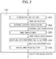
- FIG. 2is a schematic block diagram of a configuration of the wavelength selection section 113 as a component of the etching amount detector 110 illustrated in FIG. 1 .
- the emission intensity signals obtained in processing of a plurality of waferswhich are output from the emission intensity database 112 and transmitted to the wavelength selection section 113 , are first transmitted to a time derivative calculator 201 that then calculates a time derivative of a temporal waveform for each wavelength for the wafers.
- a time derivative calculator 201that then calculates a time derivative of a temporal waveform for each wavelength for the wafers.
- Using the time derivativeprovides a temporal waveform that is less affected by a long-term trend component in the temporal waveform of each wavelength.
- the signal indicating the time derivative value of intensity of the interfering light for each wavelength for the wafersis thus detected by the time derivative calculator 201 and is transmitted to a normalization processor 202 .
- the processor 202calculates a mean value and a standard deviation of such time derivative signals across wafers and over time, and a value (normalized time derivative signal) obtained by subtracting the mean value across all wafers and over time from the time derivative signal for the wafers and dividing the derivative as a result of the subtraction by the standard deviation across all wafers and over time. This expectedly leads to a further reduction in influence of the long-term trend component, and reduces influence of a variation in intensity depending on wavelengths.
- the normalized time derivative signal for the wafers calculated by the normalization processor 202is transmitted to a time smoother 203 .
- the time smoother 203calculates a signal (time smoothed signal) by smoothing the received normalized time derivative signal for the wafers in a time direction. This reduces influence of high-frequency noise.
- the time smoothed signal for the wafers calculated by the time smoother 203is transmitted to a mutual information calculator 204 .
- the mutual information calculator 204calculates mutual information between a change in intensity of each wavelength and a change in intensity of the fundamental wavelength based on the received time smoothed signal for the wafers.
- the first embodimentis based on the premise that at least one fundamental wavelength suitable for endpoint detection is beforehand found based on film composition information.
- the mutual information for each wavelength calculated by the mutual information calculator 204is transmitted to a wavelength selector 205 .
- the wavelength selector 205receives the mutual information for each wavelength and selects wavelengths with relatively large mutual information. For example, the wavelength selector 205 may select prescribed number of wavelengths in the order of larger mutual information, or may select wavelengths with mutual information equal to or larger than a prescribed threshold.
- a time waveform signal indicating a change in intensity of light of each wavelengthwhich is sent from the processing chamber 102 and output from the spectrometer 111 at arbitrary time t in a predetermined period during processing of the sample 104 , is represented as y_m, n, t for each wafer and for each wavelength.
- the index mindicates a wafer, and may be affixed such that its value increases or decreases in the processing order, or may be reassigned after picking only appropriately selected wafers.
- the index nindicates a wavelength, and in the first embodiment, may be affixed such that its value regularly increases or decreases from a short wavelength to a long wavelength, or may be reassigned after picking appropriately selected wavelengths.
- the index tindicates time.
- a gradient of a linear regressionmay be used in place of the derivative.
- a second-order derivative or a gradient of a quadratic regressionmay also be used.
- time derivative values at all timesare obtained in batch processing in a possible configuration.
- processingis performed for each sample, and when samples are acquired together, the samples are also processed together.
- Such a configurationis used as well in any processing in this invention.
- the time smoother 203calculates a signal (time smoothed signal) s_m, n, t by smoothing the normalized time derivative signal z_m, n, t for each wafer and for each wavelength in a time direction.
- the time smoothingmay be performed by averaging of any number of samples, such as three-point averaging, five-point averaging, and seven-point averaging.
- median filtering, convolution operation of a low-pass filter, or spline smoothingmay be used in place of the averaging.
- the mutual information calculator 204calculates mutual information I_n between a change in intensity at each wavelength n and a change in intensity at the fundamental wavelength n_0 from a time smoothed signal s_m, n, t for each wafer and for each wavelength.
- s_ ⁇ m, n_0, t ⁇ across all wafers m and over full time tare arranged in ascending order with respect to the fundamental wavelength n_0.
- Such an ascending order listis denoted as L(n_0).
- s_m, n, t across all wafers m and over full time tare arranged in ascending order with respect to a wavelength n.
- Such an ascending order listis denoted as L(n).
- a specified minimum discretization sample number G_minis assigned to a discretization sample number G.
- the elements of L(n_0) arranged in the ascending orderare equally divided into G groups.
- the equally divided listis denoted as LG(n_0).
- the elements of L(n) arranged in ascending orderare equally divided into G groups.
- the equally divided listis denoted as LG(n).
- An index gis affixed to the group of LG(n_0), and an index h is affixed to the group of LG(n).
- the number of elements of the group g of LG(n_0)is indicated by c(g), and the number of elements of the group h of LG(n) is indicated by c(h).
- the number of elements of a set of m and tis indicated by c(g, h), where s_ ⁇ m, n_0, t ⁇ belongs to the group g of LG(n_0) and s_m, n, t belongs to the group h of LG(n).
- I _ G,n⁇ _ g ⁇ _ h c ( g,h )/( MT ) ⁇ log( c ( g,h )/( MT )) ⁇ log( c ( g )/( MT )) ⁇ log( c ( h )/( MT )) ⁇ where M is the number of all wafers, and T is the number of all time indexes.
- I_ ⁇ G+1, n ⁇is calculated by similar processing.
- Gis increased from the specified minimum discretization sample number G_min to the maximum discretization sample number G_max, I_ ⁇ G_min, n ⁇ to I_ ⁇ G_max, n ⁇ are sequentially calculated.
- the largest I_G, n among I_ ⁇ G_min, n ⁇ , I_ ⁇ G_min+1, n ⁇ to I_ ⁇ G_max, n ⁇is output as the final mutual information I_n.
- the wavelength selector 205selects a specified number of pieces of mutual information I_n for respective wavelengths in descending order of n.
- the wavelength selector 205may select a plurality of pieces of n where I_n is equal to or larger than a specified threshold.
- FIG. 3is a schematic block diagram of the endpoint determination section 114 as a component of the etching amount detector 110 illustrated in FIG. 1 .
- the emission intensity signal for each wavelengthwhich is output from the spectrometer 111 and transmitted to the endpoint determination section 114 , is first transmitted to a time derivative calculator 301 that then calculates a time derivative of a temporal waveform for each wavelength.
- a time derivative calculator 301that then calculates a time derivative of a temporal waveform for each wavelength.
- Using the time derivativeprovides a temporal waveform that is less affected by a long-term trend component in the temporal waveform of each wavelength.
- the signal indicating the time derivative value of intensity of the interfering light for each wavelengthis thus detected by the time derivative calculator 301 and is transmitted to a normalization processor 302 .
- the processor 302calculates a value (normalized time derivative signal) obtained by subtracting the mean value across all wafers and over time from the time derivative signal and dividing the derivative as a result of the subtraction by the standard deviation across all wafers and over time. This expectedly leads to a further reduction in influence of the long-term trend component, and reduces influence of a variation in intensity depending on wavelengths. Values are beforehand calculated by the normalization processor 202 of the wavelength selection section 113 and used as the mean value and the standard deviation of the time derivative signals across wafers and over time.
- the normalized time derivative signal calculated by the normalization processor 302is transmitted to a time smoother 303 .
- the time smoother 303calculates a signal (time smoothed signal) by smoothing the received normalized time derivative signal in a time direction. This reduces influence of high-frequency noise.
- the time smoothed signal calculated by the time smoother 303is transmitted to a mutual information multiplier 304 .
- the mutual information multiplier 304calculates a signal (mutual information-multiplied signal) as a result of multiplication of the received time smoothed signal by mutual information for each wavelength. This results in weighting by the mutual information, and reduces influence of a wavelength having a small dependence on the etching amount, the endpoint, or a change in intensity of emission.
- the mutual information multiplier 304reserves only the signal of the selected wavelength sent from the wavelength selection section 113 among the mutual information-multiplied signals for respective wavelengths and eliminates signals of other wavelengths. This provides further high selectivity.
- the mutual information-multiplied signal calculated by the mutual information multiplier 304is transmitted to an etching amount estimator 305 .
- the etching amount estimator 305calculates a similarity of a vector including a sequence of values of all wavelengths at each time of the mutual information-multiplied signal beforehand stored in association with the etching amount to a vector including a sequence of values of all wavelengths at each time t of the mutual information-multiplied signal, and outputs an etching amount in association with a vector with the highest similarity.
- cosine similarity or the reciprocal of a Euclidean distancemay be used as the similarity between the vectors.
- the etching amount estimator 305calculates a similarity of a vector including a sequence of values of all wavelengths at time t-D of the mutual information-multiplied signal to a vector including a sequence of values of all wavelengths at each time t of the mutual information-multiplied signal.
- Dis a specified positive constant.
- the etching amount estimator 305calculates an absolute value of a time derivative value on the calculated similarity for each time. Further, the etching amount estimator 305 outputs a cumulative value in a time direction of the time derivative absolute value as the etching amount.
- the etching amount calculated by the etching amount estimator 305is transmitted to an endpoint determinator 306 .
- the endpoint determinator 306determines whether the current time is the endpoint depending on the etching amount for each time. Whether the current time is the endpoint may be determined, for example, based on whether the etching amount at a relevant time is equal to or larger than a specified threshold, whether the absolute value of the time derivative value of the etching amount at a relevant time is equal to or larger than a threshold, or whether the second-order time derivative of the etching amount at a relevant time has zero cross.
- FIG. 4is a flowchart illustrating a procedure of operation of the plasma processing apparatus of the first embodiment illustrated in FIG. 1 to determine the etching amount.
- a parameteris first set before the plasma processing apparatus 100 processes the sample 104 , or before start of processing, in which the film structure including the mask layer and the processing-object film layer beforehand disposed on the surface of the sample 104 is etched, or before processing data obtained during the etching processing (step 401 ).
- the parameteris set before start of operation.
- a bias potentialis generated above the surface of the sample 104 by high-frequency power from a high-frequency power source, and etching processing of the processing-object film layer on the sample 104 is started, and then detection of light from the inside of the processing chamber 102 is started (step 402 ).
- a change in intensity of light of each wavelength of predetermined spectra of a plurality of wavelengthswhich is obtained by dispersing light received from the inside of the processing chamber 102 , is detected at every time t in a sampling interval ⁇ t. Intensity of light of each of the plurality of wavelengths is thus detected at every interval ⁇ t, and a time derivative ⁇ y_n, t of the intensity is calculated from a signal of the intensity by time derivative calculation (step 403 ).
- a normalized time derivative signal z_n, tis calculated on the obtained time derivative signal ⁇ y_n, t (step 404 ). Further, a time smoothed signal s_n, t is calculated based on the normalized time derivative signal z_n, t (step 405 ). The obtained time smoothed signal s_n, t is multiplied by mutual information I_n to calculate a mutual information-multiplied signal (step 406 ). The etching amount is estimated based on the mutual information-multiplied signal (step 407 ). Endpoint determination is performed in correspondence to the etching amount estimated in such a manner (step 408 ).
- the etching amount detector 110When the etching amount is determined to reach a desired etching amount, detection of light from the inside of the processing chamber 102 is finished and plasma is extinguished, leading to the end of etching processing of the processing-object film layer using the plasma on the surface of the sample 104 (step 409 ). When it is determined that the etching amount does not reach the desired etching amount, a subsequent relevant film layer is etched without interruption, and light from the inside of the processing chamber 102 is detected by the etching amount detector 110 at subsequent time t+ ⁇ t.
- the etching endpoint or the etching amountcan be determined using a previously known technical means or method, such as detection of a change in intensity of emission from plasma of a wavelength associated with a reaction product from an under-film layer disposed adjacent to the lower boundary of the processing-object film layer. Further, in a usable existing technique, a change in intensity of interfering light, which comes from a plurality of boundary surfaces of a film structure including a plurality of film layers beforehand disposed on the surface of the sample 104 , is detected, and a result of the detection is compared with a pattern of a beforehand obtained residual thickness value and intensity of interfering light with a wavelength as a parameter or a differential value of the intensity, to detect the etching amount from the residual thickness or initial thickness.
- the first embodimentis effective in the case where the processing-object film layer includes two film layers configured of respective different materials and vertically stacked with a boundary between the two film layers, and emission from the materials configuring the two film layers or compounds of the respective materials and the processing gas contains a plurality of wavelengths with large mutual information.
- the first embodimentis also effective in the case where the processing-object film layer includes a lower first film layer, an upper second film layer, and a third film layer formed between the first film layer and the second film layer when the second film layer is formed over the first film layer, and the two film layers include the first and second film layers or the second and third film layers.
- a change in intensity of a wavelength to be used for estimating the etching amountis not always in linear correlation with a change in intensity of the fundamental wavelength, but may be nonlinearly in relation to the change in intensity of the fundamental wavelength while having a dependency on the intensity of the fundamental wavelength.
- a level of the dependencycannot be estimated by an index such as a correlation coefficient, but can be advantageously estimated by the mutual information.
- part of a configuration of one embodimentcan be substituted for a configuration of another embodiment, and a configuration of one embodiment can be added to a configuration of another embodiment.
- a configuration of one embodimentcan be added to, eliminated from, or substituted for part of a configuration of another embodiment.
- the above-described configurations, functions, processing sections, and/or processing meansmay be partially or entirely achieved by hardware, such as, for example, designing with an integrated circuit.
- the configurations, functions, and the likemay be achieved by software with a processor that interprets and executes a program to implement each function.
- the informationsuch as the program to implement each function, a table, and a file can be stored in a recording device such as a memory, a hard disc, and a solid state drive (SSD) or a recording medium such as an IC card, an SD card, and DVD.
- SSDsolid state drive
- control lines and information linesare those considered to be necessary for explanation, and all control lines and information lines for a product are not necessarily disclosed.
- many components configuring the apparatus, or unit sets constituted by combining such componentsare connected to one another.
Landscapes
- Engineering & Computer Science (AREA)
- Physics & Mathematics (AREA)
- Manufacturing & Machinery (AREA)
- Computer Hardware Design (AREA)
- Microelectronics & Electronic Packaging (AREA)
- Power Engineering (AREA)
- Chemical & Material Sciences (AREA)
- Plasma & Fusion (AREA)
- General Physics & Mathematics (AREA)
- Condensed Matter Physics & Semiconductors (AREA)
- Analytical Chemistry (AREA)
- Spectroscopy & Molecular Physics (AREA)
- Chemical Kinetics & Catalysis (AREA)
- General Chemical & Material Sciences (AREA)
- Inorganic Chemistry (AREA)
- Drying Of Semiconductors (AREA)
- Crystals, And After-Treatments Of Crystals (AREA)
Abstract
Description
I_G,n=Σ_gΣ_h c(g,h)/(MT)×{log(c(g,h)/(MT))−log(c(g)/(MT))−log(c(h)/(MT))}
where M is the number of all wafers, and T is the number of all time indexes.
- 100 Plasma processing apparatus
- 101 Vacuum container
- 102 Processing chamber
- 103 Plasma
- 104 Sample
- 105 Sample stage
- 106 Optical fiber
- 110 Etching amount detector
- 111 Spectrometer
- 112 Emission intensity database
- 113 Wavelength selection section
- 114 Endpoint determination section
- 115 Display
Claims (16)
Applications Claiming Priority (1)
| Application Number | Priority Date | Filing Date | Title |
|---|---|---|---|
| PCT/JP2019/050253WO2021130798A1 (en) | 2019-12-23 | 2019-12-23 | Plasma treatment method and wavelength selecting method used for plasma treatment |
Publications (2)
| Publication Number | Publication Date |
|---|---|
| US20210249317A1 US20210249317A1 (en) | 2021-08-12 |
| US11569135B2true US11569135B2 (en) | 2023-01-31 |
Family
ID=76574121
Family Applications (1)
| Application Number | Title | Priority Date | Filing Date |
|---|---|---|---|
| US16/981,612Active2040-01-07US11569135B2 (en) | 2019-12-23 | 2019-12-23 | Plasma processing method and wavelength selection method used in plasma processing |
Country Status (6)
| Country | Link |
|---|---|
| US (1) | US11569135B2 (en) |
| JP (1) | JP7094377B2 (en) |
| KR (1) | KR102429079B1 (en) |
| CN (1) | CN113302722B (en) |
| TW (1) | TWI770596B (en) |
| WO (1) | WO2021130798A1 (en) |
Families Citing this family (2)
| Publication number | Priority date | Publication date | Assignee | Title |
|---|---|---|---|---|
| JP6239294B2 (en) | 2013-07-18 | 2017-11-29 | 株式会社日立ハイテクノロジーズ | Plasma processing apparatus and method of operating plasma processing apparatus |
| JP7423854B1 (en)* | 2022-03-04 | 2024-01-29 | 株式会社日立ハイテク | Plasma treatment method and plasma treatment device |
Citations (54)
| Publication number | Priority date | Publication date | Assignee | Title |
|---|---|---|---|---|
| US4238312A (en) | 1979-07-23 | 1980-12-09 | International Business Machines Corporation | Sputtering system for optimizing quartz deposition uniformity |
| JPS6153728A (en) | 1984-08-24 | 1986-03-17 | Hitachi Ltd | Etching end point judging method |
| JPS63200533A (en) | 1987-02-16 | 1988-08-18 | Anelva Corp | plasma processing equipment |
| JPS63254732A (en) | 1987-04-13 | 1988-10-21 | Hitachi Ltd | Etching end point determination method |
| JPH0457092B2 (en) | 1986-01-17 | 1992-09-10 | Hitachi Ltd | |
| JPH0766173A (en) | 1993-08-23 | 1995-03-10 | Tokyo Electron Ltd | Plasma etching method |
| US5511009A (en) | 1993-04-16 | 1996-04-23 | Sextant Avionique | Energy-based process for the detection of signals drowned in noise |
| US5565114A (en) | 1993-03-04 | 1996-10-15 | Tokyo Electron Limited | Method and device for detecting the end point of plasma process |
| US5664066A (en) | 1992-11-09 | 1997-09-02 | The United States Of America As Represented By The United States Department Of Energy | Intelligent system for automatic feature detection and selection or identification |
| US5711843A (en) | 1995-02-21 | 1998-01-27 | Orincon Technologies, Inc. | System for indirectly monitoring and controlling a process with particular application to plasma processes |
| US5841651A (en) | 1992-11-09 | 1998-11-24 | The United States Of America As Represented By The United States Department Of Energy | Closed loop adaptive control of spectrum-producing step using neural networks |
| JP2000228397A (en) | 1998-12-01 | 2000-08-15 | Hitachi Ltd | Etching end point judging method, etching end point judging apparatus and insulating film etching method using the same |
| US6285971B1 (en) | 1997-08-22 | 2001-09-04 | Voyan Technology | Method for real-time nonlinear system state estimation and control |
| JP2001319924A (en) | 2000-05-12 | 2001-11-16 | Tokyo Ohka Kogyo Co Ltd | Method and apparatus for detecting end point of plasma treatment |
| US6447369B1 (en) | 2000-08-30 | 2002-09-10 | Micron Technology, Inc. | Planarizing machines and alignment systems for mechanical and/or chemical-mechanical planarization of microelectronic substrates |
| US6490497B1 (en) | 1999-01-22 | 2002-12-03 | Nec Corporation | Working process end point real time determination method |
| US6609947B1 (en) | 2000-08-30 | 2003-08-26 | Micron Technology, Inc. | Planarizing machines and control systems for mechanical and/or chemical-mechanical planarization of micro electronic substrates |
| US20040020624A1 (en) | 2000-11-03 | 2004-02-05 | Duncan Stephen Richard | Control of deposition and other processes |
| WO2004102642A2 (en) | 2003-05-09 | 2004-11-25 | Unaxis Usa Inc. | Envelope follower end point detection in time division multiplexed processes |
| US20040267399A1 (en) | 2003-06-30 | 2004-12-30 | Tokyo Electron Limited | Feedforward, feedback wafer to wafer control method for an etch process |
| US20050134835A1 (en) | 2003-12-19 | 2005-06-23 | Kim Yong-Jin | Methods of determining an etching end point based on compensation for etching distubances |
| US20060037938A1 (en) | 2002-10-31 | 2006-02-23 | Tokyo Electron Limited | Method and apparatus for detecting endpoint |
| US20060195218A1 (en) | 2005-02-01 | 2006-08-31 | Tokyo Electron Limited | Iso/nested control for soft mask processing |
| US20070092407A1 (en) | 2005-10-26 | 2007-04-26 | General Electric Company | Optical sensor array system and method for parallel processing of chemical and biochemical information |
| US20070232045A1 (en) | 2006-03-30 | 2007-10-04 | Tokyo Electron, Ltd. | Damage assessment of a wafer using optical metrology |
| US20070229807A1 (en) | 2006-03-30 | 2007-10-04 | Tokyo Electron, Ltd. | Measuring a damaged structure formed on a wafer using optical metrology |
| US20070233404A1 (en) | 2006-03-30 | 2007-10-04 | Tokyo Electron, Ltd. | Creating a library for measuring a damaged structure formed on a wafer using optical metrology |
| US20070229806A1 (en) | 2006-03-30 | 2007-10-04 | Tokyo Electron, Ltd. | Measuring a damaged structure formed on a wafer using optical metrology |
| US20070237383A1 (en) | 2006-03-28 | 2007-10-11 | Merritt Funk | Dynamic metrology sampling with wafer uniformity control |
| US20070238201A1 (en) | 2006-03-28 | 2007-10-11 | Merritt Funk | Dynamic metrology sampling with wafer uniformity control |
| US20090089024A1 (en) | 2007-09-28 | 2009-04-02 | Chung-Ho Huang | Methods and arrangement for creating models for fine-tuning recipes |
| US20090242513A1 (en) | 2008-03-31 | 2009-10-01 | Tokyo Electron Limited | Multi-Layer/Multi-Input/Multi-Output (MLMIMO) Models and Method for Using |
| US20100036514A1 (en) | 2008-08-06 | 2010-02-11 | Tokyo Electron Limited | Creating Multi-Layer/Multi-Input/Multi-Output (MLMIMO) Models for Metal-Gate Structures |
| US20100036518A1 (en) | 2008-08-06 | 2010-02-11 | Tokyo Electron Limited | Using Multi-Layer/Multi-Input/Multi-Output (MLMIMO) Models for Metal-Gate Structures |
| WO2010106712A1 (en) | 2009-03-17 | 2010-09-23 | 株式会社日立ハイテクノロジーズ | Etching apparatus, analysis apparatus, etching treatment method, and etching treatment program |
| JP2011009546A (en) | 2009-06-26 | 2011-01-13 | Toppan Printing Co Ltd | Endpoint detecting device, dry etching device, and dry etching method |
| US20110054863A1 (en) | 2009-09-03 | 2011-03-03 | Adaptics, Inc. | Method and system for empirical modeling of time-varying, parameter-varying, and nonlinear systems via iterative linear subspace computation |
| US20120091097A1 (en) | 2010-10-18 | 2012-04-19 | Tokyo Electron Limited | Using Vacuum Ultra-Violet (VUV) Data in Radio Frequency (RF) Sources |
| US20120253497A1 (en) | 2011-03-31 | 2012-10-04 | Tokyo Electron Limited | Contact Processing Using Multi-Input/Multi-Output (MIMO) Models |
| US20120252141A1 (en) | 2011-03-28 | 2012-10-04 | Tokyo Electron Limited | Adaptive Recipe Selector |
| US8284401B2 (en) | 2007-07-10 | 2012-10-09 | Nanolambda, Inc. | Digital filter spectrum sensor |
| US20130246006A1 (en) | 2012-03-13 | 2013-09-19 | King Fahd University Of Petroleum And Minerals | Method for kalman filter state estimation in bilinear systems |
| US20140022540A1 (en) | 2012-07-20 | 2014-01-23 | Hitachi High -Technologies Corporation | Analysis method, analysis device, and etching processing system |
| US20140156322A1 (en) | 2012-08-10 | 2014-06-05 | Itron, Inc. | Unified Framework for Electrical Load Forecasting |
| US20140262029A1 (en) | 2013-03-15 | 2014-09-18 | Hitachi High-Technologies Corporation | Semiconductor etching apparatus and analyzing apparatus |
| US20140323897A1 (en) | 2013-04-24 | 2014-10-30 | Emery N. Brown | System and method for estimating high time-frequency resolution eeg spectrograms to monitor patient state |
| US20140367260A1 (en) | 2013-06-14 | 2014-12-18 | Nanophoretics Llc | Method and Apparatus for Identifying Objects in a Plurality of Objects Using Dielectrophoresis |
| US20150021294A1 (en)* | 2013-07-18 | 2015-01-22 | Hitachi High-Technologies Corporation | Plasma processing apparatus and operational method thereof |
| US20160173525A1 (en) | 2014-12-15 | 2016-06-16 | Sophos Limited | Server drift monitoring |
| US20160211186A1 (en)* | 2015-01-19 | 2016-07-21 | Hitachi High-Technologies Corporation | Plasma processing apparatus |
| US20160336154A1 (en) | 2015-05-12 | 2016-11-17 | Hitachi High-Technologies Corporation | Plasma processing apparatus, data processing apparatus and data processing method |
| US20160351405A1 (en)* | 2015-05-25 | 2016-12-01 | Hitachi High-Technologies Corporation | Plasma processing apparatus and plasma processing method |
| US20170178874A1 (en) | 2015-12-17 | 2017-06-22 | Hitachi High-Technologies Corporation | Plasma processing apparatus and operating method of plasma processing apparatus |
| US20180275621A1 (en) | 2017-03-24 | 2018-09-27 | Mitsubishi Electric Research Laboratories, Inc. | Model Predictive Control with Uncertainties |
Family Cites Families (9)
| Publication number | Priority date | Publication date | Assignee | Title |
|---|---|---|---|---|
| US6635573B2 (en)* | 2001-10-29 | 2003-10-21 | Applied Materials, Inc | Method of detecting an endpoint during etching of a material within a recess |
| US7009714B2 (en)* | 2003-02-26 | 2006-03-07 | Hitachi High-Technologies Corporation | Method of dry etching a sample and dry etching system |
| KR100945889B1 (en)* | 2009-05-08 | 2010-03-05 | 가부시키가이샤 히다치 하이테크놀로지즈 | Determination Method of Plasma Treatment |
| JP5411215B2 (en)* | 2011-08-01 | 2014-02-12 | 株式会社日立ハイテクノロジーズ | Plasma processing equipment |
| JP6186152B2 (en)* | 2013-03-29 | 2017-08-23 | 株式会社日立ハイテクノロジーズ | Plasma processing apparatus and plasma processing method |
| JP5744965B2 (en)* | 2013-05-15 | 2015-07-08 | 株式会社日立ハイテクノロジーズ | Defect inspection method and apparatus |
| JP6820775B2 (en)* | 2017-03-17 | 2021-01-27 | 株式会社日立ハイテク | Etching method and plasma processing equipment |
| JP6837886B2 (en)* | 2017-03-21 | 2021-03-03 | 株式会社日立ハイテク | Plasma processing equipment and plasma processing method |
| JP6762401B2 (en)* | 2019-04-25 | 2020-09-30 | 株式会社日立ハイテク | Plasma processing equipment and plasma processing method |
- 2019
- 2019-12-23USUS16/981,612patent/US11569135B2/enactiveActive
- 2019-12-23JPJP2020545368Apatent/JP7094377B2/enactiveActive
- 2019-12-23CNCN201980016061.8Apatent/CN113302722B/enactiveActive
- 2019-12-23WOPCT/JP2019/050253patent/WO2021130798A1/ennot_activeCeased
- 2019-12-23KRKR1020207023252Apatent/KR102429079B1/enactiveActive
- 2020
- 2020-08-28TWTW109129496Apatent/TWI770596B/enactive
Patent Citations (63)
| Publication number | Priority date | Publication date | Assignee | Title |
|---|---|---|---|---|
| US4238312A (en) | 1979-07-23 | 1980-12-09 | International Business Machines Corporation | Sputtering system for optimizing quartz deposition uniformity |
| JPS6153728A (en) | 1984-08-24 | 1986-03-17 | Hitachi Ltd | Etching end point judging method |
| JPH0457092B2 (en) | 1986-01-17 | 1992-09-10 | Hitachi Ltd | |
| JPS63200533A (en) | 1987-02-16 | 1988-08-18 | Anelva Corp | plasma processing equipment |
| JPS63254732A (en) | 1987-04-13 | 1988-10-21 | Hitachi Ltd | Etching end point determination method |
| US5664066A (en) | 1992-11-09 | 1997-09-02 | The United States Of America As Represented By The United States Department Of Energy | Intelligent system for automatic feature detection and selection or identification |
| US5841651A (en) | 1992-11-09 | 1998-11-24 | The United States Of America As Represented By The United States Department Of Energy | Closed loop adaptive control of spectrum-producing step using neural networks |
| US5565114A (en) | 1993-03-04 | 1996-10-15 | Tokyo Electron Limited | Method and device for detecting the end point of plasma process |
| US5511009A (en) | 1993-04-16 | 1996-04-23 | Sextant Avionique | Energy-based process for the detection of signals drowned in noise |
| JPH0766173A (en) | 1993-08-23 | 1995-03-10 | Tokyo Electron Ltd | Plasma etching method |
| US5711843A (en) | 1995-02-21 | 1998-01-27 | Orincon Technologies, Inc. | System for indirectly monitoring and controlling a process with particular application to plasma processes |
| US6285971B1 (en) | 1997-08-22 | 2001-09-04 | Voyan Technology | Method for real-time nonlinear system state estimation and control |
| JP2000228397A (en) | 1998-12-01 | 2000-08-15 | Hitachi Ltd | Etching end point judging method, etching end point judging apparatus and insulating film etching method using the same |
| US6596551B1 (en) | 1998-12-01 | 2003-07-22 | Hitachi, Ltd. | Etching end point judging method, etching end point judging device, and insulating film etching method using these methods |
| US6490497B1 (en) | 1999-01-22 | 2002-12-03 | Nec Corporation | Working process end point real time determination method |
| JP2001319924A (en) | 2000-05-12 | 2001-11-16 | Tokyo Ohka Kogyo Co Ltd | Method and apparatus for detecting end point of plasma treatment |
| US6447369B1 (en) | 2000-08-30 | 2002-09-10 | Micron Technology, Inc. | Planarizing machines and alignment systems for mechanical and/or chemical-mechanical planarization of microelectronic substrates |
| US6609947B1 (en) | 2000-08-30 | 2003-08-26 | Micron Technology, Inc. | Planarizing machines and control systems for mechanical and/or chemical-mechanical planarization of micro electronic substrates |
| US20040020624A1 (en) | 2000-11-03 | 2004-02-05 | Duncan Stephen Richard | Control of deposition and other processes |
| US20060037938A1 (en) | 2002-10-31 | 2006-02-23 | Tokyo Electron Limited | Method and apparatus for detecting endpoint |
| WO2004102642A2 (en) | 2003-05-09 | 2004-11-25 | Unaxis Usa Inc. | Envelope follower end point detection in time division multiplexed processes |
| JP2010251813A (en) | 2003-05-09 | 2010-11-04 | Unaxis Usa Inc | Envelope follower endpoint detection in time-division multiplex process |
| US20040267399A1 (en) | 2003-06-30 | 2004-12-30 | Tokyo Electron Limited | Feedforward, feedback wafer to wafer control method for an etch process |
| US20050134835A1 (en) | 2003-12-19 | 2005-06-23 | Kim Yong-Jin | Methods of determining an etching end point based on compensation for etching distubances |
| US20060195218A1 (en) | 2005-02-01 | 2006-08-31 | Tokyo Electron Limited | Iso/nested control for soft mask processing |
| US20070092407A1 (en) | 2005-10-26 | 2007-04-26 | General Electric Company | Optical sensor array system and method for parallel processing of chemical and biochemical information |
| US20070238201A1 (en) | 2006-03-28 | 2007-10-11 | Merritt Funk | Dynamic metrology sampling with wafer uniformity control |
| US20070237383A1 (en) | 2006-03-28 | 2007-10-11 | Merritt Funk | Dynamic metrology sampling with wafer uniformity control |
| US20070232045A1 (en) | 2006-03-30 | 2007-10-04 | Tokyo Electron, Ltd. | Damage assessment of a wafer using optical metrology |
| US20070229806A1 (en) | 2006-03-30 | 2007-10-04 | Tokyo Electron, Ltd. | Measuring a damaged structure formed on a wafer using optical metrology |
| US20070229807A1 (en) | 2006-03-30 | 2007-10-04 | Tokyo Electron, Ltd. | Measuring a damaged structure formed on a wafer using optical metrology |
| US20070233404A1 (en) | 2006-03-30 | 2007-10-04 | Tokyo Electron, Ltd. | Creating a library for measuring a damaged structure formed on a wafer using optical metrology |
| US8284401B2 (en) | 2007-07-10 | 2012-10-09 | Nanolambda, Inc. | Digital filter spectrum sensor |
| US20090089024A1 (en) | 2007-09-28 | 2009-04-02 | Chung-Ho Huang | Methods and arrangement for creating models for fine-tuning recipes |
| US20090242513A1 (en) | 2008-03-31 | 2009-10-01 | Tokyo Electron Limited | Multi-Layer/Multi-Input/Multi-Output (MLMIMO) Models and Method for Using |
| US20100036514A1 (en) | 2008-08-06 | 2010-02-11 | Tokyo Electron Limited | Creating Multi-Layer/Multi-Input/Multi-Output (MLMIMO) Models for Metal-Gate Structures |
| US20100036518A1 (en) | 2008-08-06 | 2010-02-11 | Tokyo Electron Limited | Using Multi-Layer/Multi-Input/Multi-Output (MLMIMO) Models for Metal-Gate Structures |
| JP2010219263A (en) | 2009-03-17 | 2010-09-30 | Hitachi High-Technologies Corp | Etching device, analyzing device, etching processing method, and etching processing program |
| KR20110084302A (en) | 2009-03-17 | 2011-07-21 | 가부시키가이샤 히다치 하이테크놀로지즈 | Etching Apparatus, Analysis Apparatus, Etching Processing Method, and Etching Processing Program |
| US20110315661A1 (en) | 2009-03-17 | 2011-12-29 | Toshihiro Morisawa | Etching apparatus, analysis apparatus, etching treatment method, and etching treatment program |
| WO2010106712A1 (en) | 2009-03-17 | 2010-09-23 | 株式会社日立ハイテクノロジーズ | Etching apparatus, analysis apparatus, etching treatment method, and etching treatment program |
| JP2011009546A (en) | 2009-06-26 | 2011-01-13 | Toppan Printing Co Ltd | Endpoint detecting device, dry etching device, and dry etching method |
| US20110054863A1 (en) | 2009-09-03 | 2011-03-03 | Adaptics, Inc. | Method and system for empirical modeling of time-varying, parameter-varying, and nonlinear systems via iterative linear subspace computation |
| US20120091097A1 (en) | 2010-10-18 | 2012-04-19 | Tokyo Electron Limited | Using Vacuum Ultra-Violet (VUV) Data in Radio Frequency (RF) Sources |
| US20120252141A1 (en) | 2011-03-28 | 2012-10-04 | Tokyo Electron Limited | Adaptive Recipe Selector |
| US20120253497A1 (en) | 2011-03-31 | 2012-10-04 | Tokyo Electron Limited | Contact Processing Using Multi-Input/Multi-Output (MIMO) Models |
| US20130246006A1 (en) | 2012-03-13 | 2013-09-19 | King Fahd University Of Petroleum And Minerals | Method for kalman filter state estimation in bilinear systems |
| US20140022540A1 (en) | 2012-07-20 | 2014-01-23 | Hitachi High -Technologies Corporation | Analysis method, analysis device, and etching processing system |
| JP2014022621A (en) | 2012-07-20 | 2014-02-03 | Hitachi High-Technologies Corp | Analytical method, analyzer, and etching treatment system |
| US20140156322A1 (en) | 2012-08-10 | 2014-06-05 | Itron, Inc. | Unified Framework for Electrical Load Forecasting |
| US20140262029A1 (en) | 2013-03-15 | 2014-09-18 | Hitachi High-Technologies Corporation | Semiconductor etching apparatus and analyzing apparatus |
| JP2014179474A (en) | 2013-03-15 | 2014-09-25 | Hitachi High-Technologies Corp | Semiconductor etching device and analyzer |
| US20140323897A1 (en) | 2013-04-24 | 2014-10-30 | Emery N. Brown | System and method for estimating high time-frequency resolution eeg spectrograms to monitor patient state |
| US20140367260A1 (en) | 2013-06-14 | 2014-12-18 | Nanophoretics Llc | Method and Apparatus for Identifying Objects in a Plurality of Objects Using Dielectrophoresis |
| US20150021294A1 (en)* | 2013-07-18 | 2015-01-22 | Hitachi High-Technologies Corporation | Plasma processing apparatus and operational method thereof |
| JP2015023104A (en) | 2013-07-18 | 2015-02-02 | 株式会社日立ハイテクノロジーズ | Plasma processing apparatus and method of operating plasma processing apparatus |
| US20160173525A1 (en) | 2014-12-15 | 2016-06-16 | Sophos Limited | Server drift monitoring |
| US20160211186A1 (en)* | 2015-01-19 | 2016-07-21 | Hitachi High-Technologies Corporation | Plasma processing apparatus |
| US20160336154A1 (en) | 2015-05-12 | 2016-11-17 | Hitachi High-Technologies Corporation | Plasma processing apparatus, data processing apparatus and data processing method |
| US20160351405A1 (en)* | 2015-05-25 | 2016-12-01 | Hitachi High-Technologies Corporation | Plasma processing apparatus and plasma processing method |
| US20170178874A1 (en) | 2015-12-17 | 2017-06-22 | Hitachi High-Technologies Corporation | Plasma processing apparatus and operating method of plasma processing apparatus |
| US9934946B2 (en) | 2015-12-17 | 2018-04-03 | Hitachi High-Technologies Corporation | Plasma processing apparatus and operating method of plasma processing apparatus |
| US20180275621A1 (en) | 2017-03-24 | 2018-09-27 | Mitsubishi Electric Research Laboratories, Inc. | Model Predictive Control with Uncertainties |
Non-Patent Citations (4)
| Title |
|---|
| E.H. van Veen et al; Kalman Filtering of Data from Overlapping Lines in Inductively Coupled Plasma-Atomic Emission Spectrometry ; Spectrochimica Acta vol. 45B No. 8, 1990, pp. 313-328 (Year: 1990). |
| E.H. van Veen et al; The Kalman Filtering Approach to Inductively Coupled Plasma Atomic Emission Spectrometry; Spectrochimica Acta Part B: Atomic Spectroscopy vol. 49, Issue 8, 1994, pp. 829-846 (Year: 1994). |
| Search Report dated Apr. 7, 2020 in corresponding International Application No. PCT/JP2019/050253. |
| Written Opinion dated Apr. 7, 2020 in corresponding International Application No. PCT/JP2019/050253. |
Also Published As
| Publication number | Publication date |
|---|---|
| TW202125623A (en) | 2021-07-01 |
| JPWO2021130798A1 (en) | 2021-12-23 |
| WO2021130798A1 (en) | 2021-07-01 |
| KR102429079B1 (en) | 2022-08-03 |
| KR20210084340A (en) | 2021-07-07 |
| TWI770596B (en) | 2022-07-11 |
| JP7094377B2 (en) | 2022-07-01 |
| CN113302722B (en) | 2023-12-08 |
| US20210249317A1 (en) | 2021-08-12 |
| CN113302722A (en) | 2021-08-24 |
Similar Documents
| Publication | Publication Date | Title |
|---|---|---|
| KR101835437B1 (en) | Plasma processing apparatus and operating method of plasma processing apparatus | |
| TWI528452B (en) | Plasma processing device and plasma processing method | |
| TWI518525B (en) | Method of endpoint detection of plasma etching process using multivariate analysis | |
| TWI593020B (en) | Plasma processing apparatus and plasma processing method | |
| US11424110B2 (en) | Plasma processing apparatus and operational method thereof | |
| TWI615901B (en) | Plasma processing apparatus and plasma processing method | |
| US11569135B2 (en) | Plasma processing method and wavelength selection method used in plasma processing | |
| CN114360993B (en) | Plasma processing device and plasma processing method | |
| US20040200718A1 (en) | Plasma processing method and apparatus | |
| JP2005527984A (en) | Method and system for determining seasoning state of chamber by light emission | |
| JP6762401B2 (en) | Plasma processing equipment and plasma processing method | |
| US12074076B2 (en) | Plasma processing apparatus and plasma processing method | |
| CN104285288A (en) | Spin Absorption Spectroscopy for Process Monitoring and Control in Semiconductor Manufacturing | |
| US20240203712A1 (en) | Plasma processing apparatus, data analysis apparatus, and semiconductor device manufacturing system | |
| JPH11238723A (en) | Method and apparatus for monitoring plasma processing | |
| JP2000040690A (en) | Etching method and device |
Legal Events
| Date | Code | Title | Description |
|---|---|---|---|
| AS | Assignment | Owner name:HITACHI HIGH-TECH CORPORATION, JAPAN Free format text:ASSIGNMENT OF ASSIGNORS INTEREST;ASSIGNORS:KAWAGUCHI, YOHEI;USUI, TATEHITO;NAKAMOTO, SHIGERU;SIGNING DATES FROM 20200821 TO 20200826;REEL/FRAME:053794/0127 | |
| FEPP | Fee payment procedure | Free format text:ENTITY STATUS SET TO UNDISCOUNTED (ORIGINAL EVENT CODE: BIG.); ENTITY STATUS OF PATENT OWNER: LARGE ENTITY | |
| STPP | Information on status: patent application and granting procedure in general | Free format text:DOCKETED NEW CASE - READY FOR EXAMINATION | |
| STPP | Information on status: patent application and granting procedure in general | Free format text:NON FINAL ACTION MAILED | |
| STPP | Information on status: patent application and granting procedure in general | Free format text:RESPONSE TO NON-FINAL OFFICE ACTION ENTERED AND FORWARDED TO EXAMINER | |
| STPP | Information on status: patent application and granting procedure in general | Free format text:FINAL REJECTION MAILED | |
| STPP | Information on status: patent application and granting procedure in general | Free format text:DOCKETED NEW CASE - READY FOR EXAMINATION | |
| STPP | Information on status: patent application and granting procedure in general | Free format text:NOTICE OF ALLOWANCE MAILED -- APPLICATION RECEIVED IN OFFICE OF PUBLICATIONS | |
| STPP | Information on status: patent application and granting procedure in general | Free format text:PUBLICATIONS -- ISSUE FEE PAYMENT RECEIVED | |
| STPP | Information on status: patent application and granting procedure in general | Free format text:PUBLICATIONS -- ISSUE FEE PAYMENT VERIFIED | |
| STCF | Information on status: patent grant | Free format text:PATENTED CASE |