US11562947B2 - Semiconductor package having a conductive pad with an anchor flange - Google Patents
Semiconductor package having a conductive pad with an anchor flangeDownload PDFInfo
- Publication number
- US11562947B2 US11562947B2US16/920,908US202016920908AUS11562947B2US 11562947 B2US11562947 B2US 11562947B2US 202016920908 AUS202016920908 AUS 202016920908AUS 11562947 B2US11562947 B2US 11562947B2
- Authority
- US
- United States
- Prior art keywords
- conductive pad
- semiconductor package
- chip
- molding compound
- layer
- Prior art date
- Legal status (The legal status is an assumption and is not a legal conclusion. Google has not performed a legal analysis and makes no representation as to the accuracy of the status listed.)
- Active
Links
- 239000004065semiconductorSubstances0.000titleclaimsabstractdescription44
- 238000000465mouldingMethods0.000claimsabstractdescription33
- 150000001875compoundsChemical class0.000claimsabstractdescription23
- PXHVJJICTQNCMI-UHFFFAOYSA-NNickelChemical compound[Ni]PXHVJJICTQNCMI-UHFFFAOYSA-N0.000claimsdescription25
- 229910000679solderInorganic materials0.000claimsdescription18
- 239000010949copperSubstances0.000claimsdescription14
- RYGMFSIKBFXOCR-UHFFFAOYSA-NCopperChemical compound[Cu]RYGMFSIKBFXOCR-UHFFFAOYSA-N0.000claimsdescription12
- 229910052802copperInorganic materials0.000claimsdescription11
- PCHJSUWPFVWCPO-UHFFFAOYSA-NgoldChemical compound[Au]PCHJSUWPFVWCPO-UHFFFAOYSA-N0.000claimsdescription10
- 229910052759nickelInorganic materials0.000claimsdescription9
- 238000009713electroplatingMethods0.000claimsdescription7
- 239000007769metal materialSubstances0.000claimsdescription4
- 238000007747platingMethods0.000abstractdescription4
- 238000005476solderingMethods0.000abstractdescription4
- 238000000926separation methodMethods0.000abstractdescription3
- 238000000034methodMethods0.000description33
- 238000004519manufacturing processMethods0.000description8
- 230000009977dual effectEffects0.000description6
- 238000012858packaging processMethods0.000description5
- HUWSZNZAROKDRZ-RRLWZMAJSA-N(3r,4r)-3-azaniumyl-5-[[(2s,3r)-1-[(2s)-2,3-dicarboxypyrrolidin-1-yl]-3-methyl-1-oxopentan-2-yl]amino]-5-oxo-4-sulfanylpentane-1-sulfonateChemical compoundOS(=O)(=O)CC[C@@H](N)[C@@H](S)C(=O)N[C@@H]([C@H](C)CC)C(=O)N1CCC(C(O)=O)[C@H]1C(O)=OHUWSZNZAROKDRZ-RRLWZMAJSA-N0.000description4
- 238000005530etchingMethods0.000description4
- 238000000206photolithographyMethods0.000description4
- 239000002131composite materialSubstances0.000description3
- LNUFLCYMSVYYNW-ZPJMAFJPSA-N[(2r,3r,4s,5r,6r)-2-[(2r,3r,4s,5r,6r)-6-[(2r,3r,4s,5r,6r)-6-[(2r,3r,4s,5r,6r)-6-[[(3s,5s,8r,9s,10s,13r,14s,17r)-10,13-dimethyl-17-[(2r)-6-methylheptan-2-yl]-2,3,4,5,6,7,8,9,11,12,14,15,16,17-tetradecahydro-1h-cyclopenta[a]phenanthren-3-yl]oxy]-4,5-disulfoChemical compoundO([C@@H]1[C@@H](COS(O)(=O)=O)O[C@@H]([C@@H]([C@H]1OS(O)(=O)=O)OS(O)(=O)=O)O[C@@H]1[C@@H](COS(O)(=O)=O)O[C@@H]([C@@H]([C@H]1OS(O)(=O)=O)OS(O)(=O)=O)O[C@@H]1[C@@H](COS(O)(=O)=O)O[C@H]([C@@H]([C@H]1OS(O)(=O)=O)OS(O)(=O)=O)O[C@@H]1C[C@@H]2CC[C@H]3[C@@H]4CC[C@@H]([C@]4(CC[C@@H]3[C@@]2(C)CC1)C)[C@H](C)CCCC(C)C)[C@H]1O[C@H](COS(O)(=O)=O)[C@@H](OS(O)(=O)=O)[C@H](OS(O)(=O)=O)[C@H]1OS(O)(=O)=OLNUFLCYMSVYYNW-ZPJMAFJPSA-N0.000description2
- 239000000758substrateSubstances0.000description2
- 239000004020conductorSubstances0.000description1
- 238000007796conventional methodMethods0.000description1
- 239000011889copper foilSubstances0.000description1
- 238000009413insulationMethods0.000description1
- 239000000463materialSubstances0.000description1
- 238000004806packaging method and processMethods0.000description1
Images


Classifications
- H—ELECTRICITY
- H01—ELECTRIC ELEMENTS
- H01L—SEMICONDUCTOR DEVICES NOT COVERED BY CLASS H10
- H01L23/00—Details of semiconductor or other solid state devices
- H01L23/48—Arrangements for conducting electric current to or from the solid state body in operation, e.g. leads, terminal arrangements ; Selection of materials therefor
- H01L23/482—Arrangements for conducting electric current to or from the solid state body in operation, e.g. leads, terminal arrangements ; Selection of materials therefor consisting of lead-in layers inseparably applied to the semiconductor body (electrodes)
- H01L23/485—Arrangements for conducting electric current to or from the solid state body in operation, e.g. leads, terminal arrangements ; Selection of materials therefor consisting of lead-in layers inseparably applied to the semiconductor body (electrodes) consisting of layered constructions comprising conductive layers and insulating layers, e.g. planar contacts
- H01L23/4855—Overhang structure
- H—ELECTRICITY
- H01—ELECTRIC ELEMENTS
- H01L—SEMICONDUCTOR DEVICES NOT COVERED BY CLASS H10
- H01L23/00—Details of semiconductor or other solid state devices
- H01L23/48—Arrangements for conducting electric current to or from the solid state body in operation, e.g. leads, terminal arrangements ; Selection of materials therefor
- H01L23/488—Arrangements for conducting electric current to or from the solid state body in operation, e.g. leads, terminal arrangements ; Selection of materials therefor consisting of soldered or bonded constructions
- H01L23/495—Lead-frames or other flat leads
- H01L23/49579—Lead-frames or other flat leads characterised by the materials of the lead frames or layers thereon
- H01L23/49582—Metallic layers on lead frames
- H—ELECTRICITY
- H01—ELECTRIC ELEMENTS
- H01L—SEMICONDUCTOR DEVICES NOT COVERED BY CLASS H10
- H01L21/00—Processes or apparatus adapted for the manufacture or treatment of semiconductor or solid state devices or of parts thereof
- H01L21/02—Manufacture or treatment of semiconductor devices or of parts thereof
- H01L21/04—Manufacture or treatment of semiconductor devices or of parts thereof the devices having potential barriers, e.g. a PN junction, depletion layer or carrier concentration layer
- H01L21/48—Manufacture or treatment of parts, e.g. containers, prior to assembly of the devices, using processes not provided for in a single one of the groups H01L21/18 - H01L21/326 or H10D48/04 - H10D48/07
- H01L21/4814—Conductive parts
- H01L21/4821—Flat leads, e.g. lead frames with or without insulating supports
- H01L21/4825—Connection or disconnection of other leads to or from flat leads, e.g. wires, bumps, other flat leads
- H—ELECTRICITY
- H01—ELECTRIC ELEMENTS
- H01L—SEMICONDUCTOR DEVICES NOT COVERED BY CLASS H10
- H01L21/00—Processes or apparatus adapted for the manufacture or treatment of semiconductor or solid state devices or of parts thereof
- H01L21/02—Manufacture or treatment of semiconductor devices or of parts thereof
- H01L21/04—Manufacture or treatment of semiconductor devices or of parts thereof the devices having potential barriers, e.g. a PN junction, depletion layer or carrier concentration layer
- H01L21/48—Manufacture or treatment of parts, e.g. containers, prior to assembly of the devices, using processes not provided for in a single one of the groups H01L21/18 - H01L21/326 or H10D48/04 - H10D48/07
- H01L21/4814—Conductive parts
- H01L21/4821—Flat leads, e.g. lead frames with or without insulating supports
- H01L21/4828—Etching
- H01L21/4832—Etching a temporary substrate after encapsulation process to form leads
- H—ELECTRICITY
- H01—ELECTRIC ELEMENTS
- H01L—SEMICONDUCTOR DEVICES NOT COVERED BY CLASS H10
- H01L21/00—Processes or apparatus adapted for the manufacture or treatment of semiconductor or solid state devices or of parts thereof
- H01L21/02—Manufacture or treatment of semiconductor devices or of parts thereof
- H01L21/04—Manufacture or treatment of semiconductor devices or of parts thereof the devices having potential barriers, e.g. a PN junction, depletion layer or carrier concentration layer
- H01L21/50—Assembly of semiconductor devices using processes or apparatus not provided for in a single one of the groups H01L21/18 - H01L21/326 or H10D48/04 - H10D48/07 e.g. sealing of a cap to a base of a container
- H01L21/56—Encapsulations, e.g. encapsulation layers, coatings
- H01L21/561—Batch processing
- H—ELECTRICITY
- H01—ELECTRIC ELEMENTS
- H01L—SEMICONDUCTOR DEVICES NOT COVERED BY CLASS H10
- H01L21/00—Processes or apparatus adapted for the manufacture or treatment of semiconductor or solid state devices or of parts thereof
- H01L21/02—Manufacture or treatment of semiconductor devices or of parts thereof
- H01L21/04—Manufacture or treatment of semiconductor devices or of parts thereof the devices having potential barriers, e.g. a PN junction, depletion layer or carrier concentration layer
- H01L21/50—Assembly of semiconductor devices using processes or apparatus not provided for in a single one of the groups H01L21/18 - H01L21/326 or H10D48/04 - H10D48/07 e.g. sealing of a cap to a base of a container
- H01L21/56—Encapsulations, e.g. encapsulation layers, coatings
- H01L21/565—Moulds
- H—ELECTRICITY
- H01—ELECTRIC ELEMENTS
- H01L—SEMICONDUCTOR DEVICES NOT COVERED BY CLASS H10
- H01L21/00—Processes or apparatus adapted for the manufacture or treatment of semiconductor or solid state devices or of parts thereof
- H01L21/02—Manufacture or treatment of semiconductor devices or of parts thereof
- H01L21/04—Manufacture or treatment of semiconductor devices or of parts thereof the devices having potential barriers, e.g. a PN junction, depletion layer or carrier concentration layer
- H01L21/50—Assembly of semiconductor devices using processes or apparatus not provided for in a single one of the groups H01L21/18 - H01L21/326 or H10D48/04 - H10D48/07 e.g. sealing of a cap to a base of a container
- H01L21/56—Encapsulations, e.g. encapsulation layers, coatings
- H01L21/568—Temporary substrate used as encapsulation process aid
- H—ELECTRICITY
- H01—ELECTRIC ELEMENTS
- H01L—SEMICONDUCTOR DEVICES NOT COVERED BY CLASS H10
- H01L21/00—Processes or apparatus adapted for the manufacture or treatment of semiconductor or solid state devices or of parts thereof
- H01L21/67—Apparatus specially adapted for handling semiconductor or electric solid state devices during manufacture or treatment thereof; Apparatus specially adapted for handling wafers during manufacture or treatment of semiconductor or electric solid state devices or components ; Apparatus not specifically provided for elsewhere
- H01L21/683—Apparatus specially adapted for handling semiconductor or electric solid state devices during manufacture or treatment thereof; Apparatus specially adapted for handling wafers during manufacture or treatment of semiconductor or electric solid state devices or components ; Apparatus not specifically provided for elsewhere for supporting or gripping
- H01L21/6835—Apparatus specially adapted for handling semiconductor or electric solid state devices during manufacture or treatment thereof; Apparatus specially adapted for handling wafers during manufacture or treatment of semiconductor or electric solid state devices or components ; Apparatus not specifically provided for elsewhere for supporting or gripping using temporarily an auxiliary support
- H—ELECTRICITY
- H01—ELECTRIC ELEMENTS
- H01L—SEMICONDUCTOR DEVICES NOT COVERED BY CLASS H10
- H01L21/00—Processes or apparatus adapted for the manufacture or treatment of semiconductor or solid state devices or of parts thereof
- H01L21/70—Manufacture or treatment of devices consisting of a plurality of solid state components formed in or on a common substrate or of parts thereof; Manufacture of integrated circuit devices or of parts thereof
- H01L21/77—Manufacture or treatment of devices consisting of a plurality of solid state components or integrated circuits formed in, or on, a common substrate
- H01L21/78—Manufacture or treatment of devices consisting of a plurality of solid state components or integrated circuits formed in, or on, a common substrate with subsequent division of the substrate into plural individual devices
- H—ELECTRICITY
- H01—ELECTRIC ELEMENTS
- H01L—SEMICONDUCTOR DEVICES NOT COVERED BY CLASS H10
- H01L23/00—Details of semiconductor or other solid state devices
- H01L23/28—Encapsulations, e.g. encapsulating layers, coatings, e.g. for protection
- H01L23/31—Encapsulations, e.g. encapsulating layers, coatings, e.g. for protection characterised by the arrangement or shape
- H01L23/3107—Encapsulations, e.g. encapsulating layers, coatings, e.g. for protection characterised by the arrangement or shape the device being completely enclosed
- H01L23/3114—Encapsulations, e.g. encapsulating layers, coatings, e.g. for protection characterised by the arrangement or shape the device being completely enclosed the device being a chip scale package, e.g. CSP
- H—ELECTRICITY
- H01—ELECTRIC ELEMENTS
- H01L—SEMICONDUCTOR DEVICES NOT COVERED BY CLASS H10
- H01L23/00—Details of semiconductor or other solid state devices
- H01L23/48—Arrangements for conducting electric current to or from the solid state body in operation, e.g. leads, terminal arrangements ; Selection of materials therefor
- H01L23/488—Arrangements for conducting electric current to or from the solid state body in operation, e.g. leads, terminal arrangements ; Selection of materials therefor consisting of soldered or bonded constructions
- H01L23/495—Lead-frames or other flat leads
- H01L23/49517—Additional leads
- H01L23/49524—Additional leads the additional leads being a tape carrier or flat leads
- H—ELECTRICITY
- H01—ELECTRIC ELEMENTS
- H01L—SEMICONDUCTOR DEVICES NOT COVERED BY CLASS H10
- H01L24/00—Arrangements for connecting or disconnecting semiconductor or solid-state bodies; Methods or apparatus related thereto
- H01L24/01—Means for bonding being attached to, or being formed on, the surface to be connected, e.g. chip-to-package, die-attach, "first-level" interconnects; Manufacturing methods related thereto
- H01L24/18—High density interconnect [HDI] connectors; Manufacturing methods related thereto
- H01L24/23—Structure, shape, material or disposition of the high density interconnect connectors after the connecting process
- H01L24/24—Structure, shape, material or disposition of the high density interconnect connectors after the connecting process of an individual high density interconnect connector
- H—ELECTRICITY
- H01—ELECTRIC ELEMENTS
- H01L—SEMICONDUCTOR DEVICES NOT COVERED BY CLASS H10
- H01L24/00—Arrangements for connecting or disconnecting semiconductor or solid-state bodies; Methods or apparatus related thereto
- H01L24/01—Means for bonding being attached to, or being formed on, the surface to be connected, e.g. chip-to-package, die-attach, "first-level" interconnects; Manufacturing methods related thereto
- H01L24/34—Strap connectors, e.g. copper straps for grounding power devices; Manufacturing methods related thereto
- H01L24/39—Structure, shape, material or disposition of the strap connectors after the connecting process
- H01L24/40—Structure, shape, material or disposition of the strap connectors after the connecting process of an individual strap connector
- H—ELECTRICITY
- H01—ELECTRIC ELEMENTS
- H01L—SEMICONDUCTOR DEVICES NOT COVERED BY CLASS H10
- H01L24/00—Arrangements for connecting or disconnecting semiconductor or solid-state bodies; Methods or apparatus related thereto
- H01L24/01—Means for bonding being attached to, or being formed on, the surface to be connected, e.g. chip-to-package, die-attach, "first-level" interconnects; Manufacturing methods related thereto
- H01L24/42—Wire connectors; Manufacturing methods related thereto
- H01L24/47—Structure, shape, material or disposition of the wire connectors after the connecting process
- H01L24/48—Structure, shape, material or disposition of the wire connectors after the connecting process of an individual wire connector
- H—ELECTRICITY
- H01—ELECTRIC ELEMENTS
- H01L—SEMICONDUCTOR DEVICES NOT COVERED BY CLASS H10
- H01L24/00—Arrangements for connecting or disconnecting semiconductor or solid-state bodies; Methods or apparatus related thereto
- H01L24/80—Methods for connecting semiconductor or other solid state bodies using means for bonding being attached to, or being formed on, the surface to be connected
- H01L24/82—Methods for connecting semiconductor or other solid state bodies using means for bonding being attached to, or being formed on, the surface to be connected by forming build-up interconnects at chip-level, e.g. for high density interconnects [HDI]
- H—ELECTRICITY
- H01—ELECTRIC ELEMENTS
- H01L—SEMICONDUCTOR DEVICES NOT COVERED BY CLASS H10
- H01L24/00—Arrangements for connecting or disconnecting semiconductor or solid-state bodies; Methods or apparatus related thereto
- H01L24/80—Methods for connecting semiconductor or other solid state bodies using means for bonding being attached to, or being formed on, the surface to be connected
- H01L24/85—Methods for connecting semiconductor or other solid state bodies using means for bonding being attached to, or being formed on, the surface to be connected using a wire connector
- H—ELECTRICITY
- H01—ELECTRIC ELEMENTS
- H01L—SEMICONDUCTOR DEVICES NOT COVERED BY CLASS H10
- H01L24/00—Arrangements for connecting or disconnecting semiconductor or solid-state bodies; Methods or apparatus related thereto
- H01L24/93—Batch processes
- H01L24/95—Batch processes at chip-level, i.e. with connecting carried out on a plurality of singulated devices, i.e. on diced chips
- H01L24/96—Batch processes at chip-level, i.e. with connecting carried out on a plurality of singulated devices, i.e. on diced chips the devices being encapsulated in a common layer, e.g. neo-wafer or pseudo-wafer, said common layer being separable into individual assemblies after connecting
- H—ELECTRICITY
- H01—ELECTRIC ELEMENTS
- H01L—SEMICONDUCTOR DEVICES NOT COVERED BY CLASS H10
- H01L2221/00—Processes or apparatus adapted for the manufacture or treatment of semiconductor or solid state devices or of parts thereof covered by H01L21/00
- H01L2221/67—Apparatus for handling semiconductor or electric solid state devices during manufacture or treatment thereof; Apparatus for handling wafers during manufacture or treatment of semiconductor or electric solid state devices or components; Apparatus not specifically provided for elsewhere
- H01L2221/683—Apparatus for handling semiconductor or electric solid state devices during manufacture or treatment thereof; Apparatus for handling wafers during manufacture or treatment of semiconductor or electric solid state devices or components; Apparatus not specifically provided for elsewhere for supporting or gripping
- H01L2221/68304—Apparatus for handling semiconductor or electric solid state devices during manufacture or treatment thereof; Apparatus for handling wafers during manufacture or treatment of semiconductor or electric solid state devices or components; Apparatus not specifically provided for elsewhere for supporting or gripping using temporarily an auxiliary support
- H01L2221/68359—Apparatus for handling semiconductor or electric solid state devices during manufacture or treatment thereof; Apparatus for handling wafers during manufacture or treatment of semiconductor or electric solid state devices or components; Apparatus not specifically provided for elsewhere for supporting or gripping using temporarily an auxiliary support used as a support during manufacture of interconnect decals or build up layers
- H—ELECTRICITY
- H01—ELECTRIC ELEMENTS
- H01L—SEMICONDUCTOR DEVICES NOT COVERED BY CLASS H10
- H01L2224/00—Indexing scheme for arrangements for connecting or disconnecting semiconductor or solid-state bodies and methods related thereto as covered by H01L24/00
- H01L2224/01—Means for bonding being attached to, or being formed on, the surface to be connected, e.g. chip-to-package, die-attach, "first-level" interconnects; Manufacturing methods related thereto
- H01L2224/02—Bonding areas; Manufacturing methods related thereto
- H01L2224/04—Structure, shape, material or disposition of the bonding areas prior to the connecting process
- H01L2224/06—Structure, shape, material or disposition of the bonding areas prior to the connecting process of a plurality of bonding areas
- H01L2224/0601—Structure
- H01L2224/0603—Bonding areas having different sizes, e.g. different heights or widths
- H—ELECTRICITY
- H01—ELECTRIC ELEMENTS
- H01L—SEMICONDUCTOR DEVICES NOT COVERED BY CLASS H10
- H01L2224/00—Indexing scheme for arrangements for connecting or disconnecting semiconductor or solid-state bodies and methods related thereto as covered by H01L24/00
- H01L2224/01—Means for bonding being attached to, or being formed on, the surface to be connected, e.g. chip-to-package, die-attach, "first-level" interconnects; Manufacturing methods related thereto
- H01L2224/18—High density interconnect [HDI] connectors; Manufacturing methods related thereto
- H01L2224/23—Structure, shape, material or disposition of the high density interconnect connectors after the connecting process
- H01L2224/24—Structure, shape, material or disposition of the high density interconnect connectors after the connecting process of an individual high density interconnect connector
- H01L2224/241—Disposition
- H01L2224/24151—Connecting between a semiconductor or solid-state body and an item not being a semiconductor or solid-state body, e.g. chip-to-substrate, chip-to-passive
- H01L2224/24153—Connecting between a semiconductor or solid-state body and an item not being a semiconductor or solid-state body, e.g. chip-to-substrate, chip-to-passive the body and the item being arranged next to each other, e.g. on a common substrate
- H01L2224/24175—Connecting between a semiconductor or solid-state body and an item not being a semiconductor or solid-state body, e.g. chip-to-substrate, chip-to-passive the body and the item being arranged next to each other, e.g. on a common substrate the item being metallic
- H—ELECTRICITY
- H01—ELECTRIC ELEMENTS
- H01L—SEMICONDUCTOR DEVICES NOT COVERED BY CLASS H10
- H01L2224/00—Indexing scheme for arrangements for connecting or disconnecting semiconductor or solid-state bodies and methods related thereto as covered by H01L24/00
- H01L2224/01—Means for bonding being attached to, or being formed on, the surface to be connected, e.g. chip-to-package, die-attach, "first-level" interconnects; Manufacturing methods related thereto
- H01L2224/18—High density interconnect [HDI] connectors; Manufacturing methods related thereto
- H01L2224/23—Structure, shape, material or disposition of the high density interconnect connectors after the connecting process
- H01L2224/24—Structure, shape, material or disposition of the high density interconnect connectors after the connecting process of an individual high density interconnect connector
- H01L2224/241—Disposition
- H01L2224/24151—Connecting between a semiconductor or solid-state body and an item not being a semiconductor or solid-state body, e.g. chip-to-substrate, chip-to-passive
- H01L2224/24221—Connecting between a semiconductor or solid-state body and an item not being a semiconductor or solid-state body, e.g. chip-to-substrate, chip-to-passive the body and the item being stacked
- H01L2224/24245—Connecting between a semiconductor or solid-state body and an item not being a semiconductor or solid-state body, e.g. chip-to-substrate, chip-to-passive the body and the item being stacked the item being metallic
- H—ELECTRICITY
- H01—ELECTRIC ELEMENTS
- H01L—SEMICONDUCTOR DEVICES NOT COVERED BY CLASS H10
- H01L2224/00—Indexing scheme for arrangements for connecting or disconnecting semiconductor or solid-state bodies and methods related thereto as covered by H01L24/00
- H01L2224/01—Means for bonding being attached to, or being formed on, the surface to be connected, e.g. chip-to-package, die-attach, "first-level" interconnects; Manufacturing methods related thereto
- H01L2224/34—Strap connectors, e.g. copper straps for grounding power devices; Manufacturing methods related thereto
- H01L2224/39—Structure, shape, material or disposition of the strap connectors after the connecting process
- H01L2224/40—Structure, shape, material or disposition of the strap connectors after the connecting process of an individual strap connector
- H01L2224/401—Disposition
- H01L2224/40151—Connecting between a semiconductor or solid-state body and an item not being a semiconductor or solid-state body, e.g. chip-to-substrate, chip-to-passive
- H01L2224/40153—Connecting between a semiconductor or solid-state body and an item not being a semiconductor or solid-state body, e.g. chip-to-substrate, chip-to-passive the body and the item being arranged next to each other, e.g. on a common substrate
- H01L2224/40175—Connecting between a semiconductor or solid-state body and an item not being a semiconductor or solid-state body, e.g. chip-to-substrate, chip-to-passive the body and the item being arranged next to each other, e.g. on a common substrate the item being metallic
- H—ELECTRICITY
- H01—ELECTRIC ELEMENTS
- H01L—SEMICONDUCTOR DEVICES NOT COVERED BY CLASS H10
- H01L2224/00—Indexing scheme for arrangements for connecting or disconnecting semiconductor or solid-state bodies and methods related thereto as covered by H01L24/00
- H01L2224/01—Means for bonding being attached to, or being formed on, the surface to be connected, e.g. chip-to-package, die-attach, "first-level" interconnects; Manufacturing methods related thereto
- H01L2224/42—Wire connectors; Manufacturing methods related thereto
- H01L2224/47—Structure, shape, material or disposition of the wire connectors after the connecting process
- H01L2224/48—Structure, shape, material or disposition of the wire connectors after the connecting process of an individual wire connector
- H01L2224/4805—Shape
- H01L2224/4809—Loop shape
- H01L2224/48091—Arched
- H—ELECTRICITY
- H01—ELECTRIC ELEMENTS
- H01L—SEMICONDUCTOR DEVICES NOT COVERED BY CLASS H10
- H01L2224/00—Indexing scheme for arrangements for connecting or disconnecting semiconductor or solid-state bodies and methods related thereto as covered by H01L24/00
- H01L2224/01—Means for bonding being attached to, or being formed on, the surface to be connected, e.g. chip-to-package, die-attach, "first-level" interconnects; Manufacturing methods related thereto
- H01L2224/42—Wire connectors; Manufacturing methods related thereto
- H01L2224/47—Structure, shape, material or disposition of the wire connectors after the connecting process
- H01L2224/48—Structure, shape, material or disposition of the wire connectors after the connecting process of an individual wire connector
- H01L2224/481—Disposition
- H01L2224/48151—Connecting between a semiconductor or solid-state body and an item not being a semiconductor or solid-state body, e.g. chip-to-substrate, chip-to-passive
- H01L2224/48153—Connecting between a semiconductor or solid-state body and an item not being a semiconductor or solid-state body, e.g. chip-to-substrate, chip-to-passive the body and the item being arranged next to each other, e.g. on a common substrate
- H01L2224/48175—Connecting between a semiconductor or solid-state body and an item not being a semiconductor or solid-state body, e.g. chip-to-substrate, chip-to-passive the body and the item being arranged next to each other, e.g. on a common substrate the item being metallic
- H—ELECTRICITY
- H01—ELECTRIC ELEMENTS
- H01L—SEMICONDUCTOR DEVICES NOT COVERED BY CLASS H10
- H01L2224/00—Indexing scheme for arrangements for connecting or disconnecting semiconductor or solid-state bodies and methods related thereto as covered by H01L24/00
- H01L2224/01—Means for bonding being attached to, or being formed on, the surface to be connected, e.g. chip-to-package, die-attach, "first-level" interconnects; Manufacturing methods related thereto
- H01L2224/42—Wire connectors; Manufacturing methods related thereto
- H01L2224/47—Structure, shape, material or disposition of the wire connectors after the connecting process
- H01L2224/48—Structure, shape, material or disposition of the wire connectors after the connecting process of an individual wire connector
- H01L2224/481—Disposition
- H01L2224/48151—Connecting between a semiconductor or solid-state body and an item not being a semiconductor or solid-state body, e.g. chip-to-substrate, chip-to-passive
- H01L2224/48221—Connecting between a semiconductor or solid-state body and an item not being a semiconductor or solid-state body, e.g. chip-to-substrate, chip-to-passive the body and the item being stacked
- H01L2224/48245—Connecting between a semiconductor or solid-state body and an item not being a semiconductor or solid-state body, e.g. chip-to-substrate, chip-to-passive the body and the item being stacked the item being metallic
- H01L2224/48247—Connecting between a semiconductor or solid-state body and an item not being a semiconductor or solid-state body, e.g. chip-to-substrate, chip-to-passive the body and the item being stacked the item being metallic connecting the wire to a bond pad of the item
- H—ELECTRICITY
- H01—ELECTRIC ELEMENTS
- H01L—SEMICONDUCTOR DEVICES NOT COVERED BY CLASS H10
- H01L2224/00—Indexing scheme for arrangements for connecting or disconnecting semiconductor or solid-state bodies and methods related thereto as covered by H01L24/00
- H01L2224/01—Means for bonding being attached to, or being formed on, the surface to be connected, e.g. chip-to-package, die-attach, "first-level" interconnects; Manufacturing methods related thereto
- H01L2224/42—Wire connectors; Manufacturing methods related thereto
- H01L2224/47—Structure, shape, material or disposition of the wire connectors after the connecting process
- H01L2224/48—Structure, shape, material or disposition of the wire connectors after the connecting process of an individual wire connector
- H01L2224/481—Disposition
- H01L2224/48151—Connecting between a semiconductor or solid-state body and an item not being a semiconductor or solid-state body, e.g. chip-to-substrate, chip-to-passive
- H01L2224/48221—Connecting between a semiconductor or solid-state body and an item not being a semiconductor or solid-state body, e.g. chip-to-substrate, chip-to-passive the body and the item being stacked
- H01L2224/48245—Connecting between a semiconductor or solid-state body and an item not being a semiconductor or solid-state body, e.g. chip-to-substrate, chip-to-passive the body and the item being stacked the item being metallic
- H01L2224/48257—Connecting between a semiconductor or solid-state body and an item not being a semiconductor or solid-state body, e.g. chip-to-substrate, chip-to-passive the body and the item being stacked the item being metallic connecting the wire to a die pad of the item
- H—ELECTRICITY
- H01—ELECTRIC ELEMENTS
- H01L—SEMICONDUCTOR DEVICES NOT COVERED BY CLASS H10
- H01L2224/00—Indexing scheme for arrangements for connecting or disconnecting semiconductor or solid-state bodies and methods related thereto as covered by H01L24/00
- H01L2224/80—Methods for connecting semiconductor or other solid state bodies using means for bonding being attached to, or being formed on, the surface to be connected
- H01L2224/82—Methods for connecting semiconductor or other solid state bodies using means for bonding being attached to, or being formed on, the surface to be connected by forming build-up interconnects at chip-level, e.g. for high density interconnects [HDI]
- H01L2224/82001—Methods for connecting semiconductor or other solid state bodies using means for bonding being attached to, or being formed on, the surface to be connected by forming build-up interconnects at chip-level, e.g. for high density interconnects [HDI] involving a temporary auxiliary member not forming part of the bonding apparatus
- H—ELECTRICITY
- H01—ELECTRIC ELEMENTS
- H01L—SEMICONDUCTOR DEVICES NOT COVERED BY CLASS H10
- H01L2224/00—Indexing scheme for arrangements for connecting or disconnecting semiconductor or solid-state bodies and methods related thereto as covered by H01L24/00
- H01L2224/80—Methods for connecting semiconductor or other solid state bodies using means for bonding being attached to, or being formed on, the surface to be connected
- H01L2224/85—Methods for connecting semiconductor or other solid state bodies using means for bonding being attached to, or being formed on, the surface to be connected using a wire connector
- H01L2224/85001—Methods for connecting semiconductor or other solid state bodies using means for bonding being attached to, or being formed on, the surface to be connected using a wire connector involving a temporary auxiliary member not forming part of the bonding apparatus, e.g. removable or sacrificial coating, film or substrate
- H—ELECTRICITY
- H01—ELECTRIC ELEMENTS
- H01L—SEMICONDUCTOR DEVICES NOT COVERED BY CLASS H10
- H01L2224/00—Indexing scheme for arrangements for connecting or disconnecting semiconductor or solid-state bodies and methods related thereto as covered by H01L24/00
- H01L2224/80—Methods for connecting semiconductor or other solid state bodies using means for bonding being attached to, or being formed on, the surface to be connected
- H01L2224/85—Methods for connecting semiconductor or other solid state bodies using means for bonding being attached to, or being formed on, the surface to be connected using a wire connector
- H01L2224/8538—Bonding interfaces outside the semiconductor or solid-state body
- H01L2224/85399—Material
- H01L2224/854—Material with a principal constituent of the material being a metal or a metalloid, e.g. boron (B), silicon (Si), germanium (Ge), arsenic (As), antimony (Sb), tellurium (Te) and polonium (Po), and alloys thereof
- H01L2224/85438—Material with a principal constituent of the material being a metal or a metalloid, e.g. boron (B), silicon (Si), germanium (Ge), arsenic (As), antimony (Sb), tellurium (Te) and polonium (Po), and alloys thereof the principal constituent melting at a temperature of greater than or equal to 950°C and less than 1550°C
- H01L2224/85444—Gold (Au) as principal constituent
- H—ELECTRICITY
- H01—ELECTRIC ELEMENTS
- H01L—SEMICONDUCTOR DEVICES NOT COVERED BY CLASS H10
- H01L23/00—Details of semiconductor or other solid state devices
- H01L23/28—Encapsulations, e.g. encapsulating layers, coatings, e.g. for protection
- H01L23/31—Encapsulations, e.g. encapsulating layers, coatings, e.g. for protection characterised by the arrangement or shape
- H01L23/3107—Encapsulations, e.g. encapsulating layers, coatings, e.g. for protection characterised by the arrangement or shape the device being completely enclosed
- H—ELECTRICITY
- H01—ELECTRIC ELEMENTS
- H01L—SEMICONDUCTOR DEVICES NOT COVERED BY CLASS H10
- H01L2924/00—Indexing scheme for arrangements or methods for connecting or disconnecting semiconductor or solid-state bodies as covered by H01L24/00
- H01L2924/0001—Technical content checked by a classifier
- H01L2924/00014—Technical content checked by a classifier the subject-matter covered by the group, the symbol of which is combined with the symbol of this group, being disclosed without further technical details
- H—ELECTRICITY
- H01—ELECTRIC ELEMENTS
- H01L—SEMICONDUCTOR DEVICES NOT COVERED BY CLASS H10
- H01L2924/00—Indexing scheme for arrangements or methods for connecting or disconnecting semiconductor or solid-state bodies as covered by H01L24/00
- H01L2924/15—Details of package parts other than the semiconductor or other solid state devices to be connected
- H01L2924/181—Encapsulation
- H01L2924/1815—Shape
- H01L2924/1816—Exposing the passive side of the semiconductor or solid-state body
- H01L2924/18162—Exposing the passive side of the semiconductor or solid-state body of a chip with build-up interconnect
- H—ELECTRICITY
- H01—ELECTRIC ELEMENTS
- H01L—SEMICONDUCTOR DEVICES NOT COVERED BY CLASS H10
- H01L2924/00—Indexing scheme for arrangements or methods for connecting or disconnecting semiconductor or solid-state bodies as covered by H01L24/00
- H01L2924/15—Details of package parts other than the semiconductor or other solid state devices to be connected
- H01L2924/181—Encapsulation
- H01L2924/1815—Shape
- H01L2924/1816—Exposing the passive side of the semiconductor or solid-state body
- H01L2924/18165—Exposing the passive side of the semiconductor or solid-state body of a wire bonded chip
Definitions
- the present inventionrelates to a semiconductor package and a method for manufacturing the same, particularly to a method by which the semiconductor package can be manufactured in low package height.
- QFNquad flat no-lead
- DNNdual flat no-lead
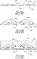
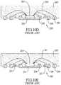
- a conventional QFN packaging processis illustrated.
- a lead frame 200is etched to form a die pad 201 and a plurality of intermediate leads 202 .
- a chip 203can be attached on the die pad 201 and electrically connected to the die pad 201 .
- the lead frame 200may be made of copper or other conductive materials.
- the chip 203is electrically connected to the plurality of the intermediate leads 202 through bonding wires 204 .
- a molding compound 18is formed by a molding process to cover the chip 203 , the die pad 201 , the bonding wires 204 and the intermediate leads 202 .
- a bottom surface of the lead frame 200is processed by a second etching process such that the intermediate leads 202 become the finished leads 206 . Further, a partial bottom of the molding compound 205 is exposed.
- an insulating layer 207is provided to cover a portion of the finished leads 206 .
- the QFN package manufactured by the foregoing processescan be soldered to a circuit board (not shown) through the die pad 201 and the finished leads 206 .
- the semiconductor packagestill needs to be improved. Since the die pad 201 and the finished leads 206 are manufactured based on the lead frame 200 , an uneven surface of the lead frame 200 may result in soldering problems. Further, the poor coverage of the insulation layer 207 on the finished leads 206 may cause problems of copper exposure.
- An objective of the present disclosureis to provide a semiconductor package.
- the semiconductor packagecomprises:
- a molding compoundhaving a top surface and a bottom surface
- Another objective of the present disclosureis to provide a manufacturing method of a semiconductor package.
- the methodcomprises:
- a die-bonding region on a carrierand forming a conductive pad on the carrier, wherein the conductive pad has a perpendicular side surface and an anchor flange formed by over plating and around a top surface of the conductive pad;
- FIGS. 1 A to 1 Care cross-sectional views showing a process of manufacturing conductive pads on a substrate
- FIG. 2is a cross-sectional view of the conductive pad
- FIGS. 3 A to 3 Fare cross-sectional views of packaging processes of the present disclosure, wherein a wire-bonding process is used for electrical connection;
- FIG. 4 Ais a top view of a dual lead semiconductor package
- FIG. 4 Bis a bottom view of the dual lead semiconductor package of FIG. 4 A ;
- FIG. 5is a cross-sectional view of a three-lead semiconductor package with bonding wires
- FIGS. 6 A to 6 Gare cross-sectional views of packaging processes of the present disclosure, wherein a redistribution process is used for electrical connection;
- FIG. 7is a cross-sectional view of a three-lead semiconductor package with a redistribution layer
- FIG. 8 A to 8 Dare cross-sectional views showing a process of manufacturing conductive pads on a substrate in accordance with another embodiment of the present invention.
- FIG. 9 Ais a top view of a dual lead semiconductor package manufactured based on a carrier formed by processes of FIGS. 8 A to 8 D ;
- FIG. 9 Bis a bottom view of the dual lead semiconductor of FIG. 9 A ;
- FIGS. 10 A to 10 Eare cross-sectional views showing a conventional method of manufacturing QFP semiconductor packages.
- the present disclosurerelates to a semiconductor package such as a quad flat no-lead (QFN) package or a dual flat no-lead (DFN) package.
- QFNquad flat no-lead
- DFNdual flat no-lead
- a diode packageis taken as an example of the semiconductor package for purpose of describing the present disclosure.
- FIGS. 1 A to 1 Ca manufacturing process of conductive pads on a carrier are shown.
- a photomask 11 made through a photolithography processis applied on a carrier 10 .
- the carrier 10may be a copper foil, a strip, a wafer, a panel, etc.
- the patterns of the photomask 11are determined based on product types. For example, areas covered by the photomask 11 on the carrier 10 are defined as die-bonding regions while other areas uncovered by the photomask 11 are defined as conductive pad regions.
- An electroplating processis performed to form a composite conductive layer on the conductive pad regions. In the embodiment of FIG.
- the composite conductive layeris formed by sequentially plating an aurum layer (Au) 21 , a nickel layer (Ni) 22 , a copper layer (Cu) 23 , a nickel layer (Ni) 24 and an aurum layer (Au) 25 on the carrier 10 .
- the electroplating materials and sequencemay be varied by demands and are not limited to the examples listed above.
- the conductive pad regions on the carrier 10are deliberately over-plated so that the copper layer 23 is slightly above the top surface of the photomask 11 . As shown in FIG. 1 B , the top surface of the copper layer 23 is above the top surface of the photomask 11 .
- the nickel layer 24 and the aurum layer 25are subsequently plated on the copper layer 23 .
- the photomask 11is removed from the carrier 10 .
- the composite conductive layer remaining on the carrier 10constitutes the conductive pad 20 .
- the conductive pad 20has the mushroom-shaped appearance with a perpendicular side surface and an anchor flange 26 around the top surface of the conductive pad 20 .
- the carrier 10 with the conductive pads 20 formed thereonmay further be processed by subsequent packaging processes as shown in FIGS. 3 A to 3 F .
- a chip 30is bonded on the die-bonding region of the carrier 10 .
- the height of the chip 30is approximately equal to the height of the conductive pad 20 so that the top of chip 30 is substantially co-planar with the top of the conductive pad 20 .
- the top surface of the chip 30is provided with at least one connecting pad 31 and the bottom of the chip 30 may be electroplated by metal material in advance to form a solder layer 32 .
- the wire-bonding processis performed to connect the connecting pad 31 of the chip 30 to the respective conductive pad 20 via a wire 33 .
- the molding processis performed to encapsulate the chip 30 and the conductive pad 20 with a molding compound 40 .
- the carrier 10is removed by etching such that the solder layer 32 of the chip 30 and the bottom of the conductive pad 20 are exposed.
- a sawing processis then performed to cut the molding compound 40 along the paths as indicated by the broken lines on FIG. 3 E .
- a plurality of individual semiconductor packages 100is manufactured.
- the anchor flange 26 of the conductive pad 20engages the molding compound 40 to enhance interlock between the conductive pad 20 and the molding compound 40 and prevent the conductive pad 20 from separation.
- FIG. 4 Ashows a top view of the semiconductor package 100 , wherein the chip 30 and the conductive pad 20 are similar in size.
- FIG. 4 Bshows a bottom view of the semiconductor package 100 .
- the semiconductor package 100is a dual-lead element such as a diode having an anode and a cathode.
- the solder layer 32 of the chip 30 and the bottom of the conductive pad 20function as two solder leads of the dual-lead element for electrically mounting on a circuit board.
- the size of the solder layer 32is similar to the size of the bottom of the conductive pad 20 .
- the processes of the present disclosure discussed abovemay be applied to manufacture a three-lead or multi-lead semiconductor package 100 .
- different connecting pads 31 a , 31 b on the chip 30are connected to respective conductive pads 20 via multiple wires 33 .
- the bottoms of the conductive pads 20 and the chip 30constitute a plurality of solder leads of the multi-lead semiconductor package 100 .
- the electrical connection between the chip 30 and the conductive pad 20is implemented by a redistribution-layer (RDL) process shown in FIGS. 6 A to 6 G instead of the wire-bonding process.
- RDLredistribution-layer
- FIGS. 6 A and 6 Bbecause the processes of forming the conductive pad 20 and die-bonding are the same as shown in FIGS. 3 A and 3 B , the detailed descriptions for FIGS. 6 A and 6 B are omitted to avoid redundant description.
- a dielectric layer 50is coated on the carrier 10 and etched through the photolithography process to define a wire pattern, wherein parts of the connecting pad 31 of the chip 30 and the conductive pad 20 are exposed from the wire pattern.
- connection circuits 60are made of aurum.
- connection circuits 60 made by the redistribution layermay be used to fabricate the three-lead or multi-lead semiconductor package 100 .
- Different connecting pads 31 a , 31 b on the chip 30are connected to respective conductive pads 20 via the connection circuits 60 .
- the bottoms of the conductive pads 20 and the chip s 30constitute a plurality of solder leads of the semiconductor package 100 .
- the soldering pads of the semiconductor packageshould be formed in a specific size and shape.
- die pads 36 with needed size and shapemay be pre-manufactured on the carrier 10 for connecting the chip 30 .
- a first photomask 71 made through photolithographyis applied on a carrier 10 to define patterns of the conductive pads 20 as well as die pads 36 .
- the surface of the carrier 10 uncovered by the first photomask 71is plated to form an aurum layer 21 (Au) and a nickel layer 22 (Ni) sequentially.
- the aurum layer (Au) 21 and the nickel layer (Ni) 22 corresponding to patterns of the chips 30form a die pad 36 .
- a second photomask 72 made through photolithographyis applied on the carrier 10 to cover the die pads 36 .
- the regions exposed from the second photomask 72are then plated to form a copper layer (Cu) 23 , a nickel layer (Ni) 24 and an aurum layer (Au) 25 sequentially.
- the multi-layer structure composed of the aurum layer (Au) 21 , the nickel layer (Ni) 22 , the copper layer (Cu) 23 , the nickel layer (Ni) 24 and the aurum layer (Au) 25forms a conductive pad 20 .
- the second photomask 72is removed from the carrier 10 , wherein the conductive pads 20 as well as the die pads 36 remain on the carrier 10 .
- the chip 30can be bonded on the die pad 36 and electrically connected to the neighboring conductive pads 20 through wire bonding or RDL processes.
- the die pad 36 for electrically connecting the chip 30is exposed from the bottom of the molding compound 18 , the die pad 36 functions as the plated solder layer 32 discussed in FIG. 4 B . Therefore, the distribution, sizes or shapes of solder pads of the semiconductor package 100 are substantially determined by the die pads 36 and the conductive pads 20 .
- the semiconductor package and manufacturing method thereof in accordance with present disclosureat least have the following features:
- the semiconductor packageis not manufactured based on any lead frame used, the problems resulted from the lead frame such as copper exposure and uneven surface of the lead frame are avoided.
- the thickness of the semiconductor packageis reduced as much as possible.
- the conductive padis manufactured to form an anchor flange for engaging the molding compound. As a result, the separation of the conductive pad and the molding compound can be avoided.
Landscapes
- Engineering & Computer Science (AREA)
- Microelectronics & Electronic Packaging (AREA)
- Computer Hardware Design (AREA)
- Power Engineering (AREA)
- Physics & Mathematics (AREA)
- Condensed Matter Physics & Semiconductors (AREA)
- General Physics & Mathematics (AREA)
- Manufacturing & Machinery (AREA)
- Lead Frames For Integrated Circuits (AREA)
- Structures Or Materials For Encapsulating Or Coating Semiconductor Devices Or Solid State Devices (AREA)
Abstract
Description
- a bottom exposed from the bottom surface of the molding compound;
- a perpendicular side surface; and
- an anchor flange formed around a top surface of the conductive pad to engage the molding compound.
Claims (7)
Priority Applications (2)
| Application Number | Priority Date | Filing Date | Title |
|---|---|---|---|
| US16/920,908US11562947B2 (en) | 2020-07-06 | 2020-07-06 | Semiconductor package having a conductive pad with an anchor flange |
| US17/646,344US11848254B2 (en) | 2020-07-06 | 2021-12-29 | Method for manufacturing a semiconductor package having a conductive pad with an anchor flange |
Applications Claiming Priority (1)
| Application Number | Priority Date | Filing Date | Title |
|---|---|---|---|
| US16/920,908US11562947B2 (en) | 2020-07-06 | 2020-07-06 | Semiconductor package having a conductive pad with an anchor flange |
Related Child Applications (1)
| Application Number | Title | Priority Date | Filing Date |
|---|---|---|---|
| US17/646,344DivisionUS11848254B2 (en) | 2020-07-06 | 2021-12-29 | Method for manufacturing a semiconductor package having a conductive pad with an anchor flange |
Publications (2)
| Publication Number | Publication Date |
|---|---|
| US20220005749A1 US20220005749A1 (en) | 2022-01-06 |
| US11562947B2true US11562947B2 (en) | 2023-01-24 |
Family
ID=79167004
Family Applications (2)
| Application Number | Title | Priority Date | Filing Date |
|---|---|---|---|
| US16/920,908ActiveUS11562947B2 (en) | 2020-07-06 | 2020-07-06 | Semiconductor package having a conductive pad with an anchor flange |
| US17/646,344ActiveUS11848254B2 (en) | 2020-07-06 | 2021-12-29 | Method for manufacturing a semiconductor package having a conductive pad with an anchor flange |
Family Applications After (1)
| Application Number | Title | Priority Date | Filing Date |
|---|---|---|---|
| US17/646,344ActiveUS11848254B2 (en) | 2020-07-06 | 2021-12-29 | Method for manufacturing a semiconductor package having a conductive pad with an anchor flange |
Country Status (1)
| Country | Link |
|---|---|
| US (2) | US11562947B2 (en) |
Citations (21)
| Publication number | Priority date | Publication date | Assignee | Title |
|---|---|---|---|---|
| US20020180011A1 (en)* | 2001-05-30 | 2002-12-05 | Nec Corporation | Lead frame, semiconductor device using the same and method of producing the semiconductor device |
| US20030194855A1 (en)* | 2002-04-11 | 2003-10-16 | Samsung Electro-Mechanics Co., Ltd. | Method of manufacturing semiconductor device package |
| US7537965B2 (en)* | 2006-06-21 | 2009-05-26 | Delphi Technologies, Inc. | Manufacturing method for a leadless multi-chip electronic module |
| US20110267789A1 (en)* | 2010-04-28 | 2011-11-03 | Advanpack Solutions Pte Ltd. | Etch-back type semiconductor package, substrate and manufacturing method thereof |
| US20120306065A1 (en)* | 2011-06-02 | 2012-12-06 | Texas Instruments Incorporated | Semiconductor package with pre-soldered grooves in leads |
| US20130040426A1 (en)* | 2011-08-08 | 2013-02-14 | Renesas Electronics Corporation | Manufacturing method using multi-step adhesive curing for sealed semiconductor device |
| US20130264710A1 (en)* | 2012-04-05 | 2013-10-10 | Renesas Electronics Corporation | Semiconductor device |
| US20140210091A1 (en)* | 2012-03-02 | 2014-07-31 | Renesas Electronics Corporation | Method of manufacturing semiconductor device and semiconductor device |
| US20150194322A1 (en)* | 2011-07-03 | 2015-07-09 | Eoplex Limited | Lead carrier with thermally fused package components |
| US20160005680A1 (en)* | 2014-07-02 | 2016-01-07 | Nxp B.V. | Exposed-Heatsink Quad Flat No-Leads (QFN) Package |
| US20160379916A1 (en)* | 2015-06-29 | 2016-12-29 | Stmicroelectronics, Inc. | Method for making semiconductor device with sidewall recess and related devices |
| TW201709456A (en) | 2015-05-04 | 2017-03-01 | 艾歐普雷克斯有限公司 | Lead carrier structure and packages formed therefrom without die attach pads |
| TWI579991B (en) | 2012-03-27 | 2017-04-21 | Mediatek Inc | Semiconductor package |
| US20170162489A1 (en)* | 2015-09-01 | 2017-06-08 | Texas Instruments Incorporated | Flat No-Lead Packages with Electroplated Edges |
| US20170301612A1 (en)* | 2016-04-14 | 2017-10-19 | Rohm Co., Ltd. | Semiconductor device and method for manufacturing the same |
| US20190006266A1 (en)* | 2017-06-28 | 2019-01-03 | Stmicroelectronics, Inc. | Protection from esd during the manufacturing process of semiconductor chips |
| US20190067212A1 (en)* | 2017-08-31 | 2019-02-28 | Stmicroelectronics, Inc. | Package with interlocking leads and manufacturing the same |
| US20190096788A1 (en)* | 2017-09-22 | 2019-03-28 | Stmicroelectronics, Inc. | Package with lead frame with improved lead design for discrete electrical components and manufacturing the same |
| US10529655B2 (en)* | 2017-09-09 | 2020-01-07 | Amkor Technology, Inc. | Method of forming a packaged semiconductor device having enhanced wettable flank and structure |
| US10727169B2 (en)* | 2018-03-29 | 2020-07-28 | Rohm Co., Ltd. | Semiconductor device having lead with back and end surfaces provided with plating layers |
| US20210050285A1 (en)* | 2018-03-29 | 2021-02-18 | Aoi Electronics Co., Ltd. | Semiconductor Device |
Family Cites Families (6)
| Publication number | Priority date | Publication date | Assignee | Title |
|---|---|---|---|---|
| DE102010023815A1 (en)* | 2010-06-15 | 2011-12-15 | Osram Opto Semiconductors Gmbh | Surface-mountable optoelectronic component and method for producing a surface-mountable optoelectronic component |
| KR20120091629A (en)* | 2011-02-09 | 2012-08-20 | 엘지전자 주식회사 | Solar cell |
| US8643165B2 (en)* | 2011-02-23 | 2014-02-04 | Texas Instruments Incorporated | Semiconductor device having agglomerate terminals |
| DE102012109905B4 (en)* | 2012-10-17 | 2021-11-11 | OSRAM Opto Semiconductors Gesellschaft mit beschränkter Haftung | Process for the production of a large number of optoelectronic semiconductor components |
| US9263299B2 (en)* | 2014-07-02 | 2016-02-16 | Nxp B.V. | Exposed die clip bond power package |
| JP7170498B2 (en)* | 2018-10-24 | 2022-11-14 | 株式会社三井ハイテック | Leadframes and leadframe packages |
- 2020
- 2020-07-06USUS16/920,908patent/US11562947B2/enactiveActive
- 2021
- 2021-12-29USUS17/646,344patent/US11848254B2/enactiveActive
Patent Citations (21)
| Publication number | Priority date | Publication date | Assignee | Title |
|---|---|---|---|---|
| US20020180011A1 (en)* | 2001-05-30 | 2002-12-05 | Nec Corporation | Lead frame, semiconductor device using the same and method of producing the semiconductor device |
| US20030194855A1 (en)* | 2002-04-11 | 2003-10-16 | Samsung Electro-Mechanics Co., Ltd. | Method of manufacturing semiconductor device package |
| US7537965B2 (en)* | 2006-06-21 | 2009-05-26 | Delphi Technologies, Inc. | Manufacturing method for a leadless multi-chip electronic module |
| US20110267789A1 (en)* | 2010-04-28 | 2011-11-03 | Advanpack Solutions Pte Ltd. | Etch-back type semiconductor package, substrate and manufacturing method thereof |
| US20120306065A1 (en)* | 2011-06-02 | 2012-12-06 | Texas Instruments Incorporated | Semiconductor package with pre-soldered grooves in leads |
| US20150194322A1 (en)* | 2011-07-03 | 2015-07-09 | Eoplex Limited | Lead carrier with thermally fused package components |
| US20130040426A1 (en)* | 2011-08-08 | 2013-02-14 | Renesas Electronics Corporation | Manufacturing method using multi-step adhesive curing for sealed semiconductor device |
| US20140210091A1 (en)* | 2012-03-02 | 2014-07-31 | Renesas Electronics Corporation | Method of manufacturing semiconductor device and semiconductor device |
| TWI579991B (en) | 2012-03-27 | 2017-04-21 | Mediatek Inc | Semiconductor package |
| US20130264710A1 (en)* | 2012-04-05 | 2013-10-10 | Renesas Electronics Corporation | Semiconductor device |
| US20160005680A1 (en)* | 2014-07-02 | 2016-01-07 | Nxp B.V. | Exposed-Heatsink Quad Flat No-Leads (QFN) Package |
| TW201709456A (en) | 2015-05-04 | 2017-03-01 | 艾歐普雷克斯有限公司 | Lead carrier structure and packages formed therefrom without die attach pads |
| US20160379916A1 (en)* | 2015-06-29 | 2016-12-29 | Stmicroelectronics, Inc. | Method for making semiconductor device with sidewall recess and related devices |
| US20170162489A1 (en)* | 2015-09-01 | 2017-06-08 | Texas Instruments Incorporated | Flat No-Lead Packages with Electroplated Edges |
| US20170301612A1 (en)* | 2016-04-14 | 2017-10-19 | Rohm Co., Ltd. | Semiconductor device and method for manufacturing the same |
| US20190006266A1 (en)* | 2017-06-28 | 2019-01-03 | Stmicroelectronics, Inc. | Protection from esd during the manufacturing process of semiconductor chips |
| US20190067212A1 (en)* | 2017-08-31 | 2019-02-28 | Stmicroelectronics, Inc. | Package with interlocking leads and manufacturing the same |
| US10529655B2 (en)* | 2017-09-09 | 2020-01-07 | Amkor Technology, Inc. | Method of forming a packaged semiconductor device having enhanced wettable flank and structure |
| US20190096788A1 (en)* | 2017-09-22 | 2019-03-28 | Stmicroelectronics, Inc. | Package with lead frame with improved lead design for discrete electrical components and manufacturing the same |
| US10727169B2 (en)* | 2018-03-29 | 2020-07-28 | Rohm Co., Ltd. | Semiconductor device having lead with back and end surfaces provided with plating layers |
| US20210050285A1 (en)* | 2018-03-29 | 2021-02-18 | Aoi Electronics Co., Ltd. | Semiconductor Device |
Also Published As
| Publication number | Publication date |
|---|---|
| US11848254B2 (en) | 2023-12-19 |
| US20220005749A1 (en) | 2022-01-06 |
| US20220122904A1 (en) | 2022-04-21 |
Similar Documents
| Publication | Publication Date | Title |
|---|---|---|
| US10861760B2 (en) | Method of manufacturing semiconductor devices and corresponding semiconductor device | |
| US8278150B2 (en) | Stackable packages for three-dimensional packaging of semiconductor dice | |
| US9842792B2 (en) | Method of producing a semiconductor package | |
| US7071570B2 (en) | Chip scale package and method of fabricating the same | |
| US6423643B1 (en) | Process of making carrier substrate and semiconductor device | |
| US6762118B2 (en) | Package having array of metal pegs linked by printed circuit lines | |
| US20040080025A1 (en) | Lead frame, method of manufacturing the same, and semiconductor device manufactured with the same | |
| US7226811B1 (en) | Process for fabricating a leadless plastic chip carrier | |
| US20080237857A1 (en) | Semiconductor package | |
| US20050218499A1 (en) | Method for manufacturing leadless semiconductor packages | |
| US20130020688A1 (en) | Chip package structure and manufacturing method thereof | |
| US8835225B2 (en) | Method for fabricating quad flat non-leaded semiconductor package | |
| US20150084171A1 (en) | No-lead semiconductor package and method of manufacturing the same | |
| US8652882B2 (en) | Chip package structure and chip packaging method | |
| US6380062B1 (en) | Method of fabricating semiconductor package having metal peg leads and connected by trace lines | |
| US11562947B2 (en) | Semiconductor package having a conductive pad with an anchor flange | |
| US11749621B2 (en) | Leadframe with ground pad cantilever | |
| TWI757133B (en) | Quad flat no-lead package structure | |
| US20010001069A1 (en) | Metal stud array packaging | |
| TWI718947B (en) | Semiconductor packaging element and manufacturing method thereof | |
| EP4184572A1 (en) | Substrate-based package semiconductor device with side wettable flanks | |
| US20250070071A1 (en) | Semiconductor device and semiconductor device fabrication method | |
| US20240021530A1 (en) | Semiconductor package including connection layer | |
| KR19990027041A (en) | Semiconductor package and manufacturing method | |
| KR20090088265A (en) | Semiconductor package and manufacturing method thereof |
Legal Events
| Date | Code | Title | Description |
|---|---|---|---|
| AS | Assignment | Owner name:PANJIT INTERNATIONAL INC., TAIWAN Free format text:ASSIGNMENT OF ASSIGNORS INTEREST;ASSIGNORS:HO, CHUNG-HSIUNG;LI, CHI-HSUEH;REEL/FRAME:053124/0212 Effective date:20200703 | |
| FEPP | Fee payment procedure | Free format text:ENTITY STATUS SET TO UNDISCOUNTED (ORIGINAL EVENT CODE: BIG.); ENTITY STATUS OF PATENT OWNER: LARGE ENTITY | |
| STPP | Information on status: patent application and granting procedure in general | Free format text:RESPONSE TO NON-FINAL OFFICE ACTION ENTERED AND FORWARDED TO EXAMINER | |
| STPP | Information on status: patent application and granting procedure in general | Free format text:FINAL REJECTION MAILED | |
| STPP | Information on status: patent application and granting procedure in general | Free format text:DOCKETED NEW CASE - READY FOR EXAMINATION | |
| STPP | Information on status: patent application and granting procedure in general | Free format text:NON FINAL ACTION MAILED | |
| STPP | Information on status: patent application and granting procedure in general | Free format text:RESPONSE TO NON-FINAL OFFICE ACTION ENTERED AND FORWARDED TO EXAMINER | |
| STPP | Information on status: patent application and granting procedure in general | Free format text:RESPONSE TO NON-FINAL OFFICE ACTION ENTERED AND FORWARDED TO EXAMINER | |
| STPP | Information on status: patent application and granting procedure in general | Free format text:NOTICE OF ALLOWANCE MAILED -- APPLICATION RECEIVED IN OFFICE OF PUBLICATIONS | |
| STPP | Information on status: patent application and granting procedure in general | Free format text:PUBLICATIONS -- ISSUE FEE PAYMENT VERIFIED | |
| STCF | Information on status: patent grant | Free format text:PATENTED CASE |