US11549175B2 - Method of depositing tungsten and other metals in 3D NAND structures - Google Patents
Method of depositing tungsten and other metals in 3D NAND structuresDownload PDFInfo
- Publication number
- US11549175B2 US11549175B2US17/250,014US201917250014AUS11549175B2US 11549175 B2US11549175 B2US 11549175B2US 201917250014 AUS201917250014 AUS 201917250014AUS 11549175 B2US11549175 B2US 11549175B2
- Authority
- US
- United States
- Prior art keywords
- pulses
- tungsten
- pulse
- metal precursor
- inert gas
- Prior art date
- Legal status (The legal status is an assumption and is not a legal conclusion. Google has not performed a legal analysis and makes no representation as to the accuracy of the status listed.)
- Active
Links
- WFKWXMTUELFFGS-UHFFFAOYSA-NtungstenChemical compound[W]WFKWXMTUELFFGS-UHFFFAOYSA-N0.000titleclaimsabstractdescription162
- 229910052721tungstenInorganic materials0.000titleclaimsabstractdescription155
- 239000010937tungstenSubstances0.000titleclaimsabstractdescription153
- 238000000034methodMethods0.000titleclaimsabstractdescription133
- 229910052751metalInorganic materials0.000titleclaimsabstractdescription101
- 239000002184metalSubstances0.000titleclaimsabstractdescription101
- 238000000151depositionMethods0.000titledescription94
- 150000002739metalsChemical class0.000titledescription2
- 239000002243precursorSubstances0.000claimsabstractdescription152
- 238000010926purgeMethods0.000claimsabstractdescription102
- 230000008021depositionEffects0.000claimsabstractdescription92
- 239000011261inert gasSubstances0.000claimsabstractdescription55
- 229910052750molybdenumInorganic materials0.000claimsabstractdescription44
- ZOKXTWBITQBERF-UHFFFAOYSA-NMolybdenumChemical compound[Mo]ZOKXTWBITQBERF-UHFFFAOYSA-N0.000claimsabstractdescription43
- 239000011733molybdenumSubstances0.000claimsabstractdescription43
- 239000000463materialSubstances0.000claimsabstractdescription36
- 239000001257hydrogenSubstances0.000claimsabstractdescription27
- 229910052739hydrogenInorganic materials0.000claimsabstractdescription27
- 239000000460chlorineSubstances0.000claimsdescription31
- KPGXUAIFQMJJFB-UHFFFAOYSA-Htungsten hexachlorideChemical compoundCl[W](Cl)(Cl)(Cl)(Cl)ClKPGXUAIFQMJJFB-UHFFFAOYSA-H0.000claimsdescription29
- 229910052801chlorineInorganic materials0.000claimsdescription28
- 229910003091WCl6Inorganic materials0.000claimsdescription24
- ZAMOUSCENKQFHK-UHFFFAOYSA-NChlorine atomChemical compound[Cl]ZAMOUSCENKQFHK-UHFFFAOYSA-N0.000claimsdescription21
- YOUIDGQAIILFBW-UHFFFAOYSA-JtetrachlorotungstenChemical compoundCl[W](Cl)(Cl)ClYOUIDGQAIILFBW-UHFFFAOYSA-J0.000claimsdescription16
- WIDQNNDDTXUPAN-UHFFFAOYSA-Itungsten(v) chlorideChemical compoundCl[W](Cl)(Cl)(Cl)ClWIDQNNDDTXUPAN-UHFFFAOYSA-I0.000claimsdescription13
- 125000001309chloro groupChemical groupCl*0.000claimsdescription7
- CNRRZWMERIANGJ-UHFFFAOYSA-Nchloro hypochlorite;molybdenumChemical compound[Mo].ClOClCNRRZWMERIANGJ-UHFFFAOYSA-N0.000claimsdescription5
- ASLHVQCNFUOEEN-UHFFFAOYSA-Ndioxomolybdenum;dihydrochlorideChemical compoundCl.Cl.O=[Mo]=OASLHVQCNFUOEEN-UHFFFAOYSA-N0.000claimsdescription5
- GICWIDZXWJGTCI-UHFFFAOYSA-Imolybdenum pentachlorideChemical compoundCl[Mo](Cl)(Cl)(Cl)ClGICWIDZXWJGTCI-UHFFFAOYSA-I0.000claimsdescription5
- PDKHNCYLMVRIFV-UHFFFAOYSA-Hmolybdenum;hexachlorideChemical compound[Cl-].[Cl-].[Cl-].[Cl-].[Cl-].[Cl-].[Mo]PDKHNCYLMVRIFV-UHFFFAOYSA-H0.000claimsdescription5
- BWKCCRPHMILRGD-UHFFFAOYSA-Nchloro hypochlorite;tungstenChemical compound[W].ClOClBWKCCRPHMILRGD-UHFFFAOYSA-N0.000claimsdescription4
- 125000004435hydrogen atomChemical class[H]*0.000claims2
- 229910015221MoCl5Inorganic materials0.000claims1
- 229910015686MoOCl4Inorganic materials0.000claims1
- SFPKXFFNQYDGAH-UHFFFAOYSA-Noxomolybdenum;tetrahydrochlorideChemical compoundCl.Cl.Cl.Cl.[Mo]=OSFPKXFFNQYDGAH-UHFFFAOYSA-N0.000claims1
- 239000003638chemical reducing agentSubstances0.000abstractdescription31
- UFHFLCQGNIYNRP-UHFFFAOYSA-NHydrogenChemical compound[H][H]UFHFLCQGNIYNRP-UHFFFAOYSA-N0.000abstractdescription15
- 239000007789gasSubstances0.000description84
- 239000010410layerSubstances0.000description79
- 239000000758substrateSubstances0.000description74
- 230000008569processEffects0.000description72
- 230000006911nucleationEffects0.000description24
- 238000010899nucleationMethods0.000description24
- 235000012431wafersNutrition0.000description24
- 238000012545processingMethods0.000description20
- 239000004065semiconductorSubstances0.000description18
- 238000005229chemical vapour depositionMethods0.000description17
- YCKRFDGAMUMZLT-UHFFFAOYSA-NFluorine atomChemical compound[F]YCKRFDGAMUMZLT-UHFFFAOYSA-N0.000description16
- 238000000231atomic layer depositionMethods0.000description16
- 229910052731fluorineInorganic materials0.000description16
- 239000011737fluorineSubstances0.000description16
- XKRFYHLGVUSROY-UHFFFAOYSA-NArgonChemical compound[Ar]XKRFYHLGVUSROY-UHFFFAOYSA-N0.000description14
- 230000001276controlling effectEffects0.000description14
- NRTOMJZYCJJWKI-UHFFFAOYSA-NTitanium nitrideChemical compound[Ti]#NNRTOMJZYCJJWKI-UHFFFAOYSA-N0.000description12
- 238000004519manufacturing processMethods0.000description12
- 239000000376reactantSubstances0.000description12
- 238000012546transferMethods0.000description11
- 238000010586diagramMethods0.000description10
- 150000002431hydrogenChemical class0.000description10
- NJPPVKZQTLUDBO-UHFFFAOYSA-NnovaluronChemical compoundC1=C(Cl)C(OC(F)(F)C(OC(F)(F)F)F)=CC=C1NC(=O)NC(=O)C1=C(F)C=CC=C1FNJPPVKZQTLUDBO-UHFFFAOYSA-N0.000description10
- 239000000203mixtureSubstances0.000description9
- 230000004888barrier functionEffects0.000description8
- 239000012071phaseSubstances0.000description8
- 229910052786argonInorganic materials0.000description7
- 238000009826distributionMethods0.000description7
- 239000002356single layerSubstances0.000description7
- NXHILIPIEUBEPD-UHFFFAOYSA-Htungsten hexafluorideChemical compoundF[W](F)(F)(F)(F)FNXHILIPIEUBEPD-UHFFFAOYSA-H0.000description7
- -1annealingSubstances0.000description6
- 238000005137deposition processMethods0.000description6
- 238000001208nuclear magnetic resonance pulse sequenceMethods0.000description6
- IJGRMHOSHXDMSA-UHFFFAOYSA-NAtomic nitrogenChemical compoundN#NIJGRMHOSHXDMSA-UHFFFAOYSA-N0.000description5
- PXHVJJICTQNCMI-UHFFFAOYSA-NNickelChemical compound[Ni]PXHVJJICTQNCMI-UHFFFAOYSA-N0.000description5
- UORVGPXVDQYIDP-UHFFFAOYSA-NboraneChemical classBUORVGPXVDQYIDP-UHFFFAOYSA-N0.000description5
- 238000005530etchingMethods0.000description5
- 229910052710siliconInorganic materials0.000description5
- 239000010703siliconSubstances0.000description5
- 230000009286beneficial effectEffects0.000description4
- 230000008901benefitEffects0.000description4
- 239000012159carrier gasSubstances0.000description4
- 239000003153chemical reaction reagentSubstances0.000description4
- 238000009792diffusion processMethods0.000description4
- 239000001307heliumSubstances0.000description4
- 229910052734heliumInorganic materials0.000description4
- SWQJXJOGLNCZEY-UHFFFAOYSA-Nhelium atomChemical compound[He]SWQJXJOGLNCZEY-UHFFFAOYSA-N0.000description4
- 230000007246mechanismEffects0.000description4
- 238000005240physical vapour depositionMethods0.000description4
- 239000010936titaniumSubstances0.000description4
- BLRPTPMANUNPDV-UHFFFAOYSA-NSilaneChemical compound[SiH4]BLRPTPMANUNPDV-UHFFFAOYSA-N0.000description3
- VYPSYNLAJGMNEJ-UHFFFAOYSA-NSilicium dioxideChemical compoundO=[Si]=OVYPSYNLAJGMNEJ-UHFFFAOYSA-N0.000description3
- XUIMIQQOPSSXEZ-UHFFFAOYSA-NSiliconChemical compound[Si]XUIMIQQOPSSXEZ-UHFFFAOYSA-N0.000description3
- RTAQQCXQSZGOHL-UHFFFAOYSA-NTitaniumChemical compound[Ti]RTAQQCXQSZGOHL-UHFFFAOYSA-N0.000description3
- OQPDWFJSZHWILH-UHFFFAOYSA-N[Al].[Al].[Al].[Ti]Chemical compound[Al].[Al].[Al].[Ti]OQPDWFJSZHWILH-UHFFFAOYSA-N0.000description3
- 230000015572biosynthetic processEffects0.000description3
- 229910000085boraneInorganic materials0.000description3
- 229910052799carbonInorganic materials0.000description3
- 150000001875compoundsChemical class0.000description3
- 238000007796conventional methodMethods0.000description3
- 230000000694effectsEffects0.000description3
- 150000004767nitridesChemical class0.000description3
- 229920002120photoresistant polymerPolymers0.000description3
- 229910021420polycrystalline siliconInorganic materials0.000description3
- 229920005591polysiliconPolymers0.000description3
- 229910052814silicon oxideInorganic materials0.000description3
- UYEGPKGLVUUIGD-UHFFFAOYSA-Jtetrachloro(oxo)molybdenumChemical compoundCl[Mo](Cl)(Cl)(Cl)=OUYEGPKGLVUUIGD-UHFFFAOYSA-J0.000description3
- 229910052719titaniumInorganic materials0.000description3
- 229910021324titanium aluminideInorganic materials0.000description3
- YZCKVEUIGOORGS-UHFFFAOYSA-NHydrogen atomChemical compound[H]YZCKVEUIGOORGS-UHFFFAOYSA-N0.000description2
- BOTDANWDWHJENH-UHFFFAOYSA-NTetraethyl orthosilicateChemical compoundCCO[Si](OCC)(OCC)OCCBOTDANWDWHJENH-UHFFFAOYSA-N0.000description2
- GWEVSGVZZGPLCZ-UHFFFAOYSA-NTitan oxideChemical compoundO=[Ti]=OGWEVSGVZZGPLCZ-UHFFFAOYSA-N0.000description2
- 238000009825accumulationMethods0.000description2
- 239000013590bulk materialSubstances0.000description2
- 238000004422calculation algorithmMethods0.000description2
- 230000008859changeEffects0.000description2
- 238000006243chemical reactionMethods0.000description2
- 150000001805chlorine compoundsChemical class0.000description2
- 238000004590computer programMethods0.000description2
- 230000008878couplingEffects0.000description2
- 238000010168coupling processMethods0.000description2
- 238000005859coupling reactionMethods0.000description2
- 238000010790dilutionMethods0.000description2
- 239000012895dilutionSubstances0.000description2
- 229910000078germaneInorganic materials0.000description2
- 238000010438heat treatmentMethods0.000description2
- 238000010348incorporationMethods0.000description2
- 230000000977initiatory effectEffects0.000description2
- 238000001459lithographyMethods0.000description2
- 150000001247metal acetylidesChemical class0.000description2
- 229910044991metal oxideInorganic materials0.000description2
- 150000004706metal oxidesChemical class0.000description2
- 238000013508migrationMethods0.000description2
- 230000005012migrationEffects0.000description2
- 238000012986modificationMethods0.000description2
- 230000004048modificationEffects0.000description2
- 229910052759nickelInorganic materials0.000description2
- 238000000059patterningMethods0.000description2
- 238000011160researchMethods0.000description2
- 229910000077silaneInorganic materials0.000description2
- 229910010271silicon carbideInorganic materials0.000description2
- LIVNPJMFVYWSIS-UHFFFAOYSA-Nsilicon monoxideChemical class[Si-]#[O+]LIVNPJMFVYWSIS-UHFFFAOYSA-N0.000description2
- 239000000126substanceSubstances0.000description2
- 229910052715tantalumInorganic materials0.000description2
- GUVRBAGPIYLISA-UHFFFAOYSA-Ntantalum atomChemical compound[Ta]GUVRBAGPIYLISA-UHFFFAOYSA-N0.000description2
- OGIDPMRJRNCKJF-UHFFFAOYSA-Ntitanium oxideInorganic materials[Ti]=OOGIDPMRJRNCKJF-UHFFFAOYSA-N0.000description2
- 238000011282treatmentMethods0.000description2
- MTPVUVINMAGMJL-UHFFFAOYSA-Ntrimethyl(1,1,2,2,2-pentafluoroethyl)silaneChemical compoundC[Si](C)(C)C(F)(F)C(F)(F)FMTPVUVINMAGMJL-UHFFFAOYSA-N0.000description2
- 239000011800void materialSubstances0.000description2
- ZOXJGFHDIHLPTG-UHFFFAOYSA-NBoronChemical compound[B]ZOXJGFHDIHLPTG-UHFFFAOYSA-N0.000description1
- OKTJSMMVPCPJKN-UHFFFAOYSA-NCarbonChemical compound[C]OKTJSMMVPCPJKN-UHFFFAOYSA-N0.000description1
- 229910017333Mo(CO)6Inorganic materials0.000description1
- 229910015711MoOxInorganic materials0.000description1
- 229910052581Si3N4Inorganic materials0.000description1
- 238000003848UV Light-CuringMethods0.000description1
- 229910009045WCl2Inorganic materials0.000description1
- UGACIEPFGXRWCH-UHFFFAOYSA-N[Si].[Ti]Chemical compound[Si].[Ti]UGACIEPFGXRWCH-UHFFFAOYSA-N0.000description1
- 238000000137annealingMethods0.000description1
- QVGXLLKOCUKJST-UHFFFAOYSA-Natomic oxygenChemical compound[O]QVGXLLKOCUKJST-UHFFFAOYSA-N0.000description1
- IVHJCRXBQPGLOV-UHFFFAOYSA-NazanylidynetungstenChemical compound[W]#NIVHJCRXBQPGLOV-UHFFFAOYSA-N0.000description1
- 230000000903blocking effectEffects0.000description1
- 229910052796boronInorganic materials0.000description1
- 239000006227byproductSubstances0.000description1
- FQNHWXHRAUXLFU-UHFFFAOYSA-Ncarbon monoxide;tungstenChemical compound[W].[O+]#[C-].[O+]#[C-].[O+]#[C-].[O+]#[C-].[O+]#[C-].[O+]#[C-]FQNHWXHRAUXLFU-UHFFFAOYSA-N0.000description1
- 230000003197catalytic effectEffects0.000description1
- 239000007795chemical reaction productSubstances0.000description1
- 238000004140cleaningMethods0.000description1
- 238000004891communicationMethods0.000description1
- 239000004020conductorSubstances0.000description1
- 238000011109contaminationMethods0.000description1
- 238000001816coolingMethods0.000description1
- 239000000112cooling gasSubstances0.000description1
- 238000001723curingMethods0.000description1
- 230000007423decreaseEffects0.000description1
- UDJQAOMQLIIJIE-UHFFFAOYSA-LdichlorotungstenChemical compoundCl[W]ClUDJQAOMQLIIJIE-UHFFFAOYSA-L0.000description1
- 239000003989dielectric materialSubstances0.000description1
- 238000007865dilutingMethods0.000description1
- 239000006185dispersionSubstances0.000description1
- 238000010494dissociation reactionMethods0.000description1
- 230000005593dissociationsEffects0.000description1
- 238000005516engineering processMethods0.000description1
- 239000012530fluidSubstances0.000description1
- 230000004907fluxEffects0.000description1
- 229910052732germaniumInorganic materials0.000description1
- GNPVGFCGXDBREM-UHFFFAOYSA-Ngermanium atomChemical compound[Ge]GNPVGFCGXDBREM-UHFFFAOYSA-N0.000description1
- 230000010354integrationEffects0.000description1
- 238000005468ion implantationMethods0.000description1
- 238000005259measurementMethods0.000description1
- 238000002844meltingMethods0.000description1
- 230000008018meltingEffects0.000description1
- 238000001465metallisationMethods0.000description1
- OYMJNIHGVDEDFX-UHFFFAOYSA-Jmolybdenum tetrachlorideChemical classCl[Mo](Cl)(Cl)ClOYMJNIHGVDEDFX-UHFFFAOYSA-J0.000description1
- 238000012544monitoring processMethods0.000description1
- PEUPIGGLJVUNEU-UHFFFAOYSA-Nnickel siliconChemical compound[Si].[Ni]PEUPIGGLJVUNEU-UHFFFAOYSA-N0.000description1
- 229910052757nitrogenInorganic materials0.000description1
- 239000001301oxygenSubstances0.000description1
- 229910052760oxygenInorganic materials0.000description1
- 230000002093peripheral effectEffects0.000description1
- 150000003003phosphinesChemical class0.000description1
- 238000007747platingMethods0.000description1
- 238000011112process operationMethods0.000description1
- BGRYSGVIVVUJHH-UHFFFAOYSA-Nprop-2-ynyl propanoateChemical compoundCCC(=O)OCC#CBGRYSGVIVVUJHH-UHFFFAOYSA-N0.000description1
- 230000009467reductionEffects0.000description1
- 230000001105regulatory effectEffects0.000description1
- 238000009877renderingMethods0.000description1
- 238000005389semiconductor device fabricationMethods0.000description1
- 238000012163sequencing techniqueMethods0.000description1
- 150000004756silanesChemical class0.000description1
- 235000012239silicon dioxideNutrition0.000description1
- 239000000377silicon dioxideSubstances0.000description1
- HQVNEWCFYHHQES-UHFFFAOYSA-Nsilicon nitrideChemical compoundN12[Si]34N5[Si]62N3[Si]51N64HQVNEWCFYHHQES-UHFFFAOYSA-N0.000description1
- 239000007787solidSubstances0.000description1
- 238000001179sorption measurementMethods0.000description1
- 239000002344surface layerSubstances0.000description1
- 238000006557surface reactionMethods0.000description1
- MZLGASXMSKOWSE-UHFFFAOYSA-Ntantalum nitrideChemical compound[Ta]#NMZLGASXMSKOWSE-UHFFFAOYSA-N0.000description1
- UONOETXJSWQNOL-UHFFFAOYSA-Ntungsten carbideChemical compound[W+]#[C-]UONOETXJSWQNOL-UHFFFAOYSA-N0.000description1
- 239000012808vapor phaseSubstances0.000description1
Images


Classifications
- H—ELECTRICITY
- H01—ELECTRIC ELEMENTS
- H01L—SEMICONDUCTOR DEVICES NOT COVERED BY CLASS H10
- H01L21/00—Processes or apparatus adapted for the manufacture or treatment of semiconductor or solid state devices or of parts thereof
- H01L21/02—Manufacture or treatment of semiconductor devices or of parts thereof
- H01L21/04—Manufacture or treatment of semiconductor devices or of parts thereof the devices having potential barriers, e.g. a PN junction, depletion layer or carrier concentration layer
- H01L21/18—Manufacture or treatment of semiconductor devices or of parts thereof the devices having potential barriers, e.g. a PN junction, depletion layer or carrier concentration layer the devices having semiconductor bodies comprising elements of Group IV of the Periodic Table or AIIIBV compounds with or without impurities, e.g. doping materials
- H01L21/28—Manufacture of electrodes on semiconductor bodies using processes or apparatus not provided for in groups H01L21/20 - H01L21/268
- H01L21/283—Deposition of conductive or insulating materials for electrodes conducting electric current
- H01L21/285—Deposition of conductive or insulating materials for electrodes conducting electric current from a gas or vapour, e.g. condensation
- H01L21/28506—Deposition of conductive or insulating materials for electrodes conducting electric current from a gas or vapour, e.g. condensation of conductive layers
- H01L21/28512—Deposition of conductive or insulating materials for electrodes conducting electric current from a gas or vapour, e.g. condensation of conductive layers on semiconductor bodies comprising elements of Group IV of the Periodic Table
- H01L21/28556—Deposition of conductive or insulating materials for electrodes conducting electric current from a gas or vapour, e.g. condensation of conductive layers on semiconductor bodies comprising elements of Group IV of the Periodic Table by chemical means, e.g. CVD, LPCVD, PECVD, laser CVD
- C—CHEMISTRY; METALLURGY
- C23—COATING METALLIC MATERIAL; COATING MATERIAL WITH METALLIC MATERIAL; CHEMICAL SURFACE TREATMENT; DIFFUSION TREATMENT OF METALLIC MATERIAL; COATING BY VACUUM EVAPORATION, BY SPUTTERING, BY ION IMPLANTATION OR BY CHEMICAL VAPOUR DEPOSITION, IN GENERAL; INHIBITING CORROSION OF METALLIC MATERIAL OR INCRUSTATION IN GENERAL
- C23C—COATING METALLIC MATERIAL; COATING MATERIAL WITH METALLIC MATERIAL; SURFACE TREATMENT OF METALLIC MATERIAL BY DIFFUSION INTO THE SURFACE, BY CHEMICAL CONVERSION OR SUBSTITUTION; COATING BY VACUUM EVAPORATION, BY SPUTTERING, BY ION IMPLANTATION OR BY CHEMICAL VAPOUR DEPOSITION, IN GENERAL
- C23C16/00—Chemical coating by decomposition of gaseous compounds, without leaving reaction products of surface material in the coating, i.e. chemical vapour deposition [CVD] processes
- C23C16/04—Coating on selected surface areas, e.g. using masks
- C23C16/045—Coating cavities or hollow spaces, e.g. interior of tubes; Infiltration of porous substrates
- C—CHEMISTRY; METALLURGY
- C23—COATING METALLIC MATERIAL; COATING MATERIAL WITH METALLIC MATERIAL; CHEMICAL SURFACE TREATMENT; DIFFUSION TREATMENT OF METALLIC MATERIAL; COATING BY VACUUM EVAPORATION, BY SPUTTERING, BY ION IMPLANTATION OR BY CHEMICAL VAPOUR DEPOSITION, IN GENERAL; INHIBITING CORROSION OF METALLIC MATERIAL OR INCRUSTATION IN GENERAL
- C23C—COATING METALLIC MATERIAL; COATING MATERIAL WITH METALLIC MATERIAL; SURFACE TREATMENT OF METALLIC MATERIAL BY DIFFUSION INTO THE SURFACE, BY CHEMICAL CONVERSION OR SUBSTITUTION; COATING BY VACUUM EVAPORATION, BY SPUTTERING, BY ION IMPLANTATION OR BY CHEMICAL VAPOUR DEPOSITION, IN GENERAL
- C23C16/00—Chemical coating by decomposition of gaseous compounds, without leaving reaction products of surface material in the coating, i.e. chemical vapour deposition [CVD] processes
- C23C16/02—Pretreatment of the material to be coated
- C23C16/0272—Deposition of sub-layers, e.g. to promote the adhesion of the main coating
- C—CHEMISTRY; METALLURGY
- C23—COATING METALLIC MATERIAL; COATING MATERIAL WITH METALLIC MATERIAL; CHEMICAL SURFACE TREATMENT; DIFFUSION TREATMENT OF METALLIC MATERIAL; COATING BY VACUUM EVAPORATION, BY SPUTTERING, BY ION IMPLANTATION OR BY CHEMICAL VAPOUR DEPOSITION, IN GENERAL; INHIBITING CORROSION OF METALLIC MATERIAL OR INCRUSTATION IN GENERAL
- C23C—COATING METALLIC MATERIAL; COATING MATERIAL WITH METALLIC MATERIAL; SURFACE TREATMENT OF METALLIC MATERIAL BY DIFFUSION INTO THE SURFACE, BY CHEMICAL CONVERSION OR SUBSTITUTION; COATING BY VACUUM EVAPORATION, BY SPUTTERING, BY ION IMPLANTATION OR BY CHEMICAL VAPOUR DEPOSITION, IN GENERAL
- C23C16/00—Chemical coating by decomposition of gaseous compounds, without leaving reaction products of surface material in the coating, i.e. chemical vapour deposition [CVD] processes
- C23C16/06—Chemical coating by decomposition of gaseous compounds, without leaving reaction products of surface material in the coating, i.e. chemical vapour deposition [CVD] processes characterised by the deposition of metallic material
- C23C16/08—Chemical coating by decomposition of gaseous compounds, without leaving reaction products of surface material in the coating, i.e. chemical vapour deposition [CVD] processes characterised by the deposition of metallic material from metal halides
- C23C16/14—Deposition of only one other metal element
- C—CHEMISTRY; METALLURGY
- C23—COATING METALLIC MATERIAL; COATING MATERIAL WITH METALLIC MATERIAL; CHEMICAL SURFACE TREATMENT; DIFFUSION TREATMENT OF METALLIC MATERIAL; COATING BY VACUUM EVAPORATION, BY SPUTTERING, BY ION IMPLANTATION OR BY CHEMICAL VAPOUR DEPOSITION, IN GENERAL; INHIBITING CORROSION OF METALLIC MATERIAL OR INCRUSTATION IN GENERAL
- C23C—COATING METALLIC MATERIAL; COATING MATERIAL WITH METALLIC MATERIAL; SURFACE TREATMENT OF METALLIC MATERIAL BY DIFFUSION INTO THE SURFACE, BY CHEMICAL CONVERSION OR SUBSTITUTION; COATING BY VACUUM EVAPORATION, BY SPUTTERING, BY ION IMPLANTATION OR BY CHEMICAL VAPOUR DEPOSITION, IN GENERAL
- C23C16/00—Chemical coating by decomposition of gaseous compounds, without leaving reaction products of surface material in the coating, i.e. chemical vapour deposition [CVD] processes
- C23C16/44—Chemical coating by decomposition of gaseous compounds, without leaving reaction products of surface material in the coating, i.e. chemical vapour deposition [CVD] processes characterised by the method of coating
- C23C16/455—Chemical coating by decomposition of gaseous compounds, without leaving reaction products of surface material in the coating, i.e. chemical vapour deposition [CVD] processes characterised by the method of coating characterised by the method used for introducing gases into reaction chamber or for modifying gas flows in reaction chamber
- C23C16/45523—Pulsed gas flow or change of composition over time
- C23C16/45525—Atomic layer deposition [ALD]
- C23C16/45527—Atomic layer deposition [ALD] characterized by the ALD cycle, e.g. different flows or temperatures during half-reactions, unusual pulsing sequence, use of precursor mixtures or auxiliary reactants or activations
- C—CHEMISTRY; METALLURGY
- C23—COATING METALLIC MATERIAL; COATING MATERIAL WITH METALLIC MATERIAL; CHEMICAL SURFACE TREATMENT; DIFFUSION TREATMENT OF METALLIC MATERIAL; COATING BY VACUUM EVAPORATION, BY SPUTTERING, BY ION IMPLANTATION OR BY CHEMICAL VAPOUR DEPOSITION, IN GENERAL; INHIBITING CORROSION OF METALLIC MATERIAL OR INCRUSTATION IN GENERAL
- C23C—COATING METALLIC MATERIAL; COATING MATERIAL WITH METALLIC MATERIAL; SURFACE TREATMENT OF METALLIC MATERIAL BY DIFFUSION INTO THE SURFACE, BY CHEMICAL CONVERSION OR SUBSTITUTION; COATING BY VACUUM EVAPORATION, BY SPUTTERING, BY ION IMPLANTATION OR BY CHEMICAL VAPOUR DEPOSITION, IN GENERAL
- C23C16/00—Chemical coating by decomposition of gaseous compounds, without leaving reaction products of surface material in the coating, i.e. chemical vapour deposition [CVD] processes
- C23C16/44—Chemical coating by decomposition of gaseous compounds, without leaving reaction products of surface material in the coating, i.e. chemical vapour deposition [CVD] processes characterised by the method of coating
- C23C16/54—Apparatus specially adapted for continuous coating
- H—ELECTRICITY
- H01—ELECTRIC ELEMENTS
- H01L—SEMICONDUCTOR DEVICES NOT COVERED BY CLASS H10
- H01L21/00—Processes or apparatus adapted for the manufacture or treatment of semiconductor or solid state devices or of parts thereof
- H01L21/02—Manufacture or treatment of semiconductor devices or of parts thereof
- H01L21/02104—Forming layers
- H01L21/02107—Forming insulating materials on a substrate
- H01L21/02109—Forming insulating materials on a substrate characterised by the type of layer, e.g. type of material, porous/non-porous, pre-cursors, mixtures or laminates
- H01L21/02205—Forming insulating materials on a substrate characterised by the type of layer, e.g. type of material, porous/non-porous, pre-cursors, mixtures or laminates the layer being characterised by the precursor material for deposition
- H—ELECTRICITY
- H01—ELECTRIC ELEMENTS
- H01L—SEMICONDUCTOR DEVICES NOT COVERED BY CLASS H10
- H01L21/00—Processes or apparatus adapted for the manufacture or treatment of semiconductor or solid state devices or of parts thereof
- H01L21/02—Manufacture or treatment of semiconductor devices or of parts thereof
- H01L21/02104—Forming layers
- H01L21/02107—Forming insulating materials on a substrate
- H01L21/02225—Forming insulating materials on a substrate characterised by the process for the formation of the insulating layer
- H01L21/0226—Forming insulating materials on a substrate characterised by the process for the formation of the insulating layer formation by a deposition process
- H01L21/02263—Forming insulating materials on a substrate characterised by the process for the formation of the insulating layer formation by a deposition process deposition from the gas or vapour phase
- H01L21/02271—Forming insulating materials on a substrate characterised by the process for the formation of the insulating layer formation by a deposition process deposition from the gas or vapour phase deposition by decomposition or reaction of gaseous or vapour phase compounds, i.e. chemical vapour deposition
- H01L21/0228—Forming insulating materials on a substrate characterised by the process for the formation of the insulating layer formation by a deposition process deposition from the gas or vapour phase deposition by decomposition or reaction of gaseous or vapour phase compounds, i.e. chemical vapour deposition deposition by cyclic CVD, e.g. ALD, ALE, pulsed CVD
- H—ELECTRICITY
- H01—ELECTRIC ELEMENTS
- H01L—SEMICONDUCTOR DEVICES NOT COVERED BY CLASS H10
- H01L21/00—Processes or apparatus adapted for the manufacture or treatment of semiconductor or solid state devices or of parts thereof
- H01L21/02—Manufacture or treatment of semiconductor devices or of parts thereof
- H01L21/04—Manufacture or treatment of semiconductor devices or of parts thereof the devices having potential barriers, e.g. a PN junction, depletion layer or carrier concentration layer
- H01L21/18—Manufacture or treatment of semiconductor devices or of parts thereof the devices having potential barriers, e.g. a PN junction, depletion layer or carrier concentration layer the devices having semiconductor bodies comprising elements of Group IV of the Periodic Table or AIIIBV compounds with or without impurities, e.g. doping materials
- H01L21/28—Manufacture of electrodes on semiconductor bodies using processes or apparatus not provided for in groups H01L21/20 - H01L21/268
- H01L21/28008—Making conductor-insulator-semiconductor electrodes
- H01L21/28017—Making conductor-insulator-semiconductor electrodes the insulator being formed after the semiconductor body, the semiconductor being silicon
- H01L21/28158—Making the insulator
- H01L21/28167—Making the insulator on single crystalline silicon, e.g. using a liquid, i.e. chemical oxidation
- H01L21/28194—Making the insulator on single crystalline silicon, e.g. using a liquid, i.e. chemical oxidation by deposition, e.g. evaporation, ALD, CVD, sputtering, laser deposition
- H—ELECTRICITY
- H01—ELECTRIC ELEMENTS
- H01L—SEMICONDUCTOR DEVICES NOT COVERED BY CLASS H10
- H01L21/00—Processes or apparatus adapted for the manufacture or treatment of semiconductor or solid state devices or of parts thereof
- H01L21/02—Manufacture or treatment of semiconductor devices or of parts thereof
- H01L21/04—Manufacture or treatment of semiconductor devices or of parts thereof the devices having potential barriers, e.g. a PN junction, depletion layer or carrier concentration layer
- H01L21/18—Manufacture or treatment of semiconductor devices or of parts thereof the devices having potential barriers, e.g. a PN junction, depletion layer or carrier concentration layer the devices having semiconductor bodies comprising elements of Group IV of the Periodic Table or AIIIBV compounds with or without impurities, e.g. doping materials
- H01L21/28—Manufacture of electrodes on semiconductor bodies using processes or apparatus not provided for in groups H01L21/20 - H01L21/268
- H01L21/283—Deposition of conductive or insulating materials for electrodes conducting electric current
- H01L21/285—Deposition of conductive or insulating materials for electrodes conducting electric current from a gas or vapour, e.g. condensation
- H01L21/28506—Deposition of conductive or insulating materials for electrodes conducting electric current from a gas or vapour, e.g. condensation of conductive layers
- H01L21/28512—Deposition of conductive or insulating materials for electrodes conducting electric current from a gas or vapour, e.g. condensation of conductive layers on semiconductor bodies comprising elements of Group IV of the Periodic Table
- H01L21/28556—Deposition of conductive or insulating materials for electrodes conducting electric current from a gas or vapour, e.g. condensation of conductive layers on semiconductor bodies comprising elements of Group IV of the Periodic Table by chemical means, e.g. CVD, LPCVD, PECVD, laser CVD
- H01L21/28562—Selective deposition
- H—ELECTRICITY
- H01—ELECTRIC ELEMENTS
- H01L—SEMICONDUCTOR DEVICES NOT COVERED BY CLASS H10
- H01L21/00—Processes or apparatus adapted for the manufacture or treatment of semiconductor or solid state devices or of parts thereof
- H01L21/67—Apparatus specially adapted for handling semiconductor or electric solid state devices during manufacture or treatment thereof; Apparatus specially adapted for handling wafers during manufacture or treatment of semiconductor or electric solid state devices or components ; Apparatus not specifically provided for elsewhere
- H01L21/67005—Apparatus not specifically provided for elsewhere
- H01L21/67011—Apparatus for manufacture or treatment
- H01L21/67017—Apparatus for fluid treatment
- H—ELECTRICITY
- H10—SEMICONDUCTOR DEVICES; ELECTRIC SOLID-STATE DEVICES NOT OTHERWISE PROVIDED FOR
- H10B—ELECTRONIC MEMORY DEVICES
- H10B41/00—Electrically erasable-and-programmable ROM [EEPROM] devices comprising floating gates
- H10B41/20—Electrically erasable-and-programmable ROM [EEPROM] devices comprising floating gates characterised by three-dimensional arrangements, e.g. with cells on different height levels
- H—ELECTRICITY
- H10—SEMICONDUCTOR DEVICES; ELECTRIC SOLID-STATE DEVICES NOT OTHERWISE PROVIDED FOR
- H10B—ELECTRONIC MEMORY DEVICES
- H10B41/00—Electrically erasable-and-programmable ROM [EEPROM] devices comprising floating gates
- H10B41/30—Electrically erasable-and-programmable ROM [EEPROM] devices comprising floating gates characterised by the memory core region
- H10B41/35—Electrically erasable-and-programmable ROM [EEPROM] devices comprising floating gates characterised by the memory core region with a cell select transistor, e.g. NAND
- H—ELECTRICITY
- H01—ELECTRIC ELEMENTS
- H01L—SEMICONDUCTOR DEVICES NOT COVERED BY CLASS H10
- H01L21/00—Processes or apparatus adapted for the manufacture or treatment of semiconductor or solid state devices or of parts thereof
- H01L21/70—Manufacture or treatment of devices consisting of a plurality of solid state components formed in or on a common substrate or of parts thereof; Manufacture of integrated circuit devices or of parts thereof
- H01L21/71—Manufacture of specific parts of devices defined in group H01L21/70
- H01L21/768—Applying interconnections to be used for carrying current between separate components within a device comprising conductors and dielectrics
- H01L21/76838—Applying interconnections to be used for carrying current between separate components within a device comprising conductors and dielectrics characterised by the formation and the after-treatment of the conductors
- H01L21/76841—Barrier, adhesion or liner layers
- H01L21/76871—Layers specifically deposited to enhance or enable the nucleation of further layers, i.e. seed layers
- H—ELECTRICITY
- H01—ELECTRIC ELEMENTS
- H01L—SEMICONDUCTOR DEVICES NOT COVERED BY CLASS H10
- H01L2924/00—Indexing scheme for arrangements or methods for connecting or disconnecting semiconductor or solid-state bodies as covered by H01L24/00
- H01L2924/01—Chemical elements
- H01L2924/01074—Tungsten [W]
- H—ELECTRICITY
- H10—SEMICONDUCTOR DEVICES; ELECTRIC SOLID-STATE DEVICES NOT OTHERWISE PROVIDED FOR
- H10B—ELECTRONIC MEMORY DEVICES
- H10B43/00—EEPROM devices comprising charge-trapping gate insulators
- H10B43/20—EEPROM devices comprising charge-trapping gate insulators characterised by three-dimensional arrangements, e.g. with cells on different height levels
- H10B43/23—EEPROM devices comprising charge-trapping gate insulators characterised by three-dimensional arrangements, e.g. with cells on different height levels with source and drain on different levels, e.g. with sloping channels
- H10B43/27—EEPROM devices comprising charge-trapping gate insulators characterised by three-dimensional arrangements, e.g. with cells on different height levels with source and drain on different levels, e.g. with sloping channels the channels comprising vertical portions, e.g. U-shaped channels
Definitions
- Deposition of tungsten-containing materialsis an integral part of many semiconductor fabrication processes. These materials may be used for horizontal interconnects, vias between adjacent metal layers, and contacts between metal layers and devices.
- the substrateis heated to the process temperature in a vacuum chamber and a very thin portion of tungsten film that serves as a seed layer (also called a nucleation layer) is deposited. Thereafter, the remainder of the tungsten film (referred to as the bulk layer) is deposited on the nucleation layer by exposing the substrate to two reactants simultaneously in a chemical vapor deposition (CVD) process.
- the bulk layeris generally deposited more rapidly than the nucleation layer.
- CVDchemical vapor deposition
- One aspect of the disclosurerelates to a method for filling structures with a metal-containing material, the method including: providing a structure to be filled with a metal-containing material, exposing the structure to multiple deposition cycles, with each deposition cycle including exposure to one or more alternating reducing agent (e.g. hydrogen (H 2 )) dose/inert gas purge pulses pulse followed by exposure to one or more alternating metal precursor dose pulses and inert gas purge pulses.
- alternating reducing agente.g. hydrogen (H 2 )
- the metalmay be tungsten (W) or molybdenum (Mo) in some embodiments.
- the structureis a partially fabricated three-dimension (3-D) NAND structure having sidewalls and a plurality of openings in the sidewalls leading to a plurality of features having a plurality of interior regions fluidically accessible through the openings.
- the metal precursoris a chlorine-containing metal precursor, such as tungsten hexachloride, tungsten pentachloride, tungsten tetrachhloride, molybdenum pentachloride, molybdenum dichloride dioxide, and molybdenum tetrachloride oxide, and mixtures thereof.
- a pulse of the chlorine-containing metal precursorcomprises between about 0.1% and about 5.0% of chlorine-containing metal precursor by volume.
- the exposure to multiple alternating metal precursor pulses and inert gas purge pulsesincludes turning the inert gas purge flow off during the metal precursor pulses.
- the duration of an inert gas purge pulseis at least 1.5 times that of a metal precursor pulse.
- each deposition cyclecomprises at least five or at least ten alternating metal precursor pulses and inert gas purge pulses.
- each deposition cycleincludes only one H 2 pulse. In other embodiments, each deposition cycle includes multiple alternating H 2 and inert gas pulses.
- Another aspect of the disclosurerelates to a method for filling structures with a metal-containing material, the method including: providing a structure to be filled with a metal-containing material, exposing the structure to multiple deposition cycles, with each deposition cycle including exposure to a reducing agent (e.g. hydrogen (H 2 )) dose pulse followed by exposure to an inert gas pulse and exposure to multiple alternating metal precursor dose pulses and inert gas purge pulses.
- a reducing agente.g. hydrogen (H 2 )
- the structureis a partially fabricated three-dimension (3-D) NAND structure having sidewalls and a plurality of openings in the sidewalls leading to a plurality of features having a plurality of interior regions fluidically accessible through the openings.
- the metal precursoris a chlorine-containing metal precursor, such as tungsten hexachloride, tungsten pentachloride, tungsten tetrachhloride, molybdenum pentachloride, molybdenum dichloride dioxide, and molybdenum tetrachloride oxide, and mixtures thereof.
- a pulse of the chlorine-containing metal precursorcomprises between about 0.1% and about 5.0% of chlorine-containing metal precursor by volume.
- the exposure to multiple alternating metal precursor pulses and inert gas purge pulsesincludes turning the inert gas purge flow off during the metal precursor pulses.
- the duration of an inert gas purge pulseis at least 1.5 times that of a metal precursor pulse.
- each deposition cyclecomprises at least five or at least ten alternating metal precursor pulses and inert gas purge pulses.
- Another aspect of the disclosurerelates to an apparatus including one or more process chambers each configured to hold a substrate; one or more process gas inlets for coupling to a reducing agent (e.g., hydrogen (H 2 )) gas source, a metal precursor gas source, and an inert purge gas source; and a controller for controlling operations in the apparatus, comprising machine-readable instructions for performing multiple deposition cycles, wherein each deposition cycle comprises: inletting a hydrogen (H 2 ) pulse to the one or more process chambers via the one more process gas inlets; after inletting the H 2 pulse, inletting an inert purge gas pulse to the one or more process chamber via the one or more process gas inlets; after inletting the inert purge gas pulse, inletting multiple alternating metal precursor pulses and inert gas purge pulses to the one or more process chambers via the one or more purge gas inlets.
- a reducing agente.g., hydrogen (H 2 )
- the metal precursoris a chlorine-containing metal precursor.
- the instructionscomprise instructions for turning the inert gas purge flow off during the metal precursor pulses.
- the duration of the inert gas purge pulseis at least 1.5 times that of the metal precursor pulses.
- each deposition cyclecomprises at least five alternating metal precursor pulses and inert gas purge pulses. In some embodiments, each deposition cycle comprises at least ten alternating metal precursor pulses and inert gas purge pulses.
- Another aspect of the disclosurerelates to a method for filling structures with a metal-containing material, the method including: providing a structure to be filled with a metal-containing material, exposing the structure to multiple deposition cycles, with each deposition cycle including exposure to multiple alternating hydrogen (H 2 ) pulses and inert gas pulses followed and exposure to metal precursor pulse followed by an inert gas purge pulse.
- the structureis a partially fabricated three-dimension (3-D) NAND structure having sidewalls and a plurality of openings in the sidewalls leading to a plurality of features having a plurality of interior regions fluidically accessible through the openings.
- the metal precursoris a chlorine-containing metal precursor.
- a pulse of the chlorine-containing metal precursorcomprises between about 0.1% and about 5.0% of chlorine-containing metal precursor by volume.
- the exposure to multiple alternating H 2 pulses and inert gas purge pulsesincludes turning the inert gas purge flow off during the metal precursor pulses.
- each deposition cycleincludes only one metal precursor pulse. In other embodiments, each deposition cycle includes multiple alternating metal precursor and inert gas pulses.
- Another aspect of the disclosurerelates to an apparatus including one or more process chambers each configured to hold a substrate; one or more process gas inlets for coupling to a hydrogen (H 2 ) gas source, a metal precursor gas source, and an inert purge gas source; and a controller for controlling operations in the apparatus, comprising machine-readable instructions for performing multiple deposition cycles, wherein each deposition cycle comprises: inletting multiple alternating H 2 pulses and inert gas purge pulses to the one or more process chambers via the one or more purge gas inlets, and inletting a metal precursor pulse followed by an inert gas pulse.
- the metal precursoris a chlorine-containing metal precursor.
- the instructionscomprise instructions for turning the inert gas purge flow off during the H 2 pulses.
- FIG. 1 Ais a schematic illustration of example films on a substrate.
- FIGS. 1 B- 1 Jare schematic examples of various structures in which tungsten or molybdenum may be deposited in accordance with certain disclosed embodiments.
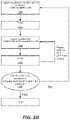
- FIGS. 2 A- 2 Cis a process flow diagram depicting operations for methods in accordance with certain disclosed embodiments.
- FIG. 3is a timing sequence diagram showing example cycles in methods for depositing films in accordance with certain disclosed embodiments.
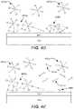
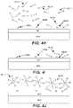
- FIGS. 4 A- 4 Jare schematic diagrams of an example of a mechanism for depositing films in accordance with certain disclosed embodiments.
- FIG. 5shows an illustration of experimental results comparing tungsten fill of 3-D NAND structures using a H2/Ar/WClx/Ar sequence and a H2/Ar/n(WClx/Ar) sequence.
- FIG. 6is a schematic diagram of an example process tool for performing certain disclosed embodiments.
- FIG. 7is a schematic diagram of an example station for performing certain disclosed embodiments.
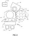
- FIG. 8is a schematic diagram showing basic features of a manifold system that may be used in accordance with certain embodiments.
- Tungsten (W) fill of featuresis often used in semiconductor device fabrication to form electrical contacts.
- a nucleation tungsten layeris first deposited into a via or contact.
- a nucleation layeris a thin conformal layer that serves to facilitate the subsequent formation of a bulk material thereon.
- the tungsten nucleation layermay be deposited to conformally coat the sidewalls and bottom of the feature. Conforming to the underlying feature bottom and sidewalls can be critical to support high quality deposition.
- Nucleation layersare often deposited using atomic layer deposition (ALD) or pulsed nucleation layer (PNL) methods.
- ALDatomic layer deposition
- PNLpulsed nucleation layer
- PNLpulses of reactant are sequentially injected and purged from the reaction chamber, typically by a pulse of a purge gas between reactants.
- a first reactantcan be adsorbed onto the substrate, available to react with the next reactant.
- the processis repeated in a cyclical fashion until the desired thickness is achieved.
- PNL techniquesare similar to ALD techniques. PNL is generally distinguished from ALD by its higher operating pressure range (greater than 1 Torr) and its higher growth rate per cycle (greater than 1 monolayer film growth per cycle). Chamber pressure during PNL deposition may range from about 1 Torr to about 400 Torr.
- PNLbroadly embodies any cyclical process of sequentially adding reactants for reaction on a semiconductor substrate.
- CVDchemical vapor deposition
- PNL and ALD processesare distinct from CVD processes and vice versa.
- bulk tungstenis typically deposited by a CVD process by reducing tungsten hexafluoride (WF 6 ) using a reducing agent such as hydrogen (H 2 ).
- WF 6tungsten hexafluoride
- H 2hydrogen
- Bulk tungstenis different from a tungsten nucleation layer.
- Bulk tungsten as used hereinrefers to tungsten used to fill most or all of a feature, such as at least about 50% of the feature.
- bulk tungstenis used to carry current. It may be characterized by larger grain size and lower resistivity as compared to a nucleation film.
- bulk tungstenis tungsten deposited to a thickness of at least 50 ⁇ .
- One method of preventing fluorine diffusionincludes depositing one or more barrier layers prior to depositing tungsten to prevent fluorine from diffusing from tungsten to other layers of the substrate such as an oxide layer.
- FIG. 1 Ashows an example stack of layers deposited on a substrate.
- Substrate 190includes a silicon layer 192 , an oxide layer 194 (e.g., titanium oxide (TiOx), tetraethyl orthosilicate (TEOS) oxide, etc.), a barrier layer 196 (e.g., titanium nitride (TiN)), a tungsten nucleation layer 198 , and a bulk tungsten layer 199 .
- an oxide layer 194e.g., titanium oxide (TiOx), tetraethyl orthosilicate (TEOS) oxide, etc.
- a barrier layer 196e.g., titanium nitride (TiN)
- TiNtitanium nitride
- Barrier layer 196is deposited to prevent fluorine diffusion from the bulk tungsten layer 199 and the tungsten nucleation layer 198 to the oxide layer. However, as devices shrink, barrier layers become thinner, and fluorine may still diffuse from the deposited tungsten layers. Although chemical vapor deposition of bulk tungsten performed at a higher temperature results in lower fluorine content, such films may have poor step coverage.
- tungsten filmstend to have increased tensile stress.
- Conventional techniques for depositing bulk tungsten films by chemical vapor depositionhave a tensile stress greater than 2.5 GPa for a 200 ⁇ film.
- High thermal tensile stresscauses the substrate to curl, which makes subsequent processing difficult.
- subsequent processesmay include chemical mechanical planarization, deposition of materials, and/or clamping of the substrate to a substrate holder to perform processes in a chamber.
- these processesoften rely on the substrate being flat, and a curled substrate results in non-uniform processing or inability to process the substrate.
- tungstendoes not have the surface mobility to allow grains to be moved or altered once it is deposited due to its high melting point.
- Fluorine-free tungsten (FFW) precursorsare useful to prevent such reliability and integration issues or device performance issues.
- Current FFW precursorsinclude metal organic precursors, but undesirable traces of elements from the metal organic precursors may be incorporated in the tungsten film as well, such as carbon, hydrogen, nitrogen, and oxygen.
- Some metal organic fluorine-free precursorsare also not easily implemented or integrated in tungsten deposition processes.
- Tungsten chlorideincludes tungsten pentachloride (WCl 5 ), tungsten hexachloride (WCl 6 ), tungsten tetrachloride (WCl 4 ), tungsten dichloride (WCl 2 ), and mixtures thereof.
- Wl 5tungsten pentachloride
- Wl 6tungsten hexachloride
- Wl 4tungsten tetrachloride
- WCl 2tungsten dichloride
- films deposited using certain disclosed embodimentsare fluorine-free. Certain disclosed embodiments are directed to depositing bulk tungsten using alternating pulses of a chlorine-containing tungsten precursor and hydrogen.
- Deposition by WCl 5 and WCl 6presents challenges that are not present with WF 6 , due to possible etching by the tungsten chlorides. Tungsten chlorides are less reactive, and as a result, deposition is performed at higher temperature than deposition using WF 6 . Evaporated WCl 6 has a high enough vapor pressure to enable carrying it into the tungsten deposition chamber. However, WCl 6 may be more likely to etch the substrate than WCl 5 . While WCl 5 is less likely to etch the substrate, WCl 5 also has a higher vapor pressure than WCl 6 . Although the lower vapor pressure is useful in depositing tungsten films having low resistivity, some deposition operations may have poor step coverage.
- Molybdenummay be used to form low resistance metallization stack structures and may take the place of tungsten.
- Methodsmay be used to deposit tungsten or molybdenum into features with high step coverage, and may also be used to deposit tungsten into 3D NAND structures.
- the methods described hereinare performed on a substrate that may be housed in a chamber.
- the substratemay be a silicon or other semiconductor wafer, e.g., a 200-mm wafer, a 300-mm wafer, or a 450-mm wafer, including wafers having one or more layers of material, such as dielectric, conducting, or semi-conducting material deposited thereon.
- the methodsare not limit to semiconductor substrates, and may be performed to fill any feature with metal such as tungsten.
- Substratesmay have features such as via or contact holes, which may be characterized by one or more of narrow and/or re-entrant openings, constrictions within the feature, and high aspect ratios.
- a featuremay be formed in one or more of the above described layers.
- the featuremay be formed at least partially in a dielectric layer.
- a featuremay have an aspect ratio of at least about 2:1, at least about 4:1, at least about 6:1, at least about 10:1, at least about 25:1, or higher.
- One example of a featureis a hole or via in a semiconductor substrate or a layer on the substrate.
- FIGS. 1 B- 1 Hare schematic examples of various structures in which a metal may be deposited in accordance with disclosed embodiments.
- FIG. 1 Bshows an example of a cross-sectional depiction of a vertical feature 101 to be filled with a metal, such as tungsten or molybdenum.
- the featurecan include a feature hole 105 in a substrate 103 .
- the hole 105 or other featuremay have a dimension near the opening, e.g., an opening diameter or line width of between about 10 nm to 500 nm, for example between about 25 nm and about 300 nm.
- the feature hole 105can be referred to as an unfilled feature or simply a feature.
- the feature 101and any feature, may be characterized in part by an axis 118 that extends through the length of the feature, with vertically-oriented features having vertical axes and horizontally-oriented features having horizontal axes.
- featuresare wordline features in a 3D NAND structure.
- a substratemay include a wordline structure having an arbitrary number of wordlines (e.g., 50 to 150) with vertical channels at least 200 ⁇ deep.
- wordlinese.g., 50 to 150
- trench in a substrate or layere.g., a trench in a substrate or layer.
- the featuremay have an under-layer, such as a barrier layer or adhesion layer.
- under-layersinclude dielectric layers and conducting layers, e.g., silicon oxides, silicon nitrides, silicon carbides, metal oxides, metal nitrides, metal carbides, and metal layers.
- FIG. 1 Cshows an example of a feature 101 that has a re-entrant profile.
- a re-entrant profileis a profile that narrows from a bottom, closed end, or interior of the feature to the feature opening. According to various implementations, the profile may narrow gradually and/or include an overhang at the feature opening.
- FIG. 1 Cshows an example of the latter, with an under-layer 113 lining the sidewall or interior surfaces of the feature hole 105 .
- the under-layer 113can be for example, a diffusion barrier layer, an adhesion layer, a nucleation layer, a combination of thereof, or any other applicable material.
- Non-limiting examples of under-layerscan include dielectric layers and conducting layers, e.g., silicon oxides, silicon nitrides, silicon carbides, metal oxides, metal nitrides, metal carbides, and metal layers.
- an under-layercan be one or more of titanium, titanium nitride, tungsten nitride, titanium aluminide, tungsten, and molybdenum.
- the under-layeris tungsten-free.
- the under-layeris molybdenum-free.
- the under-layer 113forms an overhang 115 such that the under-layer 113 is thicker near the opening of the feature 101 than inside the feature 101 .
- FIG. 1 Dshows examples of views of various filled features having constrictions.
- Each of the examples (a), (b) and (c) in FIG. 1 Dincludes a constriction 109 at a midpoint within the feature.
- the constriction 109can be, for example, between about 15 nm-20 nm wide.
- Constrictionscan cause pinch off during deposition of tungsten or molybdenum in the feature using conventional techniques, with deposited metal blocking further deposition past the constriction before that portion of the feature is filled, resulting in voids in the feature.
- Example (b)further includes a liner/barrier overhang 115 at the feature opening. Such an overhang could also be a potential pinch-off point.
- Example (c)includes a constriction 112 further away from the field region than the overhang 115 in example (b).
- FIG. 1 Eshows an example of a horizontal feature 150 that includes a constriction 151 .
- horizontal feature 150may be a word line in a 3D NAND structure.
- the constrictionscan be due to the presence of pillars in a 3D NAND or other structure. For instance, FIG.
- FIG. 1 Fpresents a cross-sectional side-view of a 3-D NAND (also referred to as vertical NAND or VNAND) structure 110 (formed on a semiconductor substrate 103 ) having VNAND stacks (left 125 and right 126 ), central vertical structure 130 , and a plurality of stacked horizontal features 120 with openings 122 on opposite sidewalls 140 of central vertical structure 130 .
- a 3-D NANDalso referred to as vertical NAND or VNAND
- VNANDvertical NAND
- the horizontal features 120are 3-D memory wordline features that are fluidically accessible from the central vertical structure 130 through the openings 122 .
- the horizontal features 120present in both the 3-D NAND stacks 125 and 126 shown in FIG.
- each 3-D NAND stack 125 , 126contains a stack of wordline features that are fluidically accessible from both sides of the 3-D NAND stack through a central vertical structure 130 .
- each 3-D NAND stackcontains 6 pairs of stacked wordlines, however, in other embodiments, a 3-D NAND memory layout may contain any number of vertically stacked pairs of wordlines.
- the wordline features in a 3-D NAND stackare typically formed by depositing an alternating stack of silicon oxide and silicon nitride layers, and then selectively removing the nitride layers leaving a stack of oxides layers having gaps between them. These gaps are the wordline features.
- Any number of wordlinesmay be vertically stacked in such a 3-D NAND structure so long as there is a technique for forming them available, as well as a technique available to successfully accomplish (substantially) void-free fills of the vertical features.
- a VNAND stackmay include between 2 and 256 horizontal wordline features, or between 8 and 128 horizontal wordline features, or between 16 and 64 horizontal wordline features, and so forth (the listed ranges understood to include the recited end points).
- FIG. 1 Gpresents a cross-sectional top-down view of the same 3-D NAND structure 110 shown in side-view in FIG. 1 F with the cross-section taken through the horizontal section 160 as indicated by the dashed horizontal line in FIG. 1 F .
- the cross-section of FIG. 1 Gillustrates several rows of pillars 155 , which are shown in FIG. 1 F to run vertically from the base of semiconductor substrate 103 to the top of 3-D NAND stack 110 .
- these pillars 155are formed from a polysilicon material and are structurally and functionally significant to the 3-D NAND structure 110 .
- such polysilicon pillarsmay serve as gate electrodes for stacked memory cells formed within the pillars.
- FIGS. 1 H, 1 I, and 1 Jillustrates that the pillars 155 form constrictions in the openings 122 to wordline features 120 —i.e. fluidic accessibility of wordline features 120 from the central vertical structure 130 via openings 122 (as indicated by the arrows in FIG. 1 G ) is inhibited by pillars 155 .
- the size of the horizontal gap between adjacent polysilicon pillarsis between about 1 and 20 nm. This reduction in fluidic accessibility increases the difficulty of uniformly filling wordline features 120 with tungsten material.
- FIGS. 1 H, 1 I, and 1 JThe structure of wordline features 1 and the challenge of uniformly filling them with tungsten material or molybdenum material due to the presence of pillars 155 is further illustrated in FIGS. 1 H, 1 I, and 1 J .
- FIG. 1 Hexhibits a vertical cut through a 3-D NAND structure similar to that shown in FIG. 1 F , but here focused on a single pair of wordline features 120 and additionally schematically illustrating a metal fill process which resulted in the formation of a void 175 in the filled wordline features 120 .
- FIG. 1 Ialso schematically illustrates void 175 , but in this figure illustrated via a horizontal cut through pillars 155 , similar to the horizontal cut exhibited in FIG. 1 G .
- 1 Jillustrates the accumulation of tungsten or molybdenum material around the constriction-forming pillars 155 , the accumulation resulting in the pinch-off of openings 122 , so that no additional tungsten or molybdenum material can be deposited in the region of voids 175 .
- FIGS. 1 Jillustrates the accumulation of tungsten or molybdenum material around the constriction-forming pillars 155 , the accumulation resulting in the pinch-off of openings 122 , so that no additional tungsten or molybdenum material can be deposited in the region of voids 175 .
- void-free tungsten or molybdenum fillrelies on migration of sufficient quantities of deposition precursor down through vertical structure 130 , through openings 122 , past the constricting pillars 155 , and into the furthest reaches of wordline features 120 , prior to the accumulated deposition of tungsten around pillars 155 causing a pinch-off of the openings 122 and preventing further precursor migration into wordline features 120 .
- FIG. 1 H and 1 Iis that void-free tungsten or molybdenum fill relies on migration of sufficient quantities of deposition precursor down through vertical structure 130 , through openings 122 , past the constricting pillars 155 , and into the furthest reaches of wordline features 120 , prior to the accumulated deposition of tungsten around pillars 155 causing a pinch-off of the openings 122 and preventing further precursor migration into wordline features 120 .
- FIG. 1 Jexhibits a single wordline feature 120 viewed cross-sectionally from above and illustrates how a generally conformal deposition of tungsten or molybdenum material begins to pinch-off the interior of wordline feature 120 due to the fact that the significant width of pillars 155 acts to partially block, and/or narrow, and/or constrict what would otherwise be an open path through wordline feature 120 .
- FIG. 1 Jcan be understood as a 2-D rendering of the 3-D features of the structure of the pillar constrictions shown in FIG. 1 I , thus illustrating constrictions that would be seen in a plan view rather than in a cross-sectional view.
- Three-dimensional structuresmay need longer and/or more concentrated exposure to precursors to allow the innermost and bottommost areas to be filled.
- Three-dimensional structurescan be particularly challenging when employing WCl precursors because of their proclivity to etch, with longer and more concentrated exposure allowing for more etch as parts of the structure. These challenges may also be present with molybdenum chloride precursors.
- the methods described belowinvolve exposing a structure to multiple reducing agent/purge cycles and/or multiple metal-precursor/purge cycles within an ALD cycle.
- multiple tungsten-containing precursor doses interspersed with purge gas pulsinge.g., W/Ar/W/Ar/W/Ar/W/Ar, where W represents a pulse of a tungsten-containing precursor and Ar a pulse of an argon purge gas
- Wrepresents a pulse of a tungsten-containing precursor
- Ara pulse of an argon purge gas
- multiple molybdenum-containing precursor doses interspersed with purge gas pulsinge.g., Mo/Ar/Mo/Ar/Mo/Ar/Mo/Ar, where Mo represents a pulse of a molybdenum-containing precursor and Ar a pulse of an argon purge gas
- purge gas pulsinge.g., Mo/Ar/Mo/Ar/Mo/Ar/Mo/Ar, where Mo represents a pulse of a molybdenum-containing precursor and Ar a pulse of an argon purge gas
- the inert gas purge pulse after each metal-containing pulsecan ensure that a monolayer of metal-containing precursor is adsorbed throughout the structure.
- the multiple pulses, each followed by a purge gasensure that multiple monolayers of the metal-containing precursor do not build up at the parts of the structure that are more accessible. This can prevent undesired etching of the structure.
- having alternate pulsesenables pressurization of a metal precursor reservoir before each pulse. This can aid in flux to the bottom of the feature.
- multiple reducing agent doses interspersed with purge gas pulses pulsinge.g., H 2 /Ar/H 2 /Ar/W/Ar/W/Ar, where H 2 is the reducing agent, W represents a pulse of a tungsten-containing precursor and Ar a pulse of an argon purge gas or H 2 /Ar/H 2 /Ar/Mo/Ar/Mo/Ar where Mo represents a pulse of molybdenum-containing precursor
- H 2 /Ar/H 2 /Ar/W/Ar/W/Arwhere H 2 is the reducing agent
- Wrepresents a pulse of a tungsten-containing precursor
- Ara pulse of an argon purge gas or H 2 /Ar/H 2 /Ar/Mo/Ar/Mo/Ar where Mo represents a pulse of molybdenum-containing precursor
- tungsten feature fill and molybdenum feature fillaspects of the disclosure may also be implemented in filling features with other materials.
- feature fill using one or more techniques described hereinmay be used to fill features with other materials including other tungsten-containing materials (e.g., tungsten nitride (WN) and tungsten carbide (WC)), titanium-containing materials (e.g., titanium (Ti), titanium nitride (TiN), titanium silicide (TiSi), titanium carbide (TiC) and titanium aluminide (TiAl)), tantalum-containing materials (e.g., tantalum (Ta), and tantalum nitride (TaN)), and nickel-containing materials (e.g., nickel (Ni) and nickel silicide (NiSi).
- the methods and apparatus disclosed hereinare not limited to feature fill, but can be used to deposit tungsten on any appropriate surface including forming blanket films on planar surfaces.
- FIGS. 2 A- 2 Cprovide process flow diagrams for methods performed in accordance with disclosed embodiments. As described below, the method is performed to fill a structure on a substrate with tungsten. Examples of structures are described above with reference to FIGS. 1 B- 1 H .
- Temperaturemay vary depending on the chemistry employed.
- certain disclosed embodimentsmay be performed at a substrate temperature between about 400° C. and about 600° C., such as about 525° C.
- substrate temperaturerefers to the temperature to which the pedestal holding the substrate is set.
- certain disclosed embodimentsmay be performed at a substrate temperature between about 400° C. and about 600° C., such as about 525° C.
- substrate temperaturerefers to the temperature to which the pedestal holding the substrate is set.
- Certain disclosed embodimentsmay be performed at a chamber pressure between about 3 Torr and about 60 Torr.
- the chamber pressure for tungsten deposition using WCl x precursorsis between 5 Torr and 20 Torr, e.g., 10 Torr.
- a structure to be filled with tungsten or molybdenumis exposed to a reducing agent pulse.
- the reducing agent pulseis hydrogen (H 2 ).
- Other reducing agentsincluding silanes, boranes, germanes, phosphines, hydrogen-containing gases, and combinations thereof, may be used.
- bulk tungsten deposition or bulk molybdenum depositionis performed using hydrogen as a reducing agent.
- the reducing agentis pulsed without flowing another reactant.
- a carrier gasmay be flowed.
- a carrier gassuch as nitrogen (N 2 ), argon (Ar), helium (He), or other inert gases, may be flowed during operation 200 .
- Operation 200may be performed for any suitable duration.
- Example durationsinclude between about 0.25 seconds and about 30 seconds, about 0.25 seconds and about 20 seconds, about 0.25 seconds and about 5 seconds, or about 0.5 seconds and about 3 seconds.
- the chamberis purged to remove excess hydrogen that did not adsorb to the surface of the substrate.
- a purgemay be conducted by flowing an inert gas at a fixed pressure thereby reducing the pressure of the chamber and re-pressurizing the chamber before initiating another reactant gas exposure.
- Example inert gasesinclude nitrogen (N 2 ), argon (Ar), helium (He), and mixtures thereof.
- the purgemay be performed for a duration between about 0.25 seconds and about 30 seconds, about 0.25 seconds and about 20 seconds, about 0.25 seconds and about 5 seconds, or about 0.5 seconds and about 3 seconds.
- Operations 200 and 202are then repeated until they are performed k times, where k is an integer of at least 21.
- operation 200may have a duration of 0.5 seconds, and operation 202 a duration of 1 seconds between reducing agent pulses.
- Example precursorsinclude chlorine-containing tungsten precursors such as tungsten chlorides and tungsten oxychlorides.
- Tungsten chloridesmay be WCh, where x is an integer between and including 2 and 6, such as 2, 3, 4, 5, or 6. Examples include WCl 5 and WCl 6 .
- the chlorine-containing tungsten precursormay include a mixture of WCl compounds.
- Tungsten oxychloridesinclude WO x Cl y where x and y are numbers greater than 0.
- Molybdenum precursors including molybdenum chlorides and molybdenum oxychloridesare used to deposit molybdenum. These include molybdenum pentachloride (MoCl 5 ), molybdenum dichloride dioxide (MoO 2 Cl 2 ), molybdenum tetrachloride oxide (MoOCl 4 ).
- a carrier gassuch as nitrogen (N 2 ), argon (Ar), helium (He), or other inert gases, may be flowed during operation 206 .
- Operation 204may be performed for any suitable duration and at any suitable temperature.
- operation 206may be performed for a duration between about 0.25 seconds and about 30 seconds, about 0.25 seconds and about 20 seconds, about 0.25 seconds and about 5 seconds, or about 0.5 seconds and about 3 seconds. This operation may be performed in some embodiments for a duration sufficient to saturate the active sites on the surface of the substrate.
- the precursormay be diverted to fill the gas line and line change before dosing.
- the carrier gasmay be any of those described above with respect to operation 202 .
- some WCl xmay react with H 2 that remains on the surface from operation 200 and some WCl x may not fully react with H 2 that remained on the surface. Also in various embodiments, some H 2 may not react with WCl x at all and WCl x may instead be physisorbed onto the surface of the substrate where no H 2 is physisorbed or remains on the substrate surface. In some embodiments, H 2 may remain on the substrate surface but may not be physisorbed or chemisorbed to the surface. Operation 204 of FIG. 2 A may thereby form a sub-monolayer of tungsten in some embodiments. Similarly, operation 204 may form a sub-monolayer of molybdenum in some embodiments.
- a purgeis performed to purge excess precursor still in gas phase that did not react with hydrogen or other reducing agent on the surface of the feature.
- a purgemay be conducted by flowing an inert gas at a fixed pressure thereby reducing the pressure of the chamber and re-pressurizing the chamber before initiating another gas exposure.
- the chambermay be purged for any suitable duration.
- the chambermay be purged for a duration between about 0.25 seconds and about 30 seconds, about 0.25 seconds and about 20 seconds, about 0.25 seconds and about 5 seconds, or about 0.5 seconds and about 3 seconds.
- the purge durationis between about 0.1 seconds and about 2 seconds and may prevent removing all of the WCl x or other precursor from the substrate surface due to the low adsorption rate of WCl x to a surface of tungsten.
- purge durationis between about 0.1 seconds and about 15 seconds, such as about 7 seconds.
- the chambermay be purged for about 2 seconds during operation 206 .
- the purge gasmay be any of the gases described above with respect to operation 202 .
- Operations 204 and 206are then repeated until they are performed n times, where n is an integer of at least 2.
- nis an integer of at least 2.
- operation 204may have a duration of 0.7 seconds
- operation 208it is determined whether the tungsten or molybdenum layer has been deposited to an adequate thickness. If not, operations 200 - 206 are repeated until a desired thickness of a tungsten or molybdenum layer is deposited on the surface of the feature. Each repetition of operations 200 - 206 may be referred to as a “cycle.” In some embodiments, the order of operations 200 / 202 and 204 / 206 may be reversed, such that a tungsten or molybdenum precursor is introduced prior to the introduction of a reducing agent.
- FIG. 2 Bprovides a process flow diagram for embodiments in which each ALD cycle includes a single reducing agent pulse and multiple tungsten or molybdenum precursor pulses, such that operations 200 and 202 are not repeated during the cycle.
- FIG. 2 Cprovides a process flow diagram for embodiments in which each ALD cycle includes a single tungsten or molybdenum precursor pulse and multiple reducing agent pulses such that operations 204 and 206 are not repeated during the cycle.
- the process blocks in FIGS. 2 B and 2 Care otherwise as described above with respect to FIG. 2 A .
- FIG. 3provides a timing sequence diagram depicting example deposition cycles 311 A and 311 B in a process for depositing tungsten using H 2 and WCl x .
- FIG. 3shows H 2 pulse in deposition cycle 311 A which is an example of an embodiment of operation 200 of FIGS. 2 A- 2 C .
- the Ar and WCl x flowsare turned off.
- a purge gasmay continue to flow during the reducing agent pulse.
- turning the purge gas off during the reducing agent pulseis beneficial to increase exposure to the reducing agent.
- an Ar pulseis shown. This is an example of an embodiment of operation 202 of FIGS. 2 A- 2 C .
- the H 2 and WCl x flowsare turned off.
- the dotted boxindicates an arbitrary number of H 2 /Ar purge pulses that are then performed without an intervening tungsten precursor pulse. This is an example of an embodiment of operations 200 and 202 of FIGS. 2 A and 2 C . Five H 2 /Ar pulse sequences are shown, but the number of H 2 /Ar pulse sequences can range from one to k as described above.
- the dotted box at 340indicates the repeated WCl x /Ar purge pulses that are then performed without an intervening reducing agent pulse. This is an example of an embodiment of operations 204 and 206 of FIGS. 2 A and 2 B .
- Ar flowmay remain on during H 2 and/or WCl x pulses, with Ar pulses characterized by no H 2 and WCl x flows and in some embodiments, increased Ar flow.
- Fill of 3-D NAND structuresbenefit from higher W concentration at the wafer; diluting it will result in poor fill.
- turning the purge gas off and pressuring the purge manifold during the tungsten precursor pulseenables a more efficient purging of the chamber than a continuous purge flow with W pulses in between.
- an Ar pulseconcludes deposition cycle 311 A.
- WCl xis shown in the example of FIG. 3 for illustrative purposes, the timing sequence in FIG. 3 may be used for other precursors including tungsten oxychloride precursors and molybdenum chloride and molybdenum oxychloride precursors.
- other purge gases and/or other reducing agentsmay be used instead of Ar and H 2 .
- FIGS. 2 A- 2 C and the pulse sequence described with reference to FIG. 3is an example of a pulse sequence.
- a different purge gasmay be used as described above.
- the described processis particularly useful for chlorine-containing tungsten or molybdenum precursors and due their proclivity to etch substrates at high concentration, the process may also be used for filling structures with using other precursors and materials, including fluorine-containing W and Mo precursors. In particular, the process may be advantageous for fill of high aspect ratio and/or three-dimensional structures.
- FIGS. 4 A- 4 Jare schematic illustrations of an example mechanism of a deposition cycle in the deposition of tungsten from WCl 6 .
- FIG. 4 Adepicts an example mechanism where H 2 is introduced to the substrate 400 , which has an underlayer 401 deposited thereon.
- Underlayer 401may be a barrier layer in some embodiments.
- underlayer 401is a titanium nitride (TiN) layer.
- the substrate 400does not include a tungsten nucleation layer. In other embodiments, it may include a tungsten nucleation layer.
- Hydrogenis introduced in gas phase ( 411 a and 411 b ) and some H 2 ( 413 a and 413 b ) is on the surface of the underlayer 401 , where it may catalytically dissociate into chemically active adsorbed atomic hydrogen on metal surfaces (e.g. H 2 ) or physisorb on catalytically inactive surfaces (e.g. TiN).
- H 2may not necessarily chemisorb onto the underlayer 401 , but in some embodiments, may physisorb onto the surface of the underlayer 401 .
- FIG. 4 Bshows an example illustration whereby H 2 previously in gas phase ( 411 a and 411 b in FIG. 4 A ) are purged from the chamber, and H 2 previously on the surface ( 443 a and 413 b ) remain on the surface of the underlayer 401 .
- FIG. 4 Cshows an example schematic illustration whereby the substrate is exposed to WCl 6 , some of which is in gas phase ( 431 a and 431 b ) and some of which is at or near the surface of the substrate ( 423 a and 423 b ).
- some H 2may react with WCl 6 that remained on the surface from the prior dose.
- WCl 6may react with H 2 to temporarily form intermediate 443 b , whereby in FIG. 4 E , intermediate 443 b fully reacts to leave tungsten 490 on the surface of the substrate 400 on the underlayer 401 , and HCl in gas phase ( 451 a and 451 b , for example).
- tungsten 490grows directly on the underlayer 401 without depositing a nucleation layer and without treating the underlayer 401 prior to depositing tungsten.
- the underlayer 401may be exposed to a soak treatment, such as by exposing to diborane.
- the underlayer 401may have been previously treated with a mixture of SiH 4 , B 2 H 6 , and H 2 to form a solid Si—B—H interfacial surface layer that can react sacrificially during subsequent WCl x -H 2 exposures.
- the stoichiometry of the Si—B—H layerscan vary greatly from low (10%) to high (95%) boron concentration.
- H 2may not fully react with WCl 6 (or other W chlorides) that remained on the surface from the prior dose.
- WCl 6may partially react with H 2 to form intermediate 443 a , whereby in FIG. 4 E , intermediate 443 a remains partially reacted on the surface of the substrate 400 on the underlayer 401 .
- the film deposited using a chlorine-containing tungsten precursor and hydrogenhas a lower resistivity than a film deposited using a borane, silane, or germane, for deposition thicknesses up to about 50 ⁇ .
- the stoichiometry of WCl 6may use at least three H 2 molecules to react with one molecule of WCl 6 . It is possible that WCl 6 partially reacts with molecules of H 2 but rather than forming tungsten, an intermediate is formed. For example, this may occur if there is not enough H 2 in its vicinity to react with WCl 6 based on stoichiometric principles (e.g., three H 2 molecules are used to react with one molecule of WCl 6 ) thereby leaving an intermediate 343 a on the surface of the substrate.
- stoichiometric principlese.g., three H 2 molecules are used to react with one molecule of WCl 6
- Tungsten chloridesmay be chemically inert to molecular H 2 and require the presence of adsorbed atomic hydrogen created by the catalytic dissociation of molecular H 2 . In this case large excesses of molecular H 2 beyond simple stoichiometric ratios may be required to fully reduce tungsten chlorides to metallic tungsten (molecular H 2 /WClx ratios of 100's to 1).
- FIG. 4 Fprovides an example schematic of the substrate when the chamber is purged. This may correspond to operation 202 of FIGS. 2 A- 2 C . Note that compound 443 c of FIG. 4 F may be an intermediate formed but not completely reacted, while some tungsten 490 may be formed on the substrate. Each cycle thereby forms a sub-monolayer of tungsten on the substrate.
- FIG. 4 Gshows an illustration when a cycle is repeated, whereby H 2 411 c in gas phase is introduced to the substrate with the deposited tungsten 490 and the partially reacted intermediate 443 d thereon.
- Thismay correspond to operation 200 of FIGS. 2 A- 2 C in a repeated cycle after determining in operation 208 that tungsten has not been deposited to an adequate thickness.
- the H 2 introducedmay now fully react with the intermediate 443 d on the substrate such that, as shown in FIG. 4 H , the reacted compound 443 d leaves behind deposited tungsten 490 b and 490 c , and byproducts HCl 451 c and 451 d are formed in gas phase.
- Some H 2 411 cmay remain in gas phase, while some H 2 413 c may remain on the tungsten layer 490 a.
- FIG. 4 Ithe chamber is purged (thereby corresponding with operation 202 of FIGS. 2 A- 2 C ), leaving behind deposited tungsten 490 a , 490 b , and 490 c , and some H 2 413 c .
- FIG. 4 JWCl 6 is again introduced in a dose such that molecules 431 c and 423 c may then adsorb and/or react with H 2 and the substrate.
- FIG. 4 Jmay correspond to operation 204 of FIGS. 2 A- 2 C .
- the chambermay again be purged and cycles may be repeated again until the desired thickness of tungsten is deposited.
- Tungsten films deposited using certain disclosed embodimentshave no fluorine content. Molybdenum films may also have no fluorine content. Overall tensile stress of films may be less than about 0.2 GPa.
- Fluorine-free tungsten precursorsmay include tungsten carbonyl (W(CO) 6 ) and tungsten chlorides (WCl) such as tungsten pentachloride (WCl 5 ) and tungsten hexachloride (WCl 6 ).
- Fluorine-free molybdenum precursorsinclude the molybdenum oxychloride and molybdenum chloride precursors described herein as well as molybdenum hexacarbonyl (Mo(CO) 6 ).
- Disclosed embodimentsmay have various applications in tungsten and molybdenum deposition processes. It will be understood that various combinations of the applications described herein may be used to deposit tungsten or molybdenum and methods are not limited to the examples provided herein.
- a featuremay be filled by depositing a tungsten nucleation layer by ALD cycles of alternating pulses of a reducing agent (e.g., a borane, a silane, or a germane with hydrogen) and a tungsten precursor such as WCl 6 , followed by bulk tungsten deposition by alternating pulses of hydrogen and a chlorine-containing tungsten precursor as described above with respect to FIGS. 2 and 3 .
- a featuremay be filled by depositing a molybdenum layer by ALD cycles of alternating pulses of a reducing agent and a molybdenum precursor.
- Deposition of bulk tungsten by a process that uses alternating pulses of a tungsten chloride precursor and a hydrogen reducing agentmay be referred to as ALD processes due to the alternating pulses of reactants.
- the methods described hereintypically involve purging between reactant cycles to ensure that there is no growth component from a CVD mechanism.
- the methodsmay be used with “sequential CVD” processes as described in U.S. Patent Publication No. 20170117155 and U.S. Pat. No. 9,613,818, both of which are incorporated herein by reference.
- a the precursorcan be delivered deep into 3D NAND wordlines with minimizing etching at the top and lateral edges of the structures.
- a monolayer or sub-monolayer of the precursorcan be adsorbed throughout the structure.
- having alternate precursor and purge pulsesenables a precursor reservoir to be pressurized before precursor dose delivery. This can result in better transport into the structure.
- Table 1shows conditions and resulting TiN underlayer etch for 300 Angstrom PVD TiN blanket films exposed to a H 2 /Ar/WCl x /Ar sequence and a H 2 /Ar/n(WCl x /Ar) sequence, with n equal to 10.
- FIG. 5shows a schematic illustration of experimental results comparing tungsten fill of 3-D NAND structures using a H 2 /Ar/WCl x /Ar sequence and a H 2 /Ar/n(WCl x /Ar) sequence.
- a nucleation layerwas deposited in each structure prior to these sequences.
- the illustrations in FIG. 5are representative of cross-sections from the middle sections of 3-D NAND structures.
- 3-D NAND structure 503was imaged after a H 2 /Ar/WCl x /Ar sequence, shows poor tungsten deposition in center wordlines, as indicated at 511 .
- Each of the n tungsten pulsesis short and may be delivered at a constant pressure.
- the total amount of tungsten precursoris sufficient for the tungsten precursor to reach the bottom of the structure and to provide enough material to coat the entire structure laterally.
- the intervening inert gas purgemay remove the tungsten precursor at the top and edges of structure, reducing or eliminating substrate etch. If there is not a sufficient inert gas purge, this beneficial effect may not be observed. Further, a pinching effect at peripheral openings may be observed for insufficient purge between multiple tungsten pulses.
- the duration of the inert gas purgeis at least as long as the tungsten or molybdenum precursor duration. In some embodiments, the inert gas purge is at least 1.5 times, or at least 2 times, or at least 3 times the duration of the tungsten or molybdenum precursor pulse.
- the purge gas to precursor exposuremay also be characterized in terms of partial pressure ⁇ duration. The purge may be performed with 100% purge gas, with a precursor diluted to 1% to 5% of flow.
- the processes described above with reference to FIGS. 2 and 3may be performed with feature fill using other precursors and/or other materials.
- the methodis beneficial for chemistries that can etch the structure.
- the methods including multiple precursor pulse/purge cyclesmay be beneficial to obtain growth without a CVD-type character by purging non-adsorbed molecules.
- Disclosed embodimentsmay be performed at any suitable pressure, such as pressures greater than about 10 Torr, or pressures less than about 10 Torr.
- each pedestalmay be set at different temperatures. In some embodiments, each pedestal is set at the same temperature. Substrates may be cycled from station to station during any or all of any of the above described operations in accordance with disclosed embodiments.
- Chamber pressuremay also be modulated in one or more operations of certain disclosed embodiments.
- chamber pressure during nucleation depositionis different from chamber pressure during bulk deposition.
- chamber pressure during nucleation depositionis the same as the chamber pressure during bulk deposition.
- Example deposition apparatusesinclude various systems, e.g., ALTUS® and ALTUS® Max, available from Lam Research Corp., of Fremont, Calif., or any of a variety of other commercially available processing systems.
- sequential chemical vapor deposition (CVD)may be performed at a first station that is one of two, five, or even more deposition stations positioned within a single deposition chamber.
- hydrogen (H 2 ) and tungsten hexachloride (WCl 6 )may be introduced in alternating pulses to the surface of the semiconductor substrate, at the first station, using an individual gas supply system that creates a localized atmosphere at the substrate surface.
- Another stationmay be used for fluorine-free tungsten deposition, or CVD.
- Two or more stationsmay be used to deposit tungsten in a parallel processing.
- a wafermay be indexed to have the sequential CVD operations performed over two or more stations sequentially.
- FIG. 6is a schematic of a process system suitable for conducting deposition processes in accordance with embodiments.
- the system 600includes a transfer module 603 .
- the transfer module 603provides a clean, pressurized environment to minimize risk of contamination of substrates being processed as they are moved between various reactor modules.
- a multi-station reactor 609capable of performing ALD and CVD according to various embodiments.
- Multi-station reactor 609may include multiple stations 611 , 613 , 615 , and 617 that may sequentially perform operations in accordance with disclosed embodiments.
- multi-station reactor 609may be configured such that station 611 performs a PNL tungsten nucleation layer deposition using a chlorine-containing tungsten precursor or a fluorine-containing precursor, and station 613 performs an ALD tungsten deposition operation according to various embodiments.
- station 615may also form an ALD tungsten deposition operation, and station 617 may perform a non-sequential CVD operation.
- the number (n) of tungsten precursor pulsesmay be varied from station 613 to 615 .
- Stationsmay include a heated pedestal or substrate support, one or more gas inlets or showerhead or dispersion plate.
- An example of a deposition station 700is depicted in FIG. 7 , including substrate support 702 and showerhead 703 .
- a heatermay be provided in pedestal portion 701 .
- the transfer module 503also mounted on the transfer module 503 may be one or more single or multi-station modules 607 capable of performing plasma or chemical (non-plasma) pre-cleans, other deposition operations, or etch operations.
- the modulemay also be used for various treatments to, for example, prepare a substrate for a deposition process.
- the system 600also includes one or more wafer source modules 601 , where wafers are stored before and after processing.
- An atmospheric robot (not shown) in the atmospheric transfer chamber 619may first remove wafers from the source modules 601 to loadlocks 621 .
- a wafer transfer device(generally a robot arm unit) in the transfer module 603 moves the wafers from loadlocks 621 to and among the modules mounted on the transfer module 603 .
- a system controller 629is employed to control process conditions during deposition.
- the controller 629will typically include one or more memory devices and one or more processors.
- a processormay include a CPU or computer, analog and/or digital input/output connections, stepper motor controller boards, etc.
- the controller 629may control all of the activities of the deposition apparatus.
- the system controller 629executes system control software, including sets of instructions for controlling the timing, mixture of gases, chamber pressure, chamber temperature, wafer temperature, radio frequency (RF) power levels, wafer chuck or pedestal position, and other parameters of a particular process.
- RFradio frequency
- Other computer programs stored on memory devices associated with the controller 629may be employed in some embodiments.
- the user interfacemay include a display screen, graphical software displays of the apparatus and/or process conditions, and user input devices such as pointing devices, keyboards, touch screens, microphones, etc.
- System control logicmay be configured in any suitable way.
- the logiccan be designed or configured in hardware and/or software.
- the instructions for controlling the drive circuitrymay be hard coded or provided as software.
- the instructionsmay be provided by “programming.” Such programming is understood to include logic of any form, including hard coded logic in digital signal processors, application-specific integrated circuits, and other devices which have specific algorithms implemented as hardware. Programming is also understood to include software or firmware instructions that may be executed on a general purpose processor.
- System control softwaremay be coded in any suitable computer readable programming language.
- the computer program code for controlling the germanium-containing reducing agent pulses, hydrogen flow, and tungsten-containing precursor pulses, and other processes in a process sequencecan be written in any conventional computer readable programming language: for example, assembly language, C, C++, Pascal, Fortran, or others. Compiled object code or script is executed by the processor to perform the tasks identified in the program. Also as indicated, the program code may be hard coded.
- the controller parametersrelate to process conditions, such as, for example, process gas composition and flow rates, temperature, pressure, cooling gas pressure, substrate temperature, and chamber wall temperature. These parameters are provided to the user in the form of a recipe, and may be entered utilizing the user interface.
- Signals for monitoring the processmay be provided by analog and/or digital input connections of the system controller 629 .
- the signals for controlling the processare output on the analog and digital output connections of the deposition apparatus 600 .
- the system softwaremay be designed or configured in many different ways. For example, various chamber component subroutines or control objects may be written to control operation of the chamber components necessary to carry out the deposition processes in accordance with the disclosed embodiments. Examples of programs or sections of programs for this purpose include substrate positioning code, process gas control code, pressure control code, and heater control code.
- a controller 629is part of a system, which may be part of the above-described examples.
- Such systemscan include semiconductor processing equipment, including a processing tool or tools, chamber or chambers, a platform or platforms for processing, and/or specific processing components (a wafer pedestal, a gas flow system, etc.).
- These systemsmay be integrated with electronics for controlling their operation before, during, and after processing of a semiconductor wafer or substrate.
- the electronicsmay be referred to as the “controller,” which may control various components or subparts of the system or systems.
- the controller 629may be programmed to control any of the processes disclosed herein, including the delivery of processing gases, temperature settings (e.g., heating and/or cooling), pressure settings, vacuum settings, power settings, radio frequency (RF) generator settings in some systems, RF matching circuit settings, frequency settings, flow rate settings, fluid delivery settings, positional and operation settings, wafer transfers into and out of a tool and other transfer tools and/or load locks connected to or interfaced with a specific system.
- temperature settingse.g., heating and/or cooling
- pressure settingse.g., vacuum settings
- power settingse.g., radio frequency (RF) generator settings in some systems
- RF matching circuit settingse.g., frequency settings, flow rate settings, fluid delivery settings, positional and operation settings
- the controllermay be defined as electronics having various integrated circuits, logic, memory, and/or software that receive instructions, issue instructions, control operation, enable cleaning operations, enable endpoint measurements, and the like.
- the integrated circuitsmay include chips in the form of firmware that store program instructions, digital signal processors (DSPs), chips defined as application specific integrated circuits (ASICs), and/or one or more microprocessors, or microcontrollers that execute program instructions (e.g., software).
- Program instructionsmay be instructions communicated to the controller in the form of various individual settings (or program files), defining operational parameters for carrying out a particular process on or for a semiconductor wafer or to a system.
- the operational parametersmay, in some embodiments, be part of a recipe defined by process engineers to accomplish one or more processing steps during the fabrication of one or more layers, materials, metals, oxides, silicon, silicon dioxide, surfaces, circuits, and/or dies of a wafer.
- the controller 629may be a part of or coupled to a computer that is integrated with, coupled to the system, otherwise networked to the system, or a combination thereof.
- the controller 629may be in the “cloud” or all or a part of a fab host computer system, which can allow for remote access of the wafer processing.
- the computermay enable remote access to the system to monitor current progress of fabrication operations, examine a history of past fabrication operations, examine trends or performance metrics from a plurality of fabrication operations, to change parameters of current processing, to set processing steps to follow a current processing, or to start a new process.
- a remote computere.g.
- a servercan provide process recipes to a system over a network, which may include a local network or the Internet.
- the remote computermay include a user interface that enables entry or programming of parameters and/or settings, which are then communicated to the system from the remote computer.
- the controllerreceives instructions in the form of data, which specify parameters for each of the processing steps to be performed during one or more operations. It should be understood that the parameters may be specific to the type of process to be performed and the type of tool that the controller is configured to interface with or control.
- the controllermay be distributed, such as by including one or more discrete controllers that are networked together and working towards a common purpose, such as the processes and controls described herein.
- An example of a distributed controller for such purposeswould be one or more integrated circuits on a chamber in communication with one or more integrated circuits located remotely (such as at the platform level or as part of a remote computer) that combine to control a process on the chamber.
- example systemsmay include a plasma etch chamber or module, a deposition chamber or module, a spin-rinse chamber or module, a metal plating chamber or module, a clean chamber or module, a bevel edge etch chamber or module, a physical vapor deposition (PVD) chamber or module, a CVD chamber or module, an ALD chamber or module, an atomic layer etch (ALE) chamber or module, an ion implantation chamber or module, a track chamber or module, and any other semiconductor processing systems that may be associated or used in the fabrication and/or manufacturing of semiconductor wafers.
- PVDphysical vapor deposition
- CVDchemical vapor deposition
- ALDatomic layer etch
- ALEatomic layer etch
- the controllermight communicate with one or more of other tool circuits or modules, other tool components, cluster tools, other tool interfaces, adjacent tools, neighboring tools, tools located throughout a factory, a main computer, another controller, or tools used in material transport that bring containers of wafers to and from tool locations and/or load ports in a semiconductor manufacturing factory.
- the controller 629may include various programs.
- a substrate positioning programmay include program code for controlling chamber components that are used to load the substrate onto a pedestal or chuck and to control the spacing between the substrate and other parts of the chamber such as a gas inlet and/or target.
- a process gas control programmay include code for controlling gas composition, flow rates, pulse times, and optionally for flowing gas into the chamber prior to deposition in order to stabilize the pressure in the chamber.
- a pressure control programmay include code for controlling the pressure in the chamber by regulating, e.g., a throttle valve in the exhaust system of the chamber.
- a heater control programmay include code for controlling the current to a heating unit that is used to heat the substrate. Alternatively, the heater control program may control delivery of a heat transfer gas such as helium to the wafer chuck.
- the apparatusmay include a gas manifold system, which provides line charges to the various gas distribution lines as shown schematically in FIG. 8 .
- Manifold 804has an input 802 from a source of a tungsten-containing or molybdenum-containing precursor gas (not shown)
- manifold 811has an input 809 from a source of hydrogen or other reducing gas (not shown)
- manifold 821has an input 819 from a source of inert purge gas (not shown).
- the manifolds 804 , 811 and 821provide the precursor gas, reducing gas and purge gas to the deposition chamber through valved distribution lines, 805 , 813 and 825 respectively.
- valve 806is closed to vacuum and valve 808 is closed. After a suitable increment of time, valve 808 is opened and the precursor gas is delivered to the chamber. After a suitable time for delivery of the gas, valve 808 is closed. The chamber can then be purged to a vacuum by opening of valve 806 to vacuum.
- Similar processesare used to deliver the reducing gas and the purge gas.
- distribution line 813is charged by closing valve 815 and closing valve 817 to vacuum. Opening of valve 815 allows for delivery of the reducing gas to the chamber.
- distribution line 825is charged by closing valve 827 and closing valve 823 to vacuum. Opening of valve 827 allows for delivery of the argon or other inert purge gas to the chamber.
- the amount of time allowed for line chargeschanges the amount and timing of the initial delivery of the gas.
- FIG. 6also shows vacuum pumps in which valves 806 , 817 and 823 , respectively, can be opened to purge the system.
- the supply of gas through the various distribution linesis controlled by a controller, such as a mass flow controller which is controlled by a microprocessor, a digital signal processor or the like, that is programmed with the flow rates, duration of the flow, and the sequencing of the processes.
- valve and MFC commandsare delivered to embedded digital input-output controllers (IOC) in discrete packets of information containing instructions for all time-critical commands for all or a part of a PNL deposition sequence.
- IOCembedded digital input-output controllers
- the ALTUS systems of Lam Researchprovide at least one IOC sequence.
- the IOCscan be physically located at various points in the apparatus; e.g., within the process module or on a stand-alone power rack standing some distance away from the process module. There are typically multiple IOCs in each module (e.g., 3 per module).
- all commands for controlling valves and setting flow for MFCsmay be included in a single IOC sequence. This assures that the timing of all the devices is tightly controlled from an absolute standpoint and also relative to each other.
- IOC sequencesrunning at any given time. This allows for, say, PNL to run at station 1-2 with all timing controlled for all the hardware components needed to deposit a PNL-W nucleation layer at those stations.
- a second sequencemight be running concurrently to deposit a tungsten bulk using the timing sequence described above at other deposition stations in the same module.
- the relative timing of the devices controlling the delivery of reagents to stations 3-4is important within that group of devices, but the relative timing of the PNL process at stations 1-2 can be offset from the relative timing of stations 3-4.
- An IOCtranslates the information in a packetized sequence and delivers digital or analog command signals directly to MFC or pneumatic solenoid banks controlling the valves.
- a pulse of tungsten-containing gasmay be generated as follows. Initially, the system diverts WCl to a vacuum pump for a period of time while the MFC or other flow-controlling device stabilizes. This may be done for a period of between about 0.5 to 5 seconds in one example. Next, the system pressurizes the tungsten gas delivery manifold by closing both the divert outlet 606 and the outlet 608 to the deposition chamber. This may be done for a period of between about 0.1 and 5 seconds, for example, to create an initial burst of reagent when the outlet to the deposition chamber is opened. This is accomplished by opening outlet valve 808 for between about 0.1 and 10 seconds in one example.
- the tungsten-containing gasis purged from the deposition chamber using a suitable purge gas.
- the pulsed flow of other reagentsmay be done in a similar manner.
- a pulse of molybdenum-containing gasmay be generating in a similar fashion.
- Lithographic patterning of a filmtypically includes some or all of the following steps, each step provided with a number of possible tools: (1) application of photoresist on a workpiece, i.e., substrate, using a spin-on or spray-on tool; (2) curing of photoresist using a hot plate or furnace or UV curing tool; (3) exposing the photoresist to visible or UV or x-ray light with a tool such as a wafer stepper; (4) developing the resist so as to selectively remove resist and thereby pattern it using a tool such as a wet bench; (5) transferring the resist pattern into an underlying film or workpiece by using a dry or plasma-assisted etching tool; and (6) removing the resist using a tool such as an RF or microwave plasma resist stripper.
- a toolsuch as an RF or microwave plasma resist stripper.
Landscapes
- Chemical & Material Sciences (AREA)
- Engineering & Computer Science (AREA)
- Chemical Kinetics & Catalysis (AREA)
- General Chemical & Material Sciences (AREA)
- Materials Engineering (AREA)
- Mechanical Engineering (AREA)
- Metallurgy (AREA)
- Organic Chemistry (AREA)
- General Physics & Mathematics (AREA)
- Condensed Matter Physics & Semiconductors (AREA)
- Physics & Mathematics (AREA)
- Manufacturing & Machinery (AREA)
- Computer Hardware Design (AREA)
- Microelectronics & Electronic Packaging (AREA)
- Power Engineering (AREA)
- Crystallography & Structural Chemistry (AREA)
- Chemical Vapour Deposition (AREA)
- Electrodes Of Semiconductors (AREA)
- Semiconductor Memories (AREA)
- Non-Volatile Memory (AREA)
Abstract
Description
| Partial | ||||||
| pressure * | ||||||
| Ar | duration (W | TiN Etch | ||||
| Under- | W Dose | Purge | Torr-Sec) * | (Ang- | ||
| Process | layer | Time | Time | Cycles | 1000 | stroms) |
| 300 A | x | y | 10z | 250 | 144 | |
| W/Ar Pulses | PVD | |||||
| 0.5% | TiN | |||||
| FFW | ||||||
| 1 W/Ar | 300 A | 10x | 10y | z | 250 | 300 |
| Pulses 0.5% | PVD | |||||
| W | TiN | |||||
The conditions and results in Table 1 show that for the same overall tungsten precursor exposure, the amount of TiN etched is significantly lower with multiple pulses of tungsten precursor. Notably, all of the TiN was etched for the sequence having a single tungsten precursor pulse.
Claims (22)
Priority Applications (1)
| Application Number | Priority Date | Filing Date | Title |
|---|---|---|---|
| US17/250,014US11549175B2 (en) | 2018-05-03 | 2019-05-03 | Method of depositing tungsten and other metals in 3D NAND structures |
Applications Claiming Priority (3)
| Application Number | Priority Date | Filing Date | Title |
|---|---|---|---|
| US201862666588P | 2018-05-03 | 2018-05-03 | |
| US17/250,014US11549175B2 (en) | 2018-05-03 | 2019-05-03 | Method of depositing tungsten and other metals in 3D NAND structures |
| PCT/US2019/030712WO2019213604A1 (en) | 2018-05-03 | 2019-05-03 | Method of depositing tungsten and other metals in 3d nand structures |
Publications (2)
| Publication Number | Publication Date |
|---|---|
| US20210238736A1 US20210238736A1 (en) | 2021-08-05 |
| US11549175B2true US11549175B2 (en) | 2023-01-10 |
Family
ID=68386126
Family Applications (1)
| Application Number | Title | Priority Date | Filing Date |
|---|---|---|---|
| US17/250,014ActiveUS11549175B2 (en) | 2018-05-03 | 2019-05-03 | Method of depositing tungsten and other metals in 3D NAND structures |
Country Status (5)
| Country | Link |
|---|---|
| US (1) | US11549175B2 (en) |
| JP (2) | JP2021523292A (en) |
| KR (1) | KR102806630B1 (en) |
| CN (1) | CN112262457A (en) |
| WO (1) | WO2019213604A1 (en) |
Cited By (11)
| Publication number | Priority date | Publication date | Assignee | Title |
|---|---|---|---|---|
| US20220186370A1 (en)* | 2019-04-19 | 2022-06-16 | Lam Research Corporation | Rapid flush purging during atomic layer deposition |
| US11821071B2 (en) | 2019-03-11 | 2023-11-21 | Lam Research Corporation | Precursors for deposition of molybdenum-containing films |
| US11970776B2 (en) | 2019-01-28 | 2024-04-30 | Lam Research Corporation | Atomic layer deposition of metal films |
| US11972952B2 (en) | 2018-12-14 | 2024-04-30 | Lam Research Corporation | Atomic layer deposition on 3D NAND structures |
| US12002679B2 (en) | 2019-04-11 | 2024-06-04 | Lam Research Corporation | High step coverage tungsten deposition |
| US12074029B2 (en) | 2018-11-19 | 2024-08-27 | Lam Research Corporation | Molybdenum deposition |
| US12077858B2 (en) | 2019-08-12 | 2024-09-03 | Lam Research Corporation | Tungsten deposition |
| US12237221B2 (en) | 2019-05-22 | 2025-02-25 | Lam Research Corporation | Nucleation-free tungsten deposition |
| US12327762B2 (en) | 2019-10-15 | 2025-06-10 | Lam Research Corporation | Molybdenum fill |
| US12334351B2 (en) | 2019-09-03 | 2025-06-17 | Lam Research Corporation | Molybdenum deposition |
| US12362188B2 (en) | 2016-08-16 | 2025-07-15 | Lam Research Corporation | Method for preventing line bending during metal fill process |
Families Citing this family (239)
| Publication number | Priority date | Publication date | Assignee | Title |
|---|---|---|---|---|
| US20130023129A1 (en) | 2011-07-20 | 2013-01-24 | Asm America, Inc. | Pressure transmitter for a semiconductor processing environment |
| US20160376700A1 (en) | 2013-02-01 | 2016-12-29 | Asm Ip Holding B.V. | System for treatment of deposition reactor |
| US10941490B2 (en) | 2014-10-07 | 2021-03-09 | Asm Ip Holding B.V. | Multiple temperature range susceptor, assembly, reactor and system including the susceptor, and methods of using the same |
| US10276355B2 (en) | 2015-03-12 | 2019-04-30 | Asm Ip Holding B.V. | Multi-zone reactor, system including the reactor, and method of using the same |
| US11139308B2 (en) | 2015-12-29 | 2021-10-05 | Asm Ip Holding B.V. | Atomic layer deposition of III-V compounds to form V-NAND devices |
| US10529554B2 (en) | 2016-02-19 | 2020-01-07 | Asm Ip Holding B.V. | Method for forming silicon nitride film selectively on sidewalls or flat surfaces of trenches |
| US10343920B2 (en) | 2016-03-18 | 2019-07-09 | Asm Ip Holding B.V. | Aligned carbon nanotubes |
| US11453943B2 (en) | 2016-05-25 | 2022-09-27 | Asm Ip Holding B.V. | Method for forming carbon-containing silicon/metal oxide or nitride film by ALD using silicon precursor and hydrocarbon precursor |
| US10612137B2 (en) | 2016-07-08 | 2020-04-07 | Asm Ip Holdings B.V. | Organic reactants for atomic layer deposition |
| US9859151B1 (en) | 2016-07-08 | 2018-01-02 | Asm Ip Holding B.V. | Selective film deposition method to form air gaps |
| US9887082B1 (en) | 2016-07-28 | 2018-02-06 | Asm Ip Holding B.V. | Method and apparatus for filling a gap |
| US9812320B1 (en) | 2016-07-28 | 2017-11-07 | Asm Ip Holding B.V. | Method and apparatus for filling a gap |
| US11532757B2 (en) | 2016-10-27 | 2022-12-20 | Asm Ip Holding B.V. | Deposition of charge trapping layers |
| US10714350B2 (en) | 2016-11-01 | 2020-07-14 | ASM IP Holdings, B.V. | Methods for forming a transition metal niobium nitride film on a substrate by atomic layer deposition and related semiconductor device structures |
| KR102546317B1 (en) | 2016-11-15 | 2023-06-21 | 에이에스엠 아이피 홀딩 비.브이. | Gas supply unit and substrate processing apparatus including the same |
| US11581186B2 (en) | 2016-12-15 | 2023-02-14 | Asm Ip Holding B.V. | Sequential infiltration synthesis apparatus |
| US11447861B2 (en) | 2016-12-15 | 2022-09-20 | Asm Ip Holding B.V. | Sequential infiltration synthesis apparatus and a method of forming a patterned structure |
| US11390950B2 (en) | 2017-01-10 | 2022-07-19 | Asm Ip Holding B.V. | Reactor system and method to reduce residue buildup during a film deposition process |
| US10468261B2 (en) | 2017-02-15 | 2019-11-05 | Asm Ip Holding B.V. | Methods for forming a metallic film on a substrate by cyclical deposition and related semiconductor device structures |
| US10770286B2 (en) | 2017-05-08 | 2020-09-08 | Asm Ip Holdings B.V. | Methods for selectively forming a silicon nitride film on a substrate and related semiconductor device structures |
| US12040200B2 (en) | 2017-06-20 | 2024-07-16 | Asm Ip Holding B.V. | Semiconductor processing apparatus and methods for calibrating a semiconductor processing apparatus |
| US11306395B2 (en) | 2017-06-28 | 2022-04-19 | Asm Ip Holding B.V. | Methods for depositing a transition metal nitride film on a substrate by atomic layer deposition and related deposition apparatus |
| KR20190009245A (en) | 2017-07-18 | 2019-01-28 | 에이에스엠 아이피 홀딩 비.브이. | Methods for forming a semiconductor device structure and related semiconductor device structures |
| US11374112B2 (en) | 2017-07-19 | 2022-06-28 | Asm Ip Holding B.V. | Method for depositing a group IV semiconductor and related semiconductor device structures |
| US10590535B2 (en) | 2017-07-26 | 2020-03-17 | Asm Ip Holdings B.V. | Chemical treatment, deposition and/or infiltration apparatus and method for using the same |
| TWI815813B (en) | 2017-08-04 | 2023-09-21 | 荷蘭商Asm智慧財產控股公司 | Showerhead assembly for distributing a gas within a reaction chamber |
| US10770336B2 (en) | 2017-08-08 | 2020-09-08 | Asm Ip Holding B.V. | Substrate lift mechanism and reactor including same |
| US10692741B2 (en) | 2017-08-08 | 2020-06-23 | Asm Ip Holdings B.V. | Radiation shield |
| US11769682B2 (en) | 2017-08-09 | 2023-09-26 | Asm Ip Holding B.V. | Storage apparatus for storing cassettes for substrates and processing apparatus equipped therewith |
| WO2019036292A1 (en) | 2017-08-14 | 2019-02-21 | Lam Research Corporation | Metal fill process for three-dimensional vertical nand wordline |
| US11830730B2 (en) | 2017-08-29 | 2023-11-28 | Asm Ip Holding B.V. | Layer forming method and apparatus |
| US11295980B2 (en) | 2017-08-30 | 2022-04-05 | Asm Ip Holding B.V. | Methods for depositing a molybdenum metal film over a dielectric surface of a substrate by a cyclical deposition process and related semiconductor device structures |
| US10658205B2 (en) | 2017-09-28 | 2020-05-19 | Asm Ip Holdings B.V. | Chemical dispensing apparatus and methods for dispensing a chemical to a reaction chamber |
| US10403504B2 (en) | 2017-10-05 | 2019-09-03 | Asm Ip Holding B.V. | Method for selectively depositing a metallic film on a substrate |
| US10923344B2 (en) | 2017-10-30 | 2021-02-16 | Asm Ip Holding B.V. | Methods for forming a semiconductor structure and related semiconductor structures |
| CN111344522B (en) | 2017-11-27 | 2022-04-12 | 阿斯莫Ip控股公司 | Including clean mini-environment device |
| WO2019103613A1 (en) | 2017-11-27 | 2019-05-31 | Asm Ip Holding B.V. | A storage device for storing wafer cassettes for use with a batch furnace |
| US10872771B2 (en) | 2018-01-16 | 2020-12-22 | Asm Ip Holding B. V. | Method for depositing a material film on a substrate within a reaction chamber by a cyclical deposition process and related device structures |
| TWI799494B (en) | 2018-01-19 | 2023-04-21 | 荷蘭商Asm 智慧財產控股公司 | Deposition method |
| KR102695659B1 (en) | 2018-01-19 | 2024-08-14 | 에이에스엠 아이피 홀딩 비.브이. | Method for depositing a gap filling layer by plasma assisted deposition |
| US11081345B2 (en) | 2018-02-06 | 2021-08-03 | Asm Ip Holding B.V. | Method of post-deposition treatment for silicon oxide film |
| WO2019158960A1 (en) | 2018-02-14 | 2019-08-22 | Asm Ip Holding B.V. | A method for depositing a ruthenium-containing film on a substrate by a cyclical deposition process |
| US10896820B2 (en) | 2018-02-14 | 2021-01-19 | Asm Ip Holding B.V. | Method for depositing a ruthenium-containing film on a substrate by a cyclical deposition process |
| US10731249B2 (en) | 2018-02-15 | 2020-08-04 | Asm Ip Holding B.V. | Method of forming a transition metal containing film on a substrate by a cyclical deposition process, a method for supplying a transition metal halide compound to a reaction chamber, and related vapor deposition apparatus |
| KR102636427B1 (en) | 2018-02-20 | 2024-02-13 | 에이에스엠 아이피 홀딩 비.브이. | Substrate processing method and apparatus |
| US10975470B2 (en) | 2018-02-23 | 2021-04-13 | Asm Ip Holding B.V. | Apparatus for detecting or monitoring for a chemical precursor in a high temperature environment |
| US11473195B2 (en) | 2018-03-01 | 2022-10-18 | Asm Ip Holding B.V. | Semiconductor processing apparatus and a method for processing a substrate |
| KR102646467B1 (en) | 2018-03-27 | 2024-03-11 | 에이에스엠 아이피 홀딩 비.브이. | Method of forming an electrode on a substrate and a semiconductor device structure including an electrode |
| KR102600229B1 (en) | 2018-04-09 | 2023-11-10 | 에이에스엠 아이피 홀딩 비.브이. | Substrate supporting device, substrate processing apparatus including the same and substrate processing method |
| US12025484B2 (en) | 2018-05-08 | 2024-07-02 | Asm Ip Holding B.V. | Thin film forming method |
| US12272527B2 (en) | 2018-05-09 | 2025-04-08 | Asm Ip Holding B.V. | Apparatus for use with hydrogen radicals and method of using same |
| KR102596988B1 (en) | 2018-05-28 | 2023-10-31 | 에이에스엠 아이피 홀딩 비.브이. | Method of processing a substrate and a device manufactured by the same |
| US11718913B2 (en) | 2018-06-04 | 2023-08-08 | Asm Ip Holding B.V. | Gas distribution system and reactor system including same |
| KR102568797B1 (en) | 2018-06-21 | 2023-08-21 | 에이에스엠 아이피 홀딩 비.브이. | Substrate processing system |
| US10797133B2 (en) | 2018-06-21 | 2020-10-06 | Asm Ip Holding B.V. | Method for depositing a phosphorus doped silicon arsenide film and related semiconductor device structures |
| KR102854019B1 (en) | 2018-06-27 | 2025-09-02 | 에이에스엠 아이피 홀딩 비.브이. | Periodic deposition method for forming a metal-containing material and films and structures comprising the metal-containing material |
| TWI873894B (en) | 2018-06-27 | 2025-02-21 | 荷蘭商Asm Ip私人控股有限公司 | Cyclic deposition methods for forming metal-containing material and films and structures including the metal-containing material |
| US10755922B2 (en) | 2018-07-03 | 2020-08-25 | Asm Ip Holding B.V. | Method for depositing silicon-free carbon-containing film as gap-fill layer by pulse plasma-assisted deposition |
| US10388513B1 (en) | 2018-07-03 | 2019-08-20 | Asm Ip Holding B.V. | Method for depositing silicon-free carbon-containing film as gap-fill layer by pulse plasma-assisted deposition |
| US11430674B2 (en) | 2018-08-22 | 2022-08-30 | Asm Ip Holding B.V. | Sensor array, apparatus for dispensing a vapor phase reactant to a reaction chamber and related methods |
| KR102707956B1 (en) | 2018-09-11 | 2024-09-19 | 에이에스엠 아이피 홀딩 비.브이. | Method for deposition of a thin film |
| US11024523B2 (en) | 2018-09-11 | 2021-06-01 | Asm Ip Holding B.V. | Substrate processing apparatus and method |
| CN110970344B (en) | 2018-10-01 | 2024-10-25 | Asmip控股有限公司 | Substrate holding apparatus, system comprising the same and method of using the same |
| KR102592699B1 (en) | 2018-10-08 | 2023-10-23 | 에이에스엠 아이피 홀딩 비.브이. | Substrate support unit and apparatuses for depositing thin film and processing the substrate including the same |
| KR102546322B1 (en) | 2018-10-19 | 2023-06-21 | 에이에스엠 아이피 홀딩 비.브이. | Substrate processing apparatus and substrate processing method |
| US12378665B2 (en) | 2018-10-26 | 2025-08-05 | Asm Ip Holding B.V. | High temperature coatings for a preclean and etch apparatus and related methods |
| US11087997B2 (en) | 2018-10-31 | 2021-08-10 | Asm Ip Holding B.V. | Substrate processing apparatus for processing substrates |
| KR102748291B1 (en) | 2018-11-02 | 2024-12-31 | 에이에스엠 아이피 홀딩 비.브이. | Substrate support unit and substrate processing apparatus including the same |
| US11572620B2 (en) | 2018-11-06 | 2023-02-07 | Asm Ip Holding B.V. | Methods for selectively depositing an amorphous silicon film on a substrate |
| US10818758B2 (en) | 2018-11-16 | 2020-10-27 | Asm Ip Holding B.V. | Methods for forming a metal silicate film on a substrate in a reaction chamber and related semiconductor device structures |
| US12040199B2 (en) | 2018-11-28 | 2024-07-16 | Asm Ip Holding B.V. | Substrate processing apparatus for processing substrates |
| KR102636428B1 (en) | 2018-12-04 | 2024-02-13 | 에이에스엠 아이피 홀딩 비.브이. | A method for cleaning a substrate processing apparatus |
| US11158513B2 (en) | 2018-12-13 | 2021-10-26 | Asm Ip Holding B.V. | Methods for forming a rhenium-containing film on a substrate by a cyclical deposition process and related semiconductor device structures |
| TWI874340B (en) | 2018-12-14 | 2025-03-01 | 荷蘭商Asm Ip私人控股有限公司 | Method of forming device structure, structure formed by the method and system for performing the method |
| TWI866480B (en) | 2019-01-17 | 2024-12-11 | 荷蘭商Asm Ip 私人控股有限公司 | Methods of forming a transition metal containing film on a substrate by a cyclical deposition process |
| TWI845607B (en) | 2019-02-20 | 2024-06-21 | 荷蘭商Asm Ip私人控股有限公司 | Cyclical deposition method and apparatus for filling a recess formed within a substrate surface |
| TWI838458B (en) | 2019-02-20 | 2024-04-11 | 荷蘭商Asm Ip私人控股有限公司 | Apparatus and methods for plug fill deposition in 3-d nand applications |
| TWI873122B (en) | 2019-02-20 | 2025-02-21 | 荷蘭商Asm Ip私人控股有限公司 | Method of filling a recess formed within a surface of a substrate, semiconductor structure formed according to the method, and semiconductor processing apparatus |
| TWI842826B (en) | 2019-02-22 | 2024-05-21 | 荷蘭商Asm Ip私人控股有限公司 | Substrate processing apparatus and method for processing substrate |
| US11742198B2 (en) | 2019-03-08 | 2023-08-29 | Asm Ip Holding B.V. | Structure including SiOCN layer and method of forming same |
| KR102858005B1 (en) | 2019-03-08 | 2025-09-09 | 에이에스엠 아이피 홀딩 비.브이. | Method for Selective Deposition of Silicon Nitride Layer and Structure Including Selectively-Deposited Silicon Nitride Layer |
| JP2020167398A (en) | 2019-03-28 | 2020-10-08 | エーエスエム・アイピー・ホールディング・ベー・フェー | Door openers and substrate processing equipment provided with door openers |
| KR102809999B1 (en) | 2019-04-01 | 2025-05-19 | 에이에스엠 아이피 홀딩 비.브이. | Method of manufacturing semiconductor device |
| KR20200123380A (en)* | 2019-04-19 | 2020-10-29 | 에이에스엠 아이피 홀딩 비.브이. | Layer forming method and apparatus |
| KR20200125453A (en) | 2019-04-24 | 2020-11-04 | 에이에스엠 아이피 홀딩 비.브이. | Gas-phase reactor system and method of using same |
| KR20200130121A (en) | 2019-05-07 | 2020-11-18 | 에이에스엠 아이피 홀딩 비.브이. | Chemical source vessel with dip tube |
| KR20200130652A (en) | 2019-05-10 | 2020-11-19 | 에이에스엠 아이피 홀딩 비.브이. | Method of depositing material onto a surface and structure formed according to the method |
| JP7612342B2 (en) | 2019-05-16 | 2025-01-14 | エーエスエム・アイピー・ホールディング・ベー・フェー | Wafer boat handling apparatus, vertical batch furnace and method |
| JP7598201B2 (en) | 2019-05-16 | 2024-12-11 | エーエスエム・アイピー・ホールディング・ベー・フェー | Wafer boat handling apparatus, vertical batch furnace and method |
| USD947913S1 (en) | 2019-05-17 | 2022-04-05 | Asm Ip Holding B.V. | Susceptor shaft |
| USD975665S1 (en) | 2019-05-17 | 2023-01-17 | Asm Ip Holding B.V. | Susceptor shaft |
| KR20200141002A (en) | 2019-06-06 | 2020-12-17 | 에이에스엠 아이피 홀딩 비.브이. | Method of using a gas-phase reactor system including analyzing exhausted gas |
| KR20200141931A (en) | 2019-06-10 | 2020-12-21 | 에이에스엠 아이피 홀딩 비.브이. | Method for cleaning quartz epitaxial chambers |
| KR20200143254A (en) | 2019-06-11 | 2020-12-23 | 에이에스엠 아이피 홀딩 비.브이. | Method of forming an electronic structure using an reforming gas, system for performing the method, and structure formed using the method |
| KR20210005515A (en) | 2019-07-03 | 2021-01-14 | 에이에스엠 아이피 홀딩 비.브이. | Temperature control assembly for substrate processing apparatus and method of using same |
| JP7499079B2 (en) | 2019-07-09 | 2024-06-13 | エーエスエム・アイピー・ホールディング・ベー・フェー | Plasma device using coaxial waveguide and substrate processing method |
| CN112216646A (en) | 2019-07-10 | 2021-01-12 | Asm Ip私人控股有限公司 | Substrate supporting assembly and substrate processing device comprising same |
| KR20210010307A (en) | 2019-07-16 | 2021-01-27 | 에이에스엠 아이피 홀딩 비.브이. | Substrate processing apparatus |
| KR20210010816A (en) | 2019-07-17 | 2021-01-28 | 에이에스엠 아이피 홀딩 비.브이. | Radical assist ignition plasma system and method |
| KR102860110B1 (en) | 2019-07-17 | 2025-09-16 | 에이에스엠 아이피 홀딩 비.브이. | Methods of forming silicon germanium structures |
| US11643724B2 (en) | 2019-07-18 | 2023-05-09 | Asm Ip Holding B.V. | Method of forming structures using a neutral beam |
| KR20210010817A (en) | 2019-07-19 | 2021-01-28 | 에이에스엠 아이피 홀딩 비.브이. | Method of Forming Topology-Controlled Amorphous Carbon Polymer Film |
| TWI851767B (en) | 2019-07-29 | 2024-08-11 | 荷蘭商Asm Ip私人控股有限公司 | Methods for selective deposition utilizing n-type dopants and/or alternative dopants to achieve high dopant incorporation |
| CN112309899A (en) | 2019-07-30 | 2021-02-02 | Asm Ip私人控股有限公司 | Substrate processing apparatus |
| US12169361B2 (en) | 2019-07-30 | 2024-12-17 | Asm Ip Holding B.V. | Substrate processing apparatus and method |
| CN112309900A (en) | 2019-07-30 | 2021-02-02 | Asm Ip私人控股有限公司 | Substrate processing apparatus |
| US11587814B2 (en) | 2019-07-31 | 2023-02-21 | Asm Ip Holding B.V. | Vertical batch furnace assembly |
| US11587815B2 (en) | 2019-07-31 | 2023-02-21 | Asm Ip Holding B.V. | Vertical batch furnace assembly |
| US11227782B2 (en) | 2019-07-31 | 2022-01-18 | Asm Ip Holding B.V. | Vertical batch furnace assembly |
| CN112323048B (en) | 2019-08-05 | 2024-02-09 | Asm Ip私人控股有限公司 | Liquid level sensor for chemical source container |
| CN112342526A (en) | 2019-08-09 | 2021-02-09 | Asm Ip私人控股有限公司 | Heater assembly including cooling device and method of using same |
| USD965044S1 (en) | 2019-08-19 | 2022-09-27 | Asm Ip Holding B.V. | Susceptor shaft |
| USD965524S1 (en) | 2019-08-19 | 2022-10-04 | Asm Ip Holding B.V. | Susceptor support |
| JP2021031769A (en) | 2019-08-21 | 2021-03-01 | エーエスエム アイピー ホールディング ビー.ブイ. | Production apparatus of mixed gas of film deposition raw material and film deposition apparatus |
| USD979506S1 (en) | 2019-08-22 | 2023-02-28 | Asm Ip Holding B.V. | Insulator |
| KR20210024423A (en) | 2019-08-22 | 2021-03-05 | 에이에스엠 아이피 홀딩 비.브이. | Method for forming a structure with a hole |
| US11286558B2 (en) | 2019-08-23 | 2022-03-29 | Asm Ip Holding B.V. | Methods for depositing a molybdenum nitride film on a surface of a substrate by a cyclical deposition process and related semiconductor device structures including a molybdenum nitride film |
| KR20210024420A (en) | 2019-08-23 | 2021-03-05 | 에이에스엠 아이피 홀딩 비.브이. | Method for depositing silicon oxide film having improved quality by peald using bis(diethylamino)silane |
| CN119980191A (en) | 2019-08-28 | 2025-05-13 | 朗姆研究公司 | Metal Deposition |
| KR102806450B1 (en) | 2019-09-04 | 2025-05-12 | 에이에스엠 아이피 홀딩 비.브이. | Methods for selective deposition using a sacrificial capping layer |
| KR102733104B1 (en) | 2019-09-05 | 2024-11-22 | 에이에스엠 아이피 홀딩 비.브이. | Substrate processing apparatus |
| US11562901B2 (en) | 2019-09-25 | 2023-01-24 | Asm Ip Holding B.V. | Substrate processing method |
| CN112593212B (en) | 2019-10-02 | 2023-12-22 | Asm Ip私人控股有限公司 | Method for forming topologically selective silicon oxide film by cyclic plasma enhanced deposition process |
| TWI846953B (en) | 2019-10-08 | 2024-07-01 | 荷蘭商Asm Ip私人控股有限公司 | Substrate processing device |
| TW202128273A (en) | 2019-10-08 | 2021-08-01 | 荷蘭商Asm Ip私人控股有限公司 | Gas injection system, reactor system, and method of depositing material on surface of substratewithin reaction chamber |
| KR20210042810A (en) | 2019-10-08 | 2021-04-20 | 에이에스엠 아이피 홀딩 비.브이. | Reactor system including a gas distribution assembly for use with activated species and method of using same |
| TWI846966B (en) | 2019-10-10 | 2024-07-01 | 荷蘭商Asm Ip私人控股有限公司 | Method of forming a photoresist underlayer and structure including same |
| US12009241B2 (en) | 2019-10-14 | 2024-06-11 | Asm Ip Holding B.V. | Vertical batch furnace assembly with detector to detect cassette |
| TWI834919B (en) | 2019-10-16 | 2024-03-11 | 荷蘭商Asm Ip私人控股有限公司 | Method of topology-selective film formation of silicon oxide |
| US11637014B2 (en) | 2019-10-17 | 2023-04-25 | Asm Ip Holding B.V. | Methods for selective deposition of doped semiconductor material |
| KR102845724B1 (en) | 2019-10-21 | 2025-08-13 | 에이에스엠 아이피 홀딩 비.브이. | Apparatus and methods for selectively etching films |
| KR20210050453A (en) | 2019-10-25 | 2021-05-07 | 에이에스엠 아이피 홀딩 비.브이. | Methods for filling a gap feature on a substrate surface and related semiconductor structures |
| US11646205B2 (en) | 2019-10-29 | 2023-05-09 | Asm Ip Holding B.V. | Methods of selectively forming n-type doped material on a surface, systems for selectively forming n-type doped material, and structures formed using same |
| KR20210054983A (en) | 2019-11-05 | 2021-05-14 | 에이에스엠 아이피 홀딩 비.브이. | Structures with doped semiconductor layers and methods and systems for forming same |
| US11501968B2 (en) | 2019-11-15 | 2022-11-15 | Asm Ip Holding B.V. | Method for providing a semiconductor device with silicon filled gaps |
| KR102861314B1 (en) | 2019-11-20 | 2025-09-17 | 에이에스엠 아이피 홀딩 비.브이. | Method of depositing carbon-containing material on a surface of a substrate, structure formed using the method, and system for forming the structure |
| CN112951697B (en) | 2019-11-26 | 2025-07-29 | Asmip私人控股有限公司 | Substrate processing apparatus |
| US11450529B2 (en) | 2019-11-26 | 2022-09-20 | Asm Ip Holding B.V. | Methods for selectively forming a target film on a substrate comprising a first dielectric surface and a second metallic surface |
| CN112885692B (en) | 2019-11-29 | 2025-08-15 | Asmip私人控股有限公司 | Substrate processing apparatus |
| CN120432376A (en) | 2019-11-29 | 2025-08-05 | Asm Ip私人控股有限公司 | Substrate processing apparatus |
| JP7527928B2 (en) | 2019-12-02 | 2024-08-05 | エーエスエム・アイピー・ホールディング・ベー・フェー | Substrate processing apparatus and substrate processing method |
| KR20210070898A (en) | 2019-12-04 | 2021-06-15 | 에이에스엠 아이피 홀딩 비.브이. | Substrate processing apparatus |
| KR20210078405A (en) | 2019-12-17 | 2021-06-28 | 에이에스엠 아이피 홀딩 비.브이. | Method of forming vanadium nitride layer and structure including the vanadium nitride layer |
| KR20210080214A (en) | 2019-12-19 | 2021-06-30 | 에이에스엠 아이피 홀딩 비.브이. | Methods for filling a gap feature on a substrate and related semiconductor structures |
| JP7730637B2 (en) | 2020-01-06 | 2025-08-28 | エーエスエム・アイピー・ホールディング・ベー・フェー | Gas delivery assembly, components thereof, and reactor system including same |
| JP7636892B2 (en) | 2020-01-06 | 2025-02-27 | エーエスエム・アイピー・ホールディング・ベー・フェー | Channeled Lift Pins |
| US11993847B2 (en) | 2020-01-08 | 2024-05-28 | Asm Ip Holding B.V. | Injector |
| EP4091192A4 (en)* | 2020-01-16 | 2024-07-03 | Entegris, Inc. | ENGRAVING OR DEPOSITION PROCESS |
| KR20210093163A (en) | 2020-01-16 | 2021-07-27 | 에이에스엠 아이피 홀딩 비.브이. | Method of forming high aspect ratio features |
| KR102675856B1 (en) | 2020-01-20 | 2024-06-17 | 에이에스엠 아이피 홀딩 비.브이. | Method of forming thin film and method of modifying surface of thin film |
| TWI889744B (en) | 2020-01-29 | 2025-07-11 | 荷蘭商Asm Ip私人控股有限公司 | Contaminant trap system, and baffle plate stack |
| TW202513845A (en) | 2020-02-03 | 2025-04-01 | 荷蘭商Asm Ip私人控股有限公司 | Semiconductor structures and methods for forming the same |
| KR20210100010A (en) | 2020-02-04 | 2021-08-13 | 에이에스엠 아이피 홀딩 비.브이. | Method and apparatus for transmittance measurements of large articles |
| US11776846B2 (en) | 2020-02-07 | 2023-10-03 | Asm Ip Holding B.V. | Methods for depositing gap filling fluids and related systems and devices |
| KR20210103956A (en) | 2020-02-13 | 2021-08-24 | 에이에스엠 아이피 홀딩 비.브이. | Substrate processing apparatus including light receiving device and calibration method of light receiving device |
| TW202146691A (en) | 2020-02-13 | 2021-12-16 | 荷蘭商Asm Ip私人控股有限公司 | Gas distribution assembly, shower plate assembly, and method of adjusting conductance of gas to reaction chamber |
| TWI855223B (en) | 2020-02-17 | 2024-09-11 | 荷蘭商Asm Ip私人控股有限公司 | Method for growing phosphorous-doped silicon layer |
| CN113410160A (en) | 2020-02-28 | 2021-09-17 | Asm Ip私人控股有限公司 | System specially used for cleaning parts |
| KR20210113043A (en) | 2020-03-04 | 2021-09-15 | 에이에스엠 아이피 홀딩 비.브이. | Alignment fixture for a reactor system |
| US11876356B2 (en) | 2020-03-11 | 2024-01-16 | Asm Ip Holding B.V. | Lockout tagout assembly and system and method of using same |
| KR20210116240A (en) | 2020-03-11 | 2021-09-27 | 에이에스엠 아이피 홀딩 비.브이. | Substrate handling device with adjustable joints |
| KR102775390B1 (en) | 2020-03-12 | 2025-02-28 | 에이에스엠 아이피 홀딩 비.브이. | Method for Fabricating Layer Structure Having Target Topological Profile |
| US12173404B2 (en) | 2020-03-17 | 2024-12-24 | Asm Ip Holding B.V. | Method of depositing epitaxial material, structure formed using the method, and system for performing the method |
| KR102755229B1 (en) | 2020-04-02 | 2025-01-14 | 에이에스엠 아이피 홀딩 비.브이. | Thin film forming method |
| TWI887376B (en) | 2020-04-03 | 2025-06-21 | 荷蘭商Asm Ip私人控股有限公司 | Method for manufacturing semiconductor device |
| FR3108920B1 (en)* | 2020-04-07 | 2022-07-22 | Commissariat Energie Atomique | METHOD FOR DEPOSITING A METALLIC FILM OF TUNGSTEN OR MOLYBDENUM BY ALD |
| TWI888525B (en) | 2020-04-08 | 2025-07-01 | 荷蘭商Asm Ip私人控股有限公司 | Apparatus and methods for selectively etching silcon oxide films |
| KR20210127620A (en) | 2020-04-13 | 2021-10-22 | 에이에스엠 아이피 홀딩 비.브이. | method of forming a nitrogen-containing carbon film and system for performing the method |
| KR20210128343A (en) | 2020-04-15 | 2021-10-26 | 에이에스엠 아이피 홀딩 비.브이. | Method of forming chromium nitride layer and structure including the chromium nitride layer |
| US11821078B2 (en) | 2020-04-15 | 2023-11-21 | Asm Ip Holding B.V. | Method for forming precoat film and method for forming silicon-containing film |
| US11996289B2 (en) | 2020-04-16 | 2024-05-28 | Asm Ip Holding B.V. | Methods of forming structures including silicon germanium and silicon layers, devices formed using the methods, and systems for performing the methods |
| KR20210130646A (en) | 2020-04-21 | 2021-11-01 | 에이에스엠 아이피 홀딩 비.브이. | Method for processing a substrate |
| KR102866804B1 (en) | 2020-04-24 | 2025-09-30 | 에이에스엠 아이피 홀딩 비.브이. | Vertical batch furnace assembly comprising a cooling gas supply |
| CN113555279A (en) | 2020-04-24 | 2021-10-26 | Asm Ip私人控股有限公司 | Methods of forming vanadium nitride-containing layers and structures comprising the same |
| KR20210132600A (en) | 2020-04-24 | 2021-11-04 | 에이에스엠 아이피 홀딩 비.브이. | Methods and systems for depositing a layer comprising vanadium, nitrogen, and a further element |
| TW202208671A (en) | 2020-04-24 | 2022-03-01 | 荷蘭商Asm Ip私人控股有限公司 | Methods of forming structures including vanadium boride and vanadium phosphide layers |
| KR20210132612A (en) | 2020-04-24 | 2021-11-04 | 에이에스엠 아이피 홀딩 비.브이. | Methods and apparatus for stabilizing vanadium compounds |
| KR102783898B1 (en) | 2020-04-29 | 2025-03-18 | 에이에스엠 아이피 홀딩 비.브이. | Solid source precursor vessel |
| KR20210134869A (en) | 2020-05-01 | 2021-11-11 | 에이에스엠 아이피 홀딩 비.브이. | Fast FOUP swapping with a FOUP handler |
| JP7726664B2 (en) | 2020-05-04 | 2025-08-20 | エーエスエム・アイピー・ホールディング・ベー・フェー | Substrate processing system for processing a substrate |
| KR20210137395A (en) | 2020-05-07 | 2021-11-17 | 에이에스엠 아이피 홀딩 비.브이. | Apparatus and methods for performing an in-situ etch of reaction chambers with fluorine-based radicals |
| KR102788543B1 (en) | 2020-05-13 | 2025-03-27 | 에이에스엠 아이피 홀딩 비.브이. | Laser alignment fixture for a reactor system |
| TW202146699A (en) | 2020-05-15 | 2021-12-16 | 荷蘭商Asm Ip私人控股有限公司 | Method of forming a silicon germanium layer, semiconductor structure, semiconductor device, method of forming a deposition layer, and deposition system |
| KR20210143653A (en) | 2020-05-19 | 2021-11-29 | 에이에스엠 아이피 홀딩 비.브이. | Substrate processing apparatus |
| JP7433132B2 (en)* | 2020-05-19 | 2024-02-19 | 東京エレクトロン株式会社 | Film-forming method and film-forming equipment |
| KR20210145079A (en) | 2020-05-21 | 2021-12-01 | 에이에스엠 아이피 홀딩 비.브이. | Flange and apparatus for processing substrates |
| KR102795476B1 (en) | 2020-05-21 | 2025-04-11 | 에이에스엠 아이피 홀딩 비.브이. | Structures including multiple carbon layers and methods of forming and using same |
| TWI873343B (en) | 2020-05-22 | 2025-02-21 | 荷蘭商Asm Ip私人控股有限公司 | Reaction system for forming thin film on substrate |
| KR20210146802A (en) | 2020-05-26 | 2021-12-06 | 에이에스엠 아이피 홀딩 비.브이. | Method for depositing boron and gallium containing silicon germanium layers |
| TWI876048B (en) | 2020-05-29 | 2025-03-11 | 荷蘭商Asm Ip私人控股有限公司 | Substrate processing device |
| TW202212620A (en) | 2020-06-02 | 2022-04-01 | 荷蘭商Asm Ip私人控股有限公司 | Apparatus for processing substrate, method of forming film, and method of controlling apparatus for processing substrate |
| TW202208659A (en) | 2020-06-16 | 2022-03-01 | 荷蘭商Asm Ip私人控股有限公司 | Method for depositing boron containing silicon germanium layers |
| TW202218133A (en) | 2020-06-24 | 2022-05-01 | 荷蘭商Asm Ip私人控股有限公司 | Method for forming a layer provided with silicon |
| TWI873359B (en) | 2020-06-30 | 2025-02-21 | 荷蘭商Asm Ip私人控股有限公司 | Substrate processing method |
| TW202202649A (en) | 2020-07-08 | 2022-01-16 | 荷蘭商Asm Ip私人控股有限公司 | Substrate processing method |
| KR20220010438A (en) | 2020-07-17 | 2022-01-25 | 에이에스엠 아이피 홀딩 비.브이. | Structures and methods for use in photolithography |
| TWI878570B (en) | 2020-07-20 | 2025-04-01 | 荷蘭商Asm Ip私人控股有限公司 | Method and system for depositing molybdenum layers |
| KR20220011092A (en) | 2020-07-20 | 2022-01-27 | 에이에스엠 아이피 홀딩 비.브이. | Method and system for forming structures including transition metal layers |
| US12322591B2 (en) | 2020-07-27 | 2025-06-03 | Asm Ip Holding B.V. | Thin film deposition process |
| KR20220021863A (en) | 2020-08-14 | 2022-02-22 | 에이에스엠 아이피 홀딩 비.브이. | Method for processing a substrate |
| US12040177B2 (en) | 2020-08-18 | 2024-07-16 | Asm Ip Holding B.V. | Methods for forming a laminate film by cyclical plasma-enhanced deposition processes |
| TW202228863A (en) | 2020-08-25 | 2022-08-01 | 荷蘭商Asm Ip私人控股有限公司 | Method for cleaning a substrate, method for selectively depositing, and reaction system |
| US11725280B2 (en) | 2020-08-26 | 2023-08-15 | Asm Ip Holding B.V. | Method for forming metal silicon oxide and metal silicon oxynitride layers |
| TW202229601A (en) | 2020-08-27 | 2022-08-01 | 荷蘭商Asm Ip私人控股有限公司 | Method of forming patterned structures, method of manipulating mechanical property, device structure, and substrate processing system |
| USD990534S1 (en) | 2020-09-11 | 2023-06-27 | Asm Ip Holding B.V. | Weighted lift pin |
| KR20220036866A (en) | 2020-09-16 | 2022-03-23 | 에이에스엠 아이피 홀딩 비.브이. | Silicon oxide deposition method |
| USD1012873S1 (en) | 2020-09-24 | 2024-01-30 | Asm Ip Holding B.V. | Electrode for semiconductor processing apparatus |
| TWI889903B (en) | 2020-09-25 | 2025-07-11 | 荷蘭商Asm Ip私人控股有限公司 | Semiconductor processing method |
| US12009224B2 (en) | 2020-09-29 | 2024-06-11 | Asm Ip Holding B.V. | Apparatus and method for etching metal nitrides |
| KR20220045900A (en) | 2020-10-06 | 2022-04-13 | 에이에스엠 아이피 홀딩 비.브이. | Deposition method and an apparatus for depositing a silicon-containing material |
| CN114293174A (en) | 2020-10-07 | 2022-04-08 | Asm Ip私人控股有限公司 | Gas supply unit and substrate processing apparatus including the same |
| TW202229613A (en) | 2020-10-14 | 2022-08-01 | 荷蘭商Asm Ip私人控股有限公司 | Method of depositing material on stepped structure |
| TW202232565A (en) | 2020-10-15 | 2022-08-16 | 荷蘭商Asm Ip私人控股有限公司 | Method of manufacturing semiconductor device, and substrate treatment apparatus using ether-cat |
| TW202217037A (en) | 2020-10-22 | 2022-05-01 | 荷蘭商Asm Ip私人控股有限公司 | Method of depositing vanadium metal, structure, device and a deposition assembly |
| TW202223136A (en) | 2020-10-28 | 2022-06-16 | 荷蘭商Asm Ip私人控股有限公司 | Method for forming layer on substrate, and semiconductor processing system |
| TW202229620A (en) | 2020-11-12 | 2022-08-01 | 特文特大學 | Deposition system, method for controlling reaction condition, method for depositing |
| TW202229795A (en) | 2020-11-23 | 2022-08-01 | 荷蘭商Asm Ip私人控股有限公司 | A substrate processing apparatus with an injector |
| TW202235649A (en) | 2020-11-24 | 2022-09-16 | 荷蘭商Asm Ip私人控股有限公司 | Methods for filling a gap and related systems and devices |
| TW202235675A (en) | 2020-11-30 | 2022-09-16 | 荷蘭商Asm Ip私人控股有限公司 | Injector, and substrate processing apparatus |
| US12255053B2 (en) | 2020-12-10 | 2025-03-18 | Asm Ip Holding B.V. | Methods and systems for depositing a layer |
| TW202233884A (en) | 2020-12-14 | 2022-09-01 | 荷蘭商Asm Ip私人控股有限公司 | Method of forming structures for threshold voltage control |
| US11946137B2 (en) | 2020-12-16 | 2024-04-02 | Asm Ip Holding B.V. | Runout and wobble measurement fixtures |
| CN116601742A (en)* | 2020-12-17 | 2023-08-15 | 株式会社国际电气 | Semiconductor device manufacturing method, program, and substrate processing apparatus |
| TW202232639A (en) | 2020-12-18 | 2022-08-16 | 荷蘭商Asm Ip私人控股有限公司 | Wafer processing apparatus with a rotatable table |
| TW202231903A (en) | 2020-12-22 | 2022-08-16 | 荷蘭商Asm Ip私人控股有限公司 | Transition metal deposition method, transition metal layer, and deposition assembly for depositing transition metal on substrate |
| TW202242184A (en) | 2020-12-22 | 2022-11-01 | 荷蘭商Asm Ip私人控股有限公司 | Precursor capsule, precursor vessel, vapor deposition assembly, and method of loading solid precursor into precursor vessel |
| TW202226899A (en) | 2020-12-22 | 2022-07-01 | 荷蘭商Asm Ip私人控股有限公司 | Plasma treatment device having matching box |
| EP4334490A4 (en) | 2021-05-07 | 2025-08-06 | Entegris Inc | PROCESS FOR DEPOSITING MOLYBDENUM OR TUNGSTEN MATERIALS |
| USD1023959S1 (en) | 2021-05-11 | 2024-04-23 | Asm Ip Holding B.V. | Electrode for substrate processing apparatus |
| USD980814S1 (en) | 2021-05-11 | 2023-03-14 | Asm Ip Holding B.V. | Gas distributor for substrate processing apparatus |
| USD981973S1 (en) | 2021-05-11 | 2023-03-28 | Asm Ip Holding B.V. | Reactor wall for substrate processing apparatus |
| USD980813S1 (en) | 2021-05-11 | 2023-03-14 | Asm Ip Holding B.V. | Gas flow control plate for substrate processing apparatus |
| JP2023036399A (en)* | 2021-09-02 | 2023-03-14 | キオクシア株式会社 | Semiconductor device, semiconductor storage device, and method for manufacturing semiconductor device |
| USD990441S1 (en) | 2021-09-07 | 2023-06-27 | Asm Ip Holding B.V. | Gas flow control plate |
| USD1060598S1 (en) | 2021-12-03 | 2025-02-04 | Asm Ip Holding B.V. | Split showerhead cover |
| US12159804B2 (en)* | 2022-03-09 | 2024-12-03 | Applied Materials, Inc. | Tungsten molybdenum structures |
| JP2023135391A (en)* | 2022-03-15 | 2023-09-28 | キオクシア株式会社 | Film deposition method and film deposition apparatus |
| CN116926495A (en)* | 2022-04-02 | 2023-10-24 | 中微半导体设备(上海)股份有限公司 | Semiconductor device and substrate processing method thereof |
| KR20250108659A (en)* | 2022-11-10 | 2025-07-15 | 램 리써치 코포레이션 | Pulsed ALD sequence for low fluorine WN deposition |
Citations (348)
| Publication number | Priority date | Publication date | Assignee | Title |
|---|---|---|---|---|
| JPS5629648A (en) | 1979-08-16 | 1981-03-25 | Toshiba Tungaloy Co Ltd | High hardness sintered body |
| US4746375A (en) | 1987-05-08 | 1988-05-24 | General Electric Company | Activation of refractory metal surfaces for electroless plating |
| US4804560A (en) | 1986-03-17 | 1989-02-14 | Fujitsu Limited | Method of selectively depositing tungsten upon a semiconductor substrate |
| US4874719A (en) | 1986-05-06 | 1989-10-17 | Kabushiki Kaisha Toshiba | Method for manufacturing an electrical connection between conductor levels |
| JPH02187031A (en) | 1989-01-14 | 1990-07-23 | Sharp Corp | Semiconductor device |
| US4962063A (en) | 1988-11-10 | 1990-10-09 | Applied Materials, Inc. | Multistep planarized chemical vapor deposition process with the use of low melting inorganic material for flowing while depositing |
| US5028565A (en) | 1989-08-25 | 1991-07-02 | Applied Materials, Inc. | Process for CVD deposition of tungsten layer on semiconductor wafer |
| EP0437110A2 (en) | 1990-01-08 | 1991-07-17 | Lsi Logic Corporation | Tungsten deposition process for low contact resistivity to silicon |
| JPH04142061A (en) | 1990-10-02 | 1992-05-15 | Sony Corp | Formation of tungsten plug |
| US5227329A (en) | 1990-08-31 | 1993-07-13 | Hitachi, Ltd. | Method of manufacturing semiconductor device |
| JPH05226280A (en) | 1992-02-14 | 1993-09-03 | Matsushita Electric Ind Co Ltd | Manufacture of semiconductor device |
| US5250467A (en) | 1991-03-29 | 1993-10-05 | Applied Materials, Inc. | Method for forming low resistance and low defect density tungsten contacts to silicon semiconductor wafer |
| US5250329A (en) | 1989-04-06 | 1993-10-05 | Microelectronics And Computer Technology Corporation | Method of depositing conductive lines on a dielectric |
| US5308655A (en) | 1991-08-16 | 1994-05-03 | Materials Research Corporation | Processing for forming low resistivity titanium nitride films |
| US5326723A (en) | 1992-09-09 | 1994-07-05 | Intel Corporation | Method for improving stability of tungsten chemical vapor deposition |
| US5370739A (en) | 1992-06-15 | 1994-12-06 | Materials Research Corporation | Rotating susceptor semiconductor wafer processing cluster tool module useful for tungsten CVD |
| JPH07147321A (en) | 1993-11-26 | 1995-06-06 | Nec Corp | Manufacture of semiconductor device |
| JPH07226393A (en) | 1994-02-15 | 1995-08-22 | Sony Corp | Method and apparatus for dry-etching |
| US5502005A (en) | 1992-11-27 | 1996-03-26 | Nec Corporation | Production method of semiconductor device having a wiring layer containing gold |
| JPH08115984A (en) | 1994-10-17 | 1996-05-07 | Hitachi Ltd | Semiconductor device and manufacturing method thereof |
| US5567583A (en) | 1991-12-16 | 1996-10-22 | Biotronics Corporation | Methods for reducing non-specific priming in DNA detection |
| JPH0922896A (en) | 1995-07-07 | 1997-01-21 | Toshiba Corp | Selective metal film formation method |
| JPH0927596A (en) | 1995-07-11 | 1997-01-28 | Sanyo Electric Co Ltd | Manufacture of semiconductor device |
| US5633200A (en) | 1996-05-24 | 1997-05-27 | Micron Technology, Inc. | Process for manufacturing a large grain tungsten nitride film and process for manufacturing a lightly nitrided titanium salicide diffusion barrier with a large grain tungsten nitride cover layer |
| US5643394A (en) | 1994-09-16 | 1997-07-01 | Applied Materials, Inc. | Gas injection slit nozzle for a plasma process reactor |
| TW310461B (en) | 1995-11-10 | 1997-07-11 | Matsushita Electric Industrial Co Ltd | |
| US5661080A (en) | 1992-12-10 | 1997-08-26 | Hyundai Electronics Industries Co., Ltd. | Method for fabricating tungsten plug |
| US5726096A (en) | 1993-12-17 | 1998-03-10 | Hyundai Electronics Industries Co., Ltd. | Method for forming a tungsten silicide layer in a semiconductor device |
| JPH10144688A (en) | 1996-11-02 | 1998-05-29 | Hyundai Electron Ind Co Ltd | Method of forming contact plugs of semiconductor device having contact holes different in size |
| JPH10163132A (en) | 1996-11-28 | 1998-06-19 | Hyundai Electron Ind Co Ltd | Metal wiring of semiconductor device and its formation |
| US5795824A (en) | 1997-08-28 | 1998-08-18 | Novellus Systems, Inc. | Method for nucleation of CVD tungsten films |
| US5804249A (en) | 1997-02-07 | 1998-09-08 | Lsi Logic Corporation | Multistep tungsten CVD process with amorphization step |
| US5817576A (en) | 1994-09-27 | 1998-10-06 | Applied Materials, Inc. | Utilization of SiH4 soak and purge in deposition processes |
| US5833817A (en) | 1996-04-22 | 1998-11-10 | Taiwan Semiconductor Manufacturing Company, Ltd. | Method for improving conformity and contact bottom coverage of sputtered titanium nitride barrier layers |
| WO1998051838A1 (en) | 1997-05-16 | 1998-11-19 | Applied Materials, Inc. | Low resistivity w using b2h¿6? |
| KR100196018B1 (en) | 1994-12-06 | 1999-06-15 | 포만 제프리 엘 | Method for electrically connect of separated devices |
| US5913145A (en) | 1997-08-28 | 1999-06-15 | Texas Instruments Incorporated | Method for fabricating thermally stable contacts with a diffusion barrier formed at high temperatures |
| US5916634A (en) | 1996-10-01 | 1999-06-29 | Sandia Corporation | Chemical vapor deposition of W-Si-N and W-B-N |
| US5926720A (en) | 1997-09-08 | 1999-07-20 | Lsi Logic Corporation | Consistent alignment mark profiles on semiconductor wafers using PVD shadowing |
| US5956609A (en) | 1997-08-11 | 1999-09-21 | Taiwan Semiconductor Manufacturing Company, Ltd. | Method for reducing stress and improving step-coverage of tungsten interconnects and plugs |
| US5963833A (en) | 1996-07-03 | 1999-10-05 | Micron Technology, Inc. | Method for cleaning semiconductor wafers and |
| JP2966406B2 (en) | 1998-01-26 | 1999-10-25 | エルジー セミコン カンパニー リミテッド | Semiconductor element wiring forming method |
| JPH11330006A (en) | 1998-04-30 | 1999-11-30 | Internatl Business Mach Corp <Ibm> | Ultrathin single phase barrier layer for conductor and its manufacturing method |
| US5994749A (en) | 1997-01-20 | 1999-11-30 | Nec Corporation | Semiconductor device having a gate electrode film containing nitrogen |
| US6001729A (en) | 1995-01-10 | 1999-12-14 | Kawasaki Steel Corporation | Method of forming wiring structure for semiconductor device |
| US6017818A (en) | 1996-01-22 | 2000-01-25 | Texas Instruments Incorporated | Process for fabricating conformal Ti-Si-N and Ti-B-N based barrier films with low defect density |
| US6034419A (en) | 1989-04-07 | 2000-03-07 | Inmos Limited | Semiconductor device with a tungsten contact |
| US6037263A (en) | 1998-11-05 | 2000-03-14 | Vanguard International Semiconductor Corporation | Plasma enhanced CVD deposition of tungsten and tungsten compounds |
| US6066366A (en) | 1998-07-22 | 2000-05-23 | Applied Materials, Inc. | Method for depositing uniform tungsten layers by CVD |
| JP2000208516A (en) | 1999-01-11 | 2000-07-28 | Nec Corp | Semiconductor device having multilayer wiring structure and manufacture thereof |
| US6099904A (en) | 1997-12-02 | 2000-08-08 | Applied Materials, Inc. | Low resistivity W using B2 H6 nucleation step |
| US6103609A (en) | 1997-12-11 | 2000-08-15 | Lg Semicon Co., Ltd. | Method for fabricating semiconductor device |
| US6107200A (en) | 1998-03-12 | 2000-08-22 | Fujitsu Limited | Semiconductor device manufacturing method |
| JP2000235962A (en) | 1999-02-17 | 2000-08-29 | Ulvac Japan Ltd | Manufacture of barrier film |
| US6143082A (en) | 1998-10-08 | 2000-11-07 | Novellus Systems, Inc. | Isolation of incompatible processes in a multi-station processing chamber |
| US6174812B1 (en) | 1999-06-08 | 2001-01-16 | United Microelectronics Corp. | Copper damascene technology for ultra large scale integration circuits |
| WO2001027347A1 (en) | 1999-10-15 | 2001-04-19 | Asm Microchemistry Oy | Method of depositing transition metal nitride thin films |
| WO2001029893A1 (en) | 1999-10-15 | 2001-04-26 | Asm America, Inc. | Method for depositing nanolaminate thin films on sensitive surfaces |
| TW434708B (en) | 1998-12-22 | 2001-05-16 | Hyundai Electronics Ind | Method for forming gate electrodes of semiconductor device |
| US6245654B1 (en) | 1999-03-31 | 2001-06-12 | Taiwan Semiconductor Manufacturing Company, Ltd | Method for preventing tungsten contact/via plug loss after a backside pressure fault |
| US20010007797A1 (en) | 2000-01-06 | 2001-07-12 | Seong-Dai Jang | Method of forming a tungsten plug in a semiconductor device |
| US20010008808A1 (en) | 1995-10-25 | 2001-07-19 | Fernando Gonzalez | A Method Of Fabricating A DRAM Transistor With A Dual Gate Oxide Technique |
| US6265312B1 (en) | 1999-08-02 | 2001-07-24 | Stmicroelectronics, Inc. | Method for depositing an integrated circuit tungsten film stack that includes a post-nucleation pump down step |
| US20010014533A1 (en) | 1999-01-08 | 2001-08-16 | Shih-Wei Sun | Method of fabricating salicide |
| US6277744B1 (en) | 2000-01-21 | 2001-08-21 | Advanced Micro Devices, Inc. | Two-level silane nucleation for blanket tungsten deposition |
| US20010015494A1 (en) | 1997-06-13 | 2001-08-23 | Kie Y. Ahn | Integrated circuit wiring with low rc time delay |
| TW452607B (en) | 1999-03-26 | 2001-09-01 | Nat Science Council | Production of a refractory metal by chemical vapor deposition of a bilayer-stacked tungsten metal |
| US6284316B1 (en) | 1998-02-25 | 2001-09-04 | Micron Technology, Inc. | Chemical vapor deposition of titanium |
| US6287965B1 (en) | 1997-07-28 | 2001-09-11 | Samsung Electronics Co, Ltd. | Method of forming metal layer using atomic layer deposition and semiconductor device having the metal layer as barrier metal layer or upper or lower electrode of capacitor |
| US6294468B1 (en) | 1999-05-24 | 2001-09-25 | Agere Systems Guardian Corp. | Method of chemical vapor depositing tungsten films |
| US6297152B1 (en) | 1996-12-12 | 2001-10-02 | Applied Materials, Inc. | CVD process for DCS-based tungsten silicide |
| JP2001284360A (en) | 2000-03-31 | 2001-10-12 | Hitachi Ltd | Semiconductor device |
| US6306211B1 (en) | 1999-03-23 | 2001-10-23 | Matsushita Electric Industrial Co., Ltd. | Method for growing semiconductor film and method for fabricating semiconductor device |
| US6306216B1 (en) | 1999-07-15 | 2001-10-23 | Moohan Co., Ltd. | Apparatus for deposition of thin films on wafers through atomic layer epitaxial process |
| KR20010093766A (en) | 2000-03-29 | 2001-10-29 | 조셉 제이. 스위니 | Reduced fluorine containation for tungsten cvd |
| US6310300B1 (en) | 1996-11-08 | 2001-10-30 | International Business Machines Corporation | Fluorine-free barrier layer between conductor and insulator for degradation prevention |
| US6309966B1 (en) | 1999-09-03 | 2001-10-30 | Motorola, Inc. | Apparatus and method of a low pressure, two-step nucleation tungsten deposition |
| US6309964B1 (en) | 1999-07-08 | 2001-10-30 | Taiwan Semiconductor Manufacturing Company | Method for forming a copper damascene structure over tungsten plugs with improved adhesion, oxidation resistance, and diffusion barrier properties using nitridation of the tungsten plug |
| EP1156132A2 (en) | 2000-05-19 | 2001-11-21 | Murata Manufacturing Co., Ltd. | Method of forming electrode film |
| US20010044041A1 (en) | 2000-05-18 | 2001-11-22 | Badding Michael E. | High performance solid electrolyte fuel cells |
| JP2002016066A (en) | 2000-06-27 | 2002-01-18 | Mitsubishi Electric Corp | Semiconductor device and method of manufacturing the same |
| EP1179838A2 (en) | 2000-07-31 | 2002-02-13 | Applied Materials, Inc. | Deposition of tungsten films from W(CO)6 |
| US6355558B1 (en) | 1999-06-10 | 2002-03-12 | Texas Instruments Incorporated | Metallization structure, and associated method, to improve crystallographic texture and cavity fill for CVD aluminum/PVD aluminum alloy films |
| US6359160B1 (en) | 1997-12-05 | 2002-03-19 | Taiwan Semiconductor Manufacturing Company | MOCVD molybdenum nitride diffusion barrier for CU metallization |
| US20020037630A1 (en) | 2000-06-08 | 2002-03-28 | Micron Technology, Inc. | Methods for forming and integrated circuit structures containing ruthenium and tungsten containing layers |
| US20020048938A1 (en) | 1998-12-18 | 2002-04-25 | Hotaka Ishizuka | Tungsten film forming method |
| WO2002041379A1 (en) | 2000-11-17 | 2002-05-23 | Tokyo Electron Limited | Method of forming metal wiring and semiconductor manufacturing apparatus for forming metal wiring |
| US6404054B1 (en) | 1998-10-28 | 2002-06-11 | Samsung Electronics Co., Ltd. | Tungsten layer formation method for semiconductor device and semiconductor device using the same |
| KR20020049730A (en) | 2000-12-20 | 2002-06-26 | 윤종용 | Method for forming an interconnection of semiconductor device having a smooth surface |
| US20020090796A1 (en) | 1999-09-13 | 2002-07-11 | Applied Materials, Inc. | Silicon layer to improve plug filling by CVD |
| US20020117399A1 (en) | 2001-02-23 | 2002-08-29 | Applied Materials, Inc. | Atomically thin highly resistive barrier layer in a copper via |
| US20020155722A1 (en) | 1999-08-24 | 2002-10-24 | Alessandra Satta | Method for bottomless deposition of barrier layers in integrated circuit metallization schemes |
| US20020168840A1 (en) | 2001-05-11 | 2002-11-14 | Applied Materials, Inc. | Deposition of tungsten silicide films |
| US20020177316A1 (en) | 2000-11-16 | 2002-11-28 | Miller Anne E. | Slurry and method for chemical mechanical polishing of copper |
| US6491978B1 (en) | 2000-07-10 | 2002-12-10 | Applied Materials, Inc. | Deposition of CVD layers for copper metallization using novel metal organic chemical vapor deposition (MOCVD) precursors |
| US20020190379A1 (en) | 2001-03-28 | 2002-12-19 | Applied Materials, Inc. | W-CVD with fluorine-free tungsten nucleation |
| US20030013300A1 (en) | 2001-07-16 | 2003-01-16 | Applied Materials, Inc. | Method and apparatus for depositing tungsten after surface treatment to improve film characteristics |
| US20030019428A1 (en) | 2001-04-28 | 2003-01-30 | Applied Materials, Inc. | Chemical vapor deposition chamber |
| US20030059980A1 (en) | 2001-09-25 | 2003-03-27 | Ling Chen | Copper interconnect barrier layer structure and formation method |
| WO2003029515A2 (en) | 2001-07-16 | 2003-04-10 | Applied Materials, Inc. | Formation of composite tungsten films |
| US6551929B1 (en) | 2000-06-28 | 2003-04-22 | Applied Materials, Inc. | Bifurcated deposition process for depositing refractory metal layers employing atomic layer deposition and chemical vapor deposition techniques |
| US20030082902A1 (en) | 2001-10-31 | 2003-05-01 | Shoichi Fukui | Semiconductor-device fabrication method |
| US20030082296A1 (en)* | 2001-09-14 | 2003-05-01 | Kai Elers | Metal nitride deposition by ALD with reduction pulse |
| US20030091870A1 (en) | 2001-11-15 | 2003-05-15 | Siddhartha Bhowmik | Method of forming a liner for tungsten plugs |
| US6566250B1 (en) | 2002-03-18 | 2003-05-20 | Taiwant Semiconductor Manufacturing Co., Ltd | Method for forming a self aligned capping layer |
| US6566262B1 (en) | 2001-11-01 | 2003-05-20 | Lsi Logic Corporation | Method for creating self-aligned alloy capping layers for copper interconnect structures |
| US20030104126A1 (en) | 2001-10-10 | 2003-06-05 | Hongbin Fang | Method for depositing refractory metal layers employing sequential deposition techniques |
| KR20030050652A (en) | 2001-12-19 | 2003-06-25 | 주식회사 하이닉스반도체 | Method for forming tungsten layer |
| US20030123216A1 (en) | 2001-12-27 | 2003-07-03 | Yoon Hyungsuk A. | Deposition of tungsten for the formation of conformal tungsten silicide |
| JP2003193233A (en) | 2001-08-14 | 2003-07-09 | Tokyo Electron Ltd | Method for depositing tungsten film |
| US20030129828A1 (en) | 1999-10-02 | 2003-07-10 | Uri Cohen | Methods for making multiple seed layers for metallic interconnects |
| US20030127043A1 (en) | 2001-07-13 | 2003-07-10 | Applied Materials, Inc. | Pulsed nucleation deposition of tungsten layers |
| US6593233B1 (en) | 1995-03-03 | 2003-07-15 | Nec Electronics Corporation | Semiconductor device and method for manufacturing the same |
| US20030190802A1 (en) | 2001-06-19 | 2003-10-09 | United Microelectronics Corp. | Method for forming a plug metal layer |
| US20030194825A1 (en) | 2002-04-10 | 2003-10-16 | Kam Law | Deposition of gate metallization for active matrix liquid crystal display (AMLCD) applications |
| US6635965B1 (en) | 2001-05-22 | 2003-10-21 | Novellus Systems, Inc. | Method for producing ultra-thin tungsten layers with improved step coverage |
| US20030209193A1 (en) | 2000-07-07 | 2003-11-13 | Van Wijck Margreet Albertine Anne-Marie | Atomic layer CVD |
| KR20030087448A (en) | 2002-05-10 | 2003-11-14 | 주식회사 웰스킨 | Whitening makeup composition containing sphingosine-1-phosphate and its derivative |
| US20030224217A1 (en) | 2002-05-31 | 2003-12-04 | Applied Materials, Inc. | Metal nitride formation |
| US20040044127A1 (en) | 2002-08-22 | 2004-03-04 | Konica Corporation | Organic-inorganic hybrid film, its manufacturing method, optical film, and polarizing film |
| US6706625B1 (en) | 2002-12-06 | 2004-03-16 | Chartered Semiconductor Manufacturing Ltd. | Copper recess formation using chemical process for fabricating barrier cap for lines and vias |
| US6720261B1 (en) | 1999-06-02 | 2004-04-13 | Agere Systems Inc. | Method and system for eliminating extrusions in semiconductor vias |
| US6740585B2 (en) | 2001-07-25 | 2004-05-25 | Applied Materials, Inc. | Barrier formation using novel sputter deposition method with PVD, CVD, or ALD |
| US20040142557A1 (en) | 2003-01-21 | 2004-07-22 | Novellus Systems, Inc. | Deposition of tungsten nitride |
| US20040151845A1 (en) | 2003-02-04 | 2004-08-05 | Tue Nguyen | Nanolayer deposition process |
| US6777331B2 (en) | 2000-03-07 | 2004-08-17 | Simplus Systems Corporation | Multilayered copper structure for improving adhesion property |
| JP2004235456A (en) | 2003-01-30 | 2004-08-19 | Seiko Epson Corp | Film forming apparatus, film forming method, and semiconductor device manufacturing method |
| US6794287B2 (en)* | 2000-01-18 | 2004-09-21 | Asm International Nv | Process for growing metal or metal carbide thin films utilizing boron-containing reducing agents |
| JP2004273764A (en) | 2003-03-07 | 2004-09-30 | Tokyo Electron Ltd | Method for forming tungsten film |
| US20040202786A1 (en) | 2001-05-22 | 2004-10-14 | Novellus Systems, Inc. | Method of forming low-resistivity tungsten interconnects |
| US20040206267A1 (en) | 2002-12-23 | 2004-10-21 | Sankar Sambasivan | Aluminum phosphate coatings |
| US20050009325A1 (en) | 2003-06-18 | 2005-01-13 | Hua Chung | Atomic layer deposition of barrier materials |
| US6844258B1 (en) | 2003-05-09 | 2005-01-18 | Novellus Systems, Inc. | Selective refractory metal and nitride capping |
| JP2005029821A (en) | 2003-07-09 | 2005-02-03 | Tokyo Electron Ltd | Film-forming method |
| US20050031786A1 (en) | 2001-05-22 | 2005-02-10 | Novellus Systems, Inc. | Method for reducing tungsten film roughness and improving step coverage |
| US6861356B2 (en) | 1997-11-05 | 2005-03-01 | Tokyo Electron Limited | Method of forming a barrier film and method of forming wiring structure and electrodes of semiconductor device having a barrier film |
| US20050059236A1 (en) | 2003-09-11 | 2005-03-17 | Akio Nishida | Semiconductor device and a method of manufacturing the same |
| WO2005034223A1 (en) | 2003-09-30 | 2005-04-14 | Tokyo Electron Limited | Method of depositing metal layers from metal-carbonyl precursors |
| US6903016B2 (en) | 1999-10-02 | 2005-06-07 | Uri Cohen | Combined conformal/non-conformal seed layers for metallic interconnects |
| JP2005150416A (en) | 2003-11-17 | 2005-06-09 | Hitachi Ltd | Semiconductor integrated circuit device and manufacturing method thereof |
| KR20050054122A (en) | 2003-12-04 | 2005-06-10 | 성명모 | Method of fabricating thin film using uv-enhanced atomic layer deposition |
| US6905543B1 (en) | 2002-06-19 | 2005-06-14 | Novellus Systems, Inc | Methods of forming tungsten nucleation layer |
| US6908848B2 (en) | 2000-12-20 | 2005-06-21 | Samsung Electronics, Co., Ltd. | Method for forming an electrical interconnection providing improved surface morphology of tungsten |
| US20050136594A1 (en) | 2003-12-23 | 2005-06-23 | Hynix Semiconductor Inc. | Method for forming bit-line of semiconductor device |
| KR20050068555A (en) | 2003-12-30 | 2005-07-05 | 주식회사 아이피에스 | A method of plating a thin film |
| KR20050087428A (en) | 2004-02-26 | 2005-08-31 | 노벨러스 시스템즈, 인코포레이티드 | Deposition of tungsten nitride |
| US20050191803A1 (en) | 1997-11-05 | 2005-09-01 | Tokyo Electron Limited | Method of forming a metal film for electrode |
| US6958174B1 (en) | 1999-03-15 | 2005-10-25 | Regents Of The University Of Colorado | Solid material comprising a thin metal film on its surface and methods for producing the same |
| US6962873B1 (en) | 2002-12-10 | 2005-11-08 | Novellus Systems, Inc. | Nitridation of electrolessly deposited cobalt |
| US20050277296A1 (en) | 2004-06-10 | 2005-12-15 | Adetutu Olubunmi O | Method to reduce impurity elements during semiconductor film deposition |
| US20050282384A1 (en) | 2004-06-17 | 2005-12-22 | Hidemi Nawafune | Method for forming protective film and electroless plating bath |
| US20060003581A1 (en) | 2004-06-30 | 2006-01-05 | Johnston Steven W | Atomic layer deposited tantalum containing adhesion layer |
| US20060046521A1 (en) | 2004-09-01 | 2006-03-02 | Vaartstra Brian A | Deposition methods using heteroleptic precursors |
| WO2006036865A2 (en) | 2004-09-27 | 2006-04-06 | Tokyo Electron Limited | Deposition of ruthenium metal layers in a thermal chemical vapor deposition process |
| US20060102950A1 (en) | 2003-06-30 | 2006-05-18 | Kabushiki Kaisha Toshiba | Semiconductor device including nonvolatile memory and method for fabricating the same |
| US20060145190A1 (en) | 2004-12-31 | 2006-07-06 | Salzman David B | Surface passivation for III-V compound semiconductors |
| TW200626748A (en) | 2005-01-19 | 2006-08-01 | Applied Materials Inc | Methods for depositing tungsten layers employing atomic layer deposition techniques |
| KR20060087844A (en) | 2005-01-31 | 2006-08-03 | 삼성전자주식회사 | Semiconductor device and manufacturing method thereof |
| US20060211244A1 (en) | 2005-03-18 | 2006-09-21 | International Business Machines Corporation | Clustered surface preparation for silicide and metal contacts |
| EP1728894A1 (en) | 2005-06-01 | 2006-12-06 | Interuniversitair Microelektronica Centrum ( Imec) | Atomic layer deposition (ald) method for producing a high quality layer |
| US20060284317A1 (en) | 2005-06-17 | 2006-12-21 | Fujitsu Limited | Semiconductor device and a fabrication process thereof |
| US20070009658A1 (en)* | 2001-07-13 | 2007-01-11 | Yoo Jong H | Pulse nucleation enhanced nucleation technique for improved step coverage and better gap fill for WCVD process |
| JP2007009298A (en) | 2005-07-01 | 2007-01-18 | Tokyo Electron Ltd | Tungsten film forming method, film forming apparatus, storage medium, and semiconductor device |
| JP2007027627A (en) | 2005-07-21 | 2007-02-01 | Sharp Corp | Vapor deposition method |
| US20070066060A1 (en) | 2005-09-19 | 2007-03-22 | Taiwan Semiconductor Manufacturing Co., Ltd. | Semiconductor devices and fabrication methods thereof |
| JP2007507892A (en) | 2003-09-30 | 2007-03-29 | 東京エレクトロン株式会社 | A method of forming a metal layer using an intermittent precursor gas flow process. |
| US20070077712A1 (en) | 2004-08-24 | 2007-04-05 | Samsung Electronics Co., Ltd. | Methods of fabricating non-volatile memory devices including nanocrystals |
| KR100705936B1 (en) | 2006-06-30 | 2007-04-13 | 주식회사 하이닉스반도체 | Bit line formation method of semiconductor device |
| US20070087560A1 (en) | 2005-10-14 | 2007-04-19 | Samsung Electronics Co., Ltd. | Method of manufacturing semiconductor device |
| US20070099420A1 (en) | 2005-11-02 | 2007-05-03 | Dominguez Juan E | Direct tailoring of the composition and density of ALD films |
| US7220671B2 (en) | 2005-03-31 | 2007-05-22 | Intel Corporation | Organometallic precursors for the chemical phase deposition of metal films in interconnect applications |
| JP2007250907A (en) | 2006-03-16 | 2007-09-27 | Renesas Technology Corp | Semiconductor device and manufacturing method therefor |
| JP2007251164A (en) | 2006-03-15 | 2007-09-27 | Internatl Business Mach Corp <Ibm> | Interconnect structure, semiconductor structure and method of forming interconnect structure (formation of oxidation-resistant seed layer for interconnect usage) |
| WO2007121249A2 (en) | 2006-04-11 | 2007-10-25 | Applied Materials, Inc. | Process for forming cobalt-containing materials |
| US20070264105A1 (en) | 2006-05-12 | 2007-11-15 | Axcelis Technologies Inc. | Combination load lock for handling workpieces |
| WO2007146537A2 (en) | 2006-06-09 | 2007-12-21 | Micron Technology, Inc. | Method of forming a layer of material using an atomic layer deposition process |
| KR20080001460A (en) | 2006-06-29 | 2008-01-03 | 주식회사 하이닉스반도체 | Tungsten film formation method of semiconductor device and tungsten wiring layer formation method using same |
| US20080014352A1 (en) | 2002-04-16 | 2008-01-17 | Ming Xi | System and method for forming an integrated barrier layer |
| US20080017891A1 (en) | 2006-06-30 | 2008-01-24 | Suman Datta | Pinning layer for low resistivity n-type source drain ohmic contacts |
| US20080045010A1 (en) | 2003-08-26 | 2008-02-21 | Novellus Systems, Inc. | Reducing silicon attack and improving resistivity of tungsten nitride film |
| US7338900B2 (en) | 2002-12-27 | 2008-03-04 | Ulvac Inc. | Method for forming tungsten nitride film |
| JP2008060603A (en) | 2001-08-24 | 2008-03-13 | Tokyo Electron Ltd | Method of forming film |
| CN101154576A (en) | 2006-09-29 | 2008-04-02 | 海力士半导体有限公司 | Method of forming tungsten polymetallic gates with low resistance |
| US20080081453A1 (en) | 2006-09-29 | 2008-04-03 | Hynix Semiconductor Inc. | Method of forming metal wire of semiconductor device |
| US20080081127A1 (en) | 2006-09-28 | 2008-04-03 | Thompson David M | Organometallic compounds, processes for the preparation thereof and methods of use thereof |
| KR20080036679A (en) | 2006-10-24 | 2008-04-29 | 삼성전자주식회사 | Method for forming nonvolatile memory device |
| US20080124926A1 (en) | 2001-05-22 | 2008-05-29 | Novellus Systems, Inc. | Methods for growing low-resistivity tungsten film |
| KR20080060012A (en) | 2006-12-26 | 2008-07-01 | 동부일렉트로닉스 주식회사 | Metal wiring formation method of semiconductor device |
| KR20080061978A (en) | 2006-12-28 | 2008-07-03 | 주식회사 하이닉스반도체 | Wiring Formation Method of Semiconductor Device |
| US7416979B2 (en) | 2001-07-25 | 2008-08-26 | Applied Materials, Inc. | Deposition methods for barrier and tungsten materials |
| US7419904B2 (en) | 2004-04-12 | 2008-09-02 | Ulvac Inc. | Method for forming barrier film and method for forming electrode film |
| JP2008205219A (en) | 2007-02-20 | 2008-09-04 | Masato Toshima | Showerhead, and cvd apparatus using the same showerhead |
| JP2008211183A (en) | 2007-02-27 | 2008-09-11 | Advanced Micro-Fabrication Equipment Inc Asia | Capacitive-coupled plasma chamber, showerhead structure, method of manufacturing showerhead, and method of newly recycling showerhead |
| US7429402B2 (en) | 2004-12-10 | 2008-09-30 | Applied Materials, Inc. | Ruthenium as an underlayer for tungsten film deposition |
| US20080248649A1 (en) | 2007-04-05 | 2008-10-09 | Adetutu Olubunmi O | First inter-layer dielectric stack for non-volatile memory |
| US20080254623A1 (en) | 2001-05-22 | 2008-10-16 | Novellus Systems, Inc. | Methods for growing low-resistivity tungsten for high aspect ratio and small features |
| US20080254619A1 (en) | 2007-04-14 | 2008-10-16 | Tsang-Jung Lin | Method of fabricating a semiconductor device |
| US20080268642A1 (en)* | 2007-04-20 | 2008-10-30 | Kazutaka Yanagita | Deposition of transition metal carbide containing films |
| CN101308794A (en) | 2007-05-15 | 2008-11-19 | 应用材料股份有限公司 | Atomic Layer Deposition of Tungsten Materials |
| US20080283844A1 (en) | 2007-05-16 | 2008-11-20 | Oki Electric Industry Co., Ltd. | Method for manufacturing a field effect transistor having a field plate |
| US7465665B2 (en) | 2000-06-28 | 2008-12-16 | Applied Materials, Inc. | Method for depositing tungsten-containing layers by vapor deposition techniques |
| US20080317972A1 (en)* | 2007-06-21 | 2008-12-25 | Asm International N.V. | Method for depositing thin films by mixed pulsed cvd and ald |
| US20090004848A1 (en) | 2007-06-28 | 2009-01-01 | Choon Hwan Kim | Method for fabricating interconnection in semiconductor device |
| US7485340B2 (en) | 1999-10-15 | 2009-02-03 | Asm International N.V. | Production of elemental films using a boron-containing reducing agent |
| US20090053893A1 (en) | 2005-01-19 | 2009-02-26 | Amit Khandelwal | Atomic layer deposition of tungsten materials |
| US20090050937A1 (en) | 2003-12-26 | 2009-02-26 | Panasonic Corporation | Semiconductor device and method for manufacturing semiconductor device |
| US7501344B2 (en) | 2000-06-27 | 2009-03-10 | Applied Materials, Inc. | Formation of boride barrier layers using chemisorption techniques |
| US20090137117A1 (en) | 2007-11-15 | 2009-05-28 | Samsung Electronics Co., Ltd. | Method Forming Contact Plug for Semiconductor Device Using H2 Remote Plasma Treatment |
| CN101447427A (en) | 2007-11-30 | 2009-06-03 | 海力士半导体有限公司 | Method for forming tungsten film and method for forming wiring of semiconductor device using the same |
| US20090142509A1 (en) | 2007-12-03 | 2009-06-04 | Kabushiki Kaisha Kobe Seiko Sho (Kobe Steel, Ltd) | Hard coating excellent in sliding property and method for forming same |
| US20090149022A1 (en) | 2007-12-05 | 2009-06-11 | Novellus Systems, Inc. | Method for improving uniformity and adhesion of low resistivity tungsten film |
| KR20090068187A (en) | 2007-12-21 | 2009-06-25 | 노벨러스 시스템즈, 인코포레이티드 | Method for forming all-tungsten junctions and lines |
| US20090160030A1 (en) | 2005-09-01 | 2009-06-25 | Micron Technology, Inc. | Methods for forming through wafer interconnects and structures resulting therefrom |
| KR20090074560A (en) | 2008-01-02 | 2009-07-07 | 주식회사 하이닉스반도체 | Tungsten Film Formation Method of Semiconductor Device |
| US7560581B2 (en) | 2002-07-12 | 2009-07-14 | President And Fellows Of Harvard College | Vapor deposition of tungsten nitride |
| US20090239368A1 (en) | 2008-03-24 | 2009-09-24 | Samsung Electronics Co., Ltd. | Methods of Forming an Oxide Layer and Methods of Forming a Gate Using the Same |
| KR20090103815A (en) | 2008-03-28 | 2009-10-01 | 도쿄엘렉트론가부시키가이샤 | Electrostatic chuck and manufacturing method thereof |
| US20090315154A1 (en) | 2008-06-19 | 2009-12-24 | Micron Technology, Inc. | Semiconductor with through-substrate interconnect |
| US20100007797A1 (en) | 2008-07-08 | 2010-01-14 | Zeitera, Llc | Digital Video Fingerprinting Based on Resultant Weighted Gradient Orientation Computation |
| US7655567B1 (en) | 2007-07-24 | 2010-02-02 | Novellus Systems, Inc. | Methods for improving uniformity and resistivity of thin tungsten films |
| WO2010025357A2 (en) | 2008-08-29 | 2010-03-04 | Novellus Systems, Inc. | Method for reducing tungsten roughness and improving reflectivity |
| US7675119B2 (en) | 2006-12-25 | 2010-03-09 | Elpida Memory, Inc. | Semiconductor device and manufacturing method thereof |
| US20100062149A1 (en) | 2008-09-08 | 2010-03-11 | Applied Materials, Inc. | Method for tuning a deposition rate during an atomic layer deposition process |
| KR20100029952A (en) | 2008-09-09 | 2010-03-18 | 주식회사 하이닉스반도체 | Phase change random access memory device with the metallic capping layer and manufacturing of the same |
| US20100072623A1 (en) | 2008-09-19 | 2010-03-25 | Advanced Micro Devices, Inc. | Semiconductor device with improved contact plugs, and related fabrication methods |
| US20100107927A1 (en) | 2005-03-18 | 2010-05-06 | Stewart Michael P | Electroless deposition process on a silicon contact |
| US20100120245A1 (en) | 2008-11-07 | 2010-05-13 | Agus Sofian Tjandra | Plasma and thermal anneal treatment to improve oxidation resistance of metal-containing films |
| US20100130002A1 (en) | 2008-11-25 | 2010-05-27 | Dao Thuy B | Multilayered through via |
| US20100130003A1 (en) | 2008-11-25 | 2010-05-27 | Chuan-Yi Lin | Method of Forming Through-Silicon Vias |
| US7732327B2 (en) | 2000-06-28 | 2010-06-08 | Applied Materials, Inc. | Vapor deposition of tungsten materials |
| US20100144140A1 (en) | 2008-12-10 | 2010-06-10 | Novellus Systems, Inc. | Methods for depositing tungsten films having low resistivity for gapfill applications |
| US20100155846A1 (en) | 2008-12-19 | 2010-06-24 | Niloy Mukherjee | Metal-insulator-semiconductor tunneling contacts |
| US20100159694A1 (en) | 2008-06-12 | 2010-06-24 | Novellus Systems Inc. | Method for depositing thin tungsten film with low resistivity and robust micro-adhesion characteristics |
| US7745329B2 (en) | 2002-02-26 | 2010-06-29 | Applied Materials, Inc. | Tungsten nitride atomic layer deposition processes |
| US20100167527A1 (en) | 2008-12-31 | 2010-07-01 | Applied Materials, Inc. | Method of depositing tungsten film with reduced resistivity and improved surface morphology |
| CN101770978A (en) | 2008-12-31 | 2010-07-07 | Y·舒尔 | High aspect ratio plug fill process |
| US20100213541A1 (en) | 2009-02-24 | 2010-08-26 | Samsung Electronics Co., Ltd. | Semiconductor device having recess channel structure |
| US20100244141A1 (en) | 2009-03-31 | 2010-09-30 | Sven Beyer | Threshold adjustment of transistors including high-k metal gate electrode structures comprising an intermediate etch stop layer |
| US20100244260A1 (en) | 2008-10-09 | 2010-09-30 | Panasonic Corporation | Semiconductor device and method for fabricating the same |
| US20100267235A1 (en) | 2009-04-16 | 2010-10-21 | Feng Chen | Methods for depositing ultra thin low resistivity tungsten film for small critical dimension contacts and interconnects |
| US20100320607A1 (en) | 2007-02-26 | 2010-12-23 | Tokyo Electron Limited | Interconnect structures with a metal nitride diffusion barrier containing ruthenium |
| US20100330800A1 (en) | 2009-06-26 | 2010-12-30 | Seagate Technology Llc | Methods of forming layers of alpha-tantalum |
| CN101952945A (en) | 2007-11-29 | 2011-01-19 | 朗姆研究公司 | Pulsed bias plasma process to control microloading |
| US20110020546A1 (en)* | 2009-05-15 | 2011-01-27 | Asm International N.V. | Low Temperature ALD of Noble Metals |
| US20110021024A1 (en) | 2008-04-11 | 2011-01-27 | Freescale Semiconductor, Inc. | Surface treatment in semiconductor manufacturing |
| JP2011035366A (en) | 2009-08-04 | 2011-02-17 | Novellus Systems Inc | Method of depositing tungsten on feature with high aspect ratio |
| US20110059608A1 (en) | 2009-09-09 | 2011-03-10 | Novellus Systems, Inc. | Method for improving adhesion of low resistivity tungsten/tungsten nitride layers |
| US20110156154A1 (en) | 2009-12-30 | 2011-06-30 | Jan Hoentschel | High-k metal gate electrode structures formed at different process stages of a semiconductor device |
| US7977243B2 (en) | 2001-11-14 | 2011-07-12 | Canon Anelva Corporation | Barrier metal film production apparatus, barrier metal film production method, metal film production method, and metal film production apparatus |
| US20110221044A1 (en) | 2010-03-12 | 2011-09-15 | Michal Danek | Tungsten barrier and seed for copper filled tsv |
| KR20110105645A (en) | 2010-03-19 | 2011-09-27 | 노벨러스 시스템즈, 인코포레이티드 | Deposition of Tungsten Thin Films with Low Resistance and Strong Micro-adhesive Properties |
| US20110233778A1 (en) | 2010-03-24 | 2011-09-29 | Applied Materials, Inc. | Formation of liner and barrier for tungsten as gate electrode and as contact plug to reduce resistance and enhance device performance |
| US20110236594A1 (en) | 2010-03-25 | 2011-09-29 | Jason Haverkamp | In-Situ Deposition of Film Stacks |
| JP2011192680A (en) | 2010-03-11 | 2011-09-29 | Novellus Systems Inc | Method of forming tungsten thin film with low resistivity and robust micro-adhesion characteristic |
| US20110256645A1 (en) | 2010-04-14 | 2011-10-20 | Applied Materials, Inc. | Multiple precursor showerhead with by-pass ports |
| US8062977B1 (en) | 2008-01-31 | 2011-11-22 | Novellus Systems, Inc. | Ternary tungsten-containing resistive thin films |
| US20110287184A1 (en) | 2007-07-13 | 2011-11-24 | Rohm And Haas Electronic Materials Llc | Precursor compositions and methods |
| US8087966B2 (en) | 2004-04-21 | 2012-01-03 | Koninklijke Philips Electronics N.V. | Method for the thermal treatment of tungsten electrodes free from thorium oxide for high-pressure discharge lamps |
| US20120009785A1 (en) | 2010-07-09 | 2012-01-12 | Anand Chandrashekar | Depositing Tungsten Into High Aspect Ratio Features |
| US20120045589A1 (en) | 2010-02-25 | 2012-02-23 | Air Products And Chemicals, Inc. | Amidate Precursors For Depositing Metal Containing Films |
| US8129270B1 (en) | 2008-12-10 | 2012-03-06 | Novellus Systems, Inc. | Method for depositing tungsten film having low resistivity, low roughness and high reflectivity |
| US20120077342A1 (en) | 2010-09-27 | 2012-03-29 | Juwen Gao | Systems and methods for selective tungsten deposition in vias |
| WO2012047591A1 (en) | 2010-09-27 | 2012-04-12 | Astrowatt, Inc. | Electronic device including a semiconductor layer and a metal-containing layer, and a process of forming the same |
| US20120187305A1 (en) | 2011-01-21 | 2012-07-26 | Uchicago Argonne Llc | Microchannel plate detector and methods for their fabrication |
| US20120199887A1 (en) | 2011-02-03 | 2012-08-09 | Lana Chan | Methods of controlling tungsten film properties |
| US8258057B2 (en) | 2006-03-30 | 2012-09-04 | Intel Corporation | Copper-filled trench contact for transistor performance improvement |
| US20120225192A1 (en) | 2011-03-01 | 2012-09-06 | Applied Materials, Inc. | Apparatus And Process For Atomic Layer Deposition |
| US20120231626A1 (en) | 2011-03-10 | 2012-09-13 | Applied Materials, Inc. | Formation of liner and barrier for tungsten as gate electrode and as contact plug to reduce resistance and enhance device performance |
| US8278216B1 (en) | 2006-08-18 | 2012-10-02 | Novellus Systems, Inc. | Selective capping of copper |
| US20120294874A1 (en) | 2009-11-19 | 2012-11-22 | Paul Anthony Macary | Method for Producing T Cell Receptor-Like Monoclonal Antibodies and Uses Thereof |
| US20130043554A1 (en) | 2011-08-18 | 2013-02-21 | Wafertech, Llc | Method and structure for vertical integration of semiconductor devices |
| US20130062677A1 (en) | 2011-09-09 | 2013-03-14 | International Business Machines Corporation | Self-aligned bottom plate for metal high-k dielectric metal insulator metal (mim) embedded dynamic random access memory |
| US20130109172A1 (en) | 2011-10-28 | 2013-05-02 | Joshua Collins | High temperature tungsten metallization process |
| JP2013080891A (en) | 2011-09-22 | 2013-05-02 | Toshiba Corp | Semiconductor device and manufacturing method of the same |
| US20130168864A1 (en) | 2001-05-22 | 2013-07-04 | Sang-Hyeob Lee | Method for producing ultra-thin tungsten layers with improved step coverage |
| US20130189837A1 (en) | 2010-06-10 | 2013-07-25 | Asm International N.V. | Selective formation of metallic films on metallic surfaces |
| WO2013148880A1 (en) | 2012-03-27 | 2013-10-03 | Novellus Systems, Inc. | Tungsten feature fill |
| US20140011358A1 (en) | 2012-06-29 | 2014-01-09 | Novellus Systems, Inc. | Methods of forming tensile tungsten films and compressive tungsten films |
| US20140030889A1 (en) | 2012-07-27 | 2014-01-30 | Feng Chen | Methods of improving tungsten contact resistance in small critical dimension features |
| US20140027664A1 (en) | 2012-07-26 | 2014-01-30 | Lam Research Corporation | Ternary tungsten boride nitride films and methods for forming same |
| TW201409697A (en) | 2012-08-31 | 2014-03-01 | Sk Hynix Inc | Semiconductor device having tungsten gate electrode and method of fabricating the same |
| US20140061931A1 (en) | 2012-08-31 | 2014-03-06 | SK Hynix Inc. | Semiconductor device including fluorine-free tungsten barrier layer and method for fabricating the same |
| US20140073135A1 (en) | 2012-09-09 | 2014-03-13 | Yan Guan | Method for depositing tungsten film with low roughness and low resistivity |
| US20140106083A1 (en) | 2012-10-11 | 2014-04-17 | Applied Materials, Inc. | Tungsten growth modulation by controlling surface composition |
| JP2014074190A (en) | 2012-10-02 | 2014-04-24 | Tokyo Electron Ltd | Film deposition apparatus |
| US20140147589A1 (en) | 2012-11-26 | 2014-05-29 | Applied Materials, Inc. | Method of reducing tungsten film roughness and resistivity |
| US20140154883A1 (en) | 2009-04-16 | 2014-06-05 | Lam Research Corporation | Tungsten nucleation process to enable low resistivity tungsten feature fill |
| US20140308812A1 (en) | 2013-04-12 | 2014-10-16 | Reza Arghavani | Cvd based metal/semiconductor ohmic contact for high volume manufacturing applications |
| US20140319614A1 (en) | 2013-04-25 | 2014-10-30 | GlobalFoundries, Inc. | Finfet channel stress using tungsten contacts in raised epitaxial source and drain |
| US20150037972A1 (en) | 2013-07-30 | 2015-02-05 | Lam Research Corporation | Methods and apparatuses for atomic layer cleaning of contacts and vias |
| WO2015023404A1 (en) | 2013-08-16 | 2015-02-19 | Applied Materials, Inc. | Tungsten deposition with tungsten hexafluoride (wf6) etchback |
| US8993055B2 (en) | 2005-10-27 | 2015-03-31 | Asm International N.V. | Enhanced thin film deposition |
| JP2015067869A (en) | 2013-09-30 | 2015-04-13 | 株式会社日立国際電気 | Method of manufacturing semiconductor device, and substrate processing apparatus and program |
| TW201519317A (en) | 2013-07-25 | 2015-05-16 | Lam Res Corp | Void free tungsten fill in different sized features |
| US20150179461A1 (en) | 2013-12-19 | 2015-06-25 | Lam Research Corporation | Method for depositing extremely low resistivity tungsten |
| US9082826B2 (en) | 2013-05-24 | 2015-07-14 | Lam Research Corporation | Methods and apparatuses for void-free tungsten fill in three-dimensional semiconductor features |
| US20150262939A1 (en) | 2014-03-14 | 2015-09-17 | Kabushiki Kaisha Toshiba | Semiconductor Device and Method Of Manufacturing the Same |
| KR20150108780A (en) | 2014-03-18 | 2015-09-30 | 도쿄엘렉트론가부시키가이샤 | Film forming apparatus |
| US20150325475A1 (en) | 2014-05-09 | 2015-11-12 | Lam Research Corporation | Methods of preparing tungsten and tungsten nitride thin films using tungsten chloride precursor |
| US20150348840A1 (en) | 2014-05-31 | 2015-12-03 | Lam Research Corporation | Methods of filling high aspect ratio features with fluorine free tungsten |
| US20150354064A1 (en) | 2014-06-05 | 2015-12-10 | Lam Research Corporation | Electroless plating with at least two borane reducing agents |
| US20160040289A1 (en) | 2013-03-15 | 2016-02-11 | Julien Gatineau | Bis(alkylimido)-bis(alkylamido)molybdenum molecules for deposition of molybdenum-containing films |
| US20160077435A1 (en) | 2014-09-16 | 2016-03-17 | SK Hynix Inc. | Methods of forming patterns |
| US20160109800A1 (en) | 2010-05-31 | 2016-04-21 | Rohm And Haas Electronic Materials Llc | Photoresist compositions and methods of forming photolithographic patterns |
| JP2016098406A (en) | 2014-11-21 | 2016-05-30 | 東京エレクトロン株式会社 | Film deposition method of molybdenum film |
| US20160172211A1 (en) | 2014-12-15 | 2016-06-16 | Applied Materials, Inc. | Uv assisted cvd aln film for beol etch stop application |
| US20160181272A1 (en) | 2014-12-18 | 2016-06-23 | Sandisk Technologies Inc. | Fabricating 3D NAND Memory Having Monolithic Crystalline Silicon Vertical NAND Channel |
| US20160233220A1 (en) | 2015-02-11 | 2016-08-11 | Lam Research Corporation | Tungsten for wordline applications |
| US20160293467A1 (en) | 2013-10-18 | 2016-10-06 | Brooks Automation, Inc. | Processing apparatus |
| US20160336222A1 (en) | 2015-05-13 | 2016-11-17 | Applied Materials, Inc. | Tungsten Films by Organometallic or Silane Pre-Treatment of Substrate |
| US20160351402A1 (en) | 2015-05-28 | 2016-12-01 | Tokyo Electron Limited | Method of reducing stress in metal film and metal film forming method |
| US20160351401A1 (en)* | 2015-05-27 | 2016-12-01 | Lam Research Corporation | Deposition of low fluorine tungsten by sequential cvd process |
| US20160351444A1 (en) | 2015-05-27 | 2016-12-01 | Lam Research Corporation | Tungsten films having low fluorine content |
| WO2016191432A1 (en) | 2015-05-27 | 2016-12-01 | Asm Ip Holding B.V. | Synthesis and use of precursors for ald of molybdenum or tungsten containing thin films |
| US20170062224A1 (en) | 2015-08-28 | 2017-03-02 | Applied Materials, Inc. | Methods of Depositing Metal Films Using Metal Oxyhalide Precursors |
| US20170069527A1 (en) | 2011-12-09 | 2017-03-09 | Asm International N.V. | Selective formation of metallic films on metallic surfaces |
| US20170117155A1 (en)* | 2015-05-27 | 2017-04-27 | Lam Research Corporation | Method of forming low resistivity fluorine free tungsten film without nucleation |
| US20170125548A1 (en) | 2015-10-28 | 2017-05-04 | United Microelectronics Corp. | Semiconductor structure and fabrication method thereof |
| US20170229341A1 (en) | 2016-02-09 | 2017-08-10 | Taiwan Semiconductor Manufacturing Company, Ltd. | Method of Forming Trenches |
| US20170268107A1 (en) | 2014-08-14 | 2017-09-21 | L'Air Liquide, Société Anonyme pour I'Etude et I'Exploitation des Procédé Georges Claude | Group 6 transition metal-containing compounds for vapor deposition of group 6 transition metal-containing films |
| US20180019165A1 (en) | 2016-07-14 | 2018-01-18 | Entegris, Inc. | CVD Mo DEPOSITION BY USING MoOCl4 |
| US20180053660A1 (en)* | 2016-08-16 | 2018-02-22 | Lam Research Corporation | Method for preventing line bending during metal fill process |
| US20180142345A1 (en) | 2016-11-23 | 2018-05-24 | Entegris, Inc. | Low temperature molybdenum film deposition utilizing boron nucleation layers |
| US20180261503A1 (en) | 2016-11-23 | 2018-09-13 | Entegris, Inc. | Low temperature molybdenum film deposition utilizing boron nucleation layers |
| US20180294187A1 (en) | 2017-04-10 | 2018-10-11 | Lam Research Corporation | Low resistivity films containing molybdenum |
| US20190003050A1 (en) | 2016-02-19 | 2019-01-03 | Merck Patent Gmbh | Deposition of Molybdenum Thin Films Using A Molybdenum Carbonyl Precursor |
| WO2019036292A1 (en) | 2017-08-14 | 2019-02-21 | Lam Research Corporation | Metal fill process for three-dimensional vertical nand wordline |
| US20190067094A1 (en) | 2017-08-30 | 2019-02-28 | Asm Ip Holding B.V. | Methods for depositing a molybdenum metal film over a dielectric surface of a substrate by a cyclical deposition process and related semiconductor device structures |
| US20190067003A1 (en) | 2017-08-30 | 2019-02-28 | Asm Ip Holding B.V. | Methods for depositing a molybdenum metal film on a dielectric surface of a substrate and related semiconductor device structures |
| WO2019055317A1 (en) | 2017-09-13 | 2019-03-21 | Lam Research Corporation | Dielectric gapfill of high aspect ratio features utilizing a sacrificial etch cap layer |
| US10283404B2 (en) | 2017-03-30 | 2019-05-07 | Lam Research Corporation | Selective deposition of WCN barrier/adhesion layer for interconnect |
| US20190161853A1 (en) | 2016-07-26 | 2019-05-30 | Tokyo Electron Limited | Method for forming tungsten film |
| US20190226086A1 (en) | 2018-01-19 | 2019-07-25 | Entegris, Inc. | Vapor deposition of molybdenum using a bis(alkyl-arene) molybdenum precursor |
| US20190256467A1 (en) | 2010-10-29 | 2019-08-22 | Applied Materials, Inc. | Nitrogen-Containing Ligands And Their Use In Atomic Layer Deposition Methods |
| WO2020023790A1 (en) | 2018-07-26 | 2020-01-30 | Lam Research Corporation | Deposition of pure metal films |
| WO2020028587A1 (en) | 2018-07-31 | 2020-02-06 | Lam Research Corporation | Multi-layer feature fill |
| WO2020185618A1 (en) | 2019-03-11 | 2020-09-17 | Lam Research Corporation | Precursors for deposition of molybdenum-containing films |
| US20200402846A1 (en) | 2017-11-20 | 2020-12-24 | Lam Research Corporation | Self-limiting growth |
| US20210335617A1 (en) | 2018-12-14 | 2021-10-28 | Lam Research Corporation | Atomic layer deposition on 3d nand structures |
| US20210407809A1 (en) | 2020-06-24 | 2021-12-30 | Asm Ip Holding B.V. | Vapor deposition of films comprising molybdenum |
| US20220013365A1 (en) | 2018-11-19 | 2022-01-13 | Lam Research Corporation | Molybdenum templates for tungsten |
| US20220181158A1 (en) | 2019-04-11 | 2022-06-09 | Lam Research Corporation | High step coverage tungsten deposition |
| US20220195598A1 (en) | 2019-01-28 | 2022-06-23 | Lam Research Corporation | Deposition of metal films |
| US20220254685A1 (en) | 2019-05-22 | 2022-08-11 | Lam Research Corporation | Nucleation-free tungsten deposition |
| US20220298624A1 (en) | 2019-08-22 | 2022-09-22 | Lam Research Corporation | Substantially carbon-free molybdenum-containing and tungsten-containing films in semiconductor device manufacturing |
| US20220328317A1 (en) | 2019-09-03 | 2022-10-13 | Lam Research Corporation | Molybdenum deposition |
| US20220364232A1 (en) | 2019-08-12 | 2022-11-17 | Lam Research Corporation | Tungsten deposition |
| US20220375792A1 (en) | 2019-10-15 | 2022-11-24 | Lam Research Corporation | Molybdenum fill |
Family Cites Families (5)
| Publication number | Priority date | Publication date | Assignee | Title |
|---|---|---|---|---|
| KR102397797B1 (en)* | 2015-05-27 | 2022-05-12 | 램 리써치 코포레이션 | Deposition of low fluorine tungsten by sequential cvd process |
| JP6478813B2 (en)* | 2015-05-28 | 2019-03-06 | 東京エレクトロン株式会社 | Method for forming metal film |
| US9972504B2 (en)* | 2015-08-07 | 2018-05-15 | Lam Research Corporation | Atomic layer etching of tungsten for enhanced tungsten deposition fill |
| US10865475B2 (en)* | 2016-04-21 | 2020-12-15 | Asm Ip Holding B.V. | Deposition of metal borides and silicides |
| TWI732846B (en)* | 2016-04-25 | 2021-07-11 | 美商應用材料股份有限公司 | Enhanced spatial ald of metals through controlled precursor mixing |
- 2019
- 2019-05-03KRKR1020207034800Apatent/KR102806630B1/enactiveActive
- 2019-05-03CNCN201980038600.8Apatent/CN112262457A/enactivePending
- 2019-05-03JPJP2020561743Apatent/JP2021523292A/enactivePending
- 2019-05-03USUS17/250,014patent/US11549175B2/enactiveActive
- 2019-05-03WOPCT/US2019/030712patent/WO2019213604A1/ennot_activeCeased
- 2024
- 2024-07-18JPJP2024114404Apatent/JP2024147716A/enactivePending
Patent Citations (513)
| Publication number | Priority date | Publication date | Assignee | Title |
|---|---|---|---|---|
| JPS5629648A (en) | 1979-08-16 | 1981-03-25 | Toshiba Tungaloy Co Ltd | High hardness sintered body |
| US4804560A (en) | 1986-03-17 | 1989-02-14 | Fujitsu Limited | Method of selectively depositing tungsten upon a semiconductor substrate |
| US4874719A (en) | 1986-05-06 | 1989-10-17 | Kabushiki Kaisha Toshiba | Method for manufacturing an electrical connection between conductor levels |
| US4746375A (en) | 1987-05-08 | 1988-05-24 | General Electric Company | Activation of refractory metal surfaces for electroless plating |
| US4962063A (en) | 1988-11-10 | 1990-10-09 | Applied Materials, Inc. | Multistep planarized chemical vapor deposition process with the use of low melting inorganic material for flowing while depositing |
| JPH02187031A (en) | 1989-01-14 | 1990-07-23 | Sharp Corp | Semiconductor device |
| US5250329A (en) | 1989-04-06 | 1993-10-05 | Microelectronics And Computer Technology Corporation | Method of depositing conductive lines on a dielectric |
| US6034419A (en) | 1989-04-07 | 2000-03-07 | Inmos Limited | Semiconductor device with a tungsten contact |
| US5028565A (en) | 1989-08-25 | 1991-07-02 | Applied Materials, Inc. | Process for CVD deposition of tungsten layer on semiconductor wafer |
| US5391394A (en) | 1990-01-08 | 1995-02-21 | Lsi Logic Corporation | Tungsten deposition process for low contact resistivity to silicon |
| EP0437110A2 (en) | 1990-01-08 | 1991-07-17 | Lsi Logic Corporation | Tungsten deposition process for low contact resistivity to silicon |
| US5227329A (en) | 1990-08-31 | 1993-07-13 | Hitachi, Ltd. | Method of manufacturing semiconductor device |
| JPH04142061A (en) | 1990-10-02 | 1992-05-15 | Sony Corp | Formation of tungsten plug |
| US5250467A (en) | 1991-03-29 | 1993-10-05 | Applied Materials, Inc. | Method for forming low resistance and low defect density tungsten contacts to silicon semiconductor wafer |
| US5308655A (en) | 1991-08-16 | 1994-05-03 | Materials Research Corporation | Processing for forming low resistivity titanium nitride films |
| US5567583A (en) | 1991-12-16 | 1996-10-22 | Biotronics Corporation | Methods for reducing non-specific priming in DNA detection |
| JPH05226280A (en) | 1992-02-14 | 1993-09-03 | Matsushita Electric Ind Co Ltd | Manufacture of semiconductor device |
| US5370739A (en) | 1992-06-15 | 1994-12-06 | Materials Research Corporation | Rotating susceptor semiconductor wafer processing cluster tool module useful for tungsten CVD |
| US5326723A (en) | 1992-09-09 | 1994-07-05 | Intel Corporation | Method for improving stability of tungsten chemical vapor deposition |
| US5502005A (en) | 1992-11-27 | 1996-03-26 | Nec Corporation | Production method of semiconductor device having a wiring layer containing gold |
| US5661080A (en) | 1992-12-10 | 1997-08-26 | Hyundai Electronics Industries Co., Ltd. | Method for fabricating tungsten plug |
| JPH07147321A (en) | 1993-11-26 | 1995-06-06 | Nec Corp | Manufacture of semiconductor device |
| US5726096A (en) | 1993-12-17 | 1998-03-10 | Hyundai Electronics Industries Co., Ltd. | Method for forming a tungsten silicide layer in a semiconductor device |
| JPH07226393A (en) | 1994-02-15 | 1995-08-22 | Sony Corp | Method and apparatus for dry-etching |
| US5643394A (en) | 1994-09-16 | 1997-07-01 | Applied Materials, Inc. | Gas injection slit nozzle for a plasma process reactor |
| US5817576A (en) | 1994-09-27 | 1998-10-06 | Applied Materials, Inc. | Utilization of SiH4 soak and purge in deposition processes |
| JPH08115984A (en) | 1994-10-17 | 1996-05-07 | Hitachi Ltd | Semiconductor device and manufacturing method thereof |
| KR100196018B1 (en) | 1994-12-06 | 1999-06-15 | 포만 제프리 엘 | Method for electrically connect of separated devices |
| US6001729A (en) | 1995-01-10 | 1999-12-14 | Kawasaki Steel Corporation | Method of forming wiring structure for semiconductor device |
| US6593233B1 (en) | 1995-03-03 | 2003-07-15 | Nec Electronics Corporation | Semiconductor device and method for manufacturing the same |
| JPH0922896A (en) | 1995-07-07 | 1997-01-21 | Toshiba Corp | Selective metal film formation method |
| JPH0927596A (en) | 1995-07-11 | 1997-01-28 | Sanyo Electric Co Ltd | Manufacture of semiconductor device |
| US20010008808A1 (en) | 1995-10-25 | 2001-07-19 | Fernando Gonzalez | A Method Of Fabricating A DRAM Transistor With A Dual Gate Oxide Technique |
| US6260266B1 (en) | 1995-11-10 | 2001-07-17 | Matsushita Electric Industrial Co., Ltd. | Method of forming wire interconnection wire |
| TW310461B (en) | 1995-11-10 | 1997-07-11 | Matsushita Electric Industrial Co Ltd | |
| US6017818A (en) | 1996-01-22 | 2000-01-25 | Texas Instruments Incorporated | Process for fabricating conformal Ti-Si-N and Ti-B-N based barrier films with low defect density |
| US5833817A (en) | 1996-04-22 | 1998-11-10 | Taiwan Semiconductor Manufacturing Company, Ltd. | Method for improving conformity and contact bottom coverage of sputtered titanium nitride barrier layers |
| US5633200A (en) | 1996-05-24 | 1997-05-27 | Micron Technology, Inc. | Process for manufacturing a large grain tungsten nitride film and process for manufacturing a lightly nitrided titanium salicide diffusion barrier with a large grain tungsten nitride cover layer |
| US5963833A (en) | 1996-07-03 | 1999-10-05 | Micron Technology, Inc. | Method for cleaning semiconductor wafers and |
| US5916634A (en) | 1996-10-01 | 1999-06-29 | Sandia Corporation | Chemical vapor deposition of W-Si-N and W-B-N |
| JPH10144688A (en) | 1996-11-02 | 1998-05-29 | Hyundai Electron Ind Co Ltd | Method of forming contact plugs of semiconductor device having contact holes different in size |
| US6310300B1 (en) | 1996-11-08 | 2001-10-30 | International Business Machines Corporation | Fluorine-free barrier layer between conductor and insulator for degradation prevention |
| JPH10163132A (en) | 1996-11-28 | 1998-06-19 | Hyundai Electron Ind Co Ltd | Metal wiring of semiconductor device and its formation |
| US6297152B1 (en) | 1996-12-12 | 2001-10-02 | Applied Materials, Inc. | CVD process for DCS-based tungsten silicide |
| US5994749A (en) | 1997-01-20 | 1999-11-30 | Nec Corporation | Semiconductor device having a gate electrode film containing nitrogen |
| US5804249A (en) | 1997-02-07 | 1998-09-08 | Lsi Logic Corporation | Multistep tungsten CVD process with amorphization step |
| WO1998051838A1 (en) | 1997-05-16 | 1998-11-19 | Applied Materials, Inc. | Low resistivity w using b2h¿6? |
| JP2001525889A (en) | 1997-05-16 | 2001-12-11 | アプライド マテリアルズ インコーポレイテッド | Low resistivity tungsten using B lower 2 H lower 6 |
| US20010015494A1 (en) | 1997-06-13 | 2001-08-23 | Kie Y. Ahn | Integrated circuit wiring with low rc time delay |
| US6287965B1 (en) | 1997-07-28 | 2001-09-11 | Samsung Electronics Co, Ltd. | Method of forming metal layer using atomic layer deposition and semiconductor device having the metal layer as barrier metal layer or upper or lower electrode of capacitor |
| US5956609A (en) | 1997-08-11 | 1999-09-21 | Taiwan Semiconductor Manufacturing Company, Ltd. | Method for reducing stress and improving step-coverage of tungsten interconnects and plugs |
| US5913145A (en) | 1997-08-28 | 1999-06-15 | Texas Instruments Incorporated | Method for fabricating thermally stable contacts with a diffusion barrier formed at high temperatures |
| US5795824A (en) | 1997-08-28 | 1998-08-18 | Novellus Systems, Inc. | Method for nucleation of CVD tungsten films |
| US5926720A (en) | 1997-09-08 | 1999-07-20 | Lsi Logic Corporation | Consistent alignment mark profiles on semiconductor wafers using PVD shadowing |
| US6861356B2 (en) | 1997-11-05 | 2005-03-01 | Tokyo Electron Limited | Method of forming a barrier film and method of forming wiring structure and electrodes of semiconductor device having a barrier film |
| US20050191803A1 (en) | 1997-11-05 | 2005-09-01 | Tokyo Electron Limited | Method of forming a metal film for electrode |
| US6206967B1 (en) | 1997-12-02 | 2001-03-27 | Applied Materials, Inc. | Low resistivity W using B2H6 nucleation step |
| US6099904A (en) | 1997-12-02 | 2000-08-08 | Applied Materials, Inc. | Low resistivity W using B2 H6 nucleation step |
| US6359160B1 (en) | 1997-12-05 | 2002-03-19 | Taiwan Semiconductor Manufacturing Company | MOCVD molybdenum nitride diffusion barrier for CU metallization |
| US6103609A (en) | 1997-12-11 | 2000-08-15 | Lg Semicon Co., Ltd. | Method for fabricating semiconductor device |
| JP2966406B2 (en) | 1998-01-26 | 1999-10-25 | エルジー セミコン カンパニー リミテッド | Semiconductor element wiring forming method |
| KR100272523B1 (en) | 1998-01-26 | 2000-12-01 | 김영환 | Method for forming metallization of semiconductor device |
| US6284316B1 (en) | 1998-02-25 | 2001-09-04 | Micron Technology, Inc. | Chemical vapor deposition of titanium |
| US6107200A (en) | 1998-03-12 | 2000-08-22 | Fujitsu Limited | Semiconductor device manufacturing method |
| JPH11330006A (en) | 1998-04-30 | 1999-11-30 | Internatl Business Mach Corp <Ibm> | Ultrathin single phase barrier layer for conductor and its manufacturing method |
| US6066366A (en) | 1998-07-22 | 2000-05-23 | Applied Materials, Inc. | Method for depositing uniform tungsten layers by CVD |
| US6143082A (en) | 1998-10-08 | 2000-11-07 | Novellus Systems, Inc. | Isolation of incompatible processes in a multi-station processing chamber |
| US6404054B1 (en) | 1998-10-28 | 2002-06-11 | Samsung Electronics Co., Ltd. | Tungsten layer formation method for semiconductor device and semiconductor device using the same |
| US6037263A (en) | 1998-11-05 | 2000-03-14 | Vanguard International Semiconductor Corporation | Plasma enhanced CVD deposition of tungsten and tungsten compounds |
| US20020048938A1 (en) | 1998-12-18 | 2002-04-25 | Hotaka Ishizuka | Tungsten film forming method |
| US6465347B2 (en) | 1998-12-18 | 2002-10-15 | Tokyo Electron Limited | Tungsten film forming method |
| US6340629B1 (en) | 1998-12-22 | 2002-01-22 | Hyundai Electronics Industries Co., Ltd. | Method for forming gate electrodes of semiconductor device using a separated WN layer |
| TW434708B (en) | 1998-12-22 | 2001-05-16 | Hyundai Electronics Ind | Method for forming gate electrodes of semiconductor device |
| US20010014533A1 (en) | 1999-01-08 | 2001-08-16 | Shih-Wei Sun | Method of fabricating salicide |
| JP2000208516A (en) | 1999-01-11 | 2000-07-28 | Nec Corp | Semiconductor device having multilayer wiring structure and manufacture thereof |
| JP2000235962A (en) | 1999-02-17 | 2000-08-29 | Ulvac Japan Ltd | Manufacture of barrier film |
| US6958174B1 (en) | 1999-03-15 | 2005-10-25 | Regents Of The University Of Colorado | Solid material comprising a thin metal film on its surface and methods for producing the same |
| US6306211B1 (en) | 1999-03-23 | 2001-10-23 | Matsushita Electric Industrial Co., Ltd. | Method for growing semiconductor film and method for fabricating semiconductor device |
| TW452607B (en) | 1999-03-26 | 2001-09-01 | Nat Science Council | Production of a refractory metal by chemical vapor deposition of a bilayer-stacked tungsten metal |
| US6245654B1 (en) | 1999-03-31 | 2001-06-12 | Taiwan Semiconductor Manufacturing Company, Ltd | Method for preventing tungsten contact/via plug loss after a backside pressure fault |
| US6294468B1 (en) | 1999-05-24 | 2001-09-25 | Agere Systems Guardian Corp. | Method of chemical vapor depositing tungsten films |
| US6720261B1 (en) | 1999-06-02 | 2004-04-13 | Agere Systems Inc. | Method and system for eliminating extrusions in semiconductor vias |
| US6174812B1 (en) | 1999-06-08 | 2001-01-16 | United Microelectronics Corp. | Copper damascene technology for ultra large scale integration circuits |
| US6355558B1 (en) | 1999-06-10 | 2002-03-12 | Texas Instruments Incorporated | Metallization structure, and associated method, to improve crystallographic texture and cavity fill for CVD aluminum/PVD aluminum alloy films |
| US6309964B1 (en) | 1999-07-08 | 2001-10-30 | Taiwan Semiconductor Manufacturing Company | Method for forming a copper damascene structure over tungsten plugs with improved adhesion, oxidation resistance, and diffusion barrier properties using nitridation of the tungsten plug |
| US6306216B1 (en) | 1999-07-15 | 2001-10-23 | Moohan Co., Ltd. | Apparatus for deposition of thin films on wafers through atomic layer epitaxial process |
| US6265312B1 (en) | 1999-08-02 | 2001-07-24 | Stmicroelectronics, Inc. | Method for depositing an integrated circuit tungsten film stack that includes a post-nucleation pump down step |
| US20020155722A1 (en) | 1999-08-24 | 2002-10-24 | Alessandra Satta | Method for bottomless deposition of barrier layers in integrated circuit metallization schemes |
| US6309966B1 (en) | 1999-09-03 | 2001-10-30 | Motorola, Inc. | Apparatus and method of a low pressure, two-step nucleation tungsten deposition |
| US20020090796A1 (en) | 1999-09-13 | 2002-07-11 | Applied Materials, Inc. | Silicon layer to improve plug filling by CVD |
| US6903016B2 (en) | 1999-10-02 | 2005-06-07 | Uri Cohen | Combined conformal/non-conformal seed layers for metallic interconnects |
| US20030129828A1 (en) | 1999-10-02 | 2003-07-10 | Uri Cohen | Methods for making multiple seed layers for metallic interconnects |
| WO2001029893A1 (en) | 1999-10-15 | 2001-04-26 | Asm America, Inc. | Method for depositing nanolaminate thin films on sensitive surfaces |
| US6902763B1 (en) | 1999-10-15 | 2005-06-07 | Asm International N.V. | Method for depositing nanolaminate thin films on sensitive surfaces |
| US7485340B2 (en) | 1999-10-15 | 2009-02-03 | Asm International N.V. | Production of elemental films using a boron-containing reducing agent |
| WO2001027347A1 (en) | 1999-10-15 | 2001-04-19 | Asm Microchemistry Oy | Method of depositing transition metal nitride thin films |
| KR20020040877A (en) | 1999-10-15 | 2002-05-30 | 추후제출 | Method of depositing transition metal nitride thin films |
| US20010007797A1 (en) | 2000-01-06 | 2001-07-12 | Seong-Dai Jang | Method of forming a tungsten plug in a semiconductor device |
| US6794287B2 (en)* | 2000-01-18 | 2004-09-21 | Asm International Nv | Process for growing metal or metal carbide thin films utilizing boron-containing reducing agents |
| US6277744B1 (en) | 2000-01-21 | 2001-08-21 | Advanced Micro Devices, Inc. | Two-level silane nucleation for blanket tungsten deposition |
| US6777331B2 (en) | 2000-03-07 | 2004-08-17 | Simplus Systems Corporation | Multilayered copper structure for improving adhesion property |
| KR20010093766A (en) | 2000-03-29 | 2001-10-29 | 조셉 제이. 스위니 | Reduced fluorine containation for tungsten cvd |
| US6429126B1 (en) | 2000-03-29 | 2002-08-06 | Applied Materials, Inc. | Reduced fluorine contamination for tungsten CVD |
| US20020024140A1 (en) | 2000-03-31 | 2002-02-28 | Takashi Nakajima | Semiconductor device |
| JP2001284360A (en) | 2000-03-31 | 2001-10-12 | Hitachi Ltd | Semiconductor device |
| US20010044041A1 (en) | 2000-05-18 | 2001-11-22 | Badding Michael E. | High performance solid electrolyte fuel cells |
| EP1156132A2 (en) | 2000-05-19 | 2001-11-21 | Murata Manufacturing Co., Ltd. | Method of forming electrode film |
| US6581258B2 (en) | 2000-05-19 | 2003-06-24 | Murata Manufacturing Co., Ltd. | Method of forming electrode film |
| US20020037630A1 (en) | 2000-06-08 | 2002-03-28 | Micron Technology, Inc. | Methods for forming and integrated circuit structures containing ruthenium and tungsten containing layers |
| JP2002016066A (en) | 2000-06-27 | 2002-01-18 | Mitsubishi Electric Corp | Semiconductor device and method of manufacturing the same |
| US7501343B2 (en) | 2000-06-27 | 2009-03-10 | Applied Materials, Inc. | Formation of boride barrier layers using chemisorption techniques |
| US7501344B2 (en) | 2000-06-27 | 2009-03-10 | Applied Materials, Inc. | Formation of boride barrier layers using chemisorption techniques |
| US7235486B2 (en) | 2000-06-28 | 2007-06-26 | Applied Materials, Inc. | Method for forming tungsten materials during vapor deposition processes |
| US7745333B2 (en) | 2000-06-28 | 2010-06-29 | Applied Materials, Inc. | Methods for depositing tungsten layers employing atomic layer deposition techniques |
| US6551929B1 (en) | 2000-06-28 | 2003-04-22 | Applied Materials, Inc. | Bifurcated deposition process for depositing refractory metal layers employing atomic layer deposition and chemical vapor deposition techniques |
| US7465665B2 (en) | 2000-06-28 | 2008-12-16 | Applied Materials, Inc. | Method for depositing tungsten-containing layers by vapor deposition techniques |
| US7405158B2 (en) | 2000-06-28 | 2008-07-29 | Applied Materials, Inc. | Methods for depositing tungsten layers employing atomic layer deposition techniques |
| US20090156004A1 (en) | 2000-06-28 | 2009-06-18 | Moris Kori | Method for forming tungsten materials during vapor deposition processes |
| US7465666B2 (en) | 2000-06-28 | 2008-12-16 | Applied Materials, Inc. | Method for forming tungsten materials during vapor deposition processes |
| US20080280438A1 (en) | 2000-06-28 | 2008-11-13 | Ken Kaung Lai | Methods for depositing tungsten layers employing atomic layer deposition techniques |
| US7674715B2 (en) | 2000-06-28 | 2010-03-09 | Applied Materials, Inc. | Method for forming tungsten materials during vapor deposition processes |
| US7709385B2 (en) | 2000-06-28 | 2010-05-04 | Applied Materials, Inc. | Method for depositing tungsten-containing layers by vapor deposition techniques |
| US7732327B2 (en) | 2000-06-28 | 2010-06-08 | Applied Materials, Inc. | Vapor deposition of tungsten materials |
| US20030209193A1 (en) | 2000-07-07 | 2003-11-13 | Van Wijck Margreet Albertine Anne-Marie | Atomic layer CVD |
| US6491978B1 (en) | 2000-07-10 | 2002-12-10 | Applied Materials, Inc. | Deposition of CVD layers for copper metallization using novel metal organic chemical vapor deposition (MOCVD) precursors |
| EP1179838A2 (en) | 2000-07-31 | 2002-02-13 | Applied Materials, Inc. | Deposition of tungsten films from W(CO)6 |
| JP2002124488A (en) | 2000-07-31 | 2002-04-26 | Applied Materials Inc | Method for depositing tungsten film from W (CO) 6 |
| US20020177316A1 (en) | 2000-11-16 | 2002-11-28 | Miller Anne E. | Slurry and method for chemical mechanical polishing of copper |
| JP2008283220A (en) | 2000-11-17 | 2008-11-20 | Tokyo Electron Ltd | Forming method of tungsten film |
| WO2002041379A1 (en) | 2000-11-17 | 2002-05-23 | Tokyo Electron Limited | Method of forming metal wiring and semiconductor manufacturing apparatus for forming metal wiring |
| US6908848B2 (en) | 2000-12-20 | 2005-06-21 | Samsung Electronics, Co., Ltd. | Method for forming an electrical interconnection providing improved surface morphology of tungsten |
| KR20020049730A (en) | 2000-12-20 | 2002-06-26 | 윤종용 | Method for forming an interconnection of semiconductor device having a smooth surface |
| US20020117399A1 (en) | 2001-02-23 | 2002-08-29 | Applied Materials, Inc. | Atomically thin highly resistive barrier layer in a copper via |
| JP2004536960A (en) | 2001-03-28 | 2004-12-09 | アプライド マテリアルズ インコーポレイテッド | W-CVD by fluorine-free tungsten nucleation |
| US20020190379A1 (en) | 2001-03-28 | 2002-12-19 | Applied Materials, Inc. | W-CVD with fluorine-free tungsten nucleation |
| US20030019428A1 (en) | 2001-04-28 | 2003-01-30 | Applied Materials, Inc. | Chemical vapor deposition chamber |
| US20020168840A1 (en) | 2001-05-11 | 2002-11-14 | Applied Materials, Inc. | Deposition of tungsten silicide films |
| US20150279732A1 (en) | 2001-05-22 | 2015-10-01 | Novellus Systems, Inc. | Method for producing ultra-thin tungsten layers with improved step coverage |
| US8048805B2 (en) | 2001-05-22 | 2011-11-01 | Novellus Systems, Inc. | Methods for growing low-resistivity tungsten film |
| US7262125B2 (en) | 2001-05-22 | 2007-08-28 | Novellus Systems, Inc. | Method of forming low-resistivity tungsten interconnects |
| US7589017B2 (en) | 2001-05-22 | 2009-09-15 | Novellus Systems, Inc. | Methods for growing low-resistivity tungsten film |
| US20100035427A1 (en) | 2001-05-22 | 2010-02-11 | Novellus Systems, Inc. | Methods for growing low-resistivity tungsten film |
| US7141494B2 (en) | 2001-05-22 | 2006-11-28 | Novellus Systems, Inc. | Method for reducing tungsten film roughness and improving step coverage |
| US7955972B2 (en) | 2001-05-22 | 2011-06-07 | Novellus Systems, Inc. | Methods for growing low-resistivity tungsten for high aspect ratio and small features |
| US20110223763A1 (en) | 2001-05-22 | 2011-09-15 | Lana Hiului Chan | Methods for growing low-resistivity tungsten for high aspect ratio and small features |
| US20040202786A1 (en) | 2001-05-22 | 2004-10-14 | Novellus Systems, Inc. | Method of forming low-resistivity tungsten interconnects |
| US20080254623A1 (en) | 2001-05-22 | 2008-10-16 | Novellus Systems, Inc. | Methods for growing low-resistivity tungsten for high aspect ratio and small features |
| US8409985B2 (en) | 2001-05-22 | 2013-04-02 | Novellus Systems, Inc. | Methods for growing low-resistivity tungsten for high aspect ratio and small features |
| US20130168864A1 (en) | 2001-05-22 | 2013-07-04 | Sang-Hyeob Lee | Method for producing ultra-thin tungsten layers with improved step coverage |
| US20080124926A1 (en) | 2001-05-22 | 2008-05-29 | Novellus Systems, Inc. | Methods for growing low-resistivity tungsten film |
| US9076843B2 (en) | 2001-05-22 | 2015-07-07 | Novellus Systems, Inc. | Method for producing ultra-thin tungsten layers with improved step coverage |
| US9583385B2 (en) | 2001-05-22 | 2017-02-28 | Novellus Systems, Inc. | Method for producing ultra-thin tungsten layers with improved step coverage |
| US20050031786A1 (en) | 2001-05-22 | 2005-02-10 | Novellus Systems, Inc. | Method for reducing tungsten film roughness and improving step coverage |
| US6635965B1 (en) | 2001-05-22 | 2003-10-21 | Novellus Systems, Inc. | Method for producing ultra-thin tungsten layers with improved step coverage |
| US20030190802A1 (en) | 2001-06-19 | 2003-10-09 | United Microelectronics Corp. | Method for forming a plug metal layer |
| US7695563B2 (en) | 2001-07-13 | 2010-04-13 | Applied Materials, Inc. | Pulsed deposition process for tungsten nucleation |
| US7211144B2 (en) | 2001-07-13 | 2007-05-01 | Applied Materials, Inc. | Pulsed nucleation deposition of tungsten layers |
| US20070009658A1 (en)* | 2001-07-13 | 2007-01-11 | Yoo Jong H | Pulse nucleation enhanced nucleation technique for improved step coverage and better gap fill for WCVD process |
| US20030127043A1 (en) | 2001-07-13 | 2003-07-10 | Applied Materials, Inc. | Pulsed nucleation deposition of tungsten layers |
| US20080317954A1 (en) | 2001-07-13 | 2008-12-25 | Xinliang Lu | Pulsed deposition process for tungsten nucleation |
| JP2005518088A (en) | 2001-07-16 | 2005-06-16 | アプライド マテリアルズ インコーポレイテッド | Formation of tungsten composite film |
| US7605083B2 (en) | 2001-07-16 | 2009-10-20 | Applied Materials, Inc. | Formation of composite tungsten films |
| US20030013300A1 (en) | 2001-07-16 | 2003-01-16 | Applied Materials, Inc. | Method and apparatus for depositing tungsten after surface treatment to improve film characteristics |
| US7749815B2 (en) | 2001-07-16 | 2010-07-06 | Applied Materials, Inc. | Methods for depositing tungsten after surface treatment |
| TW567544B (en) | 2001-07-16 | 2003-12-21 | Applied Materials Inc | Method and apparatus for depositing tungsten after surface treatment to improve film characteristics |
| WO2003029515A2 (en) | 2001-07-16 | 2003-04-10 | Applied Materials, Inc. | Formation of composite tungsten films |
| US20080227291A1 (en) | 2001-07-16 | 2008-09-18 | Lai Ken K | Formation of composite tungsten films |
| US6936538B2 (en) | 2001-07-16 | 2005-08-30 | Applied Materials, Inc. | Method and apparatus for depositing tungsten after surface treatment to improve film characteristics |
| US20040014315A1 (en) | 2001-07-16 | 2004-01-22 | Applied Materials, Inc. | Formation of composite tungsten films |
| US6939804B2 (en) | 2001-07-16 | 2005-09-06 | Applied Materials, Inc. | Formation of composite tungsten films |
| US7416979B2 (en) | 2001-07-25 | 2008-08-26 | Applied Materials, Inc. | Deposition methods for barrier and tungsten materials |
| US7611990B2 (en) | 2001-07-25 | 2009-11-03 | Applied Materials, Inc. | Deposition methods for barrier and tungsten materials |
| US6740585B2 (en) | 2001-07-25 | 2004-05-25 | Applied Materials, Inc. | Barrier formation using novel sputter deposition method with PVD, CVD, or ALD |
| JP2003193233A (en) | 2001-08-14 | 2003-07-09 | Tokyo Electron Ltd | Method for depositing tungsten film |
| JP2008060603A (en) | 2001-08-24 | 2008-03-13 | Tokyo Electron Ltd | Method of forming film |
| US20030082296A1 (en)* | 2001-09-14 | 2003-05-01 | Kai Elers | Metal nitride deposition by ALD with reduction pulse |
| US6607976B2 (en) | 2001-09-25 | 2003-08-19 | Applied Materials, Inc. | Copper interconnect barrier layer structure and formation method |
| US20030059980A1 (en) | 2001-09-25 | 2003-03-27 | Ling Chen | Copper interconnect barrier layer structure and formation method |
| US20060040052A1 (en)* | 2001-10-10 | 2006-02-23 | Hongbin Fang | Methods for depositing tungsten layers employing atomic layer deposition techniques |
| US20040247788A1 (en) | 2001-10-10 | 2004-12-09 | Hongbin Fang | Method for depositing refractory metal layers employing sequential deposition techniques |
| US20030104126A1 (en) | 2001-10-10 | 2003-06-05 | Hongbin Fang | Method for depositing refractory metal layers employing sequential deposition techniques |
| US6797340B2 (en) | 2001-10-10 | 2004-09-28 | Applied Materials, Inc. | Method for depositing refractory metal layers employing sequential deposition techniques |
| JP2008303466A (en) | 2001-10-10 | 2008-12-18 | Applied Materials Inc | Method for depositing a refractory metal layer using a series of deposition techniques |
| US20030082902A1 (en) | 2001-10-31 | 2003-05-01 | Shoichi Fukui | Semiconductor-device fabrication method |
| US6566262B1 (en) | 2001-11-01 | 2003-05-20 | Lsi Logic Corporation | Method for creating self-aligned alloy capping layers for copper interconnect structures |
| US7977243B2 (en) | 2001-11-14 | 2011-07-12 | Canon Anelva Corporation | Barrier metal film production apparatus, barrier metal film production method, metal film production method, and metal film production apparatus |
| US20030091870A1 (en) | 2001-11-15 | 2003-05-15 | Siddhartha Bhowmik | Method of forming a liner for tungsten plugs |
| KR20030050652A (en) | 2001-12-19 | 2003-06-25 | 주식회사 하이닉스반도체 | Method for forming tungsten layer |
| US20030123216A1 (en) | 2001-12-27 | 2003-07-03 | Yoon Hyungsuk A. | Deposition of tungsten for the formation of conformal tungsten silicide |
| US7745329B2 (en) | 2002-02-26 | 2010-06-29 | Applied Materials, Inc. | Tungsten nitride atomic layer deposition processes |
| US6566250B1 (en) | 2002-03-18 | 2003-05-20 | Taiwant Semiconductor Manufacturing Co., Ltd | Method for forming a self aligned capping layer |
| US20030194825A1 (en) | 2002-04-10 | 2003-10-16 | Kam Law | Deposition of gate metallization for active matrix liquid crystal display (AMLCD) applications |
| US20080014352A1 (en) | 2002-04-16 | 2008-01-17 | Ming Xi | System and method for forming an integrated barrier layer |
| KR20030087448A (en) | 2002-05-10 | 2003-11-14 | 주식회사 웰스킨 | Whitening makeup composition containing sphingosine-1-phosphate and its derivative |
| US20030224217A1 (en) | 2002-05-31 | 2003-12-04 | Applied Materials, Inc. | Metal nitride formation |
| US6905543B1 (en) | 2002-06-19 | 2005-06-14 | Novellus Systems, Inc | Methods of forming tungsten nucleation layer |
| US7560581B2 (en) | 2002-07-12 | 2009-07-14 | President And Fellows Of Harvard College | Vapor deposition of tungsten nitride |
| US20040044127A1 (en) | 2002-08-22 | 2004-03-04 | Konica Corporation | Organic-inorganic hybrid film, its manufacturing method, optical film, and polarizing film |
| US6706625B1 (en) | 2002-12-06 | 2004-03-16 | Chartered Semiconductor Manufacturing Ltd. | Copper recess formation using chemical process for fabricating barrier cap for lines and vias |
| US6962873B1 (en) | 2002-12-10 | 2005-11-08 | Novellus Systems, Inc. | Nitridation of electrolessly deposited cobalt |
| US20040206267A1 (en) | 2002-12-23 | 2004-10-21 | Sankar Sambasivan | Aluminum phosphate coatings |
| US7338900B2 (en) | 2002-12-27 | 2008-03-04 | Ulvac Inc. | Method for forming tungsten nitride film |
| US20060094238A1 (en) | 2003-01-21 | 2006-05-04 | Novellus Systems, Inc. | Deposition of tungsten nitride |
| US7005372B2 (en) | 2003-01-21 | 2006-02-28 | Novellus Systems, Inc. | Deposition of tungsten nitride |
| US7691749B2 (en) | 2003-01-21 | 2010-04-06 | Novellus Systems, Inc. | Deposition of tungsten nitride |
| US20040142557A1 (en) | 2003-01-21 | 2004-07-22 | Novellus Systems, Inc. | Deposition of tungsten nitride |
| JP2004235456A (en) | 2003-01-30 | 2004-08-19 | Seiko Epson Corp | Film forming apparatus, film forming method, and semiconductor device manufacturing method |
| US20040151845A1 (en) | 2003-02-04 | 2004-08-05 | Tue Nguyen | Nanolayer deposition process |
| JP2004273764A (en) | 2003-03-07 | 2004-09-30 | Tokyo Electron Ltd | Method for forming tungsten film |
| US7157798B1 (en) | 2003-05-09 | 2007-01-02 | Novellus Systems, Inc. | Selective refractory metal and nitride capping |
| US6844258B1 (en) | 2003-05-09 | 2005-01-18 | Novellus Systems, Inc. | Selective refractory metal and nitride capping |
| US20070190780A1 (en) | 2003-06-18 | 2007-08-16 | Applied Materials, Inc. | Atomic layer deposition of barrier materials |
| US7595263B2 (en) | 2003-06-18 | 2009-09-29 | Applied Materials, Inc. | Atomic layer deposition of barrier materials |
| US20050009325A1 (en) | 2003-06-18 | 2005-01-13 | Hua Chung | Atomic layer deposition of barrier materials |
| US20060102950A1 (en) | 2003-06-30 | 2006-05-18 | Kabushiki Kaisha Toshiba | Semiconductor device including nonvolatile memory and method for fabricating the same |
| JP2005029821A (en) | 2003-07-09 | 2005-02-03 | Tokyo Electron Ltd | Film-forming method |
| WO2005027211A1 (en) | 2003-08-26 | 2005-03-24 | Novellus Systems, Inc. | Method for reducing tungsten film roughness and improving step coverage |
| US7754604B2 (en) | 2003-08-26 | 2010-07-13 | Novellus Systems, Inc. | Reducing silicon attack and improving resistivity of tungsten nitride film |
| US20080045010A1 (en) | 2003-08-26 | 2008-02-21 | Novellus Systems, Inc. | Reducing silicon attack and improving resistivity of tungsten nitride film |
| KR20050022261A (en) | 2003-08-26 | 2005-03-07 | 노벨러스 시스템즈, 인코포레이티드 | Method for reducing tungsten film roughness and improving step coverage |
| US20050059236A1 (en) | 2003-09-11 | 2005-03-17 | Akio Nishida | Semiconductor device and a method of manufacturing the same |
| WO2005034223A1 (en) | 2003-09-30 | 2005-04-14 | Tokyo Electron Limited | Method of depositing metal layers from metal-carbonyl precursors |
| JP2007520052A (en) | 2003-09-30 | 2007-07-19 | 東京エレクトロン株式会社 | A method of depositing a metal layer from a metal-carbonyl precursor. |
| JP2007507892A (en) | 2003-09-30 | 2007-03-29 | 東京エレクトロン株式会社 | A method of forming a metal layer using an intermittent precursor gas flow process. |
| JP2005150416A (en) | 2003-11-17 | 2005-06-09 | Hitachi Ltd | Semiconductor integrated circuit device and manufacturing method thereof |
| KR20050054122A (en) | 2003-12-04 | 2005-06-10 | 성명모 | Method of fabricating thin film using uv-enhanced atomic layer deposition |
| US20050136594A1 (en) | 2003-12-23 | 2005-06-23 | Hynix Semiconductor Inc. | Method for forming bit-line of semiconductor device |
| US20090050937A1 (en) | 2003-12-26 | 2009-02-26 | Panasonic Corporation | Semiconductor device and method for manufacturing semiconductor device |
| KR20050068555A (en) | 2003-12-30 | 2005-07-05 | 주식회사 아이피에스 | A method of plating a thin film |
| KR20050087428A (en) | 2004-02-26 | 2005-08-31 | 노벨러스 시스템즈, 인코포레이티드 | Deposition of tungsten nitride |
| US7419904B2 (en) | 2004-04-12 | 2008-09-02 | Ulvac Inc. | Method for forming barrier film and method for forming electrode film |
| US8087966B2 (en) | 2004-04-21 | 2012-01-03 | Koninklijke Philips Electronics N.V. | Method for the thermal treatment of tungsten electrodes free from thorium oxide for high-pressure discharge lamps |
| US20050277296A1 (en) | 2004-06-10 | 2005-12-15 | Adetutu Olubunmi O | Method to reduce impurity elements during semiconductor film deposition |
| US20050282384A1 (en) | 2004-06-17 | 2005-12-22 | Hidemi Nawafune | Method for forming protective film and electroless plating bath |
| US20060003581A1 (en) | 2004-06-30 | 2006-01-05 | Johnston Steven W | Atomic layer deposited tantalum containing adhesion layer |
| US20070077712A1 (en) | 2004-08-24 | 2007-04-05 | Samsung Electronics Co., Ltd. | Methods of fabricating non-volatile memory devices including nanocrystals |
| US20060046521A1 (en) | 2004-09-01 | 2006-03-02 | Vaartstra Brian A | Deposition methods using heteroleptic precursors |
| WO2006036865A2 (en) | 2004-09-27 | 2006-04-06 | Tokyo Electron Limited | Deposition of ruthenium metal layers in a thermal chemical vapor deposition process |
| US7429402B2 (en) | 2004-12-10 | 2008-09-30 | Applied Materials, Inc. | Ruthenium as an underlayer for tungsten film deposition |
| US20060145190A1 (en) | 2004-12-31 | 2006-07-06 | Salzman David B | Surface passivation for III-V compound semiconductors |
| US20120244699A1 (en) | 2005-01-19 | 2012-09-27 | Applied Materials, Inc. | Atomic layer deposition of tungsten materials |
| TW200626748A (en) | 2005-01-19 | 2006-08-01 | Applied Materials Inc | Methods for depositing tungsten layers employing atomic layer deposition techniques |
| US7964505B2 (en) | 2005-01-19 | 2011-06-21 | Applied Materials, Inc. | Atomic layer deposition of tungsten materials |
| US20090053893A1 (en) | 2005-01-19 | 2009-02-26 | Amit Khandelwal | Atomic layer deposition of tungsten materials |
| KR20060087844A (en) | 2005-01-31 | 2006-08-03 | 삼성전자주식회사 | Semiconductor device and manufacturing method thereof |
| US20060211244A1 (en) | 2005-03-18 | 2006-09-21 | International Business Machines Corporation | Clustered surface preparation for silicide and metal contacts |
| US20100107927A1 (en) | 2005-03-18 | 2010-05-06 | Stewart Michael P | Electroless deposition process on a silicon contact |
| US7220671B2 (en) | 2005-03-31 | 2007-05-22 | Intel Corporation | Organometallic precursors for the chemical phase deposition of metal films in interconnect applications |
| EP1728894A1 (en) | 2005-06-01 | 2006-12-06 | Interuniversitair Microelektronica Centrum ( Imec) | Atomic layer deposition (ald) method for producing a high quality layer |
| US20060284317A1 (en) | 2005-06-17 | 2006-12-21 | Fujitsu Limited | Semiconductor device and a fabrication process thereof |
| JP2007027680A (en) | 2005-06-17 | 2007-02-01 | Fujitsu Ltd | Semiconductor device manufacturing method and semiconductor device |
| TW200710968A (en) | 2005-07-01 | 2007-03-16 | Tokyo Electron Ltd | Method for depositing tungsten film, film deposition system, storage medium, and semiconductor device |
| JP2007009298A (en) | 2005-07-01 | 2007-01-18 | Tokyo Electron Ltd | Tungsten film forming method, film forming apparatus, storage medium, and semiconductor device |
| US20090045517A1 (en) | 2005-07-01 | 2009-02-19 | Tokyo Electron Limited | Method for forming tungsten film, film-forming apparatus, storage medium and semiconductor device |
| JP2007027627A (en) | 2005-07-21 | 2007-02-01 | Sharp Corp | Vapor deposition method |
| US20090160030A1 (en) | 2005-09-01 | 2009-06-25 | Micron Technology, Inc. | Methods for forming through wafer interconnects and structures resulting therefrom |
| US20070066060A1 (en) | 2005-09-19 | 2007-03-22 | Taiwan Semiconductor Manufacturing Co., Ltd. | Semiconductor devices and fabrication methods thereof |
| US20070087560A1 (en) | 2005-10-14 | 2007-04-19 | Samsung Electronics Co., Ltd. | Method of manufacturing semiconductor device |
| US8993055B2 (en) | 2005-10-27 | 2015-03-31 | Asm International N.V. | Enhanced thin film deposition |
| US20070099420A1 (en) | 2005-11-02 | 2007-05-03 | Dominguez Juan E | Direct tailoring of the composition and density of ALD films |
| JP2007251164A (en) | 2006-03-15 | 2007-09-27 | Internatl Business Mach Corp <Ibm> | Interconnect structure, semiconductor structure and method of forming interconnect structure (formation of oxidation-resistant seed layer for interconnect usage) |
| JP2007250907A (en) | 2006-03-16 | 2007-09-27 | Renesas Technology Corp | Semiconductor device and manufacturing method therefor |
| US8258057B2 (en) | 2006-03-30 | 2012-09-04 | Intel Corporation | Copper-filled trench contact for transistor performance improvement |
| WO2007121249A2 (en) | 2006-04-11 | 2007-10-25 | Applied Materials, Inc. | Process for forming cobalt-containing materials |
| KR20080110897A (en) | 2006-04-11 | 2008-12-19 | 어플라이드 머티어리얼스, 인코포레이티드 | Process for Forming Cobalt-Containing Materials |
| JP2009533877A (en) | 2006-04-11 | 2009-09-17 | アプライド マテリアルズ インコーポレイテッド | Process for forming cobalt-containing materials |
| US20070264105A1 (en) | 2006-05-12 | 2007-11-15 | Axcelis Technologies Inc. | Combination load lock for handling workpieces |
| JP2009540123A (en) | 2006-06-09 | 2009-11-19 | マイクロン テクノロジー, インク. | Method of forming a material layer using atomic layer deposition |
| WO2007146537A2 (en) | 2006-06-09 | 2007-12-21 | Micron Technology, Inc. | Method of forming a layer of material using an atomic layer deposition process |
| KR20080001460A (en) | 2006-06-29 | 2008-01-03 | 주식회사 하이닉스반도체 | Tungsten film formation method of semiconductor device and tungsten wiring layer formation method using same |
| US7563718B2 (en) | 2006-06-29 | 2009-07-21 | Hynix Semiconductor Inc. | Method for forming tungsten layer of semiconductor device and method for forming tungsten wiring layer using the same |
| KR100705936B1 (en) | 2006-06-30 | 2007-04-13 | 주식회사 하이닉스반도체 | Bit line formation method of semiconductor device |
| JP2008016803A (en) | 2006-06-30 | 2008-01-24 | Hynix Semiconductor Inc | Method of forming bit line of semiconductor element |
| US20080017891A1 (en) | 2006-06-30 | 2008-01-24 | Suman Datta | Pinning layer for low resistivity n-type source drain ohmic contacts |
| US7355254B2 (en) | 2006-06-30 | 2008-04-08 | Intel Corporation | Pinning layer for low resistivity N-type source drain ohmic contacts |
| US8278216B1 (en) | 2006-08-18 | 2012-10-02 | Novellus Systems, Inc. | Selective capping of copper |
| KR20090095546A (en) | 2006-09-28 | 2009-09-09 | 프랙스에어 테크놀로지, 인코포레이티드 | Organometallic precursor compounds |
| US20080081127A1 (en) | 2006-09-28 | 2008-04-03 | Thompson David M | Organometallic compounds, processes for the preparation thereof and methods of use thereof |
| CN101154576A (en) | 2006-09-29 | 2008-04-02 | 海力士半导体有限公司 | Method of forming tungsten polymetallic gates with low resistance |
| US20080081453A1 (en) | 2006-09-29 | 2008-04-03 | Hynix Semiconductor Inc. | Method of forming metal wire of semiconductor device |
| US20080081452A1 (en) | 2006-09-29 | 2008-04-03 | Soo Hyun Kim | Method of forming tungsten polymetal gate having low resistance |
| JP2008091844A (en) | 2006-09-29 | 2008-04-17 | Hynix Semiconductor Inc | Metal wiring forming method for semiconductor element |
| KR20080036679A (en) | 2006-10-24 | 2008-04-29 | 삼성전자주식회사 | Method for forming nonvolatile memory device |
| US7675119B2 (en) | 2006-12-25 | 2010-03-09 | Elpida Memory, Inc. | Semiconductor device and manufacturing method thereof |
| KR20080060012A (en) | 2006-12-26 | 2008-07-01 | 동부일렉트로닉스 주식회사 | Metal wiring formation method of semiconductor device |
| KR20080061978A (en) | 2006-12-28 | 2008-07-03 | 주식회사 하이닉스반도체 | Wiring Formation Method of Semiconductor Device |
| JP2008205219A (en) | 2007-02-20 | 2008-09-04 | Masato Toshima | Showerhead, and cvd apparatus using the same showerhead |
| US20100320607A1 (en) | 2007-02-26 | 2010-12-23 | Tokyo Electron Limited | Interconnect structures with a metal nitride diffusion barrier containing ruthenium |
| JP2008211183A (en) | 2007-02-27 | 2008-09-11 | Advanced Micro-Fabrication Equipment Inc Asia | Capacitive-coupled plasma chamber, showerhead structure, method of manufacturing showerhead, and method of newly recycling showerhead |
| KR20100014714A (en) | 2007-04-05 | 2010-02-10 | 프리스케일 세미컨덕터, 인크. | A first inter-layer dielectric stack for non-volatile memory |
| US20080248649A1 (en) | 2007-04-05 | 2008-10-09 | Adetutu Olubunmi O | First inter-layer dielectric stack for non-volatile memory |
| US20080254619A1 (en) | 2007-04-14 | 2008-10-16 | Tsang-Jung Lin | Method of fabricating a semiconductor device |
| US20080268642A1 (en)* | 2007-04-20 | 2008-10-30 | Kazutaka Yanagita | Deposition of transition metal carbide containing films |
| CN101308794A (en) | 2007-05-15 | 2008-11-19 | 应用材料股份有限公司 | Atomic Layer Deposition of Tungsten Materials |
| KR20080101745A (en) | 2007-05-15 | 2008-11-21 | 어플라이드 머티어리얼스, 인코포레이티드 | Atomic Layer Deposition of Tungsten Materials |
| JP2009024252A (en) | 2007-05-15 | 2009-02-05 | Applied Materials Inc | Atomic layer deposition of tungsten materials |
| US20080283844A1 (en) | 2007-05-16 | 2008-11-20 | Oki Electric Industry Co., Ltd. | Method for manufacturing a field effect transistor having a field plate |
| US20080317972A1 (en)* | 2007-06-21 | 2008-12-25 | Asm International N.V. | Method for depositing thin films by mixed pulsed cvd and ald |
| US20090004848A1 (en) | 2007-06-28 | 2009-01-01 | Choon Hwan Kim | Method for fabricating interconnection in semiconductor device |
| US20110287184A1 (en) | 2007-07-13 | 2011-11-24 | Rohm And Haas Electronic Materials Llc | Precursor compositions and methods |
| US7655567B1 (en) | 2007-07-24 | 2010-02-02 | Novellus Systems, Inc. | Methods for improving uniformity and resistivity of thin tungsten films |
| US8101521B1 (en) | 2007-07-24 | 2012-01-24 | Novellus Systems, Inc. | Methods for improving uniformity and resistivity of thin tungsten films |
| US20090137117A1 (en) | 2007-11-15 | 2009-05-28 | Samsung Electronics Co., Ltd. | Method Forming Contact Plug for Semiconductor Device Using H2 Remote Plasma Treatment |
| CN101952945A (en) | 2007-11-29 | 2011-01-19 | 朗姆研究公司 | Pulsed bias plasma process to control microloading |
| US20110281438A1 (en) | 2007-11-29 | 2011-11-17 | Lam Research Corporation | Pulsed bias plasma process to control microloading |
| CN101447427A (en) | 2007-11-30 | 2009-06-03 | 海力士半导体有限公司 | Method for forming tungsten film and method for forming wiring of semiconductor device using the same |
| US20090142509A1 (en) | 2007-12-03 | 2009-06-04 | Kabushiki Kaisha Kobe Seiko Sho (Kobe Steel, Ltd) | Hard coating excellent in sliding property and method for forming same |
| US20100273327A1 (en) | 2007-12-05 | 2010-10-28 | Novellus Systems, Inc. | Method for improving uniformity and adhesion of low resistivity tungsten film |
| US20090149022A1 (en) | 2007-12-05 | 2009-06-11 | Novellus Systems, Inc. | Method for improving uniformity and adhesion of low resistivity tungsten film |
| US7772114B2 (en) | 2007-12-05 | 2010-08-10 | Novellus Systems, Inc. | Method for improving uniformity and adhesion of low resistivity tungsten film |
| US8329576B2 (en) | 2007-12-05 | 2012-12-11 | Novellus Systems, Inc. | Method for improving uniformity and adhesion of low resistivity tungsten film |
| JP2009144242A (en) | 2007-12-05 | 2009-07-02 | Novellus Systems Inc | Method for improving uniformity and adhesiveness of low-resistivity tungsten film |
| US20120040530A1 (en) | 2007-12-21 | 2012-02-16 | Raashina Humayun | Methods for forming all tungsten contacts and lines |
| US20090163025A1 (en) | 2007-12-21 | 2009-06-25 | Novellus Systems, Inc. | Methods for forming all tungsten contacts and lines |
| US8367546B2 (en) | 2007-12-21 | 2013-02-05 | Novellus Systems, Inc. | Methods for forming all tungsten contacts and lines |
| KR20090068187A (en) | 2007-12-21 | 2009-06-25 | 노벨러스 시스템즈, 인코포레이티드 | Method for forming all-tungsten junctions and lines |
| US8053365B2 (en) | 2007-12-21 | 2011-11-08 | Novellus Systems, Inc. | Methods for forming all tungsten contacts and lines |
| KR20090074560A (en) | 2008-01-02 | 2009-07-07 | 주식회사 하이닉스반도체 | Tungsten Film Formation Method of Semiconductor Device |
| US8062977B1 (en) | 2008-01-31 | 2011-11-22 | Novellus Systems, Inc. | Ternary tungsten-containing resistive thin films |
| US20090239368A1 (en) | 2008-03-24 | 2009-09-24 | Samsung Electronics Co., Ltd. | Methods of Forming an Oxide Layer and Methods of Forming a Gate Using the Same |
| KR20090103815A (en) | 2008-03-28 | 2009-10-01 | 도쿄엘렉트론가부시키가이샤 | Electrostatic chuck and manufacturing method thereof |
| US20110021024A1 (en) | 2008-04-11 | 2011-01-27 | Freescale Semiconductor, Inc. | Surface treatment in semiconductor manufacturing |
| US8409987B2 (en) | 2008-06-12 | 2013-04-02 | Novellus Systems, Inc. | Method for depositing thin tungsten film with low resistivity and robust micro-adhesion characteristics |
| US20100159694A1 (en) | 2008-06-12 | 2010-06-24 | Novellus Systems Inc. | Method for depositing thin tungsten film with low resistivity and robust micro-adhesion characteristics |
| US20120015518A1 (en) | 2008-06-12 | 2012-01-19 | Anand Chandrashekar | Method for depositing thin tungsten film with low resistivity and robust micro-adhesion characteristics |
| US8058170B2 (en) | 2008-06-12 | 2011-11-15 | Novellus Systems, Inc. | Method for depositing thin tungsten film with low resistivity and robust micro-adhesion characteristics |
| US20090315154A1 (en) | 2008-06-19 | 2009-12-24 | Micron Technology, Inc. | Semiconductor with through-substrate interconnect |
| US20100007797A1 (en) | 2008-07-08 | 2010-01-14 | Zeitera, Llc | Digital Video Fingerprinting Based on Resultant Weighted Gradient Orientation Computation |
| US20100055904A1 (en) | 2008-08-29 | 2010-03-04 | Novellus Systems Inc. | Method for reducing tungsten roughness and improving reflectivity |
| US8551885B2 (en) | 2008-08-29 | 2013-10-08 | Novellus Systems, Inc. | Method for reducing tungsten roughness and improving reflectivity |
| WO2010025357A2 (en) | 2008-08-29 | 2010-03-04 | Novellus Systems, Inc. | Method for reducing tungsten roughness and improving reflectivity |
| KR20130119519A (en) | 2008-08-29 | 2013-10-31 | 노벨러스 시스템즈, 인코포레이티드 | Method for reducing tungsten roughness and improving reflectivity |
| KR20110056494A (en) | 2008-08-29 | 2011-05-30 | 노벨러스 시스템즈, 인코포레이티드 | How to reduce tungsten roughness and improve reflectance |
| US20100062149A1 (en) | 2008-09-08 | 2010-03-11 | Applied Materials, Inc. | Method for tuning a deposition rate during an atomic layer deposition process |
| KR20100029952A (en) | 2008-09-09 | 2010-03-18 | 주식회사 하이닉스반도체 | Phase change random access memory device with the metallic capping layer and manufacturing of the same |
| US20100072623A1 (en) | 2008-09-19 | 2010-03-25 | Advanced Micro Devices, Inc. | Semiconductor device with improved contact plugs, and related fabrication methods |
| US20100244260A1 (en) | 2008-10-09 | 2010-09-30 | Panasonic Corporation | Semiconductor device and method for fabricating the same |
| US20100120245A1 (en) | 2008-11-07 | 2010-05-13 | Agus Sofian Tjandra | Plasma and thermal anneal treatment to improve oxidation resistance of metal-containing films |
| US20100130003A1 (en) | 2008-11-25 | 2010-05-27 | Chuan-Yi Lin | Method of Forming Through-Silicon Vias |
| US20100130002A1 (en) | 2008-11-25 | 2010-05-27 | Dao Thuy B | Multilayered through via |
| US8129270B1 (en) | 2008-12-10 | 2012-03-06 | Novellus Systems, Inc. | Method for depositing tungsten film having low resistivity, low roughness and high reflectivity |
| US20100144140A1 (en) | 2008-12-10 | 2010-06-10 | Novellus Systems, Inc. | Methods for depositing tungsten films having low resistivity for gapfill applications |
| US20120164832A1 (en) | 2008-12-10 | 2012-06-28 | Anand Chandrashekar | Method for depositing tungsten film having low resistivity, low roughness and high reflectivity |
| KR20110084166A (en) | 2008-12-19 | 2011-07-21 | 인텔 코포레이션 | Metal-Insulator-Semiconductor Tunnel Contact |
| US20100155846A1 (en) | 2008-12-19 | 2010-06-24 | Niloy Mukherjee | Metal-insulator-semiconductor tunneling contacts |
| US8110877B2 (en) | 2008-12-19 | 2012-02-07 | Intel Corporation | Metal-insulator-semiconductor tunneling contacts having an insulative layer disposed between source/drain contacts and source/drain regions |
| US8071478B2 (en) | 2008-12-31 | 2011-12-06 | Applied Materials, Inc. | Method of depositing tungsten film with reduced resistivity and improved surface morphology |
| US20100167527A1 (en) | 2008-12-31 | 2010-07-01 | Applied Materials, Inc. | Method of depositing tungsten film with reduced resistivity and improved surface morphology |
| CN101770978A (en) | 2008-12-31 | 2010-07-07 | Y·舒尔 | High aspect ratio plug fill process |
| KR20110108382A (en) | 2008-12-31 | 2011-10-05 | 어플라이드 머티어리얼스, 인코포레이티드 | Method of depositing tungsten film with reduced resistivity and improved surface morphology |
| KR20100096488A (en) | 2009-02-24 | 2010-09-02 | 삼성전자주식회사 | Semiconductor device having recess channel structure |
| US20100213541A1 (en) | 2009-02-24 | 2010-08-26 | Samsung Electronics Co., Ltd. | Semiconductor device having recess channel structure |
| US20100244141A1 (en) | 2009-03-31 | 2010-09-30 | Sven Beyer | Threshold adjustment of transistors including high-k metal gate electrode structures comprising an intermediate etch stop layer |
| US20100267235A1 (en) | 2009-04-16 | 2010-10-21 | Feng Chen | Methods for depositing ultra thin low resistivity tungsten film for small critical dimension contacts and interconnects |
| US9159571B2 (en) | 2009-04-16 | 2015-10-13 | Lam Research Corporation | Tungsten deposition process using germanium-containing reducing agent |
| US20100267230A1 (en) | 2009-04-16 | 2010-10-21 | Anand Chandrashekar | Method for forming tungsten contacts and interconnects with small critical dimensions |
| US8623733B2 (en) | 2009-04-16 | 2014-01-07 | Novellus Systems, Inc. | Methods for depositing ultra thin low resistivity tungsten film for small critical dimension contacts and interconnects |
| KR20100114856A (en) | 2009-04-16 | 2010-10-26 | 노벨러스 시스템즈, 인코포레이티드 | Methods for depositing ultra thin low resistivity tungsten film for small critical dimension contacts and interconnects |
| US20140154883A1 (en) | 2009-04-16 | 2014-06-05 | Lam Research Corporation | Tungsten nucleation process to enable low resistivity tungsten feature fill |
| US9673146B2 (en) | 2009-04-16 | 2017-06-06 | Novellus Systems, Inc. | Low temperature tungsten film deposition for small critical dimension contacts and interconnects |
| JP2010251760A (en) | 2009-04-16 | 2010-11-04 | Novellus Systems Inc | Method for depositing ultra-thin, low-resistance tungsten films for small critical dimension contact devices and interconnectors |
| US20140162451A1 (en) | 2009-04-16 | 2014-06-12 | Novellus Systems, Inc. | Methods for depositing ultra thin low resistivity tungsten film for small critical dimension contacts and interconnects |
| US9236297B2 (en) | 2009-04-16 | 2016-01-12 | Novellus Systems, Inc. | Low tempature tungsten film deposition for small critical dimension contacts and interconnects |
| US20160118345A1 (en) | 2009-04-16 | 2016-04-28 | Novellus Systems, Inc. | Low tempature tungsten film deposition for small critical dimension contacts and interconnects |
| KR101495372B1 (en) | 2009-04-16 | 2015-02-24 | 노벨러스 시스템즈, 인코포레이티드 | Methods for depositing ultra thin low resistivity tungsten film for small critical dimension contacts and interconnects |
| US20110020546A1 (en)* | 2009-05-15 | 2011-01-27 | Asm International N.V. | Low Temperature ALD of Noble Metals |
| US20100330800A1 (en) | 2009-06-26 | 2010-12-30 | Seagate Technology Llc | Methods of forming layers of alpha-tantalum |
| JP2011035366A (en) | 2009-08-04 | 2011-02-17 | Novellus Systems Inc | Method of depositing tungsten on feature with high aspect ratio |
| US20130302980A1 (en) | 2009-08-04 | 2013-11-14 | Anand Chandrashekar | Tungsten feature fill |
| US9653353B2 (en) | 2009-08-04 | 2017-05-16 | Novellus Systems, Inc. | Tungsten feature fill |
| US10103058B2 (en) | 2009-08-04 | 2018-10-16 | Novellus Systems, Inc. | Tungsten feature fill |
| US8119527B1 (en) | 2009-08-04 | 2012-02-21 | Novellus Systems, Inc. | Depositing tungsten into high aspect ratio features |
| US20190019725A1 (en) | 2009-08-04 | 2019-01-17 | Novellus Systems, Inc. | Tungsten feature fill |
| US8207062B2 (en) | 2009-09-09 | 2012-06-26 | Novellus Systems, Inc. | Method for improving adhesion of low resistivity tungsten/tungsten nitride layers |
| KR20110027607A (en) | 2009-09-09 | 2011-03-16 | 노벨러스 시스템즈, 인코포레이티드 | How to improve adhesion of low resistivity tungsten / tungsten nitride layers |
| US20110059608A1 (en) | 2009-09-09 | 2011-03-10 | Novellus Systems, Inc. | Method for improving adhesion of low resistivity tungsten/tungsten nitride layers |
| US20120294874A1 (en) | 2009-11-19 | 2012-11-22 | Paul Anthony Macary | Method for Producing T Cell Receptor-Like Monoclonal Antibodies and Uses Thereof |
| US20110156154A1 (en) | 2009-12-30 | 2011-06-30 | Jan Hoentschel | High-k metal gate electrode structures formed at different process stages of a semiconductor device |
| US20120045589A1 (en) | 2010-02-25 | 2012-02-23 | Air Products And Chemicals, Inc. | Amidate Precursors For Depositing Metal Containing Films |
| JP2011192680A (en) | 2010-03-11 | 2011-09-29 | Novellus Systems Inc | Method of forming tungsten thin film with low resistivity and robust micro-adhesion characteristic |
| US20110221044A1 (en) | 2010-03-12 | 2011-09-15 | Michal Danek | Tungsten barrier and seed for copper filled tsv |
| US8709948B2 (en) | 2010-03-12 | 2014-04-29 | Novellus Systems, Inc. | Tungsten barrier and seed for copper filled TSV |
| KR20110105645A (en) | 2010-03-19 | 2011-09-27 | 노벨러스 시스템즈, 인코포레이티드 | Deposition of Tungsten Thin Films with Low Resistance and Strong Micro-adhesive Properties |
| WO2011119293A2 (en) | 2010-03-24 | 2011-09-29 | Applied Materials, Inc. | Formation of liner and barrier for tungsten as gate electrode and as contact plug to reduce resistance and enhance device performance |
| US20110233778A1 (en) | 2010-03-24 | 2011-09-29 | Applied Materials, Inc. | Formation of liner and barrier for tungsten as gate electrode and as contact plug to reduce resistance and enhance device performance |
| US20110236594A1 (en) | 2010-03-25 | 2011-09-29 | Jason Haverkamp | In-Situ Deposition of Film Stacks |
| US20110256645A1 (en) | 2010-04-14 | 2011-10-20 | Applied Materials, Inc. | Multiple precursor showerhead with by-pass ports |
| US20160109800A1 (en) | 2010-05-31 | 2016-04-21 | Rohm And Haas Electronic Materials Llc | Photoresist compositions and methods of forming photolithographic patterns |
| US20130189837A1 (en) | 2010-06-10 | 2013-07-25 | Asm International N.V. | Selective formation of metallic films on metallic surfaces |
| US20120009785A1 (en) | 2010-07-09 | 2012-01-12 | Anand Chandrashekar | Depositing Tungsten Into High Aspect Ratio Features |
| US20120077342A1 (en) | 2010-09-27 | 2012-03-29 | Juwen Gao | Systems and methods for selective tungsten deposition in vias |
| CN103125013A (en) | 2010-09-27 | 2013-05-29 | 诺发系统公司 | Systems and methods for selective tungsten deposition in vias |
| WO2012047591A1 (en) | 2010-09-27 | 2012-04-12 | Astrowatt, Inc. | Electronic device including a semiconductor layer and a metal-containing layer, and a process of forming the same |
| US20190256467A1 (en) | 2010-10-29 | 2019-08-22 | Applied Materials, Inc. | Nitrogen-Containing Ligands And Their Use In Atomic Layer Deposition Methods |
| US20120187305A1 (en) | 2011-01-21 | 2012-07-26 | Uchicago Argonne Llc | Microchannel plate detector and methods for their fabrication |
| US20120199887A1 (en) | 2011-02-03 | 2012-08-09 | Lana Chan | Methods of controlling tungsten film properties |
| US20120225192A1 (en) | 2011-03-01 | 2012-09-06 | Applied Materials, Inc. | Apparatus And Process For Atomic Layer Deposition |
| US20120231626A1 (en) | 2011-03-10 | 2012-09-13 | Applied Materials, Inc. | Formation of liner and barrier for tungsten as gate electrode and as contact plug to reduce resistance and enhance device performance |
| US20130285195A1 (en) | 2011-08-18 | 2013-10-31 | Wafertech, Llc | Vertically integrated semiconductor devices |
| US20130043554A1 (en) | 2011-08-18 | 2013-02-21 | Wafertech, Llc | Method and structure for vertical integration of semiconductor devices |
| US20130062677A1 (en) | 2011-09-09 | 2013-03-14 | International Business Machines Corporation | Self-aligned bottom plate for metal high-k dielectric metal insulator metal (mim) embedded dynamic random access memory |
| JP2013080891A (en) | 2011-09-22 | 2013-05-02 | Toshiba Corp | Semiconductor device and manufacturing method of the same |
| US20130109172A1 (en) | 2011-10-28 | 2013-05-02 | Joshua Collins | High temperature tungsten metallization process |
| US20170069527A1 (en) | 2011-12-09 | 2017-03-09 | Asm International N.V. | Selective formation of metallic films on metallic surfaces |
| US20150056803A1 (en) | 2012-03-27 | 2015-02-26 | Novellus Systems, Inc. | Tungsten feature fill |
| US9240347B2 (en) | 2012-03-27 | 2016-01-19 | Novellus Systems, Inc. | Tungsten feature fill |
| WO2013148880A1 (en) | 2012-03-27 | 2013-10-03 | Novellus Systems, Inc. | Tungsten feature fill |
| TW201405781A (en) | 2012-03-27 | 2014-02-01 | Novellus Systems Inc | Tungsten feature fill |
| US20160190008A1 (en) | 2012-03-27 | 2016-06-30 | Novellus Systems, Inc. | Tungsten feature fill |
| US20140011358A1 (en) | 2012-06-29 | 2014-01-09 | Novellus Systems, Inc. | Methods of forming tensile tungsten films and compressive tungsten films |
| US9034760B2 (en) | 2012-06-29 | 2015-05-19 | Novellus Systems, Inc. | Methods of forming tensile tungsten films and compressive tungsten films |
| US9969622B2 (en) | 2012-07-26 | 2018-05-15 | Lam Research Corporation | Ternary tungsten boride nitride films and methods for forming same |
| US20140027664A1 (en) | 2012-07-26 | 2014-01-30 | Lam Research Corporation | Ternary tungsten boride nitride films and methods for forming same |
| US8975184B2 (en) | 2012-07-27 | 2015-03-10 | Novellus Systems, Inc. | Methods of improving tungsten contact resistance in small critical dimension features |
| US20140030889A1 (en) | 2012-07-27 | 2014-01-30 | Feng Chen | Methods of improving tungsten contact resistance in small critical dimension features |
| TW201409697A (en) | 2012-08-31 | 2014-03-01 | Sk Hynix Inc | Semiconductor device having tungsten gate electrode and method of fabricating the same |
| US20140061784A1 (en) | 2012-08-31 | 2014-03-06 | SK Hynix Inc. | Semiconductor device having tungsten gate electrode and method for fabricating the same |
| US20140061931A1 (en) | 2012-08-31 | 2014-03-06 | SK Hynix Inc. | Semiconductor device including fluorine-free tungsten barrier layer and method for fabricating the same |
| JP2014049747A (en) | 2012-08-31 | 2014-03-17 | Sk Hynix Inc | Semiconductor device including tungsten gate electrode and method for manufacturing the same |
| US8853080B2 (en) | 2012-09-09 | 2014-10-07 | Novellus Systems, Inc. | Method for depositing tungsten film with low roughness and low resistivity |
| US20140073135A1 (en) | 2012-09-09 | 2014-03-13 | Yan Guan | Method for depositing tungsten film with low roughness and low resistivity |
| JP2014074190A (en) | 2012-10-02 | 2014-04-24 | Tokyo Electron Ltd | Film deposition apparatus |
| KR20150063562A (en) | 2012-10-11 | 2015-06-09 | 어플라이드 머티어리얼스, 인코포레이티드 | Tungsten growth modulation by controlling surface composition |
| US20140106083A1 (en) | 2012-10-11 | 2014-04-17 | Applied Materials, Inc. | Tungsten growth modulation by controlling surface composition |
| WO2014058536A1 (en) | 2012-10-11 | 2014-04-17 | Applied Materials, Inc. | Tungsten growth modulation by controlling surface composition |
| US20140147589A1 (en) | 2012-11-26 | 2014-05-29 | Applied Materials, Inc. | Method of reducing tungsten film roughness and resistivity |
| US20160040289A1 (en) | 2013-03-15 | 2016-02-11 | Julien Gatineau | Bis(alkylimido)-bis(alkylamido)molybdenum molecules for deposition of molybdenum-containing films |
| US9153486B2 (en) | 2013-04-12 | 2015-10-06 | Lam Research Corporation | CVD based metal/semiconductor OHMIC contact for high volume manufacturing applications |
| KR102255768B1 (en) | 2013-04-12 | 2021-05-25 | 램 리써치 코포레이션 | Cvd based metal/semiconductor ohmic contact for high volume manufacturing applications |
| US20140308812A1 (en) | 2013-04-12 | 2014-10-16 | Reza Arghavani | Cvd based metal/semiconductor ohmic contact for high volume manufacturing applications |
| US20140319614A1 (en) | 2013-04-25 | 2014-10-30 | GlobalFoundries, Inc. | Finfet channel stress using tungsten contacts in raised epitaxial source and drain |
| US9082826B2 (en) | 2013-05-24 | 2015-07-14 | Lam Research Corporation | Methods and apparatuses for void-free tungsten fill in three-dimensional semiconductor features |
| TW201519317A (en) | 2013-07-25 | 2015-05-16 | Lam Res Corp | Void free tungsten fill in different sized features |
| US20150037972A1 (en) | 2013-07-30 | 2015-02-05 | Lam Research Corporation | Methods and apparatuses for atomic layer cleaning of contacts and vias |
| WO2015023404A1 (en) | 2013-08-16 | 2015-02-19 | Applied Materials, Inc. | Tungsten deposition with tungsten hexafluoride (wf6) etchback |
| JP2015067869A (en) | 2013-09-30 | 2015-04-13 | 株式会社日立国際電気 | Method of manufacturing semiconductor device, and substrate processing apparatus and program |
| US20160293467A1 (en) | 2013-10-18 | 2016-10-06 | Brooks Automation, Inc. | Processing apparatus |
| US20150179461A1 (en) | 2013-12-19 | 2015-06-25 | Lam Research Corporation | Method for depositing extremely low resistivity tungsten |
| US20170133231A1 (en) | 2013-12-19 | 2017-05-11 | Lam Research Corporation | Method for depositing extremely low resistivity tungsten |
| US9589808B2 (en) | 2013-12-19 | 2017-03-07 | Lam Research Corporation | Method for depositing extremely low resistivity tungsten |
| US20150262939A1 (en) | 2014-03-14 | 2015-09-17 | Kabushiki Kaisha Toshiba | Semiconductor Device and Method Of Manufacturing the Same |
| KR20150108780A (en) | 2014-03-18 | 2015-09-30 | 도쿄엘렉트론가부시키가이샤 | Film forming apparatus |
| KR101745074B1 (en) | 2014-03-18 | 2017-06-08 | 도쿄엘렉트론가부시키가이샤 | Film forming apparatus |
| KR20150128615A (en) | 2014-05-09 | 2015-11-18 | 램 리써치 코포레이션 | Methods of preparing tungsten and tungsten nitride thin films using tungsten chloride precursor |
| US20150325475A1 (en) | 2014-05-09 | 2015-11-12 | Lam Research Corporation | Methods of preparing tungsten and tungsten nitride thin films using tungsten chloride precursor |
| US9595470B2 (en) | 2014-05-09 | 2017-03-14 | Lam Research Corporation | Methods of preparing tungsten and tungsten nitride thin films using tungsten chloride precursor |
| US20150348840A1 (en) | 2014-05-31 | 2015-12-03 | Lam Research Corporation | Methods of filling high aspect ratio features with fluorine free tungsten |
| US20150354064A1 (en) | 2014-06-05 | 2015-12-10 | Lam Research Corporation | Electroless plating with at least two borane reducing agents |
| US20180355484A1 (en) | 2014-08-14 | 2018-12-13 | L'Air Liquide, Société Anonyme pour l'Etude et I'Exploitation des Procédés Georges Claude | Group 6 transition metal-containing compounds for vapor deposition of group 6 transition metal-containing films |
| US10094021B2 (en) | 2014-08-14 | 2018-10-09 | L'air Liquide, Societe Anonyme Pour I'etude Et I'exploitation Des Procedes Georges Claude | Group 6 transition metal-containing compounds for vapor deposition of group 6 transition metal-containing films |
| US20170268107A1 (en) | 2014-08-14 | 2017-09-21 | L'Air Liquide, Société Anonyme pour I'Etude et I'Exploitation des Procédé Georges Claude | Group 6 transition metal-containing compounds for vapor deposition of group 6 transition metal-containing films |
| US20160077435A1 (en) | 2014-09-16 | 2016-03-17 | SK Hynix Inc. | Methods of forming patterns |
| JP2016098406A (en) | 2014-11-21 | 2016-05-30 | 東京エレクトロン株式会社 | Film deposition method of molybdenum film |
| US20160172211A1 (en) | 2014-12-15 | 2016-06-16 | Applied Materials, Inc. | Uv assisted cvd aln film for beol etch stop application |
| US20160181272A1 (en) | 2014-12-18 | 2016-06-23 | Sandisk Technologies Inc. | Fabricating 3D NAND Memory Having Monolithic Crystalline Silicon Vertical NAND Channel |
| KR20160098986A (en) | 2015-02-11 | 2016-08-19 | 램 리써치 코포레이션 | Tungsten for wordline applications |
| US20160233220A1 (en) | 2015-02-11 | 2016-08-11 | Lam Research Corporation | Tungsten for wordline applications |
| US20160336222A1 (en) | 2015-05-13 | 2016-11-17 | Applied Materials, Inc. | Tungsten Films by Organometallic or Silane Pre-Treatment of Substrate |
| US9613818B2 (en) | 2015-05-27 | 2017-04-04 | Lam Research Corporation | Deposition of low fluorine tungsten by sequential CVD process |
| WO2016191432A1 (en) | 2015-05-27 | 2016-12-01 | Asm Ip Holding B.V. | Synthesis and use of precursors for ald of molybdenum or tungsten containing thin films |
| US10546751B2 (en) | 2015-05-27 | 2020-01-28 | Lam Research Corporation | Forming low resistivity fluorine free tungsten film without nucleation |
| US9754824B2 (en) | 2015-05-27 | 2017-09-05 | Lam Research Corporation | Tungsten films having low fluorine content |
| US20160351401A1 (en)* | 2015-05-27 | 2016-12-01 | Lam Research Corporation | Deposition of low fluorine tungsten by sequential cvd process |
| US20160351444A1 (en) | 2015-05-27 | 2016-12-01 | Lam Research Corporation | Tungsten films having low fluorine content |
| US20170117155A1 (en)* | 2015-05-27 | 2017-04-27 | Lam Research Corporation | Method of forming low resistivity fluorine free tungsten film without nucleation |
| US9978605B2 (en) | 2015-05-27 | 2018-05-22 | Lam Research Corporation | Method of forming low resistivity fluorine free tungsten film without nucleation |
| US20180240675A1 (en)* | 2015-05-27 | 2018-08-23 | Lam Research Corporation | Forming low resistivity fluorine free tungsten film without nucleation |
| US20160351402A1 (en) | 2015-05-28 | 2016-12-01 | Tokyo Electron Limited | Method of reducing stress in metal film and metal film forming method |
| US20170062224A1 (en) | 2015-08-28 | 2017-03-02 | Applied Materials, Inc. | Methods of Depositing Metal Films Using Metal Oxyhalide Precursors |
| US10121671B2 (en) | 2015-08-28 | 2018-11-06 | Applied Materials, Inc. | Methods of depositing metal films using metal oxyhalide precursors |
| US20170125548A1 (en) | 2015-10-28 | 2017-05-04 | United Microelectronics Corp. | Semiconductor structure and fabrication method thereof |
| US20170229341A1 (en) | 2016-02-09 | 2017-08-10 | Taiwan Semiconductor Manufacturing Company, Ltd. | Method of Forming Trenches |
| US20190003050A1 (en) | 2016-02-19 | 2019-01-03 | Merck Patent Gmbh | Deposition of Molybdenum Thin Films Using A Molybdenum Carbonyl Precursor |
| US20180019165A1 (en) | 2016-07-14 | 2018-01-18 | Entegris, Inc. | CVD Mo DEPOSITION BY USING MoOCl4 |
| US20190161853A1 (en) | 2016-07-26 | 2019-05-30 | Tokyo Electron Limited | Method for forming tungsten film |
| US10573522B2 (en) | 2016-08-16 | 2020-02-25 | Lam Research Corporation | Method for preventing line bending during metal fill process |
| US20180053660A1 (en)* | 2016-08-16 | 2018-02-22 | Lam Research Corporation | Method for preventing line bending during metal fill process |
| US20220262640A1 (en) | 2016-08-16 | 2022-08-18 | Lam Research Corporation | Method for preventing line bending during metal fill process |
| US11355345B2 (en) | 2016-08-16 | 2022-06-07 | Lam Research Corporation | Method for preventing line bending during metal fill process |
| US20200144066A1 (en) | 2016-08-16 | 2020-05-07 | Lam Research Corporation | Method for preventing line bending during metal fill process |
| US20180142345A1 (en) | 2016-11-23 | 2018-05-24 | Entegris, Inc. | Low temperature molybdenum film deposition utilizing boron nucleation layers |
| US20180261503A1 (en) | 2016-11-23 | 2018-09-13 | Entegris, Inc. | Low temperature molybdenum film deposition utilizing boron nucleation layers |
| US10283404B2 (en) | 2017-03-30 | 2019-05-07 | Lam Research Corporation | Selective deposition of WCN barrier/adhesion layer for interconnect |
| US20220223471A1 (en) | 2017-04-10 | 2022-07-14 | Lam Research Corporation | Low resistivity films containing molybdenum |
| US10510590B2 (en) | 2017-04-10 | 2019-12-17 | Lam Research Corporation | Low resistivity films containing molybdenum |
| US20200365456A1 (en) | 2017-04-10 | 2020-11-19 | Lam Research Corporation | Low resistivity films containing molybdenum |
| WO2018191183A1 (en) | 2017-04-10 | 2018-10-18 | Lam Research Corporation | Low resistivity films containing molybdenum |
| US20200075403A1 (en) | 2017-04-10 | 2020-03-05 | Lam Research Corporation | Low resistivity films containing molybdenum |
| US20180294187A1 (en) | 2017-04-10 | 2018-10-11 | Lam Research Corporation | Low resistivity films containing molybdenum |
| US10777453B2 (en) | 2017-04-10 | 2020-09-15 | Lam Research Corporation | Low resistivity films containing molybdenum |
| WO2019036292A1 (en) | 2017-08-14 | 2019-02-21 | Lam Research Corporation | Metal fill process for three-dimensional vertical nand wordline |
| US11348795B2 (en) | 2017-08-14 | 2022-05-31 | Lam Research Corporation | Metal fill process for three-dimensional vertical NAND wordline |
| US20190067003A1 (en) | 2017-08-30 | 2019-02-28 | Asm Ip Holding B.V. | Methods for depositing a molybdenum metal film on a dielectric surface of a substrate and related semiconductor device structures |
| US20190067094A1 (en) | 2017-08-30 | 2019-02-28 | Asm Ip Holding B.V. | Methods for depositing a molybdenum metal film over a dielectric surface of a substrate by a cyclical deposition process and related semiconductor device structures |
| WO2019055317A1 (en) | 2017-09-13 | 2019-03-21 | Lam Research Corporation | Dielectric gapfill of high aspect ratio features utilizing a sacrificial etch cap layer |
| US20200402846A1 (en) | 2017-11-20 | 2020-12-24 | Lam Research Corporation | Self-limiting growth |
| US20190226086A1 (en) | 2018-01-19 | 2019-07-25 | Entegris, Inc. | Vapor deposition of molybdenum using a bis(alkyl-arene) molybdenum precursor |
| WO2020023790A1 (en) | 2018-07-26 | 2020-01-30 | Lam Research Corporation | Deposition of pure metal films |
| WO2020028587A1 (en) | 2018-07-31 | 2020-02-06 | Lam Research Corporation | Multi-layer feature fill |
| US20220359211A1 (en) | 2018-11-19 | 2022-11-10 | Lam Research Corporation | Molybdenum templates for tungsten |
| US20220013365A1 (en) | 2018-11-19 | 2022-01-13 | Lam Research Corporation | Molybdenum templates for tungsten |
| US20210335617A1 (en) | 2018-12-14 | 2021-10-28 | Lam Research Corporation | Atomic layer deposition on 3d nand structures |
| US20220195598A1 (en) | 2019-01-28 | 2022-06-23 | Lam Research Corporation | Deposition of metal films |
| US20220356579A1 (en) | 2019-01-28 | 2022-11-10 | Lam Research Corporation | Deposition of metal films |
| WO2020185618A1 (en) | 2019-03-11 | 2020-09-17 | Lam Research Corporation | Precursors for deposition of molybdenum-containing films |
| US20220170155A1 (en) | 2019-03-11 | 2022-06-02 | Lam Research Corporation | Precursors for deposition of molybdenum-containing films |
| US20220181158A1 (en) | 2019-04-11 | 2022-06-09 | Lam Research Corporation | High step coverage tungsten deposition |
| US20220254685A1 (en) | 2019-05-22 | 2022-08-11 | Lam Research Corporation | Nucleation-free tungsten deposition |
| US20220364232A1 (en) | 2019-08-12 | 2022-11-17 | Lam Research Corporation | Tungsten deposition |
| US20220298624A1 (en) | 2019-08-22 | 2022-09-22 | Lam Research Corporation | Substantially carbon-free molybdenum-containing and tungsten-containing films in semiconductor device manufacturing |
| US20220328317A1 (en) | 2019-09-03 | 2022-10-13 | Lam Research Corporation | Molybdenum deposition |
| US20220375792A1 (en) | 2019-10-15 | 2022-11-24 | Lam Research Corporation | Molybdenum fill |
| US20210407809A1 (en) | 2020-06-24 | 2021-12-30 | Asm Ip Holding B.V. | Vapor deposition of films comprising molybdenum |
Non-Patent Citations (372)
| Title |
|---|
| Aldjapan.com "Principle-ALD Japan, Inc." [webpage] pp. 1-10. [retrieved from URL: https://aldjapan.com/%E5%8E%9F%E7%90%86/]. |
| Becker, Jill (Apr. 7, 2003) "Diffusion barrier properties of tungsten nitride films grown by atomic layer deposition from bis(tert-butylimido)bis(dimethylamido)tungsten and ammonia," Applied Physics Letters, 82(14):2239-2241, [Retrieved online Dec. 13, 2013 at http://dx.doi.org/10.1063/1.1565699]. |
| Bell et al. (Jan. 1996) "Batch Reactor Kinetic Studies of Tungsten LPCVD from Silane and Tungsten Hexafluoride", J. Electrochem. Soc., 143(1):296-302. |
| Chinese Fifth Office Action dated Aug. 24, 2018 issued in Application No. CN 201380022693.8. |
| Chinese Fifth Office Action dated May 5, 2015 issued in Application No. CN 200980133560.1. |
| Chinese First Office Action dated Jan. 4, 2021 issued in Application No. CN 201710700258.6. |
| Chinese First Office Action dated Jun. 2, 2017 issued in Application No. CN 201410856793.7. |
| Chinese First Office Action dated Mar. 18, 2016 issued in Application No. CN 201380022693.8. |
| Chinese First Office Action dated Oct. 27, 2020 issued in Application No. CN 201811491805.5. |
| Chinese First Office Action dated Sep. 18, 2012 issued in Application No. CN 200980133560.1. |
| Chinese First Office Action dated Sep. 6, 2015 issued in Application No. CN 201310320848.8. |
| Chinese Fourth Office Action dated Jan. 5, 2015 issued in Application No. CN 200980133560.1. |
| Chinese Fourth Office Action dated Mar. 15, 2018 issued in Application No. CN 201380022693.8. |
| Chinese Second Office Action dated Aug. 7, 2013 issued in Application No. CN 200980133560.1. |
| Chinese Second Office Action dated Feb. 5, 2018 issued in Application No. CN 201410856793.7. |
| Chinese Second Office Action dated Jan. 23, 2017 issued in Application No. CN 201380022693.8. |
| Chinese Second Office Action dated Jun. 17, 2021 issued in Application No. CN 201710700258.6. |
| Chinese Second Office Action dated May 16, 2016 issued in Application No. CN 201310320848.8. |
| Chinese Third Office Action dated Apr. 22, 2014 issued in Application No. CN 200980133560.1. |
| Chinese Third Office Action dated Oct. 8, 2018 issued in Application No. CN 201410856793.7. |
| Chinese Third Office Action dated Sep. 25, 2017 issued in Application No. CN 201380022693.8. |
| Chiu, H. et al., "Deposition of Molybdenum Carbonitride Thin Films from Mo(NBut)2(NHBut)2", J. Mater. Res, Jul. 1994, vol. 9, No. 7, pp. 1622-1624. |
| CN Office Action dated Nov. 17, 2022, in Application No. CN202080011300.3 with English translation. |
| CN Office Action dated Oct. 11, 2022, in Application No. CN201910418672.7 with English translation. |
| Collins et al. (Jan. 21, 2003) "Pulsed Deposition of Ultra Thin Tungsten for Plugfill of High Aspect Ratio Contacts," Presentation made at Semicon Korea, 9 pages. |
| Co-pending U.S. Appl. No. 17/633,562, filed Jul. 2, 2022. |
| Co-pending U.S. Appl. No. 17/639,846, inventor Na; Jeong-Seok, filed Mar. 2, 2022. |
| Co-pending U.S. pending U.S. Appl. No. 17/763,529, filed Mar. 24, 2022. |
| Coventor brochure: "3D NAND: Challenges beyond 96-Layer Memory Arrays". Oct. 12, 2018, pp. 1-4.* |
| Diawara, Y. et al. (1993) "Rapid thermal annealing for reducing stress in tungsten x-ray mask absorber," http://dx.doi.org/10.1116/1.586673, Journal of Vacuum Science & Technology B 11:296-300 (per table of contents of journal). |
| Dominique, Suhr, et al., "An alternative to Tungsten in 3D-NAND technology," 2021 IEEE International Interconnect Technology Conference (IITC), 2021, pp. 1-3.* |
| Elam et al. (2001) "Nucleation and Growth During Tungsten Atomic Layer Deposition on SiO2 Surfaces," Thin Solid Films, 13pp. |
| Fair, James A. (1983) Presentation by Inventor "Chemical Vapor Deposition of Refractory Metal Silicides," GENUS Incorporated, 27 pp. |
| Final Office Action dated May 23, 2019 issued in U.S. Appl. No. 15/948,143. |
| Final Office Action dated Sep. 2, 2021 issued in U.S. Appl. No. 16/947,286. |
| George et al. (1996) "Surface Chemistry for atomic Layer Growth", J. Phys. Chem, 100(31):13121-13131. |
| Gonohe, Narishi (2002) "Tungsten Nitride Deposition by Thermal Chemical Vapor Deposition as Barrier Metal for Cu Interconnection," [http://www.jim.co.jp/journal/e/pdf3/43/07/1585.pdf.], Materials Transactions, 43(7):1585-1592. |
| Habuka, Hitoshi (2010) "Advance of Atomic Layer Deposition in Semiconductor Materials Manufacturing Process: Cleaning Technology for Thin Film Formation Reactor" Department of Chemical and Energy Engineering, Yokohama National University, 79, 5 Tokiwadai Hodogaya-ku Kanagawa 240, 8501, Japan. |
| Hoover, Cynthia (Jul. 2007) "Enabling Materials for Contact Metallization," Praxair Electronic Materials R&D, pp. 1-16. |
| International Preliminary Report on Patentability and written opinion dated Sep. 15, 2022, in PCT Application No. PCT/US2021/020748. |
| International Preliminary Report on Patentability dated Apr. 28, 2022, in PCT Application No. PCT/US2020/055596. |
| International Preliminary Report on Patentability dated Aug. 12, 2021, issued in Application No. PCT/US2020/015241. |
| International Preliminary Report on Patentability dated Dec. 2, 2021, issued in PCT/US2020/033461. |
| International Preliminary Report on Patentability dated Feb. 24, 2022 in PCT Application No. PCT/US2020/070394. |
| International Preliminary Report on Patentability dated Feb. 4, 2021 in Application No. PCT/US2019/043514. |
| International Preliminary Report on Patentability dated Jun. 24, 2021 issued in Application No. PCT/US2019/066301. |
| International Preliminary Report on Patentability dated Jun. 3, 2021 in Application No. PCT/US2019/062067. |
| International Preliminary Report on Patentability dated Jun. 4, 2020 in Application No. PCT/US2018/061803. |
| International Preliminary Report on Patentability dated Mar. 10, 2022, in Application No. PCT/US2020/070434. |
| International Preliminary Report on Patentability dated Mar. 17, 2022 in PCT Application No. PCT/US2020/048951. |
| International Preliminary Report on Patentability dated Mar. 3, 2022, in Application No. PCT/US2020/070390. |
| International Preliminary Report on Patentability dated Nov. 19, 2020 in Application No. PCT/US2019/030712. |
| International Preliminary Report on Patentability dated Oct. 21, 2021, in application No. PCT/US2020/027107. |
| International Preliminary Report on Patentability dated Oct. 24, 2019 in Application No. PCT/US2018/026746. |
| International Preliminary Report on Patentability dated Sep. 23, 2021 issued in Application No. PCT/US2020/021543. |
| International Search Report and Written Opinion dated Apr. 13, 2020 issued in Application No. PCT/US2019/066301. |
| International Search Report and Written Opinion dated Aug. 18, 2019, in Application No. PCT/US2019/030712. |
| International Search Report and Written Opinion dated Dec. 4, 2020, in PCT Application No. PCT/US2020/048951. |
| International Search Report and Written Opinion dated Feb. 3, 2021, in Application No. PCT/US2020/055596. |
| International Search Report and Written Opinion dated Feb. 4, 2021, in PCT Application No. PCT/US2020/070390. |
| International Search Report and Written Opinion dated Jul. 1, 2020 in Application No. PCT/US2020/021543. |
| International Search Report and Written Opinion dated Jul. 24, 2020 issued in Application No. PCT/US2020/027107. |
| International Search Report and Written Opinion dated Jul. 27, 2018 in Application No. PCT/US2018/026746. |
| International Search Report and Written Opinion dated Jun. 3, 2020, issued in Application No. PCT/US2020/015241. |
| International Search Report and Written Opinion dated Jun. 9, 2022 in International Application No. PCT/US2022/01700. |
| International Search Report and Written Opinion dated Mar. 8, 2019 in Application No. PCT/US2018/061803. |
| International Search Report and Written Opinion dated Mar. 9, 2020 in Application No. PCT/US2019/062067. |
| International Search Report and Written Opinion dated Nov. 11, 2019 in Application No. PCT/US2019/043514. |
| International Search Report and Written Opinion dated Nov. 11, 2020 issued in Application No. PCT/US2020/070434. |
| International Search Report and Written Opinion dated Nov. 27, 2020, in PCT Application No. PCT/US2020/070394. |
| International Search Report and Written Opinion dated Sep. 4, 2020 in PCT Application No. PCT/US2020/033461. |
| International Search Report and Written Opinion dated Sep. 7, 2022 in Application No. PCT/US2022/028845. |
| Japanese First Office Action dated Jun. 24, 2020 issued in Application No. JP 2016-105216. |
| Japanese First Office Action dated Jun. 3, 2020 issued in Application No. JP 2016-104837. |
| Japanese Notification of Reasons for Rejection dated Dec. 20, 2016 issued in Application No. JP 2015-503547. |
| Japanese Office Action dated Dec. 3, 2013 issued in Application No. JP 2011-525228. |
| Japanese Office Action dated Jul. 29, 2014 issued in Application No. JP 2010-093544. |
| Japanese Office Action dated Jun. 17, 2014 issued in Application No. JP 2010-055163. |
| Japanese Office Action dated Mar. 4, 2014 issued in Application No. JP 2010-093522. |
| Japanese Office Action dated May 7, 2013, issued in Application No. JP 2008-310322. |
| Japanese Office Action dated Sep. 3, 2013, issued in Application No. JP 2008-325333. |
| Japanese Second Office Action dated Apr. 5, 2021 issued in Application No. JP 2016-104837. |
| Japanese Second Office Action dated Mar. 3, 2021 issued in Application No. JP 2016-105216. |
| Johnson, Richard W., et al., "A brief review of atomic layer deposition: from fundamentals to applications". Materials Today, vol. 17, No. 5, Jun. 2014, pp. 236-246.* |
| JP Office Action dated Apr. 19, 2022 in Application No. JP20200504286 with English translation. |
| JP Office Action dated May 31, 2022, in Application No. JP2016-104837 with English translation. |
| JP Office Action dated Nov. 24, 2021, in Application No. JP20160104837 with English translation. |
| Kim, Kyu-Beom, et al., "Simulation of Residual Stress and Its Impact on a Poly-Silicon Channel for Three-Dimensional, Stacked, Vertical-NAND Flash Memories". Journal of the Korean Physical Society, vol. 70, No. 12, Jun. 2017, pp. 1041-1048.* |
| Kim, S. et al., "Effects of B2H6 Pretreatment on ALD of W Film Using a Sequential Supply of WF6 and SiH4", Electrochemical and Solid-State Letters, The Electrochemical Society, 2005, vol. 8, No. 10, pp. C155-C159. |
| Klaus et al. (2000) "Atomic layer deposition of tungsten using sequential surface chemistry with a sacrificial stripping reaction," Thin Solid Films 360:145-153. |
| Klaus et al. (2000) "Atomically Controlled Growth of Tungsten and Tungsten Nitride Using Sequential Surface Reactions," Applied Surface Science, pp. 162-163, 479-491. |
| Korean Decision for Grant dated Apr. 7, 2020 issued in Application No. KR 10-2020-7000199. |
| Korean Decision for Grant dated Nov. 5, 2021 issued in Application No. KR 10-2014-0192527. |
| Korean Final Rejection dated Jun. 30, 2021 issued in Application No. KR 10-2014-0192527. |
| Korean Final Rejection Office Action dated Apr. 27, 2021 issued in Application No. KR 10-2016-0064157. |
| Korean First Notification of Provisional Rejection, dated Dec. 8, 2010, issued in Application No. KR 2004-0036346. |
| Korean First Office Action [No Translation] dated Oct. 21, 2019 issued in Application No. KR 10-2013-0108151. |
| Korean First Office Action dated Apr. 18, 2019 issued in Application No. KR 10-2014-7030125. |
| Korean First Office Action dated Aug. 2, 2021, issued in Application No. KR 10-2014-0184759. |
| Korean First Office Action dated Aug. 30, 2019 issued in Application No. KR 10-2013-0075854. |
| Korean First Office Action dated Aug. 6, 2020 issued in Application No. KR 10-2014-0044410. |
| Korean First Office Action dated Dec. 21, 2020 issued in Application No. KR 10-2014-0192527. |
| Korean First Office Action dated Jan. 1, 2019 issued in Application No. KR 10-2013-0089130. |
| Korean First Office Action dated Jul. 10, 2015 issued in Application No. KR 10-2014-0090283. |
| Korean First Office Action dated Jul. 12, 2021 issued in Application No. KR 10-2021-0063953. |
| Korean First Office Action dated Nov. 25, 2020 issued in Application No. KR 10-2020-0124056. |
| Korean First Office Action dated Oct. 1, 2020 issued in Application No. KR 10-2016-0064157. |
| Korean First Office Action dated Sep. 24, 2019 issued in Application No. KR 10-2013-0089834. |
| Korean Notification of Provisional Rejection dated Jul. 17, 2012, issued in Application No. KR 2010-0087997. |
| Korean Office Action dated Jul. 19, 2013 issued in Application No. KR 2011-7004322. |
| Korean Office Action dated Jul. 28, 2021 issued in Application No. KR 10-2016-0064157. |
| Korean Office Action dated Jun. 17, 2014 issued in Application No. KR 10-2013-7027117. |
| Korean Office Action dated Jun. 22, 2021 issued in Application No. KR 10-2020-0124056. |
| Korean Office Action dated Jun. 28, 2020 issued in Application No. KR 10-2020-0141428. |
| Korean Office Action dated Mar. 21, 2013 issued in Application No. KR 10-2010-0024905. |
| Korean Office Action dated Mar. 4, 2013 in Application No. KR 2010-0035449. |
| Korean Office Action dated Nov. 30, 2020 issued in Application No. KR 10-2020-0141428. |
| Korean Office Action dated Nov. 4, 2013 issued in Application No. KR 10-2013-7027117. |
| Korean Office Action dated Sep. 6, 2012 issued in Application No. KR 2011-7004322. |
| Korean Office Action, dated Jun. 13, 2011, issued in Application No. KR 2011-0032098. |
| Korean Office Action, dated Mar. 28, 2013, issued in Application No. KR 10-2007-0012027. |
| Korean Office Action, dated Nov. 24, 2010, issued in Application No. KR 10-2004-0013210. |
| Korean Second Office Action dated Apr. 7, 2020 issued in Application No. KR 10-2013-0075854. |
| Korean Second Office Action dated Jan. 25, 2014 in Application No. KR 10-2010-0035453. |
| Korean Second Office Action dated Mar. 12, 2020 issued in Application No. KR 10-2013-0108151. |
| Korean Third Office Action dated Jun. 26, 2020 issued in Application No. KR 10-2013-0108151. |
| Korean Third Office Action dated Jun. 29, 2020 issued in Application No. KR 10-2013-0075854. |
| KR Final Rejection dated Oct. 5, 2021, in application No. KR1020200141428 with English translation. |
| KR Office Action dated Apr. 19, 2022, in application No. KR20140184759 with English Translation. |
| KR Office Action dated Dec. 14, 2021, in application No. 20210063953 with English translation. |
| KR Office Action dated Feb. 16, 2022, in Application No. KR1020160064157 with English translation. |
| KR Office Action dated Feb. 21, 2022, in Application No. KR10-2017-0102113 with English Translation. |
| KR Office Action dated Feb. 21, 2022, in Application No. KR10-2017-0102113. |
| KR Office Action dated Jan. 11, 2022, in KR Application No. 10-2022-0000825 with English translation. |
| KR Office Action dated Jun. 23, 2022, in Application No. KR10-2022-0015236. |
| KR Office action dated May 25, 2022, in Application No. KR20210063953 with English Translation. |
| KR Office Action dated May 30, 2022, in Application No. KR10-2019-7033130 With English Translation. |
| KR Office Action dated Sep. 27, 2022, in Application No. KR10-2017-0102113. |
| Kurek et al. "Recent advances using guanidinate ligands for chemical vapour deposition (CVD) and atomic layer deposition (ALD) applications," Australian Journal of Chemistry, vol. 67, Jun. 2014, pp. 989-996. |
| Lai, Ken et al. (Jul. 17, 2000) "Tungsten chemical vapor deposition using tungsten hexacarbonyl: microstructure of as-deposited and annealed films," [http://dx.doi.org/10.1016/S0040-6090(00)00943-3], Thin Solid Films, 370:114-121. |
| Lai, Ken K. and Lamb, H. Henry (1995) "Precursors for Organometallic Chemical Vapor Deposition of Tungsten Carbide Films," Chemistry Material, 7(12):2284-2292. |
| Lam brochure: "ALD Tungsten Solves Capacity Challenges in 3D Nand Device Manufacturing". Jan. 22, 2019, pp. 1-4.* |
| Lee et al. (Jan. 21, 2003) "Pulsed Deposition of Ultra Thin Tungsten and its Application for Plugfill of High Aspect Ratio Contacts," Abstract, 1 page. |
| Li et al. (2002) "Deposition of WNxCy—Thin Films by ALCVDTM Method for Diffusion Barriers in Metallization," IITC Conference Report, 3 pp. |
| Li, Zhengwen, et al., "Atomic Layer Deposition of Ultrathin Copper Metal Films from a Liquid Copper(I) Amidinate Precursor". Journal of the Electrochemical Society, 153 (11) C787-C794, 2006.* |
| Lim, Booyong S., et al., "Atomic layer deposition of transition metals". Nature Materials, vol. 2, Nov. 2003, pp. 749-754.* |
| Lin, S. et al., "Effect of Nitrogen on the Physical Properties and work Function of MoNu Cap Layers on HfO2 Gate Dielectrics", ECS Journal of Solid State Science and Technology, 2014, vol. 3, No. 12, pp. N161-N165. |
| Majumder et al. "Investigation on the diffusion barrier properties of sputtered Mo/W—N thin films in Cu interconnects," Applied Physics Letters, vol. 91 (2007), pp. 162108-1-162108-3. |
| Manik. P, et al. (2012) "Fermi-level unpinning and low resistivity in contacts to n-type Ge with a thin ZnO interfacial layer," App. Phys. Lett. 101:182105-5. |
| Miikkulainen, V. et al., "Atomic Layer Deposition of Molybdenum Nitride from Bis(tert-butylimido)-bis(dimethylamido)molybdenum and Ammonia onto Several Types of Substrate Materials with Equal Growth per Cycle", Chemistry of Materials, 2007, vol. 19, pp. 263-269. |
| Miikkulainen, V. et al., "Bis(tert-butylimido)-bis(dialkylamido) Complexes of Molybdenum as Atomic Layer Deposition (ALD) Precursors for Molybdenum Nitride: the Effect of the Alkyl Group", Chemical Vapor Deposition, 2008, vol. 14, pp. 71-77. |
| Mohimi, E, et al., "Low temperature chemical vapor deposition of superconducting molybdenum carbonitride thin films", Journal of Vacuum Science & Technology A , 2019, vol. 37, No. 2, 021503, 6 pages. |
| Nandi, D.K. et al., "Atomic Layer Deposited Molybdenum Nitride Thin Film: A Promising Anode Material for Li Ion Batteries", ACS Applied Material Interfaces, 2014, vol. 6, pp. 6606-6615. |
| Notice of Allowance dated Apr. 27, 2020 issued in U.S. Appl. No. 16/676,169. |
| Notice of Allowance dated Aug. 6, 2019 issued in U.S. Appl. No. 15/948,143. |
| Notice of Allowance dated Dec. 3, 2012, issued in U.S. Appl. No. 13/095,734. |
| Office Action dated Apr. 27, 2021 issued in U.S. Appl. No. 16/947,286. |
| Office Action dated Aug. 12, 2021 issued in U.S. Appl. No. 16/764,812. |
| Office Action dated Feb. 4, 2019 issued in U.S. Appl. No. 15/948,143. |
| Office Action Requirement for Restriction/Election dated Sep. 22, 2021 issued in U.S. Appl. No. 17/250,452. |
| Otsuka et al. A novel molybdenum thiolato compound, tetrakis (tertbutylthilolato molybdenum(IV),preparation and crystal and molecular structure Journal of American chemistry society, 1981, pp. 3011-3014. |
| PCT International Preliminary Report on Patentability and Written Opinion, dated Mar. 10, 2011, issued in PCT/US2009/055349. |
| PCT International Preliminary Report on Patentability and Written Opinion, dated Oct. 9, 2014, issued in PCT/US2013/034167. |
| PCT International Search Report and Written Opinion, dated Apr. 12, 2010, issued in PCT/US2009/055349. |
| PCT International Search Report and Written Opinion, dated Jul. 26, 2013, issued in PCT/US2013/034167. |
| PCT Search Report and Written Opinion, dated Jan. 19, 2005, issued in PCT/US2004/006940. |
| Ranade, P. et al., "Work Function Engineering of Molybdenum Gate Electrodes by Nitrogen Implantation", Electrochemical and Solid-State Letters, 2001, vol. 4, No. 11, pp. G85-G87. |
| Saito et al. (2001) "A Novel Copper Interconnection Technology Using Self Aligned Metal Capping Method," IEEE, 3pp. |
| Semiconductor Digest News and Industry Trends for Solid State Technology, "Lam Research enables next-generation memory with industry's first ALD process for low-fluorine tungsten fill" Aug. 2016, 2 pages. No author.* |
| Shimizu, H. et al., "Precursor-based designs of nano-structures and their processing forCo(W) alloy films as a single layered barrier/liner layer in future Cu-interconnect", Journal of Materials Chemistry C, 2015, vol. 3, pp. 2500-2510. |
| Shioya, Yoshimi et al. (Dec. 1, 1985) "Analysis of stress in chemical vapor deposition tungsten silicide film," [Retrieved online Dec. 18, 2013 at http://dx.doi.org/10.1063/1.335552], Journal of Applied Physics, 58(11):4194-4199. |
| Specification of U.S. Appl. No. 62/425,704, filed Nov. 23, 2016. |
| Taiwan Examination Report dated Dec. 26, 2016 issued in Application No. TW 102123248. |
| Taiwan Examination Report dated Mar. 16, 2017 issued in Application No. TW 102132433. |
| Taiwan Examination Report dated Oct. 26, 2016 issued in Application No. TW 102126696. |
| Taiwan Examination Report dated Oct. 26, 2016 issued in Application No. TW 102126976. |
| Taiwan Examination Report, dated Jun. 22, 2017, issued in Application No. TW 103113287. |
| Taiwan First Office Action [Reissued] dated Jun. 20, 2018, issued in Application No. TW 103144260. |
| Taiwan First Office Action dated Jun. 27, 2018 issued in Application No. TW 103145125. |
| Taiwan Office Action (Rejection Decision) dated Oct. 28, 2015 issued in Application No. TW 099130354. |
| Taiwan Office Action and Search Report dated Feb. 12, 2015 issued in Application No. TW 099130354. |
| Taiwan Office Action dated Aug. 4, 2015 issued in Application No. TW 099111859. |
| Taiwan Office Action dated Dec. 27, 2014 issued in Application No. TW 099111860. |
| Taiwan Office Action dated Jan. 10, 2017 issued in Application No. TW 105105984. |
| Taiwan Office Action dated Jun. 8, 2015 issued in Application No. TW 099107504. |
| Taiwan Office Action dated Oct. 25, 2016 issued in Application No. TW 102110947. |
| Taiwan Search Report dated Nov. 30, 2016 issued in Application No. TW 099130354. |
| Taiwanese First Office Action dated Nov. 13, 2019 issued in Application No. TW 105116371. |
| Taiwanese First Office Action dated Nov. 25, 2019 issued in Application No. TW 105116363. |
| Taiwanese Second Office Action dated Aug. 19, 2020 issued in Application No. TW 105116371. |
| Taiwanese Third Office Action dated Mar. 16, 2021 issued in Application No. TW 105116371. |
| TW Office Action dated Aug. 16, 2022, in Application No. TW107141042. |
| TW Office Action dated Feb. 21, 2022, in Application No. TW107128141 with English translation. |
| TW Office Action dated May 24, 2022, in Application No. TW20180112210 with English translation. |
| TW Office Action dated Oct. 18, 2021, in application No. TW107112210 with English translation. |
| TW Office Action dated Sep. 14, 2022, in Application No. TW107112210 with English translation. |
| U.S Advisory Action dated May 3, 2022 in U.S. Appl. No. 16/764,812. |
| U.S. Advisory Action dated Oct. 18, 2022, in U.S. Appl. No. 17/250,452. |
| U.S. Appl. No. 13/758,928, Inventors Humayun et al.,filed Feb. 4, 2013. |
| U.S. Appl. No. 17/294,378, inventors van Cleemput et al., filed May 14, 2021. |
| U.S. Appl. No. 17/310,293, inventors Collins et al., filed Jul. 27, 2021. |
| U.S. Appl. No. 17/436,944, inventors Blakeney et al., filed Sep. 7, 2021. |
| U.S. Appl. No. 17/601,918, Inventors Bowes et al., filed Oct. 6, 2021. |
| U.S. Appl. No. 17/639,846, inventors Na Jeong-Seok et al., filed Mar. 2, 2022. |
| U.S. Appl. No. 17/753,042, filed Feb. 16, 2022. |
| U.S. Appl. No. 17/814,206, inventors Collins et al., filed Jul. 21, 2022. |
| U.S. Appl. No. 17/814,207, inventors Thombare et al., filed Jul. 21, 2022. |
| U.S. Appl. No. 17/814,209, inventors Cleemput et al., filed Jul. 21, 2022. |
| U.S. Corrected Notice of Allowance dated Feb. 16, 2022, in U.S. Appl. No. 16/724,231. |
| U.S. Corrected Notice of Allowance dated May 11, 2022, in U.S. Appl. No. 16/724,231. |
| U.S. Corrected Notice of Allowance dated May 5, 2022 in U.S. Appl. No. 16/638,430. |
| U.S. Final Office Action dated Jan. 31, 2022 in U.S. Appl. No. 16/764,812. |
| U.S. Final office Action dated Jul. 25, 2022 in U.S. Appl. No. 17/250,452. |
| U.S. Final Office Action dated Mar. 21, 2019, issued in U.S. Appl. No. 15/415,800. |
| U.S. Final Office Action dated Mar. 29, 2021 issued in U.S. Appl. No. 16/724,231. |
| U.S. Final Office Action dated Nov. 30, 2022 in U.S. Appl. No. 16/764,812. |
| U.S. Final Office Action, dated Apr. 14, 2017, issued in U.S. Appl. No. 14/965,806. |
| U.S. Final Office Action, dated Apr. 28, 2009, issued in U.S. Appl. No. 11/782,570. |
| U.S. Final Office Action, dated Apr. 30, 2012, issued in U.S. Appl. No. 12/755,248. |
| U.S. Final Office Action, dated Dec. 28, 2005, issued in U.S. Appl. No. 10/815,560. |
| U.S. Final Office Action, dated Dec. 30, 2010, issued in U.S. Appl. No. 11/963,698. |
| U.S. Final Office Action, dated Dec. 9, 2009, issued in U.S. Appl. No. 11/963,698. |
| U.S. Final Office Action, dated Feb. 14, 2014, issued in U.S. Appl. No. 13/560,688. |
| U.S. Final Office Action, dated Feb. 25, 2009, issued in U.S. Appl. No. 11/349,035. |
| U.S. Final Office Action, dated Feb. 26, 2009, issued in U.S. Appl. No. 11/265,531. |
| U.S. Final Office Action, dated Feb. 7, 2011, issued in U.S. Appl. No. 12/202,126. |
| U.S. Final Office Action, dated Jan. 13, 2010, issued in U.S. Appl. No. 12/030,645. |
| U.S. Final Office Action, dated Jan. 14, 2016, issued in U.S. Appl. No. 13/949,092. |
| U.S. Final Office Action, dated Jan. 20, 2017, issued in U.S. Appl. No. 14/723,275. |
| U.S. Final Office Action, dated Jan. 26, 2010 from U.S. Appl. No. 11/951,236. |
| U.S. Final Office Action, dated Jul. 14, 2005, issued in U.S. Appl. No. 10/649,351. |
| U.S. Final Office Action, dated Jul. 17, 2015, issued in U.S. Appl. No. 14/502,817. |
| U.S. Final Office Action, dated Jul. 2, 2014, issued in U.S. Appl. No. 13/020,748. |
| U.S. Final Office Action, dated Jul. 23, 2010, issued in U.S. Appl. No. 12/030,645. |
| U.S. Final Office Action, dated Jul. 25, 2016, issued in U.S. Appl. No. 14/738,685. |
| U.S. Final Office Action, dated Jun. 15, 2011, issued in U.S. Appl. No. 12/636,616. |
| U.S. Final Office Action, dated Jun. 2, 2015, issued in U.S. Appl. No. 14/097,160. |
| U.S. Final Office Action, dated May 17, 2006, issued in U.S. Appl. No. 10/984,126. |
| U.S. Final Office Action, dated May 18, 2017, issued in U.S. Appl. No. 13/949,092. |
| U.S. Final Office Action, dated May 31, 2016, issued in U.S. Appl. No. 14/135,375. |
| U.S. Final Office Action, dated May 7, 2010, issued in U.S. Appl. No. 12/202,126. |
| U.S. Final Office Action, dated Nov. 16, 2012, issued in U.S. Appl. No. 13/020,748. |
| U.S. Final Office Action, dated Nov. 17, 2011, issued in U.S. Appl. No. 12/829,119. |
| U.S. Final Office Action, dated Nov. 20, 2009, issued in U.S. Appl. No. 11/349,035. |
| U.S. Final Office Action, dated Nov. 26, 2013, issued in U.S. Appl. No. 13/633,798. |
| U.S. Final Office Action, dated Nov. 5, 2014, issued in U.S. Appl. No. 13/633,502. |
| U.S. Final Office Action, dated Oct. 16, 2014, issued in U.S. Appl. No. 13/862,048. |
| U.S. Final Office Action, dated Oct. 19, 2010, issued in U.S. Appl. No. 12/407,541. |
| U.S. Final Office Action, dated Sep. 12, 2012, issued in U.S. Appl. No. 12/755,259. |
| U.S. Final Office Action, dated Sep. 29, 2015, issued in U.S. Appl. No. 14/135,375. |
| U.S. Non Final Office Action dated Mar. 21, 2022, in U.S. Appl. No. 17/250,452. |
| U.S. Non-Final Office Action dated Jun. 24, 2022, in U.S. Appl. No. 17/436,944. |
| U.S. Non-Final Office Action dated May 16, 2022 in U.S. Appl. No. 16/764,812. |
| U.S. Non-Final Office Action dated Nov. 19, 2021, in U.S. Appl. No. 17/250,452. |
| U.S. Non-Final Office Action dated Nov. 30, 2022 in U.S. Appl. No. 17/814,207. |
| U.S. Non-Final Office Action dated Sep. 21, 2021, in U.S. Appl. No. 16/638,430. |
| U.S. Notice of Allowance (Supplemental Notice of Allowability), dated Apr. 16, 2015, issued in U.S. Appl. No. 13/633,502. |
| U.S. Notice of Allowance and Fee Due, dated Jan. 24, 2011, issued in U.S. Appl. No. 12/030,645. |
| U.S. Notice of Allowance dated Dec. 24, 2013, issued in U.S. Appl. No. 12/723,532. |
| U.S. Notice of Allowance dated Feb. 2, 2022 in U.S. Appl. No. 16/724,231. |
| U.S. Notice of Allowance dated Jan. 25, 2022, in U.S. Appl. No. 16/638,430. |
| U.S. Notice of Allowance dated Nov. 29, 2012, issued in U.S. Appl. No. 13/244,016. |
| U.S. Notice of allowance dated Sep. 29, 2021 issued in U.S. Appl. No. 16/724,231. |
| U.S. Notice of Allowance dated Sep. 4, 2013 issued in U.S. Appl. No. 12/755,259. |
| U.S. Notice of Allowance, dated Apr. 28, 2015, issued in U.S. Appl. No. 13/862,048. |
| U.S. Notice of Allowance, dated Apr. 6, 2010, issued in U.S. Appl. No. 11/951,236. |
| U.S. Notice of Allowance, dated Aug. 25, 2006, issued in U.S. Appl. No. 10/984,126. |
| U.S. Notice of Allowance, dated Aug. 3, 2016, issued in U.S. Appl. No. 13/851,885. |
| U.S. Notice of Allowance, dated Aug. 7, 2012, issued in U.S. Appl. No. 12/829,119. |
| U.S. Notice of Allowance, dated Dec. 14, 2016, issued in U.S. Appl. No. 13/851,885. |
| U.S. Notice of Allowance, dated Jan. 12, 2018, issued in U.S. Appl. No. 13/949,092. |
| U.S. Notice of Allowance, dated Jan. 19, 2005, issued in U.S. Appl. No. 10/435,010. |
| U.S. Notice of Allowance, dated Jan. 19, 2018, issued in U.S. Appl. No. 15/398,462. |
| U.S. Notice of Allowance, dated Jan. 20, 2017, issued in U.S. Appl. No. 14/989,444. |
| U.S. Notice of Allowance, dated Jan. 22, 2015, issued in U.S. Appl. No. 13/928,216. |
| U.S. Notice of Allowance, dated Jul. 10, 2013, issued in U.S. Appl. No. 12/755,259. |
| U.S. Notice of Allowance, dated Jul. 21, 2006, issued in U.S. Appl. No. 10/649,351. |
| U.S. Notice of Allowance, dated Jul. 25, 2011, issued in U.S. Appl. No. 12/363,330. |
| U.S. Notice of Allowance, dated Jun. 17, 2015, issued in U.S. Appl. No. 13/862,048. |
| U.S. Notice of Allowance, dated Jun. 2, 2015, issued in U.S. Appl. No. 14/173,733. |
| U.S. Notice of Allowance, dated Jun. 30, 2011, issued in U.S. Appl. No. 12/538,770. |
| U.S. Notice of Allowance, dated Jun. 7, 2013, issued in U.S. Appl. No. 12/202,126. |
| U.S. Notice of Allowance, dated Mar. 12, 2003, issued in U.S. Appl. No. 09/975,074. |
| U.S. Notice of Allowance, dated Mar. 2, 2010, issued in U.S. Appl. No. 11/349,035. |
| U.S. Notice of Allowance, dated Mar. 2, 2012, issued in U.S. Appl. No. 12/556,490. |
| U.S. Notice of Allowance, dated Mar. 2, 2015, issued in U.S. Appl. No. 13/633,502. |
| U.S. Notice of Allowance, dated Mar. 24, 2017, issued in U.S. Appl. No. 13/851,885. |
| U.S. Notice of Allowance, dated May 23, 2014, issued in U.S. Appl. No. 13/633,798. |
| U.S. Notice of Allowance, dated May 4, 2009, issued in U.S. Appl. No. 11/265,531. |
| U.S. Notice of Allowance, dated May 4, 2017, issued in U.S. Appl. No. 14/723,275. |
| U.S. Notice of Allowance, dated Nov. 17, 2009, issued in U.S. Appl. No. 11/305,368. |
| U.S. Notice of Allowance, dated Nov. 18, 2016, issued in U.S. Appl. No. 14/723,270. |
| U.S. Notice of Allowance, dated Nov. 4, 2014, issued in U.S. Appl. No. 13/560,688. |
| U.S. Notice of Allowance, dated Oct. 13, 2016, issued in U.S. Appl. No. 14/738,685. |
| U.S. Notice of Allowance, dated Oct. 25, 2016, issued in U.S. Appl. No. 14/135,375. |
| U.S. Notice of Allowance, dated Oct. 4, 2012, issued in U.S. Appl. No. 13/276,170. |
| U.S. Notice of Allowance, dated Oct. 7, 2004, issued in U.S. Appl. No. 10/435,010. |
| U.S. Notice of Allowance, dated Sep. 14, 2005, issued in U.S. Appl. No. 10/690,492. |
| U.S. Notice of Allowance, dated Sep. 17, 2009, issued in U.S. Appl. No. 11/782,570. |
| U.S. Notice of Allowance, dated Sep. 19, 2011, issued in U.S. Appl. No. 12/407,541. |
| U.S. Notice of Allowance, dated Sep. 2, 2011, issued in U.S. Appl. No. 11/963,698. |
| U.S. Notice of Allowance, dated Sep. 25, 2015, issued in U.S. Appl. No. 14/502,817. |
| U.S. Notice of Allowance, dated Sep. 30, 2011, issued in U.S. Appl. No. 12/636,616. |
| U.S. Notice of Allowance, dated Sep. 6, 2019, issued in U.S. Appl. No. 15/958,662. |
| U.S. Notice of Allowance, dated Sep. 9, 2015, issued in U.S. Appl. No. 14/097,160. |
| U.S. Notice of Allowance,, dated Apr. 24, 2007, issued in U.S. Appl. No. 10/815,560. |
| U.S. Office Action dated Dec. 18, 2012, issued in U.S. Appl. No. 12/723,532. |
| U.S. Office Action dated Jul. 18, 2013, issued in U.S. Appl. No. 12/723,532. |
| U.S. Office Action dated Oct. 21, 2009, issued in U.S. Appl. No. 12/202,126. |
| U.S. Office Action dated Sep. 22, 2020 issued in U.S. Appl. No. 16/724,231. |
| U.S. Office Action, dated Apr. 16, 2012, issued in U.S. Appl. No. 13/276,170. |
| U.S. Office Action, dated Apr. 17, 2006, issued in U.S. Appl. No. 10/815,560. |
| U.S. Office Action, dated Apr. 19, 2012, issued in U.S. Appl. No. 12/829,119. |
| U.S. Office Action, dated Apr. 3, 2009, issued in U.S. Appl. No. 11/305,368. |
| U.S. Office Action, dated Apr. 4, 2019, issued in U.S. Appl. No. 15/958,662. |
| U.S. Office Action, dated Apr. 7, 2014, issued in U.S. Appl. No. 13/633,502. |
| U.S. Office Action, dated Aug. 21, 2008, issued in U.S. Appl. No. 11/265,531. |
| U.S. Office Action, dated Aug. 5, 2009, issued in U.S. Appl. No. 11/951,236. |
| U.S. Office Action, dated Aug. 6, 2012, issued in U.S. Appl. No. 13/095,734. |
| U.S. Office Action, dated Dec. 11, 2014, issued in U.S. Appl. No. 14/173,733. |
| U.S. Office Action, dated Dec. 18, 2014, issued in U.S. Appl. No. 14/097,160. |
| U.S. Office Action, dated Dec. 18, 2014, issued in U.S. Appl. No. 14/502,817. |
| U.S. Office Action, dated Dec. 23, 2014, issued in U.S. Appl. No. 13/851,885. |
| U.S. Office Action, dated Dec. 30, 2005, issued in U.S. Appl. No. 10/649,351. |
| U.S. Office Action, dated Feb. 1, 2016, issued in U.S. Appl. No. 14/723,275. |
| U.S. Office Action, dated Feb. 15, 2013, issued in U.S. Appl. No. 12/755,248. |
| U.S. Office Action, dated Feb. 16, 2012, issued in U.S. Appl. No. 12/755,259. |
| U.S. Office Action, dated Feb. 24, 2014, issued in U.S. Appl. No. 13/020,748. |
| U.S. Office Action, dated Feb. 8, 2005, issued in U.S. Appl. No. 10/649,351. |
| U.S. Office Action, dated Jan. 12, 2016, issued in U.S. Appl. No. 14/738,685. |
| U.S. Office Action, dated Jan. 21, 2016, issued in U.S. Appl. No. 14/135,375. |
| U.S. Office Action, dated Jan. 25, 2011, issued in U.S. Appl. No. 12/636,616. |
| U.S. Office Action, dated Jan. 7, 2013, issued in U.S. Appl. No. 12/202,126. |
| U.S. Office Action, dated Jul. 12, 2005, issued in U.S. Appl. No. 10/815,560. |
| U.S. Office Action, dated Jul. 12, 2016, issued in U.S. Appl. No. 14/723,270. |
| U.S. Office Action, dated Jul. 17, 2002, issued in U.S. Appl. No. 09/975,074. |
| U.S. Office Action, dated Jul. 20, 2017, issued in U.S. Appl. No. 15/398,462. |
| U.S. Office Action, dated Jul. 26, 2010 issued in U.S. Appl. No. 12/202,126. |
| U.S. Office Action, dated Jul. 28, 2016, issued in U.S. Appl. No. 14/723,275. |
| U.S. Office Action, dated Jul. 7, 2016, issued in U.S. Appl. No. 14/989,444. |
| U.S. Office Action, dated Jun. 11, 2009, issued in U.S. Appl. No. 11/963,698. |
| U.S. Office Action, dated Jun. 11, 2010, issued in U.S. Appl. No. 11/963,698. |
| U.S. Office Action, dated Jun. 14, 2011, issued in U.S. Appl. No. 12/556,490. |
| U.S. Office Action, dated Jun. 14, 2013, issued in U.S. Appl. No. 13/633,798. |
| U.S. Office Action, dated Jun. 20, 2013, issued in U.S. Appl. No. 13/560,688. |
| U.S. Office Action, dated Jun. 22, 2004, issued in U.S. Appl. No. 10/435,010. |
| U.S. Office Action, dated Jun. 24, 2009, issued in U.S. Appl. No. 12/030,645. |
| U.S. Office Action, dated Jun. 27, 2008, issued in U.S. Appl. No. 11/305,368. |
| U.S. Office Action, dated Jun. 30, 2011, issued in U.S. Appl. No. 12/829,119. |
| U.S. Office Action, dated Jun. 4, 2009, issued in U.S. Appl. No. 11/349,035. |
| U.S. Office Action, dated Mar. 23, 2005, issued in U.S. Appl. No. 10/690,492. |
| U.S. Office Action, dated Mar. 6, 2012, issued in U.S. Appl. No. 13/244,016. |
| U.S. Office Action, dated May 10, 2012, issued in U.S. Appl. No. 13/020,748. |
| U.S. Office Action, dated May 13, 2011, issued in U.S. Appl. No. 12/755,248. |
| U.S. Office Action, dated May 2, 2011, issued in U.S. Appl. No. 12/407,541. |
| U.S. Office Action, dated May 29, 2015, issued in U.S. Appl. No. 13/949,092. |
| U.S. Office Action, dated May 3, 2010, issued in U.S. Appl. No. 12/407,541. |
| U.S. Office Action, dated May 30, 2014, issued in U.S. Appl. No. 13/862,048. |
| U.S. Office Action, dated May 6, 2015, issued in U.S. Appl. No. 14/135,375. |
| U.S. Office Action, dated Nov. 23, 2005, issued in U.S. Appl. No. 10/984,126. |
| U.S. Office Action, dated Nov. 23, 2010, issued in U.S. Appl. No. 12/538,770. |
| U.S. Office Action, dated Oct. 16, 2008, issued in U.S. Appl. No. 11/349,035. |
| U.S. Office Action, dated Oct. 24, 2018, issued in U.S. Appl. No. 15/415,800. |
| U.S. Office Action, dated Oct. 28, 2011, issued in U.S. Appl. No. 12/755,248. |
| U.S. Office Action, dated Sep. 11, 2017, issued in U.S. Appl. No. 14/965,806. |
| U.S. Office Action, dated Sep. 18, 2014, issued in U.S. Appl. No. 13/928,216. |
| U.S. Office Action, dated Sep. 19, 2016, issued in U.S. Appl. No. 13/949,092. |
| U.S. Office Action, dated Sep. 2, 2016, issued in U.S. Appl. No. 14/965,806. |
| U.S. Office Action, dated Sep. 28, 2006, issued in U.S. Appl. No. 10/815,560. |
| U.S. Office Action, dated Sep. 29, 2008, issued in U.S. Appl. No. 11/782,570. |
| Wikipedia "Atomic layer deposition" [webpage] Mar. 25, 2020, pp. 1-9. retrieved from, URL: https://ja.wikipedia.org/w/index.php?title=Atomic Layer Deposition & oldid=76757564. |
| Wilt, Jamie, et al., "In situ atomic layer deposition and electron tunneling characterization of monolayer Al2O3 on Fe for magnetic tunnel junctions". AIP Advances 8, 125218 (2018), pp. 1-9.* |
Cited By (14)
| Publication number | Priority date | Publication date | Assignee | Title |
|---|---|---|---|---|
| US12362188B2 (en) | 2016-08-16 | 2025-07-15 | Lam Research Corporation | Method for preventing line bending during metal fill process |
| US12074029B2 (en) | 2018-11-19 | 2024-08-27 | Lam Research Corporation | Molybdenum deposition |
| US12148623B2 (en) | 2018-11-19 | 2024-11-19 | Lam Research Corporation | Deposition of tungsten on molybdenum templates |
| US11972952B2 (en) | 2018-12-14 | 2024-04-30 | Lam Research Corporation | Atomic layer deposition on 3D NAND structures |
| US11970776B2 (en) | 2019-01-28 | 2024-04-30 | Lam Research Corporation | Atomic layer deposition of metal films |
| US12351914B2 (en) | 2019-01-28 | 2025-07-08 | Lam Research Corporation | Deposition of films using molybdenum precursors |
| US11821071B2 (en) | 2019-03-11 | 2023-11-21 | Lam Research Corporation | Precursors for deposition of molybdenum-containing films |
| US12002679B2 (en) | 2019-04-11 | 2024-06-04 | Lam Research Corporation | High step coverage tungsten deposition |
| US12060639B2 (en)* | 2019-04-19 | 2024-08-13 | Lam Research Corporation | Rapid flush purging during atomic layer deposition |
| US20220186370A1 (en)* | 2019-04-19 | 2022-06-16 | Lam Research Corporation | Rapid flush purging during atomic layer deposition |
| US12237221B2 (en) | 2019-05-22 | 2025-02-25 | Lam Research Corporation | Nucleation-free tungsten deposition |
| US12077858B2 (en) | 2019-08-12 | 2024-09-03 | Lam Research Corporation | Tungsten deposition |
| US12334351B2 (en) | 2019-09-03 | 2025-06-17 | Lam Research Corporation | Molybdenum deposition |
| US12327762B2 (en) | 2019-10-15 | 2025-06-10 | Lam Research Corporation | Molybdenum fill |
Also Published As
| Publication number | Publication date |
|---|---|
| JP2024147716A (en) | 2024-10-16 |
| JP2021523292A (en) | 2021-09-02 |
| CN112262457A (en) | 2021-01-22 |
| US20210238736A1 (en) | 2021-08-05 |
| WO2019213604A1 (en) | 2019-11-07 |
| KR102806630B1 (en) | 2025-05-12 |
| KR20200140391A (en) | 2020-12-15 |
Similar Documents
| Publication | Publication Date | Title |
|---|---|---|
| US11549175B2 (en) | Method of depositing tungsten and other metals in 3D NAND structures | |
| US12362188B2 (en) | Method for preventing line bending during metal fill process | |
| US10546751B2 (en) | Forming low resistivity fluorine free tungsten film without nucleation | |
| US20250285920A1 (en) | Molybdenum fill | |
| US9613818B2 (en) | Deposition of low fluorine tungsten by sequential CVD process | |
| US12014928B2 (en) | Multi-layer feature fill | |
| CN113424300B (en) | Atomic layer deposition on 3D NAND structures | |
| US20230122846A1 (en) | Feature fill with nucleation inhibition | |
| US20220181158A1 (en) | High step coverage tungsten deposition | |
| US20250038050A1 (en) | Feature fill with nucleation inhibition | |
| US12060639B2 (en) | Rapid flush purging during atomic layer deposition | |
| US20240376598A1 (en) | Process gas ramp during semiconductor processing | |
| US20240158913A1 (en) | Reducing line bending during metal fill process | |
| CN118383092A (en) | Tungsten word line fill in high aspect ratio 3D NAND structures | |
| US20250323045A1 (en) | Method for preventing line bending during metal fill process | |
| WO2024196766A1 (en) | Sequence for tungsten nitride deposition | |
| WO2024196896A1 (en) | Pulse ald sequence for low fluorine nucleation layer deposition | |
| CN120380194A (en) | Fill with suppressed features | |
| CN120187893A (en) | Pulsed ALD Sequence for Low-Fluorine WN Deposition |
Legal Events
| Date | Code | Title | Description |
|---|---|---|---|
| FEPP | Fee payment procedure | Free format text:ENTITY STATUS SET TO UNDISCOUNTED (ORIGINAL EVENT CODE: BIG.); ENTITY STATUS OF PATENT OWNER: LARGE ENTITY | |
| AS | Assignment | Owner name:LAM RESEARCH CORPORATION, CALIFORNIA Free format text:ASSIGNMENT OF ASSIGNORS INTEREST;ASSIGNORS:BUTAIL, GORUN;COLLINS, JOSHUA;BAMNOLKER, HANNA;AND OTHERS;SIGNING DATES FROM 20190503 TO 20190508;REEL/FRAME:055612/0568 | |
| STPP | Information on status: patent application and granting procedure in general | Free format text:APPLICATION DISPATCHED FROM PREEXAM, NOT YET DOCKETED | |
| STPP | Information on status: patent application and granting procedure in general | Free format text:DOCKETED NEW CASE - READY FOR EXAMINATION | |
| STPP | Information on status: patent application and granting procedure in general | Free format text:NON FINAL ACTION MAILED | |
| STPP | Information on status: patent application and granting procedure in general | Free format text:RESPONSE TO NON-FINAL OFFICE ACTION ENTERED AND FORWARDED TO EXAMINER | |
| STPP | Information on status: patent application and granting procedure in general | Free format text:NOTICE OF ALLOWANCE MAILED -- APPLICATION RECEIVED IN OFFICE OF PUBLICATIONS | |
| STPP | Information on status: patent application and granting procedure in general | Free format text:DOCKETED NEW CASE - READY FOR EXAMINATION | |
| STPP | Information on status: patent application and granting procedure in general | Free format text:NOTICE OF ALLOWANCE MAILED -- APPLICATION RECEIVED IN OFFICE OF PUBLICATIONS | |
| STPP | Information on status: patent application and granting procedure in general | Free format text:PUBLICATIONS -- ISSUE FEE PAYMENT VERIFIED | |
| STCF | Information on status: patent grant | Free format text:PATENTED CASE |