US11543454B2 - Double-beam test probe - Google Patents
Double-beam test probeDownload PDFInfo
- Publication number
- US11543454B2 US11543454B2US16/141,422US201816141422AUS11543454B2US 11543454 B2US11543454 B2US 11543454B2US 201816141422 AUS201816141422 AUS 201816141422AUS 11543454 B2US11543454 B2US 11543454B2
- Authority
- US
- United States
- Prior art keywords
- beams
- substrate
- individual ones
- probe
- coupled
- Prior art date
- Legal status (The legal status is an assumption and is not a legal conclusion. Google has not performed a legal analysis and makes no representation as to the accuracy of the status listed.)
- Active, expires
Links
- 239000000523sampleSubstances0.000titleclaimsabstractdescription178
- 238000012360testing methodMethods0.000titleclaimsabstractdescription117
- 239000000758substrateSubstances0.000claimsabstractdescription107
- 230000008878couplingEffects0.000claimsdescription24
- 238000010168coupling processMethods0.000claimsdescription24
- 238000005859coupling reactionMethods0.000claimsdescription24
- 238000000034methodMethods0.000claimsdescription20
- 238000004519manufacturing processMethods0.000claimsdescription4
- 239000000463materialSubstances0.000description8
- 238000005259measurementMethods0.000description7
- 239000004020conductorSubstances0.000description5
- XEEYBQQBJWHFJM-UHFFFAOYSA-NIronChemical compound[Fe]XEEYBQQBJWHFJM-UHFFFAOYSA-N0.000description4
- PXHVJJICTQNCMI-UHFFFAOYSA-NNickelChemical compound[Ni]PXHVJJICTQNCMI-UHFFFAOYSA-N0.000description4
- 230000006835compressionEffects0.000description4
- 238000007906compressionMethods0.000description4
- 239000003989dielectric materialSubstances0.000description4
- 239000003550markerSubstances0.000description4
- 238000013461designMethods0.000description3
- 229910000679solderInorganic materials0.000description3
- RYGMFSIKBFXOCR-UHFFFAOYSA-NCopperChemical compound[Cu]RYGMFSIKBFXOCR-UHFFFAOYSA-N0.000description2
- 239000000853adhesiveSubstances0.000description2
- 230000001070adhesive effectEffects0.000description2
- 239000011248coating agentSubstances0.000description2
- 238000000576coating methodMethods0.000description2
- 229910017052cobaltInorganic materials0.000description2
- 239000010941cobaltSubstances0.000description2
- GUTLYIVDDKVIGB-UHFFFAOYSA-Ncobalt atomChemical compound[Co]GUTLYIVDDKVIGB-UHFFFAOYSA-N0.000description2
- 239000002131composite materialSubstances0.000description2
- 229910052802copperInorganic materials0.000description2
- 239000010949copperSubstances0.000description2
- 230000001419dependent effectEffects0.000description2
- 239000011521glassSubstances0.000description2
- 229910052742ironInorganic materials0.000description2
- 238000012986modificationMethods0.000description2
- 230000004048modificationEffects0.000description2
- 229910052759nickelInorganic materials0.000description2
- 239000004033plasticSubstances0.000description2
- 229910052710siliconInorganic materials0.000description2
- 239000010703siliconSubstances0.000description2
- 229910052709silverInorganic materials0.000description2
- 239000004332silverSubstances0.000description2
- 238000013519translationMethods0.000description2
- 238000004458analytical methodMethods0.000description1
- 238000004873anchoringMethods0.000description1
- 239000000919ceramicSubstances0.000description1
- 238000005516engineering processMethods0.000description1
- 230000007246mechanismEffects0.000description1
- 230000037361pathwayEffects0.000description1
- 230000008569processEffects0.000description1
- 230000009467reductionEffects0.000description1
- 230000001846repelling effectEffects0.000description1
- 239000004065semiconductorSubstances0.000description1
- 238000005476solderingMethods0.000description1
- 239000007787solidSubstances0.000description1
- 229910001220stainless steelInorganic materials0.000description1
- 239000010935stainless steelSubstances0.000description1
Images


Classifications
- G—PHYSICS
- G01—MEASURING; TESTING
- G01R—MEASURING ELECTRIC VARIABLES; MEASURING MAGNETIC VARIABLES
- G01R1/00—Details of instruments or arrangements of the types included in groups G01R5/00 - G01R13/00 and G01R31/00
- G01R1/02—General constructional details
- G01R1/06—Measuring leads; Measuring probes
- G01R1/067—Measuring probes
- G01R1/073—Multiple probes
- G01R1/07307—Multiple probes with individual probe elements, e.g. needles, cantilever beams or bump contacts, fixed in relation to each other, e.g. bed of nails fixture or probe card
- G01R1/07357—Multiple probes with individual probe elements, e.g. needles, cantilever beams or bump contacts, fixed in relation to each other, e.g. bed of nails fixture or probe card with flexible bodies, e.g. buckling beams
- G—PHYSICS
- G01—MEASURING; TESTING
- G01R—MEASURING ELECTRIC VARIABLES; MEASURING MAGNETIC VARIABLES
- G01R31/00—Arrangements for testing electric properties; Arrangements for locating electric faults; Arrangements for electrical testing characterised by what is being tested not provided for elsewhere
- G01R31/28—Testing of electronic circuits, e.g. by signal tracer
- G01R31/317—Testing of digital circuits
- G01R31/3181—Functional testing
- G01R31/319—Tester hardware, i.e. output processing circuits
- G01R31/31903—Tester hardware, i.e. output processing circuits tester configuration
- G01R31/31905—Interface with the device under test [DUT], e.g. arrangements between the test head and the DUT, mechanical aspects, fixture
Definitions
- Test probesmay be used to measure aspects of semiconductor packages.
- test probesmay include a plurality of beams that are configured to contact one or more portions of a device under test (DUT), and thereby allow a computing system coupled with the test probes to make one or more measurements about the DUT.
- DUTdevice under test
- the test probesmay become prohibitively expensive as they become smaller.
- some legacy probesmay have significant overtravel requirements, generally on the order of several millimeters (mms).
- the relatively long overtravel distancemay increase the risk of positional accuracy error at the tip of the test probe when the pitch of the probe's scales below a certain threshold.
- some probesmay suffer from high-scrub (i.e., horizontal to vertical translation) characteristics. More specifically, if the probe is not allowed to translate in the scrub direction, then the probe may undergo a buckling stress and ultimately yield or fall off the desired portion of the DUT.
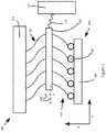
- FIG. 1depicts a simplified example test probe, in accordance with various embodiments.
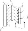
- FIG. 2depicts an alternative view of the simplified example test probe when the test probe is in contact with a DUT, in accordance with various embodiments.
- FIG. 3depicts an alternative simplified example test probe, in accordance with various embodiments.
- FIG. 4depicts an example technique for constructing a test probe, in accordance with various embodiments.
- phrase “A or B”means (A), (B), or (A and B).
- phrase “A, B, or C”means (A), (B), (C), (A and B), (A and C), (B and C), or (A, B and C).
- Coupledmay mean one or more of the following. “Coupled” may mean that two or more elements are in direct physical or electrical contact. However, “coupled” may also mean that two or more elements indirectly contact each other, but yet still cooperate or interact with each other, and may mean that one or more other elements are coupled or connected between the elements that are said to be coupled with each other.
- directly coupledmay mean that two or elements are in direct contact.
- the phrase “a first feature formed, deposited, or otherwise disposed on a second feature,”may mean that the first feature is formed, deposited, or disposed over the feature layer, and at least a part of the first feature may be in direct contact (e.g., direct physical or electrical contact) or indirect contact (e.g., having one or more other features between the first feature and the second feature) with at least a part of the second feature.
- direct contacte.g., direct physical or electrical contact
- indirect contacte.g., having one or more other features between the first feature and the second feature
- Embodiments hereinmay leverage batch-based manufacturing, but conjoin it in a geometry that adds higher overtravel while canceling out undesirable scrub seen at the connection between the test probe and the DUT.
- overtravelmay refer to the vertical distance that the test probe needs to travel after first coupling with the DUT (assuming that the test probe and the DUT are vertically aligned). The overtravel may ensure a stronger connection between the test probe and the DUT.
- Scrubmay refer to lateral translation of the end of the test probe based on vertical compression of the test probe to the DUT (again assuming that the test probe and the DUT are vertically aligned). Specifically, as the test probe is moved closer to the DUT, the beams of the test probe may deform laterally.
- Scrubmay be especially prevalent if the beams are angled with respect to the vertical axis prior to coupling the test probe and the DUT. For example, in some legacy cases vertical movement of approximately 25 micrometers (“microns” or “m”) may result in approximately 25 to 50 microns of scrub. More generally, vertical movement of x microns may result in between approximately 1x-2x microns of scrub. This level of scrub may be undesirable as it may cause beams of the test probe to short against one another, or it may cause the ends of the test probe to slip away from the portion of the DUT which the test probe is intended to measure.
- the test probemay include a mid-layer substrate with one or more degrees of freedom.
- the degrees of freedommay stem from a first plurality of angled beams secured to the top side of the mid-layer, and also anchored to a solid base.
- the lower side of the test probemay include an additional plurality of beams that are coupled with the substrate and are to contact the DUT. Both the top and the bottom plurality of beams may be configured to deform to achieve a desirable amount of compression for an electrically stable interconnect.
- FIG. 1depicts a simplified example test probe 100 , in accordance with various embodiments.
- the test probe 100may include a probe base 105 .
- the probe base 105may be generally formed of a material such as plastic, stainless steel, silicon, glass, or some other generally dielectric material.
- the probe base 105may be coupled with a first plurality of beams 130 .
- the beamsmay be formed of a conductive material such as nickel, iron, cobalt, composites thereof, or some other conductive material.
- the first plurality of beams 130may have a conductive coating such as silver, copper, etc.
- respective beams of the first plurality of beams 130may be angled away from normal by an angle ⁇ 1 .
- “normal”may refer to a direction perpendicular to the face of the base or substrate to which the beams are coupled.
- the angle ⁇ 1may be between approximately 20 and approximately 45 degrees. However, in other embodiments the angle ⁇ 1 may be greater or lesser.
- each beam within the first plurality of beams 130may be angled at the same angle, while in other embodiments different beams may have a different amount of angle.
- respective beams of the first plurality of beams 130may have a z-height Z 1 of between approximately 300 microns and approximately 500 microns, however in other embodiments the beams may have a greater or lesser z-height.
- the first plurality of beams 130may have a z-height Z 1 as high as approximately 1000 microns.
- the probe base 105may include one or more conductive elements such as traces, vias, or some other conductive element that may be coupled with respective beams of the first plurality of beams 130 .
- the conductive elementsmay be configured to convey signals to or from one or more of the beams of the first plurality of beams 130 .
- the test probe 100may also include an intermediate substrate 120 .
- the intermediate substrate 120may be formed of a dielectric material such as the dielectric materials discussed above with respect to probe base 105 .
- the intermediate substrate 120may be formed of plastic, ceramics, silicon, glass, or some other material.
- movement of the intermediate substrate 120may be constrained in the lateral direction, for example along the horizontal axis “X” as shown in FIG. 1 .
- the movement of the intermediate substrate 120may be constrained by constraint 115 .
- Constraint 115may be, for example, a spring that is coupled with the intermediate substrate 120 at one end and coupled with a body 110 of the probe device of which the test probe 100 is a part. If the constraint 115 is a spring, then the spring may have a relatively low spring constant, which would have a positive value in the embodiment depicted in FIG. 1 , however the spring configuration or spring constant may vary in other embodiments.
- the constraint 115may be, for example, a magnet (e.g., repelling or attracting magnets coupled with the body 110 and the intermediate substrate 120 ), a physical stop, or some other type of constraint.
- the constraint 115may be on the left side of the intermediate substrate 120 (as oriented in FIG. 1 ) rather than the right side.
- the test probe 100may include a plurality of constraints which may be of the same type or different type as one another, and may be on the same side or different sides from one another with respect to the intermediate substrate 120 . In some embodiments, there may not be a constraint 115 .
- the test probe 100may further include a second plurality of beams 135 .
- the second plurality of beams 135may be formed of a conductive material similar to the conductive material discussed above with respect to the first plurality of beams 130 .
- the second plurality of beams 135may be formed of a material such as nickel, iron, cobalt, composites thereof, or some other conductive material.
- the second plurality of beams 135may have a conductive coating such as silver, copper, etc.
- the first plurality of beams 130 and the second plurality of beams 135may be formed of the same material as one another, or they may be formed of different materials from one another. As can be seen in FIG.
- the second plurality of beams 135may be offset from normal with respect to the face of the intermediate substrate 120 by an angle ⁇ 2 .
- ⁇ 2may be between approximately 20 degrees and approximately 45 degrees away from normal.
- the angles ⁇ 1 and ⁇ 2may be the same as one another or different from one another.
- the normal for measurement of the angles ⁇ 1 and ⁇ 2may be the same as one another (e.g., both measured with respect to the probe base 105 or the intermediate substrate 120 ), or the normal for measurement of the angle ⁇ 1 may be with respect to probe base 105 while the normal for measurement of the angle ⁇ 2 may be with respect to intermediate substrate 120 .
- the second plurality of beams 135may have a z-height Z 2 of between approximately 200 microns and approximately 350 microns, however in other embodiments the z-height of the second plurality of beams may be larger or smaller.
- the second plurality of beams 135may have a z-height Z 2 of up to approximately 700 microns.
- the arrangement of the first plurality of beams 130 , the intermediate substrate 120 , and the second plurality of beams 135may allow the second plurality of beams to have a pitch of less than 40 microns and, in some embodiments, less than or equal to 36 microns. More specifically, the distance from a central point at the end of one beam of the second plurality of beams 135 may be less than or equal to 36 microns from a central point at the end of another beam of the second plurality of beams along the X axis. It is worth noting that in some embodiments the first plurality of beams 130 may have a pitch that is different than the pitch of the second plurality of beams 135 .
- the first plurality of beams 130may have a pitch that is larger than the pitch of the second plurality of beams 135 .
- the pitch of the second plurality of beams 135 at a portion of the second plurality of beams 135 coupled with the intermediate substrate 120may be different than the pitch of the second plurality of beams 135 at a portion of the second plurality of beams 135 that is to couple with the DUT, as described in further detail below.
- the second plurality of beams 135may be configured to couple with a DUT. More specifically, the ends of the second plurality of beams 135 that are furthest from the intermediate substrate 120 may be configured to couple with the DUT. As mentioned above, the second plurality of beams 135 may be configured to receive or generate one or more electrical signals that may propagate throughout the second plurality of beams 135 .
- the intermediate substrate 120may have one or more traces or vias (not shown) that communicatively coupled the second plurality of beams 135 with the first plurality of beams 130 . The electrical signals may therefore propagate from the second plurality of beams 135 , through the intermediate substrate 120 , and to the first plurality of beams 130 . The electrical signals may then propagate from the first plurality of beams 130 through the probe base 105 and ultimately to a system that is coupled with the test probe 100 .
- the first plurality of beams 130 and the second plurality of beams 135may deform. More specifically, they may compress in the direction indicated by the Z axis.
- the intermediate substrate 120may move both laterally (e.g., along the X axis) and vertically (e.g., along the Z axis).
- Marker lines 125depict a starting position of the top left (as oriented with respect to FIG. 1 ) corner of the intermediate substrate 120 .
- FIG. 2depicts an example of the test probe 100 being coupled with a DUT 103 .
- the DUT 103may include a DUT substrate 140 and a plurality of contacts 150 .
- the DUT substrate 140may be, for example, a cored or coreless substrate composed of a dielectric material such as Ajimoto Build-Up Film (ABF) or some other material.
- the DUT substrate 140may have a plurality of traces, vias, or some other conductive pathway therein.
- the DUT substrate 140may have a plurality of elements such as circuitry, transistors, logic, processors, memory, etc. either coupled with the substrate or positioned at least partially within the substrate.
- the contacts 150may be, for examples, pads, solder bumps, balls of a ball grid array (BGA), pins of a pin grid array (PGA) or some other type of contact.
- BGAball grid array
- PGApin grid array
- the ends of the second plurality of beams 135may be configured to communicatively and physically couple with the contacts 150 of the DUT 103 .
- the test probe 100may be configured to send one or more electrical signals, through the second plurality of beams 135 , to the DUT 103 .
- the test probe 100may be configured to receive those return signals and transmit them to a system coupled with the test probe for further measurement or analysis. Additionally or alternatively, the test probe 100 may be configured to passively receive one or more signals from the DUT 103 without first providing a signal to the DUT 103 .
- the first plurality of beams 130 and the second plurality of beams 135may deform as shown in FIG. 2 .
- the intermediate substrate 120may travel both laterally (e.g., along the X axis), and vertically (e.g., along the Z axis), as described above. This travel may be seen with reference to marker lines 125 . More specifically, whereas in FIG. 1 the top left corner (with reference to the orientation of FIGS. 1 and 2 ) of the substrate was depicted aligned with the marker lines 125 , it can be seen in FIG. 2 that the top left corner of the substrate may be up and to the right of the marker lines 125 .
- the test probemay be compressed by approximately 25 to approximately 60 microns, though in other embodiments the amount of compression may be greater or smaller dependent on test parameters.
- the intermediate substrate 120may travel approximately 20 microns to approximately 80 microns along the X axis and approximately ten microns to approximately 40 microns along the Z axis. More generally, the intermediate substrate 120 may travel approximately half of the distance along the Z axis that it travels along the X axis.
- the ends of the second plurality of beams 135 that are coupled with the contacts 150 of the DUT 103may experience little to no scrub, as described above.
- some amount of scrubmay still be allowed, and the amount may be a targeted or designed value based on, for example, contact dynamic characteristics.
- first and second plurality of beams 130 and 135may deform as shown in FIG. 2 , and the intermediate substrate 120 may travel along the X and Z axes, the ends of the second plurality of beams 135 may travel along the Z axis when under compression with little to no travel along the X axis.
- difficulties experienced by legacy test probessuch as scrub, shorting, or other difficulties may be almost entirely, or completely, negated. If scrub still exists, it may be on the order of 0-20% movement rather than the approximately 100-200% that may be experienced by legacy test probes.
- the travel along the X axis of the ends of the second plurality of beams 135 that are coupled with the DUTmay be between approximately zero and approximately 20% of the travel along the Z axis of the same ends.
- This scrubmay allow the test probe to operate using a pitch (e.g., 36 microns as discussed above) that is significantly less than the pitch achievable by legacy test probes. Additionally, the amount of stress seen by each beam in the test probe may be reduced by approximately 38%, which may result in a more robust and longer-lasting beam design.
- the amount of stress seen by each beam in the test probemay be reduced by approximately 30% and 50% over legacy designs, although it will be understood that the specific reduction in stress may vary based on design factors, materials used, the cross sections of various materials such as the beams or the intermediate substrate, etc.
- test probes 100may be batch-produced on a wafer-level scale, the cost of each test probe may be significantly lower than the cost of a legacy test probe. By eliminating or reducing these difficulties, the test probe 100 may stay more completely coupled with the DUT 103 , and resultant test signals or measurements may therefore be taken with a lower rate of measurement errors.
- FIG. 3depicts an alternative simplified example test probe 200 .
- the test probe 200may include a probe base 205 , a first plurality of beams 230 , an intermediate substrate 220 , and a second plurality of beams 235 which may be respectively similar to probe base 105 , first plurality of beams 130 , intermediate substrate 120 , and second plurality of beams 135 .
- the test probe 200may be coupled with a DUT 203 , which may be similar to DUT 103 , and which may include DUT substrate 240 and contacts 250 , which may be similar to DUT substrate 140 and contacts 150 .
- there may be additional elementssuch as a constraint similar to constraint 115 , however some of those elements may not be depicted in FIG. 3 for the sake of lack of redundancy.
- the first plurality of beams 130may be solidly anchored to the probe base 105 .
- the first plurality of beams 130may be soldered or otherwise coupled to the probe base 105 such that the end of the first plurality of beams 130 that is coupled to the probe base 105 is unable to move with respect to the probe base.
- the end of the first plurality of beams 230may be coupled with the probe base 205 by a pivotable joint 210 .
- the pivotable joint 210may be, for example, a ball-and-socket joint or some other type of pivotable joint that may act similarly to a ball-and-socket joint, or even a different type of joint.
- the pivotable joint 210may simply be a vertical constraint on the end of the first plurality of beams 230 that is coupled with the probe base 205 via one or more other mechanical mechanisms.
- the pivotable joint 210may allow the end of the first plurality of beams 230 that is coupled with the pivotable joint 210 to rotate with respect to the probe base 205 when the test probe 200 is coupled with the DUT 203 . This rotation may, for example, further reduce stress on the test probe 200 and thereby further extend the useful life of the test probe 200 .
- FIGS. 1 , 2 , and 3are intended as simplified examples, and specific numbers or element proportions should not be assumed based on the Figures unless otherwise explicitly stated.
- first or second plurality of beams 130 / 230 / 135 / 235may number in the tens, hundreds, thousands, or more.
- the DUTmay have more or fewer contacts than depicted in FIG. 1 or 2 .
- constraint 115may be coupled with the intermediate substrate 120 .
- the probe base 105 / 205 or the intermediate substrate 120 / 220may be disaggregated into a plurality of pieces rather than a single piece. Other variations may be present in other embodiments.
- the second plurality of beams 135 / 235are described as being configured to couple with a DUT.
- the couplingmay be a removable coupling. That is, the second plurality of beams 135 / 235 may be configured to temporarily contact the DUT, but not be adhered to the DUT. In this way, the same test probe may be able to able to test several DUTs over the life span of the test probe.
- the test probe, and more specifically the second plurality of beams 135 / 235may be configured to adhere to the DUT in some way, for example via an adhesive, a solder joint, etc.
- the adherencemay be light (e.g., a mild adhesive) so that the test probe may still be able to test a plurality of DUTs, while in other embodiments the adherence may be relatively permanent (e.g., a solder joint), so that the test probe may only be able to test one or only a few DUTs over the useful life span of the probe.
- lighte.g., a mild adhesive
- relatively permanente.g., a solder joint
- FIG. 4depicts an example technique for constructing a test probe, in accordance with various embodiments.
- the techniquemay include coupling, at 405 , a first plurality of beams to a probe base.
- the first plurality of beamsmay be, for example, the first plurality of beams 130
- the probe basemay be, for example, probe base 105 .
- the first plurality of beamsmay be coupled with the probe base through an anchoring technique such as soldering or some other technique.
- the first plurality of beamsmay be similar to the first plurality of beams 230 and may be coupled with a probe base such as probe base 205 by a pivotable joint such as pivotable joint 210 .
- the techniquemay further include coupling, at 410 , a substrate to the first plurality of beams such that the first plurality of beams is between the probe base and the substrate.
- the substratemay be, for example, intermediate substrates 120 or 220 .
- the techniquemay further include coupling, at 415 , a second plurality of beams to the substrate such that the substrate is between the first plurality of beams and the second plurality of beams.
- the second plurality of beamsmay be, for example, second plurality of beams 135 or 235 .
- element 415may occur prior to element 405 . That is, the beams may be coupled to the substrate before the first plurality of beams are coupled with the probe base. Alternatively, element 415 may occur prior to element 410 . Other variations may be envisioned.
- Example 1includes a test probe comprising a base that includes a face and a first plurality of beams, where individual ones of the first plurality of beams include a first end and a second end opposite the first end, the first end of the individual ones of the first plurality of the beams is coupled with the face of the base, and the individual ones of the first plurality of beams are angled in a first direction as measured perpendicular to the face of the base.
- the test probefurther comprises a second plurality of beams, where individual ones of the second plurality of beams include a first end and a second end, the first end of the individual ones of the second plurality of beams is coupled with the second end of the individual ones of the first plurality of beams, and the individual ones of the second plurality of beams are angled in a second direction as measured perpendicular to the face of the base.
- Example 2includes the test probe of example 1, further comprising a substrate positioned between the first plurality of beams and the second plurality of beams, wherein the substrate is coupled with the second end of the first plurality of beams and the substrate is further coupled with the first end of the second plurality of beams.
- Example 3includes the test probe of example 1, wherein the second end of the second plurality of beams are to temporarily couple with a DUT.
- Example 4includes the test probe of any of examples 1-3, wherein the first plurality of beams have a z-height, as measured perpendicular to the face of the base, of between 300 and 1000 micrometers.
- Example 5includes the test probe of any of examples 1-3, wherein the second plurality of beams have a z-height, as measured perpendicular to the face of the base, of between 200 and 700 micrometers.
- Example 6includes the test probe of any of examples 1-3, wherein the first direction is opposite the second direction.
- Example 7includes the test probe of any of examples 1-3, wherein the first plurality of beams are angled by between 20 and 45 degrees.
- Example 8includes the test probe of any of examples 1-3, wherein the second plurality of beams are angled by between 20 and 45 degrees.
- Example 9includes the test probe of any of examples 1-3, wherein the second plurality of beams have a pitch of less than 36 micrometers.
- Example 10includes a test probe comprising: a probe base that includes a face; a first set of beams coupled with the face of the probe base, wherein the first set of beams are angled away from a normal in a first direction, the normal measured/defined in a direction perpendicular to the face; a substrate with a first side and a second side opposite the first side, wherein the first side of the substrate is coupled with the first set of beams such that the first set of beams are positioned between the probe base and the substrate; and a second set of beams coupled with the second side of the substrate.
- Example 11includes the test probe of example 10, wherein the second set of beams is angled in a second direction, and where the first direction is opposite the second direction.
- Example 12includes the test probe of examples 10 or 11, wherein the second set of beams are to couple with a DUT.
- Example 13includes the test probe of example 12, wherein lateral scrub of a side of the second set of beams that is coupled with the DUT is between 0 and 20% of vertical movement of the second set of beams when the test probe is coupled with the DUT.
- Example 14includes the test probe of examples 10 or 11, wherein the first set of beams is coupled with the probe base by a pivotable joint.
- Example 15includes the test probe of example 14, wherein the pivotable joint behaves similar to a ball-and-socket joint.
- Example 16includes the test probe of examples 10 or 11, wherein movement of the substrate is constrained in a direction parallel to the face of the probe base.
- Example 17includes the test probe of example 16, wherein the movement of the substrate is constrained by a stop, a spring, or a magnet.
- Example 18includes a method of manufacturing a test probe, the method comprising: coupling a first plurality of beams to a probe base; coupling a substrate to the first plurality of beams such that the first plurality of beams is between the probe base and the substrate; and coupling a second plurality of beams to the substrate such that the substrate is between the first plurality of beams and the second plurality of beams.
- Example 19includes the method of example 18, wherein coupling the first plurality of beams to the probe base includes coupling the first plurality of beams at an angle between 20 and 45 degrees away from a normal, the normal measured/defined with respect to a face of the probe base to which the first plurality of beams are coupled.
- Example 20includes the method of example 18, wherein coupling the second plurality of beams to the substrate includes coupling the second plurality of beams at an angle between 20 and 45 degrees away from a normal, the normal measured/defined with respect to a face of the substrate to which the second plurality of beams are coupled.
- Example 21includes the method of any of examples 18-20, further comprising constraining movement of the substrate in a direction parallel to a face of the substrate to which the first plurality of beams or the second plurality of beams are coupled.
- Example 22includes the method of example 21, wherein constraining the movement includes coupling the substrate with a stop, a magnet, or a spring.
- Example 23includes the method of any of examples 18-20, wherein coupling the first plurality of beams to the probe base includes coupling the first plurality of beams to the probe base using a pivotable couple.
- Example 24includes the method of example 23, wherein the pivotable couple is a ball-and-socket joint.
- Example 25includes a probe device that comprises: a body; a mount to physically (e.g., mechanically) and communicatively couple the body to a test system; and a plurality of test probes coupled to the body, wherein a test probe of the plurality of test probes comprises: a probe base; a first plurality of beams coupled with the probe base; a substrate coupled with the first plurality of beams such that the first plurality of beams are positioned between the probe base and the substrate; and a second plurality of beams coupled with the substrate such that the substrate is positioned between the first plurality of beams and the second plurality of beams.
- a test probe of the plurality of test probescomprises: a probe base; a first plurality of beams coupled with the probe base; a substrate coupled with the first plurality of beams such that the first plurality of beams are positioned between the probe base and the substrate; and a second plurality of beams coupled with the substrate such that the substrate is positioned between the first plurality of beam
- Example 26includes the probe device of example 25, wherein the first plurality of beams are coupled with the probe base at an angle between 20 and 45 degrees away from a normal as defined with respect to a face of the probe base to which the first plurality of beams are coupled.
- Example 27includes the probe device of example 25, wherein the second plurality of beams are coupled with the substrate at an angle between 20 and 45 degrees away from a normal as defined with respect to a face of the substrate to which the second plurality of beams are coupled.
- Example 28includes the probe device of any of examples 25-27, wherein movement of the substrate is constrained in a direction parallel to a face of the substrate to which the first plurality of beams or the second plurality of beams are coupled.
- Example 29includes the probe device of example 28, wherein the movement of the substrate is constrained by a constraint coupled with the body of the probe device.
- Example 30includes the probe device of example 29, wherein the constraint is a stop, a spring, or a magnet.
- Example 31includes the probe device of any of examples 25-27, wherein the second plurality of beams are to couple with a DUT.
- Example 32includes the probe device of any of examples 25-27, wherein the first plurality of beams have a z-height, as measured perpendicular to a face of the probe base to which the first plurality of beams are coupled, of between 300 and 500 micrometers.
- Example 33includes the probe device of any of examples 25-27, wherein the second plurality of beams have a z-height, as measured perpendicular to a face of the substrate to which the second plurality of beams are coupled, of between 200 and 350 micrometers.
- Various embodimentsmay include any suitable combination of the above-described embodiments including alternative (or) embodiments of embodiments that are described in conjunctive form (and) above (e.g., the “and” may be “and/or”). Furthermore, some embodiments may include one or more articles of manufacture (e.g., non-transitory computer-readable media) having instructions, stored thereon, that when executed result in actions of any of the above-described embodiments. Moreover, some embodiments may include apparatuses or systems having any suitable means for carrying out the various operations of the above-described embodiments.
Landscapes
- Physics & Mathematics (AREA)
- General Physics & Mathematics (AREA)
- Engineering & Computer Science (AREA)
- General Engineering & Computer Science (AREA)
- Measuring Leads Or Probes (AREA)
- Testing Or Measuring Of Semiconductors Or The Like (AREA)
Abstract
Description
Claims (24)
Priority Applications (1)
| Application Number | Priority Date | Filing Date | Title |
|---|---|---|---|
| US16/141,422US11543454B2 (en) | 2018-09-25 | 2018-09-25 | Double-beam test probe |
Applications Claiming Priority (1)
| Application Number | Priority Date | Filing Date | Title |
|---|---|---|---|
| US16/141,422US11543454B2 (en) | 2018-09-25 | 2018-09-25 | Double-beam test probe |
Publications (2)
| Publication Number | Publication Date |
|---|---|
| US20200096567A1 US20200096567A1 (en) | 2020-03-26 |
| US11543454B2true US11543454B2 (en) | 2023-01-03 |
Family
ID=69885401
Family Applications (1)
| Application Number | Title | Priority Date | Filing Date |
|---|---|---|---|
| US16/141,422Active2040-12-22US11543454B2 (en) | 2018-09-25 | 2018-09-25 | Double-beam test probe |
Country Status (1)
| Country | Link |
|---|---|
| US (1) | US11543454B2 (en) |
Families Citing this family (2)
| Publication number | Priority date | Publication date | Assignee | Title |
|---|---|---|---|---|
| US11815538B2 (en)* | 2021-08-18 | 2023-11-14 | Eagle Technology, Llc | Sensor receiver having a Rydberg cell with a plurality of excitation sources and associated methods |
| US12332372B2 (en)* | 2021-08-18 | 2025-06-17 | Eagle Technology, Llc | Sensor receiver having Rydberg cell and RF data rate greater than reciprocal of temporal pulse width and associated methods |
Citations (88)
| Publication number | Priority date | Publication date | Assignee | Title |
|---|---|---|---|---|
| US3622387A (en) | 1968-06-26 | 1971-11-23 | S I C E R Soc Ind & Commercial | Evaporator or cooking apparatus |
| US4581260A (en) | 1984-09-25 | 1986-04-08 | Ampex Corporation | Electroless plating method and apparatus |
| US5307560A (en) | 1992-07-30 | 1994-05-03 | Allen Aksu | Automated test pin loading method |
| US5453701A (en) | 1992-12-23 | 1995-09-26 | Honeywell Inc. | Bare die test and burn-in device |
| US5592222A (en) | 1989-02-10 | 1997-01-07 | Canon Kabushiki Kaisha | Sensor chip and photo-electric conversion apparatus using the same |
| US5635848A (en) | 1995-03-10 | 1997-06-03 | International Business Machines Corporation | Method and system for controlling high-speed probe actuators |
| US5747999A (en) | 1994-08-15 | 1998-05-05 | Okano Hitech Co., Ltd. | Feed control element used in substrate inspection and method and apparatus for inspecting substrates |
| US5767692A (en) | 1996-02-26 | 1998-06-16 | Circuit Line Spa | Device for converting the test point grid of a machine for electrically testing unassembled printed circuit boards |
| US5917329A (en) | 1997-04-17 | 1999-06-29 | International Business Machines Corporation | Substrate tester having shorting pad actuator method and apparatus |
| EP0962776A2 (en) | 1998-06-02 | 1999-12-08 | Advantest Corporation | Probe card suitable for inspection of multi-pin devices |
| US6130545A (en) | 1996-01-24 | 2000-10-10 | Intel Corporation | Method and apparatus for scrubbing the bond pads of an integrated circuit during wafer sort |
| US6292004B1 (en) | 1999-04-23 | 2001-09-18 | Douglas Kocher | Universal grid interface |
| US20020024347A1 (en) | 2000-05-11 | 2002-02-28 | Stefano Felici | Microstructure testing head |
| US6356090B2 (en) | 1997-12-24 | 2002-03-12 | Stmicroelectronics S.A. | Probe tip card for the testing of semiconductor components |
| US6441315B1 (en) | 1998-11-10 | 2002-08-27 | Formfactor, Inc. | Contact structures with blades having a wiping motion |
| US20020163349A1 (en) | 2000-05-18 | 2002-11-07 | Kouichi Wada | Probe card and method of producing the same |
| US6740163B1 (en) | 2001-06-15 | 2004-05-25 | Seagate Technology Llc | Photoresist recirculation and viscosity control for dip coating applications |
| US6774654B2 (en)* | 2000-09-06 | 2004-08-10 | Renesas Technology Corp. | Semiconductor-device inspecting apparatus and a method for manufacturing the same |
| US6812718B1 (en) | 1999-05-27 | 2004-11-02 | Nanonexus, Inc. | Massively parallel interface for electronic circuits |
| US20050051515A1 (en) | 2003-09-08 | 2005-03-10 | Lg Electronics Inc. | Cantilever microstructure and fabrication method thereof |
| US20050151547A1 (en) | 2004-01-09 | 2005-07-14 | Nihon Denshizairyo Kabushiki Kaisha | Probe card |
| US20050231855A1 (en) | 2004-04-06 | 2005-10-20 | Availableip.Com | NANO-electronic memory array |
| US20050263401A1 (en) | 2004-05-26 | 2005-12-01 | Gerald Olsen | Method and apparatus for plating substrates |
| US20060152232A1 (en) | 2002-12-20 | 2006-07-13 | The Provost Fellows And Scholars Of The College Of | Method and apparatus for inspection of high frequency and microwave hybrid circuits and printed circuit boards |
| US20060151614A1 (en) | 2003-07-03 | 2006-07-13 | Hirotaka Nishizawa | Multi-function card device |
| US20060171425A1 (en) | 2003-03-17 | 2006-08-03 | Phicom Corporation | Probe and method of making same |
| US20060214674A1 (en) | 2005-03-25 | 2006-09-28 | Lee K R | Apparatus, system and method for testing electronic elements |
| US7189077B1 (en) | 1999-07-30 | 2007-03-13 | Formfactor, Inc. | Lithographic type microelectronic spring structures with improved contours |
| US20070126440A1 (en) | 2005-12-02 | 2007-06-07 | Formfactor, Inc. | Probe Card Assembly With A Mechanically Decoupled Wiring Substrate |
| US20070126435A1 (en) | 2005-12-02 | 2007-06-07 | Formfactor, Inc. | Apparatus And Method For Adjusting An Orientation Of Probes |
| US20070290371A1 (en) | 2006-06-20 | 2007-12-20 | Taiwan Semiconductor Manufacturing Co., Ltd. | Pad structure and method of testing |
| US20080074132A1 (en)* | 2006-09-27 | 2008-03-27 | Formfactor, Inc. | Single support structure probe group with staggered mounting pattern |
| US20080088327A1 (en) | 2006-10-11 | 2008-04-17 | January Kister | Probe cards employing probes having retaining portions for potting in a potting region |
| US20080196474A1 (en) | 2007-02-20 | 2008-08-21 | Centipede Systems, Inc. | Method and apparatus for aligning and/or leveling a test head |
| US20080204061A1 (en) | 2007-02-28 | 2008-08-28 | Dov Chartarifsky | Spring loaded probe pin assembly |
| US20080231300A1 (en) | 2007-03-23 | 2008-09-25 | Tokyo Electron Limted | Method for detecting tip position of probe, alignment method, apparatus for detecting tip position of probe and probe apparatus |
| US7436193B2 (en) | 2002-07-30 | 2008-10-14 | Intel Corporation | Thin film probe card contact drive system |
| US20080309363A1 (en) | 2007-06-15 | 2008-12-18 | Nictech Co., Ltd. | Probe assembly with wire probes |
| US20090056428A1 (en) | 2007-08-28 | 2009-03-05 | King William P | Cantilever probe and applications of the same |
| US20090072851A1 (en) | 2007-09-13 | 2009-03-19 | Touchdown Technologies, Inc. | Multi-Pivot Probe Card For Testing Semiconductor Devices |
| US7566228B2 (en) | 2007-06-26 | 2009-07-28 | Intel Corporation | Skived electrical contact for connecting an IC device to a circuit board and method of making a contact by skiving |
| US20090219047A1 (en) | 2005-10-31 | 2009-09-03 | Capres A/S | probe for testing electrical properties of a test sample |
| US20090237099A1 (en) | 2008-03-20 | 2009-09-24 | Touchdown Technologies, Inc. | Probe card substrate with bonded via |
| US20100052715A1 (en) | 1992-10-19 | 2010-03-04 | International Business Machines Corporation | High density integrated circuit apparatus, test probe and methods of use thereof |
| US20100066393A1 (en) | 2000-07-28 | 2010-03-18 | Bottoms W R | High density interconnect system for ic packages and interconnect assemblies |
| US20100079159A1 (en) | 2008-09-26 | 2010-04-01 | Formfactor, Inc. | Method and apparatus for providing a tester integrated circuit for testing a semiconductor device under test |
| US20100276572A1 (en) | 2005-06-02 | 2010-11-04 | Sony Corporation | Semiconductor image sensor module and method of manufacturing the same |
| US7884632B2 (en) | 2008-02-13 | 2011-02-08 | Shinko Electric Electric Industries Co., Ltd. | Semiconductor inspecting device |
| US20110031991A1 (en) | 2007-08-21 | 2011-02-10 | Gigalane Co. Ltd. | Probe block |
| US7928522B2 (en) | 2007-09-27 | 2011-04-19 | Intel Corporation | Arrangements for and fabrication of mechanical suspension of a movable structure |
| US20110115513A1 (en) | 2009-11-13 | 2011-05-19 | Kabushiki Kaisha Toshiba | Wafer prober and failure analysis method using the same |
| US20110163773A1 (en) | 2008-07-15 | 2011-07-07 | Rosenberger Hochfrequenztechnik Gmbh & Co. Kg | Measuring probe |
| US20110234251A1 (en) | 2008-12-03 | 2011-09-29 | Tokyo Electron Limited | Probe card |
| US8029291B2 (en) | 2008-08-07 | 2011-10-04 | Sang Yang Park | Flat plate folding type coil spring, pogo pin and manufacturing method |
| US20120038383A1 (en) | 2010-08-13 | 2012-02-16 | Chien-Chou Wu | Direct-docking probing device |
| US20120071037A1 (en) | 2009-01-20 | 2012-03-22 | Rise Technology S.R.L. | Elastic contact device for electronic components with buckling columns |
| US20120100287A1 (en) | 2010-10-20 | 2012-04-26 | Seagate Technology, Llc | Laminar flow plating rack |
| US20120117799A1 (en) | 2010-11-11 | 2012-05-17 | Dr. Qi Luo | Miniaturized Spring Contact |
| US20120146679A1 (en)* | 2010-12-14 | 2012-06-14 | Formfactor, Inc. | Probe card stiffener with decoupling |
| US8267831B1 (en) | 2009-05-19 | 2012-09-18 | Western Digital Technologies, Inc. | Method and apparatus for washing, etching, rinsing, and plating substrates |
| US20120319710A1 (en) | 2011-06-15 | 2012-12-20 | Probelogic, Inc. | Method and apparatus for implementing probes for electronic circuit testing |
| US20130002285A1 (en) | 2010-03-10 | 2013-01-03 | Johnstech International Corporation | Electrically Conductive Pins For Microcircuit Tester |
| US8411550B2 (en) | 2008-10-27 | 2013-04-02 | Intel Corporation | Seek and scan probe (SSP) cantilever stop structures |
| US20130099812A1 (en) | 2011-10-21 | 2013-04-25 | Taiwan Semiconductor Manufacturing Company, Ltd. | Probe Cards for Probing Integrated Circuits |
| US20130200910A1 (en) | 2012-02-02 | 2013-08-08 | International Business Machines Corporation | 3-dimensional integrated circuit testing using mems switches with tungsten cone contacts |
| US20130285688A1 (en) | 2012-03-23 | 2013-10-31 | Advantest Corporation | Laterally driven probes for semiconductor testing |
| US20140021976A1 (en) | 2012-07-23 | 2014-01-23 | Kabushiki Kaisha Nihon Micronics | Contact inspection device |
| US20140125372A1 (en) | 2012-11-05 | 2014-05-08 | Shinko Electric Industries Co., Ltd. | Probe card and method of manufacturing the same |
| US20140132297A1 (en) | 2012-11-13 | 2014-05-15 | Qualcomm Incorporated | Reconfigurable electric field probe |
| US20140253162A1 (en) | 2013-03-11 | 2014-09-11 | Taiwan Semiconductor Manufacturing Co., Ltd. | Integrated circuit test system and method |
| US20140347085A1 (en) | 2011-09-15 | 2014-11-27 | Taiwan Semiconductor Manufacturing Co., Ltd. | Test probe card |
| US20140362425A1 (en) | 2013-06-10 | 2014-12-11 | Freescale Semiconductor, Inc. | Communication System Die Stack |
| US20140363905A1 (en) | 2013-06-10 | 2014-12-11 | Freescale Semiconductor, Inc. | Optical Wafer and Die Probe Testing |
| US20150015291A1 (en) | 2013-07-15 | 2015-01-15 | Mpi Corporation | Cantilever probe card for high-frequency signal transmission |
| US20150123693A1 (en) | 2013-11-07 | 2015-05-07 | Nidec-Read Corporation | Inspection jig |
| US20150192633A1 (en) | 2014-01-07 | 2015-07-09 | International Business Machines Corporation | 3d chip testing through micro-c4 interface |
| US20150226783A1 (en) | 2014-02-11 | 2015-08-13 | Samsung Electronics Co., Ltd. | Probe card and wafer test system including the same |
| US9227324B1 (en) | 2014-09-25 | 2016-01-05 | WD Media, LLC | Mandrel for substrate transport system with notch |
| US20160079635A1 (en) | 2013-05-01 | 2016-03-17 | Nissan Motor Co., Ltd. | Charging and discharging inspection device and charging and discharging inspection method for thin secondary battery |
| US20160178663A1 (en) | 2014-12-23 | 2016-06-23 | Intel Corporation | Formed wire probe interconnect for test die contactor |
| US20160223590A1 (en)* | 2015-02-04 | 2016-08-04 | Mpi Corporation | Probe head and upper guider plate |
| US20170219626A1 (en) | 2016-02-03 | 2017-08-03 | Globalfoundries Inc. | Gimbal assembly test system and method |
| US20180003767A1 (en) | 2015-03-13 | 2018-01-04 | Technoprobe S.P.A. | Testing head comprising vertical probes |
| US20180143222A1 (en) | 2015-05-13 | 2018-05-24 | Industry-University Cooperation Foundation Sogang University | Method for manufacturing microcantilever having functional probe |
| US20190203370A1 (en) | 2017-12-28 | 2019-07-04 | Intel Corporation | Massively-parallel micronozzle array for direct write electrodeposition of high-density microstructure arrays |
| US20190212366A1 (en) | 2018-01-05 | 2019-07-11 | Intel Corporation | High density and fine pitch interconnect structures in an electric test apparatus |
| US20200006868A1 (en) | 2018-06-28 | 2020-01-02 | John D. Tillotson, JR. | Insulation displacement termination (idt) for applying multiple electrical wire gauge sizes simultaneously or individually to electrical connectors, stamped and formed strip terminal products, and assembly fixtures thereof |
| US20210302489A1 (en) | 2017-12-05 | 2021-09-30 | Intel Corporation | Multi-member test probe structure |
- 2018
- 2018-09-25USUS16/141,422patent/US11543454B2/enactiveActive
Patent Citations (90)
| Publication number | Priority date | Publication date | Assignee | Title |
|---|---|---|---|---|
| US3622387A (en) | 1968-06-26 | 1971-11-23 | S I C E R Soc Ind & Commercial | Evaporator or cooking apparatus |
| US4581260A (en) | 1984-09-25 | 1986-04-08 | Ampex Corporation | Electroless plating method and apparatus |
| US5592222A (en) | 1989-02-10 | 1997-01-07 | Canon Kabushiki Kaisha | Sensor chip and photo-electric conversion apparatus using the same |
| US5307560A (en) | 1992-07-30 | 1994-05-03 | Allen Aksu | Automated test pin loading method |
| US20100052715A1 (en) | 1992-10-19 | 2010-03-04 | International Business Machines Corporation | High density integrated circuit apparatus, test probe and methods of use thereof |
| US5453701A (en) | 1992-12-23 | 1995-09-26 | Honeywell Inc. | Bare die test and burn-in device |
| US5747999A (en) | 1994-08-15 | 1998-05-05 | Okano Hitech Co., Ltd. | Feed control element used in substrate inspection and method and apparatus for inspecting substrates |
| US5635848A (en) | 1995-03-10 | 1997-06-03 | International Business Machines Corporation | Method and system for controlling high-speed probe actuators |
| US6130545A (en) | 1996-01-24 | 2000-10-10 | Intel Corporation | Method and apparatus for scrubbing the bond pads of an integrated circuit during wafer sort |
| US5767692A (en) | 1996-02-26 | 1998-06-16 | Circuit Line Spa | Device for converting the test point grid of a machine for electrically testing unassembled printed circuit boards |
| US5917329A (en) | 1997-04-17 | 1999-06-29 | International Business Machines Corporation | Substrate tester having shorting pad actuator method and apparatus |
| US6356090B2 (en) | 1997-12-24 | 2002-03-12 | Stmicroelectronics S.A. | Probe tip card for the testing of semiconductor components |
| EP0962776A2 (en) | 1998-06-02 | 1999-12-08 | Advantest Corporation | Probe card suitable for inspection of multi-pin devices |
| JPH11344510A (en) | 1998-06-02 | 1999-12-14 | Advantest Corp | Probe card, probe and semiconductor testing device |
| US6441315B1 (en) | 1998-11-10 | 2002-08-27 | Formfactor, Inc. | Contact structures with blades having a wiping motion |
| US6292004B1 (en) | 1999-04-23 | 2001-09-18 | Douglas Kocher | Universal grid interface |
| US6812718B1 (en) | 1999-05-27 | 2004-11-02 | Nanonexus, Inc. | Massively parallel interface for electronic circuits |
| US7189077B1 (en) | 1999-07-30 | 2007-03-13 | Formfactor, Inc. | Lithographic type microelectronic spring structures with improved contours |
| US20020024347A1 (en) | 2000-05-11 | 2002-02-28 | Stefano Felici | Microstructure testing head |
| US20020163349A1 (en) | 2000-05-18 | 2002-11-07 | Kouichi Wada | Probe card and method of producing the same |
| US20100066393A1 (en) | 2000-07-28 | 2010-03-18 | Bottoms W R | High density interconnect system for ic packages and interconnect assemblies |
| US6774654B2 (en)* | 2000-09-06 | 2004-08-10 | Renesas Technology Corp. | Semiconductor-device inspecting apparatus and a method for manufacturing the same |
| US6740163B1 (en) | 2001-06-15 | 2004-05-25 | Seagate Technology Llc | Photoresist recirculation and viscosity control for dip coating applications |
| US7436193B2 (en) | 2002-07-30 | 2008-10-14 | Intel Corporation | Thin film probe card contact drive system |
| US20060152232A1 (en) | 2002-12-20 | 2006-07-13 | The Provost Fellows And Scholars Of The College Of | Method and apparatus for inspection of high frequency and microwave hybrid circuits and printed circuit boards |
| US20060171425A1 (en) | 2003-03-17 | 2006-08-03 | Phicom Corporation | Probe and method of making same |
| US20060151614A1 (en) | 2003-07-03 | 2006-07-13 | Hirotaka Nishizawa | Multi-function card device |
| US20050051515A1 (en) | 2003-09-08 | 2005-03-10 | Lg Electronics Inc. | Cantilever microstructure and fabrication method thereof |
| US20050151547A1 (en) | 2004-01-09 | 2005-07-14 | Nihon Denshizairyo Kabushiki Kaisha | Probe card |
| US20050231855A1 (en) | 2004-04-06 | 2005-10-20 | Availableip.Com | NANO-electronic memory array |
| US20050263401A1 (en) | 2004-05-26 | 2005-12-01 | Gerald Olsen | Method and apparatus for plating substrates |
| US20060214674A1 (en) | 2005-03-25 | 2006-09-28 | Lee K R | Apparatus, system and method for testing electronic elements |
| US20100276572A1 (en) | 2005-06-02 | 2010-11-04 | Sony Corporation | Semiconductor image sensor module and method of manufacturing the same |
| US20090219047A1 (en) | 2005-10-31 | 2009-09-03 | Capres A/S | probe for testing electrical properties of a test sample |
| US20070126435A1 (en) | 2005-12-02 | 2007-06-07 | Formfactor, Inc. | Apparatus And Method For Adjusting An Orientation Of Probes |
| US20070126440A1 (en) | 2005-12-02 | 2007-06-07 | Formfactor, Inc. | Probe Card Assembly With A Mechanically Decoupled Wiring Substrate |
| US20070290371A1 (en) | 2006-06-20 | 2007-12-20 | Taiwan Semiconductor Manufacturing Co., Ltd. | Pad structure and method of testing |
| US20080074132A1 (en)* | 2006-09-27 | 2008-03-27 | Formfactor, Inc. | Single support structure probe group with staggered mounting pattern |
| US20080088327A1 (en) | 2006-10-11 | 2008-04-17 | January Kister | Probe cards employing probes having retaining portions for potting in a potting region |
| US20080196474A1 (en) | 2007-02-20 | 2008-08-21 | Centipede Systems, Inc. | Method and apparatus for aligning and/or leveling a test head |
| US20080204061A1 (en) | 2007-02-28 | 2008-08-28 | Dov Chartarifsky | Spring loaded probe pin assembly |
| US20080231300A1 (en) | 2007-03-23 | 2008-09-25 | Tokyo Electron Limted | Method for detecting tip position of probe, alignment method, apparatus for detecting tip position of probe and probe apparatus |
| US20080309363A1 (en) | 2007-06-15 | 2008-12-18 | Nictech Co., Ltd. | Probe assembly with wire probes |
| US7566228B2 (en) | 2007-06-26 | 2009-07-28 | Intel Corporation | Skived electrical contact for connecting an IC device to a circuit board and method of making a contact by skiving |
| US20110031991A1 (en) | 2007-08-21 | 2011-02-10 | Gigalane Co. Ltd. | Probe block |
| US20090056428A1 (en) | 2007-08-28 | 2009-03-05 | King William P | Cantilever probe and applications of the same |
| US20090072851A1 (en) | 2007-09-13 | 2009-03-19 | Touchdown Technologies, Inc. | Multi-Pivot Probe Card For Testing Semiconductor Devices |
| US7928522B2 (en) | 2007-09-27 | 2011-04-19 | Intel Corporation | Arrangements for and fabrication of mechanical suspension of a movable structure |
| US7884632B2 (en) | 2008-02-13 | 2011-02-08 | Shinko Electric Electric Industries Co., Ltd. | Semiconductor inspecting device |
| US20090237099A1 (en) | 2008-03-20 | 2009-09-24 | Touchdown Technologies, Inc. | Probe card substrate with bonded via |
| US20110163773A1 (en) | 2008-07-15 | 2011-07-07 | Rosenberger Hochfrequenztechnik Gmbh & Co. Kg | Measuring probe |
| US8029291B2 (en) | 2008-08-07 | 2011-10-04 | Sang Yang Park | Flat plate folding type coil spring, pogo pin and manufacturing method |
| US20100079159A1 (en) | 2008-09-26 | 2010-04-01 | Formfactor, Inc. | Method and apparatus for providing a tester integrated circuit for testing a semiconductor device under test |
| US8411550B2 (en) | 2008-10-27 | 2013-04-02 | Intel Corporation | Seek and scan probe (SSP) cantilever stop structures |
| US20110234251A1 (en) | 2008-12-03 | 2011-09-29 | Tokyo Electron Limited | Probe card |
| US20120071037A1 (en) | 2009-01-20 | 2012-03-22 | Rise Technology S.R.L. | Elastic contact device for electronic components with buckling columns |
| US8267831B1 (en) | 2009-05-19 | 2012-09-18 | Western Digital Technologies, Inc. | Method and apparatus for washing, etching, rinsing, and plating substrates |
| US20110115513A1 (en) | 2009-11-13 | 2011-05-19 | Kabushiki Kaisha Toshiba | Wafer prober and failure analysis method using the same |
| US20130002285A1 (en) | 2010-03-10 | 2013-01-03 | Johnstech International Corporation | Electrically Conductive Pins For Microcircuit Tester |
| US20120038383A1 (en) | 2010-08-13 | 2012-02-16 | Chien-Chou Wu | Direct-docking probing device |
| US20120100287A1 (en) | 2010-10-20 | 2012-04-26 | Seagate Technology, Llc | Laminar flow plating rack |
| US20120117799A1 (en) | 2010-11-11 | 2012-05-17 | Dr. Qi Luo | Miniaturized Spring Contact |
| US20120146679A1 (en)* | 2010-12-14 | 2012-06-14 | Formfactor, Inc. | Probe card stiffener with decoupling |
| US20120319710A1 (en) | 2011-06-15 | 2012-12-20 | Probelogic, Inc. | Method and apparatus for implementing probes for electronic circuit testing |
| US20140347085A1 (en) | 2011-09-15 | 2014-11-27 | Taiwan Semiconductor Manufacturing Co., Ltd. | Test probe card |
| US20130099812A1 (en) | 2011-10-21 | 2013-04-25 | Taiwan Semiconductor Manufacturing Company, Ltd. | Probe Cards for Probing Integrated Circuits |
| US20130200910A1 (en) | 2012-02-02 | 2013-08-08 | International Business Machines Corporation | 3-dimensional integrated circuit testing using mems switches with tungsten cone contacts |
| US20130285688A1 (en) | 2012-03-23 | 2013-10-31 | Advantest Corporation | Laterally driven probes for semiconductor testing |
| US20140021976A1 (en) | 2012-07-23 | 2014-01-23 | Kabushiki Kaisha Nihon Micronics | Contact inspection device |
| US20140125372A1 (en) | 2012-11-05 | 2014-05-08 | Shinko Electric Industries Co., Ltd. | Probe card and method of manufacturing the same |
| US20140132297A1 (en) | 2012-11-13 | 2014-05-15 | Qualcomm Incorporated | Reconfigurable electric field probe |
| US20140253162A1 (en) | 2013-03-11 | 2014-09-11 | Taiwan Semiconductor Manufacturing Co., Ltd. | Integrated circuit test system and method |
| US20160079635A1 (en) | 2013-05-01 | 2016-03-17 | Nissan Motor Co., Ltd. | Charging and discharging inspection device and charging and discharging inspection method for thin secondary battery |
| US20140362425A1 (en) | 2013-06-10 | 2014-12-11 | Freescale Semiconductor, Inc. | Communication System Die Stack |
| US20140363905A1 (en) | 2013-06-10 | 2014-12-11 | Freescale Semiconductor, Inc. | Optical Wafer and Die Probe Testing |
| US20150015291A1 (en) | 2013-07-15 | 2015-01-15 | Mpi Corporation | Cantilever probe card for high-frequency signal transmission |
| US20150123693A1 (en) | 2013-11-07 | 2015-05-07 | Nidec-Read Corporation | Inspection jig |
| US20150192633A1 (en) | 2014-01-07 | 2015-07-09 | International Business Machines Corporation | 3d chip testing through micro-c4 interface |
| US20150226783A1 (en) | 2014-02-11 | 2015-08-13 | Samsung Electronics Co., Ltd. | Probe card and wafer test system including the same |
| US9227324B1 (en) | 2014-09-25 | 2016-01-05 | WD Media, LLC | Mandrel for substrate transport system with notch |
| US20160178663A1 (en) | 2014-12-23 | 2016-06-23 | Intel Corporation | Formed wire probe interconnect for test die contactor |
| US20160223590A1 (en)* | 2015-02-04 | 2016-08-04 | Mpi Corporation | Probe head and upper guider plate |
| US20180003767A1 (en) | 2015-03-13 | 2018-01-04 | Technoprobe S.P.A. | Testing head comprising vertical probes |
| US20180143222A1 (en) | 2015-05-13 | 2018-05-24 | Industry-University Cooperation Foundation Sogang University | Method for manufacturing microcantilever having functional probe |
| US20170219626A1 (en) | 2016-02-03 | 2017-08-03 | Globalfoundries Inc. | Gimbal assembly test system and method |
| US20210302489A1 (en) | 2017-12-05 | 2021-09-30 | Intel Corporation | Multi-member test probe structure |
| US20190203370A1 (en) | 2017-12-28 | 2019-07-04 | Intel Corporation | Massively-parallel micronozzle array for direct write electrodeposition of high-density microstructure arrays |
| US20190212366A1 (en) | 2018-01-05 | 2019-07-11 | Intel Corporation | High density and fine pitch interconnect structures in an electric test apparatus |
| US20200025801A1 (en) | 2018-01-05 | 2020-01-23 | Intel Corporation | High density and fine pitch interconnect structures in an electric test apparatus |
| US20200006868A1 (en) | 2018-06-28 | 2020-01-02 | John D. Tillotson, JR. | Insulation displacement termination (idt) for applying multiple electrical wire gauge sizes simultaneously or individually to electrical connectors, stamped and formed strip terminal products, and assembly fixtures thereof |
Non-Patent Citations (4)
| Title |
|---|
| Darling, K.A., et al. , "Mitigating grain growth in binary nanocrystalline alloys through solute selection based on thermodynamic stability maps", Computational Material Science; 84 (2014), 255-266. |
| Luo, J.K. , et al., "Young's modulus of electroplated Ni thin film for MEMS applications", Materials Letters, vol. 58, Issues 17-18, Jul. 2004, pp. 2306-2309. |
| Weeden , et al., "Probe Card Tutorial", www.tek.com/keithley, 2003, 40 pages, Keithley Instruments, Inc. |
| Wikipedia , "Probe Card" , last edited on Jul. 29, 2016, 2 pages, Wikipeadia, https://en.wikipedia.org/wiki/probe_card. |
Also Published As
| Publication number | Publication date |
|---|---|
| US20200096567A1 (en) | 2020-03-26 |
Similar Documents
| Publication | Publication Date | Title |
|---|---|---|
| US8558554B2 (en) | Electrically conductive Kelvin contacts for microcircuit tester | |
| TW480692B (en) | Contact structure having silicon finger contactors and total stack-up structure using same | |
| US7498827B2 (en) | Probe card | |
| KR101482911B1 (en) | Socket for semiconductor device test | |
| US20090045831A1 (en) | Contact with plural beams | |
| US8319511B2 (en) | Probe device having a structure for being prevented from deforming | |
| JP2012524905A5 (en) | ||
| US11543454B2 (en) | Double-beam test probe | |
| US10247755B2 (en) | Electrically conductive kelvin contacts for microcircuit tester | |
| JP2021028603A (en) | Electric contact and electrical connection device | |
| TWI753277B (en) | Conductive sheet for electrical test | |
| US20120092034A1 (en) | Electrically Conductive Kelvin Contacts For Microcircuit Tester | |
| JP2021028602A (en) | Electric contact and electrical connection device | |
| TWI503553B (en) | Conductive Kelvin contact for microcircuit testers | |
| JP4750820B2 (en) | Probe card | |
| US20190302145A1 (en) | Electrically Conductive Kelvin Contacts For Microcircuit Tester | |
| KR101058600B1 (en) | Probe card with spirally twisted cantilever | |
| KR101678368B1 (en) | Contactor for semiconductor device test | |
| JPH09199552A (en) | Measuring prober for circuit elements with microstructured contacts | |
| JP3346279B2 (en) | Contact probe, probe device having the same, and method of manufacturing contact probe | |
| TWI802178B (en) | Probe card | |
| US11959941B2 (en) | Probe card | |
| JP3237875U (en) | Test equipment and contact terminals | |
| US20240110948A1 (en) | Method for producing a probe card | |
| JP5702068B2 (en) | Probe card for semiconductor inspection and manufacturing method thereof |
Legal Events
| Date | Code | Title | Description |
|---|---|---|---|
| AS | Assignment | Owner name:INTEL CORPORATION, CALIFORNIA Free format text:ASSIGNMENT OF ASSIGNORS INTEREST;ASSIGNORS:DIGLIO, PAUL J.;TADAYON, POOYA;MEYYAPPAN, KARUMBU;SIGNING DATES FROM 20180919 TO 20180924;REEL/FRAME:046966/0325 | |
| FEPP | Fee payment procedure | Free format text:ENTITY STATUS SET TO UNDISCOUNTED (ORIGINAL EVENT CODE: BIG.); ENTITY STATUS OF PATENT OWNER: LARGE ENTITY | |
| STPP | Information on status: patent application and granting procedure in general | Free format text:DOCKETED NEW CASE - READY FOR EXAMINATION | |
| STPP | Information on status: patent application and granting procedure in general | Free format text:NON FINAL ACTION MAILED | |
| STPP | Information on status: patent application and granting procedure in general | Free format text:RESPONSE TO NON-FINAL OFFICE ACTION ENTERED AND FORWARDED TO EXAMINER | |
| STPP | Information on status: patent application and granting procedure in general | Free format text:FINAL REJECTION MAILED | |
| STPP | Information on status: patent application and granting procedure in general | Free format text:RESPONSE AFTER FINAL ACTION FORWARDED TO EXAMINER | |
| STPP | Information on status: patent application and granting procedure in general | Free format text:ADVISORY ACTION MAILED | |
| STPP | Information on status: patent application and granting procedure in general | Free format text:DOCKETED NEW CASE - READY FOR EXAMINATION | |
| STPP | Information on status: patent application and granting procedure in general | Free format text:NOTICE OF ALLOWANCE MAILED -- APPLICATION RECEIVED IN OFFICE OF PUBLICATIONS | |
| STPP | Information on status: patent application and granting procedure in general | Free format text:AWAITING TC RESP., ISSUE FEE NOT PAID | |
| STPP | Information on status: patent application and granting procedure in general | Free format text:NOTICE OF ALLOWANCE MAILED -- APPLICATION RECEIVED IN OFFICE OF PUBLICATIONS | |
| STPP | Information on status: patent application and granting procedure in general | Free format text:PUBLICATIONS -- ISSUE FEE PAYMENT VERIFIED | |
| STCF | Information on status: patent grant | Free format text:PATENTED CASE |