US11527964B2 - Distributed energy conversion systems - Google Patents
Distributed energy conversion systemsDownload PDFInfo
- Publication number
- US11527964B2 US11527964B2US15/439,493US201715439493AUS11527964B2US 11527964 B2US11527964 B2US 11527964B2US 201715439493 AUS201715439493 AUS 201715439493AUS 11527964 B2US11527964 B2US 11527964B2
- Authority
- US
- United States
- Prior art keywords
- power
- converter
- power converters
- sources
- integrated power
- Prior art date
- Legal status (The legal status is an assumption and is not a legal conclusion. Google has not performed a legal analysis and makes no representation as to the accuracy of the status listed.)
- Active, expires
Links
Images


Classifications
- H—ELECTRICITY
- H02—GENERATION; CONVERSION OR DISTRIBUTION OF ELECTRIC POWER
- H02M—APPARATUS FOR CONVERSION BETWEEN AC AND AC, BETWEEN AC AND DC, OR BETWEEN DC AND DC, AND FOR USE WITH MAINS OR SIMILAR POWER SUPPLY SYSTEMS; CONVERSION OF DC OR AC INPUT POWER INTO SURGE OUTPUT POWER; CONTROL OR REGULATION THEREOF
- H02M7/00—Conversion of AC power input into DC power output; Conversion of DC power input into AC power output
- H02M7/42—Conversion of DC power input into AC power output without possibility of reversal
- H02M7/44—Conversion of DC power input into AC power output without possibility of reversal by static converters
- H02M7/48—Conversion of DC power input into AC power output without possibility of reversal by static converters using discharge tubes with control electrode or semiconductor devices with control electrode
- H02M7/4807—Conversion of DC power input into AC power output without possibility of reversal by static converters using discharge tubes with control electrode or semiconductor devices with control electrode having a high frequency intermediate AC stage
- H—ELECTRICITY
- H02—GENERATION; CONVERSION OR DISTRIBUTION OF ELECTRIC POWER
- H02J—CIRCUIT ARRANGEMENTS OR SYSTEMS FOR SUPPLYING OR DISTRIBUTING ELECTRIC POWER; SYSTEMS FOR STORING ELECTRIC ENERGY
- H02J7/00—Circuit arrangements for charging or depolarising batteries or for supplying loads from batteries
- H02J7/34—Parallel operation in networks using both storage and other DC sources, e.g. providing buffering
- H02J7/35—Parallel operation in networks using both storage and other DC sources, e.g. providing buffering with light sensitive cells
- H—ELECTRICITY
- H02—GENERATION; CONVERSION OR DISTRIBUTION OF ELECTRIC POWER
- H02J—CIRCUIT ARRANGEMENTS OR SYSTEMS FOR SUPPLYING OR DISTRIBUTING ELECTRIC POWER; SYSTEMS FOR STORING ELECTRIC ENERGY
- H02J3/00—Circuit arrangements for AC mains or AC distribution networks
- H02J3/38—Arrangements for parallely feeding a single network by two or more generators, converters or transformers
- H02J3/381—Dispersed generators
- H—ELECTRICITY
- H02—GENERATION; CONVERSION OR DISTRIBUTION OF ELECTRIC POWER
- H02J—CIRCUIT ARRANGEMENTS OR SYSTEMS FOR SUPPLYING OR DISTRIBUTING ELECTRIC POWER; SYSTEMS FOR STORING ELECTRIC ENERGY
- H02J3/00—Circuit arrangements for AC mains or AC distribution networks
- H02J3/38—Arrangements for parallely feeding a single network by two or more generators, converters or transformers
- H02J3/40—Synchronising a generator for connection to a network or to another generator
- H—ELECTRICITY
- H02—GENERATION; CONVERSION OR DISTRIBUTION OF ELECTRIC POWER
- H02M—APPARATUS FOR CONVERSION BETWEEN AC AND AC, BETWEEN AC AND DC, OR BETWEEN DC AND DC, AND FOR USE WITH MAINS OR SIMILAR POWER SUPPLY SYSTEMS; CONVERSION OF DC OR AC INPUT POWER INTO SURGE OUTPUT POWER; CONTROL OR REGULATION THEREOF
- H02M3/00—Conversion of DC power input into DC power output
- H02M3/02—Conversion of DC power input into DC power output without intermediate conversion into AC
- H02M3/04—Conversion of DC power input into DC power output without intermediate conversion into AC by static converters
- H—ELECTRICITY
- H02—GENERATION; CONVERSION OR DISTRIBUTION OF ELECTRIC POWER
- H02M—APPARATUS FOR CONVERSION BETWEEN AC AND AC, BETWEEN AC AND DC, OR BETWEEN DC AND DC, AND FOR USE WITH MAINS OR SIMILAR POWER SUPPLY SYSTEMS; CONVERSION OF DC OR AC INPUT POWER INTO SURGE OUTPUT POWER; CONTROL OR REGULATION THEREOF
- H02M7/00—Conversion of AC power input into DC power output; Conversion of DC power input into AC power output
- H02M7/42—Conversion of DC power input into AC power output without possibility of reversal
- H02M7/44—Conversion of DC power input into AC power output without possibility of reversal by static converters
- H—ELECTRICITY
- H02—GENERATION; CONVERSION OR DISTRIBUTION OF ELECTRIC POWER
- H02S—GENERATION OF ELECTRIC POWER BY CONVERSION OF INFRARED RADIATION, VISIBLE LIGHT OR ULTRAVIOLET LIGHT, e.g. USING PHOTOVOLTAIC [PV] MODULES
- H02S40/00—Components or accessories in combination with PV modules, not provided for in groups H02S10/00 - H02S30/00
- H02S40/30—Electrical components
- H02S40/32—Electrical components comprising DC/AC inverter means associated with the PV module itself, e.g. AC modules
- H—ELECTRICITY
- H02—GENERATION; CONVERSION OR DISTRIBUTION OF ELECTRIC POWER
- H02J—CIRCUIT ARRANGEMENTS OR SYSTEMS FOR SUPPLYING OR DISTRIBUTING ELECTRIC POWER; SYSTEMS FOR STORING ELECTRIC ENERGY
- H02J2300/00—Systems for supplying or distributing electric power characterised by decentralized, dispersed, or local generation
- H02J2300/20—The dispersed energy generation being of renewable origin
- H02J2300/22—The renewable source being solar energy
- H02J2300/24—The renewable source being solar energy of photovoltaic origin
- H02J2300/26—The renewable source being solar energy of photovoltaic origin involving maximum power point tracking control for photovoltaic sources
- H—ELECTRICITY
- H02—GENERATION; CONVERSION OR DISTRIBUTION OF ELECTRIC POWER
- H02J—CIRCUIT ARRANGEMENTS OR SYSTEMS FOR SUPPLYING OR DISTRIBUTING ELECTRIC POWER; SYSTEMS FOR STORING ELECTRIC ENERGY
- H02J2300/00—Systems for supplying or distributing electric power characterised by decentralized, dispersed, or local generation
- H02J2300/20—The dispersed energy generation being of renewable origin
- H02J2300/28—The renewable source being wind energy
- H—ELECTRICITY
- H02—GENERATION; CONVERSION OR DISTRIBUTION OF ELECTRIC POWER
- H02J—CIRCUIT ARRANGEMENTS OR SYSTEMS FOR SUPPLYING OR DISTRIBUTING ELECTRIC POWER; SYSTEMS FOR STORING ELECTRIC ENERGY
- H02J2300/00—Systems for supplying or distributing electric power characterised by decentralized, dispersed, or local generation
- H02J2300/30—The power source being a fuel cell
- Y—GENERAL TAGGING OF NEW TECHNOLOGICAL DEVELOPMENTS; GENERAL TAGGING OF CROSS-SECTIONAL TECHNOLOGIES SPANNING OVER SEVERAL SECTIONS OF THE IPC; TECHNICAL SUBJECTS COVERED BY FORMER USPC CROSS-REFERENCE ART COLLECTIONS [XRACs] AND DIGESTS
- Y02—TECHNOLOGIES OR APPLICATIONS FOR MITIGATION OR ADAPTATION AGAINST CLIMATE CHANGE
- Y02B—CLIMATE CHANGE MITIGATION TECHNOLOGIES RELATED TO BUILDINGS, e.g. HOUSING, HOUSE APPLIANCES OR RELATED END-USER APPLICATIONS
- Y02B10/00—Integration of renewable energy sources in buildings
- Y02B10/10—Photovoltaic [PV]
- Y—GENERAL TAGGING OF NEW TECHNOLOGICAL DEVELOPMENTS; GENERAL TAGGING OF CROSS-SECTIONAL TECHNOLOGIES SPANNING OVER SEVERAL SECTIONS OF THE IPC; TECHNICAL SUBJECTS COVERED BY FORMER USPC CROSS-REFERENCE ART COLLECTIONS [XRACs] AND DIGESTS
- Y02—TECHNOLOGIES OR APPLICATIONS FOR MITIGATION OR ADAPTATION AGAINST CLIMATE CHANGE
- Y02E—REDUCTION OF GREENHOUSE GAS [GHG] EMISSIONS, RELATED TO ENERGY GENERATION, TRANSMISSION OR DISTRIBUTION
- Y02E10/00—Energy generation through renewable energy sources
- Y02E10/50—Photovoltaic [PV] energy
- Y02E10/56—Power conversion systems, e.g. maximum power point trackers
- Y—GENERAL TAGGING OF NEW TECHNOLOGICAL DEVELOPMENTS; GENERAL TAGGING OF CROSS-SECTIONAL TECHNOLOGIES SPANNING OVER SEVERAL SECTIONS OF THE IPC; TECHNICAL SUBJECTS COVERED BY FORMER USPC CROSS-REFERENCE ART COLLECTIONS [XRACs] AND DIGESTS
- Y02—TECHNOLOGIES OR APPLICATIONS FOR MITIGATION OR ADAPTATION AGAINST CLIMATE CHANGE
- Y02E—REDUCTION OF GREENHOUSE GAS [GHG] EMISSIONS, RELATED TO ENERGY GENERATION, TRANSMISSION OR DISTRIBUTION
- Y02E10/00—Energy generation through renewable energy sources
- Y02E10/70—Wind energy
- Y02E10/76—Power conversion electric or electronic aspects
Definitions
- Power convertersare used to convert electric power from one form to another, for example, to convert direct current (DC) to alternating current (AC) and vice versa.
- Power convertersplay an important role in the development of alternative energy sources which often provide power in a form that is not ideal for use or distribution.
- PVphotovoltaic
- PV panels installed on the roof of a buildingmay provide power in the form of DC current at relatively low voltages. This power must be converted to AC current at higher voltages for use with lighting or appliances within the building, or for distribution to other users through the power grid.
- a plug-in hybrid vehiclemay need to convert AC power from the grid to DC power for storage in a battery.
- the DC power from the batterymay then need to be converted back to AC power to operate the vehicle drive train, or to feed power back to the grid if the vehicle is also used as an off-peak energy storage device.
- power convertersare becoming more important to implement advanced energy management, storage and conservation techniques.
- FIG. 24illustrates a prior art photovoltaic (PV) energy system for delivering solar energy to a utility grid.
- the PV arrayis voltage and current sensed to acquire maximum power point tracking at the panel or module level.
- the inverteris a critical component which controls the flow of electricity between the PV module and the load, for example, a battery or the grid.
- Conventional invertersoperate at higher power levels, typically from one to several hundred kilowatts peak (kWp). At these high power levels, inverters typically require heat sinks and fans or liquid cooling to accommodate higher heat dissipation. The addition of the fan and/or liquid cooling reduces the reliability of the system.
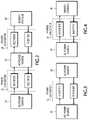
- FIG. 1illustrates an embodiment of an energy converter system according to the inventive principles of this patent disclosure.
- FIG. 2illustrates another embodiment of an energy converter system according to the inventive principles of this patent disclosure.
- FIG. 3illustrates another embodiment of an energy converter system according to the inventive principles of this patent disclosure.
- FIG. 4illustrates another embodiment of an energy converter system according to the inventive principles of this patent disclosure.
- FIG. 5illustrates an embodiment of power combining circuitry with AC power sources in parallel combination according to the inventive principles of this patent disclosure.
- FIG. 6illustrates an embodiment of power combining circuitry with AC power sources in series combination according to the inventive principles of this patent disclosure.
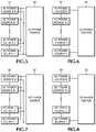
- FIG. 7illustrates an embodiment of power combining circuitry with DC power sources in parallel combination according to the inventive principles of this patent disclosure.
- FIG. 8illustrates an embodiment of power combining circuitry with DC power sources in series combination according to the inventive principles of this patent disclosure.
- FIG. 9illustrates an embodiment of a power converter stack-up with an AC power source according to the inventive principles of this patent disclosure.
- FIG. 10illustrates another embodiment of a power converter stack-up with an AC power source according to the inventive principles of this patent disclosure.
- FIG. 11illustrates another embodiment of a power converter stack-up with an AC power source according to the inventive principles of this patent disclosure.
- FIG. 12illustrates another embodiment of a power converter stack-up with an AC power source according to the inventive principles of this patent disclosure.
- FIG. 13illustrates an embodiment of a power converter stack-up with a DC power source according to the inventive principles of this patent disclosure.
- FIG. 14illustrates another embodiment of a power converter stack-up with a DC power source according to the inventive principles of this patent disclosure.
- FIG. 15illustrates an embodiment of a power converter stack-up with an energy storage device according to the inventive principles of this patent disclosure.
- FIG. 16illustrates another embodiment of a power converter stack-up with an energy storage device according to the inventive principles of this patent disclosure.
- FIG. 17illustrates an embodiment of a power converter stack-up with a power converter and power combiner according to the inventive principles of this patent disclosure.
- FIG. 18illustrates another embodiment of a power converter stack-up with a power converter and power combiner according to the inventive principles of this patent disclosure.
- FIG. 19illustrates an embodiment of a power converter stack-up with two power converters and power combiners according to the inventive principles of this patent disclosure.
- FIG. 20illustrates an embodiment of a power converter stack-up with a DC power source and power combiner according to the inventive principles of this patent disclosure.
- FIG. 21illustrates an embodiment of a power converter stack-up with a power converter and power combiner according to the inventive principles of this patent disclosure.
- FIG. 22illustrates an embodiment of a power converter stack-up with an energy storage device and power combiner according to the inventive principles of this patent disclosure.
- FIG. 23illustrates an embodiment of an inverter system according to the inventive principles of this patent disclosure.
- FIG. 24illustrates a prior art photovoltaic (PV) energy system for delivering solar energy to a utility grid.
- PVphotovoltaic
- FIG. 25illustrates an embodiment of a photovoltaic (PV) energy system according to the inventive principles of this patent disclosure.
- PVphotovoltaic
- FIGS. 26 - 29illustrate embodiments of integrated power converter arrangements according to the inventive principles of this patent disclosure.
- FIG. 30illustrates an embodiment of an integrated power converter according to the inventive principles of this patent disclosure.
- FIG. 31illustrates an embodiment of a transceiver according to the inventive principles of this patent disclosure.
- FIG. 32illustrates an embodiment of an inverter system according to the inventive principles of this patent disclosure.
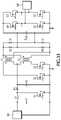
- FIG. 33is a schematic diagram of an embodiment of a main power path suitable for implementing the inverter system of FIG. 32 according to the inventive principles of this patent disclosure.
- FIG. 34illustrates an embodiment of a PV panel according to the inventive principles of this patent disclosure.
- FIG. 35illustrates another embodiment of a PV panel according to the inventive principles of this patent disclosure.
- Such systemsinclude distributed power converters including power inverters and/or power rectifiers.
- Such inverter systemsmay be used in various applications including but not limited to solar energy systems, wind power energy systems, thermal energy systems, various battery systems, fuel cell energy systems, uninterruptible power supplies, hydroelectric energy systems, data center systems, communication infrastructure power supplies, electric and hybrid vehicles, household power, motor, satellite, aerospace, consumer applications, etc.
- FIG. 1illustrates an embodiment of an energy converter system according to the inventive principles of this patent disclosure.
- the system of FIG. 1includes a DC power source section 10 , a first power converter section 12 , an AC power source section 14 , a second power converter section 16 and an energy storage section 18 .
- a DC power sourcemay be in the form of rechargeable or non-rechargeable battery, fuel cell, solar cells at the cell, multi-cell, panel, multi-panel, module, multi-module or grid level, or any other DC power source thereof, and in any combination thereof.
- Solar cellsmay be photovoltaic cells, including monocrystalline, polycrystalline, thin film, etc.
- An AC power sourcemay be in the form of an electric grid, consumer electronics, e.g., uninterruptable power supply (UPS), or any other AC power sources thereof, and in any combination thereof.
- Any AC sources, distribution systems, components, etc.may be single phase and/or multi-phase in any configuration.
- Energy storagemay be in the form of a rechargeable or non-rechargeable battery, capacitor, inductor, other charge storage device and/or element, or any combination thereof.
- An AC power combinermay combine sources in series or parallel combination depending for example on the application of the power converter system.
- An AC power combinermay combine the voltages and/or currents and/or frequency and/or phase of the individual AC sources in any manner, but preferably in a constructive manner and/or at high efficiency.
- AC power combiningmay be single phase and/or multi-phase.
- a DC power combinermay combine sources in series or parallel combination depending for example on the application of the power converter system.
- a DC power combinermay combine the voltages and/or currents of the individual DC sources in any manner, but preferably in a constructive manner and/or at high efficiency.
- the systemmay include one or more power combiners, one or more DC power sources, one or more AC power sources and one or more energy storage devices.
- the energy convertermay convert DC power to AC power and vice versa.
- the energy convertermay include one or more inverters to convert DC power to one or more AC power sources, for example, at high efficiency.
- the energy convertermay also consist of one or more rectifiers to convert AC power to one or more DC power sources and/or for storage on energy storage devices, for example, at high efficiency.
- Each DC power combiner and AC power combinermay combine power in series or parallel combination in any manner, preferably constructively and/or at high efficiency.
- DC power combiningone or more DC power sources and/or energy storage devices may be combined in series and/or parallel combination preferably in a constructive manner.
- AC power combiningone or more AC power sources may be combined in series or parallel combination preferably in a constructive manner.
- AC power combiningmay be single phase and/or multi-phase.
- Energymay be transferred from one or more DC power sources through one or more inverters to generate one or more AC sources when power is available at the DC power source and/or when energy is required at the AC power sources.
- DC power from one or more photovoltaic cellsmay be transferred to one or more AC power grids and/or consumer electronic devices.
- Energymay also be transferred from one or more AC power sources via one or more rectifiers to one or more DC power sources when power is available at the AC power source and/or when energy is required at the DC power sources and/or when energy storage is required.
- power from one or more AC power gridsmay be transferred to one or more batteries and/or capacitors.
- the number of DC power sources that may be combined by one or more DC power combinersmay be any number between 1 and H, where H may be any positive integer.
- the number of DC power combinersmay be any number between 1 and W, where W may be any positive integer.
- the DC power combinermay not be required to be part of the energy converter system depending, for example, on the application preferably when all the DC source has known and/or fixed voltage and/or current characteristic.
- Theremay be one or more rectifiers and/or inverters connected between the DC power sources and the AC power sources to, for example, convert energy from DC-AC and vice versa.
- the number of rectifiersmay be any number between 0 and J, where J may be any positive integer.
- the number of invertersmay be any number between 0 and K, where K may be any positive integer.
- the number of AC power sources that may be combined with an AC power combinermay be any number between 1 and L, where L may be any positive integer.
- the number of AC power combiners between the AC power sources and power converters that are connected to DC power sourcesmay be any number between 1 and X, where X may be any positive integer.
- the number of AC power combiners between the AC power sources and power converters that are connected to energy storage devicesmay be any number between 1 and Y, where Y may be any positive integer.
- the AC power combinersmay not be required to be part of the energy converter system depending, for example, on the application preferably when all the AC sources have known and/or fixed voltage and/or current and/or frequency and/or phase characteristics.
- the number of rectifiersmay be any number between 0 and N, where N may be any positive integer.
- the number of invertersmay be any number between 0 and M, where M may be any positive integer.
- the number of energy storage devices that may be combined with DC power combinersmay be any number between 1 and P, where P may be any positive integer.
- the number of DC power combiners on the energy storage devicesmay be any number between 1 and Z, where Z may be any positive integer.
- the DC power combiners on the energy storage devices sidemay not be required to be part of the energy converter system depending, for example, on the application preferably when all the DC sources have known and/or fixed voltage and/or current characteristics.
- FIG. 2illustrates an embodiment of another energy converter system according to the inventive principles of this patent disclosure.
- the system of FIG. 2includes a DC power source 20 , a first power converter 22 , an AC power source 24 , a second power converter 26 and an energy storage device 28 .
- the energy convertermay convert DC power to AC power and vice versa.
- the energy convertermay include one or more inverters to convert DC power to one or more AC power sources, for example, at high efficiency.
- the energy convertermay also consist of one or more rectifiers to convert AC power to one or more DC power sources and/or for storage on energy storage devices, for example, at high efficiency.
- Energymay be transferred from one or more DC power sources through one or more inverters to generate one or more AC sources when power is available at the DC power sources and/or when energy is required at the AC power sources.
- DC power from one or more photovoltaic cellsmay be transferred to the one or more AC power grids and/or consumer electronic devices.
- Energymay be transferred from one or more AC power sources via one or more rectifiers to one or more DC power sources when power is available at the AC power source and/or when energy is required at the DC power sources and/or when energy storage is required.
- power from one or more AC power gridsmay be transferred to one or more batteries and/or capacitors.
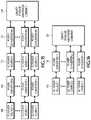
- FIG. 3illustrates an embodiment of another energy converter system according to the inventive principles of this patent disclosure.
- the system of FIG. 3includes a DC power source 30 , a power converter 32 , and an AC power source 34 .
- the energy convertermay convert DC power to AC power and vice versa.
- the energy convertermay consist of one or more inverters to convert DC power to one or more AC power sources, for example, at high efficiency.
- the energy convertermay also consist of one or more rectifiers to convert AC power to one or more DC power sources and/or for storage on energy storage devices, for example, at high efficiency.
- Energymay be transferred from one or more DC power sources through one or more inverters to generate one or more AC sources when power is available at the DC power source and/or when energy is required at the AC power sources.
- DC power from one or more photovoltaic cellsmay be transferred to the one or more AC power grids and/or consumer electronic devices.
- Energymay be transferred from one or more AC power sources via one or more rectifiers to one or more DC power sources when power is available at the AC power source and/or when energy is required at the DC power sources and/or when energy storage is required.
- power from one or more AC power gridsmay be transferred to create one or more DC power supplies for various applications.
- FIG. 4illustrates an embodiment of another energy converter system according to the inventive principles of this patent disclosure.
- the system of FIG. 4includes an AC power source 36 , a power converter 38 and an energy storage device 40 .
- the energy convertermay convert DC power to AC power and vice versa.
- the energy convertermay consist of one or more inverters to convert DC power to one or more AC power sources, for example, at high efficiency.
- the energy convertermay also consist of one or more rectifiers to convert AC power to one or more DC power sources and/or for storage on energy storage devices, for example, at high efficiency.
- Energymay be transferred from one or more energy storage devices through one or more inverters to generate one or more AC sources when power is available at the energy storage devices and/or when energy is required at the AC power sources.
- DC power from one or more batteries or capacitorsmay be transferred to the one or more AC power grids and/or consumer electronic devices.
- Energymay be transferred from one or more AC power sources via one or more rectifiers to one or more DC power sources, when power is available at the AC power source and/or when energy is required at the DC power sources and/or when energy storage is required.
- power from one or more AC power gridsmay be transferred to one or more batteries and/or capacitors.
- FIG. 5illustrates an embodiment of power combining circuitry with AC power sources in parallel combination according to the inventive principles of this patent disclosure.
- the parallel combination of the individual AC power sources 42may be arranged such that the currents of some or all of the individual AC power sources may be combined in any way to provide the combined AC power source 44 , but preferably in a constructive manner.
- the AC power sourcesmay be phase shifted and/or adjusted so that one or some or all of the AC currents add together constructively.
- the number of AC power sources that may be combined in parallel combinationmay be 1 to N, where N is any positive integer.
- FIG. 6illustrates an embodiment of power combining circuitry with AC power sources in series combination according to the inventive principles of this patent disclosure.
- the series combination of the individual AC power sources 46may be arranged such that the voltages of some or all of the individual AC power sources may be combined in any way to provide the combined AC power source 48 , but preferably in a constructive manner.
- the AC power sourcesmay be phase shifted and/or adjusted so that one or more or all of the AC voltages add together constructively.
- the number of AC power sources that may be combined in series combinationmay be 1 to N, where N is any positive integer.
- AC power combiningmay be single phase and/or multi-phase.
- FIG. 7illustrates an embodiment of power combining circuitry with DC power sources in parallel combination according to the inventive principles of this patent disclosure.
- the parallel combination of the individual DC power sources 50may be arranged such that the currents of some or all of the individual DC power sources may be combined in any way to provide the combined DC power source 52 , but preferably in a constructive manner.
- the number of DC power sources that may be combined in parallel combinationmay be 1 to N, where N is any positive integer.
- FIG. 8illustrates an embodiment of power combining circuitry with DC power sources in series combination according to the inventive principles of this patent disclosure.
- the series combination of the individual DC power sources 54may be arranged such that the voltages of some or all of the individual DC power sources may be combined in any way to provide the combined DC power source 56 , but preferably in a constructive manner.
- the number of DC power sources that may be combined in series combinationmay be 1 to N, where N is any positive integer.
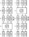
- FIG. 9illustrates an embodiment of a power converter stack-up with an AC power source according to the inventive principles of this patent disclosure.
- the embodiment of FIG. 9includes an AC power source 62 , N DC power sources 58 and M energy storage devices 66 .
- the single AC power sourcemay be connected to one or more DC power sources and/or one or more energy storage devices.
- the single AC power sourcemay include power combining circuitry where AC power may be added, preferably in a constructive manner.
- the power combining circuitrymay provide a parallel and/or series combination where the AC currents at the outputs of one or more or all of the power converters 60 may be added, preferably in a constructive manner.
- the AC voltages of one or more or all AC of the outputs of power converters 64may be added, preferably in a constructive manner.
- AC power combiningmay be single phase and/or multi-phase.
- the number of DC power sources that may be combined in series and/or parallel combinationmay be 1 to N, where N is any positive integer.
- the number of energy storage devices that may be combined in series and/or parallel combinationmay be 1 to M, where M is any positive integer. N may be less than, greater than or equal to M.
- FIG. 10illustrates another embodiment of a power converter stack-up with an AC power source according to the inventive principles of this patent disclosure.
- the embodiment of FIG. 10includes an AC power source 72 , N DC power sources 68 and L energy storage devices 76 .
- the single AC power sourcemay be connected to one or more DC power sources and/or one or more energy storage devices.
- the single AC power sourcemay include power combining circuitry where AC power may be added, preferably in a constructive manner.
- the power combining circuitrymay provide a parallel and/or series combination where the AC currents of one or more or all of the outputs of power converters 70 may be added, preferably in a constructive manner.
- the AC voltages of one or more or all of the outputs of power converters 74may be added, preferably in a constructive manner.
- AC power combiningmay be single phase and/or multi-phase.
- the number of DC power sources that may be combined in series and/or parallel combinationmay be 1 to N, where N is any positive integer.
- the number of power converters on the DC power source sidemay be 1 to M, where M is any positive integer.
- the number of power converter on the energy storage sidemay be 1 to K, where K is any positive integer.
- the number of energy storage devices that may be combined in series and/or parallel combinationmay be 1 to L, where L is any positive integer.
- the number of DC power sourcesmay be less than, greater than or equal to the number of power converters they are connected to.
- the number of energy storage devicesmay be less than, greater than, or equal to the number of power converters they are connected to.
- FIG. 11illustrates another embodiment of a power converter stack-up with an AC power source according to the inventive principles of this patent disclosure.
- the embodiment of FIG. 11includes an AC power source 82 connected to N DC power sources 78 .
- the AC power sourcemay include power combining circuitry where AC power may be added, preferably in a constructive manner.
- the power combining circuitrymay provide a parallel and/or series AC combination where the AC currents of one or more or all of the outputs of power converters 80 may be added, preferably in a constructive manner.
- the number of DC power sources that may be combined in series and/or parallel combinationmay be 1 to N, where N is any positive integer.
- the number of power convertersmay be 1 to M, where M is any positive integer.
- the number of DC power sourcesmay be less than, greater than or equal to the number of power converters they are connected to.
- FIG. 12illustrates another embodiment of a power converter stack-up with an AC power source according to the inventive principles of this patent disclosure.
- the embodiment of FIG. 12includes an AC power source 84 connected to M energy storage devices 88 .
- the single AC power sourcemay include power combining circuitry where AC power may be added, preferably in a constructive manner.
- the power combining circuitrymay provide a parallel and/or series combination where the AC currents of one or more or all AC currents at the outputs of power converters 86 may be added, preferably in a constructive manner.
- the number of power convertersmay be 1 to N, where N is any positive integer.
- the number of energy storage devices that may be combined in series and/or parallel combinationmay be 1 to M, where M is any positive integer.
- the number of energy storage devicesmay be less than, greater than, or equal to the number of power converters they are connected to.
- FIG. 13illustrates an embodiment of a power converter stack-up with a DC power source according to the inventive principles of this patent disclosure.
- the embodiment of FIG. 13includes a DC power source 90 , N+K power converters 92 and 96 , M AC power sources 94 and L energy storage devices 98 .
- the single DC power sourcemay be connected to one or more of the AC power sources and/or one or more energy storage devices via the power converters.
- the single DC power sourcemay include power combining circuitry where DC power may be added, preferably in a constructive manner.
- the power combining circuitrymay provide a parallel and/or series combination where the DC currents of one or more or all of the outputs of power converters 92 may be added, preferably in a constructive manner.
- the number of power converters on the DC power source sidemay be 1 to N, where N is any positive integer.
- the number of AC power sourcesmay be 1 to M, where M is any positive integer.
- the number of power converter on the energy storage sidemay be 1 to K, where K is any positive integer.
- the number of energy storage devices that may be combined in series and/or parallel combinationmay be 1 to L, where L is any positive integer.
- the number of energy storage devices and/or AC power sourcesmay be less than, greater than, or equal to the number of power converters they are connected to.
- FIG. 14illustrates another embodiment of a power converter stack-up with a DC power source according to the inventive principles of this patent disclosure.
- the embodiment of FIG. 14includes a DC power source 100 , N power converters 102 and M AC power sources 104 .
- the single DC power sourcemay be connected to one or more AC power sources via power the converters 102 .
- the single DC power sourcemay include power combining circuitry where DC power may be added, preferably in a constructive manner.
- the power combining circuitrymay provide a parallel and/or series combination where the DC currents of one or more or all outputs of the power converters may be added, preferably in a constructive manner.
- the number of power convertersmay be 1 to N, where N is any positive integer.
- the number of AC power sourcesmay be 1 to M, where M is any positive integer.
- the number of AC power sourcesmay be less than, greater than, or equal to the number of power converters they are connected to.
- FIG. 15illustrates an embodiment of a power converter stack-up with an energy storage device according to the inventive principles of this patent disclosure.
- the embodiment of FIG. 15includes an energy storage device 114 , M+L power converters 108 and 112 , N DC power sources 106 , and K AC power sources 110 .
- the single energy storage devicemay be connected to one or more DC power sources and/or one or more AC power sources via the power converters.
- the single energy storage devicemay include power combining circuitry where DC power may be added, preferably in a constructive manner.
- the power combining circuitrymay provide a parallel and/or series combination where the DC currents of one or more or all of the outputs of the power converters may be added, preferably in a constructive manner.
- the number of DC power sourcesmay be 1 to N, where N is any positive integer.
- the number of power converters on the DC power source sidemay be 1 to M, where M is any positive integer.
- the number of AC power sourcesmay be 1 to K, where K is any positive integer.
- the number of power converters on the energy storage sidemay be 1 to L, where L is any positive integer.
- the number of AC power sources and/or DC power sourcesmay be less than, greater than, or equal to the number of power converters they are connected to.
- FIG. 16illustrates another embodiment of a power converter stack-up with an energy storage device according to the inventive principles of this patent disclosure.
- the embodiment of FIG. 16includes an energy storage device 120 , M power converters 118 , and N AC power sources 116 .
- the single energy storage devicemay be connected to one or more AC power sources via the power converters.
- the single energy storage devicemay include power combining circuitry where DC power may be added, preferably in a constructive manner.
- the power combining circuitrymay provide a parallel and/or series DC combination where the DC currents of one or more or all of the outputs of the power converters may be added, preferably in a constructive manner.
- the number of AC power sourcesmay be 1 to N, where N is any positive integer.
- the number of power convertersmay be 1 to M, where M is any positive integer.
- the number of AC power sourcesmay be less than, greater than, or equal to the number of power converters they are connected to.
- FIG. 17illustrates an embodiment of a power converter stack-up with a power converter and power combiner according to the inventive principles of this patent disclosure.
- the embodiment of FIG. 17includes a power converter and power combiner 124 , energy storage devices 130 , power converters 128 , AC power sources 126 and DC power sources 122 .
- the power converter and combinermay be connected to one or more AC power sources and/or DC power sources and/or energy storage devices.
- the number of DC power sourcesmay be 1 to N, where N may be any positive integer.
- the number of AC power sourcesmay be 1 to M, where M may be any positive integer.
- the number of power convertersmay be 1 to K, where K may be any positive integer.
- the number of energy storage devicesmay be 1 to L, where L is any positive integer.
- FIG. 18illustrates another embodiment of a power converter stack-up with a power converter and power combiner according to the inventive principles of this patent disclosure.
- the embodiment of FIG. 18includes a power converter and power combiner 138 , energy storage devices 140 , power converters 134 , AC power sources 136 and DC power sources 132 .
- the power converter and combinermay be connected to one or more AC power sources and/or DC power sources and/or energy storage devices.
- the number of DC power sourcesmay be 1 to N, where N may be any positive integer.
- the number of power convertersmay be 1 to M, where M may be any positive integer.
- the number of AC power sourcesmay be 1 to K, where K may be any positive integer.
- the number of energy storage devicesmay be 1 to L, where L is any positive integer.
- FIG. 19illustrates an embodiment of a power converter stack-up with two power converters and power combiners according to the inventive principles of this patent disclosure.
- the embodiment of FIG. 19includes DC power sources 142 , a first power converter and power combiner 144 , AC power sources 146 , a second power converter and power combiner 148 , and energy storage devices 150 .
- the DC power sourcesmay be connected to the first power converter and power combiner.
- the AC power sourcesmay be connected between the first and second power converters and power combiners.
- the energy storage devicesmay be connected to the second power converter and power combiner.
- the number of DC power sourcesmay be 1 to N, where N may be any positive integer.
- the number of AC power sourcesmay be 1 to M, where M may be any positive integer.
- the number of energy storage devicesmay be 1 to K, where K is any positive integer.
- FIG. 20illustrates an embodiment of a power converter stack-up with a DC power source and power combiner according to the inventive principles of this patent disclosure.
- the embodiment of FIG. 20includes a DC power source and power combiner 152 which may be connected to energy storage devices 156 through power converters 154 .
- the number of power convertersmay be 1 to M, where M may be any positive integer.
- the number of energy storage devicesmay be 1 to K, where K is any positive integer.
- FIG. 21illustrates an embodiment of a power converter stack-up with a power converter and power combiner according to the inventive principles of this patent disclosure.
- the embodiment of FIG. 21includes a power converter and power combiner 160 , DC power sources 158 , and energy storage devices 162 .
- the number of DC power sourcesmay be 1 to N, where N may be any positive integer.
- the number of energy storage devicesmay be 1 to K, where K is any positive integer.
- FIG. 22illustrates an embodiment of a power converter stack-up with an energy storage device and power combiner according to the inventive principles of this patent disclosure.
- the embodiment of FIG. 22includes an energy storage device and power combiner 168 which may be connected to DC power sources 164 through power converters 166 .
- the number of DC power sourcesmay be 1 to N, where N may be any positive integer.
- the number of power convertersmay be 1 to M, where M is any positive integer.
- FIG. 23illustrates an embodiment of an inverter system according to the inventive principles of this patent disclosure.
- the system of FIG. 23may be designed to convert DC power from any type of DC power source 170 to AC power.
- the AC power invertermay be single phase and/or multi-phase.
- DSPsdigital signal processors
- ADCsanalog-to-digital converters
- DACsdigital-to-analog converters
- the power control block 172may control the power that flows through the inverter circuits. For example, it may be designed to maximize the power conversion efficiency of the inverter. It may also be include maximum power point tracking (MPPT) to assure the inverter is operating at the maximum power available from the DC power source.
- MPPTmaximum power point tracking
- the power control blockmay also be designed to control power in the inverter in response to changes in the environment, for example, variations in temperature, and/or pressure, and/or humidity, and/or light illumination, and/or availability of input DC power.
- the power control blockmay also be designed to accommodate other operational factors, for example; variations in integration process whether inter-process, intra-process and/or voltage supply.
- the power converter 174may convert one or more DC input voltages and/or currents to one or more DC output voltages and/or currents, preferably at high power conversion efficiency.
- the power convertermay be designed to step-up (i.e. boost) the input DC voltage to a higher output DC voltage and/or step-down (i.e. buck) the input DC voltage to a lower output DC voltage depending on, for example, the specific application the inverter system is intended for.
- the power converter circuitmay also be designed to provide both step-up and step-down (i.e. buck-boost/boost-buck) operation and/or to generate multiple output DC voltages from a single input (e.g. as in a fly-back converter).
- the input voltages to, and output voltages from, the power convertermay be a positive or negative signals.
- the output voltagesmay be of the same polarity different polarity relative to the input voltages depending, for example, on the specific application that the inverter system is intended for.
- the DC power converter circuitmay be in the form of a linear and/or a switching regulator. Pulse width modulated signals may be used to control one or more output voltages of the DC power conversion, for example, in switching voltage regulators.
- the power circuits and/or drivers block (power driver circuit) 176may convert one or more DC voltages and/or currents to one or more AC voltages and/or currents preferably at high power conversion efficiency and/or low total harmonic distortion (THD).
- Passive or active filtersmay be included within the power driver circuit, for example, to reduce harmonic distortion in the DC-AC power conversion.
- Power switchesmay also be implemented within the power driver circuit, for example, to drive high power AC devices and/or to withstand high output voltages.
- the protection circuit 198may be included to protect the inverter system and/or protect any or all circuitry connected to the inverter system.
- the protect circuitrymay limit the voltage, and/or current, and/or temperature of the circuitry it protects from exceeding a certain range, for example, to protect it from damage.
- the protection circuitrymay have over-voltage protection capability and/or under-voltage protection capability to limit the voltage range of the inverter system and/or the circuitry it is protecting.
- the protection circuitrymay also have over-current and/or under-current protection capability to limit the current range of the inverter system and/or the circuitry it is protecting.
- the protection circuitrymay also have over-temperature and/or under-temperature protection capability to limit the current range of the inverter system and/or the circuitry it is protecting.
- the filter block 178may include active and/or passive circuitry.
- the filtermay be designed to reduce the total harmonic distortion (THD) in the inverter system.
- TDDtotal harmonic distortion
- the filtermay be low pass, high pass, band pass and/or band reject depending, for example, on the intended purpose of the filter.
- the filtermay be designed with only passive elements, for example, resistors and/or capacitors and/or inductors, or the filter may include active components, for example, operational amplifiers (op amps).
- Analog control block 180may be included to provide analog control of the power converter and/or driver circuitry, preferably to improve power conversion efficiency.
- the analog controlmay be designed as a feed back loop to the DC-DC power converter and/or DC-AC power driver circuitry, for example, to dynamically control and maximize the power conversion efficiency of these circuit blocks.
- Sensing circuitry 184may be included to sense voltages and/or currents at any location in the inverter system.
- the sensing circuitmay be designed to sense one or more DC voltages and/or currents at, for example, the DC power source and/or at the output of the DC power converter.
- the sensing circuitmay also be designed to sense one or more AC voltages and/or currents at, for example, the AC power source and/or at the output of the DC-AC power converter and/or power driver circuit.
- Energy Storage Device 194may be in the form of rechargeable or non-rechargeable battery, inductor, capacitor, other charge storage device and/or element, or any combination thereof.
- Analog/Digital converter (ADC) 186may be designed to convert one or more analog signals of any form to digital signals.
- the digital signal to the DSPmay be sampled with Nyquist sample, oversampling or any other sampling methods, or any combination thereof.
- Digital/Analog Converter (DAC) 188may be designed to convert digital signals to analog signals of any form.
- the digital signal to the DSPmay be sampled with Nyquist sampling, oversampling or any other sampling methods, or any combination thereof.
- Digital signal processor (DSP) 182may be designed and/or optimized, for example, for low power operation and/or for high speed operation.
- the DSP coremay include an internal analog/digital converter to convert analog signal of any form to digital signals.
- the DSP coremay be, in the form of application specific integrated circuit (ASIC) and/or field programmable gate arrays depending, for example, on the specific application the inverter system is intended for.
- ASICapplication specific integrated circuit
- the digital signal processormay be designed to process digital signals, for example, in the time domain, and/or frequency domain, and/or spatial domain, and/or wavelet domain and/or autocorrelation domain.
- the DSP blockmay consist of random access memory (RAM) that may be read/write or read only memory (ROM) that may be preprogrammed or electrically erasable (i.e. EEPROM).
- RAMrandom access memory
- ROMread only memory
- EEPROMelectrically erasable
- the type of ROM and/or RAM usemay be of any type including flash and/or non-volatile memory.
- the digital signal to the DSPmay be sampled with Nyquist sampling, oversampling or any other sampling methods, or any combination thereof.
- the DSPmay be designed to include one or more digital filters, for example, finite impulse response (FIR) filters and/or infinite impulse response (IIR) filters.
- FIRfinite impulse response
- IIRinfinite impulse response
- the DSP coremay be designed to implement maximum power point tracking (MPPT) for the inverter to, for example, assure the inverter is operating at and/or close to the maximum power.
- Pulse width modulation (PWM) of signalsmay be implemented with the DSP core to, for example, implement the control circuitry for the DC-DC power converter.
- the DSPmay be programmed to act as an active filter for reducing harmonic distortion, for example, in the power converter from DC-AC.
- the DSPmay be programmed to control switching of circuitry within the inverter system, for example, the DC-AC power conversion circuit.
- the DSPmay also be programmed to add intelligence to the power control circuit, for example, to find the maximum power point and/or bypassing of damaged or inefficient DC power sources as part of the inverter system.
- Multiplexer 190may be designed to choose between different digital and/or analog input sources.
- the multiplexer circuitrymay be designed to select between the different sensing circuitry (for example) voltage and/or current sensing and/or any other digital and/or analog signal.
- Transceiver 192may be design to communicate through circuitry outside of the inverter for example, through the power line and or wireless links.
- the transceivermay include a line interface circuit to, for example, interface the power grid to the transceiver.
- the transceivermay include one or more low noise amplifiers (LNA) to, for example, amplify the receive signal with low noise figure and/or high gain.
- LNAlow noise amplifiers
- the transceivermay include automatic gain control (AGC), for example, to automatically control the gain of the receiver.
- the transceivermay include driver circuits, for example, to drive the transmitted signals at high gain and/or efficiency.
- the transceivermay include a buffer circuit, for example, to amplify the signal to the driver circuitry.
- the transceivermay include on or more filters, for example, to filter unwanted frequency contents, i.e. high frequency noise.
- the transceivermay include its own ADC and DAC, for example, to convert analog
- Power management block 196may be designed to supply a stable DC power source to the inverter system.
- Power managementmay include one or more switches or circuitry which controls, monitors and/or analyzes (i) the power conversion operation of the inverter system and/or components thereof (for example, the DC-DC and/or DC-AC power conversion circuitry) (ii) the operating characteristics of the inverter and/or components thereof, (iii) the characteristics of the output power of the inverter system (for example, current, voltage and temporal characteristics thereof), (iv) the storage operation of one or more of the charge storage or other energy storage devices and/or charge or energy supplied thereto (via, for example, the inverter system), and/or (v) the characteristics of the output power of one or more of the charge storage or other energy storage devices (for example, current, voltage and temporal characteristics thereof).
- power controlmay be included when maximum power point tracking (MPPT) is included as part of the system, but may be excluded, for example, when the power coming from the DC power source is fixed and/or when the AC load may be modulated to operate at the peak output power.
- MPPTmaximum power point tracking
- DC power conversionmay not be included as part of the inverter when DC voltage and/or current is sufficient for direct conversion to AC voltage and/or current.
- Filtersmay not be included as part of the inverter system when, for example, the total harmonic distortion of the inverter system does not need to be suppressed and/or when the number of external components may be minimized to reduce system cost.
- the analog control blockmay not be included, for example, when feedback from the analog control is not required and/or when the DC-DC and DC-AC power converters does not need to be dynamically controlled and/or when power conversion efficiency of these circuit blocks does not need to be maximized.
- the digital signal processormay not be included as part of the inverter system when, for example, digital processing is not required by the inverter system and/or when the inverter system requirements are simple to reduce cost and/or when the operation required of the DSP can be reproduced with other internal and/or external circuitry.
- the sensing circuitrymay not be included as part of the inverter system when, for example, no DC and/or AC is needed for maximum power point tracking and/or monitoring of the AC load is not needed.
- the multiplexer circuitrymay not be included as part of the inverter system when, for example, when multiplexing of analog and/or digital signals is not required.
- the transceiver circuitrymay not be included when, for example, data transmission of any kind is not needed.
- An energy storage devicemay not be included as part of the inverter system when, for example, energy storage of any kind is not needed.
- the power management featuremay not be included when, for example, power management and/or power control and/or power conditioning of any kind is not needed.
- Protection circuitrymay not be included as part of the inverter system when, for example, the inverter system has externally connected protection circuitry and/or the voltages and/or current and/or temperature of the protection circuit may be externally controlled.
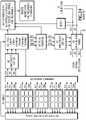
- FIG. 25illustrates an embodiment of a photovoltaic (PV) energy system according to the inventive principles of this patent disclosure.
- the system of FIG. 25may include a PV array of one or more solar cells 202 and/or solar panels 202 and/or modules and/or solar grids, one or more integrated power converters 206 , one or more remote monitoring and/or recording computers 208 , one or more AC distribution panels 210 , one or more power line data interfaces 212 , one or more meters 214 and/or AC wiring.
- PVphotovoltaic
- the photovoltaic power conversionmay be performed at the cell, and/or multi-cell, and/or panel, and/or multi-panel, and/or module, and/or multi-module, and/or grid level.
- an integrated power convertermay be fabricated entirely on a single integrated circuit (IC) (or “chip”), including all passive components. In other embodiments, it may be preferable to have the largest passive components such as inductors, transformers and capacitors located off the IC. In some other embodiments, the integrated power converter may be fabricated on multiple ICs, for example in a multi-chip module (MCM), in which case various key active or passive components may be located on the same chip or chips as the remainder of the semiconductor devices and/or on a separate chip or chips and/or off-chip, for example, on a common substrate within the package or packages or outside the package or packages.
- MCMmulti-chip module
- An integrated power convertermay be designed to, for example, reduce the cost of the solar energy conversion system and/or improve the power conversion efficiency and/or improve system reliability and/or improve diagnostics and maintenance. By integrating one or more functions of an inverter system on an integrated circuit, an integrated power converter may be able to implement these functions at more relaxed specifications.
- Remote monitoring/recording Computer 208may record power output of the solar energy conversion system at, for example, the cell level. It may be designed to, for example, monitor shading effects of the individual solar cell and or monitor which solar cell and/or group of solar cells are not operating and/or inefficiently operating.
- AC distribution panel 210may be designed to divide the main electrical lines and/or source into various electrical circuits.
- the AC distribution panelmay consist of one or more fuses and/or one or more circuit breakers and/or one or more main switches.
- Power line data interface 212may be designed to communicate across the power line to the remote monitoring/recording computer.
- the power line data interfacemay consist of a wireless link to communicate with the remote monitoring/recording computer.
- the power line data interfacemay also be designed to receive critical data.
- the system of FIG. 25may reduce the cost of a solar energy system, for example, by reducing the number of external components and/or number of magnetic components.
- An integrated power converter implementationmay be designed to, for example, reduce or eliminate DC wiring and/or cabling issues, and/or reduce or eliminate cable trays or conduits, and/or reduce or eliminate DC fuses and/or connectors. With reduced or no DC wiring, no DC surge protection and/or junction box and/or ground fault detection and/or protection devices may be required. With no DC wires, DC training and/or certifications are not required for the installation of such a system.
- the power driving capacity and voltage across each individual integrated power convertermay be reduced. Reducing the power driving and voltage driving specifications of the integrated power converter may reduce the cost of the individual integrated power converters. Fewer or no blocking diodes may be required at lower power drive and/or less or no integration of bypass diodes are required. At lower voltages across the integrated power converter, the integrated power converter may be designed in standard high-voltage CMOS processes and may be designed to increase power conversion efficiency of the solar energy system.
- Integration of one or more inverter functions in a high voltage CMOS process and/or at lower powermay reduce noise in the system and/or improve electromagnetic interference and/or may improve localized maximum power point tracking (MPPT).
- MPPTlocalized maximum power point tracking
- the inverter integrated on a chipthe assembly process of the solar energy system may be made very simple to reduce the assembly cost associated with the system.
- the individual invertermay be designed and packaged such that it is easily integrated into the solar energy system assembly.
- the packaging of a solar energy system at the panel and/or module levelmay be implemented so that additional panels and/or modules may be easily added or removed.
- the integrated power converter implementationmay be designed for adaptive islanding where power in the whole array is not lost and/or for improved reliability and/or better grid reliability and/or component reliability due to lower voltage and power scaling. It may also be designed to automatically resolve cross circulatory current with natural load distribution and/or with active harmonic control and/or for easy implementation of advanced control algorithms.
- a distributed inverter systemmay be designed such that it is optimized for lower system cost, and/or higher system performance, and/or improved reliability, and/or ease of integration, and/or diagnostics and maintenance. Diagnostics and/or maintenance may be improved by, for example, reducing ground fault detection and/or eliminating the need for inverter shelter and/or adding the ability to detect faulty circuitry remotely and/or automatically detect faulty and/or dead inverters.
- a distributed inverter method according to the inventive principles of this patent disclosuremay be optimized for lower system cost, for example, by reducing or eliminating altogether the number of external and/or custom off the shelf components, and/or high cost components (for example transformers) and/or DC wiring and/or DC cable trays and/or conduits and/or fuses and/or over current protection circuitry and/or required holders and/or DC connectors, and/or DC surge protection circuitry, and/or junction boxes, and/or blocking diodes, and/or heavy duty electronics (e.g. transformers).
- high cost componentsfor example transformers
- the distributed inverter methods according to the inventive principles of this patent disclosuremay be optimized for higher energy output and/or increased energy extraction and/or increased power conversion efficiency, for example, by limiting or eliminated the losses due to shadowing in photovoltaic systems.
- Methods of increasing energy extraction and/or increased power conversion efficiencymay include but are not limited to implementation of localized maximum power point tracking of individual input DC sources.
- FIGS. 26 - 29illustrate embodiments of integrated power converter arrangements according to the inventive principles of this patent disclosure.
- An integrated power convertermay be installed at the cell, and/or multi-cell, and/or panel, and/or multi-panel, and/or module, and/or multi-module, and/or grid level.
- the number of cells for each subsetmay be two or more, however, there may be additional benefits where the number of cells per subset is a multiple of 2, 4, 6, 8, 9 or 12.
- each panel levelthere may be one integrated power converter 224 at each panel 226 as shown in FIG. 28 .
- the multi-panel levelthere may be one or more integrated power converters for each subset of panel.
- the number of panels in the subsetmay be two or more.
- the module levelthere may be one or more integrated power converters for every module.
- the multi-module levelthere may be one or more integrated power converters for each subset of module.
- the number of modules in a subsetmay be two or more.
- the number of integrated power convertersmay be one or more for every grid.
- the integrated power convertersmay be placed so that they may, for example, reduce the amount of AC wiring. There may be one or more integrated power converters for every single panel.
- the integrated power convertersmay be located close together, for example, for ease of integration or they may be located further apart, for example, each at a particular solar cell.
- multiple invertersmay be located in a single housing, in multiple housings, in no housing, etc.
- a housingmay be a separate component, while in other embodiments, a housing may be part of some other system component.
- the multiple integrated power converters 228may be located in a common housing attached directly to the panel 230 , or located separately from the panel, e.g., on a rack that holds the panel.
- the integrated power convertersmay be located in separate housings, or smaller groups of the integrated power converters may be located in multiple housings, either mounted directly to the panel, and/or separately from the panel, etc.
- or more of the integrated power convertersmay be housed in some other system component such as an encapsulant on a panel.
- FIG. 30illustrates an embodiment of an integrated power converter according to the inventive principles of this patent disclosure. Though shown in the context of a photovoltaic system, the embodiment of FIG. 30 may be utilized with any other type of DC power source.
- the system of FIG. 30may include some or all of the following components: a controller 232 , shadow bypass control 234 , power conditioning converter 236 , power circuitry and driver 238 , passive filter 240 , analog control loop 242 , transceiver circuit 244 , energy storage conditioning 246 , power conditioning 248 , power switches 250 , voltage reference circuit 252 , startup circuit 254 , multiplexers 256 , sensing circuitry 258 , ADC 260 , clock generation circuit 262 , external crystal oscillator 264 , and/or energy storage device 266 .
- a controller 232shadow bypass control 234 , power conditioning converter 236 , power circuitry and driver 238 , passive filter 240 , analog control loop 242 , transceiver circuit 244 , energy storage conditioning 246 , power conditioning 248 , power switches 250 , voltage reference circuit 252 , startup circuit 254 , multiplexers 256 , sensing circuitry 258 , ADC 260 , clock generation circuit 26
- the controller 232may include any type of logic including a digital signal processor (DSP), microcontroller, etc., and may be designed and/or optimized, for example, for low power operation and/or for high speed operation.
- the controllermay implement any or all of the following functionality: maximum power point tracking, active filtering, HD control, power factor control, waveform generation, optimization, switch control, configuration management, shutdown control, startup control, and/or shadow bypass control.
- the DSP coremay include internal analog/digital converters to convert analog signal of any forms to digital signals.
- the DSP coremay be in the form of application specific integrated circuit (ASIC) and/or field programmable gate arrays depending, for example, on the specific application the inverter system is intended for.
- Digital signal processingmay be included to process digital signals, for example, in the time domain, and/or frequency domain, and/or spatial domain, and/or wavelet domain and/or autocorrelation domain.
- the digital signals to the DSPmay be sampled with Nyquist sampling, oversampling or any other sampling methods, or any combination thereof.
- the DSPmay be designed to include digital filtering, for example, finite impulse response (FIR) filters and/or infinite impulse response (IIR) filters.
- FIRfinite impulse response
- IIRinfinite impulse response
- the DSP coremay be designed to implement maximum power point tracking (MPPT) for the inverter to, for example, assure the inverter is operating at and/or close to the maximum power.
- Pulse width modulation (PWM) of signalsmay be implemented with the DSP core to, for example, implement the control circuitry for a DC-DC power converter.
- the DSPmay be programmed to act as an active filter for reducing harmonic distortion, for example, in the power converter from DC-AC.
- the DSPmay be programmed to control switching of circuitry within the inverter system, for example, the DC-AC power conversion circuit.
- the DSPmay also be programmed to add intelligence to the power control circuit, for example, to find the maximum power point and/or bypassing of damaged or inefficient DC power sources as part of the inverter system.
- controllermay include HD control, PF control, waveform generation, optimization, configuration management, shutdowns, etc.
- Shadow bypass control 234may be designed to control the power that flows through the solar energy inverter circuits, for example, when power is available from the photovoltaic cells that the block is connected to.
- the shadow bypass control circuitrymay also be designed so that one or more or all photovoltaic cells connect to it may be disabled, for example, when the light illumination on the photovoltaic cell or cells is low.
- the shadow bypass control circuitrymay be design for the bypassing of damaged or inefficient photovoltaic cells as part of a solar energy inverter system.
- the shadow bypass control blockmay be designed such that the power conversion efficiency of the inverter may be maximized.
- Maximum power point trackingmay be designed as part of the shadow bypass control to, for example, assure the inverter is operating at maximum power.
- the shadow bypass controlmay also be designed to control power in the inverter in response to changes in the environment, for example, variations in temperature, and/or pressure, and/or humidity, and/or light illumination, and/or availability of input DC power.
- the shadow bypass control circuitrymay be designed to account for other factors, for example, variations in the integration process whether inter-process or intra-process and/or voltage supply.
- Power conditioning converter 236may be designed to convert a DC voltage to one or more DC voltages preferably at high power conversion efficiency.
- the power conditioning convertermay be designed to step-up (i.e. boost) the input DC voltage to a higher output DC voltage and/or the power converter may be designed to step-down (i.e. buck) the input DC voltage to a lower output DC voltage depending on, for example, the specific application the inverter system is intended for.
- the power conditioning converter circuitmay also be design to operate for both step-up and step-down (i.e. buck-boost/boost-buck) and/or designed to generate multiple output DC voltages from a single input (e.g., as in a fly-back converter).
- the input DC voltages and output DC voltages to the power convertermay be a positive or negative signals.
- the output DC voltagesmay be of the same or different polarities relative to the input DC voltages depending, for example, on the specific application that the inverter system is intended for.
- the DC power conditioning converter circuitmay be in the form of a linear and/or switching regulator. Pulse width modulated signals may be used to control one or more output voltages of the DC power conversion, for example, in switching voltage regulators.
- Power circuitry and driver 238may be designed to convert one or more DC voltages to one or more AC voltages, preferably at high power conversion efficiency.
- the power driver circuitmay be designed to generate an AC signal, preferably for example, at high power conversion efficiency and/or at low total harmonic distortion (THD).
- Passive or active filtersmay be designed within the power driver circuit, for example, to reduce harmonic distortion in the DC-AC power conversion.
- Power switchesmay also be implemented within the power driver circuit, for example, to drive high power AC devices and/or to withstand high output voltages.
- Filter(s) 240may be designed to be active or passive.
- the filtermay be designed to reduce the total harmonic distortion (THD) in the inverter system.
- TDDtotal harmonic distortion
- the filtermay be low pass, high pass, band pass or band reject depending, for example, on the intended purpose of the filter.
- the filtermay be designed with only passive elements, for example, resistors and/or capacitors and/or inductors, or the filter may include active components, for example, operational amplifiers.
- Analog control loop 242may be designed to control the power circuit and driver circuitry. It may be designed to provide analog control of the power converter and/or driver circuitry, preferably to improve power conversion efficiency of the inverter system.
- the analog control loopmay be design as a feed back loop to the DC-DC power converter and/or DC-AC driver circuitry, for example, to dynamically control and maximize the power conversion efficiency of these circuit blocks.
- the control loopmay be implemented in digital or mixed-signal form separate from, or integral with, the controller 232 .
- Transceiver circuit 244may be designed to, for example, communicate with the monitoring unit via the power line.
- the transceivermay be designed to, for example, operate at high frequency and low power.
- the transceivermay be design to communicate through circuitry outside of the inverter for example, through the power line and/or wireless links.
- the transceivermay include a line interface circuit to, for example interface the power grid to the transceiver.
- the transceivermay include one or more low noise amplifiers (LNA) to, for example, amplify the receive signal with low noise figure and/or high gain.
- LNAlow noise amplifiers
- the transceivermay include automatic gain control (AGC), for example, to automatically control the gain of the receiver.
- AGCautomatic gain control
- the transceivermay include driver circuits, for example, to drive the transmitted signals at high gain and/or efficiency.
- the transceivermay include a buffer circuit, for example, to amplify the signal to the driver circuitry.
- the transceivermay include on or more filters, for example, to filter unwanted frequency contents, i.e. high frequency noise.
- the transceivermay include its own ADC and DAC, for example, to convert analog signals to digital signals and vice versa.
- Energy storage conditioning 246may be designed to enable the system to store energy in the energy storage device.
- Power conditioning 248may include functionality which controls, monitors and/or analyzes (i) the power conversion operation of the inverter system and/or components thereof (for example, the DC-DC and/or DC-AC power conversion circuitry) (ii) the operating characteristics of the inverter and/or components thereof, (iii) the characteristics of the output power of the inverter system (for example, current, voltage and temporal characteristics thereof), (iv) the storage operation of one or more of the energy storage devices and/or energy supplied thereto (via, for example, the inverter system), and/or (v) the characteristics of the output power of one or more of the energy storage devices (for example, current, voltage and temporal characteristics thereof).
- Power switch block 250may include one or more power switches to transfer power from the solar cells to the power grid.
- Voltage reference circuit 252may be designed to control the voltage that is delivered to the power grid and/or the power condition circuit.
- Startup circuit 254may be designed to start up the integrated power converter as there is enough solar energy or other energy to power up the system.
- Multiplexer 256may be designed to choose between different digital or analog input sources.
- the multiplexer circuitrymay be designed to select between the different sensing circuitry (for example) voltage and/or current sensing and/or any other digital and/or analog signal.
- Sensing circuitry 258 A-Fmay be designed to sense voltages and/or currents in the inverter system.
- the sensing circuitmay be designed to sense one or more DC voltages and/or currents at, for example, the DC power source and/or at the output of the DC power converter.
- the sensing circuitmay also be designed to sense one or more AC voltages and/or currents at, for example, the AC power source and/or at the output of the DC-AC power converter and/or power driver circuit.
- Clock generation circuit 262may be designed to generate one or more clocks for the integrated power converter, particularly for the transceiver circuit.
- Crystal Oscillator 264may include an internal or external crystal oscillator to generate the input clock to the clock generation circuitry.
- Energy storage block 266may include one or more energy storage devices which may be designed to store energy from the inverter system. It may be in the form of rechargeable or non-rechargeable battery, capacitor, other charge storage device and/or element, and/or inductor, or any combination thereof.
- Analog/Digital converter (ADC) 260may be designed to convert analog signals of any form to digital signals.
- the digital signals to the DSPmay be sampled with Nyquist sampling, oversampling, or any other sampling methods, or any combination thereof.
- a ground fault interruption (GFI) circuitmay be included to provide protection by detecting and/or shutting down the system in response to ground fault conditions, communicating with a remote monitoring station, and/or taking other appropriate actions.
- GFIground fault interruption
- FIG. 31illustrates an embodiment of a transceiver according to the inventive principles of this patent disclosure.
- the system of FIG. 31may include some or all of the following: a line interface circuit 268 , low noise amplifier 270 , automatic gain control 272 , driver circuit 274 , buffer circuit 276 , one or more filters 278 , ADC 280 , DAC 282 , Pre-MAC 284 , I/ 0 MUX 286 , and/or an interface circuit 288 for a processor.
- Line interface circuit 268may be designed to interface the power grid to the transceiver.
- Low noise amplifier (LNA) 270may be designed to operate with, for example, low noise figure and/or high gain.
- Automatic gain control (AGC) 272may be designed to automatically control the gain of the receiver.
- Driver circuit 274may be designed to drive the transmitted signal to the power grid at, for example, high gain and/or efficiency.
- Buffer circuit 276may be designed to pre-amplify the signal going to the driver circuitry.
- Filter(s) 278 A and Bmay be designed to filter out unwanted frequency contents, for example, high frequency noise.
- Analog/digital converter 280may be designed to operate at high, moderate, or low resolution at high, moderate or low speed. It may be designed, for example to dissipate low power.
- Digital/analog converter 282may be designed to operate at high, moderate, or low resolution at high, moderate or low speed. It may be designed, for example to dissipate low power.
- Pre-MAC and I/O Mux 284may choose between receive mode and/or transmit mode and/or idle mode.
- Interface circuit 288may interface the transceiver to any and all types of processors. The interface may be serial or parallel or a combination of the two.
- FIG. 32illustrates an embodiment of an inverter system according to the inventive principles of this patent disclosure.
- DC poweris applied to the system at terminals 292 and 294 .
- the embodiment of FIG. 32is shown in the context of a solar panel 290 , but it may be utilized with other DC power sources such as fuel cells, batteries, capacitors, etc.
- the main power pathcontinues through a collection of components that form a DC-DC converter 306 .
- the DC-DC convertertransforms the DC power from relatively low voltage and high current, which is characteristic of PV panels having crystalline cells and some other DC power sources, to relatively higher voltage and lower current suitable for conversion to AC power in a form that can be easily distributed to a local user and/or transmitted to remote users through a power grid, etc.
- the DC powermay be generated at higher voltages, thereby eliminating or reducing the need or usefulness of voltage boosting, pre-regulation, etc.
- the DC-DC converteris shown with two stages: a boost-type pre-regulator and a push-pull type main stage. In other embodiments, however, the DC-DC converter may be implemented with any suitable arrangement of single or multiple stages.
- a zero-ripple input filter 296for example a passive filter, may be utilized to reduce high frequency (HF) ripple for improved efficiency.
- HFhigh frequency
- the benefit of the zero ripple filtermay not be worth the additional cost.
- Pre-regulator 298may enable the system to operate from a wider range of input voltages to accommodate PV panels from different manufacturers.
- the pre-regulatormay also facilitate the implementation of an advanced control loop to reduce input ripple as discussed below.
- the pre-regulatormay be implemented, for example, as a high-frequency (HF) boost stage with soft switching for high efficiency and compact size. In this example, the pre-regulator provides a modest amount of initial voltage boost to feed the next stage.
- HFhigh-frequency
- other pre-regulator stagessuch as buck converters, buck-boost converters, push-pull converters, etc., may be used as a pre-regulator stage.
- Push-pull stage 300provides the majority of the voltage boost in conjunction with a transformer 302 and rectifier 304 .
- the use of a push-pull stagemay facilitate the implementation of the entire system with a single integrated circuit since the drivers for both power switches may be referenced to the same common voltage.
- the output from the rectifier stage 304is applied to a DC link capacitor C DC which provides a high voltage DC bus to feed the DC-AC inverter stage 312 .
- the inverter stage 312includes a high voltage output bridge 308 which, in this embodiment, is implemented as a simple H-bridge to provide single-phase AC power, but multi-phase embodiments may also be implemented.
- a passive output filter 310smoothes the waveform of the AC output before it is applied to a load or grid at the neutral and line output terminals L and N.
- a first (input) PWM controller 314controls the pre-regulator 296 in response to various sense inputs.
- voltage sensors 316 and 320 and current sensor 318provide a measure of the overall input voltage and current and the output voltage of the pre-regulator, respectively.
- the first PWM controllermay operate in response to fewer or more sense inputs. For example, any of these sense inputs may be omitted and/or other sense inputs may be included, e.g., the voltage on DC link capacitor C DC , or currents measured at any other points along the power path.
- the first PWM controller 314implements an inner control loop (shown conceptually by arrow 315 ) by controlling the pre-regulator 296 to maintain a constant voltage at the input terminals 292 and 294 .
- Thismay reduce or eliminate input ripple, thereby reducing the size of capacitor C 1 and eliminating the zero ripple filter.
- the inner control loopmay transfer the energy storage function from the input capacitor C 1 to the DC link capacitor C DC .
- This energy storageis used for cycle-by-cycle power balance at the AC output frequency. That is, power is preferably drawn from the DC source at a constant rate, whereas the instantaneous AC power output fluctuates between zero and some maximum value at twice the AC line frequency.
- a decoupling capacitoris used to store energy during troughs (or “valleys”) in the AC line cycle, and release energy during peaks in the AC line cycle. This is typically accomplished through the use of a large electrolytic capacitor for C 1 .
- the inner control loopmoves this energy storage to the DC link capacitor C DC where energy is stored and discharged in the form of large voltage fluctuations on the capacitor. This is in contrast to conventional systems in which the DC link voltage is regulated to a constant value.
- Regulating a constant DC input voltagemay provide several advantages. First, reducing ripple in the input waveform improves the efficiency of some DC power sources such as PV panels which suffer from resistive losses related to the ripple. Second, moving the energy storage to the DC link capacitor may eliminate the need for an input electrolytic capacitor which is an expensive, bulky and unreliable component with a short lifespan. Instead, the energy may be stored in a higher voltage form on the DC link capacitor which is less expensive, more reliable, has a longer lifespan and may take up less space. Moreover, the size of the DC link capacitor itself may also be reduced.
- a maximum power point tracking (MPPT) circuit 344forms an outer control loop to maintain the average input voltage and current, sensed by voltage and current sensors 316 and 318 , respectively, at the optimum points to maximize the output power available from the DC power source, which in this example, is a PV panel.
- MPPTmaximum power point tracking
- a second (push-pull) PWM controller 324controls the push-pull stage in response to the DC link voltage sensed by voltage sensor 326 .
- a DC-link voltage controller 322provides a feedback signal which is compared to a reference signal REF and applied to the second PWM controller 324 .
- the DC-link voltage controller 322may operate in different modes. In one mode, it may simply convey the instantaneous DC-link voltage to the PWM circuit, thereby causing the DC-link voltage to be regulated to a constant value.
- the DC-link voltage controller 322may filter out the AC ripple so that the second PWM loop only regulates the long-term DC value (e.g., the RMS value) of the DC-link voltage. That is, the AC ripple on the DC-link capacitor rides on a DC pedestal that slides up or down in response to the DC-link voltage controller. This may be useful, for example, to control distortion in the AC output power as discussed below.
- the long-term DC valuee.g., the RMS value
- a third (output) PWM controller 330controls the four switches in the H-bridge 308 to provide a sinusoidal AC output waveform.
- a non-DQ, non-cordic polar form digital phase locked loop (DPLL) 332helps synchronize the output PWM to the AC power line.
- the overall AC outputis monitored and controlled by a grid current control loop 336 which adjusts the third PWM controller 330 in response to outputs from the MPPT circuit, the DC-link voltage controller, the DPLL, and the output voltage and/or current.
- a harmonic distortion mitigation circuit 338further adjusts the output PWM through a summing circuit 334 to eliminate or reduce distortion in response to the output voltage and current waveforms sensed by voltage and current sensors 340 and 342 , respectively.
- An output signal from the harmonic distortion mitigation circuit 338may also be applied to the DC-link voltage controller for optimization of the DC-link voltage. In general, it may be preferable to minimize the DC-link voltage to increase overall efficiency. However, if the troughs of the voltage excursions on the DC-link capacitor fall too low, it may cause excessive distortion in the AC output. Thus, the DC-link voltage controller may slide the DC pedestal on the DC-link capacitor up or down to maintain the bottoms of the AC troughs at the lowest point possible while still holding distortion to an acceptable level as indicated by the harmonic distortion mitigation circuit.
- FIG. 33is a schematic diagram of an embodiment of a main power path suitable for implementing the inverter system of FIG. 32 according to the inventive principles of this patent disclosure.
- Power from DC power source 346is applied to the system at capacitor Cl which may be a large energy storage capacitor, or if the input ripple reduction control loop is used, a smaller filter capacitor to prevent HF switching transients from being fed back into the DC power source.
- capacitor Clmay be a large energy storage capacitor, or if the input ripple reduction control loop is used, a smaller filter capacitor to prevent HF switching transients from being fed back into the DC power source.
- Inductor L 1 , transistor Q 1 and diode D 1form the pre-regulation boost converter which is controlled by the input PWM controller.
- the output from the boost converterappears across capacitor C 2 which may provide HF filtering and/or energy storage depending on the implementation.
- the push-pull stageincludes transistors Q 2 and Q 3 which alternately drive a split-core transformer T 1 , T 2 in response to the push-pull PWM controller.
- the transformerhas an appropriate turns ratio to generate a high-voltage DC bus across the DC-link capacitor C DC to adequately feed the output bridge.
- the transformermay also provide galvanic isolation between the input and output of the inverter system.
- the rectifiermay include passive diodes D 2 -D 5 as shown in FIG. 33 , active synchronous rectifiers, or any other suitable arrangement.
- Transistors Q 4 -Q 7 in the HV output bridgeare controlled by the output PWM controller to generate the AC output which is filtered by grid filter 348 before being applied to the load or power grid.
- An advantage of the embodiment of FIG. 33is that it is readily adaptable to fabrication as an integrated power converter, for example, with a single integrated circuit (IC). Since most of the power switches are referenced to a common power supply connection, isolated drivers are not required for these switches. In a monolithic implementation of the entire structure, there may be dielectric isolation between the high-side switches in the output H-bridge and their corresponding low-side switches. There may also be isolation between different sections of the system. For example, sense circuitry located in one section may transfer information to processing circuitry in another section that performs control and/or communication and/or other functions in response to the information received from the first section.
- all of the components including the power electronics, passive components, and control circuitry (intelligence)may be fabricated directly on the IC chip.
- the system of FIG. 33may be implemented as a multi-chip solution.
- FIG. 34illustrates an embodiment of a PV panel according to the inventive principles of this patent disclosure.
- the panelincludes PV cells 350 , 352 , 354 , etc., arranged above a first isolation layer or stratum 356 .
- Each PV cellis coupled to a corresponding one of inverters 362 , 364 , 366 , etc., which are fabricated as single integrated power converters.
- contactse.g., bond pads
- the AC outputs from the multiple invertersare coupled together to form an AC distribution (or collection) bus between the first isolation layer 356 and a second isolation layer 358 .
- AC outputsmay be single phase and/or multi-phase.
- An encapsulation layer 360may be formed over the inverters to provide protection from environmental elements and/or additional structural integrity.
- FIG. 35illustrates another embodiment of a PV panel according to the inventive principles of this patent disclosure.
- each inverter 374is connected to a string of PV cells 368 , 370 , 372 , etc., rather than individual cells.
- only one isolation layer 376separates the PV cells from the inverter or inverters.
- the terminals for the AC outputs L and Nare arranged on the opposite side of the integrated power converter from the DC inputs Vp PV and COM.
- the AC outputsare provided on wire leads 380 and 382 which may be combined with the outputs of other inverters on the panel, if any, and/or wired directly to a load or power distribution grid.
- AC outputsmay be single phase and/or multi-phase.
- An encapsulation layer 378may be formed over the inverters to provide protection from environmental elements and/or additional structural integrity.
- an additional ground linemay be added to the AC distribution bus depending on the implementation or application.
- the panels of FIGS. 34 and 35may further include a glass superstrate located above the PV cells to provide a rigid structure for the entire panel.
- one or both of the isolation layersmay provide the structural basis for the panel, either rigid or flexible.
- FIGS. 34 and 35provide quasi-exploded cross-sectionals views that are not to scale or proportion for purposes of illustrating the general arrangement of components. Spaces shown in the illustrations may not actually be implemented and/or may be filled with encapsulants, insulators, adhesives, etc.
- the embodiments shown in FIGS. 34 and 35illustrate some possible implementation details of the panels shown in FIGS. 26 - 29 , but neither the panels of FIGS. 26 - 29 , nor the embodiments shown in FIGS. 34 and 35 are limited to these details.
- one embodiment of an energy conversion systemincludes one or more DC power sources and two or more inverters to convert DC power from the power sources to AC power.
- the AC power from the two or more invertersmay be combined to provide a single AC output.
- the one or more DC power cellsmay include one or more fuel cells, one or more photovoltaic cells, one or more capacitors, e.g., large electrolytic capacitors, or any combination thereof.
- each of the invertersmay be coupled for example to a single one of the DC power cells, or each of the inverters is coupled to a single string of the DC power cells, etc.
- the systemmay be arranged so that the components are part of a single compact assembly, or physically distributed.
Landscapes
- Engineering & Computer Science (AREA)
- Power Engineering (AREA)
- Inverter Devices (AREA)
- Supply And Distribution Of Alternating Current (AREA)
Abstract
Description
Claims (13)
Priority Applications (1)
| Application Number | Priority Date | Filing Date | Title |
|---|---|---|---|
| US15/439,493US11527964B2 (en) | 2007-12-21 | 2017-02-22 | Distributed energy conversion systems |
Applications Claiming Priority (4)
| Application Number | Priority Date | Filing Date | Title |
|---|---|---|---|
| US867007P | 2007-12-21 | 2007-12-21 | |
| US12/340,715US9263895B2 (en) | 2007-12-21 | 2008-12-20 | Distributed energy conversion systems |
| US14/988,497US9608448B2 (en) | 2007-12-21 | 2016-01-05 | Distributed energy conversion systems |
| US15/439,493US11527964B2 (en) | 2007-12-21 | 2017-02-22 | Distributed energy conversion systems |
Related Parent Applications (1)
| Application Number | Title | Priority Date | Filing Date |
|---|---|---|---|
| US14/988,497ContinuationUS9608448B2 (en) | 2007-12-21 | 2016-01-05 | Distributed energy conversion systems |
Publications (2)
| Publication Number | Publication Date |
|---|---|
| US20170163042A1 US20170163042A1 (en) | 2017-06-08 |
| US11527964B2true US11527964B2 (en) | 2022-12-13 |
Family
ID=40787737
Family Applications (3)
| Application Number | Title | Priority Date | Filing Date |
|---|---|---|---|
| US12/340,715Active2031-05-05US9263895B2 (en) | 2007-12-21 | 2008-12-20 | Distributed energy conversion systems |
| US14/988,497ActiveUS9608448B2 (en) | 2007-12-21 | 2016-01-05 | Distributed energy conversion systems |
| US15/439,493Active2030-10-07US11527964B2 (en) | 2007-12-21 | 2017-02-22 | Distributed energy conversion systems |
Family Applications Before (2)
| Application Number | Title | Priority Date | Filing Date |
|---|---|---|---|
| US12/340,715Active2031-05-05US9263895B2 (en) | 2007-12-21 | 2008-12-20 | Distributed energy conversion systems |
| US14/988,497ActiveUS9608448B2 (en) | 2007-12-21 | 2016-01-05 | Distributed energy conversion systems |
Country Status (5)
| Country | Link |
|---|---|
| US (3) | US9263895B2 (en) |
| EP (1) | EP2232689A4 (en) |
| KR (2) | KR101235990B1 (en) |
| CN (1) | CN101946394A (en) |
| WO (1) | WO2009082721A1 (en) |
Cited By (2)
| Publication number | Priority date | Publication date | Assignee | Title |
|---|---|---|---|---|
| TWI891353B (en)* | 2023-07-13 | 2025-07-21 | 台達電子工業股份有限公司 | Power supply system and control method |
| US12413076B2 (en) | 2023-06-27 | 2025-09-09 | Bloom Energy Corporation | Systems and methods for microgrid-power distribution management when distributed energy resources transition between operating modes |
Families Citing this family (151)
| Publication number | Priority date | Publication date | Assignee | Title |
|---|---|---|---|---|
| US9196770B2 (en) | 2007-03-27 | 2015-11-24 | Newdoll Enterprises Llc | Pole-mounted power generation systems, structures and processes |
| CA2737134C (en) | 2007-10-15 | 2017-10-10 | Ampt, Llc | Systems for highly efficient solar power |
| US9263895B2 (en) | 2007-12-21 | 2016-02-16 | Sunpower Corporation | Distributed energy conversion systems |
| US8963923B2 (en)* | 2008-03-11 | 2015-02-24 | Enphase Energy, Inc. | Method and apparatus for electrical power visualization |
| US8154892B2 (en)* | 2008-04-02 | 2012-04-10 | Arraypower, Inc. | Method for controlling electrical power |
| US8288891B2 (en)* | 2008-05-02 | 2012-10-16 | Bloom Energy Corporation | Integrated fuel cell system with auxiliary power delivery |
| US8097967B2 (en) | 2008-06-30 | 2012-01-17 | Demand Energy Networks, Inc. | Energy systems, energy devices, energy utilization methods, and energy transfer methods |
| US8352091B2 (en)* | 2009-01-02 | 2013-01-08 | International Business Machines Corporation | Distributed grid-interactive photovoltaic-based power dispatching |
| US8971057B2 (en) | 2009-03-25 | 2015-03-03 | Stem, Inc | Bidirectional energy converter with controllable filter stage |
| US8239149B2 (en)* | 2009-06-25 | 2012-08-07 | Array Power, Inc. | Method for determining the operating condition of a photovoltaic panel |
| JP5371580B2 (en)* | 2009-06-29 | 2013-12-18 | ヤンマー株式会社 | Power generation system |
| WO2011008505A2 (en)* | 2009-06-29 | 2011-01-20 | Powergetics, Inc | High speed feedback adjustment of power charge/discharge from energy storage system |
| US8350521B2 (en) | 2009-06-29 | 2013-01-08 | Stem, Inc. | High speed feedback adjustment of power charge/discharge from an energy storage system |
| US20160065127A1 (en) | 2009-08-14 | 2016-03-03 | Newdoll Enterprises Llc | Enhanced solar panels, liquid delivery systems and associated processes for solar energy systems |
| EP2464465A4 (en)* | 2009-08-14 | 2014-05-07 | Newdoll Entpr Llc | ENHANCED SOLAR PANELS, LIQUID DELIVERY SYSTEMS AND ASSOCIATED METHODS FOR SOLAR ENERGY SYSTEMS |
| US8482156B2 (en)* | 2009-09-09 | 2013-07-09 | Array Power, Inc. | Three phase power generation from a plurality of direct current sources |
| CA2774982A1 (en)* | 2009-09-21 | 2011-03-24 | Renewable Energy Solution Systems, Inc. | Solar power distribution system |
| US20110090089A1 (en)* | 2009-10-15 | 2011-04-21 | Yuhao Luo | Method and apparatus for detecting a fault in a solar cell panel and an inverter |
| US9466737B2 (en) | 2009-10-19 | 2016-10-11 | Ampt, Llc | Solar panel string converter topology |
| US9012766B2 (en) | 2009-11-12 | 2015-04-21 | Silevo, Inc. | Aluminum grid as backside conductor on epitaxial silicon thin film solar cells |
| JP4845062B2 (en)* | 2009-11-16 | 2011-12-28 | シャープ株式会社 | Power operation system, power operation method, and solar power generation apparatus |
| US8648495B2 (en)* | 2009-11-23 | 2014-02-11 | Ses Technologies, Llc | Smart-grid combination power system |
| US8508071B1 (en)* | 2009-12-18 | 2013-08-13 | Synapse Wireless, Inc. | Systems and methods for combining current from solar power arrays |
| CN102236349A (en) | 2010-04-30 | 2011-11-09 | 新奥科技发展有限公司 | System energy efficiency controller, energy efficiency grain device and intelligent energy service system for energy utilization |
| US20110273917A1 (en)* | 2010-05-05 | 2011-11-10 | Electric Power Research Institute, Inc. | Intelligent photovoltaic interface and system |
| US9214576B2 (en) | 2010-06-09 | 2015-12-15 | Solarcity Corporation | Transparent conducting oxide for photovoltaic devices |
| WO2011163437A2 (en)* | 2010-06-25 | 2011-12-29 | Massachusetts Institute Of Technology | Power processing methods and apparatus for photovoltaic systems |
| US8626368B2 (en)* | 2010-09-07 | 2014-01-07 | Caterpillar Inc. | Electric drive power response management system and method |
| US9773928B2 (en) | 2010-09-10 | 2017-09-26 | Tesla, Inc. | Solar cell with electroplated metal grid |
| JP5591641B2 (en)* | 2010-09-17 | 2014-09-17 | ローム株式会社 | Charging circuit, control IC thereof, and electronic device using the same |
| US9800053B2 (en)* | 2010-10-08 | 2017-10-24 | Tesla, Inc. | Solar panels with integrated cell-level MPPT devices |
| JP5587421B2 (en)* | 2010-10-15 | 2014-09-10 | 三洋電機株式会社 | Power system |
| JP5912404B2 (en)* | 2010-10-29 | 2016-04-27 | 株式会社半導体エネルギー研究所 | Photoelectric conversion device |
| US20140101462A1 (en)* | 2010-11-15 | 2014-04-10 | Inertech Ip Llc | Energy-efficient uninterruptible electrical distribution systems and methods |
| US9118213B2 (en) | 2010-11-24 | 2015-08-25 | Kohler Co. | Portal for harvesting energy from distributed electrical power sources |
| US9467063B2 (en)* | 2010-11-29 | 2016-10-11 | Sunpower Corporation | Technologies for interleaved control of an inverter array |
| CN102142689B (en)* | 2010-11-30 | 2013-04-17 | 浙江工业大学 | Blade type inversion server suitable for microgrid |
| CN104967110B (en)* | 2011-02-22 | 2018-03-23 | 台达电子工业股份有限公司 | Multi-power-supply parallel power supply system |
| TWI429162B (en)* | 2011-02-22 | 2014-03-01 | Delta Electronics Inc | A power supply system with multiple power sources in parallel |
| US9423448B1 (en) | 2011-03-06 | 2016-08-23 | Sunpower Corporation | Testing of module integrated electronics using power reversal |
| US8988096B1 (en) | 2011-03-06 | 2015-03-24 | Sunpower Corporation | Flash testing of photovoltaic modules with integrated electronics |
| US9136710B1 (en) | 2011-03-08 | 2015-09-15 | Sunpower Corporation | Multi-path converters for PV substrings |
| US8922062B2 (en)* | 2011-03-14 | 2014-12-30 | Sunpower Corporation | Automatic voltage regulation for photovoltaic systems |
| CN103460589A (en)* | 2011-03-29 | 2013-12-18 | 索尼公司 | An AC tied inverter, system and method |
| US8829715B2 (en)* | 2011-04-29 | 2014-09-09 | General Electric Company | Switching coordination of distributed dc-dc converters for highly efficient photovoltaic power plants |
| US9054256B2 (en) | 2011-06-02 | 2015-06-09 | Solarcity Corporation | Tunneling-junction solar cell with copper grid for concentrated photovoltaic application |
| US8587146B2 (en) | 2011-06-07 | 2013-11-19 | Hamilton Sundstrand Corporation | Solid state contactor assembly |
| AU2011370315B2 (en)* | 2011-06-10 | 2015-07-23 | Abb Technology Ag | Methods for de-energizing a chain-link converter, controller, computer programs and computer program products |
| US9525285B2 (en) | 2011-06-13 | 2016-12-20 | Demand Energy Networks, Inc. | Energy systems and energy supply methods |
| JP5802076B2 (en)* | 2011-08-01 | 2015-10-28 | Jx日鉱日石エネルギー株式会社 | Ground fault detection device, ground fault detection method, solar power generation system, and ground fault detection program |
| CN103765727A (en)* | 2011-08-19 | 2014-04-30 | 雷根科技有限责任公司 | A power management system and method for optimizing fuel consumption |
| CN103703643B (en) | 2011-09-02 | 2017-12-19 | 株式会社日立制作所 | System voltage stabilizing device and stabilization method |
| GB201116299D0 (en)* | 2011-09-21 | 2011-11-02 | Aker Subsea Ltd | Condition monitoring employing cross-correlation |
| US9830301B1 (en)* | 2011-10-04 | 2017-11-28 | Sunpower Corporation | Predictive service requirement estimation for photovoltaic arrays |
| US8284574B2 (en)* | 2011-10-17 | 2012-10-09 | Solarbridge Technologies, Inc. | Method and apparatus for controlling an inverter using pulse mode control |
| US9680301B2 (en) | 2011-10-27 | 2017-06-13 | Sunpower Corporation | Master-slave architecture for controlling operation of photovoltaic power plants |
| CN102411376B (en)* | 2011-11-02 | 2013-11-13 | 江苏东升光伏发电设备有限公司 | Photovoltaic support synchronous tracking method adopting direct current bus |
| US9112430B2 (en) | 2011-11-03 | 2015-08-18 | Firelake Acquisition Corp. | Direct current to alternating current conversion utilizing intermediate phase modulation |
| JPWO2013094396A1 (en)* | 2011-12-19 | 2015-04-27 | パナソニックIpマネジメント株式会社 | Charge / discharge device and charge / discharge system using the same |
| US8803570B2 (en)* | 2011-12-29 | 2014-08-12 | Stem, Inc | Multiphase electrical power assignment at minimal loss |
| US8774977B2 (en)* | 2011-12-29 | 2014-07-08 | Stem, Inc. | Multiphase electrical power construction and assignment at minimal loss |
| US8922192B2 (en) | 2011-12-30 | 2014-12-30 | Stem, Inc. | Multiphase electrical power phase identification |
| US8847614B2 (en)* | 2012-02-15 | 2014-09-30 | E Gear Llc | Electrical combiner box with improved functionality |
| WO2013151528A1 (en)* | 2012-04-02 | 2013-10-10 | Schneider Electric It Corporation | Power supply control |
| US9406094B2 (en) | 2012-08-14 | 2016-08-02 | Stem Inc. | Method and apparatus for delivering power using external data |
| US10782721B2 (en) | 2012-08-27 | 2020-09-22 | Stem, Inc. | Method and apparatus for balancing power on a per phase basis in multi-phase electrical load facilities using an energy storage system |
| US11454999B2 (en) | 2012-08-29 | 2022-09-27 | Stem, Inc. | Method and apparatus for automatically reconfiguring multi-phased networked energy storage devices at a site |
| US9634508B2 (en) | 2012-09-13 | 2017-04-25 | Stem, Inc. | Method for balancing frequency instability on an electric grid using networked distributed energy storage systems |
| US10756543B2 (en) | 2012-09-13 | 2020-08-25 | Stem, Inc. | Method and apparatus for stabalizing power on an electrical grid using networked distributed energy storage systems |
| US10389126B2 (en) | 2012-09-13 | 2019-08-20 | Stem, Inc. | Method and apparatus for damping power oscillations on an electrical grid using networked distributed energy storage systems |
| US10693294B2 (en) | 2012-09-26 | 2020-06-23 | Stem, Inc. | System for optimizing the charging of electric vehicles using networked distributed energy storage systems |
| JP6351601B2 (en) | 2012-10-04 | 2018-07-04 | ソーラーシティ コーポレーション | Photovoltaic device using electroplated metal grid |
| US9865754B2 (en) | 2012-10-10 | 2018-01-09 | Tesla, Inc. | Hole collectors for silicon photovoltaic cells |
| US8648498B1 (en)* | 2012-11-19 | 2014-02-11 | Renewable Power Conversion, Inc | Photovoltaic power system with distributed photovoltaic string to polyphase AC power converters |
| US10074755B2 (en) | 2013-01-11 | 2018-09-11 | Tesla, Inc. | High efficiency solar panel |
| US9219174B2 (en) | 2013-01-11 | 2015-12-22 | Solarcity Corporation | Module fabrication of solar cells with low resistivity electrodes |
| US9878635B1 (en)* | 2013-02-13 | 2018-01-30 | University Of Maryland | Powertrain system in plug-in electric vehicles |
| US9397497B2 (en) | 2013-03-15 | 2016-07-19 | Ampt, Llc | High efficiency interleaved solar power supply system |
| US9543455B2 (en)* | 2013-05-01 | 2017-01-10 | Tigo Energy, Inc. | System and method for low-cost, high-efficiency solar panel power feed |
| US9624595B2 (en) | 2013-05-24 | 2017-04-18 | Solarcity Corporation | Electroplating apparatus with improved throughput |
| CN104348342B (en)* | 2013-08-02 | 2019-05-31 | 通用电气公司 | Electrical conversion systems and method |
| JP6122746B2 (en)* | 2013-09-20 | 2017-04-26 | 株式会社東芝 | Power conversion device, device detection method and program |
| JP5958448B2 (en)* | 2013-11-06 | 2016-08-02 | トヨタ自動車株式会社 | Solar cell control device |
| US10309012B2 (en) | 2014-07-03 | 2019-06-04 | Tesla, Inc. | Wafer carrier for reducing contamination from carbon particles and outgassing |
| JP6378572B2 (en)* | 2014-07-30 | 2018-08-22 | 株式会社日立産機システム | Power conversion control device and photovoltaic power generation system |
| CN104393499B (en)* | 2014-09-28 | 2015-07-01 | 长江勘测规划设计研究有限责任公司 | Differential configuration method for large-distance-difference DC conflux cables of film photovoltaic power station |
| US9647455B2 (en)* | 2014-09-30 | 2017-05-09 | The Boeing Company | EMI filter systems and methods for parallel modular converters |
| US9652222B1 (en)* | 2014-11-13 | 2017-05-16 | Marvell International Ltd. | Prototyping apparatus with built-in programming facility and corresponding methods |
| US9899546B2 (en) | 2014-12-05 | 2018-02-20 | Tesla, Inc. | Photovoltaic cells with electrodes adapted to house conductive paste |
| US9947822B2 (en) | 2015-02-02 | 2018-04-17 | Tesla, Inc. | Bifacial photovoltaic module using heterojunction solar cells |
| US10126721B2 (en) | 2015-02-18 | 2018-11-13 | Enphase Energy, Inc. | Method and apparatus for activation and de-activation of power conditioners in distributed resource island systems using low voltage AC |
| US9755537B2 (en)* | 2015-03-04 | 2017-09-05 | Infineon Technologies Austria Ag | Multi-cell power conversion method with failure detection and multi-cell power converter |
| US10020759B2 (en) | 2015-08-04 | 2018-07-10 | The Boeing Company | Parallel modular converter architecture for efficient ground electric vehicles |
| US20170063127A1 (en)* | 2015-08-26 | 2017-03-02 | The Aes Corporation | Battery Backup Capacity Method and System |
| TW201717511A (en)* | 2015-09-25 | 2017-05-16 | 沃爾特有限責任公司 | Method, system and device for power generation |
| US9761744B2 (en) | 2015-10-22 | 2017-09-12 | Tesla, Inc. | System and method for manufacturing photovoltaic structures with a metal seed layer |
| US9842956B2 (en) | 2015-12-21 | 2017-12-12 | Tesla, Inc. | System and method for mass-production of high-efficiency photovoltaic structures |
| US10965128B2 (en)* | 2015-12-22 | 2021-03-30 | Sinewatts Inc. | Systems and methods for advanced grid integration of distributed generators and energy resources |
| US9496429B1 (en) | 2015-12-30 | 2016-11-15 | Solarcity Corporation | System and method for tin plating metal electrodes |
| US10115838B2 (en) | 2016-04-19 | 2018-10-30 | Tesla, Inc. | Photovoltaic structures with interlocking busbars |
| US10160336B2 (en)* | 2016-05-05 | 2018-12-25 | GM Global Technology Operations LLC | Multiphase converter auxiliary power reduction |
| US10381838B2 (en)* | 2016-05-10 | 2019-08-13 | Tesla, Inc. | Power control system with fault detection and data retention for energy generation systems |
| WO2017218856A1 (en)* | 2016-06-15 | 2017-12-21 | The Regents Of The University Of Colorado, A Body Corporate | Active variable reactance rectifier circuit and related techniques |
| US10130016B2 (en)* | 2016-08-26 | 2018-11-13 | TECO—Westinghouse Motor Company | Modular size multi-megawatt silicon carbide-based medium voltage conversion system |
| USD822890S1 (en) | 2016-09-07 | 2018-07-10 | Felxtronics Ap, Llc | Lighting apparatus |
| CN107809172B (en)* | 2016-09-09 | 2020-01-31 | 泰达电子股份有限公司 | Power supply conversion device |
| US10411486B2 (en) | 2016-09-09 | 2019-09-10 | Delta Electronics (Thailand) Public Company Limited | Power conversion device |
| US10020754B2 (en) | 2016-09-30 | 2018-07-10 | Sunpower Corporation | String inverter system |
| CN206250778U (en)* | 2016-11-04 | 2017-06-13 | 阳光电源股份有限公司 | A kind of photovoltaic inverting system |
| CN108206670B (en)* | 2016-12-19 | 2021-05-07 | 丰郅(上海)新能源科技有限公司 | Monitoring system and monitoring method for detecting insulation state of photovoltaic battery pack string |
| US10587115B2 (en) | 2016-12-20 | 2020-03-10 | Google Inc. | Modular direct current (DC) architectures |
| US12071036B2 (en) | 2019-09-06 | 2024-08-27 | Netzero V2G Technologies Llc | Minimum cost demand charge management by electric vehicles |
| US10541535B2 (en)* | 2017-04-18 | 2020-01-21 | Kilowatt Labs, Inc. | Apparatus and method for aggregating and supplying energy to a load |
| US10775030B2 (en) | 2017-05-05 | 2020-09-15 | Flex Ltd. | Light fixture device including rotatable light modules |
| US10461542B2 (en) | 2017-07-10 | 2019-10-29 | Ge Aviation Systems Llc | Power distribution network |
| US20190036481A1 (en)* | 2017-07-25 | 2019-01-31 | Sunpower Corporation | Photovoltaic module with distributed power conversion circuits |
| USD872319S1 (en) | 2017-08-09 | 2020-01-07 | Flex Ltd. | Lighting module LED light board |
| USD846793S1 (en) | 2017-08-09 | 2019-04-23 | Flex Ltd. | Lighting module locking mechanism |
| USD862777S1 (en) | 2017-08-09 | 2019-10-08 | Flex Ltd. | Lighting module wide distribution lens |
| USD832494S1 (en) | 2017-08-09 | 2018-10-30 | Flex Ltd. | Lighting module heatsink |
| USD877964S1 (en) | 2017-08-09 | 2020-03-10 | Flex Ltd. | Lighting module |
| USD833061S1 (en) | 2017-08-09 | 2018-11-06 | Flex Ltd. | Lighting module locking endcap |
| USD832495S1 (en) | 2017-08-18 | 2018-10-30 | Flex Ltd. | Lighting module locking mechanism |
| USD862778S1 (en) | 2017-08-22 | 2019-10-08 | Flex Ltd | Lighting module lens |
| USD888323S1 (en) | 2017-09-07 | 2020-06-23 | Flex Ltd | Lighting module wire guard |
| US10672919B2 (en) | 2017-09-19 | 2020-06-02 | Tesla, Inc. | Moisture-resistant solar cells for solar roof tiles |
| US11637426B2 (en)* | 2017-09-29 | 2023-04-25 | The Texas A&M University System | Power electronics intelligence at the network edge (PINE) |
| CN107465191B (en)* | 2017-09-30 | 2020-10-13 | 国网青海省电力公司 | Photovoltaic power station DC/DC-DC/AC harmonic control method |
| KR101843552B1 (en)* | 2017-10-16 | 2018-03-30 | 주식회사 썬웨이 | A sunlight generation system for recycling electric power of less than inverter active voltage |
| US11894770B2 (en) | 2017-11-10 | 2024-02-06 | Tesla, Inc. | High power voltage regulator module with different plane orientations |
| WO2019148095A1 (en)* | 2018-01-27 | 2019-08-01 | Static Clean International, Inc. | Static-neutralization system and high-voltage power supply for use in conjunction therewith |
| US11190128B2 (en) | 2018-02-27 | 2021-11-30 | Tesla, Inc. | Parallel-connected solar roof tile modules |
| US10732688B2 (en)* | 2018-03-09 | 2020-08-04 | Cisco Technology, Inc. | Delivery of AC power with higher power PoE (power over ethernet) systems |
| EP3788697B1 (en)* | 2018-05-04 | 2024-07-03 | Nextracker LLC | Systems and methods of dc power conversion and transmission for solar fields |
| TWI669891B (en)* | 2018-09-18 | 2019-08-21 | 台達電子工業股份有限公司 | Power conversion system with abnormal energy protection and method of operating the same |
| CN109494788B (en)* | 2018-11-08 | 2020-09-29 | 珠海格力电器股份有限公司 | Photovoltaic electrical appliance system and voltage protection value control method and device thereof |
| CN110008059B (en)* | 2019-02-20 | 2021-05-11 | 深圳市汇顶科技股份有限公司 | Data update method, device and storage medium of non-volatile storage medium |
| US12071020B2 (en) | 2019-09-24 | 2024-08-27 | Netzero V2G Technologies Llc | Electric vehicle service equipment adapter module to control added loads |
| CN113615030B (en)* | 2020-02-19 | 2024-09-24 | 华为数字能源技术有限公司 | Power supply conversion device and power supply system |
| CN112117753A (en)* | 2020-09-25 | 2020-12-22 | 江苏方天电力技术有限公司 | Modular data center system based on direct current bus |
| JP7260071B2 (en)* | 2020-10-23 | 2023-04-18 | 東芝三菱電機産業システム株式会社 | Control device for power converter |
| CN112319298B (en)* | 2020-11-04 | 2022-07-15 | 四川光慧新能源科技有限公司 | Method for coordinating current distribution of multiple charging modules |
| US11502618B2 (en)* | 2021-02-12 | 2022-11-15 | NeoVolta, Inc. | DC photovoltaic input emulation using an AC generator source |
| CN117157864A (en)* | 2021-04-19 | 2023-12-01 | 华为数字能源技术有限公司 | Direct-current combiner box, photovoltaic power generation system and fault detection method |
| EP4322400A4 (en)* | 2021-04-30 | 2024-09-11 | Huawei Digital Power Technologies Co., Ltd. | Power converter box and photovoltaic system |
| AU2022308363A1 (en)* | 2021-07-08 | 2024-01-18 | Nextracker Llc | Common dc bus and common ac bus power electronics systems and methods |
| US12424870B2 (en)* | 2021-11-16 | 2025-09-23 | Vertiv Corporation | System and method for intelligent power converter control of fuel cells and other auxiliary power sources |
| WO2023178307A2 (en)* | 2022-03-18 | 2023-09-21 | Grid Mover Inc. | Peer to peer distribution and pv combiner box |
| CN114362257B (en)* | 2022-03-18 | 2022-07-08 | 北京思凌科半导体技术有限公司 | Distributed power supply system |
| US12218509B2 (en)* | 2022-07-05 | 2025-02-04 | OPTiVOLTS, LLC | Methods and apparatus for optimizing efficiencies of a solar power system |
| WO2025049356A1 (en)* | 2023-08-25 | 2025-03-06 | REON Technology, Inc. | Distributed power system for management and control |
Citations (70)
| Publication number | Priority date | Publication date | Assignee | Title |
|---|---|---|---|---|
| US4217633A (en) | 1978-06-09 | 1980-08-12 | The United States Of America As Represented By The Administrator Of The National Aeronautics And Space Administration | Solar cell system having alternating current output |
| US4404472A (en) | 1981-12-28 | 1983-09-13 | General Electric Company | Maximum power control for a solar array connected to a load |
| US5274274A (en) | 1992-03-23 | 1993-12-28 | Power Integrations, Inc. | Dual threshold differential discriminator |
| US5604430A (en) | 1994-10-11 | 1997-02-18 | Trw Inc. | Solar array maximum power tracker with arcjet load |
| US5623398A (en) | 1995-10-30 | 1997-04-22 | The United States Of America As Represented By The Administrator Of The National Aeronautics And Space Administration | Series connected converter for control of multi-bus spacecraft power utility |
| US5677833A (en) | 1995-05-16 | 1997-10-14 | Raytheon Company | Power conditioning system for a four quadrant photovoltaic array with an inverter for each array quadrant |
| US5691627A (en) | 1996-09-17 | 1997-11-25 | Hughes Electronics | Push-pull full shunt switching bus voltage limiter with current sense capability |
| US5801519A (en) | 1996-06-21 | 1998-09-01 | The Board Of Trustees Of The University Of Illinois | Self-excited power minimizer/maximizer for switching power converters and switching motor drive applications |
| US5870266A (en) | 1994-06-17 | 1999-02-09 | Harris Corporation | Bridge control circuit and method |
| US5914542A (en) | 1997-04-15 | 1999-06-22 | The United States Of America As Represented By The Secretary Of The Air Force | Super capacitor charging |
| US6075716A (en) | 1999-04-06 | 2000-06-13 | Lucent Technologies Inc. | Two-stage, three phase boost converter with reduced total harmonic distortion |
| JP2000207040A (en) | 1999-01-13 | 2000-07-28 | Ntt Power & Building Facilities Inc | Power supply system |
| US6111767A (en) | 1998-06-22 | 2000-08-29 | Heliotronics, Inc. | Inverter integrated instrumentation having a current-voltage curve tracer |
| US6259017B1 (en) | 1998-10-15 | 2001-07-10 | Canon Kabushiki Kaisha | Solar power generation apparatus and control method therefor |
| US6262558B1 (en) | 1997-11-27 | 2001-07-17 | Alan H Weinberg | Solar array system |
| US6307144B1 (en) | 1998-10-30 | 2001-10-23 | Canon Kabushiki Kaisha | Solar cell module, solar cell array and sunlight power generation apparatus |
| US6462976B1 (en) | 1997-02-21 | 2002-10-08 | University Of Arkansas | Conversion of electrical energy from one form to another, and its management through multichip module structures |
| JP2002305886A (en) | 2001-04-02 | 2002-10-18 | Matsushita Electric Ind Co Ltd | Portable solar power generator |
| US20020179140A1 (en) | 2001-05-30 | 2002-12-05 | Fumitaka Toyomura | Power converter, and photovoltaic element module and power generator using the same |
| US20030036806A1 (en) | 2001-06-25 | 2003-02-20 | Schienbein Lawrence A. | Modular, integrated power conversion and energy management system |
| US6593521B2 (en) | 2000-10-31 | 2003-07-15 | Canon Kabushiki Kaisha | Power converter integrated solar cell module |
| US6611441B2 (en) | 2001-02-26 | 2003-08-26 | Canon Kabushiki Kaisha | Method of reducing leakage current in power supply systems |
| US6614133B2 (en) | 2001-10-31 | 2003-09-02 | Hewlett-Packard Development Company, L.P. | Power system with plural parallel power supplies with at least one power supply in standby mode for energy efficiency |
| US20030198063A1 (en) | 2002-04-18 | 2003-10-23 | Smyth David Bruce | Audio band conducted emissions suppression on power feeders |
| US6690590B2 (en) | 2001-12-26 | 2004-02-10 | Ljubisav S. Stamenic | Apparatus for regulating the delivery of power from a DC power source to an active or passive load |
| US6713890B2 (en) | 2001-05-29 | 2004-03-30 | Canon Kabushiki Kaisha | Power generation apparatus and its control method |
| US20040117676A1 (en) | 2002-12-11 | 2004-06-17 | Canon Kabushiki Kaisha | Method of controlling signal generator |
| US6800964B2 (en) | 2002-06-10 | 2004-10-05 | Bernhard Beck | Plural configurable DC sources to provide optimal power to plural configurable inverters |
| US6801519B1 (en) | 2000-04-11 | 2004-10-05 | Sprint Communications Company, L.P. | Traffic distribution in a wireless communication system |
| US20040223310A1 (en) | 2003-05-09 | 2004-11-11 | Canon Kabushiki Kaisha | Printed circuit board and apparatus using the same |
| US20040255999A1 (en)* | 2003-04-17 | 2004-12-23 | Canon Kabushiki Kaisha | Solar cell module with power converters |
| US6838611B2 (en) | 2000-09-29 | 2005-01-04 | Canon Kabushiki Kaisha | Solar battery module and power generation apparatus |
| US6849842B2 (en) | 2002-06-29 | 2005-02-01 | Rwe Schott Solar, Inc. | Rotating shadowband pyranometer |
| US6870087B1 (en)* | 2001-09-14 | 2005-03-22 | Patrick Gallagher | Assembly method and apparatus for photovoltaic module |
| US20050110454A1 (en) | 2003-11-25 | 2005-05-26 | Wen-Yin Tsai | Methods and apparatuses for tracking maximum power point of solar electricity generating system |
| US20050275386A1 (en) | 2002-06-23 | 2005-12-15 | Powerlynx A/S | Power converter |
| WO2006005125A1 (en) | 2004-07-13 | 2006-01-19 | Central Queensland University | A device for distributed maximum power tracking for solar arrays |
| US20060062034A1 (en) | 2003-09-11 | 2006-03-23 | The Board Of Trustees Of The University Of Illinois | Power conditioning system for energy sources |
| US7031176B2 (en) | 2002-07-15 | 2006-04-18 | Koninklijke Philips Electronics N.V. | Inverter |
| US20060164065A1 (en) | 2005-01-24 | 2006-07-27 | Linear Technology Corporation | System and method for tracking a variable characteristic through a range of operation |
| US7091752B2 (en) | 2003-09-30 | 2006-08-15 | Power Integrations, Inc. | Method and apparatus for simplifying the control of a switch |
| US20060185727A1 (en)* | 2004-12-29 | 2006-08-24 | Isg Technologies Llc | Converter circuit and technique for increasing the output efficiency of a variable power source |
| US20060250115A1 (en) | 2005-05-03 | 2006-11-09 | Johnson James P | Method for reducing undesired currents in an electrical power generation system |
| US7158389B2 (en) | 2002-11-29 | 2007-01-02 | Sony Corporation | Switching power supply circuit |
| US20070000535A1 (en) | 2005-06-30 | 2007-01-04 | Intel Corporation | Integrated energy conversion |
| US7221011B2 (en) | 2001-09-07 | 2007-05-22 | Power Integrations, Inc. | High-voltage vertical transistor with a multi-gradient drain doping profile |
| US20070133241A1 (en) | 2003-05-06 | 2007-06-14 | Asim Mumtaz | Power supply circuits |
| US20070159866A1 (en) | 2005-01-28 | 2007-07-12 | Kasemsan Siri | Solar array inverter with maximum power tracking |
| WO2007080429A2 (en) | 2006-01-13 | 2007-07-19 | Enecsys Limited | Power conditioning unit |
| US20070221267A1 (en) | 2006-03-23 | 2007-09-27 | Pvi Solutions Inc. | Method and apparatus for converting direct current to alternating current |
| US20070236187A1 (en) | 2006-04-07 | 2007-10-11 | Yuan Ze University | High-performance solar photovoltaic ( PV) energy conversion system |
| US7319313B2 (en) | 2005-08-10 | 2008-01-15 | Xantrex Technology, Inc. | Photovoltaic DC-to-AC power converter and control method |
| US20080055952A1 (en) | 2006-06-29 | 2008-03-06 | Lesley Chisenga | DC to AC Power Converter |
| US7382112B2 (en) | 2005-08-16 | 2008-06-03 | The Board Of Trustees Of The University Of Illinois | Methods and devices for input waveform control in switching power supplies |
| US20080136367A1 (en) | 2006-12-06 | 2008-06-12 | Meir Adest | Battery power delivery module |
| US20080143188A1 (en) | 2006-12-06 | 2008-06-19 | Meir Adest | Distributed power harvesting systems using dc power sources |
| US20080144294A1 (en) | 2006-12-06 | 2008-06-19 | Meir Adest | Removal component cartridge for increasing reliability in power harvesting systems |
| US20080147335A1 (en) | 2006-12-06 | 2008-06-19 | Meir Adest | Monitoring of distributed power harvesting systems using dc power sources |
| US7391088B2 (en) | 2004-10-26 | 2008-06-24 | Power Integrations, Inc. | Integrated circuit with multi-length output transistor segments |
| US20080150366A1 (en) | 2006-12-06 | 2008-06-26 | Solaredge, Ltd. | Method for distributed power harvesting using dc power sources |
| US20080164766A1 (en) | 2006-12-06 | 2008-07-10 | Meir Adest | Current bypass for distributed power harvesting systems using dc power sources |
| US7435897B2 (en) | 2002-04-11 | 2008-10-14 | Schott Solar, Inc. | Apparatus and method for mounting photovoltaic power generating systems on buildings |
| US20080266922A1 (en) | 2004-11-08 | 2008-10-30 | Asim Mumtaz | Integrated Circuits and Power Supplies |
| US20080272653A1 (en)* | 2005-03-31 | 2008-11-06 | Honda Motor Co., Ltd. | Power Source Apparatus and Control Method of the Power Source Apparatus |
| US20080283118A1 (en)* | 2007-05-17 | 2008-11-20 | Larankelo, Inc. | Photovoltaic ac inverter mount and interconnect |
| US20090025778A1 (en)* | 2007-07-23 | 2009-01-29 | Day4 Energy Inc. | Shading protection for solar cells and solar cell modules |
| US20090160259A1 (en) | 2007-12-21 | 2009-06-25 | Wi-Chi, Inc. | Distributed Energy Conversion Systems |
| US20090159677A1 (en)* | 2007-12-20 | 2009-06-25 | General Electric Company | Contactless power and data transfer system and method |
| US20100157638A1 (en) | 2008-12-20 | 2010-06-24 | Azuray Technologies, Inc. | Energy Conversion Systems With Power Control |
| US20100157632A1 (en) | 2008-12-20 | 2010-06-24 | Azuray Technologies, Inc. | Energy Conversion Systems With Power Control |
Family Cites Families (10)
| Publication number | Priority date | Publication date | Assignee | Title |
|---|---|---|---|---|
| JP2804718B2 (en)* | 1994-07-29 | 1998-09-30 | 三洋電機株式会社 | Maximum power point tracking control method and apparatus for solar cell |
| JP3499941B2 (en)* | 1994-12-21 | 2004-02-23 | 三洋電機株式会社 | Solar power generator |
| DE19508250A1 (en)* | 1995-03-08 | 1996-09-12 | Dorfmueller Solaranlagen Gmbh | Solar power plant for feeding electrical energy into AC mains network |
| JP3554116B2 (en)* | 1996-09-06 | 2004-08-18 | キヤノン株式会社 | Power control device and solar power generation system using the same |
| DE20012131U1 (en)* | 2000-07-13 | 2001-02-22 | Pätz, Werner, Dipl.-Ing., 86928 Hofstetten | Solar generator |
| ATE357766T1 (en)* | 2001-10-17 | 2007-04-15 | Bernhard Beck | SYSTEM FOR FEEDING ELECTRICITY FROM DC GENERATORS INTO THE AC NETWORK |
| JP2003134667A (en)* | 2001-10-17 | 2003-05-09 | Mitsubishi Heavy Ind Ltd | Photovoltaic power generation device |
| WO2005001177A1 (en)* | 2003-06-26 | 2005-01-06 | Klaus Bloch | Fishing line |
| CN1797892A (en)* | 2004-12-30 | 2006-07-05 | 中国科学院电工研究所 | Tracker for maximum power of light-volt electric-power production by solar energy, and control method |
| KR20070094322A (en)* | 2006-03-17 | 2007-09-20 | 엘지이노텍 주식회사 | Charging system and its power control method |
- 2008
- 2008-12-20USUS12/340,715patent/US9263895B2/enactiveActive
- 2008-12-21EPEP08864982Apatent/EP2232689A4/ennot_activeWithdrawn
- 2008-12-21KRKR1020107015800Apatent/KR101235990B1/ennot_activeExpired - Fee Related
- 2008-12-21WOPCT/US2008/087882patent/WO2009082721A1/enactiveApplication Filing
- 2008-12-21KRKR1020127004459Apatent/KR20120039722A/ennot_activeCeased
- 2008-12-21CNCN2008801271516Apatent/CN101946394A/enactivePending
- 2016
- 2016-01-05USUS14/988,497patent/US9608448B2/enactiveActive
- 2017
- 2017-02-22USUS15/439,493patent/US11527964B2/enactiveActive
Patent Citations (75)
| Publication number | Priority date | Publication date | Assignee | Title |
|---|---|---|---|---|
| US4217633A (en) | 1978-06-09 | 1980-08-12 | The United States Of America As Represented By The Administrator Of The National Aeronautics And Space Administration | Solar cell system having alternating current output |
| US4404472A (en) | 1981-12-28 | 1983-09-13 | General Electric Company | Maximum power control for a solar array connected to a load |
| US5274274A (en) | 1992-03-23 | 1993-12-28 | Power Integrations, Inc. | Dual threshold differential discriminator |
| US5870266A (en) | 1994-06-17 | 1999-02-09 | Harris Corporation | Bridge control circuit and method |
| US5604430A (en) | 1994-10-11 | 1997-02-18 | Trw Inc. | Solar array maximum power tracker with arcjet load |
| US5677833A (en) | 1995-05-16 | 1997-10-14 | Raytheon Company | Power conditioning system for a four quadrant photovoltaic array with an inverter for each array quadrant |
| US5623398A (en) | 1995-10-30 | 1997-04-22 | The United States Of America As Represented By The Administrator Of The National Aeronautics And Space Administration | Series connected converter for control of multi-bus spacecraft power utility |
| US5801519A (en) | 1996-06-21 | 1998-09-01 | The Board Of Trustees Of The University Of Illinois | Self-excited power minimizer/maximizer for switching power converters and switching motor drive applications |
| US5691627A (en) | 1996-09-17 | 1997-11-25 | Hughes Electronics | Push-pull full shunt switching bus voltage limiter with current sense capability |
| US6462976B1 (en) | 1997-02-21 | 2002-10-08 | University Of Arkansas | Conversion of electrical energy from one form to another, and its management through multichip module structures |
| US5914542A (en) | 1997-04-15 | 1999-06-22 | The United States Of America As Represented By The Secretary Of The Air Force | Super capacitor charging |
| US6262558B1 (en) | 1997-11-27 | 2001-07-17 | Alan H Weinberg | Solar array system |
| US6111767A (en) | 1998-06-22 | 2000-08-29 | Heliotronics, Inc. | Inverter integrated instrumentation having a current-voltage curve tracer |
| US6339538B1 (en) | 1998-06-22 | 2002-01-15 | Clayton Kling Philips Handleman | Inverter circuit and method of operation |
| US6259017B1 (en) | 1998-10-15 | 2001-07-10 | Canon Kabushiki Kaisha | Solar power generation apparatus and control method therefor |
| US6307144B1 (en) | 1998-10-30 | 2001-10-23 | Canon Kabushiki Kaisha | Solar cell module, solar cell array and sunlight power generation apparatus |
| JP2000207040A (en) | 1999-01-13 | 2000-07-28 | Ntt Power & Building Facilities Inc | Power supply system |
| US6075716A (en) | 1999-04-06 | 2000-06-13 | Lucent Technologies Inc. | Two-stage, three phase boost converter with reduced total harmonic distortion |
| US6801519B1 (en) | 2000-04-11 | 2004-10-05 | Sprint Communications Company, L.P. | Traffic distribution in a wireless communication system |
| US6838611B2 (en) | 2000-09-29 | 2005-01-04 | Canon Kabushiki Kaisha | Solar battery module and power generation apparatus |
| US6593521B2 (en) | 2000-10-31 | 2003-07-15 | Canon Kabushiki Kaisha | Power converter integrated solar cell module |
| US6611441B2 (en) | 2001-02-26 | 2003-08-26 | Canon Kabushiki Kaisha | Method of reducing leakage current in power supply systems |
| JP2002305886A (en) | 2001-04-02 | 2002-10-18 | Matsushita Electric Ind Co Ltd | Portable solar power generator |
| US6713890B2 (en) | 2001-05-29 | 2004-03-30 | Canon Kabushiki Kaisha | Power generation apparatus and its control method |
| US20020179140A1 (en) | 2001-05-30 | 2002-12-05 | Fumitaka Toyomura | Power converter, and photovoltaic element module and power generator using the same |
| US20030036806A1 (en) | 2001-06-25 | 2003-02-20 | Schienbein Lawrence A. | Modular, integrated power conversion and energy management system |
| US7335944B2 (en) | 2001-09-07 | 2008-02-26 | Power Integrations, Inc. | High-voltage vertical transistor with a multi-gradient drain doping profile |
| US7221011B2 (en) | 2001-09-07 | 2007-05-22 | Power Integrations, Inc. | High-voltage vertical transistor with a multi-gradient drain doping profile |
| US6870087B1 (en)* | 2001-09-14 | 2005-03-22 | Patrick Gallagher | Assembly method and apparatus for photovoltaic module |
| US6614133B2 (en) | 2001-10-31 | 2003-09-02 | Hewlett-Packard Development Company, L.P. | Power system with plural parallel power supplies with at least one power supply in standby mode for energy efficiency |
| US6690590B2 (en) | 2001-12-26 | 2004-02-10 | Ljubisav S. Stamenic | Apparatus for regulating the delivery of power from a DC power source to an active or passive load |
| US7435897B2 (en) | 2002-04-11 | 2008-10-14 | Schott Solar, Inc. | Apparatus and method for mounting photovoltaic power generating systems on buildings |
| US20030198063A1 (en) | 2002-04-18 | 2003-10-23 | Smyth David Bruce | Audio band conducted emissions suppression on power feeders |
| US6800964B2 (en) | 2002-06-10 | 2004-10-05 | Bernhard Beck | Plural configurable DC sources to provide optimal power to plural configurable inverters |
| US20050275386A1 (en) | 2002-06-23 | 2005-12-15 | Powerlynx A/S | Power converter |
| US6849842B2 (en) | 2002-06-29 | 2005-02-01 | Rwe Schott Solar, Inc. | Rotating shadowband pyranometer |
| US7031176B2 (en) | 2002-07-15 | 2006-04-18 | Koninklijke Philips Electronics N.V. | Inverter |
| US7158389B2 (en) | 2002-11-29 | 2007-01-02 | Sony Corporation | Switching power supply circuit |
| US20040117676A1 (en) | 2002-12-11 | 2004-06-17 | Canon Kabushiki Kaisha | Method of controlling signal generator |
| US20040255999A1 (en)* | 2003-04-17 | 2004-12-23 | Canon Kabushiki Kaisha | Solar cell module with power converters |
| US20070133241A1 (en) | 2003-05-06 | 2007-06-14 | Asim Mumtaz | Power supply circuits |
| US20040223310A1 (en) | 2003-05-09 | 2004-11-11 | Canon Kabushiki Kaisha | Printed circuit board and apparatus using the same |
| US7372709B2 (en) | 2003-09-11 | 2008-05-13 | The Board Of Trustees Of The University Of Illinois | Power conditioning system for energy sources |
| US20060062034A1 (en) | 2003-09-11 | 2006-03-23 | The Board Of Trustees Of The University Of Illinois | Power conditioning system for energy sources |
| US7091752B2 (en) | 2003-09-30 | 2006-08-15 | Power Integrations, Inc. | Method and apparatus for simplifying the control of a switch |
| US20050110454A1 (en) | 2003-11-25 | 2005-05-26 | Wen-Yin Tsai | Methods and apparatuses for tracking maximum power point of solar electricity generating system |
| WO2006005125A1 (en) | 2004-07-13 | 2006-01-19 | Central Queensland University | A device for distributed maximum power tracking for solar arrays |
| US7391088B2 (en) | 2004-10-26 | 2008-06-24 | Power Integrations, Inc. | Integrated circuit with multi-length output transistor segments |
| US20080266922A1 (en) | 2004-11-08 | 2008-10-30 | Asim Mumtaz | Integrated Circuits and Power Supplies |
| US20060185727A1 (en)* | 2004-12-29 | 2006-08-24 | Isg Technologies Llc | Converter circuit and technique for increasing the output efficiency of a variable power source |
| US20060164065A1 (en) | 2005-01-24 | 2006-07-27 | Linear Technology Corporation | System and method for tracking a variable characteristic through a range of operation |
| US20070159866A1 (en) | 2005-01-28 | 2007-07-12 | Kasemsan Siri | Solar array inverter with maximum power tracking |
| US20080272653A1 (en)* | 2005-03-31 | 2008-11-06 | Honda Motor Co., Ltd. | Power Source Apparatus and Control Method of the Power Source Apparatus |
| US20060250115A1 (en) | 2005-05-03 | 2006-11-09 | Johnson James P | Method for reducing undesired currents in an electrical power generation system |
| US20070000535A1 (en) | 2005-06-30 | 2007-01-04 | Intel Corporation | Integrated energy conversion |
| US7319313B2 (en) | 2005-08-10 | 2008-01-15 | Xantrex Technology, Inc. | Photovoltaic DC-to-AC power converter and control method |
| US7382112B2 (en) | 2005-08-16 | 2008-06-03 | The Board Of Trustees Of The University Of Illinois | Methods and devices for input waveform control in switching power supplies |
| WO2007080429A2 (en) | 2006-01-13 | 2007-07-19 | Enecsys Limited | Power conditioning unit |
| US20070221267A1 (en) | 2006-03-23 | 2007-09-27 | Pvi Solutions Inc. | Method and apparatus for converting direct current to alternating current |
| US20070236187A1 (en) | 2006-04-07 | 2007-10-11 | Yuan Ze University | High-performance solar photovoltaic ( PV) energy conversion system |
| US20080055952A1 (en) | 2006-06-29 | 2008-03-06 | Lesley Chisenga | DC to AC Power Converter |
| US20080144294A1 (en) | 2006-12-06 | 2008-06-19 | Meir Adest | Removal component cartridge for increasing reliability in power harvesting systems |
| US20080150366A1 (en) | 2006-12-06 | 2008-06-26 | Solaredge, Ltd. | Method for distributed power harvesting using dc power sources |
| US20080164766A1 (en) | 2006-12-06 | 2008-07-10 | Meir Adest | Current bypass for distributed power harvesting systems using dc power sources |
| US20080147335A1 (en) | 2006-12-06 | 2008-06-19 | Meir Adest | Monitoring of distributed power harvesting systems using dc power sources |
| US20080143188A1 (en) | 2006-12-06 | 2008-06-19 | Meir Adest | Distributed power harvesting systems using dc power sources |
| US20080136367A1 (en) | 2006-12-06 | 2008-06-12 | Meir Adest | Battery power delivery module |
| US20080283118A1 (en)* | 2007-05-17 | 2008-11-20 | Larankelo, Inc. | Photovoltaic ac inverter mount and interconnect |
| US20090025778A1 (en)* | 2007-07-23 | 2009-01-29 | Day4 Energy Inc. | Shading protection for solar cells and solar cell modules |
| US20090159677A1 (en)* | 2007-12-20 | 2009-06-25 | General Electric Company | Contactless power and data transfer system and method |
| US20090160259A1 (en) | 2007-12-21 | 2009-06-25 | Wi-Chi, Inc. | Distributed Energy Conversion Systems |
| US9263895B2 (en) | 2007-12-21 | 2016-02-16 | Sunpower Corporation | Distributed energy conversion systems |
| US20100157638A1 (en) | 2008-12-20 | 2010-06-24 | Azuray Technologies, Inc. | Energy Conversion Systems With Power Control |
| US20100157632A1 (en) | 2008-12-20 | 2010-06-24 | Azuray Technologies, Inc. | Energy Conversion Systems With Power Control |
| US8796884B2 (en) | 2008-12-20 | 2014-08-05 | Solarbridge Technologies, Inc. | Energy conversion systems with power control |
Non-Patent Citations (27)
| Title |
|---|
| Ahmed, N.A., "Time-Sharing Sinewave Absolute Value Tracking Boost Chopper Controlled One Stage Power Conditioner with Non Electrolytic Capacitor DC Filter Link", International Conference on Power Electronics and Drives Systems (PEDS), 2005, p. 185-191, vol. 1, IEEE PEDS. |
| Amaratunga, Gehan, "Grid Connected Solar Power in Cities", Oct. 16, 2007, Power Point presentation, pp. 1-27, University of Cambridge. |
| Brekken, T., "Utility-Connected Power Converter for Maximizing Power Transfer from a Photovoltaic Source While Drawing Ripple-Free Current", Power Electronics Specialists Conference, 2002, IEEE 33rd Annual, p. 1518-1522, vol. 3, IEEE. |
| C. Rodriguez and G. Amaratunga, "Dynamic stability of grid-connected photovoltaic systems," in Proc. IEEE Power Eng. Soc. Gen. Meeting, Jun. 2004, pp. 2194-2200. |
| Choi, J.W., "Resonant Link Bidirectional Power Converter Without Electrolytic Capacitor", 1993, 24th Annual IEEE Power Electronics Specialists Conference, 1993, PESC '93 Record, p. 293-299, IEEE. |
| De Oliveira Filho, M.E., "A Control Method for Voltage Source Inverter Without DC Link Capacitor", Jun. 2008, IEEE Power Electronics Specialists Conference, 2008_PESC 2008, p. 4432-4437, IEEE. |
| Enslin, J.H.R., "Integrated Photovoltaic Maximum Power Point Tracking Converter", Dec. 1997, pp. 769-773, vol. 44 Issue 6, IEEE Transactions on Industrial Electronics. |
| Hirao, T, "A Modified Modulation Control of a Single-Phase Inverter with Enhanced Power Decoupling for a Photovoltaic AC Module", 2005 European Conference on Power Electronics and Applications, p. 1-10. |
| International Preliminary Report on Patentability dated Jun. 22, 2010, for PCT application No. PCT/US2008/87882, filed Dec. 21, 2008. |
| International Search Report and Written Opinion dated Aug. 3, 2010, from PCT application No. PCT/US2009/068871, filed Dec. 18, 2009, 9 pages. |
| International Search Report dated Feb. 12, 2009, from related PCT application No. PCT/US2008/87882, filed Dec. 21, 2008. |
| Khajehoddin, SA, "A Robust Power Decoupler and Maximum Power Point Tracker Topology for a Grid-Connected Photovoltaic System", Jun. 2008, Power Electronics Specialists Conference (PESC 2008), p. 66- 69, IFFF. |
| Kjaer, S.B., "A Review of Single-Phase Grid-Connected Inverters for Photovoltaic Modules", Oct. 2005, IEEE Transactions on Industry Applications, pp. 1292-2005, vol. 41, No. 5, IEEE. |
| Li, Q., "A Review of the Single Phase Photovoltaic Module Integrated Converter Topologies With Three Different DC Link Configurations", May 2008, IEEE Transactions on Power Electronics, pp. 1320-1333, vol. 23, No. 3, IEEE. |
| Li, Q., "Recent Development in the Topologies for Photovoltaic Module Integrated Converters", Jun. 2006, Power Electronics Specialists Conference, 2006 (PESC '06) 37th IEEE, pp. 1-8, IEEE. |
| National Electrical Code 2005 Edition, p. 70-546. |
| Ninth Edition, Modern Dictionary of Electronics by Rudolf F. Graf, Copyright 1999, ISBN 0-7506-9866-7, Newnes is an imprint of Butterworth-Heinemann. |
| Rodriguez, C., "Energy Control for Long Lifetime Photovoltaic AC Module Inverter", Jun. 2006, 37th IEEE Power Electronics Specialists Conference, 2006 (PESC '06), p. 1-6, IEEE. |
| Rodriguez, C., "Long-Lifetime Power Inverter for Photovoltaic AC Modules", Jul. 2008, IEEE Transactions on Industrial Electronics, p. 2593-2601, vol. 55, Issue 7, IEEE. |
| Saren, H. "Verification of Frequency Converter with Small DC-Link Capacitor", 2005 European Conference on Power Electronics and Applications, p. 1-10. |
| Shimizu, T., "A Flyback-type Single Phase Utility Interactive Inverter with Low-frequency Ripple Current Reduction on the DC Input for an AC Photovoltaic Module System", 2002, pp. 1483-1488, IEEE. |
| Shinjo, F., "A Single-Phase Grid-Connected Inverter with a Power Decoupling Function", Power Electronics Specialists Conference, 2007 (PESC 2007) IEEE, p. 1245-1249, IEEE. |
| U.S. Appl. No. 12/368,987, filed Feb. 10, 2009, not yet published. |
| U.S. Appl. No. 12/368,990, filed Feb. 10, 2009, not yet published. |
| Walker, G.R., "Cascaded DC-DC Converter Connection of Photovoltaic Modules", Jul. 2004, p. 1130-1139, vol. 19 Issue 4, IEEE Transactions on Power Electronics. |
| Wills, "The AC Photovoltaic Module," May 1996, 25th PVSC, pp. 1231-1234, IEEE. |
| Written Opinion of the International Searching Authority from International Search Report dated Feb. 12, 2009, from related PCT application No. PCT/US2008/87882, filed Dec. 21, 2008. |
Cited By (2)
| Publication number | Priority date | Publication date | Assignee | Title |
|---|---|---|---|---|
| US12413076B2 (en) | 2023-06-27 | 2025-09-09 | Bloom Energy Corporation | Systems and methods for microgrid-power distribution management when distributed energy resources transition between operating modes |
| TWI891353B (en)* | 2023-07-13 | 2025-07-21 | 台達電子工業股份有限公司 | Power supply system and control method |
Also Published As
| Publication number | Publication date |
|---|---|
| US9263895B2 (en) | 2016-02-16 |
| KR20100092974A (en) | 2010-08-23 |
| CN101946394A (en) | 2011-01-12 |
| EP2232689A4 (en) | 2012-10-24 |
| KR20120039722A (en) | 2012-04-25 |
| KR101235990B1 (en) | 2013-02-21 |
| WO2009082721A1 (en) | 2009-07-02 |
| US9608448B2 (en) | 2017-03-28 |
| US20170163042A1 (en) | 2017-06-08 |
| US20090160259A1 (en) | 2009-06-25 |
| EP2232689A1 (en) | 2010-09-29 |
| US20160211672A1 (en) | 2016-07-21 |
Similar Documents
| Publication | Publication Date | Title |
|---|---|---|
| US11527964B2 (en) | Distributed energy conversion systems | |
| KR102139389B1 (en) | Stacked voltage source inverter with separate dc sources | |
| US9136703B2 (en) | Architecture for power plant comprising clusters of power-generation devices | |
| US8378656B2 (en) | Quasi-AC, photovoltaic module for unfolder photovoltaic inverter | |
| US9520803B2 (en) | Photovoltaic power conditioning units | |
| US20100126550A1 (en) | Apparatus and methods for managing output power of strings of solar cells | |
| US9077202B1 (en) | Power converter with series energy storage | |
| EP2380070B1 (en) | Power control of serially connected cells | |
| US20120098344A1 (en) | Photovoltaic units, methods of operating photovoltaic units and controllers therefor | |
| US20120187768A1 (en) | Low filter capacitance power systems, structures, and processes for solar plants | |
| JP2015092829A (en) | Power control method of photovoltaic module for solar panel tolerant to non-uniform illumination | |
| WO2013064828A1 (en) | Photovoltaic power conditioning units | |
| US20230378873A1 (en) | Power Device | |
| US20120101645A1 (en) | Power control method using orthogonal-perturbation, power generation system, and power converter | |
| KR20180099245A (en) | Power converting device and and photovoltaic module including the same | |
| CN110198073B (en) | Energy supply system and energy management method | |
| Kumar et al. | Solar Energy Implementation with Grid Interfacing | |
| Vasudevan et al. | Modeling and Dynamic Performance of Photovoltaic and Fuel Cell Power Generation for Hybrid Converter System | |
| KR20240088483A (en) | PV(photovoltaic) module | |
| KR20240088484A (en) | PV(photovoltaic) module | |
| Ganesan et al. | An Overview of the PV System | |
| Medveď | Maximum Power Point Tracking System |
Legal Events
| Date | Code | Title | Description |
|---|---|---|---|
| AS | Assignment | Owner name:AZURAY TECHNOLOGIES, INC., OREGON Free format text:ASSIGNMENT OF ASSIGNORS INTEREST;ASSIGNORS:NAIKNAWARE, RAVINDRANATH;LE, TRIET TU;FIEZ, TERRI SHREEVE;AND OTHERS;SIGNING DATES FROM 20090205 TO 20090208;REEL/FRAME:041800/0381 Owner name:SUNPOWER CORPORATION, CALIFORNIA Free format text:ASSIGNMENT OF ASSIGNORS INTEREST;ASSIGNOR:SOLARBRIDGE TECHNOLOGIES, INC.;REEL/FRAME:041800/0496 Effective date:20141218 Owner name:SOLARBRIDGE TECHNOLOGIES, INC., TEXAS Free format text:ASSIGNMENT OF ASSIGNORS INTEREST;ASSIGNOR:AZURAY TECHNOLOGIES, INC.;REEL/FRAME:041800/0450 Effective date:20121208 | |
| STPP | Information on status: patent application and granting procedure in general | Free format text:DOCKETED NEW CASE - READY FOR EXAMINATION | |
| AS | Assignment | Owner name:ENPHASE ENERGY, INC., CALIFORNIA Free format text:ASSIGNMENT OF ASSIGNORS INTEREST;ASSIGNOR:SUNPOWER CORPORATION;REEL/FRAME:046964/0203 Effective date:20180809 | |
| STPP | Information on status: patent application and granting procedure in general | Free format text:NON FINAL ACTION MAILED | |
| STPP | Information on status: patent application and granting procedure in general | Free format text:RESPONSE TO NON-FINAL OFFICE ACTION ENTERED AND FORWARDED TO EXAMINER | |
| STPP | Information on status: patent application and granting procedure in general | Free format text:FINAL REJECTION MAILED | |
| STPP | Information on status: patent application and granting procedure in general | Free format text:RESPONSE AFTER FINAL ACTION FORWARDED TO EXAMINER | |
| STPP | Information on status: patent application and granting procedure in general | Free format text:ADVISORY ACTION MAILED | |
| STCV | Information on status: appeal procedure | Free format text:NOTICE OF APPEAL FILED | |
| STCV | Information on status: appeal procedure | Free format text:APPEAL BRIEF (OR SUPPLEMENTAL BRIEF) ENTERED AND FORWARDED TO EXAMINER | |
| STPP | Information on status: patent application and granting procedure in general | Free format text:NON FINAL ACTION MAILED | |
| STPP | Information on status: patent application and granting procedure in general | Free format text:FINAL REJECTION MAILED | |
| STPP | Information on status: patent application and granting procedure in general | Free format text:ADVISORY ACTION MAILED | |
| STCV | Information on status: appeal procedure | Free format text:NOTICE OF APPEAL FILED | |
| STPP | Information on status: patent application and granting procedure in general | Free format text:RESPONSE TO NON-FINAL OFFICE ACTION ENTERED AND FORWARDED TO EXAMINER | |
| STPP | Information on status: patent application and granting procedure in general | Free format text:FINAL REJECTION MAILED | |
| STPP | Information on status: patent application and granting procedure in general | Free format text:PUBLICATIONS -- ISSUE FEE PAYMENT RECEIVED | |
| STPP | Information on status: patent application and granting procedure in general | Free format text:PUBLICATIONS -- ISSUE FEE PAYMENT VERIFIED | |
| STCF | Information on status: patent grant | Free format text:PATENTED CASE |