US11527472B2 - Electronic package, supporting structure and fabrication method thereof - Google Patents
Electronic package, supporting structure and fabrication method thereofDownload PDFInfo
- Publication number
- US11527472B2 US11527472B2US16/868,038US202016868038AUS11527472B2US 11527472 B2US11527472 B2US 11527472B2US 202016868038 AUS202016868038 AUS 202016868038AUS 11527472 B2US11527472 B2US 11527472B2
- Authority
- US
- United States
- Prior art keywords
- conductive posts
- protective layer
- metal member
- layer
- end surfaces
- Prior art date
- Legal status (The legal status is an assumption and is not a legal conclusion. Google has not performed a legal analysis and makes no representation as to the accuracy of the status listed.)
- Active
Links
Images


Classifications
- H—ELECTRICITY
- H01—ELECTRIC ELEMENTS
- H01L—SEMICONDUCTOR DEVICES NOT COVERED BY CLASS H10
- H01L21/00—Processes or apparatus adapted for the manufacture or treatment of semiconductor or solid state devices or of parts thereof
- H01L21/02—Manufacture or treatment of semiconductor devices or of parts thereof
- H01L21/04—Manufacture or treatment of semiconductor devices or of parts thereof the devices having potential barriers, e.g. a PN junction, depletion layer or carrier concentration layer
- H01L21/48—Manufacture or treatment of parts, e.g. containers, prior to assembly of the devices, using processes not provided for in a single one of the groups H01L21/18 - H01L21/326 or H10D48/04 - H10D48/07
- H01L21/4814—Conductive parts
- H01L21/4821—Flat leads, e.g. lead frames with or without insulating supports
- H01L21/4828—Etching
- H01L21/4832—Etching a temporary substrate after encapsulation process to form leads
- H—ELECTRICITY
- H01—ELECTRIC ELEMENTS
- H01L—SEMICONDUCTOR DEVICES NOT COVERED BY CLASS H10
- H01L23/00—Details of semiconductor or other solid state devices
- H01L23/48—Arrangements for conducting electric current to or from the solid state body in operation, e.g. leads, terminal arrangements ; Selection of materials therefor
- H01L23/488—Arrangements for conducting electric current to or from the solid state body in operation, e.g. leads, terminal arrangements ; Selection of materials therefor consisting of soldered or bonded constructions
- H01L23/498—Leads, i.e. metallisations or lead-frames on insulating substrates, e.g. chip carriers
- H01L23/49866—Leads, i.e. metallisations or lead-frames on insulating substrates, e.g. chip carriers characterised by the materials
- H01L23/49872—Leads, i.e. metallisations or lead-frames on insulating substrates, e.g. chip carriers characterised by the materials the conductive materials containing semiconductor material
- H—ELECTRICITY
- H01—ELECTRIC ELEMENTS
- H01L—SEMICONDUCTOR DEVICES NOT COVERED BY CLASS H10
- H01L21/00—Processes or apparatus adapted for the manufacture or treatment of semiconductor or solid state devices or of parts thereof
- H01L21/02—Manufacture or treatment of semiconductor devices or of parts thereof
- H01L21/04—Manufacture or treatment of semiconductor devices or of parts thereof the devices having potential barriers, e.g. a PN junction, depletion layer or carrier concentration layer
- H01L21/48—Manufacture or treatment of parts, e.g. containers, prior to assembly of the devices, using processes not provided for in a single one of the groups H01L21/18 - H01L21/326 or H10D48/04 - H10D48/07
- H01L21/4814—Conductive parts
- H01L21/4821—Flat leads, e.g. lead frames with or without insulating supports
- H01L21/4842—Mechanical treatment, e.g. punching, cutting, deforming, cold welding
- H—ELECTRICITY
- H01—ELECTRIC ELEMENTS
- H01L—SEMICONDUCTOR DEVICES NOT COVERED BY CLASS H10
- H01L21/00—Processes or apparatus adapted for the manufacture or treatment of semiconductor or solid state devices or of parts thereof
- H01L21/02—Manufacture or treatment of semiconductor devices or of parts thereof
- H01L21/04—Manufacture or treatment of semiconductor devices or of parts thereof the devices having potential barriers, e.g. a PN junction, depletion layer or carrier concentration layer
- H01L21/48—Manufacture or treatment of parts, e.g. containers, prior to assembly of the devices, using processes not provided for in a single one of the groups H01L21/18 - H01L21/326 or H10D48/04 - H10D48/07
- H01L21/4814—Conductive parts
- H01L21/4846—Leads on or in insulating or insulated substrates, e.g. metallisation
- H01L21/4853—Connection or disconnection of other leads to or from a metallisation, e.g. pins, wires, bumps
- H—ELECTRICITY
- H01—ELECTRIC ELEMENTS
- H01L—SEMICONDUCTOR DEVICES NOT COVERED BY CLASS H10
- H01L23/00—Details of semiconductor or other solid state devices
- H01L23/48—Arrangements for conducting electric current to or from the solid state body in operation, e.g. leads, terminal arrangements ; Selection of materials therefor
- H01L23/488—Arrangements for conducting electric current to or from the solid state body in operation, e.g. leads, terminal arrangements ; Selection of materials therefor consisting of soldered or bonded constructions
- H01L23/498—Leads, i.e. metallisations or lead-frames on insulating substrates, e.g. chip carriers
- H01L23/49811—Additional leads joined to the metallisation on the insulating substrate, e.g. pins, bumps, wires, flat leads
- H—ELECTRICITY
- H01—ELECTRIC ELEMENTS
- H01L—SEMICONDUCTOR DEVICES NOT COVERED BY CLASS H10
- H01L24/00—Arrangements for connecting or disconnecting semiconductor or solid-state bodies; Methods or apparatus related thereto
- H01L24/80—Methods for connecting semiconductor or other solid state bodies using means for bonding being attached to, or being formed on, the surface to be connected
- H—ELECTRICITY
- H01—ELECTRIC ELEMENTS
- H01L—SEMICONDUCTOR DEVICES NOT COVERED BY CLASS H10
- H01L2224/00—Indexing scheme for arrangements for connecting or disconnecting semiconductor or solid-state bodies and methods related thereto as covered by H01L24/00
- H01L2224/01—Means for bonding being attached to, or being formed on, the surface to be connected, e.g. chip-to-package, die-attach, "first-level" interconnects; Manufacturing methods related thereto
- H01L2224/10—Bump connectors; Manufacturing methods related thereto
- H01L2224/15—Structure, shape, material or disposition of the bump connectors after the connecting process
- H01L2224/16—Structure, shape, material or disposition of the bump connectors after the connecting process of an individual bump connector
- H01L2224/161—Disposition
- H01L2224/16151—Disposition the bump connector connecting between a semiconductor or solid-state body and an item not being a semiconductor or solid-state body, e.g. chip-to-substrate, chip-to-passive
- H01L2224/16221—Disposition the bump connector connecting between a semiconductor or solid-state body and an item not being a semiconductor or solid-state body, e.g. chip-to-substrate, chip-to-passive the body and the item being stacked
- H01L2224/16225—Disposition the bump connector connecting between a semiconductor or solid-state body and an item not being a semiconductor or solid-state body, e.g. chip-to-substrate, chip-to-passive the body and the item being stacked the item being non-metallic, e.g. insulating substrate with or without metallisation
- H—ELECTRICITY
- H01—ELECTRIC ELEMENTS
- H01L—SEMICONDUCTOR DEVICES NOT COVERED BY CLASS H10
- H01L23/00—Details of semiconductor or other solid state devices
- H01L23/48—Arrangements for conducting electric current to or from the solid state body in operation, e.g. leads, terminal arrangements ; Selection of materials therefor
- H01L23/488—Arrangements for conducting electric current to or from the solid state body in operation, e.g. leads, terminal arrangements ; Selection of materials therefor consisting of soldered or bonded constructions
- H01L23/495—Lead-frames or other flat leads
- H01L23/49503—Lead-frames or other flat leads characterised by the die pad
- H01L23/49513—Lead-frames or other flat leads characterised by the die pad having bonding material between chip and die pad
- H—ELECTRICITY
- H01—ELECTRIC ELEMENTS
- H01L—SEMICONDUCTOR DEVICES NOT COVERED BY CLASS H10
- H01L23/00—Details of semiconductor or other solid state devices
- H01L23/48—Arrangements for conducting electric current to or from the solid state body in operation, e.g. leads, terminal arrangements ; Selection of materials therefor
- H01L23/488—Arrangements for conducting electric current to or from the solid state body in operation, e.g. leads, terminal arrangements ; Selection of materials therefor consisting of soldered or bonded constructions
- H01L23/495—Lead-frames or other flat leads
- H01L23/49579—Lead-frames or other flat leads characterised by the materials of the lead frames or layers thereon
- H01L23/49582—Metallic layers on lead frames
- H—ELECTRICITY
- H01—ELECTRIC ELEMENTS
- H01L—SEMICONDUCTOR DEVICES NOT COVERED BY CLASS H10
- H01L2924/00—Indexing scheme for arrangements or methods for connecting or disconnecting semiconductor or solid-state bodies as covered by H01L24/00
- H01L2924/15—Details of package parts other than the semiconductor or other solid state devices to be connected
- H01L2924/181—Encapsulation
- H—ELECTRICITY
- H01—ELECTRIC ELEMENTS
- H01L—SEMICONDUCTOR DEVICES NOT COVERED BY CLASS H10
- H01L2924/00—Indexing scheme for arrangements or methods for connecting or disconnecting semiconductor or solid-state bodies as covered by H01L24/00
- H01L2924/19—Details of hybrid assemblies other than the semiconductor or other solid state devices to be connected
- H01L2924/191—Disposition
- H01L2924/19101—Disposition of discrete passive components
- H01L2924/19105—Disposition of discrete passive components in a side-by-side arrangement on a common die mounting substrate
- H—ELECTRICITY
- H01—ELECTRIC ELEMENTS
- H01L—SEMICONDUCTOR DEVICES NOT COVERED BY CLASS H10
- H01L2924/00—Indexing scheme for arrangements or methods for connecting or disconnecting semiconductor or solid-state bodies as covered by H01L24/00
- H01L2924/19—Details of hybrid assemblies other than the semiconductor or other solid state devices to be connected
- H01L2924/191—Disposition
- H01L2924/19101—Disposition of discrete passive components
- H01L2924/19107—Disposition of discrete passive components off-chip wires
Definitions
- the present disclosurerelates to packaging structures and fabrication methods thereof, and more particularly, to an electronic package, and a supporting structure and a fabrication method thereof.
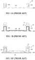
- FIGS. 1 A to 1 Dare schematic cross-sectional views illustrating a method for fabricating a semiconductor package 1 according to the prior art.
- a lead frame 15which comprises a supporting plate 152 , a bonding pad 151 and a plurality of conductive posts 150 spacingly arranged on the supporting plate 152 .
- a protective layer 19such as a copper-containing agent is formed on the lead frame 15 , and a solder material 13 is formed on end surfaces of the conductive posts 150 through such as a flux 17 containing rosin.
- an electronic componentis bonded onto the conductive posts 150 so as to be stacked on the lead frame 15 .
- the electronic componentcomprises a substrate structure 10 , and a first semiconductor chip 11 and a second semiconductor chip 12 disposed on the substrate structure 10 . Further, the first semiconductor chip 11 is bonded onto the bonding pad 151 through a thin film 18 . Furthermore, the conductive posts 150 are bonded onto the substrate structure 10 through the solder material 13 . In addition, the electronic component further comprises a covering layer 14 covering the second semiconductor chip 12 .
- an encapsulant 16is formed between the substrate structure 10 and the lead frame 15 (the supporting plate 152 ) to encapsulate the first semiconductor chip 11 , the solder material 13 and the conductive posts 150 . Thereafter, the supporting plate 152 is removed so as to expose end surfaces of the conductive posts 150 and the bonding pad 151 from the encapsulant 16 .
- the flux 17since the flux 17 is in a liquid state during a high temperature process, it will permeate to the protective layer 19 along sides of the conductive posts 150 and damage the protective layer 19 .
- the solder material 13when the solder material 13 is reflowed, since no protective layer 19 remains on the lead frame 15 and the sides of the conductive posts 150 , the solder material 13 is prone to overflow, thereby leading to channeling of tin, as shown in FIG. 1 B ′. Consequently, the solder material 13 is electrically connected to the first semiconductor chip 11 and a short circuit occurs.
- the present disclosureprovides a supporting structure, which comprises: a metal member having a plurality of conductive posts; a protective layer formed on the metal member and exposing end surfaces of the conductive posts; and conductors formed on the end surfaces of the conductive posts.
- the conductorscomprise a solder material.
- the present disclosurefurther provides a supporting structure, which comprises: a metal member having a plurality of conductive posts; stop bodies formed on end surfaces of the conductive posts; and a protective layer formed on the metal member and the stop bodies.
- the stop bodiescomprise ink.
- the metal memberis a copper frame.
- the protective layeris a metal layer.
- the metal layercomprises aluminum, stainless steel, iron, nickel or chromium.
- the present disclosurefurther provides a method for fabricating a supporting structure, which comprises: providing a metal member having a plurality of conductive posts; forming stop bodies on end surfaces of the conductive posts; forming a protective layer on the metal member and the stop bodies; removing the stop bodies and the protective layer thereon to expose the end surfaces of the conductive posts; and forming conductors on the end surfaces of the conductive posts.
- the stop bodiescomprise ink.
- the present disclosurefurther provides a method for fabricating a supporting structure, which comprises: providing a metal member having a plurality of conductive posts; forming a protective layer on the metal member; removing portions of the protective layer to expose end surfaces of the conductive posts; and forming conductors on the end surfaces of the conductive posts.
- the portions of the protective layerare removed by grinding or polishing.
- the metal memberis a copper frame.
- the protective layeris a metal layer.
- the metal layeris formed by sputtering.
- the metal layercomprises aluminum, stainless steel, iron, nickel or chromium.
- the conductorscomprise a solder material.
- the present disclosurefurther provides an electronic package, which comprises: the supporting structure as described above; and an electronic component bonded onto the conductive posts of the supporting structure to stack the electronic component on the metal member.
- the present disclosurefurther provides a method for fabricating an electronic package, which comprises: providing the supporting structure as described above; and bonding an electronic component onto the conductive posts of the supporting structure to stack the electronic component on the metal member.
- the electronic componentcomprises at least one electronic element.
- the end surfaces of the conductive postsare covered by the stop bodies or the protective layer so as to be exposed subsequently. Therefore, compared with the prior art, during reflow of the conductors, the protective layer can prevent overflow of the solder material of the conductors so as to avoid channeling of tin and further prevent a short circuit from occurring between the conductors and the electronic element.
- FIGS. 1 A to 1 Dare schematic cross-sectional views illustrating a method for fabricating a semiconductor package according to the prior art
- FIG. 1 B ′is a schematic view illustrating overflow of the solder material according to the prior art.
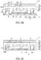
- FIGS. 2 A to 2 Care schematic cross-sectional views illustrating a method for fabricating a supporting structure according to the present disclosure
- FIGS. 2 D to 2 Eare schematic cross-sectional views illustrating a method for fabricating an electronic package according to the present disclosure.
- FIGS. 3 A and 3 Bare schematic cross-sectional views illustrating another fabrication method of FIG. 2 B .
- FIGS. 2 A to 2 Eare schematic cross-sectional views illustrating a method for fabricating an electronic package 2 using a supporting structure 2 ′, 2 ′′ according to the present disclosure.
- a supporting structure 2 ′′ having a metal member 25is provided.
- the metal member 25comprises a supporting plate 252 , at least a bonding pad 251 and a plurality of conductive posts 250 spacingly arranged on the supporting plate 252 .
- the metal member 25is a lead frame.
- the supporting plate 252 , the bonding pad 251 and the conductive posts 250can be integrally formed.
- a copper plateis partially removed by etching, laser ablation and so on so as to form the metal member 25 .
- stop bodies 27are formed on end surfaces 250 a of the conductive posts 250 , and a protective layer 29 is formed on the metal member 25 and the stop bodies 27 .
- the stop bodies 27are made of ink, and the protective layer 29 is a metal layer having an anti-solder characteristic.
- the stop bodies 27are formed by coating, and the protective layer 29 is made of aluminum, stainless steel, iron, nickel, chromium or other metal having an anti-solder characteristic and formed by sputtering.
- the stop bodies 27 and the protective layer 29 thereonare removed so as to expose the end surfaces 250 a of the conductive posts 250 .
- conductors 23are formed on the end surfaces 250 a of the conductive posts 250 so as to form another supporting structure 2 ′.
- the conductors 23are made of a solder material or other conductive materials suitable for bonding and formed on the end surfaces 250 a of the conductive posts 250 through such as a flux 230 containing rosin.
- the protective layer 29is formed on all surfaces of the metal member 25 except the end surfaces 250 a of the conductive posts 250 . Therefore, in other embodiments, the stop bodies 27 can be omitted. As shown in FIGS. 3 A and 3 B , the protective layer 29 directly encapsulates the metal member 25 and then portions of the protective layer 29 on the end surfaces 250 a of the conductive posts 250 are removed by grinding or polishing. As such, a structure of FIG. 2 B or 3 B is provided so as for the conductors 23 to be formed thereon.
- an electronic component 2 ais bonded onto the conductive posts 250 of the supporting structure 2 ′ so as to be stacked on the metal member 25 .
- the electronic component 2 acomprises a carrier structure 20 and a first electronic element 21 and a second electronic element 22 disposed on the carrier structure 20 .
- the carrier structure 20has a first side 20 a and a second side 20 b opposing the first side 20 a .
- the carrier structure 20is a packaging substrate having a core layer and a circuit structure or a coreless circuit structure, which has a plurality of circuit layers 200 such as fan-out redistribution layers (RDLs).
- RDLsfan-out redistribution layers
- the carrier structure 20can be other carrier units for carrying an electronic element such as a chip.
- the carrier structure 20is a lead frame.
- the first electronic element 21is disposed on the first side 20 a of the carrier structure 20 .
- the first electronic element 21is an active element such as a semiconductor chip, a passive element such as a resistor, a capacitor or an inductor, or a combination thereof.
- the first electronic element 21is flip-chip disposed on and electrically connected to the circuit layers 200 through a plurality of conductive bumps 210 made of such as a solder material.
- the first electronic element 21can be electrically connected to the circuit layers 200 through a plurality of bonding wires (not shown) in a wire-bonding manner. But it should be noted that the manner in which the first electronic element 21 electrically connects the carrier structure 20 is not limited to the above-described examples.
- the second electronic element 22is disposed on the second side 20 b of the carrier structure 20 .
- the second electronic element 22is an active element such as a semiconductor chip, a passive element such as a resistor, a capacitor or an inductor, or a combination thereof.
- the second electronic element 22is disposed on the circuit layers 200 in a flip-chip manner through a plurality of conductive bumps 220 made of such as a solder material.
- the second electronic element 22can be electrically connected to the circuit layers 200 through a plurality of bonding wires (not shown) in a wire-bonding manner.
- the second electronic element 22can be in direct contact with the circuit layers 200 . But it should be noted that the manner in which the second electronic element 22 electronic connects the carrier structure 20 is not limited to the above-described examples.
- the first electronic element 21can be bonded to the bonding pad 251 through a bonding layer 28 .
- the bonding layer 28is made of such as a thin film, an epoxy resin or a thermal interface material (TIM).
- the conductive posts 250are bonded to the circuit layers 200 of the first side 20 a of the carrier structure 20 through the conductors 23 .
- the electronic component 2 ahas a covering layer 24 formed on the second side 20 b of the carrier structure 20 for covering the second electronic element 22 .
- the covering layer 24is made of, but not limited to, polyimide (PI), a dry film, an epoxy resin, or a molding compound.
- an encapsulant 26is formed between the first side 20 a of the carrier structure 20 and the metal member 25 (the supporting plate 252 ) to encapsulate the first electronic element 21 , the protective layer 29 , the conductors 23 and the conductive posts 250 . Thereafter, the supporting plate 252 is removed to expose the other end surfaces 250 b of the conductive posts 250 and the bonding pad 251 (and even the protective layer 29 ) from the encapsulant 26 , thus forming the electronic package 2 of the present disclosure.
- the encapsulant 26has a first surface 26 a and a second surface 26 b opposite to the first surface 26 a .
- the second surface 26 b of the encapsulant 26is bonded to the first side 20 a of the carrier structure 20 .
- the conductive posts 250 and the bonding pad 251are embedded in the first surface 26 a of the encapsulant 26 , and the end surfaces 250 b of the conductive posts 250 and the bonding pad 251 are exposed from the first surface 26 a of the encapsulant 26 .
- the end surfaces 250 b of the conductive posts 250 and the surface of the bonding pad 251are flush with the first surface 26 a of the encapsulant 26 .
- bumpssuch as solder balls (not shown) can be mounted on the exposed surfaces (e.g., end surfaces 250 b ) of the conductive posts 250 for connecting with an electronic device such as a circuit board.
- the encapsulant 26can be made of polyimide, a dry film, an epoxy resin or a molding compound.
- the encapsulant 26 and the covering layer 24can be made of the same or different materials.
- the end surfaces 250 a of the conductive posts 250are covered by the stop bodies 27 or the protective layer 29 so as to be exposed subsequently. Therefore, during reflow of the conductors 23 , the protective layer 29 remains on the metal member 25 and the side surfaces 250 c of the conductive posts 250 so as to prevent overflow of the solder material of the conductors 23 , thereby avoiding channeling of tin and further preventing a short circuit from occurring between the conductors 23 and the first electronic element 21 (or the conductive bumps 210 ).
- the present disclosurefurther provides a supporting structure 2 ′, 2 ′′, which includes a metal member 25 , a protective layer 29 and conductors 23 (or stop bodies 27 ).
- the metal member 25has a plurality of conductive posts 250 .
- the protective layer 29is formed on the metal member 25 and exposing end surfaces 250 a of the conductive posts 250 .
- the conductors 23(or the stop bodies 27 ) are formed on the end surfaces 250 a of the conductive posts 250 .
- the protective layer 29is further formed on the stop bodies 27 .
- the conductors 23comprise a solder material.
- the stop bodies 27comprise ink.
- the metal member 25is a copper frame.
- the protective layer 29is a metal layer made of such as aluminum, stainless steel, iron, nickel or chromium.
- the present disclosurefurther provides an electronic package 2 , which includes the supporting structure 2 ′ and at least an electronic component 2 a.
- the electronic component 2 ais bonded onto the conductive posts 250 of the supporting structure 2 ′ through the conductors 23 so as to be stacked on the metal member 25 .
- the electronic component 2 acomprises a first electronic element 21 and/or a second electronic element 22 .
- the end surfaces of the conductive postsare covered by the stop bodies or the protective layer so as to be exposed subsequently.
- the protective layer on the metal member and the side surfaces of the conductive postscan prevent overflow of the solder material of the conductors so as to avoid channeling of tin and further prevent a short circuit from occurring between the conductors and the first electronic element. Therefore, the supporting structure and fabrication method thereof according to the present disclosure can improve the reliability of the electronic package.
Landscapes
- Engineering & Computer Science (AREA)
- Computer Hardware Design (AREA)
- Microelectronics & Electronic Packaging (AREA)
- Power Engineering (AREA)
- Physics & Mathematics (AREA)
- Condensed Matter Physics & Semiconductors (AREA)
- General Physics & Mathematics (AREA)
- Manufacturing & Machinery (AREA)
- Ceramic Engineering (AREA)
- Electric Connection Of Electric Components To Printed Circuits (AREA)
- Structures For Mounting Electric Components On Printed Circuit Boards (AREA)
- Wire Bonding (AREA)
- Cooling Or The Like Of Semiconductors Or Solid State Devices (AREA)
- Internal Circuitry In Semiconductor Integrated Circuit Devices (AREA)
Abstract
Description
Claims (14)
Applications Claiming Priority (2)
| Application Number | Priority Date | Filing Date | Title |
|---|---|---|---|
| TW109110013ATWI719866B (en) | 2020-03-25 | 2020-03-25 | Electronic package, supporting structure and manufacturing method thereof |
| TW109110013 | 2020-03-25 |
Publications (2)
| Publication Number | Publication Date |
|---|---|
| US20210305148A1 US20210305148A1 (en) | 2021-09-30 |
| US11527472B2true US11527472B2 (en) | 2022-12-13 |
Family
ID=75745915
Family Applications (1)
| Application Number | Title | Priority Date | Filing Date |
|---|---|---|---|
| US16/868,038ActiveUS11527472B2 (en) | 2020-03-25 | 2020-05-06 | Electronic package, supporting structure and fabrication method thereof |
Country Status (3)
| Country | Link |
|---|---|
| US (1) | US11527472B2 (en) |
| CN (1) | CN113451248B (en) |
| TW (1) | TWI719866B (en) |
Citations (16)
| Publication number | Priority date | Publication date | Assignee | Title |
|---|---|---|---|---|
| US3959874A (en)* | 1974-12-20 | 1976-06-01 | Western Electric Company, Inc. | Method of forming an integrated circuit assembly |
| US20050009329A1 (en)* | 2003-05-13 | 2005-01-13 | Kazumasa Tanida | Semiconductor chip production method, semiconductor device production method, semiconductor chip, and semiconductor device |
| US20060192299A1 (en)* | 2005-02-25 | 2006-08-31 | Seiko Epson Corporation | Manufacturing method for electronic device |
| US20070273049A1 (en)* | 2006-05-12 | 2007-11-29 | Broadcom Corporation | Interconnect structure and formation for package stacking of molded plastic area array package |
| US20080173884A1 (en)* | 2007-01-22 | 2008-07-24 | Cree, Inc. | Wafer level phosphor coating method and devices fabricated utilizing method |
| US20080258278A1 (en)* | 2002-04-29 | 2008-10-23 | Mary Jean Ramos | Partially patterned lead frames and methods of making and using the same in semiconductor packaging |
| US7633765B1 (en)* | 2004-03-23 | 2009-12-15 | Amkor Technology, Inc. | Semiconductor package including a top-surface metal layer for implementing circuit features |
| US20130207255A1 (en)* | 2012-02-15 | 2013-08-15 | Alan J. Magnus | Semiconductor device package having backside contact and method for manufacturing |
| US20140151874A1 (en)* | 2012-12-05 | 2014-06-05 | Murata Manufacturing Co., Ltd. | Bump-equipped electronic component and method for manufacturing bump-equipped electronic component |
| US20140199796A1 (en)* | 2013-01-15 | 2014-07-17 | Samsung Electronics Co., Ltd. | Semiconductor light emitting device and method of manufacturing the same |
| US20150102476A1 (en)* | 2012-04-06 | 2015-04-16 | Huatian Technology (Xi'an) Co., Ltd. | Quad flat no lead package and production method thereof |
| US20150162270A1 (en)* | 2013-12-07 | 2015-06-11 | Fairchild Semiconductor Corporation | Packaged semiconductor devices and methods of manufacturing |
| US20160284638A1 (en)* | 2015-03-27 | 2016-09-29 | Silergy Semiconductor Technology (Hangzhou) Ltd | Chip package structure and manufacturing method therefor |
| US20170270398A1 (en)* | 2014-05-14 | 2017-09-21 | Linxens Holding | Method for Producing a Circuit for a Chip Card Module and Circuit for a Chip Card Module |
| US20190287944A1 (en)* | 2018-03-13 | 2019-09-19 | Stmicroelectronics S.R.L. | Asics face to face self assembly |
| US20190355577A1 (en)* | 2018-05-16 | 2019-11-21 | Unijet Co., Ltd. | Method for printing micro line pattern using inkjet technology |
Family Cites Families (13)
| Publication number | Priority date | Publication date | Assignee | Title |
|---|---|---|---|---|
| TWI255157B (en)* | 2004-10-26 | 2006-05-11 | Phoenix Prec Technology Corp | Method for fabricating conductive connection structure of circuit board |
| US7335986B1 (en)* | 2005-09-14 | 2008-02-26 | Amkor Technology, Inc. | Wafer level chip scale package |
| US8288207B2 (en)* | 2009-02-13 | 2012-10-16 | Infineon Technologies Ag | Method of manufacturing semiconductor devices |
| US8441124B2 (en)* | 2010-04-29 | 2013-05-14 | Taiwan Semiconductor Manufacturing Company, Ltd. | Cu pillar bump with non-metal sidewall protection structure |
| US9048135B2 (en)* | 2010-07-26 | 2015-06-02 | Taiwan Semiconductor Manufacturing Company, Ltd. | Copper pillar bump with cobalt-containing sidewall protection |
| TWI449479B (en)* | 2012-11-01 | 2014-08-11 | Rtr Tech Technology Co Ltd | Method for manufacturing circuit |
| MY171261A (en)* | 2014-02-19 | 2019-10-07 | Carsem M Sdn Bhd | Stacked electronic packages |
| TWI555101B (en)* | 2014-05-27 | 2016-10-21 | 矽品精密工業股份有限公司 | Package structure and method of manufacture |
| TWI587458B (en)* | 2015-03-17 | 2017-06-11 | 矽品精密工業股份有限公司 | Electronic package and the manufacture thereof and substrate structure |
| TWI562318B (en)* | 2015-09-11 | 2016-12-11 | Siliconware Precision Industries Co Ltd | Electronic package and fabrication method thereof |
| TWI652787B (en)* | 2017-05-25 | 2019-03-01 | 矽品精密工業股份有限公司 | Electronic package and its manufacturing method |
| CN109243980A (en)* | 2017-07-10 | 2019-01-18 | 华为技术有限公司 | A kind of production method and package substrate of package substrate |
| CN110970374A (en)* | 2019-12-31 | 2020-04-07 | 湖北方晶电子科技有限责任公司 | Flip-chip power device packaging structure |
- 2020
- 2020-03-25TWTW109110013Apatent/TWI719866B/enactive
- 2020-03-31CNCN202010243647.2Apatent/CN113451248B/enactiveActive
- 2020-05-06USUS16/868,038patent/US11527472B2/enactiveActive
Patent Citations (29)
| Publication number | Priority date | Publication date | Assignee | Title |
|---|---|---|---|---|
| US3959874A (en)* | 1974-12-20 | 1976-06-01 | Western Electric Company, Inc. | Method of forming an integrated circuit assembly |
| US20080258278A1 (en)* | 2002-04-29 | 2008-10-23 | Mary Jean Ramos | Partially patterned lead frames and methods of making and using the same in semiconductor packaging |
| US20070018320A1 (en)* | 2003-05-13 | 2007-01-25 | Rohm Co., Ltd. | Semiconductor chip production method, semiconductor device production method, semiconductor chip, and semiconductor device |
| US20050009329A1 (en)* | 2003-05-13 | 2005-01-13 | Kazumasa Tanida | Semiconductor chip production method, semiconductor device production method, semiconductor chip, and semiconductor device |
| US7253527B2 (en)* | 2003-05-13 | 2007-08-07 | Rohm Co., Ltd. | Semiconductor chip production method, semiconductor device production method, semiconductor chip, and semiconductor device |
| US7122457B2 (en)* | 2003-05-13 | 2006-10-17 | Renesas Technology Corporation | Semiconductor chip production method, semiconductor device production method, semiconductor chip, and semiconductor device |
| US7633765B1 (en)* | 2004-03-23 | 2009-12-15 | Amkor Technology, Inc. | Semiconductor package including a top-surface metal layer for implementing circuit features |
| US20060192299A1 (en)* | 2005-02-25 | 2006-08-31 | Seiko Epson Corporation | Manufacturing method for electronic device |
| US20070273049A1 (en)* | 2006-05-12 | 2007-11-29 | Broadcom Corporation | Interconnect structure and formation for package stacking of molded plastic area array package |
| US7714453B2 (en)* | 2006-05-12 | 2010-05-11 | Broadcom Corporation | Interconnect structure and formation for package stacking of molded plastic area array package |
| US20080173884A1 (en)* | 2007-01-22 | 2008-07-24 | Cree, Inc. | Wafer level phosphor coating method and devices fabricated utilizing method |
| US9024349B2 (en)* | 2007-01-22 | 2015-05-05 | Cree, Inc. | Wafer level phosphor coating method and devices fabricated utilizing method |
| US20130207255A1 (en)* | 2012-02-15 | 2013-08-15 | Alan J. Magnus | Semiconductor device package having backside contact and method for manufacturing |
| US8685790B2 (en)* | 2012-02-15 | 2014-04-01 | Freescale Semiconductor, Inc. | Semiconductor device package having backside contact and method for manufacturing |
| US9275941B2 (en)* | 2012-04-06 | 2016-03-01 | Tianshui Huatian Technology Co. | Quad flat no lead package and production method thereof |
| US20150102476A1 (en)* | 2012-04-06 | 2015-04-16 | Huatian Technology (Xi'an) Co., Ltd. | Quad flat no lead package and production method thereof |
| US20140151874A1 (en)* | 2012-12-05 | 2014-06-05 | Murata Manufacturing Co., Ltd. | Bump-equipped electronic component and method for manufacturing bump-equipped electronic component |
| US9343360B2 (en)* | 2012-12-05 | 2016-05-17 | Murata Manufacturing Co., Ltd. | Bump-equipped electronic component and method for manufacturing bump-equipped electronic component |
| US20140199796A1 (en)* | 2013-01-15 | 2014-07-17 | Samsung Electronics Co., Ltd. | Semiconductor light emitting device and method of manufacturing the same |
| US9236304B2 (en)* | 2013-01-15 | 2016-01-12 | Samsung Electronics Co., Ltd. | Semiconductor light emitting device and method of manufacturing the same |
| US20150162270A1 (en)* | 2013-12-07 | 2015-06-11 | Fairchild Semiconductor Corporation | Packaged semiconductor devices and methods of manufacturing |
| US9536800B2 (en)* | 2013-12-07 | 2017-01-03 | Fairchild Semiconductor Corporation | Packaged semiconductor devices and methods of manufacturing |
| US20170270398A1 (en)* | 2014-05-14 | 2017-09-21 | Linxens Holding | Method for Producing a Circuit for a Chip Card Module and Circuit for a Chip Card Module |
| US10417548B2 (en)* | 2014-05-14 | 2019-09-17 | Linxens Holding | Method for producing a circuit for a chip card module and circuit for a chip card module |
| US20160284638A1 (en)* | 2015-03-27 | 2016-09-29 | Silergy Semiconductor Technology (Hangzhou) Ltd | Chip package structure and manufacturing method therefor |
| US9780081B2 (en)* | 2015-03-27 | 2017-10-03 | Silergy Semiconductor Technology (Hangzhou) Ltd | Chip package structure and manufacturing method therefor |
| US20190287944A1 (en)* | 2018-03-13 | 2019-09-19 | Stmicroelectronics S.R.L. | Asics face to face self assembly |
| US10770432B2 (en)* | 2018-03-13 | 2020-09-08 | Stmicroelectronics S.R.L. | ASICS face to face self assembly |
| US20190355577A1 (en)* | 2018-05-16 | 2019-11-21 | Unijet Co., Ltd. | Method for printing micro line pattern using inkjet technology |
Also Published As
| Publication number | Publication date |
|---|---|
| CN113451248A (en) | 2021-09-28 |
| US20210305148A1 (en) | 2021-09-30 |
| TW202137435A (en) | 2021-10-01 |
| CN113451248B (en) | 2025-09-16 |
| TWI719866B (en) | 2021-02-21 |
Similar Documents
| Publication | Publication Date | Title |
|---|---|---|
| US11289346B2 (en) | Method for fabricating electronic package | |
| US11024559B2 (en) | Semiconductor package with electromagnetic interference shielding structures | |
| US7656040B2 (en) | Stack structure of circuit board with semiconductor component embedded therein | |
| US10916526B2 (en) | Method for fabricating electronic package with conductive pillars | |
| US9287191B2 (en) | Semiconductor device package and method | |
| US12255182B2 (en) | Electronic package and manufacturing method thereof | |
| US10002823B2 (en) | Packaging substrate and method of fabricating the same | |
| TW201405745A (en) | Package substrate, package structure and method for manufacturing package structure | |
| US9907186B1 (en) | Electronic package structure and method for fabricating the same | |
| US20130341774A1 (en) | Semiconductor package and method of fabricating the same | |
| US12394636B2 (en) | Method for fabricating electronic package | |
| KR100924554B1 (en) | Flip chip package and manufacturing method thereof | |
| US20210296260A1 (en) | Semiconductor packaging substrate, fabrication method and packaging process thereof | |
| US11527472B2 (en) | Electronic package, supporting structure and fabrication method thereof | |
| CN108511352A (en) | Electronic package structure and method for fabricating the same | |
| US11545385B2 (en) | Method for fabricating electronic package and carrier structure thereof | |
| CN118099136A (en) | Electronic package and method for manufacturing the same | |
| CN222355138U (en) | Electronic components | |
| US20250140635A1 (en) | Electronic package and manufacturing method thereof | |
| US20250038061A1 (en) | Electronic package and manufacturing method thereof | |
| CN223052137U (en) | Electronic package | |
| US20240096721A1 (en) | Electronic package and manufacturing method thereof | |
| TW201725668A (en) | Package substrate and its fabrication method |
Legal Events
| Date | Code | Title | Description |
|---|---|---|---|
| AS | Assignment | Owner name:SILICONWARE PRECISION INDUSTRIES CO., LTD., TAIWAN Free format text:ASSIGNMENT OF ASSIGNORS INTEREST;ASSIGNORS:CHANG, CHO-HSIN;FANG, HAO-JU;CHI, TING-WEI;AND OTHERS;REEL/FRAME:052589/0330 Effective date:20200424 | |
| FEPP | Fee payment procedure | Free format text:ENTITY STATUS SET TO UNDISCOUNTED (ORIGINAL EVENT CODE: BIG.); ENTITY STATUS OF PATENT OWNER: LARGE ENTITY | |
| STPP | Information on status: patent application and granting procedure in general | Free format text:RESPONSE TO NON-FINAL OFFICE ACTION ENTERED AND FORWARDED TO EXAMINER | |
| STPP | Information on status: patent application and granting procedure in general | Free format text:FINAL REJECTION MAILED | |
| STPP | Information on status: patent application and granting procedure in general | Free format text:DOCKETED NEW CASE - READY FOR EXAMINATION | |
| STPP | Information on status: patent application and granting procedure in general | Free format text:NON FINAL ACTION MAILED | |
| STPP | Information on status: patent application and granting procedure in general | Free format text:RESPONSE TO NON-FINAL OFFICE ACTION ENTERED AND FORWARDED TO EXAMINER | |
| STPP | Information on status: patent application and granting procedure in general | Free format text:FINAL REJECTION MAILED | |
| STPP | Information on status: patent application and granting procedure in general | Free format text:DOCKETED NEW CASE - READY FOR EXAMINATION | |
| STPP | Information on status: patent application and granting procedure in general | Free format text:NOTICE OF ALLOWANCE MAILED -- APPLICATION RECEIVED IN OFFICE OF PUBLICATIONS | |
| STPP | Information on status: patent application and granting procedure in general | Free format text:PUBLICATIONS -- ISSUE FEE PAYMENT VERIFIED | |
| STCF | Information on status: patent grant | Free format text:PATENTED CASE |