US11515309B2 - Process for preparing a channel region of a thin-film transistor in a 3-dimensional thin-film transistor array - Google Patents
Process for preparing a channel region of a thin-film transistor in a 3-dimensional thin-film transistor arrayDownload PDFInfo
- Publication number
- US11515309B2 US11515309B2US17/125,477US202017125477AUS11515309B2US 11515309 B2US11515309 B2US 11515309B2US 202017125477 AUS202017125477 AUS 202017125477AUS 11515309 B2US11515309 B2US 11515309B2
- Authority
- US
- United States
- Prior art keywords
- semiconductor material
- thin
- isolation layer
- layer
- dopant
- Prior art date
- Legal status (The legal status is an assumption and is not a legal conclusion. Google has not performed a legal analysis and makes no representation as to the accuracy of the status listed.)
- Active, expires
Links
Images


Classifications
- H—ELECTRICITY
- H10—SEMICONDUCTOR DEVICES; ELECTRIC SOLID-STATE DEVICES NOT OTHERWISE PROVIDED FOR
- H10D—INORGANIC ELECTRIC SEMICONDUCTOR DEVICES
- H10D30/00—Field-effect transistors [FET]
- H10D30/01—Manufacture or treatment
- H10D30/021—Manufacture or treatment of FETs having insulated gates [IGFET]
- H10D30/031—Manufacture or treatment of FETs having insulated gates [IGFET] of thin-film transistors [TFT]
- H10D30/0321—Manufacture or treatment of FETs having insulated gates [IGFET] of thin-film transistors [TFT] comprising silicon, e.g. amorphous silicon or polysilicon
- H—ELECTRICITY
- H01—ELECTRIC ELEMENTS
- H01L—SEMICONDUCTOR DEVICES NOT COVERED BY CLASS H10
- H01L21/00—Processes or apparatus adapted for the manufacture or treatment of semiconductor or solid state devices or of parts thereof
- H01L21/02—Manufacture or treatment of semiconductor devices or of parts thereof
- H01L21/04—Manufacture or treatment of semiconductor devices or of parts thereof the devices having potential barriers, e.g. a PN junction, depletion layer or carrier concentration layer
- H01L21/18—Manufacture or treatment of semiconductor devices or of parts thereof the devices having potential barriers, e.g. a PN junction, depletion layer or carrier concentration layer the devices having semiconductor bodies comprising elements of Group IV of the Periodic Table or AIIIBV compounds with or without impurities, e.g. doping materials
- H01L21/30—Treatment of semiconductor bodies using processes or apparatus not provided for in groups H01L21/20 - H01L21/26
- H01L21/31—Treatment of semiconductor bodies using processes or apparatus not provided for in groups H01L21/20 - H01L21/26 to form insulating layers thereon, e.g. for masking or by using photolithographic techniques; After treatment of these layers; Selection of materials for these layers
- H01L21/3105—After-treatment
- H01L21/311—Etching the insulating layers by chemical or physical means
- H01L21/31105—Etching inorganic layers
- H01L21/31111—Etching inorganic layers by chemical means
- H01L21/31116—Etching inorganic layers by chemical means by dry-etching
- H01L27/1052—
- H—ELECTRICITY
- H01—ELECTRIC ELEMENTS
- H01L—SEMICONDUCTOR DEVICES NOT COVERED BY CLASS H10
- H01L21/00—Processes or apparatus adapted for the manufacture or treatment of semiconductor or solid state devices or of parts thereof
- H01L21/02—Manufacture or treatment of semiconductor devices or of parts thereof
- H01L21/04—Manufacture or treatment of semiconductor devices or of parts thereof the devices having potential barriers, e.g. a PN junction, depletion layer or carrier concentration layer
- H01L21/18—Manufacture or treatment of semiconductor devices or of parts thereof the devices having potential barriers, e.g. a PN junction, depletion layer or carrier concentration layer the devices having semiconductor bodies comprising elements of Group IV of the Periodic Table or AIIIBV compounds with or without impurities, e.g. doping materials
- H01L21/30—Treatment of semiconductor bodies using processes or apparatus not provided for in groups H01L21/20 - H01L21/26
- H01L21/302—Treatment of semiconductor bodies using processes or apparatus not provided for in groups H01L21/20 - H01L21/26 to change their surface-physical characteristics or shape, e.g. etching, polishing, cutting
- H01L21/306—Chemical or electrical treatment, e.g. electrolytic etching
- H01L21/3065—Plasma etching; Reactive-ion etching
- H01L29/6675—
- H01L29/78642—
- H01L29/78663—
- H01L29/78672—
- H—ELECTRICITY
- H10—SEMICONDUCTOR DEVICES; ELECTRIC SOLID-STATE DEVICES NOT OTHERWISE PROVIDED FOR
- H10B—ELECTRONIC MEMORY DEVICES
- H10B41/00—Electrically erasable-and-programmable ROM [EEPROM] devices comprising floating gates
- H10B41/20—Electrically erasable-and-programmable ROM [EEPROM] devices comprising floating gates characterised by three-dimensional arrangements, e.g. with cells on different height levels
- H—ELECTRICITY
- H10—SEMICONDUCTOR DEVICES; ELECTRIC SOLID-STATE DEVICES NOT OTHERWISE PROVIDED FOR
- H10B—ELECTRONIC MEMORY DEVICES
- H10B43/00—EEPROM devices comprising charge-trapping gate insulators
- H10B43/20—EEPROM devices comprising charge-trapping gate insulators characterised by three-dimensional arrangements, e.g. with cells on different height levels
- H—ELECTRICITY
- H10—SEMICONDUCTOR DEVICES; ELECTRIC SOLID-STATE DEVICES NOT OTHERWISE PROVIDED FOR
- H10D—INORGANIC ELECTRIC SEMICONDUCTOR DEVICES
- H10D30/00—Field-effect transistors [FET]
- H10D30/60—Insulated-gate field-effect transistors [IGFET]
- H10D30/67—Thin-film transistors [TFT]
- H10D30/6728—Vertical TFTs
- H—ELECTRICITY
- H10—SEMICONDUCTOR DEVICES; ELECTRIC SOLID-STATE DEVICES NOT OTHERWISE PROVIDED FOR
- H10D—INORGANIC ELECTRIC SEMICONDUCTOR DEVICES
- H10D30/00—Field-effect transistors [FET]
- H10D30/60—Insulated-gate field-effect transistors [IGFET]
- H10D30/67—Thin-film transistors [TFT]
- H10D30/674—Thin-film transistors [TFT] characterised by the active materials
- H10D30/6741—Group IV materials, e.g. germanium or silicon carbide
- H10D30/6743—Silicon
- H10D30/6745—Polycrystalline or microcrystalline silicon
- H—ELECTRICITY
- H10—SEMICONDUCTOR DEVICES; ELECTRIC SOLID-STATE DEVICES NOT OTHERWISE PROVIDED FOR
- H10D—INORGANIC ELECTRIC SEMICONDUCTOR DEVICES
- H10D30/00—Field-effect transistors [FET]
- H10D30/60—Insulated-gate field-effect transistors [IGFET]
- H10D30/67—Thin-film transistors [TFT]
- H10D30/674—Thin-film transistors [TFT] characterised by the active materials
- H10D30/6741—Group IV materials, e.g. germanium or silicon carbide
- H10D30/6743—Silicon
- H10D30/6746—Amorphous silicon
Definitions
- Provisional Applicationentitled “PROCESS FOR PREPARING A CHANNEL REGION OF A THIN-FILM TRANSISTOR IN A 3-DIMENSIONAL THIN-FILM TRANSISTOR ARRAY,” filed on Dec. 19, 2019.
- Provisional Applicationis hereby incorporated by reference in its entirety.
- the present inventionrelates to the processes used in manufacturing semiconductor circuits.
- the present inventionrelates to processes used in manufacturing 3-dimensional arrays of thin-film transistors, such as thin-film memory transistors.
- 3-dimensional arrays of thin-film memory cellshave been described, for example, in U.S. Pat. No. 10,121,553, entitled “Capacitive-Coupled Non-Volatile Thin-Film Transistor NOR Strings In 3-Dimensional Arrays,” issued on Nov. 6, 2018.
- the '553 patentdiscloses a 3-dimensional array of NOR-type memory strings in which each NOR-type memory string comprises thin-film memory transistors formed along a horizontal strip of semiconductor materials, with each strip of semiconductor materials comprising a horizontal layer of channel material between two horizontal conductive semiconductor layers.
- the conductive semiconductor layersform a common drain region and a common source region, respectively, for the thin-film transistors of the NOR-type memory string.
- the detailed description belowrefers to thin-film transistors formed above a planar surface of a semiconductor substrate.
- the terms “horizontal” and “vertical”refer to a direction substantially parallel and substantially orthogonal to the planar surface, respectively.
- the X-direction and the Y-directionrefer to two orthogonal directions parallel to the planar surface, and the Z-direction is orthogonal to both the X-direction and the Y-directions.
- FIG. 1( a )shows structure 100 of a 3-dimensional thin-film transistor array at an intermediate step of formation.
- FIG. 1( a )is a vertical cross-section of structure 100 .
- structure 100shows active stacks 101 - 1 , 101 - 2 and 101 - 3 —which are three of numerous parallel active stacks of semiconductor strips—separated from each other by trenches 109 .
- each active stackincludes a selected number of active strips 110 each isolated from its neighbors by isolation layers 106 (e.g., isolation layers 106 - 2 and 106 - 3 isolating active strip 110 - 2 from active strips 110 - 1 and 110 - 3 ).
- each active stackis arranged along the X-direction, each extending lengthwise along the Y-direction; each active strip also extends lengthwise along the Y-direction and are stacked along the Z-direction.
- a material or layeris generally referred to by a first reference numeral (e.g., n)
- specific instances of the material or layerare distinguished by a second reference numeral hyphenated to the first reference numeral (e.g., n-1, n-2, etc.).
- each active stackincludes eight active strips 110 - 1 , 110 - 2 , . . . , 110 - 8 .
- active strips 110 - 1 , 110 - 2 and 110 - 3are shown for each of active stacks 101 - 1 , 101 - 2 , and 101 - 3 .
- any suitable number of active stackse.g., 1, 2, 4, 16, 32, 64, 128, . . .
- any suitable number of active stripse.g., 1, 2, 4, 8, 16, . . .
- the active strips(e.g., 5-nm-wide each) are isolated from each other by isolation layers 106 (e.g., isolation layers 106 - 1 , 106 - 2 , and 106 - 3 ).
- Each active stripincludes common drain region, a common drain region and a body oxide layer in between (e.g., in active strip 110 - 1 , common drain region 102 - 1 , common source region 103 - 1 and body oxide layer 104 - 1 ).
- Each common drain regionis also provided an adjacent metal layer to reduce resistance along its length (e.g., common drain region 102 - 1 is in contact with metal layer 108 - 1 , such as tungsten).
- a sacrificial SiN layerstands in for metal layer 108 - 1 , which is replaced by the metal at a subsequent step.
- body oxide layers 104e.g., body oxide layers 104 - 1 , 104 - 2 and 104 - 3
- body oxide layers 104are isotropically etched to recess from the sidewalls of trenches 109 .
- an intrinsic or lightly doped semiconductor material(“channel semiconductor material”) is conformally deposited on the sidewalls of trenches 109 .
- This channel semiconductor materialshown in FIG. 1( a ) as layers 107 , for example, are intended to serve as channel regions between the common drain region and the common source region for the thin-film storage transistors in each active strip.
- a separation etchtypically an anisotropic etch
- FIG. 1( b )shows one instance of resulting structure 100 after a separation etch.
- the separation etchhas a high aspect-ratio (e.g., trenches 109 may each be 60-nm wide and 2-um deep)
- the channel semiconductor material adjacent the body oxide layeroften becomes too thin due to sideway etching, as indicated by arrow A, and leaves undesirable stringers towards the bottom of trenches 109 , as indicated by arrow B.
- both excessive thinning of the channel semiconductor material adjacent the body oxide layer and leaving stringers on the sidewalls of the trenchesare undesirable. Also, if metal layers 108 have already been provided, the anisotropic etch may sputter the metal to result in contamination.
- a processincludes (a) providing a semiconductor substrate having a planar surface; (b) forming a plurality of thin-film layers above the planar surface of the semiconductor substrate, one on top of another, including among the thin-film layers first and second isolation layers, wherein a significantly greater concentration of a first dopant specie is provided in the first isolation layer than in the second isolation layer; (c) etching along a direction substantially orthogonal to the planar surface through the thin-films to create a trench having sidewalls that expose the thin-film layers; (d) depositing conformally a semiconductor material (e.g., an amorphous silicon and a polysilicon) on the sidewalls of the trench; (e) annealing the first isolation layer at a predetermined temperature and a predetermined duration such that the first isolation layer act as a source of the first dopant specie which dopes a portion of the semiconductor material adjacent the first isolation layer; and (f) selectively etching (e.g.
- the first isolation layermay include an organosilicon layer (e.g., SiOCH or SiOC), a silicon nitride layer or a silicate glass (e.g., BSG or PSG), and (ii) the selective etching uses an etchant that that may include tetra-methyl ammonium hydroxide (TMAH), potassium hydroxide (KOH), or ethylene diamine and pyrocatechol (EDP).
- TMAHtetra-methyl ammonium hydroxide
- KOHpotassium hydroxide
- EDPethylene diamine and pyrocatechol
- the annealing stepmay include a rapid thermal annealing step, and wherein the predetermined temperature is between 650° C. and 820° C., preferably about 750° C.
- the first isolation layermay be carbon-doped with a carbon dopant concentration of about 10 20 cm ⁇ 3 or greater, and the selective etching uses an etchant that comprises ethylene diamine and pyrocatechol (EDP).
- EDPethylene diamine and pyrocatechol
- the annealing stepcomprises a rapid thermal annealing step, and the predetermined temperature is between about 600° C. and about 820° C., preferably about 750° C.
- an additional material that is highly doped with a second dopantmay be deposited adjacent and over the semiconductor material.
- An annealing stepdiffuses the second dopant specie into the semiconductor material, so as to adjust an effective dopant concentration in the semiconductor material. That effective dopant concentration may determine a threshold voltage of a thin-film transistor in which the semiconductor material serve as a channel region.
- the first dopant speciemay be boron and the second dopant specie may be phosphorus, or vice versa.
- the first isolation layerincludes an organosilicon layer (e.g., BSG or PSG, with a dopant concentration greater than 1.0 ⁇ 10 22 cm ⁇ 3 ), a silicon nitride layer or a silicate glass, and the selective etching uses an etchant that may include atomic chlorine, HF (gaseous or in an aqueous solution) or a fluorocarbon gas.
- the annealing stepmay include a rapid thermal annealing step, and the predetermined temperature is between about 600° C. and about 820° C., preferably about 750° C.
- a suitable aqueous HF solutionmay include HF, nitric acid and acetic acid, in various suitable proportions.
- a capping layermay be deposited over the conformally deposited semiconductor material.
- FIG. 1( a )shows structure 100 of a 3-dimensional thin-film transistor array at an intermediate step of formation.
- FIG. 1( b )shows one instance of resulting structure 100 after a separation etch.
- FIG. 2( a )show the resulting structure 100 , in which the portions of channel semiconductor material 107 on the sidewalls of trenches 109 are designated 107 - 1 , while the boron-doped portions of the channel semiconductor material 107 adjacent body oxide layers 104 are designated 107 - 2 , in accordance with one embodiment of the present invention.
- FIG. 2( b )shows the resulting structure 100 after a selective etch using an etchant has a significantly different etch rate between undoped polysilicon and doped silicon of a predetermined dopant concentration or greater.
- FIG. 3shows, after the selective etch of FIG. 2( b ) , a thin layer of phosphorus silicate glass (PSG), e.g., 10-nm thick, may be deposited on structure 100 , in accordance with one embodiment of the present invention.
- PSGphosphorus silicate glass
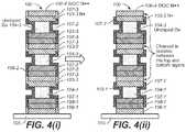
- FIGS. 4( i ) and (ii)illustrate an alternatively embodiment of the present invention, in which isolation layers 106 dope their adjacent channel semiconductor material 107 for selective removal, in accordance with one embodiment of the present invention.
- FIGS. 5( i ) and (ii)illustrate a second embodiment of the present invention, in which isolation layers 106 dope their adjacent channel semiconductor material 107 for selective removal, in accordance with one embodiment of the present invention.
- FIGS. 6( i ) , 6 ( ii ) and 6 ( iii )illustrate a third alternatively embodiment of the present invention, in which isolation layers 106 dope their adjacent channel semiconductor material 107 for selective removal, in accordance with one embodiment of the present invention.
- the present inventionavoids both the excessive thinning of the channel semiconductor material adjacent the body oxide layer and the stringers on the sidewalls of the trenches.
- the methods of the present inventionchemically convert either the portions of the channel semiconductor material in the recesses adjacent the body oxide layers, or the portions of the channel semiconductor material on the sidewalls of the trenches, or both, such that a subsequent etch may selectively removes the portions of the channel semiconductor material from the sidewalls of the trenches.
- body oxide layers 104 of structure 100 of FIG. 1( a )is heavily boron-doped (i.e., p + -type), as deposited, while common drain regions 102 and common source regions 103 are arsenic-doped (i.e., n + -type).
- body oxide layer 104may be, for example, a 50-nm thick organosilicon layer (e.g., SiOCH) with a dopant concentration of about 1.0 ⁇ 10 20 cm ⁇ 3 or greater.
- an annealing stepe.g., a rapid thermal annealing (RTA) step at 750° C. for 10 min.
- RTArapid thermal annealing
- boron from body oxide layers 104out-diffuses into their adjacent portions of channel semiconductor material 107 , resulting in a dopant concentration in those portions of, for example, between about 5.0 ⁇ 10 18 cm ⁇ 3 and about 1.0 ⁇ 10 19 cm ⁇ 3 .
- some amount of arsenicmay also out-diffuse from common drain layers 102 and common source layers 103 into their respective adjacent portions of channel semiconductor material 107 .
- FIG. 2( a )show the resulting structure 100 , in which the portions of channel semiconductor material 107 on the sidewalls of trenches 109 are designated 107 - 1 , while the boron-doped portions of the channel semiconductor material 107 adjacent body oxide layers 104 are designated 107 - 2 .
- a selective etch using, for example, tetra-methyl ammonium hydroxide (TMAH)may be used to remove channel semiconductor material 107 - 1 from the sidewalls of trenches 109 , leaving behind channel semiconductor material 107 - 2 in the recesses of body oxide layers 104 , as TMAH has an etch rate that is at least 5 times higher for undoped polysilicon than doped polysilicon of dopant concentration of at least about 10 18 cm ⁇ 3 .
- the selective etchmay an isotropic wet etch or dry etch. The resulting structure is shown in FIG. 2( b ) .
- etchants with high selectivity of undoped polysilicon over doped polysiliconmay also be used.
- potassium hydroxide (KOH)has a selectivity of 20:1 for undoped polysilicon over doped polysilicon of a dopant concentration exceeding 10 20 cm ⁇ 3 .
- an aqueous solution of ethylene diamine and pyrocatechol (EDP)has a selectivity of 50:1 for undoped polysilicon over doped polysilicon of a dopant concentration exceeding 7.0 ⁇ 10 19 cm ⁇ 3 .
- body oxide layers 104 of structure 100 of FIG. 1( a )is carbon-doped, as deposited, while common drain regions 102 and common source regions 103 are arsenic-doped (i.e., n + -type).
- body oxide layer 104may be, for example, a 50-nm thick carbon-doped oxide with a carbon dopant concentration of about 5.0 ⁇ 10 20 cm ⁇ 3 or greater.
- an RTA stepe.g., at 750° C. for 10 min. is carried out.
- a selective etch using, for example, EDPmay be used to remove channel semiconductor material 107 - 1 from the sidewalls of trenches 109 , leaving behind carbon-doped channel semiconductor material 107 - 2 in the recesses of body oxide layers 104 , as EDP has an etch rate that is at least 100 times higher for undoped polysilicon than carbon-doped polysilicon of dopant concentration of at least about 10 20 cm ⁇ 3 .
- the selective etchmay an isotropic wet etch or dry etch.
- V ththreshold voltage of the resulting thin-film transistor.
- the resulting V thmay be much greater than the more desirable 1.5 volts achievable at the lesser dopant concentration of 5.0 ⁇ 10 18 cm ⁇ 3 .
- the V th of the resulting thin-film transistorsmay be too high.
- onemay counter-dope channel semiconductor material 107 - 2 after the selective etch of FIG. 2( b ) . According to one embodiment of the present invention, after the selective etch of FIG.
- a thin layer 120 of phosphorus silicate glass (PSG), e.g., 10-nm thick,may be deposited on structure 100 , as shown in FIG. 3 .
- Phosphorus in the PSGis then allowed to diffuse into channel semiconductor material 107 - 2 in a subsequent annealing step.
- the initial dopant concentration in the PSG, and the temperature and the duration of this subsequent RTA stepmay be empirically determined to achieve a given desired V th in the resulting thin-film transistors. Generally, at temperatures lower than 1000° C., phosphorus has a greater diffusion rate in polysilicon than boron.
- PSG layer 120may be removed by wet isotropic etching after the RTA step (e.g., using hydrofluoric acid (HF)).
- HFhydrofluoric acid
- isolation layers 106are initially deposited as heavily doped n ++ -type c-silicon (SiOC), with a phosphorus dopant concentration of greater than 5.0 ⁇ 10 20 cm ⁇ 3 , for example.
- channel semiconductor material 107may be deposited in situ doped to the desired dopant concentration for the channel regions (e.g., 1.0 ⁇ 10 18 cm ⁇ 3 ).
- a subsequent RTA annealing stepturns the portions of channel semiconductor material 107 adjacent isolation layers 106 into n-type semiconductor material 107 - 3 , as shown FIG. 4( i ) .
- n-type channel semiconductor material 107 - 3may be removed at up to a 40:1 selectivity of n ++ -type polysilicon (e.g., dopant concentration of 3.0 ⁇ 10 20 cm ⁇ 3 or greater) over p-type polysilicon. It is believed that the difference in selectivity results from sensitivity to the phosphorus dopant profile. (See, e.g., Solid State Science and Technology, 2 (9). pp.
- FIG. 4 ( ii )The resulting structure is shown FIG. 4 ( ii ). Note that, unlike the other embodiments described above, in this embodiment, some portions of channel semiconductor material 107 - 3 remains on the sidewalls of trenches 109 , although the result channel regions in the active strips achieve electrical isolation from each other.
- isolation layers 106are initially deposited as heavily doped p ++ -type borosilicate (BSG), with a boron dopant concentration of greater than 5.0 ⁇ 10 21 cm ⁇ 3 , for example.
- BSGheavily doped p ++ -type borosilicate
- a 10-nm thick channel semiconductor material 107may be deposited in situ doped to the desired dopant concentration for the channel regions (e.g., 1.0 ⁇ 10 18 cm ⁇ 3 ).
- An RTA annealing stepe.g., at 600° C. for a duration of 14 minutes, including the deposition time of channel semiconductor material 107 ) turns the portions of channel semiconductor material 107 adjacent isolation layers 106 into 10-nm thick p-type semiconductor material 107 - 3 , as shown in FIG.
- buffer oxide layer 121may be added between isolation layers 106 and adjacent common source regions 103 to avoid boron diffusion into source regions 103 .
- BSG layers 106 , buffer oxide 121 and body oxide layers 104are recessed in a previous oxide etch step.
- p-type channel semiconductor material 107 - 3may be removed at up to a 50:1 selectivity of p-type polysilicon (e.g., dopant concentration of 5.0 ⁇ 10 21 cm ⁇ 3 or greater) over undoped or lightly-doped polysilicon.
- a selectivity of p-type polysilicone.g., dopant concentration of 5.0 ⁇ 10 21 cm ⁇ 3 or greater
- HNO 3nitric acid
- HF, HNO 3 and acetic acid (CH 3 COOH) vaporsmay be used. (See, e.g., U.S. Pat. No. 4,681,657 to Hwang et al.).
- CH 3 COOHacetic acid
- FIGS. 6( i ) - 6 (iii)illustrate a third alternatively embodiment of the present invention, in which isolation layers 106 dope their adjacent channel semiconductor material 107 for selective removal, in accordance with one embodiment of the present invention.
- isolation layers 106are initially deposited as heavily doped PSG, with a phosphorus dopant concentration of greater than 1.0 ⁇ 10 22 cm ⁇ 3 , for example.
- channel semiconductor material 107may be deposited as in situ doped amorphous silicon at 550° C. or as polysilicon at 625° C.
- 2-nm capping layer 122 of silicon oxide or silicon nitride, deposited at a temperature of 650° C. or lessmay be provided to prevent diffusion of the phosphorus out of channel semiconductor material 107 .
- both common source regions 103 and common drain regions 102are provided adjacent metal layers 108 to reduce resistivity.
- an RTA annealing stepat 820° C. for 60 seconds or less turns the portions of channel semiconductor material 107 adjacent isolation layers 106 into heavily doped n-type channel semiconductor material 107 - 3 , activating the phosphorus dopants at the same time (e.g., to an equilibrium dopant concentration of about 3.0 ⁇ 10 20 cm ⁇ 3 ).
- the deposited amorphous siliconis also crystallized as channel semiconductor material 107 - 2 .
- arsenic diffusion from common source regions 103 and common drain regions 102 into channel semiconductor 107is insignificant.
- capping layer 122is isotropically removed.
- heavily-doped n-type channel semiconductor material 107 - 3may be removed at a greater than 6:1 selectivity of n-type polysilicon (e.g., dopant concentration of about 3.0 ⁇ 10 20 cm ⁇ 3 or greater) over lightly-doped p-type polysilicon, as illustrated in FIG. 6 ( iii ).
Landscapes
- Engineering & Computer Science (AREA)
- Physics & Mathematics (AREA)
- Microelectronics & Electronic Packaging (AREA)
- Manufacturing & Machinery (AREA)
- Power Engineering (AREA)
- Condensed Matter Physics & Semiconductors (AREA)
- General Physics & Mathematics (AREA)
- Chemical & Material Sciences (AREA)
- Computer Hardware Design (AREA)
- Plasma & Fusion (AREA)
- Chemical Kinetics & Catalysis (AREA)
- Inorganic Chemistry (AREA)
- General Chemical & Material Sciences (AREA)
- Thin Film Transistor (AREA)
- Crystallography & Structural Chemistry (AREA)
- Element Separation (AREA)
- Insulated Gate Type Field-Effect Transistor (AREA)
Abstract
Description
Claims (19)
Priority Applications (2)
| Application Number | Priority Date | Filing Date | Title |
|---|---|---|---|
| US17/125,477US11515309B2 (en) | 2019-12-19 | 2020-12-17 | Process for preparing a channel region of a thin-film transistor in a 3-dimensional thin-film transistor array |
| US18/050,937US11844204B2 (en) | 2019-12-19 | 2022-10-28 | Process for preparing a channel region of a thin-film transistor in a 3-dimensional thin-film transistor array |
Applications Claiming Priority (2)
| Application Number | Priority Date | Filing Date | Title |
|---|---|---|---|
| US201962950390P | 2019-12-19 | 2019-12-19 | |
| US17/125,477US11515309B2 (en) | 2019-12-19 | 2020-12-17 | Process for preparing a channel region of a thin-film transistor in a 3-dimensional thin-film transistor array |
Related Child Applications (1)
| Application Number | Title | Priority Date | Filing Date |
|---|---|---|---|
| US18/050,937ContinuationUS11844204B2 (en) | 2019-12-19 | 2022-10-28 | Process for preparing a channel region of a thin-film transistor in a 3-dimensional thin-film transistor array |
Publications (2)
| Publication Number | Publication Date |
|---|---|
| US20210193660A1 US20210193660A1 (en) | 2021-06-24 |
| US11515309B2true US11515309B2 (en) | 2022-11-29 |
Family
ID=76438380
Family Applications (2)
| Application Number | Title | Priority Date | Filing Date |
|---|---|---|---|
| US17/125,477Active2041-03-10US11515309B2 (en) | 2019-12-19 | 2020-12-17 | Process for preparing a channel region of a thin-film transistor in a 3-dimensional thin-film transistor array |
| US18/050,937ActiveUS11844204B2 (en) | 2019-12-19 | 2022-10-28 | Process for preparing a channel region of a thin-film transistor in a 3-dimensional thin-film transistor array |
Family Applications After (1)
| Application Number | Title | Priority Date | Filing Date |
|---|---|---|---|
| US18/050,937ActiveUS11844204B2 (en) | 2019-12-19 | 2022-10-28 | Process for preparing a channel region of a thin-film transistor in a 3-dimensional thin-film transistor array |
Country Status (3)
| Country | Link |
|---|---|
| US (2) | US11515309B2 (en) |
| TW (1) | TWI762091B (en) |
| WO (1) | WO2021127218A1 (en) |
Cited By (1)
| Publication number | Priority date | Publication date | Assignee | Title |
|---|---|---|---|---|
| US20220199643A1 (en)* | 2017-06-20 | 2022-06-23 | Sunrise Memory Corporation | 3-dimensional nor memory array architecture and methods for fabrication thereof |
Families Citing this family (3)
| Publication number | Priority date | Publication date | Assignee | Title |
|---|---|---|---|---|
| WO2021178309A1 (en)* | 2020-03-04 | 2021-09-10 | Lam Research Corporation | Protection of channel layer in three-terminal vertical memory structure |
| US11508755B2 (en)* | 2021-02-25 | 2022-11-22 | Taiwan Semiconductor Manufacturing Company, Ltd. | Stacked ferroelectric structure |
| US20230078883A1 (en)* | 2021-09-14 | 2023-03-16 | Sunrise Memory Corporation | Three-dimensional memory string array of thin-film ferroelectric transistors formed with an oxide semiconductor channel in a channel last process |
Citations (133)
| Publication number | Priority date | Publication date | Assignee | Title |
|---|---|---|---|---|
| US5583808A (en) | 1994-09-16 | 1996-12-10 | National Semiconductor Corporation | EPROM array segmented for high performance and method for controlling same |
| US5646886A (en) | 1995-05-24 | 1997-07-08 | National Semiconductor Corporation | Flash memory having segmented array for improved operation |
| US5656842A (en) | 1995-06-20 | 1997-08-12 | Mitsubishi Denki Kabushiki Kaisha | Vertical mosfet including a back gate electrode |
| US5768192A (en) | 1996-07-23 | 1998-06-16 | Saifun Semiconductors, Ltd. | Non-volatile semiconductor memory cell utilizing asymmetrical charge trapping |
| US5789776A (en) | 1995-09-22 | 1998-08-04 | Nvx Corporation | Single poly memory cell and array |
| US5915167A (en) | 1997-04-04 | 1999-06-22 | Elm Technology Corporation | Three dimensional structure memory |
| US6040605A (en) | 1998-01-28 | 2000-03-21 | Hitachi, Ltd. | Semiconductor memory device |
| US6107133A (en) | 1998-05-28 | 2000-08-22 | International Business Machines Corporation | Method for making a five square vertical DRAM cell |
| US6118171A (en) | 1998-12-21 | 2000-09-12 | Motorola, Inc. | Semiconductor device having a pedestal structure and method of making |
| US6130838A (en) | 1997-08-12 | 2000-10-10 | Samsung Electronics, Co., Ltd. | Structure nonvolatile semiconductor memory cell array and method for fabricating same |
| US20010030340A1 (en) | 1998-11-04 | 2001-10-18 | Ichiro Fujiwara | Nonvolatile semiconductor memory device and process of production and write method thereof |
| US6314046B1 (en) | 1999-03-30 | 2001-11-06 | Sanyo Electric Co., Ltd. | Dual memory control circuit |
| US6313518B1 (en) | 1997-10-14 | 2001-11-06 | Micron Technology, Inc. | Porous silicon oxycarbide integrated circuit insulator |
| US20010053092A1 (en) | 2000-06-12 | 2001-12-20 | Sony Corporation | Memory system and programming method thereof |
| US20020028541A1 (en) | 2000-08-14 | 2002-03-07 | Lee Thomas H. | Dense arrays and charge storage devices, and methods for making same |
| US6362508B1 (en)* | 2000-04-03 | 2002-03-26 | Tower Semiconductor Ltd. | Triple layer pre-metal dielectric structure for CMOS memory devices |
| US20020051378A1 (en) | 2000-08-17 | 2002-05-02 | Takashi Ohsawa | Semiconductor memory device and method of manufacturing the same |
| US6434053B1 (en) | 1999-12-06 | 2002-08-13 | Sony Corporation | Nonvolatile semiconductor memory device and method of operation thereof |
| US20020193484A1 (en) | 2001-02-02 | 2002-12-19 | The 54 Group, Ltd. | Polymeric resins impregnated with insect repellants |
| US6580124B1 (en) | 2000-08-14 | 2003-06-17 | Matrix Semiconductor Inc. | Multigate semiconductor device with vertical channel current and method of fabrication |
| US20040000679A1 (en)* | 2002-06-27 | 2004-01-01 | Matrix Semiconductor, Inc. | High density 3D rail stack arrays and method of making |
| US6744094B2 (en) | 2001-08-24 | 2004-06-01 | Micron Technology Inc. | Floating gate transistor with horizontal gate layers stacked next to vertical body |
| US6774458B2 (en) | 2002-07-23 | 2004-08-10 | Hewlett Packard Development Company, L.P. | Vertical interconnection structure and methods |
| US6781858B2 (en)* | 2002-04-02 | 2004-08-24 | Hewlett-Packard Development Company, L.P. | Cubic memory array |
| US20040214387A1 (en) | 2002-07-08 | 2004-10-28 | Madurawe Raminda Udaya | Methods for fabricating three dimensional integrated circuits |
| US20040246807A1 (en) | 2003-06-03 | 2004-12-09 | Seung-Hoon Lee | Multi-port memory device with stacked banks |
| US20040262772A1 (en) | 2003-06-30 | 2004-12-30 | Shriram Ramanathan | Methods for bonding wafers using a metal interlayer |
| US20040262681A1 (en) | 2003-05-28 | 2004-12-30 | Fujio Masuoka | Semiconductor device |
| US6873004B1 (en) | 2002-02-04 | 2005-03-29 | Nexflash Technologies, Inc. | Virtual ground single transistor memory cell, memory array incorporating same, and method of operation thereof |
| US20050128815A1 (en) | 2003-12-09 | 2005-06-16 | Renesas Technology Corp. | Semiconductor data processing device |
| US6946703B2 (en) | 2003-01-09 | 2005-09-20 | Samsung Electronics Co., Ltd. | SONOS memory device having side gate stacks and method of manufacturing the same |
| US20050236625A1 (en)* | 2004-04-23 | 2005-10-27 | Sharp Laboratories Of America, Inc. | Vertical thin film transistor |
| US20050280061A1 (en) | 2004-06-21 | 2005-12-22 | Sang-Yun Lee | Vertical memory device structures |
| US7005350B2 (en) | 2002-12-31 | 2006-02-28 | Matrix Semiconductor, Inc. | Method for fabricating programmable memory array structures incorporating series-connected transistor strings |
| US20060155921A1 (en) | 2004-12-16 | 2006-07-13 | Gorobets Sergey A | Non-volatile memory and method with multi-stream update tracking |
| US7223653B2 (en)* | 2004-06-15 | 2007-05-29 | International Business Machines Corporation | Process for forming a buried plate |
| US7307308B2 (en) | 2003-04-07 | 2007-12-11 | Silicon Storage Technology, Inc. | Buried bit line non-volatile floating gate memory cell with independent controllable control gate in a trench, and array thereof, and method of formation |
| US20080160765A1 (en)* | 2006-12-27 | 2008-07-03 | Hynix Semiconductor Inc. | Method for forming pattern in semiconductor device |
| US20080239812A1 (en) | 2007-03-30 | 2008-10-02 | Kabushiki Kaisha Toshiba | Nonvolatile semiconductor memory system |
| US20080301359A1 (en) | 2004-12-16 | 2008-12-04 | Peter John Smith | Non-Volatile Memory and Method With Multi-Stream Updating |
| US7489002B2 (en) | 2001-02-09 | 2009-02-10 | Micron Technology, Inc. | Memory having a vertical transistor |
| US20090057722A1 (en) | 2007-05-30 | 2009-03-05 | Unisantis Electronics (Japan) Ltd. | Semiconductor device |
| US7524725B2 (en) | 2005-03-31 | 2009-04-28 | Hynix Semiconductor Inc. | Vertical transistor of semiconductor device and method for forming the same |
| US20090157946A1 (en) | 2007-12-12 | 2009-06-18 | Siamak Arya | Memory having improved read capability |
| US20090237996A1 (en) | 2008-03-20 | 2009-09-24 | Micron Technology, Inc. | Memory structure having volatile and non-volatile memory portions |
| US7612411B2 (en) | 2005-08-03 | 2009-11-03 | Walker Andrew J | Dual-gate device and method |
| US20090279360A1 (en) | 2008-05-07 | 2009-11-12 | Aplus Flash Technology, Inc. | NAND based NMOS NOR flash memory cell, a NAND based NMOS nor flash memory array, and a method of forming a NAND based NMOS NOR flash memory array |
| US20090316487A1 (en) | 2008-06-20 | 2009-12-24 | Aplus Flash Technology, Inc. | Apparatus and method for inhibiting excess leakage current in unselected nonvolatile memory cells in an array |
| JP2010108522A (en) | 2010-02-02 | 2010-05-13 | Toshiba Corp | Method of controlling memory system |
| US20100124116A1 (en) | 2008-11-14 | 2010-05-20 | Kabushiki Kaisha Toshiba | Non-volatile semiconductor storage device |
| US20100128509A1 (en) | 2008-11-25 | 2010-05-27 | Sukpil Kim | Three-Dimensional Semiconductor Devices and Methods of Operating the Same |
| JP2011028540A (en) | 2009-07-27 | 2011-02-10 | Renesas Electronics Corp | Information processing system, method for controlling cache memory, program and compiler |
| US20110044113A1 (en) | 2009-08-18 | 2011-02-24 | Samsung Electronics Co., Ltd. | Nonvolatile memory device, method for programming same, and memory system incorporating same |
| US20110115011A1 (en) | 2009-11-13 | 2011-05-19 | Fujio Masuoka | Semiconductor element and semiconductor device |
| US20110143519A1 (en)* | 2007-07-27 | 2011-06-16 | Ralf Lerner | Production of isolation trenches with different sidewall dopings |
| US20110208905A1 (en) | 2008-12-09 | 2011-08-25 | Rambus Inc. | Non-Volatile Memory Device For Concurrent And Pipelined Memory Operations |
| US8026521B1 (en) | 2010-10-11 | 2011-09-27 | Monolithic 3D Inc. | Semiconductor device and structure |
| US20110298013A1 (en) | 2010-06-07 | 2011-12-08 | Samsung Electronics Co., Ltd. | Vertical Structure Semiconductor Memory Devices And Methods Of Manufacturing The Same |
| US8139418B2 (en) | 2009-04-27 | 2012-03-20 | Micron Technology, Inc. | Techniques for controlling a direct injection semiconductor memory device |
| US20120074478A1 (en)* | 2010-09-28 | 2012-03-29 | Fujitsu Semiconductor Limited | Semiconductor device and manufacturing method thereof |
| US8178396B2 (en) | 2009-03-11 | 2012-05-15 | Micron Technology, Inc. | Methods for forming three-dimensional memory devices, and related structures |
| US20120182801A1 (en) | 2011-01-19 | 2012-07-19 | Macronix International Co., Ltd. | Memory Architecture of 3D NOR Array |
| KR20120085591A (en) | 2011-01-24 | 2012-08-01 | 김진선 | Non-volatile memory device, method of operating the same, and method of fabricating the same |
| US20120243314A1 (en) | 2011-03-25 | 2012-09-27 | Kabushiki Kaisha Toshiba | Nonvolatile semiconductor memory device |
| US20120307568A1 (en) | 2011-06-06 | 2012-12-06 | Micron Technology, Inc. | Techniques for providing a semiconductor memory device |
| US20120327714A1 (en) | 2011-06-23 | 2012-12-27 | Macronix International Co., Ltd. | Memory Architecture of 3D Array With Diode in Memory String |
| US20130031325A1 (en) | 2011-07-29 | 2013-01-31 | The Boeing Company | System for Updating an Associative Memory |
| US20130256780A1 (en) | 2012-03-30 | 2013-10-03 | Kabushiki Kaisha Toshiba | Semiconductor device and manufacturing method thereof |
| US20130337646A1 (en)* | 2012-06-15 | 2013-12-19 | Sandisk 3D Llc | Method for forming staircase word lines in a 3d non-volatile memory having vertical bit lines |
| US20140015036A1 (en) | 2012-07-13 | 2014-01-16 | United Silicon Carbide, Inc. | Trenched and implanted accumulation mode metal-oxide-semiconductor field-effect transistor |
| US20140040698A1 (en) | 2012-08-06 | 2014-02-06 | Advanced Micro Devices, Inc. | Stacked memory device with metadata mangement |
| US20140117366A1 (en) | 2012-10-31 | 2014-05-01 | Kabushiki Kaisha Toshiba | Semiconductor device and method for manufacturing same |
| US20140151774A1 (en) | 2012-12-04 | 2014-06-05 | Mosaid Technologies Incorporated | Nand flash memory with vertical cell stack structure and method for manufacturing same |
| US8767473B2 (en) | 2009-06-19 | 2014-07-01 | Samsung Electronics Co., Ltd. | Programming methods for three-dimensional memory devices having multi-bit programming, and three-dimensional memory devices programmed thereby |
| US20140213032A1 (en)* | 2013-01-31 | 2014-07-31 | Sandisk 3D Llc | Process For Forming Resistive Switching Memory Cells Using Nano-Particles |
| US20140229131A1 (en) | 2012-05-04 | 2014-08-14 | Lsi Corporation | Retention-drift-history-based non-volatile memory read threshold optimization |
| US20140247674A1 (en) | 2013-03-01 | 2014-09-04 | Micron Technology, Inc. | Vertical access device and apparatuses having a body connection line, and related method of operating the same |
| US20140252454A1 (en)* | 2013-03-07 | 2014-09-11 | Sandisk 3D Llc | Vertical bit line tft decoder for high voltage operation |
| US20140252532A1 (en)* | 2013-03-11 | 2014-09-11 | Nanya Technology Corporation | Semiconductor device and method for fabricating the same |
| US8848425B2 (en) | 2008-12-19 | 2014-09-30 | Unity Semiconductor Corporation | Conductive metal oxide structures in non volatile re-writable memory devices |
| US8878278B2 (en) | 2012-03-21 | 2014-11-04 | Sandisk Technologies Inc. | Compact three dimensional vertical NAND and method of making thereof |
| US20140328128A1 (en) | 2013-05-01 | 2014-11-06 | Zeno Semiconductor, Inc. | NAND String Utilizing Floating Body Memory Cell |
| US20140340952A1 (en) | 2013-05-17 | 2014-11-20 | Micron Technology, Inc. | Apparatuses having a ferroelectric field-effect transistor memory array and related method |
| US20150079744A1 (en)* | 2012-03-12 | 2015-03-19 | SK Hynix Inc. | Semiconductor device with buried bit line and method for fabricating the same |
| US20150079743A1 (en)* | 2013-09-17 | 2015-03-19 | SanDisk Technologies, Inc. | Methods of fabricating a three-dimensional non-volatile memory device |
| US20150098272A1 (en) | 2013-10-03 | 2015-04-09 | Apple Inc. | Programmable peak-current control in non-volatile memory devices |
| US20150113214A1 (en) | 2013-10-21 | 2015-04-23 | Sehat Sutardja | Final level cache system and corresponding methods |
| US20150187823A1 (en)* | 2013-12-27 | 2015-07-02 | Semiconductor Energy Laboratory Co., Ltd. | Semiconductor device |
| US20150194440A1 (en) | 2014-01-09 | 2015-07-09 | Young-Jin Noh | Nonvolatile Memory Devices And Methods Of Fabricating The Same |
| US20150206886A1 (en)* | 2012-08-21 | 2015-07-23 | Micron Technology, Inc. | Methods of Forming Memory Arrays and Semiconductor Constructions |
| US20150249143A1 (en) | 2014-02-28 | 2015-09-03 | Sandisk 3D Llc | Method For Forming Oxide Below Control Gate In Vertical Channel Thin Film Transistor |
| US9190293B2 (en) | 2013-12-18 | 2015-11-17 | Applied Materials, Inc. | Even tungsten etch for high aspect ratio trenches |
| US20150340371A1 (en)* | 2014-05-21 | 2015-11-26 | Macronix International Co., Ltd. | 3d independent double gate flash memory on bounded conductor layer |
| US9202694B2 (en) | 2013-03-04 | 2015-12-01 | Sandisk 3D Llc | Vertical bit line non-volatile memory systems and methods of fabrication |
| US9230985B1 (en) | 2014-10-15 | 2016-01-05 | Sandisk 3D Llc | Vertical TFT with tunnel barrier |
| US20160019951A1 (en) | 2014-07-18 | 2016-01-21 | Samsung Electronics Co., Ltd. | Resistive memory device, resistive memory system, and method of operating resistive memory device |
| US20160049404A1 (en)* | 2014-08-18 | 2016-02-18 | Micron Technology, Inc. | Array Of Gated Devices And Methods Of Forming An Array Of Gated Devices |
| US20160086953A1 (en)* | 2014-08-21 | 2016-03-24 | Macronix International Co., Ltd. | Method for fabricating memory device |
| US20160086970A1 (en) | 2014-09-23 | 2016-03-24 | Haibing Peng | Three-dimensional non-volatile nor-type flash memory |
| US20160225860A1 (en) | 2013-08-12 | 2016-08-04 | Micron Technology, Inc. | Vertical Ferroelectric Field Effect Transistor Constructions, Constructions Comprising A Pair Of Vertical Ferroelectric Field Effect Transistors, Vertical Strings Of Ferroelectric Field Effect Transistors, And Vertical Strings Of Laterally Opposing Pairs Of Vertical Ferroelectric Field Effect Transistors |
| US9412752B1 (en) | 2015-09-22 | 2016-08-09 | Macronix International Co., Ltd. | Reference line and bit line structure for 3D memory |
| US20160300724A1 (en) | 2007-05-25 | 2016-10-13 | Cypress Semiconductor Corporation | Oxide-Nitride-Oxide Stack Having Multiple Oxynitride Layers |
| US20160314042A1 (en) | 2015-04-27 | 2016-10-27 | Invensas Corporation | Preferred state encoding in non-volatile memories |
| US20170092371A1 (en) | 2015-09-30 | 2017-03-30 | Eli Harari | Capacitive-coupled non-volatile thin-film transistor strings in three dimensional arrays |
| US20170092370A1 (en) | 2015-09-30 | 2017-03-30 | Eli Harari | Multi-gate nor flash thin-film transistor strings arranged in stacked horizontal active strips with vertical control gates |
| US20170148517A1 (en) | 2015-11-25 | 2017-05-25 | Eli Harari | Three-dimensional vertical nor flash thin film transistor strings |
| US20170148810A1 (en) | 2015-11-20 | 2017-05-25 | Sandisk Technologies Llc | Three-dimensional nand device containing support pedestal structures for a buried source line and method of making the same |
| US9748172B2 (en) | 2015-02-25 | 2017-08-29 | Sandisk Technologies Llc | Floating staircase word lines and process in a 3D non-volatile memory having vertical bit lines |
| US20170358594A1 (en) | 2016-06-13 | 2017-12-14 | Sandisk Technologies Llc | Method of forming a staircase in a semiconductor device using a linear alignmnent control feature |
| US20180151419A1 (en)* | 2016-11-29 | 2018-05-31 | Taiwan Semiconductor Manufacturing Company, Ltd. | Method of forming a device having a doping layer and device formed |
| US10074667B1 (en) | 2017-03-10 | 2018-09-11 | Toshiba Memory Corporation | Semiconductor memory device |
| US20180269229A1 (en) | 2015-09-21 | 2018-09-20 | Monolithic 3D Inc. | 3D Semiconductor Device and Structure |
| US20180342544A1 (en) | 2014-09-30 | 2018-11-29 | Apple Inc. | Image Sensor with a Cross-Wafer Capacitator |
| US20180342455A1 (en) | 2017-05-25 | 2018-11-29 | Sandisk Technologies Llc | Interconnect structure containing a metal silicide hydrogen diffusion barrier and method of making thereof |
| US20180366489A1 (en) | 2017-06-20 | 2018-12-20 | Sunrise Memory Corporation | 3-Dimensional NOR Memory Array Architecture and Methods for Fabrication Thereof |
| US20180366471A1 (en) | 2017-06-20 | 2018-12-20 | Sunrise Memory Corporation | 3-Dimensional NOR String Arrays in Segmented Stacks |
| US20190019564A1 (en)* | 2017-07-13 | 2019-01-17 | Qualcomm Incorporated | Multiple (multi-) level cell (mlc) non-volatile (nv) memory (nvm) matrix circuits for performing matrix computations with multi-bit input vectors |
| US10254968B1 (en) | 2015-06-10 | 2019-04-09 | Firquest Llc | Hybrid memory device for lookup operations |
| US20190157296A1 (en) | 2017-11-17 | 2019-05-23 | Sunrise Memory Corporation | Reverse memory cell |
| US20190206890A1 (en) | 2017-12-28 | 2019-07-04 | Sunrise Memory Corporation | 3-Dimensional NOR Memory Array with Very Fine Pitch: Device and Method |
| US10373956B2 (en) | 2011-03-01 | 2019-08-06 | Micron Technology, Inc. | Gated bipolar junction transistors, memory arrays, and methods of forming gated bipolar junction transistors |
| US20190244971A1 (en) | 2018-02-02 | 2019-08-08 | Sunrise Memory Corporation | Three-dimensional vertical NOR Flash Thin-Film Transistor Strings |
| US20190259769A1 (en) | 2017-08-31 | 2019-08-22 | Micron Technology, Inc. | Apparatuses Having Memory Cells with Two Transistors and One Capacitor, and Having Body Regions of the Transistors Coupled with Reference Voltages |
| US10431596B2 (en) | 2017-08-28 | 2019-10-01 | Sunrise Memory Corporation | Staggered word line architecture for reduced disturb in 3-dimensional NOR memory arrays |
| US20190319044A1 (en) | 2018-02-02 | 2019-10-17 | Sunrise Memory Corporation | Three-dimensional vertical NOR Flash Thin-Film Transistor Strings |
| US20190348424A1 (en) | 2018-05-08 | 2019-11-14 | Micron Technology, Inc. | Integrated Assemblies Having Ferroelectric Transistors with Body Regions Coupled to Carrier Reservoirs; and Methods of Forming Integrated Assemblies |
| US20190370117A1 (en) | 2016-06-28 | 2019-12-05 | International Business Machines Corporation | File level access to block level incremental backups of a virtual disk |
| US20200020718A1 (en) | 2018-07-12 | 2020-01-16 | Sunrise Memory Corporation | Fabrication Method for a 3-Dimensional NOR Memory Array |
| US20200051990A1 (en) | 2018-07-12 | 2020-02-13 | Sunrise Memory Corporation | Device Structure for a 3-Dimensional NOR Memory Array and Methods for Improved Erase Operations Applied Thereto |
| US20200098779A1 (en) | 2018-09-20 | 2020-03-26 | Sunrise Memory Corporation | Staircase Structures for Electrically Connecting Multiple Horizontal Conductive Layers of a 3-Dimensional Memory Device |
| US20200098738A1 (en) | 2018-09-24 | 2020-03-26 | Sunrise Memory Corporation | Wafer Bonding in Fabrication of 3-Dimensional NOR Memory Circuits |
| US20200176468A1 (en) | 2018-12-04 | 2020-06-04 | Sunrise Memory Corporation | Methods for forming multilayer horizontal nor-type thin-film memory strings |
| US20200258897A1 (en) | 2019-02-11 | 2020-08-13 | Sunrise Memory Corporation | Device with embedded high-bandwidth, high-capacity memory using wafer bonding |
Family Cites Families (227)
| Publication number | Priority date | Publication date | Assignee | Title |
|---|---|---|---|---|
| US4213139A (en) | 1978-05-18 | 1980-07-15 | Texas Instruments Incorporated | Double level polysilicon series transistor cell |
| US4984153A (en) | 1988-04-27 | 1991-01-08 | Unisys Corporation | Storage locking control for a plurality of processors which share a common storage unit |
| JP2531802B2 (en) | 1989-09-28 | 1996-09-04 | 甲府日本電気株式会社 | Request buffer control system |
| EP0833348B1 (en) | 1996-09-30 | 2003-07-09 | STMicroelectronics S.r.l. | Method and circuit for checking multilevel programming of floating-gate nonvolatile memory cells, particlarly flash cells |
| JP3543905B2 (en) | 1997-03-19 | 2004-07-21 | シャープ株式会社 | Semiconductor storage device |
| US6551857B2 (en) | 1997-04-04 | 2003-04-22 | Elm Technology Corporation | Three dimensional structure integrated circuits |
| US6057862A (en) | 1997-07-01 | 2000-05-02 | Memtrax Llc | Computer system having a common display memory and main memory |
| JP2000339978A (en) | 1999-05-24 | 2000-12-08 | Sony Corp | Nonvolatile semiconductor memory device and its reading method |
| TW587252B (en) | 2000-01-18 | 2004-05-11 | Hitachi Ltd | Semiconductor memory device and data processing device |
| US6407435B1 (en) | 2000-02-11 | 2002-06-18 | Sharp Laboratories Of America, Inc. | Multilayer dielectric stack and method |
| US6639835B2 (en) | 2000-02-29 | 2003-10-28 | Micron Technology, Inc. | Static NVRAM with ultra thin tunnel oxides |
| US6455424B1 (en) | 2000-08-07 | 2002-09-24 | Micron Technology, Inc. | Selective cap layers over recessed polysilicon plugs |
| US7012297B2 (en) | 2001-08-30 | 2006-03-14 | Micron Technology, Inc. | Scalable flash/NV structures and devices with extended endurance |
| GB0123416D0 (en) | 2001-09-28 | 2001-11-21 | Memquest Ltd | Non-volatile memory control |
| JP2004079606A (en) | 2002-08-12 | 2004-03-11 | Fujitsu Ltd | Semiconductor device having high dielectric constant film and method of manufacturing the same |
| JP4206707B2 (en) | 2002-08-27 | 2009-01-14 | 株式会社日立製作所 | Communication quality setting apparatus, method and program |
| WO2004090984A1 (en) | 2003-04-03 | 2004-10-21 | Kabushiki Kaisha Toshiba | Phase change memory device |
| US6754105B1 (en) | 2003-05-06 | 2004-06-22 | Advanced Micro Devices, Inc. | Trench side wall charge trapping dielectric flash memory device |
| KR100535651B1 (en) | 2003-06-30 | 2005-12-08 | 주식회사 하이닉스반도체 | Method for reading a flash memory cell and a flash memory equipment of NAND and NOR type |
| US7241654B2 (en) | 2003-12-17 | 2007-07-10 | Micron Technology, Inc. | Vertical NROM NAND flash memory array |
| US7312505B2 (en) | 2004-03-31 | 2007-12-25 | Intel Corporation | Semiconductor substrate with interconnections and embedded circuit elements |
| JP4407431B2 (en) | 2004-08-30 | 2010-02-03 | 株式会社日立製作所 | Computer system and bandwidth control method for computer system |
| JP4785180B2 (en) | 2004-09-10 | 2011-10-05 | 富士通セミコンダクター株式会社 | Ferroelectric memory, multilevel data recording method, and multilevel data reading method |
| JP4284259B2 (en) | 2004-09-28 | 2009-06-24 | シャープ株式会社 | Semiconductor memory device and electronic device |
| US7284226B1 (en) | 2004-10-01 | 2007-10-16 | Xilinx, Inc. | Methods and structures of providing modular integrated circuits |
| US7450433B2 (en) | 2004-12-29 | 2008-11-11 | Sandisk Corporation | Word line compensation in non-volatile memory erase operations |
| US7473589B2 (en) | 2005-12-09 | 2009-01-06 | Macronix International Co., Ltd. | Stacked thin film transistor, non-volatile memory devices and methods for fabricating the same |
| JP2006252624A (en) | 2005-03-09 | 2006-09-21 | Toshiba Corp | Semiconductor memory device |
| US7493441B2 (en) | 2005-03-15 | 2009-02-17 | Dot Hill Systems Corporation | Mass storage controller with apparatus and method for extending battery backup time by selectively providing battery power to volatile memory banks not storing critical data |
| KR101377305B1 (en) | 2005-06-24 | 2014-03-25 | 구글 인코포레이티드 | An integrated memory core and memory interface circuit |
| US7538000B2 (en) | 2005-07-28 | 2009-05-26 | Freescale Semiconductor, Inc. | Method of forming double gate transistors having varying gate dielectric thicknesses |
| US7429767B2 (en) | 2005-09-01 | 2008-09-30 | Micron Technology, Inc. | High performance multi-level non-volatile memory device |
| KR101293365B1 (en) | 2005-09-30 | 2013-08-05 | 모사이드 테크놀로지스 인코퍼레이티드 | Memory with output control |
| US20070192518A1 (en) | 2006-02-14 | 2007-08-16 | Aarohi Communications, Inc., A California Corporation | Apparatus for performing I/O sharing & virtualization |
| JP2007280505A (en) | 2006-04-06 | 2007-10-25 | Toshiba Corp | Semiconductor memory device |
| JP4745108B2 (en) | 2006-04-06 | 2011-08-10 | 株式会社東芝 | Nonvolatile semiconductor memory device |
| US7457902B2 (en) | 2006-07-21 | 2008-11-25 | Emulex Design & Manufacturing Corporation | Lock and release mechanism for out-of-order frame prevention and support of native command queueing in FC-SATA |
| JP4282699B2 (en) | 2006-09-01 | 2009-06-24 | 株式会社東芝 | Semiconductor device |
| JP2008182035A (en) | 2007-01-24 | 2008-08-07 | Toshiba Corp | Semiconductor memory device and manufacturing method thereof |
| US7857907B2 (en) | 2007-01-25 | 2010-12-28 | Au Optronics Corporation | Methods of forming silicon nanocrystals by laser annealing |
| US7898009B2 (en) | 2007-02-22 | 2011-03-01 | American Semiconductor, Inc. | Independently-double-gated transistor memory (IDGM) |
| US8706914B2 (en) | 2007-04-23 | 2014-04-22 | David D. Duchesneau | Computing infrastructure |
| JP2008276858A (en) | 2007-04-27 | 2008-11-13 | Spansion Llc | Nonvolatile storage device and bias control method therefor |
| US7512012B2 (en) | 2007-04-30 | 2009-03-31 | Macronix International Co., Ltd. | Non-volatile memory and manufacturing method and operating method thereof and circuit system including the non-volatile memory |
| CN101675505B (en) | 2007-05-03 | 2012-11-21 | 朗姆研究公司 | Hardmask open and etch profile control with hardmask open |
| US7687891B2 (en) | 2007-05-14 | 2010-03-30 | Infineon Technologies Ag | Diode having one or more zones of a first conductivity type and one or more zones of a second conductivity type each located within a layer of the second conductivity type |
| US20080291723A1 (en) | 2007-05-23 | 2008-11-27 | Wang Daniel C | Source biasing of nor-type flash array with dynamically variable source resistance |
| US7816727B2 (en) | 2007-08-27 | 2010-10-19 | Macronix International Co., Ltd. | High-κ capped blocking dielectric bandgap engineered SONOS and MONOS |
| US7709359B2 (en) | 2007-09-05 | 2010-05-04 | Qimonda Ag | Integrated circuit with dielectric layer |
| KR101391881B1 (en) | 2007-10-23 | 2014-05-07 | 삼성전자주식회사 | Multi-bit flash memory device and program and read methods thereof |
| US20090140318A1 (en) | 2007-12-03 | 2009-06-04 | Zhong Dong | Nonvolatile memories with higher conduction-band edge adjacent to charge-trapping dielectric |
| US7542348B1 (en) | 2007-12-19 | 2009-06-02 | Juhan Kim | NOR flash memory including bipolar segment read circuit |
| JP2009206451A (en) | 2008-02-29 | 2009-09-10 | Toshiba Corp | Nonvolatile semiconductor storage device and manufacturing method thereof |
| KR101559868B1 (en) | 2008-02-29 | 2015-10-14 | 삼성전자주식회사 | Vertical semiconductor device and manufacturing method thereof. |
| JP5354944B2 (en) | 2008-03-27 | 2013-11-27 | 株式会社東芝 | Semiconductor device and field effect transistor |
| US8304823B2 (en) | 2008-04-21 | 2012-11-06 | Namlab Ggmbh | Integrated circuit including a ferroelectric memory cell and method of manufacturing the same |
| KR101660430B1 (en) | 2009-08-14 | 2016-09-27 | 삼성전자 주식회사 | Semiconductor package |
| JP2009301600A (en) | 2008-06-10 | 2009-12-24 | Panasonic Corp | Nonvolatile semiconductor memory device, and signal processing system |
| US9116828B2 (en) | 2008-06-11 | 2015-08-25 | Micron Technology, Inc. | Data bus inversion usable in a memory system |
| KR101435588B1 (en) | 2008-06-23 | 2014-09-25 | 삼성전자주식회사 | Nonvolatile memory device and manufacturing method thereof |
| TWI376773B (en) | 2008-07-17 | 2012-11-11 | Au Optronics Corp | Method for manufacturing non-volatile memory and structure threrof |
| KR101468594B1 (en) | 2008-07-31 | 2014-12-04 | 삼성전자주식회사 | Oxide semiconductor and thin film transistor including the same |
| DE102008036453A1 (en) | 2008-08-05 | 2010-02-11 | Infineon Technologies Ag | Method for sending data and communication device |
| US20100121994A1 (en) | 2008-11-10 | 2010-05-13 | International Business Machines Corporation | Stacked memory array |
| KR20100052597A (en) | 2008-11-11 | 2010-05-20 | 삼성전자주식회사 | Vertical type semiconductor device |
| JP2010135384A (en)* | 2008-12-02 | 2010-06-17 | Mitsubishi Electric Corp | Thin film transistor array substrate, manufacturing method thereof, and liquid crystal display device |
| KR101495799B1 (en) | 2009-02-16 | 2015-03-03 | 삼성전자주식회사 | Nonvolatile memory device and manufacturing method thereof |
| KR101532366B1 (en) | 2009-02-25 | 2015-07-01 | 삼성전자주식회사 | Semiconductor memory element |
| JP4956598B2 (en) | 2009-02-27 | 2012-06-20 | シャープ株式会社 | Nonvolatile semiconductor memory device and manufacturing method thereof |
| JP4897009B2 (en) | 2009-03-24 | 2012-03-14 | 株式会社東芝 | Method for manufacturing nonvolatile semiconductor memory device |
| US8284601B2 (en) | 2009-04-01 | 2012-10-09 | Samsung Electronics Co., Ltd. | Semiconductor memory device comprising three-dimensional memory cell array |
| JP2010251572A (en) | 2009-04-16 | 2010-11-04 | Toshiba Corp | Nonvolatile semiconductor memory device |
| KR101476817B1 (en) | 2009-07-03 | 2014-12-26 | 가부시키가이샤 한도오따이 에네루기 켄큐쇼 | Display device including transistor and manufacturing method thereof |
| KR101584113B1 (en) | 2009-09-29 | 2016-01-13 | 삼성전자주식회사 | Three-dimensional semiconductor memory device and manufacturing method thereof |
| US8417917B2 (en) | 2009-09-30 | 2013-04-09 | International Business Machines Corporation | Processor core stacking for efficient collaboration |
| EP2333830B1 (en) | 2009-12-07 | 2014-09-03 | STMicroelectronics (Research & Development) Limited | a package comprising a first and a second die coupled by a multiplexed bus |
| KR101048987B1 (en)* | 2009-12-10 | 2011-07-12 | 삼성모바일디스플레이주식회사 | Flat panel display and manufacturing method thereof |
| US8871590B2 (en)* | 2009-12-31 | 2014-10-28 | Lg Display Co., Ltd. | Thin film transistor array substrate, liquid crystal display device including the same and fabricating methods thereof |
| CN102116980B (en)* | 2009-12-31 | 2014-04-09 | 乐金显示有限公司 | Thin film transistor array substrate and method for fabricating same |
| US8247895B2 (en) | 2010-01-08 | 2012-08-21 | International Business Machines Corporation | 4D device process and structure |
| US8395942B2 (en) | 2010-05-17 | 2013-03-12 | Sandisk Technologies Inc. | Junctionless TFT NAND flash memory |
| KR101137929B1 (en) | 2010-05-31 | 2012-05-09 | 에스케이하이닉스 주식회사 | Nonvolatile memory device and method for manufacturing the same |
| US8237213B2 (en) | 2010-07-15 | 2012-08-07 | Micron Technology, Inc. | Memory arrays having substantially vertical, adjacent semiconductor structures and the formation thereof |
| US10217667B2 (en) | 2011-06-28 | 2019-02-26 | Monolithic 3D Inc. | 3D semiconductor device, fabrication method and system |
| US20120063223A1 (en) | 2010-09-09 | 2012-03-15 | Aplus Flash Technology, Inc. | Most compact flotox-based combo NVM design without sacrificing EEPROM endurance cycles for 1-die data and code storage |
| KR20120085603A (en) | 2011-01-24 | 2012-08-01 | 김진선 | Non-volatile memory device, method of operating the same, and method of fabricating the same |
| ITTO20110181A1 (en) | 2011-02-01 | 2012-08-02 | St Microelectronics Srl | MEMORIZATION SUPPORT PROVIDED WITH ELEMENTS OF RAILWAY MATERIAL AND ITS NON-DESTRUCTIVE READING METHOD |
| US20120208347A1 (en) | 2011-02-11 | 2012-08-16 | Samsung Electronics Co., Ltd. | Three-dimensional semiconductor memory devices and methods of fabricating the same |
| US9213054B2 (en) | 2011-03-14 | 2015-12-15 | Rambus Inc. | Methods and apparatus for testing inaccessible interface circuits in a semiconductor device |
| US9218852B2 (en) | 2011-06-30 | 2015-12-22 | Sandisk Technologies Inc. | Smart bridge for memory core |
| US8604618B2 (en) | 2011-09-22 | 2013-12-10 | International Business Machines Corporation | Structure and method for reducing vertical crack propagation |
| KR20130088348A (en) | 2012-01-31 | 2013-08-08 | 에스케이하이닉스 주식회사 | 3-dimensional non-volatile memory device |
| US8557632B1 (en) | 2012-04-09 | 2013-10-15 | Monolithic 3D Inc. | Method for fabrication of a semiconductor device and structure |
| KR102072449B1 (en) | 2012-06-01 | 2020-02-04 | 삼성전자주식회사 | Storage device including non-volatile memory device and repair method thereof |
| US8922243B2 (en) | 2012-12-23 | 2014-12-30 | Advanced Micro Devices, Inc. | Die-stacked memory device with reconfigurable logic |
| JP2014053571A (en) | 2012-09-10 | 2014-03-20 | Toshiba Corp | Ferroelectric memory and method of manufacturing the same |
| KR101975534B1 (en) | 2012-09-11 | 2019-05-07 | 삼성전자주식회사 | Semiconductor memory device with operation functions |
| US8988937B2 (en) | 2012-10-24 | 2015-03-24 | Sandisk Technologies Inc. | Pre-charge during programming for 3D memory using gate-induced drain leakage |
| KR101447547B1 (en) | 2012-11-23 | 2014-10-06 | 삼성전자주식회사 | Method for imaging magnetic resonance image and appratus using the same thereof |
| US9053801B2 (en) | 2012-11-30 | 2015-06-09 | Micron Technology, Inc. | Memory cells having ferroelectric materials |
| US9055044B2 (en) | 2012-12-03 | 2015-06-09 | Hitachi, Ltd. | Computer system and method of controlling computer system |
| US8902663B1 (en) | 2013-03-11 | 2014-12-02 | Monolithic 3D Inc. | Method of maintaining a memory state |
| US10840239B2 (en) | 2014-08-26 | 2020-11-17 | Monolithic 3D Inc. | 3D semiconductor device and structure |
| JP2014187191A (en)* | 2013-03-22 | 2014-10-02 | Toshiba Corp | Semiconductor storage device manufacturing method and semiconductor storage device |
| US9297971B2 (en) | 2013-04-26 | 2016-03-29 | Oracle International Corporation | Hybrid-integrated photonic chip package with an interposer |
| US9053802B2 (en) | 2013-06-04 | 2015-06-09 | Namlab Ggmbh | Ferroelectric memory cell for an integrated circuit |
| CN103366798B (en) | 2013-07-10 | 2016-02-17 | 格科微电子(上海)有限公司 | Dynamic RAM and manufacture method, semiconductor package part and method for packing |
| US9934043B2 (en) | 2013-08-08 | 2018-04-03 | Linear Algebra Technologies Limited | Apparatus, systems, and methods for providing computational imaging pipeline |
| WO2015025357A1 (en) | 2013-08-19 | 2015-02-26 | 株式会社 東芝 | Memory system |
| US9231206B2 (en) | 2013-09-13 | 2016-01-05 | Micron Technology, Inc. | Methods of forming a ferroelectric memory cell |
| US8971676B1 (en) | 2013-10-07 | 2015-03-03 | Oracle International Corporation | Hybrid-integrated photonic chip package |
| US9219225B2 (en) | 2013-10-31 | 2015-12-22 | Micron Technology, Inc. | Multi-bit ferroelectric memory device and methods of forming the same |
| KR102128469B1 (en) | 2013-11-08 | 2020-06-30 | 삼성전자주식회사 | Semiconductor devices |
| US10169948B2 (en) | 2014-01-31 | 2019-01-01 | International Business Machines Corporation | Prioritizing storage operation requests utilizing data attributes |
| KR102183713B1 (en) | 2014-02-13 | 2020-11-26 | 삼성전자주식회사 | Staircase Connection Structure Of Three-Dimensional Semiconductor Device And Method Of Forming The Same |
| US20150279431A1 (en) | 2014-04-01 | 2015-10-01 | Micron Technology, Inc. | Stacked semiconductor die assemblies with partitioned logic and associated systems and methods |
| US9263577B2 (en) | 2014-04-24 | 2016-02-16 | Micron Technology, Inc. | Ferroelectric field effect transistors, pluralities of ferroelectric field effect transistors arrayed in row lines and column lines, and methods of forming a plurality of ferroelectric field effect transistors |
| US9768181B2 (en) | 2014-04-28 | 2017-09-19 | Micron Technology, Inc. | Ferroelectric memory and methods of forming the same |
| KR20150135903A (en)* | 2014-05-26 | 2015-12-04 | 에스케이하이닉스 주식회사 | Semiconductor device and system having the same, and operating method thereof |
| KR102251809B1 (en) | 2014-05-28 | 2021-05-13 | 삼성전자주식회사 | Memory system, memory interface device and interfacing method in memory system |
| US9472560B2 (en) | 2014-06-16 | 2016-10-18 | Micron Technology, Inc. | Memory cell and an array of memory cells |
| US9391084B2 (en) | 2014-06-19 | 2016-07-12 | Macronix International Co., Ltd. | Bandgap-engineered memory with multiple charge trapping layers storing charge |
| US20150372099A1 (en) | 2014-06-19 | 2015-12-24 | Taiwan Semiconductor Manufacturing Company, Ltd. | Contact silicide formation using a spike annealing process |
| WO2016004388A1 (en) | 2014-07-03 | 2016-01-07 | Yale University | Circuitry for ferroelectric fet-based dynamic random access memory and non-volatile memory |
| US20160013156A1 (en) | 2014-07-14 | 2016-01-14 | Apple Inc. | Package-on-package options with multiple layer 3-d stacking |
| US9558804B2 (en) | 2014-07-23 | 2017-01-31 | Namlab Ggmbh | Charge storage ferroelectric memory hybrid and erase scheme |
| US9685429B2 (en) | 2014-07-29 | 2017-06-20 | Dyi-chung Hu | Stacked package-on-package memory devices |
| US9299580B2 (en) | 2014-08-19 | 2016-03-29 | Applied Materials, Inc. | High aspect ratio plasma etch for 3D NAND semiconductor applications |
| US20160118404A1 (en) | 2014-10-09 | 2016-04-28 | Haibing Peng | Three-dimensional non-volatile ferroelectric random access memory |
| US9460797B2 (en)* | 2014-10-13 | 2016-10-04 | Ememory Technology Inc. | Non-volatile memory cell structure and non-volatile memory apparatus using the same |
| US9698152B2 (en) | 2014-11-13 | 2017-07-04 | Sandisk Technologies Llc | Three-dimensional memory structure with multi-component contact via structure and method of making thereof |
| EP3038141B1 (en) | 2014-12-23 | 2019-08-28 | IMEC vzw | Method of reading a memory cell of a vertical ferroelectric memory device |
| US9812461B2 (en) | 2015-03-17 | 2017-11-07 | Sandisk Technologies Llc | Honeycomb cell structure three-dimensional non-volatile memory device |
| KR20160128127A (en) | 2015-04-28 | 2016-11-07 | 에스케이하이닉스 주식회사 | Semiconductor device and manufaturing method thereof |
| US9818848B2 (en) | 2015-04-29 | 2017-11-14 | Yale University | Three-dimensional ferroelectric FET-based structures |
| KR102298661B1 (en) | 2015-04-30 | 2021-09-07 | 삼성전자주식회사 | Storage device and initializing method thereof |
| CN106206447A (en) | 2015-05-05 | 2016-12-07 | 中芯国际集成电路制造(上海)有限公司 | The forming method of 3D NAND device |
| US9620605B2 (en) | 2015-05-15 | 2017-04-11 | Taiwan Semiconductor Manufacturing Company, Ltd. | Semiconductor device structure and method |
| US10116557B2 (en) | 2015-05-22 | 2018-10-30 | Gray Research LLC | Directional two-dimensional router and interconnection network for field programmable gate arrays, and other circuits and applications of the router and network |
| US9553104B2 (en) | 2015-06-08 | 2017-01-24 | Macronix International Co., Ltd. | Semiconductor device and method of fabricating the same |
| EP3128534B1 (en) | 2015-08-07 | 2021-02-17 | IMEC vzw | Ferroelectric memory device and fabrication method thereof |
| US11956952B2 (en) | 2015-08-23 | 2024-04-09 | Monolithic 3D Inc. | Semiconductor memory device and structure |
| US20170062456A1 (en) | 2015-08-31 | 2017-03-02 | Cypress Semiconductor Corporation | Vertical division of three-dimensional memory device |
| US11978731B2 (en) | 2015-09-21 | 2024-05-07 | Monolithic 3D Inc. | Method to produce a multi-level semiconductor memory device and structure |
| US20190148286A1 (en) | 2015-09-21 | 2019-05-16 | Monolithic 3D Inc. | Multi-level semiconductor device and structure with memory |
| US11120884B2 (en) | 2015-09-30 | 2021-09-14 | Sunrise Memory Corporation | Implementing logic function and generating analog signals using NOR memory strings |
| DE102015015854B4 (en) | 2015-12-03 | 2021-01-28 | Namlab Ggmbh | Integrated circuit with a ferroelectric memory cell and use of the integrated circuit |
| US9876018B2 (en) | 2015-12-03 | 2018-01-23 | Micron Technology, Inc. | Ferroelectric capacitor, ferroelectric field effect transistor, and method used in forming an electronic component comprising conductive material and ferroelectric material |
| US10090036B2 (en) | 2015-12-21 | 2018-10-02 | Imec Vzw | Non-volatile memory cell having pinch-off ferroelectric field effect transistor |
| US10886228B2 (en) | 2015-12-23 | 2021-01-05 | Intel Corporation | Improving size and efficiency of dies |
| US9780105B2 (en) | 2015-12-30 | 2017-10-03 | Toshiba Memory Corporation | Semiconductor memory device including a plurality of columnar structures and a plurality of electrode films |
| KR102398664B1 (en) | 2016-01-26 | 2022-05-16 | 삼성전자주식회사 | Method of manufacturing semiconductor device |
| US10056393B2 (en) | 2016-03-01 | 2018-08-21 | Namlab Ggmbh | Application of antiferroelectric like materials in non-volatile memory devices |
| JP6523997B2 (en) | 2016-03-14 | 2019-06-05 | 株式会社東芝 | Semiconductor device manufacturing method |
| US10636471B2 (en) | 2016-04-20 | 2020-04-28 | Micron Technology, Inc. | Memory arrays, ferroelectric transistors, and methods of reading and writing relative to memory cells of memory arrays |
| US9995785B2 (en) | 2016-09-30 | 2018-06-12 | Intel Corporation | Stacked semiconductor package and method for performing bare die testing on a functional die in a stacked semiconductor package |
| US10403627B2 (en) | 2016-10-11 | 2019-09-03 | Imec Vzw | Memory device for a dynamic random access memory |
| DE102016015010A1 (en) | 2016-12-14 | 2018-06-14 | Namlab Ggmbh | An integrated circuit including a ferroelectric memory cell and a manufacturing method therefor |
| KR20180076298A (en) | 2016-12-27 | 2018-07-05 | 아이엠이씨 브이제트더블유 | Methods of fabricating a vertical channel-type three-dimensional non-volatile semiconductor memory device having a replacement gate |
| US10256245B2 (en) | 2017-03-10 | 2019-04-09 | Sandisk Technologies Llc | Three-dimensional memory device with short-free source select gate contact via structure and method of making the same |
| US10217719B2 (en) | 2017-04-06 | 2019-02-26 | Micron Technology, Inc. | Semiconductor device assemblies with molded support substrates |
| US9875784B1 (en) | 2017-04-13 | 2018-01-23 | Qualcomm Incorporated | Three-dimensional (3D) ferroelectric dipole metal-oxide semiconductor ferroelectric field-effect transistor (MOSFeFET) system, and related methods and systems |
| US9941299B1 (en) | 2017-05-24 | 2018-04-10 | Sandisk Technologies Llc | Three-dimensional ferroelectric memory device and method of making thereof |
| US10038092B1 (en) | 2017-05-24 | 2018-07-31 | Sandisk Technologies Llc | Three-level ferroelectric memory cell using band alignment engineering |
| US10521343B2 (en) | 2017-06-12 | 2019-12-31 | Western Digital Technologies, Inc. | Storage system with a controller having a persistent memory interface to local memory |
| US10608008B2 (en) | 2017-06-20 | 2020-03-31 | Sunrise Memory Corporation | 3-dimensional nor strings with segmented shared source regions |
| KR20190001455A (en) | 2017-06-27 | 2019-01-04 | 에스케이하이닉스 주식회사 | Ferroelectric Memory Device |
| US10600808B2 (en) | 2017-09-05 | 2020-03-24 | Namlab Ggmbh | Ferroelectric memory cell for an integrated circuit |
| US10630296B2 (en) | 2017-09-12 | 2020-04-21 | iCometrue Company Ltd. | Logic drive with brain-like elasticity and integrality based on standard commodity FPGA IC chips using non-volatile memory cells |
| US10283452B2 (en) | 2017-09-15 | 2019-05-07 | Yangtze Memory Technology Co., Ltd. | Three-dimensional memory devices having a plurality of NAND strings |
| CN107658317B (en) | 2017-09-15 | 2019-01-01 | 长江存储科技有限责任公司 | A kind of semiconductor device and preparation method thereof |
| US11289509B2 (en) | 2017-09-29 | 2022-03-29 | Intel Corporation | Double-gated ferroelectric field-effect transistor |
| US10445181B2 (en) | 2017-10-23 | 2019-10-15 | Western Digital Technologies, Inc. | Lossless synchronization software reset |
| US10460788B2 (en) | 2017-10-27 | 2019-10-29 | Ferroelectric Memory Gmbh | Memory cell and methods thereof |
| US10438645B2 (en) | 2017-10-27 | 2019-10-08 | Ferroelectric Memory Gmbh | Memory cell and methods thereof |
| US10290332B1 (en) | 2017-10-31 | 2019-05-14 | Sandisk Technologies Llc | Signal path optimization for read operations in storage devices |
| US10424379B2 (en) | 2017-12-01 | 2019-09-24 | Namlab Ggmbh | Polarization-based configurable logic gate |
| US10606513B2 (en) | 2017-12-06 | 2020-03-31 | Western Digital Technologies, Inc. | Volatility management for non-volatile memory device |
| US10937482B2 (en) | 2017-12-27 | 2021-03-02 | Micron Technology, Inc. | Memory cells and arrays of elevationally-extending strings of memory cells |
| US10283493B1 (en) | 2018-01-17 | 2019-05-07 | Sandisk Technologies Llc | Three-dimensional memory device containing bonded memory die and peripheral logic die and method of making thereof |
| US20190237470A1 (en) | 2018-01-31 | 2019-08-01 | Sandisk Technologies Llc | Vertical 1t ferroelectric memory cells, memory arrays and methods of forming the same |
| KR102538701B1 (en) | 2018-02-22 | 2023-06-01 | 에스케이하이닉스 주식회사 | Ferroelectric Memory Device and Method of Operating Nonvolatile Memory Device |
| US10644826B2 (en) | 2018-02-23 | 2020-05-05 | Advanced Micro Devices, Inc. | Flexibile interfaces using through-silicon via technology |
| KR102512754B1 (en) | 2018-03-30 | 2023-03-23 | 삼성전자주식회사 | Memory device sampling data using control signal transmitted through tsv |
| US10742217B2 (en) | 2018-04-12 | 2020-08-11 | Apple Inc. | Systems and methods for implementing a scalable system |
| US10431576B1 (en) | 2018-04-20 | 2019-10-01 | Taiwan Semiconductor Manufacturing Company, Ltd. | Memory cell array and method of manufacturing same |
| US10650892B2 (en) | 2018-04-23 | 2020-05-12 | Ferroelectric Memory Gmbh | Ternary memory cell and ternary memory cell arrangement |
| TWI659359B (en) | 2018-04-27 | 2019-05-11 | 慧榮科技股份有限公司 | Method for controlling storage device |
| US10319696B1 (en) | 2018-05-10 | 2019-06-11 | Micron Technology, Inc. | Methods for fabricating 3D semiconductor device packages, resulting packages and systems incorporating such packages |
| US10515907B2 (en) | 2018-05-17 | 2019-12-24 | Sandisk Technologies Llc | Three-dimensional memory device containing hydrogen diffusion blocking structures and method of making the same |
| US10651153B2 (en) | 2018-06-18 | 2020-05-12 | Intel Corporation | Three-dimensional (3D) memory with shared control circuitry using wafer-to-wafer bonding |
| FR3082638B1 (en) | 2018-06-18 | 2021-07-02 | Commissariat Energie Atomique | DESIGN OF A 3D CIRCUIT INCLUDING MACROS |
| US12300688B2 (en) | 2018-07-02 | 2025-05-13 | Shanghai Denglin Technologies Co. Ltd | Configurable random-access memory (RAM) array including through-silicon via (TSV) bypassing physical layer |
| US11751391B2 (en) | 2018-07-12 | 2023-09-05 | Sunrise Memory Corporation | Methods for fabricating a 3-dimensional memory structure of nor memory strings |
| US10692837B1 (en) | 2018-07-20 | 2020-06-23 | Xilinx, Inc. | Chip package assembly with modular core dice |
| US10963776B2 (en) | 2018-08-24 | 2021-03-30 | Namlab Ggmbh | Artificial neuron based on ferroelectric circuit element |
| US11380709B2 (en) | 2018-09-04 | 2022-07-05 | Sandisk Technologies Llc | Three dimensional ferroelectric memory |
| US10651182B2 (en) | 2018-09-28 | 2020-05-12 | Intel Corporation | Three-dimensional ferroelectric NOR-type memory |
| US10651196B1 (en) | 2018-11-08 | 2020-05-12 | Sandisk Technologies Llc | Three-dimensional multilevel device containing seamless unidirectional metal layer fill and method of making same |
| EP3891780A4 (en) | 2018-12-07 | 2022-12-21 | Sunrise Memory Corporation | METHOD OF FABRICATION OF MULTILAYER VERTICAL NOR STORAGE STRING ARRAYS |
| US11086733B2 (en) | 2018-12-19 | 2021-08-10 | Micron Technology, Inc. | Reporting control information errors |
| US10700093B1 (en) | 2018-12-20 | 2020-06-30 | Sandisk Technologies Llc | Ferroelectric memory devices employing conductivity modulation of a thin semiconductor material or a two-dimensional charge carrier gas and methods of operating the same |
| KR102702091B1 (en) | 2018-12-21 | 2024-09-04 | 삼성전자주식회사 | Memory device |
| WO2020160169A1 (en) | 2019-01-30 | 2020-08-06 | Sunrise Memory Corporation | Device with embedded high-bandwidth, high-capacity memory using wafer bonding |
| US11301172B2 (en) | 2019-04-09 | 2022-04-12 | Sunrise Memory Corporation | Quasi-volatile memory device with a back-channel usage |
| DE102019003223A1 (en) | 2019-05-02 | 2020-11-05 | Namlab Ggmbh | Negative capacity electrical storage device |
| EP3736813B1 (en) | 2019-05-08 | 2025-07-02 | Ferroelectric Memory GmbH | Voltage supply circuit, memory cell arrangement, and method for operating a memory cell arrangement |
| US11594271B2 (en) | 2019-05-08 | 2023-02-28 | Ferroelectric Memory Gmbh | Memory cell driver, memory cell arrangement, and methods thereof |
| US11205467B2 (en) | 2019-05-09 | 2021-12-21 | Namlab Ggmbh | Ferroelectric memory and logic cell and operation method |
| US10825834B1 (en) | 2019-05-10 | 2020-11-03 | Yung-Tin Chen | Three-dimensional ferroelectric random-access memory (FeRAM) |
| US11043472B1 (en) | 2019-05-31 | 2021-06-22 | Kepler Compute Inc. | 3D integrated ultra high-bandwidth memory |
| KR102749136B1 (en) | 2019-06-04 | 2025-01-03 | 삼성전자주식회사 | Memory device |
| US11139401B2 (en) | 2019-06-07 | 2021-10-05 | Intel Corporation | Vertical thin film transistor structures with localized gate dielectric |
| US10923450B2 (en) | 2019-06-11 | 2021-02-16 | Intel Corporation | Memory arrays with bonded and shared logic circuitry |
| US10879269B1 (en) | 2019-06-27 | 2020-12-29 | Sandisk Technologies Llc | Ferroelectric memory device containing a series connected select gate transistor and method of forming the same |
| US10978482B2 (en) | 2019-06-28 | 2021-04-13 | Sandisk Technologies Llc | Ferroelectric memory device with select gate transistor and method of forming the same |
| US11158361B2 (en) | 2019-07-05 | 2021-10-26 | Ferroelectric Memory Gmbh | Memory cell arrangement and methods thereof |
| WO2021007399A1 (en) | 2019-07-09 | 2021-01-14 | Sunrise Memory Corporation | Process for a 3-dimensional array of horizontal nor-type memory strings |
| US11715797B2 (en) | 2019-08-27 | 2023-08-01 | Micron Technology, Inc. | Ferroelectric transistors and assemblies comprising ferroelectric transistors |
| US10978485B2 (en) | 2019-09-09 | 2021-04-13 | Macronix International Co., Ltd. | Vertical-channel ferroelectric flash memory |
| US11133329B2 (en) | 2019-09-09 | 2021-09-28 | Macronix International Co., Ltd. | 3D and flash memory architecture with FeFET |
| US20210111179A1 (en) | 2019-10-11 | 2021-04-15 | Intel Corporation | 3d-ferroelectric random access memory (3d-fram) |
| TWI836184B (en) | 2020-02-07 | 2024-03-21 | 美商森恩萊斯記憶體公司 | High capacity memory circuit with low effective latency |
| WO2021158994A1 (en) | 2020-02-07 | 2021-08-12 | Sunrise Memory Corporation | Quasi-volatile system-level memory |
| US11508693B2 (en) | 2020-02-24 | 2022-11-22 | Sunrise Memory Corporation | High capacity memory module including wafer-section memory circuit |
| TW202220191A (en) | 2020-07-21 | 2022-05-16 | 美商日升存儲公司 | Methods for fabricating a 3-dimensional memory structure of nor memory strings |
| US11693582B2 (en) | 2020-08-07 | 2023-07-04 | Intel Corporation | Automatic read calibration operations |
- 2020
- 2020-12-17WOPCT/US2020/065670patent/WO2021127218A1/ennot_activeCeased
- 2020-12-17USUS17/125,477patent/US11515309B2/enactiveActive
- 2020-12-18TWTW109144865Apatent/TWI762091B/enactive
- 2022
- 2022-10-28USUS18/050,937patent/US11844204B2/enactiveActive
Patent Citations (156)
| Publication number | Priority date | Publication date | Assignee | Title |
|---|---|---|---|---|
| US5583808A (en) | 1994-09-16 | 1996-12-10 | National Semiconductor Corporation | EPROM array segmented for high performance and method for controlling same |
| US5646886A (en) | 1995-05-24 | 1997-07-08 | National Semiconductor Corporation | Flash memory having segmented array for improved operation |
| US5656842A (en) | 1995-06-20 | 1997-08-12 | Mitsubishi Denki Kabushiki Kaisha | Vertical mosfet including a back gate electrode |
| US5789776A (en) | 1995-09-22 | 1998-08-04 | Nvx Corporation | Single poly memory cell and array |
| US5768192A (en) | 1996-07-23 | 1998-06-16 | Saifun Semiconductors, Ltd. | Non-volatile semiconductor memory cell utilizing asymmetrical charge trapping |
| US5915167A (en) | 1997-04-04 | 1999-06-22 | Elm Technology Corporation | Three dimensional structure memory |
| US6130838A (en) | 1997-08-12 | 2000-10-10 | Samsung Electronics, Co., Ltd. | Structure nonvolatile semiconductor memory cell array and method for fabricating same |
| US6313518B1 (en) | 1997-10-14 | 2001-11-06 | Micron Technology, Inc. | Porous silicon oxycarbide integrated circuit insulator |
| US6040605A (en) | 1998-01-28 | 2000-03-21 | Hitachi, Ltd. | Semiconductor memory device |
| US6107133A (en) | 1998-05-28 | 2000-08-22 | International Business Machines Corporation | Method for making a five square vertical DRAM cell |
| US20010030340A1 (en) | 1998-11-04 | 2001-10-18 | Ichiro Fujiwara | Nonvolatile semiconductor memory device and process of production and write method thereof |
| US6118171A (en) | 1998-12-21 | 2000-09-12 | Motorola, Inc. | Semiconductor device having a pedestal structure and method of making |
| US6314046B1 (en) | 1999-03-30 | 2001-11-06 | Sanyo Electric Co., Ltd. | Dual memory control circuit |
| US6434053B1 (en) | 1999-12-06 | 2002-08-13 | Sony Corporation | Nonvolatile semiconductor memory device and method of operation thereof |
| US6362508B1 (en)* | 2000-04-03 | 2002-03-26 | Tower Semiconductor Ltd. | Triple layer pre-metal dielectric structure for CMOS memory devices |
| US20010053092A1 (en) | 2000-06-12 | 2001-12-20 | Sony Corporation | Memory system and programming method thereof |
| US20020028541A1 (en) | 2000-08-14 | 2002-03-07 | Lee Thomas H. | Dense arrays and charge storage devices, and methods for making same |
| US6580124B1 (en) | 2000-08-14 | 2003-06-17 | Matrix Semiconductor Inc. | Multigate semiconductor device with vertical channel current and method of fabrication |
| US20120223380A1 (en)* | 2000-08-14 | 2012-09-06 | Sandisk 3D Llc | Dense arrays and charge storage devices |
| US20020051378A1 (en) | 2000-08-17 | 2002-05-02 | Takashi Ohsawa | Semiconductor memory device and method of manufacturing the same |
| US20020193484A1 (en) | 2001-02-02 | 2002-12-19 | The 54 Group, Ltd. | Polymeric resins impregnated with insect repellants |
| US7489002B2 (en) | 2001-02-09 | 2009-02-10 | Micron Technology, Inc. | Memory having a vertical transistor |
| US6744094B2 (en) | 2001-08-24 | 2004-06-01 | Micron Technology Inc. | Floating gate transistor with horizontal gate layers stacked next to vertical body |
| US6873004B1 (en) | 2002-02-04 | 2005-03-29 | Nexflash Technologies, Inc. | Virtual ground single transistor memory cell, memory array incorporating same, and method of operation thereof |
| US6781858B2 (en)* | 2002-04-02 | 2004-08-24 | Hewlett-Packard Development Company, L.P. | Cubic memory array |
| US20040000679A1 (en)* | 2002-06-27 | 2004-01-01 | Matrix Semiconductor, Inc. | High density 3D rail stack arrays and method of making |
| US20040214387A1 (en) | 2002-07-08 | 2004-10-28 | Madurawe Raminda Udaya | Methods for fabricating three dimensional integrated circuits |
| US6774458B2 (en) | 2002-07-23 | 2004-08-10 | Hewlett Packard Development Company, L.P. | Vertical interconnection structure and methods |
| US7005350B2 (en) | 2002-12-31 | 2006-02-28 | Matrix Semiconductor, Inc. | Method for fabricating programmable memory array structures incorporating series-connected transistor strings |
| US6946703B2 (en) | 2003-01-09 | 2005-09-20 | Samsung Electronics Co., Ltd. | SONOS memory device having side gate stacks and method of manufacturing the same |
| US7307308B2 (en) | 2003-04-07 | 2007-12-11 | Silicon Storage Technology, Inc. | Buried bit line non-volatile floating gate memory cell with independent controllable control gate in a trench, and array thereof, and method of formation |
| US20040262681A1 (en) | 2003-05-28 | 2004-12-30 | Fujio Masuoka | Semiconductor device |
| US20040246807A1 (en) | 2003-06-03 | 2004-12-09 | Seung-Hoon Lee | Multi-port memory device with stacked banks |
| US20040262772A1 (en) | 2003-06-30 | 2004-12-30 | Shriram Ramanathan | Methods for bonding wafers using a metal interlayer |
| US20050128815A1 (en) | 2003-12-09 | 2005-06-16 | Renesas Technology Corp. | Semiconductor data processing device |
| US20050236625A1 (en)* | 2004-04-23 | 2005-10-27 | Sharp Laboratories Of America, Inc. | Vertical thin film transistor |
| US7223653B2 (en)* | 2004-06-15 | 2007-05-29 | International Business Machines Corporation | Process for forming a buried plate |
| US20050280061A1 (en) | 2004-06-21 | 2005-12-22 | Sang-Yun Lee | Vertical memory device structures |
| US20060155921A1 (en) | 2004-12-16 | 2006-07-13 | Gorobets Sergey A | Non-volatile memory and method with multi-stream update tracking |
| US20080301359A1 (en) | 2004-12-16 | 2008-12-04 | Peter John Smith | Non-Volatile Memory and Method With Multi-Stream Updating |
| US7524725B2 (en) | 2005-03-31 | 2009-04-28 | Hynix Semiconductor Inc. | Vertical transistor of semiconductor device and method for forming the same |
| US7612411B2 (en) | 2005-08-03 | 2009-11-03 | Walker Andrew J | Dual-gate device and method |
| US20080160765A1 (en)* | 2006-12-27 | 2008-07-03 | Hynix Semiconductor Inc. | Method for forming pattern in semiconductor device |
| US20080239812A1 (en) | 2007-03-30 | 2008-10-02 | Kabushiki Kaisha Toshiba | Nonvolatile semiconductor memory system |
| US20160300724A1 (en) | 2007-05-25 | 2016-10-13 | Cypress Semiconductor Corporation | Oxide-Nitride-Oxide Stack Having Multiple Oxynitride Layers |
| US20090057722A1 (en) | 2007-05-30 | 2009-03-05 | Unisantis Electronics (Japan) Ltd. | Semiconductor device |
| US8278183B2 (en)* | 2007-07-27 | 2012-10-02 | X-Fab Semiconductor Foundries Ag | Production of isolation trenches with different sidewall dopings |
| US20110143519A1 (en)* | 2007-07-27 | 2011-06-16 | Ralf Lerner | Production of isolation trenches with different sidewall dopings |
| US20090157946A1 (en) | 2007-12-12 | 2009-06-18 | Siamak Arya | Memory having improved read capability |
| US20090237996A1 (en) | 2008-03-20 | 2009-09-24 | Micron Technology, Inc. | Memory structure having volatile and non-volatile memory portions |
| US20090279360A1 (en) | 2008-05-07 | 2009-11-12 | Aplus Flash Technology, Inc. | NAND based NMOS NOR flash memory cell, a NAND based NMOS nor flash memory array, and a method of forming a NAND based NMOS NOR flash memory array |
| US20090316487A1 (en) | 2008-06-20 | 2009-12-24 | Aplus Flash Technology, Inc. | Apparatus and method for inhibiting excess leakage current in unselected nonvolatile memory cells in an array |
| US20100124116A1 (en) | 2008-11-14 | 2010-05-20 | Kabushiki Kaisha Toshiba | Non-volatile semiconductor storage device |
| US20100128509A1 (en) | 2008-11-25 | 2010-05-27 | Sukpil Kim | Three-Dimensional Semiconductor Devices and Methods of Operating the Same |
| US20110208905A1 (en) | 2008-12-09 | 2011-08-25 | Rambus Inc. | Non-Volatile Memory Device For Concurrent And Pipelined Memory Operations |
| US8848425B2 (en) | 2008-12-19 | 2014-09-30 | Unity Semiconductor Corporation | Conductive metal oxide structures in non volatile re-writable memory devices |
| US8178396B2 (en) | 2009-03-11 | 2012-05-15 | Micron Technology, Inc. | Methods for forming three-dimensional memory devices, and related structures |
| US8139418B2 (en) | 2009-04-27 | 2012-03-20 | Micron Technology, Inc. | Techniques for controlling a direct injection semiconductor memory device |
| US8767473B2 (en) | 2009-06-19 | 2014-07-01 | Samsung Electronics Co., Ltd. | Programming methods for three-dimensional memory devices having multi-bit programming, and three-dimensional memory devices programmed thereby |
| JP2011028540A (en) | 2009-07-27 | 2011-02-10 | Renesas Electronics Corp | Information processing system, method for controlling cache memory, program and compiler |
| US20110044113A1 (en) | 2009-08-18 | 2011-02-24 | Samsung Electronics Co., Ltd. | Nonvolatile memory device, method for programming same, and memory system incorporating same |
| US20110115011A1 (en) | 2009-11-13 | 2011-05-19 | Fujio Masuoka | Semiconductor element and semiconductor device |
| JP2010108522A (en) | 2010-02-02 | 2010-05-13 | Toshiba Corp | Method of controlling memory system |
| US20110298013A1 (en) | 2010-06-07 | 2011-12-08 | Samsung Electronics Co., Ltd. | Vertical Structure Semiconductor Memory Devices And Methods Of Manufacturing The Same |
| US20120074478A1 (en)* | 2010-09-28 | 2012-03-29 | Fujitsu Semiconductor Limited | Semiconductor device and manufacturing method thereof |
| US8026521B1 (en) | 2010-10-11 | 2011-09-27 | Monolithic 3D Inc. | Semiconductor device and structure |
| US8630114B2 (en) | 2011-01-19 | 2014-01-14 | Macronix International Co., Ltd. | Memory architecture of 3D NOR array |
| US20120182801A1 (en) | 2011-01-19 | 2012-07-19 | Macronix International Co., Ltd. | Memory Architecture of 3D NOR Array |
| KR20120085591A (en) | 2011-01-24 | 2012-08-01 | 김진선 | Non-volatile memory device, method of operating the same, and method of fabricating the same |
| US10373956B2 (en) | 2011-03-01 | 2019-08-06 | Micron Technology, Inc. | Gated bipolar junction transistors, memory arrays, and methods of forming gated bipolar junction transistors |
| US20120243314A1 (en) | 2011-03-25 | 2012-09-27 | Kabushiki Kaisha Toshiba | Nonvolatile semiconductor memory device |
| US20120307568A1 (en) | 2011-06-06 | 2012-12-06 | Micron Technology, Inc. | Techniques for providing a semiconductor memory device |
| US20120327714A1 (en) | 2011-06-23 | 2012-12-27 | Macronix International Co., Ltd. | Memory Architecture of 3D Array With Diode in Memory String |
| US20130031325A1 (en) | 2011-07-29 | 2013-01-31 | The Boeing Company | System for Updating an Associative Memory |
| US20150079744A1 (en)* | 2012-03-12 | 2015-03-19 | SK Hynix Inc. | Semiconductor device with buried bit line and method for fabricating the same |
| US8878278B2 (en) | 2012-03-21 | 2014-11-04 | Sandisk Technologies Inc. | Compact three dimensional vertical NAND and method of making thereof |
| US20130256780A1 (en) | 2012-03-30 | 2013-10-03 | Kabushiki Kaisha Toshiba | Semiconductor device and manufacturing method thereof |
| US20140229131A1 (en) | 2012-05-04 | 2014-08-14 | Lsi Corporation | Retention-drift-history-based non-volatile memory read threshold optimization |
| US20130337646A1 (en)* | 2012-06-15 | 2013-12-19 | Sandisk 3D Llc | Method for forming staircase word lines in a 3d non-volatile memory having vertical bit lines |
| US20140015036A1 (en) | 2012-07-13 | 2014-01-16 | United Silicon Carbide, Inc. | Trenched and implanted accumulation mode metal-oxide-semiconductor field-effect transistor |
| US20140040698A1 (en) | 2012-08-06 | 2014-02-06 | Advanced Micro Devices, Inc. | Stacked memory device with metadata mangement |
| US20150206886A1 (en)* | 2012-08-21 | 2015-07-23 | Micron Technology, Inc. | Methods of Forming Memory Arrays and Semiconductor Constructions |
| US20140117366A1 (en) | 2012-10-31 | 2014-05-01 | Kabushiki Kaisha Toshiba | Semiconductor device and method for manufacturing same |
| US20140151774A1 (en) | 2012-12-04 | 2014-06-05 | Mosaid Technologies Incorporated | Nand flash memory with vertical cell stack structure and method for manufacturing same |
| US20140213032A1 (en)* | 2013-01-31 | 2014-07-31 | Sandisk 3D Llc | Process For Forming Resistive Switching Memory Cells Using Nano-Particles |
| US20140247674A1 (en) | 2013-03-01 | 2014-09-04 | Micron Technology, Inc. | Vertical access device and apparatuses having a body connection line, and related method of operating the same |
| US20150129955A1 (en)* | 2013-03-01 | 2015-05-14 | Micron Technology, Inc. | Semiconductor devices including vertical memory cells and methods of forming same |
| US9202694B2 (en) | 2013-03-04 | 2015-12-01 | Sandisk 3D Llc | Vertical bit line non-volatile memory systems and methods of fabrication |
| US20140252454A1 (en)* | 2013-03-07 | 2014-09-11 | Sandisk 3D Llc | Vertical bit line tft decoder for high voltage operation |
| US20140252532A1 (en)* | 2013-03-11 | 2014-09-11 | Nanya Technology Corporation | Semiconductor device and method for fabricating the same |
| US20140328128A1 (en) | 2013-05-01 | 2014-11-06 | Zeno Semiconductor, Inc. | NAND String Utilizing Floating Body Memory Cell |
| US20140340952A1 (en) | 2013-05-17 | 2014-11-20 | Micron Technology, Inc. | Apparatuses having a ferroelectric field-effect transistor memory array and related method |
| US20160225860A1 (en) | 2013-08-12 | 2016-08-04 | Micron Technology, Inc. | Vertical Ferroelectric Field Effect Transistor Constructions, Constructions Comprising A Pair Of Vertical Ferroelectric Field Effect Transistors, Vertical Strings Of Ferroelectric Field Effect Transistors, And Vertical Strings Of Laterally Opposing Pairs Of Vertical Ferroelectric Field Effect Transistors |
| US20150079743A1 (en)* | 2013-09-17 | 2015-03-19 | SanDisk Technologies, Inc. | Methods of fabricating a three-dimensional non-volatile memory device |
| US20150098272A1 (en) | 2013-10-03 | 2015-04-09 | Apple Inc. | Programmable peak-current control in non-volatile memory devices |
| US20150113214A1 (en) | 2013-10-21 | 2015-04-23 | Sehat Sutardja | Final level cache system and corresponding methods |
| US9190293B2 (en) | 2013-12-18 | 2015-11-17 | Applied Materials, Inc. | Even tungsten etch for high aspect ratio trenches |
| US20150187823A1 (en)* | 2013-12-27 | 2015-07-02 | Semiconductor Energy Laboratory Co., Ltd. | Semiconductor device |
| US20150194440A1 (en) | 2014-01-09 | 2015-07-09 | Young-Jin Noh | Nonvolatile Memory Devices And Methods Of Fabricating The Same |
| US20150249143A1 (en) | 2014-02-28 | 2015-09-03 | Sandisk 3D Llc | Method For Forming Oxide Below Control Gate In Vertical Channel Thin Film Transistor |
| US20150340371A1 (en)* | 2014-05-21 | 2015-11-26 | Macronix International Co., Ltd. | 3d independent double gate flash memory on bounded conductor layer |
| US20160019951A1 (en) | 2014-07-18 | 2016-01-21 | Samsung Electronics Co., Ltd. | Resistive memory device, resistive memory system, and method of operating resistive memory device |
| US20160049404A1 (en)* | 2014-08-18 | 2016-02-18 | Micron Technology, Inc. | Array Of Gated Devices And Methods Of Forming An Array Of Gated Devices |
| US20160086953A1 (en)* | 2014-08-21 | 2016-03-24 | Macronix International Co., Ltd. | Method for fabricating memory device |
| US20160086970A1 (en) | 2014-09-23 | 2016-03-24 | Haibing Peng | Three-dimensional non-volatile nor-type flash memory |
| US20180342544A1 (en) | 2014-09-30 | 2018-11-29 | Apple Inc. | Image Sensor with a Cross-Wafer Capacitator |
| US9230985B1 (en) | 2014-10-15 | 2016-01-05 | Sandisk 3D Llc | Vertical TFT with tunnel barrier |
| US9748172B2 (en) | 2015-02-25 | 2017-08-29 | Sandisk Technologies Llc | Floating staircase word lines and process in a 3D non-volatile memory having vertical bit lines |
| US20160314042A1 (en) | 2015-04-27 | 2016-10-27 | Invensas Corporation | Preferred state encoding in non-volatile memories |
| US10254968B1 (en) | 2015-06-10 | 2019-04-09 | Firquest Llc | Hybrid memory device for lookup operations |
| US20180269229A1 (en) | 2015-09-21 | 2018-09-20 | Monolithic 3D Inc. | 3D Semiconductor Device and Structure |
| US9412752B1 (en) | 2015-09-22 | 2016-08-09 | Macronix International Co., Ltd. | Reference line and bit line structure for 3D memory |
| US10096364B2 (en) | 2015-09-30 | 2018-10-09 | Sunrise Memory Corporation | Three-dimensional vertical NOR flash thin-film transistor strings |
| US20190006009A1 (en) | 2015-09-30 | 2019-01-03 | Sunrise Memory Corporation | Three-dimensional Vertical NOR Flash Thin-Film Transistor Strings |
| US9892800B2 (en) | 2015-09-30 | 2018-02-13 | Sunrise Memory Corporation | Multi-gate NOR flash thin-film transistor strings arranged in stacked horizontal active strips with vertical control gates |
| US9911497B1 (en) | 2015-09-30 | 2018-03-06 | Sunrise Memory Corporation | Three-dimensional vertical NOR flash thin-film transistor strings |
| US20180108416A1 (en) | 2015-09-30 | 2018-04-19 | Sunrise Memory Corporation | Three-dimensional vertical nor flash thin-film transistor strings |
| US20170092371A1 (en) | 2015-09-30 | 2017-03-30 | Eli Harari | Capacitive-coupled non-volatile thin-film transistor strings in three dimensional arrays |
| US20170092370A1 (en) | 2015-09-30 | 2017-03-30 | Eli Harari | Multi-gate nor flash thin-film transistor strings arranged in stacked horizontal active strips with vertical control gates |
| US10395737B2 (en) | 2015-09-30 | 2019-08-27 | Sunrise Memory Corporation | Three-dimensional vertical NOR flash thin-film transistor strings |
| US20200219572A1 (en)* | 2015-09-30 | 2020-07-09 | Sunrise Memory Corporation | 3-dimensional arrays of nor-type memory strings |
| US10121553B2 (en) | 2015-09-30 | 2018-11-06 | Sunrise Memory Corporation | Capacitive-coupled non-volatile thin-film transistor NOR strings in three-dimensional arrays |
| US20190325964A1 (en) | 2015-09-30 | 2019-10-24 | Sunrise Memory Corporation | Three-dimensional Vertical NOR Flash Thin-Film Transistor Strings |
| US20190180821A1 (en) | 2015-09-30 | 2019-06-13 | Sunrise Memory Corporation | Three-dimensional Vertical NOR Flash Thin-Film Transistor Strings |
| US10249370B2 (en) | 2015-09-30 | 2019-04-02 | Sunrise Memory Corporation | Three-dimensional vertical NOR flash thing-film transistor strings |
| US20170148810A1 (en) | 2015-11-20 | 2017-05-25 | Sandisk Technologies Llc | Three-dimensional nand device containing support pedestal structures for a buried source line and method of making the same |
| US9842651B2 (en) | 2015-11-25 | 2017-12-12 | Sunrise Memory Corporation | Three-dimensional vertical NOR flash thin film transistor strings |
| US20170148517A1 (en) | 2015-11-25 | 2017-05-25 | Eli Harari | Three-dimensional vertical nor flash thin film transistor strings |
| US20170358594A1 (en) | 2016-06-13 | 2017-12-14 | Sandisk Technologies Llc | Method of forming a staircase in a semiconductor device using a linear alignmnent control feature |
| US20190370117A1 (en) | 2016-06-28 | 2019-12-05 | International Business Machines Corporation | File level access to block level incremental backups of a virtual disk |
| US10157780B2 (en)* | 2016-11-29 | 2018-12-18 | Taiwan Semiconductor Manufacturing Company, Ltd. | Method of forming a device having a doping layer and device formed |
| US20180151419A1 (en)* | 2016-11-29 | 2018-05-31 | Taiwan Semiconductor Manufacturing Company, Ltd. | Method of forming a device having a doping layer and device formed |
| US10074667B1 (en) | 2017-03-10 | 2018-09-11 | Toshiba Memory Corporation | Semiconductor memory device |
| US20180342455A1 (en) | 2017-05-25 | 2018-11-29 | Sandisk Technologies Llc | Interconnect structure containing a metal silicide hydrogen diffusion barrier and method of making thereof |
| US20180366489A1 (en) | 2017-06-20 | 2018-12-20 | Sunrise Memory Corporation | 3-Dimensional NOR Memory Array Architecture and Methods for Fabrication Thereof |
| WO2018236937A1 (en) | 2017-06-20 | 2018-12-27 | Sunrise Memory Corporation | NON-THREE DIMENSIONAL MEMORY MATRIX ARCHITECTURE AND METHODS OF MAKING THE SAME |
| US20180366471A1 (en) | 2017-06-20 | 2018-12-20 | Sunrise Memory Corporation | 3-Dimensional NOR String Arrays in Segmented Stacks |
| US20190019564A1 (en)* | 2017-07-13 | 2019-01-17 | Qualcomm Incorporated | Multiple (multi-) level cell (mlc) non-volatile (nv) memory (nvm) matrix circuits for performing matrix computations with multi-bit input vectors |
| US20190355747A1 (en) | 2017-08-28 | 2019-11-21 | Sunrise Memory Corporation | Staggered Word Line Architecture for Reduced Disturb in 3-Dimensional NOR Memory Arrays |
| US10431596B2 (en) | 2017-08-28 | 2019-10-01 | Sunrise Memory Corporation | Staggered word line architecture for reduced disturb in 3-dimensional NOR memory arrays |
| US20190259769A1 (en) | 2017-08-31 | 2019-08-22 | Micron Technology, Inc. | Apparatuses Having Memory Cells with Two Transistors and One Capacitor, and Having Body Regions of the Transistors Coupled with Reference Voltages |
| US20190157296A1 (en) | 2017-11-17 | 2019-05-23 | Sunrise Memory Corporation | Reverse memory cell |
| US20200203378A1 (en) | 2017-12-28 | 2020-06-25 | Sunrise Memory Corporation | 3-dimensional nor memory array with very fine pitch: device and method |
| US10622377B2 (en) | 2017-12-28 | 2020-04-14 | Sunrise Memory Corporation | 3-dimensional NOR memory array with very fine pitch: device and method |
| US20190206890A1 (en) | 2017-12-28 | 2019-07-04 | Sunrise Memory Corporation | 3-Dimensional NOR Memory Array with Very Fine Pitch: Device and Method |
| US10381378B1 (en) | 2018-02-02 | 2019-08-13 | Sunrise Memory Corporation | Three-dimensional vertical NOR flash thin-film transistor strings |
| US10475812B2 (en) | 2018-02-02 | 2019-11-12 | Sunrise Memory Corporation | Three-dimensional vertical NOR flash thin-film transistor strings |
| US20190319044A1 (en) | 2018-02-02 | 2019-10-17 | Sunrise Memory Corporation | Three-dimensional vertical NOR Flash Thin-Film Transistor Strings |
| US20190244971A1 (en) | 2018-02-02 | 2019-08-08 | Sunrise Memory Corporation | Three-dimensional vertical NOR Flash Thin-Film Transistor Strings |
| US20190348424A1 (en) | 2018-05-08 | 2019-11-14 | Micron Technology, Inc. | Integrated Assemblies Having Ferroelectric Transistors with Body Regions Coupled to Carrier Reservoirs; and Methods of Forming Integrated Assemblies |
| US20200051990A1 (en) | 2018-07-12 | 2020-02-13 | Sunrise Memory Corporation | Device Structure for a 3-Dimensional NOR Memory Array and Methods for Improved Erase Operations Applied Thereto |
| US20200020718A1 (en) | 2018-07-12 | 2020-01-16 | Sunrise Memory Corporation | Fabrication Method for a 3-Dimensional NOR Memory Array |
| US20200098779A1 (en) | 2018-09-20 | 2020-03-26 | Sunrise Memory Corporation | Staircase Structures for Electrically Connecting Multiple Horizontal Conductive Layers of a 3-Dimensional Memory Device |
| US20200098738A1 (en) | 2018-09-24 | 2020-03-26 | Sunrise Memory Corporation | Wafer Bonding in Fabrication of 3-Dimensional NOR Memory Circuits |
| US20200176468A1 (en) | 2018-12-04 | 2020-06-04 | Sunrise Memory Corporation | Methods for forming multilayer horizontal nor-type thin-film memory strings |
| US20200258897A1 (en) | 2019-02-11 | 2020-08-13 | Sunrise Memory Corporation | Device with embedded high-bandwidth, high-capacity memory using wafer bonding |
Non-Patent Citations (15)
Cited By (2)
| Publication number | Priority date | Publication date | Assignee | Title |
|---|---|---|---|---|
| US20220199643A1 (en)* | 2017-06-20 | 2022-06-23 | Sunrise Memory Corporation | 3-dimensional nor memory array architecture and methods for fabrication thereof |
| US11729980B2 (en)* | 2017-06-20 | 2023-08-15 | Sunrise Memory Corporation | 3-dimensional NOR memory array architecture and methods for fabrication thereof |
Also Published As
| Publication number | Publication date |
|---|---|
| TWI762091B (en) | 2022-04-21 |
| US20210193660A1 (en) | 2021-06-24 |
| US11844204B2 (en) | 2023-12-12 |
| WO2021127218A1 (en) | 2021-06-24 |
| TW202133346A (en) | 2021-09-01 |
| US20230072345A1 (en) | 2023-03-09 |
Similar Documents
| Publication | Publication Date | Title |
|---|---|---|
| US11844204B2 (en) | Process for preparing a channel region of a thin-film transistor in a 3-dimensional thin-film transistor array | |
| CN110364536B (en) | Method for manufacturing three-dimensional memory and three-dimensional memory | |
| US9105666B2 (en) | Methods of fabricating semiconductor structures | |
| US10797060B2 (en) | Three-dimensional memory device having stressed vertical semiconductor channels and method of making the same | |
| US9343358B1 (en) | Three-dimensional memory device with stress compensation layer within a word line stack | |
| US9230987B2 (en) | Multilevel memory stack structure and methods of manufacturing the same | |
| KR102717706B1 (en) | Three-dimensional dynamic random access memory (dram) and methods of forming the same | |
| US7994014B2 (en) | Semiconductor devices having faceted silicide contacts, and related fabrication methods | |
| US8575670B2 (en) | Embedded dynamic random access memory device formed in an extremely thin semiconductor on insulator (ETSOI) substrate | |
| US8642423B2 (en) | Polysilicon/metal contact resistance in deep trench | |
| US20160268209A1 (en) | Crystalline layer stack for forming conductive layers in a three-dimensional memory structure | |
| CN110168742A (en) | Method for fabricating photovoltaic cells with backside polysilicon passivated contacts | |
| US20040159873A1 (en) | Strees-reduced layer system for use in storage capacitors | |
| CN106298472B (en) | Method for forming semiconductor structure | |
| US11818877B2 (en) | Three-dimensional dynamic random access memory (DRAM) and methods of forming the same | |
| CN109384195B (en) | Cavity forming method based on deep groove corrosion | |
| US7804157B2 (en) | Device configured to have a nanowire formed laterally between two electrodes and methods for forming the same | |
| KR20110135768A (en) | Method of manufacturing semiconductor device | |
| EP1415330B1 (en) | Selective base etching | |
| KR20130106151A (en) | Method for fabricating capacitor with high aspect ratio | |
| TWI607580B (en) | Method for manufacturing double-sided solar cell structure | |
| US20250132163A1 (en) | Engineering epi stacks for extreme wafer thinning |
Legal Events
| Date | Code | Title | Description |
|---|---|---|---|
| AS | Assignment | Owner name:SUNRISE MEMORY CORPORATION, CALIFORNIA Free format text:ASSIGNMENT OF ASSIGNORS INTEREST;ASSIGNORS:HARARI, ELI;PURAYATH, VINOD;CHIEN, WU-YI HENRY;AND OTHERS;SIGNING DATES FROM 20191219 TO 20200106;REEL/FRAME:054685/0600 | |
| FEPP | Fee payment procedure | Free format text:ENTITY STATUS SET TO UNDISCOUNTED (ORIGINAL EVENT CODE: BIG.); ENTITY STATUS OF PATENT OWNER: SMALL ENTITY | |
| FEPP | Fee payment procedure | Free format text:ENTITY STATUS SET TO SMALL (ORIGINAL EVENT CODE: SMAL); ENTITY STATUS OF PATENT OWNER: SMALL ENTITY | |
| STPP | Information on status: patent application and granting procedure in general | Free format text:APPLICATION DISPATCHED FROM PREEXAM, NOT YET DOCKETED | |
| STPP | Information on status: patent application and granting procedure in general | Free format text:DOCKETED NEW CASE - READY FOR EXAMINATION | |
| STPP | Information on status: patent application and granting procedure in general | Free format text:NON FINAL ACTION MAILED | |
| STPP | Information on status: patent application and granting procedure in general | Free format text:RESPONSE TO NON-FINAL OFFICE ACTION ENTERED AND FORWARDED TO EXAMINER | |
| STPP | Information on status: patent application and granting procedure in general | Free format text:NOTICE OF ALLOWANCE MAILED -- APPLICATION RECEIVED IN OFFICE OF PUBLICATIONS | |
| STPP | Information on status: patent application and granting procedure in general | Free format text:PUBLICATIONS -- ISSUE FEE PAYMENT VERIFIED | |
| STCF | Information on status: patent grant | Free format text:PATENTED CASE |