US11501966B2 - Selective layer formation using deposition and removing - Google Patents
Selective layer formation using deposition and removingDownload PDFInfo
- Publication number
- US11501966B2 US11501966B2US17/113,383US202017113383AUS11501966B2US 11501966 B2US11501966 B2US 11501966B2US 202017113383 AUS202017113383 AUS 202017113383AUS 11501966 B2US11501966 B2US 11501966B2
- Authority
- US
- United States
- Prior art keywords
- deposition
- passivation layer
- reactant
- substrate
- dielectric
- Prior art date
- Legal status (The legal status is an assumption and is not a legal conclusion. Google has not performed a legal analysis and makes no representation as to the accuracy of the status listed.)
- Active, expires
Links
- 230000008021depositionEffects0.000titleclaimsabstractdescription81
- 230000015572biosynthetic processEffects0.000titledescription5
- 238000002161passivationMethods0.000claimsabstractdescription124
- 238000000151depositionMethods0.000claimsabstractdescription92
- 238000000034methodMethods0.000claimsabstractdescription87
- 239000000463materialSubstances0.000claimsabstractdescription69
- 239000000758substrateSubstances0.000claimsabstractdescription61
- 238000005137deposition processMethods0.000claimsabstractdescription29
- 239000010410layerSubstances0.000claimsdescription119
- 239000000376reactantSubstances0.000claimsdescription64
- 230000008569processEffects0.000claimsdescription50
- 229910052751metalInorganic materials0.000claimsdescription45
- 239000002184metalSubstances0.000claimsdescription44
- 238000000231atomic layer depositionMethods0.000claimsdescription39
- 239000002243precursorSubstances0.000claimsdescription28
- VYPSYNLAJGMNEJ-UHFFFAOYSA-NSilicium dioxideChemical compoundO=[Si]=OVYPSYNLAJGMNEJ-UHFFFAOYSA-N0.000claimsdescription25
- QVGXLLKOCUKJST-UHFFFAOYSA-Natomic oxygenChemical compound[O]QVGXLLKOCUKJST-UHFFFAOYSA-N0.000claimsdescription22
- 239000001301oxygenSubstances0.000claimsdescription22
- 229910052760oxygenInorganic materials0.000claimsdescription22
- 229910052814silicon oxideInorganic materials0.000claimsdescription15
- 239000003989dielectric materialSubstances0.000claimsdescription14
- 238000004380ashingMethods0.000claimsdescription8
- 238000005530etchingMethods0.000claimsdescription7
- 239000012044organic layerSubstances0.000claimsdescription5
- 230000003213activating effectEffects0.000claimsdescription2
- 239000011368organic materialSubstances0.000claimsdescription2
- 239000007800oxidant agentSubstances0.000description10
- 230000001590oxidative effectEffects0.000description9
- 238000010926purgeMethods0.000description9
- 229910044991metal oxideInorganic materials0.000description7
- 150000004706metal oxidesChemical class0.000description7
- 239000004642PolyimideSubstances0.000description6
- 238000006243chemical reactionMethods0.000description6
- 239000007789gasSubstances0.000description6
- 230000003647oxidationEffects0.000description6
- 238000007254oxidation reactionMethods0.000description6
- 229920001721polyimidePolymers0.000description6
- 229910052681coesiteInorganic materials0.000description5
- 229910052906cristobaliteInorganic materials0.000description5
- 239000000377silicon dioxideSubstances0.000description5
- 229910052682stishoviteInorganic materials0.000description5
- 229910052905tridymiteInorganic materials0.000description5
- GWEVSGVZZGPLCZ-UHFFFAOYSA-NTitan oxideChemical compoundO=[Ti]=OGWEVSGVZZGPLCZ-UHFFFAOYSA-N0.000description4
- MCMNRKCIXSYSNV-UHFFFAOYSA-NZirconium dioxideChemical compoundO=[Zr]=OMCMNRKCIXSYSNV-UHFFFAOYSA-N0.000description4
- 229910052802copperInorganic materials0.000description4
- 239000010949copperSubstances0.000description4
- 238000010586diagramMethods0.000description4
- 239000000203mixtureSubstances0.000description4
- ZKATWMILCYLAPD-UHFFFAOYSA-Nniobium pentoxideChemical compoundO=[Nb](=O)O[Nb](=O)=OZKATWMILCYLAPD-UHFFFAOYSA-N0.000description4
- 229920000642polymerPolymers0.000description4
- 229910052721tungstenInorganic materials0.000description4
- 239000006227byproductSubstances0.000description3
- 238000011065in-situ storageMethods0.000description3
- 238000011534incubationMethods0.000description3
- 230000003993interactionEffects0.000description3
- 238000012804iterative processMethods0.000description3
- 238000004519manufacturing processMethods0.000description3
- 238000000059patterningMethods0.000description3
- 239000012686silicon precursorSubstances0.000description3
- XKRFYHLGVUSROY-UHFFFAOYSA-NArgonChemical compound[Ar]XKRFYHLGVUSROY-UHFFFAOYSA-N0.000description2
- ATJFFYVFTNAWJD-UHFFFAOYSA-NTinChemical compound[Sn]ATJFFYVFTNAWJD-UHFFFAOYSA-N0.000description2
- 238000005229chemical vapour depositionMethods0.000description2
- CJNBYAVZURUTKZ-UHFFFAOYSA-Nhafnium(IV) oxideInorganic materialsO=[Hf]=OCJNBYAVZURUTKZ-UHFFFAOYSA-N0.000description2
- 239000007769metal materialSubstances0.000description2
- 230000004048modificationEffects0.000description2
- 238000012986modificationMethods0.000description2
- GNRSAWUEBMWBQH-UHFFFAOYSA-Nnickel(II) oxideInorganic materials[Ni]=OGNRSAWUEBMWBQH-UHFFFAOYSA-N0.000description2
- 150000004767nitridesChemical class0.000description2
- 238000005457optimizationMethods0.000description2
- 239000000047productSubstances0.000description2
- 239000004065semiconductorSubstances0.000description2
- LIVNPJMFVYWSIS-UHFFFAOYSA-Nsilicon monoxideChemical compound[Si-]#[O+]LIVNPJMFVYWSIS-UHFFFAOYSA-N0.000description2
- 238000010301surface-oxidation reactionMethods0.000description2
- PBCFLUZVCVVTBY-UHFFFAOYSA-Ntantalum pentoxideInorganic materialsO=[Ta](=O)O[Ta](=O)=OPBCFLUZVCVVTBY-UHFFFAOYSA-N0.000description2
- ZNOKGRXACCSDPY-UHFFFAOYSA-Ntungsten(VI) oxideInorganic materialsO=[W](=O)=OZNOKGRXACCSDPY-UHFFFAOYSA-N0.000description2
- 229910002451CoOxInorganic materials0.000description1
- RYGMFSIKBFXOCR-UHFFFAOYSA-NCopperChemical compound[Cu]RYGMFSIKBFXOCR-UHFFFAOYSA-N0.000description1
- 229910005900GeTeInorganic materials0.000description1
- 229910005855NiOxInorganic materials0.000description1
- 239000004952PolyamideSubstances0.000description1
- 229910019897RuOxInorganic materials0.000description1
- 229910017629Sb2Te3Inorganic materials0.000description1
- -1SiO) filmsChemical compound0.000description1
- XUIMIQQOPSSXEZ-UHFFFAOYSA-NSiliconChemical compound[Si]XUIMIQQOPSSXEZ-UHFFFAOYSA-N0.000description1
- 229910052782aluminiumInorganic materials0.000description1
- 229910052786argonInorganic materials0.000description1
- 150000004770chalcogenidesChemical class0.000description1
- 230000008859changeEffects0.000description1
- 229910017052cobaltInorganic materials0.000description1
- 239000010941cobaltSubstances0.000description1
- GUTLYIVDDKVIGB-UHFFFAOYSA-Ncobalt atomChemical compound[Co]GUTLYIVDDKVIGB-UHFFFAOYSA-N0.000description1
- 230000003247decreasing effectEffects0.000description1
- 230000000694effectsEffects0.000description1
- 238000010574gas phase reactionMethods0.000description1
- AMGQUBHHOARCQH-UHFFFAOYSA-Nindium;oxotinChemical compound[In].[Sn]=OAMGQUBHHOARCQH-UHFFFAOYSA-N0.000description1
- 239000011261inert gasSubstances0.000description1
- 230000000977initiatory effectEffects0.000description1
- 150000002500ionsChemical class0.000description1
- 229910052742ironInorganic materials0.000description1
- 230000000873masking effectEffects0.000description1
- 229910052961molybdeniteInorganic materials0.000description1
- CWQXQMHSOZUFJS-UHFFFAOYSA-Nmolybdenum disulfideChemical compoundS=[Mo]=SCWQXQMHSOZUFJS-UHFFFAOYSA-N0.000description1
- 229910052982molybdenum disulfideInorganic materials0.000description1
- 230000007935neutral effectEffects0.000description1
- 229910052759nickelInorganic materials0.000description1
- 229910052758niobiumInorganic materials0.000description1
- 229910052756noble gasInorganic materials0.000description1
- 229910000510noble metalInorganic materials0.000description1
- 229920002647polyamidePolymers0.000description1
- 230000009467reductionEffects0.000description1
- 229910052710siliconInorganic materials0.000description1
- 239000010703siliconSubstances0.000description1
- 238000001179sorption measurementMethods0.000description1
- 238000006557surface reactionMethods0.000description1
- 229910052723transition metalInorganic materials0.000description1
- 150000003624transition metalsChemical class0.000description1
- WFKWXMTUELFFGS-UHFFFAOYSA-NtungstenChemical compound[W]WFKWXMTUELFFGS-UHFFFAOYSA-N0.000description1
- 239000010937tungstenSubstances0.000description1
Images


Classifications
- H—ELECTRICITY
- H01—ELECTRIC ELEMENTS
- H01L—SEMICONDUCTOR DEVICES NOT COVERED BY CLASS H10
- H01L21/00—Processes or apparatus adapted for the manufacture or treatment of semiconductor or solid state devices or of parts thereof
- H01L21/02—Manufacture or treatment of semiconductor devices or of parts thereof
- H01L21/02104—Forming layers
- H01L21/02107—Forming insulating materials on a substrate
- H01L21/02225—Forming insulating materials on a substrate characterised by the process for the formation of the insulating layer
- H01L21/0226—Forming insulating materials on a substrate characterised by the process for the formation of the insulating layer formation by a deposition process
- H01L21/02263—Forming insulating materials on a substrate characterised by the process for the formation of the insulating layer formation by a deposition process deposition from the gas or vapour phase
- H01L21/02271—Forming insulating materials on a substrate characterised by the process for the formation of the insulating layer formation by a deposition process deposition from the gas or vapour phase deposition by decomposition or reaction of gaseous or vapour phase compounds, i.e. chemical vapour deposition
- H01L21/0228—Forming insulating materials on a substrate characterised by the process for the formation of the insulating layer formation by a deposition process deposition from the gas or vapour phase deposition by decomposition or reaction of gaseous or vapour phase compounds, i.e. chemical vapour deposition deposition by cyclic CVD, e.g. ALD, ALE, pulsed CVD
- C—CHEMISTRY; METALLURGY
- C23—COATING METALLIC MATERIAL; COATING MATERIAL WITH METALLIC MATERIAL; CHEMICAL SURFACE TREATMENT; DIFFUSION TREATMENT OF METALLIC MATERIAL; COATING BY VACUUM EVAPORATION, BY SPUTTERING, BY ION IMPLANTATION OR BY CHEMICAL VAPOUR DEPOSITION, IN GENERAL; INHIBITING CORROSION OF METALLIC MATERIAL OR INCRUSTATION IN GENERAL
- C23C—COATING METALLIC MATERIAL; COATING MATERIAL WITH METALLIC MATERIAL; SURFACE TREATMENT OF METALLIC MATERIAL BY DIFFUSION INTO THE SURFACE, BY CHEMICAL CONVERSION OR SUBSTITUTION; COATING BY VACUUM EVAPORATION, BY SPUTTERING, BY ION IMPLANTATION OR BY CHEMICAL VAPOUR DEPOSITION, IN GENERAL
- C23C16/00—Chemical coating by decomposition of gaseous compounds, without leaving reaction products of surface material in the coating, i.e. chemical vapour deposition [CVD] processes
- C23C16/04—Coating on selected surface areas, e.g. using masks
- C—CHEMISTRY; METALLURGY
- C23—COATING METALLIC MATERIAL; COATING MATERIAL WITH METALLIC MATERIAL; CHEMICAL SURFACE TREATMENT; DIFFUSION TREATMENT OF METALLIC MATERIAL; COATING BY VACUUM EVAPORATION, BY SPUTTERING, BY ION IMPLANTATION OR BY CHEMICAL VAPOUR DEPOSITION, IN GENERAL; INHIBITING CORROSION OF METALLIC MATERIAL OR INCRUSTATION IN GENERAL
- C23C—COATING METALLIC MATERIAL; COATING MATERIAL WITH METALLIC MATERIAL; SURFACE TREATMENT OF METALLIC MATERIAL BY DIFFUSION INTO THE SURFACE, BY CHEMICAL CONVERSION OR SUBSTITUTION; COATING BY VACUUM EVAPORATION, BY SPUTTERING, BY ION IMPLANTATION OR BY CHEMICAL VAPOUR DEPOSITION, IN GENERAL
- C23C16/00—Chemical coating by decomposition of gaseous compounds, without leaving reaction products of surface material in the coating, i.e. chemical vapour deposition [CVD] processes
- C23C16/22—Chemical coating by decomposition of gaseous compounds, without leaving reaction products of surface material in the coating, i.e. chemical vapour deposition [CVD] processes characterised by the deposition of inorganic material, other than metallic material
- C23C16/30—Deposition of compounds, mixtures or solid solutions, e.g. borides, carbides, nitrides
- C23C16/40—Oxides
- C23C16/407—Oxides of zinc, germanium, cadmium, indium, tin, thallium or bismuth
- C—CHEMISTRY; METALLURGY
- C23—COATING METALLIC MATERIAL; COATING MATERIAL WITH METALLIC MATERIAL; CHEMICAL SURFACE TREATMENT; DIFFUSION TREATMENT OF METALLIC MATERIAL; COATING BY VACUUM EVAPORATION, BY SPUTTERING, BY ION IMPLANTATION OR BY CHEMICAL VAPOUR DEPOSITION, IN GENERAL; INHIBITING CORROSION OF METALLIC MATERIAL OR INCRUSTATION IN GENERAL
- C23C—COATING METALLIC MATERIAL; COATING MATERIAL WITH METALLIC MATERIAL; SURFACE TREATMENT OF METALLIC MATERIAL BY DIFFUSION INTO THE SURFACE, BY CHEMICAL CONVERSION OR SUBSTITUTION; COATING BY VACUUM EVAPORATION, BY SPUTTERING, BY ION IMPLANTATION OR BY CHEMICAL VAPOUR DEPOSITION, IN GENERAL
- C23C16/00—Chemical coating by decomposition of gaseous compounds, without leaving reaction products of surface material in the coating, i.e. chemical vapour deposition [CVD] processes
- C23C16/44—Chemical coating by decomposition of gaseous compounds, without leaving reaction products of surface material in the coating, i.e. chemical vapour deposition [CVD] processes characterised by the method of coating
- C23C16/455—Chemical coating by decomposition of gaseous compounds, without leaving reaction products of surface material in the coating, i.e. chemical vapour deposition [CVD] processes characterised by the method of coating characterised by the method used for introducing gases into reaction chamber or for modifying gas flows in reaction chamber
- C23C16/45523—Pulsed gas flow or change of composition over time
- C23C16/45525—Atomic layer deposition [ALD]
- C23C16/45527—Atomic layer deposition [ALD] characterized by the ALD cycle, e.g. different flows or temperatures during half-reactions, unusual pulsing sequence, use of precursor mixtures or auxiliary reactants or activations
- C23C16/45529—Atomic layer deposition [ALD] characterized by the ALD cycle, e.g. different flows or temperatures during half-reactions, unusual pulsing sequence, use of precursor mixtures or auxiliary reactants or activations specially adapted for making a layer stack of alternating different compositions or gradient compositions
- C—CHEMISTRY; METALLURGY
- C23—COATING METALLIC MATERIAL; COATING MATERIAL WITH METALLIC MATERIAL; CHEMICAL SURFACE TREATMENT; DIFFUSION TREATMENT OF METALLIC MATERIAL; COATING BY VACUUM EVAPORATION, BY SPUTTERING, BY ION IMPLANTATION OR BY CHEMICAL VAPOUR DEPOSITION, IN GENERAL; INHIBITING CORROSION OF METALLIC MATERIAL OR INCRUSTATION IN GENERAL
- C23C—COATING METALLIC MATERIAL; COATING MATERIAL WITH METALLIC MATERIAL; SURFACE TREATMENT OF METALLIC MATERIAL BY DIFFUSION INTO THE SURFACE, BY CHEMICAL CONVERSION OR SUBSTITUTION; COATING BY VACUUM EVAPORATION, BY SPUTTERING, BY ION IMPLANTATION OR BY CHEMICAL VAPOUR DEPOSITION, IN GENERAL
- C23C16/00—Chemical coating by decomposition of gaseous compounds, without leaving reaction products of surface material in the coating, i.e. chemical vapour deposition [CVD] processes
- C23C16/44—Chemical coating by decomposition of gaseous compounds, without leaving reaction products of surface material in the coating, i.e. chemical vapour deposition [CVD] processes characterised by the method of coating
- C23C16/455—Chemical coating by decomposition of gaseous compounds, without leaving reaction products of surface material in the coating, i.e. chemical vapour deposition [CVD] processes characterised by the method of coating characterised by the method used for introducing gases into reaction chamber or for modifying gas flows in reaction chamber
- C23C16/45523—Pulsed gas flow or change of composition over time
- C23C16/45525—Atomic layer deposition [ALD]
- C23C16/45527—Atomic layer deposition [ALD] characterized by the ALD cycle, e.g. different flows or temperatures during half-reactions, unusual pulsing sequence, use of precursor mixtures or auxiliary reactants or activations
- C23C16/45534—Use of auxiliary reactants other than used for contributing to the composition of the main film, e.g. catalysts, activators or scavengers
- C—CHEMISTRY; METALLURGY
- C23—COATING METALLIC MATERIAL; COATING MATERIAL WITH METALLIC MATERIAL; CHEMICAL SURFACE TREATMENT; DIFFUSION TREATMENT OF METALLIC MATERIAL; COATING BY VACUUM EVAPORATION, BY SPUTTERING, BY ION IMPLANTATION OR BY CHEMICAL VAPOUR DEPOSITION, IN GENERAL; INHIBITING CORROSION OF METALLIC MATERIAL OR INCRUSTATION IN GENERAL
- C23C—COATING METALLIC MATERIAL; COATING MATERIAL WITH METALLIC MATERIAL; SURFACE TREATMENT OF METALLIC MATERIAL BY DIFFUSION INTO THE SURFACE, BY CHEMICAL CONVERSION OR SUBSTITUTION; COATING BY VACUUM EVAPORATION, BY SPUTTERING, BY ION IMPLANTATION OR BY CHEMICAL VAPOUR DEPOSITION, IN GENERAL
- C23C16/00—Chemical coating by decomposition of gaseous compounds, without leaving reaction products of surface material in the coating, i.e. chemical vapour deposition [CVD] processes
- C23C16/44—Chemical coating by decomposition of gaseous compounds, without leaving reaction products of surface material in the coating, i.e. chemical vapour deposition [CVD] processes characterised by the method of coating
- C23C16/455—Chemical coating by decomposition of gaseous compounds, without leaving reaction products of surface material in the coating, i.e. chemical vapour deposition [CVD] processes characterised by the method of coating characterised by the method used for introducing gases into reaction chamber or for modifying gas flows in reaction chamber
- C23C16/45523—Pulsed gas flow or change of composition over time
- C23C16/45525—Atomic layer deposition [ALD]
- C23C16/45527—Atomic layer deposition [ALD] characterized by the ALD cycle, e.g. different flows or temperatures during half-reactions, unusual pulsing sequence, use of precursor mixtures or auxiliary reactants or activations
- C23C16/45536—Use of plasma, radiation or electromagnetic fields
- C—CHEMISTRY; METALLURGY
- C23—COATING METALLIC MATERIAL; COATING MATERIAL WITH METALLIC MATERIAL; CHEMICAL SURFACE TREATMENT; DIFFUSION TREATMENT OF METALLIC MATERIAL; COATING BY VACUUM EVAPORATION, BY SPUTTERING, BY ION IMPLANTATION OR BY CHEMICAL VAPOUR DEPOSITION, IN GENERAL; INHIBITING CORROSION OF METALLIC MATERIAL OR INCRUSTATION IN GENERAL
- C23C—COATING METALLIC MATERIAL; COATING MATERIAL WITH METALLIC MATERIAL; SURFACE TREATMENT OF METALLIC MATERIAL BY DIFFUSION INTO THE SURFACE, BY CHEMICAL CONVERSION OR SUBSTITUTION; COATING BY VACUUM EVAPORATION, BY SPUTTERING, BY ION IMPLANTATION OR BY CHEMICAL VAPOUR DEPOSITION, IN GENERAL
- C23C16/00—Chemical coating by decomposition of gaseous compounds, without leaving reaction products of surface material in the coating, i.e. chemical vapour deposition [CVD] processes
- C23C16/44—Chemical coating by decomposition of gaseous compounds, without leaving reaction products of surface material in the coating, i.e. chemical vapour deposition [CVD] processes characterised by the method of coating
- C23C16/455—Chemical coating by decomposition of gaseous compounds, without leaving reaction products of surface material in the coating, i.e. chemical vapour deposition [CVD] processes characterised by the method of coating characterised by the method used for introducing gases into reaction chamber or for modifying gas flows in reaction chamber
- C23C16/45523—Pulsed gas flow or change of composition over time
- C23C16/45525—Atomic layer deposition [ALD]
- C23C16/45553—Atomic layer deposition [ALD] characterized by the use of precursors specially adapted for ALD
- C—CHEMISTRY; METALLURGY
- C23—COATING METALLIC MATERIAL; COATING MATERIAL WITH METALLIC MATERIAL; CHEMICAL SURFACE TREATMENT; DIFFUSION TREATMENT OF METALLIC MATERIAL; COATING BY VACUUM EVAPORATION, BY SPUTTERING, BY ION IMPLANTATION OR BY CHEMICAL VAPOUR DEPOSITION, IN GENERAL; INHIBITING CORROSION OF METALLIC MATERIAL OR INCRUSTATION IN GENERAL
- C23C—COATING METALLIC MATERIAL; COATING MATERIAL WITH METALLIC MATERIAL; SURFACE TREATMENT OF METALLIC MATERIAL BY DIFFUSION INTO THE SURFACE, BY CHEMICAL CONVERSION OR SUBSTITUTION; COATING BY VACUUM EVAPORATION, BY SPUTTERING, BY ION IMPLANTATION OR BY CHEMICAL VAPOUR DEPOSITION, IN GENERAL
- C23C16/00—Chemical coating by decomposition of gaseous compounds, without leaving reaction products of surface material in the coating, i.e. chemical vapour deposition [CVD] processes
- C23C16/56—After-treatment
- H—ELECTRICITY
- H01—ELECTRIC ELEMENTS
- H01L—SEMICONDUCTOR DEVICES NOT COVERED BY CLASS H10
- H01L21/00—Processes or apparatus adapted for the manufacture or treatment of semiconductor or solid state devices or of parts thereof
- H01L21/02—Manufacture or treatment of semiconductor devices or of parts thereof
- H01L21/02104—Forming layers
- H01L21/02107—Forming insulating materials on a substrate
- H01L21/02109—Forming insulating materials on a substrate characterised by the type of layer, e.g. type of material, porous/non-porous, pre-cursors, mixtures or laminates
- H01L21/02112—Forming insulating materials on a substrate characterised by the type of layer, e.g. type of material, porous/non-porous, pre-cursors, mixtures or laminates characterised by the material of the layer
- H01L21/02123—Forming insulating materials on a substrate characterised by the type of layer, e.g. type of material, porous/non-porous, pre-cursors, mixtures or laminates characterised by the material of the layer the material containing silicon
- H01L21/02164—Forming insulating materials on a substrate characterised by the type of layer, e.g. type of material, porous/non-porous, pre-cursors, mixtures or laminates characterised by the material of the layer the material containing silicon the material being a silicon oxide, e.g. SiO2
- H—ELECTRICITY
- H01—ELECTRIC ELEMENTS
- H01L—SEMICONDUCTOR DEVICES NOT COVERED BY CLASS H10
- H01L21/00—Processes or apparatus adapted for the manufacture or treatment of semiconductor or solid state devices or of parts thereof
- H01L21/02—Manufacture or treatment of semiconductor devices or of parts thereof
- H01L21/02104—Forming layers
- H01L21/02107—Forming insulating materials on a substrate
- H01L21/02109—Forming insulating materials on a substrate characterised by the type of layer, e.g. type of material, porous/non-porous, pre-cursors, mixtures or laminates
- H01L21/02112—Forming insulating materials on a substrate characterised by the type of layer, e.g. type of material, porous/non-porous, pre-cursors, mixtures or laminates characterised by the material of the layer
- H01L21/02172—Forming insulating materials on a substrate characterised by the type of layer, e.g. type of material, porous/non-porous, pre-cursors, mixtures or laminates characterised by the material of the layer the material containing at least one metal element, e.g. metal oxides, metal nitrides, metal oxynitrides or metal carbides
- H01L21/02175—Forming insulating materials on a substrate characterised by the type of layer, e.g. type of material, porous/non-porous, pre-cursors, mixtures or laminates characterised by the material of the layer the material containing at least one metal element, e.g. metal oxides, metal nitrides, metal oxynitrides or metal carbides characterised by the metal
- H—ELECTRICITY
- H01—ELECTRIC ELEMENTS
- H01L—SEMICONDUCTOR DEVICES NOT COVERED BY CLASS H10
- H01L21/00—Processes or apparatus adapted for the manufacture or treatment of semiconductor or solid state devices or of parts thereof
- H01L21/02—Manufacture or treatment of semiconductor devices or of parts thereof
- H01L21/02104—Forming layers
- H01L21/02107—Forming insulating materials on a substrate
- H01L21/02109—Forming insulating materials on a substrate characterised by the type of layer, e.g. type of material, porous/non-porous, pre-cursors, mixtures or laminates
- H01L21/02205—Forming insulating materials on a substrate characterised by the type of layer, e.g. type of material, porous/non-porous, pre-cursors, mixtures or laminates the layer being characterised by the precursor material for deposition
- H01L21/02208—Forming insulating materials on a substrate characterised by the type of layer, e.g. type of material, porous/non-porous, pre-cursors, mixtures or laminates the layer being characterised by the precursor material for deposition the precursor containing a compound comprising Si
- H01L21/02211—Forming insulating materials on a substrate characterised by the type of layer, e.g. type of material, porous/non-porous, pre-cursors, mixtures or laminates the layer being characterised by the precursor material for deposition the precursor containing a compound comprising Si the compound being a silane, e.g. disilane, methylsilane or chlorosilane
- H—ELECTRICITY
- H01—ELECTRIC ELEMENTS
- H01L—SEMICONDUCTOR DEVICES NOT COVERED BY CLASS H10
- H01L21/00—Processes or apparatus adapted for the manufacture or treatment of semiconductor or solid state devices or of parts thereof
- H01L21/02—Manufacture or treatment of semiconductor devices or of parts thereof
- H01L21/02104—Forming layers
- H01L21/02107—Forming insulating materials on a substrate
- H01L21/02109—Forming insulating materials on a substrate characterised by the type of layer, e.g. type of material, porous/non-porous, pre-cursors, mixtures or laminates
- H01L21/02205—Forming insulating materials on a substrate characterised by the type of layer, e.g. type of material, porous/non-porous, pre-cursors, mixtures or laminates the layer being characterised by the precursor material for deposition
- H01L21/02208—Forming insulating materials on a substrate characterised by the type of layer, e.g. type of material, porous/non-porous, pre-cursors, mixtures or laminates the layer being characterised by the precursor material for deposition the precursor containing a compound comprising Si
- H01L21/02219—Forming insulating materials on a substrate characterised by the type of layer, e.g. type of material, porous/non-porous, pre-cursors, mixtures or laminates the layer being characterised by the precursor material for deposition the precursor containing a compound comprising Si the compound comprising silicon and nitrogen
- H—ELECTRICITY
- H01—ELECTRIC ELEMENTS
- H01L—SEMICONDUCTOR DEVICES NOT COVERED BY CLASS H10
- H01L21/00—Processes or apparatus adapted for the manufacture or treatment of semiconductor or solid state devices or of parts thereof
- H01L21/02—Manufacture or treatment of semiconductor devices or of parts thereof
- H01L21/02104—Forming layers
- H01L21/02107—Forming insulating materials on a substrate
- H01L21/02225—Forming insulating materials on a substrate characterised by the process for the formation of the insulating layer
- H01L21/0226—Forming insulating materials on a substrate characterised by the process for the formation of the insulating layer formation by a deposition process
- H01L21/02263—Forming insulating materials on a substrate characterised by the process for the formation of the insulating layer formation by a deposition process deposition from the gas or vapour phase
- H01L21/02271—Forming insulating materials on a substrate characterised by the process for the formation of the insulating layer formation by a deposition process deposition from the gas or vapour phase deposition by decomposition or reaction of gaseous or vapour phase compounds, i.e. chemical vapour deposition
- H01L21/02274—Forming insulating materials on a substrate characterised by the process for the formation of the insulating layer formation by a deposition process deposition from the gas or vapour phase deposition by decomposition or reaction of gaseous or vapour phase compounds, i.e. chemical vapour deposition in the presence of a plasma [PECVD]
- H—ELECTRICITY
- H01—ELECTRIC ELEMENTS
- H01L—SEMICONDUCTOR DEVICES NOT COVERED BY CLASS H10
- H01L21/00—Processes or apparatus adapted for the manufacture or treatment of semiconductor or solid state devices or of parts thereof
- H01L21/02—Manufacture or treatment of semiconductor devices or of parts thereof
- H01L21/04—Manufacture or treatment of semiconductor devices or of parts thereof the devices having potential barriers, e.g. a PN junction, depletion layer or carrier concentration layer
- H01L21/18—Manufacture or treatment of semiconductor devices or of parts thereof the devices having potential barriers, e.g. a PN junction, depletion layer or carrier concentration layer the devices having semiconductor bodies comprising elements of Group IV of the Periodic Table or AIIIBV compounds with or without impurities, e.g. doping materials
- H01L21/30—Treatment of semiconductor bodies using processes or apparatus not provided for in groups H01L21/20 - H01L21/26
- H01L21/302—Treatment of semiconductor bodies using processes or apparatus not provided for in groups H01L21/20 - H01L21/26 to change their surface-physical characteristics or shape, e.g. etching, polishing, cutting
- H01L21/306—Chemical or electrical treatment, e.g. electrolytic etching
- H01L21/3065—Plasma etching; Reactive-ion etching
- H—ELECTRICITY
- H01—ELECTRIC ELEMENTS
- H01L—SEMICONDUCTOR DEVICES NOT COVERED BY CLASS H10
- H01L21/00—Processes or apparatus adapted for the manufacture or treatment of semiconductor or solid state devices or of parts thereof
- H01L21/02—Manufacture or treatment of semiconductor devices or of parts thereof
- H01L21/04—Manufacture or treatment of semiconductor devices or of parts thereof the devices having potential barriers, e.g. a PN junction, depletion layer or carrier concentration layer
- H01L21/18—Manufacture or treatment of semiconductor devices or of parts thereof the devices having potential barriers, e.g. a PN junction, depletion layer or carrier concentration layer the devices having semiconductor bodies comprising elements of Group IV of the Periodic Table or AIIIBV compounds with or without impurities, e.g. doping materials
- H01L21/30—Treatment of semiconductor bodies using processes or apparatus not provided for in groups H01L21/20 - H01L21/26
- H01L21/31—Treatment of semiconductor bodies using processes or apparatus not provided for in groups H01L21/20 - H01L21/26 to form insulating layers thereon, e.g. for masking or by using photolithographic techniques; After treatment of these layers; Selection of materials for these layers
- H01L21/3105—After-treatment
- H01L21/31058—After-treatment of organic layers
- H—ELECTRICITY
- H01—ELECTRIC ELEMENTS
- H01L—SEMICONDUCTOR DEVICES NOT COVERED BY CLASS H10
- H01L21/00—Processes or apparatus adapted for the manufacture or treatment of semiconductor or solid state devices or of parts thereof
- H01L21/02—Manufacture or treatment of semiconductor devices or of parts thereof
- H01L21/04—Manufacture or treatment of semiconductor devices or of parts thereof the devices having potential barriers, e.g. a PN junction, depletion layer or carrier concentration layer
- H01L21/18—Manufacture or treatment of semiconductor devices or of parts thereof the devices having potential barriers, e.g. a PN junction, depletion layer or carrier concentration layer the devices having semiconductor bodies comprising elements of Group IV of the Periodic Table or AIIIBV compounds with or without impurities, e.g. doping materials
- H01L21/30—Treatment of semiconductor bodies using processes or apparatus not provided for in groups H01L21/20 - H01L21/26
- H01L21/31—Treatment of semiconductor bodies using processes or apparatus not provided for in groups H01L21/20 - H01L21/26 to form insulating layers thereon, e.g. for masking or by using photolithographic techniques; After treatment of these layers; Selection of materials for these layers
- H01L21/3105—After-treatment
- H01L21/311—Etching the insulating layers by chemical or physical means
- H01L21/31105—Etching inorganic layers
- H01L21/31111—Etching inorganic layers by chemical means
- H01L21/31116—Etching inorganic layers by chemical means by dry-etching
- H—ELECTRICITY
- H01—ELECTRIC ELEMENTS
- H01L—SEMICONDUCTOR DEVICES NOT COVERED BY CLASS H10
- H01L21/00—Processes or apparatus adapted for the manufacture or treatment of semiconductor or solid state devices or of parts thereof
- H01L21/02—Manufacture or treatment of semiconductor devices or of parts thereof
- H01L21/04—Manufacture or treatment of semiconductor devices or of parts thereof the devices having potential barriers, e.g. a PN junction, depletion layer or carrier concentration layer
- H01L21/18—Manufacture or treatment of semiconductor devices or of parts thereof the devices having potential barriers, e.g. a PN junction, depletion layer or carrier concentration layer the devices having semiconductor bodies comprising elements of Group IV of the Periodic Table or AIIIBV compounds with or without impurities, e.g. doping materials
- H01L21/30—Treatment of semiconductor bodies using processes or apparatus not provided for in groups H01L21/20 - H01L21/26
- H01L21/31—Treatment of semiconductor bodies using processes or apparatus not provided for in groups H01L21/20 - H01L21/26 to form insulating layers thereon, e.g. for masking or by using photolithographic techniques; After treatment of these layers; Selection of materials for these layers
- H01L21/32—Treatment of semiconductor bodies using processes or apparatus not provided for in groups H01L21/20 - H01L21/26 to form insulating layers thereon, e.g. for masking or by using photolithographic techniques; After treatment of these layers; Selection of materials for these layers using masks
- H—ELECTRICITY
- H01—ELECTRIC ELEMENTS
- H01L—SEMICONDUCTOR DEVICES NOT COVERED BY CLASS H10
- H01L21/00—Processes or apparatus adapted for the manufacture or treatment of semiconductor or solid state devices or of parts thereof
- H01L21/02—Manufacture or treatment of semiconductor devices or of parts thereof
- H01L21/04—Manufacture or treatment of semiconductor devices or of parts thereof the devices having potential barriers, e.g. a PN junction, depletion layer or carrier concentration layer
- H01L21/18—Manufacture or treatment of semiconductor devices or of parts thereof the devices having potential barriers, e.g. a PN junction, depletion layer or carrier concentration layer the devices having semiconductor bodies comprising elements of Group IV of the Periodic Table or AIIIBV compounds with or without impurities, e.g. doping materials
- H01L21/30—Treatment of semiconductor bodies using processes or apparatus not provided for in groups H01L21/20 - H01L21/26
- H01L21/31—Treatment of semiconductor bodies using processes or apparatus not provided for in groups H01L21/20 - H01L21/26 to form insulating layers thereon, e.g. for masking or by using photolithographic techniques; After treatment of these layers; Selection of materials for these layers
- H01L21/3205—Deposition of non-insulating-, e.g. conductive- or resistive-, layers on insulating layers; After-treatment of these layers
- H01L21/321—After treatment
- H01L21/3213—Physical or chemical etching of the layers, e.g. to produce a patterned layer from a pre-deposited extensive layer
- H01L21/32133—Physical or chemical etching of the layers, e.g. to produce a patterned layer from a pre-deposited extensive layer by chemical means only
- H01L21/32135—Physical or chemical etching of the layers, e.g. to produce a patterned layer from a pre-deposited extensive layer by chemical means only by vapour etching only
- H01L21/32136—Physical or chemical etching of the layers, e.g. to produce a patterned layer from a pre-deposited extensive layer by chemical means only by vapour etching only using plasmas
Definitions
- the present disclosurerelates generally to the field of semiconductor device manufacturing and, more particularly, to selective formation of layers employing deposition and removal of films.
- film growthmay be desired on one surface but not on a second, different surface.
- These two different surfacescan comprise different materials, for example a metal and a dielectric.
- Good selective processescould reduce the number process steps by avoiding more complicated processes for separate patterning of the deposited material, such as photolithographic masking and patterning, thus saving time and money.
- a method for an atomic layer deposition (ALD) processfor selectively forming a dielectric material on a first surface of a patterned substrate.
- the methodincludes providing a substrate comprising a first surface and a second surface, wherein the second surface comprises a passivation layer thereover.
- the methodfurther includes conducting at least one deposition cycle comprising alternately and sequentially contacting the substrate with a first precursor and a second reactant comprising oxygen.
- the methodfurther includes wherein the second reactant reacts with the first precursor to form a dielectric material on the first surface, and wherein the passivation layer is ashed by the second reactant during each deposition cycle.
- the method for an ALD processfurther includes wherein the first surface is a dielectric surface.
- the dielectric surfacecomprises silicon oxide.
- the first surfacecomprises a low-k material.
- the second surfaceis a metal surface.
- the metal surfacecomprises at least one of Co, Cu or W.
- the dielectric materialis an oxide.
- the oxideis silicon oxide.
- the oxideis a metal oxide.
- the first precursorcomprises a metal precursor, a silicon precursor, or mixtures thereof. In some embodiments, the first precursor is an alkylaminosilane.
- the passivation layercomprises an organic material. In some embodiments, the passivation layer is selectively deposited on the second surface relative to the first surface prior to beginning the first deposition cycle. In some embodiments, the deposition cycle is repeated a plurality of times to form an oxide film of a desired thickness on the dielectric surface. In some embodiments, additional passivation layer is selectively deposited on the passivation layer between the beginning and end of each deposition cycle.
- the ALD processis a plasma enhanced atomic layer deposition (PEALD) process.
- the at least one deposition cyclebegins with contacting the substrate with the second reactant before contact with the first precursor.
- the at least one deposition cyclefurther comprises contacting the substrate with at least one additional reactant in each cycle.
- the second reactantfurther comprises plasma.
- contacting the substrate with the second reactantfurther comprises activating the second reactant with plasma.
- the dielectric materialis selectively formed on the first surface relative to the passivation layer. In some embodiments, the dielectric material is formed on the passivation layer and the dielectric material is removed from the passivation layer with the ashing of the passivation layer, thereby selectively forming the dielectric material on the first surface.
- a cyclical deposition processfor selectively a forming a material on a surface of a patterned substrate.
- the methodincludes providing a substrate comprising a first surface and a second surface, wherein the second surface comprises a passivation layer thereover.
- the methodfurther includes conducting at least one deposition cycle comprising alternately and sequentially contacting the substrate with a first precursor and a second reactant.
- the second reactantreacts with the first precursor to form the material on the first surface, and the passivation layer is etched by the second reactant during each deposition cycle.
- the processcomprises atomic layer deposition (ALD). In some embodiments, the process comprises plasma enhanced ALD (PEALD). In some embodiments, the second reactant comprises plasma-activated species. In some embodiments, the second reactant comprises oxygen, the passivation layer comprises an organic layer, and etching comprises ashing. In some embodiments, the passivation layer comprises a polymer.
- ALDatomic layer deposition
- PEALDplasma enhanced ALD
- the second reactantcomprises plasma-activated species.
- the second reactantcomprises oxygen
- the passivation layercomprises an organic layer
- etchingcomprises ashing.
- the passivation layercomprises a polymer.
- depositionis halted before the etching of the passivation layer exposes the second surface.
- the methodincludes further depositing additional passivation layer over the second surface after halting the deposition and prior to continuing the deposition.
- a plasma enhanced atomic layer deposition (PEALD) processfor selectively forming an oxide material on a first dielectric surface of a patterned substrate.
- the methodincludes providing a substrate comprising a first dielectric surface and a second metallic surface, wherein the second metallic surface comprises an organic passivation layer thereover.
- the methodfurther includes conducting at least one deposition cycle comprising alternately and sequentially contacting the substrate with a first precursor and a second reactant comprising oxygen and plasma.
- the second reactantreacts with the first precursor to form an oxide material on the first dielectric surface, and the organic passivation layer is ashed by the second reactant during each deposition cycle.
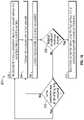
- FIG. 1Ais a flow diagram illustrating a selective deposition process for depositing a material on a first surface while reducing the thickness of a passivation layer over a second surface.
- FIG. 1Bis a flow diagram illustrating a selective deposition process for depositing a material on a first surface while reducing the thickness of a passivation layer selectively deposited over a second surface.
- FIG. 2is a graph of some embodiments showing the thickness of a polyimide layer versus the number of cycles of oxidation performed, wherein a passivation ash rate is calculated.
- FIG. 3illustrates the selective deposition of a material on a first surface of a substrate by a cyclical deposition process, while the cyclical deposition process removes a passivation layer over a second surface.
- Dielectric filmssuch as metal oxide or silicon oxide (e.g., SiO) films
- metal oxide or silicon oxide (e.g., SiO) filmshave a wide variety of applications, as will be apparent to the skilled artisan, for example in integrated circuit fabrication.
- various dielectric films, particularly oxide films, precursors, and methods for depositing such filmsare provided.
- a materialis formed on a first surface of a substrate relative to a second surface by a selective deposition process.
- the materialis an oxide material.
- a dielectric filmis formed selectively using a cyclical deposition process on a dielectric surface of a substrate relative to a passivation layer on a metal surface.
- FIG. 1Ais a flow diagram 100 illustrating a selective deposition process of depositing a material on a first surface while reducing the thickness of a passivation layer over a second surface.
- a substrate with a first surface and a second surfaceis provided, wherein the second surface comprises a passivation layer thereover.
- the substrateis contacted with a first reactant
- block 106the substrate is contacted with a second reactant.
- blocks 104 and 106are performed alternately and sequentially.
- the substratemay be repeatedly exposed to the first and second reactants in blocks 104 and 106 until a material of sufficient thickness is formed.
- a sufficiently thick materialis formed and therefore blocks 104 and 106 are not repeated. In some embodiments, a sufficiently thick material is not formed and therefore blocks 104 and 106 are repeated, and the repetition of blocks 104 and 106 is referred to as a cyclical deposition process. Blocks 104 and 106 need not be in the same sequence nor identically performed in each repetition. In some embodiments, blocks 104 and 106 are performed consecutively. In some embodiments, blocks 104 and 106 are separated by one or more intermittent processes. In some embodiments, the repetition of blocks 104 and 106 are performed consecutively. In some embodiments, the repetition of blocks 104 and 106 is separated by one or more intermittent processes.
- intermittent processesmay be selected from at least one of excess reactant and byproduct removal (e.g., vacuum and/or inert gas purge), selective deposition of an additional passivation layer, additional clean up etch, repeated exposure of the same reactant prior to exposure of another reactant, and/or exposure to an additional reactant in some or all cycles.
- excess reactant and byproduct removale.g., vacuum and/or inert gas purge
- selective deposition of an additional passivation layere.g., additional clean up etch
- repeated exposure of the same reactant prior to exposure of another reactante.g., exposure to an additional reactant in some or all cycles.
- Intervening removal of excess reactant and byproductaids in separating the supply of different reactants to minimize risk of gas phase interaction and limit the deposition reactions to surface reactions. Skilled artisans will appreciate that some interactions with residual gases may be tolerated in order to minimize duration of the intervening removal (e.g., purge) steps.
- the selective deposition processis completed in block 110 , where the material is selectively obtained on a first surface and a passivation layer with a reduced thickness is obtained on the second surface.
- Reactantscan be precursors that leave one or more elements in the deposited film.
- one or more reactantscan serve to chemically reduce, oxidize or getter products of the deposited material.
- FIG. 1Bis an example flow diagram 200 illustrating the selective deposition of a material on a first surface while reducing the thickness of a passivation layer, however FIG. 1B includes selectively forming a passivation layer on a second surface. It is to be understood that any of the same or similar features or functions discussed with regard to FIG. 1A may also be applied to the same or similar features or functions of FIG. 1B .
- a passivation layeris selectively formed on a second surface of a substrate relative to a first surface.
- the substrateis contacted with a first reactant
- the substrateis contacted with a second reactant.
- a sufficiently thick materialmay be formed and therefore the material is selectively obtained on the first surface with a passivation layer of a reduced thickness as shown in block 212 . If a sufficiently thick material is not yet formed and if the passivation layer is not at risk of being fully consumed by exposure to the reactants, decision block 210 illustrates that the substrate may be repeatedly and alternately exposed to the first and second reactants in blocks 204 and 206 .
- decision block 210illustrates that first illustrated block 202 may be repeated where a passivation layer is selectively formed on a second surface of a substrate relative to a first surface before the substrate is exposed to the first and second reactants in blocks 204 and 206 .
- the cyclical deposition processis atomic layer deposition (ALD). In some embodiments, the cyclical deposition process is cyclical chemical vapor deposition (CVD).
- the passivation layerwas previously deposited on the second surface (for example, the metal surface). In some embodiments, the passivation layer is partially removed during the cyclical deposition process.
- the passivation layermay be slowly removed, such as by etching, during ALD phases. For example, for an organic (e.g., polymer) passivation layer, etching (e.g., ashing) may be accomplished during deposition phases in which oxidants are supplied, while simultaneously a dielectric film is deposited on the dielectric surface.
- a passivation layeris simultaneously removed while an oxide material is deposited on the dielectric surface during exposure of the substrate to a second reactant in the ALD process.
- the slow etching of the passivation layermay prevent deposition of the dielectric on the passivation layer and on the metal.
- the ALD processmay be a plasma enhanced atomic layer deposition process (PEALD).
- PEALDplasma enhanced atomic layer deposition process
- plasma poweris provided to generate more reactive species from reactants containing oxygen.
- reactant containing oxygencomprises O 2 gas, which is subjected to plasma generating power.
- the plasmamay be generated remotely from the deposition chamber and plasma products supplied to the deposition chamber. In some remote plasma embodiments, the delivery path optimizes delivery of neutral O species while minimizing ion delivery to the substrate. In some embodiments, the plasma may be generated in situ within the deposition chamber.
- the first surface of the substratecomprises a dielectric surface.
- the dielectric surface of the substratecomprises a silicon oxide (e.g., SiO 2 ).
- the dielectric surface of the substratecomprises a low-k material.
- the second surfacecomprises a metal surface.
- a surfaceif a surface is referred to as a metal surface herein, it may be a metal surface or a metallic surface.
- the metal or metallic surfacemay comprise metal, metal oxides, and/or mixtures thereof.
- the metal or metallic surfacemay comprise surface oxidation.
- the metal or metallic material of the metal or metallic surfaceis electrically conductive with or without surface oxidation.
- metal or a metallic surfacecomprises one or more transition metals.
- the metal or metallic surfacecomprises one or more of Al, Cu, Co, Ni, W, Nb, Fe.
- the metal or metallic surfacecomprises at least one of Co, Cu or W.
- the metal or metallic surfacecomprises one or more noble metals, such as Ru.
- the metal or metallic surfacecomprises a conductive metal oxide, nitride, carbide, boride, or combination thereof.
- the metal or metallic surfacemay comprise one or more of RuO x , NbC x , NbB x , NiO x , CoO x , NbO x and WNC x .
- the substratemay comprise a metal nitride, including, but not limited to TiN and/or TaN.
- the metal surfacemay comprise a metal carbide, including, but not limited to TiC and/or TaC.
- the metal surfacemay comprise a metal chalcogenide, including, but not limited to MoS 2 , Sb 2 Te 3 , and/or GeTe.
- the metal surfaceis a TiN surface. In some embodiments the metal surface is a W surface.
- Selectivitycan be given as a percentage calculated by [(deposition on first surface)-(deposition on second surface)]/(deposition on the first surface).
- Depositioncan be measured in any of a variety of ways. In some embodiments deposition may be given as the measured thickness of the deposited material. In some embodiments deposition may be given as the measured amount of material deposited.
- selectivityis greater than about 10%, greater than about 50%, greater than about 75%, greater than about 85%, greater than about 90%, greater than about 93%, greater than about 95%, greater than about 98%, greater than about 99% or even greater than about 99.5%.
- the selectivitycan change over the duration or thickness of a deposition.
- deposition of the dielectricsuch as an oxide
- deposition on the first surface of the substrate relative to the passivation layeris at least about 80% selective, which may be selective enough for some particular applications.
- deposition on the first surface of the substrate relative to the passivation layeris at least about 50% selective, which may be selective enough for some particular applications.
- deposition on the first surface of the substrate relative to the passivation layeris at least about 10% selective, which may be selective enough for some particular applications.
- the passivation layermay be selectively formed on the metal surface prior to selective deposition of the dielectric material on the dielectric surface.
- a passivation layermay be blanket deposited on a patterned substrate, and patterned and etched by traditional processes to leave the passivation layer selectively where the subsequent deposition is to be avoided, such as over a metal surface.
- a passivation layermay be selectively deposited on a metal layer. Selective deposition of a passivation layer may be carried out, for example, as described below, and as described in US Patent Publication No. 2017-0352533 A1 (application Ser. No. 15/170,769) or US Patent Publication No. 2017-0352550 A1 (application Ser. No. 15/486,124), the entire disclosure of each of which is incorporated by reference herein in its entirety.
- the selective formation of the passivation layer over metal surfacesneed not be 100% selective in order to achieve 100% selectivity.
- the passivation layer depositionmay be partially selective such that it is formed to be thicker over the metal surface than over the dielectric surface.
- a subsequent short, timed etch of the passivation materialmay be conducted for a duration to expose the dielectric surface while leaving some passivation layer covering the metal surface.
- a dielectric filmis deposited on a first surface of a substrate with an oxygen based ALD process.
- the deposited dielectric filmmay be, for example, silicon oxide (e.g., SiO 2 ) or other metal oxide that can be grown with a PEALD process.
- the deposited dielectric filmcan comprise SiO 2 , TiO 2 , ZrO 2 , HfO 2 , Nb 2 O 5 , Ta 2 O 5 , WO 3 , NiO and combinations thereof.
- the second surface of the substratemay be covered by a passivation layer.
- the passivation layeris an organic layer.
- the organic passivation layermay be a polymer, such as polyimide or polyamide.
- an oxide material filmis deposited on a first surface of a substrate with an oxygen based ALD process.
- the deposited oxide material filmmay be a conductive oxide film.
- the conductive oxide filmis an indium tin oxide (ITO) film.
- the deposited oxide material filmmay be a dielectric film, as described herein.
- the passivation layerinhibits oxide material film and/or dielectric film deposition there.
- the passivation layerdoes not inhibit deposition of the oxide material film or dielectric film, that is, the oxide material film or dielectric film chemistry may not be selective as between the underlying dielectric substrate surface and the passivation layer. This is due to the fact that conditions are selected to ensure some removal of the passivation layer during the ALD process, thus undercutting and removing any deposition of the oxide material film or dielectric film over the passivation layer.
- the passivation layeris sacrificial, the passivation layer is slowly removed (e.g., etched) during one of the cyclical deposition phases.
- an organic (e.g., polymer) passivation layermay be slowly ashed by an oxidant phase of the ALD sequence, which prevents oxide material film or dielectric film growth on the passivation layer.
- a passivation layeris removed during exposure of the substrate to a second reactant in the ALD process, which prevents oxide material film or dielectric film growth on the passivation layer. Relative to the growth over the passivation layer, the oxide material film or dielectric film is deposited normally (non-selectively, or with low selectivity) on the dielectric surface.
- any passivation layer remaining on the dielectric surfacecan be removed with a plasma pretreatment with suitable parameters.
- any passivation layer remaining on the dielectric surfaceis removed by initial phases of the ALD process, including oxidation phase, or by simply conducting the oxidation phase of the ALD process before initiating the full ALD process wherein after the thinner passivation layer on dielectric is completely ashed the oxide material film or dielectric film deposition process begins.
- the ALD sequencemay start with the second reactant, including oxidant, to serve for a short timed etch of undesired passivation material from the first surface, without removal of all the passivation material from the second surface, before selective deposition on the first surface.
- the second reactantincluding oxidant
- the oxidation phase of the ALD processis a plasma process in a PEALD sequence.
- the plasmais oxygen based.
- the plasmamay be generated in O 2 gas or a mixture of O 2 and a noble gas, such as Ar.
- the plasmamay be generated in a gas comprising oxygen, or may otherwise comprise excited oxygen species.
- the oxidation phase of the ALD processis a non-plasma oxidation process (e.g., H 2 O or O 3 ).
- plasmafor example oxygen containing plasma
- plasmamay be generated by applying RF power of from about 10 W to about 2000 W, from about 50 W to about 1000 W, from about 100 W to about 500 W, from about 30 W to 100 W, or about 100 W in some embodiments.
- the RF power densitymay be from about 0.02 W/cm 2 to about 2.0 W/cm 2 , or from about 0.05 W/cm 2 to about 1.5 W/cm 2 .
- the RF powermay be applied to a reactant that flows during the plasma contacting time, that flows continuously through the reaction chamber, and/or that flows through a remote plasma generator.
- the plasmais generated in situ, while in other embodiments the plasma is generated remotely.
- a showerhead reactoris utilized and plasma is generated in situ between a susceptor (on top of which the substrate is located) and a showerhead plate.
- the gap between the susceptor and showerhead plateis from about 0.1 cm to about 20 cm, from about 0.5 cm to about 5 cm, or from about 0.8 cm to about 3.0 cm.
- the thickness of the oxide film that can be formed on dielectric surface before the passivation layer is completely removeddepends on the passivation layer initial thickness, ash rate of the passivation layer, and the growth rate of the oxide deposition process.
- FIG. 2demonstrates that with an ash rate of ⁇ 0.2 ⁇ /cycle, a 20 nm sacrificial polyimide layer on a metal surface, and a growth per cycle (GPC) of 1 ⁇ /cycle, 50 nm of SiO 2 may be deposited on a dielectric surface by applying 500 cycles of the oxygen based PEALD process.
- each oxidant phaseincludes 1 second of O 2 plasma and 1 second of purge.
- the PEALDwould include one phase of the above oxidant phase alternated with supply of a silicon precursor and purge, where the silicon precursor is selected for adsorption on the dielectric or growing silicon oxide film and to react with the oxidant phases to form silicon oxide.
- oxidant phasescan be alternated with a supply of one or more metal precursor phase(s) and attendant purge phase(s), where the metal precursor is selected to adsorb on the dielectric surface or the growing metal oxide film and to react to with the oxidant phases to form the desired oxide.
- optimization of the etch rate of the sacrificial passivation layercan be tuned so that growth of the oxide material film or dielectric film does not result in net deposition on the passivation layer during the ALD process.
- the incubation time for deposition on the passivation layeris sufficiently long enough that a desired oxide layer thickness is deposited on the dielectric surface.
- a thick enough passivation layeris formed over the metal surface such that a sufficiently thick oxide film may be deposited over the dielectric surface using the ALD process without further depositing another passivation film layer, i.e., without fully consuming the initial passivation layer.
- a selective passivation layer deposition and the selective ALD processare performed in an iterative manner, for example such using the process described in FIG. 1B .
- This iterative processmay enable the thickness of the passivation layer to be replenished after the ALD process is performed, therefore allowing subsequent ALD processes to be performed.
- the passivation layeris ashed away in 100 cycles or if the incubation on passivation layer is 100 cycles before the deposited oxide begins to form on the passivation layer faster than it can be removed by undercutting
- 90 cycles of a first ALD processmay be performed to selectively deposit the oxide on the dielectric surface
- deposition of a subsequent passivation layer over the previous passivation layermay be performed
- a second 90 cycles of the ALD processmay be performed.
- this iterative processmay be repeated as many times as desired to obtain a desired oxide layer thickness on the dielectric surface.
- the PEALD depositionmay be carried out essentially as described above.
- the substrateis alternately and sequentially contacted with a first reactant comprising elements to be included in the deposited material, such as a metal or silicon, and a second reactant comprising oxygen, and a second plasma reactant.
- the second plasma reactantdoes not comprise oxygen species.
- no reactants comprising oxygen speciesare used other than the second reactant.
- the plasma and precursorsi.e. the first and second reactants
- a PEALD deposition processbegins with the plasma pulse followed by the precursors, and the reaction sequence, or deposition cycle, may be repeated a desired number of times (A): A ⁇ (plasma pulse/purge/precursors/purge)
- the deposition cyclebegins with the non-plasma precursors, which is then followed by the plasma pulse.
- PEALD processes utilizedmay be any suitable oxygen based plasma processes.
- the deposited dielectric filmis an oxide film.
- the deposited dielectric filmis a metal oxide film.
- the deposited dielectric filmmay be selected from the group consisting of SiO 2 , TiO 2 , ZrO 2 , HfO 2 , Nb 2 O 5 , Ta 2 O 5 , WO 3 and NiO.
- the deposited dielectric filmis silicon oxide.
- an oxide precursoris an alkylaminosilane, which is used to deposit silicon oxide films.
- an oxide filmis selectively formed on a first dielectric surface of a substrate relative to a second, different metal or metallic surface of the substrate by an oxygen-based PEALD process.
- silicon oxidemay be selectively deposited by oxygen-based PEALD on a low-k dielectric surface (e.g., silicon oxide-based surface) relative to a metal surface.
- FIG. 3shows a schematic of some embodiments, wherein a substrate 302 comprises a first surface of a first structure 304 (for example, a dielectric surface of a dielectric layer) and a second surface of a second structure 306 that has a different material composition (for example, a metal surface of a metal layer, such as a cobalt, copper or tungsten surface) further comprising an initial passivation layer 308 A having a first thickness (for example, 20 nm of a polyimide organic layer), in which a material 312 is selectively deposited on the first surface relative to the second surface (due to selectively relative to the overlying initial passivation layer 308 A).
- the selectively deposited material 312is an oxide material.
- the oxide materialis a dielectric material.
- the dielectric oxideis a film of silicon oxide.
- the material 312for example, 50 nm of SiO
- the selective deposition processhalts before all of the initial passivation layer is removed.
- the reduced thickness of the remaining passivation layer 308 Bmay be subsequently removed (for example, by ashing) without deposition to expose the second surface of the second structure 306 .
- the PEALD process disclosedmay accomplish selective formation of silicon oxide or other oxides on dielectric surfaces. In some embodiments, the PEALD process disclosed may accomplish a reduction in the number of steps for forming desired patterns in various device manufacturing process flows, relative to convention patterning processes.
Landscapes
- Chemical & Material Sciences (AREA)
- Engineering & Computer Science (AREA)
- Physics & Mathematics (AREA)
- Chemical Kinetics & Catalysis (AREA)
- Condensed Matter Physics & Semiconductors (AREA)
- General Physics & Mathematics (AREA)
- Manufacturing & Machinery (AREA)
- Computer Hardware Design (AREA)
- Microelectronics & Electronic Packaging (AREA)
- Power Engineering (AREA)
- General Chemical & Material Sciences (AREA)
- Materials Engineering (AREA)
- Mechanical Engineering (AREA)
- Metallurgy (AREA)
- Organic Chemistry (AREA)
- Plasma & Fusion (AREA)
- Inorganic Chemistry (AREA)
- Electromagnetism (AREA)
- Formation Of Insulating Films (AREA)
- Chemical Vapour Deposition (AREA)
- Internal Circuitry In Semiconductor Integrated Circuit Devices (AREA)
- Electrodes Of Semiconductors (AREA)
- Treatments Of Macromolecular Shaped Articles (AREA)
Abstract
Description
The present application is a continuation of U.S. patent application Ser. No. 16/399,328, filed Apr. 30, 2019, which claims priority to U.S. Provisional Patent Application No. 62/666,039, filed May 2, 2018, the disclosures of each of which are incorporated herein by reference in their entireties for all purposes.
The present disclosure relates generally to the field of semiconductor device manufacturing and, more particularly, to selective formation of layers employing deposition and removal of films.
In the semiconductor industry, there is an increasing need for selective processes. For example, film growth may be desired on one surface but not on a second, different surface. These two different surfaces can comprise different materials, for example a metal and a dielectric. Good selective processes could reduce the number process steps by avoiding more complicated processes for separate patterning of the deposited material, such as photolithographic masking and patterning, thus saving time and money.
In one aspect a method is provided for an atomic layer deposition (ALD) process for selectively forming a dielectric material on a first surface of a patterned substrate. The method includes providing a substrate comprising a first surface and a second surface, wherein the second surface comprises a passivation layer thereover. The method further includes conducting at least one deposition cycle comprising alternately and sequentially contacting the substrate with a first precursor and a second reactant comprising oxygen. The method further includes wherein the second reactant reacts with the first precursor to form a dielectric material on the first surface, and wherein the passivation layer is ashed by the second reactant during each deposition cycle.
In some embodiments, the method for an ALD process further includes wherein the first surface is a dielectric surface. In some embodiments, the dielectric surface comprises silicon oxide. In some embodiments, the first surface comprises a low-k material. In some embodiments, the second surface is a metal surface. In some embodiments, the metal surface comprises at least one of Co, Cu or W. In some embodiments, the dielectric material is an oxide. In some embodiments, the oxide is silicon oxide. In some embodiments, the oxide is a metal oxide.
In some embodiments, the first precursor comprises a metal precursor, a silicon precursor, or mixtures thereof. In some embodiments, the first precursor is an alkylaminosilane.
In some embodiments, the passivation layer comprises an organic material. In some embodiments, the passivation layer is selectively deposited on the second surface relative to the first surface prior to beginning the first deposition cycle. In some embodiments, the deposition cycle is repeated a plurality of times to form an oxide film of a desired thickness on the dielectric surface. In some embodiments, additional passivation layer is selectively deposited on the passivation layer between the beginning and end of each deposition cycle.
In some embodiments, the ALD process is a plasma enhanced atomic layer deposition (PEALD) process. In some embodiments, the at least one deposition cycle begins with contacting the substrate with the second reactant before contact with the first precursor. In some embodiments, the at least one deposition cycle further comprises contacting the substrate with at least one additional reactant in each cycle. In some embodiments, the second reactant further comprises plasma. In some embodiments, contacting the substrate with the second reactant further comprises activating the second reactant with plasma.
In some embodiments, the dielectric material is selectively formed on the first surface relative to the passivation layer. In some embodiments, the dielectric material is formed on the passivation layer and the dielectric material is removed from the passivation layer with the ashing of the passivation layer, thereby selectively forming the dielectric material on the first surface.
In another aspect a cyclical deposition process is provided for selectively a forming a material on a surface of a patterned substrate. The method includes providing a substrate comprising a first surface and a second surface, wherein the second surface comprises a passivation layer thereover. The method further includes conducting at least one deposition cycle comprising alternately and sequentially contacting the substrate with a first precursor and a second reactant. The second reactant reacts with the first precursor to form the material on the first surface, and the passivation layer is etched by the second reactant during each deposition cycle.
In some embodiments, the process comprises atomic layer deposition (ALD). In some embodiments, the process comprises plasma enhanced ALD (PEALD). In some embodiments, the second reactant comprises plasma-activated species. In some embodiments, the second reactant comprises oxygen, the passivation layer comprises an organic layer, and etching comprises ashing. In some embodiments, the passivation layer comprises a polymer.
In some embodiments, deposition is halted before the etching of the passivation layer exposes the second surface. In some embodiments, the method includes further depositing additional passivation layer over the second surface after halting the deposition and prior to continuing the deposition.
In another aspect a plasma enhanced atomic layer deposition (PEALD) process is provided for selectively forming an oxide material on a first dielectric surface of a patterned substrate. The method includes providing a substrate comprising a first dielectric surface and a second metallic surface, wherein the second metallic surface comprises an organic passivation layer thereover. The method further includes conducting at least one deposition cycle comprising alternately and sequentially contacting the substrate with a first precursor and a second reactant comprising oxygen and plasma. The second reactant reacts with the first precursor to form an oxide material on the first dielectric surface, and the organic passivation layer is ashed by the second reactant during each deposition cycle.
Dielectric films, such as metal oxide or silicon oxide (e.g., SiO) films, have a wide variety of applications, as will be apparent to the skilled artisan, for example in integrated circuit fabrication. According to some embodiments of the present disclosure, various dielectric films, particularly oxide films, precursors, and methods for depositing such films are provided.
In some embodiments, a material is formed on a first surface of a substrate relative to a second surface by a selective deposition process. In some embodiments, the material is an oxide material. In some embodiments, a dielectric film is formed selectively using a cyclical deposition process on a dielectric surface of a substrate relative to a passivation layer on a metal surface.
For example,FIG. 1A is a flow diagram100 illustrating a selective deposition process of depositing a material on a first surface while reducing the thickness of a passivation layer over a second surface. In the first illustrated block102 a substrate with a first surface and a second surface is provided, wherein the second surface comprises a passivation layer thereover. Inblock 104 the substrate is contacted with a first reactant, and inblock 106 the substrate is contacted with a second reactant. In some embodiments, blocks104 and106 are performed alternately and sequentially. In illustrateddecision block 108, the substrate may be repeatedly exposed to the first and second reactants inblocks blocks Blocks blocks blocks block 110, where the material is selectively obtained on a first surface and a passivation layer with a reduced thickness is obtained on the second surface. Reactants can be precursors that leave one or more elements in the deposited film. In some embodiments, one or more reactants can serve to chemically reduce, oxidize or getter products of the deposited material.
Similar toFIG. 1A ,FIG. 1B is an example flow diagram200 illustrating the selective deposition of a material on a first surface while reducing the thickness of a passivation layer, howeverFIG. 1B includes selectively forming a passivation layer on a second surface. It is to be understood that any of the same or similar features or functions discussed with regard toFIG. 1A may also be applied to the same or similar features or functions ofFIG. 1B . In the first illustrated block202 a passivation layer is selectively formed on a second surface of a substrate relative to a first surface. Inblock 204 the substrate is contacted with a first reactant, and inblock 206 the substrate is contacted with a second reactant. In illustrateddecision block 208, a sufficiently thick material may be formed and therefore the material is selectively obtained on the first surface with a passivation layer of a reduced thickness as shown inblock 212. If a sufficiently thick material is not yet formed and if the passivation layer is not at risk of being fully consumed by exposure to the reactants,decision block 210 illustrates that the substrate may be repeatedly and alternately exposed to the first and second reactants inblocks decision block 210 illustrates that firstillustrated block 202 may be repeated where a passivation layer is selectively formed on a second surface of a substrate relative to a first surface before the substrate is exposed to the first and second reactants inblocks
In some embodiments, the cyclical deposition process is atomic layer deposition (ALD). In some embodiments, the cyclical deposition process is cyclical chemical vapor deposition (CVD). In some embodiments, the passivation layer was previously deposited on the second surface (for example, the metal surface). In some embodiments, the passivation layer is partially removed during the cyclical deposition process. During an ALD process, for example, the passivation layer may be slowly removed, such as by etching, during ALD phases. For example, for an organic (e.g., polymer) passivation layer, etching (e.g., ashing) may be accomplished during deposition phases in which oxidants are supplied, while simultaneously a dielectric film is deposited on the dielectric surface. In another example, a passivation layer is simultaneously removed while an oxide material is deposited on the dielectric surface during exposure of the substrate to a second reactant in the ALD process. The slow etching of the passivation layer may prevent deposition of the dielectric on the passivation layer and on the metal.
In some embodiments, the ALD process may be a plasma enhanced atomic layer deposition process (PEALD). In some embodiments, plasma power is provided to generate more reactive species from reactants containing oxygen. In some embodiments, reactant containing oxygen comprises O2gas, which is subjected to plasma generating power. In some embodiments, the plasma may be generated remotely from the deposition chamber and plasma products supplied to the deposition chamber. In some remote plasma embodiments, the delivery path optimizes delivery of neutral O species while minimizing ion delivery to the substrate. In some embodiments, the plasma may be generated in situ within the deposition chamber.
In some embodiments, the first surface of the substrate comprises a dielectric surface. In some embodiments, the dielectric surface of the substrate comprises a silicon oxide (e.g., SiO2). In some embodiments, the dielectric surface of the substrate comprises a low-k material.
In some embodiments, the second surface comprises a metal surface. Unless otherwise indicated, if a surface is referred to as a metal surface herein, it may be a metal surface or a metallic surface. In some embodiments the metal or metallic surface may comprise metal, metal oxides, and/or mixtures thereof. In some embodiments the metal or metallic surface may comprise surface oxidation. In some embodiments the metal or metallic material of the metal or metallic surface is electrically conductive with or without surface oxidation. In some embodiments metal or a metallic surface comprises one or more transition metals. In some embodiments the metal or metallic surface comprises one or more of Al, Cu, Co, Ni, W, Nb, Fe. In some embodiments the metal or metallic surface comprises at least one of Co, Cu or W. In some embodiments the metal or metallic surface comprises one or more noble metals, such as Ru. In some embodiments the metal or metallic surface comprises a conductive metal oxide, nitride, carbide, boride, or combination thereof. For example, the metal or metallic surface may comprise one or more of RuOx, NbCx, NbBx, NiOx, CoOx, NbOxand WNCx. In some embodiments the substrate may comprise a metal nitride, including, but not limited to TiN and/or TaN. In some embodiments the metal surface may comprise a metal carbide, including, but not limited to TiC and/or TaC. In some embodiments the metal surface may comprise a metal chalcogenide, including, but not limited to MoS2, Sb2Te3, and/or GeTe. In some embodiments the metal surface is a TiN surface. In some embodiments the metal surface is a W surface.
Selectivity
Selectivity can be given as a percentage calculated by [(deposition on first surface)-(deposition on second surface)]/(deposition on the first surface). Deposition can be measured in any of a variety of ways. In some embodiments deposition may be given as the measured thickness of the deposited material. In some embodiments deposition may be given as the measured amount of material deposited.
In some embodiments selectivity is greater than about 10%, greater than about 50%, greater than about 75%, greater than about 85%, greater than about 90%, greater than about 93%, greater than about 95%, greater than about 98%, greater than about 99% or even greater than about 99.5%. In embodiments described herein, the selectivity can change over the duration or thickness of a deposition.
In some embodiments deposition of the dielectric, such as an oxide, only occurs on the first dielectric surface and does not occur on the passivation layer over the second metal surface. In some embodiments deposition on the first surface of the substrate relative to the passivation layer is at least about 80% selective, which may be selective enough for some particular applications. In some embodiments the deposition on the first surface of the substrate relative to the passivation layer is at least about 50% selective, which may be selective enough for some particular applications. In some embodiments the deposition on the first surface of the substrate relative to the passivation layer is at least about 10% selective, which may be selective enough for some particular applications.
In some embodiments the passivation layer may be selectively formed on the metal surface prior to selective deposition of the dielectric material on the dielectric surface. For example, in some embodiments, a passivation layer may be blanket deposited on a patterned substrate, and patterned and etched by traditional processes to leave the passivation layer selectively where the subsequent deposition is to be avoided, such as over a metal surface. In other embodiments, a passivation layer may be selectively deposited on a metal layer. Selective deposition of a passivation layer may be carried out, for example, as described below, and as described in US Patent Publication No. 2017-0352533 A1 (application Ser. No. 15/170,769) or US Patent Publication No. 2017-0352550 A1 (application Ser. No. 15/486,124), the entire disclosure of each of which is incorporated by reference herein in its entirety.
As noted above, the selective formation of the passivation layer over metal surfaces need not be 100% selective in order to achieve 100% selectivity. For example, the passivation layer deposition may be partially selective such that it is formed to be thicker over the metal surface than over the dielectric surface. A subsequent short, timed etch of the passivation material may be conducted for a duration to expose the dielectric surface while leaving some passivation layer covering the metal surface.
ALD Process
According to some embodiments, a dielectric film is deposited on a first surface of a substrate with an oxygen based ALD process. In some embodiments, the deposited dielectric film may be, for example, silicon oxide (e.g., SiO2) or other metal oxide that can be grown with a PEALD process. In some embodiments, the deposited dielectric film can comprise SiO2, TiO2, ZrO2, HfO2, Nb2O5, Ta2O5, WO3, NiO and combinations thereof. The second surface of the substrate may be covered by a passivation layer. In some embodiments, the passivation layer is an organic layer. The organic passivation layer may be a polymer, such as polyimide or polyamide.
In some embodiments, an oxide material film is deposited on a first surface of a substrate with an oxygen based ALD process. In some embodiments, the deposited oxide material film may be a conductive oxide film. For example, in some embodiments the conductive oxide film is an indium tin oxide (ITO) film. In some embodiments, the deposited oxide material film may be a dielectric film, as described herein.
In some embodiments, the passivation layer inhibits oxide material film and/or dielectric film deposition there. However, in some embodiments, the passivation layer does not inhibit deposition of the oxide material film or dielectric film, that is, the oxide material film or dielectric film chemistry may not be selective as between the underlying dielectric substrate surface and the passivation layer. This is due to the fact that conditions are selected to ensure some removal of the passivation layer during the ALD process, thus undercutting and removing any deposition of the oxide material film or dielectric film over the passivation layer. As the passivation layer is sacrificial, the passivation layer is slowly removed (e.g., etched) during one of the cyclical deposition phases. For example, in an ALD sequence, an organic (e.g., polymer) passivation layer may be slowly ashed by an oxidant phase of the ALD sequence, which prevents oxide material film or dielectric film growth on the passivation layer. In another example, in an ALD sequence, a passivation layer is removed during exposure of the substrate to a second reactant in the ALD process, which prevents oxide material film or dielectric film growth on the passivation layer. Relative to the growth over the passivation layer, the oxide material film or dielectric film is deposited normally (non-selectively, or with low selectivity) on the dielectric surface. Regardless of whether the oxide material film or dielectric material is deposited normally or selectively on the dielectric surface, slowly etching (e.g., ashing) the sacrificial passivation layer by an oxidant phase of the ALD sequence has the end effect of selectively forming the oxide material film or dielectric material on the dielectric substrate relative to the passivation layer. Thus, using the process ofFIG. 1A or 1B can effectively increase selectivity of the formation of the oxide material film or dielectric film.
In some embodiments, before deposition of the oxide material film or dielectric film is performed but after the passivation layer is formed, any passivation layer remaining on the dielectric surface can be removed with a plasma pretreatment with suitable parameters. In some embodiments, rather than a separate process to remove any passivation material from over the dielectric surface, any passivation layer remaining on the dielectric surface is removed by initial phases of the ALD process, including oxidation phase, or by simply conducting the oxidation phase of the ALD process before initiating the full ALD process wherein after the thinner passivation layer on dielectric is completely ashed the oxide material film or dielectric film deposition process begins. Thus, the ALD sequence may start with the second reactant, including oxidant, to serve for a short timed etch of undesired passivation material from the first surface, without removal of all the passivation material from the second surface, before selective deposition on the first surface.
In some embodiments, the oxidation phase of the ALD process is a plasma process in a PEALD sequence. In some embodiments, the plasma is oxygen based. For example, the plasma may be generated in O2gas or a mixture of O2and a noble gas, such as Ar. In some embodiments the plasma may be generated in a gas comprising oxygen, or may otherwise comprise excited oxygen species. In some embodiments, the oxidation phase of the ALD process is a non-plasma oxidation process (e.g., H2O or O3).
In some embodiments plasma, for example oxygen containing plasma, may be generated by applying RF power of from about 10 W to about 2000 W, from about 50 W to about 1000 W, from about 100 W to about 500 W, from about 30 W to 100 W, or about 100 W in some embodiments. In some embodiments the RF power density may be from about 0.02 W/cm2to about 2.0 W/cm2, or from about 0.05 W/cm2to about 1.5 W/cm2. The RF power may be applied to a reactant that flows during the plasma contacting time, that flows continuously through the reaction chamber, and/or that flows through a remote plasma generator. Thus in some embodiments the plasma is generated in situ, while in other embodiments the plasma is generated remotely. In some embodiments a showerhead reactor is utilized and plasma is generated in situ between a susceptor (on top of which the substrate is located) and a showerhead plate. In some embodiments the gap between the susceptor and showerhead plate is from about 0.1 cm to about 20 cm, from about 0.5 cm to about 5 cm, or from about 0.8 cm to about 3.0 cm.
The thickness of the oxide film that can be formed on dielectric surface before the passivation layer is completely removed depends on the passivation layer initial thickness, ash rate of the passivation layer, and the growth rate of the oxide deposition process. For example,FIG. 2 demonstrates that with an ash rate of ˜0.2 Å/cycle, a 20 nm sacrificial polyimide layer on a metal surface, and a growth per cycle (GPC) of 1 Å/cycle, 50 nm of SiO2may be deposited on a dielectric surface by applying 500 cycles of the oxygen based PEALD process.FIG. 2 shows the ash rate of polyimide when exposed to oxidant phases in which argon is supplied at 700 sccm, O2is supplied at 100 sccm, pressure is kept at 2 Torr, plasma power is set to 100 W, substrate temperature is maintained at 100° C., and each oxidant phase includes 1 second of O2plasma and 1 second of purge. The PEALD would include one phase of the above oxidant phase alternated with supply of a silicon precursor and purge, where the silicon precursor is selected for adsorption on the dielectric or growing silicon oxide film and to react with the oxidant phases to form silicon oxide. In other embodiments, oxidant phases can be alternated with a supply of one or more metal precursor phase(s) and attendant purge phase(s), where the metal precursor is selected to adsorb on the dielectric surface or the growing metal oxide film and to react to with the oxidant phases to form the desired oxide.
In some embodiments, optimization of the etch rate of the sacrificial passivation layer can be tuned so that growth of the oxide material film or dielectric film does not result in net deposition on the passivation layer during the ALD process. In some embodiments, the incubation time for deposition on the passivation layer is sufficiently long enough that a desired oxide layer thickness is deposited on the dielectric surface. In some embodiments a thick enough passivation layer is formed over the metal surface such that a sufficiently thick oxide film may be deposited over the dielectric surface using the ALD process without further depositing another passivation film layer, i.e., without fully consuming the initial passivation layer.
In some embodiments, a selective passivation layer deposition and the selective ALD process are performed in an iterative manner, for example such using the process described inFIG. 1B . This iterative process may enable the thickness of the passivation layer to be replenished after the ALD process is performed, therefore allowing subsequent ALD processes to be performed. For example, if the passivation layer is ashed away in 100 cycles or if the incubation on passivation layer is 100 cycles before the deposited oxide begins to form on the passivation layer faster than it can be removed by undercutting, 90 cycles of a first ALD process may be performed to selectively deposit the oxide on the dielectric surface, deposition of a subsequent passivation layer over the previous passivation layer may be performed, and a second 90 cycles of the ALD process may be performed. In some embodiments, this iterative process may be repeated as many times as desired to obtain a desired oxide layer thickness on the dielectric surface. A person of ordinary skill in the art would appreciate that the number of iterative processes necessary would vary depending on a number of factors such as, for example, the thickness of the deposited oxide desired, the thickness of the passivation layer, and the ash rate or incubation period of the passivation layer.
In some embodiments, the PEALD deposition may be carried out essentially as described above. In other embodiments, the substrate is alternately and sequentially contacted with a first reactant comprising elements to be included in the deposited material, such as a metal or silicon, and a second reactant comprising oxygen, and a second plasma reactant. In some embodiments the second plasma reactant does not comprise oxygen species. In some embodiments no reactants comprising oxygen species are used other than the second reactant. The plasma and precursors (i.e. the first and second reactants) may be provided in pulses separated by a removal process (e.g., purge) in which excess reactant and reaction byproducts, if any, are removed from the reaction space. In some embodiments, a PEALD deposition process begins with the plasma pulse followed by the precursors, and the reaction sequence, or deposition cycle, may be repeated a desired number of times (A):
A×(plasma pulse/purge/precursors/purge)
A×(plasma pulse/purge/precursors/purge)
In some embodiments the deposition cycle begins with the non-plasma precursors, which is then followed by the plasma pulse.
According to some embodiments, PEALD processes utilized may be any suitable oxygen based plasma processes. In some embodiments, the deposited dielectric film is an oxide film. In some embodiments, the deposited dielectric film is a metal oxide film. In some embodiments, the deposited dielectric film may be selected from the group consisting of SiO2, TiO2, ZrO2, HfO2, Nb2O5, Ta2O5, WO3and NiO. In some embodiments, the deposited dielectric film is silicon oxide. In some embodiments, an oxide precursor is an alkylaminosilane, which is used to deposit silicon oxide films.
In some embodiments, an oxide film is selectively formed on a first dielectric surface of a substrate relative to a second, different metal or metallic surface of the substrate by an oxygen-based PEALD process. For example, silicon oxide may be selectively deposited by oxygen-based PEALD on a low-k dielectric surface (e.g., silicon oxide-based surface) relative to a metal surface.
In some embodiments, the PEALD process disclosed may accomplish selective formation of silicon oxide or other oxides on dielectric surfaces. In some embodiments, the PEALD process disclosed may accomplish a reduction in the number of steps for forming desired patterns in various device manufacturing process flows, relative to convention patterning processes.
It will be understood by those of skill in the art that numerous and various modifications can be made without departing from the spirit of the present invention. The described features, structures, characteristics and precursors can be combined in any suitable manner. Therefore, it should be clearly understood that the forms of the present invention are illustrative only and are not intended to limit the scope of the present invention. All modifications and changes are intended to fall within the scope of the invention, as defined by the appended claims.
Claims (20)
1. A method of selectively forming a dielectric material on a first surface of a substrate, the method comprising:
providing a substrate comprising a first surface and a second surface, wherein the second surface comprises a passivation layer thereover;
conducting a cyclical deposition process that comprises a plurality of deposition cycles, wherein at least one deposition cycle of the deposition cycles comprises separately contacting the substrate with a precursor and a reactant comprising oxygen;
wherein the reactant reacts with the precursor on the first surface to form a dielectric material on the first surface; and
wherein passivation material of the passivation layer is ashed by the reactant during the at least one deposition cycle, such that a result of the cyclical deposition process is to selectively form the dielectric material on the first surface.
2. The method ofclaim 1 , further comprising depositing additional passivation material over the passivation layer between an end of the one deposition cycle of the cyclical deposition process and a beginning of a subsequent deposition cycle of the cyclical deposition process.
3. The method ofclaim 1 , wherein the cyclical deposition process is halted before the ashing of the passivation layer exposes the second surface.
4. The method ofclaim 1 , wherein the passivation layer is ashed in each of the deposition cycles of the cyclical deposition process that include contacting the substrate with the reactant.
5. The method ofclaim 1 , further comprising selectively depositing the passivation layer on the second surface relative to the first surface prior to beginning a first deposition cycle of the at least one deposition cycle.
6. The method ofclaim 1 , wherein the at least one deposition cycle is repeated a plurality of times to form an oxide film of a desired thickness on the first surface.
7. The method ofclaim 6 , further comprising selectively depositing additional passivation material over the second surface between a beginning and an end of the cyclical deposition process.
8. The method ofclaim 1 , wherein said contacting the substrate with the reactant comprises activating the reactant with plasma.
9. The method ofclaim 1 , wherein the first surface is a dielectric surface.
10. The method ofclaim 1 , wherein the first surface comprises silicon oxide.
11. The method ofclaim 1 , wherein the second surface is a metal surface.
12. The method ofclaim 1 , wherein the passivation layer comprises an organic material.
13. The method ofclaim 1 , wherein the at least one deposition cycle begins with contacting the substrate with the reactant before contacting the substrate with the precursor.
14. The method ofclaim 1 , wherein the cyclical deposition process is an atomic layer deposition process.
15. A method for selectively forming a material on a surface of a patterned substrate, the method comprising:
providing a substrate comprising a first surface and a second surface, wherein the second surface comprises a passivation layer thereover;
conducting deposition cycles, wherein at least one of the deposition cycles comprises separately contacting the substrate with a precursor and a reactant, wherein the reactant reacts with the precursor on the first surface to form the material on the first surface, wherein the passivation layer is etched by the reactant while reacting with the precursor during the at least one of the deposition cycles, such that the deposition cycles selectively form the material on the first surface; and
depositing passivation material over the second surface between a first deposition cycle of the deposition cycles and a last deposition cycle of the deposition cycles.
16. The method ofclaim 15 , wherein the reactant comprises a plasma-activated species.
17. The method ofclaim 15 , wherein the reactant comprises oxygen, the passivation layer comprises an organic layer, and etching comprises ashing.
18. The method ofclaim 17 , wherein the material is formed on the passivation layer, and wherein the material on the passivation layer is removed by ashing the passivation layer.
19. A plasma enhanced method for selectively forming an oxide material on a dielectric surface of a substrate, the plasma enhanced method comprising:
providing a substrate comprising a dielectric surface and a metallic surface, wherein the metallic surface comprises a passivation layer thereover; and
conducting deposition cycles, at least one deposition cycle of the deposition cycles comprising separately contacting the substrate with a precursor and a reactant, wherein the reactant comprises oxygen and plasma;
wherein the reactant reacts with the precursor on the dielectric surface to form an oxide material on the dielectric surface; and
wherein the passivation layer is ashed by the reactant during the at least one deposition cycle, and wherein the oxide material is selectively formed on the dielectric surface by the deposition cycles.
20. The plasma enhanced method ofclaim 19 , further comprising depositing passivation material over the metallic surface between a first deposition cycle and a last deposition cycle.
Priority Applications (2)
| Application Number | Priority Date | Filing Date | Title |
|---|---|---|---|
| US17/113,383US11501966B2 (en) | 2018-05-02 | 2020-12-07 | Selective layer formation using deposition and removing |
| US17/934,817US11804373B2 (en) | 2018-05-02 | 2022-09-23 | Selective layer formation using deposition and removing |
Applications Claiming Priority (3)
| Application Number | Priority Date | Filing Date | Title |
|---|---|---|---|
| US201862666039P | 2018-05-02 | 2018-05-02 | |
| US16/399,328US10872765B2 (en) | 2018-05-02 | 2019-04-30 | Selective layer formation using deposition and removing |
| US17/113,383US11501966B2 (en) | 2018-05-02 | 2020-12-07 | Selective layer formation using deposition and removing |
Related Parent Applications (1)
| Application Number | Title | Priority Date | Filing Date |
|---|---|---|---|
| US16/399,328ContinuationUS10872765B2 (en) | 2018-05-02 | 2019-04-30 | Selective layer formation using deposition and removing |
Related Child Applications (1)
| Application Number | Title | Priority Date | Filing Date |
|---|---|---|---|
| US17/934,817ContinuationUS11804373B2 (en) | 2018-05-02 | 2022-09-23 | Selective layer formation using deposition and removing |
Publications (2)
| Publication Number | Publication Date |
|---|---|
| US20210118669A1 US20210118669A1 (en) | 2021-04-22 |
| US11501966B2true US11501966B2 (en) | 2022-11-15 |
Family
ID=68383895
Family Applications (3)
| Application Number | Title | Priority Date | Filing Date |
|---|---|---|---|
| US16/399,328ActiveUS10872765B2 (en) | 2018-05-02 | 2019-04-30 | Selective layer formation using deposition and removing |
| US17/113,383Active2039-06-15US11501966B2 (en) | 2018-05-02 | 2020-12-07 | Selective layer formation using deposition and removing |
| US17/934,817ActiveUS11804373B2 (en) | 2018-05-02 | 2022-09-23 | Selective layer formation using deposition and removing |
Family Applications Before (1)
| Application Number | Title | Priority Date | Filing Date |
|---|---|---|---|
| US16/399,328ActiveUS10872765B2 (en) | 2018-05-02 | 2019-04-30 | Selective layer formation using deposition and removing |
Family Applications After (1)
| Application Number | Title | Priority Date | Filing Date |
|---|---|---|---|
| US17/934,817ActiveUS11804373B2 (en) | 2018-05-02 | 2022-09-23 | Selective layer formation using deposition and removing |
Country Status (5)
| Country | Link |
|---|---|
| US (3) | US10872765B2 (en) |
| JP (3) | JP7146690B2 (en) |
| KR (2) | KR102521375B1 (en) |
| CN (2) | CN110444476B (en) |
| TW (3) | TWI783909B (en) |
Cited By (2)
| Publication number | Priority date | Publication date | Assignee | Title |
|---|---|---|---|---|
| US20230016537A1 (en)* | 2018-05-02 | 2023-01-19 | Asm Ip Holding B.V. | Selective layer formation using deposition and removing |
| US12154785B2 (en) | 2016-11-29 | 2024-11-26 | Asm Ip Holding B.V. | Deposition of oxide thin films |
Families Citing this family (34)
| Publication number | Priority date | Publication date | Assignee | Title |
|---|---|---|---|---|
| US9112003B2 (en) | 2011-12-09 | 2015-08-18 | Asm International N.V. | Selective formation of metallic films on metallic surfaces |
| TWI661072B (en) | 2014-02-04 | 2019-06-01 | 荷蘭商Asm Ip控股公司 | Selective deposition of metals, metal oxides, and dielectrics |
| US10047435B2 (en) | 2014-04-16 | 2018-08-14 | Asm Ip Holding B.V. | Dual selective deposition |
| US9490145B2 (en) | 2015-02-23 | 2016-11-08 | Asm Ip Holding B.V. | Removal of surface passivation |
| US10428421B2 (en) | 2015-08-03 | 2019-10-01 | Asm Ip Holding B.V. | Selective deposition on metal or metallic surfaces relative to dielectric surfaces |
| US10566185B2 (en) | 2015-08-05 | 2020-02-18 | Asm Ip Holding B.V. | Selective deposition of aluminum and nitrogen containing material |
| US10121699B2 (en) | 2015-08-05 | 2018-11-06 | Asm Ip Holding B.V. | Selective deposition of aluminum and nitrogen containing material |
| US10814349B2 (en) | 2015-10-09 | 2020-10-27 | Asm Ip Holding B.V. | Vapor phase deposition of organic films |
| US10695794B2 (en) | 2015-10-09 | 2020-06-30 | Asm Ip Holding B.V. | Vapor phase deposition of organic films |
| US11081342B2 (en) | 2016-05-05 | 2021-08-03 | Asm Ip Holding B.V. | Selective deposition using hydrophobic precursors |
| US10453701B2 (en) | 2016-06-01 | 2019-10-22 | Asm Ip Holding B.V. | Deposition of organic films |
| US10373820B2 (en) | 2016-06-01 | 2019-08-06 | Asm Ip Holding B.V. | Deposition of organic films |
| US9803277B1 (en) | 2016-06-08 | 2017-10-31 | Asm Ip Holding B.V. | Reaction chamber passivation and selective deposition of metallic films |
| JP7169072B2 (en)* | 2017-02-14 | 2022-11-10 | エーエスエム アイピー ホールディング ビー.ブイ. | Selective passivation and selective deposition |
| US11501965B2 (en)* | 2017-05-05 | 2022-11-15 | Asm Ip Holding B.V. | Plasma enhanced deposition processes for controlled formation of metal oxide thin films |
| KR102684628B1 (en) | 2017-05-16 | 2024-07-15 | 에이에스엠 아이피 홀딩 비.브이. | Selective PEALD of oxides on dielectrics |
| US10900120B2 (en) | 2017-07-14 | 2021-01-26 | Asm Ip Holding B.V. | Passivation against vapor deposition |
| JP2020056104A (en) | 2018-10-02 | 2020-04-09 | エーエスエム アイピー ホールディング ビー.ブイ. | Selective passivation and selective deposition |
| JP7166431B2 (en)* | 2019-03-20 | 2022-11-07 | 株式会社Kokusai Electric | Substrate processing method, semiconductor device manufacturing method, substrate processing apparatus, and program |
| US11965238B2 (en) | 2019-04-12 | 2024-04-23 | Asm Ip Holding B.V. | Selective deposition of metal oxides on metal surfaces |
| US11139163B2 (en) | 2019-10-31 | 2021-10-05 | Asm Ip Holding B.V. | Selective deposition of SiOC thin films |
| TW202140832A (en) | 2020-03-30 | 2021-11-01 | 荷蘭商Asm Ip私人控股有限公司 | Selective deposition of silicon oxide on metal surfaces |
| TWI862807B (en) | 2020-03-30 | 2024-11-21 | 荷蘭商Asm Ip私人控股有限公司 | Selective deposition of silicon oxide on dielectric surfaces relative to metal surfaces |
| TWI865747B (en)* | 2020-03-30 | 2024-12-11 | 荷蘭商Asm Ip私人控股有限公司 | Simultaneous selective deposition of two different materials on two different surfaces |
| US11542597B2 (en) | 2020-04-08 | 2023-01-03 | Applied Materials, Inc. | Selective deposition of metal oxide by pulsed chemical vapor deposition |
| TW202208665A (en) | 2020-04-24 | 2022-03-01 | 荷蘭商Asm Ip私人控股有限公司 | Method for filling a gap in a three-dimensional structure on a semiconductor substrate |
| CN113838744A (en) | 2020-06-24 | 2021-12-24 | Asm Ip私人控股有限公司 | Regioselective organic material removal |
| KR20250027594A (en)* | 2020-09-10 | 2025-02-26 | 가부시키가이샤 코쿠사이 엘렉트릭 | Method of processing, method of manufacturing semiconductor device, processing apparatus, and program |
| US11515154B2 (en)* | 2020-10-27 | 2022-11-29 | Applied Materials, Inc. | Selective deposition of a passivation film |
| US11621161B2 (en)* | 2020-10-27 | 2023-04-04 | Applied Materials, Inc. | Selective deposition of a passivation film on a metal surface |
| KR20220081907A (en) | 2020-12-09 | 2022-06-16 | 에이에스엠 아이피 홀딩 비.브이. | Toposelective vapor deposition using an inhibitor |
| JP2022135709A (en)* | 2021-03-05 | 2022-09-15 | 東京エレクトロン株式会社 | Film forming method and film forming apparatus |
| JP7315744B1 (en)* | 2022-03-14 | 2023-07-26 | 株式会社Kokusai Electric | Substrate processing method, semiconductor device manufacturing method, substrate processing apparatus, and program |
| WO2024205123A1 (en)* | 2023-03-31 | 2024-10-03 | 주성엔지니어링(주) | Solar cell and method for manufacturing same |
Citations (248)
| Publication number | Priority date | Publication date | Assignee | Title |
|---|---|---|---|---|
| US4804640A (en) | 1985-08-27 | 1989-02-14 | General Electric Company | Method of forming silicon and aluminum containing dielectric film and semiconductor device including said film |
| US4863879A (en) | 1987-12-16 | 1989-09-05 | Ford Microelectronics, Inc. | Method of manufacturing self-aligned GaAs MESFET |
| US4948755A (en) | 1987-10-08 | 1990-08-14 | Standard Microsystems Corporation | Method of manufacturing self-aligned conformal metallization of semiconductor wafer by selective metal deposition |
| EP0469456A1 (en) | 1990-07-30 | 1992-02-05 | Mitsubishi Gas Chemical Company, Inc. | Process for producing copper-clad laminate |
| US5288697A (en) | 1991-05-15 | 1994-02-22 | Basf Aktiengesellschaft | Production of thin protective polyimide layers on high temperature superconductors |
| US5447887A (en) | 1994-04-01 | 1995-09-05 | Motorola, Inc. | Method for capping copper in semiconductor devices |
| US5604153A (en) | 1992-04-28 | 1997-02-18 | Tsubouchi; Kazuo | Process for thin film formation |
| US5633036A (en) | 1995-04-21 | 1997-05-27 | The Board Of Trustees Of The University Of Illinois | Selective low temperature chemical vapor deposition of titanium disilicide onto silicon regions |
| EP0880168A2 (en) | 1997-05-22 | 1998-11-25 | Sharp Kabushiki Kaisha | System and method of selectively cleaning copper substrate surfaces, in-situ, to remove copper oxides |
| US5869135A (en) | 1997-10-03 | 1999-02-09 | Massachusetts Institute Of Technology | Selective chemical vapor deposition of polymers |
| US5925494A (en) | 1996-02-16 | 1999-07-20 | Massachusetts Institute Of Technology | Vapor deposition of polymer films for photolithography |
| US6046108A (en) | 1999-06-25 | 2000-04-04 | Taiwan Semiconductor Manufacturing Company | Method for selective growth of Cu3 Ge or Cu5 Si for passivation of damascene copper structures and device manufactured thereby |
| KR20010001072A (en) | 1999-06-01 | 2001-01-05 | 부원영 | A Football Game on Online Network |
| US20010019803A1 (en) | 1999-12-06 | 2001-09-06 | The Regents Of The University Of California | Mitigation of substrate defects in reflective reticles using sequential coating and annealing |
| US20010025205A1 (en) | 1994-11-14 | 2001-09-27 | Applied Materials, Inc. | Construction of a film on a semiconductor wafer |
| US20020027261A1 (en) | 2000-01-18 | 2002-03-07 | Besser Paul R. | Selective Deposition Process For Passivating Top Interface Of Damascene-Type Cu Interconnect Lines |
| US20020068458A1 (en) | 2000-12-06 | 2002-06-06 | Chiang Tony P. | Method for integrated in-situ cleaning and susequent atomic layer deposition within a single processing chamber |
| WO2002045167A2 (en) | 2000-11-30 | 2002-06-06 | Asm International N.V. | Thin films for magnetic devices |
| US6416577B1 (en) | 1997-12-09 | 2002-07-09 | Asm Microchemistry Ltd. | Method for coating inner surfaces of equipment |
| US20020090777A1 (en) | 2001-01-05 | 2002-07-11 | Leonard Forbes | Methods of forming capacitor structures, and capacitor structures |
| US20020107316A1 (en) | 1999-08-19 | 2002-08-08 | Bice Jo-Ann E. | Hydrophobic particulate inorganic oxides and polymeric compositions containing same |
| US6455414B1 (en) | 2000-11-28 | 2002-09-24 | Tokyo Electron Limited | Method for improving the adhesion of sputtered copper films to CVD transition metal based underlayers |
| US6482740B2 (en) | 2000-05-15 | 2002-11-19 | Asm Microchemistry Oy | Method of growing electrical conductors by reducing metal oxide film with organic compound containing -OH, -CHO, or -COOH |
| US20030027431A1 (en) | 1999-12-22 | 2003-02-06 | Ofer Sneh | Apparatus and method to achieve continuous interface and ultrathin film during atomic layer deposition |
| KR20030027392A (en) | 2001-09-28 | 2003-04-07 | 삼성전자주식회사 | Method for forming a titanium silicide thin film |
| US20030066487A1 (en) | 2001-09-28 | 2003-04-10 | Nobumasa Suzuki | Plasma processing system and surface processing method |
| US6586330B1 (en) | 2002-05-07 | 2003-07-01 | Tokyo Electron Limited | Method for depositing conformal nitrified tantalum silicide films by thermal CVD |
| US20030143839A1 (en) | 2000-05-15 | 2003-07-31 | Ivo Raaijmakers | Sealing porous structures |
| US20030176559A1 (en) | 1999-08-19 | 2003-09-18 | Bice Jo-Ann E. | Hydrophobic particulate inorganic oxides and polymeric compositions containing same |
| US20030181035A1 (en) | 2001-12-21 | 2003-09-25 | Applied Materials, Inc. | Selective deposition of abarrier layer on a metal film |
| US20030185997A1 (en) | 2001-12-11 | 2003-10-02 | Yen-Wu Hsieh | Method of reducing the chamber particle level |
| US20030192090P1 (en) | 2002-04-03 | 2003-10-09 | Meilland Alain A. | Hybrid tea rose plant named 'Meibderos' |
| US20030193090A1 (en) | 2000-09-06 | 2003-10-16 | Miharu Otani | Semiconductor device and method of manufacturing the semiconductor device |
| US6679951B2 (en) | 2000-05-15 | 2004-01-20 | Asm Intenational N.V. | Metal anneal with oxidation prevention |
| US20040092073A1 (en) | 2002-11-08 | 2004-05-13 | Cyril Cabral | Deposition of hafnium oxide and/or zirconium oxide and fabrication of passivated electronic structures |
| KR20040056026A (en) | 2002-12-23 | 2004-06-30 | 주식회사 하이닉스반도체 | Method of forming a capping layer |
| US6811448B1 (en) | 2003-07-15 | 2004-11-02 | Advanced Micro Devices, Inc. | Pre-cleaning for silicidation in an SMOS process |
| US20040219746A1 (en) | 2003-04-29 | 2004-11-04 | Micron Technology, Inc. | Systems and methods for forming metal oxide layers |
| US6844258B1 (en) | 2003-05-09 | 2005-01-18 | Novellus Systems, Inc. | Selective refractory metal and nitride capping |
| US20050012975A1 (en) | 2002-12-17 | 2005-01-20 | George Steven M. | Al2O3 atomic layer deposition to enhance the deposition of hydrophobic or hydrophilic coatings on micro-electromechcanical devices |
| US6858533B2 (en) | 2002-09-11 | 2005-02-22 | Samsung Electronics Co., Ltd. | Semiconductor device having an etch stopper formed of a sin layer by low temperature ALD and method of fabricating the same |
| US6878628B2 (en) | 2000-05-15 | 2005-04-12 | Asm International Nv | In situ reduction of copper oxide prior to silicon carbide deposition |
| US20050136604A1 (en) | 2000-08-10 | 2005-06-23 | Amir Al-Bayati | Semiconductor on insulator vertical transistor fabrication and doping process |
| US20050160575A1 (en) | 2004-01-22 | 2005-07-28 | International Business Machines Corporation | Integration of high performance copper inductors with bond pads |
| US20050223989A1 (en) | 2004-03-31 | 2005-10-13 | Lee Chung J | System for forming composite polymer dielectric film |
| US6958174B1 (en) | 1999-03-15 | 2005-10-25 | Regents Of The University Of Colorado | Solid material comprising a thin metal film on its surface and methods for producing the same |
| TW200539321A (en) | 2004-05-28 | 2005-12-01 | Applied Materials Inc | Method for improving high density plasmachemical vapor deposition process |
| US20060019493A1 (en) | 2004-07-15 | 2006-01-26 | Li Wei M | Methods of metallization for microelectronic devices utilizing metal oxide |
| US20060047132A1 (en) | 2004-09-02 | 2006-03-02 | Rohm And Haas Electronic Materials Llc | Method |
| US7041609B2 (en) | 2002-08-28 | 2006-05-09 | Micron Technology, Inc. | Systems and methods for forming metal oxides using alcohols |
| US20060121271A1 (en) | 2004-12-03 | 2006-06-08 | 3M Innovative Properties Company | Microfabrication using patterned topography and self-assembled monolayers |
| US20060121733A1 (en) | 2004-10-26 | 2006-06-08 | Kilpela Olli V | Selective formation of metal layers in an integrated circuit |
| US20060128150A1 (en) | 2004-12-10 | 2006-06-15 | Applied Materials, Inc. | Ruthenium as an underlayer for tungsten film deposition |
| US7067407B2 (en) | 2003-08-04 | 2006-06-27 | Asm International, N.V. | Method of growing electrical conductors |
| US20060141155A1 (en) | 2002-11-15 | 2006-06-29 | Havard University | Atomic layer deposition using metal amidinates |
| US20060156979A1 (en) | 2004-11-22 | 2006-07-20 | Applied Materials, Inc. | Substrate processing apparatus using a batch processing chamber |
| US7084060B1 (en) | 2005-05-04 | 2006-08-01 | International Business Machines Corporation | Forming capping layer over metal wire structure using selective atomic layer deposition |
| US20060176559A1 (en) | 2005-02-04 | 2006-08-10 | Matsushita Electric Industrial Co., Ltd. | Diffractive element, method of manufacturing the same, optical pickup device, and optical disc apparatus |
| US20060199399A1 (en) | 2005-02-22 | 2006-09-07 | Muscat Anthony J | Surface manipulation and selective deposition processes using adsorbed halogen atoms |
| US7118779B2 (en) | 2003-05-09 | 2006-10-10 | Asm America, Inc. | Reactor surface passivation through chemical deactivation |
| US20060226409A1 (en) | 2005-04-06 | 2006-10-12 | International Business Machines Corporation | Structure for confining the switching current in phase memory (PCM) cells |
| US20060292845A1 (en) | 2004-09-17 | 2006-12-28 | Chiang Tony P | Processing substrates using site-isolated processing |
| US20070014919A1 (en) | 2005-07-15 | 2007-01-18 | Jani Hamalainen | Atomic layer deposition of noble metal oxides |
| US20070026654A1 (en) | 2005-03-15 | 2007-02-01 | Hannu Huotari | Systems and methods for avoiding base address collisions |
| US20070063317A1 (en) | 2005-06-24 | 2007-03-22 | Samsung Electronics Co., Ltd. | Overlay key, method of forming the overlay key, semiconductor device including the overlay key and method of manufacturing the semiconductor device |
| US20070098894A1 (en) | 2003-05-09 | 2007-05-03 | Mohith Verghese | Reactor surface passivation through chemical deactivation |
| US20070099422A1 (en) | 2005-10-28 | 2007-05-03 | Kapila Wijekoon | Process for electroless copper deposition |
| US20070232082A1 (en) | 2006-03-31 | 2007-10-04 | Mihaela Balseanu | Method to improve the step coverage and pattern loading for dielectric films |
| US20070241390A1 (en) | 2006-04-14 | 2007-10-18 | Masayuki Tanaka | Semiconductor device and method for manufacturing the same |
| US20070251444A1 (en) | 2006-04-25 | 2007-11-01 | Stmicroelectronics S.A. | PEALD Deposition of a Silicon-Based Material |
| US20070292604A1 (en) | 2005-08-31 | 2007-12-20 | Lam Research Corporation | Processes and systems for engineering a copper surface for selective metal deposition |
| US7323411B1 (en) | 2003-09-26 | 2008-01-29 | Cypress Semiconductor Corporation | Method of selective tungsten deposition on a silicon surface |
| US20080066680A1 (en) | 1996-06-21 | 2008-03-20 | Asm America, Inc. | Sequential chemical vapor deposition |
| US20080072819A1 (en) | 1998-09-11 | 2008-03-27 | Asm International N.V. | Metal oxide films |
| US20080124932A1 (en) | 2006-11-28 | 2008-05-29 | Hideki Tateishi | Apparatus and method for surface treatment of substrate, and substrate processing apparatus and method |
| US7405143B2 (en) | 2004-03-25 | 2008-07-29 | Asm International N.V. | Method for fabricating a seed layer |
| US20080179741A1 (en) | 2007-01-31 | 2008-07-31 | Christof Streck | Increasing reliability of copper-based metallization structures in a microstructure device by using aluminum nitride |
| US7425350B2 (en) | 2005-04-29 | 2008-09-16 | Asm Japan K.K. | Apparatus, precursors and deposition methods for silicon-containing materials |
| US20080241575A1 (en) | 2007-03-28 | 2008-10-02 | Lavoie Adrein R | Selective aluminum doping of copper interconnects and structures formed thereby |
| US20080282970A1 (en) | 2005-11-16 | 2008-11-20 | Peter Nicholas Heys | Cyclopentadienyl Type Hafnium and Zirconium Precursors and Use Thereof in Atomic Layer Deposition |
| US20090035949A1 (en) | 2001-08-03 | 2009-02-05 | Jaakko Niinisto | Method of depositing rare earth oxide thin films |
| US7494927B2 (en) | 2000-05-15 | 2009-02-24 | Asm International N.V. | Method of growing electrical conductors |
| US20090071505A1 (en) | 2007-09-19 | 2009-03-19 | Hitachi-Kokusai Electric Inc. | Cleaning method and substrate processing apparatus |
| US20090081385A1 (en) | 2007-09-14 | 2009-03-26 | Peter Nicholas Heys | Methods of atomic layer deposition using hafnium and zirconium-based precursors |
| US20090203222A1 (en) | 2006-06-02 | 2009-08-13 | Christian Dussarrat | Method of forming dielectric films, new precursors and their use in semiconductor manufacturing |
| US7595271B2 (en) | 2005-12-01 | 2009-09-29 | Asm America, Inc. | Polymer coating for vapor deposition tool |
| KR100920033B1 (en) | 2007-12-10 | 2009-10-07 | (주)피앤테크 | Thin Film Formation Method Using Precursor for SIO Thin Film Manufacturing |
| US20090269507A1 (en) | 2008-04-29 | 2009-10-29 | Sang-Ho Yu | Selective cobalt deposition on copper surfaces |
| US7611751B2 (en) | 2006-11-01 | 2009-11-03 | Asm America, Inc. | Vapor deposition of metal carbide films |
| US20090275163A1 (en) | 2008-04-30 | 2009-11-05 | Joseph Damian Gordon Lacey | System and Method of Encapsulation |
| US20090274887A1 (en) | 2008-05-02 | 2009-11-05 | Millward Dan B | Graphoepitaxial Self-Assembly of Arrays of Downward Facing Half-Cylinders |
| US20100015756A1 (en) | 2008-07-16 | 2010-01-21 | Applied Materials, Inc. | Hybrid heterojunction solar cell fabrication using a doping layer mask |
| TW201005827A (en) | 2008-03-25 | 2010-02-01 | Tokyo Electron Ltd | Film formation device and film formation method |
| US7695567B2 (en) | 2006-02-10 | 2010-04-13 | Applied Materials, Inc. | Water vapor passivation of a wall facing a plasma |
| US20100102417A1 (en) | 2008-10-27 | 2010-04-29 | Applied Materials, Inc. | Vapor deposition method for ternary compounds |
| US20100147396A1 (en) | 2008-12-15 | 2010-06-17 | Asm Japan K.K. | Multiple-Substrate Transfer Apparatus and Multiple-Substrate Processing Apparatus |
| US7754621B2 (en) | 2000-04-14 | 2010-07-13 | Asm International N.V. | Process for producing zirconium oxide thin films |
| US20100178468A1 (en) | 2006-02-13 | 2010-07-15 | Jiang Ying-Bing | Ultra-thin microporous/hybrid materials |
| US7790631B2 (en) | 2006-11-21 | 2010-09-07 | Intel Corporation | Selective deposition of a dielectric on a self-assembled monolayer-adsorbed metal |
| US20100248473A1 (en) | 2009-03-31 | 2010-09-30 | Tokyo Electron Limited | Selective deposition of metal-containing cap layers for semiconductor devices |
| US20100270626A1 (en) | 2009-04-27 | 2010-10-28 | Raisanen Petri I | Atomic layer deposition of hafnium lanthanum oxides |
| US20100297474A1 (en) | 2007-11-06 | 2010-11-25 | Hcf Partners, Lp. | Atomic Layer Deposition Process |
| US20100314765A1 (en) | 2009-06-16 | 2010-12-16 | Liang Wen-Ping | Interconnection structure of semiconductor integrated circuit and method for making the same |
| US20110053800A1 (en) | 2009-09-01 | 2011-03-03 | Sungkyunkwan University Foundation For Corporate Collaboration | Method of manufacturing patterned subtrate for culturing cells, patterned subtrate for culturing cells, patterning method of culturing cells, and patterned cell chip |
| US7910177B2 (en) | 2001-02-13 | 2011-03-22 | Mosaid Technologies Incorporated | Sequential pulse deposition |
| US7927942B2 (en) | 2008-12-19 | 2011-04-19 | Asm International N.V. | Selective silicide process |
| US20110120542A1 (en) | 2009-11-20 | 2011-05-26 | Levy David H | Method for selective deposition and devices |
| US20110124192A1 (en) | 2006-04-11 | 2011-05-26 | Seshadri Ganguli | Process for forming cobalt-containing materials |
| US7951637B2 (en) | 2008-08-27 | 2011-05-31 | Applied Materials, Inc. | Back contact solar cells using printed dielectric barrier |
| US7964505B2 (en) | 2005-01-19 | 2011-06-21 | Applied Materials, Inc. | Atomic layer deposition of tungsten materials |
| US20110146568A1 (en) | 2007-12-21 | 2011-06-23 | Asm International N.V. | Modification of nanoimprint lithography templates by atomic layer deposition |
| US20110146703A1 (en) | 2009-12-17 | 2011-06-23 | Lam Research Corporation | Method and apparatus for processing bevel edge |
| US20110221061A1 (en) | 2008-12-01 | 2011-09-15 | Shiva Prakash | Anode for an organic electronic device |
| JP2011187583A (en) | 2010-03-05 | 2011-09-22 | Tokyo Electron Ltd | Method of manufacturing semiconductor device |
| US20110244680A1 (en) | 2010-03-30 | 2011-10-06 | Tokyo Electron Limited | Surface cleaning and selective deposition of metal-containing cap layers for semiconductor devices |
| WO2011156705A2 (en) | 2010-06-10 | 2011-12-15 | Asm International N.V. | Selective formation of metallic films on metallic surfaces |
| US20110311726A1 (en) | 2010-06-18 | 2011-12-22 | Cambridge Nanotech Inc. | Method and apparatus for precursor delivery |
| US20120032311A1 (en) | 2010-08-09 | 2012-02-09 | International Business Machines Corporation | Multi component dielectric layer |
| US20120046421A1 (en) | 2010-08-17 | 2012-02-23 | Uchicago Argonne, Llc | Ordered Nanoscale Domains by Infiltration of Block Copolymers |
| US20120052681A1 (en) | 2010-08-31 | 2012-03-01 | Micron Technology, Inc. | Methods of selectively forming a material |
| US20120088369A1 (en) | 2010-10-06 | 2012-04-12 | Applied Materials, Inc. | Atomic Layer Deposition Of Photoresist Materials And Hard Mask Precursors |
| US20120189868A1 (en) | 2009-07-31 | 2012-07-26 | Akzo Nobel Chemicals International B.V. | Process for the preparation of a coated substrate, coated substrate, and use thereof |
| US20120219824A1 (en) | 2011-02-28 | 2012-08-30 | Uchicago Argonne Llc | Atomic layer deposition of super-conducting niobium silicide |
| US20120241411A1 (en) | 2011-03-24 | 2012-09-27 | Uchicago Argonne Llc | Sequential infiltration synthesis for advanced lithography |
| US20120264291A1 (en) | 2001-07-25 | 2012-10-18 | Applied Materials, Inc. | Process for forming cobalt-containing materials |
| US8293658B2 (en) | 2010-02-17 | 2012-10-23 | Asm America, Inc. | Reactive site deactivation against vapor deposition |
| US20120269970A1 (en) | 2011-03-29 | 2012-10-25 | Tokyo Electron Limited | Cleaning method and film depositing method |
| KR20120120902A (en) | 2011-04-22 | 2012-11-02 | 에이에스엠 인터내셔널 엔.브이. | Metal silicide, metal germanide, methods for making the same and nickel thin film depositions |
| US20130005133A1 (en) | 2011-06-28 | 2013-01-03 | Samsung Electronics Co., Ltd. | Method of manufacturing a semiconductor device |
| US20130078793A1 (en) | 2011-09-23 | 2013-03-28 | Qingqing Sun | Method for depositing a gate oxide and a gate electrode selectively |
| US20130089983A1 (en) | 2010-07-01 | 2013-04-11 | Tokyo Electron Limited | Method of manufacturing semiconductor device |
| US20130095664A1 (en) | 2011-10-12 | 2013-04-18 | ASM International. N.V. | Atomic layer deposition of antimony oxide films |
| US8425739B1 (en) | 2008-09-30 | 2013-04-23 | Stion Corporation | In chamber sodium doping process and system for large scale cigs based thin film photovoltaic materials |
| US20130115768A1 (en) | 2008-12-19 | 2013-05-09 | Viljami J. Pore | Methods for depositing nickel films and for making nickel silicide and nickel germanide |
| US20130115763A1 (en) | 2011-11-04 | 2013-05-09 | ASM International. N.V. | Methods for forming doped silicon oxide thin films |
| US20130126815A1 (en) | 2011-11-22 | 2013-05-23 | Jin Hyock KIM | Semiconductor device and method of fabricating the same |
| US20130143401A1 (en) | 2011-06-03 | 2013-06-06 | Jengyi Yu | Metal and silicon containing capping layers for interconnects |
| US20130146881A1 (en) | 2000-08-10 | 2013-06-13 | Semiconductor Energy Laboratory Co., Ltd. | Area sensor and display apparatus provided with an area sensor |
| US20130157409A1 (en) | 2011-12-16 | 2013-06-20 | Kaushik Vaidya | Selective atomic layer deposition of passivation layers for silicon-based photovoltaic devices |
| US20130196502A1 (en) | 2011-12-09 | 2013-08-01 | ASM International. N.V. | Selective formation of metallic films on metallic surfaces |
| US20130203267A1 (en) | 2012-02-06 | 2013-08-08 | Asm Ip Holding B.V. | Multiple vapor sources for vapor deposition |
| US20130280919A1 (en) | 2010-11-19 | 2013-10-24 | Hitachi Kokusai Electric Inc. | Method of manufacturing semiconductor device, substrate processing method and substrate processing apparatus |
| US20130284094A1 (en) | 2009-12-15 | 2013-10-31 | Primestar Solar, Inc. | Modular System for Continuous Deposition of a Thin Film Layer on a Substrate |
| WO2013161772A1 (en) | 2012-04-27 | 2013-10-31 | 東京エレクトロン株式会社 | Film-forming method and film-forming device |
| US20130309457A1 (en) | 2012-05-15 | 2013-11-21 | Tokyo Electron Limited | Method of forming patterns using block copolymers and articles thereof |
| US20130316080A1 (en) | 2012-05-28 | 2013-11-28 | Tokyo Electron Limited | Film forming method |
| US20130323930A1 (en) | 2012-05-29 | 2013-12-05 | Kaushik Chattopadhyay | Selective Capping of Metal Interconnect Lines during Air Gap Formation |
| US20140001572A1 (en) | 2012-06-29 | 2014-01-02 | Mark T. Bohr | Through gate fin isolation |
| US8623468B2 (en) | 2012-01-05 | 2014-01-07 | Taiwan Semiconductor Manufacturing Company, Ltd. | Methods of fabricating metal hard masks |
| US20140024200A1 (en) | 2012-07-20 | 2014-01-23 | Tokyo Electron Limited | Film deposition apparatus and film deposition method |
| US20140091308A1 (en) | 2012-09-28 | 2014-04-03 | Sansaptak DASGUPTA | Self-aligned structures and methods for asymmetric gan transistors & enhancement mode operation |
| US20140120738A1 (en) | 2012-11-01 | 2014-05-01 | Asm Ip Holding B.V. | Method of depositing thin film |
| JP2014093331A (en) | 2012-10-31 | 2014-05-19 | Tokyo Electron Ltd | Deposition method of polymerized film, environment maintenance method of deposition device, deposition device and manufacturing method of electronic product |
| US20140152383A1 (en) | 2012-11-30 | 2014-06-05 | Dmitri E. Nikonov | Integrated circuits and systems and methods for producing the same |
| US20140193598A1 (en) | 2011-08-10 | 2014-07-10 | 3M Innovative Properties Company | Multilayer Adhesive Film, in Particular for Bonding Optical Sensors |
| US20140190409A1 (en) | 2009-07-22 | 2014-07-10 | Tokyo Electron Limited | Device and method for forming film |
| US8778815B2 (en) | 2012-05-28 | 2014-07-15 | Tokyo Electron Limited | Film forming method |
| US20140205766A1 (en) | 2013-01-24 | 2014-07-24 | Jennifer Lynn Lyon | Surface nanoreplication using polymer nanomasks |
| US20140209022A1 (en) | 2013-01-31 | 2014-07-31 | Tokyo Electron Limited | Raw material gas supply device, film forming apparatus, raw material gas supply method, and non-transitory storage medium |
| US20140227461A1 (en) | 2013-02-14 | 2014-08-14 | Dillard University | Multiple Beam Pulsed Laser Deposition Of Composite Films |
| US20140273527A1 (en) | 2013-03-13 | 2014-09-18 | Asm Ip Holding B.V. | Methods for forming silicon nitride thin films |
| US20140272194A1 (en) | 2011-05-24 | 2014-09-18 | Air Products And Chemicals, Inc. | Organoaminosilane precursors and methods for making and using same |
| US20140273523A1 (en) | 2013-03-15 | 2014-09-18 | Tokyo Electron Limited | Multi-step bake apparatus and method for directed self-assembly lithography control |
| US20140273514A1 (en) | 2013-03-14 | 2014-09-18 | Tokyo Electron Limited | Topography minimization of neutral layer overcoats in directed self-assembly applications |
| US20140273290A1 (en) | 2013-03-15 | 2014-09-18 | Tokyo Electron Limited | Solvent anneal processing for directed-self assembly applications |
| US20140273477A1 (en) | 2013-03-14 | 2014-09-18 | Asm Ip Holding B.V. | Si PRECURSORS FOR DEPOSITION OF SiN AT LOW TEMPERATURES |
| WO2014156782A1 (en) | 2013-03-28 | 2014-10-02 | 東京エレクトロン株式会社 | Method for manufacturing hollow structure |
| US8890264B2 (en) | 2012-09-26 | 2014-11-18 | Intel Corporation | Non-planar III-V field effect transistors with conformal metal gate electrode and nitrogen doping of gate dielectric interface |
| WO2014209390A1 (en) | 2013-06-28 | 2014-12-31 | Intel Corporation | Selective epitaxially grown iii-v materials based devices |
| US20150004806A1 (en) | 2006-11-01 | 2015-01-01 | Lam Research Corporation | Low-k oxide deposition by hydrolysis and condensation |
| US20150011032A1 (en) | 2010-02-17 | 2015-01-08 | Japan Display Inc. | Method for fabricating a liquid crystal display device comprising an alignment film that includes a photolytic polymer and a non-photolytic polymer |
| US20150011093A1 (en) | 2013-07-08 | 2015-01-08 | Lam Research Corporation | Ion beam etching system |
| US20150037972A1 (en) | 2013-07-30 | 2015-02-05 | Lam Research Corporation | Methods and apparatuses for atomic layer cleaning of contacts and vias |
| US8962482B2 (en) | 2003-11-14 | 2015-02-24 | Micron Technology, Inc. | Multi-layer interconnect with isolation layer |
| US20150064931A1 (en) | 2013-09-02 | 2015-03-05 | Tokyo Electron Limited | Film formation method and film formation apparatus |
| US20150083415A1 (en) | 2013-09-20 | 2015-03-26 | Baker Hughes Incorporated | Composites for use in stimulation and sand control operations |
| US8993404B2 (en) | 2013-01-23 | 2015-03-31 | Intel Corporation | Metal-insulator-metal capacitor formation techniques |
| US20150093890A1 (en) | 2013-09-27 | 2015-04-02 | James M. Blackwell | Cobalt metal precursors |
| WO2015047345A1 (en) | 2013-09-27 | 2015-04-02 | Intel Corporation | Forming layers of materials over small regions by selective chemical reaction including limiting encroachment of the layers over adjacent regions |
| US20150097292A1 (en) | 2005-06-03 | 2015-04-09 | Intel Corporation | Interconnects having sealing structures to enable selective metal capping layers |
| US20150118863A1 (en) | 2013-10-25 | 2015-04-30 | Lam Research Corporation | Methods and apparatus for forming flowable dielectric films having low porosity |
| US20150162214A1 (en) | 2013-12-09 | 2015-06-11 | Applied Materials, Inc. | Methods Of Selective Layer Deposition |
| US20150170961A1 (en) | 2013-12-18 | 2015-06-18 | Patricio E. Romero | Selective area deposition of metal films by atomic layer deposition (ald) and chemical vapor deposition (cvd) |
| WO2015094305A1 (en) | 2013-12-19 | 2015-06-25 | Intel Corporation | Self-aligned gate edge and local interconnect and method to fabricate same |
| US20150179798A1 (en) | 2013-12-24 | 2015-06-25 | Scott B. Clendenning | Conformal thin film deposition of electropositive metal alloy films |
| US9067958B2 (en) | 2013-10-14 | 2015-06-30 | Intel Corporation | Scalable and high yield synthesis of transition metal bis-diazabutadienes |
| US20150217330A1 (en)* | 2014-02-04 | 2015-08-06 | Asm Ip Holding B.V. | Selective deposition of metals, metal oxides, and dielectrics |
| US20150240121A1 (en) | 2014-02-27 | 2015-08-27 | Tokyo Electron Limited | Method for Improving Chemical Resistance of Polymerized Film, Polymerized Film Forming Method, Film Forming Apparatus, and Electronic Product Manufacturing Method |
| US20150270140A1 (en) | 2014-06-09 | 2015-09-24 | American Air Liquide, Inc. | Atomic layer or cyclic plasma etching chemistries and processes |
| US20150275355A1 (en) | 2014-03-26 | 2015-10-01 | Air Products And Chemicals, Inc. | Compositions and methods for the deposition of silicon oxide films |
| WO2015147843A1 (en) | 2014-03-27 | 2015-10-01 | Intel Corporation | Precursor and process design for photo-assisted metal atomic layer deposition (ald) and chemical vapor deposition (cvd) |
| WO2015147858A1 (en) | 2014-03-28 | 2015-10-01 | Intel Corporation | Selective epitaxially grown iii-v materials based devices |
| US9159558B2 (en) | 2013-03-15 | 2015-10-13 | International Business Machines Corporation | Methods of reducing defects in directed self-assembled structures |
| US20150299848A1 (en) | 2014-04-16 | 2015-10-22 | Asm Ip Holding B.V. | Dual selective deposition |
| US20150371866A1 (en) | 2014-06-19 | 2015-12-24 | Applied Materials, Inc. | Highly selective doped oxide removal method |
| US20150376211A1 (en) | 2015-03-30 | 2015-12-31 | L'Air Liquide, Société Anonyme pour l'Etude et l'Exploitation des Procédés Georges Claude | Si-CONTAINING FILM FORMING PRECURSORS AND METHODS OF USING THE SAME |
| US20160075884A1 (en) | 2014-02-10 | 2016-03-17 | National Tsing Hua University | Inorganic-organic Hybrid Oxide Polymer and Manufacturing Method thereof |
| US20160079524A1 (en) | 2014-09-15 | 2016-03-17 | SK Hynix Inc. | Electronic device and method for fabricating the same |
| US9349687B1 (en) | 2015-12-19 | 2016-05-24 | International Business Machines Corporation | Advanced manganese/manganese nitride cap/etch mask for air gap formation scheme in nanocopper low-K interconnect |
| US20160172189A1 (en) | 2014-12-15 | 2016-06-16 | Tokyo Electron Limited | Method of selective gas phase film deposition on a substrate |
| US20160186004A1 (en) | 2014-12-30 | 2016-06-30 | Rohm And Haas Electronic Materials Llc | Copolymer formulation for directed self assembly, methods of manufacture thereof and articles comprising the same |
| US20160222504A1 (en) | 2015-02-03 | 2016-08-04 | Asm Ip Holding B.V. | Selective deposition |
| US20160247695A1 (en) | 2015-02-23 | 2016-08-25 | Asm Ip Holding B.V. | Removal of surface passivation |
| US9455138B1 (en) | 2015-11-10 | 2016-09-27 | Asm Ip Holding B.V. | Method for forming dielectric film in trenches by PEALD using H-containing gas |
| US20160284568A1 (en) | 2015-03-25 | 2016-09-29 | Rf Micro Devices, Inc. | Encapsulated dies with enhanced thermal performance |
| US20160293398A1 (en) | 2015-04-03 | 2016-10-06 | Lam Research Corporation | Deposition of conformal films by atomic layer deposition and atomic layer etch |
| US20160346838A1 (en) | 2013-11-06 | 2016-12-01 | Dowa Electronics Materials Co., Ltd. | Copper particle dispersing solution and method for producing conductive film using same |
| US9512541B2 (en) | 2014-10-29 | 2016-12-06 | Tokyo Electron Limited | Selective growth method and substrate processing apparatus |
| US20160365280A1 (en) | 2015-06-12 | 2016-12-15 | International Business Machines Corporation | Chemoepitaxy etch trim using a self aligned hard mask for metal line to via |
| US9552979B2 (en) | 2013-05-31 | 2017-01-24 | Asm Ip Holding B.V. | Cyclic aluminum nitride deposition in a batch reactor |
| US20170040164A1 (en) | 2015-08-05 | 2017-02-09 | Asm Ip Holding B.V. | Selective deposition of aluminum and nitrogen containing material |
| US20170037513A1 (en) | 2015-08-03 | 2017-02-09 | Asm Ip Holding B.V. | Selective deposition on metal or metallic surfaces relative to dielectric surfaces |
| US20170100743A1 (en) | 2015-10-09 | 2017-04-13 | Asm Ip Holding B.V. | Vapor phase deposition of organic films |
| US20170100742A1 (en) | 2015-10-09 | 2017-04-13 | Asm Ip Holding B.V. | Vapor phase deposition of organic films |
| US20170107413A1 (en) | 2015-10-19 | 2017-04-20 | Liang Wang | Anti-icing composition driven by catalytic hydrogen generation under subzero temperatures |
| KR20170046591A (en) | 2015-10-21 | 2017-05-02 | 울트라테크 인크. | Methods of forming an ald-inhibiting layer using a self-assembled monolayer |
| US20170154806A1 (en) | 2015-08-05 | 2017-06-01 | Asm Ip Holding B.V. | Selective deposition of aluminum and nitrogen containing material |
| US9754779B1 (en) | 2016-02-19 | 2017-09-05 | Asm Ip Holding B.V. | Method for forming silicon nitride film selectively on sidewalls or flat surfaces of trenches |
| US9786491B2 (en) | 2015-11-12 | 2017-10-10 | Asm Ip Holding B.V. | Formation of SiOCN thin films |
| US9786492B2 (en) | 2015-11-12 | 2017-10-10 | Asm Ip Holding B.V. | Formation of SiOCN thin films |
| US20170298503A1 (en) | 2016-04-18 | 2017-10-19 | Asm Ip Holding B.V. | Combined anneal and selective deposition systems |
| US20170301542A1 (en) | 2016-04-18 | 2017-10-19 | Asm Ip Holding B.V. | Combined anneal and selective deposition process |
| WO2017184357A1 (en) | 2016-04-18 | 2017-10-26 | Asm Ip Holding B.V. | Method of forming a directed self-assembled layer on a substrate |
| US9803277B1 (en) | 2016-06-08 | 2017-10-31 | Asm Ip Holding B.V. | Reaction chamber passivation and selective deposition of metallic films |
| US9805974B1 (en) | 2016-06-08 | 2017-10-31 | Asm Ip Holding B.V. | Selective deposition of metallic films |
| US20170323776A1 (en) | 2016-05-05 | 2017-11-09 | Asm Ip Holding B.V. | Selective deposition using hydrophobic precursors |
| US20170332179A1 (en) | 2016-05-16 | 2017-11-16 | The Regents Of The University Of Colorado, A Body Corporate | Thermal and thermoacoustic nanodevices and methods of making and using same |
| US20170352550A1 (en) | 2016-06-01 | 2017-12-07 | Asm Ip Holding B.V. | Deposition of organic films |
| US20170352533A1 (en) | 2016-06-01 | 2017-12-07 | Asm Ip Holding B.V. | Deposition of organic films |
| JP2017222928A (en) | 2016-05-31 | 2017-12-21 | 東京エレクトロン株式会社 | Selective accumulation by surface treatment |
| US20180040708A1 (en) | 2016-08-04 | 2018-02-08 | International Business Machines Corporation | Binary metal oxide based interlayer for high mobility channels |
| US9911595B1 (en) | 2017-03-17 | 2018-03-06 | Lam Research Corporation | Selective growth of silicon nitride |
| US20180151355A1 (en) | 2016-11-29 | 2018-05-31 | Asm Ip Holding B.V. | Formation of silicon-containing thin films |
| US20180151345A1 (en) | 2016-11-29 | 2018-05-31 | Asm Ip Holding B.V. | Deposition of oxide thin films |
| US20180182618A1 (en) | 2016-12-22 | 2018-06-28 | Asm Ip Holding B.V. | Method of forming a structure on a substrate |
| US10014212B2 (en) | 2016-06-08 | 2018-07-03 | Asm Ip Holding B.V. | Selective deposition of metallic films |
| US20180190489A1 (en)* | 2017-01-05 | 2018-07-05 | Applied Materials, Inc. | Method and apparatus for selective epitaxy |
| US20180222933A1 (en) | 2015-06-18 | 2018-08-09 | Intel Corporation | Inherently selective precursors for deposition of second or third row transition metal thin films |
| US20180233350A1 (en) | 2017-02-14 | 2018-08-16 | Asm Ip Holding B.V. | Selective passivation and selective deposition |
| WO2018204709A1 (en) | 2017-05-05 | 2018-11-08 | Asm Ip Holding B.V. | Plasma enhanced deposition processes for controlled formation of oxygen containing thin films |
| WO2018213018A1 (en) | 2017-05-16 | 2018-11-22 | Asm Ip Holding B.V. | Selective peald of oxide on dielectric |
| US20190017170A1 (en) | 2017-07-14 | 2019-01-17 | Asm Ip Holding B.V. | Passivation against vapor deposition |
| US20190057858A1 (en) | 2017-08-18 | 2019-02-21 | Lam Research Corporation | Geometrically selective deposition of a dielectric film |
| US20190074441A1 (en) | 2017-09-05 | 2019-03-07 | Sandisk Technologies Llc | Resistive random access memory device containing replacement word lines and method of making thereof |
| US10378810B2 (en) | 2017-10-31 | 2019-08-13 | Jung Kyun Na | Eco-friendly ice pack to be easily separated and discharged |
| US20190283077A1 (en) | 2015-10-09 | 2019-09-19 | Asm Ip Holding B.V. | Vapor phase deposition of organic films |
| US20190341245A1 (en) | 2018-05-02 | 2019-11-07 | Asm Ip Holding B.V. | Selective layer formation using deposition and removing |
| US10546741B2 (en) | 2017-03-30 | 2020-01-28 | Tokyo Electron Limited | Selective growth method |
Family Cites Families (5)
| Publication number | Priority date | Publication date | Assignee | Title |
|---|---|---|---|---|
| JP2004281479A (en) | 2003-03-13 | 2004-10-07 | Rikogaku Shinkokai | Thin film forming method |
| US8084087B2 (en) | 2007-02-14 | 2011-12-27 | The Board Of Trustees Of The Leland Stanford Junior University | Fabrication method of size-controlled, spatially distributed nanostructures by atomic layer deposition |
| US8030212B2 (en) | 2007-09-26 | 2011-10-04 | Eastman Kodak Company | Process for selective area deposition of inorganic materials |
| JP2010232316A (en) | 2009-03-26 | 2010-10-14 | Fujifilm Corp | Method and apparatus for forming zinc oxide based semiconductor thin film |
| TWI627192B (en) | 2015-03-13 | 2018-06-21 | 村田製作所股份有限公司 | Atomic layer deposition inhibiting material |
- 2019
- 2019-04-26JPJP2019086534Apatent/JP7146690B2/enactiveActive
- 2019-04-29TWTW111126563Apatent/TWI783909B/enactive
- 2019-04-29TWTW108114884Apatent/TWI773897B/enactive
- 2019-04-29TWTW111139156Apatent/TWI820967B/enactive
- 2019-04-30CNCN201910359770.8Apatent/CN110444476B/enactiveActive
- 2019-04-30USUS16/399,328patent/US10872765B2/enactiveActive
- 2019-04-30CNCN202210315113.5Apatent/CN114678271A/enactivePending
- 2019-05-02KRKR1020190051858Apatent/KR102521375B1/enactiveActive
- 2020
- 2020-12-07USUS17/113,383patent/US11501966B2/enactiveActive
- 2022
- 2022-09-21JPJP2022149800Apatent/JP7240549B2/enactiveActive
- 2022-09-23USUS17/934,817patent/US11804373B2/enactiveActive
- 2023
- 2023-03-01JPJP2023031061Apatent/JP2023065574A/enactivePending
- 2023-04-10KRKR1020230046707Apatent/KR20230051653A/ennot_activeCeased
Patent Citations (307)
| Publication number | Priority date | Publication date | Assignee | Title |
|---|---|---|---|---|
| US4804640A (en) | 1985-08-27 | 1989-02-14 | General Electric Company | Method of forming silicon and aluminum containing dielectric film and semiconductor device including said film |
| US4948755A (en) | 1987-10-08 | 1990-08-14 | Standard Microsystems Corporation | Method of manufacturing self-aligned conformal metallization of semiconductor wafer by selective metal deposition |
| US4863879A (en) | 1987-12-16 | 1989-09-05 | Ford Microelectronics, Inc. | Method of manufacturing self-aligned GaAs MESFET |
| EP0469456A1 (en) | 1990-07-30 | 1992-02-05 | Mitsubishi Gas Chemical Company, Inc. | Process for producing copper-clad laminate |
| US5288697A (en) | 1991-05-15 | 1994-02-22 | Basf Aktiengesellschaft | Production of thin protective polyimide layers on high temperature superconductors |
| US5604153A (en) | 1992-04-28 | 1997-02-18 | Tsubouchi; Kazuo | Process for thin film formation |
| US5447887A (en) | 1994-04-01 | 1995-09-05 | Motorola, Inc. | Method for capping copper in semiconductor devices |
| US20010025205A1 (en) | 1994-11-14 | 2001-09-27 | Applied Materials, Inc. | Construction of a film on a semiconductor wafer |
| US5633036A (en) | 1995-04-21 | 1997-05-27 | The Board Of Trustees Of The University Of Illinois | Selective low temperature chemical vapor deposition of titanium disilicide onto silicon regions |
| US5925494A (en) | 1996-02-16 | 1999-07-20 | Massachusetts Institute Of Technology | Vapor deposition of polymer films for photolithography |
| US20080066680A1 (en) | 1996-06-21 | 2008-03-20 | Asm America, Inc. | Sequential chemical vapor deposition |
| US20020047144A1 (en) | 1997-05-22 | 2002-04-25 | Tue Nguyen | Integrated circuit prepared by selectively cleaning copper substrates, in-situ, to remove copper oxides |
| EP0880168A2 (en) | 1997-05-22 | 1998-11-25 | Sharp Kabushiki Kaisha | System and method of selectively cleaning copper substrate surfaces, in-situ, to remove copper oxides |
| US5869135A (en) | 1997-10-03 | 1999-02-09 | Massachusetts Institute Of Technology | Selective chemical vapor deposition of polymers |
| US6416577B1 (en) | 1997-12-09 | 2002-07-09 | Asm Microchemistry Ltd. | Method for coating inner surfaces of equipment |
| US20080072819A1 (en) | 1998-09-11 | 2008-03-27 | Asm International N.V. | Metal oxide films |
| US6958174B1 (en) | 1999-03-15 | 2005-10-25 | Regents Of The University Of Colorado | Solid material comprising a thin metal film on its surface and methods for producing the same |
| KR20010001072A (en) | 1999-06-01 | 2001-01-05 | 부원영 | A Football Game on Online Network |
| US6046108A (en) | 1999-06-25 | 2000-04-04 | Taiwan Semiconductor Manufacturing Company | Method for selective growth of Cu3 Ge or Cu5 Si for passivation of damascene copper structures and device manufactured thereby |
| US20030176559A1 (en) | 1999-08-19 | 2003-09-18 | Bice Jo-Ann E. | Hydrophobic particulate inorganic oxides and polymeric compositions containing same |
| US20020107316A1 (en) | 1999-08-19 | 2002-08-08 | Bice Jo-Ann E. | Hydrophobic particulate inorganic oxides and polymeric compositions containing same |
| US20010019803A1 (en) | 1999-12-06 | 2001-09-06 | The Regents Of The University Of California | Mitigation of substrate defects in reflective reticles using sequential coating and annealing |
| US20030027431A1 (en) | 1999-12-22 | 2003-02-06 | Ofer Sneh | Apparatus and method to achieve continuous interface and ultrathin film during atomic layer deposition |
| US20020027261A1 (en) | 2000-01-18 | 2002-03-07 | Besser Paul R. | Selective Deposition Process For Passivating Top Interface Of Damascene-Type Cu Interconnect Lines |
| US7754621B2 (en) | 2000-04-14 | 2010-07-13 | Asm International N.V. | Process for producing zirconium oxide thin films |
| US6887795B2 (en) | 2000-05-15 | 2005-05-03 | Asm International N.V. | Method of growing electrical conductors |
| US6679951B2 (en) | 2000-05-15 | 2004-01-20 | Asm Intenational N.V. | Metal anneal with oxidation prevention |
| US6482740B2 (en) | 2000-05-15 | 2002-11-19 | Asm Microchemistry Oy | Method of growing electrical conductors by reducing metal oxide film with organic compound containing -OH, -CHO, or -COOH |
| US20030143839A1 (en) | 2000-05-15 | 2003-07-31 | Ivo Raaijmakers | Sealing porous structures |
| US7955979B2 (en) | 2000-05-15 | 2011-06-07 | Asm International N.V. | Method of growing electrical conductors |
| US7241677B2 (en) | 2000-05-15 | 2007-07-10 | Asm International N.V. | Process for producing integrated circuits including reduction using gaseous organic compounds |
| US6921712B2 (en) | 2000-05-15 | 2005-07-26 | Asm International Nv | Process for producing integrated circuits including reduction using gaseous organic compounds |
| US6759325B2 (en) | 2000-05-15 | 2004-07-06 | Asm Microchemistry Oy | Sealing porous structures |
| US8536058B2 (en) | 2000-05-15 | 2013-09-17 | Asm International N.V. | Method of growing electrical conductors |
| US7494927B2 (en) | 2000-05-15 | 2009-02-24 | Asm International N.V. | Method of growing electrical conductors |
| US6878628B2 (en) | 2000-05-15 | 2005-04-12 | Asm International Nv | In situ reduction of copper oxide prior to silicon carbide deposition |
| US20050136604A1 (en) | 2000-08-10 | 2005-06-23 | Amir Al-Bayati | Semiconductor on insulator vertical transistor fabrication and doping process |
| US20130146881A1 (en) | 2000-08-10 | 2013-06-13 | Semiconductor Energy Laboratory Co., Ltd. | Area sensor and display apparatus provided with an area sensor |
| US20030193090A1 (en) | 2000-09-06 | 2003-10-16 | Miharu Otani | Semiconductor device and method of manufacturing the semiconductor device |
| US6455414B1 (en) | 2000-11-28 | 2002-09-24 | Tokyo Electron Limited | Method for improving the adhesion of sputtered copper films to CVD transition metal based underlayers |
| KR100869326B1 (en) | 2000-11-30 | 2008-11-18 | 에이에스엠 인터내셔널 엔.브이. | Thin Films for Magnetic Devices |
| JP4333900B2 (en) | 2000-11-30 | 2009-09-16 | エーエスエム インターナショナル エヌ.ヴェー. | Magnetic memory cell, method for manufacturing magnetic structure and magnetic element, and method for growing metal layer for magnetic structure |
| EP1340269A2 (en) | 2000-11-30 | 2003-09-03 | ASM Microchemistry Oy | Thin films for magnetic devices |
| US7220669B2 (en) | 2000-11-30 | 2007-05-22 | Asm International N.V. | Thin films for magnetic device |
| WO2002045167A2 (en) | 2000-11-30 | 2002-06-06 | Asm International N.V. | Thin films for magnetic devices |
| US20020068458A1 (en) | 2000-12-06 | 2002-06-06 | Chiang Tony P. | Method for integrated in-situ cleaning and susequent atomic layer deposition within a single processing chamber |
| US20020090777A1 (en) | 2001-01-05 | 2002-07-11 | Leonard Forbes | Methods of forming capacitor structures, and capacitor structures |
| US7910177B2 (en) | 2001-02-13 | 2011-03-22 | Mosaid Technologies Incorporated | Sequential pulse deposition |
| US20120264291A1 (en) | 2001-07-25 | 2012-10-18 | Applied Materials, Inc. | Process for forming cobalt-containing materials |
| US20090035949A1 (en) | 2001-08-03 | 2009-02-05 | Jaakko Niinisto | Method of depositing rare earth oxide thin films |
| KR20030027392A (en) | 2001-09-28 | 2003-04-07 | 삼성전자주식회사 | Method for forming a titanium silicide thin film |
| US20030066487A1 (en) | 2001-09-28 | 2003-04-10 | Nobumasa Suzuki | Plasma processing system and surface processing method |
| US20030185997A1 (en) | 2001-12-11 | 2003-10-02 | Yen-Wu Hsieh | Method of reducing the chamber particle level |
| US20030181035A1 (en) | 2001-12-21 | 2003-09-25 | Applied Materials, Inc. | Selective deposition of abarrier layer on a metal film |
| US20030192090P1 (en) | 2002-04-03 | 2003-10-09 | Meilland Alain A. | Hybrid tea rose plant named 'Meibderos' |
| US6586330B1 (en) | 2002-05-07 | 2003-07-01 | Tokyo Electron Limited | Method for depositing conformal nitrified tantalum silicide films by thermal CVD |
| US7041609B2 (en) | 2002-08-28 | 2006-05-09 | Micron Technology, Inc. | Systems and methods for forming metal oxides using alcohols |
| US6858533B2 (en) | 2002-09-11 | 2005-02-22 | Samsung Electronics Co., Ltd. | Semiconductor device having an etch stopper formed of a sin layer by low temperature ALD and method of fabricating the same |
| US20040092073A1 (en) | 2002-11-08 | 2004-05-13 | Cyril Cabral | Deposition of hafnium oxide and/or zirconium oxide and fabrication of passivated electronic structures |
| US20060141155A1 (en) | 2002-11-15 | 2006-06-29 | Havard University | Atomic layer deposition using metal amidinates |
| US20050012975A1 (en) | 2002-12-17 | 2005-01-20 | George Steven M. | Al2O3 atomic layer deposition to enhance the deposition of hydrophobic or hydrophilic coatings on micro-electromechcanical devices |
| KR20040056026A (en) | 2002-12-23 | 2004-06-30 | 주식회사 하이닉스반도체 | Method of forming a capping layer |
| US20040219746A1 (en) | 2003-04-29 | 2004-11-04 | Micron Technology, Inc. | Systems and methods for forming metal oxide layers |
| US7799135B2 (en) | 2003-05-09 | 2010-09-21 | Asm America, Inc. | Reactor surface passivation through chemical deactivation |
| US7118779B2 (en) | 2003-05-09 | 2006-10-10 | Asm America, Inc. | Reactor surface passivation through chemical deactivation |
| US6844258B1 (en) | 2003-05-09 | 2005-01-18 | Novellus Systems, Inc. | Selective refractory metal and nitride capping |
| US7914847B2 (en) | 2003-05-09 | 2011-03-29 | Asm America, Inc. | Reactor surface passivation through chemical deactivation |
| US20070098894A1 (en) | 2003-05-09 | 2007-05-03 | Mohith Verghese | Reactor surface passivation through chemical deactivation |
| US6811448B1 (en) | 2003-07-15 | 2004-11-02 | Advanced Micro Devices, Inc. | Pre-cleaning for silicidation in an SMOS process |
| US7067407B2 (en) | 2003-08-04 | 2006-06-27 | Asm International, N.V. | Method of growing electrical conductors |
| US7323411B1 (en) | 2003-09-26 | 2008-01-29 | Cypress Semiconductor Corporation | Method of selective tungsten deposition on a silicon surface |
| US8962482B2 (en) | 2003-11-14 | 2015-02-24 | Micron Technology, Inc. | Multi-layer interconnect with isolation layer |
| US20050160575A1 (en) | 2004-01-22 | 2005-07-28 | International Business Machines Corporation | Integration of high performance copper inductors with bond pads |
| US7405143B2 (en) | 2004-03-25 | 2008-07-29 | Asm International N.V. | Method for fabricating a seed layer |
| US20050223989A1 (en) | 2004-03-31 | 2005-10-13 | Lee Chung J | System for forming composite polymer dielectric film |
| TW200539321A (en) | 2004-05-28 | 2005-12-01 | Applied Materials Inc | Method for improving high density plasmachemical vapor deposition process |
| US20060019493A1 (en) | 2004-07-15 | 2006-01-26 | Li Wei M | Methods of metallization for microelectronic devices utilizing metal oxide |
| US20060047132A1 (en) | 2004-09-02 | 2006-03-02 | Rohm And Haas Electronic Materials Llc | Method |
| US20060292845A1 (en) | 2004-09-17 | 2006-12-28 | Chiang Tony P | Processing substrates using site-isolated processing |
| US20060121733A1 (en) | 2004-10-26 | 2006-06-08 | Kilpela Olli V | Selective formation of metal layers in an integrated circuit |
| US7476618B2 (en) | 2004-10-26 | 2009-01-13 | Asm Japan K.K. | Selective formation of metal layers in an integrated circuit |
| US20060156979A1 (en) | 2004-11-22 | 2006-07-20 | Applied Materials, Inc. | Substrate processing apparatus using a batch processing chamber |
| US20060121271A1 (en) | 2004-12-03 | 2006-06-08 | 3M Innovative Properties Company | Microfabrication using patterned topography and self-assembled monolayers |
| US20060128150A1 (en) | 2004-12-10 | 2006-06-15 | Applied Materials, Inc. | Ruthenium as an underlayer for tungsten film deposition |
| US7964505B2 (en) | 2005-01-19 | 2011-06-21 | Applied Materials, Inc. | Atomic layer deposition of tungsten materials |
| US20060176559A1 (en) | 2005-02-04 | 2006-08-10 | Matsushita Electric Industrial Co., Ltd. | Diffractive element, method of manufacturing the same, optical pickup device, and optical disc apparatus |
| US20060199399A1 (en) | 2005-02-22 | 2006-09-07 | Muscat Anthony J | Surface manipulation and selective deposition processes using adsorbed halogen atoms |
| US20070026654A1 (en) | 2005-03-15 | 2007-02-01 | Hannu Huotari | Systems and methods for avoiding base address collisions |
| US20060226409A1 (en) | 2005-04-06 | 2006-10-12 | International Business Machines Corporation | Structure for confining the switching current in phase memory (PCM) cells |
| US7425350B2 (en) | 2005-04-29 | 2008-09-16 | Asm Japan K.K. | Apparatus, precursors and deposition methods for silicon-containing materials |
| US7084060B1 (en) | 2005-05-04 | 2006-08-01 | International Business Machines Corporation | Forming capping layer over metal wire structure using selective atomic layer deposition |
| US20150097292A1 (en) | 2005-06-03 | 2015-04-09 | Intel Corporation | Interconnects having sealing structures to enable selective metal capping layers |
| US20070063317A1 (en) | 2005-06-24 | 2007-03-22 | Samsung Electronics Co., Ltd. | Overlay key, method of forming the overlay key, semiconductor device including the overlay key and method of manufacturing the semiconductor device |
| US20070014919A1 (en) | 2005-07-15 | 2007-01-18 | Jani Hamalainen | Atomic layer deposition of noble metal oxides |
| US20070292604A1 (en) | 2005-08-31 | 2007-12-20 | Lam Research Corporation | Processes and systems for engineering a copper surface for selective metal deposition |
| US20070099422A1 (en) | 2005-10-28 | 2007-05-03 | Kapila Wijekoon | Process for electroless copper deposition |
| US20080282970A1 (en) | 2005-11-16 | 2008-11-20 | Peter Nicholas Heys | Cyclopentadienyl Type Hafnium and Zirconium Precursors and Use Thereof in Atomic Layer Deposition |
| US7595271B2 (en) | 2005-12-01 | 2009-09-29 | Asm America, Inc. | Polymer coating for vapor deposition tool |
| US7695567B2 (en) | 2006-02-10 | 2010-04-13 | Applied Materials, Inc. | Water vapor passivation of a wall facing a plasma |
| US20100178468A1 (en) | 2006-02-13 | 2010-07-15 | Jiang Ying-Bing | Ultra-thin microporous/hybrid materials |
| US20070232082A1 (en) | 2006-03-31 | 2007-10-04 | Mihaela Balseanu | Method to improve the step coverage and pattern loading for dielectric films |
| US20110124192A1 (en) | 2006-04-11 | 2011-05-26 | Seshadri Ganguli | Process for forming cobalt-containing materials |
| US20070241390A1 (en) | 2006-04-14 | 2007-10-18 | Masayuki Tanaka | Semiconductor device and method for manufacturing the same |
| US20070251444A1 (en) | 2006-04-25 | 2007-11-01 | Stmicroelectronics S.A. | PEALD Deposition of a Silicon-Based Material |
| US20090311879A1 (en) | 2006-06-02 | 2009-12-17 | L'air Liquide, Societe Anonyme Pour L'etude Et L'exploitation Des Procedes Georges Claude | Method of forming high-k dielectric films based on novel titanium, zirconium, and hafnium precursors and their use for semiconductor manufacturing |
| US20090203222A1 (en) | 2006-06-02 | 2009-08-13 | Christian Dussarrat | Method of forming dielectric films, new precursors and their use in semiconductor manufacturing |
| US7611751B2 (en) | 2006-11-01 | 2009-11-03 | Asm America, Inc. | Vapor deposition of metal carbide films |
| US20150004806A1 (en) | 2006-11-01 | 2015-01-01 | Lam Research Corporation | Low-k oxide deposition by hydrolysis and condensation |
| US7790631B2 (en) | 2006-11-21 | 2010-09-07 | Intel Corporation | Selective deposition of a dielectric on a self-assembled monolayer-adsorbed metal |
| US20080124932A1 (en) | 2006-11-28 | 2008-05-29 | Hideki Tateishi | Apparatus and method for surface treatment of substrate, and substrate processing apparatus and method |
| US20080179741A1 (en) | 2007-01-31 | 2008-07-31 | Christof Streck | Increasing reliability of copper-based metallization structures in a microstructure device by using aluminum nitride |
| US20080241575A1 (en) | 2007-03-28 | 2008-10-02 | Lavoie Adrein R | Selective aluminum doping of copper interconnects and structures formed thereby |
| US20090081385A1 (en) | 2007-09-14 | 2009-03-26 | Peter Nicholas Heys | Methods of atomic layer deposition using hafnium and zirconium-based precursors |
| US20090071505A1 (en) | 2007-09-19 | 2009-03-19 | Hitachi-Kokusai Electric Inc. | Cleaning method and substrate processing apparatus |
| US20100297474A1 (en) | 2007-11-06 | 2010-11-25 | Hcf Partners, Lp. | Atomic Layer Deposition Process |
| KR100920033B1 (en) | 2007-12-10 | 2009-10-07 | (주)피앤테크 | Thin Film Formation Method Using Precursor for SIO Thin Film Manufacturing |
| US20110146568A1 (en) | 2007-12-21 | 2011-06-23 | Asm International N.V. | Modification of nanoimprint lithography templates by atomic layer deposition |
| US20110039420A1 (en) | 2008-03-25 | 2011-02-17 | Tokyo Electron Limited | Film forming apparatus and film forming method |
| TW201005827A (en) | 2008-03-25 | 2010-02-01 | Tokyo Electron Ltd | Film formation device and film formation method |
| US20090269507A1 (en) | 2008-04-29 | 2009-10-29 | Sang-Ho Yu | Selective cobalt deposition on copper surfaces |
| US20090275163A1 (en) | 2008-04-30 | 2009-11-05 | Joseph Damian Gordon Lacey | System and Method of Encapsulation |
| US20090274887A1 (en) | 2008-05-02 | 2009-11-05 | Millward Dan B | Graphoepitaxial Self-Assembly of Arrays of Downward Facing Half-Cylinders |
| US20100015756A1 (en) | 2008-07-16 | 2010-01-21 | Applied Materials, Inc. | Hybrid heterojunction solar cell fabrication using a doping layer mask |
| US7951637B2 (en) | 2008-08-27 | 2011-05-31 | Applied Materials, Inc. | Back contact solar cells using printed dielectric barrier |
| US8425739B1 (en) | 2008-09-30 | 2013-04-23 | Stion Corporation | In chamber sodium doping process and system for large scale cigs based thin film photovoltaic materials |
| US20100102417A1 (en) | 2008-10-27 | 2010-04-29 | Applied Materials, Inc. | Vapor deposition method for ternary compounds |
| US20110221061A1 (en) | 2008-12-01 | 2011-09-15 | Shiva Prakash | Anode for an organic electronic device |
| US20100147396A1 (en) | 2008-12-15 | 2010-06-17 | Asm Japan K.K. | Multiple-Substrate Transfer Apparatus and Multiple-Substrate Processing Apparatus |
| US7927942B2 (en) | 2008-12-19 | 2011-04-19 | Asm International N.V. | Selective silicide process |
| US9129897B2 (en) | 2008-12-19 | 2015-09-08 | Asm International N.V. | Metal silicide, metal germanide, methods for making the same |
| US20130115768A1 (en) | 2008-12-19 | 2013-05-09 | Viljami J. Pore | Methods for depositing nickel films and for making nickel silicide and nickel germanide |
| US8293597B2 (en) | 2008-12-19 | 2012-10-23 | Asm International N.V. | Selective silicide process |
| US20100248473A1 (en) | 2009-03-31 | 2010-09-30 | Tokyo Electron Limited | Selective deposition of metal-containing cap layers for semiconductor devices |
| US20100270626A1 (en) | 2009-04-27 | 2010-10-28 | Raisanen Petri I | Atomic layer deposition of hafnium lanthanum oxides |
| US20100314765A1 (en) | 2009-06-16 | 2010-12-16 | Liang Wen-Ping | Interconnection structure of semiconductor integrated circuit and method for making the same |
| US20140190409A1 (en) | 2009-07-22 | 2014-07-10 | Tokyo Electron Limited | Device and method for forming film |
| US20120189868A1 (en) | 2009-07-31 | 2012-07-26 | Akzo Nobel Chemicals International B.V. | Process for the preparation of a coated substrate, coated substrate, and use thereof |
| US20110053800A1 (en) | 2009-09-01 | 2011-03-03 | Sungkyunkwan University Foundation For Corporate Collaboration | Method of manufacturing patterned subtrate for culturing cells, patterned subtrate for culturing cells, patterning method of culturing cells, and patterned cell chip |
| US20110120542A1 (en) | 2009-11-20 | 2011-05-26 | Levy David H | Method for selective deposition and devices |
| US20130284094A1 (en) | 2009-12-15 | 2013-10-31 | Primestar Solar, Inc. | Modular System for Continuous Deposition of a Thin Film Layer on a Substrate |
| US20110146703A1 (en) | 2009-12-17 | 2011-06-23 | Lam Research Corporation | Method and apparatus for processing bevel edge |
| US20150011032A1 (en) | 2010-02-17 | 2015-01-08 | Japan Display Inc. | Method for fabricating a liquid crystal display device comprising an alignment film that includes a photolytic polymer and a non-photolytic polymer |
| US8293658B2 (en) | 2010-02-17 | 2012-10-23 | Asm America, Inc. | Reactive site deactivation against vapor deposition |
| JP2011187583A (en) | 2010-03-05 | 2011-09-22 | Tokyo Electron Ltd | Method of manufacturing semiconductor device |
| US20110244680A1 (en) | 2010-03-30 | 2011-10-06 | Tokyo Electron Limited | Surface cleaning and selective deposition of metal-containing cap layers for semiconductor devices |
| US9257303B2 (en) | 2010-06-10 | 2016-02-09 | Asm International N.V. | Selective formation of metallic films on metallic surfaces |
| US20160276208A1 (en) | 2010-06-10 | 2016-09-22 | Asm International N.V. | Selective formation of metallic films on metallic surfaces |
| US9679808B2 (en) | 2010-06-10 | 2017-06-13 | Asm International N.V. | Selective formation of metallic films on metallic surfaces |
| WO2011156705A2 (en) | 2010-06-10 | 2011-12-15 | Asm International N.V. | Selective formation of metallic films on metallic surfaces |
| US10049924B2 (en) | 2010-06-10 | 2018-08-14 | Asm International N.V. | Selective formation of metallic films on metallic surfaces |
| US8956971B2 (en) | 2010-06-10 | 2015-02-17 | Asm International N.V. | Selective formation of metallic films on metallic surfaces |
| US20130189837A1 (en) | 2010-06-10 | 2013-07-25 | Asm International N.V. | Selective formation of metallic films on metallic surfaces |
| US20110311726A1 (en) | 2010-06-18 | 2011-12-22 | Cambridge Nanotech Inc. | Method and apparatus for precursor delivery |
| US20130089983A1 (en) | 2010-07-01 | 2013-04-11 | Tokyo Electron Limited | Method of manufacturing semiconductor device |
| US20120032311A1 (en) | 2010-08-09 | 2012-02-09 | International Business Machines Corporation | Multi component dielectric layer |
| US20120046421A1 (en) | 2010-08-17 | 2012-02-23 | Uchicago Argonne, Llc | Ordered Nanoscale Domains by Infiltration of Block Copolymers |
| US20120052681A1 (en) | 2010-08-31 | 2012-03-01 | Micron Technology, Inc. | Methods of selectively forming a material |
| US20120088369A1 (en) | 2010-10-06 | 2012-04-12 | Applied Materials, Inc. | Atomic Layer Deposition Of Photoresist Materials And Hard Mask Precursors |
| US20130280919A1 (en) | 2010-11-19 | 2013-10-24 | Hitachi Kokusai Electric Inc. | Method of manufacturing semiconductor device, substrate processing method and substrate processing apparatus |
| US20120219824A1 (en) | 2011-02-28 | 2012-08-30 | Uchicago Argonne Llc | Atomic layer deposition of super-conducting niobium silicide |
| US8980418B2 (en) | 2011-03-24 | 2015-03-17 | Uchicago Argonne, Llc | Sequential infiltration synthesis for advanced lithography |
| US20120241411A1 (en) | 2011-03-24 | 2012-09-27 | Uchicago Argonne Llc | Sequential infiltration synthesis for advanced lithography |
| US20120269970A1 (en) | 2011-03-29 | 2012-10-25 | Tokyo Electron Limited | Cleaning method and film depositing method |
| KR20120120902A (en) | 2011-04-22 | 2012-11-02 | 에이에스엠 인터내셔널 엔.브이. | Metal silicide, metal germanide, methods for making the same and nickel thin film depositions |
| US20140272194A1 (en) | 2011-05-24 | 2014-09-18 | Air Products And Chemicals, Inc. | Organoaminosilane precursors and methods for making and using same |
| US20130143401A1 (en) | 2011-06-03 | 2013-06-06 | Jengyi Yu | Metal and silicon containing capping layers for interconnects |
| US20130005133A1 (en) | 2011-06-28 | 2013-01-03 | Samsung Electronics Co., Ltd. | Method of manufacturing a semiconductor device |
| US20140193598A1 (en) | 2011-08-10 | 2014-07-10 | 3M Innovative Properties Company | Multilayer Adhesive Film, in Particular for Bonding Optical Sensors |
| US20130078793A1 (en) | 2011-09-23 | 2013-03-28 | Qingqing Sun | Method for depositing a gate oxide and a gate electrode selectively |
| US20130095664A1 (en) | 2011-10-12 | 2013-04-18 | ASM International. N.V. | Atomic layer deposition of antimony oxide films |
| US20130115763A1 (en) | 2011-11-04 | 2013-05-09 | ASM International. N.V. | Methods for forming doped silicon oxide thin films |
| US20130126815A1 (en) | 2011-11-22 | 2013-05-23 | Jin Hyock KIM | Semiconductor device and method of fabricating the same |
| US10157786B2 (en) | 2011-12-09 | 2018-12-18 | Asm International N.V. | Selective formation of metallic films on metallic surfaces |
| US9502289B2 (en) | 2011-12-09 | 2016-11-22 | Asm International N.V. | Selective formation of metallic films on metallic surfaces |
| US9112003B2 (en) | 2011-12-09 | 2015-08-18 | Asm International N.V. | Selective formation of metallic films on metallic surfaces |
| US20170069527A1 (en) | 2011-12-09 | 2017-03-09 | Asm International N.V. | Selective formation of metallic films on metallic surfaces |
| US20130196502A1 (en) | 2011-12-09 | 2013-08-01 | ASM International. N.V. | Selective formation of metallic films on metallic surfaces |
| US20130157409A1 (en) | 2011-12-16 | 2013-06-20 | Kaushik Vaidya | Selective atomic layer deposition of passivation layers for silicon-based photovoltaic devices |
| US8623468B2 (en) | 2012-01-05 | 2014-01-07 | Taiwan Semiconductor Manufacturing Company, Ltd. | Methods of fabricating metal hard masks |
| US20130203267A1 (en) | 2012-02-06 | 2013-08-08 | Asm Ip Holding B.V. | Multiple vapor sources for vapor deposition |
| WO2013161772A1 (en) | 2012-04-27 | 2013-10-31 | 東京エレクトロン株式会社 | Film-forming method and film-forming device |
| US20150087158A1 (en) | 2012-04-27 | 2015-03-26 | Tokyo Electron Limited | Method for depositing a film and film deposition apparatus |
| US20130309457A1 (en) | 2012-05-15 | 2013-11-21 | Tokyo Electron Limited | Method of forming patterns using block copolymers and articles thereof |
| US20130316080A1 (en) | 2012-05-28 | 2013-11-28 | Tokyo Electron Limited | Film forming method |
| US8778815B2 (en) | 2012-05-28 | 2014-07-15 | Tokyo Electron Limited | Film forming method |
| US20130323930A1 (en) | 2012-05-29 | 2013-12-05 | Kaushik Chattopadhyay | Selective Capping of Metal Interconnect Lines during Air Gap Formation |
| US20140001572A1 (en) | 2012-06-29 | 2014-01-02 | Mark T. Bohr | Through gate fin isolation |
| US20140024200A1 (en) | 2012-07-20 | 2014-01-23 | Tokyo Electron Limited | Film deposition apparatus and film deposition method |
| US8890264B2 (en) | 2012-09-26 | 2014-11-18 | Intel Corporation | Non-planar III-V field effect transistors with conformal metal gate electrode and nitrogen doping of gate dielectric interface |
| US20140091308A1 (en) | 2012-09-28 | 2014-04-03 | Sansaptak DASGUPTA | Self-aligned structures and methods for asymmetric gan transistors & enhancement mode operation |
| JP2014093331A (en) | 2012-10-31 | 2014-05-19 | Tokyo Electron Ltd | Deposition method of polymerized film, environment maintenance method of deposition device, deposition device and manufacturing method of electronic product |
| US20140120738A1 (en) | 2012-11-01 | 2014-05-01 | Asm Ip Holding B.V. | Method of depositing thin film |
| US20140152383A1 (en) | 2012-11-30 | 2014-06-05 | Dmitri E. Nikonov | Integrated circuits and systems and methods for producing the same |
| US8993404B2 (en) | 2013-01-23 | 2015-03-31 | Intel Corporation | Metal-insulator-metal capacitor formation techniques |
| US20140205766A1 (en) | 2013-01-24 | 2014-07-24 | Jennifer Lynn Lyon | Surface nanoreplication using polymer nanomasks |
| TW201439365A (en) | 2013-01-31 | 2014-10-16 | Tokyo Electron Ltd | Raw material gas supply device, film forming apparatus, raw material gas supply method, and non-transitory storage medium |
| US20140209022A1 (en) | 2013-01-31 | 2014-07-31 | Tokyo Electron Limited | Raw material gas supply device, film forming apparatus, raw material gas supply method, and non-transitory storage medium |
| US20140227461A1 (en) | 2013-02-14 | 2014-08-14 | Dillard University | Multiple Beam Pulsed Laser Deposition Of Composite Films |
| US20140273527A1 (en) | 2013-03-13 | 2014-09-18 | Asm Ip Holding B.V. | Methods for forming silicon nitride thin films |
| US20140273477A1 (en) | 2013-03-14 | 2014-09-18 | Asm Ip Holding B.V. | Si PRECURSORS FOR DEPOSITION OF SiN AT LOW TEMPERATURES |
| US20140273514A1 (en) | 2013-03-14 | 2014-09-18 | Tokyo Electron Limited | Topography minimization of neutral layer overcoats in directed self-assembly applications |
| US20140273290A1 (en) | 2013-03-15 | 2014-09-18 | Tokyo Electron Limited | Solvent anneal processing for directed-self assembly applications |
| US9136110B2 (en) | 2013-03-15 | 2015-09-15 | Tokyo Electron Limited | Multi-step bake apparatus and method for directed self-assembly lithography control |
| US9159558B2 (en) | 2013-03-15 | 2015-10-13 | International Business Machines Corporation | Methods of reducing defects in directed self-assembled structures |
| US20140273523A1 (en) | 2013-03-15 | 2014-09-18 | Tokyo Electron Limited | Multi-step bake apparatus and method for directed self-assembly lithography control |
| WO2014156782A1 (en) | 2013-03-28 | 2014-10-02 | 東京エレクトロン株式会社 | Method for manufacturing hollow structure |
| US9552979B2 (en) | 2013-05-31 | 2017-01-24 | Asm Ip Holding B.V. | Cyclic aluminum nitride deposition in a batch reactor |
| WO2014209390A1 (en) | 2013-06-28 | 2014-12-31 | Intel Corporation | Selective epitaxially grown iii-v materials based devices |
| US20150011093A1 (en) | 2013-07-08 | 2015-01-08 | Lam Research Corporation | Ion beam etching system |
| US20150037972A1 (en) | 2013-07-30 | 2015-02-05 | Lam Research Corporation | Methods and apparatuses for atomic layer cleaning of contacts and vias |
| US20150064931A1 (en) | 2013-09-02 | 2015-03-05 | Tokyo Electron Limited | Film formation method and film formation apparatus |
| US20150083415A1 (en) | 2013-09-20 | 2015-03-26 | Baker Hughes Incorporated | Composites for use in stimulation and sand control operations |
| US20150093890A1 (en) | 2013-09-27 | 2015-04-02 | James M. Blackwell | Cobalt metal precursors |
| US20160190060A1 (en) | 2013-09-27 | 2016-06-30 | Rami Hourani | Forming layers of materials over small regions by selectiv chemical reaction including limiting enchroachment of the layers over adjacent regions |
| WO2015047345A1 (en) | 2013-09-27 | 2015-04-02 | Intel Corporation | Forming layers of materials over small regions by selective chemical reaction including limiting encroachment of the layers over adjacent regions |
| US9067958B2 (en) | 2013-10-14 | 2015-06-30 | Intel Corporation | Scalable and high yield synthesis of transition metal bis-diazabutadienes |
| US20150118863A1 (en) | 2013-10-25 | 2015-04-30 | Lam Research Corporation | Methods and apparatus for forming flowable dielectric films having low porosity |
| US20160346838A1 (en) | 2013-11-06 | 2016-12-01 | Dowa Electronics Materials Co., Ltd. | Copper particle dispersing solution and method for producing conductive film using same |
| US20150162214A1 (en) | 2013-12-09 | 2015-06-11 | Applied Materials, Inc. | Methods Of Selective Layer Deposition |
| US20150170961A1 (en) | 2013-12-18 | 2015-06-18 | Patricio E. Romero | Selective area deposition of metal films by atomic layer deposition (ald) and chemical vapor deposition (cvd) |
| US9236292B2 (en) | 2013-12-18 | 2016-01-12 | Intel Corporation | Selective area deposition of metal films by atomic layer deposition (ALD) and chemical vapor deposition (CVD) |
| US20160086850A1 (en) | 2013-12-18 | 2016-03-24 | Patricio E. Romero | Selective area deposition of metal films by atomic layer deposition (ald) and chemical vapor deposition (cvd) |
| WO2015094305A1 (en) | 2013-12-19 | 2015-06-25 | Intel Corporation | Self-aligned gate edge and local interconnect and method to fabricate same |
| US20150179798A1 (en) | 2013-12-24 | 2015-06-25 | Scott B. Clendenning | Conformal thin film deposition of electropositive metal alloy films |
| US20150217330A1 (en)* | 2014-02-04 | 2015-08-06 | Asm Ip Holding B.V. | Selective deposition of metals, metal oxides, and dielectrics |
| US9895715B2 (en) | 2014-02-04 | 2018-02-20 | Asm Ip Holding B.V. | Selective deposition of metals, metal oxides, and dielectrics |
| US20160075884A1 (en) | 2014-02-10 | 2016-03-17 | National Tsing Hua University | Inorganic-organic Hybrid Oxide Polymer and Manufacturing Method thereof |
| US20150240121A1 (en) | 2014-02-27 | 2015-08-27 | Tokyo Electron Limited | Method for Improving Chemical Resistance of Polymerized Film, Polymerized Film Forming Method, Film Forming Apparatus, and Electronic Product Manufacturing Method |
| US20150275355A1 (en) | 2014-03-26 | 2015-10-01 | Air Products And Chemicals, Inc. | Compositions and methods for the deposition of silicon oxide films |
| US20170058401A1 (en) | 2014-03-27 | 2017-03-02 | Intel Corporation | Precursor and Process Design for Photo-Assisted Metal Atomic Layer Deposition (ALD) and Chemical Vapor Deposition (CVD) |
| WO2015147843A1 (en) | 2014-03-27 | 2015-10-01 | Intel Corporation | Precursor and process design for photo-assisted metal atomic layer deposition (ald) and chemical vapor deposition (cvd) |
| WO2015147858A1 (en) | 2014-03-28 | 2015-10-01 | Intel Corporation | Selective epitaxially grown iii-v materials based devices |
| US10443123B2 (en) | 2014-04-16 | 2019-10-15 | Asm Ip Holding B.V. | Dual selective deposition |
| US10047435B2 (en) | 2014-04-16 | 2018-08-14 | Asm Ip Holding B.V. | Dual selective deposition |
| US20150299848A1 (en) | 2014-04-16 | 2015-10-22 | Asm Ip Holding B.V. | Dual selective deposition |
| US20150270140A1 (en) | 2014-06-09 | 2015-09-24 | American Air Liquide, Inc. | Atomic layer or cyclic plasma etching chemistries and processes |
| US20150371866A1 (en) | 2014-06-19 | 2015-12-24 | Applied Materials, Inc. | Highly selective doped oxide removal method |
| US20160079524A1 (en) | 2014-09-15 | 2016-03-17 | SK Hynix Inc. | Electronic device and method for fabricating the same |
| US9512541B2 (en) | 2014-10-29 | 2016-12-06 | Tokyo Electron Limited | Selective growth method and substrate processing apparatus |
| US20160172189A1 (en) | 2014-12-15 | 2016-06-16 | Tokyo Electron Limited | Method of selective gas phase film deposition on a substrate |
| US20160186004A1 (en) | 2014-12-30 | 2016-06-30 | Rohm And Haas Electronic Materials Llc | Copolymer formulation for directed self assembly, methods of manufacture thereof and articles comprising the same |
| US20160222504A1 (en) | 2015-02-03 | 2016-08-04 | Asm Ip Holding B.V. | Selective deposition |
| US9816180B2 (en) | 2015-02-03 | 2017-11-14 | Asm Ip Holding B.V. | Selective deposition |
| US9490145B2 (en) | 2015-02-23 | 2016-11-08 | Asm Ip Holding B.V. | Removal of surface passivation |
| US20160247695A1 (en) | 2015-02-23 | 2016-08-25 | Asm Ip Holding B.V. | Removal of surface passivation |
| US10115603B2 (en) | 2015-02-23 | 2018-10-30 | Asm Ip Holding B.V. | Removal of surface passivation |
| US20160284568A1 (en) | 2015-03-25 | 2016-09-29 | Rf Micro Devices, Inc. | Encapsulated dies with enhanced thermal performance |
| US20150376211A1 (en) | 2015-03-30 | 2015-12-31 | L'Air Liquide, Société Anonyme pour l'Etude et l'Exploitation des Procédés Georges Claude | Si-CONTAINING FILM FORMING PRECURSORS AND METHODS OF USING THE SAME |
| US20160293398A1 (en) | 2015-04-03 | 2016-10-06 | Lam Research Corporation | Deposition of conformal films by atomic layer deposition and atomic layer etch |
| US20160365280A1 (en) | 2015-06-12 | 2016-12-15 | International Business Machines Corporation | Chemoepitaxy etch trim using a self aligned hard mask for metal line to via |
| US20180222933A1 (en) | 2015-06-18 | 2018-08-09 | Intel Corporation | Inherently selective precursors for deposition of second or third row transition metal thin films |
| US10428421B2 (en) | 2015-08-03 | 2019-10-01 | Asm Ip Holding B.V. | Selective deposition on metal or metallic surfaces relative to dielectric surfaces |
| US20170037513A1 (en) | 2015-08-03 | 2017-02-09 | Asm Ip Holding B.V. | Selective deposition on metal or metallic surfaces relative to dielectric surfaces |
| US20170040164A1 (en) | 2015-08-05 | 2017-02-09 | Asm Ip Holding B.V. | Selective deposition of aluminum and nitrogen containing material |
| US20170154806A1 (en) | 2015-08-05 | 2017-06-01 | Asm Ip Holding B.V. | Selective deposition of aluminum and nitrogen containing material |
| US20190283077A1 (en) | 2015-10-09 | 2019-09-19 | Asm Ip Holding B.V. | Vapor phase deposition of organic films |
| US10343186B2 (en) | 2015-10-09 | 2019-07-09 | Asm Ip Holding B.V. | Vapor phase deposition of organic films |
| US10695794B2 (en) | 2015-10-09 | 2020-06-30 | Asm Ip Holding B.V. | Vapor phase deposition of organic films |
| US20170100742A1 (en) | 2015-10-09 | 2017-04-13 | Asm Ip Holding B.V. | Vapor phase deposition of organic films |
| US20170100743A1 (en) | 2015-10-09 | 2017-04-13 | Asm Ip Holding B.V. | Vapor phase deposition of organic films |
| US20170107413A1 (en) | 2015-10-19 | 2017-04-20 | Liang Wang | Anti-icing composition driven by catalytic hydrogen generation under subzero temperatures |
| KR20170046591A (en) | 2015-10-21 | 2017-05-02 | 울트라테크 인크. | Methods of forming an ald-inhibiting layer using a self-assembled monolayer |
| US9455138B1 (en) | 2015-11-10 | 2016-09-27 | Asm Ip Holding B.V. | Method for forming dielectric film in trenches by PEALD using H-containing gas |
| US9786492B2 (en) | 2015-11-12 | 2017-10-10 | Asm Ip Holding B.V. | Formation of SiOCN thin films |
| US9786491B2 (en) | 2015-11-12 | 2017-10-10 | Asm Ip Holding B.V. | Formation of SiOCN thin films |
| US9349687B1 (en) | 2015-12-19 | 2016-05-24 | International Business Machines Corporation | Advanced manganese/manganese nitride cap/etch mask for air gap formation scheme in nanocopper low-K interconnect |
| US9754779B1 (en) | 2016-02-19 | 2017-09-05 | Asm Ip Holding B.V. | Method for forming silicon nitride film selectively on sidewalls or flat surfaces of trenches |
| US20170301542A1 (en) | 2016-04-18 | 2017-10-19 | Asm Ip Holding B.V. | Combined anneal and selective deposition process |
| WO2017184358A1 (en) | 2016-04-18 | 2017-10-26 | Asm Ip Holding B.V. | Combined anneal and selective deposition process |
| WO2017184357A1 (en) | 2016-04-18 | 2017-10-26 | Asm Ip Holding B.V. | Method of forming a directed self-assembled layer on a substrate |
| US10204782B2 (en) | 2016-04-18 | 2019-02-12 | Imec Vzw | Combined anneal and selective deposition process |
| US20170298503A1 (en) | 2016-04-18 | 2017-10-19 | Asm Ip Holding B.V. | Combined anneal and selective deposition systems |
| US20190155159A1 (en) | 2016-04-18 | 2019-05-23 | Asm Ip Holding B.V. | Method of forming a directed self-assembled layer on a substrate |
| US20170323776A1 (en) | 2016-05-05 | 2017-11-09 | Asm Ip Holding B.V. | Selective deposition using hydrophobic precursors |
| US20170332179A1 (en) | 2016-05-16 | 2017-11-16 | The Regents Of The University Of Colorado, A Body Corporate | Thermal and thermoacoustic nanodevices and methods of making and using same |
| US10378105B2 (en) | 2016-05-31 | 2019-08-13 | Tokyo Electron Limited | Selective deposition with surface treatment |
| JP2017222928A (en) | 2016-05-31 | 2017-12-21 | 東京エレクトロン株式会社 | Selective accumulation by surface treatment |
| US20200051829A1 (en) | 2016-06-01 | 2020-02-13 | Asm Ip Holding B.V. | Deposition of organic films |
| US20170352550A1 (en) | 2016-06-01 | 2017-12-07 | Asm Ip Holding B.V. | Deposition of organic films |
| US10453701B2 (en) | 2016-06-01 | 2019-10-22 | Asm Ip Holding B.V. | Deposition of organic films |
| US20170352533A1 (en) | 2016-06-01 | 2017-12-07 | Asm Ip Holding B.V. | Deposition of organic films |
| US10373820B2 (en) | 2016-06-01 | 2019-08-06 | Asm Ip Holding B.V. | Deposition of organic films |
| US20190333761A1 (en) | 2016-06-01 | 2019-10-31 | Asm Ip Holding B.V. | Deposition of organic films |
| US10480064B2 (en) | 2016-06-08 | 2019-11-19 | Asm Ip Holding B.V. | Reaction chamber passivation and selective deposition of metallic films |
| US9803277B1 (en) | 2016-06-08 | 2017-10-31 | Asm Ip Holding B.V. | Reaction chamber passivation and selective deposition of metallic films |
| US9805974B1 (en) | 2016-06-08 | 2017-10-31 | Asm Ip Holding B.V. | Selective deposition of metallic films |
| US10041166B2 (en) | 2016-06-08 | 2018-08-07 | Asm Ip Holding B.V. | Reaction chamber passivation and selective deposition of metallic films |
| US10014212B2 (en) | 2016-06-08 | 2018-07-03 | Asm Ip Holding B.V. | Selective deposition of metallic films |
| US20180080121A1 (en) | 2016-06-08 | 2018-03-22 | Asm Ip Holding B.V. | Reaction chamber passivation and selective deposition of metallic films |
| US20180040708A1 (en) | 2016-08-04 | 2018-02-08 | International Business Machines Corporation | Binary metal oxide based interlayer for high mobility channels |
| US10186420B2 (en) | 2016-11-29 | 2019-01-22 | Asm Ip Holding B.V. | Formation of silicon-containing thin films |
| US20180151345A1 (en) | 2016-11-29 | 2018-05-31 | Asm Ip Holding B.V. | Deposition of oxide thin films |
| US20180151355A1 (en) | 2016-11-29 | 2018-05-31 | Asm Ip Holding B.V. | Formation of silicon-containing thin films |
| US20180182618A1 (en) | 2016-12-22 | 2018-06-28 | Asm Ip Holding B.V. | Method of forming a structure on a substrate |
| US20180190489A1 (en)* | 2017-01-05 | 2018-07-05 | Applied Materials, Inc. | Method and apparatus for selective epitaxy |
| US20180233350A1 (en) | 2017-02-14 | 2018-08-16 | Asm Ip Holding B.V. | Selective passivation and selective deposition |
| US9911595B1 (en) | 2017-03-17 | 2018-03-06 | Lam Research Corporation | Selective growth of silicon nitride |
| US10546741B2 (en) | 2017-03-30 | 2020-01-28 | Tokyo Electron Limited | Selective growth method |
| WO2018204709A1 (en) | 2017-05-05 | 2018-11-08 | Asm Ip Holding B.V. | Plasma enhanced deposition processes for controlled formation of oxygen containing thin films |
| US20200066512A1 (en) | 2017-05-16 | 2020-02-27 | Asm Ip Holding B.V. | Selective peald of oxide on dielectric |
| WO2018213018A1 (en) | 2017-05-16 | 2018-11-22 | Asm Ip Holding B.V. | Selective peald of oxide on dielectric |
| US20190017170A1 (en) | 2017-07-14 | 2019-01-17 | Asm Ip Holding B.V. | Passivation against vapor deposition |
| US20190057858A1 (en) | 2017-08-18 | 2019-02-21 | Lam Research Corporation | Geometrically selective deposition of a dielectric film |
| US20190074441A1 (en) | 2017-09-05 | 2019-03-07 | Sandisk Technologies Llc | Resistive random access memory device containing replacement word lines and method of making thereof |
| US10378810B2 (en) | 2017-10-31 | 2019-08-13 | Jung Kyun Na | Eco-friendly ice pack to be easily separated and discharged |
| US20190341245A1 (en) | 2018-05-02 | 2019-11-07 | Asm Ip Holding B.V. | Selective layer formation using deposition and removing |
| US10872765B2 (en) | 2018-05-02 | 2020-12-22 | Asm Ip Holding B.V. | Selective layer formation using deposition and removing |
Non-Patent Citations (71)
| Title |
|---|
| "Tungsten and Tungsten Silicide Chemical Vapor Deposition", TimeDomain CVD, Inc., retrieved from link: http:--www.timedomaincvd.com-CVD_Fundamentals-films-W_WSi.html, Last modified Jul. 11, 2008. |
| Aaltonen et al., "Atomic Layer Deposition of Iridium Thin Films", Journal of The Electrochemical Society, 151 (8) G489-G492 (2004). |
| Au et al., "Selective Chemical Vapor Deposition of Manganese Self-Aligned Capping Layer for Cu Interconnections in Microelectronics", Journal of the Electrochemical Society, vol. 157, No. 6, 2010, pp. D341-D345. |
| Benzotriazole, Wikipedia via https:--en.wikipedia.org-wiki-Benzotriazole; pp. 1-5, no date available. |
| Bernal-Ramos, et al., "Atomic Layer Deposition of Cobalt Silicide Thin Films Studied by in Situ Infrared Spectroscopy", Chem. Mater. 2015, 27, pp. 4943-4949. |
| Bouteville et al., "Selective R.T.L.P.C.V.D. of Tungsten by Silane Reduction on Patterned PPQ-Si Wafers" Journal De Physique IV, Colloque C2, suppl. au Journal de Physique II, vol. 1, Sep. 1991, pp. C2-857-C2-864. |
| Burton, B.B. et al., "Atomic Layer Deposition of MgO Using Bis(ethylcyclopentadienyl)magnesium and H20". J. Phys. Chem. C, 2009, 113, 1939-1946. |
| Burton, B.B., et al., "Si02 Atomic Layer Deposition Using Tris(dimethylamino)silane and Hydrogen Peroxide Studied by in Situ Transmission FTIR Spectroscopy". J. Phys. Chem. C, 2009, 113, 8249-8257. |
| Carlsson, J., "Precursor Design for Chemical Vapour Deposition", Acta Chemica Scandinavica, vol. 45, 1991, pp. 864-869. |
| Chang et al., "Influences of damage and contamination from reactive ion etching on selective tungsten deposition in a low-pressure chemical-vapor-deposition reactor", J. Appl. Phys., vol. 80, No. 5, Sep. 1, 1996, pp. 3056-3061. |
| Chen et al., Highly Stable Monolayer Resists for Atomic Layer Deposition on Germanium and Silicon, Chem. Matter, vol. 18, No. 16, pp. 3733-3741, 2006. |
| Cho et al., "Atomic layer deposition of Al2O3 thin films using dimethylaluminum isopropoxide and water", Journal of Vacuum Science & Technology A 21, (2003), doi: 10.1116-1.1562184, pp. 1366-1370. |
| Coclite, et al.; 25th Anniversary Article: CVD Polymers: A New Paradigm for Surface Modification and Device Fabrication; Advanced Materials; Oct. 2013; 25; pp. 5392-5423. |
| Elam et al., "Kinetics of the WF6 and Si2H6 surface reactions during tungsten atomic layer deposition", Surface Science, vol. 479, 2001, pp. 121-135. |
| Elam et al., "Nucleation and growth during tungsten atomic layer deposition on SiO2 surfaces", Thin Solid Films, vol. 386, 2001 pp. 41-52. |
| Ellinger et al., "Selective Area Spatial Atomic Layer Deposition of ZnO, Al2O3, and Aluminum-Doped ZnO Using Poly(vinyl pyrrolidone)", Chem. Mater. 2014, 26, pp. 1514-1522. |
| Fabreguette et al., Quartz crystal microbalance study of tungsten atomic layer deposition using WF6 and Si2H6, Thin Solid Films, vol. 488, 2005, pp. 103-110. |
| Farm et al. Selective-Area Atomic Layer Deposition Using Poly( methyl methacrylate) Films as Mask Layers, J. Phys. Chem. C, 2008, 112, pp. 15791-15795. (Year: 2008). |
| Farm et al., "Self-Assembled Octadecyltrimethoxysilane Monolayers Enabling Selective-Area Atomic Layer Deposition of Iridium", Chem. Vap. Deposition, 2006, 12, pp. 415-417. |
| Farr, Isaac Vincent; Synthesis and Characterization of Novel Polyimide Gas Separation Membrane Material Systems, Chapter 2; Virginia Tech Chemistry PhD Dissertation; URN# etd-080999-123034; Jul. 26, 1999. |
| Formic Acid, Wikipedia via https:--en.wikipedia.org-wiki-Formic_acid; pp. 1-5, no date available. |
| George, Steven M., "Atomic Layer Deposition: An Overview", Chem. Rev. 2010, 110, pp. 111-113. |
| Ghosal et al., Controlling Atomic Layer Deposition of Ti02 in Aerogels through Surface Functionalization, Chem. Matter, vol. 21, pp. 1989-1992, 2009. |
| Grubbs et al., "Nucleation and growth during the atomic layer deposition of W on Al2O3 and Al2O3 on W", Thin Solid Films, vol. 467, 2004, pp. 16-27. |
| Hashemi et al., "A New Resist for Area Selective Atomic and Molecular Layer Deposition on Metal-Dielectric Patterns", J. Phys. Chem. C 2014, 118, pp. 10957-10962. |
| Hashemi et al., "Selective Deposition of Dieletrics: Limits and Advantages of Alkanethiol Blocking Agents on Metal-Dielectric Patterns", ACS Appl. Mater. Interfaces 2016, 8, pp. 33264-33272. |
| Hymes et al., "Surface cleaning of copper by thermal and plasma treatment in reducing and inert ambients", J. Vac. Sci. Technol. B, vol. 16, No. 3, May-Jun. 1998, pp. 1107-1109. |
| International Search Report and Written Opinion dated Aug. 8, 2018 in Application No. PCT-US2018-030974, filed May 3, 2018. |
| International Search Report and Written Opinion dated Feb. 17, 2012 in Application No. PCT-US2011-039970, filed Jun. 10, 2011. |
| International Search Report and Written Opinion dated Jul. 24, 2018 in Application No. PCT-US2018-030979, filed May 3, 2018. |
| King, "Dielectric Barrier, Etch Stop, and Metal Capping Materials for State of the Art and beyond Metal Interconnects", ECS Journal of Solid State Science and Technology, vol. 4, Issue 1, pp. N3029-N3047, 2015. |
| Klaus et al., "Atomic layer deposition of tungsten using sequential surface chemistry with a sacrificial stripping reaction", Thin Solid Films, vol. 360, 2000, pp. 145-153. |
| Klaus et al., "Atomically controlled growth of tungsten and tungsten nitride using sequential surface reactions", Applied Surface Science 162-163, 2000, pp. 479-491. |
| Kukli et al., "Properties of hafnium oxide films grown by atomic layer deposition from hafnium tetraiodide and oxygen", J. Appl. Phys., vol. 92, No. 10, Nov. 15, 2002, pp. 5698-5703. |
| Lecordier et al., "Vapor-deposited octadecanethlol masking layer on copper to enable area selective Hf3N4 atomic layer deposition on dielectrics studied by in situ spectroscopic ellipsometry", J. Vac. Sci. Technol. A36(3), May-Jun. 2018, pp. 031605-1-031605-8. |
| Lee et al., Area-Selective Atomic Layor Deposition Using Self-Assembled Monolayer and Scanning Probe Lithography, Journal of The Electrochemical Society, vol. 156, Issue 9, pp. G125-G128, 2009. |
| Lei et al., "Real-time observation and opitimization of tungsten atomic layer deposition process cycle", J. Vac. Sci. Technol. B, vol. 24, No. 2, Mar-Apr. 2006, pp. 780-789. |
| Lemonds, A.M., "Atomic layer deposition of TaSix thin films on SiO2 using TaF5 and Si2H6", Thin Solid Films 488, 2005 pp. 9-14. |
| Lemonds, Andrew Michael, "Atomic Layer Deposition and Properties of Refractory Transition Metal-Based Copper-Diffusion Barriers for ULSI Interconnect", The University of Texas at Austin, 2003, pp. 1-197. |
| Leusink et al., "Growth kinetics and inhibition of growth of chemical vapor deposited thin tungsten films on silicon from tungsten hexafluoride", J. Appl. Phys., vol. 72, No. 2, Jul. 15, 1992, pp. 490-498. |
| Liang, Xuehai, et al., "Growth of Ge Nanofilms Using Electrochemical Atomic Layer Deposition, with a "Bait and Switch" Surface-Limited Reaction". Journal of the American Chemical Society, 2011, 133, 8199-8024. |
| Lohokare et al., "Reactions of Disilane on Cu(111): Direct Observation of Competitive Dissociation, Disproportionation, and Thin Film Growth Processes", Langmuir 1995, vol. 11, pp. 3902-3912. |
| Low et al., Selective deposition of CVD iron on silicon dioxide and tungsten, Microelectronic Engineering 83, pp. 2229-2233, 2006. |
| Mackus et al., "The use of atomic layer deposition in advanced nanopatterning", Nanoscale, 2014, 6, pp. 10941-10960. |
| Mackus et al., Influence of Oxygen Exposure on the Nucleation of Platinum Atomic Layer Deposition: Consequences for Film Growth, Nanopatterning, and Nanoparticle Synthesis, Chem. Matter, vol. 25, pp. 1905-1911, 2013. |
| Mackus et al., Local deposition of high-purity Pt nanostructures by combining electron beam induced deposition and atomic layer deposition, Journal of Applied Physics, vol. 107, pp. 116102-1-116102-3, 2010. |
| Maluf et al., "Selective tungsten filling of sub-0.25μm trenches for the fabrication of scaled contacts and x-ray masks", J. Vac. Sci. Technol. B, vol. 8, No. 3, May-Jun. 1990, pp. 568-569. |
| Norrman, et al.; 6 Studies of Spin-Coated Polymer Films; Annu. Rep. Prag. Chem.; Sect. C; 2005; 101; pp. 174-201. |
| Office Action dated Jun. 8, 2017 in Korean Application No. 2013-7000596. |
| Overhage et al., Selective Atomic Layer Deposition (SALD) of Titanium Dioxide on Silicon and Copper Patterned Substrates, Journal of Undergraduate Research 4, Mar. 29, 2011 in 4 pages. |
| Parulekar et al., Atomic Layer Deposition of Zirconium Oxide on Copper Patterned Silicon Substrate, Journal of Undergraduate Research, vol. 7, pp. 15-17, 2014. |
| Parulekar et al., Selective atomic layer deposition of zirconium oxide on copper patterned silicon substrate, pp. 1-6, 2013. |
| Prasittichai et al., "Area Selective Molecular Layer Deposition of Polyurea Film", Applied Materials & Interfaces, 2013, vol. 5, pp. 13391-13396. |
| Proslier et al., "Atomic Layer Deposition and Superconducting Properties of NbSi Films", The Journal of Physical Chemistry C, 2011, vol. 115, No. 50, pp. 1-26. |
| Putkonen, et al.; Atomic Layer Deposition of Polyimide Thin Films; Journal of Materials Chemistry; 2007, 17, pp. 664-669. |
| Ratta, Varun; Crystallization, Morphology, Thermal Stability and Adhesive Properties of Novel High Performance Semicrystalline Polyimides, Chapter 1; Virginia Tech Chemistry PhD Dissertation; URN #etd-051799-162256; Apr. 26, 1999. |
| Roberts et al., "Selective Mn deposition on Cu lines", poster presentation, 12th International Conference on Atomic Layer Deposition, Jun. 19, 2012, Dresden, Germany. |
| Sapp, et al.; Thermo-Mechanical and Electrical Characterization of Through-Silicon Vias with a Vapor Deposited Polyimide Dielectric Liner; IEEE; 2012. |
| Schmeißer, Decomposition of formic acid, Chemnitz University of Technology, pp. 1-13, Aug. 31, 2011. |
| Schmeißer, Reduction of Copper Oxide by Formic Acid an ab-initio study, Chemnitz University of Technology, pp. 1-42, Sep. 2011. |
| Schuisky et al., "Atomic layer deposition of thin films using O2 as oxygen source," Langmuir, 2001, vol. 17, pp. 5508-5512. |
| Selvaraj et al., Selective atomic layer deposition of zirconia on copper patterned silicon substrates using ethanol as oxygen source as well as copper reductant, Journal of Vacuum Science & Technology A, vol. 32, No. 1, pp. 010601-1-010601-4, Jan. 2014. |
| Senesky et al., "Aluminum nitride as a masking material for the plasma etching of silicon carbide structures," 2010, IEEE, pp. 352-355. |
| Sundberg, et al.; Organic and Inorganic-Organic Thin Film Structures by Molecular Layer Deposition: A Review; Beilstein J. Nanotechnol; 2014, 5, pp. 1104-1136. |
| Suntola, Tuomo, "Thin Films and Epitaxy Part B: Grown mechanism and Dynamics", Handbook of Crystal Growth vol. 3, Elsevier, 1994, 33 pages. |
| Ting, et al., "Selective Electroless Metal Deposition for Integrated Circuit Fabrication", J. Electrochem. Soc., vol. 136, No. 2, Feb. 1989, pp. 456-462. |
| Toirov, et al.; Thermal Cyclodehydration of Polyamic Acid Initiated by UV-Irradiation; Iranian Polymer Journal; vol. 5, No. 1; pp. 1A323:C3286-22; 1996; Iran. |
| Vallat et al., Selective deposition of Ta205 by adding plasma etching super-cycles in plasma enhanced atomic layer deposition steps, Journal of Vacuum Science & Technology A, vol. 35, No. 1, pp. 01B104-1-01B104-7, Jan. 2017. |
| Vervuurt et al., "Area-selective atomic layer deposition of platinum using photosensitive polyimide", Nanotechnology 27, 2016, in 6 pages. |
| Yu et al., "Gas-surface reactions in the chemical vapor deposition of tungsten using WF6-SiH4 mixtures", J. Vac. Sci. Technol. A, vol. 7, No. 3, May-Jun. 1989, pp. 625-629. |
| Zhou, et al.; Fabrication of Organic Interfacial Layers by Molecular Layer Deposition: Present Status and Future Opportunities; Journal of Vacuum Science & Technology; A 31 (4), 040801-1 to 040801-18; 2013. |
Cited By (3)
| Publication number | Priority date | Publication date | Assignee | Title |
|---|---|---|---|---|
| US12154785B2 (en) | 2016-11-29 | 2024-11-26 | Asm Ip Holding B.V. | Deposition of oxide thin films |
| US20230016537A1 (en)* | 2018-05-02 | 2023-01-19 | Asm Ip Holding B.V. | Selective layer formation using deposition and removing |
| US11804373B2 (en)* | 2018-05-02 | 2023-10-31 | ASM IP Holding, B.V. | Selective layer formation using deposition and removing |
Also Published As
| Publication number | Publication date |
|---|---|
| JP7146690B2 (en) | 2022-10-04 |
| TW201947054A (en) | 2019-12-16 |
| CN110444476A (en) | 2019-11-12 |
| US20210118669A1 (en) | 2021-04-22 |
| JP2019195059A (en) | 2019-11-07 |
| US20190341245A1 (en) | 2019-11-07 |
| US20230016537A1 (en) | 2023-01-19 |
| TW202307245A (en) | 2023-02-16 |
| JP2022177198A (en) | 2022-11-30 |
| CN110444476B (en) | 2022-04-19 |
| KR102521375B1 (en) | 2023-04-14 |
| JP7240549B2 (en) | 2023-03-15 |
| TW202242172A (en) | 2022-11-01 |
| US11804373B2 (en) | 2023-10-31 |
| TWI783909B (en) | 2022-11-11 |
| JP2023065574A (en) | 2023-05-12 |
| TWI773897B (en) | 2022-08-11 |
| US10872765B2 (en) | 2020-12-22 |
| TWI820967B (en) | 2023-11-01 |
| CN114678271A (en) | 2022-06-28 |
| KR20230051653A (en) | 2023-04-18 |
| KR20190127578A (en) | 2019-11-13 |
Similar Documents
| Publication | Publication Date | Title |
|---|---|---|
| US11804373B2 (en) | Selective layer formation using deposition and removing | |
| US12170197B2 (en) | Selective passivation and selective deposition | |
| KR101540077B1 (en) | Atomic layer deposition of metal carbide films using aluminum hydrocarbon compounds | |
| US10991573B2 (en) | Uniform deposition of SiOC on dielectric and metal surfaces | |
| KR101379015B1 (en) | METHOD OF DEPOSITING Ru FILM USING PEALD AND DENSE Ru FILM | |
| TW202026461A (en) | Method of selective deposition and cluster tool and system for selective deposition | |
| KR101506019B1 (en) | Vapor deposition of metal carbide films | |
| CN118280833A (en) | Method for selectively forming dielectric layer on metal surface relative to dielectric surface | |
| TW202407132A (en) | Selective deposition of material comprising noble metal |
Legal Events
| Date | Code | Title | Description |
|---|---|---|---|
| FEPP | Fee payment procedure | Free format text:ENTITY STATUS SET TO UNDISCOUNTED (ORIGINAL EVENT CODE: BIG.); ENTITY STATUS OF PATENT OWNER: LARGE ENTITY | |
| STPP | Information on status: patent application and granting procedure in general | Free format text:APPLICATION DISPATCHED FROM PREEXAM, NOT YET DOCKETED | |
| STPP | Information on status: patent application and granting procedure in general | Free format text:DOCKETED NEW CASE - READY FOR EXAMINATION | |
| AS | Assignment | Owner name:ASM IP HOLDING B.V., NETHERLANDS Free format text:ASSIGNMENT OF ASSIGNORS INTEREST;ASSIGNORS:TOIS, EVA;PORE, VILJAMI;REEL/FRAME:058847/0673 Effective date:20190426 | |
| STPP | Information on status: patent application and granting procedure in general | Free format text:NOTICE OF ALLOWANCE MAILED -- APPLICATION RECEIVED IN OFFICE OF PUBLICATIONS | |
| STPP | Information on status: patent application and granting procedure in general | Free format text:AWAITING TC RESP, ISSUE FEE PAYMENT VERIFIED | |
| STPP | Information on status: patent application and granting procedure in general | Free format text:PUBLICATIONS -- ISSUE FEE PAYMENT VERIFIED | |
| STCF | Information on status: patent grant | Free format text:PATENTED CASE |