US11489119B2 - Apparatus and techniques for electronic device encapsulation - Google Patents
Apparatus and techniques for electronic device encapsulationDownload PDFInfo
- Publication number
- US11489119B2 US11489119B2US16/574,334US201916574334AUS11489119B2US 11489119 B2US11489119 B2US 11489119B2US 201916574334 AUS201916574334 AUS 201916574334AUS 11489119 B2US11489119 B2US 11489119B2
- Authority
- US
- United States
- Prior art keywords
- substrate
- gas
- module
- curing
- region
- Prior art date
- Legal status (The legal status is an assumption and is not a legal conclusion. Google has not performed a legal analysis and makes no representation as to the accuracy of the status listed.)
- Active, expires
Links
Images


Classifications
- H01L51/0004—
- H—ELECTRICITY
- H10—SEMICONDUCTOR DEVICES; ELECTRIC SOLID-STATE DEVICES NOT OTHERWISE PROVIDED FOR
- H10K—ORGANIC ELECTRIC SOLID-STATE DEVICES
- H10K71/00—Manufacture or treatment specially adapted for the organic devices covered by this subclass
- B—PERFORMING OPERATIONS; TRANSPORTING
- B05—SPRAYING OR ATOMISING IN GENERAL; APPLYING FLUENT MATERIALS TO SURFACES, IN GENERAL
- B05B—SPRAYING APPARATUS; ATOMISING APPARATUS; NOZZLES
- B05B15/00—Details of spraying plant or spraying apparatus not otherwise provided for; Accessories
- B05B15/60—Arrangements for mounting, supporting or holding spraying apparatus
- B—PERFORMING OPERATIONS; TRANSPORTING
- B05—SPRAYING OR ATOMISING IN GENERAL; APPLYING FLUENT MATERIALS TO SURFACES, IN GENERAL
- B05C—APPARATUS FOR APPLYING FLUENT MATERIALS TO SURFACES, IN GENERAL
- B05C13/00—Means for manipulating or holding work, e.g. for separate articles
- B—PERFORMING OPERATIONS; TRANSPORTING
- B05—SPRAYING OR ATOMISING IN GENERAL; APPLYING FLUENT MATERIALS TO SURFACES, IN GENERAL
- B05C—APPARATUS FOR APPLYING FLUENT MATERIALS TO SURFACES, IN GENERAL
- B05C15/00—Enclosures for apparatus; Booths
- B—PERFORMING OPERATIONS; TRANSPORTING
- B05—SPRAYING OR ATOMISING IN GENERAL; APPLYING FLUENT MATERIALS TO SURFACES, IN GENERAL
- B05D—PROCESSES FOR APPLYING FLUENT MATERIALS TO SURFACES, IN GENERAL
- B05D3/00—Pretreatment of surfaces to which liquids or other fluent materials are to be applied; After-treatment of applied coatings, e.g. intermediate treating of an applied coating preparatory to subsequent applications of liquids or other fluent materials
- B05D3/06—Pretreatment of surfaces to which liquids or other fluent materials are to be applied; After-treatment of applied coatings, e.g. intermediate treating of an applied coating preparatory to subsequent applications of liquids or other fluent materials by exposure to radiation
- B05D3/061—Pretreatment of surfaces to which liquids or other fluent materials are to be applied; After-treatment of applied coatings, e.g. intermediate treating of an applied coating preparatory to subsequent applications of liquids or other fluent materials by exposure to radiation using U.V.
- B05D3/065—After-treatment
- B—PERFORMING OPERATIONS; TRANSPORTING
- B05—SPRAYING OR ATOMISING IN GENERAL; APPLYING FLUENT MATERIALS TO SURFACES, IN GENERAL
- B05D—PROCESSES FOR APPLYING FLUENT MATERIALS TO SURFACES, IN GENERAL
- B05D5/00—Processes for applying liquids or other fluent materials to surfaces to obtain special surface effects, finishes or structures
- B—PERFORMING OPERATIONS; TRANSPORTING
- B41—PRINTING; LINING MACHINES; TYPEWRITERS; STAMPS
- B41J—TYPEWRITERS; SELECTIVE PRINTING MECHANISMS, i.e. MECHANISMS PRINTING OTHERWISE THAN FROM A FORME; CORRECTION OF TYPOGRAPHICAL ERRORS
- B41J11/00—Devices or arrangements of selective printing mechanisms, e.g. ink-jet printers or thermal printers, for supporting or handling copy material in sheet or web form
- B41J11/0015—Devices or arrangements of selective printing mechanisms, e.g. ink-jet printers or thermal printers, for supporting or handling copy material in sheet or web form for treating before, during or after printing or for uniform coating or laminating the copy material before or after printing
- B—PERFORMING OPERATIONS; TRANSPORTING
- B41—PRINTING; LINING MACHINES; TYPEWRITERS; STAMPS
- B41J—TYPEWRITERS; SELECTIVE PRINTING MECHANISMS, i.e. MECHANISMS PRINTING OTHERWISE THAN FROM A FORME; CORRECTION OF TYPOGRAPHICAL ERRORS
- B41J2/00—Typewriters or selective printing mechanisms characterised by the printing or marking process for which they are designed
- B41J2/005—Typewriters or selective printing mechanisms characterised by the printing or marking process for which they are designed characterised by bringing liquid or particles selectively into contact with a printing material
- B41J2/01—Ink jet
- B—PERFORMING OPERATIONS; TRANSPORTING
- B41—PRINTING; LINING MACHINES; TYPEWRITERS; STAMPS
- B41J—TYPEWRITERS; SELECTIVE PRINTING MECHANISMS, i.e. MECHANISMS PRINTING OTHERWISE THAN FROM A FORME; CORRECTION OF TYPOGRAPHICAL ERRORS
- B41J3/00—Typewriters or selective printing or marking mechanisms characterised by the purpose for which they are constructed
- B41J3/407—Typewriters or selective printing or marking mechanisms characterised by the purpose for which they are constructed for marking on special material
- H—ELECTRICITY
- H01—ELECTRIC ELEMENTS
- H01L—SEMICONDUCTOR DEVICES NOT COVERED BY CLASS H10
- H01L21/00—Processes or apparatus adapted for the manufacture or treatment of semiconductor or solid state devices or of parts thereof
- H01L21/67—Apparatus specially adapted for handling semiconductor or electric solid state devices during manufacture or treatment thereof; Apparatus specially adapted for handling wafers during manufacture or treatment of semiconductor or electric solid state devices or components ; Apparatus not specifically provided for elsewhere
- H01L21/67005—Apparatus not specifically provided for elsewhere
- H01L21/67011—Apparatus for manufacture or treatment
- H01L21/67017—Apparatus for fluid treatment
- H—ELECTRICITY
- H01—ELECTRIC ELEMENTS
- H01L—SEMICONDUCTOR DEVICES NOT COVERED BY CLASS H10
- H01L21/00—Processes or apparatus adapted for the manufacture or treatment of semiconductor or solid state devices or of parts thereof
- H01L21/67—Apparatus specially adapted for handling semiconductor or electric solid state devices during manufacture or treatment thereof; Apparatus specially adapted for handling wafers during manufacture or treatment of semiconductor or electric solid state devices or components ; Apparatus not specifically provided for elsewhere
- H01L21/67005—Apparatus not specifically provided for elsewhere
- H01L21/67011—Apparatus for manufacture or treatment
- H01L21/67098—Apparatus for thermal treatment
- H01L21/67115—Apparatus for thermal treatment mainly by radiation
- H—ELECTRICITY
- H01—ELECTRIC ELEMENTS
- H01L—SEMICONDUCTOR DEVICES NOT COVERED BY CLASS H10
- H01L21/00—Processes or apparatus adapted for the manufacture or treatment of semiconductor or solid state devices or of parts thereof
- H01L21/67—Apparatus specially adapted for handling semiconductor or electric solid state devices during manufacture or treatment thereof; Apparatus specially adapted for handling wafers during manufacture or treatment of semiconductor or electric solid state devices or components ; Apparatus not specifically provided for elsewhere
- H01L21/67005—Apparatus not specifically provided for elsewhere
- H01L21/67011—Apparatus for manufacture or treatment
- H01L21/6715—Apparatus for applying a liquid, a resin, an ink or the like
- H—ELECTRICITY
- H01—ELECTRIC ELEMENTS
- H01L—SEMICONDUCTOR DEVICES NOT COVERED BY CLASS H10
- H01L21/00—Processes or apparatus adapted for the manufacture or treatment of semiconductor or solid state devices or of parts thereof
- H01L21/67—Apparatus specially adapted for handling semiconductor or electric solid state devices during manufacture or treatment thereof; Apparatus specially adapted for handling wafers during manufacture or treatment of semiconductor or electric solid state devices or components ; Apparatus not specifically provided for elsewhere
- H01L21/67005—Apparatus not specifically provided for elsewhere
- H01L21/67011—Apparatus for manufacture or treatment
- H01L21/67155—Apparatus for manufacturing or treating in a plurality of work-stations
- H01L21/67161—Apparatus for manufacturing or treating in a plurality of work-stations characterized by the layout of the process chambers
- H01L21/67167—Apparatus for manufacturing or treating in a plurality of work-stations characterized by the layout of the process chambers surrounding a central transfer chamber
- H—ELECTRICITY
- H01—ELECTRIC ELEMENTS
- H01L—SEMICONDUCTOR DEVICES NOT COVERED BY CLASS H10
- H01L21/00—Processes or apparatus adapted for the manufacture or treatment of semiconductor or solid state devices or of parts thereof
- H01L21/67—Apparatus specially adapted for handling semiconductor or electric solid state devices during manufacture or treatment thereof; Apparatus specially adapted for handling wafers during manufacture or treatment of semiconductor or electric solid state devices or components ; Apparatus not specifically provided for elsewhere
- H01L21/67005—Apparatus not specifically provided for elsewhere
- H01L21/67011—Apparatus for manufacture or treatment
- H01L21/67155—Apparatus for manufacturing or treating in a plurality of work-stations
- H01L21/67161—Apparatus for manufacturing or treating in a plurality of work-stations characterized by the layout of the process chambers
- H01L21/67173—Apparatus for manufacturing or treating in a plurality of work-stations characterized by the layout of the process chambers in-line arrangement
- H—ELECTRICITY
- H01—ELECTRIC ELEMENTS
- H01L—SEMICONDUCTOR DEVICES NOT COVERED BY CLASS H10
- H01L21/00—Processes or apparatus adapted for the manufacture or treatment of semiconductor or solid state devices or of parts thereof
- H01L21/67—Apparatus specially adapted for handling semiconductor or electric solid state devices during manufacture or treatment thereof; Apparatus specially adapted for handling wafers during manufacture or treatment of semiconductor or electric solid state devices or components ; Apparatus not specifically provided for elsewhere
- H01L21/67005—Apparatus not specifically provided for elsewhere
- H01L21/67011—Apparatus for manufacture or treatment
- H01L21/67155—Apparatus for manufacturing or treating in a plurality of work-stations
- H01L21/67184—Apparatus for manufacturing or treating in a plurality of work-stations characterized by the presence of more than one transfer chamber
- H—ELECTRICITY
- H01—ELECTRIC ELEMENTS
- H01L—SEMICONDUCTOR DEVICES NOT COVERED BY CLASS H10
- H01L21/00—Processes or apparatus adapted for the manufacture or treatment of semiconductor or solid state devices or of parts thereof
- H01L21/67—Apparatus specially adapted for handling semiconductor or electric solid state devices during manufacture or treatment thereof; Apparatus specially adapted for handling wafers during manufacture or treatment of semiconductor or electric solid state devices or components ; Apparatus not specifically provided for elsewhere
- H01L21/67005—Apparatus not specifically provided for elsewhere
- H01L21/67011—Apparatus for manufacture or treatment
- H01L21/67155—Apparatus for manufacturing or treating in a plurality of work-stations
- H01L21/6719—Apparatus for manufacturing or treating in a plurality of work-stations characterized by the construction of the processing chambers, e.g. modular processing chambers
- H—ELECTRICITY
- H01—ELECTRIC ELEMENTS
- H01L—SEMICONDUCTOR DEVICES NOT COVERED BY CLASS H10
- H01L21/00—Processes or apparatus adapted for the manufacture or treatment of semiconductor or solid state devices or of parts thereof
- H01L21/67—Apparatus specially adapted for handling semiconductor or electric solid state devices during manufacture or treatment thereof; Apparatus specially adapted for handling wafers during manufacture or treatment of semiconductor or electric solid state devices or components ; Apparatus not specifically provided for elsewhere
- H01L21/67005—Apparatus not specifically provided for elsewhere
- H01L21/67011—Apparatus for manufacture or treatment
- H01L21/67155—Apparatus for manufacturing or treating in a plurality of work-stations
- H01L21/67196—Apparatus for manufacturing or treating in a plurality of work-stations characterized by the construction of the transfer chamber
- H—ELECTRICITY
- H01—ELECTRIC ELEMENTS
- H01L—SEMICONDUCTOR DEVICES NOT COVERED BY CLASS H10
- H01L21/00—Processes or apparatus adapted for the manufacture or treatment of semiconductor or solid state devices or of parts thereof
- H01L21/67—Apparatus specially adapted for handling semiconductor or electric solid state devices during manufacture or treatment thereof; Apparatus specially adapted for handling wafers during manufacture or treatment of semiconductor or electric solid state devices or components ; Apparatus not specifically provided for elsewhere
- H01L21/67005—Apparatus not specifically provided for elsewhere
- H01L21/67011—Apparatus for manufacture or treatment
- H01L21/67155—Apparatus for manufacturing or treating in a plurality of work-stations
- H01L21/67201—Apparatus for manufacturing or treating in a plurality of work-stations characterized by the construction of the load-lock chamber
- H—ELECTRICITY
- H01—ELECTRIC ELEMENTS
- H01L—SEMICONDUCTOR DEVICES NOT COVERED BY CLASS H10
- H01L21/00—Processes or apparatus adapted for the manufacture or treatment of semiconductor or solid state devices or of parts thereof
- H01L21/67—Apparatus specially adapted for handling semiconductor or electric solid state devices during manufacture or treatment thereof; Apparatus specially adapted for handling wafers during manufacture or treatment of semiconductor or electric solid state devices or components ; Apparatus not specifically provided for elsewhere
- H01L21/67005—Apparatus not specifically provided for elsewhere
- H01L21/67011—Apparatus for manufacture or treatment
- H01L21/67155—Apparatus for manufacturing or treating in a plurality of work-stations
- H01L21/67207—Apparatus for manufacturing or treating in a plurality of work-stations comprising a chamber adapted to a particular process
- H—ELECTRICITY
- H01—ELECTRIC ELEMENTS
- H01L—SEMICONDUCTOR DEVICES NOT COVERED BY CLASS H10
- H01L21/00—Processes or apparatus adapted for the manufacture or treatment of semiconductor or solid state devices or of parts thereof
- H01L21/67—Apparatus specially adapted for handling semiconductor or electric solid state devices during manufacture or treatment thereof; Apparatus specially adapted for handling wafers during manufacture or treatment of semiconductor or electric solid state devices or components ; Apparatus not specifically provided for elsewhere
- H01L21/673—Apparatus specially adapted for handling semiconductor or electric solid state devices during manufacture or treatment thereof; Apparatus specially adapted for handling wafers during manufacture or treatment of semiconductor or electric solid state devices or components ; Apparatus not specifically provided for elsewhere using specially adapted carriers or holders; Fixing the workpieces on such carriers or holders
- H01L21/6735—Closed carriers
- H01L21/67383—Closed carriers characterised by substrate supports
- H—ELECTRICITY
- H01—ELECTRIC ELEMENTS
- H01L—SEMICONDUCTOR DEVICES NOT COVERED BY CLASS H10
- H01L21/00—Processes or apparatus adapted for the manufacture or treatment of semiconductor or solid state devices or of parts thereof
- H01L21/67—Apparatus specially adapted for handling semiconductor or electric solid state devices during manufacture or treatment thereof; Apparatus specially adapted for handling wafers during manufacture or treatment of semiconductor or electric solid state devices or components ; Apparatus not specifically provided for elsewhere
- H01L21/677—Apparatus specially adapted for handling semiconductor or electric solid state devices during manufacture or treatment thereof; Apparatus specially adapted for handling wafers during manufacture or treatment of semiconductor or electric solid state devices or components ; Apparatus not specifically provided for elsewhere for conveying, e.g. between different workstations
- H01L21/67739—Apparatus specially adapted for handling semiconductor or electric solid state devices during manufacture or treatment thereof; Apparatus specially adapted for handling wafers during manufacture or treatment of semiconductor or electric solid state devices or components ; Apparatus not specifically provided for elsewhere for conveying, e.g. between different workstations into and out of processing chamber
- H01L21/6776—Continuous loading and unloading into and out of a processing chamber, e.g. transporting belts within processing chambers
- H—ELECTRICITY
- H01—ELECTRIC ELEMENTS
- H01L—SEMICONDUCTOR DEVICES NOT COVERED BY CLASS H10
- H01L21/00—Processes or apparatus adapted for the manufacture or treatment of semiconductor or solid state devices or of parts thereof
- H01L21/67—Apparatus specially adapted for handling semiconductor or electric solid state devices during manufacture or treatment thereof; Apparatus specially adapted for handling wafers during manufacture or treatment of semiconductor or electric solid state devices or components ; Apparatus not specifically provided for elsewhere
- H01L21/677—Apparatus specially adapted for handling semiconductor or electric solid state devices during manufacture or treatment thereof; Apparatus specially adapted for handling wafers during manufacture or treatment of semiconductor or electric solid state devices or components ; Apparatus not specifically provided for elsewhere for conveying, e.g. between different workstations
- H01L21/67784—Apparatus specially adapted for handling semiconductor or electric solid state devices during manufacture or treatment thereof; Apparatus specially adapted for handling wafers during manufacture or treatment of semiconductor or electric solid state devices or components ; Apparatus not specifically provided for elsewhere for conveying, e.g. between different workstations using air tracks
- H—ELECTRICITY
- H01—ELECTRIC ELEMENTS
- H01L—SEMICONDUCTOR DEVICES NOT COVERED BY CLASS H10
- H01L21/00—Processes or apparatus adapted for the manufacture or treatment of semiconductor or solid state devices or of parts thereof
- H01L21/67—Apparatus specially adapted for handling semiconductor or electric solid state devices during manufacture or treatment thereof; Apparatus specially adapted for handling wafers during manufacture or treatment of semiconductor or electric solid state devices or components ; Apparatus not specifically provided for elsewhere
- H01L21/683—Apparatus specially adapted for handling semiconductor or electric solid state devices during manufacture or treatment thereof; Apparatus specially adapted for handling wafers during manufacture or treatment of semiconductor or electric solid state devices or components ; Apparatus not specifically provided for elsewhere for supporting or gripping
- H01L21/6838—Apparatus specially adapted for handling semiconductor or electric solid state devices during manufacture or treatment thereof; Apparatus specially adapted for handling wafers during manufacture or treatment of semiconductor or electric solid state devices or components ; Apparatus not specifically provided for elsewhere for supporting or gripping with gripping and holding devices using a vacuum; Bernoulli devices
- H01L51/00—
- H01L51/0005—
- H01L51/0029—
- H01L51/5253—
- H01L51/56—
- H—ELECTRICITY
- H10—SEMICONDUCTOR DEVICES; ELECTRIC SOLID-STATE DEVICES NOT OTHERWISE PROVIDED FOR
- H10K—ORGANIC ELECTRIC SOLID-STATE DEVICES
- H10K50/00—Organic light-emitting devices
- H10K50/80—Constructional details
- H10K50/84—Passivation; Containers; Encapsulations
- H10K50/844—Encapsulations
- H—ELECTRICITY
- H10—SEMICONDUCTOR DEVICES; ELECTRIC SOLID-STATE DEVICES NOT OTHERWISE PROVIDED FOR
- H10K—ORGANIC ELECTRIC SOLID-STATE DEVICES
- H10K71/00—Manufacture or treatment specially adapted for the organic devices covered by this subclass
- H10K71/10—Deposition of organic active material
- H10K71/12—Deposition of organic active material using liquid deposition, e.g. spin coating
- H10K71/13—Deposition of organic active material using liquid deposition, e.g. spin coating using printing techniques, e.g. ink-jet printing or screen printing
- H10K71/135—Deposition of organic active material using liquid deposition, e.g. spin coating using printing techniques, e.g. ink-jet printing or screen printing using ink-jet printing
- H—ELECTRICITY
- H10—SEMICONDUCTOR DEVICES; ELECTRIC SOLID-STATE DEVICES NOT OTHERWISE PROVIDED FOR
- H10K—ORGANIC ELECTRIC SOLID-STATE DEVICES
- H10K71/00—Manufacture or treatment specially adapted for the organic devices covered by this subclass
- H10K71/811—Controlling the atmosphere during processing
- H—ELECTRICITY
- H10—SEMICONDUCTOR DEVICES; ELECTRIC SOLID-STATE DEVICES NOT OTHERWISE PROVIDED FOR
- H10K—ORGANIC ELECTRIC SOLID-STATE DEVICES
- H10K99/00—Subject matter not provided for in other groups of this subclass
- B—PERFORMING OPERATIONS; TRANSPORTING
- B41—PRINTING; LINING MACHINES; TYPEWRITERS; STAMPS
- B41J—TYPEWRITERS; SELECTIVE PRINTING MECHANISMS, i.e. MECHANISMS PRINTING OTHERWISE THAN FROM A FORME; CORRECTION OF TYPOGRAPHICAL ERRORS
- B41J11/00—Devices or arrangements of selective printing mechanisms, e.g. ink-jet printers or thermal printers, for supporting or handling copy material in sheet or web form
- B41J11/0015—Devices or arrangements of selective printing mechanisms, e.g. ink-jet printers or thermal printers, for supporting or handling copy material in sheet or web form for treating before, during or after printing or for uniform coating or laminating the copy material before or after printing
- B41J11/002—Curing or drying the ink on the copy materials, e.g. by heating or irradiating
- B41J11/0021—Curing or drying the ink on the copy materials, e.g. by heating or irradiating using irradiation
- B41J11/00214—Curing or drying the ink on the copy materials, e.g. by heating or irradiating using irradiation using UV radiation
- C—CHEMISTRY; METALLURGY
- C09—DYES; PAINTS; POLISHES; NATURAL RESINS; ADHESIVES; COMPOSITIONS NOT OTHERWISE PROVIDED FOR; APPLICATIONS OF MATERIALS NOT OTHERWISE PROVIDED FOR
- C09D—COATING COMPOSITIONS, e.g. PAINTS, VARNISHES OR LACQUERS; FILLING PASTES; CHEMICAL PAINT OR INK REMOVERS; INKS; CORRECTING FLUIDS; WOODSTAINS; PASTES OR SOLIDS FOR COLOURING OR PRINTING; USE OF MATERIALS THEREFOR
- C09D11/00—Inks
- C09D11/02—Printing inks
- C09D11/10—Printing inks based on artificial resins
- C09D11/101—Inks specially adapted for printing processes involving curing by wave energy or particle radiation, e.g. with UV-curing following the printing
- H—ELECTRICITY
- H10—SEMICONDUCTOR DEVICES; ELECTRIC SOLID-STATE DEVICES NOT OTHERWISE PROVIDED FOR
- H10K—ORGANIC ELECTRIC SOLID-STATE DEVICES
- H10K59/00—Integrated devices, or assemblies of multiple devices, comprising at least one organic light-emitting element covered by group H10K50/00
- H10K59/80—Constructional details
- H10K59/87—Passivation; Containers; Encapsulations
- H10K59/873—Encapsulations
- H—ELECTRICITY
- H10—SEMICONDUCTOR DEVICES; ELECTRIC SOLID-STATE DEVICES NOT OTHERWISE PROVIDED FOR
- H10K—ORGANIC ELECTRIC SOLID-STATE DEVICES
- H10K71/00—Manufacture or treatment specially adapted for the organic devices covered by this subclass
- H10K71/40—Thermal treatment, e.g. annealing in the presence of a solvent vapour
Definitions
- PCT/US2015/11854claims benefit of priority of each of the following: (1) U.S. Provisional Patent Application No. 61/929,668, titled “DISPLAY DEVICE FABRICATION SYSTEMS AND TECHNIQUES USING INERT ENVIRONMENT,” filed on Jan. 21, 2014; (2) U.S. Provisional Patent Application No. 61/945,059, titled “DISPLAY DEVICE FABRICATION SYSTEMS AND TECHNIQUES USING INERT ENVIRONMENT,” filed on Feb. 26, 2014; (3) U.S. Provisional Patent Application No. 61/947,671, titled “DISPLAY DEVICE FABRICATION SYSTEMS AND TECHNIQUES USING INERT ENVIRONMENT,” filed on Mar.
- Organic optoelectronic devicescan be fabricated using organic materials, particularly using thin-film processing techniques. Such organic optoelectronic devices can be volumetrically compact because of their relatively thin and planar structure, along with providing enhanced power efficiency and enhanced visual performance, such as compared to other display technologies. In certain examples, such devices can be mechanically flexible (e.g., foldable or bendable), or optically transparent, unlike competing technologies. Applications for an organic optoelectronic device can include general illumination, use as a backlight illumination source, or use as a pixel light source or other element in an electroluminescent display, for example.
- One class of organic optoelectronic devicesincludes organic light emitting diode (OLED) devices, which can generate light using electroluminescent emissive organic materials such as small molecules, polymers, fluorescent, or phosphorescent materials, for example.
- OLEDorganic light emitting diode
- OLED devicescan be fabricated in part via vacuum deposition of a series of organic thin films onto a substrate using the technique of thermal evaporation.
- vacuum processing in this manneris relatively: (1) complex, generally involving a large vacuum chamber and pumping subsystem to maintain such vacuum; (2) wasteful of the organic raw material, as a large fraction of the material in such a system is generally deposited onto the walls and fixtures of the interior, such that more material is generally wasted than deposited onto the substrate; and (3) difficult to maintain, such as involving frequently stopping the operation of the vacuum deposition tool to open and clean the walls and fixtures of built-up waste material.
- a blanket coatingcan be deposited over the substrate and photolithography can be considered for achieving desired patterning.
- photolithography processescan damage the deposited organic film or the underlying organic films.
- a so-called shadowmaskcan be used to pattern the deposited layer directly when using a vacuum deposition technique.
- the shadowmaskin such cases comprises a physical stencil, often manufactured as a metal sheet with cut-outs for the deposition regions.
- the shadowmaskis generally placed in proximity to or in contact with, and aligned to, the substrate prior to deposition, kept in place during deposition, and then removed after deposition.
- Shadowmask techniquesalso generally involve relatively thin masks to achieve the pixel scale patterning required for display applications, and such thin masks are mechanically unstable over large areas, limiting the maximum size of substrate that can be processed. Improving scalability remains a major challenge for OLED manufacturing, so such limitations on scalability can be significant.
- organic materials used in OLED devicesare also generally highly sensitive to exposure to various ambient materials, such as oxygen, ozone, or water.
- organic materials used in various internal layers of an OLED devicesuch as including an electron injection or transport layer, a hole injection or transport layer, a blocking layer, or an emission layer, for example, can be subject to a variety of degradation mechanisms.
- Such degradationcan be driven at least in part by incorporation of chemically or electrically/optically active contaminants into the device structure, either within the bulk material of each film or at the interfaces between layers in the overall device stack. Over time chemically active contaminants can trigger a chemical reaction in the film that degrades the film material.
- Such chemical reactionscan occur simply as a function of time, absent any other triggers, or can be triggered by ambient optical energy or injected electrical energy, for example.
- Electrically or optically active contaminantscan create parasitic electrical or optical pathways for the electrical or optical energy introduced or generated in the device during operation. Such pathways can result in suppression of light output, or generation of incorrect light output (e.g., light output of the wrong spectrum.)
- the degradation or lossmay manifest as failure of an individual OLED display elements, “black” spotting in portions of an array of OLED elements, visible artifacts or loss of electrical or optical efficiency, or unwanted deviation in color rendering accuracy, contrast, or brightness in various affected regions of the array of OLED elements.
- One or more layers of an OLED devicecan be fabricated (e.g., deposited or patterned) using a printing technique.
- an organic materialsuch as for example a hole injection material, a hole transport material, an emissive material, an electron transport material, a hole blocking material, or an electron injection material can be dissolved or otherwise suspended in a carrier fluid (e.g., a solvent), and a layer of an OLED device including the organic material can be formed by ink-jet printing and subsequent evaporation of the carrier fluid to provide a patterned layer.
- a carrier fluide.g., a solvent
- an organic materialsuch as an organic thin film encapsulation material
- an organic materialcan be inkjet printed in a pattern onto a substrate as a liquid mixture of organic compounds, the patterned organic layer coating at least a portion of a light-emitting device fabricated upon the substrate and subsequently solidified by a curing process, such by UV illumination so as to induce a cross linking reaction, thereby forming a patterned solid layer.
- a solid-phase organic materialcan be vaporized thermally for deposition onto a substrate through a jet.
- organic materialcan be dissolved or otherwise suspended in a carrier liquid, and a layer of OLED device including the organic material can be formed by dispensing a continuous stream on fluid from a nozzle onto a substrate to form a line (so-called “nozzle printing” or “nozzle jet”) and subsequent evaporation of the carrier to provide a line patterned layer.
- nozzle printingor “nozzle jet”
- Such approachescan generally be referred to as organic “printing” techniques, such as can be performed using a printing system.
- the present inventorshave recognized, among other things, that printing techniques and other processing operations can be carried out using systems having enclosures configured to provide a controlled environment, such as including an atmosphere comprising a gas that is minimally reactive or non-reactive with one or more species deposited upon or comprising a substrate being processed, such gas having a specified purity level.
- a purity levelcan also include controlled maximum impurity concentrations of other species, such as oxygen or water, such as to prevent degradation of OLED devices during fabrication or to inhibit or suppress defects.
- Particulate controlscan also be provided, such as to maintain a specified particulate level within the controlled environment.
- the arrangement of enclosurescan include respective modules having individually-maintained controlled environments, or one or more of the modules can share a controlled environment with other modules. Facilities such as gas purification, temperature control, solvent abatement, or particulate control can be shared between modules or can be provided in a dedicated manner.
- OLED devices being fabricatedcan be transferred to other fabrication equipment such as using one or more of a loading module (e.g., a “load-lock”), a transfer module including a handler, or using techniques such as an inert or otherwise non-reactive gas curtain and gate arrangement.
- a loading modulee.g., a “load-lock”
- a transfer module including a handleror using techniques such as an inert or otherwise non-reactive gas curtain and gate arrangement.
- transfer of a respective substrate being fabricatedcan occur without substantially altering an environment of the enclosed modules or without requiring purging of the enclosed modules.
- the environment of the enclosed modulescan be controlled, such as to provide an environment having less than 100 parts-per-million of oxygen and less than 100 parts-per-million of water vapor.
- the present inventorshave also recognized that use of a load-locked arrangement can allow for controlled-atmosphere-containing line elements to be integrated with other fabrication processes such as open-air or vacuum processes, without substantially altering the controlled (e.g., non-reactive and particulate controlled) environment within a respective module, or without requiring time-consuming purging of the non-reactive gas volumes in each enclosed module.
- controllede.g., non-reactive and particulate controlled
- the present inventorshave also recognized, among other things, that a problem can exist where active regions of a substrate are not supported continuously and uniformly can exhibit non-uniformities or visible defects during or after processing.
- the substratecan be supported by a mechanical chuck that employs vacuum or mechanical clamping to hold the substrate in place during processing.
- lift pinscan be used in center regions of the substrate so as to raise or lower the substrate with respect to the chuck so as to facilitate loading and unloading.
- vacuum holes or grooves in the center regions of the substratesare generally used to hold the substrate down in place.
- holes or groovesare therefore present in the center region of the chuck when such generally-available support techniques are used and such holes or grooves can represent regions of non-uniform support.
- defectsare believed to be associated with, for example, a non-uniform thermal profile or non-uniform electrostatic field profile across the surface of the substrate or on a surface opposite a coating or film layer being deposited or treated.
- the present inventorshave recognized that various specialized uniform support techniques can be used to achieve uniform, defect free coatings such as including avoiding non-uniform support in areas of the substrate upon or opposite such active regions.
- the present inventorshave recognized, among other things, that the substrate can be uniformly supported at least in part using a gas cushion, such as during one or more of a printing operation or other processing such as before or during ultraviolet treatment in a curing module.
- a gas cushioncan enhance uniformity of a coating or film layer on the substrate, such as by reducing or minimizing mura or other visible defects.
- an organic thin film encapsulation layercan be printed and treated, such as using support techniques including a gas cushion upon or opposite active regions of the substrate where light emitting devices are located.
- vacuum grooves and holescan be avoided by retaining the substrate using a distributed vacuum region thereby avoiding or reducing discontinuities in the thermal and electrical characteristics of the structure supporting the substrate in one or more active regions, at least with respect to the vacuum retention mechanism.
- a coating system for providing a coating on a substratecan include an enclosed printing system configured to deposit a patterned organic layer on a substrate, the patterned organic layer coating at least a portion of a light-emitting device fabricated upon the substrate, an enclosed curing module including an ultraviolet treatment region configured to accommodate a substrate and configured to provide an ultraviolet treatment to the patterned organic layer, and an enclosed substrate transfer module configured to receive the substrate from an atmospheric environment different from an environment of one or more of the enclosed printing system or the enclosed curing module.
- the patterned organic layercan occupy a deposition region of the substrate on a first side of the substrate; and the enclosed curing module can be configured to uniformly support the substrate in the ultraviolet treatment region using a gas cushion, the gas cushion provided to a second side of the substrate opposite the first side, the gas cushion established between the substrate and a chuck.
- a techniquesuch as a method, can include transferring a substrate from an inorganic thin film encapsulation system to a transfer module of an organic thin film encapsulation system, transferring the substrate to an enclosed printing system, the enclosed printing system configured to deposit a patterned organic layer in a deposition region on a first side of the substrate, the patterned organic layer coating at least a portion of a light-emitting device fabricated upon the substrate, uniformly supporting the substrate in the enclosed printing system using a first gas cushion provided to a second side of the substrate opposite the deposition region, printing monomer over the deposition region of the substrate using the enclosed printing system, transferring the substrate from the enclosed printing system to the transfer module, transferring the substrate from the transfer module to an enclosed curing module, uniformly supporting the substrate in the enclosed curing module using a second gas cushion provided to the second side of the substrate opposite the first side, and treating the monomer film layer in the enclosed curing module to provide a mura-free polymerized organic layer in the deposition region.
- a techniquesuch as a method, can include transferring a substrate from an inorganic thin film encapsulation system to a transfer module of an organic thin film encapsulation system, transferring the substrate to an enclosed printing system, the enclosed printing system configured to deposit a patterned organic layer in a deposition region on a first side of the substrate, the patterned organic layer coating at least a portion of a light-emitting device fabricated upon the substrate, uniformly supporting the substrate in the enclosed printing system using a first uniform support provided to a second side of the substrate opposite the deposition region, printing monomer over the deposition region of the substrate using the enclosed printing system, transferring the substrate from the enclosed printing system to the transfer module, transferring the substrate from the transfer module to an enclosed curing module, uniformly supporting the substrate in the enclosed curing module using a second uniform support provided to the second side of the substrate opposite the first side, and treating the monomer film layer in the enclosed curing module to provide a mura-free polymerized organic layer in the deposition region.
- a coating system for providing a coating on a substratecan include an enclosed printing system configured to deposit a patterned organic layer on a substrate, the patterned organic layer coating at least a portion of a light-emitting device being fabricated upon the substrate, the enclosed first printing system configured to provide a first processing environment, an enclosed curing module including a stacked configuration of ultraviolet treatment regions, the ultraviolet treatment regions offset from each other and each configured to accommodate a substrate, the enclosed curing module configured to provide a second processing environment, an enclosed substrate transfer module comprising a chamber configured to receive the substrate from an atmospheric environment different from the environment of one or more of the enclosed printing system or the enclosed curing module.
- the first and second processing environmentscan include controlled environments at or near atmospheric pressure and established to remain below specified limits of limits of particulate contamination level, water vapor content, and oxygen content.
- such systems and techniquescan be used in support of fabrication of display devices on substrates having a generation 2 (“Gen 2”) size, such as having a rectangular geometry including dimensions of about 37 centimeters (cm) by about 47 cm.
- the systems described hereincan also be used for somewhat larger substrate geometries, such as in support of fabrication of display devices on substrates having a generation 3.5 (“Gen 3.5”) substrate size, such as having a rectangular geometry including dimensions of about 61 centimeters (cm) by about 72 cm.
- the systems described hereincan also be used for even larger substrate geometries, such as in support of fabrication of display devices on substrates having a substrate size corresponding to “Gen 5.5,” having dimensions of about 130 cm ⁇ 150 cm, or a “Gen 7” or “Gen 7.5” substrate, having dimensions of about 195 cm ⁇ 225 cm.
- a Gen 7 or Gen 7.5 substratecan be singulated (e.g., cut or otherwise separated) into eight 42 inch (diagonal dimension) or six 47 inch (diagonal dimension) flat panel displays.
- a “Gen 8” substratecan include dimensions of about 216 ⁇ 246 cm.
- a “Gen 8.5” substratecan include dimensions of about 220 cm ⁇ 250 cm, and can be singulated to provide six 55 inch or eight 46 inch flat panels per substrate.
- a “Gen 10” substrate having dimensions of about 285 cm ⁇ 305 cm, or beyondcan be fabricated at least in part using systems and techniques described herein.
- the panel sizes described herein, while generally applicable to glass substrates,can applied to substrates of any material suitable for use in display device fabrication, and in particular OLED display fabrication that can include forming one or more layers using printing techniques.
- a variety of glass substrate materialscan be used, as well as a variety of polymeric substrate materials, for example, polyimide.
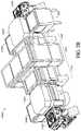
- FIG. 1Aillustrates generally an example of a plan view of at least a portion of a system, such as including a printing system and a curing module, that can be used in manufacturing an electronic device (e.g., an organic light emitting diode (OLED) device).
- OLEDorganic light emitting diode
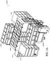
- FIG. 1B and FIG. 1Cillustrate generally illustrative examples of isometric views of at least a portion of a system, such as including a printing system and a curing module, that can be used in manufacturing an electronic device (e.g., an organic light emitting diode (OLED) device).
- a printing systeme.g., a graphics processing unit (GPU)
- a curing modulee.g., a laser light emitting diode (OLED) device.
- OLEDorganic light emitting diode
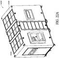
- FIG. 2Aillustrates generally an example of a plan view of at least a portion of a system that can be used in manufacturing a light emitting device (e.g., an OLED device).
- a light emitting devicee.g., an OLED device
- FIG. 2Billustrates generally an isometric view of at least a portion of a system that can be used in manufacturing a light emitting device (e.g., an OLED device).
- a light emitting devicee.g., an OLED device
- FIG. 3Aillustrates generally an isometric view of at least a portion of a system, such as including a printing system and other modules.
- FIG. 3Billustrates generally a plan view of at least a portion of a system, such as can include a printing system and other modules.
- FIG. 3Cillustrates generally a further example of a plan view of at least a portion of a system, such as can include a printing system and other modules.
- FIG. 4A and FIG. 4Billustrate techniques, such as methods, that can include forming an organic thin-film encapsulation layer (OTFEL) of a light emitting device (e.g., an OEL of an OLED device).
- OTFELorganic thin-film encapsulation layer
- FIG. 5illustrates generally an example of a diagram illustrating a portion of an ultraviolet treatment system that can be used in manufacturing a light emitting device.
- FIG. 6illustrates generally an example of a diagram illustrating an ultraviolet treatment system that can be used in manufacturing a light emitting device.
- FIG. 7A and FIG. 7Billustrate generally examples of at least a portion of an ultraviolet treatment system that can include a linear configuration of ultraviolet sources, such as can be used in manufacturing a light emitting device.
- FIG. 8A and FIG. 8Billustrate generally examples of at least a portion of an ultraviolet treatment system that can include a linear configuration of ultraviolet sources and a photodetector.
- FIG. 9illustrates generally an example of a diagram illustrating a portion of an ultraviolet treatment system that can include a two-dimensional array configuration of ultraviolet sources, such as can be used in manufacturing a light emitting device.
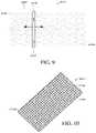
- FIG. 10illustrates generally an example of a two-dimensional array configuration of ultraviolet sources, such as can be used as a portion of an ultraviolet treatment system.
- FIG. 11illustrates generally an example of a housing configuration for an array of ultraviolet sources, such as can be included as a portion of an ultraviolet treatment system.
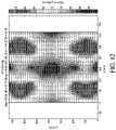
- FIG. 12illustrates generally an illustrative example of an intensity plot showing a non-uniformity of delivered ultraviolet energy, such as can be used to establish an inverse or normalization filter configuration.
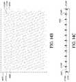
- FIG. 13A and FIG. 13Billustrate generally illustrative examples of a chuck configuration that includes ports or grooves in contact with a substrate in FIG. 13A , such as during one or more of a deposition, holding, material flow or dispersal, or cure process, and corresponding visible non-uniformities (e.g., “mura”) in a layer of the substrate in FIG. 13B .
- a chuck configurationthat includes ports or grooves in contact with a substrate in FIG. 13A , such as during one or more of a deposition, holding, material flow or dispersal, or cure process, and corresponding visible non-uniformities (e.g., “mura”) in a layer of the substrate in FIG. 13B .
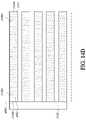
- FIG. 14A , FIG. 14B , FIG. 14C , and FIG. 14Dinclude illustrative examples depicting various regions of a substrate, and corresponding fixtures such as a chuck or end effector that can include one or more pressurized gas ports, vacuum ports, or vacuum regions.
- FIG. 15A and FIG. 15Billustrate generally illustrative examples of a chuck configuration that can include a combination of one or more mechanical support pins and one or more vacuum regions
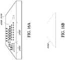
- FIG. 16A and FIG. 16Binclude illustrative examples of a chuck configuration that can include ports configured to establish a pressurized gas cushion to support a substrate in FIG. 16A , such as during one or more of a deposition (e.g., printing), holding, or cure process, and a corresponding uniformity in the resulting substrate in FIG. 16B .
- a depositione.g., printing
- a cure processe.g., a corresponding uniformity in the resulting substrate in FIG. 16B .
- FIGS. 16C and 16Dillustrate generally illustrative examples of a chuck configurations that include a porous medium, such as to establish a distributed vacuum or pressurized gas cushion during one or more of a deposition (e.g., printing), holding, material flow or dispersal, or cure process, such as providing uniformity in the resulting substrate as shown in FIG. 16E .
- a depositione.g., printing
- material flow or dispersal, or cure processsuch as providing uniformity in the resulting substrate as shown in FIG. 16E .
- FIG. 16Eillustrates generally and illustrative example of a resulting substrate, such as can be provided using a chuck configuration shown in FIG. 16C or FIG. 16D .
- FIG. 17illustrates generally a schematic representation of a gas purification scheme that can be used in relation to portions or entireties of one or more other examples described herein, such as to establish or maintain an controlled environment in an enclosure housing fabrication equipment used in manufacturing a light emitting device (e.g., an OLED device).
- a light emitting devicee.g., an OLED device
- FIGS. 18A and 18Billustrate generally examples of a gas enclosure system for integrating and controlling non-reactive gas and clean dry air (CDA) sources such as can be used to establish the controlled environment referred to in other examples described elsewhere herein, and such as can include a supply of pressurized gas for use with a floatation table.
- CDAclean dry air
- FIGS. 19A and 19Billustrate generally examples of a gas enclosure system for integrating and controlling non-reactive gas and clean dry air (CDA) sources such as can be used to establish the controlled environment referred to in other examples described elsewhere herein, and such as can include a blower loop to provide, for example, pressurized gas and at least partial vacuum for use with a floatation table.
- CDAnon-reactive gas and clean dry air
- FIG. 19Cillustrates generally a further example of a system for integrating and controlling one or more gas or air sources, such as to establish floatation control zones included as a portion of a floatation conveyance system.
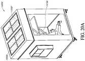
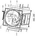
- FIG. 20A , FIG. 20B , and FIG. 20Cillustrate generally views of at least a portion of a system, such as including a transfer module, that can be used in manufacturing an electronic device (e.g., an organic light emitting diode (OLED) device).
- a transfer modulee.g., a transfer module that can be used in manufacturing an electronic device (e.g., an organic light emitting diode (OLED) device).
- OLEDorganic light emitting diode
- FIG. 21A and FIG. 21Billustrate generally views of a portion of a system, such as can include a stacked configuration of substrate processing areas that can be used in manufacturing an electronic device (e.g., an organic light emitting diode (OLED) device).
- an electronic devicee.g., an organic light emitting diode (OLED) device.
- OLEDorganic light emitting diode
- FIG. 22Aillustrates generally a portion of a system, such as including a transfer module coupled to other chambers or modules, that can be used in manufacturing an electronic device (e.g., an organic light emitting diode (OLED) device).
- OLEDorganic light emitting diode
- FIG. 22Billustrates generally a handler configuration that can be used, such as for manipulating a substrate within the module shown in FIG. 22A .
- FIG. 1Aillustrates generally an example of a plan view of at least a portion of a system 1000 A, such as including a printing system 2000 and a processing module 1300 , that can be used in manufacturing an electronic device (e.g., an organic light emitting diode (OLED) device).
- the system 1000 Acan be used to form an organic thin film encapsulation layer (OTFEL) upon a substrate containing one or more electronic devices.
- OTFELorganic thin film encapsulation layer
- the system 1000 Acan include a printing system 2000 (e.g., to “print” or otherwise deposit a film encapsulation layer onto a substrate).
- the system 1000 Acan include a transfer module 1400 .
- One or more processing modulessuch as a processing module 1300 can be coupled to the transfer module 1400 .
- each of the printing system 2000 , the transfer module 1400 , and processing module 1300can be enclosed, such as to provide a controlled environment at about atmospheric pressure or above atmospheric pressure (e.g., a nitrogen environment having a specified maximum level of one or more impurity species).
- Substratescan be transferred to or from the system 1000 A such as using a loading module 1100 .
- the processing module 1300can be configured to perform one or a variety of processing operations, such as one or more of a holding operation, a curing operation (e.g., using heat or exposure to ultraviolet radiation to treat a substrate, for example), a buffering operation, or one or more other operations.
- processing operationssuch as one or more of a holding operation, a curing operation (e.g., using heat or exposure to ultraviolet radiation to treat a substrate, for example), a buffering operation, or one or more other operations.
- the system 1000 A of FIG. 1Acan be stand-alone, or can be integrated with other elements, such as shown in other examples herein.
- the system 1000 A of FIG. 1Acan operate in aggregate in a cluster or in-line mode.
- substratescan be loaded and unloaded from loading module 1100 .
- substratescan be loaded into the left side of printing system 2000 and unloaded from loading module 1100 .
- FIG. 1B and FIG. 1Cillustrate generally illustrative example of front-facing and rear-facing isometric views of at least a portion of the system 1000 A that can be used in manufacturing a light emitting device (e.g., an OLED device), such as for fabricating an OTFEL of an OLED device according to the techniques illustrated in FIG. 4A or 4B .
- the system 1000 Acan include a loading module 1100 for transfer of one or more substrates into or out of a controlled environment within one or more portions of the system 1000 A, such as using a handler located in a transfer module 1400 .
- the system 1000 Acan include a printing system 2000 , such as having a conveyor extending through a first region 2100 , a printing region 2200 , and second region 2300 , similar to other printing system examples described herein.
- Substrates to be processedcan be queued or can be held to provide a specified holding duration to allow flowing or dispersal of an organic material deposited upon the substrate by the printing system 2000 .
- a first module 1200 , a second module 1300 , or a third module 8500can be used for holding one or more substrates before printing or after printing.
- the configuration of the one or more modules 1200 , 1300 , or 8500can be specified at least in part using information about the substrate panel size.
- the first module 1200can be used as an encapsulation layer holding module and a curing module, such as providing uniform support for the substrate using one or more of the techniques described elsewhere herein (e.g., using a gas cushion or otherwise uniformly supporting the substrate using uniform physical contact inside the “active” regions where light emitting devices are formed on the substrate).
- OELorganic encapsulation layer
- the inventorshave recognized, among other things, that uniform support techniques described below including gas floatation (or alternatively uniform physical contact inside the “active” regions) during one or more of printing, holding, or curing operations can suppress or inhibit formation of visible non-uniformities (e.g., mura) in an OEL fabrication process.
- uniform support techniques described belowincluding gas floatation (or alternatively uniform physical contact inside the “active” regions) during one or more of printing, holding, or curing operations can suppress or inhibit formation of visible non-uniformities (e.g., mura) in an OEL fabrication process.
- the second module 1300can be used as a reorientation module.
- the reorientation modulecan provide a volume in which a handler can flip or rotate a substrate being fabricated.
- the third module 8500can include a holding module such as to store substrates in environmentally-controlled regions in a stacked configuration such as shown illustratively in examples elsewhere herein (e.g., as shown in FIG. 21A or FIG. 21B ).
- the third processing module 8500can be configured to provide a reorientation module
- the first processing module 1200can be configured to provide an encapsulation curing module
- the second processing module 1300can be configured as a holding or buffering module having one or more environmentally-controlled regions.
- Other configurationscan be used, such as shown illustratively in the examples of FIG. 2A or 2B , such as can be used with large panel geometries or to enhance throughput.
- a controlled environment within one or more enclosed portions of the systemcan include specifications such as including one or more of (1) better than Class 10 particle control for particles greater than or equal to two micrometers in diameter, (2) less than 10 parts-per-million of each of water and oxygen or less than 1 part-per-million of each of water and oxygen, or (3) temperature control of the ambient gas environment to within plus or minus 2 degrees Celsius.
- FIGS. 1A and 1Bshow a single processing module 1200 coupled to the transfer module 1400 A, other configurations are possible.
- FIG. 2Aillustrates generally an example of a plan view of at least a portion of a system 1000 B, such as including a printing system 2000 , first and second processing modules 1200 A and 1200 B, and a third processing module 1300 , that can be used in manufacturing an electronic device (e.g., an organic light emitting diode (OLED) device) and
- FIG. 2Billustrates generally an illustrative example of an isometric view of at least a portion of the system 1000 B.
- OLEDorganic light emitting diode
- the system 1000 Bcan include first and second transfer modules 1400 A and 1400 B coupled to the printing system 2000 .
- One or more other modulescan be coupled to the printing system 2000 , such as through the transfer module 1400 A or the second transfer module 1400 B.
- the first processing module 1200 Acan be coupled to the first transfer module 1400 A
- the second and third processing modules 1200 B and 1300can be coupled to the second transfer module 1400 B.
- the first, second, or third processing modules 1200 A, 1200 B, or 1300can include a holding or buffer module, a curing module, or one or more other modules.
- One or more of the first, second, or third processing modulescan include a stacked configuration, such as shown illustratively in the examples of FIG. 5 , FIG. 21A , or FIG. 21B .
- a holding or buffer modulecan also be used to hold substrates for a period of time as a part of a functional process flow.
- the substratecan be held for in a holding module, such as to provide a specified duration for dispersal or flowing of an organic material printed upon the substrate, such as during a process for forming an organic encapsulation layer.
- a holding operationcan have a specified duration.
- the substratecan be held (e.g., for a specified duration), in a curing module, such as before enabling ultraviolet or heat treatment of the substrate.
- timed holding operationcan be performed to allow the substrate to evolve from one state to another.
- a timed holding operation having a specified durationmay be used to allow the liquid to flow, settle, dry, or any combination of the three prior to fixing the film via a curing operation, such as a curing operation including thermal treatment or optical treatment.
- the first, second, or third processing modules 1200 A, 1200 B, or 1300can include a vacuum drying module, such as can accommodate a single substrate or multiple substrates, such as in a stacked configuration, as shown illustratively in FIG. 21A or FIG. 21B .
- a vacuum drying modulecan provide for the drying (at pressures below ambient pressures) of a liquid material, such as can be deposited onto the substrate via printing.
- the system 1000 Bcan include both a holding module providing various functions as described above and a separate vacuum drying module.
- the system 1000 Bcan include a holding module configured to provide holding or buffering at ambient pressure, or at about ambient pressure during certain durations, and to provide vacuum drying during other durations.
- the system 1000 Bcan be enclosed, such as having an controlled processing environment.
- a controlled processing environmentcan be established to remain below specified limits of one or more of particulate contamination level, water vapor content, oxygen content, and organic vapor content.
- the controlled processing environmentcan include nitrogen or another gas or mixture of gases specified for minimal or no reactivity with a species deposited on a substrate being processed using the system 1000 B.
- a controlled processing environmentcan be established at least in part using a gas purification system include within or coupled to various portions of the system 1000 B (e.g., as shown in FIG. 17 , FIG. 18A , FIG. 18B , FIG. 19A , FIG. 19B , or FIG. 19C ).
- a particulate level of the controlled environmentcan also be controlled, such as using apparatus coupled to the system 1000 B or located within one or more modules of the system 1000 B, as shown and described in other examples herein.
- one or more of the first, second, or third processing modules 1200 A, 1200 B, or 1200 C, the printing system 2000 , or the transfer module 1400 Acan include an controlled environment established by a shared gas purification facility, a single dedicated gas purification facility, or multiple dedicated gas purification facilities individually associated with different portions of the system 1000 B.
- various modulescan include gates or valving such as to be controllably isolated from other portions of the system 1000 B to allow various operations as might be performed during nominal system operation or during maintenance, without requiring an entirety of the controlled environment of the system 1000 B to be purged or otherwise contaminated.
- the system 1000 Bcan include one or more loading modules, such as one or more of a first loading module 1100 A or a second loading module 1100 B, such as to provide a point-of-entry or point-of-exit for one or more substrates being fabricated.
- the first or second loading modules 1100 A or 1100 Bcan be fixed or removable, such as directly coupling the system 1000 B to other apparatus in a manufacturing line, or even providing a removable assembly that can be transported to or from other apparatus.
- one or more of the first or second loading modules 1100 A or 1100 Bcan be configured to transfer the substrate to or from an environment different from the environment within the system 1000 B.
- the first loading module 1100 A or second loading module 1100 Bcan be coupled to a vacuum source, or a purge source, or both, and can be configured for independently sealing the interface port to system 1000 B and the interface port to the prior or next environment (which could be the ambient environment or a controlled environment associated with another enclosed processing module).
- the first or second loading modules 1100 A or 1100 Bcan internally seal itself and transition the internal environment of the loading modules 1100 A or 11008 between one that is not compatible with system 10008 to one that is compatible with system 1000 B (e.g., a controlled environment at about atmospheric pressure or above atmospheric pressure that when exposed to system 1000 B via the interface port would substantially maintain the quality of the controlled environment in system 1000 B).
- first loading module 1100 A or second loading module 1100 Bcan be used to transfer the substrate to an environment suitable for other processing (e.g., a second environment at or near atmospheric pressure but having a different composition than the controlled environment, or a vacuum environment).
- an environment suitable for other processinge.g., a second environment at or near atmospheric pressure but having a different composition than the controlled environment, or a vacuum environment.
- the first or second loading modules 1100 A or 1100 Bcan provide a transfer conduit between the controlled environment of the system 1000 B and other apparatus.
- the first loading module 1100 A or the second loading module 1100 Bcan include a permanently-attached configuration, or a cart or other transportable configuration.
- a substrate being fabricatedcan be placed within one of the loading modules 1100 A or 1100 B through a port, such as using a handler located within the system 1000 B, or using one or more handlers located elsewhere, such as a first handler (e.g., a robot) located within the first transfer module 1400 A or elsewhere, or a second handler located within the second transfer module 1400 B or elsewhere.
- a first handlere.g., a robot
- a loading module(e.g., the first loading module 1100 A or the second loading module 11008 ) can then be provided with a non-reactive atmosphere or otherwise “charged” using a purified gas stream, such as including one or more purge operations, to prepare an interior region of the loading module (e.g., the first loading module 1100 A or the second loading module 1100 B) for exposure to interior portions of the enclosed system 1000 B.
- a purified gas streamsuch as including one or more purge operations
- an internal region of one or more of the first or second loading modulescan be at least partially evacuated or purged in order to avoid contamination in a manner exceeding the specified limits of particulate contamination level, water vapor content, oxygen content, ozone content, and organic vapor content of the controlled processing environment within an enclosed region defined by other portions of the system 1000 B.
- a substrate being processedcan be placed in the first or second loading modules 1100 A or 1100 B.
- the loading modulee.g., the first loading module 1100 A or the second loading module 1100 B
- the loading modulecan be isolated from a non-reactive gas environment elsewhere in the system 1000 B, such as coupled to a vacuum source to be evacuated for subsequent processing under vacuum conditions, or otherwise for transport of the substrate being fabricated to other apparatus or processing under vacuum conditions, ambient conditions or some other static controlled environment.
- one of the first or second loading modules 1100 A or 1100 Bcan be configured to provide the substrate to the controlled processing environment within the system 1000 B without raising a concentration of a reactive species by more than, for example, 1000 parts per million within the enclosed region or similarly, without raising the ambient particle levels by more than a specified amount, or without depositing more than a specified number of particles of specified size per square meter of substrate area onto the substrate.
- the first loading module 1100 Acan be coupled to the transfer module 1400 A by a port (e.g., including a physical gate having a substantially gas impermeable seal) or gas curtain.
- a porte.g., including a physical gate having a substantially gas impermeable seal
- gas curtainWhen the port is opened, an interior of the first loading module 1100 A can be accessed by a handler located in the first transfer module 1400 A.
- the handlercan include a robotic assembly having various degrees of freedom, such as to manipulate a substrate using an end effector.
- Such an end effectorcan include a tray or frame configured to support the substrate by gravity, or the end effector can securely grasp, clamp, or otherwise retain the substrate, such as to allow reorientation of the substrate from a face-up or face-down configuration to one or more other configurations.
- end effector configurationscan be used, such as including pneumatic or vacuum-operated features to either actuate portions of the end effector or otherwise retain the substrate.
- transfer modulesincluding handlers, and various end effector configurations are described below.
- the system 1000 Bcan be operated in so-called “cluster” and “linear” (or “in-line”) modes, these two operating modes being mainly differentiated by the flow of a substrate in from and then back to the same chamber in the “cluster” mode and the flow of a substrate in from one chamber and out to a different chamber in the “linear” or “in-line” mode.
- the subject matter described hereincan be included or used in both “cluster” and “linear” or “in-line” configurations.
- the first transfer module 1400 Acan position a substrate to be located in an input enclosure region 2100 of a printing system, such as located on a conveyer.
- the conveyercan position the substrate at a specified location within the printing module such as using one or more of physical mechanical contact or using gas cushion to controllably float the substrate (e.g., an “air bearing” table configuration).
- An illustrative example of floatation control zones, such as can be included for floatation-type conveyanceis illustrated in FIG. 19C .
- a printer region 2200 of the system 1000 Bcan be used to controllably deposit one or more film layers on the substrate during fabrication.
- the printer region 2200can also be coupled to an output enclosure region 2300 of the printing module.
- the conveyercan extend along the input enclosure region 2100 , the printer region 2200 , and the output enclosure region 2300 of the printing module, and the substrate 4000 can be repositioned as desired for various deposition tasks, or during a single deposition operation.
- the controlled environments within the input enclosure region 2100 , the printer region 2200 , and the output enclosure region 2300can be commonly-shared.
- the printer region 2200can include one or more print heads, e.g. nozzle printing, thermal jet or ink-jet type, coupled to or otherwise traversing an overhead carriage, such as configured to deposit one or more film layers on the substrate in a “face up” configuration of the substrate.
- Such layerscan include one or more of an electron injection or transport layer, a hole injection or transport layer, a blocking layer, or an emission layer, for example.
- Such materialscan provide one or more electrically functional layers.
- Other materialscan be deposited using printing techniques, such as a monomer or polymer material, as described in other examples described herein, such as for providing one or more encapsulation layers for a substrate being fabricated.
- the system 1000can include a second transfer module 1400 B, such as including a second handler 1410 B that can be similar to the first handler 1410 A.
- the substrate 4000can be manipulated by the second handler 1410 B, such as accessed using the output enclosure region 2300 of the printing module.
- the second handler 1410 Bcan be isolated from the printing module, such as using a gate or other arrangement.
- a second processing module 1300such as having an controlled environment, can be coupled to the second transfer module 1400 B, such as to provide a buffer having one or more environmentally-controlled regions, or to provide one or more other capabilities supporting fabrication.
- the systemcan include a second loading module 1100 B, such as similar to the first loading module 1100 A.
- the second loading modulecan be used to transfer substrates out of the system 1000 , such as after one or more deposition operations involving the printing module, or after other processing.
- the first or second processing modules 1200 or 1300can provide other processing, such as for drying or solvent evaporation.
- Other examplescan include ultraviolet exposure, substrate holding (e.g., to facilitate material flow or dispersal after printing and before curing, so as to achieve a more planar or uniform coating), reorientation (e.g., to rotate the substrate 4000 ), holding, or buffering (e.g., storage of substrates in-process in a controlled environment such as in a queued fashion).
- a gas cushion arrangementto uniformly support the substrate during one or more of printing or other processing operations such as substrate holding (e.g., to facilitate material flow or dispersal) or film curing can reduce or suppress formation of visible defects (e.g., “mura”) in active regions of the substrate.
- substrate holdinge.g., to facilitate material flow or dispersal
- film curingcan reduce or suppress formation of visible defects (e.g., “mura”) in active regions of the substrate.
- active regionscan be defined as portions of the area of the substrate where light emitting electronic devices are being fabricated or encapsulated.
- FIG. 3Aillustrates generally an isometric view
- FIG. 3Billustrates generally a plan view of at least a portion of a system 3000 A, such as including a first printing system 2000 A, a second printing system 2000 B, and other modules, that can be used in manufacturing an electronic device (e.g., an organic light emitting diode (OLED) device).
- an electronic devicee.g., an organic light emitting diode (OLED) device.
- OLEDorganic light emitting diode
- the system 3000 Acan include a first printing system 2000 A, such as a printing system as described in relation to other examples herein. In order to provide one or more of increased throughput, redundancy, or multiple processing operations, other printing systems can be included, such as a second printing system 2000 B.
- the system 3000 Acan also include one or more other modules, such as first processing module 1200 or a second processing module 1300 .
- the first or second processing modules 1200 or 1300can be used for one or more of holding a substrate (e.g., to facilitate flowing or dispersing the deposited material layer, such as to achieve a more planar or uniform film) or curing (e.g. via UV light illumination) a layer of material, such as deposited by one or more of the first or second printing modules 2000 A or 2000 B.
- a material layer that flows or disperses, or is cured, using the first or second processing modules 1200 or 1300can include a portion of an encapsulation layer (such as a thin film layer comprising an organic encapsulant cured or treated via exposure to ultraviolet light).
- the first or second processing modules 1200 or 1300can be configured for holding substrates as described above, such as in a stacked configuration. Processing module 1300 could alternatively (or additionally) be configured for vacuum drying one or more substrates, such as in a stacked configuration. In the case that one or more of the first or second processing modules 1200 or 1300 function as a vacuum drying module for more than one substrate at a time, the stacked configuration can include multiple drying slots in a single chamber or a stack of isolated chambers, each having a single drying slot. In yet another configuration, one or more of the first or second processing modules 1200 or 1300 can be configured for holding substrates and another processing module can be provided attached to transfer module 1400 A for vacuum drying one or more substrates.
- the first and second printers 2000 A and 2000 Bcan be used, for example, to deposit the same layers on the substrate or printers 2000 A and 2000 B can be used to deposit different layers on the substrate.
- the system 3000 Acan include a input or output module 1101 (e.g., a “loading module”), such as can be used as a load-lock or otherwise in a manner that allows transfer of a substrate 4000 into or out of an interior of one or more chambers of the system 3000 A in a manner that substantially avoids disruption of a controlled environment maintained within one or more enclosures of the system 3000 A.
- a loading modulee.g., a “loading module”
- substantially avoids disruptioncan refer to avoiding raising a concentration of a reactive species by a specified amount, such as avoiding raising such a species by more than 10 parts per million, 100 parts per million, or 1000 parts per million within the one or more enclosures during or after a transfer operation of a substrate 4000 into or out the one or more enclosures.
- a transfer module 1400 Bsuch as can include a handler 1410 B, can be used to manipulate the substrate 4000 before, during, or after various operations.
- An example of a configuration that can be used for the transfer module 1400 Bis shown illustratively in FIGS. 22A and 22B .
- One or more additional handlerscan be included, such as to provide a substrate to the input or output module 1101 or receive a substrate from the input or output module 1101 .
- FIG. 3Cillustrates generally a further example of a plan view of at least a portion of a system 3000 B, such as can be used in manufacturing an electronic device (e.g., an organic light emitting diode (OLED) device).
- first and second printing systems 2000 A and 2000 Bcan be arranged similarly to the example of FIGS. 7A, 7B (e.g., for depositing different or similar layers on a substrate).
- the system 3000 Bcan be extended as compared with the example of system 3000 A, such as including first and second processing modules 1200 A and 1200 B, and third and fourth processing modules 1300 A and 1300 B.
- the processing modules 1200 A, 1200 B, 1300 A, or 1300 Bcan include curing modules configured to provide ultraviolet treatment or can be configured to hold one or more substrates for any of the holding functions described elsewhere.
- the examples of FIGS. 3A, 3B, and 3Cillustrate generally a configuration that can include two printing systems 2000 A and 2000 B, but more than two printing systems can be included.
- additional (or fewer) processing modulescan be included.
- FIG. 4A and FIG. 4Billustrate techniques, such as methods, that can include forming an organic thin-film encapsulation layer (OTFEL) of a light emitting device (e.g., an OEL of an OLED device).
- OTFELorganic thin-film encapsulation layer
- a light emitting devicee.g., an OEL of an OLED device.
- as substratecan be transferred from an inorganic thin film encapsulation system to a transfer chamber of an organic thin film encapsulation (OTFE) system, such as a system as shown and described in relation to other examples herein.
- the substratecan be transferred from an environment different from a controlled environment of the transfer module, such as using loading module (e.g., “load lock”).
- loading modulee.g., “load lock”.
- the substratecan be transferred to an enclosed printing system, such as at least in part using a handler robot located within the transfer module or within the enclosed printing system.
- the substratecan be uniformly supported in the printing system, such as using techniques and apparatus to reduce or inhibit formation of visible defects or “mura” during printing operations or other operations.
- such supportcan include a chuck configuration (e.g., a planar chuck or tray) such as configured to provide uniform physical contact in areas of the substrate upon or opposite regions of the substrate where active devices such as light emitting electronic devices have been formed.
- a chuck configuratione.g., a planar chuck or tray
- active devicessuch as light emitting electronic devices have been formed.
- chucksgenerally provide holes in central regions of the substrate through which lift pins can raise and lower the substrate, so as to facilitate loading and unloading operations. These holes can represent regions of non-uniform physical contact with the substrate.
- a support chuck(or other portion of the system supporting the substrate), can be configured so as to position chuck features to minimize or eliminate their impact on the target coating pattern.
- the chuckcan further provide non-uniform physical contact to certain areas of the substrate upon or opposite regions of the substrate outside where active devices such as light emitting electronic devices have been formed, or where active devices such as light emitting devices have been formed but which do not have a strict uniformity requirement—for example, devices that will only be used for testing or which are manufactured and sold as second grade product.
- light emitting electronic devicesare used as just one illustrative example, but the same support structure configurations can be applied to any active electronic, optical, or optoelectronic devices, wherein the active region can represent a region within which the devices being encapsulated are located.
- Remaining holes in the chuck associated with the lift pinscan be restricted to one or more of a periphery of the substrate or a periphery of active regions (including regions opposite a surface defining a periphery of the substrate or a periphery of active regions of the substrate).
- the present inventorshave also recognized, among other things, that the substrate can be uniformly supported at least in part using a gas cushion, such as during one or more of a printing operation or other processing such as before or during ultraviolet treatment in a curing module.
- a gas cushioncan enhance uniformity of a coating or film layer on the substrate. For example, by floating the substrate above a physical substrate support surface, the substrate sees a uniform gas in all of the supported regions and is relatively less sensitive to the presence of holes for lift pins or other localized features that may be present on physical substrate support surface.
- lift pins in the center region of the substratecan be incorporated into the support mechanism without affecting film uniformity in those areas because the substrate is not in physical contact with extended or retracted lift pins and is supported by a gas cushion in the center region during processing such as printing, holding, or curing.
- the substratecan be further uniformly supported or retained by physical contact restricted to regions outside such active regions, such as in one or more of the substrate periphery or a periphery between active regions. In this way, all of the substrate area can offer a highly uniform coating and can be used productively, except, potentially, for an exclusion zone at the substrate edge where the substrate is physically contacted so as to constraint or hold it in place in the floatation plane.
- an organic materialsuch as a monomer can be printed in a target deposition region of the substrate, such as including a monomer to form an organic encapsulation layer.
- the phrase “deposition region”generally refers to the region where the organic encapsulation layer is being formed.
- the substratecan be transferred from the printing system to the transfer module. In an example, the substrate is retained in the enclosed printing system for a specified holding duration after printing to allow flowing or dispersal of an organic material deposited upon the substrate by the printing system.
- the substratecan be transferred from the transfer module to a curing module.
- the substratecan be supported in the curing system, such as uniformly supported in one or more specified regions.
- the manner of supporting the substratecan be similar to or different from the substrate support technique used during the printing operation at 4500 .
- the substrate supportcan again provide uniform support, such as via uniform physical contact (e.g., a vacuum chuck such as providing a distributed vacuum region) or gas floatation, within those active areas to be uniformly coated, during printing, curing, or holding operations (e.g., during which a material flows or disperses prior to curing).
- a chuckconfigured to support the substrate at least in part using a gas cushion.
- the curing modulecan be configured to treat the printed organic material at 4900 , such as to provide a mura-free OTFE layer.
- the curing modulecan be configured to provide optical treatment, such as an ultraviolet light treatment, to a printed monomer layer to polymerize or otherwise cure the monomer layer.
- FIG. 4Billustrates another example 4150 , such as for providing a mura-free OTFE layer.
- a substratecan be transferred from an ITFE system to a transfer chamber of an OTFE system.
- the substratecan be transferred to a substrate support system of a printing system, such as to provide uniform support of the substrate at least in one or more active regions of the substrate.
- a substrate support systemcan include apparatus or techniques as mentioned above to help suppress or inhibit mura formation during one or more operations such as printing or holding (e.g., prior to curing so as to facilitate the dispersal or flow of the deposited material).
- the substrate support systemcan include a floatation table configuration, such as having various floatation control zones including one or more of a pneumatically-supplied gas cushion, or a combination of pneumatic and at least partial vacuum supplied regions to provide a gas cushion supporting the substrate.
- a distributed vacuum regioncan be used such as to provide uniform support of the substrate at least in one or more active regions of the substrate.
- a monomercan be printed over a target deposition region.
- the substratecan be transferred from the printing system to the transfer chamber, such as using a handler located in the transfer chamber, as mentioned above in relation to FIG. 4A .
- the substratecan be transferred from the transfer chamber to a substrate support system of an OTFE curing module.
- the substrate support systemcan include a chuck configured to support the substrate in a manner that can suppress or inhibit mura formation during one or more of a holding operation or curing operation.
- the substratecan be held for a specified duration after printing and before treatment by the curing module, such as before ultraviolet treatment.
- the monomer layercan be cured such as using an ultraviolet treatment provided by the curing module, such as to provide a mura-free OTFE layer.
- a handler robotcan include an end effector configuration such as to provide support for a substrate while avoiding non-uniform direct physical contact with active regions on a first side of the substrate, or corresponding portions of a second side of the substrate opposite the first side.
- FIG. 5illustrates generally an example of a diagram illustrating a portion of an ultraviolet treatment system that can be used in manufacturing a light emitting device.
- the example of FIG. 5can include apparatus or can include using techniques that can be combined other examples herein, such as those described above (e.g., to provide an organic encapsulation layer fabrication system or other system for performing processing of substrates, such as substrates including one or more OLED devices).
- the system of FIG. 5can include an enclosure having a controlled environment, such as a non-reactive gas environment, such as including a transfer module 1400 .
- the transfer modulecan include a handler 1411 , such as coupled to an end effector 1422 to manipulate one or more substrates such as a first substrate 4000 A, second substrate 4000 B, or third substrate 4000 C.
- the systemcan include a curing module 2302 .
- the curing modulecan also be used for providing holding of substrates, such as to facilitate an evolution of a substrate from one processing state to another (e.g., for dispersal or flowing of the deposited material), or to provide buffering for queuing of substrates. Additionally, or alternatively, other processing modules can providing holding or buffering capabilities.
- the environmentally-controlled regionscan include one or more of a specified gas purity, temperature, or particulate level.
- Gas within various regions of the example of FIG. 5can be circulated laterally across a surface of a substrate such as to provide a substantially laminar flow profile.
- one or more fan filter units (FFUs)such as an FFU 1500 can provide a top-down flow profile, such as recovering gas through one or more ducts such as a duct 5201 .
- a temperature controller 5650can be coupled to one or more other portions of the system, such as to a heat exchanger located on or within the FFU 1500 . In this manner, a temperature within the transfer module 1400 (or other portions of the system) can be controlled.
- the systemcan include or can be coupled to a gas purification system, such as including a gas controller 5600 configured to monitor or control a gas purity level of the controlled environment.
- a gas purification systemsuch as including a gas controller 5600 configured to monitor or control a gas purity level of the controlled environment.
- the modulessuch as a holding module or the curing module 2302 can include separate gas purification loops, or such modules can share a controlled environment and purification facilities with the transfer module 1400 .
- the curing module 2302can include one or more lamps such as an ultraviolet lamp. Such lamps can be located within the curing module 2302 , or outside the chamber such as optically coupled to the chamber through a quartz (or other UV-transparent) window.
- one or more of the substrates in the thermally-controlled regionscan be supported by a chuck configuration such as including a plate, frame, or tray.
- a chuck configurationsuch as including a plate, frame, or tray.
- a plate, frame, or traycan include one or more retractable lift pins (e.g., a pin 2324 ).
- the one or more retractable pins or other mechanical support featurescan be located in regions at the perimeter or between display devices on the substrate.
- a vacuum chuckcan support the substrate.
- a vacuum chuckcan be outfitted with vacuum ports and a vacuum supply, which can be turned on and off controllably, so as to provide vacuum suction to the backside of substrate during a processing operation to improve the stability of the substrate or the thermal contact between the substrate and the chuck during that processing operation.
- a non-vacuum chuckcan be provided and the substrate can be held in place either primarily by gravity and friction, or primarily by mechanical clamping.
- Substratescan be placed or removed from various positions, such as using an end effector 1422 of a handler 1411 .
- One or more pinssuch as a lift pin can be used to elevate the substrate for access by the end effector, as described further below.
- the curing module 2302can also be used to facilitate the dispersal or flow of the film layer deposited on the substrate, such as to achieve a more planar and uniform coating (e.g., an OEL layer printed using a printing module), such as using one or more of gravity, rotation of the substrate, or using one or more vacuum ports to further planarize the substrate during one or more of the holding, material flowing or dispersing, or curing operation.
- a vacuum chuck having large ports during one or more of holding, material flowing or dispersal or ultraviolet treatmentcan lead to unwanted visible defects or “mura.”
- the configuration shown in FIG. 5can help to facilitate production of an organic thin film encapsulant layer while inhibiting or suppressing mura formation.
- a source of ultraviolet emissioncan be used such as to treat one or more layers deposited on a substrate being fabricated.
- ultraviolet emissioncan be used to polymerize or otherwise treat an organic layer deposited on the substrate, such as for use in one or more processes related to manufacturing a flat panel display assembly, such as including an OLED display assembly.
- the system of FIG. 5can include one or more enclosed regions (e.g., “cells” or chambers) such as first region 2301 A, a second region 2301 B, and an “Nth” region 2301 N.
- three regionscan be included (e.g., as shown illustratively in FIG. 5 ), and in another example, other numbers of regions can be included.
- the regionscan be oriented in a “stacked” configuration along a vertical axis of the system, such as shown illustratively in FIG. 5 .
- a material flowing or dispersal operationcan be performed, such as to improve the planarization or uniformity of a coating.
- a duration of the material flowing or dispersal operationcan generally be greater than a duration of an ultraviolet treatment operation.
- respective holding modulescan be used, such as separate from the curing module 2302 and arranged in a stacked configuration with each region configured to house a substrate as shown in FIG. 21A or 21B .
- the material flowing or dispersal operationcan proceed without restricting access or otherwise tying up a separate ultraviolet treatment region.
- multiple ultraviolet sourcescan be used, such including user lower-cost sources.
- a throughput impact of idling an ultraviolet sourceneed not preclude use of the same “cell” or region (e.g., 2301 A through 2301 N) for both a holding operation and ultraviolet treatment operation, because multiple regions are configured to provide ultraviolet treatment, enhancing throughput.
- Such an approachcan also provide redundancy of the ultraviolet sources such that processing can continue even if a particular ultraviolet source fails or is undergoing maintenance.
- Yet another benefit to such an approachis that the substrate can undergo a material flowing or dispersal operation to disperse or flow a printed organic layer (e.g., to improve planarization or uniformity) and the substrate can be treated, such as receiving an ultraviolet treatment, without requiring movement of the substrate from the cell.
- a first ultraviolet source 2310 A(e.g., an ultraviolet-emitting LED array) can provide ultraviolet emission 2328 having a specified range of wavelengths to a first substrate 4000 A.
- the ultraviolet emissioncan be coupled to an interior of the enclosed region 2310 A such as through a window 2310 A (e.g., a quartz window or an assembly such as including a normalization filter, or other filters or coatings).
- a window 2310 Ae.g., a quartz window or an assembly such as including a normalization filter, or other filters or coatings.
- the environment within the region 2301 Acan be controlled and can be isolated from a housing containing the first ultraviolet source 2310 A.
- the second substrate 4000 BIn the second enclosed region 2310 B, the second substrate 4000 B can be held for a specified duration, such as for material flowing or dispersal or to await availability of other processes. During the specified holding duration, a second ultraviolet source 2310 B can be disabled.
- a chuckcan be used, such as contacting at least a portion of a substrate such as to one or more of convey, support, or retain the substrate.
- the present inventorshave recognized, among other things, that for some operations or material systems, such as in relation to providing for the flowing or dispersing a deposited organic layer, visible defects can be induced in the display regions of the substrate 4000 A when the substrate is supported in a non-uniform manner.
- pins, support frames, holes in the chuck associated with retracted lift-pins, or vacuum apertures in the chuck under the substrate 4000 Acan induce visible defects in a finished device as shown illustratively in FIGS. 15A and 15B .
- such defectscan result from localized variations in thermal conductivity that can create local gradients in the temperature of the substrate 4000 A during, for example, a material flowing or dispersal operation or from electrostatic interactions between the substrate 4000 A and other portions of the system, such as can be influenced by contact between the substrate 4000 A and other portions of the system.
- a specified temperature uniformitycan be maintained in a local region of the substrate, for example, such that deviation in temperature adjacent to or within the local region is limited.
- a significant temperature variation across the substratecan be tolerated but such variation can have a limited gradient such that the temperature does not vary significantly over a small distance along the substrate. In this manner, abrupt changes in visible characteristics of the finished display can be avoided and such gradual changes are less likely to be noticed or even detectable.
- regions outside the emitting or display region of the substratecan be used to support substrate 4000 A (e.g., as shown illustratively in FIG. 13A , FIG. 13B , or FIG. 13C ).
- substrate 4000 Ae.g., as shown illustratively in FIG. 13A , FIG. 13B , or FIG. 13C .
- large portions of the substrate 4000 Agenerally do include emitting regions or portions of the actual display region, it can be impractical to support the substrate only at the periphery of such regions because such support induces unacceptable mechanical forces or stresses elsewhere across the substrate 4000 A, which may either distort or fracture the substrate 4000 A.
- the substrate 4000 Acan be supported by a chuck 2320 A, such as during an ultraviolet treatment operation, such as at least in part using a pressurized gas 2304 A to provide a gas cushion.
- the substrate 4000 Acan be supported exclusively by a controlled arrangement of the pressurized gas 2304 A, such as to “float” the substrate 4000 A.
- the substrate 4000 Acan be supported using a uniform vacuum region under active areas of the substrate or otherwise in areas where defects induced by non-uniformities would be deemed unacceptable.
- Retractable lift pinscan be located in regions at the periphery of the substrate, or between active regions such as to facilitate loading or unloading of the substrate, such as shown illustratively in FIG. 15A or 15B .
- the substrate 4000 Acan be supported by a pressurized gas 2304 A impinging on a first surface of the substrate 4000 A, and an opposing force can be provided such as by a mechanical stop 2312 contacting an opposing face of the substrate 4000 A or arranged to contact the substrate at one or more locations laterally.
- a gas cushionis used to the support the substrate
- the substratecan be supported by a gas cushion provided between a surface of the substrate opposite the surface including the active regions or the organic encapsulation layer, such as in a “face up” example where the organic encapsulation is on a top surface of the substrate and the gas cushion is provided on a bottom surface.
- a second chuck 2320 Bcan be provided as a portion of the second cell (e.g., the region 2301 B), and an “Nth” chuck 2320 N can be provided as a portion of the “Nth” cell (e.g., the region 2301 N).
- an elevating handler 1411(or a handler robot as described in other examples herein) can include a table (or a corresponding end effector 1422 ) including pressurized gas arrangement to support a substrate at least in part using the pressurized gas.
- a conveyor 1430can also include such a pressurized gas arrangement, such that a substrate (e.g., a substrate 4000 C) can be conveyed along a path 2440 from a region 2101 elsewhere in the system (or external to the system) to a desired cell, such as the region 2301 N.
- a substratee.g., a substrate 4000 C
- a desired cellsuch as the region 2301 N.
- one or more of the conveyer 1430 , the effector 1422 , or the first through “Nth” chucks 2320 A through 2320 Ncan each define a “floatation zone.”
- an arrangemente.g., an array
- portssuch as a port 2306 A can be used to establish a gas cushion partially or entirely supporting the substrate 4000 A.
- a combination of positive gas pressure and vacuumcan be applied through the arrangement of ports.
- Such a zone having both pressure and vacuum controlcan effectively provide a fluidic spring between the chuck 2320 A and a substrate.
- a combination of positive pressure and vacuum controlcan provide a fluidic spring with bidirectional stiffness.
- the gap that exists between the substrate (e.g., substrate 4000 A) and a surface (e.g., the first chuck 2320 A)can be referred to as the “fly height,” and such a height can be controlled or otherwise established by controlling the positive pressure and vacuum port states. In this manner, the substrate orientation can be carefully controlled such as for one or more of a holding operation, a material flowing or dispersing operation or an ultraviolet treatment operation.
- pressure-only floatation zonescan be provided, such as along the conveyor 1430 or elsewhere.
- a “transition” zonecan be provided such as where a ratio of pressure to vacuum nozzles or area increases or decreases gradually, such as along the conveyor 1430 , along the table 1422 , or elsewhere.
- a fly height of a substrate over pressure-only zones elsewherecan be greater than the fly height of a substrate over a pressure-vacuum zone, such as in order to allow enough height so that a substrate will not collide with a floatation table in the pressure-only zones.
- an OLED panel substratecan have a fly height of between about 150 micrometers ⁇ to about 300 ⁇ above pressure-only zones, and then between about 30 ⁇ to about 50 ⁇ above a pressure-vacuum zone.
- one or more portions of the conveyor 1430 , the table 1422 , or the chucks 2320 A through 2320 Ncan include an “air bearing” assembly provided by NewWay® Air Bearings (Aston, Pa., United States of America).
- gas pressurized support of a substrateWhile the examples of gas pressurized support of a substrate are discussed in relation to FIG. 5 , such techniques can be used in addition to or instead of other conveyance or support approaches, such as in relation other system examples described herein, and as discussed in relation to FIG. 19C .
- mechanical retaining techniquessuch as pins or a frame, can be used to restrict lateral translation of a substrate while the substrate is supported by a gas cushion.
- Such retaining techniquescan include using spring loaded structures, such as to reduce the instantaneous forces incident the sides of the substrate while the substrate is being retained; this can be beneficial as a high force impact between a laterally translating substrate and a retaining means can cause substrate chipping or even catastrophic breakage.
- Each of the regions 2301 A through 2301 Ncan either share one or more gas purification loops or can each be served by a respective gas purification loop.
- one or more FFUscan be located to provide a laminar airflow parallel to a surface of substrate in each of the regions 2301 A through 2301 N.
- the regions 2301 A through 2301 Ncan each include a valve or gate, such as to isolate the controlled environment of each enclosed region 2301 A through 2301 N from the transfer module 1400 or from each other.
- the ultraviolet sources 2310 A through 2310 Nneed not be housed in enclosures isolated from the interior of the regions 2301 A through 2301 N. Accordingly, such as during maintenance, a particular region can have its controlled environment isolated from the rest of the enclosed regions using a valve or gate.
- a temperature within the enclosed transfer module 1400 or within other portions of the systemcan be controlled as described extensively in other examples herein, such as using a temperature controller 5650 .
- the temperature controller 5650can be coupled to the FFU 1500 or one or more FFUs elsewhere.
- the temperature controller 5650 or other techniquescan be used such as to control a temperature of gas supplied by one or more of the chucks 2320 A through 2320 N, the table 1422 , or the conveyor 1430 .
- one or more of the ultraviolet sources 2310 A through 2310 Ncan be cooled using a liquid or circulating gas, such as including one or more cooling loops isolated from other portions of the system.
- FIG. 6illustrates generally an example of a diagram illustrating an ultraviolet treatment system that can be used in manufacturing a light emitting device.
- the treatment systemcan be included as a portion of other systems or techniques described herein, such as for use as a curing module (or, e.g., for use as a combination curing and holding module).
- the ultraviolet treatment systemcan include an ultraviolet source assembly 912 , such as configured to couple ultraviolet energy to a surface of a substrate 4000 .
- a curing module 8314can include a controlled environment, such as provided by one or more gas purification loops and coupled to one or more fan-filter-units (FFUs), such as to provide an environment having a specified maximum level of particulates or reactive contaminants.
- FFUsfan-filter-units
- the substrate 4000can be loaded into the curing module 8314 or removed from the chamber 8314 such as using a handler 1410 and end effector 1420 , which can access the curing module 8314 from an adjacent transfer module 1400 , or through another chamber or assembly such as a load lock.
- a chuck 920can be used to support the substrate 4000 , such as using physical contact and vacuum to hold the substrate in place or using a gas cushion arrangement as mentioned in other examples.
- One or more lift pinscan be used, such as to elevate the substrate 4000 so that the substrate 4000 can be manipulated by the end effector 1420 , such as shown illustratively in FIG. 15A or 15B .
- An array of ultraviolet sourcescan provide ultraviolet energy, such as including a wavelength selected from the range of about 350 nanometers to about 400 nanometers. For example, a wavelength of about 385 nanometers or about 395 nanometers can be used.
- the sourcescan include a variety of configurations, such as using relatively small number of high-power sources as shown in the example of FIG. 7A , or using an array of relatively lower-power sources, such as shown illustratively in FIG. 9 , FIG. 10 , or FIG. 11 .
- the sourcescan include generally-available ultraviolet emitters, such as ultraviolet-emitting light-emitting diodes (UV LEDs) or one or more mercury-based devices, such as one or more mercury arc sources.
- UV LEDsultraviolet-emitting light-emitting diodes
- mercury-based devicessuch as one or more mercury arc sources.
- a substrate or housing 918 of the ultraviolet source assembly 912can be liquid or air-cooled.
- a plenum 914can be provided, such as having one or more blowers such as a blower 915 to force air across or through a portion of the ultraviolet source assembly 912 .
- Such a cooling loopcan be separated from the controlled environment within the curing module 8314 or the transfer module 1400 , for example.
- the environment surrounding the sources 910 A through 910 Ncan include the curing module 8314 controlled environment, or the environment surrounding the sources 910 A through 910 N can form a separate enclosure, such as having a window 916 to allow ultraviolet energy to pass from the source enclosure to the curing module 8314 . In this manner, maintenance of the source enclosure need not disturb the controlled environment within the curing module 8314 .
- the window 916need not be uniformly transmissive.
- the windowcan include or can be coupled to optics to converge, diverge, or collimate the ultraviolet energy.
- the window 916can include transmission characteristics that vary in a specified manner over the area of the window, such as to invert or otherwise compensate for a non-uniform power density of delivered ultraviolet energy in the plane of the substrate 4000 , such as within a specified region of the substrate.
- the window and the ultraviolet sources 910 A through 910 Nare shown as arranged in a planar configuration, but other configurations are possible, such as a cylindrical, parabolic, or spherical configuration.
- the ultraviolet sources 910 A through 910 Ncan be used to treat one or more organic material layers to encapsulate an organic light emitting diode (OLED) display device being fabricated as a portion of the substrate 4000 .
- Such treatmentgenerally includes providing a specified dose of ultraviolet energy within a specified range of wavelengths, and having a specified uniformity over a specified area of the substrate 4000 .
- a treatment processcan generally be established in terms of a desired dose or dose-range of ultraviolet exposure, such as specified in terms of energy per unit area (e.g., Joules per square centimeter). Dose can be calculated such as by multiplying incident power density by exposure duration. A trade-off can exist between intensity (e.g., incident power) and exposure duration. For example, a relatively high-power source can be used and a desired UV dose can be achieved using a relatively short exposure duration, which beneficially shortens processing time. However, such high-power UV irradiation may damage or degrade other portions of the display assembly, so a limit can exist as to the power density provided at the substrate by the ultraviolet source such as to avoid such damage or degradation.
- a uniformity of delivered ultraviolet energycan also be controlled, such as to avoid variation in organic encapsulation layer characteristics over a surface of the substrate 4000 .
- a uniformitycan be specified in terms of incident power or delivered UV dose, such as having a value of no more than 20% variation from highest to lowest incident power or dose over a specified curing area of the substrate 4000 , or having no more than 50% variation from highest to lowest incident power or dose over the specified curing area of the substrate 4000 , or having no more than 10% variation from highest to lowest incident power or dose over the specified curing area of the substrate 4000 .
- a linear array or “bar” sourcecan be used as shown in the configuration 8315 of FIG. 7A .
- Such a bar configurationcan include a precision reflector, such as to focus or collimate the ultraviolet energy in a direction towards the substrate 4000 .
- such a bar configurationcan include one or more of a diffuser or transmissive filter, such as discussed in relation to other examples herein.
- a two-dimensional array configurationcan be used, such as shown illustratively in the configurations 8316 through 8318 of FIG. 9 , FIG. 10 , or FIG. 11 .
- a sparse array of high-intensity sourcescan be used, such as can provide the power density illustrated in the example of FIG. 12 , such as including one or more reflectors.
- One or more of these source configurationscan be mechanically fixed, or can be scanned across a surface of the substrate. In such examples, either or both the substrate 4000 or the sources 910 A through 910 N can be scanned.
- the sources 910 A through 910 Ncan be fixed, and the substrate 4000 can be repositioned, such as to create a relative motion between the substrate 4000 and the sources 910 A through 910 N to achieve scanning.
- FIG. 7A , FIG. 7B , FIG. 8A , and FIG. 8Billustrate generally examples illustrating a portion of an ultraviolet treatment system 8315 that can include a linear array configuration 910 of ultraviolet sources such as can be used in manufacturing a light emitting device.
- the linear array 910can be scanned in at least one axis to sweep a beam of ultraviolet emission 922 across a specified region of the substrate 4000 , such as in a region where a monomer has been deposited and is to be cured or otherwise treated with ultraviolet light. Such scanning can be achieved through either or both of repositioning the substrate 4000 or the linear array 910 , such as during ultraviolet treatment.
- a window 916can be used, such as when the linear array 910 is located in an enclosure separate from a chamber 8314 housing the substrate 4000 .
- a window 916can include or can be coupled to one or more of optics or a filter, such as discussed below in relation to FIG. 12 or other examples.
- the linear array 910can offer an advantage of fewer ultraviolet sources (e.g., about 5 to about 10 LED sources, in an illustrative example). But, such a linear area 910 may result in additional system complexity where mechanical scanning is used to provide exposure to all of the specified curing area of the substrate 4000 .
- Mechanical scanningcan be simplified in part by specifying that the linear array 910 is at least as wide or as a long as one axis of the substrate, so that scanning is used only in the orthogonal axis (e.g., such axis as shown by arrows in FIGS. 7A and 8A ).
- the linear array 910can include a precision reflector configuration, as mentioned above.
- a high-power UV LED light bar supplying light at or near 395 nm wavelengthis available from Phoseon Technology (Hillsboro, Oreg., USA), such as including a reflector configuration to enhance uniformity of a field illuminated by the linear array 910 .
- one or more of a filter or diffusercan be used, such as statically configured nearby the window 916 or included as a portion of the window 916 .
- one or more of a filter or diffusercan be included as a portion of the linear array 910 assembly, such as mechanically scanned as a portion of the linear array 910 .
- the power density supplied by the linear UV sourceis between 20 mW/cm 2 and 400 mW/cm 2 .
- an optical sensor 917such as an ultraviolet-sensitive photometer can be used to monitor the health of the linear array 910 .
- the optical sensor 917can be mechanically scanned in an axis parallel to the linear array 910 so that information can be obtained regarding the state of one or more optical sources included along the linear array 910 .
- the optical sensor 917can include multiple sensors placed along an axis parallel to the linear array 910 , such as obviating a need for mechanical scanning of the optical sensor 917 .
- Other configurations of optical sensorscan be used, such as mentioned in relation to other examples below.
- one or more aperturescan be provided in the chamber 8314 , such as to provide a mounting location for a fan or fan filter unit, or to provide a location for an inlet or outlet of a non-reactive gas to be used within the chamber 8314 , such as to facilitate coupling of a duct to the chamber 8314 .
- a linear array 910 source height from an upward-facing portion of the substrate 4000can be represented by “H,” a relative velocity between the optical energy emitted by the array 910 and the substrate can be represented by “V.”
- the velocitycan be established by moving one or more of the array 910 relative to the substrate 4000 (e.g., scanning the array mechanically) or the substrate 4000 relative to the array, such as by either floating the substrate on a cushion of gas or by moving a chuck 920 supporting the substrate.
- An illuminated widthcan be represented by “W,” with such a width increasing as H increases and decreasing as H decreases.
- a width of the array 910can be multiplied by the illuminated width W to estimate an area of the substrate 4000 irradiated by the array 910 .
- one objectivecan be to provide an ultraviolet dose in a manner that the appropriate dose is delivered in a short or minimum amount of time, which can also reduce likelihood of damaging other portions of the substrate 4000 either through reducing or minimizing exposure to energy from the source, or merely through reducing or minimizing the time during which the substrate is being processed.
- a tradeoffcan exist between various processing parameters such that the velocity, dose of energy, and source height H are generally not arbitrarily established.
- FIG. 9illustrates generally an example of a diagram illustrating a portion of an ultraviolet treatment system that can include a two-dimensional array configuration 8316 of ultraviolet sources 910 A through 910 N, such as can be used as a portion of an ultraviolet treatment system for treating a specified area of a substrate 4000 .
- a dense two-dimensional array of low-power ultraviolet sourcescan be used.
- Such low-power sourcescan include low-power UV LEDs, which are generally more cost effective and reliable than mercury arc devices.
- Such low-power UV LEDscan also be used for large substrate 4000 geometries (e.g., exceeding 1 meter by 1 meter), such as where high-power UV LEDs would become cost prohibitive due to the large numbers of devices generally used to cover the large substrate 4000 area.
- the dense array of hundreds of individual emitterscan provide enhanced uniformity of delivered power at the substrate 4000 surface, as compared to other approaches. Remaining non-uniformity can be addressed such as using a diffuser plate or other filter or optics between the array 8316 and the substrate 4000 .
- a diffuser plate or other filter or opticsbetween the array 8316 and the substrate 4000 .
- degradation or failure of one or more of the ultraviolet sources 910 A through 910 Ncan result in a non-uniform ultraviolet exposure field.
- Such a non-uniform fieldcan lead to visible defects or unwanted variations in one or more layers of the substrate 4000 .
- one or more optical sensors 917 A through 917 Ne.g., photometric sensors
- each of the optical sensors 917 A through 917 Ncan, but need not, be aligned to provide a 1 : 1 correspondence to an optical source in a particular row or column and a corresponding optical sensor position, so that a failure of an individual optical source can be detected.
- a spatially-averaged or spatially-cumulative specified intensitycan be used as a go/no criterion, and fewer sensors can be used.
- a failure of an individual optical sourcecan reduce an average intensity or a cumulative intensity detected at one or more of the optical sensors, such as triggering repair or replacement of the optical source array or otherwise halting further processing.
- one or more of the array 8316 of ultraviolet sources 910 A through 910 N or the optical sensors 917 Acan be mechanically scanned, such as to sample the output of the ultraviolet sources 910 A through 910 N. In the event of a detected degradation or failure, further processing can be halted until the array 8316 is repaired or replaced.
- the array 8316can include redundant sources amongst the sources 910 A through 910 N. In the event of degradation or failure, use of a combination of one or more defective sources can be suppressed, and a combination of other redundant ultraviolet sources can be used instead.
- FIG. 10illustrates generally an example of a two-dimensional array configuration 8317 of UV LED sources 1710 A through 1710 N, such as can be used as a portion of an ultraviolet treatment system for treating a specified area of a substrate 4000 .
- the two-dimensional array 8317 shown in FIG. 10can eliminate use of precision reflectors, since such an array generally provides UV radiation in the desired direction without use of large reflectors.
- Use of low-power UV LEDscan also allow precision control of intensity (through duty cycle modulation or current modulation) and exposure duration, such as allowing duration control to a precision of about 20 milliseconds.
- a substrate 1718 of the array 8317can include a heat-sink material, such as to assist in coupling heat away from the individual sources 1710 A through 1710 N in the array 8317 .
- the substrate 1718can include or can be coupled to a structural support frame.
- the individual sources 1710 A through 1710 Ncan each include a lens structure, such as to provide a converging, diverging, or collimated ultraviolet beam for each of the individual sources 1710 A through 1710 N.
- FIG. 11illustrates generally an example of a housing configuration 8318 for an array of ultraviolet sources, such as can be included as a portion of an ultraviolet treatment system.
- the housingcan include forced air circulation, such as using one or more fans as indicated by apertures 1815 A through 1815 D.
- An array of UV LEDs, such as a UV LED 1810 A,can be included within a housing 1812 .
- One or more alignment or support postscan be included, such as one or more of posts 1824 A through 1824 D.
- FIG. 12illustrates generally an illustrative example of an intensity plot 1900 showing a non-uniformity of delivered ultraviolet energy corresponding to a known distance from the UV sources and the substrate.
- Such an intensity plotcan be used to establish an inverse or normalization filter configuration.
- a small number of fixed high-power lampscan be used along with a reflector, such as illuminating a desired curing area of the substrate 4000 .
- a reflectorsuch as illuminating a desired curing area of the substrate 4000 .
- mechanically simplesuch an approach can have drawbacks.
- four high-power LEDsare used to illuminate an area of about 0.650 meters by about 0.725 meters.
- Such an approachcan provide areas of relatively higher incident power, such as an area 1902 , along with areas of relatively lower incident power, such as in the center of the plot 1900 .
- Uniformitycan be enhanced by increasing a density of sources, but at the cost of using a greater number of individual high-power LEDs.
- the present inventorshave recognized, among other things, that information about an intensity map such as shown in the plot 1900 can be used to establish an inverting filter to provide a uniform intensity or power distribution over a desired cure area while still using a sparse array or relatively small number of UV sources.
- the plot 1900can be normalized to a least intense region and then the plot 1900 can be inverted.
- the inverted representationcan be used to establish a transmissive filter whereby the least intense regions of the plot 1900 have the least, less, or no filtering as compared to other regions, and the more intense regions are filtered to reduce transmission of energy through the filter proportionally in those more intense regions and thereby level out their transmission to a value similar to the least intense regions.
- a uniform area illuminationcan be achieved on the substrate.
- Such inversion and transmissionneed not be continuously varying, and in some examples all areas can be filtered to some extent.
- a transmissive filtercan include a half-tone or other dithering pattern of opaque material (e.g., an array of dots or other regions) such as to provide a range of transmitted intensities across a surface of the filter corresponding to the inverted intensity pattern of a UV source.
- opaque materiale.g., an array of dots or other regions
- the transmissive filtercan be included as a portion of a window as discussed in other examples, or can be coupled to a window.
- an absorbing coatingcan be patterned on a flexible film or on a rigid medium such as glass or quartz.
- the transmissive filteris coupled to a quartz window or a transparent support plate at a specified location between the substrate 4000 and UV sources.
- the transmissive filteris patterned on a film and structurally supported by a frame at a specified location between the substrate 4000 and the UV sources.
- a diffusercan be used to provide a more uniform illumination field.
- a diffusercan be more efficient than a transmissive filter having optically opaque regions. This inefficiency of a transmissive filter can occur because brighter regions in the illumination field (e.g., “hotspots”) are generally reflected or absorbed (e.g., blocked) by the transmissive filter, such as to achieve uniformity of illumination of the substrate.
- a diffusercan assist in providing more uniform illumination by redirection of propagating light using one or more of refraction, diffraction, or scattering, such as comprising a translucent material.
- the window region 916 in one or more of FIG. 7A , FIG. 7B , FIG. 8A , or FIG. 8B , or other examples hereincan include a diffuser such as including a plate or film similar to the examples discussed above in relation to the transmissive filter.
- a diffusercan include a holographically-imprinted plate or film.
- Such a diffusercan be used in examples where the UV light source is static (e.g., an array source as shown in FIG. 9 , FIG. 10 , or FIG. 11 ).
- Such a diffusercan also be used in examples where the UV light source is mechanically scanned relative to the substrate or vice versa (e.g., FIG. 7A , FIG. 7B , FIG.
- Examples of diffuserscan include one or more light management films such as can be obtained from WaveFront Technology, Inc. (Paramount, Calif., United States of America), such as can include a micro-diffuser including a holographically recorded surface relief microstructure.
- Other diffuser technologiescan be used, such as can include bead structures or prismatic structures, for example.
- a homogenizing diffusercan be used, such as available from Luminit, LLC (Torrance, Calif., United States of America).
- Such a diffuser arrangementcan provide a more space-efficient UV exposure apparatus, such as by eliminating large reflectors and compressing a distance between individual UV sources (e.g., LEDs) and the substrate, as compared to approaches where the UV sources are mounted with a large separation from the substrate, and large reflectors are used to assist in collimating or otherwise providing a more uniform illumination field.
- a diffusercan provide a transmissive efficiency of greater than 80 percent, or greater than 90 percent, such as to provide UV illumination having a field uniformity of better than 15% (e.g, having a uniformity that does not vary more than 15% in intensity from a lowest intensity portion of the specified region defining the field to a highest intensity portion of the specified region defining the field).
- FIG. 13A and FIG. 13Billustrate generally illustrative examples of a chuck configuration 2420 A that includes ports or grooves in contact with a substrate 4006 A in FIG. 13A , such as during one or more of a deposition, holding, material flow or dispersal, or cure process, and corresponding visible non-uniformities (e.g., “mura”) in a layer of the substrate in FIG. 13B .
- the chuck 2420 Acan include one or more of a groove 4008 (e.g., coupled to a vacuum or included for another purpose), a retracted lift pin 4016 , a large vacuum port 4014 , a vacuum groove 4012 , or one or more other features.
- the chuck 2420 Acan be used to retain a substrate 4006 A during processing, such as during deposition of an organic thin film encapsulant, or during other operations such as providing for the flow or dispersal of a deposited encapsulant layer (e.g., to achieve a more uniform or planar coating), or during thermal or ultraviolet treatment of such an encapsulant layer.
- a resulting layer uniformity on the substrate 4006 Acan exhibit visible defects such as a defect 4018 corresponding to the groove 4016 , a defect 4026 corresponding to the retracted lift pin 4016 , a defect 4022 corresponding to the vacuum groove 4012 , and a defect 4024 corresponding to the vacuum port 4014 .
- Such defectscan manifest as rainbow-colored interference patterns that having varying color uniformity creating visible outlines of the shapes shown in FIG. 13B , or shadows where display brightness or color rendering or not consistent in such regions.
- variationscan be caused at least in part by variations in the thermal environment in contact with the substrate 2420 A, even if such variations occur in relation to features contacting a side of the substrate (e.g., a back side) opposite the deposition side.
- the present inventorshave recognized, among other things, that such mura can be suppressed or inhibited using various s uniform support techniques such as described below and elsewhere herein.
- the use of uniform support techniques to suppress muracan also beneficially reduce other sources of degradation such as particulate contamination.
- degradationcan be driven at least in part by incorporation of chemically or electrically/optically contaminants into the device structure, either within the bulk material of each film or at the interfaces between layers in the overall device stack.
- chemically active contaminantscan trigger a chemical reaction in the film that degrades the film material.
- Such chemical reactionscan occur simply as a function of time, absent any other triggers, or can be triggered by ambient optical energy or injected electrical energy, for example.
- Electrically or optically active contaminantscan create parasitic electrical or optical pathways for the electrical or optical energy introduced or generated in the device during operation.
- Such pathwayscan result in suppression of light output, or generation of incorrect light output (e.g., light output of the wrong spectrum.)
- the degradation or lossmay manifest as failure of an individual OLED display elements, “black” spotting in portions of an array of OLED elements, visible artifacts or loss of electrical or optical efficiency, or unwanted deviation in color rendering accuracy, contrast, or brightness in various affected regions of the array of OLED elements.
- FIG. 14A , FIG. 14B , FIG. 14C , and FIG. 14Dinclude illustrative examples depicting various regions of a substrate, and corresponding fixtures such as a chuck or end effector that can include one or more pressurized gas ports, vacuum ports, or vacuum regions.
- a substrate 4000can include a glass material or one or more other materials.
- the substrate 4000can include either a single large display or two or more smaller displays that can be singulated from the substrate 4000 .
- four display regions 4002 A, 4002 B, 4002 C, and 4002 Dare shown.
- active regionscan be referred to as “active” regions or “emitting regions,” for example.
- Use of the term “active” in this exampledoes not somehow imply that such regions are actually optically emissive during processing, but instead refers to regions that can include devices configured to emit light or regions that otherwise form an emissive or transmissive portion of a display that is visible to an end user.
- regions 4002 A through 4002 Dwill be deemed unacceptable by end users, and accordingly various techniques can be used such as to enhance a visible uniformity of the regions 4002 A through 4002 D.
- Other variations in panel configuration of the substrate 4000are possible.
- a substrate 4000can include a single display or array of OLED devices.
- the substrate 4000can be divided up into two, four, or eight regions, such as establishing corresponding perimeters for support, or such as having corresponding distributed porous media regions as mentioned in other examples herein.
- the definition of “active”can be adjusted to suitably encompass the regions corresponding to those devices.
- supportcan be uniform within each of the display regions 4002 A through 4002 D and can be non-uniform within the region 4004 , extending around the periphery of the substrate 4000 as a whole and extends into the interior spaces between each of the display regions 4002 A through 4002 D.
- a region 4004can be referred to as a “keep out” area, indicating that emitting or active elements of the display should be kept clear of such non-uniform support regions (or vice versa).
- one or more “lift pins”can be located in an area as shown illustratively in FIG.
- one or more of the locations in the arraycan instead include a vacuum port, such as to retain the substrate in place and hold it flat and in level physical contact with the chuck surface.
- one or more lift pinscan be used to raise or lower the substrate relative to a chuck before or after processing, and one or more vacuum ports can be used to retain the substrate during processing.
- the substratecan be supported by a cushion of gas.
- the chuckmay comprise a continuous array of small pressure apertures, or a continuous porous plate, providing a continuous flow of pressurized gas on which the substrate can float. Holes can still be provided in the chuck surface, such as 2124 A and 2124 B, for example, for lift pins (which when retracted sit below the chuck surface), but because the substrate floats above the chuck surface, the presence of mura or non-uniformity in the coated over such holes can be reduced or eliminated. In this way, even the interior regions in between regions 4002 A through 4002 D may be utilized as active regions, improve productivity and enabling the manufacture of a larger continuous active device.
- a combination of pressurized gas ports and vacuum portscan be used, such as shown in the illustrative example of FIGS. 14B through 14D .
- the substrate 4000can be retained such as by one or more vacuum ports (e.g., circular ports, or slots, for example) such as in the regions 2124 A through 2124 N as shown in region 4004 of FIG. 14B .
- Such a region 4004can again include a periphery of a substrate 4000 .
- physical contact between the substrate 4000 and any fixturescan generally be restricted to such a periphery region 4004 during certain processing operations, such as during one or more of a deposition operation (e.g., printing of a material on substrate 4000 ), a holding operation, a material flow or dispersal operation, or a heat or ultraviolet treatment operation.
- a deposition operatione.g., printing of a material on substrate 4000
- a holding operatione.g., a holding operation
- a material flow or dispersal operatione.g., a material flow or dispersal operation
- a heat or ultraviolet treatment operatione.g., heat or ultraviolet treatment operation.
- Such operationscan be included as at least a portion of a thin film encapsulation (TFE) process, where the substrate 4000 may be susceptible to creation of imperfections or visible defects
- Such a region 4004can, for example, extend inward from the edges of the substrate by 100 millimeters or 200 millimeters.
- the substratecan be supported at least in part in the region 4002 using one or more pressurized gas ports 2106 A through 2106 N.
- Such a combination of vacuum ports and pressurized gas portscan avoid imparting undue stress on a large substrate 4000 because the substrate can be supported physically in the periphery region 4004 , and supported at least in part by pressurized gas in the central region 4002 . In this manner, it does not matter whether the substrate 4000 includes a single large display being fabricated, or several smaller displays.
- a common fixture 2120 configurationcan be used for a variety of different display configurations because such a fixture 2120 can restrict contact to the peripheral region 4004 of the substrate 4000 while supporting the substrate 4000 elsewhere (e.g., centrally) with pressurized gas.
- the fixture 2120serves as a chuck
- one or more of the regions 2124 A through 2124 Ncan include a lift pin instead of a vacuum port, or in addition to a vacuum port, such as to lift the substrate 4000 to allow clearance under the substrate for manipulation by a handler.
- a flow of pressurized gascan be modulated at one or more of the gas ports 2106 A through 2106 N, such as to assist in supporting or lifting the substrate for or during manipulation.
- the combination of gas ports 2106 A through 2106 Ncan be used to assist in “floating” the substrate for conveyance to other equipment, as mentioned in other examples.
- FIG. 14Dillustrates generally that the combination of pressurized gas and vacuum ports need not be restricted to a static chuck configuration as shown in FIG. 14B .
- an end effector of a handlercan include a combination of pressurized gas ports 2106 A through 2106 N, and vacuum ports in the regions 2124 A through 2124 N.
- the side view of FIG. 14Ccan also describe a side view of one of the “tines” of the forked end effector configuration shown in FIG. 14D .
- Such an end effectorcan be used to manipulate the substrate 4000 without physically contacting the substrate 4000 in regions other than the region 4004 .
- a distributed vacuum regioncan be established such as aligned with one or more of the regions 4002 A through 4002 D or 4002 of FIGS. 14A through 14C , such as shown and discussed in the illustrative examples of FIGS. 15A and 15B , to assist in retaining and maintaining a planar configuration of the substrate 4000 .
- a distributed vacuum regioncan include using a porous material such as a carbon or ceramic material, sintered glass, or some other material such as can include a pore size of less than 1 micrometer or even less than 0.5 micrometers in diameter.
- a gas cushion established by a pressurized gascan be used at least in part to support the substrate such as within the display regions 4002 A through 4002 D, such as to avoid formation of visible defects during a holding, a material flow or dispersal operation or an ultraviolet treatment operation, or during other production processes.
- a gas cushion established by a pressurized gascan be used at least in part to support the substrate such as within the display regions 4002 A through 4002 D, such as to avoid formation of visible defects during a holding, a material flow or dispersal operation or an ultraviolet treatment operation, or during other production processes.
- FIGS. 16A and 16BSuch an example is illustrated generally in FIGS. 16A and 16B .
- FIG. 15A and FIG. 15Billustrate generally illustrative examples of a chuck configuration that can include a combination of one or more mechanical support pins and one or more vacuum regions.
- a chuck 2220can include one or more mechanical support pins (e.g., including an extended lift pin 2224 A).
- the mechanical support pinscan include an extended configuration and a retracted configuration, such as actuated pneumatically, hydraulically, or electrically. As discussed in relation to FIG.
- the mechanical support pinscan be located in regions other than the active areas of one or more displays, in the case that substrate is supported via physical contact (whereas in contrast, one of the benefits of using a floatation support mechanism is the ability to achieve mura free coatings even over lift pin holes).
- the mechanical support pinsincluding the extended lift pin 2224 A, can illustrate generally an extended configuration, such as displacing a substrate 4000 vertically. Such a configuration can allow a gap under the substrate 4000 , such as to accommodate manipulation of the substrate by one or more end effectors, such as forked end effector 1420 .
- the end effector 1420can include grooves, slots, other features, or can otherwise be sized and shaped to avoid interference with one or more of the mechanical support pins when the pins are in the extended configuration.
- the one or more mechanical support pinscan be retracted, such as to a location flush or below flush with a surface of the chuck 2220 , such as shown in FIG. 15B , including a retracted lift pin 2224 B.
- the substrate 4000can be further processed without further retention or anchoring.
- one or more of vacuum ports or distributed vacuum regionscan be used, such as to assist in maintaining the substrate in a planar configuration.
- one or more distributed (e.g., porous) vacuum regionscan be included as a portion of the chuck 2220 , such as including regions 2206 A, 2206 B, 2206 C, and 2206 D. Unlike larger vacuum ports, or mechanical support pins, such regions 2206 A through 2206 D can be located directly below portions of the substrate 4000 where “active” or “emitting” regions are being fabricated.
- Such distributed vacuum regionscan reduce or suppress formation of visible defects in one or more layers being deposited or otherwise formed on the substrate 4000 , because such distributed vacuum regions avoid the abrupt changes in thermal characteristics (e.g., thermal conductivity) presented by other types of structures, such as discussed above in relation to FIGS. 13A and 13B .
- the use of the chuck structures shown herein, such as a distributed vacuum region provided by a porous medium,can also enhance uniformity of a coating or film layer deposited on the substrate 4000 such as providing a uniform electrostatic coupling or field between the substrate 4000 and the porous regions 2206 A, 2206 B, 2206 C, and 2206 D.
- FIGS. 16A and 16Billustrate generally examples of a chuck 2420 B configuration that includes ports configured to establish a pressurized gas cushion to support a substrate 4006 B in FIG.
- a substrate 4006 B as shown in FIG. 16Bcan avoid the large and highly-visible mura produced by the features shown FIG. 13A .
- Different port configurationscan be used, such as having a first port density in the region 2406 A, and a second port density in the region 2406 B.
- a fly height, “h”can be established such as by using a combination of vacuum and pressurized gas ports, such as in the arrays of the regions 2406 A and 2406 B.
- the portscan alternate between being assigned as a vacuum port or a pressurized gas port.
- precise control of the height, hcan be established and the substrate 4006 B can be stabilized in the z-dimension with respect to the chuck surface.
- a combination of mechanical anchoring and pressurized gascan also be used.
- lateral motion of the substrate 4006 B(e.g., in a direction parallel a surface of the chuck) can be limited, such as by using one or more lateral stops or bumpers.
- FIGS. 16C and 16Dillustrate generally examples of a chuck configuration that includes a porous medium 1906 , such as to establish a distributed vacuum (in FIG. 16C ) or distributed pressure during one or more of a deposition, a holding operation, a material dispersing or flowing operation, or curing process, such as providing uniformity in the resulting substrate as shown in FIG. 16E .
- a distributed vacuumin FIG. 16C
- a material dispersing or flowing operationsuch as providing uniformity in the resulting substrate as shown in FIG. 16E .
- a porous medium 1906 “plate”such as coupled to or included as a portion of a chuck 2420 C can provide a “distributed” vacuum to securely hold the substrate 4006 C during processing, or a pressurized gas cushion to support the substrate 4006 C, such as without using large apertures as shown in FIG. 13A , and providing a substrate 4006 C as shown in FIG. 16E having reduced or minimize the formation of mura or other visible defects.
- a porous medium 1906 “plate”such as coupled to or included as portion of a chuck 2420 C can provide a “distributed” pressure to uniformly float the substrate 4006 C during processing, such as without using individual apertures as shown in FIG. 16A .
- a porous medium 1906 as mentioned in relation to FIG. 15A, 16C, 16D , or similar distributed pressure or vacuum regions as mentioned elsewhere herein,can be obtained such as from Nano TEM Co., Ltd. (Niigata, Japan), such as having physical dimensions specified to occupy an entirety of the substrate 4006 C, or specified regions of the substrate such as display regions or regions outside display regions.
- Such a porous mediumcan include a pore size specified to provide a desired vacuum holding force over a specified area, while reducing or eliminating mura or other visible defect formation such as during holding, curing, or material dispersal or flowing operations.
- a porous mediumcan enhance uniformity of a coating or film layer on the substrate 4006 C, such as by reducing or minimizing mura or other visible defects associated with non-uniform thermal profile or electrostatic field profiled across the surface of the substrate, or on a surface opposite the coating or film layer.
- a porous mediumcan be coupled to a pneumatic supply, such as to provide a gas cushion, or various porous media regions can be coupled to a pneumatic supply and a vacuum supply, respectively, to provide a gas cushion having a controlled “fly height,” such as in one or more specified zones as mentioned in FIG. 19C .
- chuck configurations discussed in the examples of FIG. 5 , FIG. 6 , FIG. 14A , FIG. 14B , FIG. 14C , FIG. 14D , FIG. 15A , FIG. 16A, 16C, 16D , and other examples hereincan be used in a variety of operations.
- such chuck configurationscan be included as a portion of an enclosed printing module, a holding module, a transfer module, a curing module such as including one or more ultraviolet treatment regions, or in modules configured to perform a combination of such operations, such as within an environment having specified particulate contamination levels and a specified reactive species contamination level.
- one or more of the modules shown in the systems 1000 A, 1000 B, 3000 A, or 3000 B, or in other examplescan include shared or dedicated gas purification and monitoring facilities, temperature control facilities, or particulate control facilities.
- each modulecan include one or more gas purification loops, fan filter units, or temperature controllers.
- a controlled environment in a respective modulecan be contiguous (e.g., fluidically coupled) to an adjacent module, or the modules can include controlled environments that can be isolated from one another, such as for enhanced control of gas purity, temperature, particulate levels, or maintenance of a particular module.
- such as systemscan include valving or gates such as to isolate an environment in one or more modules from one or more other modules, such as to facilitate maintenance of temperature control, gas purification, solvent abatement, or particulate control systems without requiring dumping or purging of the controlled environment contained in other modules, or without substantially altering an environment contained in other modules.
- An environment within or surrounding the fabrication systems discussed elsewhere in this document hereincan include illumination selected to avoid or suppress degradation of the materials used in fabrication or the devices being fabricated.
- various examples described in this documentcan refer to gas-filled enclosures, such as providing a controlled environment having one or more of a specified temperature, impurity level, or particulate level.
- different light sourcescan be used in lighting elements to illuminate interior portions of the systems shown and described herein or to illuminate other regions, such as for visualization of portions of the system by operators or machine vision systems.
- a number or a grouping of lighting elementscan be selected in a variety of manners, for use within or surrounding the systems shown and described elsewhere herein.
- one or more lighting elementscan be mounted flat, or in an adjustable manner to provide a variety of lighting positions or illumination angles.
- the placement of lighting elementsneed not be limited to a ceiling location, and such lighting elements can be located on other interior or exterior surfaces of the systems shown and described herein.
- the lighting elementscan comprise any number, type, or combination of lights, for example, halogen lights, white lights, incandescent lights, arc lamps, or light emitting diodes or devices (LEDs).
- a lighting elementcan include from 1 LED to about 100 LEDs, from about 10 LEDs to about 50 LEDs, or greater than 100 LEDs.
- LED or other lighting devicescan emit any color or combination of colors in the visible color spectrum, outside the visible color spectrum, or a combination thereof.
- a wavelength of light for lighting elements installed in or used to illuminate an OLED fabrication systemcan be selected to suppress or eliminate material degradation during processing.
- a 4 ⁇ cool white LEDcan be used, as can a 4 ⁇ yellow LED, or any combination thereof.
- An example of a 4 ⁇ cool white LEDcan include part number LF1B-D45-2THWW4 available from IDEC Corporation of Sunnyvale, Calif.
- An example of a 4 ⁇ yellow LEDcan include part number LF1B-D4S-2SHY6, also available from IDEC Corporation.
- LEDs or other lighting elementscan be positioned or hung from any position on any interior portion of a ceiling frame or on another surface of an OLED fabrication system. Lighting elements are not limited to LEDs, and other types of lighting elements or combinations of lighting elements can be used.
- FIG. 17illustrates generally a schematic representation of a gas purification scheme that can be used in relation to portions or entireties of one or more other examples described herein, such as to establish or maintain an controlled environment in an enclosure housing fabrication equipment used in manufacturing a light emitting device (e.g., an OLED device).
- a gas enclosure system 502can include a gas enclosure assembly 100 (e.g., an enclosure having a controlled environment), a gas purification loop 130 in fluid communication with the gas enclosure assembly 100 , and a thermal regulation system 140 (e.g., as can be referred to as a temperature controller in other examples herein).
- the system 502can include a pressurized gas recirculation system 300 , which can supply gas for operating various devices, such as a substrate flotation table or other pressurized-gas devices, such as for an OLED printing system.
- the pressurized gas recirculation system 300can include or use a compressor, a blower, or both.
- the gas enclosure system 502can have a circulation and filtration system internal to gas enclosure system 502 (e.g., one or more fan filter units (FFUs) as described in other examples herein).
- FFUsfan filter units
- One or more ducts or bafflescan separate non-reactive gas circulated through the gas purification loop 130 from the non-reactive gas that is otherwise filtered and circulated internally for various embodiments of a gas enclosure assembly.
- the gas purification loop 130can include an outlet line 131 from the gas enclosure assembly 100 .
- a solvent removal component 132can be provided, for solvent abatement, and gas to be purified can be routed from the solvent removal component 132 to a gas purification system 134 .
- Gas purified of solvent and other reactive gas speciessuch as one or more of ozone, oxygen, and water vapor, can be circulated back to the gas enclosure assembly 100 , such as through an inlet line 133 .
- the gas purification loop 130can include appropriate conduits and connections such as to interface with monitoring or control devices. For example, ozone, oxygen, water vapor, or solvent vapor sensors can be included.
- a gas circulating unitsuch as a fan, blower, or other arrangement, can be separately provided or integrated, for example, in gas purification system 134 , such as to circulate gas through the gas purification loop 130 .
- the solvent removal component 132 and gas purification system 134are shown as separate units. However, the solvent removal component 132 and gas purification system 134 can be housed together as a single unit.
- the gas purification loop 130 of FIG. 17can have solvent removal component 132 placed upstream of gas purification system 134 , so that gas circulated from gas enclosure assembly 100 can pass through solvent removal component 132 , such as via an outlet line 131 .
- the solvent removal component 132can include a solvent trapping system based on adsorbing solvent vapor from a gas passing through the solvent removal component 132 .
- a bed or beds of a sorbentsuch as activated charcoal, molecular sieves, or the like, can effectively remove a wide variety of organic solvent vapors.
- a cold trap technologycan be used to remove solvent vapors as a portion of the solvent removal component 132 .
- Sensorssuch as ozone, oxygen, water vapor and solvent vapor sensors, can be used to monitor the removal of such species from gas continuously circulating through a gas enclosure system, such as gas enclosure system 502 .
- information obtained from such sensors or other devicescan indicate when sorbent, such as activated carbon, molecular sieves, or the like, have reached capacity or have otherwise become less effective, so that the bed or beds of sorbent can be regenerated or replaced, for example.
- Regeneration of a molecular sievecan involve heating the molecular sieve, contacting the molecular sieve with a forming gas, a combination thereof, or the like.
- a forming gascan include hydrogen, for example, a forming gas comprising about 96% nitrogen and about 4% hydrogen, with said percentages being by volume or by weight.
- Physical regeneration of activated charcoalcan be done using a procedure of heating under a controlled environment.
- a portion of the gas purification system 134 of the gas purification loop 130can include systems available, for example, from MBRAUN Inc., of Statham, N.H., or Alternative Technology of Amesbury, Mass.
- the gas purification system 134can be used to purify one or more gases in gas enclosure system 502 , for example, to purify the entire gas atmosphere within a gas enclosure assembly.
- the gas purification system 134in order to circulate gas through gas purification loop 130 , can have a gas circulating unit, such as a fan or blower, for example.
- a gas purification systemcan be selected or configured depending on the volume of the enclosure, which can define a volumetric flow rate for moving a non-reactive gas through a gas purification system.
- a gas enclosure system having a gas enclosure assemblycan include a volume of about 4 cubic meters and a gas purification system that can move about 84 cubic meters per hour can be used.
- a gas enclosure system having a gas enclosure assemblycan include a volume of about 10 cubic meters and a gas purification system that can move about 155 cubic meters per hour can be used.
- a gas enclosure assembly having a volume of between about 52 to about 114 cubic meters, more than one gas purification systemcan be used.
- Gas filters, dryers, or other purifying devicescan be included in the gas purification system 134 .
- a gas purification system 134can include two or more purifying devices, such as in a parallel configuration or otherwise arranged such that one of the devices can be taken off line for maintenance and one or more other devices can be used to continue system operation without interruption.
- the gas purification system 134can comprise one or more molecular sieves, such as at least a first molecular sieve and a second molecular sieve, such that, when one of the molecular sieves becomes saturated with impurities, or otherwise is deemed not to be operating efficiently enough, the system can switch to the other molecular sieve while regenerating the saturated or non-efficient molecular sieve.
- a control unitcan be provided for determining the operational efficiency of each molecular sieve, for switching between operation of different molecular sieves, for regenerating one or more molecular sieves, or for a combination thereof. As previously mentioned, molecular sieves can be regenerated and reused.
- the thermal regulation system 140 of FIG. 17can include at least one chiller 142 , which can have a fluid outlet line 141 for circulating a coolant into a gas enclosure assembly, and fluid inlet line 143 for returning the coolant to the chiller.
- An at least one fluid chiller 142can be provided for cooling the gas atmosphere within gas enclosure system 502 .
- the fluid chiller 142can deliver cooled fluid to heat exchangers within the enclosure, where gas can be passed over a filtration system internal the enclosure.
- At least one fluid chillercan also be provided with gas enclosure system 502 to cool heat evolving from an apparatus enclosed within gas enclosure system 502 .
- a fluid chillercan also be provided for gas enclosure system 502 to cool heat evolving from an OLED printing system.
- the thermal regulation system 140can include heat-exchange or Peltier devices and can have various cooling capacities.
- a chillercan provide a cooling capacity of from between about 2 kilowatts (kW) to about 20 kW of capacity.
- the gas enclosure system 502can have a plurality of fluid chillers that can chill one or more fluids.
- a fluid chillercan use various fluids as a heat transfer medium, for example, such as water, anti-freeze, a refrigerant, or combination thereof. Leak-free, locking connections can be used in connecting the associated conduits and system components.
- cooling capacities and chilling applicationscan also be applied to applications where including buffering of substrates in a controlled environment, or for applications where circulating gas can be maintained at a temperature similar to other portions of the system, such as to avoid unwanted heat transfer from substrates being fabricated or to avoid disruption of temperature uniformity across a substrate or between substrates.
- FIGS. 18A and 18Billustrate generally examples of a gas enclosure system for integrating and controlling non-reactive gas and clean dry air (CDA) sources such as can be used to establish the controlled environment referred to in other examples described elsewhere herein, and such as can include a supply of pressurized gas for use with a floatation table.
- FIGS. 19A and 19Billustrate generally examples of a gas enclosure system for integrating and controlling non-reactive gas and clean dry air (CDA) sources such as can be used to establish the controlled environment referred to in other examples described elsewhere herein, and such as can include a blower loop to provide, for example, pressurized gas and at least partial vacuum for use with a floatation table.
- FIG. 19Cillustrates generally a further example of a system for integrating and controlling one or more gas or air sources, such as to establish floatation control zones included as a portion of a floatation conveyance system.
- a contoured gas enclosure assemblycan have a gas enclosure volume of between about 6 m 3 to about 95 m 3 for various examples of a gas enclosure assembly of the present teachings covering, for example, substrate sizes from Gen 3.5 to Gen 10.
- a contoured gas enclosure assemblycan have a gas enclosure volume of, for example, but not limited by, of between about 15 m 3 to about 30 m 3 , which might be useful for OLED printing of, for example, Gen 5.5 to Gen 8.5 substrate sizes or other substrate sizes.
- Various examples of an auxiliary enclosurecan be constructed as a section of gas enclosure assembly and readily integrated with gas circulation and filtration, as well as purification components to form a gas enclosure system that can sustain a controlled, substantially low-particle environment for processes requiring such an environment.
- various examples of a gas enclosure systemcan include a pressurized non-reactive gas recirculation system.
- Various examples of a pressurized gas recirculation loopcan utilize a compressor, a blower and combinations thereof.
- several engineering challengeswere addressed in order to provide for various examples of a pressurized gas recirculation system in a gas enclosure system.
- a gas enclosure systemcan be maintained at a slightly positive internal pressure (e.g., above atmospheric pressure) relative to an external pressure in order to safeguard against outside gas or air from entering the interior should any leaks develop in a gas enclosure system.
- the interior of a gas enclosure systemcan be maintained at a pressure relative to the surrounding atmosphere external to the enclosure system, for example, of at least 2 mbarg, for example, at a pressure of at least 4 mbarg, at a pressure of at least 6 mbarg, at a pressure of at least 8 mbarg, or at a higher pressure.
- Maintaining a pressurized gas recirculation system within a gas enclosure systemcan be challenging, as it presents a dynamic and ongoing balancing act regarding maintaining a slight positive internal pressure of a gas enclosure system, while at the same time continuously introducing pressurized gas into a gas enclosure system. Further, variable demand of various devices and apparatuses can create an irregular pressure profile for various gas enclosure assemblies and systems of the present teachings. Maintaining a dynamic pressure balance for a gas enclosure system held at a slight positive pressure relative to the external environment under such conditions can provide for the integrity of an ongoing OLED fabrication process.
- a pressurized gas recirculation systemcan include various examples of a pressurized gas loop that can utilize at least one of a compressor, an accumulator, and a blower, and combinations thereof.
- Various examples of a pressurized gas recirculation system that include various examples of a pressurized gas loopcan have a specially designed pressure-controlled bypass loop that can provide internal pressure of a non-reactive gas in a gas enclosure system of the present teachings at a stable, defined value.
- a pressurized gas recirculation systemcan be configured to re-circulate pressurized gas via a pressure-controlled bypass loop when a pressure of a gas in an accumulator of a pressurized gas loop exceeds a pre-set threshold pressure.
- the threshold pressurecan be, for example, within a range from between about 25 psig to about 200 psig, or more specifically within a range of between about 75 psig to about 125 psig, or more specifically within a range from between about 90 psig to about 95 psig.
- a gas enclosure system of the present teachingshaving a pressurized gas recirculation system with various examples of a specially designed pressure-controlled bypass loop can maintain a balance of having a pressurized gas recirculation system in an hermetically sealed gas enclosure.
- various devices and apparatusescan be disposed in the interior of a gas enclosure system and in fluid communication with various examples of a pressurized gas recirculation system.
- the use of various pneumatically operated devices and apparatusescan provide low-particle generating performance, as well as being low maintenance.
- Exemplary devices and apparatuses that can be disposed in the interior of a gas enclosure system and in fluid communication with various pressurized gas loopscan include, for example, but not limited by, one or more of a pneumatic robot, a substrate floatation table, an air bearing, an air bushing, a compressed gas tool, a pneumatic actuator, and combinations thereof.
- a substrate floatation table, as well as air bearingscan be used for various aspects of operating an OLED printing system in accordance with various examples of a gas enclosure system of the present teachings.
- a substrate floatation table utilizing air-bearing technologycan be used to transport a substrate into position in a printhead chamber, as well as to support a substrate during an OLED printing process.
- various examples of gas enclosure system 503 and gas enclosure system 504can have external gas loop 3200 for integrating and controlling a non-reactive gas source 3201 and clean dry air (CDA) source 3203 for use in various aspects of operation of gas enclosure system 503 and gas enclosure system 504 .
- Gas enclosure system 503 and gas enclosure system 504can also include various examples of an internal particle filtration and gas circulation system, as well as various examples of an external gas purification system, as previously described.
- Such examples of a gas enclosure systemcan include a gas purification system for purifying various reactive species from a gas.
- Non-reactive gascan include nitrogen, any of the noble gases, and any combination thereof.
- Various examples of a gas purification system according to the present teachingscan maintain levels for each species of various reactive species, including various reactive atmospheric gases, such as water vapor, oxygen, ozone, as well as organic solvent vapors at 1000 ppm or lower, for example, at 100 ppm or lower, at 10 ppm or lower, at 1.0 ppm or lower, or at 0.1 ppm or lower.
- gas enclosure system 503 and gas enclosure system 504can have compressor loop 3250 , which can supply gas for operating various devices and apparatuses that can be disposed in the interior of gas enclosure system 503 and gas enclosure system 504 .
- a vacuum system 3270can be also be provided, such as in communication with gas enclosure assembly 1005 through line 3272 when valve 3274 is in an open position.
- Compressor loop 3250 of FIG. 18Acan include compressor 3262 , first accumulator 3264 and second accumulator 3268 , which are configured to be in fluid communication.
- Compressor 3262can be configured to compress gas withdrawn from gas enclosure assembly 1005 to a desired pressure.
- An inlet side of compressor loop 3250can be in fluid communication with gas enclosure assembly 1005 via gas enclosure assembly outlet 3252 through line 3254 , having valve 3256 and check valve 3258 .
- Compressor loop 3250can be in fluid communication with gas enclosure assembly 1005 on an outlet side of compressor loop 3250 via external gas loop 3200 .
- Accumulator 3264can be disposed between compressor 3262 and the junction of compressor loop 3250 with external gas loop 3200 and can be configured to generate a pressure of 5 psig or higher.
- Second accumulator 3268can be in compressor loop 3250 for providing dampening fluctuations due to compressor piston cycling at about 60 Hz.
- first accumulator 3264can have a capacity of between about 80 gallons to about 160 gallons
- second accumulatorcan have a capacity of between about 30 gallons to about 60 gallons.
- compressor 3262can be a zero ingress compressor.
- zero ingress compressorscan operate without leaking atmospheric gases into various examples of a gas enclosure system of the present teachings.
- Various examples of a zero ingress compressorcan be run continuously, for example, during an OLED fabrication process utilizing the use of various devices and apparatuses requiring compressed gas.
- Accumulator 3264can be configured to receive and accumulate compressed gas from compressor 3262 . Accumulator 3264 can supply the compressed gas as needed in gas enclosure assembly 1005 .
- accumulator 3264can provide gas to maintain pressure for various components of gas enclosure assembly 1005 , such as, but not limited by, one or more of a pneumatic robot, a substrate floatation table, an air bearing, an air bushing, a compressed gas tool, a pneumatic actuator, and combinations thereof.
- gas enclosure assembly 1005can have an OLED printing system 2000 enclosed therein. As schematically depicted in FIG. 18A , printing system 2000 can be supported by printing system base 2150 , which can be a granite stage.
- Printing system base 2150can support a substrate support apparatus, such as a chuck, for example, but not limited by, a vacuum chuck, a substrate floatation chuck having pressure ports, and a substrate floatation chuck having vacuum and pressure ports.
- a substrate support apparatuscan be a substrate floatation table, such as substrate floatation table printing region 2250 .
- Substrate floatation table printing region 2250can be used for the frictionless support of a substrate.
- printing system 2000can have a Y-axis motion system utilizing air bushings.
- printing system 2000can have at least one X,Z-axis carriage assembly with motion control provided by a low-particle generating X-axis air bearing assembly.
- Various components of a low-particle generating motion systemsuch as an X-axis air bearing assembly, can be used in place of, for example, various particle-generating linear mechanical bearing systems.
- Compressor loop 3250can be configured to continuously supply pressurized gas to various devices and apparatuses of gas enclosure system 503 .
- substrate floatation table printing region 2250 of inkjet printing system 2000which utilizes air bearing technology, also utilizes vacuum system 3270 , which is in communication with gas enclosure assembly 1005 through line 3272 when valve 3274 is in an open position.
- a pressurized gas recirculation systemcan have pressure-controlled bypass loop 3260 as shown in FIG. 18A for compressor loop 3250 , which acts to compensate for variable demand of pressurized gas during use, thereby providing dynamic balance for various examples of a gas enclosure system of the present teachings.
- a bypass loopcan maintain a constant pressure in accumulator 3264 without disrupting or changing the pressure in enclosure 1005 .
- Bypass loop 3260can have first bypass inlet valve 3261 on an inlet side of bypass loop, which is closed unless bypass loop 3260 is used.
- Bypass loop 3260can also have back pressure regulator 3266 , which can be used when second valve 3263 is closed.
- bypass loop 3260can have second accumulator 3268 disposed at an outlet side of bypass loop 3260 .
- bypass loop 3260can compensate for small excursions of pressure that can occur over time during use of a gas enclosure system.
- Bypass loop 3260can be in fluid communication with compressor loop 3250 on an inlet side of bypass loop 3260 when bypass inlet valve 3261 is in an opened position. When bypass inlet valve 3261 is opened, gas shunted through bypass loop 3260 can be recirculated to the compressor if gas from compressor loop 3250 is not in demand within the interior of gas enclosure assembly 1005 .
- Compressor loop 3250is configured to shunt gas through bypass loop 3260 when a pressure of the gas in accumulator 3264 exceeds a pre-set threshold pressure.
- a pre-set threshold pressure for accumulator 3264can be from between about 25 psig to about 200 psig at a flow rate of at least about 1 cubic feet per minute (cfm), or from between about 50 psig to about 150 psig at a flow rate of at least about 1 cubic feet per minute (cfm), or from between about 75 psig to about 125 psig at a flow rate of at least about 1 cubic feet per minute (cfm) or between about 90 psig to about 95 psig at a flow rate of at least about 1 cubic feet per minute (cfm).
- compressor loop 3250can utilize a variety of compressors other than a zero ingress compressor, such as a variable speed compressor or a compressor that can be controlled to be in either an on or off state.
- a zero ingress compressorensures that no atmospheric reactive species can be introduced into a gas enclosure system.
- any compressor configuration preventing atmospheric reactive species from being introduced into a gas enclosure systemcan be utilized for compressor loop 3250 .
- compressor 3262 of gas enclosure system 503can be housed in, for example, but not limited by, an hermetically-sealed housing.
- the housing interiorcan be configured in fluid communication with a source of gas, for example, the same gas that forms the gas atmosphere for gas enclosure assembly 1005 .
- compressor 3262can be controlled at a constant speed to maintain a constant pressure. In other examples of compressor loop 3250 not utilizing a zero ingress compressor, compressor 3262 can be turned off when a maximum threshold pressure is reached, and turned on when a minimum threshold pressure is reached.
- blower loop 3280utilizing vacuum blower 3290 is shown for the operation of substrate floatation table printing region 2250 of inkjet printing system 2000 , which are housed in gas enclosure assembly 1005 .
- blower loop 3280can be configured to continuously supply pressurized gas to a substrate floatation table printing region 2250 of printing system 2000 .
- a gas enclosure systemthat can utilize a pressurized gas recirculation system can have various loops utilizing a variety of pressurized gas sources, such as at least one of a compressor, a blower, and combinations thereof.
- compressor loop 3250can be in fluid communication with external gas loop 3200 , which can be used for the supply of gas for high consumption manifold 3225 , as well as low consumption manifold 3215 .
- external gas loop 3200can be used for the supply of gas for high consumption manifold 3225 , as well as low consumption manifold 3215 .
- high consumption manifold 3225can be used to supply gas to various devices and apparatuses, such as, but not limited by, one or more of a substrate floatation table, a pneumatic robot, an air bearing, an air bushing, and a compressed gas tool, and combinations thereof.
- low consumption 3215can be used to supply gas to various apparatuses and devises, such as, but not limited by, one or more of an isolator, and a pneumatic actuator, and combinations thereof.
- a blower loop 3280can be utilized to supply pressurized gas to various examples of substrate floatation table printing region 2250 .
- substrate floatation table printing region 2250 of OLED inkjet printing system 2000which utilizes air bearing technology, also utilizes blower vacuum 3290 , which is in communication with gas enclosure assembly 1005 through line 3292 when valve 3294 is in an open position.
- housing 3282 of blower loop 3280can maintain first blower 3284 for supplying a pressurized source of gas to substrate floatation table printing region 2250 , and second blower 3290 , acting as a vacuum source for substrate floatation table printing region 2250 , which is housed in a gas environment in gas enclosure assembly 1005 .
- Attributes that can make blowers suitable for use as a source of either pressurized gas or vacuum for various examples a substrate floatation tableinclude, for example, but not limited by, that they have high reliability; making them low maintenance, have variable speed control, and have a wide range of flow volumes; various examples capable of providing a volume flow of between about 100 m 3 /h to about 2,500 m 3 /h.
- blower loop 3280additionally can have first isolation valve 3283 at an inlet end of blower loop 3280 , as well as check valve 3285 and a second isolation valve 3287 at an outlet end of blower loop 3280 .
- blower loop 3280can have adjustable valve 3286 , which can be, for example, but not limited by, a gate, butterfly, needle or ball valve, as well as heat exchanger 3288 for maintaining gas from blower loop 3280 to substrate floatation table printing region 2250 at a defined temperature.
- FIG. 19Adepicts external gas loop 3200 , also shown in FIG. 18A , for integrating and controlling gas source 3201 and clean dry air (CDA) source 3203 for use in various aspects of operation of gas enclosure system 503 of FIG. 18A and gas enclosure system 504 of FIG. 19A .
- External gas loop 3200 of FIG. 18A and FIG. 19Acan include at least four mechanical valves. These valves include first mechanical valve 3202 , second mechanical valve 3204 , third mechanical valve 3206 , and fourth mechanical valve 3208 . These various valves are located at positions in various flow lines that allow control of both a non-reactive gas and an air source such as clean dry air (CDA).
- CDAclean dry air
- a non-reactive gascan be any gas that does not undergo a chemical reaction under a defined set of conditions.
- Some commonly used non-limiting examples of non-reactive gascan include nitrogen, any of the noble gases, and any combination thereof.
- a house gas line 3210extends from a house gas source 3201 .
- House gas line 3210continues to extend linearly as low consumption manifold line 3212 , which is in fluid communication with low consumption manifold 3215 .
- a cross-line first section 3214extends from a first flow juncture 3216 , which is located at the intersection of house gas line 3210 , low consumption manifold line 3212 , and cross-line first section 3214 .
- Cross-line first section 3214extends to a second flow juncture 3218 .
- a compressor gas line 3220extends from accumulator 3264 of compressor loop 3250 and terminates at second flow juncture 3218 .
- a CDA line 3222extends from a CDA source 3203 and continues as high consumption manifold line 3224 , which is in fluid communication with high consumption manifold 3225 .
- a third flow juncture 3226is positioned at the intersection of a cross-line second section 3228 , clean dry air line 3222 , and high consumption manifold line 3224 .
- Cross-line second section 3228extends from second flow juncture 3218 to third flow juncture 3226 .
- Various components that are high consumptioncan be supplied CDA during maintenance, by means high consumption manifold 3225 .
- Isolating the compressor using valves 3204 , 3208 , and 3230can prevent reactive species, such as ozone, oxygen, and water vapor from contaminating a gas within the compressor and accumulator.
- FIGS. 18B and 19Billustrate generally a configuration wherein a pressure of gas inside the gas enclosure assembly 1005 can be maintained within a desired or specified range, such as using a valve coupled to a pressure monitor, P, where the valve allows gas to be exhausted to another enclosure, system, or a region surrounding the gas enclosure assembly 1005 using information obtained from the pressure monitor.
- a desired or specified rangesuch as using a valve coupled to a pressure monitor, P, where the valve allows gas to be exhausted to another enclosure, system, or a region surrounding the gas enclosure assembly 1005 using information obtained from the pressure monitor.
- Such gascan be recovered and re-processed as in other examples described herein.
- such regulationcan assist in maintaining a slight positive internal pressure of a gas enclosure system, because pressurized gas is also contemporaneously introduced into the gas enclosure system.
- Variable demand of various devices and apparatusescan create an irregular pressure profile for various gas enclosure assemblies and systems of the present teachings. Accordingly, the approach shown in FIGS. 18B and 19B can be used in addition or
- FIG. 19Cillustrates generally a further example of a system 505 for integrating and controlling one or more gas or air sources, such as to establish floatation control zones included as a portion of a floatation conveyance system. Similar to the examples of FIGS. 19 A and 19 B, FIG. 19C illustrates generally a floatation table printing region 2250 . Additionally shown in the illustrative example of FIG. 19C are an input region 2100 and an output region 2300 . The regions 2100 , 2200 , 2300 are referred to as input, printing, and output for illustration only. Such regions can be used for other processing steps, such as conveyance of a substrate, or support of a substrate such as during one or more of holding, drying, or curing of the substrate in one or more other modules.
- a first blower 3284 Ais configured to provide pressurized gas in one or more of the input or output regions 2100 or 2300 of a floatation table apparatus.
- Such pressurized gascan be temperature controlled such as using a first chiller 142 A coupled to a first heat exchanger 1502 A.
- Such pressurized gascan be filtered using a first filter 1503 A.
- a temperature monitor 8701 Acan be coupled to the first chiller 142 (or other temperature controller).
- a second blower 3284 Bcan be coupled to the printing region 2200 of the floatation table.
- a separate chiller 142 Bcan be coupled to a loop including a second heat exchanger 1502 B and a second filter 1503 B.
- a second temperature monitor 8701 Bcan be used to provide independent regulation of the temperature of pressurized gas provided by the second blower 3284 B.
- the input and output regions 2100 and 2300are supplied with positive pressure, but the printing region 2200 can include use of a combination of positive pressure and vacuum control to provide precise control over the substrate position.
- the substratecan be exclusively controlled using the floating gas cushion provided by the system 504 in the zone defined by the printing region 2200 .
- the vacuumcan be established by a third blower 3290 , such as also provided at least a portion of the make-up gas for the first and second blowers 3284 A or 3284 B within the blower housing 3282 .
- FIG. 20A , FIG. 20B , and FIG. 20Cillustrate generally views of at least a portion of a system, such as including a transfer module, that can be used in manufacturing an electronic device (e.g., an organic light emitting diode (OLED) device).
- the controlled environment within various enclosures of a systemcan include a controlled particulate level. Particulates can be reduced or minimized such as by using air circulation units and filters, such as can be referred to as fan filter units (FFUs).
- An array of FFUscan be located along a path traversed by the substrate during processing. The FFUs need not provide a down-flow direction of air flow.
- an FFU or ductworkcan be positioned to provide a substantially laminar flow in a lateral direction across a surface of the substrate. Such laminar flow in the lateral direction can enhance or otherwise provide particulate control.
- one or more fan filter unitssuch as FFUs 1500 A through 1500 F can be used to assist in maintaining an environment within the transfer module 1400 A having a controlled level of particulates or contaminants.
- Ductingsuch as first and second ducts 5201 A or 5201 B can be used, such as to provide a return air pathway as shown in the down-flow examples of FIG. 20B and FIG. 20C .
- a controlled temperaturecan be maintained at least in part using a temperature controller 8700 , such as coupled to one or more heat exchangers 1502 .
- One or more temperature monitorscan be placed in specified locations (e.g., on or nearby a substrate, such, or end effector) to provide feedback to assist in maintaining a substrate or a region nearby a substrate within a specified range of temperatures.
- the temperature monitorcan be a non-contact sensor, such as an infrared temperature monitor configured to provide information indicative of a surface temperature sampled by the sensor.
- Other configurationsare possible, such as can include placing the heat exchanger within or nearby a return air duct in a lower portion of the chamber as shown illustratively in FIG. 21B .
- a circledenotes generally an outer dimensional limit of sweep of the handler 1410 , and the regions indicated in the corners can be used as ducts 5201 A, 5201 B, 5201 C, or 5201 D, such as to provide a return pathway for a purified gas (e.g., nitrogen) to be captured from the bottom of the transfer module 1400 A and then recirculated or scrubbed, such as for reinjection through one or more FFUs 1500 A through 1500 F located at the top of the transfer module 1400 A.
- a purified gase.g., nitrogen
- FIG. 21A and FIG. 21Billustrate generally views of a portion of a system, such as can include a stacked configuration of substrate 4000 processing areas.
- a port of the processing module 1200can include one or more doors or hatches, such as a door 3301 .
- doorscan be mechanically or electrically interlocked so that a door accessible to an exterior of a fabrication system is unable to be opened unless a corresponding door elsewhere on or within the system is closed.
- the door 3301can be used to perform maintenance, while the processing module 1200 is otherwise isolated from an inert environment, or a particulate or contaminant-controlled environment in other enclosed portions of a fabrication system.
- such a particulate or contaminant-controlled environmentcan be maintained at least in part using one or more FFUs 1500 .
- a cross-flow configurationis used, such as to maintain a substantially laminar flow of gas (e.g., a non-reactive gas) across each of one or more cells 3350 that can include a substrate.
- a heat exchanger 1502can, but need not be located nearby or as a portion of the FFU 1500 .
- the heat exchanger 1502can be located below a substrate handling area, such as included within or as a portion of a return duct 5201 .
- a temperaturecan be controlled by a temperature controller 8700 , such as coupled to a temperature sensor 8701 .
- the curved profile of portions of the duct 5201can be specified at least in part using a computational fluid dynamics technique, such as to maintain specified flow characteristics (e.g., laminar flow) within the processing module 1200 .
- the processing module 1200can functionally participate in the substrate fabrication process, for example by providing drying functions, or by holding the substrate for a specified duration (or until specified criteria are met) so as to allow the substrate to evolve from one condition to another.
- the substratecan be held so as to allow for a liquid to settle or flow.
- a temperature of the substrate during such evolutioncan be controlled through the controlled application of temperature controlled gas flow across the substrate surface, such as laminar flow, which can be provided to flow across the plane of the substrate, as indicated in FIG. 21B .
- the holding module temperatureneed not be the same as the temperature of the environment in or surrounding the other system modules, for example, the printing module or the substrate handling module.
- the substratecan rest on a cushion of temperature-controlled gas (similar to other examples described herein, such as where the substrate is supported using a floating cushion of gas for one or more of printing, holding, or curing operations such a curing operation including ultraviolet treatment).
- the controlled environmentcan provide for continuous removal of evaporated vapors via a vapor trap or gas recirculation and purification system, and the dying process can be further controlled through the controlled application of gas flow across the substrate surface, such as laminar flow, which can be provided to flow across the plane of the substrate, as indicated in FIG. 21B .
- the processing module 1200includes a drying module, and other portions of a system can be configured to at least partially evacuate or purge an atmosphere within the drying module to facilitate a drying operation, such as after a printing operation.
- FIG. 22Aillustrates generally a portion of a system, such as including a transfer module coupled to other chambers or modules, that can be used in manufacturing an electronic device (e.g., an organic light emitting diode (OLED) device).
- FIG. 22Billustrates generally a handler configuration that can be used, such as for manipulating a substrate within the module shown in FIG. 12A .
- OLEDorganic light emitting diode
- the transfer module 1400 Bcan include one or more fan filter units (FFUs), such as 1500 A through 1500 N (e.g., 14 FFUs).
- FIG. 22Billustrates generally a handler 2732 configuration that can be used, such as for manipulating a substrate 4000 within the module 1400 B shown in FIG. 21A .
- the hander 1410 B of FIG. 22Billustrates generally that a track 2734 or rail configuration can be used, such as to provide linear translation of the handler 2732 in an axis.
- one or more ductscan be located in portions of the transfer module 1400 B in a region outside the race-track shaped range of motion of the handler 1410 B. For example, such locations can be used to provide return ducts to bring a gas (e.g., nitrogen) from a lower portion of the transfer module 1400 B upwards to a plenum above the FFU array as shown in other examples.
- a gase.g., nitrogen
- An end effector of the handlers shown in FIG. 20C or 22Bcan include a uniform substrate support system similar to the various examples of chuck and end effector configurations described elsewhere herein, such as to facilitate formation of a mura-free organic encapsulation layer.
- Example 1can include or use subject matter (such as an apparatus, a method, a means for performing acts, or a device readable medium including instructions that, when performed by the device, can cause the device to perform acts), such as can include or use a coating system for providing a coating on a substrate, the system comprising an enclosed printing system configured to deposit a patterned organic layer on a substrate, the patterned organic layer coating at least a portion of a light-emitting device fabricated upon the substrate, an enclosed curing module including an ultraviolet treatment region configured to accommodate a substrate and configured to provide an ultraviolet treatment to the patterned organic layer, and an enclosed substrate transfer module configured to receive the substrate from an atmospheric environment different from an environment of one or more of the enclosed printing system or the enclosed curing module.
- subject mattersuch as an apparatus, a method, a means for performing acts, or a device readable medium including instructions that, when performed by the device, can cause the device to perform acts
- a coating system for providing a coating on a substratethe system comprising an enclosed printing system configured to deposit
- the patterned organic layeris to occupy a deposition region of the substrate on a first side of the substrate, and the enclosed curing module is configured to uniformly support the substrate in the ultraviolet treatment region using a gas cushion, the gas cushion provided to a second side of the substrate opposite the first side, the gas cushion established between the substrate and a chuck.
- Example 2can include, or can optionally be combined with the subject matter of Example 1, to optionally include a deposition region on the first side of the substrate that overlaps with an active region of the substrate comprising the light-emitting device, and wherein the gas cushion is provided to the second side of the substrate opposite the active region.
- Example 3can include, or can optionally be combined with the subject matter of Example 2, to optionally include a chuck configured to support the substrate using physical contact with the second side of the substrate, opposite the first side, where the physical contact is in an area corresponding to a region outside the active region.
- Example 4can include, or can optionally be combined with the subject matter of one or any combination of Examples 1 through 3 to optionally include a chuck that comprises a porous ceramic material, and wherein the gas cushion is established by forcing gas through the porous ceramic material to support the second side of the substrate above the porous ceramic material.
- Example 5can include, or can optionally be combined with the subject matter of one or any combination of Examples 1 through 4 to optionally include a gas cushion established using pressurized gas.
- Example 6can include, or can optionally be combined with the subject matter of one or any combination of Examples 1 through 5 to optionally include a gas cushion that is established using a combination of a pressurized gas region and at least a partial vacuum region.
- Example 7can include, or can optionally be combined with the subject matter of Example 6, to optionally include at least one of pressurized gas or evacuated gas used to establish the gas cushion that is recovered and recirculated.
- Example 8can include, or can optionally be combined with the subject matter of one or any combination of Examples 1 through 7 to optionally include a patterned organic layer comprising at least a portion of an encapsulation structure, the substrate comprising a glass sheet and light-emitting devices, the encapsulation structure established to seal at least a portion of the light-emitting devices from exposure to ambient air against the glass sheet, and the enclosed curing module configured (1) to hold the substrate at rest for a duration for dispersal of the patterned organic layer to cover the light-emitting devices, and (2) to provide the ultraviolet treatment without requiring further movement of the substrate between holding and ultraviolet treatment operations.
- a patterned organic layercomprising at least a portion of an encapsulation structure
- the substratecomprising a glass sheet and light-emitting devices
- the encapsulation structureestablished to seal at least a portion of the light-emitting devices from exposure to ambient air against the glass sheet
- the enclosed curing moduleconfigured (1) to hold the substrate at rest for a duration for dispersal of
- Example 9can include, or can optionally be combined with the subject matter of one or any combination of Examples 1 through 8 to optionally include an ultraviolet treatment region of the curing module comprising a gantry-mounted ultraviolet (UV) source, the gantry configured to transport the UV source relative to the substrate during curing.
- UVgantry-mounted ultraviolet
- Example 10can include, or can optionally be combined with the subject matter of one or any combination of Examples 1 through 9 to optionally include an enclosed printing system and the enclosed curing module configured to provide controlled processing environments at or near atmospheric pressure and established to remain below specified limits of particulate contamination level, water vapor content, and oxygen content.
- Example 11can include, or can optionally be combined with the subject matter of one or any combination of Examples 1 through 10 to optionally include a deposition region that includes a length dimension and a width dimension, and an ultraviolet treatment region that comprises an ultraviolet (UV) source including an array of UV emitters, the array having a span in at least one dimension that is greater than at least one of the length dimension or the width dimension.
- UVultraviolet
- Example 12can include, or can optionally be combined with the subject matter of Example 11, to optionally include an array of UV emitters that extends in two dimensions.
- Example 13can include, or can optionally be combined with the subject matter of Example 11, to optionally include an array of UV emitters comprising an array of light emitting diodes.
- Example 14can include, or can optionally be combined with the subject matter of one or any combination of Examples 1 through 13 to optionally include an ultraviolet treatment region that comprises an ultraviolet (UV) source and a diffuser, the diffuser configured to normalize an intensity of the UV source across an area of the deposition region treated using the UV source.
- UVultraviolet
- Example 15can include, or can optionally be combined with the subject matter of one or any combination of Examples 1 through 14 to optionally include an enclosed curing is configured to control a temperature of the substrate in a manner to maintain a specified temperature uniformity across the deposition region.
- Example 16can include, or can optionally be combined with the subject matter of one or any combination of Examples 1 through 15 to include, subject matter (such as an apparatus, a method, a means for performing acts, or a machine readable medium including instructions that, when performed by the machine, that can cause the machine to perform acts), such as can include providing a coating, comprising transferring a substrate from an inorganic thin film encapsulation system to a transfer module of an organic thin film encapsulation system, transferring the substrate to an enclosed printing system, the enclosed printing system configured to deposit a patterned organic layer in a deposition region on a first side of the substrate, the patterned organic layer coating at least a portion of a light-emitting device fabricated upon the substrate, uniformly supporting the substrate in the enclosed printing system using a first gas cushion provided to a second side of the substrate opposite the deposition region, printing monomer over the deposition region of the substrate using the enclosed printing system, transferring the substrate from the enclosed printing system to the transfer module, transferring the substrate from the transfer module to an enclosed
- Example 17can include, or can optionally be combined with the subject matter of Example 16, to optionally include a deposition region on the first side of the substrate that overlaps with an active region of the substrate comprising the light-emitting device, and wherein at least one of the first or second gas cushions is provided to the second side of the substrate opposite the active region.
- Example 18can include, or can optionally be combined with the subject matter of Example 17, to optionally include at least one of supporting the substrate in the enclosed printing system or the enclosed curing module including using physical contact with the second side of the substrate, opposite the first side, where the physical contact is in an area corresponding to a region outside the active region.
- Example 19can include, or can optionally be combined with the subject matter of one or any combination of Examples 16 through 18 to optionally include treating the monomer layer including providing an ultraviolet treatment.
- Example 20can include, or can optionally be combined with the subject matter of Example 19, to optionally include a holding the substrate in the enclosed curing module for a specified duration after deposition of the monomer layer and before ultraviolet treatment.
- Example 21can include, or can optionally be combined with the subject matter of one or any combination of Examples 16 through 20 to optionally include transferring the substrate from the inorganic thin film deposition system to the transfer module of the organic thin film deposition system includes receiving the substrate from an atmospheric environment different from an environment of one or more of the printing system or the curing module.
- Example 22can include, or can optionally be combined with the subject matter of one or any combination of Examples 16 through 21 to optionally include at least one of the first or second gas cushions established using a porous ceramic material by forcing gas through the porous ceramic material to support the second side of the substrate above the porous ceramic material.
- Example 23can include, or can optionally be combined with the subject matter of one or any combination of Examples 16 through 22 to optionally include establishing at least one of the first or second gas cushions using pressurized gas.
- Example 24can include, or can optionally be combined with the subject matter of one or any combination of Examples 16 through 22 to optionally include establishing at least one of the first or second gas cushions using a combination of a pressurized gas region and at least a partial vacuum region.
- Example 25can include, or can optionally be combined with the subject matter of one or any combination of Examples 16 through 24 to optionally include the enclosed printing system and the enclosed curing module providing controlled processing environments at or near atmospheric pressure and established to remain below specified limits of particulate contamination level, water vapor content, and oxygen content.
- Example 26can include, or can optionally be combined with the subject matter of one or any combination of Examples 1 through 25 to include, subject matter (such as an apparatus, a method, a means for performing acts, or a machine readable medium including instructions that, when performed by the machine, that can cause the machine to perform acts), such as can include a coating system for providing a coating on a substrate, the system comprising an enclosed printing system configured to deposit a patterned organic layer on a substrate, the patterned organic layer coating at least a portion of a light-emitting device being fabricated upon the substrate, the enclosed first printing system configured to provide a first processing environment, an enclosed curing module including a stacked configuration of ultraviolet treatment regions, the ultraviolet treatment regions offset from each other and each configured to accommodate a substrate, the enclosed curing module configured to provide a second processing environment, and an enclosed substrate transfer module comprising a chamber configured to receive the substrate from an atmospheric environment different from the environment of one or more of the enclosed printing system or the enclosed curing module.
- the first and second processing environmentscomprise controlled environments at or
- Example 27can include, or can optionally be combined with the subject matter of Example 26, to optionally include respective ones of the ultraviolet treatment regions configured to hold the substrate for a specified duration.
- Example 28can include, or can optionally be combined with the subject matter of one or any combination of Examples 26 or 27 to optionally include respective ones of the ultraviolet treatment regions configured to hold the substrate for a specified duration after deposition of the patterned organic layer and before ultraviolet treatment.
- Example 29can include, or can optionally be combined with the subject matter of one or any combination of Examples 26 through 28 to optionally include an enclosed holding module configured to provide a third processing environment comprising a controlled environment at or near atmospheric pressure and established to remain below specified limits of limits of particulate contamination level, water vapor content, and oxygen content, the enclosed holding module configured to hold the substrate when the substrate is transferred to the enclosed holding module from one or more of the printing system or from elsewhere.
- an enclosed holding moduleconfigured to provide a third processing environment comprising a controlled environment at or near atmospheric pressure and established to remain below specified limits of limits of particulate contamination level, water vapor content, and oxygen content, the enclosed holding module configured to hold the substrate when the substrate is transferred to the enclosed holding module from one or more of the printing system or from elsewhere.
- Example 30can include, or can optionally be combined with the subject matter of one or any combination of Examples 26 through 29 to optionally include a substrate oriented in a face-up configuration for deposition of the patterned organic layer on the upward-facing surface of the substrate.
- Example 31can include, or can optionally be combined with the subject matter of one or any combination of Examples 26 through 30 to optionally include an atmospheric environment different from the environment of one or more of the printing system or the curing module comprising a vacuum.
- Example 32can include, or can optionally be combined with the subject matter of one or any combination of Examples 26 through 31 to optionally include a substrate loading module configured to transition the substrate to an environment above atmospheric pressure and to provide the substrate to the transfer module.
- Example 33can include, or can optionally be combined with the subject matter of one or any combination of Examples 26 through 32 to optionally include a printing system comprising an inkjet printing system.
- Example 34can include, or can optionally be combined with the subject matter of one or any combination of Examples 26 through 33 to optionally include first and second processing environments including a non-reactive gas specified for minimal or no reactivity with a species deposited on the substrate.
- Example 35can include, or can optionally be combined with the subject matter of one or any combination of Examples 26 through 34 to optionally include first and second processing environments comprising nitrogen above atmospheric pressure.
- Example 36can include, or can optionally be combined with the subject matter of one or any combination of Examples 26 through 35 to optionally include first and second processing environments established to maintain an environment having less than 100 parts-per-million of oxygen and less than 100 parts-per-million of water vapor.
- Example 37can include, or can optionally be combined with the subject matter of one or any combination of Examples 26 through 36 to optionally include a particulate contamination level controlled at least in part using multiple fan filter units located along or nearby a path traversed by the substrate.
- Example 38can include, or can optionally be combined with the subject matter of one or any combination of Examples 26 through 37 to optionally include first and second processing environments are substantially the same.
- the terms “a” or “an”are used, as is common in patent documents, to include one or more than one, independent of any other instances or usages of “at least one” or “one or more.”
- the term “or”is used to refer to a nonexclusive or, such that “A or B” includes “A but not B,” “B but not A,” and “A and B,” unless otherwise indicated.
- Method examples described hereincan be machine or computer-implemented at least in part. Some examples can include a computer-readable medium or machine-readable medium encoded with instructions operable to configure an electronic device to perform methods as described in the above examples.
- An implementation of such methodscan include code, such as microcode, assembly language code, a higher-level language code, or the like. Such code can include computer readable instructions for performing various methods. The code may form portions of computer program products. Further, in an example, the code can be tangibly stored on one or more volatile, non-transitory, or non-volatile tangible computer-readable media, such as during execution or at other times.
- Examples of these tangible computer-readable mediacan include, but are not limited to, hard disks, removable magnetic disks, removable optical disks (e.g., compact disks and digital video disks), magnetic cassettes, memory cards or sticks, random access memories (RAMs), read only memories (ROMs), and the like.
Landscapes
- Engineering & Computer Science (AREA)
- Manufacturing & Machinery (AREA)
- Physics & Mathematics (AREA)
- Condensed Matter Physics & Semiconductors (AREA)
- General Physics & Mathematics (AREA)
- Computer Hardware Design (AREA)
- Microelectronics & Electronic Packaging (AREA)
- Power Engineering (AREA)
- Optics & Photonics (AREA)
- Health & Medical Sciences (AREA)
- Toxicology (AREA)
- Plasma & Fusion (AREA)
- Electroluminescent Light Sources (AREA)
- Coating Apparatus (AREA)
- Non-Metallic Protective Coatings For Printed Circuits (AREA)
- Application Of Or Painting With Fluid Materials (AREA)
- Manufacturing Of Printed Wiring (AREA)
- Container, Conveyance, Adherence, Positioning, Of Wafer (AREA)
Abstract
Description
Claims (22)
Priority Applications (2)
| Application Number | Priority Date | Filing Date | Title |
|---|---|---|---|
| US16/574,334US11489119B2 (en) | 2014-01-21 | 2019-09-18 | Apparatus and techniques for electronic device encapsulation |
| US17/820,782US20220399499A1 (en) | 2014-01-21 | 2022-08-18 | Apparatus and techniques for electronic device encapsulation |
Applications Claiming Priority (10)
| Application Number | Priority Date | Filing Date | Title |
|---|---|---|---|
| US201461929668P | 2014-01-21 | 2014-01-21 | |
| US201461945059P | 2014-02-26 | 2014-02-26 | |
| US201461947671P | 2014-03-04 | 2014-03-04 | |
| US201461986868P | 2014-04-30 | 2014-04-30 | |
| US201462002384P | 2014-05-23 | 2014-05-23 | |
| PCT/US2015/011854WO2015112454A1 (en) | 2014-01-21 | 2015-01-16 | Apparatus and techniques for electronic device encapsulation |
| US14/727,602US9343678B2 (en) | 2014-01-21 | 2015-06-01 | Apparatus and techniques for electronic device encapsulation |
| US15/047,458US9579905B2 (en) | 2014-01-21 | 2016-02-18 | Apparatus and techniques for electronic device encapsulation |
| US15/421,190US10512931B2 (en) | 2014-01-21 | 2017-01-31 | Apparatus and techniques for electronic device encapsulation |
| US16/574,334US11489119B2 (en) | 2014-01-21 | 2019-09-18 | Apparatus and techniques for electronic device encapsulation |
Related Parent Applications (1)
| Application Number | Title | Priority Date | Filing Date |
|---|---|---|---|
| US15/421,190ContinuationUS10512931B2 (en) | 2014-01-21 | 2017-01-31 | Apparatus and techniques for electronic device encapsulation |
Related Child Applications (1)
| Application Number | Title | Priority Date | Filing Date |
|---|---|---|---|
| US17/820,782ContinuationUS20220399499A1 (en) | 2014-01-21 | 2022-08-18 | Apparatus and techniques for electronic device encapsulation |
Publications (2)
| Publication Number | Publication Date |
|---|---|
| US20200009597A1 US20200009597A1 (en) | 2020-01-09 |
| US11489119B2true US11489119B2 (en) | 2022-11-01 |
Family
ID=53681858
Family Applications (2)
| Application Number | Title | Priority Date | Filing Date |
|---|---|---|---|
| US16/574,334Active2036-05-01US11489119B2 (en) | 2014-01-21 | 2019-09-18 | Apparatus and techniques for electronic device encapsulation |
| US17/820,782PendingUS20220399499A1 (en) | 2014-01-21 | 2022-08-18 | Apparatus and techniques for electronic device encapsulation |
Family Applications After (1)
| Application Number | Title | Priority Date | Filing Date |
|---|---|---|---|
| US17/820,782PendingUS20220399499A1 (en) | 2014-01-21 | 2022-08-18 | Apparatus and techniques for electronic device encapsulation |
Country Status (7)
| Country | Link |
|---|---|
| US (2) | US11489119B2 (en) |
| EP (3) | EP3624175B1 (en) |
| JP (5) | JP6113923B2 (en) |
| KR (7) | KR102307190B1 (en) |
| CN (3) | CN107611287A (en) |
| TW (5) | TWI552413B (en) |
| WO (1) | WO2015112454A1 (en) |
Families Citing this family (29)
| Publication number | Priority date | Publication date | Assignee | Title |
|---|---|---|---|---|
| US8899171B2 (en) | 2008-06-13 | 2014-12-02 | Kateeva, Inc. | Gas enclosure assembly and system |
| US10434804B2 (en) | 2008-06-13 | 2019-10-08 | Kateeva, Inc. | Low particle gas enclosure systems and methods |
| US11975546B2 (en) | 2008-06-13 | 2024-05-07 | Kateeva, Inc. | Gas enclosure assembly and system |
| US12064979B2 (en) | 2008-06-13 | 2024-08-20 | Kateeva, Inc. | Low-particle gas enclosure systems and methods |
| US12018857B2 (en) | 2008-06-13 | 2024-06-25 | Kateeva, Inc. | Gas enclosure assembly and system |
| US10468279B2 (en) | 2013-12-26 | 2019-11-05 | Kateeva, Inc. | Apparatus and techniques for thermal treatment of electronic devices |
| KR102307190B1 (en) | 2014-01-21 | 2021-09-30 | 카티바, 인크. | Apparatus and techniques for electronic device encapsulation |
| US9343678B2 (en) | 2014-01-21 | 2016-05-17 | Kateeva, Inc. | Apparatus and techniques for electronic device encapsulation |
| EP3882961B1 (en) | 2014-04-30 | 2023-07-26 | Kateeva, Inc. | Gas cushion apparatus and techniques for substrate coating |
| WO2016086192A1 (en)* | 2014-11-26 | 2016-06-02 | Kateeva, Inc. | Environmentally controlled coating systems |
| CN107848309B (en)* | 2015-07-31 | 2020-05-19 | 科迪华公司 | Ink delivery system and method |
| US10180248B2 (en) | 2015-09-02 | 2019-01-15 | ProPhotonix Limited | LED lamp with sensing capabilities |
| CN107331230A (en)* | 2016-10-28 | 2017-11-07 | 湖南机电职业技术学院 | A kind of intelligence manufacture production, teaching & research platform processed towards Metal Flake handicraft |
| EP3361316A1 (en)* | 2017-02-14 | 2018-08-15 | VAT Holding AG | Pneumatic pin lifting device and pneumatic lifting cylinder |
| CN109860434B (en)* | 2017-12-04 | 2020-11-03 | 苏州迈创信息技术有限公司 | Manufacturing equipment for stage conveying of OLED (organic light emitting diode) module |
| KR102059127B1 (en)* | 2018-03-02 | 2019-12-24 | 주식회사 아이엔티코리아 | Pressure management apparatus of processing chamber |
| CN108465621B (en)* | 2018-04-28 | 2019-07-30 | 江苏灵氟隆环境工程有限公司 | A kind of filter bag pinprick glue stations and its glue spreading method |
| CN111483235A (en)* | 2019-06-21 | 2020-08-04 | 广东聚华印刷显示技术有限公司 | Inkjet printing method and inkjet printing apparatus for light emitting device |
| WO2021149695A1 (en)* | 2020-01-21 | 2021-07-29 | 株式会社ニコン | Mist film formation device and mist film formation method |
| JP7106607B2 (en)* | 2020-08-06 | 2022-07-26 | 芝浦メカトロニクス株式会社 | Organic film forming device |
| CN111967108A (en)* | 2020-08-28 | 2020-11-20 | 广西玉柴机器股份有限公司 | Design method and system for modular oil pan of engine |
| CN112151418B (en)* | 2020-09-11 | 2024-04-05 | 安徽龙芯微科技有限公司 | Packaging mechanism and packaging method of silicon-based adapter plate |
| US11908711B2 (en)* | 2020-09-30 | 2024-02-20 | Canon Kabushiki Kaisha | Planarization process, planarization system and method of manufacturing an article |
| US12426433B2 (en)* | 2020-10-02 | 2025-09-23 | Universal Display Corporation | Application of nanoparticles for plasmon energy extraction in organic devices |
| US20220143657A1 (en)* | 2020-11-06 | 2022-05-12 | Jelight Company, Inc. | Ultraviolet specimen cleaning apparatus |
| CN117242559A (en)* | 2021-03-11 | 2023-12-15 | 应用材料公司 | Systems and methods for manufacturing micro LED displays |
| US12027373B2 (en)* | 2021-05-28 | 2024-07-02 | Canon Kabushiki Kaisha | Planarization process, planarization system, and method of manufacturing an article |
| CN113347834B (en)* | 2021-06-17 | 2023-06-20 | 广州国显科技有限公司 | Brightness compensation device and brightness compensation equipment |
| WO2025080944A1 (en)* | 2023-10-13 | 2025-04-17 | Regents Of The University Of Michigan | Source material configuration in organic deposition apparatus |
Citations (373)
| Publication number | Priority date | Publication date | Assignee | Title |
|---|---|---|---|---|
| US3251139A (en) | 1965-03-10 | 1966-05-17 | Us Dynamics Mfg Corp | Dynamic insulating systems |
| US3632374A (en) | 1968-06-03 | 1972-01-04 | Eastman Kodak Co | Method of making photographic elements |
| US4226897A (en) | 1977-12-05 | 1980-10-07 | Plasma Physics Corporation | Method of forming semiconducting materials and barriers |
| JPS57135184A (en) | 1981-02-17 | 1982-08-20 | Nippon Telegr & Teleph Corp <Ntt> | Printer |
| US4409889A (en) | 1981-11-02 | 1983-10-18 | Burleson Maurice L | Modular clean room |
| US4587002A (en) | 1982-08-24 | 1986-05-06 | Edward Bok | Apparatus for floating transport and processing of substrate or tape |
| JPS6122201B2 (en) | 1975-09-16 | 1986-05-30 | Exxon Research Engineering Co | |
| JPS6298783U (en) | 1985-12-13 | 1987-06-23 | ||
| US4676144A (en) | 1985-12-30 | 1987-06-30 | Smithkline Beckman Corporation | Clean room system |
| US4693175A (en) | 1984-09-18 | 1987-09-15 | Takasago Thermal Engineering Co., Ltd. | Clean room system |
| US4721121A (en) | 1984-11-16 | 1988-01-26 | Adams Charles R | Combination pressing comb dryer and blow dryer |
| US4751531A (en) | 1986-03-27 | 1988-06-14 | Fuji Xerox Co., Ltd. | Thermal-electrostatic ink jet recording apparatus |
| US4788447A (en) | 1984-08-07 | 1988-11-29 | Omron Tateisi Electronics Co. | Switch control device for motor vehicle |
| US5016363A (en) | 1987-05-09 | 1991-05-21 | Kurt Krieger | Device for float-conveying of webs of material |
| US5029518A (en) | 1989-10-16 | 1991-07-09 | Clean Air Technology, Inc. | Modular clean room structure |
| US5041161A (en) | 1988-02-24 | 1991-08-20 | Dataproducts Corporation | Semi-solid ink jet and method of using same |
| US5053355A (en) | 1989-01-14 | 1991-10-01 | Nukem Gmbh | Method and means for producing a layered system of semiconductors |
| US5065169A (en) | 1988-03-21 | 1991-11-12 | Hewlett-Packard Company | Device to assure paper flatness and pen-to-paper spacing during printing |
| US5116148A (en) | 1986-08-27 | 1992-05-26 | Hitachi, Ltd. | Heat transfer ink sheet having a precoating layer which is thermally transferred prior to sublimation of an ink dye |
| US5141918A (en) | 1988-04-22 | 1992-08-25 | Ngk Spark Plug Co., Ltd. | Method of forming an oxide superconducting thin film of a single phase having no carbonate |
| US5155502A (en) | 1989-01-13 | 1992-10-13 | Canon Kabushiki Kaisha | Ink-jet cartridge |
| US5172139A (en) | 1989-05-09 | 1992-12-15 | Ricoh Company, Ltd. | Liquid jet head for gradation recording |
| JPH0549294A (en) | 1991-08-16 | 1993-02-26 | Fuji Electric Co Ltd | Reversible operating unit for motor |
| US5202659A (en) | 1984-04-16 | 1993-04-13 | Dataproducts, Corporation | Method and apparatus for selective multi-resonant operation of an ink jet controlling dot size |
| US5247190A (en) | 1989-04-20 | 1993-09-21 | Cambridge Research And Innovation Limited | Electroluminescent devices |
| US5314377A (en) | 1992-10-05 | 1994-05-24 | Airo Clean Inc. | Clean air isolation enclosure |
| US5344365A (en) | 1993-09-14 | 1994-09-06 | Sematech, Inc. | Integrated building and conveying structure for manufacturing under ultraclean conditions |
| US5388944A (en) | 1992-02-07 | 1995-02-14 | Tokyo Electron Tohoku Kabushiki Kaisha | Vertical heat-treating apparatus and heat-treating process by using the vertical heat-treating apparatus |
| US5405710A (en) | 1993-11-22 | 1995-04-11 | At&T Corp. | Article comprising microcavity light sources |
| US5562539A (en) | 1991-04-17 | 1996-10-08 | Matsushita Electric Industrial Co., Ltd. | Clean space system |
| US5574485A (en) | 1994-10-13 | 1996-11-12 | Xerox Corporation | Ultrasonic liquid wiper for ink jet printhead maintenance |
| JPH09503704A (en) | 1993-07-16 | 1997-04-15 | クレフテンス・ベケンペルセ | Operation execution method and apparatus |
| US5623292A (en) | 1993-12-17 | 1997-04-22 | Videojet Systems International, Inc. | Temperature controller for ink jet printing |
| US5633133A (en) | 1994-07-14 | 1997-05-27 | Long; David M. | Ligation with hammerhead ribozymes |
| US5651625A (en) | 1995-04-10 | 1997-07-29 | Security Operating Systems, Inc. | Printer enclosure and controller unit |
| US5707745A (en) | 1994-12-13 | 1998-01-13 | The Trustees Of Princeton University | Multicolor organic light emitting devices |
| US5731828A (en) | 1994-10-20 | 1998-03-24 | Canon Kabushiki Kaisha | Ink jet head, ink jet head cartridge and ink jet apparatus |
| US5781210A (en) | 1995-02-17 | 1998-07-14 | Sony Corporation | Recording method and recording solution |
| US5788447A (en) | 1995-08-05 | 1998-08-04 | Kokusai Electric Co., Ltd. | Substrate processing apparatus |
| US5801721A (en) | 1994-09-09 | 1998-09-01 | Signtech U.S.A. Ltd. | Apparatus for producing an image on a first side of a substrate and a mirror image on a second side of the substrate |
| JPH10249237A (en) | 1997-03-14 | 1998-09-22 | Ebara Corp | Air purifying apparatus, method for cleaning hermetically closed space using the same and hermetically closed space |
| US5896154A (en) | 1993-04-16 | 1999-04-20 | Hitachi Koki Co., Ltd. | Ink jet printer |
| US5947022A (en) | 1997-11-07 | 1999-09-07 | Speedline Technologies, Inc. | Apparatus for dispensing material in a printer |
| US5951770A (en) | 1997-06-04 | 1999-09-14 | Applied Materials, Inc. | Carousel wafer transfer system |
| US5956051A (en) | 1997-05-29 | 1999-09-21 | Pitney Bowes Inc. | Disabling a mailing machine when a print head is not installed |
| JPH11312640A (en) | 1998-02-25 | 1999-11-09 | Canon Inc | Processing apparatus and device manufacturing method using the processing apparatus |
| KR100232852B1 (en) | 1997-10-15 | 1999-12-01 | 윤종용 | Inkjet Printer Head and Manufacturing Method Thereof |
| US6013982A (en) | 1996-12-23 | 2000-01-11 | The Trustees Of Princeton University | Multicolor display devices |
| US6049167A (en) | 1997-02-17 | 2000-04-11 | Tdk Corporation | Organic electroluminescent display device, and method and system for making the same |
| US6065825A (en) | 1997-11-13 | 2000-05-23 | Eastman Kodak Company | Printer having mechanically-assisted ink droplet separation and method of using same |
| US6086195A (en) | 1998-09-24 | 2000-07-11 | Hewlett-Packard Company | Filter for an inkjet printhead |
| US6086196A (en) | 1995-04-14 | 2000-07-11 | Sony Corporation | Printing device |
| US6086679A (en) | 1997-10-24 | 2000-07-11 | Quester Technology, Inc. | Deposition systems and processes for transport polymerization and chemical vapor deposition |
| US6087196A (en) | 1998-01-30 | 2000-07-11 | The Trustees Of Princeton University | Fabrication of organic semiconductor devices using ink jet printing |
| US6089282A (en) | 1998-05-08 | 2000-07-18 | Aeronex, Inc. | Method for recovery and reuse of gas |
| US6091195A (en) | 1997-02-03 | 2000-07-18 | The Trustees Of Princeton University | Displays having mesa pixel configuration |
| US6095630A (en) | 1997-07-02 | 2000-08-01 | Sony Corporation | Ink-jet printer and drive method of recording head for ink-jet printer |
| US6097147A (en) | 1998-09-14 | 2000-08-01 | The Trustees Of Princeton University | Structure for high efficiency electroluminescent device |
| JP2000223548A (en) | 1999-01-28 | 2000-08-11 | Toshiba Corp | Display device manufacturing equipment |
| US6189989B1 (en) | 1993-04-12 | 2001-02-20 | Canon Kabushiki Kaisha | Embroidering using ink jet printing apparatus |
| KR20010015386A (en) | 1999-07-23 | 2001-02-26 | 야마자끼 순페이 | Method of fabricating an EL display device, and apparatus for forming a thin film |
| US6228171B1 (en) | 1999-01-29 | 2001-05-08 | Tokyo Electron Ltd. | Heat processing apparatus |
| US6250747B1 (en) | 1999-01-28 | 2001-06-26 | Hewlett-Packard Company | Print cartridge with improved back-pressure regulation |
| JP2001223077A (en) | 1999-11-29 | 2001-08-17 | Semiconductor Energy Lab Co Ltd | Film forming apparatus and method for manufacturing light emitting device using the same |
| WO2001060623A1 (en) | 2000-02-17 | 2001-08-23 | Lexmark International, Inc. | Maintenance mist control |
| US6294398B1 (en) | 1999-11-23 | 2001-09-25 | The Trustees Of Princeton University | Method for patterning devices |
| US6303238B1 (en) | 1997-12-01 | 2001-10-16 | The Trustees Of Princeton University | OLEDs doped with phosphorescent compounds |
| US6312083B1 (en) | 1999-12-20 | 2001-11-06 | Xerox Corporation | Printhead assembly with ink monitoring system |
| US20010041530A1 (en) | 2000-04-18 | 2001-11-15 | Secretary Of Agency Of Industrial Science And Technology | Local clean method and local clean processing and treating apparatus |
| JP2001326162A (en) | 2000-05-17 | 2001-11-22 | Canon Inc | Semiconductor manufacturing apparatus and semiconductor device manufacturing method |
| US20010045973A1 (en) | 2000-01-11 | 2001-11-29 | Eastman Kodak Company | Assisted drop-on-demand inkjet printer |
| US6326224B1 (en) | 1998-04-27 | 2001-12-04 | Motorola, Inc. | Method of purifying a primary color generated by an OED |
| US6337102B1 (en) | 1997-11-17 | 2002-01-08 | The Trustees Of Princeton University | Low pressure vapor phase deposition of organic thin films |
| US20020008732A1 (en) | 2000-07-20 | 2002-01-24 | Moon Jae-Ho | Ink-jet printhead |
| JP2002069650A (en) | 2000-08-31 | 2002-03-08 | Applied Materials Inc | Vapor phase deposition method and apparatus, and semiconductor device manufacturing method and apparatus |
| US20020033860A1 (en) | 2000-06-01 | 2002-03-21 | Hidemi Kubota | Inkjet recording apparatus |
| JP2002093878A (en) | 2000-09-12 | 2002-03-29 | Hitachi Kokusai Electric Inc | Semiconductor manufacturing equipment |
| US20020053589A1 (en) | 1999-04-07 | 2002-05-09 | Owen Mark D. | Material inspection |
| US20020071745A1 (en) | 2000-12-11 | 2002-06-13 | Robert Mainberger | Apparatus and method for grasping and transporting wafers |
| US20020079057A1 (en) | 1999-10-08 | 2002-06-27 | Ken Yoshioka | Apparatus for processing specimens |
| US20020084464A1 (en) | 2000-12-12 | 2002-07-04 | Shunpei Yamazaki | Light emitting device and method of manufacturing the same |
| US6431702B2 (en) | 1999-06-08 | 2002-08-13 | Hewlett-Packard Company | Apparatus and method using ultrasonic energy to fix ink to print media |
| US6437351B1 (en) | 1997-09-10 | 2002-08-20 | Applied Materials, Inc. | Method and apparatus for controlling a workpiece in a vacuum chamber |
| US20020113846A1 (en) | 2001-02-20 | 2002-08-22 | Qing-Ming Wang | Ink jet printheads and methods therefor |
| US6444400B1 (en) | 1999-08-23 | 2002-09-03 | Agfa-Gevaert | Method of making an electroconductive pattern on a support |
| US20020124906A1 (en) | 2000-12-04 | 2002-09-12 | Yoko Suzuki | Substrate transport apparatus, POD and method |
| US6453810B1 (en) | 1997-11-07 | 2002-09-24 | Speedline Technologies, Inc. | Method and apparatus for dispensing material in a printer |
| US6460972B1 (en) | 2001-11-06 | 2002-10-08 | Eastman Kodak Company | Thermal actuator drop-on-demand apparatus and method for high frequency |
| US6472962B1 (en) | 2001-05-17 | 2002-10-29 | Institute Of Microelectronics | Inductor-capacitor resonant RF switch |
| US20020191063A1 (en) | 2000-08-30 | 2002-12-19 | Daniel Gelbart | Method for imaging with UV curable inks |
| US20020197145A1 (en) | 2001-06-21 | 2002-12-26 | Hitachi Kokusai Electric Inc. | Substrate processing apparatus and a method for fabricating a semiconductor device by using same |
| US20030000476A1 (en) | 2001-06-28 | 2003-01-02 | Hitachi Kokusai Electric Inc. | Substrate processing apparatus, conveying unit thereof, and semiconductor device fabricating Method |
| US20030040193A1 (en) | 2001-08-27 | 2003-02-27 | Applied Materials, Inc. | Method for enhancing substrate processing |
| US20030040061A1 (en) | 1997-09-18 | 2003-02-27 | Genentech, Inc. | Secreted and transmembrane polypeptides and nucleic acids encoding the same |
| CN1416365A (en) | 2000-02-22 | 2003-05-07 | 基因谱公司 | Microarray fabrication tech and appts. |
| US6562405B2 (en) | 2001-09-14 | 2003-05-13 | University Of Delaware | Multiple-nozzle thermal evaporation source |
| US20030097929A1 (en) | 2001-10-31 | 2003-05-29 | Tadaharu Watanabe | Materials and method for the purification of hydride gases |
| US6576134B1 (en) | 1998-10-20 | 2003-06-10 | Erik Agner | Method for displacement chromatography |
| JP2003173871A (en) | 2001-12-04 | 2003-06-20 | Miwa Seisakusho:Kk | Manufacturing method of organic electroluminescent element |
| US6586763B2 (en) | 1996-06-25 | 2003-07-01 | Northwestern University | Organic light-emitting diodes and methods for assembly and emission control |
| TW200301665A (en) | 2001-12-25 | 2003-07-01 | Hitachi Ltd | Image display device and method of manufacturing the device |
| TW200302678A (en) | 2002-01-23 | 2003-08-01 | Seiko Epson Corporatoin | Manufacturing method of organic EL device, organic EL device, electronic machine and liquid drop spraying device |
| US6601936B2 (en) | 2000-11-14 | 2003-08-05 | Cypress Semiconductor Corp. | Real time adaptive inkjet temperature regulation controller |
| US6604810B1 (en) | 2000-05-23 | 2003-08-12 | Silverbrook Research Pty Ltd | Printhead capping arrangement |
| TW200303829A (en) | 2002-03-15 | 2003-09-16 | Seiko Epson Corp | Through structure of connecting line at gastight chamber, and ejection system incorporating same; method of manufacturing LCD device, organic EL device, electron emitting device, PDP device, electrophoresis display device, color filter, and organic EL |
| JP2003270417A (en) | 2002-03-13 | 2003-09-25 | Fuji Xerox Co Ltd | Periodical structural body of refractive index and method for manufacturing the same |
| JP2003272847A (en) | 2002-03-20 | 2003-09-26 | Seiko Epson Corp | Chamber device, electro-optical device and organic EL device having the same |
| US20030196597A1 (en) | 1999-10-13 | 2003-10-23 | Semiconductor Energy Laboratory Co., Ltd. | Thin film forming apparatus |
| US20030230980A1 (en) | 2002-06-18 | 2003-12-18 | Forrest Stephen R | Very low voltage, high efficiency phosphorescent oled in a p-i-n structure |
| US6666548B1 (en) | 2002-11-04 | 2003-12-23 | Eastman Kodak Company | Method and apparatus for continuous marking |
| TW200400537A (en) | 2002-05-17 | 2004-01-01 | Semiconductor Energy Lab | Multi-chamber manufacturing apparatus and method of fabricating a light emitting device |
| US20040009304A1 (en) | 2002-07-09 | 2004-01-15 | Osram Opto Semiconductors Gmbh & Co. Ogh | Process and tool with energy source for fabrication of organic electronic devices |
| US20040021762A1 (en) | 2002-03-11 | 2004-02-05 | Seiko Epson Corporation | Optical writing head such as organic EL array exposure head, method of manufacturing the same, and image forming apparatus using the same |
| JP2004047452A (en) | 2002-05-17 | 2004-02-12 | Semiconductor Energy Lab Co Ltd | manufacturing device |
| US20040048183A1 (en) | 2002-06-10 | 2004-03-11 | Seiko Epson Corporation | Production method of toner, toner, and toner producing apparatus |
| US20040048000A1 (en) | 2001-09-04 | 2004-03-11 | Max Shtein | Device and method for organic vapor jet deposition |
| US20040050325A1 (en) | 2002-09-12 | 2004-03-18 | Samoilov Arkadii V. | Apparatus and method for delivering process gas to a substrate processing system |
| US20040056244A1 (en) | 2002-09-23 | 2004-03-25 | Eastman Kodak Company | Device for depositing patterned layers in OLED displays |
| US20040056915A1 (en) | 2002-08-02 | 2004-03-25 | Seiko Epson Corporation | Material arranging method, film-forming apparatus, electronic device and manufacturing method thereof, electro-optical device and manufacturing method thereof, and electronic apparatus |
| US20040062856A1 (en) | 2002-09-23 | 2004-04-01 | Eastman Kodak Company | Depositing layers in OLED devices using viscous flow |
| US20040075704A1 (en) | 2002-08-02 | 2004-04-22 | Yutaka Takano | Liquid droplet ejection apparatus, method of manufacturing electrooptic device, electrooptic device, and electronic device |
| US20040075385A1 (en) | 2002-08-12 | 2004-04-22 | Ye Tao | Photoresist mask/smoothing layer ensuring the field homogeneity and better step-coverage in OLED displays |
| US20040086631A1 (en) | 2002-10-25 | 2004-05-06 | Yu-Kai Han | Ink jet printing device and method |
| JP2004146369A (en) | 2002-09-20 | 2004-05-20 | Semiconductor Energy Lab Co Ltd | Manufacturing method of manufacturing device and light emitting device |
| JP2004164873A (en) | 2002-11-08 | 2004-06-10 | Hirano Tecseed Co Ltd | Apparatus and method for manufacturing organic EL panel using coating nozzle by capillary action |
| US20040115339A1 (en) | 2002-09-19 | 2004-06-17 | Nobuyuki Ito | Method and apparatus for manufacturing organic EL display and color filter by ink jet method |
| US20040118309A1 (en) | 2002-07-03 | 2004-06-24 | Therics, Inc. | Apparatus, systems and methods for use in three-dimensional printing |
| US20040123804A1 (en) | 2002-09-20 | 2004-07-01 | Semiconductor Energy Laboratory Co., Ltd. | Fabrication system and manufacturing method of light emitting device |
| KR20040072383A (en) | 2003-02-12 | 2004-08-18 | 삼성전자주식회사 | Substrate transfer module |
| US6781684B1 (en) | 2000-11-07 | 2004-08-24 | Donald L. Ekhoff | Workpiece levitation using alternating positive and negative pressure flows |
| JP2004241751A (en) | 2002-04-22 | 2004-08-26 | Seiko Epson Corp | Thin film forming method, thin film forming apparatus, semiconductor device manufacturing method, electro-optical device, and electronic equipment |
| JP2004247111A (en) | 2003-02-12 | 2004-09-02 | Seiko Epson Corp | Elongated body arrangement structure, droplet discharge device, electro-optical device, method of manufacturing electro-optical device, and electronic apparatus |
| JP2004253332A (en) | 2003-02-21 | 2004-09-09 | Toshiba Corp | Application substrate, ink application system, application method therefor, and device manufacturing apparatus using the same |
| US20040202794A1 (en) | 2003-04-11 | 2004-10-14 | Dainippon Screen Mfg. Co., Ltd. | Coating material applying method and coating material applying apparatus for applying a coating material to surfaces of prints, and a printing machine having the coating material applying apparatus |
| JP2004291456A (en) | 2003-03-27 | 2004-10-21 | Seiko Epson Corp | Tube for droplet discharge device, droplet discharge device |
| US20040206307A1 (en) | 2003-04-16 | 2004-10-21 | Eastman Kodak Company | Method and system having at least one thermal transfer station for making OLED displays |
| US6811896B2 (en) | 2002-07-29 | 2004-11-02 | Xerox Corporation | Organic light emitting device (OLED) with thick (100 to 250 nanometers) porphyrin buffer layer |
| US6824262B2 (en) | 2001-08-10 | 2004-11-30 | Seiko Epson Corporation | Ink set and ink jet recording method |
| JP2004535956A (en) | 2001-07-20 | 2004-12-02 | ジェムプリュス | Pressure regulation by transferring the volume of the calibration gas |
| US20040254297A1 (en) | 2003-04-22 | 2004-12-16 | Che-Hsiung Hsu | Water dispersible polythiophenes made with polymeric acid colloids |
| JP2004362854A (en) | 2003-06-03 | 2004-12-24 | Seiko Epson Corp | Chamber apparatus operating method, chamber apparatus, work processing equipment equipped with the apparatus, and organic EL apparatus |
| JP2005502487A (en) | 2001-09-17 | 2005-01-27 | ニューフレイ リミテッド ライアビリティ カンパニー | Extraction tool for spiral coil insertion part with core |
| TW200504798A (en) | 2003-05-09 | 2005-02-01 | Seiko Epson Corp | Substrate, device, method of manufacturing device, method of manufacturing active-matrix substrate, electrooptical apparatus and electronic apparatus |
| US20050040338A1 (en) | 2003-08-08 | 2005-02-24 | Photon Dynamics, Inc. | High precision gas bearing split-axis stage for transport and constraint of large flat flexible media during processing |
| US6861800B2 (en) | 2003-02-18 | 2005-03-01 | Eastman Kodak Company | Tuned microcavity color OLED display |
| US6869636B2 (en) | 2001-10-16 | 2005-03-22 | Chi Mei Optoelectronics Corporation | Method of evaporating film used in an organic electro-luminescent display |
| JP2005074299A (en) | 2003-08-29 | 2005-03-24 | Seiko Epson Corp | Draft chamber, head cleaning facility, head storage facility, droplet discharge device, electro-optical device manufacturing method, electro-optical device, and electronic apparatus |
| US20050079278A1 (en) | 2003-10-14 | 2005-04-14 | Burrows Paul E. | Method and apparatus for coating an organic thin film on a substrate from a fluid source with continuous feed capability |
| US20050104945A1 (en) | 2003-11-17 | 2005-05-19 | Samsung Electronics Co., Ltd. | Apparatus for forming a thin film using an inkjet printing method |
| US6896346B2 (en) | 2002-12-26 | 2005-05-24 | Eastman Kodak Company | Thermo-mechanical actuator drop-on-demand apparatus and method with multiple drop volumes |
| US6896436B2 (en) | 2001-02-27 | 2005-05-24 | Incumed, Inc. | Adjustable locking mount and methods of use |
| US20050140764A1 (en) | 2003-12-31 | 2005-06-30 | Ritdisplay Corporation | Ink-jet printing apparatus |
| US6917159B2 (en) | 2003-08-14 | 2005-07-12 | Eastman Kodak Company | Microcavity OLED device |
| JP2005209631A (en) | 2003-12-26 | 2005-08-04 | Semiconductor Energy Lab Co Ltd | Light emitting device, electronic apparatus, and method for manufacturing light emitting device |
| JP2005218899A (en) | 2004-02-03 | 2005-08-18 | Toshiba Corp | Coating device and display device manufacturing apparatus having the same |
| US20050190220A1 (en) | 2004-02-27 | 2005-09-01 | Lim Seong-Taek | Method of driving an ink-jet printhead |
| US6939212B1 (en) | 2001-12-21 | 2005-09-06 | Lam Research Corporation | Porous material air bearing platen for chemical mechanical planarization |
| KR20050092369A (en) | 2002-12-19 | 2005-09-21 | 쓰리엠 이노베이티브 프로퍼티즈 컴파니 | Organic electroluminescent device and fabrication method thereof |
| JP2005254038A (en) | 2004-03-09 | 2005-09-22 | Neomax Co Ltd | Linear motor drive stage, functional thin film manufacturing apparatus using the same, and Z-axis linear motor |
| WO2005090085A2 (en) | 2004-03-19 | 2005-09-29 | Zipher Limited | Liquid supply system |
| JP2005286069A (en) | 2004-03-29 | 2005-10-13 | Kyocera Corp | Gas nozzle, manufacturing method thereof, and thin film forming apparatus using the same |
| US20050223994A1 (en) | 2004-04-08 | 2005-10-13 | Blomiley Eric R | Substrate susceptors for receiving semiconductor substrates to be deposited upon and methods of depositing materials over semiconductor substrates |
| US20050255249A1 (en) | 2002-05-29 | 2005-11-17 | Dirk Schlatterbeck | Method for applying coatings to surfaces |
| TWI247554B (en) | 2002-01-23 | 2006-01-11 | Eastman Kodak Co | Using a multichannel linear laser light beam in making OLED devices by thermal transfer |
| US20060008491A1 (en) | 2002-09-03 | 2006-01-12 | Leach David N | Eremophilone and eremophilone derivatives for pest control |
| US20060008591A1 (en) | 2004-07-09 | 2006-01-12 | Innolux Display Corp. | Coating apparatus and method using the same |
| CN1722918A (en) | 2004-07-15 | 2006-01-18 | 三星Sdi株式会社 | Mask frame component and organic light-emitting display device fabricated using the component |
| JP2006026463A (en) | 2004-07-12 | 2006-02-02 | Toshiba Corp | Coating apparatus and coating method |
| WO2006021568A1 (en) | 2004-08-24 | 2006-03-02 | Otb Groep B.V. | In-line process for making thin film electronic devices |
| US20060045669A1 (en) | 2004-06-16 | 2006-03-02 | Matsushita Electric Industrial Co., Ltd. | Clean room, local cleaning system, methods of use thereof, and clean room monitoring system |
| US20060057750A1 (en) | 2004-09-14 | 2006-03-16 | Motonobu Aoki | Method and apparatus for manufacturing display |
| US20060054774A1 (en) | 2001-12-27 | 2006-03-16 | Yuval Yassour | High-performance non-contact support platforms |
| US7023013B2 (en) | 2004-06-16 | 2006-04-04 | Eastman Kodak Company | Array of light-emitting OLED microcavity pixels |
| KR20060031968A (en) | 2004-10-11 | 2006-04-14 | 두산디앤디 주식회사 | Large Area Organic Thin Film Deposition System Combining Inkjet Printing and Low Molecular Organic Deposition |
| US7037810B2 (en) | 2002-02-12 | 2006-05-02 | Seiko Epson Corporation | Method of replacing atmosphere of chamber apparatus, chamber apparatus, electro-optic apparatus, and organic EL device |
| US20060099328A1 (en) | 2002-09-26 | 2006-05-11 | Waite Michael S | Creating layers in thin-film structures |
| US20060100776A1 (en) | 2004-11-08 | 2006-05-11 | General Motors Corporation | System and method for large route data handling within a telematics communication system |
| JP2006120382A (en) | 2004-10-20 | 2006-05-11 | Seiko Epson Corp | Manufacturing apparatus and method of organic EL device, electro-optical device, and electronic apparatus |
| KR20060044265A (en) | 2004-11-11 | 2006-05-16 | 엘지전자 주식회사 | Device for manufacturing organic electroluminescent display device |
| JP2006123551A (en) | 2004-10-29 | 2006-05-18 | Samsung Electronics Co Ltd | NOZZLE PLATE, INKJET PRINT HEAD HAVING THE SAME, AND METHOD FOR PRODUCING NOZZLE PLATE |
| US20060115585A1 (en) | 2004-11-19 | 2006-06-01 | Vladimir Bulovic | Method and apparatus for depositing LED organic film |
| US20060119669A1 (en) | 2004-12-03 | 2006-06-08 | Eastman Kodak Company | Methods and apparatuses for forming an article |
| JP2006150900A (en) | 2004-12-01 | 2006-06-15 | Canon Inc | Liquid discharge head and manufacturing method thereof |
| JP2006159116A (en) | 2004-12-08 | 2006-06-22 | Seiko Epson Corp | Work gap adjustment method, work gap adjustment device, droplet discharge device, electro-optical device manufacturing method, electro-optical device, and electronic apparatus |
| US7077513B2 (en) | 2001-02-09 | 2006-07-18 | Seiko Epson Corporation | Ink jet recording apparatus, control and ink replenishing method executed in the same, ink supply system incorporated in the same, and method of managing ink amount supplied by the system |
| KR20060084048A (en) | 2005-01-17 | 2006-07-21 | 삼성에스디아이 주식회사 | Deposition equipment |
| KR20060088909A (en) | 1998-11-17 | 2006-08-07 | 동경 엘렉트론 주식회사 | Vacuum processing system |
| US20060219605A1 (en) | 2004-11-08 | 2006-10-05 | Devitt Andrew J | Non-contact porous air bearing and glass flattening device |
| US20060236938A1 (en) | 2005-04-26 | 2006-10-26 | Powell Ricky C | System and method for depositing a material on a substrate |
| US20060273713A1 (en) | 2005-06-02 | 2006-12-07 | Eastman Kodak Company | Process for making an organic light-emitting device |
| US20060274096A1 (en) | 2005-04-08 | 2006-12-07 | Canon Kabushiki Kaisha | Image forming system, print control method and control program for printing apparatus |
| US20070004328A1 (en) | 2005-04-07 | 2007-01-04 | Mzander Holding Ag | Device for Handling and/or Treating Products |
| WO2007009000A2 (en) | 2005-07-13 | 2007-01-18 | Fujifilm Dimatix, Inc. | Fluid deposition cluster tool |
| JP2007013140A (en) | 2005-06-29 | 2007-01-18 | Asml Netherlands Bv | Lithographic device and manufacturing method for device utilizing movement of clean air for reducing contamination |
| US20070021050A1 (en) | 2005-06-16 | 2007-01-25 | Kennedy Michael A | System for providing and managing a laminar flow of clean air |
| US20070024686A1 (en) | 2005-07-29 | 2007-02-01 | Fuji Photo Film Co., Ltd. | Image forming apparatus |
| US20070040877A1 (en) | 2005-08-16 | 2007-02-22 | Fuji Photo Film Co., Ltd. | Ink supply device, ink jet recording apparatus and ink cartridge |
| US20070044713A1 (en) | 2005-08-24 | 2007-03-01 | Motohiro Yasui | Film Forming Apparatus, Film Forming Method And Method For Manufacturing Piezoelectric Actuator |
| US20070046185A1 (en) | 2005-08-26 | 2007-03-01 | Kim Byung H | Organic light emitting display and method for fabricating the same |
| US20070058010A1 (en) | 2005-09-14 | 2007-03-15 | Fuji Photo Film Co., Ltd. | Liquid ejection head and image forming apparatus |
| TW200714652A (en) | 2005-09-12 | 2007-04-16 | Du Pont | Ink jet printable hydrogel for sensor electrode applications |
| KR20070042272A (en) | 2005-10-18 | 2007-04-23 | 두산디앤디 주식회사 | Nitrogen Enclosure and Nitrogen Gas Recovery Method |
| US20070099310A1 (en) | 2005-11-02 | 2007-05-03 | Applied Materials, Inc. | Reclaiming substrates having defects and contaminants |
| US20070098891A1 (en) | 2005-10-31 | 2007-05-03 | Eastman Kodak Company | Vapor deposition apparatus and method |
| JP2007511890A (en) | 2003-11-18 | 2007-05-10 | スリーエム イノベイティブ プロパティズ カンパニー | Electroluminescent device and method for manufacturing electroluminescent device comprising color conversion element |
| US20070134512A1 (en) | 2005-12-13 | 2007-06-14 | Eastman Kodak Company | Electroluminescent device containing an anthracene derivative |
| KR20070069287A (en) | 2005-12-28 | 2007-07-03 | 주식회사 에이디피엔지니어링 | LCD manufacturing device |
| US7247394B2 (en) | 2004-05-04 | 2007-07-24 | Eastman Kodak Company | Tuned microcavity color OLED display |
| KR20070079834A (en) | 2006-02-03 | 2007-08-08 | 삼성전자주식회사 | Substrate Processing Apparatus and Method |
| US20070195653A1 (en) | 2004-04-14 | 2007-08-23 | Yuval Yassour | Non-contact support platforms for distance adjustment |
| US20070234952A1 (en) | 2002-12-24 | 2007-10-11 | Kenji Kojima | Liquid droplet ejecting apparatus, electro-optical device, method of manufacturing the electro-optical device, and electronic apparatus |
| KR20070106472A (en) | 2006-04-29 | 2007-11-01 | 어플라이드 머티어리얼스, 인코포레이티드 | Method and apparatus for holding inkjet printhead using parking structure with ejection mechanism |
| US20070257033A1 (en) | 2006-04-27 | 2007-11-08 | Tokyo Electron Limited | Seal member, depressurized chamber, depressurizing processing apparatus, seal mechanism of depressurized chamber, and method of manufacturing a depressurized chamber |
| US20070286944A1 (en) | 2006-06-13 | 2007-12-13 | Itc Inc., Ltd. | Fabrication of full-color oled panel using micro-cavity structure |
| CN101093878A (en) | 2006-12-29 | 2007-12-26 | 清华大学 | Organic electroluminescence device |
| JP2008004919A (en) | 2006-06-23 | 2008-01-10 | Semes Co Ltd | First-in first-out buffer system |
| JP2008047340A (en) | 2006-08-11 | 2008-02-28 | Dainippon Printing Co Ltd | Organic electroluminescence device |
| JP2008060577A (en) | 2006-08-30 | 2008-03-13 | Asm Japan Kk | Substrate processing apparatus and substrate transfer apparatus having buffer mechanism |
| US20080085652A1 (en) | 2006-10-10 | 2008-04-10 | Winters Dustin L | Oled display device with adjusted filter array |
| US7374984B2 (en) | 2004-10-29 | 2008-05-20 | Randy Hoffman | Method of forming a thin film component |
| US7377616B2 (en) | 2004-09-09 | 2008-05-27 | Brother Kogyo Kabushiki Kaisha | Inkjet printer including discharger with cap |
| CN101189271A (en) | 2004-02-13 | 2008-05-28 | 北卡罗来纳大学查珀尔希尔分校 | Functional materials and novel methods for fabricating microfluidic devices |
| US20080145190A1 (en) | 2004-03-17 | 2008-06-19 | Yuval Yassour | Non-Contact Thermal Platforms |
| KR20080060111A (en) | 2006-12-26 | 2008-07-01 | 엘지디스플레이 주식회사 | Manufacturing method of organic light emitting device |
| US20080174235A1 (en) | 2006-10-13 | 2008-07-24 | Samsung Sdi Co., Ltd. | Mask used to fabricate organic light-emitting diode (oled) display device, method of fabricating oled display device using the mask, oled display device fabricated using the mask, and method of fabricating the mask |
| US7406761B2 (en) | 2005-03-21 | 2008-08-05 | Honeywell International Inc. | Method of manufacturing vibrating micromechanical structures |
| US7410240B2 (en) | 2004-03-04 | 2008-08-12 | Fujifilm Corporation | Inkjet recording head and inkjet recording apparatus |
| CN101243543A (en) | 2005-07-13 | 2008-08-13 | 富士胶片迪麦提克斯公司 | Fluid deposition cluster tool |
| WO2008102694A1 (en) | 2007-02-21 | 2008-08-28 | Ulvac, Inc. | Display device, apparatus for manufacturing display device, and method for manufacturing display device |
| US20080206036A1 (en) | 2007-02-27 | 2008-08-28 | Smith John M | Magnetic media processing tool with storage bays and multi-axis robot arms |
| US20080238310A1 (en) | 2007-03-30 | 2008-10-02 | Forrest Stephen R | OLED with improved light outcoupling |
| US20080241587A1 (en) | 2004-03-29 | 2008-10-02 | Tadahiro Ohmi | Film-Forming Apparatus And Film-Forming Method |
| US7431968B1 (en) | 2001-09-04 | 2008-10-07 | The Trustees Of Princeton University | Process and apparatus for organic vapor jet deposition |
| US7431435B2 (en) | 2004-08-06 | 2008-10-07 | Matthew Grant Lopez | Systems and methods for varying dye concentrations |
| US20080259101A1 (en) | 2007-03-23 | 2008-10-23 | Applied Materials, Inc. | Methods and apparatus for minimizing the number of print passes in flat panel display manufacturing |
| US20080260938A1 (en) | 2006-12-05 | 2008-10-23 | Semiconductor Energy Laboratory Co., Ltd. | Film Formation Apparatus, Film Formation Method, Manufacturing Apparatus, and Method for Manufacturing Light-Emitting Device |
| WO2008142966A1 (en) | 2007-05-16 | 2008-11-27 | Ulvac, Inc. | Apparatus for manufacturing organic el device |
| US20080308037A1 (en) | 2007-06-14 | 2008-12-18 | Massachusetts Institute Of Technology | Method and apparatus for thermal jet printing |
| CN101357541A (en) | 2007-08-02 | 2009-02-04 | 精工爱普生株式会社 | Droplet ejection device, manufacturing method of electro-optical device, and electro-optical device |
| US20090031579A1 (en) | 2007-07-31 | 2009-02-05 | Piatt Michael J | Micro-structured drying for inkjet printers |
| US20090047103A1 (en) | 2005-01-24 | 2009-02-19 | Tokyo Electron Limited | Stage apparatus and application processing apparatus |
| US20090045739A1 (en) | 2007-08-16 | 2009-02-19 | Sam-Il Kho | Organic light emitting diode display device and method of fabricating the same |
| US20090058915A1 (en) | 2007-08-30 | 2009-03-05 | Seiko Epson Corporation | Suction device and liquid droplet ejection apparatus having the same, as well as electro-optical apparatus and manufacturing method thereof |
| US20090081885A1 (en) | 2007-09-26 | 2009-03-26 | Levy David H | Deposition system for thin film formation |
| US20090078204A1 (en) | 2007-09-26 | 2009-03-26 | Kerr Roger S | Deposition system for thin film formation |
| US20090115706A1 (en) | 2007-11-05 | 2009-05-07 | Samsung Electronics Co., Ltd. | Organic light emitting diode display and method for manufacturing the same |
| JP2009112889A (en) | 2007-11-02 | 2009-05-28 | Nakan Corp | Liquid material applicator, liquid material application method and substrate using this method |
| US20090167162A1 (en) | 2007-12-28 | 2009-07-02 | Universal Display Corporation | Dibenzothiophene-containing materials in phosphorescent light emitting diodes |
| US20090189938A1 (en) | 2008-01-28 | 2009-07-30 | Seiko Epson Corporation | Droplet discharge device, discharge method, method for manufacturing color filter, and method for manufacturing organic electro luminescent device |
| US20090220680A1 (en) | 2008-02-29 | 2009-09-03 | Winters Dustin L | Oled device with short reduction |
| US20090244510A1 (en) | 2004-12-14 | 2009-10-01 | Radove Gmbh | Process and apparatus for the production of collimated uv rays for photolithographic transfer |
| US7603439B2 (en) | 2002-04-09 | 2009-10-13 | Akamai Technologies, Inc. | System for tiered distribution in a content delivery network |
| JP2009248918A (en) | 2008-04-10 | 2009-10-29 | Autonetworks Technologies Ltd | Image display device, image display method and computer program |
| US20090295857A1 (en) | 2008-05-28 | 2009-12-03 | Toshiba Tec Kabushiki Kaisha | Ink jet printing apparatus |
| KR20090126568A (en) | 2008-06-04 | 2009-12-09 | 세메스 주식회사 | Substrate processing apparatus having a conveyor type multi-stage baking unit, and processing method thereof |
| KR20090128328A (en) | 2008-06-10 | 2009-12-15 | 도오꾜오까고오교 가부시끼가이샤 | Coating device and coating method |
| US7635244B2 (en) | 2002-06-04 | 2009-12-22 | Rorze Corporation | Sheet-like electronic component clean transfer device and sheet-like electronic component manufacturing system |
| US20090324368A1 (en) | 2008-06-27 | 2009-12-31 | Applied Materials, Inc. | Processing system and method of operating a processing system |
| US20090326703A1 (en) | 2007-04-30 | 2009-12-31 | Presley Bryan S | Integrated miniature microelectronic device factory |
| US20100055810A1 (en) | 2008-09-01 | 2010-03-04 | Samsung Mobile Display Co.,Ltd. | Mask for thin film deposition and method of manufacturing oled using the same |
| US7677690B2 (en) | 2005-11-22 | 2010-03-16 | Fujifilm Corporation | Liquid ejection apparatus and liquid agitation method |
| US20100079513A1 (en) | 2008-09-26 | 2010-04-01 | Brother Kogyo Kabushiki Kaisha | Liquid-ejection apparatus |
| CN201446232U (en) | 2009-07-10 | 2010-05-05 | 西北工业大学 | A closed cycle purification inert atmosphere control device |
| JP2010134315A (en) | 2008-12-08 | 2010-06-17 | Seiko Epson Corp | Liquid discharge apparatus |
| KR20100079840A (en) | 2008-12-31 | 2010-07-08 | 엘아이지에이디피 주식회사 | Ultra violet curing apparatus |
| US20100171780A1 (en) | 2009-01-05 | 2010-07-08 | Kateeva, Inc. | Rapid Ink-Charging Of A Dry Ink Discharge Nozzle |
| US20100182359A1 (en) | 2009-01-20 | 2010-07-22 | Sung-Wook Kim | Ink jet head and ink supplying method thereof |
| CN101794076A (en) | 2009-02-03 | 2010-08-04 | 王氏港建经销有限公司 | Automatic substrate conveying system and method |
| US20100201749A1 (en) | 2008-06-13 | 2010-08-12 | Kateeva, Inc. | Method And Apparatus for Load-Locked Printing |
| US20100282271A1 (en) | 2005-08-02 | 2010-11-11 | New Way Machine Components, Inc. | Method and apparatus for in-line processing and immediately sequential or simultaneous processing of flat and flexible substrates through viscous shear in thin cross section gaps for the manufacture of micro-electronic circuits or displays |
| JP2010267399A (en) | 2009-05-12 | 2010-11-25 | Panasonic Corp | Coating device |
| US20100301377A1 (en) | 2006-08-25 | 2010-12-02 | Tomoko Kato | Curable organopolysiloxane composition and semiconductor device |
| CN101911281A (en) | 2008-01-21 | 2010-12-08 | 应用材料股份有限公司 | Apparatus and method for supporting, positioning and rotating a substrate in a processing chamber |
| US20100310424A1 (en) | 2003-12-05 | 2010-12-09 | Massachusetts Institute Of Technology | Organic materials able to detect analytes |
| US7857121B2 (en) | 2005-09-15 | 2010-12-28 | Coreflow Scientific Solutions Ltd. | System and method for enhancing conveying performance of conveyors |
| US20110008541A1 (en) | 2009-05-01 | 2011-01-13 | Kateeva, Inc. | Method and apparatus for organic vapor printing |
| US7883832B2 (en) | 2005-01-04 | 2011-02-08 | International Business Machines Corporation | Method and apparatus for direct referencing of top surface of workpiece during imprint lithography |
| JP2011031555A (en) | 2009-08-04 | 2011-02-17 | Mitsuboshi Diamond Industrial Co Ltd | Parting method of substrate and table for parting |
| US20110043554A1 (en) | 2009-08-21 | 2011-02-24 | Silverbrook Research Pty Ltd | Continuous web printer for printing non-identical copies within a print run |
| TW201107432A (en) | 2009-07-31 | 2011-03-01 | Hewlett Packard Development Co | Inkjet ink and intermediate transfer medium for inkjet printing |
| US20110057171A1 (en) | 2006-12-28 | 2011-03-10 | Universal Display Corporation | Long lifetime Phosphorescent Organic Light Emitting Device (OLED) Structures |
| KR20110030564A (en) | 2008-06-11 | 2011-03-23 | 어플라이드 머티어리얼스 이탈리아 에스.알.엘. | Short thermal profile oven useful for screen printing |
| JP2011065967A (en) | 2009-09-18 | 2011-03-31 | Toppan Printing Co Ltd | Heating and drying device for organic el |
| KR20110039133A (en) | 2009-10-09 | 2011-04-15 | 주식회사 프로텍 | Wafer back coating device |
| EP2315501A1 (en) | 2008-07-22 | 2011-04-27 | Showa Denko K.K. | Method for manufacturing organic electroluminescence element provided with sealing member |
| CN201812332U (en) | 2010-09-27 | 2011-04-27 | 杭州杰马电子有限公司 | Self-service bank receipt printer |
| US20110096124A1 (en) | 2009-10-22 | 2011-04-28 | Silverbrook Research Pty Ltd | Inkjet printhead having low-loss contact for thermal actuators |
| US20110100394A1 (en) | 2008-06-27 | 2011-05-05 | Sang In Yi | Superimposition of rapid periodic and extensive post multiple substrate uv-ozone clean sequences for high throughput and stable substrate to substrate performance |
| JP2011088101A (en) | 2009-10-26 | 2011-05-06 | Seiko Epson Corp | Liquid droplet discharge device |
| JP2011092855A (en) | 2009-10-29 | 2011-05-12 | Hitachi Plant Technologies Ltd | Inkjet coating apparatus and method |
| KR20110058008A (en) | 2009-11-25 | 2011-06-01 | 세메스 주식회사 | Air Floating Stage Unit Using Swirl Flow Unit |
| US20110148985A1 (en) | 2009-12-23 | 2011-06-23 | Ulvac, Inc. | Parallel motion system for industrial printing |
| JP2011129275A (en) | 2009-12-15 | 2011-06-30 | Mitsubishi Chemicals Corp | Method for manufacturing organic electroluminescent element, organic electroluminescent element, organic el display device and organic el illumination |
| JP2011146705A (en) | 2010-01-12 | 2011-07-28 | Semes Co Ltd | Substrate-processing apparatus |
| US7989025B2 (en) | 2005-09-28 | 2011-08-02 | Seiko Epson Corporation | Film forming method, method for manufacturing organic electroluminescent device, organic electroluminescent device, and electronic apparatus |
| WO2011118652A1 (en) | 2010-03-26 | 2011-09-29 | シャープ株式会社 | Film forming apparatus and film forming method |
| JP2011225355A (en) | 2010-04-22 | 2011-11-10 | Sumitomo Heavy Ind Ltd | Air floating unit, stage device, inspection system, exposure system, and application system |
| US20110293818A1 (en) | 2009-11-27 | 2011-12-01 | Kateeva Inc. | Method and Apparatus for Depositing A Film Using A Rotating Source |
| US20110305824A1 (en) | 2009-03-09 | 2011-12-15 | E.I. Du Pont De Nemours And Company | Process for forming an electroactive layer |
| JP2011255366A (en) | 2010-05-12 | 2011-12-22 | Panasonic Corp | Ink jet device |
| US20110318503A1 (en) | 2010-06-29 | 2011-12-29 | Christian Adams | Plasma enhanced materials deposition system |
| WO2012003440A2 (en) | 2010-07-01 | 2012-01-05 | The Regents Of The University Of Michigan | Gas cushion control of ovjp print head position |
| KR20120001852A (en) | 2010-06-30 | 2012-01-05 | 한국산업기술대학교산학협력단 | Glass inspection device |
| WO2012001741A1 (en) | 2010-06-30 | 2012-01-05 | パナソニック株式会社 | Organic el display panel and method for manufacturing same |
| CN102328317A (en) | 2011-09-08 | 2012-01-25 | 杭州泰林生物技术设备有限公司 | Soft cabin isolator |
| TW201208891A (en) | 2010-05-17 | 2012-03-01 | Silverbrook Res Pty Ltd | Maintenance system having translatable and rotatable wiper for printhead |
| US20120056923A1 (en) | 2009-01-05 | 2012-03-08 | Kateeva, Inc. | Control systems and methods for thermal-jet printing |
| KR20120022197A (en) | 2010-09-01 | 2012-03-12 | 주성엔지니어링(주) | Apparatus and method for manufacturing of thin film type solar cell |
| US20120080666A1 (en) | 2010-09-30 | 2012-04-05 | Naoyuki Hayashi | Composition, film using the composition, charge transport layer, organic electroluminescence device, and method for forming charge transport layer |
| JP2012074370A (en) | 2010-09-03 | 2012-04-12 | Sumitomo Chemical Co Ltd | Organic electroluminescent element and manufacturing method thereof |
| US20120089180A1 (en) | 2010-05-06 | 2012-04-12 | Duke University | Adhesive bonding composition and method of use |
| KR20120040070A (en) | 2010-10-18 | 2012-04-26 | 에이피시스템 주식회사 | Apparatus for fabricating flexible liquid crystal display |
| US20120128890A1 (en) | 2008-04-22 | 2012-05-24 | Vladislav Yurievich Mirchev | Method for curing substances by uv radiation, device for carrying out said method and ink cured by uv radiation |
| JP4954162B2 (en) | 2008-08-29 | 2012-06-13 | 東京エレクトロン株式会社 | Processing system |
| US20120154473A1 (en) | 2010-12-15 | 2012-06-21 | Matthew Tennis | InkJet Printer with Controlled Oxygen Levels |
| US20120156365A1 (en) | 2003-08-15 | 2012-06-21 | Semiconductor Energy Laboratory Co., Ltd. | Deposition apparatus and manufacturing apparatus |
| US20120201749A1 (en) | 2009-08-25 | 2012-08-09 | Melanie Jayne Crawshaw | NP-1 Antagonists and Their Therapeutic Use |
| JP2012170846A (en) | 2011-02-18 | 2012-09-10 | Tokyo Ohka Kogyo Co Ltd | Coater |
| KR20120128996A (en) | 2011-05-18 | 2012-11-28 | 주식회사 탑 엔지니어링 | Panel transferring apparatus for flat panel display |
| US20120326139A1 (en) | 2011-06-21 | 2012-12-27 | Kateeva, Inc. | Materials and methods for controlling properties of organic light-emitting device |
| US20130004656A1 (en) | 2011-07-01 | 2013-01-03 | Kateeva, Inc. | Apparatus and method to separate carrier liquid vapor from ink |
| US20130005076A1 (en) | 2011-06-29 | 2013-01-03 | Kateeva, Inc. | Thermal jet printhead |
| US20130038649A1 (en) | 2011-08-09 | 2013-02-14 | Kateeva, Inc. | Apparatus and method for control of print gap |
| US20130040061A1 (en) | 2011-08-09 | 2013-02-14 | Kateeva, Inc. | Face-down printing apparatus and method |
| JP2013048238A (en) | 2012-08-16 | 2013-03-07 | Tokyo Electron Ltd | Device manufacturing method |
| JP2013508560A (en) | 2009-10-27 | 2013-03-07 | イーストマン コダック カンパニー | Fluid transfer system having flexible holding mechanism |
| CN102983289A (en) | 2011-09-06 | 2013-03-20 | 应用材料公司 | Method for maskless encapsulation |
| US20130082263A1 (en) | 2011-09-29 | 2013-04-04 | Semiconductor Energy Laboratory Co., Ltd. | Semiconductor device |
| US8414688B1 (en) | 2011-06-15 | 2013-04-09 | Kla-Tencor Corporation | Recirculation high purity system for protecting optical modules or inspection system during storage, transport and shipping |
| TW201316593A (en) | 2011-06-29 | 2013-04-16 | Tokyo Electron Ltd | Pigment adsorption device and dye adsorption method |
| JP2013069701A (en) | 2002-01-24 | 2013-04-18 | Semiconductor Energy Lab Co Ltd | Light-emitting device |
| US20130096124A1 (en) | 2010-06-17 | 2013-04-18 | Steve Nanchen | 5-aryl isoxazolines for controlling pests |
| TW201322518A (en) | 2011-11-17 | 2013-06-01 | Mitsubishi Heavy Ind Ltd | Method for manufacturing organic EL panel and sealing device for organic EL panel |
| CN103171286A (en) | 2011-12-22 | 2013-06-26 | 科迪华公司 | Gas enclosure assembly and system |
| WO2013096503A1 (en) | 2011-12-22 | 2013-06-27 | Kateeva, Inc | Gas enclosure assembly and system |
| KR20130079682A (en) | 2011-12-30 | 2013-07-11 | 엘아이지에이디피 주식회사 | Electronic paper display device and manufacturing method thereof |
| JP5255630B2 (en) | 2007-06-15 | 2013-08-07 | ゼネラル・エレクトリック・カンパニイ | Micro-electromechanical system based switching in heating, ventilation and air conditioning systems |
| US20130203269A1 (en) | 2012-02-03 | 2013-08-08 | Dainippon Screen Mfg. Co., Ltd. | Heat treatment apparatus for heating substrate by irradiation with flashes of light, and heat treatment method |
| WO2013120054A1 (en) | 2012-02-10 | 2013-08-15 | Brooks Automation, Inc. | Substrate processing apparatus |
| US20130206058A1 (en) | 2008-06-13 | 2013-08-15 | Kateeva, Inc. | Gas enclosure assembly and system |
| US20130209199A1 (en) | 2012-02-14 | 2013-08-15 | Seiko Epson Corporation | Part inspection apparatus and handler |
| US20130206671A1 (en) | 2010-10-13 | 2013-08-15 | Tomo International Co., Ltd. | Water Electrolysis Treatment Device |
| JP2013175486A (en) | 2002-11-11 | 2013-09-05 | Semiconductor Energy Lab Co Ltd | Light-emitting device manufacturing device and light-emitting device manufacturing method |
| US20130240844A1 (en) | 2010-03-15 | 2013-09-19 | Mitsubishi Chemical Corporation | Organic electroluminescence element, production method thereof, organic el display device, organic el lighting, and apparatus for producing organic electroluminescence element |
| US20130252533A1 (en) | 2008-06-13 | 2013-09-26 | Kateeva, Inc. | Gas Enclosure Assembly and System |
| US20130258709A1 (en) | 2010-12-04 | 2013-10-03 | 3M Innovation Properties Company | Illumination assembly and method of forming same |
| JP2013206858A (en) | 2012-03-29 | 2013-10-07 | Shibaura Mechatronics Corp | Method and apparatus of forming uv-cured film |
| US20130284354A1 (en) | 2010-12-27 | 2013-10-31 | Lg Chem, Ltd. | Substrate for an organic light-emitting device and method for manufacturing the same |
| US20130293621A1 (en) | 2012-05-02 | 2013-11-07 | David F. Tunmore | Multi-zone condensation control method |
| WO2013168532A1 (en) | 2012-05-09 | 2013-11-14 | デクセリアルズ株式会社 | Method for manufacturing image display device |
| US8592251B2 (en) | 2009-11-20 | 2013-11-26 | Semiconductor Energy Laboratory Co., Ltd. | Method for manufacturing semiconductor device |
| US20130316182A1 (en) | 2010-12-27 | 2013-11-28 | Konica Minolta, Inc. | Method for producing gas barrier film, gas barrier film, and electronic device |
| WO2014017194A1 (en) | 2012-07-25 | 2014-01-30 | 東京エレクトロン株式会社 | Bake processing system |
| US20140253616A1 (en) | 2013-03-06 | 2014-09-11 | E I Du Pont De Nemours And Company | System and process for liquid replenishment for a printing apparatus for depositing a liquid composition on a backplane |
| US20140290567A1 (en) | 2008-06-13 | 2014-10-02 | Kateeva, Inc. | Low Particle Gas Enclosure Systems and Methods |
| JP2014191337A (en) | 2013-03-28 | 2014-10-06 | Toppan Printing Co Ltd | Image display body and article |
| JP2014199806A (en) | 2013-03-14 | 2014-10-23 | 東京エレクトロン株式会社 | Dryer and dry processing method |
| US20140311405A1 (en) | 2008-06-13 | 2014-10-23 | Kateeva, Inc. | Gas enclosure systems and methods utilizing an auxiliary enclosure |
| JP2014221935A (en) | 2013-05-13 | 2014-11-27 | 住友金属鉱山株式会社 | Film forming apparatus and method of producing metallized resin film using the same |
| WO2015112454A1 (en) | 2014-01-21 | 2015-07-30 | Kateeva, Inc. | Apparatus and techniques for electronic device encapsulation |
| US20150259786A1 (en) | 2014-01-21 | 2015-09-17 | Kateeva, Inc. | Apparatus and Techniques for Electronic Device Encapsulation |
| US20150259756A1 (en) | 2010-11-12 | 2015-09-17 | InceIIDx, Inc. | Methods and Systems for Predicting Whether a Subject Has a Cervical Intraepithelial Neoplasia (CIN) Lesion from a Suspension Sample of Cervical Cells |
| US20150314325A1 (en) | 2014-04-30 | 2015-11-05 | Kateeva, Inc. | Gas Cushion Apparatus and Techniques for Substrate Coating |
| EP2973676A2 (en) | 2013-03-13 | 2016-01-20 | Kateeva, Inc. | Gas enclosure systems and methods utilizing an auxiliary enclosure |
| JP2016506024A (en) | 2012-11-30 | 2016-02-25 | カティーバ, インコーポレイテッド | Gas enclosure assembly and system |
| US9278564B2 (en) | 2014-07-18 | 2016-03-08 | Kateeva, Inc. | Gas enclosure systems and methods utilizing multi-zone circulation and filtration |
| CN105818540A (en) | 2012-12-19 | 2016-08-03 | 科迪华公司 | Gas enclosure assembly and system |
| US20170004983A1 (en) | 2013-12-26 | 2017-01-05 | Kateeva, Inc. | Apparatus and Techniques for Thermal Treatment of Electronic Devices |
| US20170080730A1 (en) | 2008-06-13 | 2017-03-23 | Kateeva, Inc. | Gas Enclosure Assembly and System |
| JP6122201B1 (en) | 2016-10-28 | 2017-04-26 | 中島 秀夫 | A rehabilitation walker that can measure the assistance power of people in wheelchairs. |
| US20170141310A1 (en) | 2015-11-16 | 2017-05-18 | Kateeva, Inc | Systems and Methods for Thermal Processing of a Substrate |
| WO2017154085A1 (en) | 2016-03-08 | 2017-09-14 | 株式会社ナノテム | Conveyance pad, and conveyance device and conveyance method using same |
| JP2020202388A (en) | 2016-10-14 | 2020-12-17 | 株式会社日本製鋼所 | Laser irradiation device, laser irradiation method, and method of manufacturing semiconductor device |
Family Cites Families (22)
| Publication number | Priority date | Publication date | Assignee | Title |
|---|---|---|---|---|
| KR100746828B1 (en)* | 2001-05-15 | 2007-08-07 | 엘지전자 주식회사 | Sealing device and method of organic electroluminescent device |
| JP2003088798A (en)* | 2001-09-19 | 2003-03-25 | Matsushita Electric Ind Co Ltd | Bake device and method of manufacturing liquid crystal display device using the same |
| US20030168174A1 (en)* | 2002-03-08 | 2003-09-11 | Foree Michael Todd | Gas cushion susceptor system |
| US8900366B2 (en)* | 2002-04-15 | 2014-12-02 | Samsung Display Co., Ltd. | Apparatus for depositing a multilayer coating on discrete sheets |
| US7427329B2 (en)* | 2002-05-08 | 2008-09-23 | Asm International N.V. | Temperature control for single substrate semiconductor processing reactor |
| US6705608B2 (en) | 2002-07-01 | 2004-03-16 | Heidelberger Druckmaschinen Ag | Sheet material conveying apparatus with adjustable top grippers for pockets |
| KR100486690B1 (en)* | 2002-11-29 | 2005-05-03 | 삼성전자주식회사 | Substrate processing apparatus and method for controlling contamination in substrate transfer module |
| JP3544543B2 (en)* | 2003-08-04 | 2004-07-21 | 株式会社リコー | Liquid resin injection device and resin structure |
| US7792489B2 (en)* | 2003-12-26 | 2010-09-07 | Semiconductor Energy Laboratory Co., Ltd. | Light emitting device, electronic appliance, and method for manufacturing light emitting device |
| US7061586B2 (en)* | 2004-03-02 | 2006-06-13 | Asml Netherlands Bv | Lithographic apparatus and device manufacturing method |
| KR100629599B1 (en)* | 2004-12-17 | 2006-09-27 | 엘지전자 주식회사 | Sealant Curing Device |
| US7948171B2 (en)* | 2005-02-18 | 2011-05-24 | Semiconductor Energy Laboratory Co., Ltd. | Light emitting device |
| JP5144041B2 (en)* | 2006-07-26 | 2013-02-13 | パナソニック株式会社 | ORGANIC ELECTROLUMINESCENT LIGHT EMITTING DEVICE AND ORGANIC ELECTROLUMINESCENT LIGHTING DEVICE |
| US20080156679A1 (en)* | 2006-12-08 | 2008-07-03 | Bonora Anthony C | Environmental isolation system for flat panel displays |
| US20090056116A1 (en)* | 2007-08-07 | 2009-03-05 | Micro Foundry Inc. | Integrated miniature device factory |
| JP2010231001A (en)* | 2009-03-27 | 2010-10-14 | Toppan Printing Co Ltd | Pattern forming body manufacturing method and manufacturing apparatus, color filter manufacturing method, ink jet printing apparatus |
| GB2480693A (en)* | 2010-05-28 | 2011-11-30 | Nordson Corp | Ultra violet light emitting diode curing assembly |
| JP2012024731A (en)* | 2010-07-27 | 2012-02-09 | Seiko Epson Corp | Ultraviolet irradiation apparatus, and droplet discharging apparatus |
| JP5741078B2 (en)* | 2011-03-09 | 2015-07-01 | セイコーエプソン株式会社 | Printing device |
| DE102012100825A1 (en)* | 2011-12-01 | 2013-06-06 | solar-semi GmbH | Apparatus for processing a substrate and method therefor |
| JP5830440B2 (en)* | 2012-06-20 | 2015-12-09 | 東京エレクトロン株式会社 | Peeling system, peeling method, program, and computer storage medium |
| KR101749973B1 (en)* | 2014-05-23 | 2017-06-23 | 엠에스티코리아(주) | System for curing thin film used in oled encapsulation |
- 2015
- 2015-01-16KRKR1020197026574Apatent/KR102307190B1/enactiveActive
- 2015-01-16KRKR1020177031818Apatent/KR102050152B1/enactiveActive
- 2015-01-16CNCN201710914561.6Apatent/CN107611287A/enactivePending
- 2015-01-16CNCN201710368338.6Apatent/CN107256840B/enactiveActive
- 2015-01-16EPEP19198806.2Apatent/EP3624175B1/enactiveActive
- 2015-01-16JPJP2016528850Apatent/JP6113923B2/enactiveActive
- 2015-01-16WOPCT/US2015/011854patent/WO2015112454A1/enactiveApplication Filing
- 2015-01-16KRKR1020187019537Apatent/KR102022816B1/enactiveActive
- 2015-01-16EPEP15740186.0Apatent/EP3050135B1/enactiveActive
- 2015-01-16KRKR1020247017015Apatent/KR20240093868A/enactivePending
- 2015-01-16CNCN201580002316.7Apatent/CN105637669B/enactiveActive
- 2015-01-16KRKR1020227036157Apatent/KR102669753B1/enactiveActive
- 2015-01-16KRKR1020217030501Apatent/KR102458181B1/enactiveActive
- 2015-01-16EPEP21208178.0Apatent/EP3975229A1/enactivePending
- 2015-01-16KRKR1020167015302Apatent/KR101813828B1/enactiveActive
- 2015-01-20TWTW104101762Apatent/TWI552413B/enactive
- 2015-01-20TWTW105119106Apatent/TWI593155B/enactive
- 2015-01-20TWTW105126475Apatent/TWI594478B/enactive
- 2015-01-20TWTW106120173Apatent/TWI652845B/enactive
- 2015-01-20TWTW108102087Apatent/TWI697143B/enactive
- 2017
- 2017-03-15JPJP2017049899Apatent/JP6159496B1/enactiveActive
- 2017-06-09JPJP2017114390Apatent/JP6691510B2/enactiveActive
- 2019
- 2019-09-18USUS16/574,334patent/US11489119B2/enactiveActive
- 2020
- 2020-04-10JPJP2020070776Apatent/JP6955790B2/enactiveActive
- 2021
- 2021-09-09JPJP2021146927Apatent/JP7128554B2/enactiveActive
- 2022
- 2022-08-18USUS17/820,782patent/US20220399499A1/enactivePending
Patent Citations (472)
| Publication number | Priority date | Publication date | Assignee | Title |
|---|---|---|---|---|
| US3251139A (en) | 1965-03-10 | 1966-05-17 | Us Dynamics Mfg Corp | Dynamic insulating systems |
| US3632374A (en) | 1968-06-03 | 1972-01-04 | Eastman Kodak Co | Method of making photographic elements |
| JPS6122201B2 (en) | 1975-09-16 | 1986-05-30 | Exxon Research Engineering Co | |
| US4226897A (en) | 1977-12-05 | 1980-10-07 | Plasma Physics Corporation | Method of forming semiconducting materials and barriers |
| JPS57135184A (en) | 1981-02-17 | 1982-08-20 | Nippon Telegr & Teleph Corp <Ntt> | Printer |
| US4409889A (en) | 1981-11-02 | 1983-10-18 | Burleson Maurice L | Modular clean room |
| US4587002A (en) | 1982-08-24 | 1986-05-06 | Edward Bok | Apparatus for floating transport and processing of substrate or tape |
| US5202659A (en) | 1984-04-16 | 1993-04-13 | Dataproducts, Corporation | Method and apparatus for selective multi-resonant operation of an ink jet controlling dot size |
| US4788447A (en) | 1984-08-07 | 1988-11-29 | Omron Tateisi Electronics Co. | Switch control device for motor vehicle |
| US4693175A (en) | 1984-09-18 | 1987-09-15 | Takasago Thermal Engineering Co., Ltd. | Clean room system |
| US4721121A (en) | 1984-11-16 | 1988-01-26 | Adams Charles R | Combination pressing comb dryer and blow dryer |
| JPS6298783U (en) | 1985-12-13 | 1987-06-23 | ||
| US4676144A (en) | 1985-12-30 | 1987-06-30 | Smithkline Beckman Corporation | Clean room system |
| US4751531A (en) | 1986-03-27 | 1988-06-14 | Fuji Xerox Co., Ltd. | Thermal-electrostatic ink jet recording apparatus |
| US5116148A (en) | 1986-08-27 | 1992-05-26 | Hitachi, Ltd. | Heat transfer ink sheet having a precoating layer which is thermally transferred prior to sublimation of an ink dye |
| US5016363A (en) | 1987-05-09 | 1991-05-21 | Kurt Krieger | Device for float-conveying of webs of material |
| US5041161A (en) | 1988-02-24 | 1991-08-20 | Dataproducts Corporation | Semi-solid ink jet and method of using same |
| US5065169A (en) | 1988-03-21 | 1991-11-12 | Hewlett-Packard Company | Device to assure paper flatness and pen-to-paper spacing during printing |
| US5141918A (en) | 1988-04-22 | 1992-08-25 | Ngk Spark Plug Co., Ltd. | Method of forming an oxide superconducting thin film of a single phase having no carbonate |
| US5155502A (en) | 1989-01-13 | 1992-10-13 | Canon Kabushiki Kaisha | Ink-jet cartridge |
| US5053355A (en) | 1989-01-14 | 1991-10-01 | Nukem Gmbh | Method and means for producing a layered system of semiconductors |
| US5247190A (en) | 1989-04-20 | 1993-09-21 | Cambridge Research And Innovation Limited | Electroluminescent devices |
| US5172139A (en) | 1989-05-09 | 1992-12-15 | Ricoh Company, Ltd. | Liquid jet head for gradation recording |
| US5029518A (en) | 1989-10-16 | 1991-07-09 | Clean Air Technology, Inc. | Modular clean room structure |
| US5562539A (en) | 1991-04-17 | 1996-10-08 | Matsushita Electric Industrial Co., Ltd. | Clean space system |
| JPH0549294A (en) | 1991-08-16 | 1993-02-26 | Fuji Electric Co Ltd | Reversible operating unit for motor |
| US5388944A (en) | 1992-02-07 | 1995-02-14 | Tokyo Electron Tohoku Kabushiki Kaisha | Vertical heat-treating apparatus and heat-treating process by using the vertical heat-treating apparatus |
| US5314377A (en) | 1992-10-05 | 1994-05-24 | Airo Clean Inc. | Clean air isolation enclosure |
| US6189989B1 (en) | 1993-04-12 | 2001-02-20 | Canon Kabushiki Kaisha | Embroidering using ink jet printing apparatus |
| US5896154A (en) | 1993-04-16 | 1999-04-20 | Hitachi Koki Co., Ltd. | Ink jet printer |
| JPH09503704A (en) | 1993-07-16 | 1997-04-15 | クレフテンス・ベケンペルセ | Operation execution method and apparatus |
| US5344365A (en) | 1993-09-14 | 1994-09-06 | Sematech, Inc. | Integrated building and conveying structure for manufacturing under ultraclean conditions |
| US5405710A (en) | 1993-11-22 | 1995-04-11 | At&T Corp. | Article comprising microcavity light sources |
| US5623292A (en) | 1993-12-17 | 1997-04-22 | Videojet Systems International, Inc. | Temperature controller for ink jet printing |
| US5633133A (en) | 1994-07-14 | 1997-05-27 | Long; David M. | Ligation with hammerhead ribozymes |
| US5801721A (en) | 1994-09-09 | 1998-09-01 | Signtech U.S.A. Ltd. | Apparatus for producing an image on a first side of a substrate and a mirror image on a second side of the substrate |
| US5574485A (en) | 1994-10-13 | 1996-11-12 | Xerox Corporation | Ultrasonic liquid wiper for ink jet printhead maintenance |
| US5731828A (en) | 1994-10-20 | 1998-03-24 | Canon Kabushiki Kaisha | Ink jet head, ink jet head cartridge and ink jet apparatus |
| US5707745A (en) | 1994-12-13 | 1998-01-13 | The Trustees Of Princeton University | Multicolor organic light emitting devices |
| US5781210A (en) | 1995-02-17 | 1998-07-14 | Sony Corporation | Recording method and recording solution |
| US5651625A (en) | 1995-04-10 | 1997-07-29 | Security Operating Systems, Inc. | Printer enclosure and controller unit |
| US6086196A (en) | 1995-04-14 | 2000-07-11 | Sony Corporation | Printing device |
| US5788447A (en) | 1995-08-05 | 1998-08-04 | Kokusai Electric Co., Ltd. | Substrate processing apparatus |
| KR100244041B1 (en) | 1995-08-05 | 2000-02-01 | 엔도 마코토 | Substrate processing apparatus |
| US6586763B2 (en) | 1996-06-25 | 2003-07-01 | Northwestern University | Organic light-emitting diodes and methods for assembly and emission control |
| US6013982A (en) | 1996-12-23 | 2000-01-11 | The Trustees Of Princeton University | Multicolor display devices |
| US6091195A (en) | 1997-02-03 | 2000-07-18 | The Trustees Of Princeton University | Displays having mesa pixel configuration |
| US6049167A (en) | 1997-02-17 | 2000-04-11 | Tdk Corporation | Organic electroluminescent display device, and method and system for making the same |
| JPH10249237A (en) | 1997-03-14 | 1998-09-22 | Ebara Corp | Air purifying apparatus, method for cleaning hermetically closed space using the same and hermetically closed space |
| US5956051A (en) | 1997-05-29 | 1999-09-21 | Pitney Bowes Inc. | Disabling a mailing machine when a print head is not installed |
| US5951770A (en) | 1997-06-04 | 1999-09-14 | Applied Materials, Inc. | Carousel wafer transfer system |
| US6095630A (en) | 1997-07-02 | 2000-08-01 | Sony Corporation | Ink-jet printer and drive method of recording head for ink-jet printer |
| US6437351B1 (en) | 1997-09-10 | 2002-08-20 | Applied Materials, Inc. | Method and apparatus for controlling a workpiece in a vacuum chamber |
| US20030040061A1 (en) | 1997-09-18 | 2003-02-27 | Genentech, Inc. | Secreted and transmembrane polypeptides and nucleic acids encoding the same |
| KR100232852B1 (en) | 1997-10-15 | 1999-12-01 | 윤종용 | Inkjet Printer Head and Manufacturing Method Thereof |
| US6257706B1 (en) | 1997-10-15 | 2001-07-10 | Samsung Electronics Co., Ltd. | Micro injecting device and a method of manufacturing |
| US6086679A (en) | 1997-10-24 | 2000-07-11 | Quester Technology, Inc. | Deposition systems and processes for transport polymerization and chemical vapor deposition |
| US5947022A (en) | 1997-11-07 | 1999-09-07 | Speedline Technologies, Inc. | Apparatus for dispensing material in a printer |
| US6453810B1 (en) | 1997-11-07 | 2002-09-24 | Speedline Technologies, Inc. | Method and apparatus for dispensing material in a printer |
| US6065825A (en) | 1997-11-13 | 2000-05-23 | Eastman Kodak Company | Printer having mechanically-assisted ink droplet separation and method of using same |
| US6337102B1 (en) | 1997-11-17 | 2002-01-08 | The Trustees Of Princeton University | Low pressure vapor phase deposition of organic thin films |
| US6303238B1 (en) | 1997-12-01 | 2001-10-16 | The Trustees Of Princeton University | OLEDs doped with phosphorescent compounds |
| US6087196A (en) | 1998-01-30 | 2000-07-11 | The Trustees Of Princeton University | Fabrication of organic semiconductor devices using ink jet printing |
| JPH11312640A (en) | 1998-02-25 | 1999-11-09 | Canon Inc | Processing apparatus and device manufacturing method using the processing apparatus |
| US6326224B1 (en) | 1998-04-27 | 2001-12-04 | Motorola, Inc. | Method of purifying a primary color generated by an OED |
| US6089282A (en) | 1998-05-08 | 2000-07-18 | Aeronex, Inc. | Method for recovery and reuse of gas |
| US6097147A (en) | 1998-09-14 | 2000-08-01 | The Trustees Of Princeton University | Structure for high efficiency electroluminescent device |
| US6086195A (en) | 1998-09-24 | 2000-07-11 | Hewlett-Packard Company | Filter for an inkjet printhead |
| US6576134B1 (en) | 1998-10-20 | 2003-06-10 | Erik Agner | Method for displacement chromatography |
| KR20060088909A (en) | 1998-11-17 | 2006-08-07 | 동경 엘렉트론 주식회사 | Vacuum processing system |
| JP2000223548A (en) | 1999-01-28 | 2000-08-11 | Toshiba Corp | Display device manufacturing equipment |
| US6250747B1 (en) | 1999-01-28 | 2001-06-26 | Hewlett-Packard Company | Print cartridge with improved back-pressure regulation |
| US6228171B1 (en) | 1999-01-29 | 2001-05-08 | Tokyo Electron Ltd. | Heat processing apparatus |
| US20020053589A1 (en) | 1999-04-07 | 2002-05-09 | Owen Mark D. | Material inspection |
| US6431702B2 (en) | 1999-06-08 | 2002-08-13 | Hewlett-Packard Company | Apparatus and method using ultrasonic energy to fix ink to print media |
| KR20010015386A (en) | 1999-07-23 | 2001-02-26 | 야마자끼 순페이 | Method of fabricating an EL display device, and apparatus for forming a thin film |
| US20050005850A1 (en) | 1999-07-23 | 2005-01-13 | Semiconductor Energy Laboratory Co., Ltd. | Method of fabricating an EL display device, and apparatus for forming a thin film |
| US7258768B2 (en) | 1999-07-23 | 2007-08-21 | Semiconductor Energy Laboratory Co., Ltd. | Method of fabricating an EL display device, and apparatus for forming a thin film |
| TW504941B (en) | 1999-07-23 | 2002-10-01 | Semiconductor Energy Lab | Method of fabricating an EL display device, and apparatus for forming a thin film |
| US6444400B1 (en) | 1999-08-23 | 2002-09-03 | Agfa-Gevaert | Method of making an electroconductive pattern on a support |
| US20020079057A1 (en) | 1999-10-08 | 2002-06-27 | Ken Yoshioka | Apparatus for processing specimens |
| US20030196597A1 (en) | 1999-10-13 | 2003-10-23 | Semiconductor Energy Laboratory Co., Ltd. | Thin film forming apparatus |
| US6468819B1 (en) | 1999-11-23 | 2002-10-22 | The Trustees Of Princeton University | Method for patterning organic thin film devices using a die |
| US6294398B1 (en) | 1999-11-23 | 2001-09-25 | The Trustees Of Princeton University | Method for patterning devices |
| JP2001223077A (en) | 1999-11-29 | 2001-08-17 | Semiconductor Energy Lab Co Ltd | Film forming apparatus and method for manufacturing light emitting device using the same |
| US20100255184A1 (en) | 1999-11-29 | 2010-10-07 | Semiconductor Energy Laboratory Co., Ltd. | Film Deposition Apparatus and a Method of Manufacturing a Light Emitting Device Using the Apparatus |
| US6312083B1 (en) | 1999-12-20 | 2001-11-06 | Xerox Corporation | Printhead assembly with ink monitoring system |
| US20010045973A1 (en) | 2000-01-11 | 2001-11-29 | Eastman Kodak Company | Assisted drop-on-demand inkjet printer |
| WO2001060623A1 (en) | 2000-02-17 | 2001-08-23 | Lexmark International, Inc. | Maintenance mist control |
| US6375304B1 (en) | 2000-02-17 | 2002-04-23 | Lexmark International, Inc. | Maintenance mist control |
| CN1416365A (en) | 2000-02-22 | 2003-05-07 | 基因谱公司 | Microarray fabrication tech and appts. |
| US20010041530A1 (en) | 2000-04-18 | 2001-11-15 | Secretary Of Agency Of Industrial Science And Technology | Local clean method and local clean processing and treating apparatus |
| JP2001326162A (en) | 2000-05-17 | 2001-11-22 | Canon Inc | Semiconductor manufacturing apparatus and semiconductor device manufacturing method |
| US6604810B1 (en) | 2000-05-23 | 2003-08-12 | Silverbrook Research Pty Ltd | Printhead capping arrangement |
| US20020033860A1 (en) | 2000-06-01 | 2002-03-21 | Hidemi Kubota | Inkjet recording apparatus |
| US20020008732A1 (en) | 2000-07-20 | 2002-01-24 | Moon Jae-Ho | Ink-jet printhead |
| US20020191063A1 (en) | 2000-08-30 | 2002-12-19 | Daniel Gelbart | Method for imaging with UV curable inks |
| JP2002069650A (en) | 2000-08-31 | 2002-03-08 | Applied Materials Inc | Vapor phase deposition method and apparatus, and semiconductor device manufacturing method and apparatus |
| JP2002093878A (en) | 2000-09-12 | 2002-03-29 | Hitachi Kokusai Electric Inc | Semiconductor manufacturing equipment |
| US6781684B1 (en) | 2000-11-07 | 2004-08-24 | Donald L. Ekhoff | Workpiece levitation using alternating positive and negative pressure flows |
| US6601936B2 (en) | 2000-11-14 | 2003-08-05 | Cypress Semiconductor Corp. | Real time adaptive inkjet temperature regulation controller |
| US20020124906A1 (en) | 2000-12-04 | 2002-09-12 | Yoko Suzuki | Substrate transport apparatus, POD and method |
| US20020071745A1 (en) | 2000-12-11 | 2002-06-13 | Robert Mainberger | Apparatus and method for grasping and transporting wafers |
| US20020084464A1 (en) | 2000-12-12 | 2002-07-04 | Shunpei Yamazaki | Light emitting device and method of manufacturing the same |
| US20040075112A1 (en) | 2000-12-12 | 2004-04-22 | Semiconductor Energy Laboratory Co., Ltd., A Japan Corporation | Light emitting device and method of manufacturing the same |
| US7077513B2 (en) | 2001-02-09 | 2006-07-18 | Seiko Epson Corporation | Ink jet recording apparatus, control and ink replenishing method executed in the same, ink supply system incorporated in the same, and method of managing ink amount supplied by the system |
| US20020113846A1 (en) | 2001-02-20 | 2002-08-22 | Qing-Ming Wang | Ink jet printheads and methods therefor |
| US6896436B2 (en) | 2001-02-27 | 2005-05-24 | Incumed, Inc. | Adjustable locking mount and methods of use |
| US6472962B1 (en) | 2001-05-17 | 2002-10-29 | Institute Of Microelectronics | Inductor-capacitor resonant RF switch |
| US20020197145A1 (en) | 2001-06-21 | 2002-12-26 | Hitachi Kokusai Electric Inc. | Substrate processing apparatus and a method for fabricating a semiconductor device by using same |
| US20030000476A1 (en) | 2001-06-28 | 2003-01-02 | Hitachi Kokusai Electric Inc. | Substrate processing apparatus, conveying unit thereof, and semiconductor device fabricating Method |
| JP2004535956A (en) | 2001-07-20 | 2004-12-02 | ジェムプリュス | Pressure regulation by transferring the volume of the calibration gas |
| US20050062773A1 (en) | 2001-07-20 | 2005-03-24 | Gemplus | Pressure regulation by transfer of a calibrated gas volume |
| US6824262B2 (en) | 2001-08-10 | 2004-11-30 | Seiko Epson Corporation | Ink set and ink jet recording method |
| US20030040193A1 (en) | 2001-08-27 | 2003-02-27 | Applied Materials, Inc. | Method for enhancing substrate processing |
| US20080311296A1 (en) | 2001-09-04 | 2008-12-18 | The Trustees Of Princeton University | Device and Method for Organic Vapor Jet Deposition |
| US20080299311A1 (en) | 2001-09-04 | 2008-12-04 | The Trustees Of Princeton University | Process and Apparatus for Organic Vapor Jet Deposition |
| US7431968B1 (en) | 2001-09-04 | 2008-10-07 | The Trustees Of Princeton University | Process and apparatus for organic vapor jet deposition |
| US7404862B2 (en) | 2001-09-04 | 2008-07-29 | The Trustees Of Princeton University | Device and method for organic vapor jet deposition |
| US20040048000A1 (en) | 2001-09-04 | 2004-03-11 | Max Shtein | Device and method for organic vapor jet deposition |
| US6982005B2 (en) | 2001-09-14 | 2006-01-03 | University Of Delaware | Multiple-nozzle thermal evaporation source |
| US6562405B2 (en) | 2001-09-14 | 2003-05-13 | University Of Delaware | Multiple-nozzle thermal evaporation source |
| JP2005502487A (en) | 2001-09-17 | 2005-01-27 | ニューフレイ リミテッド ライアビリティ カンパニー | Extraction tool for spiral coil insertion part with core |
| US6869636B2 (en) | 2001-10-16 | 2005-03-22 | Chi Mei Optoelectronics Corporation | Method of evaporating film used in an organic electro-luminescent display |
| US20030097929A1 (en) | 2001-10-31 | 2003-05-29 | Tadaharu Watanabe | Materials and method for the purification of hydride gases |
| US6460972B1 (en) | 2001-11-06 | 2002-10-08 | Eastman Kodak Company | Thermal actuator drop-on-demand apparatus and method for high frequency |
| JP2003173871A (en) | 2001-12-04 | 2003-06-20 | Miwa Seisakusho:Kk | Manufacturing method of organic electroluminescent element |
| US6939212B1 (en) | 2001-12-21 | 2005-09-06 | Lam Research Corporation | Porous material air bearing platen for chemical mechanical planarization |
| TW200301665A (en) | 2001-12-25 | 2003-07-01 | Hitachi Ltd | Image display device and method of manufacturing the device |
| US20060054774A1 (en) | 2001-12-27 | 2006-03-16 | Yuval Yassour | High-performance non-contact support platforms |
| US7530778B2 (en) | 2001-12-27 | 2009-05-12 | Coreflow Ltd. | High-Performance non-contact support platforms |
| TWI247554B (en) | 2002-01-23 | 2006-01-11 | Eastman Kodak Co | Using a multichannel linear laser light beam in making OLED devices by thermal transfer |
| US7517549B2 (en) | 2002-01-23 | 2009-04-14 | Seiko Epson Corporation | Method of, and apparatus for, manufacturing organic EL device; organic EL device; electronic device; and liquid droplet ejection apparatus |
| CN1956209A (en) | 2002-01-23 | 2007-05-02 | 精工爱普生株式会社 | Organic EL device and manufacturing device thereof, electronic device, and droplet discharge device |
| TW200302678A (en) | 2002-01-23 | 2003-08-01 | Seiko Epson Corporatoin | Manufacturing method of organic EL device, organic EL device, electronic machine and liquid drop spraying device |
| US20030175414A1 (en) | 2002-01-23 | 2003-09-18 | Seiko Epson Corporation | Method of, and apparatus for, manufacturing organic EL device; organic EL device; electronic device; and liquid droplet ejection apparatus |
| JP2013069701A (en) | 2002-01-24 | 2013-04-18 | Semiconductor Energy Lab Co Ltd | Light-emitting device |
| US7037810B2 (en) | 2002-02-12 | 2006-05-02 | Seiko Epson Corporation | Method of replacing atmosphere of chamber apparatus, chamber apparatus, electro-optic apparatus, and organic EL device |
| US20040021762A1 (en) | 2002-03-11 | 2004-02-05 | Seiko Epson Corporation | Optical writing head such as organic EL array exposure head, method of manufacturing the same, and image forming apparatus using the same |
| JP2003270417A (en) | 2002-03-13 | 2003-09-25 | Fuji Xerox Co Ltd | Periodical structural body of refractive index and method for manufacturing the same |
| JP2003266007A (en) | 2002-03-15 | 2003-09-24 | Seiko Epson Corp | Connection line penetration structure in airtight chamber and discharge device provided with the same, liquid crystal display device manufacturing method, organic EL device manufacturing method, electron emission device manufacturing method, PDP device manufacturing method, electrophoretic display device manufacturing Method, color filter manufacturing method, organic EL manufacturing method, spacer forming method, metal wiring forming method, lens forming method, resist forming method, and light diffuser forming method |
| TW200303829A (en) | 2002-03-15 | 2003-09-16 | Seiko Epson Corp | Through structure of connecting line at gastight chamber, and ejection system incorporating same; method of manufacturing LCD device, organic EL device, electron emitting device, PDP device, electrophoresis display device, color filter, and organic EL |
| US7384662B2 (en) | 2002-03-15 | 2008-06-10 | Seiko Epson Corporation | Through structure of connecting line at gastight chamber, and ejection system incorporating same; method of manufacturing LCD device, organic EL device, electron emitting device, PDP device, electrophoresis display device, color filter, and organic EL; and method of forming spacer, metal wiring, lens, resist, and light diffuser |
| CN1445089A (en) | 2002-03-15 | 2003-10-01 | 精工爱普生株式会社 | Through structure of sealed chamber connecting pipeline, device with the structure and its making method |
| JP2003272847A (en) | 2002-03-20 | 2003-09-26 | Seiko Epson Corp | Chamber device, electro-optical device and organic EL device having the same |
| US7603439B2 (en) | 2002-04-09 | 2009-10-13 | Akamai Technologies, Inc. | System for tiered distribution in a content delivery network |
| JP2004241751A (en) | 2002-04-22 | 2004-08-26 | Seiko Epson Corp | Thin film forming method, thin film forming apparatus, semiconductor device manufacturing method, electro-optical device, and electronic equipment |
| TW200400537A (en) | 2002-05-17 | 2004-01-01 | Semiconductor Energy Lab | Multi-chamber manufacturing apparatus and method of fabricating a light emitting device |
| JP2004047452A (en) | 2002-05-17 | 2004-02-12 | Semiconductor Energy Lab Co Ltd | manufacturing device |
| US20050255249A1 (en) | 2002-05-29 | 2005-11-17 | Dirk Schlatterbeck | Method for applying coatings to surfaces |
| US7635244B2 (en) | 2002-06-04 | 2009-12-22 | Rorze Corporation | Sheet-like electronic component clean transfer device and sheet-like electronic component manufacturing system |
| US20040048183A1 (en) | 2002-06-10 | 2004-03-11 | Seiko Epson Corporation | Production method of toner, toner, and toner producing apparatus |
| US20030230980A1 (en) | 2002-06-18 | 2003-12-18 | Forrest Stephen R | Very low voltage, high efficiency phosphorescent oled in a p-i-n structure |
| US20040118309A1 (en) | 2002-07-03 | 2004-06-24 | Therics, Inc. | Apparatus, systems and methods for use in three-dimensional printing |
| US20040009304A1 (en) | 2002-07-09 | 2004-01-15 | Osram Opto Semiconductors Gmbh & Co. Ogh | Process and tool with energy source for fabrication of organic electronic devices |
| US6811896B2 (en) | 2002-07-29 | 2004-11-02 | Xerox Corporation | Organic light emitting device (OLED) with thick (100 to 250 nanometers) porphyrin buffer layer |
| US20040056915A1 (en) | 2002-08-02 | 2004-03-25 | Seiko Epson Corporation | Material arranging method, film-forming apparatus, electronic device and manufacturing method thereof, electro-optical device and manufacturing method thereof, and electronic apparatus |
| JP2004122112A (en) | 2002-08-02 | 2004-04-22 | Seiko Epson Corp | Droplet discharge device, method of manufacturing electro-optical device, electro-optical device, and electronic apparatus |
| US20040075704A1 (en) | 2002-08-02 | 2004-04-22 | Yutaka Takano | Liquid droplet ejection apparatus, method of manufacturing electrooptic device, electrooptic device, and electronic device |
| US20040075385A1 (en) | 2002-08-12 | 2004-04-22 | Ye Tao | Photoresist mask/smoothing layer ensuring the field homogeneity and better step-coverage in OLED displays |
| US20060008491A1 (en) | 2002-09-03 | 2006-01-12 | Leach David N | Eremophilone and eremophilone derivatives for pest control |
| US20040050325A1 (en) | 2002-09-12 | 2004-03-18 | Samoilov Arkadii V. | Apparatus and method for delivering process gas to a substrate processing system |
| US20040115339A1 (en) | 2002-09-19 | 2004-06-17 | Nobuyuki Ito | Method and apparatus for manufacturing organic EL display and color filter by ink jet method |
| JP2004146369A (en) | 2002-09-20 | 2004-05-20 | Semiconductor Energy Lab Co Ltd | Manufacturing method of manufacturing device and light emitting device |
| US20040123804A1 (en) | 2002-09-20 | 2004-07-01 | Semiconductor Energy Laboratory Co., Ltd. | Fabrication system and manufacturing method of light emitting device |
| US20040056244A1 (en) | 2002-09-23 | 2004-03-25 | Eastman Kodak Company | Device for depositing patterned layers in OLED displays |
| US6911671B2 (en) | 2002-09-23 | 2005-06-28 | Eastman Kodak Company | Device for depositing patterned layers in OLED displays |
| US20040062856A1 (en) | 2002-09-23 | 2004-04-01 | Eastman Kodak Company | Depositing layers in OLED devices using viscous flow |
| US20060099328A1 (en) | 2002-09-26 | 2006-05-11 | Waite Michael S | Creating layers in thin-film structures |
| US20040086631A1 (en) | 2002-10-25 | 2004-05-06 | Yu-Kai Han | Ink jet printing device and method |
| US6666548B1 (en) | 2002-11-04 | 2003-12-23 | Eastman Kodak Company | Method and apparatus for continuous marking |
| JP2004164873A (en) | 2002-11-08 | 2004-06-10 | Hirano Tecseed Co Ltd | Apparatus and method for manufacturing organic EL panel using coating nozzle by capillary action |
| JP2013175486A (en) | 2002-11-11 | 2013-09-05 | Semiconductor Energy Lab Co Ltd | Light-emitting device manufacturing device and light-emitting device manufacturing method |
| JP2006511916A (en) | 2002-12-19 | 2006-04-06 | スリーエム イノベイティブ プロパティズ カンパニー | Organic electroluminescence device and manufacturing method thereof |
| KR20050092369A (en) | 2002-12-19 | 2005-09-21 | 쓰리엠 이노베이티브 프로퍼티즈 컴파니 | Organic electroluminescent device and fabrication method thereof |
| US20070234952A1 (en) | 2002-12-24 | 2007-10-11 | Kenji Kojima | Liquid droplet ejecting apparatus, electro-optical device, method of manufacturing the electro-optical device, and electronic apparatus |
| US6896346B2 (en) | 2002-12-26 | 2005-05-24 | Eastman Kodak Company | Thermo-mechanical actuator drop-on-demand apparatus and method with multiple drop volumes |
| KR20040072383A (en) | 2003-02-12 | 2004-08-18 | 삼성전자주식회사 | Substrate transfer module |
| JP2004247111A (en) | 2003-02-12 | 2004-09-02 | Seiko Epson Corp | Elongated body arrangement structure, droplet discharge device, electro-optical device, method of manufacturing electro-optical device, and electronic apparatus |
| US6861800B2 (en) | 2003-02-18 | 2005-03-01 | Eastman Kodak Company | Tuned microcavity color OLED display |
| JP2004253332A (en) | 2003-02-21 | 2004-09-09 | Toshiba Corp | Application substrate, ink application system, application method therefor, and device manufacturing apparatus using the same |
| JP2004291456A (en) | 2003-03-27 | 2004-10-21 | Seiko Epson Corp | Tube for droplet discharge device, droplet discharge device |
| US20040202794A1 (en) | 2003-04-11 | 2004-10-14 | Dainippon Screen Mfg. Co., Ltd. | Coating material applying method and coating material applying apparatus for applying a coating material to surfaces of prints, and a printing machine having the coating material applying apparatus |
| US20040206307A1 (en) | 2003-04-16 | 2004-10-21 | Eastman Kodak Company | Method and system having at least one thermal transfer station for making OLED displays |
| US20040254297A1 (en) | 2003-04-22 | 2004-12-16 | Che-Hsiung Hsu | Water dispersible polythiophenes made with polymeric acid colloids |
| TW200504798A (en) | 2003-05-09 | 2005-02-01 | Seiko Epson Corp | Substrate, device, method of manufacturing device, method of manufacturing active-matrix substrate, electrooptical apparatus and electronic apparatus |
| JP2004362854A (en) | 2003-06-03 | 2004-12-24 | Seiko Epson Corp | Chamber apparatus operating method, chamber apparatus, work processing equipment equipped with the apparatus, and organic EL apparatus |
| US20060096395A1 (en) | 2003-08-08 | 2006-05-11 | Photon Dynamics, Inc. | High precision gas bearing split-axis stage for transport and constraint of large flat flexible media during processing |
| US20050040338A1 (en) | 2003-08-08 | 2005-02-24 | Photon Dynamics, Inc. | High precision gas bearing split-axis stage for transport and constraint of large flat flexible media during processing |
| TW200508124A (en) | 2003-08-08 | 2005-03-01 | Photon Dynamics Inc | High precision gas bearing split-axis stage for transport and constraint of large flat flexible media during processing |
| US6917159B2 (en) | 2003-08-14 | 2005-07-12 | Eastman Kodak Company | Microcavity OLED device |
| US20120156365A1 (en) | 2003-08-15 | 2012-06-21 | Semiconductor Energy Laboratory Co., Ltd. | Deposition apparatus and manufacturing apparatus |
| JP2005074299A (en) | 2003-08-29 | 2005-03-24 | Seiko Epson Corp | Draft chamber, head cleaning facility, head storage facility, droplet discharge device, electro-optical device manufacturing method, electro-optical device, and electronic apparatus |
| US20050079278A1 (en) | 2003-10-14 | 2005-04-14 | Burrows Paul E. | Method and apparatus for coating an organic thin film on a substrate from a fluid source with continuous feed capability |
| US7703911B2 (en) | 2003-11-17 | 2010-04-27 | Samsung Electronics Co., Ltd. | Apparatus for forming a thin film using an inkjet printing method |
| KR20050047313A (en) | 2003-11-17 | 2005-05-20 | 삼성전자주식회사 | Printing equipments for forming a thin layer |
| US20050104945A1 (en) | 2003-11-17 | 2005-05-19 | Samsung Electronics Co., Ltd. | Apparatus for forming a thin film using an inkjet printing method |
| US20080273072A1 (en) | 2003-11-17 | 2008-11-06 | Jin-Koo Chung | Apparatus for forming a thin film using an inkjet printing method |
| US7410251B2 (en) | 2003-11-17 | 2008-08-12 | Samsung Electronics Co., Ltd. | Apparatus for forming a thin film using an inkjet printing method |
| JP2007511890A (en) | 2003-11-18 | 2007-05-10 | スリーエム イノベイティブ プロパティズ カンパニー | Electroluminescent device and method for manufacturing electroluminescent device comprising color conversion element |
| US20100310424A1 (en) | 2003-12-05 | 2010-12-09 | Massachusetts Institute Of Technology | Organic materials able to detect analytes |
| JP2005209631A (en) | 2003-12-26 | 2005-08-04 | Semiconductor Energy Lab Co Ltd | Light emitting device, electronic apparatus, and method for manufacturing light emitting device |
| US20050140764A1 (en) | 2003-12-31 | 2005-06-30 | Ritdisplay Corporation | Ink-jet printing apparatus |
| KR20060042895A (en) | 2004-02-03 | 2006-05-15 | 가부시끼가이샤 도시바 | Apparatus and method for applying material to a subject |
| JP2005218899A (en) | 2004-02-03 | 2005-08-18 | Toshiba Corp | Coating device and display device manufacturing apparatus having the same |
| CN101189271A (en) | 2004-02-13 | 2008-05-28 | 北卡罗来纳大学查珀尔希尔分校 | Functional materials and novel methods for fabricating microfluidic devices |
| US20050190220A1 (en) | 2004-02-27 | 2005-09-01 | Lim Seong-Taek | Method of driving an ink-jet printhead |
| US7410240B2 (en) | 2004-03-04 | 2008-08-12 | Fujifilm Corporation | Inkjet recording head and inkjet recording apparatus |
| JP2005254038A (en) | 2004-03-09 | 2005-09-22 | Neomax Co Ltd | Linear motor drive stage, functional thin film manufacturing apparatus using the same, and Z-axis linear motor |
| US20080145190A1 (en) | 2004-03-17 | 2008-06-19 | Yuval Yassour | Non-Contact Thermal Platforms |
| US7603028B2 (en) | 2004-03-17 | 2009-10-13 | Coreflow Scientific Solutions Ltd. | Non-contact thermal platforms |
| WO2005090085A2 (en) | 2004-03-19 | 2005-09-29 | Zipher Limited | Liquid supply system |
| JP4423082B2 (en) | 2004-03-29 | 2010-03-03 | 京セラ株式会社 | Gas nozzle, manufacturing method thereof, and thin film forming apparatus using the same |
| JP2005286069A (en) | 2004-03-29 | 2005-10-13 | Kyocera Corp | Gas nozzle, manufacturing method thereof, and thin film forming apparatus using the same |
| US20080241587A1 (en) | 2004-03-29 | 2008-10-02 | Tadahiro Ohmi | Film-Forming Apparatus And Film-Forming Method |
| US20050223994A1 (en) | 2004-04-08 | 2005-10-13 | Blomiley Eric R | Substrate susceptors for receiving semiconductor substrates to be deposited upon and methods of depositing materials over semiconductor substrates |
| US20070195653A1 (en) | 2004-04-14 | 2007-08-23 | Yuval Yassour | Non-contact support platforms for distance adjustment |
| US7604439B2 (en) | 2004-04-14 | 2009-10-20 | Coreflow Scientific Solutions Ltd. | Non-contact support platforms for distance adjustment |
| US7247394B2 (en) | 2004-05-04 | 2007-07-24 | Eastman Kodak Company | Tuned microcavity color OLED display |
| US7023013B2 (en) | 2004-06-16 | 2006-04-04 | Eastman Kodak Company | Array of light-emitting OLED microcavity pixels |
| US20060045669A1 (en) | 2004-06-16 | 2006-03-02 | Matsushita Electric Industrial Co., Ltd. | Clean room, local cleaning system, methods of use thereof, and clean room monitoring system |
| US7326300B2 (en) | 2004-07-09 | 2008-02-05 | Innolux Display Corp. | Coating apparatus and method using the same |
| US20060008591A1 (en) | 2004-07-09 | 2006-01-12 | Innolux Display Corp. | Coating apparatus and method using the same |
| JP2006026463A (en) | 2004-07-12 | 2006-02-02 | Toshiba Corp | Coating apparatus and coating method |
| US7802537B2 (en) | 2004-07-15 | 2010-09-28 | Samsung Mobile Display Co., Ltd. | Mask frame assembly for depositing thin layer and organic light emitting display device manufactured using the mask frame assembly |
| CN1722918A (en) | 2004-07-15 | 2006-01-18 | 三星Sdi株式会社 | Mask frame component and organic light-emitting display device fabricated using the component |
| EP1626103B1 (en) | 2004-07-15 | 2009-10-28 | Samsung Mobile Display Co., Ltd. | Mask frame assembly for depositing thin layer and organic light emitting display device manufactured using the mask frame assembly |
| US20060012290A1 (en) | 2004-07-15 | 2006-01-19 | Chang-Ho Kang | Mask frame assembly for depositing thin layer and organic light emitting display device manufactured using the mask frame assembly |
| US7431435B2 (en) | 2004-08-06 | 2008-10-07 | Matthew Grant Lopez | Systems and methods for varying dye concentrations |
| WO2006021568A1 (en) | 2004-08-24 | 2006-03-02 | Otb Groep B.V. | In-line process for making thin film electronic devices |
| CN101088141A (en) | 2004-08-24 | 2007-12-12 | Otb集团有限公司 | In-line process for making thin film electronic devices |
| JP2008511146A (en) | 2004-08-24 | 2008-04-10 | オーティービー・グループ・ビー.ブイ. | In-line method for making thin film electronic devices |
| US7377616B2 (en) | 2004-09-09 | 2008-05-27 | Brother Kogyo Kabushiki Kaisha | Inkjet printer including discharger with cap |
| US20060057750A1 (en) | 2004-09-14 | 2006-03-16 | Motonobu Aoki | Method and apparatus for manufacturing display |
| WO2006041240A1 (en) | 2004-10-11 | 2006-04-20 | Doosan Dnd Co., Ltd. | Large-size oled manufacturing apparatus using ink- jet printing techniques and low molecule thermal deposition techniques |
| KR20060031968A (en) | 2004-10-11 | 2006-04-14 | 두산디앤디 주식회사 | Large Area Organic Thin Film Deposition System Combining Inkjet Printing and Low Molecular Organic Deposition |
| JP2006120382A (en) | 2004-10-20 | 2006-05-11 | Seiko Epson Corp | Manufacturing apparatus and method of organic EL device, electro-optical device, and electronic apparatus |
| JP2006123551A (en) | 2004-10-29 | 2006-05-18 | Samsung Electronics Co Ltd | NOZZLE PLATE, INKJET PRINT HEAD HAVING THE SAME, AND METHOD FOR PRODUCING NOZZLE PLATE |
| US7374984B2 (en) | 2004-10-29 | 2008-05-20 | Randy Hoffman | Method of forming a thin film component |
| US20060100776A1 (en) | 2004-11-08 | 2006-05-11 | General Motors Corporation | System and method for large route data handling within a telematics communication system |
| US7908885B2 (en) | 2004-11-08 | 2011-03-22 | New Way Machine Components, Inc. | Non-contact porous air bearing and glass flattening device |
| US20060219605A1 (en) | 2004-11-08 | 2006-10-05 | Devitt Andrew J | Non-contact porous air bearing and glass flattening device |
| KR20060044265A (en) | 2004-11-11 | 2006-05-16 | 엘지전자 주식회사 | Device for manufacturing organic electroluminescent display device |
| US8128753B2 (en) | 2004-11-19 | 2012-03-06 | Massachusetts Institute Of Technology | Method and apparatus for depositing LED organic film |
| US20060115585A1 (en) | 2004-11-19 | 2006-06-01 | Vladimir Bulovic | Method and apparatus for depositing LED organic film |
| JP2006150900A (en) | 2004-12-01 | 2006-06-15 | Canon Inc | Liquid discharge head and manufacturing method thereof |
| US20060119669A1 (en) | 2004-12-03 | 2006-06-08 | Eastman Kodak Company | Methods and apparatuses for forming an article |
| JP2006159116A (en) | 2004-12-08 | 2006-06-22 | Seiko Epson Corp | Work gap adjustment method, work gap adjustment device, droplet discharge device, electro-optical device manufacturing method, electro-optical device, and electronic apparatus |
| US20090244510A1 (en) | 2004-12-14 | 2009-10-01 | Radove Gmbh | Process and apparatus for the production of collimated uv rays for photolithographic transfer |
| US7883832B2 (en) | 2005-01-04 | 2011-02-08 | International Business Machines Corporation | Method and apparatus for direct referencing of top surface of workpiece during imprint lithography |
| KR20060084048A (en) | 2005-01-17 | 2006-07-21 | 삼성에스디아이 주식회사 | Deposition equipment |
| US20090047103A1 (en) | 2005-01-24 | 2009-02-19 | Tokyo Electron Limited | Stage apparatus and application processing apparatus |
| US7406761B2 (en) | 2005-03-21 | 2008-08-05 | Honeywell International Inc. | Method of manufacturing vibrating micromechanical structures |
| US20070004328A1 (en) | 2005-04-07 | 2007-01-04 | Mzander Holding Ag | Device for Handling and/or Treating Products |
| US20060274096A1 (en) | 2005-04-08 | 2006-12-07 | Canon Kabushiki Kaisha | Image forming system, print control method and control program for printing apparatus |
| US20060236938A1 (en) | 2005-04-26 | 2006-10-26 | Powell Ricky C | System and method for depositing a material on a substrate |
| US20060273713A1 (en) | 2005-06-02 | 2006-12-07 | Eastman Kodak Company | Process for making an organic light-emitting device |
| US20070021050A1 (en) | 2005-06-16 | 2007-01-25 | Kennedy Michael A | System for providing and managing a laminar flow of clean air |
| JP2007013140A (en) | 2005-06-29 | 2007-01-18 | Asml Netherlands Bv | Lithographic device and manufacturing method for device utilizing movement of clean air for reducing contamination |
| US20070026151A1 (en) | 2005-07-13 | 2007-02-01 | Higginson John A | Fluid Deposition Cluster Tool |
| CN101243543A (en) | 2005-07-13 | 2008-08-13 | 富士胶片迪麦提克斯公司 | Fluid deposition cluster tool |
| KR20080026168A (en) | 2005-07-13 | 2008-03-24 | 후지필름 디마틱스, 인크. | Fluid Deposition Cluster Tool |
| JP2009501083A (en) | 2005-07-13 | 2009-01-15 | フジフィルム ディマティックス,インコーポレイテッド | Fluid deposition cluster tool |
| WO2007009000A2 (en) | 2005-07-13 | 2007-01-18 | Fujifilm Dimatix, Inc. | Fluid deposition cluster tool |
| US20070024686A1 (en) | 2005-07-29 | 2007-02-01 | Fuji Photo Film Co., Ltd. | Image forming apparatus |
| US20100282271A1 (en) | 2005-08-02 | 2010-11-11 | New Way Machine Components, Inc. | Method and apparatus for in-line processing and immediately sequential or simultaneous processing of flat and flexible substrates through viscous shear in thin cross section gaps for the manufacture of micro-electronic circuits or displays |
| US20070040877A1 (en) | 2005-08-16 | 2007-02-22 | Fuji Photo Film Co., Ltd. | Ink supply device, ink jet recording apparatus and ink cartridge |
| US7648230B2 (en) | 2005-08-16 | 2010-01-19 | Fujifilm Corporation | Ink supply device, ink jet recording apparatus and ink cartridge |
| US20070044713A1 (en) | 2005-08-24 | 2007-03-01 | Motohiro Yasui | Film Forming Apparatus, Film Forming Method And Method For Manufacturing Piezoelectric Actuator |
| US20070046185A1 (en) | 2005-08-26 | 2007-03-01 | Kim Byung H | Organic light emitting display and method for fabricating the same |
| TW200714652A (en) | 2005-09-12 | 2007-04-16 | Du Pont | Ink jet printable hydrogel for sensor electrode applications |
| US20070058010A1 (en) | 2005-09-14 | 2007-03-15 | Fuji Photo Film Co., Ltd. | Liquid ejection head and image forming apparatus |
| JP2007076168A (en) | 2005-09-14 | 2007-03-29 | Fujifilm Corp | Liquid ejection head and image forming apparatus |
| US7857121B2 (en) | 2005-09-15 | 2010-12-28 | Coreflow Scientific Solutions Ltd. | System and method for enhancing conveying performance of conveyors |
| US7989025B2 (en) | 2005-09-28 | 2011-08-02 | Seiko Epson Corporation | Film forming method, method for manufacturing organic electroluminescent device, organic electroluminescent device, and electronic apparatus |
| KR20070042272A (en) | 2005-10-18 | 2007-04-23 | 두산디앤디 주식회사 | Nitrogen Enclosure and Nitrogen Gas Recovery Method |
| US20070098891A1 (en) | 2005-10-31 | 2007-05-03 | Eastman Kodak Company | Vapor deposition apparatus and method |
| US20070099310A1 (en) | 2005-11-02 | 2007-05-03 | Applied Materials, Inc. | Reclaiming substrates having defects and contaminants |
| US7677690B2 (en) | 2005-11-22 | 2010-03-16 | Fujifilm Corporation | Liquid ejection apparatus and liquid agitation method |
| US20070134512A1 (en) | 2005-12-13 | 2007-06-14 | Eastman Kodak Company | Electroluminescent device containing an anthracene derivative |
| KR20070069287A (en) | 2005-12-28 | 2007-07-03 | 주식회사 에이디피엔지니어링 | LCD manufacturing device |
| KR20070079834A (en) | 2006-02-03 | 2007-08-08 | 삼성전자주식회사 | Substrate Processing Apparatus and Method |
| US20070257033A1 (en) | 2006-04-27 | 2007-11-08 | Tokyo Electron Limited | Seal member, depressurized chamber, depressurizing processing apparatus, seal mechanism of depressurized chamber, and method of manufacturing a depressurized chamber |
| JP2007299785A (en) | 2006-04-27 | 2007-11-15 | Tokyo Electron Ltd | Sealing member, depressurizing container, sealing mechanism therefor, depressuriging processing apparatus, and manufacturing method of depressurizing container |
| KR20070106472A (en) | 2006-04-29 | 2007-11-01 | 어플라이드 머티어리얼스, 인코포레이티드 | Method and apparatus for holding inkjet printhead using parking structure with ejection mechanism |
| US20070286944A1 (en) | 2006-06-13 | 2007-12-13 | Itc Inc., Ltd. | Fabrication of full-color oled panel using micro-cavity structure |
| JP2008004919A (en) | 2006-06-23 | 2008-01-10 | Semes Co Ltd | First-in first-out buffer system |
| JP2008047340A (en) | 2006-08-11 | 2008-02-28 | Dainippon Printing Co Ltd | Organic electroluminescence device |
| US20100301377A1 (en) | 2006-08-25 | 2010-12-02 | Tomoko Kato | Curable organopolysiloxane composition and semiconductor device |
| JP2008060577A (en) | 2006-08-30 | 2008-03-13 | Asm Japan Kk | Substrate processing apparatus and substrate transfer apparatus having buffer mechanism |
| US20080085652A1 (en) | 2006-10-10 | 2008-04-10 | Winters Dustin L | Oled display device with adjusted filter array |
| US20080174235A1 (en) | 2006-10-13 | 2008-07-24 | Samsung Sdi Co., Ltd. | Mask used to fabricate organic light-emitting diode (oled) display device, method of fabricating oled display device using the mask, oled display device fabricated using the mask, and method of fabricating the mask |
| US20080260938A1 (en) | 2006-12-05 | 2008-10-23 | Semiconductor Energy Laboratory Co., Ltd. | Film Formation Apparatus, Film Formation Method, Manufacturing Apparatus, and Method for Manufacturing Light-Emitting Device |
| KR20080060111A (en) | 2006-12-26 | 2008-07-01 | 엘지디스플레이 주식회사 | Manufacturing method of organic light emitting device |
| US20110057171A1 (en) | 2006-12-28 | 2011-03-10 | Universal Display Corporation | Long lifetime Phosphorescent Organic Light Emitting Device (OLED) Structures |
| CN101093878A (en) | 2006-12-29 | 2007-12-26 | 清华大学 | Organic electroluminescence device |
| WO2008102694A1 (en) | 2007-02-21 | 2008-08-28 | Ulvac, Inc. | Display device, apparatus for manufacturing display device, and method for manufacturing display device |
| US20080206036A1 (en) | 2007-02-27 | 2008-08-28 | Smith John M | Magnetic media processing tool with storage bays and multi-axis robot arms |
| US20080259101A1 (en) | 2007-03-23 | 2008-10-23 | Applied Materials, Inc. | Methods and apparatus for minimizing the number of print passes in flat panel display manufacturing |
| US20080238310A1 (en) | 2007-03-30 | 2008-10-02 | Forrest Stephen R | OLED with improved light outcoupling |
| US20090326703A1 (en) | 2007-04-30 | 2009-12-31 | Presley Bryan S | Integrated miniature microelectronic device factory |
| WO2008142966A1 (en) | 2007-05-16 | 2008-11-27 | Ulvac, Inc. | Apparatus for manufacturing organic el device |
| JP2010533057A (en) | 2007-06-14 | 2010-10-21 | マサチューセッツ インスティテュート オブ テクノロジー | Method and apparatus for thin film lamination |
| CN101754861A (en) | 2007-06-14 | 2010-06-23 | 麻省理工学院 | Method and apparatus for controlled film deposition |
| US20080308037A1 (en) | 2007-06-14 | 2008-12-18 | Massachusetts Institute Of Technology | Method and apparatus for thermal jet printing |
| US20080311307A1 (en) | 2007-06-14 | 2008-12-18 | Massachusetts Institute Of Technology | Method and apparatus for depositing films |
| US20110267390A1 (en) | 2007-06-14 | 2011-11-03 | Massachusetts Institute Of Technology | Method and apparatus for depositing films |
| US20110181644A1 (en) | 2007-06-14 | 2011-07-28 | Massachusetts Institute Of Technology | Method and Apparatus for Controlling Film Deposition |
| US20080311289A1 (en) | 2007-06-14 | 2008-12-18 | Vladimir Bulovic | Method and apparatus for controlling film deposition |
| JP5255630B2 (en) | 2007-06-15 | 2013-08-07 | ゼネラル・エレクトリック・カンパニイ | Micro-electromechanical system based switching in heating, ventilation and air conditioning systems |
| US20090031579A1 (en) | 2007-07-31 | 2009-02-05 | Piatt Michael J | Micro-structured drying for inkjet printers |
| CN101357541A (en) | 2007-08-02 | 2009-02-04 | 精工爱普生株式会社 | Droplet ejection device, manufacturing method of electro-optical device, and electro-optical device |
| US20090045739A1 (en) | 2007-08-16 | 2009-02-19 | Sam-Il Kho | Organic light emitting diode display device and method of fabricating the same |
| US20090058915A1 (en) | 2007-08-30 | 2009-03-05 | Seiko Epson Corporation | Suction device and liquid droplet ejection apparatus having the same, as well as electro-optical apparatus and manufacturing method thereof |
| US20090078204A1 (en) | 2007-09-26 | 2009-03-26 | Kerr Roger S | Deposition system for thin film formation |
| JP2010540775A (en) | 2007-09-26 | 2010-12-24 | イーストマン コダック カンパニー | Deposition equipment for thin film formation |
| CN101809193A (en) | 2007-09-26 | 2010-08-18 | 伊斯曼柯达公司 | Process and deposition system for thin film formation with gas delivery head having spatial separation of reactive gases and movement of the substrate passed the delivery head |
| US20090081885A1 (en) | 2007-09-26 | 2009-03-26 | Levy David H | Deposition system for thin film formation |
| JP2009112889A (en) | 2007-11-02 | 2009-05-28 | Nakan Corp | Liquid material applicator, liquid material application method and substrate using this method |
| US20090115706A1 (en) | 2007-11-05 | 2009-05-07 | Samsung Electronics Co., Ltd. | Organic light emitting diode display and method for manufacturing the same |
| US20090167162A1 (en) | 2007-12-28 | 2009-07-02 | Universal Display Corporation | Dibenzothiophene-containing materials in phosphorescent light emitting diodes |
| CN101911281B (en) | 2008-01-21 | 2012-08-22 | 应用材料公司 | Apparatus and method for supporting, positioning and rotating a substrate in a processing chamber |
| CN101911281A (en) | 2008-01-21 | 2010-12-08 | 应用材料股份有限公司 | Apparatus and method for supporting, positioning and rotating a substrate in a processing chamber |
| JP2009175572A (en) | 2008-01-28 | 2009-08-06 | Seiko Epson Corp | Droplet discharge device, discharge method, color filter manufacturing method, organic EL device manufacturing method |
| US20090189938A1 (en) | 2008-01-28 | 2009-07-30 | Seiko Epson Corporation | Droplet discharge device, discharge method, method for manufacturing color filter, and method for manufacturing organic electro luminescent device |
| US20090220680A1 (en) | 2008-02-29 | 2009-09-03 | Winters Dustin L | Oled device with short reduction |
| JP2009248918A (en) | 2008-04-10 | 2009-10-29 | Autonetworks Technologies Ltd | Image display device, image display method and computer program |
| US20120128890A1 (en) | 2008-04-22 | 2012-05-24 | Vladislav Yurievich Mirchev | Method for curing substances by uv radiation, device for carrying out said method and ink cured by uv radiation |
| US20090295857A1 (en) | 2008-05-28 | 2009-12-03 | Toshiba Tec Kabushiki Kaisha | Ink jet printing apparatus |
| KR20090126568A (en) | 2008-06-04 | 2009-12-09 | 세메스 주식회사 | Substrate processing apparatus having a conveyor type multi-stage baking unit, and processing method thereof |
| KR20090128328A (en) | 2008-06-10 | 2009-12-15 | 도오꾜오까고오교 가부시끼가이샤 | Coating device and coating method |
| KR20110030564A (en) | 2008-06-11 | 2011-03-23 | 어플라이드 머티어리얼스 이탈리아 에스.알.엘. | Short thermal profile oven useful for screen printing |
| US20130209669A1 (en) | 2008-06-13 | 2013-08-15 | Kateeva, Inc. | Method and apparatus for load-locked printing |
| US20140311405A1 (en) | 2008-06-13 | 2014-10-23 | Kateeva, Inc. | Gas enclosure systems and methods utilizing an auxiliary enclosure |
| US20130206058A1 (en) | 2008-06-13 | 2013-08-15 | Kateeva, Inc. | Gas enclosure assembly and system |
| US20130209670A1 (en) | 2008-06-13 | 2013-08-15 | Kateeva, Inc. | Method and apparatus for load-locked printing |
| US20100201749A1 (en) | 2008-06-13 | 2010-08-12 | Kateeva, Inc. | Method And Apparatus for Load-Locked Printing |
| US20130252533A1 (en) | 2008-06-13 | 2013-09-26 | Kateeva, Inc. | Gas Enclosure Assembly and System |
| US20180370263A1 (en) | 2008-06-13 | 2018-12-27 | Kateeva, Inc. | Low-Particle Gas Enclosure Systems and Methods |
| US20170321911A1 (en) | 2008-06-13 | 2017-11-09 | Kateeva, Inc. | Gas Enclosure Assembly and System |
| US20130307898A1 (en) | 2008-06-13 | 2013-11-21 | Kateeva, Inc. | Method and apparatus for load-locked printing |
| US20170239966A1 (en) | 2008-06-13 | 2017-08-24 | Kateeva, Inc. | Gas Enclosure Systems and Methods Utilizing an Auxiliary Enclosure |
| US20170130315A1 (en) | 2008-06-13 | 2017-05-11 | Kateeva, Inc. | Method and Apparatus for Load-Locked Printing |
| US8720366B2 (en) | 2008-06-13 | 2014-05-13 | Kateeva, Inc. | Method and apparatus for load-locked printing |
| US20170080730A1 (en) | 2008-06-13 | 2017-03-23 | Kateeva, Inc. | Gas Enclosure Assembly and System |
| US20160207313A1 (en) | 2008-06-13 | 2016-07-21 | Kateeva, Inc. | Method and Apparatus for Load-Locked Printing |
| US9248643B2 (en) | 2008-06-13 | 2016-02-02 | Kateeva, Inc. | Method and apparatus for load-locked printing |
| US9174433B2 (en) | 2008-06-13 | 2015-11-03 | Kateeva, Inc. | Method and apparatus for load-locked printing |
| US9048344B2 (en) | 2008-06-13 | 2015-06-02 | Kateeva, Inc. | Gas enclosure assembly and system |
| US20130164438A1 (en) | 2008-06-13 | 2013-06-27 | Kateeva, Inc. | Method and apparatus for load-locked printing |
| US8899171B2 (en) | 2008-06-13 | 2014-12-02 | Kateeva, Inc. | Gas enclosure assembly and system |
| US20130164439A1 (en) | 2008-06-13 | 2013-06-27 | Kateeva, Inc. | Method and apparatus for load-locked printing |
| US8875648B2 (en) | 2008-06-13 | 2014-11-04 | Kateeva, Inc. | Method and apparatus for load-locked printing |
| US20120306951A1 (en) | 2008-06-13 | 2012-12-06 | Kateeva, Inc. | Method and apparatus for load-locked printing |
| US8802195B2 (en) | 2008-06-13 | 2014-08-12 | Kateeva, Inc. | Method and apparatus for load-locked printing |
| US20140290567A1 (en) | 2008-06-13 | 2014-10-02 | Kateeva, Inc. | Low Particle Gas Enclosure Systems and Methods |
| US20130209671A1 (en) | 2008-06-13 | 2013-08-15 | Kateeva, Inc. | Method and apparatus for load-locked printing |
| US8383202B2 (en) | 2008-06-13 | 2013-02-26 | Kateeva, Inc. | Method and apparatus for load-locked printing |
| US8807071B2 (en) | 2008-06-13 | 2014-08-19 | Kateeva, Inc. | Method and apparatus for load-locked printing |
| US8802186B2 (en) | 2008-06-13 | 2014-08-12 | Kateeva, Inc. | Method and apparatus for load-locked printing |
| US20090324368A1 (en) | 2008-06-27 | 2009-12-31 | Applied Materials, Inc. | Processing system and method of operating a processing system |
| US20110100394A1 (en) | 2008-06-27 | 2011-05-05 | Sang In Yi | Superimposition of rapid periodic and extensive post multiple substrate uv-ozone clean sequences for high throughput and stable substrate to substrate performance |
| EP2315501A1 (en) | 2008-07-22 | 2011-04-27 | Showa Denko K.K. | Method for manufacturing organic electroluminescence element provided with sealing member |
| JP4954162B2 (en) | 2008-08-29 | 2012-06-13 | 東京エレクトロン株式会社 | Processing system |
| US20100055810A1 (en) | 2008-09-01 | 2010-03-04 | Samsung Mobile Display Co.,Ltd. | Mask for thin film deposition and method of manufacturing oled using the same |
| US20100079513A1 (en) | 2008-09-26 | 2010-04-01 | Brother Kogyo Kabushiki Kaisha | Liquid-ejection apparatus |
| JP2010134315A (en) | 2008-12-08 | 2010-06-17 | Seiko Epson Corp | Liquid discharge apparatus |
| KR20100079840A (en) | 2008-12-31 | 2010-07-08 | 엘아이지에이디피 주식회사 | Ultra violet curing apparatus |
| US20100188457A1 (en) | 2009-01-05 | 2010-07-29 | Madigan Connor F | Method and apparatus for controlling the temperature of an electrically-heated discharge nozzle |
| US20120056923A1 (en) | 2009-01-05 | 2012-03-08 | Kateeva, Inc. | Control systems and methods for thermal-jet printing |
| CN102271922A (en) | 2009-01-05 | 2011-12-07 | 卡帝瓦公司 | Rapid ink filling of dry ink discharge nozzles |
| US20100171780A1 (en) | 2009-01-05 | 2010-07-08 | Kateeva, Inc. | Rapid Ink-Charging Of A Dry Ink Discharge Nozzle |
| US20100182359A1 (en) | 2009-01-20 | 2010-07-22 | Sung-Wook Kim | Ink jet head and ink supplying method thereof |
| CN101794076A (en) | 2009-02-03 | 2010-08-04 | 王氏港建经销有限公司 | Automatic substrate conveying system and method |
| US20110305824A1 (en) | 2009-03-09 | 2011-12-15 | E.I. Du Pont De Nemours And Company | Process for forming an electroactive layer |
| US20110008541A1 (en) | 2009-05-01 | 2011-01-13 | Kateeva, Inc. | Method and apparatus for organic vapor printing |
| JP2012525505A (en) | 2009-05-01 | 2012-10-22 | カティーヴァ、インク. | Organic evaporative material printing method and apparatus |
| JP2010267399A (en) | 2009-05-12 | 2010-11-25 | Panasonic Corp | Coating device |
| CN201446232U (en) | 2009-07-10 | 2010-05-05 | 西北工业大学 | A closed cycle purification inert atmosphere control device |
| TW201107432A (en) | 2009-07-31 | 2011-03-01 | Hewlett Packard Development Co | Inkjet ink and intermediate transfer medium for inkjet printing |
| JP2011031555A (en) | 2009-08-04 | 2011-02-17 | Mitsuboshi Diamond Industrial Co Ltd | Parting method of substrate and table for parting |
| US20110043554A1 (en) | 2009-08-21 | 2011-02-24 | Silverbrook Research Pty Ltd | Continuous web printer for printing non-identical copies within a print run |
| US20120201749A1 (en) | 2009-08-25 | 2012-08-09 | Melanie Jayne Crawshaw | NP-1 Antagonists and Their Therapeutic Use |
| JP2011065967A (en) | 2009-09-18 | 2011-03-31 | Toppan Printing Co Ltd | Heating and drying device for organic el |
| KR20110039133A (en) | 2009-10-09 | 2011-04-15 | 주식회사 프로텍 | Wafer back coating device |
| US20110096124A1 (en) | 2009-10-22 | 2011-04-28 | Silverbrook Research Pty Ltd | Inkjet printhead having low-loss contact for thermal actuators |
| JP2011088101A (en) | 2009-10-26 | 2011-05-06 | Seiko Epson Corp | Liquid droplet discharge device |
| JP2013508560A (en) | 2009-10-27 | 2013-03-07 | イーストマン コダック カンパニー | Fluid transfer system having flexible holding mechanism |
| JP2011092855A (en) | 2009-10-29 | 2011-05-12 | Hitachi Plant Technologies Ltd | Inkjet coating apparatus and method |
| US8592251B2 (en) | 2009-11-20 | 2013-11-26 | Semiconductor Energy Laboratory Co., Ltd. | Method for manufacturing semiconductor device |
| KR20110058008A (en) | 2009-11-25 | 2011-06-01 | 세메스 주식회사 | Air Floating Stage Unit Using Swirl Flow Unit |
| US20110293818A1 (en) | 2009-11-27 | 2011-12-01 | Kateeva Inc. | Method and Apparatus for Depositing A Film Using A Rotating Source |
| JP2011129275A (en) | 2009-12-15 | 2011-06-30 | Mitsubishi Chemicals Corp | Method for manufacturing organic electroluminescent element, organic electroluminescent element, organic el display device and organic el illumination |
| US20110148985A1 (en) | 2009-12-23 | 2011-06-23 | Ulvac, Inc. | Parallel motion system for industrial printing |
| JP2011146705A (en) | 2010-01-12 | 2011-07-28 | Semes Co Ltd | Substrate-processing apparatus |
| US20130240844A1 (en) | 2010-03-15 | 2013-09-19 | Mitsubishi Chemical Corporation | Organic electroluminescence element, production method thereof, organic el display device, organic el lighting, and apparatus for producing organic electroluminescence element |
| WO2011118652A1 (en) | 2010-03-26 | 2011-09-29 | シャープ株式会社 | Film forming apparatus and film forming method |
| JP2011225355A (en) | 2010-04-22 | 2011-11-10 | Sumitomo Heavy Ind Ltd | Air floating unit, stage device, inspection system, exposure system, and application system |
| US20120089180A1 (en) | 2010-05-06 | 2012-04-12 | Duke University | Adhesive bonding composition and method of use |
| JP2011255366A (en) | 2010-05-12 | 2011-12-22 | Panasonic Corp | Ink jet device |
| TW201208891A (en) | 2010-05-17 | 2012-03-01 | Silverbrook Res Pty Ltd | Maintenance system having translatable and rotatable wiper for printhead |
| US20130096124A1 (en) | 2010-06-17 | 2013-04-18 | Steve Nanchen | 5-aryl isoxazolines for controlling pests |
| US20110318503A1 (en) | 2010-06-29 | 2011-12-29 | Christian Adams | Plasma enhanced materials deposition system |
| WO2012001741A1 (en) | 2010-06-30 | 2012-01-05 | パナソニック株式会社 | Organic el display panel and method for manufacturing same |
| KR20120001852A (en) | 2010-06-30 | 2012-01-05 | 한국산업기술대학교산학협력단 | Glass inspection device |
| WO2012003440A2 (en) | 2010-07-01 | 2012-01-05 | The Regents Of The University Of Michigan | Gas cushion control of ovjp print head position |
| KR20120022197A (en) | 2010-09-01 | 2012-03-12 | 주성엔지니어링(주) | Apparatus and method for manufacturing of thin film type solar cell |
| JP2012074370A (en) | 2010-09-03 | 2012-04-12 | Sumitomo Chemical Co Ltd | Organic electroluminescent element and manufacturing method thereof |
| CN201812332U (en) | 2010-09-27 | 2011-04-27 | 杭州杰马电子有限公司 | Self-service bank receipt printer |
| US20120080666A1 (en) | 2010-09-30 | 2012-04-05 | Naoyuki Hayashi | Composition, film using the composition, charge transport layer, organic electroluminescence device, and method for forming charge transport layer |
| US20130206671A1 (en) | 2010-10-13 | 2013-08-15 | Tomo International Co., Ltd. | Water Electrolysis Treatment Device |
| KR20120040070A (en) | 2010-10-18 | 2012-04-26 | 에이피시스템 주식회사 | Apparatus for fabricating flexible liquid crystal display |
| US20150259756A1 (en) | 2010-11-12 | 2015-09-17 | InceIIDx, Inc. | Methods and Systems for Predicting Whether a Subject Has a Cervical Intraepithelial Neoplasia (CIN) Lesion from a Suspension Sample of Cervical Cells |
| US20130258709A1 (en) | 2010-12-04 | 2013-10-03 | 3M Innovation Properties Company | Illumination assembly and method of forming same |
| US20120154473A1 (en) | 2010-12-15 | 2012-06-21 | Matthew Tennis | InkJet Printer with Controlled Oxygen Levels |
| US20130316182A1 (en) | 2010-12-27 | 2013-11-28 | Konica Minolta, Inc. | Method for producing gas barrier film, gas barrier film, and electronic device |
| US20130284354A1 (en) | 2010-12-27 | 2013-10-31 | Lg Chem, Ltd. | Substrate for an organic light-emitting device and method for manufacturing the same |
| JP2012170846A (en) | 2011-02-18 | 2012-09-10 | Tokyo Ohka Kogyo Co Ltd | Coater |
| KR20120128996A (en) | 2011-05-18 | 2012-11-28 | 주식회사 탑 엔지니어링 | Panel transferring apparatus for flat panel display |
| US8414688B1 (en) | 2011-06-15 | 2013-04-09 | Kla-Tencor Corporation | Recirculation high purity system for protecting optical modules or inspection system during storage, transport and shipping |
| US20120326139A1 (en) | 2011-06-21 | 2012-12-27 | Kateeva, Inc. | Materials and methods for controlling properties of organic light-emitting device |
| US20140134776A1 (en) | 2011-06-29 | 2014-05-15 | Tokyo Electron Limited | Dye adsorption device and dye adsorption method |
| TW201316593A (en) | 2011-06-29 | 2013-04-16 | Tokyo Electron Ltd | Pigment adsorption device and dye adsorption method |
| US20130005076A1 (en) | 2011-06-29 | 2013-01-03 | Kateeva, Inc. | Thermal jet printhead |
| US20130004656A1 (en) | 2011-07-01 | 2013-01-03 | Kateeva, Inc. | Apparatus and method to separate carrier liquid vapor from ink |
| US20130038649A1 (en) | 2011-08-09 | 2013-02-14 | Kateeva, Inc. | Apparatus and method for control of print gap |
| WO2013023099A1 (en) | 2011-08-09 | 2013-02-14 | Kateeva, Inc. | Face-down printing apparatus and method |
| US20170136793A1 (en) | 2011-08-09 | 2017-05-18 | Kateeva, Inc. | Apparatus and Method for Control of Print Gap |
| US20170144462A1 (en) | 2011-08-09 | 2017-05-25 | Kateeva, Inc. | Apparatus and Method for Control of Print Gap |
| US20130040061A1 (en) | 2011-08-09 | 2013-02-14 | Kateeva, Inc. | Face-down printing apparatus and method |
| US20180326767A1 (en) | 2011-08-09 | 2018-11-15 | Kateeva, Inc. | Apparatus and Method for Control of Print Gap |
| CN102983289A (en) | 2011-09-06 | 2013-03-20 | 应用材料公司 | Method for maskless encapsulation |
| CN102328317A (en) | 2011-09-08 | 2012-01-25 | 杭州泰林生物技术设备有限公司 | Soft cabin isolator |
| US20130082263A1 (en) | 2011-09-29 | 2013-04-04 | Semiconductor Energy Laboratory Co., Ltd. | Semiconductor device |
| JP2013084946A (en) | 2011-09-29 | 2013-05-09 | Semiconductor Energy Lab Co Ltd | Semiconductor device |
| TW201322518A (en) | 2011-11-17 | 2013-06-01 | Mitsubishi Heavy Ind Ltd | Method for manufacturing organic EL panel and sealing device for organic EL panel |
| CN103171286A (en) | 2011-12-22 | 2013-06-26 | 科迪华公司 | Gas enclosure assembly and system |
| CN103171286B (en) | 2011-12-22 | 2016-09-07 | 科迪华公司 | gas containment system |
| WO2013096503A1 (en) | 2011-12-22 | 2013-06-27 | Kateeva, Inc | Gas enclosure assembly and system |
| KR20130079682A (en) | 2011-12-30 | 2013-07-11 | 엘아이지에이디피 주식회사 | Electronic paper display device and manufacturing method thereof |
| US20130203269A1 (en) | 2012-02-03 | 2013-08-08 | Dainippon Screen Mfg. Co., Ltd. | Heat treatment apparatus for heating substrate by irradiation with flashes of light, and heat treatment method |
| WO2013120054A1 (en) | 2012-02-10 | 2013-08-15 | Brooks Automation, Inc. | Substrate processing apparatus |
| US20130209199A1 (en) | 2012-02-14 | 2013-08-15 | Seiko Epson Corporation | Part inspection apparatus and handler |
| JP2013206858A (en) | 2012-03-29 | 2013-10-07 | Shibaura Mechatronics Corp | Method and apparatus of forming uv-cured film |
| US20130293621A1 (en) | 2012-05-02 | 2013-11-07 | David F. Tunmore | Multi-zone condensation control method |
| WO2013168532A1 (en) | 2012-05-09 | 2013-11-14 | デクセリアルズ株式会社 | Method for manufacturing image display device |
| JP2014026764A (en) | 2012-07-25 | 2014-02-06 | Tokyo Electron Ltd | Baking-treatment system |
| WO2014017194A1 (en) | 2012-07-25 | 2014-01-30 | 東京エレクトロン株式会社 | Bake processing system |
| JP2013048238A (en) | 2012-08-16 | 2013-03-07 | Tokyo Electron Ltd | Device manufacturing method |
| JP2016506024A (en) | 2012-11-30 | 2016-02-25 | カティーバ, インコーポレイテッド | Gas enclosure assembly and system |
| CN105818540A (en) | 2012-12-19 | 2016-08-03 | 科迪华公司 | Gas enclosure assembly and system |
| US20140253616A1 (en) | 2013-03-06 | 2014-09-11 | E I Du Pont De Nemours And Company | System and process for liquid replenishment for a printing apparatus for depositing a liquid composition on a backplane |
| JP2016518675A (en) | 2013-03-13 | 2016-06-23 | カティーバ, インコーポレイテッド | Gas enclosure system and method utilizing an auxiliary enclosure |
| EP2973676A2 (en) | 2013-03-13 | 2016-01-20 | Kateeva, Inc. | Gas enclosure systems and methods utilizing an auxiliary enclosure |
| JP2014199806A (en) | 2013-03-14 | 2014-10-23 | 東京エレクトロン株式会社 | Dryer and dry processing method |
| JP2014191337A (en) | 2013-03-28 | 2014-10-06 | Toppan Printing Co Ltd | Image display body and article |
| JP2014221935A (en) | 2013-05-13 | 2014-11-27 | 住友金属鉱山株式会社 | Film forming apparatus and method of producing metallized resin film using the same |
| US20170004983A1 (en) | 2013-12-26 | 2017-01-05 | Kateeva, Inc. | Apparatus and Techniques for Thermal Treatment of Electronic Devices |
| US9343678B2 (en) | 2014-01-21 | 2016-05-17 | Kateeva, Inc. | Apparatus and techniques for electronic device encapsulation |
| US20170232462A1 (en) | 2014-01-21 | 2017-08-17 | Kateeva, Inc. | Apparatus and Techniques for Electronic Device Encapsulation |
| US20150259786A1 (en) | 2014-01-21 | 2015-09-17 | Kateeva, Inc. | Apparatus and Techniques for Electronic Device Encapsulation |
| US9579905B2 (en) | 2014-01-21 | 2017-02-28 | Kateeva, Inc. | Apparatus and techniques for electronic device encapsulation |
| WO2015112454A1 (en) | 2014-01-21 | 2015-07-30 | Kateeva, Inc. | Apparatus and techniques for electronic device encapsulation |
| WO2015168036A1 (en) | 2014-04-30 | 2015-11-05 | Kateeva, Inc. | Gas cushion apparatus and techniques for substrate coating |
| US20170189935A1 (en) | 2014-04-30 | 2017-07-06 | Kateeva, Inc. | Gas Cushion Apparatus and Techniques for Substrate Coating |
| US20150314325A1 (en) | 2014-04-30 | 2015-11-05 | Kateeva, Inc. | Gas Cushion Apparatus and Techniques for Substrate Coating |
| US10537911B2 (en) | 2014-04-30 | 2020-01-21 | Kateeva, Inc. | Gas cushion apparatus and techniques for substrate coating |
| US9278564B2 (en) | 2014-07-18 | 2016-03-08 | Kateeva, Inc. | Gas enclosure systems and methods utilizing multi-zone circulation and filtration |
| US20170141310A1 (en) | 2015-11-16 | 2017-05-18 | Kateeva, Inc | Systems and Methods for Thermal Processing of a Substrate |
| WO2017154085A1 (en) | 2016-03-08 | 2017-09-14 | 株式会社ナノテム | Conveyance pad, and conveyance device and conveyance method using same |
| JP2020202388A (en) | 2016-10-14 | 2020-12-17 | 株式会社日本製鋼所 | Laser irradiation device, laser irradiation method, and method of manufacturing semiconductor device |
| JP6122201B1 (en) | 2016-10-28 | 2017-04-26 | 中島 秀夫 | A rehabilitation walker that can measure the assistance power of people in wheelchairs. |
Non-Patent Citations (313)
| Title |
|---|
| Advisory Action dated Jan. 23, 2020 in U.S. Appl. No. 15/409,844. |
| Chung, G.S., "Fabrication and Characterization of Micro-heaters with Low-power Consumption using SOI membrane and Trench Structures," Sensors and Actuators A, 2004, vol. 112, pp. 55-60. |
| CN First Office Action dated Apr. 5, 2017 for CN Patent Application No. 80071004.7. |
| CN Office Action dated Aug. 1, 2017 for CN Patent Application No. 201610692510.9. |
| CN Office Action dated Dec. 17, 2010 issued for CN Patent Application No. 200880020151.6. |
| CN Office Action dated Jan. 12, 2011 for CN Patent Application No. 200880019990.6. |
| CN Office Action dated Jan. 23, 2017 for CN Patent Application No. 201480027671.5. |
| CN Office Action dated Mar. 27, 2017 for CN Patent Application No. 201610181336.1. |
| CN Office Action dated Oct. 12, 2010 for CN Patent Application No. 200880020197.8. |
| CN Second Office Action dated Apr. 6, 2017 for CN Patent Application 201580002316.7. |
| CN Second Office Action dated Jun. 22, 2011 for CN Patent Application No. 200880020197.8. |
| CN Second Office Action dated Oct. 8, 2019 for CN Patent Application No. 201810257998.1. |
| Decision of Rejection dated Apr. 23, 2021 for KR Patent Application No. 10-2019-726574. |
| Decision on Rejection dated Aug. 13, 2018 CN Patent Application No. 201480071004.7. |
| EP Extended Search Report dated Aug. 24, 2021 for EP Patent Application No. 21167787.7. |
| EP Search Report dated Mar. 25, 2019 in EP Patent Application No. 18201256.7. |
| European Search Report dated Apr. 17, 2019 in EP Patent Application No. 19162637.3. |
| European Supplemental Search Report dated Nov. 7, 2016 for EP Application No. 15740186.0. |
| Examination Report and Search Report dated Mar. 13, 2017 in TW Patent Application No. 105144240. |
| Examination Report dated Apr. 12, 2017 in EP Patent Application No. 13858304.2. |
| Examination Report dated Apr. 19, 2017 in TW Patent Application No. 103108995. |
| Examination Report dated Apr. 26, 2016 in TW Patent Application No. 101148932. |
| Examination Report dated Aug. 13, 2015 for CN Patent Application No. 201310704315.X. |
| Examination Report dated Aug. 13, 2018 in TW Patent Application 106145084. |
| Examination Report dated Dec. 5, 2019 in TW Patent Application No. 108100450. |
| Examination Report dated Jun. 6, 2017 in TW Patent Application No. 104113869. |
| Examination Report dated Jun. 6, 2017 to TW Patent Application No. 104113869. |
| Examination Report dated Mar. 22, 2018 in TW Patent Application No. 103117122. |
| Examination Report dated Mar. 23, 2018 in TW Patent Application No. 106120173. |
| Examination Report dated Mar. 23, 2018, to TW Patent Application No. 106120173. |
| Examination Report dated Mar. 27, 2019 in TW Patent Application No. 107102956. |
| Examination Report dated May 10, 2017 in TW Patent Application No. 105117833. |
| Examination Report dated May 2, 2019 in TW Patent Application No. 107116642. |
| Examination Report dated May 20, 2019 for EP Patent Application No. 14810543.0. |
| Examination Report dated May 20, 2019 to EP Patent Application No. 14810543.0. |
| Examination Report dated Sep. 15, 2021 for TW Patent Application No. 109109239. |
| Examiner-Initiated Interview Summary dated Dec. 14, 2016 for U.S. Appl. No. 14/697,370. |
| Examnation Report dated Oct. 8, 2015 in TW Patent Application No. 102143142. |
| Extended EP Search Report dated Dec. 15, 2017, to EP Patent Application No. 15786568.4. |
| Extended European Search Report dated Apr. 12, 2017 in EP Patent Application No. 14810543.0. |
| Extended European Search Report dated Dec. 15, 2017 in EP Patent Application No. 15786568.4. |
| Extended European Search Report dated Feb. 19, 2020 in EP Patent Application No. 19198806.2. |
| Extended European Search Report dated Jul. 1, 2016 in EP Patent Application No. 13585304.2. |
| Extended European Search Report dated Jun. 19, 2017 in EP Patent Application No. 14779907.6. |
| Extended Search Report dated Mar. 9, 2018 in EP Patent Application No. 18155378.5. |
| Extended Search Report dated May 4, 2017 in EP Patent Application No. 14873900.6. |
| Final Notice of Reason for Refusal dated Apr. 19, 2021 for JP Patent Application No. 2020-014690. |
| Final Office Action dated Apr. 14, 2022 for U.S. Appl. No. 17/247,591. |
| Final Office Action dated Aug. 5, 2019 in U.S. Appl. No. 16/102,392. |
| Final Office Action dated Jan. 7, 2020 in U.S. Appl. No. 16/362,595. |
| Final Office Action dated Jul. 19, 2017 in U.S. Appl. No. 15/409,844. |
| Final Office Action dated Jul. 28, 2017 in U.S. Appl. No. 14/996,086. |
| Final Office Action dated Jul. 3, 2018 in U.S. Appl. No. 15/421,190. |
| Final Office Action dated Jul. 9, 2019 in U.S. Appl. No. 14/996,086. |
| Final Office Action dated Jun. 10, 2014 in U.S. Appl. No. 13/773,649. |
| Final Office Action dated Jun. 12, 2014 in U.S. Appl. No. 13/773,643. |
| Final Office Action dated Jun. 12, 2020 for U.S. Appl. No. 16/362,595. |
| Final Office Action dated Jun. 18, 2014 in U.S. Appl. No. 13/774,577. |
| Final Office Action dated Mar. 1, 2018 in U.S. Appl. No. 15/106,907. |
| Final Office Action dated Mar. 22, 2019 in U.S. Appl. No. 15/446,984. |
| Final Office action dated Mar. 22, 2019 to U.S. Appl. No. 15/446,984. |
| Final Office Action dated Mar. 3, 2020 in JP Patent Application No. 2018-156034. |
| Final Office Action dated Mar. 7, 2018 in U.S. Appl. No. 14/543,786. |
| Final Office Action dated May 14, 2018 in JP Patent Application No. 2016-148189. |
| Final Office Action dated Nov. 21, 2018 in JP Patent Application No. 2016-090252. |
| Final Office Action dated Nov. 8, 2013 in U.S. Appl. No. 13/551,209. |
| Final Office Action dated Oct. 14, 2016 in U.S. Appl. No. 14/205,340. |
| Final Office Action dated Oct. 25, 2019 to U.S. Appl. No. 15/409,844. |
| Final Office Action dated Oct. 7, 2016 in U.S. Appl. No. 14/275,637. |
| Final Office Action dated Sep. 17, 2018 in U.S. Appl. No. 15/417,583. |
| Final Office Action dated Sep. 17, 2018, to U.S. Appl. No. 15/417,583. |
| First Examination Report dated Mar. 2, 2017 in EP Application No. 15740186.0. |
| First Examination Report dated Mar. 2, 2017 to EP Application No. 15740186.0. |
| First Office Action dated Aug. 23, 2016 for CN Application No. 201580002316.7. |
| First Office Action dated Aug. 23, 2016 for CN Patent Application No. 201580002316.7. |
| Forest, Stephen R., "The Path to Ubiquitous and Low-cost Organic Electronic Appliances on Plastic," Nature, Apr. 29, 2004, vol. 428, 8 pages. |
| Fourth Office Action dated Mar. 25, 2016 in CN Application No. 201210596572.1. |
| Geffroy et al., "Organic Light-emitting Diode (OLED) Technology: Material Devices and Display Technologies," Polymer International, Jun. 2006, vol. 55, pp. 572-582. (Abstract only). |
| International Preliminary Report on Patentability dated Dec. 17, 2009 for International Application No. PCT/US08/67002. |
| International Preliminary Report on Patentability dated Dec. 17, 2009 in International Application No. PCT/US08/066991. |
| International Preliminary Report on Patentability dated Dec. 17, 2009 in International Application No. PCT/US08/66975. |
| International Search Report and Written Opinion dated Apr. 17, 2015 in International Application PCT/US15/11854. |
| International Search Report and Written Opinion dated Apr. 17, 2015, to PCT Application PCT/US15/11854. |
| International Search Report and Written Opinion dated Apr. 3, 2015 in International Application No. PCT/US14/72263. |
| International Search Report and Written Opinion dated Aug. 4, 2015 in International Application No. PCT/US15/27835. |
| International Search Report and Written Opinion dated Aug. 4, 2015, PCT Application PCT/US15/27835. |
| International Search Report and Written Opinion dated Dec. 22, 2014 in International Application No. PCT/US14/023820. |
| International Search Report and Written Opinion dated Feb. 26, 2013 in International Application No. PCT/US12/70717. |
| International Search Report and Written Opinion dated Jan. 17, 2013 to International Application No. PCT/US12/050207. |
| International Search Report and Written Opinion dated Jun. 18, 2013 in International Application No. PCT/US13/031083. |
| International Search Report and Written Opinion dated Mar. 11, 2014 in International Application No. PCT/US13/063128. |
| International Search Report and Written Opinion dated Mar. 24, 2011 in International Application No. PCT/US10/058145. |
| International Search Report and Written Opinion dated Oct. 8, 2014 in corresponding International Application No. PCT/US2014/037722. |
| International Search Report dated Dec. 15, 2010 in International Application No. PCT/US10/020144. |
| International Search Report dated Feb. 1, 2017 in International Application No. PCT/US16/61932. |
| International Search Report dated Sep. 2, 2010 in International Application No. PCT/US10/033315. |
| JP Non-final Office Action dated Apr. 5, 2022 for JP Patent Application No. 2020-144660. |
| JP Notice of Reason for Refusal dated Jun. 28, 2021 for JP Patent Application No. 2020-144660. |
| KR Office Action dated Dec. 10, 2021 for KR Patent Application No. 10-2021-7036621. |
| KR Office Action dated Dec. 16, 2021 for KR Patent Application No. 10-2021-7030501. |
| Leblanc et al., "Micromachined Printheads for the Evaporative Patterning of Organic Materials and Metals," Journal of Microelectromechanical Systems, Apr. 2007, vol. 16, No. 2, 7 pp. 1-139. |
| Lindermann et al., "Thermal Bubble Jet Printhead with Integrated Nozzle Plate," NIP20: International Conference on Digital Printing Technologies, Oct. 2004, pp. 834-839. |
| MBRAUN-HPL-STACK, Glovebox Integrated and Stand Alone-Ovens and Hot Plate, http://www.mbraunusa.com/products/ovens-hotplates/hotplates/hotplate, Dec. 16, 2013, 2 pages. |
| Non Final Office Action dated Mar. 28, 2019 to U.S. Appl. No. 16/102,392. |
| Non Final Office Action dated May 23, 2019 to U.S. Appl. No. 15/409,844. |
| Non Final Office Action dated Oct. 3, 2019 to U.S. Appl. No. 16/362,595. |
| Non-Final Office Action dated Apr. 12, 2018 in U.S. Appl. No. 15/417,583. |
| Non-Final Office Action dated Apr. 12, 2018 to U.S. Appl. No. 15/417,583. |
| Non-Final Office Action dated Apr. 15, 2015 in U.S. Appl. No. 13/776,602. |
| Non-Final Office Action dated Apr. 17, 2015 in U.S. Appl. No. 13/774,693. |
| Non-Final Office Action dated Apr. 24, 2013 in U.S. Appl. No. 13/551,209. |
| Non-Final Office Action dated Apr. 27, 2016, to U.S. Appl. No. 14/543,786. |
| Non-Final Office Action dated Apr. 28, 2014 in U.S. Appl. No. 13/720,830. |
| Non-Final Office Action dated Apr. 4, 2016, to U.S. Appl. No. 14/205,340. |
| Non-Final Office Action dated Aug. 3, 2015 in U.S. Appl. No. 14/727,602. |
| Non-Final Office Action dated Aug. 31, 2017 for U.S. Appl. No. 15/351,424. |
| Non-Final Office Action dated Aug. 9, 2017 for U.S. Appl. No. 15/106,907. |
| Non-Final Office Action dated Dec. 15, 2017 to U.S. Appl. No. 15/421,190. |
| Non-Final Office Action dated Dec. 3, 2018 to U.S. Appl. No. 15/417,583. |
| Non-Final Office Action dated Dec. 31, 2013 in U.S. Appl. No. 13/774,577. |
| Non-Final Office Action dated Dec. 31, 2013 to U.S. Appl. No. 13/774,577. |
| Non-Final Office Action dated Feb. 13, 2018 in U.S. Appl. No. 14/996,086. |
| Non-Final Office Action dated Feb. 17, 2017 for U.S. Appl. No. 15/409,844. |
| Non-Final Office Action dated Feb. 28, 2014 to U.S. Appl. No. 13/773,649. |
| Non-Final Office Action dated Feb. 7, 2014 to U.S. Appl. No. 13/773,643. |
| Non-Final Office Action dated Jan. 17, 2017 for U.S. Appl. No. 14/996,086. |
| Non-Final Office Action dated Jan. 26, 2018 to U.S. Appl. No. 15/184,755. |
| Non-Final Office Action dated Jan. 28, 2019 in U.S. Appl. No. 14/996,086. |
| Non-Final Office Action dated Jan. 7, 2014 in U.S. Appl. No. 13/773,643. |
| Non-Final Office Action dated Jul. 1, 2014 in U.S. Appl. No. 13/773,654. |
| Non-Final Office Action dated Jun. 13, 2016 in U.S. Appl. No. 14/697,370. |
| Non-Final Office Action dated Jun. 14, 2012 in U.S. Appl. No. 12/652,040. |
| Non-Final Office Action dated Jun. 20, 2013 in U.S. Appl. No. 13/551,209. |
| Non-Final Office Action dated Jun. 29, 2018 in U.S. Appl. No. 15/605,806. |
| Non-Final Office Action dated Mar. 10, 2016 in U.S. Appl. No. 14/275,637. |
| Non-Final Office Action dated Mar. 22, 2019 in U.S. Appl. No. 15/421,190. |
| Non-Final Office Action dated Mar. 24, 2021 for U.S. Appl. No. 16/553,909. |
| Non-final Office Action dated Mar. 28, 2022 for U.S. Appl. No. 16/574,334. |
| Non-Final Office Action dated May 16, 2014 in U.S. Appl. No. 13/802,304. |
| Non-Final Office Action dated May 6, 2016 in U.S. Appl. No. 15/047,458. |
| Non-Final Office Action dated Nov. 20, 2015 in U.S. Appl. No. 14/637,301. |
| Non-Final Office Action dated Nov. 4, 2016 in U.S. Appl. No. 14/543,786. |
| Non-Final Office Action dated Oct. 17, 2018 in U.S. Appl. No. 15/446,984. |
| Non-Final Office Action dated Oct. 5, 2017 in U.S. Appl. No. 15/594,856. |
| Non-final Office Action dated Oct. 6, 2021 for U.S. Appl. No. 17/247,591. |
| Non-Final Office Action dated Oct. 8, 2014 in U.S. Appl. No. 13/571,166. |
| Non-Final Office Action dated Sep. 18, 2017 in U.S. Appl. No. 14/543,786. |
| Non-Final Office Action dated Sep. 28, 2018 in U.S. Appl. No. 15/106,907. |
| Notice of Allowability dated Jun. 24, 2019 in U.S. Appl. No. 14/275,637. |
| Notice of Allowance dated Apr. 17, 2019 to U.S. Appl. No. 15/184,755. |
| Notice of Allowance dated Apr. 26, 2021 for U.S. Appl. No. 16/421,834. |
| Notice of Allowance dated Apr. 4, 2019 for U.S. Appl. No. 15/106,907. |
| Notice of Allowance dated Aug. 5, 2019 in U.S. Appl. No. 15/421,190. |
| Notice of Allowance dated Aug. 5, 2019 in U.S. Appl. No. 15/446,984. |
| Notice of Allowance dated Dec. 14, 2016 in U.S. Appl. No. 14/697,370. |
| Notice of Allowance dated Dec. 16, 2015 in U.S. Appl. No. 14/727,602. |
| Notice of Allowance dated Dec. 2, 2016 in U.S. Appl. No. 15/047,458. |
| Notice of Allowance dated Dec. 7, 2012 in U.S. Appl. No. 12/652,040. |
| Notice of Allowance dated Dec. 9, 2014 in U.S. Appl. No. 13/802,304. |
| Notice of Allowance dated Feb. 20, 2014 in U.S. Appl. No. 13/551,209. |
| Notice of Allowance dated Feb. 27, 2019 in U.S. Appl. No. 14/543,786. |
| Notice of Allowance dated Feb. 27, 2019 to U.S. Appl. No. 14/543,786. |
| Notice of Allowance dated Jan. 15, 2020 in U.S. Appl. No. 15/409,844. |
| Notice of Allowance dated Jan. 31, 2017 in U.S. Appl. No. 14/205,340. |
| Notice of Allowance dated Jan. 6, 2020 in U.S. Appl. No. 14/543,786. |
| Notice of Allowance dated Jul. 1, 2014 in U.S. Appl. No. 13/773,649. |
| Notice of Allowance dated Jul. 10, 2019 in U.S. Appl. No. 15/106,907. |
| Notice of Allowance dated Jul. 14, 2017 in U.S. Appl. No. 15/385,803. |
| Notice of Allowance dated Jul. 17, 2015 in U.S. Appl. No. 13/570,154. |
| Notice of Allowance dated Jul. 2, 2014 in U.S. Appl. No. 13/774,577. |
| Notice of Allowance dated Jul. 2, 2018 in U.S. Appl. No. 15/351,424. |
| Notice of Allowance dated Jul. 22, 2019 in U.S. Appl. No. 15/417,583. |
| Notice of Allowance dated Jun. 24, 2019 in U.S. Appl. No. 15/184,755. |
| Notice of Allowance dated Jun. 30, 2014 in U.S. Appl. No. 13/773,643. |
| Notice of Allowance dated Mar. 2, 2015 in U.S. Appl. No. 13/571,166. |
| Notice of Allowance dated Mar. 29, 2017 in U.S. Appl. No. 15/423,169. |
| Notice of Allowance dated Mar. 4, 2019 in U.S. Appl. No. 15/409,844. |
| Notice of Allowance dated Mar. 4, 2019 to U.S. Appl. No. 15/409,844. |
| Notice of Allowance dated Mar. 7, 2019 in U.S. Appl. No. 15/605,806. |
| Notice of Allowance dated Mar. 7, 2019 to U.S. Appl. No. 15/605,806. |
| Notice of Allowance dated Mar. 8, 2019 in U.S. Appl. No. 14/275,637. |
| Notice of Allowance dated Mar. 8, 2019 to U.S. Appl. No. 14/275,637. |
| Notice of Allowance dated Mar. 9, 2018 in U.S. Appl. No. 15/594,856. |
| Notice of Allowance dated May 16, 2016 in U.S. Appl. No. 14/637,301. |
| Notice of Allowance dated Nov. 19, 2015 in U.S. Appl. No. 13/776,602. |
| Notice of Allowance dated Oct. 23, 2019 to U.S. Appl. No. 16/102,392. |
| Notice of Allowance dated Oct. 4, 2019 to U.S. Appl. No. 15/417,583. |
| Notice of Allowance dated Oct. 5, 2021 for U.S. Appl. No. 16/949,412. |
| Notice of Allowance dated Oct. 6, 2014 in U.S. Appl. No. 13/720,830. |
| Notice of Allowance dated Sep. 16, 2019 in U.S. Appl. No. 14/996,086. |
| Notice of Allowance dated Sep. 29, 2014 in U.S. Appl. No. 13/773,654. |
| Notice of Allowance dated Sep. 29, 2020 for U.S. Appl. No. 16/362,595. |
| Notice of Allowance dated Sep. 9, 2015 in U.S. Appl. No. 13/774,693. |
| Notice of Final Rejection dated Jul. 29, 2021 to KR Patent Application No. 10-2020-7032729. |
| Notice of Final Rejection dated Mar. 23, 2021 in KR Patent Application No. 10-2019-7026574. |
| Notice of First (Non-Final) Refusal dated May 31, 2017 to KR Patent Application No. 10-2016-7015302. |
| Notice of First Refusal dated Jul. 19, 2019 in KR Patent Application No. 10-2017-7031818. |
| Notice of First Refusal dated May 31, 2017 in KR Patent Application No. 10-2016-7015302. |
| Notice of Provisional Rejection dated Jan. 7, 2020 in KR Patent Application No. 10-2019-7037354. |
| Notice of Reason for Refusal dated Oct. 1, 2021 for JP Patent Application No. 2020-181803. |
| Notice of Reasons for Refusal dated Aug. 1, 2021 to KR Patent Application No. 10-2021-7018547. |
| Notice of Reasons for Refusal dated Feb. 22, 2021 in JP Patent Application No. 2020-088797. |
| Notification of First Refusal dated Oct. 23, 2018 in KR Patent Application No. 10-2017-7018730. |
| Notification of First Refusal dated Oct. 23, 2018 in KR Patent Application No. 10-2017-7018732. |
| Notification of Provisional Rejection dated Apr. 13, 2020 in KR Application No. 10-2020-7009581. |
| Notification of Provisional Rejection dated Apr. 4, 2019 in KR Patent Application No. 10-2019-7008155. |
| Notification of Provisional Rejection dated Apr. 4, 2019 to KR Patent Application No. 10-2019-7008155. |
| Notification of Provisional Rejection dated Aug. 22, 2016 in KR Patent Application No. 10-2015-7003107. |
| Notification of Provisional Rejection dated Dec. 9, 2015 in KR Patent Application No. 10-2015-7014277. |
| Notification of Provisional Rejection dated Jan. 18, 2018 in KR Patent Application No. 10-2017-7018730. |
| Notification of Provisional Rejection dated Jun. 14, 2016 in KR Patent Application No. 10-2016-7014087. |
| Notification of Provisional Rejection dated May 25, 2017 in KR Patent Application No. 10-2014-7020478. |
| Notification of Reason for Refusal dated Dec. 14, 2020 in KR Patent Application No. 10-2020-7027327. |
| Notification of Reason for Refusal dated Feb. 22, 2022 for KR Patent Application No. 10-2021-7018547. |
| Notification of Reason for Refusal dated Mar. 28, 2022 in KR Patent Application No. 10-2021-7041315. |
| Office Action dated Apr. 23, 2019 in JP Patent Application No. 2018-140175. |
| Office Action dated Apr. 26, 2017 in JP Patent Application No. 2016-90252. |
| Office Action dated Apr. 26, 2019 in CN Patent Application No. 201610837821.X. |
| Office Action dated Apr. 26, 2019, to CN Patent Application No. 201610837821.X. |
| Office Action dated Aug. 13, 2015 in CN Patent Application No. 201310704315.X. |
| Office Action dated Aug. 29, 2017 in Japanese Patent Application No. 2016-537494. |
| Office Action dated Aug. 3, 2017 in JP Patent Application No. 2016-148189. |
| Office Action dated Aug. 3, 2018 to JP Patent Application No. 2017-255134. |
| Office Action dated Aug. 9, 2019 in U.S. Appl. No. 14/543,786. |
| Office Action dated Dec. 18, 2019 in CN Patent Application No. 201811010130.8. |
| Office Action dated Dec. 18, 2019 in TW Patent Application No. 108102087. |
| Office Action dated Dec. 24, 2019 in JP Patent Application No. 2018-140175. |
| Office Action dated Dec. 29, 2020 to CN Patent Application No. 201710914561.6. |
| Office Action dated Feb. 13, 2018 in CN Patent Application No. 201710368338.6. |
| Office Action dated Feb. 13, 2018 to CN Patent Application No. 201710368338.6. |
| Office Action dated Feb. 2, 2018 in JP Patent Application No. 2016-519508. |
| Office Action dated Feb. 28, 2019 in CN Patent Application No. 201810257998.1. |
| Office Action dated Jan. 21, 2020 in JP Patent Application No. 2016-90252. |
| Office Action dated Jan. 28, 2016 in JP Patent Application No. 2015-526775. |
| Office Action dated Jul. 10, 2020 for CN Patent Application No. 201811010130.8. |
| Office Action dated Jul. 16, 2019 in JP Patent Application No. 2018-115532. |
| Office Action dated Jul. 30, 2019 in JP Patent Application No. 2018-107016. |
| Office Action dated Jun. 1, 2017 to JP Patent Application No. 2016-501353. |
| Office Action dated Jun. 16, 2020 for JP Patent Application No. 2019-246. |
| Office Action dated Jun. 22, 2016 in CN Patent Application No. 201480045349.5. |
| Office Action dated Jun. 23, 2016 in CN Patent Application No. 201380052559.2. |
| Office Action dated Jun. 26, 2018 in CN Patent Application No. 201710427402.3. |
| Office Action dated Jun. 28, 2019 in JP Patent Application No. 2018-156034. |
| Office Action dated Jun. 28, 2020 to CN Patent Application No. 201710914561.6. |
| Office Action dated Mar. 2, 2018 to JP Patent Application No. 2016-563454. |
| Office Action dated Mar. 23, 2015 in CN Patent Application No. 201210596572. |
| Office Action dated Mar. 7, 2017 in TW Patent Application No. 105126475. |
| Office Action dated Mar. 7, 2017 to TW Application No. 105126475. |
| Office Action dated Mar. 9, 2020 in CN Patent Application No. 201610837821.X. |
| Office Action dated May 22, 2018 in JP Patent Application No. 2017-49899. |
| Office Action dated May 7, 2019 for JP Patent Application No. 2018-142544. |
| Office Action dated May 7, 2019 in JP Patent Application No. 2018-142544. |
| Office Action dated Nov. 28, 2018 in CN Patent Application No. 201710914561.6. |
| Office Action dated Nov. 28, 2018, to CN Patent Application No. 201710914561.6. |
| Office Action dated Oct. 11, 2016 in JP Patent Application No. 2016-528850. |
| Office Action dated Oct. 11, 2016 to JP Patent Application No. 2016-528850. |
| Office Action dated Oct. 26, 2015 in Japanese Patent Application No. 2015-544055. |
| Office Action dated Oct. 8, 2018 in CN Patent Application No. 201610837821.X. |
| Office Action dated Sep. 3, 2018 in CN Patent Application No. 201580023550.8. |
| Office Action dated Sep. 3, 2018 in CN Patent Application No. 201710428301.8. |
| Office Action dated Sep. 3, 2018, to CN Patent Application No. 201580023550.8. |
| Official Action dated Feb. 19, 2020 in Japanese Patent Application No. 2019-246. |
| Official Action dated Jul. 28, 2016 in Japanese Patent Application No. 2014-548852. |
| Official Action with Search Report dated Feb. 21, 2017 to TW Application No. 105119106. |
| Official Letter dated Jul. 17, 2018, to TW Patent Application No. 106120173. |
| Official Letter dated Sep. 28, 2018 in TW Application No. 106111554. |
| Penultimate Office Action dated Aug. 29, 2019 in JP Patent Application No. 2017-114390. |
| Penultimate Office Action dated Mar. 22, 2018 in JP Patent Application No. 2016-90252. |
| Provisional Rejection dated Apr. 18, 2018 in KR Patent Application No. 10-2016-7033463. |
| Provisional Rejection dated Apr. 18, 2018 to KR Patent Application No. 10-2016-7033463. |
| Provisional Rejection dated Aug. 28, 2017 in KR Patent Application No. 10-2016-7019863. |
| Provisional Rejection dated Dec. 10, 2018 in KR Application No. 10-2017-7031818. |
| Provisional Rejection dated Dec. 10, 2018, to KR Application No. 10-2017-7031818. |
| Provisional Rejection dated Feb. 25, 2019 in KR Patent Application No. 20187027231. |
| Provisional Rejection dated Jan. 18, 2018 in KR Patent Application No. 10-2017-7018732. |
| Provisional Rejection dated Jan. 28, 2019 in KR Patent Application No. 10-2018-7035564. |
| Provisional Rejection dated Jan. 28, 2019, to KR Patent Application No. 10-2018-7035564. |
| Provisional Rejection dated Jul. 18, 2018 in KR Patent Application No. 10-2018-7019221. |
| Provisional Rejection dated Jul. 6, 2018 in KR Patent Application No. 10-2016-7000033. |
| Provisional Rejection dated Mar. 14, 2018 in KR Patent Application No. 10-2018-7003619. |
| Provisional Rejection dated Nov. 14, 2018 in KR Patent Application No. 10-2018-7019537. |
| Provisional Rejection dated Nov. 14, 2018, to KR Patent Application No. 10-2018-7019537. |
| Provisional Rejection dated Nov. 17, 2020 to KR Patent Application No. 10-2020-7032028. |
| Provisional Rejection dated Oct. 14, 2016 in KR Patent Application No. 10-2016-7015302. |
| Provisional Rejection dated Oct. 14, 2016 to KR Application No. 10-2016-7015302. |
| Provisional Rejection dated Oct. 17, 2017 in KR Patent Application No. 10-2015-7027963. |
| Provisional Rejection dated Sep. 10, 2018 in KR Patent Application No. 10-2018-7016567. |
| Rejection Decision dated Jul. 25, 2018 in TW Patent Application No. 103117122. |
| Search Report dated Jul. 29, 2015 in CN Patent Application No. 201310704315.X. |
| Second Office Action dated Apr. 6, 2017 to CN Patent Application 201580002316.7. |
| Second Office Action dated Aug. 14, 2018 in CN Patent Application No. 201710368338.6. |
| Second Office Action dated Aug. 14, 2018, to CN Patent Application No. 201710368338.6. |
| Second Office Action dated Feb. 6, 2018 in CN Patent Application No. 201480071004.7. |
| Second Office Action dated Jan. 31, 2019 in JP Patent Application No. 2017-114390. |
| Second Office Action dated Jan. 31, 2019 to JP Patent Application No. 2017-114390. |
| Second Office Action dated Jul. 2, 2019 in CN Application No. 201710914561.6. |
| Second Office Action dated Jul. 31, 2017 in CN Patent Application No. 20140027671.5. |
| Second Office Action dated Jun. 26, 2018 in CN Patent Application No. 201710427402.3. |
| Second Office Action dated Mar. 2, 2017 in CN Patent Application 201380052559.2. |
| Second Office Action dated Mar. 5, 2019 in CN Patent Application No. 201580023550.8. |
| Second Office Action dated Mar. 5, 2019 to CN Patent Application No. 201580023550.8. |
| Second Office Action dated Sep. 27, 2017 in CN Patent Application No. 201610181336.1. |
| Second Office Action issued in CN Patent Application No. 201210596572 dated Oct. 8, 2015. |
| Second Provisional Rejection dated Feb. 27, 2017 in KR Patent Application No. 10-2016-7014087. |
| Street et al., "Jet Printing of Active-Matrix TFT Backplanes for Displays and Sensors", IS&T Archiving, Dec. 2005, vol. 20, No. 5, 16 pages. |
| Supplemental Notice of Allowability dated Feb. 28, 2019 in U.S. Appl. No. 15/184,755. |
| Supplemental Notice of Allowability dated Feb. 28, 2019 to U.S. Appl. No. 15/184,755. |
| Supplemental Notice of Allowability dated Jun. 7, 2017 in U.S. Appl. No. 14/543,786. |
| Supplemental Notice of Allowance dated Nov. 1, 2017 in U.S. Appl. No. 14/275,637. |
| Third Office Action dated Feb. 27, 2018 in CN Patent Application No. 201480027671.5. |
| Third Office Action dated Jan. 26, 2016 in CN Patent Application No. 201210596572. |
| Third Office Action dated Nov. 23, 2018 in CN Patent Application No. 201710368338.6. |
| Third Office Action dated Nov. 23, 2018, to CN Patent Application 201710368338.6. |
Also Published As
Similar Documents
| Publication | Publication Date | Title |
|---|---|---|
| US20220399499A1 (en) | Apparatus and techniques for electronic device encapsulation | |
| US10512931B2 (en) | Apparatus and techniques for electronic device encapsulation |
Legal Events
| Date | Code | Title | Description |
|---|---|---|---|
| FEPP | Fee payment procedure | Free format text:ENTITY STATUS SET TO UNDISCOUNTED (ORIGINAL EVENT CODE: BIG.); ENTITY STATUS OF PATENT OWNER: SMALL ENTITY | |
| FEPP | Fee payment procedure | Free format text:ENTITY STATUS SET TO SMALL (ORIGINAL EVENT CODE: SMAL); ENTITY STATUS OF PATENT OWNER: SMALL ENTITY | |
| STPP | Information on status: patent application and granting procedure in general | Free format text:APPLICATION DISPATCHED FROM PREEXAM, NOT YET DOCKETED | |
| AS | Assignment | Owner name:KATEEVA, INC., CALIFORNIA Free format text:ASSIGNMENT OF ASSIGNORS INTEREST;ASSIGNORS:KO, ALEXANDER SOU-KANG;MAUCK, JUSTIN;VRONSKY, ELIYAHU;AND OTHERS;SIGNING DATES FROM 20150603 TO 20150608;REEL/FRAME:050799/0467 | |
| AS | Assignment | Owner name:KATEEVA, INC., CALIFORNIA Free format text:ASSIGNMENT OF ASSIGNORS INTEREST;ASSIGNORS:HARJEE, NAHID;BUCHNER, CHRISTOPHER;LEWIS, GREGORY;SIGNING DATES FROM 20150603 TO 20150608;REEL/FRAME:050833/0843 | |
| AS | Assignment | Owner name:KATEEVA, INC., CALIFORNIA Free format text:RELEASE BY SECURED PARTY;ASSIGNOR:EAST WEST BANK, A CALIFORNIA BANKING CORPORATION;REEL/FRAME:051664/0802 Effective date:20200121 | |
| AS | Assignment | Owner name:SINO XIN JI LIMITED, HONG KONG Free format text:SECURITY AGREEMENT;ASSIGNOR:KATEEVA, INC.;REEL/FRAME:051682/0212 Effective date:20200120 | |
| STPP | Information on status: patent application and granting procedure in general | Free format text:DOCKETED NEW CASE - READY FOR EXAMINATION | |
| AS | Assignment | Owner name:SINO XIN JI LIMITED, HONG KONG Free format text:SECURITY INTEREST;ASSIGNORS:KATEEVA, INC.;KATEEVA CAYMAN HOLDING, INC.;REEL/FRAME:059382/0053 Effective date:20220307 | |
| STPP | Information on status: patent application and granting procedure in general | Free format text:NON FINAL ACTION MAILED | |
| AS | Assignment | Owner name:HB SOLUTION CO., LTD., KOREA, REPUBLIC OF Free format text:SECURITY INTEREST;ASSIGNOR:KATEEVA CAYMAN HOLDING, INC.;REEL/FRAME:059727/0111 Effective date:20220414 | |
| STPP | Information on status: patent application and granting procedure in general | Free format text:RESPONSE TO NON-FINAL OFFICE ACTION ENTERED AND FORWARDED TO EXAMINER | |
| STPP | Information on status: patent application and granting procedure in general | Free format text:NOTICE OF ALLOWANCE MAILED -- APPLICATION RECEIVED IN OFFICE OF PUBLICATIONS | |
| STPP | Information on status: patent application and granting procedure in general | Free format text:NOTICE OF ALLOWANCE MAILED -- APPLICATION RECEIVED IN OFFICE OF PUBLICATIONS | |
| STPP | Information on status: patent application and granting procedure in general | Free format text:PUBLICATIONS -- ISSUE FEE PAYMENT VERIFIED | |
| STPP | Information on status: patent application and granting procedure in general | Free format text:PUBLICATIONS -- ISSUE FEE PAYMENT VERIFIED | |
| STCF | Information on status: patent grant | Free format text:PATENTED CASE |