US11473191B2 - Method for creating a dielectric filled nanostructured silica substrate for flat optical devices - Google Patents
Method for creating a dielectric filled nanostructured silica substrate for flat optical devicesDownload PDFInfo
- Publication number
- US11473191B2 US11473191B2US16/395,005US201916395005AUS11473191B2US 11473191 B2US11473191 B2US 11473191B2US 201916395005 AUS201916395005 AUS 201916395005AUS 11473191 B2US11473191 B2US 11473191B2
- Authority
- US
- United States
- Prior art keywords
- substrate
- trench
- dielectric
- encapsulating
- refractive index
- Prior art date
- Legal status (The legal status is an assumption and is not a legal conclusion. Google has not performed a legal analysis and makes no representation as to the accuracy of the status listed.)
- Active, expires
Links
Images


Classifications
- C—CHEMISTRY; METALLURGY
- C23—COATING METALLIC MATERIAL; COATING MATERIAL WITH METALLIC MATERIAL; CHEMICAL SURFACE TREATMENT; DIFFUSION TREATMENT OF METALLIC MATERIAL; COATING BY VACUUM EVAPORATION, BY SPUTTERING, BY ION IMPLANTATION OR BY CHEMICAL VAPOUR DEPOSITION, IN GENERAL; INHIBITING CORROSION OF METALLIC MATERIAL OR INCRUSTATION IN GENERAL
- C23C—COATING METALLIC MATERIAL; COATING MATERIAL WITH METALLIC MATERIAL; SURFACE TREATMENT OF METALLIC MATERIAL BY DIFFUSION INTO THE SURFACE, BY CHEMICAL CONVERSION OR SUBSTITUTION; COATING BY VACUUM EVAPORATION, BY SPUTTERING, BY ION IMPLANTATION OR BY CHEMICAL VAPOUR DEPOSITION, IN GENERAL
- C23C16/00—Chemical coating by decomposition of gaseous compounds, without leaving reaction products of surface material in the coating, i.e. chemical vapour deposition [CVD] processes
- C23C16/02—Pretreatment of the material to be coated
- C23C16/0227—Pretreatment of the material to be coated by cleaning or etching
- C—CHEMISTRY; METALLURGY
- C23—COATING METALLIC MATERIAL; COATING MATERIAL WITH METALLIC MATERIAL; CHEMICAL SURFACE TREATMENT; DIFFUSION TREATMENT OF METALLIC MATERIAL; COATING BY VACUUM EVAPORATION, BY SPUTTERING, BY ION IMPLANTATION OR BY CHEMICAL VAPOUR DEPOSITION, IN GENERAL; INHIBITING CORROSION OF METALLIC MATERIAL OR INCRUSTATION IN GENERAL
- C23C—COATING METALLIC MATERIAL; COATING MATERIAL WITH METALLIC MATERIAL; SURFACE TREATMENT OF METALLIC MATERIAL BY DIFFUSION INTO THE SURFACE, BY CHEMICAL CONVERSION OR SUBSTITUTION; COATING BY VACUUM EVAPORATION, BY SPUTTERING, BY ION IMPLANTATION OR BY CHEMICAL VAPOUR DEPOSITION, IN GENERAL
- C23C16/00—Chemical coating by decomposition of gaseous compounds, without leaving reaction products of surface material in the coating, i.e. chemical vapour deposition [CVD] processes
- C23C16/04—Coating on selected surface areas, e.g. using masks
- C23C16/045—Coating cavities or hollow spaces, e.g. interior of tubes; Infiltration of porous substrates
- G—PHYSICS
- G02—OPTICS
- G02B—OPTICAL ELEMENTS, SYSTEMS OR APPARATUS
- G02B1/00—Optical elements characterised by the material of which they are made; Optical coatings for optical elements
- G02B1/04—Optical elements characterised by the material of which they are made; Optical coatings for optical elements made of organic materials, e.g. plastics
- C—CHEMISTRY; METALLURGY
- C03—GLASS; MINERAL OR SLAG WOOL
- C03C—CHEMICAL COMPOSITION OF GLASSES, GLAZES OR VITREOUS ENAMELS; SURFACE TREATMENT OF GLASS; SURFACE TREATMENT OF FIBRES OR FILAMENTS MADE FROM GLASS, MINERALS OR SLAGS; JOINING GLASS TO GLASS OR OTHER MATERIALS
- C03C17/00—Surface treatment of glass, not in the form of fibres or filaments, by coating
- C03C17/34—Surface treatment of glass, not in the form of fibres or filaments, by coating with at least two coatings having different compositions
- C03C17/3411—Surface treatment of glass, not in the form of fibres or filaments, by coating with at least two coatings having different compositions with at least two coatings of inorganic materials
- C03C17/3429—Surface treatment of glass, not in the form of fibres or filaments, by coating with at least two coatings having different compositions with at least two coatings of inorganic materials at least one of the coatings being a non-oxide coating
- C—CHEMISTRY; METALLURGY
- C23—COATING METALLIC MATERIAL; COATING MATERIAL WITH METALLIC MATERIAL; CHEMICAL SURFACE TREATMENT; DIFFUSION TREATMENT OF METALLIC MATERIAL; COATING BY VACUUM EVAPORATION, BY SPUTTERING, BY ION IMPLANTATION OR BY CHEMICAL VAPOUR DEPOSITION, IN GENERAL; INHIBITING CORROSION OF METALLIC MATERIAL OR INCRUSTATION IN GENERAL
- C23C—COATING METALLIC MATERIAL; COATING MATERIAL WITH METALLIC MATERIAL; SURFACE TREATMENT OF METALLIC MATERIAL BY DIFFUSION INTO THE SURFACE, BY CHEMICAL CONVERSION OR SUBSTITUTION; COATING BY VACUUM EVAPORATION, BY SPUTTERING, BY ION IMPLANTATION OR BY CHEMICAL VAPOUR DEPOSITION, IN GENERAL
- C23C16/00—Chemical coating by decomposition of gaseous compounds, without leaving reaction products of surface material in the coating, i.e. chemical vapour deposition [CVD] processes
- C23C16/22—Chemical coating by decomposition of gaseous compounds, without leaving reaction products of surface material in the coating, i.e. chemical vapour deposition [CVD] processes characterised by the deposition of inorganic material, other than metallic material
- C23C16/30—Deposition of compounds, mixtures or solid solutions, e.g. borides, carbides, nitrides
- C23C16/40—Oxides
- C23C16/405—Oxides of refractory metals or yttrium
Definitions
- Embodiments of the present disclosuregenerally relate to optical devices. More specifically, aspects of the disclosure relate to a dielectric filled nanostructured silica substrate for flat optical devices.
- dielectric filmsare structured with features that are smaller than the wavelength of operation.
- the smallest features of nanostructuresoften become as small as 30 nanometers which is beyond most of the lithography methods available for large scale device fabrication.
- Flat optical devicesare often subjected to harsh conditions during service.
- Conventional flat optical designshave structures that limit their use as the designs may not be rugged enough for service conditions.
- a method for creating a flat optical structurecomprising providing a substrate, etching at least one nanotrench in the substrate, placing a dielectric material in the at least one nanotrench in the substrate and encapsulating a top of the substrate with a film.
- a method for creating a flat optical structurecomprising: providing a substrate, depositing a material on to a first face of the substrate, etching at least one nanotrench in the material deposited on the first face of the substrate and encapsulating a top of the material deposited on the first face of the substrate with an encapsulating material.
- a method for creating a flat optical structurecomprising: providing a substrate, depositing a material on to a first face of the substrate, etching at least one trench in the material deposited on the first face of the substrate, and encapsulating a top of the material deposited on the first face of the substrate with an encapsulating material.
- a method for creating a flat optical structurecomprising: providing a silicon dioxide substrate with at least one flat surface; etching at least one trench in the at least one flat surface of the silicon dioxide substrate; placing a dielectric material in the at least one trench in the at least one flat surface of the silicon dioxide substrate and encapsulating the placed dielectric material in the at least one trench in the at least one flat surface of the silicon dioxide substrate with a film.
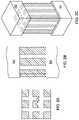
- FIGS. 1A, 1B, and 1Cdisclose a top view, side view and perspective view of dielectric nanotrenches in one non-limiting example embodiment of the aspects described.
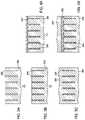
- FIGS. 2A, 2B and 2Cdisclose a top view, side view and perspective view of dielectric nanopillars with an encapsulant and substrate.
- FIGS. 3A, 3B and 3Cdisclose a proposed ideal method of etching, filling and encapsulating an arrangement in one non-limiting example embodiment of the aspects described.
- FIGS. 4A and 4Bare actual results of the ideal method of etching filling and encapsulating the arrangement of FIG. 3 .
- FIGS. 5A, 5B and 5Cillustrate a process flow for nanotrench creation, filling and processing in accordance with another non-limiting example embodiment of an aspect described.
- FIGS. 6A, 6B and 6Cillustrate a second process flow for nanotrench creation, filling and processing in accordance with another non-limiting example embodiment of an aspect described.
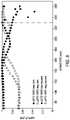
- FIG. 7is a graph of phase change of pillar and trench arrangement diameters in a dielectric film verses diameter measurement for positive and negative circle and square configurations.
- FIG. 8is a graph of amplitude of pillar and trench arrangement diameters in a dielectric film verses diameter measurement for positive and negative circle and square configurations.
- FIG. 9is a graph of phase change vs. film thickness.
- FIG. 10is a chart of nanopillar height and minimum and maximum dimensions and spacings for pillar design.
- the functional materialsmay be referred to as a “dielectric” which has a high refractive index (RI) and low k and different than the substrate, inter-structure spaces and encapsulants.
- RIrefractive index
- klow k
- the terms trenches and pillarsare used.
- the lateral dimensions of the trenches and pillarsare on the order of half of a wavelength of operation.
- aspects of the disclosureseek to use trenches in dielectric materials to achieve a similar result.
- manufacturingsome embodiments are more cost effective to establish using trenching technologies than to establish using pillars.
- the encapsulantmay cover one section of an arrangement and provide for not only the dielectric properties required, but also wear capabilities to make the resulting configurations more fit for intended purposes.
- silicon dioxide materialsare used as device encapsulants, producing faster, cheaper and overall superior operating devices.
- a structured silicon dioxide filmis used in conjunction with a silicon dioxide substrate that has desired nanostructures.
- the nanostructuresmay be pillars or holes and have different cross sections, such as square, circle, ellipse or arbitrary shape.
- a latticemay also be configured with square, hexagonal or arbitrary positions.
- Gaps in the created nanostructuresmay be filled, as desired.
- the gapsmay be filled with spin-on dielectric materials (titanium dioxide, SiN, ZnO, etc.) or materials that may be used with chemical vapor deposition that are flowable.
- holes or trenchesmay be placed in a dielectric film compared to established dielectric nanopillars.
- flat optical devicesmay be made, starting with a silica substrate and then depositing a dielectric thin film over the structured silica substrate and any gap filling materials.
- the gaps in the arrangements createdare filled and then encapsulated.
- a silica substrateis created such that the silica substrate is structured with a profile. This profile is then filled by using a spin-on dielectric in order to easily and cost effectively fill in the structured substrate to build nanostructures.
- trenches (holes) in a dielectric filmmay occur, in place of pillars, delivering comparable optical performance to pillar construction embodiments.
- making trenches on a dielectric film or in a substrateis a superior process compared to conventional methods of making isolated pillars on a dielectric film.
- Nanotrenchesmay be used with a structured silica method or a method of depositing a dielectric film on a planar silica substrate and nanostructuring the result.
- a top view of a dielectric nanotrenchis illustrated.
- the values d and gare such that these values are less than one measured wavelength.
- the structure measured by value gis a TiO 2 as a non-limiting embodiment.
- a high RI valuemay be used with a low absorption dielectric (e.g., TiO 2 , GaP, aSi, cSi, SiN, etc.) for value g.
- the structure designated by distance dis SiO 2 which has a low RI and is a low absorption dielectric.
- 1Bmay be variable as the distance between the substrate 100 and the encapsulant 102 may vary.
- a perspective view, 1 Cis presented indicating the layers of SiO 2 and TiO 2 .
- the titanium dioxide TiO 2is formed in a hashtag or pound shape (i.e., “#”) with silicon dioxide forming the remainder of the substrate, encapsulant and the spaces between the constituent flanges of the shape.
- a top view of a dielectric nanopillar arrangementis illustrated.
- the values d and gare such that these values are less than one measured wavelength.
- the structure measured by value gis a SiO 2 as a non-limiting embodiment.
- the value of dmeasures a part of the nanopillar structure that is made of TiO 2 .
- a high RI valuemay be used with a low absorption dielectric for example (TiO 2 , GaP, aSi, cSi, SiN, etc.).
- the height of the trench created “h”may be variable as the distance between the substrate 200 and the encapsulant 202 may vary.
- a perspective view, 2 Cis presented indicating the layers of SiO 2 and TiO 2 .
- FIGS. 3A, 3B and 3Ca process flow is illustrated for a nanopillar or nanotrench design.
- a substrate 300is provided where etched pillars/trenches 302 are provided.
- a spin on high RI, low k dielectricis used to fill the pillars/trenches 302 .
- FIG. 3Cthe arrangement from FIG. 3B is encapsulated with SiO 2 indicating the ideal configuration.
- FIGS. 4A and 4Bthe as-constructed arrangement resulting from FIG. 3 is presented. While FIGS. 3A, 3B and 3C , illustrate the ideal construction resulting from the methodology described, FIGS. 4A and 4B present that the filling of the trenches, in FIG. 3B , actually occur such that the trenches are filled over the top, with a top layer of overfilled dielectric layer 400 present. Then, the encapsulate 402 is placed over the dielectric layer 400 to construct the final arrangement.
- FIGS. 5A, 5B and 5Ca second process flow is illustrated in another embodiment.
- SiO 2 pillarsare etched on a SiO 2 substrate.
- the nanotrenches etched in the SiO 2are filled with spin-on high n, low k dielectric material.
- FIG. 5Cthe resulting arrangement from 5 B are encapsulated with a low RI, low k material.
- FIGS. 6A, 6B and 6Can alternate process flow to that described in FIGS. 5A, 5B and 5C is illustrated.
- a SiO 2 substrate 600is provided and a high RI, low k dielectric 602 is placed on the substrate 600 surface, such as SiO 2 .
- nanotrenches 604are placed in the high RI, low k dielectric layer 602 .
- the trenchesare filled with a low RI, low k material to provide a completed arrangement.
- phase changevs. diameter
- solid circledesignate a pillar with circular cross section.
- a hollow circleprovides a trench with circular cross section.
- a solid squaredesignates a pillar with square cross section.
- a hollow squaredesignates a trench with square cross-section.
- the transmission phase of both the circular and square pillarsstart from a value of 0 and increase to 1 over the life of the graph.
- the values of transmission phasestart from 1 and decrease to 0 over the life of the graph.
- phase changedoes occur for both positive and negative configurations.
- the transmission amplitudeshould remain as close to 1 as possible, i.e., maximal, irrespective of the change in the sizes of the nanostructures.
- FIG. 8a graph of amplitude vs diameter is illustrated.
- solid circledesignate a positive circle configuration.
- a hollow circleprovides a negative circle configuration.
- a solid squaredesignates a positive square configuration.
- a hollow squaredesignates a negative square configuration.
- the positive circle and positive square configurationshave an approximate value of 1 up till value 180 nm and then slowly decrease.
- the negative circle and negative square valueshave slightly lower amplitude of approximately 0.7 and then increasing to approximately a value of 1 for the remainder of the diameter values.
- pillarstransmit larger amplitudes than trenches.
- FIG. 9a graph of phase change vs square side dimension is illustrated.
- the taller the pillars for a specific configuration may bethe larger will be the minimum (closest) gap between two adjacent pillars.
- the overall transmission amplitudeis increased as well as improving the minimum gap requirement from 40 nm to 600 nm.
- FIG. 10presents features of wavelength, dielectric type and sizing in one non-limiting embodiment. In the embodiments shown, aspects of the disclose indicate that a square pillar shape is more desired than a square trench that is more desired than a circular pillar than is more desirable than a circular trench.
- testingindicates that rounding corners of square trenches can be compensated for by increasing a thickness of the dielectric film used in different embodiments.
- the “as constructed” arrangementhas a residual top layer, minimal changes to phase change and amplitude of signal occur.
- Encapsulation material used for the top surfacemay impact the depth of trenches used. Lowering the refractive index of the encapsulation material, the lower the aspect ratio (h:d) and, hence, the more relaxed the fabrication constraints in terms of etching the nanostructures.
- the arrangement describedmay have configurations that are smaller than 30 nanometers, thereby exceeding the resolution limit of conventional apparatus.
- the flat optical devicesare processed such that components are encapsulated. Such encapsulation allows for more durable devices that are more fit for intended purposes.
- aspects of the disclosureprovide a method for producing flat optical devices that is economical for large scale fabrication.
- a method for creating a flat optical structurecomprising: providing a substrate; etching at least one trench in the substrate; placing a dielectric material in the at least one trench in the substrate; and encapsulating a top of the substrate with a film.
- the methodis provided wherein the substrate is made of silicon dioxide.
- the methodis provided wherein the placing the dielectric material in the at least one trench in the substrate is through a spinning process.
- the methodis provided wherein the encapsulating the top of the substrate with the film is through use of a SiO 2 film.
- the methodis provided wherein the placing the dielectric material in the at least one trench in the substrate includes providing an overfill dielectric layer.
- a method for creating a flat optical structurecomprising: providing a substrate, depositing a material on to a first face of the substrate, etching at least one trench in the material deposited on the first face of the substrate and encapsulating a top of the material deposited on the first face of the substrate with an encapsulating material.
- the methodmay be performed wherein the substrate is made of SiO 2 .
- the methodmay be performed wherein the encapsulating material has a low refractive index and is a low k material.
- an arrangementcomprising a substrate with at least one trench, a spun material placed in the at least one nanotrench; and an encapsulating material placed in contact with the substrate and the spun material.
- the spun material placed in the at least one trenchfurther comprises an overfill layer.
- the spun material placed in the at least one trenchis titanium dioxide.
- the substrate with the at least one trenchis made of silicon dioxide.
- the spun materialis one of GaP, aSi, cSi and SiN.
- a method for creating a flat optical structurecomprising: providing a silicon dioxide substrate with at least one flat surface; etching at least one trench in the at least one flat surface of the silicon dioxide substrate; placing a dielectric material in the at least one trench in the at least one flat surface of the silicon dioxide substrate and encapsulating the placed dielectric material in the at least one trench in the at least one flat surface of the silicon dioxide substrate with a film.
- the methodmay be performed wherein the dielectric material is deposited through a spinning process.
- the methodmay be performed wherein the material is GaP.
- the methodmay be performed wherein the material is one of aSi and SiN.
Landscapes
- Chemical & Material Sciences (AREA)
- Materials Engineering (AREA)
- Engineering & Computer Science (AREA)
- Chemical Kinetics & Catalysis (AREA)
- General Chemical & Material Sciences (AREA)
- Organic Chemistry (AREA)
- Metallurgy (AREA)
- Mechanical Engineering (AREA)
- Physics & Mathematics (AREA)
- Inorganic Chemistry (AREA)
- General Physics & Mathematics (AREA)
- Optics & Photonics (AREA)
- Geochemistry & Mineralogy (AREA)
- Life Sciences & Earth Sciences (AREA)
- Optical Integrated Circuits (AREA)
- Optical Elements Other Than Lenses (AREA)
- Diffracting Gratings Or Hologram Optical Elements (AREA)
- Micromachines (AREA)
Abstract
Description
Claims (15)
Priority Applications (7)
| Application Number | Priority Date | Filing Date | Title |
|---|---|---|---|
| JP2021549253AJP7690394B2 (en) | 2019-02-27 | 2020-02-09 | Dielectric-filled nanostructured silica substrates for flat optical devices |
| PCT/US2020/017383WO2020176227A1 (en) | 2019-02-27 | 2020-02-09 | Dielectric filled nanostructured silica substrate for flat optical devices |
| KR1020217030533AKR102827734B1 (en) | 2019-02-27 | 2020-02-09 | Dielectrically charged nanostructured silica substrates for flat optical devices |
| EP20763703.4AEP3931605A4 (en) | 2019-02-27 | 2020-02-09 | DIELECTRIC FILLED NANOSTRUCTURED SILICA CARRIER FOR FLAT OPTICAL DEVICES |
| CN202080015721.3ACN113454495A (en) | 2019-02-27 | 2020-02-09 | Dielectric-filled nanostructured silicon dioxide substrates for planar optical devices |
| TW109104298ATWI756630B (en) | 2019-02-27 | 2020-02-12 | Dielectric filled nanostructured silica substrate for flat optical devices |
| US17/963,983US20230033741A1 (en) | 2019-02-27 | 2022-10-11 | Dielectric filled nanostructured silica substrate for flat optical devices |
Applications Claiming Priority (2)
| Application Number | Priority Date | Filing Date | Title |
|---|---|---|---|
| IN201941007558 | 2019-02-27 | ||
| IN201941007558 | 2019-02-27 |
Related Child Applications (1)
| Application Number | Title | Priority Date | Filing Date |
|---|---|---|---|
| US17/963,983DivisionUS20230033741A1 (en) | 2019-02-27 | 2022-10-11 | Dielectric filled nanostructured silica substrate for flat optical devices |
Publications (2)
| Publication Number | Publication Date |
|---|---|
| US20200270746A1 US20200270746A1 (en) | 2020-08-27 |
| US11473191B2true US11473191B2 (en) | 2022-10-18 |
Family
ID=72142818
Family Applications (2)
| Application Number | Title | Priority Date | Filing Date |
|---|---|---|---|
| US16/395,005Active2039-12-02US11473191B2 (en) | 2019-02-27 | 2019-04-25 | Method for creating a dielectric filled nanostructured silica substrate for flat optical devices |
| US17/963,983PendingUS20230033741A1 (en) | 2019-02-27 | 2022-10-11 | Dielectric filled nanostructured silica substrate for flat optical devices |
Family Applications After (1)
| Application Number | Title | Priority Date | Filing Date |
|---|---|---|---|
| US17/963,983PendingUS20230033741A1 (en) | 2019-02-27 | 2022-10-11 | Dielectric filled nanostructured silica substrate for flat optical devices |
Country Status (7)
| Country | Link |
|---|---|
| US (2) | US11473191B2 (en) |
| EP (1) | EP3931605A4 (en) |
| JP (1) | JP7690394B2 (en) |
| KR (1) | KR102827734B1 (en) |
| CN (1) | CN113454495A (en) |
| TW (1) | TWI756630B (en) |
| WO (1) | WO2020176227A1 (en) |
Families Citing this family (5)
| Publication number | Priority date | Publication date | Assignee | Title |
|---|---|---|---|---|
| EP3676973A4 (en) | 2017-08-31 | 2021-05-05 | Metalenz, Inc. | TRANSMISSIVE METASURFACE LENS INTEGRATION |
| US11473191B2 (en)* | 2019-02-27 | 2022-10-18 | Applied Materials, Inc. | Method for creating a dielectric filled nanostructured silica substrate for flat optical devices |
| CN114286953B (en) | 2019-07-26 | 2025-04-01 | 梅特兰兹股份有限公司 | Porosity-metasurface and hybrid refraction-metasurface imaging systems |
| CN116940866A (en)* | 2021-01-06 | 2023-10-24 | 梅特兰兹股份有限公司 | Self-aligned nanopillar coatings and methods of making the same |
| CN120188073A (en) | 2022-03-31 | 2025-06-20 | 梅特兰兹股份有限公司 | Polarization-sorting metasurface microlens array device |
Citations (41)
| Publication number | Priority date | Publication date | Assignee | Title |
|---|---|---|---|---|
| US6130454A (en)* | 1998-07-07 | 2000-10-10 | Advanced Micro Devices, Inc. | Gate conductor formed within a trench bounded by slanted sidewalls |
| US6140652A (en)* | 1998-09-09 | 2000-10-31 | Intersil Corporation | Device containing sample preparation sites for transmission electron microscopic analysis and processes of formation and use |
| US6214697B1 (en)* | 1997-12-18 | 2001-04-10 | Micron Technology, Inc | Trench isolation for semiconductor devices |
| US20010024556A1 (en)* | 2000-03-23 | 2001-09-27 | Beguin Alain M.J. | Liquid overclad-encapsulated optical device |
| US6404942B1 (en)* | 1998-10-23 | 2002-06-11 | Corning Incorporated | Fluid-encapsulated MEMS optical switch |
| US20030049865A1 (en)* | 2000-03-02 | 2003-03-13 | Santini John T. | Microfabricated devices for the storage and selective exposure of chemicals and devices |
| US6649489B1 (en)* | 2003-02-13 | 2003-11-18 | Taiwan Semiconductor Manufacturing Company | Poly etching solution to improve silicon trench for low STI profile |
| US6686293B2 (en)* | 2002-05-10 | 2004-02-03 | Applied Materials, Inc | Method of etching a trench in a silicon-containing dielectric material |
| US20050130400A1 (en)* | 2003-12-16 | 2005-06-16 | Asulab S.A. | Method for manufacturing a transparent element with invisible electrodes |
| US6919259B2 (en)* | 2002-10-21 | 2005-07-19 | Taiwan Semiconductor Manufacturing Co., Ltd | Method for STI etching using endpoint detection |
| US6949460B2 (en)* | 2003-11-12 | 2005-09-27 | Lam Research Corporation | Line edge roughness reduction for trench etch |
| US20060113598A1 (en)* | 2004-11-16 | 2006-06-01 | Chen Howard H | Device and method for fabricating double-sided SOI wafer scale package with optical through via connections |
| US20060157854A1 (en)* | 2005-01-14 | 2006-07-20 | Nec Electronics Corporation | Semiconductor device featuring copper wiring layers of different widths having metal capping layers of different thickness formed thereon, and method for manufacturing the same |
| US20060177178A1 (en)* | 2001-08-27 | 2006-08-10 | Greiner Christoph M | Amplitude and phase control in distributed optical structures |
| US7132134B2 (en)* | 1998-03-20 | 2006-11-07 | Applied Materials, Inc. | Staggered in-situ deposition and etching of a dielectric layer for HDP CVD |
| US20080286660A1 (en)* | 2007-05-16 | 2008-11-20 | International Business Machines Corporation | Damascene reticle and method of manufacture thereof |
| US20090121371A1 (en) | 2006-05-12 | 2009-05-14 | Sharp Kabushiki Kaisha | Process for Producing Microlens |
| US20130028564A1 (en)* | 2009-09-09 | 2013-01-31 | Draka Comteq B.V. | Trench-Assisted Multimode Optical Fiber |
| US20130128336A1 (en)* | 2010-04-05 | 2013-05-23 | Kenneth A. Dean | Spectrum-modulated smart windows |
| US20130234698A1 (en)* | 2012-02-15 | 2013-09-12 | Northrop Grumman Litef Gmbh | Integrated optical circuit and method for measuring current as well as sensor module and measuring device |
| US8867879B2 (en)* | 2010-07-02 | 2014-10-21 | Draka Comteq, B.V. | Single-mode optical fiber |
| US20150212346A1 (en)* | 2014-01-29 | 2015-07-30 | Futurewei Technologies, Inc. | Interdigitated Optical Modulator |
| US20150277036A1 (en)* | 2014-03-28 | 2015-10-01 | Futurewei Technologies, Inc. | Apparatus and Method for an Optical Waveguide Edge Coupler for Photonic Integrated Chips |
| US20150304051A1 (en)* | 2014-04-22 | 2015-10-22 | Kabushiki Kaisha Toshiba | Optical device |
| US9236328B1 (en)* | 2014-10-27 | 2016-01-12 | International Business Machines Corporation | Electrical and optical through-silicon-via (TSV) |
| US20160084761A1 (en)* | 2014-08-08 | 2016-03-24 | Quantum-Si Incorporated | Integrated device with external light source for probing detecting and analyzing molecules |
| US20160197111A1 (en)* | 2015-01-05 | 2016-07-07 | The Research Foundation For The State University Of New York | Integrated photonics including germanium |
| US20160291405A1 (en)* | 2013-11-21 | 2016-10-06 | Finisar Corporation | High Reflectivity LCOS Device |
| US20160351135A1 (en)* | 2015-05-28 | 2016-12-01 | Pixtronix, Inc. | Thick routing lines in dark trenches |
| US20170137943A1 (en)* | 2015-11-16 | 2017-05-18 | Lam Research Corporation | Apparatus for uv flowable dielectric |
| US9799702B2 (en)* | 2016-03-24 | 2017-10-24 | Taiwan Semiconductor Manufacturing Company, Ltd. | Deep trench isolation structure and method of forming same |
| US9795718B1 (en)* | 2016-08-05 | 2017-10-24 | International Business Machines Corporation | Biocompatible devices with dissolvable substrates and methods of forming the same |
| WO2018136972A1 (en) | 2017-01-23 | 2018-07-26 | The Regents Of The University Of California | Broadband absorbers via nanostructures |
| US20180224574A1 (en) | 2017-02-03 | 2018-08-09 | Samsung Electronics Co., Ltd. | Meta-optical device and method of manufacturing the same |
| US20180341090A1 (en)* | 2015-11-24 | 2018-11-29 | President And Fellows Of Harvard College | Atomic layer deposition process for fabricating dielectric metasurfaces for wavelengths in the visible spectrum |
| US20180348548A1 (en) | 2017-06-02 | 2018-12-06 | Applied Materials, Inc. | Nanostructured flat lenses for display technologies |
| US20190033683A1 (en) | 2017-12-18 | 2019-01-31 | Intel Corporation | Broadband flat optical elements and methods of manufacture |
| US20190181181A1 (en)* | 2017-12-12 | 2019-06-13 | Samsung Electronics Co., Ltd. | Method of fabricating light emitting device package |
| US20200270746A1 (en)* | 2019-02-27 | 2020-08-27 | Applied Materials, Inc. | Dielectric filled nanostructured silica substrate for flat optical devices |
| US10782468B2 (en)* | 2016-10-13 | 2020-09-22 | Stmicroelectronics Sa | Method for manufacturing an optical device |
| US20210183915A1 (en)* | 2019-12-17 | 2021-06-17 | Texas Instruments Incorporated | Optical Sensor with Trench Etched Through Dielectric Over Silicon |
Family Cites Families (6)
| Publication number | Priority date | Publication date | Assignee | Title |
|---|---|---|---|---|
| US20030033975A1 (en)* | 2001-08-17 | 2003-02-20 | Michael Bazylenko | Method of forming a planar waveguide core |
| US8153502B2 (en)* | 2006-05-16 | 2012-04-10 | Micron Technology, Inc. | Methods for filling trenches in a semiconductor material |
| US20100123386A1 (en)* | 2008-11-13 | 2010-05-20 | Maven Optronics Corp. | Phosphor-Coated Light Extraction Structures for Phosphor-Converted Light Emitting Devices |
| US8652934B1 (en)* | 2012-12-26 | 2014-02-18 | Micron Technology, Inc. | Semiconductor substrate for photonic and electronic structures and method of manufacture |
| TWI646678B (en)* | 2017-12-07 | 2019-01-01 | 晶相光電股份有限公司 | Image sensing device |
| US11222987B2 (en)* | 2018-03-21 | 2022-01-11 | Intel Corporation | Optical receiver employing a metasurface collection lens having concentric belts or rings |
- 2019
- 2019-04-25USUS16/395,005patent/US11473191B2/enactiveActive
- 2020
- 2020-02-09JPJP2021549253Apatent/JP7690394B2/enactiveActive
- 2020-02-09EPEP20763703.4Apatent/EP3931605A4/enactivePending
- 2020-02-09WOPCT/US2020/017383patent/WO2020176227A1/ennot_activeCeased
- 2020-02-09CNCN202080015721.3Apatent/CN113454495A/enactivePending
- 2020-02-09KRKR1020217030533Apatent/KR102827734B1/enactiveActive
- 2020-02-12TWTW109104298Apatent/TWI756630B/enactive
- 2022
- 2022-10-11USUS17/963,983patent/US20230033741A1/enactivePending
Patent Citations (41)
| Publication number | Priority date | Publication date | Assignee | Title |
|---|---|---|---|---|
| US6214697B1 (en)* | 1997-12-18 | 2001-04-10 | Micron Technology, Inc | Trench isolation for semiconductor devices |
| US7132134B2 (en)* | 1998-03-20 | 2006-11-07 | Applied Materials, Inc. | Staggered in-situ deposition and etching of a dielectric layer for HDP CVD |
| US6130454A (en)* | 1998-07-07 | 2000-10-10 | Advanced Micro Devices, Inc. | Gate conductor formed within a trench bounded by slanted sidewalls |
| US6140652A (en)* | 1998-09-09 | 2000-10-31 | Intersil Corporation | Device containing sample preparation sites for transmission electron microscopic analysis and processes of formation and use |
| US6404942B1 (en)* | 1998-10-23 | 2002-06-11 | Corning Incorporated | Fluid-encapsulated MEMS optical switch |
| US20030049865A1 (en)* | 2000-03-02 | 2003-03-13 | Santini John T. | Microfabricated devices for the storage and selective exposure of chemicals and devices |
| US20010024556A1 (en)* | 2000-03-23 | 2001-09-27 | Beguin Alain M.J. | Liquid overclad-encapsulated optical device |
| US20060177178A1 (en)* | 2001-08-27 | 2006-08-10 | Greiner Christoph M | Amplitude and phase control in distributed optical structures |
| US6686293B2 (en)* | 2002-05-10 | 2004-02-03 | Applied Materials, Inc | Method of etching a trench in a silicon-containing dielectric material |
| US6919259B2 (en)* | 2002-10-21 | 2005-07-19 | Taiwan Semiconductor Manufacturing Co., Ltd | Method for STI etching using endpoint detection |
| US6649489B1 (en)* | 2003-02-13 | 2003-11-18 | Taiwan Semiconductor Manufacturing Company | Poly etching solution to improve silicon trench for low STI profile |
| US6949460B2 (en)* | 2003-11-12 | 2005-09-27 | Lam Research Corporation | Line edge roughness reduction for trench etch |
| US20050130400A1 (en)* | 2003-12-16 | 2005-06-16 | Asulab S.A. | Method for manufacturing a transparent element with invisible electrodes |
| US20060113598A1 (en)* | 2004-11-16 | 2006-06-01 | Chen Howard H | Device and method for fabricating double-sided SOI wafer scale package with optical through via connections |
| US20060157854A1 (en)* | 2005-01-14 | 2006-07-20 | Nec Electronics Corporation | Semiconductor device featuring copper wiring layers of different widths having metal capping layers of different thickness formed thereon, and method for manufacturing the same |
| US20090121371A1 (en) | 2006-05-12 | 2009-05-14 | Sharp Kabushiki Kaisha | Process for Producing Microlens |
| US20080286660A1 (en)* | 2007-05-16 | 2008-11-20 | International Business Machines Corporation | Damascene reticle and method of manufacture thereof |
| US20130028564A1 (en)* | 2009-09-09 | 2013-01-31 | Draka Comteq B.V. | Trench-Assisted Multimode Optical Fiber |
| US20130128336A1 (en)* | 2010-04-05 | 2013-05-23 | Kenneth A. Dean | Spectrum-modulated smart windows |
| US8867879B2 (en)* | 2010-07-02 | 2014-10-21 | Draka Comteq, B.V. | Single-mode optical fiber |
| US20130234698A1 (en)* | 2012-02-15 | 2013-09-12 | Northrop Grumman Litef Gmbh | Integrated optical circuit and method for measuring current as well as sensor module and measuring device |
| US20160291405A1 (en)* | 2013-11-21 | 2016-10-06 | Finisar Corporation | High Reflectivity LCOS Device |
| US20150212346A1 (en)* | 2014-01-29 | 2015-07-30 | Futurewei Technologies, Inc. | Interdigitated Optical Modulator |
| US20150277036A1 (en)* | 2014-03-28 | 2015-10-01 | Futurewei Technologies, Inc. | Apparatus and Method for an Optical Waveguide Edge Coupler for Photonic Integrated Chips |
| US20150304051A1 (en)* | 2014-04-22 | 2015-10-22 | Kabushiki Kaisha Toshiba | Optical device |
| US20160084761A1 (en)* | 2014-08-08 | 2016-03-24 | Quantum-Si Incorporated | Integrated device with external light source for probing detecting and analyzing molecules |
| US9236328B1 (en)* | 2014-10-27 | 2016-01-12 | International Business Machines Corporation | Electrical and optical through-silicon-via (TSV) |
| US20160197111A1 (en)* | 2015-01-05 | 2016-07-07 | The Research Foundation For The State University Of New York | Integrated photonics including germanium |
| US20160351135A1 (en)* | 2015-05-28 | 2016-12-01 | Pixtronix, Inc. | Thick routing lines in dark trenches |
| US20170137943A1 (en)* | 2015-11-16 | 2017-05-18 | Lam Research Corporation | Apparatus for uv flowable dielectric |
| US20180341090A1 (en)* | 2015-11-24 | 2018-11-29 | President And Fellows Of Harvard College | Atomic layer deposition process for fabricating dielectric metasurfaces for wavelengths in the visible spectrum |
| US9799702B2 (en)* | 2016-03-24 | 2017-10-24 | Taiwan Semiconductor Manufacturing Company, Ltd. | Deep trench isolation structure and method of forming same |
| US9795718B1 (en)* | 2016-08-05 | 2017-10-24 | International Business Machines Corporation | Biocompatible devices with dissolvable substrates and methods of forming the same |
| US10782468B2 (en)* | 2016-10-13 | 2020-09-22 | Stmicroelectronics Sa | Method for manufacturing an optical device |
| WO2018136972A1 (en) | 2017-01-23 | 2018-07-26 | The Regents Of The University Of California | Broadband absorbers via nanostructures |
| US20180224574A1 (en) | 2017-02-03 | 2018-08-09 | Samsung Electronics Co., Ltd. | Meta-optical device and method of manufacturing the same |
| US20180348548A1 (en) | 2017-06-02 | 2018-12-06 | Applied Materials, Inc. | Nanostructured flat lenses for display technologies |
| US20190181181A1 (en)* | 2017-12-12 | 2019-06-13 | Samsung Electronics Co., Ltd. | Method of fabricating light emitting device package |
| US20190033683A1 (en) | 2017-12-18 | 2019-01-31 | Intel Corporation | Broadband flat optical elements and methods of manufacture |
| US20200270746A1 (en)* | 2019-02-27 | 2020-08-27 | Applied Materials, Inc. | Dielectric filled nanostructured silica substrate for flat optical devices |
| US20210183915A1 (en)* | 2019-12-17 | 2021-06-17 | Texas Instruments Incorporated | Optical Sensor with Trench Etched Through Dielectric Over Silicon |
Non-Patent Citations (17)
| Title |
|---|
| Banzhaf, S., et al., "Post-trench processing of silicon deep trench capacitors for power electronic applications," 2016 28th International Symposium on Power Semiconductor Devices and ICs (ISPSD), 2016, pp. 399-402, doi: 10.1109/ISPSD.2016.7520862.* |
| Belyansky, M., et al., "Study of silicon strain in shallow trench isolation". J. Vac. Sci. Technol. A 28(4), Jul./Aug. 2010, pp. 829-833.* |
| Chapman, Gemma, et al., "Focused electron beam deposited silicon dioxide derivatives for nano-electronic applications". Materials Science in Semiconductor Processing 147 (2022) 106736, pp. 1-6.* |
| Chen, Yunhan, et al., "Robust Method of Fabricating Epitaxially Encapsulated MEMS Devices with Large Gaps". Journal of Microelectromechanical Systems, vol. 26, No. 6, Dec. 2017, p. 1235-1243.* |
| Darnon, Maxime, et al., "Patterning of narrow porous SiOCH trenches using a TiN hard mask". Microelectronic Engineering, Elsevier, 2008, 85 (11), pp. 2226-2235. ff10.1016/j.mee.2008.06.025ff. ffhal-00387506f.* |
| Gerung, Henry, et al., "In situ real-time monitoring of profile evolution during plasma etching of mesoporous low-dielectric-constant SiO2". J. Vac. Sci. Technol. A 23 (2), Mar./Apr. 2005, pp. 347-354.* |
| Hadi, Mohammed, et al., "Preparation of high transmittance TiO2 thin films by sol-gel technique as antireflection coating", IOP Conf. Series: 2018 J. Phys.: Conf. Ser. 1032 012018, pp. 1-11.* |
| International Search Report and Written Opinion dated Jun. 5, 2020 for Application No. PCT/US2020/017383. |
| Kim, Sejeong, et al., "Photonic crystal cavities from hexagonal boron nitride". Nature Communications, (2018) 9:2623, pp. 1-8.* |
| Laermer, F., et al., "Bosch Deep Silicon Etching: Improving Uniformity and Etch Rate for Advanced MEMS Applications". Proceedings of the IEEE Micro Electro Mechanical Systems (MEMS), 1999, pp. 211-216. 10.1109/MEMSYS.1999.746812.* |
| Patterson, Oliver D., et al., "Methodology for Trench Capacitor Etch Optimization using Voltage Contrast Inspection and Special Processing". 2010 IEEE/SEMI Advanced Semiconductor Manufacturing Conference (ASMC), 2010, pp. 109-114, doi: 10.1109/ASMC.2010.5551433.* |
| Shin, Young Jae, et al., "Fabrication and Encapsulation of a Short-Period Wire Grid Polarizer with Improved Viewing Angle by the Angled-Evaporation Method". Advanced Optical Materials, 2013, 1, 863-868.* |
| Shkondin, E., et al., "High aspect ratio titanium nitride trench structures as plasmonic biosensor". Optical Materials Express 4171, vol. 7, No. 11, Nov. 1, 2017, 12 pages.* |
| Taiwan Office Action dated Feb. 3, 2021 for Application No. 109104298. |
| Vengurlekar, Arvind S., "Optical properties of metallo-dielectric deep trench gratings: role of surface plasmons and Wood—Rayleigh anomaly". Optics Letters, vol. 33, No. 15, Aug. 1, 2008, pp. 1669-1671.* |
| Zhao, Qiancheng, et al., "Optical properties of V-groove silicon nitride trench waveguides". Journal of the Optical Society of America A, vol. 33, No. 9, Sep. 2016, p. 1851-1859.* |
| Zhao, Qiancheng, et al., "Optical properties of V-groove silicon nitride trench waveguides". Journal of the Optical Society of America A, vol. 33, No. 9, Sep. 2016, pp. 1851-1859.* |
Also Published As
| Publication number | Publication date |
|---|---|
| TW202102707A (en) | 2021-01-16 |
| TWI756630B (en) | 2022-03-01 |
| KR102827734B1 (en) | 2025-06-30 |
| JP7690394B2 (en) | 2025-06-10 |
| CN113454495A (en) | 2021-09-28 |
| KR20210122312A (en) | 2021-10-08 |
| US20230033741A1 (en) | 2023-02-02 |
| EP3931605A1 (en) | 2022-01-05 |
| US20200270746A1 (en) | 2020-08-27 |
| JP2022522416A (en) | 2022-04-19 |
| WO2020176227A1 (en) | 2020-09-03 |
| EP3931605A4 (en) | 2023-05-03 |
Similar Documents
| Publication | Publication Date | Title |
|---|---|---|
| US11473191B2 (en) | Method for creating a dielectric filled nanostructured silica substrate for flat optical devices | |
| US20220057553A1 (en) | Wafer level microstructures for an optical lens | |
| US7312158B2 (en) | Method of forming pattern | |
| CN110783351B (en) | Narrow band filter with high transmittance | |
| EP2654083A1 (en) | Improved method for producing a transistor structure with stacked nanowires and gate-all-around | |
| US8836055B2 (en) | MEMS structures and methods for forming the same | |
| US20160146736A1 (en) | Surface Enhanced Raman Spectroscopy Resonator Structures And Methods Of Making Same | |
| US8969205B2 (en) | Double patterning via triangular shaped sidewall spacers | |
| WO2016059670A1 (en) | Silicon carbide epitaxial wafer production method | |
| US9911661B2 (en) | Nano wire structure and method for fabricating the same | |
| US8680631B2 (en) | High aspect ratio capacitively coupled MEMS devices | |
| CN103488058B (en) | Method for manufacturing grid line with high uniformity through double exposure | |
| CN102437020B (en) | Wafer control slice and forming method thereof | |
| TWI863493B (en) | Ambient light sensor | |
| CN102339840A (en) | Light pipe fabrication with improved sensitivity | |
| CN103512508B (en) | Semiconductor device testing method | |
| US7125738B2 (en) | Method of fabricating a photosensitive structure | |
| US20190393251A1 (en) | Anti-reflective layers in semiconductor devices | |
| CN112701079A (en) | SON structure and preparation method thereof | |
| JP5850407B2 (en) | Semiconductor device and manufacturing method of semiconductor device | |
| TW201944123A (en) | Optical devices and fabrication method thereof | |
| TWI688012B (en) | Method for manufacturing a semiconductor structure | |
| KR102062684B1 (en) | Method for measuring thickness of insulating layer | |
| KR100301247B1 (en) | Method of manufacturing a monitoring box | |
| KR20220066821A (en) | Top-down fabrication process for vertically-stracked silicon-nanowire array |
Legal Events
| Date | Code | Title | Description |
|---|---|---|---|
| FEPP | Fee payment procedure | Free format text:ENTITY STATUS SET TO UNDISCOUNTED (ORIGINAL EVENT CODE: BIG.); ENTITY STATUS OF PATENT OWNER: LARGE ENTITY | |
| AS | Assignment | Owner name:APPLIED MATERIALS, INC., CALIFORNIA Free format text:ASSIGNMENT OF ASSIGNORS INTEREST;ASSIGNORS:ROY, TAPASHREE;MEYER TIMMERMAN THIJSSEN, RUTGER;GODET, LUDOVIC;AND OTHERS;REEL/FRAME:049027/0163 Effective date:20190412 | |
| STPP | Information on status: patent application and granting procedure in general | Free format text:NON FINAL ACTION MAILED | |
| STPP | Information on status: patent application and granting procedure in general | Free format text:RESPONSE TO NON-FINAL OFFICE ACTION ENTERED AND FORWARDED TO EXAMINER | |
| STPP | Information on status: patent application and granting procedure in general | Free format text:FINAL REJECTION MAILED | |
| STPP | Information on status: patent application and granting procedure in general | Free format text:DOCKETED NEW CASE - READY FOR EXAMINATION | |
| STPP | Information on status: patent application and granting procedure in general | Free format text:EX PARTE QUAYLE ACTION MAILED | |
| STPP | Information on status: patent application and granting procedure in general | Free format text:RESPONSE TO EX PARTE QUAYLE ACTION ENTERED AND FORWARDED TO EXAMINER | |
| STPP | Information on status: patent application and granting procedure in general | Free format text:NOTICE OF ALLOWANCE MAILED -- APPLICATION RECEIVED IN OFFICE OF PUBLICATIONS | |
| STPP | Information on status: patent application and granting procedure in general | Free format text:PUBLICATIONS -- ISSUE FEE PAYMENT RECEIVED | |
| STPP | Information on status: patent application and granting procedure in general | Free format text:PUBLICATIONS -- ISSUE FEE PAYMENT VERIFIED | |
| STCF | Information on status: patent grant | Free format text:PATENTED CASE |