US11453956B2 - Method for growth of a merged crystal by bonding at least a first and second crystal to an adhesion layer to form a tiled substrate and growing a crystalline composition over said tiled substrate - Google Patents
Method for growth of a merged crystal by bonding at least a first and second crystal to an adhesion layer to form a tiled substrate and growing a crystalline composition over said tiled substrateDownload PDFInfo
- Publication number
- US11453956B2 US11453956B2US16/550,947US201916550947AUS11453956B2US 11453956 B2US11453956 B2US 11453956B2US 201916550947 AUS201916550947 AUS 201916550947AUS 11453956 B2US11453956 B2US 11453956B2
- Authority
- US
- United States
- Prior art keywords
- crystal
- epitaxial layer
- grown
- layer
- grown epitaxial
- Prior art date
- Legal status (The legal status is an assumption and is not a legal conclusion. Google has not performed a legal analysis and makes no representation as to the accuracy of the status listed.)
- Active, expires
Links
Images


Classifications
- C—CHEMISTRY; METALLURGY
- C30—CRYSTAL GROWTH
- C30B—SINGLE-CRYSTAL GROWTH; UNIDIRECTIONAL SOLIDIFICATION OF EUTECTIC MATERIAL OR UNIDIRECTIONAL DEMIXING OF EUTECTOID MATERIAL; REFINING BY ZONE-MELTING OF MATERIAL; PRODUCTION OF A HOMOGENEOUS POLYCRYSTALLINE MATERIAL WITH DEFINED STRUCTURE; SINGLE CRYSTALS OR HOMOGENEOUS POLYCRYSTALLINE MATERIAL WITH DEFINED STRUCTURE; AFTER-TREATMENT OF SINGLE CRYSTALS OR A HOMOGENEOUS POLYCRYSTALLINE MATERIAL WITH DEFINED STRUCTURE; APPARATUS THEREFOR
- C30B7/00—Single-crystal growth from solutions using solvents which are liquid at normal temperature, e.g. aqueous solutions
- C30B7/10—Single-crystal growth from solutions using solvents which are liquid at normal temperature, e.g. aqueous solutions by application of pressure, e.g. hydrothermal processes
- C30B7/105—Single-crystal growth from solutions using solvents which are liquid at normal temperature, e.g. aqueous solutions by application of pressure, e.g. hydrothermal processes using ammonia as solvent, i.e. ammonothermal processes
- C—CHEMISTRY; METALLURGY
- C30—CRYSTAL GROWTH
- C30B—SINGLE-CRYSTAL GROWTH; UNIDIRECTIONAL SOLIDIFICATION OF EUTECTIC MATERIAL OR UNIDIRECTIONAL DEMIXING OF EUTECTOID MATERIAL; REFINING BY ZONE-MELTING OF MATERIAL; PRODUCTION OF A HOMOGENEOUS POLYCRYSTALLINE MATERIAL WITH DEFINED STRUCTURE; SINGLE CRYSTALS OR HOMOGENEOUS POLYCRYSTALLINE MATERIAL WITH DEFINED STRUCTURE; AFTER-TREATMENT OF SINGLE CRYSTALS OR A HOMOGENEOUS POLYCRYSTALLINE MATERIAL WITH DEFINED STRUCTURE; APPARATUS THEREFOR
- C30B19/00—Liquid-phase epitaxial-layer growth
- C30B19/06—Reaction chambers; Boats for supporting the melt; Substrate holders
- C30B19/068—Substrate holders
- C—CHEMISTRY; METALLURGY
- C30—CRYSTAL GROWTH
- C30B—SINGLE-CRYSTAL GROWTH; UNIDIRECTIONAL SOLIDIFICATION OF EUTECTIC MATERIAL OR UNIDIRECTIONAL DEMIXING OF EUTECTOID MATERIAL; REFINING BY ZONE-MELTING OF MATERIAL; PRODUCTION OF A HOMOGENEOUS POLYCRYSTALLINE MATERIAL WITH DEFINED STRUCTURE; SINGLE CRYSTALS OR HOMOGENEOUS POLYCRYSTALLINE MATERIAL WITH DEFINED STRUCTURE; AFTER-TREATMENT OF SINGLE CRYSTALS OR A HOMOGENEOUS POLYCRYSTALLINE MATERIAL WITH DEFINED STRUCTURE; APPARATUS THEREFOR
- C30B19/00—Liquid-phase epitaxial-layer growth
- C30B19/12—Liquid-phase epitaxial-layer growth characterised by the substrate
- C—CHEMISTRY; METALLURGY
- C30—CRYSTAL GROWTH
- C30B—SINGLE-CRYSTAL GROWTH; UNIDIRECTIONAL SOLIDIFICATION OF EUTECTIC MATERIAL OR UNIDIRECTIONAL DEMIXING OF EUTECTOID MATERIAL; REFINING BY ZONE-MELTING OF MATERIAL; PRODUCTION OF A HOMOGENEOUS POLYCRYSTALLINE MATERIAL WITH DEFINED STRUCTURE; SINGLE CRYSTALS OR HOMOGENEOUS POLYCRYSTALLINE MATERIAL WITH DEFINED STRUCTURE; AFTER-TREATMENT OF SINGLE CRYSTALS OR A HOMOGENEOUS POLYCRYSTALLINE MATERIAL WITH DEFINED STRUCTURE; APPARATUS THEREFOR
- C30B25/00—Single-crystal growth by chemical reaction of reactive gases, e.g. chemical vapour-deposition growth
- C30B25/02—Epitaxial-layer growth
- C30B25/18—Epitaxial-layer growth characterised by the substrate
- C—CHEMISTRY; METALLURGY
- C30—CRYSTAL GROWTH
- C30B—SINGLE-CRYSTAL GROWTH; UNIDIRECTIONAL SOLIDIFICATION OF EUTECTIC MATERIAL OR UNIDIRECTIONAL DEMIXING OF EUTECTOID MATERIAL; REFINING BY ZONE-MELTING OF MATERIAL; PRODUCTION OF A HOMOGENEOUS POLYCRYSTALLINE MATERIAL WITH DEFINED STRUCTURE; SINGLE CRYSTALS OR HOMOGENEOUS POLYCRYSTALLINE MATERIAL WITH DEFINED STRUCTURE; AFTER-TREATMENT OF SINGLE CRYSTALS OR A HOMOGENEOUS POLYCRYSTALLINE MATERIAL WITH DEFINED STRUCTURE; APPARATUS THEREFOR
- C30B29/00—Single crystals or homogeneous polycrystalline material with defined structure characterised by the material or by their shape
- C30B29/10—Inorganic compounds or compositions
- C30B29/40—AIIIBV compounds wherein A is B, Al, Ga, In or Tl and B is N, P, As, Sb or Bi
- C30B29/403—AIII-nitrides
- C30B29/406—Gallium nitride
- C—CHEMISTRY; METALLURGY
- C30—CRYSTAL GROWTH
- C30B—SINGLE-CRYSTAL GROWTH; UNIDIRECTIONAL SOLIDIFICATION OF EUTECTIC MATERIAL OR UNIDIRECTIONAL DEMIXING OF EUTECTOID MATERIAL; REFINING BY ZONE-MELTING OF MATERIAL; PRODUCTION OF A HOMOGENEOUS POLYCRYSTALLINE MATERIAL WITH DEFINED STRUCTURE; SINGLE CRYSTALS OR HOMOGENEOUS POLYCRYSTALLINE MATERIAL WITH DEFINED STRUCTURE; AFTER-TREATMENT OF SINGLE CRYSTALS OR A HOMOGENEOUS POLYCRYSTALLINE MATERIAL WITH DEFINED STRUCTURE; APPARATUS THEREFOR
- C30B33/00—After-treatment of single crystals or homogeneous polycrystalline material with defined structure
- C30B33/06—Joining of crystals
- H—ELECTRICITY
- H01—ELECTRIC ELEMENTS
- H01L—SEMICONDUCTOR DEVICES NOT COVERED BY CLASS H10
- H01L21/00—Processes or apparatus adapted for the manufacture or treatment of semiconductor or solid state devices or of parts thereof
- H01L21/02—Manufacture or treatment of semiconductor devices or of parts thereof
- H01L21/02104—Forming layers
- H01L21/02365—Forming inorganic semiconducting materials on a substrate
- H01L21/02518—Deposited layers
- H01L21/02521—Materials
- H01L21/02538—Group 13/15 materials
- H01L21/0254—Nitrides
- H—ELECTRICITY
- H01—ELECTRIC ELEMENTS
- H01L—SEMICONDUCTOR DEVICES NOT COVERED BY CLASS H10
- H01L21/00—Processes or apparatus adapted for the manufacture or treatment of semiconductor or solid state devices or of parts thereof
- H01L21/02—Manufacture or treatment of semiconductor devices or of parts thereof
- H01L21/02104—Forming layers
- H01L21/02365—Forming inorganic semiconducting materials on a substrate
- H01L21/02518—Deposited layers
- H01L21/02609—Crystal orientation
- H01L29/2003—
- H—ELECTRICITY
- H10—SEMICONDUCTOR DEVICES; ELECTRIC SOLID-STATE DEVICES NOT OTHERWISE PROVIDED FOR
- H10D—INORGANIC ELECTRIC SEMICONDUCTOR DEVICES
- H10D62/00—Semiconductor bodies, or regions thereof, of devices having potential barriers
- H10D62/80—Semiconductor bodies, or regions thereof, of devices having potential barriers characterised by the materials
- H10D62/85—Semiconductor bodies, or regions thereof, of devices having potential barriers characterised by the materials being Group III-V materials, e.g. GaAs
- H10D62/8503—Nitride Group III-V materials, e.g. AlN or GaN
Definitions
- Embodiments of the disclosureinclude techniques for material processing in a capsule disposed within a high-pressure apparatus enclosure.
- the methodscan be applied to growing crystals of GaN, AlN, InN, and their alloys, including, for example, InGaN, AlGaN, and AlInGaN, and others for the manufacture of bulk or patterned substrates.
- Such bulk or patterned substratescan be used for a variety of applications including optoelectronic devices, lasers, light emitting diodes, solar cells, photoelectrochemical water splitting and hydrogen generation devices, photodetectors, integrated circuits, and transistors, among other devices.
- nitride crystals and substratesare needed for a variety of applications, including light emitting diodes, laser diodes, transistors, and photodetectors.
- there is an economy of scale with device processingsuch that the cost per device is reduced as the diameter of the substrate is increased.
- large area seed crystalsare needed for bulk nitride crystal growth.
- GaNgallium nitride
- HVPEhydride vapor phase epitaxy
- the non-polar planes of gallium nitridesuch as ⁇ 1 0 ⁇ 1 0 ⁇ and ⁇ 1 1 ⁇ 2 0 ⁇
- the semi-polar planes of gallium nitridesuch as ⁇ 1 0 ⁇ 1 ⁇ 1 ⁇ , ⁇ 1 0 ⁇ 1 ⁇ 2 ⁇ , ⁇ 1 0 ⁇ 1 3 ⁇ , and ⁇ 1 1 ⁇ 2 ⁇ 2 ⁇ , ⁇ 2 0 ⁇ 2 1 ⁇
- Unfortunatelyno large area, high quality non-polar or semi-polar GaN wafers are generally available for large scale commercial applications.
- Other conventional methods for growing very high quality GaN crystalsfor example, with a dislocation density less than 10 4 cm ⁇ 2 have been proposed. These crystals, however, are typically small, less than 1-5 centimeters in diameter, and are not commercially available.
- Legacy techniqueshave suggested a method for merging elementary GaN seed crystals into a larger compound crystal by a tiling method.
- Some of the legacy methodsuse elementary GaN seed crystals grown by hydride vapor phase epitaxy (HVPE) and polishing the edges of the elementary crystals at oblique angles to cause merger in fast-growing directions.
- HVPEhydride vapor phase epitaxy
- Such legacy techniqueshave limitations. For example, legacy techniques do not specify the accuracy of the crystallographic orientation between the merged elementary seed crystals they provide a method capable of producing highly accurate crystallographic registry between the elementary seed crystals and the observed defects resulting from the merging of the elementary seed crystals.
- This disclosureprovides a method for growth of a large-area, gallium-containing nitride crystal.
- the methodincludes providing at least two nitride crystals having a dislocation density below about 10 7 cm ⁇ 2 together with a handle substrate.
- the nitride crystalsare bonded to the handle substrate.
- the nitride crystalsare grown to coalescence into a merged nitride crystal.
- the polar misorientation angle ⁇ between the first nitride crystal and the second nitride crystalis greater than about 0.005 degree and less than about 0.5 degree and the azimuthal misorientation angles ⁇ and ⁇ are greater than about 0.01 degree and less than about 1 degree.
- a semiconductor structurecan be formed on the nitride crystals as desired.
- the disclosureincludes the steps above, and also includes methods of providing a release layer and a high quality epitaxial layer on each of the two nitride crystals.
- the epitaxial layersare grown to cause coalescence of the two nitride crystals into a merged nitride crystal.
- the polar misorientation angle ⁇ between the first nitride crystal and the second nitride crystalis less than 0.5 degree and azimuthal misorientation angles ⁇ and ⁇ are less than 1 degree.
- the disclosed methodscan provide a crystal that includes at least two single crystal domains having a nitride composition and characterized by a dislocation density within each of the domains of less than 10 7 cm ⁇ 2 .
- Each of the at least two single crystal domainsis separated by a line of dislocations with a linear density greater than 50 cm ⁇ 1 and less than 5 ⁇ 10 5 cm ⁇ 1 .
- the polar misorientation angle ⁇ between the first domain and the second domainis less than 0.5 degree and the azimuthal misorientation angles ⁇ and ⁇ are less than 1 degree.
- crystalscomprising at least two single crystal domains having a nitride composition
- a first domainhaving a first thickness, a first lateral dimension, and a second lateral dimension
- the first lateral dimension and the second lateral dimensiondefine a plane that is perpendicular to the first thickness, and each of the first lateral dimension and the second lateral dimension is greater than about 2 millimeters
- a second domainhaving a second thickness, a third lateral dimension and a fourth lateral dimension, wherein the third lateral dimension and the fourth later dimension define a plane that is perpendicular to the second thickness, wherein each of the third lateral dimension and the fourth lateral dimension is greater than about 2 millimeters
- each of the at least two single crystal domainsare characterized by a dislocation density of less than 10 7 cm ⁇ 2 , are separated by a line of dislocations with a linear density between about 50 cm ⁇ 1 and about 5 ⁇ 10 5 cm ⁇ 1 , and a
- method of fabricating a crystalcomprising: providing at least two crystals, each of the at least two crystals characterized by a dislocation density below about 10 7 cm ⁇ 2 ; providing a handled substrate; bonding the at least two crystals to the handle substrate; and growing the at least two crystals to cause a coalescence into a merged crystal; wherein the merged crystal comprises a first domain and a second domain characterized by a polar misorientation angle ⁇ between the first domain and the second domain is greater than about 0.005 degrees and less than about 0.5 degrees and the misorientation angles ⁇ and ⁇ between the first domain and the second domain are greater than about 0.01 degrees and less than about 1 degree.
- FIGS. 1A, 1B, 1C, 1D, 1E, 1F, 1G, 1H, 1I, 1J, and 1Kare diagrams illustrating methods for bonding crystals.
- FIG. 2is a diagram illustrating the crystallographic misorientation between two adjacent wafer-bonded crystals.
- FIGS. 3A, 3B, 3C, and 3Dare diagrams illustrating arrangements of tiled crystals.
- FIGS. 4A, 4B, 5, and 6are diagrams illustrating a method for coalescing wafer-bonded crystals.
- FIGS. 7A, 7B, 7C, and 7Dare diagrams illustrating arrangements of merged crystals.
- FIGS. 8, 9, and 10are diagrams illustrating lateral growth from a seed crystal.
- FIG. 11is a flow chart of a method for making crystals according to some embodiments.
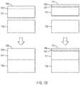
- a crystal 101 having a first surface 105is provided.
- a crystalreferred to as crystal 101 as a “nitride crystal”, as nitride crystals with a wurtzite crystal structure, which crystal and crystal structure is discussed in detail for a particular set of embodiments.
- the method disclosedalso uses the term “nitride crystal”, which includes non-nitride crystals and nitride crystals.
- non-nitride crystalsexamples include diamond, cubic boron nitride, boron carbide, silicon, silicon carbide, germanium, silicon germanium, indium phosphide, gallium phosphide, zinc oxide, zinc selenide, gallium arsenide, cadmium telluride, and cadmium zinc telluride.
- nitride crystal 101comprises GaN or Al x In y Ga (1-x-y) N, where 0 ⁇ x and y ⁇ 1 and is characterized a very high crystallographic quality.
- crystal 101has a wurtzite crystal structure and is selected from ZnO, ZnS, AgI, CdS, CdSe, 2H—SiC, 4H—SiC, and 6H—SiC.
- Nitride crystal 101preferably has a surface dislocation density less than about 10 7 cm ⁇ 2 , 10 6 cm ⁇ 2 , 10 5 cm ⁇ 2 , 10 4 cm ⁇ 2 , 10 3 cm ⁇ 2 , or in certain embodiments, less than about 10 2 cm ⁇ 2 .
- Nitride crystal 101also preferably has a stacking-fault concentration below 10 4 , below 10 3 cm ⁇ 1 , 10 2 cm ⁇ 1 , 10 cm ⁇ 1 , or in certain embodiments, below 1 cm ⁇ 1 .
- Nitride crystal 101also has a symmetric x-ray rocking curve full width at half maximum (FWHM) less than about 300 arc sec, 200 arc sec, 100 arc sec, 50 arc sec, 35 arc sec, 25 arc sec, or in certain embodiments less than about 15 arc sec.
- FWHMfull width at half maximum
- Nitride crystal 101has a crystallographic radius of curvature greater than 0.1 meter, 1 meter, 10 meters, 100 meters, or in certain embodiments, greater than 1000 meters, in up to three independent or orthogonal directions.
- Nitride crystal 101may comprise regions characterized by a relatively high concentration of threading dislocations separated by one or more regions characterized by a relatively low concentration of threading dislocations.
- the concentration of threading dislocations in the relatively high concentration regionsmay be greater than about 10 6 cm ⁇ 2 , 10 7 cm ⁇ 2 , or in certain embodiments, greater than about 10 8 cm ⁇ 2 .
- the concentration of threading dislocations in the relatively low concentration regionsmay be less than about 10 6 cm ⁇ 2 , 10 5 cm ⁇ 2 , or in certain embodiments, less than about 10 4 cm ⁇ 2 .
- the thickness of nitride crystal 101may be between about 10 microns and about 100 millimeters, or in certain embodiments, between about 0.1 millimeter and about 10 millimeters.
- Crystal 101may have a first lateral dimension and a second lateral dimension, the lateral dimensions defining a plane that is perpendicular to the thickness of the nitride crystal 101 , where each of the first lateral dimension and the second lateral dimension may be at least about 0.5 millimeter, 1 millimeter, 2 millimeters, 4 millimeters, 5 millimeters, 10 millimeters, 15 millimeters, 20 millimeters, 25 millimeters, 35 millimeters, 50 millimeters, 75 millimeters, 100 millimeters, 150 millimeters, or in certain embodiments, at least about 200 millimeters.
- Surface 105may be characterized by a crystallographic orientation within 5 degrees, within 2 degrees, within 1 degree, within 0.5 degree, within 0.2 degree, within 0.1 degree, within 0.05 degree, within 0.02 degree, or in certain embodiments, within about 0.01 degree of the (0 0 0 1) Ga-polar plane, the (0 0 0 ⁇ 1) N-polar plane, the ⁇ 1 0 ⁇ 1 0 ⁇ non-polar plane, or the ⁇ 1 1 ⁇ 2 0 ⁇ non-polar a-plane.
- the crystallographic orientation of surface 105is within 5 degrees, 2 degrees, 1 degree, 0.5 degree, 0.2 degree, 0.1 degree, 0.05 degree, 0.02 degree, or in certain embodiments, within 0.01 degree of any one of the ⁇ 1 1 ⁇ 2 ⁇ 2 ⁇ plane, the ⁇ 6 0 ⁇ 6 ⁇ 1 ⁇ plane, the ⁇ 5 0 ⁇ 5 ⁇ 1 ⁇ plane, the ⁇ 40 ⁇ 4 ⁇ 1 ⁇ plane, the ⁇ 3 0 ⁇ 3 ⁇ 1 ⁇ plane, the ⁇ 5 0 ⁇ 5 ⁇ 2 ⁇ plane, the ⁇ 7 0 ⁇ 7 3 ⁇ plane, the plane, the ⁇ 2 0 ⁇ 2 ⁇ 1 ⁇ plane, the ⁇ 3 0 ⁇ 3 ⁇ 2 ⁇ plane, the ⁇ 4 0 ⁇ 4 ⁇ 3 ⁇ plane, the ⁇ 5 0 ⁇ 5 ⁇ 4 ⁇ plane, the ⁇ 1 0 ⁇ 1 ⁇ plane, the ⁇ 1 0 ⁇ 1 ⁇ plane, the ⁇ 1 0 ⁇ 1 ⁇ 2
- Nitride crystal 101may have a minimum lateral dimension of at least two millimeters, but it can be four millimeters, one centimeter, two centimeters, three centimeters, four centimeters, five centimeters, six centimeters, eight centimeters, or in certain embodiments at least ten centimeters.
- crystal 101is characterized by a cubic crystal structure.
- crystal 101has a cubic diamond structure and is selected from diamond, silicon, germanium, and silicon germanium.
- crystal 101is characterized by a cubic zincblende structure and is selected from cubic BN, BP, BAs, AlP, AlAs, AlSb, ⁇ -SiC, GaP, GaAs, GaSb, InP, InAs, ZnS, ZnSe, CdS, CdSe, CdTe, CdZeTe, and HgCdTe.
- the crystallographic orientation of surface 105is within 5 degrees, 2 degrees, 1 degree, 0.5 degree, 0.2 degree, 0.1 degree, 0.05 degree, 0.02 degree, or in certain embodiments within 0.01 degree of one of the ⁇ 1 1 1 ⁇ plane, the ⁇ 1 1 0 ⁇ plane, the ⁇ 1 0 0 ⁇ plane, the ⁇ 3 1 ⁇ plane, and the ⁇ 2 1 1 ⁇ plane.
- nitride crystal 101is grown by hydride vapor phase epitaxy (HVPE) according to known methods. In other embodiments, nitride crystal 101 is grown by molecular beam epitaxy (MBE) or metalorganic chemical vapor deposition (MOCVD). Nitride crystal 101 may be grown on a heteroepitaxial substrate such as sapphire, silicon carbide, or gallium arsenide. In some embodiments, nitride crystal 101 is grown by a flux or high temperature solution method. In one specific embodiment, nitride crystal 101 is grown in a solution comprising gallium metal at a temperature between about 1,400 degrees Celsius and about 1,600 degrees Celsius and a nitrogen pressure between about 10 kbar and about 30 kbar.
- HVPEhydride vapor phase epitaxy
- MBEmolecular beam epitaxy
- MOCVDmetalorganic chemical vapor deposition
- Nitride crystal 101may be grown on a heteroepitaxial substrate such as sapphire, silicon carbide, or gallium ar
- nitride crystal 101is grown ammonothermally. In certain embodiments, nitride crystal 101 is characterized by an atomic impurity concentration of hydrogen (H) greater than about 1 ⁇ 10 16 cm ⁇ 3 , greater than about 1 ⁇ 10 17 cm ⁇ 3 , or greater than about 1 ⁇ 10 18 cm ⁇ 3 . In certain embodiments, a ratio of the atomic impurity concentration of H to an atomic impurity concentration of oxygen (O) is between about 1.1 and about 1000, or between about 5 and about 100.
- Hatomic impurity concentration of hydrogen
- Ooxygen
- nitride crystal 101is characterized by an impurity concentration greater than about 10 15 cm ⁇ 1 of at least one of Li, Na, K, Rb, Cs, Mg, Ca, F, and Cl. In some embodiments, nitride crystal 101 is characterized by an impurity concentration greater than about 10 14 cm ⁇ 1 of at least one of Be, Mg, Ca, Sr, Ba, Sc, Y, a rare earth element, Ti, Zr, Hf, V, Nb, Ta, Cr, Mo, and W.
- nitride crystal 101is characterized by an impurity concentration of O, H, carbon (C), Na, and K between about 1 ⁇ 10 16 cm ⁇ 3 and 1 ⁇ 10 19 cm ⁇ 3 , between about 1 ⁇ 10 16 cm ⁇ 3 and 2 ⁇ 10 19 cm ⁇ 3 , below 1 ⁇ 10 17 cm ⁇ 3 , below 1 ⁇ 10 16 cm ⁇ 3 , and below 1 ⁇ 10 16 cm ⁇ 3 , respectively, as quantified by calibrated secondary ion mass spectrometry (SIMS).
- SIMScalibrated secondary ion mass spectrometry
- nitride crystal 101is characterized by an impurity concentration of O, H, C, and at least one of Na and K between about 1 ⁇ 10 16 cm ⁇ 3 and 1 ⁇ 10 19 cm ⁇ 3 , between about 1 ⁇ 10 16 cm ⁇ 3 and 2 ⁇ 10 19 cm ⁇ 3 , below 1 ⁇ 10 17 cm ⁇ 3 , and between about 3 ⁇ 10 15 cm ⁇ 3 and 1 ⁇ 10 18 cm ⁇ 3 , respectively, as quantified by calibrated secondary ion mass spectrometry (SIMS).
- SIMScalibrated secondary ion mass spectrometry
- nitride crystal 101his characterized by an impurity concentration of O, H, C, and at least one of F and Cl between about 1 ⁇ 10 16 cm ⁇ 3 and 1 ⁇ 10 19 cm ⁇ 3 , between about 1 ⁇ 10 16 cm ⁇ 3 and 2 ⁇ 10 19 cm ⁇ 3 , below 1 ⁇ 10 17 cm ⁇ 3 , and between about 1 ⁇ 10 15 cm ⁇ 3 and 1 ⁇ 10 17 cm ⁇ 3 , respectively, as quantified by calibrated secondary ion mass spectrometry (SIMS).
- SIMScalibrated secondary ion mass spectrometry
- nitride crystal 101is characterized by an impurity concentration of H between about 5 ⁇ 10 17 cm ⁇ 3 and 1 ⁇ 10 19 cm ⁇ 3 , as quantified by calibrated secondary ion mass spectrometry (SIMS). In certain embodiments, nitride crystal 101 is characterized by an impurity concentration of copper (Cu), manganese (Mn), and iron (Fe) between about 1 ⁇ 10 16 cm ⁇ 3 and 1 ⁇ 10 19 cm ⁇ 3 .
- Cucopper
- Mnmanganese
- Feiron
- One of the steps in the preparation of nitride crystal 101can be lateral growth from a seed crystal.
- a bar-shaped c-plane seed crystal 330 having two a-plane-oriented edgesis provided.
- Ammonothermal growthmay be performed, using conditions that favor rapid growth in the a-direction, to produce laterally-grown wings (e.g., wing 340 and wing 350 ).
- the laterally-grown wings 440 and 450may be separated from the seed crystal, producing crystals 430 with a shape approximating a half-rhombus. Referring to FIG.
- a bar-shaped m-plane seed crystal 780 having +c and ⁇ c-plane-oriented edgesis provided. Ammonothermal growth may be performed, using conditions that favor rapid growth in the +c- and/or ⁇ c-directions, producing laterally-grown crystal 790 . If desired, the laterally-grown wings may be separated.
- nitride crystal 101may be substantially free of stacking faults.
- concentrations of threading dislocations and stacking faultscan be quantified on polar ( ⁇ c-plane) and nonpolar (e.g., m-plane) and a range of semipolar planes, on both HVPE GaN and ammonothermal GaN, by etching in a molten salt comprising one or more of NaOH and KOH, or in a solution comprising one or more of H 3 PO 4 and H 3 PO 4 that has been conditioned by prolonged heat treatment to form polyphosphoric acid, and H 2 SO 4 , at temperatures between about 100 degrees Celsius and about 500 degrees Celsius for times between about 5 minutes and about 5 hours; where the processing temperature and time are selected so as to cause formation of etch pits with diameters between about 1 micrometer and about 25 micrometers.
- Large area nonpolar and semipolar nitride crystals that are substantially free of stacking faultsmay be prepared by extended ammonothermal lateral growth from a seed crystal to form a wing or sector followed by separation of the laterally-grown wing or sector from the seed and removal of residual defective material from the laterally-grown wing or sector.
- the conditions for the final growth step of crystal 101are chosen so that the crystal grows to the nominal orientation and is highly flat.
- the growth conditionmay be chosen so that the growth rates in directions parallel to surface 105 are greater, by at least a factor of 2, a factor of 5, a factor of 10, a factor of 20, or a factor of 50, than the growth rate perpendicular to surface 105 .
- Establishing an on-axis orientation by direct growthmay be particularly advantageous when surface 105 has an orientation selected from the (0 0 0 1) Ga-polar plane, the (0 0 0 ⁇ 1) N-polar plane, the ⁇ 1 0 ⁇ 1 0 ⁇ non-polar plane, and the ⁇ 1 0 ⁇ 1 ⁇ 1 ⁇ semi-polar plane. Additional steps in the preparation of nitride crystal 101 and of surface 105 may include grinding, dicing, sawing, lapping, polishing, dry etching, and chemical mechanical polishing. Surface 105 may be optically flat, with a deviation from flatness less than 1 micron, 0.5 micron, 0.2 micron, 0.1 micron, or in certain embodiments less than 0.05 micron.
- Surface 105may be smooth, with a root-mean-square roughness less than 5 nanometers, 2 nanometers, 1 nanometer, 0.5 nanometers, 0.2 nanometer, 0.1 nanometer, or in certain embodiments less than 0.05 nanometer, measured over an area of at least 10 microns ⁇ 10 microns.
- At least one edge, at least two edges, or at least three edges of nitride crystal 101are as-grown. In some embodiments, at least one edge, at least two edges, or at least three edges of nitride crystal 101 are cleaved. In some embodiments, at least one edge, at least two edges, or at least three edges of nitride crystal 101 are diced, sawed, ground, lapped, polished, and/or etched, for example, by reactive ion etching (RIE) or inductively-coupled plasma (ICP). In one specific embodiment, one or more edges of the surface of crystal 101 are defined by etching one or more trenches in a larger crystal.
- RIEreactive ion etching
- ICPinductively-coupled plasma
- At least one edge, at least two edges, or at least three edges of nitride crystal 101have a ⁇ 1 0 ⁇ 1 0 ⁇ m-plane orientation.
- nitride crystal 101has a substantially hexagonal shape.
- nitride crystal 101has a substantially rhombus or half-rhombus shape.
- nitride crystal 101is substantially rectangular.
- nitride crystal 101has a (0 0 0 1)+c-plane edge and a (0 0 0 ⁇ 1)-c-plane edge.
- nitride crystal 101has two ⁇ 1 1 ⁇ 2 0 ⁇ edges.
- nitride crystal 101has two ⁇ 1 0 ⁇ 1 0 ⁇ edges. In still another specific embodiment, crystal 101 has a cubic crystal structure and at least one edge, at least two edges, or at least three edges have a ⁇ 111 ⁇ orientation. In yet another, specific embodiment, crystal 101 has a cubic zincblende crystal structure and at least one edge, at least two edges, or at least three edges have a ⁇ 110 ⁇ orientation.
- surface 105 of nitride crystal 101is implanted with ions, forming an implanted/damaged region 103 according to methods that are known in the art.
- the ion implantationmay be performed with at least one of H + , H 2 + , He + , Ne + , Ar + , Kr + , Xe + , N + , and N 2 + .
- the implantation energycan be between about 10 keV and about 1 MeV, or in certain embodiments, between about 20 keV and about 200 keV.
- the ion fluence or dosemay be between about 10 16 cm ⁇ 2 and about 10 19 cm ⁇ 2 , between about 10 17 cm ⁇ 2 and about 10 18 cm ⁇ 2 , or between about 2 ⁇ 10 17 cm ⁇ 2 and about 4 ⁇ 10 17 cm ⁇ 2 .
- the back side of crystal 101is also implanted with ions, forming a second implanted/damaged region (not shown), with a similar ion composition, energy, and fluence, so as to minimize bow in crystal 101 .
- release layer 107is provided.
- release layer 107is characterized by an optical absorption coefficient greater than 1,000 cm ⁇ 1 at least one wavelength where nitride crystal 101 having surface 105 is substantially transparent, for example, where nitride crystal 101 is characterized by an optical absorption coefficient less than 50 cm ⁇ 1 .
- the release layeris characterized by an optical absorption coefficient greater than 5,000 cm ⁇ 1 at least one wavelength where nitride crystal 101 is substantially transparent.
- release layer 107can be selectively wet etched, electrochemically etched, or photoelectrochemically etched preferentially with respect to crystal 101 and with respect to high quality epitaxial layer 109 overlying release layer 107 .
- the release layercomprises Al x In y Ga 1-x-y N, where 0 ⁇ x, y, x+y ⁇ 1.
- the release layerfurther comprises at least one impurity to render the release layer strongly absorbing at some wavelengths.
- a number of dopant impurities, including H, O, C, Mn, Fe, and Co,may render an Al x In y Ga 1-x-y N or GaN crystal absorbing at visible wavelengths.
- Heavy doping with cobaltcan render GaN black, that is, with a high optical absorption coefficient across the visible spectrum.
- the optical absorption coefficientmay be greater than 5,000 cm ⁇ 1 across the entire visible spectrum, including the range between about 465 nm and about 700 nm.
- the optical absorption coefficientmay also be greater than 5,000 cm ⁇ 1 between about 700 nm and about 3,077 nm and at wavelengths between about 3,333 nm and about 6,667 nm.
- Incorporation of Incan decrease the bandgap of GaN, leading to strong absorption at wavelengths where GaN or AlGaN is substantially transparent.
- Release layer 107may be deposited epitaxially on nitride crystal 101 by metalorganic chemical vapor deposition (MOCVD), hydride vapor phase epitaxy (HVPE), molecular beam epitaxy (MBE), ammonothermal growth, or flux growth, as described in U.S. Pat. No. 8,148,801, which is incorporated by reference in its entirety.
- MOCVDmetalorganic chemical vapor deposition
- HVPEhydride vapor phase epitaxy
- MBEmolecular beam epitaxy
- ammonothermal growthor flux growth
- the release layer 107comprises nitrogen and at least one element selected from Si, Sc, Ti, V, Cr, Y, Zr, Nb, Mo, a rare earth element, Hf, Ta, and W.
- a metal layermay be deposited on the base crystal, to a thickness between about 1 nm and about 1 micron by sputtering, thermal evaporation, e-beam evaporation, or the like.
- the metal layermay then be nitrided by heating in a nitrogen-containing atmosphere such as ammonia at a temperature between about 600 degrees Celsius and about 1,200 degrees Celsius. During the nitridation process the metal partially de-wets from the base crystal, creating nano-to-micro openings through which high quality epitaxy can take place.
- the nitridation stepmay be performed in an MOCVD reactor, in an HVPE reactor, or in an ammonothermal reactor immediately prior to deposition of a high quality epitaxial layer.
- the release layer 107comprises Al x In y Ga 1-x-y N, where 0 ⁇ x, y, x+y ⁇ 1, but may not have an optical absorption coefficient larger than that of nitride crystal 101 .
- nitride crystal 101comprises GaN and release layer 107 comprises Al 1-x In x N, where x is approximately equal to 0.17 so that the release layer is lattice-matched to nitride crystal 101 , also known as the nitride base crystal.
- a high quality epitaxial layer 109may be provided overlying release layer 107 .
- the high quality epitaxial layer 109is grown in a separate step, by MOCVD, by MBE, or by HVPE, after deposition of the release layer.
- the high quality epitaxial layeris grown ammonothermally.
- the high quality epitaxial layer 109may have a thickness between about 0.05 micron and about 500 microns. In some embodiments, the thickness of the high quality epitaxial layer is between about one micron and about 50 microns.
- the high quality epitaxial layer 109has the same crystallographic orientation as nitride crystal 101 , to within about 0.5 degree, within 0.2 degree, within 0.1 degree, within 0.05 degree, within 0.02 degree, or within 0.01 degree, and very similar crystallographic properties.
- High quality epitaxial layer 109may be between 0.1 micron and 50 microns thick, comprises nitrogen and may have a surface dislocation density below 10 7 cm ⁇ 2 .
- high quality epitaxial layer 109comprises GaN or Al x In y Ga (1-x-y) N, where 0 ⁇ x, y ⁇ 1 and is characterized by high crystallographic quality.
- High quality epitaxial layer 109may be characterized by a surface dislocation density less than about 10 7 cm ⁇ 2 , less than about 10 6 cm ⁇ 2 , less than about 10 5 cm ⁇ 2 , less than about 10 4 cm ⁇ 2 , less than about 10 3 cm ⁇ 2 , or less than about 10 2 cm ⁇ 2 .
- High quality epitaxial layer 109may be characterized by a stacking-fault concentration below 10 3 cm ⁇ 1 , below 10 2 cm ⁇ 1 , below 10 cm ⁇ 1 or below 1 cm ⁇ 1 .
- High quality epitaxial layer 109may be characterized by a symmetric x-ray rocking curve full width at half maximum (FWHM) less than about 300 arc sec, less than about 200 arc sec, less than about 100 arc sec, less than about 50 arc sec, less than about 35 arc sec, less than about 25 arc sec, or less than about 15 arc sec.
- the high quality epitaxial layeris substantially transparent, with an optical absorption coefficient below 100 cm ⁇ 1 , below 50 cm ⁇ 1 , below 5 cm ⁇ 1 , or below 1 cm ⁇ 1 at wavelengths between about 700 nm and about 3,077 nm and at wavelengths between about 3,333 nm and about 6,667 nm.
- the high quality epitaxial layeris substantially free of low angle grain boundaries, or tilt boundaries. In other embodiments, the high quality epitaxial layer comprises at least two tilt boundaries, with the separation between adjacent tilt boundaries not less than 3 mm.
- the high quality epitaxial layermay have impurity concentrations of O, H, C, Na, and K below 1 ⁇ 10 17 cm ⁇ 3 , 2 ⁇ 10 17 cm ⁇ 3 , 1 ⁇ 10 17 cm ⁇ 3 , 1 ⁇ 10 16 cm ⁇ 3 , and 1 ⁇ 10 16 cm ⁇ 3 , respectively, as quantified by calibrated secondary ion mass spectrometry (SIMS), glow discharge mass spectrometry (GDMS), interstitial gas analysis (IGA), or the like.
- SIMSsecondary ion mass spectrometry
- GDMSglow discharge mass spectrometry
- IGAinterstitial gas analysis
- the process of depositing a release layer 107 and a high quality epitaxial layer 109may be repeated at least one, at least two, at least four, at least eight, or at least sixteen times.
- the high quality epitaxial layerscomprise GaN and the release layers comprise lattice-matched Al 0.83 In 0.17 N.
- the rolesare reversed, and the release layers comprise GaN and the high quality epitaxial layers comprise lattice-matched Al 0.83 In 0.17 N.
- the outermost surface 111 of the one or more high quality epitaxial layershas the same crystallographic orientation as surface 105 .
- a series of channels 110are provided through surface 111 of a high quality epitaxial layer 109 and a release layer 107 overlying nitride crystal 101 .
- a patternfor example, a series of stripes, may be defined by conventional photolithography.
- Channels 110may be etched by reactive ion etching (RIE), inductively-coupled plasma (ICP) etching, ion bombardment, or the like.
- the channels 110are etched through only a single high quality epitaxial layer.
- a channelmay or may not cut through the outermost release layer, but a release layer is exposed in each channel.
- the channelsare cut through two or more high quality epitaxial layers.
- the spacing between adjacent channelsmay be, for example, between about 10 microns and about 10 millimeters, or between about 0.1 millimeter and 1 millimeter.
- Block 112may comprise stainless steel, steel, an iron-based alloy, a nickel-based alloy, a cobalt-based alloy, a copper-based alloy, or the like.
- Block 112may have edges that are machined or accurately ground. For example, at least two parallel faces on block 112 may be parallel to within 1 degree, within 0.5 degree, within 0.2 degree, within 0.1 degree, within 0.05 degree, within 0.02 degree, or to within 0.01 degree.
- At least two perpendicular faces on block 112may be perpendicular to within 1 degree, within 0.5 degree, within 0.2 degree, within 0.1 degree, within 0.05 degree, within 0.02 degree, or to within 0.01 degree.
- Nitride crystal 101may be affixed to block 112 by means of a cement, an epoxy, an adhesive, an Au—Sn eutectic, a solder bond, a braze joint, a polymer-based cement, or the like.
- One or more edges of nitride crystal 101may also be accurately ground. At least one edge of nitride crystal 101 may be co-planar with an edge of block 112 . In some embodiments, at least two edges of crystal 101 are co-planar with edges of block 112 .
- nitride crystal 101 with implanted/damaged region 103 and overlying crystal surface 105are affixed to block 112 .
- nitride crystal 101 , having release layer 107 and overlying high quality epitaxial layer 109 with crystal surface 111are affixed to block 112 .
- Handle substrate 117having a surface 115 is provided.
- Handle substrate 117may comprise a single crystal, a polycrystalline material, or an amorphous material.
- Handle substrate 117may comprise, for example, sapphire, aluminum oxide, mullite, silicon, silicon nitride, germanium, gallium arsenide, silicon carbide, MgAl 2 O 4 spinel, zinc oxide, indium phosphide, gallium nitride, indium nitride, gallium aluminum indium nitride, or aluminum nitride.
- Handle substrate 117may comprise substantially the same composition as crystal 101 .
- handle substrate 117comprises crystals that have been merged or tiled together using methods other than those provided by the present disclosure.
- handle substrate 117may be formed using at least one of the tiling methods disclosed by Dwilinski et al., U.S. Patent Application Publication No. 2008/0156254 or the method disclosed in U.S. patent application Ser. No. 12/635,645, filed on Dec. 10, 2009, which is incorporated by reference in its entirety.
- handle substrate 117comprises substantially the same composition as crystal 101 and has a crystallographic orientation within about 10 degrees, within about 5 degrees, within about 2 degrees, or within about 1 degree of that of crystal 101 .
- Handle substrate 117may comprise a glass.
- Handle substrate 117may comprise an oxide, nitride, or oxynitride of at least one of Si, Ge, Sn, Pb, B, Al, Ga, In, Tl, P, As, Sb, Pb, Li, Na, K, Rb, Cs, Mg, Ca, Sr, Ba, Y, Ti, Zr, Hf, Mn, Zn, and Cd.
- handle substrate 117comprises borophosphosilicate glass.
- Handle substrate 117may be characterized by a thermal expansion coefficient parallel to surface 115 between room temperature and about 700 degrees Celsius that is between about 2.5 ⁇ 10 ⁇ 6 K ⁇ 1 and about 7 ⁇ 10 6 K ⁇ 1 .
- Handle substrate 117may have a thermal expansion coefficient parallel to surface 115 between room temperature and about 700 degrees Celsius that is between about 5.5 ⁇ 10 ⁇ 6 K ⁇ 1 and about 6.5 ⁇ 10 ⁇ 6 K ⁇ 1 .
- Handle substrate 117may have a softening point, that is, where the viscosity has a value of about 10 8 Poise, at a temperature between about 500 degrees Celsius and about 1400 degrees Celsius.
- Handle substrate 117may have a glass transition temperature between about 600 degrees Celsius and about 1200 degrees Celsius.
- Handle substrate 117may have a softening point, that is, where its viscosity is characterized by a value of about 10 Poise, at a temperature between about 600 degrees Celsius and about 900 degrees Celsius.
- Handle substrate surface 115may be optically flat, with a deviation from flatness less than 1 micron, less than 0.5 micron, less than 0.2 micron, less than 0.1 micron, or less than 0.05 micron. Handle substrate surface 115 may be smooth, with a root-mean-square roughness less than 5 nanometers, less than 2 nanometers, less than 1 nanometer, less than 0.5 nanometer, less than 0.2 nanometer, less than 0.1 nanometer, or less than 0.05 nanometer, measured over an area of at least 10 microns ⁇ 10 microns.
- Adhesion layer 113may be deposited on surface 115 of handle substrate 117 .
- Adhesion layer 113may comprise at least one of SiO 2 , GeO 2 , SiN x , AlN x , or B, Al, Si, P, Zn, Ga, Si, Ge, Au, Ag, Ni, Ti, Cr, Zn, Cd, In, Sn, Sb, Tl, W, In, Cu, or Pb, or an oxide, nitride, or oxynitride thereof.
- Adhesion layer 113may further comprise hydrogen.
- the adhesion layer 113may be deposited by thermal evaporation, electron-beam evaporation, sputtering, chemical vapor deposition, plasma-enhanced chemical vapor deposition, electroplating, or the like, or by thermal oxidation of a deposited metallic film.
- the thickness of adhesion layer 113may, for example, between about 1 nanometer and about 10 microns, or between about 10 nanometers and about 1 micron.
- Adhesion layer 113may comprise a non-homogenous composition.
- adhesion layer 113comprises a stack of thin films of varying compositions or a film of graded or continuously-varying composition.
- adhesion layer 113 or at least one thin film contained within adhesion layer 113is laterally non-uniform.
- adhesion layer 113 or at least one thin film contained withincomprises an array of dots, squares, rectangle, lines, a grid pattern, or the like.
- the composition of adhesion layer 113may be chosen so as to undergo nascent melting at a temperature below about 300 degrees Celsius, below about 400 degrees Celsius, or below about 500 degrees Celsius.
- the composition of adhesion layer 113may be chosen so as to have a melting point above about 600 degrees Celsius, above about 700 degrees Celsius, above about 800 degrees Celsius, or above about 900 degrees Celsius.
- the composition and structure of adhesion layer 113may be chosen so as to undergo nascent melting at a temperature below about 300 degrees Celsius, below about 400 degrees Celsius, below about 500 degrees Celsius, or below about 600 degrees Celsius, then, following a thermal treatment at a temperature below the solidus temperature, to remain unmelted, or with a volume fraction of melt below about 20%, below about 10%, or below about 5%, at a temperature above about 600 degrees Celsius, above about 700 degrees Celsius, above about 800 degrees Celsius, or above about 900 degrees Celsius.
- an adhesion layeris deposited on surface 105 of nitride crystal 101 or on surface 111 of high quality epitaxial layer 109 (not shown).
- the adhesion layer(s)may be annealed, for example, to a temperature between about 300 degrees Celsius and about 1,000 degrees Celsius.
- an adhesion layeris deposited on surface 105 of crystal 101 and annealed prior to forming an implanted/damaged layer by ion implantation.
- at least one adhesion layeris chemical-mechanically polished.
- the root-mean-square surface roughness of at least one adhesion layermay be below about 0.5 nanometer, or below about 0.3 nanometer over a 20 ⁇ 20 ⁇ m 2 area.
- nitride crystal 101 having surface 105 and implanted/damaged region 103may be affixed to adhesion layer 113 overlying handle substrate 117 .
- surface 105 or 111 of nitride crystal 101 , surface 111 of high quality epitaxial layer 109 overlying release layer 107 , or an adhesion layer placed thereuponmay be placed in contact with adhesion layer 113 and/or with the surface 115 of the handle substrate 117 and bonded.
- the bondingcomprises wafer bonding.
- the bondingcomprises a eutectic die attach or die bonding operation.
- the bonding operationis performed in a clean room, with less than 10,000, less than 1,000, less than 100, or less than 10 particles per cubic centimeter in the air.
- Particlesmay be removed from at least one of the surfaces immediately prior to bonding by spraying, brushing, or rinsing with ionized nitrogen, a CO 2 jet, CO 2 snow, high-resistivity water, an organic solvent, such as methanol, ethanol, isopropanol, acetone, or the like.
- surface 111 of high quality epitaxial layer 109 , or the surface of an adhesion layer placed thereupon, and corresponding surfacesare brought into contact while immersed in a liquid.
- at least one of the surfacesis exposed to a plasma to enhance bonding.
- nitride crystal 101The positional and orientational accuracy of the placement of nitride crystal 101 with respect to handle substrate 117 may be precisely controlled.
- nitride crystalis placed on handle substrate 117 by a pick and place machine, or robot, or a die attach tool.
- Nitride crystal 101may be picked up by a vacuum chuck, translated to the desired position above handle substrate 117 by a stepper-motor-driven x-y stage, re-oriented, if necessary, by a digital-camera-driven rotational drive, and lowered onto the handle substrate.
- the positional accuracy of placementmay be better than 50 microns, better than 30 microns, better than 20 microns, better than 10 microns, or better than 5 microns.
- the orientational accuracy of placementmay be better than 5 degrees, better than 2 degrees, better than 1 degree, better than 0.5 degree, better than 0.2 degree, better than 0.1 degree, better than 0.05 degree, better than 0.02 degree, or better than 0.01 degree.
- block 112attached to nitride crystal 101 , is placed in a kinematic mount.
- the kinematic mountestablishes orientational accuracy with respect to handle substrate 117 that is better than 1 degree, better than 0.5 degree, better than 0.2 degree, better than 0.1 degree, better than 0.05 degree, better than 0.02 degree, or better than 0.01 degree.
- Nitride crystal 101 , block 112 , and the kinematic mountmay then be positioned with respect to handle substrate 117 with submicron accuracy using an x-y stage similar to that in a stepper photolithography tool, using stepper motors in conjunction with voice coils.
- the azimuthal crystallographic orientations of crystal 101 and handle substrate 117are equivalent to within about 10 degrees, within about 5 degrees, within about 2 degrees, or within about 1 degree.
- Nitride crystal 101may be pressed against handle substrate 117 with a pressure between about 0.001 megapascals and about 100 megapascals. In some embodiments, van der Waals forces or capillarity associated with nascent melting of the adhesion layer(s) are sufficient to obtain a good bond and very little or no additional applied force is necessary. Nitride crystal 101 and handle substrate 117 may be heated to a temperature between about 30 degrees Celsius and about 950 degrees Celsius, between about 30 degrees Celsius and about 400 degrees Celsius, between about 30 degrees Celsius and about 200 degrees Celsius to strengthen the bond. In some embodiments, heating of nitride crystal 101 and handle substrate 117 is performed while they are placed in mechanical contact and/or mechanically loaded against one another.
- At least the surface region of bonded nitride crystal 101 having implanted/damaged region 103 and handle substrate 117are heated to a temperature between about 200 degrees Celsius and about 800 degrees Celsius or between about 500 degrees Celsius and about 700 degrees Celsius to cause micro-bubbles, micro-cracks, micro-blisters, or other mechanical flaws within region 103 .
- surface 105 or high quality epitaxial layer 109is heated by means of optical or infrared radiation through handle substrate 117 , and the distal portion of crystal 101 , which may be in contact with block 112 (not shown), may remain less than about 300 degrees Celsius, less than about 200 degrees Celsius, or less than about 100 degrees Celsius.
- mechanical energymay be provided instead of or in addition to thermal energy.
- an energy sourcesuch as a pressurized fluid is directed to a selected region, such as an edge, of bonded nitride crystal 101 to initiate a controlled cleaving action within region 103 .
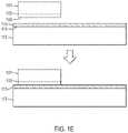
- the distal portion of nitride crystal 101is removed, leaving a proximate portion of nitride crystal 101 bonded to handle substrate 117 .
- distal portion of nitride crystal 101remains bonded to block 112 (not shown).
- the newly exposed surface of distal portion of nitride crystal 101is polished, dry-etched, or chemical-mechanically polished.
- an adhesion layeris deposited on the newly exposed surface of distal portion of crystal 101 .
- the adhesion layeris chemical-mechanically polished.
- nitride crystal 101is separated from high quality epitaxial layer 109 and handle substrate 117 by laser irradiation.
- the release layer 107may be illuminated through nitride crystal 101 by through-crystal laser radiation 125 having a wavelength at which the release layer has an optical absorption coefficient greater than 1,000 cm ⁇ 1 and the nitride crystal is substantially transparent, with an optical absorption coefficient less than 50 cm ⁇ 1 .
- the release layeris illuminated through handle substrate 117 and adhesion layer 113 by through-handle laser radiation 127 having a wavelength at which the release layer has an optical absorption coefficient greater than 1,000 cm ⁇ 1 and the handle substrate is substantially transparent, with an optical absorption coefficient less than 50 cm ⁇ 1 .
- Absorption of the laser energy by the release layer 107occurs on a very short length scale, causing considerable local heating. Such local heating causes partial or complete decomposition of the release layer and/or a thin portion of the nitride crystal in direct contact with the release layer, forming metal and N 2 , which may occur as a thin layer or as micro- or nano-bubbles.
- Such methodsare disclosed, for example, in U.S. Pat. No. 8,148,801.
- the thin layer or micro- or nano-bubbles of N 2mechanically weakens the interface between the nitride crystal and the high quality epitaxial layer, enabling facile separation of the nitride crystal from the high quality epitaxial layer, which is in turn bonded to the handle substrate.
- the optimal degree of weakening of the interface, without causing undesired damage to the high quality epitaxial layer or the handle substrate,is achieved by adjusting the die temperature, the laser power, the laser spot size, the laser pulse duration, and/or the number of laser pulses.
- the laser fluence to effect separationmay be between 300 and 900 millijoules per square centimeter or between about 400 mJ/cm ⁇ 2 and about 750 mJ/cm ⁇ 2 .
- the uniformity of the laser beammay be improved by inclusion of a beam homogenizer in the beam path, and the beam size may be about 4 mm by 4 mm.
- the laser beamis scanned or rastered across the release layer rather than being held stationary. Separation may be performed at a temperature above the melting point of the metal produced by decomposition, e.g., above about 30 degrees Celsius in the case of gallium metal.
- multiple release layers and high quality epitaxial layersare present in the wafer-bonded stack.
- laser illuminationis preferably applied through the handle substrate, and the fluence controlled so that substantial decomposition takes place only within the release layer closest to the handle substrate and the remaining release layers and high quality epitaxial layers remain bonded to the nitride crystal after liftoff.
- any residual gallium, indium, or other metal or nitride on the newly exposed back surface of the high quality epitaxial layer, on nitride crystal 101 , or on another newly-exposed high quality epitaxial layer still bonded to nitride crystal 101may be removed by treatment with at least one of hydrogen peroxide, an alkali hydroxide, tetramethylammonium hydroxide, an ammonium salt of a rare-earth nitrate, perchloric acid, sulfuric acid, nitric acid, acetic acid, hydrochloric acid, and hydrofluoric acid.
- the surfacesmay be further cleaned or damage removed by dry-etching in at least one of Ar, Cl 2 , and BCl 3 , by techniques such as chemically-assisted ion beam etching (CAIBE), inductively coupled plasma (ICP) etching, or reactive ion etching (RIE).
- CAIBEchemically-assisted ion beam etching
- ICPinductively coupled plasma
- RIEreactive ion etching
- the surfacesmay be further treated by chemical mechanical polishing.
- traces of the release layermay remain after laser liftoff or etching from the edges of the release layer.
- Residual release layer materialmay be removed by photoelectrochemical etching, illuminating the back side of the high quality epitaxial layer or the front side of nitride crystal 101 or of the front side of the outermost high quality epitaxial layer still bonded to nitride crystal 101 with radiation at a wavelength at which the release layer has an optical absorption coefficient greater than 1,000 cm ⁇ 1 and the high quality epitaxial layer is substantially transparent, with an optical absorption coefficient less than 50 cm ⁇ 1 .
- the high quality epitaxial layer bonded to the handle substrateis separated from the nitride crystal by means of chemical etching of the release layer.
- FIG. 1Hshows nitride crystal 101 having alternate release layers 107 and high quality epitaxial layers 109 bonded to adhesion layer 113 overlying handle substrate 117 .
- Nitride crystal 101 and one or more of release layers 107 and/or high quality epitaxial layers 109can be removed from a high quality epitaxial layer 109 bonded to adhesion layer 113 overlying handle substrate 117 .
- one or more edges of the release layeris treated with at least one of 1,2-diaminoethane, hydrogen peroxide, an alkali hydroxide, tetramethylammonium hydroxide, an ammonium salt of a rare-earth nitrate, perchloric acid, sulfuric acid, nitric acid, acetic acid, hydrochloric acid, and hydrofluoric acid.
- the edge of the release layeris etched by treatment in a mixture of 200 milliliters of deionized water, 50 grams of diammonium cerium nitrate, Ce(NH 4 ) 2 (NO 3 ) 6 , and 13 milliliters of perchloric acid, HClO 4 , at approximately 70 degrees Celsius. At least one edge of the release layer is etched away, mechanically weakening the interface between the nitride base crystal and the high quality epitaxial layer and enabling facile separation of the nitride base crystal from the high quality epitaxial layer, which is in turn bonded to at least one semiconductor device layer.
- the right degree of weakening of the interfaceis achieved by adjusting the temperature and time of the chemical treatment.
- the time required for lateral etching of the release layermay be reduced by incorporating a pre-formed set of channels in the release layer.
- transfermay be restricted to the outermost high quality epitaxial layer by utilizing etch channels that penetrate only the outermost high quality epitaxial layer.
- the high quality epitaxial layer bonded to the handle substrateis separated from the nitride crystal by means of photoelectrochemical (PEC) etching of the release layer.
- PECphotoelectrochemical
- an InGaN layer or InGaN/InGaN superlatticemay be deposited as the release layer.
- An electrical contactmay be placed on the nitride crystal and the release layer illuminated with above-bandgap radiation, for example, by means of a Xe lamp and a filter to remove light with energy greater than the bandgap of the high quality epitaxial layer and/or the nitride crystal.
- the laser radiation 127is provided through the handle substrate 117 and adhesion layer 113 and the intensity adjusted so that essentially all the light is absorbed by the release layer in closest proximity to the handle substrate. At least one edge of a release layer 107 is exposed to an electrolyte, for example, a stirred, 0.004M HCl solution. The time required for lateral etching of the release layer 107 may be reduced by incorporating a pre-formed set of channels in the release layer.
- transfermay be restricted to the outermost high quality epitaxial layer even when the etch channels penetrate multiple high quality epitaxial layers by ensuring that the light is fully absorbed by only the outermost release layer.
- GaNis deposited as the release layer and lattice-matched AlInN comprises the high quality epitaxial layer, and the wavelength range of the illumination is chosen so that electron-hole pairs are generated in the GaN but not in the AlInN.
- the high quality epitaxial layer bonded to the handle substrateis separated from the nitride crystal by means of selective oxidation followed by chemical etching of the release layer.
- at least one release layercomprising Al x In y Ga 1-x-y N, where 0 ⁇ x, x+y ⁇ 1, 0 ⁇ y ⁇ 1, or Al 0.83 In 0.17 N, lattice matched to GaN, may be selectively oxidized.
- the selective oxidationmay be performed by exposing at least one edge of the Al-containing release layer to a solution comprising nitriloacetic acid (NTA) and potassium hydroxide at a pH of approximately 8 to 11 and an anodic current of approximately 20 ⁇ A/cm ⁇ 2 , to about 0.1 kA/cm ⁇ 2 .
- NTAnitriloacetic acid
- the oxide layermay then be removed by treatment in a nitric acid solution at approximately 100 degrees Celsius.
- the time required for lateral etching of the release layermay be reduced by incorporating a pre-formed set of channels in the release layer.
- transfermay be restricted to the outermost high quality epitaxial layer by utilizing etch channels that penetrate only the outermost high quality epitaxial layer.
- the second nitride crystal 131may have an ion-implanted, damaged region 133 or at least one release layer 137 and at least one high quality epitaxial layer 139 , similar to the first nitride crystal.
- the second nitride crystal or the outer most high quality epitaxial layer on the second nitride crystalhas a surface 135 wherein the crystallographic orientation is essentially identical to that of surface 105 of the nitride crystals 101 or to that of surface 111 of the first high quality epitaxial layer.
- accurate equality between the surface orientation of the first and second nitride crystalsis achieved by growing each crystal to an accurately flat on-axis orientation, for example, (0 0 0 1) Ga-polar, (0 0 0 ⁇ 1) N-polar, ⁇ 1 0 ⁇ 1 0 ⁇ non-polar, or ⁇ 1 0 ⁇ 1 ⁇ 1 ⁇ semi-polar.
- first and/or second nitride crystalsare polished, dry-etched, or chemical-mechanically polished, care is taken so as not to significantly alter the surface orientation of either.
- accurate equality between the surface orientation of the first and second nitride crystalsis achieved by removing a uniform, thin proximate portion of the first nitride crystal to form the second nitride crystal. If the distal portion of the first nitride crystal, used also as the second nitride crystal, is polished, dry-etched, or chemical-mechanically polished, care is taken so as not to significantly alter the surface orientation.
- accurate equality between the surface orientation of the first and second nitride crystalsis achieved by removing a uniform, thin high quality epitaxial layer from the first nitride crystal to form the second nitride crystal. If the distal portion of the first nitride crystal, used also as the second nitride crystal, is polished, dry-etched, or chemical-mechanically polished, care is taken so as not to significantly alter the surface orientation.
- the crystallographic orientations of first surfaces 105 or 111 and 135 , respectively, of the outermost surface or high quality epitaxial layers on the first and second nitride crystalsmay be identical to less than 0.5 degree, less than 0.2 degree, less than 0.1 degree, less than 0.05 degree, less than 0.02 degree, or less than 0.01 degree.
- accurate equality between the surface orientation of the first and second nitride crystalsis achieved by very careful crystallographic orientation and grinding and/or polishing, for example, using a high-precision goniometer. After bonding, a distal portion of the second nitride crystal may be removed.
- Gap 145 between the edges of two or more adjacent nitride crystals or proximate portions thereofmay be less than 1 millimeter, less than 100 microns, less than 50 microns, less than 20 microns, less than 10 microns, less than 5 microns, less than 2 microns, or less than 1 micron.
- the bonding processmay be repeated more than two, more than 4, more than 8, more than 16, more than 32, or more than 64 times.
- first coordinate system 221(x 1 y 1 z 1 ) represents the crystallographic orientation of the first nitride crystal or of the proximate portion of the high quality epitaxial layer of the first nitride crystal 201 , where z 1 is the negative surface normal of the nominal orientation of the surface 211 of first nitride crystal 20 , and x 1 and y 1 are vectors that are orthogonal to z 1 .
- z 1is a unit vector along [0 0 0 ⁇ 1]
- x 1 and y 1may be chosen to be along [1 0 ⁇ 1 0] and [1 ⁇ 2 1 0], respectively.
- z 1is a unit vector along [ ⁇ 1 0 1 0] and x 1 and y 1 may be chosen to be along [1 ⁇ 2 1 0] and [0 0 0 1], respectively.
- second coordinate system 222(x 2 y 2 z 2 ) represents the crystallographic orientation of the second nitride crystal or of the proximate portion of the high quality epitaxial layer from the second nitride crystal 202 , where z 2 is the negative surface normal of the nominal orientation of surface 212 of second nitride crystal 202 and x 2 and y 2 are vectors that are orthogonal to z 2 , where the same convention is used for the crystallographic directions corresponding to (x 2 y 2 z 2 ) as for (x 1 y 1 z 1 ).
- the crystallographic misorientation between the surface of first nitride crystal and the surface of second nitride crystalmay be specified by the three angles ⁇ , ⁇ , and ⁇ , where ⁇ is the angle between x 1 and x 2 , ⁇ is the angle between y 1 and y 2 , and ⁇ is the angle between z 1 and z 2 . Because the surface orientations of the first and second nitride crystals are nearly identical, the polar misorientation angle ⁇ is very small, for example, less than 0.5 degree, less than 0.2 degree, less than 0.1 degree, less than 0.05 degree, less than 0.02 degree, or less than 0.01 degree.
- the misorientation angles ⁇ and ⁇are also very small, for example, less than 1 degree, less than 0.5 degree, less than 0.2 degree, less than 0.1 degree, less than 0.05 degree, less than 0.02 degree, or less than 0.01 degree.
- ⁇will be less than or equal to ⁇ and ⁇ .
- the crystallographic misorientation between additional, adjacent nitride crystalsis similarly very small.
- the crystallographic misorientation angles ⁇ , ⁇ , and ⁇may be detectable by x-ray measurements and may be greater than about 0.005 degree, greater than about 0.02 degree, greater than about 0.05 degree, greater than about 0.1 degree, greater than 0.3 degree, or greater than 0.5 degree.
- a tiled arrangement of high quality epitaxial layersmay be formed, with each adjacent pair on the handle substrate being accurately aligned crystallographically with its neighbor(s).
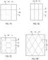
- the tiling patternmay be, for example, (a) square ( FIG. 3A ), (b) rectangular ( FIG. 3B ), (c) hexagonal ( FIG. 3C ), (d) rhombal ( FIG. 3D ), or (e) irregular (not shown). Other arrangements are also possible.
- the gaps between the edges of two or more adjacent high quality epitaxial layersmay be less than 5 millimeters, less than 1 millimeter, less than 100 microns, less than 50 microns, less than 20 microns, less than 10 microns, less than 5 microns, less than 2 microns, or less than 1 micron.
- the crystalsmay have a first lateral dimension 380 and a second lateral dimension 390 , the lateral dimensions defining a plane that is perpendicular to the thickness, where each of the first lateral dimension and the second lateral dimension may be at least about 0.5 millimeter, 1 millimeter, 2 millimeters, 4 millimeters, 5 millimeters, 10 millimeters, 15 millimeters, 20 millimeters, 25 millimeters, 35 millimeters, 50 millimeters, 75 millimeters, 100 millimeters, 150 millimeters, or can be at least about 200 millimeters.
- a similar set of nitride crystals or high quality epitaxial layersis wafer-bonded to the back surface of the handle substrate by an analogous procedure to that used to form the tile pattern of nitride crystals or high quality epitaxial layers on the front surface of the handle substrate.
- the tile pattern on the back surface of the handle substrateis a mirror image of the tile pattern on the front surface of the handle substrate, with the front and back tile patterns in registry.
- the at least two nitride crystals or high quality epitaxial layers on the handle substrateare used as a substrate for fabrication of one or more devices.
- the two or more tiled high quality epitaxial layers or crystals bonded to the handle substratemay be prepared for lateral growth for epitaxial growth and/or for fusion of the tiled crystals into a single larger crystal.
- the lateral crystal growthmay be achieved by techniques such as molecular beam epitaxy (MBE), metalorganic chemical vapor deposition (MOCVD), hydride vapor phase epitaxy (HVPE), ammonothermal crystal growth, or crystal growth from a flux.
- the handle substrateis suitable for exposure to the epitaxial growth environment without further treatment.
- a thermal treatmentmay be applied to increase the melting point of at least a portion of the adhesion layer(s).
- growthmay proceed more smoothly, with fewer stresses, if the gaps between adjacent nitride crystals are undercut.
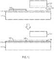
- a photoresist 447may be spun onto the bonded, tiled substrate comprising handle substrate 117 , first nitride crystal 201 , and second nitride crystal 202 .
- Photoresist 447may be exposed through a mask, etched, and an exposed channel 410 etched by dry etching, and the photoresist removed to form patterned nitride/handle substrate 450 .
- the gaps between the adjacent nitride crystalsmay be undercut or increased in depth by fast ion-beam etching, wire-sawing, sawing, or dicing.
- patterned nitride/handle substrate 450may be used as a substrate for epitaxial nitride growth by MBE, MOCVD, HVPE, ammonothermal growth, or flux growth.
- FIG. 4Bshows patterned nitride/handle substrate 450 comprising a first nitride crystal 201 and second nitride crystal 202 separated by channel 410 overlying adhesion layer 113 and handle substrate 117 .
- Growthis performed as known in the art, and the at least two nitride crystals 201 and 202 grow both laterally and vertically to form a merged nitride crystal 455 .
- Horizontal growthcauses nitride crystal 201 and nitride crystal 202 to grow toward each other and separated by gap 412 over channel 410 .
- the coalescence front 457may have a modest concentration of dislocations but a classical low angle grain boundary or tilt boundary may be difficult to detect. Threading dislocations, for example, edge dislocations, may be present at coalescence fronts 457 , for example, with a line density that is less than about 1 ⁇ 10 5 cm ⁇ 1 , less than about 3 ⁇ 10 4 cm ⁇ 1 , less than about 1 ⁇ 10 4 cm ⁇ 1 , less than about 3 ⁇ 10 3 cm ⁇ 1 , less than about 1 ⁇ 10 3 cm ⁇ 1 , less than about 3 ⁇ 10 2 cm ⁇ 1 , or less than about 1 ⁇ 10 2 cm ⁇ 1 .
- the density of dislocations along the coalescence frontsmay be greater than 5 cm ⁇ 1 , greater than 10 cm ⁇ 1 , greater than 20 cm ⁇ 1 , greater than 50 cm ⁇ 1 , greater than 100 cm ⁇ 1 , greater than 200 cm ⁇ 1 , or greater than 500 cm ⁇ 1 .
- the handle substrate and/or the adhesion layermay not be suitable for exposure to the epitaxial growth environment without further treatment. Exposed portions of the handle substrate may be coated with a suitable inert material. Referring to FIG. 5 , first nitride crystal 201 and second nitride crystal 202 may be masked, for example, by a shadow mask or by photolithography with a photoresist, and the regions between the masked areas on the handle substrate 117 and/or adhesion layer 113 coated with inert coating 561 .
- Inert coating 561may comprise at least one of Ag, Au, Pt, Pd, Rh, Ru, Ir, Ni, Cr, V, Ti, Ta, SiO 2 , SiN x , or AlN. Inert coating 561 may further comprise an adhesion layer (not shown) in contact with the surface of handle substrate 117 and/or adhesion layer 113 comprising, for example, at least one of Ti, V, Cr, Al, Ni, B, Si, P, Zn, Ga, Si, Ge, Au, Ag, Zn, Cd, In, Sn, Sb, Tl, Ta, W, In, Cu, or Pb, or an oxide, nitride, or oxynitride thereof.
- Inert coating 561may be deposited by sputtering, thermal evaporation, electron beam evaporation, chemical vapor deposition, plasma enhanced chemical vapor deposition, electroplating, or the like.
- Masked nitride/handle substrate 550may be used as a substrate for epitaxial nitride growth by MBE, MOCVD, HVPE, ammonothermal growth, or flux growth.
- Flux growthmay be performed, for example, using liquid Ga under a nitrogen pressure of 1-3 GPa, using an alloy comprising Ga and at least one alkali metal under a pressure of a nitrogen-containing gas at a pressure of 10 MPa to 200 MPa, or using one or more halide, nitride, or amide salts under a pressure of a nitrogen-containing gas at a pressure of 0.1 MPa to 200 MPa. Growth is performed as known in the art, and the at least two nitride crystals 201 and 202 grow both laterally and vertically to form a merged nitride crystal 455 . Because of the very low crystallographic misorientation between nitride crystals 201 and 202 , the coalescence front 457 may have a modest concentration of dislocations but a classical low angle grain boundary or tilt boundary may be difficult to detect.
- patterned nitride/handle substrate 650 having first nitride crystal 201 and second nitride crystal 202 with an etched gap 601 between themmay be masked, for example, by a shadow mask or by photolithography with a photoresist, and the regions between the masked areas on handle substrate 117 and/or adhesion layer 113 coated with inert coating 561 .
- Masked/patterned/etched nitride/handle substrate 670may be used as a substrate for epitaxial nitride growth by MBE, MOCVD, HVPE, ammonothermal growth, or flux growth.
- the at least two nitride crystals 201 and 202grow both laterally and vertically to form a merged nitride crystal 455 . Because of the very low crystallographic misorientation between nitride crystals 201 and 202 , the coalescence front 457 may have a modest concentration of dislocations but a classical low angle grain boundary or tilt boundary may be difficult to detect.
- Threading dislocationsmay be present at coalescence fronts 457 , for example, with a line density that is less than about 1 ⁇ 10 5 cm ⁇ 1 , less than about 3 ⁇ 10 4 cm ⁇ 1 , less than about 1 ⁇ 10 4 cm ⁇ 1 , less than about 3 ⁇ 10 3 cm ⁇ 1 , less than about 1 ⁇ 10 3 cm ⁇ 1 , less than about 3 ⁇ 10 2 cm ⁇ 1 , or less than about 1 ⁇ 10 2 cm ⁇ 1 .
- the density of dislocations along the coalescence frontsmay be greater than 5 cm ⁇ 1 , greater than 10 cm ⁇ 1 , greater than 20 cm ⁇ 1 , greater than 50 cm ⁇ 1 , greater than 100 cm ⁇ 1 , greater than 200 cm ⁇ 1 , or greater than 500 cm ⁇ 1 .
- the merged nitride crystalmay be grown to a thickness greater than 5 microns, greater than 50 microns, greater than 0.5 millimeters, or greater than 5 millimeters. After cooling and removal from the reactor, the merged nitride crystal may be separated from the handle substrate.
- the inert coatingif present, may be removed from at least a portion of the edge of the handle substrate by scribing, abrasion, etching, or the like.
- the handle substratemay be dissolved or etched away, for example, by placing in contact with an acid, a base, or a molten flux, preferably in a way that produces negligible etching or other damage to the merged nitride crystal.
- a glass, silicon, or germanium substratemay be etched away without damaging the merged nitride crystal by treatment in a solution comprising HF and/or H 2 SiF 6 .
- a glass or zinc oxide substratemay be etched away without damaging the merged nitride crystal by treatment in a solution comprising NaOH, KOH, or NH 4 OH.
- a gallium arsenide or zinc oxide substratemay be etched away without damaging the merged nitride crystal by treatment in a solution comprising aqua regia or one or more of HCl, HNO 3 , HF, H 2 SO 4 , and H 3 PO 4 .
- a sapphire or alumina substratemay be etched away without damaging the merged nitride crystal by treatment in molten KBF 4 .
- one or more surface of the merged nitride crystalmay be lapped, polished, and/or chemical-mechanically polished.
- the merged nitride crystalmay be sliced (sawed, polished, and/or chemical-mechanically polished) into one or more wafers.
- the merged nitride crystalcomprises two or more domains separated by one or more lines of dislocations.
- the pattern of domainsmay be, for example, (a) square ( FIG. 7A ), (b) rectangular ( FIG. 7B ), (c) hexagonal ( FIG. 7C ), (d) rhombal ( FIG. 7D ), or (e) irregular (not shown). Other patterns are also possible.
- the domainsmay have a first lateral dimension 380 and a second lateral dimension 390 , the lateral dimensions defining a plane that is perpendicular to the thickness, where each of the first lateral dimension 380 and the second lateral dimension 390 may be at least about 0.5 millimeter, 1 millimeter, 2 millimeters, 4 millimeters, 5 millimeters, 10 millimeters, 15 millimeters, 20 millimeters, 25 millimeters, 35 millimeters, 50 millimeters, 75 millimeters, 100 millimeters, 150 millimeters, or at least about 200 millimeters.
- the polar misorientation angle ⁇ between adjacent domainsmay be less than 0.5 degree, less than 0.2 degree, less than 0.1 degree, less than 0.05 degree, less than 0.02 degree, or less than 0.01 degree.
- the misorientation angles ⁇ and ⁇ between adjacent domainsmay be less than 1 degree, less than 0.5 degree, less than 0.2 degree, less than 0.1 degree, less than 0.05 degree, less than 0.02 degree, or less than 0.01 degree.
- ⁇will be less than or equal to ⁇ and ⁇ .
- the crystallographic misorientation angles ⁇ , 0 , and ⁇may be greater than about 0.01 degree, greater than about 0.02 degree, greater than about 0.05 degree, or greater than about 0.1 degree.
- the density of dislocations along the lines between adjacent domainsmay be less than about 5 ⁇ 10 5 cm ⁇ 1 , less than about 2 ⁇ 10 5 cm ⁇ 1 , less than about 1 ⁇ 10 5 cm ⁇ 1 , less than about 5 ⁇ 10 4 cm ⁇ 1 , less than about 2 ⁇ 10 4 cm ⁇ 1 , less than about 1 ⁇ 10 3 cm ⁇ 1 , less than about 5 ⁇ 10 3 cm ⁇ 1 , less than about 2 ⁇ 10 3 cm ⁇ 1 , or less than about 1 ⁇ 10 3 cm ⁇ 1 .
- the density of dislocations along the lines between adjacent domainsmay be greater than 50 cm ⁇ 1 , greater than 100 cm ⁇ 1 , greater than 200 cm ⁇ 1 , greater than 500 cm ⁇ 1 , greater than 1,000 cm ⁇ 1 , greater than 2000 cm ⁇ 1 , or greater than 5000 cm ⁇ 1 .
- the merged nitride crystalmay have a surface dislocation density less than about 10 7 cm ⁇ 2 , less than about 10 6 cm ⁇ 2 , less than about 10 5 cm ⁇ 2 , less than about 10 4 cm ⁇ 2 , less than about 10 3 cm ⁇ 2 , or less than about 10 2 cm ⁇ 2 .
- the domainsmay have a stacking-fault concentration below 10 3 cm ⁇ 1 , below 10 2 cm ⁇ 1 , below 10 cm ⁇ 1 or below 1 cm ⁇ 1 .
- the merged nitride crystalmay have a symmetric x-ray rocking curve full width at half maximum (FWHM) less than about 300 arc sec, less than about 200 arc sec, less than about 100 arc sec, less than about 50 arc sec, less than about 35 arc sec, less than about 25 arc sec, or less than about 15 arc sec.
- the merged nitride crystalmay have a thickness between about 100 microns and about 100 millimeters, or between about 1 millimeter and about 10 millimeters.
- the merged nitride crystalmay have a diameter of at least about 5 millimeters, at least about 10 millimeters, at least about 15 millimeters, at least about 20 millimeters, at least about 25 millimeters, at least about 35 millimeters, at least about 50 millimeters, at least about 75 millimeters, at least about 100 millimeters, at least about 150 millimeters, at least about 200 millimeters, or at least about 400 millimeters.
- the surface of the merged nitride crystalmay have a crystallographic orientation within 10 degrees, within 5 degrees, within 2 degrees, within 1 degree, within 0.5 degree, within 0.2 degree, within 0.1 degree, within 0.05 degree, within 0.02 degree, or within 0.01 degree of (0 0 0 1) Ga-polar, (0 0 0 ⁇ 1) N-polar, ⁇ 1 0 ⁇ 1 0 ⁇ non-polar, or ⁇ 1 1 ⁇ 2 0 ⁇ non-polar a-plane.
- the crystallographic orientation of the merged nitride crystalis within 10 degrees, within 5 degrees, within 2 degrees, within 1 degree, within 0.5 degree, within 0.2 degree, within 0.1 degree, within 0.05 degree, within 0.02 degree, or within 0.01 degree of ⁇ 11 ⁇ 2 ⁇ 2 ⁇ , ⁇ 6 0 ⁇ 6 ⁇ 1 ⁇ , ⁇ 5 0 ⁇ 5 ⁇ 1 ⁇ , ⁇ 40 ⁇ 4 ⁇ 1 ⁇ , ⁇ 3 0 ⁇ 3 ⁇ 1 ⁇ , ⁇ 5 0 ⁇ 5 ⁇ 2 ⁇ , ⁇ 7 0 ⁇ 7 ⁇ 3 ⁇ , ⁇ 2 0 ⁇ 2 ⁇ 1 ⁇ , ⁇ 3 0 ⁇ 3 ⁇ 2 ⁇ , ⁇ 4 0 ⁇ 4 ⁇ 3 ⁇ , ⁇ 5 0 ⁇ 5 ⁇ 4 ⁇ , ⁇ 1 0 ⁇ 1 ⁇ , ⁇ 1 0 ⁇ 1 ⁇ , ⁇ 1 0 ⁇ 1 ⁇ 2 ⁇ , ⁇ 1 0 ⁇ 1 ⁇ 3 ⁇ , ⁇ 2 1 ⁇
- the merged nitride crystalhas a minimum lateral dimension of at least four millimeters. In some embodiments, the merged nitride crystal has a minimum lateral dimension of at least one centimeter, at least two centimeters, at least three centimeters, at least four centimeters, at least five centimeters, at least six centimeters, at least eight centimeters, at least ten centimeters, or at least twenty centimeters.
- the merged nitride crystalis used as a substrate for epitaxy, forming a semiconductor structure.
- the merged nitride crystalmay be sawed, lapped, polished, dry etched, and/or chemical-mechanically polished by methods that are known in the art. One or more edges of the merged nitride crystal may be ground.
- the merged nitride crystal, or a wafer formed therefrom,may be placed in a suitable reactor and an epitaxial layer grown by MOCVD, MBE, HVPE, or the like.
- the epitaxial layercomprises GaN or Al x In y Ga (1-x-y) N, where 0 ⁇ x, y ⁇ 1.
- the morphology of the epitaxial layeris uniform from one domain to another over the surface because the surface orientation is almost identical.
- the merged nitride crystalis used as a substrate for further tiling.
- the nitride crystal 101may be chosen to be a merged nitride crystal.
- the tiling, coalescence, and re-tiling operationmay be iterated more than twice, more than 4 times, more than 8 times, or more than 16 times. In this way, by successive tiling operations, a merged nitride crystal with excellent crystalline quality and very large diameter may be fabricated.
- the merged nitride crystal, or a wafer that has been sliced and polished from the merged nitride crystal or from a boule obtained by bulk crystal growth using the merged nitride crystal as a seedmay be used as a substrate for fabrication into optoelectronic and electronic devices such as at least one of a light emitting diode, a laser diode, a photodetector, an avalanche photodiode, a transistor, a rectifier, a Schottky rectifier, a thyristor, a p-i-n diode, a metal-semiconductor-metal diode, high-electron mobility transistor, a metal semiconductor field effect transistor, a metal oxide field effect transistor, a power metal oxide semiconductor field effect transistor, a power metal insulator semiconductor field effect transistor, a bipolar junction transistor, a metal insulator field effect transistor, a heterojunction bipolar transistor, a power insulated gate bipolar transistor,
- the merged nitride crystal, or a wafer sliced and polished from the merged nitride crystalis used as a seed crystal for bulk crystal growth.
- the tiled crystal, or a wafer sliced and polished from the merged nitride crystalis used as a seed crystal for ammonothermal crystal growth.
- the tiled crystal, or a wafer sliced and polished from the merged nitride crystalis used as a seed crystal for HVPE crystal growth.
- the at least two nitride crystals or high quality epitaxial layers on the handle substrate, non-mergedare used as a substrate for fabrication into optoelectronic and electronic devices such as at least one of a light emitting diode, a laser diode, a photodetector, an avalanche photodiode, a transistor, a rectifier, a Schottky rectifier, a thyristor, a p-i-n diode, a metal-semiconductor-metal diode, high-electron mobility transistor, a metal semiconductor field effect transistor, a metal oxide field effect transistor, a power metal oxide semiconductor field effect transistor, a power metal insulator semiconductor field effect transistor, a bipolar junction transistor, a metal insulator field effect transistor, a heterojunction bipolar transistor, a power insulated gate bipolar transistor, a power vertical junction field effect transistor, a cascode switch, an inner sub-band emitter, a quantum
- FIG. 11is a flow chart depicting a method of making large area crystals.
- FIG. 11shows a method 1100 for growth of a large-area crystal, the method comprising: providing at least two crystals having a dislocation density below about 10 7 cm ⁇ 2 (see step 1110 ); providing a handle substrate (see step 1120 ); performing bonding of the at least two crystals to the handle substrate (see step 1130 ); and growing the at least two crystals to cause a coalescence into a merged crystal comprising a first domain and a second domain (see step 1140 ); wherein a polar misorientation angle ⁇ between the first domain and the second domain is greater than about 0.005 degree and less than about 0.5 degree and the misorientation angles ⁇ and ⁇ between the first domain and the second domain are greater than about 0.01 degree and less than about 1 degree (also see step 1140 ).
- Still further embodimentssupport method of making and method of use. Any of the embodiments below can be practiced in a variety of variations.
- the at least two crystalshave a hexagonal crystal structure.
- the at least two crystalshave a cubic crystal structure.
- the at least two crystals having a cubic crystal structureare selected from BN, BP, BAs, AlP, AlAs, AlSb, ⁇ -SiC, GaP, GaAs, GaSb, InP, InAs, ZnS, ZnSe, CdS, CdSe, CdTe, CdZeTe, and HgCdTe.
- the at least two crystals having a cubic crystal structureare selected from among ZnO, ZnS, AgI, CdS, CdSe, 2H—SiC, 4H—SiC, and 6H—SiC.
- the at least two crystalscomprise regions having a concentration of threading dislocations higher than about 10 6 cm ⁇ 2 separated by at least one region characterized by a concentration of threading dislocations lower than about 10 6 cm ⁇ 2 .
- the at least two nitride crystals having a hexagonal crystal structurecomprise Al x In y Ga (1-x-y) N, where 0 ⁇ x, y, x+y ⁇ 1.
- the at least two crystalsare characterized by a threading dislocation density below about 10 6 cm ⁇ 2 .
- the at least two crystalsare characterized by a threading dislocation density below about 10 4 cm ⁇ 2 .
- At least one of the two crystalshas an ion-implanted/damaged region.
- the surfaces of the at least two crystals being bonded to the handle substratehave a crystallographic orientation within about 10 degrees of (0 0 0 1), (0 0 0 ⁇ 1), ⁇ 1 0 ⁇ 1 0 ⁇ , ⁇ 2 0 ⁇ 2 ⁇ 1 ⁇ , ⁇ 1 1 ⁇ 2 ⁇ 2 ⁇ , ⁇ 6 0 ⁇ 6 ⁇ 1 ⁇ , ⁇ 5 0 ⁇ 5 ⁇ 1 ⁇ , ⁇ 40 ⁇ 4 ⁇ 1 ⁇ , ⁇ 3 0 ⁇ 3 ⁇ 1 ⁇ , ⁇ 5 0 ⁇ 5 2 ⁇ , ⁇ 7 0 ⁇ 7 ⁇ 3 ⁇ , ⁇ 2 0 ⁇ 2 ⁇ 1 ⁇ , ⁇ 3 0 ⁇ 3 ⁇ 2 ⁇ , ⁇ 4 0 ⁇ 4 ⁇ 3 ⁇ , ⁇ 5 0 ⁇ 5 ⁇ 4 ⁇ , ⁇ 1 0 ⁇ 1 ⁇ , ⁇ 1 0 ⁇ 1 ⁇ , ⁇ 1 0 ⁇ 1 ⁇ 2 ⁇ , ⁇ 1 0 ⁇ 1 ⁇ 1 ⁇
- the large-area crystalhas a region with a threading dislocation density below about 10 6 cm ⁇ 2 .
- each of the first crystal, the second crystal, the first domain, and the second domainhave a minimum lateral dimension of at least two millimeters.
- the first crystalis derived from and detached from an ion-implanted crystal and the second crystal is derived from and detached from the same crystal.
- the first crystalis derived from a first epitaxial layer on a third crystal and the second crystal is derived from a second epitaxial layer on the third crystal.
- the bonding of the at least two crystals to the handle substrateis performed using a wafer-bonding tool.
- the bonding of the at least two crystals to the handle substrateis performed using a pick-and-place tool.
- the methodfurther comprises applying a thermal treatment to increase the melting point of an adhesion layer provided between the at least two crystals and the handle substrate.
- the methodfurther comprises forming a semiconductor structure on the merged crystal, or a wafer that has been sliced and polished from the merged crystal or from a boule obtained by bulk crystal growth using the merged crystal as a seed.
- the semiconductor structureis incorporated into an optoelectronic or electronic device, the optoelectronic or electronic device comprising at least one of wafer sliced and polished from the merged crystal or from a boule obtained by bulk crystal growth using the merged crystal as a seed.
- the positions of the devices with respect to the domain structure in the merged crystalare chosen so that the active regions of individual devices lie within a single domain of the merged crystal.
- a templatewas prepared using four HVPE-grown bulk GaN crystals wafer-bonded to a handle substrate, also comprising HVPE-grown bulk GaN.
- the nitride crystalsexhibited a crystallographic orientation within 1 degree of the (0 0 0 1)+c-plane (Ga face).
- the adjoining surfaces of the nitride crystals and the handle substratewere each coated with a 200 ⁇ ngstrom Ti layer followed by a 1.5 micron Au layer and wafer-bonded at a pressure of 5.4 MPa and a temperature of 450° C. under vacuum.
- the gaps between adjacent bonded nitride crystalswere approximately 85 microns.
- the misorientation angles ⁇ , ⁇ , and ⁇ between the adjacent bonded nitride crystalswere all less than 0.1 degrees.
- the templatewas degreased, suspended by a silver wire, and placed in a silver capsule with a baffle. Approximately 37.3 g of polycrystalline GaN, 1.27 g of NH 4 F mineralizer, and 30.4 g of ammonia were also placed in the capsule and the capsule was hermetically sealed. The capsule was placed in an internally-heated high pressure apparatus, heated to a temperature of approximately 675° C. for approximately 68 hours, then cooled, removed, and opened. The gap between the two nitride crystals was closed by newly-grown GaN, causing full coalescence of the crystals.
- the coalesced nitride crystalwas removed from the handle substrate by dissolution of the Ti—Au adhesion layers by soaking in concentrated aqua regia solution.
- the linear etch pit densities at the coalescence frontswere measured as approximately 1.2 ⁇ 10 3 cm ⁇ 1 , indicating high-quality boundaries.
- a templatewas prepared using two HVPE-grown bulk GaN crystals bonded to a handle substrate, also comprising HVPE-grown bulk GaN.
- the nitride crystalsexhibited a crystallographic orientation within 1 degree of the (0 0 0 1)+c-plane (Ga face).
- the adjoining surfaces of the handle substrate and the nitride crystalswere coated with a 200 ⁇ ngstrom Ti layer followed by a 1.0 micron Au layer.
- the nitride crystalsfurther had an array of 300 micron diameter Si dots having a height of 0.6 microns, the dots being located at the vertices of a square grid having a period of 1,000 microns in both the x- and y-directions.
- the handle substratewas then placed on a heated stage at 475° C. and a pick and place tool was used to precisely position the two nitride crystals on the handle substrate.
- the adjoining surfaces of the nitride crystals and the handle substrate, while precisely aligned,were placed in contact for approximately 30 seconds and a bond was formed.
- the misorientation angles ⁇ and ⁇ between the adjacent bonded nitride crystalswere less than 0.3 degrees and the misorientation angle ⁇ between the adjacent bonded nitride crystals was less than 0.1 degree.
- the bonded templatewas subsequently heated to 275° C. in a nitrogen atmosphere and held for 24 hours.
- the templatewas degreased, suspended by a silver wire, and placed in a silver capsule with a baffle.
- a templatewas prepared using three HVPE-grown bulk GaN crystals bonded to a handle substrate, also comprising HVPE-grown bulk GaN.
- the nitride crystalsexhibited a crystallographic orientation that was miscut from the ⁇ 1 0 ⁇ 1 0 ⁇ m-plane by approximately 0.25 degree toward [0 0 0 ⁇ 1].
- the adjoining surfaces of the handle substrate and the nitride crystalswere coated with a 200 ⁇ ngstrom Ti layer followed by approximately a 20 micron thick Au layer and 3 micron thick AuSn layer on the handle substrate and the nitride crystals, respectively.
- the handle substratewas then placed on a heated stage at 330° C.
- the templatewas degreased and placed in a silver capsule with a baffle. Approximately 4,815 g of polycrystalline GaN, 172 g of NH 4 F mineralizer, and 3,608 g of ammonia were also placed in the capsule and the capsule was hermetically sealed. The capsule was placed in an internally-heated high pressure apparatus, heated to a temperature of approximately 680° C. for approximately 100 hours, then cooled, removed, and opened.
- the gap between the three nitride crystalswas closed by newly-grown GaN, causing full coalescence of the crystals.
- the three nitride crystalswere subsequently removed from the handle substrate as one distinct piece.
- the misorientation angles ⁇ and ⁇ between the adjacent bonded nitride crystalswere between about 0.02 degree and about 0.45 degrees and the misorientation angles ⁇ between the adjacent bonded nitride crystals were about 0.09 degree and about 0.11 degree, respectively.
- the linear etch pit densities at the coalescence frontswere measured as approximately 6.08 ⁇ 10 3 cm ⁇ 1 and 5.84 ⁇ 10 3 cm ⁇ 1 for the two coalescence boundaries, indicating high-quality boundaries.
- a templatewas prepared using three HVPE-grown bulk GaN crystals bonded to a handle substrate comprising polycrystalline AlN.
- the nitride crystalsexhibited a crystallographic orientation within about 0.5 degree of ⁇ 1 0 ⁇ 1 ⁇ 1 ⁇ .
- the adjoining surfaces of the handle substrate and the nitride crystalswere coated with a 200 ⁇ ngstrom Ti layer followed by approximately a 20 micron thick Au layer and 3 micron thick AuSn layer on the handle substrate and the nitride crystals, respectively.
- the handle substratewas then placed on a heated stage at 330° C. and a pick and place tool was used to precisely position the three nitride crystals on the handle substrate.
- the templatewas degreased and placed in a silver capsule with a baffle. Approximately 43.5 g of polycrystalline GaN, 2.56 g of NH 4 F mineralizer, and 30 g of ammonia were also placed in the capsule and the capsule was hermetically sealed.
- the capsulewas placed in an internally-heated high pressure apparatus, heated to a temperature of approximately 655° C. for approximately 51 hours, then cooled, removed, and opened. The gap between the three nitride crystals was closed by newly-grown GaN, causing full coalescence of the crystals.
- the misorientation angles ⁇ and ⁇ between the adjacent pairs of bonded nitride crystalswere between about 0.03 degree and about 0.26 degree and the misorientation angles ⁇ between the adjacent bonded nitride crystals were about 0.085 degree and less than 0.01 degree, respectively.
- a templatewas prepared using two HVPE-grown bulk GaN crystals bonded to a handle substrate comprising AlN.
- the nitride crystalsexhibited a crystallographic orientation that was miscut from the ⁇ 1 0 ⁇ 1 0 ⁇ m-plane by approximately 0.25 degree toward [0 0 0 ⁇ 1].
- the adjoining surfaces of the handle substrate and the nitride crystalswere coated with a 3,000 ⁇ ngstrom Ti layer followed by approximately a 20 micron thick Au layer and 3 micron thick AuSn layer on the handle substrate and the nitride crystals, respectively.
- the handle substratewas then placed on a heated stage at 330° C. and a pick and place tool was used to precisely position the two nitride crystals on the handle substrate.
- the templatewas degreased and placed in a silver capsule with a baffle. Approximately 37.54 g of polycrystalline GaN, 2.57 g of NH 4 F mineralizer, and 30.08 g of ammonia were also placed in the capsule and the capsule was hermetically sealed.
- the capsulewas placed in an internally-heated high pressure apparatus, heated to a temperature of approximately 663° C. for approximately 51 hours, then cooled, removed, and opened. The gap between the two nitride crystals was closed by newly-grown GaN, causing full coalescence of the crystals.
- the two nitride crystalswere subsequently removed from the handle substrate as one distinct piece.
- the nitride crystalswere then placed in a silver capsule with a baffle.
- Approximately 3,560 g of polycrystalline GaN, 174.1 g of NH 4 F mineralizer, and 2,637.88 g of ammoniawere also placed in the capsule and the capsule was hermetically sealed.
- the capsulewas placed in an internally-heated high pressure apparatus, heated to a temperature of approximately 680° C. for approximately 116 hours, then cooled, removed, and opened.
- the misorientation angles ⁇ and ⁇ between the adjacent bonded nitride crystalswere approximately 0.03 degree and the misorientation angle ⁇ between the adjacent bonded nitride crystals was approximately 0.04 degree.
- the linear etch pit densities at the coalescence frontwas measured as approximately 6.75 ⁇ 10 3 cm ⁇ 1 , indicating high-quality boundaries.
Landscapes
- Chemical & Material Sciences (AREA)
- Engineering & Computer Science (AREA)
- Crystallography & Structural Chemistry (AREA)
- Organic Chemistry (AREA)
- Materials Engineering (AREA)
- Metallurgy (AREA)
- General Chemical & Material Sciences (AREA)
- Chemical Kinetics & Catalysis (AREA)
- Inorganic Chemistry (AREA)
- Physics & Mathematics (AREA)
- Condensed Matter Physics & Semiconductors (AREA)
- General Physics & Mathematics (AREA)
- Manufacturing & Machinery (AREA)
- Computer Hardware Design (AREA)
- Microelectronics & Electronic Packaging (AREA)
- Power Engineering (AREA)
- Crystals, And After-Treatments Of Crystals (AREA)
Abstract
Description
Claims (29)
Priority Applications (1)
| Application Number | Priority Date | Filing Date | Title |
|---|---|---|---|
| US16/550,947US11453956B2 (en) | 2010-06-18 | 2019-08-26 | Method for growth of a merged crystal by bonding at least a first and second crystal to an adhesion layer to form a tiled substrate and growing a crystalline composition over said tiled substrate |
Applications Claiming Priority (6)
| Application Number | Priority Date | Filing Date | Title |
|---|---|---|---|
| US35648910P | 2010-06-18 | 2010-06-18 | |
| US38687910P | 2010-09-27 | 2010-09-27 | |
| US13/160,307US20120000415A1 (en) | 2010-06-18 | 2011-06-14 | Large Area Nitride Crystal and Method for Making It |
| US13/731,453US9564320B2 (en) | 2010-06-18 | 2012-12-31 | Large area nitride crystal and method for making it |
| US15/426,770US10400352B2 (en) | 2010-06-18 | 2017-02-07 | Method for growth of a merged crystal by bonding at least a first and second crystal to an adhesion layer to form a tiled substrate and growing a crystalline composition over said tiled substrate |
| US16/550,947US11453956B2 (en) | 2010-06-18 | 2019-08-26 | Method for growth of a merged crystal by bonding at least a first and second crystal to an adhesion layer to form a tiled substrate and growing a crystalline composition over said tiled substrate |
Related Parent Applications (1)
| Application Number | Title | Priority Date | Filing Date |
|---|---|---|---|
| US15/426,770ContinuationUS10400352B2 (en) | 2010-06-18 | 2017-02-07 | Method for growth of a merged crystal by bonding at least a first and second crystal to an adhesion layer to form a tiled substrate and growing a crystalline composition over said tiled substrate |
Publications (2)
| Publication Number | Publication Date |
|---|---|
| US20200087813A1 US20200087813A1 (en) | 2020-03-19 |
| US11453956B2true US11453956B2 (en) | 2022-09-27 |
Family
ID=48279745
Family Applications (3)
| Application Number | Title | Priority Date | Filing Date |
|---|---|---|---|
| US13/731,453Expired - Fee RelatedUS9564320B2 (en) | 2010-06-18 | 2012-12-31 | Large area nitride crystal and method for making it |
| US15/426,770ActiveUS10400352B2 (en) | 2010-06-18 | 2017-02-07 | Method for growth of a merged crystal by bonding at least a first and second crystal to an adhesion layer to form a tiled substrate and growing a crystalline composition over said tiled substrate |
| US16/550,947Active2031-10-01US11453956B2 (en) | 2010-06-18 | 2019-08-26 | Method for growth of a merged crystal by bonding at least a first and second crystal to an adhesion layer to form a tiled substrate and growing a crystalline composition over said tiled substrate |
Family Applications Before (2)
| Application Number | Title | Priority Date | Filing Date |
|---|---|---|---|
| US13/731,453Expired - Fee RelatedUS9564320B2 (en) | 2010-06-18 | 2012-12-31 | Large area nitride crystal and method for making it |
| US15/426,770ActiveUS10400352B2 (en) | 2010-06-18 | 2017-02-07 | Method for growth of a merged crystal by bonding at least a first and second crystal to an adhesion layer to form a tiled substrate and growing a crystalline composition over said tiled substrate |
Country Status (1)
| Country | Link |
|---|---|
| US (3) | US9564320B2 (en) |
Cited By (1)
| Publication number | Priority date | Publication date | Assignee | Title |
|---|---|---|---|---|
| US20200203521A1 (en)* | 2017-07-20 | 2020-06-25 | Swegan Ab | A heterostructure for a high electron mobility transistor and a method of producing the same |
Families Citing this family (86)
| Publication number | Priority date | Publication date | Assignee | Title |
|---|---|---|---|---|
| DE102004063180B4 (en)* | 2004-12-29 | 2020-02-06 | Robert Bosch Gmbh | Method for producing semiconductor chips from a silicon wafer and semiconductor components produced therewith |
| US8871024B2 (en)* | 2008-06-05 | 2014-10-28 | Soraa, Inc. | High pressure apparatus and method for nitride crystal growth |
| US9157167B1 (en) | 2008-06-05 | 2015-10-13 | Soraa, Inc. | High pressure apparatus and method for nitride crystal growth |
| US8097081B2 (en) | 2008-06-05 | 2012-01-17 | Soraa, Inc. | High pressure apparatus and method for nitride crystal growth |
| US20090320745A1 (en)* | 2008-06-25 | 2009-12-31 | Soraa, Inc. | Heater device and method for high pressure processing of crystalline materials |
| US9404197B2 (en)* | 2008-07-07 | 2016-08-02 | Soraa, Inc. | Large area, low-defect gallium-containing nitride crystals, method of making, and method of use |
| US8979999B2 (en)* | 2008-08-07 | 2015-03-17 | Soraa, Inc. | Process for large-scale ammonothermal manufacturing of gallium nitride boules |
| US10036099B2 (en) | 2008-08-07 | 2018-07-31 | Slt Technologies, Inc. | Process for large-scale ammonothermal manufacturing of gallium nitride boules |
| USRE47114E1 (en) | 2008-12-12 | 2018-11-06 | Slt Technologies, Inc. | Polycrystalline group III metal nitride with getter and method of making |
| US20100147210A1 (en)* | 2008-12-12 | 2010-06-17 | Soraa, Inc. | high pressure apparatus and method for nitride crystal growth |
| US9589792B2 (en) | 2012-11-26 | 2017-03-07 | Soraa, Inc. | High quality group-III metal nitride crystals, methods of making, and methods of use |
| US8987156B2 (en) | 2008-12-12 | 2015-03-24 | Soraa, Inc. | Polycrystalline group III metal nitride with getter and method of making |
| US8878230B2 (en) | 2010-03-11 | 2014-11-04 | Soraa, Inc. | Semi-insulating group III metal nitride and method of manufacture |
| US9543392B1 (en) | 2008-12-12 | 2017-01-10 | Soraa, Inc. | Transparent group III metal nitride and method of manufacture |
| US9250044B1 (en) | 2009-05-29 | 2016-02-02 | Soraa Laser Diode, Inc. | Gallium and nitrogen containing laser diode dazzling devices and methods of use |
| US9800017B1 (en) | 2009-05-29 | 2017-10-24 | Soraa Laser Diode, Inc. | Laser device and method for a vehicle |
| US8509275B1 (en) | 2009-05-29 | 2013-08-13 | Soraa, Inc. | Gallium nitride based laser dazzling device and method |
| US9175418B2 (en) | 2009-10-09 | 2015-11-03 | Soraa, Inc. | Method for synthesis of high quality large area bulk gallium based crystals |
| US9564320B2 (en) | 2010-06-18 | 2017-02-07 | Soraa, Inc. | Large area nitride crystal and method for making it |
| US8729559B2 (en) | 2010-10-13 | 2014-05-20 | Soraa, Inc. | Method of making bulk InGaN substrates and devices thereon |
| US9694158B2 (en) | 2011-10-21 | 2017-07-04 | Ahmad Mohamad Slim | Torque for incrementally advancing a catheter during right heart catheterization |
| US10029955B1 (en) | 2011-10-24 | 2018-07-24 | Slt Technologies, Inc. | Capsule for high pressure, high temperature processing of materials and methods of use |
| KR101883843B1 (en)* | 2012-02-16 | 2018-08-01 | 엘지이노텍 주식회사 | Method for forming a cleaved facet of semiconductor device |
| US10145026B2 (en) | 2012-06-04 | 2018-12-04 | Slt Technologies, Inc. | Process for large-scale ammonothermal manufacturing of semipolar gallium nitride boules |
| US9275912B1 (en) | 2012-08-30 | 2016-03-01 | Soraa, Inc. | Method for quantification of extended defects in gallium-containing nitride crystals |
| US9299555B1 (en) | 2012-09-28 | 2016-03-29 | Soraa, Inc. | Ultrapure mineralizers and methods for nitride crystal growth |
| EP2912685B1 (en)* | 2012-10-26 | 2020-04-08 | RFHIC Corporation | Semiconductor devices with improved reliability and operating life and methods of manufacturing the same |
| EP2736068B1 (en) | 2012-11-21 | 2019-03-27 | Seoul Viosys Co., Ltd. | Substrate recycling method |
| WO2014097931A1 (en) | 2012-12-17 | 2014-06-26 | 三菱化学株式会社 | Gallium nitride substrate, and method for producing nitride semiconductor crystal |
| US20140183579A1 (en)* | 2013-01-02 | 2014-07-03 | Japan Science And Technology Agency | Miscut semipolar optoelectronic device |
| WO2014129544A1 (en) | 2013-02-22 | 2014-08-28 | 三菱化学株式会社 | Crystal of nitride of group-13 metal on periodic table, and method for producing same |
| US9650723B1 (en) | 2013-04-11 | 2017-05-16 | Soraa, Inc. | Large area seed crystal for ammonothermal crystal growth and method of making |
| KR102116828B1 (en) | 2013-04-29 | 2020-06-01 | 서울바이오시스 주식회사 | Method of recycling a substrate |
| EP3140838B1 (en) | 2014-05-05 | 2021-08-25 | 3D Glass Solutions, Inc. | Inductive device in a photo-definable glass structure |
| US9443923B2 (en)* | 2014-05-07 | 2016-09-13 | Raytheon Company | Substrate for molecular beam epitaxy (MBE) HgCdTe growth |
| US20150372096A1 (en)* | 2014-06-20 | 2015-12-24 | Ishiang Shih | High Electron Mobility Transistors and Integrated Circuits with Improved Feature Uniformity and Reduced defects for Microwave and Millimetre Wave Applications |
| US9653554B2 (en)* | 2014-07-21 | 2017-05-16 | Soraa, Inc. | Reusable nitride wafer, method of making, and use thereof |
| JP5950070B1 (en)* | 2014-12-16 | 2016-07-13 | 三菱化学株式会社 | GaN substrate |
| KR101743017B1 (en)* | 2015-05-19 | 2017-06-05 | 한국과학기술연구원 | Method for manufacturing semiconductor device using high speed epitaxial lift-off and template for iii-v direct growth and semiconductor device manufactured using the same |
| US11437774B2 (en) | 2015-08-19 | 2022-09-06 | Kyocera Sld Laser, Inc. | High-luminous flux laser-based white light source |
| HUE053005T2 (en)* | 2016-02-11 | 2021-06-28 | Flisom Ag | Manufacture of thin film optoelectronic devices with added rubidium and / or cesium |
| KR20180134868A (en) | 2016-02-25 | 2018-12-19 | 3디 글래스 솔루션즈 인코포레이티드 | A photoactive substrate for fabricating 3D capacitors and capacitor arrays |
| US12165809B2 (en) | 2016-02-25 | 2024-12-10 | 3D Glass Solutions, Inc. | 3D capacitor and capacitor array fabricating photoactive substrates |
| US11161773B2 (en) | 2016-04-08 | 2021-11-02 | 3D Glass Solutions, Inc. | Methods of fabricating photosensitive substrates suitable for optical coupler |
| CN106409715A (en)* | 2016-10-25 | 2017-02-15 | 华南理工大学 | Non-polar GaN film defect density test method |
| CN108615757A (en)* | 2016-12-09 | 2018-10-02 | 清华大学 | The field-effect transistor and integrated circuit with separate gate structures of light modulation |
| US10174438B2 (en) | 2017-03-30 | 2019-01-08 | Slt Technologies, Inc. | Apparatus for high pressure reaction |
| KR102273624B1 (en) | 2017-04-28 | 2021-07-07 | 3디 글래스 솔루션즈 인코포레이티드 | Rf Circulator |
| KR102418671B1 (en) | 2017-07-07 | 2022-07-12 | 3디 글래스 솔루션즈 인코포레이티드 | 2d and 3d rf lumped element devices for rf system in a package photoactive glass substrates |
| CN107749316A (en)* | 2017-10-09 | 2018-03-02 | 哈尔滨工业大学 | Diamond schottky isotope battery and preparation method thereof |
| JP7008824B2 (en) | 2017-12-15 | 2022-01-25 | スリーディー グラス ソリューションズ,インク | Connection transmission line resonant RF filter |
| US10707308B2 (en) | 2017-12-24 | 2020-07-07 | HangZhou HaiCun Information Technology Co., Ltd. | Hetero-epitaxial output device array |
| EP3735743A4 (en) | 2018-01-04 | 2021-03-03 | 3D Glass Solutions, Inc. | Impedance matching conductive structure for high efficiency rf circuits |
| CN108565219A (en)* | 2018-01-08 | 2018-09-21 | 德淮半导体有限公司 | Method for forming semiconductor structure |
| DE102018102415B4 (en)* | 2018-02-02 | 2022-09-01 | Infineon Technologies Ag | WAFER COMPOSITION AND PROCESS FOR MANUFACTURING A SEMICONDUCTOR COMPONENT |
| DE102019102323A1 (en) | 2018-02-02 | 2019-08-08 | Infineon Technologies Ag | Wafer composite and method for the production of semiconductor components |
| FR3079531B1 (en) | 2018-03-28 | 2022-03-18 | Soitec Silicon On Insulator | METHOD FOR MANUFACTURING A MONOCRYSTALLINE LAYER OF PZT MATERIAL AND SUBSTRATE FOR GROWTH BY EPITAXIS OF A MONOCRYSTALLINE LAYER OF PZT MATERIAL |
| FR3079532B1 (en)* | 2018-03-28 | 2022-03-25 | Soitec Silicon On Insulator | METHOD FOR MANUFACTURING A MONOCRYSTALLINE LAYER OF AIN MATERIAL AND SUBSTRATE FOR GROWTH BY EPITAXIS OF A MONOCRYSTALLINE LAYER OF AIN MATERIAL |
| FR3079533B1 (en)* | 2018-03-28 | 2021-04-09 | Soitec Silicon On Insulator | METHOD OF MANUFACTURING A MONOCRISTALLINE LAYER OF LNO MATERIAL AND SUBSTRATE FOR GROWTH BY EPITAXY OF A MONOCRISTALLINE LAYER OF LNO MATERIAL |
| EP3643148A4 (en) | 2018-04-10 | 2021-03-31 | 3D Glass Solutions, Inc. | INTEGRATED RF POWER CONDITIONING CAPACITOR |
| CN108711549A (en)* | 2018-04-28 | 2018-10-26 | 西安交通大学 | Ultrathin alumina dielectric layer diamond field effect transistor and preparation method thereof |
| US10903545B2 (en) | 2018-05-29 | 2021-01-26 | 3D Glass Solutions, Inc. | Method of making a mechanically stabilized radio frequency transmission line device |
| US11139582B2 (en) | 2018-09-17 | 2021-10-05 | 3D Glass Solutions, Inc. | High efficiency compact slotted antenna with a ground plane |
| US11239637B2 (en) | 2018-12-21 | 2022-02-01 | Kyocera Sld Laser, Inc. | Fiber delivered laser induced white light system |
| US11421843B2 (en) | 2018-12-21 | 2022-08-23 | Kyocera Sld Laser, Inc. | Fiber-delivered laser-induced dynamic light system |
| AU2019416325A1 (en) | 2018-12-28 | 2021-02-04 | 3D Glass Solutions, Inc. | Heterogenous integration for RF, microwave and mm wave systems in photoactive glass substrates |
| AU2019416327B2 (en) | 2018-12-28 | 2021-12-09 | 3D Glass Solutions, Inc. | Annular capacitor RF, microwave and MM wave systems |
| US11466384B2 (en) | 2019-01-08 | 2022-10-11 | Slt Technologies, Inc. | Method of forming a high quality group-III metal nitride boule or wafer using a patterned substrate |
| US12000552B2 (en) | 2019-01-18 | 2024-06-04 | Kyocera Sld Laser, Inc. | Laser-based fiber-coupled white light system for a vehicle |
| US12152742B2 (en) | 2019-01-18 | 2024-11-26 | Kyocera Sld Laser, Inc. | Laser-based light guide-coupled wide-spectrum light system |
| US11884202B2 (en) | 2019-01-18 | 2024-01-30 | Kyocera Sld Laser, Inc. | Laser-based fiber-coupled white light system |
| JP7140435B2 (en) | 2019-04-05 | 2022-09-21 | スリーディー グラス ソリューションズ,インク | Glass-based empty substrate integrated waveguide device |
| CN110071414A (en)* | 2019-04-09 | 2019-07-30 | 青岛海泰光电技术有限公司 | Miniature Er-Yb codoped phosphate laser glass with both ends bonding body |
| KR102601781B1 (en) | 2019-04-18 | 2023-11-14 | 3디 글래스 솔루션즈 인코포레이티드 | High efficiency die dicing and release |
| US11127595B2 (en)* | 2019-09-19 | 2021-09-21 | Microsoft Technology Licensing, Llc | Method for bonding a semiconductor substrate to a carrier |
| EP4090790A1 (en)* | 2020-01-16 | 2022-11-23 | SLT Technologies, Inc. | High-quality group-iii metal nitride seed crystal and method of making |
| WO2021162727A1 (en) | 2020-02-11 | 2021-08-19 | SLT Technologies, Inc | Improved group iii nitride substrate, method of making, and method of use |
| US12091771B2 (en) | 2020-02-11 | 2024-09-17 | Slt Technologies, Inc. | Large area group III nitride crystals and substrates, methods of making, and methods of use |
| US11721549B2 (en)* | 2020-02-11 | 2023-08-08 | Slt Technologies, Inc. | Large area group III nitride crystals and substrates, methods of making, and methods of use |
| WO2021163230A1 (en) | 2020-02-11 | 2021-08-19 | Slt Technologies, Inc. | Large area group iii nitride crystals and substrates, methods of making, and methods of use |
| KR20220164800A (en) | 2020-04-17 | 2022-12-13 | 3디 글래스 솔루션즈 인코포레이티드 | broadband inductor |
| CN113972128A (en)* | 2020-07-23 | 2022-01-25 | 乂馆信息科技(上海)有限公司 | Preparation method of self-supporting substrate |
| US20230122332A1 (en)* | 2020-10-22 | 2023-04-20 | National Cheng Kung University | Epitaxial film with multiple stress states and method thereof |
| JP7483669B2 (en) | 2020-11-02 | 2024-05-15 | エスエルティー テクノロジーズ インコーポレイテッド | Ultra-high purity mineralizers and improved methods for nitride crystal growth. |
| CN113050308B (en)* | 2021-03-10 | 2022-05-10 | 济南晶正电子科技有限公司 | Electro-optical crystal film for electro-optical modulator, preparation method and electronic component |
| US11855040B2 (en)* | 2021-05-12 | 2023-12-26 | Taiwan Semiconductor Manufacturing Co., Ltd. | Ion implantation with annealing for substrate cutting |
Citations (206)
| Publication number | Priority date | Publication date | Assignee | Title |
|---|---|---|---|---|
| US3303053A (en) | 1963-03-26 | 1967-02-07 | Gen Electric | Pattern diamond growth on dimaond crystals |
| US4030966A (en) | 1975-06-27 | 1977-06-21 | Western Electric Company, Inc. | Method of hydrothermally growing quartz |
| US4066868A (en) | 1974-12-26 | 1978-01-03 | National Forge Company | Temperature control method and apparatus |
| US4350560A (en) | 1981-08-07 | 1982-09-21 | Ferrofluidics Corporation | Apparatus for and method of handling crystals from crystal-growing furnaces |
| US4870045A (en) | 1986-07-23 | 1989-09-26 | Dynamit Nobel Aktiengesellschaft | High-temperature resistant molded catalysts and process for their production |
| US5098673A (en) | 1987-09-04 | 1992-03-24 | AVL Gesellschaft fur Verbrennungskraftmaschinen und Messtechnik m.b.H. Prof.Dr.Dr.h.c. Hans List | Apparatus for growing homogeneous crystals |
| US5127983A (en) | 1989-05-22 | 1992-07-07 | Sumitomo Electric Industries, Ltd. | Method of producing single crystal of high-pressure phase material |
| US5169486A (en) | 1991-03-06 | 1992-12-08 | Bestal Corporation | Crystal growth apparatus and process |
| US5474021A (en)* | 1992-09-24 | 1995-12-12 | Sumitomo Electric Industries, Ltd. | Epitaxial growth of diamond from vapor phase |
| US6129900A (en) | 1991-02-15 | 2000-10-10 | Sumitomo Electric Industries, Ltd. | Process for the synthesis of diamond |
| US6163557A (en) | 1998-05-21 | 2000-12-19 | Xerox Corporation | Fabrication of group III-V nitrides on mesas |
| US20010011935A1 (en) | 2000-01-17 | 2001-08-09 | Samsung Electro-Mechanics Co., Ltd. | Saw filter manufactured by using GaN single crystal thin film, and manufacturing method therefore |
| US6273948B1 (en) | 1997-06-05 | 2001-08-14 | Centrum Badan Wysokocisnieniowych Polskiej Akademii Nauk | Method of fabrication of highly resistive GaN bulk crystals |
| US6398867B1 (en) | 1999-10-06 | 2002-06-04 | General Electric Company | Crystalline gallium nitride and method for forming crystalline gallium nitride |
| US6406540B1 (en) | 1999-04-27 | 2002-06-18 | The United States Of America As Represented By The Secretary Of The Air Force | Process and apparatus for the growth of nitride materials |
| US20020155691A1 (en) | 2001-03-23 | 2002-10-24 | Lee Jong Lam | Method of fabricating ohmic contact on n-type gallium nitride (GaN) of room temperature by plasma surface treatment |
| US20020189532A1 (en) | 2001-04-12 | 2002-12-19 | Kensaku Motoki | Oxygen doping method to gallium nitride single crystal substrate and oxygen-doped N-type gallium nitride freestanding single crystal substrate |
| US6500257B1 (en) | 1998-04-17 | 2002-12-31 | Agilent Technologies, Inc. | Epitaxial material grown laterally within a trench and method for producing same |
| US20030027014A1 (en) | 2000-06-26 | 2003-02-06 | Ada Environmental Solutions, Llc | Low sulfur coal additive for improved furnace operation |
| US6528427B2 (en) | 2001-03-30 | 2003-03-04 | Lam Research Corporation | Methods for reducing contamination of semiconductor substrates |
| US20030056718A1 (en)* | 2001-09-27 | 2003-03-27 | Hoya Corporation | Method of manufacturing single crystal substrate |
| US20030082466A1 (en)* | 2001-10-19 | 2003-05-01 | Asml, Lithography Division | Wafer handling system and method for use in lithography patterning |
| US6562127B1 (en)* | 2002-01-16 | 2003-05-13 | The United States Of America As Represented By The Secretary Of The Navy | Method of making mosaic array of thin semiconductor material of large substrates |
| US20030128041A1 (en) | 2001-06-25 | 2003-07-10 | Byrd Phillip E. | Apparatus to prevent damage to probe card |
| US20030127041A1 (en) | 2001-06-08 | 2003-07-10 | Xueping Xu | High surface quality GaN wafer and method of fabricating same |
| US6596079B1 (en) | 2000-03-13 | 2003-07-22 | Advanced Technology Materials, Inc. | III-V nitride substrate boule and method of making and using the same |
| US20030138732A1 (en) | 2001-08-24 | 2003-07-24 | Hiroyuki Nagase | Method for preparing lithographic printing plate |
| US6599362B2 (en) | 2001-01-03 | 2003-07-29 | Sandia Corporation | Cantilever epitaxial process |
| US20030140845A1 (en) | 2002-01-31 | 2003-07-31 | General Electric Company | Pressure vessel |
| US20030145784A1 (en) | 1999-04-08 | 2003-08-07 | Thompson Margarita P. | Cubic (zinc-blende) aluminum nitride and method of making same |
| US20030183155A1 (en) | 2002-03-27 | 2003-10-02 | General Electric Company | High pressure high temperature growth of crystalline group III metal nitrides |
| US20030209191A1 (en) | 2002-05-13 | 2003-11-13 | Purdy Andrew P. | Ammonothermal process for bulk synthesis and growth of cubic GaN |
| US6656615B2 (en) | 2001-06-06 | 2003-12-02 | Nichia Corporation | Bulk monocrystalline gallium nitride |
| US20030232512A1 (en) | 2002-06-13 | 2003-12-18 | Dickinson C. John | Substrate processing apparatus and related systems and methods |
| US20040000266A1 (en) | 2002-06-27 | 2004-01-01 | D'evelyn Mark Philip | Method for reducing defect concentrations in crystals |
| US20040007763A1 (en) | 2002-03-14 | 2004-01-15 | Commonwealth Scientific And Industrial Research Organization Campbell, Australia | Method and resulting structure for manufacturing semiconductor substrates |
| US6686608B1 (en) | 1999-09-10 | 2004-02-03 | Sharp Kabushiki Kaisha | Nitride semiconductor light emitting device |
| US20040023427A1 (en) | 2001-09-27 | 2004-02-05 | University Of Singapore | Forming indium nitride (InN) and indium gallium nitride (InGaN) quantum dots grown by metal-organic-vapor-phase-epitaxy (MOCVD) |
| US6756246B2 (en) | 2001-09-06 | 2004-06-29 | Sumitomo Chemical Company, Limited | Method for fabricating III-V group compound semiconductor |
| US20040124435A1 (en) | 2002-12-27 | 2004-07-01 | General Electric Company | Homoepitaxial gallium-nitride-based electronic devices and method for producing same |
| US6765240B2 (en) | 1994-01-27 | 2004-07-20 | Cree, Inc. | Bulk single crystal gallium nitride and method of making same |
| US6764297B2 (en) | 1998-06-12 | 2004-07-20 | Husky Injection Molding Systems Ltd. | Molding system with integrated film heaters and sensors |
| WO2004061923A1 (en) | 2002-12-27 | 2004-07-22 | General Electric Company | Gallium nitride crystal, homoepitaxial gallium-nitride-based devices and method for producing same |
| US6784463B2 (en) | 1997-06-03 | 2004-08-31 | Lumileds Lighting U.S., Llc | III-Phospide and III-Arsenide flip chip light-emitting devices |
| US6787814B2 (en) | 2000-06-22 | 2004-09-07 | Showa Denko Kabushiki Kaisha | Group-III nitride semiconductor light-emitting device and production method thereof |
| US6805745B2 (en) | 2000-03-13 | 2004-10-19 | Ii-Vi Incorporated | Large size single crystal seed crystal fabrication by intergrowth of tiled seed crystals |
| US6806508B2 (en) | 2001-04-20 | 2004-10-19 | General Electic Company | Homoepitaxial gallium nitride based photodetector and method of producing |
| US6818529B2 (en)* | 2002-09-12 | 2004-11-16 | Applied Materials, Inc. | Apparatus and method for forming a silicon film across the surface of a glass substrate |
| US20040245535A1 (en) | 2000-10-23 | 2004-12-09 | General Electric Company | Homoepitaxial gallium-nitride-based light emitting device and method for producing |
| US6861130B2 (en) | 2001-11-02 | 2005-03-01 | General Electric Company | Sintered polycrystalline gallium nitride and its production |
| US20050087753A1 (en) | 2003-10-24 | 2005-04-28 | D'evelyn Mark P. | Group III-nitride based resonant cavity light emitting devices fabricated on single crystal gallium nitride substrates |
| US6887144B2 (en) | 1996-11-12 | 2005-05-03 | Diamond Innovations, Inc. | Surface impurity-enriched diamond and method of making |
| US20050093003A1 (en) | 2003-10-29 | 2005-05-05 | Hitachi Cable, Ltd. | III-V group nitride system semiconductor substrate |
| US20050098095A1 (en) | 2002-12-27 | 2005-05-12 | General Electric Company | Gallium nitride crystals and wafers and method of making |
| US20050118349A1 (en)* | 2001-11-13 | 2005-06-02 | Whitehead Andrew J. | Layered structures |
| US20050128469A1 (en) | 2003-12-11 | 2005-06-16 | Hall Benjamin L. | Semiconductor array tester |
| US20050152820A1 (en) | 2002-01-31 | 2005-07-14 | D'evelyn Mark P. | High temperature high pressure capsule for processing materials in supercritical fluids |
| US20050170611A1 (en)* | 2003-01-07 | 2005-08-04 | Bruno Ghyselen | Recycling of a wafer comprising a multi-layer structure after taking-off a thin layer |
| US20050205215A1 (en) | 2004-03-17 | 2005-09-22 | General Electric Company | Apparatus for the evaporation of aqueous organic liquids and the production of powder pre-forms in flame hydrolysis processes |
| JP2005289797A (en) | 2004-03-10 | 2005-10-20 | Mitsubishi Chemicals Corp | Method and apparatus for producing nitride crystal |
| JP2005298269A (en) | 2004-04-12 | 2005-10-27 | Sumitomo Electric Ind Ltd | Group III nitride crystal substrate, manufacturing method thereof, and group III nitride semiconductor device |
| WO2005121415A1 (en) | 2004-06-11 | 2005-12-22 | Ammono Sp. Z O.O. | Bulk mono-crystalline gallium-containing nitride and its application |
| US20060032428A1 (en) | 2002-06-26 | 2006-02-16 | Ammono. Sp. Z.O.O. | Process for obtaining of bulk monocrystalline gallium-containing nitride |
| US7001577B2 (en) | 2001-11-02 | 2006-02-21 | Diamond Innovaitons, Inc. | Low oxygen cubic boron nitride and its production |
| US20060037530A1 (en) | 2002-12-11 | 2006-02-23 | Ammono Sp. Z O.O. | Process for obtaining bulk mono-crystalline gallium-containing nitride |
| US7026756B2 (en) | 1996-07-29 | 2006-04-11 | Nichia Kagaku Kogyo Kabushiki Kaisha | Light emitting device with blue light LED and phosphor components |
| WO2006038467A1 (en) | 2004-10-01 | 2006-04-13 | Tokyo Denpa Co., Ltd. | Hexagonal wurtzite type single crystal, process for producing the same, and hexagonal wurtzite type single crystal substrate |
| US20060084245A1 (en) | 2004-10-18 | 2006-04-20 | Shinichi Kohda | Semiconductor device, semiconductor device production method, and substrate for the semiconductor device |
| WO2006057463A1 (en) | 2004-11-26 | 2006-06-01 | Ammono Sp. Z O.O. | Nitride single crystal seeded growth in supercritical ammonia with alkali metal ion |
| US20060124051A1 (en) | 2003-04-03 | 2006-06-15 | Mitsubishi Chemical Corporation | Zinc oxide single crystal |
| US20060177362A1 (en) | 2005-01-25 | 2006-08-10 | D Evelyn Mark P | Apparatus for processing materials in supercritical fluids and methods thereof |
| US7101433B2 (en) | 2002-12-18 | 2006-09-05 | General Electric Company | High pressure/high temperature apparatus with improved temperature control for crystal growth |
| US20060207497A1 (en) | 2005-03-18 | 2006-09-21 | General Electric Company | Crystals for a semiconductor radiation detector and method for making the crystals |
| US7112829B2 (en) | 2001-12-13 | 2006-09-26 | Commissariat A L'energie Atomique | Light emitting device and method for making same |
| US20060213429A1 (en) | 2001-10-09 | 2006-09-28 | Sumitomo Electric Industries, Ltd. | Single crystal GaN substrate, method of growing single crystal GaN and method of producing single crystal GaN substrate |
| US7119372B2 (en) | 2003-10-24 | 2006-10-10 | Gelcore, Llc | Flip-chip light emitting diode |
| US20060228901A1 (en)* | 2003-07-08 | 2006-10-12 | Seoul National University Industry Foundation | Growth method for nitride semiconductor epitaxial layers |
| US20060228870A1 (en) | 2005-04-08 | 2006-10-12 | Hitachi Cable, Ltd. | Method of making group III-V nitride-based semiconductor crystal |
| US20060255341A1 (en)* | 2005-04-21 | 2006-11-16 | Aonex Technologies, Inc. | Bonded intermediate substrate and method of making same |
| JP2006315947A (en) | 2005-04-11 | 2006-11-24 | Nichia Chem Ind Ltd | Nitride semiconductor wafer and method for manufacturing the same |
| US20060288927A1 (en) | 2005-06-24 | 2006-12-28 | Robert Chodelka | System and high pressure, high temperature apparatus for producing synthetic diamonds |
| US7160531B1 (en) | 2001-05-08 | 2007-01-09 | University Of Kentucky Research Foundation | Process for the continuous production of aligned carbon nanotubes |
| WO2007004495A1 (en) | 2005-07-01 | 2007-01-11 | Mitsubishi Chemical Corporation | Process for producing crystal with supercrtical solvent, crystal growth apparatus, crystal, and device |
| US20070012943A1 (en) | 2005-01-11 | 2007-01-18 | Takuji Okahisa | Group III nitride semiconductor substrate and manufacturing method thereof |
| US7170095B2 (en) | 2003-07-11 | 2007-01-30 | Cree Inc. | Semi-insulating GaN and method of making the same |
| JP2007039321A (en) | 2005-07-01 | 2007-02-15 | Mitsubishi Chemicals Corp | Crystal manufacturing method, crystal growth apparatus, crystal and device using supercritical solvent |
| US20070057337A1 (en) | 2005-09-12 | 2007-03-15 | Sanyo Electric Co., Ltd. | Semiconductor device |
| US7198671B2 (en) | 2001-07-11 | 2007-04-03 | Matsushita Electric Industrial Co., Ltd. | Layered substrates for epitaxial processing, and device |
| US20070105351A1 (en) | 1997-10-30 | 2007-05-10 | Kensaku Motoki | GaN single crystal substrate and method of making the same |
| US7220658B2 (en) | 2002-12-16 | 2007-05-22 | The Regents Of The University Of California | Growth of reduced dislocation density non-polar gallium nitride by hydride vapor phase epitaxy |
| US20070131967A1 (en) | 2005-12-08 | 2007-06-14 | Hitachi Cable, Ltd. | Self-standing GaN single crystal substrate, method of making same, and method of making a nitride semiconductor device |
| US20070142204A1 (en) | 2005-12-20 | 2007-06-21 | General Electric Company | Crystalline composition, device, and associated method |
| US20070141819A1 (en) | 2005-12-20 | 2007-06-21 | General Electric Company | Method for making crystalline composition |
| US20070138505A1 (en) | 2005-12-12 | 2007-06-21 | Kyma Technologies, Inc. | Low defect group III nitride films useful for electronic and optoelectronic devices and methods for making the same |
| US20070151509A1 (en) | 2005-12-20 | 2007-07-05 | General Electric Company | Apparatus for making crystalline composition |
| US20070158785A1 (en) | 2002-12-27 | 2007-07-12 | General Electric Company | Gallium nitride crystals and wafers and method of making |
| US20070197004A1 (en) | 2006-02-23 | 2007-08-23 | Armin Dadgar | Nitride semiconductor component and process for its production |
| US20070210074A1 (en) | 2006-02-24 | 2007-09-13 | Christoph Maurer | Surface heating element and method for producing a surface heating element |
| US20070218703A1 (en) | 2006-01-20 | 2007-09-20 | Kaeding John F | Method for improved growth of semipolar (Al,In,Ga,B)N |
| US20070215033A1 (en) | 2006-03-20 | 2007-09-20 | Ngk Insulators, Ltd. | Method and apparatus for manufacturing group iii nitride crystals |
| US20070215887A1 (en) | 2002-12-27 | 2007-09-20 | General Electric Company | Gallium nitride crystal and method of making same |
| US20070231978A1 (en) | 2006-03-30 | 2007-10-04 | Mitsubishi Electric Corporation | Nitride semiconductor device and manufacturing method thereof |
| US7279040B1 (en) | 2005-06-16 | 2007-10-09 | Fairfield Crystal Technology, Llc | Method and apparatus for zinc oxide single crystal boule growth |
| US20070234946A1 (en) | 2006-04-07 | 2007-10-11 | Tadao Hashimoto | Method for growing large surface area gallium nitride crystals in supercritical ammonia and lagre surface area gallium nitride crystals |
| US20070252164A1 (en) | 2006-02-17 | 2007-11-01 | Hong Zhong | METHOD FOR GROWTH OF SEMIPOLAR (Al,In,Ga,B)N OPTOELECTRONIC DEVICES |
| US20070264733A1 (en) | 2006-05-10 | 2007-11-15 | Samsung Electro-Mechanics Co., Ltd. | Method of manufacturing vertical gallium nitride-based light emitting diode |
| US20070274359A1 (en) | 2003-03-31 | 2007-11-29 | Sanyo Electric Co., Ltd. | Semiconductor laser device and method of fabricating the same |
| US20080006831A1 (en) | 2006-07-10 | 2008-01-10 | Lucent Technologies Inc. | Light-emitting crystal structures |
| US20080025360A1 (en) | 2006-07-27 | 2008-01-31 | Christoph Eichler | Semiconductor layer structure with superlattice |
| US7335262B2 (en) | 2002-05-17 | 2008-02-26 | Ammono Sp. Z O.O. | Apparatus for obtaining a bulk single crystal using supercritical ammonia |
| US20080083741A1 (en) | 2006-09-14 | 2008-04-10 | General Electric Company | Heater, apparatus, and associated method |
| US20080083970A1 (en) | 2006-05-08 | 2008-04-10 | Kamber Derrick S | Method and materials for growing III-nitride semiconductor compounds containing aluminum |
| US20080087919A1 (en) | 2006-10-08 | 2008-04-17 | Tysoe Steven A | Method for forming nitride crystals |
| US7361576B2 (en) | 2005-05-31 | 2008-04-22 | The Regents Of The University Of California | Defect reduction of non-polar and semi-polar III-Nitrides with sidewall lateral epitaxial overgrowth (SLEO) |
| US20080096470A1 (en) | 2006-10-24 | 2008-04-24 | Epoch Material Co., Ltd. | Chemical mechanical polishing slurry, its preparation method, and use for the same |
| US7381391B2 (en) | 2004-07-09 | 2008-06-03 | Cornell Research Foundation, Inc. | Method of making Group III nitrides |
| US20080193363A1 (en) | 2004-08-20 | 2008-08-14 | Mitsubishi Chemical Corporation | Metal Nitrides and Process for Production Thereof |
| US7420261B2 (en) | 2001-10-26 | 2008-09-02 | Ammono Sp. Z O.O. | Bulk nitride mono-crystal including substrate for epitaxy |
| US20080272462A1 (en) | 2004-11-22 | 2008-11-06 | Toshitaka Shimamoto | Nitride-Based Semiconductor Device and Method for Fabricating the Same |
| US7470938B2 (en) | 2004-03-30 | 2008-12-30 | Samsung Electro-Mechanics Co., Ltd. | Nitride semiconductor light emitting device |
| US20090140287A1 (en) | 2007-11-30 | 2009-06-04 | Sumitomo Electric Industries, Ltd. | III Nitride Crystal Substrate, and Light-Emitting Device and Method of Its Manufacture |
| US20090170286A1 (en)* | 2007-12-27 | 2009-07-02 | Semiconductor Energy Laboratory Co., Ltd. | Method for manufacturing semiconductor substrate and method for manufacturing semiconductor device |
| US20090218593A1 (en) | 2005-12-16 | 2009-09-03 | Takeshi Kamikawa | Nitride semiconductor light emitting device and method of frabicating nitride semiconductor laser device |
| US20090236694A1 (en) | 2006-11-17 | 2009-09-24 | Sumitomo Electric Industries, Ltd. | Method of Manufacturing III-Nitride Crystal, and Semiconductor Device Utilizing the Crystal |
| US20090250686A1 (en) | 2008-04-04 | 2009-10-08 | The Regents Of The University Of California | METHOD FOR FABRICATION OF SEMIPOLAR (Al, In, Ga, B)N BASED LIGHT EMITTING DIODES |
| US20090298265A1 (en) | 2008-05-28 | 2009-12-03 | Sumitomo Electric Industries, Ltd. | Method of Manufacturing III Nitride Crystal, III Nitride Crystal Substrate, and Semiconductor Device |
| US20090301388A1 (en) | 2008-06-05 | 2009-12-10 | Soraa Inc. | Capsule for high pressure processing and method of use for supercritical fluids |
| US20090301387A1 (en) | 2008-06-05 | 2009-12-10 | Soraa Inc. | High pressure apparatus and method for nitride crystal growth |
| US20090309105A1 (en) | 2008-06-04 | 2009-12-17 | Edward Letts | Methods for producing improved crystallinity group III-nitride crystals from initial group III-Nitride seed by ammonothermal Growth |
| US20090309110A1 (en) | 2008-06-16 | 2009-12-17 | Soraa, Inc. | Selective area epitaxy growth method and structure for multi-colored devices |
| US20090320744A1 (en) | 2008-06-18 | 2009-12-31 | Soraa, Inc. | High pressure apparatus and method for nitride crystal growth |
| US20090320745A1 (en) | 2008-06-25 | 2009-12-31 | Soraa, Inc. | Heater device and method for high pressure processing of crystalline materials |
| US20100003942A1 (en) | 2006-09-26 | 2010-01-07 | Takeshi Ikeda | Loop antenna input circuit for am and am radio receiver using the same |
| US20100001300A1 (en) | 2008-06-25 | 2010-01-07 | Soraa, Inc. | COPACKING CONFIGURATIONS FOR NONPOLAR GaN AND/OR SEMIPOLAR GaN LEDs |
| US20100003492A1 (en) | 2008-07-07 | 2010-01-07 | Soraa, Inc. | High quality large area bulk non-polar or semipolar gallium based substrates and methods |
| US20100025656A1 (en) | 2008-08-04 | 2010-02-04 | Soraa, Inc. | White light devices using non-polar or semipolar gallium containing materials and phosphors |
| US20100031876A1 (en) | 2008-08-07 | 2010-02-11 | Soraa,Inc. | Process and apparatus for large-scale manufacturing of bulk monocrystalline gallium-containing nitride |
| US20100031875A1 (en) | 2008-08-07 | 2010-02-11 | Soraa, Inc. | Process for large-scale ammonothermal manufacturing of gallium nitride boules |
| US20100031872A1 (en) | 2008-08-07 | 2010-02-11 | Soraa, Inc. | Apparatus and method for seed crystal utilization in large-scale manufacturing of gallium nitride |
| US20100031874A1 (en) | 2008-08-07 | 2010-02-11 | Soraa, Inc. | Process and apparatus for growing a crystalline gallium-containing nitride using an azide mineralizer |
| US20100031873A1 (en) | 2008-08-07 | 2010-02-11 | Soraa, Inc. | Basket process and apparatus for crystalline gallium-containing nitride |
| US20100065854A1 (en) | 2006-11-02 | 2010-03-18 | The Regents Of The University Of California | Growth and manufacture of reduced dislocation density and free-standing aluminum nitride films by hydride vapor phase epitaxy |
| US20100075175A1 (en) | 2008-09-11 | 2010-03-25 | Soraa, Inc. | Large-area seed for ammonothermal growth of bulk gallium nitride and method of manufacture |
| US20100104495A1 (en) | 2006-10-16 | 2010-04-29 | Mitsubishi Chemical Corporation | Method for producing nitride semiconductor, crystal growth rate increasing agent, single crystal nitride, wafer and device |
| US20100108985A1 (en) | 2008-10-31 | 2010-05-06 | The Regents Of The University Of California | Optoelectronic device based on non-polar and semi-polar aluminum indium nitride and aluminum indium gallium nitride alloys |
| US20100109126A1 (en) | 2008-10-30 | 2010-05-06 | S.O.I.Tec Silicon On Insulator Technologies, S.A. | Methods of forming layers of semiconductor material having reduced lattice strain, semiconductor structures, devices and engineered substrates including same |
| WO2010068916A1 (en) | 2008-12-12 | 2010-06-17 | Soraa, Inc. | Polycrystalline group iii metal nitride with getter and method of making |
| US20100147210A1 (en) | 2008-12-12 | 2010-06-17 | Soraa, Inc. | high pressure apparatus and method for nitride crystal growth |
| US7759710B1 (en) | 2009-05-05 | 2010-07-20 | Chang Gung University | Oxidized low density lipoprotein sensing device for gallium nitride process |
| US20100187568A1 (en) | 2009-01-28 | 2010-07-29 | S.O.I.Tec Silicon On Insulator Technologies, S.A. | Epitaxial methods and structures for forming semiconductor materials |
| US20100189981A1 (en) | 2009-01-29 | 2010-07-29 | Soraa, Inc. | Large-area bulk gallium nitride wafer and method of manufacture |
| US20100219505A1 (en) | 2008-08-25 | 2010-09-02 | Soraa, Inc. | Nitride crystal with removable surface layer and methods of manufacture |
| US20100243988A1 (en) | 2009-03-27 | 2010-09-30 | Sharp Kabushiki Kaishsa | Nitride semiconductor light-emitting chip, method of manufacture thereof, and semiconductor optical device |
| US20110062415A1 (en) | 2009-08-21 | 2011-03-17 | The Regents Of The University Of California | Anisotropic strain control in semipolar nitride quantum wells by partially or fully relaxed aluminum indium gallium nitride layers with misfit dislocations |
| US20110064103A1 (en) | 2009-08-21 | 2011-03-17 | The Regents Of The University Of California | Semipolar nitride-based devices on partially or fully relaxed alloys with misfit dislocations at the heterointerface |
| US20110068347A1 (en) | 2009-09-18 | 2011-03-24 | Palo Alto Research Center Incorporated | Nitride Semiconductor Structure and Method of Making Same |
| WO2011044554A1 (en) | 2009-10-09 | 2011-04-14 | Soraa, Inc. | Method for synthesis of high quality large area bulk gallium based crystals |
| US7932382B2 (en) | 2004-01-16 | 2011-04-26 | The Regents Of The University Of Michigan | Conformationally constrained Smac mimetics and the uses thereof |
| US20110101400A1 (en) | 2005-01-11 | 2011-05-05 | Chen-Fu Chu | Light emitting diodes (leds) with improved light extraction by roughening |
| US20110100291A1 (en) | 2009-01-29 | 2011-05-05 | Soraa, Inc. | Plant and method for large-scale ammonothermal manufacturing of gallium nitride boules |
| US20110101414A1 (en) | 2009-04-15 | 2011-05-05 | The Regents Of The University Of California | Light emitting diodes with zinc oxide current spreading and light extraction layers deposited from low temperature aqueous solution |
| US20110124139A1 (en) | 2009-11-24 | 2011-05-26 | Chun-Yen Chang | Method for manufacturing free-standing substrate and free-standing light-emitting device |
| US20110158275A1 (en) | 2009-12-25 | 2011-06-30 | Sumitomo Electric Industries, Ltd. | Group-iii nitride semiconductor laser device, and method of fabricating group-iii nitride semiconductor laser device |
| US20110175200A1 (en) | 2010-01-21 | 2011-07-21 | Hitachi Cable, Ltd. | Manufacturing method of conductive group iii nitride crystal, manufacturing method of conductive group iii nitride substrate and conductive group iii nitride substrate |
| US20110183498A1 (en) | 2008-06-05 | 2011-07-28 | Soraa, Inc. | High Pressure Apparatus and Method for Nitride Crystal Growth |
| US20110186860A1 (en) | 2008-10-17 | 2011-08-04 | Sumitomo Electric Industries, Ltd. | Nitride-based semiconductor light emitting device, method for manufacturing nitride-based semiconductor light emitting device, and light emitting apparatus |
| US20110220912A1 (en) | 2010-03-11 | 2011-09-15 | Soraa, Inc. | Semi-insulating Group III Metal Nitride and Method of Manufacture |
| US20110260189A1 (en) | 2010-04-23 | 2011-10-27 | Sun Kyung Kim | Light emitting device, manufacturing method thereof, light emitting device package, and lighting system |
| US20110309373A1 (en) | 2010-06-18 | 2011-12-22 | Soraa, Inc. | Singulation Method and Resulting Device of Thick Gallium and Nitrogen Containing Substrates |
| US20120000415A1 (en) | 2010-06-18 | 2012-01-05 | Soraa, Inc. | Large Area Nitride Crystal and Method for Making It |
| WO2012016033A1 (en) | 2010-07-28 | 2012-02-02 | Momentive Performance Materials Inc. | Apparatus for processing materials at high temperatures and pressures |
| US8148180B2 (en) | 2011-07-15 | 2012-04-03 | Sorra, Inc. | Techniques of forming Ohmic contacts on GaN light emitting diodes |
| US20120091465A1 (en) | 2010-10-13 | 2012-04-19 | Soraa, Inc. | Method of Making Bulk InGaN Substrates and Devices Thereon |
| US20120104359A1 (en) | 2010-11-09 | 2012-05-03 | Soraa, Inc. | Method of Fabricating Optical Devices Using Laser Treatment of Contact Regions of Gallium and Nitrogen Containing Material |
| US20120104412A1 (en) | 2007-11-30 | 2012-05-03 | The Regents Of The University Of California | High light extraction efficiency nitride based light emitting diode by surface roughening |
| US20120112320A1 (en) | 2009-06-01 | 2012-05-10 | Mitsubishi Chemical Corporation | Nitride semiconductor crystal and production process thereof |
| US20120119218A1 (en) | 2010-11-15 | 2012-05-17 | Applied Materials, Inc. | Method for forming a semiconductor device using selective epitaxy of group iii-nitride |
| US20120137966A1 (en) | 2009-09-29 | 2012-06-07 | Elmhurst Research, Inc. | High Pressure Apparatus with Stackable Rings |
| US20120187412A1 (en) | 2011-01-24 | 2012-07-26 | Soraa, Inc. | Gallium-Nitride-on-Handle Substrate Materials and Devices and Method of Manufacture |
| US8278656B2 (en) | 2007-07-13 | 2012-10-02 | Saint-Gobain Glass France | Substrate for the epitaxial growth of gallium nitride |
| US8306081B1 (en) | 2009-05-27 | 2012-11-06 | Soraa, Inc. | High indium containing InGaN substrates for long wavelength optical devices |
| US8354679B1 (en) | 2008-10-02 | 2013-01-15 | Soraa, Inc. | Microcavity light emitting diode method of manufacture |
| US20130112987A1 (en) | 2011-11-07 | 2013-05-09 | Industrial Technology Research Institute | Light emitting diode and fabricating method thereof |
| US20130119401A1 (en) | 2010-06-18 | 2013-05-16 | Soraa, Inc. | Large area nitride crystal and method for making it |
| US20130126902A1 (en) | 2010-08-06 | 2013-05-23 | Panasonic Corporation | Semiconductor light emitting element |
| US8482104B2 (en) | 2012-01-09 | 2013-07-09 | Soraa, Inc. | Method for growth of indium-containing nitride films |
| US8492185B1 (en) | 2011-07-14 | 2013-07-23 | Soraa, Inc. | Large area nonpolar or semipolar gallium and nitrogen containing substrate and resulting devices |
| US20130251615A1 (en) | 2008-12-12 | 2013-09-26 | Soraa, Inc. | Polycrystalline group iii metal nitride with getter and method of making |
| US20130323490A1 (en) | 2012-06-04 | 2013-12-05 | Sorra, Inc. | Process for large-scale ammonothermal manufacturing of semipolar gallium nitride boules |
| US20140050244A1 (en) | 2011-05-02 | 2014-02-20 | Panasonic Corporation | Superluminescent diode |
| US20140065360A1 (en) | 2008-07-07 | 2014-03-06 | Soraa, Inc. | Large Area, Low-Defect Gallium-Containing Nitride Crystals, Method of Making, and Method of Use |
| US20140147650A1 (en) | 2012-11-26 | 2014-05-29 | Soraa, Inc. | High quality group-iii metal nitride crystals, mehods of making, and methods of use |
| US20140217553A1 (en) | 2010-11-23 | 2014-08-07 | Arizona Board Of Regents For And On Behalf Of Arizona State University | Template layers for heteroepitaxial deposition of iii nitride semiconductor materials using hvpe processes |
| US9012306B2 (en) | 2008-12-24 | 2015-04-21 | Saint-Gobain Cristaux Et Detecteurs | Manufacturing of low defect density free-standing gallium nitride substrates and devices fabricated thereof |
| US9209596B1 (en) | 2014-02-07 | 2015-12-08 | Soraa Laser Diode, Inc. | Manufacturing a laser diode device from a plurality of gallium and nitrogen containing substrates |
| JP2016037426A (en) | 2014-08-08 | 2016-03-22 | 豊田合成株式会社 | Method of manufacturing group iii nitride semiconductor and group iii nitride semiconductor wafer |
| JP2016088756A (en) | 2014-10-29 | 2016-05-23 | 三菱化学株式会社 | MANUFACTURING METHOD OF GaN SUBSTRATE |
| US9650723B1 (en) | 2013-04-11 | 2017-05-16 | Soraa, Inc. | Large area seed crystal for ammonothermal crystal growth and method of making |
| US9834859B2 (en) | 2012-01-11 | 2017-12-05 | Osaka University | Method for producing group III nitride crystal, group III nitride crystal, and semiconductor device |
| US20170362739A1 (en) | 2014-12-16 | 2017-12-21 | Mitsubishi Chemical Corporation | GaN SUBSTRATE |
| US20180087185A1 (en) | 2016-09-29 | 2018-03-29 | Sciocs Company Limited | Method for manufacturing nitride crystal substrate and nitride crystal laminate |
| US20180202067A1 (en) | 2015-10-20 | 2018-07-19 | Ngk Insulators, Ltd. | Underlying substrate, method of manufacturing underlying substrate, and method of producing group 13 nitride crystal |
| US10094017B2 (en) | 2015-01-29 | 2018-10-09 | Slt Technologies, Inc. | Method and system for preparing polycrystalline group III metal nitride |
| USRE47114E1 (en) | 2008-12-12 | 2018-11-06 | Slt Technologies, Inc. | Polycrystalline group III metal nitride with getter and method of making |
| US20190189439A1 (en) | 2016-08-08 | 2019-06-20 | Mitsubishi Chemical Corporation | METHOD FOR GROWING GaN CRYSTAL AND C-PLANE GaN SUBSTRATE |
| US20200224331A1 (en) | 2019-01-08 | 2020-07-16 | SLT Technologies, Inc | High quality group-iii metal nitride crystals, methods of making, and methods of use |
Family Cites Families (103)
| Publication number | Priority date | Publication date | Assignee | Title |
|---|---|---|---|---|
| US3245760A (en) | 1961-10-31 | 1966-04-12 | Sawyer Res Products Inc | Apparatus for growing crystals |
| US3335084A (en) | 1964-03-16 | 1967-08-08 | Gen Electric | Method for producing homogeneous crystals of mixed semiconductive materials |
| ATE11875T1 (en) | 1979-12-20 | 1985-03-15 | Fd Int Ltd | METHOD AND DEVICE FOR TRANSFORMING SUBSTANCES USING HIGH PRESSURES AND TEMPERATURES. |
| JPH0687691B2 (en) | 1987-12-28 | 1994-11-09 | 株式会社クボタ | Walk-type paddy work machine |
| US6861290B1 (en) | 1995-12-19 | 2005-03-01 | Micron Technology, Inc. | Flip-chip adaptor package for bare die |
| JPH1032348A (en) | 1996-07-12 | 1998-02-03 | Toyoda Gosei Co Ltd | Device and manufacture of group iii nitride semiconductor light emitting element |
| WO1998019375A1 (en) | 1996-10-30 | 1998-05-07 | Hitachi, Ltd. | Optical information processor and semiconductor light emitting device suitable for the same |
| US6533874B1 (en) | 1996-12-03 | 2003-03-18 | Advanced Technology Materials, Inc. | GaN-based devices using thick (Ga, Al, In)N base layers |
| US6677619B1 (en) | 1997-01-09 | 2004-01-13 | Nichia Chemical Industries, Ltd. | Nitride semiconductor device |
| US5868837A (en) | 1997-01-17 | 1999-02-09 | Cornell Research Foundation, Inc. | Low temperature method of preparing GaN single crystals |
| US6090202A (en) | 1998-04-29 | 2000-07-18 | Sawyer Research Products, Inc. | Method and apparatus for growing crystals |
| JPH10335750A (en) | 1997-06-03 | 1998-12-18 | Sony Corp | Semiconductor substrate and semiconductor device |
| KR100304881B1 (en) | 1998-10-15 | 2001-10-12 | 구자홍 | GaN system compound semiconductor and method for growing crystal thereof |
| US6152977A (en) | 1998-11-30 | 2000-11-28 | General Electric Company | Surface functionalized diamond crystals and methods for producing same |
| US6455877B1 (en) | 1999-09-08 | 2002-09-24 | Sharp Kabushiki Kaisha | III-N compound semiconductor device |
| US6452220B1 (en) | 1999-12-09 | 2002-09-17 | The Regents Of The University Of California | Current isolating epitaxial buffer layers for high voltage photodiode array |
| US6350191B1 (en) | 2000-01-14 | 2002-02-26 | General Electric Company | Surface functionalized diamond crystals and methods for producing same |
| US6372002B1 (en) | 2000-03-13 | 2002-04-16 | General Electric Company | Functionalized diamond, methods for producing same, abrasive composites and abrasive tools comprising functionalized diamonds |
| JP3882539B2 (en) | 2000-07-18 | 2007-02-21 | ソニー株式会社 | Semiconductor light emitting device, method for manufacturing the same, and image display device |
| WO2002021604A1 (en) | 2000-09-08 | 2002-03-14 | Sharp Kabushiki Kaisha | Nitride semiconductor light-emitting device and optical device including the same |
| US7102158B2 (en) | 2000-10-23 | 2006-09-05 | General Electric Company | Light-based system for detecting analytes |
| US6936488B2 (en) | 2000-10-23 | 2005-08-30 | General Electric Company | Homoepitaxial gallium-nitride-based light emitting device and method for producing |
| US6534797B1 (en) | 2000-11-03 | 2003-03-18 | Cree, Inc. | Group III nitride light emitting devices with gallium-free layers |
| JP2002190635A (en) | 2000-12-20 | 2002-07-05 | Sharp Corp | Semiconductor laser device and method of manufacturing the same |
| US6541115B2 (en) | 2001-02-26 | 2003-04-01 | General Electric Company | Metal-infiltrated polycrystalline diamond composite tool formed from coated diamond particles |
| US6656272B2 (en) | 2001-03-30 | 2003-12-02 | Technologies And Devices International, Inc. | Method of epitaxially growing submicron group III nitride layers utilizing HVPE |
| US7211833B2 (en) | 2001-07-23 | 2007-05-01 | Cree, Inc. | Light emitting diodes including barrier layers/sublayers |
| JP2003063897A (en) | 2001-08-28 | 2003-03-05 | Sony Corp | Nitride-based iii-v group compound semiconductor substrate and method for producing the same, method for producing light emitting device of semiconductor and method for producing semiconductor device |
| EP2017901A1 (en) | 2001-09-03 | 2009-01-21 | Panasonic Corporation | Semiconductor light emitting device, light emitting apparatus and production method for semiconductor light emitting DEV |
| US7105865B2 (en) | 2001-09-19 | 2006-09-12 | Sumitomo Electric Industries, Ltd. | AlxInyGa1−x−yN mixture crystal substrate |
| US6475254B1 (en) | 2001-11-16 | 2002-11-05 | General Electric Company | Functionally graded coatings for abrasive particles and use thereof in vitreous matrix composites |
| US7208393B2 (en) | 2002-04-15 | 2007-04-24 | The Regents Of The University Of California | Growth of planar reduced dislocation density m-plane gallium nitride by hydride vapor phase epitaxy |
| AUPS240402A0 (en) | 2002-05-17 | 2002-06-13 | Macquarie Research Limited | Gallium nitride |
| US6927382B2 (en) | 2002-05-22 | 2005-08-09 | Agilent Technologies | Optical excitation/detection device and method for making same using fluidic self-assembly techniques |
| JP4523225B2 (en) | 2002-09-24 | 2010-08-11 | 東京エレクトロン株式会社 | Heat treatment equipment |
| US7009199B2 (en) | 2002-10-22 | 2006-03-07 | Cree, Inc. | Electronic devices having a header and antiparallel connected light emitting diodes for producing light from AC current |
| US7638815B2 (en) | 2002-12-27 | 2009-12-29 | Momentive Performance Materials Inc. | Crystalline composition, wafer, and semi-conductor structure |
| TWI230978B (en) | 2003-01-17 | 2005-04-11 | Sanken Electric Co Ltd | Semiconductor device and the manufacturing method thereof |
| WO2004068572A2 (en) | 2003-01-31 | 2004-08-12 | Osram Opto Semiconductors Gmbh | Method for producing a semiconductor component |
| JP3778186B2 (en) | 2003-02-18 | 2006-05-24 | 株式会社豊田自動織機 | Light guide plate |
| WO2004084275A2 (en) | 2003-03-18 | 2004-09-30 | Crystal Photonics, Incorporated | Method for making group iii nitride devices and devices produced thereby |
| US7067407B2 (en) | 2003-08-04 | 2006-06-27 | Asm International, N.V. | Method of growing electrical conductors |
| US7026755B2 (en) | 2003-08-07 | 2006-04-11 | General Electric Company | Deep red phosphor for general illumination applications |
| EP1658642B1 (en) | 2003-08-28 | 2014-02-26 | Panasonic Corporation | Semiconductor light emitting device, light emitting module, lighting apparatus, display element and manufacturing method of semiconductor light emitting device |
| EP1516896B1 (en) | 2003-09-22 | 2009-01-21 | FUJIFILM Corporation | Organic pigment fine-particle, and method of producing the same |
| US7122827B2 (en) | 2003-10-15 | 2006-10-17 | General Electric Company | Monolithic light emitting devices based on wide bandgap semiconductor nanostructures and methods for making same |
| US7012279B2 (en) | 2003-10-21 | 2006-03-14 | Lumileds Lighting U.S., Llc | Photonic crystal light emitting device |
| EP2320482B1 (en) | 2003-12-09 | 2016-11-16 | The Regents of The University of California | Highly efficient gallium nitride based light emitting diodes via surface roughening |
| US7245357B2 (en) | 2003-12-15 | 2007-07-17 | Asml Netherlands B.V. | Lithographic apparatus and device manufacturing method |
| TWI229463B (en) | 2004-02-02 | 2005-03-11 | South Epitaxy Corp | Light-emitting diode structure with electro-static discharge protection |
| US7285801B2 (en) | 2004-04-02 | 2007-10-23 | Lumination, Llc | LED with series-connected monolithically integrated mesas |
| DE102004021233A1 (en) | 2004-04-30 | 2005-12-01 | Osram Opto Semiconductors Gmbh | LED array |
| JP4841550B2 (en) | 2004-06-30 | 2011-12-21 | ソウル オプト デバイス カンパニー リミテッド | LIGHT EMITTING ELEMENT, ITS MANUFACTURING METHOD, AND LIGHT EMITTING DEVICE USING THE SAME |
| US7288679B2 (en) | 2004-08-06 | 2007-10-30 | Agfa-Gevaert | Device provided with a dedicated dye compound |
| TWI241036B (en) | 2004-08-18 | 2005-10-01 | Formosa Epitaxy Inc | GaN LED structure with enhanced light emitting luminance |
| JP2006086516A (en) | 2004-08-20 | 2006-03-30 | Showa Denko Kk | Manufacturing method of semiconductor light emitting device |
| US7527742B2 (en) | 2005-06-27 | 2009-05-05 | Momentive Performance Materials Inc. | Etchant, method of etching, laminate formed thereby, and device |
| US7646033B2 (en) | 2005-01-11 | 2010-01-12 | Semileds Corporation | Systems and methods for producing white-light light emitting diodes |
| US7221044B2 (en) | 2005-01-21 | 2007-05-22 | Ac Led Lighting, L.L.C. | Heterogeneous integrated high voltage DC/AC light emitter |
| US7358542B2 (en) | 2005-02-02 | 2008-04-15 | Lumination Llc | Red emitting phosphor materials for use in LED and LCD applications |
| US7535028B2 (en) | 2005-02-03 | 2009-05-19 | Ac Led Lighting, L.Lc. | Micro-LED based high voltage AC/DC indicator lamp |
| JP5010108B2 (en) | 2005-03-25 | 2012-08-29 | 株式会社沖データ | Semiconductor composite device, print head, and image forming apparatus using the same |
| US7329371B2 (en) | 2005-04-19 | 2008-02-12 | Lumination Llc | Red phosphor for LED based lighting |
| JP4636501B2 (en) | 2005-05-12 | 2011-02-23 | 株式会社沖データ | Semiconductor device, print head, and image forming apparatus |
| TWI377602B (en) | 2005-05-31 | 2012-11-21 | Japan Science & Tech Agency | Growth of planar non-polar {1-100} m-plane gallium nitride with metalorganic chemical vapor deposition (mocvd) |
| WO2007009035A2 (en) | 2005-07-13 | 2007-01-18 | The Regents Of The University Of California | Lateral growth method for defect reduction of semipolar nitride films |
| EP1938385B1 (en) | 2005-09-07 | 2014-12-03 | Cree, Inc. | Transistors with fluorine treatment |
| US20070096239A1 (en) | 2005-10-31 | 2007-05-03 | General Electric Company | Semiconductor devices and methods of manufacture |
| JP4978009B2 (en) | 2006-01-16 | 2012-07-18 | ソニー株式会社 | GaN-based semiconductor light-emitting device and manufacturing method thereof |
| US8193079B2 (en) | 2006-02-10 | 2012-06-05 | The Regents Of The University Of California | Method for conductivity control of (Al,In,Ga,B)N |
| JP5393158B2 (en) | 2006-02-23 | 2014-01-22 | アズッロ セミコンダクターズ アクチエンゲゼルシャフト | Nitride semiconductor device and manufacturing method thereof |
| KR100765075B1 (en) | 2006-03-26 | 2007-10-09 | 엘지이노텍 주식회사 | Nitride semiconductor light emitting device and manufacturing method thereof |
| JP4854566B2 (en) | 2006-06-15 | 2012-01-18 | シャープ株式会社 | Nitride semiconductor light emitting device manufacturing method and nitride semiconductor light emitting device |
| KR101113878B1 (en) | 2006-06-23 | 2012-03-09 | 엘지이노텍 주식회사 | Light emitting diode having vertical topology and method of making the same |
| JP4246242B2 (en) | 2006-09-27 | 2009-04-02 | 三菱電機株式会社 | Semiconductor light emitting device |
| US7714348B2 (en) | 2006-10-06 | 2010-05-11 | Ac-Led Lighting, L.L.C. | AC/DC light emitting diodes with integrated protection mechanism |
| TWI371870B (en) | 2006-11-08 | 2012-09-01 | Epistar Corp | Alternate current light-emitting device and fabrication method thereof |
| EP1921669B1 (en) | 2006-11-13 | 2015-09-02 | Cree, Inc. | GaN based HEMTs with buried field plates |
| JP2008133151A (en) | 2006-11-28 | 2008-06-12 | Sumitomo Electric Ind Ltd | Crystal growth method, crystal substrate, and semiconductor device |
| US8742251B2 (en) | 2006-12-20 | 2014-06-03 | Jds Uniphase Corporation | Multi-segment photovoltaic power converter with a center portion |
| TWI440210B (en) | 2007-01-22 | 2014-06-01 | Cree Inc | Illumination device using external interconnection array of light-emitting device and manufacturing method thereof |
| JP2010518626A (en) | 2007-02-12 | 2010-05-27 | ザ リージェンツ オブ ザ ユニバーシティ オブ カリフォルニア | Optimization of laser rod orientation for nonpolar and semipolar (Ga, Al, In, B) N diode lasers |
| KR20110110867A (en) | 2007-03-13 | 2011-10-07 | 서울옵토디바이스주식회사 | AC LED |
| JP4821007B2 (en) | 2007-03-14 | 2011-11-24 | 国立大学法人大阪大学 | Method for producing group III element nitride crystal and group III element nitride crystal |
| KR100974923B1 (en) | 2007-03-19 | 2010-08-10 | 서울옵토디바이스주식회사 | Light emitting diode |
| US7843980B2 (en) | 2007-05-16 | 2010-11-30 | Rohm Co., Ltd. | Semiconductor laser diode |
| JP4614988B2 (en) | 2007-05-31 | 2011-01-19 | シャープ株式会社 | Nitride-based semiconductor laser device and manufacturing method thereof |
| JP5460984B2 (en) | 2007-08-17 | 2014-04-02 | 株式会社半導体エネルギー研究所 | Method for manufacturing semiconductor device |
| US7572425B2 (en) | 2007-09-14 | 2009-08-11 | General Electric Company | System and method for producing solar grade silicon |
| US8058663B2 (en) | 2007-09-26 | 2011-11-15 | Iii-N Technology, Inc. | Micro-emitter array based full-color micro-display |
| US20110017298A1 (en) | 2007-11-14 | 2011-01-27 | Stion Corporation | Multi-junction solar cell devices |
| US20090213593A1 (en) | 2008-02-26 | 2009-08-27 | Reflexite Corporation | Optical device and system for black level enhancement and methods of use thereof |
| JP4404162B2 (en) | 2008-02-27 | 2010-01-27 | 住友電気工業株式会社 | Nitride semiconductor wafer |
| US8284810B1 (en) | 2008-08-04 | 2012-10-09 | Soraa, Inc. | Solid state laser device using a selected crystal orientation in non-polar or semi-polar GaN containing materials and methods |
| KR101332794B1 (en) | 2008-08-05 | 2013-11-25 | 삼성전자주식회사 | Light emitting device, light emitting system comprising the same, and fabricating method of the light emitting device and the light emitting system |
| US20100117118A1 (en) | 2008-08-07 | 2010-05-13 | Dabiran Amir M | High electron mobility heterojunction device |
| US20100295088A1 (en) | 2008-10-02 | 2010-11-25 | Soraa, Inc. | Textured-surface light emitting diode and method of manufacture |
| US8062916B2 (en) | 2008-11-06 | 2011-11-22 | Koninklijke Philips Electronics N.V. | Series connected flip chip LEDs with growth substrate removed |
| US20110203514A1 (en) | 2008-11-07 | 2011-08-25 | The Regents Of The University Of California | Novel vessel designs and relative placements of the source material and seed crystals with respect to the vessel for the ammonothermal growth of group-iii nitride crystals |
| US8299473B1 (en) | 2009-04-07 | 2012-10-30 | Soraa, Inc. | Polarized white light devices using non-polar or semipolar gallium containing materials and transparent phosphors |
| JP4787891B2 (en) | 2009-06-09 | 2011-10-05 | 住友電気工業株式会社 | Group III nitride crystal substrate for epitaxial layer formation, group III nitride crystal substrate with epitaxial layer, and semiconductor device |
| US8203161B2 (en) | 2009-11-23 | 2012-06-19 | Koninklijke Philips Electronics N.V. | Wavelength converted semiconductor light emitting device |
| US20120007102A1 (en) | 2010-07-08 | 2012-01-12 | Soraa, Inc. | High Voltage Device and Method for Optical Devices |
- 2012
- 2012-12-31USUS13/731,453patent/US9564320B2/ennot_activeExpired - Fee Related
- 2017
- 2017-02-07USUS15/426,770patent/US10400352B2/enactiveActive
- 2019
- 2019-08-26USUS16/550,947patent/US11453956B2/enactiveActive
Patent Citations (252)
| Publication number | Priority date | Publication date | Assignee | Title |
|---|---|---|---|---|
| US3303053A (en) | 1963-03-26 | 1967-02-07 | Gen Electric | Pattern diamond growth on dimaond crystals |
| US4066868A (en) | 1974-12-26 | 1978-01-03 | National Forge Company | Temperature control method and apparatus |
| US4030966A (en) | 1975-06-27 | 1977-06-21 | Western Electric Company, Inc. | Method of hydrothermally growing quartz |
| US4350560A (en) | 1981-08-07 | 1982-09-21 | Ferrofluidics Corporation | Apparatus for and method of handling crystals from crystal-growing furnaces |
| US4870045A (en) | 1986-07-23 | 1989-09-26 | Dynamit Nobel Aktiengesellschaft | High-temperature resistant molded catalysts and process for their production |
| US5098673A (en) | 1987-09-04 | 1992-03-24 | AVL Gesellschaft fur Verbrennungskraftmaschinen und Messtechnik m.b.H. Prof.Dr.Dr.h.c. Hans List | Apparatus for growing homogeneous crystals |
| US5127983A (en) | 1989-05-22 | 1992-07-07 | Sumitomo Electric Industries, Ltd. | Method of producing single crystal of high-pressure phase material |
| US6129900A (en) | 1991-02-15 | 2000-10-10 | Sumitomo Electric Industries, Ltd. | Process for the synthesis of diamond |
| US5169486A (en) | 1991-03-06 | 1992-12-08 | Bestal Corporation | Crystal growth apparatus and process |
| US5474021A (en)* | 1992-09-24 | 1995-12-12 | Sumitomo Electric Industries, Ltd. | Epitaxial growth of diamond from vapor phase |
| US6765240B2 (en) | 1994-01-27 | 2004-07-20 | Cree, Inc. | Bulk single crystal gallium nitride and method of making same |
| US7026756B2 (en) | 1996-07-29 | 2006-04-11 | Nichia Kagaku Kogyo Kabushiki Kaisha | Light emitting device with blue light LED and phosphor components |
| US6887144B2 (en) | 1996-11-12 | 2005-05-03 | Diamond Innovations, Inc. | Surface impurity-enriched diamond and method of making |
| US6784463B2 (en) | 1997-06-03 | 2004-08-31 | Lumileds Lighting U.S., Llc | III-Phospide and III-Arsenide flip chip light-emitting devices |
| US6273948B1 (en) | 1997-06-05 | 2001-08-14 | Centrum Badan Wysokocisnieniowych Polskiej Akademii Nauk | Method of fabrication of highly resistive GaN bulk crystals |
| US20070105351A1 (en) | 1997-10-30 | 2007-05-10 | Kensaku Motoki | GaN single crystal substrate and method of making the same |
| US6500257B1 (en) | 1998-04-17 | 2002-12-31 | Agilent Technologies, Inc. | Epitaxial material grown laterally within a trench and method for producing same |
| US6163557A (en) | 1998-05-21 | 2000-12-19 | Xerox Corporation | Fabrication of group III-V nitrides on mesas |
| US6764297B2 (en) | 1998-06-12 | 2004-07-20 | Husky Injection Molding Systems Ltd. | Molding system with integrated film heaters and sensors |
| US20030145784A1 (en) | 1999-04-08 | 2003-08-07 | Thompson Margarita P. | Cubic (zinc-blende) aluminum nitride and method of making same |
| US6406540B1 (en) | 1999-04-27 | 2002-06-18 | The United States Of America As Represented By The Secretary Of The Air Force | Process and apparatus for the growth of nitride materials |
| US6686608B1 (en) | 1999-09-10 | 2004-02-03 | Sharp Kabushiki Kaisha | Nitride semiconductor light emitting device |
| US6398867B1 (en) | 1999-10-06 | 2002-06-04 | General Electric Company | Crystalline gallium nitride and method for forming crystalline gallium nitride |
| US20010011935A1 (en) | 2000-01-17 | 2001-08-09 | Samsung Electro-Mechanics Co., Ltd. | Saw filter manufactured by using GaN single crystal thin film, and manufacturing method therefore |
| US6596079B1 (en) | 2000-03-13 | 2003-07-22 | Advanced Technology Materials, Inc. | III-V nitride substrate boule and method of making and using the same |
| US6805745B2 (en) | 2000-03-13 | 2004-10-19 | Ii-Vi Incorporated | Large size single crystal seed crystal fabrication by intergrowth of tiled seed crystals |
| US6787814B2 (en) | 2000-06-22 | 2004-09-07 | Showa Denko Kabushiki Kaisha | Group-III nitride semiconductor light-emitting device and production method thereof |
| US20030027014A1 (en) | 2000-06-26 | 2003-02-06 | Ada Environmental Solutions, Llc | Low sulfur coal additive for improved furnace operation |
| US7053413B2 (en) | 2000-10-23 | 2006-05-30 | General Electric Company | Homoepitaxial gallium-nitride-based light emitting device and method for producing |
| US20040245535A1 (en) | 2000-10-23 | 2004-12-09 | General Electric Company | Homoepitaxial gallium-nitride-based light emitting device and method for producing |
| US6599362B2 (en) | 2001-01-03 | 2003-07-29 | Sandia Corporation | Cantilever epitaxial process |
| US20020155691A1 (en) | 2001-03-23 | 2002-10-24 | Lee Jong Lam | Method of fabricating ohmic contact on n-type gallium nitride (GaN) of room temperature by plasma surface treatment |
| US6528427B2 (en) | 2001-03-30 | 2003-03-04 | Lam Research Corporation | Methods for reducing contamination of semiconductor substrates |
| US20020189532A1 (en) | 2001-04-12 | 2002-12-19 | Kensaku Motoki | Oxygen doping method to gallium nitride single crystal substrate and oxygen-doped N-type gallium nitride freestanding single crystal substrate |
| US6806508B2 (en) | 2001-04-20 | 2004-10-19 | General Electic Company | Homoepitaxial gallium nitride based photodetector and method of producing |
| US7160531B1 (en) | 2001-05-08 | 2007-01-09 | University Of Kentucky Research Foundation | Process for the continuous production of aligned carbon nanotubes |
| US6656615B2 (en) | 2001-06-06 | 2003-12-02 | Nichia Corporation | Bulk monocrystalline gallium nitride |
| US7252712B2 (en) | 2001-06-06 | 2007-08-07 | Ammono Sp. Z O.O. | Process and apparatus for obtaining bulk monocrystalline gallium-containing nitride |
| US20030127041A1 (en) | 2001-06-08 | 2003-07-10 | Xueping Xu | High surface quality GaN wafer and method of fabricating same |
| US20030128041A1 (en) | 2001-06-25 | 2003-07-10 | Byrd Phillip E. | Apparatus to prevent damage to probe card |
| US7198671B2 (en) | 2001-07-11 | 2007-04-03 | Matsushita Electric Industrial Co., Ltd. | Layered substrates for epitaxial processing, and device |
| US20030138732A1 (en) | 2001-08-24 | 2003-07-24 | Hiroyuki Nagase | Method for preparing lithographic printing plate |
| US6756246B2 (en) | 2001-09-06 | 2004-06-29 | Sumitomo Chemical Company, Limited | Method for fabricating III-V group compound semiconductor |
| US20040023427A1 (en) | 2001-09-27 | 2004-02-05 | University Of Singapore | Forming indium nitride (InN) and indium gallium nitride (InGaN) quantum dots grown by metal-organic-vapor-phase-epitaxy (MOCVD) |
| US20030056718A1 (en)* | 2001-09-27 | 2003-03-27 | Hoya Corporation | Method of manufacturing single crystal substrate |
| US20060213429A1 (en) | 2001-10-09 | 2006-09-28 | Sumitomo Electric Industries, Ltd. | Single crystal GaN substrate, method of growing single crystal GaN and method of producing single crystal GaN substrate |
| US20030082466A1 (en)* | 2001-10-19 | 2003-05-01 | Asml, Lithography Division | Wafer handling system and method for use in lithography patterning |
| US7420261B2 (en) | 2001-10-26 | 2008-09-02 | Ammono Sp. Z O.O. | Bulk nitride mono-crystal including substrate for epitaxy |
| US6861130B2 (en) | 2001-11-02 | 2005-03-01 | General Electric Company | Sintered polycrystalline gallium nitride and its production |
| US7001577B2 (en) | 2001-11-02 | 2006-02-21 | Diamond Innovaitons, Inc. | Low oxygen cubic boron nitride and its production |
| US20050118349A1 (en)* | 2001-11-13 | 2005-06-02 | Whitehead Andrew J. | Layered structures |
| US7112829B2 (en) | 2001-12-13 | 2006-09-26 | Commissariat A L'energie Atomique | Light emitting device and method for making same |
| US6562127B1 (en)* | 2002-01-16 | 2003-05-13 | The United States Of America As Represented By The Secretary Of The Navy | Method of making mosaic array of thin semiconductor material of large substrates |
| US7125453B2 (en) | 2002-01-31 | 2006-10-24 | General Electric Company | High temperature high pressure capsule for processing materials in supercritical fluids |
| US20030140845A1 (en) | 2002-01-31 | 2003-07-31 | General Electric Company | Pressure vessel |
| US7625446B2 (en) | 2002-01-31 | 2009-12-01 | Momentive Performance Materials Inc. | High temperature high pressure capsule for processing materials in supercritical fluids |
| US20050152820A1 (en) | 2002-01-31 | 2005-07-14 | D'evelyn Mark P. | High temperature high pressure capsule for processing materials in supercritical fluids |
| US20040007763A1 (en) | 2002-03-14 | 2004-01-15 | Commonwealth Scientific And Industrial Research Organization Campbell, Australia | Method and resulting structure for manufacturing semiconductor substrates |
| US7368015B2 (en) | 2002-03-27 | 2008-05-06 | Momentive Performance Materials Inc. | Apparatus for producing single crystal and quasi-single crystal, and associated method |
| US7063741B2 (en) | 2002-03-27 | 2006-06-20 | General Electric Company | High pressure high temperature growth of crystalline group III metal nitrides |
| US20030183155A1 (en) | 2002-03-27 | 2003-10-02 | General Electric Company | High pressure high temperature growth of crystalline group III metal nitrides |
| US20060037529A1 (en) | 2002-03-27 | 2006-02-23 | General Electric Company | Single crystal and quasi-single crystal, composition, apparatus, and associated method |
| US20060048699A1 (en) | 2002-03-27 | 2006-03-09 | General Electric Company | Apparatus for producing single crystal and quasi-single crystal, and associated method |
| US20030209191A1 (en) | 2002-05-13 | 2003-11-13 | Purdy Andrew P. | Ammonothermal process for bulk synthesis and growth of cubic GaN |
| US7335262B2 (en) | 2002-05-17 | 2008-02-26 | Ammono Sp. Z O.O. | Apparatus for obtaining a bulk single crystal using supercritical ammonia |
| US20030232512A1 (en) | 2002-06-13 | 2003-12-18 | Dickinson C. John | Substrate processing apparatus and related systems and methods |
| US20060032428A1 (en) | 2002-06-26 | 2006-02-16 | Ammono. Sp. Z.O.O. | Process for obtaining of bulk monocrystalline gallium-containing nitride |
| US20060096521A1 (en) | 2002-06-27 | 2006-05-11 | D Evelyn Mark P | Method for reducing defect concentration in crystals |
| US7175704B2 (en) | 2002-06-27 | 2007-02-13 | Diamond Innovations, Inc. | Method for reducing defect concentrations in crystals |
| US20040000266A1 (en) | 2002-06-27 | 2004-01-01 | D'evelyn Mark Philip | Method for reducing defect concentrations in crystals |
| US6818529B2 (en)* | 2002-09-12 | 2004-11-16 | Applied Materials, Inc. | Apparatus and method for forming a silicon film across the surface of a glass substrate |
| US20060037530A1 (en) | 2002-12-11 | 2006-02-23 | Ammono Sp. Z O.O. | Process for obtaining bulk mono-crystalline gallium-containing nitride |
| US7220658B2 (en) | 2002-12-16 | 2007-05-22 | The Regents Of The University Of California | Growth of reduced dislocation density non-polar gallium nitride by hydride vapor phase epitaxy |
| US7101433B2 (en) | 2002-12-18 | 2006-09-05 | General Electric Company | High pressure/high temperature apparatus with improved temperature control for crystal growth |
| US20050098095A1 (en) | 2002-12-27 | 2005-05-12 | General Electric Company | Gallium nitride crystals and wafers and method of making |
| US7078731B2 (en) | 2002-12-27 | 2006-07-18 | General Electric Company | Gallium nitride crystals and wafers and method of making |
| US20070215887A1 (en) | 2002-12-27 | 2007-09-20 | General Electric Company | Gallium nitride crystal and method of making same |
| US7098487B2 (en) | 2002-12-27 | 2006-08-29 | General Electric Company | Gallium nitride crystal and method of making same |
| US20070158785A1 (en) | 2002-12-27 | 2007-07-12 | General Electric Company | Gallium nitride crystals and wafers and method of making |
| US20040124435A1 (en) | 2002-12-27 | 2004-07-01 | General Electric Company | Homoepitaxial gallium-nitride-based electronic devices and method for producing same |
| WO2004061923A1 (en) | 2002-12-27 | 2004-07-22 | General Electric Company | Gallium nitride crystal, homoepitaxial gallium-nitride-based devices and method for producing same |
| US20050170611A1 (en)* | 2003-01-07 | 2005-08-04 | Bruno Ghyselen | Recycling of a wafer comprising a multi-layer structure after taking-off a thin layer |
| US20070274359A1 (en) | 2003-03-31 | 2007-11-29 | Sanyo Electric Co., Ltd. | Semiconductor laser device and method of fabricating the same |
| US20060124051A1 (en) | 2003-04-03 | 2006-06-15 | Mitsubishi Chemical Corporation | Zinc oxide single crystal |
| US20060228901A1 (en)* | 2003-07-08 | 2006-10-12 | Seoul National University Industry Foundation | Growth method for nitride semiconductor epitaxial layers |
| US7170095B2 (en) | 2003-07-11 | 2007-01-30 | Cree Inc. | Semi-insulating GaN and method of making the same |
| US20050087753A1 (en) | 2003-10-24 | 2005-04-28 | D'evelyn Mark P. | Group III-nitride based resonant cavity light emitting devices fabricated on single crystal gallium nitride substrates |
| US7119372B2 (en) | 2003-10-24 | 2006-10-10 | Gelcore, Llc | Flip-chip light emitting diode |
| US20050093003A1 (en) | 2003-10-29 | 2005-05-05 | Hitachi Cable, Ltd. | III-V group nitride system semiconductor substrate |
| US20050128469A1 (en) | 2003-12-11 | 2005-06-16 | Hall Benjamin L. | Semiconductor array tester |
| US7932382B2 (en) | 2004-01-16 | 2011-04-26 | The Regents Of The University Of Michigan | Conformationally constrained Smac mimetics and the uses thereof |
| JP2005289797A (en) | 2004-03-10 | 2005-10-20 | Mitsubishi Chemicals Corp | Method and apparatus for producing nitride crystal |
| US20050205215A1 (en) | 2004-03-17 | 2005-09-22 | General Electric Company | Apparatus for the evaporation of aqueous organic liquids and the production of powder pre-forms in flame hydrolysis processes |
| US7470938B2 (en) | 2004-03-30 | 2008-12-30 | Samsung Electro-Mechanics Co., Ltd. | Nitride semiconductor light emitting device |
| JP2005298269A (en) | 2004-04-12 | 2005-10-27 | Sumitomo Electric Ind Ltd | Group III nitride crystal substrate, manufacturing method thereof, and group III nitride semiconductor device |
| WO2005121415A1 (en) | 2004-06-11 | 2005-12-22 | Ammono Sp. Z O.O. | Bulk mono-crystalline gallium-containing nitride and its application |
| US7569206B2 (en) | 2004-07-09 | 2009-08-04 | Cornell Research Foundation, Inc. | Group III nitride compositions |
| US7381391B2 (en) | 2004-07-09 | 2008-06-03 | Cornell Research Foundation, Inc. | Method of making Group III nitrides |
| US20080193363A1 (en) | 2004-08-20 | 2008-08-14 | Mitsubishi Chemical Corporation | Metal Nitrides and Process for Production Thereof |
| US20080056984A1 (en) | 2004-10-01 | 2008-03-06 | Tokyo Denpa Co., Ltd. | Hexagonal Wurtzite Type Single Crystal, Process For Producing The Same, And Hexagonal Wurtzite Type Single Crystal Substrate |
| WO2006038467A1 (en) | 2004-10-01 | 2006-04-13 | Tokyo Denpa Co., Ltd. | Hexagonal wurtzite type single crystal, process for producing the same, and hexagonal wurtzite type single crystal substrate |
| US20060084245A1 (en) | 2004-10-18 | 2006-04-20 | Shinichi Kohda | Semiconductor device, semiconductor device production method, and substrate for the semiconductor device |
| US20080272462A1 (en) | 2004-11-22 | 2008-11-06 | Toshitaka Shimamoto | Nitride-Based Semiconductor Device and Method for Fabricating the Same |
| US20080156254A1 (en)* | 2004-11-26 | 2008-07-03 | Ammono Sp. Z O.O. | Nitride Single Crystal Seeded Growth in Supercritical Ammonia with Alkali Metal Ion |
| CN101061570A (en) | 2004-11-26 | 2007-10-24 | 波兰商艾蒙诺公司 | Seeded Growth of Nitride Single Crystals in Supercritical Ammonia with Alkali Metal Ions |
| WO2006057463A1 (en) | 2004-11-26 | 2006-06-01 | Ammono Sp. Z O.O. | Nitride single crystal seeded growth in supercritical ammonia with alkali metal ion |
| US20070012943A1 (en) | 2005-01-11 | 2007-01-18 | Takuji Okahisa | Group III nitride semiconductor substrate and manufacturing method thereof |
| US20110101400A1 (en) | 2005-01-11 | 2011-05-05 | Chen-Fu Chu | Light emitting diodes (leds) with improved light extraction by roughening |
| US7704324B2 (en) | 2005-01-25 | 2010-04-27 | General Electric Company | Apparatus for processing materials in supercritical fluids and methods thereof |
| US20060177362A1 (en) | 2005-01-25 | 2006-08-10 | D Evelyn Mark P | Apparatus for processing materials in supercritical fluids and methods thereof |
| US20070178039A1 (en) | 2005-03-18 | 2007-08-02 | General Electric Company | Crystals for a semiconductor radiation detector and method for making the crystals |
| US20070181056A1 (en) | 2005-03-18 | 2007-08-09 | General Electric Company | Crystals for a semiconductor radiation detector and method for making the crystals |
| US20060207497A1 (en) | 2005-03-18 | 2006-09-21 | General Electric Company | Crystals for a semiconductor radiation detector and method for making the crystals |
| US7316746B2 (en) | 2005-03-18 | 2008-01-08 | General Electric Company | Crystals for a semiconductor radiation detector and method for making the crystals |
| US20060228870A1 (en) | 2005-04-08 | 2006-10-12 | Hitachi Cable, Ltd. | Method of making group III-V nitride-based semiconductor crystal |
| JP2006315947A (en) | 2005-04-11 | 2006-11-24 | Nichia Chem Ind Ltd | Nitride semiconductor wafer and method for manufacturing the same |
| US20060255341A1 (en)* | 2005-04-21 | 2006-11-16 | Aonex Technologies, Inc. | Bonded intermediate substrate and method of making same |
| US7361576B2 (en) | 2005-05-31 | 2008-04-22 | The Regents Of The University Of California | Defect reduction of non-polar and semi-polar III-Nitrides with sidewall lateral epitaxial overgrowth (SLEO) |
| US7279040B1 (en) | 2005-06-16 | 2007-10-09 | Fairfield Crystal Technology, Llc | Method and apparatus for zinc oxide single crystal boule growth |
| US20060288927A1 (en) | 2005-06-24 | 2006-12-28 | Robert Chodelka | System and high pressure, high temperature apparatus for producing synthetic diamonds |
| WO2007004495A1 (en) | 2005-07-01 | 2007-01-11 | Mitsubishi Chemical Corporation | Process for producing crystal with supercrtical solvent, crystal growth apparatus, crystal, and device |
| US20090092536A1 (en) | 2005-07-01 | 2009-04-09 | Tohoku University | Crystal production process using supercritical solvent, crystal growth apparatus, crystal and device |
| JP2007039321A (en) | 2005-07-01 | 2007-02-15 | Mitsubishi Chemicals Corp | Crystal manufacturing method, crystal growth apparatus, crystal and device using supercritical solvent |
| US20070057337A1 (en) | 2005-09-12 | 2007-03-15 | Sanyo Electric Co., Ltd. | Semiconductor device |
| US20070131967A1 (en) | 2005-12-08 | 2007-06-14 | Hitachi Cable, Ltd. | Self-standing GaN single crystal substrate, method of making same, and method of making a nitride semiconductor device |
| US20070138505A1 (en) | 2005-12-12 | 2007-06-21 | Kyma Technologies, Inc. | Low defect group III nitride films useful for electronic and optoelectronic devices and methods for making the same |
| US20090218593A1 (en) | 2005-12-16 | 2009-09-03 | Takeshi Kamikawa | Nitride semiconductor light emitting device and method of frabicating nitride semiconductor laser device |
| US7935382B2 (en) | 2005-12-20 | 2011-05-03 | Momentive Performance Materials, Inc. | Method for making crystalline composition |
| US8039412B2 (en) | 2005-12-20 | 2011-10-18 | Momentive Performance Materials Inc. | Crystalline composition, device, and associated method |
| US20070151509A1 (en) | 2005-12-20 | 2007-07-05 | General Electric Company | Apparatus for making crystalline composition |
| US20070141819A1 (en) | 2005-12-20 | 2007-06-21 | General Electric Company | Method for making crystalline composition |
| US20070142204A1 (en) | 2005-12-20 | 2007-06-21 | General Electric Company | Crystalline composition, device, and associated method |
| US20070218703A1 (en) | 2006-01-20 | 2007-09-20 | Kaeding John F | Method for improved growth of semipolar (Al,In,Ga,B)N |
| US20070252164A1 (en) | 2006-02-17 | 2007-11-01 | Hong Zhong | METHOD FOR GROWTH OF SEMIPOLAR (Al,In,Ga,B)N OPTOELECTRONIC DEVICES |
| US20070197004A1 (en) | 2006-02-23 | 2007-08-23 | Armin Dadgar | Nitride semiconductor component and process for its production |
| US20070210074A1 (en) | 2006-02-24 | 2007-09-13 | Christoph Maurer | Surface heating element and method for producing a surface heating element |
| US20070215033A1 (en) | 2006-03-20 | 2007-09-20 | Ngk Insulators, Ltd. | Method and apparatus for manufacturing group iii nitride crystals |
| US20070231978A1 (en) | 2006-03-30 | 2007-10-04 | Mitsubishi Electric Corporation | Nitride semiconductor device and manufacturing method thereof |
| US20070234946A1 (en) | 2006-04-07 | 2007-10-11 | Tadao Hashimoto | Method for growing large surface area gallium nitride crystals in supercritical ammonia and lagre surface area gallium nitride crystals |
| US20080083970A1 (en) | 2006-05-08 | 2008-04-10 | Kamber Derrick S | Method and materials for growing III-nitride semiconductor compounds containing aluminum |
| US20070264733A1 (en) | 2006-05-10 | 2007-11-15 | Samsung Electro-Mechanics Co., Ltd. | Method of manufacturing vertical gallium nitride-based light emitting diode |
| US20080006831A1 (en) | 2006-07-10 | 2008-01-10 | Lucent Technologies Inc. | Light-emitting crystal structures |
| US20080025360A1 (en) | 2006-07-27 | 2008-01-31 | Christoph Eichler | Semiconductor layer structure with superlattice |
| US20080083741A1 (en) | 2006-09-14 | 2008-04-10 | General Electric Company | Heater, apparatus, and associated method |
| US7705276B2 (en) | 2006-09-14 | 2010-04-27 | Momentive Performance Materials Inc. | Heater, apparatus, and associated method |
| US20100003942A1 (en) | 2006-09-26 | 2010-01-07 | Takeshi Ikeda | Loop antenna input circuit for am and am radio receiver using the same |
| US7642122B2 (en) | 2006-10-08 | 2010-01-05 | Momentive Performance Materials Inc. | Method for forming nitride crystals |
| US20080087919A1 (en) | 2006-10-08 | 2008-04-17 | Tysoe Steven A | Method for forming nitride crystals |
| US20100104495A1 (en) | 2006-10-16 | 2010-04-29 | Mitsubishi Chemical Corporation | Method for producing nitride semiconductor, crystal growth rate increasing agent, single crystal nitride, wafer and device |
| US20080096470A1 (en) | 2006-10-24 | 2008-04-24 | Epoch Material Co., Ltd. | Chemical mechanical polishing slurry, its preparation method, and use for the same |
| US20100065854A1 (en) | 2006-11-02 | 2010-03-18 | The Regents Of The University Of California | Growth and manufacture of reduced dislocation density and free-standing aluminum nitride films by hydride vapor phase epitaxy |
| US20090236694A1 (en) | 2006-11-17 | 2009-09-24 | Sumitomo Electric Industries, Ltd. | Method of Manufacturing III-Nitride Crystal, and Semiconductor Device Utilizing the Crystal |
| US8278656B2 (en) | 2007-07-13 | 2012-10-02 | Saint-Gobain Glass France | Substrate for the epitaxial growth of gallium nitride |
| US20090140287A1 (en) | 2007-11-30 | 2009-06-04 | Sumitomo Electric Industries, Ltd. | III Nitride Crystal Substrate, and Light-Emitting Device and Method of Its Manufacture |
| US20120104412A1 (en) | 2007-11-30 | 2012-05-03 | The Regents Of The University Of California | High light extraction efficiency nitride based light emitting diode by surface roughening |
| US20090170286A1 (en)* | 2007-12-27 | 2009-07-02 | Semiconductor Energy Laboratory Co., Ltd. | Method for manufacturing semiconductor substrate and method for manufacturing semiconductor device |
| US20090250686A1 (en) | 2008-04-04 | 2009-10-08 | The Regents Of The University Of California | METHOD FOR FABRICATION OF SEMIPOLAR (Al, In, Ga, B)N BASED LIGHT EMITTING DIODES |
| US20090298265A1 (en) | 2008-05-28 | 2009-12-03 | Sumitomo Electric Industries, Ltd. | Method of Manufacturing III Nitride Crystal, III Nitride Crystal Substrate, and Semiconductor Device |
| US20090309105A1 (en) | 2008-06-04 | 2009-12-17 | Edward Letts | Methods for producing improved crystallinity group III-nitride crystals from initial group III-Nitride seed by ammonothermal Growth |
| US20090301387A1 (en) | 2008-06-05 | 2009-12-10 | Soraa Inc. | High pressure apparatus and method for nitride crystal growth |
| US8097081B2 (en) | 2008-06-05 | 2012-01-17 | Soraa, Inc. | High pressure apparatus and method for nitride crystal growth |
| US20110183498A1 (en) | 2008-06-05 | 2011-07-28 | Soraa, Inc. | High Pressure Apparatus and Method for Nitride Crystal Growth |
| US20120118223A1 (en) | 2008-06-05 | 2012-05-17 | Soraa, Inc. | High Pressure Apparatus and Method for Nitride Crystal Growth |
| US20090301388A1 (en) | 2008-06-05 | 2009-12-10 | Soraa Inc. | Capsule for high pressure processing and method of use for supercritical fluids |
| US20090309110A1 (en) | 2008-06-16 | 2009-12-17 | Soraa, Inc. | Selective area epitaxy growth method and structure for multi-colored devices |
| US20090320744A1 (en) | 2008-06-18 | 2009-12-31 | Soraa, Inc. | High pressure apparatus and method for nitride crystal growth |
| US8303710B2 (en) | 2008-06-18 | 2012-11-06 | Soraa, Inc. | High pressure apparatus and method for nitride crystal growth |
| US20090320745A1 (en) | 2008-06-25 | 2009-12-31 | Soraa, Inc. | Heater device and method for high pressure processing of crystalline materials |
| US20100001300A1 (en) | 2008-06-25 | 2010-01-07 | Soraa, Inc. | COPACKING CONFIGURATIONS FOR NONPOLAR GaN AND/OR SEMIPOLAR GaN LEDs |
| US20100003492A1 (en) | 2008-07-07 | 2010-01-07 | Soraa, Inc. | High quality large area bulk non-polar or semipolar gallium based substrates and methods |
| US20140065360A1 (en) | 2008-07-07 | 2014-03-06 | Soraa, Inc. | Large Area, Low-Defect Gallium-Containing Nitride Crystals, Method of Making, and Method of Use |
| US20100025656A1 (en) | 2008-08-04 | 2010-02-04 | Soraa, Inc. | White light devices using non-polar or semipolar gallium containing materials and phosphors |
| US20100031873A1 (en) | 2008-08-07 | 2010-02-11 | Soraa, Inc. | Basket process and apparatus for crystalline gallium-containing nitride |
| US8444765B2 (en) | 2008-08-07 | 2013-05-21 | Soraa, Inc. | Process and apparatus for large-scale manufacturing of bulk monocrystalline gallium-containing nitride |
| US8430958B2 (en) | 2008-08-07 | 2013-04-30 | Soraa, Inc. | Apparatus and method for seed crystal utilization in large-scale manufacturing of gallium nitride |
| US8021481B2 (en) | 2008-08-07 | 2011-09-20 | Soraa, Inc. | Process and apparatus for large-scale manufacturing of bulk monocrystalline gallium-containing nitride |
| US20100031876A1 (en) | 2008-08-07 | 2010-02-11 | Soraa,Inc. | Process and apparatus for large-scale manufacturing of bulk monocrystalline gallium-containing nitride |
| US8323405B2 (en) | 2008-08-07 | 2012-12-04 | Soraa, Inc. | Process and apparatus for growing a crystalline gallium-containing nitride using an azide mineralizer |
| US20100031875A1 (en) | 2008-08-07 | 2010-02-11 | Soraa, Inc. | Process for large-scale ammonothermal manufacturing of gallium nitride boules |
| US20100031872A1 (en) | 2008-08-07 | 2010-02-11 | Soraa, Inc. | Apparatus and method for seed crystal utilization in large-scale manufacturing of gallium nitride |
| US20100031874A1 (en) | 2008-08-07 | 2010-02-11 | Soraa, Inc. | Process and apparatus for growing a crystalline gallium-containing nitride using an azide mineralizer |
| US8148801B2 (en) | 2008-08-25 | 2012-04-03 | Soraa, Inc. | Nitride crystal with removable surface layer and methods of manufacture |
| US8329511B2 (en) | 2008-08-25 | 2012-12-11 | Soraa, Inc. | Nitride crystal with removable surface layer and methods of manufacture |
| US20100219505A1 (en) | 2008-08-25 | 2010-09-02 | Soraa, Inc. | Nitride crystal with removable surface layer and methods of manufacture |
| US20100075175A1 (en) | 2008-09-11 | 2010-03-25 | Soraa, Inc. | Large-area seed for ammonothermal growth of bulk gallium nitride and method of manufacture |
| US8465588B2 (en) | 2008-09-11 | 2013-06-18 | Soraa, Inc. | Ammonothermal method for growth of bulk gallium nitride |
| US7976630B2 (en) | 2008-09-11 | 2011-07-12 | Soraa, Inc. | Large-area seed for ammonothermal growth of bulk gallium nitride and method of manufacture |
| US8354679B1 (en) | 2008-10-02 | 2013-01-15 | Soraa, Inc. | Microcavity light emitting diode method of manufacture |
| US20110186860A1 (en) | 2008-10-17 | 2011-08-04 | Sumitomo Electric Industries, Ltd. | Nitride-based semiconductor light emitting device, method for manufacturing nitride-based semiconductor light emitting device, and light emitting apparatus |
| US20100109126A1 (en) | 2008-10-30 | 2010-05-06 | S.O.I.Tec Silicon On Insulator Technologies, S.A. | Methods of forming layers of semiconductor material having reduced lattice strain, semiconductor structures, devices and engineered substrates including same |
| US20100108985A1 (en) | 2008-10-31 | 2010-05-06 | The Regents Of The University Of California | Optoelectronic device based on non-polar and semi-polar aluminum indium nitride and aluminum indium gallium nitride alloys |
| US8461071B2 (en) | 2008-12-12 | 2013-06-11 | Soraa, Inc. | Polycrystalline group III metal nitride with getter and method of making |
| US20100151194A1 (en) | 2008-12-12 | 2010-06-17 | Soraa, Inc. | Polycrystalline group iii metal nitride with getter and method of making |
| US20100147210A1 (en) | 2008-12-12 | 2010-06-17 | Soraa, Inc. | high pressure apparatus and method for nitride crystal growth |
| US20130251615A1 (en) | 2008-12-12 | 2013-09-26 | Soraa, Inc. | Polycrystalline group iii metal nitride with getter and method of making |
| WO2010068916A1 (en) | 2008-12-12 | 2010-06-17 | Soraa, Inc. | Polycrystalline group iii metal nitride with getter and method of making |
| USRE47114E1 (en) | 2008-12-12 | 2018-11-06 | Slt Technologies, Inc. | Polycrystalline group III metal nitride with getter and method of making |
| US9012306B2 (en) | 2008-12-24 | 2015-04-21 | Saint-Gobain Cristaux Et Detecteurs | Manufacturing of low defect density free-standing gallium nitride substrates and devices fabricated thereof |
| US20100187568A1 (en) | 2009-01-28 | 2010-07-29 | S.O.I.Tec Silicon On Insulator Technologies, S.A. | Epitaxial methods and structures for forming semiconductor materials |
| US8048225B2 (en) | 2009-01-29 | 2011-11-01 | Soraa, Inc. | Large-area bulk gallium nitride wafer and method of manufacture |
| US20100189981A1 (en) | 2009-01-29 | 2010-07-29 | Soraa, Inc. | Large-area bulk gallium nitride wafer and method of manufacture |
| US20110100291A1 (en) | 2009-01-29 | 2011-05-05 | Soraa, Inc. | Plant and method for large-scale ammonothermal manufacturing of gallium nitride boules |
| US20100243988A1 (en) | 2009-03-27 | 2010-09-30 | Sharp Kabushiki Kaishsa | Nitride semiconductor light-emitting chip, method of manufacture thereof, and semiconductor optical device |
| US20110101414A1 (en) | 2009-04-15 | 2011-05-05 | The Regents Of The University Of California | Light emitting diodes with zinc oxide current spreading and light extraction layers deposited from low temperature aqueous solution |
| US7759710B1 (en) | 2009-05-05 | 2010-07-20 | Chang Gung University | Oxidized low density lipoprotein sensing device for gallium nitride process |
| US8306081B1 (en) | 2009-05-27 | 2012-11-06 | Soraa, Inc. | High indium containing InGaN substrates for long wavelength optical devices |
| US20120112320A1 (en) | 2009-06-01 | 2012-05-10 | Mitsubishi Chemical Corporation | Nitride semiconductor crystal and production process thereof |
| US20110062415A1 (en) | 2009-08-21 | 2011-03-17 | The Regents Of The University Of California | Anisotropic strain control in semipolar nitride quantum wells by partially or fully relaxed aluminum indium gallium nitride layers with misfit dislocations |
| US20110064103A1 (en) | 2009-08-21 | 2011-03-17 | The Regents Of The University Of California | Semipolar nitride-based devices on partially or fully relaxed alloys with misfit dislocations at the heterointerface |
| US20110068347A1 (en) | 2009-09-18 | 2011-03-24 | Palo Alto Research Center Incorporated | Nitride Semiconductor Structure and Method of Making Same |
| US20120137966A1 (en) | 2009-09-29 | 2012-06-07 | Elmhurst Research, Inc. | High Pressure Apparatus with Stackable Rings |
| US8435347B2 (en) | 2009-09-29 | 2013-05-07 | Soraa, Inc. | High pressure apparatus with stackable rings |
| WO2011044554A1 (en) | 2009-10-09 | 2011-04-14 | Soraa, Inc. | Method for synthesis of high quality large area bulk gallium based crystals |
| US20110256693A1 (en) | 2009-10-09 | 2011-10-20 | Soraa, Inc. | Method for Synthesis of High Quality Large Area Bulk Gallium Based Crystals |
| US20110124139A1 (en) | 2009-11-24 | 2011-05-26 | Chun-Yen Chang | Method for manufacturing free-standing substrate and free-standing light-emitting device |
| US20110158275A1 (en) | 2009-12-25 | 2011-06-30 | Sumitomo Electric Industries, Ltd. | Group-iii nitride semiconductor laser device, and method of fabricating group-iii nitride semiconductor laser device |
| US20110175200A1 (en) | 2010-01-21 | 2011-07-21 | Hitachi Cable, Ltd. | Manufacturing method of conductive group iii nitride crystal, manufacturing method of conductive group iii nitride substrate and conductive group iii nitride substrate |
| US20110220912A1 (en) | 2010-03-11 | 2011-09-15 | Soraa, Inc. | Semi-insulating Group III Metal Nitride and Method of Manufacture |
| US20110260189A1 (en) | 2010-04-23 | 2011-10-27 | Sun Kyung Kim | Light emitting device, manufacturing method thereof, light emitting device package, and lighting system |
| US20130119401A1 (en) | 2010-06-18 | 2013-05-16 | Soraa, Inc. | Large area nitride crystal and method for making it |
| US10400352B2 (en) | 2010-06-18 | 2019-09-03 | Soraa, Inc. | Method for growth of a merged crystal by bonding at least a first and second crystal to an adhesion layer to form a tiled substrate and growing a crystalline composition over said tiled substrate |
| US20200087813A1 (en) | 2010-06-18 | 2020-03-19 | Soraa, Inc. | Method for growth of a merged crystal by bonding at least a first and second crystal to an adhesion layer to form a tiled substrate and growing a crystalline composition over said tiled substrate |
| US8313964B2 (en) | 2010-06-18 | 2012-11-20 | Soraa, Inc. | Singulation method and resulting device of thick gallium and nitrogen containing substrates |
| US20110309373A1 (en) | 2010-06-18 | 2011-12-22 | Soraa, Inc. | Singulation Method and Resulting Device of Thick Gallium and Nitrogen Containing Substrates |
| US20120000415A1 (en) | 2010-06-18 | 2012-01-05 | Soraa, Inc. | Large Area Nitride Crystal and Method for Making It |
| WO2012016033A1 (en) | 2010-07-28 | 2012-02-02 | Momentive Performance Materials Inc. | Apparatus for processing materials at high temperatures and pressures |
| US20130126902A1 (en) | 2010-08-06 | 2013-05-23 | Panasonic Corporation | Semiconductor light emitting element |
| US20120091465A1 (en) | 2010-10-13 | 2012-04-19 | Soraa, Inc. | Method of Making Bulk InGaN Substrates and Devices Thereon |
| US20120104359A1 (en) | 2010-11-09 | 2012-05-03 | Soraa, Inc. | Method of Fabricating Optical Devices Using Laser Treatment of Contact Regions of Gallium and Nitrogen Containing Material |
| US20120119218A1 (en) | 2010-11-15 | 2012-05-17 | Applied Materials, Inc. | Method for forming a semiconductor device using selective epitaxy of group iii-nitride |
| US20140217553A1 (en) | 2010-11-23 | 2014-08-07 | Arizona Board Of Regents For And On Behalf Of Arizona State University | Template layers for heteroepitaxial deposition of iii nitride semiconductor materials using hvpe processes |
| US20120187412A1 (en) | 2011-01-24 | 2012-07-26 | Soraa, Inc. | Gallium-Nitride-on-Handle Substrate Materials and Devices and Method of Manufacture |
| US20140050244A1 (en) | 2011-05-02 | 2014-02-20 | Panasonic Corporation | Superluminescent diode |
| US8492185B1 (en) | 2011-07-14 | 2013-07-23 | Soraa, Inc. | Large area nonpolar or semipolar gallium and nitrogen containing substrate and resulting devices |
| US8148180B2 (en) | 2011-07-15 | 2012-04-03 | Sorra, Inc. | Techniques of forming Ohmic contacts on GaN light emitting diodes |
| US20130112987A1 (en) | 2011-11-07 | 2013-05-09 | Industrial Technology Research Institute | Light emitting diode and fabricating method thereof |
| US8482104B2 (en) | 2012-01-09 | 2013-07-09 | Soraa, Inc. | Method for growth of indium-containing nitride films |
| US9834859B2 (en) | 2012-01-11 | 2017-12-05 | Osaka University | Method for producing group III nitride crystal, group III nitride crystal, and semiconductor device |
| US20130323490A1 (en) | 2012-06-04 | 2013-12-05 | Sorra, Inc. | Process for large-scale ammonothermal manufacturing of semipolar gallium nitride boules |
| US20140147650A1 (en) | 2012-11-26 | 2014-05-29 | Soraa, Inc. | High quality group-iii metal nitride crystals, mehods of making, and methods of use |
| US9589792B2 (en) | 2012-11-26 | 2017-03-07 | Soraa, Inc. | High quality group-III metal nitride crystals, methods of making, and methods of use |
| US9650723B1 (en) | 2013-04-11 | 2017-05-16 | Soraa, Inc. | Large area seed crystal for ammonothermal crystal growth and method of making |
| US9209596B1 (en) | 2014-02-07 | 2015-12-08 | Soraa Laser Diode, Inc. | Manufacturing a laser diode device from a plurality of gallium and nitrogen containing substrates |
| JP2016037426A (en) | 2014-08-08 | 2016-03-22 | 豊田合成株式会社 | Method of manufacturing group iii nitride semiconductor and group iii nitride semiconductor wafer |
| JP2016088756A (en) | 2014-10-29 | 2016-05-23 | 三菱化学株式会社 | MANUFACTURING METHOD OF GaN SUBSTRATE |
| US20170362739A1 (en) | 2014-12-16 | 2017-12-21 | Mitsubishi Chemical Corporation | GaN SUBSTRATE |
| US10094017B2 (en) | 2015-01-29 | 2018-10-09 | Slt Technologies, Inc. | Method and system for preparing polycrystalline group III metal nitride |
| US10619239B2 (en) | 2015-01-29 | 2020-04-14 | Slt Technologies, Inc. | Method and system for preparing polycrystalline group III metal nitride |
| US20180202067A1 (en) | 2015-10-20 | 2018-07-19 | Ngk Insulators, Ltd. | Underlying substrate, method of manufacturing underlying substrate, and method of producing group 13 nitride crystal |
| US20190189439A1 (en) | 2016-08-08 | 2019-06-20 | Mitsubishi Chemical Corporation | METHOD FOR GROWING GaN CRYSTAL AND C-PLANE GaN SUBSTRATE |
| US20180087185A1 (en) | 2016-09-29 | 2018-03-29 | Sciocs Company Limited | Method for manufacturing nitride crystal substrate and nitride crystal laminate |
| US20200224331A1 (en) | 2019-01-08 | 2020-07-16 | SLT Technologies, Inc | High quality group-iii metal nitride crystals, methods of making, and methods of use |
Non-Patent Citations (52)
| Title |
|---|
| "Semiconductor Wafer Bonding" by Q.-Y. Tong and U. Gosele, Annu. Rev. Mater. Sci., vol. 28, pp. 215-241 (1998). |
| Altoukhov et al., High reflectivity airgap distributed Bragg reflectors realized by wet etching of AlInN sacrificial layers Applied Physics Letters 95, 1191102 (2009), 3 pages. |
| Callahan et al., ‘Synthesis and Growth of Gallium Nitride by The Chemical Vapor Reaction Process (CVRP)', MRS Internet Journal Nitride Semiconductor Research’, vol. 4, No. 10, 1999, pp. 1-6. |
| Cao et al., "Defect generation in InGaN/GaN light-emitting diodes under forward and reverse electrical stresses," Microelectronics Reliability, 2003, vol. 43, pp. 1987-1991. |
| Chakraborty et al., ‘Defect Reduction in Nonpolar a-Plane GaN Films Using in situ SiNx Nanomask’, Applied Physics Letters, vol. 89, 2006, pp. 041903-1-041903-3. |
| Chen et al. (Applied Physics Letters 75, 2062 (1999)). |
| Chen et al. (Japanese Journal of Applied Physics 42, L818 (2003)). |
| Choi et al., 2.5 _ microcavity InGaN light-emitting diodes fabricated by a selective dry-etch thinning process, Applied Physics Letters 91, 061120 (2007), 3 pages. |
| Darakchieva et al., "Lattice parameters of bulk GaN fabricated by halide vapor phase epitaxy," Journal of Crystal Growth, 2008, vol. 310, pp. 959-965. |
| Davidsson et al., ‘Effect of AIN Nucleation Layer on the Structural Properties of Bulk GaN Grown on Sapphire by Molecular-Beam Epitaxy’, Journal of Applied Physics, vol. 98, No. 1, 2005, pp. 016109-1-016109-3. |
| D'Evelyn et al., ‘Bulk GaN Crystal Growth by the High-Pressure Ammonothermal Method’, Journal of Crystal Growth, vol. 300, 2007, pp. 11-16. |
| Dorsaz et al., ‘Selective oxidation of AlInN Layers for current confinement III-nitride devices’, Applied Physics Letters, vol. 87, 2005, pp. 072102. |
| Dorsaz et al., Selective oxidation of AlInN layers for current confinement in III-nitride devices, Applied Physics Letters 87, 072102 (2005), 3 pages. |
| Dwilinski et al., ‘Ammono Method of BN, AIN and GaN Synthesis and Crystal Growth’, MRS Internet Journal Nitride Semiconductor Research, vol. 3, No. 25, 1998, pp. 1-5. |
| Dwilinski et al., ‘Excellent Crystallinity of Truly Bulk Ammonothermal GaN’, Journal of Crystal Growth, vol. 310, 2008, pp. 3911-3916. |
| Ehrentraut et al., ‘The ammonothermal crystal growth of gallium nitride—A technique on the up rise’, Proceedings IEEE, 2010, 98(7), pp. 1316-1323. |
| Ehrentraut et al.,The Ammonothermal Crystal Growth of Gallium NitrideVA Technique on the Up Rise, Proceedings of the IEEE, vol. 0, No. 0,2009, pp. 1-8, 8 pages. |
| Fang et al., Deep centers in semi-insulating Fe-doped native GaN substrates grown by hydride vapour phase epitaxy, phys. stat. sol. (c) 5, No. 6, pp. 1508-1511 (2008), 4 pages. |
| Final Office Action dated Nov. 30, 2021 for U.S. Appl. No. 16/736,274. |
| Fujito et al., ‘Development of Bulk GaN Crystals and Nonpolar/Semipolar Substrates by HVPE’, MRS Bulletin, May 2009, vol. 34, No. 5, pp. 313-317. |
| Fukuda et al., ‘Prospects for the Ammonothermal Growth of Large GaN Crystal’, Journal of Crystal Growth, vol. 305, 2007, pp. 304-310. |
| Gladkov et al., Effect of Fe doping on optical properties of freestanding semi-insulating HVPE GaN:Fe, Journal of Crystal Growth 312 (2010) pp. 1205-1209, 5 pages. |
| Grzegory, ‘High pressure growth of bulk GaN from Solutions in gallium’, Journal of Physics Condensed Matter, vol. 13, 2001, pp. 6875-6892. |
| Hashimoto et al., ‘A GaN bulk crystal with improved structural quality grown by the ammonothermal method’, Nature Materials, vol. 6, 2007, pp. 568-671. |
| Hashimoto et al., ‘Ammonothermal Growth of Bulk GaN’, Journal of Crystal Growth, vol. 310, 2008, pp. 3907-3910. |
| International Search Report dated May 6, 2021 for Application No. PCT/US2021/017514. |
| International Search Report dated Nov. 2, 2020 for Application No. PCT/US2020/034405). |
| Katona et al., ‘Observation of Crystallographic Wing Tilt in Cantilever Epitaxy of GaN on Silicon Carbide and Silicon (111) Substrates’, Applied Physics Letters, vol. 79, No. 18, 2001, pp. 2907-2909. |
| Kaun et al., "Effects of Threading Dislocation Density on the Gate Leakage of AlGaN/GaN Heterostructures for High Electron Mobility Transistors," Applied Physics Express, 2011, vol. 4, p. 024101. |
| Kolis et al., ‘Crystal Growth of Gallium Nitride in Supercritical Ammonia’, Journal of Crystal Growth, vol. 222, 2001, pp. 431-434. |
| Kolis et al., ‘Materials Chemistry and Bulk Crystal Growth of Group III Nitrides in Supercritical Ammonia’, Material Resources Society Symposium Proceedings, vol. 495, 1998, pp. 367-372. |
| Linthicum et al. (Applied Physics Letters, 75, 196, (1999)). |
| Motoki et al., ‘Growth and Characterization of Freestanding GaN Substrates’, Journal of Crystal Growth, vol. 237-239, 2002, pp. 912-921. |
| Moutanabbir, ‘Bulk GaN Ion Cleaving’, Journal of Electronic Materials, vol. 39, 2010, pp. 482-488. |
| Nakamura et al., ‘GaN Growth Using GaN Buffer Layer’, Japanese Journal of Applied Physics, vol. 30, No. 10A, 1991, pp. L1705-L1707. |
| Non-Final Office Action for U.S. Appl. No. 16/736,274 dated Apr. 5, 2022. |
| Office Action dated Aug. 30, 2021 for U.S. Appl. No. 16/736,274. |
| Orita et al., "Analysis of Diffusion Involved in Degradation of InGaN-based Laser Diodes," IEEE International Reliability Physics Symposium Proceedings, 2009, pp. 736-740. |
| Oshima et al., ‘Thermal and Optical Properties of Bulk GaN Crystals Fabricated Through Hydride Vapor Phase Epitaxy With Void-Assisted Separation’, Journal of Applied Physics, vol. 98, No. 10, Nov. 18, 2005, pp. 103509-1-103509-4. |
| Pattison et al., Gallium nitride based microcavity light emitting diodes with 2_ effective cavity thickness, Applied Physics Letters 90, 031111 (2007), 3 pages. |
| Porowski et al., High resistivity GaN single crystalline substrates, APPA Vo. 92 (1997), 5 pages. |
| Porowski, ‘Near Defect Free GaN Substrates’, Journal of Nitride Semiconductor, 1999, pp. 1-11. |
| S. K. Mathis et al., "Modeling of threading dislocation reduction in growing GaN layers," Journal of Crystal Growth, 2001, vol. 231, pp. 371-390. |
| Schubert etal., Applied Physics Letters, 2007, 91(23), 231114. |
| Sharma et al., ‘Vertically oriented GaN-based air-gap distributed Bragg reflector structure fabricated using band-gap-selective photoelectrochemical etching’, Applied Physics Letters, vol. 87, 2005, pp. 051107. |
| Sumiya et al., ‘Growth Mode and Surface Morphology of a GaN Film Deposited Along The N-Face Polar Direction on c-Plane Sapphire Substrate’, Journal of Applied Physics, vol. 88, No. 2, 2000, pp. 1158-1165. |
| Sumiya et al., ‘High-pressure synthesis of high-purity diamond crystal’, Diamond and Related Materials, 1996, vol. 5, pp. 1359-1365. |
| Tapajna et al. "Influence of threading dislocation density on early degradation in AlGaN/GaN high electron mobility transistors," Applied Physics Letters, 2011, vol. 99, pp. 223501. |
| Tomiya et al., "Dislocation Related Issues in the Degradation of GaN-Based Laser Diodes," IEEE Journal of Selected Topics in Quantum Electronics, 2004, vol. 10, No. 6, pp. 1277-1286. |
| Tyagi et al., Partial strain relaxation via misfit dislocation generation at heterointerfaces in (Al,In)GaN epitaxial layers grown on semipolar (1122) GaN free standing substrates, Applied Physics Letters 95, 1191102 (2009), 3 pages. |
| Wang et al., Ammonothermal growth of GaN crystals in alkaline solutions, Journal of Crystal Growth 287 (2006) pp. 376-380, 5 pages. |
| Weisbuch et al., Recent results and latest views on microcavity LEDs, Proc. of SPIE, vol. 5366, 2009, pp. 1-19, 19 pages. |
Cited By (2)
| Publication number | Priority date | Publication date | Assignee | Title |
|---|---|---|---|---|
| US20200203521A1 (en)* | 2017-07-20 | 2020-06-25 | Swegan Ab | A heterostructure for a high electron mobility transistor and a method of producing the same |
| US12002881B2 (en)* | 2017-07-20 | 2024-06-04 | Swegan Ab | Heterostructure for a high electron mobility transistor and a method of producing the same |
Also Published As
| Publication number | Publication date |
|---|---|
| US10400352B2 (en) | 2019-09-03 |
| US9564320B2 (en) | 2017-02-07 |
| US20200087813A1 (en) | 2020-03-19 |
| US20130119401A1 (en) | 2013-05-16 |
| US20170145585A1 (en) | 2017-05-25 |
Similar Documents
| Publication | Publication Date | Title |
|---|---|---|
| US11453956B2 (en) | Method for growth of a merged crystal by bonding at least a first and second crystal to an adhesion layer to form a tiled substrate and growing a crystalline composition over said tiled substrate | |
| US20120000415A1 (en) | Large Area Nitride Crystal and Method for Making It | |
| JP7607010B2 (en) | Group III metal nitride crystals and methods for forming same | |
| USRE49677E1 (en) | Reusable nitride wafer, method of making, and use thereof | |
| US10301745B2 (en) | Large area, low-defect gallium-containing nitride crystals, method of making, and method of use | |
| US9650723B1 (en) | Large area seed crystal for ammonothermal crystal growth and method of making | |
| US8329511B2 (en) | Nitride crystal with removable surface layer and methods of manufacture | |
| US11661670B2 (en) | High quality group-III metal nitride seed crystal and method of making | |
| US12091771B2 (en) | Large area group III nitride crystals and substrates, methods of making, and methods of use | |
| US20210249266A1 (en) | Large area group iii nitride crystals and substrates, methods of making, and methods of use | |
| JP2023513570A (en) | Improved III-Nitride Substrates, Methods of Making the Same, and Methods of Using The Same | |
| JP2025102870A (en) | Large area III-nitride crystals and substrates, methods of making and using same - Patents.com | |
| JP2008282942A (en) | Semiconductor device and manufacturing method thereof | |
| US20230340695A1 (en) | Large area group iii nitride crystals and substrates, methods of making, and methods of use | |
| WO2024211817A1 (en) | High quality group-iii metal nitride crystals and methods of making | |
| WO2025196961A1 (en) | Bonded substrate, semiconductor device, and method for manufacturing semiconductor device |
Legal Events
| Date | Code | Title | Description |
|---|---|---|---|
| FEPP | Fee payment procedure | Free format text:ENTITY STATUS SET TO UNDISCOUNTED (ORIGINAL EVENT CODE: BIG.); ENTITY STATUS OF PATENT OWNER: LARGE ENTITY | |
| FEPP | Fee payment procedure | Free format text:ENTITY STATUS SET TO SMALL (ORIGINAL EVENT CODE: SMAL); ENTITY STATUS OF PATENT OWNER: LARGE ENTITY | |
| AS | Assignment | Owner name:SORAA, INC., CALIFORNIA Free format text:ASSIGNMENT OF ASSIGNORS INTEREST;ASSIGNORS:D'EVELYN, MARK P.;SPECK, JAMES S.;KAMBER, DERRICK S.;AND OTHERS;SIGNING DATES FROM 20130102 TO 20130110;REEL/FRAME:050458/0091 | |
| AS | Assignment | Owner name:SLT TECHNOLOGIES, INC., CALIFORNIA Free format text:ASSIGNMENT OF ASSIGNORS INTEREST;ASSIGNOR:SORAA, INC.;REEL/FRAME:051210/0211 Effective date:20191024 | |
| AS | Assignment | Owner name:SORAA, INC., CALIFORNIA Free format text:RELEASE BY SECURED PARTY;ASSIGNORS:SPECIAL VALUE CONTINUATION PARTNERS, LP;TENNENBAUM OPPORTUNITIES PARTNERS V, LP;TCPC SBIC, LP;AND OTHERS;REEL/FRAME:051974/0413 Effective date:20200219 | |
| FEPP | Fee payment procedure | Free format text:ENTITY STATUS SET TO UNDISCOUNTED (ORIGINAL EVENT CODE: BIG.); ENTITY STATUS OF PATENT OWNER: LARGE ENTITY | |
| STPP | Information on status: patent application and granting procedure in general | Free format text:NON FINAL ACTION MAILED | |
| STPP | Information on status: patent application and granting procedure in general | Free format text:RESPONSE TO NON-FINAL OFFICE ACTION ENTERED AND FORWARDED TO EXAMINER | |
| STPP | Information on status: patent application and granting procedure in general | Free format text:FINAL REJECTION MAILED | |
| STPP | Information on status: patent application and granting procedure in general | Free format text:ADVISORY ACTION MAILED | |
| STPP | Information on status: patent application and granting procedure in general | Free format text:DOCKETED NEW CASE - READY FOR EXAMINATION | |
| STPP | Information on status: patent application and granting procedure in general | Free format text:NON FINAL ACTION MAILED | |
| STPP | Information on status: patent application and granting procedure in general | Free format text:RESPONSE TO NON-FINAL OFFICE ACTION ENTERED AND FORWARDED TO EXAMINER | |
| STPP | Information on status: patent application and granting procedure in general | Free format text:NOTICE OF ALLOWANCE MAILED -- APPLICATION RECEIVED IN OFFICE OF PUBLICATIONS | |
| STPP | Information on status: patent application and granting procedure in general | Free format text:AWAITING TC RESP., ISSUE FEE NOT PAID | |
| STPP | Information on status: patent application and granting procedure in general | Free format text:NOTICE OF ALLOWANCE MAILED -- APPLICATION RECEIVED IN OFFICE OF PUBLICATIONS | |
| STPP | Information on status: patent application and granting procedure in general | Free format text:PUBLICATIONS -- ISSUE FEE PAYMENT VERIFIED | |
| STCF | Information on status: patent grant | Free format text:PATENTED CASE | |
| CC | Certificate of correction |