US11444053B2 - Batch processing oven and method - Google Patents
Batch processing oven and methodDownload PDFInfo
- Publication number
- US11444053B2 US11444053B2US16/851,977US202016851977AUS11444053B2US 11444053 B2US11444053 B2US 11444053B2US 202016851977 AUS202016851977 AUS 202016851977AUS 11444053 B2US11444053 B2US 11444053B2
- Authority
- US
- United States
- Prior art keywords
- oven
- processing chamber
- gas
- thermal plates
- thermal
- Prior art date
- Legal status (The legal status is an assumption and is not a legal conclusion. Google has not performed a legal analysis and makes no representation as to the accuracy of the status listed.)
- Active, expires
Links
- 238000012545processingMethods0.000titleclaimsdescription27
- 238000000034methodMethods0.000titleabstractdescription58
- 235000012431wafersNutrition0.000claimsabstractdescription70
- 238000010438heat treatmentMethods0.000claimsabstractdescription57
- 239000004065semiconductorSubstances0.000claimsabstractdescription7
- 239000012530fluidSubstances0.000claimsdescription19
- 239000013529heat transfer fluidSubstances0.000claimsdescription5
- 238000001816coolingMethods0.000abstractdescription52
- 230000008569processEffects0.000abstractdescription44
- 229910000679solderInorganic materials0.000abstractdescription29
- BDAGIHXWWSANSR-UHFFFAOYSA-Nmethanoic acidNatural productsOC=OBDAGIHXWWSANSR-UHFFFAOYSA-N0.000abstractdescription26
- OSWFIVFLDKOXQC-UHFFFAOYSA-N4-(3-methoxyphenyl)anilineChemical compoundCOC1=CC=CC(C=2C=CC(N)=CC=2)=C1OSWFIVFLDKOXQC-UHFFFAOYSA-N0.000abstractdescription13
- 235000019253formic acidNutrition0.000abstractdescription13
- 238000013461designMethods0.000abstractdescription10
- 239000003638chemical reducing agentSubstances0.000abstractdescription9
- 238000004806packaging method and processMethods0.000abstractdescription6
- 238000006243chemical reactionMethods0.000abstractdescription5
- 238000011109contaminationMethods0.000abstractdescription4
- 230000001419dependent effectEffects0.000abstractdescription2
- 238000005516engineering processMethods0.000abstractdescription2
- 230000004907fluxEffects0.000abstractdescription2
- 238000002347injectionMethods0.000abstractdescription2
- 239000007924injectionSubstances0.000abstractdescription2
- 239000007789gasSubstances0.000description30
- 238000012546transferMethods0.000description13
- 238000010586diagramMethods0.000description9
- XKRFYHLGVUSROY-UHFFFAOYSA-NArgonChemical compound[Ar]XKRFYHLGVUSROY-UHFFFAOYSA-N0.000description4
- IJGRMHOSHXDMSA-UHFFFAOYSA-NAtomic nitrogenChemical compoundN#NIJGRMHOSHXDMSA-UHFFFAOYSA-N0.000description4
- 230000008901benefitEffects0.000description4
- 239000000463materialSubstances0.000description4
- 230000007246mechanismEffects0.000description4
- 230000005855radiationEffects0.000description4
- 230000004048modificationEffects0.000description3
- 238000012986modificationMethods0.000description3
- 229920000642polymerPolymers0.000description3
- 238000000926separation methodMethods0.000description3
- 238000005476solderingMethods0.000description3
- 229910052786argonInorganic materials0.000description2
- QVGXLLKOCUKJST-UHFFFAOYSA-Natomic oxygenChemical compound[O]QVGXLLKOCUKJST-UHFFFAOYSA-N0.000description2
- 239000000112cooling gasSubstances0.000description2
- 239000001307heliumSubstances0.000description2
- 229910052734heliumInorganic materials0.000description2
- SWQJXJOGLNCZEY-UHFFFAOYSA-Nhelium atomChemical compound[He]SWQJXJOGLNCZEY-UHFFFAOYSA-N0.000description2
- 230000010354integrationEffects0.000description2
- 239000007788liquidSubstances0.000description2
- 239000002184metalSubstances0.000description2
- 229910052751metalInorganic materials0.000description2
- 229910052757nitrogenInorganic materials0.000description2
- 239000001301oxygenSubstances0.000description2
- 229910052760oxygenInorganic materials0.000description2
- 238000005240physical vapour depositionMethods0.000description2
- 230000007480spreadingEffects0.000description2
- 238000003892spreadingMethods0.000description2
- UFHFLCQGNIYNRP-UHFFFAOYSA-NHydrogenChemical compound[H][H]UFHFLCQGNIYNRP-UHFFFAOYSA-N0.000description1
- ATJFFYVFTNAWJD-UHFFFAOYSA-NTinChemical compound[Sn]ATJFFYVFTNAWJD-UHFFFAOYSA-N0.000description1
- 239000002253acidSubstances0.000description1
- 238000013459approachMethods0.000description1
- 230000015572biosynthetic processEffects0.000description1
- 238000009529body temperature measurementMethods0.000description1
- 239000000919ceramicSubstances0.000description1
- 239000011248coating agentSubstances0.000description1
- 238000000576coating methodMethods0.000description1
- 238000009826distributionMethods0.000description1
- 238000001035dryingMethods0.000description1
- 230000007613environmental effectEffects0.000description1
- JVPLOXQKFGYFMN-UHFFFAOYSA-Ngold tinChemical compound[Sn].[Au]JVPLOXQKFGYFMN-UHFFFAOYSA-N0.000description1
- 239000001257hydrogenSubstances0.000description1
- 229910052739hydrogenInorganic materials0.000description1
- 230000006872improvementEffects0.000description1
- 238000001465metallisationMethods0.000description1
- 150000002739metalsChemical class0.000description1
- 238000002156mixingMethods0.000description1
- 238000000465mouldingMethods0.000description1
- 238000013021overheatingMethods0.000description1
- 239000002245particleSubstances0.000description1
- 239000002243precursorSubstances0.000description1
- 238000005086pumpingMethods0.000description1
- 238000010926purgeMethods0.000description1
- 239000010453quartzSubstances0.000description1
- 230000009467reductionEffects0.000description1
- 230000000717retained effectEffects0.000description1
- VYPSYNLAJGMNEJ-UHFFFAOYSA-Nsilicon dioxideInorganic materialsO=[Si]=OVYPSYNLAJGMNEJ-UHFFFAOYSA-N0.000description1
- 239000000126substanceSubstances0.000description1
- XLYOFNOQVPJJNP-UHFFFAOYSA-NwaterChemical compoundOXLYOFNOQVPJJNP-UHFFFAOYSA-N0.000description1
- 238000009736wettingMethods0.000description1
Images


Classifications
- H—ELECTRICITY
- H01—ELECTRIC ELEMENTS
- H01L—SEMICONDUCTOR DEVICES NOT COVERED BY CLASS H10
- H01L21/00—Processes or apparatus adapted for the manufacture or treatment of semiconductor or solid state devices or of parts thereof
- H01L21/67—Apparatus specially adapted for handling semiconductor or electric solid state devices during manufacture or treatment thereof; Apparatus specially adapted for handling wafers during manufacture or treatment of semiconductor or electric solid state devices or components ; Apparatus not specifically provided for elsewhere
- H01L21/67005—Apparatus not specifically provided for elsewhere
- H01L21/67011—Apparatus for manufacture or treatment
- H01L21/67098—Apparatus for thermal treatment
- H01L21/67109—Apparatus for thermal treatment mainly by convection
- B—PERFORMING OPERATIONS; TRANSPORTING
- B23—MACHINE TOOLS; METAL-WORKING NOT OTHERWISE PROVIDED FOR
- B23K—SOLDERING OR UNSOLDERING; WELDING; CLADDING OR PLATING BY SOLDERING OR WELDING; CUTTING BY APPLYING HEAT LOCALLY, e.g. FLAME CUTTING; WORKING BY LASER BEAM
- B23K1/00—Soldering, e.g. brazing, or unsoldering
- B23K1/005—Soldering by means of radiant energy
- B23K1/0053—Soldering by means of radiant energy soldering by means of I.R.
- B—PERFORMING OPERATIONS; TRANSPORTING
- B23—MACHINE TOOLS; METAL-WORKING NOT OTHERWISE PROVIDED FOR
- B23K—SOLDERING OR UNSOLDERING; WELDING; CLADDING OR PLATING BY SOLDERING OR WELDING; CUTTING BY APPLYING HEAT LOCALLY, e.g. FLAME CUTTING; WORKING BY LASER BEAM
- B23K1/00—Soldering, e.g. brazing, or unsoldering
- B23K1/008—Soldering within a furnace
- B—PERFORMING OPERATIONS; TRANSPORTING
- B23—MACHINE TOOLS; METAL-WORKING NOT OTHERWISE PROVIDED FOR
- B23K—SOLDERING OR UNSOLDERING; WELDING; CLADDING OR PLATING BY SOLDERING OR WELDING; CUTTING BY APPLYING HEAT LOCALLY, e.g. FLAME CUTTING; WORKING BY LASER BEAM
- B23K1/00—Soldering, e.g. brazing, or unsoldering
- B23K1/19—Soldering, e.g. brazing, or unsoldering taking account of the properties of the materials to be soldered
- B—PERFORMING OPERATIONS; TRANSPORTING
- B23—MACHINE TOOLS; METAL-WORKING NOT OTHERWISE PROVIDED FOR
- B23K—SOLDERING OR UNSOLDERING; WELDING; CLADDING OR PLATING BY SOLDERING OR WELDING; CUTTING BY APPLYING HEAT LOCALLY, e.g. FLAME CUTTING; WORKING BY LASER BEAM
- B23K3/00—Tools, devices, or special appurtenances for soldering, e.g. brazing, or unsoldering, not specially adapted for particular methods
- B23K3/04—Heating appliances
- B23K3/047—Heating appliances electric
- H—ELECTRICITY
- H01—ELECTRIC ELEMENTS
- H01L—SEMICONDUCTOR DEVICES NOT COVERED BY CLASS H10
- H01L21/00—Processes or apparatus adapted for the manufacture or treatment of semiconductor or solid state devices or of parts thereof
- H01L21/67—Apparatus specially adapted for handling semiconductor or electric solid state devices during manufacture or treatment thereof; Apparatus specially adapted for handling wafers during manufacture or treatment of semiconductor or electric solid state devices or components ; Apparatus not specifically provided for elsewhere
- H01L21/67005—Apparatus not specifically provided for elsewhere
- H01L21/67011—Apparatus for manufacture or treatment
- H01L21/67098—Apparatus for thermal treatment
- H01L21/67103—Apparatus for thermal treatment mainly by conduction
- H—ELECTRICITY
- H01—ELECTRIC ELEMENTS
- H01L—SEMICONDUCTOR DEVICES NOT COVERED BY CLASS H10
- H01L24/00—Arrangements for connecting or disconnecting semiconductor or solid-state bodies; Methods or apparatus related thereto
- H01L24/74—Apparatus for manufacturing arrangements for connecting or disconnecting semiconductor or solid-state bodies
- H01L24/75—Apparatus for connecting with bump connectors or layer connectors
- H—ELECTRICITY
- H01—ELECTRIC ELEMENTS
- H01L—SEMICONDUCTOR DEVICES NOT COVERED BY CLASS H10
- H01L24/00—Arrangements for connecting or disconnecting semiconductor or solid-state bodies; Methods or apparatus related thereto
- H01L24/80—Methods for connecting semiconductor or other solid state bodies using means for bonding being attached to, or being formed on, the surface to be connected
- H01L24/81—Methods for connecting semiconductor or other solid state bodies using means for bonding being attached to, or being formed on, the surface to be connected using a bump connector
- H—ELECTRICITY
- H01—ELECTRIC ELEMENTS
- H01L—SEMICONDUCTOR DEVICES NOT COVERED BY CLASS H10
- H01L24/00—Arrangements for connecting or disconnecting semiconductor or solid-state bodies; Methods or apparatus related thereto
- H01L24/93—Batch processes
- H01L24/94—Batch processes at wafer-level, i.e. with connecting carried out on a wafer comprising a plurality of undiced individual devices
- H—ELECTRICITY
- H01—ELECTRIC ELEMENTS
- H01L—SEMICONDUCTOR DEVICES NOT COVERED BY CLASS H10
- H01L24/00—Arrangements for connecting or disconnecting semiconductor or solid-state bodies; Methods or apparatus related thereto
- H01L24/93—Batch processes
- H01L24/95—Batch processes at chip-level, i.e. with connecting carried out on a plurality of singulated devices, i.e. on diced chips
- B—PERFORMING OPERATIONS; TRANSPORTING
- B23—MACHINE TOOLS; METAL-WORKING NOT OTHERWISE PROVIDED FOR
- B23K—SOLDERING OR UNSOLDERING; WELDING; CLADDING OR PLATING BY SOLDERING OR WELDING; CUTTING BY APPLYING HEAT LOCALLY, e.g. FLAME CUTTING; WORKING BY LASER BEAM
- B23K2101/00—Articles made by soldering, welding or cutting
- B23K2101/36—Electric or electronic devices
- B23K2101/40—Semiconductor devices
- H—ELECTRICITY
- H01—ELECTRIC ELEMENTS
- H01L—SEMICONDUCTOR DEVICES NOT COVERED BY CLASS H10
- H01L2224/00—Indexing scheme for arrangements for connecting or disconnecting semiconductor or solid-state bodies and methods related thereto as covered by H01L24/00
- H01L2224/01—Means for bonding being attached to, or being formed on, the surface to be connected, e.g. chip-to-package, die-attach, "first-level" interconnects; Manufacturing methods related thereto
- H01L2224/10—Bump connectors; Manufacturing methods related thereto
- H01L2224/12—Structure, shape, material or disposition of the bump connectors prior to the connecting process
- H01L2224/13—Structure, shape, material or disposition of the bump connectors prior to the connecting process of an individual bump connector
- H01L2224/13001—Core members of the bump connector
- H01L2224/13099—Material
- H01L2224/131—Material with a principal constituent of the material being a metal or a metalloid, e.g. boron [B], silicon [Si], germanium [Ge], arsenic [As], antimony [Sb], tellurium [Te] and polonium [Po], and alloys thereof
- H01L2224/13101—Material with a principal constituent of the material being a metal or a metalloid, e.g. boron [B], silicon [Si], germanium [Ge], arsenic [As], antimony [Sb], tellurium [Te] and polonium [Po], and alloys thereof the principal constituent melting at a temperature of less than 400°C
- H01L2224/13111—Tin [Sn] as principal constituent
- H—ELECTRICITY
- H01—ELECTRIC ELEMENTS
- H01L—SEMICONDUCTOR DEVICES NOT COVERED BY CLASS H10
- H01L2224/00—Indexing scheme for arrangements for connecting or disconnecting semiconductor or solid-state bodies and methods related thereto as covered by H01L24/00
- H01L2224/01—Means for bonding being attached to, or being formed on, the surface to be connected, e.g. chip-to-package, die-attach, "first-level" interconnects; Manufacturing methods related thereto
- H01L2224/10—Bump connectors; Manufacturing methods related thereto
- H01L2224/12—Structure, shape, material or disposition of the bump connectors prior to the connecting process
- H01L2224/13—Structure, shape, material or disposition of the bump connectors prior to the connecting process of an individual bump connector
- H01L2224/13001—Core members of the bump connector
- H01L2224/13099—Material
- H01L2224/131—Material with a principal constituent of the material being a metal or a metalloid, e.g. boron [B], silicon [Si], germanium [Ge], arsenic [As], antimony [Sb], tellurium [Te] and polonium [Po], and alloys thereof
- H01L2224/13138—Material with a principal constituent of the material being a metal or a metalloid, e.g. boron [B], silicon [Si], germanium [Ge], arsenic [As], antimony [Sb], tellurium [Te] and polonium [Po], and alloys thereof the principal constituent melting at a temperature of greater than or equal to 950°C and less than 1550°C
- H01L2224/13144—Gold [Au] as principal constituent
- H—ELECTRICITY
- H01—ELECTRIC ELEMENTS
- H01L—SEMICONDUCTOR DEVICES NOT COVERED BY CLASS H10
- H01L2224/00—Indexing scheme for arrangements for connecting or disconnecting semiconductor or solid-state bodies and methods related thereto as covered by H01L24/00
- H01L2224/01—Means for bonding being attached to, or being formed on, the surface to be connected, e.g. chip-to-package, die-attach, "first-level" interconnects; Manufacturing methods related thereto
- H01L2224/10—Bump connectors; Manufacturing methods related thereto
- H01L2224/15—Structure, shape, material or disposition of the bump connectors after the connecting process
- H01L2224/16—Structure, shape, material or disposition of the bump connectors after the connecting process of an individual bump connector
- H01L2224/161—Disposition
- H01L2224/16135—Disposition the bump connector connecting between different semiconductor or solid-state bodies, i.e. chip-to-chip
- H01L2224/16145—Disposition the bump connector connecting between different semiconductor or solid-state bodies, i.e. chip-to-chip the bodies being stacked
- H—ELECTRICITY
- H01—ELECTRIC ELEMENTS
- H01L—SEMICONDUCTOR DEVICES NOT COVERED BY CLASS H10
- H01L2224/00—Indexing scheme for arrangements for connecting or disconnecting semiconductor or solid-state bodies and methods related thereto as covered by H01L24/00
- H01L2224/74—Apparatus for manufacturing arrangements for connecting or disconnecting semiconductor or solid-state bodies and for methods related thereto
- H01L2224/75—Apparatus for connecting with bump connectors or layer connectors
- H01L2224/751—Means for controlling the bonding environment, e.g. valves, vacuum pumps
- H01L2224/75101—Chamber
- H01L2224/75102—Vacuum chamber
- H—ELECTRICITY
- H01—ELECTRIC ELEMENTS
- H01L—SEMICONDUCTOR DEVICES NOT COVERED BY CLASS H10
- H01L2224/00—Indexing scheme for arrangements for connecting or disconnecting semiconductor or solid-state bodies and methods related thereto as covered by H01L24/00
- H01L2224/74—Apparatus for manufacturing arrangements for connecting or disconnecting semiconductor or solid-state bodies and for methods related thereto
- H01L2224/75—Apparatus for connecting with bump connectors or layer connectors
- H01L2224/7525—Means for applying energy, e.g. heating means
- H01L2224/75251—Means for applying energy, e.g. heating means in the lower part of the bonding apparatus, e.g. in the apparatus chuck
- H—ELECTRICITY
- H01—ELECTRIC ELEMENTS
- H01L—SEMICONDUCTOR DEVICES NOT COVERED BY CLASS H10
- H01L2224/00—Indexing scheme for arrangements for connecting or disconnecting semiconductor or solid-state bodies and methods related thereto as covered by H01L24/00
- H01L2224/74—Apparatus for manufacturing arrangements for connecting or disconnecting semiconductor or solid-state bodies and for methods related thereto
- H01L2224/75—Apparatus for connecting with bump connectors or layer connectors
- H01L2224/7525—Means for applying energy, e.g. heating means
- H01L2224/75272—Oven
- H—ELECTRICITY
- H01—ELECTRIC ELEMENTS
- H01L—SEMICONDUCTOR DEVICES NOT COVERED BY CLASS H10
- H01L2224/00—Indexing scheme for arrangements for connecting or disconnecting semiconductor or solid-state bodies and methods related thereto as covered by H01L24/00
- H01L2224/74—Apparatus for manufacturing arrangements for connecting or disconnecting semiconductor or solid-state bodies and for methods related thereto
- H01L2224/75—Apparatus for connecting with bump connectors or layer connectors
- H01L2224/7525—Means for applying energy, e.g. heating means
- H01L2224/75283—Means for applying energy, e.g. heating means by infrared heating, e.g. infrared heating lamp
- H—ELECTRICITY
- H01—ELECTRIC ELEMENTS
- H01L—SEMICONDUCTOR DEVICES NOT COVERED BY CLASS H10
- H01L2224/00—Indexing scheme for arrangements for connecting or disconnecting semiconductor or solid-state bodies and methods related thereto as covered by H01L24/00
- H01L2224/74—Apparatus for manufacturing arrangements for connecting or disconnecting semiconductor or solid-state bodies and for methods related thereto
- H01L2224/75—Apparatus for connecting with bump connectors or layer connectors
- H01L2224/755—Cooling means
- H01L2224/75501—Cooling means in the lower part of the bonding apparatus, e.g. in the apparatus chuck
- H—ELECTRICITY
- H01—ELECTRIC ELEMENTS
- H01L—SEMICONDUCTOR DEVICES NOT COVERED BY CLASS H10
- H01L2224/00—Indexing scheme for arrangements for connecting or disconnecting semiconductor or solid-state bodies and methods related thereto as covered by H01L24/00
- H01L2224/74—Apparatus for manufacturing arrangements for connecting or disconnecting semiconductor or solid-state bodies and for methods related thereto
- H01L2224/75—Apparatus for connecting with bump connectors or layer connectors
- H01L2224/759—Means for monitoring the connection process
- H01L2224/75901—Means for monitoring the connection process using a computer, e.g. fully- or semi-automatic bonding
- H—ELECTRICITY
- H01—ELECTRIC ELEMENTS
- H01L—SEMICONDUCTOR DEVICES NOT COVERED BY CLASS H10
- H01L2224/00—Indexing scheme for arrangements for connecting or disconnecting semiconductor or solid-state bodies and methods related thereto as covered by H01L24/00
- H01L2224/74—Apparatus for manufacturing arrangements for connecting or disconnecting semiconductor or solid-state bodies and for methods related thereto
- H01L2224/75—Apparatus for connecting with bump connectors or layer connectors
- H01L2224/7598—Apparatus for connecting with bump connectors or layer connectors specially adapted for batch processes
- H—ELECTRICITY
- H01—ELECTRIC ELEMENTS
- H01L—SEMICONDUCTOR DEVICES NOT COVERED BY CLASS H10
- H01L2224/00—Indexing scheme for arrangements for connecting or disconnecting semiconductor or solid-state bodies and methods related thereto as covered by H01L24/00
- H01L2224/80—Methods for connecting semiconductor or other solid state bodies using means for bonding being attached to, or being formed on, the surface to be connected
- H01L2224/81—Methods for connecting semiconductor or other solid state bodies using means for bonding being attached to, or being formed on, the surface to be connected using a bump connector
- H01L2224/81053—Bonding environment
- H01L2224/81054—Composition of the atmosphere
- H01L2224/81065—Composition of the atmosphere being reducing
- H—ELECTRICITY
- H01—ELECTRIC ELEMENTS
- H01L—SEMICONDUCTOR DEVICES NOT COVERED BY CLASS H10
- H01L2224/00—Indexing scheme for arrangements for connecting or disconnecting semiconductor or solid-state bodies and methods related thereto as covered by H01L24/00
- H01L2224/80—Methods for connecting semiconductor or other solid state bodies using means for bonding being attached to, or being formed on, the surface to be connected
- H01L2224/81—Methods for connecting semiconductor or other solid state bodies using means for bonding being attached to, or being formed on, the surface to be connected using a bump connector
- H01L2224/81053—Bonding environment
- H01L2224/8109—Vacuum
- H—ELECTRICITY
- H01—ELECTRIC ELEMENTS
- H01L—SEMICONDUCTOR DEVICES NOT COVERED BY CLASS H10
- H01L2224/00—Indexing scheme for arrangements for connecting or disconnecting semiconductor or solid-state bodies and methods related thereto as covered by H01L24/00
- H01L2224/80—Methods for connecting semiconductor or other solid state bodies using means for bonding being attached to, or being formed on, the surface to be connected
- H01L2224/81—Methods for connecting semiconductor or other solid state bodies using means for bonding being attached to, or being formed on, the surface to be connected using a bump connector
- H01L2224/812—Applying energy for connecting
- H01L2224/8121—Applying energy for connecting using a reflow oven
- H01L2224/81211—Applying energy for connecting using a reflow oven with a graded temperature profile
- H—ELECTRICITY
- H01—ELECTRIC ELEMENTS
- H01L—SEMICONDUCTOR DEVICES NOT COVERED BY CLASS H10
- H01L2224/00—Indexing scheme for arrangements for connecting or disconnecting semiconductor or solid-state bodies and methods related thereto as covered by H01L24/00
- H01L2224/80—Methods for connecting semiconductor or other solid state bodies using means for bonding being attached to, or being formed on, the surface to be connected
- H01L2224/81—Methods for connecting semiconductor or other solid state bodies using means for bonding being attached to, or being formed on, the surface to be connected using a bump connector
- H01L2224/818—Bonding techniques
- H01L2224/81801—Soldering or alloying
- H01L2224/81815—Reflow soldering
- H—ELECTRICITY
- H01—ELECTRIC ELEMENTS
- H01L—SEMICONDUCTOR DEVICES NOT COVERED BY CLASS H10
- H01L2224/00—Indexing scheme for arrangements for connecting or disconnecting semiconductor or solid-state bodies and methods related thereto as covered by H01L24/00
- H01L2224/80—Methods for connecting semiconductor or other solid state bodies using means for bonding being attached to, or being formed on, the surface to be connected
- H01L2224/81—Methods for connecting semiconductor or other solid state bodies using means for bonding being attached to, or being formed on, the surface to be connected using a bump connector
- H01L2224/81908—Methods for connecting semiconductor or other solid state bodies using means for bonding being attached to, or being formed on, the surface to be connected using a bump connector involving monitoring, e.g. feedback loop
- H—ELECTRICITY
- H01—ELECTRIC ELEMENTS
- H01L—SEMICONDUCTOR DEVICES NOT COVERED BY CLASS H10
- H01L2224/00—Indexing scheme for arrangements for connecting or disconnecting semiconductor or solid-state bodies and methods related thereto as covered by H01L24/00
- H01L2224/93—Batch processes
- H01L2224/94—Batch processes at wafer-level, i.e. with connecting carried out on a wafer comprising a plurality of undiced individual devices
- H—ELECTRICITY
- H01—ELECTRIC ELEMENTS
- H01L—SEMICONDUCTOR DEVICES NOT COVERED BY CLASS H10
- H01L24/00—Arrangements for connecting or disconnecting semiconductor or solid-state bodies; Methods or apparatus related thereto
- H01L24/01—Means for bonding being attached to, or being formed on, the surface to be connected, e.g. chip-to-package, die-attach, "first-level" interconnects; Manufacturing methods related thereto
- H01L24/10—Bump connectors ; Manufacturing methods related thereto
- H01L24/12—Structure, shape, material or disposition of the bump connectors prior to the connecting process
- H01L24/13—Structure, shape, material or disposition of the bump connectors prior to the connecting process of an individual bump connector
- H—ELECTRICITY
- H01—ELECTRIC ELEMENTS
- H01L—SEMICONDUCTOR DEVICES NOT COVERED BY CLASS H10
- H01L24/00—Arrangements for connecting or disconnecting semiconductor or solid-state bodies; Methods or apparatus related thereto
- H01L24/01—Means for bonding being attached to, or being formed on, the surface to be connected, e.g. chip-to-package, die-attach, "first-level" interconnects; Manufacturing methods related thereto
- H01L24/10—Bump connectors ; Manufacturing methods related thereto
- H01L24/15—Structure, shape, material or disposition of the bump connectors after the connecting process
- H01L24/16—Structure, shape, material or disposition of the bump connectors after the connecting process of an individual bump connector
Definitions
- the present disclosurerelates to henetogeneous integration, assembly and packaging of integrated circuits in general, and fluxless solder reflow process and tools in particular, especially in vertical batch processing of wafers.
- 10,490,431(“Combination vacuum and over-pressure process chamber and methods related thereto”)
- US 2019/0314738(“Trap assembly and system for trapping polymer vapors in process oven vacuum systems”)
- US 2020/0013591“Plasma spreading apparatus and system, and method for spreading plasma in process oven”.
- Reflow solderingis a process in which a solder paste is used to attach one physical component to another physical component in an electronic circuit, after which the entire assembly is subjected to controlled heat to make a permanent bond between the components.
- Traditional solder reflow ovenshave a horizontal configuration with in-line wafer transfer in the horizontal direction. This introduces a lot of complexities, such as uneven heat distribution, contamination, and lower throughput, while performing fluxless reflow of solder in advanced packaging applications. Additionally, the traditional horizontal solder reflow ovens have a large footprint and wafer-to-wafer variation.
- a vertical oven with multiple wafershas the advantage of lower footprint, higher throughput and good temperature control. What is needed is modification of the existing vertical ovens to suit fluxless solder reflow process to allow soldering of metal parts with surface oxides for high quality wetting of the solder to metals to get void-free solder joints.
- the vertical ovencomprises a reflow chamber inside which the batch of wafers is loaded, the reflow chamber housing a plurality of wafer-support plates, each wafer-support plate holding a respective wafer of the batch of wafers in a contactless manner.
- the vertical ovenalso comprises a first port to bring the reflow chamber to a vacuum or near-vaccum level after the batch of wafers are loaded and the reflow chamber is sealed from atmosphere; a second port to introduce a non-reactive gas into the reflow chamber after the reflow chamber is brought down to the vacuum or the near-vaccum level, wherein the non-reactive gas brings the reflow chamber to a predetermined sub-atmospheric pressure customized for the fluxless solder reflow process; and, a third port to inject a reducing agent into the reflow chamber, wherein a predetermined laminar flow of the reducing agent inside the reflow chamber assists the fluxless solder reflow process.
- the vertical ovencomprises a temperature control mechanism for controlled ramping up of temperature for the solder reflow to occur uniformly across all the wafers in the batch of wafers, and for controlled ramping down of temperature uniformly across all the wafers in the batch of wafers after the solder reflow has occurred.
- the temperature control mechanismmay be based on flow of high-temperature thermal transfer fluid in one embodiment. In another embodiment, the temperature control mechanism may be based on specially designed infrared heaters with independent zone control capabilities.
- FIG. 1illustrates steps of processing a batch of wafers in a reflow chamber in a vertical oven, according to an embodiment of the present disclosure.
- FIG. 2illustrates the concept of heating and cooling wafers/panels using high temperature thermal transfer (HTF) fluid, according to a first embodiment of the present disclosure.
- HTFhigh temperature thermal transfer
- FIGS. 3A and 3Brespectively illustrate the longitudinal cross-sectional view and top view of a heating/cooling plate, according to the first embodiment of the present disclosure.
- FIG. 4illustrates a schematic plot to show a fluxless solder reflow process, according to embodiments of the present disclosure.
- FIGS. 5A and 5Brespectively illustrate the concept of heating panels with infra-red (IR) radiation and cooling in a separate zone within the chamber, according to a second embodiment of the present disclosure.
- IRinfra-red
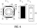
- FIG. 6schematically illustrates different views of the IR heater arrangement around the heating chamber, according to the second embodiment of the present disclosure.
- aspects of the present disclosureare directed to compact vertical oven for reflow of solder bumps for backend processes in semiconductor wafer assembly and packaging that results in void-free solder joints.
- the backend processesinclude but are not limited to wafer-to-wafer interconnect bonding anneal and degas/bake before physical vapor deposition (PVD) metallization with possible extension to underfill and environmental molding cure/anneal in heterogeneous integration that encompasses metal-to-polymer wafer bonding.
- PVDphysical vapor deposition
- formic acidis described as an illustrative example of reducing agent for fluxless soldering, the systems and methods described herein are effective for other reducing agents as well as long as the reducing agent is introduced in a fluidic (gas/liquid) form.
- the reducing agentmay also be referred as process gas.
- the materials of the soldermay vary, but the oven is versatile enough to handle different types of solder. Most of the solders are lead-free. Tin (Sn)-based solders are common for fluxless processes, and example being gold-tin (AuSn) solder.
- This disclosureis to address those issues by designing a vertical oven which uses a plurality of wafers (e.g., an example value is 50-100 wafers) in a batch with controlled injection of the reducing agent (e.g. formic acid), resulting in a process largely free of contamination.
- the reducing agente.g. formic acid
- This disclosuredescribes controlled formic acid flow through a vertical system using laminar flow technology in a sub-atmospheric pressure environment, which is not currently available in the industry.
- the efficacy of the processdepends on effective formic acid vapor delivery, integrated temperature control during heating and cooling, and careful design of the vapor flow path with exhaust. Zone-dependent reaction dynamics managed by vapor delivery process, two-steps temperature ramp control, and controlled cooling process and formic acid content ensures the effective reaction without any flux.
- diagram “A”shows a cassette 100 that is loaded with a stack of wafers/wafer-holding panels ( 101 ) in a vertical configuration.
- the number of waferscan be any arbitrary number based on the capacity of the cassette.
- diagram “B”a reflow chamber 103 is shown.
- the reflow chamber 103has built-in stack of heating/cooling plates 102 .
- the number of heating/cooling plates 102is greater than or equal to the number of panels 101 .
- the chamber 103also has vacuum port ( 104 ), acid port ( 105 ) and gas port ( 106 ). For example, formic acid is injected via port 105 when certain temperature and vacuum level are reached.
- Controlled rate heatingcan be done either in vacuum or in a non-reactive gas environment, such as helium, nitrogen, argon, hydrogen etc.
- Diagram “C”shows that the cassette loaded with the wafers 101 is inserted within a reflow chamber 103 , so that each wafer/panel ( 101 ) is adjacent to its corresponding heating/cooling plate 102 within the chamber 103 .
- Diagram “D”shows controlled rate cooling.
- cooling gas flow 107can be introduced in the chamber 103 .
- the cooling gas flowcan use forced convection or other methods.
- Diagram “E”shows the cassette 100 is taken out of the chamber 103 after the reflow process is completed.
- the cassette 100can be loaded in the chamber 103 whose door (not shown) can be closed/sealed after loading and a vacuum condition is achieved (or non-reactive gas is injected in the chamber).
- the chamber racksmay be robotically loaded with wafers/panels 101 .
- Electrical connections(not shown) enable mounting of thermocouples.
- Chamberalso has external/internal wall heaters to keep walls at certain temperature to reduce heat losses from the side areas of the wafers/panels to the wall when the wafers/panels are heated up. This reduces wafer/panel temperature non-uniformity.
- the heating/cooling plates 102may have a predefined vertical separation (e.g., 15-50 mm).
- the wafers/panels 101retained by the cassette 100 , are parallel and adjacent to the heating/cooling plates 102 and are kept at a certain distance from the plates to prevent formation of hot/cold zones that is likely to be created when the wafers/panels 101 touch the heating/cooling plates 102 because of warpage.
- FIG. 2shows a single heating/cooling plate 102 of the stack of heating/cooling plates shown in FIG. 1 to show that each heating/cooling plate 102 has a built-in channel 202 inside where hot/cold fluid comes in at one end 210 and hot/cold fluid comes out at the other end 212 .
- the hot/cold fluidcan be thermal transfer fluid (HTF), such as synthetic oil, Galden etc. that flow through the channels for heating/cooling purposes.
- the chambercan be kept at vacuum or filled with other non-reactive gases (e.g, nitrogen, helium, Argon etc.) to a certain pressure that improves heat transfer between the heating/cooling plates 102 and the wafers/panels 101 .
- non-reactive gasese.g, nitrogen, helium, Argon etc.
- the chambermay have gas maniforlds inside to flow cold or heated gas across the wafers/panels 101 in order to speed up heating/cooling by introducing forced convection, and/or to assist in improving temperature uniformity across the wafers/panels 101 that may have been caused by wafer/panel warpage or any other reason.
- the hot heat transfer fluidis pumped thru the heating/cooling plates to initiate heating of the wafers/panels by radiation, and/or also by convection and conduction heat transfer mechanism if the chamber has gas inside.
- the HTF temperature and flow ratemay be adjusted to control the panels/wafers heat-up rate, or to stop heating when it is required by the process.
- Two 3-way valves 206 and 207(or any other hardware that assist with maintaining the required fluid temperature) can switch between cold/hot fluid though the channel 202 .
- the cold/hot fluidscome from the two zones 205 and 204 of a two-zone HTF heat exchanger 203 .
- 203can be a combination of two heat exchangers instead of a single two-zone heat exchanger.
- 203can be a heat exchanger with hot HTF and is coupled to a chiller that recirculates cold or warm fluid (30-45° C. are typical but other ranges are possible).
- a chillerthat recirculates cold or warm fluid (30-45° C. are typical but other ranges are possible).
- the term “heat exchanger 203 ”encompasses all of these configurations.
- Each heating/cooling plate 102has two independent passages to separately flow hot and cold HTF through the same plate. This is shown in greater detail in FIGS. 3A and 3B (longitudinal cross sectional view and top view respectively).
- the heating/cooling plate liquid inletsare connected to the heat exchanger 203 .
- the HTF flow rate thru the cooling/heating platesmay be adjusted by bypassing portion of the fluid back to a heat exchanger 203 .
- Maintaining required temperature of the heating/cooling plates 102can be achieved by mixing hot and cold HTF or by pumping hot and cold HTFs thru the heating/cooling plates simultaneously with different flow rates to maintain desired temperature.
- Heating/cooling plates 102may be any shape and made from any suitable material, as long as the material has a good heat transfer coefficient and an appropriate emissivity for better heat transfer via radiation.
- the heating/cooling plates 102may have textured surface, or extruded type of surface to increase surface area in order to improve heat transfer.
- the plates' surfacemay have coating to prevent plate material from chemical attack by process gases (i.e., formic acid that may result in particle creation and plate damage).
- the heating/cooling plates' internal channelsmay be any shape and any size to optimize heat transfer and uniform heating of the wafers/panels, which will result in fast and controlled heating/cooling ramp rates of the panels/wafers.
- One of the plates' design approachesis shown in FIGS. 3A and 3B .
- the platehas numerous channels for hot and for cold HTFs. Hot fluid channels are shown as 302 and cold fluid channels are shown as 303 . There is a separation between the hot fluid and cold fluid channels.
- the heating/cooling plates 102may have a single set of channels for both hot and cold HTF supplied by the heat exchanger 203 .
- the heating/cooling plates for HTFcan be replaced with, for example, ceramic resistive heating elements for heating only. Cooling in this case can be done with a gas flowing across the panels.
- Temperature of the wafer/panel 101may be monitored by any known method, and when temperature is reached required value (e.g., 150-180° C.), the process gas (e.g., formic acid) can be injected inside the chamber 103 for being soaked by the wafers/panels to remove oxides. At this point, the wafer/panels' heating rate may be reduced to certain value (can even be reduced to zero) to control the chemical reaction involving the process gas.
- required valuee.g. 150-180° C.
- the heating with high ratemay be resumed to reach temperature required for the reflow process (e.g., 232-265° C.).
- the hot HTF flowis stopped and the cold HTF starts flowing thru the heating/cooling plates 102 to cool panels down with the controlled rate.
- the wafers/panels 101radiate energy back to the cold heating/cooling plates 102 .
- a gas at certain pressuremay be introduced into the chamber to speed up cooling, and/or to reduce temperature non-uniformity among the wafers/panels.
- the chambermay have gas manifolds to flow gas across the wafers/panels to speed up cooling by forced convection.
- any gasexcept reactive gases like oxygen
- gascan be recirculated through a chiller or a cooling tower.
- the chambercan be vented to atmosphere and the cassette with the wafers/panels can be removed from the chamber.
- a certain valuee.g., 82° C.
- the cassette with wafers/panelscan be removed from the chamber when the wafers/panels are still hot, and put into a buffer station in a non-reactive gas (e.g., N2) environment to complete cooling to a temperature when they can be safely exposed to atmosphere and removed from the module.
- This hardwaremay be connected to equipment front end module (EFEM) to load/unload front-opening unified pods (FOUPs).
- EFEMequipment front end module
- FOUPsload/unload front-opening unified pods
- FIG. 4shows a time versus temperature profile of a typical solder reflow process, where the liquidus temperature is between T 4 and T 5 within the reflow time (from t 3 to t 4 ).
- the design of the vertical chamber of this disclosuremakes it possible to control the temperature ramps of this plot accurately.
- Some of the major advantages of the proposed conceptinclude but are not limited to: a single chamber operation for heating and cooling, to perform reflow process; and, the wafers/panels being parallel to the heating/cooling plates, resulting in very efficient heat transfer by radiation/convection, and reduction in wafer/panel temperature non-uniformity.
- a single process chambertranslates to reduced footprint, reduced cost of the hardware, reduced complexity and increased reliability of the system, and the possibility of changing heating and cooling ramp rates almost instantaneously to follow the reflow process requirements.
- Thisis a vast improvement over current state-of-the-art conventional reflow ovens that comprise multiple chambers (up to 12) for different processing stages, and therefore occupy a lot of factory/fab floor space for a throughput that is lower than what is achievable by the reflow oven disclosed here.
- Method and Apparatus #2Panels Heating with Infrared Radiant Heaters and Cooling in a Separate Zone
- An alternative design of the vertical ovenhas two separate zones for heating and cooling the wafers/panels.
- wafers/panelsare loaded on a cassette 100 (similar to what is described in FIG. 1 ) and the cassette 100 is moved into the sealed enclosure 520 inside a frame 526 .
- the sealed enclosure 520may have gas manifolds 522 to flow gas to purge the enclosure of oxygen before cassette cooling.
- the cassette 100may have susceptors between the wafers/panels to achieve uniform heating.
- the cassette loaded with the wafers/panels into the sealed enclosure 520is lifted into a reflow chamber 103 (similar to what is shown in FIG. 1 ) using a door lift assembly 528 .
- the reflow chamber 103comprises a quartz tube 514 , top plate 510 , bottom plate 516 and has cooling channels 508 (e.g., to protect O-rings and to prevent parts from overheating), and a temperature measurement device (not shown).
- IR radiant heating structure 512there is an infrared (IR) radiant heating structure 512 around the walls of the chamber 103 , as shown in the top view (diagram A of FIG. 6 ), to heat up the wafers/panels 101 in a controlled manner.
- Number of IR heatersis shown as four in FIG. 6 , but it can be any arbitrary numbers.
- the distance ‘d’ of the heater from the edge of the panel 101 and the width ‘w’ of the heater, as shown in the top view (diagram A of FIG. 6 ), as well as the height of the heater ‘h’ as shown in the side view (diagram B of FIG. 6 )are design parameters that can be varied.
- Each heatermay have independently controlled zones (such as zones 1, 2, 3 as shown in diagram “C” of FIG.
- the door 536is in the up position ( FIG. 5A ) or down position ( FIG. 5B ) depending on whether the cassette 100 is in the reflow chamber 103 or in the cool-down chamber 520 .
- Reflow chamber 103is sealed and pumped down to remove water vapor on the wafers/panels. This may take multiple cycles. N2 or other gas may be pumped into the chamber to help with the vapor removal. Multiple cycles may be required. O2 levels will be monitored to verify correct O2 levels are achieved. N2 may be pre-heated to speed up the vapor removal process. Chamber may be filled with gas to improve panels/wafers temperature uniformity.
- Radiant heaters 512are set to target temperature and the wafers/panels start heating with the controlled heating up rate. If necessary, the heating can be paused to wait until panels/wafers are in the desired temperature range required by the process.
- the heaters 512are turned off (as shown in FIG. 5B ), chamber 103 is vented and cassette 100 is moved down into the area 530 within the air-tight enclosure 520 with N2 environment.
- the wafers/panelsare cooled down with incoming N2 gas 524 flowing across the wafers/panels in a controlled manner.
- the outgoing N2 gas 534can be recirculated thru the chiller, or exhausted to atmosphere (using the release valve 532 ).
- N2other non-reactive gases
- the sealed enclosure 520may have a N2 collectoe 518 and optionally a fan 538 to cool down the walls of the enclosure 520 . After a cool down is complete, cassette 100 is unloaded from the enclosure 520 and new cassette is loaded to repeat the solder reflow process.
- Advantages of the current design and methodinclude but are not limited to: separation of the heating and cooling zones resulting in high heat up and cool down rates; and, better temperature control via the infrared heaters (e.g., IR heaters can be turned on/off, or set to desired temperature per the process requirements almost instantaneously).
Landscapes
- Engineering & Computer Science (AREA)
- Computer Hardware Design (AREA)
- Microelectronics & Electronic Packaging (AREA)
- Power Engineering (AREA)
- Mechanical Engineering (AREA)
- Manufacturing & Machinery (AREA)
- Condensed Matter Physics & Semiconductors (AREA)
- General Physics & Mathematics (AREA)
- Physics & Mathematics (AREA)
- Chemical & Material Sciences (AREA)
- Materials Engineering (AREA)
- Electric Connection Of Electric Components To Printed Circuits (AREA)
- Furnace Details (AREA)
Abstract
Description
Claims (14)
Priority Applications (4)
| Application Number | Priority Date | Filing Date | Title |
|---|---|---|---|
| US16/851,977US11444053B2 (en) | 2020-02-25 | 2020-04-17 | Batch processing oven and method |
| PCT/US2021/017634WO2021173360A1 (en) | 2020-02-25 | 2021-02-11 | Batch processing oven and method |
| TW110105741ATWI878461B (en) | 2020-02-25 | 2021-02-19 | Batch processing oven and method of using the same |
| US17/464,863US11335662B2 (en) | 2020-02-25 | 2021-09-02 | Solder reflow oven for batch processing |
Applications Claiming Priority (2)
| Application Number | Priority Date | Filing Date | Title |
|---|---|---|---|
| US202062981441P | 2020-02-25 | 2020-02-25 | |
| US16/851,977US11444053B2 (en) | 2020-02-25 | 2020-04-17 | Batch processing oven and method |
Related Child Applications (1)
| Application Number | Title | Priority Date | Filing Date |
|---|---|---|---|
| US17/464,863ContinuationUS11335662B2 (en) | 2020-02-25 | 2021-09-02 | Solder reflow oven for batch processing |
Publications (2)
| Publication Number | Publication Date |
|---|---|
| US20210265301A1 US20210265301A1 (en) | 2021-08-26 |
| US11444053B2true US11444053B2 (en) | 2022-09-13 |
Family
ID=77366416
Family Applications (2)
| Application Number | Title | Priority Date | Filing Date |
|---|---|---|---|
| US16/851,977Active2040-08-26US11444053B2 (en) | 2020-02-25 | 2020-04-17 | Batch processing oven and method |
| US17/464,863ActiveUS11335662B2 (en) | 2020-02-25 | 2021-09-02 | Solder reflow oven for batch processing |
Family Applications After (1)
| Application Number | Title | Priority Date | Filing Date |
|---|---|---|---|
| US17/464,863ActiveUS11335662B2 (en) | 2020-02-25 | 2021-09-02 | Solder reflow oven for batch processing |
Country Status (3)
| Country | Link |
|---|---|
| US (2) | US11444053B2 (en) |
| TW (1) | TWI878461B (en) |
| WO (1) | WO2021173360A1 (en) |
Cited By (2)
| Publication number | Priority date | Publication date | Assignee | Title |
|---|---|---|---|---|
| US11688621B2 (en) | 2020-12-10 | 2023-06-27 | Yield Engineering Systems, Inc. | Batch processing oven and operating methods |
| EP4451813A1 (en) | 2023-04-21 | 2024-10-23 | Yield Engineering Systems, Inc. | Increasing adhesion of metal- organic interfaces by silane vapor treatment |
Families Citing this family (6)
| Publication number | Priority date | Publication date | Assignee | Title |
|---|---|---|---|---|
| DE102020129759A1 (en)* | 2020-11-11 | 2022-05-12 | Martin Schweikhart | Method for operating a vacuum system and vacuum system |
| US11465225B1 (en) | 2021-08-31 | 2022-10-11 | Yield Engineering Systems, Inc. | Method of using processing oven |
| US11456274B1 (en)* | 2021-08-31 | 2022-09-27 | Yield Engineering Systems, Inc. | Method of using a processing oven |
| US12374569B2 (en) | 2021-10-20 | 2025-07-29 | Yield Engineering Systems, Inc. | Batch processing oven for magnetic anneal |
| CN116313946B (en)* | 2023-05-24 | 2023-10-17 | 长鑫存储技术有限公司 | Temperature adjusting system and adjusting method |
| KR20250015009A (en) | 2023-07-24 | 2025-02-03 | 삼성전자주식회사 | Solder reflow apparatus and method of manufacturing an electronic device |
Citations (34)
| Publication number | Priority date | Publication date | Assignee | Title |
|---|---|---|---|---|
| US1991331A (en)* | 1932-07-30 | 1935-02-12 | Amco Inc | Glass melting tank |
| US3302939A (en)* | 1964-05-19 | 1967-02-07 | Salem Brosius Inc | Industrial furnace cooling system |
| US4597736A (en) | 1985-05-03 | 1986-07-01 | Yield Engineering Systems, Inc. | Method and apparatus for heating semiconductor wafers |
| US5320680A (en)* | 1991-04-25 | 1994-06-14 | Silicon Valley Group, Inc. | Primary flow CVD apparatus comprising gas preheater and means for substantially eddy-free gas flow |
| US5478397A (en)* | 1993-06-14 | 1995-12-26 | Tokyo Electron Kabushiki Kaisha | Heat treating device |
| US5516283A (en) | 1994-03-16 | 1996-05-14 | Kabushiki Kaisha Toshiba | Apparatus for processing a plurality of circular wafers |
| US5525780A (en) | 1993-08-31 | 1996-06-11 | Texas Instruments Incorporated | Method and apparatus for uniform semiconductor material processing using induction heating with a chuck member |
| US5662470A (en) | 1995-03-31 | 1997-09-02 | Asm International N.V. | Vertical furnace |
| US5763856A (en)* | 1993-08-11 | 1998-06-09 | Tokyo Electron Limited | Heat treatment apparatus and method |
| US6005225A (en)* | 1997-03-28 | 1999-12-21 | Silicon Valley Group, Inc. | Thermal processing apparatus |
| US6059567A (en)* | 1998-02-10 | 2000-05-09 | Silicon Valley Group, Inc. | Semiconductor thermal processor with recirculating heater exhaust cooling system |
| US6198075B1 (en) | 1998-11-25 | 2001-03-06 | Yield Engineering Systems, Inc. | Rapid heating and cooling vacuum oven |
| US6225602B1 (en) | 1997-05-02 | 2001-05-01 | Advanced Semiconductor Materials International N.V. | Vertical furnace for the treatment of semiconductor substrates |
| US6369361B2 (en)* | 2000-01-28 | 2002-04-09 | Tokyo Electron Limited | Thermal processing apparatus |
| US20020102353A1 (en)* | 1999-09-29 | 2002-08-01 | Electrovac, Fabrikation Electrotechnischer Spezialartikel Gesellschaft M.B.H. | Method of producing a nanotube layer on a substrate |
| US20020182870A1 (en)* | 2001-05-30 | 2002-12-05 | Hitachi Kokusai Electric Inc. | Substrate processing apparatus and a method for fabricating a semiconductor device by using same |
| US20030094451A1 (en)* | 2001-11-16 | 2003-05-22 | Kabushiki Kaisha Kobe Seiko Sho(Kobe Steel, Ltd.) | Heating apparatus |
| US20030183614A1 (en)* | 2002-03-26 | 2003-10-02 | Hitachi Kokusai Electric Inc. | Heat treatment apparatus and method for processing substrates |
| US6780225B2 (en) | 2002-05-24 | 2004-08-24 | Vitronics Soltec, Inc. | Reflow oven gas management system and method |
| US20050183820A1 (en)* | 2004-02-24 | 2005-08-25 | Kenji Fukuda | Thermal treatment equipment |
| US20070167026A1 (en) | 2004-01-07 | 2007-07-19 | Mineo Miura | Production method for semiconductor device |
| US20080023141A1 (en) | 2006-07-26 | 2008-01-31 | Hitachi Kokusai Electric Inc. | Substrate processing apparatus |
| US20090145890A1 (en) | 2007-12-07 | 2009-06-11 | Tokyo Electron Limited | Treatment apparatus, treatment method, and storage medium |
| US20120000425A1 (en) | 2010-06-30 | 2012-01-05 | Samsung Mobile Display Co., Ltd. | Apparatus for Processing Substrate |
| US20120067521A1 (en)* | 2010-09-21 | 2012-03-22 | Hitachi High-Technologies Corporation | Vacuum processing system |
| US8361548B2 (en) | 2003-09-05 | 2013-01-29 | Yield Engineering Systems, Inc. | Method for efficient coating of substrates including plasma cleaning and dehydration |
| US9028614B2 (en)* | 2011-02-28 | 2015-05-12 | Hitachi Kokusai Electric Inc. | Substrate processing apparatus |
| US9222732B2 (en)* | 2010-09-16 | 2015-12-29 | Hitachi Kokusai Electric Inc. | Substrate processing apparatus and method of manufacturing semiconductor device |
| US10147617B2 (en) | 2016-01-21 | 2018-12-04 | Yield Engineering Systems, Inc. | Method for the rapid processing of polymer layers in support of imidization processes and fan out wafer level packaging including efficient drying of precursor layers |
| WO2019099401A2 (en) | 2016-11-14 | 2019-05-23 | Yield Engineering Systems | Trap assembly and system for trapping polymer vapors in process oven vacuum systems |
| WO2019161109A1 (en) | 2017-02-15 | 2019-08-22 | Yield Engineering Systems | Plasma spreading apparatus and system, and method for spreading plasma in process ovens |
| US20190314738A1 (en) | 2016-11-14 | 2019-10-17 | Yield Engineering Systems, Inc. | Trap assembly and system for trapping polymer vapors in process oven vacuum systems |
| US10490431B2 (en) | 2017-03-10 | 2019-11-26 | Yield Engineering Systems, Inc. | Combination vacuum and over-pressure process chamber and methods related thereto |
| US20200013591A1 (en) | 2018-02-15 | 2020-01-09 | Yield Engineering Systems, Inc. | Plasma Spreading Apparatus And System, And Method Of Spreading Plasma In Process Ovens |
Family Cites Families (4)
| Publication number | Priority date | Publication date | Assignee | Title |
|---|---|---|---|---|
| KR101094279B1 (en)* | 2009-11-06 | 2011-12-19 | 삼성모바일디스플레이주식회사 | Heating means and substrate processing apparatus comprising the same |
| KR101392378B1 (en)* | 2013-03-27 | 2014-05-12 | 주식회사 유진테크 | Apparatus for processing substrate |
| KR101540070B1 (en) | 2014-10-27 | 2015-07-29 | 삼성전자주식회사 | Package substrate and a method of manufacturing semiconductor packages |
| US10276411B2 (en)* | 2017-08-18 | 2019-04-30 | Applied Materials, Inc. | High pressure and high temperature anneal chamber |
- 2020
- 2020-04-17USUS16/851,977patent/US11444053B2/enactiveActive
- 2021
- 2021-02-11WOPCT/US2021/017634patent/WO2021173360A1/ennot_activeCeased
- 2021-02-19TWTW110105741Apatent/TWI878461B/enactive
- 2021-09-02USUS17/464,863patent/US11335662B2/enactiveActive
Patent Citations (34)
| Publication number | Priority date | Publication date | Assignee | Title |
|---|---|---|---|---|
| US1991331A (en)* | 1932-07-30 | 1935-02-12 | Amco Inc | Glass melting tank |
| US3302939A (en)* | 1964-05-19 | 1967-02-07 | Salem Brosius Inc | Industrial furnace cooling system |
| US4597736A (en) | 1985-05-03 | 1986-07-01 | Yield Engineering Systems, Inc. | Method and apparatus for heating semiconductor wafers |
| US5320680A (en)* | 1991-04-25 | 1994-06-14 | Silicon Valley Group, Inc. | Primary flow CVD apparatus comprising gas preheater and means for substantially eddy-free gas flow |
| US5478397A (en)* | 1993-06-14 | 1995-12-26 | Tokyo Electron Kabushiki Kaisha | Heat treating device |
| US5763856A (en)* | 1993-08-11 | 1998-06-09 | Tokyo Electron Limited | Heat treatment apparatus and method |
| US5525780A (en) | 1993-08-31 | 1996-06-11 | Texas Instruments Incorporated | Method and apparatus for uniform semiconductor material processing using induction heating with a chuck member |
| US5516283A (en) | 1994-03-16 | 1996-05-14 | Kabushiki Kaisha Toshiba | Apparatus for processing a plurality of circular wafers |
| US5662470A (en) | 1995-03-31 | 1997-09-02 | Asm International N.V. | Vertical furnace |
| US6005225A (en)* | 1997-03-28 | 1999-12-21 | Silicon Valley Group, Inc. | Thermal processing apparatus |
| US6225602B1 (en) | 1997-05-02 | 2001-05-01 | Advanced Semiconductor Materials International N.V. | Vertical furnace for the treatment of semiconductor substrates |
| US6059567A (en)* | 1998-02-10 | 2000-05-09 | Silicon Valley Group, Inc. | Semiconductor thermal processor with recirculating heater exhaust cooling system |
| US6198075B1 (en) | 1998-11-25 | 2001-03-06 | Yield Engineering Systems, Inc. | Rapid heating and cooling vacuum oven |
| US20020102353A1 (en)* | 1999-09-29 | 2002-08-01 | Electrovac, Fabrikation Electrotechnischer Spezialartikel Gesellschaft M.B.H. | Method of producing a nanotube layer on a substrate |
| US6369361B2 (en)* | 2000-01-28 | 2002-04-09 | Tokyo Electron Limited | Thermal processing apparatus |
| US20020182870A1 (en)* | 2001-05-30 | 2002-12-05 | Hitachi Kokusai Electric Inc. | Substrate processing apparatus and a method for fabricating a semiconductor device by using same |
| US20030094451A1 (en)* | 2001-11-16 | 2003-05-22 | Kabushiki Kaisha Kobe Seiko Sho(Kobe Steel, Ltd.) | Heating apparatus |
| US20030183614A1 (en)* | 2002-03-26 | 2003-10-02 | Hitachi Kokusai Electric Inc. | Heat treatment apparatus and method for processing substrates |
| US6780225B2 (en) | 2002-05-24 | 2004-08-24 | Vitronics Soltec, Inc. | Reflow oven gas management system and method |
| US8361548B2 (en) | 2003-09-05 | 2013-01-29 | Yield Engineering Systems, Inc. | Method for efficient coating of substrates including plasma cleaning and dehydration |
| US20070167026A1 (en) | 2004-01-07 | 2007-07-19 | Mineo Miura | Production method for semiconductor device |
| US20050183820A1 (en)* | 2004-02-24 | 2005-08-25 | Kenji Fukuda | Thermal treatment equipment |
| US20080023141A1 (en) | 2006-07-26 | 2008-01-31 | Hitachi Kokusai Electric Inc. | Substrate processing apparatus |
| US20090145890A1 (en) | 2007-12-07 | 2009-06-11 | Tokyo Electron Limited | Treatment apparatus, treatment method, and storage medium |
| US20120000425A1 (en) | 2010-06-30 | 2012-01-05 | Samsung Mobile Display Co., Ltd. | Apparatus for Processing Substrate |
| US9222732B2 (en)* | 2010-09-16 | 2015-12-29 | Hitachi Kokusai Electric Inc. | Substrate processing apparatus and method of manufacturing semiconductor device |
| US20120067521A1 (en)* | 2010-09-21 | 2012-03-22 | Hitachi High-Technologies Corporation | Vacuum processing system |
| US9028614B2 (en)* | 2011-02-28 | 2015-05-12 | Hitachi Kokusai Electric Inc. | Substrate processing apparatus |
| US10147617B2 (en) | 2016-01-21 | 2018-12-04 | Yield Engineering Systems, Inc. | Method for the rapid processing of polymer layers in support of imidization processes and fan out wafer level packaging including efficient drying of precursor layers |
| WO2019099401A2 (en) | 2016-11-14 | 2019-05-23 | Yield Engineering Systems | Trap assembly and system for trapping polymer vapors in process oven vacuum systems |
| US20190314738A1 (en) | 2016-11-14 | 2019-10-17 | Yield Engineering Systems, Inc. | Trap assembly and system for trapping polymer vapors in process oven vacuum systems |
| WO2019161109A1 (en) | 2017-02-15 | 2019-08-22 | Yield Engineering Systems | Plasma spreading apparatus and system, and method for spreading plasma in process ovens |
| US10490431B2 (en) | 2017-03-10 | 2019-11-26 | Yield Engineering Systems, Inc. | Combination vacuum and over-pressure process chamber and methods related thereto |
| US20200013591A1 (en) | 2018-02-15 | 2020-01-09 | Yield Engineering Systems, Inc. | Plasma Spreading Apparatus And System, And Method Of Spreading Plasma In Process Ovens |
Non-Patent Citations (1)
| Title |
|---|
| International Search Report and Written Opinion of corresponding application PCT/US2021/017634 issued by the European Patent Office (17 pages). |
Cited By (2)
| Publication number | Priority date | Publication date | Assignee | Title |
|---|---|---|---|---|
| US11688621B2 (en) | 2020-12-10 | 2023-06-27 | Yield Engineering Systems, Inc. | Batch processing oven and operating methods |
| EP4451813A1 (en) | 2023-04-21 | 2024-10-23 | Yield Engineering Systems, Inc. | Increasing adhesion of metal- organic interfaces by silane vapor treatment |
Also Published As
| Publication number | Publication date |
|---|---|
| TWI878461B (en) | 2025-04-01 |
| WO2021173360A1 (en) | 2021-09-02 |
| TW202204072A (en) | 2022-02-01 |
| US11335662B2 (en) | 2022-05-17 |
| US20210398937A1 (en) | 2021-12-23 |
| US20210265301A1 (en) | 2021-08-26 |
Similar Documents
| Publication | Publication Date | Title |
|---|---|---|
| US11444053B2 (en) | Batch processing oven and method | |
| US6497734B1 (en) | Apparatus and method for enhanced degassing of semiconductor wafers for increased throughput | |
| KR102444827B1 (en) | Batch heating and cooling chamber or loadlock | |
| US7371998B2 (en) | Thermal wafer processor | |
| US6448537B1 (en) | Single-wafer process chamber thermal convection processes | |
| JP4409756B2 (en) | Dual substrate load-lock process equipment | |
| CN102934214B (en) | Load the sclerosis of lock batch ozone | |
| US20160013084A1 (en) | Apparatus and Method for Pre-Baking Substrate Upstream of Process Chamber | |
| US7442900B2 (en) | Chamber for uniform heating of large area substrates | |
| US11688621B2 (en) | Batch processing oven and operating methods | |
| JP6377717B2 (en) | Temperature control system and method for small lot substrate handling system | |
| KR20180123522A (en) | Chamber for substrate degassing | |
| KR102298028B1 (en) | Electronic device manufacturing systems, methods, and apparatus for heating substrates and reducing contamination in load locks | |
| TWI710043B (en) | Thermal treatment chamber and method of manufacturing thermally treated workpieces | |
| CN101901739B (en) | Substrate cooling method, substrate cooling system and substrate processing device | |
| JP4003206B2 (en) | Heat treatment apparatus and heat treatment method | |
| CN100485874C (en) | Processing equipment for object to be processed | |
| US12374569B2 (en) | Batch processing oven for magnetic anneal |
Legal Events
| Date | Code | Title | Description |
|---|---|---|---|
| FEPP | Fee payment procedure | Free format text:ENTITY STATUS SET TO UNDISCOUNTED (ORIGINAL EVENT CODE: BIG.); ENTITY STATUS OF PATENT OWNER: SMALL ENTITY | |
| FEPP | Fee payment procedure | Free format text:ENTITY STATUS SET TO SMALL (ORIGINAL EVENT CODE: SMAL); ENTITY STATUS OF PATENT OWNER: SMALL ENTITY | |
| AS | Assignment | Owner name:YIELD ENGINEERING SYSTEMS, INC., CALIFORNIA Free format text:ASSIGNMENT OF ASSIGNORS INTEREST;ASSIGNORS:KARIM, M ZIAUL;HALL, RANDY;KROTOV, PETER;SIGNING DATES FROM 20200420 TO 20200428;REEL/FRAME:052523/0031 | |
| STPP | Information on status: patent application and granting procedure in general | Free format text:DOCKETED NEW CASE - READY FOR EXAMINATION | |
| STPP | Information on status: patent application and granting procedure in general | Free format text:NON FINAL ACTION MAILED | |
| STPP | Information on status: patent application and granting procedure in general | Free format text:NON FINAL ACTION MAILED | |
| STPP | Information on status: patent application and granting procedure in general | Free format text:RESPONSE TO NON-FINAL OFFICE ACTION ENTERED AND FORWARDED TO EXAMINER | |
| STPP | Information on status: patent application and granting procedure in general | Free format text:NOTICE OF ALLOWANCE MAILED -- APPLICATION RECEIVED IN OFFICE OF PUBLICATIONS | |
| STPP | Information on status: patent application and granting procedure in general | Free format text:PUBLICATIONS -- ISSUE FEE PAYMENT VERIFIED | |
| STCF | Information on status: patent grant | Free format text:PATENTED CASE | |
| AS | Assignment | Owner name:YIELD ENGINEERING SPV LLC, CALIFORNIA Free format text:ASSIGNMENT OF ASSIGNORS INTEREST;ASSIGNOR:YIELD ENGINEERING SYSTEMS, INC.;REEL/FRAME:063584/0553 Effective date:20230505 Owner name:AON IP ADVANTAGE FUND LP, ILLINOIS Free format text:SECURITY INTEREST;ASSIGNOR:YIELD ENGINEERING SPV LLC;REEL/FRAME:063585/0001 Effective date:20230505 |