US11437368B2 - Multilevel semiconductor device and structure with oxide bonding - Google Patents
Multilevel semiconductor device and structure with oxide bondingDownload PDFInfo
- Publication number
- US11437368B2 US11437368B2US17/717,094US202217717094AUS11437368B2US 11437368 B2US11437368 B2US 11437368B2US 202217717094 AUS202217717094 AUS 202217717094AUS 11437368 B2US11437368 B2US 11437368B2
- Authority
- US
- United States
- Prior art keywords
- level
- layer
- oxide
- silicon
- bonded
- Prior art date
- Legal status (The legal status is an assumption and is not a legal conclusion. Google has not performed a legal analysis and makes no representation as to the accuracy of the status listed.)
- Active
Links
Images


Classifications
- H01L27/0688—
- H—ELECTRICITY
- H01—ELECTRIC ELEMENTS
- H01L—SEMICONDUCTOR DEVICES NOT COVERED BY CLASS H10
- H01L25/00—Assemblies consisting of a plurality of semiconductor or other solid state devices
- H01L25/03—Assemblies consisting of a plurality of semiconductor or other solid state devices all the devices being of a type provided for in a single subclass of subclasses H10B, H10D, H10F, H10H, H10K or H10N, e.g. assemblies of rectifier diodes
- H01L25/04—Assemblies consisting of a plurality of semiconductor or other solid state devices all the devices being of a type provided for in a single subclass of subclasses H10B, H10D, H10F, H10H, H10K or H10N, e.g. assemblies of rectifier diodes the devices not having separate containers
- H01L25/075—Assemblies consisting of a plurality of semiconductor or other solid state devices all the devices being of a type provided for in a single subclass of subclasses H10B, H10D, H10F, H10H, H10K or H10N, e.g. assemblies of rectifier diodes the devices not having separate containers the devices being of a type provided for in group H10H20/00
- H01L25/0756—Stacked arrangements of devices
- H—ELECTRICITY
- H01—ELECTRIC ELEMENTS
- H01L—SEMICONDUCTOR DEVICES NOT COVERED BY CLASS H10
- H01L23/00—Details of semiconductor or other solid state devices
- H01L23/58—Structural electrical arrangements for semiconductor devices not otherwise provided for, e.g. in combination with batteries
- H01L23/64—Impedance arrangements
- H01L23/66—High-frequency adaptations
- H01L27/14634—
- H01L27/14636—
- H01L27/156—
- H—ELECTRICITY
- H10—SEMICONDUCTOR DEVICES; ELECTRIC SOLID-STATE DEVICES NOT OTHERWISE PROVIDED FOR
- H10F—INORGANIC SEMICONDUCTOR DEVICES SENSITIVE TO INFRARED RADIATION, LIGHT, ELECTROMAGNETIC RADIATION OF SHORTER WAVELENGTH OR CORPUSCULAR RADIATION
- H10F39/00—Integrated devices, or assemblies of multiple devices, comprising at least one element covered by group H10F30/00, e.g. radiation detectors comprising photodiode arrays
- H10F39/80—Constructional details of image sensors
- H10F39/809—Constructional details of image sensors of hybrid image sensors
- H—ELECTRICITY
- H10—SEMICONDUCTOR DEVICES; ELECTRIC SOLID-STATE DEVICES NOT OTHERWISE PROVIDED FOR
- H10F—INORGANIC SEMICONDUCTOR DEVICES SENSITIVE TO INFRARED RADIATION, LIGHT, ELECTROMAGNETIC RADIATION OF SHORTER WAVELENGTH OR CORPUSCULAR RADIATION
- H10F39/00—Integrated devices, or assemblies of multiple devices, comprising at least one element covered by group H10F30/00, e.g. radiation detectors comprising photodiode arrays
- H10F39/80—Constructional details of image sensors
- H10F39/811—Interconnections
- H—ELECTRICITY
- H10—SEMICONDUCTOR DEVICES; ELECTRIC SOLID-STATE DEVICES NOT OTHERWISE PROVIDED FOR
- H10H—INORGANIC LIGHT-EMITTING SEMICONDUCTOR DEVICES HAVING POTENTIAL BARRIERS
- H10H29/00—Integrated devices, or assemblies of multiple devices, comprising at least one light-emitting semiconductor element covered by group H10H20/00
- H10H29/10—Integrated devices comprising at least one light-emitting semiconductor component covered by group H10H20/00
- H10H29/14—Integrated devices comprising at least one light-emitting semiconductor component covered by group H10H20/00 comprising multiple light-emitting semiconductor components
- H10H29/142—Two-dimensional arrangements, e.g. asymmetric LED layout
- G—PHYSICS
- G02—OPTICS
- G02B—OPTICAL ELEMENTS, SYSTEMS OR APPARATUS
- G02B6/00—Light guides; Structural details of arrangements comprising light guides and other optical elements, e.g. couplings
- G02B6/10—Light guides; Structural details of arrangements comprising light guides and other optical elements, e.g. couplings of the optical waveguide type
- G02B6/12—Light guides; Structural details of arrangements comprising light guides and other optical elements, e.g. couplings of the optical waveguide type of the integrated circuit kind
- G02B2006/12083—Constructional arrangements
- G02B2006/12119—Bend
- G—PHYSICS
- G02—OPTICS
- G02B—OPTICAL ELEMENTS, SYSTEMS OR APPARATUS
- G02B6/00—Light guides; Structural details of arrangements comprising light guides and other optical elements, e.g. couplings
- G02B6/10—Light guides; Structural details of arrangements comprising light guides and other optical elements, e.g. couplings of the optical waveguide type
- G02B6/12—Light guides; Structural details of arrangements comprising light guides and other optical elements, e.g. couplings of the optical waveguide type of the integrated circuit kind
- G02B6/12004—Combinations of two or more optical elements
- G—PHYSICS
- G02—OPTICS
- G02B—OPTICAL ELEMENTS, SYSTEMS OR APPARATUS
- G02B6/00—Light guides; Structural details of arrangements comprising light guides and other optical elements, e.g. couplings
- G02B6/10—Light guides; Structural details of arrangements comprising light guides and other optical elements, e.g. couplings of the optical waveguide type
- G02B6/12—Light guides; Structural details of arrangements comprising light guides and other optical elements, e.g. couplings of the optical waveguide type of the integrated circuit kind
- G02B6/122—Basic optical elements, e.g. light-guiding paths
- G02B6/125—Bends, branchings or intersections
- H—ELECTRICITY
- H01—ELECTRIC ELEMENTS
- H01L—SEMICONDUCTOR DEVICES NOT COVERED BY CLASS H10
- H01L2223/00—Details relating to semiconductor or other solid state devices covered by the group H01L23/00
- H01L2223/58—Structural electrical arrangements for semiconductor devices not otherwise provided for
- H01L2223/64—Impedance arrangements
- H01L2223/66—High-frequency adaptations
- H01L2223/6605—High-frequency electrical connections
- H01L2223/6627—Waveguides, e.g. microstrip line, strip line, coplanar line
- H—ELECTRICITY
- H10—SEMICONDUCTOR DEVICES; ELECTRIC SOLID-STATE DEVICES NOT OTHERWISE PROVIDED FOR
- H10D—INORGANIC ELECTRIC SEMICONDUCTOR DEVICES
- H10D88/00—Three-dimensional [3D] integrated devices
Definitions
- This inventiondescribes applications of monolithic 3D integration to various disciplines, including but not limited to, for example, light-emitting diodes, displays, image-sensors and solar cells.
- LEDsLight emitting diodes
- Red LEDsare typically made on Gallium Arsenide (GaAs) substrates, and include quantum wells constructed of various materials such as AlInGaP and GaInP.
- Blue and green LEDsare typically made on Sapphire or Silicon Carbide (SiC) or bulk Gallium Nitride (GaN) substrates, and include quantum wells constructed of various materials such as GaN and InGaN.
- a white LED for lighting and display applicationscan be constructed by either using a blue LED coated with phosphor (called phosphor-coated LED or pcLED) or by combining light from red, blue, and green LEDs (called RGB LED).
- RGB LEDsare typically constructed by placing red, blue, and green LEDs side-by-side. While RGB LEDs are more energy-efficient than pcLEDs, they are less efficient in mixing red, blue and green colors to form white light. They also are much more costly than pcLEDs. To tackle issues with RGB LEDs, several proposals have been made.
- RGB LED proposal from Hong Kong Universityis described in “Design of vertically stacked polychromatic light emitting diodes”, Optics Express, June 2009 by K. Hui, X. Wang, et al (“Hui”). It involves stacking red, blue, and green LEDs on top of each other after individually packaging each of these LEDs. While this solves light mixing problems, this RGB-LED is still much more costly than a pcLED solution since three LEDs for red, blue, and green color need to be packaged. A pcLED, on the other hand, requires just one LED to be packaged and coated with phosphor.
- RGB LED proposalfrom Nichia Corporation is described in “Phosphor Free High-Luminous-Efficiency White Light-Emitting Diodes Composed of InGaN Multi-Quantum Well”, Japanese Journal of Applied Physics, 2002 by M. Yamada, Y. Narukawa, et al. (“Yamada”). It involves constructing and stacking red, blue and green LEDs of GaN-based materials on a sapphire or SiC substrate. However, red LEDs are not efficient when constructed with GaN-based material systems, and that hampers usefulness of this implementation. It is not possible to deposit defect-free AlInGaP/InGaP for red LEDs on the same substrate as GaN based blue and green LEDs, due to a mismatch in thermal expansion co-efficient between the various material systems.
- RGB-LED proposalis described in “Cascade Single chip phosphor-free while light emitting diodes”, Applied Physics Letters, 2008 by X. Guo, G. Shen, et al. (“Guo”). It involves bonding GaAs based red LEDs with GaN based blue-green LEDs to produce white light. Unfortunately, this bonding process requires 600° C. temperatures, causing issues with mismatch of thermal expansion co-efficients and cracking.
- Another publication on this topicis “A trichromatic phosphor-free white light-emitting diode by using adhesive bonding scheme”, Proc. SPIE, Vol. 7635, 2009 by D. Chuai, X. Guo, et al. (“Chuai”). It involves bonding red LEDs with green-blue LED stacks. Bonding is done at the die level after dicing, which is more costly than a wafer-based approach.
- U.S. patent application Ser. No. 12/130,824describes various stacked RGB LED devices. It also briefly mentions a method for construction of a stacked LED where all layers of the stacked LED are transferred using lift-off with a temporary carrier and Indium Tin Oxide (ITO) to semiconductor bonding. This method has several issues for constructing a RGB LED stack. First, it is difficult to manufacture a lift-off with a temporary carrier of red LEDs for producing a RGB LED stack, especially for substrates larger than 2 inch. This is because red LEDs are typically constructed on non-transparent GaAs substrates, and lift-off with a temporary carrier is done by using an epitaxial lift-off process.
- ITOIndium Tin Oxide
- the thin film to be transferredtypically sits atop a “release-layer” (eg. AlAs), this release layer is removed by etch procedures after the thin film is attached to a temporary substrate. Scaling this process to 4 inch wafers and bigger is difficult. Second, it is very difficult to perform the bonding of ITO to semiconductor materials of a LED layer at reasonable temperatures, as described in the patent application Ser. No. 12/130,824.
- a “release-layer”eg. AlAs
- RGB LEDsare significantly more efficient than pcLEDs, they can be used as replacements of today's phosphor-based LEDs for many applications, provided a cheap and effective method of constructing RGB LEDs can be invented.
- Image sensorsare used in applications such as cameras. Red, blue, and green components of the incident light are sensed and stored in digital format.
- CMOS image sensorstypically contain a photodetector and sensing circuitry. Almost all image sensors today have both the photodetector and sensing circuitry on the same chip. Since the area consumed by the sensing circuits is high, the photodetector cannot see the entire incident light, and image capture is not as efficient.
- the International Technology Roadmap for Semiconductorssuggests that the 2-4 ⁇ m TSV pitch will be the industry standard until 2012. A 2-4 ⁇ m pitch TSV will be too big for a sub-1 ⁇ m pixel. Therefore, novel techniques of stacking photodetectors and sensing circuitry are required.
- LCDsLiquid Crystal Displays
- TFTsamorphous/polycrystalline silicon thin-film-transistors
- Microdisplaysthat utilize single-crystal silicon transistors. Microdisplays are typically used where very high resolution is needed, such as camera/camcorder view-finders, projectors and wearable computers.
- Microdisplaysare made in semiconductor fabs with 200 mm or 300 mm wafers. They are typically constructed with LCOS (Liquid-Crystal-on-Silicon) Technology and are reflective in nature. An exception to this trend of reflective microdisplays is technology from Kopin Corporation (U.S. Pat. No. 5,317,236, filed December 1991). This company utilizes transmittive displays with a lift-off layer transfer scheme. Transmittive displays may be generally preferred for various applications.
- LCOSLiquid-Crystal-on-Silicon
- Solar cellscan be constructed of several materials such as, for example, silicon and compound semiconductors.
- the highest efficiency solar cellsare typically multi-junction solar cells that are constructed of compound semiconductor materials. These multi-junction solar cells are typically constructed on a germanium substrate, and semiconductors with various band-gaps are epitaxially grown atop this substrate to capture different portions of the solar spectrum.
- Image sensors based on Charge-Coupled Device (CCD) technologyhas been around for several decades.
- the CCD technologyrelies on a collect and shift scheme, wherein charges are collected in individual cells according to the luminosity of the light falling on each of them, then the charges are sequentially shifted towards one edge of the sensor where readout circuits read the sequence of charges one at a time.
- CCD technologyhas better light sensitivity since almost the entire CCD cell area is dedicated to light collecting, and the control and readout circuits are all on one edge not blocking the light.
- the photodiodes in each cellhave to share space with the control and readout circuits adjacent to them, and so their size and light sensitivity are therefore limited.
- HDRHigh Dynamic Range
- the typical approachis to capture images using exposure bracketing, and then combining them into a single HDR image.
- the issue with thisis that multiple exposures are performed over some period of time, and if there is movement of the camera or target during the time of the exposures, the final HDR image will reflect this by loss of sharpness.
- multiple imagesmay lead to large data in storage devices.
- Other methodsuse software algorithms to extract HDR information from a single exposure, but as they can only process information that is recordable by the sensor, there is a permanent loss of some details.
- CMOSComplementary Metal Oxide Semiconductor
- 3D stacking of semiconductor devices or chipsis one avenue to tackle the wire issues.
- the transistors in ICscan be placed closer to each other. This reduces wire lengths and keeps wiring delay low.
- TSVThrough-silicon via
- Monolithic 3D technologyWith this approach, multiple layers of transistors and wires can be monolithically constructed.
- Some monolithic 3D and 3DIC approachesare described in U.S. Pat. Nos. 8,273,610, 8,298,875, 8,362,482, 8,378,715, 8,379,458, 8,450,804, 8,557,632, 8,574,929, 8,581,349, 8,642,416, 8,669,778, 8,674,470, 8,687,399, 8,742,476, 8,803,206, 8,836,073, 8,902,663, 8,994,404, 9,023,688, 9,029,173, 9,030,858, 9,117,749, 9,142,553, 9,219,005, 9,385,058, 9,406,670, 9,460,978, 9,509,313, 9,640,531, 9,691,760, 9,711,407, 9,721,927, 9,799,761, 9,871,034, 9,953,870, 9,953,994, 10,014,292, 10,014,
- PCT/US2010/052093PCT/US2011/042071 (WO2012/015550), PCT/US2016/52726 (WO2017053329), PCT/US2017/052359 (WO2018/071143), PCT/US2018/016759 (WO2018144957), PCT/US2018/52332(WO 2019/060798), and PCT/US2021/44110.
- PCT/US2010/052093PCT/US2011/042071 (WO2012/015550), PCT/US2016/52726 (WO2017053329), PCT/US2017/052359 (WO2018/071143), PCT/US2018/016759 (WO2018144957), PCT/US2018/52332(WO 2019/060798), and PCT/US2021/44110.
- Electro-OpticsThere is also work done for integrated monolithic 3D including layers of different crystals, such as U.S. Pat. Nos. 8,283,215, 8,163,581, 8,753,913, 8,823,122, 9,197,804, 9,419,031, 9,941,319, 10,679,977, 10,943,934, 10,998,374, 11,063,071, and 11,133,344.
- a multi-level semiconductor deviceincluding: a first level including integrated circuits; a second level including an optical waveguide, where the second level is disposed above the first level, where the first level includes crystalline silicon; and an oxide layer disposed between the first level and the second level, where the second level is bonded to the oxide layer, and where the bonded includes oxide to oxide bonds.
- a multi-level semiconductor deviceincluding: a first level including an optical waveguide; a second level including integrated circuits, where the second level is disposed above the first level, where the first level includes crystalline silicon; and an oxide layer disposed between the first level and the second level, where the second level is bonded to the oxide layer, and where the bonded includes oxide to oxide bonds.
- a multi-level semiconductor deviceincluding: a first level including integrated circuits; a second level including a plurality of optical modulators, where the second level is disposed above the first level, where the first level includes crystalline silicon; and an oxide layer disposed between the first level and the second level, where the second level is bonded to the oxide layer, and where the bonded includes oxide to oxide bonds.
- a multi-level semiconductor deviceincluding: a first level including integrated circuits; a second level including an electromagnetic waveguide, where the second level is disposed above the first level, where the first level includes crystalline silicon; and an oxide layer disposed between the first level and the second level, where the second level is bonded to the oxide layer, and where the bonded includes oxide to oxide bonds.
- a multi-level semiconductor deviceincluding: a first level including an electromagnetic waveguide; a second level including integrated circuits, where the second level is disposed above the first level, where the first level includes crystalline silicon; and an oxide layer disposed between the first level and the second level, where the second level is bonded to the oxide layer, and where the bonded includes oxide to oxide bonds.
- a multi-level semiconductor deviceincluding: a first level including integrated circuits; a second level including a plurality of electromagnetic modulators, where the second level is disposed above the first level, where the first level includes crystalline silicon; and an oxide layer disposed between the first level and the second level, where the second level is bonded to the oxide layer, and where the bonded includes oxide to oxide bonds.
- a multi-level semiconductor deviceincluding: a first level including integrated circuits; a second level including a structure designed to conduct electromagnetic waves in a confined manner, where the second level is disposed above the first level, where the first level includes crystalline silicon, where the second level includes crystalline silicon; and an oxide layer disposed between the first level and the second level, where the second level is bonded to the oxide layer, and where the bonded includes oxide to oxide bonds.
- a multi-level semiconductor deviceincluding: a first level including a structure designed to conduct electromagnetic waves in a confined manner; a second level including integrated circuits, where the second level is disposed above the first level, where the first level includes crystalline silicon; and an oxide layer disposed between the first level and the second level, where the second level is bonded to the oxide layer, and where the bonded includes oxide to oxide bonds.
- a multi-level semiconductor deviceincluding: a first level including integrated circuits; a second level including a plurality of electromagnetic modulators, where the second level is disposed above the first level, where the first level includes crystalline silicon, where the second level includes crystalline silicon; and an oxide layer disposed between the first level and the second level, where the second level is bonded to the first level.
- a multi-level semiconductor deviceincluding: a first level including integrated circuits; a second level including a structure designed to conduct electromagnetic waves, where the second level is disposed above the first level, where the first level includes crystalline silicon, where the second level includes crystalline silicon; an oxide layer disposed between the first level and the second level; and a plurality of electromagnetic modulators, where the second level is bonded to the oxide layer, and where the bonded includes oxide to oxide bonds.
- a multi-level semiconductor deviceincluding: a first level including a structure designed to conduct electromagnetic waves; a second level including integrated circuits, where the second level is disposed above the first level; a plurality of electromagnetic modulators; and an oxide layer disposed between the first level and the second level, where the first level includes crystalline silicon, where the second level is bonded to the oxide layer, and where the bonded includes oxide to oxide bonds.
- a multi-level semiconductor deviceincluding: a first level including integrated circuits and electromagnetic modulators; a second level including a plurality of transistors, where the second level is disposed above the first level, where the first level includes crystalline silicon, where the second level includes crystalline silicon; and an oxide layer disposed between the first level and the second level, where the second level is bonded to the first level.
- a multi-level semiconductor deviceincluding: a first level including integrated circuits; a second level including a structure designed to conduct electromagnetic waves, where the second level is disposed above the first level, where the first level includes crystalline silicon; an oxide layer disposed between the first level and the second level; and a plurality of electromagnetic modulators, where the second level is bonded to the oxide layer, and where the bonded includes oxide to oxide bonds.
- a multi-level semiconductor deviceincluding: a first level including a structure designed to conduct electromagnetic waves; a second level including integrated circuits, where the second level is disposed above the first level; a plurality of electromagnetic modulators; and an oxide layer disposed between the first level and the second level, where the second level is bonded to the oxide layer, and where the bonded includes oxide to oxide bonds.
- a multi-level semiconductor deviceincluding: a first level including integrated circuits and electromagnetic modulators; a second level including a plurality of interconnects lines, where the second level is disposed above the first level, where the first level includes crystalline silicon; and an oxide layer disposed between the first level and the second level, where the second level is bonded to the first level, and where the bonded includes oxide to oxide bonds.
- a multi-level semiconductor deviceincluding: a first level including integrated circuits; a second level including a structure designed to conduct electromagnetic waves, where the second level is disposed above the first level, where the first level includes crystalline silicon; and an oxide layer disposed between the first level and the second level; where the second level is bonded to the oxide layer, and where the bonded includes oxide to oxide bonds.
- a multi-level semiconductor deviceincluding: a first level including a structure designed to conduct electromagnetic waves; a second level including integrated circuits, where the second level is disposed above the first level, and at least one transmitter and at least one receiver; and an oxide layer disposed between the first level and the second level, where the second level is bonded to the oxide layer, and where the bonded includes oxide to oxide bonds.
- a multi-level semiconductor deviceincluding: a first level including integrated circuits and communication control circuits; a second level including a plurality of interconnect lines, where the second level is disposed above the first level, where the first level includes crystalline silicon; and an oxide layer disposed between the first level and the second level, where the second level is bonded to the first level, and where the bonded includes oxide to oxide bonds.
- FIGS. 1A-1Gare exemplary drawn illustrations of a display constructed using sub-400° C. processed single crystal silicon recessed channel transistors on a glass substrate;
- FIGS. 2A-2Iare exemplary drawn illustrations of a display constructed using sub-400° C. processed single crystal silicon replacement gate transistors on a glass substrate;
- FIGS. 3A-3Fare exemplary drawn illustrations of a display constructed using sub-400° C. processed single crystal junction-less transistors on a glass substrate;
- FIGS. 4A-4Dare exemplary drawn illustrations of a display constructed using sub-400° C. processed amorphous silicon or polysilicon junctionless transistors on a glass substrate;
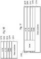
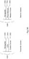
- FIGS. 5A-5Care exemplary drawn illustrations of a microdisplay constructed using stacked RGB LEDs and control circuits are connected to each pixel with solder bumps;
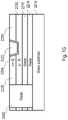
- FIGS. 6A-6Dare exemplary drawn illustrations of a microdisplay constructed using stacked RGB LEDs and control circuits are monolithically stacked above the LED.
- FIGS. 31 A-Hillustrate an embodiment of this invention, where a LED-driven chip-to-chip optical interconnect is constructed by monolithically stacking using layer transfer techniques;
- FIGS. 7A-7Hillustrate an embodiment of this invention, where a LED-driven chip-to-chip optical interconnect is constructed by monolithically stacking using layer transfer techniques;
- FIGS. 8A-8Dillustrate an embodiment of this invention, where a laser-driven chip-to-chip optical interconnect is constructed by monolithically stacking using layer transfer techniques;
- FIGS. 9A-9Cillustrate an embodiment of this invention, where a LED-driven on-chip optical interconnect is constructed by monolithically stacking using layer transfer techniques;
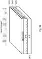
- FIG. 10illustrates a typical hollow-metal waveguide (HMWG) structure which enables on-chip communication via waveguides stacked on top of the active layer of the chip (prior art).
- HMWGhollow-metal waveguide
- FIGS. 11A-11Cillustrate an embodiment of this invention, where a laser-driven on-chip optical interconnect is constructed by monolithically stacking using layer transfer techniques.
- FIGS. 1-11Embodiments of the present invention are now described with reference to FIGS. 1-11 , it being appreciated that the figures illustrate the subject matter not to scale or to measure.
- a smart layer transfermay be defined as one or more of the following processes:
- RGB LEDscould include several steps that occur in a sequence from Step (A) to Step (S). Many of them share common characteristics, features, modes of operation, etc.
- Step (A)Step (S)
- SStep (S)
- the same reference numbersare used in different drawing figures, they are used to indicate analogous, similar or identical structures to enhance the understanding of the present invention by clarifying the relationships between the structures and embodiments presented in the various diagrams—particularly in relating analogous, similar or identical functionality to different physical structures.
- transistorsneed to be formed on glass or plastic substrates. These substrates typically cannot withstand high process temperatures (e.g., >400° C.). Layer transfer can be advantageously used for constructing displays and microdisplays as well, since it may enable transistors to be processed on these substrates at ⁇ 400° C.
- Various embodiments of transistors constructed on glass substratesare described in this patent application. These transistors constructed on glass substrates could form part of liquid crystal displays (LCDs) or other types of displays. It will be clear to those skilled in the art based on the present disclosure that these techniques can also be applied to plastic substrates.
- LCDsliquid crystal displays
- FIGS. 1A-1Gdescribe a process for forming recessed channel single crystal (or monocrystalline) transistors on glass substrates at a temperature approximately less than 400° C. for display and microdisplay applications.
- This processcould include several steps that occur in a sequence from Step (A) to Step (G). Many of these steps share common characteristics, features, modes of operation, etc.
- identical reference numbersare used in different drawing figures, they are used to indicate analogous, similar or identical structures to enhance the understanding of the present invention by clarifying the relationships between the structures and embodiments presented in the various diagrams—particularly in relating analogous, similar or identical functionality to different physical structures.
- Step (A)is illustrated in FIG. 1A .
- a silicon wafer 2202is taken and a n+ region 2204 is formed by ion implantation. Following this formation, a layer of p ⁇ Silicon 2206 is epitaxially grown. An oxide layer 2210 is then deposited. Following this deposition, an anneal is performed to activate dopants in various layers. It will be clear to one skilled in the art based on the present disclosure that various other procedures can be used to get the structure shown in FIG. 22A .
- Step (B)is illustrated in FIG. 1B . Hydrogen is implanted into the structure shown in FIG. 22A at a certain depth indicated by 2212 . Alternatively, Helium can be used for this purpose.
- Step (C)is illustrated in FIG. 1C .
- a glass substrate 2214is taken and a silicon oxide layer 2216 is deposited atop it at compatible temperatures.
- Step (D)is illustrated in FIG. 1D .
- Various elements in FIG. 1Dsuch as 2202 , 2204 , 2206 , 2210 , 2214 , and 2216 have been described previously.
- the structure shown in FIG. 1Bis flipped and bonded to the structure shown in FIG. 1C using oxide-to-oxide bonding of layers 2210 and 2216 .
- Step (E)is illustrated in FIG. 1E .
- Step (F)is illustrated in FIG. 1F .
- An oxide layer 2220is formed using a shallow trench isolation (STI) process. This helps isolate transistors.
- Step (G)is illustrated in FIG. 1G .
- Various elements in FIG. 1Gsuch as 2210 , 2216 , 2220 and 2214 have been described previously.
- n+ Silicon layer from FIG. 1F and optionally p ⁇ Silicon layer from FIG. 1Fare etched.
- a thin gate dielectricis deposited, after which a gate dielectrode is deposited.
- the gate dielectric and gate electrodeare then polished away to form the gate dielectric layer 2224 and gate electrode layer 2222 .
- the n+ Silicon layers 2228 and 2226form the source and drain regions of the transistors while the p ⁇ Silicon region after this step is indicated by 2230 .
- Contacts and other parts of the display/microdisplayare then fabricated. It can be observed that during the whole process, the glass substrate substantially always experiences temperatures less than 400° C., or even lower. This is because the crystalline silicon can be transferred atop the glass substrate at a temperature less than 400° C., and dopants are pre-activated before layer transfer to glass.
- FIG. 2A-2Idescribes a process of forming both nMOS and pMOS transistors with single-crystal silicon on a glass substrate at temperatures less than 400° C., and even lower. Ion-cut technology (which is a smart layer transfer technology) is used. While the process flow described is shown for both nMOS and pMOS on a glass substrate, it could also be used for just constructing nMOS devices or for just constructing pMOS devices. This process could include several steps that occur in a sequence from Step (A) to Step (H). Many of these steps share common characteristics, features, modes of operation, etc.
- Step (A)is illustrated in FIG. 2A .
- a p ⁇ Silicon wafer 2302is taken and a n well 2304 is formed on the p ⁇ Silicon wafer 2302 .
- Various additional implants to optimize dopant profilescan also be done.
- an isolation processis conducted to form isolation regions 2306 .
- a dummy gate dielectric 2310 made of silicon dioxide and a dummy gate electrode 2308 made of polysiliconare constructed.
- Step (B)is illustrated in FIG. 2B .
- Various elements of FIG. 2Bsuch as 2302 , 2304 , 2306 , 2308 and 2310 have been described previously.
- Implantsare done to form source-drain regions 2312 and 2314 for both nMOS and pMOS transistors.
- a rapid thermal annealis then done to activate dopants.
- RTArapid thermal anneal
- a spike anneal or a laser annealcould be done.
- Step (C)is illustrated in FIG. 2C .
- Various elements of FIG. 2Csuch as 2302 , 2304 , 2306 , 2308 , 2310 , 2312 and 2314 have been described previously.
- An oxide layer 2316is deposited and planarized with CMP.
- Step (D)is illustrated in FIG. 2D .
- Various elements of FIG. 2Dsuch as 2302 , 2304 , 2306 , 2308 , 2310 , 2312 , 2314 , and 2316 have been described previously.
- Hydrogenis implanted into the wafer at a certain depth indicated by 2318 .
- Step (E)is illustrated in FIG. 2E .
- Various elements of FIG. 2Esuch as 2302 , 2304 , 2306 , 2308 , 2310 , 2312 , 2314 , 2316 , and 2318 have been described previously.
- a temporary bonding adhesiveis a polyimide that can be removed by shining a laser.
- An example of a temporary carrier waferis glass.
- Step (F)is illustrated in FIG. 2F .
- the structure shown in FIG. 2Eis cleaved at the hydrogen plane using a mechanical force. Alternatively, an anneal could be used.
- FIG. 2Fshows the structure after all these steps are done, with the deposited oxide layer indicated as 2328 .
- the p ⁇ Silicon regionis indicated as 2322
- the n ⁇ Silicon regionis indicated as 2324
- the oxide isolation regionsare indicated as 2326 .
- Various other elements in FIG. 23Fsuch as 2308 , 2320 , 2312 , 2314 , 2310 , and 2316 have been described previously.
- Step (G)is illustrated in FIG. 2G .
- the structure shown in FIG. 2Fis bonded to a glass substrate 2332 with an oxide layer 2330 using oxide-to-oxide bonding.
- FIG. 2Gsuch as 2308 , 2326 , 2322 , 2324 , 2312 , 2314 , and 2310 have been described previously.
- Oxide regions 2328 and 2330are bonded together.
- the temporary carrier wafer from FIG. 2Fis removed by shining a laser through it.
- a CMP processis then conducted to reach the surface of the gate electrode 2308 .
- FIG. 2HThe oxide layer remaining is denoted as 2334 .
- Step (H)is illustrated in FIG. 2I .
- Various elements in FIG. 2Isuch as 2312 , 2314 , 2328 , 2330 , 2332 , 2334 , 2326 , 2324 , and 2322 have been described previously.
- the dummy gate dielectric and dummy gate electrodeare etched away in this step and a replacement gate dielectric 2336 and a replacement gate electrode 2338 are deposited and planarized with CMP.
- Examples of replacement gate dielectricscould be hafnium oxide or aluminum oxide while examples of replacement gate electrodes could be TiN or TaN or some other material.
- Contact formation, metallization and other steps for building a display/microdisplayare then conducted. It can be observed that after attachment to the glass substrate, no process step requires a processing temperature above 400° C.
- FIGS. 3A-3Fdescribe an embodiment of this invention, where single-crystal Silicon junction-less transistors are constructed above glass substrates at a temperature approximately less than 400° C.
- An ion-cut process(which is a smart layer transfer process) is utilized for this purpose. This process could include several steps that occur in a sequence from Step (A) to Step (F). Many of these steps share common characteristics, features, modes of operation, etc.
- identical reference numbersare used in different drawing figures, they are used to indicate analogous, similar or identical structures to enhance the understanding of the present invention by clarifying the relationships between the structures and embodiments presented in the various diagrams—particularly in relating analogous, similar or identical functionality to different physical structures.
- Step (A)is illustrated in FIG. 3A .
- a glass substrate 2402is taken and a layer of silicon oxide 2404 is deposited on the glass substrate 2402 .
- Step (B)is illustrated in FIG. 3B .
- a p ⁇ Silicon wafer 2406is implanted with a n+ Silicon layer 2408 above which an oxide layer 2410 is deposited.
- a RTA or spike anneal or laser annealis conducted to activate dopants.
- hydrogenis implanted into the wafer at a certain depth indicated by 2412 .
- heliumcan be implanted.
- Step (C)is illustrated in FIG. 3C .
- the structure shown in FIG. 3Bis flipped and bonded onto the structure shown in FIG. 3A using oxide-to-oxide bonding. This bonded structure is cleaved at its hydrogen plane, after which a CMP is done.
- FIG. 3Cshows the structure after all these processes are completed.
- Step (D)is illustrated in FIG. 3D .
- a lithography and etch processis conducted to pattern the n+ Silicon layer 2414 in FIG. 3C to form n+ Silicon regions 2418 in FIG. 3D .
- the glass substrateis indicated as 2402 and the bonded oxide layers 2404 and 2410 are shown as well.
- Step (E)is illustrated in FIG. 3E .
- a gate dielectric 2420 and gate electrode 2422are deposited, following which a CMP is done. 2402 is as described previously.
- the n+ Si regions 2418are not visible in this figure, since they are covered by the gate electrode 2422 .
- Oxide regions 2404 and 2410have been described previously.
- Step (F)is illustrated in FIG. 3F .
- the gate dielectric 2420 and gate electrode 2422 from FIG. 3Eare patterned and etched to form the structure shown in FIG. 3F .
- the gate dielectric after the etch processis indicated as 2424 while the gate electrode after the etch process is indicated as 2426 .
- n+ Si regionsare indicated as 2418 while the glass substrate is indicated as 2402 .
- Oxide regions 2404 and 2410have been described previously. It can be observed that a three-side gated junction-less transistor is formed at the end of the process described with respect of FIGS. 3A-3F . Contacts, metallization and other steps for constructing a display/microdisplay are performed after the steps indicated by FIGS. 3A-3F . It can be seen that the glass substrate is not exposed to temperatures greater than approximately 400° C. during any step of the above process for forming the junction-less transistor.
- FIGS. 4A-Ddescribe an embodiment of this invention, where amorphous Si or polysilicon junction-less transistors are constructed above glass substrates at a temperature less than 400° C.
- This processcould include several steps that occur in a sequence from Step (A) to Step (D). Many of these steps share common characteristics, features, modes of operation, etc.
- identical reference numbersare used in different drawing figures, they are used to indicate analogous, similar or identical structures to enhance the understanding of the present invention by clarifying the relationships between the structures and embodiments presented in the various diagrams—particularly in relating analogous, similar or identical functionality to different physical structures.
- Step (A)is illustrated in FIG. 4A .
- a glass substrate 2502is taken and a layer of silicon oxide 2504 is deposited on the glass substrate 2502 .
- a layer of n+ Si 2506is deposited using low-pressure chemical vapor deposition (LPCVD) or plasma enhanced chemical vapor deposition (PECVD). This layer of n+ Si could optionally be hydrogenated.
- Step (B)is illustrated in FIG. 4B .
- a lithography and etch processis conducted to pattern the n+ Silicon layer 2506 in FIG. 4A to form n+ Silicon regions 2518 in FIG. 4B .
- 2502 and 2504have been described previously.
- Step (C)is illustrated in FIG. 4C .
- a gate dielectric 2520 and gate electrode 2522are deposited, following which a CMP is optionally done. 2502 is as described previously.
- the n+ Si regions 2518are not visible in this figure, since they are covered by the gate electrode 2522 .
- Step (D)is illustrated in FIG. 4D .
- the gate dielectric 2520 and gate electrode 2522 from FIG. 4Care patterned and etched to form the structure shown in FIG. 4D .
- the gate dielectric after the etch processis indicated as 2524 while the gate electrode after the etch process is indicated as 2526 .
- n+ Si regionsare indicated as 2518 while the glass substrate is indicated as 2502 . It can be observed that a three-side gated junction-less transistor is formed at the end of the process described with respect of FIGS.
- FIGS. 4A-4DContacts, metallization and other steps for constructing a display/microdisplay are performed after the steps indicated by FIGS. 4A-4D . It can be seen that the glass substrate is not exposed to temperatures greater than 400° C. during any step of the above process for forming the junction-less transistor.
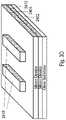
- FIGS. 5A-5Cillustrate an embodiment of this invention, where a microdisplay is constructed using stacked RGB LEDs and control circuits are connected to each pixel with solder bumps.
- This processcould include several steps that occur in a sequence from Step (A) to Step (C). Many of these steps share common characteristics, features, modes of operation, etc.
- identical reference numbersare used in different drawing figures, they are used to indicate analogous, similar or identical structures to enhance the understanding of the present invention by clarifying the relationships between the structures and embodiments presented in the various diagrams—particularly in relating analogous, similar or identical functionality to different physical structures.
- Step (A)is illustrated in FIG. 5A .
- the structure shown in FIG. 5Ais constructed.
- Various elements of FIG. 5Aare as follows:
- FIGS. 6A-6Dillustrate an embodiment of this invention, where a microdisplay is constructed using stacked RGB LEDs and control circuits are integrated with the RGB LED stack.
- This processcould include several steps that occur in a sequence from Step (A) to Step (D). Many of these steps share common characteristics, features, modes of operation, etc.
- identical reference numbersare used in different drawing figures, they are used to indicate analogous, similar or identical structures to enhance the understanding of the present invention by clarifying the relationships between the structures and embodiments presented in the various diagrams—particularly in relating analogous, similar or identical functionality to different physical structures.
- Step (A)is illustrated in FIG. 6A .
- the structure shown in FIG. 6Ais constructed.
- 2746a glass substrate
- 2744an oxide layer
- 2734an oxide layer
- 2733a an optional reflector (e.g., a Distributed Bragg Reflector or some other type of reflector)
- 2732a P-type confinement layer that is used for a Blue LED
- 2730a buffer layer that is typically used for a Blue LED
- 2728a multiple quantum well used for a Blue LED
- 2727a N-type confinement layer that is used for a Blue LED
- 2748an oxide layer
- 2722an oxide layer
- Step (B)is illustrated in FIG. 6B .
- Via holes 2762are etched to the substrate layer 2746 to isolate different pixels in the microdisplay/display.
- via holes 2760are etched to make contacts to various layers of the stack. These via holes may be preferably filled with a compatible oxide and the surface can be planarized with CMP.
- Various elements of FIG. 6Bsuch as 2746 , 2744 , 2734 , 2733 , 2732 , 2730 , 2728 , 2727 , 2748 , 2722 , 2721 , 2720 , 2718 , 2716 , 2715 , 2752 , 2710 , 2709 , 2708 , 2706 , 2704 , 2756 and 2758 have been described previously.
- Step (C)is illustrated in FIG. 6C .
- Metal 2764(for example) is constructed within the via holes 2760 using procedures similar to those described in respect to FIGS. 4A-4S of parent U.S. patent application Ser. No. 13/274,161 issued as U.S. Pat. No. 9,197,804, incorporated herein by reference. Following this construction, an oxide layer 2766 is deposited. Various elements of FIG.
- Step (D)is illustrated in FIG. 6D .
- a single crystal silicon transistor layer 2768can be monolithically integrated using ion-cut technology atop the structure shown in FIG. 6C .
- This transistor layer 2768is connected to various contacts of the stacked LED layers (not shown in the figure for simplicity).
- nickel layer 2770is constructed and solder layer 2772 is constructed.
- the packaging processthen is conducted where the structure shown in FIG. 6D is connected to a silicon sub-mount. It can be seen that the structure shown in FIG. 6D can have each pixel emit a certain color of light by tuning the voltage given to the red, green and blue layers within each pixel.
- This microdisplayis constructed using the ion-cut technology, a smart layer transfer technique.
- FIGS. 5-6may enable novel implementations of “smart-lighting concepts” (also known as visible light communications) that are described in “Switching LEDs on and off to enlighten wireless communications”, EETimes, June 2010 by R. Colin Johnson.
- LED lightscould be turned on and off faster than the eye can react, so signaling or communication of information with these LED lights is possible.
- An embodiment of this inventioninvolves designing the displays/microdisplays described in FIGS. 5-6 to transmit information, by modulating wavelength of each pixel and frequency of switching each pixel on or off.
- Optical interconnects in inter-chip communicationhave become a feasible replacement for electrical interconnects as the line capacitance of the latter has imposed increasingly difficult limitations due to scaling. As electrical component density increases, optical lines can carry more information between electrical components.
- An optical interconnect systemmay consist of several components. The first is a transmission component that generates and modulates the light that is used to send the information. The second is a network of waveguides that guides the light to the receiving destination on the chip. Finally, there is the receiver network, which converts the light back to electrical signals so that the information can be processed by the electronic devices on the chip.
- the transmission componentis typically built out of lasers and modulators.
- Lasersare built typically using III-V semiconductors like GaAs, InP, and InGaAs which have superior optical mechanisms compared to Group IV semiconductors such as silicon or germanium.
- III-V materialssuch as silicon or germanium.
- the drawback with these III-V materialsis that their processing is not compatible with the Group IV materials used for the electronic components of the chip.
- the laseris placed off-chip, which additionally offers the advantage of insulating the laser operation from the temperature variations and power limits of the chip itself.
- Another optionis to use a layer of LEDs in a monolithic 3D configuration as the light sources for the data transmission. The advantage of this option is that LEDs are cheaper than lasers and are easier to modulate directly.
- LEDspresent some limitations as to the data transmission efficiency through the waveguides since, unlike the generated light from lasers, the generated light from LEDs are not coherent or collimated, and, hence, waveguide loss is significant.
- Waveguidesare passive optical components designed to confine light in one direction. Typically they are made out of Silicon, Silicon Dioxide, and Silicon Nitride, which are materials already being used for the electronic components in conventional chips, and thus are materially compatible and can be grown or deposited on top of these layers. So in Silicon-based chips, such dielectric waveguides are usually used, in which a material with high permittivity corresponding to a high index of refraction, is surrounded by a material with lower permittivity corresponding to a lower index of refraction. The structure then guides optical waves by total internal reflection. For example, Silicon may be used for the high permittivity material and Silicon dioxide for the low permittivity material. Another type of waveguides use photonic crystal structures, which again can be constructed using Silicon and Silicon dioxide.
- dielectric waveguidesare not able to contain light where sharp turns are required because of the limits imposed on light refraction between two materials by the critical angle, and light leakage may result. So they may be suitable for chip-to-chip optical communications where most waveguides only need to be mostly straight and here the significant distance between the two chips may allow for gradual turns if needed.
- HMWGhollow metal waveguides
- HMWG'sallow light to be reflected around sharp corners, which may be a potential advantage as described in Mathai, S., et al., US Patent Application 2009/0244716A1.
- HMWG'smay be used to enable the sharp turns required for the light signals.
- the receiving componentmay include an array of photodetectors, typically made from Ge or SiGe. These photodetectors may have a p-n or p-i-n structure and may be biased to capture photons and subsequently convert them into electronic carriers.
- Layer transfer technologymay be utilized for constructing the layers for an optical interconnect system.
- the transmission componentmay consist of a layer of light-emitting diodes (LEDs) physically coupled with a layer of control circuits to manage the triggering of the LEDs so as to control the light being transmitted to enable data communication.
- the lightmay then be sent through a layer of waveguides which may distribute the light to their respective destinations on the chip, which may then be received by a layer of photo-detectors and converted to electrical signals by the readout circuits that can be handled by the electronic components of the chip.
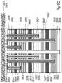
- FIGS. 7A-7Hillustrate an embodiment of the invention, where the transmitter block: LED control circuit layer 3142 , LED layer 3148 ; communication channel: waveguide layer 3136 ; and receiver block: photo-detector layer 3110 , and readout circuit layer 3100 may be stacked monolithically with layer transfer.
- the process of forming the optical communication systemmay include several steps that occur in a sequence from Step A to Step H. Many of these steps share common characteristics, features, modes of operation, etc.
- identical reference numbersare used in different drawing figures, they are used to indicate analogous, similar or identical structures to enhance the understanding of the present invention by clarifying the relationships between the structures and embodiments presented in the various diagrams—particularly in relating analogous, similar or identical functionality to different physical structures.
- FIG. 7Aillustrates the first step for constructing the photo-detector layer 3110 and readout circuit layer 3100 , where the photo-detector layer 3110 may be formed atop the read-out circuit layer 3100 using layer transfer.
- FIG. 7Aillustrates a cross-sectional view of silicon wafer substrate with pre-processed read-out circuits 3102 , above which an oxide layer 3104 may be deposited. Thus readout circuit layer 3100 is formed.
- FIG. 7Afurther illustrates the cross-sectional view of another Silicon wafer 3112 which may have a p+ Silicon layer 3114 , a p Silicon layer 3116 , a n Silicon layer 3118 , a n+ Silicon layer 3120 , and an oxide layer 3122 .
- These layersmay be formed using procedures similar to those described in FIG. 15A-15G of incorporated parent U.S. Pat. No. 9,197,804.
- An annealmay then be performed to activate dopants in various layers.
- Hydrogenmay be implanted in the wafer at a certain depth depicted by dashed line 3190 .
- FIG. 7Billustrates the photo-detector and readout circuit structure 3192 formed by an ion-cut layer transfer process.
- the photo-detector layer 3110 of p+pnn+ silicon consisting of the photo-detector diodesmay be layer transferred atop the silicon wafer with readout circuit layer 3100 wherein oxide layer 3104 may be bonded to oxide layer 3122 , and p+ silicon layer 3115 may be a result of the cleave and polish operations.
- Procedures for layer transfer and alignment for forming the structure in FIG. 31Bare similar to procedures used for constructing the image sensor shown in FIGS. 15A-15G of incorporated parent U.S. Pat. No. 9,197,804.
- Step (C)is illustrated in FIG. 7C .
- An oxide layer 3124may be deposited on top of p+ silicon layer 3115 . Connections may be made to the terminals of the photo-detector by lithographic, etch, and fill operations similar to those described in FIGS. 15A-15G of incorporated parent U.S. Pat. No. 9,197,804, and are indicated as p+ contact 3126 and n+ contact 3128 .
- Various elements of FIG. 7Csuch as 3102 , 3104 , 3115 , 3116 , 3118 , 3120 , and 3122 have been described previously herein or in incorporated parent U.S. Pat. No. 9,197,804.
- Contacts 3130 and interconnects (not shown) for connecting terminals of the photo-detector, such as p+ contact 3124 and p+ contact 3128 , to read-out circuits in silicon wafer substrate with pre-processed read-out circuits 3102may be done.
- silicon wafer containing the photo-detectors and read-out circuits 3131may be formed. The functionality of the photo-detectors may be tested at this point.
- FIGS. 15A-15G of incorporated parent U.S. Pat. No. 9,197,804illustrate a process whereby oxide vias constructed before layer transfer may be used to look through photo-detector layers to observe alignment marks on the read-out circuit wafer below it.
- an alternative embodiment of this inventionmay involve constructing oxide vias after layer transfer. Essentially, after layer transfer of structures without oxide vias, oxide vias whose diameters are larger than the maximum misalignment of the bonding/alignment scheme may be formed. This order of sequences may enable observation of alignment marks on the bottom read-out circuit wafer by looking through the photo-detector wafer.
- Waveguidesare structures designed to confine light in one direction.
- dielectric waveguidesare usually used, in which a material with high permittivity corresponding to a high index of refraction, is surrounded by a material with lower permittivity corresponding to a lower index of refraction.
- the structureguides optical waves by total internal reflection.
- convenient materialsare Silicon for the high permittivity material and Silicon dioxide for the low permittivity material.
- Another type of waveguidesuse photonic crystal structures, which again can be constructed using Silicon and Silicon dioxide. In most cases, masks and etching are used to construct the structures.
- Yet another type of waveguidesmay be called hollow metal waveguides (HMWG), made of trenches in the material with walls coated with reflective metals which may include silver. In combination with beam-splitters, HMWG's allow light to be reflected around sharp corners, which may be a potential advantage.
- HMWGhollow metal waveguides
- Step (D)is illustrated in FIG. 7D .
- Silicon waveguides 3136may be formed on the SOI wafer 3132 and BOX 3134 by electron beam lithography followed by electron cyclotron resonance plasma etching. The wafer may then be coated with Silicon Dioxide 3138 to form the over-cladding. It will be obvious to one skilled in the art that many configurations and material combinations are being currently used and/or possible in the formation of the waveguides. This invention is not limited to one particular configuration or set of materials. Hydrogen may be implanted in the wafer at a certain depth depicted by 3140 . Thus, Silicon/Silicon Dioxide waveguide layer 3139 may be formed.
- Step (E)is illustrated in FIG. 7E .
- the Silicon/Silicon Dioxide waveguide layer 3139may then be ion-cut layer transferred atop the silicon wafer containing the photo-detectors and read-out circuits 3131 .
- Procedures for layer transfer and alignment for forming the structure 3141 in FIG. 7Eare similar to procedures used previously herein and/or in incorporated parent U.S. Pat. No.
- Silicon/Silicon Dioxide waveguide layer 3139may be flipped and bonded atop silicon wafer containing the photo-detectors and read-out circuits 3131 using oxide-oxide bonding and the Silicon substrate 3132 may then be cleaved and polished until the oxide layer 3134 , now labeled 3135 after the cleave and polish process, is reached.
- Step (F)is shown in FIG. 7F which is used for constructing the LED and control circuit layers, where the Red LED layer from Red LED wafer 3148 may be formed atop the electronic control circuit layer 3142 using ion-cut layer transfer. Silicon wafer with control circuits 3144 may be conventionally constructed, above which an oxide layer 3146 may be deposited. Red LED wafer 3148 may include GaAs wafer 3150 , n-type confinement layer 3152 , multiple quantum well (MQW) layer 3154 , P-type confinement layer 3156 , and an ITO current spreader layer 3158 .
- MQWmultiple quantum well
- Examples of materials used to construct these layersmay include, but are not limited to; doped AlInGaP for the n-type confinement layer 3152 and p-type confinement layer 3156 , multiple quantum well layer 3154 could be composed of AlInGaP and GaInP. These layers may be formed by processes such as molecular beam epitaxy, MOCVD, etc.
- the red LED wafer described in FIG. 7Fmay have hydrogen implanted into it at a certain depth as shown by dotted line 3160 . Alternatively, helium can be implanted.
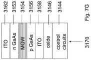
- Step (G)is shown in FIG. 7G .
- the layer of GaAs structures consisting of the red LEDs 3148may be layer transferred atop the silicon wafer with the control circuits 3142 forming the LED stack 3170 .
- Procedures for layer transfer and alignment for forming the structure in FIG. 7Gmay be similar to procedures used for constructing the LED lighting shown in FIGS. 12A-12F of incorporated parent U.S. Pat. No. 9,197,804.
- n-GaAs layer 3152is renamed 3153 after the cleaving and polishing process.
- An ITO layer 3162is deposited atop n-GaAs layer 3153 , thus forming the LED stack 3170 .
- the functionality of the LEDsmay be tested at this point.
- Step (H)is illustrated by FIG. 7H .
- the structure shown in FIG. 31G , LED stack 3170may be flipped and bonded atop the structure shown in FIG. 7E , structure 3141 , using oxide-to-oxide bonding of ITO layer 3162 and oxide layer 3135 .
- Various elements in FIG. 7Hsuch as 3102 , 3104 , 3115 , 3116 , 3118 , 3120 , 3122 , 3124 , 3135 , 3136 , 3138 , 3144 , 3146 , 3153 , 3154 , 3156 , 3158 and 3162 have been described previously herein and/or in incorporated parent U.S. Pat. No. 9,197,804.
- LED-driven chip-to-chip optical interconnect 3199may be formed.
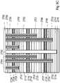
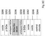
- FIGS. 8A-8Dillustrate an embodiment of this invention, where the transmitter block: modulator control circuit layer 3242 , modulator layer 3248 ; communication channel: waveguide layer 3236 ; and receiver block: photodetector layer 3210 , and readout circuit layer 3200 are stacked monolithically with layer transfer.
- FIG. 8Aillustrates the first step for constructing the waveguide layer 3236 , photodetector layer 3210 , readout circuit layer 3200 , where the waveguide layer 3236 with oxide layer 3234 , oxide layer 3228 , oxide layer 3221 oxide layer 3222 and oxide layer 3204 may be formed atop the photodetector layer 3210 , which in turn may be formed atop the readout circuit layer 3200 using layer transfer procedures described in FIG. 7A-7E .
- Step (B)is shown in FIG. 8B which is used for constructing the modulator and control circuit layers, where the modulator layer is formed atop the electronic control circuit layer using layer transfer.
- 3242shows a cross-sectional view of 3244 , a silicon wafer with control circuits constructed on it, above which an oxide layer 3246 is deposited.
- a Silicon wafer 3250 containing Silicon-Germanium modulatorsmay include a P-type Silicon-Germanium buffer layer 3252 , an undoped Silicon-Germanium spacer 3254 , a Germanium/Silicon-Germanium multiple quantum well (MQW) 3256 , another undoped Silicon-Germanium spacer 3258 , an N-type Silicon-Germanium layer 3260 , and a deposited oxide layer 3262 .
- Examples of materials used to construct these layersinclude, but are not limited to, doped GaAs for the N-type cap layer 3260 and P-type buffer layer 3252 , the multiple quantum well layer 3256 could be of GaAs and AlGaAs.
- a double heterostructure configuration or single quantum well configurationcould be used instead of a multiple quantum well configuration.
- Various other material types and configurationscould be used for constructing the modulators for this process.
- the modulator wafer described in FIG. 8Bhas hydrogen implanted into it at a certain depth.
- the dotted line 3264depicts the hydrogen implant.
- heliumcan be implanted.
- Step (C)is shown in FIG. 8C .
- the layer of SiGe structures consisting of the modulators 3248is layer transferred atop the silicon wafer with the control circuits 3242 .
- Procedures for layer transfer and alignment for forming the structure in FIG. 8Care similar to procedures used for constructing the photo-detectors shown in FIGS. 15A-G of incorporated parent U.S. Pat. No. 9,197,804. The functionality of the modulators can be tested at this point.
- Step (D)is illustrated by FIG. 8D .
- the structure shown in FIG. 8Cis flipped and bonded atop the structure shown in FIG. 8A using oxide-to-oxide bonding of layers 3266 and 3234 .
- Various elements in FIG. 32Dsuch as 3202 , 3204 , 3214 , 3216 , 3218 , 3220 , 3222 , 3234 , 3236 , 3238 , 3244 , 3246 , 3252 , 3254 , 3256 , 3258 , 3260 , 3262 and 3266 have been described previously herein and/or within incorporated parent U.S. Pat. No. 9,197,804.
- An external laser 3268(typically made of InP) is then coupled to the structure via an optical fiber 3270 by known techniques.
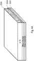
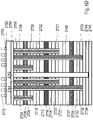
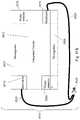
- FIGS. 9A-9Cillustrate an embodiment of this invention, where the LED-driven optical communication is among sections on a single chip.
- FIG. 9Aillustrates a cross-sectional view of a transmitter section 3350 and a receiver section 3360 .
- the transmitter section 3350may include LED control circuit layer 3352 , LED layer 3354 and waveguide layer 3356 stacked monolithically with layer transfer.
- the receiver section 3360may contain readout circuit layer 3362 , photo-detector layer 3364 and waveguide layer 3166 stacked monolithically with layer transfer. Layer transfer procedures are similar to those described in FIGS. 7A-7H herein.
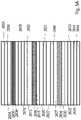
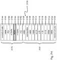
- FIG. 9Billustrates an exemplary top view of integrated circuit chip 3310 which may include integrated circuits 3312 , optical transmitters using LEDs 3314 and 3316 , optical receivers using photo-detectors 3318 and 3320 , and waveguide sections 3322 and 3324 enabling optical communication from one end of the chip to the other.
- FIG. 9Cillustrates a cross-sectional view (not to scale) of an integrated circuit chip 3330 with a substrate 3332 , control and readout circuit sections 3338 and 3340 , integrated circuit section 3334 , LED and photo-detector layer 3336 , and waveguide layer 3342 .
- each layermay use the same material throughout the layer for ease of processing, but may differ among different layers.
- the waveguide layer 3342may use Silicon
- the LED and photo-detector layer 3336may use III-V semiconductor material
- the layer with control and readout circuit sections 3338 and 3340 and integrated circuits section 3334may use Silicon
- the substrate 3332may use silicon.
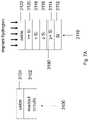
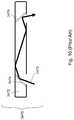
- FIG. 10illustrates cross-sectional view of a waveguide structure 3470 with Hollow-metal waveguide (HMWG) 3472 , beam-splitters 3474 and 3476 and light signal 3478 .
- HMWG with reflective metal coating and beam-splittersare capable of guiding light through sharp turns by allowing sharp-angled reflections which may be a potential advantage compared to dielectric waveguides when waveguide layer thickness is in consideration.
- FIGS. 11A-11Cillustrate an embodiment of this invention, where the laser-driven optical communication is among sections on a single chip.
- FIG. 11Aillustrates a cross-sectional view of a transmitter section 3550 and a receiver section 3560 .
- the transmitter section 3550may include modulator control circuit layer 3552 , modulator layer 3554 and waveguide layer 3556 stacked monolithically with layer transfer, external laser 3558 , fiber-optic coupling 3559 (connecting external laser 3559 to modulator layer 3554 ).
- the receiver section 3560may contain a readout circuit layer 3562 , photo-detector layer 3564 and waveguide layer 3566 stacked monolithically with layer transfer. Layer transfer procedures are similar to those described in FIG. 8A-8D herein.
- FIG. 11Billustrates an exemplary top view of integrated circuit chip 3510 which may include integrated circuits 3512 , optical transmitters using external laser 3526 , fiber-optic couplings 3528 and 3529 , modulators 3514 and 3516 , optical receivers using photo-detectors 3518 and 3520 , and waveguide sections 3522 and 3524 enabling optical communication from one end of the chip to the other.
- integrated circuit chip 3510may include integrated circuits 3512 , optical transmitters using external laser 3526 , fiber-optic couplings 3528 and 3529 , modulators 3514 and 3516 , optical receivers using photo-detectors 3518 and 3520 , and waveguide sections 3522 and 3524 enabling optical communication from one end of the chip to the other.
- FIG. 11Cillustrates a cross-sectional view (not to scale) of an integrated circuit chip 3530 with substrate 3532 , control and readout circuit sections 3538 and 3540 , integrated circuit section 3534 , modulator and photo-detector layer 3536 , waveguide layer 3542 , external laser 3544 and fiber-optic coupling 3546 .
- each layermay use the same material throughout the layer for ease of processing, but may differ among different layers.
- the waveguide layer 3542may use Silicon
- the modulator and photo-detector layer 3536may use III-V semiconductor material
- the layer with control and readout circuit sections 3538 and 3540 and integrated circuits section 3534may use Silicon
- the substrate 3532may use silicon.
- the waveguide layermay use HMWGs with reflective metal coating and beam-splitters capable of guiding light through sharp turns by allowing sharp-angled reflections which may be a potential advantage compared to dielectric waveguides when waveguide layer thickness is in consideration.
- Germanium or Silicon-Germaniumcould be utilized.
- the advantage of Germaniumis that it is sensitive to infra-red wavelengths as well.
- Germaniumalso suffers from high dark current.
- the photo-detector layer 3110is denoted as a p-n junction layer; however, any type of photo-detector layer, such as a p-i-n layer or some other type of photo-detector can be used.
- the thickness of the photo-detector layermay be typically less than approximately 5 ⁇ m, but may also be greater.
- a double hetero-structure configuration or single quantum well configurationcould be used instead of a multiple quantum well configuration such as the shown multiple quantum well layer 3154 .
- various other material types and configurationssuch as GaAs, AlInGaP, and GaInP, could be used for constructing the red LEDs for this process.
Landscapes
- Engineering & Computer Science (AREA)
- Power Engineering (AREA)
- Microelectronics & Electronic Packaging (AREA)
- Physics & Mathematics (AREA)
- Condensed Matter Physics & Semiconductors (AREA)
- General Physics & Mathematics (AREA)
- Computer Hardware Design (AREA)
- Metal-Oxide And Bipolar Metal-Oxide Semiconductor Integrated Circuits (AREA)
Abstract
Description
This application is a continuation-in-part of U.S. patent application Ser. No. 17/492,627 filed on Oct. 3, 2021, now U.S. Pat. No. 11,327,227 issued on May 10, 2022; which is a continuation-in-part of U.S. patent application Ser. No. 17/330,186 filed on May 5, 2021, now U.S. Pat. No. 11,163,112 issued on Nov. 2, 2021; which is a continuation-in-part of U.S. patent application Ser. No. 17/189,201 filed on Mar. 1, 2021, now U.S. Pat. No. 11,063,071 issued on Jul. 13, 2021; which is a continuation-in-part of U.S. patent application Ser. No. 17/121,726 filed on Dec. 14, 2020, now U.S. Pat. No. 10,978,501 issued on Apr. 13, 2021; which is a continuation-in-part of U.S. patent application Ser. No. 17/027,217 filed on Sep. 21, 2020, now U.S. Pat. No. 10,943,934 issued on Mar. 9, 2021; which is a continuation-in-part of U.S. patent application Ser. No. 16/860,027 filed on Apr. 27, 2020, now U.S. Pat. No. 10,833,108 issued on Nov. 11, 2020; which is a continuation-in-part of U.S. patent application Ser. No. 15/920,499 filed on Mar. 14, 2018, now U.S. Pat. No. 10,679,977 issued on Jun. 9, 2020; which is a continuation-in-part of U.S. patent application Ser. No. 14/936,657 filed on Nov. 9, 2015, now U.S. Pat. No. 9,941,319 issued on Apr. 10, 2018; which is a continuation-in-part of U.S. patent application Ser. No. 13/274,161 filed on Oct. 14, 2011, now U.S. Pat. No. 9,197,804 issued on Nov. 24, 2015; and this application is a continuation-in-part of U.S. patent application Ser. No. 12/904,103 filed on Oct. 13, 2010, now U.S. Pat. No. 8,163,581 issued on Apr. 24, 2012; the entire contents of all of the preceding are incorporated herein by reference.
This invention describes applications of monolithic 3D integration to various disciplines, including but not limited to, for example, light-emitting diodes, displays, image-sensors and solar cells.
Semiconductor and optoelectronic devices often require thin monocrystalline (or single-crystal) films deposited on a certain wafer. To enable this deposition, many techniques, generally referred to as layer transfer technologies, have been developed. These include:
- Ion-cut, variations of which are referred to as smart-cut, nano-cleave and smart-cleave: Further information on ion-cut technology is given in “Frontiers of silicon-on-insulator,” J. Appl. Phys. 93, 4955-4978 (2003) by G. K. Celler and S. Cristolovean (“Celler”) and also in “Mechanically induced Si layer transfer in hydrogen-implanted Si wafers,” Appl. Phys. Lett., vol. 76, pp. 2370-2372, 2000 by K. Henttinen, I. Suni, and S. S. Lau (“Hentinnen”).
- Porous silicon approaches such as ELTRAN: These are described in “Eltran, Novel SOI Wafer Technology”, JSAP International, Number 4, July 2001 by T. Yonehara and K. Sakaguchi (“Yonehara”).
- Lift-off with a temporary substrate, also referred to as epitaxial lift-off: This is described in “Epitaxial lift-off and its applications”, 1993 Semicond. Sci. Technol. 8 1124 by P. Demeester, et al (“Demeester”).
- Bonding a substrate with single crystal layers followed by Polishing, Time-controlled etch-back or Etch-stop layer controlled etch-back to thin the bonded substrate: These are described in U.S. Pat. No. 6,806,171 by A. Ulyashin and A. Usenko (“Ulyashin”) and “Enabling SOI-Based Assembly Technology for Three-Dimensional (3D) Integrated Circuits (ICs),” IEDM Tech. Digest, p. 363 (2005) by A. W. Topol, D. C. La Tulipe, L. Shi, S. M. Alam, D. J. Frank, S. E. Steen, J. Vichiconti, D. Posillico, M. Cobb, S. Medd, J. Patel, S. Goma, D. DiMilia, M. T. Robson, E. Duch, M. Farinelli, C. Wang, R. A. Conti, D. M. Canaperi, L. Deligianni, A. Kumar, K. T. Kwietniak, C. D'Emic, J. Ott, A. M. Young, K. W. Guarini, and M. Ieong (“Topol”).
- Bonding a wafer with a Gallium Nitride film epitaxially grown on a sapphire substrate followed by laser lift-off for removing the transparent sapphire substrate: This method may be suitable for deposition of Gallium Nitride thin films, and is described in U.S. Pat. No. 6,071,795 by Nathan W. Cheung, Timothy D. Sands and William S. Wong (“Cheung”).
- Rubber stamp layer transfer: This is described in “Solar cells sliced and diced”, 19 May 2010, Nature News.
With novel applications of these methods and recognition of their individual strengths and weaknesses, one can significantly enhance today's light-emitting diode (LED), display, image-sensor and solar cell technologies.
Background on LEDs
Light emitting diodes (LEDs) are used in many applications, including automotive lighting, incandescent bulb replacements, and as backlights for displays. Red LEDs are typically made on Gallium Arsenide (GaAs) substrates, and include quantum wells constructed of various materials such as AlInGaP and GaInP. Blue and green LEDs are typically made on Sapphire or Silicon Carbide (SiC) or bulk Gallium Nitride (GaN) substrates, and include quantum wells constructed of various materials such as GaN and InGaN.
A white LED for lighting and display applications can be constructed by either using a blue LED coated with phosphor (called phosphor-coated LED or pcLED) or by combining light from red, blue, and green LEDs (called RGB LED). RGB LEDs are typically constructed by placing red, blue, and green LEDs side-by-side. While RGB LEDs are more energy-efficient than pcLEDs, they are less efficient in mixing red, blue and green colors to form white light. They also are much more costly than pcLEDs. To tackle issues with RGB LEDs, several proposals have been made.
One RGB LED proposal from Hong Kong University is described in “Design of vertically stacked polychromatic light emitting diodes”, Optics Express, June 2009 by K. Hui, X. Wang, et al (“Hui”). It involves stacking red, blue, and green LEDs on top of each other after individually packaging each of these LEDs. While this solves light mixing problems, this RGB-LED is still much more costly than a pcLED solution since three LEDs for red, blue, and green color need to be packaged. A pcLED, on the other hand, requires just one LED to be packaged and coated with phosphor.
Another RGB LED proposal from Nichia Corporation is described in “Phosphor Free High-Luminous-Efficiency White Light-Emitting Diodes Composed of InGaN Multi-Quantum Well”, Japanese Journal of Applied Physics, 2002 by M. Yamada, Y. Narukawa, et al. (“Yamada”). It involves constructing and stacking red, blue and green LEDs of GaN-based materials on a sapphire or SiC substrate. However, red LEDs are not efficient when constructed with GaN-based material systems, and that hampers usefulness of this implementation. It is not possible to deposit defect-free AlInGaP/InGaP for red LEDs on the same substrate as GaN based blue and green LEDs, due to a mismatch in thermal expansion co-efficient between the various material systems.
Yet another RGB-LED proposal is described in “Cascade Single chip phosphor-free while light emitting diodes”, Applied Physics Letters, 2008 by X. Guo, G. Shen, et al. (“Guo”). It involves bonding GaAs based red LEDs with GaN based blue-green LEDs to produce white light. Unfortunately, this bonding process requires 600° C. temperatures, causing issues with mismatch of thermal expansion co-efficients and cracking. Another publication on this topic is “A trichromatic phosphor-free white light-emitting diode by using adhesive bonding scheme”, Proc. SPIE, Vol. 7635, 2009 by D. Chuai, X. Guo, et al. (“Chuai”). It involves bonding red LEDs with green-blue LED stacks. Bonding is done at the die level after dicing, which is more costly than a wafer-based approach.
U.S. patent application Ser. No. 12/130,824 describes various stacked RGB LED devices. It also briefly mentions a method for construction of a stacked LED where all layers of the stacked LED are transferred using lift-off with a temporary carrier and Indium Tin Oxide (ITO) to semiconductor bonding. This method has several issues for constructing a RGB LED stack. First, it is difficult to manufacture a lift-off with a temporary carrier of red LEDs for producing a RGB LED stack, especially for substrates larger than 2 inch. This is because red LEDs are typically constructed on non-transparent GaAs substrates, and lift-off with a temporary carrier is done by using an epitaxial lift-off process. Here, the thin film to be transferred typically sits atop a “release-layer” (eg. AlAs), this release layer is removed by etch procedures after the thin film is attached to a temporary substrate. Scaling this process to 4 inch wafers and bigger is difficult. Second, it is very difficult to perform the bonding of ITO to semiconductor materials of a LED layer at reasonable temperatures, as described in the patent application Ser. No. 12/130,824.
It is therefore clear that a better method for constructing RGB LEDs will be helpful. Since RGB LEDs are significantly more efficient than pcLEDs, they can be used as replacements of today's phosphor-based LEDs for many applications, provided a cheap and effective method of constructing RGB LEDs can be invented.
Background on Image-sensors:
Image sensors are used in applications such as cameras. Red, blue, and green components of the incident light are sensed and stored in digital format. CMOS image sensors typically contain a photodetector and sensing circuitry. Almost all image sensors today have both the photodetector and sensing circuitry on the same chip. Since the area consumed by the sensing circuits is high, the photodetector cannot see the entire incident light, and image capture is not as efficient.
To tackle this problem, several researchers have proposed building the photodetectors and the sensing circuitry on separate chips and stacking them on top of each other. A publication that describes this method is “Megapixel CMOS image sensor fabricated in three-dimensional integrated circuit technology”, Intl. Solid State Circuits Conference 2005 by Suntharalingam, V., Berger, R., et al. (“Suntharalingam”). These proposals use through-silicon via (TSV) technology where alignment is done in conjunction with bonding. However, pixel size is reaching the 1 μm range, and successfully processing TSVs in the 1 μm range or below is very difficult. This is due to alignment issues while bonding. For example, the International Technology Roadmap for Semiconductors (ITRS) suggests that the 2-4 μm TSV pitch will be the industry standard until 2012. A 2-4 μm pitch TSV will be too big for a sub-1 μm pixel. Therefore, novel techniques of stacking photodetectors and sensing circuitry are required.
A possible solution to this problem is given in “Setting up 3D Sequential Integration for Back-Illuminated CMOS Image Sensors with Highly Miniaturized Pixels with Low Temperature Fully-depleted SOI Transistors,” IEDM, p. 1-4 (2008) by P. Coudrain et al. (“Coudrain”). In the publication, transistors are monolithically integrated on top of photodetectors. Unfortunately, transistor process temperatures reach 600° C. or more. This is not ideal for transistors (that require a higher thermal budget) and photodetectors (that may prefer a lower thermal budget).
Background on Displays:
Liquid Crystal Displays (LCDs) can be classified into two types based on manufacturing technology utilized: (1) Large-size displays that are made of amorphous/polycrystalline silicon thin-film-transistors (TFTs), and (2) Microdisplays that utilize single-crystal silicon transistors. Microdisplays are typically used where very high resolution is needed, such as camera/camcorder view-finders, projectors and wearable computers.
Microdisplays are made in semiconductor fabs with 200 mm or 300 mm wafers. They are typically constructed with LCOS (Liquid-Crystal-on-Silicon) Technology and are reflective in nature. An exception to this trend of reflective microdisplays is technology from Kopin Corporation (U.S. Pat. No. 5,317,236, filed December 1991). This company utilizes transmittive displays with a lift-off layer transfer scheme. Transmittive displays may be generally preferred for various applications.
While lift-off layer transfer schemes are viable for transmittive displays, they are frequently not used for semiconductor manufacturing due to yield issues. Therefore, other layer transfer schemes will be helpful. However, it is not easy to utilize other layer transfer schemes for making transistors in microdisplays. For example, application of “smart-cut” layer transfer to attach monocrystalline silicon transistors to glass is described in “Integration of Single Crystal Si TFTs and Circuits on a Large Glass Substrate”, IEDM 2009 by Y. Takafuji, Y. Fukushima, K. Tomiyasu, et al. (“Takafuji”). Unfortunately, hydrogen is implanted through the gate oxide of transferred transistors in the process, and this degrades performance. Process temperatures are as high as 600° C. in this paper, and this requires costly glass substrates. Several challenges therefore need to be overcome for efficient layer transfer, and require innovation.
Background on Solar Cells:
Solar cells can be constructed of several materials such as, for example, silicon and compound semiconductors. The highest efficiency solar cells are typically multi-junction solar cells that are constructed of compound semiconductor materials. These multi-junction solar cells are typically constructed on a germanium substrate, and semiconductors with various band-gaps are epitaxially grown atop this substrate to capture different portions of the solar spectrum.
There are a few issues with standard multi-junction solar cells. Since multiple junctions are grown epitaxially above a single substrate (such as Germanium) at high temperature, materials used for different junctions are restricted to those that have lattice constants and thermal expansion co-efficients close to those of the substrate. Therefore, the choice of materials used to build junctions for multi-junction solar cells is limited. As a result, most multi-junction solar cells commercially available today cannot capture the full solar spectrum. Efficiency of the solar cell can be improved if a large band of the solar spectrum is captured. Furthermore, multi-junction solar cells today suffer from high cost of the substrate above which multiple junctions are epitaxially grown. Methods to build multi-junction solar cells that tackle both these issues will be helpful.
A method of making multi-junction solar cells by mechanically bonding two solar cells, one with a Germanium junction and another with a compound semiconductor junction is described in “Towards highly efficient 4-terminal mechanical photovoltaic stacks”, III-Vs Review, Volume 19, Issue 7, September-October 2006 by Giovanni Flamand, Jef Poortmans (“Flamand”). In this work, the authors make the compound semiconductor junctions on a Germanium substrate epitaxially. They then etch away the entire Germanium substrate after bonding to the other substrate with the Germanium junction. The process uses two Germanium substrates, and is therefore expensive.
Techniques to create multi-junction solar cells with layer transfer have been described in “Wafer bonding and layer transfer processes for 4-junction high efficiency solar cells,”Photovoltaic Specialists Conference,2002. Conference Record of the Twenty-Ninth IEEE, vol., no., pp. 1039-1042, 19-24 May 2002 by Zahler, J. M.; Fontcuberta i Morral, A.; Chang-Geun Ahn; Atwater, H. A.; Wanlass, M. W.; Chu, C. and Iles, P. A. An anneal is used for ion-cut purposes, and this anneal is typically done at temperatures higher than 350-400° C. (if high bond strength is desired). When that happens, cracking and defects can be produced due to mismatch of co-efficients of thermal expansion between various layers in the stack. Furthermore, semiconductor layers are bonded together, and the quality of this bond not as good as oxide-to-oxide bonding, especially for lower process temperatures.
Background on CCD Sensors:
Image sensors based on Charge-Coupled Device (CCD) technology has been around for several decades. The CCD technology relies on a collect and shift scheme, wherein charges are collected in individual cells according to the luminosity of the light falling on each of them, then the charges are sequentially shifted towards one edge of the sensor where readout circuits read the sequence of charges one at a time.
The advantage of CCD technology is it has better light sensitivity since almost the entire CCD cell area is dedicated to light collecting, and the control and readout circuits are all on one edge not blocking the light. On the other hand, in a CMOS sensor, the photodiodes in each cell have to share space with the control and readout circuits adjacent to them, and so their size and light sensitivity are therefore limited.
The main issue with CCD technology is this sequential shifting of image information from cell to cell is slow and limits the speed and cell density of CCD image sensors. A potential solution is to put the readout circuits directly under each CCD cell, so that the information is read in parallel rather than in time sequence, thus removing the shifting delay entirely.
Background on High Dynamic Range (HDR) Sensors:
Ever since the advent of commercial digital photography in the 1990s, achieving High Dynamic Range (HDR) imaging has been a goal for most camera manufacturers in their image sensors. The idea is to use various techniques to compensate for the lower dynamic range of image sensors relative to the human eye. The concept of HDR however, is not new. Combining multiple exposures of a single image to achieve a wide range of luminosity was actually pioneered in the 1850s by Gustave Le Gray to render seascapes showing both the bright sky and the dark sea. This was necessary to produce realistic photographic images as the film used at that time had extremely low dynamic range compared to the human eye.
In digital cameras, the typical approach is to capture images using exposure bracketing, and then combining them into a single HDR image. The issue with this is that multiple exposures are performed over some period of time, and if there is movement of the camera or target during the time of the exposures, the final HDR image will reflect this by loss of sharpness. Moreover, multiple images may lead to large data in storage devices. Other methods use software algorithms to extract HDR information from a single exposure, but as they can only process information that is recordable by the sensor, there is a permanent loss of some details.
Over the past 40 years, there has been a dramatic increase in functionality and performance of Integrated Circuits (ICs). This has largely been due to the phenomenon of “scaling”; i.e., component sizes within ICs have been reduced (“scaled”) with every successive generation of technology. There are two main classes of components in Complementary Metal Oxide Semiconductor (CMOS) ICs, namely transistors and wires. With “scaling”, transistor performance and density typically improve and this has contributed to the previously-mentioned increases in IC performance and functionality. However, wires (interconnects) that connect together transistors degrade in performance with “scaling”. The situation today is that wires dominate the performance, functionality and power consumption of ICs.
3D stacking of semiconductor devices or chips is one avenue to tackle the wire issues. By arranging transistors in 3 dimensions instead of 2 dimensions (as was the case in the 1990s), the transistors in ICs can be placed closer to each other. This reduces wire lengths and keeps wiring delay low.
There are many techniques to construct 3D stacked integrated circuits or chips including:
Through-silicon via (TSV) technology: Multiple layers of transistors (with or without wiring levels) can be constructed separately. Following this, they can be bonded to each other and connected to each other with through-silicon vias (TSVs).
Monolithic 3D technology: With this approach, multiple layers of transistors and wires can be monolithically constructed. Some monolithic 3D and 3DIC approaches are described in U.S. Pat. Nos. 8,273,610, 8,298,875, 8,362,482, 8,378,715, 8,379,458, 8,450,804, 8,557,632, 8,574,929, 8,581,349, 8,642,416, 8,669,778, 8,674,470, 8,687,399, 8,742,476, 8,803,206, 8,836,073, 8,902,663, 8,994,404, 9,023,688, 9,029,173, 9,030,858, 9,117,749, 9,142,553, 9,219,005, 9,385,058, 9,406,670, 9,460,978, 9,509,313, 9,640,531, 9,691,760, 9,711,407, 9,721,927, 9,799,761, 9,871,034, 9,953,870, 9,953,994, 10,014,292, 10,014,318, 10,515,981, 10,892,016; and U.S. patent Application Publications and application Ser. Nos. 14/642,724, 15/150,395, 15/173,686, 16/337,665, 16/558,304, 16/649,660, 16/836,659, 17/151,867, 62/651,722; 62/681,249, 62/713,345, 62/770,751, 62/952,222, 62/824,288, 63/075,067, 63/091,307, 63/115,000, 63/220,443, 2021/0242189, 2020/0013791, Ser. No. 16/558,304; and PCT Applications (and Publications): PCT/US2010/052093, PCT/US2011/042071 (WO2012/015550), PCT/US2016/52726 (WO2017053329), PCT/US2017/052359 (WO2018/071143), PCT/US2018/016759 (WO2018144957), PCT/US2018/52332(WO 2019/060798), and PCT/US2021/44110. The entire contents of all of the foregoing patents, publications, and applications are incorporated herein by reference.
Electro-Optics: There is also work done for integrated monolithic 3D including layers of different crystals, such as U.S. Pat. Nos. 8,283,215, 8,163,581, 8,753,913, 8,823,122, 9,197,804, 9,419,031, 9,941,319, 10,679,977, 10,943,934, 10,998,374, 11,063,071, and 11,133,344. The entire contents of all of the foregoing patents, publications, and applications are incorporated herein by reference.
In addition, the entire contents of U.S. Pat. Nos. 8,273,610, 9,000,557, 8,753,913, 8,823,122, 9,419,031, 9,197,804, 9,941,319, 10,679,977, 10,833,108, 10,943,934, 10,978,501, 10,998,374, 11,063,071, 11,133,344, 11,163,112, 11,164,898, 11,315,965 and U.S. Patent Application Publication 2020/0194416, and U.S. patent application Ser. Nos. 17/402,527 and 17/492,627; all of the foregoing are incorporated herein by reference.
Techniques to utilize layer transfer schemes such as ion-cut to form novel light emitting diodes (LEDs), CMOS image sensors, displays, microdisplays and solar cells are discussed.
In one aspect, a multi-level semiconductor device, the device including: a first level including integrated circuits; a second level including an optical waveguide, where the second level is disposed above the first level, where the first level includes crystalline silicon; and an oxide layer disposed between the first level and the second level, where the second level is bonded to the oxide layer, and where the bonded includes oxide to oxide bonds.
In another aspect, a multi-level semiconductor device, the device including: a first level including an optical waveguide; a second level including integrated circuits, where the second level is disposed above the first level, where the first level includes crystalline silicon; and an oxide layer disposed between the first level and the second level, where the second level is bonded to the oxide layer, and where the bonded includes oxide to oxide bonds.
In another aspect, a multi-level semiconductor device, the device including: a first level including integrated circuits; a second level including a plurality of optical modulators, where the second level is disposed above the first level, where the first level includes crystalline silicon; and an oxide layer disposed between the first level and the second level, where the second level is bonded to the oxide layer, and where the bonded includes oxide to oxide bonds.
In another aspect, a multi-level semiconductor device, the device including: a first level including integrated circuits; a second level including an electromagnetic waveguide, where the second level is disposed above the first level, where the first level includes crystalline silicon; and an oxide layer disposed between the first level and the second level, where the second level is bonded to the oxide layer, and where the bonded includes oxide to oxide bonds.
In another aspect, a multi-level semiconductor device, the device including: a first level including an electromagnetic waveguide; a second level including integrated circuits, where the second level is disposed above the first level, where the first level includes crystalline silicon; and an oxide layer disposed between the first level and the second level, where the second level is bonded to the oxide layer, and where the bonded includes oxide to oxide bonds.
In another aspect, a multi-level semiconductor device, the device including: a first level including integrated circuits; a second level including a plurality of electromagnetic modulators, where the second level is disposed above the first level, where the first level includes crystalline silicon; and an oxide layer disposed between the first level and the second level, where the second level is bonded to the oxide layer, and where the bonded includes oxide to oxide bonds.
In another aspect, a multi-level semiconductor device, the device including: a first level including integrated circuits; a second level including a structure designed to conduct electromagnetic waves in a confined manner, where the second level is disposed above the first level, where the first level includes crystalline silicon, where the second level includes crystalline silicon; and an oxide layer disposed between the first level and the second level, where the second level is bonded to the oxide layer, and where the bonded includes oxide to oxide bonds.
In another aspect, a multi-level semiconductor device, the device including: a first level including a structure designed to conduct electromagnetic waves in a confined manner; a second level including integrated circuits, where the second level is disposed above the first level, where the first level includes crystalline silicon; and an oxide layer disposed between the first level and the second level, where the second level is bonded to the oxide layer, and where the bonded includes oxide to oxide bonds.
In another aspect, a multi-level semiconductor device, the device including: a first level including integrated circuits; a second level including a plurality of electromagnetic modulators, where the second level is disposed above the first level, where the first level includes crystalline silicon, where the second level includes crystalline silicon; and an oxide layer disposed between the first level and the second level, where the second level is bonded to the first level.
In another aspect, a multi-level semiconductor device, the device including: a first level including integrated circuits; a second level including a structure designed to conduct electromagnetic waves, where the second level is disposed above the first level, where the first level includes crystalline silicon, where the second level includes crystalline silicon; an oxide layer disposed between the first level and the second level; and a plurality of electromagnetic modulators, where the second level is bonded to the oxide layer, and where the bonded includes oxide to oxide bonds.
In another aspect, a multi-level semiconductor device, the device including: a first level including a structure designed to conduct electromagnetic waves; a second level including integrated circuits, where the second level is disposed above the first level; a plurality of electromagnetic modulators; and an oxide layer disposed between the first level and the second level, where the first level includes crystalline silicon, where the second level is bonded to the oxide layer, and where the bonded includes oxide to oxide bonds.
In another aspect, a multi-level semiconductor device, the device including: a first level including integrated circuits and electromagnetic modulators; a second level including a plurality of transistors, where the second level is disposed above the first level, where the first level includes crystalline silicon, where the second level includes crystalline silicon; and an oxide layer disposed between the first level and the second level, where the second level is bonded to the first level.
In another aspect, a multi-level semiconductor device, the device including: a first level including integrated circuits; a second level including a structure designed to conduct electromagnetic waves, where the second level is disposed above the first level, where the first level includes crystalline silicon; an oxide layer disposed between the first level and the second level; and a plurality of electromagnetic modulators, where the second level is bonded to the oxide layer, and where the bonded includes oxide to oxide bonds.
In another aspect, a multi-level semiconductor device, the device including: a first level including a structure designed to conduct electromagnetic waves; a second level including integrated circuits, where the second level is disposed above the first level; a plurality of electromagnetic modulators; and an oxide layer disposed between the first level and the second level, where the second level is bonded to the oxide layer, and where the bonded includes oxide to oxide bonds.
In another aspect, a multi-level semiconductor device, the device including: a first level including integrated circuits and electromagnetic modulators; a second level including a plurality of interconnects lines, where the second level is disposed above the first level, where the first level includes crystalline silicon; and an oxide layer disposed between the first level and the second level, where the second level is bonded to the first level, and where the bonded includes oxide to oxide bonds.
In another aspect, a multi-level semiconductor device, the device including: a first level including integrated circuits; a second level including a structure designed to conduct electromagnetic waves, where the second level is disposed above the first level, where the first level includes crystalline silicon; and an oxide layer disposed between the first level and the second level; where the second level is bonded to the oxide layer, and where the bonded includes oxide to oxide bonds.
In another aspect, a multi-level semiconductor device, the device including: a first level including a structure designed to conduct electromagnetic waves; a second level including integrated circuits, where the second level is disposed above the first level, and at least one transmitter and at least one receiver; and an oxide layer disposed between the first level and the second level, where the second level is bonded to the oxide layer, and where the bonded includes oxide to oxide bonds.
In another aspect, a multi-level semiconductor device, the device including: a first level including integrated circuits and communication control circuits; a second level including a plurality of interconnect lines, where the second level is disposed above the first level, where the first level includes crystalline silicon; and an oxide layer disposed between the first level and the second level, where the second level is bonded to the first level, and where the bonded includes oxide to oxide bonds.
Various embodiments of the invention will be understood and appreciated more fully from the following detailed description, taken in conjunction with the drawings in which:
Embodiments of the present invention are now described with reference toFIGS. 1-11 , it being appreciated that the figures illustrate the subject matter not to scale or to measure.
A smart layer transfer may be defined as one or more of the following processes:
- Ion-cut, variations of which are referred to as smart-cut, nano-cleave and smart-cleave: Further information on ion-cut technology is given in “Frontiers of silicon-on-insulator,” J. Appl. Phys. 93, 4955-4978 (2003) by G. K. Celler and S. Cristolovean (“Celler”) and also in “Mechanically induced Si layer transfer in hydrogen-implanted Si wafers,” Appl. Phys. Lett., vol. 76, pp. 2370-2372, 2000 by K. Henttinen, I. Suni, and S. S. Lau (“Hentinnen”).
- Porous silicon approaches such as ELTRAN: These are described in “Eltran, Novel SOI Wafer Technology,” JSAP International, Number 4, July 2001 by T. Yonehara and K. Sakaguchi (“Yonehara”).
- Bonding a substrate with single crystal layers followed by Polishing, Time-controlled etch-back or Etch-stop layer controlled etch-back to thin the bonded substrate: These are described in U.S. Pat. No. 6,806,171 by A. Ulyashin and A. Usenko (“Ulyashin”) and “Enabling SOI-Based Assembly Technology for Three-Dimensional (3D) Integrated Circuits (ICs),” IEDM Tech. Digest, p. 363 (2005) by A. W. Topol, D. C. La Tulipe, L. Shi, S. M. Alam, D. J. Frank, S. E. Steen, J. Vichiconti, D. Posillico, M. Cobb, S. Medd, J. Patel, S. Goma, D. DiMilia, M. T. Robson, E. Duch, M. Farinelli, C. Wang, R. A. Conti, D. M. Canaperi, L. Deligianni, A. Kumar, K. T. Kwietniak, C. D'Emic, J. Ott, A. M. Young, K. W. Guarini, and M. Ieong (“Topol”).
- Bonding a wafer with a Gallium Nitride film epitaxially grown on a sapphire substrate followed by laser lift-off for removing the transparent sapphire substrate: This method may be suitable for deposition of Gallium Nitride thin films, and is described in U.S. Pat. No. 6,071,795 by Nathan W. Cheung, Timothy D. Sands and William S. Wong (“Cheung”).
- Rubber stamp layer transfer: This is described in “Solar cells sliced and diced,” 19 May 2010, Nature News.
This process of constructing RGB LEDs could include several steps that occur in a sequence from Step (A) to Step (S). Many of them share common characteristics, features, modes of operation, etc. When the same reference numbers are used in different drawing figures, they are used to indicate analogous, similar or identical structures to enhance the understanding of the present invention by clarifying the relationships between the structures and embodiments presented in the various diagrams—particularly in relating analogous, similar or identical functionality to different physical structures.
NuDisplay Technology:
In displays and microdisplays (small size displays where optical magnification is needed), transistors need to be formed on glass or plastic substrates. These substrates typically cannot withstand high process temperatures (e.g., >400° C.). Layer transfer can be advantageously used for constructing displays and microdisplays as well, since it may enable transistors to be processed on these substrates at <400° C. Various embodiments of transistors constructed on glass substrates are described in this patent application. These transistors constructed on glass substrates could form part of liquid crystal displays (LCDs) or other types of displays. It will be clear to those skilled in the art based on the present disclosure that these techniques can also be applied to plastic substrates.
Step (A) is illustrated inFIG. 1A . Asilicon wafer 2202 is taken and an+ region 2204 is formed by ion implantation. Following this formation, a layer of p−Silicon 2206 is epitaxially grown. Anoxide layer 2210 is then deposited. Following this deposition, an anneal is performed to activate dopants in various layers. It will be clear to one skilled in the art based on the present disclosure that various other procedures can be used to get the structure shown inFIG. 22A .
Step (B) is illustrated inFIG. 1B . Hydrogen is implanted into the structure shown inFIG. 22A at a certain depth indicated by2212. Alternatively, Helium can be used for this purpose. Various elements inFIG. 1B , such as2202,2204,2006, and2210 have been described previously.
Step (C) is illustrated inFIG. 1C . Aglass substrate 2214 is taken and asilicon oxide layer 2216 is deposited atop it at compatible temperatures.
Step (D) is illustrated inFIG. 1D . Various elements inFIG. 1D , such as2202,2204,2206,2210,2214, and2216 have been described previously. The structure shown inFIG. 1B is flipped and bonded to the structure shown inFIG. 1C using oxide-to-oxide bonding oflayers
Step (E) is illustrated inFIG. 1E . The structure shown inFIG. 1D is cleaved at thehydrogen plane 2212 ofFIG. 1D . A CMP is then done to planarize the surface and yield then+ Si layer 2218. Various other elements inFIG. 1E , such as2214,2216,2210 and2206 have been described previously.
Step (F) is illustrated inFIG. 1F . Various elements inFIG. 1F such as2214,2216,2210, and2206 have been described previously. Anoxide layer 2220 is formed using a shallow trench isolation (STI) process. This helps isolate transistors.
Step (G) is illustrated inFIG. 1G . Various elements inFIG. 1G such as2210,2216,2220 and2214 have been described previously. Using etch techniques, part of the n+ Silicon layer fromFIG. 1F and optionally p− Silicon layer fromFIG. 1F are etched. After this a thin gate dielectric is deposited, after which a gate dielectrode is deposited. The gate dielectric and gate electrode are then polished away to form thegate dielectric layer 2224 andgate electrode layer 2222. The n+ Silicon layers2228 and2226 form the source and drain regions of the transistors while the p− Silicon region after this step is indicated by2230. Contacts and other parts of the display/microdisplay are then fabricated. It can be observed that during the whole process, the glass substrate substantially always experiences temperatures less than 400° C., or even lower. This is because the crystalline silicon can be transferred atop the glass substrate at a temperature less than 400° C., and dopants are pre-activated before layer transfer to glass.
Step (B) is illustrated in
Step (C) is illustrated in
Step (D) is illustrated in
Step (E) is illustrated in
Step (F) is illustrated in
Step (G) is illustrated in
Step (A) is illustrated inFIG. 2A . A p−Silicon wafer 2302 is taken and a nwell 2304 is formed on the p−Silicon wafer 2302. Various additional implants to optimize dopant profiles can also be done. Following this formation, an isolation process is conducted to formisolation regions 2306. A dummy gate dielectric2310 made of silicon dioxide and adummy gate electrode 2308 made of polysilicon are constructed.
Step (B) is illustrated inFIG. 2B . Various elements ofFIG. 2B , such as2302,2304,2306,2308 and2310 have been described previously. Implants are done to form source-drain regions
Step (C) is illustrated inFIG. 2C . Various elements ofFIG. 2C such as2302,2304,2306,2308,2310,2312 and2314 have been described previously. Anoxide layer 2316 is deposited and planarized with CMP.
Step (D) is illustrated inFIG. 2D . Various elements ofFIG. 2D such as2302,2304,2306,2308,2310,2312,2314, and2316 have been described previously. Hydrogen is implanted into the wafer at a certain depth indicated by2318. Alternatively, helium can be implanted.
Step (E) is illustrated inFIG. 2E . Various elements ofFIG. 2E such as2302,2304,2306,2308,2310,2312,2314,2316, and2318 have been described previously. Using a temporary bonding adhesive, the oxide layer is bonded to atemporary carrier wafer 2320. An example of a temporary bonding adhesive is a polyimide that can be removed by shining a laser. An example of a temporary carrier wafer is glass.
Step (F) is illustrated inFIG. 2F . The structure shown inFIG. 2E is cleaved at the hydrogen plane using a mechanical force. Alternatively, an anneal could be used. Following this cleave, a CMP is done to planarize the surface. An oxide layer is then deposited.FIG. 2F shows the structure after all these steps are done, with the deposited oxide layer indicated as2328. After the cleave, the p− Silicon region is indicated as2322, the n− Silicon region is indicated as2324, and the oxide isolation regions are indicated as2326. Various other elements inFIG. 23F such as2308,2320,2312,2314,2310, and2316 have been described previously.
Step (G) is illustrated inFIG. 2G . The structure shown inFIG. 2F is bonded to aglass substrate 2332 with anoxide layer 2330 using oxide-to-oxide bonding. Various elements inFIG. 2G such as2308,2326,2322,2324,2312,2314, and2310 have been described previously.Oxide regions FIG. 2F is removed by shining a laser through it. A CMP process is then conducted to reach the surface of thegate electrode 2308. Thus, the structure may be illustrated byFIG. 2H . The oxide layer remaining is denoted as2334.
Step (H) is illustrated inFIG. 2I . Various elements inFIG. 2I such as2312,2314,2328,2330,2332,2334,2326,2324, and2322 have been described previously. The dummy gate dielectric and dummy gate electrode are etched away in this step and areplacement gate dielectric 2336 and areplacement gate electrode 2338 are deposited and planarized with CMP. Examples of replacement gate dielectrics could be hafnium oxide or aluminum oxide while examples of replacement gate electrodes could be TiN or TaN or some other material. Contact formation, metallization and other steps for building a display/microdisplay are then conducted. It can be observed that after attachment to the glass substrate, no process step requires a processing temperature above 400° C.
Step (B) is illustrated in
Step (C) is illustrated in
Step (D) is illustrated in
Step (E) is illustrated in
Step (F) is illustrated in
Step (G) is illustrated in
Step (H) is illustrated in
Step (A) is illustrated inFIG. 3A . Aglass substrate 2402 is taken and a layer ofsilicon oxide 2404 is deposited on theglass substrate 2402.
Step (B) is illustrated inFIG. 3B . A p−Silicon wafer 2406 is implanted with an+ Silicon layer 2408 above which anoxide layer 2410 is deposited. A RTA or spike anneal or laser anneal is conducted to activate dopants. Following this, hydrogen is implanted into the wafer at a certain depth indicated by2412. Alternatively, helium can be implanted.
Step (C) is illustrated inFIG. 3C . The structure shown inFIG. 3B is flipped and bonded onto the structure shown inFIG. 3A using oxide-to-oxide bonding. This bonded structure is cleaved at its hydrogen plane, after which a CMP is done.FIG. 3C shows the structure after all these processes are completed.2414 indicates the n+ Si layer, while2402,2404, and2410 have been described previously.
Step (D) is illustrated inFIG. 3D . A lithography and etch process is conducted to pattern then+ Silicon layer 2414 inFIG. 3C to formn+ Silicon regions 2418 inFIG. 3D . The glass substrate is indicated as2402 and the bondedoxide layers
Step (E) is illustrated inFIG. 3E . Agate dielectric 2420 andgate electrode 2422 are deposited, following which a CMP is done.2402 is as described previously. Then+ Si regions 2418 are not visible in this figure, since they are covered by thegate electrode 2422.Oxide regions
Step (F) is illustrated inFIG. 3F . Thegate dielectric 2420 andgate electrode 2422 fromFIG. 3E are patterned and etched to form the structure shown inFIG. 3F . The gate dielectric after the etch process is indicated as2424 while the gate electrode after the etch process is indicated as2426. n+ Si regions are indicated as2418 while the glass substrate is indicated as2402.Oxide regions FIGS. 3A-3F . Contacts, metallization and other steps for constructing a display/microdisplay are performed after the steps indicated byFIGS. 3A-3F . It can be seen that the glass substrate is not exposed to temperatures greater than approximately 400° C. during any step of the above process for forming the junction-less transistor.
Step (C) is illustrated in
Step (D) is illustrated in
Step (E) is illustrated in
Step (F) is illustrated in
Step (A) is illustrated inFIG. 4A . Aglass substrate 2502 is taken and a layer ofsilicon oxide 2504 is deposited on theglass substrate 2502. Following this deposition, a layer ofn+ Si 2506 is deposited using low-pressure chemical vapor deposition (LPCVD) or plasma enhanced chemical vapor deposition (PECVD). This layer of n+ Si could optionally be hydrogenated.
Step (B) is illustrated inFIG. 4B . A lithography and etch process is conducted to pattern then+ Silicon layer 2506 inFIG. 4A to formn+ Silicon regions 2518 inFIG. 4B .2502 and2504 have been described previously.
Step (C) is illustrated inFIG. 4C . Agate dielectric 2520 andgate electrode 2522 are deposited, following which a CMP is optionally done.2502 is as described previously. Then+ Si regions 2518 are not visible in this figure, since they are covered by thegate electrode 2522.
Step (D) is illustrated inFIG. 4D . Thegate dielectric 2520 andgate electrode 2522 fromFIG. 4C are patterned and etched to form the structure shown inFIG. 4D . The gate dielectric after the etch process is indicated as2524 while the gate electrode after the etch process is indicated as2526. n+ Si regions are indicated as2518 while the glass substrate is indicated as2502. It can be observed that a three-side gated junction-less transistor is formed at the end of the process described with respect ofFIGS. 4A-4D . Contacts, metallization and other steps for constructing a display/microdisplay are performed after the steps indicated byFIGS. 4A-4D . It can be seen that the glass substrate is not exposed to temperatures greater than 400° C. during any step of the above process for forming the junction-less transistor.
Step (B) is illustrated in
Step (C) is illustrated in
Step (D) is illustrated in
Step (A) is illustrated inFIG. 5A . Using procedures similar toFIG. 4A-4S of parent U.S. patent application Ser. No. 13/274,161 issued as U.S. Pat. No. 9,197,804, incorporated herein by reference, the structure shown inFIG. 5A is constructed. Various elements ofFIG. 5A are as follows:
- 2646—a glass substrate,
- 2644—an oxide layer, could be a conductive oxide such as ITO,
- 2634—an oxide layer, could be a conductive oxide such as ITO
- 2633—a an optional reflector, could be a Distributed Bragg Reflector or some other type of reflector,
- 2632—a P-type confinement layer that is used for a Blue LED (One example of a material for this region is GaN),
- 2630—a buffer layer that is typically used for a Blue LED (One example of a material for this region is AlGaN),
- 2628—a multiple quantum well used for a Blue LED (One example of materials for this region are InGaN/GaN),
- 2627—a N-type confinement layer that is used for a Blue LED (One example of a material for this region is GaN).
- 2648—an oxide layer, may be preferably a conductive metal oxide such as ITO,
- 2622—an oxide layer, may be preferably a conductive metal oxide such as ITO,
- 2621—an optional reflector (for example, a Distributed Bragg Reflector),
- 2620—a P-type confinement layer that is used for a Green LED (One example of a material for this region is GaN),
- 2618—a buffer layer that is typically used for a Green LED (One example of a material for this region is AlGaN),
- 2616—a multiple quantum well used for a Green LED (One example of materials for this region are InGaN/GaN),
- 2615—a N-type confinement layer that is used for a Green LED (One example of a material for this region is GaN),
- 2652—an oxide layer, may be preferably a conductive metal oxide such as ITO,
- 2610—an oxide layer, may be preferably a conductive metal oxide such as ITO,
- 2609—an optional reflector (for example, a Distributed Bragg Reflector),
- 2608—a P-type confinement layer used for a Red LED (One example of a material for this region is AlInGaP),
- 2606—a multiple quantum well used for a Red LED (One example of materials for this region are AlInGaP/GaInP),
2604—a P-type confinement layer used for a Red LED (One example of a material for this region is AlInGaP), - 2656—an oxide layer, may be preferably a transparent conductive metal oxide such as ITO, and
- 2658—a reflector (for example, aluminum or silver).
Step (B) is illustrated inFIG. 5B . Viaholes 2662 are etched to thesubstrate layer 2646 to isolate different pixels in the microdisplay/display. Also, viaholes 2660 are etched to make contacts to various layers of the stack. These via holes may be preferably not filled. An alternative is to fill the via holes with a compatible oxide and planarize the surface with CMP. Various elements inFIG. 5B such as2646,2644,2634,2633,2632,2630,2628,2627,2648,2622,2621,2620,2618,2616,2615,2652,2610,2609,2608,2606,2604,2656 and2658 have been described previously.
Step (C) is illustrated inFIG. 5C . Using procedures similar to those described in respect toFIGS. 4A-4S of parent U.S. patent application Ser. No. 13/274,161 issued as U.S. Pat. No. 9,197,804, incorporated herein by reference, the viaholes 2660 have contacts2664 (for example, with Aluminum) made to them. Also, using procedures similar to those described inFIGS. 4A-4S ,nickel layers 2666,solder layers 2668, and asilicon sub-mount 2670 with circuits integrated on them are constructed. Thesilicon sub-mount 2670 has transistors to control each pixel in the microdisplay/display. Various elements inFIG. 5C such as2646,2644,2634,2633,2632,2630,2628,2627,2648,2622,2621,2620,2618,2616,2615,2652,2610,2609,2608,2606,2604,2656,2660,2662, and2658 have been described previously.
It can be seen that the structure shown inFIG. 5C can have each pixel emit a certain color of light by tuning the voltage given to the red, green and blue layers within each pixel. This microdisplay may be constructed using the ion-cut technology, a smart layer transfer technique.
Step (A) is illustrated inFIG. 6A . Using procedures similar to those illustrated inFIGS. 4A-4S of parent U.S. patent application Ser. No. 13/274,161 issued as U.S. Pat. No. 9,197,804, incorporated herein by reference, the structure shown inFIG. 6A is constructed. Various elements ofFIG. 6A are as follows:
2746—a glass substrate,
2744—an oxide layer, could be a conductive oxide such as ITO,
2734—an oxide layer, could be a conductive oxide such as ITO,
2733—a an optional reflector (e.g., a Distributed Bragg Reflector or some other type of reflector),
2732—a P-type confinement layer that is used for a Blue LED (One example of a material for this region is GaN),
2730—a buffer layer that is typically used for a Blue LED (One example of a material for this region is AlGaN),
2728—a multiple quantum well used for a Blue LED (One example of materials for this region are InGaN/GaN),
2727—a N-type confinement layer that is used for a Blue LED (One example of a material for this region is GaN),
2748—an oxide layer, may be preferably a conductive metal oxide such as ITO,
2722—an oxide layer, may be preferably a conductive metal oxide such as ITO,
2721—an optional reflector (e.g., a Distributed Bragg Reflector),
2720—a P-type confinement layer that is used for a Green LED (One example of a material for this region is GaN),
2718—a buffer layer that is typically used for a Green LED (One example of a material for this region is AlGaN),
2716—a multiple quantum well used for a Green LED (One example of materials for this region are InGaN/GaN),
2715—a N-type confinement layer that is used for a Green LED (One example of a material for this region is GaN),
2752—an oxide layer, may be preferably a conductive metal oxide such as ITO,
2710—an oxide layer, may be preferably a conductive metal oxide such as ITO,
2709—an optional reflector (e.g., a Distributed Bragg Reflector),
2708—a P-type confinement layer used for a Red LED (One example of a material for this region is AlInGaP),
2706—a multiple quantum well used for a Red LED (One example of materials for this region are AlInGaP/GaInP),
2704—a P-type confinement layer used for a Red LED (One example of a material for this region is AlInGaP),
2756—an oxide layer, may be preferably a transparent conductive metal oxide such as ITO,
2758—a reflector (e.g., aluminum or silver).
Step (B) is illustrated inFIG. 6B . Viaholes 2762 are etched to thesubstrate layer 2746 to isolate different pixels in the microdisplay/display. Also, viaholes 2760 are etched to make contacts to various layers of the stack. These via holes may be preferably filled with a compatible oxide and the surface can be planarized with CMP. Various elements ofFIG. 6B such as2746,2744,2734,2733,2732,2730,2728,2727,2748,2722,2721,2720,2718,2716,2715,2752,2710,2709,2708,2706,2704,2756 and2758 have been described previously.
Step (C) is illustrated inFIG. 6C . Metal2764 (for example) is constructed within the via holes2760 using procedures similar to those described in respect toFIGS. 4A-4S of parent U.S. patent application Ser. No. 13/274,161 issued as U.S. Pat. No. 9,197,804, incorporated herein by reference. Following this construction, anoxide layer 2766 is deposited. Various elements ofFIG. 6C such as2746,2744,2734,2733,2732,2730,2728,2727,2748,2722,2721,2720,2718,2716,2715,2752,2710,2709,2708,2706,2704,2756,2760,2762 and2758 have been described previously.
Step (D) is illustrated inFIG. 6D . Using procedures described in U.S. patent application Ser. No. 12/901,890, issued as U.S. Pat. No. 8,026,521, the entire contents of which is incorporated herein by reference, a single crystalsilicon transistor layer 2768 can be monolithically integrated using ion-cut technology atop the structure shown inFIG. 6C . Thistransistor layer 2768 is connected to various contacts of the stacked LED layers (not shown in the figure for simplicity). Following this connection,nickel layer 2770 is constructed andsolder layer 2772 is constructed. The packaging process then is conducted where the structure shown inFIG. 6D is connected to a silicon sub-mount. It can be seen that the structure shown inFIG. 6D can have each pixel emit a certain color of light by tuning the voltage given to the red, green and blue layers within each pixel. This microdisplay is constructed using the ion-cut technology, a smart layer transfer technique.
2746—a glass substrate,
2744—an oxide layer, could be a conductive oxide such as ITO,
2734—an oxide layer, could be a conductive oxide such as ITO,
2733—a an optional reflector (e.g., a Distributed Bragg Reflector or some other type of reflector),
2732—a P-type confinement layer that is used for a Blue LED (One example of a material for this region is GaN),
2730—a buffer layer that is typically used for a Blue LED (One example of a material for this region is AlGaN),
2728—a multiple quantum well used for a Blue LED (One example of materials for this region are InGaN/GaN),
2727—a N-type confinement layer that is used for a Blue LED (One example of a material for this region is GaN),
2748—an oxide layer, may be preferably a conductive metal oxide such as ITO,
2722—an oxide layer, may be preferably a conductive metal oxide such as ITO,
2721—an optional reflector (e.g., a Distributed Bragg Reflector),
2720—a P-type confinement layer that is used for a Green LED (One example of a material for this region is GaN),
2718—a buffer layer that is typically used for a Green LED (One example of a material for this region is AlGaN),
2716—a multiple quantum well used for a Green LED (One example of materials for this region are InGaN/GaN),
2715—a N-type confinement layer that is used for a Green LED (One example of a material for this region is GaN),
2752—an oxide layer, may be preferably a conductive metal oxide such as ITO,
2710—an oxide layer, may be preferably a conductive metal oxide such as ITO,
2709—an optional reflector (e.g., a Distributed Bragg Reflector),
2708—a P-type confinement layer used for a Red LED (One example of a material for this region is AlInGaP),
2706—a multiple quantum well used for a Red LED (One example of materials for this region are AlInGaP/GaInP),
2704—a P-type confinement layer used for a Red LED (One example of a material for this region is AlInGaP),
2756—an oxide layer, may be preferably a transparent conductive metal oxide such as ITO,
2758—a reflector (e.g., aluminum or silver).
Step (B) is illustrated in
Step (C) is illustrated in
Step (D) is illustrated in
The embodiments of this invention described inFIGS. 5-6 may enable novel implementations of “smart-lighting concepts” (also known as visible light communications) that are described in “Switching LEDs on and off to enlighten wireless communications”, EETimes, June 2010 by R. Colin Johnson. For these prior art smart lighting concepts, LED lights could be turned on and off faster than the eye can react, so signaling or communication of information with these LED lights is possible. An embodiment of this invention involves designing the displays/microdisplays described inFIGS. 5-6 to transmit information, by modulating wavelength of each pixel and frequency of switching each pixel on or off. One could thus transmit a high bandwidth through the visible light communication link compared to a LED, since each pixel could emit its own information stream, compared to just one information stream for a standard LED. The stacked RGB LED embodiment described inFIGS. 4A-4S of parent U.S. patent application Ser. No. 13/274,161 issued as U.S. Pat. No. 9,197,804, incorporated herein by reference, could also provide an improved smart-light than prior art since it allows wavelength tunability besides the ability to turn the LED on and off faster than the eye can react.
Optical Interconnects:
Optical interconnects in inter-chip communication have become a feasible replacement for electrical interconnects as the line capacitance of the latter has imposed increasingly difficult limitations due to scaling. As electrical component density increases, optical lines can carry more information between electrical components.
An optical interconnect system may consist of several components. The first is a transmission component that generates and modulates the light that is used to send the information. The second is a network of waveguides that guides the light to the receiving destination on the chip. Finally, there is the receiver network, which converts the light back to electrical signals so that the information can be processed by the electronic devices on the chip.
The transmission component is typically built out of lasers and modulators. Lasers are built typically using III-V semiconductors like GaAs, InP, and InGaAs which have superior optical mechanisms compared to Group IV semiconductors such as silicon or germanium. The drawback with these III-V materials is that their processing is not compatible with the Group IV materials used for the electronic components of the chip. In this case, it may be advantageous that the laser is placed off-chip, which additionally offers the advantage of insulating the laser operation from the temperature variations and power limits of the chip itself. Another option is to use a layer of LEDs in a monolithic 3D configuration as the light sources for the data transmission. The advantage of this option is that LEDs are cheaper than lasers and are easier to modulate directly. However, LEDs present some limitations as to the data transmission efficiency through the waveguides since, unlike the generated light from lasers, the generated light from LEDs are not coherent or collimated, and, hence, waveguide loss is significant.
Waveguides are passive optical components designed to confine light in one direction. Typically they are made out of Silicon, Silicon Dioxide, and Silicon Nitride, which are materials already being used for the electronic components in conventional chips, and thus are materially compatible and can be grown or deposited on top of these layers. So in Silicon-based chips, such dielectric waveguides are usually used, in which a material with high permittivity corresponding to a high index of refraction, is surrounded by a material with lower permittivity corresponding to a lower index of refraction. The structure then guides optical waves by total internal reflection. For example, Silicon may be used for the high permittivity material and Silicon dioxide for the low permittivity material. Another type of waveguides use photonic crystal structures, which again can be constructed using Silicon and Silicon dioxide. In most cases, masks and etching are used to construct the structures. One of the potential disadvantages of dielectric waveguides is they are not able to contain light where sharp turns are required because of the limits imposed on light refraction between two materials by the critical angle, and light leakage may result. So they may be suitable for chip-to-chip optical communications where most waveguides only need to be mostly straight and here the significant distance between the two chips may allow for gradual turns if needed.
Yet another type of waveguides is called hollow metal waveguides (HMWG), made of trenches in the material with walls coated with reflective metals which may include, for example, silver. In combination with beam-splitters, HMWG's allow light to be reflected around sharp corners, which may be a potential advantage as described in Mathai, S., et al., US Patent Application 2009/0244716A1. In intra-chip optical communications, where waveguide layer thickness may be limited, HMWG's may be used to enable the sharp turns required for the light signals.
The receiving component may include an array of photodetectors, typically made from Ge or SiGe. These photodetectors may have a p-n or p-i-n structure and may be biased to capture photons and subsequently convert them into electronic carriers.
Layer transfer technology may be utilized for constructing the layers for an optical interconnect system.
LED-driven chip-to-chip optical interconnect:
The transmission component may consist of a layer of light-emitting diodes (LEDs) physically coupled with a layer of control circuits to manage the triggering of the LEDs so as to control the light being transmitted to enable data communication. The light may then be sent through a layer of waveguides which may distribute the light to their respective destinations on the chip, which may then be received by a layer of photo-detectors and converted to electrical signals by the readout circuits that can be handled by the electronic components of the chip.
The process of forming the optical communication system may include several steps that occur in a sequence from Step A to Step H. Many of these steps share common characteristics, features, modes of operation, etc. When identical reference numbers are used in different drawing figures, they are used to indicate analogous, similar or identical structures to enhance the understanding of the present invention by clarifying the relationships between the structures and embodiments presented in the various diagrams—particularly in relating analogous, similar or identical functionality to different physical structures.
Step (A):FIG. 7A illustrates the first step for constructing the photo-detector layer 3110 andreadout circuit layer 3100, where the photo-detector layer 3110 may be formed atop the read-outcircuit layer 3100 using layer transfer.FIG. 7A illustrates a cross-sectional view of silicon wafer substrate with pre-processed read-out circuits 3102, above which anoxide layer 3104 may be deposited. Thusreadout circuit layer 3100 is formed.FIG. 7A further illustrates the cross-sectional view of anotherSilicon wafer 3112 which may have ap+ Silicon layer 3114,a p Silicon layer 3116, a nSilicon layer 3118, an+ Silicon layer 3120, and anoxide layer 3122. These layers may be formed using procedures similar to those described inFIG. 15A-15G of incorporated parent U.S. Pat. No. 9,197,804. An anneal may then be performed to activate dopants in various layers. Hydrogen may be implanted in the wafer at a certain depth depicted by dashedline 3190.
Step (B):FIG. 7B illustrates the photo-detector andreadout circuit structure 3192 formed by an ion-cut layer transfer process. The photo-detector layer 3110 of p+pnn+ silicon consisting of the photo-detector diodes may be layer transferred atop the silicon wafer withreadout circuit layer 3100 whereinoxide layer 3104 may be bonded tooxide layer 3122, andp+ silicon layer 3115 may be a result of the cleave and polish operations. Procedures for layer transfer and alignment for forming the structure inFIG. 31B are similar to procedures used for constructing the image sensor shown inFIGS. 15A-15G of incorporated parent U.S. Pat. No. 9,197,804.
Step (C) is illustrated inFIG. 7C . Anoxide layer 3124 may be deposited on top ofp+ silicon layer 3115. Connections may be made to the terminals of the photo-detector by lithographic, etch, and fill operations similar to those described inFIGS. 15A-15G of incorporated parent U.S. Pat. No. 9,197,804, and are indicated asp+ contact 3126 andn+ contact 3128. Various elements ofFIG. 7C such as3102,3104,3115,3116,3118,3120, and3122 have been described previously herein or in incorporated parent U.S. Pat. No. 9,197,804.Contacts 3130 and interconnects (not shown) for connecting terminals of the photo-detector, such asp+ contact 3124 andp+ contact 3128, to read-out circuits in silicon wafer substrate with pre-processed read-out circuits 3102 may be done. Thus silicon wafer containing the photo-detectors and read-out circuits 3131 may be formed. The functionality of the photo-detectors may be tested at this point.
As described previously,FIGS. 15A-15G of incorporated parent U.S. Pat. No. 9,197,804 illustrate a process whereby oxide vias constructed before layer transfer may be used to look through photo-detector layers to observe alignment marks on the read-out circuit wafer below it. However, an alternative embodiment of this invention may involve constructing oxide vias after layer transfer. Essentially, after layer transfer of structures without oxide vias, oxide vias whose diameters are larger than the maximum misalignment of the bonding/alignment scheme may be formed. This order of sequences may enable observation of alignment marks on the bottom read-out circuit wafer by looking through the photo-detector wafer.
Waveguides are structures designed to confine light in one direction. In Silicon-based chips, dielectric waveguides are usually used, in which a material with high permittivity corresponding to a high index of refraction, is surrounded by a material with lower permittivity corresponding to a lower index of refraction. The structure then guides optical waves by total internal reflection. For Silicon-based chips, convenient materials are Silicon for the high permittivity material and Silicon dioxide for the low permittivity material. Another type of waveguides use photonic crystal structures, which again can be constructed using Silicon and Silicon dioxide. In most cases, masks and etching are used to construct the structures. Yet another type of waveguides may be called hollow metal waveguides (HMWG), made of trenches in the material with walls coated with reflective metals which may include silver. In combination with beam-splitters, HMWG's allow light to be reflected around sharp corners, which may be a potential advantage.
Step (D) is illustrated inFIG. 7D .Silicon waveguides 3136 may be formed on theSOI wafer 3132 andBOX 3134 by electron beam lithography followed by electron cyclotron resonance plasma etching. The wafer may then be coated withSilicon Dioxide 3138 to form the over-cladding. It will be obvious to one skilled in the art that many configurations and material combinations are being currently used and/or possible in the formation of the waveguides. This invention is not limited to one particular configuration or set of materials. Hydrogen may be implanted in the wafer at a certain depth depicted by3140. Thus, Silicon/SiliconDioxide waveguide layer 3139 may be formed.
Step (E) is illustrated inFIG. 7E . The Silicon/SiliconDioxide waveguide layer 3139 may then be ion-cut layer transferred atop the silicon wafer containing the photo-detectors and read-out circuits 3131. Procedures for layer transfer and alignment for forming thestructure 3141 inFIG. 7E are similar to procedures used previously herein and/or in incorporated parent U.S. Pat. No. 9,197,804: Silicon/SiliconDioxide waveguide layer 3139 may be flipped and bonded atop silicon wafer containing the photo-detectors and read-out circuits 3131 using oxide-oxide bonding and theSilicon substrate 3132 may then be cleaved and polished until theoxide layer 3134, now labeled3135 after the cleave and polish process, is reached.
Step (F) is shown inFIG. 7F which is used for constructing the LED and control circuit layers, where the Red LED layer fromRed LED wafer 3148 may be formed atop the electroniccontrol circuit layer 3142 using ion-cut layer transfer. Silicon wafer withcontrol circuits 3144 may be conventionally constructed, above which anoxide layer 3146 may be deposited.Red LED wafer 3148 may includeGaAs wafer 3150, n-type confinement layer 3152, multiple quantum well (MQW)layer 3154, P-type confinement layer 3156, and an ITOcurrent spreader layer 3158. Examples of materials used to construct these layers may include, but are not limited to; doped AlInGaP for the n-type confinement layer 3152 and p-type confinement layer 3156, multiplequantum well layer 3154 could be composed of AlInGaP and GaInP. These layers may be formed by processes such as molecular beam epitaxy, MOCVD, etc. The red LED wafer described inFIG. 7F may have hydrogen implanted into it at a certain depth as shown by dottedline 3160. Alternatively, helium can be implanted.
Step (G) is shown inFIG. 7G . The layer of GaAs structures consisting of thered LEDs 3148 may be layer transferred atop the silicon wafer with thecontrol circuits 3142 forming theLED stack 3170. Procedures for layer transfer and alignment for forming the structure inFIG. 7G may be similar to procedures used for constructing the LED lighting shown inFIGS. 12A-12F of incorporated parent U.S. Pat. No. 9,197,804. n-GaAs layer 3152 is renamed3153 after the cleaving and polishing process. AnITO layer 3162 is deposited atop n-GaAs layer 3153, thus forming theLED stack 3170. The functionality of the LEDs may be tested at this point.
Step (H) is illustrated byFIG. 7H . The structure shown inFIG. 31G ,LED stack 3170, may be flipped and bonded atop the structure shown inFIG. 7E ,structure 3141, using oxide-to-oxide bonding ofITO layer 3162 andoxide layer 3135. Various elements inFIG. 7H such as3102,3104,3115,3116,3118,3120,3122,3124,3135,3136,3138,3144,3146,3153,3154,3156,3158 and3162 have been described previously herein and/or in incorporated parent U.S. Pat. No. 9,197,804. Thus, LED-driven chip-to-chipoptical interconnect 3199 may be formed.
Laser-driven chip-to-chip optical interconnect:
Step (A):FIG. 8A illustrates the first step for constructing thewaveguide layer 3236, photodetector layer3210, readout circuit layer3200, where thewaveguide layer 3236 withoxide layer 3234, oxide layer3228, oxide layer3221oxide layer 3222 andoxide layer 3204 may be formed atop the photodetector layer3210, which in turn may be formed atop the readout circuit layer3200 using layer transfer procedures described inFIG. 7A-7E .
Step (B) is shown inFIG. 8B which is used for constructing the modulator and control circuit layers, where the modulator layer is formed atop the electronic control circuit layer using layer transfer.3242 shows a cross-sectional view of3244, a silicon wafer with control circuits constructed on it, above which anoxide layer 3246 is deposited.3248 shows the cross-sectional view of aSilicon wafer 3250 containing Silicon-Germanium modulators and may include a P-type Silicon-Germanium buffer layer 3252, an undoped Silicon-Germanium spacer 3254, a Germanium/Silicon-Germanium multiple quantum well (MQW)3256, another undoped Silicon-Germanium spacer 3258, an N-type Silicon-Germanium layer 3260, and a depositedoxide layer 3262. Examples of materials used to construct these layers, include, but are not limited to, doped GaAs for the N-type cap layer 3260 and P-type buffer layer 3252, the multiplequantum well layer 3256 could be of GaAs and AlGaAs. A double heterostructure configuration or single quantum well configuration could be used instead of a multiple quantum well configuration. Various other material types and configurations could be used for constructing the modulators for this process. The modulator wafer described inFIG. 8B has hydrogen implanted into it at a certain depth. The dottedline 3264 depicts the hydrogen implant. Alternatively, helium can be implanted.
Step (C) is shown inFIG. 8C . The layer of SiGe structures consisting of themodulators 3248 is layer transferred atop the silicon wafer with thecontrol circuits 3242. Procedures for layer transfer and alignment for forming the structure inFIG. 8C are similar to procedures used for constructing the photo-detectors shown inFIGS. 15A-G of incorporated parent U.S. Pat. No. 9,197,804. The functionality of the modulators can be tested at this point.
Step (D) is illustrated byFIG. 8D . The structure shown inFIG. 8C is flipped and bonded atop the structure shown inFIG. 8A using oxide-to-oxide bonding oflayers FIG. 32D such as3202,3204,3214,3216,3218,3220,3222,3234,3236,3238,3244,3246,3252,3254,3256,3258,3260,3262 and3266 have been described previously herein and/or within incorporated parent U.S. Pat. No. 9,197,804. An external laser3268 (typically made of InP) is then coupled to the structure via anoptical fiber 3270 by known techniques.
On-chip LED-driven Optical Interconnects
On-chip Laser-Driven Optical Interconnects
As described inFIG. 10 , the waveguide layer may use HMWGs with reflective metal coating and beam-splitters capable of guiding light through sharp turns by allowing sharp-angled reflections which may be a potential advantage compared to dielectric waveguides when waveguide layer thickness is in consideration.
Persons of ordinary skill in the art will appreciate that while Silicon has been suggested as the material for the photo-detector layer ofFIG. 7A , Germanium or Silicon-Germanium could be utilized. The advantage of Germanium is that it is sensitive to infra-red wavelengths as well. However, Germanium also suffers from high dark current. Moreover, the photo-detector layer 3110 is denoted as a p-n junction layer; however, any type of photo-detector layer, such as a p-i-n layer or some other type of photo-detector can be used. Furthermore, the thickness of the photo-detector layer may be typically less than approximately 5 μm, but may also be greater. Moreover, a double hetero-structure configuration or single quantum well configuration could be used instead of a multiple quantum well configuration such as the shown multiplequantum well layer 3154. Further, various other material types and configurations, such as GaAs, AlInGaP, and GaInP, could be used for constructing the red LEDs for this process. Thus the invention is to be limited only by the appended claims.
Several material systems have been illustrated as examples for various embodiments of this invention in this patent application. It will be clear to one skilled in the art based on the present disclosure that various other material systems and configurations can also be used without violating the concepts described. It will also be appreciated by persons of ordinary skill in the art that the present invention is not limited to what has been particularly shown and described hereinabove. Rather, the scope of the invention includes both combinations and sub-combinations of the various features described herein above as well as modifications and variations which would occur to such skilled persons upon reading the foregoing description. Thus the invention is to be limited only by the appended claims.
Claims (17)
1. A multi-level semiconductor device, the device comprising:
a first level comprising integrated circuits;
a second level comprising a structure designed to conduct electromagnetic waves,
wherein said second level is disposed above said first level,
wherein said first level comprises crystalline silicon; and
an oxide layer disposed between said first level and said second level,
wherein said second level is bonded to said oxide layer, and
wherein said bonded comprises oxide to oxide bonds.
2. The device according toclaim 1 ,
wherein said structure is designed to conduct said electromagnetic waves in a confined manner.
3. The device according toclaim 1 ,
wherein said structure comprises an electromagnetic waveguide.
4. The device according toclaim 1 , further comprising:
a third level comprising a crystalline silicon layer,
wherein a thickness of said crystalline silicon layer is less than 60 microns.
5. The device according toclaim 1 ,
wherein said second level comprises a crystalline III-V material.
6. The device according toclaim 1 , further comprising:
a transmitter disposed within said second level,
wherein said transmitter comprises at least one modulator.
7. The device according toclaim 1 , further comprising:
a third level,
wherein said third level comprises a layer comprising electronic circuits comprising crystalline silicon.
8. A multi-level semiconductor device, the device comprising:
a first level comprising a structure designed to conduct electromagnetic waves;
a second level comprising integrated circuits,
wherein said second level is disposed above said first level, and
at least one transmitter and at least one receiver; and
an oxide layer disposed between said first level and said second level,
wherein said second level is bonded to said oxide layer, and
wherein said bonded comprises oxide to oxide bonds.
9. The device according toclaim 8 ,
wherein said structure is designed to conduct said electromagnetic waves in a confined manner.
10. The device according toclaim 8 ,
wherein said structure comprises an electromagnetic waveguide.
11. The device according toclaim 8 , further comprising:
a third level comprising a crystalline silicon layer,
wherein a thickness of said crystalline silicon layer is less than 60 microns.
12. The device according toclaim 8 ,
wherein said first level comprises a crystalline III-V material.
13. The device according toclaim 8 ,
wherein said transmitter comprises at least one electromagnetic modulator.
14. The device according toclaim 8 , further comprising:
a third level,
wherein said third level comprises a layer comprising electronic circuits comprising crystalline silicon.
15. A multi-level semiconductor device, the device comprising:
a first level comprising integrated circuits and communication control circuits;
a second level comprising a plurality of interconnect lines,
wherein said second level is disposed above said first level,
wherein said first level comprises crystalline silicon;
an oxide layer disposed between said first level and said second level,
wherein said second level is bonded to said first level, and
wherein said bonded comprises oxide to oxide bonds; and
a plurality of electromagnetic waveguides.
16. A multi-level semiconductor device, the device comprising:
a first level comprising integrated circuits and communication control circuits;
a second level comprising a plurality of interconnect lines,
wherein said second level is disposed above said first level,
wherein said first level comprises crystalline silicon;
an oxide layer disposed between said first level and said second level,
wherein said second level is bonded to said first level, and
wherein said bonded comprises oxide to oxide bonds; and
at least one transmitter and at least one receiver.
17. A multi-level semiconductor device, the device comprising:
a first level comprising integrated circuits and communication control circuits;
a second level comprising a plurality of interconnect lines,
wherein said second level is disposed above said first level,
wherein said first level comprises crystalline silicon;
an oxide layer disposed between said first level and said second level,
wherein said second level is bonded to said first level,
wherein said bonded comprises oxide to oxide bonds; and
wherein said plurality of interconnect lines are designed to conduct electromagnetic waves in a confined manner.
Priority Applications (7)
| Application Number | Priority Date | Filing Date | Title |
|---|---|---|---|
| US17/717,094US11437368B2 (en) | 2010-10-13 | 2022-04-10 | Multilevel semiconductor device and structure with oxide bonding |
| US17/868,776US11594526B2 (en) | 2010-10-13 | 2022-07-20 | Multilevel semiconductor device and structure with oxide bonding |
| US18/102,710US11694922B2 (en) | 2010-10-13 | 2023-01-28 | Multilevel semiconductor device and structure with oxide bonding |
| US18/136,335US11855100B2 (en) | 2010-10-13 | 2023-04-18 | Multilevel semiconductor device and structure with oxide bonding |
| US18/388,848US11984438B2 (en) | 2010-10-13 | 2023-11-12 | Multilevel semiconductor device and structure with oxide bonding |
| US18/622,867US12360310B2 (en) | 2010-10-13 | 2024-03-30 | Multilevel semiconductor device and structure with oxide bonding |
| US19/232,790US20250309209A1 (en) | 2010-10-13 | 2025-06-09 | Multilevel semiconductor device and structure with oxide bonding |
Applications Claiming Priority (11)
| Application Number | Priority Date | Filing Date | Title |
|---|---|---|---|
| US12/904,103US8163581B1 (en) | 2010-10-13 | 2010-10-13 | Semiconductor and optoelectronic devices |
| US13/274,161US9197804B1 (en) | 2011-10-14 | 2011-10-14 | Semiconductor and optoelectronic devices |
| US14/936,657US9941319B2 (en) | 2010-10-13 | 2015-11-09 | Semiconductor and optoelectronic methods and devices |
| US15/920,499US10679977B2 (en) | 2010-10-13 | 2018-03-14 | 3D microdisplay device and structure |
| US16/860,027US10833108B2 (en) | 2010-10-13 | 2020-04-27 | 3D microdisplay device and structure |
| US17/027,217US10943934B2 (en) | 2010-10-13 | 2020-09-21 | Multilevel semiconductor device and structure |
| US17/121,726US10978501B1 (en) | 2010-10-13 | 2020-12-14 | Multilevel semiconductor device and structure with waveguides |
| US17/189,201US11063071B1 (en) | 2010-10-13 | 2021-03-01 | Multilevel semiconductor device and structure with waveguides |
| US17/330,186US11163112B2 (en) | 2010-10-13 | 2021-05-25 | Multilevel semiconductor device and structure with electromagnetic modulators |
| US17/492,627US11327227B2 (en) | 2010-10-13 | 2021-10-03 | Multilevel semiconductor device and structure with electromagnetic modulators |
| US17/717,094US11437368B2 (en) | 2010-10-13 | 2022-04-10 | Multilevel semiconductor device and structure with oxide bonding |
Related Parent Applications (1)
| Application Number | Title | Priority Date | Filing Date |
|---|---|---|---|
| US17/492,627Continuation-In-PartUS11327227B2 (en) | 2010-10-13 | 2021-10-03 | Multilevel semiconductor device and structure with electromagnetic modulators |
Related Child Applications (1)
| Application Number | Title | Priority Date | Filing Date |
|---|---|---|---|
| US17/868,776Continuation-In-PartUS11594526B2 (en) | 2010-10-13 | 2022-07-20 | Multilevel semiconductor device and structure with oxide bonding |
Publications (2)
| Publication Number | Publication Date |
|---|---|
| US20220238514A1 US20220238514A1 (en) | 2022-07-28 |
| US11437368B2true US11437368B2 (en) | 2022-09-06 |
Family
ID=82494824
Family Applications (1)
| Application Number | Title | Priority Date | Filing Date |
|---|---|---|---|
| US17/717,094ActiveUS11437368B2 (en) | 2010-10-13 | 2022-04-10 | Multilevel semiconductor device and structure with oxide bonding |
Country Status (1)
| Country | Link |
|---|---|
| US (1) | US11437368B2 (en) |
Cited By (2)
| Publication number | Priority date | Publication date | Assignee | Title |
|---|---|---|---|---|
| US20220359473A1 (en)* | 2010-10-13 | 2022-11-10 | Monolithic 3D Inc. | Multilevel semiconductor device and structure with oxide bonding |
| US20230253408A1 (en)* | 2010-10-13 | 2023-08-10 | Monolithic 3D Inc. | Multilevel semiconductor device and structure with oxide bonding |
Citations (799)
| Publication number | Priority date | Publication date | Assignee | Title |
|---|---|---|---|---|
| US3007090A (en) | 1957-09-04 | 1961-10-31 | Ibm | Back resistance control for junction semiconductor devices |
| US3819959A (en) | 1970-12-04 | 1974-06-25 | Ibm | Two phase charge-coupled semiconductor device |
| US4009483A (en) | 1974-04-04 | 1977-02-22 | Motorola, Inc. | Implementation of surface sensitive semiconductor devices |
| US4197555A (en) | 1975-12-29 | 1980-04-08 | Fujitsu Limited | Semiconductor device |
| US4213139A (en) | 1978-05-18 | 1980-07-15 | Texas Instruments Incorporated | Double level polysilicon series transistor cell |
| US4400715A (en) | 1980-11-19 | 1983-08-23 | International Business Machines Corporation | Thin film semiconductor device and method for manufacture |
| US4487635A (en) | 1982-03-25 | 1984-12-11 | Director-General Of The Agency Of Industrial Science & Technology | Method of fabricating a multi-layer type semiconductor device including crystal growth by spirally directing energy beam |
| US4510670A (en) | 1982-03-30 | 1985-04-16 | Siemens Aktiengesellschaft | Method for the manufacture of integrated MOS-field effect transistor circuits silicon gate technology having diffusion zones coated with silicide as low-impedance printed conductors |
| US4522657A (en) | 1983-10-20 | 1985-06-11 | Westinghouse Electric Corp. | Low temperature process for annealing shallow implanted N+/P junctions |
| US4612083A (en) | 1984-07-20 | 1986-09-16 | Nec Corporation | Process of fabricating three-dimensional semiconductor device |
| US4643950A (en) | 1985-05-09 | 1987-02-17 | Agency Of Industrial Science And Technology | Semiconductor device |
| US4704785A (en) | 1986-08-01 | 1987-11-10 | Texas Instruments Incorporated | Process for making a buried conductor by fusing two wafers |
| US4711858A (en) | 1985-07-12 | 1987-12-08 | International Business Machines Corporation | Method of fabricating a self-aligned metal-semiconductor FET having an insulator spacer |
| US4721885A (en) | 1987-02-11 | 1988-01-26 | Sri International | Very high speed integrated microelectronic tubes |
| US4733288A (en) | 1982-06-30 | 1988-03-22 | Fujitsu Limited | Gate-array chip |
| US4732312A (en) | 1986-11-10 | 1988-03-22 | Grumman Aerospace Corporation | Method for diffusion bonding of alloys having low solubility oxides |
| US4829018A (en) | 1986-06-27 | 1989-05-09 | Wahlstrom Sven E | Multilevel integrated circuits employing fused oxide layers |
| US4854986A (en) | 1987-05-13 | 1989-08-08 | Harris Corporation | Bonding technique to join two or more silicon wafers |
| US4866304A (en) | 1988-05-23 | 1989-09-12 | Motorola, Inc. | BICMOS NAND gate |
| US4939568A (en) | 1986-03-20 | 1990-07-03 | Fujitsu Limited | Three-dimensional integrated circuit and manufacturing method thereof |
| US4956307A (en) | 1988-11-10 | 1990-09-11 | Texas Instruments, Incorporated | Thin oxide sidewall insulators for silicon-over-insulator transistors |
| US5012153A (en) | 1989-12-22 | 1991-04-30 | Atkinson Gary M | Split collector vacuum field effect transistor |
| US5032007A (en) | 1988-04-07 | 1991-07-16 | Honeywell, Inc. | Apparatus and method for an electronically controlled color filter for use in information display applications |
| US5047979A (en) | 1990-06-15 | 1991-09-10 | Integrated Device Technology, Inc. | High density SRAM circuit with ratio independent memory cells |
| US5087585A (en) | 1989-07-11 | 1992-02-11 | Nec Corporation | Method of stacking semiconductor substrates for fabrication of three-dimensional integrated circuit |
| US5093704A (en) | 1986-09-26 | 1992-03-03 | Canon Kabushiki Kaisha | Semiconductor device having a semiconductor region in which a band gap being continuously graded |
| US5106775A (en) | 1987-12-10 | 1992-04-21 | Hitachi, Ltd. | Process for manufacturing vertical dynamic random access memories |
| US5152857A (en) | 1990-03-29 | 1992-10-06 | Shin-Etsu Handotai Co., Ltd. | Method for preparing a substrate for semiconductor devices |
| US5162879A (en) | 1990-04-06 | 1992-11-10 | Texas Instruments Incorporated | Diffusionless conductor/oxide semiconductor field effect transistor and methods for making and using the same |
| US5189500A (en) | 1989-09-22 | 1993-02-23 | Mitsubishi Denki Kabushiki Kaisha | Multi-layer type semiconductor device with semiconductor element layers stacked in opposite directions and manufacturing method thereof |
| US5217916A (en) | 1989-10-03 | 1993-06-08 | Trw Inc. | Method of making an adaptive configurable gate array |
| US5250460A (en) | 1991-10-11 | 1993-10-05 | Canon Kabushiki Kaisha | Method of producing semiconductor substrate |
| US5258643A (en) | 1991-07-25 | 1993-11-02 | Massachusetts Institute Of Technology | Electrically programmable link structures and methods of making same |
| US5265047A (en) | 1992-03-09 | 1993-11-23 | Monolithic System Technology | High density SRAM circuit with single-ended memory cells |
| US5266511A (en) | 1991-10-02 | 1993-11-30 | Fujitsu Limited | Process for manufacturing three dimensional IC's |
| US5277748A (en) | 1992-01-31 | 1994-01-11 | Canon Kabushiki Kaisha | Semiconductor device substrate and process for preparing the same |
| US5286670A (en) | 1991-05-08 | 1994-02-15 | Korea Electronics And Telecommunications Research Institute | Method of manufacturing a semiconductor device having buried elements with electrical characteristic |
| US5294556A (en) | 1990-07-20 | 1994-03-15 | Fujitsu Limited | Method for fabricating an SOI device in alignment with a device region formed in a semiconductor substrate |
| US5308782A (en) | 1992-03-02 | 1994-05-03 | Motorola | Semiconductor memory device and method of formation |
| US5312771A (en) | 1990-03-24 | 1994-05-17 | Canon Kabushiki Kaisha | Optical annealing method for semiconductor layer and method for producing semiconductor device employing the same semiconductor layer |
| US5317236A (en) | 1990-12-31 | 1994-05-31 | Kopin Corporation | Single crystal silicon arrayed devices for display panels |
| US5355022A (en) | 1991-09-10 | 1994-10-11 | Mitsubishi Denki Kabushiki Kaisha | Stacked-type semiconductor device |
| US5371037A (en) | 1990-08-03 | 1994-12-06 | Canon Kabushiki Kaisha | Semiconductor member and process for preparing semiconductor member |
| US5374564A (en) | 1991-09-18 | 1994-12-20 | Commissariat A L'energie Atomique | Process for the production of thin semiconductor material films |
| US5374581A (en) | 1991-07-31 | 1994-12-20 | Canon Kabushiki Kaisha | Method for preparing semiconductor member |
| US5424560A (en) | 1994-05-31 | 1995-06-13 | Motorola, Inc. | Integrated multicolor organic led array |
| US5475280A (en) | 1992-03-04 | 1995-12-12 | Mcnc | Vertical microelectronic field emission devices |
| US5478762A (en) | 1995-03-16 | 1995-12-26 | Taiwan Semiconductor Manufacturing Company | Method for producing patterning alignment marks in oxide |
| US5485031A (en) | 1993-11-22 | 1996-01-16 | Actel Corporation | Antifuse structure suitable for VLSI application |
| US5498978A (en) | 1993-05-07 | 1996-03-12 | Kabushiki Kaisha Toshiba | Field programmable gate array |
| US5527423A (en) | 1994-10-06 | 1996-06-18 | Cabot Corporation | Chemical mechanical polishing slurry for metal layers |
| US5535342A (en) | 1992-11-05 | 1996-07-09 | Giga Operations Corporation | Pld connector for module having configuration of either first PLD or second PLD and reconfigurable bus for communication of two different bus protocols |
| US5554870A (en) | 1994-02-04 | 1996-09-10 | Motorola, Inc. | Integrated circuit having both vertical and horizontal devices and process for making the same |
| US5563084A (en) | 1994-09-22 | 1996-10-08 | Fraunhofer-Gesellschaft zur F orderung der angewandten Forschung e.V. | Method of making a three-dimensional integrated circuit |
| US5583350A (en) | 1995-11-02 | 1996-12-10 | Motorola | Full color light emitting diode display assembly |
| US5583349A (en) | 1995-11-02 | 1996-12-10 | Motorola | Full color light emitting diode display |
| US5586291A (en) | 1994-12-23 | 1996-12-17 | Emc Corporation | Disk controller with volatile and non-volatile cache memories |
| US5594563A (en) | 1994-05-31 | 1997-01-14 | Honeywell Inc. | High resolution subtractive color projection system |
| US5604137A (en) | 1991-09-25 | 1997-02-18 | Semiconductor Energy Laboratory Co., Ltd. | Method for forming a multilayer integrated circuit |
| US5617991A (en) | 1995-12-01 | 1997-04-08 | Advanced Micro Devices, Inc. | Method for electrically conductive metal-to-metal bonding |
| US5627106A (en) | 1994-05-06 | 1997-05-06 | United Microelectronics Corporation | Trench method for three dimensional chip connecting during IC fabrication |
| US5656553A (en) | 1994-08-22 | 1997-08-12 | International Business Machines Corporation | Method for forming a monolithic electronic module by dicing wafer stacks |
| US5656548A (en) | 1993-09-30 | 1997-08-12 | Kopin Corporation | Method for forming three dimensional processor using transferred thin film circuits |
| US5659194A (en) | 1994-01-28 | 1997-08-19 | Mitsubishi Denki Kabushiki Kaisha | Semiconductor device having metal silicide film |
| US5670411A (en) | 1992-01-31 | 1997-09-23 | Canon Kabushiki Kaisha | Process of making semiconductor-on-insulator substrate |
| US5695557A (en) | 1993-12-28 | 1997-12-09 | Canon Kabushiki Kaisha | Process for producing a semiconductor substrate |
| US5701027A (en) | 1991-04-26 | 1997-12-23 | Quicklogic Corporation | Programmable interconnect structures and programmable integrated circuits |
| US5707745A (en) | 1994-12-13 | 1998-01-13 | The Trustees Of Princeton University | Multicolor organic light emitting devices |
| US5714395A (en) | 1995-09-13 | 1998-02-03 | Commissariat A L'energie Atomique | Process for the manufacture of thin films of semiconductor material |
| US5737748A (en) | 1995-03-15 | 1998-04-07 | Texas Instruments Incorporated | Microprocessor unit having a first level write-through cache memory and a smaller second-level write-back cache memory |
| US5739552A (en) | 1994-10-24 | 1998-04-14 | Mitsubishi Denki Kabushiki Kaisha | Semiconductor light emitting diode producing visible light |
| US5744979A (en) | 1992-07-23 | 1998-04-28 | Xilinx, Inc. | FPGA having logic cells configured by SRAM memory cells and interconnect configured by antifuses |
| US5748161A (en) | 1996-03-04 | 1998-05-05 | Motorola, Inc. | Integrated electro-optical package with independent menu bar |
| US5770881A (en) | 1996-09-12 | 1998-06-23 | International Business Machines Coproration | SOI FET design to reduce transient bipolar current |
| US5770483A (en) | 1996-10-08 | 1998-06-23 | Advanced Micro Devices, Inc. | Multi-level transistor fabrication method with high performance drain-to-gate connection |
| US5781031A (en) | 1995-11-21 | 1998-07-14 | International Business Machines Corporation | Programmable logic array |
| US5817574A (en) | 1993-12-29 | 1998-10-06 | Intel Corporation | Method of forming a high surface area interconnection structure |
| US5829026A (en) | 1994-11-22 | 1998-10-27 | Monolithic System Technology, Inc. | Method and structure for implementing a cache memory using a DRAM array |
| US5835396A (en) | 1996-10-17 | 1998-11-10 | Zhang; Guobiao | Three-dimensional read-only memory |
| US5854123A (en) | 1995-10-06 | 1998-12-29 | Canon Kabushiki Kaisha | Method for producing semiconductor substrate |
| US5861929A (en) | 1990-12-31 | 1999-01-19 | Kopin Corporation | Active matrix color display with multiple cells and connection through substrate |
| US5877034A (en) | 1994-09-22 | 1999-03-02 | Fraunhofer Gesellschaft Zur Foerderung Der Angwandten Forschung E.V. | Method of making a three-dimensional integrated circuit |
| US5877070A (en) | 1997-05-31 | 1999-03-02 | Max-Planck Society | Method for the transfer of thin layers of monocrystalline material to a desirable substrate |
| US5882987A (en) | 1997-08-26 | 1999-03-16 | International Business Machines Corporation | Smart-cut process for the production of thin semiconductor material films |
| US5883525A (en) | 1994-04-01 | 1999-03-16 | Xilinx, Inc. | FPGA architecture with repeatable titles including routing matrices and logic matrices |
| US5889903A (en) | 1996-12-31 | 1999-03-30 | Intel Corporation | Method and apparatus for distributing an optical clock in an integrated circuit |
| US5893721A (en) | 1997-03-24 | 1999-04-13 | Motorola, Inc. | Method of manufacture of active matrix LED array |
| US5915167A (en) | 1997-04-04 | 1999-06-22 | Elm Technology Corporation | Three dimensional structure memory |
| US5920788A (en) | 1995-06-07 | 1999-07-06 | Micron Technology, Inc. | Chalcogenide memory cell with a plurality of chalcogenide electrodes |
| US5937312A (en) | 1995-03-23 | 1999-08-10 | Sibond L.L.C. | Single-etch stop process for the manufacture of silicon-on-insulator wafers |
| US5943574A (en) | 1998-02-23 | 1999-08-24 | Motorola, Inc. | Method of fabricating 3D multilayer semiconductor circuits |
| US5952681A (en) | 1997-11-24 | 1999-09-14 | Chen; Hsing | Light emitting diode emitting red, green and blue light |
| US5952680A (en) | 1994-10-11 | 1999-09-14 | International Business Machines Corporation | Monolithic array of light emitting diodes for the generation of light at multiple wavelengths and its use for multicolor display applications |
| US5965875A (en) | 1998-04-24 | 1999-10-12 | Foveon, Inc. | Color separation in an active pixel cell imaging array using a triple-well structure |
| US5977579A (en) | 1998-12-03 | 1999-11-02 | Micron Technology, Inc. | Trench dram cell with vertical device and buried word lines |
| US5977961A (en) | 1996-06-19 | 1999-11-02 | Sun Microsystems, Inc. | Method and apparatus for amplitude band enabled addressing arrayed elements |
| US5985742A (en) | 1997-05-12 | 1999-11-16 | Silicon Genesis Corporation | Controlled cleavage process and device for patterned films |
| US5994746A (en) | 1998-01-15 | 1999-11-30 | Siemens Aktiengesellschaft | Memory cell configuration and method for its fabrication |
| US5998808A (en) | 1997-06-27 | 1999-12-07 | Sony Corporation | Three-dimensional integrated circuit device and its manufacturing method |
| US6001693A (en) | 1994-10-06 | 1999-12-14 | Yeouchung; Yen | Method of making a metal to metal antifuse |
| US6009496A (en) | 1997-10-30 | 1999-12-28 | Winbond Electronics Corp. | Microcontroller with programmable embedded flash memory |
| US6020252A (en) | 1996-05-15 | 2000-02-01 | Commissariat A L'energie Atomique | Method of producing a thin layer of semiconductor material |
| US6020263A (en) | 1996-10-31 | 2000-02-01 | Taiwan Semiconductor Manufacturing Company, Ltd. | Method of recovering alignment marks after chemical mechanical polishing of tungsten |
| US6027958A (en) | 1996-07-11 | 2000-02-22 | Kopin Corporation | Transferred flexible integrated circuit |
| US6052498A (en) | 1997-12-19 | 2000-04-18 | Intel Corporation | Method and apparatus providing an optical input/output bus through the back side of an integrated circuit die |
| US6054370A (en) | 1998-06-30 | 2000-04-25 | Intel Corporation | Method of delaminating a pre-fabricated transistor layer from a substrate for placement on another wafer |
| US6057212A (en) | 1998-05-04 | 2000-05-02 | International Business Machines Corporation | Method for making bonded metal back-plane substrates |
| US6071795A (en) | 1998-01-23 | 2000-06-06 | The Regents Of The University Of California | Separation of thin films from transparent substrates by selective optical processing |
| US6075268A (en) | 1996-11-07 | 2000-06-13 | Advanced Micro Devices, Inc. | Ultra high density inverter using a stacked transistor arrangement |
| US6103597A (en) | 1996-04-11 | 2000-08-15 | Commissariat A L'energie Atomique | Method of obtaining a thin film of semiconductor material |
| US6111260A (en) | 1997-06-10 | 2000-08-29 | Advanced Micro Devices, Inc. | Method and apparatus for in situ anneal during ion implant |
| US6125217A (en) | 1998-06-26 | 2000-09-26 | Intel Corporation | Clock distribution network |
| US6153495A (en) | 1998-03-09 | 2000-11-28 | Intersil Corporation | Advanced methods for making semiconductor devices by low temperature direct bonding |
| US6191007B1 (en) | 1997-04-28 | 2001-02-20 | Denso Corporation | Method for manufacturing a semiconductor substrate |
| US6200878B1 (en) | 1997-12-26 | 2001-03-13 | Canon Kabushiki Kaisha | SOI substrate processing method |
| US20010000005A1 (en) | 1994-12-13 | 2001-03-15 | Forrest Stephen R. | Transparent contacts for organic devices |
| US6222203B1 (en) | 1996-06-18 | 2001-04-24 | Sony Corporation | Selfluminous display device having light emission sources having substantially non-overlapping spectra levels |
| US6226197B1 (en) | 1998-10-23 | 2001-05-01 | Canon Kabushiki Kaisha | Magnetic thin film memory, method of writing information in it, and me |
| US6229161B1 (en) | 1998-06-05 | 2001-05-08 | Stanford University | Semiconductor capacitively-coupled NDR device and its applications in high-density high-speed memories and in power switches |
| US6242778B1 (en) | 1998-09-22 | 2001-06-05 | International Business Machines Corporation | Cooling method for silicon on insulator devices |
| US6242324B1 (en) | 1999-08-10 | 2001-06-05 | The United States Of America As Represented By The Secretary Of The Navy | Method for fabricating singe crystal materials over CMOS devices |
| US6252465B1 (en) | 1999-06-25 | 2001-06-26 | Mitsubishi Denki Kabushiki Kaisha | Data phase locked loop circuit |
| US6259623B1 (en) | 1999-06-17 | 2001-07-10 | Nec Corporation | Static random access memory (SRAM) circuit |
| US6261935B1 (en) | 1999-12-13 | 2001-07-17 | Chartered Semiconductor Manufacturing Ltd. | Method of forming contact to polysilicon gate for MOS devices |
| US6264805B1 (en) | 1994-12-13 | 2001-07-24 | The Trustees Of Princeton University | Method of fabricating transparent contacts for organic devices |
| US6281102B1 (en) | 2000-01-13 | 2001-08-28 | Integrated Device Technology, Inc. | Cobalt silicide structure for improving gate oxide integrity and method for fabricating same |
| US6294018B1 (en) | 1999-09-15 | 2001-09-25 | Lucent Technologies | Alignment techniques for epitaxial growth processes |
| US20010028059A1 (en) | 1997-12-08 | 2001-10-11 | Emma Philip George | Merged logic and memory combining thin film and bulk Si transistors |
| US6306705B1 (en) | 1997-07-03 | 2001-10-23 | Micron Technology, Inc. | Methods of forming capacitors, DRAM arrays, and monolithic integrated circuits |
| US6321134B1 (en) | 1997-07-29 | 2001-11-20 | Silicon Genesis Corporation | Clustertool system software using plasma immersion ion implantation |
| US6322903B1 (en) | 1999-12-06 | 2001-11-27 | Tru-Si Technologies, Inc. | Package of integrated circuits and vertical integration |
| US6331468B1 (en) | 1998-05-11 | 2001-12-18 | Lsi Logic Corporation | Formation of integrated circuit structure using one or more silicon layers for implantation and out-diffusion in formation of defect-free source/drain regions and also for subsequent formation of silicon nitride spacers |
| US6331790B1 (en) | 2000-03-10 | 2001-12-18 | Easic Corporation | Customizable and programmable cell array |
| US6331943B1 (en) | 2000-08-28 | 2001-12-18 | Motorola, Inc. | MTJ MRAM series-parallel architecture |
| US20020025604A1 (en) | 2000-08-30 | 2002-02-28 | Sandip Tiwari | Low temperature semiconductor layering and three-dimensional electronic circuits using the layering |
| US20020024140A1 (en) | 2000-03-31 | 2002-02-28 | Takashi Nakajima | Semiconductor device |
| US6353492B2 (en) | 1997-08-27 | 2002-03-05 | The Microoptical Corporation | Method of fabrication of a torsional micro-mechanical mirror system |
| US6355501B1 (en) | 2000-09-21 | 2002-03-12 | International Business Machines Corporation | Three-dimensional chip stacking assembly |
| US6355976B1 (en) | 1992-05-14 | 2002-03-12 | Reveo, Inc | Three-dimensional packaging technology for multi-layered integrated circuits |
| US6358631B1 (en) | 1994-12-13 | 2002-03-19 | The Trustees Of Princeton University | Mixed vapor deposited films for electroluminescent devices |
| US6377504B1 (en) | 2000-12-12 | 2002-04-23 | Tachuon Semiconductor Corp | High-density memory utilizing multiplexers to reduce bit line pitch constraints |
| US6376337B1 (en) | 1997-11-10 | 2002-04-23 | Nanodynamics, Inc. | Epitaxial SiOx barrier/insulation layer |
| US6380046B1 (en) | 1998-06-22 | 2002-04-30 | Semiconductor Energy Laboratory Co., Ltd. | Method of manufacturing a semiconductor device |
| US6392253B1 (en) | 1998-08-10 | 2002-05-21 | Arjun J. Saxena | Semiconductor device with single crystal films grown on arrayed nucleation sites on amorphous and/or non-single crystal surfaces |
| US6404043B1 (en) | 2000-06-21 | 2002-06-11 | Dense-Pac Microsystems, Inc. | Panel stacking of BGA devices to form three-dimensional modules |
| US20020074668A1 (en) | 2000-12-14 | 2002-06-20 | International Business Machines Corporation | Multi-chip integrated circuit module |
| US6417108B1 (en) | 1998-02-04 | 2002-07-09 | Canon Kabushiki Kaisha | Semiconductor substrate and method of manufacturing the same |
| US20020090758A1 (en) | 2000-09-19 | 2002-07-11 | Silicon Genesis Corporation | Method and resulting device for manufacturing for double gated transistors |
| US6420215B1 (en) | 2000-04-28 | 2002-07-16 | Matrix Semiconductor, Inc. | Three-dimensional memory array and method of fabrication |
| US6423614B1 (en) | 1998-06-30 | 2002-07-23 | Intel Corporation | Method of delaminating a thin film using non-thermal techniques |
| US20020096681A1 (en) | 1997-12-15 | 2002-07-25 | Semiconductor Energy Laboratory Co., Ltd. | Semiconductor device and method of manufacturing the semiconductor device |
| US6429484B1 (en) | 2000-08-07 | 2002-08-06 | Advanced Micro Devices, Inc. | Multiple active layer structure and a method of making such a structure |
| US6430734B1 (en) | 1999-04-15 | 2002-08-06 | Sycon Design, Inc. | Method for determining bus line routing for components of an integrated circuit |
| US6429481B1 (en) | 1997-11-14 | 2002-08-06 | Fairchild Semiconductor Corporation | Field effect transistor and method of its manufacture |
| US20020113289A1 (en) | 2000-02-04 | 2002-08-22 | Cordes Michael James | Method and apparatus for thermal management of integrated circuits |
| US6448615B1 (en) | 1998-02-26 | 2002-09-10 | Micron Technology, Inc. | Methods, structures, and circuits for transistors with gate-to-body capacitive coupling |
| US20020132465A1 (en) | 1997-04-04 | 2002-09-19 | Elm Technology Corporation | Reconfigurable integrated circuit memory |
| US20020141233A1 (en) | 2001-03-29 | 2002-10-03 | Keiji Hosotani | Semiconductor memory device including memory cell portion and peripheral circuit portion |
| US20020140091A1 (en) | 1999-07-15 | 2002-10-03 | Callahan John M. | Dual die memory |
| US20020153569A1 (en) | 2001-03-23 | 2002-10-24 | Seiko Epson Corporation | Electrooptical substrate device and manufacturing method for same, electrooptical apparatus, electronic apparatus and manufacturing method for a substrate device |
| US6476493B2 (en) | 1999-08-10 | 2002-11-05 | Easic Corp | Semiconductor device |
| US6475869B1 (en) | 2001-02-26 | 2002-11-05 | Advanced Micro Devices, Inc. | Method of forming a double gate transistor having an epitaxial silicon/germanium channel region |
| US6479821B1 (en) | 2000-09-11 | 2002-11-12 | Ultratech Stepper, Inc. | Thermally induced phase switch for laser thermal processing |
| US6483707B1 (en) | 2001-06-07 | 2002-11-19 | Loctite Corporation | Heat sink and thermal interface having shielding to attenuate electromagnetic interference |
| US20020175401A1 (en) | 2001-05-25 | 2002-11-28 | Siliconware Precision Industries Co., Ltd. | Semiconductor package with stacked chips |
| US20020180069A1 (en) | 1996-05-24 | 2002-12-05 | Houston Theodore W. | SOI DRAM having P-doped poly gate for a memory pass transistor |
| EP1267594A2 (en) | 2000-02-09 | 2002-12-18 | Matsushita Electric Industrial Co., Ltd. | Transfer material, method for producing the same and wiring substrate produced by using the same |
| US20020190232A1 (en) | 2001-06-18 | 2002-12-19 | Motorola, Inc. | Structure and method for fabricating semiconductor structures and devices for detecting smoke |
| US20020199110A1 (en) | 2001-06-13 | 2002-12-26 | Algotronix Ltd. | Method of protecting intellectual property cores on field programmable gate array |
| US20030015713A1 (en) | 2001-07-17 | 2003-01-23 | Yoo Myung Cheol | Diode having high brightness and method thereof |
| US6515334B2 (en) | 1997-01-18 | 2003-02-04 | Semiconductor Energy Laboratory Co., Ltd. | Hybrid circuit and electronic device using same |
| US6515511B2 (en) | 2000-02-17 | 2003-02-04 | Nec Corporation | Semiconductor integrated circuit and semiconductor integrated circuit device |
| US20030032262A1 (en) | 2000-08-29 | 2003-02-13 | Dennison Charles H. | Silicon on insulator DRAM process utilizing both fully and partially depleted devices |
| US6526559B2 (en) | 2001-04-13 | 2003-02-25 | Interface & Control Systems, Inc. | Method for creating circuit redundancy in programmable logic devices |
| US6534352B1 (en) | 2000-06-21 | 2003-03-18 | Hynix Semiconductor Inc. | Method for fabricating a MOSFET device |
| US6534382B1 (en) | 1996-12-18 | 2003-03-18 | Canon Kabushiki Kaisha | Process for producing semiconductor article |
| US20030059999A1 (en) | 2000-06-12 | 2003-03-27 | Fernando Gonzalez | Methods of forming semiconductor constructions |
| US20030060034A1 (en) | 1999-04-02 | 2003-03-27 | Imec Vzw, A Research Center In The Country Of Belgium | Method of transferring ultra-thin substrates and application of the method to the manufacture of a multi-layer thin film device |
| US20030061555A1 (en) | 2001-09-25 | 2003-03-27 | Kabushiki Kaisha Toshiba | Semiconductor integrated circuit |
| US6545314B2 (en) | 1997-11-13 | 2003-04-08 | Micron Technology, Inc. | Memory using insulator traps |
| US6544837B1 (en) | 2000-03-17 | 2003-04-08 | International Business Machines Corporation | SOI stacked DRAM logic |
| US20030067043A1 (en) | 2001-10-07 | 2003-04-10 | Guobiao Zhang | Three-dimensional memory |
| US20030076706A1 (en) | 2001-10-22 | 2003-04-24 | Nec Corporation | Semiconductor device |
| US6555901B1 (en) | 1996-10-04 | 2003-04-29 | Denso Corporation | Semiconductor device including eutectic bonding portion and method for manufacturing the same |
| US6563139B2 (en) | 2001-09-11 | 2003-05-13 | Chang Hsiu Hen | Package structure of full color LED form by overlap cascaded die bonding |
| US20030102079A1 (en) | 2000-01-17 | 2003-06-05 | Edvard Kalvesten | Method of joining components |
| US20030107117A1 (en) | 2000-08-21 | 2003-06-12 | Agere Systems Inc. | Semiconductor manufacturing using modular substrates |
| US6580289B2 (en) | 2001-06-08 | 2003-06-17 | Viasic, Inc. | Cell architecture to reduce customization in a semiconductor device |
| US6580124B1 (en) | 2000-08-14 | 2003-06-17 | Matrix Semiconductor Inc. | Multigate semiconductor device with vertical channel current and method of fabrication |
| US20030113963A1 (en) | 2001-07-24 | 2003-06-19 | Helmut Wurzer | Method for fabricating an integrated semiconductor circuit |
| US20030119279A1 (en) | 2000-03-22 | 2003-06-26 | Ziptronix | Three dimensional device integration method and integrated device |
| US20030153163A1 (en) | 2001-12-21 | 2003-08-14 | Fabrice Letertre | Support-integrated donor wafers for repeated thin donor layer separation |
| US20030157748A1 (en) | 2002-02-20 | 2003-08-21 | Kim Sarah E. | Process of vertically stacking multiple wafers supporting different active integrated circuit (IC) devices |
| US20030160888A1 (en) | 2002-02-26 | 2003-08-28 | Kazuo Yoshikawa | Autofocus adapter |
| US6617694B2 (en) | 2000-09-08 | 2003-09-09 | Seiko Epson Corporation | Semiconductor chip, semiconductor device, methods of fabricating thereof, circuit board and electronic device |
| US20030173631A1 (en) | 2000-06-30 | 2003-09-18 | Tadamasa Murakami | Semiconductor device for providing a noise shield |
| US6627518B1 (en) | 1998-02-27 | 2003-09-30 | Seiko Epson Corporation | Method for making three-dimensional device |
| US6627985B2 (en) | 2001-12-05 | 2003-09-30 | Arbor Company Llp | Reconfigurable processor module comprising hybrid stacked integrated circuit die elements |
| US6630713B2 (en) | 1998-11-10 | 2003-10-07 | Micron Technology, Inc. | Low temperature silicon wafer bond process with bulk material bond strength |
| US6635588B1 (en) | 2000-06-12 | 2003-10-21 | Ultratech Stepper, Inc. | Method for laser thermal processing using thermally induced reflectivity switch |
| US20030206036A1 (en) | 2000-03-10 | 2003-11-06 | Easic Corporation | Customizable and programmable cell array |
| US6653209B1 (en) | 1999-09-30 | 2003-11-25 | Canon Kabushiki Kaisha | Method of producing silicon thin film, method of constructing SOI substrate and semiconductor device |
| US6653712B2 (en) | 2000-04-28 | 2003-11-25 | Matrix Semiconductor, Inc. | Three-dimensional memory array and method of fabrication |
| US20030224596A1 (en) | 2002-05-29 | 2003-12-04 | Gerd Marxsen | Method and system for improving the manufacturing of metal damascene structures |
| US20030224582A1 (en) | 1996-08-27 | 2003-12-04 | Seiko Epson Corporation | Exfoliating method, transferring method of thin film device, and thin film device, thin film integrated circuit device, and liquid crystal display device produced by the same |
| US6661085B2 (en) | 2002-02-06 | 2003-12-09 | Intel Corporation | Barrier structure against corrosion and contamination in three-dimensional (3-D) wafer-to-wafer vertical stack |
| US20040007376A1 (en) | 2002-07-09 | 2004-01-15 | Eric Urdahl | Integrated thermal vias |
| US20040014299A1 (en) | 2000-11-06 | 2004-01-22 | Hubert Moriceau | Method for making a stacked structure comprising a thin film adhering to a target substrate |
| US6686253B2 (en) | 1999-10-28 | 2004-02-03 | Easic Corporation | Method for design and manufacture of semiconductors |
| US6689660B1 (en) | 1997-07-08 | 2004-02-10 | Micron Technology, Inc. | 4 F2 folded bit line DRAM cell structure having buried bit and word lines |
| US20040033676A1 (en) | 2002-04-23 | 2004-02-19 | Stmicroelectronics S.A. | Electronic components and method of fabricating the same |
| US20040036126A1 (en) | 2002-08-23 | 2004-02-26 | Chau Robert S. | Tri-gate devices and methods of fabrication |
| US6701071B2 (en) | 2000-01-11 | 2004-03-02 | Minolta Co., Ltd. | Lens barrel with built-in blur correction mechanism |
| US6703328B2 (en) | 2001-01-31 | 2004-03-09 | Renesas Technology Corporation | Semiconductor device manufacturing method |
| US20040047539A1 (en) | 1998-10-27 | 2004-03-11 | Akihiko Okubora | Optical waveguide and method for producing same |
| US20040061176A1 (en) | 2002-09-25 | 2004-04-01 | Yutaka Takafuji | Single-crystal silicon substrate, SOI substrate, semiconductor device, display device, and manufacturing method of semiconductor device |
| US20040113207A1 (en) | 2002-12-11 | 2004-06-17 | International Business Machines Corporation | Vertical MOSFET SRAM cell |
| US6756633B2 (en) | 2001-12-27 | 2004-06-29 | Silicon Storage Technology, Inc. | Semiconductor memory array of floating gate memory cells with horizontally oriented floating gate edges |
| US6759282B2 (en) | 2001-06-12 | 2004-07-06 | International Business Machines Corporation | Method and structure for buried circuits and devices |
| US20040143797A1 (en) | 2003-01-17 | 2004-07-22 | Infineon Technologies North America Corp. | 7-Tracks standard cell library |
| US20040150070A1 (en) | 2003-02-03 | 2004-08-05 | Nec Electronics Corporation | Semiconductor device and method for manufacturing the same |
| US20040152272A1 (en) | 2001-03-23 | 2004-08-05 | Denis Fladre | Fabrication method of so1 semiconductor devices |
| US20040150068A1 (en) | 1992-04-08 | 2004-08-05 | Elm Technology Corporation | Membrane 3D IC fabrication |
| US6774010B2 (en) | 2001-01-25 | 2004-08-10 | International Business Machines Corporation | Transferable device-containing layer for silicon-on-insulator applications |
| US20040156172A1 (en) | 2003-02-07 | 2004-08-12 | Siliconware Precision Industries, Ltd., Taiwan | Thermally enhanced semicoductor package with emi shielding |
| US20040156233A1 (en) | 2003-02-10 | 2004-08-12 | Arup Bhattacharyya | TFT-based random access memory cells comprising thyristors |
| US20040166649A1 (en) | 2003-01-24 | 2004-08-26 | Soitec & Cea | Layer transfer method |
| US20040164425A1 (en) | 2001-07-10 | 2004-08-26 | Yukihiro Urakawa | Memory chip and semiconductor device using the memory chip and manufacturing method of those |
| US20040175902A1 (en) | 2001-08-14 | 2004-09-09 | Olivier Rayssac | Method of obtaining a self-supported thin semiconductor layer for electronic circuits |
| US20040174732A1 (en) | 2003-03-06 | 2004-09-09 | Sharp Kabushiki Kaisha | Non-volatile semiconductor memory device |
| US20040178819A1 (en) | 2003-03-12 | 2004-09-16 | Xilinx, Inc. | Multi-chip programmable logic device having configurable logic circuitry and configuration data storage on different dice |
| US20040195572A1 (en) | 2003-02-12 | 2004-10-07 | Kiyoshi Kato | Semiconductor device |
| US6805979B2 (en) | 2001-05-18 | 2004-10-19 | Sharp Kabushiki Kaisha | Transfer film and process for producing organic electroluminescent device using the same |
| US6806171B1 (en) | 2001-08-24 | 2004-10-19 | Silicon Wafer Technologies, Inc. | Method of producing a thin layer of crystalline material |
| US20040219765A1 (en) | 2002-12-31 | 2004-11-04 | Rafael Reif | Method of forming a multi-layer semiconductor structure incorporating a processing handle member |
| US6815781B2 (en) | 2001-09-25 | 2004-11-09 | Matrix Semiconductor, Inc. | Inverted staggered thin film transistor with salicided source/drain structures and method of making same |
| US20040229444A1 (en) | 2003-02-18 | 2004-11-18 | Couillard James G. | Glass-based SOI structures |
| US6821826B1 (en) | 2003-09-30 | 2004-11-23 | International Business Machines Corporation | Three dimensional CMOS integrated circuits having device layers built on different crystal oriented wafers |
| US20040259312A1 (en) | 2001-05-29 | 2004-12-23 | Till Schlosser | DRAM cell arrangement with vertical MOS transistors, and method for its fabrication |
| US20040262635A1 (en) | 2003-06-24 | 2004-12-30 | Sang-Yun Lee | Three-dimensional integrated circuit structure and method of making same |
| US20040262772A1 (en) | 2003-06-30 | 2004-12-30 | Shriram Ramanathan | Methods for bonding wafers using a metal interlayer |
| US20050003592A1 (en) | 2003-06-18 | 2005-01-06 | Jones A. Brooke | All-around MOSFET gate and methods of manufacture thereof |
| US6841813B2 (en) | 2001-08-13 | 2005-01-11 | Matrix Semiconductor, Inc. | TFT mask ROM and method for making same |
| US20050010725A1 (en) | 2003-07-07 | 2005-01-13 | Eilert Sean E. | Method and apparatus for generating a device ID for stacked devices |
| US20050023656A1 (en) | 2002-08-08 | 2005-02-03 | Leedy Glenn J. | Vertical system integration |
| US20050045919A1 (en) | 2003-08-27 | 2005-03-03 | Nec Corporation | Semiconductor device |
| US6864534B2 (en) | 2000-10-25 | 2005-03-08 | Renesas Technology Corp. | Semiconductor wafer |
| US20050067625A1 (en) | 2003-09-29 | 2005-03-31 | Sanyo Electric Co., Ltd. | Semiconductor light-emitting device |
| US6875671B2 (en) | 2001-09-12 | 2005-04-05 | Reveo, Inc. | Method of fabricating vertical integrated circuits |
| US20050073060A1 (en) | 2003-10-02 | 2005-04-07 | Suman Datta | Method and apparatus for improving stability of a 6T CMOS SRAM cell |
| US20050082526A1 (en) | 2003-10-15 | 2005-04-21 | International Business Machines Corporation | Techniques for layer transfer processing |
| US6888375B2 (en) | 2000-09-02 | 2005-05-03 | Actel Corporation | Tileable field-programmable gate array architecture |
| US20050098822A1 (en) | 2003-11-10 | 2005-05-12 | Leo Mathew | Transistor having three electrically isolated electrodes and method of formation |
| US20050110041A1 (en) | 2001-05-08 | 2005-05-26 | Boutros Karim S. | Integrated semiconductor circuits on photo-active Germanium substrates |
| US20050121789A1 (en) | 2003-12-04 | 2005-06-09 | Madurawe Raminda U. | Programmable structured arrays |
| US20050121676A1 (en) | 2001-12-04 | 2005-06-09 | Fried David M. | FinFET SRAM cell using low mobility plane for cell stability and method for forming |
| US20050130429A1 (en) | 2003-12-10 | 2005-06-16 | Soitec | Surface treatment for multi-layer wafers formed from layers of materials chosen from among semiconducting materials |
| US20050130351A1 (en) | 1992-04-08 | 2005-06-16 | Elm Technology Corporation | Methods for maskless lithography |
| US20050148137A1 (en) | 2003-12-30 | 2005-07-07 | Brask Justin K. | Nonplanar transistors with metal gate electrodes |
| US6927431B2 (en) | 2001-02-28 | 2005-08-09 | Micron Technology, Inc. | Semiconductor circuit constructions |
| US6943407B2 (en) | 2003-06-17 | 2005-09-13 | International Business Machines Corporation | Low leakage heterojunction vertical transistors and high performance devices thereof |
| US6943067B2 (en) | 2002-01-08 | 2005-09-13 | Advanced Micro Devices, Inc. | Three-dimensional integrated semiconductor devices |
| US6949421B1 (en) | 2002-11-06 | 2005-09-27 | National Semiconductor Corporation | Method of forming a vertical MOS transistor |
| US20050218521A1 (en) | 2004-06-21 | 2005-10-06 | Sang-Yun Lee | Electronic circuit with embedded memory |
| US6953956B2 (en) | 2002-12-18 | 2005-10-11 | Easic Corporation | Semiconductor device having borderless logic array and flexible I/O |
| US20050225237A1 (en) | 2004-04-08 | 2005-10-13 | Eastman Kodak Company | Oled microcavity subpixels and color filter elements |
| US6967149B2 (en) | 2003-11-20 | 2005-11-22 | Hewlett-Packard Development Company, L.P. | Storage structure with cleaved layer |
| US20050266659A1 (en) | 2002-01-23 | 2005-12-01 | S.O.I.Tec Silicon On Insulator Technologies S.A. | Methods for transferring a useful layer of silicon carbide to a receiving substrate |
| US20050273749A1 (en) | 2004-06-04 | 2005-12-08 | Kirk Robert S | Structured ASIC device with configurable die size and selectable embedded functions |
| US20050280061A1 (en) | 2004-06-21 | 2005-12-22 | Sang-Yun Lee | Vertical memory device structures |
| US20050280155A1 (en) | 2004-06-21 | 2005-12-22 | Sang-Yun Lee | Semiconductor bonding and layer transfer method |
| US20050280090A1 (en) | 2003-11-05 | 2005-12-22 | Anderson Brent A | Method of fabricating a FinFET |
| US20050280156A1 (en) | 2004-06-21 | 2005-12-22 | Sang-Yun Lee | Semiconductor device with base support structure |
| US20050280154A1 (en) | 2004-06-21 | 2005-12-22 | Sang-Yun Lee | Semiconductor memory device |
| US20050282019A1 (en) | 2004-06-18 | 2005-12-22 | Sharp Kabushiki Kaisha | Method for manufacturing semiconductor substrate and semiconductor substrate |
| US20060014331A1 (en) | 2004-06-30 | 2006-01-19 | Intel Corporation | Floating-body DRAM in tri-gate technology |
| US20060024923A1 (en) | 2004-08-02 | 2006-02-02 | Chandrasekhar Sarma | Deep alignment marks on edge chips for subsequent alignment of opaque layers |
| US6995456B2 (en) | 2004-03-12 | 2006-02-07 | International Business Machines Corporation | High-performance CMOS SOI devices on hybrid crystal-oriented substrates |
| US6995430B2 (en) | 2002-06-07 | 2006-02-07 | Amberwave Systems Corporation | Strained-semiconductor-on-insulator device structures |
| US20060033110A1 (en) | 2004-08-16 | 2006-02-16 | Alam Syed M | Three dimensional integrated circuit and method of design |
| US20060043367A1 (en) | 2004-09-01 | 2006-03-02 | Mao-Yi Chang | Semiconductor device and method of fabricating a low temperature poly-silicon layer |
| US20060049449A1 (en) | 2004-09-06 | 2006-03-09 | Kabushiki Kaisha Toshiba | Non-volatile semiconductor memory and method for fabricating a non-volatile semiconductor memory |
| US7015719B1 (en) | 2000-09-02 | 2006-03-21 | Actel Corporation | Tileable field-programmable gate array architecture |
| US7016569B2 (en) | 2002-07-31 | 2006-03-21 | Georgia Tech Research Corporation | Back-side-of-die, through-wafer guided-wave optical clock distribution networks, method of fabrication thereof, and uses thereof |
| US7018875B2 (en) | 2002-07-08 | 2006-03-28 | Viciciv Technology | Insulated-gate field-effect thin film transistors |
| US7019557B2 (en) | 2003-12-24 | 2006-03-28 | Viciciv Technology | Look-up table based logic macro-cells |
| US20060065953A1 (en) | 2004-09-30 | 2006-03-30 | Sun-Joon Kim | Semiconductor die with protective layer and related method of processing a semiconductor wafer |
| US20060067122A1 (en) | 2004-09-29 | 2006-03-30 | Martin Verhoeven | Charge-trapping memory cell |
| US20060071322A1 (en) | 2004-10-05 | 2006-04-06 | Tamotsu Kitamura | Automatic trace determination method and apparatus for automatically determining optimal trace positions on substrate using computation |
| US20060071332A1 (en) | 2004-09-29 | 2006-04-06 | Actel Corporation | Face-to-face bonded I/O circuit die and functional logic circuit die system |
| US20060083280A1 (en) | 2004-10-19 | 2006-04-20 | Commissariat A L'energie Atomique | Method for producing multilayers on a substrate |
| US7043106B2 (en) | 2002-07-22 | 2006-05-09 | Applied Materials, Inc. | Optical ready wafers |
| US20060108613A1 (en) | 2004-11-25 | 2006-05-25 | Young Joo Song | CMOS image sensor |
| US20060108627A1 (en) | 2004-11-24 | 2006-05-25 | Samsung Electronics Co., Ltd. | NAND flash memory devices including multi-layer memory cell transistor structures and methods of fabricating the same |
| US20060113522A1 (en) | 2003-06-23 | 2006-06-01 | Sharp Laboratories Of America, Inc. | Strained silicon fin structure |
| US20060118935A1 (en) | 2003-04-02 | 2006-06-08 | Eiji Kamiyama | Laminated semiconductor substrate process for producing the same |
| US20060121690A1 (en) | 2002-12-20 | 2006-06-08 | Pogge H B | Three-dimensional device fabrication method |
| US7064579B2 (en) | 2002-07-08 | 2006-06-20 | Viciciv Technology | Alterable application specific integrated circuit (ASIC) |
| US7068072B2 (en) | 2003-06-30 | 2006-06-27 | Xilinx, Inc. | Integrated circuit with interface tile for coupling to a stacked-die second integrated circuit |
| US20060150137A1 (en) | 2002-07-08 | 2006-07-06 | Madurawe Raminda U | Three dimensional integrated circuits |
| US7078739B1 (en) | 2003-11-12 | 2006-07-18 | T-Ram Semiconductor, Inc. | Thyristor-based memory and its method of operation |
| US20060158511A1 (en) | 2003-07-10 | 2006-07-20 | Ocuity Limited | Alignment of elements of a display apparatus |
| US20060170046A1 (en) | 2005-01-31 | 2006-08-03 | Fujitsu Limited | Semiconductor device and manufacturing method thereof |
| US20060181202A1 (en) | 2004-02-06 | 2006-08-17 | Liang-Sheng Liao | Color organic OLED device |
| US7094667B1 (en) | 2000-12-28 | 2006-08-22 | Bower Robert W | Smooth thin film layers produced by low temperature hydrogen ion cut |
| US20060189095A1 (en) | 2000-11-27 | 2006-08-24 | S.O.I.Tec Silicon on Insulator Technologies S.A., a French company | Semiconductor substrates having useful and transfer layers |
| US7098691B2 (en) | 2004-07-27 | 2006-08-29 | Easic Corporation | Structured integrated circuit device |
| US20060194401A1 (en) | 2005-02-28 | 2006-08-31 | Texas Instruments, Incorporated | Method for manufacturing a semiconductor device having an alignment feature formed using an N-type dopant and a wet oxidation process |
| US20060195729A1 (en) | 2001-12-05 | 2006-08-31 | Arbor Company Llp | Reconfigurable processor module comprising hybrid stacked integrated circuit die elements |
| US7109092B2 (en) | 2003-05-19 | 2006-09-19 | Ziptronix, Inc. | Method of room temperature covalent bonding |
| US7110629B2 (en) | 2002-07-22 | 2006-09-19 | Applied Materials, Inc. | Optical ready substrates |
| US20060207087A1 (en) | 2005-03-21 | 2006-09-21 | Honeywell International, Inc. | Method of manufacturing vibrating micromechanical structures |
| US7112815B2 (en) | 2004-02-25 | 2006-09-26 | Micron Technology, Inc. | Multi-layer memory arrays |
| US7115966B2 (en) | 2002-10-29 | 2006-10-03 | Renesas Technology Corp. | Semiconductor device |
| US20060224814A1 (en) | 2005-02-28 | 2006-10-05 | Sung-Hoon Kim | Semiconductor memory devices having controllable input/output bit architectures and related methods |
| US20060237777A1 (en) | 2005-04-22 | 2006-10-26 | Yang-Kyu Choi | Multi-bit non-volatile memory device having a dual-gate and method of manufacturing the same, and method of multi-bit cell operation |
| US20060249859A1 (en) | 2005-05-05 | 2006-11-09 | Eiles Travis M | Metrology system and method for stacked wafer alignment |
| US7148119B1 (en) | 1994-03-10 | 2006-12-12 | Canon Kabushiki Kaisha | Process for production of semiconductor substrate |
| US20070004150A1 (en) | 2005-07-04 | 2007-01-04 | System General Corp. | Electrostatic discharge protection semiconductor structure |
| US20070014508A1 (en) | 2005-07-13 | 2007-01-18 | Young-Kai Chen | Monlithically coupled waveguide and phototransistor |
| US7166520B1 (en) | 2005-08-08 | 2007-01-23 | Silicon Genesis Corporation | Thin handle substrate method and structure for fabricating devices using one or more films provided by a layer transfer process |
| US7170807B2 (en) | 2002-04-18 | 2007-01-30 | Innovative Silicon S.A. | Data storage device and refreshing method for use with such device |
| US7180091B2 (en) | 2001-08-01 | 2007-02-20 | Semiconductor Energy Laboratory Co., Ltd. | Semiconductor device and manufacturing method thereof |
| US7180379B1 (en) | 2004-05-03 | 2007-02-20 | National Semiconductor Corporation | Laser powered clock circuit with a substantially reduced clock skew |
| US7183611B2 (en) | 2003-06-03 | 2007-02-27 | Micron Technology, Inc. | SRAM constructions, and electronic systems comprising SRAM constructions |
| US7189489B2 (en) | 2001-06-11 | 2007-03-13 | Ciba Specialty Chemicals Corporation | Oxime ester photoiniators having a combined structure |
| US20070063259A1 (en) | 2004-09-02 | 2007-03-22 | Micron Technology, Inc. | Floating-gate memory cell |
| US20070072391A1 (en) | 2003-12-23 | 2007-03-29 | Commissariat A L'energie Atomique | Method of sealing two plates with the formation of an ohmic contact therebetween |
| US20070077694A1 (en) | 2003-06-24 | 2007-04-05 | Sang-Yun Lee | Three-dimensional integrated circuit structure |
| US20070076509A1 (en) | 2002-08-28 | 2007-04-05 | Guobiao Zhang | Three-Dimensional Mask-Programmable Read-Only Memory |
| US20070077743A1 (en) | 2005-09-30 | 2007-04-05 | Rao Rajesh A | Multiple fin formation |
| US7205204B2 (en) | 2003-10-22 | 2007-04-17 | Sharp Kabushiki Kaisha | Semiconductor device and fabrication method for the same |
| US7209384B1 (en) | 2005-12-08 | 2007-04-24 | Juhan Kim | Planar capacitor memory cell and its applications |
| US20070090416A1 (en) | 2005-09-28 | 2007-04-26 | Doyle Brian S | CMOS devices with a single work function gate electrode and method of fabrication |
| US20070102737A1 (en) | 2003-09-19 | 2007-05-10 | Mitsuhiro Kashiwabara | Display unit, method of manufacturing same, organic light emitting unit, and method of manufacturing same |
| US20070103191A1 (en) | 2002-04-03 | 2007-05-10 | Sony Corporation | Semiconductor-integrated circuit utilizing magnetoresistive effect elements |
| US7217636B1 (en) | 2005-02-09 | 2007-05-15 | Translucent Inc. | Semiconductor-on-insulator silicon wafer |
| US20070111406A1 (en) | 2003-07-21 | 2007-05-17 | Joshi Rajiv V | FET Channel Having a Strained Lattice Structure Along Multiple Surfaces |
| US20070109831A1 (en) | 2005-11-15 | 2007-05-17 | Siva Raghuram | Semiconductor product and method for forming a semiconductor product |
| US7223612B2 (en) | 2004-07-26 | 2007-05-29 | Infineon Technologies Ag | Alignment of MTJ stack to conductive lines in the absence of topography |
| US20070135013A1 (en) | 2001-09-12 | 2007-06-14 | Faris Sadeg M | Microchannel plate and method of manufacturing microchannel plate |
| US20070132049A1 (en) | 2005-12-12 | 2007-06-14 | Stipe Barry C | Unipolar resistance random access memory (RRAM) device and vertically stacked architecture |
| US20070141781A1 (en) | 2005-12-20 | 2007-06-21 | Samsung Electronics Co., Ltd. | Multi-bit non-volatile memory devices and methods of fabricating the same |
| US20070158659A1 (en) | 2004-01-29 | 2007-07-12 | Rwe Space Solar Power Gmbh | Semiconductor Structure Comprising Active Zones |
| US20070158831A1 (en) | 2006-01-10 | 2007-07-12 | Samsung Electronics Co., Ltd. | Methods of manufacturing a three-dimensional semiconductor device and semiconductor devices fabricated thereby |
| US20070176214A1 (en) | 2006-01-27 | 2007-08-02 | Wook-Hyun Kwon | Multilevel integrated circuit devices and methods of forming the same |
| US7256104B2 (en) | 2003-05-21 | 2007-08-14 | Canon Kabushiki Kaisha | Substrate manufacturing method and substrate processing apparatus |
| US20070187775A1 (en) | 2006-02-16 | 2007-08-16 | Serguei Okhonin | Multi-bit memory cell having electrically floating body transistor, and method of programming and reading same |
| US7259091B2 (en) | 2004-07-30 | 2007-08-21 | Advanced Micro Devices, Inc. | Technique for forming a passivation layer prior to depositing a barrier layer in a copper metallization layer |
| US20070194453A1 (en) | 2006-01-27 | 2007-08-23 | Kanad Chakraborty | Integrated circuit architecture for reducing interconnect parasitics |
| US20070206408A1 (en) | 2006-03-02 | 2007-09-06 | Schwerin Ulrike G | Phase change memory fabricated using self-aligned processing |
| US20070210336A1 (en) | 2002-07-08 | 2007-09-13 | Madurawe Raminda U | Semiconductor devices fabricated with different processing options |
| US7271420B2 (en) | 2004-07-07 | 2007-09-18 | Cao Group, Inc. | Monolitholic LED chip to emit multiple colors |
| US20070215903A1 (en) | 2006-03-15 | 2007-09-20 | Kozo Sakamoto | Power semiconductor device |
| US20070218622A1 (en) | 2006-03-15 | 2007-09-20 | Sharp Laboratories Of America, Inc. | Method of fabricating local interconnects on a silicon-germanium 3D CMOS |
| US20070228383A1 (en) | 2006-03-31 | 2007-10-04 | Kerry Bernstein | 3-dimensional integrated circuit architecture, structure and method for fabrication thereof |
| US7284226B1 (en) | 2004-10-01 | 2007-10-16 | Xilinx, Inc. | Methods and structures of providing modular integrated circuits |
| US20070252203A1 (en) | 2004-09-30 | 2007-11-01 | International Business Machines Corporation | Structure and method for manufacturing mosfet with super-steep retrograded island |
| US20070252201A1 (en) | 2006-03-27 | 2007-11-01 | Masaru Kito | Nonvolatile semiconductor memory device and manufacturing method thereof |
| US7296201B2 (en) | 2005-10-29 | 2007-11-13 | Dafca, Inc. | Method to locate logic errors and defects in digital circuits |
| US20070262457A1 (en) | 1998-12-21 | 2007-11-15 | Mou-Shiung Lin | Top layers of metal for high performance IC's |
| US20070275520A1 (en) | 2006-05-25 | 2007-11-29 | Elpida Memory, Inc. | Method of manufacturing semiconductor device |
| US20070283298A1 (en) | 2006-03-31 | 2007-12-06 | Kerry Bernstein | Structure comprising 3-dimensional integrated circuit architecture, circuit structure, and instructions for fabrication thereof |
| US7312109B2 (en) | 2002-07-08 | 2007-12-25 | Viciciv, Inc. | Methods for fabricating fuse programmable three dimensional integrated circuits |
| US20070296073A1 (en) | 2006-06-27 | 2007-12-27 | Taiwan Semiconductor Manufacturing Co., Ltd. | Three dimensional integrated circuit and method of making the same |
| US20070297232A1 (en) | 2006-06-22 | 2007-12-27 | Kabushiki Kaisha Toshiba | Nonvolatile semiconductor memory |
| US7314788B2 (en) | 2003-09-04 | 2008-01-01 | Taiwan Semiconductor Manufacturing Company, Ltd. | Standard cell back bias architecture |
| US20080003818A1 (en) | 2006-06-30 | 2008-01-03 | Robert Seidel | Nano imprint technique with increased flexibility with respect to alignment and feature shaping |
| US20080001204A1 (en) | 2006-06-29 | 2008-01-03 | Samsung Electronics Co., Ltd. | Non-volatile memory device and method for fabricating the same |
| US20080030228A1 (en) | 2006-08-03 | 2008-02-07 | Lior Amarilio | Cells of a customizable logic array device having independently accessible circuit elements |
| US7335573B2 (en) | 2001-11-30 | 2008-02-26 | Semiconductor Energy Laboratory Co., Ltd. | Vehicle, display device and manufacturing method for a semiconductor device |
| US20080048239A1 (en) | 2006-08-23 | 2008-02-28 | Zong-Liang Huo | Semiconductor memory device having DRAM cell mode and non-volatile memory cell mode and operation method thereof |
| US7338884B2 (en) | 2001-09-03 | 2008-03-04 | Nec Corporation | Interconnecting substrate for carrying semiconductor device, method of producing thereof and package of semiconductor device |
| US20080054359A1 (en) | 2006-08-31 | 2008-03-06 | International Business Machines Corporation | Three-dimensional semiconductor structure and method for fabrication thereof |
| US7342415B2 (en) | 2004-11-08 | 2008-03-11 | Tabula, Inc. | Configurable IC with interconnect circuits that also perform storage operations |
| US20080070340A1 (en) | 2006-09-14 | 2008-03-20 | Nicholas Francis Borrelli | Image sensor using thin-film SOI |
| US20080067573A1 (en) | 2006-09-14 | 2008-03-20 | Young-Chul Jang | Stacked memory and method for forming the same |
| US20080072182A1 (en) | 2006-09-19 | 2008-03-20 | The Regents Of The University Of California | Structured and parameterized model order reduction |
| US20080099780A1 (en) | 2006-10-26 | 2008-05-01 | Anh Chuong Tran | Method for producing group iii - group v vertical light-emitting diodes |
| US20080099819A1 (en) | 2006-10-17 | 2008-05-01 | Kabushiki Kaisha Toshiba | Nonvolatile semiconductor storage apparatus and method for manufacturing the same |
| US7369435B2 (en) | 2002-06-21 | 2008-05-06 | Micron Technology, Inc. | Write once read only memory employing floating gates |
| US20080108171A1 (en) | 2006-09-20 | 2008-05-08 | Rogers John A | Release strategies for making transferable semiconductor structures, devices and device components |
| US20080123418A1 (en) | 2006-11-29 | 2008-05-29 | Yuniarto Widjaja | Semiconductor memory having both volatile and non-volatile functionality and method of operating |
| US20080124845A1 (en) | 2006-11-28 | 2008-05-29 | Taiwan Semiconductor Manufacturing Co., Ltd. | Stacked structures and methods of fabricating stacked structures |
| US7381989B2 (en) | 2005-03-07 | 2008-06-03 | Samsung Electronics Co., Ltd. | Semiconductor device including upper and lower transistors and interconnection between upper and lower transistors |
| US20080128745A1 (en) | 2006-12-04 | 2008-06-05 | Mastro Michael A | Group iii-nitride growth on silicon or silicon germanium substrates and method and devices therefor |
| US20080128780A1 (en) | 2006-11-30 | 2008-06-05 | Kiyohito Nishihara | Non-volatile semiconductor storage device |
| US20080135949A1 (en) | 2006-12-08 | 2008-06-12 | Agency For Science, Technology And Research | Stacked silicon-germanium nanowire structure and method of forming the same |
| US20080136455A1 (en) | 2005-01-21 | 2008-06-12 | Novatrans Group Sa | Electronic Device and Method and Performing Logic Functions |
| US20080143379A1 (en) | 2006-12-15 | 2008-06-19 | Richard Norman | Reprogrammable circuit board with alignment-insensitive support for multiple component contact types |
| US20080142937A1 (en) | 2006-12-18 | 2008-06-19 | Mediatek Inc. | Leadframe on heat sink (lohs) semiconductor packages and fabrication methods thereof |
| US20080142959A1 (en) | 2005-10-11 | 2008-06-19 | Demulder Edward M | Method and Structure for Optimizing Yield of 3-D Chip Manufacture |
| US7393722B1 (en) | 2001-10-02 | 2008-07-01 | Actel Corporation | Reprogrammable metal-to-metal antifuse employing carbon-containing antifuse material |
| US20080160431A1 (en) | 2006-11-22 | 2008-07-03 | Jeffrey Scott | Apparatus and method for conformal mask manufacturing |
| US20080160726A1 (en) | 2006-12-27 | 2008-07-03 | Samsung Electronics Co., Ltd. | Methods of fabricating semiconductor devices including channel layers having improved defect density and surface roughness characteristics |
| US20080165521A1 (en) | 2007-01-09 | 2008-07-10 | Kerry Bernstein | Three-dimensional architecture for self-checking and self-repairing integrated circuits |
| US7402483B2 (en) | 2004-07-30 | 2008-07-22 | Samsung Electronics Co., Ltd. | Methods of forming a multi-bridge-channel MOSFET |
| US20080175032A1 (en) | 2007-01-23 | 2008-07-24 | Kabushiki Kaisha Toshiba | Semiconductor memory and method for manufacturing the same |
| US20080179678A1 (en) | 2007-01-26 | 2008-07-31 | International Business Machines Corporation | Two-sided semiconductor-on-insulator structures and methods of manufacturing the same |
| US20080180132A1 (en) | 2007-01-25 | 2008-07-31 | Nec Electronics Corporation | Semiconductor device and method of fabricating the same |
| US20080185648A1 (en) | 2007-02-02 | 2008-08-07 | Samsung Electronics Co., Ltd. | One Transistor DRAM Device and Method of Forming the Same |
| US20080191247A1 (en) | 2007-02-12 | 2008-08-14 | Samsung Electronics Co., Ltd. | Nonvolatile memory transistor having poly-silicon fin, stacked nonvolatile memory device having the transistor, method of fabricating the transistor, and method of fabricating the device |
| US20080191312A1 (en) | 2003-06-24 | 2008-08-14 | Oh Choonsik | Semiconductor circuit |
| US20080194068A1 (en) | 2007-02-13 | 2008-08-14 | Qimonda Ag | Method of manufacturing a 3-d channel field-effect transistor and an integrated circuit |
| US20080203452A1 (en) | 2007-02-26 | 2008-08-28 | Samsung Electronics Co., Ltd. | Cmos image sensors including backside illumination structure and method of manufacturing image sensor |
| US7419844B2 (en) | 2006-03-17 | 2008-09-02 | Sharp Laboratories Of America, Inc. | Real-time CMOS imager having stacked photodiodes fabricated on SOI wafer |
| US20080213982A1 (en) | 2007-03-02 | 2008-09-04 | Samsung Electronics Co., Ltd. | Method of fabricating semiconductor wafer |
| US20080220565A1 (en) | 2007-03-09 | 2008-09-11 | Chao-Shun Hsu | Design techniques for stacking identical memory dies |
| US20080220558A1 (en) | 2007-03-08 | 2008-09-11 | Integrated Photovoltaics, Inc. | Plasma spraying for semiconductor grade silicon |
| US20080224260A1 (en) | 2007-03-13 | 2008-09-18 | Easic Corporation | Programmable Vias for Structured ASICs |
| US20080239818A1 (en) | 2007-03-27 | 2008-10-02 | Sandisk 3D Llc | Three dimensional nand memory |
| US20080242028A1 (en) | 2007-03-27 | 2008-10-02 | Sandisk 3D Llc | Method of making three dimensional nand memory |
| US7432185B2 (en) | 2005-04-18 | 2008-10-07 | Samsung Electronics Co., Ltd. | Method of forming semiconductor device having stacked transistors |
| US20080248618A1 (en) | 2005-02-10 | 2008-10-09 | Micron Technology, Inc. | ATOMIC LAYER DEPOSITION OF CeO2/Al2O3 FILMS AS GATE DIELECTRICS |
| US20080254623A1 (en) | 2001-05-22 | 2008-10-16 | Novellus Systems, Inc. | Methods for growing low-resistivity tungsten for high aspect ratio and small features |
| US20080254561A2 (en) | 2003-06-04 | 2008-10-16 | Myung Yoo | Method of fabricating vertical structure compound semiconductor devices |
| US20080251862A1 (en) | 2007-04-12 | 2008-10-16 | Fonash Stephen J | Accumulation field effect microelectronic device and process for the formation thereof |
| US7439773B2 (en) | 2005-10-11 | 2008-10-21 | Casic Corporation | Integrated circuit communication techniques |
| US20080261378A1 (en) | 2005-04-04 | 2008-10-23 | Tohoku Techno Arch Co., Ltd. | Method for Growth of Gan Single Crystal, Method for Preparation of Gan Substrate, Process for Producing Gan-Based Element, and Gan-Based Element |
| US20080266960A1 (en) | 2007-04-30 | 2008-10-30 | Macronix International Co., Ltd. | Non-volatile memory and manufacturing method and operating method thereof and circuit system including the non-volatile memory |
| US20080272492A1 (en) | 2007-05-01 | 2008-11-06 | Freescale Semiconductor, Inc. | Method of blocking a void during contact formation process and device having the same |
| US20080277778A1 (en) | 2007-05-10 | 2008-11-13 | Furman Bruce K | Layer Transfer Process and Functionally Enhanced Integrated Circuits Products Thereby |
| US20080283875A1 (en) | 2005-06-14 | 2008-11-20 | Koichi Mukasa | Field effect transistor, biosensor provided with it, and detecting method |
| US20080283873A1 (en) | 2007-05-14 | 2008-11-20 | Samsung Electronics Co., Ltd. | Semiconductor device and method of manufacturing the same |
| US7459752B2 (en) | 2004-06-30 | 2008-12-02 | International Business Machines Corporation | Ultra thin body fully-depleted SOI MOSFETs |
| US20080296681A1 (en) | 2007-05-30 | 2008-12-04 | Infineon Technologies Agam Campeon | Contact structure for finfet device |
| US7463062B2 (en) | 2004-07-27 | 2008-12-09 | Easic Corporation | Structured integrated circuit device |
| US7463502B2 (en) | 2003-06-03 | 2008-12-09 | Hitachi Global Storage Technologies Netherlands B.V. | Ultra low-cost solid-state memory |
| US20080315253A1 (en) | 2006-02-13 | 2008-12-25 | Wisconsin Alumni Research Foundation | Front and backside processed thin film electronic devices |
| US20080315351A1 (en) | 2007-06-20 | 2008-12-25 | Semiconductor Energy Laboratory Co., Ltd. | Semiconductor substrate and maehtod for manufacturing the same |
| US7470598B2 (en) | 2004-06-21 | 2008-12-30 | Sang-Yun Lee | Semiconductor layer structure and method of making the same |
| US7470142B2 (en) | 2004-06-21 | 2008-12-30 | Sang-Yun Lee | Wafer bonding method |
| US20090001469A1 (en) | 2007-06-29 | 2009-01-01 | Yasunori Yoshida | Display device and method for manufacturing the same |
| US20090001504A1 (en) | 2006-03-28 | 2009-01-01 | Michiko Takei | Method for Transferring Semiconductor Element, Method for Manufacturing Semiconductor Device, and Semiconductor Device |
| US7476939B2 (en) | 2004-11-04 | 2009-01-13 | Innovative Silicon Isi Sa | Memory cell having an electrically floating body transistor and programming technique therefor |
| US7477540B2 (en) | 2004-12-22 | 2009-01-13 | Innovative Silicon Isi Sa | Bipolar reading technique for a memory cell having an electrically floating body transistor |
| US20090016716A1 (en) | 2007-07-12 | 2009-01-15 | Aidi Corporation | Fiber array unit with integrated optical power monitor |
| US20090026618A1 (en) | 2007-07-25 | 2009-01-29 | Samsung Electronics Co., Ltd. | Semiconductor device including interlayer interconnecting structures and methods of forming the same |
| US20090026541A1 (en) | 2007-07-27 | 2009-01-29 | Hynix Semiconductor Inc. | Vertical floating body cell of a semiconductor device and method for fabricating the same |
| US7486563B2 (en) | 2004-12-13 | 2009-02-03 | Innovative Silicon Isi Sa | Sense amplifier circuitry and architecture to write data into and/or read from memory cells |
| US7485968B2 (en) | 2005-08-11 | 2009-02-03 | Ziptronix, Inc. | 3D IC method and device |
| US20090032899A1 (en) | 2007-07-31 | 2009-02-05 | Nec Electronics Corporation | Integrated circuit design based on scan design technology |
| US20090032951A1 (en) | 2007-08-02 | 2009-02-05 | International Business Machines Corporation | Small Area, Robust Silicon Via Structure and Process |
| US7488980B2 (en) | 2003-09-18 | 2009-02-10 | Sharp Kabushiki Kaisha | Thin film semiconductor device and fabrication method therefor |
| US7492632B2 (en) | 2006-04-07 | 2009-02-17 | Innovative Silicon Isi Sa | Memory array having a programmable word length, and method of operating same |
| US7495473B2 (en) | 2004-12-29 | 2009-02-24 | Actel Corporation | Non-volatile look-up table for an FPGA |
| US20090052827A1 (en) | 2006-10-09 | 2009-02-26 | Colorado School Of Mines | Silicon-Compatible Surface Plasmon Optical Elements |
| US20090055789A1 (en) | 2005-07-26 | 2009-02-26 | Mcilrath Lisa G | Methods and systems for computer aided design of 3d integrated circuits |
| US7498675B2 (en) | 2003-03-31 | 2009-03-03 | Micron Technology, Inc. | Semiconductor component having plate, stacked dice and conductive vias |
| US7499358B2 (en) | 2005-09-19 | 2009-03-03 | Innovative Silicon Isi Sa | Method and circuitry to generate a reference current for reading a memory cell, and device implementing same |
| US7499352B2 (en) | 2006-05-19 | 2009-03-03 | Innovative Silicon Isi Sa | Integrated circuit having memory array including row redundancy, and method of programming, controlling and/or operating same |
| US20090061572A1 (en) | 2003-06-27 | 2009-03-05 | Intel Corporation | Nonplanar semiconductor device with partially or fully wrapped around gate electrode and methods of fabrication |
| US20090057879A1 (en) | 2007-08-28 | 2009-03-05 | Reseach Triangle Institute | Structure and process for electrical interconnect and thermal management |
| US20090070721A1 (en) | 2007-09-12 | 2009-03-12 | Solomon Research Llc | Three dimensional memory in a system on a chip |
| US20090070727A1 (en) | 2007-09-12 | 2009-03-12 | Solomon Research Llc | Three dimensional integrated circuits and methods of fabrication |
| US20090066366A1 (en) | 2007-09-12 | 2009-03-12 | Solomon Research Llc | Reprogrammable three dimensional intelligent system on a chip |
| US20090065827A1 (en) | 2007-09-07 | 2009-03-12 | Joon Hwang | Image Sensor and Manufacturing Method Thereof |
| US20090066365A1 (en) | 2007-09-12 | 2009-03-12 | Solomon Research Llc | Reprogrammable three dimensional field programmable gate arrays |
| US20090078970A1 (en) | 2007-09-21 | 2009-03-26 | Semiconductor Energy Laboratory Co., Ltd | Semiconductor device |
| US20090081848A1 (en) | 2007-09-21 | 2009-03-26 | Varian Semiconductor Equipment Associates, Inc. | Wafer bonding activated by ion implantation |
| US20090079000A1 (en) | 2007-09-21 | 2009-03-26 | Semiconductor Energy Laboratory Co., Ltd. | Semiconductor device |
| US20090087759A1 (en) | 2005-12-01 | 2009-04-02 | Akira Matsumoto | Oxime Ester Photoinitiators |
| US7514748B2 (en) | 2002-04-18 | 2009-04-07 | Innovative Silicon Isi Sa | Semiconductor device |
| US20090096024A1 (en) | 2007-10-16 | 2009-04-16 | Semiconductor Energy Laboratory Co., Ltd. | Semiconductor device and manufacturing method thereof |
| US20090096009A1 (en) | 2007-10-16 | 2009-04-16 | Promos Technologies Pte. Ltd. | Nonvolatile memories which combine a dielectric, charge-trapping layer with a floating gate |
| US7521806B2 (en) | 2005-06-14 | 2009-04-21 | John Trezza | Chip spanning connection |
| US7525186B2 (en) | 2006-09-30 | 2009-04-28 | Hynix Semiconductor Inc. | Stack package having guard ring which insulates through-via interconnection plug and method for manufacturing the same |
| US20090108318A1 (en) | 2007-10-24 | 2009-04-30 | Samsung Electronics Co., Ltd. | Integrated Circuit Semiconductor Device Including Stacked Level Transistors and Fabrication Method Thereof |
| US20090115042A1 (en) | 2004-06-04 | 2009-05-07 | Zycube Co., Ltd. | Semiconductor device having three-dimensional stacked structure and method of fabricating the same |
| US7535089B2 (en) | 2005-11-01 | 2009-05-19 | Massachusetts Institute Of Technology | Monolithically integrated light emitting devices |
| US20090128189A1 (en) | 2007-11-19 | 2009-05-21 | Raminda Udaya Madurawe | Three dimensional programmable devices |
| US20090134397A1 (en) | 2007-11-27 | 2009-05-28 | Semiconductor Energy Laboratory Co., Ltd. | Method for manufacturing semiconductor device, semiconductor device and electronic appliance |
| US7541616B2 (en) | 2001-06-18 | 2009-06-02 | Innovative Silicon Isi Sa | Semiconductor device |
| US20090144678A1 (en) | 2007-11-30 | 2009-06-04 | International Business Machines Corporation | Method and on-chip control apparatus for enhancing process reliability and process variability through 3d integration |
| US20090144669A1 (en) | 2007-11-29 | 2009-06-04 | International Business Machines Corporation | Method and arrangement for enhancing process variability and lifetime reliability through 3d integration |
| US20090146172A1 (en) | 2007-12-05 | 2009-06-11 | Luminus Devices, Inc. | Component Attach Methods and Related Device Structures |
| US7547589B2 (en) | 2003-05-15 | 2009-06-16 | Seiko Epson Corporation | Method for fabricating semiconductor device, and electro-optical device, integrated circuit and electronic apparatus including the semiconductor device |
| US20090160482A1 (en) | 2007-12-20 | 2009-06-25 | Xilinx, Inc. | Formation of a hybrid integrated circuit device |
| US20090162993A1 (en) | 2005-11-24 | 2009-06-25 | Hajime Yui | Method for fabricating semiconductor device |
| US20090161401A1 (en) | 2007-12-24 | 2009-06-25 | Christoph Bilger | Multi-die Memory, Apparatus and Multi-die Memory Stack |
| US20090159870A1 (en) | 2007-12-20 | 2009-06-25 | Hung-Cheng Lin | Light emitting diode element and method for fabricating the same |
| US7553745B2 (en) | 2005-01-27 | 2009-06-30 | Infineon Technologies Ag | Integrated circuit package, panel and methods of manufacturing the same |
| US20090166627A1 (en) | 2007-12-27 | 2009-07-02 | Chang-Hun Han | Image sensor and method for manufacturing the same |
| US7558141B2 (en) | 2007-01-05 | 2009-07-07 | Kabushiki Kaisha Toshiba | Memory system, semiconductor memory device and method of driving same |
| US7557367B2 (en) | 2004-06-04 | 2009-07-07 | The Board Of Trustees Of The University Of Illinois | Stretchable semiconductor elements and stretchable electrical circuits |
| US20090174018A1 (en) | 2008-01-09 | 2009-07-09 | Micron Technology, Inc. | Construction methods for backside illuminated image sensors |
| US20090179268A1 (en) | 2008-01-11 | 2009-07-16 | International Business Machines Corporation | Design structures for high-voltage integrated circuits |
| US7563659B2 (en) | 2003-12-06 | 2009-07-21 | Samsung Electronics Co., Ltd. | Method of fabricating poly-crystalline silicon thin film and method of fabricating transistor using the same |
| US20090185407A1 (en) | 2005-07-28 | 2009-07-23 | Samsung Electronics Co., Ltd. | Semiconductor Memory Device Having Transistors of Stacked Structure |
| US7566974B2 (en) | 2004-09-29 | 2009-07-28 | Sandisk 3D, Llc | Doped polysilicon via connecting polysilicon layers |
| US7566855B2 (en) | 2005-08-25 | 2009-07-28 | Richard Ian Olsen | Digital camera with integrated infrared (IR) response |
| US20090194152A1 (en) | 2008-02-04 | 2009-08-06 | National Taiwan University | Thin-film solar cell having hetero-junction of semiconductor and method for fabricating the same |
| US20090194829A1 (en) | 2008-01-31 | 2009-08-06 | Shine Chung | MEMS Packaging Including Integrated Circuit Dies |
| US20090194836A1 (en) | 2007-12-27 | 2009-08-06 | Kim Jong-Man | Image sensor and method for manufacturing the same |
| US20090204933A1 (en) | 2008-01-28 | 2009-08-13 | Actel Corporation | Single event transient mitigation and measurement in integrated circuits |
| US20090212317A1 (en) | 2008-02-27 | 2009-08-27 | Lumination Llc | Circuit board for direct flip chip attachment |
| US20090221110A1 (en) | 2006-10-23 | 2009-09-03 | Samsung Electro-Mechanics Co., Ltd. | Vertical light emitting diode and method of manufacturing the same |
| US20090218627A1 (en) | 2008-02-28 | 2009-09-03 | International Business Machines Corporation | Field effect device structure including self-aligned spacer shaped contact |
| US7586778B2 (en) | 2006-10-24 | 2009-09-08 | Macronix International Co., Ltd. | Methods of operating a bistable resistance random access memory with multiple memory layers and multilevel memory states |
| US20090224364A1 (en) | 2003-06-24 | 2009-09-10 | Oh Choonsik | Semiconductor circuit and method of fabricating the same |
| US20090224330A1 (en) | 2005-07-28 | 2009-09-10 | Hong Chang Min | Semiconductor Memory Device and Method for Arranging and Manufacturing the Same |
| US7589375B2 (en) | 2005-03-22 | 2009-09-15 | Samsung Electronics Co., Ltd. | Non-volatile memory devices including etching protection layers and methods of forming the same |
| US20090234331A1 (en) | 2004-11-29 | 2009-09-17 | Koninklijke Philips Electronics, N.V. | Electronically controlled pill and system having at least one sensor for delivering at least one medicament |
| US20090230462A1 (en) | 2008-03-17 | 2009-09-17 | Kabushiki Kaisha Toshiba | Non-volatile semiconductor storage device and method of manufacturing the same |
| US20090236749A1 (en) | 2008-03-18 | 2009-09-24 | Infineon Technologies Ag | Electronic device and manufacturing thereof |
| US20090242893A1 (en) | 2005-09-05 | 2009-10-01 | Kazuhide Tomiyasu | Semiconductor device, production method thereof, and display device |
| US20090250686A1 (en) | 2008-04-04 | 2009-10-08 | The Regents Of The University Of California | METHOD FOR FABRICATION OF SEMIPOLAR (Al, In, Ga, B)N BASED LIGHT EMITTING DIODES |
| US20090262583A1 (en) | 2008-04-18 | 2009-10-22 | Macronix International Co., Ltd. | Floating gate memory device with interpoly charge trapping structure |
| US20090262572A1 (en) | 2008-04-22 | 2009-10-22 | International Business Machines Corporation | Multilayer storage class memory using externally heated phase change material |
| US20090263942A1 (en) | 2008-04-18 | 2009-10-22 | Semiconductor Energy Laboratory Co., Ltd. | Semiconductor device and method for manufacturing the same |
| US7608848B2 (en) | 2006-05-09 | 2009-10-27 | Macronix International Co., Ltd. | Bridge resistance random access memory device with a singular contact structure |
| US20090268983A1 (en) | 2005-07-25 | 2009-10-29 | The Regents Of The University Of California | Digital imaging system and method using multiple digital image sensors to produce large high-resolution gapless mosaic images |
| US20090267233A1 (en) | 1996-11-04 | 2009-10-29 | Sang-Yun Lee | Bonded semiconductor structure and method of making the same |
| US7612411B2 (en) | 2005-08-03 | 2009-11-03 | Walker Andrew J | Dual-gate device and method |
| US20090272989A1 (en) | 2008-05-01 | 2009-11-05 | Frank Shum | Light emitting device having stacked multiple leds |
| US7615462B2 (en) | 2002-02-20 | 2009-11-10 | Intel Corporation | Etch stop layer for silicon (Si) via etch in three-dimensional (3-D) wafer-to-wafer vertical stack |
| US20090290434A1 (en) | 2006-12-22 | 2009-11-26 | Sidense Corp. | Dual function data register |
| US20090294822A1 (en) | 2008-06-02 | 2009-12-03 | Commissariat A L'energie Atomique | Circuit with transistors integrated in three dimensions and having a dynamically adjustable threshold voltage vt |
| US20090294861A1 (en) | 2008-06-02 | 2009-12-03 | Commissariat A L'energie Atomique | Sram memory cell having transistors integrated at several levels and the threshold voltage vt of which is dynamically adjustable |
| US20090294990A1 (en) | 2005-06-30 | 2009-12-03 | Elpida Memory, Inc. | Semiconductor memory device and manufacturing method thereof |
| US20090294836A1 (en) | 2008-06-03 | 2009-12-03 | Kabushiki Kaisha Toshiba | Nonvolatile semiconductor storage device and method for manufacturing same |
| US20090302294A1 (en) | 2008-06-05 | 2009-12-10 | Kim Hyoung-Joon | Multi-bit phase-change memory device |
| US20090302394A1 (en) | 2008-06-10 | 2009-12-10 | Toshiba America Research, Inc. | Cmos integrated circuits with bonded layers containing functional electronic devices |
| US20090302387A1 (en) | 2006-04-07 | 2009-12-10 | International Business Machines Corporation | Integrated circuit chip with fets having mixed body thicknesses and method of manufacture thereof |
| US7632738B2 (en) | 2003-06-24 | 2009-12-15 | Sang-Yun Lee | Wafer bonding method |
| US20090309152A1 (en) | 2008-06-11 | 2009-12-17 | Roman Knoefler | Integrated Circuits Having a Contact Region and Methods for Manufacturing the Same |
| US20090315095A1 (en) | 2008-06-20 | 2009-12-24 | Samsung Electronics Co., Ltd. | Multiple-layer non-volatile memory devices, memory systems employing such devices, and methods of fabrication thereof |
| US20090317950A1 (en) | 2008-06-24 | 2009-12-24 | Oki Semiconductor Co., Ltd. | Method of manufacturing semiconductor device |
| US20090325343A1 (en) | 2003-06-24 | 2009-12-31 | Sang-Yun Lee | Bonded semiconductor structure and method of fabricating the same |
| US20090321853A1 (en) | 2007-06-27 | 2009-12-31 | International Business Machines Corporation | HIGH-k/METAL GATE MOSFET WITH REDUCED PARASITIC CAPACITANCE |
| US20090321830A1 (en) | 2006-05-15 | 2009-12-31 | Carnegie Mellon University | Integrated circuit device, system, and method of fabrication |
| US20090321948A1 (en) | 2008-06-27 | 2009-12-31 | Taiwan Semiconductor Manufacturing Company, Ltd. | Method for stacking devices |
| US20100001282A1 (en) | 2008-07-03 | 2010-01-07 | Semiconductor Manufacturing International (Shanghai) Corporation | Tft floating gate memory cell structures |
| US20100013049A1 (en) | 2008-07-18 | 2010-01-21 | Kabushiki Kaisha Toshiba | Semiconductor memory device and method for manufacturing same |
| US20100025766A1 (en) | 2006-12-15 | 2010-02-04 | Nxp, B.V. | Transistor device and method of manufacturing such a transistor device |
| US20100025825A1 (en) | 2008-08-04 | 2010-02-04 | Degraw Danielle L | Metal adhesion by induced surface roughness |
| US20100031217A1 (en) | 2008-07-30 | 2010-02-04 | Synopsys, Inc. | Method and system for facilitating floorplanning for 3d ic |
| US20100032635A1 (en) | 2008-08-08 | 2010-02-11 | Qimonda Ag | Array of low resistive vertical diodes and method of production |
| US20100038699A1 (en) | 2008-08-18 | 2010-02-18 | Kabushiki Kaisha Toshiba | Nonvolatile semiconductor memory device and method for manufacturing same |
| US20100038743A1 (en) | 2003-06-24 | 2010-02-18 | Sang-Yun Lee | Information storage system which includes a bonded semiconductor structure |
| US7666723B2 (en) | 2007-02-22 | 2010-02-23 | International Business Machines Corporation | Methods of forming wiring to transistor and related transistor |
| US20100045849A1 (en) | 2008-08-25 | 2010-02-25 | Canon Kabushiki Kaisha | Image sensing apparatus, image sensing system and focus detection method |
| US7670912B2 (en) | 2003-05-15 | 2010-03-02 | Samsung Electronics Co., Ltd. | Methods of fabricating multichannel metal oxide semiconductor (MOS) transistors |
| US7671460B2 (en) | 2006-01-25 | 2010-03-02 | Teledyne Licensing, Llc | Buried via technology for three dimensional integrated circuits |
| US20100052134A1 (en) | 2008-08-29 | 2010-03-04 | Thomas Werner | 3-d integrated semiconductor device comprising intermediate heat spreading capabilities |
| US7674687B2 (en) | 2005-07-27 | 2010-03-09 | Silicon Genesis Corporation | Method and structure for fabricating multiple tiled regions onto a plate using a controlled cleaving process |
| US20100059796A1 (en) | 2008-09-09 | 2010-03-11 | Sandisk 3D Llc | Shared masks for x-lines and shared masks for y-lines for fabrication of 3D memory arrays |
| US20100058580A1 (en) | 2008-09-06 | 2010-03-11 | Farhang Yazdani | Stacking Integrated Circuits containing Serializer and Deserializer Blocks using Through Silicon Via |
| US20100059864A1 (en) | 2008-09-09 | 2010-03-11 | Infineon Technologies Ag | Method of manufacturing a semiconductor device including etching to etch stop regions |
| US7687372B2 (en) | 2005-04-08 | 2010-03-30 | Versatilis Llc | System and method for manufacturing thick and thin film devices using a donee layer cleaved from a crystalline donor |
| US7688619B2 (en) | 2005-11-28 | 2010-03-30 | Macronix International Co., Ltd. | Phase change memory cell and manufacturing method |
| US7687872B2 (en) | 2006-07-24 | 2010-03-30 | Stmicroelectronics (Crolles) 2 Sas | Back-lit image sensor with a uniform substrate temperature |
| US20100078770A1 (en) | 2008-09-26 | 2010-04-01 | International Business Machines Corporation | Lock and Key Through-Via Method for Wafer Level 3 D Integration and Structures Produced |
| US7697316B2 (en) | 2006-12-07 | 2010-04-13 | Macronix International Co., Ltd. | Multi-level cell resistance random access memory with metal oxides |
| US20100090188A1 (en) | 2008-10-15 | 2010-04-15 | Takuya Futatsuyama | Semiconductor device |
| US20100089627A1 (en) | 2008-10-13 | 2010-04-15 | Unimicron Technology Corp. | Multilayer three-dimensional circuit structure and manufacturing method thereof |
| US7709932B2 (en) | 2003-07-01 | 2010-05-04 | Renesas Technology Corp. | Semiconductor wafer having a separation portion on a peripheral area |
| US20100112753A1 (en) | 2003-06-24 | 2010-05-06 | Sang-Yun Lee | Semiconductor memory device |
| US20100112810A1 (en) | 2007-09-13 | 2010-05-06 | Macronix International Co., Ltd. | Resistive random access memory and method for manufacturing the same |
| US20100117048A1 (en) | 2008-11-07 | 2010-05-13 | Macronix International Co., Ltd. | Memory cell access device having a pn-junction with polycrystalline and single-crystal semiconductor regions |
| US7719876B2 (en) | 2008-07-31 | 2010-05-18 | Unity Semiconductor Corporation | Preservation circuit and methods to maintain values representing data in one or more layers of memory |
| US20100123202A1 (en) | 2008-11-14 | 2010-05-20 | Qimonda Ag | Integrated circuit with stacked devices |
| US20100123480A1 (en) | 2006-12-20 | 2010-05-20 | Fujitsu Limited | Semiconductor device, method of manufacturing same, and apparatus for designing same |
| US7728326B2 (en) | 2001-06-20 | 2010-06-01 | Semiconductor Energy Laboratory Co., Ltd. | Light emitting device and electronic apparatus |
| US20100137143A1 (en) | 2008-10-22 | 2010-06-03 | Ion Torrent Systems Incorporated | Methods and apparatus for measuring analytes |
| US20100133704A1 (en) | 2008-12-01 | 2010-06-03 | Stats Chippac, Ltd. | Semiconductor Device and Method of Forming an Interposer Package with Through Silicon Vias |
| US20100133695A1 (en) | 2003-01-12 | 2010-06-03 | Sang-Yun Lee | Electronic circuit with embedded memory |
| US7732301B1 (en) | 2007-04-20 | 2010-06-08 | Pinnington Thomas Henry | Bonded intermediate substrate and method of making same |
| US20100139836A1 (en) | 2007-08-10 | 2010-06-10 | Takahiro Horikoshi | Substrate Bonding Apparatus and Substrate Bonding Method |
| US20100140790A1 (en) | 2008-12-05 | 2010-06-10 | Seagate Technology Llc | Chip having thermal vias and spreaders of cvd diamond |
| US7741673B2 (en) | 2006-12-13 | 2010-06-22 | Samsung Electronics Co., Ltd. | Floating body memory and method of fabricating the same |
| US7742331B2 (en) | 2007-03-29 | 2010-06-22 | Kabushiki Kaisha Toshiba | Nonvolatile semiconductor memory device and data erase/write method thereof |
| US20100159650A1 (en) | 2008-12-18 | 2010-06-24 | Song Ho-Ju | Methods of fabricating semiconductor device having capacitorless one-transistor memory cell |
| US20100155932A1 (en) | 2008-12-24 | 2010-06-24 | International Business Machines Corporation | Bonded semiconductor substrate including a cooling mechanism |
| US20100157117A1 (en) | 2008-12-18 | 2010-06-24 | Yu Wang | Vertical stack of image sensors with cutoff color filters |
| US7745250B2 (en) | 2006-12-27 | 2010-06-29 | Dongbu Hitek Co., Ltd. | Image sensor and method for manufacturing the same |
| US7749884B2 (en) | 2008-05-06 | 2010-07-06 | Astrowatt, Inc. | Method of forming an electronic device using a separation-enhancing species |
| US7750669B2 (en) | 2005-01-06 | 2010-07-06 | Justin Martin Spangaro | Reprogrammable integrated circuit |
| US7755622B2 (en) | 2005-12-16 | 2010-07-13 | Jean-Mark Yvon | Flattening a three-dimensional wire harness representation to two dimensions |
| US7759043B2 (en) | 2004-08-18 | 2010-07-20 | Ciba Specialty Chemicals Corp. | Oxime ester photoinitiators |
| US20100181600A1 (en) | 2009-01-22 | 2010-07-22 | Law Oscar M K | Programmable Transistor Array Design Methodology |
| US20100190334A1 (en) | 2003-06-24 | 2010-07-29 | Sang-Yun Lee | Three-dimensional semiconductor structure and method of manufacturing the same |
| US7768115B2 (en) | 2006-01-26 | 2010-08-03 | Samsung Electronics Co., Ltd. | Stack chip and stack chip package having the same |
| US20100193964A1 (en) | 2009-02-03 | 2010-08-05 | International Business Machines Corporation | method of making 3d integrated circuits and structures formed thereby |
| US20100193884A1 (en) | 2009-02-02 | 2010-08-05 | Woo Tae Park | Method of Fabricating High Aspect Ratio Transducer Using Metal Compression Bonding |
| US7774735B1 (en) | 2007-03-07 | 2010-08-10 | Cadence Design Systems, Inc | Integrated circuit netlist migration |
| US7772039B2 (en) | 2004-06-04 | 2010-08-10 | Infineon Technologies Ag | Procedure for arranging chips of a first substrate on a second substrate |
| US7772096B2 (en) | 2008-07-10 | 2010-08-10 | International Machines Corporation | Formation of SOI by oxidation of silicon with engineered porosity gradient |
| US7776715B2 (en) | 2005-07-26 | 2010-08-17 | Micron Technology, Inc. | Reverse construction memory cell |
| US7777330B2 (en) | 2008-02-05 | 2010-08-17 | Freescale Semiconductor, Inc. | High bandwidth cache-to-processing unit communication in a multiple processor/cache system |
| US7786460B2 (en) | 2005-11-15 | 2010-08-31 | Macronix International Co., Ltd. | Phase change memory device and manufacturing method |
| US20100221867A1 (en) | 2009-05-06 | 2010-09-02 | International Business Machines Corporation | Low cost soi substrates for monolithic solar cells |
| US20100219392A1 (en) | 2009-02-27 | 2010-09-02 | Nobuyoshi Awaya | Nonvolatile semiconductor memory device and manufacturing method for same |
| US7790524B2 (en) | 2008-01-11 | 2010-09-07 | International Business Machines Corporation | Device and design structures for memory cells in a non-volatile random access memory and methods of fabricating such device structures |
| US20100224915A1 (en) | 2006-01-16 | 2010-09-09 | Matsushita Electric Industrial Co., Ltd. | Method for producing semiconductor chip, and field effect transistor and method for manufacturing same |
| US20100225002A1 (en) | 2009-03-06 | 2010-09-09 | Taiwan Semiconductor Manufacturing Company, Ltd. | Three-Dimensional System-in-Package Architecture |
| US20100224876A1 (en) | 2009-03-05 | 2010-09-09 | International Business Machines Corporation | Two-Sided Semiconductor Structure |
| US20100232200A1 (en) | 2009-03-10 | 2010-09-16 | Shepard Daniel R | Vertical switch three-dimensional memory array |
| US7800163B2 (en) | 2007-10-05 | 2010-09-21 | Kabushiki Kaisha Toshiba | Non-volatile semiconductor storage device |
| US7800099B2 (en) | 2001-10-01 | 2010-09-21 | Semiconductor Energy Laboratory Co., Ltd. | Light emitting device, electronic equipment, and organic polarizing film |
| US20100252934A1 (en) | 2009-04-07 | 2010-10-07 | Taiwan Semiconductor Manufacturing Company, Ltd. | Three-Dimensional Semiconductor Architecture |
| US7816721B2 (en) | 2004-11-11 | 2010-10-19 | Semiconductor Energy Laboratory Co., Ltd. | Transmission/reception semiconductor device with memory element and antenna on same side of conductive adhesive |
| US20100264551A1 (en) | 2009-04-20 | 2010-10-21 | International Business Machines Corporation | Three dimensional integrated circuit integration using dielectric bonding first and through via formation last |
| US20100276662A1 (en) | 2008-09-05 | 2010-11-04 | University College Cork, National University Of Ireland | Junctionless metal-oxide-semiconductor transistor |
| US20100289144A1 (en) | 2009-05-14 | 2010-11-18 | International Business Machines Corporation | 3d integration structure and method using bonded metal planes |
| US20100297844A1 (en) | 2009-05-21 | 2010-11-25 | Chartered Semiconductor Manufacturing Ltd. | Integrated circuit system with through silicon via and method of manufacture thereof |
| US7843718B2 (en) | 2007-07-26 | 2010-11-30 | Samsung Electronics Co., Ltd. | Non-volatile memory devices including stacked NAND-type resistive memory cell strings and methods of fabricating the same |
| US20100308211A1 (en) | 2009-06-04 | 2010-12-09 | Samsung Electronics Co., Ltd. | Optoelectronic shutter, method of operating the same and optical apparatus including the optoelectronic shutter |
| US20100307572A1 (en) | 2009-06-09 | 2010-12-09 | International Business Machines Corporation | Heterojunction III-V Photovoltaic Cell Fabrication |
| US20100308863A1 (en) | 2004-03-24 | 2010-12-09 | Gliese Joerg | Architecture of Function Blocks and Wirings in a Structured ASIC and Configurable Driver Cell of a Logic Cell Zone |
| US20100320526A1 (en) | 2009-06-22 | 2010-12-23 | Kabushiki Kaisha Toshiba | Nonvolatile semiconductor memory device and method for manufacturing same |
| US20100320514A1 (en) | 2009-06-19 | 2010-12-23 | Tredwell Timothy J | Digital radiography imager with buried interconnect layer in silicon-on-glass and method of fabricating same |
| US20100330728A1 (en) | 2009-06-26 | 2010-12-30 | Mccarten John P | Method of aligning elements in a back-illuminated image sensor |
| US7863095B2 (en) | 2008-06-30 | 2011-01-04 | Headway Technologies, Inc. | Method of manufacturing layered chip package |
| US7864568B2 (en) | 2006-12-07 | 2011-01-04 | Renesas Electronics Corporation | Semiconductor storage device |
| US20110001172A1 (en) | 2005-03-29 | 2011-01-06 | Sang-Yun Lee | Three-dimensional integrated circuit structure |
| US20110003438A1 (en) | 2005-03-29 | 2011-01-06 | Sang-Yun Lee | Three-dimensional integrated circuit structure |
| US20110026263A1 (en) | 2008-06-27 | 2011-02-03 | Bridgelux, Inc. | Surface-textured encapsulations for use with light emitting diodes |
| US20110024724A1 (en) | 2008-02-21 | 2011-02-03 | Sunlight Photonics Inc. | Multi-layered electro-optic devices |
| US20110027967A1 (en) | 2009-07-08 | 2011-02-03 | Imec | Method for insertion bonding and device thus obtained |
| US20110037052A1 (en) | 2006-12-11 | 2011-02-17 | The Regents Of The University Of California | Metalorganic chemical vapor deposition (mocvd) growth of high performance non-polar iii-nitride optical devices |
| US20110042696A1 (en) | 2004-08-04 | 2011-02-24 | Cambridge Display Technology Limited | Organic Electroluminescent Device |
| US20110050125A1 (en) | 2005-01-10 | 2011-03-03 | Cree, Inc. | Multi-chip light emitting device lamps for providing high-cri warm white light and light fixtures including the same |
| US20110049336A1 (en) | 2009-08-28 | 2011-03-03 | Sony Corporation | Solid-state imaging device, manufacturing method therefor, and electronic device |
| US20110053332A1 (en) | 2003-06-24 | 2011-03-03 | Sang-Yun Lee | Semiconductor circuit |
| US20110073989A1 (en)* | 2009-09-25 | 2011-03-31 | Haisheng Rong | Optical modulator utilizing wafer bonding technology |
| US20110101537A1 (en) | 2009-10-29 | 2011-05-05 | International Business Machines Corporation | Hybrid bonding interface for 3-dimensional chip integration |
| US20110111560A1 (en) | 2008-09-26 | 2011-05-12 | International Business Machines Corporation | Lock and Key Through-Via Method for Wafer Level 3D Integration and Structures Produced Thereby |
| US20110115023A1 (en) | 2009-11-18 | 2011-05-19 | International Business Machines Corporation | HYBRID FinFET/PLANAR SOI FETs |
| US20110128777A1 (en) | 2009-11-27 | 2011-06-02 | Semiconductor Energy Laboratory Co., Ltd. | Semiconductor device |
| US20110134683A1 (en) | 2009-11-06 | 2011-06-09 | Semiconductor Energy Laboratory Co., Ltd. | Semiconductor device |
| US20110143506A1 (en) | 2009-12-10 | 2011-06-16 | Sang-Yun Lee | Method for fabricating a semiconductor memory device |
| US7965102B1 (en) | 2006-10-02 | 2011-06-21 | Xilinx, Inc. | Formation of columnar application specific circuitry using a columnar programmable device |
| US20110147849A1 (en) | 2009-09-07 | 2011-06-23 | Commiss. A L'energie Atom. Et Aux Energ. Alterna. | Integrated circuit with electrostatically coupled mos transistors and method for producing such an integrated circuit |
| US20110147791A1 (en) | 2009-12-21 | 2011-06-23 | Alliance For Sustainable Energy, Llc | Growth of coincident site lattice matched semiconductor layers and devices on crystalline substrates |
| US7969193B1 (en) | 2010-07-06 | 2011-06-28 | National Tsing Hua University | Differential sensing and TSV timing control scheme for 3D-IC |
| US7968965B2 (en) | 2007-12-21 | 2011-06-28 | Dongbu Hitek Co., Ltd. | Semiconductor device and method for fabricating the same |
| US20110159635A1 (en) | 2009-12-30 | 2011-06-30 | Doan Hung Q | Method for forming deep isolation in imagers |
| US20110170331A1 (en) | 2010-01-08 | 2011-07-14 | Jeong-Hoon Oh | Semiconductor devices and methods of driving the same |
| US7983065B2 (en) | 2009-04-08 | 2011-07-19 | Sandisk 3D Llc | Three-dimensional array of re-programmable non-volatile memory elements having vertical bit lines |
| US20110204917A1 (en) | 2010-02-25 | 2011-08-25 | Avago Technologies Enterprise IP (Singapore) Pte. Ltd. | Configurable memory sheet and package assembly |
| US8008732B2 (en) | 2006-09-21 | 2011-08-30 | Kabushiki Kaisha Toshiba | Semiconductor memory and method of manufacturing the same |
| US8014195B2 (en) | 2008-02-06 | 2011-09-06 | Micron Technology, Inc. | Single transistor memory cell |
| US20110221022A1 (en) | 2007-06-04 | 2011-09-15 | Sony Corporation | Optical member, solid-state imaging device, and manufacturing method |
| US20110222356A1 (en) | 2010-03-15 | 2011-09-15 | Innovative Silicon Isi Sa | Techniques for providing a semiconductor memory device |
| US8022493B2 (en) | 2007-09-27 | 2011-09-20 | Dongbu Hitek Co., Ltd. | Image sensor and manufacturing method thereof |
| US20110227158A1 (en) | 2009-12-04 | 2011-09-22 | Institute of Microelectronics, Chinese Academy of Sciences | 3d integrated circuit structure, semiconductor device and method of manufacturing same |
| US8030780B2 (en) | 2008-10-16 | 2011-10-04 | Micron Technology, Inc. | Semiconductor substrates with unitary vias and via terminals, and associated systems and methods |
| US8031544B2 (en) | 2008-01-15 | 2011-10-04 | Samsung Electronics Co., Ltd. | Semiconductor memory device with three-dimensional array and repair method thereof |
| US20110241082A1 (en) | 2006-05-16 | 2011-10-06 | International Business Machines Corporation | Double-sided integrated circuit chips |
| US8044448B2 (en) | 2008-07-25 | 2011-10-25 | Kabushiki Kaisha Toshiba | Nonvolatile semiconductor memory device |
| US20110286283A1 (en) | 2010-05-21 | 2011-11-24 | Macronix International Co., Ltd. | 3d two-bit-per-cell nand flash memory |
| US20110284946A1 (en) | 2008-03-26 | 2011-11-24 | Kabushiki Kaisha Toshiba | Semiconductor memory and method for manufacturing same |
| US20110284992A1 (en) | 2010-05-24 | 2011-11-24 | Institute of Microelectronics, Chinese Academy of Sciences | 3d integrated circuit and method of manufacturing the same |
| US8068364B2 (en) | 2008-04-23 | 2011-11-29 | Kabushiki Kaisha Toshiba | Three dimensional stacked nonvolatile semiconductor memory |
| US20110304765A1 (en) | 2009-02-18 | 2011-12-15 | Yogo Takanori | Imaging apparatus |
| US20110309432A1 (en) | 2010-06-22 | 2011-12-22 | Kabushiki Kaisha Toshiba | Nonvolatile semiconductor memory device and method for manufacturing the same |
| US20120001184A1 (en) | 2010-07-02 | 2012-01-05 | Jae-Heung Ha | Organic light-emitting display device |
| US20120003815A1 (en) | 2010-07-02 | 2012-01-05 | Besang Inc. | Semiconductor structure and method of fabricating the same |
| US20120013013A1 (en)* | 2010-07-19 | 2012-01-19 | Mariam Sadaka | Temporary semiconductor structure bonding methods and related bonded semiconductor structures |
| US8106520B2 (en) | 2008-09-11 | 2012-01-31 | Micron Technology, Inc. | Signal delivery in stacked device |
| US8107276B2 (en) | 2009-12-04 | 2012-01-31 | International Business Machines Corporation | Resistive memory devices having a not-and (NAND) structure |
| US20120025388A1 (en) | 2010-07-29 | 2012-02-02 | Taiwan Semiconductor Manufacturing Company, Ltd. | Three-dimensional integrated circuit structure having improved power and thermal management |
| US20120034759A1 (en) | 2009-04-06 | 2012-02-09 | Canon Kabushiki Kaisha | Method of manufacturing semiconductor device |
| US20120032250A1 (en) | 2010-07-13 | 2012-02-09 | Samsung Electronics Co., Ltd. | Semiconductor devices |
| US8129256B2 (en) | 2008-08-19 | 2012-03-06 | International Business Machines Corporation | 3D integrated circuit device fabrication with precisely controllable substrate removal |
| US8130547B2 (en) | 2007-11-29 | 2012-03-06 | Zeno Semiconductor, Inc. | Method of maintaining the state of semiconductor memory having electrically floating body transistor |
| US8129258B2 (en) | 2009-12-23 | 2012-03-06 | Xerox Corporation | Method for dicing a semiconductor wafer, a chip diced from a semiconductor wafer, and an array of chips diced from a semiconductor wafer |
| US20120063090A1 (en) | 2010-09-09 | 2012-03-15 | Taiwan Semiconductor Manufacturing Company, Ltd. | Cooling mechanism for stacked die package and method of manufacturing the same |
| US8138502B2 (en) | 2005-08-05 | 2012-03-20 | Semiconductor Energy Laboratory Co., Ltd. | Light-emitting device and manufacturing method thereof |
| US20120074466A1 (en) | 2010-09-28 | 2012-03-29 | Seagate Technology Llc | 3d memory array with vertical transistor |
| US8153520B1 (en) | 2009-08-03 | 2012-04-10 | Novellus Systems, Inc. | Thinning tungsten layer after through silicon via filling |
| US20120086100A1 (en) | 2010-10-06 | 2012-04-12 | International Business Machines Corporation | Cmos structure and method of manufacture |
| US8178919B2 (en) | 2009-07-21 | 2012-05-15 | Kabushiki Kaisha Toshiba | Nonvolatile semiconductor memory device and method for manufacturing same |
| US8185685B2 (en) | 2007-12-14 | 2012-05-22 | Hitachi Global Storage Technologies Netherlands B.V. | NAND flash module replacement for DRAM module |
| US8184463B2 (en) | 2008-12-18 | 2012-05-22 | Hitachi, Ltd. | Semiconductor apparatus |
| US20120126197A1 (en) | 2010-11-19 | 2012-05-24 | National Chiao Tung University | Structure and process of basic complementary logic gate made by junctionless transistors |
| US20120146193A1 (en) | 2010-12-13 | 2012-06-14 | Io Semiconductor, Inc. | Thermal Conduction Paths for Semiconductor Structures |
| US8203187B2 (en) | 2009-03-03 | 2012-06-19 | Macronix International Co., Ltd. | 3D memory array arranged for FN tunneling program and erase |
| US8208279B2 (en) | 2009-03-03 | 2012-06-26 | Macronix International Co., Ltd. | Integrated circuit self aligned 3D memory array and manufacturing method |
| US20120161310A1 (en) | 2010-12-24 | 2012-06-28 | Io Semiconductor, Inc. | Trap Rich Layer for Semiconductor Devices |
| US20120169319A1 (en) | 2009-04-13 | 2012-07-05 | International Business Machines Corporation | Voltage conversion and integrated circuits with stacked voltage domains |
| US20120178211A1 (en) | 2008-12-23 | 2012-07-12 | Intersil Americas Inc. | Co-packaging approach for power converters based on planar devices, structure and method |
| US20120182801A1 (en) | 2011-01-19 | 2012-07-19 | Macronix International Co., Ltd. | Memory Architecture of 3D NOR Array |
| US20120181654A1 (en) | 2011-01-19 | 2012-07-19 | Macronix International Co., Ltd. | Multi-Layer Single Crystal 3D Stackable Memory |
| US8228684B2 (en) | 2007-05-08 | 2012-07-24 | Stmicroelectronics S.R.L. | Multi chip electronic system |
| US20120187444A1 (en) | 2011-01-04 | 2012-07-26 | Semimaterials Co., Ltd. | Template, method for manufacturing the template and method for manufacturing vertical type nitride-based semiconductor light emitting device using the template |
| US20120193785A1 (en) | 2011-02-01 | 2012-08-02 | Megica Corporation | Multichip Packages |
| US8264065B2 (en) | 2009-10-23 | 2012-09-11 | Synopsys, Inc. | ESD/antenna diodes for through-silicon vias |
| US20120241919A1 (en) | 2009-12-11 | 2012-09-27 | Sharp Kabushiki Kaisha | Method for manufacturing semiconductor device, and semiconductor device |
| US8288816B2 (en) | 2010-03-05 | 2012-10-16 | Kabushiki Kaisha Toshiba | Semiconductor memory device and method for manufacturing same |
| US8294199B2 (en) | 2010-07-22 | 2012-10-23 | Kabushiki Kaisha Toshiba | Nonvolatile semiconductor memory device and method for manufacturing the same |
| US20120286822A1 (en) | 2008-09-14 | 2012-11-15 | Raminda Udaya Madurawe | Automated metal pattern generation for integrated cirucits |
| US20120304142A1 (en) | 2010-12-09 | 2012-11-29 | Panasonic Corporation | Design support device of three-dimensional integrated circuit and method thereof |
| US8338882B2 (en) | 2010-03-10 | 2012-12-25 | Kabushiki Kaisha Toshiba | Semiconductor memory device and method for manufacturing same |
| US8343851B2 (en) | 2008-09-18 | 2013-01-01 | Samsung Electronics Co., Ltd. | Wafer temporary bonding method using silicon direct bonding |
| US8355273B2 (en) | 2007-09-19 | 2013-01-15 | Micron Technology, Inc. | Variable-resistance material memories, processes of forming same, and methods of using same |
| US8354308B2 (en) | 2010-08-30 | 2013-01-15 | Samsung Electronics Co., Ltd. | Conductive layer buried-type substrate, method of forming the conductive layer buried-type substrate, and method of fabricating semiconductor device using the conductive layer buried-type substrate |
| US20130026663A1 (en) | 2011-07-28 | 2013-01-31 | Soitec | Method for curing defects in a semiconductor layer |
| US8374033B2 (en) | 2009-07-06 | 2013-02-12 | Kabushiki Kaisha Toshiba | Nonvolatile semiconductor memory device |
| US20130037802A1 (en) | 2011-08-08 | 2013-02-14 | Micron Technology, Inc. | Semiconductor die assemblies, semiconductor devices including same, and methods of fabrication |
| US20130049796A1 (en) | 2011-08-25 | 2013-02-28 | International Business Machines Corporation | Programming the behavior of individual chips or strata in a 3d stack of integrated circuits |
| US20130070506A1 (en) | 2011-09-15 | 2013-03-21 | Elpida Memory Inc. | Semiconductor device having stacked layers |
| US20130082235A1 (en) | 2011-10-04 | 2013-04-04 | Qualcomm Incorporated | Monolithic 3-d integration using graphene |
| US20130097574A1 (en) | 2011-10-18 | 2013-04-18 | National Taiwan University | Method of analytical placement with weighted-average wirelength model |
| US20130100743A1 (en) | 2011-05-02 | 2013-04-25 | Macronix International Co., Ltd. | Method for operating a semiconductor structure |
| US8432751B2 (en) | 2010-12-22 | 2013-04-30 | Intel Corporation | Memory cell using BTI effects in high-k metal gate MOS |
| US8432719B2 (en) | 2011-01-18 | 2013-04-30 | Macronix International Co., Ltd. | Three-dimensional stacked and-type flash memory structure and methods of manufacturing and operating the same hydride |
| US20130128666A1 (en) | 2011-11-21 | 2013-05-23 | Chris Avila | Scrub Techniques for Use with Dynamic Read |
| US8470689B2 (en) | 2010-11-10 | 2013-06-25 | Commissariat A L'energie Atomique Et Aux Energies Alternatives | Method for forming a multilayer structure |
| US20130187720A1 (en) | 2012-01-23 | 2013-07-25 | Nihon Dempa Kogyo Co., Ltd. | Temperature compensation type oscillator |
| US20130193550A1 (en) | 2012-02-01 | 2013-08-01 | Commissariat A L'energie Atomique Et Aux Energies Alternatives | 3d integrated circuit |
| US20130196500A1 (en) | 2012-01-31 | 2013-08-01 | Commissariat A L'energie Atomique Et Aux Energies Alternatives | Method for forming a via contacting several levels of semiconductor layers |
| US8501564B2 (en) | 2009-12-04 | 2013-08-06 | Semiconductor Energy Laboratory Co., Ltd. | Semiconductor element, semiconductor device, and method for manufacturing the same |
| US20130203248A1 (en) | 2010-06-07 | 2013-08-08 | Commissariat A L'energie Atomique Et Aux Energies Alternatives | Integrated circuit having a junctionless depletion-mode fet device |
| US8507972B2 (en) | 2009-06-25 | 2013-08-13 | Kabushiki Kaisha Toshiba | Nonvolatile semiconductor memory device |
| US8508994B2 (en) | 2009-04-30 | 2013-08-13 | Micron Technology, Inc. | Semiconductor device with floating gate and electrically floating body |
| US20130207243A1 (en) | 2012-02-15 | 2013-08-15 | Infineon Technologies Ag | Method of Manufacturing a Semiconductor Device |
| US8516408B2 (en) | 2009-05-26 | 2013-08-20 | Lsi Corporation | Optimization of circuits having repeatable circuit instances |
| US8513725B2 (en) | 2010-09-21 | 2013-08-20 | Kabushiki Kaisha Toshiba | Nonvolatile semiconductor memory device and method of manufacturing the same |
| US8525342B2 (en) | 2010-04-12 | 2013-09-03 | Qualcomm Incorporated | Dual-side interconnected CMOS for stacked integrated circuits |
| US8546956B2 (en) | 2011-11-03 | 2013-10-01 | International Business Machines Corporation | Three-dimensional (3D) integrated circuit with enhanced copper-to-copper bonding |
| US20130263393A1 (en) | 2010-12-07 | 2013-10-10 | Trustees Of Boston University | Self-cleaning solar panels and concentrators with transparent electrodynamic screens |
| US8566762B2 (en) | 2011-03-09 | 2013-10-22 | Panasonic Corportion | Three-dimensional integrated circuit design device, three-dimensional integrated circuit design, method, and program |
| US8611756B1 (en)* | 2008-04-16 | 2013-12-17 | Cirrex Systems, Llc | Highly integrated system and method for optical communication |
| US8611388B2 (en) | 2009-10-13 | 2013-12-17 | Skorpios Technologies, Inc. | Method and system for heterogeneous substrate bonding of waveguide receivers |
| US20130337601A1 (en) | 2012-02-29 | 2013-12-19 | Solexel, Inc. | Structures and methods for high efficiency compound semiconductor solar cells |
| US8619490B2 (en) | 2010-06-10 | 2013-12-31 | Samsung Electronics Co., Ltd. | Semiconductor memory devices |
| US8630326B2 (en) | 2009-10-13 | 2014-01-14 | Skorpios Technologies, Inc. | Method and system of heterogeneous substrate bonding for photonic integration |
| US20140015136A1 (en) | 2012-07-12 | 2014-01-16 | Zhenghao Gan | Ic device including package structure and method of forming the same |
| US20140030871A1 (en) | 2010-12-24 | 2014-01-30 | Io Semiconductor, Inc. | Trap Rich Layer with Through-Silicon-Vias in Semiconductor Devices |
| US8643162B2 (en) | 2007-11-19 | 2014-02-04 | Raminda Udaya Madurawe | Pads and pin-outs in three dimensional integrated circuits |
| US20140035616A1 (en) | 2012-07-31 | 2014-02-06 | Kabushiki Kaisha Toshiba | Reconfigurable integrated circuit device and writing method thereof |
| US8654584B2 (en) | 2010-05-25 | 2014-02-18 | Samsung Electronics Co., Ltd. | Three-dimensional non-volatile memory devices having highly integrated string selection and sense amplifier circuits therein |
| US20140048867A1 (en) | 2012-08-20 | 2014-02-20 | Globalfoundries Singapore Pte. Ltd. | Multi-time programmable memory |
| US8679861B2 (en) | 2007-11-29 | 2014-03-25 | International Business Machines Corporation | Semiconductor chip repair by stacking of a base semiconductor chip and a repair semiconductor chip |
| US20140099761A1 (en) | 2010-12-15 | 2014-04-10 | Samsung Electronics Co., Ltd. | Three dimensional semiconductor memory devices and methods of forming the same |
| US20140103959A1 (en) | 2012-10-11 | 2014-04-17 | Easic Corporation | Architectural Floorplan for a Structured ASIC Manufactured on a 28 NM CMOS Process Lithographic Node or Smaller |
| US20140120695A1 (en) | 2011-05-11 | 2014-05-01 | Shin-Etsu Handotai Co., Ltd. | Method for manufacturing bonded substrate having an insulator layer in part of bonded substrate |
| US20140131885A1 (en) | 2012-11-14 | 2014-05-15 | Qualcomm Incorporated | Hard macro having blockage sites, integrated circuit including same and method of routing through a hard macro |
| US8736068B2 (en) | 2010-10-26 | 2014-05-27 | International Business Machines Corporation | Hybrid bonding techniques for multi-layer semiconductor stacks |
| US20140146630A1 (en) | 2012-11-28 | 2014-05-29 | Qualcomm Incorporated | Data transfer across power domains |
| US20140149958A1 (en) | 2012-11-28 | 2014-05-29 | Qualcomm Incorporated | 3d floorplanning using 2d and 3d blocks |
| US20140151774A1 (en) | 2012-12-04 | 2014-06-05 | Mosaid Technologies Incorporated | Nand flash memory with vertical cell stack structure and method for manufacturing same |
| US8773562B1 (en) | 2013-01-31 | 2014-07-08 | Apple Inc. | Vertically stacked image sensor |
| US20140191357A1 (en) | 2011-08-08 | 2014-07-10 | Siliconfile Technologies Inc. | Multi-substrate image sensor having a dual detection function |
| US20140225218A1 (en) | 2013-02-12 | 2014-08-14 | Qualcomm Incorporated | Ion reduced, ion cut-formed three-dimensional (3d) integrated circuits (ic) (3dics), and related methods and systems |
| US20140225235A1 (en) | 2013-02-12 | 2014-08-14 | Qualcomm Incorporated | Three-dimensional (3-d) integrated circuits (3dics) with graphene shield, and related components and methods |
| US8824183B2 (en) | 2010-12-14 | 2014-09-02 | Sandisk 3D Llc | Non-volatile memory having 3D array of read/write elements with vertical bit lines and select devices and methods thereof |
| US20140252306A1 (en) | 2013-03-07 | 2014-09-11 | Qualcomm Incorporated | Monolithic three dimensional integration of semiconductor integrated circuits |
| US20140253196A1 (en) | 2013-03-05 | 2014-09-11 | Qualcomm Incorporated | Flip-flops in a monolithic three-dimensional (3d) integrated circuit (ic) (3dic) and related methods |
| US20140264228A1 (en) | 2013-03-12 | 2014-09-18 | Globalfoundries Singapore Pte. Ltd. | Fin selector with gated rram |
| US8841777B2 (en) | 2010-01-12 | 2014-09-23 | International Business Machines Corporation | Bonded structure employing metal semiconductor alloy bonding |
| US20150021785A1 (en) | 2013-07-16 | 2015-01-22 | Taiwan Semiconductor Manufacturing Co., Ltd | Hybrid bonding with through substrate via (tsv) |
| US20150034898A1 (en) | 2013-03-14 | 2015-02-05 | Intermolecular Inc. | Confined Defect Profiling within Resistive Random Memory Access Cells |
| US8971114B2 (en) | 2011-02-09 | 2015-03-03 | Samsung Electronics Co., Ltd. | Nonvolatile memory devices and driving methods thereof |
| US9105689B1 (en) | 2014-03-24 | 2015-08-11 | Silanna Semiconductor U.S.A., Inc. | Bonded semiconductor structure with SiGeC layer as etch stop |
| US20150243887A1 (en) | 2014-02-25 | 2015-08-27 | Kabushiki Kaisha Toshiba | Semiconductor memory device and a method of manufacturing the same |
| US20150255418A1 (en) | 2014-03-04 | 2015-09-10 | General Electric Company | Ultra-thin embedded semiconductor device package and method of manufacturing thereof |
| US20150279829A1 (en) | 2014-03-26 | 2015-10-01 | United Microelectronics Corp. | Wafer package process |
| US9172008B2 (en) | 2013-01-24 | 2015-10-27 | Samsung Electronics Co., Ltd. | Semiconductor light emitting device |
| US20150340369A1 (en) | 2014-05-21 | 2015-11-26 | Macronix International Co., Ltd. | 3d independent double gate flash memory |
| US9230973B2 (en) | 2013-09-17 | 2016-01-05 | Sandisk Technologies Inc. | Methods of fabricating a three-dimensional non-volatile memory device |
| US9227456B2 (en) | 2010-12-14 | 2016-01-05 | Sandisk 3D Llc | Memories with cylindrical read/write stacks |
| US20160049201A1 (en) | 2014-08-12 | 2016-02-18 | Macronix International Co., Ltd. | Sub-block erase |
| US9269608B2 (en) | 2014-03-24 | 2016-02-23 | Qualcomm Switch Corp. | Bonded semiconductor structure with SiGeC/SiGeBC layer as etch stop |
| US20160104780A1 (en) | 2010-09-30 | 2016-04-14 | Infineon Technologies Ag | Semiconductor Devices and Methods of Manufacturing Thereof |
| US9334582B2 (en) | 2014-02-17 | 2016-05-10 | Samsung Electronics Co., Ltd. | Apparatus for evaluating quality of crystal, and method and apparatus for manufacturing semiconductor light-emitting device including the apparatus |
| US20160133603A1 (en) | 2013-05-15 | 2016-05-12 | Siliconfile Technologies Inc. | Stack memory |
| US20160141334A1 (en) | 2014-11-14 | 2016-05-19 | Sandisk 3D Llc | Monolithic three dimensional memory arrays with staggered vertical bit line select transistors and methods therfor |
| US20160141299A1 (en) | 2014-11-19 | 2016-05-19 | Macronix International Co., Ltd. | Vertical and 3d memory devices and methods of manufacturing the same |
| US9391090B2 (en) | 2014-08-21 | 2016-07-12 | Samsung Electronics Co., Ltd. | Integrated circuit device including polycrystalline semiconductor film and method of manufacturing the same |
| US9472568B2 (en) | 2013-10-10 | 2016-10-18 | Samsung Electronics Co., Ltd. | Semiconductor device and method of fabricating the same |
| US20160307952A1 (en) | 2015-04-17 | 2016-10-20 | Taiwan Semiconductor Manufacturing Company Ltd. | Image sensing device and manufacturing method thereof |
| US20160343687A1 (en) | 2015-05-19 | 2016-11-24 | Micron Technology, Inc. | Semiconductor device assembly with heat transfer structure formed from semiconductor material |
| US9570683B1 (en) | 2011-06-30 | 2017-02-14 | Crossbar, Inc. | Three-dimensional two-terminal memory with enhanced electric field and segmented interconnects |
| US9589982B1 (en) | 2015-09-15 | 2017-03-07 | Macronix International Co., Ltd. | Structure and method of operation for improved gate capacity for 3D NOR flash memory |
| US20170069601A1 (en) | 2015-09-09 | 2017-03-09 | Samsung Electronics Co., Ltd. | Memory device with separated capacitors |
| US9595530B1 (en) | 2016-07-07 | 2017-03-14 | Sandisk Technologies Llc | Methods and apparatus for vertical bit line structures in three-dimensional nonvolatile memory |
| US20170092371A1 (en) | 2015-09-30 | 2017-03-30 | Eli Harari | Capacitive-coupled non-volatile thin-film transistor strings in three dimensional arrays |
| US20170098596A1 (en) | 2013-11-12 | 2017-04-06 | Taiwan Semiconductor Manufacturing Co., Ltd. | Apparatus and method of three dimensional conductive lines |
| US9627287B2 (en) | 2013-10-18 | 2017-04-18 | Infineon Technologies Ag | Thinning in package using separation structure as stop |
| US20170148517A1 (en) | 2015-11-25 | 2017-05-25 | Eli Harari | Three-dimensional vertical nor flash thin film transistor strings |
| US9673257B1 (en) | 2016-06-03 | 2017-06-06 | Sandisk Technologies Llc | Vertical thin film transistors with surround gates |
| US20170179146A1 (en) | 2013-11-15 | 2017-06-22 | Samsung Electronics Co., Ltd. | Three-dimensional semiconductor devices and fabricating methods thereof |
| US20170278858A1 (en) | 2016-03-22 | 2017-09-28 | Schiltron Corporation | Monolithic 3-d dynamic memory and method |
| US20180090368A1 (en) | 2015-12-23 | 2018-03-29 | SK Hynix Inc. | Isolation structure and method for manufacturing the same |
| US20180090219A1 (en) | 2015-09-30 | 2018-03-29 | Sunrise Memory Corporation | Multi-gate nor flash thin-film transistor strings arranged in stacked horizontal active strips with vertical control gates |
| US9997530B2 (en) | 2014-06-23 | 2018-06-12 | Samsung Electronics Co., Ltd. | Three-dimensional semiconductor memory device and method of fabricating the same |
| US20180294284A1 (en) | 2017-04-11 | 2018-10-11 | Ahmad Tarakji | Approach to the manufacturing of monolithic 3-dimensional high-rise integrated-circuits with vertically-stacked double-sided fully-depleted silicon-on-insulator transistors |
| US10199354B2 (en) | 2016-12-20 | 2019-02-05 | Intel Corporation | Die sidewall interconnects for 3D chip assemblies |
| US20190043836A1 (en) | 2018-06-18 | 2019-02-07 | Intel Corporation | Three-dimensional (3d) memory with shared control circuitry using wafer-to-wafer bonding |
| US20190067327A1 (en) | 2017-08-28 | 2019-02-28 | Sunrise Memory Corporation | Staggered Word Line Architecture for Reduced Disturb in 3-Dimensional NOR Memory Arrays |
| US20190157296A1 (en) | 2017-11-17 | 2019-05-23 | Sunrise Memory Corporation | Reverse memory cell |
| US20200020718A1 (en) | 2018-07-12 | 2020-01-16 | Sunrise Memory Corporation | Fabrication Method for a 3-Dimensional NOR Memory Array |
| US20200051990A1 (en) | 2018-07-12 | 2020-02-13 | Sunrise Memory Corporation | Device Structure for a 3-Dimensional NOR Memory Array and Methods for Improved Erase Operations Applied Thereto |
| US20200105773A1 (en) | 2018-09-28 | 2020-04-02 | Intel Corporation | Three-Dimensional Ferroelectric NOR-Type Memory |
| US20200227123A1 (en) | 2015-09-30 | 2020-07-16 | Sunrise Memory Corporation | Implementing logic function and generating analog signals using nor memory strings |
| US20200243486A1 (en) | 2019-01-30 | 2020-07-30 | Sunrise Memory Corporation | Device with embedded high-bandwidth, high-capacity memory using wafer bonding |
- 2022
- 2022-04-10USUS17/717,094patent/US11437368B2/enactiveActive
Patent Citations (943)
| Publication number | Priority date | Publication date | Assignee | Title |
|---|---|---|---|---|
| US3007090A (en) | 1957-09-04 | 1961-10-31 | Ibm | Back resistance control for junction semiconductor devices |
| US3819959A (en) | 1970-12-04 | 1974-06-25 | Ibm | Two phase charge-coupled semiconductor device |
| US4009483A (en) | 1974-04-04 | 1977-02-22 | Motorola, Inc. | Implementation of surface sensitive semiconductor devices |
| US4197555A (en) | 1975-12-29 | 1980-04-08 | Fujitsu Limited | Semiconductor device |
| US4213139A (en) | 1978-05-18 | 1980-07-15 | Texas Instruments Incorporated | Double level polysilicon series transistor cell |
| US4400715A (en) | 1980-11-19 | 1983-08-23 | International Business Machines Corporation | Thin film semiconductor device and method for manufacture |
| US4487635A (en) | 1982-03-25 | 1984-12-11 | Director-General Of The Agency Of Industrial Science & Technology | Method of fabricating a multi-layer type semiconductor device including crystal growth by spirally directing energy beam |
| US4510670A (en) | 1982-03-30 | 1985-04-16 | Siemens Aktiengesellschaft | Method for the manufacture of integrated MOS-field effect transistor circuits silicon gate technology having diffusion zones coated with silicide as low-impedance printed conductors |
| US4733288A (en) | 1982-06-30 | 1988-03-22 | Fujitsu Limited | Gate-array chip |
| US4522657A (en) | 1983-10-20 | 1985-06-11 | Westinghouse Electric Corp. | Low temperature process for annealing shallow implanted N+/P junctions |
| US4612083A (en) | 1984-07-20 | 1986-09-16 | Nec Corporation | Process of fabricating three-dimensional semiconductor device |
| US4643950A (en) | 1985-05-09 | 1987-02-17 | Agency Of Industrial Science And Technology | Semiconductor device |
| US4711858A (en) | 1985-07-12 | 1987-12-08 | International Business Machines Corporation | Method of fabricating a self-aligned metal-semiconductor FET having an insulator spacer |
| US4939568A (en) | 1986-03-20 | 1990-07-03 | Fujitsu Limited | Three-dimensional integrated circuit and manufacturing method thereof |
| US4829018A (en) | 1986-06-27 | 1989-05-09 | Wahlstrom Sven E | Multilevel integrated circuits employing fused oxide layers |
| US4704785A (en) | 1986-08-01 | 1987-11-10 | Texas Instruments Incorporated | Process for making a buried conductor by fusing two wafers |
| US5093704A (en) | 1986-09-26 | 1992-03-03 | Canon Kabushiki Kaisha | Semiconductor device having a semiconductor region in which a band gap being continuously graded |
| US4732312A (en) | 1986-11-10 | 1988-03-22 | Grumman Aerospace Corporation | Method for diffusion bonding of alloys having low solubility oxides |
| US4721885A (en) | 1987-02-11 | 1988-01-26 | Sri International | Very high speed integrated microelectronic tubes |
| US4854986A (en) | 1987-05-13 | 1989-08-08 | Harris Corporation | Bonding technique to join two or more silicon wafers |
| US5106775A (en) | 1987-12-10 | 1992-04-21 | Hitachi, Ltd. | Process for manufacturing vertical dynamic random access memories |
| US5032007A (en) | 1988-04-07 | 1991-07-16 | Honeywell, Inc. | Apparatus and method for an electronically controlled color filter for use in information display applications |
| US4866304A (en) | 1988-05-23 | 1989-09-12 | Motorola, Inc. | BICMOS NAND gate |
| US4956307A (en) | 1988-11-10 | 1990-09-11 | Texas Instruments, Incorporated | Thin oxide sidewall insulators for silicon-over-insulator transistors |
| US5087585A (en) | 1989-07-11 | 1992-02-11 | Nec Corporation | Method of stacking semiconductor substrates for fabrication of three-dimensional integrated circuit |
| US5324980A (en) | 1989-09-22 | 1994-06-28 | Mitsubishi Denki Kabushiki Kaisha | Multi-layer type semiconductor device with semiconductor element layers stacked in opposite direction and manufacturing method thereof |
| US5189500A (en) | 1989-09-22 | 1993-02-23 | Mitsubishi Denki Kabushiki Kaisha | Multi-layer type semiconductor device with semiconductor element layers stacked in opposite directions and manufacturing method thereof |
| US5217916A (en) | 1989-10-03 | 1993-06-08 | Trw Inc. | Method of making an adaptive configurable gate array |
| US5012153A (en) | 1989-12-22 | 1991-04-30 | Atkinson Gary M | Split collector vacuum field effect transistor |
| US5312771A (en) | 1990-03-24 | 1994-05-17 | Canon Kabushiki Kaisha | Optical annealing method for semiconductor layer and method for producing semiconductor device employing the same semiconductor layer |
| US5152857A (en) | 1990-03-29 | 1992-10-06 | Shin-Etsu Handotai Co., Ltd. | Method for preparing a substrate for semiconductor devices |
| US5162879A (en) | 1990-04-06 | 1992-11-10 | Texas Instruments Incorporated | Diffusionless conductor/oxide semiconductor field effect transistor and methods for making and using the same |
| US5047979A (en) | 1990-06-15 | 1991-09-10 | Integrated Device Technology, Inc. | High density SRAM circuit with ratio independent memory cells |
| US5294556A (en) | 1990-07-20 | 1994-03-15 | Fujitsu Limited | Method for fabricating an SOI device in alignment with a device region formed in a semiconductor substrate |
| US5371037A (en) | 1990-08-03 | 1994-12-06 | Canon Kabushiki Kaisha | Semiconductor member and process for preparing semiconductor member |
| US5861929A (en) | 1990-12-31 | 1999-01-19 | Kopin Corporation | Active matrix color display with multiple cells and connection through substrate |
| US5317236A (en) | 1990-12-31 | 1994-05-31 | Kopin Corporation | Single crystal silicon arrayed devices for display panels |
| US5701027A (en) | 1991-04-26 | 1997-12-23 | Quicklogic Corporation | Programmable interconnect structures and programmable integrated circuits |
| US5286670A (en) | 1991-05-08 | 1994-02-15 | Korea Electronics And Telecommunications Research Institute | Method of manufacturing a semiconductor device having buried elements with electrical characteristic |
| US5258643A (en) | 1991-07-25 | 1993-11-02 | Massachusetts Institute Of Technology | Electrically programmable link structures and methods of making same |
| US5374581A (en) | 1991-07-31 | 1994-12-20 | Canon Kabushiki Kaisha | Method for preparing semiconductor member |
| US5355022A (en) | 1991-09-10 | 1994-10-11 | Mitsubishi Denki Kabushiki Kaisha | Stacked-type semiconductor device |
| US5374564A (en) | 1991-09-18 | 1994-12-20 | Commissariat A L'energie Atomique | Process for the production of thin semiconductor material films |
| US5604137A (en) | 1991-09-25 | 1997-02-18 | Semiconductor Energy Laboratory Co., Ltd. | Method for forming a multilayer integrated circuit |
| US5266511A (en) | 1991-10-02 | 1993-11-30 | Fujitsu Limited | Process for manufacturing three dimensional IC's |
| US5250460A (en) | 1991-10-11 | 1993-10-05 | Canon Kabushiki Kaisha | Method of producing semiconductor substrate |
| US5277748A (en) | 1992-01-31 | 1994-01-11 | Canon Kabushiki Kaisha | Semiconductor device substrate and process for preparing the same |
| US5670411A (en) | 1992-01-31 | 1997-09-23 | Canon Kabushiki Kaisha | Process of making semiconductor-on-insulator substrate |
| US5308782A (en) | 1992-03-02 | 1994-05-03 | Motorola | Semiconductor memory device and method of formation |
| US5475280A (en) | 1992-03-04 | 1995-12-12 | Mcnc | Vertical microelectronic field emission devices |
| US5265047A (en) | 1992-03-09 | 1993-11-23 | Monolithic System Technology | High density SRAM circuit with single-ended memory cells |
| US7242012B2 (en) | 1992-04-08 | 2007-07-10 | Elm Technology Corporation | Lithography device for semiconductor circuit pattern generator |
| US20050176174A1 (en) | 1992-04-08 | 2005-08-11 | Elm Technology Corporation | Methodof making an integrated circuit |
| US20050130351A1 (en) | 1992-04-08 | 2005-06-16 | Elm Technology Corporation | Methods for maskless lithography |
| US20040150068A1 (en) | 1992-04-08 | 2004-08-05 | Elm Technology Corporation | Membrane 3D IC fabrication |
| US6355976B1 (en) | 1992-05-14 | 2002-03-12 | Reveo, Inc | Three-dimensional packaging technology for multi-layered integrated circuits |
| US5744979A (en) | 1992-07-23 | 1998-04-28 | Xilinx, Inc. | FPGA having logic cells configured by SRAM memory cells and interconnect configured by antifuses |
| US5535342A (en) | 1992-11-05 | 1996-07-09 | Giga Operations Corporation | Pld connector for module having configuration of either first PLD or second PLD and reconfigurable bus for communication of two different bus protocols |
| US5498978A (en) | 1993-05-07 | 1996-03-12 | Kabushiki Kaisha Toshiba | Field programmable gate array |
| US5656548A (en) | 1993-09-30 | 1997-08-12 | Kopin Corporation | Method for forming three dimensional processor using transferred thin film circuits |
| US6624046B1 (en) | 1993-09-30 | 2003-09-23 | Kopin Corporation | Three dimensional processor using transferred thin film circuits |
| US5485031A (en) | 1993-11-22 | 1996-01-16 | Actel Corporation | Antifuse structure suitable for VLSI application |
| US5695557A (en) | 1993-12-28 | 1997-12-09 | Canon Kabushiki Kaisha | Process for producing a semiconductor substrate |
| US5980633A (en) | 1993-12-28 | 1999-11-09 | Canon Kabushiki Kaisha | Process for producing a semiconductor substrate |
| US5817574A (en) | 1993-12-29 | 1998-10-06 | Intel Corporation | Method of forming a high surface area interconnection structure |
| US5659194A (en) | 1994-01-28 | 1997-08-19 | Mitsubishi Denki Kabushiki Kaisha | Semiconductor device having metal silicide film |
| US5554870A (en) | 1994-02-04 | 1996-09-10 | Motorola, Inc. | Integrated circuit having both vertical and horizontal devices and process for making the same |
| US7148119B1 (en) | 1994-03-10 | 2006-12-12 | Canon Kabushiki Kaisha | Process for production of semiconductor substrate |
| US5883525A (en) | 1994-04-01 | 1999-03-16 | Xilinx, Inc. | FPGA architecture with repeatable titles including routing matrices and logic matrices |
| US5627106A (en) | 1994-05-06 | 1997-05-06 | United Microelectronics Corporation | Trench method for three dimensional chip connecting during IC fabrication |
| US5681756A (en) | 1994-05-31 | 1997-10-28 | Motorola | Method of fabricating an integrated multicolor organic led array |
| US5594563A (en) | 1994-05-31 | 1997-01-14 | Honeywell Inc. | High resolution subtractive color projection system |
| US5424560A (en) | 1994-05-31 | 1995-06-13 | Motorola, Inc. | Integrated multicolor organic led array |
| US5656553A (en) | 1994-08-22 | 1997-08-12 | International Business Machines Corporation | Method for forming a monolithic electronic module by dicing wafer stacks |
| US5563084A (en) | 1994-09-22 | 1996-10-08 | Fraunhofer-Gesellschaft zur F orderung der angewandten Forschung e.V. | Method of making a three-dimensional integrated circuit |
| US5877034A (en) | 1994-09-22 | 1999-03-02 | Fraunhofer Gesellschaft Zur Foerderung Der Angwandten Forschung E.V. | Method of making a three-dimensional integrated circuit |
| US6001693A (en) | 1994-10-06 | 1999-12-14 | Yeouchung; Yen | Method of making a metal to metal antifuse |
| US5527423A (en) | 1994-10-06 | 1996-06-18 | Cabot Corporation | Chemical mechanical polishing slurry for metal layers |
| US5952680A (en) | 1994-10-11 | 1999-09-14 | International Business Machines Corporation | Monolithic array of light emitting diodes for the generation of light at multiple wavelengths and its use for multicolor display applications |
| US5739552A (en) | 1994-10-24 | 1998-04-14 | Mitsubishi Denki Kabushiki Kaisha | Semiconductor light emitting diode producing visible light |
| US5829026A (en) | 1994-11-22 | 1998-10-27 | Monolithic System Technology, Inc. | Method and structure for implementing a cache memory using a DRAM array |
| US5721160A (en) | 1994-12-13 | 1998-02-24 | The Trustees Of Princeton University | Multicolor organic light emitting devices |
| US6365270B2 (en) | 1994-12-13 | 2002-04-02 | The Trustees Of Princeton University | Organic light emitting devices |
| US6030700A (en) | 1994-12-13 | 2000-02-29 | The Trustees Of Princeton University | Organic light emitting devices |
| US7173369B2 (en) | 1994-12-13 | 2007-02-06 | The Trustees Of Princeton University | Transparent contacts for organic devices |
| US6264805B1 (en) | 1994-12-13 | 2001-07-24 | The Trustees Of Princeton University | Method of fabricating transparent contacts for organic devices |
| US5757026A (en) | 1994-12-13 | 1998-05-26 | The Trustees Of Princeton University | Multicolor organic light emitting devices |
| US5707745A (en) | 1994-12-13 | 1998-01-13 | The Trustees Of Princeton University | Multicolor organic light emitting devices |
| US20030213967A1 (en) | 1994-12-13 | 2003-11-20 | Forrest Stephen R. | Transparent contacts for organic devices |
| US6358631B1 (en) | 1994-12-13 | 2002-03-19 | The Trustees Of Princeton University | Mixed vapor deposited films for electroluminescent devices |
| US20010000005A1 (en) | 1994-12-13 | 2001-03-15 | Forrest Stephen R. | Transparent contacts for organic devices |
| US20020153243A1 (en) | 1994-12-13 | 2002-10-24 | Stephen R Forrest | Method of fabricating transparent contacts for organic devices |
| US20010014391A1 (en) | 1994-12-13 | 2001-08-16 | Stephen Ross Forrest | Organic light emitting devices |
| US20070132369A1 (en) | 1994-12-13 | 2007-06-14 | Forrest Stephen R | Transparent contacts for organic devices |
| US5586291A (en) | 1994-12-23 | 1996-12-17 | Emc Corporation | Disk controller with volatile and non-volatile cache memories |
| US5737748A (en) | 1995-03-15 | 1998-04-07 | Texas Instruments Incorporated | Microprocessor unit having a first level write-through cache memory and a smaller second-level write-back cache memory |
| US5478762A (en) | 1995-03-16 | 1995-12-26 | Taiwan Semiconductor Manufacturing Company | Method for producing patterning alignment marks in oxide |
| US5937312A (en) | 1995-03-23 | 1999-08-10 | Sibond L.L.C. | Single-etch stop process for the manufacture of silicon-on-insulator wafers |
| US5920788A (en) | 1995-06-07 | 1999-07-06 | Micron Technology, Inc. | Chalcogenide memory cell with a plurality of chalcogenide electrodes |
| US5714395A (en) | 1995-09-13 | 1998-02-03 | Commissariat A L'energie Atomique | Process for the manufacture of thin films of semiconductor material |
| US5854123A (en) | 1995-10-06 | 1998-12-29 | Canon Kabushiki Kaisha | Method for producing semiconductor substrate |
| US5583350A (en) | 1995-11-02 | 1996-12-10 | Motorola | Full color light emitting diode display assembly |
| US5583349A (en) | 1995-11-02 | 1996-12-10 | Motorola | Full color light emitting diode display |
| US5781031A (en) | 1995-11-21 | 1998-07-14 | International Business Machines Corporation | Programmable logic array |
| US5617991A (en) | 1995-12-01 | 1997-04-08 | Advanced Micro Devices, Inc. | Method for electrically conductive metal-to-metal bonding |
| US5748161A (en) | 1996-03-04 | 1998-05-05 | Motorola, Inc. | Integrated electro-optical package with independent menu bar |
| US6103597A (en) | 1996-04-11 | 2000-08-15 | Commissariat A L'energie Atomique | Method of obtaining a thin film of semiconductor material |
| US6020252A (en) | 1996-05-15 | 2000-02-01 | Commissariat A L'energie Atomique | Method of producing a thin layer of semiconductor material |
| US6809009B2 (en) | 1996-05-15 | 2004-10-26 | Commissariat A L'energie Atomique | Method of producing a thin layer of semiconductor material |
| US7067396B2 (en) | 1996-05-15 | 2006-06-27 | Commissariat A L'energie Atomique | Method of producing a thin layer of semiconductor material |
| US20020180069A1 (en) | 1996-05-24 | 2002-12-05 | Houston Theodore W. | SOI DRAM having P-doped poly gate for a memory pass transistor |
| US6222203B1 (en) | 1996-06-18 | 2001-04-24 | Sony Corporation | Selfluminous display device having light emission sources having substantially non-overlapping spectra levels |
| US5977961A (en) | 1996-06-19 | 1999-11-02 | Sun Microsystems, Inc. | Method and apparatus for amplitude band enabled addressing arrayed elements |
| US6027958A (en) | 1996-07-11 | 2000-02-22 | Kopin Corporation | Transferred flexible integrated circuit |
| US20030224582A1 (en) | 1996-08-27 | 2003-12-04 | Seiko Epson Corporation | Exfoliating method, transferring method of thin film device, and thin film device, thin film integrated circuit device, and liquid crystal display device produced by the same |
| US5770881A (en) | 1996-09-12 | 1998-06-23 | International Business Machines Coproration | SOI FET design to reduce transient bipolar current |
| US6555901B1 (en) | 1996-10-04 | 2003-04-29 | Denso Corporation | Semiconductor device including eutectic bonding portion and method for manufacturing the same |
| US5770483A (en) | 1996-10-08 | 1998-06-23 | Advanced Micro Devices, Inc. | Multi-level transistor fabrication method with high performance drain-to-gate connection |
| US5835396A (en) | 1996-10-17 | 1998-11-10 | Zhang; Guobiao | Three-dimensional read-only memory |
| US6020263A (en) | 1996-10-31 | 2000-02-01 | Taiwan Semiconductor Manufacturing Company, Ltd. | Method of recovering alignment marks after chemical mechanical polishing of tungsten |
| US20090267233A1 (en) | 1996-11-04 | 2009-10-29 | Sang-Yun Lee | Bonded semiconductor structure and method of making the same |
| US6075268A (en) | 1996-11-07 | 2000-06-13 | Advanced Micro Devices, Inc. | Ultra high density inverter using a stacked transistor arrangement |
| US6534382B1 (en) | 1996-12-18 | 2003-03-18 | Canon Kabushiki Kaisha | Process for producing semiconductor article |
| US5889903A (en) | 1996-12-31 | 1999-03-30 | Intel Corporation | Method and apparatus for distributing an optical clock in an integrated circuit |
| US6515334B2 (en) | 1997-01-18 | 2003-02-04 | Semiconductor Energy Laboratory Co., Ltd. | Hybrid circuit and electronic device using same |
| US5893721A (en) | 1997-03-24 | 1999-04-13 | Motorola, Inc. | Method of manufacture of active matrix LED array |
| US5915167A (en) | 1997-04-04 | 1999-06-22 | Elm Technology Corporation | Three dimensional structure memory |
| US8928119B2 (en) | 1997-04-04 | 2015-01-06 | Glenn J. Leedy | Three dimensional structure memory |
| US20020132465A1 (en) | 1997-04-04 | 2002-09-19 | Elm Technology Corporation | Reconfigurable integrated circuit memory |
| US6191007B1 (en) | 1997-04-28 | 2001-02-20 | Denso Corporation | Method for manufacturing a semiconductor substrate |
| US20020081823A1 (en) | 1997-05-12 | 2002-06-27 | Silicon Genesis Corporation | Generic layer transfer methodology by controlled cleavage process |
| US7371660B2 (en) | 1997-05-12 | 2008-05-13 | Silicon Genesis Corporation | Controlled cleaving process |
| US5985742A (en) | 1997-05-12 | 1999-11-16 | Silicon Genesis Corporation | Controlled cleavage process and device for patterned films |
| US6528391B1 (en) | 1997-05-12 | 2003-03-04 | Silicon Genesis, Corporation | Controlled cleavage process and device for patterned films |
| US5877070A (en) | 1997-05-31 | 1999-03-02 | Max-Planck Society | Method for the transfer of thin layers of monocrystalline material to a desirable substrate |
| US6111260A (en) | 1997-06-10 | 2000-08-29 | Advanced Micro Devices, Inc. | Method and apparatus for in situ anneal during ion implant |
| US5998808A (en) | 1997-06-27 | 1999-12-07 | Sony Corporation | Three-dimensional integrated circuit device and its manufacturing method |
| US6306705B1 (en) | 1997-07-03 | 2001-10-23 | Micron Technology, Inc. | Methods of forming capacitors, DRAM arrays, and monolithic integrated circuits |
| US6689660B1 (en) | 1997-07-08 | 2004-02-10 | Micron Technology, Inc. | 4 F2 folded bit line DRAM cell structure having buried bit and word lines |
| US6321134B1 (en) | 1997-07-29 | 2001-11-20 | Silicon Genesis Corporation | Clustertool system software using plasma immersion ion implantation |
| US5882987A (en) | 1997-08-26 | 1999-03-16 | International Business Machines Corporation | Smart-cut process for the production of thin semiconductor material films |
| US6353492B2 (en) | 1997-08-27 | 2002-03-05 | The Microoptical Corporation | Method of fabrication of a torsional micro-mechanical mirror system |
| US6009496A (en) | 1997-10-30 | 1999-12-28 | Winbond Electronics Corp. | Microcontroller with programmable embedded flash memory |
| US6376337B1 (en) | 1997-11-10 | 2002-04-23 | Nanodynamics, Inc. | Epitaxial SiOx barrier/insulation layer |
| US6545314B2 (en) | 1997-11-13 | 2003-04-08 | Micron Technology, Inc. | Memory using insulator traps |
| US6429481B1 (en) | 1997-11-14 | 2002-08-06 | Fairchild Semiconductor Corporation | Field effect transistor and method of its manufacture |
| US5952681A (en) | 1997-11-24 | 1999-09-14 | Chen; Hsing | Light emitting diode emitting red, green and blue light |
| US6620659B2 (en) | 1997-12-08 | 2003-09-16 | International Business Machines Corporation | Merged logic and memory combining thin film and bulk Si transistors |
| US20010028059A1 (en) | 1997-12-08 | 2001-10-11 | Emma Philip George | Merged logic and memory combining thin film and bulk Si transistors |
| US20020096681A1 (en) | 1997-12-15 | 2002-07-25 | Semiconductor Energy Laboratory Co., Ltd. | Semiconductor device and method of manufacturing the semiconductor device |
| US6052498A (en) | 1997-12-19 | 2000-04-18 | Intel Corporation | Method and apparatus providing an optical input/output bus through the back side of an integrated circuit die |
| US6200878B1 (en) | 1997-12-26 | 2001-03-13 | Canon Kabushiki Kaisha | SOI substrate processing method |
| US5994746A (en) | 1998-01-15 | 1999-11-30 | Siemens Aktiengesellschaft | Memory cell configuration and method for its fabrication |
| US6071795A (en) | 1998-01-23 | 2000-06-06 | The Regents Of The University Of California | Separation of thin films from transparent substrates by selective optical processing |
| US6417108B1 (en) | 1998-02-04 | 2002-07-09 | Canon Kabushiki Kaisha | Semiconductor substrate and method of manufacturing the same |
| US7245002B2 (en) | 1998-02-04 | 2007-07-17 | Canon Kabushiki Kaisha | Semiconductor substrate having a stepped profile |
| US5943574A (en) | 1998-02-23 | 1999-08-24 | Motorola, Inc. | Method of fabricating 3D multilayer semiconductor circuits |
| US6448615B1 (en) | 1998-02-26 | 2002-09-10 | Micron Technology, Inc. | Methods, structures, and circuits for transistors with gate-to-body capacitive coupling |
| US6627518B1 (en) | 1998-02-27 | 2003-09-30 | Seiko Epson Corporation | Method for making three-dimensional device |
| US6153495A (en) | 1998-03-09 | 2000-11-28 | Intersil Corporation | Advanced methods for making semiconductor devices by low temperature direct bonding |
| US5965875A (en) | 1998-04-24 | 1999-10-12 | Foveon, Inc. | Color separation in an active pixel cell imaging array using a triple-well structure |
| US6057212A (en) | 1998-05-04 | 2000-05-02 | International Business Machines Corporation | Method for making bonded metal back-plane substrates |
| US6331468B1 (en) | 1998-05-11 | 2001-12-18 | Lsi Logic Corporation | Formation of integrated circuit structure using one or more silicon layers for implantation and out-diffusion in formation of defect-free source/drain regions and also for subsequent formation of silicon nitride spacers |
| US6229161B1 (en) | 1998-06-05 | 2001-05-08 | Stanford University | Semiconductor capacitively-coupled NDR device and its applications in high-density high-speed memories and in power switches |
| US6380046B1 (en) | 1998-06-22 | 2002-04-30 | Semiconductor Energy Laboratory Co., Ltd. | Method of manufacturing a semiconductor device |
| US6125217A (en) | 1998-06-26 | 2000-09-26 | Intel Corporation | Clock distribution network |
| US6423614B1 (en) | 1998-06-30 | 2002-07-23 | Intel Corporation | Method of delaminating a thin film using non-thermal techniques |
| US6054370A (en) | 1998-06-30 | 2000-04-25 | Intel Corporation | Method of delaminating a pre-fabricated transistor layer from a substrate for placement on another wafer |
| US6392253B1 (en) | 1998-08-10 | 2002-05-21 | Arjun J. Saxena | Semiconductor device with single crystal films grown on arrayed nucleation sites on amorphous and/or non-single crystal surfaces |
| US6242778B1 (en) | 1998-09-22 | 2001-06-05 | International Business Machines Corporation | Cooling method for silicon on insulator devices |
| US6226197B1 (en) | 1998-10-23 | 2001-05-01 | Canon Kabushiki Kaisha | Magnetic thin film memory, method of writing information in it, and me |
| US20040047539A1 (en) | 1998-10-27 | 2004-03-11 | Akihiko Okubora | Optical waveguide and method for producing same |
| US6630713B2 (en) | 1998-11-10 | 2003-10-07 | Micron Technology, Inc. | Low temperature silicon wafer bond process with bulk material bond strength |
| US5977579A (en) | 1998-12-03 | 1999-11-02 | Micron Technology, Inc. | Trench dram cell with vertical device and buried word lines |
| US20070262457A1 (en) | 1998-12-21 | 2007-11-15 | Mou-Shiung Lin | Top layers of metal for high performance IC's |
| US20030060034A1 (en) | 1999-04-02 | 2003-03-27 | Imec Vzw, A Research Center In The Country Of Belgium | Method of transferring ultra-thin substrates and application of the method to the manufacture of a multi-layer thin film device |
| US6430734B1 (en) | 1999-04-15 | 2002-08-06 | Sycon Design, Inc. | Method for determining bus line routing for components of an integrated circuit |
| US6259623B1 (en) | 1999-06-17 | 2001-07-10 | Nec Corporation | Static random access memory (SRAM) circuit |
| US6252465B1 (en) | 1999-06-25 | 2001-06-26 | Mitsubishi Denki Kabushiki Kaisha | Data phase locked loop circuit |
| US20020140091A1 (en) | 1999-07-15 | 2002-10-03 | Callahan John M. | Dual die memory |
| US6242324B1 (en) | 1999-08-10 | 2001-06-05 | The United States Of America As Represented By The Secretary Of The Navy | Method for fabricating singe crystal materials over CMOS devices |
| US6476493B2 (en) | 1999-08-10 | 2002-11-05 | Easic Corp | Semiconductor device |
| US6294018B1 (en) | 1999-09-15 | 2001-09-25 | Lucent Technologies | Alignment techniques for epitaxial growth processes |
| US6653209B1 (en) | 1999-09-30 | 2003-11-25 | Canon Kabushiki Kaisha | Method of producing silicon thin film, method of constructing SOI substrate and semiconductor device |
| US6686253B2 (en) | 1999-10-28 | 2004-02-03 | Easic Corporation | Method for design and manufacture of semiconductors |
| US6322903B1 (en) | 1999-12-06 | 2001-11-27 | Tru-Si Technologies, Inc. | Package of integrated circuits and vertical integration |
| US6261935B1 (en) | 1999-12-13 | 2001-07-17 | Chartered Semiconductor Manufacturing Ltd. | Method of forming contact to polysilicon gate for MOS devices |
| US6701071B2 (en) | 2000-01-11 | 2004-03-02 | Minolta Co., Ltd. | Lens barrel with built-in blur correction mechanism |
| US6281102B1 (en) | 2000-01-13 | 2001-08-28 | Integrated Device Technology, Inc. | Cobalt silicide structure for improving gate oxide integrity and method for fabricating same |
| US20030102079A1 (en) | 2000-01-17 | 2003-06-05 | Edvard Kalvesten | Method of joining components |
| US20020113289A1 (en) | 2000-02-04 | 2002-08-22 | Cordes Michael James | Method and apparatus for thermal management of integrated circuits |
| EP1267594A2 (en) | 2000-02-09 | 2002-12-18 | Matsushita Electric Industrial Co., Ltd. | Transfer material, method for producing the same and wiring substrate produced by using the same |
| US6515511B2 (en) | 2000-02-17 | 2003-02-04 | Nec Corporation | Semiconductor integrated circuit and semiconductor integrated circuit device |
| US7068070B2 (en) | 2000-03-10 | 2006-06-27 | Easic Corporation | Customizable and programmable cell array |
| US6989687B2 (en) | 2000-03-10 | 2006-01-24 | Easic Corporation | Customizable and programmable cell array |
| US6331790B1 (en) | 2000-03-10 | 2001-12-18 | Easic Corporation | Customizable and programmable cell array |
| US6985012B2 (en) | 2000-03-10 | 2006-01-10 | Easic Corporation | Customizable and programmable cell array |
| US6756811B2 (en) | 2000-03-10 | 2004-06-29 | Easic Corporation | Customizable and programmable cell array |
| US6930511B2 (en) | 2000-03-10 | 2005-08-16 | Easic Corporation | Array of programmable cells with customized interconnections |
| US6819136B2 (en) | 2000-03-10 | 2004-11-16 | Easic Corporation | Customizable and programmable cell array |
| US20030206036A1 (en) | 2000-03-10 | 2003-11-06 | Easic Corporation | Customizable and programmable cell array |
| US6642744B2 (en) | 2000-03-10 | 2003-11-04 | Easic Corporation | Customizable and programmable cell array |
| US6544837B1 (en) | 2000-03-17 | 2003-04-08 | International Business Machines Corporation | SOI stacked DRAM logic |
| US20030119279A1 (en) | 2000-03-22 | 2003-06-26 | Ziptronix | Three dimensional device integration method and integrated device |
| US20020024140A1 (en) | 2000-03-31 | 2002-02-28 | Takashi Nakajima | Semiconductor device |
| US6653712B2 (en) | 2000-04-28 | 2003-11-25 | Matrix Semiconductor, Inc. | Three-dimensional memory array and method of fabrication |
| US6420215B1 (en) | 2000-04-28 | 2002-07-16 | Matrix Semiconductor, Inc. | Three-dimensional memory array and method of fabrication |
| US6635588B1 (en) | 2000-06-12 | 2003-10-21 | Ultratech Stepper, Inc. | Method for laser thermal processing using thermally induced reflectivity switch |
| US20030059999A1 (en) | 2000-06-12 | 2003-03-27 | Fernando Gonzalez | Methods of forming semiconductor constructions |
| US6844243B1 (en) | 2000-06-12 | 2005-01-18 | Micron Technology, Inc. | Methods of forming semiconductor constructions |
| US6638834B2 (en) | 2000-06-12 | 2003-10-28 | Micron Technology, Inc. | Methods of forming semiconductor constructions |
| US6635552B1 (en) | 2000-06-12 | 2003-10-21 | Micron Technology, Inc. | Methods of forming semiconductor constructions |
| US6534352B1 (en) | 2000-06-21 | 2003-03-18 | Hynix Semiconductor Inc. | Method for fabricating a MOSFET device |
| US6404043B1 (en) | 2000-06-21 | 2002-06-11 | Dense-Pac Microsystems, Inc. | Panel stacking of BGA devices to form three-dimensional modules |
| US20030173631A1 (en) | 2000-06-30 | 2003-09-18 | Tadamasa Murakami | Semiconductor device for providing a noise shield |
| US6429484B1 (en) | 2000-08-07 | 2002-08-06 | Advanced Micro Devices, Inc. | Multiple active layer structure and a method of making such a structure |
| US6677204B2 (en) | 2000-08-14 | 2004-01-13 | Matrix Semiconductor, Inc. | Multigate semiconductor device with vertical channel current and method of fabrication |
| US20030139011A1 (en) | 2000-08-14 | 2003-07-24 | Matrix Semiconductor, Inc. | Multigate semiconductor device with vertical channel current and method of fabrication |
| US6580124B1 (en) | 2000-08-14 | 2003-06-17 | Matrix Semiconductor Inc. | Multigate semiconductor device with vertical channel current and method of fabrication |
| US20030107117A1 (en) | 2000-08-21 | 2003-06-12 | Agere Systems Inc. | Semiconductor manufacturing using modular substrates |
| US6331943B1 (en) | 2000-08-28 | 2001-12-18 | Motorola, Inc. | MTJ MRAM series-parallel architecture |
| US20030032262A1 (en) | 2000-08-29 | 2003-02-13 | Dennison Charles H. | Silicon on insulator DRAM process utilizing both fully and partially depleted devices |
| US20020025604A1 (en) | 2000-08-30 | 2002-02-28 | Sandip Tiwari | Low temperature semiconductor layering and three-dimensional electronic circuits using the layering |
| US6600173B2 (en) | 2000-08-30 | 2003-07-29 | Cornell Research Foundation, Inc. | Low temperature semiconductor layering and three-dimensional electronic circuits using the layering |
| US7015719B1 (en) | 2000-09-02 | 2006-03-21 | Actel Corporation | Tileable field-programmable gate array architecture |
| US6888375B2 (en) | 2000-09-02 | 2005-05-03 | Actel Corporation | Tileable field-programmable gate array architecture |
| US6617694B2 (en) | 2000-09-08 | 2003-09-09 | Seiko Epson Corporation | Semiconductor chip, semiconductor device, methods of fabricating thereof, circuit board and electronic device |
| US6479821B1 (en) | 2000-09-11 | 2002-11-12 | Ultratech Stepper, Inc. | Thermally induced phase switch for laser thermal processing |
| US20020090758A1 (en) | 2000-09-19 | 2002-07-11 | Silicon Genesis Corporation | Method and resulting device for manufacturing for double gated transistors |
| US6355501B1 (en) | 2000-09-21 | 2002-03-12 | International Business Machines Corporation | Three-dimensional chip stacking assembly |
| US6864534B2 (en) | 2000-10-25 | 2005-03-08 | Renesas Technology Corp. | Semiconductor wafer |
| US20040014299A1 (en) | 2000-11-06 | 2004-01-22 | Hubert Moriceau | Method for making a stacked structure comprising a thin film adhering to a target substrate |
| US20060189095A1 (en) | 2000-11-27 | 2006-08-24 | S.O.I.Tec Silicon on Insulator Technologies S.A., a French company | Semiconductor substrates having useful and transfer layers |
| US6377504B1 (en) | 2000-12-12 | 2002-04-23 | Tachuon Semiconductor Corp | High-density memory utilizing multiplexers to reduce bit line pitch constraints |
| US20020074668A1 (en) | 2000-12-14 | 2002-06-20 | International Business Machines Corporation | Multi-chip integrated circuit module |
| US6507115B2 (en) | 2000-12-14 | 2003-01-14 | International Business Machines Corporation | Multi-chip integrated circuit module |
| US7094667B1 (en) | 2000-12-28 | 2006-08-22 | Bower Robert W | Smooth thin film layers produced by low temperature hydrogen ion cut |
| US6774010B2 (en) | 2001-01-25 | 2004-08-10 | International Business Machines Corporation | Transferable device-containing layer for silicon-on-insulator applications |
| US6703328B2 (en) | 2001-01-31 | 2004-03-09 | Renesas Technology Corporation | Semiconductor device manufacturing method |
| US6475869B1 (en) | 2001-02-26 | 2002-11-05 | Advanced Micro Devices, Inc. | Method of forming a double gate transistor having an epitaxial silicon/germanium channel region |
| US6927431B2 (en) | 2001-02-28 | 2005-08-09 | Micron Technology, Inc. | Semiconductor circuit constructions |
| US20040152272A1 (en) | 2001-03-23 | 2004-08-05 | Denis Fladre | Fabrication method of so1 semiconductor devices |
| US20020153569A1 (en) | 2001-03-23 | 2002-10-24 | Seiko Epson Corporation | Electrooptical substrate device and manufacturing method for same, electrooptical apparatus, electronic apparatus and manufacturing method for a substrate device |
| US20020141233A1 (en) | 2001-03-29 | 2002-10-03 | Keiji Hosotani | Semiconductor memory device including memory cell portion and peripheral circuit portion |
| US6526559B2 (en) | 2001-04-13 | 2003-02-25 | Interface & Control Systems, Inc. | Method for creating circuit redundancy in programmable logic devices |
| US20050110041A1 (en) | 2001-05-08 | 2005-05-26 | Boutros Karim S. | Integrated semiconductor circuits on photo-active Germanium substrates |
| US6805979B2 (en) | 2001-05-18 | 2004-10-19 | Sharp Kabushiki Kaisha | Transfer film and process for producing organic electroluminescent device using the same |
| US20080254623A1 (en) | 2001-05-22 | 2008-10-16 | Novellus Systems, Inc. | Methods for growing low-resistivity tungsten for high aspect ratio and small features |
| US20020175401A1 (en) | 2001-05-25 | 2002-11-28 | Siliconware Precision Industries Co., Ltd. | Semiconductor package with stacked chips |
| US20040259312A1 (en) | 2001-05-29 | 2004-12-23 | Till Schlosser | DRAM cell arrangement with vertical MOS transistors, and method for its fabrication |
| US6483707B1 (en) | 2001-06-07 | 2002-11-19 | Loctite Corporation | Heat sink and thermal interface having shielding to attenuate electromagnetic interference |
| US6580289B2 (en) | 2001-06-08 | 2003-06-17 | Viasic, Inc. | Cell architecture to reduce customization in a semiconductor device |
| US7189489B2 (en) | 2001-06-11 | 2007-03-13 | Ciba Specialty Chemicals Corporation | Oxime ester photoiniators having a combined structure |
| US6759282B2 (en) | 2001-06-12 | 2004-07-06 | International Business Machines Corporation | Method and structure for buried circuits and devices |
| US7141853B2 (en) | 2001-06-12 | 2006-11-28 | International Business Machines Corporation | Method and structure for buried circuits and devices |
| US20020199110A1 (en) | 2001-06-13 | 2002-12-26 | Algotronix Ltd. | Method of protecting intellectual property cores on field programmable gate array |
| US7541616B2 (en) | 2001-06-18 | 2009-06-02 | Innovative Silicon Isi Sa | Semiconductor device |
| US20020190232A1 (en) | 2001-06-18 | 2002-12-19 | Motorola, Inc. | Structure and method for fabricating semiconductor structures and devices for detecting smoke |
| US7728326B2 (en) | 2001-06-20 | 2010-06-01 | Semiconductor Energy Laboratory Co., Ltd. | Light emitting device and electronic apparatus |
| US20040164425A1 (en) | 2001-07-10 | 2004-08-26 | Yukihiro Urakawa | Memory chip and semiconductor device using the memory chip and manufacturing method of those |
| US20030015713A1 (en) | 2001-07-17 | 2003-01-23 | Yoo Myung Cheol | Diode having high brightness and method thereof |
| US20030113963A1 (en) | 2001-07-24 | 2003-06-19 | Helmut Wurzer | Method for fabricating an integrated semiconductor circuit |
| US7180091B2 (en) | 2001-08-01 | 2007-02-20 | Semiconductor Energy Laboratory Co., Ltd. | Semiconductor device and manufacturing method thereof |
| US6841813B2 (en) | 2001-08-13 | 2005-01-11 | Matrix Semiconductor, Inc. | TFT mask ROM and method for making same |
| US20040175902A1 (en) | 2001-08-14 | 2004-09-09 | Olivier Rayssac | Method of obtaining a self-supported thin semiconductor layer for electronic circuits |
| US6806171B1 (en) | 2001-08-24 | 2004-10-19 | Silicon Wafer Technologies, Inc. | Method of producing a thin layer of crystalline material |
| US7338884B2 (en) | 2001-09-03 | 2008-03-04 | Nec Corporation | Interconnecting substrate for carrying semiconductor device, method of producing thereof and package of semiconductor device |
| US6563139B2 (en) | 2001-09-11 | 2003-05-13 | Chang Hsiu Hen | Package structure of full color LED form by overlap cascaded die bonding |
| US20070135013A1 (en) | 2001-09-12 | 2007-06-14 | Faris Sadeg M | Microchannel plate and method of manufacturing microchannel plate |
| US6875671B2 (en) | 2001-09-12 | 2005-04-05 | Reveo, Inc. | Method of fabricating vertical integrated circuits |
| US6815781B2 (en) | 2001-09-25 | 2004-11-09 | Matrix Semiconductor, Inc. | Inverted staggered thin film transistor with salicided source/drain structures and method of making same |
| US20030061555A1 (en) | 2001-09-25 | 2003-03-27 | Kabushiki Kaisha Toshiba | Semiconductor integrated circuit |
| US7800099B2 (en) | 2001-10-01 | 2010-09-21 | Semiconductor Energy Laboratory Co., Ltd. | Light emitting device, electronic equipment, and organic polarizing film |
| US7459763B1 (en) | 2001-10-02 | 2008-12-02 | Actel Corporation | Reprogrammable metal-to-metal antifuse employing carbon-containing antifuse material |
| US7393722B1 (en) | 2001-10-02 | 2008-07-01 | Actel Corporation | Reprogrammable metal-to-metal antifuse employing carbon-containing antifuse material |
| US20030067043A1 (en) | 2001-10-07 | 2003-04-10 | Guobiao Zhang | Three-dimensional memory |
| US7304355B2 (en) | 2001-10-07 | 2007-12-04 | Guobiao Zhang | Three-dimensional-memory-based self-test integrated circuits and methods |
| US20040155301A1 (en) | 2001-10-07 | 2004-08-12 | Guobiao Zhang | Three-dimensional-memory-based self-test integrated circuits and methods |
| US20030076706A1 (en) | 2001-10-22 | 2003-04-24 | Nec Corporation | Semiconductor device |
| US7335573B2 (en) | 2001-11-30 | 2008-02-26 | Semiconductor Energy Laboratory Co., Ltd. | Vehicle, display device and manufacturing method for a semiconductor device |
| US20050121676A1 (en) | 2001-12-04 | 2005-06-09 | Fried David M. | FinFET SRAM cell using low mobility plane for cell stability and method for forming |
| US6627985B2 (en) | 2001-12-05 | 2003-09-30 | Arbor Company Llp | Reconfigurable processor module comprising hybrid stacked integrated circuit die elements |
| US20060195729A1 (en) | 2001-12-05 | 2006-08-31 | Arbor Company Llp | Reconfigurable processor module comprising hybrid stacked integrated circuit die elements |
| US7282951B2 (en) | 2001-12-05 | 2007-10-16 | Arbor Company Llp | Reconfigurable processor module comprising hybrid stacked integrated circuit die elements |
| US20030153163A1 (en) | 2001-12-21 | 2003-08-14 | Fabrice Letertre | Support-integrated donor wafers for repeated thin donor layer separation |
| US6756633B2 (en) | 2001-12-27 | 2004-06-29 | Silicon Storage Technology, Inc. | Semiconductor memory array of floating gate memory cells with horizontally oriented floating gate edges |
| US6882572B2 (en) | 2001-12-27 | 2005-04-19 | Silicon Storage Technology, Inc. | Method of operating a semiconductor memory array of floating gate memory cells with horizontally oriented edges |
| US6943067B2 (en) | 2002-01-08 | 2005-09-13 | Advanced Micro Devices, Inc. | Three-dimensional integrated semiconductor devices |
| US20050266659A1 (en) | 2002-01-23 | 2005-12-01 | S.O.I.Tec Silicon On Insulator Technologies S.A. | Methods for transferring a useful layer of silicon carbide to a receiving substrate |
| US6661085B2 (en) | 2002-02-06 | 2003-12-09 | Intel Corporation | Barrier structure against corrosion and contamination in three-dimensional (3-D) wafer-to-wafer vertical stack |
| US20070111386A1 (en) | 2002-02-20 | 2007-05-17 | Kim Sarah E | Process of vertically stacking multiple wafers supporting different active integrated circuit (IC) devices |
| US6762076B2 (en) | 2002-02-20 | 2004-07-13 | Intel Corporation | Process of vertically stacking multiple wafers supporting different active integrated circuit (IC) devices |
| US7615462B2 (en) | 2002-02-20 | 2009-11-10 | Intel Corporation | Etch stop layer for silicon (Si) via etch in three-dimensional (3-D) wafer-to-wafer vertical stack |
| US20030157748A1 (en) | 2002-02-20 | 2003-08-21 | Kim Sarah E. | Process of vertically stacking multiple wafers supporting different active integrated circuit (IC) devices |
| US7157787B2 (en) | 2002-02-20 | 2007-01-02 | Intel Corporation | Process of vertically stacking multiple wafers supporting different active integrated circuit (IC) devices |
| US20030160888A1 (en) | 2002-02-26 | 2003-08-28 | Kazuo Yoshikawa | Autofocus adapter |
| US7274207B2 (en) | 2002-04-03 | 2007-09-25 | Sony Corporation | Semiconductor-integrated circuit utilizing magnetoresistive effect elements |
| US20070103191A1 (en) | 2002-04-03 | 2007-05-10 | Sony Corporation | Semiconductor-integrated circuit utilizing magnetoresistive effect elements |
| US7514748B2 (en) | 2002-04-18 | 2009-04-07 | Innovative Silicon Isi Sa | Semiconductor device |
| US7170807B2 (en) | 2002-04-18 | 2007-01-30 | Innovative Silicon S.A. | Data storage device and refreshing method for use with such device |
| US20040033676A1 (en) | 2002-04-23 | 2004-02-19 | Stmicroelectronics S.A. | Electronic components and method of fabricating the same |
| US20030224596A1 (en) | 2002-05-29 | 2003-12-04 | Gerd Marxsen | Method and system for improving the manufacturing of metal damascene structures |
| US6995430B2 (en) | 2002-06-07 | 2006-02-07 | Amberwave Systems Corporation | Strained-semiconductor-on-insulator device structures |
| US7369435B2 (en) | 2002-06-21 | 2008-05-06 | Micron Technology, Inc. | Write once read only memory employing floating gates |
| US7265421B2 (en) | 2002-07-08 | 2007-09-04 | Viciciv Technology | Insulated-gate field-effect thin film transistors |
| US20110102014A1 (en) | 2002-07-08 | 2011-05-05 | Raminda Udaya Madurawe | Three dimensional integrated circuits |
| US20080150579A1 (en) | 2002-07-08 | 2008-06-26 | Raminda Udaya Madurawe | Alterable Application Specific Integrated Circuit (ASIC) |
| US7018875B2 (en) | 2002-07-08 | 2006-03-28 | Viciciv Technology | Insulated-gate field-effect thin film transistors |
| US7446563B2 (en) | 2002-07-08 | 2008-11-04 | Tier Logic | Three dimensional integrated circuits |
| US20060179417A1 (en) | 2002-07-08 | 2006-08-10 | Madurawe Raminda U | Alterable application specific integrated circuit (ASIC) |
| US7362133B2 (en) | 2002-07-08 | 2008-04-22 | Viciciv Technology, Inc. | Three dimensional integrated circuits |
| US20090039918A1 (en) | 2002-07-08 | 2009-02-12 | Raminda Udaya Madurawe | Three dimensional integrated circuits |
| US20060150137A1 (en) | 2002-07-08 | 2006-07-06 | Madurawe Raminda U | Three dimensional integrated circuits |
| US7064579B2 (en) | 2002-07-08 | 2006-06-20 | Viciciv Technology | Alterable application specific integrated circuit (ASIC) |
| US20070210336A1 (en) | 2002-07-08 | 2007-09-13 | Madurawe Raminda U | Semiconductor devices fabricated with different processing options |
| US7312109B2 (en) | 2002-07-08 | 2007-12-25 | Viciciv, Inc. | Methods for fabricating fuse programmable three dimensional integrated circuits |
| US20040007376A1 (en) | 2002-07-09 | 2004-01-15 | Eric Urdahl | Integrated thermal vias |
| US7043106B2 (en) | 2002-07-22 | 2006-05-09 | Applied Materials, Inc. | Optical ready wafers |
| US7110629B2 (en) | 2002-07-22 | 2006-09-19 | Applied Materials, Inc. | Optical ready substrates |
| US7016569B2 (en) | 2002-07-31 | 2006-03-21 | Georgia Tech Research Corporation | Back-side-of-die, through-wafer guided-wave optical clock distribution networks, method of fabrication thereof, and uses thereof |
| US20090194768A1 (en) | 2002-08-08 | 2009-08-06 | Leedy Glenn J | Vertical system integration |
| US7402897B2 (en) | 2002-08-08 | 2008-07-22 | Elm Technology Corporation | Vertical system integration |
| US20080284611A1 (en) | 2002-08-08 | 2008-11-20 | Elm Technology Corporation | Vertical system integration |
| US20050023656A1 (en) | 2002-08-08 | 2005-02-03 | Leedy Glenn J. | Vertical system integration |
| US20080237591A1 (en) | 2002-08-08 | 2008-10-02 | Elm Technology Corporation | Vertical system integration |
| US20080254572A1 (en) | 2002-08-08 | 2008-10-16 | Elm Technology Corporation | Vertical system integration |
| US20040036126A1 (en) | 2002-08-23 | 2004-02-26 | Chau Robert S. | Tri-gate devices and methods of fabrication |
| US20070076509A1 (en) | 2002-08-28 | 2007-04-05 | Guobiao Zhang | Three-Dimensional Mask-Programmable Read-Only Memory |
| US20040061176A1 (en) | 2002-09-25 | 2004-04-01 | Yutaka Takafuji | Single-crystal silicon substrate, SOI substrate, semiconductor device, display device, and manufacturing method of semiconductor device |
| US7508034B2 (en) | 2002-09-25 | 2009-03-24 | Sharp Kabushiki Kaisha | Single-crystal silicon substrate, SOI substrate, semiconductor device, display device, and manufacturing method of semiconductor device |
| US20140117413A1 (en) | 2002-10-08 | 2014-05-01 | Yakimishu Co. Ltd. L.L.C. | Pads and pin-outs in three dimensional integrated circuits |
| US7115966B2 (en) | 2002-10-29 | 2006-10-03 | Renesas Technology Corp. | Semiconductor device |
| US6949421B1 (en) | 2002-11-06 | 2005-09-27 | National Semiconductor Corporation | Method of forming a vertical MOS transistor |
| US20040113207A1 (en) | 2002-12-11 | 2004-06-17 | International Business Machines Corporation | Vertical MOSFET SRAM cell |
| US6953956B2 (en) | 2002-12-18 | 2005-10-11 | Easic Corporation | Semiconductor device having borderless logic array and flexible I/O |
| US20060033124A1 (en) | 2002-12-18 | 2006-02-16 | Easic Corporation | Method for fabrication of semiconductor device |
| US7105871B2 (en) | 2002-12-18 | 2006-09-12 | Easic Corporation | Semiconductor device |
| US20060121690A1 (en) | 2002-12-20 | 2006-06-08 | Pogge H B | Three-dimensional device fabrication method |
| US7067909B2 (en) | 2002-12-31 | 2006-06-27 | Massachusetts Institute Of Technology | Multi-layer integrated semiconductor structure having an electrical shielding portion |
| US20040219765A1 (en) | 2002-12-31 | 2004-11-04 | Rafael Reif | Method of forming a multi-layer semiconductor structure incorporating a processing handle member |
| US20100133695A1 (en) | 2003-01-12 | 2010-06-03 | Sang-Yun Lee | Electronic circuit with embedded memory |
| US20040143797A1 (en) | 2003-01-17 | 2004-07-22 | Infineon Technologies North America Corp. | 7-Tracks standard cell library |
| US20040166649A1 (en) | 2003-01-24 | 2004-08-26 | Soitec & Cea | Layer transfer method |
| US20040150070A1 (en) | 2003-02-03 | 2004-08-05 | Nec Electronics Corporation | Semiconductor device and method for manufacturing the same |
| US20040156172A1 (en) | 2003-02-07 | 2004-08-12 | Siliconware Precision Industries, Ltd., Taiwan | Thermally enhanced semicoductor package with emi shielding |
| US20040156233A1 (en) | 2003-02-10 | 2004-08-12 | Arup Bhattacharyya | TFT-based random access memory cells comprising thyristors |
| US20040195572A1 (en) | 2003-02-12 | 2004-10-07 | Kiyoshi Kato | Semiconductor device |
| US20040229444A1 (en) | 2003-02-18 | 2004-11-18 | Couillard James G. | Glass-based SOI structures |
| US20040174732A1 (en) | 2003-03-06 | 2004-09-09 | Sharp Kabushiki Kaisha | Non-volatile semiconductor memory device |
| US6917219B2 (en) | 2003-03-12 | 2005-07-12 | Xilinx, Inc. | Multi-chip programmable logic device having configurable logic circuitry and configuration data storage on different dice |
| US20040178819A1 (en) | 2003-03-12 | 2004-09-16 | Xilinx, Inc. | Multi-chip programmable logic device having configurable logic circuitry and configuration data storage on different dice |
| US7498675B2 (en) | 2003-03-31 | 2009-03-03 | Micron Technology, Inc. | Semiconductor component having plate, stacked dice and conductive vias |
| US20060118935A1 (en) | 2003-04-02 | 2006-06-08 | Eiji Kamiyama | Laminated semiconductor substrate process for producing the same |
| US7670912B2 (en) | 2003-05-15 | 2010-03-02 | Samsung Electronics Co., Ltd. | Methods of fabricating multichannel metal oxide semiconductor (MOS) transistors |
| US7547589B2 (en) | 2003-05-15 | 2009-06-16 | Seiko Epson Corporation | Method for fabricating semiconductor device, and electro-optical device, integrated circuit and electronic apparatus including the semiconductor device |
| US7109092B2 (en) | 2003-05-19 | 2006-09-19 | Ziptronix, Inc. | Method of room temperature covalent bonding |
| US20070190746A1 (en) | 2003-05-21 | 2007-08-16 | Canon Kabushiki Kaisha | Substrate processing apparatus |
| US7256104B2 (en) | 2003-05-21 | 2007-08-14 | Canon Kabushiki Kaisha | Substrate manufacturing method and substrate processing apparatus |
| US7463502B2 (en) | 2003-06-03 | 2008-12-09 | Hitachi Global Storage Technologies Netherlands B.V. | Ultra low-cost solid-state memory |
| US7183611B2 (en) | 2003-06-03 | 2007-02-27 | Micron Technology, Inc. | SRAM constructions, and electronic systems comprising SRAM constructions |
| US20080254561A2 (en) | 2003-06-04 | 2008-10-16 | Myung Yoo | Method of fabricating vertical structure compound semiconductor devices |
| US6943407B2 (en) | 2003-06-17 | 2005-09-13 | International Business Machines Corporation | Low leakage heterojunction vertical transistors and high performance devices thereof |
| US20050003592A1 (en) | 2003-06-18 | 2005-01-06 | Jones A. Brooke | All-around MOSFET gate and methods of manufacture thereof |
| US7115945B2 (en) | 2003-06-23 | 2006-10-03 | Sharp Laboratories Of America, Inc. | Strained silicon fin structure |
| US20060113522A1 (en) | 2003-06-23 | 2006-06-01 | Sharp Laboratories Of America, Inc. | Strained silicon fin structure |
| US20090224364A1 (en) | 2003-06-24 | 2009-09-10 | Oh Choonsik | Semiconductor circuit and method of fabricating the same |
| US7800199B2 (en) | 2003-06-24 | 2010-09-21 | Oh Choonsik | Semiconductor circuit |
| US7867822B2 (en) | 2003-06-24 | 2011-01-11 | Sang-Yun Lee | Semiconductor memory device |
| US7052941B2 (en) | 2003-06-24 | 2006-05-30 | Sang-Yun Lee | Method for making a three-dimensional integrated circuit structure |
| US20040262635A1 (en) | 2003-06-24 | 2004-12-30 | Sang-Yun Lee | Three-dimensional integrated circuit structure and method of making same |
| US20100112753A1 (en) | 2003-06-24 | 2010-05-06 | Sang-Yun Lee | Semiconductor memory device |
| US20080191312A1 (en) | 2003-06-24 | 2008-08-14 | Oh Choonsik | Semiconductor circuit |
| US7888764B2 (en) | 2003-06-24 | 2011-02-15 | Sang-Yun Lee | Three-dimensional integrated circuit structure |
| US20060275962A1 (en) | 2003-06-24 | 2006-12-07 | Sang-Yun Lee | Three-dimensional integrated circuit structure and method of making same |
| US20100038743A1 (en) | 2003-06-24 | 2010-02-18 | Sang-Yun Lee | Information storage system which includes a bonded semiconductor structure |
| US7799675B2 (en) | 2003-06-24 | 2010-09-21 | Sang-Yun Lee | Bonded semiconductor structure and method of fabricating the same |
| US20090325343A1 (en) | 2003-06-24 | 2009-12-31 | Sang-Yun Lee | Bonded semiconductor structure and method of fabricating the same |
| US20100190334A1 (en) | 2003-06-24 | 2010-07-29 | Sang-Yun Lee | Three-dimensional semiconductor structure and method of manufacturing the same |
| US20070077694A1 (en) | 2003-06-24 | 2007-04-05 | Sang-Yun Lee | Three-dimensional integrated circuit structure |
| US20110053332A1 (en) | 2003-06-24 | 2011-03-03 | Sang-Yun Lee | Semiconductor circuit |
| US7632738B2 (en) | 2003-06-24 | 2009-12-15 | Sang-Yun Lee | Wafer bonding method |
| US20090061572A1 (en) | 2003-06-27 | 2009-03-05 | Intel Corporation | Nonplanar semiconductor device with partially or fully wrapped around gate electrode and methods of fabrication |
| US20040262772A1 (en) | 2003-06-30 | 2004-12-30 | Shriram Ramanathan | Methods for bonding wafers using a metal interlayer |
| US7068072B2 (en) | 2003-06-30 | 2006-06-27 | Xilinx, Inc. | Integrated circuit with interface tile for coupling to a stacked-die second integrated circuit |
| US7709932B2 (en) | 2003-07-01 | 2010-05-04 | Renesas Technology Corp. | Semiconductor wafer having a separation portion on a peripheral area |
| US7111149B2 (en) | 2003-07-07 | 2006-09-19 | Intel Corporation | Method and apparatus for generating a device ID for stacked devices |
| US20050010725A1 (en) | 2003-07-07 | 2005-01-13 | Eilert Sean E. | Method and apparatus for generating a device ID for stacked devices |
| US20060158511A1 (en) | 2003-07-10 | 2006-07-20 | Ocuity Limited | Alignment of elements of a display apparatus |
| US20070111406A1 (en) | 2003-07-21 | 2007-05-17 | Joshi Rajiv V | FET Channel Having a Strained Lattice Structure Along Multiple Surfaces |
| US20050045919A1 (en) | 2003-08-27 | 2005-03-03 | Nec Corporation | Semiconductor device |
| US7314788B2 (en) | 2003-09-04 | 2008-01-01 | Taiwan Semiconductor Manufacturing Company, Ltd. | Standard cell back bias architecture |
| US7488980B2 (en) | 2003-09-18 | 2009-02-10 | Sharp Kabushiki Kaisha | Thin film semiconductor device and fabrication method therefor |
| US20070102737A1 (en) | 2003-09-19 | 2007-05-10 | Mitsuhiro Kashiwabara | Display unit, method of manufacturing same, organic light emitting unit, and method of manufacturing same |
| US20050067625A1 (en) | 2003-09-29 | 2005-03-31 | Sanyo Electric Co., Ltd. | Semiconductor light-emitting device |
| US6821826B1 (en) | 2003-09-30 | 2004-11-23 | International Business Machines Corporation | Three dimensional CMOS integrated circuits having device layers built on different crystal oriented wafers |
| US20050067620A1 (en) | 2003-09-30 | 2005-03-31 | International Business Machines Corporation | Three dimensional CMOS integrated circuits having device layers built on different crystal oriented wafers |
| US20050073060A1 (en) | 2003-10-02 | 2005-04-07 | Suman Datta | Method and apparatus for improving stability of a 6T CMOS SRAM cell |
| US20070281439A1 (en) | 2003-10-15 | 2007-12-06 | International Business Machines Corporation | Techniques for Layer Transfer Processing |
| US20050082526A1 (en) | 2003-10-15 | 2005-04-21 | International Business Machines Corporation | Techniques for layer transfer processing |
| US20070108523A1 (en) | 2003-10-22 | 2007-05-17 | Sharp Kabushiki Kaisha | Semiconductor device and fabrication method for the same |
| US7205204B2 (en) | 2003-10-22 | 2007-04-17 | Sharp Kabushiki Kaisha | Semiconductor device and fabrication method for the same |
| US7436027B2 (en) | 2003-10-22 | 2008-10-14 | Sharp Kabushiki Kaisha | Semiconductor device and fabrication method for the same |
| US20050280090A1 (en) | 2003-11-05 | 2005-12-22 | Anderson Brent A | Method of fabricating a FinFET |
| US20050098822A1 (en) | 2003-11-10 | 2005-05-12 | Leo Mathew | Transistor having three electrically isolated electrodes and method of formation |
| US7078739B1 (en) | 2003-11-12 | 2006-07-18 | T-Ram Semiconductor, Inc. | Thyristor-based memory and its method of operation |
| US6967149B2 (en) | 2003-11-20 | 2005-11-22 | Hewlett-Packard Development Company, L.P. | Storage structure with cleaved layer |
| US20120319728A1 (en) | 2003-12-04 | 2012-12-20 | Raminda Udaya Madurawe | Programmable structured arrays |
| US20050121789A1 (en) | 2003-12-04 | 2005-06-09 | Madurawe Raminda U. | Programmable structured arrays |
| US7563659B2 (en) | 2003-12-06 | 2009-07-21 | Samsung Electronics Co., Ltd. | Method of fabricating poly-crystalline silicon thin film and method of fabricating transistor using the same |
| US20050130429A1 (en) | 2003-12-10 | 2005-06-16 | Soitec | Surface treatment for multi-layer wafers formed from layers of materials chosen from among semiconducting materials |
| US20070072391A1 (en) | 2003-12-23 | 2007-03-29 | Commissariat A L'energie Atomique | Method of sealing two plates with the formation of an ohmic contact therebetween |
| US20070035329A1 (en) | 2003-12-24 | 2007-02-15 | Madurawe Raminda U | Look-up table based logic macro-cells |
| US7019557B2 (en) | 2003-12-24 | 2006-03-28 | Viciciv Technology | Look-up table based logic macro-cells |
| US20050148137A1 (en) | 2003-12-30 | 2005-07-07 | Brask Justin K. | Nonplanar transistors with metal gate electrodes |
| US7105390B2 (en) | 2003-12-30 | 2006-09-12 | Intel Corporation | Nonplanar transistors with metal gate electrodes |
| US20070158659A1 (en) | 2004-01-29 | 2007-07-12 | Rwe Space Solar Power Gmbh | Semiconductor Structure Comprising Active Zones |
| US7692202B2 (en) | 2004-01-29 | 2010-04-06 | Azur Space Solar Power Gmbh | Semiconductor structure comprising active zones |
| US20060181202A1 (en) | 2004-02-06 | 2006-08-17 | Liang-Sheng Liao | Color organic OLED device |
| US7112815B2 (en) | 2004-02-25 | 2006-09-26 | Micron Technology, Inc. | Multi-layer memory arrays |
| US6995456B2 (en) | 2004-03-12 | 2006-02-07 | International Business Machines Corporation | High-performance CMOS SOI devices on hybrid crystal-oriented substrates |
| US20100308863A1 (en) | 2004-03-24 | 2010-12-09 | Gliese Joerg | Architecture of Function Blocks and Wirings in a Structured ASIC and Configurable Driver Cell of a Logic Cell Zone |
| US20050225237A1 (en) | 2004-04-08 | 2005-10-13 | Eastman Kodak Company | Oled microcavity subpixels and color filter elements |
| US7180379B1 (en) | 2004-05-03 | 2007-02-20 | National Semiconductor Corporation | Laser powered clock circuit with a substantially reduced clock skew |
| US20090115042A1 (en) | 2004-06-04 | 2009-05-07 | Zycube Co., Ltd. | Semiconductor device having three-dimensional stacked structure and method of fabricating the same |
| US7557367B2 (en) | 2004-06-04 | 2009-07-07 | The Board Of Trustees Of The University Of Illinois | Stretchable semiconductor elements and stretchable electrical circuits |
| US20050273749A1 (en) | 2004-06-04 | 2005-12-08 | Kirk Robert S | Structured ASIC device with configurable die size and selectable embedded functions |
| US7772039B2 (en) | 2004-06-04 | 2010-08-10 | Infineon Technologies Ag | Procedure for arranging chips of a first substrate on a second substrate |
| US7622367B1 (en) | 2004-06-04 | 2009-11-24 | The Board Of Trustees Of The University Of Illinois | Methods and devices for fabricating and assembling printable semiconductor elements |
| US7337425B2 (en) | 2004-06-04 | 2008-02-26 | Ami Semiconductor, Inc. | Structured ASIC device with configurable die size and selectable embedded functions |
| US20050282019A1 (en) | 2004-06-18 | 2005-12-22 | Sharp Kabushiki Kaisha | Method for manufacturing semiconductor substrate and semiconductor substrate |
| US20050280156A1 (en) | 2004-06-21 | 2005-12-22 | Sang-Yun Lee | Semiconductor device with base support structure |
| US7470142B2 (en) | 2004-06-21 | 2008-12-30 | Sang-Yun Lee | Wafer bonding method |
| US7633162B2 (en) | 2004-06-21 | 2009-12-15 | Sang-Yun Lee | Electronic circuit with embedded memory |
| US20080032463A1 (en) | 2004-06-21 | 2008-02-07 | Sang-Yun Lee | Semiconductor memory device |
| US20050218521A1 (en) | 2004-06-21 | 2005-10-06 | Sang-Yun Lee | Electronic circuit with embedded memory |
| US20080038902A1 (en) | 2004-06-21 | 2008-02-14 | Sang-Yun Lee | Semiconductor bonding and layer transfer method |
| US20050280061A1 (en) | 2004-06-21 | 2005-12-22 | Sang-Yun Lee | Vertical memory device structures |
| US20050280155A1 (en) | 2004-06-21 | 2005-12-22 | Sang-Yun Lee | Semiconductor bonding and layer transfer method |
| US20050280154A1 (en) | 2004-06-21 | 2005-12-22 | Sang-Yun Lee | Semiconductor memory device |
| US20080048327A1 (en) | 2004-06-21 | 2008-02-28 | Sang-Yun Lee | Electronic circuit with embedded memory |
| US7718508B2 (en) | 2004-06-21 | 2010-05-18 | Sang-Yun Lee | Semiconductor bonding and layer transfer method |
| US7846814B2 (en) | 2004-06-21 | 2010-12-07 | Sang-Yun Lee | Semiconductor layer structure and method of making the same |
| US7378702B2 (en) | 2004-06-21 | 2008-05-27 | Sang-Yun Lee | Vertical memory device structures |
| US7671371B2 (en) | 2004-06-21 | 2010-03-02 | Sang-Yun Lee | Semiconductor layer structure and method of making the same |
| US7470598B2 (en) | 2004-06-21 | 2008-12-30 | Sang-Yun Lee | Semiconductor layer structure and method of making the same |
| US7459752B2 (en) | 2004-06-30 | 2008-12-02 | International Business Machines Corporation | Ultra thin body fully-depleted SOI MOSFETs |
| US20060014331A1 (en) | 2004-06-30 | 2006-01-19 | Intel Corporation | Floating-body DRAM in tri-gate technology |
| US7271420B2 (en) | 2004-07-07 | 2007-09-18 | Cao Group, Inc. | Monolitholic LED chip to emit multiple colors |
| US7223612B2 (en) | 2004-07-26 | 2007-05-29 | Infineon Technologies Ag | Alignment of MTJ stack to conductive lines in the absence of topography |
| US7098691B2 (en) | 2004-07-27 | 2006-08-29 | Easic Corporation | Structured integrated circuit device |
| US7157937B2 (en) | 2004-07-27 | 2007-01-02 | Easic Corporation | Structured integrated circuit device |
| US7463062B2 (en) | 2004-07-27 | 2008-12-09 | Easic Corporation | Structured integrated circuit device |
| US7402483B2 (en) | 2004-07-30 | 2008-07-22 | Samsung Electronics Co., Ltd. | Methods of forming a multi-bridge-channel MOSFET |
| US7259091B2 (en) | 2004-07-30 | 2007-08-21 | Advanced Micro Devices, Inc. | Technique for forming a passivation layer prior to depositing a barrier layer in a copper metallization layer |
| US20060024923A1 (en) | 2004-08-02 | 2006-02-02 | Chandrasekhar Sarma | Deep alignment marks on edge chips for subsequent alignment of opaque layers |
| US20110042696A1 (en) | 2004-08-04 | 2011-02-24 | Cambridge Display Technology Limited | Organic Electroluminescent Device |
| US7312487B2 (en) | 2004-08-16 | 2007-12-25 | International Business Machines Corporation | Three dimensional integrated circuit |
| US20060033110A1 (en) | 2004-08-16 | 2006-02-16 | Alam Syed M | Three dimensional integrated circuit and method of design |
| US7723207B2 (en) | 2004-08-16 | 2010-05-25 | International Business Machines Corporation | Three dimensional integrated circuit and method of design |
| US20070287224A1 (en) | 2004-08-16 | 2007-12-13 | International Business Machines Corperation | Three dimensional integrated circuit and method of design |
| US7759043B2 (en) | 2004-08-18 | 2010-07-20 | Ciba Specialty Chemicals Corp. | Oxime ester photoinitiators |
| US20060043367A1 (en) | 2004-09-01 | 2006-03-02 | Mao-Yi Chang | Semiconductor device and method of fabricating a low temperature poly-silicon layer |
| US20070063259A1 (en) | 2004-09-02 | 2007-03-22 | Micron Technology, Inc. | Floating-gate memory cell |
| US20060049449A1 (en) | 2004-09-06 | 2006-03-09 | Kabushiki Kaisha Toshiba | Non-volatile semiconductor memory and method for fabricating a non-volatile semiconductor memory |
| US7358601B1 (en) | 2004-09-29 | 2008-04-15 | Actel Corporation | Architecture for face-to-face bonding between substrate and multiple daughter chips |
| US7915164B2 (en) | 2004-09-29 | 2011-03-29 | Sandisk 3D Llc | Method for forming doped polysilicon via connecting polysilicon layers |
| US20060071332A1 (en) | 2004-09-29 | 2006-04-06 | Actel Corporation | Face-to-face bonded I/O circuit die and functional logic circuit die system |
| US7459772B2 (en) | 2004-09-29 | 2008-12-02 | Actel Corporation | Face-to-face bonded I/O circuit die and functional logic circuit die system |
| US20060067122A1 (en) | 2004-09-29 | 2006-03-30 | Martin Verhoeven | Charge-trapping memory cell |
| US7566974B2 (en) | 2004-09-29 | 2009-07-28 | Sandisk 3D, Llc | Doped polysilicon via connecting polysilicon layers |
| US20070252203A1 (en) | 2004-09-30 | 2007-11-01 | International Business Machines Corporation | Structure and method for manufacturing mosfet with super-steep retrograded island |
| US20060065953A1 (en) | 2004-09-30 | 2006-03-30 | Sun-Joon Kim | Semiconductor die with protective layer and related method of processing a semiconductor wafer |
| US7284226B1 (en) | 2004-10-01 | 2007-10-16 | Xilinx, Inc. | Methods and structures of providing modular integrated circuits |
| US20060071322A1 (en) | 2004-10-05 | 2006-04-06 | Tamotsu Kitamura | Automatic trace determination method and apparatus for automatically determining optimal trace positions on substrate using computation |
| US20060083280A1 (en) | 2004-10-19 | 2006-04-20 | Commissariat A L'energie Atomique | Method for producing multilayers on a substrate |
| US7476939B2 (en) | 2004-11-04 | 2009-01-13 | Innovative Silicon Isi Sa | Memory cell having an electrically floating body transistor and programming technique therefor |
| US7342415B2 (en) | 2004-11-08 | 2008-03-11 | Tabula, Inc. | Configurable IC with interconnect circuits that also perform storage operations |
| US7816721B2 (en) | 2004-11-11 | 2010-10-19 | Semiconductor Energy Laboratory Co., Ltd. | Transmission/reception semiconductor device with memory element and antenna on same side of conductive adhesive |
| US20060108627A1 (en) | 2004-11-24 | 2006-05-25 | Samsung Electronics Co., Ltd. | NAND flash memory devices including multi-layer memory cell transistor structures and methods of fabricating the same |
| US20060108613A1 (en) | 2004-11-25 | 2006-05-25 | Young Joo Song | CMOS image sensor |
| US20090234331A1 (en) | 2004-11-29 | 2009-09-17 | Koninklijke Philips Electronics, N.V. | Electronically controlled pill and system having at least one sensor for delivering at least one medicament |
| US7486563B2 (en) | 2004-12-13 | 2009-02-03 | Innovative Silicon Isi Sa | Sense amplifier circuitry and architecture to write data into and/or read from memory cells |
| US7477540B2 (en) | 2004-12-22 | 2009-01-13 | Innovative Silicon Isi Sa | Bipolar reading technique for a memory cell having an electrically floating body transistor |
| US7495473B2 (en) | 2004-12-29 | 2009-02-24 | Actel Corporation | Non-volatile look-up table for an FPGA |
| US7750669B2 (en) | 2005-01-06 | 2010-07-06 | Justin Martin Spangaro | Reprogrammable integrated circuit |
| US20110050125A1 (en) | 2005-01-10 | 2011-03-03 | Cree, Inc. | Multi-chip light emitting device lamps for providing high-cri warm white light and light fixtures including the same |
| US20080136455A1 (en) | 2005-01-21 | 2008-06-12 | Novatrans Group Sa | Electronic Device and Method and Performing Logic Functions |
| US7553745B2 (en) | 2005-01-27 | 2009-06-30 | Infineon Technologies Ag | Integrated circuit package, panel and methods of manufacturing the same |
| US7795619B2 (en) | 2005-01-31 | 2010-09-14 | Fujitsu Semiconductor Limited | Semiconductor device |
| US20060170046A1 (en) | 2005-01-31 | 2006-08-03 | Fujitsu Limited | Semiconductor device and manufacturing method thereof |
| US7217636B1 (en) | 2005-02-09 | 2007-05-15 | Translucent Inc. | Semiconductor-on-insulator silicon wafer |
| US20080248618A1 (en) | 2005-02-10 | 2008-10-09 | Micron Technology, Inc. | ATOMIC LAYER DEPOSITION OF CeO2/Al2O3 FILMS AS GATE DIELECTRICS |
| US20060194401A1 (en) | 2005-02-28 | 2006-08-31 | Texas Instruments, Incorporated | Method for manufacturing a semiconductor device having an alignment feature formed using an N-type dopant and a wet oxidation process |
| US20060224814A1 (en) | 2005-02-28 | 2006-10-05 | Sung-Hoon Kim | Semiconductor memory devices having controllable input/output bit architectures and related methods |
| US7381989B2 (en) | 2005-03-07 | 2008-06-03 | Samsung Electronics Co., Ltd. | Semiconductor device including upper and lower transistors and interconnection between upper and lower transistors |
| US20060207087A1 (en) | 2005-03-21 | 2006-09-21 | Honeywell International, Inc. | Method of manufacturing vibrating micromechanical structures |
| US7589375B2 (en) | 2005-03-22 | 2009-09-15 | Samsung Electronics Co., Ltd. | Non-volatile memory devices including etching protection layers and methods of forming the same |
| US20110003438A1 (en) | 2005-03-29 | 2011-01-06 | Sang-Yun Lee | Three-dimensional integrated circuit structure |
| US20110001172A1 (en) | 2005-03-29 | 2011-01-06 | Sang-Yun Lee | Three-dimensional integrated circuit structure |
| US20080261378A1 (en) | 2005-04-04 | 2008-10-23 | Tohoku Techno Arch Co., Ltd. | Method for Growth of Gan Single Crystal, Method for Preparation of Gan Substrate, Process for Producing Gan-Based Element, and Gan-Based Element |
| US7687372B2 (en) | 2005-04-08 | 2010-03-30 | Versatilis Llc | System and method for manufacturing thick and thin film devices using a donee layer cleaved from a crystalline donor |
| US7432185B2 (en) | 2005-04-18 | 2008-10-07 | Samsung Electronics Co., Ltd. | Method of forming semiconductor device having stacked transistors |
| US20060237777A1 (en) | 2005-04-22 | 2006-10-26 | Yang-Kyu Choi | Multi-bit non-volatile memory device having a dual-gate and method of manufacturing the same, and method of multi-bit cell operation |
| US20060249859A1 (en) | 2005-05-05 | 2006-11-09 | Eiles Travis M | Metrology system and method for stacked wafer alignment |
| US20080283875A1 (en) | 2005-06-14 | 2008-11-20 | Koichi Mukasa | Field effect transistor, biosensor provided with it, and detecting method |
| US7521806B2 (en) | 2005-06-14 | 2009-04-21 | John Trezza | Chip spanning connection |
| US20090294990A1 (en) | 2005-06-30 | 2009-12-03 | Elpida Memory, Inc. | Semiconductor memory device and manufacturing method thereof |
| US20070004150A1 (en) | 2005-07-04 | 2007-01-04 | System General Corp. | Electrostatic discharge protection semiconductor structure |
| US20070014508A1 (en) | 2005-07-13 | 2007-01-18 | Young-Kai Chen | Monlithically coupled waveguide and phototransistor |
| US20090268983A1 (en) | 2005-07-25 | 2009-10-29 | The Regents Of The University Of California | Digital imaging system and method using multiple digital image sensors to produce large high-resolution gapless mosaic images |
| US20140137061A1 (en) | 2005-07-26 | 2014-05-15 | R3 Logic, Inc. | Methods and systems for computer aided design of 3d integrated circuits |
| US7776715B2 (en) | 2005-07-26 | 2010-08-17 | Micron Technology, Inc. | Reverse construction memory cell |
| US20090064058A1 (en) | 2005-07-26 | 2009-03-05 | Mcilrath Lisa G | Methods and systems for computer aided design of 3d integrated circuits |
| US20120317528A1 (en) | 2005-07-26 | 2012-12-13 | R3 Logic, Inc. | Methods and systems for computer aided design of 3d integrated circuits |
| US8650516B2 (en) | 2005-07-26 | 2014-02-11 | Lisa G. McIlrath | Methods and systems for computer aided design of 3D integrated circuits |
| US8032857B2 (en) | 2005-07-26 | 2011-10-04 | R3 Logic, Inc. | Methods and systems for computer aided design of 3D integrated circuits |
| US20110314437A1 (en) | 2005-07-26 | 2011-12-22 | R3 Logic, Inc. | Methods and systems for computer aided design of 3d integrated circuits |
| US8209649B2 (en) | 2005-07-26 | 2012-06-26 | R3 Logic, Inc | Methods and systems for computer aided design of 3D integrated circuits |
| US20090055789A1 (en) | 2005-07-26 | 2009-02-26 | Mcilrath Lisa G | Methods and systems for computer aided design of 3d integrated circuits |
| US8266560B2 (en) | 2005-07-26 | 2012-09-11 | R3 Logic, Inc. | Methods and systems for computer aided design of 3D integrated circuits |
| US7674687B2 (en) | 2005-07-27 | 2010-03-09 | Silicon Genesis Corporation | Method and structure for fabricating multiple tiled regions onto a plate using a controlled cleaving process |
| US20090224330A1 (en) | 2005-07-28 | 2009-09-10 | Hong Chang Min | Semiconductor Memory Device and Method for Arranging and Manufacturing the Same |
| US20090185407A1 (en) | 2005-07-28 | 2009-07-23 | Samsung Electronics Co., Ltd. | Semiconductor Memory Device Having Transistors of Stacked Structure |
| US7612411B2 (en) | 2005-08-03 | 2009-11-03 | Walker Andrew J | Dual-gate device and method |
| US8497512B2 (en) | 2005-08-05 | 2013-07-30 | Semiconductor Energy Laboratory Co., Ltd. | Light-emitting device and manufacturing method thereof |
| US8138502B2 (en) | 2005-08-05 | 2012-03-20 | Semiconductor Energy Laboratory Co., Ltd. | Light-emitting device and manufacturing method thereof |
| US7166520B1 (en) | 2005-08-08 | 2007-01-23 | Silicon Genesis Corporation | Thin handle substrate method and structure for fabricating devices using one or more films provided by a layer transfer process |
| US7351644B2 (en) | 2005-08-08 | 2008-04-01 | Silicon Genesis Corporation | Thin handle substrate method and structure for fabricating devices using one or more films provided by a layer transfer process |
| US7485968B2 (en) | 2005-08-11 | 2009-02-03 | Ziptronix, Inc. | 3D IC method and device |
| US7566855B2 (en) | 2005-08-25 | 2009-07-28 | Richard Ian Olsen | Digital camera with integrated infrared (IR) response |
| US20090242893A1 (en) | 2005-09-05 | 2009-10-01 | Kazuhide Tomiyasu | Semiconductor device, production method thereof, and display device |
| US7499358B2 (en) | 2005-09-19 | 2009-03-03 | Innovative Silicon Isi Sa | Method and circuitry to generate a reference current for reading a memory cell, and device implementing same |
| US20070090416A1 (en) | 2005-09-28 | 2007-04-26 | Doyle Brian S | CMOS devices with a single work function gate electrode and method of fabrication |
| US20070077743A1 (en) | 2005-09-30 | 2007-04-05 | Rao Rajesh A | Multiple fin formation |
| US20080142959A1 (en) | 2005-10-11 | 2008-06-19 | Demulder Edward M | Method and Structure for Optimizing Yield of 3-D Chip Manufacture |
| US7439773B2 (en) | 2005-10-11 | 2008-10-21 | Casic Corporation | Integrated circuit communication techniques |
| US7296201B2 (en) | 2005-10-29 | 2007-11-13 | Dafca, Inc. | Method to locate logic errors and defects in digital circuits |
| US7535089B2 (en) | 2005-11-01 | 2009-05-19 | Massachusetts Institute Of Technology | Monolithically integrated light emitting devices |
| US20090242935A1 (en) | 2005-11-01 | 2009-10-01 | Massachusetts Institute Of Technology | Monolithically integrated photodetectors |
| US7786460B2 (en) | 2005-11-15 | 2010-08-31 | Macronix International Co., Ltd. | Phase change memory device and manufacturing method |
| US20070109831A1 (en) | 2005-11-15 | 2007-05-17 | Siva Raghuram | Semiconductor product and method for forming a semiconductor product |
| US20090162993A1 (en) | 2005-11-24 | 2009-06-25 | Hajime Yui | Method for fabricating semiconductor device |
| US7688619B2 (en) | 2005-11-28 | 2010-03-30 | Macronix International Co., Ltd. | Phase change memory cell and manufacturing method |
| US20090087759A1 (en) | 2005-12-01 | 2009-04-02 | Akira Matsumoto | Oxime Ester Photoinitiators |
| US7209384B1 (en) | 2005-12-08 | 2007-04-24 | Juhan Kim | Planar capacitor memory cell and its applications |
| US20070211535A1 (en) | 2005-12-08 | 2007-09-13 | Juhan Kim | Dynamic random access memory |
| US20070132049A1 (en) | 2005-12-12 | 2007-06-14 | Stipe Barry C | Unipolar resistance random access memory (RRAM) device and vertically stacked architecture |
| US7755622B2 (en) | 2005-12-16 | 2010-07-13 | Jean-Mark Yvon | Flattening a three-dimensional wire harness representation to two dimensions |
| US20070141781A1 (en) | 2005-12-20 | 2007-06-21 | Samsung Electronics Co., Ltd. | Multi-bit non-volatile memory devices and methods of fabricating the same |
| US20070158831A1 (en) | 2006-01-10 | 2007-07-12 | Samsung Electronics Co., Ltd. | Methods of manufacturing a three-dimensional semiconductor device and semiconductor devices fabricated thereby |
| US20100224915A1 (en) | 2006-01-16 | 2010-09-09 | Matsushita Electric Industrial Co., Ltd. | Method for producing semiconductor chip, and field effect transistor and method for manufacturing same |
| US7671460B2 (en) | 2006-01-25 | 2010-03-02 | Teledyne Licensing, Llc | Buried via technology for three dimensional integrated circuits |
| US7768115B2 (en) | 2006-01-26 | 2010-08-03 | Samsung Electronics Co., Ltd. | Stack chip and stack chip package having the same |
| US20070194453A1 (en) | 2006-01-27 | 2007-08-23 | Kanad Chakraborty | Integrated circuit architecture for reducing interconnect parasitics |
| US20070176214A1 (en) | 2006-01-27 | 2007-08-02 | Wook-Hyun Kwon | Multilevel integrated circuit devices and methods of forming the same |
| US20080315253A1 (en) | 2006-02-13 | 2008-12-25 | Wisconsin Alumni Research Foundation | Front and backside processed thin film electronic devices |
| US20070187775A1 (en) | 2006-02-16 | 2007-08-16 | Serguei Okhonin | Multi-bit memory cell having electrically floating body transistor, and method of programming and reading same |
| US20070206408A1 (en) | 2006-03-02 | 2007-09-06 | Schwerin Ulrike G | Phase change memory fabricated using self-aligned processing |
| US20070218622A1 (en) | 2006-03-15 | 2007-09-20 | Sharp Laboratories Of America, Inc. | Method of fabricating local interconnects on a silicon-germanium 3D CMOS |
| US20070215903A1 (en) | 2006-03-15 | 2007-09-20 | Kozo Sakamoto | Power semiconductor device |
| US7419844B2 (en) | 2006-03-17 | 2008-09-02 | Sharp Laboratories Of America, Inc. | Real-time CMOS imager having stacked photodiodes fabricated on SOI wafer |
| US7800148B2 (en) | 2006-03-17 | 2010-09-21 | Sharp Laboratories Of America, Inc. | CMOS active pixel sensor |
| US20070252201A1 (en) | 2006-03-27 | 2007-11-01 | Masaru Kito | Nonvolatile semiconductor memory device and manufacturing method thereof |
| US20090001504A1 (en) | 2006-03-28 | 2009-01-01 | Michiko Takei | Method for Transferring Semiconductor Element, Method for Manufacturing Semiconductor Device, and Semiconductor Device |
| US20070228383A1 (en) | 2006-03-31 | 2007-10-04 | Kerry Bernstein | 3-dimensional integrated circuit architecture, structure and method for fabrication thereof |
| US20070283298A1 (en) | 2006-03-31 | 2007-12-06 | Kerry Bernstein | Structure comprising 3-dimensional integrated circuit architecture, circuit structure, and instructions for fabrication thereof |
| US7692944B2 (en) | 2006-03-31 | 2010-04-06 | International Business Machines Corporation | 3-dimensional integrated circuit architecture, structure and method for fabrication thereof |
| US20090302387A1 (en) | 2006-04-07 | 2009-12-10 | International Business Machines Corporation | Integrated circuit chip with fets having mixed body thicknesses and method of manufacture thereof |
| US7492632B2 (en) | 2006-04-07 | 2009-02-17 | Innovative Silicon Isi Sa | Memory array having a programmable word length, and method of operating same |
| US7608848B2 (en) | 2006-05-09 | 2009-10-27 | Macronix International Co., Ltd. | Bridge resistance random access memory device with a singular contact structure |
| US20090321830A1 (en) | 2006-05-15 | 2009-12-31 | Carnegie Mellon University | Integrated circuit device, system, and method of fabrication |
| US20110241082A1 (en) | 2006-05-16 | 2011-10-06 | International Business Machines Corporation | Double-sided integrated circuit chips |
| US7499352B2 (en) | 2006-05-19 | 2009-03-03 | Innovative Silicon Isi Sa | Integrated circuit having memory array including row redundancy, and method of programming, controlling and/or operating same |
| US20070275520A1 (en) | 2006-05-25 | 2007-11-29 | Elpida Memory, Inc. | Method of manufacturing semiconductor device |
| US20070297232A1 (en) | 2006-06-22 | 2007-12-27 | Kabushiki Kaisha Toshiba | Nonvolatile semiconductor memory |
| US7385283B2 (en) | 2006-06-27 | 2008-06-10 | Taiwan Semiconductor Manufacturing Co., Ltd. | Three dimensional integrated circuit and method of making the same |
| US20070296073A1 (en) | 2006-06-27 | 2007-12-27 | Taiwan Semiconductor Manufacturing Co., Ltd. | Three dimensional integrated circuit and method of making the same |
| US20080001204A1 (en) | 2006-06-29 | 2008-01-03 | Samsung Electronics Co., Ltd. | Non-volatile memory device and method for fabricating the same |
| US20080003818A1 (en) | 2006-06-30 | 2008-01-03 | Robert Seidel | Nano imprint technique with increased flexibility with respect to alignment and feature shaping |
| US7687872B2 (en) | 2006-07-24 | 2010-03-30 | Stmicroelectronics (Crolles) 2 Sas | Back-lit image sensor with a uniform substrate temperature |
| US20080030228A1 (en) | 2006-08-03 | 2008-02-07 | Lior Amarilio | Cells of a customizable logic array device having independently accessible circuit elements |
| US20080048239A1 (en) | 2006-08-23 | 2008-02-28 | Zong-Liang Huo | Semiconductor memory device having DRAM cell mode and non-volatile memory cell mode and operation method thereof |
| US20080054359A1 (en) | 2006-08-31 | 2008-03-06 | International Business Machines Corporation | Three-dimensional semiconductor structure and method for fabrication thereof |
| US20080067573A1 (en) | 2006-09-14 | 2008-03-20 | Young-Chul Jang | Stacked memory and method for forming the same |
| US20080070340A1 (en) | 2006-09-14 | 2008-03-20 | Nicholas Francis Borrelli | Image sensor using thin-film SOI |
| US20080072182A1 (en) | 2006-09-19 | 2008-03-20 | The Regents Of The University Of California | Structured and parameterized model order reduction |
| US20080108171A1 (en) | 2006-09-20 | 2008-05-08 | Rogers John A | Release strategies for making transferable semiconductor structures, devices and device components |
| US8008732B2 (en) | 2006-09-21 | 2011-08-30 | Kabushiki Kaisha Toshiba | Semiconductor memory and method of manufacturing the same |
| US7525186B2 (en) | 2006-09-30 | 2009-04-28 | Hynix Semiconductor Inc. | Stack package having guard ring which insulates through-via interconnection plug and method for manufacturing the same |
| US7965102B1 (en) | 2006-10-02 | 2011-06-21 | Xilinx, Inc. | Formation of columnar application specific circuitry using a columnar programmable device |
| US20090052827A1 (en) | 2006-10-09 | 2009-02-26 | Colorado School Of Mines | Silicon-Compatible Surface Plasmon Optical Elements |
| US20080099819A1 (en) | 2006-10-17 | 2008-05-01 | Kabushiki Kaisha Toshiba | Nonvolatile semiconductor storage apparatus and method for manufacturing the same |
| US20090221110A1 (en) | 2006-10-23 | 2009-09-03 | Samsung Electro-Mechanics Co., Ltd. | Vertical light emitting diode and method of manufacturing the same |
| US7586778B2 (en) | 2006-10-24 | 2009-09-08 | Macronix International Co., Ltd. | Methods of operating a bistable resistance random access memory with multiple memory layers and multilevel memory states |
| US20080099780A1 (en) | 2006-10-26 | 2008-05-01 | Anh Chuong Tran | Method for producing group iii - group v vertical light-emitting diodes |
| US20080160431A1 (en) | 2006-11-22 | 2008-07-03 | Jeffrey Scott | Apparatus and method for conformal mask manufacturing |
| US20080124845A1 (en) | 2006-11-28 | 2008-05-29 | Taiwan Semiconductor Manufacturing Co., Ltd. | Stacked structures and methods of fabricating stacked structures |
| US20080123418A1 (en) | 2006-11-29 | 2008-05-29 | Yuniarto Widjaja | Semiconductor memory having both volatile and non-volatile functionality and method of operating |
| US20080128780A1 (en) | 2006-11-30 | 2008-06-05 | Kiyohito Nishihara | Non-volatile semiconductor storage device |
| US20080128745A1 (en) | 2006-12-04 | 2008-06-05 | Mastro Michael A | Group iii-nitride growth on silicon or silicon germanium substrates and method and devices therefor |
| US7864568B2 (en) | 2006-12-07 | 2011-01-04 | Renesas Electronics Corporation | Semiconductor storage device |
| US7697316B2 (en) | 2006-12-07 | 2010-04-13 | Macronix International Co., Ltd. | Multi-level cell resistance random access memory with metal oxides |
| US20080135949A1 (en) | 2006-12-08 | 2008-06-12 | Agency For Science, Technology And Research | Stacked silicon-germanium nanowire structure and method of forming the same |
| US20110037052A1 (en) | 2006-12-11 | 2011-02-17 | The Regents Of The University Of California | Metalorganic chemical vapor deposition (mocvd) growth of high performance non-polar iii-nitride optical devices |
| US7741673B2 (en) | 2006-12-13 | 2010-06-22 | Samsung Electronics Co., Ltd. | Floating body memory and method of fabricating the same |
| US20080143379A1 (en) | 2006-12-15 | 2008-06-19 | Richard Norman | Reprogrammable circuit board with alignment-insensitive support for multiple component contact types |
| US20100025766A1 (en) | 2006-12-15 | 2010-02-04 | Nxp, B.V. | Transistor device and method of manufacturing such a transistor device |
| US20080142937A1 (en) | 2006-12-18 | 2008-06-19 | Mediatek Inc. | Leadframe on heat sink (lohs) semiconductor packages and fabrication methods thereof |
| US20100123480A1 (en) | 2006-12-20 | 2010-05-20 | Fujitsu Limited | Semiconductor device, method of manufacturing same, and apparatus for designing same |
| US20090290434A1 (en) | 2006-12-22 | 2009-11-26 | Sidense Corp. | Dual function data register |
| US20080160726A1 (en) | 2006-12-27 | 2008-07-03 | Samsung Electronics Co., Ltd. | Methods of fabricating semiconductor devices including channel layers having improved defect density and surface roughness characteristics |
| US7745250B2 (en) | 2006-12-27 | 2010-06-29 | Dongbu Hitek Co., Ltd. | Image sensor and method for manufacturing the same |
| US7558141B2 (en) | 2007-01-05 | 2009-07-07 | Kabushiki Kaisha Toshiba | Memory system, semiconductor memory device and method of driving same |
| US20080165521A1 (en) | 2007-01-09 | 2008-07-10 | Kerry Bernstein | Three-dimensional architecture for self-checking and self-repairing integrated circuits |
| US20080175032A1 (en) | 2007-01-23 | 2008-07-24 | Kabushiki Kaisha Toshiba | Semiconductor memory and method for manufacturing the same |
| US20080180132A1 (en) | 2007-01-25 | 2008-07-31 | Nec Electronics Corporation | Semiconductor device and method of fabricating the same |
| US20080179678A1 (en) | 2007-01-26 | 2008-07-31 | International Business Machines Corporation | Two-sided semiconductor-on-insulator structures and methods of manufacturing the same |
| US20100330752A1 (en) | 2007-02-02 | 2010-12-30 | Jae-Hun Jeong | Methods of Forming One Transistor DRAM Devices |
| US20080185648A1 (en) | 2007-02-02 | 2008-08-07 | Samsung Electronics Co., Ltd. | One Transistor DRAM Device and Method of Forming the Same |
| US20080191247A1 (en) | 2007-02-12 | 2008-08-14 | Samsung Electronics Co., Ltd. | Nonvolatile memory transistor having poly-silicon fin, stacked nonvolatile memory device having the transistor, method of fabricating the transistor, and method of fabricating the device |
| US20080194068A1 (en) | 2007-02-13 | 2008-08-14 | Qimonda Ag | Method of manufacturing a 3-d channel field-effect transistor and an integrated circuit |
| US7666723B2 (en) | 2007-02-22 | 2010-02-23 | International Business Machines Corporation | Methods of forming wiring to transistor and related transistor |
| US20080203452A1 (en) | 2007-02-26 | 2008-08-28 | Samsung Electronics Co., Ltd. | Cmos image sensors including backside illumination structure and method of manufacturing image sensor |
| US20080213982A1 (en) | 2007-03-02 | 2008-09-04 | Samsung Electronics Co., Ltd. | Method of fabricating semiconductor wafer |
| US7774735B1 (en) | 2007-03-07 | 2010-08-10 | Cadence Design Systems, Inc | Integrated circuit netlist migration |
| US20080220558A1 (en) | 2007-03-08 | 2008-09-11 | Integrated Photovoltaics, Inc. | Plasma spraying for semiconductor grade silicon |
| US20080220565A1 (en) | 2007-03-09 | 2008-09-11 | Chao-Shun Hsu | Design techniques for stacking identical memory dies |
| US20080224260A1 (en) | 2007-03-13 | 2008-09-18 | Easic Corporation | Programmable Vias for Structured ASICs |
| US20080239818A1 (en) | 2007-03-27 | 2008-10-02 | Sandisk 3D Llc | Three dimensional nand memory |
| US20080242028A1 (en) | 2007-03-27 | 2008-10-02 | Sandisk 3D Llc | Method of making three dimensional nand memory |
| US7742331B2 (en) | 2007-03-29 | 2010-06-22 | Kabushiki Kaisha Toshiba | Nonvolatile semiconductor memory device and data erase/write method thereof |
| US20080251862A1 (en) | 2007-04-12 | 2008-10-16 | Fonash Stephen J | Accumulation field effect microelectronic device and process for the formation thereof |
| US7732301B1 (en) | 2007-04-20 | 2010-06-08 | Pinnington Thomas Henry | Bonded intermediate substrate and method of making same |
| US20080266960A1 (en) | 2007-04-30 | 2008-10-30 | Macronix International Co., Ltd. | Non-volatile memory and manufacturing method and operating method thereof and circuit system including the non-volatile memory |
| US20080272492A1 (en) | 2007-05-01 | 2008-11-06 | Freescale Semiconductor, Inc. | Method of blocking a void during contact formation process and device having the same |
| US8228684B2 (en) | 2007-05-08 | 2012-07-24 | Stmicroelectronics S.R.L. | Multi chip electronic system |
| US20100081232A1 (en) | 2007-05-10 | 2010-04-01 | International Business Machines Corporation | Layer transfer process and functionally enhanced integrated circuits produced thereby |
| US20080277778A1 (en) | 2007-05-10 | 2008-11-13 | Furman Bruce K | Layer Transfer Process and Functionally Enhanced Integrated Circuits Products Thereby |
| US20080283873A1 (en) | 2007-05-14 | 2008-11-20 | Samsung Electronics Co., Ltd. | Semiconductor device and method of manufacturing the same |
| US7973314B2 (en) | 2007-05-14 | 2011-07-05 | Samsung Electronics Co., Ltd. | Semiconductor device and method of manufacturing the same |
| US20080296681A1 (en) | 2007-05-30 | 2008-12-04 | Infineon Technologies Agam Campeon | Contact structure for finfet device |
| US20110221022A1 (en) | 2007-06-04 | 2011-09-15 | Sony Corporation | Optical member, solid-state imaging device, and manufacturing method |
| US20080315351A1 (en) | 2007-06-20 | 2008-12-25 | Semiconductor Energy Laboratory Co., Ltd. | Semiconductor substrate and maehtod for manufacturing the same |
| US20090321853A1 (en) | 2007-06-27 | 2009-12-31 | International Business Machines Corporation | HIGH-k/METAL GATE MOSFET WITH REDUCED PARASITIC CAPACITANCE |
| US20090001469A1 (en) | 2007-06-29 | 2009-01-01 | Yasunori Yoshida | Display device and method for manufacturing the same |
| US20090016716A1 (en) | 2007-07-12 | 2009-01-15 | Aidi Corporation | Fiber array unit with integrated optical power monitor |
| US20090026618A1 (en) | 2007-07-25 | 2009-01-29 | Samsung Electronics Co., Ltd. | Semiconductor device including interlayer interconnecting structures and methods of forming the same |
| US7843718B2 (en) | 2007-07-26 | 2010-11-30 | Samsung Electronics Co., Ltd. | Non-volatile memory devices including stacked NAND-type resistive memory cell strings and methods of fabricating the same |
| US20090026541A1 (en) | 2007-07-27 | 2009-01-29 | Hynix Semiconductor Inc. | Vertical floating body cell of a semiconductor device and method for fabricating the same |
| US20090032899A1 (en) | 2007-07-31 | 2009-02-05 | Nec Electronics Corporation | Integrated circuit design based on scan design technology |
| US20090032951A1 (en) | 2007-08-02 | 2009-02-05 | International Business Machines Corporation | Small Area, Robust Silicon Via Structure and Process |
| US20100139836A1 (en) | 2007-08-10 | 2010-06-10 | Takahiro Horikoshi | Substrate Bonding Apparatus and Substrate Bonding Method |
| US20090057879A1 (en) | 2007-08-28 | 2009-03-05 | Reseach Triangle Institute | Structure and process for electrical interconnect and thermal management |
| US20090065827A1 (en) | 2007-09-07 | 2009-03-12 | Joon Hwang | Image Sensor and Manufacturing Method Thereof |
| US20090066366A1 (en) | 2007-09-12 | 2009-03-12 | Solomon Research Llc | Reprogrammable three dimensional intelligent system on a chip |
| US8136071B2 (en) | 2007-09-12 | 2012-03-13 | Neal Solomon | Three dimensional integrated circuits and methods of fabrication |
| US7692448B2 (en) | 2007-09-12 | 2010-04-06 | Neal Solomon | Reprogrammable three dimensional field programmable gate arrays |
| US20090066365A1 (en) | 2007-09-12 | 2009-03-12 | Solomon Research Llc | Reprogrammable three dimensional field programmable gate arrays |
| US20090070721A1 (en) | 2007-09-12 | 2009-03-12 | Solomon Research Llc | Three dimensional memory in a system on a chip |
| US20090070727A1 (en) | 2007-09-12 | 2009-03-12 | Solomon Research Llc | Three dimensional integrated circuits and methods of fabrication |
| US20100112810A1 (en) | 2007-09-13 | 2010-05-06 | Macronix International Co., Ltd. | Resistive random access memory and method for manufacturing the same |
| US8355273B2 (en) | 2007-09-19 | 2013-01-15 | Micron Technology, Inc. | Variable-resistance material memories, processes of forming same, and methods of using same |
| US8603888B2 (en) | 2007-09-19 | 2013-12-10 | Micron Technology, Inc. | Variable-resistance material memories, processes of forming same, and methods of using same |
| US7982250B2 (en) | 2007-09-21 | 2011-07-19 | Semiconductor Energy Laboratory Co., Ltd. | Semiconductor device |
| US8044464B2 (en) | 2007-09-21 | 2011-10-25 | Semiconductor Energy Laboratory Co., Ltd. | Semiconductor device |
| US20090081848A1 (en) | 2007-09-21 | 2009-03-26 | Varian Semiconductor Equipment Associates, Inc. | Wafer bonding activated by ion implantation |
| US20090078970A1 (en) | 2007-09-21 | 2009-03-26 | Semiconductor Energy Laboratory Co., Ltd | Semiconductor device |
| US20090079000A1 (en) | 2007-09-21 | 2009-03-26 | Semiconductor Energy Laboratory Co., Ltd. | Semiconductor device |
| US8022493B2 (en) | 2007-09-27 | 2011-09-20 | Dongbu Hitek Co., Ltd. | Image sensor and manufacturing method thereof |
| US7800163B2 (en) | 2007-10-05 | 2010-09-21 | Kabushiki Kaisha Toshiba | Non-volatile semiconductor storage device |
| US8324680B2 (en) | 2007-10-05 | 2012-12-04 | Kabushiki Kaisha Toshiba | Non-volatile semiconductor storage device with laminated vertical memory cell and select transistors |
| US20090096024A1 (en) | 2007-10-16 | 2009-04-16 | Semiconductor Energy Laboratory Co., Ltd. | Semiconductor device and manufacturing method thereof |
| US20090096009A1 (en) | 2007-10-16 | 2009-04-16 | Promos Technologies Pte. Ltd. | Nonvolatile memories which combine a dielectric, charge-trapping layer with a floating gate |
| US20090108318A1 (en) | 2007-10-24 | 2009-04-30 | Samsung Electronics Co., Ltd. | Integrated Circuit Semiconductor Device Including Stacked Level Transistors and Fabrication Method Thereof |
| US8643162B2 (en) | 2007-11-19 | 2014-02-04 | Raminda Udaya Madurawe | Pads and pin-outs in three dimensional integrated circuits |
| US20090128189A1 (en) | 2007-11-19 | 2009-05-21 | Raminda Udaya Madurawe | Three dimensional programmable devices |
| US20090134397A1 (en) | 2007-11-27 | 2009-05-28 | Semiconductor Energy Laboratory Co., Ltd. | Method for manufacturing semiconductor device, semiconductor device and electronic appliance |
| US8679861B2 (en) | 2007-11-29 | 2014-03-25 | International Business Machines Corporation | Semiconductor chip repair by stacking of a base semiconductor chip and a repair semiconductor chip |
| US20170221900A1 (en) | 2007-11-29 | 2017-08-03 | Zeno Semiconductor, Inc. | Method of Maintaining the State of Semiconductor Memory Having Electrically Floating Body Transistor |
| US8130547B2 (en) | 2007-11-29 | 2012-03-06 | Zeno Semiconductor, Inc. | Method of maintaining the state of semiconductor memory having electrically floating body transistor |
| US20090144669A1 (en) | 2007-11-29 | 2009-06-04 | International Business Machines Corporation | Method and arrangement for enhancing process variability and lifetime reliability through 3d integration |
| US8514623B2 (en) | 2007-11-29 | 2013-08-20 | Zeno Semiconductor, Inc. | Method of maintaining the state of semiconductor memory having electrically floating body transistor |
| US20090144678A1 (en) | 2007-11-30 | 2009-06-04 | International Business Machines Corporation | Method and on-chip control apparatus for enhancing process reliability and process variability through 3d integration |
| US20090146172A1 (en) | 2007-12-05 | 2009-06-11 | Luminus Devices, Inc. | Component Attach Methods and Related Device Structures |
| US8185685B2 (en) | 2007-12-14 | 2012-05-22 | Hitachi Global Storage Technologies Netherlands B.V. | NAND flash module replacement for DRAM module |
| US7919845B2 (en) | 2007-12-20 | 2011-04-05 | Xilinx, Inc. | Formation of a hybrid integrated circuit device |
| US20090159870A1 (en) | 2007-12-20 | 2009-06-25 | Hung-Cheng Lin | Light emitting diode element and method for fabricating the same |
| US20090160482A1 (en) | 2007-12-20 | 2009-06-25 | Xilinx, Inc. | Formation of a hybrid integrated circuit device |
| US7968965B2 (en) | 2007-12-21 | 2011-06-28 | Dongbu Hitek Co., Ltd. | Semiconductor device and method for fabricating the same |
| US20090161401A1 (en) | 2007-12-24 | 2009-06-25 | Christoph Bilger | Multi-die Memory, Apparatus and Multi-die Memory Stack |
| US20090194836A1 (en) | 2007-12-27 | 2009-08-06 | Kim Jong-Man | Image sensor and method for manufacturing the same |
| US20090166627A1 (en) | 2007-12-27 | 2009-07-02 | Chang-Hun Han | Image sensor and method for manufacturing the same |
| US20090174018A1 (en) | 2008-01-09 | 2009-07-09 | Micron Technology, Inc. | Construction methods for backside illuminated image sensors |
| US20090179268A1 (en) | 2008-01-11 | 2009-07-16 | International Business Machines Corporation | Design structures for high-voltage integrated circuits |
| US7786535B2 (en) | 2008-01-11 | 2010-08-31 | International Business Machines Corporation | Design structures for high-voltage integrated circuits |
| US7790524B2 (en) | 2008-01-11 | 2010-09-07 | International Business Machines Corporation | Device and design structures for memory cells in a non-volatile random access memory and methods of fabricating such device structures |
| US8031544B2 (en) | 2008-01-15 | 2011-10-04 | Samsung Electronics Co., Ltd. | Semiconductor memory device with three-dimensional array and repair method thereof |
| US20090204933A1 (en) | 2008-01-28 | 2009-08-13 | Actel Corporation | Single event transient mitigation and measurement in integrated circuits |
| US20090194829A1 (en) | 2008-01-31 | 2009-08-06 | Shine Chung | MEMS Packaging Including Integrated Circuit Dies |
| US20090194152A1 (en) | 2008-02-04 | 2009-08-06 | National Taiwan University | Thin-film solar cell having hetero-junction of semiconductor and method for fabricating the same |
| US7777330B2 (en) | 2008-02-05 | 2010-08-17 | Freescale Semiconductor, Inc. | High bandwidth cache-to-processing unit communication in a multiple processor/cache system |
| US8014195B2 (en) | 2008-02-06 | 2011-09-06 | Micron Technology, Inc. | Single transistor memory cell |
| US20110024724A1 (en) | 2008-02-21 | 2011-02-03 | Sunlight Photonics Inc. | Multi-layered electro-optic devices |
| US20090212317A1 (en) | 2008-02-27 | 2009-08-27 | Lumination Llc | Circuit board for direct flip chip attachment |
| US20090218627A1 (en) | 2008-02-28 | 2009-09-03 | International Business Machines Corporation | Field effect device structure including self-aligned spacer shaped contact |
| US7910432B2 (en) | 2008-03-17 | 2011-03-22 | Kabushiki Kaisha Toshiba | Non-volatile semiconductor storage device and method of manufacturing the same |
| US20090230462A1 (en) | 2008-03-17 | 2009-09-17 | Kabushiki Kaisha Toshiba | Non-volatile semiconductor storage device and method of manufacturing the same |
| US20090236749A1 (en) | 2008-03-18 | 2009-09-24 | Infineon Technologies Ag | Electronic device and manufacturing thereof |
| US20110284946A1 (en) | 2008-03-26 | 2011-11-24 | Kabushiki Kaisha Toshiba | Semiconductor memory and method for manufacturing same |
| US20090250686A1 (en) | 2008-04-04 | 2009-10-08 | The Regents Of The University Of California | METHOD FOR FABRICATION OF SEMIPOLAR (Al, In, Ga, B)N BASED LIGHT EMITTING DIODES |
| US8611756B1 (en)* | 2008-04-16 | 2013-12-17 | Cirrex Systems, Llc | Highly integrated system and method for optical communication |
| US20090263942A1 (en) | 2008-04-18 | 2009-10-22 | Semiconductor Energy Laboratory Co., Ltd. | Semiconductor device and method for manufacturing the same |
| US20090262583A1 (en) | 2008-04-18 | 2009-10-22 | Macronix International Co., Ltd. | Floating gate memory device with interpoly charge trapping structure |
| US20090262572A1 (en) | 2008-04-22 | 2009-10-22 | International Business Machines Corporation | Multilayer storage class memory using externally heated phase change material |
| US8068364B2 (en) | 2008-04-23 | 2011-11-29 | Kabushiki Kaisha Toshiba | Three dimensional stacked nonvolatile semiconductor memory |
| US20090272989A1 (en) | 2008-05-01 | 2009-11-05 | Frank Shum | Light emitting device having stacked multiple leds |
| US7749884B2 (en) | 2008-05-06 | 2010-07-06 | Astrowatt, Inc. | Method of forming an electronic device using a separation-enhancing species |
| US8183630B2 (en) | 2008-06-02 | 2012-05-22 | Commissariat A L'energie Atomique | Circuit with transistors integrated in three dimensions and having a dynamically adjustable threshold voltage VT |
| US20090294861A1 (en) | 2008-06-02 | 2009-12-03 | Commissariat A L'energie Atomique | Sram memory cell having transistors integrated at several levels and the threshold voltage vt of which is dynamically adjustable |
| US20090294822A1 (en) | 2008-06-02 | 2009-12-03 | Commissariat A L'energie Atomique | Circuit with transistors integrated in three dimensions and having a dynamically adjustable threshold voltage vt |
| US8013399B2 (en) | 2008-06-02 | 2011-09-06 | Commissariat A L'energie Atomique | SRAM memory cell having transistors integrated at several levels and the threshold voltage VT of which is dynamically adjustable |
| US20090294836A1 (en) | 2008-06-03 | 2009-12-03 | Kabushiki Kaisha Toshiba | Nonvolatile semiconductor storage device and method for manufacturing same |
| US20090302294A1 (en) | 2008-06-05 | 2009-12-10 | Kim Hyoung-Joon | Multi-bit phase-change memory device |
| US20090302394A1 (en) | 2008-06-10 | 2009-12-10 | Toshiba America Research, Inc. | Cmos integrated circuits with bonded layers containing functional electronic devices |
| US20090309152A1 (en) | 2008-06-11 | 2009-12-17 | Roman Knoefler | Integrated Circuits Having a Contact Region and Methods for Manufacturing the Same |
| US20090315095A1 (en) | 2008-06-20 | 2009-12-24 | Samsung Electronics Co., Ltd. | Multiple-layer non-volatile memory devices, memory systems employing such devices, and methods of fabrication thereof |
| US20090317950A1 (en) | 2008-06-24 | 2009-12-24 | Oki Semiconductor Co., Ltd. | Method of manufacturing semiconductor device |
| US20110026263A1 (en) | 2008-06-27 | 2011-02-03 | Bridgelux, Inc. | Surface-textured encapsulations for use with light emitting diodes |
| US20090321948A1 (en) | 2008-06-27 | 2009-12-31 | Taiwan Semiconductor Manufacturing Company, Ltd. | Method for stacking devices |
| US7863095B2 (en) | 2008-06-30 | 2011-01-04 | Headway Technologies, Inc. | Method of manufacturing layered chip package |
| US20100001282A1 (en) | 2008-07-03 | 2010-01-07 | Semiconductor Manufacturing International (Shanghai) Corporation | Tft floating gate memory cell structures |
| US7772096B2 (en) | 2008-07-10 | 2010-08-10 | International Machines Corporation | Formation of SOI by oxidation of silicon with engineered porosity gradient |
| US20100013049A1 (en) | 2008-07-18 | 2010-01-21 | Kabushiki Kaisha Toshiba | Semiconductor memory device and method for manufacturing same |
| US8044448B2 (en) | 2008-07-25 | 2011-10-25 | Kabushiki Kaisha Toshiba | Nonvolatile semiconductor memory device |
| US20100031217A1 (en) | 2008-07-30 | 2010-02-04 | Synopsys, Inc. | Method and system for facilitating floorplanning for 3d ic |
| US7719876B2 (en) | 2008-07-31 | 2010-05-18 | Unity Semiconductor Corporation | Preservation circuit and methods to maintain values representing data in one or more layers of memory |
| US20100025825A1 (en) | 2008-08-04 | 2010-02-04 | Degraw Danielle L | Metal adhesion by induced surface roughness |
| US20100032635A1 (en) | 2008-08-08 | 2010-02-11 | Qimonda Ag | Array of low resistive vertical diodes and method of production |
| US20100038699A1 (en) | 2008-08-18 | 2010-02-18 | Kabushiki Kaisha Toshiba | Nonvolatile semiconductor memory device and method for manufacturing same |
| US8129256B2 (en) | 2008-08-19 | 2012-03-06 | International Business Machines Corporation | 3D integrated circuit device fabrication with precisely controllable substrate removal |
| US20100045849A1 (en) | 2008-08-25 | 2010-02-25 | Canon Kabushiki Kaisha | Image sensing apparatus, image sensing system and focus detection method |
| US20100052134A1 (en) | 2008-08-29 | 2010-03-04 | Thomas Werner | 3-d integrated semiconductor device comprising intermediate heat spreading capabilities |
| US20100276662A1 (en) | 2008-09-05 | 2010-11-04 | University College Cork, National University Of Ireland | Junctionless metal-oxide-semiconductor transistor |
| US20100058580A1 (en) | 2008-09-06 | 2010-03-11 | Farhang Yazdani | Stacking Integrated Circuits containing Serializer and Deserializer Blocks using Through Silicon Via |
| US8014166B2 (en) | 2008-09-06 | 2011-09-06 | Broadpak Corporation | Stacking integrated circuits containing serializer and deserializer blocks using through silicon via |
| US20100059796A1 (en) | 2008-09-09 | 2010-03-11 | Sandisk 3D Llc | Shared masks for x-lines and shared masks for y-lines for fabrication of 3D memory arrays |
| US20100059864A1 (en) | 2008-09-09 | 2010-03-11 | Infineon Technologies Ag | Method of manufacturing a semiconductor device including etching to etch stop regions |
| US8106520B2 (en) | 2008-09-11 | 2012-01-31 | Micron Technology, Inc. | Signal delivery in stacked device |
| US20120286822A1 (en) | 2008-09-14 | 2012-11-15 | Raminda Udaya Madurawe | Automated metal pattern generation for integrated cirucits |
| US8343851B2 (en) | 2008-09-18 | 2013-01-01 | Samsung Electronics Co., Ltd. | Wafer temporary bonding method using silicon direct bonding |
| US20100078770A1 (en) | 2008-09-26 | 2010-04-01 | International Business Machines Corporation | Lock and Key Through-Via Method for Wafer Level 3 D Integration and Structures Produced |
| US20110111560A1 (en) | 2008-09-26 | 2011-05-12 | International Business Machines Corporation | Lock and Key Through-Via Method for Wafer Level 3D Integration and Structures Produced Thereby |
| US20100089627A1 (en) | 2008-10-13 | 2010-04-15 | Unimicron Technology Corp. | Multilayer three-dimensional circuit structure and manufacturing method thereof |
| US20100090188A1 (en) | 2008-10-15 | 2010-04-15 | Takuya Futatsuyama | Semiconductor device |
| US8030780B2 (en) | 2008-10-16 | 2011-10-04 | Micron Technology, Inc. | Semiconductor substrates with unitary vias and via terminals, and associated systems and methods |
| US20100137143A1 (en) | 2008-10-22 | 2010-06-03 | Ion Torrent Systems Incorporated | Methods and apparatus for measuring analytes |
| US20100117048A1 (en) | 2008-11-07 | 2010-05-13 | Macronix International Co., Ltd. | Memory cell access device having a pn-junction with polycrystalline and single-crystal semiconductor regions |
| US20100123202A1 (en) | 2008-11-14 | 2010-05-20 | Qimonda Ag | Integrated circuit with stacked devices |
| US20100133704A1 (en) | 2008-12-01 | 2010-06-03 | Stats Chippac, Ltd. | Semiconductor Device and Method of Forming an Interposer Package with Through Silicon Vias |
| US20100140790A1 (en) | 2008-12-05 | 2010-06-10 | Seagate Technology Llc | Chip having thermal vias and spreaders of cvd diamond |
| US20100159650A1 (en) | 2008-12-18 | 2010-06-24 | Song Ho-Ju | Methods of fabricating semiconductor device having capacitorless one-transistor memory cell |
| US8184463B2 (en) | 2008-12-18 | 2012-05-22 | Hitachi, Ltd. | Semiconductor apparatus |
| US20100157117A1 (en) | 2008-12-18 | 2010-06-24 | Yu Wang | Vertical stack of image sensors with cutoff color filters |
| US20120178211A1 (en) | 2008-12-23 | 2012-07-12 | Intersil Americas Inc. | Co-packaging approach for power converters based on planar devices, structure and method |
| US20100155932A1 (en) | 2008-12-24 | 2010-06-24 | International Business Machines Corporation | Bonded semiconductor substrate including a cooling mechanism |
| US20100181600A1 (en) | 2009-01-22 | 2010-07-22 | Law Oscar M K | Programmable Transistor Array Design Methodology |
| US20100193884A1 (en) | 2009-02-02 | 2010-08-05 | Woo Tae Park | Method of Fabricating High Aspect Ratio Transducer Using Metal Compression Bonding |
| US8158515B2 (en) | 2009-02-03 | 2012-04-17 | International Business Machines Corporation | Method of making 3D integrated circuits |
| US20100193964A1 (en) | 2009-02-03 | 2010-08-05 | International Business Machines Corporation | method of making 3d integrated circuits and structures formed thereby |
| US20110304765A1 (en) | 2009-02-18 | 2011-12-15 | Yogo Takanori | Imaging apparatus |
| US20100219392A1 (en) | 2009-02-27 | 2010-09-02 | Nobuyoshi Awaya | Nonvolatile semiconductor memory device and manufacturing method for same |
| US8203187B2 (en) | 2009-03-03 | 2012-06-19 | Macronix International Co., Ltd. | 3D memory array arranged for FN tunneling program and erase |
| US8426294B2 (en) | 2009-03-03 | 2013-04-23 | Macronix International Co., Ltd. | 3D memory array arranged for FN tunneling program and erase |
| US8208279B2 (en) | 2009-03-03 | 2012-06-26 | Macronix International Co., Ltd. | Integrated circuit self aligned 3D memory array and manufacturing method |
| US20100224876A1 (en) | 2009-03-05 | 2010-09-09 | International Business Machines Corporation | Two-Sided Semiconductor Structure |
| US20100225002A1 (en) | 2009-03-06 | 2010-09-09 | Taiwan Semiconductor Manufacturing Company, Ltd. | Three-Dimensional System-in-Package Architecture |
| US20100232200A1 (en) | 2009-03-10 | 2010-09-16 | Shepard Daniel R | Vertical switch three-dimensional memory array |
| US20120034759A1 (en) | 2009-04-06 | 2012-02-09 | Canon Kabushiki Kaisha | Method of manufacturing semiconductor device |
| US20100252934A1 (en) | 2009-04-07 | 2010-10-07 | Taiwan Semiconductor Manufacturing Company, Ltd. | Three-Dimensional Semiconductor Architecture |
| US7983065B2 (en) | 2009-04-08 | 2011-07-19 | Sandisk 3D Llc | Three-dimensional array of re-programmable non-volatile memory elements having vertical bit lines |
| US20120169319A1 (en) | 2009-04-13 | 2012-07-05 | International Business Machines Corporation | Voltage conversion and integrated circuits with stacked voltage domains |
| US20100264551A1 (en) | 2009-04-20 | 2010-10-21 | International Business Machines Corporation | Three dimensional integrated circuit integration using dielectric bonding first and through via formation last |
| US8508994B2 (en) | 2009-04-30 | 2013-08-13 | Micron Technology, Inc. | Semiconductor device with floating gate and electrically floating body |
| US20100221867A1 (en) | 2009-05-06 | 2010-09-02 | International Business Machines Corporation | Low cost soi substrates for monolithic solar cells |
| US20100289144A1 (en) | 2009-05-14 | 2010-11-18 | International Business Machines Corporation | 3d integration structure and method using bonded metal planes |
| US20100297844A1 (en) | 2009-05-21 | 2010-11-25 | Chartered Semiconductor Manufacturing Ltd. | Integrated circuit system with through silicon via and method of manufacture thereof |
| US8516408B2 (en) | 2009-05-26 | 2013-08-20 | Lsi Corporation | Optimization of circuits having repeatable circuit instances |
| US20100308211A1 (en) | 2009-06-04 | 2010-12-09 | Samsung Electronics Co., Ltd. | Optoelectronic shutter, method of operating the same and optical apparatus including the optoelectronic shutter |
| US20100307572A1 (en) | 2009-06-09 | 2010-12-09 | International Business Machines Corporation | Heterojunction III-V Photovoltaic Cell Fabrication |
| US20100320514A1 (en) | 2009-06-19 | 2010-12-23 | Tredwell Timothy J | Digital radiography imager with buried interconnect layer in silicon-on-glass and method of fabricating same |
| US20100320526A1 (en) | 2009-06-22 | 2010-12-23 | Kabushiki Kaisha Toshiba | Nonvolatile semiconductor memory device and method for manufacturing same |
| US8507972B2 (en) | 2009-06-25 | 2013-08-13 | Kabushiki Kaisha Toshiba | Nonvolatile semiconductor memory device |
| US20100330728A1 (en) | 2009-06-26 | 2010-12-30 | Mccarten John P | Method of aligning elements in a back-illuminated image sensor |
| US8374033B2 (en) | 2009-07-06 | 2013-02-12 | Kabushiki Kaisha Toshiba | Nonvolatile semiconductor memory device |
| US20110027967A1 (en) | 2009-07-08 | 2011-02-03 | Imec | Method for insertion bonding and device thus obtained |
| US8178919B2 (en) | 2009-07-21 | 2012-05-15 | Kabushiki Kaisha Toshiba | Nonvolatile semiconductor memory device and method for manufacturing same |
| US8153520B1 (en) | 2009-08-03 | 2012-04-10 | Novellus Systems, Inc. | Thinning tungsten layer after through silicon via filling |
| US20110049336A1 (en) | 2009-08-28 | 2011-03-03 | Sony Corporation | Solid-state imaging device, manufacturing method therefor, and electronic device |
| US20110147849A1 (en) | 2009-09-07 | 2011-06-23 | Commiss. A L'energie Atom. Et Aux Energ. Alterna. | Integrated circuit with electrostatically coupled mos transistors and method for producing such an integrated circuit |
| US8853785B2 (en) | 2009-09-07 | 2014-10-07 | Commissariat A L'energie Atomique Et Aux Energies Alternatives | Integrated circuit with electrostatically coupled MOS transistors and method for producing such an integrated circuit |
| US20110073989A1 (en)* | 2009-09-25 | 2011-03-31 | Haisheng Rong | Optical modulator utilizing wafer bonding technology |
| US8630326B2 (en) | 2009-10-13 | 2014-01-14 | Skorpios Technologies, Inc. | Method and system of heterogeneous substrate bonding for photonic integration |
| US8611388B2 (en) | 2009-10-13 | 2013-12-17 | Skorpios Technologies, Inc. | Method and system for heterogeneous substrate bonding of waveguide receivers |
| US8264065B2 (en) | 2009-10-23 | 2012-09-11 | Synopsys, Inc. | ESD/antenna diodes for through-silicon vias |
| US20110101537A1 (en) | 2009-10-29 | 2011-05-05 | International Business Machines Corporation | Hybrid bonding interface for 3-dimensional chip integration |
| US20110134683A1 (en) | 2009-11-06 | 2011-06-09 | Semiconductor Energy Laboratory Co., Ltd. | Semiconductor device |
| US20110115023A1 (en) | 2009-11-18 | 2011-05-19 | International Business Machines Corporation | HYBRID FinFET/PLANAR SOI FETs |
| US20110128777A1 (en) | 2009-11-27 | 2011-06-02 | Semiconductor Energy Laboratory Co., Ltd. | Semiconductor device |
| US8107276B2 (en) | 2009-12-04 | 2012-01-31 | International Business Machines Corporation | Resistive memory devices having a not-and (NAND) structure |
| US20110227158A1 (en) | 2009-12-04 | 2011-09-22 | Institute of Microelectronics, Chinese Academy of Sciences | 3d integrated circuit structure, semiconductor device and method of manufacturing same |
| US8501564B2 (en) | 2009-12-04 | 2013-08-06 | Semiconductor Energy Laboratory Co., Ltd. | Semiconductor element, semiconductor device, and method for manufacturing the same |
| US20110143506A1 (en) | 2009-12-10 | 2011-06-16 | Sang-Yun Lee | Method for fabricating a semiconductor memory device |
| US20120241919A1 (en) | 2009-12-11 | 2012-09-27 | Sharp Kabushiki Kaisha | Method for manufacturing semiconductor device, and semiconductor device |
| US20110147791A1 (en) | 2009-12-21 | 2011-06-23 | Alliance For Sustainable Energy, Llc | Growth of coincident site lattice matched semiconductor layers and devices on crystalline substrates |
| US8129258B2 (en) | 2009-12-23 | 2012-03-06 | Xerox Corporation | Method for dicing a semiconductor wafer, a chip diced from a semiconductor wafer, and an array of chips diced from a semiconductor wafer |
| US20110159635A1 (en) | 2009-12-30 | 2011-06-30 | Doan Hung Q | Method for forming deep isolation in imagers |
| US20110170331A1 (en) | 2010-01-08 | 2011-07-14 | Jeong-Hoon Oh | Semiconductor devices and methods of driving the same |
| US8841777B2 (en) | 2010-01-12 | 2014-09-23 | International Business Machines Corporation | Bonded structure employing metal semiconductor alloy bonding |
| US20110204917A1 (en) | 2010-02-25 | 2011-08-25 | Avago Technologies Enterprise IP (Singapore) Pte. Ltd. | Configurable memory sheet and package assembly |
| US8288816B2 (en) | 2010-03-05 | 2012-10-16 | Kabushiki Kaisha Toshiba | Semiconductor memory device and method for manufacturing same |
| US8338882B2 (en) | 2010-03-10 | 2012-12-25 | Kabushiki Kaisha Toshiba | Semiconductor memory device and method for manufacturing same |
| US20110222356A1 (en) | 2010-03-15 | 2011-09-15 | Innovative Silicon Isi Sa | Techniques for providing a semiconductor memory device |
| US8525342B2 (en) | 2010-04-12 | 2013-09-03 | Qualcomm Incorporated | Dual-side interconnected CMOS for stacked integrated circuits |
| US20110286283A1 (en) | 2010-05-21 | 2011-11-24 | Macronix International Co., Ltd. | 3d two-bit-per-cell nand flash memory |
| US20110284992A1 (en) | 2010-05-24 | 2011-11-24 | Institute of Microelectronics, Chinese Academy of Sciences | 3d integrated circuit and method of manufacturing the same |
| US8654584B2 (en) | 2010-05-25 | 2014-02-18 | Samsung Electronics Co., Ltd. | Three-dimensional non-volatile memory devices having highly integrated string selection and sense amplifier circuits therein |
| US20130203248A1 (en) | 2010-06-07 | 2013-08-08 | Commissariat A L'energie Atomique Et Aux Energies Alternatives | Integrated circuit having a junctionless depletion-mode fet device |
| US8619490B2 (en) | 2010-06-10 | 2013-12-31 | Samsung Electronics Co., Ltd. | Semiconductor memory devices |
| US20110309432A1 (en) | 2010-06-22 | 2011-12-22 | Kabushiki Kaisha Toshiba | Nonvolatile semiconductor memory device and method for manufacturing the same |
| US8455941B2 (en) | 2010-06-22 | 2013-06-04 | Kabushiki Kaisha Toshiba | Nonvolatile semiconductor memory device and method for manufacturing the same |
| US20120001184A1 (en) | 2010-07-02 | 2012-01-05 | Jae-Heung Ha | Organic light-emitting display device |
| US20120003815A1 (en) | 2010-07-02 | 2012-01-05 | Besang Inc. | Semiconductor structure and method of fabricating the same |
| US7969193B1 (en) | 2010-07-06 | 2011-06-28 | National Tsing Hua University | Differential sensing and TSV timing control scheme for 3D-IC |
| US20140357054A1 (en) | 2010-07-13 | 2014-12-04 | Samsung Electronics Co., Ltd. | Methods for fabricating semiconductor devices |
| US20120032250A1 (en) | 2010-07-13 | 2012-02-09 | Samsung Electronics Co., Ltd. | Semiconductor devices |
| US20120013013A1 (en)* | 2010-07-19 | 2012-01-19 | Mariam Sadaka | Temporary semiconductor structure bonding methods and related bonded semiconductor structures |
| US8294199B2 (en) | 2010-07-22 | 2012-10-23 | Kabushiki Kaisha Toshiba | Nonvolatile semiconductor memory device and method for manufacturing the same |
| US20120025388A1 (en) | 2010-07-29 | 2012-02-02 | Taiwan Semiconductor Manufacturing Company, Ltd. | Three-dimensional integrated circuit structure having improved power and thermal management |
| US8354308B2 (en) | 2010-08-30 | 2013-01-15 | Samsung Electronics Co., Ltd. | Conductive layer buried-type substrate, method of forming the conductive layer buried-type substrate, and method of fabricating semiconductor device using the conductive layer buried-type substrate |
| US20120063090A1 (en) | 2010-09-09 | 2012-03-15 | Taiwan Semiconductor Manufacturing Company, Ltd. | Cooling mechanism for stacked die package and method of manufacturing the same |
| US9564450B2 (en) | 2010-09-21 | 2017-02-07 | Kabushiki Kaisha Toshiba | Nonvolatile semiconductor memory device and method of manufacturing the same |
| US8896054B2 (en) | 2010-09-21 | 2014-11-25 | Kabushiki Kaisha Toshiba | Nonvolatile semiconductor memory device and method of manufacturing the same |
| US8513725B2 (en) | 2010-09-21 | 2013-08-20 | Kabushiki Kaisha Toshiba | Nonvolatile semiconductor memory device and method of manufacturing the same |
| US20120074466A1 (en) | 2010-09-28 | 2012-03-29 | Seagate Technology Llc | 3d memory array with vertical transistor |
| US20160104780A1 (en) | 2010-09-30 | 2016-04-14 | Infineon Technologies Ag | Semiconductor Devices and Methods of Manufacturing Thereof |
| US20120086100A1 (en) | 2010-10-06 | 2012-04-12 | International Business Machines Corporation | Cmos structure and method of manufacture |
| US8736068B2 (en) | 2010-10-26 | 2014-05-27 | International Business Machines Corporation | Hybrid bonding techniques for multi-layer semiconductor stacks |
| US8470689B2 (en) | 2010-11-10 | 2013-06-25 | Commissariat A L'energie Atomique Et Aux Energies Alternatives | Method for forming a multilayer structure |
| US20120126197A1 (en) | 2010-11-19 | 2012-05-24 | National Chiao Tung University | Structure and process of basic complementary logic gate made by junctionless transistors |
| US20130263393A1 (en) | 2010-12-07 | 2013-10-10 | Trustees Of Boston University | Self-cleaning solar panels and concentrators with transparent electrodynamic screens |
| US8775998B2 (en) | 2010-12-09 | 2014-07-08 | Panasonic Corporation | Support device of three-dimensional integrated circuit and method thereof |
| US20120304142A1 (en) | 2010-12-09 | 2012-11-29 | Panasonic Corporation | Design support device of three-dimensional integrated circuit and method thereof |
| US20120146193A1 (en) | 2010-12-13 | 2012-06-14 | Io Semiconductor, Inc. | Thermal Conduction Paths for Semiconductor Structures |
| US8824183B2 (en) | 2010-12-14 | 2014-09-02 | Sandisk 3D Llc | Non-volatile memory having 3D array of read/write elements with vertical bit lines and select devices and methods thereof |
| US9227456B2 (en) | 2010-12-14 | 2016-01-05 | Sandisk 3D Llc | Memories with cylindrical read/write stacks |
| US20140099761A1 (en) | 2010-12-15 | 2014-04-10 | Samsung Electronics Co., Ltd. | Three dimensional semiconductor memory devices and methods of forming the same |
| US8432751B2 (en) | 2010-12-22 | 2013-04-30 | Intel Corporation | Memory cell using BTI effects in high-k metal gate MOS |
| US20120161310A1 (en) | 2010-12-24 | 2012-06-28 | Io Semiconductor, Inc. | Trap Rich Layer for Semiconductor Devices |
| US20140030871A1 (en) | 2010-12-24 | 2014-01-30 | Io Semiconductor, Inc. | Trap Rich Layer with Through-Silicon-Vias in Semiconductor Devices |
| US20120187444A1 (en) | 2011-01-04 | 2012-07-26 | Semimaterials Co., Ltd. | Template, method for manufacturing the template and method for manufacturing vertical type nitride-based semiconductor light emitting device using the template |
| US8432719B2 (en) | 2011-01-18 | 2013-04-30 | Macronix International Co., Ltd. | Three-dimensional stacked and-type flash memory structure and methods of manufacturing and operating the same hydride |
| US20120182801A1 (en) | 2011-01-19 | 2012-07-19 | Macronix International Co., Ltd. | Memory Architecture of 3D NOR Array |
| US20120181654A1 (en) | 2011-01-19 | 2012-07-19 | Macronix International Co., Ltd. | Multi-Layer Single Crystal 3D Stackable Memory |
| US20120193785A1 (en) | 2011-02-01 | 2012-08-02 | Megica Corporation | Multichip Packages |
| US8971114B2 (en) | 2011-02-09 | 2015-03-03 | Samsung Electronics Co., Ltd. | Nonvolatile memory devices and driving methods thereof |
| US8566762B2 (en) | 2011-03-09 | 2013-10-22 | Panasonic Corportion | Three-dimensional integrated circuit design device, three-dimensional integrated circuit design, method, and program |
| US20130100743A1 (en) | 2011-05-02 | 2013-04-25 | Macronix International Co., Ltd. | Method for operating a semiconductor structure |
| US20140120695A1 (en) | 2011-05-11 | 2014-05-01 | Shin-Etsu Handotai Co., Ltd. | Method for manufacturing bonded substrate having an insulator layer in part of bonded substrate |
| US9570683B1 (en) | 2011-06-30 | 2017-02-14 | Crossbar, Inc. | Three-dimensional two-terminal memory with enhanced electric field and segmented interconnects |
| US20130026663A1 (en) | 2011-07-28 | 2013-01-31 | Soitec | Method for curing defects in a semiconductor layer |
| US20140191357A1 (en) | 2011-08-08 | 2014-07-10 | Siliconfile Technologies Inc. | Multi-substrate image sensor having a dual detection function |
| US20130037802A1 (en) | 2011-08-08 | 2013-02-14 | Micron Technology, Inc. | Semiconductor die assemblies, semiconductor devices including same, and methods of fabrication |
| US20130049796A1 (en) | 2011-08-25 | 2013-02-28 | International Business Machines Corporation | Programming the behavior of individual chips or strata in a 3d stack of integrated circuits |
| US20130070506A1 (en) | 2011-09-15 | 2013-03-21 | Elpida Memory Inc. | Semiconductor device having stacked layers |
| US20130082235A1 (en) | 2011-10-04 | 2013-04-04 | Qualcomm Incorporated | Monolithic 3-d integration using graphene |
| US20130097574A1 (en) | 2011-10-18 | 2013-04-18 | National Taiwan University | Method of analytical placement with weighted-average wirelength model |
| US8546956B2 (en) | 2011-11-03 | 2013-10-01 | International Business Machines Corporation | Three-dimensional (3D) integrated circuit with enhanced copper-to-copper bonding |
| US20130128666A1 (en) | 2011-11-21 | 2013-05-23 | Chris Avila | Scrub Techniques for Use with Dynamic Read |
| US20130187720A1 (en) | 2012-01-23 | 2013-07-25 | Nihon Dempa Kogyo Co., Ltd. | Temperature compensation type oscillator |
| US20130196500A1 (en) | 2012-01-31 | 2013-08-01 | Commissariat A L'energie Atomique Et Aux Energies Alternatives | Method for forming a via contacting several levels of semiconductor layers |
| US20130193550A1 (en) | 2012-02-01 | 2013-08-01 | Commissariat A L'energie Atomique Et Aux Energies Alternatives | 3d integrated circuit |
| US20130207243A1 (en) | 2012-02-15 | 2013-08-15 | Infineon Technologies Ag | Method of Manufacturing a Semiconductor Device |
| US20130337601A1 (en) | 2012-02-29 | 2013-12-19 | Solexel, Inc. | Structures and methods for high efficiency compound semiconductor solar cells |
| US20140015136A1 (en) | 2012-07-12 | 2014-01-16 | Zhenghao Gan | Ic device including package structure and method of forming the same |
| US20140035616A1 (en) | 2012-07-31 | 2014-02-06 | Kabushiki Kaisha Toshiba | Reconfigurable integrated circuit device and writing method thereof |
| US20140048867A1 (en) | 2012-08-20 | 2014-02-20 | Globalfoundries Singapore Pte. Ltd. | Multi-time programmable memory |
| US20140103959A1 (en) | 2012-10-11 | 2014-04-17 | Easic Corporation | Architectural Floorplan for a Structured ASIC Manufactured on a 28 NM CMOS Process Lithographic Node or Smaller |
| US20140131885A1 (en) | 2012-11-14 | 2014-05-15 | Qualcomm Incorporated | Hard macro having blockage sites, integrated circuit including same and method of routing through a hard macro |
| US20140149958A1 (en) | 2012-11-28 | 2014-05-29 | Qualcomm Incorporated | 3d floorplanning using 2d and 3d blocks |
| US20140146630A1 (en) | 2012-11-28 | 2014-05-29 | Qualcomm Incorporated | Data transfer across power domains |
| US20140145347A1 (en) | 2012-11-28 | 2014-05-29 | Qualcomm Incorporated | Clock distribution network for 3d integrated circuit |
| US20140151774A1 (en) | 2012-12-04 | 2014-06-05 | Mosaid Technologies Incorporated | Nand flash memory with vertical cell stack structure and method for manufacturing same |
| US9172008B2 (en) | 2013-01-24 | 2015-10-27 | Samsung Electronics Co., Ltd. | Semiconductor light emitting device |
| US8773562B1 (en) | 2013-01-31 | 2014-07-08 | Apple Inc. | Vertically stacked image sensor |
| US20140225235A1 (en) | 2013-02-12 | 2014-08-14 | Qualcomm Incorporated | Three-dimensional (3-d) integrated circuits (3dics) with graphene shield, and related components and methods |
| US20140225218A1 (en) | 2013-02-12 | 2014-08-14 | Qualcomm Incorporated | Ion reduced, ion cut-formed three-dimensional (3d) integrated circuits (ic) (3dics), and related methods and systems |
| US20140253196A1 (en) | 2013-03-05 | 2014-09-11 | Qualcomm Incorporated | Flip-flops in a monolithic three-dimensional (3d) integrated circuit (ic) (3dic) and related methods |
| US20140252306A1 (en) | 2013-03-07 | 2014-09-11 | Qualcomm Incorporated | Monolithic three dimensional integration of semiconductor integrated circuits |
| US20140264228A1 (en) | 2013-03-12 | 2014-09-18 | Globalfoundries Singapore Pte. Ltd. | Fin selector with gated rram |
| US20150034898A1 (en) | 2013-03-14 | 2015-02-05 | Intermolecular Inc. | Confined Defect Profiling within Resistive Random Memory Access Cells |
| US20160133603A1 (en) | 2013-05-15 | 2016-05-12 | Siliconfile Technologies Inc. | Stack memory |
| US20150021785A1 (en) | 2013-07-16 | 2015-01-22 | Taiwan Semiconductor Manufacturing Co., Ltd | Hybrid bonding with through substrate via (tsv) |
| US9230973B2 (en) | 2013-09-17 | 2016-01-05 | Sandisk Technologies Inc. | Methods of fabricating a three-dimensional non-volatile memory device |
| US9472568B2 (en) | 2013-10-10 | 2016-10-18 | Samsung Electronics Co., Ltd. | Semiconductor device and method of fabricating the same |
| US9627287B2 (en) | 2013-10-18 | 2017-04-18 | Infineon Technologies Ag | Thinning in package using separation structure as stop |
| US20170098596A1 (en) | 2013-11-12 | 2017-04-06 | Taiwan Semiconductor Manufacturing Co., Ltd. | Apparatus and method of three dimensional conductive lines |
| US20170179146A1 (en) | 2013-11-15 | 2017-06-22 | Samsung Electronics Co., Ltd. | Three-dimensional semiconductor devices and fabricating methods thereof |
| US9334582B2 (en) | 2014-02-17 | 2016-05-10 | Samsung Electronics Co., Ltd. | Apparatus for evaluating quality of crystal, and method and apparatus for manufacturing semiconductor light-emitting device including the apparatus |
| US20150243887A1 (en) | 2014-02-25 | 2015-08-27 | Kabushiki Kaisha Toshiba | Semiconductor memory device and a method of manufacturing the same |
| US20150255418A1 (en) | 2014-03-04 | 2015-09-10 | General Electric Company | Ultra-thin embedded semiconductor device package and method of manufacturing thereof |
| US9105689B1 (en) | 2014-03-24 | 2015-08-11 | Silanna Semiconductor U.S.A., Inc. | Bonded semiconductor structure with SiGeC layer as etch stop |
| US9269608B2 (en) | 2014-03-24 | 2016-02-23 | Qualcomm Switch Corp. | Bonded semiconductor structure with SiGeC/SiGeBC layer as etch stop |
| US20150279829A1 (en) | 2014-03-26 | 2015-10-01 | United Microelectronics Corp. | Wafer package process |
| US20150340369A1 (en) | 2014-05-21 | 2015-11-26 | Macronix International Co., Ltd. | 3d independent double gate flash memory |
| US9997530B2 (en) | 2014-06-23 | 2018-06-12 | Samsung Electronics Co., Ltd. | Three-dimensional semiconductor memory device and method of fabricating the same |
| US20160049201A1 (en) | 2014-08-12 | 2016-02-18 | Macronix International Co., Ltd. | Sub-block erase |
| US9391090B2 (en) | 2014-08-21 | 2016-07-12 | Samsung Electronics Co., Ltd. | Integrated circuit device including polycrystalline semiconductor film and method of manufacturing the same |
| US20160141334A1 (en) | 2014-11-14 | 2016-05-19 | Sandisk 3D Llc | Monolithic three dimensional memory arrays with staggered vertical bit line select transistors and methods therfor |
| US20160141299A1 (en) | 2014-11-19 | 2016-05-19 | Macronix International Co., Ltd. | Vertical and 3d memory devices and methods of manufacturing the same |
| US20160307952A1 (en) | 2015-04-17 | 2016-10-20 | Taiwan Semiconductor Manufacturing Company Ltd. | Image sensing device and manufacturing method thereof |
| US20160343687A1 (en) | 2015-05-19 | 2016-11-24 | Micron Technology, Inc. | Semiconductor device assembly with heat transfer structure formed from semiconductor material |
| US20170069601A1 (en) | 2015-09-09 | 2017-03-09 | Samsung Electronics Co., Ltd. | Memory device with separated capacitors |
| US9589982B1 (en) | 2015-09-15 | 2017-03-07 | Macronix International Co., Ltd. | Structure and method of operation for improved gate capacity for 3D NOR flash memory |
| US20190006009A1 (en) | 2015-09-30 | 2019-01-03 | Sunrise Memory Corporation | Three-dimensional Vertical NOR Flash Thin-Film Transistor Strings |
| US20170092371A1 (en) | 2015-09-30 | 2017-03-30 | Eli Harari | Capacitive-coupled non-volatile thin-film transistor strings in three dimensional arrays |
| US20180090219A1 (en) | 2015-09-30 | 2018-03-29 | Sunrise Memory Corporation | Multi-gate nor flash thin-film transistor strings arranged in stacked horizontal active strips with vertical control gates |
| US20180108416A1 (en) | 2015-09-30 | 2018-04-19 | Sunrise Memory Corporation | Three-dimensional vertical nor flash thin-film transistor strings |
| US20200227123A1 (en) | 2015-09-30 | 2020-07-16 | Sunrise Memory Corporation | Implementing logic function and generating analog signals using nor memory strings |
| US20200020408A1 (en) | 2015-09-30 | 2020-01-16 | Sunrise Memory Corporation | Memory circuit, system and method for rapid retrieval of data sets |
| US20170148517A1 (en) | 2015-11-25 | 2017-05-25 | Eli Harari | Three-dimensional vertical nor flash thin film transistor strings |
| US20180090368A1 (en) | 2015-12-23 | 2018-03-29 | SK Hynix Inc. | Isolation structure and method for manufacturing the same |
| US20170278858A1 (en) | 2016-03-22 | 2017-09-28 | Schiltron Corporation | Monolithic 3-d dynamic memory and method |
| US9673257B1 (en) | 2016-06-03 | 2017-06-06 | Sandisk Technologies Llc | Vertical thin film transistors with surround gates |
| US9595530B1 (en) | 2016-07-07 | 2017-03-14 | Sandisk Technologies Llc | Methods and apparatus for vertical bit line structures in three-dimensional nonvolatile memory |
| US10199354B2 (en) | 2016-12-20 | 2019-02-05 | Intel Corporation | Die sidewall interconnects for 3D chip assemblies |
| US20180294284A1 (en) | 2017-04-11 | 2018-10-11 | Ahmad Tarakji | Approach to the manufacturing of monolithic 3-dimensional high-rise integrated-circuits with vertically-stacked double-sided fully-depleted silicon-on-insulator transistors |
| US20190067327A1 (en) | 2017-08-28 | 2019-02-28 | Sunrise Memory Corporation | Staggered Word Line Architecture for Reduced Disturb in 3-Dimensional NOR Memory Arrays |
| US20190157296A1 (en) | 2017-11-17 | 2019-05-23 | Sunrise Memory Corporation | Reverse memory cell |
| US20190043836A1 (en) | 2018-06-18 | 2019-02-07 | Intel Corporation | Three-dimensional (3d) memory with shared control circuitry using wafer-to-wafer bonding |
| US20200020718A1 (en) | 2018-07-12 | 2020-01-16 | Sunrise Memory Corporation | Fabrication Method for a 3-Dimensional NOR Memory Array |
| US20200051990A1 (en) | 2018-07-12 | 2020-02-13 | Sunrise Memory Corporation | Device Structure for a 3-Dimensional NOR Memory Array and Methods for Improved Erase Operations Applied Thereto |
| US20200105773A1 (en) | 2018-09-28 | 2020-04-02 | Intel Corporation | Three-Dimensional Ferroelectric NOR-Type Memory |
| US20200243486A1 (en) | 2019-01-30 | 2020-07-30 | Sunrise Memory Corporation | Device with embedded high-bandwidth, high-capacity memory using wafer bonding |
Non-Patent Citations (277)
| Title |
|---|
| Ababei, C., et al., "Exploring Potential Benefits of 3D FPGA Integration", in book by Becker, J.et al. Eds., "Field Programmable Logic 2004", LNCS 3203, pp. 874-880, 2004, Springer-Verlag Berlin Heidelberg. |
| Abramovici, Breuer and Friedman, Digital Systems Testing and Testable Design, Computer Science Press, 1990, pp. 432-447. |
| Abramovici, M., "In-system silicon validation and debug", (2008) IEEE Design and Test of Computers, 25 (3), pp. 216-223. |
| Abrmovici, M., et al., A reconfigurable design-for-debug infrastructure for SoCs, (2006) Proceedings—Design Automation Conference, pp. 7-12. |
| Agarwal, A., et al., "Efficient production of silicon-on-insulator films by co-implantation of He+ with H+" Applied Physics Letters, vol. 72, No. 9, Mar. 1998, pp. 1086-1088. |
| Agoura Technologies white paper, "Wire Grid Polarizers: a New High Contrast Polarizer Technology for Liquid Crystal Displays", 2008, pp. 1-12. |
| Ahn, J., et al., "High-quality MOSFET's with ultrathin LPCVD gate SiO2," IEEE Electron Device Lett., vol. 13, No. 4, pp. 186-188, Apr. 1992. |
| Ahn, S.W., "Fabrication of a 50 nm half-pitch wire grid polarizer using nanoimprint lithography," Nanotechnology, 2005, pp. 1874-1877, vol. 16, No. 9. |
| Akasaka, Y., "Three Dimensional IC Trends," Proceedings of the IEEE, vol. 24, No. 12, Dec. 1986. |
| Anis, E., et al., "Low cost debug architecture using lossy compression for silicon debug", (2007) Proceedings of the IEEE/ACM Design, pp. 225-230. |
| Anis, E., et al., "On using lossless compression of debug data in embedded logic analysis", (2007) Proceedings of the IEEE International Test Conference, paper 18.3, pp. 1-10. |
| Aspar, B., et al., "Transfer of structured and patterned thin silicon films using the Smart-Cut process", Electronics Letters, Oct. 10, 1996, vol. 32, No. 21, pp. 1985-1986. |
| Austin, T., et al., "Reliable Systems on Unreliable Fabrics", IEEE Design & Test of Computers, Jul./Aug. 2008, vol. 25, issue 4, pp. 322-332. |
| Auth, C., et al., "45nm High-k + Metal Gate Strain-Enchanced Transistors," Symposium on VLSI Technology Digest of Technical Papers, 2008, pp. 128-129. |
| Awano, M., et al., "Advanced DSS MOSFET Technology for Ultrahigh Performance Applications", 2008 Symposium on VLSI Technology Digest of Technical Papers, pp. 24-25. |
| Azevedo, I. L., et al., "The Transition to Solid-State Lighting", Proc. IEEE, vol. 97, No. 3, Mar. 2009, pp. 481-510. |
| Bae, Y.-D., "A Single-Chip Programmable Platform Based on a Multithreaded Processor and Configurable Logic Clusters," 2002 IEEE International Solid-State Circuits Conference, Feb. 3-7, 2002, Digest of Technical Papers, ISSCC, vol. 1, pp. 336-337. |
| Bakir and Meindl, "Integrated Interconnect Technologies for 3D Nanoelectronic Systems", Artech House, 2009, Chapter 13, pp. 389-419. |
| Bakir M., et al., "3D Device-Stacking Technology for Memory," Chptr. 13.4, pp. 407-410, in "Integrated Interconnect Technologies for 3D Nano Electronic Systems", 2009, Artech House. |
| Bangsaruntip, S., et al., "Gate-all-around Silicon Nanowire 25-Stage CMOS Ring Oscillators with Diameter Down to 3 nm", 2010 Symposium on VLSI Technology Digest of papers, pp. 21-22. |
| Bangsaruntip, S., et al., "High performance and highly uniform gate-all-around silicon nanowire MOSFETs with wire size dependent scaling," Electron Devices Meeting (IEDM), 2009 IEEE International, pp. 297-300, Dec. 7-9, 2009. |
| Batude, P., et al., "3D Monolithic Integration," ISCAS 2011 pp. 2233-2236. |
| Batude, P., et al., "3D Sequential Integration: A Key Enabling Technology for Heterogeneous C-Integration of New Function With CMOS," IEEE Journal on Emerging and Selected Topics in Circuits and Systems (JETCAS), vol. 2, No. 4, Dec. 2012, pp. 714-722. |
| Batude, P., et al., "Advances in 3D CMOS Sequential Integration," 2009 IEEE International Electron Devices Meeting (Baltimore, Maryland), Dec. 7-9, 2009, pp. 345-348. |
| Batude, P., et al., "Advances, Challenges and Opportunties in 3D CMOS Sequential Integration," 2011 IEEE International Electron Devices Meeting, paper 7.3, Dec. 2011, pp. 151-154. |
| Batude, P., et al., "Demonstration of low temperature 3D sequential FDSOI integration down to 50nm gate length," 2011 Symposium on VLSI Technology Digest of Technical Papers, pp. 158-159. |
| Bernard, E., et al., "Novel integration process and performances analysis of Low STandby Power (LSTP) 3D Multi-Channel CMOSFET (MCFET) on SOI with Metal / High-K Gate stack", 2008 Symposium on VLSI Technology Digest of Technical Papers, pp. 16-17. |
| Bernstein, K., et al., "Interconnects in the Third Dimension: Design Challenges for 3DICs," Design Automation Conference, 2007, DAC'07, 44th ACM/IEEE, vol., No., pp. 562-567, Jun. 4-8, 2007. |
| Bez, R., et al., "Introduction to Flash memory," Proceedings IEEE, 91(4), 489-502 (2003). |
| Bobba, S. et al., "CELONCEL: Effective Design Technique for 3-D Monolithic Integration targeting High Performance Integrated Circuits", Asia pacific DAC 2011, paper 4A-4. |
| Bobba, S., et al., "Performance Analysis of 3-D Monolithic Integrated Circuits," 2010 IEEE International 3D Systems Integration Conference (3DIC), Nov. 2010, Munich, pp. 1-4. |
| Borkar, S., "Designing Reliable Systems from Unreliable Components: The Challenges of Transistor Variability and Degradation", IEEE Micro, IEEE Computer Society, Nov.-Dec. 2005, pp. 10-16. |
| Borland, J.O., "Low Temperature Activation of Ion Implanted Dopants: A Review", International Workshop on Junction technology 2002, S7-3, Japan Society of Applied Physics, pp. 85-88. |
| Boule, M., et al., "Adding debug enhancements to assertion checkers for hardware emulation and silicon debug", (2006) Proceedings of the IEEE International Conference on Computer Design, pp. 294-299. |
| Boule, M., et al., "Assertion checkers in verification, silicon debug and in-field diagnosis", (2007) Proceedings—Eighth International Symposium on Quality Electronic Design, ISQED 2007, pp. 613-618. |
| Brebner, G., "Tooling up for Reconfigurable System Design," IEE Colloquium on Reconfigurable Systems, 1999, Ref. No. 1999/061, pp. 2/1-2/4. |
| Brillouet, M., "Emerging Technologies on Silicon", IEDM 2004, pp. 17-24. |
| Brumfiel, G., "Solar cells sliced and diced", May 19, 2010, Nature News. |
| Brunschweiler, T., et al., "Forced Convective Interlayer Cooling in Vertically Integrated Packages," Proc. Intersoc. Conference on Thermal Management (ITHERM), 2008, pp. 1114-1125. |
| Burr, G. W., et al., "Overview of candidate device technologies for storage-class memory," IBM Journal of Research and Development, vol. 52, No. 4.5, pp. 449-464, Jul. 2008. |
| Burtscher, M., et al., "The VPC trace-compression algorithms", (2005) IEEE Transactions on Computers, 54 (11), Nov. 2005, pp. 1329-1344. |
| Celler, G.K. et al., "Frontiers of silicon-on-insulator," J. App. Phys., May 1, 2003, pp. 4955-4978, vol. 93, No. 9. |
| Chan, M., et al., "3-Dimensional Integration for Interconnect Reduction in for Nano-CMOS Technologies", IEEE Tencon, Nov. 23, 2006, Hong Kong. |
| Chang, Wei, et al., "Drain-induced Schottky barrier source-side hot carriers and its application to program local bits of nanowire charge-trapping memories," Japanese Journal of Applied Physics 53, 094001 (2014) pp. 094001-1 to 094001-5. |
| Chen, H. Y., et al., "HfOx Based Vertical Resistive Random Access Memory for Cost Effective 3D Cross-Point Architecture without Cell Selector," Proceedings IEDM 2012, pp. 497-499. |
| Chen, P., et al., "Effects of Hydrogen Implantation Damage on the Performance of InP/InGaAs/InP p-i-n Photodiodes, Transferred on Silicon," Applied Physics Letters, vol. 94, No. 1, Jan. 2009, p. 012101-1 to 012101-3. |
| Chen, W., et al., "InP Layer Transfer with Masked Implantation," Electrochemical and Solid-State Letters, Issue 12, No. 4, Apr. 2009, H149-150. |
| Chin, Y.K., et al., "Excimer Laser-Annealed Dopant Segregated Schottky (ELA-DSS) Si Nanowire Gate-All-Around (GAA) pFET with Near Zero Effective Schottky Barrier Height (SBH)", IEDM 2009, pp. 935-938. |
| Choi, S.-J., "A Novel TFT with a Laterally Engineered Bandgap for of 3D Logic and Flash Memory", 2010 Symposium of VLSI Technology Digest, pp. 111-112. |
| Choi, S.-J., et al., "High Speed Flash Memory and 1T-DRAM on Dopant Segregated Schottky Barrier (DSSB) FinFET SONOS Device for Multi-functional SoC Applications", 2008 IEDM, pp. 223-226. |
| Choi, S.-J., et al., "Performance Breakthrough in NOR Flash Memory with Dopant-Segregated Schottky-Barrier (DSSB) SONOS Devices", 2009 Symposium of VLSI Technology Digest, pp. 222-223. |
| Choi, Sung-Jin, et al., "Performance Breakthrough in NOR Flash Memory with Dopant-Segregated Schottky-Barrier (DSSB) SONOS Devices," paper 11B-3, 2009 Symposium on VLSI Technology, Digest of Technical Papers, pp. 222-223. |
| Choudhury, D., "3D Integration Technologies for Emerging Microsystems", IEEE Proceedings of the IMS 2010, pp. 1-4. |
| Chuai, D. X., et al., "A Trichromatic Phosphor-Free White Light-Emitting Diode by Using Adhesive Bonding Scheme," Proc. SPIE, 2009, vol. 7635. |
| Chung, S.-W., et al., "Highly Scalable Saddle-Fin (S-Fin) Transistor for Sub-50nm DRAM Technology," 2006 Symposium on VLSI Technology Digest of Technical Papers, pp. 32-33. |
| Clavelier, L., et al., "Engineered Substrates for Future More Moore and More Than Moore Integrated Devices", IEDM 2010, paper 2.6.1, pp. 42-45. |
| Colinge, J. P., et al., "Nanowire transistors without Junctions", Nature Nanotechnology, Feb. 21, 2010, pp. 1-5. |
| Cong, J., et al., "Quantitative Studies of Impact of 3D IC Design on Repeater Usage", Proceedings of International VLSI/ULSI Multilevel Interconnection Conference, pp. 344-348, 2008. |
| Cook III, G. O., et al., "Overview of transient liquid phase and partial transient liquid phase bonding," Journal of Material Science, vol. 46, 2011, pp. 5305-5323. |
| Coudrain, P. et al., "Setting up 3D Sequential Integration for Back-Illuminated CMOS Image Sensors with Highly Miniaturized Pixels with Low Temperature Fully-Depleted SOI Transistors," IEDM, 2008, pp. 1-4. |
| Crawford, M.H., "LEDs for Solid-State Lighting: Performance Challenges and Recent Advances", IEEE Journal of Selected Topics in Quantum Electronics, vol. 15, No. 4, Jul./Aug. 2009, pp. 1028-1040. |
| Crnogorac, F., et al., "Nano-graphoepitaxy of semiconductors for 3D integration", Microelectronic Engineering 84 (2007) 891-894. |
| Crnogorac, F., et al., "Semiconductor crystal islands for three-dimensional integration", J. Vac. Sci. Technol. B 28(6), Nov./Dec. 2010, pp. C6P53-C6P58. |
| Davis, J.A., et al., "Interconnect Limits on Gigascale Integration(GSI) in the 21st Century", Proc. IEEE, vol. 89, No. 3, pp. 305-324, Mar. 2001. |
| Davis, W.R., et al., "Demystifying 3D Ics: Pros and Cons of Going Vertical", IEEE Design and Test of Computers, Nov.-Dec. 2005, pp. 498-510. |
| Delhougne, R., et al., "First Demonstration of Monocrystalline Silicon Macaroni Channel for 3-D NAND Memory Devices" IEEE VLSI Tech Digest, 2018, pp. 203-204. |
| Demeester, P. et al., "Epitaxial lift-off and its applications," Semicond. Sci. Technol., 1993, pp. 1124-1135, vol. 8. |
| Derakhshandeh, J., et al., "A Study of the CMP Effect on the Quality of Thin Silicon Films Crystallized by Using the u-Czochralski Process," Journal of the Korean Physical Society, vol. 54, No. 1, 2009, pp. 432-436. |
| Diamant, G., et al., "Integrated Circuits based on Nanoscale Vacuum Phototubes", Applied Physics Letters 92, 262903-1 to 262903-3 (2008). |
| Dicioccio, L., et al., "Direct bonding for wafer level 3D integration", ICICDT 2010, pp. 110-113. |
| Dong, C. et al., "Reconfigurable Circuit Design with Nanomaterials," Design, Automation & Test in Europe Conference & Exhibition, Apr. 20-24, 2009, pp. 442-447. |
| Dong, C., et al., "3-D nFPGA: A Reconfigurable Architecture for 3-D CMOS/Nanomaterial Hybrid Digital Circuits", IEEE Transactions on Circuits and Systems, vol. 54, No. 11, Nov. 2007, pp. 2489-2501. |
| Dong, C., et al., "Performance and Power Evaluation of a 3D CMOS/Nanomaterial Reconfigurable Architecture", ICCAD 2007, pp. 758-764. |
| Dong, X., et al., "Chapter 10: System-Level 3D IC Cost Analysis and Design Exploration", in Xie, Y., et al., "Three-Dimensional Integrated Circuit Design", book in series "Integrated Circuits and Systems" ed. A. Andrakasan, Springer 2010. |
| Doucette, P., "Integrating Photonics: Hitachi, Oki Put LEDs on Silicon," Solid State Technology, Jan. 2007, p. 22, vol. 50, No. 1. |
| Dragoi, et al., "Plasma-activated wafer bonding: the new low-temperature tool for MEMS fabrication", Proc. SPIE, vol. 6589, 65890T (2007). |
| El-Gamal, A., "Trends in CMOS Image Sensor Technology and Design," International Electron Devices Meeting Digest of Technical Papers, Dec. 2002. |
| El-Maleh, A. H., et al., "Transistor-Level Defect Tolerant Digital System Design at the Nanoscale", Research Proposal Submitted to Internal Track Research Grant Programs, 2007. Internal Track Research Grant Programs. |
| En, W. G., et al., "The Genesis Process": A New SOI wafer fabrication method, Proceedings 1998 IEEE International SOI Conference, Oct. 1998, pp. 163-164. |
| Faynot, O. et al., "Planar Fully depleted SOI technology: A Powerful architecture for the 20nm node and beyond," Electron Devices Meeting (IEDM), 2010 IEEE International, vol. No., pp. 3.2.1, 3.2.4, Dec. 6-8, 2010. |
| Feng, J., et al., "Integration of Germanium-on-Insulator and Silicon MOSFETs on a Silicon Substrate," IEEE Electron Device Letters, vol. 27, No. 11, Nov. 2006, pp. 911-913. |
| Flamand, G. et al., "Towards Highly Efficient 4-Terminal Mechanical Photovoltaic Stacks," III-Vs Review, Sep.-Oct. 2006, pp. 24-27, vol. 19, Issue 7. |
| Franzon, P.D. et al., "Design and CAD for 3D Integrated Circuits," 45th ACM/IEEE Design, Automation Conference (DAC), Jun. 8-13, 2008, pp. 668-673. |
| Frieden, B., "Trace port on powerPC 405 cores", (2007) Electronic Product Design, 28 (6), pp. 12-14. |
| Froment, B., et al., "Nickel vs. Cobalt Silicide integration forsub-50nm CMOS", IMEC ESS Circuits, 2003. pp. 215-219. |
| Gaillardon, P-E., et al., "Can We Go Towards True 3-D Architectures?," DAC 2011, paper 58, pp. 282-283. |
| Gaudin, G., et al., "Low temperature direct wafer to wafer bonding for 3D integration", 3D Systems Integration Conference (3DIC), IEEE, 2010, Munich, Nov. 16-18, 2010, pp. 1-4. |
| Gawlik, G., et al., "GaAs on Si: towards a low-temperature "smart-cut" technology", Vacuum, vol. 70, pp. 103-107 (2003). |
| Gojman, B., et al., "3D Nanowire-Based Programmable Logic", International Conference on Nano-Networks (Nanonets 2006), Sep. 14-16, 2006. |
| Golshani, N., et al., "Monolithic 3D Integration of SRAM and Image Sensor Using Two Layers of Single Grain Silicon", 2010 IEEE International 3D Systems Integration Conference (3DIC), Nov. 16-18, 2010, pp. 1-4. |
| Goplen, B., et al., "Thermal via Placement in 3DICs," Proceedings of the International Symposium on Physical Design, Apr. 3-6, 2005, San Francisco. |
| Gosele, U., et al., "Semiconductor Wafer Bonding," Annual Review of Materials Science, Aug. 1998, pp. 215-241, vol. 28. |
| Guarini, K. W., et al., "Electrical Integrity of State-of-the-Art 0.13um SOI Device and Circuits Transferred for Three-Dimensional (3D) Integrated Circuit (IC) Fabrication," IEDM 2002, paper 16.6, pp. 943-945. |
| Guo, X. et al., "Cascade single-chip phosphor-free white light emitting diodes," Applied Physics Letters, 2008, pp. 013507-1-013507-3, vol. 92. |
| Guseynov, N. A., et al., "Ultrasonic Treatment Restores the Photoelectric Parameters of Silicon Solar Cells Degraded under the Action of 60Cobalt Gamma Radiation," Technical Physics Letters, vol. 33, No. 1, pp. 18-21 (2007). |
| Gutmann, R.J., et al., "Wafer-Level Three-Dimensional Monolithic Integration for Intelligent Wireless Terminals", Journal of Semiconductor Technology and Science, vol. 4, No. 3, Sep. 2004, pp. 196-203. |
| Hamamoto, T., et al., "Overview and future challenges of floating body RAM (FBRAM) technology for 32 nm technology node and beyond", Solid-State Electronics, vol. 53, Issue 7, Papers Selected from the 38th European Solid-State Device Research Conference—ESSDERC'08, Jul. 2009, pp. 676-683. |
| Hayashi, Y., et al., "A New Three Dimensional IC Fabrication Technology Stacking Thin Film Dual-CMOS Layers", IEDM 1991, paper 25.6.1, pp. 657-660. |
| Hayashi, Y., et al., "Fabrication of Three Dimensional IC Using "Cumulatively Bonded IC" (CUBIC) Technology", 1990 Symposium on VLSI Technology, pp. 95-96. |
| He, M., et al., "Large Polycrystalline Silicon Grains Prepared by Excimer Laser Crystallization of Sputtered Amorphous Silicon Film with Process Temperature at 100 C," Japanese Journal of Applied Physics, vol. 46, No. 3B, 2007, pp. 1245-1249. |
| He, T., et al., "Controllable Molecular Modulation of Conductivity in Silicon-Based Devices", J. Am. Chem. Soc. 2009, 131, 10023-10030. |
| Henley, F., "Engineered Substrates Using the Nanocleave Process", SemiconWest, TechXPOT Conference—Challenges in Device Scaling, Jul. 19, 2006, San Francisco. |
| Henttinen, K. et al., "Cold ion-cutting of hydrogen implanted Si," J. Nucl. Instr. and Meth. in Phys. Res. B, 2002, pp. 761-766, vol. 190. |
| Henttinen, K. et al., "Mechanically Induced Si Layer Transfer in Hydrogen-Implanted Si Wafers," Applied Physics Letters, Apr. 24, 2000, p. 2370-2372, vol. 76, No. 17. |
| Hoechbauer, T., et al., "Comparison of thermally and mechanically induced Si layer transfer in hydrogen-implanted Si wafers", Nuclear Instruments and Methods in Physics Research B, vol. 216 (2004), pp. 257-263. |
| Hopkins, A.B.T., et al., "Debug support for complex systems on-chip: A review", (2006) IEEE Proceedings: Computers and Digital Techniques, 153 (4), Jul. 2006, pp. 197-207. |
| Hsieh, P-Y, et al.,"Monolithic 3D BEOL FinFET switch arrays using location-controlled-grain technique in voltage regulator with better FOM than 2D regulators", IEDM paper 3.1, pp. IEDM19-46 to -49. |
| Hsu, Y.-C., et al., "Visibility enhancement for silicon debug", (2006) Proceedings—Design Automation Conference, Jul. 24-28, 2006, San Francisco, pp. 13-18. |
| Hubert, A., et al., "A Stacked SONOS Technology, Up to 4 Levels and 6nm Crystalline Nanowires, with Gate-All-Around or Independent Gates (ΦFlash), Suitable for Full 3D Integration", International Electron Devices Meeting, 2009, pp. 637-640. |
| Huet, K., "Ultra Low Thermal Budget Laser Thermal Annealing for 3D Semiconductor and Photovoltaic Applications," NCCAVS 2012 Junction Technology Group, Semicon West, San Francisco, Jul. 12, 2012. |
| Huet, K., et al., "Ultra Low Thermal Budget Anneals for 3D Memories: Access Device Formation," Ion Implantation Technology 2012, AIP Conf Proceedings 1496, 135-138 (2012). |
| Hui, K. N., et al., "Design of vertically-stacked polychromatic light-emitting diodes," Optics Express, Jun. 8, 2009, pp. 9873-9878, vol. 17, No. 12. |
| Ishihara, R., et al., "Monolithic 3D-ICs with single grain Si thin film transistors," Solid-State Electronics 71 (2012) pp. 80-87. |
| Iwai, H., et al., "NiSi Salicide Technology for Scaled CMOS," Microelectronic Engineering, 60 (2002), pp. 157-169. |
| James, D., "65 and 45-nm Devices—an Overview", Semicon West, Jul. 2008, paper No. ctr_024377. |
| Jan, C. H., et al., "A 32nm SoC Platform Technology with 2nd Generation High-k/Metal Gate Transistors Optimized for Ultra Low Power, High Performance, and High Density Product Applications," IEEE International Electronic Devices Meeting (IEDM), Dec. 7-9, 2009, pp. 1-4. |
| Johnson, R.C., "Switching LEDs on and off to enlighten wireless communications," EE Times, Jun. 2010, last accessed Oct. 11, 2010, <http://www.embeddedinternetdesign.com/design/225402094>. |
| Josephson, D., et al., "The crazy mixed up world of silicon debug", (2004) Proceedings of the Custom Integrated Circuits Conference, paper 30-1, pp. 665-670. |
| Josephson, D.D., "The manic depression of microprocessor debug", (2002) IEEE International Test Conference (TC), paper 23.4, pp. 657-663. |
| Joyner, J.W., "Opportunities and Limitations of Three-dimensional Integration for Interconnect Design", PhD Thesis, Georgia Institute of Technology, Jul. 2003. |
| Jung, S.-M., et al., ""Three Dimensionally Stacked NAND Flash Memory Technology Using Stacking Single Crystal Si Layers on ILD and TANOS Structure for Beyond 30nm Node"", IEDM 2006, Dec. 11-13, 2006. |
| Jung, S.-M., et al., "Highly Area Efficient and Cost Effective Double Stacked S3( Stacked Single-crystal Si ) Peripheral CMOS SSTFT and SRAM Cell Technology for 512M bit density SRAM", IEDM 2003, pp. 265-268. |
| Jung, S.-M., et al., "Highly Cost Effective and High Performance 65nm S3( Stacked Single-crystal Si) SRAM Technology with 25F2, 0.16um2 cell and doubly Stacked SSTFT Cell Transistors for Ultra High Density and High Speed Applications", 2005 Symposium on VLSI Technology Digest of Technical papers, pp. 220-221. |
| Jung, S.-M., et al., "Soft Error Immune 0.46pm2 SRAM Cell with MIM Node Capacitor by 65nm CMOS Technology for Ultra High Speed SRAM", IEDM 2003, pp. 289-292. |
| Jung, S.-M., et al., "The revolutionary and truly 3-dimensional 25F2 SRAM technology with the smallest S3 (stacked single-crystal Si) cell, 0.16um2, and SSTFT (stacked single-crystal thin film transistor) for ultra high density SRAM," VLSI Technology, 2004. Digest of Technical Papers, pp. 228-229, Jun. 15-17, 2004. |
| Kada, M., "Development of functionally innovative 3D-integrated circuit (dream chip) technology / high-density 3D-integration technology for multifunctional devices", (2009) IEEE International Conference on 3D System Integration, 3DIC 2009. |
| Kada, M., "Updated results of R&D on functionally innovative 3D-integrated circuit (dream chip) technology in FY2009", (2010) International Microsystems Packaging Assembly and Circuits Technology Conference, IMPACT 2010 and International 3D IC Conference, Proceedings. |
| Kaneko, A., et al., "High-Performance FinFET with Dopant-Segregated Schottky Source/Drain", IEDM 2006. |
| Kawaguchi, N., et al., "Pulsed Green-Laser Annealing for Single-Crystalline Silicon Film Transferred onto Silicon wafer and Non-alkaline Glass by Hydrogen-Induced Exfoliation," Japanese Journal of Appl,ied Physics, vol. 46, No. 1, 2007, pp. 21-23. |
| Khakifirooz, A., "ETSOI Technology for 20nm and Beyond", SOI Consortium Workshop: Fully Depleted SOI, Apr. 28, 2011, Hsinchu Taiwan. |
| Khater, M.H., et al., "High-k/Metal-Gate Fully Depleted Soi CMOS With Single-Silicide Schottky Source/Drain With Sub-30-nm Gate Length", IEEE Electron Device Letters, vol. 31, No. 4, Apr. 2010, pp. 275-277. |
| Kim, G.-S., et al., "A 25-mV-sensitivity 2-GB/s optimum-logic-threshold capacitive-coupling receiver for wireless wafer probing systems", (2009) IEEE Transactions on Circuits and Systems II: Express Briefs, 56 (9), pp. 709-713. |
| Kim, I.-K., et al.,"Advanced Integration Technology for a Highly Scalable SOI DRAM with SOC (Silicon-On-Capacitors)", IEDM 1996, pp. 96-605-608, 22.5.4. |
| Kim, J., et al., "A Stacked Memory Device on Logic 3D Technology for Ultra-high-density Data Storage," Nanotechnology, vol. 22, 254006 (2011). |
| Kim, J., et al.; "A stacked memory device on logic 3D technology for ultra-high-density data storage"; Nanotechnology 22 (2011) 254006 (7pp). |
| Kim, J.Y., et al., "S-RCAT (sphere-shaped-recess-channel-array transistor) technology for 70nm DRAM feature size and beyond," 2005 Symposium on VLSI Technology Digest of Technical Papers, 2005 pp. 34-35, Jun. 14-16, 2005. |
| Kim, J.Y., et al., "The breakthrough in data retention time of DRAM using Recess-Channel-Array Transistor (RCAT) for 88 nm feature size and beyond," 2003 Symposium on VLSI Technology Digest of Technical Papers, pp. 11-12, Jun. 10-12, 2003. |
| Kim, J.Y., et al., "The excellent scalability of the RCAT (recess-channel-array-transistor) technology for sub-70nm DRAM feature size and beyond," 2005 IEEE VLSI-TSA International Symposium, pp. 33-34, Apr. 25-27, 2005. |
| Kim, K., "From The Future Si Technology Perspective: Challenges and Opportunities", IEDM 2010, pp. 1.1.1-1.1.9. |
| Kim, S.D., et al., "Advanced source/drain engineering forbox-shaped ultra shallow junction formation using laser annealing and pre-amorphization implantation in sub-100-nm SOI CMOS," IEEE Trans. Electron Devices, vol. 49, No. 10, pp. 1748-1754, Oct. 2002. |
| Kim, W., et al., "Multi-Layered Vertical Gate NAND Flash Overcoming Stacking Limit for Terabit Density Storage," Symposium on VLSI Technology, 2009, pp. 188-189. |
| Kim, W., et al., "Multi-layered Vertical Gate NAND Flash overcoming stacking limit for terabit density storage", Symposium on VLSI Technology Digest of Technical Papers, 2009, pp. 188-189. |
| Kim, Y., et al., "Three-Dimensional NAND Flash Architecture Design Based on Single-Crystalline Stacked Array," IEEE Transactions on Electron Devices, vol. 59, No. 1, Jan. 2012, pp. 35-45. |
| Kinoshita, A., et al., "Comprehensive Study on Injection Velocity Enhancement in Dopant-Segregated Schottky MOSFETs", IEDM 2006. |
| Kinoshita, A., et al., "High-performance 50-nm-Gate-Length Schottky-Source/Drain MOSFETs with Dopant-Segregation Junctions", 2005 Symposium on VLSI Technology Digest of Technical Papers, pp. 158-159. |
| Kinoshita, A., et al., "Solution for High-Performance Schottky-Source/Drain MOSFETs: Schottky Barrier Height Engineering with Dopant Segregation Technique", 2004 Symposium on VLSI Technology Digest of Technical Papers, pp. 168-169. |
| Kinoshita, A., et al., "Ultra Low Voltage Operations in Bulk CMOS Logic Circuits with Dopant Segregated Schottky Source/Drain Transistors", IEDM 2006. |
| Ko, C.H., et al., "NiSi Schottky Barrier Process-Strained Si (SB-PSS) CMOS Technology for High Performance Applications", 2006 Symposium on VLSI Technology Digest of Technical Papers. |
| Ko, H.F., et al., "Algorithms for state restoration and trace-signal selection for data acquisition in silicon debug", (2009) IEEE Transactions on Computer-Aided Design of Integrated Circuits and Systems, 28 (2), pp. 285-297. |
| Ko, H.F., et al., "Distributed embedded logic analysis for post-silicon validation of SOCs", (2008) Proceedings of the IEEE International Test Conference, paper 16.3, pp. 755-763. |
| Ko, H.F., et al., "Functional scan chain design at RTL for skewed-load delay fault testing", (2004) Proceedings of the Asian Test Symposium, pp. 454-459. |
| Ko, H.F., et al., "Resource-efficient programmable trigger units for post-silicon validation", (2009) Proceedings of the 14th IEEE European Test Symposium, ETS 2009, pp. 17-22. |
| Koyanagi, M, "Different Approaches to 3D Chips", 3D IC Review, Stanford University, May 2005. |
| Koyanagi, M, "Three-Dimensional Integration Technology and Integrated Systems", ASPDAC 2009 presentation. |
| Koyanagi, M., et al., "Three-Dimensional Integration Technology and Integrated Systems", ASPDAC 2009, paper 4D-1, pp. 409-415. |
| Kunio, T., et al., "Three Dimensional Ics, Having Four Stacked Active Device Layers," IEDM 1989, paper 34.6, pp. 837-840. |
| Kuroda, T., "ThruChip Interface for Heterogeneous Chip Stacking," ElectroChemicalSociety Transactions, 50 (14) 63-68 (2012). |
| Kuroda, T., "Wireless Proximity Communications for 3D System Integration," Future Directions in IC and Package Design Workshop, Oct. 29, 2007. |
| Lajevardi, P., "Design of a 3-Dimension FPGA," Thesis paper, University of British Columbia, Submitted to Dept. of Electrical Engineering and Computer Science, Massachusetts Institute of Technology, Jul. 2005, pp. 1-71. |
| Landesberger, C., et al., "Carrier techniques for thin wafer processing", CS MANTECH Conference, May 14-17, 2007 Austin, Texas, pp. 33-36. |
| Larrieu, G., et al., "Arsenic-Segregated Rare-Earth Silicide Junctions: Reduction of Schottky Barrier and Integration in Metallic n-MOSFETs on SOI", IEEE Electron Device Letters, vol. 30, No. 12, Dec. 2009, pp. 1266-1268. |
| Larrieu, G., et al., "Low Temperature Implementation of Dopant-Segregated Band-edger Metallic S/D junctions in Thin-Body SOI p-MOSFETs", Proceedings IEDM, 2007, pp. 147-150. |
| Lee, B.H., et al., "A Novel CMP Method for cost-effective Bonded SOI Wafer Fabrication," Proceedings 1995 IEEE International SOI Conference, Oct. 1995, pp. 60-61. |
| Lee, B.H., et al., "A Novel Pattern Transfer Process for Bonded SOI Giga-bit DRAMs," Proceedings 1996 IEEE International SOI Conference, Oct. 1996, pp. 114-115. |
| Lee, C.-W., et al., "Junctionless multigate field-effect transistor," Applied Physics Letters, vol. 94, pp. 053511-1 to -2, 2009. |
| Lee, D., et al., "Single-Crystalline Silicon Micromirrors Actuated by Self-Aligned Vertical Electrostatic Combdrives with Piston-Motion and Rotation Capability," Sensors and Actuators A114, 2004, pp. 423-428. |
| Lee, K. W., et al., "Three-dimensional shared memory fabricated using wafer stacking technology," IEDM Tech. Dig., 2000, pp. 165-168. |
| Lee, M. J., et al., "A Proposal on an Optimized Device Structure With Experimental Studies on Recent Devices for the DRAM Cell Transistor," IEEE Transactions on Electron Devices, vol. 54, No. 12, pp. 3325-3335, Dec. 2007. |
| Lee, R. T.P., et al., "Novel Epitaxial Nickel Aluminide-Silicide with Low Schottky-Barrier and Series Resistance for Enhanced Performance of Dopant-Segregated Source/Drain N-channel MuGFETs", 2007 Symposium on VLSI Technology Digest of Technical Papers, pp. 108-109. |
| Lee, S. Y., et al., "3D IC Architecture for High Density Memories," IEEE International Memory Workshop, p. 1-6, May 2010. |
| Lee, S. Y., et al., "Architecture of 3D Memory Cell Array on 3D IC," IEEE International Memory Workshop, May 20, 2012, Monterey, CA. |
| Lee, Y.-J., et. al, "3D 65nm CMOS with 320° C. Microwave Dopant Activation", IEDM 2010, pp. 1-4. |
| Li, Y. A., et al., "Surface Roughness of Hydrogen Ion Cut Low Temperature Bonded Thin Film Layers", Japan Journal of Applied Physics, vol. 39 (2000), Part 1, No. 1, pp. 275-276. |
| Lin, M., et al., "Performance Benefits of Monolithically Stacked 3DFPGA", FPGA06, Feb. 22-24, 2006, Monterey, California, pp. 113-122. |
| Lin, X., et al., "Local Clustering 3-D Stacked CMOS Technology for Interconnect Loading Reduction", IEEE Transactions on electron Devices, vol. 53, No. 6, Jun. 2006, pp. 1405-1410. |
| Liu, X., et al., "On reusing test access mechanisms for debug data transfer in SoC post-silicon validation", (2008) Proceedings of the Asian Test Symposium, pp. 303-308. |
| Liu, X., et al., "Trace signal selection for visibility enhancement in post-silicon validation", (2009) Proceedings DATE, pp. 1338-1343. |
| Lu, N.C.C., et al., "A Buried-Trench DRAM Cell Using a Self-aligned Epitaxy Over Trench Technology," Electron Devices Meeting, IEDM '88 Technical Digest, International, 1988, pp. 588-591. |
| Lue, H.-T., et al., "A Highly Scalable 8-Layer 3D Vertical-Gate (VG) TFT NAND Flash Using Junction-Free Buried Channel BE-SONOS Device," Symposium on VLSI Technology, 2010, pp. 131-132. |
| Luo, Z.S. et al., "Enhancement of (In, Ga)N Light-emitting Diode Performance by Laser Liftoff and Transfer from Sapphire to Silicon," Photonics Technology Letters, Oct. 2002, pp. 1400-1402, vol. 14, No. 10. |
| Ma, X., et al., "A high-quality SOI structure fabricated by low-temperature technology with B+/H+ co-implantation and plasma bonding", Semiconductor Science and Technology, vol. 21, 2006, pp. 959-963. |
| Madan, N., et al., "Leveraging 3D Technology for Improved Reliability," Proceedings of the 40th Annual IEEE/ACM International Symposium on Microarchitecture (MICRO 2007), IEEE Computer Society. |
| Maeda, N., et al., "Development of Sub 10-μm Ultra-Thinning Technology using Device Wafers for 3D Manufacturing of Terabit Memory", 2010 Symposium on VLSI Technology Digest of Technical Papers, pp. 105-106. |
| Marchal, P., et al., "3-D technology assessment: Path-finding the technology/design sweet-spot", (2009) Proceedings of the IEEE, 97 (1), pp. 96-107. |
| McLaughlin, R., et al., "Automated debug of speed path failures using functional tests", (2009) Proceedings of the IEEE VLSI Test Symposium, pp. 91-96. |
| Meindl, J. D., "Beyond Moore's Law: The Interconnect Era", IEEE Computing in Science & Engineering, Jan./Feb. 2003, pp. 20-24. |
| Miller, D.A.B., "Optical interconnects to electronic chips," Applied Optics, vol. 49, No. 25, Sep. 1, 2010, pp. F59-F70. |
| Mistry, K., "A 45nm Logic Technology With High-K+Metal Gate Transistors, Strained Silicon, 9 Cu Interconnect Layers, 193nm Dry Patterning, and 100% Pb-Free Packaging," Electron Devices Meeting, 2007, IEDM 2007, IEEE International, Dec. 10-12, 2007, p. 247. |
| Miura, N., et al., "A Scalable 3D Heterogeneous Multi-Core Processor with Inductive-Coupling ThruChip Interface," IEEE Micro Cool Chips XVI, Yokohama, Apr. 17-19, 2013, pp. 1-3(2013). |
| Moore, B., et al., "High Throughput Non-contact SiP Testing", (2007) Proceedings—International Test Conference, paper 12.3. |
| Morris, K., "On-Chip Debugging—Built-in Logic Analyzers on your FPGA", (2004) Journal of FPGA and Structured ASIC, 2 (3). |
| Motoyoshi, M., "3D-IC Integration," 3rd Stanford and Tohoku University Joint Open Workshop, Dec. 4, 2009, pp. 1-52. |
| Moustris, G. P., et al., "Evolution of autonomous and semi-autonomous robotic surgical systems: a review of the literature," International Journal of Medical Robotics and Computer Assisted Surgery, Wiley Online Library, 2011, DOI: 10.10002/rcs.408. |
| Naito, T., et al., "World's first monolithic 3D-FPGA with TFT SRAM over 90nm 9 layer Cu CMOS", 2010 Symposium on VLSI Technology Digest of Technical Papers, pp. 219-220. |
| Nguyen, P., et al., "Systematic study of the splitting kinetic of H/He co-implanted substrate", SOI Conference, 2003, pp. 132-134. |
| Nicolici, N., et al., "Design-for-debug for post-silicon validation: Can high-level descriptions help?", (2009) Proceedings—IEEE International High-Level Design Validation and Test Workshop, HLDVT, pp. 172-175. |
| Oh, H.J., et al., "High-density low-power-operating DRAM device adopting 6F2 cell scheme with novel S-RCAT structure on 80nm feature size and beyond," Solid-State Device Research Conference, ESSDERC 2005. Proceedings of 35th European , pp. 177-180, Sep. 12-16, 2005. |
| Ohsawa, et al., "Autonomous Refresh of Floating Body Cell (FBC)", International Electron Device Meeting, 2008, pp. 801-804. |
| Okhonin, S., et al., "New Generation of Z-RAM", Electron Devices Meeting, 2007. IEDM 2007. IEEE International, pp. 925-928, Dec. 10-12, 2007. |
| Park, J.-H., et al., "N-Channel Germanium MOSFET Fabricated Below 360° C. by Cobalt-Induced Dopant Activation for Monolithic Three-Dimensional-ICs", IEEE Electron Device Letters, vol. 32, No. 3, Mar. 2011, pp. 234-236. |
| Park, S. G., et al., "Implementation of HfSiON gate dielectric for sub-60nm DRAM dual gate oxide with recess channel array transistor (RCAT) and tungsten gate," International Electron Devices Meeting, IEDM 2004, pp. 515-518, Dec. 13-15, 2004. |
| Park, S.-B., et al., "IFRA: Instruction Footprint Recording and Analysis for Post-Silicon Bug Localization", (2008) Design Automation Conference (DAC08), Jun. 8-13, 2008, Anaheim, CA, USA, pp. 373-378. |
| Park, S.-B., et al., "Post-silicon bug localization in processors using instruction footprint recording and analysis (IFRA)", (2009) IEEE Transactions on Computer-Aided Design of Integrated Circuits and Systems, 28 (10), pp. 1545-1558. |
| Qiang, J-Q, "3-D Hyperintegration and Packaging Technologies for Micro-Nano Systems," Proceedings of the IEEE, 97.1 (2009) pp. 18-30. |
| Qui, Z., et al., "A Comparative Study of Two Different Schemes to Dopant Segregation at NiSi/Si and PtSi/Si Interfaces for Schottky Barrier Height Lowering", IEEE Transactions on Electron Devices, vol. 55, No. 1, Jan. 2008, pp. 396-403. |
| Rachmady, W., et al.,"300mm Heterogeneous 3D Integration of Record Performance Layer Transfer Germanium PMOS with Silicon NMOS for Low Power High Performance Logic Applications", IEDM 2019, paper 29.7, pp. IEDM19-697 to 700. |
| Radu, I., et al., "Recent Developments of Cu-Cu non-thermo compression bonding for wafer-to-wafer 3D stacking", IEEE 3D Systems Integration Conference (3DIC), Nov. 16-18, 2010. |
| Ragnarsson, L., et al., "Ultralow-EOT (5 Å) Gate-First and Gate-Last High Performance CMOS Achieved by Gate-Electrode Optimization," IEDM Tech. Dig., pp. 663-666, 2009. |
| Rajendran, B., "Sequential 3D IC Fabrication: Challenges and Prospects", Proceedings of VLSI Multi Level Interconnect Conference 2006, pp. 57-64. |
| Rajendran, B., et al., "CMOS transistor processing compatible with monolithic 3-D Integration," Proceedings VMIC 2005. |
| Rajendran, B., et al., "Electrical Integrity of MOS Devices in Laser Annealed 3D IC Structures", proceedings VLSI Multi Level Interconnect Conference 2004, pp. 73-74. |
| Rajendran, B., et al., "Thermal Simulation of laser Annealing for 3D Integration", Proceedings VMIC 2003. |
| Ramaswami, S., "3D TSV IC Processing", 3DIC Technology Forum Semicon Taiwan 2010, Sep. 9, 2010. |
| Razavi, S.A., et al., "A Tileable Switch Module Architecture for Homogeneous 3D FPGAs," IEEE International Conference on 3D System Integration (3DIC), Sep. 28-30, 2009, 4 pages. |
| Riley, M.W., et al., "Cell broadband engine debugging for unknown events", (2007) IEEE Design and Test of Computers, 24 (5), pp. 486-493. |
| Sadaka, M., et al., "Building Blocks for wafer level 3D integration",www.electroiq.com, Aug. 18, 2010, last accessed Aug. 18, 2010. |
| Saxena, P., et al., "Repeater Scaling and Its Impact on CAD", IEEE Transactions on Computer-Aided Design of Integrated Circuits and Systems, vol. 23, No. 4, Apr. 2004. |
| Sekar, D. C., et al., "A 3D-IC Technology with Integrated Microchannel Cooling", Proc. Intl. Interconnect Technology Conference, 2008, pp. 13-15. |
| Sellathamby, C.V., et al., "Non-contact wafer probe using wireless probe cards", (2005) Proceedings—International Test Conference, 2005, pp. 447-452. |
| Sen, P & Kim, C.J., "A Fast Liquid-Metal Droplet Microswitch Using EWOD-Driven Contact-Line Sliding", Journal of Microelectromechanical Systems, vol. 18, No. 1, Feb. 2009, pp. 174-185. |
| Shen, W., et al., "Mercury Droplet Micro switch for Re-configurable Circuit Interconnect", The 12th International Conference on Solid State Sensors, Actuators and Microsystems. Boston, Jun. 8-12, 2003, pp. 464-467. |
| Shi, X., et al., "Characterization of Low-Temperature Processed Single-Crystalline Silicon Thin-Film Transistor on Glass," IEEE Electron Device Letters, vol. 24, No. 9, Sep. 2003, pp. 574-576. |
| Shino, T., et al., "Floating Body RAM Technology and its Scalability to 32nm Node and Beyond," Electron Devices Meeting, 2006, IEDM '06, International, pp. 1-4, Dec. 11-13, 2006. |
| Souri, S. J., "Interconnect Performance in 3-Dimensional Integrated Circuits", PhD Thesis, Stanford, Jul. 2003. |
| Souri, S., et al., "Multiple Si layers ICs: motivation, performance analysis, and design Implications", (2000) Proceedings—Design Automation Conference, pp. 213-220. |
| Spangler, L.J. et al., "A Technology for High Performance Single-Crystal Silicon-on-Insulator Transistors," IEEE Electron Device Letters, Apr. 1987, pp. 137-139, vol. 8, No. 4. |
| Srivastava, P. et al., "Silicon Substrate Removal of GaN DHFETs for enhanced (>1100V) Breakdown Voltage," Aug. 2010, IEEE Electron Device Letters, vol. 31, No. 8, pp. 851-852. |
| Steen, S.E., et al., "Overlay as the key to drive wafer scale 3D integration", Microelectronic Engineering 84 (2007) 1412-1415. |
| Subbarao, M., et al., "Depth from Defocus: A Spatial Domain Approach," International Journal of Computer Vision, vol. 13, No. 3, pp. 271-294 (1994). |
| Subbarao, M., et al., "Focused Image Recovery from Two Defocused Images Recorded with Different Camera Settings," IEEE Transactions on Image Processing, vol. 4, No. 12, Dec. 1995, pp. 1613-1628. |
| Suk, S. D., et al., "High performance 5 nm radius twin silicon nanowire MOSFET(TSNWFET): Fabrication on bulk Si wafer, characteristics, and reliability," in Proc. IEDM Tech. Dig., 2005, pp. 717-720. |
| Suntharalingam, V. et al., "Megapixel CMOS Image Sensor Fabricated in Three-Dimensional Integrated Circuit Technology," Solid-State Circuits Conference, Digest of Technical Papers, ISSCC, Aug. 29, 2005, pp. 356-357, vol. 1. |
| Takafuji, Y. et al., "Integration of Single Crystal Si TFTs and Circuits on a Large Glass Substrate," IEEE International Electron Devices Meeting (IEDM), Dec. 7-9, 2009, pp. 1-4. |
| Tan, C.S., et al., "Wafer Level 3-D ICs Process Technology," ISBN-10: 0387765328, Springer, 1st Ed., Sep. 19, 2008, pp. v-xii, 34, 58, and 59. |
| Tanaka, H., et al., "Bit Cost Scalable Technology with Punch and Plug Process for Ultra High Density Flash Memory," VLSI Technology, 2007 IEEE Symposium on , vol. No., pp. 14-15, Jun. 12-14, 2007. |
| Then, Han Wui, et al., "3D heterogeneous integration of high performance high-K metal gate GaN NMOS and Si PMOS transistors on 300mm high resistivity Si substrate for energy-efficient and compact power delivery, RF (5G and beyond) and SoC applications", IEDM 2019, paper 17.3, pp. IEDM19-402 to 405. |
| Tong, Q.-Y., et al., "A "smarter-cut" approach to low temperature silicon layer transfer", Applied Physics Letters, vol. 72, No. 1, Jan. 5, 1998, pp. 49-51. |
| Tong, Q.-Y., et al., "Low Temperature Si Layer Splitting", Proceedings 1997 IEEE International SOI Conference, Oct. 1997, pp. 126-127. |
| Topol, A.W., et al., "Enabling SOI-Based Assembly Technology for Three-Dimensional (3D) Integrated Circuits (ICs)," IEDM Tech. Digest, Dec. 5, 2005, pp. 363-366. |
| Uchikoga, S., et al., "Low temperature poly-Si TFT-LCD by excimer laser anneal," Thin Solid Films, vol. 383 (2001), pp. 19-24. |
| Uemoto, Y., et al., "A High-Performance Stacked-CMOS SRAM Cell by Solid Phase Growth Technique", Symposium on VLSI Technology, 2010, pp. 21-22. |
| Unipixel Displays, Inc. white paper, "Time Multi-plexed Optical Shutter (TMOS) Displays", Jun. 2007, pp. 1-49. |
| Valsamakis, E.A., "Generator for a Custom Statistical Bipolar Transistor Model," IEEE Journal of Solid-State Circuits, Apr. 1985, pp. 586-589, vol. SC-20, No. 2. |
| Vanrootselaar, G. J., et al., "Silicon debug: scan chains alone are not enough", (1999) IEEE International Test Conference (TC), pp. 892-902. |
| Vengurlekar, A., et al., "Hydrogen Plasma Enhancement of Boron Activation in Shallow Junctions", Applied Physics Letters, vol. 85, No. 18, Nov. 1, 2004, pp. 4052-4054. |
| Vengurlekar, A., et al., "Mechanism of Dopant Activation Enhancement in Shallow Junctions by Hydrogen", Proceedings of the Materials Research Society, vol. 864, Spring 2005, E9.28.1-6. |
| Vermeulen, B., "Functional debug techniques for embedded systems", (2008) IEEE Design and Test of Computers, 25 (3), pp. 208-215. |
| Vermeulen, B., et al., "Automatic Generation of Breakpoint Hardware for Silicon Debug", Proceeding of the 41st Design Automation Conference, Jun. 7-11, 2004, p. 514-517. |
| Vermeulen, B., et al., "Core-based scan architecture for silicon debug", (2002) IEEE International Test Conference (TC), pp. 638-647. |
| Vermeulen, B., et al., "Design for debug: Catching design errors in digital chips", (2002) IEEE Design and Test of Computers, 19 (3), pp. 37-45. |
| Vinet, M., et.al., "3D monolithic integration: Technological challenges and electrical results", Microelectronic Engineering Apr. 2011 vol. 88, Issue 4, pp. 331-335. |
| Vinet, M., et.al., "Germanium on Insulator and new 3D architectures opportunities for integration", International Journal of Nanotechnology, vol. 7, No. 4, (Aug. 2010) pp. 304-319. |
| Walker, A. J., "Sub-50nm Dual-Gate Thin-Film Transistors for Monolithic 3-D Flash", IEEE Trans. Elect. Dev., vol. 56, No. 11, pp. 2703-2710, Nov. 2009. |
| Weis, M. et al., "Stacked 3-Dimensional 6T SRAM Cell with Independent Double Gate Transistors," IC Design and Technology, May 18-20, 2009. |
| Weldon, M. K., et al., "Mechanism of Silicon Exfoliation Induced by Hydrogen/Helium Co-implantation," Applied Physics Letters, vol. 73, No. 25, pp. 3721-3723 (1998). |
| Wierer, J.J. et al., "High-power AlGaInN flip-chip light-emitting diodes," Applied Physics Letters, May 28, 2001, pp. 3379-3381, vol. 78, No. 22. |
| Wong, S., et al., "Monolithic 3D Integrated Circuits," VLSI Technology, Systems and Applications, 2007, International Symposium on VLSI-TSA 2007, pp. 1-4. |
| Woo, H.-J., et al., "Hydrogen Ion Implantation Mechanism in GaAs-on-insulator Wafer Formation by Ion-cut Process", Journal of Semiconductor Technology and Science, vol. 6, No. 2, Jun. 2006, pp. 95-100. |
| Wu, B., et al., "Extreme ultraviolet lithography and three dimensional circuits," Applied Phyisics Reviews, 1, 011104 (2014). |
| Xie, Y., et al., "Design space exploration for 3D architectures", (2006) ACM Journal on Emerging Technologies in Computing Systems, 2 (2), Apr. 2006, pp. 65-103. |
| Yamada, M. et al., "Phosphor Free High-Luminous-Efficiency White Light-Emitting Diodes Composed of InGaN Multi-Quantum Well," Japanese Journal of Applied Physics, 2002, pp. L246-L248, vol. 41. |
| Yang, M., et al., "High Performance CMOS Fabricated on Hybrid Substrate with Different Crystal Orientation," Proceedings IEDM 2003. |
| Yin, H., et al., "Scalable 3-D finlike poly-Si TFT and its nonvolatile memory application," IEEE Trans. Electron Devices, vol. 55, No. 2, pp. 578-584, Feb. 2008. |
| Yonehara, T. et al., "Eltran®, Novel SOI Wafer Technology," JSAP International, Jul. 2001, pp. 10-16, No. 4. |
| Yonehara, T., et al., "ELTRAN: SOI-Epi Wafer by Epitaxial Layer transfer from porous Silicon", the 198th Electrochemical Society Meeting, abstract No. 438 (2000). |
| Yoon, J., et al., "GaAs Photovoltaics and optoelectronics using releasable multilayer epitaxial assemblies", Nature, vol. 465, May 20, 2010, pp. 329-334. |
| Yoon, S.W. et al., "Fabrication and Packaging of Microbump Interconnections for 3D TSV," IEEE International Conference on 3D System Integration (3DIC), Sep. 28-30, 2009, pp. 1-5. |
| Yu, C.Y., et al., "Low-temperature fabrication and characterization of Ge-on-insulator structures", Applied Physics Letters, vol. 89, 101913-1 to 101913-2 (2006). |
| Yu, H., et al., "Allocating Power Ground Vias in 3D ICs for Simultaneous Power and Thermal Integrity" ACM Transactions on Design Automation of Electronic Systems (TODAES), vol. 14, No. 3, Article 41, May 2009, pp. 41.1-41.31. |
| Yun, C. H., et al., "Transfer of patterned ion-cut silicon layers", Applied Physics Letters, vol. 73, No. 19, Nov. 1998, pp. 2772-2774. |
| Yun, J-G., et al., "Single-Crystalline Si Stacked Array (STAR) NAND Flash Memory," IEEE Transactions on Electron Devices, vol. 58, No. 4, Apr. 2011, pp. 1006-1014. |
| Zahler, J.M. et al., "Wafer Bonding and Layer Transfer Processes for High Efficiency Solar Cells," NCPV and Solar Program Review Meeting, 2003, pp. 723-726. |
| Zahler, J.M. et al., "Wafer Bonding and Layer Transfer Processes for High Efficiency Solar Cells," Photovoltaic Specialists Conference, Conference Record of the Twenty-Ninth IEEE, May 19-24, 2002, pp. 1039-1042. |
| Zhang, M., et al., "Schottky barrier height modulation using dopant segregation in Schottky-barrier SOI-MOSFETs", Proceeding of ESSDERC, Grenoble, France, 2005, pp. 457-460. |
| Zhang, S., et al., "Stacked CMOS Technology on SOI Substrate," IEEE Electron Device Letters, vol. 25, No. 9, Sep. 2004, pp. 661-663. |
| Zhang, Z., et al., "Sharp Reduction of Contact Resistivities by Effective Schottky Barrier Lowering With Silicides as Diffusion Sources," IEEE Electron Device Letters, vol. 31, No. 7, Jul. 2010, pp. 731-733. |
| Zhu, S., et al., "N-Type Schottky Barrier Source/Drain MOSFET Using Ytterbium Silicide", IEEE Electron Device Letters, vol. 25, No. 8, Aug. 2004, pp. 565-567. |
Cited By (4)
| Publication number | Priority date | Publication date | Assignee | Title |
|---|---|---|---|---|
| US20220359473A1 (en)* | 2010-10-13 | 2022-11-10 | Monolithic 3D Inc. | Multilevel semiconductor device and structure with oxide bonding |
| US11594526B2 (en)* | 2010-10-13 | 2023-02-28 | Monolithic 3D Inc. | Multilevel semiconductor device and structure with oxide bonding |
| US20230253408A1 (en)* | 2010-10-13 | 2023-08-10 | Monolithic 3D Inc. | Multilevel semiconductor device and structure with oxide bonding |
| US11855100B2 (en)* | 2010-10-13 | 2023-12-26 | Monolithic 3D Inc. | Multilevel semiconductor device and structure with oxide bonding |
Also Published As
| Publication number | Publication date |
|---|---|
| US20220238514A1 (en) | 2022-07-28 |
Similar Documents
| Publication | Publication Date | Title |
|---|---|---|
| US9419031B1 (en) | Semiconductor and optoelectronic devices | |
| US8283215B2 (en) | Semiconductor and optoelectronic devices | |
| US9941319B2 (en) | Semiconductor and optoelectronic methods and devices | |
| US10978501B1 (en) | Multilevel semiconductor device and structure with waveguides | |
| US10833108B2 (en) | 3D microdisplay device and structure | |
| US11327227B2 (en) | Multilevel semiconductor device and structure with electromagnetic modulators | |
| US9197804B1 (en) | Semiconductor and optoelectronic devices | |
| US11437368B2 (en) | Multilevel semiconductor device and structure with oxide bonding | |
| US11063071B1 (en) | Multilevel semiconductor device and structure with waveguides | |
| US10679977B2 (en) | 3D microdisplay device and structure | |
| US20210118943A1 (en) | Multilevel semiconductor device and structure | |
| US20120091474A1 (en) | Novel semiconductor and optoelectronic devices | |
| US11594526B2 (en) | Multilevel semiconductor device and structure with oxide bonding | |
| US11374042B1 (en) | 3D micro display semiconductor device and structure | |
| US11163112B2 (en) | Multilevel semiconductor device and structure with electromagnetic modulators | |
| US12094892B2 (en) | 3D micro display device and structure | |
| US11984438B2 (en) | Multilevel semiconductor device and structure with oxide bonding | |
| US11855100B2 (en) | Multilevel semiconductor device and structure with oxide bonding | |
| US12360310B2 (en) | Multilevel semiconductor device and structure with oxide bonding | |
| US11694922B2 (en) | Multilevel semiconductor device and structure with oxide bonding | |
| US10943934B2 (en) | Multilevel semiconductor device and structure | |
| US20250309209A1 (en) | Multilevel semiconductor device and structure with oxide bonding | |
| US11682683B2 (en) | 3D micro display device and structure |
Legal Events
| Date | Code | Title | Description |
|---|---|---|---|
| AS | Assignment | Owner name:MONOLITHIC 3D INC., OREGON Free format text:ASSIGNMENT OF ASSIGNORS INTEREST;ASSIGNORS:OR-BACH, ZVI;CRONQUIST, BRIAN;SEKAR, DEEPAK;REEL/FRAME:059552/0783 Effective date:20220409 | |
| FEPP | Fee payment procedure | Free format text:ENTITY STATUS SET TO UNDISCOUNTED (ORIGINAL EVENT CODE: BIG.); ENTITY STATUS OF PATENT OWNER: SMALL ENTITY | |
| FEPP | Fee payment procedure | Free format text:ENTITY STATUS SET TO SMALL (ORIGINAL EVENT CODE: SMAL); ENTITY STATUS OF PATENT OWNER: SMALL ENTITY | |
| STCF | Information on status: patent grant | Free format text:PATENTED CASE |