US11408589B2 - Monolithic multi-focus light source device - Google Patents
Monolithic multi-focus light source deviceDownload PDFInfo
- Publication number
- US11408589B2 US11408589B2US16/704,280US201916704280AUS11408589B2US 11408589 B2US11408589 B2US 11408589B2US 201916704280 AUS201916704280 AUS 201916704280AUS 11408589 B2US11408589 B2US 11408589B2
- Authority
- US
- United States
- Prior art keywords
- light source
- lens
- substrate
- light
- source device
- Prior art date
- Legal status (The legal status is an assumption and is not a legal conclusion. Google has not performed a legal analysis and makes no representation as to the accuracy of the status listed.)
- Active, expires
Links
Images


Classifications
- F—MECHANICAL ENGINEERING; LIGHTING; HEATING; WEAPONS; BLASTING
- F21—LIGHTING
- F21V—FUNCTIONAL FEATURES OR DETAILS OF LIGHTING DEVICES OR SYSTEMS THEREOF; STRUCTURAL COMBINATIONS OF LIGHTING DEVICES WITH OTHER ARTICLES, NOT OTHERWISE PROVIDED FOR
- F21V5/00—Refractors for light sources
- F21V5/04—Refractors for light sources of lens shape
- F21V5/045—Refractors for light sources of lens shape the lens having discontinuous faces, e.g. Fresnel lenses
- H—ELECTRICITY
- H01—ELECTRIC ELEMENTS
- H01L—SEMICONDUCTOR DEVICES NOT COVERED BY CLASS H10
- H01L25/00—Assemblies consisting of a plurality of semiconductor or other solid state devices
- H01L25/03—Assemblies consisting of a plurality of semiconductor or other solid state devices all the devices being of a type provided for in a single subclass of subclasses H10B, H10D, H10F, H10H, H10K or H10N, e.g. assemblies of rectifier diodes
- H01L25/04—Assemblies consisting of a plurality of semiconductor or other solid state devices all the devices being of a type provided for in a single subclass of subclasses H10B, H10D, H10F, H10H, H10K or H10N, e.g. assemblies of rectifier diodes the devices not having separate containers
- H01L25/075—Assemblies consisting of a plurality of semiconductor or other solid state devices all the devices being of a type provided for in a single subclass of subclasses H10B, H10D, H10F, H10H, H10K or H10N, e.g. assemblies of rectifier diodes the devices not having separate containers the devices being of a type provided for in group H10H20/00
- H01L25/0753—Assemblies consisting of a plurality of semiconductor or other solid state devices all the devices being of a type provided for in a single subclass of subclasses H10B, H10D, H10F, H10H, H10K or H10N, e.g. assemblies of rectifier diodes the devices not having separate containers the devices being of a type provided for in group H10H20/00 the devices being arranged next to each other
- H—ELECTRICITY
- H10—SEMICONDUCTOR DEVICES; ELECTRIC SOLID-STATE DEVICES NOT OTHERWISE PROVIDED FOR
- H10H—INORGANIC LIGHT-EMITTING SEMICONDUCTOR DEVICES HAVING POTENTIAL BARRIERS
- H10H20/00—Individual inorganic light-emitting semiconductor devices having potential barriers, e.g. light-emitting diodes [LED]
- H10H20/80—Constructional details
- H10H20/85—Packages
- H10H20/855—Optical field-shaping means, e.g. lenses
- F—MECHANICAL ENGINEERING; LIGHTING; HEATING; WEAPONS; BLASTING
- F21—LIGHTING
- F21V—FUNCTIONAL FEATURES OR DETAILS OF LIGHTING DEVICES OR SYSTEMS THEREOF; STRUCTURAL COMBINATIONS OF LIGHTING DEVICES WITH OTHER ARTICLES, NOT OTHERWISE PROVIDED FOR
- F21V13/00—Producing particular characteristics or distribution of the light emitted by means of a combination of elements specified in two or more of main groups F21V1/00 - F21V11/00
- F21V13/12—Combinations of only three kinds of elements
- F21V13/14—Combinations of only three kinds of elements the elements being filters or photoluminescent elements, reflectors and refractors
- F—MECHANICAL ENGINEERING; LIGHTING; HEATING; WEAPONS; BLASTING
- F21—LIGHTING
- F21V—FUNCTIONAL FEATURES OR DETAILS OF LIGHTING DEVICES OR SYSTEMS THEREOF; STRUCTURAL COMBINATIONS OF LIGHTING DEVICES WITH OTHER ARTICLES, NOT OTHERWISE PROVIDED FOR
- F21V19/00—Fastening of light sources or lamp holders
- F21V19/001—Fastening of light sources or lamp holders the light sources being semiconductors devices, e.g. LEDs
- F21V19/0015—Fastening arrangements intended to retain light sources
- F21V19/0025—Fastening arrangements intended to retain light sources the fastening means engaging the conductors of the light source, i.e. providing simultaneous fastening of the light sources and their electric connections
- F—MECHANICAL ENGINEERING; LIGHTING; HEATING; WEAPONS; BLASTING
- F21—LIGHTING
- F21V—FUNCTIONAL FEATURES OR DETAILS OF LIGHTING DEVICES OR SYSTEMS THEREOF; STRUCTURAL COMBINATIONS OF LIGHTING DEVICES WITH OTHER ARTICLES, NOT OTHERWISE PROVIDED FOR
- F21V5/00—Refractors for light sources
- F21V5/002—Refractors for light sources using microoptical elements for redirecting or diffusing light
- F21V5/004—Refractors for light sources using microoptical elements for redirecting or diffusing light using microlenses
- F—MECHANICAL ENGINEERING; LIGHTING; HEATING; WEAPONS; BLASTING
- F21—LIGHTING
- F21V—FUNCTIONAL FEATURES OR DETAILS OF LIGHTING DEVICES OR SYSTEMS THEREOF; STRUCTURAL COMBINATIONS OF LIGHTING DEVICES WITH OTHER ARTICLES, NOT OTHERWISE PROVIDED FOR
- F21V5/00—Refractors for light sources
- F21V5/007—Array of lenses or refractors for a cluster of light sources, e.g. for arrangement of multiple light sources in one plane
- F—MECHANICAL ENGINEERING; LIGHTING; HEATING; WEAPONS; BLASTING
- F21—LIGHTING
- F21V—FUNCTIONAL FEATURES OR DETAILS OF LIGHTING DEVICES OR SYSTEMS THEREOF; STRUCTURAL COMBINATIONS OF LIGHTING DEVICES WITH OTHER ARTICLES, NOT OTHERWISE PROVIDED FOR
- F21V7/00—Reflectors for light sources
- F21V7/22—Reflectors for light sources characterised by materials, surface treatments or coatings, e.g. dichroic reflectors
- F21V7/28—Reflectors for light sources characterised by materials, surface treatments or coatings, e.g. dichroic reflectors characterised by coatings
- F—MECHANICAL ENGINEERING; LIGHTING; HEATING; WEAPONS; BLASTING
- F21—LIGHTING
- F21V—FUNCTIONAL FEATURES OR DETAILS OF LIGHTING DEVICES OR SYSTEMS THEREOF; STRUCTURAL COMBINATIONS OF LIGHTING DEVICES WITH OTHER ARTICLES, NOT OTHERWISE PROVIDED FOR
- F21V9/00—Elements for modifying spectral properties, polarisation or intensity of the light emitted, e.g. filters
- F21V9/04—Elements for modifying spectral properties, polarisation or intensity of the light emitted, e.g. filters for filtering out infrared radiation
- G—PHYSICS
- G02—OPTICS
- G02B—OPTICAL ELEMENTS, SYSTEMS OR APPARATUS
- G02B3/00—Simple or compound lenses
- G02B3/10—Bifocal lenses; Multifocal lenses
- G—PHYSICS
- G02—OPTICS
- G02B—OPTICAL ELEMENTS, SYSTEMS OR APPARATUS
- G02B6/00—Light guides; Structural details of arrangements comprising light guides and other optical elements, e.g. couplings
- G02B6/0001—Light guides; Structural details of arrangements comprising light guides and other optical elements, e.g. couplings specially adapted for lighting devices or systems
- G02B6/0011—Light guides; Structural details of arrangements comprising light guides and other optical elements, e.g. couplings specially adapted for lighting devices or systems the light guides being planar or of plate-like form
- G02B6/0013—Means for improving the coupling-in of light from the light source into the light guide
- G02B6/0023—Means for improving the coupling-in of light from the light source into the light guide provided by one optical element, or plurality thereof, placed between the light guide and the light source, or around the light source
- G02B6/003—Lens or lenticular sheet or layer
- H—ELECTRICITY
- H01—ELECTRIC ELEMENTS
- H01L—SEMICONDUCTOR DEVICES NOT COVERED BY CLASS H10
- H01L21/00—Processes or apparatus adapted for the manufacture or treatment of semiconductor or solid state devices or of parts thereof
- H01L21/02—Manufacture or treatment of semiconductor devices or of parts thereof
- H01L21/04—Manufacture or treatment of semiconductor devices or of parts thereof the devices having potential barriers, e.g. a PN junction, depletion layer or carrier concentration layer
- H01L21/48—Manufacture or treatment of parts, e.g. containers, prior to assembly of the devices, using processes not provided for in a single one of the groups H01L21/18 - H01L21/326 or H10D48/04 - H10D48/07
- H01L21/4814—Conductive parts
- H01L21/4846—Leads on or in insulating or insulated substrates, e.g. metallisation
- H01L21/4853—Connection or disconnection of other leads to or from a metallisation, e.g. pins, wires, bumps
- H—ELECTRICITY
- H01—ELECTRIC ELEMENTS
- H01L—SEMICONDUCTOR DEVICES NOT COVERED BY CLASS H10
- H01L23/00—Details of semiconductor or other solid state devices
- H01L23/12—Mountings, e.g. non-detachable insulating substrates
- H01L23/13—Mountings, e.g. non-detachable insulating substrates characterised by the shape
- H—ELECTRICITY
- H01—ELECTRIC ELEMENTS
- H01L—SEMICONDUCTOR DEVICES NOT COVERED BY CLASS H10
- H01L23/00—Details of semiconductor or other solid state devices
- H01L23/12—Mountings, e.g. non-detachable insulating substrates
- H01L23/14—Mountings, e.g. non-detachable insulating substrates characterised by the material or its electrical properties
- H01L23/145—Organic substrates, e.g. plastic
- H—ELECTRICITY
- H01—ELECTRIC ELEMENTS
- H01L—SEMICONDUCTOR DEVICES NOT COVERED BY CLASS H10
- H01L23/00—Details of semiconductor or other solid state devices
- H01L23/12—Mountings, e.g. non-detachable insulating substrates
- H01L23/14—Mountings, e.g. non-detachable insulating substrates characterised by the material or its electrical properties
- H01L23/147—Semiconductor insulating substrates
- H—ELECTRICITY
- H01—ELECTRIC ELEMENTS
- H01L—SEMICONDUCTOR DEVICES NOT COVERED BY CLASS H10
- H01L23/00—Details of semiconductor or other solid state devices
- H01L23/48—Arrangements for conducting electric current to or from the solid state body in operation, e.g. leads, terminal arrangements ; Selection of materials therefor
- H01L23/488—Arrangements for conducting electric current to or from the solid state body in operation, e.g. leads, terminal arrangements ; Selection of materials therefor consisting of soldered or bonded constructions
- H01L23/498—Leads, i.e. metallisations or lead-frames on insulating substrates, e.g. chip carriers
- H01L23/49811—Additional leads joined to the metallisation on the insulating substrate, e.g. pins, bumps, wires, flat leads
- H01L23/49816—Spherical bumps on the substrate for external connection, e.g. ball grid arrays [BGA]
- H01L33/483—
- H01L33/62—
- H—ELECTRICITY
- H10—SEMICONDUCTOR DEVICES; ELECTRIC SOLID-STATE DEVICES NOT OTHERWISE PROVIDED FOR
- H10H—INORGANIC LIGHT-EMITTING SEMICONDUCTOR DEVICES HAVING POTENTIAL BARRIERS
- H10H20/00—Individual inorganic light-emitting semiconductor devices having potential barriers, e.g. light-emitting diodes [LED]
- H10H20/80—Constructional details
- H10H20/85—Packages
- H10H20/8506—Containers
- H—ELECTRICITY
- H10—SEMICONDUCTOR DEVICES; ELECTRIC SOLID-STATE DEVICES NOT OTHERWISE PROVIDED FOR
- H10H—INORGANIC LIGHT-EMITTING SEMICONDUCTOR DEVICES HAVING POTENTIAL BARRIERS
- H10H20/00—Individual inorganic light-emitting semiconductor devices having potential barriers, e.g. light-emitting diodes [LED]
- H10H20/80—Constructional details
- H10H20/85—Packages
- H10H20/857—Interconnections, e.g. lead-frames, bond wires or solder balls
- F—MECHANICAL ENGINEERING; LIGHTING; HEATING; WEAPONS; BLASTING
- F21—LIGHTING
- F21Y—INDEXING SCHEME ASSOCIATED WITH SUBCLASSES F21K, F21L, F21S and F21V, RELATING TO THE FORM OR THE KIND OF THE LIGHT SOURCES OR OF THE COLOUR OF THE LIGHT EMITTED
- F21Y2105/00—Planar light sources
- F21Y2105/10—Planar light sources comprising a two-dimensional array of point-like light-generating elements
- F21Y2105/12—Planar light sources comprising a two-dimensional array of point-like light-generating elements characterised by the geometrical disposition of the light-generating elements, e.g. arranging light-generating elements in differing patterns or densities
- F—MECHANICAL ENGINEERING; LIGHTING; HEATING; WEAPONS; BLASTING
- F21—LIGHTING
- F21Y—INDEXING SCHEME ASSOCIATED WITH SUBCLASSES F21K, F21L, F21S and F21V, RELATING TO THE FORM OR THE KIND OF THE LIGHT SOURCES OR OF THE COLOUR OF THE LIGHT EMITTED
- F21Y2115/00—Light-generating elements of semiconductor light sources
- F21Y2115/10—Light-emitting diodes [LED]
- H—ELECTRICITY
- H01—ELECTRIC ELEMENTS
- H01L—SEMICONDUCTOR DEVICES NOT COVERED BY CLASS H10
- H01L23/00—Details of semiconductor or other solid state devices
- H01L23/52—Arrangements for conducting electric current within the device in operation from one component to another, i.e. interconnections, e.g. wires, lead frames
- H01L23/538—Arrangements for conducting electric current within the device in operation from one component to another, i.e. interconnections, e.g. wires, lead frames the interconnection structure between a plurality of semiconductor chips being formed on, or in, insulating substrates
- H01L23/5389—Arrangements for conducting electric current within the device in operation from one component to another, i.e. interconnections, e.g. wires, lead frames the interconnection structure between a plurality of semiconductor chips being formed on, or in, insulating substrates the chips being integrally enclosed by the interconnect and support structures
- H—ELECTRICITY
- H10—SEMICONDUCTOR DEVICES; ELECTRIC SOLID-STATE DEVICES NOT OTHERWISE PROVIDED FOR
- H10H—INORGANIC LIGHT-EMITTING SEMICONDUCTOR DEVICES HAVING POTENTIAL BARRIERS
- H10H20/00—Individual inorganic light-emitting semiconductor devices having potential barriers, e.g. light-emitting diodes [LED]
- H10H20/80—Constructional details
- H10H20/85—Packages
- H10H20/855—Optical field-shaping means, e.g. lenses
- H10H20/856—Reflecting means
Definitions
- the present inventionrelates to light emitting devices for use on mobile devices.
- the present inventionrelates to ultra-small optical devices and methods of manufacturing integrated optical components for ultra-small optical devices.
- ultra-small light source devicesare used in a variety of applications, such as mobile phones.
- designing and manufacturing ultra-small light source devicesis challenging because of the complexity involved with integrating ultra-small components used for these devices.
- Prior art solutionsinvolve complex, multi-lens solutions that are costly, incapable of the desired level of size scaling, and exhibit compromised performance.
- the present inventionsolves these challenges by combining conventional structures with novel components and configurations that together exhibit better performance, provide for better size scaling, cost less to produce, and provide a simpler solution than what is currently available in the art.
- a light source devicethat includes a light device assembly and a monolithic lens.
- the light device assemblyincludes a first substrate with opposing top and bottom surfaces and a plurality of cavities formed into the top surface, a plurality of light source chips each disposed at least partially in one of the plurality of cavities and each including a light emitting device and electrical contacts, and a plurality of electrodes each extending between the top and bottom surfaces and each electrically connected to one of the electrical contacts.
- the monolithic lensis disposed over the top surface of the first substrate, and includes a unitary substrate with a plurality of lens segments each disposed over one of the light source chips.
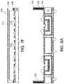
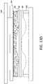
- FIGS. 1A-1Iare side cross sectional views illustrating the steps in forming a light device assembly.
- FIG. 2is a top view of the light device assembly.
- FIG. 3is a bottom view of the light device assembly.
- FIGS. 4A-4Kare side cross sectional views illustrating the steps in forming a lens assembly.
- FIGS. 5A and 5Bare side cross sectional and top views of the lens assembly.
- FIG. 6is a side cross sectional view of the lens assembly having varying lens segment designs.
- FIGS. 7A-7Fare side cross sectional views illustrating the steps in forming a diffraction lens assembly.
- FIGS. 8A-8Bare side cross sectional views showing the steps in forming a light source device.
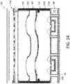
- FIG. 9is a side cross sectional view illustrating light source chips and/or their adhesive layers having different thicknesses.
- FIG. 10is a side cross sectional view of a first alternate embodiment of the light source device.
- FIG. 11is a side cross sectional view of a second alternate embodiment of the light source device.
- FIG. 12A-12Bare side cross sectional views of a third alternate embodiment of the light source device.
- FIGS. 13A-13Eare side cross sectional views illustrating the steps in forming an a lens for the third alternate embodiment.
- FIG. 14is a side cross sectional view of a fourth alternate embodiment of the light source device.
- FIGS. 1A-1Iillustrate the steps in forming a substrate on which a plurality of light source devices are mounted.
- the processbegins by providing a silicon substrate 10 .
- Silicon wafer thinningcan be performed on the substrate 10 by mechanical grinding, chemical mechanical polishing (CMP), wet etching, atmospheric downstream plasma (ADP), dry chemical etching (DCE), or a combination of aforementioned processes or any another appropriate silicon thinning method(s).
- This steppreferably reduces the thickness of silicon substrate 10 to a range of about 50 ⁇ m to 500 ⁇ m.
- An insulation layer 12is formed on the bottom surface 10 b of silicon substrate 10 .
- insulation layer 12can be silicon dioxide (hereinafter “oxide”) or silicon nitride (hereinafter “nitride”). Preferably the thickness of insulation layer 12 is greater than 0.5 ⁇ m. Insulation layer 12 can be formed by chemical vapor deposition (CVD), plasma-enhanced chemical vapor deposition (PECVD), spin and spray coatings or a combination thereof. Photoresist 14 is formed on the top surface 10 a of the substrate 10 , selectively illuminated using a mask, and developed whereby portions of the photoresist 14 are selectively removed. Photoresist formation, illumination and selective removal is a well-known photolithographic masking technique for selectively covering some portions of a layer or structure while leaving other portions exposed. The resulting structure is shown in FIG. 1A .
- One or more silicon etchesare then performed on the portions of the substrate 10 left exposed by the photoresist 14 , to form cavities 16 into the top surface 10 a of the substrate 10 (which extend into the substrate from the top surface 10 a but do not reach the substrate's bottom surface 10 b ), and to form holes 18 (which extend entirely through the substrate 10 ), as shown in FIG. 1B .
- Cavities 16 and holes 18can be formed using atmospheric downstream plasma (ADP), dry and wet chemical etching, or any other combination of the etching processes. While a single masking step is shown for forming cavities 16 and holes 18 , multiple masking steps can be used to separately form cavities 16 and holes 18 .
- the walls of holes 18are preferably, but need not be, perpendicular to the top and bottom surfaces of substrate 10 .
- an insulation layer 20is formed on the exposed surfaces of the substrate 10 , including the substrate's top surface 10 a and the surfaces of cavities 16 and holes 18 .
- Insulation layer 20can be made of oxide, nitride, polymer, polyimide, or a combination of these materials.
- the thickness of insulation layer 20is preferably greater than 0.5 ⁇ m, and can be formed by chemical vapor deposition (CVD), plasma-enhanced chemical vapor deposition (PECVD), spin and spray coatings or a combination thereof.
- the holes 18are then filled with conductive material 22 , such as for example Cu, Al, Ti, Cr, Ni or a combination thereof.
- Conductive material 22can be formed by metal sputtering, plating, filling with conductive paste or a combination thereof.
- the conductive material in each hole 18forms a conductive electrode 22 extending entirely through the substrate 10
- the resulting structureis shown in FIG. 1C .
- Light source chip 26is preferably a light emitting semiconductor device containing a light emitting device 28 such as a light emitting diode LED and electrical contacts 30 at the upper surface of light source chip 26 for powering the light emitting device 28 .
- Light emitting device 28can also be referred to as the active area of the light source chip 26 .
- light emitting device 28can be any appropriate light producing element, such as a vertical cavity surface emitting laser (VCSEL).
- An insulation layer 32e.g., oxide, nitride, polymer, polyimide, etc.
- a thickness of at least 0.5 ⁇ mis formed over the top substrate surface 10 a , and patterned using a photolithographic masking step to remove portions of the insulation layer 32 to expose the electrical contacts 30 and light emitting device 28 and the tops of electrode 22 in holes 18 , as shown in FIG. 1D (after photoresist removal).
- Photoresistis formed over the top substrate surface 10 a , and patterned using a photolithographic masking step to remove portions of the photoresist to expose the tops of electrodes 22 in holes 18 .
- Conductive materiale.g., Cu, Al, Ti, Ni, Cr, etc.
- Conductive materialis formed on the exposed tops of electrodes 22 to form conductive bond pads 34 , as shown in FIG.
- An insulation layer 36(e.g., oxide, nitride, polymer, polyimide, etc. preferably with a thickness of at least 0.5 ⁇ m) is formed over the bottom substrate surface 10 b , and patterned using a photolithographic masking step to remove portions of the insulation layer 36 to expose the bottoms of electrodes 22 in holes 18 .
- Conductive materiale.g., Cu, Al, Ti, Ni, Cr, etc.
- Formation of bond pads 34 and 35can be performed by material deposition followed by a selective removal of the deposited material using a photolithographic masking step and etch.
- An insulation layer 38(e.g., oxide, nitride, polymer, polyimide, etc. preferably with a thickness of at least 0.5 ⁇ m) is formed on insulation layer 36 and then patterned using a photolithographic masking step to expose bond pads 35 and portions of insulation layer 36 adjacent bond pads 35 .
- Conductive materiale.g., Cu, Al, Ti, Ni, Cr, etc.
- An insulation layer 42e.g., oxide, nitride, polymer, polyimide, etc.
- solder ball connectors 44are formed over the exposed portions of leads 40 as shown in FIG. 1H (after photo resist removal).
- Solder ball connectors 44(also commonly referred to as ball grid array BGA) can be formed using a print process or a ball attach process, and can be formed of Pb, Sn, SnCu or any other combination of solder materials. Solder ball connectors 44 serve as re-routed contacts for the electrodes 22 extending through substrate 10 (via bond pads 35 and leads 40 ).
- Wires 46are connected between the light source electrical contacts 30 and bond pads 34 , as shown in FIG. 1I .
- the material for wires 46can be Cu, Ag, Au, or any other appropriate material(s).
- the wires 46are part of an electrical path from each light source electrical contact 30 , through wire 46 , bond pad 34 , electrode 22 , bond pad 35 , lead 40 and BGA 44 .
- the structurecan be singulated (diced), where the structure is diced along the dicing lines DL to form a light device assembly 48 as shown in FIG. 1I . Substrate singulation/dicing of components could be done with mechanical blade dicing equipment, laser cutting or any other combination of mechanical and laser processes.
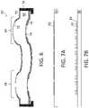
- FIG. 2is a top view of a light device assembly 48 containing three light source chips 26 arranged in a triangular spaced relationship. The number and positioning of the light source chips 26 can vary depending on the specific design specifications.
- FIG. 3is a bottom view of the light device assembly 48 of FIG. 2 , where the solder ball connectors 44 are arranged in a more evenly spaced distribution than the electrical contacts 30 to which they are electrically connected.
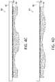
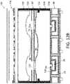
- FIGS. 4A-4Killustrate the steps in forming a monolithic multi focus lens for the above described light device assembly 48 .
- the processbegins with a first master mold 52 which has an upper surface 52 a shaped with a pattern that matches that of the desired shape of the finished lens, as shown in FIG. 4A .
- the master mold 52can be formed using photolithographic and etching techniques, or mechanical diamond tool patterning, both of which are known in the art.
- a layer of metal 54is preferably formed on the shaped upper surface 52 a of the master mold 52 (to prevent the subsequently formed polymer from sticking to the master mold upper surface 52 a ).
- a layer of polymer 56is formed on the metal layer 54 , and an adhesive layer 58 is formed on the polymer layer 56 .
- a carrier mold 60is mounted to the polymer layer 56 by adhesive 58 .
- the polymer layer 56is preferably made of a resin, polydimethylsiloxane (PMDS), cyclo-olefin polymer (COP), polymethyl methacrylate (PMMA) or any other appropriate material.
- the adhesive layer 58is preferably made of an optically transparent or UV curable material.
- the carrier mold 60can be a soft mold or a metal mold.
- the polymer layer 56can be fixed into its designed pattern by thermal curing or light curing, as shown in FIG. 4B .
- top lens replica assembly 62As shown in FIG. 4C .
- a bottom lens replica assembly 64(having its polymer layer 56 with a surface curvature matching that of the desired bottom surface of the lens) is formed in the same manner as top lens replica assembly 62 , and is shown in FIG. 4D .
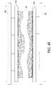
- a polymer layer 66is dispensed onto one of the top and bottom lens replica assemblies 62 / 64 , which are then mounted to a stamper assembly 68 whereby they are positioned and aligned facing each other, as shown in FIG. 4E .
- the polymer layer 66can be dispensed from a nozzle and spun into the designed thickness.
- the polymer layer 66is preferably a resin, polydimethylsiloxane (PMDS), cyclo-olefin polymer (COP), polymethyl methacrylate (PMMA) or any other transparent material(s) appropriate as a lens material.
- Contact aligners, proximity aligners, scanning projection aligners or other appropriate alignment method(s)can be used to align the replica assemblies 62 / 64 to each other.
- the stamper assembly 68then presses the replica assemblies 62 / 64 together with the desired pressure and at the desired temperature so that the polymer layer 66 conforms to (and is cured to) the shapes of the polymer layers 56 of the assemblies 62 / 64 , as shown in FIG. 4F .
- This pressing processcan be performed as a single step, or in multiple steps separately applying pressure to one of the replica assemblies 62 / 64 one at a time.
- the polymer layer 66is then extracted (as a unitary substrate having the desired upper and lower shaped surfaces 66 a / 66 b ), as shown in FIG. 4G .
- multiple lens shapescan be formed in a single lens substrate 66 , which is later diced/singulated to form a plurality of individual lenses, with each individual lens including a plurality of lens segments 84 described in further detail below.
- a metal layer 70is formed on both upper and lower surfaces 66 a / 66 b of lens substrate 66 , and can include one or more of Cu, Ti, and Al.
- the metal layer 70 on the upper surface 66 ais then patterned (e.g., a photolithographic masking step and metal etch) to create apertures 70 a in the metal layer 70 that expose portions of the underlying lens substrate 66 .
- a layer of filter material 72is then formed on the exposed portions of the lens substrate 66 .
- the filter materialis preferably a material that filters infrared light, such as magnesium fluoride (MgFl), N-BK7, or cadmium telluride (CdTe), which can be formed by Chemical Vapor Deposition (CVP), ion beam assisted deposition or any other appropriate deposition method(s).
- CVPChemical Vapor Deposition
- ion beam assisted depositionor any other appropriate deposition method(s).
- the resulting structureis shown in FIG. 4I (after removal of the photoresist used for the photolithographic masking step).
- the metal layer 70 on the lower surface 66 bis then patterned (e.g., a photolithographic masking step and metal etch) to create apertures 70 a that expose the underlying lens substrate 66 .
- a layer of anti-reflection material(AR coating 74 ) is formed over the lower surface 66 a , including directly on the exposed portions of lens substrate 66 in aperture portions 70 a of the metal layer 70 , as shown in FIG. 4J .
- lens substrate 66can be diced/singulated into the desired size and shape, for example, on the dicing lines 76 of FIG. 4J .
- the diced/singulated lens substrate 66can then be mounted to a lens holder 78 using adhesive 80 .
- lens holder 78is made of a non-transparent material such as non-transparent silicon.
- the resulting finished lens assembly 82is shown in FIG. 4K .
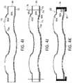
- FIGS. 5A and 5Bare side and top views of the finished lens assembly 82 .
- the lens substrate 66is unitary (continuous) and has three lens segments 84 .
- the number of lens segments 84 in the lens assembly 82can vary. All the lens segments 84 in the lens assembly 82 are shown to have the same focal properties (i.e. focal distance, optical focusing/dispersion properties, etc.).
- the focal properties between lens segments in the same lens assembly 82can be varied.
- FIG. 6illustrates a lens substrate 66 where the shapes and therefore focal properties of the lens segments 84 differ from each other. Apertures 70 a in each lens segment 84 allow light to pass through the lens segment.
- FIGS. 7A-7Fillustrate the steps in forming a micro lens array for the above described monolithic multi focus lens 82 and multi light source device substrate 10 .
- the processbegins with a substrate 90 made of a transparent material such as glass.
- the substratecan be thinned by mechanical grinding, chemical mechanical polishing (CMP), wet etching, atmospheric downstream plasma (ADP), dry chemical etching (DCE), or a combination thereof.
- a patterned layer of polymer 92is formed on the upper surface of the substrate 90 .
- polymer layer 92can be formed by forming and patterning photoresist using a photolithography masking process, and forming/curing polymer on the portions of substrate 90 left exposed by the photoresist. The resulting structure is shown in FIG.
- a photolithography masking processis performed to cover the micro lenses 96 with photoresist, but leave the adjacent area of substrate 90 exposed.
- a metal layer 98is formed on the exposed portions of the substrate 90 .
- an optical coating 100can be deposited on the micro lenses 96 , as shown in FIG. 7D .
- Optical coating 100is preferably a material that filters out infra-red light, such as magnesium fluoride (MgFl), N-BK7, cadmium telluride (CdTe) or any other appropriate IR filtering materials.
- a metal layer 102is formed on the bottom surface of substrate 90 , and patterned using a photolithography masking process and metal etch, so that the metal layer 102 includes an aperture 102 a underneath micro lenses 96 .
- An optional anti-reflective coating 104can be formed on the bottom surface of the substrate 90 in aperture 102 a , as shown in FIG. 7E .
- the material for coating 104can be magnesium fluoride (MgFl), or any other appropriate anti-reflective coating material.
- a plurality of the structures in FIG. 7Eare formed on a common substrate 90 .
- the substrate 90is singulated (diced) at this point along dicing lines DL.
- a transparent substrate 106is mounted to the metal layer 98 and over the micro lenses 96 , by adhesive 108 , as shown in FIG. 7F .
- Substrate 106can be plastic, glass, or any other appropriate transparent material.
- the surface of substrate 106 facing the micro lenses 96can include an optional anti-reflective coating 110 , and the opposite surface of substrate 106 can include an optional infrared filter coating 112 .
- the substrate 106preferably includes a cavity 114 so that substrate 106 does not interfere with micro lenses 96 .
- the final diffraction lens assembly 116is shown in FIG. 7F .
- Spacer 120is mounted to substrate 10 using an adhesive material 124 , as shown in FIG. 8A .
- Spacer 120is preferably made of a rigid material that does not transmit light, and has a low coefficient of thermal expansion (CTE) or a CTE that matches that of the substrate 10 .
- spacer 120is non-transparent silicon or glass.
- spacer 120could also be formed of metal.
- Spacer 120can be formed by etching a square or other shaped aperture through a silicon substrate using a photolithographic masking and etch process.
- An optional light reflective coating 122can be formed on the interior sidewalls of spacer 120 .
- the previously described lens assembly 82is mounted on spacer 120 so that each lens segment 84 is disposed over one of the light source chips 26 for focusing the light therefrom.
- a second spacer 120is mounted on lens assembly 82 .
- Diffraction lens assembly 116is mounted to the second spacer 120 .
- the final light source device 126is shown in FIG. 8B .
- Light source device 126integrates light sources and their respective optical elements in unique way and provides many advantages.
- Device 126provides a compact, sealed enclosure assembly protecting, among other things, light source chips 26 , lens segments 84 and micro lenses 96 .
- Light source device 126utilizes a monolithic lens, integrates it components in a thin package in a highly accurate way yet reduces cost.
- the electrical connections to the light source chips 26are routed through the substrate 10 and to its bottom surface, where they are rerouted to solder ball connectors 44 .
- Each lens segment 84is disposed over and precisely aligned with one of the light source chips 26 .
- Cavities 16provide high precision positioning of the light source chips 26 both in the x and y (lateral) directions and in the z (depth) direction.
- the light focal distance between each light source chip 26 and its lens segment 84can be precisely controlled (e.g. by spacer 120 ) to produce the desired light output, and can be varied.
- the thickness of the light source chip 26can vary, and/or the thicknesses of adhesive 24 can vary, so that the distances between the light source chips 26 and their corresponding lens segments 84 can vary within the same light source device 126 , to produce the desired total light output characteristics from the light source device 126 as a whole. See for example FIG. 9 , where the two light source chips have different thicknesses, as do the adhesive 24 underneath.
- the focal properties of lens segments 84 in the same device 126can vary to provide the desired light output.
- each light source chip 26 and its lens segment 84can produce a light output different from that from the other light source chips and lens segments, whereby the combined light outputs can produce a uniquely designed overall light output that cannot be achieved with a single light source.
- one light source chip 26 and its lens segment 84can be configured to maximize even illumination of an area closer to the device 126
- one or more of the light source chips 26 and their lens segment 84can be configured to maximize even illumination of an area further away from the device 126 .
- different light source chips 26 and lens segments 84can be configured to illuminate different spatial areas relative to the device 126 .
- Forming spacers 120 of opaque material and/or including reflective coating 122blocks any light from the outside and prevents any light leakage from device 126 , thus improving light efficiency.
- Anti-reflective coatingsreduce optical loss and increase efficiency.
- Optical coatings 72 and 100can be used to block unwanted wavelengths from the optical output of the device 126 , such as infrared light.
- the diffractive optical pattern of micro lenses 96provides the desired diffraction of the output for even or non-even light distribution as needed. Light from different light source chips 26 , using lens segments 84 with uniform or varying focal properties, to illuminate the micro lenses 96 provides the versatility to provide any desired light output pattern.
- Forming micro lenses 96 using optically transparent polymer material through a lithography process on the surface of substrate 90reduces cost and increases consistency, reliability and the ability to achieve the desired performance.
- parameters such as focal length and lens diameter of the diffractive pattern micro lens arrayare flexible and tunable directly by software.
- the light source device 126is ideal for many applications. For example, facial recognition used to unlock cell phones would benefit greatly from the invention.
- One challengeis how best to illuminate the user's face in the three dimensional space in front of the mobile phone's camera for capturing details of the user's face, given that different users hold their mobile phone differently.
- the present inventionwould use different light source chip and lens segment combinations to illuminate different regions of that three dimensional space. Specifically, one light source chip and its lens segment can be configured to best illuminate a region closer to the camera, while another light source chip and its lens segment can be configured to best illuminate a region further away from the camera, and so on. Any number of light source chip and lens segment combinations can be used to target different regions of the three dimensional space.
- Another ideal applicationcan be particle detection, where different regions of a three dimensional space are illuminated by different light source chip and lens segment combinations so that particles in the three dimensional space can be optically detected.
- Other applicationscan include automobiles, home, TV, or any other application in which precise and accurate illumination of a two dimensional or three dimensional space is needed.
- Multiple, separate, light source devices 126can be included in the same application device (i.e., cell phone, camera, automobile, home appliance, TV, etc.), where the various light source devices 126 in any given single application device can either be the same or can be different from each other in terms of size, design and/or functionality).
- a light source device 126 operating in the visible region and a light source device 126 operating in the non-visible spectrumcan be included in the same application device.
- a single light source device 126can include light source chips 26 that vary in size, design and functionality.
- a single light source device 126can include a first light source chip 26 that generates visible light and a second light source chip 26 that generates invisible light (e.g., UV or IR).
- FIG. 10illustrates a first alternative embodiment, where the electrical contacts 30 of the light source chips 26 are electrically connected to the conductive electrodes 22 in substrate 10 by conductive traces 130 instead of by wires 46 .
- Conductive traces 130can be formed by forming and patterning a layer of conductive material on substrate 10 .
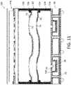
- FIG. 11illustrates a second alternative embodiment, where the filter layer 72 and A/R coating layer 74 are formed on lens substrate 66 first, followed by the formation of metal layer 70 .
- Metal layer 70is then subjected to a masking/etch process to create the apertures 70 a to expose the underlying filter layer 72 and A/R coating layer 74 .
- the resulting structurethen has metal layer 72 disposed on layers 72 / 74 .
- FIG. 12Aillustrates a third alternative embodiment, which is the same as that shown in FIG. 10 except that lens assembly 82 includes a glass substrate 132 embedded in the polymer lens substrate 66 .
- FIGS. 13A-13Eillustrate the steps in forming the glass-polymer hybrid, and starts with the top and bottom lens replica assemblies 62 and 64 of FIGS. 4C-4D .
- a glass substrate 132is placed on a carrier 134 , and polymer 66 is deposited on the glass substrate 132 , as shown in FIG. 13A .
- a stamper assembly 136then presses replica assembly 62 down onto polymer 66 with the desired pressure and temperature so that the upper surface of polymer 66 conforms to (and is cured to) the shape of the polymer layer 56 of assembly 62 , as shown in FIG. 13B .
- Carrier 134 and replica assembly 62are removed, and replaced with a carrier 138 supporting the edges of polymer 66 and glass substrate 132 .
- Polymer 66is deposited on the other side of glass substrate 132 , as shown in FIG. 13C .
- Stamper assembly 136then presses replica assembly 64 down onto polymer 66 with the desired pressure and temperature so that the top surface of polymer 66 conforms to (and is cured to) the shape of the polymer layer 56 of assembly 64 , as shown in FIG.
- the polymer substrate 66 with embedded glass substrate 132 thereinis then extracted (as a lens substrate having the desired upper and lower shaped surfaces 66 a / 66 b ), as shown in FIG. 13E .
- the glass substrate 132provides additional rigidity to the lens assembly 82 , and can make fabrication easier by providing a rigid substrate on which the polymer layers are formed.
- the metal layers 70 defining apertures 70 acan be formed on the glass substrate 132 instead of on the polymer layer 66 as previously described, as shown in FIG. 12B .
- Anti-reflection coatingscan be formed on glass substrate 132 as well.
- FIG. 14illustrates a fourth alternative embodiment, which is the same as that shown in FIG. 8B except that conductive lands 140 are formed on the redistribution leads 40 instead of solder ball connectors 44 .
- Conductive lands 140are formed as a layer of conductive material on redistribution leads 40 .
- the advantage of using conductive lands 140 instead of solder ball connectors 44is that lands 140 are thinner than solder ball connectors.
- adjacentincludes “directly adjacent” (no intermediate materials, elements or space disposed there between) and “indirectly adjacent” (intermediate materials, elements or space disposed there between)
- mounted toincludes “directly mounted to” (no intermediate materials, elements or space disposed there between) and “indirectly mounted to” (intermediate materials, elements or spaced disposed there between)
- electrically coupledincludes “directly electrically coupled to” (no intermediate materials or elements there between that electrically connect the elements together) and “indirectly electrically coupled to” (intermediate materials or elements there between that electrically connect the elements together).
- forming an element “over a substrate”can include forming the element directly on the substrate with no intermediate materials/elements there between, as well as forming the element indirectly on the substrate with one or more intermediate materials/elements there between.
Landscapes
- Engineering & Computer Science (AREA)
- Physics & Mathematics (AREA)
- General Physics & Mathematics (AREA)
- Microelectronics & Electronic Packaging (AREA)
- Power Engineering (AREA)
- Condensed Matter Physics & Semiconductors (AREA)
- Computer Hardware Design (AREA)
- General Engineering & Computer Science (AREA)
- Optics & Photonics (AREA)
- Ceramic Engineering (AREA)
- Manufacturing & Machinery (AREA)
- Spectroscopy & Molecular Physics (AREA)
- Led Device Packages (AREA)
- Fastening Of Light Sources Or Lamp Holders (AREA)
Abstract
Description
Claims (19)
Priority Applications (5)
| Application Number | Priority Date | Filing Date | Title |
|---|---|---|---|
| US16/704,280US11408589B2 (en) | 2019-12-05 | 2019-12-05 | Monolithic multi-focus light source device |
| TW109135960ATWI770639B (en) | 2019-12-05 | 2020-10-16 | Monolithic multi-focus light source device |
| JP2020193447AJP2021090052A (en) | 2019-12-05 | 2020-11-20 | Monolithic multi-focus light source device |
| KR1020200167634AKR102490428B1 (en) | 2019-12-05 | 2020-12-03 | Monolithic multi-focus light source device |
| CN202011402795.0ACN112928190A (en) | 2019-12-05 | 2020-12-04 | Monolithic multi-focal point light source device |
Applications Claiming Priority (1)
| Application Number | Priority Date | Filing Date | Title |
|---|---|---|---|
| US16/704,280US11408589B2 (en) | 2019-12-05 | 2019-12-05 | Monolithic multi-focus light source device |
Publications (2)
| Publication Number | Publication Date |
|---|---|
| US20210172581A1 US20210172581A1 (en) | 2021-06-10 |
| US11408589B2true US11408589B2 (en) | 2022-08-09 |
Family
ID=76162654
Family Applications (1)
| Application Number | Title | Priority Date | Filing Date |
|---|---|---|---|
| US16/704,280Active2040-08-27US11408589B2 (en) | 2019-12-05 | 2019-12-05 | Monolithic multi-focus light source device |
Country Status (5)
| Country | Link |
|---|---|
| US (1) | US11408589B2 (en) |
| JP (1) | JP2021090052A (en) |
| KR (1) | KR102490428B1 (en) |
| CN (1) | CN112928190A (en) |
| TW (1) | TWI770639B (en) |
Families Citing this family (2)
| Publication number | Priority date | Publication date | Assignee | Title |
|---|---|---|---|---|
| TWI871304B (en)* | 2020-03-02 | 2025-02-01 | 晶智達光電股份有限公司 | Laser package structure |
| US11745453B2 (en)* | 2020-03-05 | 2023-09-05 | Continental Autonomous Mobility US, LLC | Method of making and using a reusable mold for fabrication of optical elements |
Citations (79)
| Publication number | Priority date | Publication date | Assignee | Title |
|---|---|---|---|---|
| JPS62235787A (en) | 1986-04-07 | 1987-10-15 | Koito Mfg Co Ltd | lighting equipment |
| JPH0240534A (en) | 1988-06-21 | 1990-02-09 | Basf Ag | Dispersion level measuring apparatus for fluid suspension |
| US4904512A (en) | 1986-02-10 | 1990-02-27 | Toyo Seikan Kaisha, Ltd. | Compression-molded article having multilayer structure |
| JPH0278102A (en) | 1987-12-24 | 1990-03-19 | Mitsubishi Cable Ind Ltd | light emitting diode lighting equipment |
| JPH0492660A (en) | 1990-08-08 | 1992-03-25 | Masayoshi Kishigami | Socket with claw for artificial crotch joint |
| US5750156A (en) | 1995-09-25 | 1998-05-12 | Galic Maus Ventures | Apparatus for injection-compression molding and ejecting paired thermoplastic spectacle lens suited for fully automated dip hardcoating |
| US5914074A (en) | 1994-06-10 | 1999-06-22 | Johnson & Johnson Vision Products, Inc. | Mold clamping and precure of a polymerizable hydrogel |
| JP2000114604A (en) | 1998-09-30 | 2000-04-21 | Fuji Photo Film Co Ltd | Light emitting element array and method of manufacturing the same |
| TW490388B (en) | 1999-05-05 | 2002-06-11 | Johnson & Amp Johnson Vision C | Mold and molding machine for making ophthalmic devices |
| US20030230817A1 (en) | 2002-06-13 | 2003-12-18 | Agere Systems, Inc. | Mold for UV curable adhesive and method of use therefor |
| US6683421B1 (en) | 2001-01-25 | 2004-01-27 | Exfo Photonic Solutions Inc. | Addressable semiconductor array light source for localized radiation delivery |
| US6777767B2 (en) | 1999-12-10 | 2004-08-17 | Shellcase Ltd. | Methods for producing packaged integrated circuit devices & packaged integrated circuit devices produced thereby |
| US20040251525A1 (en) | 2003-06-16 | 2004-12-16 | Shellcase Ltd. | Methods and apparatus for packaging integrated circuit devices |
| US20050104179A1 (en) | 2003-07-03 | 2005-05-19 | Shellcase Ltd. | Methods and apparatus for packaging integrated circuit devices |
| US7033664B2 (en) | 2002-10-22 | 2006-04-25 | Tessera Technologies Hungary Kft | Methods for producing packaged integrated circuit devices and packaged integrated circuit devices produced thereby |
| US7070406B2 (en) | 2003-04-29 | 2006-07-04 | Hewlett-Packard Development Company, L.P. | Apparatus for embossing a flexible substrate with a pattern carried by an optically transparent compliant media |
| US20060163596A1 (en)* | 2005-01-26 | 2006-07-27 | Gi-Cherl Kim | Two dimensional light source using light emitting diode and liquid crystal display device using the two dimensional light source |
| US7157742B2 (en) | 1998-02-06 | 2007-01-02 | Tessera Technologies Hungary Kft. | Integrated circuit device |
| US20070190747A1 (en) | 2006-01-23 | 2007-08-16 | Tessera Technologies Hungary Kft. | Wafer level packaging to lidded chips |
| US20070190691A1 (en) | 2006-01-23 | 2007-08-16 | Tessera Technologies Hungary Kft. | Wafer level chip packaging |
| US20080083977A1 (en) | 2006-10-10 | 2008-04-10 | Tessera, Inc. | Edge connect wafer level stacking |
| US20080083976A1 (en) | 2006-10-10 | 2008-04-10 | Tessera, Inc. | Edge connect wafer level stacking |
| US20080099907A1 (en) | 2006-10-31 | 2008-05-01 | Tessera Technologies Hungary Kft. | Wafer-level fabrication of lidded chips with electrodeposited dielectric coating |
| US20080099900A1 (en) | 2006-10-31 | 2008-05-01 | Tessera Technologies Hungary Kft. | Wafer-level fabrication of lidded chips with electrodeposited dielectric coating |
| US20080116545A1 (en) | 2006-11-22 | 2008-05-22 | Tessera, Inc. | Packaged semiconductor chips |
| US20080116544A1 (en) | 2006-11-22 | 2008-05-22 | Tessera, Inc. | Packaged semiconductor chips with array |
| US20080150121A1 (en) | 2006-12-20 | 2008-06-26 | Tessera Technologies Hungary Kft. | Microelectronic assemblies having compliancy and methods therefor |
| US20080246136A1 (en) | 2007-03-05 | 2008-10-09 | Tessera, Inc. | Chips having rear contacts connected by through vias to front contacts |
| JP2008288540A (en) | 2007-05-18 | 2008-11-27 | Everlight Electronics Co Ltd | Light emitting diode module and manufacturing method thereof |
| US20090115047A1 (en) | 2007-10-10 | 2009-05-07 | Tessera, Inc. | Robust multi-layer wiring elements and assemblies with embedded microelectronic elements |
| US20090160065A1 (en) | 2006-10-10 | 2009-06-25 | Tessera, Inc. | Reconstituted Wafer Level Stacking |
| US20090212381A1 (en) | 2008-02-26 | 2009-08-27 | Tessera, Inc. | Wafer level packages for rear-face illuminated solid state image sensors |
| JP2009214387A (en) | 2008-03-10 | 2009-09-24 | Sumitomo Electric Ind Ltd | Manufacturing method of plastic film lens |
| US20100053407A1 (en) | 2008-02-26 | 2010-03-04 | Tessera, Inc. | Wafer level compliant packages for rear-face illuminated solid state image sensors |
| US20100207142A1 (en) | 2009-02-18 | 2010-08-19 | Chi Mei Lighting Technology Corp. | Light-emitting diode light source module |
| US20100230803A1 (en) | 2009-03-13 | 2010-09-16 | Wen-Cheng Chien | Electronic device package and method for forming the same |
| US20100237452A1 (en) | 2009-03-18 | 2010-09-23 | Kenichiro Hagiwara | Semiconductor device and backside illumination solid-state imaging device |
| CN101890817A (en) | 2009-05-22 | 2010-11-24 | 鸿富锦精密工业(深圳)有限公司 | Method for Imprinting and Forming Lens Arrays |
| US7859033B2 (en) | 2008-07-09 | 2010-12-28 | Eastman Kodak Company | Wafer level processing for backside illuminated sensors |
| US20110031509A1 (en) | 2008-04-24 | 2011-02-10 | Panasonic Electric Works Co., Ltd. | Led module and lighting device using the same |
| US20110215342A1 (en)* | 2010-03-02 | 2011-09-08 | Oliver Steven D | Led packaging with integrated optics and methods of manufacturing the same |
| TW201139125A (en) | 2010-05-10 | 2011-11-16 | Hon Hai Prec Ind Co Ltd | Micro lens array fabricating apparatus |
| US20120018895A1 (en) | 2010-07-23 | 2012-01-26 | Tessera Research Llc | Active chip on carrier or laminated chip having microelectronic element embedded therein |
| US20120018863A1 (en) | 2010-07-23 | 2012-01-26 | Tessera Research Llc | Microelectronic elements with rear contacts connected with via first or via middle structures |
| US20120020026A1 (en) | 2010-07-23 | 2012-01-26 | Tessera Research Llc | Microelectronic elements with post-assembly planarization |
| US20120018894A1 (en) | 2010-07-23 | 2012-01-26 | Tessera Research Llc | Non-lithographic formation of three-dimensional conductive elements |
| US20120018893A1 (en) | 2010-07-23 | 2012-01-26 | Tessera Research Llc | Methods of forming semiconductor elements using micro-abrasive particle stream |
| US20120018868A1 (en) | 2010-07-23 | 2012-01-26 | Tessera Research Llc | Microelectronic elements having metallic pads overlying vias |
| KR20120012677A (en) | 2010-08-02 | 2012-02-10 | 엘지이노텍 주식회사 | Light emitting device package and method for manufacturing same |
| JP2012032528A (en) | 2010-07-29 | 2012-02-16 | Sony Corp | Lens forming method, lens, and camera module |
| US20120037935A1 (en)* | 2010-08-13 | 2012-02-16 | Wen-Kun Yang | Substrate Structure of LED (light emitting diode) Packaging and Method of the same |
| US20120068327A1 (en) | 2010-09-17 | 2012-03-22 | Tessera Research Llc | Multi-function and shielded 3d interconnects |
| US20120068330A1 (en) | 2010-09-17 | 2012-03-22 | Tessera Research Llc | Staged via formation from both sides of chip |
| US20120068351A1 (en) | 2010-09-16 | 2012-03-22 | Tessera Research Llc | Chip assembly having via interconnects joined by plating |
| US20120068352A1 (en) | 2010-09-16 | 2012-03-22 | Tessera Research Llc | Stacked chip assembly having vertical vias |
| US20120182623A1 (en) | 2009-12-21 | 2012-07-19 | Frank Wippermann | Method for Manufacturing a Structure, Optical Component, Optical Layer Stack |
| TW201304208A (en) | 2011-07-14 | 2013-01-16 | Univ Nat Taiwan Science Tech | Polarized white light emitting diode |
| US8432011B1 (en) | 2011-12-06 | 2013-04-30 | Optiz, Inc. | Wire bond interposer package for CMOS image sensor and method of making same |
| TW201327940A (en) | 2011-12-30 | 2013-07-01 | Advanced Optoelectronic Tech | Light emitting diode package structure |
| US20130168791A1 (en) | 2012-01-04 | 2013-07-04 | Vage Oganesian | Quantum Efficiency Back Side Illuminated CMOS Image Sensor And Package, And Method Of Making Same |
| US20130249031A1 (en) | 2012-03-22 | 2013-09-26 | Vage Oganesian | Quantum Efficiency Back Side Illuminated CMOS Image Sensor And Package, And Method Of Making Same |
| US8546951B2 (en) | 2011-06-09 | 2013-10-01 | Optiz, Inc. | 3D integration microelectronic assembly for integrated circuit devices |
| US8546900B2 (en) | 2011-06-09 | 2013-10-01 | Optiz, Inc. | 3D integration microelectronic assembly for integrated circuit devices |
| US8552518B2 (en) | 2011-06-09 | 2013-10-08 | Optiz, Inc. | 3D integrated microelectronic assembly with stress reducing interconnects |
| US8570669B2 (en) | 2012-01-23 | 2013-10-29 | Optiz, Inc | Multi-layer polymer lens and method of making same |
| US8604576B2 (en) | 2011-07-19 | 2013-12-10 | Opitz, Inc. | Low stress cavity package for back side illuminated image sensor, and method of making same |
| US8692344B2 (en) | 2012-03-16 | 2014-04-08 | Optiz, Inc | Back side illuminated image sensor architecture, and method of making same |
| US8759930B2 (en) | 2012-09-10 | 2014-06-24 | Optiz, Inc. | Low profile image sensor package |
| US8796800B2 (en) | 2011-11-21 | 2014-08-05 | Optiz, Inc. | Interposer package for CMOS image sensor and method of making same |
| US20140232293A1 (en) | 2013-02-18 | 2014-08-21 | Samsung Electronics Co., Ltd. | Light-emitting device package |
| US8921759B2 (en) | 2012-07-26 | 2014-12-30 | Optiz, Inc. | Integrated image sensor package with liquid crystal lens |
| US9018725B2 (en) | 2011-09-02 | 2015-04-28 | Optiz, Inc. | Stepped package for image sensor and method of making same |
| JP2015219135A (en) | 2014-05-19 | 2015-12-07 | 株式会社リコー | Optical sensor module and method for manufacturing optical sensor module |
| US20150355470A1 (en)* | 2012-12-31 | 2015-12-10 | Iee International Electronics & Engineering S.A. | Optical system generating a structured light field from an array of light sources by means of a refracting or reflecting light structuring element |
| KR20160003746A (en) | 2013-04-22 | 2016-01-11 | 오스람 옵토 세미컨덕터스 게엠베하 | Optical arrangement and display device |
| US9233511B2 (en) | 2012-05-10 | 2016-01-12 | Optiz, Inc. | Method of making stamped multi-layer polymer lens |
| US20170242160A1 (en)* | 2016-02-24 | 2017-08-24 | Hong Kong Beida Jade Bird Display Limited | Manufacturing display panels with integrated micro lens array |
| KR20180081905A (en) | 2017-01-09 | 2018-07-18 | 엘지이노텍 주식회사 | Liquid lens, camera module and optical device/instrument including the same |
| US10679976B2 (en) | 2013-11-22 | 2020-06-09 | Ams Sensors Singapore Pte. Ltd. | Compact optoelectronic modules |
Family Cites Families (6)
| Publication number | Priority date | Publication date | Assignee | Title |
|---|---|---|---|---|
| JPH0744029Y2 (en)* | 1990-12-28 | 1995-10-09 | 株式会社小糸製作所 | LED module |
| JP3129386B2 (en)* | 1994-06-29 | 2001-01-29 | 富士通株式会社 | Optical device |
| JP2008135213A (en)* | 2006-11-27 | 2008-06-12 | Toshiba Lighting & Technology Corp | lighting equipment |
| KR101140961B1 (en)* | 2009-10-26 | 2012-05-03 | 삼성전기주식회사 | Package substrate for optical element and Manufacturing method thereof |
| JP2012212019A (en)* | 2011-03-31 | 2012-11-01 | Konica Minolta Advanced Layers Inc | Method for manufacturing optical element array, optical element array, lens unit and camera module |
| KR101960792B1 (en)* | 2012-11-05 | 2019-07-15 | 엘지이노텍 주식회사 | A light emitting device package and a light emitting module including the same |
- 2019
- 2019-12-05USUS16/704,280patent/US11408589B2/enactiveActive
- 2020
- 2020-10-16TWTW109135960Apatent/TWI770639B/enactive
- 2020-11-20JPJP2020193447Apatent/JP2021090052A/enactivePending
- 2020-12-03KRKR1020200167634Apatent/KR102490428B1/enactiveActive
- 2020-12-04CNCN202011402795.0Apatent/CN112928190A/enactivePending
Patent Citations (91)
| Publication number | Priority date | Publication date | Assignee | Title |
|---|---|---|---|---|
| US4904512A (en) | 1986-02-10 | 1990-02-27 | Toyo Seikan Kaisha, Ltd. | Compression-molded article having multilayer structure |
| JPS62235787A (en) | 1986-04-07 | 1987-10-15 | Koito Mfg Co Ltd | lighting equipment |
| JPH0278102A (en) | 1987-12-24 | 1990-03-19 | Mitsubishi Cable Ind Ltd | light emitting diode lighting equipment |
| JPH0240534A (en) | 1988-06-21 | 1990-02-09 | Basf Ag | Dispersion level measuring apparatus for fluid suspension |
| JPH0492660A (en) | 1990-08-08 | 1992-03-25 | Masayoshi Kishigami | Socket with claw for artificial crotch joint |
| US5914074A (en) | 1994-06-10 | 1999-06-22 | Johnson & Johnson Vision Products, Inc. | Mold clamping and precure of a polymerizable hydrogel |
| US5750156A (en) | 1995-09-25 | 1998-05-12 | Galic Maus Ventures | Apparatus for injection-compression molding and ejecting paired thermoplastic spectacle lens suited for fully automated dip hardcoating |
| US7157742B2 (en) | 1998-02-06 | 2007-01-02 | Tessera Technologies Hungary Kft. | Integrated circuit device |
| JP2000114604A (en) | 1998-09-30 | 2000-04-21 | Fuji Photo Film Co Ltd | Light emitting element array and method of manufacturing the same |
| TW490388B (en) | 1999-05-05 | 2002-06-11 | Johnson & Amp Johnson Vision C | Mold and molding machine for making ophthalmic devices |
| US6777767B2 (en) | 1999-12-10 | 2004-08-17 | Shellcase Ltd. | Methods for producing packaged integrated circuit devices & packaged integrated circuit devices produced thereby |
| US6683421B1 (en) | 2001-01-25 | 2004-01-27 | Exfo Photonic Solutions Inc. | Addressable semiconductor array light source for localized radiation delivery |
| US20030230817A1 (en) | 2002-06-13 | 2003-12-18 | Agere Systems, Inc. | Mold for UV curable adhesive and method of use therefor |
| US7033664B2 (en) | 2002-10-22 | 2006-04-25 | Tessera Technologies Hungary Kft | Methods for producing packaged integrated circuit devices and packaged integrated circuit devices produced thereby |
| US7070406B2 (en) | 2003-04-29 | 2006-07-04 | Hewlett-Packard Development Company, L.P. | Apparatus for embossing a flexible substrate with a pattern carried by an optically transparent compliant media |
| US20040251525A1 (en) | 2003-06-16 | 2004-12-16 | Shellcase Ltd. | Methods and apparatus for packaging integrated circuit devices |
| US20050205977A1 (en) | 2003-06-16 | 2005-09-22 | Shellcase Ltd. | Methods and apparatus for packaging integrated circuit devices |
| US20080012115A1 (en) | 2003-06-16 | 2008-01-17 | Tessera Technologies Hungary Kft. | Methods and apparatus for packaging integrated circuit devices |
| US20080017879A1 (en) | 2003-07-03 | 2008-01-24 | Tessera Technologies Hungary Kft. | Methods and apparatus for packaging integrated circuit devices |
| US20070138498A1 (en) | 2003-07-03 | 2007-06-21 | Tessera Technologies Hungary Kft. | Methods and apparatus for packaging integrated circuit devices |
| US20050104179A1 (en) | 2003-07-03 | 2005-05-19 | Shellcase Ltd. | Methods and apparatus for packaging integrated circuit devices |
| JP2006210880A (en) | 2005-01-26 | 2006-08-10 | Samsung Electronics Co Ltd | Two-dimensional light source using light emitting diode and liquid crystal display device using the same |
| US20060163596A1 (en)* | 2005-01-26 | 2006-07-27 | Gi-Cherl Kim | Two dimensional light source using light emitting diode and liquid crystal display device using the two dimensional light source |
| US20070190747A1 (en) | 2006-01-23 | 2007-08-16 | Tessera Technologies Hungary Kft. | Wafer level packaging to lidded chips |
| US20070190691A1 (en) | 2006-01-23 | 2007-08-16 | Tessera Technologies Hungary Kft. | Wafer level chip packaging |
| US20080083977A1 (en) | 2006-10-10 | 2008-04-10 | Tessera, Inc. | Edge connect wafer level stacking |
| US20080083976A1 (en) | 2006-10-10 | 2008-04-10 | Tessera, Inc. | Edge connect wafer level stacking |
| US20090160065A1 (en) | 2006-10-10 | 2009-06-25 | Tessera, Inc. | Reconstituted Wafer Level Stacking |
| US20110049696A1 (en) | 2006-10-10 | 2011-03-03 | Tessera, Inc. | Off-chip vias in stacked chips |
| US20110187007A1 (en) | 2006-10-10 | 2011-08-04 | Tessera, Inc. | Edge connect wafer level stacking |
| US20110031629A1 (en) | 2006-10-10 | 2011-02-10 | Tessera, Inc. | Edge connect wafer level stacking |
| US20110033979A1 (en) | 2006-10-10 | 2011-02-10 | Tessera, Inc. | Edge connect wafer level stacking |
| US20080099907A1 (en) | 2006-10-31 | 2008-05-01 | Tessera Technologies Hungary Kft. | Wafer-level fabrication of lidded chips with electrodeposited dielectric coating |
| US20080099900A1 (en) | 2006-10-31 | 2008-05-01 | Tessera Technologies Hungary Kft. | Wafer-level fabrication of lidded chips with electrodeposited dielectric coating |
| US20080116545A1 (en) | 2006-11-22 | 2008-05-22 | Tessera, Inc. | Packaged semiconductor chips |
| US20110012259A1 (en) | 2006-11-22 | 2011-01-20 | Tessera, Inc. | Packaged semiconductor chips |
| US20080116544A1 (en) | 2006-11-22 | 2008-05-22 | Tessera, Inc. | Packaged semiconductor chips with array |
| US20080150121A1 (en) | 2006-12-20 | 2008-06-26 | Tessera Technologies Hungary Kft. | Microelectronic assemblies having compliancy and methods therefor |
| US20100230812A1 (en) | 2006-12-20 | 2010-09-16 | Tessera, Inc. | Microelectronic Assemblies Having Compliancy and Methods Therefor |
| US20100225006A1 (en) | 2007-03-05 | 2010-09-09 | Tessera, Inc. | Chips having rear contacts connected by through vias to front contacts |
| US20080246136A1 (en) | 2007-03-05 | 2008-10-09 | Tessera, Inc. | Chips having rear contacts connected by through vias to front contacts |
| JP2008288540A (en) | 2007-05-18 | 2008-11-27 | Everlight Electronics Co Ltd | Light emitting diode module and manufacturing method thereof |
| US20090115047A1 (en) | 2007-10-10 | 2009-05-07 | Tessera, Inc. | Robust multi-layer wiring elements and assemblies with embedded microelectronic elements |
| US20100053407A1 (en) | 2008-02-26 | 2010-03-04 | Tessera, Inc. | Wafer level compliant packages for rear-face illuminated solid state image sensors |
| US20090212381A1 (en) | 2008-02-26 | 2009-08-27 | Tessera, Inc. | Wafer level packages for rear-face illuminated solid state image sensors |
| JP2009214387A (en) | 2008-03-10 | 2009-09-24 | Sumitomo Electric Ind Ltd | Manufacturing method of plastic film lens |
| US20110031509A1 (en) | 2008-04-24 | 2011-02-10 | Panasonic Electric Works Co., Ltd. | Led module and lighting device using the same |
| US7859033B2 (en) | 2008-07-09 | 2010-12-28 | Eastman Kodak Company | Wafer level processing for backside illuminated sensors |
| US20100207142A1 (en) | 2009-02-18 | 2010-08-19 | Chi Mei Lighting Technology Corp. | Light-emitting diode light source module |
| US20100230803A1 (en) | 2009-03-13 | 2010-09-16 | Wen-Cheng Chien | Electronic device package and method for forming the same |
| US20100237452A1 (en) | 2009-03-18 | 2010-09-23 | Kenichiro Hagiwara | Semiconductor device and backside illumination solid-state imaging device |
| CN101890817A (en) | 2009-05-22 | 2010-11-24 | 鸿富锦精密工业(深圳)有限公司 | Method for Imprinting and Forming Lens Arrays |
| US20120182623A1 (en) | 2009-12-21 | 2012-07-19 | Frank Wippermann | Method for Manufacturing a Structure, Optical Component, Optical Layer Stack |
| US20110215342A1 (en)* | 2010-03-02 | 2011-09-08 | Oliver Steven D | Led packaging with integrated optics and methods of manufacturing the same |
| TW201139125A (en) | 2010-05-10 | 2011-11-16 | Hon Hai Prec Ind Co Ltd | Micro lens array fabricating apparatus |
| US20120018894A1 (en) | 2010-07-23 | 2012-01-26 | Tessera Research Llc | Non-lithographic formation of three-dimensional conductive elements |
| US20120020026A1 (en) | 2010-07-23 | 2012-01-26 | Tessera Research Llc | Microelectronic elements with post-assembly planarization |
| US20120018893A1 (en) | 2010-07-23 | 2012-01-26 | Tessera Research Llc | Methods of forming semiconductor elements using micro-abrasive particle stream |
| US20120018868A1 (en) | 2010-07-23 | 2012-01-26 | Tessera Research Llc | Microelectronic elements having metallic pads overlying vias |
| US20120018863A1 (en) | 2010-07-23 | 2012-01-26 | Tessera Research Llc | Microelectronic elements with rear contacts connected with via first or via middle structures |
| US20120018895A1 (en) | 2010-07-23 | 2012-01-26 | Tessera Research Llc | Active chip on carrier or laminated chip having microelectronic element embedded therein |
| JP2012032528A (en) | 2010-07-29 | 2012-02-16 | Sony Corp | Lens forming method, lens, and camera module |
| KR20120012677A (en) | 2010-08-02 | 2012-02-10 | 엘지이노텍 주식회사 | Light emitting device package and method for manufacturing same |
| US20120037935A1 (en)* | 2010-08-13 | 2012-02-16 | Wen-Kun Yang | Substrate Structure of LED (light emitting diode) Packaging and Method of the same |
| US20120068352A1 (en) | 2010-09-16 | 2012-03-22 | Tessera Research Llc | Stacked chip assembly having vertical vias |
| US20120068351A1 (en) | 2010-09-16 | 2012-03-22 | Tessera Research Llc | Chip assembly having via interconnects joined by plating |
| US20120068327A1 (en) | 2010-09-17 | 2012-03-22 | Tessera Research Llc | Multi-function and shielded 3d interconnects |
| US20120068330A1 (en) | 2010-09-17 | 2012-03-22 | Tessera Research Llc | Staged via formation from both sides of chip |
| US8546951B2 (en) | 2011-06-09 | 2013-10-01 | Optiz, Inc. | 3D integration microelectronic assembly for integrated circuit devices |
| US8546900B2 (en) | 2011-06-09 | 2013-10-01 | Optiz, Inc. | 3D integration microelectronic assembly for integrated circuit devices |
| US8552518B2 (en) | 2011-06-09 | 2013-10-08 | Optiz, Inc. | 3D integrated microelectronic assembly with stress reducing interconnects |
| TW201304208A (en) | 2011-07-14 | 2013-01-16 | Univ Nat Taiwan Science Tech | Polarized white light emitting diode |
| US8604576B2 (en) | 2011-07-19 | 2013-12-10 | Opitz, Inc. | Low stress cavity package for back side illuminated image sensor, and method of making same |
| US9018725B2 (en) | 2011-09-02 | 2015-04-28 | Optiz, Inc. | Stepped package for image sensor and method of making same |
| US8796800B2 (en) | 2011-11-21 | 2014-08-05 | Optiz, Inc. | Interposer package for CMOS image sensor and method of making same |
| US8432011B1 (en) | 2011-12-06 | 2013-04-30 | Optiz, Inc. | Wire bond interposer package for CMOS image sensor and method of making same |
| TW201327940A (en) | 2011-12-30 | 2013-07-01 | Advanced Optoelectronic Tech | Light emitting diode package structure |
| US20130168791A1 (en) | 2012-01-04 | 2013-07-04 | Vage Oganesian | Quantum Efficiency Back Side Illuminated CMOS Image Sensor And Package, And Method Of Making Same |
| US8570669B2 (en) | 2012-01-23 | 2013-10-29 | Optiz, Inc | Multi-layer polymer lens and method of making same |
| US8692344B2 (en) | 2012-03-16 | 2014-04-08 | Optiz, Inc | Back side illuminated image sensor architecture, and method of making same |
| US20130249031A1 (en) | 2012-03-22 | 2013-09-26 | Vage Oganesian | Quantum Efficiency Back Side Illuminated CMOS Image Sensor And Package, And Method Of Making Same |
| US9233511B2 (en) | 2012-05-10 | 2016-01-12 | Optiz, Inc. | Method of making stamped multi-layer polymer lens |
| US8921759B2 (en) | 2012-07-26 | 2014-12-30 | Optiz, Inc. | Integrated image sensor package with liquid crystal lens |
| US8759930B2 (en) | 2012-09-10 | 2014-06-24 | Optiz, Inc. | Low profile image sensor package |
| US20150355470A1 (en)* | 2012-12-31 | 2015-12-10 | Iee International Electronics & Engineering S.A. | Optical system generating a structured light field from an array of light sources by means of a refracting or reflecting light structuring element |
| US20140232293A1 (en) | 2013-02-18 | 2014-08-21 | Samsung Electronics Co., Ltd. | Light-emitting device package |
| KR20160003746A (en) | 2013-04-22 | 2016-01-11 | 오스람 옵토 세미컨덕터스 게엠베하 | Optical arrangement and display device |
| US10679976B2 (en) | 2013-11-22 | 2020-06-09 | Ams Sensors Singapore Pte. Ltd. | Compact optoelectronic modules |
| JP2015219135A (en) | 2014-05-19 | 2015-12-07 | 株式会社リコー | Optical sensor module and method for manufacturing optical sensor module |
| US20170242160A1 (en)* | 2016-02-24 | 2017-08-24 | Hong Kong Beida Jade Bird Display Limited | Manufacturing display panels with integrated micro lens array |
| KR20180081905A (en) | 2017-01-09 | 2018-07-18 | 엘지이노텍 주식회사 | Liquid lens, camera module and optical device/instrument including the same |
Also Published As
| Publication number | Publication date |
|---|---|
| JP2021090052A (en) | 2021-06-10 |
| TW202139492A (en) | 2021-10-16 |
| KR102490428B1 (en) | 2023-01-19 |
| KR20210070929A (en) | 2021-06-15 |
| TWI770639B (en) | 2022-07-11 |
| US20210172581A1 (en) | 2021-06-10 |
| CN112928190A (en) | 2021-06-08 |
Similar Documents
| Publication | Publication Date | Title |
|---|---|---|
| CN108960021B (en) | Optical element manufacturing method and optical sensing device | |
| US10742856B2 (en) | Optical unit for endoscope, endoscope and method for manufacturing optical unit for endoscope | |
| JP6933697B2 (en) | Chip package and its manufacturing method | |
| US8794050B2 (en) | Fluid sample analysis systems | |
| US20130188267A1 (en) | Multi-Layer Polymer Lens And Method Of Making Same | |
| US9786824B2 (en) | Method for producing an optoelectronic component | |
| US11408589B2 (en) | Monolithic multi-focus light source device | |
| GB2391707A (en) | Imaging device | |
| TWI480990B (en) | Chip package and method of forming same | |
| CN104024897B (en) | Glass silicon chip stacks photoelectric platform | |
| WO2010116584A1 (en) | Optical device, electronic equipment, and method of producing same | |
| TW201415677A (en) | Photovoltaic module that emits light of variable intensity distribution | |
| US10817700B2 (en) | Optical fingerprint recognition chip package and packaging method | |
| TW201448185A (en) | Low profile image sensor | |
| CN100521219C (en) | Single chip integrated CMOS imaging sensor with dual-focus microlens array | |
| HK40055235A (en) | Monolithic multi-focus light source device | |
| JP2009300417A (en) | Spectroscopic module and its manufacturing method | |
| TW201415614A (en) | Compact optical module and method of manufacturing same | |
| CN1217506C (en) | Multi-wavelength optical signal processing device and manufacturing method thereof | |
| US20240411093A1 (en) | Silicon-based optical component and method of forming the same | |
| US20230099506A1 (en) | Seed structures for structured coatings for optical and other devices | |
| US20080206919A1 (en) | Method of manufacture of a microlens structure for opto-electric semiconductor device | |
| KR20080051443A (en) | Chip on glass package, method of manufacturing the same, and a camera module including the same | |
| HK1230347A1 (en) | Back side illumination image sensor with non-planar optical interface | |
| WO2014003743A1 (en) | Fluid sample analysis systems |
Legal Events
| Date | Code | Title | Description |
|---|---|---|---|
| FEPP | Fee payment procedure | Free format text:ENTITY STATUS SET TO UNDISCOUNTED (ORIGINAL EVENT CODE: BIG.); ENTITY STATUS OF PATENT OWNER: LARGE ENTITY | |
| STPP | Information on status: patent application and granting procedure in general | Free format text:DOCKETED NEW CASE - READY FOR EXAMINATION | |
| AS | Assignment | Owner name:OPTIZ, INC., CALIFORNIA Free format text:ASSIGNMENT OF ASSIGNORS INTEREST;ASSIGNOR:OGANESIAN, VAGE;REEL/FRAME:052324/0946 Effective date:20191216 | |
| STPP | Information on status: patent application and granting procedure in general | Free format text:NON FINAL ACTION MAILED | |
| STPP | Information on status: patent application and granting procedure in general | Free format text:RESPONSE TO NON-FINAL OFFICE ACTION ENTERED AND FORWARDED TO EXAMINER | |
| STPP | Information on status: patent application and granting procedure in general | Free format text:NOTICE OF ALLOWANCE MAILED -- APPLICATION RECEIVED IN OFFICE OF PUBLICATIONS | |
| STPP | Information on status: patent application and granting procedure in general | Free format text:PUBLICATIONS -- ISSUE FEE PAYMENT VERIFIED | |
| STCF | Information on status: patent grant | Free format text:PATENTED CASE | |
| STCF | Information on status: patent grant | Free format text:PATENTED CASE |