US11402288B2 - Membrane-based sensor having a plurality of spacers extending from a cap layer - Google Patents
Membrane-based sensor having a plurality of spacers extending from a cap layerDownload PDFInfo
- Publication number
- US11402288B2 US11402288B2US15/301,226US201515301226AUS11402288B2US 11402288 B2US11402288 B2US 11402288B2US 201515301226 AUS201515301226 AUS 201515301226AUS 11402288 B2US11402288 B2US 11402288B2
- Authority
- US
- United States
- Prior art keywords
- membrane
- layer
- spacer
- based sensor
- cap layer
- Prior art date
- Legal status (The legal status is an assumption and is not a legal conclusion. Google has not performed a legal analysis and makes no representation as to the accuracy of the status listed.)
- Active, expires
Links
- 239000012528membraneSubstances0.000titleclaimsabstractdescription122
- 125000006850spacer groupChemical group0.000titleclaimsabstractdescription91
- 230000002093peripheral effectEffects0.000claimsdescription31
- 239000000758substrateSubstances0.000claimsdescription4
- 239000004065semiconductorSubstances0.000claimsdescription3
- 238000000034methodMethods0.000description26
- 230000008569processEffects0.000description18
- 238000005530etchingMethods0.000description12
- 230000006355external stressEffects0.000description7
- 230000015572biosynthetic processEffects0.000description5
- VYPSYNLAJGMNEJ-UHFFFAOYSA-NSilicium dioxideChemical compoundO=[Si]=OVYPSYNLAJGMNEJ-UHFFFAOYSA-N0.000description4
- KRHYYFGTRYWZRS-UHFFFAOYSA-NFluoraneChemical compoundFKRHYYFGTRYWZRS-UHFFFAOYSA-N0.000description3
- 238000004518low pressure chemical vapour depositionMethods0.000description3
- 238000004519manufacturing processMethods0.000description3
- 238000000059patterningMethods0.000description3
- 229910052710siliconInorganic materials0.000description3
- 239000010703siliconSubstances0.000description3
- XUIMIQQOPSSXEZ-UHFFFAOYSA-NSiliconChemical compound[Si]XUIMIQQOPSSXEZ-UHFFFAOYSA-N0.000description2
- 239000003990capacitorSubstances0.000description2
- 238000005229chemical vapour depositionMethods0.000description2
- 230000004048modificationEffects0.000description2
- 238000012986modificationMethods0.000description2
- 239000000377silicon dioxideSubstances0.000description2
- 230000004075alterationEffects0.000description1
- 230000008901benefitEffects0.000description1
- 230000008859changeEffects0.000description1
- 230000008878couplingEffects0.000description1
- 238000010168coupling processMethods0.000description1
- 238000005859coupling reactionMethods0.000description1
- 230000001419dependent effectEffects0.000description1
- 238000000151depositionMethods0.000description1
- 230000008021depositionEffects0.000description1
- 230000000694effectsEffects0.000description1
- 238000005538encapsulationMethods0.000description1
- 239000012212insulatorSubstances0.000description1
- 230000005226mechanical processes and functionsEffects0.000description1
- QPJSUIGXIBEQAC-UHFFFAOYSA-Nn-(2,4-dichloro-5-propan-2-yloxyphenyl)acetamideChemical compoundCC(C)OC1=CC(NC(C)=O)=C(Cl)C=C1ClQPJSUIGXIBEQAC-UHFFFAOYSA-N0.000description1
- 230000003647oxidationEffects0.000description1
- 238000007254oxidation reactionMethods0.000description1
- 238000004806packaging method and processMethods0.000description1
- 238000000623plasma-assisted chemical vapour depositionMethods0.000description1
- 238000004886process controlMethods0.000description1
- 230000001737promoting effectEffects0.000description1
- 238000007789sealingMethods0.000description1
- 230000035945sensitivityEffects0.000description1
- 235000012239silicon dioxideNutrition0.000description1
- 239000002210silicon-based materialSubstances0.000description1
- 239000010409thin filmSubstances0.000description1
Images


Classifications
- G—PHYSICS
- G01—MEASURING; TESTING
- G01L—MEASURING FORCE, STRESS, TORQUE, WORK, MECHANICAL POWER, MECHANICAL EFFICIENCY, OR FLUID PRESSURE
- G01L9/00—Measuring steady of quasi-steady pressure of fluid or fluent solid material by electric or magnetic pressure-sensitive elements; Transmitting or indicating the displacement of mechanical pressure-sensitive elements, used to measure the steady or quasi-steady pressure of a fluid or fluent solid material, by electric or magnetic means
- G01L9/0041—Transmitting or indicating the displacement of flexible diaphragms
- G01L9/0042—Constructional details associated with semiconductive diaphragm sensors, e.g. etching, or constructional details of non-semiconductive diaphragms
- G01L9/0047—Diaphragm with non uniform thickness, e.g. with grooves, bosses or continuously varying thickness
- B—PERFORMING OPERATIONS; TRANSPORTING
- B81—MICROSTRUCTURAL TECHNOLOGY
- B81B—MICROSTRUCTURAL DEVICES OR SYSTEMS, e.g. MICROMECHANICAL DEVICES
- B81B3/00—Devices comprising flexible or deformable elements, e.g. comprising elastic tongues or membranes
- B81B3/0064—Constitution or structural means for improving or controlling the physical properties of a device
- B81B3/0067—Mechanical properties
- B81B3/0072—For controlling internal stress or strain in moving or flexible elements, e.g. stress compensating layers
- G—PHYSICS
- G01—MEASURING; TESTING
- G01L—MEASURING FORCE, STRESS, TORQUE, WORK, MECHANICAL POWER, MECHANICAL EFFICIENCY, OR FLUID PRESSURE
- G01L19/00—Details of, or accessories for, apparatus for measuring steady or quasi-steady pressure of a fluent medium insofar as such details or accessories are not special to particular types of pressure gauges
- G01L19/04—Means for compensating for effects of changes of temperature, i.e. other than electric compensation
- G—PHYSICS
- G01—MEASURING; TESTING
- G01L—MEASURING FORCE, STRESS, TORQUE, WORK, MECHANICAL POWER, MECHANICAL EFFICIENCY, OR FLUID PRESSURE
- G01L19/00—Details of, or accessories for, apparatus for measuring steady or quasi-steady pressure of a fluent medium insofar as such details or accessories are not special to particular types of pressure gauges
- G01L19/06—Means for preventing overload or deleterious influence of the measured medium on the measuring device or vice versa
- G—PHYSICS
- G01—MEASURING; TESTING
- G01L—MEASURING FORCE, STRESS, TORQUE, WORK, MECHANICAL POWER, MECHANICAL EFFICIENCY, OR FLUID PRESSURE
- G01L9/00—Measuring steady of quasi-steady pressure of fluid or fluent solid material by electric or magnetic pressure-sensitive elements; Transmitting or indicating the displacement of mechanical pressure-sensitive elements, used to measure the steady or quasi-steady pressure of a fluid or fluent solid material, by electric or magnetic means
- G01L9/0041—Transmitting or indicating the displacement of flexible diaphragms
- G01L9/0042—Constructional details associated with semiconductive diaphragm sensors, e.g. etching, or constructional details of non-semiconductive diaphragms
- G01L9/0048—Details about the mounting of the diaphragm to its support or about the diaphragm edges, e.g. notches, round shapes for stress relief
- G—PHYSICS
- G01—MEASURING; TESTING
- G01L—MEASURING FORCE, STRESS, TORQUE, WORK, MECHANICAL POWER, MECHANICAL EFFICIENCY, OR FLUID PRESSURE
- G01L9/00—Measuring steady of quasi-steady pressure of fluid or fluent solid material by electric or magnetic pressure-sensitive elements; Transmitting or indicating the displacement of mechanical pressure-sensitive elements, used to measure the steady or quasi-steady pressure of a fluid or fluent solid material, by electric or magnetic means
- G01L9/0041—Transmitting or indicating the displacement of flexible diaphragms
- G01L9/0072—Transmitting or indicating the displacement of flexible diaphragms using variations in capacitance
- G01L9/0073—Transmitting or indicating the displacement of flexible diaphragms using variations in capacitance using a semiconductive diaphragm
- H—ELECTRICITY
- H04—ELECTRIC COMMUNICATION TECHNIQUE
- H04R—LOUDSPEAKERS, MICROPHONES, GRAMOPHONE PICK-UPS OR LIKE ACOUSTIC ELECTROMECHANICAL TRANSDUCERS; DEAF-AID SETS; PUBLIC ADDRESS SYSTEMS
- H04R19/00—Electrostatic transducers
- H04R19/005—Electrostatic transducers using semiconductor materials
- H—ELECTRICITY
- H04—ELECTRIC COMMUNICATION TECHNIQUE
- H04R—LOUDSPEAKERS, MICROPHONES, GRAMOPHONE PICK-UPS OR LIKE ACOUSTIC ELECTROMECHANICAL TRANSDUCERS; DEAF-AID SETS; PUBLIC ADDRESS SYSTEMS
- H04R19/00—Electrostatic transducers
- H04R19/04—Microphones
- B—PERFORMING OPERATIONS; TRANSPORTING
- B81—MICROSTRUCTURAL TECHNOLOGY
- B81B—MICROSTRUCTURAL DEVICES OR SYSTEMS, e.g. MICROMECHANICAL DEVICES
- B81B2201/00—Specific applications of microelectromechanical systems
- B81B2201/02—Sensors
- B81B2201/0257—Microphones or microspeakers
- B—PERFORMING OPERATIONS; TRANSPORTING
- B81—MICROSTRUCTURAL TECHNOLOGY
- B81B—MICROSTRUCTURAL DEVICES OR SYSTEMS, e.g. MICROMECHANICAL DEVICES
- B81B2201/00—Specific applications of microelectromechanical systems
- B81B2201/02—Sensors
- B81B2201/0264—Pressure sensors
- B—PERFORMING OPERATIONS; TRANSPORTING
- B81—MICROSTRUCTURAL TECHNOLOGY
- B81C—PROCESSES OR APPARATUS SPECIALLY ADAPTED FOR THE MANUFACTURE OR TREATMENT OF MICROSTRUCTURAL DEVICES OR SYSTEMS
- B81C2201/00—Manufacture or treatment of microstructural devices or systems
- B81C2201/01—Manufacture or treatment of microstructural devices or systems in or on a substrate
- B81C2201/0101—Shaping material; Structuring the bulk substrate or layers on the substrate; Film patterning
- B81C2201/0128—Processes for removing material
- B81C2201/013—Etching
- B81C2201/0135—Controlling etch progression
- B81C2201/014—Controlling etch progression by depositing an etch stop layer, e.g. silicon nitride, silicon oxide, metal
- H—ELECTRICITY
- H04—ELECTRIC COMMUNICATION TECHNIQUE
- H04R—LOUDSPEAKERS, MICROPHONES, GRAMOPHONE PICK-UPS OR LIKE ACOUSTIC ELECTROMECHANICAL TRANSDUCERS; DEAF-AID SETS; PUBLIC ADDRESS SYSTEMS
- H04R31/00—Apparatus or processes specially adapted for the manufacture of transducers or diaphragms therefor
Definitions
- the present disclosurerelates to sensors and, more particularly, to micro-scale membrane sensors.
- Membrane-based sensorssuch as pressure sensors, acoustic transducers, or microphones, are typically realized using a backside wafer-trench process to define the membrane of the sensor.
- the position and/or the diameter of the backside trenchoften varies considerably due to the depth of the etching process needed to define the membrane in the sensor.
- the variation of these positional and geometric trench attributesmay cause effects such as footing in instances when a trench stops on an oxide layer during formation of the membrane.
- An over-etchmay result in a lateral undercut of the sensor structure and, in turn, form a locally larger hole diameter.
- Such diametric variations along the backside trenchmay lead to a variation in the effective membrane diameter and result in reduced membrane stiffness.
- FIG. 1shows a cross section of a prior art membrane-based sensor 100 that is susceptible to the positional and dimensional variations discussed above.
- the sensor 100is shown as a capacitive pressure sensor.
- the sensor 100has three semiconductor layers which include a substrate or base layer 102 , an intermediate layer 104 , and a backplate or cap layer 106 .
- the sensor 100also has at least two dielectric layers which include a first oxide layer 108 located between the base layer 102 and the intermediate layer 104 and a second oxide layer 110 located substantially between the intermediate layer 104 and the cap layer 106 .
- the first oxide layer 108electrically decouples the intermediate layer 104 from the base layer 102
- the second oxide layer 110electrically decouples the intermediate layer 104 from the cap layer 106 .
- the cavity 112is etched through a plurality of vent holes 114 formed in the cap layer 106 and defines an upper surface 116 of the intermediate layer 104 .
- the etching of the cavity 112also defines lower cap portion 118 of the cap layer 106 which is located generally opposite the upper surface 116 .
- the vent holes 114may be closed (not shown) via a thin film or any other encapsulation process so as to enclose a reference pressure or a reference vacuum for a pressure sensor application.
- a backside trench 120 etched from portions of the base layer 102 and the first oxide layer 108defines a lower surface 122 of the intermediate layer 104 .
- the upper surface 116 and the lower surface 122collectively define the membrane 124 of the sensor 100 .
- the conventional deep etching process used to form the backside trench 120results in considerable positional and diametric variation from wafer to wafer and within a single wafer. In some cases, the diametric variation can be on the order of five (5) to fifty (50) ⁇ m along the backside trench 120 .
- the configuration of the membrane 124 within the prior art sensor 100allows direct coupling of external stress into the membrane 124 .
- the behavior of prior art sensorsis largely dependent on external stresses induced by the operating environment of the sensor, such as from temperature change, and/or external stresses induced due to manufacturing process, such as during the packaging of the sensor.
- a membrane-based sensorhaving a backside trench with limited positional and diametric variation from wafer to wafer or within one wafer.
- a sensor device with a membrane substantially decoupled from external stressesis also desirable.
- a robust fabrication method for defining a sensor membrane within a sensor device in a precision controlled manneris further desirable.
- a membrane-based sensorincludes a membrane layer including an upper surface and a lower surface, a backside trench defined on one side by the lower surface, a central cavity defined on a first side by the upper surface, a cap layer positioned above the central cavity, and a first spacer extending from the upper surface to the cap layer and integrally formed with the cap layer, the first spacer defining a second side of the central cavity and an inner membrane portion of the membrane layer.
- an area of the upper surface surrounded by the first spaceris smaller than an area of the lower surface that defines the one side of the backside trench.
- a membrane-based sensorincludes a cap electrode defined in a portion of the cap layer directly above the central cavity.
- a membrane-based sensorincludes a peripheral cavity defined on a third side by the upper surface and defined on a fourth side by the first spacer, and a second spacer extending from the upper surface to the cap layer and integrally formed with the cap layer, the second spacer defining a fifth side of the peripheral cavity and an outer membrane portion of the membrane layer.
- the peripheral cavityextends laterally beyond the backside trench.
- a membrane-based sensorincludes a first dielectric layer portion positioned between the cap layer and the membrane layer, the first dielectric layer portion surrounding the second spacer.
- a membrane-based sensorincludes a second dielectric layer portion positioned directly beneath the membrane layer, the second dielectric layer portion surrounding the backside trench.
- the central cavityis sealed at a reference pressure.
- a method of forming a membrane-based sensorincludes forming a central trench through a first dielectric layer to expose a first upper surface portion of a membrane layer, forming a first spacer as an etch stop within the central trench on the first upper surface portion, forming a cap layer integrally with the first spacer, etching a central cavity through the cap layer, a lateral edge of the central cavity defined by the first spacer as an etch stop, and forming a backside trench to expose a lower surface of the membrane layer.
- etching the central cavityincludes exposing a first area of the upper surface, forming the backside trench includes exposing a second area of the lower surface, and the first area is less than the second area.
- a method of forming a membrane-based sensorincludes forming a cap electrode in a portion of the cap layer located inwardly of the central trench.
- a method of forming a membrane-based sensorincludes forming a peripheral trench through the first dielectric layer to expose a second upper surface portion of a membrane layer, forming a second spacer integrally with the cap layer as an etch stop within the peripheral trench on the second upper surface portion, and etching a peripheral cavity through the cap layer, a first lateral edge of the peripheral cavity defined by the first spacer as an etch stop and a second lateral edge of the peripheral cavity defined by the second spacer as an etch stop.
- a method of forming a membrane-based sensorincludes forming the backside trench with a lateral extent that is less than a lateral extent of the peripheral cavity.
- forming a cap layerincludes forming the cap layer at least partially on an upper surface of the first dielectric layer.
- forming the backside trenchincludes forming the backside trench through a second dielectric layer positioned directly beneath the membrane layer.
- a method of forming a membrane-based sensorincludes establishing a desired pressure within the central cavity, and sealing the central cavity after establishing the desired pressure.
- FIG. 1depicts a side cross-sectional view of a prior art sensor device with a sensor membrane defined on a lower side by a deep trench and on an upper side by a cavity formed to approximate the lateral dimension of the deep trench;
- FIG. 2shows a side cross-sectional view a sensor device according to one embodiment including a spacer that anchors a portion of a device layer to define a sensor membrane therein;
- FIGS. 3-7depict a process for forming the sensor device of FIG. 2 .
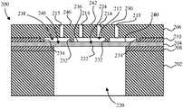
- FIG. 2shows a section view of a sensor device 200 according to one embodiment.
- the sensor device 200has at least three semiconductor layers which include a substrate layer or base layer 202 , an intermediate layer 204 , and a backplate layer or cap layer 206 .
- the sensor device 200also has at least two dielectric layers which include a first oxide layer 208 located between the base layer 202 and the intermediate layer 204 and a second oxide layer 210 located partially between the intermediate layer 204 and the cap layer 206 .
- the first oxide layer 208electrically decouples the intermediate layer 204 from the base layer 202 .
- the second oxide layer 210partially decouples the intermediate layer 204 from the cap layer 206 .
- the second oxide layer 210includes a plurality of spacers located between the cap layer 206 and the intermediate layer 204 .
- the spacersinclude at least two inner spacers 232 spaced laterally apart from one another and preferably at least two outer spacers 234 .
- a first of the outer spacers 234is spaced outwardly from the left-most one of the inner spacers 232 as viewed in the figure and a second of the outer spacers 234 is spaced outwardly from the right-most one of inner spacers 232 as viewed in the figure.
- the spacersare preferably realized using a perimeter-like closed configuration such that the spacers form a single ring, but they appear in cross section as two separate spacers.
- the peripheral cavity 238surrounds the central cavity 212 and is separated from the central cavity 212 by the inner spacers 232 .
- the cavitiesare connected to different pressures. In another embodiments, both cavities are connected to the same pressure.
- the outer peripheral cavity, after formation,is filled with an insulating oxide, a semi-conducting silicon material, or the like.
- the electrode 242is located above the central cavity 212 and aligned with the upper central surface 236 of the intermediate layer 204 .
- a first of the spacer portions 246is anchored to the first of the inner spacers 232 and a second of the spacer portions 246 is anchored to the second of the inner spacers 232 .
- the spacer portions 246are each laterally insulated from the electrode 242 and from other portions of the cap layer 206 by the trench portions 214 , 215 .
- a backside trench 220exposes a lower surface 222 of the intermediate layer 204 .
- the lower surface 222 and the upper central surface 236which is located between the inner spacers 232 , collectively define a sensor membrane or inner membrane 224 of the sensor device 200 .
- the inner membrane 224 and the electrode 242collectively define a capacitor within the sensor device 200 .
- the size of the inner membrane 224is precisely controlled since the positioning of the inner spacers 232 sets the position and the lateral dimension of the inner membrane 224 within the sensor device 200 .
- the inner membrane 224may vary in size by less than one (1) ⁇ m from wafer to wafer or within a single wafer.
- the lower surface 222 and the upper peripheral surface 240which is located between the inner spacers 232 and the outer spacers 234 , collectively define a buffer membrane/buffer area or outer membrane 248 of the sensor device 200 .
- the outer membrane 248does not provide an electrical function and, instead, provides only mechanical function.
- the outer membrane 248compensates for any variations in the diameter of the backside trench 220 since the position and the size of inner membrane 224 is no longer affected by the diameter of the backside trench 220 .
- the outer membrane 248also compensates for external stress on the sensor device 200 by deflecting slightly under an external load to absorb the external stress.
- an oxide layer 310is formed on a silicon-on-insulator (SOI) wafer 300 which includes a base layer 302 , a buried oxide layer 308 , and an intermediate layer 304 .
- the intermediate layer 304is a layer of poly- or epitaxial-silicon.
- the oxide layers 308 , 310 in the embodiment shownare layers of silicon dioxide (SiO 2 ) that can be, for example, grown by a thermal oxidation process or deposited using PECVD or LPCVD processes.
- FIG. 4shows the oxide layer 310 patterned to expose portions of the intermediate layer 304 .
- the patterning of the oxide layer 310forms a central trench portion 314 and a peripheral trench portion 315 spaced outwardly from the central trench portion. In some embodiments, only the central trench portion 314 is patterned in the oxide layer 310 .
- a layer of siliconis deposited above the patterned oxide layer 310 to form a cap layer 306 of the wafer 300 .
- the cap layer 306is deposited by chemical vapor deposition (CVD) or, more particularly, low pressure chemical vapor deposition (LPCVD), or via epitaxial layer growth.
- the cap layer 306fills the trench portions 314 , 315 and forms a plurality of spacers located between the cap layer 306 and the intermediate layer 304 .
- the spacersinclude at least two inner spacer portions 332 spaced laterally apart from one another and at least two outer spacer portions 334 .
- a first of the outer spacer portions 334is spaced outwardly from the left-most one of the inner spacer portions 332 as viewed in the figure and a second of the outer spacer portions 334 is spaced outwardly from the right-most one of inner spacer portions 332 as viewed in the figure.
- only the inner spacer portions 332are formed in the wafer 300 during the deposition of the cap layer 306 .
- FIG. 6shows the cap layer 306 of the wafer 300 with a trench portion etched therethrough.
- the trench portion in the embodiment shownincludes a central trench portion 350 and a peripheral trench portion 352 spaced outwardly from the central trench portion 350 .
- the central trench portion 350is positioned to expose portions of the oxide layer 310 located between the inner spacers 314
- the peripheral trench portion 352is positioned to expose portions of the oxide layer 310 located between the inner and the outer spacers 314 , 315 .
- the etching of the central trench portion 350electrically isolates an electrode 342 within the cap layer 306 .
- the etching of the peripheral trench portion 352isolates at least two spacer portions 346 within the cap layer 306 .
- vents holes(not shown) can also be etched through portions of the cap layer 306 to expose further portions of the oxide layer 310 located between the spacers 314 , 315 .
- a hydrofluoric acid (HF) vapor etch releaseis performed which releases entirely the portion of the oxide layer 310 located between the spacers 332 , 334 .
- the etching processforms a central cavity 312 between the inner spacers 332 , the intermediate layer 304 , and the cap layer 306 .
- the etching processalso forms a peripheral cavity 338 between the inner and the outer spacers 332 , 334 , the intermediate layer 304 , and the cap layer 304 .
- the central cavity 312 and the central trench portion 350electrically decouple the electrode 342 from the intermediate layer 304 and the cap layer 306 .
- a backside trench( 220 in FIG.
- the portion of the intermediate layer 204 exposed by the central cavity 212defines the inner membrane 224 of the sensor device 200 .
- the silicon-filled spacers 232 , 234provide a hard stop during the etching process ( FIG. 6 )
- itis the patterning of the oxide layer 310 ( FIG. 4 ) that defines the position and the size of the central cavity 212 and, therefore, the position and size of the inner membrane 224 .
- the formation of the membrane using the above-described processis substantially more controllable than the prior art fabrication methods since the patterning process that defines the membrane is performed through a relatively thin depth (e.g., the oxide layer 210 ).
- a timed-etch processis no longer relied upon to form the membrane-defining cavity ( 124 in FIG. 1 ) within the oxide layer since the spacers 232 , 234 function as etch stops during formation of the central cavity 212 in the sensor 200 .
- the membrane-based sensor produced using the above-described processincludes an inner membrane as a sensor membrane and an outer membrane as a buffer membrane.
- the inner membraneis defined by precision-formed anchor structures, and the inner membrane has both electrical and mechanical functionality.
- the outer membraneis also defined by the precision-formed anchor structures, but the outer membrane has only mechanical functionality. In particular, the outer membrane functions to compensate for any process variations and/or non-uniformities during the back-side trench process and for external stress affecting the sensor performance.
- the membrane-based sensorin various embodiments may be a pressure sensor, a capacitive pressure sensor, a microphone, and capacitive microphone.
Landscapes
- Physics & Mathematics (AREA)
- General Physics & Mathematics (AREA)
- Engineering & Computer Science (AREA)
- Chemical & Material Sciences (AREA)
- Analytical Chemistry (AREA)
- Acoustics & Sound (AREA)
- Signal Processing (AREA)
- Mechanical Engineering (AREA)
- Computer Hardware Design (AREA)
- Microelectronics & Electronic Packaging (AREA)
- Pressure Sensors (AREA)
- Measuring Fluid Pressure (AREA)
Abstract
Description
Claims (15)
Priority Applications (1)
| Application Number | Priority Date | Filing Date | Title |
|---|---|---|---|
| US15/301,226US11402288B2 (en) | 2014-04-04 | 2015-04-03 | Membrane-based sensor having a plurality of spacers extending from a cap layer |
Applications Claiming Priority (3)
| Application Number | Priority Date | Filing Date | Title |
|---|---|---|---|
| US201461975175P | 2014-04-04 | 2014-04-04 | |
| US15/301,226US11402288B2 (en) | 2014-04-04 | 2015-04-03 | Membrane-based sensor having a plurality of spacers extending from a cap layer |
| PCT/US2015/024194WO2015153938A1 (en) | 2014-04-04 | 2015-04-03 | Membrane-based sensor and method for robust manufacture of a membrane-based sensor |
Publications (2)
| Publication Number | Publication Date |
|---|---|
| US20170023426A1 US20170023426A1 (en) | 2017-01-26 |
| US11402288B2true US11402288B2 (en) | 2022-08-02 |
Family
ID=54241306
Family Applications (1)
| Application Number | Title | Priority Date | Filing Date |
|---|---|---|---|
| US15/301,226Active2037-01-12US11402288B2 (en) | 2014-04-04 | 2015-04-03 | Membrane-based sensor having a plurality of spacers extending from a cap layer |
Country Status (3)
| Country | Link |
|---|---|
| US (1) | US11402288B2 (en) |
| EP (1) | EP3127158B1 (en) |
| WO (1) | WO2015153938A1 (en) |
Cited By (1)
| Publication number | Priority date | Publication date | Assignee | Title |
|---|---|---|---|---|
| US20220026300A1 (en)* | 2018-11-27 | 2022-01-27 | Grundfos Holding A/S | A cover for a pressure sensor |
Families Citing this family (3)
| Publication number | Priority date | Publication date | Assignee | Title |
|---|---|---|---|---|
| US20160277845A1 (en)* | 2015-03-17 | 2016-09-22 | Dsp Group Ltd. | Mems-based speaker implementation |
| EP3533386A1 (en)* | 2018-02-28 | 2019-09-04 | Koninklijke Philips N.V. | Pressure sensing with capacitive pressure sensor |
| KR20210015194A (en)* | 2019-08-01 | 2021-02-10 | 현대자동차주식회사 | Vehicle rain sensor, and wiper system and method for controlling windshield wiper using the same |
Citations (72)
| Publication number | Priority date | Publication date | Assignee | Title |
|---|---|---|---|---|
| US4216401A (en)* | 1978-12-22 | 1980-08-05 | United Technologies Corporation | Surface acoustic wave (SAW) pressure sensor structure |
| US4628740A (en)* | 1983-11-21 | 1986-12-16 | Yokogawa Hokushin Electric Corporation | Pressure sensor |
| US4849071A (en)* | 1986-12-13 | 1989-07-18 | Spectrol Reliance Limited | Method of forming a sealed diaphragm on a substrate |
| US5209121A (en)* | 1990-07-24 | 1993-05-11 | Pfister Messtechnik Gmbh | Pressure sensor |
| US5220838A (en)* | 1991-03-28 | 1993-06-22 | The Foxboro Company | Overpressure-protected, differential pressure sensor and method of making the same |
| US5277068A (en)* | 1990-10-05 | 1994-01-11 | Yamatake-Honeywell Co., Ltd. | Capacitive pressure sensor and method of manufacturing the same |
| US5295395A (en)* | 1991-02-07 | 1994-03-22 | Hocker G Benjamin | Diaphragm-based-sensors |
| US5479827A (en)* | 1994-10-07 | 1996-01-02 | Yamatake-Honeywell Co., Ltd. | Capacitive pressure sensor isolating electrodes from external environment |
| US5553506A (en)* | 1993-09-29 | 1996-09-10 | Robert Bosch Gmbh | Force sensor and a method for manufacturing a force sensor |
| US5801313A (en)* | 1995-05-26 | 1998-09-01 | Omron Corporation | Capacitive sensor |
| US5824910A (en)* | 1997-04-16 | 1998-10-20 | The United States Of America As Represented By The Secretary Of The Navy | Miniature hydrostat fabricated using multiple microelectromechanical processes |
| US5891751A (en)* | 1995-06-02 | 1999-04-06 | Kulite Semiconductor Products, Inc . | Hermetically sealed transducers and methods for producing the same |
| US6346742B1 (en)* | 1998-11-12 | 2002-02-12 | Maxim Integrated Products, Inc. | Chip-scale packaged pressure sensor |
| US6426239B1 (en) | 1998-02-02 | 2002-07-30 | Motorola, Inc. | Method of manufacturing a semiconductor component having a fixed electrode between two flexible diaphragms |
| US6535460B2 (en)* | 2000-08-11 | 2003-03-18 | Knowles Electronics, Llc | Miniature broadband acoustic transducer |
| US6604425B1 (en)* | 2000-06-09 | 2003-08-12 | Hrl Laboratories, Llc | Microelectromechanical correlation device and method |
| US6612178B1 (en)* | 2002-05-13 | 2003-09-02 | Kulite Semiconductor Products, Inc. | Leadless metal media protected pressure sensor |
| US6635519B2 (en)* | 2002-01-10 | 2003-10-21 | Agere Systems, Inc. | Structurally supported thin film resonator and method of fabrication |
| US6655216B1 (en)* | 2002-07-18 | 2003-12-02 | Tem-Tech Lab. Co., Ltd. | Load transducer-type metal diaphragm pressure sensor |
| US20030222660A1 (en)* | 2002-05-29 | 2003-12-04 | Hideo Morimoto | Capacitance type sensor and method for manufacturing same |
| US6700174B1 (en) | 1997-09-25 | 2004-03-02 | Integrated Micromachines, Inc. | Batch fabricated semiconductor thin-film pressure sensor and method of making same |
| US6848320B2 (en)* | 2002-07-19 | 2005-02-01 | Matsushita Electric Works, Ltd. | Mechanical deformation amount sensor |
| US6890834B2 (en)* | 2001-06-11 | 2005-05-10 | Matsushita Electric Industrial Co., Ltd. | Electronic device and method for manufacturing the same |
| US7111518B1 (en)* | 2003-09-19 | 2006-09-26 | Silicon Microstructures, Inc. | Extremely low cost pressure sensor realized using deep reactive ion etching |
| US7202560B2 (en)* | 2004-12-15 | 2007-04-10 | Avago Technologies Wireless Ip (Singapore) Pte. Ltd. | Wafer bonding of micro-electro mechanical systems to active circuitry |
| US7247246B2 (en)* | 2003-10-20 | 2007-07-24 | Atmel Corporation | Vertical integration of a MEMS structure with electronics in a hermetically sealed cavity |
| US20070291964A1 (en)* | 2006-06-20 | 2007-12-20 | Industrial Technology Research Institute | Miniature acoustic transducer |
| US7442570B2 (en)* | 2005-03-18 | 2008-10-28 | Invensence Inc. | Method of fabrication of a AL/GE bonding in a wafer packaging environment and a product produced therefrom |
| US7478559B2 (en)* | 2003-12-04 | 2009-01-20 | National University Of Singapore | Capacitive pressure sensor with a cantilever member |
| US7484419B2 (en)* | 2006-01-23 | 2009-02-03 | Denso Corporation | Mounting structure of pressure sensor element |
| US7508040B2 (en)* | 2006-06-05 | 2009-03-24 | Hewlett-Packard Development Company, L.P. | Micro electrical mechanical systems pressure sensor |
| US20090120195A1 (en)* | 2007-11-08 | 2009-05-14 | Willcox Charles R | Pressure sensor |
| US20090193903A1 (en) | 2008-02-01 | 2009-08-06 | Honeywell International Inc. | Method for sensor fabrication and related sensor and system |
| US20090278217A1 (en) | 2006-03-20 | 2009-11-12 | Richard Ian Laming | Mems device |
| US7622782B2 (en)* | 2005-08-24 | 2009-11-24 | General Electric Company | Pressure sensors and methods of making the same |
| US7651879B2 (en)* | 2005-12-07 | 2010-01-26 | Honeywell International Inc. | Surface acoustic wave pressure sensors |
| US7661318B2 (en)* | 2006-02-27 | 2010-02-16 | Auxitrol S.A. | Stress isolated pressure sensing die, sensor assembly inluding said die and methods for manufacturing said die and said assembly |
| US7704774B2 (en)* | 2006-05-23 | 2010-04-27 | Sensirion Holding Ag | Pressure sensor having a chamber and a method for fabricating the same |
| US20100133630A1 (en) | 2007-04-26 | 2010-06-03 | Roland Scheuerer | Method for producing a micromechanical component having a trench structure for backside contact |
| US20100186515A1 (en)* | 2009-01-27 | 2010-07-29 | Epson Toyocom Corporation | Pressure detection unit and pressure sensor |
| US20100224004A1 (en) | 2009-03-03 | 2010-09-09 | S3C, Inc. | Media-compatible electrically isolated pressure sensor for high temperature applications |
| US7805821B2 (en)* | 2006-08-22 | 2010-10-05 | Yamaha Corporation | Method of making capacitance sensor |
| US20110108933A1 (en)* | 2008-07-11 | 2011-05-12 | Rohm Co., Ltd. | Mems device |
| US7955885B1 (en)* | 2009-01-09 | 2011-06-07 | Integrated Device Technology, Inc. | Methods of forming packaged micro-electromechanical devices |
| US8096196B2 (en)* | 2007-12-14 | 2012-01-17 | Siemens Ag | Load cell |
| US20120031189A1 (en)* | 2010-08-09 | 2012-02-09 | Seiko Epson Corporation | Pressure sensor |
| US8215176B2 (en)* | 2009-05-27 | 2012-07-10 | Continental Automotive Systems, Inc. | Pressure sensor for harsh media sensing and flexible packaging |
| US8384168B2 (en)* | 2011-04-21 | 2013-02-26 | Freescale Semiconductor, Inc. | Sensor device with sealing structure |
| US8387464B2 (en)* | 2009-11-30 | 2013-03-05 | Freescale Semiconductor, Inc. | Laterally integrated MEMS sensor device with multi-stimulus sensing |
| US8426934B2 (en)* | 2008-04-30 | 2013-04-23 | Pixart Imaging Incorporation | Micro-electro-mechanical system device and method for making same |
| US8445976B2 (en)* | 2009-08-10 | 2013-05-21 | Kabushiki Kaisha Toshiba | Micro movable device |
| US8476087B2 (en)* | 2011-04-21 | 2013-07-02 | Freescale Semiconductor, Inc. | Methods for fabricating sensor device package using a sealing structure |
| US20130207208A1 (en) | 2012-02-15 | 2013-08-15 | Robert Bosch Gmbh | Pressure Sensor with Doped Electrode |
| US20130214370A1 (en)* | 2010-05-03 | 2013-08-22 | S3C, Inc. | System and method for minimizing deflection of a membrance of an absolute pressure sensor |
| US8667849B2 (en)* | 2010-09-29 | 2014-03-11 | Seiko Epson Corporation | Pressure sensor |
| US8984950B2 (en)* | 2012-04-20 | 2015-03-24 | Rosemount Aerospace Inc. | Separation mode capacitors for sensors |
| US20150109889A1 (en)* | 2013-10-17 | 2015-04-23 | Merry Electronics (Shenzhen) Co., Ltd. | Acoustic transducer with membrane supporting structure |
| US9066180B2 (en)* | 2012-03-13 | 2015-06-23 | Robert Bosch Gmbh | Component having a micromechanical microphone structure |
| US20150260593A1 (en)* | 2014-03-17 | 2015-09-17 | Richtek Technology Corporation | Mirco-electro-mechanical system pressure sensor and manufacturing method thereof |
| US9212054B1 (en)* | 2014-10-15 | 2015-12-15 | DunAn Sensing, LLC | Pressure sensors and methods of making the same |
| US20160023891A1 (en)* | 2014-07-24 | 2016-01-28 | Robert Bosch Gmbh | Component including a MEMS element and a cap structure including a media connection port |
| US20160033349A1 (en)* | 2014-07-29 | 2016-02-04 | Silicon Microstructures, Inc. | Pressure sensor having cap-defined membrane |
| US9340412B2 (en)* | 2014-07-28 | 2016-05-17 | Ams International Ag | Suspended membrane for capacitive pressure sensor |
| US9369808B2 (en)* | 2013-10-17 | 2016-06-14 | Merry Electronics (Shenzhen) Co., Ltd. | Acoustic transducer with high sensitivity |
| US9506827B2 (en)* | 2014-10-15 | 2016-11-29 | Dunan Sensing Llc | Pressure sensors and methods of making the same |
| US9516428B2 (en)* | 2013-03-14 | 2016-12-06 | Infineon Technologies Ag | MEMS acoustic transducer, MEMS microphone, MEMS microspeaker, array of speakers and method for manufacturing an acoustic transducer |
| US9546922B2 (en)* | 2013-08-09 | 2017-01-17 | Continental Automotive Systems, Inc. | Absolute pressure sensor with improved cap bonding boundary |
| US9581512B2 (en)* | 2013-11-06 | 2017-02-28 | Invensense, Inc. | Pressure sensor with deformable membrane and method of manufacture |
| US9709451B2 (en)* | 2014-01-14 | 2017-07-18 | Robert Bosch Gmbh | Micromechanical pressure sensor device and corresponding manufacturing method |
| US20170219449A1 (en)* | 2016-02-02 | 2017-08-03 | Asia Pacific Microsystems, Inc. | Piezoresistive pressure sensor |
| US9764947B2 (en)* | 2014-11-25 | 2017-09-19 | Continental Automotive Systems, Inc. | Piezoresistive pressure sensor device |
| US20180202807A1 (en)* | 2017-01-18 | 2018-07-19 | Robert Bosch Gmbh | Micromechanical sensor |
- 2015
- 2015-04-03WOPCT/US2015/024194patent/WO2015153938A1/enactiveApplication Filing
- 2015-04-03USUS15/301,226patent/US11402288B2/enactiveActive
- 2015-04-03EPEP15772419.6Apatent/EP3127158B1/enactiveActive
Patent Citations (78)
| Publication number | Priority date | Publication date | Assignee | Title |
|---|---|---|---|---|
| US4216401A (en)* | 1978-12-22 | 1980-08-05 | United Technologies Corporation | Surface acoustic wave (SAW) pressure sensor structure |
| US4628740A (en)* | 1983-11-21 | 1986-12-16 | Yokogawa Hokushin Electric Corporation | Pressure sensor |
| US4849071A (en)* | 1986-12-13 | 1989-07-18 | Spectrol Reliance Limited | Method of forming a sealed diaphragm on a substrate |
| US5209121A (en)* | 1990-07-24 | 1993-05-11 | Pfister Messtechnik Gmbh | Pressure sensor |
| US5277068A (en)* | 1990-10-05 | 1994-01-11 | Yamatake-Honeywell Co., Ltd. | Capacitive pressure sensor and method of manufacturing the same |
| US5295395A (en)* | 1991-02-07 | 1994-03-22 | Hocker G Benjamin | Diaphragm-based-sensors |
| US5438875A (en)* | 1991-03-28 | 1995-08-08 | The Foxboro Company | Removing sacrificial material through temporary channels as a method of making an overpressure-protected differential pressure sensor |
| US5357808A (en)* | 1991-03-28 | 1994-10-25 | The Foxboro Company | Overpressure-protected, differential pressure sensor |
| US5220838A (en)* | 1991-03-28 | 1993-06-22 | The Foxboro Company | Overpressure-protected, differential pressure sensor and method of making the same |
| US5553506A (en)* | 1993-09-29 | 1996-09-10 | Robert Bosch Gmbh | Force sensor and a method for manufacturing a force sensor |
| US5479827A (en)* | 1994-10-07 | 1996-01-02 | Yamatake-Honeywell Co., Ltd. | Capacitive pressure sensor isolating electrodes from external environment |
| US5801313A (en)* | 1995-05-26 | 1998-09-01 | Omron Corporation | Capacitive sensor |
| US5891751A (en)* | 1995-06-02 | 1999-04-06 | Kulite Semiconductor Products, Inc . | Hermetically sealed transducers and methods for producing the same |
| US5824910A (en)* | 1997-04-16 | 1998-10-20 | The United States Of America As Represented By The Secretary Of The Navy | Miniature hydrostat fabricated using multiple microelectromechanical processes |
| US6700174B1 (en) | 1997-09-25 | 2004-03-02 | Integrated Micromachines, Inc. | Batch fabricated semiconductor thin-film pressure sensor and method of making same |
| US6426239B1 (en) | 1998-02-02 | 2002-07-30 | Motorola, Inc. | Method of manufacturing a semiconductor component having a fixed electrode between two flexible diaphragms |
| US6346742B1 (en)* | 1998-11-12 | 2002-02-12 | Maxim Integrated Products, Inc. | Chip-scale packaged pressure sensor |
| US6604425B1 (en)* | 2000-06-09 | 2003-08-12 | Hrl Laboratories, Llc | Microelectromechanical correlation device and method |
| US6535460B2 (en)* | 2000-08-11 | 2003-03-18 | Knowles Electronics, Llc | Miniature broadband acoustic transducer |
| US6890834B2 (en)* | 2001-06-11 | 2005-05-10 | Matsushita Electric Industrial Co., Ltd. | Electronic device and method for manufacturing the same |
| US6635519B2 (en)* | 2002-01-10 | 2003-10-21 | Agere Systems, Inc. | Structurally supported thin film resonator and method of fabrication |
| US6612178B1 (en)* | 2002-05-13 | 2003-09-02 | Kulite Semiconductor Products, Inc. | Leadless metal media protected pressure sensor |
| US20030222660A1 (en)* | 2002-05-29 | 2003-12-04 | Hideo Morimoto | Capacitance type sensor and method for manufacturing same |
| US6655216B1 (en)* | 2002-07-18 | 2003-12-02 | Tem-Tech Lab. Co., Ltd. | Load transducer-type metal diaphragm pressure sensor |
| US6848320B2 (en)* | 2002-07-19 | 2005-02-01 | Matsushita Electric Works, Ltd. | Mechanical deformation amount sensor |
| US7111518B1 (en)* | 2003-09-19 | 2006-09-26 | Silicon Microstructures, Inc. | Extremely low cost pressure sensor realized using deep reactive ion etching |
| US7247246B2 (en)* | 2003-10-20 | 2007-07-24 | Atmel Corporation | Vertical integration of a MEMS structure with electronics in a hermetically sealed cavity |
| US7478559B2 (en)* | 2003-12-04 | 2009-01-20 | National University Of Singapore | Capacitive pressure sensor with a cantilever member |
| US7202560B2 (en)* | 2004-12-15 | 2007-04-10 | Avago Technologies Wireless Ip (Singapore) Pte. Ltd. | Wafer bonding of micro-electro mechanical systems to active circuitry |
| US8143082B2 (en)* | 2004-12-15 | 2012-03-27 | Avago Technologies Wireless Ip (Singapore) Pte. Ltd. | Wafer bonding of micro-electro mechanical systems to active circuitry |
| US7442570B2 (en)* | 2005-03-18 | 2008-10-28 | Invensence Inc. | Method of fabrication of a AL/GE bonding in a wafer packaging environment and a product produced therefrom |
| US7622782B2 (en)* | 2005-08-24 | 2009-11-24 | General Electric Company | Pressure sensors and methods of making the same |
| US7651879B2 (en)* | 2005-12-07 | 2010-01-26 | Honeywell International Inc. | Surface acoustic wave pressure sensors |
| US7484419B2 (en)* | 2006-01-23 | 2009-02-03 | Denso Corporation | Mounting structure of pressure sensor element |
| US7661318B2 (en)* | 2006-02-27 | 2010-02-16 | Auxitrol S.A. | Stress isolated pressure sensing die, sensor assembly inluding said die and methods for manufacturing said die and said assembly |
| US7856804B2 (en)* | 2006-03-20 | 2010-12-28 | Wolfson Microelectronics Plc | MEMS process and device |
| US20090278217A1 (en) | 2006-03-20 | 2009-11-12 | Richard Ian Laming | Mems device |
| US7704774B2 (en)* | 2006-05-23 | 2010-04-27 | Sensirion Holding Ag | Pressure sensor having a chamber and a method for fabricating the same |
| US7508040B2 (en)* | 2006-06-05 | 2009-03-24 | Hewlett-Packard Development Company, L.P. | Micro electrical mechanical systems pressure sensor |
| US20070291964A1 (en)* | 2006-06-20 | 2007-12-20 | Industrial Technology Research Institute | Miniature acoustic transducer |
| US7805821B2 (en)* | 2006-08-22 | 2010-10-05 | Yamaha Corporation | Method of making capacitance sensor |
| US20100133630A1 (en) | 2007-04-26 | 2010-06-03 | Roland Scheuerer | Method for producing a micromechanical component having a trench structure for backside contact |
| US20090120195A1 (en)* | 2007-11-08 | 2009-05-14 | Willcox Charles R | Pressure sensor |
| US8096196B2 (en)* | 2007-12-14 | 2012-01-17 | Siemens Ag | Load cell |
| US7891252B2 (en)* | 2008-02-01 | 2011-02-22 | Honeywell International Inc. | Method for sensor fabrication and related sensor and system |
| US20090193903A1 (en) | 2008-02-01 | 2009-08-06 | Honeywell International Inc. | Method for sensor fabrication and related sensor and system |
| US8426934B2 (en)* | 2008-04-30 | 2013-04-23 | Pixart Imaging Incorporation | Micro-electro-mechanical system device and method for making same |
| US20110108933A1 (en)* | 2008-07-11 | 2011-05-12 | Rohm Co., Ltd. | Mems device |
| US7955885B1 (en)* | 2009-01-09 | 2011-06-07 | Integrated Device Technology, Inc. | Methods of forming packaged micro-electromechanical devices |
| US20100186515A1 (en)* | 2009-01-27 | 2010-07-29 | Epson Toyocom Corporation | Pressure detection unit and pressure sensor |
| US20100224004A1 (en) | 2009-03-03 | 2010-09-09 | S3C, Inc. | Media-compatible electrically isolated pressure sensor for high temperature applications |
| US8627559B2 (en)* | 2009-03-03 | 2014-01-14 | S3C, Inc. | Media-compatible electrically isolated pressure sensor for high temperature applications |
| US8215176B2 (en)* | 2009-05-27 | 2012-07-10 | Continental Automotive Systems, Inc. | Pressure sensor for harsh media sensing and flexible packaging |
| US8445976B2 (en)* | 2009-08-10 | 2013-05-21 | Kabushiki Kaisha Toshiba | Micro movable device |
| US8387464B2 (en)* | 2009-11-30 | 2013-03-05 | Freescale Semiconductor, Inc. | Laterally integrated MEMS sensor device with multi-stimulus sensing |
| US20130214370A1 (en)* | 2010-05-03 | 2013-08-22 | S3C, Inc. | System and method for minimizing deflection of a membrance of an absolute pressure sensor |
| US20120031189A1 (en)* | 2010-08-09 | 2012-02-09 | Seiko Epson Corporation | Pressure sensor |
| US8667849B2 (en)* | 2010-09-29 | 2014-03-11 | Seiko Epson Corporation | Pressure sensor |
| US8384168B2 (en)* | 2011-04-21 | 2013-02-26 | Freescale Semiconductor, Inc. | Sensor device with sealing structure |
| US8476087B2 (en)* | 2011-04-21 | 2013-07-02 | Freescale Semiconductor, Inc. | Methods for fabricating sensor device package using a sealing structure |
| US20130207208A1 (en) | 2012-02-15 | 2013-08-15 | Robert Bosch Gmbh | Pressure Sensor with Doped Electrode |
| US9066180B2 (en)* | 2012-03-13 | 2015-06-23 | Robert Bosch Gmbh | Component having a micromechanical microphone structure |
| US8984950B2 (en)* | 2012-04-20 | 2015-03-24 | Rosemount Aerospace Inc. | Separation mode capacitors for sensors |
| US9516428B2 (en)* | 2013-03-14 | 2016-12-06 | Infineon Technologies Ag | MEMS acoustic transducer, MEMS microphone, MEMS microspeaker, array of speakers and method for manufacturing an acoustic transducer |
| US9546922B2 (en)* | 2013-08-09 | 2017-01-17 | Continental Automotive Systems, Inc. | Absolute pressure sensor with improved cap bonding boundary |
| US9369808B2 (en)* | 2013-10-17 | 2016-06-14 | Merry Electronics (Shenzhen) Co., Ltd. | Acoustic transducer with high sensitivity |
| US20150109889A1 (en)* | 2013-10-17 | 2015-04-23 | Merry Electronics (Shenzhen) Co., Ltd. | Acoustic transducer with membrane supporting structure |
| US9581512B2 (en)* | 2013-11-06 | 2017-02-28 | Invensense, Inc. | Pressure sensor with deformable membrane and method of manufacture |
| US9709451B2 (en)* | 2014-01-14 | 2017-07-18 | Robert Bosch Gmbh | Micromechanical pressure sensor device and corresponding manufacturing method |
| US20150260593A1 (en)* | 2014-03-17 | 2015-09-17 | Richtek Technology Corporation | Mirco-electro-mechanical system pressure sensor and manufacturing method thereof |
| US20160023891A1 (en)* | 2014-07-24 | 2016-01-28 | Robert Bosch Gmbh | Component including a MEMS element and a cap structure including a media connection port |
| US9340412B2 (en)* | 2014-07-28 | 2016-05-17 | Ams International Ag | Suspended membrane for capacitive pressure sensor |
| US20160033349A1 (en)* | 2014-07-29 | 2016-02-04 | Silicon Microstructures, Inc. | Pressure sensor having cap-defined membrane |
| US9506827B2 (en)* | 2014-10-15 | 2016-11-29 | Dunan Sensing Llc | Pressure sensors and methods of making the same |
| US9212054B1 (en)* | 2014-10-15 | 2015-12-15 | DunAn Sensing, LLC | Pressure sensors and methods of making the same |
| US9764947B2 (en)* | 2014-11-25 | 2017-09-19 | Continental Automotive Systems, Inc. | Piezoresistive pressure sensor device |
| US20170219449A1 (en)* | 2016-02-02 | 2017-08-03 | Asia Pacific Microsystems, Inc. | Piezoresistive pressure sensor |
| US20180202807A1 (en)* | 2017-01-18 | 2018-07-19 | Robert Bosch Gmbh | Micromechanical sensor |
Non-Patent Citations (2)
| Title |
|---|
| International Search Report corresponding to PCT Application No. PCT/US2015/024194, dated Jun. 30, 2015 (4 pages). |
| Supplementary European Search Report corresponding to European Patent Application No. 15 77 2419 (10 pages). |
Cited By (2)
| Publication number | Priority date | Publication date | Assignee | Title |
|---|---|---|---|---|
| US20220026300A1 (en)* | 2018-11-27 | 2022-01-27 | Grundfos Holding A/S | A cover for a pressure sensor |
| US12013298B2 (en)* | 2018-11-27 | 2024-06-18 | Grundfos Holding A/S | Protective cover for a pressure sensor |
Also Published As
| Publication number | Publication date |
|---|---|
| US20170023426A1 (en) | 2017-01-26 |
| EP3127158B1 (en) | 2019-06-12 |
| EP3127158A1 (en) | 2017-02-08 |
| WO2015153938A1 (en) | 2015-10-08 |
| EP3127158A4 (en) | 2017-11-08 |
Similar Documents
| Publication | Publication Date | Title |
|---|---|---|
| US20200236470A1 (en) | Microelectromechanical electroacoustic transducer with piezoelectric actuation and corresponding manufacturing process | |
| US9458009B2 (en) | Semiconductor devices and methods of forming thereof | |
| JP5649474B2 (en) | Capacitance type pressure sensor and method of manufacturing capacitance type pressure sensor | |
| TWI624954B (en) | Inertial and pressure sensors on single chip | |
| US8673756B2 (en) | Out-of-plane spacer defined electrode | |
| TW201524891A (en) | Pressure sensor | |
| WO2009101757A1 (en) | Capacitor microphone and mems device | |
| US11402288B2 (en) | Membrane-based sensor having a plurality of spacers extending from a cap layer | |
| JP5721452B2 (en) | Capacitive MEMS sensor | |
| KR20170002947A (en) | Pressure sensor element and method for manufacturing same | |
| US10173887B2 (en) | Epi-poly etch stop for out of plane spacer defined electrode | |
| EP3614372B1 (en) | Method for manufacturing an air pulse generating element | |
| EP2815219B1 (en) | Pressure sensor with doped electrode | |
| US10209155B2 (en) | Physical quantity sensing semiconductor device and method for manufacturing the same | |
| US9302906B2 (en) | Capacitive pressure sensor and method | |
| JP2015145037A (en) | MEMS device and manufacturing method thereof | |
| KR100758641B1 (en) | MEMS device comprising a method for forming a microstructure on a silicon substrate integrated with the CMOS circuit and the microstructure formed by the method | |
| KR20120016426A (en) | Piezoresistive pressure sensor and its manufacturing method | |
| JP2015145036A (en) | MEMS device and manufacturing method thereof |
Legal Events
| Date | Code | Title | Description |
|---|---|---|---|
| AS | Assignment | Owner name:ROBERT BOSCH GMBH, GERMANY Free format text:ASSIGNMENT OF ASSIGNORS INTEREST;ASSIGNORS:FEYH, ANDO LARS;O'BRIEN, GARY;SIGNING DATES FROM 20161004 TO 20161021;REEL/FRAME:040214/0759 | |
| STPP | Information on status: patent application and granting procedure in general | Free format text:RESPONSE TO NON-FINAL OFFICE ACTION ENTERED AND FORWARDED TO EXAMINER | |
| STPP | Information on status: patent application and granting procedure in general | Free format text:FINAL REJECTION MAILED | |
| STPP | Information on status: patent application and granting procedure in general | Free format text:FINAL REJECTION MAILED | |
| STPP | Information on status: patent application and granting procedure in general | Free format text:NON FINAL ACTION MAILED | |
| STPP | Information on status: patent application and granting procedure in general | Free format text:RESPONSE TO NON-FINAL OFFICE ACTION ENTERED AND FORWARDED TO EXAMINER | |
| STPP | Information on status: patent application and granting procedure in general | Free format text:FINAL REJECTION MAILED | |
| STCV | Information on status: appeal procedure | Free format text:NOTICE OF APPEAL FILED | |
| STCV | Information on status: appeal procedure | Free format text:EXAMINER'S ANSWER TO APPEAL BRIEF MAILED | |
| STCV | Information on status: appeal procedure | Free format text:REPLY BRIEF FILED AND FORWARDED TO BPAI | |
| STCV | Information on status: appeal procedure | Free format text:ON APPEAL -- AWAITING DECISION BY THE BOARD OF APPEALS | |
| STCV | Information on status: appeal procedure | Free format text:BOARD OF APPEALS DECISION RENDERED | |
| STPP | Information on status: patent application and granting procedure in general | Free format text:AMENDMENT / ARGUMENT AFTER BOARD OF APPEALS DECISION | |
| STPP | Information on status: patent application and granting procedure in general | Free format text:NOTICE OF ALLOWANCE MAILED -- APPLICATION RECEIVED IN OFFICE OF PUBLICATIONS | |
| STPP | Information on status: patent application and granting procedure in general | Free format text:PUBLICATIONS -- ISSUE FEE PAYMENT RECEIVED | |
| STCF | Information on status: patent grant | Free format text:PATENTED CASE |