US11397835B2 - Data device including OFN functionality - Google Patents
Data device including OFN functionalityDownload PDFInfo
- Publication number
- US11397835B2 US11397835B2US15/900,317US201815900317AUS11397835B2US 11397835 B2US11397835 B2US 11397835B2US 201815900317 AUS201815900317 AUS 201815900317AUS 11397835 B2US11397835 B2US 11397835B2
- Authority
- US
- United States
- Prior art keywords
- output
- housing
- tampering
- device housing
- ofn
- Prior art date
- Legal status (The legal status is an assumption and is not a legal conclusion. Google has not performed a legal analysis and makes no representation as to the accuracy of the status listed.)
- Active
Links
Images


Classifications
- G—PHYSICS
- G06—COMPUTING OR CALCULATING; COUNTING
- G06F—ELECTRIC DIGITAL DATA PROCESSING
- G06F21/00—Security arrangements for protecting computers, components thereof, programs or data against unauthorised activity
- G06F21/70—Protecting specific internal or peripheral components, in which the protection of a component leads to protection of the entire computer
- G06F21/86—Secure or tamper-resistant housings
- G06F21/87—Secure or tamper-resistant housings by means of encapsulation, e.g. for integrated circuits
- G—PHYSICS
- G06—COMPUTING OR CALCULATING; COUNTING
- G06F—ELECTRIC DIGITAL DATA PROCESSING
- G06F1/00—Details not covered by groups G06F3/00 - G06F13/00 and G06F21/00
- G06F1/16—Constructional details or arrangements
- G06F1/1613—Constructional details or arrangements for portable computers
- G06F1/1626—Constructional details or arrangements for portable computers with a single-body enclosure integrating a flat display, e.g. Personal Digital Assistants [PDAs]
- G—PHYSICS
- G06—COMPUTING OR CALCULATING; COUNTING
- G06F—ELECTRIC DIGITAL DATA PROCESSING
- G06F1/00—Details not covered by groups G06F3/00 - G06F13/00 and G06F21/00
- G06F1/16—Constructional details or arrangements
- G06F1/1613—Constructional details or arrangements for portable computers
- G06F1/1633—Constructional details or arrangements of portable computers not specific to the type of enclosures covered by groups G06F1/1615 - G06F1/1626
- G06F1/1662—Details related to the integrated keyboard
- G—PHYSICS
- G06—COMPUTING OR CALCULATING; COUNTING
- G06F—ELECTRIC DIGITAL DATA PROCESSING
- G06F21/00—Security arrangements for protecting computers, components thereof, programs or data against unauthorised activity
- G06F21/70—Protecting specific internal or peripheral components, in which the protection of a component leads to protection of the entire computer
- G06F21/86—Secure or tamper-resistant housings
- G—PHYSICS
- G06—COMPUTING OR CALCULATING; COUNTING
- G06F—ELECTRIC DIGITAL DATA PROCESSING
- G06F3/00—Input arrangements for transferring data to be processed into a form capable of being handled by the computer; Output arrangements for transferring data from processing unit to output unit, e.g. interface arrangements
- G06F3/01—Input arrangements or combined input and output arrangements for interaction between user and computer
- G06F3/048—Interaction techniques based on graphical user interfaces [GUI]
- G06F3/0487—Interaction techniques based on graphical user interfaces [GUI] using specific features provided by the input device, e.g. functions controlled by the rotation of a mouse with dual sensing arrangements, or of the nature of the input device, e.g. tap gestures based on pressure sensed by a digitiser
- G06F3/0489—Interaction techniques based on graphical user interfaces [GUI] using specific features provided by the input device, e.g. functions controlled by the rotation of a mouse with dual sensing arrangements, or of the nature of the input device, e.g. tap gestures based on pressure sensed by a digitiser using dedicated keyboard keys or combinations thereof
Definitions
- the present inventionrelates generally to data devices.
- the present inventionseeks to provide an improved data entry device.
- a data entry deviceincluding a housing, data entry circuitry located within the housing, a keypad mounted in the housing and having a plurality of movable key elements which, when depressed, are displaced to at least a predetermined extent from a first location within the housing to a second location within the housing and Optical Finger Navigation (OFN) circuitry mounted inside the housing, being operative for sensing at least some of the plurality of movable key elements when depressed and displaced to at least the predetermined extent from the first location within the housing to the second location within the housing and providing a key displacement output indicating key displacement to the data entry circuitry.
- OFNOptical Finger Navigation
- a data entry deviceincluding a housing, data entry circuitry located within the housing, tamper detection circuitry located within the housing, a keypad mounted in the housing and having a plurality of movable key elements and OFN circuitry mounted inside the housing, being operative for sensing displacement of the plurality of movable key elements and tampering with the device and providing a key displacement output indicating key displacement to at least a predetermined extent to the data entry circuitry and a tamper indication output to the tamper detection circuitry.
- a sensitive data deviceincluding a housing, sensitive data handling circuitry located within the housing, tamper detection circuitry located within the housing and OFN circuitry mounted inside the housing, being operative for sensing tampering with the device and providing a tamper indication output to the tamper detection circuitry.
- the OFN circuitryis mounted on an electrical circuit board spaced from the movable key elements.
- the devicealso includes a spacer mounted between the electrical circuit board and the keypad.
- the electrical circuit boardis arranged such that displacement of a key from a first location within the housing to a second location within the housing by the finger of a user is detected and identified by the OFN circuitry.
- the OFN circuitryis incorporated within an OFN module which includes an illuminator and optics. Additionally, the OFN module is generally centered with respect to the plurality of movable key elements and lies therebelow so as to be in a line of sight with all of the plurality of movable key elements. Preferably, the OFN module is also in a line of sight with other regions within the housing.
- the OFN moduleviews optically identifiable markings on the plurality of movable key elements as well as other objects which provide a background useful in detecting tampering.
- a background output of the OFN moduleis employed as a reference against which an output of said OFN module indicating possible tampering is compared.
- at least one of the following eventsproduces a tampering indication: creating a hole in the data entry device using a tool, the tool being seen by the OFN module and removal of the tool, allowing light to enter the housing, the light being seen by the OFN module.
- FIGS. 1A and 1Bare simplified exploded view illustrations, taken in respective opposite directions, of a secure keypad device constructed and operative in accordance with a preferred embodiment of the present invention and including Optical Finger Navigation (OFN) circuitry operative for at least one of tamper detection and key displacement identification;
- OFNOptical Finger Navigation
- FIG. 2Ais a simplified, not to scale, illustration of a steady state scene as viewed by OFN circuitry in the embodiment of FIGS. 1A & 1B in the absence of key displacement to at least a predetermined extent and tampering;
- FIG. 2Bis a simplified, not to scale, illustration of a scene as viewed by OFN circuitry upon depression of a number 5 key in the absence of tampering;
- FIG. 2Cis a simplified, not to scale, illustration of a scene as viewed by OFN circuitry upon depression of a number 1 key in the absence of tampering;
- FIG. 2Dis a simplified, not to scale, illustration of a scene as viewed by OFN circuitry upon tampering by inserting a non-reflecting probe into the housing;
- FIG. 2Eis a simplified, not to scale, illustration of a scene as viewed by OFN circuitry upon tampering by removing a key;
- FIGS. 3A and 3Bare simplified exploded view illustrations, taken in respective opposite directions, of a secure keypad device constructed and operative in accordance with another preferred embodiment of the present invention and including OFN circuitry operative for at least one of tamper detection and key displacement identification;
- FIG. 4Ais a simplified illustration of a steady state scene as viewed by OFN circuitry in the embodiment of FIGS. 3A & 3B in the absence of key displacement to at least a predetermined extent and tampering;
- FIG. 4Bis a simplified, not to scale, illustration of a scene as viewed by OFN circuitry in the embodiment of FIGS. 3A & 3B upon depression of a number 5 key in the absence of tampering;
- FIG. 4Cis a simplified, not to scale, illustration of a scene as viewed by OFN circuitry in the embodiment of FIGS. 3A & 3B upon depression of a number 1 key in the absence of tampering;
- FIG. 4Dis a simplified, not to scale, illustration of a scene as viewed by OFN circuitry in the embodiment of FIGS. 3A & 3B upon tampering by inserting a non-reflecting probe into the housing;
- FIG. 4Eis a simplified, not to scale, illustration of a scene as viewed by OFN circuitry in the embodiment of FIGS. 3A & 3B upon tampering by removing a key;
- FIGS. 5A and 5Bare simplified, not to scale, sectional illustrations showing detection of key displacement to at least a predetermined extent in a data entry device including OFN circuitry;
- FIGS. 6A and 6Bare simplified, not to scale, sectional illustrations showing detection of insertion of a probe in a data entry device including OFN circuitry;
- FIGS. 7A and 7Bare simplified, not to scale, sectional illustrations showing detection of key removal in a data entry device including OFN circuitry;
- FIGS. 8A and 8Bare, not to scale, simplified sectional illustrations showing detection of opening of a data entry device including OFN circuitry.
- FIG. 9is a simplified functional block diagram illustrating operation of the secure keypad device constructed and operative in accordance with a preferred embodiment of the present invention and including OFN circuitry operative for at least one of tamper detection and key displacement identification of FIGS. 1A-8B .
- FIGS. 1A and 1Bpartially illustrate a secure keypad device constructed and operative in accordance with a preferred embodiment of the present invention.
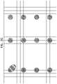
- a secure keypad device 100including a top housing element 102 and a bottom housing element (not shown), which together define a keypad device housing.
- Housing element 102includes, on a top surface 104 thereof, a display aperture 106 , through which a display (not shown) may be viewed, and an array 108 of key apertures 110 .
- An optional anti-tamper circuit board 112which preferably includes an anti-tampering grid 114 formed of a multiplicity of interconnected anti-tampering electrical conductors 116 , underlies top surface 104 and is provided with key apertures 120 in registration with key apertures 110 .
- a peripheral anti-tamper keypad enclosure 122Fixedly and electrically coupled to anti-tamper circuit board 112 is a peripheral anti-tamper keypad enclosure 122 , which preferably includes an anti-tampering grid 124 formed of a multiplicity of interconnected anti-tampering electrical conductors.
- a key mat 132preferably formed of a resilient plastic or rubber, defines a plurality of depressible keys 134 , preferably integrally formed with mat 132 , which partially extend through key apertures 110 and 120 and preferably have readily optically identifiable markings 136 formed on corresponding bottom facing surfaces 138 thereof. Additional optically identifiable markings 139 may be provided on other interior surfaces, such as inner surfaces of the housing.
- An electrical circuit board 140which functions, inter alia, as a mounting board for an OFN module 142 , is disposed in predetermined spaced relationship with key mat 132 .
- OFN module 142is preferably a Model ADBS-A350 commercially available from Pixart Imaging Inc., No. 5, Innovation Road 1, HsinChu Science Park, Hsin-Chu, Taiwan, R.O.C.
- the arrangement of key mat 132 and of electrical circuit board 140is such that depression of a key 134 by the finger of a user is detected and identified by OFN module 142 . It is noted that the OFN module 142 is operative to sense changes in the level of light received by it from various locations within its field of view.
- the OFN module 142is generally centered with respect to the plurality of depressible keys 134 and lies therebelow so as to be in a line of sight with readily optically identifiable markings 136 formed on corresponding bottom facing surfaces 138 of all of depressible keys 134 and preferably also in a line of sight with other regions within the housing and more particularly with features and/or markings, such as optically identifiable markings 139 which can be sensed by the OFN module 142 .
- a spacer 143preferably formed of a transparent material or defining open side walls, is provided between electrical circuit board 140 and key mat 132 in order to enhance the ability of the OFN module 142 to view not only all of the markings on all of the keys but also as much as possible of the interior of the housing and the markings and features thereof.
- Circuit board 140preferably includes an anti-tampering grid 144 formed of a multiplicity of interconnected anti-tampering electrical conductors.
- anti tampering grids 144 , 114 and 124 and enclosure 122are preferably interconnected so as to define a keyboard anti-tampering enclosure, which is coupled to anti-tampering detection circuitry 160 .
- Anti-tampering detection circuitry 160is typically enclosed in an anti-tampering enclosure (not shown). Alternatively, anti-tampering detection circuitry 160 may itself be secure against tampering.
- anti-tampering gridscan be interconnected in numerous ways using various types of connectors.
- the OFN module 142functions, inter alia, as a case-open switch which senses physical tampering with and opening of the housing.
- the output of the OFN moduleis preferably provided to anti-tampering detection circuitry 160 to enable the output of the OFN module to be used for detection of tampering.
- anti-tampering detection circuitry 160to enable the output of the OFN module to be used for detection of tampering.
- the secure keypad device 100includes a main microprocessor 180 which preferably includes, inter alia, encryption/decryption capabilities.
- a main microprocessormay beneficially be included in the secure keypad devices and data entry devices described hereinbelow with reference to FIGS. 5A-8B . It is appreciated that the functionality of anti-tampering detection circuitry 160 may be carried out by main microprocessor 180 .
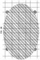
- FIG. 2Ais a simplified, not to scale, illustration of an image captured by the OFN module 142 , located generally below the 5 key, in the embodiment of FIGS. 1A & 1B , in the absence of key displacement beyond a predetermined extent and tampering.
- the dark spotsrepresent light reflected from readily optically identifiable markings 136 formed on corresponding bottom facing surfaces 138 of keys 134 .
- FIG. 2Ashows a state in which none of the keys is displaced. It is appreciated that angular optical distortions in the shape of the spots are generally not shown in FIGS. 2A-2E .
- the grid shown in FIGS. 2A-2Erepresents a pixel grid, with each block representing a single pixel or an X by Y array of pixels.
- FIG. 2Dis a simplified illustration of a scene as viewed by OFN module 142 upon tampering by inserting a non-reflecting probe into the housing.
- the probeblocks the reflected light from the optically identifiable markings 136 on the bottom surfaces of number 8 and 9 keys.
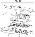
- FIGS. 3A and 3Bpartially illustrate a secure keypad device constructed and operative in accordance with another preferred embodiment of the present invention.
- an OFN moduleis not centered below the number 5 key as in the embodiment of FIGS. 1A-2E , but rather is located at a side of the housing outwardly from all of the keys.
- FIGS. 4A-4Eshow, in a simplified, not to scale, manner, an overall angular distortion resulting from the non-centered position of the OFN module.
- a secure keypad device 300including a top housing element 302 and a bottom housing element (not shown), which together define a keypad device housing.
- Housing element 302includes, on a top surface 304 thereof, a display aperture 306 , through which a display (not shown) may be viewed, and an array 308 of key apertures 310 .
- a key mat 332preferably formed of a resilient plastic or rubber, defines a plurality of depressible keys 334 , preferably integrally formed with mat 332 , which partially extend through key apertures 310 and 320 and preferably have readily optically identifiable markings 336 formed on corresponding bottom facing surfaces 338 thereof. Additional optically identifiable markings 339 may be provided on other interior surfaces, such as inner surfaces of the housing.
- An electrical circuit board 340which functions, inter alia, as a mounting board for an OFN module 342 , is disposed in predetermined spaced relationship with key mat 332 .
- OFN module 342is preferably a Model ADBS-A350 commercially available from Pixart Imaging Inc., No. 5, Innovation Road 1, HsinChu Science Park, Hsin-Chu, Taiwan, R.O.C.
- the arrangement of key mat 332 and of electrical circuit board 340is such that depression of a key 334 by the finger of a user is detected and identified by OFN module 342 . In the illustrated embodiment of FIGS.
- the OFN module 342is generally not centered with respect to the plurality of depressible keys 334 but lies therebelow so as to be in a line of sight with all of depressible keys 334 and preferably also in a line of sight with other regions within the housing.
- a spacer 343preferably formed of a transparent material or defining open side walls, is provided between electrical circuit board 340 and key mat 332 in order to enhance the ability of the OFN module to view not only all of the keys but also as much as possible of the interior of the housing.
- Circuit board 340preferably includes an anti-tampering grid 344 formed of a multiplicity of interconnected anti-tampering electrical conductors.
- anti tampering grids 344 , 314 and 324 and enclosure 322are preferably interconnected so as to define a keyboard anti-tampering enclosure, which is coupled to anti-tampering detection circuitry 360 .
- Anti-tampering detection circuitry 360is typically enclosed in an anti-tampering enclosure (not shown). Alternatively, anti-tampering detection circuitry 360 may itself be secure against tampering.
- the key displacements of one or more function keysmay be sensed by engagement thereof with corresponding conventional electrical contacts, such as contacts 374 , 376 and 378 .
- the secure keypad device 300includes a main microprocessor 380 which preferably includes, inter alia, encryption/decryption capabilities.
- a main microprocessormay beneficially be included in the secure keypad devices and data entry devices described hereinbelow with reference to FIGS. 5A-8B . It is appreciated that the functionality of anti-tampering detection circuitry 360 may be carried out by main microprocessor 380 .
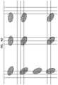
- FIG. 4Ais a simplified, not to scale, illustration of an image captured by OFN module 342 in the embodiment of FIGS. 3A & 3B in the absence of key displacement beyond a predetermined extent and tampering.
- the dark spotsrepresent light reflected from readily optically identifiable markings 336 formed on corresponding bottom facing surfaces 338 of keys 334 .
- FIG. 4Ashows a state in which none of the keys is depressed. It is appreciated that angular optical distortions in the shape of the spots are generally not shown in FIGS. 4A-4E .
- the grid shown in FIGS. 4A-4Erepresents a pixel grid, with each block representing a single pixel or an X by Y array of pixels.
- FIG. 4Bis a simplified illustration of a scene as viewed by OFN module 342 upon depression of a number 5 key from a first location within the housing to a second location within the housing in the absence of tampering. It is seen that the spot corresponding to the reflected light from marking 336 on the bottom facing surface of the number 5 key is enlarged. It is further appreciated that normally depression of a key causes the intensity of the reflected light received by OFN module 342 to increase.
- FIG. 4Dis a simplified illustration of a scene as viewed by OFN module 342 upon tampering by inserting a non-reflecting probe into the housing.
- the probeblocks the reflected light from the optically identifiable markings 336 on the bottom surfaces of number 8 and 9 keys.
- FIGS. 5A and 5Bare simplified, not to scale, sectional illustrations showing detection of a key displacement beyond a predetermined extent in a data entry device 500 including OFN circuitry, typically in the form of an OFN module 502 , such as a Model 27903 commercially available from Parallax Inc.
- FIG. 5Ashows three keys 504 , 506 and 508 , none of which is depressed and all of which are sensed by the OFN module 502 , as indicated schematically by respective beam designations 514 , 516 and 518 .
- FIG. 5Bshows key 508 being depressed and this key displacement beyond a predetermined extent being optically sensed by the OFN module 502 .
- FIGS. 6A and 6Bare simplified, not to scale, sectional illustrations showing detection of insertion of a probe in a data entry device 600 including OFN circuitry, typically in the form of an OFN module 602 , such as a Model 27903 commercially available from Parallax Inc., having a lens 603 , which may be provided to widen the field of view of the OFN module 602 .
- FIG. 6Ashows three keys 604 , 606 and 608 , all of which are sensed by the OFN module 602 , as indicated schematically by respective beam designations 614 , 616 and 618 .
- additional featuressuch as interior housing mounted reflective surfaces 620 and 622 , are also sensed by the OFN module 602 , as indicated schematically by respective beam designations 630 and 632 .
- FIGS. 7A and 7Bare simplified, not to scale, sectional illustrations showing detection of a key displacement beyond a predetermined extent in a data entry device 700 including OFN circuitry, typically in the form of an OFN module 702 , such as a Model 27903 commercially available from Parallax Inc.
- FIG. 7Ashows three keys 704 , 706 and 708 , all of which are sensed by the OFN module 702 , as indicated schematically by respective beam designations 714 , 716 and 718 .
- Keys 704 , 706 and 708preferably have readily optically identifiable markings similar to readily optically identifiable markings 136 ( FIG.
- FIG. 7Bshows key 708 having been removed and this key removal being optically sensed by the OFN module 702 , resulting in a tamper alarm indication.
- FIGS. 8A and 8Bare simplified, not to scale, sectional illustrations showing detection of opening of a data entry device 800 including OFN circuitry, typically in the form of an OFN module 802 , such as a Model ADBS-A350 commercially available from Pixart No. 5, Innovation Road 1, HsinChu Science Park, Hsin-Chu, Taiwan, R.O.C. (HQ) having a lens 803 , which may be provided to widen the field of view of the OFN module 802 .
- FIG. 8A and 8Bare simplified, not to scale, sectional illustrations showing detection of opening of a data entry device 800 including OFN circuitry, typically in the form of an OFN module 802 , such as a Model ADBS-A350 commercially available from Pixart No. 5, Innovation Road 1, HsinChu Science Park, Hsin-Chu, Taiwan, R.O.C. (HQ) having a lens 803 , which may be provided to widen the field of view of the OFN module 802 .
- FIG. 8Ashows typically four reflecting panels 804 , 806 , 808 and 810 mounted onto an interior surface of a housing portion 812 , all of which are sensed by the OFN module 802 , as indicated schematically by respective beam designations 814 , 816 and 818 and 820 .
- FIG. 8Bshows that opening of the data entry device and removal of housing portion 812 eliminates sensing of the four reflecting panels 804 , 806 , 808 and 810 mounted onto an interior surface of a housing portion 812 , as sensed by the OFN module 802 , resulting in a tamper alarm indication.
- OFN circuitry 900such as circuitry embodied in an OFN module of the type described hereinabove, provides an image output to at least two functional units, a key displacement analysis unit 902 and an image-based tamper detection unit 904 .
- the output of the OFN circuitry and or of the OFN moduleis encrypted by suitable encryption functionality.
- functional units 902 and 904may be embodied in a microprocessor included on an OFN module, such as OFN module 142 ( FIGS. 1A & 1B ), OFN module 342 ( FIGS. 3A & 3B ), OFN module 502 ( FIGS. 5A & 5B ), OFN module 602 ( FIGS. 6A & 6B ), OFN module 702 ( FIGS. 7A & 7B ) or OFN module 802 ( FIGS. 8A & 8B ).
- units 902 and 904may be separate from the OFN Module.
- units 902 and 904may be embodied in anti-tampering detection circuitry 160 ( FIGS.
- the key displacement analysis unit 902is preferably operable to ascertain which of a plurality of mechanical keys is mechanically depressed and to provide a corresponding output indication, preferably via a secure connection to a data receiver, such as a PIN data receiving module 906 .
- the key displacement analysis unit 902preferably employs optical information received from the OFN module including at least one of size, shape and intensity of reflected optical image elements.
- the image-based tamper detection unit 904is operative, for example, as described hereinabove with respect to one or more of the embodiments shown in FIGS. 1A-8B , to detect tampering with a data entry device.
- the image-based tamper detection unitupon ascertaining the existence of a tamper situation, provides a tamper output to tamper alarm circuitry 908 .
- both the key displacement analysis unit 902 and the image-based tamper detection unit 904may receive stored information from an approved key-depression database 910 , which stores data, such as image data or data derived therefrom, which corresponds to depressions of predetermined keys or combinations thereof.
- the key displacement analysis unit 902preferably employs the information stored in the database 910 for key displacement identification and the image-based tamper detection unit 904 preferably employs the information stored in the database 910 for eliminating false tamper alarms when actual key displacement to at least a predetermined extent is detected.
- the OFN circuitry in any of the OFN modulescan provide various types of tamper detection functionality.
- OFN module 142FIGS. 1A & 1B
- OFN module 342FIGS. 3A & 3B
- OFN module 502FIGS. 5A & 5B
- OFN module 602FIGS. 6A & 6B
- OFN module 702FIGS. 7A & 7B
- OFN module 802FIGS. 8A & 8B
- OFN module 142will see optically identifiable markings 136 and 139 and will likely see many other things in its field of vision. Some of the other things seen by the OFN module 142 , other than optically identifiable markings 136 and 139 , may be considered as quiescent background noise, and may be very useful in detecting tampering. This background noise may be used as a thumbprint, captured upon manufacture of the device at the factory, employed for verification, typically each time that the device is booted up, that the device has not been tampered with.
- a toolsuch as probe 634
- a data entry device equipped with an OFN module 602in accordance with an embodiment of the present invention, preferably one, more than one, or all of the following events is sensed:
- the tool that is inserted into the deviceis sensed by the OFN module as a foreign object, either by virtue of blocking a reflection from an identifiable marking, such as reflective surface 622 , or by virtue of a reflection from the tool, which is not recognized as an identifiable marking;
- Raw data outputted by an OFN modulesuch as OFN module 142 ( FIGS. 1A & 1B ), OFN module 342 ( FIGS. 3A & 3B ), OFN module 502 ( FIGS. 5A & 5B ), OFN module 602 ( FIGS. 6A & 6B ), OFN module 702 ( FIGS. 7A & 7B ) or OFN module 802 ( FIGS. 8A & 8B ) typically includes a data array of M bytes (N ⁇ N pixels), wherein the value of each byte may vary between 0 to K proportionally, or inversely proportionally, to the amount of light sensed by each given pixel.
- the OFN moduletypically includes a small on-board microcontroller and memory.
- the OFN modulecan operate in two operational modes: a Raw Data Mode and a Configurable Mode.
- the OFN moduleWhen operating in the Raw Data Mode, the OFN module sends the data array to the on board microcontroller when requested by the on board microcontroller.
- the OFN moduleWhen operating in the Configurable Mode, the OFN module can be programmed at the factory to sense and store in memory various alarm scenarios and to generate an alarm signal upon the occurrence of one of the pre-configured alarm scenarios. Alternatively, the OFN module can be configured to generate an alarm signal when the scene viewed by the OFN module does match a thumbprint stored in memory. Additionally, the OFN module can be configured to provide different alarm signals depending on the occurrence of different tampering scenarios as sensed by the OFN module.
- the encryption functionality of the OFN circuitry 900 vis a vis the main microprocessor 180 ( FIGS. 1A & 1B ) or main microprocessor 380 ( FIGS. 3A & 3B ) or the corresponding main microprocessor of any of the secure keypads or data entry devices of FIGS. 5A-8Bincludes the following functional features, described hereinbelow with respect to FIGS. 1A & 1B as an example:
- the main microprocessor 180becomes aware that there is no encryption key for its OFN module 142 .
- the main microprocessor 180generates an encryption key, which is typically a symmetric encryption key, and transmits it to the OFN module 142 as clear text. From then on, all communication between the main microprocessor 180 and the OFN module 142 is encrypted.
- an encryption keywhich is typically a symmetric encryption key
- the alarm detection circuitry 160Upon occurrence of sensed tampering, the alarm detection circuitry 160 will cause the main microprocessor 180 to erase the encryption key and any other sensitive information and thus prevent further communication and PIN entry from taking place.
- the OFN module of each devicecan be configured, inter alia, to carry out any one or more of the following functions:
- the main microprocessorperiodically requests the status of the OFN module.
- the OFN moduleWhen the device is in a sleep mode, the OFN module goes into deep sleep mode, and wakes up every second to validate its current thumbprint. If the current thumbprint matches the stored thumbprint, the OFN module returns to the sleep mode. If the current thumbprint does not match the stored thumbprint, the OFN module records this state in a nonvolatile memory, wakes up the main microprocessor and reports the not matching current thumbprint to the main microprocessor when the main microprocessor periodically requests the current status.
- the systemcan be configured so that the OFN module determines that a tamper condition has occurred, or can be configured it only report raw data, in which configuration the main microprocessor makes all determinations of tamper conditions based, inter alia, on the raw data received from the OFN module. Additionally, any suitable combination of configurations of the OFN module and the main microprocessor is also possible.
- the OFN modulewill also determine which PIN keys are pressed and report PIN keys to the main microprocessor.
Landscapes
- Engineering & Computer Science (AREA)
- Theoretical Computer Science (AREA)
- Computer Hardware Design (AREA)
- General Engineering & Computer Science (AREA)
- Physics & Mathematics (AREA)
- General Physics & Mathematics (AREA)
- Human Computer Interaction (AREA)
- Computer Security & Cryptography (AREA)
- Software Systems (AREA)
- Microelectronics & Electronic Packaging (AREA)
- Input From Keyboards Or The Like (AREA)
Abstract
Description
- Report a valid key displacement to at least a predetermined extent;
- Report a combination of key displacements to at least a predetermined extent;
- Not report when all or most of the keys are pressed;
- Report that a foreign object is present within the housing of the device;
- Report that a key has been removed;
- Report that the OFN “thumbprint” of the device has changed beyond a predetermined threshold;
- Remain in a sleep mode, as a default, to conserve energy, thereby prolonging battery life;
- Exit from sleep mode, without being prompted by the main microprocessor, to read its current thumbprint;
- If the thumbprint matches a stored thumbprint, return to sleep mode;
- If the current thumbprint does not match the stored thumbprint, send an alarm signal to the main microprocessor;
- Respond to a request from the main microprocessor to verify the current thumbprint before allowing PIN entry; and
- Accept an encryption key to facilitate encrypted communication between the OFN module and the main microprocessor.
Claims (18)
Priority Applications (1)
| Application Number | Priority Date | Filing Date | Title |
|---|---|---|---|
| US15/900,317US11397835B2 (en) | 2014-07-23 | 2018-02-20 | Data device including OFN functionality |
Applications Claiming Priority (3)
| Application Number | Priority Date | Filing Date | Title |
|---|---|---|---|
| US201462027890P | 2014-07-23 | 2014-07-23 | |
| US14/802,305US20160026275A1 (en) | 2014-07-23 | 2015-07-17 | Data device including ofn functionality |
| US15/900,317US11397835B2 (en) | 2014-07-23 | 2018-02-20 | Data device including OFN functionality |
Related Parent Applications (1)
| Application Number | Title | Priority Date | Filing Date |
|---|---|---|---|
| US14/802,305ContinuationUS20160026275A1 (en) | 2014-07-23 | 2015-07-17 | Data device including ofn functionality |
Publications (2)
| Publication Number | Publication Date |
|---|---|
| US20180173903A1 US20180173903A1 (en) | 2018-06-21 |
| US11397835B2true US11397835B2 (en) | 2022-07-26 |
Family
ID=55166754
Family Applications (2)
| Application Number | Title | Priority Date | Filing Date |
|---|---|---|---|
| US14/802,305AbandonedUS20160026275A1 (en) | 2014-07-23 | 2015-07-17 | Data device including ofn functionality |
| US15/900,317ActiveUS11397835B2 (en) | 2014-07-23 | 2018-02-20 | Data device including OFN functionality |
Family Applications Before (1)
| Application Number | Title | Priority Date | Filing Date |
|---|---|---|---|
| US14/802,305AbandonedUS20160026275A1 (en) | 2014-07-23 | 2015-07-17 | Data device including ofn functionality |
Country Status (1)
| Country | Link |
|---|---|
| US (2) | US20160026275A1 (en) |
Families Citing this family (4)
| Publication number | Priority date | Publication date | Assignee | Title |
|---|---|---|---|---|
| FR3036212B1 (en)* | 2015-05-12 | 2018-08-03 | Ingenico Group | INTRUSION OPTICAL DETECTION SYSTEM AND METHOD, CORRESPONDING ELECTRONIC DEVICE, PROGRAM, AND RECORDING MEDIUM |
| US10891401B2 (en)* | 2016-03-07 | 2021-01-12 | Bluebird Inc. | Mobile terminal having security function |
| EP3710970B1 (en)* | 2017-11-15 | 2024-05-15 | Enrico Maim | Terminals and methods for secure transactions |
| US10544923B1 (en) | 2018-11-06 | 2020-01-28 | Verifone, Inc. | Devices and methods for optical-based tamper detection using variable light characteristics |
Citations (131)
| Publication number | Priority date | Publication date | Assignee | Title |
|---|---|---|---|---|
| GB892198A (en) | 1960-06-07 | 1962-03-21 | American District Telegraph Co | Electrical protection system |
| US3466643A (en) | 1966-03-18 | 1969-09-09 | Carlton Swain Moorefield | Transmission line tampering alarm system |
| US3735353A (en) | 1971-10-28 | 1973-05-22 | Johnson Service Co | Alarm transmission line security system utilizing pseudo random encoding |
| DE2241738B2 (en) | 1971-09-22 | 1974-08-08 | Securiton Ag, Zollikofen, Bern (Schweiz) | Distribution box for alarm systems |
| US4417824A (en) | 1982-03-29 | 1983-11-29 | International Business Machines Corporation | Optical keyboard with common light transmission members |
| US4486637A (en) | 1982-06-28 | 1984-12-04 | Northern Telecom Limited | Pushbutton switch assembly |
| US4527030A (en) | 1980-11-06 | 1985-07-02 | Preh Elektrofeinmechanische Werke, Jakob Preh Nachf., Gmbh & Co. | Keyboard |
| US4593384A (en) | 1984-12-21 | 1986-06-03 | Ncr Corporation | Security device for the secure storage of sensitive data |
| GB2178235A (en) | 1985-04-04 | 1987-02-04 | British Telecomm | Keypad |
| US4749368A (en) | 1986-04-03 | 1988-06-07 | E. I. Du Pont De Nemours And Company | Contact strip terminal |
| US4807284A (en) | 1986-09-24 | 1989-02-21 | Ncr Corporation | Security device for sensitive data |
| US4837425A (en)* | 1986-08-07 | 1989-06-06 | The General Electric Company, P.L.C. | Security arrangement |
| US4836636A (en) | 1986-11-13 | 1989-06-06 | The Furukawa Electric Co., Ltd. | Optical switch and optical keyboard utilizing the same |
| US4847595A (en) | 1986-12-08 | 1989-07-11 | Atsumi Denki Kabushiki Kaisha | Alarm system |
| US4877947A (en) | 1986-08-05 | 1989-10-31 | Oki Electric Industry Co., Ltd. | Transaction processing system |
| EP0375545A1 (en) | 1988-12-20 | 1990-06-27 | Bull S.A. | Device to protect an electronic card and its use to protect a reading terminal of a magnetic and/or microprocessor card |
| US5086292A (en) | 1989-10-31 | 1992-02-04 | Iris Systems Inc. | Tamper detection device for utility meter |
| US5237307A (en) | 1991-11-27 | 1993-08-17 | The United States Of America As Represented By The United States Department Of Energy | Non-contact tamper sensing by electronic means |
| US5239664A (en) | 1988-12-20 | 1993-08-24 | Bull S.A. | Arrangement for protecting an electronic card and its use for protecting a terminal for reading magnetic and/or microprocessor cards |
| US5321143A (en) | 1988-05-26 | 1994-06-14 | Massachusetts Institute Of Technology | Ruthenium-catalyzed production of cyclic sulfates |
| US5353350A (en) | 1989-10-03 | 1994-10-04 | University Of Technology | Electro-active cradle circuits for the detection of access or penetration |
| US5506566A (en) | 1993-05-06 | 1996-04-09 | Northern Telecom Limited | Tamper detectable electronic security package |
| US5561282A (en) | 1993-04-30 | 1996-10-01 | Microbilt Corporation | Portable signature capture pad |
| US5586042A (en) | 1993-03-15 | 1996-12-17 | Hughey-Pisau, Ltd. | Apparatus and methods for measuring and detecting variations in the value of a capacitor |
| US5675319A (en) | 1996-04-26 | 1997-10-07 | David Sarnoff Research Center, Inc. | Tamper detection device |
| JPH10293915A (en) | 1997-04-21 | 1998-11-04 | Nippon Mektron Ltd | Flexible circuit board for magnetic head |
| US5861662A (en) | 1997-02-24 | 1999-01-19 | General Instrument Corporation | Anti-tamper bond wire shield for an integrated circuit |
| US5877547A (en) | 1994-11-17 | 1999-03-02 | Schlumberger Industries | Active security device including an electronic memory |
| US5998858A (en) | 1995-07-20 | 1999-12-07 | Dallas Semiconductor Corporation | Microcircuit with memory that is protected by both hardware and software |
| GB2353401A (en) | 1999-08-20 | 2001-02-21 | 3Com Corp | An integrated circuit package incorporating a capacitive sensor probe |
| US6272562B1 (en)* | 1999-05-28 | 2001-08-07 | Cross Match Technologies, Inc. | Access control unit interface |
| WO2001063994A2 (en) | 2000-02-23 | 2001-08-30 | Iridian Technologies, Inc. | Tamper proof case for electronic devices having memories with sensitive information |
| US6288640B1 (en) | 1995-12-15 | 2001-09-11 | GAGNON ANDRé | Open transmission line intrusion detection system using frequency spectrum analysis |
| US20020002683A1 (en) | 2000-02-14 | 2002-01-03 | Benson Justin H. | Security module system, apparatus and process |
| US6359338B1 (en) | 1999-07-09 | 2002-03-19 | Oki Electric Industry Co., Ltd. | Semiconductor apparatus with self-security function |
| JP2002108711A (en) | 2000-09-29 | 2002-04-12 | Tamura Electric Works Ltd | Data processor and data processing method |
| US6396400B1 (en) | 1999-07-26 | 2002-05-28 | Epstein, Iii Edwin A. | Security system and enclosure to protect data contained therein |
| US6414884B1 (en) | 2000-02-04 | 2002-07-02 | Lucent Technologies Inc. | Method and apparatus for securing electronic circuits |
| GB2372363A (en) | 2000-12-01 | 2002-08-21 | Peter Gwynne | Security device having a capacitive sensor |
| US6438825B1 (en) | 1995-03-28 | 2002-08-27 | Intel Corporation | Method to prevent intrusions into electronic circuitry |
| US6463263B1 (en) | 1999-02-01 | 2002-10-08 | Telefonaktiebolaget Lm Ericsson (Publ) | Communication station |
| US6466118B1 (en) | 2002-04-17 | 2002-10-15 | Duraswitch Industries, Inc. | Overlay electrical conductor for a magnetically coupled pushbutton switch |
| US20030025617A1 (en) | 2001-07-18 | 2003-02-06 | International Business Machines Corporation | Foil keyboard with security system |
| US6552713B1 (en)* | 1999-12-16 | 2003-04-22 | Hewlett-Packard Company | Optical pointing device |
| US6563488B1 (en) | 1997-09-29 | 2003-05-13 | Varatouch Technology Incorporated | Pointing device with integrated switch |
| US6561659B1 (en)* | 2001-11-15 | 2003-05-13 | Wintek Corporation | Photoconductor panel for lighting a keyboard |
| US6633241B2 (en) | 1999-12-28 | 2003-10-14 | Nokia Mobile Phones Ltd. | Capacitively coupled keypad structure |
| US6646565B1 (en) | 2000-06-01 | 2003-11-11 | Hewlett-Packard Development Company, L.P. | Point of sale (POS) terminal security system |
| US20040031673A1 (en)* | 2002-05-23 | 2004-02-19 | Levy David H. | Keypads and key switches |
| US20040041792A1 (en)* | 2002-09-03 | 2004-03-04 | Criscione John C. | Keypad input device |
| EP1421549A1 (en) | 2001-08-31 | 2004-05-26 | Trintech Limited | A pin pad |
| EP1432031A1 (en) | 2002-12-20 | 2004-06-23 | Lipman Electronic Engineering Ltd. | Anti-tampering enclosure for electronic circuitry |
| US20040118670A1 (en) | 2002-12-03 | 2004-06-24 | Sung-Sun Park | Rotation key device for a portable terminal |
| DE60101096T2 (en) | 2000-03-17 | 2004-07-01 | Thales E-Transactions S.A. | ELASTOMER MEMBRANE AGAINST PENETRATION FOR SECURED ELECTRONIC HOUSINGS |
| US6830182B2 (en) | 2002-04-11 | 2004-12-14 | Cis Eletronica Industria E Comercio Ltda. | Magnetic card reader |
| US6874092B1 (en) | 1998-10-06 | 2005-03-29 | Ricoh Corporation | Method and apparatus for erasing data after tampering |
| US20050081049A1 (en) | 2003-10-09 | 2005-04-14 | Takeshi Nakayama | Mobile terminal, circuit board, circuit board design aiding apparatus and method, design aiding program, and storage medium having stored therein design aiding program |
| US6912280B2 (en) | 2002-07-22 | 2005-06-28 | Sony Ericsson Mobile Communications Ab | Keypad device |
| US20050184870A1 (en) | 2004-02-25 | 2005-08-25 | Dmatek, Ltd. | Method and apparatus for portable transmitting devices |
| US6936777B1 (en) | 2004-03-12 | 2005-08-30 | Fuji Electronics Industries Co., Ltd. | Two-step switch |
| GB2411756A (en) | 2004-03-04 | 2005-09-07 | Dione Plc | Secure card reader |
| WO2005086546A2 (en) | 2004-03-04 | 2005-09-15 | Lipman Electronics Engineering Limited | Secure card reader |
| US20050275537A1 (en)* | 2004-05-27 | 2005-12-15 | Eastman Kodak Company | System and device for detecting object tampering |
| US20060049255A1 (en) | 2004-09-07 | 2006-03-09 | Clay Von Mueller | Secure magnetic stripe reader for handheld computing and method of using same |
| US20060049256A1 (en) | 2004-09-07 | 2006-03-09 | Clay Von Mueller | Transparently securing data for transmission on financial networks |
| US7042371B2 (en) | 2004-02-24 | 2006-05-09 | Nokia Corporation | Optical keyboard with geodesic optical elements |
| US20060109239A1 (en)* | 2004-11-23 | 2006-05-25 | Ta-Sung Hsiung | Integrated module combining cursor control and numeric keypad |
| US20060109251A1 (en)* | 2004-11-19 | 2006-05-25 | Jesse Kelly | Combined keyboard and movement detection system |
| US20060139185A1 (en)* | 2002-03-29 | 2006-06-29 | Pierre Bonnat | Input device for a computer system that utilizes ambient light, and a method of manufacturing the same |
| EP1676182A1 (en) | 2003-10-24 | 2006-07-05 | Trintech Limited | Circuit security |
| US20060192653A1 (en) | 2005-02-18 | 2006-08-31 | Paul Atkinson | Device and method for selectively controlling the utility of an integrated circuit device |
| US20060208089A1 (en)* | 2005-02-25 | 2006-09-21 | Hewlett-Packard Development Company, L.P. | Identifier for memory tags |
| US7170409B2 (en) | 2003-03-06 | 2007-01-30 | Cypak Ab | Tamper evident packaging |
| US20070040674A1 (en)* | 2005-08-16 | 2007-02-22 | Honeywell International, Inc. | Conductive tamper switch for security devices |
| US7214874B2 (en)* | 2004-11-04 | 2007-05-08 | International Business Machines Corporation | Venting device for tamper resistant electronic modules |
| US20070109152A1 (en)* | 2005-11-14 | 2007-05-17 | Wald Steven F | Method and apparatus for optically detecting selections made on an input device |
| US20070152839A1 (en)* | 2006-01-05 | 2007-07-05 | Honeywell International Inc. | Method and system to detect tampering using light detector |
| US20070152042A1 (en) | 2005-10-21 | 2007-07-05 | Jon Mittler | Protective cover for terminal keypad security switches |
| US20070204173A1 (en) | 2006-02-15 | 2007-08-30 | Wrg Services Inc. | Central processing unit and encrypted pin pad for automated teller machines |
| US7270275B1 (en)* | 2004-09-02 | 2007-09-18 | Ncr Corporation | Secured pin entry device |
| US7283066B2 (en) | 1999-09-15 | 2007-10-16 | Michael Shipman | Illuminated keyboard |
| US20080073491A1 (en)* | 2006-09-27 | 2008-03-27 | Honeywell International Inc. | Anti-tamper enclosure system |
| US20080135617A1 (en) | 2006-12-08 | 2008-06-12 | Verifone, Inc. | Anti-tampering protection for magnetic stripe reader |
| US20080180245A1 (en) | 2007-01-25 | 2008-07-31 | Verifone, Inc. | Anti-tamper protected enclosure |
| US20080218849A1 (en)* | 2007-02-27 | 2008-09-11 | Till I.D. Gmbh | Device for confocal illumination of a specimen |
| US20080278353A1 (en) | 2007-05-11 | 2008-11-13 | Measurement Specialties, Inc. | Tamper resistant electronic transaction assembly |
| US20080308619A1 (en)* | 2007-06-14 | 2008-12-18 | Carl Edelmann Gmbh & Co. Kg | Reclosable Folding Box with Tamper-Evident Closure Without Adhesive |
| US20090058628A1 (en) | 2007-08-27 | 2009-03-05 | Verifone, Inc. | Secure point of sale device employing capacitive sensors |
| US20090179869A1 (en)* | 2008-01-14 | 2009-07-16 | Benjamin Slotznick | Combination thumb keyboard and mouse |
| US20090184850A1 (en)* | 2008-01-22 | 2009-07-23 | Verifone, Inc. | Secured keypad devices |
| US7573463B2 (en)* | 2002-08-29 | 2009-08-11 | Koninklijke Philips Electronics N.V. | Apparatus equipped with an optical keyboard and optical input device |
| US20100058077A1 (en)* | 2007-03-27 | 2010-03-04 | Mitsubishi Electric Corporation | Confidential information memory apparatus, erasing method of confidential information, and erasing program of confidential information |
| US7784691B2 (en) | 2006-12-08 | 2010-08-31 | Verifone Inc. | Security functionality for magnetic card readers and point of sales devices |
| US20100258419A1 (en)* | 2009-04-10 | 2010-10-14 | Avago Technologies Ecbu Ip (Singapore) Pte. Ltd. | Light guide film with cut lines |
| US20100271839A1 (en)* | 2009-04-24 | 2010-10-28 | Avago Technologies Ecbu Ip (Singapore) Pte.Ltd. | Light guide display with mulitple light guide layers |
| US20100287624A1 (en)* | 2008-01-16 | 2010-11-11 | Dan Anders Lindqvist | Method and device for detecting the opening of a cover enclosing the device |
| US20110063109A1 (en) | 2007-11-29 | 2011-03-17 | Hypercom Gmbh | Device for monitoring a space by series-connected normally-open contacts, in particular cover interlock switches in a security enclosure |
| US20110100788A1 (en)* | 2008-03-21 | 2011-05-05 | Ingenico France | Protection device for electronic system |
| US20110215938A1 (en)* | 2010-03-02 | 2011-09-08 | Verifone, Inc. | Point of sale terminal having enhanced security |
| CN201984457U (en) | 2011-04-26 | 2011-09-21 | 友碁科技股份有限公司 | Optical keyboard input device |
| US20110248860A1 (en)* | 2010-04-12 | 2011-10-13 | Amihay Avital | Secure data entry device |
| US20110279279A1 (en)* | 2008-01-22 | 2011-11-17 | Verifone, Inc. | Secure point of sale terminal |
| US20110316805A1 (en)* | 2010-06-28 | 2011-12-29 | Youji Yamada | Electronic device |
| US20120018288A1 (en)* | 2010-07-21 | 2012-01-26 | Maxim Integrated Products, Inc. | Keypad having tamper-resistant keys |
| US20120020045A1 (en)* | 2010-07-21 | 2012-01-26 | Research In Motion Limited | Portable electronic device having a waterproof keypad |
| US20120047374A1 (en)* | 2011-11-03 | 2012-02-23 | Cram Worldwide, Llc | Tamper resistance extension via tamper sensing material housing integration |
| US20120056813A1 (en)* | 2010-09-03 | 2012-03-08 | Primax Electronics Ltd. | Shape-changeable camera mouse |
| US20120068846A1 (en)* | 2010-09-20 | 2012-03-22 | Honeywell International Inc. | Tamper event detection |
| US8212161B2 (en)* | 2009-04-13 | 2012-07-03 | Chi Mei Communication Systems, Inc. | Keypad assembly for electronic devices |
| CN202306504U (en) | 2010-08-26 | 2012-07-04 | 耀光联有限公司 | Optical keyboard based on gesture control |
| US20130072771A1 (en)* | 2011-09-21 | 2013-03-21 | Pixart Imaging Inc. | Optical finger mouse, electronic device and physiological characteristics detection device |
| US20130099009A1 (en)* | 2010-11-19 | 2013-04-25 | Nest Labs, Inc. | Thermostat with ring-shaped control member |
| US20130127722A1 (en)* | 2011-11-17 | 2013-05-23 | Pixart Imaging Inc. | Keyboard module and display system |
| US20130240739A1 (en)* | 2012-03-15 | 2013-09-19 | Ninve Jr. Inc. | Apparatus and Method for Detecting Tampering with an Infra-Red Motion Sensor |
| US20130283386A1 (en)* | 2012-04-24 | 2013-10-24 | Cheol Jae LEE | Tamper respondent covering |
| US8577042B2 (en)* | 2006-06-21 | 2013-11-05 | Rf Code, Inc. | Location-based security, privacy, access control and monitoring system |
| US20130342313A1 (en)* | 2012-06-25 | 2013-12-26 | Xceedid Corporation | Access credential reader connector |
| US20140132516A1 (en)* | 2012-11-12 | 2014-05-15 | Sunrex Technology Corp. | Optical keyboard |
| US20140240234A1 (en)* | 2013-02-28 | 2014-08-28 | Hewlett-Packard Development Company, L.P. | Input Device |
| US8847923B1 (en)* | 2011-07-15 | 2014-09-30 | James Harrison Bowen | Keyboard with reflected light beam finger detection |
| US20140306894A1 (en)* | 2013-04-11 | 2014-10-16 | Avago Technologies General Ip (Singapore) Pte.Ltd. | Optical Sensing Device To Sense Displacement |
| US20150061901A1 (en)* | 2013-08-29 | 2015-03-05 | Mark A. Casparian | Systems And Methods For Lighting Spring Loaded Mechanical Key Switches |
| US20150077256A1 (en)* | 2013-09-19 | 2015-03-19 | Dubois Limited | Retail security tag |
| US20150314927A1 (en)* | 2014-05-02 | 2015-11-05 | Synthetic Genomics, Inc. | Tamper-resistant assembly for securing valuable material |
| US9201511B1 (en)* | 2010-04-23 | 2015-12-01 | Cypress Semiconductor Corporation | Optical navigation sensor and method |
| US20160066391A1 (en)* | 2013-04-04 | 2016-03-03 | Koninklijke Philips N.V. | Anti-tampering daylight harvesting system |
| US9394723B1 (en)* | 2013-01-22 | 2016-07-19 | Amazon Technologies, Inc. | Lock that mechanically detects tampering |
| US20170063450A1 (en)* | 2015-09-01 | 2017-03-02 | Allied Telesis Holdings Kabushiki Kaisha | Optical signal monitoring |
| US9605167B2 (en)* | 2013-06-12 | 2017-03-28 | Sicpa Holding Sa | Heat sensitive tamper indicating markings |
| US20180059025A1 (en)* | 2016-08-24 | 2018-03-01 | Industrial Technology Research Institute | Tapered optical needle |
| US10218383B2 (en)* | 2013-06-25 | 2019-02-26 | Ncr Corporation | Keypad |
- 2015
- 2015-07-17USUS14/802,305patent/US20160026275A1/ennot_activeAbandoned
- 2018
- 2018-02-20USUS15/900,317patent/US11397835B2/enactiveActive
Patent Citations (147)
| Publication number | Priority date | Publication date | Assignee | Title |
|---|---|---|---|---|
| GB892198A (en) | 1960-06-07 | 1962-03-21 | American District Telegraph Co | Electrical protection system |
| US3466643A (en) | 1966-03-18 | 1969-09-09 | Carlton Swain Moorefield | Transmission line tampering alarm system |
| DE2241738B2 (en) | 1971-09-22 | 1974-08-08 | Securiton Ag, Zollikofen, Bern (Schweiz) | Distribution box for alarm systems |
| GB1369739A (en) | 1971-09-22 | 1974-10-09 | Securiton Ag | Cross-connection field for alarm installations |
| US3735353A (en) | 1971-10-28 | 1973-05-22 | Johnson Service Co | Alarm transmission line security system utilizing pseudo random encoding |
| US4527030A (en) | 1980-11-06 | 1985-07-02 | Preh Elektrofeinmechanische Werke, Jakob Preh Nachf., Gmbh & Co. | Keyboard |
| US4417824A (en) | 1982-03-29 | 1983-11-29 | International Business Machines Corporation | Optical keyboard with common light transmission members |
| US4486637A (en) | 1982-06-28 | 1984-12-04 | Northern Telecom Limited | Pushbutton switch assembly |
| US4593384A (en) | 1984-12-21 | 1986-06-03 | Ncr Corporation | Security device for the secure storage of sensitive data |
| GB2178235A (en) | 1985-04-04 | 1987-02-04 | British Telecomm | Keypad |
| US4749368A (en) | 1986-04-03 | 1988-06-07 | E. I. Du Pont De Nemours And Company | Contact strip terminal |
| US4877947A (en) | 1986-08-05 | 1989-10-31 | Oki Electric Industry Co., Ltd. | Transaction processing system |
| US4837425A (en)* | 1986-08-07 | 1989-06-06 | The General Electric Company, P.L.C. | Security arrangement |
| US4807284A (en) | 1986-09-24 | 1989-02-21 | Ncr Corporation | Security device for sensitive data |
| US4836636A (en) | 1986-11-13 | 1989-06-06 | The Furukawa Electric Co., Ltd. | Optical switch and optical keyboard utilizing the same |
| US4847595A (en) | 1986-12-08 | 1989-07-11 | Atsumi Denki Kabushiki Kaisha | Alarm system |
| US5321143A (en) | 1988-05-26 | 1994-06-14 | Massachusetts Institute Of Technology | Ruthenium-catalyzed production of cyclic sulfates |
| US5239664A (en) | 1988-12-20 | 1993-08-24 | Bull S.A. | Arrangement for protecting an electronic card and its use for protecting a terminal for reading magnetic and/or microprocessor cards |
| EP0375545A1 (en) | 1988-12-20 | 1990-06-27 | Bull S.A. | Device to protect an electronic card and its use to protect a reading terminal of a magnetic and/or microprocessor card |
| EP0375545B1 (en) | 1988-12-20 | 1995-02-08 | Bull S.A. | Device to protect an electronic card and its use to protect a reading terminal of a magnetic and/or microprocessor card |
| US5353350A (en) | 1989-10-03 | 1994-10-04 | University Of Technology | Electro-active cradle circuits for the detection of access or penetration |
| US5086292A (en) | 1989-10-31 | 1992-02-04 | Iris Systems Inc. | Tamper detection device for utility meter |
| US5237307A (en) | 1991-11-27 | 1993-08-17 | The United States Of America As Represented By The United States Department Of Energy | Non-contact tamper sensing by electronic means |
| US5586042A (en) | 1993-03-15 | 1996-12-17 | Hughey-Pisau, Ltd. | Apparatus and methods for measuring and detecting variations in the value of a capacitor |
| US5561282A (en) | 1993-04-30 | 1996-10-01 | Microbilt Corporation | Portable signature capture pad |
| US5506566A (en) | 1993-05-06 | 1996-04-09 | Northern Telecom Limited | Tamper detectable electronic security package |
| US5877547A (en) | 1994-11-17 | 1999-03-02 | Schlumberger Industries | Active security device including an electronic memory |
| US6438825B1 (en) | 1995-03-28 | 2002-08-27 | Intel Corporation | Method to prevent intrusions into electronic circuitry |
| US5998858A (en) | 1995-07-20 | 1999-12-07 | Dallas Semiconductor Corporation | Microcircuit with memory that is protected by both hardware and software |
| US6288640B1 (en) | 1995-12-15 | 2001-09-11 | GAGNON ANDRé | Open transmission line intrusion detection system using frequency spectrum analysis |
| US5675319A (en) | 1996-04-26 | 1997-10-07 | David Sarnoff Research Center, Inc. | Tamper detection device |
| US5861662A (en) | 1997-02-24 | 1999-01-19 | General Instrument Corporation | Anti-tamper bond wire shield for an integrated circuit |
| JPH10293915A (en) | 1997-04-21 | 1998-11-04 | Nippon Mektron Ltd | Flexible circuit board for magnetic head |
| US6563488B1 (en) | 1997-09-29 | 2003-05-13 | Varatouch Technology Incorporated | Pointing device with integrated switch |
| US6874092B1 (en) | 1998-10-06 | 2005-03-29 | Ricoh Corporation | Method and apparatus for erasing data after tampering |
| US6463263B1 (en) | 1999-02-01 | 2002-10-08 | Telefonaktiebolaget Lm Ericsson (Publ) | Communication station |
| US6272562B1 (en)* | 1999-05-28 | 2001-08-07 | Cross Match Technologies, Inc. | Access control unit interface |
| US6359338B1 (en) | 1999-07-09 | 2002-03-19 | Oki Electric Industry Co., Ltd. | Semiconductor apparatus with self-security function |
| US6396400B1 (en) | 1999-07-26 | 2002-05-28 | Epstein, Iii Edwin A. | Security system and enclosure to protect data contained therein |
| GB2353401A (en) | 1999-08-20 | 2001-02-21 | 3Com Corp | An integrated circuit package incorporating a capacitive sensor probe |
| US7283066B2 (en) | 1999-09-15 | 2007-10-16 | Michael Shipman | Illuminated keyboard |
| US6552713B1 (en)* | 1999-12-16 | 2003-04-22 | Hewlett-Packard Company | Optical pointing device |
| US6633241B2 (en) | 1999-12-28 | 2003-10-14 | Nokia Mobile Phones Ltd. | Capacitively coupled keypad structure |
| US6414884B1 (en) | 2000-02-04 | 2002-07-02 | Lucent Technologies Inc. | Method and apparatus for securing electronic circuits |
| US20020002683A1 (en) | 2000-02-14 | 2002-01-03 | Benson Justin H. | Security module system, apparatus and process |
| WO2001063994A2 (en) | 2000-02-23 | 2001-08-30 | Iridian Technologies, Inc. | Tamper proof case for electronic devices having memories with sensitive information |
| DE60101096T2 (en) | 2000-03-17 | 2004-07-01 | Thales E-Transactions S.A. | ELASTOMER MEMBRANE AGAINST PENETRATION FOR SECURED ELECTRONIC HOUSINGS |
| US6921988B2 (en) | 2000-03-17 | 2005-07-26 | Thales E-Transactions S.A. | Anti-spoofing elastomer membrane for secure electronic modules |
| US6917299B2 (en) | 2000-06-01 | 2005-07-12 | Hewlett-Packard Development Company, L.P. | Point of sale (POS) terminal security system |
| US6646565B1 (en) | 2000-06-01 | 2003-11-11 | Hewlett-Packard Development Company, L.P. | Point of sale (POS) terminal security system |
| JP2002108711A (en) | 2000-09-29 | 2002-04-12 | Tamura Electric Works Ltd | Data processor and data processing method |
| GB2372363A (en) | 2000-12-01 | 2002-08-21 | Peter Gwynne | Security device having a capacitive sensor |
| US20030025617A1 (en) | 2001-07-18 | 2003-02-06 | International Business Machines Corporation | Foil keyboard with security system |
| EP1421549A1 (en) | 2001-08-31 | 2004-05-26 | Trintech Limited | A pin pad |
| US6561659B1 (en)* | 2001-11-15 | 2003-05-13 | Wintek Corporation | Photoconductor panel for lighting a keyboard |
| US20060139185A1 (en)* | 2002-03-29 | 2006-06-29 | Pierre Bonnat | Input device for a computer system that utilizes ambient light, and a method of manufacturing the same |
| US6830182B2 (en) | 2002-04-11 | 2004-12-14 | Cis Eletronica Industria E Comercio Ltda. | Magnetic card reader |
| US6466118B1 (en) | 2002-04-17 | 2002-10-15 | Duraswitch Industries, Inc. | Overlay electrical conductor for a magnetically coupled pushbutton switch |
| US20040031673A1 (en)* | 2002-05-23 | 2004-02-19 | Levy David H. | Keypads and key switches |
| US6912280B2 (en) | 2002-07-22 | 2005-06-28 | Sony Ericsson Mobile Communications Ab | Keypad device |
| US7573463B2 (en)* | 2002-08-29 | 2009-08-11 | Koninklijke Philips Electronics N.V. | Apparatus equipped with an optical keyboard and optical input device |
| US20040041792A1 (en)* | 2002-09-03 | 2004-03-04 | Criscione John C. | Keypad input device |
| US20040118670A1 (en) | 2002-12-03 | 2004-06-24 | Sung-Sun Park | Rotation key device for a portable terminal |
| EP1432031A1 (en) | 2002-12-20 | 2004-06-23 | Lipman Electronic Engineering Ltd. | Anti-tampering enclosure for electronic circuitry |
| US6853093B2 (en) | 2002-12-20 | 2005-02-08 | Lipman Electronic Engineering Ltd. | Anti-tampering enclosure for electronic circuitry |
| US20040120101A1 (en) | 2002-12-20 | 2004-06-24 | Lipman Electronic Engineering Ltd. | Anti-tampering enclosure for electronic circuitry |
| US7170409B2 (en) | 2003-03-06 | 2007-01-30 | Cypak Ab | Tamper evident packaging |
| US20050081049A1 (en) | 2003-10-09 | 2005-04-14 | Takeshi Nakayama | Mobile terminal, circuit board, circuit board design aiding apparatus and method, design aiding program, and storage medium having stored therein design aiding program |
| EP1676182A1 (en) | 2003-10-24 | 2006-07-05 | Trintech Limited | Circuit security |
| US20060201701A1 (en) | 2003-10-24 | 2006-09-14 | Ronan Coleman | Circuit security |
| US7042371B2 (en) | 2004-02-24 | 2006-05-09 | Nokia Corporation | Optical keyboard with geodesic optical elements |
| US20050184870A1 (en) | 2004-02-25 | 2005-08-25 | Dmatek, Ltd. | Method and apparatus for portable transmitting devices |
| GB2411756A (en) | 2004-03-04 | 2005-09-07 | Dione Plc | Secure card reader |
| WO2005086546A2 (en) | 2004-03-04 | 2005-09-15 | Lipman Electronics Engineering Limited | Secure card reader |
| US6936777B1 (en) | 2004-03-12 | 2005-08-30 | Fuji Electronics Industries Co., Ltd. | Two-step switch |
| US20050275537A1 (en)* | 2004-05-27 | 2005-12-15 | Eastman Kodak Company | System and device for detecting object tampering |
| US7270275B1 (en)* | 2004-09-02 | 2007-09-18 | Ncr Corporation | Secured pin entry device |
| US7309012B2 (en) | 2004-09-07 | 2007-12-18 | Semtek Innovative Solutions, Inc. | Secure magnetic stripe reader for handheld computing and method of using same |
| US20060049256A1 (en) | 2004-09-07 | 2006-03-09 | Clay Von Mueller | Transparently securing data for transmission on financial networks |
| US20060049255A1 (en) | 2004-09-07 | 2006-03-09 | Clay Von Mueller | Secure magnetic stripe reader for handheld computing and method of using same |
| US7214874B2 (en)* | 2004-11-04 | 2007-05-08 | International Business Machines Corporation | Venting device for tamper resistant electronic modules |
| US20060109251A1 (en)* | 2004-11-19 | 2006-05-25 | Jesse Kelly | Combined keyboard and movement detection system |
| US20060109239A1 (en)* | 2004-11-23 | 2006-05-25 | Ta-Sung Hsiung | Integrated module combining cursor control and numeric keypad |
| US20060192653A1 (en) | 2005-02-18 | 2006-08-31 | Paul Atkinson | Device and method for selectively controlling the utility of an integrated circuit device |
| US20060208089A1 (en)* | 2005-02-25 | 2006-09-21 | Hewlett-Packard Development Company, L.P. | Identifier for memory tags |
| US20070040674A1 (en)* | 2005-08-16 | 2007-02-22 | Honeywell International, Inc. | Conductive tamper switch for security devices |
| US20070152042A1 (en) | 2005-10-21 | 2007-07-05 | Jon Mittler | Protective cover for terminal keypad security switches |
| US20070109152A1 (en)* | 2005-11-14 | 2007-05-17 | Wald Steven F | Method and apparatus for optically detecting selections made on an input device |
| US20070152839A1 (en)* | 2006-01-05 | 2007-07-05 | Honeywell International Inc. | Method and system to detect tampering using light detector |
| US20070204173A1 (en) | 2006-02-15 | 2007-08-30 | Wrg Services Inc. | Central processing unit and encrypted pin pad for automated teller machines |
| US8577042B2 (en)* | 2006-06-21 | 2013-11-05 | Rf Code, Inc. | Location-based security, privacy, access control and monitoring system |
| US7671324B2 (en)* | 2006-09-27 | 2010-03-02 | Honeywell International Inc. | Anti-tamper enclosure system comprising a photosensitive sensor and optical medium |
| US20080073491A1 (en)* | 2006-09-27 | 2008-03-27 | Honeywell International Inc. | Anti-tamper enclosure system |
| US20080135617A1 (en) | 2006-12-08 | 2008-06-12 | Verifone, Inc. | Anti-tampering protection for magnetic stripe reader |
| US7784691B2 (en) | 2006-12-08 | 2010-08-31 | Verifone Inc. | Security functionality for magnetic card readers and point of sales devices |
| US7497378B2 (en) | 2006-12-08 | 2009-03-03 | Verifone, Inc. | Anti-tampering protection for magnetic stripe reader |
| US20080180245A1 (en) | 2007-01-25 | 2008-07-31 | Verifone, Inc. | Anti-tamper protected enclosure |
| US7898413B2 (en) | 2007-01-25 | 2011-03-01 | Verifone, Inc. | Anti-tamper protected enclosure |
| US20080218849A1 (en)* | 2007-02-27 | 2008-09-11 | Till I.D. Gmbh | Device for confocal illumination of a specimen |
| US20100058077A1 (en)* | 2007-03-27 | 2010-03-04 | Mitsubishi Electric Corporation | Confidential information memory apparatus, erasing method of confidential information, and erasing program of confidential information |
| US20080278353A1 (en) | 2007-05-11 | 2008-11-13 | Measurement Specialties, Inc. | Tamper resistant electronic transaction assembly |
| US20080308619A1 (en)* | 2007-06-14 | 2008-12-18 | Carl Edelmann Gmbh & Co. Kg | Reclosable Folding Box with Tamper-Evident Closure Without Adhesive |
| US20090058628A1 (en) | 2007-08-27 | 2009-03-05 | Verifone, Inc. | Secure point of sale device employing capacitive sensors |
| US7843339B2 (en) | 2007-08-27 | 2010-11-30 | Verifone, Inc. | Secure point of sale device employing capacitive sensors |
| US20110063109A1 (en) | 2007-11-29 | 2011-03-17 | Hypercom Gmbh | Device for monitoring a space by series-connected normally-open contacts, in particular cover interlock switches in a security enclosure |
| US20090179869A1 (en)* | 2008-01-14 | 2009-07-16 | Benjamin Slotznick | Combination thumb keyboard and mouse |
| US20100287624A1 (en)* | 2008-01-16 | 2010-11-11 | Dan Anders Lindqvist | Method and device for detecting the opening of a cover enclosing the device |
| US20150185864A1 (en)* | 2008-01-22 | 2015-07-02 | Verifone, Inc. | Secured keypad devices |
| US20110279279A1 (en)* | 2008-01-22 | 2011-11-17 | Verifone, Inc. | Secure point of sale terminal |
| US9013336B2 (en) | 2008-01-22 | 2015-04-21 | Verifone, Inc. | Secured keypad devices |
| US20090184850A1 (en)* | 2008-01-22 | 2009-07-23 | Verifone, Inc. | Secured keypad devices |
| US20110100788A1 (en)* | 2008-03-21 | 2011-05-05 | Ingenico France | Protection device for electronic system |
| WO2010082190A1 (en) | 2009-01-19 | 2010-07-22 | Verifone, Inc. | Secure point of sale terminal |
| US20100258419A1 (en)* | 2009-04-10 | 2010-10-14 | Avago Technologies Ecbu Ip (Singapore) Pte. Ltd. | Light guide film with cut lines |
| US8212161B2 (en)* | 2009-04-13 | 2012-07-03 | Chi Mei Communication Systems, Inc. | Keypad assembly for electronic devices |
| US20100271839A1 (en)* | 2009-04-24 | 2010-10-28 | Avago Technologies Ecbu Ip (Singapore) Pte.Ltd. | Light guide display with mulitple light guide layers |
| US20110215938A1 (en)* | 2010-03-02 | 2011-09-08 | Verifone, Inc. | Point of sale terminal having enhanced security |
| US20110248860A1 (en)* | 2010-04-12 | 2011-10-13 | Amihay Avital | Secure data entry device |
| US9201511B1 (en)* | 2010-04-23 | 2015-12-01 | Cypress Semiconductor Corporation | Optical navigation sensor and method |
| US20110316805A1 (en)* | 2010-06-28 | 2011-12-29 | Youji Yamada | Electronic device |
| US20120018288A1 (en)* | 2010-07-21 | 2012-01-26 | Maxim Integrated Products, Inc. | Keypad having tamper-resistant keys |
| US20120020045A1 (en)* | 2010-07-21 | 2012-01-26 | Research In Motion Limited | Portable electronic device having a waterproof keypad |
| CN202306504U (en) | 2010-08-26 | 2012-07-04 | 耀光联有限公司 | Optical keyboard based on gesture control |
| US20120056813A1 (en)* | 2010-09-03 | 2012-03-08 | Primax Electronics Ltd. | Shape-changeable camera mouse |
| US20120068846A1 (en)* | 2010-09-20 | 2012-03-22 | Honeywell International Inc. | Tamper event detection |
| US20130099009A1 (en)* | 2010-11-19 | 2013-04-25 | Nest Labs, Inc. | Thermostat with ring-shaped control member |
| CN201984457U (en) | 2011-04-26 | 2011-09-21 | 友碁科技股份有限公司 | Optical keyboard input device |
| US8847923B1 (en)* | 2011-07-15 | 2014-09-30 | James Harrison Bowen | Keyboard with reflected light beam finger detection |
| US20130072771A1 (en)* | 2011-09-21 | 2013-03-21 | Pixart Imaging Inc. | Optical finger mouse, electronic device and physiological characteristics detection device |
| US20120047374A1 (en)* | 2011-11-03 | 2012-02-23 | Cram Worldwide, Llc | Tamper resistance extension via tamper sensing material housing integration |
| US20130127722A1 (en)* | 2011-11-17 | 2013-05-23 | Pixart Imaging Inc. | Keyboard module and display system |
| US20130240739A1 (en)* | 2012-03-15 | 2013-09-19 | Ninve Jr. Inc. | Apparatus and Method for Detecting Tampering with an Infra-Red Motion Sensor |
| US20130283386A1 (en)* | 2012-04-24 | 2013-10-24 | Cheol Jae LEE | Tamper respondent covering |
| US20130342313A1 (en)* | 2012-06-25 | 2013-12-26 | Xceedid Corporation | Access credential reader connector |
| US20140132516A1 (en)* | 2012-11-12 | 2014-05-15 | Sunrex Technology Corp. | Optical keyboard |
| US9394723B1 (en)* | 2013-01-22 | 2016-07-19 | Amazon Technologies, Inc. | Lock that mechanically detects tampering |
| US20140240234A1 (en)* | 2013-02-28 | 2014-08-28 | Hewlett-Packard Development Company, L.P. | Input Device |
| US20160066391A1 (en)* | 2013-04-04 | 2016-03-03 | Koninklijke Philips N.V. | Anti-tampering daylight harvesting system |
| US20140306894A1 (en)* | 2013-04-11 | 2014-10-16 | Avago Technologies General Ip (Singapore) Pte.Ltd. | Optical Sensing Device To Sense Displacement |
| US9605167B2 (en)* | 2013-06-12 | 2017-03-28 | Sicpa Holding Sa | Heat sensitive tamper indicating markings |
| US10218383B2 (en)* | 2013-06-25 | 2019-02-26 | Ncr Corporation | Keypad |
| US20150061901A1 (en)* | 2013-08-29 | 2015-03-05 | Mark A. Casparian | Systems And Methods For Lighting Spring Loaded Mechanical Key Switches |
| US20150077256A1 (en)* | 2013-09-19 | 2015-03-19 | Dubois Limited | Retail security tag |
| US9751668B2 (en)* | 2014-05-02 | 2017-09-05 | Synthetic Genomics, Inc. | Tamper-resistant assembly for securing valuable material |
| US20150314927A1 (en)* | 2014-05-02 | 2015-11-05 | Synthetic Genomics, Inc. | Tamper-resistant assembly for securing valuable material |
| US20170063450A1 (en)* | 2015-09-01 | 2017-03-02 | Allied Telesis Holdings Kabushiki Kaisha | Optical signal monitoring |
| US20180059025A1 (en)* | 2016-08-24 | 2018-03-01 | Industrial Technology Research Institute | Tapered optical needle |
Non-Patent Citations (18)
| Title |
|---|
| A Notice of Allowance dated Dec. 19, 2014, which issued during the prosecution of Applicant's U.S. Appl. No. 12/355,857. |
| A Notice of Allowance dated Oct. 23, 2008, which issued during the prosecution of U.S. Appl. No. 11/636,369. |
| A Notice of Allowance dated Oct. 26, 2004, which issued during the prosecution of Applicant's U.S. Appl. No. 10/326,726. |
| A Notice of Allowance dated Sep. 10, 2010, which issued during the prosecution of Applicant's U.S. Appl. No. 11/845,435. |
| An International Preliminary Report on Patentability dated Jul. 19, 2011, which issued during the prosecution of Applicant's PCT/IL2009/000724. |
| An International Search Report and a Written Opinion both dated Apr. 30, 2012, which issued during the prosecution of Applicant's PCT/US2012/020142. |
| An Office Action dated Apr. 10, 2012, which issued during the prosecution of U.S. Appl. No. 12/758,150. |
| An Office Action dated Jul. 11, 2014, which issued during the prosecution of U.S. Appl. No. 12/355,857. |
| An Office Action dated Mar. 13, 2008 which issued during the prosecution of U.S. Appl. No. 11/636,369. |
| An Office Action dated May 11, 2012, which issued during the prosecution of U.S. Appl. No. 12/355,857. |
| An Office Action dated May 13, 2010, which issued during the prosecution of Applicant's U.S. Appl. No. 11/845,435. |
| An Office Action dated May 28, 2004, which issued during the prosecution of U.S. Appl. No. 10/326,726. |
| An Office Action dated Oct. 16, 2012, which issued during the prosecution of U.S. Appl. No. 12/355,857. |
| Kremin, et al., "Capacitance sensing—waterproof capacitance sensing", Cypress Perform, Dec. 2006. |
| Supplementary European Search Report dated Oct. 31, 2013 which issued during the prosecution of Applicant's European App No. 07869932. |
| U.S. Appl. No. 61/011,993, filed Jan. 22, 2008. |
| U.S. Appl. No. 62/027,890, filed Jul. 23, 2014. |
| Van Ess, Dave; "Capacitive touch switches for automotive applications", http://www.automotivedesignline.com/, Feb. 2006. |
Also Published As
| Publication number | Publication date |
|---|---|
| US20180173903A1 (en) | 2018-06-21 |
| US20160026275A1 (en) | 2016-01-28 |
Similar Documents
| Publication | Publication Date | Title |
|---|---|---|
| US11397835B2 (en) | Data device including OFN functionality | |
| US8358218B2 (en) | Point of sale terminal having enhanced security | |
| KR20190088822A (en) | Sensor and electronic apparatus for fingerprint recognition | |
| US20190130240A1 (en) | Payment card overlay skimmer detection | |
| KR102753356B1 (en) | An electronic apparatus comprinsing a fingerprint sensor | |
| US20200302147A1 (en) | Biometric input device | |
| EP3041018B1 (en) | Secure data entry device | |
| US8284387B2 (en) | Methods and systems for recognizing tamper events | |
| JP2017117056A (en) | Transaction terminal device and information input device | |
| US7889893B2 (en) | Method and device for verifying the authenticity of a captured biometric characteristic | |
| US8126141B2 (en) | Interferometric communication | |
| ES2708086T3 (en) | System and method of optical detection of intrusion, electronic device, program and corresponding recording support | |
| US20220051534A9 (en) | Verifying messages projected from an intelligent audible device | |
| WO2023162779A1 (en) | Information processing device | |
| JP2008293466A (en) | Image input device | |
| KR20060076530A (en) | Mobile communication terminal with fingerprint recognition function | |
| CN208014115U (en) | A kind of cell intrusion alarm system with self-checking function | |
| EP3680804B1 (en) | System and method for reading information code | |
| EP3286742A1 (en) | Point of sale terminal having enhanced security | |
| ES2453291T3 (en) | Portable electronic payment terminal adapted to run non-certified programs | |
| CN218100314U (en) | Circuit is prevented tearing open by optics of access control equipment | |
| US12424076B2 (en) | Enhanced visual and audio device for use in access control systems | |
| US12051277B1 (en) | Multi-sensor input device | |
| KR20200112614A (en) | Electronic device including an image sensor and method of operating the same | |
| EP3494518A1 (en) | Verifying messages projected from an intelligent audible device |
Legal Events
| Date | Code | Title | Description |
|---|---|---|---|
| AS | Assignment | Owner name:VERIFONE, INC., CALIFORNIA Free format text:ASSIGNMENT OF ASSIGNORS INTEREST;ASSIGNORS:BARROWMAN, JOHN HENRY;MANCHESTER, DOUG LEIGH;JOHANSEN, WILLIAM MARTIN, JR.;REEL/FRAME:044980/0597 Effective date:20150816 | |
| FEPP | Fee payment procedure | Free format text:ENTITY STATUS SET TO UNDISCOUNTED (ORIGINAL EVENT CODE: BIG.); ENTITY STATUS OF PATENT OWNER: LARGE ENTITY | |
| AS | Assignment | Owner name:CREDIT SUISSE AG, CAYMAN ISLANDS BRANCH AS COLLATERAL AGENT, NEW YORK Free format text:SECOND LIEN PATENT SECURITY AGREEMENT;ASSIGNORS:VERIFONE, INC.;HYPERCOM CORPORATION;REEL/FRAME:046920/0817 Effective date:20180820 Owner name:CREDIT SUISSE AG, CAYMAN ISLANDS BRANCH AS COLLATERAL AGENT, NEW YORK Free format text:FIRST LIEN PATENT SECURITY AGREEMENT;ASSIGNORS:VERIFONE, INC.;HYPERCOM CORPORATION;REEL/FRAME:046920/0784 Effective date:20180820 Owner name:CREDIT SUISSE AG, CAYMAN ISLANDS BRANCH AS COLLATE Free format text:SECOND LIEN PATENT SECURITY AGREEMENT;ASSIGNORS:VERIFONE, INC.;HYPERCOM CORPORATION;REEL/FRAME:046920/0817 Effective date:20180820 Owner name:CREDIT SUISSE AG, CAYMAN ISLANDS BRANCH AS COLLATE Free format text:FIRST LIEN PATENT SECURITY AGREEMENT;ASSIGNORS:VERIFONE, INC.;HYPERCOM CORPORATION;REEL/FRAME:046920/0784 Effective date:20180820 | |
| STPP | Information on status: patent application and granting procedure in general | Free format text:FINAL REJECTION MAILED | |
| AS | Assignment | Owner name:VERIFONE, INC., CALIFORNIA Free format text:RELEASE OF SECURITY INTEREST RECORDED AT REEL/FRAME 46920/0817;ASSIGNOR:CREDIT SUISSE AG, CAYMAN ISLANDS BRANCH;REEL/FRAME:049150/0190 Effective date:20190510 Owner name:VERIFONE SYSTEMS, INC., CALIFORNIA Free format text:RELEASE OF SECURITY INTEREST RECORDED AT REEL/FRAME 46920/0817;ASSIGNOR:CREDIT SUISSE AG, CAYMAN ISLANDS BRANCH;REEL/FRAME:049150/0190 Effective date:20190510 Owner name:HYPERCOM CORPORATION, CALIFORNIA Free format text:RELEASE OF SECURITY INTEREST RECORDED AT REEL/FRAME 46920/0817;ASSIGNOR:CREDIT SUISSE AG, CAYMAN ISLANDS BRANCH;REEL/FRAME:049150/0190 Effective date:20190510 | |
| STCV | Information on status: appeal procedure | Free format text:NOTICE OF APPEAL FILED | |
| STCV | Information on status: appeal procedure | Free format text:APPEAL BRIEF (OR SUPPLEMENTAL BRIEF) ENTERED AND FORWARDED TO EXAMINER | |
| STCV | Information on status: appeal procedure | Free format text:EXAMINER'S ANSWER TO APPEAL BRIEF MAILED | |
| STCV | Information on status: appeal procedure | Free format text:ON APPEAL -- AWAITING DECISION BY THE BOARD OF APPEALS | |
| STCV | Information on status: appeal procedure | Free format text:BOARD OF APPEALS DECISION RENDERED | |
| STPP | Information on status: patent application and granting procedure in general | Free format text:NON FINAL ACTION MAILED | |
| STPP | Information on status: patent application and granting procedure in general | Free format text:RESPONSE TO NON-FINAL OFFICE ACTION ENTERED AND FORWARDED TO EXAMINER | |
| STPP | Information on status: patent application and granting procedure in general | Free format text:NOTICE OF ALLOWANCE MAILED -- APPLICATION RECEIVED IN OFFICE OF PUBLICATIONS | |
| STPP | Information on status: patent application and granting procedure in general | Free format text:DOCKETED NEW CASE - READY FOR EXAMINATION | |
| STPP | Information on status: patent application and granting procedure in general | Free format text:NOTICE OF ALLOWANCE MAILED -- APPLICATION RECEIVED IN OFFICE OF PUBLICATIONS | |
| STPP | Information on status: patent application and granting procedure in general | Free format text:PUBLICATIONS -- ISSUE FEE PAYMENT VERIFIED | |
| STCF | Information on status: patent grant | Free format text:PATENTED CASE | |
| AS | Assignment | Owner name:BARCLAYS BANK PLC, AS ASSIGNEE, NEW JERSEY Free format text:ASSIGNMENT OF SECURITY INTEREST IN PATENT COLLATERAL RECORDED AT R/F 046920-0784;ASSIGNOR:UBS AG, STAMFORD BRANCH, AS SUCCESSOR TO CREDIT SUISSE AG, CAYMAN ISLANDS BRANCH, AS ASSIGNOR;REEL/FRAME:071095/0667 Effective date:20250428 |