US11393683B2 - Methods for high growth rate deposition for forming different cells on a wafer - Google Patents
Methods for high growth rate deposition for forming different cells on a waferDownload PDFInfo
- Publication number
- US11393683B2 US11393683B2US15/717,694US201715717694AUS11393683B2US 11393683 B2US11393683 B2US 11393683B2US 201715717694 AUS201715717694 AUS 201715717694AUS 11393683 B2US11393683 B2US 11393683B2
- Authority
- US
- United States
- Prior art keywords
- layer
- over
- deposition
- gallium
- type
- Prior art date
- Legal status (The legal status is an assumption and is not a legal conclusion. Google has not performed a legal analysis and makes no representation as to the accuracy of the status listed.)
- Active, expires
Links
- 230000008021depositionEffects0.000titleclaimsabstractdescription217
- 238000000034methodMethods0.000titleclaimsabstractdescription100
- 239000000463materialSubstances0.000claimsabstractdescription76
- GYHNNYVSQQEPJS-UHFFFAOYSA-NGalliumChemical compound[Ga]GYHNNYVSQQEPJS-UHFFFAOYSA-N0.000claimsabstractdescription73
- 229910052733galliumInorganic materials0.000claimsabstractdescription73
- 229910001218Gallium arsenideInorganic materials0.000claimsabstractdescription72
- JBRZTFJDHDCESZ-UHFFFAOYSA-NAsGaChemical compound[As]#[Ga]JBRZTFJDHDCESZ-UHFFFAOYSA-N0.000claimsabstractdescription58
- 239000000758substrateSubstances0.000claimsabstractdescription48
- 239000004065semiconductorSubstances0.000claimsabstractdescription19
- 229910000530Gallium indium arsenideInorganic materials0.000claimsabstractdescription10
- 150000004767nitridesChemical class0.000claimsabstractdescription7
- 238000000151depositionMethods0.000claimsdescription262
- 239000007789gasSubstances0.000claimsdescription115
- 239000002243precursorSubstances0.000claimsdescription94
- 238000002161passivationMethods0.000claimsdescription54
- IJGRMHOSHXDMSA-UHFFFAOYSA-NAtomic nitrogenChemical compoundN#NIJGRMHOSHXDMSA-UHFFFAOYSA-N0.000claimsdescription45
- RBFQJDQYXXHULB-UHFFFAOYSA-NarsaneChemical compound[AsH3]RBFQJDQYXXHULB-UHFFFAOYSA-N0.000claimsdescription42
- 229910052785arsenicInorganic materials0.000claimsdescription35
- RQNWIZPPADIBDY-UHFFFAOYSA-Narsenic atomChemical compound[As]RQNWIZPPADIBDY-UHFFFAOYSA-N0.000claimsdescription35
- 229910052782aluminiumInorganic materials0.000claimsdescription32
- XAGFODPZIPBFFR-UHFFFAOYSA-NaluminiumChemical compound[Al]XAGFODPZIPBFFR-UHFFFAOYSA-N0.000claimsdescription32
- 229910052738indiumInorganic materials0.000claimsdescription30
- APFVFJFRJDLVQX-UHFFFAOYSA-Nindium atomChemical compound[In]APFVFJFRJDLVQX-UHFFFAOYSA-N0.000claimsdescription30
- UFHFLCQGNIYNRP-UHFFFAOYSA-NHydrogenChemical compound[H][H]UFHFLCQGNIYNRP-UHFFFAOYSA-N0.000claimsdescription28
- 239000006096absorbing agentSubstances0.000claimsdescription28
- 239000000203mixtureSubstances0.000claimsdescription26
- 229910052757nitrogenInorganic materials0.000claimsdescription22
- 238000010438heat treatmentMethods0.000claimsdescription17
- XCZXGTMEAKBVPV-UHFFFAOYSA-NtrimethylgalliumChemical compoundC[Ga](C)CXCZXGTMEAKBVPV-UHFFFAOYSA-N0.000claimsdescription15
- OAKJQQAXSVQMHS-UHFFFAOYSA-NHydrazineChemical compoundNNOAKJQQAXSVQMHS-UHFFFAOYSA-N0.000claimsdescription14
- 238000005229chemical vapour depositionMethods0.000claimsdescription11
- -1alkyl aluminum compoundChemical class0.000claimsdescription9
- FTWRSWRBSVXQPI-UHFFFAOYSA-Nalumanylidynearsane;gallanylidynearsaneChemical compound[As]#[Al].[As]#[Ga]FTWRSWRBSVXQPI-UHFFFAOYSA-N0.000claimsdescription9
- DIIIISSCIXVANO-UHFFFAOYSA-N1,2-DimethylhydrazineChemical compoundCNNCDIIIISSCIXVANO-UHFFFAOYSA-N0.000claimsdescription8
- XKRFYHLGVUSROY-UHFFFAOYSA-NArgonChemical compound[Ar]XKRFYHLGVUSROY-UHFFFAOYSA-N0.000claimsdescription8
- 239000012159carrier gasSubstances0.000claimsdescription7
- 239000001257hydrogenSubstances0.000claimsdescription7
- 229910052739hydrogenInorganic materials0.000claimsdescription7
- 150000001875compoundsChemical class0.000claimsdescription6
- JLTRXTDYQLMHGR-UHFFFAOYSA-NtrimethylaluminiumChemical compoundC[Al](C)CJLTRXTDYQLMHGR-UHFFFAOYSA-N0.000claimsdescription5
- 229910052786argonInorganic materials0.000claimsdescription4
- HDZGCSFEDULWCS-UHFFFAOYSA-NmonomethylhydrazineChemical compoundCNNHDZGCSFEDULWCS-UHFFFAOYSA-N0.000claimsdescription4
- VOITXYVAKOUIBA-UHFFFAOYSA-NtriethylaluminiumChemical compoundCC[Al](CC)CCVOITXYVAKOUIBA-UHFFFAOYSA-N0.000claimsdescription3
- RNQKDQAVIXDKAG-UHFFFAOYSA-Naluminum galliumChemical compound[Al].[Ga]RNQKDQAVIXDKAG-UHFFFAOYSA-N0.000claims2
- 229910045601alloyInorganic materials0.000abstractdescription13
- 239000000956alloySubstances0.000abstractdescription13
- MDPILPRLPQYEEN-UHFFFAOYSA-Naluminium arsenideChemical compound[As]#[Al]MDPILPRLPQYEEN-UHFFFAOYSA-N0.000abstractdescription8
- AJGDITRVXRPLBY-UHFFFAOYSA-Naluminum indiumChemical compound[Al].[In]AJGDITRVXRPLBY-UHFFFAOYSA-N0.000abstractdescription3
- 239000010408filmSubstances0.000abstractdescription3
- 239000010409thin filmSubstances0.000abstractdescription3
- 238000005019vapor deposition processMethods0.000abstractdescription3
- XYFCBTPGUUZFHI-UHFFFAOYSA-NPhosphineChemical compoundPXYFCBTPGUUZFHI-UHFFFAOYSA-N0.000description9
- IBEFSUTVZWZJEL-UHFFFAOYSA-NtrimethylindiumChemical compoundC[In](C)CIBEFSUTVZWZJEL-UHFFFAOYSA-N0.000description9
- 229910000073phosphorus hydrideInorganic materials0.000description6
- 239000012688phosphorus precursorSubstances0.000description6
- OAICVXFJPJFONN-UHFFFAOYSA-NPhosphorusChemical compound[P]OAICVXFJPJFONN-UHFFFAOYSA-N0.000description4
- 238000005137deposition processMethods0.000description4
- 229910052698phosphorusInorganic materials0.000description4
- 239000011574phosphorusSubstances0.000description4
- 239000002019doping agentSubstances0.000description3
- 150000002431hydrogenChemical class0.000description3
- 239000000126substanceSubstances0.000description3
- 239000012707chemical precursorSubstances0.000description2
- 229910052734heliumInorganic materials0.000description1
- 239000001307heliumSubstances0.000description1
- SWQJXJOGLNCZEY-UHFFFAOYSA-Nhelium atomChemical compound[He]SWQJXJOGLNCZEY-UHFFFAOYSA-N0.000description1
- 238000002488metal-organic chemical vapour depositionMethods0.000description1
- 238000012986modificationMethods0.000description1
- 230000004048modificationEffects0.000description1
- 230000005693optoelectronicsEffects0.000description1
- 230000007847structural defectEffects0.000description1
- RGGPNXQUMRMPRA-UHFFFAOYSA-NtriethylgalliumChemical compoundCC[Ga](CC)CCRGGPNXQUMRMPRA-UHFFFAOYSA-N0.000description1
Images


Classifications
- H—ELECTRICITY
- H01—ELECTRIC ELEMENTS
- H01L—SEMICONDUCTOR DEVICES NOT COVERED BY CLASS H10
- H01L21/00—Processes or apparatus adapted for the manufacture or treatment of semiconductor or solid state devices or of parts thereof
- H01L21/02—Manufacture or treatment of semiconductor devices or of parts thereof
- H01L21/02104—Forming layers
- H01L21/02365—Forming inorganic semiconducting materials on a substrate
- H01L21/02612—Formation types
- H01L21/02617—Deposition types
- H01L21/0262—Reduction or decomposition of gaseous compounds, e.g. CVD
- C—CHEMISTRY; METALLURGY
- C30—CRYSTAL GROWTH
- C30B—SINGLE-CRYSTAL GROWTH; UNIDIRECTIONAL SOLIDIFICATION OF EUTECTIC MATERIAL OR UNIDIRECTIONAL DEMIXING OF EUTECTOID MATERIAL; REFINING BY ZONE-MELTING OF MATERIAL; PRODUCTION OF A HOMOGENEOUS POLYCRYSTALLINE MATERIAL WITH DEFINED STRUCTURE; SINGLE CRYSTALS OR HOMOGENEOUS POLYCRYSTALLINE MATERIAL WITH DEFINED STRUCTURE; AFTER-TREATMENT OF SINGLE CRYSTALS OR A HOMOGENEOUS POLYCRYSTALLINE MATERIAL WITH DEFINED STRUCTURE; APPARATUS THEREFOR
- C30B25/00—Single-crystal growth by chemical reaction of reactive gases, e.g. chemical vapour-deposition growth
- C30B25/02—Epitaxial-layer growth
- C30B25/10—Heating of the reaction chamber or the substrate
- C—CHEMISTRY; METALLURGY
- C30—CRYSTAL GROWTH
- C30B—SINGLE-CRYSTAL GROWTH; UNIDIRECTIONAL SOLIDIFICATION OF EUTECTIC MATERIAL OR UNIDIRECTIONAL DEMIXING OF EUTECTOID MATERIAL; REFINING BY ZONE-MELTING OF MATERIAL; PRODUCTION OF A HOMOGENEOUS POLYCRYSTALLINE MATERIAL WITH DEFINED STRUCTURE; SINGLE CRYSTALS OR HOMOGENEOUS POLYCRYSTALLINE MATERIAL WITH DEFINED STRUCTURE; AFTER-TREATMENT OF SINGLE CRYSTALS OR A HOMOGENEOUS POLYCRYSTALLINE MATERIAL WITH DEFINED STRUCTURE; APPARATUS THEREFOR
- C30B25/00—Single-crystal growth by chemical reaction of reactive gases, e.g. chemical vapour-deposition growth
- C30B25/02—Epitaxial-layer growth
- C30B25/18—Epitaxial-layer growth characterised by the substrate
- C30B25/183—Epitaxial-layer growth characterised by the substrate being provided with a buffer layer, e.g. a lattice matching layer
- C—CHEMISTRY; METALLURGY
- C30—CRYSTAL GROWTH
- C30B—SINGLE-CRYSTAL GROWTH; UNIDIRECTIONAL SOLIDIFICATION OF EUTECTIC MATERIAL OR UNIDIRECTIONAL DEMIXING OF EUTECTOID MATERIAL; REFINING BY ZONE-MELTING OF MATERIAL; PRODUCTION OF A HOMOGENEOUS POLYCRYSTALLINE MATERIAL WITH DEFINED STRUCTURE; SINGLE CRYSTALS OR HOMOGENEOUS POLYCRYSTALLINE MATERIAL WITH DEFINED STRUCTURE; AFTER-TREATMENT OF SINGLE CRYSTALS OR A HOMOGENEOUS POLYCRYSTALLINE MATERIAL WITH DEFINED STRUCTURE; APPARATUS THEREFOR
- C30B29/00—Single crystals or homogeneous polycrystalline material with defined structure characterised by the material or by their shape
- C30B29/10—Inorganic compounds or compositions
- C30B29/40—AIIIBV compounds wherein A is B, Al, Ga, In or Tl and B is N, P, As, Sb or Bi
- C30B29/42—Gallium arsenide
- H—ELECTRICITY
- H01—ELECTRIC ELEMENTS
- H01L—SEMICONDUCTOR DEVICES NOT COVERED BY CLASS H10
- H01L21/00—Processes or apparatus adapted for the manufacture or treatment of semiconductor or solid state devices or of parts thereof
- H01L21/02—Manufacture or treatment of semiconductor devices or of parts thereof
- H01L21/02104—Forming layers
- H01L21/02365—Forming inorganic semiconducting materials on a substrate
- H01L21/02367—Substrates
- H01L21/0237—Materials
- H01L21/02387—Group 13/15 materials
- H01L21/02395—Arsenides
- H—ELECTRICITY
- H01—ELECTRIC ELEMENTS
- H01L—SEMICONDUCTOR DEVICES NOT COVERED BY CLASS H10
- H01L21/00—Processes or apparatus adapted for the manufacture or treatment of semiconductor or solid state devices or of parts thereof
- H01L21/02—Manufacture or treatment of semiconductor devices or of parts thereof
- H01L21/02104—Forming layers
- H01L21/02365—Forming inorganic semiconducting materials on a substrate
- H01L21/02436—Intermediate layers between substrates and deposited layers
- H01L21/02439—Materials
- H01L21/02455—Group 13/15 materials
- H01L21/02463—Arsenides
- H—ELECTRICITY
- H01—ELECTRIC ELEMENTS
- H01L—SEMICONDUCTOR DEVICES NOT COVERED BY CLASS H10
- H01L21/00—Processes or apparatus adapted for the manufacture or treatment of semiconductor or solid state devices or of parts thereof
- H01L21/02—Manufacture or treatment of semiconductor devices or of parts thereof
- H01L21/02104—Forming layers
- H01L21/02365—Forming inorganic semiconducting materials on a substrate
- H01L21/02518—Deposited layers
- H01L21/02521—Materials
- H01L21/02538—Group 13/15 materials
- H01L21/0254—Nitrides
- H—ELECTRICITY
- H01—ELECTRIC ELEMENTS
- H01L—SEMICONDUCTOR DEVICES NOT COVERED BY CLASS H10
- H01L21/00—Processes or apparatus adapted for the manufacture or treatment of semiconductor or solid state devices or of parts thereof
- H01L21/02—Manufacture or treatment of semiconductor devices or of parts thereof
- H01L21/02104—Forming layers
- H01L21/02365—Forming inorganic semiconducting materials on a substrate
- H01L21/02518—Deposited layers
- H01L21/02521—Materials
- H01L21/02538—Group 13/15 materials
- H01L21/02543—Phosphides
- H—ELECTRICITY
- H01—ELECTRIC ELEMENTS
- H01L—SEMICONDUCTOR DEVICES NOT COVERED BY CLASS H10
- H01L21/00—Processes or apparatus adapted for the manufacture or treatment of semiconductor or solid state devices or of parts thereof
- H01L21/02—Manufacture or treatment of semiconductor devices or of parts thereof
- H01L21/02104—Forming layers
- H01L21/02365—Forming inorganic semiconducting materials on a substrate
- H01L21/02518—Deposited layers
- H01L21/02521—Materials
- H01L21/02538—Group 13/15 materials
- H01L21/02546—Arsenides
Definitions
- Implementations of the disclosuregenerally relate to processes for depositing materials for solar, semiconductor, or other electronic device applications, and more particularly to epitaxial growth of Group III/V materials.
- Group III/V materialssuch as gallium arsenide or gallium aluminum arsine, may be deposited or formed by epitaxial growth during a chemical vapor deposition (CVD) process.
- CVDchemical vapor deposition
- a typical CVD processmay epitaxially grow a Group III/V material at a deposition rate within a range from about 1 ⁇ m/hr to about 3 ⁇ m/hr.
- the quality of the epitaxial materialis generally greatly reduced by slightly increasing the deposition rate.
- a Group III/V material grown at a deposition rate of about 5 ⁇ m/hris of low quality and often has structural defects within the crystalline lattice and/or contains amorphous material.
- Implementations of the disclosuregenerally relate processes for epitaxial growing Group III/V materials at high growth rates or deposition rates, such as about 30 ⁇ m/hr or greater, for example, about 40 ⁇ m/hr, about 50 ⁇ m/hr, about 55 ⁇ m/hr, about 60 ⁇ m/hr, about 70 ⁇ m/hr, about 80 ⁇ m/hr, or about 90-120 ⁇ m/hr.
- the term “greater” in connection with growth or deposition ratesmay refer to higher deposition rates including those described within the context of this disclosure.
- the term “about”may indicate an approximate value that can be within ⁇ 1%, ⁇ 2%, ⁇ 3%, ⁇ 5%, ⁇ 10%, ⁇ 15%, or ⁇ 20% of a nominal value.
- the range 90-120 ⁇ m/hrcan indicate one or more different growth or deposition rates, including about 90 ⁇ m/hr, about 95 ⁇ m/hr, about 100 ⁇ m/hr, about 105 ⁇ m/hr, about 110 ⁇ m/hr, about 115 ⁇ m/hr, or about 120 ⁇ m/hr.
- the deposited Group III/V materials or filmsmay be utilized in solar, semiconductor, or other electronic device applications.
- the Group III/V materialsmay be formed or grown on a sacrificial layer disposed on or over the support substrate during a vapor deposition process. Subsequently, the Group III/V materials may be removed from the support substrate during an epitaxial lift off (ELO) process.
- the Group III/V materialsare thin films of epitaxially grown layers which contain gallium arsenide, gallium aluminum arsenide, gallium indium arsenide, gallium indium arsenide nitride, gallium aluminum indium phosphide, phosphides thereof, nitrides thereof, derivatives thereof, alloys thereof, or combinations thereof.
- the Group III/V materialscan also be referred to as Group III/V semiconductors or Group III/V semiconductor materials.
- a method for forming a Group III/V material containing gallium arsenide on a waferincludes heating the wafer to a deposition temperature of about 600° C. or greater within a processing system, exposing the wafer to a deposition gas containing a gallium precursor gas and arsine, and depositing a gallium arsenide layer on the wafer at a deposition rate of about 30 ⁇ m/hr or greater.
- the term “30 ⁇ m/hr or greater”can refer to, for example, growth or deposition rates of about 40 ⁇ m/hr, about 50 ⁇ m/hr, about 55 ⁇ m/hr, about 60 ⁇ m/hr, about 70 ⁇ m/hr, about 80 ⁇ m/hr, or about 90-120 ⁇ m/hr.
- the term “greater” in connection with deposition temperaturesmay refer to higher temperatures including those described within the context of this disclosure.
- the waferis heated to a deposition temperature of about 650° C. or greater within a processing system, and exposed to a deposition gas containing a gallium precursor gas, an aluminum precursor gas, and arsine.
- a Group III/V material containing a gallium aluminum arsenide layeris grown at a deposition rate of about 30 ⁇ m/hr or greater.
- the range of the deposition temperaturecan be between about 680° C. and about 850° C.
- a methodin another implementation, includes heating the wafer to a deposition temperature of about 600° C. or greater within a processing system, exposing the wafer to a deposition gas containing a gallium precursor gas, an indium precursor gas, and arsine, and depositing a Group III/V layer or material on the wafer at a deposition rate of about 30 ⁇ m/hr or greater (e.g., 90-120 ⁇ m/hr deposition rates).
- the Group III/V layer or materialcontains gallium, arsenic, and indium.
- the deposition temperatureis within a range from about 650° C. to about 800° C.
- the gallium precursor gascontains trimethylgallium and the indium precursor gas contains trimethylindium.
- the range of the deposition temperaturecan be between about 680° C. and about 850° C.
- the deposition rate or growth ratemay be about 40 ⁇ m/hr or greater, such as about 50 ⁇ m/hr or greater, preferably, about 55 ⁇ m/hr or greater, and more preferably, about 60 ⁇ m/hr or greater (e.g., 90-120 ⁇ m/hr deposition rates).
- the deposition temperaturemay be about 600° C. or greater, or may be about 700° C. or greater, or may be about 800° C. or greater, or may be about 850° C. In some examples, the deposition temperature may be within a range from about 550° C. to about 900° C. In other examples, the deposition temperature may be within a range from about 600° C. to about 800° C.
- the deposition temperaturemay be within a range from about 650° C. to about 750° C. In other examples, the deposition temperature may be within a range from about 650° C. to about 720° C. For the 90-120 ⁇ m/hr deposition rates, the range of the deposition temperature can be between about 680° C. and about 850° C.
- a methodin another implementation, includes heating the wafer to a deposition temperature of about 600° C. or greater within a processing system, exposing the wafer to a deposition gas containing a gallium precursor gas, an indium precursor gas, a nitrogen precursor gas, and arsine, depositing a Group III/V layer or material on the wafer at a deposition rate of about 30 ⁇ m/hr or greater (e.g., 90-120 ⁇ m/hr deposition rates), wherein the Group III/V layer or material contains gallium, arsenic, indium, and nitrogen.
- the nitrogen precursor gasmay contain hydrazine, methylhydrazine, dimethylhydrazine, derivatives thereof, or combinations thereof.
- the nitrogen precursor gascontains dimethylhydrazine. In another example, the nitrogen precursor gas contains hydrazine. In some examples, the gallium precursor gas contains trimethylgallium and the indium precursor gas contains trimethylindium.
- the range of the deposition temperaturecan be between about 680° C. and about 850° C.
- a methodin another implementation, includes heating the wafer to a deposition temperature of about 600° C. or greater within a processing system, exposing the wafer to a deposition gas containing a gallium precursor gas, an indium precursor gas, an aluminum precursor, and a phosphorus precursor, depositing a Group III/V layer or material on the wafer at a deposition rate of about 30 ⁇ m/hr or greater (e.g., 90-120 ⁇ m/hr deposition rates), wherein the Group III/V layer or material contains gallium, indium, aluminum, and phosphorus.
- the gallium precursorcontains trimethylgallium
- the aluminum precursorcontains trimethylaluminum
- the indium precursorcontains trimethylindium
- the phosphorus precursorcontains phosphine.
- the range of the deposition temperaturecan be between about 680° C. and about 850° C.
- FIG. 1illustrates an example of a gallium arsenide stack containing a variety of Group III/V layers, as described by some implementations herein.
- FIG. 2illustrates an example of a method for forming a semiconductor material on a wafer, as described in some implementations herein.
- FIG. 3illustrates an example of another method for forming a semiconductor material on a wafer, as described in some implementations herein.
- FIG. 4illustrates an example of yet another method for forming a semiconductor material on a wafer, as described in some implementations herein.
- FIG. 5illustrates an example of a method for forming a cell, as described in some implementations herein.
- Implementations of the disclosuregenerally relate processes for epitaxial growing Group III/V materials at high growth rates, such as about 30 ⁇ m/hr or greater, for example, about 40 ⁇ m/hr, about 50 ⁇ m/hr, about 55 ⁇ m/hr, about 60 ⁇ m/hr, about 70 ⁇ m/hr, about 80 ⁇ m/hr, or about 90-120 ⁇ m/hr.
- the deposited Group III/V materials or filmsmay be utilized in solar, semiconductor, or other electronic device applications. These electronic device applications may include applications that involve optoelectronic devices, components, or modules.
- the Group III/V materialsmay be formed or grown on a sacrificial layer disposed on over the support substrate during a vapor deposition process.
- the Group III/V materialsmay be removed from the support substrate during an epitaxial lift off (ELO) process, for example.
- the Group III/V materialsare thin films of epitaxially grown layers which contain gallium arsenide, gallium aluminum arsenide, gallium indium arsenide, gallium indium arsenide nitride, gallium aluminum indium phosphide, phosphides thereof, nitrides thereof, derivatives thereof, alloys thereof, or combinations thereof.
- a method for forming a Group III/V material containing gallium arsenide on the waferincludes heating a wafer to a deposition temperature of about 550° C. or greater within a processing system, exposing the wafer to a deposition gas containing a gallium precursor gas and arsine, and depositing a gallium arsenide layer on the wafer at a deposition rate of about 30 ⁇ m/hr or greater.
- a method for forming a Group III/V material containing gallium aluminum arsenideincludes heating the wafer to a deposition temperature of about 650° C. or greater within a processing system, exposing the wafer to a deposition gas containing a gallium precursor gas, an aluminum precursor gas, and arsine, and depositing a gallium aluminum arsenide layer at a deposition rate of about 30 ⁇ m/hr or greater.
- the Group III/V materialcontains an n-type gallium aluminum arsenide layer having the chemical formula of Al 0.3 Ga 0.7 As.
- a method for forming a Group III/V material on a wafer or substrateincludes heating a wafer to a deposition temperature of about 600° C. or greater within a processing system, exposing the wafer to a deposition gas containing a gallium precursor gas, an indium precursor gas, and arsine, and depositing a Group III/V layer on the wafer at a deposition rate of about 30 ⁇ m/hr or greater.
- the Group III/V layercontains gallium, arsenic, and indium.
- the deposition temperatureis within a range from about 650° C. to about 800° C.
- the gallium precursor gascontains trimethylgallium and the indium precursor gas contains trimethylindium.
- a method for forming a Group III/V material on a wafer or substrateincludes heating a wafer to a deposition temperature of about 600° C. or greater within a processing system, exposing the wafer to a deposition gas containing a gallium precursor gas, an indium precursor gas, a nitrogen precursor gas, and arsine, depositing a Group III/V layer on the wafer at a deposition rate of about 30 ⁇ m/hr or greater, wherein the Group III/V layer contains gallium, arsenic, indium, and nitrogen.
- the nitrogen precursor gasmay contain hydrazine, methylhydrazine, dimethylhydrazine, derivatives thereof, or combinations thereof.
- the nitrogen precursor gascontains dimethylhydrazine.
- the nitrogen precursor gascontains hydrazine.
- the gallium precursor gascontains trimethylgallium and the indium precursor gas contains trimethylindium.
- a method for forming a Group III/V material on a wafer or substrateincludes heating a wafer to a deposition temperature of about 600° C. or greater within a processing system, exposing the wafer to a deposition gas containing a gallium precursor gas, an indium precursor gas, an aluminum precursor, and a phosphorus precursor, depositing a Group III/V layer on the wafer at a deposition rate of about 30 ⁇ m/hr or greater, wherein the Group III/V layer contains gallium, indium, aluminum, and phosphorus.
- the gallium precursorcontains trimethylgallium
- the aluminum precursorcontains trimethylaluminum
- the indium precursorcontains trimethylindium
- the phosphorus precursorcontains phosphine.
- the deposition rate or growth ratemay be about 40 ⁇ m/hr or greater, such as about 50 ⁇ m/hr or greater, preferably, about 55 ⁇ m/hr or greater, and more preferably, about 60 ⁇ m/hr or greater (e.g., about 70 ⁇ m/hr, about 80 ⁇ m/hr, or about 90-120 ⁇ m/hr).
- the deposition temperaturemay be about 600° C. or greater, or may be about 700° C. or greater, or may be about 800° C. or greater, or may be about 850° C. In some examples, the deposition temperature may be within a range from about 550° C. to about 900° C.
- the deposition temperaturemay be within a range from about 600° C. to about 800° C. In other examples, the deposition temperature may be within a range from about 650° C. to about 750° C. In other examples, the temperature may be within a range from about 650° C. to about 720° C. In other examples, such as for deposition rates of about 90-120 ⁇ m/hr, the deposition temperature may be within a range from about 680° C. to about 850° C.
- the gallium precursor gasmay contain an alkyl gallium compound.
- the alkyl gallium compoundmay be trimethylgallium or triethylgallium.
- the deposition gasmay further contain an aluminum precursor gas and the gallium arsenide layer further contains aluminum.
- the aluminum precursor gasmay contain an alkyl aluminum compound, such as trimethylaluminum or triethylaluminum.
- the deposition gascontains the arsine and the gallium precursor gas at an arsine/gallium precursor ratio of about 3 or greater, or may be about 4 or greater, or may be about 5 or greater, or may be about 6 or greater, or may be about 7 or greater.
- the arsine/gallium precursor ratiomay be within a range from about 5 to about 10.
- the Group III/V materialsmay be formed or grown from a deposition gas containing a ratio of Group V precursor to Group III precursor of about 30:1, or 40:1, or 50:1, or 60:1, or greater.
- the deposition gashas a phosphine/Group III precursor of about 50:1.
- the processing systemmay have an internal pressure within a range from about 20 Torr to about 1,000 Torr.
- the internal pressuremay be ambient or greater than ambient, such as within a range from about 760 Torr to about 1,000 Torr.
- the internal pressuremay be within a range from about 800 Torr to about 1,000 Torr.
- the internal pressureis within a range from about 780 Torr to about 900 Torr, such as from about 800 Torr to about 850 Torr.
- the internal pressuremay be ambient or less than ambient, such as within a range from about 20 Torr to about 760 Torr, preferably, from about 50 Torr to about 450 Torr, and more preferably, from about 100 Torr to about 250 Torr.
- the deposition gasfurther contains a carrier gas.
- the carrier gasmay contain hydrogen (H 2 ), nitrogen (N 2 ), a mixture of hydrogen and nitrogen, argon, helium, or combinations thereof.
- the carrier gascontains hydrogen, nitrogen, or a mixture of hydrogen and nitrogen.
- the flow rates for the various gases used in the deposition processmay depend on the chemical vapor deposition (e.g., metal-organic chemical vapor deposition or MOCVD) tool used for the process.
- chemical vapor depositione.g., metal-organic chemical vapor deposition or MOCVD
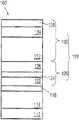
- FIG. 1depicts gallium arsenide stack 100 containing multiple Group III/V materials or layers which may be formed by the high growth rate deposition processes according to implementations described herein.
- the Group III/V materials or layerscan be grown or deposited at any one of the following deposition rates: about 30 ⁇ m/hr, about 40 ⁇ m/hr, about 50 ⁇ m/hr, about 55 ⁇ m/hr, about 60 ⁇ m/hr, about 70 ⁇ m/hr, about 80 ⁇ m/hr, about 90 ⁇ m/hr, about 95 ⁇ m/hr, about 100 ⁇ m/hr, about 105 ⁇ m/hr, about 110 ⁇ m/hr, about 115 ⁇ m/hr, and about 120 ⁇ m/hr.
- FIG. 1depicts gallium arsenide stack 100 contains gallium arsenide cell 110 disposed on or over sacrificial layer 116 disposed on or over buffer layer 114 disposed on or over wafer 112 .
- Wafer 112may be a support substrate containing Group III/V materials, and may be doped with various elements. Generally wafer 112 contains gallium arsenide, alloys thereof, derivatives thereof, and may be an n-doped substrate or a p-doped substrate. In many examples, wafer 112 is a gallium arsenide substrate or a gallium arsenide alloy substrate. The gallium arsenide substrate or wafer may have a thermal expansion coefficient of about 5.73 ⁇ 10 ⁇ 6 ° C. ⁇ 1 .
- Buffer layer 114may be a gallium arsenide buffer layer which contains gallium arsenide, alloys thereof, dopants thereof, or derivatives thereof. Buffer layer 114 may have a thickness within a range from about 100 nm to about 1000 nm, such as about 200 nm or about 300 nm.
- Sacrificial layer 116may contain aluminum arsenide, alloys thereof, derivatives thereof, or combinations thereof. Sacrificial layer 116 may have a thickness of about 20 nm or less. In some examples the thickness of sacrificial layer 116 may be within a range from about 1 nm to about 20 nm, such as from about 5 nm to about 20 nm, or in other examples, from about 1 nm to about 10 nm, such as from about 4 nm to about 6 nm.
- Gallium arsenide cell 110further contains n-type gallium arsenide stack 120 disposed on or over p-type gallium arsenide stack 130 .
- the n-type gallium arsenide stack 120usually contains multiples layers of various n-type doped materials.
- n-type gallium arsenide stack 120contains emitter layer 126 disposed on or over passivation layer 124 , disposed on or over contact layer 122 .
- the n-type gallium arsenide stack 120may have a thickness within a range from about 200 nm to about 1,300 nm.
- Contact layer 122may be a gallium arsenide contact layer which contains gallium arsenide, alloys thereof, dopants thereof, or derivatives thereof. In some examples, contact layer 122 contains an n-type gallium arsenide material. Contact layer 122 may have a thickness within a range from about 5 nm to about 100 nm, such as about 10 nm or about 50 nm.
- Passivation layer 124also referred to as the front window, generally contains aluminum gallium arsenide, alloys thereof, derivatives thereof, or combinations thereof. In many examples, passivation layer 124 contains an n-type aluminum gallium arsenide material. In one example, passivation layer 124 contains an n-type aluminum gallium arsenide material having the chemical formula of Al 0.3 Ga 0.7 As. Passivation layer 124 may have a thickness within a range from about 5 nm to about 100 nm, such as about 10 nm or about 50 nm.
- Emitter layer 126may contain gallium arsenide, alloys thereof, derivatives thereof, or combinations thereof. In many examples, emitter layer 126 contains an n-type gallium arsenide material. Emitter layer 126 may have a thickness within a range from about 100 nm to about 3000 nm. In some examples the thickness of emitter layer 126 may be within a range from about 100 nm to about 600 nm, such as from about 200 nm to about 400 nm, or in other examples, from about 600 nm to about 1,200 nm, such as from about 800 nm to about 1,000 nm.
- the p-type gallium arsenide layer or stack 130usually contains multiples layers of various p-type doped materials.
- p-type gallium arsenide stack 130contains contact layer 136 disposed on or over passivation layer 134 , disposed on or over absorber layer 132 .
- absorber layer 132is absent from p-type gallium arsenide stack 130 . Therefore, p-type gallium arsenide stack 130 contains contact layer 136 disposed on or over passivation layer 134 , and passivation layer 134 may be disposed on or over n-type gallium arsenide stack 120 , emitter layer 126 , or another layer.
- the p-type gallium arsenide stack 130may have a thickness within a range from about 100 nm to about 3,000 nm.
- Absorber layer 132may contain gallium arsenide, alloys thereof, derivatives thereof, or combinations thereof. In many examples, absorber layer 132 contains a p-type gallium arsenide material. In one implementation, absorber layer 132 may have a thickness within a range from about 1 nm to about 3,000 nm. In some examples the thickness of absorber layer 132 may be within a range from about 1 nm to about 1,000 nm, such as from about 10 nm to about 100 nm, or in other examples, from about 1,000 nm to about 3,000 nm, such as from about 1,100 nm to about 2,000 nm.
- the thickness of absorber layer 132may be within a range from about 100 nm to about 600 nm, such as from about 200 nm to about 400 nm, or in other examples, from about 600 nm to about 1,200 nm, such as from about 800 nm to about 1,000 nm.
- Passivation layer 134also referred to as the rear window, generally contains aluminum gallium arsenide, alloys thereof, derivatives thereof, or combinations thereof. In many examples, passivation layer 134 contains a p-type aluminum gallium arsenide material. In one example, passivation layer 134 contains a p-type aluminum gallium arsenide material having the chemical formula of Al 0.3 Ga 0.7 As. Passivation layer 134 may have a thickness within a range from about 25 nm to about 100 nm, such as about 50 nm or about 300 nm.
- Contact layer 136may be a p-type gallium arsenide contact layer which contains gallium arsenide, alloys thereof, dopants thereof, or derivatives thereof. In some examples, contact layer 136 contains a p-type gallium arsenide material. Contact layer 136 may have a thickness within a range from about 5 nm to about 100 nm, such as about 10 nm or about 50 nm.
- aspects of the deposition processes for depositing or forming Group III/V materialsmay be conducted in a processing system such as, for example, a single wafer deposition chamber, a multi-wafer deposition chamber, a stationary deposition chamber, or a continuous feed deposition chamber.
- a processing systemsuch as, for example, a single wafer deposition chamber, a multi-wafer deposition chamber, a stationary deposition chamber, or a continuous feed deposition chamber.
- One continuous feed deposition chamber that may be utilized for depositing or forming Group III/V materialsis described in the commonly assigned U.S. Ser. No. 12/475,131 (titled “Methods and Apparatus for a Chemical Vapor Deposition Reactor”) filed on May 29, 2009, and U.S. Ser. No.
- a deposition gasmay be formed by combining or mixing two, three, or more chemical precursors within a gas manifold prior to entering or passing through the showerhead.
- the deposition gasmay be formed by combining or mixing two, three, or more chemical precursors within a reaction zone after passing through the showerhead.
- the deposition gasmay also contain one, two or more carrier gases, which may also be combined or mixed with the precursor gases prior to or subsequent to passing through the showerhead.
- the carrier gasmay be hydrogen, nitrogen, argon, or combinations thereof.
- the internal pressure of the deposition chambermay be within a range from about 250 Torr to about 450 Torr.
- the deposition gasmay be formed by combining a gallium precursor (e.g., TMG) and an arsenic precursor (e.g., arsine).
- TMGgallium precursor
- arsenic precursore.g., arsine
- the substratemay be heated to a deposition temperature and exposed to the deposition gas.
- the deposition temperaturecan have a wide range. In one example, the deposition temperature may be within a range from about 600° C. to about 800° C., such as from about 650° C. to about 750° C. or from about 650° C. to about 720° C.
- the deposition gasmay contain about 100 cc of arsine in about 2,000 cc of hydrogen gas (H 2 ) and about 200 cc of a mixture of TMG/H 2 (about 10% TMG in H 2 .
- the Group III/V materialcontains gallium and arsenic and may be deposited at a rate of about 30 ⁇ m/hr or greater, such as about 40 ⁇ m/hr or greater, preferably, about 50 ⁇ m/hr or greater, preferably, about 55 ⁇ m/hr or greater, and more preferably, about 60 ⁇ m/hr or greater.
- deposition rates greater than about 60 ⁇ m/hrcan include deposition rates of about 70 ⁇ m/hr, about 80 ⁇ m/hr, or about 90-120 ⁇ m/hr.
- the deposition temperaturecan be in the range from about 680° C. to about 850° C.
- the deposition gasmay be formed by combining a gallium precursor (e.g., TMG), an aluminum precursor (e.g., TMA), and an arsenic precursor (e.g., arsine).
- TMGgallium precursor
- TMAaluminum precursor
- arsenic precursore.g., arsine
- the substratemay be heated to a deposition temperature and exposed to the deposition gas.
- the deposition temperaturecan have a wide range. In one example, the deposition temperature may be within a range from about 600° C. to about 800° C.
- the deposition gasmay contain about 100 cc of arsine in about 2,000 cc of hydrogen gas; about 200 cc of a mixture of TMG/H 2 (about 10% TMG in H 2 ); and about 200 cc of TMA/H 2 (about 1% TMA in H 2 ).
- the Group III/V materialcontains gallium, aluminum, and arsenic and may be deposited at a rate of about 30 ⁇ m/hr or greater, such as about 40 ⁇ m/hr or greater, preferably, about 50 ⁇ m/hr or greater, preferably, about 55 ⁇ m/hr or greater, and more preferably, about 60 ⁇ m/hr or greater.
- deposition rates greater than about 60 ⁇ m/hrcan include deposition rates of about 70 ⁇ m/hr, about 80 ⁇ m/hr, or about 90-120 ⁇ m/hr.
- the deposition temperaturecan be in the range from about 680° C. to about 850° C.
- the deposition gasmay be formed by combining a gallium precursor (e.g., TMG), an aluminum precursor (e.g., TMA), an indium precursor (e.g., trimethylindium-TMI), and a phosphorus precursor (e.g., phosphine-PH 3 ).
- TMGgallium precursor
- TMAaluminum precursor
- TMAaluminum precursor
- TMAaluminum precursor
- TMAindium precursor
- phosphorus precursore.g., phosphine-PH 3
- the substratemay be heated to a deposition temperature and exposed to the deposition gas.
- the deposition temperaturecan have a wide range. In one example, the deposition temperature may be within a range from about 600° C. to about 800° C.
- the deposition gasmay contain about 200 cc of a mixture of TMG/H 2 (about 10% TMG in H 2 ); about 200 cc of TMA/H 2 (about 1% TMA in H 2 ); about 200 cc of TMI/H 2 (about 1% TMI in H 2 ); and about 100 cc of phosphine in about 2,000 cc of hydrogen gas.
- the Group III/V materialcontains gallium, aluminum, indium, and phosphorus and may be deposited at a rate of about 30 ⁇ m/hr or greater, such as about 40 ⁇ m/hr or greater, preferably, about 50 ⁇ m/hr or greater, preferably, about 55 ⁇ m/hr or greater, and more preferably, about 60 ⁇ m/hr or greater.
- deposition rates greater than about 60 ⁇ m/hrcan include deposition rates of about 70 ⁇ m/hr, about 80 ⁇ m/hr, or about 90-120 ⁇ m/hr.
- the deposition temperaturecan be in the range from about 680° C. to about 850° C.
- the deposition gasmay be formed by combining a gallium precursor (e.g., TMG), an indium precursor (e.g., trimethylindium), and an arsenic precursor (e.g., arsine).
- TMGgallium precursor
- indium precursore.g., trimethylindium
- arsenic precursore.g., arsine
- the substratemay be heated to a deposition temperature and exposed to the deposition gas.
- the deposition temperaturecan have a wide range. In an example, the deposition temperature may be within a range from about 600° C. to about 800° C.
- the deposition gasmay contain about 100 cc of arsine in about 2,000 cc hydrogen gas; about 200 cc of a mixture of TMG/H 2 (about 10% TMG in H 2 ); and about 200 cc of TMI/H 2 (about 1% TMI in H 2 ).
- the Group III/V materialcontains gallium, indium, and arsenic and may be deposited at a rate of about 30 ⁇ m/hr or greater, such as about 40 ⁇ m/hr or greater, preferably, about 50 ⁇ m/hr or greater, preferably, about 55 ⁇ m/hr or greater, and more preferably, about 60 ⁇ m/hr or greater.
- deposition rates greater than about 60 ⁇ m/hrcan include deposition rates of about 70 ⁇ m/hr, about 80 ⁇ m/hr, or about 90-120 ⁇ m/hr.
- the deposition temperaturecan be in the range from about 680° C. to about 850° C.
- the deposition gasmay be formed by combining a gallium precursor (e.g., TMG), an indium precursor (e.g., trimethylindium), an arsenic precursor (e.g., arsine), and a nitrogen precursor (e.g., dimethylhydrazine or hydrazine).
- TMGgallium precursor
- an indium precursore.g., trimethylindium
- an arsenic precursore.g., arsine
- a nitrogen precursore.g., dimethylhydrazine or hydrazine.
- the substratemay be heated to a deposition temperature and exposed to the deposition gas.
- the deposition temperaturecan have a wide range. In an example, the deposition temperature may be within a range from about 400° C. to about 500° C., such as about 450° C.
- the deposition gasmay contain about 10 cc of arsine in about 2,000 cc of hydrogen gas; about 200 cc of a mixture of TMG/H 2 (about 10% TMG in H 2 ); about 200 cc of TMI/H 2 (about 1% TMI in H 2 ); and about 100 cc of dimethylhydrazine in about 1,000 cc of hydrogen gas.
- the Group III/V materialcontains gallium, indium, aluminum, arsenic, and nitrogen and may be deposited at a rate of about 30 ⁇ m/hr or greater, such as about 40 ⁇ m/hr or greater, preferably, about 50 ⁇ m/hr or greater, preferably, about 55 ⁇ m/hr or greater, and more preferably, about 60 ⁇ m/hr or greater.
- deposition rates greater than about 60 ⁇ m/hrcan include deposition rates of about 70 ⁇ m/hr, about 80 ⁇ m/hr, or about 90-120 ⁇ m/hr.
- the deposition temperaturecan be in the range from about 680° C. to about 850° C.
- the deposition gasmay be formed by combining a gallium precursor (e.g., TMG), an indium precursor (e.g., trimethylindium), an arsenic precursor (e.g., arsine), and a phosphorus precursor (e.g., phosphine-PH 3 ).
- the substratemay be heated to a deposition temperature and exposed to the deposition gas.
- the deposition temperaturecan have a wide range. In an example, the deposition temperature may be within a range from about 600° C. to about 800° C.
- the deposition gasmay contain about 100 cc of arsine in about 2,000 cc of hydrogen gas; about 200 cc of a mixture of TMG/H 2 (about 10% TMG in H 2 ); about 200 cc of TMI/H 2 (about 1% TMI in H 2 ); and about 100 cc of phosphine in about 2,000 cc of hydrogen gas.
- the Group III/V materialcontains gallium, indium, arsenic, and phosphorus, and may be deposited at a rate of about 30 ⁇ m/hr or greater, such as about 40 ⁇ m/hr or greater, preferably, about 50 ⁇ m/hr or greater, preferably, about 55 ⁇ m/hr or greater, and more preferably, about 60 ⁇ m/hr or greater.
- deposition rates greater than about 60 ⁇ m/hrcan include deposition rates of about 70 ⁇ m/hr, about 80 ⁇ m/hr, or about 90-120 ⁇ m/hr.
- the deposition temperaturecan be in the range from about 680° C. to about 850° C.
- ccmay refer to cubic centimeters and may correspond to a flow rate or flow unit, such as a standard cubic centimeters per minute (sccm).
- FIG. 2illustrates an example of a method 200 for forming a semiconductor material on a wafer, as described in some implementations herein.
- the method 200includes heating a wafer to a deposition temperature in a range between 550° C. and 900° C. within a processing system.
- the method 200includes exposing the wafer to a deposition gas comprising a gallium precursor gas and arsine at a total pressure in a range between 20 Torr and 1000 Torr.
- the method 200includes depositing one or more layers having gallium arsenide on the wafer at a deposition rate selected from the group consisting of 30 ⁇ m/hr, 40 ⁇ m/hr, 50 ⁇ m/hr, 55 ⁇ m/hr, 60 ⁇ m/hr, 70 ⁇ m/hr, 80 ⁇ m/hr, and 90-120 ⁇ m/hr deposition rates, wherein multiple layers, including the one or more layers, form a gallium arsenide cell.
- the range of the deposition temperaturecan be between 680° C. and 850° C.
- the deposition gascan further include an aluminum precursor gas and the gallium arsenide layer can further include aluminum.
- the aluminum precursor gascan include an alkyl aluminum compound.
- the alkyl aluminum compoundcan be trimethylaluminum or triethylaluminum.
- the deposition gascan further include a carrier gas comprising a mixture of hydrogen and argon.
- an n-type portion of the gallium arsenide cellis deposited over a sacrificial layer having a thickness between 1 nm and 20 nm, where the sacrificial layer is disposed over a buffer layer, and the buffer layer is disposed over the wafer.
- the multiple layersform an n-type gallium arsenide stack and a p-type gallium arsenide stack, where the n-type gallium arsenide stack has an emitter layer disposed on or over a first passivation layer, and where the first passivation layer is disposed on or over a first contact layer; and where the p-type gallium arsenide stack has a second contact layer disposed on or over a second passivation layer, and where the second passivation layer being disposed on or over an absorber layer.
- the range of the deposition temperaturecan be between 600° C. and 800° C.
- the range of the total pressurecan be selected from the group consisting of between 20 Torr and 760 Torr, between 50 Torr and 450 Torr, and between 100 Torr and 250 Torr.
- FIG. 3illustrates an example of a method 300 for forming a semiconductor material on a wafer, as described in some implementations herein.
- the method 300includes heating a wafer to a deposition temperature in a range between 550° C. and 900° C. within a processing system.
- the method 300includes exposing the wafer to a deposition gas comprising a gallium precursor gas, an aluminum precursor gas, and arsine at a total pressure in a range between 20 Torr and 1,000 Torr.
- the method 300includes depositing one or more layers on the wafer at a deposition rate selected from the group consisting of 30 ⁇ m/hr, 40 ⁇ m/hr, 50 ⁇ m/hr, 55 ⁇ m/hr, 60 ⁇ m/hr, 70 ⁇ m/hr, 80 ⁇ m/hr, and 90-120 ⁇ m/hr deposition rates, where the one or more layers include aluminum gallium arsenide, and multiple layers, including the one or more layers, form a gallium arsenide cell.
- the range of the deposition temperatureis between 680° C. and 850° C.
- an n-type portion of the gallium arsenide cellis deposited over a sacrificial layer having a thickness between 1 nm and 20 nm, where the sacrificial layer is disposed over a buffer layer, and where the buffer layer is disposed over the wafer.
- the multiple layersform an n-type gallium arsenide stack and a p-type gallium arsenide stack, where the n-type gallium arsenide stack has an emitter layer disposed on or over a first passivation layer, and where the first passivation layer is disposed on or over a first contact layer; and where the p-type gallium arsenide stack has a second contact layer disposed on or over a second passivation layer, and where the second passivation layer is disposed on or over an absorber layer.
- the range of the deposition temperaturecan be between 600° C. and 800° C.
- the range of the total pressurecan be selected from the group consisting of between 20 Torr and 760 Torr, between 50 Torr and 450 Torr, and between 100 Torr and 250 Torr.
- FIG. 4illustrates an example of a method 400 for forming a semiconductor material on a wafer, as described in some implementations herein.
- the method 400includes heating a wafer to a deposition temperature in a range between 550° C. and 900° C. within a processing system.
- the method 400includes exposing the wafer to a deposition gas comprising a gallium precursor gas, an indium precursor gas, a nitrogen precursor gas and arsine at a total pressure in a range between 20 Torr and 1000 Torr.
- the method 400includes depositing one or more layers on the wafer at a deposition rate selected from the group consisting of 30 ⁇ m/hr, 40 ⁇ m/hr, 50 ⁇ m/hr, 55 ⁇ m/hr, 60 ⁇ m/hr, 70 ⁇ m/hr, 80 ⁇ m/hr, and 90-120 ⁇ m/hr deposition rates, where the one or more layers comprise gallium, arsenic, nitrogen and indium, and multiple layers, including the one or more layers, form a gallium arsenide cell.
- the range of the deposition temperatureis between 680° C. and 850° C.
- the nitrogen precursor gascomprises a compound selected from the group consisting of hydrazine, methylhydrazine, dimethylhydrazine, derivatives thereof, and combinations thereof.
- an n-type portion of the gallium arsenide cellis deposited over a sacrificial layer having a thickness between 1 nm and 20 nm, where the sacrificial layer is disposed over a buffer layer, and where the buffer layer is disposed over the wafer.
- the multiple layersform an n-type gallium arsenide stack and a p-type gallium arsenide stack, where the n-type gallium arsenide stack has an emitter layer disposed on or over a first passivation layer, and where the first passivation layer is disposed on or over a first contact layer; and where the p-type gallium arsenide stack has a second contact layer disposed on or over a second passivation layer, and where the second passivation layer is disposed on or over an absorber layer.
- the deposition temperaturecan be between 400° C. and 500° C.
- the range of the total pressurecan be selected from the group consisting of between 20 Torr and 760 Torr, between 50 Torr and 450 Torr, and between 100 Torr and 250 Torr.
- FIG. 5illustrates an example of a method 500 for forming a cell, as described in some implementations herein.
- the method 500includes heating a substrate comprising gallium and arsenic to a temperature in a range between 550° C. and 900° C. within a processing system.
- the method 500includes exposing the substrate to a deposition gas comprising a gallium arsenide precursor gas and arsine.
- the method 500includes depositing an n-type contact layer comprising gallium and arsenic over the substrate, where the n-type contact layer has a thickness of 100 nm or less.
- the method 500includes depositing an n-type passivation layer comprising gallium, aluminum, and arsenic over the substrate, where the n-type passivation layer has a thickness of 100 nm or less.
- the method 500includes depositing an n-type absorber layer comprising gallium and arsenic over the substrate, where the n-type emitter layer has a thickness of 3000 nm or less.
- the method 500includes depositing a p-type passivation layer comprising gallium, aluminum, and arsenic over the substrate, where the p-type passivation layer has a thickness of 300 nm or less.
- the method 500includes depositing a p-type contact layer comprising gallium and arsenic over the substrate, the p-type contact layer having a thickness of 100 nm or less, where each of the n-type contact layer, the n-type passivation layer, the n-type absorber layer, the p-type passivation layer, and the p-type contact layer is deposited at deposition rate selected from the group consisting of 30 ⁇ m/hr, 40 ⁇ m/hr, 50 ⁇ m/hr, 55 ⁇ m/hr, 60 ⁇ m/hr, 70 ⁇ m/hr, 80 ⁇ m/hr, and 90-120 ⁇ m/hr deposition rates.
- the range of the deposition temperatureis between 680° C. and 850° C.
- the methodfurther includes depositing a sacrificial layer comprising aluminum and arsenic over the substrate at a deposition rate selected from the group consisting of 30 ⁇ m/hr, 40 ⁇ m/hr, 50 ⁇ m/hr, 55 ⁇ m/hr, 60 ⁇ m/hr, 70 ⁇ m/hr, 80 ⁇ m/hr, and 90-120 ⁇ m/hr deposition rates, where the sacrificial layer has a thickness of 20 nm or less.
- the methodcan further include depositing the n-type contact layer over the sacrificial layer, depositing the n-type passivation layer over the n-type contact layer, depositing the n-type absorber layer over the n-type passivation layer, depositing the p-type passivation layer over the p-type absorber layer, and depositing the p-type contact layer over the p-type passivation layer.
- the methodfurther includes depositing a buffer layer comprising gallium and arsenic on the substrate at a deposition rate selected from the group consisting of a 30 ⁇ m/hr deposition rate, a 40 ⁇ m/hr deposition rate, a 50 ⁇ m/hr deposition rate, a 55 ⁇ m/hr deposition rate, and a 60 ⁇ m/hr deposition rate or greater, where the buffer layer has a thickness of less than 300 nm.
- the methodfurther includes depositing a sacrificial layer comprising aluminum and arsenic over the substrate at a deposition rate selected from the group consisting of 30 ⁇ m/hr, 40 ⁇ m/hr, 50 ⁇ m/hr, 55 ⁇ m/hr, 60 ⁇ m/hr, 70 ⁇ m/hr, 80 ⁇ m/hr, and 90-120 ⁇ m/hr deposition rates, where the sacrificial layer has a thickness of 20 nm or less,
- the methodfurther includes depositing a buffer layer comprising gallium and arsenic on the substrate at a deposition rate selected from the group consisting of 30 ⁇ m/hr, 40 ⁇ m/hr, 50 ⁇ m/hr, 55 ⁇ m/hr, 60 ⁇ m/hr, 70 ⁇ m/hr, 80 ⁇ m/hr, and 90-120 ⁇ m/hr deposition rates, where the buffer layer has a thickness of less than 300 nm.
- the methodcan further include depositing the sacrificial layer over the buffer layer.
- exposing the substrate to the deposition gasfurther includes exposing the substrate to a total pressure of 450 Torr or less, or exposing the substrate to a total pressure of at least 780 Torr.
Landscapes
- Engineering & Computer Science (AREA)
- Chemical & Material Sciences (AREA)
- Computer Hardware Design (AREA)
- General Physics & Mathematics (AREA)
- Power Engineering (AREA)
- Microelectronics & Electronic Packaging (AREA)
- Manufacturing & Machinery (AREA)
- Physics & Mathematics (AREA)
- Condensed Matter Physics & Semiconductors (AREA)
- Materials Engineering (AREA)
- Metallurgy (AREA)
- Organic Chemistry (AREA)
- Crystallography & Structural Chemistry (AREA)
- Chemical Kinetics & Catalysis (AREA)
- General Chemical & Material Sciences (AREA)
- Inorganic Chemistry (AREA)
Abstract
Description
Claims (20)
Priority Applications (7)
| Application Number | Priority Date | Filing Date | Title |
|---|---|---|---|
| US15/717,694US11393683B2 (en) | 2009-10-14 | 2017-09-27 | Methods for high growth rate deposition for forming different cells on a wafer |
| JP2019541292AJP2020535626A (en) | 2017-09-27 | 2018-09-07 | High growth rate deposition of III / V materials |
| PCT/US2018/049869WO2019067177A1 (en) | 2017-09-27 | 2018-09-07 | High growth rate deposition for group iii/v materials |
| CN201880024678.XACN110582838A (en) | 2017-09-27 | 2018-09-07 | High Growth Rate Deposition of III/V Materials |
| KR1020197022544AKR20210088771A (en) | 2017-09-27 | 2018-09-07 | High Growth Rate Deposition for Group III/V Materials |
| EP18779506.7AEP3563405A1 (en) | 2017-09-27 | 2018-09-07 | High growth rate deposition for group iii/v materials |
| US16/412,328US20190272994A1 (en) | 2009-10-14 | 2019-05-14 | High growth rate deposition for group iii/v materials |
Applications Claiming Priority (3)
| Application Number | Priority Date | Filing Date | Title |
|---|---|---|---|
| US25167709P | 2009-10-14 | 2009-10-14 | |
| US12/904,090US9834860B2 (en) | 2009-10-14 | 2010-10-13 | Method of high growth rate deposition for group III/V materials |
| US15/717,694US11393683B2 (en) | 2009-10-14 | 2017-09-27 | Methods for high growth rate deposition for forming different cells on a wafer |
Related Parent Applications (1)
| Application Number | Title | Priority Date | Filing Date |
|---|---|---|---|
| US12/904,090Continuation-In-PartUS9834860B2 (en) | 2009-10-14 | 2010-10-13 | Method of high growth rate deposition for group III/V materials |
Related Child Applications (1)
| Application Number | Title | Priority Date | Filing Date |
|---|---|---|---|
| US16/412,328Continuation-In-PartUS20190272994A1 (en) | 2009-10-14 | 2019-05-14 | High growth rate deposition for group iii/v materials |
Publications (2)
| Publication Number | Publication Date |
|---|---|
| US20180019117A1 US20180019117A1 (en) | 2018-01-18 |
| US11393683B2true US11393683B2 (en) | 2022-07-19 |
Family
ID=60940715
Family Applications (1)
| Application Number | Title | Priority Date | Filing Date |
|---|---|---|---|
| US15/717,694Active2030-10-18US11393683B2 (en) | 2009-10-14 | 2017-09-27 | Methods for high growth rate deposition for forming different cells on a wafer |
Country Status (1)
| Country | Link |
|---|---|
| US (1) | US11393683B2 (en) |
Families Citing this family (5)
| Publication number | Priority date | Publication date | Assignee | Title |
|---|---|---|---|---|
| US11393683B2 (en) | 2009-10-14 | 2022-07-19 | Utica Leaseco, Llc | Methods for high growth rate deposition for forming different cells on a wafer |
| US20190272994A1 (en)* | 2009-10-14 | 2019-09-05 | Alta Devices, Inc. | High growth rate deposition for group iii/v materials |
| US20200365755A1 (en)* | 2019-05-14 | 2020-11-19 | Alta Devices, Inc. | Surface passivation of iii-v optoelectronic devices |
| EP3969642A4 (en)* | 2019-05-14 | 2023-09-27 | Utica Leaseco, LLC | DEPOSIT OF GROUP III/V MATERIALS WITH HIGH GROWTH RATE |
| DE102019008928B9 (en)* | 2019-12-20 | 2021-08-26 | Azur Space Solar Power Gmbh | Gas phase epitaxy method |
Citations (79)
| Publication number | Priority date | Publication date | Assignee | Title |
|---|---|---|---|---|
| US3993533A (en) | 1975-04-09 | 1976-11-23 | Carnegie-Mellon University | Method for making semiconductors for solar cells |
| US4172756A (en)* | 1976-02-06 | 1979-10-30 | U.S. Philips Corporation | Method for the accelerated growth from the gaseous phase of crystals, and products obtained in this manner |
| US4368098A (en)* | 1969-10-01 | 1983-01-11 | Rockwell International Corporation | Epitaxial composite and method of making |
| US4445965A (en) | 1980-12-01 | 1984-05-01 | Carnegie-Mellon University | Method for making thin film cadmium telluride and related semiconductors for solar cells |
| US4727047A (en) | 1980-04-10 | 1988-02-23 | Massachusetts Institute Of Technology | Method of producing sheets of crystalline material |
| US4742012A (en) | 1984-11-27 | 1988-05-03 | Toa Nenryo Kogyo K.K. | Method of making graded junction containing amorphous semiconductor device |
| US4846931A (en)* | 1988-03-29 | 1989-07-11 | Bell Communications Research, Inc. | Method for lifting-off epitaxial films |
| US4883561A (en) | 1988-03-29 | 1989-11-28 | Bell Communications Research, Inc. | Lift-off and subsequent bonding of epitaxial films |
| US5073230A (en) | 1990-04-17 | 1991-12-17 | Arizona Board Of Regents Acting On Behalf Of Arizona State University | Means and methods of lifting and relocating an epitaxial device layer |
| US5076860A (en)* | 1989-01-13 | 1991-12-31 | Kabushiki Kaisha Toshiba | Algan compound semiconductor material |
| US5122852A (en) | 1990-04-23 | 1992-06-16 | Bell Communications Research, Inc. | Grafted-crystal-film integrated optics and optoelectronic devices |
| US5168077A (en)* | 1989-03-31 | 1992-12-01 | Kabushiki Kaisha Toshiba | Method of manufacturing a p-type compound semiconductor thin film containing a iii-group element and a v-group element by metal organics chemical vapor deposition |
| US5201996A (en) | 1990-04-30 | 1993-04-13 | Bell Communications Research, Inc. | Patterning method for epitaxial lift-off processing |
| US5221637A (en) | 1991-05-31 | 1993-06-22 | Interuniversitair Micro Elektronica Centrum Vzw | Mesa release and deposition (MRD) method for stress relief in heteroepitaxially grown GaAs on Si |
| US5232869A (en)* | 1991-07-30 | 1993-08-03 | Shell Research Limited | Metal deposition |
| US5256562A (en) | 1990-12-31 | 1993-10-26 | Kopin Corporation | Method for manufacturing a semiconductor device using a circuit transfer film |
| US5258325A (en) | 1990-12-31 | 1993-11-02 | Kopin Corporation | Method for manufacturing a semiconductor device using a circuit transfer film |
| US5276345A (en) | 1992-10-30 | 1994-01-04 | California Institute Of Technology | Composite GaAs-on-quartz substrate for integration of millimeter-wave passive and active device circuitry |
| US5277749A (en) | 1991-10-17 | 1994-01-11 | International Business Machines Corporation | Methods and apparatus for relieving stress and resisting stencil delamination when performing lift-off processes that utilize high stress metals and/or multiple evaporation steps |
| US5286335A (en) | 1992-04-08 | 1994-02-15 | Georgia Tech Research Corporation | Processes for lift-off and deposition of thin film materials |
| US5344517A (en) | 1993-04-22 | 1994-09-06 | Bandgap Technology Corporation | Method for lift-off of epitaxial layers and applications thereof |
| US5401983A (en) | 1992-04-08 | 1995-03-28 | Georgia Tech Research Corporation | Processes for lift-off of thin film materials or devices for fabricating three dimensional integrated circuits, optical detectors, and micromechanical devices |
| US5402748A (en)* | 1992-04-09 | 1995-04-04 | Fujitsu Limited | Method of growing a compound semiconductor film |
| US5458694A (en) | 1992-04-15 | 1995-10-17 | Picogiga Societe Anonyme | Multispectral photovoltaic component comprising a stack of cells, and method of manufacture |
| US5465009A (en) | 1992-04-08 | 1995-11-07 | Georgia Tech Research Corporation | Processes and apparatus for lift-off and bonding of materials and devices |
| US5476810A (en) | 1994-01-31 | 1995-12-19 | U.S. Philips Corporation | Manufacture of electronic devices comprising thin-film circuits using a metal foil as a temporary support |
| US5479043A (en) | 1992-04-15 | 1995-12-26 | Picogiga Societe Anonyme | Multispectral photovoltaic component |
| US5528719A (en) | 1993-10-26 | 1996-06-18 | Sumitomo Metal Mining Company Limited | Optical fiber guide structure and method of fabricating same |
| US5546375A (en) | 1992-07-15 | 1996-08-13 | Canon Kabushiki Kaisha | Method of manufacturing a tip for scanning tunneling microscope using peeling layer |
| US5641381A (en) | 1995-03-27 | 1997-06-24 | The United States Of America As Represented By The Administrator Of The National Aeronautics And Space Administration | Preferentially etched epitaxial liftoff of InP material |
| US5827751A (en) | 1991-12-06 | 1998-10-27 | Picogiga Societe Anonyme | Method of making semiconductor components, in particular on GaAs of InP, with the substrate being recovered chemically |
| US5985742A (en) | 1997-05-12 | 1999-11-16 | Silicon Genesis Corporation | Controlled cleavage process and device for patterned films |
| US6071795A (en) | 1998-01-23 | 2000-06-06 | The Regents Of The University Of California | Separation of thin films from transparent substrates by selective optical processing |
| US6211539B1 (en) | 1983-10-21 | 2001-04-03 | Lucent Technologies Inc. | Semi-insulated indium phosphide based compositions |
| US6214733B1 (en) | 1999-11-17 | 2001-04-10 | Elo Technologies, Inc. | Process for lift off and handling of thin film materials |
| US6221740B1 (en) | 1999-08-10 | 2001-04-24 | Silicon Genesis Corporation | Substrate cleaving tool and method |
| US6232136B1 (en) | 1990-12-31 | 2001-05-15 | Kopin Corporation | Method of transferring semiconductors |
| US6263941B1 (en) | 1999-08-10 | 2001-07-24 | Silicon Genesis Corporation | Nozzle for cleaving substrates |
| US6284631B1 (en) | 1997-05-12 | 2001-09-04 | Silicon Genesis Corporation | Method and device for controlled cleaving process |
| US6287891B1 (en) | 2000-04-05 | 2001-09-11 | Hrl Laboratories, Llc | Method for transferring semiconductor device layers to different substrates |
| US6291313B1 (en) | 1997-05-12 | 2001-09-18 | Silicon Genesis Corporation | Method and device for controlled cleaving process |
| US6346459B1 (en) | 1999-02-05 | 2002-02-12 | Silicon Wafer Technologies, Inc. | Process for lift off and transfer of semiconductor devices onto an alien substrate |
| US6352909B1 (en) | 2000-01-06 | 2002-03-05 | Silicon Wafer Technologies, Inc. | Process for lift-off of a layer from a substrate |
| US6372981B1 (en) | 1999-08-13 | 2002-04-16 | Oki Electric Industry Co., Ltd. | Semiconductor substrate, solar cell using same, and fabrication methods thereof |
| US6387829B1 (en) | 1999-06-18 | 2002-05-14 | Silicon Wafer Technologies, Inc. | Separation process for silicon-on-insulator wafer fabrication |
| US6414783B2 (en) | 1990-12-31 | 2002-07-02 | Kopin Corporation | Method of transferring semiconductors |
| US6500732B1 (en) | 1999-08-10 | 2002-12-31 | Silicon Genesis Corporation | Cleaving process to fabricate multilayered substrates using low implantation doses |
| US6504524B1 (en) | 2000-03-08 | 2003-01-07 | E Ink Corporation | Addressing methods for displays having zero time-average field |
| US6548382B1 (en) | 1997-07-18 | 2003-04-15 | Silicon Genesis Corporation | Gettering technique for wafers made using a controlled cleaving process |
| US6559075B1 (en) | 1996-10-01 | 2003-05-06 | Siemens Aktiengesellschaft | Method of separating two layers of material from one another and electronic components produced using this process |
| US20030121468A1 (en)* | 2001-10-22 | 2003-07-03 | Boone Thomas D. | Methods of hyperdoping semiconductor materials and hyperdoped semiconductor materials and devices |
| US6669801B2 (en) | 2000-01-21 | 2003-12-30 | Fujitsu Limited | Device transfer method |
| US6677249B2 (en) | 1998-01-27 | 2004-01-13 | Robert Bosch Gmbh | Method for manufacturing breakaway layers for detaching deposited layer systems |
| US20040113225A1 (en)* | 2002-12-03 | 2004-06-17 | Mitsuhiko Ogihara | Semiconductor epitaxial structure and semiconductor light-emitting device |
| US6809044B1 (en) | 1999-06-30 | 2004-10-26 | Commissariat A L'energie Atomique | Method for making a thin film using pressurization |
| US6876013B2 (en) | 2000-09-08 | 2005-04-05 | Showa Denko K.K. | Compound semiconductor multilayer structure and bipolar transistor using the same |
| US6943050B2 (en) | 2002-07-11 | 2005-09-13 | Seiko Epson Corporation | Method for making semiconductor device, semiconductor element composite, electro-optical apparatus, and electronic system |
| US6974521B2 (en) | 2000-10-18 | 2005-12-13 | Katholieke Universiteit Nijmegen | Method for separating a film and a substrate |
| US7045878B2 (en) | 2001-05-18 | 2006-05-16 | Reveo, Inc. | Selectively bonded thin film layer and substrate layer for processing of useful devices |
| US7056808B2 (en) | 1999-08-10 | 2006-06-06 | Silicon Genesis Corporation | Cleaving process to fabricate multilayered substrates using low implantation doses |
| US7060591B2 (en) | 2001-12-28 | 2006-06-13 | Semiconductor Energy Laboratory Co., Ltd. | Method for fabricating a semiconductor device by transferring a layer to a support with curvature |
| US20060252242A1 (en) | 2001-11-08 | 2006-11-09 | Hanna Mark C | Reactive codoping of gaalinp compound semiconductors |
| US7153761B1 (en) | 2005-10-03 | 2006-12-26 | Los Alamos National Security, Llc | Method of transferring a thin crystalline semiconductor layer |
| US7163826B2 (en) | 2001-09-12 | 2007-01-16 | Reveo, Inc | Method of fabricating multi layer devices on buried oxide layer substrates |
| US7198671B2 (en) | 2001-07-11 | 2007-04-03 | Matsushita Electric Industrial Co., Ltd. | Layered substrates for epitaxial processing, and device |
| US7202141B2 (en) | 2004-03-29 | 2007-04-10 | J.P. Sercel Associates, Inc. | Method of separating layers of material |
| US7229901B2 (en) | 2004-12-16 | 2007-06-12 | Wisconsin Alumni Research Foundation | Fabrication of strained heterojunction structures |
| US7229498B2 (en)* | 2002-10-29 | 2007-06-12 | Midwest Research Institute | Nanostructures produced by phase-separation during growth of (III-V)1-x(IV2)x alloys |
| CN101409233A (en) | 2007-10-05 | 2009-04-15 | 应用材料股份有限公司 | Method for depositing group III/V compounds |
| US7638410B2 (en) | 2005-10-03 | 2009-12-29 | Los Alamos National Security, Llc | Method of transferring strained semiconductor structure |
| US20090321885A1 (en) | 2008-05-30 | 2009-12-31 | Alta Devices, Inc. | Epitaxial lift off stack having a universally shrunk handle and methods thereof |
| US20090325367A1 (en) | 2008-05-30 | 2009-12-31 | Alta Devices, Inc. | Methods and apparatus for a chemical vapor deposition reactor |
| US20100092668A1 (en) | 2008-10-10 | 2010-04-15 | Alta Devices, Inc. | Concentric Showerhead For Vapor Deposition |
| US20110083601A1 (en) | 2009-10-14 | 2011-04-14 | Alta Devices, Inc. | High growth rate deposition for group iii/v materials |
| US20110186115A1 (en) | 2004-12-30 | 2011-08-04 | Alliance For Sustainable Energy, Llc | High Performance, High Bandgap, Lattice-Mismatched, GaInP Solar Cells |
| US20120305059A1 (en)* | 2011-06-06 | 2012-12-06 | Alta Devices, Inc. | Photon recycling in an optoelectronic device |
| US20130112275A1 (en) | 2011-11-07 | 2013-05-09 | International Business Machines Corporation | Silicon heterojunction photovoltaic device with wide band gap emitter |
| US20180019117A1 (en) | 2009-10-14 | 2018-01-18 | Alta Devices, Inc. | High growth rate deposition for group iii/v materials |
| TWI640648B (en) | 2017-11-24 | 2018-11-11 | 行政院原子能委員會核能硏究所 | FABRICATION METHOD OF InGaP EPI-LAYER GROWN BY MOCVD |
- 2017
- 2017-09-27USUS15/717,694patent/US11393683B2/enactiveActive
Patent Citations (106)
| Publication number | Priority date | Publication date | Assignee | Title |
|---|---|---|---|---|
| US4368098A (en)* | 1969-10-01 | 1983-01-11 | Rockwell International Corporation | Epitaxial composite and method of making |
| US3993533A (en) | 1975-04-09 | 1976-11-23 | Carnegie-Mellon University | Method for making semiconductors for solar cells |
| US4172756A (en)* | 1976-02-06 | 1979-10-30 | U.S. Philips Corporation | Method for the accelerated growth from the gaseous phase of crystals, and products obtained in this manner |
| US4727047A (en) | 1980-04-10 | 1988-02-23 | Massachusetts Institute Of Technology | Method of producing sheets of crystalline material |
| US4445965A (en) | 1980-12-01 | 1984-05-01 | Carnegie-Mellon University | Method for making thin film cadmium telluride and related semiconductors for solar cells |
| US6211539B1 (en) | 1983-10-21 | 2001-04-03 | Lucent Technologies Inc. | Semi-insulated indium phosphide based compositions |
| US4742012A (en) | 1984-11-27 | 1988-05-03 | Toa Nenryo Kogyo K.K. | Method of making graded junction containing amorphous semiconductor device |
| US4846931A (en)* | 1988-03-29 | 1989-07-11 | Bell Communications Research, Inc. | Method for lifting-off epitaxial films |
| US4883561A (en) | 1988-03-29 | 1989-11-28 | Bell Communications Research, Inc. | Lift-off and subsequent bonding of epitaxial films |
| US5076860A (en)* | 1989-01-13 | 1991-12-31 | Kabushiki Kaisha Toshiba | Algan compound semiconductor material |
| US5168077A (en)* | 1989-03-31 | 1992-12-01 | Kabushiki Kaisha Toshiba | Method of manufacturing a p-type compound semiconductor thin film containing a iii-group element and a v-group element by metal organics chemical vapor deposition |
| US5073230A (en) | 1990-04-17 | 1991-12-17 | Arizona Board Of Regents Acting On Behalf Of Arizona State University | Means and methods of lifting and relocating an epitaxial device layer |
| US5122852A (en) | 1990-04-23 | 1992-06-16 | Bell Communications Research, Inc. | Grafted-crystal-film integrated optics and optoelectronic devices |
| US5201996A (en) | 1990-04-30 | 1993-04-13 | Bell Communications Research, Inc. | Patterning method for epitaxial lift-off processing |
| US5256562A (en) | 1990-12-31 | 1993-10-26 | Kopin Corporation | Method for manufacturing a semiconductor device using a circuit transfer film |
| US5258325A (en) | 1990-12-31 | 1993-11-02 | Kopin Corporation | Method for manufacturing a semiconductor device using a circuit transfer film |
| US6414783B2 (en) | 1990-12-31 | 2002-07-02 | Kopin Corporation | Method of transferring semiconductors |
| US6232136B1 (en) | 1990-12-31 | 2001-05-15 | Kopin Corporation | Method of transferring semiconductors |
| US5221637A (en) | 1991-05-31 | 1993-06-22 | Interuniversitair Micro Elektronica Centrum Vzw | Mesa release and deposition (MRD) method for stress relief in heteroepitaxially grown GaAs on Si |
| US5232869A (en)* | 1991-07-30 | 1993-08-03 | Shell Research Limited | Metal deposition |
| US5277749A (en) | 1991-10-17 | 1994-01-11 | International Business Machines Corporation | Methods and apparatus for relieving stress and resisting stencil delamination when performing lift-off processes that utilize high stress metals and/or multiple evaporation steps |
| US5827751A (en) | 1991-12-06 | 1998-10-27 | Picogiga Societe Anonyme | Method of making semiconductor components, in particular on GaAs of InP, with the substrate being recovered chemically |
| US5465009A (en) | 1992-04-08 | 1995-11-07 | Georgia Tech Research Corporation | Processes and apparatus for lift-off and bonding of materials and devices |
| US5401983A (en) | 1992-04-08 | 1995-03-28 | Georgia Tech Research Corporation | Processes for lift-off of thin film materials or devices for fabricating three dimensional integrated circuits, optical detectors, and micromechanical devices |
| US5286335A (en) | 1992-04-08 | 1994-02-15 | Georgia Tech Research Corporation | Processes for lift-off and deposition of thin film materials |
| US5402748A (en)* | 1992-04-09 | 1995-04-04 | Fujitsu Limited | Method of growing a compound semiconductor film |
| US5458694A (en) | 1992-04-15 | 1995-10-17 | Picogiga Societe Anonyme | Multispectral photovoltaic component comprising a stack of cells, and method of manufacture |
| US5479043A (en) | 1992-04-15 | 1995-12-26 | Picogiga Societe Anonyme | Multispectral photovoltaic component |
| US5546375A (en) | 1992-07-15 | 1996-08-13 | Canon Kabushiki Kaisha | Method of manufacturing a tip for scanning tunneling microscope using peeling layer |
| US5276345A (en) | 1992-10-30 | 1994-01-04 | California Institute Of Technology | Composite GaAs-on-quartz substrate for integration of millimeter-wave passive and active device circuitry |
| US5344517A (en) | 1993-04-22 | 1994-09-06 | Bandgap Technology Corporation | Method for lift-off of epitaxial layers and applications thereof |
| US5528719A (en) | 1993-10-26 | 1996-06-18 | Sumitomo Metal Mining Company Limited | Optical fiber guide structure and method of fabricating same |
| US5476810A (en) | 1994-01-31 | 1995-12-19 | U.S. Philips Corporation | Manufacture of electronic devices comprising thin-film circuits using a metal foil as a temporary support |
| US5641381A (en) | 1995-03-27 | 1997-06-24 | The United States Of America As Represented By The Administrator Of The National Aeronautics And Space Administration | Preferentially etched epitaxial liftoff of InP material |
| US6559075B1 (en) | 1996-10-01 | 2003-05-06 | Siemens Aktiengesellschaft | Method of separating two layers of material from one another and electronic components produced using this process |
| US6740604B2 (en) | 1996-10-01 | 2004-05-25 | Siemens Aktiengesellschaft | Method of separating two layers of material from one another |
| US7341925B2 (en) | 1996-10-01 | 2008-03-11 | Osram Gmbh | Method for transferring a semiconductor body from a growth substrate to a support material |
| US6486041B2 (en) | 1997-05-12 | 2002-11-26 | Silicon Genesis Corporation | Method and device for controlled cleaving process |
| US6010579A (en) | 1997-05-12 | 2000-01-04 | Silicon Genesis Corporation | Reusable substrate for thin film separation |
| US7160790B2 (en) | 1997-05-12 | 2007-01-09 | Silicon Genesis Corporation | Controlled cleaving process |
| US6284631B1 (en) | 1997-05-12 | 2001-09-04 | Silicon Genesis Corporation | Method and device for controlled cleaving process |
| US7348258B2 (en) | 1997-05-12 | 2008-03-25 | Silicon Genesis Corporation | Method and device for controlled cleaving process |
| US6290804B1 (en) | 1997-05-12 | 2001-09-18 | Silicon Genesis Corporation | Controlled cleavage process using patterning |
| US6291313B1 (en) | 1997-05-12 | 2001-09-18 | Silicon Genesis Corporation | Method and device for controlled cleaving process |
| US6294814B1 (en) | 1997-05-12 | 2001-09-25 | Silicon Genesis Corporation | Cleaved silicon thin film with rough surface |
| US6528391B1 (en) | 1997-05-12 | 2003-03-04 | Silicon Genesis, Corporation | Controlled cleavage process and device for patterned films |
| US6632724B2 (en) | 1997-05-12 | 2003-10-14 | Silicon Genesis Corporation | Controlled cleaving process |
| US6790747B2 (en) | 1997-05-12 | 2004-09-14 | Silicon Genesis Corporation | Method and device for controlled cleaving process |
| US6511899B1 (en) | 1997-05-12 | 2003-01-28 | Silicon Genesis Corporation | Controlled cleavage process using pressurized fluid |
| US6391740B1 (en) | 1997-05-12 | 2002-05-21 | Silicon Genesis Corporation | Generic layer transfer methodology by controlled cleavage process |
| US5985742A (en) | 1997-05-12 | 1999-11-16 | Silicon Genesis Corporation | Controlled cleavage process and device for patterned films |
| US6458672B1 (en) | 1997-05-12 | 2002-10-01 | Silicon Genesis Corporation | Controlled cleavage process and resulting device using beta annealing |
| US6155909A (en) | 1997-05-12 | 2000-12-05 | Silicon Genesis Corporation | Controlled cleavage system using pressurized fluid |
| US6548382B1 (en) | 1997-07-18 | 2003-04-15 | Silicon Genesis Corporation | Gettering technique for wafers made using a controlled cleaving process |
| US6890838B2 (en) | 1997-07-18 | 2005-05-10 | Silicon Genesis Corporation | Gettering technique for wafers made using a controlled cleaving process |
| US6071795A (en) | 1998-01-23 | 2000-06-06 | The Regents Of The University Of California | Separation of thin films from transparent substrates by selective optical processing |
| US6677249B2 (en) | 1998-01-27 | 2004-01-13 | Robert Bosch Gmbh | Method for manufacturing breakaway layers for detaching deposited layer systems |
| US6346459B1 (en) | 1999-02-05 | 2002-02-12 | Silicon Wafer Technologies, Inc. | Process for lift off and transfer of semiconductor devices onto an alien substrate |
| US6387829B1 (en) | 1999-06-18 | 2002-05-14 | Silicon Wafer Technologies, Inc. | Separation process for silicon-on-insulator wafer fabrication |
| US6809044B1 (en) | 1999-06-30 | 2004-10-26 | Commissariat A L'energie Atomique | Method for making a thin film using pressurization |
| US6513564B2 (en) | 1999-08-10 | 2003-02-04 | Silicon Genesis Corporation | Nozzle for cleaving substrates |
| US6221740B1 (en) | 1999-08-10 | 2001-04-24 | Silicon Genesis Corporation | Substrate cleaving tool and method |
| US7056808B2 (en) | 1999-08-10 | 2006-06-06 | Silicon Genesis Corporation | Cleaving process to fabricate multilayered substrates using low implantation doses |
| US6554046B1 (en) | 1999-08-10 | 2003-04-29 | Silicon Genesis Corporation | Substrate cleaving tool and method |
| US6263941B1 (en) | 1999-08-10 | 2001-07-24 | Silicon Genesis Corporation | Nozzle for cleaving substrates |
| US6500732B1 (en) | 1999-08-10 | 2002-12-31 | Silicon Genesis Corporation | Cleaving process to fabricate multilayered substrates using low implantation doses |
| US6372981B1 (en) | 1999-08-13 | 2002-04-16 | Oki Electric Industry Co., Ltd. | Semiconductor substrate, solar cell using same, and fabrication methods thereof |
| US6214733B1 (en) | 1999-11-17 | 2001-04-10 | Elo Technologies, Inc. | Process for lift off and handling of thin film materials |
| US6352909B1 (en) | 2000-01-06 | 2002-03-05 | Silicon Wafer Technologies, Inc. | Process for lift-off of a layer from a substrate |
| US6669801B2 (en) | 2000-01-21 | 2003-12-30 | Fujitsu Limited | Device transfer method |
| US6504524B1 (en) | 2000-03-08 | 2003-01-07 | E Ink Corporation | Addressing methods for displays having zero time-average field |
| US6287891B1 (en) | 2000-04-05 | 2001-09-11 | Hrl Laboratories, Llc | Method for transferring semiconductor device layers to different substrates |
| US6589811B2 (en) | 2000-04-05 | 2003-07-08 | Hrl Laboratories, Llc | Method for transferring semiconductor device layers to different substrates |
| US6876013B2 (en) | 2000-09-08 | 2005-04-05 | Showa Denko K.K. | Compound semiconductor multilayer structure and bipolar transistor using the same |
| US6974521B2 (en) | 2000-10-18 | 2005-12-13 | Katholieke Universiteit Nijmegen | Method for separating a film and a substrate |
| US7045878B2 (en) | 2001-05-18 | 2006-05-16 | Reveo, Inc. | Selectively bonded thin film layer and substrate layer for processing of useful devices |
| US7198671B2 (en) | 2001-07-11 | 2007-04-03 | Matsushita Electric Industrial Co., Ltd. | Layered substrates for epitaxial processing, and device |
| US7163826B2 (en) | 2001-09-12 | 2007-01-16 | Reveo, Inc | Method of fabricating multi layer devices on buried oxide layer substrates |
| US20030121468A1 (en)* | 2001-10-22 | 2003-07-03 | Boone Thomas D. | Methods of hyperdoping semiconductor materials and hyperdoped semiconductor materials and devices |
| US20060252242A1 (en) | 2001-11-08 | 2006-11-09 | Hanna Mark C | Reactive codoping of gaalinp compound semiconductors |
| US7060591B2 (en) | 2001-12-28 | 2006-06-13 | Semiconductor Energy Laboratory Co., Ltd. | Method for fabricating a semiconductor device by transferring a layer to a support with curvature |
| US6943050B2 (en) | 2002-07-11 | 2005-09-13 | Seiko Epson Corporation | Method for making semiconductor device, semiconductor element composite, electro-optical apparatus, and electronic system |
| US7229498B2 (en)* | 2002-10-29 | 2007-06-12 | Midwest Research Institute | Nanostructures produced by phase-separation during growth of (III-V)1-x(IV2)x alloys |
| US20040113225A1 (en)* | 2002-12-03 | 2004-06-17 | Mitsuhiko Ogihara | Semiconductor epitaxial structure and semiconductor light-emitting device |
| US7241667B2 (en) | 2004-03-29 | 2007-07-10 | J.P. Sercel Associates, Inc. | Method of separating layers of material |
| US7202141B2 (en) | 2004-03-29 | 2007-04-10 | J.P. Sercel Associates, Inc. | Method of separating layers of material |
| US7229901B2 (en) | 2004-12-16 | 2007-06-12 | Wisconsin Alumni Research Foundation | Fabrication of strained heterojunction structures |
| US20110186115A1 (en) | 2004-12-30 | 2011-08-04 | Alliance For Sustainable Energy, Llc | High Performance, High Bandgap, Lattice-Mismatched, GaInP Solar Cells |
| US7638410B2 (en) | 2005-10-03 | 2009-12-29 | Los Alamos National Security, Llc | Method of transferring strained semiconductor structure |
| US7153761B1 (en) | 2005-10-03 | 2006-12-26 | Los Alamos National Security, Llc | Method of transferring a thin crystalline semiconductor layer |
| US20090149008A1 (en) | 2007-10-05 | 2009-06-11 | Applied Materials, Inc. | Method for depositing group iii/v compounds |
| CN101409233A (en) | 2007-10-05 | 2009-04-15 | 应用材料股份有限公司 | Method for depositing group III/V compounds |
| US20090324379A1 (en) | 2008-05-30 | 2009-12-31 | Alta Devices, Inc. | Methods and apparatus for a chemical vapor deposition reactor |
| US20090325367A1 (en) | 2008-05-30 | 2009-12-31 | Alta Devices, Inc. | Methods and apparatus for a chemical vapor deposition reactor |
| US20090321885A1 (en) | 2008-05-30 | 2009-12-31 | Alta Devices, Inc. | Epitaxial lift off stack having a universally shrunk handle and methods thereof |
| US20090321886A1 (en) | 2008-05-30 | 2009-12-31 | Alta Devices, Inc. | Epitaxial lift off stack having a unidirectionally shrunk handle and methods thereof |
| US20100001374A1 (en) | 2008-05-30 | 2010-01-07 | Alta Devices, Inc. | Epitaxial lift off stack having a multi-layered handle and methods thereof |
| US20100001316A1 (en) | 2008-05-30 | 2010-01-07 | Alta Devices, Inc. | Epitaxial lift off stack having a non-uniform handle and methods thereof |
| US20090321881A1 (en) | 2008-05-30 | 2009-12-31 | Alta Devices, Inc. | Epitaxial lift off stack having a pre-curved handle and methods thereof |
| US20100092668A1 (en) | 2008-10-10 | 2010-04-15 | Alta Devices, Inc. | Concentric Showerhead For Vapor Deposition |
| US20110083601A1 (en) | 2009-10-14 | 2011-04-14 | Alta Devices, Inc. | High growth rate deposition for group iii/v materials |
| US9834860B2 (en)* | 2009-10-14 | 2017-12-05 | Alta Devices, Inc. | Method of high growth rate deposition for group III/V materials |
| US20180019117A1 (en) | 2009-10-14 | 2018-01-18 | Alta Devices, Inc. | High growth rate deposition for group iii/v materials |
| US20120305059A1 (en)* | 2011-06-06 | 2012-12-06 | Alta Devices, Inc. | Photon recycling in an optoelectronic device |
| US20130112275A1 (en) | 2011-11-07 | 2013-05-09 | International Business Machines Corporation | Silicon heterojunction photovoltaic device with wide band gap emitter |
| TWI640648B (en) | 2017-11-24 | 2018-11-11 | 行政院原子能委員會核能硏究所 | FABRICATION METHOD OF InGaP EPI-LAYER GROWN BY MOCVD |
Non-Patent Citations (21)
| Title |
|---|
| Bauhuis, G.J., "Substrate Reuse for Epitaxial Lift-Off of III-V Solar Cells", Proceedings of the 22nd European Photovoltaic Solar Energy Conference: Milan Sep. 3-7, 2007, pp. 106-110. |
| Bauhuis, G.J., "Thin film GaAs solar cells with increased quantum efficiency due to light reflection", Solar Energy Materials & Solar Cells 83 (2004) 81-90, Nov. 3, 2003. |
| Indium gallium phosphide, Wikipedia, May 10, 2005 [retrieved from the internet on Feb. 16, 2021 at https://en.wikipedia.org/wiki/Indium_gallium_phosphide], pp. 1-2. |
| International Search Report and Written Opinion corresponding to PCT Application No. PCT/US2018/049869, dated Jan. 2, 2019. |
| International Search Report and Written Opinion issued in PCT/US2020/032676, dated Sep. 1, 2020, pp. 1-9. |
| Konagai, Makoto, "High Efficieny GaAs THin Gilm Solar Cells by Peeled Film Technology", Journal of Crystal Growth 45 (1978) 277-280. |
| Kumar; P., "Sacrificial etching of AlxGa1—xAs for III-V MEMS surface micromachining", Appl. Phys. A 88, 711-714, May 24, 2007. |
| Phosphine, Wikipedia, 2002 [retrieved from the internet on Feb. 16, 2021 at https://en.wikipedia.org/wiki/Phosphine], pp. 1-11. |
| Schermer, J.J., "Expitaxial Lift-Off for large area thin film III/V devices", Phys. Stat. Sol. (1) 202, No. 4, 501-508 (2005). |
| Schremer, J.J., "Photon confinement in high-efficiency, thin-film III-IV solar cells obtained by epitaxial life-off", Thin Solid Films 511-512 (2006) 645-653, Jan. 19, 2006. |
| Schremer, J.J., "Solar Cells Based on III-V Semiconductors", Joint Solar Panel, Sep. 29, 2004. |
| Schremer, J.J., "Thin-film GaAs Epitaxial Lift-Off Solar Cells for Space Application", Prog. Photovolt: Res, Appl. 2005; 13:587-596, Apr. 28, 2005. |
| Sickmiller, M. "Packaging of Ultrathin Semiconductor Devices Through the ELO Packaging Process" Mat. Res. Soc. Symp. Proc. vol. 681E (2001). |
| Van Deelen, J., "On the development of high-efficiency thin-film GaAs and GainP2 cells", Journal of Crystal Growth 298 (2007) Nov. 28, 2006. |
| Van Niftrik, A.T.J., "A Diffusion and Reaction related Model of the Epitaxial Lift-Off Process", Journal of the Electrochemical Society, 154 (11) D629-D635 (2007), Sep. 19, 2007. |
| Van Niftrik, A.T.J., "HF Species and Dissolved Oxygen on the Epitaxial Lift-Off Process of GaAs Using AlAsP Release Layers", Journal of the Electrochemical Society, 155 (1) D35-D39 (2008), Nov. 6, 2007. |
| Van Niftrik, A.T.J., "The influence of InxGal—xAs and GaAs1-yPy Layers Surrounding the AlAs Release Layer in the Epitaxial Lift-Off Process", Crystal Growth & Design, 2007, vol. 7, No. 12, 2472-2480, Aug. 7, 2007. |
| Voncken, M.M.A.J., "Influence of radius of curvature on the lateral etch rate of the weight induced epitaxial lift-off process", Material Science and Engineering B95 (2002) 242-248, May 21, 2002. |
| Voncken, M.M.A.J., "Multiple release layer study of the intrinsic lateral etch rate of the epitaxial lift-off process", Appl. Phys. A 79, 1801-1807, Mar. 28, 2003. |
| Voncken, M.M.A.J., "Strain-accelerated HF etching of AlAs for epitaxial lift-off", J. Phys.: Condens, Matter 16 (2004) 3585-3596, May 14, 2004. |
| Yablonovitch, E., "Van De Waals bonding of GaAs epitaxial liftoff films onto arbitrary substrates" AppL Phys. Lett. 56 (24), Jun. 11, 1990. |
Also Published As
| Publication number | Publication date |
|---|---|
| US20180019117A1 (en) | 2018-01-18 |
Similar Documents
| Publication | Publication Date | Title |
|---|---|---|
| US11393683B2 (en) | Methods for high growth rate deposition for forming different cells on a wafer | |
| US5679152A (en) | Method of making a single crystals Ga*N article | |
| US20110244663A1 (en) | Forming a compound-nitride structure that includes a nucleation layer | |
| WO1996041906A1 (en) | Bulk single crystal gallium nitride and method of making same | |
| US20190272994A1 (en) | High growth rate deposition for group iii/v materials | |
| US9834860B2 (en) | Method of high growth rate deposition for group III/V materials | |
| US6043140A (en) | Method for growing a nitride compound semiconductor | |
| JP3198912B2 (en) | Method for producing group 3-5 compound semiconductor | |
| JP2011054935A (en) | Doping method | |
| US20150332914A1 (en) | Semiconductor substrate, method of manufacturing semiconductor substrate, and semiconductor device | |
| JP2789861B2 (en) | Organometallic molecular beam epitaxial growth method | |
| WO2019067177A1 (en) | High growth rate deposition for group iii/v materials | |
| JPH08316151A (en) | Semiconductor manufacturing method | |
| JP4342573B2 (en) | Method for growing compound semiconductor thin films | |
| WO2020232123A1 (en) | High growth rate deposition for group iii/v materials | |
| JPH11268996A (en) | Method for growing compound semiconductor mixed crystal | |
| JPH02203520A (en) | Growth of compound semiconductor crystal | |
| US20080171133A1 (en) | Method For the Production of C-Plane Oriented Gan Substrates or AlxGa1-xN Substrates | |
| Yao et al. | Metalorganic Chemical Vapor Deposition | |
| JP3213551B2 (en) | Method and apparatus for vapor phase growth of III-V compound semiconductors | |
| JPH0442898A (en) | Compound semiconductor crystal growth method | |
| JP2924072B2 (en) | Organometallic molecular beam epitaxial growth method and apparatus | |
| JPH03232220A (en) | Vapor growth method for compound semiconductor crystal | |
| JP2012101961A (en) | METHOD FOR MANUFACTURING In-CONTAINING p-NITRIDE COMPOUND SEMICONDUCTOR CRYSTAL | |
| JP2002175994A (en) | Manufacturing method of gallium-nitride based compound semiconductor |
Legal Events
| Date | Code | Title | Description |
|---|---|---|---|
| FEPP | Fee payment procedure | Free format text:ENTITY STATUS SET TO UNDISCOUNTED (ORIGINAL EVENT CODE: BIG.); ENTITY STATUS OF PATENT OWNER: SMALL ENTITY | |
| STPP | Information on status: patent application and granting procedure in general | Free format text:DOCKETED NEW CASE - READY FOR EXAMINATION | |
| AS | Assignment | Owner name:ALTA DEVICES, INC., CALIFORNIA Free format text:ASSIGNMENT OF ASSIGNORS INTEREST;ASSIGNORS:WASHINGTON, LORI D.;BOUR, DAVID P.;HIGASHI, GREGG;AND OTHERS;SIGNING DATES FROM 20171002 TO 20171106;REEL/FRAME:044052/0971 | |
| AS | Assignment | Owner name:UTICA LEASECO, LLC, MICHIGAN Free format text:SECURITY INTEREST;ASSIGNOR:ALTA DEVICES, INC.;REEL/FRAME:049027/0944 Effective date:20190425 | |
| STPP | Information on status: patent application and granting procedure in general | Free format text:NON FINAL ACTION MAILED | |
| STPP | Information on status: patent application and granting procedure in general | Free format text:FINAL REJECTION MAILED | |
| STPP | Information on status: patent application and granting procedure in general | Free format text:NON FINAL ACTION MAILED | |
| FEPP | Fee payment procedure | Free format text:ENTITY STATUS SET TO SMALL (ORIGINAL EVENT CODE: SMAL); ENTITY STATUS OF PATENT OWNER: SMALL ENTITY | |
| STPP | Information on status: patent application and granting procedure in general | Free format text:NON FINAL ACTION MAILED | |
| AS | Assignment | Owner name:UTICA LEASECO, LLC ASSIGNEE, MICHIGAN Free format text:CONFIRMATION OF FORECLOSURE TRANSFER OF PATENT RIGHTS;ASSIGNOR:UTICA LEASECO, LLC SECURED PARTY;REEL/FRAME:055766/0279 Effective date:20210225 | |
| STPP | Information on status: patent application and granting procedure in general | Free format text:RESPONSE TO NON-FINAL OFFICE ACTION ENTERED AND FORWARDED TO EXAMINER | |
| STPP | Information on status: patent application and granting procedure in general | Free format text:FINAL REJECTION MAILED | |
| AS | Assignment | Owner name:UTICA LEASECO, LLC ASSIGNEE, MICHIGAN Free format text:CORRECTIVE ASSIGNMENT TO CORRECT THE THE ASSIGNEE ADDRESS PREVIOUSLY RECORDED AT REEL: 055766 FRAME: 0279. ASSIGNOR(S) HEREBY CONFIRMS THE ASSIGNMENT;ASSIGNOR:UTICA LEASECO, LLC SECURED PARTY;REEL/FRAME:057117/0811 Effective date:20210225 | |
| STPP | Information on status: patent application and granting procedure in general | Free format text:DOCKETED NEW CASE - READY FOR EXAMINATION | |
| STPP | Information on status: patent application and granting procedure in general | Free format text:NON FINAL ACTION MAILED | |
| STPP | Information on status: patent application and granting procedure in general | Free format text:FINAL REJECTION MAILED | |
| STPP | Information on status: patent application and granting procedure in general | Free format text:NOTICE OF ALLOWANCE MAILED -- APPLICATION RECEIVED IN OFFICE OF PUBLICATIONS | |
| STPP | Information on status: patent application and granting procedure in general | Free format text:PUBLICATIONS -- ISSUE FEE PAYMENT VERIFIED | |
| STCF | Information on status: patent grant | Free format text:PATENTED CASE | |
| AS | Assignment | Owner name:TIGER FINANCE, LLC, MASSACHUSETTS Free format text:SECURITY INTEREST;ASSIGNOR:UTICA LEASECO, LLC;REEL/FRAME:064731/0814 Effective date:20230828 |